1
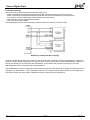
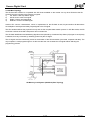
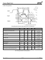
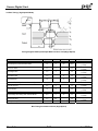
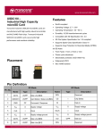
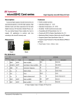
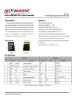
Secure Digital Card Secure Digital Card Rev. A.0 Jan 2007 Secure Digital Card Table of Contents 1. Introduction to the SD Card ..................................................................................................... 1 2. SD Card Feature ........................................................................................................................ 1 3. Product Specification ............................................................................................................... 2 4. SD Card Interface Description ................................................................................................. 9 5. Physical Outline ...................................................................................................................... 10 Rev. A.0 Jan 2007 Secure Digital Card Revision History Revision A.0 Date 01/04 ‘07 History Remark New Creation “PQI reserves the right to make changes without notification when fit, form, function, quality and reliability are not affected. The data sheets do not constitute contract documents and should not be considered part of the specification for purposes of any warranty.“ Rev. A.0 Jan 2007 Secure Digital Card 1. Introduction to the SD Card The SD Card is a memory card that is small and thin with SDMI. SD Card is a Flash–Based memory card that is designed to meet the security, capacity, performance and environment requirements inherent to use in emerging audio and video electronic device. The SD Card includes a copyright protection mechanism that complies with the security of the SDMI standard (SDMI: Secure Digital Music Initiative). The SD Card communication is based on an advance 9-pin interface (clock, command, 4x Data and 3x power lines) and the SD Card host interface supports regular MultiMediaCard operation as well. 2. SD Card Feature Flash memory card capacity support list below: Standard Capacity SD Memory Card: ¾ 256MB ¾ 512MB ¾ 1GB ¾ 2GB High Capacity SD Memory Card: ¾ 4GB ¾ 8GB ¾ 16GB ¾ 32GB Compliant SDA Specification ver 2.0 Variable clock rate: ¾ Default mode: 0-25 MHz, up to 12.5MB/sec interface speed. ¾ High-speed mode:0-50 MHz, up to 25MB/sec interface speed. High Capacity SD Memory Cards shall support Speed Class Specification and have performance more Than or equal to Class 2, it includes: ¾ Class 2 ¾ Class 4 ¾ Class 6 Support CPRM No external programming voltage required SD Card protocol compatible Targeted for portable and stationary applications for secured (copyrights protected) and non-secured data storage Correction of memory field errors Copyrights Protection Mechanism: Complies with highest security of SDMI standard. Password Protection of cards (CMD42-LOCK_UNLOCK). Card detection command (Insertion / Removal) CE and FCC certificates Easy handling for the end user Notes: The performance depends on different test platform with different result. ‧The communication channel is described in the table SD Bus/SPI Bus comparison SD Card Using SD Bus SD Card Using SPI Bus Three-wire serial data bus (Clock, dataIn, dataOut )+card specific Six-wire communication channel (clock, command, 4 data lines) CS signal(hardwired card selection) Error-protected data transfer Optional non protected data transfer mode available Single or multiple block oriented data transfer Single or multiple block oriented data transfer Rev. A.0 1/10 Jan 2007 Secure Digital Card 3. Product Specification 3.1 System Environment Specifications Temperature Moisture and corrosion Vibration Shock Altitude (relative to sea level) Operating: Non-Operating: Operating: Non-Operating: -25℃ to 85℃ -40℃ (168h) to 85℃(500h) 25°C / 95% rel. humidity 40°C / 93% rel. hum./500h salt water spray: 3% NaCl/35C; 24h acc. MIL STD Method 1009 15 G peak to peak max. 15 G peak to peak max. 1,000 G max. 1,000 G max. 80,000 feet max. 80,000 feet max. Operating: Non-Operating: Operating: Non-Operating: Operating: Non-Operating: 3.2 Reliability and Durability Specifications Durability 10,000 mating cycles Bending 10N Torque 0.15N.m or +/-2.5 deg. Drop Test 1.5m free fall UV Light Exposure UV: 254nm, 15Ws/cm2 according to IOS 7816-1 X-ray exposure Visual Inspection/Shape and Form 0.1 Gy of medium-energy radiation (70 keV to 140 keV, cumulative dose per year) to both sides of the card, according to ISO7816-1. No warp age; no mold slim; complete form; no cavities; surface smoothness≦-0.1 mm/ cm2 within contour; no cracks; no pollution (oil, dust, etc.) 3.3 Typical Card Pow Requirement VDD (fipple: max,60mV peak to peak) 2.7V~3.6V 3.4 System Reliability and Maintenance MTBF Preventive Maintenance Data Reliability Endurance Rev. A.0 >1,000,000 hours None < 1 non-recoverable error in 1014 bits read 100,000 write/erase cycles (SLC NAND flash) 10,000 write/erase cycles (MLC NAND flash) 2/10 Jan 2007 Secure Digital Card 3.5 SD Bus Topology The SD bus has six communication lines and two supply lines: ‧ CMD: Command is bi-directional signal. (Host and card drivers are operating in push pull mode.) ‧ DAT0-3: Data lines are bi-directional signals. (Host and card drivers are operating in push pull mode.) ‧ CLK: Clock is a host to cards signal. (CLK operates in push pull mode.) ‧ VDD: VDD is the power supply line for all cards ‧ VSS: VSS are two ground lines The following figure shows the bus topology of several cards with one host in SD Bus mode. SD Memory Card System Bus Topology During the initialization process, commands are sent to each card individually, allowing the application to detect the cards and assign logical addresses to the physical slots. Data is always sent to each card individually. However, to simplify the handling of the card stack, after initialization, all commands may be sent concurrently to all cards. Addressing information is provided in the command packet. The SD Bus allows dynamic configuration of the number of data lines. After power-up, by default, the SD Card will use only DAT0 for data transfer. After initialization, the host can change the bus width (number of active data lines). This feature allows and easy trade off between hardware cost and system performance. Rev. A.0 3/10 Jan 2007 Secure Digital Card 3.6 SPI Bus Topology The SD Card SPI interface is compatible with SPI hosts available on the market. As any other SPI device the SD Card SPI channel consists of the following 4 signals: 1) CS: Host to card Chip Select signal. 2) SCLK: Host to card clock signal. 3) DataIn: Host to card data signal. 4) DataOut: Card to host data signal. Another SPI common characteristic, which is implemented in the SD Card as well, is byte transfers. All data tokens are multiples of 8 bit bytes and always byte aligned to the CS signal. The SPI standard defines the physical link only and not the complete data transfer protocol. In SPI Bus mode, the SD Card uses a subset of the SD Card protocol and command set. The SD Card identification and addressing algorithms are replaced by a hardware Chip Select (CS) signal. A card (slave) is selected, for every command, by asserting (active low) the CS signal. The CS signal must be continuously active for the duration of the SPI transaction (command, response and data). The only exception is card programming time. At this time the host can de-assert the CS signal without affecting the programming process. SD Memory Card System (SPI Mode) Bus Topology Rev. A.0 4/10 Jan 2007 Secure Digital Card 3.7 Electrical Interface The power up of the SD Card bus is handled locally in each SD Card and in the bus master. SPI Mode bus operating conditions are identical to SD Card mode bus operating conditions. The CS (chip select) signal timing is identical to the input signal timing. Power Supply Voltage General Parameter Symbol Peak voltage on all lines Min. Max. Unit -0.3 VDD+ 0.3 V -10 10 uA -10 10 uA Max. Unit Remark All Inputs Input Leakage Current All Outputs Output Leakage Current Power supply Voltage Parameter Supply Voltage for voltage range Output High Voltage Output Low Voltage Input High Voltage Input Low Voltage Power up time Rev. A.0 Symbol Min. VDD VOH VOL VIH VIL 2.7 0.75* VDD 0.625* VDD VDD-0.3 5/10 3.6 0.125* VDD VDD+0.3 0.25* VDD 250 V V V V V ms Remark IOH=-100uA VDD min IOL=-100uA VDD min From 0V to VDD min Jan 2007 Secure Digital Card 3.8 Bus Timing (Default) Timing Diagram Data Input/Output Referenced to Clock(Default) Parameter Symbol Min. Clock CLK (All values are referred to min.(VIH) and max.(VIL)) Max. Unit Clock Frequency Data Transfer Mode fPP 0 25 MHz Clock Frequency Identification Mode fOD 0/100 400 KHz Clock Low Time tWL 10 ns Clock High Time tWH 10 ns Clock Rise Time tTLH 10 ns Clock Fall Time tTHL 10 ns Remark CCARD≦ 10 pF (1 card) CCARD≦ 10 pF (1 card) CCARD≦ 10 pF (1 card) CCARD≦ 10 pF (1 card) CCARD≦ 10 pF (1 card) CCARD≦ 10 pF (1 card) Inputs CMD,DAT(referenced to CLK) Input set-up time tISU 5 ns Input hold time tIH 5 ns Output Delay time during Data Transfer Mode tODLY 0 14 ns Output Delay time during Identification Mode tODLY 0 50 ns CCARD≦ 10 pF (1 card) CCARD≦ 10 pF (1 card) Outputs CMD,DAT(referenced to CLK) CL ≦ 40 Pf (1 card) CL ≦ 40 pF (1 card) Bus Timing-Parameters Values (Default) Rev. A.0 6/10 Jan 2007 Secure Digital Card 3.9 Bus Timing ( High-Speed Mode) Timing Diagram Data Input/Output Referenced to Clock(High-Speed) Parameter Symbol Min. Clock CLK (All values are referred to min.(VIH) and max.(VIL)) Max. Unit 50 MHz Clock Frequency Data Transfer Mode fPP 0 Clock Low Time tWL 7 ns Clock High Time tWH 7 ns Clock Rise Time tTLH 3 ns Clock Fall Time tTHL 3 ns Remark CCARD≦ 10 pF (1 card) CCARD≦ 10 pF (1 card) CCARD≦ 10 pF (1 card) CCARD≦ 10 pF (1 card) CCARD≦ 10 pF (1 card) Inputs CMD,DAT(referenced to CLK) Input set-up time tISU 6 ns Input hold time tIH 2 ns tODLY 0 Output Hold time tOH 2.5 Total System capacitance for each line CL CCARD≦ 10 pF (1 card) CCARD≦ 10 pF (1 card) Outputs CMD,DAT(referenced to CLK) Output Delay time during data Transfer Mode 14 ns ns 40 pF CL ≦ 40 Pf (1 card) CL ≧ 15 pF (1 card) 1 card Bus Timing-Parameters Values (High-Speed) Rev. A.0 7/10 Jan 2007 Secure Digital Card 3.10 Operating Conditions Register (OCR) The 32-bit operation conditions register stores the VDD voltage profile of the card. The SD Card is capable of executing the voltage recognition procedure (CMD1) with any standard SD Card host using operating voltages form 2 to 3.6 Volts. Accessing the data in the memory array, however, requires 2.7 to 3.6 Volts. The OCR shows the voltage range in which the card data can be accessed. The structure of the OCR register is described in under table. 24 00h 16 FFh 87 80h 43 00 0 00 Reserved Operating Voltage Range2.7-3.6 volt Reserved Busy Bit OCR Structure 3.11 Card Identification (CID) Register The CID register is 16 bytes long and contains a unique card identification number as shown in the table below. It is programmed during card manufacturing and can not be changed by SD Card hosts. Note that the CID register in the SD Card has a different structure than the CID register in the MultiMediaCard Name Manufacturer ID OEM/Application ID Product name Product version Product serial number Reserved Manufacturing date CRC7 checksum Not use, always “1” Field MID OID PNM PRV PSN -MDT CRC -- Width 8 16 40 8 32 4 12 7 1 CID-Slice [127:120] [119:104] [103:64] [63:56] [55:24] [23:20] [19:8] [7:1] [0:0] 3.12 CSD Register The Card Specific Data (CSD) register contains configuration information required in order to access the card data. In the table below, the cell type column defined the CSD field as Read only (R), One Time Programmable(R/W) or erasable(R/W/E). This table shows, for each field, the value in”real world” units and coded according to the CSD structure. The Model dependent column marks (with a check mark —√) the CSD fields which are model dependent. Note that the CSD register in the SD Card has a different structure than the CSD in the MultiMediaCard. Rev. A.0 8/10 Jan 2007 Secure Digital Card 4. SD Card Interface Description General Description of Pins and Registers The SD Card has 9 exposed contacts on one side. The host is connected to the SD Card using a 9 pin connector. Pin Assignment in SD Bus Mode Pad Definition Pin # Name Type 1 2 3 4 5 6 7 8 9 CD/DAT3 CMD Vss1 VDD CLK Vss2 DAT0 DAT1 DAT2 I/O I/O S S I S I/O I/O I/O SD Description Card Detect / Data Line [Bit 3] Command / Response Supply voltage ground Supply voltage Clock Supply voltage ground Data Line [Bit 0] Data Line [Bit 1] Data Line [Bit 2] Note: 1. S=power supply; I=input; O=output using push-pull drivers. 2. The extended DAT lines (DAT1-DAT3) are input on power up; they start to operate as DAT lines after the SET_BUS_WIDTH command. 3. After power up, this line is input with 50Kohm pull-up (can be used for card detection or SPI mode selection). The pull-up should be disconnected by the user, during regular data transfer, with SET_CLR_CARD_DETECT (ACMD42) command. Pin Assignment in SPI Bus Mode Pad Definition Pin # Name Type 1 2 3 4 5 6 7 8 9 CS DataIn Vss1 VDD CLK Vss2 DataOut RSV RSV I I S S I S O I I SD Description Chip Select (active true) Host to card command and data Supply Voltage Ground Supply Voltage Clock Supply Voltage Ground Card to Host data and status Reserved Reserved SD Card Registers Name Width CID 128 RCA 16 DSR CSD SCR OCR 16 128 64 32 Description Card identification number: individual card number for identification. Relative card address: local system address of a card, dynamically suggested by the card and approved by the host during initialization Driver Stage Register; to configure the card’s output drivers. Optional. Card specific data: information about the card operation conditions. SD Configuration Register: information about the microSD Card’s special feature capabilities. Operation Condition Register The host may reset the cards by switching the power supply off and on again. The card has its own power-on detection circuitry which puts the card into an idle state after the power-on. The card can also be reset by sending the GO_IDLE (CMD0) command. Rev. A.0 9/10 Jan 2007 Secure Digital Card 5. Physical Outline Rev. A.0 10/10 Jan 2007