1
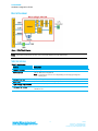
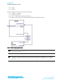
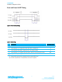
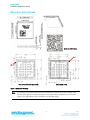
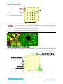
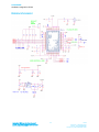
LAIRD SSD45N Hardware Integration Guide Version 1.3 Embedded Wireless Solutions Support Center: http://ews-support.lairdtech.com Americas: +1-800-492-2320 Option 2 Europe: +44-1628-858-940 Asia: +852-2923-0610 www.lairdtech.com/wireless Laird SSD45N Hardware Integration Guide REVISION HISTORY Version Revision Date Change Description Approved By 1.0 23 July 2014 Initial Release Andrew Chen 1.1 5 August 2014 Added note to SDIO Timing Requirements regarding SDIO bus clock rate. Andrew Chen 1.2 26 Mar 2015 Fixed Operational Temperature numbers. Andrew Chen 1.3 15 Oct 2015 Updated Antenna Data Sheet links Sue White Embedded Wireless Solutions Support Center: http://ews-support.lairdtech.com www.lairdtech.com/wireless 2 Laird Americas: +1-800-492-2320 Europe: +44-1628-858-940 Hong Kong: +852-2268-6567 x026 Laird SSD45N Hardware Integration Guide CONTENTS Laird SSD45N ................................................................................................................................................ 1 Revision History ............................................................................................................................................ 2 Contents ....................................................................................................................................................... 3 SCOPE ............................................................................................................................................................. 4 Operational Description .............................................................................................................................. 4 Block Diagram .............................................................................................................................................. 5 Specifications ............................................................................................................................................... 5 Recommended Operating Conditions and DC Electrical Characteristics ................................................. 9 DC Electrical Characteristics ...................................................................................................................... 10 General DC Electrical Characteristics (3.3V & 1.8V I/O operation) ............................................................. 10 SDIO Timing Requirements .................................................................................................................. 11 Pin Definitions ............................................................................................................................................ 11 Signal Names and Signal Types ................................................................................................................. 14 Reference Clock, Sleep Clock, and Clock Sharing ..................................................................................... 14 CPU_WARM_RESET ................................................................................................................................. 16 Reset and Power On/Off Timing ............................................................................................................... 17 SSD40NBT and SSD45N Pin Comparison Table ......................................................................................... 18 Mechanical Specifications ......................................................................................................................... 19 Recommendations: .............................................................................................................................. 20 RF Layout Design Guidelines ..................................................................................................................... 21 Reference Schematic .................................................................................................................................. 23 Regulatory .................................................................................................................................................. 24 Certified Antennas ................................................................................................................................... 24 Documentation Requirements .................................................................................................................. 24 FCC 24 Industry Canada................................................................................................................................... 26 European Union ................................................................................................................................... 28 Embedded Wireless Solutions Support Center: http://ews-support.lairdtech.com www.lairdtech.com/wireless 3 Laird Americas: +1-800-492-2320 Europe: +44-1628-858-940 Hong Kong: +852-2268-6567 x026 Laird SSD45N Hardware Integration Guide SCOPE This document describes key hardware aspects of the Laird SSD45N radio module. This document is intended to assist device manufacturers and related parties with the integration of this radio into their host devices. Data in this document is drawn from a number of sources and includes information found in the Qualcomm Atheros (QCA) AR6003 data sheet issued in January 2010, along with other documents provided from Qualcomm Atheros. The information in this document is subject to change. Please contact Laird Technologies or visit http://www.lairdtech.com/wireless to obtain the most recent version of this document. OPERATIONAL DESCRIPTION This device is a Laird SSD45N radio module which supports IEEE 802.11a/b/g/n standards via an SDIO (Secure Digital Input/Output) interface. The radio operates in unlicensed portions of the 2.4 GHz and 5 GHz radio frequency spectrum. The device is compliant with IEEE 802.11a, 802.11b, 802.11g, and 802.11n standards using Direct Sequence Spread Spectrum (DSSS) and Orthogonal Frequency Division Multiplexing (OFDM). The device supports all 802.11a, 802.11b, 802.11g, and 802.11n data rates and automatically adjusts data rates and operational modes based on various environmental factors. When operating on channels in the UNII-2 and UNII-2 Extended bands that are in the 5GHz portion of the frequency spectrum and are subject to Dynamic Frequency Selection requirements, the SSD45N fully conforms to applicable regulatory requirements. In the event that specified types of radar are detected by the network infrastructure, the SSD45N fully conforms to commands from the infrastructure for radar avoidance. The SSD45N is a System in Package (SiP) Quad Flat pack, No leads (QFN) module. The device is based on the Qualcomm Atheros AR6003 chip which is an integrated device providing a Media Access Controller (MAC), a Physical Layer Controller (baseband or BB processor), and fully integrated dual-band radio transceiver. To maximize operational range, the SSD45N incorporates external 2.4 and 5 GHz power amplifiers (PA) to increase transmit power. The frequency stability for both 2.4 GHz (802.11b and 802.11g) and 5 GHz (802.11a) operation is +/- 20 ppm. The SSD45N has its own RF shielding and does not require shielding provided by the host device into which it is installed in order to maintain compliance with applicable regulatory standards. As such, the device may be tested in a standalone configuration via an extender card. The device buffers all data inputs so that it will comply with all applicable regulations even in the presence of over-modulated input from the host device. Similarly, the SSD45N incorporates power regulation to comply with all applicable regulations even when receiving excess power from the host device. The SSD45N combines the 2.4 and 5 GHz signal path to signal U.FL type antenna connectors to support dual band transmission and receive. An antenna diversity function is NOT supported in this product. Supported host device antenna types include dipole and monopole antennas. Regulatory operational requirements are included with this document and may be incorporated into the operating manual of any device into which the SSD45N is installed. The SSD45N is designed for installation into mobile devices such as vehicle mount data terminals (which typically operate at distances greater than 20 cm from the human body) and portable devices such as handheld data terminals (which typically operate at distances less than 20 cm from the human body). See Documentation Requirements for more information. Embedded Wireless Solutions Support Center: http://ews-support.lairdtech.com www.lairdtech.com/wireless 4 Laird Americas: +1-800-492-2320 Europe: +44-1628-858-940 Hong Kong: +852-2268-6567 x026 Laird SSD45N Hardware Integration Guide BLOCK DIAGRAM Figure 1: SSD45 Block Diagram Note: Transmitter frequencies for Wi-Fi are 2412-2462 MHz and 5180-5805 MHz. SPECIFICATIONS Table 1: Specifications Feature Description Physical Interface QFN package Wi-Fi Interface 1-bit or 4-bit Secure Digital I/O Note: Can support 1.8 V or 3.3 V depending on the supply voltage on Antenna Interface 50 ohm RF impedance Main Chip Qualcomm Atheros AR6003 single-chip client Input Voltage Requirements 3.3 VDC ± 5% (core) I/O Signalling Voltage 3.3 VDC ± 5% 1.8 VDC ± 5% DVDD_SDIO. Embedded Wireless Solutions Support Center: http://ews-support.lairdtech.com www.lairdtech.com/wireless 5 Laird Americas: +1-800-492-2320 Europe: +44-1628-858-940 Hong Kong: +852-2268-6567 x026 Laird SSD45N Hardware Integration Guide Feature Average Current Consumption (At maximum transmit power setting) Note: Standby refers to the radio operating in PM1 powersave mode. Description Mode 802.11a 802.11b 802.11g 802.11n (2.4 GHz) 802.11n (5 GHz) Sleep 1.8 V 3.3 V Avg. Current Max. Current Avg. Current 0.11 0.11 TBD 0.11 0.11 TBD 0.11 0.11 TBD 0.11 0.11 TBD 0.11 0.11 TBD TBD 0.11 TBD 0.11 TBD 0.11 TBD 0.11 TBD 0.11 TBD TBD 496 0.2 TBD 380 0.2 TBD 355 0.2 TBD 342 0.2 TBD 422 0.2 TBD TBD Transmit Receive Standby Transmit Receive Standby Transmit Receive Standby Transmit Receive Standby Transmit Receive Standby N/A Max. Current (mA) 500 TBD 420 TBD 410 TBD 420 TBD 500 TBD TBD Operating Temperature -20° to +70°C (-4° to +158°F) Operating Humidity 10 to 95% (non-condensing) Storage Temperature -40° to 85°C (-40° to +185°F) Storage Humidity 10 to 95% (non-condensing) Maximum Electrostatic Discharge Maximum Contact Discharge (CD): 4 kV Maximum Air Discharge (AD): 8 kV Length/Width/Thickness 11.0 mm x 11.0 mm x 1.3 mm (with shield) with a tolerance of 0.1 mm at each axis. Weight Wi-Fi Media Direct Sequence-Spread Spectrum (DSSS) Complementary Code Keying (CCK) Orthogonal Frequency Divisional Multiplexing (OFDM) Wi-Fi Media Access Protocol Carrier sense multiple access with collision avoidance (CSMA/CA) Network Architecture Types Infrastructure and ad hoc Wi-Fi Standards IEEE 802.11a, 802.11b, 802.11d, 802.11e, 802.11g, 802.11h, 802.11i, 802.11n Wi-Fi Data Rates Supported 802.11a (OFDM): 6, 9, 12, 18, 24, 36, 48, 54 Mbps 802.11b (DSSS, CCK): 1, 2, 5.5, 11 Mbps 802.11g (OFDM): 6, 9, 12, 18, 24, 36, 48, 54 Mbps 802.11n (OFDM,HT20,MCS 0-7): 6.5,13,19.5, 26, 39,52, 58.5, 72.2 Mbps 7.2,14.4, 21.7, 28.9,43.3, 57.8, 65 Mbps Wi-Fi Modulation BPSK @ 1, 6, 6.5, 7.2 and 9 Mbps QPSK @ 2, 5.5, 11, 12, 13, 14.4,18, 19.5 and 21.7 Mbps 16-QAM @ 24, 26, 28.9, 36, 39 and 43.3 Mbps 64-QAM @ 48, 52, 54, 57.8, 58.5, 65, and 72.2 Mbps 802.11n Spatial Streams 1x1 SISO (Single Input, Single Output) Embedded Wireless Solutions Support Center: http://ews-support.lairdtech.com www.lairdtech.com/wireless 6 Laird Americas: +1-800-492-2320 Europe: +44-1628-858-940 Hong Kong: +852-2268-6567 x026 Laird SSD45N Hardware Integration Guide Feature Description Regulatory Domain Support FCC (Americas, Parts of Asia, and Middle East) ETSI (Europe, Middle East, Africa, and Parts of Asia) MIC (Japan) (formerly TELEC) KC (Korea) (formerly KCC) 2.4 GHz Frequency Bands 2.4 GHz Operating Channels ETSI: 2.4 GHz to 2.483 GHz FCC: 2.4 GHz to 2.483 GHz MIC (Japan): 2.4 GHz to 2.495 GHz KC: 2.4 GHz to 2.483 GHz ETSI:13 (3 non-overlapping) MIC (Japan):14 (4 non-overlapping) KCC:13 (3 non-overlapping) FCC:11 (3 non-overlapping) 5 GHz Frequency Bands ETSI 5.15 GHz to 5.35 GHz 5.47 GHz to 5.725 GHz 5.15 GHz to 5.35 GHz 5.725 GHz to 5.82 GHz FCC 5 GHz Operating Channels ETSI:19 non-overlapping) FCC: 23 non-overlapping Transmit Power Note: Transmit power varies according to individual country regulations. All values nominal, +/-2 dBm. 802.11a: Note: Laird 45 series radios support a single spatial stream and 20 MHz-wide channels only. Typical Receiver Sensitivity Note: All values nominal, +/3 dBm. Operating Systems Supported Security MIC 5.15 GHz to 5.35 GHz KC 5.15 GHz to 5.35 GHz 5.47 GHz to 5.725 GHz 5.725 GHz to 5.82 GHz MIC: 8 non-overlapping KC: 8 non-overlapping 6 Mbps 54 Mbps 802.11b: 1 Mbps 11 Mbps 802.11g: 6 Mbps 54 Mbps 802.11n (2.4 GHz): 6.5 Mbps (MCS0) 65 Mbps (MCS7) 802.11n (5 GHz): 6.5 Mbps (MCS0) 65 Mbps (MCS7) 15 dBm (32 mW) 15 dBm (32 mW) 16 dBm (40 mW) 16 dBm (40 mW) 16 dBm (40 mW) 14 dBm (25 mW) 16 dBm (40 mW) 12 dBm (16 mW) 15 dBm (32 mW) 12 dBm (16 mW) 802.11a: 6 Mbps -91 dBm 54 Mbps -73 dBm (PER <=10%) 802.11b: 1 Mbps -92 dBm 11 Mbps -84 dBm (PER <=10%) 802.11g: 6 Mbps -91 dBm 54 Mbps -74 dBm (PER <=10%) 802.11n (2.4 GHz): MCS0 Mbps -89 dBm MCS7 Mbps -71 dBm 802.11n (5 GHz): MCS0 Mbps -89 dBm MCS7 Mbps -71 dBm Android, Linux, Windows CE and Windows Mobile (NDIS5) Standards Wireless Equivalent Privacy (WEP) Wi-Fi Protected Access (WPA) IEEE 802.11i (WPA2) Note: Support for Federal Information Processing Standards (FIPS) is pending. Embedded Wireless Solutions Support Center: http://ews-support.lairdtech.com www.lairdtech.com/wireless 7 Laird Americas: +1-800-492-2320 Europe: +44-1628-858-940 Hong Kong: +852-2268-6567 x026 Laird SSD45N Hardware Integration Guide Feature Compliance Note: All certifications are pending. Description Encryption Wireless Equivalent Privacy (WEP, RC4 Algorithm) Temporal Key Integrity Protocol (TKIP, RC4 Algorithm) Advanced Encryption Standard (AES, Rijndael Algorithm) Encryption Key Provisioning Static (40-bit and 128-bit lengths) Pre-Shared (PSK) Dynamic 802.1X Extensible Authentication Protocol Types EAP-FAST PEAP-MSCHAPv2 EAP-TLS PEAP-TLS EAP-TTLS LEAP PEAP-GTC ETSI Regulatory Domain EN 300 328 EN 301 489-1 EN 301 489-17 EN 301 893 EN 60950-1 EN 62311 EU 2002/95/EC (RoHS) FCC Regulatory Domain FCC 15.247 DTS – 802.11b/g (Wi-Fi) – 2.4 GHz & 5.8 GHz FCC 15.407 UNII – 802.11a (Wi-Fi) – 2.4 GHz & 5.4 GHz Industry Canada RSS-210 – 802.11a/b/g/n (Wi-Fi) – 2.4 GHz, 5.8 GHz, 5.2 GHz, and 5.4 GHz Note: Whether or not MIC (formerly TELEC) is pursued is TBD. Certifications Note: These certifications are pending. MIC (Japan) Regulatory Domain (formerly TELEC) Article 2 Item 19, Category WW (2.4GHz Channels 1-13) Article 2 Item 19-2, Category GZ (2.4GHz Channel 14) Article 2 Item 19-3 Category XW (5150-5250 W52 & 5250-5350 W53) Wi-Fi Alliance 802.11a, 802.11b, 802.11g , 802.11n WPA Enterprise WPA2 Enterprise Cisco Compatible Extensions (Version 4) Warranty Limited Lifetime All specifications are subject to change without notice Embedded Wireless Solutions Support Center: http://ews-support.lairdtech.com www.lairdtech.com/wireless 8 Laird Americas: +1-800-492-2320 Europe: +44-1628-858-940 Hong Kong: +852-2268-6567 x026 Laird SSD45N Hardware Integration Guide RECOMMENDED OPERATING CONDITIONS AND DC ELECTRICAL CHARACTERISTICS Table 2: Absolute Maximum Ratings Symbol Parameter Min. Typ. Max. Unit VDD3_3 Power supply voltage with respect to ground -0.3 - 4.0 V VDD1_8 Power supply voltage with respect to ground -0.3 - 2.5 V DVDD_SDIO Power supply voltage with respect to ground -0.3 - 4.0 V DVDD_SOC1 Power supply voltage with respect to ground -0.3 - 4.0 V DVDD_SOC2 Power supply voltage with respect to ground -0.3 - 4.0 V Voltage Ripple ±2%, 10 KHz~100KHz, maximum values not exceeding operating voltage - - 2 % RFin Maximum RF input (references to 50 ohm) - - +10 dBm Table 3: Recommended Operating Conditions Symbol Parameter Min. Typ. Max. Unit VDD3_3 Power supply voltage with respect to ground 3.14 3.3 3.46 V VDD1_8 Power supply voltage with respect to ground 1.71 1.8 1.89 V DVDD_SDIO Power supply voltage with respect to ground 1.71 - 3.46 V DVDD_SOC1 Power supply voltage with respect to ground 1.71 - 3.46 V DVDD_SOC2 Power supply voltage with respect to ground 1.71 - 3.46 V Note: VDD_IO is a voltage from the host platform to configure the I/O signal level. It can be set 1.8 V or 3.3 V. Embedded Wireless Solutions Support Center: http://ews-support.lairdtech.com www.lairdtech.com/wireless 9 Laird Americas: +1-800-492-2320 Europe: +44-1628-858-940 Hong Kong: +852-2268-6567 x026 Laird SSD45N Hardware Integration Guide DC ELECTRICAL CHARACTERISTICS General DC Electrical Characteristics (3.3V & 1.8V I/O operation) Table 4 and Table 5 list the general DC electrical characteristics over recommended operating conditions (unless otherwise specified). Table 4: General DC electrical characteristics (for 3.3 V I/O operation) Symbol Parameter Conditions Min. Typ. Max. Unit VIH High Level Input Voltage - 0.7 x VDD - TBD V VIL Low Level Input Voltage - TBD - 0.3 x VDD V Without pull-up or pull-down 0 V < VIN < VDD 0 V < VOUT < VDD 0 - -3 nA With pull-up 0 V < VIN < VDD 0 V < VOUT < VDD 16 - 48 µA With pull-down 0 V < VIN < VDD 0 V < VOUT < VDD -14 - -47 µA IOH = -4 mA 0.9 x VDD - - V IOH = -12 mA 0.9 x VDD - - V IOH = 4 mA - - 0.1 x VDD V IOH = 12 mA - - 0.1 x VDD V Conditions Min. Typ. Max. Unit IIL Input Leakage Current VOH High Level Output Voltage VOL Low Level Output Voltage Table 5: General DC electrical characteristics (For 1.8 V I/O operation) Symbol Parameter VIH High Level Input Voltage - 0.7 x VDD - TBD V VIL Low Level Input Voltage - TBD - 0.3 x VDD V Without pull-up or pull-down 0 V < VIN < VDD 0 V < VOUT < VDD 0 - -3 nA With pull-up 0 V < VIN < VDD 0 V < VOUT < VDD 3.5 - 13 µA With pull-down 0 V < VIN < VDD 0 V < VOUT < VDD -6.2 - -23 µA IOH = -4 mA 0.9 x VDD - - V IOH = -12 mA 0.9 x VDD - - V IOH = 4 mA - - 0.1 x VDD V IOH = 12 mA - - 0.1 x VDD V IIL Input Leakage Current VOH High Level Output Voltage VOL Low Level Output Voltage Embedded Wireless Solutions Support Center: http://ews-support.lairdtech.com www.lairdtech.com/wireless 10 Laird Americas: +1-800-492-2320 Europe: +44-1628-858-940 Hong Kong: +852-2268-6567 x026 Laird SSD45N Hardware Integration Guide SDIO Timing Requirements The following figure (Figure 2) and table (Table 6) display SDIO default mode timing. Note: The SDIO bus should not exceed a 25 MHz clock rate. Figure 2: SDIO Default Mode Timing Note: Timing is based on CL ≤ 40 pF load on CMD and Data. Table 6: SDIO Timing Requirements Symbol Parameter Min. Typ. Max. Unit fPP Frequency – Data Transfer mode 0 - 50 MHz tWL Clock low time 7 - - ns tWH Clock high time 7 - - ns tTLH Clock rise time - - 10 ns tTHL Clock low time - - 10 ns Inputs: CMD, DAT (referenced to CLK) tISU Input setup time 6 - - ns tIH Input hold time 2 - - ns 0 - 14 ns Outputs: CMD, DAT (referenced to CLK) tODLY Output delay time – Data Transfer mode PIN DEFINITIONS Table 6: Pin Definitions Embedded Wireless Solutions Support Center: http://ews-support.lairdtech.com www.lairdtech.com/wireless 11 Laird Americas: +1-800-492-2320 Europe: +44-1628-858-940 Hong Kong: +852-2268-6567 x026 Laird SSD45N Hardware Integration Guide Pin # Pin Name I/O Default State Ref. Description 1 GND - - - Ground 2 RF_IN-OUT I/O - - RF signal for transmission and receiving 3 GND - - - Ground 4 GND - - - Ground 5 GND - - - Ground 6 GND - - - Ground 7 GND - - - Ground 8 GND - - - Ground 9 VDD3_3 - - - 10 TMS I High No Connect 11 I High O High JTAG Test Data Out output No Connect 13 TDI TDO/WLAN_ UART_TXD TCK 3.3 V module power JTAG Test Mode Select input JTAG Test Data In input I High JTAG Test Clock input 14 GND - - - Ground 15 GND - - - Ground 16 DEBUG_UART_TXD O Hi-Z 17 18 19 20 NC NC NC VDD3_3 - - DVDD_ SOC2 - Output for debug message for software test 3.3 V module power 21 GND - - - Ground 22 SDIO_CLK I Hi-Z 23 SDIO_DATA_1 I/O Pull-H 24 SDIO_DATA_0 I/O Pull-H 25 SDIO_CMD I/O Pull-H 26 SDIO_DATA_2 I/O Pull-H 27 SDIO_DATA_3 I/O Pull-H 28 GND - - - Ground 29 VCC3_3 - - - 3.3 V module power 30 GND - - - Ground 31 32 VDD3_3 VDD3_3 - - - 3.3 V module power 3.3 V module power 12 Embedded Wireless Solutions Support Center: http://ews-support.lairdtech.com www.lairdtech.com/wireless VDD_I O VDD_I O VDD_I O VDD_I O VDD_I O VDD_I O 12 If Unused Must be connected to GND Must be connected to GND Must be connected to GND Must be connected to GND Must be connected to GND Must be connected to GND Must be connected to GND No Connect No Connect Must be connected to GND Must be connected to GND No Connect No Connect No Connect No Connect Must be connected to GND SDIO clock SDIO data pin bit 1 SDIO data pin bit 0 SDIO command SDIO data pin bit 2 SDIO data pin bit 3 Must be connected to GND Must be connected to GND Laird Americas: +1-800-492-2320 Europe: +44-1628-858-940 Hong Kong: +852-2268-6567 x026 Laird SSD45N Hardware Integration Guide Pin # Pin Name I/O Default State Ref. Description 33 VDD_IO - - - I/O bus voltage configuration; Either 3.3 V or 1.8 V 34 GND - - - Ground 35 CLK_32K I 36 GND - 37 BT_CLK_OUT O 38 GND 39 BT_RX_FRAME I 40 BT_ACTIVE I Hi-Z VDD_I O 41 BT_PRIORITY I Hi-Z VDD_I O 42 BT_FREQ I 43 WL_LED_ACTIVE O 44 BT_CLK_REQ I 45 GND - - - 46 CLK_REQ_OUT O - - 47 48 49 VDD1_8 VDD1_8 DVDD_SOC1 - - - 50 CHIP_PWD_L 51 HMODE0 I 52 HMODE1 I 53 CPU_WARM_RESET O 54 GND 55 ANTE www.lairdtech.com/wireless - - Ground Reference clock output to to BT chip Must be connected to GND No Connect Must be connected to GND Optional software GPIO Low Pull-H VDD_I O Asserted for BT TX/RX Priority of BT transmission and direction (TX or RX) BT FREQUENCY signal from BT chip Decision of coexistence logic for BT frame. A logic high indicates BT to stop transmission. A logic low allows BT to continue with TX/RX. Clock request signal from BT chip Ground No Connect No Connect No Connect No Connect Must be connected to GND Must be connected to GND CLK_REQ signal indicating when a reference clock is needed. 1.8V power supply 1.8V power supply GPIO Input signal to power down the module. Active low See Note Regarding CHIP_PWD_L. Select the host interface SDIO: HM0=High HM1=high GSPI: HM0=Low HM1=High Optional Wake On Wireless output Ground Must be connected to GND Antenna Control signal for RF front end component O Embedded Wireless Solutions Support Center: http://ews-support.lairdtech.com Must be connected to GND Optional External 32kHz clock input Ground I If Unused 13 Laird Americas: +1-800-492-2320 Europe: +44-1628-858-940 Hong Kong: +852-2268-6567 x026 Laird SSD45N Hardware Integration Guide Pin # Pin Name I/O Default State Ref. Description 56 GND - - - Ground 57 GND - - - Ground 58 GND - - - Ground 59 GND - - - Ground 60 GND - - - Ground If Unused Must be connected to GND Must be connected to GND Must be connected to GND Must be connected to GND Must be connected to GND Signal Names and Signal Types Type Symbol NC No connection should be made to this pin _L At the end of the signal name, indicates active low signals P At the end of the signal name, indicates the positive side of a differential signal N At the end of the signal name indicates the negative side of a differential signal Signal Name Signal Types Description I/OH A digital bidirectional signal, with a weak internal pull-up I/OL A digital bidirectional signal, with a weak internal pull-down OA An analog output signal O A digital output signal P A power or ground signal Reference Clock, Sleep Clock, and Clock Sharing The Laird SSD45N has a built-in 26 MHz clock and a 32.768 KHz sleep clock; an additional external reference clock is unnecessary. Be sure to ground pin 35 to enable the internal sleep clock. The SSD45N can provide a buffered reference clock (26 MHz) output at pin 37. This clock can be used to drive other system components such as a Bluetooth device which can significantly reduce BOM cost and size. Clock sharing implementation is available when the WLAN software is downloaded (Figure 3). To enable this, the following must be done: Connect BT_CLK_REQ on the Bluetooth circuit to BT_CLK_REQ (pin 44) on the SSD45N. Connect BT_CLK_OUT (pin 37) on the SSD45N to the Bluetooth circuit clock input. CLK_REQ_OUT (pin 46) can be ignored with No Connect (NC). All power supplies must be present when using clock sharing. Clock sharing is available in both sleep and normal operating modes once the software is downloaded. A filter is required for SSD45N clock output to reduce spurs in the Bluetooth device RF output and to improve the modulation index (Figure 4). You can use a DC-coupled or AC-coupled clock depending on the requirements of your Bluetooth device. When DC-coupled is used, we recommend the following: R3 – 10 ohm C1 – 68 pF Embedded Wireless Solutions Support Center: http://ews-support.lairdtech.com www.lairdtech.com/wireless 14 Laird Americas: +1-800-492-2320 Europe: +44-1628-858-940 Hong Kong: +852-2268-6567 x026 Laird SSD45N Hardware Integration Guide R2 – 0 ohm R1 – Remove When AC-coupled is used, we recommend the following: R3 – Change to a capacitor C1 – Change to a resistor R1 and C1 – Adjust to get required DC bias point R2 – Adjust to get a better match between the SSD45N and the Bluetooth device Figure 3: Clock sharing implementation Note: We recommend that the length between the SSD45N and the BT device is smaller than 1200 mil in the clock trace layout. (Figure 4) Note: Bluetooth clock sharing filtering circuit involves three resistors and one capacitor. This could be reduced to one resistor and one capacitor with future releases but it depends on the test result. (Figure 4) Embedded Wireless Solutions Support Center: http://ews-support.lairdtech.com www.lairdtech.com/wireless 15 Laird Americas: +1-800-492-2320 Europe: +44-1628-858-940 Hong Kong: +852-2268-6567 x026 Laird SSD45N Hardware Integration Guide Figure 4: Filtering circuit when using clock sharing CPU_WARM_RESET The CPU_WARM_RESET pin (pin 53) is dedicated to wake-on-wireless (WoW); it is the hardware toggle point for WoW from the host (and requires a hardware toggle input from the host). Once the system (and client device) are placed into a low-power state, the client device generally remains associated with its current AP to receive and monitor incoming frames. If one of the specified patterns is detected in the frame, the client wakes the system by asserting a hardware pin. Once awake, the client’s driver is notified of the change in power state and data connectivity with the AP is re-established. Because CPU_WARM_RESET defaults low, the WoW interrupt is active high. Embedded Wireless Solutions Support Center: http://ews-support.lairdtech.com www.lairdtech.com/wireless 16 Laird Americas: +1-800-492-2320 Europe: +44-1628-858-940 Hong Kong: +852-2268-6567 x026 Laird SSD45N Hardware Integration Guide Reset and Power On/Off Timing Figure 5: Power on/down timing Figure 6: Reset timing Description Minimum (µsec) 1 0 Ta Time between VBAT, VDD33, and I/O supplies valid and 1.8 V supply valid Tb Time between 1.8 V supply valid and CHIP_PWD_L deassertion 5 Tc Time between CHIP_PWD_L assertion and 1.8 V supply invalid 0 Td Time between 1.8 V supply invalid and VBAT, VDD33, and I/O supplies invalid Te Length of CHIP_PWDP_L pulse 2 N/A 5 [1] Supply valid represents the voltage level has reached 90% level. [2] No strict requirements. This parameter can also be negative. Embedded Wireless Solutions Support Center: http://ews-support.lairdtech.com www.lairdtech.com/wireless 17 Laird Americas: +1-800-492-2320 Europe: +44-1628-858-940 Hong Kong: +852-2268-6567 x026 Laird SSD45N Hardware Integration Guide SSD40NBT and SSD45N Pin Comparison Table Pin # 1 2 3 4 5 6 7 8 9 10 11 12 13 14 15 16 17 18 19 20 21 22 23 24 25 26 27 28 29 30 Pin Name SSD40NBT GND GND GND GND ANT_2 GND GND GND GND ANT_1 GND GND GND GND GND GND GND GND BT_PCM_OUT RSVD BT_HOST_WAKE_B RSVD VDD3_3 GND BT_UART_CTS_N BT_UART_RTS_N BT_UART_TXD BT_UART_RXD RSVD RSVD Pin Name SSD45N GND RF_IN-OUT GND GND GND GND GND GND VDD3_3 TMS TDI TDO/WLAN_UART_TXD TCK GND GND DEBUG_UART_TXD NC NC NC DVDD_SOC2 GND SDIO_CLK SDIO_DATA_1 SDIO_DATA_0 SDIO_CMD SDIO_DATA_2 SDIO_DATA_3 GND VBAT/VDD3_3 GND Embedded Wireless Solutions Support Center: http://ews-support.lairdtech.com www.lairdtech.com/wireless 18 Pin # 31 32 33 34 35 36 37 38 39 40 41 42 43 44 45 46 47 48 49 50 51 52 53 54 55 56 57 58 59 60 Pin Name SSD40NBT RSVD VDDIO WL_LED_ACT WL_GPIO_1 SYS_RST_L CHIP_PWD_L RSVD SDIO_DATA_0 GND SDIO_CLK GND SDIO_DATA_1 SDIO_DATA_3 SDIO_DATA_2 SDIO_CMD GND RSVD SDIO_SEL WLAN_ACTIVE BT_PRIORITY BT_FREQ BT_ACTIVE RSVD RSVD RSVD RSVD - Pin Name SSD45N VDD3_3 VDD3_3 DVDD_SDIO GND CLK_32K GND BT_CLK_OUT GND BT_RX_FRAME BT_ACTIVE BT_PRIORITY BT_FREQ WLAN_ACTIVE BT_CLK_REQ GND CLK_REQ_OUT VDD1_8 VDD1_8 DVDD_SOC1 CHIP_PWD_L HMODE0 HMODE1 CPU_WARM_RESET GND ANTE GND GND GND GND GND Laird Americas: +1-800-492-2320 Europe: +44-1628-858-940 Hong Kong: +852-2268-6567 x026 Laird SSD45N Hardware Integration Guide MECHANICAL SPECIFICATIONS Units are millimeters Pin 1 Pin 1 Host device footprint (top view) SiP (bottom view) Figure 7: Mechanical Drawings Note: The following information results from Laird’s experience in producing the SDC-SSD45N. Laird provides these data for informational purposes only and provides no warranties or claims with regard to the applicability of this information to a particular design. Embedded Wireless Solutions Support Center: http://ews-support.lairdtech.com www.lairdtech.com/wireless 19 Laird Americas: +1-800-492-2320 Europe: +44-1628-858-940 Hong Kong: +852-2268-6567 x026 Laird SSD45N Hardware Integration Guide Figure 8: Recommended footprint (top view) Solder Stencil Opening for Pads (56 signal pads): 1:1 to 1:0.9 (dependent on solder type) Solder Stencil Opening for Thermal Pads (9 “window pane” pads): 1:0.5 to 1:0.75 (dependent on solder type) Note: The ground vias that are in the thermal pad (6x6 pattern of 12 mil holes) are open; they are not tented by the solder mask on the bottom side. This allows excess paste to escape from the bottom side to help ensure a flat SIP installation. Solder Paste Type: No-Clean as the soldered part to board clearance will not allow for adequate post solder cleaning. Rework is technically challenging due to parts on the SIP reflowing at the same temperature needed for rework. The SDC-SSD45N cannot be lifted by the shield during rework. As such, removal of part for rework is not recommended. Reflow without removal has been successfully used to clear shorts found during x-ray inspection. Reflow: The SDC-SSD45N is RoHS compliant and as such is sensitive to heat. The below graphic details a typical profile for such and device and is provided for reference purposes. Recommendations: If the SSD45N has been removed from the moisture-protective packaging for more than 24 hours, bake at 125 degrees Celsius for 24 hours (per Jedec-STD-033). This is a preparatory step prior to reflow to ensure that the SIPs are sufficiently dehydrated. Reflow should occur immediately following baking to prevent rehydration. Embedded Wireless Solutions Support Center: http://ews-support.lairdtech.com www.lairdtech.com/wireless 20 Laird Americas: +1-800-492-2320 Europe: +44-1628-858-940 Hong Kong: +852-2268-6567 x026 Laird SSD45N Hardware Integration Guide We recommend that the peak temperature at the solder joint be within 240°C ~ 250°C and the maximum component temperature should not exceed 250°C. We recommend that time above 220°C for the solder joints is between 60-80 seconds, and with a minimum of 50 seconds. Excessive ramp/cooling rates (>3°C/second) should be avoided. To develop the reflow profile, we recommend that you place thermocouples at various locations on the assembly to confirm that all locations meet the profile requirements. The critical locations are the solder joints of SiP Module. We also recommend that you use the actual fully loaded assembly to account for the total thermal mass. RF LAYOUT DESIGN GUIDELINES The following is a list of RF layout design guidelines and recommendation when installing a Laird radio into your device. Do not run antenna cables directly above or directly below the radio. Do not place any parts or run any high speed digital lines below the radio. If there are other radios or transmitters located on the device (such as a Bluetooth radio), place the devices as far apart from each other as possible. Ensure that there is the maximum allowable spacing separating the antenna connectors on the Laird radio from the antenna. In addition, do not place antennas directly above or directly below the radio. Laird recommends the use of a double shielded cable for the connection between the radio and the antenna elements. Laird has provided three plated mounting holes that can be used for grounding. When additional ground plane is required, you may use some or all of these grounded mounting holes. Use proper electro-static-discharge (ESD) procedures when installing the Laird radio module. For system schematic relative module, please don’t put via on module’s pad. To avoid void occupy on solder paste pad. Need to place enough ground via under the SSD45NBT. Embedded Wireless Solutions Support Center: http://ews-support.lairdtech.com www.lairdtech.com/wireless 21 Laird Americas: +1-800-492-2320 Europe: +44-1628-858-940 Hong Kong: +852-2268-6567 x026 Laird SSD45N Hardware Integration Guide Wrong Via Correct Note: Do not use the vias on the pads of the module. Figure 9: Module footprint Important: The landing pad of the U.FL connector will cause induced capacitor when the distance to the reference ground plan is less than 10 mils. This will decrease the RF performance on 5GHz. It is must to remove the ground plan in the inner layer. Be sure to make the reference ground continuous. Figure 10: Top layer (left) and inner layer (layer 2) (right) Location of the decoupling capacitor. As shown on Figure 10, the bypass capacitor should be placed as recommended. Keep the power pin bypass capacitors as close as possible Ground vias placed beside bypass capacitors Low Frequency bypass capacitors Embedded Wireless Solutions Support Center: http://ews-support.lairdtech.com www.lairdtech.com/wireless 22 Laird Americas: +1-800-492-2320 Europe: +44-1628-858-940 Hong Kong: +852-2268-6567 x026 Laird SSD45N Hardware Integration Guide REFERENCE SCHEMATIC Embedded Wireless Solutions Support Center: http://ews-support.lairdtech.com www.lairdtech.com/wireless 23 Laird Americas: +1-800-492-2320 Europe: +44-1628-858-940 Hong Kong: +852-2268-6567 x026 Laird SSD45N Hardware Integration Guide REGULATORY Certified Antennas Laird does not have specific regulatory approvals for the SSD45N. Laird has regulatory approvals for the MSD45N which is a PCB module that is based on the SSD45N. As such, the ETSI, FCC, and Industry Canada final test reports for the MSD45N may be leveraged when pursuing approvals for host devices that incorporate the SSD45N. MSD45N tests were conducted with the following antennas: Model Type Connector Maximum Gain MAG.LAYERS EDA-1513-25GR2-B2-CY Dipole SMA Jack Reverse 2 dBi MAG.LAYERS PCA-4606-2G4C1-A13-CY PCB Dipole TNOV 2.2 dBi Laird NanoBlade-IP04 PCB Dipole IPEX MHF 2.4-2.5 GHz: 2 dBi 5.15-5.35 GHz: 3.9 dBi 5.6 GHz: 4 dBi Laird MAF95310 Mini NanoBlade Flex PCB Dipole IPEX MHF 2.4 GHz: 2.79 dBi 5 GHz: 3.38 dBi Laird NanoBlue-IP04 PCB Dipole IPEX MHF 2.5 GHz only: 2 dBi IPEX MHF 2.4-2.5 GHz: 2 dBi 4.9-5.1 GHz: 3.5 dBi 5.15-5.35 GHz: 3.5 dBi 5.7-5.9 GHz: 3.5 dBi Ethertronics WLAN_1000146 Magnetic Dipole Antennas of differing types and higher gains may be integrated as well. If necessary, with the Laird Manufacturing Utility software utility, OEMs may reduce the transmit power of the SSD45N to account for higher antenna gain. In some cases, OEMs may be able to reduce certification efforts by using antennas that are of like type and equal or lesser gain to the above listed antennas. Documentation Requirements In order to maintain regulatory compliance, when integrating the Laird SSD45N into a host device and leveraging Laird’s grants and certifications, it is necessary to meet the documentation requirements set forth by the applicable regulatory agencies. The following sections (FCC, Industry Canada, and European Union) outline the information that may be included in the user’s guide and external labels for the host devices into which the SSD45N is integrated. FCC Note: You must place “Contains FCC ID: SQG-SSD45N” on the host product in such a location that it can be seen by an operator at the time of purchase. User’s Guide Requirements When integrating the SSD45N into a host device, the integrator must include specific information in the user’s guide for the device into which the SSD45N is integrated. The integrator must not provide information to the end user regarding how to install or remove this RF module in the user’s manual of the device into which the SSD45N is integrated. The following FCC statements must be added in their entirety and without modification into a prominent place in the user’s guide for the device into which the SSD45N is integrated: Embedded Wireless Solutions Support Center: http://ews-support.lairdtech.com www.lairdtech.com/wireless 24 Laird Americas: +1-800-492-2320 Europe: +44-1628-858-940 Hong Kong: +852-2268-6567 x026 Laird SSD45N Hardware Integration Guide Federal Communication Commission Interference Statement This equipment has been tested and found to comply with the limits for a Class B digital device, pursuant to Part 15 of the FCC Rules. These limits are designed to provide reasonable protection against harmful interference in a residential installation. This equipment generates, uses, and can radiate radio frequency energy and, if not installed and used in accordance with the instructions, may cause harmful interference to radio communications. However, there is no guarantee that interference will not occur in a particular installation. If this equipment does cause harmful interference to radio or television reception, which can be determined by turning the equipment off and on, the user is encouraged to try to correct the interference by one of the following measures: 1. Reorient or relocate the receiving antenna. 2. Increase the separation between the equipment and receiver. 3. Connect the equipment into an outlet on a circuit different from that to which the receiver is connected. 4. Consult the dealer or an experienced radio/TV technician for help. FCC Caution: Any changes or modifications not expressly approved by the party responsible for compliance could void the user's authority to operate this equipment. This device complies with Part 15 of the FCC Rules. Operation is subject to the following two conditions: (1) This device may not cause harmful interference, and (2) this device must accept any interference received, including interference that may cause undesired operation. This device is restricted to indoor use when operated in the 5.15 to 5.25 GHz frequency range. FCC requires this product to be used indoors for the frequency range 5.15 to 5.25 GHz to reduce the potential for harmful interference to co-channel Mobile Satellite systems. This device does not permit operations on channels 116-128 (5580 – 5640 MHz) for 11na and 120-128 (5600-5640 MHz) for 11a which overlap the 5600 -5650 MHz band. IMPORTANT NOTE: FCC Radiation Exposure Statement: This equipment complies with FCC radiation exposure limits set forth for an uncontrolled environment. This equipment should be installed and operated with minimum distance 20cm between the radiator & your body. This device is intended only for OEM integrators under the following conditions: The antenna must be installed such that 20 cm is maintained between the antenna and users, and The transmitter module may not be co-located with any other transmitter or antenna, For all products marketed in the United States, the OEM must limit the operation channels from CH1 to CH11 for 2.4 GHz band by the supplied firmware programming tool. The OEM shall not supply any tool or information to the end-user regarding Regulatory Domain change. Embedded Wireless Solutions Support Center: http://ews-support.lairdtech.com www.lairdtech.com/wireless 25 Laird Americas: +1-800-492-2320 Europe: +44-1628-858-940 Hong Kong: +852-2268-6567 x026 Laird SSD45N Hardware Integration Guide As long as the three conditions above are met, further transmitter testing is not required. However, the OEM integrator is still responsible for testing their end-product for any additional compliance requirements required with this module installed. IMPORTANT NOTE: In the event that these conditions cannot be met (for example, certain laptop configurations or co-location with another transmitter), then the FCC authorization is no longer considered valid and the FCC ID cannot be used on the final product. In these circumstances, the OEM integrator is responsible for re-evaluating the end product (including the transmitter) and obtaining a separate FCC authorization. End Product Labeling This transmitter module is authorized only for use in device where the antenna is installed such that 20 cm is maintained between the antenna and users. The final end product must be labeled in a visible area with the following: “Contains FCC ID: SQG-SSD45N”. Manual Information to the End User The OEM integrator may NOT provide information to the end user regarding how to install or remove this RF module in the user’s manual of the end product which integrates this module. The end user manual shall include all required regulatory information/warnings as show in this Hardware Integration Guide. Industry Canada Note: You must place “Contains IC ID: 3147A-SSD45N” on the host product in such a location that it can be seen by an operator at the time of purchase. User’s Guide Requirements (for Model # SSD45N) RF Radiation Hazard Warning To ensure compliance with FCC and Industry Canada RF exposure requirements, this device must be installed in a location where the antennas of the device will have a minimum distance of at least 20 cm from all persons. Using higher gain antennas and types of antennas not certified for use with this product is not allowed. The device shall not be co-located with another transmitter. Installez l'appareil en veillant à conserver une distance d'au moins 20 cm entre les éléments rayonnants et les personnes. Cet avertissement de sécurité est conforme aux limites d'exposition définies par la norme CNR102 at relative aux fréquences radio. Maximum Antenna Gain – If the integrator configures the device such that the antenna is detectable from the host product. This radio transmitter (identify the device by certification number, or model number if Category II) has been approved by Industry Canada to operate with the antenna types listed below with the maximum permissible gain and required antenna impedance for each antenna type indicated. Antenna types not included in this list, having a gain greater than the maximum gain indicated for that type, are strictly prohibited for use with this device. Antenna list refer to Certified Antennas. Le présent émetteur radio (IC: XXXXX-XXXXXXXXX) a été approuvé par Industrie Canada pour fonctionner avec les types d'antenne énumérés ci-dessous et ayant un gain admissible maximal et l'impédance requise pour chaque type d'antenne. Les types d'antenne non inclus dans cette liste, ou dont le gain est supérieur au gain maximal indiqué, sont strictement interdits pour l'exploitation de l'émetteur. Embedded Wireless Solutions Support Center: http://ews-support.lairdtech.com www.lairdtech.com/wireless 26 Laird Americas: +1-800-492-2320 Europe: +44-1628-858-940 Hong Kong: +852-2268-6567 x026 Laird SSD45N Hardware Integration Guide Le présent appareil est conforme aux CNR d'Industrie Canada applicables aux appareils radio exempts de licence. L'exploitation est autorisée aux deux conditions suivantes : (1) l'appareil ne doit pas produire de brouillage, et (2) l'utilisateur de l'appareil doit accepter tout brouillage radioélectrique subi, même si le brouillage est susceptible d'en compromettre le fonctionnement. This device is intended only for OEM integrators under the following conditions: The antenna must be installed such that 20 cm is maintained between the antenna and users, and The transmitter module may not be co-located with any other transmitter or antenna. As long as 2 conditions above are met, further transmitter test will not be required. However, the OEM integrator is still responsible for testing their end-product for any additional compliance requirements required with this module installed. Cet appareil est conçu uniquement pour les intégrateurs OEM dans les conditions suivantes: L'antenne doit être installée de telle sorte qu'une distance de 20 cm est respectée entre l'antenne et les utilisateurs, et Le module émetteur peut ne pas être coïmplanté avec un autre émetteur ou antenne. Tant que les 2 conditions ci-dessus sont remplies, des essais supplémentaires sur l'émetteur ne seront pas nécessaires. Toutefois, l'intégrateur OEM est toujours responsable des essais sur son produit final pour toutes exigences de conformité supplémentaires requis pour ce module installé. IMPORTANT NOTE: In the event that these conditions cannot be met (for example certain laptop configurations or colocation with another transmitter), then the Canada authorization is no longer considered valid and the IC ID can not be used on the final product. In these circumstances, the OEM integrator will be responsible for re-evaluating the end product (including the transmitter) and obtaining a separate Canada authorization. NOTE IMPORTANTE: Dans le cas où ces conditions ne peuvent être satisfaites (par exemple pour certaines configurations d'ordinateur portable ou de certaines co-localisation avec un autre émetteur), l'autorisation du Canada n'est plus considéré comme valide et l'ID IC ne peut pas être utilisé sur le produit final. Dans ces circonstances, l'intégrateur OEM sera chargé de réévaluer le produit final (y compris l'émetteur) et l'obtention d'une autorisation distincte au Canada. End Product Labeling This transmitter module is authorized only for use in device where the antenna may be installed such that 20 cm may be maintained between the antenna and users. The final end product must be labeled in a visible area with the following: “Contains IC: ”. Plaque signalétique du produit final Ce module émetteur est autorisé uniquement pour une utilisation dans un dispositif où l'antenne peut être installée de telle sorte qu'une distance de 20cm peut être maintenue entre l'antenne et les utilisateurs. Le produit final doit être étiqueté dans un endroit visible avec l'inscription suivante: "Contient des IC: ". Manual Information To the End User The OEM integrator has to be aware not to provide information to the end user regarding how to install or remove this RF module in the user’s manual of the end product which integrates this module. The end user manual shall include all required regulatory information/warning as show in this manual. Embedded Wireless Solutions Support Center: http://ews-support.lairdtech.com www.lairdtech.com/wireless 27 Laird Americas: +1-800-492-2320 Europe: +44-1628-858-940 Hong Kong: +852-2268-6567 x026 Laird SSD45N Hardware Integration Guide Manuel d'information à l'utilisateur final L'intégrateur OEM doit être conscient de ne pas fournir des informations à l'utilisateur final quant à la façon d'installer ou de supprimer ce module RF dans le manuel de l'utilisateur du produit final qui intègre ce module. Le manuel de l'utilisateur final doit inclure toutes les informations réglementaires requises et avertissements comme indiqué dans ce manuel. European Union User’s Guide Requirements The integrator must include specific information in the user’s guide for the device into which the SSD45N is integrated. In addition to the required FCC and IC statements outlined above, the following R&TTE statements must be added in their entirety and without modification into a prominent place in the user’s guide for the device into which the SSD45N is integrated: This device complies with the essential requirements of the R&TTE Directive 1999/5/EC. The following test methods have been applied in order to prove presumption of conformity with the essential requirements of the R&TTE Directive 1999/5/EC: EN60950-1:2006+A11+A1+A12:2011 Safety of Information Technology Equipment EN 62311: 2008 / Article 3(1)(a) and Article 2 2006/95/EC) Assessment of electronic and electrical equipment related to human exposure restrictions for electromagnetic fields (0 Hz-300 GHz) EN 300 328 V1.8.1: 2012-06 Electromagnetic compatibility and Radio spectrum Matters (ERM); Wideband transmission systems; Data transmission equipment operating using wide band modulation techniques; Harmonized EN covering the essential requirements of article 3.2 of the R&TTE Directive EN 301 893 V1.7.1: 2012-06 Broadband Radio Access Networks (BRAN); 5 GHz high performance RLAN; Harmonized EN covering the essential requirements of article 3.2 of the R&TTE Directive EN 301 489-1 V1.9.2: 2011 Electromagnetic compatibility and Radio spectrum Matters (ERM); ElectroMagnetic Compatibility (EMC) standard for radio equipment and services; Part 1: Common technical requirements EN 301 489-17 V2.2.1 2012 Electromagnetic compatibility and Radio spectrum Matters (ERM); ElectroMagnetic Compatibility (EMC) standard for radio equipment; Part 17: Specific conditions for Broadband Data Transmission Systems This device is a 2.4 GHz wideband transmission system (transceiver), intended for use in all EU member states and EFTA countries, except in France and Italy where restrictive use applies. In Italy the end-user should apply for a license at the national spectrum authorities in order to obtain authorization to use the device for setting up outdoor radio links and/or for supplying public access to telecommunications and/or network services. This device may not be used for setting up outdoor radio links in France and in some areas the RF output power may be limited to 10 mW EIRP in the frequency range of 2454 – 2483.5 MHz. For detailed information the end-user should contact the national spectrum authority in France. Embedded Wireless Solutions Support Center: http://ews-support.lairdtech.com www.lairdtech.com/wireless 28 Laird Americas: +1-800-492-2320 Europe: +44-1628-858-940 Hong Kong: +852-2268-6567 x026 Laird SSD45N Hardware Integration Guide Česky [Czech] [Jméno výrobce] tímto prohlašuje, že tento [typ zařízení] je ve shodě se základními Dansk [Danish] Undertegnede [fabrikantens navn] erklærer herved, at følgende udstyr [udstyrets typebetegnelse] overholder de væsentlige krav og øvrige relevante krav i direktiv 1999/5/EF. Deutsch [German] Hiermit erklärt [Name des Herstellers], dass sich das Gerät [Gerätetyp] in Übereinstimmung mit den grundlegenden Anforderungen und den übrigen einschlägigen Bestimmungen der Richtlinie 1999/5/EG befindet. Eesti [Estonian] Käesolevaga kinnitab [tootja nimi = name of manufacturer] seadme [seadme tüüp = type of equipment] vastavust direktiivi 1999/5/EÜ põhinõuetele ja nimetatud direktiivist tulenevatele teistele asjakohastele sätetele. English požadavky a dalšími příslušnými ustanoveními směrnice 1999/5/ES. Hereby, [name of manufacturer], declares that this [type of equipment] is in compliance with the essential requirements and other relevant provisions of Directive 1999/5/EC. Español [Spanish] Por medio de la presente [nombre del fabricante] declara que el [clase de equipo] cumple con los requisitos esenciales y cualesquiera otras disposiciones aplicables o exigibles de la Directiva 1999/5/CE. Ελληνική [Greek] ΜΕ ΤΗΝ ΠΑΡΟΥΣΑ [name of manufacturer] ΔΗΛΩΝΕΙ ΟΤΙ [type of equipment] ΣΥΜΜΟΡΦΩΝΕΤΑΙ ΠΡΟΣ ΤΙΣ ΟΥΣΙΩΔΕΙΣ ΑΠΑΙΤΗΣΕΙΣ ΚΑΙ ΤΙΣ ΛΟΙΠΕΣ ΣΧΕΤΙΚΕΣ ΔΙΑΤΑΞΕΙΣ ΤΗΣ ΟΔΗΓΙΑΣ 1999/5/ΕΚ. Français [French] Par la présente [nom du fabricant] déclare que l'appareil [type d'appareil] est conforme aux exigences essentielles et aux autres dispositions pertinentes de la directive 1999/5/CE. Italiano [Italian] Con la presente [nome del costruttore] dichiara che questo [tipo di apparecchio] è conforme ai requisiti essenziali ed alle altre disposizioni pertinenti stabilite dalla direttiva 1999/5/CE. Latviski [Latvian] Aršo[name of manufacturer /izgatavotājanosaukums] deklarē, ka[type of equipment / iekārtas tips]atbilstDirektīvas 1999/5/EK būtiskajāmprasībām un citiemar to saistītajiemnoteikumiem. Lietuvių [Lithuanian] Šiuo [manufacturer name] deklaruoja, kad šis [equipment type] atitinka esminius reikalavimus ir kitas 1999/5/EB Direktyvos nuostatas. Nederlands [Dutch] Hierbij verklaart [naam van de fabrikant] dat het toestel [type van toestel] in overeenstemming is met de essentiële eisen en de andere relevante bepalingen van richtlijn 1999/5/EG. Malti [Maltese] Hawnhekk, [isem tal-manifattur], jiddikjara li dan [il-mudel tal-prodott] jikkonforma mal-ħtiġijiet essenzjali u ma provvedimenti oħrajn relevanti li hemm fid-Dirrettiva 1999/5/EC. Magyar [Hungarian] Alulírott, [gyártó neve] nyilatkozom, hogy a [... típus]megfelel a vonatkozó alapvetõ követelményeknek és az 1999/5/EC irányelv egyéb elõírásainak. Polski [Polish] Niniejszym [nazwa producenta] oświadcza, że [nazwa wyrobu] jest zgodny z zasadniczymi wymogami oraz pozostałymi stosownymi postanowieniami Dyrektywy 1999/5/EC. Português [Portuguese] [Nome do fabricante] declara que este [tipo de equipamento] está conforme com os requisitos essenciais e outras disposições da Directiva 1999/5/CE. Embedded Wireless Solutions Support Center: http://ews-support.lairdtech.com www.lairdtech.com/wireless 29 Laird Americas: +1-800-492-2320 Europe: +44-1628-858-940 Hong Kong: +852-2268-6567 x026 Laird SSD45N Hardware Integration Guide Slovensko [Slovenian] [Ime proizvajalca] izjavlja, da je ta [tip opreme] v skladu z bistvenimi zahtevami in Slovensky [Slovak] [Menovýrobcu]týmtovyhlasuje, že[typzariadenia]spĺňazákladnépožiadavky a Suomi [Finnish] [Valmistaja = manufacturer] vakuuttaa täten että [type of equipment = laitteen tyyppimerkintä] tyyppinen laite on direktiivin 1999/5/EY oleellisten vaatimusten ja sitä ostalimi relevantnimi določili direktive 1999/5/ES. všetkypríslušnéustanoveniaSmernice 1999/5/ES. koskevien direktiivin muiden ehtojen mukainen. Svenska [Swedish] Härmed intygar [företag] att denna [utrustningstyp] står I överensstämmelse med de väsentliga egenskapskrav och övriga relevanta bestämmelser som framgår av direktiv 1999/5/EG. Labeling Requirements The final end product must be labeled in a visible area with the following notice: Embedded Wireless Solutions Support Center: http://ews-support.lairdtech.com www.lairdtech.com/wireless 30 Laird Americas: +1-800-492-2320 Europe: +44-1628-858-940 Hong Kong: +852-2268-6567 x026