1
Intel® Core™2 Duo Processor
E8000∆ and E7000∆ Series, Intel®
Pentium® Dual-Core Processor
E6000∆ and E5000∆ Series, and
Intel® Celeron® Processor E3x00∆
Series
Thermal and Mechanical Design Guidelines
August 2010
Document Number: 318734-015
THIS DOCUMENT AND RELATED MATERIALS AND INFORMATION ARE PROVIDED “AS IS” WITH NO WARRANTIES, EXPRESS OR
IMPLIED, INCLUDING BUT NOT LIMITED TO ANY IMPLIED WARRANTY OF MERCHANTABILITY, FITNESS FOR A PARTICULAR PURPOSE,
NON-INFRINGEMENT OF INTELLECTUAL PROPERTY RIGHTS, OR ANY WARRANTY OTHERWISE ARISING OUT OF ANY PROPOSAL,
SPECIFICATION, OR SAMPLE. INTEL ASSUMES NO RESPONSIBILITY FOR ANY ERRORS CONTAINED IN THIS DOCUMENT AND HAS NO
LIABILITIES OR OBLIGATIONS FOR ANY DAMAGES ARISING FROM OR IN CONNECTION WITH THE USE OF THIS DOCUMENT. Intel
products are not intended for use in medical, life saving, life sustaining, critical control or safety systems, or in nuclear facility
applications.
Intel Corporation may have patents or pending patent applications, trademarks, copyrights, or other intellectual property rights
that relate to the presented subject matter. The furnishing of documents and other materials and information does not provide
any license, express or implied, by estoppel or otherwise, to any such patents, trademarks, copyrights, or other intellectual
property rights.
Intel may make changes to specifications and product descriptions at any time, without notice. Intel accepts no duty to
update specifications or product descriptions with information. Designers must not rely on the absence or characteristics of any
features or instructions marked “reserved” or “undefined.” Intel reserves these for future definition and shall have no
responsibility whatsoever for conflicts or incompatibilities arising from future changes to them.
The hardware vendor remains solely responsible for the design, sale and functionality of its product, including any liability arising
from product infringement or product warranty. Intel provides this information for customer’s convenience only. Use at your own
risk. Intel accepts no liability for results if customer chooses at its discretion to implement these methods within its business
operations. Intel makes no representations or warranties regarding the accuracy or completeness of the information provided.
Copies of documents which have an order number and are referenced in this document, or other Intel literature, may be obtained
by calling 1-800-548-4725, or by visiting http://www.intel.com .
The Intel® Core™2 Duo processor E8000, E7000 series and Intel® Pentium® Dual-Core Processor E6000, E5000 series and Intel®
Celeron® processor E3x00 series components may contain design defects or errors known as errata, which may cause the
product to deviate from published specifications. Current characterized errata are available on request.
∆
Intel processor numbers are not a measure of performance. Processor numbers differentiate features within each processor
family, not across different processor families. Over time processor numbers will increment based on changes in clock, speed,
cache, FSB, or other features, and increments are not intended to represent proportional or quantitative increases in any
particular feature. Current roadmap processor number progression is not necessarily representative of future roadmaps. See
www.intel.com/products/processor_number for details.
Intel, Pentium, Intel Core, Celeron, Intel Inside, and the Intel logo are trademarks of Intel Corporation in the U.S. and other
countries.
*Other names and brands may be claimed as the property of others.
Copyright © 2008–2010 Intel Corporation
2
Thermal and Mechanical Design Guidelines
Contents
1
Introduction ..................................................................................................... 11
1.1
1.2
1.3
2
Processor Thermal/Mechanical Information .......................................................... 15
2.1
2.2
2.3
2.4
2.5
3
Mechanical Requirements........................................................................ 15
2.1.1
Processor Package .................................................................... 15
2.1.2
Heatsink Attach ........................................................................ 17
2.1.2.1
General Guidelines ..................................................... 17
2.1.2.2
Heatsink Clip Load Requirement .................................. 17
2.1.2.3
Additional Guidelines .................................................. 18
Thermal Requirements ........................................................................... 18
2.2.1
Processor Case Temperature ...................................................... 18
2.2.2
Thermal Profile ......................................................................... 19
2.2.3
Thermal Solution Design Requirements ....................................... 19
2.2.4
TCONTROL ................................................................................... 20
Heatsink Design Considerations ............................................................... 21
2.3.1
Heatsink Size ........................................................................... 22
2.3.2
Heatsink Mass .......................................................................... 22
2.3.3
Package IHS Flatness ................................................................ 23
2.3.4
Thermal Interface Material ......................................................... 23
System Thermal Solution Considerations .................................................. 24
2.4.1
Chassis Thermal Design Capabilities............................................ 24
2.4.2
Improving Chassis Thermal Performance ..................................... 24
2.4.3
Summary ................................................................................ 25
System Integration Considerations ........................................................... 25
Thermal Metrology ............................................................................................ 27
3.1
3.2
3.3
3.4
4
Document Goals and Scope ..................................................................... 11
1.1.1
Importance of Thermal Management ........................................... 11
1.1.2
Document Goals ....................................................................... 11
1.1.3
Document Scope ...................................................................... 12
References ............................................................................................ 13
Definition of Terms................................................................................. 13
Characterizing Cooling Performance Requirements ..................................... 27
3.1.1
Example .................................................................................. 28
Processor Thermal Solution Performance Assessment ................................. 29
Local Ambient Temperature Measurement Guidelines ................................. 29
Processor Case Temperature Measurement Guidelines ................................ 32
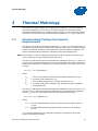
Thermal Management Logic and Thermal Monitor Feature ...................................... 33
4.1
4.2
Processor Power Dissipation .................................................................... 33
Thermal Monitor Implementation ............................................................. 33
4.2.1
PROCHOT# Signal .................................................................... 34
4.2.2
Thermal Control Circuit ............................................................. 34
4.2.2.1
Thermal Monitor ........................................................ 34
4.2.3
Thermal Monitor 2 .................................................................... 35
4.2.4
Operation and Configuration ...................................................... 36
4.2.5
On-Demand Mode ..................................................................... 37
Thermal and Mechanical Design Guidelines
3
4.2.6
4.2.7
4.2.8
4.2.9
4.2.10
4.2.11
5
Balanced Technology Extended (BTX) Thermal/Mechanical Design Information ......... 41
5.1
5.2
5.3
5.4
5.5
5.6
6
6.3
6.4
6.5
6.6
6.7
ATX Reference Design Requirements ........................................................ 53
Validation Results for Reference Design .................................................... 55
6.2.1
Heatsink Performance ............................................................... 55
6.2.2
Acoustics ................................................................................. 56
6.2.3
Altitude ................................................................................... 56
6.2.4
Heatsink Thermal Validation ....................................................... 57
Environmental Reliability Testing ............................................................. 57
6.3.1
Structural Reliability Testing ...................................................... 57
6.3.1.1
Random Vibration Test Procedure ................................ 57
6.3.1.2
Shock Test Procedure ................................................. 58
6.3.2
Power Cycling .......................................................................... 59
6.3.3
Recommended BIOS/CPU/Memory Test Procedures ...................... 60
Material and Recycling Requirements........................................................ 60
Safety Requirements .............................................................................. 61
Geometric Envelope for Intel Reference ATX Thermal Mechanical Design ...... 61
Reference Attach Mechanism ................................................................... 62
6.7.1
Structural Design Strategy ......................................................... 62
6.7.2
Mechanical Interface to the Reference Attach Mechanism .............. 63
Intel® Quiet System Technology (Intel® QST) ...................................................... 65
7.1
7.2
4
Overview of the BTX Reference Design ..................................................... 41
5.1.1
Target Heatsink Performance ..................................................... 41
5.1.2
Acoustics ................................................................................. 42
5.1.3
Effective Fan Curve ................................................................... 43
5.1.4
Voltage Regulator Thermal Management...................................... 44
5.1.5
Altitude ................................................................................... 45
5.1.6
Reference Heatsink Thermal Validation ........................................ 45
Environmental Reliability Testing ............................................................. 45
5.2.1
Structural Reliability Testing ...................................................... 45
5.2.1.1
Random Vibration Test Procedure ................................ 45
5.2.1.2
Shock Test Procedure ................................................. 46
5.2.2
Power Cycling .......................................................................... 47
5.2.3
Recommended BIOS/CPU/Memory Test Procedures ...................... 48
Material and Recycling Requirements........................................................ 48
Safety Requirements .............................................................................. 49
Geometric Envelope for Intel Reference BTX Thermal Module Assembly ........ 49
Preload and TMA Stiffness ....................................................................... 50
5.6.1
Structural Design Strategy ......................................................... 50
5.6.2
TMA Preload verse Stiffness ....................................................... 50
ATX Thermal/Mechanical Design Information ........................................................ 53
6.1
6.2
7
System Considerations .............................................................. 37
Operating System and Application Software Considerations ........... 38
THERMTRIP# Signal .................................................................. 38
Cooling System Failure Warning ................................................. 38
Digital Thermal Sensor .............................................................. 39
Platform Environmental Control Interface (PECI) .......................... 40
Intel® QST Algorithm.............................................................................. 65
7.1.1
Output Weighting Matrix............................................................ 66
7.1.2
Proportional-Integral-Derivative (PID) ......................................... 66
Board and System Implementation of Intel® QST ....................................... 68
Thermal and Mechanical Design Guidelines
7.3
7.4
Appendix A
LGA775 Socket Heatsink Loading ........................................................................ 71
A.1
A.2
A.3
A.4
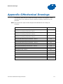
Appendix B
B.3
Overview .............................................................................................. 77
Test Preparation .................................................................................... 77
B.2.1
Heatsink Preparation ................................................................. 77
B.2.2
Typical Test Equipment ............................................................. 80
Test Procedure Examples ........................................................................ 80
B.3.1
Time-Zero, Room Temperature Preload Measurement ................... 81
B.3.2
Preload Degradation under Bake Conditions ................................. 81
Thermal Interface Management .......................................................................... 83
C.1
C.2
C.3
Appendix D
LGA775 Socket Heatsink Considerations ................................................... 71
Metric for Heatsink Preload for ATX/uATX Designs Non-Compliant with Intel®
Reference Design ................................................................................... 71
Heatsink Preload Requirement Limitations................................................. 71
A.3.1
Motherboard Deflection Metric Definition...................................... 72
A.3.2
Board Deflection Limits.............................................................. 73
A.3.3
Board Deflection Metric Implementation Example ......................... 74
A.3.4
Additional Considerations........................................................... 75
A.3.4.1
Motherboard Stiffening Considerations ......................... 76
Heatsink Selection Guidelines .................................................................. 76
Heatsink Clip Load Metrology ............................................................................. 77
B.1
B.2
Appendix C
Intel® QST Configuration and Tuning ........................................................ 70
Fan Hub Thermistor and Intel® QST ......................................................... 70
Bond Line Management .......................................................................... 83
Interface Material Area ........................................................................... 83
Interface Material Performance ................................................................ 83
Case Temperature Reference Metrology ............................................................... 85
D.1
D.2
D.3
D.4
D.5
D.6
Objective and Scope............................................................................... 85
Supporting Test Equipment ..................................................................... 85
Thermal Calibration and Controls ............................................................. 87
IHS Groove ........................................................................................... 87
Thermocouple Attach Procedure............................................................... 91
D.5.1
Thermocouple Conditioning and Preparation................................. 91
D.5.2
Thermocouple Attachment to the IHS .......................................... 92
D.5.3
Solder Process ......................................................................... 97
D.5.4
Cleaning and Completion of Thermocouple Installation ................ 100
Thermocouple Wire Management ........................................................... 104
Appendix E
Balanced Technology Extended (BTX) System Thermal Considerations .................. 105
Appendix F
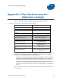
Fan Performance for Reference Design .............................................................. 109
Appendix G
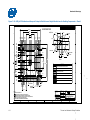
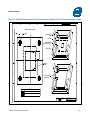
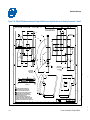
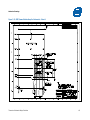
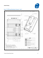
Mechanical Drawings ....................................................................................... 111
Appendix H
Intel® Enabled Reference Solution Information ................................................... 127
Thermal and Mechanical Design Guidelines
5
Figures
Figure 2-1. Package IHS Load Areas ................................................................... 15
Figure 2-2. Processor Case Temperature Measurement Location ............................. 19
Figure 2-3. Example Thermal Profile.................................................................... 20
Figure 3-1. Processor Thermal Characterization Parameter Relationships ................. 28
Figure 3-2. Locations for Measuring Local Ambient Temperature, Active ATX Heatsink31
Figure 3-3. Locations for Measuring Local Ambient Temperature, Passive Heatsink ... 31
Figure 4-1. Thermal Monitor Control.................................................................... 35
Figure 4-2. Thermal Monitor 2 Frequency and Voltage Ordering .............................. 36
Figure 4-3. TCONTROL for Digital Thermal Sensor ..................................................... 39
Figure 5-1. Effective TMA Fan Curves with Reference Extrusion .............................. 44
Figure 5-2. Random Vibration PSD ...................................................................... 46
Figure 5-3. Shock Acceleration Curve .................................................................. 46
Figure 5-4. Intel Type II TMA 65W Reference Design............................................. 49
Figure 5-5. Upward Board Deflection During Shock ............................................... 50
Figure 5-6. Minimum Required Processor Preload to Thermal Module Assembly
Stiffness .................................................................................................... 51
Figure 5-7. Thermal Module Attach Pointes and Duct-to-SRM Interface Features....... 52
Figure 6-1. E18764-001 Reference Design – Exploded View ................................... 54
Figure 6-2. Bottom View of Copper Core Applied by TC-1996 Grease....................... 54
Figure 6-3. Random Vibration PSD ...................................................................... 58
Figure 6-4. Shock Acceleration Curve .................................................................. 58
Figure 6-5. Upward Board Deflection during Shock................................................ 62
Figure 6-6. Reference Clip/Heatsink Assembly ...................................................... 63
Figure 6-7. Critical Parameters for Interfacing to Reference Clip ............................. 64
Figure 6-8. Critical Core Dimension ..................................................................... 64
Figure 7-1. Intel® QST Overview ........................................................................ 66
Figure 7-2. PID Controller Fundamentals ............................................................. 67
Figure 7-3. Intel® QST Platform Requirements ..................................................... 68
Figure 7-4. Example Acoustic Fan Speed Control Implementation ........................... 69
Figure 7-5. Digital Thermal Sensor and Thermistor ............................................... 70
Figure 7-6. Board Deflection Definition ................................................................ 73
Figure 7-7. Example—Defining Heatsink Preload Meeting Board Deflection Limit ....... 75
Figure 7-8. Load Cell Installation in Machined Heatsink Base Pocket – Bottom View .. 78
Figure 7-9. Load Cell Installation in Machined Heatsink Base Pocket – Side View ...... 79
Figure 7-10. Preload Test Configuration ............................................................... 79
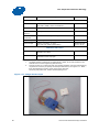
Figure 7-11. Omega Thermocouple ..................................................................... 86
Figure 7-12. 775-LAND LGA Package Reference Groove Drawing at 6 o’clock Exit ..... 88
Figure 7-13. 775-LAND LGA Package Reference Groove Drawing at 3 o’clock Exit
(Old Drawing) ............................................................................................ 89
Figure 7-14. IHS Groove at 6 o’clock Exit on the 775-LAND LGA Package ................ 90
Figure 7-15. IHS Groove at 6 o’clock Exit Orientation Relative to the LGA775 Socket 90
Figure 7-16. Inspection of Insulation on Thermocouple .......................................... 91
Figure 7-17. Bending the Tip of the Thermocouple ................................................ 92
Figure 7-18. Securing Thermocouple Wires with Kapton* Tape Prior to Attach .......... 92
Figure 7-19. Thermocouple Bead Placement ......................................................... 93
Figure 7-20. Position Bead on the Groove Step ..................................................... 94
Figure 7-21. Detailed Thermocouple Bead Placement ............................................ 94
Figure 7-22. Third Tape Installation .................................................................... 95
Figure 7-23. Measuring Resistance between Thermocouple and IHS ........................ 95
Figure 7-24. Applying Flux to the Thermocouple Bead ........................................... 96
Figure 7-25. Cutting Solder ................................................................................ 96
Figure 7-26. Positioning Solder on IHS ................................................................ 97
6
Thermal and Mechanical Design Guidelines
Figure 7-27. Solder Station Setup ....................................................................... 98
Figure 7-28. View Through Lens at Solder Station ................................................. 99
Figure 7-29. Moving Solder back onto Thermocouple Bead ..................................... 99
Figure 7-30. Removing Excess Solder ................................................................ 100
Figure 7-31. Thermocouple placed into groove ................................................... 101
Figure 7-32. Removing Excess Solder ................................................................ 101
Figure 7-33. Filling Groove with Adhesive .......................................................... 102
Figure 7-34. Application of Accelerant ............................................................... 102
Figure 7-35. Removing Excess Adhesive from IHS .............................................. 103
Figure 7-36. Finished Thermocouple Installation ................................................. 103
Figure 7-37. Thermocouple Wire Management .................................................... 104
Figure 7-38. System Airflow Illustration with System Monitor Point Area Identified . 106
Figure 7-39. Thermal sensor Location Illustration ............................................... 107
Figure 7-40. ATX/µATX Motherboard Keep-out Footprint Definition and Height
Restrictions for Enabling Components - Sheet 1 ........................................... 112
Figure 7-41. ATX/µATX Motherboard Keep-out Footprint Definition and Height
Restrictions for Enabling Components - Sheet 2 ........................................... 113
Figure 7-42. ATX/µATX Motherboard Keep-out Footprint Definition and Height
Restrictions for Enabling Components - Sheet 3 ........................................... 114
Figure 7-43. BTX Thermal Module Keep Out Volumetric – Sheet 1......................... 115
Figure 7-44. BTX Thermal Module Keep Out Volumetric – Sheet 2......................... 116
Figure 7-45. BTX Thermal Module Keep Out Volumetric – Sheet 3......................... 117
Figure 7-46. BTX Thermal Module Keep Out Volumetric – Sheet 4......................... 118
Figure 7-47. BTX Thermal Module Keep Out Volumetric – Sheet 5......................... 119
Figure 7-48. ATX Reference Clip – Sheet 1 ......................................................... 120
Figure 7-49. ATX Reference Clip - Sheet 2 ......................................................... 121
Figure 7-50. Reference Fastener - Sheet 1 ......................................................... 122
Figure 7-51. Reference Fastener - Sheet 2 ......................................................... 123
Figure 7-52. Reference Fastener - Sheet 3 ......................................................... 124
Figure 7-53. Reference Fastener - Sheet 4 ......................................................... 125
Figure 7-54. Intel® E18764-001 Reference Solution Assembly .............................. 126
Thermal and Mechanical Design Guidelines
7
Tables
Table 2–1. Heatsink Inlet Temperature of Intel Reference Thermal Solutions ........... 24
Table 2–2. Heatsink Inlet Temperature of Intel Boxed Processor Thermal Solutions .. 24
Table 5–1. Balanced Technology Extended (BTX) Type II Reference TMA Performance41
Table 5–2. Acoustic Targets ............................................................................... 42
Table 5–3. VR Airflow Requirements.................................................................... 44
Table 5–4. Processor Preload Limits .................................................................... 51
Table 6–1. E18764-001 Reference Heatsink Performance ...................................... 55
Table 6–2. Acoustic Results for ATX Reference Heatsink (E18764-001) .................... 56
Table 7–1. Board Deflection Configuration Definitions............................................ 72
Table 7–2. Typical Test Equipment ...................................................................... 80
Table 7–3. Fan Electrical Performance Requirements ........................................... 109
Table 7–4. Intel® Representative Contact for Licensing Information of BTX
Reference Design ..................................................................................... 127
Table 7–5. E18764-001 Reference Thermal Solution Providers ............................. 127
Table 7–6. BTX Reference Thermal Solution Providers ......................................... 128
8
Thermal and Mechanical Design Guidelines
Revision History
Revision
Number
Description
Revision
001
• Initial release.
January 2008
002
• Added Intel® Core™2 Duo processor E8300 and E7200
April 2008
003
004
005
®
August 2008
®
August 2008
®
October 2008
®
• Added Intel Core™2 Duo processor E8600 and E7300
• Added Intel Pentium dual-core processor E5200
• Added Intel Core™2 Duo processor E7400
006
• Added Intel Pentium dual-core processor E5300
December 2008
007
• Added Intel® Pentium dual-core processor E5400
January 2009
®
• Added Intel Core™2 Duo processor E7500
008
009
• Added Intel® Pentium dual-core processor E6300
May 2009
®
June 2009
®
• Added Intel Core™2 Duo processor E7600
010
• Added Intel Pentium dual-core processor E6500
August 2009
011
• Intel® Celeron® processor E3x00 series
August 2009
012
• Added Intel® Pentium dual-core processor E6600
January 2010
• Intel® Celeron® processor E3400
013
014
015
• Added Intel® Pentium dual-core processor E5500
April 2010
®
June 2010
®
August 2010
• Added Intel Pentium dual-core processor E6700
• Added Intel Pentium dual-core processor E5700
§
Thermal and Mechanical Design Guidelines
9
10
Thermal and Mechanical Design Guidelines
Introduction
1
Introduction
1.1
Document Goals and Scope
1.1.1
Importance of Thermal Management
The objective of thermal management is to ensure that the temperatures of all
components in a system are maintained within their functional temperature range.
Within this temperature range, a component is expected to meet its specified
performance. Operation outside the functional temperature range can degrade system
performance, cause logic errors or cause component and/or system damage.
Temperatures exceeding the maximum operating limit of a component may result in
irreversible changes in the operating characteristics of this component.
In a system environment, the processor temperature is a function of both system and
component thermal characteristics. The system level thermal constraints consist of the
local ambient air temperature and airflow over the processor as well as the physical
constraints at and above the processor. The processor temperature depends in
particular on the component power dissipation, the processor package thermal
characteristics, and the processor thermal solution.
All of these parameters are affected by the continued push of technology to increase
processor performance levels and packaging density (more transistors). As operating
frequencies increase and packaging size decreases, the power density increases while
the thermal solution space and airflow typically become more constrained or remains
the same within the system. The result is an increased importance on system design
to ensure that thermal design requirements are met for each component, including the
processor, in the system.
1.1.2
Document Goals
Depending on the type of system and the chassis characteristics, new system and
component designs may be required to provide adequate cooling for the processor.
The goal of this document is to provide an understanding of these thermal
characteristics and discuss guidelines for meeting the thermal requirements imposed
on single processor systems using the Intel® Core™2 Duo processor E8000, E7000
series, Intel® Pentium® dual-core processor E6000, E5000 series, and Intel® Celeron®
processor E3x00 series.
The concepts given in this document are applicable to any system form factor. Specific
examples used will be the Intel enabled reference solution for ATX/uATX systems. See
the applicable BTX form factor reference documents to design a thermal solution for
that form factor.
Thermal and Mechanical Design Guidelines
11
Introduction
1.1.3
Document Scope
This design guide supports the following processors:
•
Intel® Core™2 Duo processor E8000 series with 6 MB cache applies to Intel®
Core™2 Duo processors E8600, E8500, E8400, E8300, E8200, and E8190
•
Intel® Core™2 Duo processor E7000 series with 3 MB cache applies to Intel®
Core™2 Duo processors E7600, E7500, E7400, E7300, and E7200
•
Intel® Pentium® dual-core processor E5000 series with 2 MB cache applies to
Intel® Pentium® dual-core processors E5700, E5500, E5400, E5300, and E5200
•
Intel® Pentium® dual-core processor E6000 series with 2 MB cache applies to
Intel® Pentium® dual-core processor E6700, E6600, E6500, and E6300
•
Intel® Celeron® processor E3x00 series with 1 MB cache applies to the Intel®
Celeron® processor E3400, E3300, and E3200
In this document when a reference is made to “the processor” it is intended that this
includes all the processors supported by this document. If needed for clarity, the
specific processor will be listed.
In this document, when a reference is made to the “the reference design” it is
intended that this means ATX reference designs (E18764-001) supported by this
document. If needed for clarify, the specific reference design will be listed.
In this document, when a reference is made to “the datasheet”, the reader should
refer to the Intel® Core™2 Duo Processor E8000 and E7000 Series Datasheet, Intel®
Pentium® Dual-Core Processor E6000 and E5000 Series Datasheet, and Intel®
Celeron® Processor E3x00 Series Datasheet. If needed for clarity the specific
processor datasheet will be referenced.
Chapter 2 of this document discusses package thermal mechanical requirements to
design a thermal solution for the processor in the context of personal computer
applications.
Chapter 3 discusses the thermal solution considerations and metrology
recommendations to validate a processor thermal solution.
Chapter 4 addresses the benefits of the processor’s integrated thermal management
logic for thermal design.
Chapter 5 gives information on the Intel reference thermal solution for the processor
in BTX platform.
Chapter 6 gives information on the Intel reference thermal solution for the processor
in ATX platform.
Chapter 7 discusses the implementation of acoustic fan speed control.
The physical dimensions and thermal specifications of the processor that are used in
this document are for illustration only. Refer to the datasheet for the product
dimensions, thermal power dissipation and maximum case temperature. In case of
conflict, the data in the datasheet supersedes any data in this document.
12
Thermal and Mechanical Design Guidelines
Introduction
1.2
References
Material and concepts available in the following documents may be beneficial when
reading this document.
Material and concepts available in the following documents may be beneficial when
reading this document.
Document
1.3
Location
Intel® Core™2 Duo Processor E8000 and E7000 Series
Datasheet
www.intel.com/design/processor/d
atashts/318732.htm
Intel® Pentium® Dual-Core Processor E6000 and E5000
Series Datasheet
http://download.intel.com/design/
processor/datashts/320467.pdf
Intel® Celeron® Processor E3x00 Series Datasheet
http://download.intel.com/design/
processor/datashts/322567.pdf
LGA775 Socket Mechanical Design Guide
http://developer.intel.com/design/
Pentium4/guides/302666.htm
uATX SFF Design Guidance
http://www.formfactors.org/
Fan Specification for 4-wire PWM Controlled Fans
http://www.formfactors.org/
ATX Thermal Design Suggestions
http://www.formfactors.org/
microATX Thermal Design Suggestions
http://www.formfactors.org/
Balanced Technology Extended (BTX) System Design
Guide
http://www.formfactors.org/
Thermally Advantaged Chassis Design Guide
http://www.intel.com/go/chassis/
Definition of Terms
Term
Description
TA
The measured ambient temperature locally surrounding the processor. The
ambient temperature should be measured just upstream of a passive heatsink
or at the fan inlet for an active heatsink.
TC
The case temperature of the processor, measured at the geometric center of
the topside of the IHS.
TE
The ambient air temperature external to a system chassis. This temperature
is usually measured at the chassis air inlets.
TS
Heatsink temperature measured on the underside of the heatsink base, at a
location corresponding to TC.
TC-MAX
ΨCA
The maximum case temperature as specified in a component specification.
Case-to-ambient thermal characterization parameter (psi). A measure of
thermal solution performance using total package power. This is defined as:
(TC – TA) / Total Package Power.
Note: Heat source must be specified for Ψ measurements.
Thermal and Mechanical Design Guidelines
13
Introduction
Term
Description
ΨCS
Case-to-sink thermal characterization parameter. A measure of thermal
interface material performance using total package power. This is defined as:
(TC – TS) / Total Package Power.
Note: Heat source must be specified for Ψ measurements.
ΨSa
Sink-to-ambient thermal characterization parameter. A measure of heatsink
thermal performance using total package power. This is defined as: (TS – TA) /
Total Package Power.
Note: Heat source must be specified for Ψ measurements.
TIM
Thermal Interface Material: The thermally conductive compound between the
heatsink and the processor case. This material fills the air gaps and voids, and
enhances the transfer of the heat from the processor case to the heatsink.
PMAX
The maximum power dissipated by a semiconductor component.
TDP
Thermal Design Power: a power dissipation target based on worst-case
applications. Thermal solutions should be designed to dissipate the thermal
design power.
IHS
Integrated Heat Spreader: a thermally conductive lid integrated into a
processor package to improve heat transfer to a thermal solution through
heat spreading.
LGA775
Socket
ACPI
Advanced Configuration and Power Interface.
Bypass
Bypass is the area between a passive heatsink and any object that can act to
form a duct. For this example, it can be expressed as a dimension away from
the outside dimension of the fins to the nearest surface.
Thermal
Monitor
A feature on the processor that attempts to keep the processor die
temperature within factory specifications.
TCC
Thermal Control Circuit: Thermal Monitor uses the TCC to reduce die
temperature by lowering the effective processor frequency when the die
temperature has exceeded its operating limits.
DTS
Digital Thermal Sensor: Processor die sensor temperature defined as an offset
from the onset of PROCHOT#.
FSC
Fan Speed Control: Thermal solution that includes a variable fan speed which
is driven by a PWM signal and uses the on-die thermal diode as a reference to
change the duty cycle of the PWM signal.
TCONTROL
PWM
Health
Monitor
Component
14
The surface mount socket designed to accept the processors in the 775–Land
LGA package.
TCONTROL is the specification limit for use with the on-die thermal diode.
Pulse width modulation is a method of controlling a variable speed fan. The
enabled 4-wire fans use the PWM duty cycle % from the fan speed controller
to modulate the fan speed.
Any standalone or integrated component that is capable of reading the
processor temperature and providing the PWM signal to the 4-pin fan header.
BTX
Balanced Technology Extended.
TMA
Thermal Module Assembly. The heatsink, fan and duct assembly for the BTX
thermal solution
Thermal and Mechanical Design Guidelines
Processor Thermal/Mechanical Information
2
Processor Thermal/Mechanical
Information
2.1
Mechanical Requirements
2.1.1
Processor Package
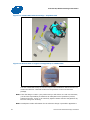
The processors covered in the document are packaged in a 775-Land LGA package
that interfaces with the motherboard using a LGA775 socket. Refer to the datasheet
for detailed mechanical specifications.
The processor connects to the motherboard through a land grid array (LGA) surface
mount socket. The socket contains 775 contacts arrayed about a cavity in the center
of the socket with solder balls for surface mounting to the motherboard. The socket is
named LGA775 socket. A description of the socket can be found in the LGA775 Socket
Mechanical Design Guide.
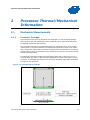
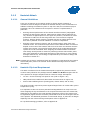
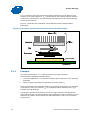
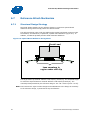
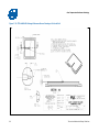
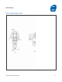
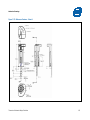
The package includes an integrated heat spreader (IHS) that is shown in Figure 2-1
for illustration only. Refer to the processor datasheet for further information. In case
of conflict, the package dimensions in the processor datasheet supersedes dimensions
provided in this document.
Figure 2-1. Package IHS Load Areas
Thermal and Mechanical Design Guidelines
15
Processor Thermal/Mechanical Information
The primary function of the IHS is to transfer the non-uniform heat distribution from
the die to the top of the IHS, out of which the heat flux is more uniform and spread
over a larger surface area (not the entire IHS area). This allows more efficient heat
transfer out of the package to an attached cooling device. The top surface of the IHS
is designed to be the interface for contacting a heatsink.
The IHS also features a step that interfaces with the LGA775 socket load plate, as
described in LGA775 Socket Mechanical Design Guide. The load from the load plate is
distributed across two sides of the package onto a step on each side of the IHS. It is
then distributed by the package across all of the contacts. When correctly actuated,
the top surface of the IHS is above the load plate allowing proper installation of a
heatsink on the top surface of the IHS. After actuation of the socket load plate, the
seating plane of the package is flush with the seating plane of the socket. Package
movement during socket actuation is along the Z direction (perpendicular to
substrate) only. Refer to the LGA775 Socket Mechanical Design Guide for further
information about the LGA775 socket.
The processor package has mechanical load limits that are specified in the processor
datasheet. The specified maximum static and dynamic load limits should not be
exceeded during their respective stress conditions. These include heatsink installation,
removal, mechanical stress testing, and standard shipping conditions.
•
When a compressive static load is necessary to ensure thermal performance of the
thermal interface material between the heatsink base and the IHS, it should not
exceed the corresponding specification given in the processor datasheet.
•
When a compressive static load is necessary to ensure mechanical performance, it
should remain in the minimum/maximum range specified in the processor
datasheet
•
The heatsink mass can also generate additional dynamic compressive load to the
package during a mechanical shock event. Amplification factors due to the impact
force during shock must be taken into account in dynamic load calculations. The
total combination of dynamic and static compressive load should not exceed the
processor datasheet compressive dynamic load specification during a vertical
shock. For example, with a 0.550 kg [1.2 lb] heatsink, an acceleration of 50G
during an 11 ms trapezoidal shock with an amplification factor of 2 results in
approximately a 539 N [117 lbf] dynamic load on the processor package. If a
178 N [40 lbf] static load is also applied on the heatsink for thermal performance
of the thermal interface material the processor package could see up to a 717 N
[156 lbf]. The calculation for the thermal solution of interest should be compared
to the processor datasheet specification.
No portion of the substrate should be used as a load- bearing surface.
Finally, the processor datasheet provides package handling guidelines in terms of
maximum recommended shear, tensile and torque loads for the processor IHS relative
to a fixed substrate. These recommendations should be followed in particular for
heatsink removal operations.
16
Thermal and Mechanical Design Guidelines
Processor Thermal/Mechanical Information
2.1.2
Heatsink Attach
2.1.2.1
General Guidelines
There are no features on the LGA775 socket to directly attach a heatsink: a
mechanism must be designed to attach the heatsink directly to the motherboard. In
addition to holding the heatsink in place on top of the IHS, this mechanism plays a
significant role in the robustness of the system in which it is implemented, in
particular:
•
Ensuring thermal performance of the thermal interface material (TIM) applied
between the IHS and the heatsink. TIMs based on phase change materials are
very sensitive to applied pressure: the higher the pressure, the better the initial
performance. TIMs such as thermal greases are not as sensitive to applied
pressure. Designs should consider a possible decrease in applied pressure over
time due to potential structural relaxation in retention components.
•
Ensuring system electrical, thermal, and structural integrity under shock and
vibration events. The mechanical requirements of the heatsink attach mechanism
depend on the mass of the heatsink and the level of shock and vibration that the
system must support. The overall structural design of the motherboard and the
system have to be considered when designing the heatsink attach mechanism.
Their design should provide a means for protecting LGA775 socket solder joints.
One of the strategies for mechanical protection of the socket is to use a preload
and high stiffness clip. This strategy is implemented by the reference design and
described in Section 6.7.
Note: Package pull-out during mechanical shock and vibration is constrained by the LGA775
socket load plate (refer to the LGA775 Socket Mechanical Design Guide for further
information).
2.1.2.2
Heatsink Clip Load Requirement
The attach mechanism for the heatsink developed to support the processor should
create a static preload on the package between 18 lbf and 70 lbf throughout the life
of the product for designs compliant with the reference design assumptions:
•
72 mm x 72 mm mounting hole span for ATX (refer to Figure 7-40)
•
TMA preload versus stiffness for BTX within the limits shown on Figure 5-6
•
And no board stiffening device (backing plate, chassis attach, and so forth).
The minimum load is required to protect against fatigue failure of socket solder joint in
temperature cycling.
It is important to take into account potential load degradation from creep over time
when designing the clip and fastener to the required minimum load. This means that,
depending on clip stiffness, the initial preload at beginning of life of the product may
be significantly higher than the minimum preload that must be met throughout the life
of the product. For additional guidelines on mechanical design, in particular on designs
departing from the reference design assumptions refer to Appendix A.
For clip load metrology guidelines, refer to Appendix B.
Thermal and Mechanical Design Guidelines
17
Processor Thermal/Mechanical Information
2.1.2.3
Additional Guidelines
In addition to the general guidelines given above, the heatsink attach mechanism for
the processor should be designed to the following guidelines:
•
Holds the heatsink in place under mechanical shock and vibration events and
applies force to the heatsink base to maintain desired pressure on the thermal
interface material. Note that the load applied by the heatsink attach mechanism
must comply with the package specifications described in the processor datasheet.
One of the key design parameters is the height of the top surface of the processor
IHS above the motherboard. The IHS height from the top of board is expected to
vary from 7.517 mm to 8.167 mm. This data is provided for information only, and
should be derived from:
The height of the socket seating plane above the motherboard after reflow, given
in the LGA775 Socket Mechanical Design Guide with its tolerances.
The height of the package, from the package seating plane to the top of the IHS,
and accounting for its nominal variation and tolerances that are given in the
corresponding processor datasheet.
2.2
•
Engages easily, and if possible, without the use of special tools. In general, the
heatsink is assumed to be installed after the motherboard has been installed into
the chassis.
•
Minimizes contact with the motherboard surface during installation and actuation
to avoid scratching the motherboard.
Thermal Requirements
Refer to the datasheet for the processor thermal specifications. The majority of
processor power is dissipated through the IHS. There are no additional components
(such as BSRAMs) that generate heat on this package. The amount of power that can
be dissipated as heat through the processor package substrate and into the socket is
usually minimal.
The thermal limits for the processor are the Thermal Profile and TCONTROL. The Thermal
Profile defines the maximum case temperature as a function of power being
dissipated. TCONTROL is a specification used in conjunction with the temperature
reported by the digital thermal sensor and a fan speed control method. Designing to
these specifications allows optimization of thermal designs for processor performance
and acoustic noise reduction.
2.2.1
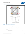
Processor Case Temperature
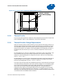
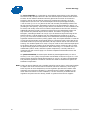
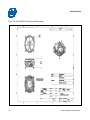
For the processor, the case temperature is defined as the temperature measured at
the geometric center of the package on the surface of the IHS. For illustration,
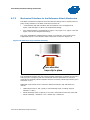
Figure 2-2 shows the measurement location for a 37.5 mm x 37.5 mm [1.474 in x
1.474 in] 775-Land LGA processor package with a 28.7 mm x 28.7 mm [1.13 in x
1.13 in] IHS top surface. Techniques for measuring the case temperature are detailed
in Section 3.4.
18
Thermal and Mechanical Design Guidelines
Processor Thermal/Mechanical Information
Figure 2-2. Processor Case Temperature Measurement Location
37.5 mm
Measure TC at this point
(geometric center of the package)
37.5 mm
2.2.2
Thermal Profile
The Thermal Profile defines the maximum case temperature as a function of processor
power dissipation. Refer to the datasheet for the further information.
2.2.3
Thermal Solution Design Requirements
While the thermal profile provides flexibility for ATX /BTX thermal design based on its
intended target thermal environment, thermal solutions that are intended to function
in a multitude of systems and environments need to be designed for the worst-case
thermal environment. The majority of ATX /BTX platforms are targeted to function in
an environment that will have up to a 35° C ambient temperature external to the
system.
For ATX platforms, an active air-cooled design, assumed be used in ATX Chassis, with
a fan installed at the top of the heatsink equivalent to the reference design (see
Chapter 6) should be designed to manage the processor TDP at an inlet temperature
of 35° C + 5°C = 40° C.
For BTX platforms, a front-to-back cooling design equivalent to Intel BTX TMA Type II
reference design (see the Chapter 5) should be designed to manage the processor
TDP at an inlet temperature of 35° C + 0.5° C = 35.5° C.
The slope of the thermal profile was established assuming a generational improvement
in thermal solution performance of the Intel reference design. For an example of Intel
Core™2 Duo Processor E8000 series with 6 MB in ATX platform, its improvement is
about 15% over the Intel reference design (E18764-001). This performance is
expressed as the slope on the thermal profile and can be thought of as the thermal
resistance of the heatsink attached to the processor, ΨCA (Refer to Section 3.1). The
intercept on the thermal profile assumes a maximum ambient operating condition that
is consistent with the available chassis solutions.
Thermal and Mechanical Design Guidelines
19
Processor Thermal/Mechanical Information
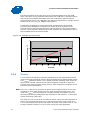
The thermal profiles for the Intel Core™2 Duo processor E8000 series with 6 MB
cache, Intel Core™2 Duo processor E7000 series with 3 MB cache, and Intel Pentium
dual-core processor E6000 and E5000 series with 2 MB cache, and Intel Celeron
processor E3x00 series with 1 MB cache are defined such that there is a single thermal
solution for all of the 775_VR_CONFIG_06 processors.
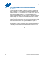
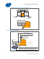
To determine compliance to the thermal profile, a measurement of the actual
processor power dissipation is required. The measured power is plotted on the
Thermal Profile to determine the maximum case temperature. Using the example in
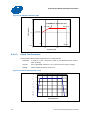
Figure 2-3 for a processor dissipating 50 W the maximum case temperature is 58° C.
See the datasheet for the thermal profile.
Figure 2-3. Example Thermal Profile
Case Temperature (°C)
70
60
50
Thermal Profile
TDP
40
0
10
20
30
40
50
60
70
Power (W)
2.2.4
TCONTROL
TCONTROL defines the maximum operating temperature for the digital thermal sensor
when the thermal solution fan speed is being controlled by the digital thermal sensor.
The TCONTROL parameter defines a very specific processor operating region where fan
speed can be reduced. This allows the system integrator a method to reduce the
acoustic noise of the processor cooling solution, while maintaining compliance to the
processor thermal specification.
Note: The TCONTROL value for the processor is relative to the Thermal Control Circuit (TCC)
activation set point which will be seen as 0 using the digital thermal sensor. As a
result the TCONTROL value will always be a negative number. See Chapter 4 for the
discussion the thermal management logic and features and Chapter 7 on Intel Quiet
System Technology (Intel QST).
The value of TCONTROL is driven by a number of factors. One of the most significant of
these is the processor idle power. As a result a processor with a high (closer to 0)
TCONTROL will dissipate more power than a part with lower value (farther from 0, such
as larger negative number) of TCONTROL when running the same application.
20
Thermal and Mechanical Design Guidelines
Processor Thermal/Mechanical Information
This is achieved in part by using the ΨCA versus RPM and RPM versus Acoustics (dBA)
performance curves from the Intel enabled thermal solution. A thermal solution
designed to meet the thermal profile would be expected to provide similar acoustic
performance of different parts with potentially different TCONTROL values.
The value for TCONTROL is calculated by the system BIOS based on values read from a
factory configured processor register. The result can be used to program a fan speed
control component. See the appropriate processor datasheet for further details on
reading the register and calculating TCONTROL.
See Chapter 7, Intel® Quiet System Technology (Intel® QST), for details on
implementing a design using TCONTROL and the Thermal Profile.
2.3
Heatsink Design Considerations
To remove the heat from the processor, three basic parameters should be considered:
•
The area of the surface on which the heat transfer takes place. Without any
enhancements, this is the surface of the processor package IHS. One method used
to improve thermal performance is by attaching a heatsink to the IHS. A heatsink
can increase the effective heat transfer surface area by conducting heat out of the
IHS and into the surrounding air through fins attached to the heatsink base.
•
The conduction path from the heat source to the heatsink fins. Providing a
direct conduction path from the heat source to the heatsink fins and selecting
materials with higher thermal conductivity typically improves heatsink
performance. The length, thickness, and conductivity of the conduction path from
the heat source to the fins directly impact the thermal performance of the
heatsink. In particular, the quality of the contact between the package IHS and
the heatsink base has a higher impact on the overall thermal solution performance
as processor cooling requirements become stricter. Thermal interface material
(TIM) is used to fill in the gap between the IHS and the bottom surface of the
heatsink, and thereby improve the overall performance of the stack-up (IHS-TIMHeatsink). With extremely poor heatsink interface flatness or roughness, TIM may
not adequately fill the gap. The TIM thermal performance depends on its thermal
conductivity as well as the pressure applied to it. Refer to Section 2.3.4 and
Appendix C for further information on TIM and on bond line management between
the IHS and the heatsink base.
•
The heat transfer conditions on the surface on which heat transfer takes
place. Convective heat transfer occurs between the airflow and the surface
exposed to the flow. It is characterized by the local ambient temperature of the
air, TA, and the local air velocity over the surface. The higher the air velocity over
the surface, and the cooler the air, the more efficient is the resulting cooling. The
nature of the airflow can also enhance heat transfer using convection. Turbulent
flow can provide improvement over laminar flow. In the case of a heatsink, the
surface exposed to the flow includes in particular the fin faces and the heatsink
base.
Active heatsinks typically incorporate a fan that helps manage the airflow through
the heatsink.
Passive heatsink solutions require in-depth knowledge of the airflow in the chassis.
Typically, passive heatsinks see lower air speed. These heatsinks are therefore
typically larger (and heavier) than active heatsinks due to the increase in fin surface
Thermal and Mechanical Design Guidelines
21
Processor Thermal/Mechanical Information
required to meet a required performance. As the heatsink fin density (the number of
fins in a given cross-section) increases, the resistance to the airflow increases: it is
more likely that the air travels around the heatsink instead of through it, unless air
bypass is carefully managed. Using air-ducting techniques to manage bypass area can
be an effective method for controlling airflow through the heatsink.
2.3.1
Heatsink Size
The size of the heatsink is dictated by height restrictions for installation in a system
and by the real estate available on the motherboard and other considerations for
component height and placement in the area potentially impacted by the processor
heatsink. The height of the heatsink must comply with the requirements and
recommendations published for the motherboard form factor of interest. Designing a
heatsink to the recommendations may preclude using it in system adhering strictly to
the form factor requirements, while still in compliance with the form factor
documentation.
For the ATX/microATX form factor, it is recommended to use:
•
The ATX motherboard keep-out footprint definition and height restrictions for
enabling components, defined for the platforms designed with the LGA775 socket
in Appendix G of this design guide.
•
The motherboard primary side height constraints defined in the ATX Specification
V2.1 and the microATX Motherboard Interface Specification V1.1 found at
http://www.formfactors.org/.
The resulting space available above the motherboard is generally not entirely available
for the heatsink. The target height of the heatsink must take into account airflow
considerations (for fan performance for example) as well as other design
considerations (air duct, and so forth).
For BTX form factor, it is recommended to use:
2.3.2
•
The BTX motherboard keep-out footprint definitions and height restrictions for
enabling components for platforms designed with the LGA77 socket in Appendix G
of this design guide.
•
An overview of other BTX system considerations for thermal solutions can be
obtained in the latest version of the Balanced Technology Extended (BTX) System
Design Guide found at http://www.formfactors.org/.
Heatsink Mass
With the need to push air cooling to better performance, heatsink solutions tend to
grow larger (increase in fin surface) resulting in increased mass. The insertion of
highly thermally conductive materials like copper to increase heatsink thermal
conduction performance results in even heavier solutions. As mentioned in
Section 2.1, the heatsink mass must take into consideration the package and socket
load limits, the heatsink attach mechanical capabilities, and the mechanical shock and
vibration profile targets. Beyond a certain heatsink mass, the cost of developing and
implementing a heatsink attach mechanism that can ensure the system integrity
under the mechanical shock and vibration profile targets may become prohibitive.
22
Thermal and Mechanical Design Guidelines
Processor Thermal/Mechanical Information
The recommended maximum heatsink mass for the ATX thermal solution is 550g. This
mass includes the fan and the heatsink only. The attach mechanism (clip, fasteners,
and so forth) are not included.
The mass limit for BTX heatsinks that use Intel reference design structural ingredients
is 900 grams. The BTX structural reference component strategy and design is
reviewed in depth in the latest version of the Balanced Technology Extended (BTX)
System Design Guide.
Note: The 550g mass limit for ATX solutions is based on the capabilities of the reference
design components that retain the heatsink to the board and apply the necessary
preload. Any reuse of the clip and fastener in derivative designs should not exceed
550g. ATX Designs that have a mass of greater than 550g should analyze the preload
as discussed in Appendix A and retention limits of the fastener.
Note: The chipset components on the board are affected by processor heatsink mass.
Exceeding these limits may require the evaluation of the chipset for shock and
vibration.
2.3.3
Package IHS Flatness
The package IHS flatness for the product is specified in the datasheet and can be used
as a baseline to predict heatsink performance during the design phase.
Intel recommends testing and validating heatsink performance in full mechanical
enabling configuration to capture any impact of IHS flatness change due to combined
socket and heatsink loading. While socket loading alone may increase the IHS
warpage, the heatsink preload redistributes the load on the package and improves the
resulting IHS flatness in the enabled state.
2.3.4
Thermal Interface Material
Thermal interface material application between the processor IHS and the heatsink
base is generally required to improve thermal conduction from the IHS to the
heatsink. Many thermal interface materials can be pre-applied to the heatsink base
prior to shipment from the heatsink supplier and allow direct heatsink attach, without
the need for a separate thermal interface material dispense or attach process in the
final assembly factory.
All thermal interface materials should be sized and positioned on the heatsink base in
a way that ensures the entire processor IHS area is covered. It is important to
compensate for heatsink-to-processor attach positional alignment when selecting the
proper thermal interface material size.
When pre-applied material is used, it is recommended to have a protective application
tape over it. This tape must be removed prior to heatsink installation.
Thermal and Mechanical Design Guidelines
23
Processor Thermal/Mechanical Information
2.4
System Thermal Solution Considerations
2.4.1
Chassis Thermal Design Capabilities
The Intel reference thermal solutions and Intel Boxed Processor thermal solutions
assume that the chassis delivers a maximum TA at the inlet of the processor fan
heatsink. The following tables show the TA requirements for the reference solutions
and Intel Boxed Processor thermal solutions.
Table 2–1. Heatsink Inlet Temperature of Intel Reference Thermal Solutions
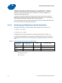
Topic
ATX E18764-001
Heatsink Inlet Temperature
40° C
NOTE:
1.
1
BTX Type II
35.5° C
Intel reference designs (E18764-001) for ATX assume the use of the thermally
advantaged chassis (refer to Thermally Advantaged Chassis (TAC) Design Guide for
TAC thermal and mechanical requirements). The TAC 2.0 Design Guide defines a new
processor cooling solution inlet temperature target of 40° C. The existing TAC 1.1
chassis can be compatible with TAC 2.0 guidelines.
Table 2–2. Heatsink Inlet Temperature of Intel Boxed Processor Thermal Solutions
Topic
Boxed Processor for Intel® Core™2 Duo Processor
E8000, E7000 Series, Intel® Pentium® Dual-Core
Processor E6000, E5000 Series, and Intel®
Celeron® Processor E3x00 Series
Heatsink Inlet Temperature
40° C
NOTE:
1.
2.4.2
Boxed Processor thermal solutions for ATX assume the use of the thermally advantaged
chassis (refer to Thermally Advantaged Chassis (TAC) Design Guide for TAC thermal
and mechanical requirements). The TAC 2.0 Design Guide defines a new processor
cooling solution inlet temperature target of 40° C. The existing TAC 1.1 chassis can be
compatible with TAC 2.0 guidelines.
Improving Chassis Thermal Performance
The heat generated by components within the chassis must be removed to provide an
adequate operating environment for both the processor and other system
components. Moving air through the chassis brings in air from the external ambient
environment and transports the heat generated by the processor and other system
components out of the system. The number, size and relative position of fans and
vents determine the chassis thermal performance, and the resulting ambient
temperature around the processor. The size and type (passive or active) of the
thermal solution and the amount of system airflow can be traded off against each
other to meet specific system design constraints. Additional constraints are board
layout, spacing, component placement, acoustic requirements, and structural
considerations that limit the thermal solution size. For more information, refer to the
Performance ATX Desktop System Thermal Design Suggestions or Performance
microATX Desktop System Thermal Design Suggestions or Balanced Technology
Extended (BTX) System Design Guide documents available on the
http://www.formfactors.org/ web site.
24
Thermal and Mechanical Design Guidelines
Processor Thermal/Mechanical Information
In addition to passive heatsinks, fan heatsinks and system fans are other solutions
that exist for cooling integrated circuit devices. For example, ducted blowers, heat
pipes, and liquid cooling are all capable of dissipating additional heat. Due to their
varying attributes, each of these solutions may be appropriate for a particular system
implementation.
To develop a reliable, cost-effective thermal solution, thermal characterization and
simulation should be carried out at the entire system level, accounting for the thermal
requirements of each component. In addition, acoustic noise constraints may limit the
size, number, placement, and types of fans that can be used in a particular design.
To ease the burden on thermal solutions, the Thermal Monitor feature and associated
logic have been integrated into the silicon of the processor. By taking advantage of
the Thermal Monitor feature, system designers may reduce thermal solution cost by
designing to TDP instead of maximum power. Thermal Monitor attempts to protect the
processor during sustained workload above TDP. Implementation options and
recommendations are described in Chapter 4.
2.4.3
Summary
In summary, considerations in heatsink design include:
• The local ambient temperature TA at the heatsink, which is a function of chassis
design.
• The thermal design power (TDP) of the processor, and the corresponding
maximum TC as calculated from the thermal profile. These parameters are usually
combined in a single lump cooling performance parameter, ΨCA (case to air
thermal characterization parameter). More information on the definition and the
use of ΨCA is given Section 3.1.
• Heatsink interface to IHS surface characteristics, including flatness and roughness.
• The performance of the thermal interface material used between the heatsink and
the IHS.
• The required heatsink clip static load, between 18 lbf to 70 lbf throughout the life
of the product (Refer to Section 2.1.2.2 for further information).
• Surface area of the heatsink.
• Heatsink material and technology.
• Volume of airflow over the heatsink surface area.
• Development of airflow entering and within the heatsink area.
• Physical volumetric constraints placed by the system
2.5
System Integration Considerations
Manufacturing with Intel® Components using 775–Land LGA Package and LGA775
Socket documentation provides Best Known Methods for all aspects LGA775 socket
based platforms and systems manufacturing. Of particular interest for package and
heatsink installation and removal is the System Assembly module. A video covering
system integration is also available. Contact your Intel field sales representative for
further information.
§
Thermal and Mechanical Design Guidelines
25
Processor Thermal/Mechanical Information
26
Thermal and Mechanical Design Guidelines
Thermal Metrology
3
Thermal Metrology
This section discusses guidelines for testing thermal solutions, including measuring
processor temperatures. In all cases, the thermal engineer must measure power
dissipation and temperature to validate a thermal solution. To define the performance
of a thermal solution the “thermal characterization parameter”, Ψ (“psi”) will be used.
3.1
Characterizing Cooling Performance
Requirements
The idea of a “thermal characterization parameter”, Ψ (“psi”), is a convenient way to
characterize the performance needed for the thermal solution and to compare thermal
solutions in identical situations (same heat source and local ambient conditions). The
thermal characterization parameter is calculated using total package power.
Note: Heat transfer is a three-dimensional phenomenon that can rarely be accurately and
easily modeled by a single resistance parameter like Ψ.
The case-to-local ambient thermal characterization parameter value (ΨCA) is used as a
measure of the thermal performance of the overall thermal solution that is attached to
the processor package. It is defined by the following equation, and measured in units
of °C/W:
ΨCA = (TC – TA) / PD (Equation 1)
Where:
ΨCA
TC
TA
PD
=
=
=
=
Case-to-local ambient thermal characterization parameter (°C/W)
Processor case temperature (°C)
Local ambient temperature in chassis at processor (°C)
Processor total power dissipation (W) (assumes all power dissipates
through the IHS)
The case-to-local ambient thermal characterization parameter of the processor, ΨCA, is
comprised of ΨCS, the thermal interface material thermal characterization parameter,
and of ΨSA, the sink-to-local ambient thermal characterization parameter:
ΨCA = ΨCS + ΨSA (Equation 2)
Where:
ΨCS = Thermal characterization parameter of the thermal interface material
(°C/W)
ΨSA = Thermal characterization parameter from heatsink-to-local ambient
(°C/W)
ΨCS is strongly dependent on the thermal conductivity and thickness of the TIM
between the heatsink and IHS.
Thermal and Mechanical Design Guidelines
27
Thermal Metrology
ΨSA is a measure of the thermal characterization parameter from the bottom of the
heatsink to the local ambient air. ΨSA is dependent on the heatsink material, thermal
conductivity, and geometry. It is also strongly dependent on the air velocity through
the fins of the heatsink.
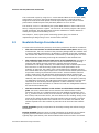
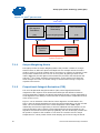
Figure 3-1 illustrates the combination of the different thermal characterization
parameters.
Figure 3-1. Processor Thermal Characterization Parameter Relationships
TA
ΨCA
Heatsink
TS
TIM
IHS
TC
Processor
LGA775 Socket
System Board
3.1.1
Example
The cooling performance, ΨCA, is defined using the principle of thermal
characterization parameter described above:
•
The case temperature TC-MAX and thermal design power TDP given in the processor
datasheet.
•
Define a target local ambient temperature at the processor, TA.
Since the processor thermal profile applies to all processor frequencies, it is important
to identify the worst case (lowest ΨCA) for a targeted chassis characterized by TA to
establish a design strategy.
The following provides an illustration of how one might determine the appropriate
performance targets. The example power and temperature numbers used here are not
related to any specific Intel processor thermal specifications, and are for illustrative
purposes only.
28
Thermal and Mechanical Design Guidelines
Thermal Metrology
Assume the TDP, as listed in the datasheet, is 100 W and the maximum case
temperature from the thermal profile for 100 W is 67° C. Assume as well that the
system airflow has been designed such that the local ambient temperature is 38° C.
Then, the following could be calculated using equation 1 from above:
ΨCA = (TC, − TA) / TDP = (67 – 38) / 100 = 0.29° C/W
To determine the required heatsink performance, a heatsink solution provider would
need to determine ΨCS performance for the selected TIM and mechanical load
configuration. If the heatsink solution were designed to work with a TIM material
performing at ΨCS ≤ 0.10° C/W, solving for equation 2 from above, the performance of
the heatsink would be:
ΨSA = ΨCA − ΨCS = 0.29 − 0.10 = 0.19° C/W
3.2
Processor Thermal Solution Performance
Assessment
Thermal performance of a heatsink should be assessed using a thermal test vehicle
(TTV) provided by Intel. The TTV is a stable heat source that the user can make
accurate power measurement, whereas processors can introduce additional factors
that can impact test results. In particular, the power level from actual processors
varies significantly, even when running the maximum power application provided by
Intel, due to variances in the manufacturing process. The TTV provides consistent
power and power density for thermal solution characterization and results can be
easily translated to real processor performance. Accurate measurement of the power
dissipated by an actual processor is beyond the scope of this document.
Once the thermal solution is designed and validated with the TTV, it is strongly
recommended to verify functionality of the thermal solution on real processors and on
fully integrated systems. The Intel maximum power application enables steady power
dissipation on a processor to assist in this testing. This maximum power application is
provided by Intel.
3.3
Local Ambient Temperature Measurement
Guidelines
The local ambient temperature TA is the temperature of the ambient air surrounding
the processor. For a passive heatsink, TA is defined as the heatsink approach air
temperature; for an actively cooled heatsink, it is the temperature of inlet air to the
active cooling fan.
It is worthwhile to determine the local ambient temperature in the chassis around the
processor to understand the effect it may have on the case temperature.
TA is best measured by averaging temperature measurements at multiple locations in
the heatsink inlet airflow. This method helps reduce error and eliminate minor spatial
variations in temperature. The following guidelines are meant to enable accurate
determination of the localized air temperature around the processor during system
thermal testing.
Thermal and Mechanical Design Guidelines
29
Thermal Metrology
For active heatsinks, it is important to avoid taking measurement in the dead flow
zone that usually develops above the fan hub and hub spokes. Measurements should
be taken at four different locations uniformly placed at the center of the annulus
formed by the fan hub and the fan housing to evaluate the uniformity of the air
temperature at the fan inlet. The thermocouples should be placed approximately
3 mm to 8 mm [0.1 to 0.3 in] above the fan hub vertically and halfway between the
fan hub and the fan housing horizontally as shown in the ATX heatsink in Figure 3-2
(avoiding the hub spokes). Using an open bench to characterize an active heatsink can
be useful, and usually ensures more uniform temperatures at the fan inlet. However,
additional tests that include a solid barrier above the test motherboard surface can
help evaluate the potential impact of the chassis. This barrier is typically clear
Plexiglas*, extending at least 100 mm [4 in] in all directions beyond the edge of the
thermal solution. Typical distance from the motherboard to the barrier is 81 mm
[3.2 in]. For even more realistic airflow, the motherboard should be populated with
significant elements like memory cards, graphic card, and chipset heatsink. If a barrier
is used, the thermocouple can be taped directly to the barrier with a clear tape at the
horizontal location as previously described, half way between the fan hub and the fan
housing. If a variable speed fan is used, it may be useful to add a thermocouple taped
to the barrier above the location of the temperature sensor used by the fan to check
its speed setting against air temperature. When measuring TA in a chassis with a live
motherboard, add-in cards, and other system components, it is likely that the TA
measurements will reveal a highly non-uniform temperature distribution across the
inlet fan section.
For passive heatsinks, thermocouples should be placed approximately 13 mm to
25 mm [0.5 to 1.0 in] away from processor and heatsink as shown in Figure 3-3. The
thermocouples should be placed approximately 51 mm [2.0 in] above the baseboard.
This placement guideline is meant to minimize the effect of localized hot spots from
baseboard components.
Note: Testing an active heatsink with a variable speed fan can be done in a thermal chamber
to capture the worst-case thermal environment scenarios. Otherwise, when doing a
bench top test at room temperature, the fan regulation prevents the heatsink from
operating at its maximum capability. To characterize the heatsink capability in the
worst-case environment in these conditions, it is then necessary to disable the fan
regulation and power the fan directly, based on guidance from the fan supplier.
30
Thermal and Mechanical Design Guidelines
Thermal Metrology
Figure 3-2. Locations for Measuring Local Ambient Temperature, Active ATX Heatsink
Note: Drawing Not to Scale
Figure 3-3. Locations for Measuring Local Ambient Temperature, Passive Heatsink
Note: Drawing Not to Scale
Thermal and Mechanical Design Guidelines
31
Thermal Metrology
3.4
Processor Case Temperature Measurement
Guidelines
To ensure functionality and reliability, the processor is specified for proper operation
when TC is maintained at or below the thermal profile as listed in the datasheet. The
measurement location for TC is the geometric center of the IHS. Figure 2-2 shows the
location for TC measurement.
Special care is required when measuring TC to ensure an accurate temperature
measurement. Thermocouples are often used to measure TC. Before any temperature
measurements are made, the thermocouples must be calibrated, and the complete
measurement system must be routinely checked against known standards. When
measuring the temperature of a surface that is at a different temperature from the
surrounding local ambient air, errors could be introduced in the measurements. The
measurement errors could be caused by poor thermal contact between the junction of
the thermocouple and the surface of the integrated heat spreader, heat loss by
radiation, convection, by conduction through thermocouple leads, or by contact
between the thermocouple cement and the heatsink base.
Appendix D defines a reference procedure for attaching a thermocouple to the IHS of
a 775-Land LGA processor package for TC measurement. This procedure takes into
account the specific features of the 775-Land LGA package and of the LGA775 socket
for which it is intended.
§
32
Thermal and Mechanical Design Guidelines
Thermal Management Logic and Thermal Monitor Feature
4
Thermal Management Logic and
Thermal Monitor Feature
4.1
Processor Power Dissipation
An increase in processor operating frequency not only increases system performance,
but also increases the processor power dissipation. The relationship between
frequency and power is generalized in the following equation:
2
P = CV F (where P = power, C = capacitance, V = voltage, F = frequency)
From this equation, it is evident that power increases linearly with frequency and with
the square of voltage. In the absence of power saving technologies, ever increasing
frequencies will result in processors with power dissipations in the hundreds of watts.
Fortunately, there are numerous ways to reduce the power consumption of a
processor, and Intel is aggressively pursuing low power design techniques. For
example, decreasing the operating voltage, reducing unnecessary transistor activity,
and using more power efficient circuits can significantly reduce processor power
consumption.
An on-die thermal management feature called Thermal Monitor is available on the
processor. It provides a thermal management approach to support the continued
increases in processor frequency and performance. By using a highly accurate on-die
temperature sensing circuit and a fast acting Thermal Control Circuit (TCC), the
processor can rapidly initiate thermal management control. The Thermal Monitor can
reduce cooling solution cost, by allowing thermal designs to target TDP.
The processor also supports an additional power reduction capability known as
Thermal Monitor 2 described in Section 4.2.3.
4.2
Thermal Monitor Implementation
The Thermal Monitor consists of the following components:
•
A highly accurate on-die temperature sensing circuit
•
A bi-directional signal (PROCHOT#) that indicates if the processor has exceeded
its maximum temperature or can be asserted externally to activate the Thermal
Control Circuit (TCC) (see Section 4.2.1 for more details on user activation of TCC
using the PROCHOT# signal)
•
A Thermal Control Circuit that will attempt to reduce processor temperature by
rapidly reducing power consumption when the on-die temperature sensor indicates
that it has exceeded the maximum operating point.
•
Registers to determine the processor thermal status.
Thermal and Mechanical Design Guidelines
33
Thermal Management Logic and Thermal Monitor Feature
4.2.1
PROCHOT# Signal
The primary function of the PROCHOT# signal is to provide an external indication that
the processor has reached the TCC activation temperature. While PROCHOT# is
asserted, the TCC will be activated. Assertion of the PROCHOT# signal is independent
of any register settings within the processor. It is asserted any time the processor die
temperature reaches the trip point.
PROCHOT# can be configured using BIOS as an output or bi-directional signal. As an
output, PROCHOT# will go active when the processor temperature of either core
reaches the TCC activation temperature. As an input, assertion of PROCHOT# will
activate the TCC for both cores. The TCC will remain active until the system de-asserts
PROCHOT#
The temperature at which the PROCHOT# signal goes active is individually calibrated
during manufacturing. Once configured, the processor temperature at which the
PROCHOT# signal is asserted is not re-configurable.
One application of the Bi-directional PROCHOT# is for the thermal protection of
voltage regulators (VR). System designers can implement a circuit to monitor the VR
temperature and activate the TCC when the temperature limit of the VR is reached. By
asserting PROCHOT# (pulled-low) which activates the TCC, the VR can cool down as a
result of reduced processor power consumption. Bi-directional PROCHOT# can allow
VR thermal designs to target maximum sustained current instead of maximum
current. Systems should still provide proper cooling for the VR, and rely on bidirectional PROCHOT# signal only as a backup in case of system cooling failure.
Note: A thermal solution designed to meet the thermal profile specifications should rarely
experience activation of the TCC as indicated by the PROCHOT# signal going active.
4.2.2
Thermal Control Circuit
The Thermal Control Circuit portion of the Thermal Monitor must be enabled for the
processor to operate within specifications. The Thermal Monitor’s TCC, when active,
will attempt to lower the processor temperature by reducing the processor power
consumption. There are two methods by which TCC can reduce processor power
dissipation. These methods are referred to as Thermal Monitor 1 (TM1) and Thermal
Monitor 2 (TM2).
4.2.2.1
Thermal Monitor
In the original implementation of thermal monitor this is done by changing the duty
cycle of the internal processor clocks, resulting in a lower effective frequency. When
active, the TCC turns the processor clocks off and then back on with a predetermined
duty cycle. The duty cycle is processor specific, and is fixed for a particular processor.
The maximum time period the clocks are disabled is ~3 µs. This time period is
frequency dependent and higher frequency processors will disable the internal clocks
for a shorter time period. Figure 4-1 illustrates the relationship between the internal
processor clocks and PROCHOT#.
Performance counter registers, status bits in model specific registers (MSRs), and the
PROCHOT# output pin are available to monitor the Thermal Monitor behavior.
34
Thermal and Mechanical Design Guidelines
Thermal Management Logic and Thermal Monitor Feature
Figure 4-1. Thermal Monitor Control
PROCHOT#
Normal clock
Internal clock
Duty cycle
control
Resultant
internal clock
4.2.3
Thermal Monitor 2
The second method of power reduction is TM2. TM2 provides an efficient means of
reducing the power consumption within the processor and limiting the processor
temperature.
When TM2 is enabled, and a high temperature situation is detected, the enhanced TCC
will be activated. The enhanced TCC causes the processor to adjust its operating
frequency (by dropping the bus-to-core multiplier to its minimum available value) and
input voltage identification (VID) value. This combination of reduced frequency and
VID results in a reduction in processor power consumption.
A processor enabled for TM2 includes two operating points, each consisting of a
specific operating frequency and voltage. The first operating point represents the
normal operating condition for the processor.
The second operating point consists of both a lower operating frequency and voltage.
When the TCC is activated, the processor automatically transitions to the new
frequency. This transition occurs very rapidly (on the order of 5 microseconds). During
the frequency transition, the processor is unable to service any bus requests, all bus
traffic is blocked. Edge-triggered interrupts will be latched and kept pending until the
processor resumes operation at the new frequency.
Once the new operating frequency is engaged, the processor will transition to the new
core operating voltage by issuing a new VID code to the voltage regulator. The voltage
regulator must support VID transitions in order to support TM2. During the voltage
change, it will be necessary to transition through multiple VID codes to reach the
target operating voltage. Each step will be one VID table entry (that is, 12.5 mV
steps). The processor continues to execute instructions during the voltage transition.
Operation at the lower voltage reduces the power consumption of the processor,
providing a temperature reduction.
Thermal and Mechanical Design Guidelines
35
Thermal Management Logic and Thermal Monitor Feature
Once the processor has sufficiently cooled, and a minimum activation time has
expired, the operating frequency and voltage transition back to the normal system
operating point. Transition of the VID code will occur first, in order to insure proper
operation once the processor reaches its normal operating frequency. Refer to
Figure 4-2 for an illustration of this ordering.
Figure 4-2. Thermal Monitor 2 Frequency and Voltage Ordering
TTM2
Temperature
PROCHOT#
fMAX
fTM2
Frequency
VID
VIDTM2
VID
Time
Refer to the datasheet for further information on TM2.
4.2.4
Operation and Configuration
Thermal Monitor must be enabled to ensure proper processor operation.
The Thermal Control Circuit feature can be configured and monitored in a number of
ways. OEMs are required to enable the Thermal Control Circuit while using various
registers and outputs to monitor the processor thermal status. The Thermal Control
Circuit is enabled by the BIOS setting a bit in an MSR (model specific register).
Enabling the Thermal Control Circuit allows the processor to attempt to maintain a
safe operating temperature without the need for special software drivers or interrupt
handling routines. When the Thermal Control Circuit has been enabled, processor
power consumption will be reduced after the thermal sensor detects a high
temperature (that is, PROCHOT# assertion). The Thermal Control Circuit and
PROCHOT# transitions to inactive once the temperature has been reduced below the
thermal trip point, although a small time-based hysteresis has been included to
prevent multiple PROCHOT# transitions around the trip point. External hardware can
monitor PROCHOT# and generate an interrupt whenever there is a transition from
active-to-inactive or inactive-to-active. PROCHOT# can also be configured to generate
an internal interrupt which would initiate an OEM supplied interrupt service routine.
36
Thermal and Mechanical Design Guidelines
Thermal Management Logic and Thermal Monitor Feature
Regardless of the configuration selected, PROCHOT# will always indicate the thermal
status of the processor.
The power reduction mechanism of thermal monitor can also be activated manually
using an “on-demand” mode. Refer to Section 4.2.5 for details on this feature.
4.2.5
On-Demand Mode
For testing purposes, the thermal control circuit may also be activated by setting bits
in the ACPI MSRs. The MSRs may be set based on a particular system event (such as,
an interrupt generated after a system event), or may be set at any time through the
operating system or custom driver control thus forcing the thermal control circuit on.
This is referred to as “on-demand” mode. Activating the thermal control circuit may be
useful for thermal solution investigations or for performance implication studies. When
using the MSRs to activate the on-demand clock modulation feature, the duty cycle is
configurable in steps of 12.5%, from 12.5% to 87.5%.
For any duty cycle, the maximum time period the clocks are disabled is ~3 µs. This
time period is frequency dependent, and decreases as frequency increases. To achieve
different duty cycles, the length of time that the clocks are disabled remains constant,
and the time period that the clocks are enabled is adjusted to achieve the desired
ratio. For example, if the clock disable period is 3 µs, and a duty cycle of ¼ (25%) is
selected, the clock on time would be reduced to approximately 1 µs [on time (1 µs) ÷
total cycle time (3 + 1) µs = ¼ duty cycle]. Similarly, for a duty cycle of 7/8 (87.5%),
the clock on time would be extended to 21 µs [21 ÷ (21 + 3) = 7/8 duty cycle].
In a high temperature situation, if the thermal control circuit and ACPI MSRs
(automatic and on-demand modes) are used simultaneously, the fixed duty cycle
determined by automatic mode would take precedence.
Note: On-demand mode cannot activate the power reduction mechanism of Thermal Monitor
2
4.2.6
System Considerations
Intel requires the Thermal Monitor and Thermal Control Circuit to be enabled for all
processors. The thermal control circuit is intended to protect against short term
thermal excursions that exceed the capability of a well designed processor thermal
solution. Thermal Monitor should not be relied upon to compensate for a thermal
solution that does not meet the thermal profile up to the thermal design power (TDP).
Each application program has its own unique power profile, although the profile has
some variability due to loop decisions, I/O activity and interrupts. In general, compute
intensive applications with a high cache hit rate dissipate more processor power than
applications that are I/O intensive or have low cache hit rates.
The processor TDP is based on measurements of processor power consumption while
running various high power applications. This data is used to determine those
applications that are interesting from a power perspective. These applications are then
evaluated in a controlled thermal environment to determine their sensitivity to
activation of the thermal control circuit. This data is used to derive the TDP targets
published in the processor datasheet.
Thermal and Mechanical Design Guidelines
37
Thermal Management Logic and Thermal Monitor Feature
A system designed to meet the thermal profile specification published in the processor
datasheet greatly reduces the probability of real applications causing the thermal
control circuit to activate under normal operating conditions. Systems that do not
meet these specifications could be subject to more frequent activation of the thermal
control circuit depending upon ambient air temperature and application power profile.
Moreover, if a system is significantly under designed, there is a risk that the Thermal
Monitor feature will not be capable of reducing the processor power and temperature
and the processor could shutdown and signal THERMTRIP#.
For information regarding THERMTRIP#, refer to the processor datasheet and to
Section 4.2.8 of this Thermal Design Guidelines.
4.2.7
Operating System and Application Software
Considerations
The Thermal Monitor feature and its thermal control circuit work seamlessly with ACPI
compliant operating systems. The Thermal Monitor feature is transparent to
application software since the processor bus snooping, ACPI timer, and interrupts are
active at all times.
4.2.8
THERMTRIP# Signal
In the event of a catastrophic cooling failure, the processor will automatically shut
down when the silicon temperature has exceeded the TCC activation temperature by
approximately 20 to 25° C. At this point the system bus signal THERMTRIP# goes
active and power must be removed from the processor. THERMTRIP# activation is
independent of processor activity and does not generate any bus cycles. Refer to the
processor datasheet for more information about THERMTRIP#.
The temperature where the THERMTRIP# signal goes active is individually calibrated
during manufacturing and once configuration cannot be changed.
4.2.9
Cooling System Failure Warning
It may be useful to use the PROCHOT# signal as an indication of cooling system
failure. Messages could be sent to the system administrator to warn of the cooling
failure, while the thermal control circuit would allow the system to continue
functioning or allow a normal system shutdown. If no thermal management action is
taken, the silicon temperature may exceed the operating limits, causing THERMTRIP#
to activate and shut down the processor. Regardless of the system design
requirements or thermal solution ability, the Thermal Monitor feature must still be
enabled to ensure proper processor operation.
38
Thermal and Mechanical Design Guidelines
Thermal Management Logic and Thermal Monitor Feature
4.2.10
Digital Thermal Sensor
Multiple digital thermal sensors can be implemented within the package without
adding a pair of signal pins per sensor as required with the thermal diode. The digital
thermal sensor is easier to place in thermally sensitive locations of the processor than
the thermal diode. This is achieved due to a smaller foot print and decreased
sensitivity to noise. Since the DTS is factory set on a per-part basis there is no need
for the health monitor components to be updated at each processor family.
The processor uses the Digital Thermal Sensor (DTS) as the on-die sensor to use for
fan speed control (FSC). The DTS is monitoring the same sensor that activates the
TCC (see Section 4.2.2). Readings from the DTS are relative to the activation of the
TCC. The DTS value where TCC activation occurs is 0 (zero).
A TCONTROL value will be provided for use with DTS. The usage model for TCONTROL with
the DTS as below:
•
If the Digital thermal sensor reading is less than TCONTROL, the fan speed can be
reduced.
•
If the Digital thermal sensor reading is greater than or equal to TCONTROL, then
TC must be maintained at or below the Thermal Profile for the measured power
dissipation.
The DTS TCONTROL value is factory configured and is written into TOFFSET MSR. The BIOS
can read the TOFFSET MSR and provide this value to the fan speed control device.
Figure 4-3. TCONTROL for Digital Thermal Sensor
Note: The processor has only DTS and no thermal diode. The TCONTROL in the MSR is relevant
only to the DTS.
Thermal and Mechanical Design Guidelines
39
Thermal Management Logic and Thermal Monitor Feature
4.2.11
Platform Environmental Control Interface (PECI)
The PECI interface is a proprietary single wire bus between the processor and the
chipset or other health monitoring device. At this time the digital thermal sensor is the
only data being transmitted. For an overview of the PECI interface, see PECI Feature
Set Overview. For additional information on the PECI, see the datasheet.
The PECI bus is available on pin G5 of the LGA 775 socket. Intel chipsets beginning
with the ICH8 have included PECI host controller. The PECI interface and the
Manageability Engine are key elements to the Intel® Quiet System Technology (Intel®
QST), see Chapter 7 and the Intel® Quiet System Technology Configuration and
Tuning Manual.
Intel has worked with many vendors that provide fan speed control devices to provide
PECI host controllers. Consult the local representative for your preferred vendor for
their product plans and availability.
§
40
Thermal and Mechanical Design Guidelines
Balanced Technology Extended (BTX) Thermal/Mechanical Design Information
5
Balanced Technology Extended
(BTX) Thermal/Mechanical
Design Information
5.1
Overview of the BTX Reference Design
The reference thermal module assembly is a Type II BTX compliant design and is
compliant with the reference BTX motherboard keep-out and height recommendations
defined in Section 6.6.
The solution comes as an integrated assembly. An isometric view of the assembly is
provided in Figure 5-4.
5.1.1
Target Heatsink Performance
Table 5–1 provides the target heatsink performance for the processor with the BTX
boundary conditions. The results will be evaluated using the test procedure described
in Section 5.2.
The table also includes a TA assumption of 35.5° C for the Intel reference thermal
solution at the processor fan heatsink inlet discussed in Section 3.3. The analysis
assumes a uniform 35° C external ambient temperature to the chassis of across the
fan inlet, resulting in a temperature rise, TR, of 0.5° C. Meeting TA and ΨCA targets can
maximize processor performance (refer to Sections 2.2, 2.4. and Chapter 4).
Minimizing TR can lead to improved acoustics.
Table 5–1. Balanced Technology Extended (BTX) Type II Reference TMA Performance
Processor
Intel Core™2 Duo Processor E8000
series with 6 MB cache
Intel Core™2 Duo processor E7000
series with 3 MB cache /Intel Pentium®
dual-core processor E6000, E5000 series
with 2 MB cache / Intel® Celeron®
processor E3x00 series with 1 MB cache
Thermal
Requirements,
Ψca
(Mean + 3σ)
TA
Assumption
Notes
0.57 °C/W
35.5 °C
1,2,3
0.594 °C/W
35.5 °C
1,2,3
NOTES:
1.
Performance targets (Ψ ca) as measured with a live processor at TDP.
2.
The difference in Ψ ca between the Intel Core™2 Duo processor E8000 series with
6 MB cache, Intel Core™2 Duo processor E7000 series with 3 MB cache, Intel Pentium®
dual-core processor E6000, E5000 series with 2 MB cache, and Intel® Celeron®
processor E3x00 series is due to a slight difference in the die size.
3.
This data is pre-silicon data, and subject to change with the post silicon validate
results.
Thermal and Mechanical Design Guidelines
41
Balanced Technology Extended (BTX) Thermal/Mechanical Design Information
5.1.2
Acoustics
To optimize acoustic emission by the fan heatsink assembly, the Type II reference
design implements a variable speed fan. A variable speed fan allows higher thermal
performance at higher fan inlet temperatures (TA) and the appropriate thermal
performance with improved acoustics at lower fan inlet temperatures. Using the
example in Table 5–2 for the Intel Core™2 Duo processor with 4 MB cache at TC-MAX of
60.1° C the required fan speed necessary to meet thermal specifications can be
controlled by the fan inlet temperature and should comply with requirements in
Table 5–2.
Table 5–2. Acoustic Targets
Fan Speed
RPM
Thermistor
Set Point
~ 5300
High
TA ≥ 35° C
Acoustic
≤ 6.4 BA
Thermal
Requirements, Ψca
Notes
0.38° C/W
Case 1:
Thermal Design Power
Maximum fan speed
100% PWM duty cycle
~ 2500
Low
TA = 23° C
No Target
Defined
0.56° C/W
Case 2
Thermal Design Power
System (PSU, HDD, TMA)
Fan speed limited by the fan
hub thermistor
~ 1400
Low
TA = 23° C
≤ 3.4 BA
~0.87° C/W
Case 3
50% Thermal Design Power
TMA Only
~ 1400
Low
TA = 23° C
≤ 4.0 BA
~0.87° C/W
Case 3
50% Thermal Design Power
System (PSU, HDD, TMA)
NOTES:
1.
Acoustic performance is defined in terms of measured sound power (LwA) as defined in
ISO 9296 standard, and measured according to ISO 7779.
2.
Acoustic testing will be for the TMA only when installed in a BTX S2 chassis for Case 1
and 3.
3.
Acoustics testing for Case 2 will be system level in the same a BTX S2 reference chassis
and commercially available power supply. Acoustic data for Case 2 will be provided in
the validation report but this condition is not a target for the design. The acoustic
model is predicting that the power supply fan will be the acoustic limiter.
4.
The fan speeds (RPM) are estimates for one of the two reference fans and will be
adjusted to meet thermal performance targets then acoustic target during validation.
The designer should identify the fan speed required to meet the effective fan curve
shown in Section 5.1.3.
While the fan hub thermistor helps optimize acoustics at high processor workloads by
adapting the maximum fan speed to support the processor thermal profile, additional
acoustic improvements can be achieved at lower processor workload by using the
TCONTROL specifications described in Section 2.2.4. Intel’s recommendation is to use the
fan with 4 Wire PWM Controlled to implement fan speed control capability based the
digital thermal sensor. Refer to Chapter 7 for further details.
Note: Appendix F gives detailed fan performance for the Intel reference thermal solutions
with 4 Wire PWM Controlled fan.
42
Thermal and Mechanical Design Guidelines
Balanced Technology Extended (BTX) Thermal/Mechanical Design Information
5.1.3
Effective Fan Curve
The TMA must fulfill the processor cooling requirements shown in Table 5–1 when it is
installed in a functional BTX system. When installed in a system, the TMA must
operate against the backpressure created by the chassis impedance (due to vents,
bezel, peripherals, and so forth) and will operate at lower net airflow than if it were
tested outside of the system on a bench top or open air environment. Therefore, an
allowance must be made to accommodate or predict the reduction in Thermal Module
performance due to the reduction in heatsink airflow from chassis impedance. For this
reason, it is required that the Thermal Module satisfy the prescribed ΨCA requirements
when operating against an impedance that is characteristic for BTX platforms.
Because of the coupling between TMA thermal performance and system impedance,
the designer should understand the TMA effective fan curve. This effective fan curve
represents the performance of the fan component AND the impedance of the stator,
heatsink, duct, and flow partitioning devices. The BTX system integrator can evaluate
a TMA based on the effective fan curve of the assembly and the airflow impedance of
their target system.
Note: It is likely that at some operating points the fans speed will be driven by the system
airflow requirements and not the processor thermal limits.
Figure 5-1 shows the effective fan curve for the reference design TMA. These curves
are based on analysis. The boundary conditions used are the S2 6.9L reference
chassis, the reference TMA with the flow partitioning device, extrusion and an AVC
Type II fan geometry.
When selecting a fan for use in the TMA care should be taken that similar effective fan
curves can be achieved. Final verification requires the overlay of the Type II MASI
curve to ensure thermal compliance.
Thermal and Mechanical Design Guidelines
43
Balanced Technology Extended (BTX) Thermal/Mechanical Design Information
Figure 5-1. Effective TMA Fan Curves with Reference Extrusion
0.400
Reference TMA @ 5300 RPM
0.350
Reference TMA @ 2500 RPM
dP (in. H2O)
0.300
Reference TMA @ 1200 RPM
0.250
0.200
0.150
0.100
0.050
0.000
0.0
5.0
10.0
15.0
20.0
25.0
30.0
35.0
Airflow (cfm )
5.1.4
Voltage Regulator Thermal Management
The BTX TMA is integral to the cooling of the processor voltage regulator (VR). The
reference design TMA will include a flow partitioning device to ensure an appropriate
airflow balance between the TMA and the VR. In validation the need for this
component will be evaluated.
The BTX thermal management strategy relies on the Thermal Module to provide
effective cooling for the voltage regulator (VR) chipset and system memory
components on the motherboard. The Thermal Module is required to have features
that allow for airflow to bypass the heatsink and flow over the VR region on both the
primary and secondary sides of the board. The following requirements apply to VR
cooling.
Table 5–3. VR Airflow Requirements
Item
Minimum VR bypass airflow for
775_VR_CONFIG_06 processors
Target
2.4 CFM
NOTES:
1.
This is the recommended airflow rate that should be delivered to the VR when the VR
power is at a maximum in order to support the 775_VR_CONFIG_06 processors at TDP
power dissipation and the chassis external environment temperature is at 35 ºC. Less
airflow is necessary when the VR power is not at a maximum or if the external ambient
temperature is less than 35 ºC.
2.
This recommended airflow rate is based on the requirements for the Intel 965 Express
Chipset Family.
44
Thermal and Mechanical Design Guidelines
Balanced Technology Extended (BTX) Thermal/Mechanical Design Information
5.1.5
Altitude
The reference TMA will be evaluated at sea level. However, many companies design
products that must function reliably at high altitude, typically 1,500 m [5,000 ft] or
more. Air-cooled temperature calculations and measurements at sea level must be
adjusted to take into account altitude effects like variation in air density and overall
heat capacity. This often leads to some degradation in thermal solution performance
compared to what is obtained at sea level, with lower fan performance and higher
surface temperatures. The system designer needs to account for altitude effects in the
overall system thermal design to make sure that the TC requirement for the processor
is met at the targeted altitude.
5.1.6
Reference Heatsink Thermal Validation
The Intel reference heatsink will be validated within the specific boundary conditions
based on the methodology described Section 5.2 , and using a thermal test vehicle.
Testing is done in a BTX chassis at ambient lab temperature. The test results, for a
number of samples, will be reported in terms of a worst-case mean + 3σ value for
thermal characterization parameter using real processors (based on the thermal test
vehicle correction factors).
5.2
Environmental Reliability Testing
5.2.1
Structural Reliability Testing
Structural reliability tests consist of unpackaged, system -level vibration and shock
tests of a given thermal solution in the assembled state. The thermal solution should
meet the specified thermal performance targets after these tests are conducted;
however, the test conditions outlined here may differ from your own system
requirements.
5.2.1.1
Random Vibration Test Procedure
Recommended performance requirement for a system:
•
Duration: 10 min/axis, 3 axes
•
Frequency Range: 5 Hz to 500 Hz
5 Hz @ .001 g2/Hz to 20 Hz @ 0.01 g2/Hz (slope up)
20 Hz to 500 Hz @ 0.01 g2/Hz (flat)
•
Power Spectral Density (PSD) Profile: 2.2 G RMS
Thermal and Mechanical Design Guidelines
45
Balanced Technology Extended (BTX) Thermal/Mechanical Design Information
Figure 5-2. Random Vibration PSD
Vibration System Level
0.1
+ 3 dB Control Limit
g2/Hz
0.01
- 3 dB Control Limit
0.001
0.0001
1
10
100
1000
Hz
5.2.1.2
Shock Test Procedure
Recommended performance requirement for a system:
• Quantity: 2 drops for + and - directions in each of 3 perpendicular axes (that is,
total 12 drops).
• Profile:
25 G trapezoidal waveform
225 in/sec minimum velocity change. (systems > 20 lbm)
250 in/sec minimum velocity change. (systems < 20 lbm)
• Setup:
Mount sample system on tester.
Figure 5-3. Shock Acceleration Curve
46
Thermal and Mechanical Design Guidelines
Balanced Technology Extended (BTX) Thermal/Mechanical Design Information
5.2.1.2.1
Recommended Test Sequence
Each test sequence should start with components (that is, motherboard, heatsink
assembly, and so forth) that have never been previously submitted to any reliability
testing.
The test sequence should always start with a visual inspection after assembly, and
BIOS/CPU/Memory test (refer to Section 6.3.3).
Prior to the mechanical shock & vibration test, the units under test should be
preconditioned for 72 hours at 45º C. The purpose is to account for load relaxation
during burn-in stage.
The stress test should be followed by a visual inspection and then BIOS/CPU/Memory
test.
5.2.1.2.2
Post-Test Pass Criteria
The post-test pass criteria are:
1. No significant physical damage to the heatsink attach mechanism (including such
items as clip and motherboard fasteners).
2. Heatsink must remain attached to the motherboard.
3. Heatsink remains seated and its bottom remains mated flatly against IHS surface.
No visible gap between the heatsink base and processor IHS. No visible tilt of the
heatsink with respect to its attach mechanism.
4. No signs of physical damage on motherboard surface due to impact of heatsink or
heatsink attach mechanism.
5. No visible physical damage to the processor package.
6. Successful BIOS/Processor/memory test of post-test samples.
7. Thermal compliance testing to demonstrate that the case temperature
specification can be met.
5.2.2
Power Cycling
Thermal performance degradation due to TIM degradation is evaluated using power
cycling testing. The test is defined by 7500 cycles for the case temperature from room
temperature (~23º C) to the maximum case temperature defined by the thermal
profile at TDP. A Thermal Test Vehicle is used for this test.
Thermal and Mechanical Design Guidelines
47
Balanced Technology Extended (BTX) Thermal/Mechanical Design Information
5.2.3
Recommended BIOS/CPU/Memory Test Procedures
This test is to ensure proper operation of the product before and after environmental
stresses, with the thermal mechanical enabling components assembled. The test shall
be conducted on a fully operational motherboard that has not been exposed to any
battery of tests prior to the test being considered.
Testing setup should include the following components, properly assembled and/or
connected:
•
Appropriate system motherboard
•
Processor
•
All enabling components, including socket and thermal solution parts
•
Power supply
•
Disk drive
•
Video card
•
DIMM
•
Keyboard
•
Monitor
The pass criterion is that the system under test shall successfully complete the
checking of BIOS, basic processor functions and memory, without any errors.
5.3
Material and Recycling Requirements
Material shall be resistant to fungal growth. Examples of non-resistant materials
include cellulose materials, animal and vegetable based adhesives, grease, oils, and
many hydrocarbons. Synthetic materials such as PVC formulations, certain
polyurethane compositions (such as, polyester and some polyethers), plastics that
contain organic fillers of laminating materials, paints, and varnishes also are
susceptible to fungal growth. If materials are not fungal growth resistant, then MILSTD-810E, Method 508.4 must be performed to determine material performance.
Material used shall not have deformation or degradation in a temperature life test.
Any plastic component exceeding 25 grams must be recyclable per the European Blue
Angel recycling standards.
48
Thermal and Mechanical Design Guidelines
Balanced Technology Extended (BTX) Thermal/Mechanical Design Information
5.4
Safety Requirements
Heatsink and attachment assemblies shall be consistent with the manufacture of units
that meet the safety standards:
5.5
•
UL Recognition-approved for flammability at the system level. All mechanical and
thermal enabling components must be a minimum UL94V-2 approved.
•
CSA Certification. All mechanical and thermal enabling components must have
CSA certification.
•
All components (in particular the heatsink fins) must meet the test requirements
of UL1439 for sharp edges.
•
If the International Accessibility Probe specified in IEC 950 can access the moving
parts of the fan, consider adding safety feature so that there is no risk of personal
injury.
Geometric Envelope for Intel Reference BTX
Thermal Module Assembly
Figure 7-43 through Figure 7-47 in Appendix G provides the motherboard keep-out
information for the BTX thermal mechanical solutions. Additional information on BTX
design considerations can be found in the Balanced Technology Extended (BTX)
System Design Guide available at http://www.formfactors.org.
The maximum height of the TMA above the motherboard is 60.60 mm [2.386 inches],
for compliance with the motherboard primary side height constraints defined in the
BTX Interface Specification for Zone A, found at http://www.formfactors.org.
Figure 5-4. Intel Type II TMA 65W Reference Design
Development vendor information for the Intel Type II TMA Reference Solution is
provided in Appendix H.
Thermal and Mechanical Design Guidelines
49
Balanced Technology Extended (BTX) Thermal/Mechanical Design Information
5.6
Preload and TMA Stiffness
5.6.1
Structural Design Strategy
Structural design strategy for the Intel Type II TMA is to minimize upward board
deflection during shock to help protect the LGA775 socket.
BTX thermal solutions use the SRM and TMA that together resists local board
curvature under the socket and minimize, board deflection (Figure 5-5). In addition, a
moderate preload provides initial downward deflection.
Figure 5-5. Upward Board Deflection During Shock
Shock Load
Less curvature in region
between SRM and TMA
5.6.2
TMA Preload verse Stiffness
The Thermal Module assembly is required to provide a static preload to ensure
protection against fatigue failure of socket solder joint. The allowable preload range
for BTX platforms is provided in Table 5–4, but the specific target value is a function
of the Thermal Module effective stiffness.
The solution space for the Thermal Module effective stiffness and applied preload
combinations is shown by the shaded region of Figure 5-6. This solution space shows
that the Thermal Module assembly must have an effective stiffness that is sufficiently
large such that the minimum preload determined from the relationship requirement in
Figure 5-6 does not exceed the maximum allowed preload shown in Table 5–4.
Furthermore, if the Thermal Module effective stiffness is so large that the minimum
preload determined from Figure 5-6 is below the minimum required value given in
Table 5–4, then the Thermal Module should be re-designed to have a preload that lies
within the range given in Table 5–4, allowing for preload tolerances.
50
Thermal and Mechanical Design Guidelines
Balanced Technology Extended (BTX) Thermal/Mechanical Design Information
Table 5–4. Processor Preload Limits
Parameter
Processor Preload
Minimum Required
Maximum
Allowed
Notes
98 N [22 lbf]
222 N [50 lbf]
1
NOTES:
1.
These values represent upper and lower bounds for the processor preload. The nominal
preload design point for the Thermal Module is based on a combination of requirements
of the TIM, ease of assembly and the Thermal Module effective stiffness.
Figure 5-6. Minimum Required Processor Preload to Thermal Module Assembly Stiffness
NOTES:
1.
The shaded region shown is the acceptable domain for Thermal Module assembly
effective stiffness and processor preload combinations. The Thermal Module design
should have a design preload and stiffness that lies within this region. The design
tolerance for the preload and TMA stiffness should also reside within this boundary.
Note that the lower and upper horizontal boundaries represent the preload limits
provided in Table 5–4. The equation for the left hand boundary is described in note 2.
2.
The equation for this section of the preload-Thermal Module stiffness boundary is given
by the following relationship: Min Preload = 1.38E-3*k^2 – 1.18486k + 320.24753 for
k < 300 N/mm where k is the Thermal Module assembly effective stiffness. Note that
this equation is only valid in the stiffness domain of 93N/mm < k < 282N/mm. This
equation would not apply, for example, for TMA stiffness less than 93N/mm.
3.
The target stiffness for the 65W Type II TMA reference design is 484 N/mm
(2764 lb / in).
Note: These preload and stiffness recommendations are specific to the TMA mounting
scheme that meets the BTX Interface Specification and Support Retention Mechanism
(SRM) Design Guide. For TMA mounting schemes that use only the motherboard
Thermal and Mechanical Design Guidelines
51
Balanced Technology Extended (BTX) Thermal/Mechanical Design Information
mounting hole position for TMA attach, the required preload is approximately 10–15N
greater than the values stipulated in Figure 5-6; however, Intel has not conducted any
validation testing with this TMA mounting scheme.
Figure 5-7. Thermal Module Attach Pointes and Duct-to-SRM Interface Features
NOTES:
1.
For clarity the motherboard is not shown in this figure. In an actual assembly, the
captive 6x32 screws in the thermal module pass through the rear holes in the
motherboard designated in the socket keep-in Figure 7-43 through Figure 7-47 in
Appendix G and screw into the SRM and chassis PEM features.
2.
This front duct ramp feature has both outer and inner lead-in that allows the feature to
slide easily into the SRM slot and around the chassis PEM nut. Note that the front PEM
nut is part of the chassis not the SRM.
52
Thermal and Mechanical Design Guidelines
ATX Thermal/Mechanical Design Information
6
ATX Thermal/Mechanical
Design Information
6.1
ATX Reference Design Requirements
This chapter will document the requirements for an active air-cooled design, with a fan
installed at the top of the heatsink. The thermal technology required for the processor.
The Intel Core™2 Duo processor E8000, E7000 series, Intel Pentium dual-core
processor E6000, E5000 series, and Intel® Celeron® processor E3x00 series require a
thermal solution equivalent to the E18764-001 reference design; see Figure 6-1 for an
exploded view of this reference design.
Note: The part number E18764-001 provided in this document is for reference only. The
revision number -001 may be subject to change without notice.
The E18764-001 reference design takes advantage of an acoustic improvement to
reduce the fan speed to show the acoustic advantage (its acoustic results show in the
Table 6–2).
The E18764-001 reference design takes advantage of the cost savings for the several
features of the design including the reduced heatsink height, inserted aluminum core
and the new TIM material (Dow Corning TC-1996 grease), see Figure 6-2. The overall
46 mm height thermal solution supports the unique and smaller desktop PCs including
small and ultra small form factors, down to the 5L size, see uATX SFF Guidance for
additional details on uATX SFF design.
Thermal and Mechanical Design Guidelines
53
ATX Thermal/Mechanical Design Information
Figure 6-1. E18764-001 Reference Design – Exploded View
Figure 6-2. Bottom View of Copper Core Applied by TC-1996 Grease
The ATX motherboard keep-out and the height recommendations defined Section 6.6
remain the same for a thermal solution for the processor in the 775-Land LGA
package.
Note: If this fan design is used in your product and you will deliver it to end use customers,
you have the responsibility to determine an adequate level of protection (such as,
protection barriers, a cage, or an interlock) against contact with the energized fan by
the user during user servicing.
Note: Development vendor information for the reference design is provided in Appendix H.
54
Thermal and Mechanical Design Guidelines
ATX Thermal/Mechanical Design Information
6.2
Validation Results for Reference Design
6.2.1
Heatsink Performance
Table 6–1 provides the E18764-001 heatsink performance for the processors of Intel
Core™2 Duo processor E8000 series with 6 MB cache, Intel Core™2 Duo processor
E7000 series with 3 MB cache, Intel Pentium dual-core processor E6000, E5000 series
with 2 MB cache, and Intel® Celeron® processor E3x00 series with 1 MB cache. The
results are based on the test procedure described in Section 6.2.4.
The tables also include a TA assumption of 40° C for the Intel reference thermal
solution at the processor fan heatsink inlet discussed Section 2.4.1.
Table 6–1. E18764-001 Reference Heatsink Performance
Target Thermal
Performance,
Ψca
(Mean + 3σ)
TA
Assumption
Notes
Intel Core™2 Duo processor E8000
series with 6 MB cache
0.50 °C/W
40 °C
1, 2
Intel Core™2 Duo processor E7000
series with 3 MB cache / Intel Pentium
dual-core processor E6000, E5000
series with 2 MB cache / Intel®
Celeron® processor E3x00 series
0.52 °C/W
40 °C
1, 2
Processor
NOTES:
1.
Performance targets (Ψ ca) as measured with a live processor at TDP.
2.
The difference in Ψ ca between the Intel Core™2 Duo processor E8000 series with
6 MB cache and Intel Core™2 Duo processor E7000 series with 3 MB cache, Intel
Pentium dual-core processor E6000, E5000 series with 2 MB cache, and Intel® Celeron®
processor E3x00 series with 1 MB cache is due to a slight difference in the die size.
Thermal and Mechanical Design Guidelines
55
ATX Thermal/Mechanical Design Information
6.2.2
Acoustics
To optimize acoustic emission by the fan heatsink assembly, the reference design
implements a variable speed fan. A variable speed fan allows higher thermal
performance at higher fan inlet temperatures (TA) and lower thermal performance with
improved acoustics at lower fan inlet temperatures. The required fan speed necessary
to meet thermal specifications can be controlled by the fan inlet temperature and
should comply with requirements in Table 6–2.
Table 6–2. Acoustic Results for ATX Reference Heatsink (E18764-001)
Fan
Speed
RPM
Thermist
or Set
Point
Acoustic
Thermal Requirements, Ψca
Notes
• 0.50° C/W (Core™2 Duo processor E8000 series 6
MB)
High
TA = 40° C
3900
5.0 BA
• 0.52° C/W (Core™2 Duo processor E7000 series 3
MB, Pentium dual-core processor E6000, E5000
series 2 MB, and Intel® Celeron® processor E3x00
series with 1 MB)
• 0.65° C/W (Core™2 Duo processor E8000 series
with 6 MB)
Low
TA = 30° C
2000
3.5 BA
• 0.68 °C/W (Core™2 Duo processor E7000 series 3
MB, Pentium dual-core processor E6000, E5000
series 2 MB, and Intel® Celeron® processor E3x00
series with 1 MB)
Thermal Design
Power, Fan
speed limited
by the fan hub
thermistor
NOTES:
1.
Acoustic performance is defined in terms of measured sound power (LwA) as defined in
ISO 9296 standard, and measured according to ISO 7779.
While the fan hub thermistor helps optimize acoustics at high processor workloads by
adapting the maximum fan speed to support the processor thermal profile, additional
acoustic improvements can be achieved at lower processor workload by using the
TCONTROL specifications described in Section 2.2.4. Intel recommendation is to use the
fan with 4 Wire PWM Controlled to implement fan speed control capability based
digital thermal sensor temperature. Refer to Chapter 7 for further details.
Note: Appendix F gives detailed fan performance for the Intel reference thermal solutions
with 4 Wire PWM Controlled fan.
6.2.3
Altitude
Many companies design products that must function reliably at high altitude, typically
1,500 m [5,000 ft] or more. Air-cooled temperature calculations and measurements at
the test site elevation must be adjusted to take into account altitude effects like
variation in air density and overall heat capacity. This often leads to some degradation
in thermal solution performance compared to what is obtained at sea level, with lower
fan performance and higher surface temperatures. The system designer needs to
account for altitude effects in the overall system thermal design to make sure that the
TC requirement for the processor is met at the targeted altitude.
56
Thermal and Mechanical Design Guidelines
ATX Thermal/Mechanical Design Information
6.2.4
Heatsink Thermal Validation
Intel recommends evaluation of the heatsink within the specific boundary conditions
based on the methodology described Section 6.3 , and using a thermal test vehicle.
Testing is done on bench top test boards at ambient lab temperature. In particular, for
the reference heatsink, the Plexiglas* barrier is installed 81.28 mm [3.2 in] above the
motherboard (refer to Sections 3.3 and 6.6).
The test results, for a number of samples, are reported in terms of a worst-case mean
+ 3σ value for thermal characterization parameter using real processors (based on the
thermal test vehicle correction factors).
Note: The above 81.28 mm obstruction height that is used for testing complies with the
recommended obstruction height of 88.9 mm for the ATX form factor. However, it
would conflict with systems in strict compliance with the ATX specification which
allows an obstruction as low as 76.2 mm above the motherboard surface in Area A.
6.3
Environmental Reliability Testing
6.3.1
Structural Reliability Testing
Structural reliability tests consist of unpackaged, board-level vibration and shock tests
of a given thermal solution in the assembled state. The thermal solution should meet
the specified thermal performance targets after these tests are conducted; however,
the test conditions outlined here may differ from your own system requirements.
6.3.1.1
Random Vibration Test Procedure
Duration: 10 min/axis, 3 axes
Frequency Range: 5 Hz to 500 Hz
Power Spectral Density (PSD) Profile: 3.13 G RMS
Thermal and Mechanical Design Guidelines
57
ATX Thermal/Mechanical Design Information
Figure 6-3. Random Vibration PSD
0.1
3.13GRMS (10 minutes per axis)
PSD (g^2/Hz)
(20, 0.02)
(500, 0.02)
(5, 0.01)
0.01
5 Hz
500 Hz
0.001
1
100
10
1000
Frequency (Hz)
6.3.1.2
Shock Test Procedure
Recommended performance requirement for a motherboard:
• Quantity:
3 drops for + and - directions in each of 3 perpendicular axes (that is,
total 18 drops).
• Profile:
50 G trapezoidal waveform, 170 in/sec minimum velocity change.
• Setup:
Mount sample board on test fixture.
Figure 6-4. Shock Acceleration Curve
A
c
c
e
l
e
r
a
t
i
o
n
(g)
60
50
40
30
20
10
0
0
2
4
6
8
10
12
Time (m illiseconds)
58
Thermal and Mechanical Design Guidelines
ATX Thermal/Mechanical Design Information
6.3.1.2.1
Recommended Test Sequence
Each test sequence should start with components (that is, motherboard, heatsink
assembly, and so forth) that have never been previously submitted to any reliability
testing.
The test sequence should always start with a visual inspection after assembly, and
BIOS/CPU/Memory test (refer to Section 6.3.3).
Prior to the mechanical shock & vibration test, the units under test should be
preconditioned for 72 hours at 45 ºC. The purpose is to account for load relaxation
during burn-in stage.
The stress test should be followed by a visual inspection and then BIOS/CPU/Memory
test.
6.3.1.2.2
Post-Test Pass Criteria
The post-test pass criteria are:
1. No significant physical damage to the heatsink attach mechanism (including such
items as clip and motherboard fasteners).
2. Heatsink must remain attached to the motherboard.
3. Heatsink remains seated and its bottom remains mated flatly against IHS surface.
No visible gap between the heatsink base and processor IHS. No visible tilt of the
heatsink with respect to its attach mechanism.
4. No signs of physical damage on motherboard surface due to impact of heatsink or
heatsink attach mechanism.
5. No visible physical damage to the processor package.
6. Successful BIOS/Processor/memory test of post-test samples.
7. Thermal compliance testing to demonstrate that the case temperature
specification can be met.
6.3.2
Power Cycling
Thermal performance degradation due to TIM degradation is evaluated using power
cycling testing. The test is defined by 7500 cycles for the case temperature from room
temperature (~23 ºC) to the maximum case temperature defined by the thermal
profile at TDP.
Thermal and Mechanical Design Guidelines
59
ATX Thermal/Mechanical Design Information
6.3.3
Recommended BIOS/CPU/Memory Test Procedures
This test is to ensure proper operation of the product before and after environmental
stresses, with the thermal mechanical enabling components assembled. The test shall
be conducted on a fully operational motherboard that has not been exposed to any
battery of tests prior to the test being considered.
Testing setup should include the following components, properly assembled and/or
connected:
•
Appropriate system motherboard
•
Processor
•
All enabling components, including socket and thermal solution parts
•
Power supply
•
Disk drive
•
Video card
•
DIMM
•
Keyboard
•
Monitor
The pass criterion is that the system under test shall successfully complete the
checking of BIOS, basic processor functions and memory, without any errors.
6.4
Material and Recycling Requirements
Material shall be resistant to fungal growth. Examples of non-resistant materials
include cellulose materials, animal and vegetable based adhesives, grease, oils, and
many hydrocarbons. Synthetic materials such as PVC formulations, certain
polyurethane compositions (such as, polyester and some polyethers), plastics that
contain organic fillers of laminating materials, paints, and varnishes also are
susceptible to fungal growth. If materials are not fungal growth resistant, then MILSTD-810E, Method 508.4 must be performed to determine material performance.
Material used shall not have deformation or degradation in a temperature life test.
Any plastic component exceeding 25 grams must be recyclable per the European Blue
Angel recycling standards.
60
Thermal and Mechanical Design Guidelines
ATX Thermal/Mechanical Design Information
6.5
Safety Requirements
Heatsink and attachment assemblies shall be consistent with the manufacture of units
that meet the safety standards:
6.6
•
UL Recognition-approved for flammability at the system level. All mechanical and
thermal enabling components must be a minimum UL94V-2 approved.
•
CSA Certification. All mechanical and thermal enabling components must have
CSA certification.
•
All components (in particular the heatsink fins) must meet the test requirements
of UL1439 for sharp edges.
•
If the International Accessibility Probe specified in IEC 950 can access the moving
parts of the fan, consider adding safety feature so that there is no risk of personal
injury.
Geometric Envelope for Intel Reference ATX
Thermal Mechanical Design
Figure 7-40, Figure 7-41, and Figure 7-42 in Appendix G provides detailed reference
ATX/μATX motherboard keep-out information for the reference thermal/mechanical
enabling design. These drawings include height restrictions in the enabling component
region.
The maximum height of the reference solution above the motherboard is 71.12 mm
[2.8 inches], and is compliant with the motherboard primary side height constraints
defined in the ATX Specification revision 2.1 and the microATX Motherboard Interface
Specification revision 1.1 found at http://www.formfactors.org. The reference solution
requires a chassis obstruction height of at least 81.28 mm [3.2 inches], measured
from the top of the motherboard (refer to Sections 3.3 and 6.2.4). This allows for
appropriate fan inlet airflow to ensure fan performance, and therefore overall cooling
solution performance. This is compliant with the recommendations found in both ATX
Specification V2.1 and microATX Motherboard Interface Specification V1.1 documents.
Thermal and Mechanical Design Guidelines
61
ATX Thermal/Mechanical Design Information
6.7
Reference Attach Mechanism
6.7.1
Structural Design Strategy
Structural design strategy for the reference design is to minimize upward board
deflection during shock to help protect the LGA775 socket.
The reference design uses a high clip stiffness that resists local board curvature under
the heatsink, and minimizes, in particular, upward board deflection (Figure 6-5). In
addition, a moderate preload provides initial downward deflection.
Figure 6-5. Upward Board Deflection during Shock
Shock Load
Less curvature in
region under stiff clip
The target metal clip nominal stiffness is 540 N/mm [3100 lb/in]. The combined target
for reference clip and fasteners nominal stiffness is 380 N/mm [2180 lb/in]. The
nominal preload provided by the reference design is 191.3 N ± 44.5 N [43 lb ± 10 lb].
Note: Intel reserves the right to make changes and modifications to the design as necessary
to the reference design, in particular the clip and fastener.
62
Thermal and Mechanical Design Guidelines
ATX Thermal/Mechanical Design Information
6.7.2
Mechanical Interface to the Reference Attach Mechanism
The attach mechanism component from the reference design can be used by other 3rd
party cooling solutions. The attach mechanism consists of:
•
A metal attach clip that interfaces with the heatsink core, see Appendix G,
Figure 7-48 and Figure 7-49 for the component drawings.
•
Four plastic fasteners, see Appendix G, Figure 7-50, Figure 7-51, Figure 7-52 and
Figure 7-53 for the component drawings.
The clip is assembled to heatsink during copper core insertion, and is meant to be
trapped between the core shoulder and the extrusion as shown in Figure 6-6.
Figure 6-6. Reference Clip/Heatsink Assembly
Clip
Core shoulder
traps clip in place
The mechanical interface with the reference attach mechanism is defined in Figure 6-7
and Figure 6-8. Complying with the mechanical interface parameters is critical to
generating a heatsink preload compliant with the minimum preload requirement given
in Section 2.1.2.2.
Additional requirements for the reference attach mechanism (clip and fasteners)
include:
•
Heatsink/fan mass ≤ 550 g (that is, total assembly mass, including clip and
fasteners < 595 g
•
Whole assembly center of gravity ≤ 25.4 mm, measured from the top of the IHS
Whole assembly = Heatsink + Fan + Attach clip + Fasteners
Thermal and Mechanical Design Guidelines
63
ATX Thermal/Mechanical Design Information
Figure 6-7. Critical Parameters for Interfacing to Reference Clip
Fan
Fin Array
Core
See Detail A
Clip
Fin Array
Clip
1.6 mm
Core
Detail A
Figure 6-8. Critical Core Dimension
Φ38.68 +/- 0.30 mm
Φ36.14 +/- 0.10 mm
Gap required to avoid
core surface blemish
during clip assembly.
Recommend 0.3 mm min.
1.00 +/- 0.10 mm
Core
1.00 mm min
R 0.40 mm max
R 0.40 mm max
2.596 +/- 0.10 mm
NOTE: Dimension from the bottom of the clip to the bottom of the
heatsink core (or base) should be met to enable the required
load from the heatsink clip (i.e., 43 lbf nominal +/- 10 lbf)
§
64
Thermal and Mechanical Design Guidelines
Intel® Quiet System Technology (Intel® QST)
7
Intel® Quiet System
Technology (Intel® QST)
In the Intel 965 Express Family Chipset a new control algorithm for fan speed control
is being introduced. It is composed of an Intel Management Engine (ME) in the
Graphics Memory Controller Hub (GMCH) which executes the Intel Quiet System
Technology (Intel QST) algorithm and the ICH8 containing the sensor bus and fan
control circuits.
The ME provides integrated fan speed control in lieu of the mechanisms available in a
SIO or a stand-alone ASIC. The Intel QST is time based as compared to the linear or
state control used by the current generation of FSC devices.
A short discussion of Intel QST will follow along with thermal solution design
recommendations. For a complete discussion of programming the Intel QST in the ME
Consult the Intel® Quiet System Technology (Intel® QST) Configuration and Tuning
Manual.
Note: Fan speed control algorithms and Intel QST in particular rely on a thermal solution
being compliant to the processor thermal profile. It is unlikely that any fan speed
control algorithm can compensate for a non-compliant thermal solution. See Chapter 5
and Chapter 6 for thermal solution requirements that should be met before evaluating
or configuring a system with Intel QST.
7.1
Intel® QST Algorithm
The objective of Intel QST is to minimize the system acoustics by more closely
controlling the thermal sensors to the corresponding processor or chipset device
TCONTROL value. This is achieved by the use of a Proportional-Integral-Derivative (PID)
control algorithm and a Fan Output Weighting Matrix. The PID algorithm takes into
account the difference between the current temperature and the target (TCONTROL), the
rate of change and direction of change to minimize the required fan speed change.
The Fan Output Weighting Matrix uses the effects of each fan on a thermal sensor to
minimize the required fan speed changes.
Figure 7-1 shows in a very simple manner how Intel QST works. See the Intel Quiet
System Technology (Intel® QST) Configuration and Tuning Manual for a detail
discussion of the inputs and response.
Thermal and Mechanical Design Guidelines
65
Intel® Quiet System Technology (Intel® QST)
Figure 7-1. Intel® QST Overview
Intel® QST
Temperature sensing
and response
Calculations
Fan to sensor
Relationship
Fan Commands
(PID)
(Output Weighting Matrix)
(PID)
PECI / SST
PWM
Temperature
Sensors
Fans
System Response
7.1.1
Output Weighting Matrix
Intel QST provides an Output Weighting Matrix that provides a means for a single
thermal sensor to affect the speed of multiple fans. An example of how the matrix
could be used is if a sensor located next to the memory is sensitive to changes in both
the processor heatsink fan and a 2nd fan in the system. By placing a factor in this
matrix additional, the Intel QST could command the processor thermal solution fan
and this 2nd fan to both accelerate a small amount. At the system level these two
small changes can result in a smaller change in acoustics than having a single fan
respond to this sensor.
7.1.2
Proportional-Integral-Derivative (PID)
The use of Proportional-Integral-Derivative (PID) control algorithms allow the
magnitude of fan response to be determined based upon the difference between
current temperature readings and specific temperature targets. A major advantage of
a PID Algorithm is the ability to control the fans to achieve sensor temperatures much
closer to the TCONTROL.
Figure 7-2 is an illustration of the PID fan control algorithm. As illustrated in the
figure, when the actual temperature is below the target temperature, the fan will slow
down. The current FSC devices have a fixed temperature versus PWM output
relationship and miss this opportunity to achieve additional acoustic benefits. As the
actual temperature starts ramping up and approaches the target temperature, the
algorithm will instruct the fan to speed up gradually, but will not abruptly increase the
fan speed to respond to the condition. It can allow an overshoot over the target
temperature for a short period of time while ramping up the fan to bring the actual
66
Thermal and Mechanical Design Guidelines
Intel® Quiet System Technology (Intel® QST)
temperature to the target temperature. As a result of its operation, the PID control
algorithm can enable an acoustic-friendly platform.
Figure 7-2. PID Controller Fundamentals
Integral (time averaged)
Temperature
Actual
Temperature
Limit
Temperature
+ dPWM
Derivative (Slope)
Time
RPM
- dPWM
Proportional
Error
Fan
Speed
For a PID algorithm to work limit temperatures are assigned for each temperature
sensor. For Intel QST, the TCONTROL for the processor and chipset are to be used as the
limit temperature. The ME will measure the error, slope and rate of change using the
equations below:
•
Proportional Error (P) = TLIMIT – TACTUAL
•
Integral (I) = Time averaged error
•
Derivative (D) = ΔTemp / ΔTime
Three gain values are used to control response of algorithm.
•
Kp = proportional gain
•
Ki = Integral gain
•
Kd = derivative gain
The Intel® Quiet System Technology (Intel® QST) Configuration and Tuning Manual
provides initial values for the each of the gain constants. In addition it provides a
methodology to tune these gain values based on system response.
Finally, the fan speed change will be calculated using the following formula:
ΔPWM = -P*(Kp) – I*(Ki) + D*(Kd)
Thermal and Mechanical Design Guidelines
67
Intel® Quiet System Technology (Intel® QST)
7.2
Board and System Implementation of Intel® QST
To implement Intel QST, the board must be configured as shown in Figure 7-3 and
listed below:
•
ME system (S0–S1) with Controller Link connected and powered
•
DRAM with Channel A DIMM 0 installed and 2 MB reserved for Intel QST FW
execution
•
SPI Flash with sufficient space for the Intel QST Firmware
•
SST-based thermal sensors to provide board thermal data for Intel QST algorithms
•
Intel QST firmware
Figure 7-3. Intel® QST Platform Requirements
Processor
Intel® (G)MCH
DRAM
DRAM
ME
ME
Controller Link
Intel®
ICH8
FSC
Control
SPI
SPI
Flash
SST
Sensor
Note: Simple Serial Transport (SST) is a single wire bus that is included in the ICH8 to
provide additional thermal and voltage sensing capability to the Intel Management
Engine (ME).
68
Thermal and Mechanical Design Guidelines
Intel® Quiet System Technology (Intel® QST)
Figure 7-4 shows the major connections for a typical implementation that can support
processors with Digital thermal sensor or a thermal diode. In this configuration a SST
Thermal Sensor has been added to read the on-die thermal diode that is in all of the
processors in the 775-land LGA packages shipped before the Intel Core™2 Duo
processor. With the proper configuration information, the ME can accommodate inputs
from PECI or SST for the processor socket. Additional SST sensors can be added to
monitor system thermal (see 0 for BTX recommendations for placement).
Figure 7-4. Example Acoustic Fan Speed Control Implementation
Intel has engaged with a number of major manufacturers of thermal / voltage sensors
to provide devices for the SST bus. Contact your Intel Field Sales representative for
the current list of manufacturers and visit their web sites or local sales representatives
for a part suitable for your design.
Thermal and Mechanical Design Guidelines
69
Intel® Quiet System Technology (Intel® QST)
7.3
Intel® QST Configuration and Tuning
Initial configuration of the Intel QST is the responsibility of the board manufacturer.
The SPI flash should be programmed with the hardware configuration of the
motherboard and initial settings for fan control, fan monitoring, voltage and thermal
monitoring. This initial data is generated using the Intel provided Configuration Tool.
At the system integrator, the Configuration Tool can be used again but this time to
tune the Intel QST subsystem to reflect the shipping system configuration. In the
tuning process the Intel QST can be modified to have the proper relationships between
the installed fans and sensors in the shipping system. A Weighting Matrix Utility and
Intel QST Log program are planned to assist in optimizing the fan management and
achieve acoustic goal.
Contact your Intel field sales representative for availability of these tools.
7.4
Fan Hub Thermistor and Intel® QST
There is no closed loop control between Intel QST and the thermistor; however, they
can work in tandem to provide the maximum fan speed reduction. The BTX reference
design includes a thermistor on the fan hub. This Variable Speed Fan curve will
determine the maximum fan speed as a function of the inlet ambient temperature and
by design provides a ΨCA sufficient to meet the thermal profile of the processor. Intel
QST, by measuring the processor Digital thermal sensor, will command the fan to
reduce speed below the VSF curve in response to processor workload. Conversely if
the processor workload increases, the FSC will command the fan using the PWM duty
cycle to accelerate the fan up to the limit imposed by the VSF curve. Care needs to be
taken in BTX designs to ensure the fan speed at the minimum operating speed
provides sufficient air flow to support the other system components.
Figure 7-5. Digital Thermal Sensor and Thermistor
Variable Speed Fan (VSF) Curve
Full
Speed
Min.
Operating
Fan Speed
Fan Speed
Operating Range
with FSC
(% PWM Duty Cycle)
Fan Speed
(RPM)
100 %
Min %
30
38
34
Inlet Temperature (°C)
70
Thermal and Mechanical Design Guidelines
LGA775 Socket Heatsink Loading
Appendix A LGA775 Socket Heatsink
Loading
A.1
LGA775 Socket Heatsink Considerations
Heatsink clip load is traditionally used for:
•
Mechanical performance in mechanical shock and vibration
Refer to Section 6.7.1 for the information on the structural design strategy for the
reference design
•
Thermal interface performance
Required preload depends on TIM
Preload can be low for thermal grease
In addition to mechanical performance in shock and vibration and TIM performance,
LGA775 socket requires a minimum heatsink preload to protect against fatigue failure
of socket solder joints.
Solder ball tensile stress is originally created when, after inserting a processor into the
socket, the LGA775 socket load plate is actuated. In addition, solder joint shear stress
is caused by coefficient of thermal expansion (CTE) mismatch induced shear loading.
The solder joint compressive axial force (Faxial) induced by the heatsink preload helps
to reduce the combined joint tensile and shear stress.
Overall, the heatsink required preload is the minimum preload needed to meet all of
the above requirements—Mechanical shock and vibration and TIM performance AND
LGA775 socket protection against fatigue failure.
A.2
Metric for Heatsink Preload for ATX/uATX
Designs Non-Compliant with Intel®
Reference Design
A.3
Heatsink Preload Requirement Limitations
Heatsink preload by itself is not an appropriate metric for solder joint force across
various mechanical designs and does not take into account for example (not an
exhaustive list):
•
•
•
•
Heatsink mounting hole span
Heatsink clip/fastener assembly stiffness and creep
Board stiffness and creep
Board stiffness is modified by fixtures like backing plate, chassis attach, and so
forth.
Thermal and Mechanical Design Guidelines
71
LGA775 Socket Heatsink Loading
Simulation shows that the solder joint force (Faxial) is proportional to the board
deflection measured along the socket diagonal. The matching of Faxial required to
protect the LGA775 socket solder joint in temperature cycling is equivalent to
matching a target MB deflection.
Therefore, the heatsink preload for LGA775 socket solder joint protection against
fatigue failure can be more generally defined as the load required to create a target
board downward deflection throughout the life of the product
This board deflection metric provides guidance for mechanical designs that differ from
the reference design for ATX//µATX form factor.
A.3.1
Motherboard Deflection Metric Definition
Motherboard deflection is measured along either diagonal (refer to Figure 7-6):
d = dmax – (d1 + d2)/2
d’ = dmax – (d’1 + d’2)/2
Configurations in which the deflection is measured are defined in the Table 7–1.
To measure board deflection, follow industry standard procedures (such as IPC) for
board deflection measurement. Height gauges and possibly dial gauges may also be
used.
Table 7–1. Board Deflection Configuration Definitions
Configuration
Parameter
Processor + Socket
load plate
Heatsink
Parameter Name
d_ref
yes
no
BOL deflection, no preload
d_BOL
yes
yes
BOL deflection with preload
d_EOL
yes
yes
EOL deflection
NOTES:
BOL: Beginning of Life
EOL: End of Life
72
Thermal and Mechanical Design Guidelines
LGA775 Socket Heatsink Loading
Figure 7-6. Board Deflection Definition
d’1
d1
d2
d’2
A.3.2
Board Deflection Limits
Deflection limits for the ATX/µATX form factor are:
d_BOL – d_ref≥ 0.09 mm and d_EOL – d_ref ≥ 0.15 mm
And
d’_BOL – d’_ref≥ 0.09 mm and d_EOL’ – d_ref’ ≥ 0.15 mm
NOTES:
1.
The heatsink preload must remain within the static load limits defined in the processor
datasheet at all times.
2.
Board deflection should not exceed motherboard manufacturer specifications.
Thermal and Mechanical Design Guidelines
73
LGA775 Socket Heatsink Loading
A.3.3
Board Deflection Metric Implementation Example
This section is for illustration only, and relies on the following assumptions:
•
72 mm x 72 mm hole pattern of the reference design
•
Board stiffness = 900 lb/in at BOL, with degradation that simulates board creep
over time
Though these values are representative, they may change with selected material
and board manufacturing process. Check with your motherboard vendor.
•
Clip stiffness assumed constant – No creep.
Using Figure 7-7, the heatsink preload at beginning of life is defined to comply with
d_EOL – d_ref = 0.15 mm depending on clip stiffness assumption.
Note that the BOL and EOL preload and board deflection differ. This is a result of the
creep phenomenon. The example accounts for the creep expected to occur in the
motherboard. It assumes no creep to occur in the clip. However, there is a small
amount of creep accounted for in the plastic fasteners. This situation is somewhat
similar to the reference design.
The impact of the creep to the board deflection is a function of the clip stiffness:
•
The relatively compliant clips store strain energy in the clip under the BOL preload
condition and tend to generate increasing amounts of board deflection as the
motherboard creeps under exposure to time and temperature.
•
In contrast, the stiffer clips stores very little strain energy, and therefore do not
generate substantial additional board deflection through life.
NOTES:
1.
Board and clip creep modify board deflection over time and depends on board stiffness,
clip stiffness, and selected materials.
2.
Designers must define the BOL board deflection that will lead to the correct end of life
board deflection.
74
Thermal and Mechanical Design Guidelines
LGA775 Socket Heatsink Loading
Figure 7-7. Example—Defining Heatsink Preload Meeting Board Deflection Limit
A.3.4
Additional Considerations
Intel recommends to design to {d_BOL - d_ref = 0.15 mm} at BOL when EOL
conditions are not known or difficult to assess
The following information is given for illustration only. It is based on the reference
keep-out, assuming there is no fixture that changes board stiffness:
d_ref is expected to be 0.18 mm on average, and be as high as 0.22 mm
As a result, the board should be able to deflect 0.37 mm minimum at BOL
Additional deflection as high as 0.09 mm may be necessary to account for additional
creep effects impacting the board/clip/fastener assembly. As a result, designs could
see as much as 0.50 mm total downward board deflection under the socket.
In addition to board deflection, other elements need to be considered to define the
space needed for the downward board total displacement under load, like the potential
interference of through-hole mount component pin tails of the board with a
mechanical fixture on the back of the board.
NOTES:
1.
The heatsink preload must remain below the maximum load limit of the package at all
times (Refer to processor datasheet).
2.
Board deflection should not exceed motherboard manufacturer specifications.
Thermal and Mechanical Design Guidelines
75
LGA775 Socket Heatsink Loading
A.3.4.1
Motherboard Stiffening Considerations
To protect LGA775 socket solder joint, designers need to drive their mechanical design
to:
•
Allow downward board deflection to put the socket balls in a desirable force state
to protect against fatigue failure of socket solder joint (refer to Sections A.3,
A.3.1, and A.3.2.
•
Prevent board upward bending during mechanical shock event.
•
Define load paths that keep the dynamic load applied to the package within
specifications published in the processor datasheet.
Limiting board deflection may be appropriate in some situations like:
•
Board bending during shock
•
Board creep with high heatsink preload
However, the load required to meet the board deflection recommendation (refer to
Section A.3.2) with a very stiff board may lead to heatsink preloads exceeding
package maximum load specification. For example, such a situation may occur when
using a backing plate that is flush with the board in the socket area, and prevents the
board to bend underneath the socket.
A.4
Heatsink Selection Guidelines
Evaluate carefully heatsinks coming with motherboard stiffening devices (like backing
plates), and conduct board deflection assessments based on the board deflection
metric.
Solutions derived from the reference design comply with the reference heatsink
preload, for example:
•
The Boxed Processor
•
The reference design (E18764-001)
Intel will collaborate with vendors participating in its third party test house program to
evaluate third party solutions. Vendor information now is available in Intel Core™2
Duo Processor Support Components webpage www.intel.com/go/thermal_Core2Duo .
§
76
Thermal and Mechanical Design Guidelines
Heatsink Clip Load Metrology
Appendix B Heatsink Clip Load
Metrology
B.1
Overview
This appendix describes a procedure for measuring the load applied by the
heatsink/clip/fastener assembly on a processor package.
This procedure is recommended to verify the preload is within the design target range
for a design, and in different situations. For example:
•
Heatsink preload for the LGA775 socket
•
Quantify preload degradation under bake conditions.
Note: This document reflects the current metrology used by Intel. Intel is continuously
exploring new ways to improve metrology.
B.2
Test Preparation
B.2.1
Heatsink Preparation
Three load cells are assembled into the base of the heatsink under test, in the area
interfacing with the processor Integrated Heat Spreader (IHS), using load cells
equivalent to those listed in Section B.2.2.
To install the load cells, machine a pocket in the heatsink base, as shown in
Figure 7-8 and Figure 7-9. The load cells should be distributed evenly, as close as
possible to the pocket walls. Apply wax around the circumference of each load cell and
the surface of the pocket around each cell to maintain the load cells in place during
the heatsink installation on the processor and motherboard (Refer to
Figure 7-9).
The depth of the pocket depends on the height of the load cell used for the test. It is
necessary that the load cells protrude out of the heatsink base. However, this
protrusion should be kept minimal, as it will create additional load by artificially raising
the heatsink base. The measurement offset depends on the whole assembly stiffness
(that is, motherboard, clip, fastener, and so forth). For example, the reference design
clip and fasteners assembly stiffness is around 380 N/mm [2180 lb/in]. In that case, a
protrusion of 0.038 mm [0.0015”] will create an extra load of 15 N [3.3 lb].
Figure 7-10 shows an example using the reference design.
Note: When optimizing the heatsink pocket depth, the variation of the load cell height should
also be taken into account to make sure that all load cells protrude equally from the
heatsink base. It may be useful to screen the load cells prior to installation to
minimize variation.
Thermal and Mechanical Design Guidelines
77
Heatsink Clip Load Metrology
Remarks: Alternate Heatsink Sample Preparation
As mentioned above, making sure that the load cells have minimum protrusion out of
the heatsink base is paramount to meaningful results. An alternate method to make
sure that the test setup will measure loads representative of the non-modified design
is:
•
Machine the pocket in the heat sink base to a depth such that the tips of the load
cells are just flush with the heat sink base
•
Then machine back the heatsink base by around 0.25 mm [0.01”], so that the
load cell tips protrude beyond the base.
Proceeding this way, the original stack height of the heatsink assembly should be
preserved. This should not affect the stiffness of the heatsink significantly.
Figure 7-8. Load Cell Installation in Machined Heatsink Base Pocket – Bottom View
Heatsink Base Pocket
Diameter ~ 29 mm
[~1.15”]
Package IHS
Outline (Top
Surface)
Load Cells
78
Thermal and Mechanical Design Guidelines
Heatsink Clip Load Metrology
Figure 7-9. Load Cell Installation in Machined Heatsink Base Pocket – Side View
Wax to maintain load cell in
position during heatsink
installation
Height of
pocket ~
height of
selected load
cell
Load cell protrusion
(Note: to be optimized depending on
assembly stiffness)
Figure 7-10. Preload Test Configuration
Preload Fixture (copper
core with milled out pocket)
Load Cells (3x)
Thermal and Mechanical Design Guidelines
79
Heatsink Clip Load Metrology
B.2.2
Typical Test Equipment
For the heatsink clip load measurement, use equivalent test equipment to the one
listed in Table 7–2.
Table 7–2. Typical Test Equipment
Item
Load cell
Notes: 1, 5
Part Number
(Model)
Description
Honeywell*-Sensotec* Model 13 subminiature
load cells, compression only
AL322BL
Select a load range depending on load level
being tested.
www.sensotec.com
Data Logger (or
scanner)
Notes: 2, 3, 4
Vishay* Measurements Group Model 6100
scanner with a 6010A strain card (one card
required per channel).
Model 6100
NOTES:
1.
Select load range depending on expected load level. It is usually better, whenever
possible, to operate in the high end of the load cell capability. Check with your load cell
vendor for further information.
2.
Since the load cells are calibrated in terms of mV/V, a data logger or scanner is
required to supply 5 volts DC excitation and read the mV response. An
automated model will take the sensitivity calibration of the load cells and convert the
mV output into pounds.
3.
With the test equipment listed above, it is possible to automate data recording and
control with a 6101-PCI card (GPIB) added to the scanner, allowing it to be connected
to a PC running LabVIEW* or Vishay's StrainSmart* software.
4.
IMPORTANT: In addition to just a zeroing of the force reading at no applied load, it is
important to calibrate the load cells against known loads. Load cells tend to drift.
Contact your load cell vendor for calibration tools and procedure information.
5.
When measuring loads under thermal stress (bake for example), load cell thermal
capability must be checked, and the test setup must integrate any hardware used along
with the load cell. For example, the Model 13 load cells are temperature compensated
up to 71° C, as long as the compensation package (spliced into the load cell's wiring) is
also placed in the temperature chamber. The load cells can handle up to 121° C
(operating), but their uncertainty increases according to 0.02% rdg/°F.
B.3
Test Procedure Examples
The following sections provide two examples of load measurement. However, this is
not meant to be used in mechanical shock and vibration testing.
Any mechanical device used along with the heatsink attach mechanism will need to be
included in the test setup (that is, back plate, attach to chassis, and so forth).
Prior to any test, make sure that the load cell has been calibrated against known
loads, following load cell vendor’s instructions.
80
Thermal and Mechanical Design Guidelines
Heatsink Clip Load Metrology
B.3.1
Time-Zero, Room Temperature Preload
Measurement
1. Pre-assemble mechanical components on the board as needed prior to mounting
the motherboard on an appropriate support fixture that replicate the board attach
to a target chassis
•
For example: standard ATX board should sit on ATX compliant stand-offs. If
the attach mechanism includes fixtures on the back side of the board, those
must be included, as the goal of the test is to measure the load provided by
the actual heatsink mechanism.
2. Install relevant test vehicle (TTV, processor) in the socket.
3. Assemble the heatsink reworked with the load cells to motherboard as shown for
the reference design example in Figure 7-10, and actuate attach mechanism.
4. Collect continuous load cell data at 1 Hz for the duration of the test. A minimum
time to allow the load cell to settle is generally specified by the load vendors
(often of order of 3 minutes). The time zero reading should be taken at the end of
this settling time.
5. Record the preload measurement (total from all three load cells) at the target time
and average the values over 10 seconds around this target time as well, that is, in
the interval , for example over [target time – 5 seconds ; target time
+5 seconds].
B.3.2
Preload Degradation under Bake Conditions
This section describes an example of testing for potential clip load degradation under
bake conditions.
1. Preheat thermal chamber to target temperature (45 ºC or 85 ºC for example)
2. Repeat time-zero, room temperature preload measurement
3. Place unit into preheated thermal chamber for specified time
4. Record continuous load cell data as follows:
•
Sample rate = 0.1 Hz for first 3 hrs
•
Sample rate = 0.01 Hz for the remainder of the bake test
5. Remove assembly from thermal chamber and set into room temperature
conditions
6. Record continuous load cell data for next 30 minutes at sample rate of 1 Hz.
§
Thermal and Mechanical Design Guidelines
81
Heatsink Clip Load Metrology
82
Thermal and Mechanical Design Guidelines
Thermal Interface Management
Appendix C Thermal Interface
Management
To optimize a heatsink design, it is important to understand the impact of factors
related to the interface between the processor and the heatsink base. Specifically, the
bond line thickness, interface material area, and interface material thermal
conductivity should be managed to realize the most effective thermal solution.
C.1
Bond Line Management
Any gap between the processor integrated heat spreader (IHS) and the heatsink base
degrades thermal solution performance. The larger the gap between the two surfaces,
the greater the thermal resistance. The thickness of the gap is determined by the
flatness and roughness of both the heatsink base and the integrated heat spreader,
plus the thickness of the thermal interface material (for example thermal grease) used
between these two surfaces and the clamping force applied by the heatsink attach
clip(s).
C.2
Interface Material Area
The size of the contact area between the processor and the heatsink base will impact
the thermal resistance. There is, however, a point of diminishing returns. Unrestrained
incremental increases in thermal interface material area do not translate to a
measurable improvement in thermal performance.
C.3
Interface Material Performance
Two factors impact the performance of the interface material between the processor
and the heatsink base:
• Thermal resistance of the material
• Wetting/filling characteristics of the material
Thermal resistance is a description of the ability of the thermal interface material to
transfer heat from one surface to another. The higher the thermal resistance, the less
efficient the interface material is at transferring heat. The thermal resistance of the
interface material has a significant impact on the thermal performance of the overall
thermal solution. The higher the thermal resistance, the larger the temperature drop
is across the interface and the more efficient the thermal solution (heatsink, fan) must
be to achieve the desired cooling.
The wetting or filling characteristic of the thermal interface material is its ability,
under the load applied by the heatsink retention mechanism, to spread and fill the gap
between the processor and the heatsink. Since air is an extremely poor thermal
conductor, the more completely the interface material fills the gaps, the lower the
temperature drops across the interface. In this case, thermal interface material area
also becomes significant; the larger the desired thermal interface material area, the
higher the force required to spread the thermal interface material.
Thermal and Mechanical Design Guidelines
83
Thermal Interface Management
§
84
Thermal and Mechanical Design Guidelines
Case Temperature Reference Metrology
Appendix D Case Temperature
Reference Metrology
D.1
Objective and Scope
This appendix defines a reference procedure for attaching a thermocouple to the IHS
of a 775-land LGA package for TC measurement. This procedure takes into account the
specific features of the 775-land LGA package and of the LGA775 socket for which it is
intended. The recommended equipment for the reference thermocouple installation,
including tools and part numbers are also provided. In addition a video Thermocouple
Attach Using Solder – Video CD-ROM is available that shows the process in real time.
The following supplier can do machining the groove and attaching a thermocouple to
the IHS followed by the reference procedure. The supplier is listed the table below as
a convenience to Intel’s general customers and the list may be subject to change
without notice.
D.2
Supplier
Contact
Phone
Email
Address
THERM-X OF
CALIFORNIA
Ernesto
B Valencia
510-441-7566
Ext. 242
[email protected]
1837 Whipple Road,
Hayward, Ca 94544
Supporting Test Equipment
To apply the reference thermocouple attach procedure, it is recommended to use the
equipment (or equivalent) given in the table below.
Item
Description
Part Number
Measurement and Output
Microscope
Olympus* Light microscope or equivalent
SZ-40
DMM
Digital Multi Meter for resistance measurement
Fluke 79 Series
Thermal Meter
Hand held thermocouple meter
Multiple Vendors
Solder Station (see note 1 for ordering information)
Heater Block
Heater assembly to reflow solder on IHS
30330
Heater
WATLOW120V 150W Firerod
0212G G1A38L12
Transformer
Superior Powerstat transformer
05F857
Thermal and Mechanical Design Guidelines
85
Case Temperature Reference Metrology
Item
Description
Part Number
Miscellaneous Hardware
Solder
Indium Corp. of America
Alloy 57BI / 42SN / 1AG 0.010 Diameter
52124
Flux
Indium Corp. of America
5RMA
Loctite* 498
Adhesive
Super glue w/thermal characteristics
49850
Adhesive
Accelerator
Loctite* 7452 for fast glue curing
18490
Kapton* Tape
For holding thermocouple in place
Not Available
Thermocouple
Omega *,36 gauge, “T” Type
(see note 2 for ordering information)
OSK2K1280/5SR
TC-TT-T-36-72
Calibration and Control
Ice Point Cell
Omega*, stable 0 ºC temperature source for
calibration and offset
TRCIII
Hot Point Cell
Omega *, temperature source to control and
understand meter slope gain
CL950-A-110
NOTES:
1.
The Solder Station consisting of the Heater Block, Heater, Press and Transformer are
available from Jemelco Engineering 480-804-9514
2.
This part number is a custom part with the specified insulation trimming and packaging
requirements necessary for quality thermocouple attachment, See Figure 7-11. Order
from Omega Anthony Alvarez, Direct phone (203) 359-7671,
Direct fax (203) 968-7142, E-Mail: [email protected]
Figure 7-11. Omega Thermocouple
86
Thermal and Mechanical Design Guidelines
Case Temperature Reference Metrology
D.3
Thermal Calibration and Controls
It is recommended that full and routine calibration of temperature measurement
equipment be performed before attempting to perform temperature case
measurement. Intel recommends checking the meter probe set against known
standards. This should be done at 0º C (using ice bath or other stable temperature
source) and at an elevated temperature, around 80º C (using an appropriate
temperature source).
Wire gauge and length also should be considered as some less expensive
measurement systems are heavily impacted by impedance. There are numerous
resources available throughout the industry to assist with implementation of proper
controls for thermal measurements.
NOTES:
1.
It is recommended to follow company standard procedures and wear safety
2.
D.4
items like glasses for cutting the IHS and gloves for chemical handling.
Ask your Intel field sales representative if you need assistance to groove
and/or install a thermocouple according to the reference process.
IHS Groove
Cut a groove in the package IHS; see the drawings given in Figure 7-12 and
Figure 7-13. The groove orientation in Figure 7-12 is toward the IHS notch to allow
the thermocouple wire to be routed under the socket lid. This will protect the
thermocouple from getting damaged or pinched when removing and installing the
heatsink (see Figure 7-37).
Thermal and Mechanical Design Guidelines
87
Case Temperature Reference Metrology
Figure 7-12. 775-LAND LGA Package Reference Groove Drawing at 6 o’clock Exit
88
Thermal and Mechanical Design Guidelines
Case Temperature Reference Metrology
Figure 7-13. 775-LAND LGA Package Reference Groove Drawing at 3 o’clock Exit (Old Drawing)
Thermal and Mechanical Design Guidelines
89
Case Temperature Reference Metrology
The orientation of the groove at 6 o’clock exit relative to the package pin 1 indicator
(gold triangle in one corner of the package) is shown in Figure 7-14 for the 775-Land
LGA package IHS.
Figure 7-14. IHS Groove at 6 o’clock Exit on the 775-LAND LGA Package
IHS Groove
Pin1 indicator
When the processor is installed in the LGA775 socket, the groove is parallel to the
socket load lever, and is toward the IHS notch as shown Figure 7-15.
Figure 7-15. IHS Groove at 6 o’clock Exit Orientation Relative to the LGA775 Socket
Select a machine shop that is capable of holding drawing specified tolerances. IHS
groove geometry is critical for repeatable placement of the thermocouple bead,
ensuring precise thermal measurements. The specified dimensions minimize the
impact of the groove on the IHS under the socket load. A larger groove may cause the
IHS to warp under the socket load such that it does not represent the performance of
an ungrooved IHS on production packages.
Inspect parts for compliance to specifications before accepting from machine shop.
90
Thermal and Mechanical Design Guidelines
Case Temperature Reference Metrology
D.5
Thermocouple Attach Procedure
The procedure to attach a thermocouple with solder takes about 15 minutes to
complete. Before proceeding turn on the solder block heater, as it can take up to
30 minutes to reach the target temperature of 153 – 155° C.
Note: To avoid damage to the processor ensure the IHS temperature does not exceed
155° C.
As a complement to the written procedure a video Thermocouple Attach Using Solder
– Video CD-ROM is available.
D.5.1
Thermocouple Conditioning and Preparation
1. Use a calibrated thermocouple as specified in Sections D.2 and D.3.
2. Under a microscope verify the thermocouple insulation meets the quality
requirements. The insulation should be about 1/16 inch (0.062 ± 0.030) from the
end of the bead (Figure 7-16).
Figure 7-16. Inspection of Insulation on Thermocouple
3. Measure the thermocouple resistance by holding both contacts on the connector
on one probe and the tip of thermocouple to the other probe of the DMM
(measurement should be about ~3.0 ohms for 36-gauge type T thermocouple).
4. Straighten the wire for about 38 mm [1 ½ inch] from the bead.
Thermal and Mechanical Design Guidelines
91
Case Temperature Reference Metrology
5. Using the microscope and tweezers, bend the tip of the thermocouple at
approximately 10 degree angle by about 0.8 mm [.030 inch] from the tip
(Figure 7-17).
Figure 7-17. Bending the Tip of the Thermocouple
D.5.2
Thermocouple Attachment to the IHS
6. Clean groove and IHS with Isopropyl Alcohol (IPA) and a lint free cloth removing
all residues prior to thermocouple attachment.
7. Place the thermocouple wire inside the groove; letting the exposed wire and bead
extend about 1.5 mm [0.030 inch] past the end of groove. Secure it with Kapton*
tape (Figure 7-18). Clean the IHS with a swab and IPA.
8. Verify under the microscope that the thermocouple wires are straight and parallel
in the groove and that the bead is still bent.
Figure 7-18. Securing Thermocouple Wires with Kapton* Tape Prior to Attach
92
Thermal and Mechanical Design Guidelines
Case Temperature Reference Metrology
9. Lift the wire at the middle of groove with tweezers and bend the front of wire to
place the thermocouple in the groove ensuring the tip is in contact with the end
and bottom of the groove in the IHS (Figure 7-19-A and B).
Figure 7-19. Thermocouple Bead Placement
(A)
(B)
10. Place the package under the microscope to continue with process. It is also
recommended to use a fixture (like processor tray or a plate) to help holding the
unit in place for the rest of the attach process.
Thermal and Mechanical Design Guidelines
93
Case Temperature Reference Metrology
11. While still at the microscope, press the wire down about 6mm [0.125”] from the
thermocouple bead using the tweezers or your finger. Place a piece of Kapton*
tape to hold the wire inside the groove (Figure 7-20). Refer to Figure 7-21 for
detailed bead placement.
Figure 7-20. Position Bead on the Groove Step
Wire section
into the
groove to
prepare for
final bead
placement
Kapton*
tape
Figure 7-21. Detailed Thermocouple Bead Placement
TC Bead
TC Wire with Insulation
IHS with Groove
94
Thermal and Mechanical Design Guidelines
Case Temperature Reference Metrology
Figure 7-22. Third Tape Installation
12. Place a 3rd piece of tape at the end of the step in the groove as shown in
Figure 7-22. This tape will create a solder dam to prevent solder from flowing into
the larger IHS groove section during the melting process.
13. Measure resistance from thermocouple end wires (hold both wires to a DMM
probe) to the IHS surface. This should be the same value as measured during the
thermocouple conditioning Section D.5.1.step 3 (Figure 7-23).
Figure 7-23. Measuring Resistance between Thermocouple and IHS
Thermal and Mechanical Design Guidelines
95
Case Temperature Reference Metrology
14. Using a fine point device, place a small amount of flux on the thermocouple bead.
Be careful not to move the thermocouple bead during this step (Figure 7-24).
Ensure the flux remains in the bead area only.
Figure 7-24. Applying Flux to the Thermocouple Bead
15. Cut two small pieces of solder 1/16 inch (0.065 inch / 1.5 mm) from the roll using
tweezers to hold the solder while cutting with a fine blade (Figure 7-25).
Figure 7-25. Cutting Solder
96
Thermal and Mechanical Design Guidelines
Case Temperature Reference Metrology
16. Place the two pieces of solder in parallel, directly over the thermocouple bead
(Figure 7-26).
Figure 7-26. Positioning Solder on IHS
17. Measure the resistance from the thermocouple end wires again using the DMM
(refer to Section D.5.1.step 2) to ensure the bead is still properly contacting the
IHS.
D.5.3
Solder Process
18. Make sure the thermocouple that monitors the Solder Block temperature is
positioned on the Heater block. Connect the thermocouple to a handheld meter to
monitor the heater block temperature
19. Verify the temperature of the Heater block station has reached 155° C ±5° C
before you proceed.
20. Connect the thermocouple for the device being soldered to a second hand held
meter to monitor IHS temperature during the solder process.
Thermal and Mechanical Design Guidelines
97
Case Temperature Reference Metrology
Figure 7-27. Solder Station Setup
21. Remove the land side protective cover and place the device to be soldered in the
solder station. Make sure the thermocouple wire for the device being soldered is
exiting the heater toward you.
Note: Do not touch the copper heater block at any time as this is very hot.
22. Move a magnified lens light close to the device in the solder status to get a better
view when the solder begins to melt.
23. Lower the Heater block onto the IHS. Monitor the device IHS temperature during
this step to ensure the maximum IHS temperature is not exceeded.
Note: The target IHS temperature during reflow is 150° C ±3° C. At no time should the IHS
temperature exceed 155° C during the solder process as damage to the device may
occur.
98
Thermal and Mechanical Design Guidelines
Case Temperature Reference Metrology
24. You may need to move the solder back toward the groove as the IHS begins to
heat. Use a fine tip tweezers to push the solder into the end of the groove until a
solder ball is built up (Figure 7-28 and Figure 7-29).
Figure 7-28. View Through Lens at Solder Station
Figure 7-29. Moving Solder back onto Thermocouple Bead
Thermal and Mechanical Design Guidelines
99
Case Temperature Reference Metrology
25. Lift the heater block and magnified lens, using tweezers quickly rotate the device
90 degrees clockwise. Using the back of the tweezers press down on the solder
this will force out the excess solder.
Figure 7-30. Removing Excess Solder
26. Allow the device to cool down. Blowing compressed air on the device can
accelerate the cooling time. Monitor the device IHS temperature with a handheld
meter until it drops below 50° C before moving it to the microscope for the final
steps.
D.5.4
Cleaning and Completion of Thermocouple
Installation
27. Remove the device from the solder station and continue to monitor IHS
Temperature with a handheld meter. Place the device under the microscope and
remove the three pieces of Kapton* tape with Tweezers, keeping the longest for
re-use.
28. Straighten the wire and work the wire in to the groove. Bend the thermocouple
over the IHS. Replace the long piece of Kapton* tape at the edge of the IHS.
Note: The wire needs to be straight so it doesn’t sit above the IHS surface at anytime
(Figure 7-31).
100
Thermal and Mechanical Design Guidelines
Case Temperature Reference Metrology
Figure 7-31. Thermocouple placed into groove
29. Using a blade carefully shave the excess solder above the IHS surface. Only shave
in one direction until solder is flush with the groove surface (Figure 7-32).
Figure 7-32. Removing Excess Solder
Note: Take usual precautions when using open blades
30. Clean the surface of the IHS with Alcohol and use compressed air to remove any
remaining contaminants.
Thermal and Mechanical Design Guidelines
101
Case Temperature Reference Metrology
31. Fill the rest of the groove with Loctite* 498 Adhesive. Verify under the microscope
that the thermocouple wire is below the surface along the entire length of the IHS
groove (Figure 7-33).
Figure 7-33. Filling Groove with Adhesive
32. To speed up the curing process apply Loctite* Accelerator on top of the Adhesive
and let it set for a couple of minutes (Figure 7-34).
Figure 7-34. Application of Accelerant
102
Thermal and Mechanical Design Guidelines
Case Temperature Reference Metrology
Figure 7-35. Removing Excess Adhesive from IHS
33. Using a blade, carefully shave any adhesive that is above the IHS surface
(Figure 7-35). The preferred method is to shave from the edge to the center of
the IHS.
Note: The adhesive shaving step should be performed while the adhesive is partially cured,
but still soft. This will help to keep the adhesive surface flat and smooth with no pits
or voids. If there are voids in the adhesive, refill the voids with adhesive and shave a
second time.
34. Clean IHS surface with IPA and a wipe.
35. Clean the LGA pads with IPA and a wipe.
36. Replace the land side cover on the device.
37. Perform a final continuity test.
38. Wind the thermocouple wire into loops and secure or if provided by the vendor
back onto the plastic roll. (Figure 7-36).
Figure 7-36. Finished Thermocouple Installation
39. Place the device in a tray or bag until it’s ready to be used for thermal testing use.
Thermal and Mechanical Design Guidelines
103
Case Temperature Reference Metrology
D.6
Thermocouple Wire Management
When installing the processor into the socket, the thermocouple wire should route
under the socket lid, as Figure 7-37. This will keep the wire from getting damaged or
pinched when removing and installing the heatsink.
Note: When thermocouple wires are damaged, the resulting reading maybe wrong. For
example, if there are any cuts into the wires insulation where the wires are pinched
between the heatsink and the socket lid when installing the heatsink, the
thermocouple wires can get in contact at this location. In that case, the reported
temperature would be the point of the heatsink/socket lid area. This temperature is
usually much lower than the temperature at the center of the IHS.
Prior to installing the heatsink, make sure that the thermocouple wires remain below
the IHS top surface, by running a flat blade on top of the IHS for example.
Figure 7-37. Thermocouple Wire Management
§
104
Thermal and Mechanical Design Guidelines
Balanced Technology Extended (BTX) System Thermal Considerations
Appendix E Balanced Technology
Extended (BTX) System
Thermal Considerations
There are anticipated system operating conditions in which the processor power may
be low but other system component powers may be high. If the only Fan Speed
Control (FSC) circuit input for the Thermal Module Assembly (TMA) fan is from the
processor sensor then the fan speed and system airflow is likely to be too low in this
operating state. Therefore, it is recommended that a second FSC circuit input be
acquired from an ambient temperature monitor location within the system.
The location of the System Monitor thermal sensor is best determined through
extensive system-level numerical thermal modeling or prototype thermal testing. In
either case, the temperature of critical components or the air temperature near critical
components should be assessed for a range of system external temperatures,
component powers, and fan speed operating conditions. The temperature at the
selected location for the System Monitor Point should be well correlated to the
temperatures at or near critical components. For instance, it may be useful to monitor
the temperature near the PSU airflow inlet, near the graphics add-in card, or near
memory.
The final system integrator is typically responsible for ensuring compliance with the
component temperature specifications at all operating conditions and, therefore,
should be responsible for specifying the System Monitor thermal sensor location.
However, it is not always possible for a board supplier – especially a channel board
supplier – to know the system into which a board will be installed. It is therefore
important for BTX board suppliers to select a System Monitor thermal sensor location
that will function properly in most systems.
A BTX system should be designed such that the TMA exhaust is the primary airflow
stream that cools the rest of the system. The airflow passes through the chipset
heatsink and its temperature will rise as the memory controller chipset power
increases. Since chipset power will increase when other subsystems (such as,
memory, graphics) are active, a System Monitor thermal sensor located in the exhaust
airflow from the chipset heatsink is a reasonable location.
It is likely that a thermal sensor that is not mounted above the board and in the
chipset exhaust airflow will reflect board temperature and not ambient temperature. It
is therefore recommended that the Thermal sensor be elevated above the board.
Thermal and Mechanical Design Guidelines
105
Balanced Technology Extended (BTX) System Thermal Considerations
The thermal sensor location and elevation are reflected in the Flotherm thermal model
airflow illustration and pictures (see Figure 7-38 and Figure 7-39).The Intel Boxed
Boards in the BTX form factor have implemented a System Monitor thermal sensor.
The following thermal sensor or its equivalent can be used for this function:
Part Number: 68801-0170
Molex Incorporated
2222 Wellington Ct.
Lisle, IL 60532
1-800-78MOLEX phone
1-630-969-1352 fax
[email protected]
Part Number: C83274-002
BizLink USA Technology, Inc.
44911 Industrial Drive
Fremont, CA 94538 USA
(510)252-0786 phone
(510)252-1178 fax
[email protected]
Figure 7-38. System Airflow Illustration with System Monitor Point Area Identified
Power Supply
Unit
Graphics
Add-In Card
Monitor Point
Memory
MCH
Thermal
Module
OM16791
106
Thermal and Mechanical Design Guidelines
Balanced Technology Extended (BTX) System Thermal Considerations
Figure 7-39. Thermal sensor Location Illustration
Thermal
Sensor
A
w
rflo
i
A
TM
MCH Heatsink
§
Thermal and Mechanical Design Guidelines
107
Balanced Technology Extended (BTX) System Thermal Considerations
108
Thermal and Mechanical Design Guidelines
Fan Performance for Reference Design
Appendix F Fan Performance for
Reference Design
The fan power requirements for proper operation are listed in Table 7–3.
Table 7–3. Fan Electrical Performance Requirements
Requirement
Value
Maximum Average fan current draw
1.5 A
Fan start-up current draw
2.2 A
Fan start-up current draw maximum
duration
1.0 second
Fan header voltage
12 V ± 5%
Tachometer output
2 pulse per revolution
Tachometer output signal
Open-collector (open-drain)
PWM signal input frequency
21 kHz to 28 kHz
PWM signal pull up in fan
3.3 V (recommended max)
5.25 V (absolute max)
PWM signal current source
Imax = 5 mA
(short circuit current)
PWM signal maximum voltage for logic
low
PWM compliant function
VIL = 0.8 V
RPM must be within spec for specified
duty cycle
In addition to comply with overall thermal requirements (Sections 5.1.1 and 6.2), and
the general environmental reliability requirements (Sections 5.2 and 6.3) the fan
should meet the following performance requirements:
•
Mechanical wear out represents the highest risk reliability parameter for fans. The
capability of the functional mechanical elements (ball bearing, shaft, and tower
assembly) must be demonstrated to a minimum useful lifetime of 57,000 hours.
•
In addition to passing the environmental reliability tests described in Sections 5.2
and 6.3, the fan must demonstrate adequate performance after 7,500 on/off
cycles with each cycle specified as 3 minutes on, 2 minutes off, at a temperature
of 70° C.
See the Fan Specification for 4-wire PWM Controlled Fans for additional details on the
fan specification.
§
Thermal and Mechanical Design Guidelines
109
Fan Performance for Reference Design
110
Thermal and Mechanical Design Guidelines
Mechanical Drawings
Appendix G Mechanical Drawings
The following table lists the mechanical drawings included in this appendix. These
drawings refer to the reference thermal mechanical enabling components for the
processor.
Note: Intel reserves the right to make changes and modifications to the design as
necessary.
Drawing Description
Page Number
ATX/µATX Motherboard Keep-out Footprint Definition and Height
Restrictions for Enabling Components - Sheet 1
112
ATX/µATX Motherboard Keep-out Footprint Definition and Height
Restrictions for Enabling Components - Sheet 2
113
ATX/µATX Motherboard Keep-out Footprint Definition and Height
Restrictions for Enabling Components - Sheet 3
114
. BTX Thermal Module Keep Out Volumetric – Sheet 1
115
BTX Thermal Module Keep Out Volumetric – Sheet 2
116
. BTX Thermal Module Keep Out Volumetric – Sheet 3
117
BTX Thermal Module Keep Out Volumetric – Sheet 4
118
BTX Thermal Module Keep Out Volumetric – Sheet 5
119
ATX Reference Clip – Sheet 1
120
ATX Reference Clip - Sheet 2
121
Reference Fastener - Sheet 1
122
Reference Fastener - Sheet 2
123
Reference Fastener - Sheet 3
124
Reference Fastener - Sheet 4
125
®
Intel E18764-001 Reference Solution Assembly
Thermal and Mechanical Design Guidelines
126
111
Mechanical Drawings
Figure 7-40. ATX/µATX Motherboard Keep-out Footprint Definition and Height Restrictions for Enabling Components - Sheet 1
REVISION HISTORY
ZONE
( 72.00 )
45.26
47.50
36.78
40.00
23.47
27.81
0.00 2
7.30
5.90
27.00
23.47
47.50
45.26
44.00
40.00
36.78
36.49
( 1.93 )
SOCKET BALL 1
( 37.50 )
DATE
APPROVED
( 1.09 )
D
SOCKET BALLS
( 1.17 )
( 16.965 )
47.50
45.26
( 0.965 )
( 1.17 )
39.01
36.78
31.96
31.51
28.00
C
DESCRIPTION
BOARD PRIMARY SIDE
( 95.00 )
D
REV
36.00
31.51
PACKAGE LANDS
21.00
20.00
PIN 1
( 2.80 )
SOCKET VOL
OUTLINE
13.00
7.05
2.20
PACKAGE BOUNDARY
( 0.570 )
23.00
19.32
15.50
C
SOCKET HOUSING
CAVITY
( 1.09 )
( 17.44 )
( 95.00 )
DETAIL A
( 37.50 )
2 0.00
( 72.00 )
LEGEND
6.15
SOCKET/THERMO/MECHANICAL COMPONENT KEEP-INS
( 16.00 )
15.50
19.32
23.00
SEE DETAIL A
24.51
10.0 MM MAX COMPONENT HEIGHT
2.5 MM MAX COMPONENT HEIGHT
B
( 20.00 )
36.00
36.78
41.00
45.26
47.50
31.51
6.0 MM MAX COMPONENT HEIGHT
36.00
25.0 MM MAX COMPONENT HEIGHT
39.01
1.8 MM MAX COMPONENT HEIGHT
BOARD ROUTING KEEP-OUT
6.00
PACKAGE
BOUNDARY
32.51
36.00
39.01
SOCKET BALL 1
27.51
( 16.87 )
39.01
36.00
33.00
32.51
27.51
4X
4X
4.03
( 19.13 )
UNLESS OTHERWISE SPECIFIED
INTERPRET DIMENSIONS AND TOLERANCES
IN ACCORDANCE WITH ASME Y14.5M-1994
DIMENSIONS ARE IN MILLIMETERS
A NOTES:
1. DIMENSIONS ARE IN MILLIMETERS.
2 GEOMETRIC CENTER OF CPU PACKAGE / SOCKET HOUSING CAVITY.
3. BOARD COMPONENET KEEP-INS AND MECHANICAL COMPONENET KEEP-OUTS
TO BE UTILIZED WITH SUFFICIENT ALLOWANCES FOR PLACEMENT AND SIZE TOLERANCES,
ASSEMBLY PROCESS ACCESS, AND DYNAMIC EXCURSIONS.
4. ASSUME SYMMETRY FOR UNDIMENSIONED CORNERS AND EDGES.
8
112
7
6
DESIGNED BY
DATE
CHECKED BY
DATE
DEPARTMENT
A
R
2200 MISSION COLLEGE BLVD.
CORP. P.O. BOX 58119
SANTA CLARA, CA 95052-8119
TITLE
APPROVED BY
LGA775 microATX
COMPONENT KEEP-INS
DATE
THIRD ANGLE PROJECTION
APPROVED BY
DATE
MATERIAL:
SIZE CAGE CODE
N/A
D
FINISH:
SCALE: NONE
N/A
5
4
3
2
DRAWING NUMBER
REV
C40819
DO NOT SCALE DRAWING
3
SHEET 1 OF 3
1
Thermal and Mechanical Design Guidelines
Mechanical Drawings
Figure 7-41. ATX/µATX Motherboard Keep-out Footprint Definition and Height Restrictions for Enabling Components - Sheet 2
8
7
THIS DRAWING CONTAINS INTEL CORPORAT
MAY NOT BE DISCLOSED, REPRODUCED, DI
6
ION CONFIDENTIAL INFORMATION. IT IS
SPLAYED OR MODIFIED, WITHOUT THE PRI
DISCLOSED IN CONFIDENCE AND ITS CONT
OR WRITTEN CONSENT OF INTEL CORPORAT
4
5
3
DWG. NO
C40819
SHT.
2
REV
1
3
ENTS
ION.
BOARD SECONDARY SIDE
D
4X
6.00
4X
D
10.00
COMPONENT VOLUMETRIC
KEEP-INS
SOCKET BALL 1
SOCKET & PROCESSOR
VOLUMETRIC KEEP-IN OUTLINE
ROUTING KEEP-OUTS
C
C
SOCKET BALL 1
(FAR SIDE)
B
B
SOCKET & PROCESSOR
VOLUMETRIC KEEP-IN
LEGEND
COMPONENT KEEP-OUT
A
A
ROUTING KEEP-OUT
DEPARTMENT
TMD
8
7
Thermal and Mechanical Design Guidelines
6
5
4
3
SIZE CAGE CODE
R
2200 MISSION COLLEGE BLVD.
CORP. P.O. BOX 58119
SANTA CLARA, CA 95052-8119
D
SCALE: NONE
2
DRAWING NUMBER
REV
C40819
DO NOT SCALE DRAWING
3
SHEET 2 OF 3
1
113
Mechanical Drawings
Figure 7-42. ATX/µATX Motherboard Keep-out Footprint Definition and Height Restrictions for Enabling Components - Sheet 3
8
7
THIS DRAWING CONTAINS INTEL CORPORAT
MAY NOT BE DISCLOSED, REPRODUCED, DI
6
ION CONFIDENTIAL INFORMATION. IT IS
SPLAYED OR MODIFIED, WITHOUT THE PRI
49.00
2X
45 X 3.00
24.50
3
DWG. NO
ENTS
ION.
C40819
SHT.
3
REV
1
3
( 37.60 )
SOCKET & PROCESSOR VOLUMETRIC KEEP-IN
14.60
6.60
1
D
4
5
DISCLOSED IN CONFIDENCE AND ITS CONT
OR WRITTEN CONSENT OF INTEL CORPORAT
SOCKET HOUSING
1
CAVITY (CPU PACKAGE)
R33.29
D
29.00
R49.44
19.25
( 37.60 )
3.00
A
14.10
6.60
( 16.00 )
30.00
2.75
32.85
C
C
120.0
A
2.50
1.00
SOCKET BALL 1
45 X 3.50
27.25
3.80
3.00
( 16.87 )
( 55.58 )
37.00
8.15
3.00
LEVER MOTION SPACE
REQUIRED TO RELEASE
SOCKET LOAD PLACE
(FARSIDE)
LEVER MOTION SPACE
REQUIRED TO RELEASE
SOCKET LOAD PLATE
B
2
( 46.11 )
B
5.80
5.80
A
NOTES:
1 SOCKET CENTER PLANES ARE REFERENCED FROM GEOMETRIC
CENTER OF SOCKET HOUSING CAVITY FOR CPU PACKAGE (ALIGNES
WITH DATUM REFERENCE GIVEN FOR BOARD COMPONENT KEEP-INS).
2 SOCKET KEEP-IN VOLUME VERTICAL HEIGHT ESTABLISHES LIMIT OF SOCKET
AND CPU PACKAGE ASSEMBLY IN THE SOCKET LOCKED DOWN POSITION.
IT ENCOMPASSES SOCKET AND CPU PACKAGE DIMENSIONAL TOLERANCES
AND DEFLECTION / SHAPE CHANGES DUE TO DSL LOAD.
3. SOCKET KEEP-IN VOLUME ENCOMPASS THE SOCKET NOMINAL VOLUME
AND ALLOWANCES FOR SIZE TOLERANCES. THERMAL/MECHANICAL COMPONENT
DEVELOPERS SHALL DESIGN TO THE OUTSIDE OF SOCKET KEEP IN VOLUME WITH
CLEARANCE MARGINS. SOCKET DEVELOPERS SHALL DESIGN TO THE INSIDE VOLUME.
8
114
3.80
SECTION A-A
7
6
A
TOP SIDE VIEW
BOTTOM SIDE VIEW
DEPARTMENT
TMD
5
4
3
SIZE CAGE CODE
R
2200 MISSION COLLEGE BLVD.
CORP. P.O. BOX 58119
SANTA CLARA, CA 95052-8119
D
SCALE: NONE
2
DRAWING NUMBER
REV
C40819
DO NOT SCALE DRAWING
3
SHEET 3 OF 3
1
Thermal and Mechanical Design Guidelines
Mechanical Drawings
Figure 7-43. BTX Thermal Module Keep Out Volumetric – Sheet 1
Thermal and Mechanical Design Guidelines
115
Mechanical Drawings
Figure 7-44. BTX Thermal Module Keep Out Volumetric – Sheet 2
116
Thermal and Mechanical Design Guidelines
Mechanical Drawings
Figure 7-45. BTX Thermal Module Keep Out Volumetric – Sheet 3
Thermal and Mechanical Design Guidelines
117
Mechanical Drawings
Figure 7-46. BTX Thermal Module Keep Out Volumetric – Sheet 4
118
Thermal and Mechanical Design Guidelines
Mechanical Drawings
Figure 7-47. BTX Thermal Module Keep Out Volumetric – Sheet 5
Thermal and Mechanical Design Guidelines
119
Mechanical Drawings
Figure 7-48. ATX Reference Clip – Sheet 1
8
7
6
5
4
3
2
DWG. NO
C85609
SHT.
1
REV
H
B
H
94.62
[ 3.725 ]
REMOVE ALL BURRS OR SHARP EDGES AROUND PERIMETER OF PART.
SHARPNESS OF EDGES SUBJECT TO HANDLING ARE REQUIRED TO
MEET THE UL1439 TEST.
7
G
G
4X 10 0.2
[ .394 .007 ]
0.5 [.019]
A B
36.44 0.2
[ 1.435 .007 ]
F
7
F
SEE DETAIL
A
A
A
E
E
NOTES:
D
94.62
[ 3.725 ]
1. THIS DRAWING TO BE USED IN CONJUNTION WITH SUPPLIED 3D
DATABASE FILE. ALL DIMENSIONS AND TOLERANCES ON THIS
DRAWING TAKE PRECEDENCE OVER SUPPLIED FILE AND ARE
APPLICABLE AT PART FREE, UNCONSTRAINED STATE UNLESS
INDICATED OTHERWISE.
2. MATERIAL:
A) TYPE: AISI 1065 COLD DRAWN STEEL OR EQUIVALENT
1.6MM THICKNESS
B) CRITICAL MECHANICAL MATERIAL PROPERTIES
FOR EQUIVALENT MATERIAL SELECTION:
ELASTIC MODULUS > 206.8 GPA [29,900 KSI]
MIN TENSILE YIELD STRENGTH (ASTM D638) > 490 MPa [71KSI]
C) MASS - 35.4 GRAMS (REF)
3. SECONDARY OPERATIONS:
A) FINISH: NICKEL PLATE REQUIRED AFTER FORMING
4. ALL DIMENSIONS AND TOLERANCES ARE SHOWN AFTER PLATING
5 PUNCH DIRECTION
6. BREAK ALL SHARP CORNERS AND BURRS
7 CRITICAL TO FUNCTION DIMENSION
8 COINING REQUIRED AS SPECIFIED
9. SECONDARY UNIT TOLERANCES SHOULD BE CALCULATED FROM PRIMARY
UNITS TO AVOID ROUND OFF ERROR.
7
D
PERMANENTLY MARK PART
NUMBER AND REVISION LEVEL
APPROXIMATELY WHERE SHOWN
XXXXXX-XXX REV XX
D
SQ 53.5 0.2
[ 2.106 .007 ]
B
0.5 [.019]
C
A B
5
B
SEE DETAIL
C
2 0.2
[ .079 .007 ]
39.6
[ 1.559 ]
QTY
TOP
C85609-001
ITEM NO
PART NUMBER
D
C
B
CLIP, STEEL, STAMPED
DESCRIPTION
PARTS LIST
7
SECTION
A
SEE DETAIL
A-A
B
3.52 0.2
[ .139 .007 ]
DEPARTMENT
UNLESS OTHERWISE SPECIFIED
INTERPRET DIMENSIONS AND TOLERANCES
IN ACCORDANCE WITH ASME Y14.5M-1994
DIMENSIONS ARE IN MILLIMETERS
ALL UNTOLERANCED LINEAR
DIMENSIONS ± 0.1
ANGLES ± 0.5
CORP.
SIZE
DRAWING NUMBER
SCALE: NONE
120
7
6
5
4
3
2200 MISSION COLLEGE BLVD.
P.O. BOX 58119
SANTA CLARA, CA 95052-8119
RCFH4 HS CLIP, 35mm core
THIRD ANGLE PROJECTION
A1
8
R
TMD
TITLE
2
REV
C85609
DO NOT SCALE DRAWING
A
B
SHEET
1 OF 2
1
Thermal and Mechanical Design Guidelines
Mechanical Drawings
Figure 7-49. ATX Reference Clip - Sheet 2
8
7
6
5
4
3
2
DWG. NO
C85609
SHT.
2
REV
H
0
H
135
7.31
[ .288 ]
G
G
2X R0.5
[ .020 ]
1.65
[ .065 ]
F
45 X 0.45 0.05
[ .018 .001 ]
1.06
[ .042 ]
5.3
[ .209 ]
R0.3
TYP
[ .012 ]
0.1 [.003]
0.2 [.007]
BOUNDARY 7
7.35
[ .289 ]
D
F
SECTION D-D
SCALE 8
2X R3.6
[ .142 ]
E
8
A B
A B
E
DETAIL A
SCALE 10
TYPICAL 4 PLACES
W
0.4 [.015]
0.5 [.019]
X 4X
D
A B
A B
45 X 0.25 0.05
[ .010 .001 ]
THIS POINT CORRESPONDS TO THE 39.6
DIMENSION ON SHEET 1 ZONE A7
C
8
DETAIL C
SCALE 10
TYP 4 PLACES
C
X
R1.4
[ .055 ]
B
133.59
B
DETAIL B
SCALE 20
W
R3.1
[ .122 ]
A
2.97
[ .117 ]
DEPARTMENT
R
TMD
8
7
Thermal and Mechanical Design Guidelines
6
5
4
CORP.
3
SIZE
2200 MISSION COLLEGE BLVD.
P.O. BOX 58119
SANTA CLARA, CA 95052-8119
2
DRAWING NUMBER
A1
SCALE:
REV
C85609
1
DO NOT SCALE DRAWING
A
0
SHEET
2 OF 2
1
121
Mechanical Drawings
Figure 7-50. Reference Fastener - Sheet 1
122
Thermal and Mechanical Design Guidelines
Mechanical Drawings
Figure 7-51. Reference Fastener - Sheet 2
Thermal and Mechanical Design Guidelines
123
Mechanical Drawings
Figure 7-52. Reference Fastener - Sheet 3
124
Thermal and Mechanical Design Guidelines
Mechanical Drawings
Figure 7-53. Reference Fastener - Sheet 4
Thermal and Mechanical Design Guidelines
125
Mechanical Drawings
Figure 7-54. Intel® E18764-001 Reference Solution Assembly
126
Thermal and Mechanical Design Guidelines
Intel® Enabled Reference Solution Information
Appendix H Intel® Enabled Reference
Solution Information
This appendix includes supplier information for Intel enabled vendors for E18764-001
reference design and BTX reference design. The reference component designs are
available for adoption by suppliers and heatsink integrators pending completion of
appropriate licensing contracts. For more information on licensing, contact the Intel
representative mentioned in Table 7–4.
Table 7–4. Intel® Representative Contact for Licensing Information of BTX Reference
Design
Company
Contact
Phone
Email
Intel Corporation
Tony De Leon
(253) 371-9339
[email protected]
The following tables list suppliers that produce Intel enabled reference components.
The part numbers listed below identifies these reference components. End-users are
responsible for the verification of the Intel enabled component offerings with the
supplier. OEMs and System Integrators are responsible for thermal, mechanical, and
environmental validation of these solutions.
Table 7–5. E18764-001 Reference Thermal Solution Providers
Supplier
Part
Description
Supplier
P/N
Foxconn*
Intel E18764001 Reference
Solution
1A0127K00
-T
Fujikura*
Intel E18764001 Reference
Solution
RPG-7029
Nidec*
Intel E18764001 Reference
Solution
F09A12BS201AC
2H3(CX)
Foxconn*
ITW
Fastex*
Contact
Jack Chen
Phone
408-919-1121
Email
[email protected]
Wanchi
Chen
408-919-6135
Wanchi.Chen@Foxconn
.com
Yuji
Yasuda
408-988-7478
[email protected]
Motokazu
Nishimura
+81-75-9356480
MOTOKAZU_NISHIMURA
@notes.nidec.co.jp
Karl
Mattson
360-666-2445
[email protected]
Fastener
Base:
C33389
Cap:
C33390
Wanchi
Chen
408-919-6135
[email protected]
m
Fastener
Base:
C33389
Cap:
C33390
Roger
Knell
Thermal and Mechanical Design Guidelines
773- 3079035
[email protected]
127
Intel® Enabled Reference Solution Information
Note: These vendors and devices are listed by Intel as a convenience to Intel's general
customer base, but Intel does not make any representations or warranties whatsoever
regarding quality, reliability, functionality, or compatibility of these devices. This list
and/or these devices may be subject to change without notice.
Table 7–6. BTX Reference Thermal Solution Providers
Supplier
Part Description
Part
Number
Contact
Phone
Notes
Mitac International
Corp
Support and
Retention Module
_
Michael Tsai
886-3-3289000 Ext.6545
1
AVC*
Type I Thermal
Module Fan
Assembly
2004
DB09238B
120084
David Chao
+886-222996930
Extension: 619
2
Type II Thermal
Module Fan
Assembly
2004
DB07038B
12UP001
David Chao
+886-222996930
Extension: 619
3
Type II Thermal
Module Fan
Assembly
65W 2006
TBD
TBD
TBD
4
Harry Lin
714-739-5797
(ASIA Vital
Components Co., Ltd)
AVC*
(ASIA Vital
Components Co., Ltd)
TBD
CCI
(Chaun-Choung
Technology Corp.)
Extrusion
AVC
(ASIA Vital
Components Co., Ltd)
Fan and Duct
TBD
Monica Chih
TBD
David Chao
+886-229952666
Extension 131
+886-222996930
Extension: 619
NOTES:
1.
Part numbers were not available at the time of release of this document. Contact the
company for part number identification prior to the next revision of this document.
2.
The user should note that for the 2004 Type I Intel reference Thermal Module
Assembly: also meets 2005 Performance (130W) and Mainstream (84W) as well as the
2004 Performance (115W).
3.
The user should note that for the 2004 Type II Intel reference Thermal Module
Assembly: meets the requirements for 115W 2004 Performance 775_VR_CONFIG_04
and 95W 2005 Mainstream 775_VR_CONFIG_05.
4.
The Type II TMA designed for 65W 2006 FMB has been optimized for acoustics and
cost. It is not interchangeable with the 95W Type II reference design.
Note: These vendors/devices are listed by Intel as a convenience to Intel's general customer
base, but Intel does not make any representations or warranties whatsoever regarding
quality, reliability, functionality, or compatibility of these devices. This list and/or
these devices may be subject to change without notice.
§
128
Thermal and Mechanical Design Guidelines