1
Electrical Specifications
2.4
Market Segment Identification (MSID)
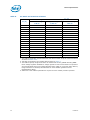
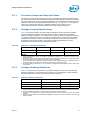
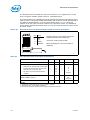
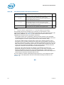
The MSID[1:0] signals may be used as outputs to determine the Market Segment of
the processor. Table 3 provides details regarding the state of MSID[1:0]. A circuit can
be used to prevent 130 W TDP processors from booting on boards optimized for 65 W
TDP.
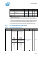
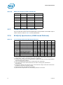
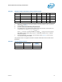
Table 3.
Market Segment Selection Truth Table for MSID[1:0]1, 2, 3, 4
MSID1
MSID0
Description
0
0
Intel® Core™2 Duo desktop processor E6000 and E4000 series and the
Intel® Core™2 Extreme processor X6800
0
1
Reserved
1
0
Reserved
1
1
Reserved
NOTES:
1. The MSID[1:0] signals are provided to indicate the Market Segment for the processor
and may be used for future processor compatibility or for keying. Circuitry on the
motherboard may use these signals to identify the processor installed.
2. These signals are not connected to the processor die.
3. A logic 0 is achieved by pulling the signal to ground on the package.
4. A logic 1 is achieved by leaving the signal as a no connect on the package.
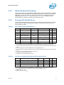
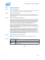
2.5
Reserved, Unused, and TESTHI Signals
All RESERVED lands must remain unconnected. Connection of these lands to VCC, VSS,
VTT, or to any other signal (including each other) can result in component malfunction
or incompatibility with future processors. See Chapter 4 for a land listing of the
processor and the location of all RESERVED lands.
In a system level design, on-die termination has been included by the processor to
allow signals to be terminated within the processor silicon. Most unused GTL+ inputs
should be left as no connects as GTL+ termination is provided on the processor silicon.
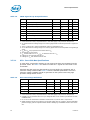
However, see Table 8 for details on GTL+ signals that do not include on-die termination.
Unused active high inputs, should be connected through a resistor to ground (VSS).
Unused outputs can be left unconnected, however this may interfere with some TAP
functions, complicate debug probing, and prevent boundary scan testing. A resistor
must be used when tying bidirectional signals to power or ground. When tying any
signal to power or ground, a resistor will also allow for system testability. Resistor
values should be within ± 20% of the impedance of the motherboard trace for front
side bus signals. For unused GTL+ input or I/O signals, use pull-up resistors of the
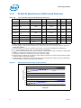
same value as the on-die termination resistors (RTT). For details, see Table 14.
TAP and CMOS signals do not include on-die termination. Inputs and used outputs must
be terminated on the motherboard. Unused outputs may be terminated on the
motherboard or left unconnected. Note that leaving unused outputs unterminated may
interfere with some TAP functions, complicate debug probing, and prevent boundary
scan testing.
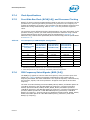
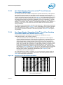
All TESTHI[13:0] lands should be individually connected to VTT via a pull-up resistor
that matches the nominal trace impedance.
18
Datasheet