1
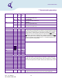
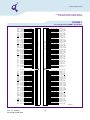
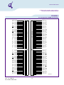
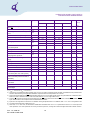
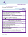
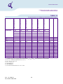
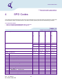
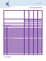
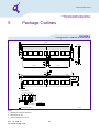
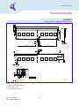
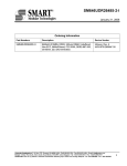
June 2008 HYS64T512020EU–[25F/2.5/3S]–A HYS72T512020EU–[25F/2.5/3S]–A 240-Pin Unbuffered DDR2 SDRAM Modules UDIMM SDRAM EU RoHS Compliant Internet Data Sheet Rev. 1.0 Internet Data Sheet HYS[64/72]T512020EU–[25F/2.5/3S]–A Unbuffered DDR2 SDRAM Modules HYS64T512020EU–[25F/2.5/3S]–A, HYS72T512020EU–[25F/2.5/3S]–A Internet Data Sheet Revision History: 2008-06, Rev. 1.0 Page Subjects (major changes since last revision) All Removed HYS[64/72]T512020EU-[3/3.7]-A product types and added Idd values and adapted to internet edition. Previous Revision: Rev. 0.20, 2007-07 All Datasheet for HYS[64/72]T512020EU-[25F/2.5/3/3S/3.7]-A. We Listen to Your Comments Any information within this document that you feel is wrong, unclear or missing at all? Your feedback will help us to continuously improve the quality of this document. Please send your proposal (including a reference to this document) to: [email protected] qag_techdoc_A4, 4.20, 2008-01-25 06112008-YHWK-B105 2 Internet Data Sheet HYS[64/72]T512020EU–[25F/2.5/3S]–A Unbuffered DDR2 SDRAM Modules 1 Overview This chapter gives an overview of the 240-pin Unbuffered DDR2 SDRAM modules product family and describes its main characteristics. 1.1 Features • 240-Pin PC2-6400 and PC2-5300 DDR2 SDRAM memory modules. • Two ranks 512M × 64, 512M × 72 module organization, and 256M × 8 chip organization. • 4GB Modules built with 2 Gbit DDR2 SDRAMs in chipsize packages PG-TFBGA-68. • Standard Double-Data-Rate-Two Synchronous DRAMs (DDR2 SDRAM) with a single + 1.8 V (± 0.1 V) power supply. • All speed grades faster than DDR2-400 comply with DDR2-400 timing specifications. • Programmable CAS Latencies (3, 4, 5, 6 and 7 ), Burst Length (8 & 4). • Auto Refresh (CBR) and Self Refresh. • • • • • • • • • • Auto Refresh for temperatures above 85 °C tREFI = 3.9 μs. Programmable self refresh rate via EMRS2 setting. Programmable partial array refresh via EMRS2 settings. DCC enabling via EMRS2 setting. All inputs and outputs SSTL_1.8 compatible. Off-Chip Driver Impedance Adjustment (OCD) and On-Die Termination (ODT). Serial Presence Detect with E2PROM. UDIMM and EDIMM Dimensions (nominal): 30 mm high, 133.35 mm wide Based on standard reference layouts Raw Cards 'E' and 'G'. RoHS compliant products1). TABLE 1 Performance Table QAG Speed Code –25F –2.5 –3S Unit tCK DRAM Speed Grade DDR2 –800D –800E –667D Module Speed Grade PC2 –6400D –6400E –5300D 5–5–5 6–6–6 5–5–5 200 200 200 MHz 266 266 266 MHz 400 333 333 MHz – 400 – MHz 12.5 15 15 ns 12.5 15 15 ns 45 45 45 ns 57.5 60 60 ns 15 17.5 18 ns CAS-RCD-RP latencies fCK3 CL4 fCK4 fCK5 CL5 CL6 fCK6 Min. RAS-CAS-Delay tRCD tRP Min. Row Precharge Time Min. Row Active Time tRAS Min. Row Cycle Time tRC Precharge-All (8 banks) command period tPREA Max. Clock Frequency CL3 Note 1)2) 1) RoHS Compliant Product: Restriction of the use of certain hazardous substances (RoHS) in electrical and electronic equipment as defined in the directive 2002/95/EC issued by the European Parliament and of the Council of 27 January 2003. These substances include mercury, lead, cadmium, hexavalent chromium, polybrominated biphenyls and polybrominated biphenyl ethers. For more information please visit www.qimonda.com/green_products . Rev. 1.0, 2008-06 06112008-YHWK-B105 3 Internet Data Sheet HYS[64/72]T512020EU–[25F/2.5/3S]–A Unbuffered DDR2 SDRAM Modules 1) This tPREA value is the minimum value at which this chip will be functional. 2) Precharge-All command for an 8 bank device will equal to tRP + 1 × tCK or tnRP + 1 × nCK, depending on the speed bin, where tnRP = RU{ tRP / tCK(avg) } and tRP is the value for a single bank precharge. 1.2 Description The Qimonda HYS[64/72]T512020EU–[25F/2.5/3S]–A module family are Unbuffered DIMM modules “UDIMMs” with 30 mm height based on DDR2 technology. DIMMs are available as non-ECC modules in 512M × 64 (4GB) and as ECC modules in 512M × 72 (4GB) in organization and density, intended for mounting into 240-pin connector sockets. The memory array is designed with 2 Gbit Double-DataRate-Two (DDR2) Synchronous DRAMs. Decoupling capacitors are mounted on the PCB board. The DIMMs feature serial presence detect based on a serial E2PROM device using the 2-pin I2C protocol. The first 128 bytes are programmed with configuration data and are write protected; the second 128 bytes are available to the customer. TABLE 2 Ordering Information Product Type1) Compliance Code2) Description SDRAM Technology HYS64T512020EU-25F-A 4GB 2R×8 PC2–6400U–555–12–E0 2 Ranks, Non-ECC 2Gbit (×8) HYS72T512020EU-25F-A 4GB 2R×8 PC2–6400E–555–12–G0 2 Ranks, ECC 2Gbit (×8) HYS64T512020EU-2.5-A 4GB 2R×8 PC2–6400U–666–12–E0 2 Ranks, Non-ECC 2Gbit (×8) HYS72T512020EU-2.5-A 4GB 2R×8 PC2–6400E–666–12–G0 2 Ranks, ECC 2Gbit (×8) HYS64T512020EU-3S-A 4GB 2R×8 PC2–5300U–555–12–E0 2 Ranks, Non-ECC 2Gbit (×8) HYS72T512020EU-3S-A 4GB 2R×8 PC2–5300E–555–12–G0 2 Ranks, ECC 2Gbit (×8) PC2-6400 (5-5-5) PC2-6400 (6-6-6) PC2-5300 (5-5-5) 1) For detailed information regarding Product Type of Qimonda please see chapter "Product Type Nomenclature" of this data sheet. 2) The Compliance Code is printed on the module label and describes the speed grade, for example "PC2–6400E–555–12–G0" where 6400E means Unbuffered DIMM modules with 6.40 GB/sec Module Bandwidth and "555–12" means Column Address Strobe (CAS) latency =5, Row Column Delay (RCD) latency = 5 and Row Precharge (RP) latency = 5 using the Industry Standard SPD Revision 1.2 and produced on the Raw Card "G". TABLE 3 Address Format DIMM Density Module Organization Memory Ranks ECC/ Non-ECC # of SDRAMs # of row/bank/column bits Raw Card 4GB 512M × 64 2 Non-ECC 16 15/3/10 E 4GB 512M × 72 2 ECC 18 15/3/10 G Rev. 1.0, 2008-06 06112008-YHWK-B105 4 Internet Data Sheet HYS[64/72]T512020EU–[25F/2.5/3S]–A Unbuffered DDR2 SDRAM Modules TABLE 4 Components on Modules Product Type1)2) DRAM Components1) DRAM Density DRAM Organisation HYS64T512020EU HYB18T2G800AF 2Gbit 256M × 8 HYS72T512020EU HYB18T2G800AF 2Gbit 256M × 8 1) Green Product 2) For a detailed description of all functionalities of the DRAM components on these modules see the component data sheet. Rev. 1.0, 2008-06 06112008-YHWK-B105 5 Internet Data Sheet HYS[64/72]T512020EU–[25F/2.5/3S]–A Unbuffered DDR2 SDRAM Modules 2 Pin Configurations and Block Diagrams 2.1 Pin Configurations The pin configuration of the Unbuffered DDR2 SDRAM DIMM is listed by function in Table 5 (240 pins). The abbreviations used in columns Pin and Buffer Type are explained in Table 6 and Table 7 respectively. The pin numbering is depicted in Figure 1 for non-ECC modules (×64) and Figure 2 for ECC modules (×72). TABLE 5 Pin Configuration of UDIMM Ball No. Name Pin Type Buffer Type Function 185 CK0 I SSTL 137 CK1 I SSTL 220 CK2 I SSTL 186 CK0 I SSTL Clock Signals 2:0, Complement Clock Signals 2:0 The system clock inputs. All address and command lines are sampled on the cross point of the rising edge of CK and the falling edge of CK. A Delay Locked Loop (DLL) circuit is driven from the clock inputs and output timing for read operations is synchronized to the input clock. 138 CK1 I SSTL 221 CK2 I SSTL 52 CKE0 I SSTL 171 CKE1 I SSTL NC NC — Not Connected Note: 1 Rank module Chip Select Rank 1:0 Enables the associated DDR2 SDRAM command decoder when LOW and disables the command decoder when HIGH. When the command decoder is disabled, new commands are ignored but previous operations continue. Rank 0 is selected by S0; Rank 1 is selected by S1. Ranks are also called "Physical banks". Note: 2 Ranks module Clock Signals Clock Enable Rank 1:0 Activates the DDR2 SDRAM CK signal when HIGH and deactivates the CK signal when LOW. By deactivating the clocks, CKE LOW initiates the Power Down Mode or the Self Refresh Mode. Note: 2 Ranks module Control Signals 193 S0 I SSTL 76 S1 I SSTL NC NC — Not Connected Note: 1 Rank module 192 RAS I SSTL Row Address Strobe When sampled at the cross point of the rising edge of CK,and falling edge of CK, RAS, CAS and WE define the operation to be executed by the SDRAM. 74 CAS I SSTL Column Address Strobe Rev. 1.0, 2008-06 06112008-YHWK-B105 6 Internet Data Sheet HYS[64/72]T512020EU–[25F/2.5/3S]–A Unbuffered DDR2 SDRAM Modules Ball No. Name Pin Type Buffer Type Function 73 WE I SSTL Write Enable 71 BA0 I SSTL 190 BA1 I SSTL Bank Address Bus 1:0 Selects which DDR2 SDRAM internal bank of four or eight is activated. 54 BA2 I SSTL Bank Address Bus 2 Greater than 512Mb DDR2 SDRAMS NC NC — Not Connected Less than 1Gb DDR2 SDRAMS Address Bus 12:0 During a Bank Activate command cycle, defines the row address when sampled at the crosspoint of the rising edge of CK and falling edge of CK. During a Read or Write command cycle, defines the column address when sampled at the cross point of the rising edge of CK and falling edge of CK. In addition to the column address, AP is used to invoke autoprecharge operation at the end of the burst read or write cycle. If AP is HIGH, autoprecharge is selected and BA0-BAn defines the bank to be precharged. If AP is LOW, autoprecharge is disabled. During a Precharge command cycle, AP is used in conjunction with BA0-BAn to control which bank(s) to precharge. If AP is HIGH, all banks will be precharged regardless of the state of BA0-BAn inputs. If AP is LOW, then BA0-BAn are used to define which bank to precharge. Address Signals 188 A0 I SSTL 183 A1 I SSTL 63 A2 I SSTL 182 A3 I SSTL 61 A4 I SSTL 60 A5 I SSTL 180 A6 I SSTL 58 A7 I SSTL 179 A8 I SSTL 177 A9 I SSTL 70 A10 I SSTL AP I SSTL 57 A11 I SSTL 176 A12 I SSTL 196 A13 I SSTL Address Signal 13 Note: 1 Gbit based module and 512M ×4/×8 NC NC — Not Connected Note: Module based on 1 Gbit ×16Module based on 512 Mbit ×16 or smaller A14 I SSTL Address Signal 14 Note: Modules based on 2 Gbit NC NC — Not Connected Note: Modules based on 1 Gbit or smaller 3 DQ0 I/O SSTL 4 DQ1 I/O SSTL Data Bus 63:0 Data Input / Output pins 9 DQ2 I/O SSTL 10 DQ3 I/O SSTL 122 DQ4 I/O SSTL 123 DQ5 I/O SSTL 128 DQ6 I/O SSTL 129 DQ7 I/O SSTL 174 Data Signals Rev. 1.0, 2008-06 06112008-YHWK-B105 7 Internet Data Sheet HYS[64/72]T512020EU–[25F/2.5/3S]–A Unbuffered DDR2 SDRAM Modules Ball No. Name Pin Type Buffer Type Function 12 DQ8 I/O SSTL 13 DQ9 I/O SSTL Data Bus 63:0 Data Input / Output pins 21 DQ10 I/O SSTL 22 DQ11 I/O SSTL 131 DQ12 I/O SSTL 132 DQ13 I/O SSTL 140 DQ14 I/O SSTL 141 DQ15 I/O SSTL 24 DQ16 I/O SSTL 25 DQ17 I/O SSTL 30 DQ18 I/O SSTL 31 DQ19 I/O SSTL 143 DQ20 I/O SSTL 144 DQ21 I/O SSTL 149 DQ22 I/O SSTL 150 DQ23 I/O SSTL 33 DQ24 I/O SSTL 34 DQ25 I/O SSTL 39 DQ26 I/O SSTL 40 DQ27 I/O SSTL 152 DQ28 I/O SSTL 153 DQ29 I/O SSTL 158 DQ30 I/O SSTL 159 DQ31 I/O SSTL 80 DQ32 I/O SSTL 81 DQ33 I/O SSTL 86 DQ34 I/O SSTL 87 DQ35 I/O SSTL 199 DQ36 I/O SSTL 200 DQ37 I/O SSTL 205 DQ38 I/O SSTL 206 DQ39 I/O SSTL 89 DQ40 I/O SSTL 90 DQ41 I/O SSTL 95 DQ42 I/O SSTL 96 DQ43 I/O SSTL 208 DQ44 I/O SSTL 209 DQ45 I/O SSTL 214 DQ46 I/O SSTL 215 DQ47 I/O SSTL Rev. 1.0, 2008-06 06112008-YHWK-B105 8 Internet Data Sheet HYS[64/72]T512020EU–[25F/2.5/3S]–A Unbuffered DDR2 SDRAM Modules Ball No. Name Pin Type Buffer Type Function 98 DQ48 I/O SSTL 99 DQ49 I/O SSTL Data Bus 63:0 Data Input / Output pins 107 DQ50 I/O SSTL 108 DQ51 I/O SSTL 217 DQ52 I/O SSTL 218 DQ53 I/O SSTL 226 DQ54 I/O SSTL 227 DQ55 I/O SSTL 110 DQ56 I/O SSTL 111 DQ57 I/O SSTL 116 DQ58 I/O SSTL 117 DQ59 I/O SSTL 229 DQ60 I/O SSTL 230 DQ61 I/O SSTL 235 DQ62 I/O SSTL 236 DQ63 I/O SSTL CB0 I/O SSTL Check Bit 0 Note: ECC type module only NC NC — Not Connected Note: Non-ECC type module only CB1 I/O SSTL Check Bit 1 Note: ECC type module only NC NC — Not Connected Note: Non-ECC type module only CB2 I/O SSTL Check Bit 2 Note: ECC type module only NC NC — Not Connected Note: Non-ECC type module only CB3 I/O SSTL Check Bit 3 Note: ECC type module only NC NC — Not Connected Note: Non-ECC type module only CB4 I/O SSTL Check Bit 4 Note: ECC type module only NC NC — Not Connected Note: Non-ECC type module only CB5 I/O SSTL Check Bit 5 Note: ECC type module only NC NC — Not Connected Note: Non-ECC type module only Check Bit Signals 42 43 48 49 161 162 Rev. 1.0, 2008-06 06112008-YHWK-B105 9 Internet Data Sheet HYS[64/72]T512020EU–[25F/2.5/3S]–A Unbuffered DDR2 SDRAM Modules Ball No. Name Pin Type Buffer Type Function 167 CB6 I/O SSTL Check Bit 6 Note: ECC type module only NC NC — Not Connected Note: Non-ECC type module only CB7 I/O SSTL Check Bit 7 Note: ECC type module only NC NC — Not Connected Note: Non-ECC module only Data Strobe Bus 8:0 The data strobes, associated with one data byte, sourced with data transfers. In Write mode, the data strobe is sourced by the controller and is centered in the data window. In Read mode the data strobe is sourced by the DDR2 SDRAM and is sent at the leading edge of the data window. DQS signals are complements, and timing is relative to the crosspoint of respective DQS and DQS. If the module is to be operated in single ended strobe mode, all DQS signals must be tied on the system board to VSS and DDR2 SDRAM mode registers programmed appropriately. 168 Data Strobe Bus 7 DQS0 I/O SSTL 16 DQS1 I/O SSTL 28 DQS2 I/O SSTL 37 DQS3 I/O SSTL 84 DQS4 I/O SSTL 93 DQS5 I/O SSTL 105 DQS6 I/O SSTL 114 DQS7 I/O SSTL 46 DQS8 I/O SSTL 6 DQS0 I/O SSTL 15 DQS1 I/O SSTL 27 DQS2 I/O SSTL 36 DQS3 I/O SSTL 83 DQS4 I/O SSTL 92 DQS5 I/O SSTL 104 DQS6 I/O SSTL 113 DQS7 I/O SSTL 45 DQS8 I/O SSTL 125 DM0 I SSTL 134 DM1 I SSTL 146 DM2 I SSTL 155 DM3 I SSTL 202 DM4 I SSTL 211 DM5 I SSTL 223 DM6 I SSTL 232 DM7 I SSTL 164 DM8 I SSTL SCL I CMOS Complement Data Strobe Bus 8:0 Data Mask Signals Data Mask Bus 8:0 The data write masks, associated with one data byte. In Write mode, DM operates as a byte mask by allowing input data to be written if it is LOW but blocks the write operation if it is HIGH. In Read mode, DM lines have no effect. EEPROM 120 Rev. 1.0, 2008-06 06112008-YHWK-B105 Serial Bus Clock This signal is used to clock data into and out of the SPD EEPROM. 10 Internet Data Sheet HYS[64/72]T512020EU–[25F/2.5/3S]–A Unbuffered DDR2 SDRAM Modules Ball No. Name Pin Type Buffer Type Function 119 SDA I/O OD Serial Bus Data This is a bidirectional pin used to transfer data into or out of the SPD EEPROM. A resistor must be connected from SDA to VDDSPD on the motherboard to act as a pull-up. 239 SA0 I CMOS 240 SA1 I CMOS Serial Address Select Bus 2:0 Address pins used to select the Serial Presence Detect base address. 101 SA2 I CMOS 1 VREF AI — I/O Reference Voltage Reference voltage for the SSTL-18 inputs. 238 VDDSPD PWR — EEPROM Power Supply Power supplies for core, I/O, Serial Presence Detect, and ground for the module. 51,56,62,72,75,, 78,170,175,181,, 191,194 VDDQ PWR — I/O Driver Power Supply 53,59,64,67,69,, 172,178,184,187, 189,197 VDD PWR — Power Supply Power supplies for core, I/O, Serial Presence Detect, and ground for the module. 2,5,8,11,14,17,, 20,23,26,29,32, 35,38,41,44,47,, 50,65,66,79,82, 85,88,91,94,97,, 100,103,106, 109,112,115,118, 121,124,127,, 130,133,136,139, 142,145,148,, 151,154,157,160, 163,166,169, 198,201,204,207, 210,213,216,, 219,222,225,228, 231,234,237 VSS GND — Ground Plane Power supplies for core, I/O, Serial Presence Detect, and ground for the module. 195 ODT0 I SSTL On-Die Termination Control 0 77 ODT1 I SSTL On-Die Termination Control 1 Asserts on-die termination for DQ, DM, DQS, and DQS signals if enabled via the DDR2 SDRAM mode register. Note: 2 Rank modules NC NC — Not Connected Note: 1 Rank modules 18,19,55,68,102,1 NC 26,135,147, 156,165,173,203, 212, 224,233 NC — Not connected Note: Pins not connected on Qimonda UDIMMs Power Supplies Other Pins Rev. 1.0, 2008-06 06112008-YHWK-B105 11 Internet Data Sheet HYS[64/72]T512020EU–[25F/2.5/3S]–A Unbuffered DDR2 SDRAM Modules TABLE 6 Abbreviations for Pin Type Abbreviation Description I Standard input-only pin. Digital levels. O Output. Digital levels. I/O I/O is a bidirectional input/output signal. AI Input. Analog levels. PWR Power GND Ground NC Not Connected TABLE 7 Abbreviations for Buffer Type Abbreviation Description SSTL Serial Stub Terminated Logic (SSTL_18) LV-CMOS Low Voltage CMOS CMOS CMOS Levels OD Open Drain. The corresponding pin has 2 operational states, active low and tri-state, and allows multiple devices to share as a wire-OR. Rev. 1.0, 2008-06 06112008-YHWK-B105 12 Internet Data Sheet HYS[64/72]T512020EU–[25F/2.5/3S]–A Unbuffered DDR2 SDRAM Modules FIGURE 1 Pin Configuration UDIMM ×72 (240 Pin) 95() 3LQ '4 3LQ 966 3LQ '46 3LQ '4 3LQ 966 3LQ '4 3LQ '46 3LQ 966 3LQ 1& 3LQ '4 3LQ 966 3LQ '4 3LQ '46 3LQ 966 3LQ '4 3LQ '4 3LQ 966 3LQ '46 3LQ '4 3LQ 966 3LQ &% 3LQ '46 3LQ 966 3LQ &% 3LQ 3LQ 9''4 9'' 3LQ 1& 3LQ $ 3LQ 9'' 3LQ 3LQ $ 3LQ $ 966 3LQ 9'' 3LQ 9'' 3LQ %$ 3LQ :( 3LQ 3LQ 9''4 2'7 3LQ 966 3LQ '4 3LQ '46 3LQ 966 3LQ '4 3LQ '4 3LQ 966 3LQ '46 3LQ 966 3LQ 966 3LQ '4 3LQ 6$ 3LQ 966 3LQ '46 3LQ '4 3LQ 966 3LQ '4 3LQ '46 3LQ 966 3LQ '4 3LQ 6'$ 3LQ Rev. 1.0, 2008-06 06112008-YHWK-B105 3LQ 966 3LQ '4 '46 3LQ 3LQ 966 '4 3LQ '4 3LQ 966 3LQ '46 3LQ 3LQ 1& 3LQ 966 '4 3LQ '4 3LQ 3LQ 966 '46 3LQ 3LQ 966 3LQ 966 '4 3LQ '46 3LQ 3LQ 966 '4 3LQ 3LQ &% 3LQ 966 '46 3LQ 3LQ &% 3LQ 966 &.( 3LQ 1&%$ 3LQ 3LQ 9''4 3LQ $ 3LQ $ 3LQ 9''4 3LQ 9'' ) 5 2 1 7 6 , ' ( % $ & . 6 , ' ( 3LQ '4 3LQ 966 3LQ 1& 3LQ '4 3LQ 966 3LQ '4 3LQ '0 3LQ 1& 3LQ &. 3LQ '4 3LQ 966 3LQ '4 3LQ '0 3LQ 966 3LQ '4 3LQ '4 3LQ 966 3LQ 1& 3LQ '4 3LQ 966 3LQ &% 3LQ '0 966 3LQ 3LQ &% 3LQ 9''4 3LQ 9'' 3LQ $ 3LQ $ 3LQ 9'' 3LQ $ 3LQ $ 3LQ 9'' 3LQ &. 3LQ $ 3LQ %$ 3LQ 5$6 9''4 3LQ 3LQ 1&$ 3LQ 966 3LQ '4 3LQ '0 3LQ 966 3LQ '4 3LQ '4 3LQ 966 3LQ 1& 3LQ '4 3LQ 966 3LQ '4 3LQ &. 3LQ 966 3LQ 1& 3LQ '4 3LQ 966 3LQ '4 3LQ '0 3LQ 966 3LQ '4 3LQ 9''6 3' 3LQ 6$ 3LQ 966 3LQ 1& $$ 3 3LQ 3LQ 9''4 3LQ &$6 1&6 3LQ 3LQ 9''4 '4 3LQ 3LQ 966 '46 3LQ '4 3LQ 3LQ 966 '4 3LQ '46 3LQ 3LQ 966 '4 3LQ '4 3LQ 3LQ 966 3LQ 1& '46 3LQ 3LQ 966 '4 3LQ '4 3LQ 3LQ 966 '46 3LQ '4 3LQ 3LQ 966 3LQ 6&/ 13 3LQ 966 3LQ '4 3LQ '0 3LQ 966 3LQ '4 3LQ '4 3LQ 966 3LQ 1& 3LQ &. 3LQ 966 3LQ '4 3LQ '4 3LQ 966 3LQ 1& 3LQ '4 3LQ 966 3LQ '4 3LQ '0 3LQ 966 3LQ '4 3LQ &% 3LQ 966 3LQ 1& 3LQ &% 3LQ 966 3LQ &.( 3LQ 1& 3LQ 9''4 3LQ $ 3LQ $ 3LQ 9''4 3LQ $ 3LQ &. 3LQ 9'' 3LQ 9'' 3LQ 9''4 3LQ 6 3LQ 2'7 3LQ 9'' 3LQ '4 3LQ 966 3LQ 1& 3LQ '4 3LQ 966 3LQ '4 3LQ '0 3LQ 966 3LQ '4 3LQ '4 3LQ 966 3LQ &. 3LQ '0 3LQ 966 3LQ '4 3LQ '4 3LQ 966 1& 3LQ 3LQ '4 3LQ 966 3LQ 6$ 033 7 Internet Data Sheet HYS[64/72]T512020EU–[25F/2.5/3S]–A Unbuffered DDR2 SDRAM Modules FIGURE 2 Pin Configuration UDIMM ×64 (240 Pin) 95() 3LQ '4 3LQ 966 3LQ '46 3LQ '4 3LQ 966 3LQ '4 3LQ '46 3LQ 966 3LQ 1& 3LQ '4 3LQ 966 3LQ '4 3LQ '46 3LQ 966 3LQ '4 3LQ '4 3LQ 966 3LQ '46 3LQ '4 3LQ 966 3LQ 1& 3LQ 1& 3LQ 966 3LQ 1& 3LQ 3LQ 9''4 9'' 3LQ 1& 3LQ $ 3LQ 9'' 3LQ 3LQ $ 3LQ $ 966 3LQ 9'' 3LQ 9'' 3LQ %$ 3LQ :( 3LQ 3LQ 9''4 2'7 3LQ 966 3LQ '4 3LQ '46 3LQ 966 3LQ '4 3LQ '4 3LQ 966 3LQ '46 3LQ '4 3LQ 966 3LQ '4 3LQ 6$ 3LQ 966 3LQ '46 3LQ '4 3LQ 966 3LQ '4 3LQ '46 3LQ 966 3LQ '4 3LQ 6'$ 3LQ Rev. 1.0, 2008-06 06112008-YHWK-B105 3LQ 966 3LQ '4 '46 3LQ 3LQ 966 3LQ '4 3LQ '4 3LQ 966 '46 3LQ 3LQ 1& 3LQ 966 '4 3LQ '4 3LQ 3LQ 966 '46 3LQ '4 3LQ 3LQ 966 '4 3LQ '46 3LQ 3LQ 966 '4 3LQ 3LQ 1& 3LQ 966 3LQ 1& 3LQ 1& 3LQ 966 &.( 3LQ 1&%$ 3LQ 3LQ 9''4 3LQ $ 3LQ $ 3LQ 9''4 3LQ 9'' ) 5 2 1 7 6 , ' ( % $ & . 6 , ' ( 3LQ '4 3LQ 966 3LQ 1& 3LQ '4 3LQ 966 3LQ '4 3LQ '0 3LQ 966 3LQ &. 3LQ '4 3LQ 966 3LQ '4 3LQ '0 3LQ 966 3LQ '4 3LQ '4 3LQ 966 3LQ 1& 3LQ '4 3LQ 966 3LQ 1& 3LQ 1& 3LQ 966 1& 3LQ 3LQ 9''4 3LQ 9'' 3LQ $ 3LQ $ 3LQ 9'' 3LQ $ 3LQ $ 3LQ 9'' 3LQ &. 3LQ $ 3LQ %$ 3LQ 5$6 3LQ 9''4 3LQ 1&$ 3LQ 966 3LQ '4 3LQ '0 3LQ 966 3LQ '4 3LQ '4 3LQ 966 3LQ 1& 3LQ '4 3LQ 966 3LQ '4 3LQ &. 3LQ 966 3LQ 1& '4 3LQ 3LQ 966 3LQ '4 3LQ '0 3LQ 966 3LQ '4 3LQ 9''6 3' 3LQ 6$ 3LQ 966 3LQ 1& $$3 3LQ 3LQ 9''4 3LQ &$6 1&6 3LQ 3LQ 9''4 '4 3LQ 3LQ 966 '46 3LQ '4 3LQ 3LQ 966 '4 3LQ '46 3LQ 3LQ 966 '4 3LQ '4 3LQ 3LQ 966 3LQ 1& '46 3LQ 3LQ 966 '4 3LQ '4 3LQ 3LQ 966 '46 3LQ '4 3LQ 3LQ 966 3LQ 6&/ 14 3LQ 966 3LQ '4 3LQ '0 3LQ 966 3LQ '4 3LQ '4 3LQ 966 3LQ 1& 3LQ &. 3LQ 966 3LQ '4 3LQ '4 3LQ 966 3LQ 1& 3LQ '4 3LQ 966 3LQ '4 3LQ '0 3LQ 966 3LQ '4 3LQ 1& 3LQ 966 3LQ 1& 3LQ 1& 3LQ 966 3LQ &.( 3LQ 1& 3LQ 9''4 3LQ $ 3LQ $ 3LQ 9''4 3LQ $ 3LQ &. 3LQ 9'' 3LQ 9'' 3LQ 9''4 3LQ 6 3LQ 2'7 3LQ 9'' 3LQ '4 3LQ 966 3LQ 1& 3LQ '4 3LQ 966 3LQ '4 3LQ '0 3LQ 966 3LQ '4 3LQ '4 3LQ 966 3LQ &. 3LQ '0 3LQ 966 3LQ '4 3LQ '4 3LQ 966 1& 3LQ 3LQ '4 3LQ 966 3LQ 6$ 033 7 Internet Data Sheet HYS[64/72]T512020EU–[25F/2.5/3S]–A Unbuffered DDR2 SDRAM Modules 3 Electrical Characteristics This chapter contains speed grade definition, AC timing parameter and ODT tables. 3.1 Absolute Maximum Ratings Attention: Stresses greater than those listed under “Absolute Maximum Ratings” may cause permanent damage to the device. This is a stress rating only and functional operation of the device at these or any other conditions above those indicated in the operational sections of this specification is not implied. Exposure to absolute maximum rating conditions for extended periods may affect reliability. TABLE 8 Absolute Maximum Ratings Symbol Parameter Rating Unit Note 1) Min. Max. Voltage on VDD pin relative to VSS –1.0 +2.3 V Voltage on VDDQ pin relative to VSS –0.5 +2.3 V Voltage on VDDL pin relative to VSS –0.5 +2.3 V Voltage on any pin relative to VSS –0.5 +2.3 1) When VDD and VDDQ and VDDL are less than 500 mV; VREF may be equal to or less than 300 mV. V VDD VDDQ VDDL VIN, VOUT TABLE 9 Environmental Requirements Parameter Symbol Values Unit Note Min. Max. 0 +55 °C 1) Storage Temperature TOPR TSTG – 50 +100 °C 2) Barometric Pressure (operating & storage) PBar +69 +105 kPa 3) Operating Humidity (relative) HOPR HSTG 10 90 % 5 95 % Operating temperature (ambient) Storage Humidity (without condensation) 1) The component maximum case temperature (Tcase) shall not exceed the value specified in the DDR2 DRAM component specification. 2) Storage Temperature is the case surface temperature on the center/top side of the DRAM. 3) Up to 3000 m. Rev. 1.0, 2008-06 06112008-YHWK-B105 15 Internet Data Sheet HYS[64/72]T512020EU–[25F/2.5/3S]–A Unbuffered DDR2 SDRAM Modules TABLE 10 DRAM Component Operating Temperature Range Symbol TCASE Parameter Rating Operating Temperature Min. Max. 0 95 Unit Note °C 1)2)3)4) 1) Operating Temperature is the case surface temperature on the center / top side of the DRAM. 2) The operating temperature range are the temperatures where all DRAM specification will be supported. During operation, the DRAM case temperature must be maintained between 0 - 95 °C under all other specification parameters. 3) Above 85 °C the Auto-Refresh command interval has to be reduced to tREFI= 3.9 μs 4) When operating this product in the 85 °C to 95 °C TCASE temperature range, the High Temperature Self Refresh has to be enabled by setting EMR(2) bit A7 to “1”. When the High Temperature Self Refresh is enabled there is an increase of IDD6 by approximately 50% 3.2 DC Operating Conditions TABLE 11 Supply Voltage Levels and DC Operating Conditions Parameter Device Supply Voltage Output Supply Voltage Input Reference Voltage SPD Supply Voltage DC Input Logic High DC Input Logic Low Symbol VDD VDDQ VREF VDDSPD VIH(DC) VIL (DC) IL Values Unit Min. Typ. Max. 1.7 1.8 1.9 V 1.7 1.8 1.9 V 1) 0.49 × VDDQ 0.5 × VDDQ 0.51 × VDDQ V 2) 1.7 — 3.6 V VREF + 0.125 — V – 0.30 — VDDQ + 0.3 VREF – 0.125 V In / Output Leakage Current –5 — 5 μA 1) Under all conditions, VDDQ must be less than or equal to VDD 2) Peak to peak AC noise on VREF may not exceed ± 2% VREF (DC).VREF is also expected to track noise in VDDQ. 3) Input voltage for any connector pin under test of 0 V ≤ VIN ≤ VDDQ + 0.3 V; all other pins at 0 V. Current is per pin Rev. 1.0, 2008-06 06112008-YHWK-B105 Note 16 3) Internet Data Sheet HYS[64/72]T512020EU–[25F/2.5/3S]–A Unbuffered DDR2 SDRAM Modules 3.3 Speed Grade Definitions TABLE 12 Speed Grade Definition Speed Grade DDR2–800D DDR2–800E QAG Sort Name –25F –2.5 CAS-RCD-RP latencies 5–5–5 6–6–6 Parameter Clock Period @ CL = 3 @ CL = 4 @ CL = 5 @ CL = 6 Row Active Time Row Cycle Time RAS-CAS-Delay Row Precharge Time Unit Note tCK Symbol Min. Max. Min. Max. — tCK tCK tCK tCK tRAS tRC tRCD tRP 5 8 5 8 ns 1)2)3)4) 3.75 8 3.75 8 ns 1)2)3)4) 2.5 8 3 8 ns 1)2)3)4) 2.5 8 2.5 8 ns 1)2)3)4) 45 70k 45 70k ns 1)2)3)4)5) 57.5 — 60 — ns 1)2)3)4) 12.5 — 15 — ns 1)2)3)4) 12.5 — 15 — ns 1)2)3)4) TABLE 13 Speed Grade Definition Speed Grade DDR2–667D QAG Sort Name –3S CAS-RCD-RP latencies 5–5–5 Parameter Clock Period @ CL = 3 @ CL = 4 @ CL = 5 Row Active Time Row Cycle Time RAS-CAS-Delay Row Precharge Time Unit Note tCK Symbol Min. Max. — tCK tCK tCK tRAS tRC tRCD tRP 5 8 ns 1)2)3)4) 3.75 8 ns 1)2)3)4) 3 8 ns 1)2)3)4) 45 70k ns 1)2)3)4)5) 60 — ns 1)2)3)4) 15 — ns 1)2)3)4) 15 — ns 1)2)3)4) 1) Timings are guaranteed with CK/CK differential Slew Rate of 2.0 V/ns. For DQS signals timings are guaranteed with a differential Slew Rate of 2.0 V/ns in differential strobe mode and a Slew Rate of 1 V/ns in single ended mode. 2) The CK/CK input reference level (for timing reference to CK/CK) is the point at which CK and CK cross. The DQS / DQS, RDQS / RDQS, input reference level is the crosspoint when in differential strobe mode. 3) Inputs are not recognized as valid until VREF stabilizes. During the period before VREF stabilizes, CKE = 0.2 x VDDQ 4) The output timing reference voltage level is VTT. 5) tRAS.MAX is calculated from the maximum amount of time a DDR2 device can operate without a refresh command which is equal to 9 x tREFI. Rev. 1.0, 2008-06 06112008-YHWK-B105 17 Internet Data Sheet HYS[64/72]T512020EU–[25F/2.5/3S]–A Unbuffered DDR2 SDRAM Modules 3.4 Component AC Timing Parameters TABLE 14 DRAM Component Timing Parameter by Speed Grade - DDR2–800 and DDR2–667 Parameter Symbol DDR2–800 DDR2–667 Unit Note1)2)3 )4)5)6)7) tCCD tCH.AVG Average clock high pulse width Average clock period tCK.AVG CKE minimum pulse width ( high and tCKE CAS to CAS command delay Min. Max. Min. Max. 2 — 2 — nCK 0.48 0.52 0.48 0.52 tCK.AVG 2500 8000 3000 8000 ps 3 — 3 — nCK 11) 0.48 0.52 0.48 0.52 tCK.AVG 9)10) WR + tnRP — WR + tnRP — nCK 12)13) 9)10) low pulse width) Average clock low pulse width Auto-Precharge write recovery + precharge time tCL.AVG tDAL Minimum time clocks remain ON after tDELAY CKE asynchronously drops LOW tIS + tCK .AVG –– + tIH tIS + –– tCK .AVG + tIH ns tDH.BASE DQ and DM input pulse width for each tDIPW 125 –– 175 –– ps 0.35 — 0.35 — tCK.AVG 0.35 — 0.35 — 0.35 — 0.35 — tCK.AVG tCK.AVG — 200 — 240 ps 15) 16) DQ and DM input hold time 14)18)19) input tDQSH DQS input low pulse width tDQSL DQS-DQ skew for DQS & associated tDQSQ DQS input high pulse width DQ signals DQS latching rising transition to associated clock edges tDQSS – 0.25 + 0.25 – 0.25 + 0.25 tCK.AVG DQ and DM input setup time tDS.BASE tDSH tDSS tFAW 50 –– 100 –– ps 17)18)19) 16) Four Activate Window for 2KB page size products 0.2 — 0.2 — 0.2 — 0.2 — tCK.AVG tCK.AVG 35 — 37.5 — ns 34) tFAW 45 — 50 — ns 34) CK half pulse width tHP Min(tCH.ABS, tCL.ABS) __ Min(tCH.ABS, tCL.ABS) __ ps 20) Data-out high-impedance time from CK / CK tHZ — tAC.MAX — tAC.MAX ps 8)21) Address and control input hold time tIH.BASE tIPW 250 — 275 — ps 22)24) 0.6 — 0.6 — tCK.AVG Address and control input setup time tIS.BASE 175 — 200 — ps 23)24) DQ low impedance time from CK/CK tLZ.DQ 2 x tAC.MIN tAC.MAX 2 x tAC.MIN tAC.MAX ps 8)21) DQS falling edge hold time from CK DQS falling edge to CK setup time Four Activate Window for 1KB page size products Control & address input pulse width for each input Rev. 1.0, 2008-06 06112008-YHWK-B105 18 16) Internet Data Sheet HYS[64/72]T512020EU–[25F/2.5/3S]–A Unbuffered DDR2 SDRAM Modules Parameter Symbol DDR2–800 DDR2–667 Unit Note1)2)3 )4)5)6)7) Min. Max. Min. Max. tAC.MIN tAC.MAX tAC.MIN tAC.MAX ps 8)21) MRS command to ODT update delay tMOD 0 12 0 12 ns 34) Mode register set command cycle time tMRD 2 — 2 — nCK OCD drive mode output delay tOIT tQH tQHS tREFI 0 12 0 12 ns 34) tHP – tQHS — tHP – tQHS — ps 25) — 300 — 340 ps 26) — 7.8 — 7.8 μs 27)28) — 3.9 — 3.9 μs 27)29) DQS/DQS low-impedance time from CK / CK DQ/DQS output hold time from DQS DQ hold skew factor Average periodic refresh Interval tLZ.DQS Auto-Refresh to Active/Auto-Refresh command period tRFC 127.5 — 127.5 — ns 30) Read preamble tRPRE tRPST tRRD 0.9 1.1 0.9 1.1 31)32) 0.4 0.6 0.4 0.6 tCK.AVG tCK.AVG 7.5 — 7.5 — ns 34) Internal Read to Precharge command tRTP delay 7.5 — 7.5 — ns 34) tWPRE Write postamble tWPST Write recovery time tWR Internal write to read command delay tWTR Exit power down to read command tXARD Exit active power-down mode to read tXARDS 0.35 — 0.35 — 0.4 0.6 0.4 0.6 tCK.AVG tCK.AVG 15 — 15 — ns 34) 7.5 — 7.5 — ns 34)35) 2 — 2 — nCK 8 – AL — 7 – AL — nCK Read postamble Active to active command period for 1KB page size products Write preamble 31)33) command (slow exit, lower power) Exit precharge power-down to any valid command (other than NOP or Deselect) tXP 2 — 2 — nCK Exit self-refresh to a non-read command tXSNR tRFC +10 — tRFC +10 — ns — 200 — Exit self-refresh to read command tXSRD 200 Write command to DQS associated clock edges WL RL – 1 RL–1 34) nCK nCK 1) VDDQ = 1.8 V ± 0.1V; VDD = 1.8 V ± 0.1 V. 2) Timing that is not specified is illegal and after such an event, in order to guarantee proper operation, the DRAM must be powered down and then restarted through the specified initialization sequence before normal operation can continue. 3) Timings are guaranteed with CK/CK differential Slew Rate of 2.0 V/ns. For DQS signals timings are guaranteed with a differential Slew Rate of 2.0 V/ns in differential strobe mode and a Slew Rate of 1 V/ns in single ended mode. 4) The CK / CK input reference level (for timing reference to CK / CK) is the point at which CK and CK cross. The DQS / DQS, RDQS / RDQS, input reference level is the crosspoint when in differential strobe mode. 5) Inputs are not recognized as valid until VREF stabilizes. During the period before VREF stabilizes, CKE = 0.2 x VDDQ is recognized as low. 6) The output timing reference voltage level is VTT. 7) New units, ‘tCK.AVG‘ and ‘nCK‘, are introduced in DDR2–667 and DDR2–800. Unit ‘tCK.AVG‘ represents the actual tCK.AVG of the input clock under operation. Unit ‘nCK‘ represents one clock cycle of the input clock, counting the actual clock edges. Note that in DDR2–400 and Rev. 1.0, 2008-06 06112008-YHWK-B105 19 Internet Data Sheet HYS[64/72]T512020EU–[25F/2.5/3S]–A Unbuffered DDR2 SDRAM Modules 8) 9) 10) 11) 12) 13) 14) 15) 16) 17) 18) 19) 20) 21) 22) 23) 24) 25) 26) 27) 28) 29) DDR2–533, ‘tCK‘ is used for both concepts. Example: tXP = 2 [nCK] means; if Power Down exit is registered at Tm, an Active command may be registered at Tm + 2, even if (Tm + 2 - Tm) is 2 x tCK.AVG + tERR.2PER(Min). When the device is operated with input clock jitter, this parameter needs to be derated by the actual tERR(6-10per) of the input clock. (output deratings are relative to the SDRAM input clock.) For example, if the measured jitter into a DDR2–667 SDRAM has tERR(6-10PER).MIN = – 272 ps and tERR(6- 10PER).MAX = + 293 ps, then tDQSCK.MIN(DERATED) = tDQSCK.MIN – tERR(6-10PER).MAX = – 400 ps – 293 ps = – 693 ps and tDQSCK.MAX(DERATED) = tDQSCK.MAX – tERR(6-10PER).MIN = 400 ps + 272 ps = + 672 ps. Similarly, tLZ.DQ for DDR2–667 derates to tLZ.DQ.MIN(DERATED) = - 900 ps – 293 ps = – 1193 ps and tLZ.DQ.MAX(DERATED) = 450 ps + 272 ps = + 722 ps. (Caution on the MIN/MAX usage!) Input clock jitter spec parameter. The jitter specified is a random jitter meeting a Gaussian distribution. These parameters are specified per their average values. tCKE.MIN of 3 clocks means CKE must be registered on three consecutive positive clock edges. CKE must remain at the valid input level the entire time it takes to achieve the 3 clocks of registration. Thus, after any CKE transition, CKE may not transition from its valid level during the time period of tIS + 2 x tCK + tIH. DAL = WR + RU{tRP(ns) / tCK(ns)}, where RU stands for round up. WR refers to the tWR parameter stored in the MRS. For tRP, if the result of the division is not already an integer, round up to the next highest integer. tCK refers to the application clock period. Example: For DDR2–533 at tCK = 3.75 ns with tWR programmed to 4 clocks. tDAL = 4 + (15 ns / 3.75 ns) clocks = 4 + (4) clocks = 8 clocks. tDAL.nCK = WR [nCK] + tnRP.nCK = WR + RU{tRP [ps] / tCK.AVG[ps] }, where WR is the value programmed in the EMR. Input waveform timing tDH with differential data strobe enabled MR[bit10] = 0, is referenced from the differential data strobe crosspoint to the input signal crossing at the VIH.DC level for a falling signal and from the differential data strobe crosspoint to the input signal crossing at the VIL.DC level for a rising signal applied to the device under test. DQS, DQS signals must be monotonic between VIL.DC.MAX and VIH.DC.MIN. See Figure 4. tDQSQ: Consists of data pin skew and output pattern effects, and p-channel to n-channel variation of the output drivers as well as output slew rate mismatch between DQS / DQS and associated DQ in any given cycle. These parameters are measured from a data strobe signal ((L/U/R)DQS / DQS) crossing to its respective clock signal (CK / CK) crossing. The spec values are not affected by the amount of clock jitter applied (i.e. tJIT.PER, tJIT.CC, etc.), as these are relative to the clock signal crossing. That is, these parameters should be met whether clock jitter is present or not. Input waveform timing tDS with differential data strobe enabled MR[bit10] = 0, is referenced from the input signal crossing at the VIH.AC level to the differential data strobe crosspoint for a rising signal, and from the input signal crossing at the VIL.AC level to the differential data strobe crosspoint for a falling signal applied to the device under test. DQS, DQS signals must be monotonic between Vil(DC)MAX and Vih(DC)MIN. See Figure 4. If tDS or tDH is violated, data corruption may occur and the data must be re-written with valid data before a valid READ can be executed. These parameters are measured from a data signal ((L/U)DM, (L/U)DQ0, (L/U)DQ1, etc.) transition edge to its respective data strobe signal ((L/U/R)DQS / DQS) crossing. tHP is the minimum of the absolute half period of the actual input clock. tHP is an input parameter but not an input specification parameter. It is used in conjunction with tQHS to derive the DRAM output timing tQH. The value to be used for tQH calculation is determined by the following equation; tHP = MIN (tCH.ABS, tCL.ABS), where, tCH.ABS is the minimum of the actual instantaneous clock high time; tCL.ABS is the minimum of the actual instantaneous clock low time. tHZ and tLZ transitions occur in the same access time as valid data transitions. These parameters are referenced to a specific voltage level which specifies when the device output is no longer driving (tHZ), or begins driving (tLZ) . input waveform timing is referenced from the input signal crossing at the VIL.DC level for a rising signal and VIH.DC for a falling signal applied to the device under test. See Figure 5. Input waveform timing is referenced from the input signal crossing at the VIH.AC level for a rising signal and VIL.AC for a falling signal applied to the device under test. See Figure 5. These parameters are measured from a command/address signal (CKE, CS, RAS, CAS, WE, ODT, BA0, A0, A1, etc.) transition edge to its respective clock signal (CK / CK) crossing. The spec values are not affected by the amount of clock jitter applied (i.e. tJIT.PER, tJIT.CC, etc.), as the setup and hold are relative to the clock signal crossing that latches the command/address. That is, these parameters should be met whether clock jitter is present or not. tQH = tHP – tQHS, where: tHP is the minimum of the absolute half period of the actual input clock; and tQHS is the specification value under the max column. {The less half-pulse width distortion present, the larger the tQH value is; and the larger the valid data eye will be.} Examples: 1) If the system provides tHP of 1315 ps into a DDR2–667 SDRAM, the DRAM provides tQH of 975 ps minimum. 2) If the system provides tHP of 1420 ps into a DDR2–667 SDRAM, the DRAM provides tQH of 1080 ps minimum. tQHS accounts for: 1) The pulse duration distortion of on-chip clock circuits, which represents how well the actual tHP at the input is transferred to the output; and 2) The worst case push-out of DQS on one transition followed by the worst case pull-in of DQ on the next transition, both of which are independent of each other, due to data pin skew, output pattern effects, and pchannel to n-channel variation of the output drivers. The Auto-Refresh command interval has be reduced to 3.9 µs when operating the DDR2 DRAM in a temperature range between 85 °C and 95 °C. 0 °C≤ TCASE ≤ 85 °C. 85 °C < TCASE ≤ 95 °C. Rev. 1.0, 2008-06 06112008-YHWK-B105 20 Internet Data Sheet HYS[64/72]T512020EU–[25F/2.5/3S]–A Unbuffered DDR2 SDRAM Modules 30) A maximum of eight Refresh commands can be posted to any given DDR2 SDRAM, meaning that the maximum absolute interval between any Refresh command and the next Refresh command is 9 x tREFI. 31) tRPST end point and tRPRE begin point are not referenced to a specific voltage level but specify when the device output is no longer driving (tRPST), or begins driving (tRPRE). Figure 3 shows a method to calculate these points when the device is no longer driving (tRPST), or begins driving (tRPRE) by measuring the signal at two different voltages. The actual voltage measurement points are not critical as long as the calculation is consistent. 32) When the device is operated with input clock jitter, this parameter needs to be derated by the actual tJIT.PER of the input clock. (output deratings are relative to the SDRAM input clock.) For example, if the measured jitter into a DDR2–667 SDRAM has tJIT.PER.MIN = – 72 ps and tJIT.PER.MAX = + 93 ps, then tRPRE.MIN(DERATED) = tRPRE.MIN + tJIT.PER.MIN = 0.9 x tCK.AVG – 72 ps = + 2178 ps and tRPRE.MAX(DERATED) = tRPRE.MAX + tJIT.PER.MAX = 1.1 x tCK.AVG + 93 ps = + 2843 ps. (Caution on the MIN/MAX usage!). 33) When the device is operated with input clock jitter, this parameter needs to be derated by the actual tJIT.DUTY of the input clock. (output deratings are relative to the SDRAM input clock.) For example, if the measured jitter into a DDR2–667 SDRAM has tJIT.DUTY.MIN = – 72 ps and tJIT.DUTY.MAX = + 93 ps, then tRPST.MIN(DERATED) = tRPST.MIN + tJIT.DUTY.MIN = 0.4 x tCK.AVG – 72 ps = + 928 ps and tRPST.MAX(DERATED) = tRPST.MAX + tJIT.DUTY.MAX = 0.6 x tCK.AVG + 93 ps = + 1592 ps. (Caution on the MIN/MAX usage!). 34) For these parameters, the DDR2 SDRAM device is characterized and verified to support tnPARAM = RU{tPARAM / tCK.AVG}, which is in clock cycles, assuming all input clock jitter specifications are satisfied. For example, the device will support tnRP = RU{tRP / tCK.AVG}, which is in clock cycles, if all input clock jitter specifications are met. This means: For DDR2–667 5–5–5, of which tRP = 15 ns, the device will support tnRP = RU{tRP / tCK.AVG} = 5, i.e. as long as the input clock jitter specifications are met, Precharge command at Tm and Active command at Tm + 5 is valid even if (Tm + 5 - Tm) is less than 15 ns due to input clock jitter. 35) tWTR is at lease two clocks (2 x tCK) independent of operation frequency. 36) This timing parameter is relaxed than Industry Standard FIGURE 3 Method for Calculating Transitions and Endpoint Rev. 1.0, 2008-06 06112008-YHWK-B105 21 Internet Data Sheet HYS[64/72]T512020EU–[25F/2.5/3S]–A Unbuffered DDR2 SDRAM Modules FIGURE 4 Differential Input Waveform Timing tDS and tDH '46 '46 W'6 W'+ W'6 W'+ 9''4 '4 9,+$&0,1 9,+'&0,1 95() 9,/'&0$; 9,/$&0$; 966 03(7 FIGURE 5 Differential Input Waveform Timing tlS and tlH &. &. W,6 W,+ W,6 W,+ 9''4 &0' $GGUHVV 9,+$&0,1 9,+'&0,1 95() 9,/'&0$; 9,/$&0$; 966 03(7 Rev. 1.0, 2008-06 06112008-YHWK-B105 22 Internet Data Sheet HYS[64/72]T512020EU–[25F/2.5/3S]–A Unbuffered DDR2 SDRAM Modules 3.5 ODT AC Electrical Characteristics This chapter describes the ODT AC electrical characteristics. TABLE 15 ODT AC Characteristics and Operating Conditions for DDR2-667 , DDR2-800 Symbol tAOND tAON tAONPD tAOFD tAOF tAOFPD tANPD tAXPD Parameter / Condition Values Unit Note Min. Max. ODT turn-on delay 2 2 nCK 1) ODT turn-on tAC.MAX + 0.7 ns 2 tCK + tAC.MAX + 1 ns ns 1)2) ODT turn-on (Power-Down Modes) tAC.MIN tAC.MIN + 2 ns ns 1) ODT turn-off delay 2.5 2.5 nCK 1) ODT turn-off ODT turn-off (Power-Down Modes) tAC.MIN tAC.MIN + 2 ns ODT to Power Down Mode Entry Latency 3 tAC.MAX + 0.6 ns ns 2.5 tCK + tAC.MAX + 1 ns ns — nCK — nCK 1)3) 1) 1) 1) ODT Power Down Exit Latency 8 1) New units, “tCK.AVG” and “nCK”, are introduced in DDR2-667 and DDR2-800 Unit “tCK.AVG” represents the actual tCK.AVG of the input clock under operation. Unit “nCK” represents one clock cycle of the input clock, counting the actual clock edges. Note that in DDR2-400 and DDR2-533, “tCK” is used for both concepts. Example: tXP = 2 [nCK] means; if Power Down exit is registered at Tm, an Active command may be registered at Tm + 2, even if (Tm + 2 - Tm) is 2 x tCK.AVG + tERR.2PER(Min). 2) ODT turn on time min is when the device leaves high impedance and ODT resistance begins to turn on. ODT turn on time max is when the ODT resistance is fully on. Both are measured from tAOND, which is interpreted differently per speed bin. For DDR2-667/800 tAOND is 2 clock cycles after the clock edge that registered a first ODT HIGH counting the actual input clock edges. 3) ODT turn off time min is when the device starts to turn off ODT resistance. ODT turn off time max is when the bus is in high impedance. Both are measured from tAOFD, which is interpreted differently per speed bin. For DDR2-667/800, if tCK(avg) = 3 ns is assumed, tAOFD is 1.5 ns (= 0.5 x 3 ns) after the second trailing clock edge counting from the clock edge that registered a first ODT LOW and by counting the actual input clock edges. Rev. 1.0, 2008-06 06112008-YHWK-B105 23 Internet Data Sheet HYS[64/72]T512020EU–[25F/2.5/3S]–A Unbuffered DDR2 SDRAM Modules 3.6 IDD Specifications and Conditions List of tables defining IDD Specifications and Conditions. TABLE 16 IDD Measurement Conditions Symbol Note1)2) Parameter 3)4)5) Operating Current 0 IDD0 One bank Active - Precharge; tCK = tCK.MIN, tRC = tRC.MIN, tRAS = tRAS.MIN, CKE is HIGH, CS is HIGH between valid commands. Address and control inputs are SWITCHING, Databus inputs are SWITCHING. Operating Current 1 One bank Active - Read - Precharge; IOUT = 0 mA, BL = 4, tCK = tCK.MIN, tRC = tRC.MIN, tRAS = tRAS.MIN, tRCD = tRCD.MIN, AL = 0, CL = CLMIN; CKE is HIGH, CS is HIGH between valid commands. Address and control inputs are SWITCHING, Databus inputs are SWITCHING. IDD1 6) Precharge Standby Current IDD2N All banks idle; CS is HIGH; CKE is HIGH; tCK = tCK.MIN; Other control and address inputs are SWITCHING, Databus inputs are SWITCHING. Precharge Power-Down Current Other control and address inputs are STABLE, Data bus inputs are FLOATING. IDD2P Precharge Quiet Standby Current All banks idle; CS is HIGH; CKE is HIGH; tCK = tCK.MIN; Other control and address inputs are STABLE, Data bus inputs are FLOATING. IDD2Q Active Standby Current Burst Read: All banks open; Continuous burst reads; BL = 4; AL = 0, CL = CLMIN; tCK = tCK.MIN; tRAS = tRAS.MAX, tRP = tRP.MIN; CKE is HIGH, CS is HIGH between valid commands. Address inputs are SWITCHING; Data Bus inputs are SWITCHING; IOUT = 0 mA. IDD3N Active Power-Down Current IDD3P(0) All banks open; tCK = tCK.MIN, CKE is LOW; Other control and address inputs are STABLE, Data bus inputs are FLOATING. MRS A12 bit is set to LOW (Fast Power-down Exit); Active Power-Down Current IDD3P(1) All banks open; tCK = tCK.MIN, CKE is LOW; Other control and address inputs are STABLE, Data bus inputs are FLOATING. MRS A12 bit is set to HIGH (Slow Power-down Exit); Operating Current - Burst Read IDD4R All banks open; Continuous burst reads; BL = 4; AL = 0, CL = CLMIN; tCK = tCKMIN; tRAS = tRASMAX; tRP = tRPMIN; CKE is HIGH, CS is HIGH between valid commands; Address inputs are SWITCHING; Data bus inputs are SWITCHING; IOUT = 0mA. Operating Current - Burst Write All banks open; Continuous burst writes; BL = 4; AL = 0, CL = CLMIN; tCK = tCK.MIN; tRAS = tRAS.MAX., tRP = tRP.MAX; CKE is HIGH, CS is HIGH between valid commands. Address inputs are SWITCHING; Data Bus inputs are SWITCHING; IDD4W Burst Refresh Current tCK = tCK.MIN., Refresh command every tRFC = tRFC.MIN interval, CKE is HIGH, CS is HIGH between valid commands, Other control and address inputs are SWITCHING, Data bus inputs are SWITCHING. IDD5B Distributed Refresh Current tCK = tCK.MIN., Refresh command every tRFC = tREFI interval, CKE is LOW and CS is HIGH between valid commands, Other control and address inputs are SWITCHING, Data bus inputs are SWITCHING. IDD5D Rev. 1.0, 2008-06 06112008-YHWK-B105 24 6) Internet Data Sheet HYS[64/72]T512020EU–[25F/2.5/3S]–A Unbuffered DDR2 SDRAM Modules Symbol Note1)2) Parameter 3)4)5) Self-Refresh Current IDD6 CKE ≤ 0.2 V; external clock off, CK and CK at 0 V; Other control and address inputs are FLOATING, Data bus inputs are FLOATING. IDD6 current values are guaranteed up to TCASE of 85 °C max. 6) All Bank Interleave Read Current IDD7 All banks are being interleaved at minimum tRC without violating tRRD using a burst length of 4. Control and address bus inputs are STABLE during DESELECTS. Iout = 0 mA. 1) VDDQ = 1.8 V ± 0.1 V; VDD = 1.8 V ± 0.1 V 2) IDD specifications are tested after the device is properly initialized and IDD parameter are specified with ODT disabled. 3) Definitions for IDD see Table 17 4) For two rank modules: All active current measurements in the same IDD current mode. The other rank is in IDD2P Precharge Power-Down Mode. 5) For details and notes see the relevant Qimonda component data sheet. 6) IDD1, IDD4R and IDD7 current measurements are defined with the outputs disabled (IOUT = 0 mA). To achieve this on module level the output buffers can be disabled using an EMRS(1) (Extended Mode Register Command) by setting A12 bit to HIGH. TABLE 17 Definitions for IDD Parameter Description LOW VIN ≤ VIL(ac).MAX, HIGH is defined as VIN ≥ VIH(ac).MIN STABLE Inputs are stable at a HIGH or LOW level. FLOATING Inputs are VREF = VDDQ /2 SWITCHING Inputs are changing between HIGH and LOW every other clock (once per 2 cycles) for address and control signals, and inputs changing between HIGH and LOW every other data transfer (once per cycle) for DQ signals not including mask or strobes. Rev. 1.0, 2008-06 06112008-YHWK-B105 25 Internet Data Sheet HYS[64/72]T512020EU–[25F/2.5/3S]–A Unbuffered DDR2 SDRAM Modules TABLE 18 Organization IDD0 IDD1 IDD2N IDD2P IDD2Q IDD3N IDD3P_0 (fast) IDD3P_1 (slow) IDD4R IDD4W IDD5B IDD5D IDD6 IDD7 HYS72T512020EU–3S–A HYS64T512020EU–3S–A HYS72T512020EU–2.5–A HYS64T512020EU–2.5–A HYS72T512020EU–25F–A Product Type HYS64T512020EU–25F–A IDD Specification for HYS[64/72]T512020EU–[25F/2.5/3S]–A Units Note1)2) 4 GB 4 GB 4 GB 4 GB 4 GB 4 GB ×64 ×72 ×64 ×72 ×64 ×72 2 Ranks 2 Ranks 2 Ranks 2 Ranks 2 Ranks 2 Ranks –25F –25F –2.5 –2.5 –3S –3S 824 927 824 927 776 873 mA 3) 872 981 872 981 832 936 mA 3) 1008 1134 1008 1134 928 1044 mA 4) 256 288 256 288 256 288 mA 4) 976 1098 976 1098 880 990 mA 4) 1104 1242 1104 1242 1008 1134 mA 4) 560 630 560 630 528 594 mA 4)5) 288 324 288 324 288 324 mA 4)6) 1328 1494 1328 1494 1216 1368 mA 3) 1448 1629 1448 1629 1328 1494 mA 3) 1976 2223 1976 2223 1936 2178 mA 3) 320 360 320 360 320 360 mA 4)7) 256 288 256 288 256 288 mA 4)7) 1872 2106 1872 2106 1728 1944 mA 3) 1) Calculated values from component data. ODT disabled. IDD1, IDD4R and IDD7 are defined with the outputs disabled. 2) IDDX (rank) = Number of components x IDDX (component) 3) IDDX = IDDX (rank) + IDD2P (rank) 4) IDDX = 2 x IDDX (rank) 5) Fast: MRS(12)=0 6) Slow: MRS(12)=1 7) IDD5D and IDD6 values are for 0°C ≤ TCase ≤ 85°C Rev. 1.0, 2008-06 06112008-YHWK-B105 26 Internet Data Sheet HYS[64/72]T512020EU–[25F/2.5/3S]–A Unbuffered DDR2 SDRAM Modules 4 SPD Codes This chapter lists all hexadecimal byte values stored in the EEPROM of the products described in this data sheet. SPD stands for serial presence detect. All values with XX in the table are module specific bytes which are defined during production. List of SPD Code Tables • Table 19 “HYS[64/72]T512020EU-[25F/2.5]-A” on Page 27 • Table 20 “HYS[64/72]T512020EU-3S-A” on Page 32 TABLE 19 Organization HYS72T512020EU–2.5–A HYS64T512020EU–2.5–A Product Type HYS72T512020EU–25F–A HYS64T512020EU–25F–A HYS[64/72]T512020EU-[25F/2.5]-A 4 GByte 4 GByte 4 GByte 4 GByte ×64 ×72 ×64 ×72 2 Ranks (×8) 2 Ranks (×8) 2 Ranks (×8) 2 Ranks (×8) Label Code PC2– 6400U–555 PC2– 6400E–555 PC2– 6400U–666 PC2– 6400E–666 JEDEC SPD Revision Rev. 1.2 Rev. 1.2 Rev. 1.2 Rev. 1.2 Byte# Description HEX HEX HEX HEX 0 Programmed SPD Bytes in EEPROM 80 80 80 80 1 Total number of Bytes in EEPROM 08 08 08 08 2 Memory Type (DDR2) 08 08 08 08 3 Number of Row Addresses 0F 0F 0F 0F 4 Number of Column Addresses 0A 0A 0A 0A 5 DIMM Rank and Stacking Information 61 61 61 61 6 Data Width 40 48 40 48 7 Not used 00 00 00 00 8 Interface Voltage Level 05 05 05 05 9 tCK @ CLMAX (Byte 18) [ns] tAC SDRAM @ CLMAX (Byte 18) [ns] 25 25 25 25 10 40 40 40 40 11 Error Correction Support (non-ECC, ECC) 00 02 00 02 12 Refresh Rate and Type 82 82 82 82 Rev. 1.0, 2008-06 06112008-YHWK-B105 27 Internet Data Sheet Organization HYS72T512020EU–2.5–A HYS64T512020EU–2.5–A Product Type HYS72T512020EU–25F–A HYS64T512020EU–25F–A HYS[64/72]T512020EU–[25F/2.5/3S]–A Unbuffered DDR2 SDRAM Modules 4 GByte 4 GByte 4 GByte 4 GByte ×64 ×72 ×64 ×72 2 Ranks (×8) 2 Ranks (×8) 2 Ranks (×8) 2 Ranks (×8) Label Code PC2– 6400U–555 PC2– 6400E–555 PC2– 6400U–666 PC2– 6400E–666 JEDEC SPD Revision Rev. 1.2 Rev. 1.2 Rev. 1.2 Rev. 1.2 Byte# Description HEX HEX HEX HEX 13 Primary SDRAM Width 08 08 08 08 14 Error Checking SDRAM Width 00 08 00 08 15 Not used 00 00 00 00 16 Burst Length Supported 0C 0C 0C 0C 17 Number of Banks on SDRAM Device 08 08 08 08 18 Supported CAS Latencies 70 70 70 70 19 DIMM Mechanical Characteristics 01 01 01 01 20 DIMM Type Information 02 02 02 02 21 DIMM Attributes 00 00 00 00 22 Component Attributes 07 07 07 07 23 25 25 30 30 40 40 45 45 30 tCK @ CLMAX -1 (Byte 18) [ns] tAC SDRAM @ CLMAX -1 [ns] tCK @ CLMAX -2 (Byte 18) [ns] tAC SDRAM @ CLMAX -2 [ns] tRP.MIN [ns] tRRD.MIN [ns] tRCD.MIN [ns] tRAS.MIN [ns] 31 32 24 25 26 27 28 29 33 34 35 36 37 3D 3D 3D 3D 50 50 50 50 32 32 3C 3C 1E 1E 1E 1E 32 32 3C 3C 2D 2D 2D 2D Module Density per Rank 02 02 02 02 tAS.MIN and tCS.MIN [ns] tAH.MIN and tCH.MIN [ns] tDS.MIN [ns] tDH.MIN [ns] tWR.MIN [ns] tWTR.MIN [ns] 17 17 17 17 Rev. 1.0, 2008-06 06112008-YHWK-B105 28 25 25 25 25 05 05 05 05 12 12 12 12 3C 3C 3C 3C 1E 1E 1E 1E Internet Data Sheet Organization HYS72T512020EU–2.5–A HYS64T512020EU–2.5–A Product Type HYS72T512020EU–25F–A HYS64T512020EU–25F–A HYS[64/72]T512020EU–[25F/2.5/3S]–A Unbuffered DDR2 SDRAM Modules 4 GByte 4 GByte 4 GByte 4 GByte ×64 ×72 ×64 ×72 2 Ranks (×8) 2 Ranks (×8) 2 Ranks (×8) 2 Ranks (×8) Label Code PC2– 6400U–555 PC2– 6400E–555 PC2– 6400U–666 PC2– 6400E–666 JEDEC SPD Revision Rev. 1.2 Rev. 1.2 Rev. 1.2 Rev. 1.2 Byte# Description HEX HEX HEX HEX 38 tRTP.MIN [ns] 1E 1E 1E 1E 39 Analysis Characteristics 00 00 00 00 40 30 30 00 00 39 39 3C 3C C3 C3 C3 C3 80 80 80 80 14 14 14 14 45 tRC and tRFC Extension tRC.MIN [ns] tRFC.MIN [ns] tCK.MAX [ns] tDQSQ.MAX [ns] tQHS.MAX [ns] 1E 1E 1E 1E 46 PLL Relock Time 0F 0F 0F 0F 47 TCASE.MAX Delta / ΔT4R4W Delta 50 50 50 50 48 Psi(T-A) DRAM 60 60 60 60 49 ΔT0 (DT0) 5F 5F 57 57 41 42 43 44 50 ΔT2N (DT2N, UDIMM) or ΔT2Q (DT2Q, RDIMM) 44 44 44 44 51 ΔT2P (DT2P) 43 43 43 43 52 ΔT3N (DT3N) 31 31 31 31 53 ΔT3P.fast (DT3P fast) 49 49 49 49 54 ΔT3P.slow (DT3P slow) 2F 2F 2F 2F 55 ΔT4R (DT4R) / ΔT4R4W Sign (DT4R4W) 72 72 72 72 56 ΔT5B (DT5B) 3A 3A 3A 3A 57 ΔT7 (DT7) 43 43 41 41 58 Psi(ca) PLL 00 00 00 00 59 Psi(ca) REG 00 00 00 00 60 ΔTPLL (DTPLL) 00 00 00 00 61 ΔTREG (DTREG) / Toggle Rate 00 00 00 00 62 SPD Revision 12 12 12 12 Rev. 1.0, 2008-06 06112008-YHWK-B105 29 Internet Data Sheet Organization HYS72T512020EU–2.5–A HYS64T512020EU–2.5–A Product Type HYS72T512020EU–25F–A HYS64T512020EU–25F–A HYS[64/72]T512020EU–[25F/2.5/3S]–A Unbuffered DDR2 SDRAM Modules 4 GByte 4 GByte 4 GByte 4 GByte ×64 ×72 ×64 ×72 2 Ranks (×8) 2 Ranks (×8) 2 Ranks (×8) 2 Ranks (×8) Label Code PC2– 6400U–555 PC2– 6400E–555 PC2– 6400U–666 PC2– 6400E–666 JEDEC SPD Revision Rev. 1.2 Rev. 1.2 Rev. 1.2 Rev. 1.2 Byte# Description HEX HEX HEX HEX 63 Checksum of Bytes 0-62 67 79 54 66 64 Manufacturer’s JEDEC ID Code (1) 7F 7F 7F 7F 65 Manufacturer’s JEDEC ID Code (2) 7F 7F 7F 7F 66 Manufacturer’s JEDEC ID Code (3) 7F 7F 7F 7F 67 Manufacturer’s JEDEC ID Code (4) 7F 7F 7F 7F 68 Manufacturer’s JEDEC ID Code (5) 7F 7F 7F 7F 69 Manufacturer’s JEDEC ID Code (6) 51 51 51 51 70 Manufacturer’s JEDEC ID Code (7) 00 00 00 00 71 Manufacturer’s JEDEC ID Code (8) 00 00 00 00 72 Module Manufacturer Location xx xx xx xx 73 Product Type, Char 1 36 37 36 37 74 Product Type, Char 2 34 32 34 32 75 Product Type, Char 3 54 54 54 54 76 Product Type, Char 4 35 35 35 35 77 Product Type, Char 5 31 31 31 31 78 Product Type, Char 6 32 32 32 32 79 Product Type, Char 7 30 30 30 30 80 Product Type, Char 8 32 32 32 32 81 Product Type, Char 9 30 30 30 30 82 Product Type, Char 10 45 45 45 45 83 Product Type, Char 11 55 55 55 55 84 Product Type, Char 12 32 32 32 32 85 Product Type, Char 13 35 35 2E 2E 86 Product Type, Char 14 46 46 35 35 87 Product Type, Char 15 41 41 41 41 Rev. 1.0, 2008-06 06112008-YHWK-B105 30 Internet Data Sheet Organization HYS72T512020EU–2.5–A HYS64T512020EU–2.5–A Product Type HYS72T512020EU–25F–A HYS64T512020EU–25F–A HYS[64/72]T512020EU–[25F/2.5/3S]–A Unbuffered DDR2 SDRAM Modules 4 GByte 4 GByte 4 GByte 4 GByte ×64 ×72 ×64 ×72 2 Ranks (×8) 2 Ranks (×8) 2 Ranks (×8) 2 Ranks (×8) Label Code PC2– 6400U–555 PC2– 6400E–555 PC2– 6400U–666 PC2– 6400E–666 JEDEC SPD Revision Rev. 1.2 Rev. 1.2 Rev. 1.2 Rev. 1.2 Byte# Description HEX HEX HEX HEX 88 Product Type, Char 16 20 20 20 20 89 Product Type, Char 17 20 20 20 20 90 Product Type, Char 18 20 20 20 20 91 Module Revision Code 0x 0x 0x 0x 92 Test Program Revision Code xx xx xx xx 93 Module Manufacturing Date Year xx xx xx xx 94 Module Manufacturing Date Week xx xx xx xx 95 - 98 Module Serial Number xx xx xx xx 99 - 127 Not used 00 00 00 00 128 255 FF FF FF FF Blank for customer use Rev. 1.0, 2008-06 06112008-YHWK-B105 31 Internet Data Sheet HYS[64/72]T512020EU–[25F/2.5/3S]–A Unbuffered DDR2 SDRAM Modules TABLE 20 HYS[64/72]T512020EU-3S-A Product Type HYS64T512020EU–3S–A HYS72T512020EU–3S–A Organization 4 GByte 4 GByte ×64 ×72 2 Ranks (×8) 2 Ranks (×8) Label Code PC2–5300U–555 PC2–5300E–555 JEDEC SPD Revision Rev. 1.2 Rev. 1.2 Byte# Description HEX HEX 0 Programmed SPD Bytes in EEPROM 80 80 1 Total number of Bytes in EEPROM 08 08 2 Memory Type (DDR2) 08 08 3 Number of Row Addresses 0F 0F 4 Number of Column Addresses 0A 0A 5 DIMM Rank and Stacking Information 61 61 6 Data Width 40 48 7 Not used 00 00 8 Interface Voltage Level 05 05 9 30 30 10 tCK @ CLMAX (Byte 18) [ns] tAC SDRAM @ CLMAX (Byte 18) [ns] 45 45 11 Error Correction Support (non-ECC, ECC) 00 02 12 Refresh Rate and Type 82 82 13 Primary SDRAM Width 08 08 14 Error Checking SDRAM Width 00 08 15 Not used 00 00 16 Burst Length Supported 0C 0C 17 Number of Banks on SDRAM Device 08 08 18 Supported CAS Latencies 38 38 19 DIMM Mechanical Characteristics 01 01 20 DIMM Type Information 02 02 21 DIMM Attributes 00 00 22 Component Attributes 07 07 23 tCK @ CLMAX -1 (Byte 18) [ns] tAC SDRAM @ CLMAX -1 [ns] tCK @ CLMAX -2 (Byte 18) [ns] tAC SDRAM @ CLMAX -2 [ns] tRP.MIN [ns] tRRD.MIN [ns] tRCD.MIN [ns] 3D 3D 50 50 50 50 60 60 3C 3C 1E 1E 3C 3C 24 25 26 27 28 29 Rev. 1.0, 2008-06 06112008-YHWK-B105 32 Internet Data Sheet HYS[64/72]T512020EU–[25F/2.5/3S]–A Unbuffered DDR2 SDRAM Modules Product Type HYS64T512020EU–3S–A HYS72T512020EU–3S–A Organization 4 GByte 4 GByte ×64 ×72 2 Ranks (×8) 2 Ranks (×8) Label Code PC2–5300U–555 PC2–5300E–555 JEDEC SPD Revision Rev. 1.2 Rev. 1.2 Byte# Description HEX HEX 30 tRAS.MIN [ns] 2D 2D 31 Module Density per Rank 02 02 32 20 20 27 27 10 10 38 tAS.MIN and tCS.MIN [ns] tAH.MIN and tCH.MIN [ns] tDS.MIN [ns] tDH.MIN [ns] tWR.MIN [ns] tWTR.MIN [ns] tRTP.MIN [ns] 1E 1E 39 Analysis Characteristics 00 00 40 tRC and tRFC Extension tRC.MIN [ns] tRFC.MIN [ns] tCK.MAX [ns] tDQSQ.MAX [ns] tQHS.MAX [ns] 33 34 35 36 37 41 42 43 44 45 17 17 3C 3C 1E 1E 00 00 3C 3C C3 C3 80 80 18 18 22 22 46 PLL Relock Time 0F 0F 47 TCASE.MAX Delta / ΔT4R4W Delta 50 50 48 Psi(T-A) DRAM 60 60 49 ΔT0 (DT0) 4B 4B 50 ΔT2N (DT2N, UDIMM) or ΔT2Q (DT2Q, RDIMM) 3B 3B 51 ΔT2P (DT2P) 43 43 52 ΔT3N (DT3N) 2B 2B 53 ΔT3P.fast (DT3P fast) 42 42 54 ΔT3P.slow (DT3P slow) 2F 2F 55 ΔT4R (DT4R) / ΔT4R4W Sign (DT4R4W) 64 64 56 ΔT5B (DT5B) 35 35 57 ΔT7 (DT7) 35 35 58 Psi(ca) PLL 00 00 59 Psi(ca) REG 00 00 60 ΔTPLL (DTPLL) 00 00 61 ΔTREG (DTREG) / Toggle Rate 00 00 62 SPD Revision 12 12 Rev. 1.0, 2008-06 06112008-YHWK-B105 33 Internet Data Sheet HYS[64/72]T512020EU–[25F/2.5/3S]–A Unbuffered DDR2 SDRAM Modules Product Type HYS64T512020EU–3S–A HYS72T512020EU–3S–A Organization 4 GByte 4 GByte ×64 ×72 2 Ranks (×8) 2 Ranks (×8) Label Code PC2–5300U–555 PC2–5300E–555 JEDEC SPD Revision Rev. 1.2 Rev. 1.2 Byte# Description HEX HEX 63 Checksum of Bytes 0-62 49 5B 64 Manufacturer’s JEDEC ID Code (1) 7F 7F 65 Manufacturer’s JEDEC ID Code (2) 7F 7F 66 Manufacturer’s JEDEC ID Code (3) 7F 7F 67 Manufacturer’s JEDEC ID Code (4) 7F 7F 68 Manufacturer’s JEDEC ID Code (5) 7F 7F 69 Manufacturer’s JEDEC ID Code (6) 51 51 70 Manufacturer’s JEDEC ID Code (7) 00 00 71 Manufacturer’s JEDEC ID Code (8) 00 00 72 Module Manufacturer Location xx xx 73 Product Type, Char 1 36 37 74 Product Type, Char 2 34 32 75 Product Type, Char 3 54 54 76 Product Type, Char 4 35 35 77 Product Type, Char 5 31 31 78 Product Type, Char 6 32 32 79 Product Type, Char 7 30 30 80 Product Type, Char 8 32 32 81 Product Type, Char 9 30 30 82 Product Type, Char 10 45 45 83 Product Type, Char 11 55 55 84 Product Type, Char 12 33 33 85 Product Type, Char 13 53 53 86 Product Type, Char 14 41 41 87 Product Type, Char 15 20 20 88 Product Type, Char 16 20 20 89 Product Type, Char 17 20 20 90 Product Type, Char 18 20 20 91 Module Revision Code 0x 0x 92 Test Program Revision Code xx xx 93 Module Manufacturing Date Year xx xx 94 Module Manufacturing Date Week xx xx 95 - 98 Module Serial Number xx xx Rev. 1.0, 2008-06 06112008-YHWK-B105 34 Internet Data Sheet HYS[64/72]T512020EU–[25F/2.5/3S]–A Unbuffered DDR2 SDRAM Modules Product Type HYS64T512020EU–3S–A HYS72T512020EU–3S–A Organization 4 GByte 4 GByte ×64 ×72 2 Ranks (×8) 2 Ranks (×8) Label Code PC2–5300U–555 PC2–5300E–555 JEDEC SPD Revision Rev. 1.2 Rev. 1.2 Byte# HEX HEX 99 - 127 Not used 00 00 128 255 FF FF Description Blank for customer use Rev. 1.0, 2008-06 06112008-YHWK-B105 35 Internet Data Sheet HYS[64/72]T512020EU–[25F/2.5/3S]–A Unbuffered DDR2 SDRAM Modules 5 Package Outlines FIGURE 6 ¡ $ % & Package Outline L-DIM-240-107 Raw Card G 0$ ; & $ % 0 ,1 'HWD LORIFR QWDFWV $ % & %XUUP D [ DOORZ H G */' Notes 1. Drawing according to ISO 8015 2. Dimensions in mm 3. General tolerances +/- 0.15 Rev. 1.0, 2008-06 06112008-YHWK-B105 36 Internet Data Sheet HYS[64/72]T512020EU–[25F/2.5/3S]–A Unbuffered DDR2 SDRAM Modules FIGURE 7 ¡ $ % & Package Outline L-DIM-240-109 Raw Card E 0 $ ; & $ % 0,1 'HWDLOR IF R QWDFWV $ % & %XUUP D[ D OORZ H G */' Notes 1. Drawing according to ISO 8015 2. Dimensions in mm 3. General tolerances +/- 0.15 Rev. 1.0, 2008-06 06112008-YHWK-B105 37 Internet Data Sheet HYS[64/72]T512020EU–[25F/2.5/3S]–A Unbuffered DDR2 SDRAM Modules 6 Product Type Nomenclature Qimonda’s nomenclature uses simple coding combined with some proprietary coding. Table 21 provides examples for module and component product type number as well as the field number. The detailed field description together with possible values and coding explanation is listed for modules in Table 22 and for components in Table 23. TABLE 21 Nomenclature Fields and Examples Example for Field Number 1 2 3 4 5 6 7 8 9 10 11 Micro-DIMM HYS 64 T 64/128 0 2 0 K M –5 –A DDR2 DRAM HYB 18 T 512/1G 16 0 A C –5 TABLE 22 DDR2 DIMM Nomenclature Field Description Values Coding 1 Qimonda Module Prefix HYS Constant 2 Module Data Width [bit] 64 Non-ECC 72 ECC 3 DRAM Technology T DDR2 4 Memory Density per I/O [Mbit]; Module Density1) 32 256 MByte 64 512 MByte 128 1 GByte 256 2 GByte 512 4 GByte 5 Raw Card Generation 0 .. 9 Look up table 6 Number of Module Ranks 0, 2, 4 1, 2, 4 7 Product Variations 0 .. 9 Look up table 8 Package, Lead-Free Status A .. Z Look up table 9 Module Type D SO-DIMM M Micro-DIMM R Registered U Unbuffered F Fully Buffered Rev. 1.0, 2008-06 06112008-YHWK-B105 38 Internet Data Sheet HYS[64/72]T512020EU–[25F/2.5/3S]–A Unbuffered DDR2 SDRAM Modules Field Description Values Coding 10 Speed Grade –19F PC2–8500 6–6–6 –1.9 PC2–8500 7–7–7 11 Die Revision –25F PC2–6400 5–5–5 –2.5 PC2–6400 6–6–6 –3 PC2–5300 4–4–4 –3S PC2–5300 5–5–5 –3.7 PC2–4200 4–4–4 –5 PC2–3200 3–3–3 –A First –B Second 1) Multiplying “Memory Density per I/O” with “Module Data Width” and dividing by 8 for Non-ECC and 9 for ECC modules gives the overall module memory density in MBytes as listed in column “Coding”. TABLE 23 DDR2 DRAM Nomenclature Field Description Values Coding 1 Qimonda Component Prefix HYB Constant 2 Interface Voltage [V] 18 SSTL_18 3 DRAM Technology T DDR2 4 Component Density [Mbit] 256 256 Mbit 5+6 Number of I/Os 512 512 Mbit 1G 1 Gbit 2G 2 Gbit 40 ×4 80 ×8 16 ×16 7 Product Variations 0 .. 9 Look up table 8 Die Revision A First B Second 9 Package, Lead-Free Status C FBGA, lead-containing F FBGA, lead-free 10 Speed Grade Rev. 1.0, 2008-06 06112008-YHWK-B105 –19F PC2–8500 6–6–6 –1.9 PC2–8500 7–7–7 –25F PC2–6400 5–5–5 –2.5 PC2–6400 6–6–6 –3 PC2–5300 4–4–4 –3S PC2–5300 5–5–5 –3.7 PC2–4200 4–4–4 –5 PC2–3200 3–3–3 39 Internet Data Sheet HYS[64/72]T512020EU–[25F/2.5/3S]–A Unbuffered DDR2 SDRAM Modules Contents 1 1.1 1.2 Overview . . . . . . . . . . . . . . . . . . . . . . . . . . . . . . . . . . . . . . . . . . . . . . . . . . . . . . . . . . . . . . . . . . . . . . . . . . . . . . . . . 3 Features . . . . . . . . . . . . . . . . . . . . . . . . . . . . . . . . . . . . . . . . . . . . . . . . . . . . . . . . . . . . . . . . . . . . . . . . . . . . . . . . . . 3 Description . . . . . . . . . . . . . . . . . . . . . . . . . . . . . . . . . . . . . . . . . . . . . . . . . . . . . . . . . . . . . . . . . . . . . . . . . . . . . . . . 4 2 2.1 Pin Configurations and Block Diagrams . . . . . . . . . . . . . . . . . . . . . . . . . . . . . . . . . . . . . . . . . . . . . . . . . . . . . . . 6 Pin Configurations . . . . . . . . . . . . . . . . . . . . . . . . . . . . . . . . . . . . . . . . . . . . . . . . . . . . . . . . . . . . . . . . . . . . . . . . . . 6 3 3.1 3.2 3.3 3.4 3.5 3.6 Electrical Characteristics. . . . . . . . . . . . . . . . . . . . . . . . . . . . . . . . . . . . . . . . . . . . . . . . . . . . . . . . . . . . . . . . . . . Absolute Maximum Ratings . . . . . . . . . . . . . . . . . . . . . . . . . . . . . . . . . . . . . . . . . . . . . . . . . . . . . . . . . . . . . . . . . . DC Operating Conditions . . . . . . . . . . . . . . . . . . . . . . . . . . . . . . . . . . . . . . . . . . . . . . . . . . . . . . . . . . . . . . . . . . . . Speed Grade Definitions . . . . . . . . . . . . . . . . . . . . . . . . . . . . . . . . . . . . . . . . . . . . . . . . . . . . . . . . . . . . . . . . . . . . Component AC Timing Parameters . . . . . . . . . . . . . . . . . . . . . . . . . . . . . . . . . . . . . . . . . . . . . . . . . . . . . . . . . . . . ODT AC Electrical Characteristics . . . . . . . . . . . . . . . . . . . . . . . . . . . . . . . . . . . . . . . . . . . . . . . . . . . . . . . . . . . . . IDD Specifications and Conditions. . . . . . . . . . . . . . . . . . . . . . . . . . . . . . . . . . . . . . . . . . . . . . . . . . . . . . . . . . . . . . 4 SPD Codes . . . . . . . . . . . . . . . . . . . . . . . . . . . . . . . . . . . . . . . . . . . . . . . . . . . . . . . . . . . . . . . . . . . . . . . . . . . . . . 27 5 Package Outlines . . . . . . . . . . . . . . . . . . . . . . . . . . . . . . . . . . . . . . . . . . . . . . . . . . . . . . . . . . . . . . . . . . . . . . . . . 36 6 Product Type Nomenclature . . . . . . . . . . . . . . . . . . . . . . . . . . . . . . . . . . . . . . . . . . . . . . . . . . . . . . . . . . . . . . . . 38 Rev. 1.0, 2008-06 06112008-YHWK-B105 40 15 15 16 17 18 23 24 Internet Data Sheet Edition 2008-06 Published by Qimonda AG Gustav-Heinemann-Ring 212 D-81739 München, Germany © Qimonda AG 2008. All Rights Reserved. Legal Disclaimer THE INFORMATION GIVEN IN THIS INTERNET DATA SHEET SHALL IN NO EVENT BE REGARDED AS A GUARANTEE OF CONDITIONS OR CHARACTERISTICS. WITH RESPECT TO ANY EXAMPLES OR HINTS GIVEN HEREIN, ANY TYPICAL VALUES STATED HEREIN AND/OR ANY INFORMATION REGARDING THE APPLICATION OF THE DEVICE, QIMONDA HEREBY DISCLAIMS ANY AND ALL WARRANTIES AND LIABILITIES OF ANY KIND, INCLUDING WITHOUT LIMITATION WARRANTIES OF NON-INFRINGEMENT OF INTELLECTUAL PROPERTY RIGHTS OF ANY THIRD PARTY. Information For further information on technology, delivery terms and conditions and prices please contact your nearest Qimonda Office. Warnings Due to technical requirements components may contain dangerous substances. For information on the types in question please contact your nearest Qimonda Office. Qimonda Components may only be used in life-support devices or systems with the express written approval of Qimonda, if a failure of such components can reasonably be expected to cause the failure of that life-support device or system, or to affect the safety or effectiveness of that device or system. Life support devices or systems are intended to be implanted in the human body, or to support and/or maintain and sustain and/or protect human life. If they fail, it is reasonable to assume that the health of the user or other persons may be endangered. www.qimonda.com


![[U2.03.04] Notice d`utilisation pour des calculs](http://vs1.manualzilla.com/store/data/006355171_1-e4204e3f6eed19ac00fe22b1d72a0ea8-150x150.png)
![[U2.03.04] Notice d`utilisation pour des calculs](http://vs1.manualzilla.com/store/data/006392130_1-0850bb8b629199b6cfe72c6b5d101727-150x150.png)