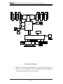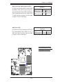
1
X8DTU-6F+
X8DTU-6TF+
X8DTU-6F+-LR
X8DTU-6TF+-LR
USER’S MANUAL
Revision 1.0a
The information in this User’s Manual has been carefully reviewed and is believed to be accurate.
The vendor assumes no responsibility for any inaccuracies that may be contained in this document,
makes no commitment to update or to keep current the information in this manual, or to notify any
person or organization of the updates. Please Note: For the most up-to-date version of this
manual, please see our website at www.supermicro.com.
Super Micro Computer, Inc. ("Supermicro") reserves the right to make changes to the product
described in this manual at any time and without notice. This product, including software and documentation, is the property of Supermicro and/or its licensors, and is supplied only under a license.
Any use or reproduction of this product is not allowed, except as expressly permitted by the terms
of said license.
IN NO EVENT WILL SUPER MICRO COMPUTER, INC. BE LIABLE FOR DIRECT, INDIRECT,
SPECIAL, INCIDENTAL, SPECULATIVE OR CONSEQUENTIAL DAMAGES ARISING FROM THE
USE OR INABILITY TO USE THIS PRODUCT OR DOCUMENTATION, EVEN IF ADVISED OF
THE POSSIBILITY OF SUCH DAMAGES. IN PARTICULAR, SUPER MICRO COMPUTER, INC.
SHALL NOT HAVE LIABILITY FOR ANY HARDWARE, SOFTWARE, OR DATA STORED OR USED
WITH THE PRODUCT, INCLUDING THE COSTS OF REPAIRING, REPLACING, INTEGRATING,
INSTALLING OR RECOVERING SUCH HARDWARE, SOFTWARE, OR DATA.
Any disputes arising between manufacturer and customer shall be governed by the laws of Santa
Clara County in the State of California, USA. The State of California, County of Santa Clara shall be
the exclusive venue for the resolution of any such disputes. Supermicro's total liability for all claims
will not exceed the price paid for the hardware product.
FCC Statement: This equipment has been tested and found to comply with the limits for a Class
A digital device pursuant to Part 15 of the FCC Rules. These limits are designed to provide
reasonable protection against harmful interference when the equipment is operated in a commercial
environment. This equipment generates, uses, and can radiate radio frequency energy and, if not
installed and used in accordance with the manufacturer’s instruction manual, may cause harmful
interference with radio communications. Operation of this equipment in a residential area is likely
to cause harmful interference, in which case you will be required to correct the interference at your
own expense.
California Best Management Practices Regulations for Perchlorate Materials: This Perchlorate
warning applies only to products containing CR (Manganese Dioxide) Lithium coin cells. “Perchlorate
Material-special handling may apply. See www.dtsc.ca.gov/hazardouswaste/perchlorate”.
WARNING: Handling of lead solder materials used in this
product may expose you to lead, a chemical known to
the State of California to cause birth defects and other
reproductive harm.
Manual Revision 1.0a
Release Date: Oct. 11, 2011
Unless you request and receive written permission from Super Micro Computer, Inc., you may not
copy any part of this document.
Information in this document is subject to change without notice. Other products and companies
referred to herein are trademarks or registered trademarks of their respective companies or mark
holders.
Copyright © 2011 by Super Micro Computer, Inc.
All rights reserved.
Printed in the United States of America
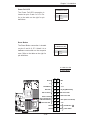
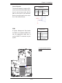
Preface
Preface
This manual is written for system integrators, PC technicians and
knowledgeable PC users. It provides information for the installation and use of the
X8DTU-6F+/X8DTU-6TF+/X8DTU-6(T)F+-LR motherboard.
About This Motherboard
The
X8DTU-6F+/X8DTU-6TF+/X8DTU-6(T)F+-LR motherboard supports
the Intel 5500/5600 Series processors, the first dual-processing platform that supports the Intel QuickPath Interconnect (QPI) Technology, providing the next generation point-to-point system interface to replace the current Front Side Bus. With the
5500/5600 Series processors built in, the X8DTU-6F+/X8DTU-6TF+/X8DTU-6(T)
F+-LR motherboard substantially enhances system performance in a small formfactor package. Please refer to our website (http://www.supermicro.com/products/)
for updates on supported processors. This product is intended to be installed and
serviced by professional technicians.
Manual Organization
Chapter 1 provides quick installation instructions.
Chapter 2 describes the features, specifications and performance of the motherboard and provides detailed information about the 5520 chipset.
Chapter 3 provides hardware installation instructions. Read this chapter when installing the processor, memory modules and other hardware components into the
system. If you encounter any problems, see Chapter 4, which describes troubleshooting procedures for video, memory and system setup stored in the CMOS.
Chapter 5 includes an introduction to the BIOS and provides detailed information
on running the CMOS Setup utility.
Appendix A provides BIOS Error Beep Codes.
Appendix B lists Other Software Program Installation Instructions.
iii
X8DTU-6F+/X8DTU-6TF+/X8DTU-6(T)F+-LR Motherboard User’s Manual
Conventions Used in the Manual
Special attention should be given to the following symbols for proper installation and
to prevent damage done to the components or injury to yourself:
Danger/Caution: Instructions to be strictly followed to prevent catastrophic
system failure or to avoid bodily injury
Warning: Important information given to ensure proper system installation
or to prevent damage to the components
Note: Additional Information given to differentiate various models or provides information for correct system setup.
Iv
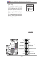
Table of Contents
Contacting Supermicro
Headquarters
Address:
Super Micro Computer, Inc.
980 Rock Ave.
San Jose, CA 95131 U.S.A.
Tel:
+1 (408) 503-8000
Fax:
+1 (408) 503-8008
Email:
[email protected] (General Information)
[email protected] (Technical Support)
Website:
www.supermicro.com
Europe
Address:
Super Micro Computer B.V.
Het Sterrenbeeld 28, 5215 ML
's-Hertogenbosch, The Netherlands
Tel:
+31 (0) 73-6400390
Fax:
+31 (0) 73-6416525
Email:
[email protected] (General Information)
[email protected] (Technical Support)
[email protected] (Customer Support)
Asia-Pacific
Address:
Super Micro Computer, Inc.
4F, No. 232-1, Liancheng Rd.
Chung-Ho 235, Taipei County
Taiwan, R.O.C.
Tel:
+886-(2) 8226-3990
Fax:
+886-(2) 8226-3991
Website:
www.supermicro.com.tw
Email:
[email protected] (Technical Support)
Tel:
+886-(2) 8226-5990 (Technical Support)
v
X8DTU-6F+/X8DTU-6TF+/X8DTU-6(T)F+-LR Motherboard User’s Manual
Table of Contents
Preface
Chapter 1 Quick Installation Guide
1-1
Installing the CPU ........................................................................................... 1-1
1-2
Installing the Passive CPU Heatsink .............................................................. 1-1
1-3
Installing the Memory Modules ....................................................................... 1-2
1-4
Installing the I/O Shield ................................................................................... 1-2
1-5
Installing the Motherboard .............................................................................. 1-3
1-6
Connecting the Power Supply......................................................................... 1-3
1-7
Installing Internal Peripherals .......................................................................... 1-4
1-8
Installing External Peripherals ........................................................................ 1-4
Chapter 2 Overview
2-1
Overview ......................................................................................................... 2-1
2-2
Chipset Overview ...........................................................................................2-11
2-3
Special Features ........................................................................................... 2-12
2-4
PC Health Monitoring .................................................................................... 2-12
2-5
ACPI Features............................................................................................... 2-13
2-6
Power Supply ................................................................................................ 2-13
2-7
Overview of the Nuvoton WPCM450 Controller ........................................... 2-14
2-8
Super I/O ....................................................................................................... 2-14
Chapter 3 Installation
3-1
Static-Sensitive Devices .................................................................................. 3-1
3-2
Processor and Heatsink Installation................................................................ 3-2
Installing an LGA 1366 Processor .................................................................. 3-2
Installing a Passive CPU Heatsink ................................................................. 3-4
Removing the Passive Heatsink ..................................................................... 3-5
Installing an Active Heatsink ........................................................................... 3-6
Removing the Active Heatsink ........................................................................ 3-7
3-3
Installing and Removing the Memory Modules............................................... 3-8
Installing & Removing DIMMs ......................................................................... 3-8
Removing Memory Modules ........................................................................... 3-8
3-4
Motherboard Installation ................................................................................ 3-13
Tools Needed ................................................................................................ 3-13
Location of Mounting Holes .......................................................................... 3-13
Installing the Motherboard ............................................................................ 3-14
3-5
Control Panel Connectors/I/O Ports.............................................................. 3-15
Back Panel Connectors/I/O Ports ................................................................. 3-15
vi
Table of Contents
Back Panel I/O Port Locations and Definitions ........................................... 3-15
ATX PS/2 Keyboard and PS/2 Mouse Ports ............................................ 3-16
Universal Serial Bus (USB) ...................................................................... 3-17
Serial Ports ............................................................................................... 3-18
Video Connector ....................................................................................... 3-18
Gigabit Ethernet Ports .............................................................................. 3-19
10Gb TLAN Ports and SFP+ Devices (X8DTU-6TF+)............................. 3-19
Unit Identifier Switches............................................................................. 3-20
Front Control Panel ....................................................................................... 3-21
Front Control Panel Pin Definitions............................................................... 3-22
NMI Button ............................................................................................... 3-22
Power LED .............................................................................................. 3-22
HDD/FP UID Switch ................................................................................. 3-23
NIC1 LED Indicator .................................................................................. 3-23
NIC2 LED Indicator .................................................................................. 3-24
Overheat (OH)/Fan Fail/PWR Fail/UID LED ............................................ 3-24
Power Fail LED ........................................................................................ 3-25
Reset Button ........................................................................................... 3-25
Power Button ........................................................................................... 3-26
3-6
Connecting Cables ........................................................................................ 3-27
Power Connectors ................................................................................... 3-27
Fan Headers............................................................................................. 3-28
Chassis Intrusion ..................................................................................... 3-28
Internal Speaker ....................................................................................... 3-29
IPMB ......................................................................................................... 3-29
DOM Power Connector ............................................................................ 3-30
Overheat LED/Fan Fail ............................................................................ 3-30
T-SGPIO 1/2 Headers .............................................................................. 3-31
Power SMB (I2C) Connector .................................................................... 3-31
UIO Power Connector .............................................................................. 3-32
SAS BBU Connector ................................................................................ 3-32
3-7
Jumper Settings ............................................................................................ 3-34
Explanation of Jumpers ................................................................................ 3-34
GLAN and TLAN Enable .......................................................................... 3-34
CMOS Clear ............................................................................................. 3-35
Watch Dog Enable/Disable ...................................................................... 3-35
I2C Bus to PCI-Exp. Slots ........................................................................ 3-36
VGA Enable .............................................................................................. 3-36
SAS Enable ............................................................................................. 3-37
vii
X8DTU-6F+/X8DTU-6TF+/X8DTU-6(T)F+-LR Motherboard User’s Manual
3-8
Onboard LED Indicators ............................................................................... 3-38
GLAN 1/2 LEDs........................................................................................ 3-38
IPMI Dedicated LAN LEDs ..................................................................... 3-38
10Gb_LAN LED (X8DTU-6TF+) ............................................................... 3-39
Onboard Power LED ............................................................................... 3-39
Rear UID LED ......................................................................................... 3-40
BMC Heartbeat LED ............................................................................... 3-40
SAS Activity & SAS Heartbeat LEDs ...................................................... 3-41
SAS Error LED ........................................................................................ 3-41
3-9
Serial ATA (SATA) and Serial Attached SCSI (SAS) Connections ............... 3-42
Serial ATA Ports........................................................................................ 3-42
SAS Ports ................................................................................................. 3-42
Chapter 4 Troubleshooting
4-1
Troubleshooting Procedures ........................................................................... 4-1
4-2
Technical Support Procedures ........................................................................ 4-4
4-3
Frequently Asked Questions ........................................................................... 4-5
4-4
Returning Merchandise for Service................................................................. 4-6
Chapter 5 BIOS
5-1
Introduction...................................................................................................... 5-1
5-2
Main Setup ...................................................................................................... 5-2
5-3
Advanced Setup Configurations...................................................................... 5-4
5-4
Security Settings ........................................................................................... 5-26
5-5
Boot Configuration ........................................................................................ 5-27
5-6
Exit Options ................................................................................................... 5-28
Appendix A BIOS Error Beep Codes
A-1
BIOS Error Beep Codes ................................................................................. A-1
Appendix B Software Installation Instructions
B-1
Installing Software Programs .......................................................................... B-1
B-2
Configuring Supero Doctor III ......................................................................... B-2
viii
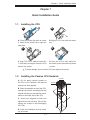
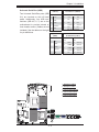
Chapter 1: Quick Installation Guide
Chapter 1
Quick Installation Guide
1-1
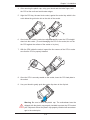
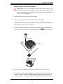
Installing the CPU
A
B
A. Press the socket clip down to unlock
it. Gently lift the socket clip to open the
load plate.
B. Align the CPU key with the socket
key.
D
C
C. Align CPU Pin 1 against Socket Pin
1. Once they are aligned, lower the CPU
down to the socket.
D. Once the CPU is fully seated on
the socket, press the socket clip down
to lock it.
To avoid damage, do not rub the CPU pins against the socket.
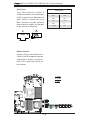
1-2
Installing the Passive CPU Heatsink
A. Do not apply thermal grease on
the CPU or the heatsink; the required
amount has been applied.
B. Place the heatsink on top of the CPU,
making sure that the mounting holes are
aligned with those on the retention mechanism on the back side of the CPU.
C. Install two diagonal screws and
tighten them until just snug. (Do not fully
tighten the screws to avoid damaging
the CPU.)
D. Finish the installation by fully installing all screws.
1-1
Screw#4
Screw#1
Screw#2
Screw#3
X8DTU-6F+/X8DTU-6TF+/X8DTU-6(T)F+-LR User’s Manual
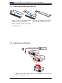
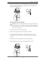
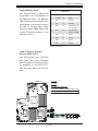
1-3
Installing the Memory Modules
A
B
C
A. Align the key on the DIMM module
C. Press the notches on the ends of
against that of the DIMM socket.
the DIMM module inwards to lock it.
B. Insert the DIMM module straight down
to the DIMM socket.
1-4
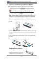
Installing the I/O Shield
A
B
Note: Chassis and I/O plate images are for illustration only. They may be
different from what you have.
1-2
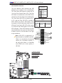
Chapter 1: Quick Installation Guide
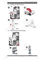
1-5
Installing the Motherboard
B
A
X8DTU-6F+
C
1-6
D
Connecting the Power Supply
X8DTU-6F+
B
A
1-3
X8DTU-6F+/X8DTU-6TF+/X8DTU-6(T)F+-LR User’s Manual
1-7
Installing Internal Peripherals
SATA / SAS Drives
1-8
Installing External Peripherals
Mouse
IPMI LAN
Keyboard USB 0/1 Serial Port
VGA Port
(COM1)
LAN 1/2 Ports TLAN 1/2 Ports UID
Switch
1-4
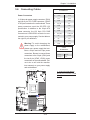
Chapter 2: Overview
Chapter 2
Overview
2-1
Overview
Checklist
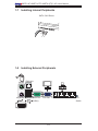
Congratulations on purchasing your computer motherboard from an acknowledged
leader in the industry. Supermicro boards are designed with the utmost attention to
detail to provide you with the highest standards in quality and performance.
Please check that the following items have all been included with your motherboard.
If anything listed here is damaged or missing, contact your retailer.
The following items are included in the retail box.
•
One (1) Supermicro Mainboard
•
One (1) I/O backpanel shield (MCP-260-00038-0N)
•
One (1) Supermicro CD containing drivers and utilities
•
One (1) User's/BIOS Manual (MNL#1188)
2-1
X8DTU-6F+/X8DTU-6TF+/X8DTU-6(T)F+-LR User’s Manual
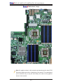
Motherboard Image
Note: All graphics shown in this manual were based upon the latest PCB
Revision available at the time of publishing of the manual. The motherboard
you've received may or may not look exactly the same as the graphics
shown in this manual.
2-2
Chapter 2: Overview
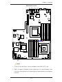
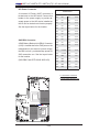
Motherboard Layout
LED2
LED7
LAN2
LAN1
TLAN1
(10Gb LAN1)
UIOP
TLAN2
(10Gb LAN2)
COM1
IPMI_LAN
JPL1
J1: PCI-E 2.0 X4 (in X16)
Intel 82599
10 Gb LAN 1/2
CTRL
Intel 82576
LAN 1/2
CTRL
PHY
SP1
Battery
JPTLAN
FAN8/CPU1
J2: PCI-E 2.0 X16
SAS BBU
J120
CPU1
P1-DIMM3A
P1-DIMM3B
P1-DIMM3C
P1-DIMM2A
P1-DIMM2B
JWD1
X8DTU-6F+
BMC
CTRL
JPG1
JI2C1JI2C2
LED3
P1-DIMM2C
SAS
CTRL
LED6
LSI 2108
LED5
LED4
JPS1
P1-DIMM1A
~7
P1-DIMM1B
P1-DIMM1C
SAS4
SAS0~3
Intel
JBT1
JPW1
P2-DIMM1B
CPU2
P2-DIMM1C
P2-DIMM1A
P2-DIMM2B
FAN1
JPW3 JPW2
JPI2C1
FAN7/CPU2
FAN6
T-SGPIO2
T-SGPIO1
FAN2
FAN3
P2-DIMM2C
IPMB
FAN5
FAN4
LED1
JF1
I-SATA5
JOH1
JWF1
USB7
USB4/5
I-SATA1
I-SATA2
I-SATA3
I-SATA4
P2-DIMM3C
BIOS
P2-DIMM2A
COM2 USB6
I-SATA0
P2-DIMM3A
ICH 10R
P2-DIMM3B
TPM
IOH 36D
Intel
JL1
USB0/1
VGA
KB/MOUSE
UID
Notes
•
•
TLAN (10 Gb LAN) Ports 1 &2 are available on the X8DTU-6TF+ only.
IPMI 2.0 support is available on the motherboard. For more information, refer
to the user guide posted on our website @ http://www.supermicro.com/support/
manuals/
2-3
X8DTU-6F+/X8DTU-6TF+/X8DTU-6(T)F+-LR User’s Manual
ED2
LED7
LAN2
LAN1
USB0/1
UIOP
TLAN2
(10Gb LAN2)
TLAN1
(10Gb LAN1)
VGA
KB/MOUSE
UID
COM1
IPMI_LAN
JPL1
J1: PCI-E 2.0 X4 (in X16)
Intel 82599
10 Gb LAN 1/2
CTRL
Intel 82576
LAN 1/2
CTRL
PHY
SP1
Battery
JPTLAN
FAN8/CPU1
J2: PCI-E 2.0 X16
SAS BBU
J120
CPU1
P1-DIMM3A
P1-DIMM3B
P1-DIMM3C
P1-DIMM2A
P1-DIMM2B
X8DTU-6F+
JWD1
JI2C1JI2C2
LED3
P1-DIMM2C
LED6
LED5
LED4
JPS1
SAS
CTRL
LSI 2108
P1-DIMM1A
~7
P1-DIMM1B
P1-DIMM1C
SAS4
SAS0~3
JPG1
BMC
CTRL
Intel
JBT1
CPU2
JPW1
P2-DIMM1C
P2-DIMM1B
P2-DIMM1A
P2-DIMM2B
P2-DIMM2C
P2-DIMM3C
BIOS
P2-DIMM2A
I-SATA0
FAN1
FAN6
T-SGPI
T-SGPI
JPI2C1
FAN3
FAN2
IPMB
FAN5
FAN4
LED1
JF1
JOH1
USB7
USB4/5
JWF1
I-SATA5
JPW3 JPW2
JL1
I-SATA1
I-SATA2
I-SATA3
I-SATA4
FAN7/CPU2
COM2 USB6
P2-DIMM3A
ICH 10R
P2-DIMM3B
TPM
IOH 36D
Intel
Notes:
•
" " indicates the location of "Pin 1".
•
Jumpers not indicated are for testing only.
•
When LED1 (Onboard Power LED Indicator) is on, system power is on. Unplug
the power cable before installing or removing any components.
2-4
Chapter 2: Overview
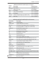
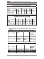
X8DTU-6F+/X8DTU-6TF+/X8DTU-6(T)F+-LR Jumpers
Jumper
Description
Default Setting
JBT1
Clear CMOS
See Chapter 3
2
2
JI C1/JI C2 SMB to PCI-E Slots
JPG1
VGA Enable
Off (Disabled)
Pins 1~2 (Enabled)
JPL1
(G-bit) LAN1/LAN2 Enable
Pins 1-2 (Enabled)
JPS1
SAS Enable
Pins 1-2 (Enabled)
JPTLAN
(10G-bit) TLAN1/2 Enable (for X8DTU -6TF+)
Pins 1-2 (Enabled)
JWD1
Watch Dog
Pins 1~2 (Reset)
X8DTU-6F+/X8DTU-6TF+/X8DTU-6(T)F+-LR Connectors
Connectors
Description
Battery
Onboard Battery
COM1/COM2
COM1/COM2 Serial Connections
FAN 1~8
CPU//System Fan Headers (Fans 7, 8: CPU Fans)
IPMB
4-pin External BMC I2C Header (for an IPMI Card)
I-SATA 0~5
Intel SB SATA Connectors 0~5
JF1
Front Panel Control Header
J1
PCI-Express 2.0 x4 in x16 Slot
J2
PCI-Express 2.0 x16 Slot
JL1
Chassis Intrusion
JOH1
Overheat/Fan Fail LED
2
JPI C1
Power Supply SMBbus I2C Header
JPW1
ATX 24-Pin Power Connector (See Warning on Pg. 2-6.)
JPW2/JPW3
12V 8-Pin Power Connectors (See Warning on Pg. 2-6.)
JPTM1
Trusted Platform Support Header (JPTM1)
JWF1
SATA DOM (Disk_On_Module) Power
KB/MS
PS2 Keyboard/Mouse
LAN1/LAN2
G-bit Ethernet Ports 1/2
TLAN1/TLAN2
10 G-bit Ethernet Ports 1/2 (for X8DTU -6TF+)
IPMI_LAN
IPMI_Dedicated LAN
SAS 0~3, 4~7
SAS (Serial_ Attached SCSI) Connectors
SAS BBU (J120)
SAS Battery-Backup Unit Connector (Part# BTR-0018L-0000LSI)
SP1
Onboard Buzzer (Internal Speaker)
T-SGPIO 1/2
Serial General Purpose I/O Headers
USB 0/1
Back Panel USB 0/1
2-5
X8DTU-6F+/X8DTU-6TF+/X8DTU-6(T)F+-LR User’s Manual
USB 4/5
Front-panel accessible USB Connections
USB 6
Type A USB Embedded Drive Connector
USB 7
USB Embedded Drive Connector
UID
UID (Unit Identifier) Switch
UIOP
Universal I/O Add-on Card Power Header (See the Warning
below.)
VGA
VGA Port
X8DTU-6F+/X8DTU-6TF+/X8DTU-6(T)F+-LR LED Indicators
LED
Description
State
Status
LED 1
Power LED
Green: On
PWR On
LED 2
UID LED
Blue: Solid On (from UID Switch), Unit IdentiBlinking (from IPMI)
fied
LED 3
BMC Heartbeat LED
Green: Blinking
BMC Normal
LED 4
SAS Activity LED
Blinking
SAS Active
LED 5
SAS Heartbeat LED
Blinking
SAS Normal
LED 6
SAS Error LED
On
SAS Errors
Occurred
10Gb Link: Green On
LED7
10Gb LAN Dual-port
LED (Up: TLAN1,
Bottom: TLAN2)
10Gb Active: Green Blinks
1Gb Link: Yellow On
1Gb Active: Yellow Blinks
Warnings!
•
To avoid damaging the power supply or motherboard, please use a power supply that contains a 24-pin and two 8-pin power connectors. Be sure to connect
these connectors to the 24-pin (JPW1) and the two 8-pin (JPW2,JPW3) power
connectors on the motherboard. Failure to do so will void the manufacturer
warranty on your power supply and motherboard.
•
To provide adequate power to the add-on cards installed on the motherboard,
please connect the UIOP PWR connector to the power supply for these cards
to work properly.
2-6
Chapter 2: Overview
Motherboard Features
CPU
•
Two Intel® 5500/5600 Series (LGA 1366) processors; each processor supports two full-width Intel QuickPath Interconnect (QPI) links with a total of
up to 51.2 GT/s Data Transfer Rate (6.4 GT/s per direction)
Memory
•
RDIMM
•
240-pin Reg. DDR3 ECC 1333/1066/800 MHz memory with support of up
to 288 GB in 18 slots
Note 1. 240-pin Dual Rank (DR) 16 GB Reg. ECC DDR3 1333/1066/800
MHz memory will support up to 288 GB. Memory speed will be downgraded
to 800 MHz. (Refer to the notes in the memory configuration tables in
Chpt. 3.)
Note 2. 240-pin Quad Rank (QR) 16 GB Reg. ECC DDR3 1066/800 MHz
memory will support up to 192 GB (with 6 DIMMs max. per CPU). Memory
speed will be downgraded to 800 MHz. (Refer to the notes in memory
configuration tables in Chpt. 3.)
•
LRDIMM (Load Reduced DIMM, for X8DTU-6F+-LR and 8XDTU-6TF+-LR
Only)
•
DDR3 ECC 1066 MHz memory with support of up 288 GB in 18 slots
Warning: For your system memory to work properly, be sure to use the
correct BIOS ROM for your system.
For the X8DTU+-6F+, use the X8DTU+-6F+BIOS. For the X8DTU+-6F+LR, use the X8DTU+-6F+-LR BIOS.
For the X8DTU+-6TF+, use the X8DTU+-6TF+ BIOS. For the X8DTU+6TF+-LR, use the X8DTU+-6TF+-LR BIOS.
To flash the BIOS, refer to http://www.supermicro.com/products/motherboard/QPI/5500/X8DTU_.cfm?IPMI=Y.
•
UDIMM
•
Unbuffered ECC/Non-ECC DDR3 1333/1066/800 MHz memory of up to
48 GB memory
DIMM Sizes
•
UDIMM 1 GB, 2 GB, and 4GB
2-7
X8DTU-6F+/X8DTU-6TF+/X8DTU-6(T)F+-LR User’s Manual
•
RDIMM 1 GB, 2GB, 4GB, 8GB, 16GB
Chipset
•
Intel® 5520 Chipset (IOH-36D & ICH10R)
Expansion
•
One (1) PCI Express 2.0 x16 slot (J2)
Slots
•
One (1) PCI Express2.0 x4 in x16 slot (J1)
Graphics
•
Winbond BMC Video Controller (Matrox G200eW)
Network
•
One Intel 82576EB Gigabit (10/100/1000 Mb/s) Ethernet
Dual-Channel Controller
•
One Intel 82599 10 Gigabit Ethernet Dual-Channel Controller for TLAN 1/2
ports with two Small_Form-Factor Pluggable Transceivers (SFPs) (X8DTU-6TF+
only)
•
Single Realtek RTL8201N PHY to support IPMI_LAN 2.0
I/O Devices SATA Connections
•
Six (6) SATA Ports with RAID 0, 1, 5, 10 support for Windows, RAID 0, 1, 10
support for Linux
SAS Connections
•
Eight (8) SAS Ports with RAID 0, 1, 10, 5, 6, 50, 60 support
Integrated IPMI 2.0
•
IPMI 2.0 supported by the WPCM450 BMC
Keyboard/Mouse
•
PS/2 Keyboard/Mouse ports on the I/O backplane
Serial (COM) Ports
•
Two (2) Fast UART 16550 Connections: one 9-pin RS-232 port and one
header
2-8
Chapter 2: Overview
Super I/O
•
Winbond Super I/O 83527HG
USB Devices
•
Two (2) USB ports on the rear I/O panel (USB 0/1) One (1) Type A connector
(USB 6)
•
•
Two Front Panel Accessible USB connections (USB 4, 5)
One Embedded USB drive connector (USB7)
BIOS
32 Mb SPI AMI BIOS® SM Flash BIOS
•
APM 1.2, PCI 2.3, ACPI 1.0/2.0/3.0, USB Keyboard, Plug & Play (PnP) and
SMBIOS 2.5
Power Configuration
•
•
•
ACPI/ACPM Power Management
Main switch override mechanism
Power-on mode for AC power recovery
PC Health
•
Onboard voltage monitors for CPU core, +3.3V, +5V, +12V, +3.3V Stdby, +5V
Stdby, VBAT, Memory, Chipset
•
•
•
•
CPU 6-Phase switching voltage regulator
CPU/System overheat LED and control
CPU Thermal Trip support
Thermal Monitor 2 (TM2) support
Fan Control
•
Fan status monitoring with firmware 4-pin (Pulse Width Modulation) fan speed
control
•
Low noise fan speed control
System Management
•
•
•
•
PECI (Platform Environment Configuration Interface) 2.0 support
System resource alert via Supero Doctor III
SuperoDoctor III, Watch Dog, NMI
Chassis Intrusion Header and Detection
Dimensions
•
16.50" (L) x 12.80" (W) (419.10 mm x 325.12 mm)
Note: For IPMI Configuration, refer to the Embedded IPMI Configuration
User's Guide available @ http://www.supermicro.com/support/manuals/.
2-9
QPI
Processor#1
Processor#0
PCI-E x4
in x8 Slot
PCI-E x16
I-PASS
E
F
C
PORT1
PORT1
E
PORT0
PORT1
Gen2 x4 PORT
1,2
PORT
3,4
Gen2 x8
Intel
82599EB
10Gb
IOH 36D
Gen2 x16
F
QPI
QPI
I-PASS
D
PORT0
DDR3 DIMM
B
PORT0
DDR3 DIMM
A
DDR3 DIMM
B
DDR3 DIMM
C
DDR3 DIMM
DDR3 DIMM
X8DTU-6F+/X8DTU-6TF+/X8DTU-6(T)F+-LR User’s Manual
SFP+
SFP+
PORT
7, 8, 9,10
Gen2 x8
LSI
SAS 2108 (Lane Reversal)
Optional BBU
PORT
5,6
ESI
CLINK
512 MB
800 MHz
DDR2
BIOS
SPI
ESI CLINK
PCIE Port 1-4
Gen1 x4
Intel
82576EB
ICH10R
PORT
8,10
PCI
COM1
USB
PCIE Port 5-6
LPC
SATA
SIO
BMC
W83527HG
COM2
VGA Connection RJ45
SATA #0
TPM
SATA #1
SLB9635TT
SATA #2
1.2
SATA #3
SATA #4
SATA #5
RJ45 RJ45
USB
USB 0/1
USB 4/5
USB 6, 7
PS2 KB/MS
System Block Diagram
Note: This is a general block diagram and may not exactly represent the
features on your motherboard. See the Motherboard Features pages for
the actual specifications of each motherboard.
2-10
Chapter 2: Overview
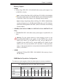
2-2
Chipset Overview
Built upon the functionality and the capability of the Intel 5520 platform, the X8DTU6F+/X8DTU-6TF+/X8DTU-6(T)F+-LR motherboard provides the performance and
feature sets required for dual-processor-based high-end systems HPC/Cluster
platforms. The 5520 platform consists of the 5500/5600 Series (LGA 1366) processor, the IOH-36D (IOH Hub), and the ICH10R (South Bridge). With the Intel
QuickPath interconnect (QPI) controller built in, the 5500/5600 Series Processor
is the first dual-processing platform that offers the next generation point-to-point
system interconnect interface, greatly enhancing system performance by utilizing
serial link interconnections which allows for increased bandwidth and scalability.
The IOH connects to each processor through an independent QuickPath Interconnect (QPI) link. Each link consists of 20 pairs of unidirectional differential lanes
for data transmission in addition to a differential forwarded clock. A full-width QPI
link pair provides 84 signals. Each processor supports two QuickPath links, one
going to the other processor and the other to the 5520 IO Hub.
The 5520 chipset supports up to 36 PCI Express Gen2 lanes, peer-to-peer read
and write transactions. The ICH10R provides up to six PCI-Express ports, six
SATA ports and six USB connections.
In addition, the 5520 chipset also offers a wide range of RAS (Reliability, Availability and Serviceability) features. These features include memory interface ECC,
x4/x8 Single Device Data Correction (SDDC), Cyclic Redundancy Check (CRC),
parity protection, out-of-band register access via SMBus, memory mirroring, and
Hot-plug support on the PCI-Express Interface.
Main Features of the 5500/5600 Series Processor and the
5520 Chipset
•
Four processor cores in each processor with 8MB shared cache among cores
•
Two full-width Intel QuickPath interconnect (QPI) links, up to 6.4 GT/s of data
transfer rate in each direction
•
Virtualization Technology, Integrated Management Engine supported
•
Point-to-point cache coherent interconnect, fast/narrow unidirectional links, and
concurrent bi-directional traffic
•
Error detection via CRC and error correction via Link-level retry
2-11
X8DTU-6F+/X8DTU-6TF+/X8DTU-6(T)F+-LR User’s Manual
2-3
Special Features
Recovery from AC Power Loss
The Basic I/O System (BIOS) provides a setting for you to determine how the
system will respond when AC power is lost and then restored to the system. You
can choose for the system to remain powered off (in which case you must press
the power switch to turn it back on), or for it to automatically return to a power-on
state. See the Advanced BIOS Setup section to change this setting. The default
setting is Last State.
2-4
PC Health Monitoring
This section describes the PC health monitoring features of the motherboard. All
have an onboard System Hardware Monitor chip that supports PC health monitoring. An onboard voltage monitor will scan these onboard voltages continuously:
CPU1 Vcore, CPU2 Vcore, 1.5V, 5V, 5VSB, 12V, 3.3Vcc, 3.3VSB, VBAT and Vtt.
Once a voltage becomes unstable, a warning is given or an error message is sent
to the screen. The user can adjust the voltage thresholds to define the sensitivity
of the voltage monitor.
Fan Status Monitor with Firmware Control
The PC health monitor can check the RPM status of the cooling fans. The onboard
CPU and chassis fans are controlled by Thermal Management via BIOS (under the
Hardware Monitoring section in the Advanced Setting).
Environmental Temperature Control
The thermal control sensor monitors the CPU temperature in real time and will turn
on the thermal control fan whenever the CPU temperature exceeds a user-defined
threshold. The overheat circuitry runs independently from the CPU. Once it detects
that the CPU temperature is too high, it will automatically turn on the thermal fan
control to prevent the CPU from overheating. The onboard chassis thermal circuitry
can monitor the overall system temperature and alert the user when the chassis
temperature is too high.
Note: To avoid possible system overheating, please be sure to provide
adequate airflow to your system.
System Resource Alert
This feature is available when used with Supero Doctor III in the Windows OS
2-12
Chapter 2: Overview
environment or used with Supero Doctor II in Linux. Supero Doctor is used to
notify the user of certain system events. For example, you can also configure
Supero Doctor to provide you with warnings when the system temperature, CPU
temperatures, voltages and fan speeds go beyond a predefined range.
2-5
ACPI Features
ACPI stands for Advanced Configuration and Power Interface. The ACPI specification defines a flexible and abstract hardware interface that provides a standard
way to integrate power management features throughout a PC system, including
its hardware, operating system and application software. This enables the system
to automatically turn on and off peripherals such as CD-ROMs, network cards, hard
disk drives and printers.
In addition to enabling operating system-directed power management, ACPI also
provides a generic system event mechanism for Plug and Play and an operating
system-independent interface for configuration control. ACPI leverages the Plug and
Play BIOS data structures, while providing a processor architecture-independent
implementation that is compatible with the Windows 2003, Windows XP, Windows
Vista and Windows 2008 Operating Systems.
Slow Blinking LED for Suspend-State Indicator
When the CPU goes into a suspend state, the chassis power LED will start blinking
to indicate that the CPU is in suspend mode. When the user presses any key, the
CPU will "wake up" and the LED will automatically stop blinking and remain on.
2-6
Power Supply
As with all computer products, a stable power source is necessary for proper and
reliable operation. It is even more important for processors that have high CPU
clock rates.
The X8DTU-6F+/X8DTU-6TF+/X8DTU-6(T)F+-LR motherboard accommodates 24pin ATX power supplies. Although most power supplies generally meet the specifications required by the CPU, some are inadequate. In addition, two 12V 8-pin power
connections are also required to ensure adequate power supply to the system. Also
your power supply must supply 1.5A for the Ethernet ports.
Warning! 1. To avoid damaging the power supply or motherboard, please
use a power supply that contains a 24-pin and two 8-pin power connectors. Be sure to connect these connectors to the 24-pin (JPW1) and the
two 8-pin (JPW2, JPW3) power connectors on the motherboard. Failure
to do so will void the manufacturer warranty on your power supply and
motherboard.
2-13
X8DTU-6F+/X8DTU-6TF+/X8DTU-6(T)F+-LR User’s Manual
2. To provide adequate power to the add-on cards installed on the motherboard, please connect the UIOP PWR connector to the power supply.
It is strongly recommended that you use a high quality power supply that meets ATX
power supply Specification 2.02 or above. It must also be SSI compliant. (For more
information, please refer to the web site at http://www.ssiforum.org/). Additionally, in
areas where noisy power transmission is present, you may choose to install a line
filter to shield the computer from noise. It is recommended that you also install a
power surge protector to help avoid problems caused by power surges.
2-7
Overview of the Nuvoton WPCM450 Controller
The Nuvoton WPCM450 Controller is a Baseboard Management Controller (BMC)
that supports the 2D/VGA-compatible Graphics Core with PCI interface, Virtual
Media, and Keyboard/Video/Mouse Redirection (KVMR) modules.
The WPCM450 interfaces with the host system via a PCI interface to communicate
with the Graphics core. It supports USB 2.0 and 1.1 for remote keyboard/mouse/
virtual media emulation. It also provides LPC interface to control Super IO functions. The WPCM450 is connected to the network via an external Ethernet PHY
module.
The Nuvoton WPCM450 Controller also supports two high-speed, 16550 compatible
serial communication ports (UARTs). Each UART includes a 16-byte send/receive
FIFO, a programmable baud rate generator, complete modem control capability and
a processor interrupt system. Both UARTs provide legacy speed with baud rate of
up to 115.2 Kbps and an advanced speed with baud rates of 250 K, 500 K, or 1
Mb/s, which support higher speed modems.
The WPCM450 communicates with onboard components via six SMBus interfaces,
fan control, and Platform Environment Control Interface (PECI) buses.
Note: For more information on IPMI configuration, please refer to the
Embedded IPMI User's Guide posted on our website @ http://www.supermicro.com/support/manuals/.
2-8
Super I/O
The Super I/O chip (Winbond W83527HG) provides functions that comply with ACPI
(Advanced Configuration and Power Interface), which includes support of legacy
and ACPI power management through an SMI or SCI function pin.
2-14
Chapter 3: Installation
Chapter 3
Installation
3-1
Static-Sensitive Devices
Electrostatic Discharge (ESD) can damage electronic components. To avoid damaging your system board, it is important to handle it very carefully. The following
measures are generally sufficient to protect your equipment from ESD.
Precautions
•
Use a grounded wrist strap designed to prevent static discharge.
•
Touch a grounded metal object before removing the board from the antistatic
bag.
•
Handle the board by its edges only; do not touch its components, peripheral
chips, memory modules, or gold contacts.
•
When handling chips or modules, avoid touching their pins.
•
Put the motherboard and peripherals back into their antistatic bags when not
in use.
•
For grounding purposes, make sure that your system chassis provides excellent
conductivity between the power supply, the case, the mounting fasteners and
the motherboard.
•
Use the correct type of onboard CMOS battery as specified by the manufacturer.
Do not install the onboard battery upside down to avoid possible explosion.
Unpacking
The motherboard is shipped in antistatic packaging to prevent static damage.
When unpacking the board, make sure that the person handling it is static protected.
3-1
X8DTU-6F+/X8DTU-6TF+/X8DTU-6(T)F+-LR User's Manual
3-2
Processor and Heatsink Installation
When handling the processor package, avoid placing direct pressure on
!
the label area of the fan.
Notes:
1. Always connect the power cord last, and always remove it before adding,
removing, or changing any hardware components. Make sure that you install
the processor into the CPU socket before installing the CPU heatsink.
2. Make sure to install the motherboard into the chassis before installing the
CPU heatsink and heatsink fans.
3. When purchasing a motherboard without a 5500/5600 Series processor preinstalled, make sure that the CPU socket plastic cap is in place, and none of
the CPU socket pins are bent; otherwise, contact the retailer immediately.
4. Refer to the Motherboard Features Section for more details on CPU support.
Installing an LGA 1366 Processor
1. Press the socket clip to release the load plate, which covers the CPU socket,
from its locking position.
2. Gently lift the socket clip to open the load plate.
3. Hold the plastic cap at its north and south center edges to remove it from the
CPU socket.
3-2
Chapter 3: Installation
4. After removing the plastic cap, using your thumb and the index finger, hold
the CPU at the north and south center edges.
5. Align the CPU key, the semi-circle cutout, against the socket key which is the
notch below the gold color dot on the side of the socket.
6. Once both CPU and the socket are aligned, carefully lower the CPU straight
down into the socket. (To avoid damaging the CPU or the socket, do not rub
the CPU against the surface of the socket or its pins.)
7. With the CPU inside the socket, inspect the four corners of the CPU to make
sure that the CPU is properly installed.
8. Once the CPU is securely seated on the socket, lower the CPU load plate to
the socket.
9. Use your thumb to gently push the socket clip down to the clip lock.
Warning: Be sure to save the plastic cap. The motherboard must be
shipped with the plastic cap properly installed to protect the CPU socket
pins. Shipment without the plastic cap properly installed will cause damage to the socket pins.
3-3
X8DTU-6F+/X8DTU-6TF+/X8DTU-6(T)F+-LR User's Manual
Installing a Passive CPU Heatsink
1. Do not apply any thermal grease to the heatsink or the CPU die because the
required amount has already been applied.
2. Place the heatsink on top of the CPU, making sure that the four mounting
holes are aligned with those on the retention mechanism.
3. Install two diagonal screws (e.g. the #1 and the #2 screws) and tighten them
until snug (Do not fully tighten the screws to avoid possible damage to the
CPU.)
4. Finish the installation by fully installing all screws.
3-4
Chapter 3: Installation
Removing the Passive Heatsink
Warning: We do not recommend that the CPU or the heatsink be removed. However, if you do need to remove the heatsink, please follow
the instructions below to uninstall the heatsink to avoid damaging the
CPU or other components.
1. Unplug the power cord from the power supply.
2. Disconnect the heatsink fan wires from the CPU fan header.
3. Using a screwdriver, remove the heatsink screws from the motherboard in the
sequence as show in the picture below.
4. Hold the heatsink as shown in the picture below and gently wriggle the heatsink to loosen it from the CPU, avoiding using excessive force while doing so.
Screw#3
Screw#1
Screw#2
Screw#4
5. Once the CPU is loosened, remove the heatsink from the CPU socket.
6. To reinstall the CPU and the heatsink, clean the surface of the CPU and the
heatsink to get rid of the old thermal grease. Reapply the proper amount of
thermal grease on the surface before reinstalling them on the motherboard.
3-5
X8DTU-6F+/X8DTU-6TF+/X8DTU-6(T)F+-LR User's Manual
Installing an Active Heatsink
1. Locate the CPU Fan power connector on the motherboard. (Refer to the
motherboard layout in Chapter 2 for the CPU Fan location.)
2. Position the heatsink in the way that the heatsink fan wires are closest to the
CPU fan power connector and do not interfere with other components.
3. Inspect the CPU Fan wires to make sure that the wires are routed through the
bottom of the heatsink.
Fan Wires
Heatsink Fins
4. Remove the thin layer of the protective film from the copper core of the heatsink.
(Warning! CPU overheat may occur if the protective film is not removed from
the heatsink.)
5. Apply the proper amount of thermal grease on the CPU. (Note: if your heatsink
came with a thermal pad, please ignore this step.)
6. If necessary, rearrange the wires to make sure that the wires are not pinched between the heatsink and the CPU. Also make sure to keep clearance between the
fan wires and the fins of the heatsink.
7. Align the four heatsink fasteners with the mounting holes on the motherboard.
8. Gently push the pairs of diagonal fasteners (#1 & #2, and #3 & #4) into the mounting holes until you hear a click. (Note: Make sure to properly orient each fastener
so that the narrow end of the groove is pointing outward.)
9. Repeat Step 7 to insert all four heatsink fasteners into the mounting holes.
3-6
Chapter 3: Installation
10. Once all four fasteners are securely inserted into the mounting holes, and the
heatsink is properly installed on the motherboard, connect the heatsink fan
wires to the CPU fan connector.
Removing the Active Heatsink
Warning: We do not recommend that the CPU or the heatsink be removed. However, if you do need to remove the heatsink, please follow
the instructions below to uninstall the heatsink and avoid damaging the
CPU or other components.
1. Unplug the power cord from the power supply.
2. Disconnect the heatsink fan wires from the CPU fan header.
3. Using your finger tips, gently press on the fastener cap and turn it counterclockwise to make a 1/4 (900) turn, and then pull the fastener upward to
loosen it.
4. Repeat Step 3 to loosen all fasteners from the mounting holes.
5. When all fasteners are loose, remove the heatsink from the CPU.
3-7
X8DTU-6F+/X8DTU-6TF+/X8DTU-6(T)F+-LR User's Manual
3-3
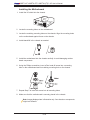
Installing and Removing the Memory Modules
Note: Check Supermicro's website for recommended memory modules.
CAUTION
Exercise extreme care when installing or removing DIMM
modules to prevent any possible damage.
Installing & Removing DIMMs
1. Insert the desired number of DIMMs into the memory slots, starting with P1DIMM #1A. (For best performance, please use the memory modules of the
same type and same speed in the same bank.)
2. Position the DIMM module's bottom key to align it with the receptive point on
the slot.
3. Push the Lock/Release tabs to the release positions. Make sure that the side
notches of a DIMM module align with the Lock/Release tabs of the slot when
pressed in.
4. Insert the DIMM module vertically and press it down until the module snaps
into place.
5. Press the Lock/Release tabs to secure the DIMM module.
Notches
Release
Release
Press Down
Lock/Release Tabs
Removing Memory Modules
Release
1. Reverse the steps above to remove the
DIMM modules from the motherboard.
3-8
Release
Chapter 3: Installation
Memory Support
•
RDIMM
•
240-pin Reg. DDR3 ECC 1333/1066/800 MHz memory with support of up
to 288 GB in 18 slots
Note 1. 240-pin Dual Rank (DR) 16 GB Reg. ECC DDR3 1333/1066/800
MHz memory will support up to 288 GB. Memory speed will be downgraded
to 800 MHz. (Refer to the notes in the following memory tables.)
Note 2. 240-pin Quad Rank (QR) 16 GB Reg. ECC DDR3 1066/800 MHz
memory will support up to 192 GB (with 6 DIMMs max. per CPU). Memory
speed will be downgraded to 800 MHz. (Refer to the notes in the following
memory tables.)
•
LRDIMM (Load Reduced DIMM, for X8DTU-6F+-LR and 8XDTU-6TF+-LR
Only)
•
LRDIMM DDR3 ECC 1066 MHz memory with support of up 288 GB in 18
slots
Warning: For your system memory to work properly, be sure to use
the correct BIOS ROM for your system. For the X8DTU+-6F+, use the
X8DTU+-6F+ BIOS. For the X8DTU+-6F+-LR, use the X8DTU+-6F+LR BIOS. For the X8DTU+-6TF+, use the X8DTU+-6TF+ BIOS. For the
X8DTU+-6TF+-LR, use the X8DTU+-6TF+-LR BIOS. To flash the BIOS,
refer to http://www.supermicro.com/products/motherboard/QPI/5500/
X8DTN_.cfm?IPMI=Y.
•
UDIMM
Unbuffered ECC/Non-ECC DDR3 1333/1066/800 MHz memory of up to
48 GB memory.
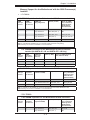
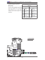
DIMM Module Population Configuration
For memory to work properly, follow the tables below for memory installation:
Memory Population for Optimal Performance
-For a Motherboard with One CPU (CPU1) Installed
P1-DIMMs
To Populate P1-DIMMs
Branch 0
Branch 1
Branch 2
3 DIMMs
P1-1A
P1-2A
P1-3A
6 DIMMs
P1-1A
P1-1B
9 DIMMs
(RDIMMs only) (Note)
P1-1A
P1-1B
P1-1C
P1-2A
P1-2B
P1-2A
P1-2B
Note: Max. of 6 UDIMM modules are supported by a CPU.
3-9
P1-2C
P1-3A
P1-3B
P1-3A
P1-3B
P1-3C
X8DTU-6F+/X8DTU-6TF+/X8DTU-6(T)F+-LR User's Manual
Memory Population for Optimal Performance
-For a Motherboard with One CPU (CPU2) Installed
P2-DIMMs
To Populate P2-DIMMs
Branch 0
Branch 1
Branch 2
3 DIMMs
P2-1A
P2-2A
P2-3A
6 DIMMs
P2-1A
P2-1B
9 DIMMs
(RDIMMs only (Note)
P2-1A
P2-1B
P2-1C
P2-2A
P2-2B
P2-2A
P2-2B
P2-2C
P2-3A
P2-3B
P2-3A
P2-3B
P2-3C
Note: Max. of 6 UDIMM modules are supported by a CPU.
Memory Population for Optimal Performance
-For a Motherboard with Two CPUs Installed
CPU 1 (To Populate P1-DIMMs)
CPU 2 (To Populate P2-DIMMs)
Branch 0
Branch 1
Branch 2
Branch 0
Branch 1
Branch 2
6 DIMMs
P1-1A
P1-2A
P1-3A
P2-1A
P2-2A
P2-3A
12 DIMMs
P1-1A/1B
P1-2A/2B
P1-3A/3B
P2-1A/1B
P2-2A/2B
P2-3A/3B
18 DIMMs
(For RDIMMs only) (Note)
P11A/1B/1C
P12A/2B/2C
P13A/3B/3C
P21A/1B/1C
P22A/2B/2C
P23A/3B/3C
Note: Max. of 6 UDIMM modules are supported by a CPU.
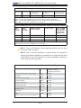
Memory Support for the Motherboard with the 5500 Processor(s)
Installed
RDIMM Population for the Motherboard w/5500 Processors Installed
DIMM
Slots per
Channel
DIMMs
Populated
per Channel
DIMM Type (Reg.=
Registered)
Speeds (in MHz)
Ranks per DIMM
(any combination;
SR=Single Rank,
DR=Dual Rank,
QR=Quad Rank)
3
1
Reg. DDR3 ECC
800,1066,1333
SR or DR
3
1
Reg. DDR3 ECC
800,1066
QR
3
2
Reg. DDR3 ECC
800,1066
Mixing SR, DR
3
2
Reg. DDR3 ECC
800 (Note)
Mixing SR, DR, QR
3
3
Reg. DDR3 ECC
800 (Note )
Mixing SR, DR
Note: 1066 RDIMMs will run at 800 MHz (-BIOS automatic downgrading)
UDIMM Population for the Motherboard w/5500 Processors Installed
DIMM
Slots per
Channel
DIMMs
Populated
per Channel
DIMM Type (Unb.=
Unbuffered)
Speeds (in MHz)
Ranks per DIMM
(any combination;
SR=Single Rank,
DR=Dual Rank,
QR=Quad Rank)
3
1
Unb. DDR3 ECC/Non-ECC
800,1066,1333
SR or DR
3
2
Unb. DDR3 ECC/Non-ECC
800,1066
Mixing SR, DR
3
3
Not available
Not available
Not available
3-10
Chapter 3: Installation
Memory Support for the Motherboard with the 5600 Processor(s)
Installed
•
1.5V DIMMs
1.5V RDIMM Population for the Motherboard w/5600 Processors Installed
DIMM
Slots per
Channel
DIMMs
Populated
per Channel
DIMM Type
(Reg.=Registered)
Speeds (in MHz)
Ranks per DIMM
(any combination;
SR=Single Rank,
DR=Dual Rank,
QR=Quad Rank)
3
1
Reg. DDR3 ECC
800,1066,1333
SR or DR
3
1
Reg. DDR3 ECC
800,1066 (Note 1)
QR
3
2
Reg. DDR3 ECC
800,1066, 1333
Mixing SR, DR
3
2
Reg. DDR3 ECC
800 (Note 2)
Mixing SR, DR, QR
3
3
Reg. DDR3 ECC
800 (Note 2)
Mixing SR, DR
Note 1: 1333 MHz RDIMMs will run at 1066 MHz (-BIOS automatic downgrading).
Note 2: 1333/1066 MHz RDIMMs will run at 800 MHz (-BIOS automatic downgrading).
Note 3: MIxing of 1.35V and 1.5V DIMMs is not recommended.
1.5V LRDIMM Population for the Motherboard w/5600 Processors
Installed (for X8DTU-6F+-LR and 8XDTU-6TF+-LR Only)
DIMM
Slots per
Channel
DIMMs
Populated
per Channel
DIMM Type
(LR= Load
Reduced)
Speeds (in MHz)
Ranks per DIMM (QR=Quad
Rank, OR=Octal Rank)
3
1
LR DDR3 ECC
1066
QR or OR
3
2
LR DDR3 ECC
1066
QR or OR
3
3
LR DDR3 ECC
1066
QR
1.5V UDIMM Population for the Motherboard w/5600 Processors Installed
DIMM
Slots per
Channel
DIMMs
Populated
per Channel
UDIMM (Unb. DIMM/
Unbuffered DIMM)
Speeds (in MHz)
Ranks per DIMM
(any combination;
SR=Single Rank,
DR=Dual Rank,
QR=Quad Rank)
3
1
Unb. DDR3 ECC/Non-ECC
800,1066,1333
SR or DR
3
2
Unb. DDR3 ECC/Non-ECC
800,1066, 1333
Mixing SR, DR
3
3
Not Available
Not Available
Not Available
Note 1: 1333 MHz for two DIMMs per channel is supported when Unbuf./ECC DIMMs are used.
Note 2: MIxing of 1.35V and 1.5V DIMMs is not recommended.
1.35V DIMMs
1.35V RDIMM Population for the Motherboard w/5600 Processors
DIMM
Slots per
Channel
DIMMs
Populated
per Channel
RDIMM (Reg. DIMM/
Registered DIMM)
Speeds (in MHz)
Ranks per DIMM
(any combination;
SR=Single Rank,
DR=Dual Rank,
QR=Quad Rank)
3
1
Reg. DDR3 ECC
800,1066,1333
SR or DR
3
1
Reg. DDR3 ECC
800 (Note 1)
QR
3-11
X8DTU-6F+/X8DTU-6TF+/X8DTU-6(T)F+-LR User's Manual
1.35V RDIMM Population for the Motherboard w/5600 Processors
3
2
Reg. DDR3 ECC
800,1066 (Note 2)
Mixing SR, DR
3
2
Reg. DDR3 ECC
800 (Note 3)
Mixing SR, DR, QR
3
3
Not Available
Not Available
Not Available
Note
Note
Note
Note
1:
2:
3:
4:
1333/1066 MHz QR RDIMMs will run at 800 MHz (-BIOS automatic downgrading).
1333 MHz SR/DR RDIMMs will run at 800 MHz (-BIOS automatic downgrading).
1333/1066 MHz SR/DR/QR RDIMMs will run at 800 MHz (-BIOS automatic downgrading).
MIxing of 1.35V and 1.5V DIMMs is not recommended.
1.35V UDIMM Population for the Motherboard w/5600 Processors Installed
DIMM
Slots per
Channel
DIMMs
Populated
per Channel
UDIMM (Unb. DIMM/
Unbuffered DIMM)
Speeds (in MHz)
Ranks per DIMM
(any combination;
SR=Single Rank,
DR=Dual Rank,
QR=Quad Rank)
3
1
Unb. DDR3 ECC
800,1066,1333
SR or DR
3
2
Unb. DDR3 ECC
800,1066
Mixing SR, DR
3
3
Not Available
Not Available
Not Available
Note 1: 1333 MHz for two DIMMs per channel is supported when Unbuf./ECC DIMMs are used.
Note 2: MIxing of 1.35V and 1.5V DIMMs is not recommended.
Note 1: Due to OS limitations, some operating systems may not show
more than 4 GB of memory.
Note 2: Due to memory allocation to system devices, the amount of
memory that remains available for operational use will be reduced when
4 GB of RAM is used. The reduction in memory availability is disproportional. (See the following Table.)
Possible System Memory Allocation & Availability
System Device
Size
Physical
Memory
Remaining (-Available)
(4 GB Total System Memory)
Firmware Hub flash memory (System BIOS)
1 MB
3.99 GB
Local APIC
4 KB
3.99 GB
Area Reserved for the chipset
2 MB
3.99 GB
I/O APIC (4 Kbytes)
4 KB
3.99 GB
PCI Enumeration Area 1
256 MB
3.76 GB
PCI Express (256 MB)
256 MB
3.51 GB
PCI Enumeration Area 2 (if needed) -Aligned on
256-MB boundary-
512 MB
3.01 GB
VGA Memory
16 MB
2.85 GB
TSEG
1 MB
2.84 GB
Memory available for the OS & other applications
3-12
2.84 GB
Chapter 3: Installation
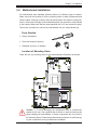
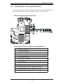
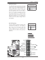
3-4
Motherboard Installation
All motherboards have standard mounting holes to fit different types of chassis.
Make sure that the locations of all the mounting holes for both motherboard and
chassis match. Although a chassis may have both plastic and metal mounting fasteners, metal ones are highly recommended because they ground the motherboard
to the chassis. Make sure that the metal standoffs click in or are screwed in tightly.
Then use a screwdriver to secure the motherboard onto the motherboard tray.
Tools Needed
•
Philips Screwdriver
•
Pan head screws (9 pieces)
•
Standoffs (9 pieces, if needed)
Location of Mounting Holes
There are nine (9) mounting holes on this motherboard indicated by the arrows.
X8DTU-6F+
Caution: 1) To avoid damaging the motherboard and its components,
please do not use a force greater than 8 lb/inch on each mounting screw
when installing the motherboard. 2) Some components are very close to
the mounting holes. Please take precautionary measures to avoid damaging the components during motherboard installation.
3-13
X8DTU-6F+/X8DTU-6TF+/X8DTU-6(T)F+-LR User's Manual
Installing the Motherboard
1. Install the I/O shield into the chassis.
2. Locate the mounting holes on the motherboard.
3. Locate the matching mounting holes on the chassis. Align the mounting holes
on the motherboard against those on the chassis.
4. Install standoffs in the chassis as needed.
5. Install the motherboard into the chassis carefully to avoid damaging motherboard components.
6. Using the Philips screwdriver, insert a Pan head #6 screw into a mounting
hole on the motherboard and its matching mounting hole on the chassis.
7. Repeat Step 5 to insert #6 screws into all mounting holes.
8. Make sure that the motherboard is securely placed in the chassis.
Note: Images displayed are is illustration only. Your chassis or components
might look different.
3-14
Chapter 3: Installation
3-5
Control Panel Connectors/I/O Ports
The I/O ports are color coded in conformance with the PC 99 specification. See
the picture below for the colors and locations of the various I/O ports.
Back Panel Connectors/I/O Ports
X8DTU-6F+
2
5
1
4
6
7
8
3
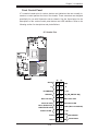
Back Panel I/O Port Locations and Definitions
1. Keyboard (Purple)
2. PS/2 Mouse (Green)
3. Back Panel USB Port 0
4. Back Panel USB Port 1
5. IPMI_Dedicated LAN
6. COM Port 1 (Turquoise)
7. VGA1 (Blue)
8. Gigabit LAN 1
9. Gigabit LAN 2
10. 10 Gb TLAN 1 + SFP+ 1 (X8DTU-6TF+ only)
11. 10 Gb TLAN 2 + SFP+ 2 (X8DTU-6TF+ only)
12. UID Switch
3-15
9 10 11 12
X8DTU-6F+/X8DTU-6TF+/X8DTU-6(T)F+-LR User's Manual
ATX PS/2 Keyboard and PS/2
PS/2 Keyboard/Mouse Pin
Definitions
Mouse Ports
The ATX PS/2 keyboard and PS/2
PS2 Keyboard
PS2 Mouse
mouse are located next to the Back
Pin#
Definition
Pin#
Definition
Panel USB Ports 0~1 on the moth-
1
KB Data
1
Mouse Data
erboard. See the table at right for pin
definitions.
2
No Connection
2
No Connection
3
Ground
3
Ground
4
Mouse/KB VCC
(+5V)
4
Mouse/KB VCC
(+5V)
5
KB Clock
5
Mouse Clock
6
No Connection
6
No Connection
VCC: with 1.5A PTC (current limit)
1. Keyboard (Purple)
2. Mouse (Green)
X8DTU-6F+
2
1
3-16
Chapter 3: Installation
Universal Serial Bus (USB)
Backplane USB
(USB 0/1)
Two Universal Serial Bus ports (USB
0/1) are located on the I/O back
panel. Additionally, four USB connections (USB 4/5, 6, 7) are on the
motherboard to provide internal or
front chassis access. (Cables are not
included). See the tables on the right
Internal and Front Panel USB
Pin Definitions (USB 4/5)
Pin# Definition
Pin # Definition
1
+5V
1
+5V
1
+5V
2
PO-
2
PO-
2
PO-
3
PO+
3
PO+
4
Ground
4
Ground
3
PO+
4
Ground
5
NA
5
for pin definitions.
1
Vcc
2
Data-
3
Data+
4
Ground
5
NA
Key
5
NC
(NC= No connection)
Embedded USB
Pin Definitions (USB 7)
Type A USB
(USB 6)
Pin# Definition
Pin # Definition
Pin # Definition
Pin # Definition
1
PWR
2
Ground
3
USBD-
4
Ground
5
USBD+
6
Ground
7
Ground
8
Ground
9
NA
10
Ground
1. Backpanel USB 0
2. Backpanel USB 1
3. Front Panel USB 4/5
4. Front Panel USB 6
5. Front Panel USB 7
X8DTU-6F+
4
3
5
2
1
3-17
X8DTU-6F+/X8DTU-6TF+/X8DTU-6(T)F+-LR User's Manual
Serial Ports
Serial COM) Ports
Pin Definitions
Two COM connections (COM1 &
COM2) are located on the motherboard.
COM1 is located on the Backplane I/O
panel. COM2 is located next to the
BMC controller to provide additional
serial connection support. See the table
on the right for pin definitions.
1
Pin #
Definition
Pin #
1
DCD
6
DSR
2
RXD
7
RTS
3
TXD
8
CTS
4
DTR
9
RI
5
Ground
10
N/A
2
COM2
COM1
Video Connector
A Video (VGA) port is located next to
COM1 on the I/O backplane to provide
video/graphic display connection.
Refer to the board layout below for
the locations.
3
1
1. COM1
2. COM2
3. VGA
X8DTU-6F+
2
1
3-18
Definition
3
Chapter 3: Installation
Gigabit Ethernet Ports
LAN Ports
Pin Definition
Two Ethernet ports (LAN1/LAN2)
are located on the I/O backplane on
the X8DTU-6F+/6TF+. An additional
IPMI_Dedicated LAN is located on the
motherboard to provide KVM support
for IPMI 2.0. All these ports accept
RJ45 type cables. (Note: Please refer
Pin# Definition
1
P2V5SB
10
SGND
2
TD0+
11
Act LED
3
TD0-
12
P3V3SB
4
TD1+
13
Link 100 LED (Yellow, +3V3SB)
5
TD1-
14
Link 1000 LED
(Yellow, +3V3SB)
6
TD2+
15
Ground
7
TD2-
16
Ground
8
TD3+
17
Ground
9
TD3-
18
Ground
to the LED Indicator Section for LAN
LED information.)
(NC: No Connection)
10Gb TLAN Ports and SFP+
Devices (X8DTU-6TF+)
Two 10Gb Ethernet ports (TLAN1/2)
with Small_Form Factor Pluggable
Device support are located at on the
I/O backplane on the X8DTU-6TF+.
See the layout below for the locations.
1. LAN1
2. LAN2
3. IPMI-Dedicated LAN
4. TLAN 1 (w/SFP+) (X8DTU-6TF+ only)
5. TLAN 2 (w/SFP+) (X8DTU-6TF+ only)
X8DTU-6F+
3
1
3-19
2
4
5
X8DTU-6F+/X8DTU-6TF+/X8DTU-6(T)F+-LR User's Manual
Unit Identifier Switches
UID Switch (UID)
Pin Definitions
Two Unit Identifier (UID) Switches and LED
Indicators are located on the motherboard.
Pin# Definition
The Front Panel UID Switch is located at Pin
13 on the Front Control Panel (JF1). The Rear
UID Switch is located next to the UIOP Power
connector on the rear side of the motherboard.
1
Ground
2
Ground
3
Button In
4
Ground
The Front Panel UID LED is located at Pin 7
UID LED (LED 2)
Status
of JF1, and the Rear UID LED is located at
LED2. When you press a UID switch on the
front panel or on the back panel, both Rear UID
Color/State OS Status
Blue: On
Windows OS
Unit Identified
LED and Front Panel UID LED will be turned
on. Press the UID switch again to turn off both
LED Indicators. These UID Indicators provide
easy identification of a system unit that may be
in need of service. See the table on the right
for pin definitions.
Blue:
Blinking
Linux OS
Unit Identified
Note: UID LED is supported by a
physical switch or the BMC controller.
When it is controlled by the physical
switch (for a Windows system), it
will stay solid. When it is controlled
by the BMC (for a Linux system), it
will blink.
1 2
20
19
Ground
NMI
X
X
3.3 V
FP PWRLED
3
ID_UID_SW/3/3V Stby
HDD LED
NIC1 Link LED
NIC1 Active LED
NIC2 Link LED
NIC2 Active LED
Blue+ (OH/Fan Fail/
PWR FaiL/UID LED
4
Red+ (Blue Led Cathode)
Power Fail LED
3.3V
Ground
Ground
2
Reset
Reset Button
PWR
Power Button
1
1. Rear UID Switch
2. Rear UID LED (LED 2)
3. FP UID Switch
4. FP UID LED
X8DTU-6F+
1
3-20
Chapter 3: Installation
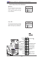
Front Control Panel
JF1 contains header pins for various buttons and indicators that are normally located on a control panel at the front of the chassis. These connectors are designed
specifically for use with Supermicro server chassis. See the figure below for the
descriptions of the various control panel buttons and LED indicators. Refer to the
following section for descriptions and pin definitions.
JF1 Header Pins
X8DTU-6F+
20
19
Ground
NMI
X
X
3.3 V
FP PWRLED
ID_UID_SW/3/3V Stby
HDD LED
NIC1 Link LED
NIC1 Active LED
NIC2 Link LED
NIC2 Active LED
Blue+ (OH/Fan Fail/
PWR FaiL/UID LED
Red+ (Blue Led Cathode)
Power Fail LED
3.3V
Ground
Reset
Reset Button
Ground
PWR
Power Button
2
3-21
1
X8DTU-6F+/X8DTU-6TF+/X8DTU-6(T)F+-LR User's Manual
Front Control Panel Pin Definitions
NMI Button
NMI Button
Pin Definitions (JF1)
The non-maskable interrupt button
header is located on pins 19 and 20
of JF1. Refer to the table on the right
for pin definitions.
Pin#
Definition
19
Control
20
Ground
Power LED
Power LED
Pin Definitions (JF1)
The Power LED connection is located
on pins 15 and 16 of JF1. Refer to the
table on the right for pin definitions.
Pin#
Definition
15
+5V
16
Ground
A. NMI
B. PWR LED
20
19
Ground
No Connection A
Key
Key
B Power LED
3.3V
FP UID Switch/3.3V SB
HDD LED
X8DTU-6F+
NIC1(Link) LED
NIC1 (Activity) LED
NIC2 (Link) LED
NIC2 (Activity) LED
OH/Fan Fail/PWR
Fail/UID LED
Blue_LED_Cathode
(UID)/5V SB
PWR Fail LED
3.3V
Ground
Ground
2
3-22
1
Reset
Reset Button
PWR
Power Button
Chapter 3: Installation
HDD/FP UID Switch
HDD/UID Switch
Pin Definitions (JF1)
The HDD/UID Switch connections are located
on pins 13/14 of JF1. Attach a hard-drive LED
cable to display HDD or SATA activities. This
connection can also be used as a front panel
Pin#
Definition
13
UID Signal/3.3V SB
14
HDD Active
UID (Unit Identifier) switch. The UID LED on
Pin 7 of JF1 works in conjunction with this
UID Switch located at Pin 13. When the user
presses and releases the UID switch, the UID
LED will be turned on or off to indicate the
location of the unit. (Refer to Page 2-20 for
more details.)
NIC1 LED Indicator
GLAN1 LED
Pin Definitions (JF1)
The NIC (Network Interface Controller) LED
connections for GLAN port 1 are located on
pins 11 and 12 of JF1. Attach a NIC LED
cable to display LAN Port1 connections and
activities. Refer to the table on the right for pin
definitions.
Pin#
Definition
11
NIC1 Activity
12
NIC1 Link
A. HDD LED
B. FP UID Switch
C. NIC1 Link LED
D. NIC1 Activity LED
20
19
Ground
NMI
X
C
X8DTU-6F+
X
FP PWRLED
3.3 V
A HDD LED
ID_UID_SW/3/3V Stby B
NIC1 Link LED
NIC1 Active LED D
NIC2 Link LED
NIC2 Active LED
Blue+ (OH/Fan Fail/
PWR FaiL/UID LED
Red+ (Blue Led Cathode)
Power Fail LED
3.3V
Ground
Ground
2
3-23
1
Reset
Reset Button
PWR
Power Button
X8DTU-6F+/X8DTU-6TF+/X8DTU-6(T)F+-LR User's Manual
NIC2 LED Indicator
GLAN2 LED
Pin Definitions (JF1)
The Network LED connections for
GLAN port 2 are located on pins 9 and
Pin#
10 of JF1. Attach a NIC LED cable to
display LAN Port2 connections and
Definition
9
NIC2 Activity
10
NIC2 Link
activities. Refer to the table on the
right for pin definitions.
OH/Fan Fail/ PWR Fail/Blue_UID
LED Pin Definitions (JF1)
Pin#
Overheat (OH)/Fan Fail/PWR Fail/
UID LED
Connect an LED cable to pins 7 and
8 of JF1 to use the Overheat/Fan Fail/
Power Fail/UID LED connections.
Refer to Page 3-20 for more information on UID Switches/LED Indicators.
See the tables on the right for pin
definitions.
Definition
7
Blue_LED Cathode (UID)
8
OH/Fan Fail/PWR Fail/UID LED
OH/Fan Fail/PWR Fail LED Status
Pin 7
Pin 8
Red LED
Blue LED
Low
High
On: OH/FF/PWR Fail
(Solid On: OH
Fast Blinking: Fan Fail
Slow Blinking: PWR Fail)
Off
High
Low
Off
(System: Normal)
On
UID LED
High
High
Off
Off
A. NIC 2 Link LED
B. NIC 2 Activity LED
C. OH/Fan Fail/PWR Fail/UID LED (Red LED)
D. UID LED (Blue)
20
19
Ground
NMI
X
X
3.3 V
FP PWRLED
ID_UID_SW/3/3V Stby
HDD LED
NIC1 Active LED
NIC1 Link LED
NIC2 Active LED B
A NIC2 Link LED
C Blue+ (OH/Fan Fail/
X8DTU-6F+
Red+ (Blue Led Cathode) D
PWR FaiL/UID LED
Power Fail LED
3.3V
Ground
Ground
2
3-24
1
Reset
Reset Button
PWR
Power Button
Chapter 3: Installation
Power Fail LED
PWR Fail LED
Pin Definitions (JF1)
The Power Fail LED connection is
located on pins 5 and 6 of JF1. Refer to the table on the right for pin
definitions.
Pin#
Definition
5
3.3 V
6
Ground
Reset Button
Reset Button
Pin Definitions (JF1)
The Reset Button connection is located
on pins 3 and 4 of JF1. Attach it to a
hardware reset switch on the computer
case. Refer to the table on the right for
pin definitions.
Pin#
Definition
3
Reset
4
Ground
A. PWR Fail LED
B. Reset Button
20
19
Ground
NMI
X
X
3.3 V
FP PWRLED
ID_UID_SW/3/3V Stby
HDD LED
X8DTU-6F+
NIC1 Link LED
NIC1 Active LED
NIC2 Link LED
NIC2 Active LED
Blue+ (OH/Fan Fail/
PWR FaiL/UID LED
Red+ (Blue Led Cathode)
A Power Fail LED
3.3V
Ground
Reset
Reset Button
Ground
PWR
Power Button
2
3-25
1
B
X8DTU-6F+/X8DTU-6TF+/X8DTU-6(T)F+-LR User's Manual
Power Button
Power Button
Pin Definitions (JF1)
The Power Button connection is located
on pins 1 and 2 of JF1. Momentarily
Pin#
Definition
contacting both pins will power on/off
1
Signal
the system. This button can also be con-
2
+3V Standby
figured to function as a suspend button
(with a setting in the BIOS - see Chapter
5). To turn off the power when the system
is in suspend mode, press the button for
at least 4 seconds. Refer to the table on
the right for pin definitions.
A. PWR Button
20
19
Ground
NMI
X
X
3.3 V
FP PWRLED
ID_UID_SW/3/3V Stby
HDD LED
X8DTU-6F+
NIC1 Link LED
NIC1 Active LED
NIC2 Link LED
NIC2 Active LED
Blue+ (OH/Fan Fail/
PWR FaiL/UID LED
Red+ (Blue Led Cathode)
Power Fail LED
3.3V
Ground
Ground
2
3-26
1
Reset
Reset Button
PWR
Power Button
A
Chapter 3: Installation
3-6
Connecting Cables
ATX Power 24-pin Connector
Pin Definitions
Pin# Definition Pin #
Power Connectors
13
+3.3V
1
+3.3V
A 24-pin main power supply connector (JPW1)
and two 8-pin CPU PWR connectors (JPW2/
14
-12V
2
+3.3V
15
COM
3
COM
JPW3) are located on the motherboard. These
16
PS_ON
4
+5V
power connectors meet the SSI EPS 12V
17
COM
5
COM
specification. In addition to the 24-pin ATX
power connector, the 12V 8-pin CPU PWR
18
COM
6
+5V
19
COM
7
COM
connectors at JPW2/JPW3 must also be con-
20
Res (NC)
8
PWR_OK
nected to your power supply. See the table on
the right for pin definitions.
21
+5V
9
5VSB
22
+5V
10
+12V
23
+5V
11
+12V
24
COM
12
+3.3V
Warning! To avoid damaging the
power supply or the motherboard,
please use a power supply that contains a 24-pin and two 8-pin power
connectors. Be sure to connect these
connectors to the 24-pin (JPW1) and
the two 8-pin (JPW2, JPW3) power
connectors on the motherboard. Failure to do so will void the manufacturer warranty on your power supply
and motherboard.
LED2
LED7
LAN2
LAN1
USB0/1
UIOP
TLAN2
(10Gb LAN2)
TLAN1
(10Gb LAN1)
VGA
KB/MOUSE
UID
COM1
IPMI_LAN
JPL1
J1: PCI-E 2.0 X4 (in X16)
Intel 82599
10 Gb LAN 1/2
CTRL
Intel 82576
LAN 1/2
CTRL
PHY
Battery
FAN8/CPU1
J2: PCI-E 2.0 X16
SAS BBU
CPU1
P1-DIMM3A
P1-DIMM3B
P1-DIMM3C
P1-DIMM2C
P1-DIMM2A
X8DTU-6F+
JWD1
JI2C1JI2C2
LED3
P1-DIMM2B
P1-DIMM1C
SAS
CTRL
LED6
LSI 2108
LED5
LED4
JPS1
P1-DIMM1B
~7
P1-DIMM1A
SAS4
SAS0~3
JPG1
BMC
CTRL
Intel
JBT1
CPU2
C
I-SATA0
JPW3 JPW2
JPI2C1
FAN1
FAN6
T-SGPIO2
T-SGPIO1
FAN2
FAN3
FAN7/CPU2
IPMB
FAN4
JOH1
LED1
JF1
I-SATA5
FAN5
JWF1
USB7
USB4/5
I-SATA1
I-SATA2
I-SATA3
I-SATA4
JPW1
P2-DIMM1C
P2-DIMM1B
P2-DIMM1A
P2-DIMM2B
P2-DIMM2C
P2-DIMM3C
P2-DIMM2A
COM2 USB6
P2-DIMM3A
BIOS
P2-DIMM3B
TPM
IOH 36D
Intel
ICH 10R
12V 8-pin PWR Connector
Pin Definitions
Pins
Definition
1 through 4
Ground
5 through 8
+12V
(Required)
A. 24-pin ATX PWR (Req'd)
B/C.8-pin Processor PWR
(Req'd)
SP1
JPTLAN
J120
JL1
Definition
A
B
3-27
X8DTU-6F+/X8DTU-6TF+/X8DTU-6(T)F+-LR User's Manual
Fan Headers
Fan Header
Pin Definitions
This motherboard has six chassis/system
fan headers (Fan 1 to Fan 6) and two
CPU fans (Fan7/Fan8) on the motherboard. All these 4-pin fans headers are
backward compatible with the traditional
3-pin fans. However, fan speed control
Pin#
Definition
1
Ground
2
+12V
3
Tachometer
4
PWR Modulation
is available for 4-pin fans only. The fan
speeds are controlled by Thermal Management via Hardware Monitoring in the
Advanced Setting in the BIOS. See the
table on the right for pin definitions.
Chassis Intrusion
Chassis Intrusion
Pin Definitions
A Chassis Intrusion header is located
at JL1 on the motherboard. Attach an
appropriate cable from the chassis to
inform you of a chassis intrusion when
the chassis is opened.
Pin#
Definition
1
Intrusion Input
2
Ground
LED2
A. Fan 1 (CPU1 Fan)
LED7
LAN2
LAN1
USB0/1
UIOP
TLAN2
(10Gb LAN2)
TLAN1
(10Gb LAN1)
VGA
KB/MOUSE
UID
COM1
IPMI_LAN
JPL1
J1: PCI-E 2.0 X4 (in X16)
Intel 82599
10 Gb LAN 1/2
CTRL
Intel 82576
LAN 1/2
CTRL
C. Fan 3
D. Fan 4
PHY
SP1
Battery
H
JPTLAN
B. Fan 2 (CPU2 Fan)
E. Fan 5
F. Fan 6
FAN8/CPU1
G. Fan 7 (CPU2 Fan)
J2: PCI-E 2.0 X16
SAS BBU
H. Fan 8 (CPU1 Fan)
i. Chassis Intrusion
J120
CPU1
P1-DIMM3A
P1-DIMM3B
P1-DIMM3C
P1-DIMM2A
JPG1
BMC
CTRL
Intel
JBT1
CPU2
G
I-SATA0
JPW3 JPW2
A
JPI2C1
FAN6
T-SGPIO2
T-SGPIO1
FAN2
FAN3
B
FAN1
C
FAN7/CPU2
IPMB
JF1
I-SATA5
JOH1
LED1
FAN4
E D
F
FAN5
JWF1
USB7
USB4/5
I
I-SATA1
I-SATA2
I-SATA3
I-SATA4
JPW1
P2-DIMM1C
P2-DIMM1B
P2-DIMM1A
P2-DIMM2B
P2-DIMM2C
P2-DIMM3C
BIOS
P2-DIMM2A
COM2 USB6
P2-DIMM3A
ICH 10R
P2-DIMM3B
TPM
IOH 36D
Intel
JL1
P1-DIMM2B
X8DTU-6F+
JWD1
JI2C1JI2C2
LED3
P1-DIMM2C
SAS
CTRL
LED6
LSI 2108
LED5
LED4
JPS1
P1-DIMM1B
P1-DIMM1C
~7
P1-DIMM1A
SAS4
SAS0~3
3-28
Chapter 3: Installation
Internal Speaker
Internal Buzzer (SP1)
Pin Definition
The Internal Speaker, located at SP1,
can be used to provide audible indica-
Pin#
tions for various beep codes. See the
table on the right for pin definitions.
Definitions
Pin 1
Pos. (+)
Beep In
Pin 2
Neg. (-)
Alarm
Speaker
Refer to the layout below for the location of the Internal Buzzer.
IPMB Header
Pin Definitions
IPMB
A System Management Bus header
for IPMI 2.0 is located at IPMB. Connect the appropriate cable here to
use the IPMB I2C connection on your
system.
LED2
LED7
LAN2
LAN1
TLAN1
(10Gb LAN1)
TLAN2
(10Gb LAN2)
UIOP
JPL1
J1: PCI-E 2.0 X4 (in X16)
Intel 82576
LAN 1/2
CTRL
PHY
SP1
A
Battery
JPTLAN
FAN8/CPU1
J2: PCI-E 2.0 X16
SAS BBU
J120
CPU1
P1-DIMM3A
P1-DIMM3B
P1-DIMM3C
P1-DIMM2C
P1-DIMM2A
X8DTU-6F+
JWD1
JI2C1JI2C2
LED3
P1-DIMM2B
P1-DIMM1C
SAS
CTRL
LED6
LSI 2108
LED5
LED4
JPS1
P1-DIMM1B
~7
P1-DIMM1A
SAS4
SAS0~3
JPG1
BMC
CTRL
Intel
JBT1
CPU2
JPW1
P2-DIMM1C
P2-DIMM1B
P2-DIMM1A
P2-DIMM2B
P2-DIMM2C
P2-DIMM3C
P2-DIMM2A
I-SATA0
JPW3 JPW2
JPI2C1
FAN3
FAN1
FAN6
T-SGPIO2
T-SGPIO1
B
FAN2
IPMB
FAN4
JOH1
LED1
JF1
I-SATA5
FAN5
JWF1
USB7
USB4/5
I-SATA1
I-SATA2
I-SATA3
I-SATA4
FAN7/CPU2
COM2 USB6
P2-DIMM3A
BIOS
P2-DIMM3B
TPM
IOH 36D
Intel
ICH 10R
JL1
COM1
IPMI_LAN
Intel 82599
10 Gb LAN 1/2
CTRL
Definition
1
Data
2
Ground
3
Clock
4
No Connection
A. Internal Speaker (Buzzer)
USB0/1
VGA
KB/MOUSE
UID
Pin#
3-29
B. IPMB
X8DTU-6F+/X8DTU-6TF+/X8DTU-6(T)F+-LR User's Manual
DOM Power Connector
DOM PWR
Pin Definitions
A power connector for SATA DOM
(Disk_On_Module) Devices is located
at JWF1. Connect the appropriate
cable here to provide power support
for your DOM devices.
Pin#
Definition
1
+5V
2
Ground
3
Ground
Overheat LED/Fan Fail
Overheat LED
Pin Definitions
The JOH1 header is used to connect
an LED indicator to provide warnings
of chassis overheating or fan failure.
This LED will blink when a fan failure
occurs. Refer to the table on right for
pin definitions.
LED2
LED7
LAN2
LAN1
TLAN1
(10Gb LAN1)
TLAN2
(10Gb LAN2)
UIOP
JPL1
J1: PCI-E 2.0 X4 (in X16)
Intel 82576
LAN 1/2
CTRL
PHY
SP1
Battery
JPTLAN
FAN8/CPU1
J2: PCI-E 2.0 X16
SAS BBU
J120
CPU1
P1-DIMM3A
P1-DIMM3B
P1-DIMM3C
P1-DIMM2C
P1-DIMM2A
X8DTU-6F+
JWD1
JI2C1JI2C2
LED3
P1-DIMM2B
P1-DIMM1C
SAS
CTRL
LED6
LSI 2108
LED5
LED4
JPS1
P1-DIMM1B
~7
P1-DIMM1A
SAS4
SAS0~3
JPG1
BMC
CTRL
Intel
JBT1
CPU2
JPW1
P2-DIMM1C
P2-DIMM1B
P2-DIMM1A
P2-DIMM2B
P2-DIMM2C
P2-DIMM3C
P2-DIMM2A
I-SATA0
JPW3 JPW2
FAN6
T-SGPIO2
T-SGPIO1
JPI2C1
FAN1
FAN3
FAN2
B
IPMB
FAN4
LED1
JF1
JOH1
A
I-SATA5
FAN5
JWF1
USB7
USB4/5
I-SATA1
I-SATA2
I-SATA3
I-SATA4
FAN7/CPU2
COM2 USB6
P2-DIMM3A
BIOS
P2-DIMM3B
TPM
IOH 36D
Intel
ICH 10R
JL1
COM1
IPMI_LAN
Intel 82599
10 Gb LAN 1/2
CTRL
1
5vDC
2
OH Active
State
Message
Solid
Overheat
Blinking
Fan Fail
A. DOM PWR
USB0/1
VGA
Definition
OH/Fan Fail LED
Status
KB/MOUSE
UID
Pin#
3-30
B. Overheat LED
Chapter 3: Installation
T-SGPIO 1/2 Headers
T-SGPIO
Pin Definitions
Two SGPIO (Serial General Purpose
Input/Output) headers are located on
the motherboard. These headers support Serial_Link interfaces for onboard
SATA connections. See the table on
the right for pin definitions.
Pin#
Definition
Pin
Definition
1
NC
2
NC
3
Ground
4
Data
5
Load
6
Ground
7
Clock
8
NC
Note: NC= No Connection
Power SMB (I2C) Connector
PWR SMB
Pin Definitions
Power System Management Bus (I2C)
Connector (JPI2C1) monitors power
supply, fan and system temperatures.
See the table on the right for pin
definitions.
LED2
LED7
LAN2
KB/MOUSE
TLAN1
(10Gb LAN1)
TLAN2
(10Gb LAN2)
UIOP
IPMI_LAN
JPL1
J1: PCI-E 2.0 X4 (in X16)
PHY
SP1
Battery
FAN8/CPU1
CPU1
P1-DIMM3A
P1-DIMM3B
P1-DIMM3C
P1-DIMM2C
P1-DIMM2A
X8DTU-6F+
JWD1
JI2C1JI2C2
LED3
P1-DIMM2B
P1-DIMM1C
SAS
CTRL
LED6
LSI 2108
LED5
LED4
JPS1
P1-DIMM1B
~7
P1-DIMM1A
SAS4
SAS0~3
JPG1
BMC
CTRL
Intel
JBT1
CPU2
JPW1
P2-DIMM1C
P2-DIMM1B
P2-DIMM1A
P2-DIMM2B
P2-DIMM2C
P2-DIMM3C
P2-DIMM2A
I-SATA0
FAN6
T-SGPIO2
T-SGPIO1
JPI2C1
JPW3 JPW2
C
FAN1
FAN3
FAN2
IPMB
FAN4
LED1
JF1
JOH1
JWF1
I-SATA5
FAN5
AB
USB7
USB4/5
I-SATA1
I-SATA2
I-SATA3
I-SATA4
FAN7/CPU2
COM2 USB6
P2-DIMM3A
BIOS
P2-DIMM3B
TPM
IOH 36D
Intel
ICH 10R
Clock
2
Data
3
PWR Fail
4
Ground
5
+3.3V
B. T-SGPIO-2
C. PWR SMB
Intel 82576
LAN 1/2
CTRL
J2: PCI-E 2.0 X16
SAS BBU
JL1
COM1
JPTLAN
J120
1
USB0/1
VGA
Intel 82599
10 Gb LAN 1/2
CTRL
Definition
A. T-SGPIO-1
LAN1
UID
Pin#
3-31
X8DTU-6F+/X8DTU-6TF+/X8DTU-6(T)F+-LR User's Manual
UIO Power Connector
A Universal I/O Power (UIOP) connector is
located next to the UID switch. Connect this
header to the power supply to provide adequate power to the UIO device installed on
the I/O slot for the device to function properly.
See the layout below for the location.
SAS BBU Connector
A SAS Battery-Backup Unit (BBU) Connector
(J120) is located above the SAS ports on the
motherboard. In the event of a power outage,
the BBU unit will provide backup power for
SAS connection use. See the layout below
for the location.
(SAS BBU Part#: BTR-0018L-0000-LSI)
LED2
A
LED7
LAN2
COM1
IPMI_LAN
JPL1
J1: PCI-E 2.0 X4 (in X16)
Intel 82576
LAN 1/2
CTRL
PHY
SP1
Battery
JPTLAN
FAN8/CPU1
J2: PCI-E 2.0 X16
SAS BBU
J120
CPU1
P1-DIMM3A
P1-DIMM3B
P1-DIMM3C
P1-DIMM2A
P1-DIMM2B
X8DTU-6F+
JWD1
JI2C1JI2C2
LED3
P1-DIMM2C
P1-DIMM1C
SAS
CTRL
LED6
LSI 2108
LED5
LED4
JPS1
P1-DIMM1B
~7
P1-DIMM1A
SAS4
SAS0~3
JPG1
BMC
CTRL
Intel
JBT1
CPU2
JPW1
P2-DIMM1C
P2-DIMM1B
P2-DIMM1A
P2-DIMM2B
P2-DIMM2C
P2-DIMM3C
BIOS
P2-DIMM2A
I-SATA0
FAN1
JPW3 JPW2
FAN6
T-SGPIO2
T-SGPIO1
FAN2
FAN3
JPI2C1
IPMB
JOH1
FAN5
LED1
JF1
I-SATA5
FAN4
JWF1
USB7
USB4/5
I-SATA1
I-SATA2
I-SATA3
I-SATA4
FAN7/CPU2
COM2 USB6
P2-DIMM3A
ICH 10R
P2-DIMM3B
TPM
IOH 36D
Intel
JL1
KB/MOUSE
TLAN2
(10Gb LAN2)
TLAN1
(10Gb LAN1)
UIOP
B
Definition
Pin #
B1
+5V
A1
+3.3V
B2
+5V
A2
+3.3V
B3
+5V
A3
+3.3V
B4
+5V
A4
+3.3V
B5
+5V
A5
+3.3V
B6
+5V
A6
+3.3V
B7
+5V
A7
+3.3V
B8
+5V
A8
+3.3V
B9
+5V
A9
+3.3V
B10
+5V
A10
+3.3V
B11
-12V
A11
+3.3V
Key
Definition
Key
B12
+3.3VSb
A12
+3.3V
B13
+3.3VSb
A13
+12V
B14
GND
A14
+12V
B15
GND
A15
+12V
B16
GND
A16
+12V
B17
GND
A17
+12V
B18
GND
A 18
GND
USB0/1
VGA
Intel 82599
10 Gb LAN 1/2
CTRL
Pins#
A. UIO Power Connector
LAN1
UID
Universal I/O Power Header
Pin Definitions
3-32
B. SAS Battery-Backup Unit
Chapter 3: Installation
Trusted Platform Module Header
Trusted Platform Module (TPM) Header
Pin Definitions
A Trusted Platform Module (TPM)
header is located next to the COM2
connection. This header provides
TPM support to ensure data integrity
and system security. Refer to the
table on the right for pin definitions.
Pin#
Definition
Pin #
Definition
1
LPC Clock
2
GND
3
LPC FRAME#
4
Key
5
LPC Reset#
6
+5V (X)
7
LAD3
8
LAD2
9
+3.3V
10
LAD1
11
LAD0
12
GND
13
SCL
14
SDAT
15
+3V_DUAL
16
SERIRQ (X)
17
GND
18
CLKRUN(X)
19
LPCPD# (X)
20
LDRQ#(X)
Notes:
(X)=TPM does not use the signals.
SCL, SDAT are I2C bus clock and data.
LED2
A. TPM Connector
LED7
LAN2
LAN1
UIOP
TLAN2
(10Gb LAN2)
TLAN1
(10Gb LAN1)
COM1
IPMI_LAN
JPL1
J1: PCI-E 2.0 X4 (in X16)
Intel 82599
10 Gb LAN 1/2
CTRL
Intel 82576
LAN 1/2
CTRL
PHY
SP1
Battery
JPTLAN
FAN8/CPU1
J2: PCI-E 2.0 X16
SAS BBU
J120
CPU1
P1-DIMM3A
P1-DIMM3B
P1-DIMM3C
P1-DIMM2A
P1-DIMM2B
X8DTU-6F+
JWD1
JI2C1JI2C2
LED3
P1-DIMM2C
P1-DIMM1C
SAS
CTRL
LED6
LSI 2108
LED5
LED4
JPS1
P1-DIMM1B
~7
P1-DIMM1A
SAS4
SAS0~3
JPG1
BMC
CTRL
Intel
JBT1
CPU2
JPW1
P2-DIMM1C
P2-DIMM1B
P2-DIMM1A
P2-DIMM2B
P2-DIMM2C
P2-DIMM3C
A
P2-DIMM2A
I-SATA0
FAN1
JPW3 JPW2
FAN6
T-SGPIO2
T-SGPIO1
FAN2
FAN3
JPI2C1
IPMB
JOH1
FAN5
LED1
JF1
I-SATA5
FAN4
JWF1
USB7
USB4/5
I-SATA1
I-SATA2
I-SATA3
I-SATA4
FAN7/CPU2
COM2 USB6
P2-DIMM3A
BIOS
P2-DIMM3B
TPM
IOH 36D
Intel
ICH 10R
JL1
USB0/1
VGA
KB/MOUSE
UID
3-33
X8DTU-6F+/X8DTU-6TF+/X8DTU-6(T)F+-LR User's Manual
3-7
Jumper Settings
Explanation of Jumpers
Connector
Pins
3
2
1
3
2
1
To modify the operation of the motherboard,
jumpers can be used to choose between
optional settings. Jumpers create shorts
between two pins to change the function
Jumper
Cap
of the connector. Pin 1 is identified with
a square solder pad on the printed circuit
Setting
board. See the motherboard layout pages
for jumper locations.
Pin 1-2 short
N o t e: O n t wo p in jump e r s,
"Closed" means the jumper is on
and "Open" means the jumper is
off the pins.
GLAN Enable
Jumper Settings
GLAN and TLAN Enable
JPL1 enables or disables the GLAN Port1/
GLAN Port2 on the motherboard. In addition, JPTLAN on the X8DTU-6TF+ is
used to enable the 10 Gb LAN ports on
this motherboard. The default setting is
Enabled.
LED2
LED7
LAN2
LAN1
TLAN2
(10Gb LAN2)
TLAN1
(10Gb LAN1)
UIOP
JPL1
J1: PCI-E 2.0 X4 (in X16)
Intel 82576
LAN 1/2
CTRL
Battery
P1-DIMM3A
P1-DIMM3B
P1-DIMM3C
P1-DIMM2A
P1-DIMM2B
P1-DIMM2C
P1-DIMM1C
P1-DIMM1B
P1-DIMM1A
SAS
CTRL
LED6
LSI 2108
LED5
LED4
JPS1
JI2C1JI2C2
JWD1
X8DTU-6F+
JPG1
BMC
CTRL
Intel
JBT1
CPU2
JPW1
P2-DIMM1C
P2-DIMM1B
P2-DIMM1A
P2-DIMM2B
P2-DIMM2C
P2-DIMM3C
P2-DIMM2A
I-SATA0
FAN1
JPW3 JPW2
FAN6
T-SGPIO2
T-SGPIO1
FAN2
FAN3
JPI2C1
IPMB
JOH1
FAN5
LED1
JF1
I-SATA5
FAN4
JWF1
USB7
USB4/5
I-SATA1
I-SATA2
I-SATA3
I-SATA4
FAN7/CPU2
COM2 USB6
P2-DIMM3A
BIOS
P2-DIMM3B
TPM
IOH 36D
Intel
(10 Gb) TLAN Enable
Jumper Settings (X8DTU-6TF+)
Jumper Setting Definition
1-2
Enabled (default)
2-3
Disabled
A. GLAN Ports 1/2 Enable
6TF+)
~7
ICH 10R
Disabled
B. TLAN Ports 1/2 Enable (X8DTU-
FAN8/CPU1
SAS4
LED3
2-3
JPTLAN
CPU1
SAS0~3
Enabled (default)
SP1
J2: PCI-E 2.0 X16
SAS BBU
1-2
PHY
B
J120
JL1
COM1
IPMI_LAN
A
Intel 82599
10 Gb LAN 1/2
CTRL
USB0/1
VGA
KB/MOUSE
UID
Jumper Setting Definition
3-34
Chapter 3: Installation
CMOS Clear
JBT1 is used to clear CMOS. Instead of pins, this "jumper" consists of contact
pads to prevent the accidental clearing of CMOS. To clear CMOS, use a metal
object such as a small screwdriver to touch both pads at the same time to short
the connection. Always remove the AC power cord from the system before clearing CMOS.
Note 1. For an ATX power supply, you must completely shut down the
system, remove the AC power cord and short JBT1 to clear CMOS.
Note 2. Clearing CMOS will also clear any passwords.
Watch Dog Enable/Disable
Watch Dog (JWD1) is a system monitor that
can reboot the system when a software application hangs. Close Pins 1-2 to reset the
system if an application hangs. Close Pins
2-3 to generate non-maskable interrupt signals for the application that hangs. See the
table on the right for jumper settings. Watch
Dog must also be enabled in the BIOS.
LED2
LED7
LAN2
LAN1
UIOP
TLAN2
(10Gb LAN2)
TLAN1
(10Gb LAN1)
COM1
IPMI_LAN
JPL1
J1: PCI-E 2.0 X4 (in X16)
Intel 82599
10 Gb LAN 1/2
CTRL
Intel 82576
LAN 1/2
CTRL
PHY
SP1
Battery
JPTLAN
FAN8/CPU1
J2: PCI-E 2.0 X16
SAS BBU
J120
CPU1
P1-DIMM3A
P1-DIMM3B
P1-DIMM3C
P1-DIMM2A
JI2C1JI2C2
JWD1
X8DTU-6F+
JPG1
BMC
CTRL
A
Intel
JBT1
CPU2
JPW1
P2-DIMM1C
P2-DIMM1B
P2-DIMM1A
P2-DIMM2B
P2-DIMM2C
P2-DIMM3C
BIOS
P2-DIMM2A
I-SATA0
FAN1
JPW3 JPW2
FAN6
T-SGPIO2
T-SGPIO1
FAN2
FAN3
JPI2C1
IPMB
JOH1
FAN5
LED1
JF1
I-SATA5
FAN4
JWF1
USB7
USB4/5
I-SATA1
I-SATA2
I-SATA3
I-SATA4
FAN7/CPU2
COM2 USB6
P2-DIMM3A
ICH 10R
P2-DIMM3B
TPM
IOH 36D
Intel
JL1
P1-DIMM2B
B
LED3
P1-DIMM2C
P1-DIMM1C
SAS
CTRL
LED6
LSI 2108
LED5
LED4
JPS1
P1-DIMM1B
~7
P1-DIMM1A
SAS4
SAS0~3
Jumper Setting
Definition
Pins 1-2
Reset (default)
Pins 2-3
NMI
Open
Disabled
A. Clear CMOS
USB0/1
VGA
KB/MOUSE
UID
Watch Dog
Jumper Settings
3-35
B. Watch Dog Enable
X8DTU-6F+/X8DTU-6TF+/X8DTU-6(T)F+-LR User's Manual
I2C Bus to PCI-Exp. Slots
I2C for PCI/PCI-E slots
Jumper Settings
Jumpers JI2C1 and JI2C2 allow you to
Jumper Setting
connect the System Management Bus
(I2C) to PCI and PCI-Express slots.
These two jumpers are to be set at the
Definition
Closed
Enabled
Open
Disabled (Default)
same time. The default setting is Open
to disable the connections. See the
table on the right for jumper settings.
VGA Enable
VGA Enable
Jumper Settings
Jumper JPG1 allows the user to enable the onboard VGA connectors.
The default setting is 1-2 to enable
the connection. See the table on the
right for jumper settings.
LED2
LED7
LAN2
LAN1
UIOP
TLAN2
(10Gb LAN2)
TLAN1
(10Gb LAN1)
COM1
IPMI_LAN
JPL1
J1: PCI-E 2.0 X4 (in X16)
Intel 82599
10 Gb LAN 1/2
CTRL
Intel 82576
LAN 1/2
CTRL
SP1
Battery
FAN8/CPU1
J2: PCI-E 2.0 X16
SAS BBU
CPU1
P1-DIMM3A
P1-DIMM3B
P1-DIMM3C
P1-DIMM2A
JI2C1JI2C2
LED3
P1-DIMM2B
X8DTU-6F+
JWD1
A
P1-DIMM2C
P1-DIMM1C
SAS
CTRL
LED6
LSI 2108
LED5
LED4
JPS1
P1-DIMM1B
~7
P1-DIMM1A
SAS4
SAS0~3
BMC
CTRL
JPG1
C
B
Intel
JBT1
CPU2
JPW1
P2-DIMM1C
P2-DIMM1B
P2-DIMM1A
P2-DIMM2B
P2-DIMM2C
P2-DIMM3C
P2-DIMM2A
I-SATA0
FAN1
JPW3 JPW2
FAN6
T-SGPIO2
T-SGPIO1
FAN2
FAN3
JPI2C1
IPMB
JOH1
FAN5
LED1
JF1
I-SATA5
FAN4
JWF1
USB7
USB4/5
I-SATA1
I-SATA2
I-SATA3
I-SATA4
FAN7/CPU2
COM2 USB6
P2-DIMM3A
BIOS
P2-DIMM3B
TPM
IOH 36D
Intel
ICH 10R
Definition
1-2
Enabled (Default)
2-3
Disabled
A. JI2C1
B. JI2C2
C. VGA Enable
PHY
JPTLAN
J120
JL1
USB0/1
VGA
KB/MOUSE
UID
Jumper Setting
3-36
Chapter 3: Installation
SAS Enable
SAS Enable
Jumper Settings
Use Jumper JPS1 to enable or disable
SAS support on the motherboard. See
Jumper Setting
the table on the right for jumper set-
Pins 1-2
SAS Enabled (Default)
tings.
Pins 2-3
SAS Disabled
Definition
Note: For more information on IPMI configuration, please refer to the
WPCM 450 IPMI BMC User's Guide posted on our website @ http://www.
supermicro.com/support/manuals/.
LED2
LED7
LAN2
LAN1
USB0/1
UIOP
TLAN2
(10Gb LAN2)
TLAN1
(10Gb LAN1)
VGA
KB/MOUSE
UID
COM1
IPMI_LAN
JPL1
J1: PCI-E 2.0 X4 (in X16)
Intel 82599
10 Gb LAN 1/2
CTRL
Intel 82576
LAN 1/2
CTRL
PHY
SP1
Battery
JPTLAN
FAN8/CPU1
J2: PCI-E 2.0 X16
SAS BBU
J120
CPU1
P1-DIMM3A
P1-DIMM3B
P1-DIMM3C
P1-DIMM2C
P1-DIMM2A
P1-DIMM2B
P1-DIMM1C
SAS
CTRL
LED6
LSI 2108
LED5
LED4
JPS1
P1-DIMM1B
~7
P1-DIMM1A
SAS4
SAS0~3
A
X8DTU-6F+
JWD1
JI2C1JI2C2
LED3
JPG1
BMC
CTRL
Intel
JBT1
CPU2
JPW1
P2-DIMM1C
P2-DIMM1B
P2-DIMM1A
P2-DIMM2B
P2-DIMM2C
P2-DIMM3C
P2-DIMM2A
P2-DIMM3A
I-SATA0
JPW3 JPW2
FAN6
T-SGPIO2
T-SGPIO1
JPI2C1
FAN1
FAN3
FAN2
IPMB
FAN4
JOH1
LED1
JF1
I-SATA5
FAN5
JWF1
USB7
USB4/5
I-SATA1
I-SATA2
I-SATA3
I-SATA4
FAN7/CPU2
COM2 USB6
JL1
BIOS
P2-DIMM3B
TPM
IOH 36D
Intel
ICH 10R
3-37
A. SAS Enable
X8DTU-6F+/X8DTU-6TF+/X8DTU-6(T)F+-LR User's Manual
3-8
Onboard LED Indicators
Activity LED
Link LED
GLAN 1/2 LEDs
Two LAN ports (LAN 1/LAN 2) are located
on the I/O Backplane of the motherboard.
Rear View (when facing the
rear side of the chassis)
GLAN Activity LEDs (Left)
LED State
Each Ethernet LAN port has two LEDs. The
Green LED indicates activity, while the oth-
Color
Status
Definition
er Link LED may be green, amber or off to
indicate the speed of the connections. See
Green
Flashing
Active
the tables at right for more information.
IPMI Dedicated LAN LEDs
In addition to LAN 1/LAN 2, an IPMI Dedicated LAN is located on the I/O Backplane
above the USB 0/1 ports . The amber LED
on the right indicates activity, while the
green LED on the left indicates the speed
of the connection. See the table at right for
more information.
LED2
LAN2
LAN1
COM1
IPMI_LAN
JPL1
PHY
J1: PCI-E 2.0 X4 (in X16)
SP1
Battery
JPTLAN
FAN8/CPU1
J2: PCI-E 2.0 X16
P1-DIMM3A
P1-DIMM3B
P1-DIMM3C
P1-DIMM2A
P1-DIMM2B
X8DTU-6F+
JWD1
JI2C1JI2C2
LED3
P1-DIMM2C
P1-DIMM1C
SAS
CTRL
LED6
LSI 2108
LED5
LED4
JPS1
P1-DIMM1B
~7
P1-DIMM1A
SAS4
JPG1
BMC
CTRL
Intel
JBT1
CPU2
JPW1
P2-DIMM1C
P2-DIMM1B
P2-DIMM1A
P2-DIMM2B
P2-DIMM2C
P2-DIMM3C
P2-DIMM2A
I-SATA0
FAN1
JPW3 JPW2
FAN6
T-SGPIO2
T-SGPIO1
FAN2
FAN3
JPI2C1
IPMB
JOH1
FAN5
LED1
JF1
I-SATA5
FAN4
JWF1
USB7
USB4/5
I-SATA1
I-SATA2
I-SATA3
I-SATA4
FAN7/CPU2
COM2 USB6
P2-DIMM3A
BIOS
P2-DIMM3B
TPM
IOH 36D
Intel
ICH 10R
Off
No Connection or 10 Mbps
Green
100 Mbps
Amber
1 Gbps
IPMI LAN (F models only)
Link LED
Activity LED
IPMI LAN Link LED (Left) &
Activity LED (Right)
Color/State
Definition
Link (Left)
Green: Solid
100 Mbps
Activity (Right)
Amber: Blinking
Active
B. LAN 2 LEDs
C. Dedicated LAN LEDs
Intel 82576
LAN 1/2
CTRL
CPU1
SAS0~3
Definition
A. LAN1 LEDs
KB/MOUSE
TLAN2
(10Gb LAN2)
TLAN1
(10Gb LAN1)
UIOP
SAS BBU
LED Color
USB0/1
VGA
Intel 82599
10 Gb LAN 1/2
CTRL
J120
JL1
C
B A
LED7
UID
GLAN Link LED (Right)
LED State
3-38
Chapter 3: Installation
10Gb_LAN LED (X8DTU-6TF+)
LAN LED (LED 7) In Yellow
LED States
A 10Gb_LAN LED is located at LED 7 on the
motherboard. When this LED color is in yellow, GLAN is connected and/or active. When
Color/State
Definition
Yellow: Blinking
Gigabit LAN Active
Yellow: Solid On
Gigabit LAN Link
(GLAN Connected)
this LED color is in green, 10 Gigabit LAN
is connected and/or active. Please note that
the 10 Gb_LAN connections are available
LAN LED (LED 7)-In Green
LED States
on the X8DTU-6TF+ only. See the tables at
Color/State
Definition
right for more information.
Green: Blinking
10 Gb_LAN Active
(X8DTU-6TF+ only)
Green: On
10 Gb_LAN Link (10
Gb_LAN connected)
(X8DTU-6TF+ only)
Onboard Power LED
An Onboard Power LED is located at LED1
on the motherboard. When this LED is lit,
the system is on. Be sure to turn off the
system and unplug the power cord before
removing or installing components. See the
table at right for more information.
Onboard PWR LED
LED Status
State/Color
Definition
Off
System Off (PWR cable
not connected)
Green
System Power On
A
LED2
LED7
LAN2
LAN1
TLAN1
(10Gb LAN1)
UIOP
TLAN2
(10Gb LAN2)
COM1
IPMI_LAN
JPL1
J1: PCI-E 2.0 X4 (in X16)
Intel 82599
10 Gb LAN 1/2
CTRL
Intel 82576
LAN 1/2
CTRL
PHY
SP1
Battery
JPTLAN
FAN8/CPU1
J2: PCI-E 2.0 X16
SAS BBU
J120
CPU1
P1-DIMM3A
P1-DIMM3B
P1-DIMM3C
P1-DIMM2C
P1-DIMM2A
X8DTU-6F+
JWD1
JI2C1JI2C2
LED3
P1-DIMM2B
P1-DIMM1C
SAS
CTRL
LED6
LSI 2108
LED5
LED4
JPS1
P1-DIMM1B
~7
P1-DIMM1A
SAS4
SAS0~3
JPG1
BMC
CTRL
Intel
JBT1
CPU2
JPW1
P2-DIMM1C
P2-DIMM1B
P2-DIMM1A
P2-DIMM2B
P2-DIMM2C
P2-DIMM3C
P2-DIMM2A
I-SATA0
JPW3 JPW2
FAN6
T-SGPIO2
T-SGPIO1
JPI2C1
FAN1
FAN3
FAN2
IPMB
B
FAN4
JOH1
LED1
JF1
I-SATA5
FAN5
JWF1
USB7
USB4/5
I-SATA1
I-SATA2
I-SATA3
I-SATA4
FAN7/CPU2
COM2 USB6
P2-DIMM3A
BIOS
P2-DIMM3B
TPM
IOH 36D
Intel
ICH 10R
JL1
USB0/1
VGA
KB/MOUSE
UID
3-39
A. LAN LED
B. Onboard PWR LED
X8DTU-6F+/X8DTU-6TF+/X8DTU-6(T)F+-LR User's Manual
Rear UID LED
UID LED
LED Status
The rear UID LED is located at LED2
on the backplane. This LED is used in
conjunction with the rear UID switch to
provide easy identification of a system
Color/State OS Status
Blue: On
Windows OS
Unit Identified
Blue:
Blinking
Linux OS
Unit Identified
that might be in need of service. Refer
to UID Switch on Page 3-20 for more
information.
BMC Heartbeat LED
A BMC Heartbeat LED is located at LED
3 on the motherboard. When LED 3 is
blinking, BMC functions normally. See
the table at right for more information.
BMC Heartbeat LED
LED State
State
Blinking
Definition
BMC: Normal
A
LED2
LED7
LAN2
LAN1
UIOP
TLAN2
(10Gb LAN2)
TLAN1
(10Gb LAN1)
COM1
IPMI_LAN
JPL1
J1: PCI-E 2.0 X4 (in X16)
Intel 82599
10 Gb LAN 1/2
CTRL
Intel 82576
LAN 1/2
CTRL
SP1
Battery
FAN8/CPU1
J2: PCI-E 2.0 X16
SAS BBU
CPU1
P1-DIMM3A
P1-DIMM3B
P1-DIMM3C
P1-DIMM2A
P1-DIMM2B
X8DTU-6F+
JI2C1JI2C2
JWD1
B
LED3
P1-DIMM2C
P1-DIMM1C
SAS
CTRL
LED6
LSI 2108
LED5
LED4
JPS1
P1-DIMM1B
~7
P1-DIMM1A
SAS4
SAS0~3
JPG1
BMC
CTRL
Intel
JBT1
CPU2
JPW1
P2-DIMM1C
P2-DIMM1B
P2-DIMM1A
P2-DIMM2B
P2-DIMM2C
P2-DIMM3C
P2-DIMM2A
I-SATA0
FAN1
JPW3 JPW2
FAN6
T-SGPIO2
T-SGPIO1
FAN2
FAN3
JPI2C1
IPMB
JOH1
FAN5
LED1
JF1
I-SATA5
FAN4
JWF1
USB7
USB4/5
I-SATA1
I-SATA2
I-SATA3
I-SATA4
FAN7/CPU2
COM2 USB6
P2-DIMM3A
BIOS
P2-DIMM3B
TPM
IOH 36D
Intel
ICH 10R
A. UID LED
B. BMC Heartbeat LED
PHY
JPTLAN
J120
JL1
USB0/1
VGA
KB/MOUSE
UID
3-40
Chapter 3: Installation
SAS Activity & SAS Heartbeat LEDs
A SAS Activity LED (LED 4) and a SAS
Heartbeat LED (LED 5) are located on
the motherboard. When LED 4 is blinking,
SAS connections are active. When LED
SAS Activity & SAS Heartbeat LEDs
LED Status
LED
State
Definition
LED 4
(SAS Activity LED)
Blinking
SAS: Active
LED 5
(SAS Heartbeat LED)
Blinking
SAS: Normal
5, SAS functions normally. See the table
at right for more information.
SAS Error LED
A SAS Error LED is located at LED 6 on
the motherboard. When LED 6 is on, a
SAS error has occurred. See the table
at right for more information.
LED2
LAN2
LAN1
KB/MOUSE
COM1
IPMI_LAN
JPL1
J1: PCI-E 2.0 X4 (in X16)
Intel 82576
LAN 1/2
CTRL
PHY
SP1
Battery
JPTLAN
FAN8/CPU1
J2: PCI-E 2.0 X16
CPU1
P1-DIMM3A
P1-DIMM3B
P1-DIMM3C
P1-DIMM2C
P1-DIMM2A
P1-DIMM2B
P1-DIMM1C
P1-DIMM1B
C
SAS
CTRL
LED6
LSI 2108
LED5
LED4
JPS1
P1-DIMM1A
~7
B
A
JPG1
BMC
CTRL
Intel
JBT1
CPU2
JPW1
P2-DIMM1C
P2-DIMM1B
P2-DIMM1A
P2-DIMM2B
P2-DIMM2C
P2-DIMM3C
BIOS
P2-DIMM2A
I-SATA0
JPW3 JPW2
FAN6
T-SGPIO2
T-SGPIO1
JPI2C1
FAN1
FAN3
FAN2
IPMB
FAN4
JOH1
LED1
JF1
I-SATA5
FAN5
JWF1
USB7
USB4/5
I-SATA1
I-SATA2
I-SATA3
I-SATA4
FAN7/CPU2
COM2 USB6
P2-DIMM3A
ICH 10R
P2-DIMM3B
TPM
IOH 36D
Intel
JL1
X8DTU-6F+
JWD1
JI2C1JI2C2
LED3
On
Definition
SAS Errors
Occurred
B. SAS Heartbeat LED (LED 5)
C. SAS Error LED (LED 6)
Intel 82599
10 Gb LAN 1/2
CTRL
SAS4
SAS0~3
State
LED 6
(SAS Error LED)
USB0/1
VGA
TLAN1
(10Gb LAN1)
TLAN2
(10Gb LAN2)
UIOP
SAS BBU
LED
A. SAS Activity LED (LED 4)
LED7
UID
J120
SAS Error LED
LED Status
3-41
X8DTU-6F+/X8DTU-6TF+/X8DTU-6(T)F+-LR User's Manual
3-9 Serial ATA (SATA) and Serial Attached SCSI (SAS)
Connections
Serial ATA Ports
Serial ATA
Pin Definitions
There are six Serial ATA Ports (I-SATA0~ISATA 5) located on the motherboard.
Pin#
Definition
These SATA ports, supported by the Intel
1
Ground
ICH10R South Bridge, provide serial-link
2
TX_P
signal connections, which are faster than
the connections of Parallel ATA. See the
3
TX_N
4
Ground
table on the right for pin definitions.
5
RX_N
6
RX_P
7
Ground
SAS Ports
SAS Ports 0~3 and 4~7 provide SerialAttached SCSI connections on the motherboard. These SAS ports are supported
by the LSI 2108 controller. See the layout
below for SAS port locations.
Note: For more information on SATA HostRAID configuration, please refer
to the Intel SATA HostRAID User's Guide posted on our website @ http://
www.supermicro.com/support/manuals/.
LED2
LED7
LAN2
LAN1
TLAN2
(10Gb LAN2)
TLAN1
(10Gb LAN1)
UIOP
JPL1
SP1
J2: PCI-E 2.0 X16
CPU1
P1-DIMM3A
P1-DIMM3B
P1-DIMM3C
P1-DIMM2A
P1-DIMM2B
P1-DIMM2C
P1-DIMM1C
P1-DIMM1B
P1-DIMM1A
~7
X8DTU-6F+
JWD1
JI2C1JI2C2
LED3
C. SAS 4~7
FAN8/CPU1
SAS
CTRL
LED6
LSI 2108
LED5
LED4
JPS1
JPG1
BMC
CTRL
Intel
JBT1
CPU2
JPW1
P2-DIMM1C
P2-DIMM1B
P2-DIMM1A
P2-DIMM2B
P2-DIMM2C
P2-DIMM3C
A
P2-DIMM2A
I-SATA0
FAN1
JPW3 JPW2
FAN6
T-SGPIO2
T-SGPIO1
FAN2
FAN3
JPI2C1
IPMB
JOH1
FAN5
LED1
JF1
I-SATA5
FAN4
JWF1
USB7
USB4/5
I-SATA1
I-SATA2
I-SATA3
I-SATA4
FAN7/CPU2
COM2 USB6
P2-DIMM3A
BIOS
P2-DIMM3B
TPM
IOH 36D
Intel
ICH 10R
JL1
PHY
Battery
SAS4
SAS0~3
A. I-SATA0~5
B. SAS 0~3
Intel 82576
LAN 1/2
CTRL
JPTLAN
C
B
COM1
IPMI_LAN
Intel 82599
10 Gb LAN 1/2
CTRL
J1: PCI-E 2.0 X4 (in X16)
SAS BBU
J120
USB0/1
VGA
KB/MOUSE
UID
3-42
Chapter 4: Troubleshooting
Chapter 4
Troubleshooting
4-1
Troubleshooting Procedures
Use the following procedures to troubleshoot your system. If you have followed all
of the procedures below and still need assistance, refer to the ‘Technical Support
Procedures’ and/or ‘Returning Merchandise for Service’ section(s) in this chapter.
Note: Always disconnect the power cord before adding, changing or installing any
hardware components.
Before Power On
1. Make sure that there are no short circuits between the motherboard and
chassis.
2. Disconnect all ribbon/wire cables from the motherboard, including those for
the keyboard and mouse.
3. Remove all add-on cards.
4. Install CPU 1 first (-making sure it is fully seated) and connect the front panel
connector to the motherboard.
No Power
1. Make sure that no short circuits between the motherboard and the chassis.
2. Make sure that the ATX power connectors are properly connected
3. Check that the 115V/230V switch on the power supply is properly set, if available.
4. Turn the power switch on and off to test the system, if applicable.
5. The battery on your motherboard may be old. Check to verify that it still supplies ~3VDC. If it does not, replace it with a new one.
4-1
X8DTU-6F+/X8DTU-6TF+/X8DTU-6(T)F+-LR User's Manual
No Video
1. If the power is on but you have no video, remove all the add-on cards and
cables.
2. Use the speaker to determine if any beep codes exist. Refer to the Appendix
for details on beep codes.
System Boot Failure
If the system does not display POST or does not respond after the power is turned
on, check the following:
1. Check for any error beep from the motherboard speaker.
•
If there is no error beep, try to turn on the system without DIMM modules. If there
is still no error beep, try to turn on the system again with only one processor in
CPU Socket#1. If there is still no error beep, replace the motherboard.
•
If there are error beeps, clear the CMOS settings by unplugging the power
cord and contracting both pads on the CMOS Clear Jumper (JBT1). (Refer to
Section 3-7 in Chapter 3.)
2. Remove all components from the motherboard, especially the DIMM modules. Make sure that the system's power is on and memory error beeps are
activated.
3. Turn on the system with only one DIMM module. If the system boots, check
for bad DIMM modules or slots by following the Memory Errors Troubleshooting procedure in this Chapter.
Losing the System’s Setup Configuration
1. Make sure that you are using a high quality power supply. A poor quality
power supply may cause the system to lose the CMOS setup information.
Refer to Section 2-6 for details on recommended power supplies.
2. The battery on your motherboard may be old. Check to verify that it still supplies ~3VDC. If it does not, replace it with a new one.
3. If the above steps do not fix the Setup Configuration problem, contact your
vendor for repairs.
4-2
Chapter 4: Troubleshooting
Memory Errors
When a No_Memory_Beep_Code is issued by the system, check the following:
1. Make sure that the memory modules are compatible and that the DIMM modules are properly and fully installed. (For memory compatibility, refer to the
Memory Compatibility Chart posted on our website @ http://www.supermicro.
com.)
2. Check if different speeds of DIMMs have been installed. It is strongly recommended to use the same RAM speed for all DIMMs in the system.
3. Make sure you are using the correct type of DDR3 Registered/Load Reduced/
Unbuffered ECC or Non-ECC SDRAM modules as recommended by the
manufacturer. Refer to Page 2-6 for memory support.
4. Check for bad DIMM modules or slots by swapping a single module among
all memory slots and check the results.
5. Make sure that all memory modules are fully seated in their slots. Follow the
instructions given in Section 3-3 in Chapter 3.
6. Please follow the instructions given in the DIMM Population Tables listed in
Section 3-3 to install your memory modules.
When the System Becomes Unstable
A. When the system becomes unstable during or after OS installation, check
the following:
1. OS Compatibility: Check if the OS is compatible with your system
1. CPU/BIOS support: Check if your CPU is supported and if you have the latest
BIOS installed.
2. Memory support: Make sure that the memory modules are supported by testing the modules using memtest86 or a similar utility.
Note: Refer to the product page on our website http:\\www.supermicro.
com for memory compatibility list.
3. HDD support: Check if all hard disk drives (HDDs) work properly. Replace the
bad HDDs with good ones.
4. System cooling: Check system cooling to make sure that all heatsink fans,
and CPU/system fans, etc., work properly. Check Hardware Monitoring set-
4-3
X8DTU-6F+/X8DTU-6TF+/X8DTU-6(T)F+-LR User's Manual
tings in the BIOS to make sure that the CPU and System temperatures are
within normal range. Also check the front panel Overheat LED and make sure
that the Overheat LED is not on.
5. Adequate power supply: Make sure that the power supply provides adequate
power to the system. Make sure that all power connectors are connected.
Please refer to our website for more information on minimum power requirement.
6. Proper software support: Make sure that the correct drivers are used.
B. When the system becomes unstable before or during OS installation, check
the following.
1. Source of installation: Make sure that the devices used for installation are
working properly, including boot devices such as CD/DVD disc, CD/DVDROM.
2. Cable connection: Check to make sure that all cables are connected and
working properly.
3. Using minimum configuration for troubleshooting: Remove all unnecessary
components, add-on cards first, and use minimum configuration (with a CPU
and a memory module installed) to identify the trouble areas. Refer to the
steps listed in Section A above for proper troubleshooting procedures.
4. Identifying bad components by isolating them: If necessary, remove a component in question from the chassis, and test it in isolation to make sure that it
works properly. Replace a bad component with a good one.
5. Check and change one component at a time instead of changing several
items at the same time. This will help isolate and identify problems.
6. To find out if a component is good, swap this component with a new one to
see if the system will work properly. If so, then the old component is bad.
You can also install the component in question in another system. If the new
system works, the component is good and the old system has problems.
4-2
Technical Support Procedures
Before contacting Technical Support, please take the following steps. Also, please
note that as a motherboard manufacturer, Supermicro does not sell directly to endusers, so it is best to first check with your distributor or reseller for troubleshooting
4-4
Chapter 4: Troubleshooting
services. They should know of any possible problem(s) with the specific system
configuration that was sold to you.
1. Please go through the ‘Troubleshooting Procedures’ and 'Frequently Asked
Question' (FAQ) sections in this chapter or see the FAQs on our web site
(http://www.supermicro.com/support/faqs/) before contacting Technical Support.
2. BIOS upgrades can be downloaded from our website (http://www.supermicro.
com/support/bios/).
3. If you still cannot resolve the problem, include the following information when
contacting Supermicro for technical support:
•
•
•
4.
•
Motherboard model and PCB revision number
BIOS release date/version (This can be seen on the initial display when your
system first boots up.)
System configuration
An example of a Technical Support form is on our web site at (http://www.
supermicro.com/support/contact.cfm).
Distributors: For immediate assistance, please have your account number ready
when placing a call to our technical support department. We can be reached by
e-mail at [email protected] or by fax at: (408) 503-8000, option 2.
4-3
Frequently Asked Questions
Question: What are the various types of memory that my motherboard can
support?
Answer: The X8DTU-6F+/X8DTU-6TF+/X8DTU-6(T)F+-LR motherboard has 18
240-pin DIMM slots that support Registered/Load Reduced ECC or Unbuffered
ECC/Non-ECC DDR3 SDRAM modules. It is strongly recommended that you do
not mix memory modules of different speeds and sizes. Please follow all memory
installation instructions given on Section 3-3 in Chapter 3.
Question: How do I update my BIOS?
It is recommended that you do not upgrade your BIOS if you are not experiencing any problems with your system. Updated BIOS files are located on our web
site at http://www.supermicro.com/support/bios/. Please check our BIOS warning
message and the information on how to update your BIOS on our web site. Select
4-5
X8DTU-6F+/X8DTU-6TF+/X8DTU-6(T)F+-LR User's Manual
your motherboard model and download the BIOS file to your computer. Also, check
the current BIOS revision and make sure that it is newer than your BIOS before
downloading. You can choose from the zip file and the .exe file. If you choose the
zip BIOS file, please unzip the BIOS file onto a bootable USB device. Run the batch
file using the format AMI.bat filename.rom from your bootable USB device to flash
the BIOS. Then, your system will automatically reboot.
Warning: Do not shut down or reset the system while updating the BIOS
to prevent possible system boot failure!)
Note: The SPI BIOS chip used on this motherboard cannot be removed.
Send your motherboard back to our RMA Department at Supermicro for
repair. For BIOS Recovery instructions, please refer to the AMI BIOS
Recovery Instructions posted at http://www.supermicro.com/support/
manuals/.
Question: What's on the CD that came with my motherboard?
Answer: The supplied compact disc has quite a few drivers and programs that will
greatly enhance your system. We recommend that you review the CD and install
the applications you need. Applications on the CD include chipset drivers for the
Windows OS, security and audio drivers.
Question: How do I handle the used battery?
Answer: Please handle used batteries carefully. Do not damage the battery in any
way; a damaged battery may release hazardous materials into the environment.
Do not discard a used battery in the garbage or a public landfill. Please comply
with the regulations set up by your local hazardous waste management agency to
dispose of your used battery properly.
4-4
Returning Merchandise for Service
A receipt or copy of your invoice marked with the date of purchase is required before any warranty service will be rendered. You can obtain service by calling your
vendor for a Returned Merchandise Authorization (RMA) number. When returning to
the manufacturer, the RMA number should be prominently displayed on the outside
of the shipping carton, and mailed prepaid or hand-carried. Shipping and handling
charges will be applied for all orders that must be mailed when service is complete.
For faster service, You can also request a RMA authorization online (http://www.
supermicro.com/support/rma/).
This warranty only covers normal consumer use and does not cover damages incurred in shipping or from failure due to the alternation, misuse, abuse or improper
maintenance of products.
During the warranty period, contact your distributor first for any product problems.
4-6
Chapter 5: AMI BIOS
Chapter 5
BIOS
5-1
Introduction
This chapter describes the AMI BIOS Setup Utility for the X8DTU-6F+/X8DTU-6TF+/
X8DTU-6(T)F+-LR. The AMI ROM BIOS is stored in a Flash EEPROM and can be
easily updated. This chapter describes the basic navigation of the AMI BIOS Setup
Utility setup screens.
Warning: For your system memory to work properly, be sure to use
the correct BIOS ROM for your system. For the X8DTU+-6F+, use the
X8DTU+-6F+ BIOS. For the X8DTU+-6F+-LR, use the X8DTU+-6F+LR BIOS. For the X8DTU+-6TF+, use the X8DTU+-6TF+ BIOS. For the
X8DTU+-6TF+-LR, use the X8DTU+-6TF+-LR BIOS.
Starting BIOS Setup Utility
To enter the AMI BIOS Setup Utility screens, press the <Delete> key while the
system is booting up.
Note: In most cases, the <Delete> key is used to invoke the AMI BIOS
setup screen. There are a few cases when other keys are used, such as
<F1>, <F2>, etc.
Each main BIOS menu option is described in this manual. The Main BIOS setup
menu screen has two main frames. The left frame displays all the options that can
be configured. Grayed-out options cannot be configured. Options in blue can be
configured by the user. The right frame displays the key legend. Above the key
legend is an area reserved for a text message. When an option is selected in the
left frame, it is highlighted in white. Often a text message will accompany it. (Note:
the AMI BIOS has default text messages built in. Supermicro retains the option to
include, omit, or change any of these text messages.)
The AMI BIOS Setup Utility uses a key-based navigation system called "hot keys".
Most of the AMI BIOS setup utility "hot keys" can be used at any time during the
setup navigation process. These keys include <F1>, <F10>, <Enter>, <ESC>, arrow keys, etc.
Note: Options printed in Bold are default settings.
5-1
X8DTU-6F+/X8DTU-6TF+/X8DTU-6(T)F+-LR Motherboard User’s Manual
How To Change the Configuration Data
The configuration data that determines the system parameters may be changed by
entering the AMI BIOS Setup utility. This Setup utility can be accessed by pressing
<Del> at the appropriate time during system boot.
Note: For AMI BIOS Recovery, please refer to the AMI BIOS Recovery
Instructions posted on our website at http://www.supermicro.com/support/
manuals/.
Starting the Setup Utility
Normally, the only visible Power-On Self-Test (POST) routine is the memory test.
As the memory is being tested, press the <Delete> key to enter the main menu of
the AMI BIOS Setup Utility. From the main menu, you can access the other setup
screens. An AMI BIOS identification string is displayed at the left bottom corner of
the screen below the copyright message.
Warning! Do not upgrade the BIOS unless your system has a BIOS-related
issue. Flashing the wrong BIOS can cause irreparable damage to the
system. In no event shall Supermicro be liable for direct, indirect, special,
incidental, or consequential damages arising from a BIOS update. If you
have to update the BIOS, do not shut down or reset the system while the
BIOS is updating. This is to avoid possible boot failure.
5-2
Main Setup
When you first enter the AMI BIOS Setup Utility, you will enter the Main setup screen.
You can always return to the Main setup screen by selecting the Main tab on the
top of the screen. The Main BIOS Setup screen is shown below.
5-2
Chapter 5: AMI BIOS
System Overview: The following BIOS information will display.
System Time/System Date
Use this option to change the system time and date. Highlight System Time or System Date using the arrow keys. Key in new values through the keyboard and press
<Enter>. Press the <Tab> key to move between fields. The date must be entered in
Day MM/DD/YY format. The time is entered in HH:MM:SS format. (Note: The time
is in the 24-hour format. For example, 5:30 P.M. appears as 17:30:00.)
SuperMicro X8DTU-6TF+
•
Version: This item displays the BIOS revision used in your system.
•
Build Date: This item displays the date when this BIOS was complete.
Processor
The AMI BIOS will automatically display the status of the processor used in your
system:
•
CPU Type: This item displays the type of CPU used in the motherboard.
•
Speed: This item displays the speed of the CPU detected by the BIOS.
•
•
Physical Count: This item displays the number of processors installed in your
system as detected by the BIOS.
Logical Count: This item displays the number of CPU Cores installed in your
system as detected by the BIOS.
System Memory
•
Size: This displays the size of memory available in the system.
5-3
X8DTU-6F+/X8DTU-6TF+/X8DTU-6(T)F+-LR Motherboard User’s Manual
5-3
Advanced Setup Configurations
Use the arrow keys to select Advanced and press <Enter> to access the submenu
items.
Boot Features
Quick Boot
If enabled, this feature will skip certain tests during POST to reduce the time needed
for system boot. The options are Enabled and Disabled.
Quiet Boot
Use this feature to modify bootup screen display between POST messages or
the OEM logo. Select Disabled to display the POST messages. Select Enabled
to display the OEM logo instead of the normal POST messages. The options are
Enabled and Disabled.
AddOn ROM Display Mode
This sets the display mode for Option ROM. The options are Force BIOS and
Keep Current.
Bootup Num-Lock
This feature selects the Power-on state for the Numlock key. The options are Off
and On.
Wait For 'F1' If Error
This forces the system to wait until the 'F1' key is pressed if an error occurs. The
options are Disabled and Enabled.
5-4
Chapter 5: AMI BIOS
Hit 'Del' Message Display
Select Enabled to display "Press DEL to run Setup" during POST. The options
are Enabled and Disabled.
Interrupt 19 Capture
Interrupt 19 is the software interrupt that handles boot disk functions. When this item
is set to Enabled, the ROM BIOS of the host adaptors will "capture" Interrupt 19
at bootup and allow the drives that are attached to these host adaptors to function
as bootable disks. If this item is set to Disabled, the ROM BIOS of the host adaptors will not capture Interrupt 19, and the drives attached to these adaptors will not
function as bootable devices. The options are Enabled and Disabled.
Watch Dog Function
If enabled, the Watch Dog Timer will allow the system to reboot when it is inactive
for more than 5 minutes. The options are Enabled and Disabled.
Power Button Function
If this feature is set to Instant_Off, the system will power off immediately as soon
as the user hits the power button. If this feature is set to 4_Second_Override, the
system will power off when the user presses the power button for 4 seconds or
longer. The options are Instant_Off and 4_Second_Override.
Restore on AC Power Loss
Use this feature to set the power state after a power outage. Select Power-Off
for the system power to remain off after a power outage. Select Power-On for
the system power to turn on after a power outage. Select Last State to allow the
system to resume its last state before a power outage. The options are Power-On,
Power-Off and Last State.
Processor and Clock Options
This submenu displays the status of the processor used in the motherboard and
allows the user to configure the Processor and Clock settings.
•
Type of the CPU: This item displays the CPU type for the motherboard.
•
Frequency: This item displays the CPU frequency for the motherboard.
•
CPUID: This item displays the CPUID for the motherboard.
•
Microcode Revision: This item displays the CPUID for the motherboard.
•
Cache L1: This item displays the size of Cache L1 of the CPU for the motherboard.
5-5
X8DTU-6F+/X8DTU-6TF+/X8DTU-6(T)F+-LR Motherboard User’s Manual
•
Cache L2: This item displays the size of Cache L2 of the CPU for the motherboard.
•
Cache L3: This item displays the size of Cache L3 of the CPU for the motherboard.
•
Ratio Status: This item displays the status of the CPU ratio.
•
Ratio Actual Value: This item displays the actual value of the CPU ratio.
CPU Ratio
Select Manual to manually configure the CPU Ratio. Select Auto to allow the BIOS
to automatically configure the CPU Ratio. The options are Auto and Manual.
Clock Spread Spectrum
Select Enable to enable Clock Spectrum support to allow the BIOS to monitor and
attempt to reduce the level of Electromagnetic Interference caused by the components whenever needed. The options are Disabled and Enabled.
Hardware Prefetcher (Available when supported by the CPU)
If set to Enabled, the hardware prefetcher will prefetch streams of data and instructions from the main memory to L2 cache in the forward or backward manner to
improve CPU performance. The options are Disabled and Enabled.
Adjacent Cache Line Prefetch (Available when supported by the CPU)
The CPU prefetches the cache line for 64 bytes if this option is set to Disabled. If
this feature is set to Enabled, the CPU prefetches both cache lines for 128 bytes
as comprised. The options are Disabled and Enabled.
L1 Data Prefetch (Available when supported by the CPU)
Select Enabled to enable Level 1 data prefetch support to enhance system performance for UP platforms. For DP/MP servers, enable or disable this feature for
system enhancement based on the specifications of the application running in the
system at the time. The options are Disabled and Enabled.
Data Reuse Optimization (Available when supported by the CPU)
For UP platforms, select Enabled to maximize data reuse support to enhance system
performance. For DP/MP servers, enable or disable this feature for system enhancement based on application specifications. The options are Enabled and Disabled.
5-6
Chapter 5: AMI BIOS
MPS and ACPI MADT Ordering
This feature allows the user to configure the MPS (Multi-Processor Specifications) and ACPI (Advanced Configuration and Power Interface) settings for your
motherboard. Select Modern Ordering if XP or a newer version of Windows OS
is used in the motherboard. Select Legacy Ordering if 2000 or an earlier version
is used. The options are Modern Ordering and Legacy Ordering.
Intel® Virtualization Technology (Available when supported by the CPU)
Select Enabled to use the feature of Virtualization Technology to allow one platform
to run multiple operating systems and applications in independent partitions, creating multiple "virtual" systems in one physical computer. The options are Enabled
and Disabled. Note: If there is any change to this setting, you will need to power
off and restart the system for the change to take effect. Please refer to Intel’s web
site for detailed information.
Execute-Disable Bit Capability (Available when supported by the OS and
the CPU)
Set to Enabled to enable Execute Disable Bit support which will allow the processor to designate areas in the system memory where an application code can be
executed and where it cannot, thus preventing a worm or a virus from flooding illegal
codes to overwhelm the processor or damage the system during an attack. The
default is Enabled. (Refer to Intel and Microsoft Web Sites for more information.)
Intel AES-NI (Available when supported by the OS and the CPU)
It set to enabled, Intel AES-NI will add new encryption features to help accelerate
AES SW application and provide code authorization and signature verification to
improve system performance. The default is Disabled. (Refer to Intel and Microsoft
Web Sites for more information.)
Simultaneous Multi-Threading (Available when supported by the CPU)
Set to Enabled to use the Simultaneous Multi-Threading Technology, which will
result in increased CPU performance. The options are Disabled and Enabled.
Active Processor Cores
Set to Enabled to use a processor's Second Core and beyond. (Please refer to Intel's
web site for more information.) The options are All, 1, 2, 3, 4, and 5.
Intel® EIST Technology
EIST (Enhanced Intel SpeedStep Technology) allows the system to automatically
adjust processor voltage and core frequency in an effort to reduce power consumption and heat dissipation. Please refer to Intel’s web site for detailed information.
The options are Disabled (Disable GV3) and Enabled (Enable GV3).
5-7
X8DTU-6F+/X8DTU-6TF+/X8DTU-6(T)F+-LR Motherboard User’s Manual
Intel® Turbo Boost (Available when Intel EIST Technology is enabled)
Select Enabled to use the TurboMode Technique to boost system performance. The
options are Enabled and Disabled.
C1E Support
Select Enabled to use the feature of Enhanced Halt State. C1E significantly reduces
the CPU's power consumption by reducing the CPU's clock cycle and voltage during
a "Halt State". The options are Disabled and Enabled.
Intel® C-STATE Tech
If enabled, C-State is set by the system automatically to either C2, C3 or C4 state.
The options are Disabled and Enabled.
C-State Package Limit Setting
If set to Auto, the AMI BIOS will automatically set the limit on the C-State package
register. The options are Auto, C1, C3, C6 and C7.
C1 Auto Demotion
When enabled, the CPU will conditionally demote C3, C6 or C7 requests to C1 based
on un-core auto-demote information. The options are Disabled and Enabled.
C3 Auto Demotion
When enabled, the CPU will conditionally demote C6 or C7 requests to C3 based
on un-core auto-demote information. The options are Disabled and Enabled.
ACPI T State
When this feature is enabled, CPU Throttling state will be reported in the ACPI
(Advanced Configuration and Power Interface) protocol. The options are Disabled
and Enabled.
Advanced Chipset Control
The items included in the Advanced Settings submenu are listed below.
QPI and IMC Configuration
QuickPath Interconnect (QPI) is the connection between the CPU and the
motherboard's I/O hub. Use this feature to modify speed and power management settings.
•
CPU Revision: This item displays the CPU revision number.
•
Current QPI Frequency: This item displays the current QPI frequency.
5-8
Chapter 5: AMI BIOS
•
Current Memory Frequency: This item displays the current CPU memory
frequency.
•
Memory Reference Code: This item displays the memory reference code for
the motherboard.
•
QPI Reference Code: This item displays the QPI reference code for the motherboard.
Request Transaction ID
QuickPath Interconnect (QPI) is the connection between the CPUs and the I/O
hub (IOH) For a transaction to be processed in the QPI, a "Transaction ID" is
required, and it is assigned by an agent (CPU1, CPU2 or the IOH). Each agent
is allocated a number of Transaction IDs based on the QPI IO Bandwidth and the
Request Transaction ID (RTID) setting (32-24-32 or 32-16-40). Once Transaction
IDs are allocated to an agent, it will assign a Transaction ID to an event so that
it can be processed in the QPI. Select Balanced to allocate transaction IDs to
an agent based on the setting 32-24-32. Select IO Bias to allocate RTIDs based
on the setting 32-16-40. The options are Balanced and IO Bias.
QPI (Quick Path Interconnect) Links Speed
QuickPath Interconnect (QPI) is the connection between the CPU and the
motherboard's I/O hub. Use this feature to set data transfer speed for QPI Link
connections. The options are Slow-Mode, and Full Speed.
QPI Frequency (Available if the item - QPI Link Speed is set to Full
Speed)
This feature allows the user to select the desired QPI frequency. The options
are Auto, 4.800 GT, 5.866GT, 6.400 GT.
QPI L0s and L1
This feature allows the user to set the QPI power state to a low setting. L0s and
L1 are automatically selected by the motherboard. The options are Disabled
and Enabled.
Memory Frequency
This feature forces a DDR3 module to run at a frequency other than what the system has detected. Select Force SPD (Serial Presence Detect) to force the module
to run at a frequency specified on the SPD table. The available options are Auto,
Force DDR-800, Force DDR-1066, Force DDR-1333 and Force SPD.
5-9
X8DTU-6F+/X8DTU-6TF+/X8DTU-6(T)F+-LR Motherboard User’s Manual
Memory Mode
If this item is set to Independent, all DIMMs are available to the operating system.
If this item is set to Channel Mirroring, the motherboard maintains two identical
copies of all data in memory for redundancy. If this item is set to Lockstep, the
motherboard uses two areas of memory to run the same set of operations in parallel. The options are Independent, Channel Mirroring, Lockstep, and Sparing.
Demand Scrubbing
This is a memory error-correction scheme when the Processor writes corrected
data back into the memory block from where it was read by the Processor. The
options are Enabled and Disabled.
Patrol Scrubbing
This is a memory error-correction scheme that works in the background looking
for and correcting resident errors. The options are Enabled and Disabled.
Channel Interleave
This feature allows the user to configure the Memory Interleave settings for an
onboard memory channel. The options are 1-way, 2-way, 3-way, 4-way, and
6-way.
Bank Interleave
This feature allows the user to configure the Memory Interleave settings for an
onboard memory bank. The options are 1-way, 2-way, and 4-way.
Throttling - Closed Loop
Throttling improves reliability and reduces power in the processor by automatic
voltage control during processor idle states. Available options are Disabled and
Enabled.
North Bridge Chipset Configuration
This feature allows the user to configure North Bridge settings. The items included
in the submenu are listed below.
•
NB Revision: This item displays the North Bridge revision number.
Intel I/OAT
The Intel I/OAT (I/O Acceleration Technology) significantly reduces CPU overhead
by leveraging CPU architectural improvements, freeing resources for more other
tasks. The options are Disabled and Enabled.
5-10
Chapter 5: AMI BIOS
DCA Technology (Available when Intel I/OAT is enabled)
Select Enabled to use Intel's DCA (Direct Cache Access) Technology to enhance
data transfer efficiency. The options are Enabled and Disabled.
DCA Prefetch Delay
A DCA Prefetch is used with TOE components to prefetch data in order to shorten
execution cycles and maximize data processing efficiency. Prefetching too frequently
can saturate the cache directory and delay necessary cache accesses. This feature
reduces or increases the frequency the system prefetches data. The options are [8],
[16], [24], [32], [40], [48], [56], [64], [72], [80], [88], [96], [104], [112], [120].
Intel VT-d
Select Enabled to enable Intel's Virtualization Technology support for Direct I/O VT-d
by reporting the I/O device assignments to VMM through the DMAR ACPI Tables.
This feature offers fully-protected I/O resource-sharing across the Intel platforms,
providing the user with greater reliability, security and availability in networking and
data-sharing. The options are Enabled and Disabled.
Active State Power Management
Select Enabled to use the power management for signal transactions between the
PCI Express L0 and L1 Links. Select Enabled to configure PCI-Exp. L0 and L1 Link
power states. The options are Disabled and Enabled.
IOH PCI-E Max Payload Size
Some add-on cards perform faster with the coalesce feature, which limits the
payload size to 128B; while others, with a payload size of 256B which inhibits the
coalesce feature. Please refer to your add-on card user guide for the desired setting.
The options are 256B and 128B.
ME-HECI Support
Select Enabled to enable ME-HECI (Host Embedded Controller Interface) support,
which will allow the Host OS to communicate directly with the Management Engine
(ME) in a standard method for system management, effectively replacing the SMbus.
The options are Enabled and Disabled.
South Bridge Configuration
This feature allows the user to configure the settings for the South Bridge chip.
USB Functions
Select Enabled to use USB devices. The options are: Disabled and Enabled.
5-11
X8DTU-6F+/X8DTU-6TF+/X8DTU-6(T)F+-LR Motherboard User’s Manual
Legacy USB Support
Select Enabled to use Legacy USB devices. If this item is set to Auto, Legacy USB
support will be automatically enabled if a legacy USB device is installed on the
motherboard, and vise versa. The settings are Disabled, Enabled and Auto.
Port 64h/60h Emulation
Select Enabled to enable 60h/64h emulation for complete USB keyboard support
for operating systems that are not compatible with USB devices. The options are
Enabled and Disabled.
USB 2.0 Controller (Available when the item: USB Functions is disabled)
This item indicates if the onboard USB 2.0 controller is activated. The default setting is Enabled.
USB 2.0 Controller Mode
This setting allows you to select the USB 2.0 Controller mode. The options are
Hi-Speed (480 Mbps) and Full Speed (12 Mbps).
BIOS EHCI Hand-Off
Select Enabled to enable BIOS Enhanced Host Controller Interface support to
provide a workaround solution for an operating system that does not support EHCI
Hand-Off. When enabled, the EHCI Interface will be changed from BIOS-controlled
to OS-controlled. The options are Disabled and Enabled.
IDE/SATA Configuration
When this submenu is selected, the AMI BIOS automatically detects the presence
of the IDE and SATA devices and displays the following items:
SATA#1 Configuration
If Compatible is selected, it sets SATA#1 to legacy compatibility mode, while selecting Enhanced sets SATA#1 to native SATA mode. The options are Disabled,
Compatible and Enhanced.
Configure SATA#1 as (Not available when SATA#1 Configuration is
disabled)
This feature allows the user to select the drive type for SATA#1. The options are
IDE, RAID and AHCI. (When the option-RAID is selected, the item-ICH RAID
Code Base will appear. When the option-AHCI is selected, the item-ICH AHCI
Codebase will be available.)
5-12
Chapter 5: AMI BIOS
AHCI Codebase (Available when RAID or AHCI is selected)
Use this feature to select the AHCI Codebase for the ICH South Bridge. The
options are BIOS Native Module and Intel AHCI ROM.
ICH RAID Code Base (Available when the option RAID is selected)
Select Intel to enable Intel's SATA RAID firmware to configure Intel's SATA
RAID settings. Select Adaptec to enable Adaptec's SATA RAID firmware
to configure Adaptec's SATA RAID settings. The options are Intel and
Adaptec.
SATA#2 Configuration (Available when the option IDE is selected)
Selecting Enhanced will set SATA#2 to native SATA mode. The options are
Disabled, and Enhanced.
IDE Detect Timeout (sec)
Use this feature to set the time-out value for the BIOS to detect the ATA, ATAPI
devices installed in the system. The options are 0 (sec), 5, 10, 15, 20, 25, 30, and
35.
Primary IDE Master/Slave, Secondary IDE Master/Slave, Third IDE Master,
and Fourth IDE Master
These settings allow the user to set the parameters the slots indicated above.
Press <Enter> to activate the following submenu screen for detailed options of
these items. Set the correct configurations accordingly. The items included in the
submenu are listed below.
Type
Select the type of device connected to the system. The options are Not Installed,
Auto, CD/DVD and ARMD.
LBA/Large Mode
LBA (Logical Block Addressing) is a method of addressing data on a disk drive.
In the LBA mode, the maximum drive capacity is 137 GB. For drive capacities
over 137 GB, your system must be equipped with a 48-bit LBA mode addressing.
If not, contact your manufacturer or install an ATA/133 IDE controller card that
supports 48-bit LBA mode. The options are Disabled and Auto.
Block (Multi-Sector Transfer)
Block Mode boosts the IDE drive performance by increasing the amount of data
transferred. Only 512 bytes of data can be transferred per interrupt if Block Mode
is not used. Block Mode allows transfers of up to 64 KB per interrupt. Select
Disabled to allow data to be transferred from and to the device one sector at
5-13
X8DTU-6F+/X8DTU-6TF+/X8DTU-6(T)F+-LR Motherboard User’s Manual
a time. Select Auto to allow data transfer from and to the device occur multiple
sectors at a time if the device supports it. The options are Auto and Disabled.
PIO Mode
The IDE PIO (Programmable I/O) Mode programs timing cycles between the
IDE drive and the programmable IDE controller. As the PIO mode increases, the
cycle time decreases. The options are Auto, 0, 1, 2, 3, and 4.
Select Auto to allow the AMI BIOS to automatically detect the PIO mode. Use
this value if the IDE disk drive support cannot be determined.
Select 0 ~ 4 to allow the AMI BIOS to use PIO mode 0 ~ 4. It has a data transfer
rate of 3.3 MB/s ~ 16.6 MB/s. See the table below.
PIO Mode Select Options
Option Selected
PIO Mode
Max. Transfer Rate
0
PIO Mode 0
3.3 MB/s
1
PIO Mode 1
5.2 MB/s
2
PIO Mode 2
8.3 MB/s
3
PIO Mode 3
11.1 MB/s
4
PIO Mode 4
16.6 MB/s
DMA Mode
Select Auto to allow the BIOS to automatically detect IDE DMA mode when the
IDE disk drive support cannot be determined. The options are Auto, SWDMAn,
MWDMAn, and UDMAn. See the table below for DMA Mode Select Options.
DMA Mode Select Options
Option Selected
DMA Mode
Max. Transfer Rate
SWMA 0
Single-Word DMA 0
2.1 MB/s
SWMA 1
Single-Word DMA 1
4.2 MB/s
SWMA 2
Single-Word DMA 2
8.3 MB/s
MWDMA 0
Multi-Word DMA 0
4.2 MB/s
MWDMA 1
Multi-Word DMA 1
13.3 MB/s
MWDMA 2
Multi-Word DMA 2
16.6 MB/s
UDMA 0
Ultra DMA 0
16.6 MB/s
UDMA 1
Ultra DMA 1
25 MB/s
UDMA 2
Ultra DMA 2
33.3 MB/s
UDMA 3
Ultra DMA 3
44.4 MB/s
UDMA 4
Ultra DMA 4
66.6 MB/s
UDMA 5
Ultra DMA 5
100 MB/s
UDMA 6
Ultra DMA 6
133 MB/s
5-14
Chapter 5: AMI BIOS
S.M.A.R.T. For Hard disk drives
Self-Monitoring Analysis and Reporting Technology (SMART) can help predict
impending drive failures. Select Auto to allow the AMI BIOS to automatically detect hard disk drive support. Select Disabled to prevent the AMI BIOS from using
the S.M.A.R.T. Select Enabled to allow the AMI BIOS to use the S.M.A.R.T. to
support hard drive disk. The options are Disabled, Enabled, and Auto.
32Bit Data Transfer
Select Enable to enable the function of 32-bit IDE data transfer. The options are
Enabled and Disabled.
PCI/PnP Configuration
Clear NVRAM
This feature clears the NVRAM (Non-Volatile Random Access Memory) during
system boot. The options are No and Yes.
Plug & Play OS
Selecting Yes allows the OS to configure Plug & Play devices. (This is not required
for system boot if Plug & Play is supported by your OS.) Select No to allow the AMI
BIOS to configure all devices in the system.
PCI Latency Timer
This feature sets the latency Timer of each PCI device installed on a PCI bus. Select
64 to set the PCI latency to 64 PCI clock cycles. The options are 32, 64, 96, 128,
160, 192, 224 and 248.
PCI IDE BusMaster
When enabled, the BIOS uses PCI bus mastering for reading/writing to IDE drives.
The options are Disabled and Enabled.
Slot J2 PCIe Width
Select Auto for the BIOS to automatically detect the PCI-E width for slot J2.
Select Force x8/ x8 to set the PCI-E width to x8/ x8. The options are Auto and
Force x8/ x8.
Slot J2 PCI-E 2.0 x16/x8 Option ROM / Slot J1 PCI-E 2.0 x4 Option ROM
Select Enabled to enable PCI-E slots indicated above. It can also enable Option
ROMs specified to boot computer using a network interface from these slots. The
options are Enabled and Disabled.
5-15
X8DTU-6F+/X8DTU-6TF+/X8DTU-6(T)F+-LR Motherboard User’s Manual
Onboard LAN Option ROM Select
Select iSCSI to use iSCSI Option ROMs to boot the computing using a network
device. Select iSCSI to use PXE Option ROMs to boot the computing using a
network device. The options are iSCSI and PXE.
Load Onboard LAN1~LAN4 Option ROM
Select Enabled to enable the onboard LAN1, LAN2, LAN3 or LAN4 Option ROM.
This is to boot computer using a network interface. The options are Enabled and
Disabled.
Load Onboard SAS Option ROM (Available when SAS is enabled)
Select Enabled to boot the system using a SAS connection. The options are
Enabled and Disabled.
Boot Graphics Adapter Priority
This feature allows the user to specify which graphics controller to be used as the
primary boot graphics controller. The options are Onboard VGA, Slot J2 PCI-E
2.0 x16, and Offboard VGA.
Super IO Device Configuration
Serial Port1 Address/ Serial Port2 Address
This option specifies the base I/O port address and the Interrupt Request address
of Serial Port 1 and Serial Port 2. Select Disabled to prevent the serial port from
accessing any system resources. When this option is set to Disabled, the serial port
physically becomes unavailable. Select 3F8/IRQ4 to allow the serial port to use 3F8
as its I/O port address and IRQ 4 for the interrupt address. The options for Serial
Port1 are Disabled, 3F8/IRQ4, 3E8/IRQ4, 2E8/IRQ3, and 2F8/IRQ3. The options for
Serial Port2 are Disabled, 2F8/IRQ3, 3E8/IRQ4, 3F8/IRQ4, and 2E8/IRQ3.
Serial Port 2 Attribute
This feature allows the user to set COM 2 as a normal serial port or a virtual COM
port used for SOL (Serial Over LAN). The options are SOL and COM.
Remote Access Configuration
Remote Access
Select Enabled to enable Remote Access support. The options are Disabled and
Enabled. If Remote Access is set to Enabled, the following items will display:
5-16
Chapter 5: AMI BIOS
Serial Port Number
This feature allows the user decide which serial port to be used for Console Redirection. The options are COM 1 and COM 2.
Base Address, IRQ
This item displays the based address and IRQ of the serial port specified
above.
Serial Port Mode
This feature allows the user to set the serial port mode for Console Redirection.
The options are 115200 8, n 1; 57600 8, n, 1; 38400 8, n, 1; 19200 8, n, 1; and
9600 8, n, 1.
Flow Control
This feature allows the user to set the flow control for Console Redirection. The
options are None, Hardware, and Software.
Redirection After BIOS POST
Select Disabled to turn off Console Redirection after Power-On Self-Test (POST).
Select Always to keep Console Redirection active all the time after POST. (Note:
This setting may not be supported by some operating systems.) Select Boot Loader
to keep Console Redirection active during POST and Boot Loader. The options
are Disabled, Boot Loader, and Always.
Terminal Type
This feature allows the user to select the target terminal type for Console Redirection. The options are ANSI, VT100, and VT-UTF8.
VT-UTF8 Combo Key Support
A terminal keyboard definition that provides a way to send commands from a remote
console. Available options are Enabled and Disabled.
Sredir Memory Display Delay
This feature defines the length of time in seconds to display memory information.
The options are No Delay, Delay 1 Sec, Delay 2 Sec, and Delay 4 Sec.
Hardware Health Monitor
This feature allows the user to monitor system health and review the status of each
item as displayed.
5-17
X8DTU-6F+/X8DTU-6TF+/X8DTU-6(T)F+-LR Motherboard User’s Manual
CPU Overheat Alarm
This option allows the user to select the CPU Overheat Alarm setting which determines when the CPU OH alarm will be activated to provide warning of possible
CPU overheat.
Warning! 1.Any temperature that exceeds the CPU threshold temperature predefined by the CPU manufacturer may result in CPU overheat or
system instability. When the CPU temperature reaches this predefined
threshold, the CPU and system cooling fans will run at full speed. 2. To
avoid possible system overheating, please be sure to provide adequate
airflow to your system.
The options are:
•
The Early Alarm: Select this setting if you want the CPU overheat alarm (including the LED and the buzzer) to be triggered as soon as the CPU temperature
reaches the CPU overheat threshold as predefined by the CPU manufacturer.
•
The Default Alarm: Select this setting if you want the CPU overheat alarm
(including the LED and the buzzer) to be triggered when the CPU temperature
reaches about 5oC above the threshold temperature as predefined by the CPU
manufacturer to give the CPU and system fans additional time needed for CPU
and system cooling. In both the alarms above, please take immediate action
as shown below.
CPU 1 Temperature/CPU 2 Temperature/System Temperature
This feature displays current temperature readings for the CPU and the System.
The following items will be displayed for your reference only:
CPU1 Temperature/CPU2 Temperature
The CPU thermal technology that reports absolute temperatures (Celsius/Fahrenheit) has been upgraded to a more advanced feature by Intel in its newer
processors. The basic concept is each CPU is embedded by unique temperature
information that the motherboard can read. This ‘Temperature Threshold’ or ‘Temperature Tolerance’ has been assigned at the factory and is the baseline on which
the motherboard takes action during different CPU temperature conditions (i.e., by
increasing CPU Fan speed, triggering the Overheat Alarm, etc). Since CPUs can
have different ‘Temperature Tolerances’, the installed CPU can now send information to the motherboard what its ‘Temperature Tolerance’ is, and not the other way
around. This results in better CPU thermal management.
Supermicro has leveraged this feature by assigning a temperature status to certain
thermal conditions in the processor (Low, Medium and High). This makes it easier
for the user to understand the CPU’s temperature status, rather than by just simply
5-18
Chapter 5: AMI BIOS
seeing a temperature reading (i.e., 25oC). The CPU Temperature feature will display
the CPU temperature status as detected by the BIOS:
Low – This level is considered as the ‘normal’ operating state. The CPU temperature
is well below the CPU ‘Temperature Tolerance’. The motherboard fans and CPU will
run normally as configured in the BIOS (Fan Speed Control).
User intervention: No action required.
Medium – The processor is running warmer. This is a ‘precautionary’ level and
generally means that there may be factors contributing to this condition, but the CPU
is still within its normal operating state and below the CPU ‘Temperature Tolerance’.
The motherboard fans and CPU will run normally as configured in the BIOS. The
fans may adjust to a faster speed depending on the Fan Speed Control settings.
User intervention: No action is required. However, consider checking the CPU fans
and the chassis ventilation for blockage.
High – The processor is running hot. This is a ‘caution’ level since the CPU’s ‘Temperature Tolerance’ has been reached (or has been exceeded) and may activate
an overheat alarm.
User intervention: If the system buzzer and Overheat LED has activated, take action
immediately by checking the system fans, chassis ventilation and room temperature
to correct any problems.
Notes: 1. The system may shut down if it continues for a long period to
prevent damage to the CPU.
2. The information provided above is for your reference only. For more
information on thermal management, please refer to Intel’s Web site at
www.Intel.com.
System Temperature: The system temperature will be displayed (in degrees in
Celsius and Fahrenheit) as it is detected by the BIOS.
Fan 1 ~ Fan 8 Reading
This feature displays the fan speed readings from fan interfaces Fan 1 through
Fan 8.
Fan Speed Control Modes
This feature allows the user to decide how the system controls the speeds of the
onboard fans. The CPU temperature and the fan speed are correlative. When the
CPU on-die temperature increases, the fan speed will also increase for effective
system cooling. Select "Full Speed/FS" to allow the onboard fans to run at full
speed for maximum cooling. The FS setting is recommended for special system
configuration or debugging. Select "Performance/PF" for better system cooling. The
PF setting is recommended for high-power-consuming and high-density systems.
5-19
X8DTU-6F+/X8DTU-6TF+/X8DTU-6(T)F+-LR Motherboard User’s Manual
Select "Balanced/BL" for the onboard fans to run at a speed that will balance the
needs between system cooling and power saving. The BL setting is recommended
for regular systems with normal hardware configurations. Select "Energy Saving/ES"
for best power efficiency and maximum quietness. The Options are: Full Speed/FS,
Performance/PF, Balanced/BL, and Energy Saving/ES.
Voltage Monitoring
CPU1 Vcore, CPU2 Vcore, CPU1 DIMM, CPU2 DIMM, 1.1V, 1.5V, 3.3V, 5V, 12V,
-12V, 3.3VSB, 5VSB, and Vbat.
ACPI Configuration
Use this feature to configure Advanced Configuration and Power Interface (ACPI)
power management settings for your system.
High Precision Event Timer
Select Enabled to activate the High Precision Event Timer (HPET) that produces
periodic interrupts at a much higher frequency than a Real-time Clock (RTC) does
in synchronizing multimedia streams, providing smooth playback and reducing
the dependency on other timestamp calculation devices, such as an x86 RDTSC
Instruction embedded in the CPU. The High Performance Event Timer is used
to replace the 8254 Programmable Interval Timer. The options are Enabled and
Disabled.
ACPI Aware O/S
Select Yes to enable ACPI support for an operating system that supports ACPI.
Select No to disable ACPI support for an OS that does not support ACPI. The options are Yes and No.
ACPI APIC Support (Available ACPI Aware O/S='Yes')
Select Enabled to include the ACPI APIC Table Pointer in the RSDT (Root System
Description Table) pointer list. The options are Enabled and Disabled.
APIC ACPI SCI IRQ
When this item is set to Enabled, APIC ACPI SCI IRQ is supported by the system.
The options are Enabled and Disabled.
Headless Mode (Available ACPI Aware O/S='Yes')
This feature is used to enable system to function without a keyboard, monitor or
mouse attached The options are Enabled and Disabled.
5-20
Chapter 5: AMI BIOS
ACPI Version Features (Available ACPI Aware O/S='Yes')
The options are ACPI v1.0, ACPI v2.0 and ACPI v3.0. Please refer to ACPI's website
for further explanation: http://www.acpi.info/
NUMA Support
Select Enabled to use the feature of Non-Uniform Memory Access to improve CPU
performance. The options are Disabled, Enabled and NUMA for SLES 11 (SUSE
Linux Enterprise Server 11).
WHEA Support
Select Enabled to enable Windows Hardware Error Architecture (WHEA) support
which will provide a common infrastructure for the system to handle hardware
errors on Windows platforms in order to reduce system crashes due to hardware
errors and to enhance system recovery and health monitoring. The default setting
is Enabled.
Intel TXT(LT) Configuration
Intel TXT Initialization
Select Enabled to initialize Intel Trusted Execution Technology (TXT) to provide the
building blocks and create trusted-platforms for safe computing. The options are Disabled and Enabled. If this item is set to Enabled, the following items will display.
BIOS AC[SCLEAN] (Available when Intel TXT(LT) Initialization is enabled)
Select Enabled to allow the processor to load an authenticated code (AC) module
in an internal memory partition to ensure that the CPU, chipset and all other related
components are launched in the same protected environment for trusted-platform
computing. The options are Disabled and Enabled.
BIOS AC[SCHECK] (Available when Intel TXT(LT) Initialization is enabled)
Select Enabled to allow the authenticated code (AC) module to check that hardware,
the memory protection mechanism and the domain manager are configured properly
to ensure safe computing in the Trusted Computing Platform Module. The options
are Disabled and Enabled.
Load DPR (Available when Intel TXT(LT) Initialization is enabled)
Select Enabled to load a DPR which is a powerful, lightweight, and compact module
used to track and record vital data in running electric-powered radio-controlled components for trusted-platform computing. The options are Disabled and Enabled.
5-21
X8DTU-6F+/X8DTU-6TF+/X8DTU-6(T)F+-LR Motherboard User’s Manual
Reset TPM Establishment Flag (Available when Intel TXT(LT) Initialization is
enabled)
Select Enabled to reset Trusted Platform Module Establishment Flag for safe computing. The options are Disabled and Enabled.
Trusted Computing (Optional)
TCG/TPM Support
Select Yes on this item and enable the TPM jumper on the motherboard to enable
TCG (TPM 1.1/1.2)/TPM support to improve data integrity and network security.
The options are No and Yes. If this feature is set to Yes, the following items will
display.
Indicate Physical (Available when TCG/TPM Support = 'Yes')
Select Yes for the BIOS to detect the presence of TPM devices at system boot.
Select No to hide the presence of TPM devices at system boot. The options
are Yes and No.
TPM Deactivated (Available when TCG/TPM Support = 'Yes')
Select Set to disable TPM support at bootup. Select Clear to activate the TPM
devices to at bootup. Select Don't Change to keep the current TPM support
status. The options are Set, Clear, and Don't Change.
TPM Owner (Available when TCG/TPM Support = 'Yes')
This feature allows the user to configure TPM Owner settings. The options are
Don't Change, Enable Install, Disable Install, and Clear.
Execute TPM Command (Available when TCG/TPM Support = 'Yes')
Select Enabled to execute TPM commands you've selected. Select Don't Change
to keep the current TPM commands without making any changes. Select Disabled to abandon the changes you have made on TPM commands. The options
are Enabled, Disabled and Don't Change.
TPM Enable/Disable Status
This item displays the status of TPM Support to indicate if TPM is currently
enabled or disabled.
TPM Owner Status
This item displays the status of TPM Ownership.
5-22
Chapter 5: AMI BIOS
IPMI Configuration
Intelligent Platform Management Interface (IPMI) is a set of common interfaces that
IT administrators can use to monitor system health and to manage the system as a
whole. For more information on the IPMI specifications, please visit Intel's website
at www.intel.com.
IPMI Firmware Version
This item displays the current IPMI Firmware Version.
Status of BMC
The Baseboard Management Controller (BMC) manages the interface between
system management software and platform hardware. This item displays the status
of the current BMC controller.
View BMC System Event Log
This feature displays the BMC System Event Log (SEL). It shows the total number
of entries of BMC System Events. To view an event, select an Entry Number and
pressing <Enter> to display the information as shown in the screen.
•
Total Number of Entries
•
SEL Entry Number
•
SEL Record ID
•
SEL Record Type
•
Event Timestamp
•
Generator ID / Manufacturer ID
•
Event Message Format Ver.
•
Event Sensor Type
•
Event Sensor Number,
•
Event Dir Type
•
Event Data.
5-23
X8DTU-6F+/X8DTU-6TF+/X8DTU-6(T)F+-LR Motherboard User’s Manual
Clear BMC System Event Log
Clear BMC System Log now
Select OK and press the <Enter> key to clear the BMC system log immediately.
Select Cancel to keep the BMC System log. The options are OK and Cancel.
Caution: Any cleared information is unrecoverable. Make absolutely sure
that you no longer need any data stored in the log before clearing the
BMC Event Log.
Set LAN Configuration
Set this feature to configure the IPMI LAN adapter with a network address as shown
in the following graphics.
Channel Number - This feature displays the channel number.
Channel Number Status - This feature returns the channel status for the
Channel Number selected above: "Channel Number is OK" or "Wrong Channel
Number".
IP Address Source
This features allows the user to select how an IP address is assigned to a client computer or network device. Select DHCP (Dynamic Host Configuration
Protocol) to allow a client (computer or device) obtains an IP address from a
DHCP server that manages a pool of IP addresses and network information on
a "request and grant" basis. Upon time-out (or lease expiration), the IP address
assigned to the client can be reassigned to a new client. Select Static (Static
Allocation) to allow the host server to allocate an IP address based on a table
containing MAC Address/IP Address pairs that are manually entered (probably
by a network administrator). Only clients with a MAC address listed in the MAC/
IP Address Table will be assigned an IP address. The IP Address allocated to
the client is on a longer term basis than that assigned by the DHCP mentioned
in the other option. The options are DHCP and Static.
IP Address
The BIOS will automatically enter the IP address for the system when the IP
Address Source is set to 'Static'. It can also allow the user to set an IP address
for the system If the IP Address Source is set to "DHCP". However, the IP address may be overwritten. The value of each three-digit number separated by
dots should not exceed 255.
Subnet Mask (When IP Address Source is set to 'Static')
This item displays the current subnet mask setting for your IPMI connection. The
value of each three-digit number separated by dots should not exceed 255.
5-24
Chapter 5: AMI BIOS
Gateway Address (When IP Address Source is set to 'Static')
The BIOS will automatically enter the Gateway address for the system when the
IP Address Source is set to 'Static'. It can also allow the user to set a Gateway
address for the system If the IP Address Source is set to "DHCP". However,
the Gateway address may be overwritten. The value of each three-digit number
separated by dots should not exceed 255.
MAC Address (When IP Address Source is set to 'Static')
The BIOS will automatically enter the MAC address for the system when the IP
Address Source is set to 'Static'. It can also allow the user to set an MAC address for the system If the IP Address Source is set to "DHCP". However, the
MAC address may be overwritten. Mac addresses are 6 two-digit hexadecimal
numbers (Base 16, 0 ~ 9, A, B, C, D, E, F) separated by dots. (i.e., 00.30.48.
D0.D4.60).
BMC Watch Dog Timer Action
Allows the BMC to reset or power down the system if the operating system hangs
or crashes. The options are Disabled, Reset System, Power Down, Power Cycle.
If the feature is not set to Disabled, the following item will display.
BMC Watch Dog TimeOut [Min:Sec]
This option appears if BMC Watch Dog Timer Action (above) is enabled. This
is a timed delay in minutes or seconds, before a system power down or reset
after an operating system failure is detected. The options are [5 Min], [1 Min],
[30 Sec], and [10 Sec].
Event Log Configuration
View Event Log
Use this option to view the System Event Log.
Mark All Events as Read
This option marks all events as read. The options are OK and Cancel.
Clear Event Log
This option clears the Event Log memory of all messages. The options are OK
and Cancel.
PCIE Event Log
Select Yes to activate and display the PCI-Express slot event log. The options are
Yes and No.
5-25
X8DTU-6F+/X8DTU-6TF+/X8DTU-6(T)F+-LR Motherboard User’s Manual
Memory ECC Error Log
Select Yes to activate and display ECC Memory Error event log. The options are
Yes and No.
5-4
Security Settings
The AMI BIOS provides a Supervisor and a User password. If you use both passwords, the Supervisor password must be set first.
Supervisor Password
This item indicates if a Supervisor password has been entered for the system. "Not
Installed" means a Supervisor password has not been used.
User Password
This item indicates if a user password has been entered for the system. "Not Installed" means that a user password has not been used.
Change Supervisor Password
Select this feature and press <Enter> to access the submenu, and then type in a
new Supervisor Password.
User Access Level (Available when Supervisor Password is set as above)
Available options are Full Access: grants full User read and write access to the
Setup Utility, View Only: allows access to the Setup Utility but the fields cannot be
changed, Limited: allows only limited fields to be changed such as Date and Time,
No Access: prevents User access to the Setup Utility.
5-26
Chapter 5: AMI BIOS
Change User Password
Select this feature and press <Enter> to access the submenu , and then type in a
new User Password.
Clear User Password (Available only when User Password has been set)
This item allows you to clear a user password after it has been entered.
Password Check
Select Setup for the system to check for a password at Setup. Select Always for the
system to check for a password at bootup. The options are Setup and Always.
Boot Sector Virus Protection
When Enabled, the AMI BIOS displays a warning when any program (or virus) issues a Disk Format command or attempts to write to the boot sector of the hard
disk drive. The options are Enabled and Disabled.
5-5
Boot Configuration
Use this feature to configure boot settings.
Boot Device Priority
This feature allows the user to specify the sequence of priority for the Boot Device.
The settings are 1st boot device, 2nd boot device, 3rd boot device, 4th boot device,
5th boot device and Disabled.
•
1st Boot Device - [SATA: XXXXXXXXX]
5-27
X8DTU-6F+/X8DTU-6TF+/X8DTU-6(T)F+-LR Motherboard User’s Manual
Hard Disk Drive, CD/DVD-ROM Drive, Removable Drive
This feature allows the user to specify the boot sequence from all available hard
disk drives. The settings are Disabled and a list of all hard disk drives that have
been detected (i.e., 1st Drive, 2nd Drive, 3rd Drive, etc.).
•
1st Boot Device ~ 5th Boot Device
Removable Drives
This feature allows the user to specify the boot sequence from available Removable
Drives. The settings are 1st boot device, 2nd boot device, and Disabled.
•
1st Drive/2nd Drive
CD/DVD Drives
This feature allows the user to specify the boot sequence from available CD/DVD
Drives.
•
1st Drive/2nd Drive
USB Drives
This feature allows the user to specify the boot sequence from available USB
Drives.
Network Drives
This feature allows the user to specify the boot sequence from available Network
Drives.
Retry Boot Devices
Select Enabled to enable Retry Boot Devices support to allow the system to attempt
to boot from a specific boot device after a boot failure. The options are Enabled
and Disabled.
5-6
Exit Options
Select the Exit tab from the AMI BIOS Setup Utility screen to enter the Exit BIOS
Setup screen.
5-28
Chapter 5: AMI BIOS
Save Changes and Exit
When you have completed the system configuration changes, select this option
to leave the BIOS Setup Utility and reboot the computer, so the new system configuration parameters can take effect. Select Save Changes and Exit from the Exit
menu and press <Enter>.
Discard Changes and Exit
Select this option to quit the BIOS Setup without making any permanent changes
to the system configuration, and reboot the computer. Select Discard Changes and
Exit from the Exit menu and press <Enter>.
Discard Changes
Select this option and press <Enter> to discard all the changes and return to the
AMI BIOS Utility Program.
Load Optimal Defaults
To set this feature, select Load Optimal Defaults from the Exit menu and press
<Enter>. Then, select OK to allow the AMI BIOS to automatically load Optimal Defaults to the BIOS Settings. The Optimal settings are designed for maximum system
performance, but may not work best for all computer applications.
Load Fail-Safe Defaults
To set this feature, select Load Fail-Safe Defaults from the Exit menu and press
<Enter>. The Fail-Safe settings are designed for maximum system stability, but not
for maximum performance.
5-29
X8DTU-6F+/X8DTU-6TF+/X8DTU-6(T)F+-LR Motherboard User’s Manual
Notes
5-30
Appendix A: BIOS POST Error Codes
Appendix A
BIOS Error Beep Codes
During the POST (Power-On Self-Test) routines, which are performed each time
the system is powered on, errors may occur.
Non-fatal errors are those which, in most cases, allow the system to continue
the boot-up process. The error messages normally appear on the screen.
Fatal errors will not allow the system to continue the boot-up procedure. If a
fatal error occurs, you should consult with your system manufacturer for possible
repairs.
These fatal errors are usually communicated through a series of audible beeps.
The numbers on the fatal error list correspond to the number of beeps for the
corresponding error.
A-1 BIOS Error Beep Codes
BIOS Error Beep Codes
Beep Code
Error Message
Description
1 beep
Refresh
Circuits have been reset.
(Ready to power up)
5 short beeps + 1 long
beep
Memory error
No memory detected in the
system
8 beeps
Display memory
read/write error
Video adapter missing or with
faulty memory
Continuous High (pitch)
+ Low (pitch) (siren-like)
System OH
System Overheat
A-1
X8DTU-6F+/X8DTU-6TF+/X8DTU-6(T)F+-LR User's Manual
Notes
A-2
Appendix B: Software Installation Instructions
Appendix B
Software Installation Instructions
B-1 Installing Software Programs
After you've installed the operating system, a screen as shown below will appear.
You are ready to install software programs and drivers that have not yet been installed. To install these programs, click the icons to the right of these items.
Note: To install the Windows OS, please refer to the instructions posted
on our website at http://www.supermicro.com/support/manuals/.
Driver/Tool Installation Display Screen
Note 1. Click the icons showing a hand writing on the paper to view the
readme files for each item. Click on a computer icon to the right of an item
to install an item (from top to the bottom) one at a time. After installing
each item, you must reboot the system before proceeding with the next
item on the list. The bottom icon with a CD on it allows you to view the
entire contents of the CD.
Note 2. When making a storage driver diskette by booting into a driver CD,
please set the SATA Configuration to "Compatible Mode" and configure
SATA as IDE in the BIOS Setup. After making the driver diskette, be sure
to change the SATA settings back to your original settings.
B-1
X8DTU-6F+/X8DTU-6TF+/X8DTU-6(T)F+-LR User's Manual
B-2 Configuring Supero Doctor III
The Supero Doctor III program is a web-based management tool that supports
remote management. It includes Remote and Local Management tools. The local
management is called the SD III Client. The Supero Doctor III program included on
the CDROM that came with your motherboard allows you to monitor the environment
and operation of your system. Supero Doctor III displays crucial system information
such as CPU temperature, system voltages and fan status. See the screen shot
below for a display of the Supero Doctor III interface.
Note: 1 The default user name and password are ADMIN.
Note 2: In the Windows OS environment, the Supero Doctor III settings
take precedence over the BIOS settings. When first installed, Supero
Doctor III adopts the temperature threshold settings previously set in the
BIOS. Any subsequent changes to these thresholds must be made within
Supero Doctor, since the SD III settings override the BIOS settings. For
the Windows OS to adopt the BIOS temperature threshold settings, please
change the SDIII settings to be the same as those set in the BIOS.
Supero Doctor III Interface Display Screen-I (Health Information)
B-2
Appendix B: Software Installation Instructions
Supero Doctor III Interface Display Screen-II (Remote Control)
Note: SD III Software Revision 1.0 can be downloaded from our Web
site at: ftp://ftp.supermicro.com/utility/Supero_Doctor_III/. You can also
download SDIII User's Guide at: http://www.supermicro.com/PRODUCT/
Manuals/SDIII/UserGuide.pdf. For Linux, we will still recommend that you
use Supero Doctor II.
B-3
X8DTU-6F+/X8DTU-6TF+/X8DTU-6(T)F+-LR User's Manual
Notes
B-4
(Disclaimer Continued)
The products sold by Supermicro are not intended for and will not be used in life support systems, medical equipment, nuclear facilities or systems, aircraft, aircraft devices,
aircraft/emergency communication devices or other critical systems whose failure to perform be reasonably expected to result in significant injury or loss of life or catastrophic
property damage. Accordingly, Supermicro disclaims any and all liability, and should buyer use or sell such products for use in such ultra-hazardous applications, it does so
entirely at its own risk. Furthermore, buyer agrees to fully indemnify, defend and hold Supermicro harmless for and against any and all claims, demands, actions, litigation, and
proceedings of any kind arising out of or related to such ultra-hazardous use or sale.