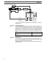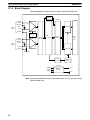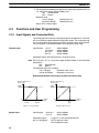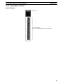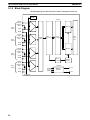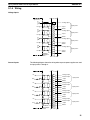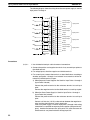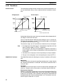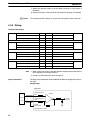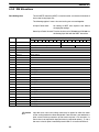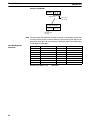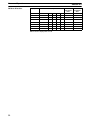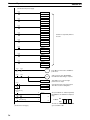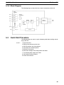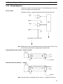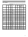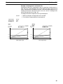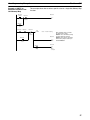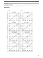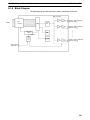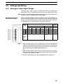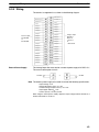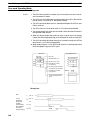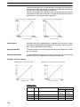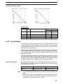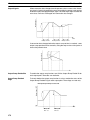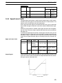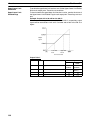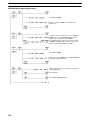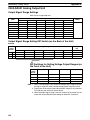
1
Cat. No. W258-E1-05 SYSMAC C-series/CVM1/CV-series Analog I/O Units SYSMAC C-series/CVM1/CV-series Analog I/O Units Operation Manual Revised August 2007 iv Notice: OMRON products are manufactured for use according to proper procedures by a qualified operator and only for the purposes described in this manual. The following conventions are used to indicate and classify precautions in this manual. Always heed the information provided with them. Failure to heed precautions can result in injury to people or damage to property. DANGER Indicates an imminently hazardous situation which, if not avoided, will result in death or serious injury. Additionally, there may be severe property damage. ! WARNING Indicates a potentially hazardous situation which, if not avoided, could result in death or serious injury. Additionally, there may be severe property damage. ! Caution Indicates a potentially hazardous situation which, if not avoided, may result in minor or moderate injury, or property damage. ! OMRON Product References All OMRON products are capitalized in this manual. The word “Unit” is also capitalized when it refers to an OMRON product, regardless of whether or not it appears in the proper name of the product. The abbreviation “Ch,” which appears in some displays and on some OMRON products, often means “word” and is abbreviated “Wd” in documentation in this sense. The abbreviation “PC” means Programmable Controller and is not used as an abbreviation for anything else. Visual Aids The following headings appear in the left column of the manual to help you locate different types of information. Note Indicates information of particular interest for efficient and convenient operation of the product. 1, 2, 3... 1. Indicates lists of one sort or another, such as procedures, checklists, etc. OMRON, 1995 All rights reserved. No part of this publication may be reproduced, stored in a retrieval system, or transmitted, in any form, or by any means, mechanical, electronic, photocopying, recording, or otherwise, without the prior written permission of OMRON. No patent liability is assumed with respect to the use of the information contained herein. Moreover, because OMRON is constantly striving to improve its high-quality products, the information contained in this manual is subject to change without notice. Every precaution has been taken in the preparation of this manual. Nevertheless, OMRON assumes no responsibility for errors or omissions. Neither is any liability assumed for damages resulting from the use of the information contained in this publication. v vi TABLE OF CONTENTS PRECAUTIONS . . . . . . . . . . . . . . . . . . . . . . . . . . . . . . . . . 1 Intended Audience . . . . . . . . . . . . . . . . . . . . . . . . . . . . . . . . . . . . . . . . . . . . . . . . . . . . . . . . . . . 2 General Precautions . . . . . . . . . . . . . . . . . . . . . . . . . . . . . . . . . . . . . . . . . . . . . . . . . . . . . . . . . . 3 Safety Precautions . . . . . . . . . . . . . . . . . . . . . . . . . . . . . . . . . . . . . . . . . . . . . . . . . . . . . . . . . . . 4 Operating Environment Precautions . . . . . . . . . . . . . . . . . . . . . . . . . . . . . . . . . . . . . . . . . . . . . 5 Application Precautions . . . . . . . . . . . . . . . . . . . . . . . . . . . . . . . . . . . . . . . . . . . . . . . . . . . . . . 6 Conformance to EC Directives . . . . . . . . . . . . . . . . . . . . . . . . . . . . . . . . . . . . . . . . . . . . . . . . . SECTION 1 Features and Basic Configuration . . . . . . . . . . . . . . . . . . 1-1 1-2 Features . . . . . . . . . . . . . . . . . . . . . . . . . . . . . . . . . . . . . . . . . . . . . . . . . . . . . . . . . . . . . . . Basic Configuration . . . . . . . . . . . . . . . . . . . . . . . . . . . . . . . . . . . . . . . . . . . . . . . . . . . . . . SECTION 2 3G2A5-AD001 to 3G2A5-AD005 Analog Input Units . . . 2-1 2-2 2-3 Specifications and General Information . . . . . . . . . . . . . . . . . . . . . . . . . . . . . . . . . . . . . . IR/CIO Bit Allocations . . . . . . . . . . . . . . . . . . . . . . . . . . . . . . . . . . . . . . . . . . . . . . . . . . . Functions and User Programming . . . . . . . . . . . . . . . . . . . . . . . . . . . . . . . . . . . . . . . . . . . SECTION 3 3G2A5-AD006 and 3G2A5-AD007 Analog Input Units . 3-1 3-2 3-3 Specifications and General Information . . . . . . . . . . . . . . . . . . . . . . . . . . . . . . . . . . . . . . IR/CIO Bit Allocations . . . . . . . . . . . . . . . . . . . . . . . . . . . . . . . . . . . . . . . . . . . . . . . . . . . Functions and User Programs . . . . . . . . . . . . . . . . . . . . . . . . . . . . . . . . . . . . . . . . . . . . . . SECTION 4 C500-AD101 Analog Input Unit . . . . . . . . . . . . . . . . . . . . 4-1 4-2 4-3 4-4 Specifications and General Information . . . . . . . . . . . . . . . . . . . . . . . . . . . . . . . . . . . . . . Functions, Settings and Wiring . . . . . . . . . . . . . . . . . . . . . . . . . . . . . . . . . . . . . . . . . . . . . Two-word Operation . . . . . . . . . . . . . . . . . . . . . . . . . . . . . . . . . . . . . . . . . . . . . . . . . . . . . Four-word Operation . . . . . . . . . . . . . . . . . . . . . . . . . . . . . . . . . . . . . . . . . . . . . . . . . . . . . SECTION 5 C500-AD501 Analog Input Unit . . . . . . . . . . . . . . . . . . . . 5-1 5-2 5-3 5-4 5-5 5-6 5-7 Specifications and General Information . . . . . . . . . . . . . . . . . . . . . . . . . . . . . . . . . . . . . . Quick Start Procedure . . . . . . . . . . . . . . . . . . . . . . . . . . . . . . . . . . . . . . . . . . . . . . . . . . . . Installation, Settings, and Wiring . . . . . . . . . . . . . . . . . . . . . . . . . . . . . . . . . . . . . . . . . . . . Data Exchange with CPU Unit . . . . . . . . . . . . . . . . . . . . . . . . . . . . . . . . . . . . . . . . . . . . . Memory Map . . . . . . . . . . . . . . . . . . . . . . . . . . . . . . . . . . . . . . . . . . . . . . . . . . . . . . . . . . . Functions . . . . . . . . . . . . . . . . . . . . . . . . . . . . . . . . . . . . . . . . . . . . . . . . . . . . . . . . . . . . . . User Programming Examples . . . . . . . . . . . . . . . . . . . . . . . . . . . . . . . . . . . . . . . . . . . . . . SECTION 6 3G2A5-DA001 to 3G2A5-DA005 Analog Output Units . 6-1 6-2 6-3 Specifications and General Information . . . . . . . . . . . . . . . . . . . . . . . . . . . . . . . . . . . . . . IR/CIO Bit Allocations . . . . . . . . . . . . . . . . . . . . . . . . . . . . . . . . . . . . . . . . . . . . . . . . . . . Functions and User Programs . . . . . . . . . . . . . . . . . . . . . . . . . . . . . . . . . . . . . . . . . . . . . . SECTION 7 C500-DA101 Analog Output Unit . . . . . . . . . . . . . . . . . . . 7-1 7-2 7-3 Specifications and General Information . . . . . . . . . . . . . . . . . . . . . . . . . . . . . . . . . . . . . . IR/CIO Bit Allocations . . . . . . . . . . . . . . . . . . . . . . . . . . . . . . . . . . . . . . . . . . . . . . . . . . . Functions and User Programs . . . . . . . . . . . . . . . . . . . . . . . . . . . . . . . . . . . . . . . . . . . . . . xv xvi xvi xvi xvii xvii xix 1 2 5 7 8 13 14 17 18 23 23 27 28 31 37 50 61 62 69 70 76 80 87 94 105 106 110 110 115 116 122 123 vii TABLE OF CONTENTS SECTION 8 C500-DA103 Analog Output Unit . . . . . . . . . . . . . . . . . . . 8-1 8-2 8-3 Specifications and General Information . . . . . . . . . . . . . . . . . . . . . . . . . . . . . . . . . . . . . . IR/CIO Bit Allocations . . . . . . . . . . . . . . . . . . . . . . . . . . . . . . . . . . . . . . . . . . . . . . . . . . . Functions and User Programs . . . . . . . . . . . . . . . . . . . . . . . . . . . . . . . . . . . . . . . . . . . . . . SECTION 9 C500-DA501 Analog Output Unit . . . . . . . . . . . . . . . . . . . 9-1 9-2 9-3 9-4 9-5 Specifications and General Information . . . . . . . . . . . . . . . . . . . . . . . . . . . . . . . . . . . . . . Settings and Wiring . . . . . . . . . . . . . . . . . . . . . . . . . . . . . . . . . . . . . . . . . . . . . . . . . . . . . . Data Exchange with CPU Unit . . . . . . . . . . . . . . . . . . . . . . . . . . . . . . . . . . . . . . . . . . . . . Functions . . . . . . . . . . . . . . . . . . . . . . . . . . . . . . . . . . . . . . . . . . . . . . . . . . . . . . . . . . . . . . User Programming Examples . . . . . . . . . . . . . . . . . . . . . . . . . . . . . . . . . . . . . . . . . . . . . . 127 128 132 132 135 136 147 153 175 182 Appendices A DM Memory Coding Sheets . . . . . . . . . . . . . . . . . . . . . . . . . . . . . . . . . . . . . . . . . . . . . . . . . . B Dimensions . . . . . . . . . . . . . . . . . . . . . . . . . . . . . . . . . . . . . . . . . . . . . . . . . . . . . . . . . . . . . . . . Index . . . . . . . . . . . . . . . . . . . . . . . . . . . . . . . . . . . . . . . . . . Revision History . . . . . . . . . . . . . . . . . . . . . . . . . . . . . . . . . viii 193 207 209 213 About this Manual: This manual describes the installation and operation of the C-series/CVM1/CV-series Analog I/O Units and includes the sections described below. Please read this manual carefully and be sure you understand the information provided before attempting to install and operate the Analog I/O Units. Section 1 provides a general introduction on the Analog I/O Units. Section 2 provides information on 3G2A5-AD001 to 3G2A5-AD005 Analog Input Units including the specifications, connections, IR/CIO bit allocations, and applications. Section 3 provides information on 3G2A5-AD006 and 3G2A5-AD007 Analog Input Units including the specifications, connections, IR/CIO bit allocations, and applications. Section 4 provides information on the C500-AD101 Analog Input Unit including the specifications, connections, IR/CIO bit allocations, and applications for both two-word and four-word operation. Section 5 provides information on the C500-AD501 Analog Input Unit including the specifications, connections, IR/CIO bit allocations, and applications. Section 6 provides information on 3G2A5-DA001 to 3G2A5-DA005 Analog Output Units including the specifications, connections, IR/CIO bit allocations, and applications. Section 7 provides information on the C500-DA101 Analog Output Unit including the specifications, connections, IR/CIO bit allocations, and applications. Section 8 provides information on the C500-DA103 Analog Output Unit including the specifications, connections, IR/CIO bit allocations, and applications. Section 9 provides information on the C500-DA501 Analog Output Unit including the specifications, connections, IR/CIO bit allocations, and applications. Appendix A provides DM memory and memory map coding sheets for the C500-AD101 Analog Input Unit, the C500-AD501 Analog Input Unit, and the C500-DA501 Analog Output Unit. Appendix B provides the dimensions of the Analog I/O Units. ! WARNING Failure to read and understand the information provided in this manual may result in personal injury or death, damage to the product, or product failure. Please read each section in its entirety and be sure you understand the information provided in the section and related sections before attempting any of the procedures or operations given. ix Read and Understand this Manual Please read and understand this manual before using the product. Please consult your OMRON representative if you have any questions or comments. Warranty and Limitations of Liability ÁÁÁÁÁÁÁÁÁÁÁÁÁÁÁÁÁÁÁÁÁÁÁÁÁÁÁÁÁÁÁÁÁ WARRANTY ÁÁÁÁÁÁÁÁÁÁÁÁÁÁÁÁÁÁÁÁÁÁÁÁÁÁÁÁÁÁÁÁÁ ÁÁÁÁÁÁÁÁÁÁÁÁÁÁÁÁÁÁÁÁÁÁÁÁÁÁÁÁÁÁÁÁÁ ÁÁÁÁÁÁÁÁÁÁÁÁÁÁÁÁÁÁÁÁÁÁÁÁÁÁÁÁÁÁÁÁÁ ÁÁÁÁÁÁÁÁÁÁÁÁÁÁÁÁÁÁÁÁÁÁÁÁÁÁÁÁÁÁÁÁÁ ÁÁÁÁÁÁÁÁÁÁÁÁÁÁÁÁÁÁÁÁÁÁÁÁÁÁÁÁÁÁÁÁÁ ÁÁÁÁÁÁÁÁÁÁÁÁÁÁÁÁÁÁÁÁÁÁÁÁÁÁÁÁÁÁÁÁÁ ÁÁÁÁÁÁÁÁÁÁÁÁÁÁÁÁÁÁÁÁÁÁÁÁÁÁÁÁÁÁÁÁÁ ÁÁÁÁÁÁÁÁÁÁÁÁÁÁÁÁÁÁÁÁÁÁÁÁÁÁÁÁÁÁÁÁÁ ÁÁÁÁÁÁÁÁÁÁÁÁÁÁÁÁÁÁÁÁÁÁÁÁÁÁÁÁÁÁÁÁÁ LIMITATIONS OF LIABILITY ÁÁÁÁÁÁÁÁÁÁÁÁÁÁÁÁÁÁÁÁÁÁÁÁÁÁÁÁÁÁÁÁÁ ÁÁÁÁÁÁÁÁÁÁÁÁÁÁÁÁÁÁÁÁÁÁÁÁÁÁÁÁÁÁÁÁÁ ÁÁÁÁÁÁÁÁÁÁÁÁÁÁÁÁÁÁÁÁÁÁÁÁÁÁÁÁÁÁÁÁÁ ÁÁÁÁÁÁÁÁÁÁÁÁÁÁÁÁÁÁÁÁÁÁÁÁÁÁÁÁÁÁÁÁÁ ÁÁÁÁÁÁÁÁÁÁÁÁÁÁÁÁÁÁÁÁÁÁÁÁÁÁÁÁÁÁÁÁÁ ÁÁÁÁÁÁÁÁÁÁÁÁÁÁÁÁÁÁÁÁÁÁÁÁÁÁÁÁÁÁÁÁÁ ÁÁÁÁÁÁÁÁÁÁÁÁÁÁÁÁÁÁÁÁÁÁÁÁÁÁÁÁÁÁÁÁÁ ÁÁÁÁÁÁÁÁÁÁÁÁÁÁÁÁÁÁÁÁÁÁÁÁÁÁÁÁÁÁÁÁÁ ÁÁÁÁÁÁÁÁÁÁÁÁÁÁÁÁÁÁÁÁÁÁÁÁÁÁÁÁÁÁÁÁÁ ÁÁÁÁÁÁÁÁÁÁÁÁÁÁÁÁÁÁÁÁÁÁÁÁÁÁÁÁÁÁÁÁÁ ÁÁÁÁÁÁÁÁÁÁÁÁÁÁÁÁÁÁÁÁÁÁÁÁÁÁÁÁÁÁÁÁÁ OMRON’s exclusive warranty is that the products are free from defects in materials and workmanship for a period of one year (or other period if specified) from date of sale by OMRON. OMRON MAKES NO WARRANTY OR REPRESENTATION, EXPRESS OR IMPLIED, REGARDING NON–INFRINGEMENT, MERCHANTABILITY, OR FITNESS FOR PARTICULAR PURPOSE OF THE PRODUCTS. ANY BUYER OR USER ACKNOWLEDGES THAT THE BUYER OR USER ALONE HAS DETERMINED THAT THE PRODUCTS WILL SUITABLY MEET THE REQUIREMENTS OF THEIR INTENDED USE. OMRON DISCLAIMS ALL OTHER WARRANTIES, EXPRESS OR IMPLIED. OMRON SHALL NOT BE RESPONSIBLE FOR SPECIAL, INDIRECT, OR CONSEQUENTIAL DAMAGES, LOSS OF PROFITS OR COMMERCIAL LOSS IN ANY WAY CONNECTED WITH THE PRODUCTS, WHETHER SUCH CLAIM IS BASED ON CONTRACT, WARRANTY, NEGLIGENCE, OR STRICT LIABILITY. In no event shall the responsibility of OMRON for any act exceed the individual price of the product on which liability is asserted. IN NO EVENT SHALL OMRON BE RESPONSIBLE FOR WARRANTY, REPAIR, OR OTHER CLAIMS REGARDING THE PRODUCTS UNLESS OMRON’S ANALYSIS CONFIRMS THAT THE PRODUCTS WERE PROPERLY HANDLED, STORED, INSTALLED, AND MAINTAINED AND NOT SUBJECT TO CONTAMINATION, ABUSE, MISUSE, OR INAPPROPRIATE MODIFICATION OR REPAIR. xi Application Considerations ÁÁÁÁÁÁÁÁÁÁÁÁÁÁÁÁÁÁÁÁÁÁÁÁÁÁÁÁÁÁÁÁÁ SUITABILITY FOR USE ÁÁÁÁÁÁÁÁÁÁÁÁÁÁÁÁÁÁÁÁÁÁÁÁÁÁÁÁÁÁÁÁÁ ÁÁÁÁÁÁÁÁÁÁÁÁÁÁÁÁÁÁÁÁÁÁÁÁÁÁÁÁÁÁÁÁÁ ÁÁÁÁÁÁÁÁÁÁÁÁÁÁÁÁÁÁÁÁÁÁÁÁÁÁÁÁÁÁÁÁÁ ÁÁÁÁÁÁÁÁÁÁÁÁÁÁÁÁÁÁÁÁÁÁÁÁÁÁÁÁÁÁÁÁÁ ÁÁÁÁÁÁÁÁÁÁÁÁÁÁÁÁÁÁÁÁÁÁÁÁÁÁÁÁÁÁÁÁÁ ÁÁÁÁÁÁÁÁÁÁÁÁÁÁÁÁÁÁÁÁÁÁÁÁÁÁÁÁÁÁÁÁÁ ÁÁÁÁÁÁÁÁÁÁÁÁÁÁÁÁÁÁÁÁÁÁÁÁÁÁÁÁÁÁÁÁÁ ÁÁÁÁÁÁÁÁÁÁÁÁÁÁÁÁÁÁÁÁÁÁÁÁÁÁÁÁÁÁÁÁÁ ÁÁÁÁÁÁÁÁÁÁÁÁÁÁÁÁÁÁÁÁÁÁÁÁÁÁÁÁÁÁÁÁÁ ÁÁÁÁÁÁÁÁÁÁÁÁÁÁÁÁÁÁÁÁÁÁÁÁÁÁÁÁÁÁÁÁÁ ÁÁÁÁÁÁÁÁÁÁÁÁÁÁÁÁÁÁÁÁÁÁÁÁÁÁÁÁÁÁÁÁÁ ÁÁÁÁÁÁÁÁÁÁÁÁÁÁÁÁÁÁÁÁÁÁÁÁÁÁÁÁÁÁÁÁÁ ÁÁÁÁÁÁÁÁÁÁÁÁÁÁÁÁÁÁÁÁÁÁÁÁÁÁÁÁÁÁÁÁÁ ÁÁÁÁÁÁÁÁÁÁÁÁÁÁÁÁÁÁÁÁÁÁÁÁÁÁÁÁÁÁÁÁÁ ÁÁÁÁÁÁÁÁÁÁÁÁÁÁÁÁÁÁÁÁÁÁÁÁÁÁÁÁÁÁÁÁÁ ÁÁÁÁÁÁÁÁÁÁÁÁÁÁÁÁÁÁÁÁÁÁÁÁÁÁÁÁÁÁÁÁÁ ÁÁÁÁÁÁÁÁÁÁÁÁÁÁÁÁÁÁÁÁÁÁÁÁÁÁÁÁÁÁÁÁÁ ÁÁÁÁÁÁÁÁÁÁÁÁÁÁÁÁÁÁÁÁÁÁÁÁÁÁÁÁÁÁÁÁÁ ÁÁÁÁÁÁÁÁÁÁÁÁÁÁÁÁÁÁÁÁÁÁÁÁÁÁÁÁÁÁÁÁÁ ÁÁÁÁÁÁÁÁÁÁÁÁÁÁÁÁÁÁÁÁÁÁÁÁÁÁÁÁÁÁÁÁÁ ÁÁÁÁÁÁÁÁÁÁÁÁÁÁÁÁÁÁÁÁÁÁÁÁÁÁÁÁÁÁÁÁÁ ÁÁÁÁÁÁÁÁÁÁÁÁÁÁÁÁÁÁÁÁÁÁÁÁÁÁÁÁÁÁÁÁÁ ÁÁÁÁÁÁÁÁÁÁÁÁÁÁÁÁÁÁÁÁÁÁÁÁÁÁÁÁÁÁÁÁÁ ÁÁÁÁÁÁÁÁÁÁÁÁÁÁÁÁÁÁÁÁÁÁÁÁÁÁÁÁÁÁÁÁÁ PROGRAMMABLE PRODUCTS ÁÁÁÁÁÁÁÁÁÁÁÁÁÁÁÁÁÁÁÁÁÁÁÁÁÁÁÁÁÁÁÁÁ ÁÁÁÁÁÁÁÁÁÁÁÁÁÁÁÁÁÁÁÁÁÁÁÁÁÁÁÁÁÁÁÁÁ ÁÁÁÁÁÁÁÁÁÁÁÁÁÁÁÁÁÁÁÁÁÁÁÁÁÁÁÁÁÁÁÁÁ OMRON shall not be responsible for conformity with any standards, codes, or regulations that apply to the combination of products in the customer’s application or use of the products. At the customer’s request, OMRON will provide applicable third party certification documents identifying ratings and limitations of use that apply to the products. This information by itself is not sufficient for a complete determination of the suitability of the products in combination with the end product, machine, system, or other application or use. The following are some examples of applications for which particular attention must be given. This is not intended to be an exhaustive list of all possible uses of the products, nor is it intended to imply that the uses listed may be suitable for the products: • Outdoor use, uses involving potential chemical contamination or electrical interference, or conditions or uses not described in this manual. • Nuclear energy control systems, combustion systems, railroad systems, aviation systems, medical equipment, amusement machines, vehicles, safety equipment, and installations subject to separate industry or government regulations. • Systems, machines, and equipment that could present a risk to life or property. Please know and observe all prohibitions of use applicable to the products. NEVER USE THE PRODUCTS FOR AN APPLICATION INVOLVING SERIOUS RISK TO LIFE OR PROPERTY WITHOUT ENSURING THAT THE SYSTEM AS A WHOLE HAS BEEN DESIGNED TO ADDRESS THE RISKS, AND THAT THE OMRON PRODUCTS ARE PROPERLY RATED AND INSTALLED FOR THE INTENDED USE WITHIN THE OVERALL EQUIPMENT OR SYSTEM. OMRON shall not be responsible for the user’s programming of a programmable product, or any consequence thereof. xii Disclaimers ÁÁÁÁÁÁÁÁÁÁÁÁÁÁÁÁÁÁÁÁÁÁÁÁÁÁÁÁÁÁÁÁÁ CHANGE IN SPECIFICATIONS ÁÁÁÁÁÁÁÁÁÁÁÁÁÁÁÁÁÁÁÁÁÁÁÁÁÁÁÁÁÁÁÁÁ ÁÁÁÁÁÁÁÁÁÁÁÁÁÁÁÁÁÁÁÁÁÁÁÁÁÁÁÁÁÁÁÁÁ ÁÁÁÁÁÁÁÁÁÁÁÁÁÁÁÁÁÁÁÁÁÁÁÁÁÁÁÁÁÁÁÁÁ ÁÁÁÁÁÁÁÁÁÁÁÁÁÁÁÁÁÁÁÁÁÁÁÁÁÁÁÁÁÁÁÁÁ ÁÁÁÁÁÁÁÁÁÁÁÁÁÁÁÁÁÁÁÁÁÁÁÁÁÁÁÁÁÁÁÁÁ ÁÁÁÁÁÁÁÁÁÁÁÁÁÁÁÁÁÁÁÁÁÁÁÁÁÁÁÁÁÁÁÁÁ ÁÁÁÁÁÁÁÁÁÁÁÁÁÁÁÁÁÁÁÁÁÁÁÁÁÁÁÁÁÁÁÁÁ ÁÁÁÁÁÁÁÁÁÁÁÁÁÁÁÁÁÁÁÁÁÁÁÁÁÁÁÁÁÁÁÁÁ ÁÁÁÁÁÁÁÁÁÁÁÁÁÁÁÁÁÁÁÁÁÁÁÁÁÁÁÁÁÁÁÁÁ DIMENSIONS AND WEIGHTS ÁÁÁÁÁÁÁÁÁÁÁÁÁÁÁÁÁÁÁÁÁÁÁÁÁÁÁÁÁÁÁÁÁ ÁÁÁÁÁÁÁÁÁÁÁÁÁÁÁÁÁÁÁÁÁÁÁÁÁÁÁÁÁÁÁÁÁ ÁÁÁÁÁÁÁÁÁÁÁÁÁÁÁÁÁÁÁÁÁÁÁÁÁÁÁÁÁÁÁÁÁ ÁÁÁÁÁÁÁÁÁÁÁÁÁÁÁÁÁÁÁÁÁÁÁÁÁÁÁÁÁÁÁÁÁ ÁÁÁÁÁÁÁÁÁÁÁÁÁÁÁÁÁÁÁÁÁÁÁÁÁÁÁÁÁÁÁÁÁ PERFORMANCE DATA ÁÁÁÁÁÁÁÁÁÁÁÁÁÁÁÁÁÁÁÁÁÁÁÁÁÁÁÁÁÁÁÁÁ ÁÁÁÁÁÁÁÁÁÁÁÁÁÁÁÁÁÁÁÁÁÁÁÁÁÁÁÁÁÁÁÁÁ ÁÁÁÁÁÁÁÁÁÁÁÁÁÁÁÁÁÁÁÁÁÁÁÁÁÁÁÁÁÁÁÁÁ ÁÁÁÁÁÁÁÁÁÁÁÁÁÁÁÁÁÁÁÁÁÁÁÁÁÁÁÁÁÁÁÁÁ ÁÁÁÁÁÁÁÁÁÁÁÁÁÁÁÁÁÁÁÁÁÁÁÁÁÁÁÁÁÁÁÁÁ ÁÁÁÁÁÁÁÁÁÁÁÁÁÁÁÁÁÁÁÁÁÁÁÁÁÁÁÁÁÁÁÁÁ ERRORS AND OMISSIONS ÁÁÁÁÁÁÁÁÁÁÁÁÁÁÁÁÁÁÁÁÁÁÁÁÁÁÁÁÁÁÁÁÁ ÁÁÁÁÁÁÁÁÁÁÁÁÁÁÁÁÁÁÁÁÁÁÁÁÁÁÁÁÁÁÁÁÁ ÁÁÁÁÁÁÁÁÁÁÁÁÁÁÁÁÁÁÁÁÁÁÁÁÁÁÁÁÁÁÁÁÁ ÁÁÁÁÁÁÁÁÁÁÁÁÁÁÁÁÁÁÁÁÁÁÁÁÁÁÁÁÁÁÁÁÁ Product specifications and accessories may be changed at any time based on improvements and other reasons. It is our practice to change model numbers when published ratings or features are changed, or when significant construction changes are made. However, some specifications of the products may be changed without any notice. When in doubt, special model numbers may be assigned to fix or establish key specifications for your application on your request. Please consult with your OMRON representative at any time to confirm actual specifications of purchased products. Dimensions and weights are nominal and are not to be used for manufacturing purposes, even when tolerances are shown. Performance data given in this manual is provided as a guide for the user in determining suitability and does not constitute a warranty. It may represent the result of OMRON’s test conditions, and the users must correlate it to actual application requirements. Actual performance is subject to the OMRON Warranty and Limitations of Liability. The information in this manual has been carefully checked and is believed to be accurate; however, no responsibility is assumed for clerical, typographical, or proofreading errors, or omissions. xiii xiv PRECAUTIONS This section provides general precautions for using the Programmable Controller (PC) and Analog I/O Units. The information contained in this section is important for the safe and reliable application of the Analog I/O Units. You must read this section and understand the information contained before attempting to set up or operate a PC system and Analog I/O Units. 1 Intended Audience . . . . . . . . . . . . . . . . . . . . . . . . . . . . . . . . . . . . . . . . . . . . . . . . . . . . . . . . . . . . 2 General Precautions . . . . . . . . . . . . . . . . . . . . . . . . . . . . . . . . . . . . . . . . . . . . . . . . . . . . . . . . . . . 3 Safety Precautions . . . . . . . . . . . . . . . . . . . . . . . . . . . . . . . . . . . . . . . . . . . . . . . . . . . . . . . . . . . . 4 Operating Environment Precautions . . . . . . . . . . . . . . . . . . . . . . . . . . . . . . . . . . . . . . . . . . . . . . 5 Application Precautions . . . . . . . . . . . . . . . . . . . . . . . . . . . . . . . . . . . . . . . . . . . . . . . . . . . . . . . . 6 Conformance to EC Directives . . . . . . . . . . . . . . . . . . . . . . . . . . . . . . . . . . . . . . . . . . . . . . . . . . xvi xvi xvi xvii xvii xix xv Safety Precautions 1 3 Intended Audience This manual is intended for the following personnel, who must also have knowledge of electrical systems (an electrical engineer or the equivalent). • Personnel in charge of installing FA systems • Personnel in charge of designing FA systems • Personnel in charge of managing FA systems and facilities 2 General Precautions The user must operate the product according to the performance specifications described in the operation manuals. Before using the product under conditions which are not described in the manual or applying the product to nuclear control systems, railroad systems, aviation systems, vehicles, combustion systems, medical equipment, amusement machines, safety equipment, and other systems, machines, and equipment that may have a serious influence on lives and property if used improperly, consult your OMRON representative. Make sure that the ratings and performance characteristics of the product are sufficient for the systems, machines, and equipment, and be sure to provide the systems, machines, and equipment with double safety mechanisms. This manual provides information for programming and operating OMRON Analog I/O Units. Be sure to read this manual before attempting to use the software and keep this manual close at hand for reference during operation. ! WARNING It is extremely important that a PC and all PC Units be used for the specified purpose and under the specified conditions, especially in applications that can directly or indirectly affect human life. You must consult with your OMRON representative before applying a PC System to the above-mentioned applications. 3 Safety Precautions ! WARNING Do not attempt to take any Unit apart while power is being supplied. Doing so may result in electric shock. ! WARNING Do not touch any of the terminals or terminal blocks while power is being supplied. Doing so may result in electric shock. xvi ! Caution Tighten the screws on the terminal block of the AC Power Supply Unit to the torque specified in the operation manual. The loose screws may result in burning or malfunction. ! Caution Confirm safety at the destination node before transferring a program to another node or changing contents of the I/O memory area. Doing either of these without confirming safety may result in injury. Application Precautions 4 5 Operating Environment Precautions ! Caution Do not operate the control system in the following places: • Locations subject to direct sunlight. • Locations subject to temperatures or humidity outside the range specified in the specifications. • Locations subject to condensation as the result of severe changes in temperature. • Locations subject to corrosive or flammable gases. • Locations subject to dust (especially iron dust) or salts. • Locations subject to exposure to water, oil, or chemicals. • Locations subject to shock or vibration. ! Caution Take appropriate and sufficient countermeasures when installing systems in the following locations: • Locations subject to static electricity or other forms of noise. • Locations subject to strong electromagnetic fields. • Locations subject to possible exposure to radioactivity. • Locations close to power supplies. ! Caution 5 The operating environment of the PC System can have a large effect on the longevity and reliability of the system. Improper operating environments can lead to malfunction, failure, and other unforeseeable problems with the PC System. Be sure that the operating environment is within the specified conditions at installation and remains within the specified conditions during the life of the system. Application Precautions Observe the following precautions when using the PC. ! WARNING Always heed these precautions. Failure to abide by the following precautions could lead to serious or possibly fatal injury. • Always connect to a ground of 100 Ω or less when installing the Units. Not connecting to a ground of 100 Ω or less may result in electric shock. • Always turn off the power supply to the PC before attempting any of the following. Not turning off the power supply may result in malfunction or electric shock. • Mounting or dismounting Power Supply Units, I/O Units, CPU Units, Memory Cassettes, or any other Units. • Assembling the Units. • Setting DIP switch or rotary switches. • Connecting or wiring the cables. • Connecting or disconnecting the connectors. ! Caution Failure to abide by the following precautions could lead to faulty operation of the PC or the system, or could damage the PC or PC Units. Always heed these precautions. • Fail-safe measures must be taken by the customer to ensure safety in the event of incorrect, missing, or abnormal signals caused by broken signal lines, momentary power interruptions, or other causes. xvii Application Precautions 5 • Interlock circuits, limit circuits, and similar safety measures in external circuits (i.e., not in the Programmable Controller) must be provided by the customer. • Always use the power supply voltage specified in this manual. An incorrect voltage may result in malfunction or burning. • Take appropriate measures to ensure that the specified power with the rated voltage and frequency is supplied. Be particularly careful in places where the power supply is unstable. An incorrect power supply may result in malfunction. • Install external breakers and take other safety measures against short-circuiting in external wiring. Insufficient safety measures against short-circuiting may result in burning. • Do not apply voltages to the Input Units in excess of the rated input voltage. Excess voltages may result in burning. • Do not apply voltages or connect loads to the Output Units in excess of the maximum switching capacity. Excess voltage or loads may result in burning. • Disconnect the functional ground terminal when performing withstand voltage tests. Not disconnecting the functional ground terminal may result in burning. • Do not attempt to disassemble, repair, or modify any Units. • Tighten screws on the terminal block to a torque of 0.8 N S m. Incorrect tightening torque may result in malfunction. • Be careful not to allow wire cuttings to enter inside the Unit when wiring. Allowing wire cuttings inside the Unit may result in malfunction. • Use crimp terminals for wiring. Do not connect bare stranded wires directly to terminals. Connection of bare stranded wires may result in burning. • Double-check all the wiring before turning on the power supply. Incorrect wiring may result in burning. • Mount the Unit only after checking the terminal block completely. • Be sure that the terminal blocks, Memory Units, expansion cables, and other items with locking devices are properly locked into place. Improper locking may result in malfunction. • Check the user program for proper execution before actually running it on the Unit. Not checking the program may result in an unexpected operation. • Confirm that no adverse effect will occur in the system before attempting any of the following. Not doing so may result in an unexpected operation. • Changing the operating mode of the PC. • Force-setting/force-resetting any bit in memory. • Changing the present value of any word or any set value in memory. • Resume operation only after transferring to the new CPU Unit the contents of the DM Area, HR Area, and other data required for resuming operation. Not doing so may result in an unexpected operation. • Do not pull on the cables or bend the cables beyond their natural limit. Doing either of these may break the cables. • Do not place objects on top of the cables or other wiring lines. Doing so may break the cables. • Before touching the Unit, be sure to first touch a grounded metallic object in order to discharge any static built-up. Not doing so may result in malfunction or damage. • When replacing parts, be sure to confirm that the rating of a new part is correct. Not doing so may result in malfunction or burning. xviii Conformance to EC Directives 6 Section 6 Conformance to EC Directives Applicable Directives • EMC Directives • Low Voltage Directive Concepts EMC Directives OMRON supplies electric devices that are used built into other devices or manufacturing equipment. These OMRON products are designed to conform to the related EMC standards (see note) so that the devices or equipment in which they are used can more easily conform to EMC standards. EMC-related performance of the OMRON devices that conform to EC Directives will vary depending on the configuration, wiring, and other conditions of the equipment or control panel on which the OMRON devices are installed. The customer must, therefore, perform the final check to confirm that devices and the overall machine conform to EMC standards. Note Applicable EMC (Electromagnetic Compatibility) standards are as follows: EN 61131-2 Low Voltage Directive Always ensure that devices operating at voltages of 50 to 1,000 V AC and 75 to 1,500 V DC meet the required safety standards for the PLC (EN 61131-2). Conformance to EC Directives CV-series products conform to EC Directives (see note). However, the following precautions must be observed to ensure that the machine or device in which the CV-series PLC is used conforms to EC Directives: 1. The CV-series PLC must be installed within a control panel. 2. You must use reinforced insulation or double insulation for the DC power supplies connected to the power supply terminals on PLCs that take DC power and for the DC power supplies connected to I/O Units. The DC power supply connected to the power supply terminals on PLCs using DC power must have an output hold time of at least 10 ms. 3. CV-series products conforming to EC Directives also conform to EN 61131-2 for EMI. Radiated emission characteristics (10-m regulations) may vary depending on the configuration of the control panel used, other devices connected to the control panel, wiring, and other conditions. You must therefore confirm that the overall machine or equipment conforms to EC Directives even when using CV-series products that conform to EC Directives. Note Of the products that appear in this manual, the following products conform to EC Directives. C500H-AD101 Analog Input Unit C500H-DA101 Analog Output Unit xix SECTION 1 Features and Basic Configuration This section provides a general introduction on the Analog I/O Units. 1-1 1-2 Features . . . . . . . . . . . . . . . . . . . . . . . . . . . . . . . . . . . . . . . . . . . . . . . . . . . . . . . . . . . . . . . . 1-1-1 Analog Input Units . . . . . . . . . . . . . . . . . . . . . . . . . . . . . . . . . . . . . . . . . . . . . . . . . 1-1-2 Analog Output Units . . . . . . . . . . . . . . . . . . . . . . . . . . . . . . . . . . . . . . . . . . . . . . . Basic Configuration . . . . . . . . . . . . . . . . . . . . . . . . . . . . . . . . . . . . . . . . . . . . . . . . . . . . . . . 2 2 3 5 1 Section 1-1 Features 1-1 Features 1-1-1 Analog Input Units This operation manual describes the features of the following Analog Input Units. • 3G2A5-AD001 to 3G2A5-AD007 • C500-AD101 • C500-AD501 Basic Function Analog quantities, such as temperature, pressure, power, and power factor, input to an Analog Input Unit via a preamplifier or transducer are converted to digital values for input to the CPU Unit. Features 3G2A5-AD001 to 3G2A5-AD007 Analog signals from sensors are converted to 12-bit binary data by the 3G2A5AD001 to 3G2A5-AD005 Analog Input Units (resolution: 1/4095); or to 10-bit binary data by the 3G2A5-AD006 and 3G2A5-AD007 Analog Input Units (resolution: 1/1023). Number of Input Points Per Unit Each Unit can handle A/D conversion for either two or four input points. Unit Number of Inputs 3G2A5-AD001 to 3G2A5-AD005 2 points 3G2A5-AD006/007 4 points Compatible Input Specifications The Units are compatible with a variety of input specifications. Select the appropriate Unit from the table below. Input signal range Voltage g Current C500-AD101 2 1 to 5 V 0 to 10 V 0 to 5 V –10 to 10 V –5 to 5 V 4 to 20 mA Unit 3G2A5-AD001/006 3G2A5-AD002/007 3G2A5-AD003 3G2A5-AD004 3G2A5-AD005 3G2A5-AD001/006 This Unit converts analog signals from sensors to 12-bit binary data. Number of Input Points Per Unit Each Unit has eight input points. An separate input signal range can be set for each input point, to permit the simultaneous use of sensors with different output forms. Input Signal Ranges The input signal ranges can be set as required between 0 and 10 V for a voltage input or between 0 and 20 mA for a current input. Many Features In addition to A/D conversion, the Analog Input Units offer peak hold, mean value, scaling, and disconnection detection functions. High Accuracy and High Speed The C500-AD101 achieves a resolution up to 1/4095 and a conversion time of 10 ms max. per point. The I/O READ and I/O WRITE instructions, READ and WRIT, can be used to transfer data with the CPU Unit, thereby simplifying program creation and achieving high-speed processing with batch transfer. Section 1-1 Features C500-AD501 This Analog Input Unit converts analog voltage or current signals from sensors to signed BCD data or to binary data (with two’s complements used for negative values). A microprocessor is built into the C500-AD501 to enable advanced data processing in the Analog Input Unit before transferring the data to the CPU Unit. Number of Input Points Per Unit Each Unit has sixteen input points. An separate input signal range can be set for each input point, to permit the simultaneous use of sensors with different output forms. Input Signal Ranges The input signal ranges can be set as required as follows: Voltage inputs: 0 to 5 V, 0 to 10 V, –5 to 5 V, or –10 to 10 V Current inputs: 0 to 20 mA or –20 to 20 mA Many Features In addition to A/D conversion, the Analog Input Units offer scaling, filtering, averaging, peak hold, upper/lower limits, and input range high/low alarms. These functions can be set separately for each input point. Executing these function in the Analog Input Unit greatly reduces the load on the ladder program and the CPU Unit. High Accuracy and High Speed The C500-AD501 achieves a resolution up to 1/4095 and a conversion time of 25 ms max. per 16 input points. (The use of the above special function will increase the conversion time.) The I/O READ and I/O WRITE instructions, READ and WRIT, can be used to transfer data with the CPU Unit, thereby simplifying program creation and achieving high-speed processing with batch transfer. A Pointer Word can also be set to limit the words being read or written to further increase speed. Built-in EEPROM An EEPROM is built into the C500-AD501 to enable storing parameters. The parameters stored in EEPROM are transferred to RAM at the start of operation before beginning actual operation. 1-1-2 Analog Output Units This operation manual describes the features of the following Analog Output Units. • 3G2A5-DA001 to 3G2A5-DA005 • C500-DA101/103 • C500-DA501 Basic Function Conversion of PC digital output signals to analog signals to drive instruments and devices requiring an analog input. Features 3G2A5-DA001 to 3G2A5-DA005 These Units convert 12-bit binary data with a resolution of 1/4095 to analog signals. Number of Output Points Per Unit Each Unit can handle D/A conversion for two output points. 3 Section 1-1 Features Output Specifications The Units are compatible with a variety of output specifications. Select the appropriate Unit from the table below. Output signal range Voltage g Current C500-DA101/103 1 to 5 V 0 to 10 V 0 to 5 V –10 to 10 V –5 to 5 V 4 to 20 mA Unit 3G2A5-DA001 3G2A5-DA002 3G2A5-DA003 3G2A5-DA004 3G2A5-DA005 3G2A5-DA001 The C500-DA101 converts 12-bit binary data and the C500-DA103 converts binary data with 1 sign bit + 11 data bits to analog output signals, with resolution of 1/4095 in each case. Number of Output Points Per Unit Each Unit can handle D/A conversion for four output points. A separate output signal range can be set for each C500-DA101 output point. Output Specifications The C500-DA101 can be set to one of the three output signal ranges shown in the table below. Output signal range Voltage Current C500-DA501 1 to 5 V 0 to 10 V –10 to 10 V 4 to 20 mA Unit C500-DA101 C500-DA103 C500-DA101 The C500-DA501 converts 12-bit binary/BCD data or binary/BCD data with 1 sign bit + 11 data bits to analog output signals, with resolution of 1/4095 in each case. Number of Output Points Per Unit Each Unit can handle D/A conversion for eight output points. A separate output signal range can be set for each C500-DA501 output point. Output Specifications Each output point for the C500-DA501 can be set to one of the output signal ranges shown in the following table. Output signal range Voltage Current 0 to 10 V 0 to 5 V –5 to 5 V –10 to 10 V 0 to 20 mA 4 to 20 mA Unit C500-DA501 BCD or binary can be selected as the output data for each output point. The scaling function can be set for each output point. The upper/lower limit function can be set for each output point. The output ramp function can be set for each output point. High-speed D/A conversion can be set for all eight output points. 4 Basic Configuration 1-2 Section 1-2 Basic Configuration 3G2A5-AD001 to 3G2A5-AD007 or C500-AD101/501 Analog Input Unit 3G2A5-DA001 to 3G2A5-DA005 or C500-DA101/103/501 Analog Output Unit CPU SYSMAC C500 C1000H C2000H CVM1 CV500/CV1000/CV2000 Regulator Temperature Pressure Speed Flow rate (Temperature control) Sensor Preamp Servomotor controller (Position control) Voltage Current Power Power factor Inverter Transducer (Speed control) Sensor Chart recorder The diagram above shows the C500-AD501 and C500-DA101 as examples of Analog I/O Units. Example Configurations Temperature Regulating System C500-AD501 Analog Input Unit C500-DA101 Analog Output Unit Transducer Temperature sensing element M Valve controller Fuel 5 Basic Configuration Section 1-2 Servomotor Positioning System Sensor Encoder ÇÇÇÇ ÇÇÇ ÇÇÇÇÇÇÇ M Servo controller Servo motor Platform Locating pulse C500-DA101 Analog Output Unit C500-CT012 High-speed Counter Unit C500-AD501 Analog Input Unit The diagram above shows the C500-AD501 and C500-DA101 as examples of Analog I/O Units. ! Caution System Configuration The I/O READ and I/O WRITE instructions (READ and WRIT) cannot be used for Units mounted to SYSMAC BUS Slave Racks. Set the C500-AD101 or C500-DA501 for four-word operation whenever they are mounted to a SYSMAC BUS Slave Rack. The C500-AD501 can operate only through the READ and WRIT instructions and therefore cannot be mounted on a SYSMAC BUS Slave Rack. Rack CPU Rack, Expansion I/O Rack, SYSMAC BUS/2 Slave Rack SYSMAC BUS Slave Rack ! Caution 6 READ/WRIT instruction Can be used. Cannot be used. Using the Units Turn OFF the PC power supply before connecting or disconnecting Units or wiring. To reduce noise problems, wire the input and output lines through a duct separate from the high-voltage and power cables. Refer to Wiring in the section on the relevant Unit for detailed information and cautions on wiring. SECTION 2 3G2A5-AD001 to 3G2A5-AD005 Analog Input Units This section provides information on 3G2A5-AD001 to 3G2A5-AD005 Analog Input Units including the specifications, connections, IR/CIO bit allocations, and applications. 2-1 2-2 2-3 Specifications and General Information . . . . . . . . . . . . . . . . . . . . . . . . . . . . . . . . . . . . . . . . 2-1-1 Specifications . . . . . . . . . . . . . . . . . . . . . . . . . . . . . . . . . . . . . . . . . . . . . . . . . . . . . 2-1-2 Description of Parts . . . . . . . . . . . . . . . . . . . . . . . . . . . . . . . . . . . . . . . . . . . . . . . . 2-1-3 Block Diagram . . . . . . . . . . . . . . . . . . . . . . . . . . . . . . . . . . . . . . . . . . . . . . . . . . . . 2-1-4 Wiring . . . . . . . . . . . . . . . . . . . . . . . . . . . . . . . . . . . . . . . . . . . . . . . . . . . . . . . . . . IR/CIO Bit Allocations . . . . . . . . . . . . . . . . . . . . . . . . . . . . . . . . . . . . . . . . . . . . . . . . . . . . . Functions and User Programming . . . . . . . . . . . . . . . . . . . . . . . . . . . . . . . . . . . . . . . . . . . . 2-3-1 Input Signals and Converted Data . . . . . . . . . . . . . . . . . . . . . . . . . . . . . . . . . . . . . 2-3-2 Ladder Programming Example . . . . . . . . . . . . . . . . . . . . . . . . . . . . . . . . . . . . . . . 8 8 9 10 11 13 14 14 15 7 Section 2-1 Specifications and General Information 2-1 Specifications and General Information 2-1-1 Specifications General Specifications All general specifications of the 3G2A5-AD001 through 3G2A5-AD005 Analog Input Units conform to those of the C Series, except the following. • Insulation between the External Terminals and the Frame: 5MΩ min. at 250 VDC • Breakdown Voltage between the External Terminals and the Frame: 500 VAC, 50-60 Hz for 1 minute Performance Specifications Item Number of analog inputs Input p signal g range g Specification 2 Voltage g input p AD001 1 to 5 V AD002 0 to 10 V AD003 0 to 5 V AD004 –10 to 10 V AD005 –5 to 5 V AD001 4 to 20 mA ±15 V max. ±60 mA max. 1 MΩ min. 250 Ω Resolution Current input Voltage input Current input Voltage input Current input 1/4095 (full scale) PC signal (see note 1) 12-bit binary Linearity error ±0.1% max. Accuracy ±0.2% max. (full scale at 25°C) Max. input p signal g External input p impedance p Accuracy temperature coefficient ±100 PPM/°C (full scale) Note 8 Conversion time 2.5 ms max./point Conversion cycle 5 ms max. Max. PC write delay (see note 2) Conversion method 1 s max. Words allocated 2 input words External connections 17-pin terminal block (not removable) Power consumption 500 mA max. at 5 VDC External dimensions 34.5 x 250 x 113 mm (W x H x D) Weight 600 g max. Sequential comparison 1. A sign bit + 11 data bits binary data for Units with –10 to 10 V and –5 to 5 V range (3G2A5-AD004 and 3G2A5-AD005). 2. The PC write delay is the time required for a change in the input signal to be converted and transferred to the PC bus. Section 2-1 Specifications and General Information PC Write Delay Analog input signal 0V Time Conversion cycle A filter inside the Unit causes the digital signal to increase in a stepwise fashion. Digital output signal 0000 Time PC write delay 2-1-2 Description of Parts 3G2A5-AD001 to 3G2A5-AD005 Model label 17-pin terminal block Refer to 2-1-4 Wiring for details of wiring connections. 9 Section 2-1 Specifications and General Information 2-1-3 Block Diagram The following diagram shows the basic internal connections of the Unit. Disconnection detector Input point 1 Isolation +Voltage input +Current input Memory –Input Shield Range selector Input point 2 Multiplexer +Voltage input +Current input A/D converter Photocoupler Bus interface –Input Memory Shield Analog 0 V Photocoupler Timing circuit Isolation Analog power supply DC/DC converter +5 V 0V Note Disconnection detection for input signal specifications 1 to 5 V, 4 to 20 mA range (3G2A5-AD001) only. 10 Section 2-1 Specifications and General Information 2-1-4 Wiring Voltage Inputs 1, 2, 3... 1. Common Mode Input Signals Input device 0V 0V Shielded twisted-pair cable 0 1 2 3 4 5 6 7 8 9 +Voltage input Input point 1 –Input Shield +Voltage input Input point 2 –Input Shield 2. Differential Output Signals Separate power supplies for input points 1 and 2 are used. Input device + +V 0V +V 0V – + – Shielded twisted-pair cable Current Inputs 0 1 2 3 4 5 6 7 8 9 +Voltage input Input point 1 –Input Shield +Voltage input Input point 2 –Input Shield Separate power supplies for input points 1 and 2 are used. Input device +V 0V +V 0V + 0 1 2 3 4 5 6 7 8 9 – + – +Voltage input +Current input – Input Input point 1 Shield +Voltage input +Current input – Input Input point 2 Shield Shielded twisted-pair cable 11 Section 2-1 Specifications and General Information Precautions Abide by the following precautions when using separate power supplies for the input points. 1, 2, 3... Voltage Input and Differential Output Signals 1, 2, 3... 1. Use shielded twisted-pair cable for external connections. 2. Connect the positive and negative terminals of any unused input points to the shield terminal. 3. Use separate power supplies for input points 1 and 2 whenever possible. In this case, the shield terminal must be shorted to the negative terminal, as shown in the diagrams above. Failure to do so may cause errors of several percent in the output data. 4. If the same power supply must be used for input points 1 and 2, connect the wiring as shown in the diagram below. The connections shown in the previous diagrams should not be used for a single power supply, because the internal connections of the shield terminals for input points 1 and 2 inside the Unit cause interference between the input points and inaccurate data will result. Connect as shown in previous diagram (1) for voltage input signals in common mode. Connect according to one of the following methods when the same power supply is used for input points 1 and 2. 1. Connect shield terminal to signal supply common terminal. Input device +V + 0 1 2 3 4 5 6 7 8 9 – 0V +V + – 0V +Voltage input Input point 1 – Input Shield +Voltage input – Input Input point 2 Shield Shielded twisted-pair cable 2. Connect resistors from the shield to the positive and negative terminals. Input device +V R: 15 kΩ + – R 0V +V + – R 0V Shielded twisted-pair cable 12 0 1 2 3 4 5 6 7 8 9 +Voltage input Input point 1 – Input Shield +Voltage input – Input Shield Input point 2 IR/CIO Bit Allocations Section 2-2 Current Input Connect as shown below when the same power supply is used for input points 1 and 2. Connect resistors from the shield to the negative terminal. This connection results in an accuracy of ±1%. Input device R: 25 kΩ + +V 0V R – + +V R 0V – 0 1 2 3 4 5 6 7 8 9 +Voltage input +Current input Input point 1 – Input Shield +Voltage input +Current input – Input Input point 2 Shield Shielded twisted-pair cable Precaution Abide by the following precaution when the same power supply is used for the input points. Connect the wiring as shown in the diagram above when the same power supply is used for input points 1 and 2. Note Unlike when separate power supplies are used, the shield terminal must not be shorted to the negative terminal. 2-2 IR/CIO Bit Allocations The IR/CIO bit allocations are shown below. Each Unit is allocated two words. Input words Bit Note 0 IR/CIO n: Point 1 A/D converted data 20 IR/CIO n+1: Point 2 A/D converted data 20 1 A/D converted data 21 A/D converted data 21 2 A/D converted data 22 A/D converted data 22 3 A/D converted data 23 A/D converted data 23 4 A/D converted data 24 A/D converted data 24 5 A/D converted data 25 A/D converted data 25 6 A/D converted data 26 A/D converted data 26 7 A/D converted data 27 A/D converted data 27 8 A/D converted data 28 A/D converted data 28 9 A/D converted data 29 A/D converted data 29 10 A/D converted data 210 A/D converted data 210 11 (See note 1) A/D converted data 211 A/D converted data 211 12 0 0 13 0 0 14 0 0 15 (See note 2) Disconnection detect bit Disconnection detect bit 1. The function of bit 11 differs for a unipolar and bipolar input, as follows: Unipolar Input: A/D Converted Data: 211 Bipolar Input: Sign Bit: OFF for positive values ON for negative values 13 Functions and User Programming Section 2-3 2. The disconnection detection bit operates for input signal specifications 1 to 5 V, 4 to 20 mA ranges (3G2A5-AD001) only. ON: Disconnection OFF: Normal Detection Level 1 to 5 V Range: Detected at 0.5 V 4 to 20 mA Range: Detected at 2 mA Always OFF in other ranges. 2-3 Functions and User Programming 2-3-1 Input Signals and Converted Data The Analog Input Unit converts analog input signals into digital data. Five models are available to support different analog input ranges. The analog input signals can be unipolar inputs which are positive, or bipolar inputs which are positive and negative. The resolution differs according to the input range. Unipolar Input Input Ranges: 1 to 5 V 4 to 20 mA 0 to 10 V 0 to 5 V 3G2A5-AD001 3G2A5-AD001 3G2A5-AD002 3G2A5-AD003 Converted Output: A/D converted data, 12-bit binary data Note Bit 15 for the 1 to 5 V, 4 to 20 mA ranges (3G2A5-AD001) is the connection detection bit. ON: Disconnection OFF: Normal The detection levels are as follows. 1 to 5 V Range: Detected at 0.5 V max. 4 to 20 mA Range: Detected at 2 mA max. Relationship Between Input Signals and A/D Conversion Data Decimal equivalent of binary code Decimal equivalent of binary code 0FFF (4095) 0FFF (4095) 0 0V 1V (4 mA) 5V (20 mA) Analog input 0 0V Input: 1 to 5 V, 4 to 20 mA Bipolar Input 14 10 V (5 V) Analog input Input: 0 to 10 V, 0 to 5 V Input Ranges: –10 to 10 V –5 to 5 V 3G2A5-AD004 3G2A5-AD005 Converted Output: 1 sign bit + 11 A/D converted data bits Bit 11 is the sign bit: OFF for positive values ON for negative values Functions and User Programming Section 2-3 Relationship Between Input Signals and A/D Conversion Data Decimal equivalent of binary code 0V –10 V (–5 V) 10 V (5 V) Analog input Sign bit, bit 11 2-3-2 Ladder Programming Example The following example program uses a 1 to 5 V input-range Analog Input Unit to convert two different analog input signals to 4-digit BCD values (4,095 maximum) and outputs the result. Connections IR 001 IR 002 Input point 1 Input point 2 Analog Input Unit IR 004 IR 003 0 00 1 01 2 02 3 03 4 04 5 05 6 06 7 07 8 COM 08 9 10 09 11 10 12 11 13 12 14 13 15 14 16 15 17 COM 18 19 Output Unit Input point 1 4-digit BCD output. X 100 X 101 X 102 X 103 0 00 01 1 02 2 03 3 04 4 05 5 06 6 07 7 8 COM 08 9 10 09 11 10 12 11 13 12 14 13 15 14 16 15 17 COM 18 19 Output Unit IR 005 Input point 2 4-digit BCD output. X 100 X 101 X 102 X 103 00 0 01 1 02 2 03 3 04 4 05 5 06 6 07 7 8 COM 08 9 10 09 11 10 12 11 13 12 14 13 15 14 16 15 17 COM 18 19 Input point 1 disconnected output Input point 2 disconnected output Output Unit 15 Functions and User Programming Section 2-3 Programming Example for the C1000H Always ON Flag 25313 ANDW(34) For input point 1 (*1) 001 #0FFF DM 0000 BCD(24) DM 0000 003 Reads the converted data from IR 001 and stores it in DM 0000. Converts the content of DM 0000 to BCD and outputs it to IR 003. 00115 00501 Input disconnected output Always ON Flag 25313 For input point 2 (*2) ANDW(34) 002 #0FFF DM 0001 BCD(24) DM 0001 Reads the converted data from IR 002 and stores it in DM 0001. Converts the content of DM 0001 to BCD and outputs it to IR 004. 004 00215 00509 Input disconnected output Note The Analog Input Unit outputs 16-bit data but bits 0 to 11 are the converted data and bit 15 is the disconnection detection signal. Therefore, the converted data only is read at *1 and *2 in the program. 16 SECTION 3 3G2A5-AD006 and 3G2A5-AD007 Analog Input Units This section provides information on 3G2A5-AD006 and 3G2A5-AD007 Analog Input Units including the specifications, connections, IR/CIO bit allocations, and applications. 3-1 3-2 3-3 Specifications and General Information . . . . . . . . . . . . . . . . . . . . . . . . . . . . . . . . . . . . . . . . 3-1-1 Specifications . . . . . . . . . . . . . . . . . . . . . . . . . . . . . . . . . . . . . . . . . . . . . . . . . . . . . 3-1-2 Description of Parts . . . . . . . . . . . . . . . . . . . . . . . . . . . . . . . . . . . . . . . . . . . . . . . . 3-1-3 Block Diagram . . . . . . . . . . . . . . . . . . . . . . . . . . . . . . . . . . . . . . . . . . . . . . . . . . . . 3-1-4 Wiring . . . . . . . . . . . . . . . . . . . . . . . . . . . . . . . . . . . . . . . . . . . . . . . . . . . . . . . . . . IR/CIO Bit Allocations . . . . . . . . . . . . . . . . . . . . . . . . . . . . . . . . . . . . . . . . . . . . . . . . . . . . . Functions and User Programs . . . . . . . . . . . . . . . . . . . . . . . . . . . . . . . . . . . . . . . . . . . . . . . 3-3-1 Input Signals and Converted Data . . . . . . . . . . . . . . . . . . . . . . . . . . . . . . . . . . . . . 3-3-2 Ladder Programming Example . . . . . . . . . . . . . . . . . . . . . . . . . . . . . . . . . . . . . . . 18 18 19 20 21 23 23 23 24 17 Section 3-1 Specifications and General Information 3-1 Specifications and General Information 3-1-1 Specifications General Specifications All general specifications of the 3G2A5-AD006 and 3G2A5-AD007 Analog Input Units conform to those of the C Series, except the following. • Insulation between the External Terminals and the Frame: 5MΩ min. at 250 VDC • Breakdown Voltage between the External Terminals and the Frame: 500 VAC, 50-60 Hz for 1 minute Performance Specifications Item Specification Number of analog inputs Input range p signal g g 4 Voltage g input p AD006 1 to 5 V AD007 0 to 10 V AD006 4 to 20 mA ±15 V max. ±60 mA max. 1 MΩ min. 250 Ω Resolution Current input Voltage input Current input Voltage input Current input 1/1023 (full scale) PC signal 10-bit binary Linearity error ±0.2% max. Accuracy ±0.2% max. (full scale at 25°C) Max. input p signal g External input p impedance p Accuracy temperature coefficient ±150 PPM/°C (full scale) Conversion time 2.5 ms max./point Conversion cycle 10 ms max. Max. PC write delay (see note) 1 s max. Conversion method Sequential comparison Words allocated 4 input words External connections 17-pin terminal block (not removable) Power consumption 750 mA max. at 5 VDC External dimensions 34.5 x 250 x 113 mm (W x H x D) Weight 650 g max. Note The PC write delay is the time required for a change in the input signal to be converted and transferred to the PC bus. PC Write Delay Analog input signal 0 Time Conversion cycle A filter inside the Unit causes the digital signal to increase in a stepwise fashion. Digital output signal 0000 Time PC write delay 18 Section 3-1 Specifications and General Information 3-1-2 Description of Parts 3G2A5-AD006/007 Model label 17-pin terminal block Refer to 3-1-4 Wiring for details of wiring connections. 19 Section 3-1 Specifications and General Information 3-1-3 Block Diagram The following diagram shows the basic internal connections of the Unit. Range selector Isolation +Voltage input +Current input Input point 1 Memory –Input Shield Input point 2 +Voltage input +Current input Multiplexer A/D converter Photocoupler Bus interface –Input Shield +Voltage input +Current input Input point 3 Memory –Input Shield Input point 4 Photocoupler +Voltage input +Current input Isolation Analog power supply –Input Shield Analog 0 V 20 Timing circuit DC/DC converter +5 V 0V Section 3-1 Specifications and General Information 3-1-4 Wiring Voltage Inputs Input device 0V 0V 0V 0V Shielded twisted-pair cable Current Inputs 0 1 2 3 4 5 6 7 8 9 10 11 12 13 14 15 16 +Voltage input Input point 1 –Input Shield +Voltage input Input point 2 –Input Shield +Voltage input Input point 3 –Input Shield +Voltage input Input point 4 –Input Shield The following diagram shows the wiring when separate power supplies are used for input points 1 through 4. Input device +V 0V +V 0V + – + – + +V 0V +V 0V – + – Shielded twisted-pair cable 0 1 2 3 4 5 6 7 8 9 10 11 12 13 14 15 16 +Voltage input +Current input Input point 1 – Input Shield +Voltage input +Current input – Input Input point 2 Shield +Voltage input +Current input – Input Input point 3 Shield +Voltage input +Current input – Input Input point 4 Shield 21 Section 3-1 Specifications and General Information The following diagram shows the wiring when the same power supply is used for input points 1 through 4. Input device R: 25 kW +V 0V +V 0V +V 0V +VV 0V + R – + R – + R – + R – Shielded twisted-pair cable 0 1 2 3 4 5 6 7 8 9 10 11 12 13 14 15 16 +Voltage input +Current input Input point 1 – Input Shield +Voltage input +Current input – Input Input point 2 Shield +Voltage input +Current input – Input Input point 3 Shield +Voltage input +Current input – Input Input point 4 Shield Precautions 1, 2, 3... 1. Use shielded twisted-pair cable for external connections. 2. Connect the positive and negative terminals of any unused input points to the shield terminal. 3. For voltage inputs, short the negative and shield terminals. 4. For current inputs, connect the terminals as described below, according to whether input points 1 through 4 are isolated. Inaccurate data will be obtained if the shield terminal is open. a) When Separate Power Supplies Are Used for Input Points 1 through 4 (Input Points Isolated) Connect the positive terminal to the resistance terminal at each input point. Connect the negative terminal to the shield terminal at each input point. b) When the Same Power Supply Is Used for Input Points 1 through 4 (Input Points Not Isolated) Connect the positive terminal to the resistance terminal at each input point. Connect a 25 kΩ-min. (1/4 W) carbon resistor between the negative terminal and the shield terminal at each input point. If the same power supply is used for input points 1 through 4 with wiring connections as specified for separate power supplies (see previous diagram), interference between the input points will result because the shield terminals are joined inside the Analog Input Unit. 22 Functions and User Programs 3-2 Section 3-3 IR/CIO Bit Allocations The IR/CIO bit allocations are shown below. Each Unit is allocated four words. Input words Bit 0 IR/CIO n: Point 1 A/D converted data 20 IR/CIO n+1: Point 2 A/D converted data 20 IR/CIO n+2: Point 3 A/D converted data 20 IR/CIO n+3: Point 4 A/D converted data 20 1 A/D converted data 21 A/D converted data 21 A/D converted data 21 A/D converted data 21 2 A/D converted data 22 22 22 A/D converted data 22 3 A/D converted data 23 A/D converted data 23 A/D converted data 23 A/D converted data 23 4 A/D converted data 24 24 24 A/D converted data 24 5 A/D converted data 25 A/D converted data 25 A/D converted data 25 A/D converted data 25 6 A/D converted data 26 A/D converted data 26 A/D converted data 26 A/D converted data 26 7 A/D converted data 27 A/D converted data 27 A/D converted data 27 A/D converted data 27 8 A/D converted data 28 A/D converted data 28 A/D converted data 28 A/D converted data 28 9 A/D converted data 29 29 29 A/D converted data 29 10 0 0 0 0 11 0 0 0 0 12 0 0 0 0 13 0 0 0 0 14 0 0 0 0 15 0 0 0 0 3-3 A/D converted data A/D converted data A/D converted data A/D converted data A/D converted data A/D converted data Functions and User Programs 3-3-1 Input Signals and Converted Data The Analog Input Unit converts analog input signals into digital data. The analog input signals must be unipolar inputs. Three models are available to support different analog input ranges. Unipolar Input Input Ranges: 1 to 5 V 4 to 20 mA 0 to 10 V 3G2A5-AD006 3G2A5-AD006 3G2A5-AD007 Converted Output: A/D converted data, 10-bit binary data Relationship Between Input Signals and A/D Conversion Data Decimal equivalent of binary code Decimal equivalent of binary code 03FF (1023) 03FF (1023) 0 0V 1V (4 mA) 5V (20 mA) Input: 1 to 5 V, 4 to 20 mA Analog input 0 0V 10 V (5 V) Analog input Input: 0 to 10 V 23 Functions and User Programs Section 3-3 3-3-2 Ladder Programming Example The following example program converts four different analog input signals to 4-digit BCD values (1023 maximum) and outputs the result. Connections IR 001 IR 002 IR 003 IR 004 Input point 1 Input point 2 Input point 3 Input point 4 0 00 1 01 2 02 3 03 4 04 5 05 6 06 7 07 8 COM 08 9 10 09 11 10 12 11 13 12 14 13 15 14 16 15 17 COM 18 19 Analog Input Output Unit Unit 24 IR 006 IR 005 Input point 1 4-digit BCD output. X 100 X 101 X 102 X 103 0 00 01 1 02 2 03 3 04 4 05 5 06 6 07 7 8 COM 08 9 10 09 11 10 12 11 13 12 14 13 15 14 16 15 17 COM 18 19 Output Unit IR 008 IR 007 Input point 2 4-digit BCD output. X 100 X 101 X 102 X 103 0 00 01 1 02 2 03 3 04 4 05 5 06 6 07 7 8 COM 08 9 10 09 11 10 12 11 13 12 14 13 15 14 16 15 17 COM 18 19 Output Unit Input point 3 4-digit BCD output. X 100 X 101 X 102 X 103 0 00 01 1 02 2 03 3 04 4 05 5 06 6 07 7 8 COM 08 9 10 09 11 10 12 11 13 12 14 13 15 14 16 15 17 COM 18 19 Output Unit Input point 4 4-digit BCD output. X 100 X 101 X 102 X 103 Functions and User Programs Section 3-3 Program Example Using C1000H Always ON Flag 25313 ANDW(34) For input point 1 001 #03FF DM 0000 BCD(24) DM 0000 005 Reads the converted data from IR 001 and stores it in DM 0000. Converts the content of DM 0000 to BCD and outputs it to IR 005. Always ON Flag 25313 ANDW(34) For input point 2 002 #03FF DM 0001 BCD(24) DM 0001 006 Reads the converted data from IR 002 and stores it in DM 0001. Converts the content of DM 0001 to BCD and outputs it to IR 006. Always ON Flag 25313 ANDW(34) For input point 3 003 #03FF DM 0002 BCD(24) DM 0002 007 Reads the converted data from IR 003 and stores it in DM 0002. Converts the content of DM 0002 to BCD and outputs it to IR 007. Always ON Flag 25313 ANDW(34) For input point 4 004 #03FF DM 0003 BCD(24) DM 0003 008 Reads the converted data from IR 004 and stores it in DM 0003. Converts the content of DM 0003 to BCD and outputs it to IR 008. 25 SECTION 4 C500-AD101 Analog Input Unit This section provides information on the C500-AD101 Analog Input Unit including the specifications, connections, IR/CIO bit allocations, and applications for both two-word and four-word operation. 4-1 4-2 4-3 4-4 Specifications and General Information . . . . . . . . . . . . . . . . . . . . . . . . . . . . . . . . . . . . . . . . 4-1-1 Specifications . . . . . . . . . . . . . . . . . . . . . . . . . . . . . . . . . . . . . . . . . . . . . . . . . . . . . 4-1-2 Description of Parts . . . . . . . . . . . . . . . . . . . . . . . . . . . . . . . . . . . . . . . . . . . . . . . . 4-1-3 Block Diagram . . . . . . . . . . . . . . . . . . . . . . . . . . . . . . . . . . . . . . . . . . . . . . . . . . . . Functions, Settings and Wiring . . . . . . . . . . . . . . . . . . . . . . . . . . . . . . . . . . . . . . . . . . . . . . 4-2-1 Operational Flow . . . . . . . . . . . . . . . . . . . . . . . . . . . . . . . . . . . . . . . . . . . . . . . . . . 4-2-2 Functions . . . . . . . . . . . . . . . . . . . . . . . . . . . . . . . . . . . . . . . . . . . . . . . . . . . . . . . . 4-2-3 Word Operating Mode . . . . . . . . . . . . . . . . . . . . . . . . . . . . . . . . . . . . . . . . . . . . . . 4-2-4 Setting the Input Ranges . . . . . . . . . . . . . . . . . . . . . . . . . . . . . . . . . . . . . . . . . . . . 4-2-5 Wiring . . . . . . . . . . . . . . . . . . . . . . . . . . . . . . . . . . . . . . . . . . . . . . . . . . . . . . . . . . Two-word Operation . . . . . . . . . . . . . . . . . . . . . . . . . . . . . . . . . . . . . . . . . . . . . . . . . . . . . . 4-3-1 Communications with CPU Unit . . . . . . . . . . . . . . . . . . . . . . . . . . . . . . . . . . . . . . 4-3-2 IR/CIO Bit Allocations . . . . . . . . . . . . . . . . . . . . . . . . . . . . . . . . . . . . . . . . . . . . . 4-3-3 DM Allocations . . . . . . . . . . . . . . . . . . . . . . . . . . . . . . . . . . . . . . . . . . . . . . . . . . . 4-3-4 Programming Examples . . . . . . . . . . . . . . . . . . . . . . . . . . . . . . . . . . . . . . . . . . . . . Four-word Operation . . . . . . . . . . . . . . . . . . . . . . . . . . . . . . . . . . . . . . . . . . . . . . . . . . . . . . 4-4-1 Communications with CPU Unit . . . . . . . . . . . . . . . . . . . . . . . . . . . . . . . . . . . . . . 4-4-2 IR/CIO Bit Allocations . . . . . . . . . . . . . . . . . . . . . . . . . . . . . . . . . . . . . . . . . . . . . 4-4-3 Programming Examples . . . . . . . . . . . . . . . . . . . . . . . . . . . . . . . . . . . . . . . . . . . . . 28 28 29 30 31 31 32 33 34 36 37 37 39 40 43 50 50 50 51 27 Section 4-1 Specifications and General Information 4-1 Specifications and General Information 4-1-1 Specifications General Specifications All general specifications of the C500-AD101 Analog Input Unit conform to those of the C Series. Performance Specifications Item Specification Number of analog inputs Input p signal g range g ((see note 1)) 8 Max. input p signal g Voltage input Current input Voltage input Current input 1/4095 (full scale) External input p impedance p Resolution (see note 2) CPU Unit signal Overall accuracy Voltage input Current input 12-bit binary 25°C 0 to 55°C Note 28 Settable in the range 0 to 10 V Settable in the range 0 to 20 mA ±15 V ±30 mA 1 MΩ min. 250 Ω ±0.5 % max. (full scale, including linearity error) ±1.0 % max. (full scale, including linearity error) Conversion time (see note 3) 10 ms max./point Words allocated 2 or 4 input words (settable by switch) External connections Isolation 30-pin terminal block (not removable) Power consumption Between input terminals and CPU Unit: Photocoupler Between input terminals and Unit: None 880 mA max. at 5 VDC External dimensions 34.5 x 250 x 120 mm (W x H x D) Weight 700 g max. 1. Set the required input signal range between 0 V and 10 V, 0 mA and 20 mA. 2. The resolution is 1/4095 for a difference between gain and offset levels of 4 V (16 mA) min. The resolution decreases as this difference decreases. The resolution is 1/2047 for a difference of 2 V. 3. The conversion time is defined as the time to convert the full range (e.g., 1 to 5 V) of input data written to the Analog Input Unit. Section 4-1 Specifications and General Information 4-1-2 Description of Parts Front Rear Model label Cover 30-pin terminal block Four-word operation Operating mode setting switch Two-word operation Under the Cover SW1: DIP switch to select input points SW2: Toggle switch to read input range 29 Section 4-1 Specifications and General Information 4-1-3 Block Diagram The following diagram shows the basic internal connections of the Unit. ÉÉÉ ÉÉÉ ÉÉÉ +Voltage/current input Input point 1 –Current input Timing –Voltage/current input Memory I/O bus –Current input –Voltage/current input Multiplexer Input point 2 Shield A/D converter +Voltage/current input Photocoupler Shield Bus interface +Voltage/current input Input point 7 CPU –Current input –Voltage/current input Shield +Voltage/current input Input point 8 –Current input –Voltage/current input Shield Analog 0 V Analog power supply DC/DC converter +5 V 0V 30 Functions, Settings and Wiring 4-2 Section 4-2 Functions, Settings and Wiring 4-2-1 Operational Flow Start Set operating mode Set the C500-AD101 operating mode to two- or four-word operation according to the model of the CPU Unit and C500-AD101 mounting position. Refer to 4-2-3 Word Operation Mode. Mount the Unit. Set the input range for each input port. The factory setting is 1 to 5 V (4 to 20 mA). The setting does not need to be changed to use this range. Set input ranges Refer to 4-2-4 Setting the Input Ranges. Wiring connections Connect input signal wiring. Refer to 4-2-5 Wiring. Word allocation Programming Allocate words in IR/CIO and DM Areas. Refer to 4-3 Two-word Operation and 4-4 Four-word Operation. Write the CPU Unit program. Operate 31 Functions, Settings and Wiring Section 4-2 4-2-2 Functions A/D Conversion The relationships between the input analog values and the converted binary values are shown below. Binary values are given with their hexadecimal equivalents. Voltage Inputs Current Inputs Gain (see note 2) Gain (see note 2) 0FFF (4095) 0FFF (4095) (2) Digital value Digital value (1) (2) (1) 0000 0 1V 5V 10 V Analog input voltage Offset (see note 1) 0000 0 4 mA 20 mA Analog input voltage Offset (see note 1) * Current input 20 mA max. Analog input voltage and current values are converted to binary between the offset and gain values set for the input. Line (1) in the above figures shows the factory settings of 1 to 5 V (4 to 20 mA). This means that an input of 1 V (4 mA) will be converted to 000Hex and an input of 5 V (20 mA) will be converted to FFFHex. The maximum ranges, 0 to 10 V (0 to 20 mA) are shown by line (2) in the figures. Note 1. For voltage input, if the offset or gain is set outside the range of 0 to 10 V, the output is locked at 000Hex or FFFHex , respectively. For current input, the output corresponding to a negative current input is locked at 000Hex but the output corresponding to an input exceeding 20 mA is not locked. 2. The offset is the analog input value corresponding to an output of 000Hex. 3. The gain is the analog input value corresponding to an output of FFFHex. C500-AD101 Functions The C500-AD101 offers the following four functions in addition to A/D conversion. Mean Value The mean input data value over the specified sampling count is output. Specify the sampling count between 2 and 9,999. The maximum conversion time is 10 ms per input. Peak Hold The peak value of the input signals is held and output when requested by the CPU Unit. The peak value can be reset by an instruction from the CPU Unit. Disconnection Detection Detects if an input lead is disconnected, and turns the Disconnection Detect Flag ON. The disconnection detection level is half or less of the lower limit specified by the user. If, for example, 4 mA is specified as the lower limit, disconnection will be detected when the current value drops below 2 mA. This function is not available if the gain is lower than 1 V (4 mA). 32 Functions, Settings and Wiring Section 4-2 Scaling The C500-AD101 normally outputs hexadecimal values in the range 000Hex to FFFHex. However, scaling can be used to convert the outputs into 4-digit BCD data. The offset and gain are set individually to convert the outputs to the BCD data required. Scaling is not available during four-word operation. Note The conversion time is 10 ms for A/D conversion only, but 1 or 2 ms more is required for internal processing if many of the functions above are used. 4-2-3 Word Operating Mode C500-AD101 can be set to be allocated two or four words to match the model of the CPU Unit and the Rack to which the Unit is mounted. Operating mode Two-word Four-word PC CVM1, CV, C2000H, C1000H,, C C500 Instructions I/O READ and I/O WRITE Instructions: READ and WRIT MOVE instruction: MOV Rack CPU Rack, I/O Rack, Expansion I/O Rack, SYSMAC BUS/2 Slave Rack CPU Rack, I/O Rack, Expansion I/O Rack, SYSMAC BUS Slave Rack Note Two-word operation can be set only when the CPU Unit and the Rack to which the Unit is mounted support the I/O READ and I/O WRITE instructions, READ and WRIT. When using the C500, only the 3G2C3-CPU11-EV1 CPU Unit supports READ and WRIT. Even when using a CPU Unit which does support READ and WRIT, set the C500-AD101 to four-word operation if it is mounted to a SYSMAC BUS Slave Rack. Two-word Operation Data transfer between C500-AD101 and CPU Unit using the read (READ) and write (WRIT) instructions. Programming is simple and the immediate execution (I/O refresh immediately after instruction execution) achieves high-speed processing. Four-word Operation Data transfer between C500-AD101 and CPU Unit using the MOV instruction. Using the MOV instruction, I/O refresh is matched to the CPU Unit cycle time. Always set the C500-AD101 to four-word operation when using it with a CPU Unit that does not support the I/O READ and I/O WRITE instructions (READ and WRIT) or when it is mounted to a SYSMAC BUS Slave Rack. 33 Functions, Settings and Wiring Setting the Switch Section 4-2 Set this switch before mounting the C500-AD101. This switch setting is read when the PC’s power supply is turned ON. Four-word operation Two-word operation Back of Unit 4-2-4 Setting the Input Ranges The procedure for setting the type and range of the input signals at each input point is described below. Each point is set to an offset (minimum) of 1 V (4 mA) and a gain (maximum) of 5 V (20 mA). Use the following procedure to change these settings if necessary. Preparations 1, 2, 3... 1. A DC power supply and measuring instruments are required for this setting, as follows: Voltage Input: 0 to 10 VDC power supply and DC voltmeter Current Input: 0 to 20 mA power supply and DC ammeter 2. Mount the C500-AD101 and connect the DC power supply and meter. Each input point can be independently set for voltage input or current input. Example 1: Setting Input 1 as 0 to 10 V Input 0 to 10 VDC Example 2: Setting Input 5 as 0 to 10 mA Input 0 to 20 mA DC Short 16 and 17. 3. Turn ON the PC. The PC power supply must be ON when the input ranges are set. 34 Functions, Settings and Wiring Section 4-2 4. Follow the setting procedure described below to set the input range for each input point. Removing the Cover Under the Cover Attaching the Cover Hold the cover between your thumb and middle finger, position the lower edge and push the cover into place with your index finger. Place your thumb at the bottom left edge of the cover and push it to the right. SW1 (DIP switch to select input points) SW2 (toggle switch to read input range) Setting Procedure 1, 2, 3... 1. Remove the cover from the front face of the Unit. 2. The numbers on the DIP switch pins (SW1) indicate the input ports 1 to 8. Initially, turn ON only pin 1 and make sure that all other pins are OFF. Press with a pen tip, etc. 3. Apply the minimum (offset) value of voltage (0 V) or current (0 mV) to input 1. The offset converted output is 000Hex. 4. Set the toggle switch (SW2) down to read the offset. SW 1 SW 2 Read offset Firmly press toggle switch. Toggle switch automatically resets and returns to original position when released. 5. Apply the maximum (gain) value of voltage (10 V) or current (10 mV) to input 1. The gain converted output is FFFHex. 6. Set the toggle switch (SW2) up to read the gain. SW 1 SW 2 Read gain Firmly press toggle switch. Toggle switch automatically resets and returns to original position when released. 35 Functions, Settings and Wiring Section 4-2 7. Repeat the previous steps to set the offset and gain for input points 2 through 8. 8. Replace the cover at the front of the Unit when the settings are complete. ! Caution Turn ON only one DIP switch pin. Do not turn ON two pins at the same time. 4-2-5 Wiring Terminal Connections Point 1 Point 2 Point 3 Point 4 + Voltage/current input 1 0 15 + Voltage/current input 5 – Current input 1 1 16 – Current input 5 – Voltage/current input 1 2 17 – Voltage/current input 5 Shield 3 18 Shield + Voltage/current input 2 4 19 + Voltage/current input 6 – Current input 2 5 20 – Current input 6 – Voltage/current input 2 6 21 – Voltage/current input 6 Not connected 7 22 Not connected + Voltage/current input 3 8 23 + Voltage/current input 7 – Current input 3 9 24 – Current input 7 – Voltage/current input 3 10 25 – Voltage/current input 7 Shield 11 26 Shield + Voltage/current input 4 12 27 + Voltage/current input 8 – Current input 4 13 28 – Current input 8 – Voltage/current input 4 14 29 – Voltage/current input 8 Note Point 5 Point 6 Point 7 Point 8 1. When using current input, short the negative voltage/current input terminal to the negative current input terminal. 2. Connect all shield terminals to the analog 0 V. Input Connections The input wiring connections to the C500-AD101 differ for voltage input and current input. Voltage Input C500-AD101 + Sensor 0V +Voltage/Current input –Voltage/Current input Shield (analog 0 V) Input impedance 1 MΩ 36 µPC251 To A/D section Two-word Operation Section 4-3 Current Input C500-AD101 +Voltage/Current input + µPC251 Sensor To A/D section 0V – Current input –Voltage/ Current input Shield (analog 0 V) Input impedance 250 Ω Note 1. When using current input, short the negative voltage/current input terminal to the negative current input terminal. 2. Use shielded twisted-pair cable for external connections. 4-3 Two-word Operation 4-3-1 Communications with CPU Unit The I/O READ and I/O WRITE instructions, READ and WRIT, are used for data transfer between the C500-AD101 and the CPU Unit in two-word operation mode. Special instruction WRIT instruction IR/CIO n Write data Shared memory READ instruction Read data Analysis of special instructions and data transfer between shared memory and data carrier. IR/CIO n+1 CPU Unit OUT instruction Output bits Peak Reset Peak Read IR/CIO n, Bit 03 to 15 LD instruction, etc. Input bits I/O words Unconfirmed Data Peak IR/CIO n+1, Bit 03 to 15 The I/O WRITE Instruction, WRIT, is executed when the instruction execution conditions are ON and the A/D Busy Flag (IR/CIO n+1, Bit 00) and A/D Read Completed Flag (IR/CIO n+1, Bit 01) are both OFF. A NOP (No Operation) results if either the A/D Busy Flag or A/D Read Completed Flag is ON. When execution of the instruction is complete, the PC Write Completed Flag (IR/ CIO n, Bit 01) turns ON temporarily (differential output) and the Equal Flag (SR 6306, SR 25506, A50006) turn ON. Completion of WRIT instruction execution can be evaluated from the Equal Flag immediately after the WRIT instruction. 37 Two-word Operation Section 4-3 The I/O READ instruction, READ, is executed when the instruction execution conditions are ON, the A/D Busy Flag (IR/CIO n+1, Bit 00) is OFF, and A/D Write Completed Flag (IR/CIO n+1, Bit 01) is ON. A NOP (No Operation) results if the A/D Busy Flag is ON or the A/D Write Completed Flag is OFF. Immediate execution is used for the READ and WRIT instructions, but I/O data is handled by the MOV instruction, which is executed according to I/O refresh timing. During programming, take into account the difference in timing between writing the data to shared memory and data output. 1 scan I/O refresh WRIT MOV When executing WRIT Time Data is written to shared memory Data is output Time lag I/O WRITE Instruction – WRIT WRIT W S D Number of words transferred Transfer start address Specify word n allocated to the Unit. I/O READ Instruction – READ READ W S D Number of words transferred Specify word n + 1 allocated to the Unit. Destination address The function codes for the I/O READ and I/O WRITE instructions, READ and WRIT, differ according to the PC, as shown in the table below. Instruction Function code Mnemonic I/O WRITE instruction WRIT C500/C1000H/C2000H 87 I/O READ instruction READ 88 CVM1/CV 191 190 READ/WRIT Execution Restrictions 1, 2, 3... 38 1. The differentiated READ and WRIT instructions cannot be executed for Special I/O Units on SYSMAC BUS/2 Slave Racks. The READ and WRIT instructions must be executed until the = Flag (A50006) turns ON indicating that the execution is completed. 2. The READ and WRIT instructions cannot be simultaneously executed for the same Special I/O Unit. In such cases, execute WRIT first, and after the execution is completed, execute READ. 3. One SYSMAC BUS/2 Remote I/O Master Unit can simultaneously handle up to two READ and WRIT instructions. If two READ and WRIT instructions are executed for Units mounted to SYSMAC BUS/2 Slave Racks and an attempt is made to execute a READ or WRIT instruction for a third Unit, the CY Flag (A50004) will be turned ON without executing the third instruction. 4. Therefore, when continuously executing READ instructions, you can use the READ and WRIT instructions for a maximum of two Special I/O Units under each SYSMAC BUS/2 Remote I/O Master Unit. Two-word Operation Section 4-3 5. Up to four SYSMAC BUS/2 Remote I/O Master Units can be mounted to the CV1000 or CV2000. In this case, therefore, up to eight READ and WRIT instructions can be executed simultaneously. 6. Up to 255 words can be transferred using a READ or WRIT instruction. 4-3-2 IR/CIO Bit Allocations Allocations Words Bit Output IR/CIO n Input IR/CIO n+1 00 PC Busy A/D Busy 01 PC Write Complete A/D Write Complete 02 PC Read Complete A/D Read Complete 03 0 Unconfirmed Data Flag 04 0 0 05 0 0 06 0 0 07 Peak Reset Bit 0 08 Peak Read Bit 1 Peak Flag 1 09 Peak Read Bit 2 Peak Flag 2 10 Peak Read Bit 3 Peak Flag 3 11 Peak Read Bit 4 Peak Flag 4 12 Peak Read Bit 5 Peak Flag 5 13 Peak Read Bit 6 Peak Flag 6 14 Peak Read Bit 7 Peak Flag 7 15 Peak Read Bit 8 Peak Flag 8 Unconfirmed Data Flag This flag turns ON when the converted data is unconfirmed, when power is turned ON, for example. Peak Reset Bit This bit is turned ON with one or more of the Peak Read Bits in order to reset the peak values of the input points designated by the Peak Read Bit. Peak Read Bits Use a Peak Read Bit with the Peak Bit to read the peak value for a particular input point. Turn this bit ON with the Peak Reset Bit to reset the stored peak value. Peak Flags A Peak Flag turns ON to indicate that the input value of the input point has reached a peak value. Use this flag with the Peak Read Flag to read the peak value for a particular input point. ! Caution The user cannot use IR/CIO n and IR/CIO n+1, Bits 0 to 2. Words n and n+1 indicate the IR/CIO addresses according to the slot in which the Analog Input Unit is mounted. When using the I/O READ and I/O WRITE instructions (READ and WRIT), n and n+1 are the write (output) and read (input) addresses, respectively. 39 Two-word Operation Section 4-3 4-3-3 DM Allocations Data Writing Area The I/O WRITE Instruction (WRIT) is used to transfer a maximum of 26 words of data to the Analog Input Unit. The following applies if mean value and scaling are not used together. All Input Points Used: No setting of WRIT data required. Use without changing the settings. Some Input Points Unused:Transfer the data set in DM 0000 and DM 0001 to the Analog Input Unit with the WRIT instruction. Point Bit DM word 15 14 13 12 11 10 9 8 7 6 5 4 3 0 DM m Specify points for mean function Specify points to be used 1 DM m+1 Specify points for scaling function 0 2 DM m+2 Mean value 1 3 DM m+3 Mean value 2 4 DM m+4 Mean value 3 5 DM m+5 Mean value 4 6 DM m+6 Mean value 5 7 DM m+7 Mean value 6 8 DM m+8 Mean value 7 9 DM m+9 Mean value 8 10 DM m+10 Scaling offset 1 11 DM m+11 Scaling gain 1 12 DM m+12 Scaling offset 2 13 DM m+13 Scaling gain 2 14 DM m+14 Scaling offset 3 15 DM m+15 Scaling gain 3 16 DM m+16 Scaling offset 4 17 DM m+17 Scaling gain 4 18 DM m+18 Scaling offset 5 19 DM m+19 Scaling gain 5 20 DM m+20 Scaling offset 6 21 DM m+21 Scaling gain 6 22 DM m+22 Scaling offset 7 23 DM m+23 Scaling gain 7 24 DM m+24 Scaling offset 8 25 DM m+25 Scaling gain 8 ! Caution 40 2 1 0 0 Input the mean value and scaling values only for points for which the mean and/or scaling function has been designated. If one of these is not needed for a point, move all other parameters up one word to replace it. For example, if a mean value is not required for input point 3 but is required for points 1, 2, and 4, the mean value for point 4 would be placed in DM m+ 4 instead of DM m+5. Two-word Operation Section 4-3 Data Reading Area Point The I/O READ instruction (READ) is used to transfer a maximum of 9 words of data from the Analog Input Unit. Bit DM word 0 DM l 15 14 13 12 11 10 Input point 1 converted data 1 DM l+1 Input point 2 converted data 2 DM l+2 Input point 3 converted data 3 DM l+3 Input point 4 converted data 4 DM l+4 Input point 5 converted data 5 DM l+5 Input point 6 converted data 6 DM l+6 Input point 7 converted data 7 DM l+7 Input point 8 converted data 8 DM l+8 0 ! Caution 9 8 0 7 6 5 4 3 2 1 0 Disconnected Detect Flags Do not allocate the same words for both writing and reading data. Data Writing Area Setting Contents Point Specification If a point is to be used, turn ON the corresponding bit. If a point is not to be used, turn OFF the corresponding bit. DM m 07 06 05 04 03 02 01 00 Input point 1 to Input point 8 Mean Value Specification If mean for an input point is to be used, turn ON the corresponding bit. If mean is not to be used, turn OFF the corresponding bit. DM m 15 14 13 12 11 10 09 08 Input point 1 to Input point 8 Mean Value Data This specifies the number of samplings to obtain the mean value as BCD data in the range 2 through 9,999. DM m+2 15 to 00 to to DM m+9 ! Caution Input point 1 15 to 00 Input point 8 Set mean value data for the required input points only. If data is not needed for a point, move all parameters up one word to replace it. 41 Two-word Operation Section 4-3 Scaling If scaling is to be used for an input point, turn ON the corresponding bit. If scaling is not to be used, turn OFF the corresponding bit. DM m+1 15 14 13 12 11 10 09 08 Input point 1 to Input point 8 Scaling Data Enter the offset and gain for each point for which the scaling function has been designated. The offset is the value that is to correspond to 000Hex. The gain is the value corresponding to FFFHex. The offset and gain must be set in BCD and must be in the range 0 through 9,999. DM m+10 15 to 00 Offset DM m+11 15 to 00 Gain Input point 1 to to DM m+24 15 to 00 Offset DM m+25 15 to 00 Gain Input point 8 ! Caution Set scaling data for the required input points only. If data is not needed at a point, move all parameters up one word to replace it. The gain must be greater than the offset. Data Reading Area Setting Contents Input Point Converted Data A/D converted data is output to the specified words. When scaling is used, data is in 4-bit BCD (bits 00 to 15). When scaling is not used, data is in 3-bit hexadecimal (bits 00 to 11). DM l 15 to 00 to DM l+7 Input point 1 to 15 to 00 Input point 8 Disconnection Detect Flags When an input line disconnection is detected, the flag assigned to the input point will turn ON. The offset value must be at least 1 V (4 mA) for these flags to work. DM l+8 07 06 05 04 03 02 01 00 Input point 1 to Input point 8 42 Two-word Operation Section 4-3 4-3-4 Programming Examples Example programs are shown below for data transfer between the C500-AD101 Analog Input Unit and the C1000H. Refer to page 48 for information on using these programs with the CVM1 and CV Series. Settings Used in the Programming Examples Input Points All input points from 1 to 8 are used. Mean Values The mean is to be obtained for input points 5 to 8. Scaling Scaling used on input points 7 and 8. Analog Input Unit Mounting Position The C500-AD101 Analog Input Unit is mounted at IR 000, such that IR 000 is allocated as the output word and IR 001 is allocated as the input word. DM Area Allocation Data Writing Area: DM 0000 to DM 0009 Data Reading Area: DM 0100 to DM 0108 Peak Storage Area: DM 0200 to DM 0207 store peak values of input ports 1 to 8 BCD Converted Data Storage Area: DM 0300 to DM 0307 store BCD converted data of input ports 1 to 8 Data Writing Area Settings Address Set value Contents DM 0000 F 0 F F Mean value specification/point to be used DM 0001 C 0 0 0 Scaling specification DM 0002 DM 0003 DM 0004 DM 0005 DM 0006 DM 0007 DM 0008 DM 0009 0 0 0 0 0 3 1 5 0 0 0 0 0 0 0 0 0 1 2 5 0 0 0 0 5 0 0 0 0 0 0 0 Point 5 Point 6 Point 7 Point 8 Point 7 Offset data Point 7 Gain data Point 8 Offset data Point 8 Gain data Mean value data (Sampling ( p g counts)) Scaling g data Contents of DM 0000 DM 0000 F 0 F F Upper 8 bits Lower 8 bits Mean specification 1 1 1 1 Specify points 5 through 8 0 0 0 0 Points to be used 1 1 1 1 1 1 1 1 Specify points 1 through 8 43 Two-word Operation Section 4-3 Contents of DM 0001 DM 0001 C 0 0 0 Upper 8 bits Set to 00 (not used) Scaling specification 1 1 0 0 0 0 0 0 Specify points 7 and 8 Note The data writing area extends to 26 words maximum. If some points are not used for mean value or scaling, as shown above, the area will be smaller. Set only the data which needs to be set according to the settings of the first two words (here it’s DM 0000 and DM 0001). Data Reading Area Allocation Input point Normal converted data BCD converted data 1 DM 0100 DM 0200 DM 0300 2 DM 0101 DM 0201 DM 0301 3 DM 0102 DM 0202 DM 0302 4 DM 0103 DM 0203 DM 0303 5 DM 0104 DM 0204 DM 0304 6 DM 0105 DM 0205 DM 0305 7 DM 0106 DM 0206 DM 0306 8 DM 0107 DM 0207 DM 0307 Disconnection Detect Flag: 44 Peak value DM 0108 Two-word Operation Section 4-3 Ladder Programming Example Using C1000H First Scan Flag 25315 MOV(21) #F0FF Specifies the points to be used and mean value settings. DM0000 MOV(21) #C000 DM0001 MOV(21) #0005 Specifies scaling settings. Input point 5 (5 samples) DM0002 MOV(21) #0010 Input point 6 (10 samples) DM0003 MOV(21) #0020 Input point 7 (20 samples) Sets the mean data (sampling counts). DM0004 Input point 8 (50 samples) MOV(21) #0050 DM0005 MOV(21) #0000 These settings can be made via the Programming Console using data modification functions instead of in programming, if desired. Input point 7 offset data DM0006 MOV(21) #3000 Input point 7 gain data DM0007 Sets the scaling data. Input point 8 offset data MOV(21) #1000 DM0008 Input point 8 gain data MOV(21) #5000 DM0009 First Scan Flag 25315 WRIT(87) #0010 DM0000 000 Transfers the 10 words of parameters from DM 0000 through DM 0009 to the Analog Input Unit. (EQ) 07000 25506 07000 (Continued on next page.) When the transfer is complete, SR 25506 (the Equal Flags) turns ON. Here, IR 07000 is used as a work bit to hold the status of EQ at this point. 45 Two-word Operation Section 4-3 (From previous page.) 07000 00103 READ(88) #0009 001 DM0100 (EQ) 07001 A/D converted data and the Disconnection Detect Flags from points 1 through 8 are read in and stored in DM 0100 through DM 0108. IR 00103 (the Unconfirmed Data Flag) stops unconfirmed data from being accepted. 25506 07001 07001 MOV(21) DM0108 When reading is complete, SR 25506 (the Equal Flags) turns ON, activating IR 07001. Disconnection Detect Flags (the lower 8 bits of DM 0108) are output to IR 072. 072 07200 Input point 1 BCD(24) DM0100 DM0300 07201 Input point 2 BCD(24) DM0101 DM0301 07202 Input point 3 BCD(24) DM0102 DM0302 07203 Input point 4 BCD(24) DM0103 DM0303 07204 Binary data from points 1 through 6 is converted to BCD and written to DM 0300 through DM 0305. IR 07200 through 07207 are used as work bits activated by the Disconnection Detect Flags to prevent data from being moved when an input is disconnected. Input point 5 BCD(24) DM0104 DM0304 07205 Input point 6 BCD(24) DM0105 DM0305 07206 Input point 7 MOV(21) DM0106 DM0306 07207 Input point 8 MOV(21) DM0107 DM0307 07100 00008 07101 00009 07102 00010 (Continued on next page.) 46 Scaling (BCD output) is performed on points 7 and 8 and the data is written to DM 0306 and DM 0307 without conversion. Two-word Operation Section 4-3 (From previous page.) 07103 00011 07104 00012 07105 00013 07106 00014 07107 00015 07108 00007 00008 00108 MOV(21) DM0100 DM0200 00009 00109 MOV(21) DM0101 DM0201 00010 00110 MOV(21) DM0102 DM0202 00011 00111 MOV(21) DM0103 DM0203 00012 00112 MOV(21) DM0104 DM0204 00013 00113 MOV(21) DM0105 DM0205 00014 00114 MOV(21) DM0106 DM0206 00015 00115 MOV(21) DM0107 DM0207 IR 0033 is used for peak values. IR 00008 through IR 00015 are used to activate the moving of the peak values into the desired storage locations. Turn ON the Peak Read Bits and check the Peak Flags to read the peak values (see above). IR 00007 is used as the Peak Reset Flag. Turn ON both the Peak Reset Bit and the Peak Read Bit to reset a peak value. 47 Two-word Operation Section 4-3 IR 00108 through IR 00115 are used as Peak Flags. When the input point data reaches a peak value, the flag corresponding to the input point will turn ON. When both the Peak Read Bit and Peak Flags are ON, the peak value, which will have been read at the last READ(87), will be written to DM 0200 through DM 0207. CV/CVM1 Series Programming Examples Because the CV/CVM1 Series offers higher processing speeds than the C Series, C Series programs may not run correctly if converted for the CV Series. To use a program with the CV Series, the C500-AD101 Unconfirmed Data Flag (CIO n+1, Bit 03) must be inserted as a execution condition for the WRIT instruction. I/O bit 48 Function 000103 C500-AD101 Unconfirmed Data 010000 Write Complete 010001 Write Complete Hold 010002 Read Complete 010100 Data 0 Disconnected 010101 Data 1 Disconnected 010102 Data 2 Disconnected 010103 Data 3 Disconnected 010104 Data 4 Disconnected 010105 Data 5 Disconnected 010106 Data 6 Disconnected 010107 Data 7 Disconnected Two-word Operation Section 4-3 (1 cycle ON) A500 15 0100 01 0001 03 0100 00 (191) WRIT (030) MOV #F0FF D00000 (030) MOV #C000 D00001 (030) MOV #0005 D00002 (030) MOV #0010 D00003 (030) MOV #0020 D00004 (030) MOV #0050 D00005 (030) MOV #0000 D00006 (030) MOV #3000 D00007 (030) MOV #1000 D00008 (030) MOV #5000 D00009 #0010 D00000 0000 A500 06 0100 00 (EQ) 0100 01 0100 01 0100 01 0001 03 (190) READ #0009 0001 A500 06 D00100 0100 02 (EQ) 0100 02 0101 00 0101 01 0101 02 0101 03 0101 04 0101 05 0101 06 0101 07 (030) MOV D00108 (101) BCD D00100 D00300 (101) BCD D00101 D00301 (101) BCD D00102 D00302 (101) BCD D00103 D00303 (101) BCD D00104 D00304 (101) BCD D00105 D00305 (030) MOV D00106 D00306 (030) MOV D00107 D00307 0101 49 Four-word Operation 4-4 Section 4-4 Four-word Operation 4-4-1 Communications with CPU Unit The MOV instruction is used for data transfer between the C500-AD101 and the CPU Unit in four-word operation mode. Special instruction MOV instruction IR/CIO n MOV instruction Write data Shared memory Read data Analysis of special instruction and data transfer between shared memory and data carrier. IR/CIO n+2 CPU Unit OUT instruction Output bits IR/CIO n, Bit 03 to 15 LD instruction, etc. Input bits Handshake Peak Reset A/D Conversion Disconnected I/O words IR/CIO n+3, Bit 03 to 15 Always set four-word operation if the READ and WRIT instructions cannot be used because the CPU Unit does not support READ and WRIT or if the C500-AD101 is mounted to a SYSMAC BUS Slave Rack Using the MOV instruction, I/O refresh is matched to the CPU Unit cycle time. 4-4-2 IR/CIO Bit Allocations IR/CIO Bit Allocations Word Bit Output 00 01 02 03 04 05 06 07 08 09 10 11 12 13 14 15 50 IR/CIO n Write data IR/CIO n+1 Point 1 Control Bit Point 2 Control Bit Point 3 Control Bit Point 4 Control Bit Point 5 Control Bit Point 6 Control Bit Point 7 Control Bit Point 8 Control Bit Normal/Peak Control Bit 0 0 0 Peak Reset Bit A/D Conversion Bit PC Write Completed Bit PC Read Completed Bit Input IR/CIO n+2 Read data IR/CIO n+3 Point 1 Read Flag Point 2 Read Flag Point 3 Read Flag Point 4 Read Flag Point 5 Read Flag Point 6 Read Flag Point 7 Read Flag Point 8 Read Flag Disconnection Detect Flag Normal/Peak Flag 0 0 0 0 A/D Read Completed Flag A/D Write Completed Flag Four-word Operation Section 4-4 Point Control Bits Turn ON one of the Point Control Bits to designate the desired input point when writing the number of sampling counts for the mean value and when reading binary-converted data. When using peak hold, turn OFF the A/D Conversion Bit. When not using peak hold, turn ON this bit. Normal/Peak Control Bit Turn ON this bit and the A/D Conversion Bit to read normal binary-converted values and turn OFF this bit and the A/D Conversion Bit to read peak values. Peak Reset Bit Turn ON this bit to reset an input point for which the peak value is being read. A/D Conversion Bit Turn ON this bit when reading normal data, and turn it OFF when reading peak values or writing the number of sampling counts for the mean value. Point Read Flags One of these flags turns ON to designate the input point for which data is being read. Disconnection Detect Flag When the signal line of the point designated by the Point Read Flags is burned out or disconnected, this flag turns ON. The offset must be set to at least 1 V (4 mA) for this flag to work. Normal/Peak Flag This flag turns ON when the data being read is normal data and turns OFF when the data is the peak value. Note The scaling function does not work with 4-word operation. 4-4-3 Programming Examples Example programs are shown below for four-word operation using the C1000H. Create programs as described below for a CPU Unit that does not support the I/O READ and I/O WRITE instructions (READ and WRIT) or when the Analog I/O Unit is mounted to a SYSMAC BUS Slave Rack. IR Bit Allocation The C500-AD101 is allocated IR 000 to IR 003. Words Bit Output 00 01 02 03 04 05 06 07 08 09 10 11 12 13 14 15 000 Write data 001 Input p point p Point 1 d i designation i Point 2 Point 3 Point 4 Point 5 Point 6 Point 7 Point 8 Normal/Peak Control Bit 0 0 0 Peak Reset Bit A/D Conversion Bit PC Write Completed Bit PC Read Completed Bit Input 002 Read data 003 Read data Point 1 point i designad i Point 2 tion Point 3 Point 4 Point 5 Point 6 Point 7 Point 8 Disconnection Detect Flag Normal/Peak Flag 0 0 0 0 A/D Read Completed Flag A/D Write Completed Flag 51 Four-word Operation DM Area Allocation Section 4-4 Input point Mean value sample count Peak converted data 1 DM 0000 0 0 0 0 DM 0100 DM 0200 2 DM 0001 0 0 0 0 DM 0101 DM 0201 3 DM 0002 0 0 0 0 DM 0102 DM 0202 4 DM 0003 0 0 0 0 DM 0103 DM 0203 5 DM 0004 0 0 0 5 DM 0104 DM 0204 6 DM 0005 0 0 1 0 DM 0105 DM 0205 7 DM 0006 0 0 2 0 DM 0106 DM 0206 8 DM 0007 0 0 5 0 DM 0107 DM 0207 Mean value at input points 5 to 8. 52 Normal converted data Four-word Operation Section 4-4 Programming Using Only One Point In four-word operation, a program uses the MOV instruction and the PC and A/D Read/Write Complete Flags. Initially, set the mean value sampling count for the input point. If the mean is not required, set the sampling count to zero or do not create a program to write the mean value. Programming Concept IR/CIO n+3, bit 14 Port Control Bit CIO/IR n+1, bits 00 to 07 A/D Read Completed Flag PC Write Completed Bit IR/CIO n+1, bit 14 IR/CIO n+3, bit 00 to 07 IR/CIO n+3, bit 15 MOV(21) Port Read Flag AD Write Completed Flag n+2 Read data: IR/CIO n+2 DM 0100 PC Read Completed Bit IR/CIO n+1, bit 15 Timing Chart when Using Four Points I/O refresh Port Control Bit CPU Unit PC Write Completed Bit PC Read Completed Bit A/D conversion Read data Previous data New data Analog Input A/D Read Completed Flag Unit AD Write Completed Flag Port Read Flag One cycle of A/D conversion/reading 53 Four-word Operation Section 4-4 Programming Using Only Point 1 The following program is used when only one of the input points is used. First Scan Flag 25315 MOV(21) #0000 A/D Read Completed Flag 00314 000 If you are not using mean, set the number of samples to 0 or delete this part of the program. 07001 07001 07000 07001 00113 Starts A/D conversion. 00108 Turned ON for normal value and OFF for peak value. 00100 Specifies the point. 00114 Indicates PC write is complete. 07000 07001 00314 A/D Read Completed Flag 07001 00300 00315 DIFD(014) Designates point 1. 10000 A/D Write Completed Flag 00308 10000 Reads the data below with the falling edge of bit IR 00315 (A/D Write Completion Flag). 00309 MOV(21) Conditions for read satisfied. Disconnection Detect Flag Normal value 002 Transfers normal value. DM 0100 00309 MOV(21) Peak value 002 Transfers peak value. DM 0200 00115 07100 00112 07101 07000 54 Indicates PC read is complete. Turned ON to reset peak value. This bit turns ON to turn OFF IR 00113, the A/D Conversion Bit when the peak value has been read. Four-word Operation Section 4-4 Programming Using All 8 Points The following program can be used when all eight input points are being used. First Scan Flag 25315 MOV(21) #0000 Input point 1 DM 0000 MOV21 #0000 Input point 2 DM 0001 MOV(21) #0000 If you are not using mean values, set to #0000. See note 1. Input point 3 DM 0002 MOV(21) #0000 Input point 4 Initial parameter setting DM 0003 MOV(21) #0005 Input point 5 DM 0004 MOV(21) #0010 Input point 6 DM 0005 Set the mean data (number of samples.) See note 2. MOV(21) #0020 Input point 7 DM 0006 MOV(21) #0050 Input point 8 DM 0007 First Scan Flag 25315 MOV(21) #0001 070 Always OFF Flag 25314 IN Bits IR 07001 through IR 07008 are shifted to move consecutive parameters to the output word. SFT(10) 00314 07008 CP Sets the initial value of the shift register. This will be used for writing data consecutively through the output word. 070 ON 25314 Always OFF Flag (Continued on next page.) Note R IR 00314 070 OFF The bits are shifted when bit IR 00314 goes from OFF to ON. 1. When mean is not used, no setting is necessary. The above example includes settings for all points to allow for easy modification. 2. Mean processing starts after the points are specified. It takes 10 ms x (number of samples) for the data to be output. 55 Four-word Operation Section 4-4 (Continued from previous page) 07000 MOV(21) DM 0000 000 07001 MOV(21) DM 0001 000 07002 MOV(21) DM 0002 000 07003 MOV(21) DM 0003 Set data is sequentially written to the Unit. 000 07004 MOV(21) DM 0004 000 07005 MOV(21) DM 0005 000 07006 MOV(21) DM 0006 000 07007 MOV(21) DM 0007 000 07000 07101 00108 07008 07101 00113 DIFU(13) 07009 Turns ON for normal values and OFF for peak values. A/D conversion starts. Bit IR 07008 turns ON after data writing is complete. Turns ON for one scan after eight parameters are output. 07009 MOV(21) #0001 07208 Sets the initial value of the shift register. This will be used for reading data. 072 Always OFF Flag 25314 IN SFT(10) 00315 07008 CP 072 25314 Always OFF Flag R 072 The specified bits are shifted sequentially. Bit IR 00315 is the A/D Write Completed Flag. IR 00315 ON OFF (Continued on next page.) 56 The bits are shifted when bit IR 00315 goes from OFF to ON. Four-word Operation Section 4-4 (Continued from previous page) 07200 00101 00102 00103 00104 00105 00106 00107 00100 07000 07201 00100 00102 00103 00104 00105 00106 00107 00101 07001 07202 00100 00101 00103 00104 00105 00106 00107 00102 07002 07203 00100 00101 00102 00104 00105 00106 00107 00103 Specify the points to be read. These are set up so that only one of the operand of these OUT’s is ON at the same time. 07003 07204 00100 00101 00102 00103 00105 00106 00107 00104 07004 07205 00100 00101 00102 00103 00104 00106 00107 00105 07005 07206 00100 00101 00102 00103 00104 00105 00107 00106 07006 07207 00100 00101 00102 00103 00104 00105 00106 00107 07007 (Continued on next page) 57 Four-word Operation Section 4-4 (From previous page.) 00100 00314 00114 PC write is complete. This bit is turned ON when the point to be used is specified. 00101 00102 00103 00104 00105 00106 00107 00300 00315 DIFD(014) Designates A/D Write point 1. Completed Flag 10000 10000 00309 00308 Reads the data below with the falling edge of bit IR 00315 (A/D Write Completion Flag). 00108 MOV(21) 002 Input point 1 Normal DM 0100 00309 00108 MOV(21) 002 Peak value DM 0200 00301 00315 00308 00309 00108 MOV(21) 002 Input point 2 Normal Data moved to storage locations. DM 0101 00309 00108 MOV(21) 002 Peak value DM 0201 00302 00315 00308 00309 IR 00315 is the A/D Write Completed Flag. 00108 MOV(21) 002 Input point 3 Normal DM 0102 00309 00108 MOV(21) 002 Peak value DM 0202 00303 00315 00308 00309 00108 MOV(21) 002 Input point 4 Normal DM 0103 00309 00108 MOV(21) (Continued on next page.) 002 DM 0203 58 IR 00300 through IR 00307 specify input data setting for points 1 through 8. Peak value IR 00308 is the Disconnection Detect Flag. IR 00309 is the Normal/Peak Flag (usually used with IR 00108). Four-word Operation Section 4-4 (From previous page.) 00304 00315 00308 00309 00108 MOV(21) 002 Input point 5 Normal DM 0104 00309 00108 MOV(21) 002 Peak value DM 0204 00305 00315 00308 00309 00108 MOV(21) 002 Input point 6 Normal DM 0105 00309 00108 MOV(21) 002 Peak value DM 0205 00306 00315 00308 00309 00108 MOV(21) 002 Input point 7 Normal Data moved (continued from previous page). DM 0106 00309 00108 MOV(21) 002 Peak value DM 0206 00307 00315 00308 00309 00108 MOV(21) 002 Input point 8 Normal DM 0107 00309 00108 MOV(21) 002 Peak value DM 0207 00315 07301 07300 00115 IR 00115, the PC Read Completed Flag, turns ON when IR 00315, the A/D Read Completed Flag, turns ON. 00112 Turns ON when a peak value is reset. IR 00144 is the PC Write Completed Flag. See Note 1. 07101 Turns ON when a peak value is being read (any bit can be used). See Note 1. 00114 00114 Note 1. The peak value is reset when the Peak Reset Flag turns OFF. 2. The peak value is held while the Peak Flag is ON. IR 00114 initiates the reading of new peak values while IR 07301 is ON. 59 SECTION 5 C500-AD501 Analog Input Unit This section describes information on the C500-AD501 Analog Input Unit, including the specifications, connections, I/O word allocations, and applications. 5-1 5-2 5-3 5-4 5-5 5-6 5-7 Specifications and General Information . . . . . . . . . . . . . . . . . . . . . . . . . . . . . . . . . . . . . . . . 5-1-1 Specifications . . . . . . . . . . . . . . . . . . . . . . . . . . . . . . . . . . . . . . . . . . . . . . . . . . . . . 5-1-2 Theory of Operation . . . . . . . . . . . . . . . . . . . . . . . . . . . . . . . . . . . . . . . . . . . . . . . 5-1-3 Unit Data Format . . . . . . . . . . . . . . . . . . . . . . . . . . . . . . . . . . . . . . . . . . . . . . . . . . 5-1-4 Functions . . . . . . . . . . . . . . . . . . . . . . . . . . . . . . . . . . . . . . . . . . . . . . . . . . . . . . . . 5-1-5 Description of Parts . . . . . . . . . . . . . . . . . . . . . . . . . . . . . . . . . . . . . . . . . . . . . . . . 5-1-6 Indicators . . . . . . . . . . . . . . . . . . . . . . . . . . . . . . . . . . . . . . . . . . . . . . . . . . . . . . . . 5-1-7 DIP Switches and Slide Switches . . . . . . . . . . . . . . . . . . . . . . . . . . . . . . . . . . . . . 5-1-8 Block Diagram . . . . . . . . . . . . . . . . . . . . . . . . . . . . . . . . . . . . . . . . . . . . . . . . . . . . Quick Start Procedure . . . . . . . . . . . . . . . . . . . . . . . . . . . . . . . . . . . . . . . . . . . . . . . . . . . . . Installation, Settings, and Wiring . . . . . . . . . . . . . . . . . . . . . . . . . . . . . . . . . . . . . . . . . . . . . 5-3-1 Unpacking the Unit . . . . . . . . . . . . . . . . . . . . . . . . . . . . . . . . . . . . . . . . . . . . . . . . 5-3-2 Installation Requirements . . . . . . . . . . . . . . . . . . . . . . . . . . . . . . . . . . . . . . . . . . . 5-3-3 Setting Input Ranges . . . . . . . . . . . . . . . . . . . . . . . . . . . . . . . . . . . . . . . . . . . . . . . 5-3-4 Wiring . . . . . . . . . . . . . . . . . . . . . . . . . . . . . . . . . . . . . . . . . . . . . . . . . . . . . . . . . . 5-3-5 Wiring Diagrams . . . . . . . . . . . . . . . . . . . . . . . . . . . . . . . . . . . . . . . . . . . . . . . . . . Data Exchange with CPU Unit . . . . . . . . . . . . . . . . . . . . . . . . . . . . . . . . . . . . . . . . . . . . . . . 5-4-1 Communications with the CPU Unit . . . . . . . . . . . . . . . . . . . . . . . . . . . . . . . . . . . 5-4-2 IR/CIO Bit Allocations . . . . . . . . . . . . . . . . . . . . . . . . . . . . . . . . . . . . . . . . . . . . . Memory Map . . . . . . . . . . . . . . . . . . . . . . . . . . . . . . . . . . . . . . . . . . . . . . . . . . . . . . . . . . . . 5-5-1 Error Flags . . . . . . . . . . . . . . . . . . . . . . . . . . . . . . . . . . . . . . . . . . . . . . . . . . . . . . . 5-5-2 Overview . . . . . . . . . . . . . . . . . . . . . . . . . . . . . . . . . . . . . . . . . . . . . . . . . . . . . . . . 5-5-3 Memory Map Details . . . . . . . . . . . . . . . . . . . . . . . . . . . . . . . . . . . . . . . . . . . . . . . 5-5-4 Using the Unit Memory Map Configuration Sheet . . . . . . . . . . . . . . . . . . . . . . . . Functions . . . . . . . . . . . . . . . . . . . . . . . . . . . . . . . . . . . . . . . . . . . . . . . . . . . . . . . . . . . . . . . 5-6-1 Overview . . . . . . . . . . . . . . . . . . . . . . . . . . . . . . . . . . . . . . . . . . . . . . . . . . . . . . . . 5-6-2 Scaling . . . . . . . . . . . . . . . . . . . . . . . . . . . . . . . . . . . . . . . . . . . . . . . . . . . . . . . . . . 5-6-3 Averaging . . . . . . . . . . . . . . . . . . . . . . . . . . . . . . . . . . . . . . . . . . . . . . . . . . . . . . . . 5-6-4 Filtering . . . . . . . . . . . . . . . . . . . . . . . . . . . . . . . . . . . . . . . . . . . . . . . . . . . . . . . . . 5-6-5 Peak Hold . . . . . . . . . . . . . . . . . . . . . . . . . . . . . . . . . . . . . . . . . . . . . . . . . . . . . . . . 5-6-6 High/Low Alarms . . . . . . . . . . . . . . . . . . . . . . . . . . . . . . . . . . . . . . . . . . . . . . . . . 5-6-7 EEPROM Functions . . . . . . . . . . . . . . . . . . . . . . . . . . . . . . . . . . . . . . . . . . . . . . . User Programming Examples . . . . . . . . . . . . . . . . . . . . . . . . . . . . . . . . . . . . . . . . . . . . . . . 5-7-1 Basic Programming . . . . . . . . . . . . . . . . . . . . . . . . . . . . . . . . . . . . . . . . . . . . . . . . 5-7-2 Using the Unit Configuration Worksheet . . . . . . . . . . . . . . . . . . . . . . . . . . . . . . . 5-7-3 Using the Pointer Word in the Unit Memory Map . . . . . . . . . . . . . . . . . . . . . . . . 5-7-4 Writing Data to the Unit . . . . . . . . . . . . . . . . . . . . . . . . . . . . . . . . . . . . . . . . . . . . 5-7-5 Reading Data from the Unit . . . . . . . . . . . . . . . . . . . . . . . . . . . . . . . . . . . . . . . . . . 5-7-6 Typical Programming Examples . . . . . . . . . . . . . . . . . . . . . . . . . . . . . . . . . . . . . . 62 62 64 64 65 66 67 68 69 69 70 70 70 70 72 73 76 76 78 80 80 81 82 87 87 87 88 91 91 92 92 93 94 94 94 95 95 98 100 61 Section Specifications and General Information 5-1 5-1 Specifications and General Information 5-1-1 Specifications General Specifications All general specifications of the C500-AD501 Analog Output Unit conform to those of the C Series. Performance Specifications Item Specification Number of analog inputs Input signal Voltage input range (See Current input note 1.) 16 points, differential Advanced functions Scaling, alarms, averaging, filtering, peak hold. Select and configure per input point Resolution Accuracy 1/4096 (12 Bit) 0.02% Voltage input Current input Conversion time (See note 2.) Input p Voltage input impedance Current input 0 to 5 VDC, 0 to 10 VDC, –5 to 5 VDC, –10 to 10 VDC 0 to 20 mA, –20 to 20 mA ±0.08% at 25°C ±0.15% over 0° to 55°C with 95% ±0.18% at 25°C ±0.25% over 0° to 55°C with 95% *Includes internal 0.1% 250 Ω resistor 25 ms minimum, all 16 inputs Voltage Current Reporting data format 1 MΩ minimum 250 Ω ± 15 VDC ± 30 mA Signed BCD 2’s complement binary Set from CPU Unit or serial port Number of I/O words 2 PC communications I/O READ and I/O WRITE instructions Internal memory RAM EEPROM for memory map storage Run, error, range, comm error, transmit/receive Maximum input p signal Front window indicators Input connector Vibration resistance OMRON 38-terminal removable connector C500-PAR-PTC 38 Durability Malfunction Impact resistance Isolation Durability 10 to 54.8 Hz at 0.25 mm amplitude in X, Y and Z directions for 12 times in 10 min. 54.8 to 300 Hz at 3G in X, Y and Z directions for 12 times in 10 min. 10 to 61.2 Hz at 0.1 mm amplitude in X, Y and Z directions for 4 times in 8 min. 61.2 to 150 Hz acceleration at 1.5 G in X, Y and Z directions for 4 times in 8 min. 30 G in X, Y and Z directions three times each direction Optical isolation between input terminals and PC: 1,500 VDC Power consumption 1.2 A from Backplane; 6.2 W max. Dimensions 34.5 x 250 x 120 mm (W x H x D) Weight 700 g max. Note 1. The input signal ranges are set using the DIP switches and slide switches. 2. Using special functions will increase the A/D conversion time. 62 Section Specifications and General Information 5-1 Input Specifications The input specifications of the C500-AD501 Analog Input Unit are shown below. Binary (Hex) Mode A/D converted data 0FFF (4095) 0 to 10 V 0 to 5 V (0 to 20 mA) –10 to 10 V –5 to 5 V (–20 to 20 mA) 07FF (2047) 0000 (0000) F800 (A048) F000 (C095) –10 V –5 V (–20 mA) ‘‘1” 0V (0 mA) 5V (20 mA) ‘‘0” 10 V Input signal ranges Status of sign bit (bit 15) A/D converted data 0 to 10 V 0 to 5 V/0 to 20 mA 0FFF –10 to 10 V A/D converted data –5 to 5 V/–20 to 20 mA 07FF 0000 FFFF F800 0000 0V 0 mA 5V 20 mA 10 V –10 V –5 V –20 mA Input signal range 0V 0 mA 5V 20 mA 10 V Input signal range BCD Mode 0 to 10 V A/D converted data 0 to 5 V/0 to 20 mA 4095 –10 to 10 V A/D converted data –5 to 5 V/–20 to 20 mA 2047 0000 0000 0V 0 mA 5V 20 mA 10 V A048 –10 V –5 V –20 mA 0V 0 mA 5V 20 mA 10 V Input signal range ‘‘1” ‘‘0” Status of sign bit (bit 15) 63 Section Specifications and General Information 5-1-2 5-1 Theory of Operation The Unit converts field signals (voltage and current) to digital values that are available to the CPU Unit’s ladder program for processing. A microprocessor allows the Unit to perform advanced functions on the converted data prior to being accessible to the CPU Unit. The Unit’s microprocessor reduces the amount of ladder logic required to perform functions such as scaling, averaging, filtering, peak hold, and alarms. These functions are executed in the Unit which reduce the burden on the CPU Unit. 5-1-3 Unit Data Format The Unit can be configured to report (output) data in two different formats. They are signed BCD and 2’s Complement Binary. These formats can be selected per input point with the default set to BCD. In addition, the Unit memory map consists of 16 bit words that contain either data or are bit oriented as flags or bits. The following conventions are used when describing the Unit memory map locations and their functions. Data in the Unit memory map can be formatted in either signed BCD or 2’s complement binary. All values for a specific input point must be in the same format. Some values are always entered in unsigned BCD. Refer to 5-5-2 Overview for valid data ranges for all Unit memory map locations. Format type Signed g BCD 2’s Complement Binary p y 64 Decimal range Memory map format –7999 7999 –32767 F999 (Bit 15 is the sign bit) 7999 8001 –1 0 32767 FFFF 0000 7FFF Section Specifications and General Information 5-1 5-1-4 Functions The C500-AD501 Analog Input Unit offers maximum application flexibility and high performance processing by combining the latest in analog and software technology to provide the following features. • Flexible configuration options • High point density • High accuracy and conversion speed • Advanced functions • Advanced digital state-of-the-art calibration thereby eliminating potentiometers, and no need to perform calibrations during the life of the Unit. The following table lists the functions of the C500-AD501. Function Description Input point enable/disable settings Only the input points that will be used can be enabled, preventing processing for unused points to increase processing speed. Input signal range settings Binary/BCD settings for output data Pointer word The input signal range can be set separately for each input point. The data format for converted and processed data can be set to either binary or BCD. The pointer word can be set to specify the first word to be read or written using the I/O READ or I/O WRITE instructions. Processing speed is increased because only the required words are read or written. Scaling Converted data can be converted full-scale between upper and lower limits sets by the user. A filter can be set to prevent the output data from changing rapidly even if the input value changes rapidly. This function can be used to reduce errors that can occur as a result of inductive noise. Filtering Averaging An averaging function can be used to output an averaged based on a specific number of samples. This function can be used to reduce errors that can occur as a result of noise on the analog input signal. Peak hold High/low alarms The peak hold function enables outputting the maximum converted value. High and low limits can be set to turn ON High or Low Alarm Flags when the converted data exceeds one of the limits. Over-range and under-range errors EEPROM parameter storage An Out-of-range Error Flag is turned ON when the input signal exceeds the set input signal range. Parameters can be stored in EEPROM so that they are used automatically at startup. Refer to 5-6 Functions for details on special functions. 65 Section Specifications and General Information 5-1-5 Description of Parts The parts of the Unit are identified below. Unit model Indicator cover Backplane connector Set screw Input 1 DIP switches I/O terminal block Set screw Front of Unit 66 Slide switches Input 16 Front of Unit without Terminal Block Removed Rear of Unit 5-1 Section Specifications and General Information 5-1 5-1-6 Indicators Indicators Function RUN (Green) Unit is operating correctly. If an error occurs, this indicator turns OFF and the Unit stops operating. The indicator flashes when the number of write operations to EEPROM exceeds 10,000. If the indicator flashes, replace the Unit. ERROR (Red) An internal diagnostic error or an out-of-range error occurred. RANGE (Red) An input signal is outside the selected range. Indicator cover I/O terminal block 67 Section Specifications and General Information 5-1 5-1-7 DIP Switches and Slide Switches The DIP switches and slide switches are located beneath the detachable terminal block. To set these switches, first remove the upper and lower set screws and the remove the terminal block. The locations of the DIP switches and slide switches are shown in the following diagrams. The DIP switch pins are divided into groups of four pins each (pins 1 to 4 and pins 5 to 8). They are used to set inputs 1 to 16 in order from the indicator cover. One slide switch is allocated for each input. They are used to set inputs 1 to 16 in order from the indicator cover. DIP switch pins for inputs 1 and 2 Slide switch for input 1 DIP switch pins for input 5 DIP switch pins for input 6 Slide switch for input 4 Slide switch for input 5 Board DIP switch pins for input 7 DIP switch pins for inputs 15 and 16 68 Slide switch for input 16 Slide switch for input 6 Section Quick Start Procedure 5-2 5-1-8 Block Diagram The following diagram shows the basic internal connections of the Unit. Input amplifiers Input 1 Analog multiplexers Input 2 Input 3 Sampleand-hold Input 4 A/D converter CPU I/O bus interface I/O bus Buffer amplifier Input 16 Shield 5-2 Clock Analog 0 V Quick Start Procedure The following steps are used as a quick reference guide when installing and setting up the Unit. 1, 2, 3... 1. 2. 3. 4. 5. 6. 7. 8. 9. Unpack the Unit. Replace the connector on the Unit. Set DIP switches and slide switches. Install the Unit on the Backplane. Wire the I/O terminals. Write down settings in the configuration worksheet. Turn ON the power supply to the Unit. Verify default ladder programs. Check Unit indicators. 69 Installation, Settings, and Wiring 5-3 Section 5-3 Installation, Settings, and Wiring 5-3-1 Unpacking the Unit To unpack the Unit, open the shipping carton and slide out the corrugated insert containing the Unit. Remove the Unit from the insert, making sure to retain the installation slip which accompanies the Unit. Be sure to keep the shipping carton and corrugated insert, in the event it should become necessary to return the Unit for service. ! Caution The components on the C500-AD501 Analog Input Unit can be damaged by static electricity. Static control precautions should be observed when unpacking and handling the Unit during installation and setup. 5-3-2 Installation Requirements Signal Requirements Before setting the Unit input ranges and installing the Unit to the Backplane, make sure to review the application requirements, voltage or current modes, and input cable configuration. Analog signal cables generally have two signal wires which are labeled plus (+) and minus (–). They may also have an optional common wire and/or shield wire. Use the configuration worksheet in Appendix A to record Unit settings. Power Consumption The Unit uses 5 volt power from the PC power supply. The maximum current consumption is 1.2 amps. Refer to the Installation Guide for your PC to determine total system power requirements. Unit Mounting Locations The Unit uses the I/O READ and I/O WRITE ladder instructions to communicate with the CPU Unit. Each Unit occupies two I/O words in the I/O table. The Units may be located on the following racks. • CPU Rack • CV-series CPU Expansion Rack • Local Expansion Rack • SYSMAC BUS/2 Slave Rack The Unit cannot be mounted to a SYSMAC BUS Slave Rack. There are normally no restrictions to the number of Units that can be mounted to the Racks as long as the power supply capacity is not exceeded. Refer to page 78 for special restrictions on SYSMAC BUS/2 Slave Racks. 5-3-3 Setting Input Ranges The C500–AD501 Analog Input Unit has six input signal ranges. The input signal range is set for each input by setting a DIP switch. The input signal ranges and DIP switch settings are listed below. Set the voltage/current input selection at the same time using the slide switch. 70 Section Installation, Settings, and Wiring 5-3 Slide switch setting DIP switch pin settings I Input t range 0 to 5 VDC 0 to 10 VDC –5 to 5 VDC –10 to 10 VDC 0 to 20 mA –20 to 20 mA 5 1 OFF OFF ON ON OFF ON 6 2 OFF OFF ON ON OFF ON 7 3 ON OFF ON OFF ON ON 8 4 ON OFF ON OFF ON ON Slid switch Slide it h settings tti Voltage g input p Current input p Note DIP switch and slide switch settings are enabled when the power supply to the PC is turned ON. Follow steps 1 through 5 to set current or voltage range for each input point. 1. Remove the I/O terminal block in the front of the Unit by backing out the captive screw at the top and bottom of the block, then pull off the terminal block. 2. Set the input range for each input. An input range is set using the corresponding DIP switch pins and slide switch. (Each DIP switch is used to set two input ranges.) 3. The DIP switch pins are ON when they are up (i.e., in the direction of the arrow) and OFF when they are down. The slide switch sets a voltage input when it is on the left and a current input when it is on the right. Slide switch Voltage input Slide switch Board Current input Board 4. Use the Configuration Sheet in Appendix A to record Unit settings. 5. After settings are made, reinstall the I/O terminal block and tightening the captive screws. 71 Section Installation, Settings, and Wiring 5-3 5-3-4 Wiring Wiring is accomplished at the terminal connectors or also referred to as terminal blocks. To access the terminal connectors proceed as follows. 1, 2, 3... 1. Insert each wire in the appropriate connector. 2. Secure each wire with the terminal screw. I/O terminal block designations Indicator cover Set screw I/O terminal block C500-AD501 Analog Input Unit Input signals on protective plastic cover Shield Input 1 + Input 2 + Input 3 + Input 4 + Input 5 + Input 6 + Input 7 + Input 8 + Shield Input 9 + Input 10 + Input 11 + Input 12 + Input 13 + Input 14 + Input 15 + Input 16 + Shield 72 A0 A1 A2 A3 A4 A5 A6 A7 A8 A9 A10 A11 A12 A13 A14 A15 A16 A17 A18 B0 B1 B2 B3 B4 B5 B6 B7 B8 B9 B10 B11 B12 B13 B14 B15 B16 B17 B18 Shield Input 1 – Input 2 – Input 3 – Input 4 – Input 5 – Input 6 – Input 7 – Input 8 – Shield Input 9 – Input 10 – Input 11 – Input 12 – Input 13 – Input 14 – Input 15 – Input 16 – Shield Input signals on protective plastic cover Section Installation, Settings, and Wiring 5-3 5-3-5 Wiring Diagrams The Unit can accept a variety of input signals. The following diagrams show the various input signal wiring configurations. Unit Front End The diagram below is a simplified schematic of the front end of the Unit. Input 1 + – Shield MUX Input 2 + – Shield Input points 3 to 16 are similar. Note Shield terminals are not connected to the chassis ground of the PC Rack. They are connected to the internal analog ground plane of the Unit. Single-ended Input with Shield (+, Common, Shield) Source + An – Bn Shield Differential Input with Shield (+, –, Shield) Source + An – Bn G Shield Note Only one ground is connected from this source as a reference for the Unit. 73 Section Installation, Settings, and Wiring 5-3 Single-ended and Differential Inputs on the Same Unit Single-ended source + An – Bn Differential source + An – Bn G Shield Note 74 1. For best results, OMRON recommends using only shielded, twisted-pair cable. Shields should be connected in a star fashion to the shield terminal. 2. Shield terminals are not directly connected to chassis ground of the Rack. They are used as a floating reference for the isolated analog ground plane in the Unit. Section Installation, Settings, and Wiring 5-3 Differential Source with Multiple Points (Single Reference) Source + An – Bn + An +1 – Bn +1 + An +2 – Bn +2 Shield + An – Bn G Shield Note Only one ground should be connected at the source when multiple points are connected to the Unit. Precautions Observe the following precautions when wiring the Analog Input Unit. • Use shielded twisted-pair cables for signals lines. • Keep all cables as short as possible. • Analog signal cables contain positive and negative lines. Do not reverse the polarity when wiring the inputs. • Never wire low-voltage cables (such as analog input cables) near high-voltage cables. • Use wiring ducts for all cables and place signal cables and power cables in separate ducts. • Do not bend the cables past their natural bending radius. • Do not wire cables in places subject to vibration. • Short the positive and negative terminals on all unused inputs to reduce external interference. If the terminals are not shorted, an out-of-range error may occur, causing the ERROR indicator to light. 75 Section Data Exchange with CPU Unit 5-4 5-4-1 5-4 Data Exchange with CPU Unit Communications with the CPU Unit The Unit communicates with the CPU Unit in 2-word mode using the I/O READ/ WRITE instructions in ladder logic. Specific ladder logic examples are in 5-7 Programming Examples. Details about the ladder instructions and their execution can be found in the Operation Manual for your PC. The Unit has internal memory that provides storage for the Unit data and configuration parameters. This map contains both read and write areas, and is accessed by the CPU Unit through the I/O READ/WRITE ladder instructions. The Unit is allocated two I/O words. The first word, referred to as “n” in this manual, is used to output (write) data from the CPU Unit to the Analog I/O Unit. The second word, n + 1, is used to input (read) data from the Analog I/O Unit to the CPU Unit. The following diagram illustrates the basic data movements. RAM addresses READ Word n+1 000 Data read to 045 046 WRIT Word n to Data written (special commands) Special commands are used to transfer data between shared memory and a Data Carrier. 153 CPU Unit Data transferred at startup EEPROM Data written to EEPROM OUT Output bits Bits 03 to 15 in word n I/O words LD Input bits Bits 03 to 15 in word n+1 EEPROM write setting High/low alarm reset Out-of-range error reset Peak hold data reset Setting errors Conversion errors High/low alarms Out-of-range alarms Note The C500-AD501 requires the I/O READ and I/O WRITE instructions to operate. It therefore cannot be mounted to a SYSMAC BUS Slave Rack. 76 Section Data Exchange with CPU Unit Internal Processing and Parameter Settings 1, 2, 3... 5-4 The C500-AD501 contains a processor that converts analog data and performs advanced functions on the data. The following processing is performed. 1. RAM is initialized and internal diagnosis is performed with power is turned ON. 2. Parameters are transferred from EEPROM to RAM. From this point on, the Unit will operate using the parameters in RAM unless they are changed, e.g., by executing the I/O WRITE instruction. Note EEPROM contains the default settings for parameters when the Unit is shipped from the factory. 3. The I/O WRITE instruction can be executed to change the parameters in RAM. The parameters in EEPROM, however, will not be changed and any changes to the RAM parameters will be lost the next time power is turned OFF. 4. The parameters in RAM at any time can be written to EEPROM by using the EEPROM Write Bit. Refer to 5-6-7 EEPROM Functions. The data written to EEPROM will not be lost even if power is turned OFF. 5. RAM contains addresses 000 to 153. Addresses 000 to 045 are read-only and are used to monitor operation. Addresses 046 to 153 are used to set up or execute the various functions. The I/O READ instruction can be used for all RAM addresses 000 to 153. The I/O WRITE instruction, however, can be used only for RAM addresses 0046 to 153. Note however, that the number of addresses that can be read or written with the I/O READ/WRITE instructions in one operation is limited to 127. Therefore, in order to read addresses 000 to 153 using the I/O READ instruction, it is necessary to execute I/O READ twice. (Execute the I/O READ instruction twice using the I/O WRITE instruction to set the beginning address that is read.) 6. Input data is converted every 25 ms for all of the enabled input points. (Of the 16 input points, enable only the ones that are actually used.) Note Using the advanced function can increase the conversion time to greater than 25 ms. 7. The I/O READ and I/O WRITE instructions are used as shown below. Refer to the Operation Manual for your PC for details on programming. I/O READ Instruction – READ READ W S D Number of words transferred Specify word n + 1 allocated to the Unit. Destination address I/O WRITE Instruction – WRIT WRIT W S D Number of words transferred Transfer start address Specify word n allocated to the Unit. The function codes for the I/O READ and I/O WRITE instructions, READ and WRIT, differ according to the PC, as shown in the table below. Instruction Function code Mnemonic I/O READ instruction READ C500/C1000H/C2000H 88 I/O WRITE instruction WRIT 87 CVM1/CV 190 191 77 Section Data Exchange with CPU Unit 5-4 The completion of execution of the I/O READ and I/O WRITE instructions can be determined by checking the status of the Equals Flag. The Equals Flag will be ON when execution has been completed. Flag Equals Flag C500 SR 6306 C1000H/C2000H SR 25506 CVM1/CV A50006 READ/WRIT Execution Restrictions 1, 2, 3... 1. The differentiated versions of the READ and WRIT instructions cannot be executed for Special I/O Units on SYSMAC BUS/2 Slave Racks. The READ and WRIT instructions must be executed until the = Flag (A50006) turns ON indicating that the execution is completed. 2. The READ and WRIT instructions cannot be simultaneously executed for the same Special I/O Unit. In such cases, execute WRIT first, and after the execution is completed, execute READ. 3. One SYSMAC BUS/2 Remote I/O Master Unit can simultaneously handle up to two READ and WRIT instructions. If two READ and WRIT instructions are executed for Units mounted to SYSMAC BUS/2 Slave Racks and an attempt is made to execute a READ or WRIT instruction for a third Unit, the CY Flag (A50004) will be turned ON without executing the third instruction. 4. Therefore, when continuously executing READ instructions, you can use the READ and WRIT instructions for a maximum of two Special I/O Units under each SYSMAC BUS/2 Remote I/O Master Unit. 5. Up to four SYSMAC BUS/2 Remote I/O Master Units can be mounted to the CV1000 or CV2000. In this case, therefore, up to eight READ and WRIT instructions can be executed simultaneously. 6. Up to 255 words can be transferred using a READ or WRIT instruction. If the program writes output data after parameters, design the program as follows: Even if an attempt is made to write output data immediately after parameters, such as scaling upper and lower limits, upper and lower limits, and binary/ BCD mode settings, are written, the data may not be correctly written due to the internal processing of the Analog Output Unit. For this reason, design the program so that it writes output data at least 100 ms after parameters have been written. Also, the Parameter Update Bit must be turned ON to make the written parameters valid. 5-4-2 IR/CIO Bit Allocations The Analog Input Unit communicates to the CPU Unit using two-word mode addressing. The I/O READ and I/O WRITE ladder instructions are used to read/ write data between the Analog Input Unit and the CPU Unit. The Unit requires two words in the I/O table, one output word from the CPU Unit to the Analog Input Unit, and one input word from the Analog Input Unit to the CPU Unit. The functions of these words are described in the following tables. 78 Section Data Exchange with CPU Unit 5-4 Output Word Direction n: F From CPU Unit to Analog I/O Unit Bit Name Description These bits operate automatically when executing I/O READ/WRITE instructions. i t ti It is i nott possible ibl for f the th user to t write to these bits. Set to 0 when outputting word n using an output instruction, such as the MOV instruction. 0 PC Busy 1 PC Write Complete 2 PC Read Complete 3 EEPROM write bit Turn ON this bit to cause the Unit to write the current RAM configuration to EEPROM memory in the Unit. On power up, the new parameters will be the default start up parameters. 4 Serial port write enable bit 5 6 7 High/low alarm reset bit Out-of-range error reset bit Peak hold reset bank select bit 8 9 10 11 12 13 14 15 Peak hold register 1/9 reset bit Peak hold register 2/10 reset bit Peak hold register 3/11 reset bit Peak hold register 4/12 reset bit Peak hold register 5/13 reset bit Peak hold register 6/14 reset bit Peak hold register 7/15 reset bit Peak hold register 8/16 reset bit This bit enables/disables the serial port on the Unit for writing to the Unit memory map. Turns OFF bit 5 of word n+1, the High/Low Alarm Flag. Turns OFF bit 6 of word n+1, the Out-of-range Flag. Selects which bank of peak hold registers to reset. When this bit is OFF, bits 8 to 15 correspond to input points 1 through 8. When this bit is ON, bits 8 to 15 correspond to input points 9 to 16. These bits reset the peak hold registers in the Unit memoryy p g map for the input points specified. Input Word Direction n+1: From F Analog I/O Unit to CPU Unit Bit Name Description 0 1 2 3 A/D Busy A/D Read Complete A/D Write Complete Unconfirmed data error flag These bits operate p automatically y when executing g I/O READ/WRITE instructions. 4 Conversion error flag 5 High/low alarm error flag 6 Out-of-range error flag 7 Unit good flag 8 9 10 11 12 13 14 15 Peak hold reset 1/9 acknowledged flag Peak hold reset 2/10 acknowledged flag Peak hold reset 3/11 acknowledged flag Peak hold reset 4/12 acknowledged flag Peak hold reset 5/13 acknowledged flag Peak hold reset 6/14 acknowledged flag Peak hold reset 7/15 acknowledged flag Peak hold reset 8/16 acknowledged flag This flag is turned ON if the Unit detects an internal conversion or calculation error. This flag is turned ON when a high/low alarm occurs for any input point. This flag is turned ON when an out-of-range range error occurs for any input point. This flag oscillates at a rate of 1 Hz when the Unit is operating correctly, 0.5 s ON, 0.5 s OFF. These flags g acknowledge g that the p peak hold registers g have been reset by the Unit. This flag is turned ON when invalid data is received from the serial port or an I/O WRITE instruction. The flag is turned OFF when valid data is sent to the Unit. 79 Section Memory Map 5-5 5-5 Memory Map The C500-AD501 has internal RAM for storage of operating parameters during execution. Internal EEPROM memory provides non-volatile storage for these parameters without the need for batteries. Both memory areas have a Unit memory map which defines the operating parameters for the Unit. This Unit memory map is uploaded from EEPROM on power up and used by the Unit during operation. The EEPROM default parameters may be customized and changed by the user to meet the application requirements. The Unit memory map has read/write and read-only areas. These are marked in the Unit memory map below. The functional description of each memory location is described also. The table below is an outline of the complete Unit memory map. The detailed functional description of each location and default values are also provided. Word Indicates a memory location in the CPU Unit data memory or in the Unit memory map. A word can contain a single piece of data or it can contain bits or flags for each of 16 input points (see format below). Turned ON by the user to enable a particular function. 0 = OFF/DISABLE, 1 = ON/ENABLE Turned ON by the Unit to indicate status of a Unit function. 0 = OFF/DISABLE, 1 = ON/ENABLE Bit Flag Both bits and flags are arranged in the following format and correspond to the input points indicated below. Bit (MSB) 15 14 13 12 11 10 9 8 7 6 5 4 3 2 1 0 Input point 16 15 14 13 12 11 10 9 8 7 6 5 4 3 2 1 (LSB) Data in the Unit memory map can be formatted in either signed BCD or 2’s Complement Binary. All values for a specific input point must be in the same format. Some values are entered in unsigned BCD. Refer to 5-5-2 Overview for valid data ranges for all Unit memory map locations. Format type Signed g BCD 2’s Complement p Binary y Decimal range Memory map format –7999 7999 –32767 F999 (Bit 15 is the sign bit) 7999 8001 –1 0 32767 FFFF 0000 7FFF 5-5-1 Error Flags There are a number of memory map error flags in the Unit which can be used to verify status and operation. These flags are listed in the following table. Flag type High and low alarm flags Over and under range errors Unconfirmed data error flags EEPROM error flags 80 Function Indicate the input signal is outside the alarm limits specified in the Unit memory map Indicate the input signal is outside the specified range selected by the DIP switches Indicate a data conversion error in the Unit Indicate errors with the EEPROM write function and write cycle counts Section Memory Map 5-5 5-5-2 Overview The following table outlines the contents of the memory map. Refer to the next section for details. Contents Memory map word Read/ write Data format Alarm flags 00 R Binary Conversion data 01 to 16 R High/low alarm flags Peak hold data 17 to 21 Factory default Save/ load EEPROM Reset Reset Conditions on on input function point enable enable 0 or 1 0 No No No Set by Unit. Reset by user using I/O word n. Binary BCD –32768 to 32767 –7999 to 7999 0 0 No Yes Yes Set by Unit. R Binary 0 or 1 0 No No No Set by Unit. 22 to 37 R Binary BCD –32768 to 32767 –7999 to 7999 0 0 No Yes Yes Set by Unit. Input point active flags Function active flags Pointer word 38 R Binary 0 or 1 All 1 No Yes No Set by Unit. 39 to 45 R Binary 0 or 1 0 No No Yes Set by Unit. 46 R/W BCD 00 to 153 0 No No No Input point enable bits 47 R/W Binary 0 or 1 All 1 Yes No No BCD/binary select bits 48 R/W Binary 0 or 1 Yes No No Function enable bits 49 to 54 R/W Binary 0 or 1 All 1 (BCD) 0 Yes No No High/low alarm limits 55 to 86 R/W Binary BCD –32768 to 32767 –7999 to 7999 — — Yes No No Set by user. Set by user. Set by user. Set by user. Set by user. Filter constants 87 to 102 R/W Yes No No 103 to 118 119 to 150 R/W 1 to 32767 1 to 7999 1 to 32767 1 to 7999 –32768 to 32767 –7999 to 7999 100 Averaging sample count Binary BCD Binary BCD Binary BCD 100 Yes No No — — Yes No No 151 R Binary 0000 to 9999 0 Yes No No Set by Unit. 152 R Binary 0 or 1 0 No No No Set by Unit. 153 W Binary 0000 to 9999 0 No No No Set by user. Scaling limits EEPROM write count EEPROM error flags EEPROM compare word R/W Valid data range Set by user. Set by user. Set by user. 81 Section Memory Map 5-5 5-5-3 Memory Map Details Read/ write Memory map word Bits Input point Function Description R 00 00 to 15 1 to 16 Alarm flags These flags are turned ON by the Unit when a low or high alarm condition occurs (word 17 and 18). They are turned OFF when individual alarms are reset in words 17 and 18. R 01 02 03 04 05 06 07 08 09 10 11 12 13 14 15 16 00 to 15 1 2 3 4 5 6 7 8 9 10 11 12 13 14 15 16 Converted data These words contain the last A/D conversion values for each input point. The data format is selected by word 48 for each input point. The default format is BCD. If advanced functions such as scaling, filtering, and averaging are enabled, they are performed on the data before it is entered into these locations. R 17 00 to 15 1 to 16 High alarm flags These flags are turned ON by the Unit when a high alarm condition occurs for each input point. These bits are turned OFF by bit 05 of I/O word n for the Unit. R 18 00 to 15 1 to 16 Low alarm flags These flags are turned ON by the Unit when a low alarm condition occurs for each input point. These bits are turned OFF by bit 05 of I/O word n for the Unit. R 19 00 to 15 1 to 16 Over range flags These flags are turned ON by the Unit when an over range condition occurs for each input point. The Unit detects a voltage higher than the range setting of the DIP switches for each input. The Unit will turn these bits ON and OFF based on the input signal level. The Unit also turns ON bit 06 of I/O word n+1 when this error occurs. These alarms are always active. R 20 00 to 15 1 to 16 Under range flags These flags are turned ON by the Unit when an under range condition occurs for each input point. The Unit detects a voltage lower than the range setting of the DIP switches for each input. The Unit will turn these bits ON and OFF based on the input signal level. The Unit also turns ON bit 06 of I/O word n+1 when this error occurs. These alarms are always active. 82 Section Memory Map Read/ write R Memory map word 21 Bits 00 to 15 Input point 1 to 16 5-5 Function Description Unconfirmed data error flags These flags are turned ON by the Unit when invalid configuration data is written to the Unit memory map for an input point. The bits are cleared when valid data is written to the Unit memory map. The Unit also turns ON bit 3 of I/O word n+1 when this error occurs. R 22 23 24 25 26 27 28 29 30 31 32 33 34 35 36 37 00 to 15 1 2 3 4 5 6 7 8 9 10 11 12 13 14 15 16 Peak hold data These words contain the latest peak hold values for each input point. The data format Is determined by word 48. The Unit performs scaling, filtering, and averaging functions if selected before placing peak hold values in these words. The peak hold function is enabled/disabled for each input point by turning ON bits in word 52. These words are reset by I/O word n, bits 07 through 15. The Unit acknowledges the reset in I/O word n+1 bits 08 to15. See 5-6-5 Peak Hold for details. R 38 00 to 15 1 to 16 Input point active flags These flags are turned ON by the Unit indicating the enable/disable status of each input point that is set in word 47. R 39 00 to 15 1 to 16 BCD/binary select flags These flags are turned ON by the Unit indicating the data format selected for each input point in word 48. R 40 00 to 15 1 to 16 Scaling active flags These flags are turned ON by the Unit indicating the enable/disable status of the scaling function for each input point set in word 49. R 41 00 to 15 1 to 16 Averaging active flags These flags are turned ON by the Unit indicating the enable/disable status of the averaging function for each input point set in word 50. R 42 00 to 15 1 to 16 Filtering active flags These flags are turned ON by the Unit indicating the enable/disable status of the filtering function for each input point set in word 51. R 43 00 to 15 1 to 16 Peak hold active flags These flags are turned ON by the Unit indicating the enable/disable status of the peak hold function for each input point set in word 52. R 44 00 to 15 1 to 16 Low alarm active flags These flags are turned ON by the Unit indicating the enable/disable status of the low alarm function for each input point set in word 53. R 45 00 to 15 1 to 16 High alarm active flags These flags are turned ON by the Unit indicating the enable/disable status of the high alarm function for each input point set in word 54. 83 Section Memory Map Read/ write R/W Memory map word 46 00 to 15 --- Pointer word The pointer word is used to set the starting location in the Unit memory map for the I/O READ and I/O WRITE instructions that are executed in ladder logic in the CPU Unit. This allows the user to selectively read and write parts of the Unit memory map. R/W 47 00 to 15 1 to 16 Input point enable bits R/W 48 00 to 15 1 to 16 BCD/binary select bits These bits are turned ON by the user to enable/disable each input point. The Unit scans only input points that are enabled. The default value is all input points enabled. These bits are turned ON or OFF by the user to select the data format used by each input point. ON: BCD OFF: Binary This selection specifies the format of the conversion data in words 01 to16. BCD and binary can be used at the same time for different input points. NOTE: When specifying a data format for an input point, all Unit memory map words for that specific input point should have the same format. Mixing formats for an input point will cause erroneous results to be reported. The default value is BCD (ON) for all input points. R/W 49 00 to 15 1 to 16 Scaling enable bits These bits are turned ON by the user to enable/disable the scaling function for each input point. The default value is disabled (OFF) for all input points. R/W 50 00 to 15 1 to 16 Averaging enable bits R/W 51 00 to 15 1 to 16 Filtering enable bits These bits are turned ON by the user to enable/disable the Averaging function for each input point. The default value is disabled (OFF) for all input points. These bits are turned ON by the user to enable/disable the filtering function for each input point. The default value is disabled (OFF) for all input points. R/W 52 00 to 15 1 to 16 Peak hold enable bits R/W 53 00 to 15 1 to 16 Low alarm enable bits 84 Bits Input point Function 5-5 Description These bits are turned ON by the user to enable/disable the peak hold function for each input point. The default value is disabled (OFF) for all input points. These bits are turned ON by the user to enable/disable the low alarm function for each input point. The default value is disabled (OFF) for all input points. Section Memory Map Read/ write R/W Memory map word 54 R/W 55 56 57 58 59 60 61 62 63 64 65 66 67 68 69 70 71 72 73 74 75 76 77 78 79 80 81 82 83 84 85 86 87 88 89 90 91 92 93 94 95 96 97 98 99 100 101 102 R/W Bits 00 to 15 00 to 15 00 to 15 Input point 1 to 16 1 1 2 2 3 3 4 4 5 5 6 6 7 7 8 8 9 9 10 10 11 11 12 12 13 13 14 14 15 15 16 16 1 2 3 4 5 6 7 8 9 10 11 12 13 14 15 16 Function High alarm enable bits Low alarm limit High alarm limit Low alarm limit High alarm limit Low alarm limit High alarm limit Low alarm limit High alarm limit Low alarm limit High alarm limit Low alarm limit High alarm limit Low alarm limit High alarm limit Low alarm limit High alarm limit Low alarm limit High alarm limit Low alarm limit High alarm limit Low alarm limit High alarm limit Low alarm limit High alarm limit Low alarm limit High alarm limit Low alarm limit High alarm limit Low alarm limit High alarm limit Low alarm limit High alarm limit Filter constants 5-5 Description These bits are turned ON by the user to enable/disable the high alarm function for each input point. The default value is disabled (OFF) for all input points. These words contain the low and high alarm limits for each input point. The format of these values should match the data format selected for each input point in word 48. Valid values are XXXX to XXXX binary and –7999 to 7999 BCD. Alarm limits must be specified in scaled units if the scaling function is enabled for the input point. The default values are 0100 for the low limit and 3900 for the high limit. These words contain the filtering time constants for each input point. The values are in milliseconds. Valid values are BCD 0001 to 9999 and binary 0001 to 7FFF. The default value is 0100 BCD. The filtering function is performed prior to the data being placed in the conversion data words (01 through 16). 85 Section Memory Map Read/ write R/W Memory map word 103 104 105 106 107 108 109 110 111 112 113 114 115 116 117 118 R/W Bits Input point Function 5-5 Description 00 to 15 1 2 3 4 5 6 7 8 9 10 11 12 13 14 15 16 Averaging sample count These words contain the number of Unit conversions to average before reporting conversion data to words 01 to16. The values are in number of samples. Valid values are BCD 0001 to 9999 and binary 0001 to 7FFF. The default value is 0020 BCD. The averaging function is performed prior to the data being placed in the conversion data words (01 through 16). 119 120 121 122 123 124 125 126 127 128 129 130 131 132 133 134 135 136 137 138 139 140 141 142 143 144 145 146 147 148 149 150 00 to 15 1 1 2 2 3 3 4 4 5 5 6 6 7 7 8 8 9 9 10 10 11 11 12 12 13 13 14 14 15 15 16 16 Scaling low limit Scaling high limit Scaling low limit Scaling high limit Scaling low limit Scaling high limit Scaling low limit Scaling high limit Scaling low limit Scaling high limit Scaling low limit Scaling high limit Scaling low limit Scaling high limit Scaling low limit Scaling high limit Scaling low limit Scaling high limit Scaling low limit Scaling high limit Scaling low limit Scaling high limit Scaling low limit Scaling high limit Scaling low limit Scaling high limit Scaling low limit Scaling high limit Scaling low limit Scaling high limit Scaling low limit Scaling high limit These words contain the scaling low and high limits for each input point. The values are in engineering units. The default values are 0000 for the low limit and 4095 for the high limit. The scaling function is performed prior to the data being placed in the conversion data words (0 to16). R 151 00 to 15 --- EEPROM write count This word contains the current number of write operations that have been executed for the EEPROM. R 152 00 to 06 --- EEPROM error flags This word contains error flags used during the EEPROM write operation. R/W 153 00 to 15 --- EEPROM compare word This word is set by the user to confirm that an EEPROM write operation should occur. This is a safety to prevent erroneous writes from occurring and damaging the EEPROM chip. 86 Section Functions 5-5-4 5-6 Using the Unit Memory Map Configuration Sheet To assist in the custom configuration of the Unit, a Configuration Worksheet has been provided in Appendix A. Values for all advanced functions can be entered in the worksheet. These values can then be easily transferred to data memory for use by the Unit. 5-6 5-6-1 Functions Overview The C500-AD501 is microprocessor based and can perform a number of functions on the converted data before putting it in the Unit memory map where it can be read by the CPU Unit. The following pages describe the operation of these functions and how to enable the functions. The specific Unit memory map locations, valid values, and functions are described in 5-5 Memory Map in Analog Input Unit. Power up Initialization A/D Conversion Scaling* Filtering* Peak Hold* Alarms* Averaging* Store Value In Unit Memory Map Note When configuring the Unit’s functions, use the following steps: 1, 2, 3... 1. Disable the input point to be configured in Unit memory map word 47. 2. Reconfigure the input point for the desired function. 3. Enable the input point in Unit memory map word 47. 87 Section Functions Averaging and Alarms 5-6-2 5-6 High and low limit alarms are processed before averaging is performed. It is thus possible that the averaged input data will still be within the set limits even when a high or low alarm has been given. This can happen when the upper or lower limit has been exceeded only momentarily, causing the High or Low Alarm Flag to turn ON even though the average value has not yet (and possibly never will) exceeded the limits. Scaling The scaling function can be used to perform conversion of data to engineering units prior to transfer to the CPU Unit. With this feature enabled, the Unit maps the 0 to 4095 range of the analog input to a new user-specified range. The range can have upper and lower limits anywhere in the range –32768 to 32767 (binary) or –7999 to 7999 (BCD). Scaling can even be used to accomplish a sign inversion by setting the lower scale value positive and the upper scale value negative. Examples 1, 2, and 3, illustrate scaling: Example 1: Scaling 0 to 10 Volts to Engineering Units (0 to 5,000 l/min) Input point 1 of the Unit is connected to a 0 to 10 V signal from a flow sensor in a pipe. It has been determined that a 0 V reading on the sensor indicates no flow in the pipe and a 10 V reading on the sensor indicates 5,000 liters/minute. To configure the Unit to report the data in percentage full: 1, 2, 3... Input Range: Scaling High: Scaling Low: 1. Set the scaling low and high limits to 0 and 5000. 2. Turn ON the scaling enable bit for input point 1. 0 to 10 V 5000 liters/minute 0 liters/minute BCD Binary (Hex) Scaling Data A/D Data Normal Data 5000 1388 4095 0FFF 2500 09C4 2047 07FF 0000 Normal Data 0000 0V 5V Input signal range 88 Scaling Data A/D Data 10 V 0V 5V Input signal range 10 V Section Functions 5-6 Example 2: Scaling 0 to 5 V to Percent Full Input point 6 of the Unit is connected to a 0 to 5 V signal from a level sensor in a tank. The user is not interested in the actual volume of liquid in the tank, but rather in the percent full reading for the tank. It has been determined that a 0 V reading on the sensor indicates the tank is 25% full, and a 5 V reading on the sensor indicates the tank is 100% full. To configure the Unit to report the data in percentage full: 1, 2, 3... Input Range: Scaling High: Scaling Low: 1. Set the scaling low and high limits to 25 and 100. 2. Turn ON the scaling enable bit for input point 6. 0 to 5V 100% 25% BCD Scaling Data A/D Data Normal Data Binary (Hex) A/D Data 4095 0FFF 0100 0064 0025 0019 0000 0000 0V 5V Input signal range Scaling Data Normal Data 0V 5V Input signal range 89 Section Functions 5-6 Example 3: Scaling 4 to 20 mA to 300 to 1,200 PSI Input point 12 of the Unit is connected to a 4 to 20 mA signal from a pressure sensor in pipe. The range for input point 12 has been set to 0 to 20 mA. It has been determined that a 4 mA reading on the sensor indicates a pressure of 300 psi, and a 20 mA reading on the sensor indicates a pressure of 1200 psi. Thus the range of the sensor is (900 psi)/(16 mA), or 56.25 psi/mA. If the sensor could report a reading of 0 mA, the pressure would be 300 * (56.25 4), or 75 psi. To configure the Unit to report the data in percentage full: 1, 2, 3... Input Range: Scaling High: Scaling Low: 1. Set the scaling low and high limits to 75 and 1200. 2. Turn ON the scaling enable bit for input point 12. 0 to 20mA 1,200 PSI 75 PSI BCD Scaling Data A/D Data Normal Data Binary (Hex) A/D Data 4095 0FFF 1200 04B0 0300 012C 0075 004B 0000 Scaling Data Normal Data 0000 0 mA 4 mA 20 mA Input signal range 0 mA 4 mA 20 mA Input signal range Unit memory map location Description Valid data 40 Scaling active flags 0 or 1 49 Scaling enable bits 0 or 1 119 to 150 Scaling low and high limits BCD or 2’s Complement Binary To use the scaling function for each input point do the following: 1, 2, 3... 90 1. Set the input point scaling low and input point scaling high values for each input point. 2. Turn ON the scaling enable/disable bit for the input point. Section Functions 5-6-3 5-6 Averaging The averaging function can be used to perform averaging of many samples of data prior to reporting the value to the CPU Unit. This function is useful for reducing or eliminating noise commonly found in analog input signals. When averaging is enabled for a particular input point, the Unit takes the requested number of input samples for that input point and computes an average before reporting data to the CPU Unit. The average is the algebraic sum of all of the conversions for the user-specified count divided by the sample count value. Averaging uses a sequential method as shown below. 1st Reported Value= Conv1 + Conv2 +...+ Convn n 2nd Reported Value= Convn+1 + Convn+2 +...+ Convn+n n n = number of sample counts, in BCD, specified by the user (minimum of 1, maximum of 9999) Unit memory map location Description Valid data 41 Averaging active flags 0 or 1 50 Averaging enable bits 0 or 1 103 to 118 Averaging sample counts BCD: 0001 to 9999 Binary: 0001 to 7FFF To use this function for each input point do the following: 1, 2, 3... 1. Set the input point averaging sample counts value for each input point. 2. Turn ON the averaging enable bit for each input point. 5-6-4 Filtering The filtering function is used to filter samples of data prior to reporting the value to the CPU Unit. The filtering option is similar in function to the averaging function. While the averaging function is based on a quantity of counts to reach the data, the filtering function is based on a time. The filtering function is useful for eliminating aberrations in the data due to noise or stray induced signals. Unit memory map location Description Valid data 42 Filtering active flags 0 or 1 51 Filtering enable bits 0 or 1 87 to 102 Filtering constants BCD: 0001 to 9999 Binary: 0001 to 7FFF To use this function for each input point do the following: 1. Set the input point filtering time constant value for each input point. 2. Turn ON the filtering enable bit for each input point. ! Caution When performing filtering, it is recommended that the ladder program perform READ instructions only. Performing WRIT during filtering may cause long filtering delays due to the constant recalculation of the Unit operating parameters. 91 Section Functions 5-6-5 5-6 Peak Hold The peak hold function can be used to detect peak conversion values of rapidly changing analog input signals. These values are stored in separate memory locations in the Unit memory map. This data is reset each time the peak hold function is enabled for the input point. There are also Reset Bits and Acknowledge Flags for the peak hold registers. Refer to pages 78 and 79 for details Unit memory map location 22 to 37 Description Valid data Peak hold data 43 Peak hold active flags BCD: –7999 to 7999 Binary: –32767 to 32767 0 or 1 52 Peak hold enable bits 0 or 1 To use this function for each input point, turn ON the input point peak hold enable bit for each input point. Note The peak hold function retains invalid values when changing from binary to BCD. Therefore, the peak hold enable bit should be re-enabled after changing data formats. 5-6-6 High/Low Alarms The alarm function can be used to perform a comparison of the input point conversion data to specific low and high limits that are stored in the Unit memory map. The Unit turns ON the alarm flags in the Unit memory map when the input point conversion data is outside the specified limits. The Unit can produces low alarms, high alarms, or both. Once turned ON, the High and Low Alarm Flags will remain ON even if the input data returns to within the set limits. Turn ON the High and Low Alarm Reset Bits to turn OFF the Alarm Flags. Unit memory map location Description Valid data 00 Alarm flags 0 or 1 17 High alarm flags 0 or 1 18 Low alarm flags 0 or 1 44 Low alarm active flags 0 or 1 45 High alarm active flags 0 or 1 53 Low alarm enable bits 0 or 1 54 High alarm enable bits 0 or 1 55 to 86 Low and high alarm limits BCD: –7999 to 7999 Binary: –32767 to 32767 To use this function for each input point proceed as follows: 1, 2, 3... 92 1. Set the input point low alarm limit value and input point high alarm limit value for each input point. 2. Turn ON the input point low alarm enable bit and input point high alarm enable enable bit for each input point. Section Functions 5-6-7 5-6 EEPROM Functions The Unit has an internal EEPROM memory which stores the Unit memory map. When power is applied, the Unit uploads the EEPROM to RAM and begins execution using the RAM values in the Unit memory map. There is an EEPROM write function that allows the user to store new default Unit memory map values that will be uploaded on the next power up of the Unit. Unit memory map location 151 Description Valid data EEPROM write count 0000 to 9999 152 EEPROM error flags 1 = 5000 writes to EEPROM 2 = 10000 writes to EEPROM 3 = Write disabled to serial port 4 = Calibration data error 5 = Parameter data error 6 through 15 reserved 0 or 1 153 EEPROM compare word 0000 to 9999 To store the current Unit memory map into EEPROM, do the following. 1, 2, 3... Note 1. Read Unit memory map location 151. 2. Set Unit memory map location 153 equal to location 151. 3. Turn OFF the execution conditions for all READ/WRIT instructions to the Unit. 4. Turn ON bit 03 in I/O word n. The Unit will write the Unit memory map to EEPROM. The Unit will then increment location 151 by 1. Location 153 must be updated again to enable another write cycle to take place. 1. The EEPROM has a life of 10,000 write cycles. When writing to the EEPROM, use caution to avoid continuous write operations by executing the ladder logic only one time or updating the location manually using data memory. The Unit will require a replacement EEPROM at 10,000 write cycles. 2. During the EEPROM write cycle, the Unit temporarily suspends the cycling of the Unit good flag in I/O word n+1 bit 07. The cycling resumes after the EEPROM has been written. 93 Section User Programming Examples 5-7 5-7 User Programming Examples This section provides some user programming examples for CV-series PCs. These examples may need to be altered for use with other PCs. Refer to the documentation on programming for your PC for details. 5-7-1 Basic Programming The ladder diagram instruction shown below is used in conjunction with the default settings. It can be executed to read the A/D data and alarm flags for each input point into the data memory (DM) area. This programming rung assumes that the Unit is in its factory default settings. A 50013 Always ON [READ N=17 S=yyyy D=xxxx] N: Read 17 locations S: Unit I/O word D: Start word to store data in DM Alarm flags and analog conversion data will be stored in CPU Unit memory beginning at the DM address specified in the ladder diagram instruction. DM xxxx Unit alarm flags DM xxxx + 1 to xxxx + 16 Input conversion data in BCD format, for inputs 1 to 16 READ/WRIT Execution Restrictions 1, 2, 3... 1. The differentiated READ and WRIT instructions cannot be executed for Special I/O Units on SYSMAC BUS/2 Slave Racks. The READ and WRIT instructions must be executed until the Equals Flag (A50006) turns ON indicating that the execution is completed. 2. The READ and WRIT instructions cannot be simultaneously executed for the same Special I/O Unit. In such cases, execute WRIT first, and after the execution is completed, execute READ. 3. One SYSMAC BUS/2 Remote I/O Master Unit can simultaneously handle up to two READ and WRIT instructions. If two READ and WRIT instructions are executed for Units mounted to SYSMAC BUS/2 Slave Racks and an attempt is made to execute a READ or WRIT instruction for a third Unit, the Carry Flag (A50004) will be turned ON without executing the third instruction. 4. Therefore, when continuously executing READ instructions, you can use the READ and WRIT instructions for a maximum of two Special I/O Units under each SYSMAC BUS/2 Remote I/O Master Unit. 5. Up to four SYSMAC BUS/2 Remote I/O Master Units can be mounted to the CV1000 or CV2000. In this case, therefore, up to eight READ and WRIT instructions can be executed simultaneously. 6. Up to 255 words can be transferred using a READ or WRIT instruction. 5-7-2 Using the Unit Configuration Worksheet Appendix A is a worksheet to use when configuring the advanced functions available in the Unit. It is particularly useful in setting up a table in the CPU Unit data memory area that corresponds to the Unit memory map. The data can then be easily transferred to the Unit using the I/O WRITE ladder instruction. Note When configuring the Unit’s advanced functions, use the following steps. 1, 2, 3... 94 1. Disable the input point to be configured in Unit memory map word 47. 2. Reconfigure the input point for the desired advanced function. 3. Enable the input point in Unit memory map word 47. Section User Programming Examples 5-7-3 5-7 Using the Pointer Word in the Unit Memory Map The Unit has an internal memory map for storage of data and configuration parameters. The table is 153 words in length, with both read-only and read/write registers. The pointer word is used to set the beginning memory map location for either the I/O READ or I/O WRITE ladder instructions. This allows the user to access any area of the table directly without reading or writing data that is not required. The result is faster Unit processing, and faster data transfer between the Unit and the CPU Unit. The pointer word is memory map location 46. The format is unsigned BCD. Valid values are 0 to 0153. The default value is 0000.The following sections explain the operation of the pointer word with both the I/O READ and I/O WRITE ladder instructions. 5-7-4 Writing Data to the Unit This section describes the use of the pointer word with the I/O WRITE ladder instruction. For additional information regarding the I/O WRITE instruction, refer to the Operation Manual for your PC. There are two rules when using the pointer word with the I/O WRITE instruction. 1, 2, 3... 1. If the number of words transferred (specified in the instruction) to the Unit is one, the following processing occurs. • The Unit writes the value of this word to the pointer word location in the Unit memory map (46). • This value now becomes the first memory location to be read in subsequent I/O READ instructions. • The pointer word retains this value unless another 1-word I/O write is executed, or the system power is cycled. If the value has been saved to the EEPROM in the Unit, then it is automatically uploaded on power up. Example: Execute a 1-word I/O write to the Unit. The value of the word transferred is 0022. The Unit sees the number of words is 1, and places the value 0022 into memory map location 46. Execute an I/O READ instruction specifying the number of words to be read as 0016. The Unit returns 16 words to the CPU Unit, beginning with Unit memory map location 22 through 37. Note The I/O READ instruction can transfer a maximum of 127 words. The Unit always prepares a table for transfer that is 127 words in length. If the pointer word is set to a value greater than 27 (i.e., 28, 153 – 28 = 125) , and the read request is for 127 words, the Unit transfers words 28 to 153 (125 words) and fills words 126 and 127 with 0000. This is because the pointer word is set to a value and the read is for a number of words that goes beyond the end of the table. 2. If the number of words transferred to the Unit is greater than one, the following processing occurs. • The Unit interprets the first word as a temporary pointer value (which does not replace word 46 in the Unit memory map). • If the value of first word is 0000, then the Unit updates the memory map beginning at location 47 with the remaining words transferred. This is the first word of the write area in the Unit memory map. • If the first word is greater than 0 and less than 47, the Unit turns ON the unconfirmed data error flag because an attempt has been made to write to a read-only area of the Unit memory map. The data sent is ignored. 95 Section User Programming Examples 5-7 • If the temporary pointer value is greater than 46, the Unit writes the data following the temporary pointer value into the Unit memory map beginning at the location specified by the temporary pointer value. The temporary pointer value is then discarded. Example: Execute a 10-word I/O write to the Unit. The value of the first word transferred is 0047. The Unit sees the number of words is greater than one, and reads the first word as the temporary pointer value. The Unit then updates its memory map with the remaining nine words beginning at location 47. Note 1. Whenever data is written to the Unit using WRIT, the validity of all the data is checked. If there are any errors in the data, none of the data will be written. It is thus best to write only the required data to reduce the chance of errors. When writing data that includes values for functions not being used, be sure to set the values for unused functions to the defaults in advance. 2. When executing the WRITE instruction with the First Cycle Flag, there is a possibility that the Analog I/O Unit’s internal processing may not be completed, and the WRITE instruction is not executed. When executing the WRITE instruction immediately after operation is started, use either of the following as the execution condition of the WRITE instruction: • Bit 2 of word n+1 (A/D Write Completed Flag) • A timer of at least 3 s. Example 1: WRITE Data Memory to the Unit Memory Map This example show how to write the entire Unit Memory Map Write area (Locations 47 to 150). These are the user configurable locations in the Unit Memory Map that enable the various Unit functions. The Data Memory in the CPU Unit can be set up using the Unit configuration worksheet in Appendix A. The first word is the temporary write pointer. Q000102 Execution condition Q000101 ( ) Write complete Q000102 Q000102 Q000202 Q000101 [ (191) WRIT #0105 D00246 Q0002 ] Write complete Q000100 Q000100 ( ) Latch Latch Q000101 A50006 ( ) = Flag 96 Write 105 words to the Unit memory map beginning with Unit memory map location 47. This example writes the entire write area of the Unit memory map. D00246 = 0047 (pointer) or 0000 defaults to 0047. D00247 to D00351 = values to be entered in Unit memory map. Section User Programming Examples Example 2: WRITE to Selected Locations in the Unit Memory Map 5-7 This example shows how to write a specific value to a single Unit Memory Map Location. Q000105 Execution condition Q000104 ( ) Write complete Q000105 Q000105 Q000202 Q000104 [ (191) WRIT #0002 D00354 Q0002 ] Write complete Q000103 Q000103 ( ) Latch Latch This example writes 1 word to the Unit memory map. D00354 = the Unit memory map location temporary pointer. D00355 = the value to put in the Unit memory map location specified in D00354. Q000104 A50006 ( ) = Flag Write Complete 97 Section User Programming Examples 5-7-5 Reading Data from the Unit I/O READ Instruction (READ) and the Pointer Word Operation 1, 2, 3... Example 1: READ Alarm and Conversion Data from the Unit This section describes the use of the pointer word with the I/O READ ladder instruction. For additional information regarding the I/O READ instruction, refer to the Operation Manual for your PC. There are three rules when using the pointer word with the I/O READ instruction. 1. The default value of the Pointer word is 0, except when the value has been modified and this modified value saved to the EEPROM in the Unit. On power up, the Unit uploads this value from the EEPROM into RAM prior to execution. 2. When an I/O READ instruction is executed, the Unit reads the value of the pointer word and returns the number of words requested beginning with the location specified by the pointer word in the Unit memory map. The pointer word value can be 0000 to 0153. 3. If the number of words requested extends beyond the end of the table given a value in the pointer word, then the remaining words transferred up to 127 will be filled with zeros (0000). This example shows how to read the first 46 words from the Unit Memory Map. This data includes the Conversion Data, Alarm Data, and Peak Hold Data. A50013 (190) [ READ Always ON 98 5-7 #0046 I0003 D00000 ] Section User Programming Examples Example 2: READ the Entire Unit Memory Map into Data Memory Q000101 5-7 This example shows how to read the entire Unit Memory Map into the Data Memory of the CPU Unit. Q000105 [ (030) MOV (191) WRIT Q000104 [ #0000 #0001 ] D00154 D00154 Q000112 Step 1: Using a 1-word write instruction, set the pointer word to 0. ] Q0002 Q000104 ( ) (011) KEEP A50006 [ Q000105 ] I0003 D00000 ] Q000107 Q000105 Q000107 [ (190) READ #0047 Q000106 Q000106 ( ) A50006 Q000115 (020) A50006 Step 2: Read the first 47 words from the Unit memory map and store in DM000 to DM0046. Confirm that the pointer was set to 0. ( ) D00046 ] [ CMP D00154 Q000115 [ (011) KEEP ] Q000107 Step 3: Read complete Q000109 Q000107 (030) Q000109 [ Q000108 (191) WRIT [ MOV #0046 #0001 D00154 D00154 ] Step 4: Set pointer with word equal to 0046 using a 1-word write instruction. ] Q0002 Q000108 ( ) A50006 [ (011) KEEP Q000109 ] Q000112 Q000109 Q000112 [ (190) READ #0108 I0003 D00046 ] Q000111 Q000111 Step 5: Read 108 words from the Unit memory map beginning with word 46 and store in DM0046 DM015. ( ) A50006 (020) [ CMP D00154 A50006 Q000112 D00046 ] ( ) 99 Section User Programming Examples 5-7-6 5-7 Typical Programming Examples Examples 1 through 4 are typical ladder diagrams that show the flexible access to the Unit set up and advanced functions. Example 1: Configuring the Scaling Function Execution condition This example shows how to configure the scaling function for specific input points. Refer to 5-6-2 Scaling for information on using the scaling function. (191) WRIT Q000114 [ #0003 D00418 Q0002 ] Q000113 Q000113 ( ) Latch Latch Step 1: Set the scaling low and high limits for input point 5. D00418 = 0063 (Pointer) D00419 = 0010 (Low) D00420 = 0500 (High) Value in DM0419 is written to Unit memory map location 63, D00420 to location 64. Q000114 A50006 ( ) = Flag Q000114 (191) Q000401 [ WRIT D00416 Q0002 ] #0002 Q000400 Step 2: Turn ON the scaling enable bit for point 5 to Unit memory map location 49. D00416 = 0049 D00417 = 0010 Q000400 ( ) Latch Latch Q000401 A50006 ( ) = Flag Q000401 Q000403 [ (191) WRIT #0002 D00414 Q0002] Q000402 Q000402 ( ) Step 3: Turn ON the input point enable bit for input point 5 in word 47 of the Unit memory map. D00414 = 0047 (Pointer) D00415 = 0010 Latch Latch Q000403 A50006 ( ) = Flag A50013 [ Always ON 100 (190) READ #0047 I0003 D000000 ] Step 4: Read first 47 words from Unit memory map-store in D00000 to D00046 Section User Programming Examples Example 2: Configuring the Alarm Function Execution condition 5-7 This example shows how to configure the alarm function for specific input points. Refer to 5-6-6 High/Low Alarms for general information on using the high/low alarms. Q000405 [ (191) WRIT #0005 D00472 Q0002 ] Q000404 Q000404 ( ) Latch Latch Step 1: Set the low and high alarm limits for input points 10 and 11 in Unit memory map locations 73, 74, 75, 76. D00472 = 0073 (Pointer) D00473 = 0006 D00474 = 0200 D00475 = 0127 D00476 = 4020 Q000405 A50006 ( ) = Flag Q000405 (191) Q000407 [ WRIT #0003 D00469 Q0002 ] Q000406 Q000406 ( ) Latch Latch Step 2: Turn ON the low and high alarm enable bits for input points 10 and 11 in Unit memory map location 53 and 54. D00469 = 0053 (pointer) D00470 = 0600 D00471 = 0600 Q000407 A50006 ( ) = Flag Q000407 Q000409 [ (191) WRIT #0002 D00467 Q0002] Q000408 Q000408 Step 3: Turn ON the input point enable bits for input points 10 and in Unit memory map location 47. D00467 = 0047 D00468 = 0060 ( ) Latch Latch Q000409 AR50006 ( ) = Flag A50013 (190) [ READ Always ON #0047 I0003 DM00000 ] Step 4: Read the first 47 words from the Unit memory map and store the values in D00000 to D00046 101 Section User Programming Examples Example 3: Configuring the Filtering Function Execution condition This example shows how to configure the filtering function for specific input points. Refer to 5-6-4 Filtering for information on using the filtering function. Q000411 [ (191) WRIT #0005 D00498 Q0002 ] Q000410 Q000410 ( ) Latch Latch Q000411 A50006 Step 1: Set the filtering time constants for input points 13, 14, 15, and 16 in Unit memory map locations 99 through 102. Each value is set to 120 milliseconds. D00498 = 0099 (pointer) D00499 = 0120 D00500 = 0120 D00501 = 0120 ( ) = Flag Q000411 Q000413 [ (191) WRIT #0002 D00496 Q0002] Q000412 Q000412 ( ) Step 2: Turn ON the filtering enable bits for input points 13, 14, 15, and 16 in Unit memory map location 51. D00496 = 0051 (pointer) D00497 = F000 (1111 0000 0000 0000) Latch Latch Q000413 A50006 ( ) = Flag Q000413 Q000415 [ (191) WRIT #0002 D00494 Q0002] Q000414 Q000414 ( ) Latch Latch Step 3: Turn ON the input point enable bits for input points 13, 14, 15, and 16 in Unit memory map location 47. D00494 = 0047 (pointer) D00495 = F000 (1111 0000 0000 0000) Q000415 A50006 ( ) = Flag A50013 (190) [ READ Always ON 102 5-7 #0047 0003 DM00000 ] Step 4: Read the first 47 words from the Unit memory map and store the data in D00000 through D00046. Section User Programming Examples Example 4: Configuring the Averaging Function Execution condition 5-7 This example shows how to configure the averaging function for specific input points. Refer to 5-6-3 Averaging for information on using the averaging function. Q000501 [ (191) WRIT #0004 Q0002 ] D00508 Q000500 Q000500 ( ) Latch Latch Step 1: Set the averaging sample counts for input points 7, 8, and 9 in Unit memory map locations 109, 110, and 111. The value is 25. D00508 = 0109 (pointer) D00509 = 0025 D00510 = 0025 D00511 = 0025 Q000501 A50006 ( ) = Flag Q000501 Q000503 [ WRIT #0002 D00506 Q0002 ] Q000502 Q000502 ( ) Step 2: Turn ON the averaging enable bits for input points 7, 8, and 9 in Unit memory map location 50. D00506 = 0050 (pointer) D00507 = 01C0 (0000 0001 1100 0000) Latch Latch Q000503 A50006 ( ) = Flag Q000503 Q000505 [ WRIT #0002 D00504 Q0002 ] Q000504 Q000504 ( ) Step 3: Turn ON the input point enable bits for input points 7, 8, and 9 in Unit memory map location 47. D00504 = 0047 (pointer) D00505 = 01C0 (0000 0001 1100 0000) Latch Latch Q000505 A50006 ( ) = Flag A50013 (190) [ READ Always ON #0047 0003 DM00000 ] Step 4: Read the first 47 words from the Unit memory map and store the values in D00000 to D00046. 103 SECTION 6 3G2A5-DA001 to 3G2A5-DA005 Analog Output Units This section provides information on 3G2A5-DA001 to 3G2A5-DA005 Analog Output Units including the specifications, connections, IR/CIO bit allocations, and applications. 6-1 6-2 6-3 Specifications and General Information . . . . . . . . . . . . . . . . . . . . . . . . . . . . . . . . . . . . . . . . 6-1-1 Specifications . . . . . . . . . . . . . . . . . . . . . . . . . . . . . . . . . . . . . . . . . . . . . . . . . . . . . 6-1-2 Description of Parts . . . . . . . . . . . . . . . . . . . . . . . . . . . . . . . . . . . . . . . . . . . . . . . . 6-1-3 Block Diagram . . . . . . . . . . . . . . . . . . . . . . . . . . . . . . . . . . . . . . . . . . . . . . . . . . . . 6-1-4 Wiring . . . . . . . . . . . . . . . . . . . . . . . . . . . . . . . . . . . . . . . . . . . . . . . . . . . . . . . . . . IR/CIO Bit Allocations . . . . . . . . . . . . . . . . . . . . . . . . . . . . . . . . . . . . . . . . . . . . . . . . . . . . . Functions and User Programs . . . . . . . . . . . . . . . . . . . . . . . . . . . . . . . . . . . . . . . . . . . . . . . 6-3-1 Output Signals and Converted Data . . . . . . . . . . . . . . . . . . . . . . . . . . . . . . . . . . . . 6-3-2 Ladder Programming Example . . . . . . . . . . . . . . . . . . . . . . . . . . . . . . . . . . . . . . . 106 106 107 108 109 110 110 110 112 105 Section 6-1 Specifications and General Information 6-1 Specifications and General Information 6-1-1 Specifications General Specifications All general specifications of the 3G2A5-DA001 through 3G2A5-DA005 Analog Output Units conform to those of the C Series, except the following: • Insulation between the External Terminals and the Frame: 5 MΩ min. at 250 VDC • Breakdown Voltage between the External Terminals and the Frame: 500 VAC, 50-60 Hz for 1 minute Performance Specifications Item Specification Number of analog outputs Output p signal g range g 2 Voltage g output p Max. output current Current output Voltage output DA001 DA002 DA003 DA004 DA005 DA001 15 mA External output impedance Voltage output 0.5 Ω max. Max. load resistance Current output 550 Ω max. Resolution 1/4095 (full scale) PC signal (See note 1) 12-bit binary Linearity error ±1/2 LSB max. (at 25°C) Accuracy ±0.2% max. (full scale at 25°C) 1 to 5 V 0 to 10 V 0 to 5 V –10 to 10 V –5 to 5 V 4 to 20 mA Accuracy temperature coefficient ±50 PPM/°C Note 106 Conversion time (See note 2) 5 ms max. Conversion cycle CPU Unit program cycle time Words allocated 2 output words External connections 17-pin terminal block (not removable) Power consumption 550 mA max. at 5 VDC External dimensions 34.5 x 250 x 113 mm (W x H x D) Weight 600 g max. 1. A sign bit + 11 data bits binary data for Units with –10 to 10 V and –5 to 5 V range. 2. Incorrect data results if the writing cycle is faster than the conversion time. Section 6-1 Specifications and General Information 6-1-2 Description of Parts 3G2A5-DA001 to 3G2A5-DA005 Model label 17-pin terminal block Refer to 6-1-4 Wiring for details of wiring connections. 107 Section 6-1 Specifications and General Information 6-1-3 Block Diagram The following diagram shows the basic internal connections of the Unit. Analog 0 V D/A + Current output _ Memory Isolation Point 1 + Voltage output _ Photocoupler Bus interface Point 2 + Voltage output _ Analog 0 V D/A + Current output _ Memory Ranger selector I/O bus Photocoupler Photocoupler Timing circuit Isolation Analog power supply DC/DC converter +5 V 0V The current outputs are not connected in Units whose voltage output range is other than 1 to 5V. 108 Section 6-1 Specifications and General Information 6-1-4 Wiring Voltage Outputs Unit + – + – 0 1 2 3 4 5 6 7 8 9 +Voltage output –Voltage output (0 V) Point 1 +Voltage output –Voltage output (0 V) Point 2 +Current output –Current output (0 V) Point 1 +Current output –Current output (0 V) Point 2 Shielded twisted-pair cable Current Outputs Unit + – + – 0 1 2 3 4 5 6 7 8 9 Shielded twisted-pair cable Precautions 1, 2, 3... 1. Use shielded twisted-pair cable for external connections. 2. Ground the shields to the load for both voltage and current outputs. 3. For current outputs, isolate the signal lines for each output point. These signal lines must also be isolated from the signal lines of other output circuits. If a negative current output terminal is shared between points 1 and 2, or if the negative current output terminal of a point is connected to another output circuit, interference will occur between both points or between a point and another output circuit, resulting in incorrect outputs. 4. A voltage (current) may be output momentarily from the output terminal when the power supply to the PC is turned ON or OFF. A maximum of 10 V will be output for several hundred milliseconds after the power is turned OFF and will gradually drop down to 0 V. If this causes a problem, provide countermeasures so that the power supply or output timing of external devices differs from the ON/OFF timing of the power supply at the PC. 109 Functions and User Programs 6-2 Section 6-3 IR/CIO Bit Allocations Bit allocations for words that contain the values that will be converted to analog values for output from each Analog Output Unit output point are shown below. Output words Bit 0 IR/CIO n: Point 1 D/A conversion data 20 IR/CIO n+1: Point 2 D/A conversion data 20 1 D/A conversion data 21 D/A conversion data 21 2 D/A conversion data 22 D/A conversion data 22 3 D/A conversion data 23 D/A conversion data 23 4 D/A conversion data 24 D/A conversion data 24 5 D/A conversion data 25 D/A conversion data 25 6 D/A conversion data 26 D/A conversion data 26 7 D/A conversion data 27 D/A conversion data 27 8 D/A conversion data 28 D/A conversion data 28 9 D/A conversion data 29 D/A conversion data 29 10 D/A conversion data 210 D/A conversion data 210 11 D/A conversion data 211 D/A conversion data 211 12 0 0 13 0 0 14 0 0 15 0 0 Note For bipolar outputs, bit 11 is OFF for positive output values and ON for negative output values. 6-3 Functions and User Programs 6-3-1 Output Signals and Converted Data The Analog Output Unit converts digital output data to analog signals. It converts the 12-bit binary data output by the CPU Unit program to either an voltage or current output. Five models are available to support different output ranges. The analog output signals can be unipolar outputs which are positive, or bipolar outputs which are positive and negative. The resolution differs according to the output range. Unipolar Output 110 Output Ranges: 1 to 5 V 3G2A5-DA001 4 to 20 mA 3G2A5-DA001 0 to 10 V 3G2A5-DA002 0 to 5 V 3G2A5-DA003 Converted Data: 12-bit binary input data Functions and User Programs Section 6-3 Relationship Between Input Data and Output Signals: Output Output 5V (20 mA) 10 V (5 V) 1V (4 mA) 0 Digital value 0FFF (4095) 0V 0 Input: 1 to 5 V, 4 to 20 mA 0FFF (4095) Digital value Input: 0 to 10 V, 0 to 5 V Note Data exceeding FFFHex (4095) cannot be converted. Bipolar Output Output Ranges: –10 to 10 V 3G2A5-DA004 –5 to 5 V 3G2A5-DA005 Converted Data: 1 sign bit + 11 bits binary input data Bit 11 is the sign bit: OFF for positive values ON for negative values Relationship Between Input Data and Output Signals Output 10 V (5 V) 0FFF (–2047) 0 0V 07FF (2047) Digital value –10 V (–5 V) Note The numbers 2048 to 4095 (800Hex to FFFHex) represent the values 0 to –2047. Data exceeding FFFHex (4095) cannot be converted. 111 Functions and User Programs Section 6-3 6-3-2 Ladder Programming Example The following example program converts two different 4-digit BCD values (4095 maximum) to analog signals and outputs the result. Connections IR 001 Input point 2 4-digit BCD output. Input point 1 4-digit BCD output. X100 X101 X102 X103 20 21 22 23 20 21 22 23 20 21 22 23 20 21 22 23 0 00 01 1 2 02 3 03 4 04 5 05 6 06 7 07 8 COM 08 9 10 09 11 10 12 11 13 12 14 13 15 14 16 15 17 COM 18 19 Input Unit 112 IR 002 X100 X101 X102 X103 20 21 22 23 20 21 22 23 20 21 22 23 20 21 22 23 IR 003 Input data 1 read timing 0 00 01 1 2 02 3 03 4 04 5 05 6 06 7 07 8 COM 08 9 10 09 11 10 12 11 13 12 14 13 15 14 16 15 17 COM 18 19 Input Unit Input data 2 read timing 0 00 01 1 2 02 3 03 4 04 5 05 6 06 7 07 8 COM 08 9 10 09 11 10 12 11 13 12 14 13 15 14 16 15 17 COM 18 19 Input Unit IR 005 IR 006 IR 004 0 00 1 01 2 02 3 03 4 04 5 05 6 06 7 07 8 COM 08 9 10 09 11 10 12 11 13 12 14 13 15 14 16 15 17 COM 18 19 Output Unit Input data 1 not convertible Input data 2 not convertible Input data analog output Input data analog output Analog Output Unit Functions and User Programs Section 6-3 Programming Example Using C1000H Input data 1 read condition 00300 CMP(20) 001 Compares input 1 data with 4096. #4096 25507 (LE) BIN(23) 001 005 Converts input 1 data to 12-bit binary and transfers it to the Analog Output Unit. Analog Output Unit outputs converted data. 25507 (LE) 00400 25503 (ER) Indicates input 1 data is not convertible. (See note.) 00400 Input data 2 read condition 00301 CMP(20) 002 Compares input 2 data with 4096. #4096 25507 (LE) BIN(23) 002 006 Converts input 2 data to 12-bit binary and transfers it to the Analog Output Unit. Analog Output Unit outputs converted data. 25507 (LE) 00401 25503 (ER) Indicates input 2 data is not convertible. (See note.) 00401 Note The Error Flag turns ON if the input data is not in BCD form. 113 SECTION 7 C500-DA101 Analog Output Unit This section provides information on the C500-DA101 Analog Output Unit including the specifications, connections, IR/CIO bit allocations, and applications. 7-1 7-2 7-3 Specifications and General Information . . . . . . . . . . . . . . . . . . . . . . . . . . . . . . . . . . . . . . . . 7-1-1 Specifications . . . . . . . . . . . . . . . . . . . . . . . . . . . . . . . . . . . . . . . . . . . . . . . . . . . . . 7-1-2 Description of Parts . . . . . . . . . . . . . . . . . . . . . . . . . . . . . . . . . . . . . . . . . . . . . . . . 7-1-3 Block Diagram . . . . . . . . . . . . . . . . . . . . . . . . . . . . . . . . . . . . . . . . . . . . . . . . . . . . 7-1-4 Setting Output Range . . . . . . . . . . . . . . . . . . . . . . . . . . . . . . . . . . . . . . . . . . . . . . . 7-1-5 Wiring . . . . . . . . . . . . . . . . . . . . . . . . . . . . . . . . . . . . . . . . . . . . . . . . . . . . . . . . . . IR/CIO Bit Allocations . . . . . . . . . . . . . . . . . . . . . . . . . . . . . . . . . . . . . . . . . . . . . . . . . . . . . Functions and User Programs . . . . . . . . . . . . . . . . . . . . . . . . . . . . . . . . . . . . . . . . . . . . . . . 7-3-1 Operational Flow . . . . . . . . . . . . . . . . . . . . . . . . . . . . . . . . . . . . . . . . . . . . . . . . . . 7-3-2 Functions . . . . . . . . . . . . . . . . . . . . . . . . . . . . . . . . . . . . . . . . . . . . . . . . . . . . . . . . 7-3-3 Ladder Programming Example . . . . . . . . . . . . . . . . . . . . . . . . . . . . . . . . . . . . . . . 116 116 117 118 119 120 122 123 123 123 124 115 Section 7-1 Specifications and General Information 7-1 Specifications and General Information 7-1-1 Specifications General Specifications All general specifications of the C500-DA101 Analog Output Unit conform to those of the C Series. Performance Specifications Item Specification Number of analog outputs Output p signal g range g 4 Voltage g output p Max. output current Current output Voltage output 1 to 5 V 0 to 10 V 4 to 20 mA 10 mA External output impedance Voltage output 0.5 Ω max. Max. load resistance Current output 400 Ω max. Resolution 1/4095 (full scale) PC signal Overall accuracy 12-bit binary Conversion time (see note) ±0.5% max. (full scale, including linearity error) 0 to 55°C ±1.0% max. (full scale, including linearity error) 10 ms max./4 words (also 1 word) Words allocated 4 output words External connections 17-pin terminal block (not removable) Isolation Between output terminals and CPU Unit: Photocoupler (no isolation between outputs) Power consumption 1.3 A max. at 5 VDC External dimensions 34.5 x 250 x 113 mm (W x H x D) Weight 650 g max. 25°C Note The conversion time is defined as the time to convert the output data written to the Analog Output Unit to full range (e.g., 1 to 10 V). Incorrect data results if the writing cycle is faster than the conversion time. 116 Section 7-1 Specifications and General Information 7-1-2 Description of Parts Front View Rear View Model label SW1: Output range setting switch 17-pin terminal block Refer to 7-1-5 Wiring for details of wiring connections. SW2: Output range setting switch 117 Section 7-1 Specifications and General Information 7-1-3 Block Diagram The following diagram shows the basic internal connections of the Unit. Isolation Bus interface ÉÉ ÉÉ ÉÉ ÉÉÉÉÉÉ ÉÉ ÉÉ ÉÉ ÉÉÉÉ ÉÉ Photocoupler 118 ÉÉ ÉÉ ÉÉ ÉÉ Timing circuit I/O bus Photocoupler ÉÉ Memory Memory Memory Memory ÉÉ ÉÉ ÉÉ ÉÉ ÉÉ ÉÉ Point 1 + Voltage output – D/A + Current output – Point 2 + Voltage output – D/A + Current output – Point 3 + Voltage output – D/A + Current output – Point 4 + Voltage output – D/A + Current output – Range selector Isolation +5 V 0V DC/DC converter Analog power supply Section 7-1 Specifications and General Information 7-1-4 Setting Output Range Set the output range for each output point using the DIP switches on the back of the Analog Output Unit. SW1 SW2 Back of Unit DIP switch SW1 Port 1 2 SW2 3 4 Output range Pin 1 2 3 4 5 6 7 8 1 2 3 4 5 6 7 8 0 to 10 V OFF OFF OFF ON OFF OFF OFF ON OFF OFF OFF ON OFF OFF OFF ON 1 to 5 V ON ON OFF OFF ON ON OFF OFF ON ON OFF OFF ON ON OFF OFF 4 to 20 mA ON ON ON OFF ON ON ON OFF ON ON ON OFF ON ON ON OFF 119 Section 7-1 Specifications and General Information The DIP switches are factory-set to the 1 to 5 V range. Change the switch settings to set the 1 to 5 V, 4 to 20 mA range. OFF ON 7-1-5 Wiring Terminal Allocations The terminals used depend on whether the output port 1 to 4 is a voltage output or current output. Point 1 Output Voltage g output p Current output p 2 Voltage g output p Current output p 3 Voltage g output p Current output p 4 Voltage g output p Current output p Polarity Terminal + – + – + – + – + – + – + – + – 0 1 2 3 4 5 6 7 8 9 10 11 12 13 14 15 16 Not used. Wiring Voltage Outputs Unit + – 0 1 E Current Outputs Unit + – 6 7 E Precautions 1, 2, 3... 120 1. Use shielded twisted-pair cable for external connections to prevent induction and noise. 2. Do not run the Unit cables or near, or bundle them to, the main circuit cables or high-voltage cables. 3. Do not use the same cable for signal lines and AC wiring to external devices. 4. Ground shields to the Unit. Specifications and General Information Section 7-1 5. A voltage (current) may be output momentarily from the output terminal when the power supply to the PC is turned ON or OFF. Approximately 1 V will be output for several hundred milliseconds after the power is turned ON or OFF. If this causes a problem, provide countermeasures so that the power supply or output timing of external devices differs from the ON/OFF timing of the power supply at the PC. 121 IR/CIO Bit Allocations 7-2 Section 7-2 IR/CIO Bit Allocations Each C500-DA101 Analog Output Unit is allocated four words. Output words I/O bit 0 IR/CIO n: Point 1 D/A conversion data 20 IR/CIO n+1: Point 2 D/A conversion data 20 IR/CIO n+2: Point 3 D/A conversion data 20 IR/CIO n+3: Point 4 D/A conversion data 20 1 D/A conversion data 21 D/A conversion data 21 D/A conversion data 21 D/A conversion data 21 2 D/A conversion data 22 D/A conversion data 22 D/A conversion data 22 D/A conversion data 22 3 D/A conversion data 23 23 23 D/A conversion data 23 4 D/A conversion data 24 D/A conversion data 24 D/A conversion data 24 D/A conversion data 24 5 D/A conversion data 25 25 25 D/A conversion data 25 6 D/A conversion data 26 D/A conversion data 26 D/A conversion data 26 D/A conversion data 26 7 D/A conversion data 27 D/A conversion data 27 D/A conversion data 27 D/A conversion data 27 8 D/A conversion data 28 D/A conversion data 28 D/A conversion data 28 D/A conversion data 28 9 D/A conversion data 29 D/A conversion data 29 D/A conversion data 29 210 D/A conversion data D/A conversion data D/A conversion data 29 D/A conversion data D/A conversion data 210 D/A conversion data 210 10 D/A conversion data 11 D/A conversion data 211 D/A conversion data 211 D/A conversion data 211 D/A conversion data 211 12 0 0 0 0 13 0 0 0 0 14 0 0 0 0 15 0 0 0 0 122 D/A conversion data 210 D/A conversion data Functions and User Programs 7-3 Section 7-3 Functions and User Programs 7-3-1 Operational Flow The C500-DA101 Analog Output Unit converts 12-bit binary data to voltage or current analog output signals. The Unit has four output points, each of which can be independently set to one of three ranges: 1 to 5 V or 0 to 10 V voltage output, or 4 to 20 mA current output. The basic operational flow is described below. Start Use the DIP switches on the back of the Unit. Set the output ranges Refer to 7-1-4 Setting Output Range. Mount the Unit. The Unit is allocated 4 words. Wire connections. Connect the points to the external device Refer to 7-1-5 Wiring. Write a CPU Unit program which transfers binary data in the range 0000 through 0FFF to the IR/CIO n through IR/CIO n+3. Program. Refer to 7-3-3 Ladder Programming Example. Operate 7-3-2 Functions D/A Conversion This Unit converts 3-digit hexadecimal values (0000 to 0FFF) from the specified words (IR/CIO n to n+3) for output from the Analog Output Unit. The output range depends on the setting of the DIP switches. CPU Unit BCD data 0000 to 4095 Hexadecimal data 0000 to 0FFF C500-DA101 BCD to BIN conversion IR/CIO n to IR/CIO n+3 Data transfer D/A conversion Analog output External device 123 Functions and User Programs Section 7-3 Relationship Between Input Data and Output Signals Output Output 5V (20 mA) 10 V 0V 0000 0FFF (4095) Digital value Output: 0 to 10 V 1V (4 mA) 0000 0FFF (4095) Digital value Output: 1 to 5 V, 4 to 20 mA 7-3-3 Ladder Programming Example Example programs are shown below for the C500-DA101 Analog Output Unit mounted in the C1000H. The conversion data is stored in DM 0100. The Unit uses IR 010 through IR 013. Only the programming for point 1 (IR 010) is shown. Programming Examples Using C1000H Program for BCD Data: Output condition CMP(20) DM 0100 Compares the content of DM 0100 with 4096. #4096 25507 (<) BIN(23) DM 0100 010 25507 (<) 06400 25503 (ER) 06400 124 If the data is less than 4096, the data is converted to binary and transferred to the Unit. If the data is not convertible, IR 06400 is turned ON. Functions and User Programs Section 7-3 Program for Binary Data: Output condition CMP(20) DM 0100 Compares the content of DM 0100 with 0FFF. #0FFF 25505 (>) MOV(21) DM 0100 If the data is not greater than 0FFF, the data is transferred to the Unit. 010 25505 (>) 06400 06400 If the data is not convertible, IR 06400 is turned ON. 125 SECTION 8 C500-DA103 Analog Output Unit This section provides information on the C500-DA103 Analog Output Unit including the specifications, connections, IR/CIO bit allocations, and applications. 8-1 8-2 8-3 Specifications and General Information . . . . . . . . . . . . . . . . . . . . . . . . . . . . . . . . . . . . . . . . 8-1-1 Specifications . . . . . . . . . . . . . . . . . . . . . . . . . . . . . . . . . . . . . . . . . . . . . . . . . . . . . 8-1-2 Description of Parts . . . . . . . . . . . . . . . . . . . . . . . . . . . . . . . . . . . . . . . . . . . . . . . . 8-1-3 Block Diagram . . . . . . . . . . . . . . . . . . . . . . . . . . . . . . . . . . . . . . . . . . . . . . . . . . . . 8-1-4 Wiring . . . . . . . . . . . . . . . . . . . . . . . . . . . . . . . . . . . . . . . . . . . . . . . . . . . . . . . . . . IR/CIO Bit Allocations . . . . . . . . . . . . . . . . . . . . . . . . . . . . . . . . . . . . . . . . . . . . . . . . . . . . . Functions and User Programs . . . . . . . . . . . . . . . . . . . . . . . . . . . . . . . . . . . . . . . . . . . . . . . 8-3-1 Conversion Data and Output Signals . . . . . . . . . . . . . . . . . . . . . . . . . . . . . . . . . . . 8-3-2 Ladder Programming Example . . . . . . . . . . . . . . . . . . . . . . . . . . . . . . . . . . . . . . . 128 128 129 130 131 132 132 132 133 127 Section 8-1 Specifications and General Information 8-1 Specifications and General Information 8-1-1 Specifications General Specifications All general specifications of the C500-DA103 Analog Output Unit conform to those of the C Series. Performance Specifications Item Specification Number of analog outputs 4 Output signal range Voltage output Max. output current ±5 mA External output impedance 0.5 Ω max. Resolution 1/4095 (full scale) PC signal Overall accuracy 1 sign bit + 11-bit binary –10 to 10 V Conversion time ±0.5% max. (full scale, including linearity error) 0 to 55°C ±1.0% max. (full scale, including linearity error) 10 ms max./4 words (also 1 word) Words allocated 4 output words External connections 17-pin terminal block (not removable) Isolation Between output terminals and CPU Unit: Photocoupler (no isolation between outputs) Power consumption 1.3 A max. at 5 VDC External dimensions 34.5 x 250 x 113 mm (W x H x D) Weight 650 g max. 25°C Note The conversion time is defined as the time to convert the output data written to the Analog Output Unit to full range (e.g., –10 to 10 V). Incorrect data results if the writing cycle is faster than the conversion time. 128 Section 8-1 Specifications and General Information 8-1-2 Description of Parts C500-DA103 Model label 17-pin terminal block Refer to 8-1-4 Wiring for details of wiring connections. 129 Section 8-1 Specifications and General Information 8-1-3 Block Diagram The following diagram shows the basic internal connections of the Unit. Isolation Bus interface ÉÉ ÉÉ ÉÉ ÉÉÉÉÉÉ ÉÉ ÉÉ ÉÉ ÉÉÉÉ ÉÉ Photocoupler 130 ÉÉ ÉÉ ÉÉ ÉÉ Timing circuit I/O bus Photocoupler ÉÉ Memory Memory Memory Memory ÉÉ ÉÉ ÉÉ ÉÉ ÉÉ ÉÉ D/A Analog 0 V D/A Analog 0 V D/A Analog 0 V D/A Analog 0 V Isolation +5 V 0V DC/DC converter Analog power supply Point 1 + Voltage output – Point 2 + Voltage output – Point 3 + Voltage output – Point 4 + Voltage output – Section 8-1 Specifications and General Information 8-1-4 Wiring Terminal Allocations Terminal Number Description 0 +Voltage output for point 1 1 –Voltage output for point 1 2 Not used 3 Not used 4 +Voltage output for point 2 5 –Voltage output for point 2 6 Not used 7 Not used 8 +Voltage output for point 3 9 –Voltage output for point 3 10 Not used 11 Not used 12 +Voltage output for point 4 13 –Voltage output for point 4 14 Not used 15 Not used 16 Not used Voltage Outputs Load Unit + – + – + – + – 0 1 2 3 4 5 6 7 8 9 10 11 12 13 14 15 16 +Voltage output 1 –Voltage output 1 (0 V) Point 1 +Voltage output 2 –Voltage output 2 (0 V) Point 2 +Voltage output 3 –Voltage output 3 (0 V) Point 3 +Voltage output 4 –Voltage output 4 (0 V) Point 4 Shielded twisted-pair cable Precautions 1, 2, 3... 1. Use shielded twisted-pair cable for external connections to prevent induction and noise. 2. Ground shields to the Load Unit. 3. Consider the Load Unit impedance to ensure that the current does not exceed the prescribed limit. 4. Pass the output wires through a different duct from the high-voltage and power cables. 131 Functions and User Programs 8-2 Section 8-3 IR/CIO Bit Allocations IR/CIO Bit Allocations Each C500-DA103 Analog Output Unit is allocated four words. Output words Bit 0 IR/CIO n: Point 1 D/A conversion data 20 IR/CIO n+1: Point 2 D/A conversion data 20 IR/CIO n+2: Point 3 D/A conversion data 20 IR/CIO n+3: Point 4 D/A conversion data 20 1 D/A conversion data 21 D/A conversion data 21 D/A conversion data 21 D/A conversion data 21 2 D/A conversion data 22 22 22 D/A conversion data 22 3 D/A conversion data 23 D/A conversion data 23 D/A conversion data 23 D/A conversion data 23 4 D/A conversion data 24 24 24 D/A conversion data 24 5 D/A conversion data 25 D/A conversion data 25 D/A conversion data 25 D/A conversion data 25 6 D/A conversion data 26 D/A conversion data 26 D/A conversion data 26 D/A conversion data 26 7 D/A conversion data 27 D/A conversion data 27 D/A conversion data 27 D/A conversion data 27 8 D/A conversion data 28 D/A conversion data 28 D/A conversion data 28 D/A conversion data 28 9 D/A conversion data 29 29 29 D/A conversion data 29 10 D/A conversion data 210 D/A conversion data 210 D/A conversion data 210 D/A conversion data 210 11 0 0 0 0 12 0 0 0 0 13 0 0 0 0 14 0 0 0 0 15 Sign bit Sign bit Sign bit Sign bit D/A conversion data D/A conversion data D/A conversion data Note Bit 15 is the sign bit: 8-3 D/A conversion data D/A conversion data D/A conversion data OFF for positive values ON for negative values Functions and User Programs 8-3-1 Conversion Data and Output Signals The C500-DA103 Analog Output Unit converts digital data to analog output signals. Function This Unit converts 4-digit hexadecimal values (0000 to 07FF or 8000 to 87FF) from the specified words (IR/CIO n to n+3) for output from the Analog Output Unit. CPU Unit BCD data 0 to 2047 +, – sign 132 C500-DA103 BCD to BIN conversion Hexadecimal data 0000 to 07FF 8000 to 87FF IR/CIO n to IR/CIO n+3 Data transfer D/A conversion Analog output External device Functions and User Programs Section 8-3 Relationship Between Input Data and Output Signals Output 10 V 87FF (–2047) 0000 (0000) 0V 07FF (2047) Digital value –10 V 07FFHex = 2047 is converted to 10 V 0000Hex and 8000Hex = 0 and –0 are converted to 0 V –2047 is converted to –10 V 87FFHex = Data cannot be converted in ranges 0800Hex to 7FFFHex or 8800Hex to FFFFHex. 8-3-2 Ladder Programming Example Example programs are shown below for the C500-DA103 Analog Output Unit mounted in the C1000H. The conversion data is stored in DM 0100. The Unit uses IR 000 through IR 003. Only the programming for point 1 (IR 0000) is shown. Programming Example Using C1000H Output condition MOV(21) DM 0100 The conversion data is transferred to IR 000, then converted by the Unit. 000 133 SECTION 9 C500-DA501 Analog Output Unit This section describes information on the C500-DA501 Analog Output Unit including the specifications, connections, I/O word allocations, and applications. 9-1 9-2 9-3 9-4 9-5 Specifications and General Information . . . . . . . . . . . . . . . . . . . . . . . . . . . . . . . . . . . . . . . . 9-1-1 Specifications . . . . . . . . . . . . . . . . . . . . . . . . . . . . . . . . . . . . . . . . . . . . . . . . . . . . . 9-1-2 Overview . . . . . . . . . . . . . . . . . . . . . . . . . . . . . . . . . . . . . . . . . . . . . . . . . . . . . . . . 9-1-3 Description of Parts . . . . . . . . . . . . . . . . . . . . . . . . . . . . . . . . . . . . . . . . . . . . . . . . 9-1-4 Indicators . . . . . . . . . . . . . . . . . . . . . . . . . . . . . . . . . . . . . . . . . . . . . . . . . . . . . . . . 9-1-5 Block Diagram . . . . . . . . . . . . . . . . . . . . . . . . . . . . . . . . . . . . . . . . . . . . . . . . . . . . 9-1-6 Internal Structure . . . . . . . . . . . . . . . . . . . . . . . . . . . . . . . . . . . . . . . . . . . . . . . . . . 9-1-7 Operation Flow . . . . . . . . . . . . . . . . . . . . . . . . . . . . . . . . . . . . . . . . . . . . . . . . . . . Settings and Wiring . . . . . . . . . . . . . . . . . . . . . . . . . . . . . . . . . . . . . . . . . . . . . . . . . . . . . . . 9-2-1 Setting the Output Signal Ranges . . . . . . . . . . . . . . . . . . . . . . . . . . . . . . . . . . . . . 9-2-2 Setting the Two-word or Four-word Operating Mode . . . . . . . . . . . . . . . . . . . . . . 9-2-3 Setting the Output Signals at PC Power Interruption and Recovery . . . . . . . . . . . 9-2-4 Wiring . . . . . . . . . . . . . . . . . . . . . . . . . . . . . . . . . . . . . . . . . . . . . . . . . . . . . . . . . . Data Exchange with CPU Unit . . . . . . . . . . . . . . . . . . . . . . . . . . . . . . . . . . . . . . . . . . . . . . . 9-3-1 Basic Operation . . . . . . . . . . . . . . . . . . . . . . . . . . . . . . . . . . . . . . . . . . . . . . . . . . . 9-3-2 IR/CIO Bit Allocations . . . . . . . . . . . . . . . . . . . . . . . . . . . . . . . . . . . . . . . . . . . . . 9-3-3 Memory Map . . . . . . . . . . . . . . . . . . . . . . . . . . . . . . . . . . . . . . . . . . . . . . . . . . . . . Functions . . . . . . . . . . . . . . . . . . . . . . . . . . . . . . . . . . . . . . . . . . . . . . . . . . . . . . . . . . . . . . . 9-4-1 BCD/Binary Mode . . . . . . . . . . . . . . . . . . . . . . . . . . . . . . . . . . . . . . . . . . . . . . . . . 9-4-2 Scaling . . . . . . . . . . . . . . . . . . . . . . . . . . . . . . . . . . . . . . . . . . . . . . . . . . . . . . . . . . 9-4-3 Output Ramps . . . . . . . . . . . . . . . . . . . . . . . . . . . . . . . . . . . . . . . . . . . . . . . . . . . . 9-4-4 Upper/Lower LImits . . . . . . . . . . . . . . . . . . . . . . . . . . . . . . . . . . . . . . . . . . . . . . . User Programming Examples . . . . . . . . . . . . . . . . . . . . . . . . . . . . . . . . . . . . . . . . . . . . . . . 9-5-1 Two-word Operating Mode . . . . . . . . . . . . . . . . . . . . . . . . . . . . . . . . . . . . . . . . . . 9-5-2 Four-word Operating Mode . . . . . . . . . . . . . . . . . . . . . . . . . . . . . . . . . . . . . . . . . . 9-5-3 Using Pulse Signals . . . . . . . . . . . . . . . . . . . . . . . . . . . . . . . . . . . . . . . . . . . . . . . . 9-5-4 Writing EEPROM . . . . . . . . . . . . . . . . . . . . . . . . . . . . . . . . . . . . . . . . . . . . . . . . . 136 136 141 142 142 143 144 146 147 147 149 150 151 153 154 163 167 175 175 175 177 179 182 182 184 189 190 135 Section Specifications and General Information 9-1 9-1 Specifications and General Information 9-1-1 Specifications General Specifications All general specifications of the C500-DA501 Analog Output Unit conform to those of the C Series, except the following: Item Ambient operating temperature Specification 8 points with voltage outputs: 0 to 55_C 4 points with voltage or current outputs: 0 to 50_C 8 points with current outputs: 0 to 45_C Performance Specifications Item Number of analog output points Output signal range Specification 8 Voltage outputs Current outputs 0 to 10 V 0 to 5 V –5 to 5 V –10 to 10 V 0 to 20 mA 4 to 20 mA Max. output current Voltage outputs 10 mA External output impedance Max. load resistance i 0.5 Ω max. Power supply from PC External power supply Resolution Conversion data ranges Voltage outputs Settable as shown on the left for each output point. (All 8 output points are factory-set to 0 to 10 V.) Voltage outputs: The range is set using the DIP switches on the rear panel and the voltage output range short-circuit pins on the front panel panel. Current outputs: The range is set using the DIP switches on the rear panel. Current outputs 750 Ω max. Voltage outputs 10 kΩ min. 5 VDC (supplied from Backplane) 24 VDC ±5% 1/4095 (full scale) Without Scaling Voltage outputs 0 to 10 V 0 to 5 V Current outputs 0 to 20 mA 4 to 20 mA Voltage outputs –5 to 5 V –10 to 10 V BCD mode: Unsigned decimal values in BCD, 0 to 4095 (0000 to 4095Hex) Binary mode: Unsigned decimal values in binary, binary 0 to 4095 (0000 to 0FFFHex) (BCD or binary can be set for each output point.) BCD mode: Signed decimal values in BCD, –2048 to 2047 (A048 to 2047Hex) Binary mode: Signed decimal values in binary, –2048 to 2047 (F800 to 07FFHex) (BCD or binary can be set for each output point.) With Scaling Range: Scaling lower limit to scaling upper limit (see note below) The upper and lower limits must be within the following ranges. BCD mode: Decimal values –7999 to 7999 (F999 to 7999Hex) Binary mode: Decimal values –32767 to 32767 (8001 to 7FFFHex) Note: 136 The scaling lower limit can be greater than the scaling upper limit, in which case reverse scaling will be performed. Section Specifications and General Information Item Overall accuracy (full scale) 9-1 Specification Voltage outputs Current outputs 0 to 10 V 0 to 5 V –5 to 5 V –10 to 10 V 0 to 20 mA 4 to 20 mA 0.1% (at 25_C), 0.4% (at 0 to 55_C) 0.4% (at 0 to 55_C) Reproducibility 0.0047% (full range) Conversion time Normal/BCD mode: 13.4 ms (With output ramp and upper/lower limits: 16.6 ms) High-speed mode: 3.4 ms Words allocated 2 words (1 input word and 1 output word) or 4 words (2 input words and 2 output words) Set using the two/four-word operating mode short-circuit pins on the front panel. Factory-set to two-word operating mode. Data exchange with CPU Unit Two-word operating mode (factory setting): The CPU Unit directly accesses the Memory Map in RAM using the I/O WRITE and I/O READ instructions, WRIT and READ. Four-word operating mode: The CPU Unit accesses the Memory Map in RAM via the allocated I/O words using the MOV and other instructions. Internal memory RAM EEPROM Mountable Racks 62 words: Consists of data that can be accessed by CPU Unit using the above instructions, including conversion data, scaling upper/lower limits, upper/lower limit values, BCD mode parameters, binary mode parameters, etc. Contains parameter data that can be written from RAM. It transfers data back to RAM when the power is turned ON. Two-word operating mode: CPU Rack, Expansion CPU Rack, Expansion I/O Rack, and SYSMAC BUS/2 Slave Rack (Cannot be mounted to a SYSMAC BUS Slave Rack.) Four-word operating mode: CPU Rack, Expansion CPU Rack, Expansion I/O Rack, and SYSMAC BUS Slave Rack Special functions BCD/binary mode selection (Set for each point) Specifies whether conversion data, scaling upper and lower limits, upper and lower limit values, and output ramp set time are to be handled as BCD or binary data. Scaling (Set for each point) Initially sets 16-bit upper and lower limits as a scale and automatically performs scaling for conversion data (converts it to a rate of 0% to 100%) according to the initial settings. If lower limit > upper limit, reverse scaling will be performed (lower limit: 100%, upper limit: 0%). BCD mode: Decimal values –7999 to 7999 (F999 to 7999Hex) (see note 1) Binary mode: Decimal values –32767 to 32767 (B001 to 7FFFHex) (see note 2) Output ramp (Set for each point) Upper/lower limits (Set for each point) Note 1: Bit 15 is the sign (0: +, 1: –). Note 2: Two’s complement Makes output signals change at a specified rate to prevent sudden changes in response to changes in the present value. Set the time required to change a present value to a new value. BCD mode: 8 to 7,999 ms Binary mode: 8 to 32,767 ms (see 4-3 Two-word Operation for details.) Makes output signal values constant when conversion data goes beyond a certain range. (This function can be combined with the scaling function.) The upper and lower limits can be set within the set data or scaling data range provided that the upper limit is greater than the lower limit. Conversion time switching EEPROM Switches the D/A conversion time between normal speed and high speed. Writes data from RAM to EEPROM (according to the EEPROM Write Bit setting in the allocated I/O words). Data is automatically read from EEPROM to RAM when the power is turned ON. This makes it unnecessary to transfer parameter data from the ladder program each time. 137 Section Specifications and General Information Item Output signals when PC is turned OFF External connections Isolation Specification 0 V or 0 mA (factory setting) Output signal value immediately before power is interrupted is maintained as long as 5–V power from PC to Unit is ON, and then 0 V or 0 mA is output. Either 0 V or 0 mA can be selected using the toggle switch on the back of the Unit. 38-pin terminal block (detachable) Between output terminal and power supply, between output terminals, between external power supply and power supply: Photocoupler Power consumption Dimensions Between external power supply and output terminal: Transformer Power supply from Rack: 0.3 A max. at 5 VDC External power supply: 0.8 A max. at 24 VDC 34.5 × 250 × 120 mm (W × H × D) Weight 700 g max. 138 9-1 Section Specifications and General Information 9-1 Output Specifications The output specifications of the C500-DA501 Analog Output Unit without scaling are shown below. Voltage Outputs BCD Data Binary Data 0 to 10 V Output Output voltage (V) Output voltage (V) 0 to 10 V Output Conversion data Conversion data 0 to 5 V Output Output voltage (V) Output voltage (V) 0 to 5 V Output Conversion data Conversion data –10 to 10 V Output Output voltage (V) Output voltage (V) –10 to 10 V Output Conversion data Conversion data –5 to 5 V Output Output voltage (V) Output voltage (V) –5 to 5 V Output Conversion data Conversion data 139 Section Specifications and General Information 9-1 Current Outputs BCD Data Binary Data Current output (mA) 0 to 20 mA Output Current output (mA) 0 to 20 mA Output Conversion data (unsigned BCD) Conversion data (unsigned 12-bit binary) Current output (mA) 4 to 20 mA Output Current output (mA) 4 to 20 mA Output Conversion data (unsigned BCD) Conversion data (unsigned 12-bit binary) The output specifications of the C500-DA501 Analog Output Unit with scaling are shown below. Values between the scaling upper limit and lower limit are set as conversion data in engineering units. 20 mA, 20 mA, 10 V, 5 V, 10V 4 mA, 0 mA, –10 V, 0 V, 0 V Scaling lower limit Scaling upper limit Conversion Data Limits (in BCD or Binary Mode) Limits Setting range between scaling upper limit and lower limit 140 BCD mode –7999 to 7999 (F999 to 7999Hex) Binary mode –32767 to 32767 (8001 to 7FFFHex) Section Specifications and General Information 9-1 9-1-2 Overview The C500-DA501 is a Special I/O Unit for the C500, C1000H, C2000H, CVM1, and CV-series PCs. It has eight analog output points and the following functions. • Output signal range can be selected for each output point (0 to 10 V, 0 to 5 V, –5 to 5 V, –10 to 10 V, 0 to 20 mA, or 4 to 20 mA). • Either BCD or binary format can be selected for the conversion data for each output point. • Scaling can be set for each output point. • Upper/lower limits can be set for each output point. • An output ramp can be set for each output point. • High-speed conversion can be set for all eight output points (only when scaling, upper/lower limits, and output ramps are not used). Output Signal Range Selection Output signal range can be set. BCD/Binary Mode Selection Either BCD or binary can be set. Upper/Lower Limits Output signals remain constant when conversion data exceeds the upper limit or drops below the lower limit. Output signal Output signal Scaling Conversion data can be set in engineering units. The scaling upper and lower limits are set. Conversion Example: 0 Scaling lower limit Upper limit Lower limit (Resolution) Conversion 300 Scaling upper limit Lower limit Upper limit Conversion data Note Reverse scaling (lower limit: 100%, upper limit: 0%) is also possible. Output Ramps Output ramps can be used to make output signals change at a specified rate to prevent sudden changes in response to changes in conversion data. Output signal (V) Changes in conversion data Set time Set time Set time Time 141 Section Specifications and General Information 9-1 9-1-3 Description of Parts Model label Indicator cover Backplane connector Set screw Output 1 Output 2 Output 3 Terminal block Output 4 Output 5 Output 6 Output 7 Output 8 DIP switches for setting voltage output ranges Allocated I/O two/four-word mode switch DIP switches for setting output ranges Switch for setting operation when PC power is interrupted Set screw Front Front (With Terminal Block and Cover Removed) Rear 9-1-4 Indicators Indicator RUN Color Green Function Lit while the Unit is operating normally. Turns OFF when an error occurs. The Unit will stop operating. This indicator flashes when the total number of write operations to EEPROM reaches 5,000 or 10,000. ERROR Red RANGE Red Lights or flashes in the following situations. Internal memory error. Incorrect data settings. Disconnected external 24 VDC power supply. With Scaling Output signal range of 0 to 10 V, 0 to 5 V, 0 to 20 mA, or 4 to 20 mA: Lights when conversion data is smaller than 0 or greater than 4095, and turns OFF when conversion data is between 0 and 4095. Output signal range of –5 to 5 V or –10 to 10 V: Lights when conversion data is smaller than –2048 or greater than 2047, and turns OFF when conversion data is between –2048 and 2047. Without Scaling Lights when conversion data is smaller than the scaling lower limit or greater than the scaling upper limit, and turns OFF when conversion data is between the scaling lower limit and upper limit. 142 Section Specifications and General Information 9-1 9-1-5 Block Diagram The following diagram shows the basic internal connections of the Unit. D/A converters I/O bus Bus interface Voltage output Current output Output 1 Voltage output Current output Output 2 Voltage output Current output Output 8 Isolation Watchdog timer Shutdown Power supply (insulated) External power supply, 24 V 143 Section Specifications and General Information 9-1 9-1-6 Internal Structure The C500-DA501 Analog Output Unit has an internal 62-word Memory Map in RAM which contains conversion data, parameters, and status data. It is also allocated either 2 or 4 I/O words as a Special I/O Unit. High-speed D/A conversion can be set for all 8 points. Address Binary mode Without scaling Without upper/ lower limits Without output ramp BCD mode With scaling With upper/ lower limits With output ramp Binary mode Without scaling Without upper/ lower limits Without output ramp BCD mode With scaling With upper/ lower limits With output ramp Output point Normal D/A conversion Analog output Normal D/A conversion Analog output Output area Parameter settings Note The default settings are shown above. Data transferred at startup Allocated I/O Words 2 words or All RAM data can be written to EEPROM by turning ON the EEPROM Write Bit. 4 words In two-word operating mode, the CPU Unit executes the I/O WRITE Instruction, WRIT, to directly set data in the output area with addresses 01 to 08 in RAM. In four-word operating mode, the CPU Unit executes a transfer instruction such as MOV to set data in the above output area through the allocated I/O words. When the scaling function is enabled, data in scaling-based engineering units (between the scaling lower and upper limits) is set in the output area. Likewise, the CPU Unit sets data in each parameter area of RAM. Note If parameter data is to be read from EEPROM at power-ON instead of transferring it from the ladder program each time, shift the EEPROM Write Flag from 0 to 1. All data will be automatically written from RAM to EEPROM when the power is turned ON. 144 Section Specifications and General Information Relationship with CPU Unit 9-1 When two words are allocated, the CPU Unit uses the I/O WRITE and I/O READ instructions, WRIT and READ, to directly access RAM. When four I/O words are allocated, the CPU Unit uses the MOV or OUT instruction to access RAM through the allocated I/O words. CPU Unit Analog Output Unit Ladder program WRIT in two-word operating mode Special functions such as scaling Word 00 D/A conversion 8 analog output points READ Parameter settings Word 61 Data transferred at startup MOV or OUT in four-word operating mode Data written to EEPROM I/O refresh Allocated I/O words (2 or 4 words) Memory Map Address I/O refresh Allocated I/O words (2 or 4 words) Memory Map in the Analog Output Unit consists of 62 words. It contains conversion data, status flags, and parameter setting data. Invalid Data Received Flags, Conversion Error Flags Status flags: Analog Output Unit → CPU Unit Conversion data (corresponding to words 01 to 08) Conversion data: Analog Output Unit ↔ CPU Unit Scaling Enabled Flags, Output Ramp Enabled Flags Status flags (for parameter settings): Analog Output Unit → CPU Unit Upper/Lower Limit Enabled Flags, BCD/Binary Mode Flags Conversion Data Enabled Flags Read Pointer Pointer: Analog Output Unit ↔ CPU Unit Scaling Enable Bits, Output Ramp Enable Bits Upper/Lower Limit Enable Bits, BCD/Binary Mode Bits Conversion Data Enable Bits Conversion Speed Mode Setting Scaling Lower Limits (for each point) Scaling Upper Limits (for each point) Parameter settings: CPU Unit → Analog Output Unit Output Ramp Set Times (for each point) Output Upper/Lower Limits (for each point) Invalid Data Received Address Invalid Data Received Error Code Total EEPROM Write Count EEPROM Write Result Total EEPROM Write Count Setting Status data: Analog Output Unit → CPU Unit Analog Output Unit ↔ CPU Unit 145 Section Specifications and General Information 9-1-7 Operation Flow Start Set two-word or four-word operating mode. Set output signal range. Set output signals at PC power interruption and recovery. Set the mode for exchanging data with the CPU Unit by using the two/four-word operating mode short-circuit pins on the front panel of the Analog Output Unit. Refer to 9-3 Data Exchange with CPU Unit and 9-2-2 Setting the Two-word or Four-word Operating Mode. Select an output signal range from four voltage output ranges and two current output ranges by using the DIP switches on the rear panel of the Unit. For voltage output, set the output signal range using the short-circuit pins on the front panel of the Unit. Refer to 9-2-1 Setting the Output Signal Range. Set output signals at PC power interruption and recovery by using the short-circuit pins on the rear panel of the Unit. Refer to 9-2-3 Setting the Output Signals at PC Power Interruption and Recovery. Set BCD or binary mode. Refer to 9-4-1 BCD/Binary Mode. Specify whether to use scaling function. Refer to 9-4-2 Scaling. Mount the Unit. Refer to 9-2-4 Wiring. Wire connections. Operate 146 Specify whether to use upper/lower limit function. Refer to 9-4-4 Upper/Lower LImits. Specify whether to use output ramp function. Refer to 9-4-3 Output Ramps. Specify Memory Map setting data. Refer to 9-3-3 Memory Map. Programming Refer to 9-3 Data Exchange with CPU Unit, 9-3-2 Allocated I/O Words, and 9-5 Programming Examples. 9-1 Section Settings and Wiring 9-2 9-2 Settings and Wiring 9-2-1 Setting the Output Signal Ranges The output signal ranges are set by using the DIP switches for output signal range settings and for voltage output range settings (for voltage outputs only). Note Be sure to turn OFF the power to the PC before removing or mounting the terminal block or before changing the DIP switch settings. There are four DIP switches on the back of the Unit with a total of 24 pins. As shown in the following diagram, they correspond in order from top to bottom to outputs 1 to 8. In the factory settings, all points are set to the 0 to 10 V range. Use an implement such as a ballpoint pen to set the DIP switch pins. DIP Switches for Setting Output Signal Ranges Rear panel of the Unit Output signal DIP switch i N pin No. Voltage output 0 to 10 V 0 to 5V –5 to 5V Factory setting Current output –10 to 10 V 0 to 20 mA 4 to 20 mA 0 to 10 V 0 to 10 V Output 1 Output 2 1 4 ON ON ON ON OFF OFF ON 2 5 ON ON OFF OFF ON ON ON Output 3 Output 4 3 6 OFF ON ON OFF OFF ON OFF DIP switches for setting voltage output ranges Output 5 Output 6 Output 7 Output 8 Note Setting required (see note 1). Setting not required (see note 1). 1. When a voltage output is set, it is also necessary to set the voltage output range DIP switch pins beneath the terminal block on the back of the Unit. Set the same voltage output range specifications on both DIP switches. Operation will not be correct if different specifications are set. 2. When the output signal range is set to 4 to 20 mA or to 0 to 20 mA, the outputs will not be affected by the settings of the voltage output range DIP switch pins on the back of the Unit. 3. The DIP switch settings are made valid when the PC is turned ON. 147 Section Settings and Wiring 9-2 When a voltage output is set, it is also necessary to set the voltage output range DIP switch pins under the terminal block on the back of the Unit to the same voltage output range. DIP Switches for Setting Voltage Output Ranges When mounting the terminal block, insert the connector correctly into the circuit board and then push the terminal block all the way in. As shown in the following diagram, the DIP switches correspond in order from top to bottom to outputs 1 to 8. In the factory settings, all outputs are set to the 0 to 10 V range. DIP switch pin No. 4 Output 1 Output 2 Output 3 Output 4 Output 5 Output 6 Output 7 Output 8 148 Note Voltage mode ON OFF –10 to 10 V Enabled Disabled Factory setting OFF 3 –5 to 5 V Enabled Disabled OFF 2 0 to 10 V Enabled Disabled ON 1 0 to 5 V Enabled Disabled OFF 1. Outputs will not be correct if more than one DIP switch pin is turned ON. Turn ON only one of the pins shown above. 2. When the output signal range is set to 4 to 20 mA or to 0 to 20 mA, the outputs will not be affected by the settings of these DIP switch pins. 3. Voltage output range DIP switch settings are enabled when the power supply to the PC is turned ON. Section Settings and Wiring 9-2 Mounting the Terminal Block When the output signal range has been set, mount the terminal block and tighten the upper and lower set screws. Mounting the Unit When mounting the Unit on the Backplane, make sure that the Unit is correctly inserted in the slot, then tighten the upper and lower mounting screws. 9-2-2 Setting the Two-word or Four-word Operating Mode There is a toggle switch on the back of the Unit for selecting either two–word or four–word mode for the I/O allocations. The factory setting is for two–word mode. Rear of Unit Backplane connector Two/four-word mode switch Toggle switch setting Allocated I/O mode Remarks Two-word mode Factory setting Four-word mode --- 149 Section Settings and Wiring 9-2 9-2-3 Setting the Output Signals at PC Power Interruption and Recovery A toggle switch on the back of the Unit can be used to set the output signals from the Analog Output Unit when power to the PC (i.e., to the Power Supply Unit) is turned OFF. The factory setting is for 0 V or 0 mA whether power to the PC is OFF or ON. Rear of Unit Switch for setting operation when PC power is turned OFF Toggle gg switch it h setting Remarks Output signal When PC power is turned ON When PC power is turned OFF When 5 V power from Rack to Unit is turned OFF 0 V or 0 mA 0 V or 0 mA 0 V or 0 mA Factory setting 0 V or 0 mA Output signal value at power interruption 0 V or 0 mA See note. Note With this setting, the output signal status is as shown in the following diagrams. When power is turned OFF Power supply to PC 5 V power from Rack to Unit Output signal 150 Output at power interruption Section Settings and Wiring 9-2 9-2-4 Wiring The terminal arrangement is as shown in the following diagram. External 24 V + External 24 V + External 0 V External 0 V None None Output 1 + Output 1 + Output 1 – Output 1 – Output 2 + Output 2 + Output 2 – Output 2 – Current output: 4 to 20 mA or 0 to 20 mA Output 3 + Output 3 + Output 3 – Output 3 – Output 4 + Output 4 + Output 4 – Output 4 – Output 5 + Voltage output: 0 to 10 V 0 to 5 V –5 to 5 V or –10 to 10 V Output 5 + Output 5 – Output 5 – Output 6 + Output 6 + Output 6 – Output 6 – Output 7 + Output 7 + Output 7 – Output 7 – Output 8 + Output 8 + Output 8 – Output 8 – External Power Supply This Analog Output Unit must receive an external power supply of 24 VDC ±5%. The current consumption is 0.8 A. 24 VDC or 24 VDC Note The external power supply to be used must meet the following specifications. Output voltage: 24 V Voltage adjustment range: ±5% min. Constant-voltage output accuracy: ±3% max. Output ripple: 400 mVp-p max. Current capacity: 1 A min. per Unit When using the external power supply, adjust the output voltage between A0 and A1 or between B0 and B1 to 24 ±0.3 V. 151 Section Settings and Wiring 9-2 Output Connections Output devices C500-DA501 Output 1 Output 2 Output 8 Precautions 152 Observe the following precautions when connecting cables to the Unit. • Use shielded twisted pair cables as signal lines. • Connect the shield to the output device. However, if doing so makes the negative terminal shared between the C500-DA501 and the output device and this fails to ensure insulation between output points, connect the shield to the C500-DA501. • Use as short a cable as possible. • The analog output signal cable contains a positive signal line and a negative signal line. Be careful to identify each signal line correctly. • Do not route low-voltage cables, such as analog output signal cables, near high-voltage cables. • Use wiring ducts to house cables. Use separate ducts for signal lines and power lines. • Do not bend cables at acute angles. • Do not route cables in places subject to vibration. Section Data Exchange with CPU Unit 9-3 9-3 Data Exchange with CPU Unit Overview This section describes differences in data exchange with the CPU Unit between two-word and four-word operating modes. The two/four-word operating mode short-circuit pins on the front panel of the Unit are used to switch between twoword and four-word operating modes. Two-word Operating Mode The I/O READ and I/O WRITE instructions, READ and WRIT, are used to directly access RAM in the Analog Output Unit. More than one word can be read and written at a time. Data is exchanged when an instruction is executed. CPU Unit Analog Output Unit The WRIT and READ instructions are used to directly access RAM in the Analog Output Unit. D/A conversion Address Data memory, etc. (ex. 01) (See note) Written by WRIT Read by READ I/O words allocated for a Special I/O Unit Word n Word n+1 Address (ex. 08) RAM Data: Addresses 01 to 08 contain the data for 8 output points. Other addresses contain the scaling upper and lower limits, upper and lower limits, biary/BCD mode settings, and other parameters/flags. 8 analog output points Read Pointer: This pointer indicates the first read address in RAM of the Analog Output Unit. – This value is set each time one word is written by the WRIT instruction (see note). – This value specifies the first address of the read source when data is read by the READ instruction. Parameter Update Request Bit, EEPROM Write Bit, etc. Status flags, such as Invalid Data Received Flag Note This value is not used when more than one word is written by the WRIT instruction. Instead, data in the first write word is used as the first RAM address. 153 Section Data Exchange with CPU Unit 9-3 The MOV, OUT, and other generic instructions are used to read and write RAM data in the Analog Output Unit through the allocated I/O words. One word is read or written at a time. Data is exchanged at I/O refresh. Four-word Operating Mode CPU Unit Analog Output Unit Instructions such as MOV are used to write to or read from the allocated I/O words. RAM Data: Addresses 01 to 08 contain the data for 8 output points. Other addresses contain the scaling upper and lower limits, upper and lower limits, biary/BCD mode settings, and other parameters/flags. D/A conversion Address 8 analog output points Data memory, etc. MOV, etc. Read/Write Pointer: This pointer specifies RAM addresses in the Analog Output Unit. Write destination and read source addresses are specified in the pointer. Read I/O words allocated for a Special I/O Unit Write data Address Read data I/O refresh Write Word n Word n+1 Word n+2 Word n+3 Read/write process is performed for RAM address indicated by the Read/Write Pointer. One word is read or written at a time. Read/write process is performed through handshaking with the Read/Write Request Bit, PC Write Completed Bit, and PC Read Completed Bit. Comparison between Two-word and Four-word Operating Modes Operating mode Two-word operation Instructions available I/O READ (READ) and I/O WRITE (WRIT) Four-word operation MOV, OUT, and other instructions Access to RAM Data exchange Each time an 63 words max. instruction is executed. High-speed processing is possible. At the I/O refresh One word at a time Word access Direct access Indirect access (via the allocated I/O words) Restrictions Cannot be used for Units on SYSMAC BUS Slave Racks. Can be used for Units on SYSMAC BUS Slave Racks. 9-3-1 Basic Operation Two-word Operating Mode 1, 2, 3... 1. Use the I/O WRITE instruction, WRIT, to write parameters to the specified addresses in the Analog Output Unit. 2. After 100 ms (internal processing time required for the Analog Output Unit), use the WRIT instruction to write conversion data to addresses 02 to 08 in the Analog Output Unit. Write parameters After 100 ms Write conversion data Using WRIT instruction (see note) Timer instruction is used. Using WRIT instruction (see note) Note Specify a value greater than 1 as the number of words transferred in the WRIT instruction. 154 Section Data Exchange with CPU Unit 9-3 Using the I/O WRITE Instruction, WRIT The function of the WRIT instruction depends on the number of words transferred (1 or more than 1) as described below. When writing parameters and conversion data directly to RAM in the Analog Operation Unit, set the number of words transferred to a value greater than 1. When executing the WRITE instruction with the First Cycle Flag, there is a possibility that the Analog I/O Unit’s internal processing may not be completed, and the WRITE instruction is not executed. When executing the WRITE instruction immediately after operation is started, use either of the following as the execution condition of the WRITE instruction: • Bit 2 of word n+1 (A/D Write Completed Flag) • A timer of at least 3 s. All data written by the WRIT instruction is checked regardless of whether a function is enabled. If setting errors are detected, none of the data will be written. Therefore, only the data required for settings should be written individually. If a series of data containing the settings of the functions not to be used is written, make settings so that the default values will be written as the settings for unused functions. This must be done before executing the WRIT instruction. When the Number of Words Transferred is 1 First allocated I/O address Transfer source address Number of words transferred = 0001 CPU Unit Set the value of the Read Pointer (address 12) for the Analog Output Unit. The content of S is written to address 12. Use this instruction in conjunction with the READ Instruction. Analog Output Unit (Allocated I/O words: n, n+1) Pointer settings Address Read Pointer Example: Allocated I/O words: 0002, 0003 Transfer source address Always #0001 The content of D00100 is written to the Read Pointer (address 12). CPU Unit Analog Output Unit Pointer settings Address Read Pointer The I/O READ instruction, READ, uses the set value of the Read Pointer to read data from the specified number of words starting from the specified address in RAM. The value of the Read Pointer remains valid until the next WRIT instruction is executed with the number of words transferred is turned ON, until the power is 155 Section Data Exchange with CPU Unit 9-3 turned OFF and then ON, or until the Unit is restarted. This value is turned OFF when the power is turned OFF and then ON or when the Unit is restarted. When the Number of Words Transferred is Greater than 1 First allocated I/O address Transfer source address Number of words transferred y0002 (m – 1) words starting from word S+1 are written by using the content of word S as the first RAM address of the Analog Output Unit. Use this instruction when writing parameters and conversion data directly to the Unit. Analog Output Unit (Allocated I/O: n, n+1) CPU Unit First RAM address: a m words (See note.) Address m–1 words Write Note The specified first RAM address is not set in the Read Pointer (address 12) in RAM. Example: Allocated I/O: 0002, 0003 Write source first address Number of words transferred CPU Unit Analog Output Unit First RAM address: 01 (See note.) 9 words 8 words Address Write Using the I/O READ Instruction, READ The READ instruction reads the specified number of words by using the content of the Read Pointer (address 12) in RAM of the Analog Output Unit as the first RAM address. Data destination start address Allocated I/O start address + 1 Number of words transferred CPU Unit The READ instruction uses the value of the Read Pointer in RAM as the first RAM address to read data from m words and write it to words D to D+(m–1). Before executing the READ instruction, set the value of the Read Pointer in the WRIT instruction with the number of words transferred set to 1. Analog Output Unit (Allocated I/O: n, n+1) Read Address m words Read Pointer Set using the WRIT instruction with the number of words transferred set to 1. 156 Section Data Exchange with CPU Unit 9-3 Ladder Programming Insert the WRIT instruction in a ladder program as follows: • When the input conditions are met, a self-holding (latched) bit must used to keep the execution condition ON until the WRIT instruction has been completed normally. • While a WRIT instruction is being executed, a NC condition for the = Flag (which turns ON when the WRIT instruction has completed normally) must be used as an execution to prevent the next WRIT instruction from being executed. Input condition Self-holding (= Flag) ON when WRIT is completed normally READ/WRIT Execution Restrictions 1, 2, 3... 1. The differentiated READ and WRIT instructions cannot be executed for Special I/O Units on SYSMAC BUS/2 Slave Racks. The READ and WRIT instructions must be executed until the = Flag (A50006) turns ON indicating that the execution is completed. 2. The READ and WRIT instructions cannot be simultaneously executed for the same Special I/O Unit. In such cases, execute WRIT first, and after the execution is completed, execute READ. 3. One SYSMAC BUS/2 Remote I/O Master Unit can simultaneously handle up to two READ and WRIT instructions. If two READ and WRIT instructions are executed for Units mounted to SYSMAC BUS/2 Slave Racks and an attempt is made to execute a READ or WRIT instruction for a third Unit, the CY Flag (A50004) will be turned ON without executing the third instruction. 4. Therefore, when continuously executing READ instructions, you can use the READ and WRIT instructions for a maximum of two Special I/O Units under each SYSMAC BUS/2 Remote I/O Master Unit. 5. Up to four SYSMAC BUS/2 Remote I/O Master Units can be mounted to the CV1000 or CV2000. In this case, therefore, up to eight READ and WRIT instructions can be executed simultaneously. 6. Up to 255 words can be transferred using a READ or WRIT instruction. 157 Section Data Exchange with CPU Unit 9-3 If the program writes conversion data after parameters, design the program as follows: Even if an attempt is made to write conversion data immediately after parameters, such as scaling upper and lower limits, upper and lower limits, and binary/BCD mode settings, are written, the data may not be correctly written due to the internal processing of the Analog Output Unit. For this reason, design the program so that it writes conversion data at least 100 ms after parameters have been written. Also, the Parameter Update Bit must be turned ON to make the written parameters valid. Input condition Y1 A Y1 Word n+1, bit 2 Y1 Writes parameters B (= Flag) 100-ms timer (delay timer for internal processing time of Analog Output Unit) Self-holding bit Turns ON 100 ms after parameter is written (A turns ON) Input condition Writes conversion data (= Flag) 158 Section Data Exchange with CPU Unit 9-3 If write data, such as the first RAM addresses, parameters, and conversion data, is to be set in the data memory immediately before the WRIT instruction is executed, design the program as shown in the following diagram. Input condition Y1 A Y1 Word n+1, bit 2 Y1 Sets first RAM address a in S Write source first address First RAM address B Data Data Sets parameters and conversion data in S+1 Sets parameters and conversion data in S+2 Writes data from m words starting from S+1 to the addresses starting from a in the Analog Output Unit. (= Flag) 159 Section Data Exchange with CPU Unit 9-3 Four-word Operating Mode Writing Data 1, 2, 3... 1. The CPU Unit uses MOV or another similar instruction to set data in word n of the allocated I/O words. 2. The CPU Unit sets RAM address of the Analog Output Unit in the leftmost byte of word n+1 (bits 08 to 15: Read/Write Pointer). 3. The CPU Unit sets bit 00 of word n+1 (Read/Write Request Bit: OFF for read, ON for write) to 1. 4. The CPU Unit turns ON bit 06 of word n+1 (PC Write Completed Bit). 5. The Analog Output Unit reads data from word n of the allocated I/O words to the specified RAM address. 6. When the Analog Output Unit reads the data, bit 06 of word n+3 (Analog Output Unit Read Completed Flag) in the allocated I/O words is turned ON. 7. The CPU Unit verifies that bit 06 of word n+3 is turned ON, then turns OFF bit 06 of word n+1 (PC Write Completed Bit). 8. When bit 06 of word n+1 turns OFF, bit 06 of word n+3 (Analog Output Unit Read Completed Flag) turns OFF again. CPU Unit Allocated I/O words Analog Output Unit 1. Sets data. Allocated I/O words 2. Sets RAM address b. 3. Specifies read or write. 4. Turns ON the PC Write Completed Bit. 5. Reads data. 6. The Analog Output Unit Read Completed Flag is turned ON. 7. Turns OFF the PC Write Completed Bit. 8. The Analog Output Unit Read Completed Flag turns OFF again. Timing Chart Data 00 to 15 Pointer Read/Write Request Bit 08 to 15 PC Write Completed Bit Analog Output Unit Read Completed Flag 160 Writes to RAM Address Section Data Exchange with CPU Unit 9-3 Ladder Programming An example of data write processing and write completion monitoring programs is shown below. Input conditions Latched until write process is completed. Bit 06 of word n+3 Turns ON C in 1 cycle when bit 06 of word n+3 (Analog Output Unit Read Completed Flag) is turned OFF. Monitors the completion of write process. Turns ON when write process is completed (1 cycle). Data Address Bit 06 of word n+3 Sets data in word n. Sets RAM address in the leftmost byte of word n+1. Bit 00 of word n+1 Turns ON bit 00 of word n+1 (Read/Write Request Bit) to specify a write. Bit 06 of word n+1 Turns ON bit 06 of word n+1 (PC Write Completed Bit), and turns it OFF when bit 06 of word n+3 (Analog Output Unit Read Completed Flag) is turned ON. Write process Reading Data 1, 2, 3... 1. The CPU Unit sets RAM address of the Analog Output Unit in the leftmost byte of word n+1 (bits 08 to 15: Read/Write Pointer) in the allocated I/O words. 2. The CPU Unit turns OFF bit 00 of word n+1 (Read/Write Request Bit: OFF for read, ON for write). 3. The CPU Unit turns ON bit 06 of word n+1 (PC Write Completed Bit) to notify the Analog Output Unit that RAM address has been set. 4. When the Analog Output Unit reads RAM address, bit 06 of word n+3 (Analog Output Unit Read Completed Flag) is turned ON. 5. The CPU Unit verifies that bit 06 of word n+3 is turned ON, then turns OFF bit 06 of word n+1 (PC Write Completed Bit). 6. When bit 06 of word n+1 is turned OFF, bit 06 of word n+3 (Analog Output Unit Read Completed Flag) turns OFF again. 7. When the Analog Output Unit reads data from the specified address and sets it in word n+2, bit 07 of word n+3 (Analog Output Unit Write Completed Flag) is turned ON. 8. The CPU Unit verifies that bit 07 of word n+3 is ON, then reads data from word n+2. At the same time, it turns ON bit 07 of word n+1 (PC Read Completed Bit). 9. When bit 07 of word n+1 is turned ON, bit 07 of word n+3 (Analog Output Unit Write Completed Flag) turns OFF again. 161 Section Data Exchange with CPU Unit 9-3 10. The CPU Unit verifies that bit 07 of word n+3 is OFF, then turns OFF bit 07 of word n+1 (PC Read Completed Bit). CPU Unit Allocated I/O words Analog Output Unit 1. Sets RAM address b. Allocated I/O words 2. Specifies read or write. 3. Turns ON the PC Write Completed Bit. 4. The Analog Output Unit Read Completed Flag is turned ON. 5. Turns OFF the PC Write Completed Bit. 7. Reads data. Address 6. The Analog Output Unit Read Completed Flag turns OFF again. 7. Data is set in word n+2, and the Analog Output Unit Write Completed Flag is turned ON. 8. Reads data from word n+2 and turns ON the PC Read Completed Bit. 9. The Analog Output Unit Write Completed Flag is turned OFF. 10. Turns OFF the PC Read Completed Bit. Timing Chart Pointer 08 to 15 Read/Write Request Bit PC Write Completed Bit Reads address Analog Output Unit Read Completed Flag Read data Analog Output Unit Write Completed Flag PC Read Completed Bit 162 00 to 15 Reads data Section Data Exchange with CPU Unit 9-3 9-3-2 IR/CIO Bit Allocations Two-word Operating Mode Output Words (CPU Unit → Analog Output Unit) Allocated I/O word n Bit Name 0 PC Busy 1 PC Write Complete 2 PC Read Complete 3 EEPROM Write Bit 4 5 Reserved Parameter Update Bit 6 7 8 9 10 11 12 13 14 15 Reserved Reserved Reserved Reserved Reserved Reserved Reserved Reserved Reserved Reserved Function These bits operate automatically when executing I/O READ/WRITE instructions. instructions It is not possible for the user to write to these bits. Set to 0 when outputting word n using an output instruction instruction, such as the MOV instruction. When this bit is turned ON, the content of RAM is written to EEPROM. The data is automatically read from EEPROM back to RAM when the power is turned ON. --When this bit is turned ON, the last set parameters such as the scaling function, output ramp function, upper/lower limit function, and binary/BCD mode are made valid. Due to the internal processing time of the Analog Output Unit, turn ON this bit at least 100 ms after the parameters have been written. --------------------- 163 Section Data Exchange with CPU Unit 9-3 Input Words (Analog Output Unit → CPU Unit) Allocated I/O word n+1 Bit Name Function These bits operate p automaticallyy when executing g I/O READ/WRITE iinstructions. i 0 1 2 3 D/A Busy D/A Read Complete D/A Write Complete Invalid Data Received Flag 4 Conversion Error Flag This flag is turned ON when a conversion error is detected in the Analog Output Unit. The Analog Output Unit will return to the original configuration and ignore all data containing errors. This flag is turned OFF when valid data is written. 5 Conversion Speed Mode Flag This flag is used to select either of the following conversion speed modes. This flag is turned ON when invalid data is received from the I/O WRITE instruction, WRIT. The Analog Output Unit will return to the original configuration and ignore all data containing errors. This flag is turned OFF when valid data is written. OFF: Normal ON: High-speed 6 7 8 Reserved Reserved Upper/Lower Limit Over Flag 9 External Power Supply ON Flag Reserved Pulse Signal Flag 10 11 164 ----This flag is turned ON when conversion data exceeds the upper limit or drops below the lower limit. It is cleared when conversion data between the upper and lower limits is written. This flag is turned ON when external power supply is turned ON. --The Analog Output Unit generates ON-OFF signals with a frequency of 1 Hz and a load cycle of 50% (ON for 0.5 second, OFF for 0.5 second) during normal operation. It temporarily stops outputting pulse signals while data is being written to EEPROM, and restarts outputting signals when the write operation has been completed. 12 Analog Output Unit OK Flag This flag is turned ON when the internal diagnostic function ends normally. It is turned OFF when an internal error has been detected. If turning the power OFF and then ON does not turn OFF this flag, replace the Unit. 13 14 15 Reserved Reserved Reserved ------- Section Data Exchange with CPU Unit 9-3 Four-word Operating Mode Output Words (CPU Unit → Analog Output Unit) Allocated I/O word Bit Name n 00 to 15 Write Data n+1 00 Read/Write Request Bit Function This data is automatically written to RAM addresses specified by the Read/Write Pointer (bits 08 to 15 of word n+1) while a write cycle is being performed for the Analog Output Unit. This bit specifies whether access to the Analog Output Unit is a read request (OFF) or a write request (ON). When a read request is specified, data in RAM addresses specified by the Read/Write Pointer (bits 08 to 15 of word n+1) is read and stored as read data in word n+2. When a write request is specified, write data in word n is written to RAM addresses specified by the Read/Write Pointer (bits 08 to 15 of word n+1). 01 02 03 Reserved Reserved EEPROM Write Bit 04 05 Reserved Parameter Update Bit 06 PC Write Completed Bit 07 PC Read Completed Bit 08 to 15 Read/Write Pointer 15 Reserved ----When this bit is turned ON, data is transferred from RAM to EEPROM. Due to the internal processing time of the Analog Output Unit, turn ON this bit at least 100 ms between each write operation. --When this bit is turned ON, the last set parameters, such as the scaling function, output ramp function, upper/lower limit function, and binary/BCD mode, are made valid. Due to the internal processing time of the Analog Output Unit, turn ON this bit at least 100 ms after the parameters have been written. This bit is turned ON in the CPU Unit to notify the Analog Output Unit that there is new data in words n and n+1. After verifying that the Analog Output Unit Read Completed Flag (bit 06 of word n+3) is ON, the CPU Unit turns OFF this bit. When this bit is turned OFF, the Analog Output Unit Read Completed Flag turns OFF again. If an attempt is made to write data without turning ON this bit, it will be ignored. This bit is turned ON in the CPU Unit to notify the Analog Output Unit that data has been read from words n+2 and n+3. When this bit is turned ON, the Analog Output Unit Write Completed Flag (bit 07 of word n+3) turns OFF again. After verifying that the Analog Output Unit Write Completed flag is turned OFF, the CPU Unit turns OFF this bit. This pointer specifies a RAM address. BCD values between 00 and 61 are valid. --- 165 Section Data Exchange with CPU Unit 9-3 Input Words (Analog Output Unit → CPU Unit) Allocated I/O word Bit Name Function n+2 00 to 15 Read Data This data is automatically read from RAM addresses specified by the Read/Write Pointer (bits 08 to 15 of word n+1) when a read cycle is performed for the Analog Output Unit. --This flag is turned ON when invalid data is sent to the Analog Output Unit. The Analog Output Unit will return to the original configuration and ignore all data containing errors. This flag is turned OFF when valid data is written. n+3 00 to 02 03 Reserved Invalid Data Received Flag 04 Conversion Error Flag This flag is turned ON when a conversion error is detected in the Analog Output Unit. The Analog Output Unit will return to the original configuration and ignore all data containing errors. This flag is turned OFF when valid data is written. 05 Conversion Speed Mode Flag This flag is used to select either of the following conversion speed modes. ON: Normal OFF: High-speed 06 Analog Output Unit Read Completed Flag 07 Analog Output Unit Write Completed Flag 08 Upper/Lower Limit Over Flag 09 External Power Supply ON Flag Data Transfer Sequence Error Flag 10 166 This flag is turned ON when the Analog Output Unit reads data from words n and n+1. The Analog Output Unit uses this flag to notify the CPU Unit that data has been read from words n and n+1. This flag is turned ON when the Analog Output Unit writes data to word n+2. The Analog Output Unit uses this flag to notify the CPU Unit that data has been written to word n+2. This flag is turned ON when conversion data exceeds the upper limit or drops below the lower limit. It is turned OFF when conversion data between the upper and lower limits is written. This flag is turned ON when external power supply is turned ON. This flag indicates a transfer protocol error. It is turned ON when the data transfer sequence ends abnormally. This flag is turned OFF by setting or resetting the PC Read Completed Bit (bit 07 of word n+1). All read and write operations are ignored until this flag is turned OFF. The Analog Output Unit generates ON-OFF signals with a frequency of 1 Hz and a load cycle of 50% (ON for 0.5 second, OFF for 0.5 second) during normal operation. It temporarily stops outputting pulse signals while data is being written to EEPROM, and restarts outputting signals when the write operation is completed. 11 Pulse Signal Flag 12 Analog Output Unit OK Flag This flag is turned ON when the internal diagnostic function ends normally. It is turned OFF when an internal error is detected. If turning the power OFF and then ON does not turn OFF this flag, replace the Unit. 13 14 15 Reserved Reserved Reserved ------- Section Data Exchange with CPU Unit 9-3 9-3-3 Memory Map The Analog Output Unit has a 62-word RAM which contains 16-bit data, 1-bit control bits, and 1-bit flags. RAM contains data in BCD or binary format. Use the BCD/Binary Mode Bit to specify the data format (BCD or binary) for each output point. By default, all output points are set to BCD format. All data for each point will be in the same format (BCD or binary). The sign (signed/unsigned)and range of data in BCD or binary format depend on the data format in RAM, as shown in the following table. Data fformat Sign BCD Binary y Decimal notation i –7999 –2048 –1 0 2047 4095 7999 –32767 –2048 –1 0 2047 4095 32767 Data format Format in RAM Conversion data, upper and lower limits F999 (see note) A048 (see note) 8001 (see note) 0000 2047 4095 7999 8001 F800 FFFF 0000 07FF 0FFF 7FFF Output ramp set time Without scaling 0 to 10 V –5 to 5 V 0 to 5 V –10 to 10 V 0 to 20 mA 4 to 20 mA Unsigned Signed With scaling Signed Unsigned Not possible. Not possible. Not possible. OK OK OK Not possible. Not possible. Not possible. Not possible. OK OK OK Not possible. OK OK OK OK OK OK OK OK OK OK OK OK OK OK Not possible. Not possible. Not possible. OK OK OK OK Not possible. Not possible. Not possible. OK OK OK OK Not possible. OK OK OK OK Not possible. Not possible. Not possible. Not possible. OK OK OK Not possible. Not possible. Note Bit 15 is the sign bit. Control Bits and Flags In addition to data, RAM contains control bits and flags. Control bits Flag Set in the CPU Unit to execute a specific function. Set by the Analog Output Unit to notify the CPU Unit of status. OFF: Disabled or OFF ON: Enabled or ON Both control bits and flags are arranged in the following format. Bits 0 to 7 and 8 to 15 correspond to output points 1 to 8. Bit number 15 14 13 12 11 10 09 08 07 06 05 04 03 02 01 00 Output 8 7 6 5 4 3 2 1 8 7 6 5 4 3 2 1 167 Section Data Exchange with CPU Unit 9-3 Memory Map Contents Words 00 Bits 0 to 7 Output points 1 to 8 8 to 15 1 to 8 Name Description Invalid Data Received Flags Turned ON by the Analog Output Unit when invalid data is written to an output point in RAM. Turned OFF when valid data is written to the same part of RAM. Conversion Error Flags When this error occurs, bit 3 of word n+1 (bit 3 of word n+3) in the allocated I/O words is also turned ON. Turned ON when a conversion error is detected in the Analog Output Unit. Data Default Read: R Write: W ON: Error OFF: Normal 0 R ON: Error OFF: Normal 0 R With No Scaling 0000Hex R/W ON: Enabled OFF: Disabled 0 R ON: Enabled OFF: Disabled 0 R When this error occurs, bit 4 of word n+1 (bit 4 of word n+3) in the allocated I/O words is also turned ON. 01 to 08 0 to 15 1 to 8 Conversion Data Conversion source data for each output signal. conversion data can be in either BCD or binary (set in bits 8 to 15 of address 14 in RAM). If the scaling function is disabled, conversion data is taken immediately before conversion. If the scaling function is enabled, conversion data is in engineering units. (This data is scaled and then subject to conversion.) If the upper/lower limit function is enabled, the upper and lower limits are written whenever values above the upper limit or below the lower limit are set. 09 10 11 168 0 to 7 Binary: 0000 to 0FFFHex or F800 to 07FFHex With Scaling BCD: –7999 to 7999 (F999 to 7999Hex) Binary: –32767 to 32767 (8001 to 7FFFHex) 1 to 8 Scaling Enabled Flags 8 to 15 1 to 8 Output Ramp Enabled Flags 0 to 7 Upper/Lower Limit Enabled Flags Turned ON by the Analog ON: Enabled Output Unit to indicate status OFF: Disabled of the upper/lower limit function specified in bits 00 to 07 of word 14. 0 R 8 to 15 1 to 8 BCD/Binary Mode Selection Flags Turned ON by the Analog Output Unit to indicate selection of either the BCD or binary mode specified in bits 08 to 15 of word 14. ON: BCD OFF: Binary 1 R 0 to 7 Conversion Data Enabled Flags Turned ON by the Analog Output Unit to indicate the output points specified in bits 00 to 07 of word 15. ON: Enabled OFF: Disabled 0 R 1 to 8 1 to 8 Turned ON by the Analog Output Unit to indicate status of scaling specified in bits 00 to 07 of word 13. Turned ON by the Analog Output Unit to indicate status of the output ramps specified in bits 08 to 15 of word 13. BCD: 0 to 4095 (0000 to 4095Hex) or –2048 to 2048 (A048 to 2048Hex) Section Data Exchange with CPU Unit Words Bits 12 0 to 15 13 0 to 7 14 Output points Name Description Data Default Read: R Write: W (Pointer) Read Pointer Specifies the first RAM 0000 to 0061 address from which data is to (BCD) be read when the READ instruction is executed from the CPU Unit. It is set in the WRIT instruction with the number of words transferred set to 1. 0000 (BCD) Scaling Enable Bits Set by the user to enable or disable the scaling for each output point. ON: Enabled OFF: Disabled 0 R/W 8 to 15 1 to 8 Output Ramp Enable Bits Set by the user to enable or disable the output ramp for each output point. ON: Enabled OFF: Disabled 0 R/W 0 to 7 Upper/Lower Limit Enable Bits Set by the user to enable or disable the upper/lower limits for each output point. ON: Enabled OFF: Disabled 0 R/W BCD/Binary Mode Bits Set by the user to select either BCD or binary data. The same data format is used for all data for each output point. ON: BCD OFF: Binary 1 R/W 1 to 8 1 to 8 8 to 15 1 to 8 9-3 Conversion data: Addresses 01 to 08 Scaling upper and lower limits: Addresses 17 to 32 Output ramp set time: Addresses 33 to 40 Upper/lower limits: Addresses 41 to 56 15 0 to 7 1 to 8 Conversion Data Enable Bits Set by the user to enable or disable each output point. Conversion will be performed for only the enabled output points. ON: Enabled OFF: Disabled 1 R/W 16 0 to 15 1 to 8 Conversion Speed Mode Setting Set by the user to select the conversion speed mode for all output points. 0000Hex: Normal FFFFHex: High-speed 0000Hex R/W 169 Section Data Exchange with CPU Unit Words 17 Output Name points 0 to 15 1 Scaling Lower Limit for Output Point 1 18 0 to 15 Scaling Upper Limit for Output Point 1 Scaling upper limit for output point 1. Set in engineering units. Binary: –32767 to 32767 (8001 to 7FFFHex) 19 0 to 15 2 Scaling Lower Limit for Output Point 2 Scaling lower limit for output point 2. Set in engineering units. 20 0 to 15 Scaling Upper Limit for Output Point 2 Scaling upper limit for output point 2. Set in engineering units. 21 0 to 15 3 Scaling Lower Limit for Output Point 3 Scaling lower limit for output point 3. Set in engineering units. 22 0 to 15 Scaling Upper Limit for Output Point 3 Scaling upper limit for output point 3. Set in engineering units. Be sure to set values within the allowable range regardless of whether the scaling function is enabled If values enabled. outside the range are set, the Invalid Data Received Flag and other related flags may turn ON. 23 0 to 15 4 Scaling Lower Limit for Output Point 4 Scaling lower limit for output point 4. Set in engineering units. 24 0 to 15 Scaling Upper Limit for Output Point 4 Scaling upper limit for output point 4. Set in engineering units. 25 0 to 15 5 Scaling Lower Limit for Output Point 5 Scaling lower limit for output point 5. Set in engineering units. 26 0 to 15 Scaling Upper Limit for Output Point 5 Scaling upper limit for output point 5. Set in engineering units. 27 0 to 15 6 Scaling Lower Limit for Output Point 6 Scaling lower limit for output point 6. Set in engineering units. 28 0 to 15 Scaling Upper Limit for Output Point 6 Scaling upper limit for output point 6. Set in engineering units. 29 0 to 15 7 Scaling Lower Limit for Output Point 7 Scaling lower limit for output point 7. Set in engineering units. 30 0 to 15 Scaling Upper Limit for Output Point 7 Scaling upper limit for output point 7. Set in engineering units. 31 0 to 15 8 Scaling Lower Limit for Output Point 8 Scaling lower limit for output point 8. Set in engineering units. 32 0 to 15 Scaling Upper Limit for Output Point 8 Scaling upper limit for output point 8. Set in engineering units. 170 Bits Description Data Default Scaling lower limit for output point 1. Set in engineering units. BCD: –7999 to 7999 ((F999 to 7999Hex) Lower limit: 0000Hex U Upper limit: 4095Hex 9-3 Read: R Write: W R/W Section Data Exchange with CPU Unit Words Bits 33 Output Name points 0 to 15 1 Output Ramp Set Time for Output Point 1 Description Data 34 0 to 15 2 Output Ramp Set Time for Output Point 2 35 0 to 15 3 Output Ramp Set Time for Output Point 3 Output ramp set time for output Binary: point 2 (in ms). It must be 8 ms 8 to 32767 (0008 or more. to 7FFFHex) Output ramp set time for output point 3 (in ms). It must be 8 ms or more. 36 0 to 15 4 Output Ramp Set Time for Output Point 4 Output ramp set time for output point 4 (in ms). It must be 8 ms or more. 37 0 to 15 5 Output Ramp Set Time for Output Point 5 Output ramp set time for output point 5 (in ms). It must be 8 ms or more. 38 0 to 15 6 Output Ramp Set Time for Output Point 6 Output ramp set time for output point 6 (in ms). It must be 8 ms or more. 39 0 to 15 7 Output Ramp Set Time for Output Point 7 Output ramp set time for output point 7 (in ms). It must be 8 ms or more. 40 0 to 15 8 Output Ramp Set Time for Output Point 8 Output ramp set time for output point 8 (in ms). It must be 8 ms or more. Output ramp set time for output BCD: point 1 (in ms). It must be 8 ms 8 to 7999 (0008 to 7999Hex) or more. Default 0008Hex 9-3 Read: R Write: W R/W 171 Section Data Exchange with CPU Unit Words 41 42 43 44 Bits Output Name points 0 to 15 1 Output Lower Limit for Output Point 1 0 to 15 0 to 15 2 0 to 15 Description Data Default Output lower limit for output point 1. This is used to restrict the output signal range. When the scaling function is enabled, data is set in engineering units. With No Scaling Lower limit: 0000Hex Upper limit: 4095Hex Output Upper Limit for Output Point 1 Output upper limit for output point 1. This is used to restrict the output signal range. When the scaling function is enabled, data is set in engineering units. Output Lower Limit for Output Point 2 Output lower limit for output point 2. This is used to restrict the output signal range. When the scaling function is enabled, data is set in engineering units. Output Upper Limit for Output Point 2 Output upper limit for output point 2. This is used to restrict the output signal range. When the scaling function is enabled, data is set in engineering units. 45 0 to 15 3 Output Lower Limit for Output Point 3 Output lower limit for output point 3. This is used to restrict the output signal range. When the scaling function is enabled, data is set in engineering units. 46 0 to 15 Output Upper Limit for Output Point 3 Output upper limit for output point 3. This is used to restrict the output signal range. When the scaling function is enabled, data is set in engineering units. 47 0 to 15 4 Output Lower Limit for Output Point 4 Output lower limit for output point 4. This is used to restrict the output signal range. When the scaling function is enabled, data is set in engineering units. 48 0 to 15 Output Upper Limit for Output Point 4 Output upper limit for output point 4. This is used to restrict the output signal range. When the scaling function is enabled, data is set in engineering units. 172 BCD: 0 to 4095 (0000 to 4095Hex) or –2048 to 2048 (A048 to 2048Hex) Binary: 0000 to 0FFFHex or F800 to 07FFHex With Scaling BCD: –7999 to 7999 (F999 to t 7999Hex) Binary: –32767 to 32767 (8001 to 7FFFHex) Be sure to set values within the allowable range regardless of whether the upper/lower limit function is enabled. If values outside the range are set, the Upper/Lower Limit Over Flag and other related flags may turn ON. 9-3 Read: R Write: W R/W Section Data Exchange with CPU Unit Words 49 50 51 52 Bits Output Name points 0 to 15 5 Output Lower Limit for Output Point 5 0 to 15 0 to 15 6 0 to 15 Description Data Default Output lower limit for output point 5. This is used to restrict the output signal range. When the scaling function is enabled, data is set in engineering units. With No Scaling Lower limit: 0000Hex Upper limit: 4095Hex Output Upper Limit for Output Point 5 Output upper limit for output point 5. This is used to restrict the output signal range. When the scaling function is enabled, data is set in engineering units. Output Lower Limit for Output Point 6 Output lower limit for output point 6. This is used to restrict the output signal range. When the scaling function is enabled, data is set in engineering units. Output Upper Limit for Output Point 6 Output upper limit for output point 6. This is used to restrict the output signal range. When the scaling function is enabled, data is set in engineering units. 53 0 to 15 7 Output Lower Limit for Output Point 7 Output lower limit for output point 7. This is used to restrict the output signal range. When the scaling function is enabled, data is set in engineering units. 54 0 to 15 Output Upper Limit for Output Point 7 Output upper limit for output point 7. This is used to restrict the output signal range. When the scaling function is enabled, data is set in engineering units. 55 0 to 15 8 Output Lower Limit for Output Point 8 Output lower limit for output point 8. This is used to restrict the output signal range. When the scaling function is enabled, data is set in engineering units. 56 0 to 15 Output Upper Limit for Output Point 8 Output upper limit for output point 8. This is used to restrict the output signal range. When the scaling function is enabled, data is set in engineering units. 57 0 to 15 1 to 8 Invalid Data Received Address The last RAM address that received invalid data BCD: 0 to 4095 (0000 to 4095Hex) or –2048 to 2048 (A048 to 2048Hex) 9-3 Read: R Write: W R/W Binary: 0000 to 0FFFHex or F800 to 07FFHex With Scaling BCD: –7999 to 7999 (F999 to t 7999Hex) Binary: –32767 to 32767 (8001 to 7FFFHex) Be sure to set values within the allowable range regardless of whether the upper/lower limit function is enabled. If values outside the range are set, the Upper/Lower Limit Over Flag and other related flags may turn ON. 0000 to 0061 (BCD) --- R 173 Section Data Exchange with CPU Unit Words 58 Bits Output Name points 0 to 15 1 to 8 Invalid Data Received Error Code Description Error when invalid data was received Data 0001Hex: Invalid BCD value Default --- Read: R Write: W R 0002Hex: Outside the scaling limits 0003Hex: Outside the conversion range 0004Hex: Other than 0000Hex and FFFFHex 0005Hex: 8000Hex is invalid. 0006Hex: Scaling lower and upper limits are the same. 0007Hex: Negative values are invalid. 0008Hex: Lower limit is greater than upper limit. 59 0 to 15 1 to 8 60 0 to 15 1 to 8 Total EEPROM Write Count EEPROM Write Result Total number of write operations to EEPROM An error flag for write operation to EEPROM 0000 to 9999 --(BCD) 0002Hex: A total of --5,000 write operations performed for EEPROM. R R 0004Hex: A total of 10,000 write operations performed for EEPROM. 61 174 0 to 15 1 to 8 Total EEPROM Write Count Setting The total EEPROM write count (address 59) is set in this word for writing data to EEPROM. If the EEPROM Write Bit (bit 3 of word n or n+1) is then turned ON, data will be written from RAM to EEPROM. At the same time, the total EEPROM write count (address 59) will be incremented by 1. 0008Hex, 0010Hex, 0020Hex, or 0040Hex: Error occurred in Unit during diagnosis after power was turned ON. Replace the Unit. ----- 9-3 R/W Section Functions 9-4 9-4 Functions 9-4-1 BCD/Binary Mode The BCD/Binary Mode Bits (bits 8 to 15 of address 14) in RAM of the Analog Output Unit are used to select either BCD or binary mode for each output point. The default is BCD mode. The data format is specified for the following four values in RAM by using the BCD/Binary Mode Bit. 1. Conversion data 2. Scaling upper and lower limits 3. Output ramp set time 4. Upper and lower limits To enable the BCD/Binary Mode Bit, turn ON this bit, and turn ON the Parameter Update Bit in the allocated I/O words. Conversion data in RAM will be rewritten and the Analog Output Unit will generate output signals according to the new parameter settings. BCD/Binary Mode Bits The BCD/Binary Mode Bits are used to set either BCD or binary mode individually for each output point. Turning ON a bit sets BCD mode. In this case, all the conversion data, scaling upper and lower limits, output ramp set time,and upper and lower limits that are written to RAM will be handled in BCD format. If there is inconvertible data, the Conversion Error Flag will be set. Data that has been written to RAM before the BCD/Binary Mode Bit is set is treated as BCD data and is not converted into BCD format. If data is invalid for BCD format, the Invalid Data Received Flag will be set and the entire data block containing the invalid data will be discarded. Turning OFF the BCD/Binary Mode Bit sets binary mode. In this case, all the conversion data, scaling upper and lower limits, output ramp set time, and upper and lower limits that are written to RAM will be handled in binary format. Data that has been written to RAM before the BCD/Binary Mode Bit is set is treated as binary data and is not converted into binary format. No conversion or invalid data errors occur when data is converted into binary format. BCD/Binary Mode Flag The BCD/Binary Mode Flag is turned ON to notify the CPU Unit of the data format setting (BCD or binary). This flag is read-only. 9-4-2 Scaling The scaling function automatically scales data set in engineering units (converts to a rate of 0% to 100%) and generates output signals. It can be set individually for each output point. Reverse scaling is also possible. To enable scaling, set the scaling upper and lower limits, turn ON the Scaling Enable Bit, and turn ON the Parameter Update Bit in the allocated I/O words. Conversion data in RAM will be rewritten and the Analog Output Unit will generate output signals according to the new parameter settings. Scaling Upper and Lower Limits Limit Scaling upper limit Scaling lower limit BCD F999 to 7999Hex (D i l –7999 (Decimal: 7999 to 7999) Binary 8001 to 7FFFHex (D i l –32767 (Decimal: 32767 to 32767) 175 Section Functions 9-4 When the scaling lower limit is smaller than the scaling upper limit, the lower limit corresponds to output signal level 0%, the upper limit corresponds to output signal level 100%, and positive scaling is performed. When the scaling lower limit is greater than the scaling upper limit, the lower limit corresponds to output signal level 100%, the upper limit corresponds to output signal level 0%, and reverse scaling is performed. Scaling Lower Limit > Scaling Upper Limit Output signal Output signal Scaling Lower Limit < Scaling Upper Limit Scaling lower limit Scaling upper limit Scaling upper limit Conversion data Scaling lower limit Conversion data Output Signals Conversion data set in engineering units is converted into a rate of 0% to 100% (0 to 4095) according to the scaling upper and lower limits, subject to conversion, and then generated as output signals. Scaling Enable Bits To enable scaling, turn ON the Scaling Enable Bit for each output point. These bits are read/write. Scaling Enabled Flags To check whether the scaling function is active, monitor the status of the Scaling Enabled Flag for each output point. These flags are read-only. Examples of Positive Scaling Example 1: 0 to 5 V output for 0 to 100% Output signal Output signal Example 2: 4 to 20 mA output for –100 to 200_C Conversion data Conversion data Output Point 1 Address 176 Bit Settings Function Example 1 ON (Enabled) ON (BCD) Example 2 ON (Enabled) ON (BCD) 1 to 15 Scaling Lower Limit 0000Hex 8100Hex 1 to 15 Scaling Upper Limit 0100Hex 0200Hex 13 0 Scaling Enable Bit 14 8 BCD/Binary Mode Bit 17 18 Section Functions 9-4 Examples of Reverse Scaling Example 3: 0 to 5 V output for 0 to 100% Output signal Output signal Example 4: 4 to 20 mA output for 300 to 0_C Conversion data Conversion data Output Point 3 Address Bit Settings Function Example 3 ON (Enabled) ON (BCD) Example 4 ON (Enabled) ON (BCD) 13 2 Scaling Enable Bit 14 10 BCD/Binary Mode Bit 21 1 to 15 Scaling Lower Limit 0100Hex 0300Hex 22 1 to 15 Scaling Upper Limit 0000Hex 0000Hex 9-4-3 Output Ramps The output ramps make output signals gradually change with time to prevent sudden changes in response to Conversion data fluctuations. The time required to change the present value to a new value is set in ms. This function can be set individually for each output point. When an output signal reaches the new value after the ramp set time elapses, the output signal holds that value if there is no new change in the conversion data. Therefore, when using this function, change conversion data only if output needs to be changed. To enable the output ramp function, set the output ramp set time, turn ON the Output Ramp Enable Bit, and turn ON the Parameter Update Bit in the allocated I/O words. Conversion data in RAM will be rewritten and the Analog Output Unit will generate output signals according to the new parameter settings. Output Ramp Set Time Set the output ramp set time in ms. The setting range depends on the data format (BCD or binary mode) as shown in the following table. The output ramp set time must be 8 ms or greater. BCD Output ramp set time (Unit: ms) Note 0008 to 7999Hex (Decimal: 8 to 7999) Binary 0008 to 7FFFHex (Decimal: 8 to 32767) 1. If a value outside the setting range is set, other data will not be written (to RAM). 2. Because conversion data is updated every 8 ms, the time required for an output signal to reach a new value is a multiple of 8 ms. Therefore, the maximum output ramp set time accuracy is + 8 ms. 177 Section Functions When conversion data changes from the present value to a new value, the output signal is linearly changed to the new value within the output ramp set time instead of rapidly changing the output signal. Once the output signal reaches the new value, it remains unchanged until conversion data changes. Output signal Output Signals 9-4 Time Ramp set time Ramp set time Ramp set time Output signal If conversion data changes before the output ramp set time is reached, a new output ramp operation will be started by using the output value at that point of time as the present value. Output Ramp Enable Bits To enable the output ramp function, turn ON the Output Ramp Enable Bit for each output point. These bits are read/write. Output Ramp Enabled Flags To check whether the output ramp function is active, monitor the status of the Output Ramp Enabled Flag for each output point. These flags are read-only. Output signal Example: Output Ramp for 5 Seconds Time Ramp set time: 5 s 178 Ramp set time: 5 s Section Functions 9-4 Output Point 1 Address Bit Settings Function BCD mode 13 8 Output Ramp Enable Bit ON (Enabled) ON (BCD) 14 8 BCD/Binary Mode Bit 33 1 to 15 Output Ramp Set Time (ms) 5000Hex Binary mode ON (Enabled) OFF (Binary) 1388Hex 9-4-4 Upper/Lower LImits The upper/lower limit function is used to restrict output signals so that conversion data above the upper limit or below the lower limit is made constant. This function can be set individually for each output point. Even if data above the upper limit or below the lower limit is set as conversion data in RAM, the upper or lower limit value will be stored in RAM whichever applicable. When the scaling function is enabled, set the upper and lower limits in engineering units. Even if reverse scaling is specified, the lower limit must be smaller than the upper limit. To enable the upper/lower limit function, set the upper and lower limits, turn ON the Upper/Lower Limit Enable Bit, and turn ON the Parameter Update Bit in the allocated I/O words. Conversion data in RAM will be rewritten and the Analog Output Unit will generate output signals according to the new parameter settings. Upper and Lower Limits Limits Upper and lower limits Scaling setting Scaling disabled Output signal 0 to 10 V 0 to 5 V 0 to 20 mA 4 to 20 mA –5 to 5 V –10 to 10 V Scaling enabled Binary 0000 to 4095 (Decimal: 0 to 4095) 0000 to 0FFF (Decimal: 0 to 4095) A048 to 2047 (Decimal: –2048 to 2047) F800 to 07FF (Decimal: –2048 to 2047) F999 to 7999Hex (Decimal: –7999 to 7999) 8001 to 7FFFHex (Decimal: –32767 to 32767) When conversion data exceeds the upper limit, the output signal remains at the upper limit. Likewise, when conversion data drops below the lower limit, the output signal remains at the lower limit. Output signal Output Signals BCD Lower limit Upper limit Conversion data 179 Section Functions 9-4 Upper/Lower Limit Enable Bits To enable the upper/lower limit function, turn ON the Upper/Lower Limit Enable Bit for each output point. These bits are read/write. Upper/Lower Limit Enabled Flags To check whether the upper/lower limit function is active, monitor the status of the Upper/Lower Limit Enabled Flag for each output point. These flags are readonly. Example: Output of 4 to 20 mA for 0 to 300_C When the lower and upper limits are set to 45_C and 270_C, respectively, output signals will be restricted to 6.4 mA at 45_C or lower and to 18.4 mA at 270_C or higher. Output signal Lower limit 45_C Upper limit 270_C Conversion data Output Point 1 Address Bit Settings Function BCD mode 180 14 0 Upper/Lower Limit Enable Bit 14 8 BCD/Binary Mode Bit 41 1 to 15 Lower Limit 0045Hex Binary mode ON (Enabled) OFF (Binary) 002DHex 42 1 to 15 Upper Limit 0270Hex 010EHex ON (Enabled) ON (BCD) Section Functions 9-4 Example: Reverse Output of 4 to 20 mA for 0 to 300_C When the lower and upper limits are set to 45_C and 270_C, respectively, output signals will be restricted to 17.6 mA at 45_C or lower and to 5.6 mA at 270_C or higher. The upper/lower limit function is valid for conversion data. Therefore, even if reverse scaling is specified, the lower limit must be smaller than the upper limit. Output signal Lower limit 45_C Upper limit 270_C Conversion data Output Point 1 Address Bit Settings Function BCD mode 14 0 Upper/Lower Limit Enable Bit 14 8 BCD/Binary Mode Bit 41 1 to 15 Lower Limit 0045Hex Binary mode ON (Enabled) OFF (Binary) 002DHex 42 1 to 15 Upper Limit 0270Hex 010EHex ON (Enabled) ON (BCD) 181 Section User Programming Examples 9-5 9-5 User Programming Examples 9-5-1 Two-word Operating Mode Writing Default Data and Conversion Data Example: Parameters are set in RAM addresses 13 to 18 of the Analog Output Unit and, 100 ms later, data is set in RAM address 01 (when the Analog Output Unit is allocated to words CIO 0002 to CIO 0003.) Sets #0013 in D00112 (first RAM address). Sets the value of D00113 OR #0001 in D00113 (see note). (Enables scaling for output 1.) Sets the value of D00113 AND #FEFF in D00113 (see note). (Disables output ramp for output 1.) Sets the value of D00114 OR #0100 in D00114 (see note). (Sets BCD mode for output 1.) Sets the value of D00114 AND #FFFE in D00114 (see note). (Disables upper/lower limits for output 1.) Sets the value of D00115 OR #0001 in D00115 (see note). (Enables data for output 1.) Sets #B000 (–3000) in D00117. (Scaling lower limit) Sets #3000 in D00118. (Scaling upper limit) Writes 7 words to the Analog Output Unit using the value of D00112 as the first RAM address. Turns ON CIO 200001 when the WRIT instruction ends normally. (= Flag) Note Data is set by calculating a logical sum (OR) and reset by calculating a logical product (AND) to make settings without changing the previous values of other output points. 100-ms timer (delay timer for internal processing time of Analog Output Unit) Self-holding bit Writes the parameter values of D00113 to D00118 to RAM addresses 13 to 18 and, 100 ms later, turns ON the Parameter Update Bit (bit 05 of word n+1). Turns ON CIO 200003 when the Parameter Update Bit turns ON (self-holding bit). Sets #0001 in D00100. Sets the value of D00201 in D00101. Writes the value of D00101 to RAM address 01 (the value of D00100). (= Flag) 182 Turns ON CIO 200005 when the WRIT instruction ends normally. Section User Programming Examples 9-5 Reading Data Reading Consecutive Data Example: A total of 62 words is read from RAM addresses 00 to 61 of the Analog Output Unit to addresses D00000 to D00061 (when the Analog Output Unit is allocated to words 0002 to 0003). Sets #0000 in D00062. Writes the content of D00062 to the Read Pointer (address 12). (= Flag) Reads 62 words of data from RAM addresses 00 to 61 to addresses D00000 to D00061 by using the value (00) of the Read Pointer as the first address. Turns ON CIO 200103 if the READ instruction ends normally and the value of D00012 matches #0000 (the value of the Read Pointer is #0000). 183 Section User Programming Examples 9-5 9-5-2 Four-word Operating Mode Writing Data Writing Default Data and Conversion Data Example: Parameters are set in RAM addresses 13 to 18 of the Analog Output Unit and, 100 ms later, data is set in RAM address 01 (when the Analog Output Unit is allocated to words CIO 0002 to CIO 0005.) Sets #0013 in D00112 (first RAM address). Sets the value of D00113 OR #0001 in D00113 (see note). (Enables scaling for output 1.) Sets the value of D00113 AND #FEFF in D00113 (see note). (Disables output ramp for output 1.) Sets the value of D00114 OR #0100 in D00114 (see note). (Sets BCD mode for output 1.) Sets the value of D00114 AND #FFFE in D00114 (see note). (Disables upper/lower limits for output 1.) Sets the value of D00115 OR #0001 in D00115 (see note). (Enables data for output 1.) Sets #B000 (–3000) in D00117. (Scaling lower limit) Sets #3000 in D00118. (Scaling upper limit) Sets #0113 in D00199. Increments the value of D00199 by 1 when the Analog Output Unit Read Completed Flag (bit 06 of word n+3, CIO 000506) is turned OFF. Compares the value of D00199 with #0118, and turns ON CIO 200001 if they match (or data up to D00118 has been written). Note Data is set by calculating a logical sum (OR) and reset by calculating a logical product (AND) to make settings without changing the previous values of other output points. Writes the data memory value at the address indicated by the value of D00199 to word n (word 0002). (indirect address) Sets the rightmost byte of D00199 in the leftmost byte of word n+1 (CIO 0003). Turns ON CIO 200200 to set the Read/Write Request Bit to Write. Turns ON CIO 200300 to turn ON the PC Write Completed Bit. Turns OFF this bit when the Analog Output Unit Read Completed Flag (bit 06 of word n+3, CIO 000506) turns ON. (Continued on next page) 184 Section User Programming Examples 9-5 (Continued from previous page) 100-ms timer (delay timer for internal processing time of Analog Output Unit) Self-holding bit Writes the parameter values of D00113 to D00118 to RAM addresses 13 to 18 and, 100 ms later, turns ON the Parameter Update Bit (bit 05 of word n+1). Turns ON CIO 200003 when the Parameter Update Bit turns ON (self-holding). Sets #0001 in D00100. Sets the value of D00201 in D00101. Sets #0100 in D00198. Increments the value of D00198 by 1 when the Analog Output Unit Read Completed Flag (bit 06 of word n+3, CIO 000506) turns OFF. Compares the value of D00198 with #0101, and turns ON CIO 200005 if they match (or data up to D00101 has been written). Writes the data memory value at the address indicated by the value of D00198 to word n (CIO 0002). (indirect address) Sets the rightmost byte of D00198 in the leftmost byte of word n+1 (CIO 0003). Turns ON CIO 200201 to set the Read/Write Request Bit to Write. Turns ON CIO 200301 to turn ON the PC Write Completed Bit. Turns ON bit 00 of word n+1 (to set the Read/Write Request Bit to Write) when CIO 200200 or CIO 200201 turns ON. Turns ON bit 06 of word n+1 (PC Write Completed Bit) when CIO 200300 or CIO 200301 turns ON. 185 Section User Programming Examples Incremented by INC 186 Indirect address Address Analog Output Unit Indirect address Address Analog Output Unit 9-5 Section User Programming Examples 9-5 Reading Data Example: Data is read from RAM addresses 01 to 18 of the Analog Output Unit to addresses D00001 to D00018 (when the Analog Output Unit is allocated to words CIO 0002 to CIO 0005). Sets #0001 in D00197 (default). Turns ON CIO 200101 for 1 cycle when the PC Read Completed Bit (bit 07 of word n+1, CIO 000307) turns OFF. Increments the value of D00197 by 1 each time CIO200101 turns ON. Compares the value of D00197 with #0018, and turns ON CIO 200102 if they match (or data up to D00018 has been written). Sets the rightmost byte of D00197 in the leftmost byte of word n+1 (CIO 0003). When the Analog Output Unit reads data from RAM address, bit 06 of word n+3 (CIO 000506) turns ON to latch CIO 200103. Also, when the Analog Output Unit Write Completed Flag (bit 07 of word n+3, CIO 000507) turns ON, data is written from word n+2 (CIO 0004) to the address indicated by the value of D00197 in the data memory (indirect address). At the same time, bit 07 of word n+1 (CIO 0003) is turned ON. Incremented by INC Analog Output Unit Address Specifies 187 Section User Programming Examples Programming Precautions in Four-word Operating Mode 9-5 In four-word operating mode, the same handshake bit in the allocated I/O words, the PC Write Completed Bit, is used for both write and read operations in the Analog Output Unit. Therefore, even if exclusive control is performed for each read and write process, when a block in a program turns ON the PC Write Completed Bit, other invalid blocks in the program may turn OFF the bit. To prevent this problem, the following two methods are available. 1, 2, 3... 1. The JUMP (JMP) instruction should be used to prevent invalid blocks in the program from turning OFF the PC Write Completed Bit. 2. Write and read processes should not be concurrently executed. Instead, only one process should be executed at a time. Also, the PC Write Completed Bit should not be directly turned ON or OFF by each write and read process. Instead, the process result should be reflected in word bits, and the PC Write Completed Bit should be turned ON or OFF according to the OR of these bits. Method 1 In this method, execution conditions for each program block are specified in the JMP instruction to jump over invalid program blocks. Program block #1 Executed when A turns ON. Writes parameters to Analog Output Unit. Program block #2 Executed when B turns ON. Writes conversion data to Analog Output Unit. Program block #3 Executed when C turns ON. Reads parameters or conversion data from Analog Output Unit. 188 Jumps to JME #0001 without executing program block #1 when B or C is ON (when program block #2 or #3 is being executed). Jumps to JME #0002 without executing program block #2 when A or C is ON (when program block #1 or #3 is being executed). Jumps to JME #0003 without executing program block #3 when A or B is ON (when program block #1 or #2 is being executed). Section User Programming Examples 9-5 Method 2 In this method, each work bit is turned ON when PC write process is completed, and the result is set in the PC Write Completed Bit according to an OR of these bits. This prevents the PC Write Completed Bit turned ON by one program block from being turned OFF by another program block. Program block #1 Writes parameters to Analog Output Unit. Turns ON work bit D when PC write process is completed. After #1 ends, #2 starts. Program block #2 Writes conversion data to Analog Output Unit. Turns ON work bit E when PC write process is completed. After #2 ends, #3 starts. Program block #3 Reads parameters or conversion data from Analog Output Unit. Turns ON work bit F when PC write process is completed. Bit 06 of word n+1 (PC Write Completed Bit) 9-5-3 Using Pulse Signals In the C500-DA501 Analog Output Unit, a pulse signal that turns ON and OFF every 0.5 second is output to the allocated I/O words during normal operation. These pulse signals are not output when operation is abnormal. Therefore, the CPU Unit can use this flag as an input condition to check reliability of conversion data from the Analog Output Unit. An example of a simple program for monitoring the pulse signal is shown below. Pulse Signal Flag: (Two-word operating mode: Bit 11 of word n+1) (Four-word operating mode: Bit 11 of word n+3) 189 Section User Programming Examples 9-5 Example: A 1.5-s timer is used to monitor pulse signal ON timing. Bit A remains OFF when the pulse signal is normal, but is turned ON when pulse signal is abnormal. Pulse Signal Flag (bit 11 of word n+1) Turns ON bit B for 1 cycle when pulse signals turn ON. The timer starts counting after 1 cycle. If pulse signal turns ON and OFF every 0.5 second, the timer is reset before timeout occurs, leaving bit A turned OFF. Otherwise, the timer expires after 1.5 seconds, causing bit A to turn ON. Normal Operation Pulse Signal Flag 0.5 s 0.5 s 1 cycle 0.5 s 0.5 s 1 cycle Timer T001 1.5 s Count 1.5 s Count Reset Reset Abnormal Operation Pulse Signal Flag Timer T001 1.5 s Count If pulse signal OFF timing is also to be monitored, a 0.8-s timer is used to monitor both pulse signal ON and OFF timing. 9-5-4 Writing EEPROM Data can be written from RAM to EEPROM. Data in RAM will be lost when the power is turned OFF. Therefore, if data needs to be stored, use this function to write it to EEPROM. Function Setting Procedure 1, 2, 3... 190 1. Word 59 in RAM or EEPROM (Total EEPROM Write Count) is read and stored in DM. 2. The value stored in DM is written to word 61 in RAM (Total EEPROM Write Count Setting). Section User Programming Examples 9-5 3. Bit 3 of word n (EEPROM Write Bit) is turned ON to write data from RAM to EEPROM. When the write process has been completed, word 59 in RAM or EEPROM (Total EEPROM Write Count) is incremented by 1. For programming examples, see EEPROM Write Programming Example on page 192. EEPROM Write Count There is a limit to the EEPROM write count. When the total EEPROM count exceeds 9,999, the RUN indicator will flash. If this occurs, replace the Unit. EEPROM Write Result The following bits of word 60 in RAM turn ON according to the result of the EEPROM write process. Bit Status 01 Turns ON when the total EEPROM write count reaches 5,000 (see note). 02 Turns ON when the total EEPROM write count reaches 10,000. At the same time, the RUN indicator flashes. Replace the Unit. Turn ON when an internal diagnostic error occurs at startup. At the same time, the ERROR indicator lights. Replace the Unit. 03 04 05 06 Note When the total write count reaches 5,000, write 4F43 (one word only) to enable writing beyond 5,000 times. If 4F43 is not written, further writing to EEPROM will not be possible. 191 Section User Programming Examples 9-5 EEPROM Write Programming Example Sets #0012 in D00062. Writes the content of D00062 to the Read Pointer (address 12). (= Flag) Reads the contents of addresses 12 to 61 to D00012 to D00061. Then, the Total EEPROM Write Count Flag (address 59) is read and stored in D000059. (= Flag) If the READ instruction ends normally and the contents of D00062 and D00012 match (the value of the Read Pointer is #0012), CIO 025003 is turned ON. Sets #0061 in D00058. Writes the content of D00058 to the Total EEPROM Write Count Setting Flag (address 61). (= Flag) 100-ms timer (delay timer for internal processing time of Analog Output Unit) Self-holding bit Turns ON the EEPROM Write Bit. 192 Appendix A DM Memory Coding Sheets C500-AD101 Analog Input Unit DM Data 0 0 1 0 0 Description 0 Specify points for mean function Specify points to be used Specify points for scaling function 0 0 Mean value 1 Mean value 2 Mean value 3 Mean value 4 Mean value 5 Mean value 6 Mean value 7 Mean value 8 Scaling offset 1 Scaling gain 1 Scaling offset 2 Scaling gain 2 Scaling offset 3 Scaling gain 3 Scaling offset 4 Scaling gain 4 Scaling offset 5 Scaling gain 5 Scaling offset 6 Scaling gain 6 Scaling offset 7 Scaling gain 7 Scaling offset 8 Scaling gain 8 ! Caution Input the mean value and scaling values only for points for which the mean and/or scaling function has been designated. If one of these is not needed for a point, move all other parameters up one word to replace it. For example, if a mean value is not required for input point 3 but is required for points 1, 2, and 4, the mean value for point 4 would be placed in DM m+ 04 instead of DM m+5. 193 Appendix A DM Memory Coding Sheets C500-AD501 Analog Input Unit Input Signal Range Settings Input number Input p signal g range g 16 15 14 13 12 11 10 9 8 7 6 5 4 3 2 1 0 to 5 V 0 to 10 V –5 to 5 V –10 to 10 V 0 to 20 mA –20 to 20 mA DIP switch pin settings Input range 0 to 5 V 0 to 10 V –5 to 5 V –10 to 10 V 0 to 20 mA –20 to 20 mA 5 1 OFF OFF ON ON OFF ON 6 2 OFF OFF ON ON OFF ON 7 3 ON OF ON OFF ON ON 8 4 ON OFF ON OFF ON ON Slide switch settings g Voltage g input p Current input p Slide switch Voltage input Slide switch Board Current input Board Note 1. Turn OFF the power to the PC before changing the above settings. 2. The above settings are enabled when the power supply to the PC is turned ON. 194 Appendix A DM Memory Coding Sheets DM word Unit memory map 47 14 13 12 11 10 9 8 7 6 5 4 3 2 1 0 Input point 16 15 14 13 12 11 10 9 8 7 6 5 4 3 2 1 Hex/BCD value l Function Input point enable bits Input point binary/ BCD select bits 48 DM word Bit 15 49 Input point scaling enable bits 50 Input point averaging enable bits 51 Input point filtering enable bits 52 Input point peak hold enable bits 53 Input point low alarm enable bits 54 Input point high alarm enable bits Unit memory map Function 55 Low alarm limit – input point 1 56 High alarm limit – input point 1 57 Low alarm limit – input point 2 58 High alarm limit – input point 2 59 Low alarm limit – input point 3 60 High alarm limit – input point 3 61 Low alarm limit – input point 4 62 High alarm limit – input point 4 63 Low alarm limit – input point 5 64 High alarm limit – input point 5 65 Low alarm limit – input point 6 66 High alarm limit – input point 6 67 Low alarm limit – input point 7 68 High alarm limit – input point 7 69 Low alarm limit – input point 8 70 High alarm limit – input point 8 71 Low alarm limit – input point 9 72 High alarm limit – input point 9 73 Low alarm limit – input point 10 74 High alarm limit – input point 10 Decimal value Hex/BCD value 195 Appendix A DM Memory Coding Sheets DM word 196 Unit memory map Function 75 Low alarm limit – input point 11 76 High alarm limit – input point 11 77 Low alarm limit – input point 12 78 High alarm limit – input point 12 79 Low alarm limit – input point 13 80 High alarm limit – input point 13 81 Low alarm limit – input point 14 82 High alarm limit – input point 14 83 Low alarm limit – input point 15 84 High alarm limit – input point 15 85 Low alarm limit – input point 16 86 High alarm limit – input point 16 87 Filtering time constant – input point 1 88 Filtering time constant – input point 2 89 Filtering time constant – input point 3 90 Filtering time constant – input point 4 91 Filtering time constant – input point 5 92 Filtering time constant – input point 6 93 Filtering time constant – input point 7 94 Filtering time constant – input point 8 95 Filtering time constant – input point 9 96 Filtering time constant – input point 10 97 Filtering time constant – input point 11 98 Filtering time constant – input point 12 99 Filtering time constant – input point 13 100 Filtering time constant – input point 14 101 Filtering time constant – input point 15 102 Filtering time constant – input point 16 103 Averaging sample counts – input point 1 104 Averaging sample counts – input point 2 105 Averaging sample counts – input point 3 106 Averaging sample counts – input point 4 107 Averaging sample counts – input point 5 108 Averaging sample counts – input point 6 109 Averaging sample counts – input point 7 110 Averaging sample counts – input point 8 111 Averaging sample counts – input point 9 112 Averaging sample counts – input point 10 113 Averaging sample counts – input point 11 114 Averaging sample counts – input point 12 115 Averaging sample counts – input point 13 Decimal value Hex/BCD value Appendix A DM Memory Coding Sheets DM word Unit memory map Function 116 Averaging sample counts – input point 14 117 Averaging sample counts – input point 15 118 Averaging sample counts – input point 16 119 Scaling low limit – input point 1 120 Scaling high limit – input point 1 121 Scaling low limit – input point 2 122 Scaling high limit – input point 2 123 Scaling low limit – input point 3 124 Scaling high limit – input point 3 125 Scaling low limit – input point 4 126 Scaling high limit – input point 4 127 Scaling low limit – input point 5 128 Scaling high limit – input point 5 129 Scaling low limit – input point 6 130 Scaling high limit – input point 6 131 Scaling low limit – input point 7 132 Scaling high limit – input point 7 133 Scaling low limit – input point 8 134 Scaling high limit – input point 8 135 Scaling low limit – input point 9 136 Scaling high limit – input point 9 137 Scaling low limit – input point 10 138 Scaling high limit – input point 10 139 Scaling low limit – input point 11 140 Scaling high limit – input point 11 141 Scaling low limit – input point 12 142 Scaling high limit – input point 12 143 Scaling low limit – input point 13 144 Scaling high limit – input point 13 145 Scaling low limit – input point 14 146 Scaling high limit – input point 14 147 Scaling low limit – input point 15 148 Scaling high limit – input point 15 149 Scaling low limit – input point 16 150 Scaling high limit – input point 16 Decimal value Hex/BCD value 197 Appendix A DM Memory Coding Sheets C500-DA501 Analog Output Unit Output Signal Range Settings Enter circles in applicable cells. Output signal range Output p point i 0 to 10 V 0 to 5 V –5 to 5 V –10 to 10 V 0 to 20 mA Factory y setting i 4 to 20 mA 1 0 to 10 V 2 3 4 5 6 7 8 Output Signal Range Setting DIP Switch (on the Back of the Unit) Settings DIP s c switch pin No. Output signal range Factory setting 1 4 0 to 10 V ON 0 to 5 V ON –5 to 5 V ON –10 to 10 V ON 0 to 20 mA OFF 4 to 20 mA OFF 0 to 10 V ON 2 5 ON ON OFF OFF ON ON ON 3 6 OFF ON ON OFF OFF ON OFF DIP Switches for Setting Voltage Output Ranges (on the Front of the Unit) DIP switch pin No. Voltage output ON OFF Factory setting 4 –10 to 10 V Enabled Disabled OFF 3 –5 to 5 V Enabled Disabled OFF 2 0 to 10 V Enabled Disabled ON 1 0 to 5 V Enabled Disabled ON Note 1. When a voltage output is set, set the same output signal range on the output signal range DIP switch and the voltage output range DIP switch. 2. Outputs will not be correct if more than one DIP switch pin is turned ON. Turn ON only one of the pins shown above. 3. When the output signal range is set to 4 to 20 mA or to 0 to 20 mA, the output will not be affected by the settings of these DIP switch pins. 198 Appendix A DM Memory Coding Sheets DIP Switch Settings Enter circles in applicable cells. Output point Output point 1 p p Output p p point 2 Output p p point 3 Output p p point 4 Output p p point 5 Output p p point 6 Output point 7 p p Output p p point 8 Pin ON OFF 1 2 3 4 5 6 1 2 3 4 5 6 1 2 3 4 5 6 1 2 3 4 5 6 199 Appendix A DM Memory Coding Sheets RAM Data Memory Encoding Sheet Word Bit 01 Output point 0 to 15 1 02 0 to 15 2 03 0 to 15 3 04 0 to 15 4 05 0 to 15 5 06 0 to 15 6 07 Value Name Conversion Data If the upper/lower limit function is enabled, the upper and lower limits are written whenever values above the upper limit or below the lower limit are set. 08 0 to 15 8 12 0 to 15 --- Read Pointer 13 0 1 2 3 4 5 6 7 8 9 10 11 12 13 14 15 Scaling g Enable Bi Bits 200 Conversion source data for each output signal. Conversion data can be in either BCD or binary (set in bits 8 to 15 of address 14 in RAM) RAM). If the scaling function is disabled, disabled conversion data is taken immediately before D/A conversion. If the scaling g f i is i enabled, bl d conversion i function data is in engineering units. (This data is scaled and then subject to D/A conversion.) 0 to 15 7 1 2 3 4 5 6 7 8 1 2 3 4 5 6 7 8 Description Output p Ramp p E bl Bits Enable Bi Data With No Scaling Default 0000Hex BCD: 0 to 4095 (0000 to 4095Hex) or –2048 to 2048 (A048 to 2048Hex) Binary: 0000 to 0FFFHex or F800 to 07FFHex With Scaling BCD: –7999 to 7999 (F999 to t 7999Hex) Binary: 32767 to 32767 –32767 (8001 to 7FFFHex) Specifies the leading RAM address from which data is to be read when the READ instruction is executed in the CPU Unit. It is set using the WRIT instruction with the number of words transferred set to 1. Enables or disables the li function f i for f each h scaling output point point. 0000 to 0061 (BCD) 0000 (BCD) ON: Enabled OFF Di bl d OFF: Disabled 0 Enables or disables the output p ramp ffunction i ffor each h output point point. ON: Enabled OFF Di OFF: Disabled bl d 0 Appendix A DM Memory Coding Sheets Word 14 15 16 Bit 0 1 2 3 4 5 6 7 8 Output point 1 2 3 4 5 6 7 8 1 Value Name Description 9 2 10 3 11 4 12 5 13 6 Sca g uppe d lower o e limits: s Scaling upper a and Addresses 17 to 32 14 7 Output ramp set time: Addresses 33 to 40 15 8 0 1 2 3 4 5 6 7 0 to 15 1 2 3 4 5 6 7 8 1 to 8 Data Default Upper/Lower pp Li i E bl Limit Enable Bits Enables or disables the /l lilimiti ffunction i ffor upper/lower each output point. point ON: Enabled OFF Di bl d OFF: Disabled 0 BCD/Binary Mode Bits Specifies either BCD (1) or binary (0) data. ON: BCD OFF: Binary 1 ON: Enabled OFF Di OFF: Disabled bl d 1 The same data format is used f allll settings for tti for f each h output t t p point. Conversion data: Addresses 01 to 08 Conversion D Data E Enable bl Bits D/A Conversion Speed Mode Bits Upper/lower limit function: Addresses 41 to 56 Enables or disables each output point. i D/A conversion i will be performed for only the enabled output points. Sets the D/A conversion speed 0000Hex: Normal mode for all output points. FFFFHex: High-speed 0000Hex 201 Appendix A DM Memory Coding Sheets Word Bit 17 Output point 0 to 15 1 18 Value Name Description Data Scaling Lower Limit (Output Point 1) Scaling lower limit for output point 1. Set in engineering units. BCD: –7999 to 7999 ((F999 to 7999Hex) 0 to 15 Scaling Upper Limit (Output Point 1) Scaling upper limit for output point 1. Set in engineering units. Binary: –32767 to 32767 (8001 to 7FFFHex) 19 0 to 15 2 Scaling Lower Limit (Output Point 2) Scaling lower limit for output point 2. Set in engineering units. 20 0 to 15 Scaling Upper Limit (Output Point 2) Scaling upper limit for output point 2. Set in engineering units. 21 0 to 15 3 Scaling Lower Limit (Output Point 3) Scaling lower limit for output point 3. Set in engineering units. 22 0 to 15 Scaling Upper Limit (Output Point 3) Scaling upper limit for output point 3. Set in engineering units. 23 0 to 15 4 Scaling Lower Limit (Output Point 4) Scaling lower limit for output point 4. Set in engineering units. 24 0 to 15 Scaling Upper Limit (Output Point 4) Scaling upper limit for output point 4. Set in engineering units. 25 0 to 15 5 Scaling Lower Limit (Output Point 5) Scaling lower limit for output point 5. Set in engineering units. 26 0 to 15 Scaling Upper Limit (Output Point 5) Scaling upper limit for output point 5. Set in engineering units. 27 0 to 15 6 Scaling Lower Limit (Output Point 6) Scaling lower limit for output point 6. Set in engineering units. 28 0 to 15 Scaling Upper Limit (Output Point 6) Scaling upper limit for output point 6. Set in engineering units. 29 0 to 15 7 Scaling Lower Limit (Output Point 7) Scaling lower limit for output point 7. Set in engineering units. 30 0 to 15 Scaling Upper Limit (Output Point 7) Scaling upper limit for output point 7. Set in engineering units. 31 0 to 15 8 Scaling Lower Limit (Output Point 8) Scaling lower limit for output point 8. Set in engineering units. 32 0 to 15 Scaling Upper Limit (Output Point 8) Scaling upper limit for output point 8. Set in engineering units. 202 Default Lower limit: 0000Hex U Upper limit: 4095Hex Appendix A DM Memory Coding Sheets Word Bit 33 Output point 0 to 15 1 34 Value Name Description Data Output Ramp Output ramp set time for Set Time output point 1 (in ms). It must (Output Point 1) be 8 ms or more. BCD: 8 to 7999 ((0008 to 7999Hex) 0 to 15 2 Output Ramp Output ramp set time for Set Time output point 2 (in ms). It must (Output Point 2) be 8 ms or more. Binary: 8 to 32767 (0008 to 7FFFHex) 35 0 to 15 3 Output Ramp Output ramp set time for Set Time output point 3 (in ms). It must (Output Point 3) be 8 ms or more. 36 0 to 15 4 Output Ramp Output ramp set time for Set Time output point 4 (in ms). It must (Output Point 4) be 8 ms or more. 37 0 to 15 5 Output Ramp Output ramp set time for Set Time output point 5 (in ms). It must (Output Point 5) be 8 ms or more. 38 0 to 15 6 Output Ramp Output ramp set time for Set Time output point 6 (in ms). It must (Output Point 6) be 8 ms or more. 39 0 to 15 7 Output Ramp Output ramp set time for Set Time output point 7 (in ms). It must (Output Point 7) be 8 ms or more. 40 0 to 15 8 Output Ramp Output ramp set time for Set Time output point 8 (in ms). It must (Output Point 8) be 8 ms or more. Default 0008Hex 203 Appendix A DM Memory Coding Sheets Word 41 Bit Output point 0 to 15 1 Value Name Output Lower Limit (Output Point 1) 42 0 to 15 Output Upper Limit (Output Point 1) 43 0 to 15 2 Output Lower Limit (Output Point 2) 44 0 to 15 Output Upper Limit (Output Point 2) Description Output lower limit for output point 1. This is used to restrict the output signal range. When the scaling function is enabled, data is set in engineering units. With No Scaling BCD: 0 to 4095 (0000 to 4095Hex) or –2048 to 2048 (A048 to 2048Hex) Output upper limit for output point 1. This is used to restrict the output signal range. When Binary: the scaling function is enabled, 0000 to 0FFFHex data is set in engineering units. or Output lower limit for output F800 to 07FFHex point 2. This is used to restrict With Scaling the output signal range. When the scaling function is enabled, BCD: data is set in engineering units. –7999 to 7999 (F999 to t 7999Hex) Output upper limit for output point 2. This is used to restrict Binary: the output signal range. When –32767 to 32767 the scaling function is enabled, (8001 to 7FFFHex) data is set in engineering units. 45 0 to 15 3 Output Lower Limit (Output Point 3) Output lower limit for output point 3. This is used to restrict the output signal range. When the scaling function is enabled, data is set in engineering units. 46 0 to 15 Output Upper Limit (Output Point 3) Output upper limit for output point 3. This is used to restrict the output signal range. When the scaling function is enabled, data is set in engineering units. 47 0 to 15 4 Output Lower Limit (Output Point 4) Output lower limit for output point 4. This is used to restrict the output signal range. When the scaling function is enabled, data is set in engineering units. 48 0 to 15 Output Upper Limit (Output Point 4) Output upper limit for output point 4. This is used to restrict the output signal range. When the scaling function is enabled, data is set in engineering units. 204 Data Default Lower limit: 0000Hex Upper limit: 4095Hex Appendix A DM Memory Coding Sheets Word 49 Bit Output point 0 to 15 5 Value Name Output Lower Limit (Output Point 5) 50 0 to 15 Output Upper Limit (Output Point 5) 51 0 to 15 6 Output Lower Limit (Output Point 6) 52 0 to 15 Output Upper Limit (Output Point 6) Description Output lower limit for output point 5. This is used to restrict the output signal range. When the scaling function is enabled, data is set in engineering units. Data With No Scaling BCD: 0 to 4095 (0000 to 4095Hex) or –2048 to 2048 (A048 to 2048Hex) Output upper limit for output point 5. This is used to restrict the output signal range. When Binary: the scaling function is enabled, 0000 to 0FFFHex data is set in engineering units. or Output lower limit for output F800 to 07FFHex point 6. This is used to restrict With Scaling the output signal range. When the scaling function is enabled, BCD: data is set in engineering units. –7999 to 7999 (F999 to t 7999Hex) Output upper limit for output Default Lower limit: 0000Hex Upper limit: 4095Hex point 6. This is used to restrict Binary: the output signal range. When –32767 to 32767 the scaling function is enabled, (8001 to 7FFFHex) data is set in engineering units. 53 0 to 15 7 Output Lower Limit (Output Point 7) Output lower limit for output point 7. This is used to restrict the output signal range. When the scaling function is enabled, data is set in engineering units. 54 0 to 15 Output Upper Limit (Output Point 7) Output upper limit for output point 7. This is used to restrict the output signal range. When the scaling function is enabled, data is set in engineering units. 55 0 to 15 8 Output Lower Limit (Output Point 8) Output lower limit for output point 8. This is used to restrict the output signal range. When the scaling function is enabled, data is set in engineering units. 56 0 to 15 Output Upper Limit (Output Point 8) Output upper limit for output point 8. This is used to restrict the output signal range. When the scaling function is enabled, data is set in engineering units. 205 Appendix B Dimensions All dimensions are in millimeters. 3G2A5-AD001 to 3G2A5-AD007 Analog Input Units 3G2A5-DA001 to 3G2A5-DA005 Analog Output Units C500-DA101 and C500-DA103 Analog Output Units C500-AD101 Analog Input Unit 207 Appendix B Dimensions C500-AD501 Analog Input Unit C500-DA501 Analog Output Unit 250 93 35 116 208 Index A alarms, C500-AD501, 79, 82, 83, 84, 85, 92, 101 allocations See also memory allocations DM, C500-AD101, 40 IR/CIO bits 3G2A5-AD001 to 3G2A5-AD005, 13 3G2A5-AD006 and 3G2A5-AD007, 23 3G2A5-DA001 to 3G2A5-DA005, 110 C500-AD101, 39, 50 C500-AD501, 78 C500-DA101, 122 C500-DA501, 163 C500-DA103, 132 averaging See also mean value C500-AD501, 83, 84, 86, 91, 103 B bipolar inputs, 3G2A5-AD001 to 3G2A5-AD005, 14 bipolar outputs, 3G2A5-DA001 to 3G2A5-DA005, 111 block diagrams 3G2A5-AD001 to 3G2A5-AD005, 10 3G2A5-AD006 and 3G2A5-AD007, 20 3G2A5-DA001 to 3G2A5-DA005, 108 C500-AD101, 30 C500-AD501, 69 C500-DA101, 118 C500-DA501, 143 C500-DA103, 130 C common mode input signals, 3G2A5-AD001 to 3G2A5-AD005, 11 configuration worksheets C500-AD101, 193 C500-AD501, 194 C500-DA501, 198 DM memory, C500-AD101, 193 configurations, 5 servomotor positioning system, 6 temperature regulating system, 5 conversion data 3G2A5-DA001 to 3G2A5-DA005, 110 C500-DA101, 122 C500-DA103, 132 C500-DA501, 168 conversion errors, C500-DA501, 164, 166 conversion speed, C500-DA501, 164, 166, 169 converted data 3G2A5-AD001 to 3G2A5-AD005, 13 3G2A5-AD006 and 3G2A5-AD007, 23 C500-AD101, 42, 51 C500-AD501, 82 CPU Unit, communications C500-AD101, 37, 50 C500-AD501, 76 C500-DA501, 145, 153 current inputs 3G2A5-AD001 to 3G2A5-AD005, 11 3G2A5-AD006 and 3G2A5-AD007, 21 C500-AD101, 37 data conversion, C500-AD101, 32 current outputs 3G2A5-DA001 to 3G2A5-DA005, 109 C500-DA501, 140 C500-DA101, 120 D data coding. See configuration worksheets data conversion 3G2A5-AD001 to 3G2A5-AD005, 14 3G2A5-DA001 to 3G2A5-DA005, 110 3G2A5-AD006 and 3G2A5-AD007, 23 C500-AD101, 32 C500-AD501, 63 C500-DA101, 123 C500-DA501, 139 C500-DA103, 132 enabling, C500-DA501, 168, 169 data format BCD or binary C500-AD501, 64, 84 C500-DA501, 140 selection C500-AD501, 83 C500-DA501, 167, 168, 169, 175 differential output signals, 3G2A5-AD001 to 3G2A5-AD005, 11, 12 dimensions, 207 DIP switches, C500-DA501, 147 disconnection detection, C500-AD101, 32, 42, 51 DM allocation, C500-AD101, 40 data reading area, 41, 42 data writing area, 40 E EEPROM C500-AD501, 79, 86, 93 C500-DA501, 163, 165, 174, 190 209 Index error flags C500-AD501, 79, 80 C500-DA501, 164, 166, 168, 174, 175 no error flags, C500-DA501, 164, 166 F features Analog Input Units, 2 Analog Output Units, 3 filtering, C500-AD501, 83, 84, 85, 91, 102 functions See also features C500-AD101, 32 C500-AD501, 65, 87 C500-DA501, 141, 175 I I/O READ and I/O WRITE instructions C500-AD101, 37 C500-AD501, 76, 94 C500-DA501, 145, 153, 155, 156 indicators C500-AD501, 67 C500-DA501, 142 input point specification C500-AD101, 41, 51 C500-AD501, 83, 84 input ranges, 2, 3 error flags, C500-AD501, 82 errors, C500-AD501, 79 settings C500-AD101, 34 C500-AD501, 70 internal structure, C500-DA501, 144 invalid data, C500-DA501, 166, 168, 173, 174 L ladder programming C500-DA501, 157, 161 examples 3G2A5-AD001 to 3G2A5-AD005, 15 3G2A5-AD006 and 3G2A5-AD007, 24 3G2A5-DA001 to 3G2A5-DA005, 112 C500-AD101, 43, 51 C500-DA101, 124 C500-AD501, 94, 100 C500-DA501, 182 C500-DA103, 133 210 M mean value See also averaging C500-AD101, 32, 41, 51 memory allocations See also allocations 3G2A5-AD001 to 3G2A5-AD005, 13 3G2A5-AD006 and 3G2A5-AD007, 23 3G2A5-DA001 to 3G2A5-DA005, 110 C500-AD101 four-word operation, 50 two-word operation, 39 C500-AD501, 78 C500-DA101, 122 C500-DA501, 163 C500-DA103, 132 memory map C500-AD501, 80 C500-DA501, 145, 167 O operation C500-AD101, 31, 33 C500-DA501, 146, 149, 154 C500-DA101, 123 output ramps, C500-DA501, 141, 168, 169, 171, 177 output ranges, 2, 4 3G2A5-DA001 to 3G2A5-DA005, 110 enabling limits, C500-DA501, 169 errors, C500-DA501, 164 limits, 168 C500-DA501, 166, 172, 173, 179 settings C500-DA101, 119 C500-DA501, 147 P parameters, updating, C500-DA501, 163, 165 parts, description 3G2A5-AD001 to 3G2A5-AD005, 9 3G2A5-AD006 and 3G2A5-AD007, 19 3G2A5-DA001 to 3G2A5-DA005, 107 C500-AD101, 29 C500-AD501, 66 C500-DA101, 117 C500-DA501, 142 C500-DA103, 129 PC write delay 3G2A5-AD001 to 3G2A5-AD005, 9 3G2A5-AD006 and 3G2A5-AD007, 18 peak hold C500-AD101, 32, 39, 51 C500-AD501, 79, 83, 84, 92 Index pointer word C500-AD501, 84, 95 C500-DA501, 165, 169 power consumption, C500-AD501, 70 power supply, flag, C500-DA501, 164, 166 precautions applications, xvii averaging and alarms, C500-AD501, 88 C500-AD101 mean values, 41 scaling, 42 general, xv, xvi operating environment, xvii programming, C500-DA501, 188 safety, xvi system configuration, 6 wiring, 6 3G2A5-AD001 to 3G2A5-AD005, 12, 13 3G2A5-AD006 and 3G2A5-AD007, 22 3G2A5-DA001 to 3G2A5-DA005, 109 C500-DA101, 120 C500-AD501, 75 C500-DA501, 152 C500-DA103, 131 programming. See ladder programming pulse signals, applications, C500-DA501, 189 R reading data automatic, C500-DA501, 166 C500-AD101, 41, 42 C500-AD501, 98 C500-DA501, 161, 183, 187 completing, C500-DA501, 165, 166 requesting read/write, C500-DA501, 165 S scaling C500-AD101, 33, 42 C500-AD501, 83, 84, 86, 88, 100 C500-DA501, 168, 169, 170, 175 serial port, enabling, C500-AD501, 79 servomotor positioning system, 6 specifications general 3G2A5-AD001 to 3G2A5-AD005, 8 3G2A5-AD006 and 3G2A5-AD007, 18 3G2A5-DA001 to 3G2A5-DA005, 106 C500-AD101, 28 C500-AD501, 62 C500-DA101, 116 C500-DA501, 136 C500-DA103, 128 input, C500-AD501, 63 output, C500-DA501, 139 performance 3G2A5-AD001 to 3G2A5-AD005, 8 3G2A5-AD006 and 3G2A5-AD007, 18 3G2A5-DA001 to 3G2A5-DA005, 106 C500-AD101, 28 C500-AD501, 62 C500-DA101, 116 C500-DA501, 136 C500-DA103, 128 switch settings C500-AD101, 34 input ranges, 35 C500-AD501, 68 input ranges, 70 C500-DA501, 150 output ranges, 147 T temperature regulating system, 5 terminal connections C500-AD101, 36 C500-DA501, 151 C500-DA101, 120 C500-DA103, 131 U unconfirmed data, C500-AD101, 39 unipolar inputs 3G2A5-AD001 to 3G2A5-AD005, 14 3G2A5-AD006 and 3G2A5-AD007, 23 unipolar outputs, 3G2A5-DA001 to 3G2A5-DA005, 110 Unit locations C500-AD501, 70 C500-DA501, 149 V voltage inputs 3G2A5-AD001 to 3G2A5-AD005, 11, 12 3G2A5-AD006 and 3G2A5-AD007, 21 C500-AD101, 36 data conversion, C500-AD101, 32 voltage outputs 3G2A5-DA001 to 3G2A5-DA005, 109 C500-DA501, 139 C500-DA101, 120 C500-DA103, 131 W wiring C500-AD501, 72 C500-DA501, 151 current inputs 3G2A5-AD001 to 3G2A5-AD005, 11, 13 3G2A5-AD006 and 3G2A5-AD007, 21 C500-AD101, 37 211 Index current outputs 3G2A5-DA001 to 3G2A5-DA005, 109 C500-DA101, 120 diagrams, C500-AD501, 73 precautions 3G2A5-AD001 to 3G2A5-AD005, 12, 13 3G2A5-AD006 and 3G2A5-AD007, 22 3G2A5-DA001 to 3G2A5-DA005, 109 C500-DA101, 120 C500-AD501, 75 C500-DA501, 152 C500-DA103, 131 terminal connections C500-AD101, 36 C500-DA101, 120 C500-DA103, 131 212 voltage inputs 3G2A5-AD001 to 3G2A5-AD005, 11 3G2A5-AD006 and 3G2A5-AD007, 21 C500-AD101, 36 voltage outputs 3G2A5-DA001 to 3G2A5-DA005, 109 C500-DA101, 120 C500-DA103, 131 writing data C500-AD101, 40 C500-AD501, 95 C500-DA501, 160, 182, 184 completing, C500-DA501, 165, 166 requesting read/write, C500-DA501, 165 setting contents, C500-AD101, 41 Revision History A manual revision code appears as a suffix to the catalog number on the front cover of the manual. Cat. No. W258-E1-05 Revision code The following table outlines the changes made to the manual during each revision. Page numbers refer to the previous version. Revision code 1 Date July 1995 1A December 1995 2 July 1999 Revised content Original production Page 49: Last two lines of the program corrected. C500-AD501 Analog Input Unit added (from W259) to section 1, as a new section, section 5, and to the appendices. C500-DA501 Analog Output Unit added to section 1, as a new section, section 9, and to the appendices. Modified terminology to agree with other manuals. Added PLP section. Added two appendices. Page 6 and 33: Corrected wording of cautions on Slave Racks. Page 32: Added information on disconnection detection. 3 July 2001 Page 38: Added information on restrictions for READ/WRIT. The insert providing precautionary information was moved to pages 105 and 116. In addition, the following changes were made. Page xiii: Minor change to wording of Application Precautions. Pages 53 and 57: Changes made to ladder diagrams. Page 75: Information added to step 5. Page 77, 156, and 157: Changes made to tables. Page 94: Note added and changes made to ladder diagram. Page 149: Information added after first paragraph. Page 152: Changes made to ladder programs. Page 170: Note added. 213 Revision History Revision code Date 04 April 2003 Revised content The following changes were made. Page 30: Callouts changed. Page 53: Program concept diagram and timing chart added. Page 91: Item 0 for 152 removed from table and item 5 removed from list. Page 172: Data changed for word 60. Page 189: Bit 00 removed from table. 05 August 2007 The following changes were made to reflect changes in C500-AD501 and C500-DA501 specifications. Page xi: Added Warranty and Limitations of Liability. Page xiv: Added Conformance to EC Directives. Page 62: Updated information for the input signal ranges and added notes below the table. Page 66: Replaced the figures. Page 67: Deleted the top paragraph, modified the table, and replaced the figures. Page 68: Modified the text and replaced the figures. Page 69: Replaced the figures. Pages 70 and 71: Modified the texts, tables and figures. Page 72: Replaced the figures. Page 138: Updated information on the output signals when PC is turned OFF. Pages 142 and 143: Replaced the figures and modified the table. Pages 147, 148, 149, and 150: Modified the texts, tables, and figures. Page 194: Added information on input signal range settings. Page 197: Modified information on the output signal range setting DIP switch. 214 OMRON Corporation Control Devices Division H.Q. Shiokoji Horikawa, Shimogyo-ku, Kyoto, 600-8530 Japan Tel: (81)75-344-7109/Fax: (81)75-344-7149 Regional Headquarters OMRON EUROPE B.V. Wegalaan 67-69, NL-2132 JD Hoofddorp The Netherlands Tel: (31)2356-81-300/Fax: (31)2356-81-388 OMRON ELECTRONICS LLC One Commerce Drive Schaumburg, IL 60173-5302 U.S.A. Tel: (1) 847-843-7900/Fax: (1) 847-843-7787 OMRON ASIA PACIFIC PTE. LTD. No. 438A Alexandra Road # 05-05/08 (Lobby 2), Alexandra Technopark, Singapore 119967 Tel: (65) 6835-3011/Fax: (65) 6835-2711 OMRON (CHINA) CO., LTD. Room 2211, Bank of China Tower, 200 Yin Cheng Zhong Road, Pu Dong New Area, Shanghai, 200120, China Tel: (86) 21-5037-2222/Fax: (86) 21-5037-2200 Authorized Distributor: Cat. No. W258-E1-05 Note: Specifications subject to change without notice. This manual is printed on 100% recycled paper. Printed in Japan