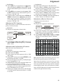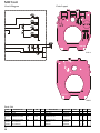
1
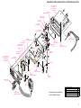
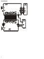
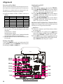
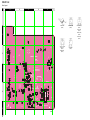
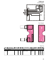
25 Watt VHF/FM Marine Transceiver
QUEST GX1255S
SERVICE MANUAL
EM001N90A
1
Specifications
GENERAL
Channels:
Input Voltage:
Current Drain:
Dimensions:
Flush-Mount Dimensions:
Weight:
All USA, International and Canadian
13.8 VDC ±20%
Standby 0.5 A
Receive 1.5 A
Transmit 5.0 A (Hi); 1.5 A (Lo)
2-1/2” H x 6-5/16” W x 6-5/16” D (64 H x 160 W x 160 D mm)
2” H x 5-5/16” W x 5-1/8” D (50 H x 136 W x 130 D mm)
2.2 lbs (1 kg)
TRANSMITTER
Frequency Range:
RF Output:
Conducted Spurious Emissions:
Audio Response:
Audio Distortion:
Modulation:
Frequency Stability:
FM Hum and Noise:
156.025 to 157.425 MHz
25 W (Hi); 1 W (Lo)
80 dB (Hi); 60 dB (Lo)
within +1/–3 of a 6 dB/octave (pre-emphasis characteristic at 300 to 3000 Hz)
5%
16K0G3E, for DSC 16K0G2B
±0.0005% (–20 °C to +50 °C)
50 dB
RECEIVER
Frequency Range:
Sensitivity:
156.050 to 163.275 MHz
20 dB Quieting: 0.35 µV
12 dB SINAD: 0.25 µV
Squelch Sensitivity (Threshold): 0.13 µV
Modulation Acceptance Bandwidth: ±7.5 kHz
Selectivity:
Spurious and Image Rejection: –70 dB
Intermodulation and Rejection at 12 dB SINAD: –70 dB
Audio Output:
4W
Audio Response:
within + 2/–8 of a 6 dB/octave (de-emphasis characteristic at 300 to 3000 Hz)
Frequency Stability:
±0.0005 % (–20°C to +50°C)
Channel Spacing:
25 kHz
DSC Format:
RTCMSC101
Performance specifications are nominal, unless otherwise indicated, and are subject to change without notice.
2
ExplodCircuit Descriptioned View & Miscellaneous Parts
RA0458700 (BLACK)
SLEEVE ASSY BK
ƒ
RA0422500 (WHITE)
SLEEVE ASSY
ƒ
ƒ
RA0422700
RUBBER PACKING FRONT
RA0421500 (x 2pcs)
O RING (SCREW)
P1091158
MR-S AM001N
‚
RA0422900
O RING M CONECT
‚
ƒ
RA0423000
HOLDER PLATE PWR
„
T9207012A
WIRE ASSY AM001N
RA0449400
REFERECTOR SHEET (A)
RA0418600
LIGHT GUIDE (LCD)
RA0418600 (x 2pcs)
INTER CONNECTOR
RA0422800
CHASSIS
„
G6090148
LCD
„
CNTL UNIT
„ •
RA0418800
LCD HOLDER
RA0457900 (BLACK)
FRONT PANEL ASSY BK
RA0423100
O RING BOTTOM
„
„
RA0418700
LIGHT GUIDE (KNOB)
RA0292100
SHEET (MICROTEX C010)
G1093695
RA35H1516M
•
„
…
RA0419000 (WHITE)
FRONT PANEL ASSY
MAIN UNIT
„
…
RA041830A
SHIELD CASE COVER F
RA0449500
REFERECTOR SHEET (B)
…
…
…
RA0423200
LOCK PLATE
RA0422200 (x 2pcs)
KNOB ASSY
VR UNIT
RA0433800 (x 2pcs)
RUBBER PACKING (KNOB)
Non-designated parts are available only
as part of a designated assembly.
REF. VXSTD P/N
• U00306002
‚ U20305020
ƒ U20307020
„ U23308001
… U24308002
Description
Qty.
PAN HEAD SCREW M3X6NI
2
BIND HEAD SCREW M3X5SUS
2
BIND HEAD SCREW M3X7SUS
4
TAP TITE SCREW M3X8
8
TAP TITE SCREW M3X8NI
5
3
Note
4
Block Diagram
5
Connection Diagram
6
Circuit Description
Reception and transmission are switched by “RX-CNTL”
and “TX-CNTL” lines from the CNTL Unit. The receiver
uses double-conversion superheterodyne circuitry, with
a 21.4 MHz 1st IF and 450 kHz 2nd IF. The 1st local is
produced by a PLL synthesizer, yielding the 21.4 MHz
1st IF. The 2nd local uses a 21.850 MHz crystal oscillator,
yielding the 450 kHz 2nd IF. The 2nd mixer and other circuits use a custom IC to convert and amplify the 2nd IF
and detect FM to obtain demodulated signals. During
transmit, the PLL synthesizer oscillates at the desired frequency directly, for amplification to obtain RF power output. During transmit, voice modulation is applied to this
synthesizer. Transceiver functions, such as TX/RX control,
PLL synthesizer settings, and channel programming, are
controlled using the MPU.
Receiver
Incoming RF signals from the antenna connector are delivered to the RF Unit, and pass through a low-pass filter
(LPF) consisting of coils and capacitors, and antenna
switching diodes D1003 and D1004 (both XB15A308) for
delivery to the receiver front end.
Signals within the frequency range of the transceiver are
then passed through a bandpass filter consisting of T1001
and T1002 before RF amplification by Q1014 (2SC5006).
The amplified RF is then bandpass filtered again by T1003,
T1004, and T1005, to ensure pure in-band input to 1st
mixer Q1018 (3SK320).
Buffered output from the VCO Unit is amplified by Q1016
(2SC5006) and bandpass filtered by L2012, C1072, and
C1078, to provide a pure 1st local signal between 134.65
and 140.625 MHz for delivery to the 1st mixer.
The 21.4 MHz 1st mixer product then passes through dual
monolithic crystal filter XF2001 (±6.5 kHz BW), and is amplified by Q1022 (2SC4400-3) and delivered to the input
of the FM IF subsystem IC Q1024 (TA31136FN). This IC
contains the 2nd mixer, 2nd local oscillator, limiter amplifier, FM detector, noise amplifier, and squelch gates.
The 2nd local in the IF-IC is produced from crystal X1001
(21.850 MHz), and the 1st IF is converted to 450 kHz by
the 2nd mixer and stripped of unwanted components by
ceramic filter CF1001.
After passing through a limiter amplifier, the signal is
demodulated by the FM detector. Demodulated receive
audio from the IF-IC is amplified by Q1025 (2SC4154E),
then the signal is through the AF Mute switch Q1027
(TC4S66F).
After volume adjustment by the AF power amplifier
Q1031 (TDA2003), the audio signal is passed to the external Speaker terminal in the accessory cable and 16-Ohm
internal loudspeaker.
PLL Synthesizer
The 1st LO maintains stability from the PLL synthesizer
by using a 21.850 MHz reference signal from crystal X1001.
PLL synthesizer IC Q1017 (LV2105V) consists of a prescaler, reference counter, swallow counter, programmable
counter, a serial data input port to set these counters based
on the external data, a phase comparator, and a charge
pump.
The PLL-IC divides the 21.850 MHz reference signal by
874 using the reference counter (25 kHz comparison frequency). The VCO output is divided by the prescaler,
swallow counter and programmable counter. These two
signals are compared by the phase comparator and applied to the charge pump.
A voltage proportional to their phase difference is delivered to the low-pass filter circuit, then fed back to the VCO
as a voltage with phase error, controlling and stabilizing
the oscillating frequency. This synthesizer also operates
as a modulator during transmit.
The VCO is comprised of Q1020 (2SK210GR) and D1011/
1012, (both 1SV230); it oscillates at 21.4 MHz during receive, and at the fundamental frequency during transmit,
with direct frequency-modulation using varactor diode
D1009 (1SV214). The VCO output passes through buffer
amplifier Q1019 (2SC5374), and is amplified by Q1016
(2SC5374) to obtain stable output. The VCO DC supply
is regulated by Q1015 (2SC4154E). Synthesizer output is
fed to the 1st mixer by diode switch D1007 (DAN235U)
during receive, and to drive amplifiers Q1013 (2SC52274), Q1011 (2SC3357), and Q1001 for transmit.
The reference oscillator feeds the PLL synthesizer.
Transmitter
Voice audio from the microphone is delivered via the MIC
connector to the RF Unit. After passing through amplifier
Q1028 (NJM2902M), a pre-emphasis network, limiter
(IDC: instantaneous deviation control), and LPF Q1028
(NJM2902M), the audio is adjusted for optimum deviation level and delivered to the next stage.
Voice or DSC(Digital Selective Calling) encode signal inputs from the LPF Q1028 is8 FM-modulated in the VCO
of the synthesizer. Synthesizer output, after passing
through diode switch D1006 (DAN235U), is amplified by
driver Q1013 (2SC5227), Q1011 (2SC3357), and RF power
amplifier Q1001 (RA35H1516M) to obtain full RF output.
The RF energy then passes through antenna switch D1003
and a low-pass filter circuit and finally to the antenna connector.
RF output power from the final amplifier is sampled by
C1006 and C1011 and is rectified by D1002 (1SS321). The
resulting DC is fed through Automatic Power Control-
7
Circuit Description
lers Q1004 (2SA1602A), Q1008 (2SC4154E) and Q1012
(2SA1602A) to transmitter RF power amplifier Q1001,
thus providing positive control of the power output.
Generation of spurious products by the transmitter is minimized by the fundamental carrier frequency being equal
to the final transmitting frequency, modulated directly in
the transmit VCO. Additional harmonic suppression is
provided by a low-pass filter consisting of coils and capacitors, resulting in more than 70 dB of harmonic suppression prior to delivery of the RF energy to the antenna.
DSC Encoder/ Decoder
Encoder
The DCS (Digital Selective Calling) encode signal which
D/A converted in the 8-bit MPU IC Q2003 is fed through
the low-pass filter Q1028 on the RF Unit to the VCO.
Decoder
The receiving DCS code is demodulated by the FM IC
Q1024, then fed through the low-pass filter Q1026
(2SC4154E) to the DCS Decoder IC Q1032 (NJM2211M)
which the receiving DCS code is decoded. The decoded
DCS signal delivered to the 8-bit MPU IC Q2003
8
1050 Hz Weather Alert Decoder
1050Hz Weather Alert signals are demodulated on the
CNTL Unit, and are applied to low-pass filter Q1026
(2SC4154E), and pass thorugh the limiter comparator
Q1028 (NJM2902M).
MPU
Operation is controlled by 8-bit MPU IC Q2003
(M37560M). The system clock uses a 9.8304 MHz crystal
for a time base. IC Q2004 (PST597CN) resets the MPU
when the power is on, and monitors the voltage of the
regulated 5V power supply line.
EEPROM
The EE-PROM retains TX and RX data for all memory
channels , prescaler dividing, IF frequency, local oscillator injection side, and reference oscillator data.
Alignment
The GX1255S has been carefully aligned at the factory
for the specified performance across the marine band.
Realignment should therefore not be necessary except in
the event of a component failure. All component replacement and service should be performed only by an authorized Standard Horizon representative, or the warranty
policy may be voided.
The following procedures cover the sometimes critical and
tedious adjustments that are not normally required once
the transceiver has left the factory. However, if damage
occurs and some parts are replaced, realignment may be
required. If a sudden problem occurs during normal operation, it is likely due to component failure; realignment
should not be done until after the faulty component has
been replaced.
We recommend that servicing be performed only by authorized Standard Horizon service technicians who are
experienced with the circuitry and fully equipped for repair and alignment. Therefore, if a fault is suspected, contact the dealer from whom the transceiver was purchased
for instructions regarding repair. Authorized Standard
Horizon service technicians realign all circuits and make
complete performance checks to ensure compliance with
factory specifications after replacing any faulty components.
Those who do undertake any of the following alignments
are cautioned to proceed at their own risk. Problems
caused by unauthorized attempts at realignment are not
covered by the warranty policy. Also, Standard Horizon,
a division of VERTEX STANDARD, must reserve the right
to change circuits and alignment procedures in the interest of improved performance, without notifying owners.
Under no circumstances should any alignment be attempted unless the normal function and operation of the transceiver are clearly understood, the cause of the malfunction has been clearly pinpointed and any faulty components replaced, and the need for realignment determined
to be absolutely necessary.
The following test equipment (and thorough familiarity
with its correct use) is necessary for complete realignment.
Correction of problems caused by misalignment resulting from use of improper test equipment is not covered
under the warranty policy. While most steps do not require all of the equipment listed, the interactions of some
adjustments may require that more complex adjustments
be performed afterwards. Do not attempt to perform only
a single step unless it is clearly isolated electrically from
all other steps. Have all test equipment ready before beginning, and follow all of the steps in a section in the order presented.
Required Test Equipment
r RF Signal Generator with calibrated output level at
200 MHz
r Deviation Meter (linear detector)
r AF Millivoltmeter
r SINAD Meter
r Inline Wattmeter with 5% accuracy at 200 MHz
r Regulated DC Power Supply: 13.8 VDC, 10A
r 50-ohm Non-reactive Dummy Load: 30W at 200 MHz
r Frequency Counter: >0.1 ppm accuracy at 200 MHz
r AF Signal Generator
r DC Voltmeter: high impedance
r VHF Sampling Coupler
r AF Dummy Load: 4 Ohms, 10 W
r Oscilloscope
r Spectrum Analyzer
r GX1260S Marine Transceiver
Alignment Preparation & Precautions
A dummy load and inline wattmeter must be connected
to the main antenna jack in all procedures that call for
transmission. Correct alignment is not possible with an
antenna.
After completing one step, read the following step to determine whether the same test equipment will be required.
If not, remove the test equipment (except dummy load
and wattmeter, if connected) before proceeding.
Correct alignment requires that the ambient temperature
be the same as that of the transceiver and test equipment,
and that this temperature be held constant between 68 °F
and 86 °F (20 °C and 30 °C). When the transceiver is
brought into the shop from hot or cold air it should be
allowed some time for thermal equalization with the environment before alignment. If possible, alignments
should be made with oscillator shields and circuit boards
firmly affixed in place. Also, the test equipment must be
thoroughly warmed up before beginning.
Note: Signal levels in dB referred to in this procedure are
based on 0 dBµ = 0.5 µV (closed circuit).
9
Alignment
Overview of Test Mode
Confirmation of VCO
The test mode has been build in the microprocessor in order to adjust and comfirm the performance of transceiver.
— Confirmation —
The purpose is to adjust transceiver simply and to confirm the performance of transceiver smoothly.
(a) Expansion channels “EXP01 - EXP06” will be set as
follows:
DISPLAY
EXP01
EXP02
EXP03
EXP04
EXP05
EXP06
WX10
RX FREQUENCY
156.050 MHz
—
163.275 MHz
155.050 MHz
162.025 MHz
163.575 MHz
163.275 MHz
TX FREQUENCY
156.050 MHz
157.425 MHz
—
155.050 MHz
162.025 MHz
158.975 MHz
—
SCAN
X
X
X
O
X
X
O
(B) In CH70, ever time you are in transmit mode, (every
time you press PTT), the following test tone can be
outputted:
1st transmission: 1300 Hz
2nd transmission:2100 Hz
3rd transmission: Synthetic tone of 1300 Hz and 2100 Hz
4th transmission: Return to 1st transmission
(C) Scan the channels between WX10 and EXP04 in the
SCAN mode.
r Connect the DC voltmeter to the test point (TP1019).
r Use the [p(UP)]/[q(DOWN)] key to set the channel
to EXP04, confirm that voltage on the test point is
over 1.0 V in the receive and transmit mode.
r Use the [p(UP)]/[q(DOWN)] key to set the channel
to EXP05, confirm that voltage on the test point is
below 5.0 V in the transmit mode.
r Use the [p(UP)]/[q(DOWN)] key to set the channel
to EXP06, confirm that voltage on the test point is
below 5.0 V in the receive mode.
Adjustment and Confirmation of Transmit Power
Adjust power at high and low in the transmit mode, and
confirm power in the specified bandwidth.
— Adjustment —
r Connect the wattmeter and 50-ohm dummy load to
the antenna jack.
r Use the [H/L] key to set transceiver to high power
and set the channel to CH16. With the PTT switch
pressed, adjust VR1001 so that RF power is 25 W.
r Use the [H/L] key to set transceiver to low power and
set the channel to CH16. With the PTT switch pressed,
adjust VR1002 so that RF power is 0.8 W.
Starting Test Mode
Confirm that PWR/VOL switch is off, and short the TEST
points (JP1001). Turn on the PWR/VOL switch while press
and holding the [DIST] and [DW] keys.
VR1002
VR1001
VR1003
T1001
JP1001
TP1019
T1002
TC1001
T1003
T1004
T1005
MAIN UNIT ALIGNMENT POINT
10
Alignment
— Confirmation —
— Confirmation —
r Use the [H/L] key to set transceiver to high power
and set the channel to EXP01. With the PTT switch
pressed, confirm that RF power is between 23 W and
27 W.
r Use the [H/L] key to set transceiver to low power. With
the PTT switch pressed, confirm that RF power is
between 0.5 W and 1.0 W.
r As descried above, confirm RF power at EXP04 and
EXP05. Set transceiver to high power and confirm
that RF power is between 23 W and 27 W. Set transceiver to low power and confirm that RF power is
between 0.5 W and 1.0 W.
r Set the output of the AG to 1 kHz and 150 mV.
r Set the channel to EXP01, confirm that maximum
deviation is between ±4.3 kHz and ±5.0 kHz.
r Set the channel to EXP02, confirm that maximum
deviation is between ±4.3 kHz and ±5.0 kHz.
r Set the channel to EXP04, confirm that maximum
deviation is between ±4.0 kHz and ±5.0 kHz.
r Set the channel to EXP05, confirm that maximum deviation is between ±4.0 kHz and ±5.0 kHz.
Adjustment of PLL Frequency
— Adjustment —
Adjust the frequency in the transmit mode and local frequency in the receive mode.
— Adjustment —
r Setup the test equipment as shown below.
50-ohm
Dummy Load
Sampling
Coupler
ANT
GX1255S
J1003
Pin 1
AF Signal
Generator
Deviation
Meter
Adjustment of Receiver Front-end
Adjust the receiver front-end coil.
r Setup the test equipment as shown below.
Tracking
Generator
ANT
GX1255S
TP1013
Spectrum
Analizer
r Set the center frequency of t he spectrum analyzer to
159.00 MHz, set SPAN to 20.00 MHz, set RBW and
VBW to 30 kHz, and set SWP to 56 ms.
r Adjust T1001, T1002, T1003, T1004, and T1005
until the wave form shown in below is obtained.
ATTEN 20dB
RL 10.0dBm
10dB/
GX1255S-FRONT-END
r Set the channel to CH16. With the PTT switch pressed,
adjust TC1001 so that RF frequency is 156.80000
MHz ± 50 Hz.
Adjustment and Confirmation of Deviation
Adjust deviation in the transmit mode.
— Adjustment —
r Setup the test equipment as shown below.
r Set the channel to CH16.
r Set the output of the audio generator (AG) to 1 kHz
and 150 mV.
r With the PTT switch pressed, adjust VR1003 so that
the maximum deviation is ±4.5 kHz.
r Decrease the output level of AG by 20 dB (the output
level of AG should be 1/10).
r With the PTT switch pressed, adjust the output level
of AG so that the deviation is ±3.0 kHz.
r Increase the output level of AG by 20 dB (10 times of
the output level of AG) which is supposed to be Detective Modulation Level ±4.5 kHz).
r Repeat steps 3 though 6 three times so that deviation
is ±3.0 kHz and the maximum deviation is ±4.4 kHz
to ±4.6 kHz.
CENTER 159.00 MHz
*RBW 30 kHz VBW 30 kHz
SPAN 20.00 MHz
SWP 56.0 ms
Note: Adjust the output of the tracking generator so that
RF AMP and spectrum analyzer will not saturate.
Figure shows the reference wave form. The wave form
varies with measuring instruments. It is impotent to take
the lowest possible value at the stop band near 150 MHz
and the highest possible value at the band near 156 MHz.
Each coil shall be adjusted at the range between the initial
condition and right and left revolving.
11
Alignment
Confirmation of Weather Alert Tone
Confirmation of DSC Operation
In the weather channel mode, when transceiver receives
the specific emergency tone (1050 Hz), weather alert tone
will be output (Weather Alert Operation). The Weather
Alert mode will be active when a NOAA weather channel is in memory and radio is in memory scan or P-scan
mode.
— Confirmation —
— Confirmation —
r Connect the standard signal generator (SSG) to the
antenna jack.
r Squelch position set to tight.
r Press the [SCAN] key and start to Memory Scan mode.
r Set the SSG to 163.275 MHz (WX10) and output level
of the SSG to 20 dBµV, ±3.0 kHz deviation with 1050
Hz tone modulation.
r Set the output of the SSG to ON.
r Confirm that the channel of transceiver stops at WX10
and the transceiver outputs the weather alert tone (1050
Hz).
Confirmation of receiver NMEA data
Input NMEA format data output from GPS receiver to
NMEA terminal A of transceiver and display it to the LCD
of the transceiver.
NMEA format data output from GPS receiver is applied
to NMEA terminal of transceiver’s option connector and
LCD of transceiver will show data.
— Confirmation —
r Setup the test equipment as shown below.
Blue
ACC Cable
NMEA Input (+)
Green
ACC Cable
NMEA (GND)
GX1255S
GPS
Receiver
r Press and hold the [H/L] key, confirm that the position data is displayed on the LCD of transceiver.
12
r Prepare the confirmation transceiver (GX1260S).
r Input below data to the confirmation transceiver in
advance.
- Input “TEST” to NAME of INDIVIDUAL DIRECTORY
- Input “123456789” to MMSI of INDIVIDUAL
DIRECTORY
- Input “123456780” to local MMSI
- Channel 13 in U.S.A. mode
r Setup the test transceiver as follows:
- Channel 21 in U.S.A.
r In 3 seconds, send the INDIVIDUAL CALL from the
conformation transceiver.
r Confirm that the test transceiver receives the INDIVIDUAL CALL from the conformation transceiver
and outputs the beep.
Press the [CALL/SET] key of the test transceiver and
turn off the beep.
Simultaneously, confirm that “123456780” of conformation transceiver’s MMSI is displayed in the LCD
of the test transceiver.
r Confirm that the conformation transceiver receives the
response from the test transceiver and outputs beep.
Press the [CALL/SET] key of the conformation transceiver and turn off the beep.
Simultaneously, confirm that “TEST” of test
transceiver’s MMSI is displayed in the LCD of the
conformation transceiver.
MAIN Unit
Circuit Diagram
RX: –10.6 dBµ
RX: 1.9 V
RX: 7.7 V
TX: 0.8 V
RX: –8.0 dBµ
RX: –7.0 dBµ (21.4 MHz)
RX: 1.2 V
RX: 7.5 V
RX: +3.0 dBµ
RX: 4.7 V
RX: 1.0 V
RX: 0.5 V
RX: 1.2 V
RX: +10.0 dBµ (21.4 MHz)
RX: 0.5 V
TX HI: 2.9 V
TX LOW: 2.1 V
SQL ON: 4.8 V
SQL OFF: 0 V
RX: 7.9 V
TX: +18.0 dBm
TX: 4.7 V
RX: 5.2 V
RX: +6.0 dBµ (21.4 MHz)
RX: 1.0 V
RX: 5.1 V
RX: 5.5 V
RX: +10 dBm
RX: 4.4 V
TX: 0.7 V
RX: 5.5 V
RX: 0.7 V
RX: 5.5 V
TX: +10 dBm
TX: 4.4 V
RX: 600 mVp-p
@ STD.MOD.
7.3 V
RX: 4.3 V
RX: 5.4 V
3.6 V
6.8 V
3.6 V
RX: 5.2 V
RX: 2.6 V
TX HI: 5.7 V
TX LOW: 4.2 V
5.8 V
0.9 V
TX: 1.6 V
RX: 2.9 V
RX: 2.3 V
TX HI: 1.3 V
TX LOW: 0.2 V
+10 dBm
0.6 V
TX HI: 6.2 V
TX LOW: 0.9 V
RX: 0.8 V
TX: 7.3 V
RX: 400 mVp-p
@ STD.MOD.
DSC DATA “H”: 4.8 V
DSC DATA “L”: 0 V
TX HI: 1.4 V
TX LOW: 0.3 V
RX: 200 mVp-p
@ STD.MOD.
7.3 V
TX: 0 V
RX: 5.0 V
TX HI: 0 V
TX LOW: 5.0 V
RX: 5.0 V
3.6 V
4.8 V
2.5 V
AF MUTE “ON”: 0 V
AF MUTE “OFF”: 5.0 V
TX HI: 4.0 V
TX LOW: 0.6 V
2.5 V
1.5 V
2.4 V
0.9 V
8.0 V
2.3 V
4.3 V
1.6 V
1.6 V
5.0 V
UNLOCK: 4.0 V
TX: 8.0 V
RX: 0 V
6.5 V
1.3 V
TX: 5.0 V
RX: 0 V
ì
PLL DATA “H”: 5.0 V ï
í
PLL DATA “L”: 0 V ï
î
TX: 0 V
RX: 8.0 V
4.6 V
MUTE “ON”: 5.0 V
MUTE “OFF”: 0 V
4.8 V
1.6 V
1.6 V
1.6 V
1.6 V
1.6 V
2.0 V
1.6 V
1.6 V
1.6 V
TX: 0 V
RX: 5.0 V
MIC MUTE “ON”: 0 V
MIC MUTE “OFF”: 5.0 V
1.6 V
13
MAIN Unit
Note
14
MAIN Unit
Parts Layout
A
RA35H1516
(Q1001)
LA4425A
(Q1031)
NJM7808FA
(Q1002)
LV2105V
(Q1017)
NJM12902V
(Q1028)
NJM2904V
(Q1034)
NJM78M05
(Q1003)
2SK210GR (YG)
(Q1020)
3SK320 (U7)
(Q1018)
2SA1602A (MF)
(Q1007)
2SC3357 (MF)
(Q1011)
RT1N241M (N2)
(Q1029, 1033)
B
C
D
E
F
1
TA31136FN
(Q 1024)
2
3
RT1N441U (M3)
(Q1005, 1009, 1010,
1023, 1035)
2SC4154 (LE)
(Q1025, 1026)
DTB123EK (F52)
(Q1006)
2SC5006 (24)
(Q1019)
4
TC4S66F
(Q1037, 1030)
1SS302 (C3)
(D1005)
5
Side A
15
MAIN Unit
Parts Layout
a
b
c
d
e
f
NJM2212M
(Q1032)
2SA1162GR (SG)
(Q1036)
2SC2712GR (LG)
(Q1037)
2SC4154 (LE)
(Q1015)
2SC4400 (RT4)
(Q1022)
1
2SC5006 (24)
(Q1014)
1SS321 (F9)
(D1002)
DAN235U (M)
(D1006)
2
3
4
5
Side B
16
HZM5.6MB2
(Q1032)
MAIN Unit
Parts List
REF
C
C
C
C
C
C
C
C
C
C
C
C
C
C
C
C
C
C
C
C
C
C
C
C
C
C
C
C
C
C
C
C
C
C
C
C
C
C
C
C
C
C
C
C
C
C
C
C
C
C
C
C
C
C
C
C
C
C
C
C
C
C
C
C
C
C
C
C
C
C
C
C
C
C
1001
1002
1004
1006
1007
1008
1009
1010
1011
1012
1013
1014
1015
1016
1017
1019
1021
1024
1025
1027
1028
1029
1030
1031
1032
1033
1034
1035
1036
1037
1039
1041
1042
1043
1046
1047
1048
1049
1050
1051
1054
1055
1056
1057
1059
1060
1061
1062
1063
1064
1065
1067
1068
1069
1070
1071
1072
1075
1076
1077
1078
1079
1080
1081
1084
1086
1088
1090
1091
1094
1098
1099
1100
1101
DESCRIPTION
PCB with Components
Printed Circuit Board
CHIP CAP.
CERAMIC CAP.
CERAMIC CAP.
CHIP CAP.
CHIP CAP.
CHIP CAP.
CERAMIC CAP.
AL.ELECTRO.CAP.
CHIP CAP.
CERAMIC CAP.
CERAMIC CAP.
CERAMIC CAP.
CHIP CAP.
CHIP CAP.
AL.ELECTRO.CAP.
CHIP CAP.
CHIP CAP.
CHIP CAP.
CHIP CAP.
CHIP CAP.
CHIP CAP.
CHIP CAP.
CHIP CAP.
CHIP CAP.
CHIP CAP.
CHIP CAP.
CHIP CAP.
AL.ELECTRO.CAP.
CHIP CAP.
CHIP TA.CAP.
CHIP CAP.
CHIP CAP.
CHIP CAP.
CHIP TA.CAP.
CHIP CAP.
CHIP CAP.
CHIP CAP.
CHIP CAP.
CHIP CAP.
CHIP CAP.
CHIP CAP.
CHIP CAP.
CHIP CAP.
CHIP TA.CAP.
CHIP CAP.
CHIP CAP.
CHIP CAP.
CHIP TA.CAP.
CHIP CAP.
CHIP CAP.
CHIP CAP.
CHIP CAP.
CHIP CAP.
CHIP CAP.
CHIP CAP.
CHIP CAP.
CHIP CAP.
CHIP CAP.
CHIP CAP.
CHIP CAP.
CHIP CAP.
CHIP CAP.
CHIP CAP.
CHIP CAP.
CHIP CAP.
CHIP CAP.
CHIP CAP.
CHIP CAP.
CHIP CAP.
CHIP CAP.
CHIP CAP.
CHIP CAP.
CHIP CAP.
CHIP CAP.
VALUE
0.001uF
12pF
22pF
1pF
0.001uF
0.001uF
27pF
1000uF
1pF
18pF
47pF
15pF
0.001uF
0.001uF
100uF
0.01uF
0.1uF
22pF
0.001uF
0.001uF
0.001uF
0.01uF
27pF
0.01uF
0.01uF
8pF
0.01uF
10uF
0.001uF
4.7uF
0.001uF
2pF
100pF
10uF
5pF
22pF
18pF
15pF
0.001uF
0.001uF
0.001uF
0.001uF
0.001uF
10uF
0.1uF
2pF
5pF
10uF
5pF
15pF
0.001uF
8pF
3pF
15pF
18pF
12pF
7pF
6pF
0.001uF
0.001uF
15pF
0.001uF
1pF
0.001uF
0.001uF
1pF
0.1uF
0.001uF
0.1uF
0.001uF
33pF
0.001uF
6pF
6pF
V/W
50V
50V
50V
50V
50V
50V
50V
25V
50V
50V
50V
50V
50V
50V
25V
50V
16V
50V
50V
50V
50V
50V
50V
50V
50V
50V
50V
16V
50V
10V
50V
50V
50V
10V
50V
50V
50V
50V
50V
50V
50V
50V
50V
10V
16V
50V
50V
10V
50V
50V
50V
50V
50V
50V
50V
50V
50V
50V
50V
50V
50V
50V
50V
50V
50V
50V
25V
50V
16V
50V
50V
50V
50V
50V
TOL.
B
CH
CH
CK
B
B
CH
CK
CH
CH
CH
B
B
B
B
CH
B
B
B
B
CH
B
B
CH
B
B
B
CK
CH
CH
CH
CH
CH
B
B
B
B
B
B
CK
CH
CH
CH
B
CH
CJ
CH
CH
CH
CH
CH
B
B
CH
B
CK
B
B
CK
F
B
B
B
CH
B
CH
CH
MFR'S DESIG
AM001N000
GRM39B102K50PT
CHU5 120J6
CHU5 220J6
GRM39CK010C50PT
GRM39B102K50PT
GRM39B102K50PT
CHU5 270J6
RE3-25V102M 1000UF
GRM39CK010C50PT
CHU5 180J6
CHU5 470J6
CHU5 150J6
GRM39B102K50PT
GRM39B102K50PT
RE2-25V101M 100UF
GRM39B103M50PT
GRM39B104K16PT
GRM39CH220J50PT
GRM39B102K50PT
GRM39B102K50PT
GRM39B102K50PT
GRM39B103M50PT
GRM39CH270J50PT
GRM39B103M50PT
GRM39B103M50PT
GRM39CH080D50PT
GRM39B103M50PT
RC2-16V100M(4X7)
GRM39B102K50PT
TEMSVA1A475M-8R
GRM39B102K50PT
GRM39CK020C50PT
GRM39CH101J50PT
TEMSVA1A106M-8R
GRM39CH050C50PT
GRM39CH220J50PT
GRM39CH180J50PT
GRM39CH150J50PT
GRM39B102K50PT
GRM39B102K50PT
GRM39B102K50PT
GRM39B102K50PT
GRM39B102K50PT
TEMSVA1A106M-8R
GRM39B104K16PT
GRM39CK020C50PT
GRM39CH050C50PT
TEMSVA1A106M-8R
GRM39CH050C50PT
GRM39CH150J50PT
GRM39B102K50PT
GRM39CH080D50PT
GRM39CJ030C50PT
GRM39CH150J50PT
GRM39CH180J50PT
GRM39CH120J50PT
GRM39CH070D50PT
GRM39CH060D50PT
GRM39B102K50PT
GRM39B102K50PT
GRM39CH150J50PT
GRM39B102K50PT
GRM39CK010C50PT
GRM39B102K50PT
GRM39B102K50PT
GRM39CK010C50PT
GRM39F104Z25PT
GRM39B102K50PT
GRM39B104K16PT
GRM39B102K50PT
GRM39CH330J50PT
GRM39B102K50PT
GRM39CH060D50PT
GRM39CH060D50PT
VXSTD P/N
CB2155001
FR008500C
K22174821
K02179103
K02179106
K22174202
K22174821
K22174821
K02179107
K40149045
K22174202
K02179105
K02179110
K02179104
K22174821
K22174821
K40149028
K22174823
K22124805
K22174219
K22174821
K22174821
K22174821
K22174823
K22174221
K22174823
K22174823
K22174209
K22174823
K40129012
K22174821
K78100022
K22174821
K22174203
K22174235
K78100028
K22174206
K22174219
K22174217
K22174215
K22174821
K22174821
K22174821
K22174821
K22174821
K78100028
K22124805
K22174203
K22174206
K78100028
K22174206
K22174215
K22174821
K22174209
K22174204
K22174215
K22174217
K22174213
K22174208
K22174207
K22174821
K22174821
K22174215
K22174821
K22174202
K22174821
K22174821
K22174202
K22145001
K22174821
K22124805
K22174821
K22174223
K22174821
K22174207
K22174207
VERS.
LOT SIDE LAY ADR
111111111111111111111111111111111111111111111111111111111111111111111111111-
A
A
A
B
B
B
A
A
B
A
A
A
B
A
A
B
A
A
A
A
A
B
A
B
A
A
A
A
A
A
A
B
A
A
B
B
B
A
B
B
B
B
B
B
A
B
B
B
B
B
B
A
B
B
A
A
A
B
A
A
A
A
A
A
A
A
B
A
A
A
A
A
A
A
D2
E1
E2
a2
a2
d2
E1
D2
a2
E2
E2
E1
c1
B1
A3
e3
B2
B1
B2
B2
B2
e3
E2
e2
C3
E3
B3
A3
B3
C1
C3
a3
B2
B2
a3
a4
a4
B3
a4
a4
b3
b3
a4
b2
C3
a4
a5
b3
b4
b4
b3
C4
b5
b4
C4
D4
E4
b5
D3
C4
D4
D4
D4
D3
D3
D3
c3
D4
D3
C4
D4
D4
D3
D3
17
MAIN Unit
Parts List
REF
C 1104
C 1107
C 1109
C 1110
C 1113
C 1115
C 1117
C 1119
C 1121
C 1123
C 1129
C 1132
C 1133
C 1134
C 1135
C 1136
C 1139
C 1140
C 1141
C 1142
C 1143
C 1144
C 1145
C 1146
C 1147
C 1148
C 1149
C 1151
C 1152
C 1153
C 1154
C 1156
C 1157
C 1158
C 1159
C 1160
C 1162
C 1163
C 1164
C 1165
C 1166
C 1167
C 1168
C 1170
C 1171
C 1172
C 1173
C 1175
C 1177
C 1178
C 1179
C 1180
C 1182
C 1183
C 1185
C 1186
C 1187
C 1188
C 1190
C 1193
C 1194
C 1196
C 1197
C 1200
C 1205
C 1206
C 1207
C 1208
C 1209
C 1210
C 1211
C 1212
C 1213
C 1214
C 1215
C 1216
18
DESCRIPTION
CHIP CAP.
CHIP TA.CAP.
CHIP CAP.
CHIP CAP.
CHIP TA.CAP.
CHIP CAP.
CHIP CAP.
CHIP CAP.
CHIP CAP.
CHIP CAP.
CHIP CAP.
CHIP CAP.
CHIP CAP.
CHIP CAP.
CHIP CAP.
CHIP CAP.
CHIP CAP.
CHIP CAP.
CHIP CAP.
CHIP CAP.
CHIP CAP.
CHIP CAP.
CHIP CAP.
CHIP CAP.
CHIP CAP.
AL.ELECTRO.CAP.
CHIP CAP.
CHIP CAP.
CHIP CAP.
CHIP CAP.
CHIP CAP.
CHIP CAP.
CHIP CAP.
CHIP CAP.
CHIP CAP.
CHIP CAP.
CHIP CAP.
CHIP CAP.
CHIP CAP.
CHIP CAP.
CHIP CAP.
CHIP CAP.
CHIP CAP.
CHIP CAP.
CHIP CAP.
CHIP CAP.
CHIP CAP.
CHIP CAP.
CHIP TA.CAP.
CHIP CAP.
AL.ELECTRO.CAP.
CHIP CAP.
FILM CAP.
CHIP CAP.
CHIP CAP.
AL.ELECTRO.CAP.
CHIP TA.CAP.
CHIP CAP.
CHIP CAP.
CHIP CAP.
CHIP CAP.
CHIP CAP.
CHIP CAP.
CHIP CAP.
CHIP CAP.
CHIP CAP.
CHIP CAP.
CHIP CAP.
CHIP CAP.
CHIP TA.CAP.
CHIP CAP.
CHIP CAP.
CHIP CAP.
CHIP CAP.
CHIP CAP.
CHIP CAP.
VALUE
0.01uF
10uF
7pF
0.001uF
0.47uF
1pF
0.001uF
1pF
0.001uF
7pF
1pF
1uF
0.0056uF
0.01uF
330pF
0.01uF
0.1uF
0.01uF
1uF
0.0068uF
0.1uF
0.1uF
0.1uF
0.01uF
15pF
10uF
0.01uF
0.022uF
1pF
0.0047uF
0.1uF
0.01uF
0.1uF
0.1uF
0.1uF
820pF
1uF
82pF
0.1uF
1uF
470pF
470pF
0.01uF
0.0047uF
0.1uF
0.1uF
0.1uF
1uF
10uF
15pF
100uF
0.001uF
0.027uF
0.1uF
0.001uF
470uF
10uF
0.0047uF
0.1uF
15pF
0.1uF
0.001uF
0.0068uF
0.0022uF
15pF
0.1uF
4pF
3pF
0.1uF
10uF
0.001uF
0.001uF
0.001uF
0.001uF
5pF
5pF
V/W
50V
6.3V
50V
50V
25V
50V
50V
50V
50V
50V
50V
10V
50V
50V
50V
50V
25V
50V
10V
50V
16V
16V
16V
50V
50V
16V
50V
25V
50V
50V
16V
50V
25V
16V
16V
50V
10V
50V
16V
10V
50V
50V
50V
50V
16V
16V
16V
10V
10V
50V
25V
50V
16V
16V
50V
16V
10V
50V
16V
50V
16V
50V
50V
50V
50V
16V
50V
50V
25V
10V
50V
50V
50V
50V
50V
50V
TOL.
B
CH
B
CK
B
CK
B
CH
CK
F
B
B
B
B
F
B
F
B
B
B
B
B
CH
B
B
CK
B
B
B
F
B
B
B
F
CH
B
F
B
B
B
B
B
B
B
F
CH
B
B
B
B
B
CH
B
B
B
B
CH
B
CH
CJ
F
B
B
B
B
CH
CH
MFR'S DESIG
GRM39B103M50PT
TEMSVA0J106M-8R
GRM39CH070D50PT
GRM39B102K50PT
TESVA1E474M1-8R
GRM39CK010C50PT
GRM39B102K50PT
GRM39CK010C50PT
GRM39B102K50PT
GRM39CH070D50PT
GRM39CK010C50PT
GRM39F105Z10PT
GRM39B562M50PT
GRM39B103M50PT
GRM39B331K50PT
GRM39B103M50PT
GRM39F104Z25PT
GRM39B103M50PT
GRM39F105Z10PT
GRM39B682K50PT
GRM39B104K16PT
GRM39B104K16PT
GRM39B104K16PT
GRM39B103M50PT
GRM39CH150J50PT
RC2-16V100M(4X7)
GRM39B103M50PT
GRM39B223K25PT
GRM39CK010C50PT
GRM39B472K50PT
GRM39B104K16PT
GRM39B103M50PT
GRM39F104Z25PT
GRM39B104K16PT
GRM39B104K16PT
GRM39B821M50PT
GRM39F105Z10PT
GRM39CH820J50PT
GRM39B104K16PT
GRM39F105Z10PT
ECUV1H471KBV
ECUV1H471KBV
GRM39B103M50PT
GRM39B472K50PT
GRM39B104K16PT
GRM39B104K16PT
GRM39B104K16PT
GRM39F105Z10PT
TEMSVA1A106M-8R
GRM39CH150J50PT
RE2-25V101M 100UF
GRM39B102K50PT
ECHU1C273JB5
GRM39B104K16PT
GRM39B102K50PT
RE3-16V471M 470UF
TEMSVA1A106M-8R
GRM39B472K50PT
GRM39B104K16PT
GRM39CH150J50PT
GRM39B104K16PT
GRM39B102K50PT
GRM39B682K50PT
GRM39B222K50PT
GRM39CH150J50PT
GRM39B104K16PT
GRM39CH040C50PT
GRM39CJ030C50PT
GRM39F104Z25PT
TEMSVA1A106M-8R
GRM39B102K50PT
GRM39B102K50PT
GRM39B102K50PT
GRM39B102K50PT
GRM39CH050C50PT
GRM39CH050C50PT
VXSTD P/N
K22174823
K78080027
K22174208
K22174821
K78140009
K22174202
K22174821
K22174202
K22174821
K22174208
K22174202
K22105001
K22174818
K22174823
K22174820
K22174823
K22145001
K22174823
K22105001
K22174834
K22124805
K22124805
K22124805
K22174823
K22174215
K40129012
K22174823
K22144807
K22174202
K22174833
K22124805
K22174823
K22145001
K22124805
K22124805
K22174808
K22105001
K22174233
K22124805
K22105001
K22179610
K22179610
K22174823
K22174833
K22124805
K22124805
K22124805
K22105001
K78100028
K22174215
K40149028
K22174821
K57120012
K22124805
K22174821
K40129066
K78100028
K22174833
K22124805
K22174215
K22124805
K22174821
K22174834
K22174822
K22174215
K22124805
K22174205
K22174204
K22145001
K78100028
K22174821
K22174821
K22174821
K22174821
K22174206
K22174206
VERS.
LOT SIDE LAY ADR
1- A
D4
1- B
b3
1- A
D3
1- A
D3
1- B
b4
1- A
C4
1- A
C3
1- A
D3
1- B
b4
1- A
C5
1- A
C5
1- A
C3
1- A
B4
1- B
c5
1- A
B4
1- B
c4
1- A
B4
1- B
c4
1- A
B5
1- A
B4
1- A
B5
1- A
B4
1- A
B5
1- B
c4
1- A
B4
1- A
B4
1- A
C5
1- A
B5
1- A
C4
1- A
B5
1- A
C4
1- A
B4
1- A
A4
1- A
A3
1- A
B4
1- A
B5
1- A
A5
1- B
c5
1- B
c4
1- A
A3
1- B
c5
1- B
c5
1- A
B5
1- B
d5
1- A
A3
1- A
B3
1- B
d4
1- A
A4
1- B
d4
1- A
A4
1- A
A1
1- B
e1
1- B
e4
1- A
A4
1- A
A4
1- A
A2
1- A
A4
1- A
A4
1- B
d4
1- A
A3
1- A
A4
1- A
A3
1- B
e4
1- B
e5
1- A
E4
1- B
a3
1- B
a2
1- B
a2
1- A
B4
1- A
C3
1- B
e2
1- B
e2
1- A
A2
1- A
A3
1- B
a4
1- B
a4
MAIN Unit
Parts List
REF
C 1217
C 1218
C 1219
C 1220
C 1221
C 1222
C 1223
C 1224
C 1225
C 1226
C 1227
C 1228
C 1229
C 1233
C 1234
C 1235
C 1236
C 1237
C 1238
C 1239
CD1001
CF1001
D 1001
D 1002
D 1003
D 1004
D 1005
D 1006
D 1010
D 1011
D 1012
D 1013
D 1014
D 1015
J 1001
J 1002
J 1003
L 1001
L 1002
L 1003
L 1004
L 1005
L 1006
L 1007
L 1010
L 1012
L 1013
L 1014
L 1015
L 1016
L 1017
L 1018
L 1019
L 1022
L 1023
L 1024
Q 1001
Q 1002
Q 1003
Q 1005
Q 1006
Q 1007
Q 1009
Q 1010
Q 1011
Q 1014
Q 1015
Q 1017
Q 1018
Q 1019
Q 1020
Q 1022
Q 1023
Q 1024
Q 1025
Q 1026
DESCRIPTION
CHIP TA.CAP.
CHIP CAP.
CHIP CAP.
CHIP CAP.
CHIP CAP.
CHIP CAP.
CHIP CAP.
CHIP CAP.
CHIP CAP.
CHIP CAP.
CHIP CAP.
CHIP CAP.
CHIP CAP.
CHIP CAP.
CHIP CAP.
CHIP CAP.
CHIP TA.CAP.
CHIP TA.CAP.
CHIP TA.CAP.
CERAMIC CAP.
CERAMIC DISC
CERAMIC FILTER
DIODE
DIODE
DIODE
DIODE
DIODE
DIODE
DIODE
DIODE
DIODE
DIODE
DIODE
DIODE
CONNECTOR
CONNECTOR
CONNECTOR
M.RFC
COIL A1
COIL A1
COIL A1
COIL A1
COIL
COIL
M.RFC
M.RFC
M.RFC
M.RFC
M.RFC
M.RFC
M.RFC
M.RFC
M.RFC
M.RFC
M.RFC
M.RFC
IC
IC
IC
TRANSISTOR
TRANSISTOR
TRANSISTOR
TRANSISTOR
TRANSISTOR
TRANSISTOR
TRANSISTOR
TRANSISTOR
IC
FET
TRANSISTOR
FET
TRANSISTOR
TRANSISTOR
IC
TRANSISTOR
TRANSISTOR
VALUE
10uF
8pF
0.1uF
0.001uF
0.1uF
0.1uF
0.001uF
0.001uF
0.1uF
0.001uF
0.001uF
0.001uF
0.1uF
0.001uF
0.1uF
15pF
0.1uF
10uF
10uF
0.01uF
V/W
10V
50V
16V
50V
16V
16V
50V
50V
16V
50V
50V
50V
25V
50V
25V
50V
35V
10V
10V
16V
TOL.
CH
B
B
B
B
B
B
B
B
B
B
F
B
F
CH
Y
4.7uH
0.082uH
0.082uH
0.068uH
0.068uH
0.1uH
2.2uH
1.5uH
0.068uH
2.2uH
0.22uH
2.2uH
0.047uH
2%
2%
2%
MFR'S DESIG
TEMSVA1A106M-8R
GRM39CH080D50PT
GRM39B104K16PT
GRM39B102K50PT
GRM39B104K16PT
GRM39B104K16PT
GRM39B102K50PT
GRM39B102K50PT
GRM39B104K16PT
GRM39B102K50PT
GRM39B102K50PT
GRM39B102K50PT
GRM39F104Z25PT
GRM39B102K50PT
GRM39F104Z25PT
GRM39CH150J50PT
TESVA1V104M1-8R
TEMSVA1A106M-8R
TEMSVA1A106M-8R
EP050Y103N-A
CDA450C24
ALFYM450E=K
1N5402
1SS321 TE85R
XB15A308A2GB
XB15A308A2GB
1SS302 TE85R
DAN235U TL
1SV214 TPH
HVU350TRF
HVU350TRF
HZM5.6NB2 TR
HSU277TRF
1SS355 TE-17
28FLT-SM1-TB
B7B-PH-K-S
B2B-PH-K-S
LAL03NA4R7K
4.5T3.5D0.8UEW R
4.5T3.5D0.8UEW R
4.5T3.5D0.8UEW R
3.5T4.0D0.8UEW R
E2 0.25-1.9-8T-L
E2 0.25-1.9-8T-L
HK1608 82NJ-T
HK1608 82NJ-T
C1608CA-68NG
C1608CA-68NG
HK1608 R10J-T
LK1608 2R2K-T
LK1608 1R5K-T
C2012C-68NG
LK1608 2R2K-T
HK1608 R22J-T
LK1608 2R2K-T
HK1608 47NJ-T
RA35H1516M-01
NJM7808FA
NJM78M05DL1A(TE1)
RT1N441U-T11-1
DTB123EK T146
2SA1602A-T11-1F
RT1N441U-T11-1
RT1N441U-T11-1
2SC3357-T2 RF
2SC5006-T1
2SC4154-T11-1E
LV2105V-TLM
3SK320(TE85L)
2SC5006-T1
2SK210GR TE85R
2SC4400-3-TL
RT1N441U-T11-1
TA31136FN(EL)
2SC4154-T11-1E
2SC4154-T11-1E
VXSTD P/N
K78100028
K22174209
K22124805
K22174821
K22124805
K22124805
K22174821
K22174821
K22124805
K22174821
K22174821
K22174821
K22145001
K22174821
K22145001
K22174215
K78160025
K78100028
K78100028
K28129001
H7901430
H3900535
G2090778
G2070076
G2090742
G2090742
G2070088
G2070176
G2070356
G2070380
G2070380
G2070722
G2070118
G2070470
P1091149
P0090401
P0090396
L1190203
L0021149A
L0021149A
L0021149A
L0022245
L0022550
L0022550
L1690527
L1690527
L1691042
L1691042
L1690528
L1690634
L1690846
L1690774
L1690634
L1690940
L1690634
L1690524
G1093695
G1093640
G1093660
G3070247
G3070022
G3116028F
G3070247
G3070247
G3333577F
G3350068
G3341548E
G1093191
G4803208
G3350068
G3802107G
G3344008C
G3070247
G1091605
G3341548E
G3341548E
VERS.
LOT SIDE LAY ADR
1- A
B4
1- A
B2
1- A
B2
1- A
C2
1- A
C2
1- A
B2
1- A
B2
1- A
B2
1- A
C2
1- A
C2
1- A
D4
1- B
c3
1- B
c3
1- A
C4
1- A
C4
1- A
D3
1- A
C3
1- A
A2
1- A
C3
11- A
C5
1- A
C4
1- A
C2
1- B
a2
1- A
E2
1- A
D2
1- A
E3
1- B
b3
1- A
D3
1- A
D4
1- A
D3
1- B
d4
1- A
D3
11- A
B4
1- A
A3
1- A
A4
1- A
D2
1- A
E1
1- A
D2
1- A
E1
1- A
E2
1- A
B2
1- A
B2
1- B
b4
1- A
E4
1- A
D4
1- A
D4
1- A
D3
1- A
D3
1- A
D4
1- A
D3
1- A
D3
1- B
a4
1- A
D4
1- A
E2
1- A
B1
1- A
A2
1- A
A3
1- A
C1
1- A
B3
1- A
C3
1- A
B3
1- A
C3
1- A
B2
1- B
a4
1- B
b3
1- A
C4
1- A
D4
1- A
D3
1- A
D3
1- B
c5
1- A
C3
1- A
C5
1- A
A4
1- A
B4
19
MAIN Unit
Parts List
REF
Q 1027
Q 1028
Q 1029
Q 1030
Q 1031
Q 1032
Q 1033
Q 1034
Q 1035
Q 1036
Q 1037
R 1001
R 1002
R 1003
R 1004
R 1005
R 1006
R 1007
R 1008
R 1009
R 1010
R 1011
R 1013
R 1014
R 1015
R 1016
R 1018
R 1020
R 1022
R 1024
R 1025
R 1026
R 1027
R 1028
R 1029
R 1030
R 1031
R 1032
R 1033
R 1034
R 1035
R 1037
R 1038
R 1039
R 1040
R 1041
R 1043
R 1044
R 1045
R 1046
R 1047
R 1048
R 1049
R 1050
R 1052
R 1053
R 1054
R 1055
R 1056
R 1057
R 1059
R 1061
R 1064
R 1066
R 1068
R 1069
R 1070
R 1071
R 1072
R 1073
R 1074
R 1075
R 1076
R 1077
R 1078
R 1079
20
DESCRIPTION
IC
IC
TRANSISTOR
IC
IC
IC
TRANSISTOR
IC
TRANSISTOR
TRANSISTOR
TRANSISTOR
CHIP RES.
CHIP RES.
CHIP RES.
CHIP RES.
CHIP RES.
CHIP RES.
CHIP RES.
CHIP RES.
CHIP RES.
CHIP RES.
CHIP RES.
CHIP RES.
CHIP RES.
CHIP RES.
CHIP RES.
CHIP RES.
CHIP RES.
CHIP RES.
CHIP RES.
CHIP RES.
CHIP RES.
CHIP RES.
CHIP RES.
CHIP RES.
CHIP RES.
CHIP RES.
CHIP RES.
CHIP RES.
CHIP RES.
CHIP RES.
CHIP RES.
CHIP RES.
CHIP RES.
CHIP RES.
CHIP RES.
CHIP RES.
CHIP RES.
CHIP RES.
CHIP RES.
CHIP RES.
CHIP RES.
CHIP RES.
CHIP RES.
CHIP RES.
CHIP RES.
CHIP RES.
CHIP RES.
CHIP RES.
CHIP RES.
CHIP RES.
CHIP RES.
CHIP RES.
CHIP RES.
CHIP RES.
CHIP RES.
CHIP RES.
CHIP RES.
CHIP RES.
CHIP RES.
CHIP RES.
CHIP RES.
CHIP RES.
CHIP RES.
CHIP RES.
CHIP RES.
VALUE
56k
100
4.7k
0
0
4.7k
4.7k
10k
47k
10k
2.2k
470
100
1k
470k
10k
4.7k
2.2k
47
10k
0
2.2k
220k
2.2k
330
2.2k
100
560
470
47
0
47
100k
100
47k
100
0
100
100
270
100
47k
100
100
22k
47k
100
1.2k
220
1k
470
1k
10k
2.7k
100k
0
220k
330
39k
100
39k
220
2.2k
330k
4.7k
V/W
1/10W
1W
1/16W
1/16W
1/16W
1/16W
1/16W
1/16W
1/16W
1/16W
1/16W
1/16W
1/16W
1/16W
1/16W
1/16W
1/16W
1/16W
1/16W
1/16W
1/16W
1/16W
1/16W
1/16W
1/16W
1/16W
1/16W
1/16W
1/16W
1/16W
1/16W
1/16W
1/16W
1/16W
1/16W
1/16W
1/16W
1/16W
1/16W
1/16W
1/16W
1/16W
1/16W
1/16W
1/16W
1/16W
1/16W
1/16W
1/16W
1/16W
1/16W
1/16W
1/16W
1/16W
1/16W
1/16W
1/16W
1/16W
1/16W
1/16W
1/16W
1/16W
1/16W
1/16W
1/16W
TOL.
5%
5%
5%
5%
5%
5%
5%
5%
5%
5%
5%
5%
5%
5%
5%
5%
5%
5%
5%
5%
5%
5%
5%
5%
5%
5%
5%
5%
5%
5%
5%
5%
5%
5%
5%
5%
5%
5%
5%
5%
5%
5%
5%
5%
5%
5%
5%
5%
5%
5%
5%
5%
5%
5%
5%
5%
5%
5%
5%
5%
5%
5%
5%
5%
5%
MFR'S DESIG
TC4S66F TE85R
NJM12902V(TE1)
RT1N241M-T11-1
TC4S66F TE85R
LA4425A
NJM2211M(TE1)
RT1N241M-T11-1
NJM2904V-TE1
RT1N441U-T11-1
2SA1162GR TE85R
2SC2712GR TE85R
RMC1/10T 563J
RMC1 101JTE
RMC1/16 472JATP
RMC1/16 000JATP
RMC1/16 000JATP
RMC1/16 472JATP
RMC1/16 472JATP
RMC1/16 103JATP
RMC1/16 473JATP
RMC1/16 103JATP
RMC1/16 222JATP
RMC1/16 471JATP
RMC1/16 101JATP
RMC1/16 102JATP
RMC1/16 474JATP
RMC1/16 103JATP
RMC1/16 472JATP
RMC1/16 222JATP
RMC1/16 470JATP
RMC1/16 103JATP
RMC1/16 000JATP
RMC1/16 222JATP
RMC1/16 224JATP
RMC1/16 222JATP
RMC1/16 331JATP
RMC1/16 222JATP
RMC1/16 101JATP
RMC1/16 561JATP
RMC1/16 471JATP
RMC1/16 470JATP
RMC1/16 000JATP
RMC1/16 470JATP
RMC1/16 104JATP
RMC1/16 101JATP
RMC1/16 473JATP
RMC1/16 101JATP
RMC1/16 000JATP
RMC1/16 101JATP
RMC1/16 101JATP
RMC1/16 271JATP
RMC1/16 101JATP
RMC1/16 473JATP
RMC1/16 101JATP
RMC1/16 101JATP
RMC1/16 223JATP
RMC1/16 473JATP
RMC1/16 101JATP
RMC1/16 122JATP
RMC1/16 221JATP
RMC1/16 102JATP
RMC1/16 471JATP
RMC1/16 102JATP
RMC1/16 103JATP
RMC1/16 272JATP
RMC1/16 104JATP
RMC1/16 000JATP
RMC1/16 224JATP
RMC1/16 331JATP
RMC1/16 393JATP
RMC1/16 101JATP
RMC1/16 393JATP
RMC1/16 221JATP
RMC1/16 222JATP
RMC1/16 334JATP
RMC1/16 472JATP
VXSTD P/N
G1090893
G1093592
G3070249
G1090893
G1092241
G1092943
G3070249
G1091677
G3070247
G3111627G
G3327127G
J24205563
J24305101
J24185472
J24185000
J24185000
J24185472
J24185472
J24185103
J24185473
J24185103
J24185222
J24185471
J24185101
J24185102
J24185474
J24185103
J24185472
J24185222
J24185470
J24185103
J24185000
J24185222
J24185224
J24185222
J24185331
J24185222
J24185101
J24185561
J24185471
J24185470
J24185000
J24185470
J24185104
J24185101
J24185473
J24185101
J24185000
J24185101
J24185101
J24185271
J24185101
J24185473
J24185101
J24185101
J24185223
J24185473
J24185101
J24185122
J24185221
J24185102
J24185471
J24185102
J24185103
J24185272
J24185104
J24185000
J24185224
J24185331
J24185393
J24185101
J24185393
J24185221
J24185222
J24185334
J24185472
VERS.
LOT SIDE LAY ADR
1- A
A4
1- A
A4
1- A
A3
1- A
A4
1- A
A2
1- B
e4
1- A
D3
1- A
B2
1- A
C2
1- B
c3
1- B
c3
1- B
a1
1- A
D2
1- B
a2
1- B
a2
1- B
a2
1- B
a2
1- A
B1
1- A
C3
1- A
C2
1- A
B1
1- A
C3
1- A
B2
1- A
B2
1- A
B2
1- A
B2
1- A
C2
1- A
C2
1- A
C2
1- A
B2
1- A
C2
1- A
B2
1- A
B3
1- B
a4
1- B
b3
1- B
a4
1- B
a4
1- B
a4
1- B
a4
1- B
b2
1- A
C3
1- A
D3
1- A
C4
1- A
D4
1- A
D3
1- A
D3
1- A
D4
1- B
c3
1- A
D3
1- A
D3
1- B
c3
1- A
C4
1- A
D3
1- B
c4
1- B
c4
1- A
D4
1- A
D3
1- B
c4
1- A
D4
1- B
b3
1- A
D4
1- B
c3
1- B
b3
1- A
D3
1- B
c5
1- A
C3
1- A
C3
1- B
c4
1- B
c5
1- A
B4
1- B
c4
1- A
B4
1- B
c4
1- B
c4
1- A
B4
1- A
B5
MAIN Unit
Parts List
REF
R 1080
R 1081
R 1082
R 1083
R 1084
R 1085
R 1086
R 1088
R 1089
R 1090
R 1091
R 1092
R 1093
R 1095
R 1096
R 1097
R 1098
R 1099
R 1100
R 1101
R 1102
R 1103
R 1104
R 1105
R 1106
R 1107
R 1108
R 1109
R 1110
R 1111
R 1112
R 1113
R 1114
R 1116
R 1117
R 1118
R 1119
R 1120
R 1121
R 1122
R 1123
R 1124
R 1125
R 1126
R 1127
R 1131
R 1132
R 1133
R 1135
R 1136
R 1137
R 1138
R 1139
R 1140
R 1141
R 1142
R 1143
R 1145
R 1146
R 1148
R 1149
R 1150
R 1151
R 1152
R 1153
R 1154
R 1155
R 1156
R 1157
R 1158
R 1159
R 1160
R 1162
R 1163
R 1164
T 1001
DESCRIPTION
CHIP RES.
CHIP RES.
CHIP RES.
CHIP RES.
CHIP RES.
CHIP RES.
CHIP RES.
CHIP RES.
CHIP RES.
CHIP RES.
CHIP RES.
CHIP RES.
CHIP RES.
CHIP RES.
CHIP RES.
CHIP RES.
CHIP RES.
CHIP RES.
CHIP RES.
CHIP RES.
CHIP RES.
CHIP RES.
CHIP RES.
CHIP RES.
CHIP RES.
CHIP RES.
CHIP RES.
CHIP RES.
CHIP RES.
CHIP RES.
CHIP RES.
CHIP RES.
CHIP RES.
CHIP RES.
CHIP RES.
CHIP RES.
CHIP RES.
CHIP RES.
CHIP RES.
CHIP RES.
CHIP RES.
CHIP RES.
CHIP RES.
CHIP RES.
CHIP RES.
CHIP RES.
CHIP RES.
CHIP RES.
CHIP RES.
CHIP RES.
CHIP RES.
CHIP RES.
CHIP RES.
CHIP RES.
CHIP RES.
CHIP RES.
CHIP RES.
CHIP RES.
CHIP RES.
CHIP RES.
CHIP RES.
CHIP RES.
CHIP RES.
CHIP RES.
CHIP RES.
CHIP RES.
CHIP RES.
CHIP RES.
CHIP RES.
CHIP RES.
CHIP RES.
CHIP RES.
CHIP RES.
CHIP RES.
CHIP RES.
COIL
VALUE
10k
1k
33k
56k
22k
330k
5.6k
22k
4.7k
120k
100k
10k
100k
22k
2.2k
2.2M
15k
100
1.8k
10k
15k
2.2k
0
100k
100k
47k
100k
100
100k
47k
22k
120k
100k
1k
0
100k
330k
0
0
100k
100
100k
5.6k
10k
47k
10k
100k
10k
47k
10k
1k
100k
10k
0
18k
10k
4.7k
100k
100
4.7k
1k
470k
10k
100k
10k
220
470
22
22k
22k
4.7k
4.7k
22
47k
4.7k
V/W
1/16W
1/16W
1/16W
1/16W
1/16W
1/16W
1/16W
1/16W
1/16W
1/16W
1/16W
1/16W
1/16W
1/16W
1/16W
1/16W
1/16W
1/16W
1/16W
1/16W
1/16W
1/16W
1/16W
1/16W
1/16W
1/16W
1/16W
1/16W
1/16W
1/16W
1/16W
1/16W
1/16W
1/16W
1/16W
1/16W
1/16W
1W
1/16W
1/16W
1/16W
1/16W
1/16W
1/16W
1/16W
1/16W
1/16W
1/16W
1/16W
1/16W
1/16W
1/16W
1/16W
1/16W
1/16W
1/16W
1/16W
1/16W
1/16W
1/16W
1/16W
1/16W
1/16W
1/16W
1/16W
1/16W
1/16W
1/16W
1/16W
1/16W
1/16W
1/16W
1/16W
1/16W
1/16W
TOL.
5%
5%
5%
5%
5%
5%
5%
5%
5%
5%
5%
5%
5%
5%
5%
5%
5%
5%
5%
5%
5%
5%
5%
5%
5%
5%
5%
5%
5%
5%
5%
5%
5%
5%
5%
5%
5%
5%
5%
5%
5%
5%
5%
1%
5%
5%
5%
1%
5%
5%
5%
5%
5%
5%
5%
5%
5%
5%
5%
5%
5%
5%
5%
5%
5%
5%
5%
5%
5%
5%
5%
5%
5%
5%
5%
MFR'S DESIG
RMC1/16 103JATP
RMC1/16 102JATP
RMC1/16 333JATP
RMC1/16 563JATP
RMC1/16 223JATP
RMC1/16 334JATP
RMC1/16 562JATP
RMC1/16 223JATP
RMC1/16 472JATP
RMC1/16 124JATP
RMC1/16 104JATP
RMC1/16 103JATP
RMC1/16 104JATP
RMC1/16 223JATP
RMC1/16 222JATP
RMC1/16 225JATP
RMC1/16 153JATP
RMC1/16 101JATP
RMC1/16 182JATP
RMC1/16 103JATP
RMC1/16 153JATP
RMC1/16 222JATP
RMC1/16 000JATP
RMC1/16 104JATP
RMC1/16 104JATP
RMC1/16 473JATP
RMC1/16 104JATP
RMC1/16 101JATP
RMC1/16 104JATP
RMC1/16 473JATP
RMC1/16 223JATP
RMC1/16 124JATP
RMC1/16 104JATP
RMC1/16 102JATP
RMC1/16 000JATP
RMC1/16 104JATP
RMC1/16 334JATP
RMC1 JPATE
RMC1/16 000JATP
RMC1/16 104JATP
RMC1/16 101JATP
RMC1/16 104JATP
RMC1/16 562JATP
RMC1/16 103FTP
RMC1/16 473JATP
RMC1/16 103JATP
RMC1/16 104JATP
RMC1/16 103FTP
RMC1/16 473JATP
RMC1/16 103JATP
RMC1/16 102JATP
RMC1/16 104JATP
RMC1/16 103JATP
RMC1/16 000JATP
RMC1/16 183JATP
RMC1/16 103JATP
RMC1/16 472JATP
RMC1/16 104JATP
RMC1/16 101JATP
RMC1/16 472JATP
RMC1/16 102JATP
RMC1/16 474JATP
RMC1/16 103JATP
RMC1/16 104JATP
RMC1/16 103JATP
RMC1/16 221JATP
RMC1/16 471JATP
RMC1/16 220JATP
RMC1/16 223JATP
RMC1/16 223JATP
RMC1/16 472JATP
RMC1/16 472JATP
RMC1/16 220JATP
RMC1/16 473JATP
RMC1/16 472JATP
MC120 E526HNSA-110461
VXSTD P/N
J24185103
J24185102
J24185333
J24185563
J24185223
J24185334
J24185562
J24185223
J24185472
J24185124
J24185104
J24185103
J24185104
J24185223
J24185222
J24185225
J24185153
J24185101
J24185182
J24185103
J24185153
J24185222
J24185000
J24185104
J24185104
J24185473
J24185104
J24185101
J24185104
J24185473
J24185223
J24185124
J24185104
J24185102
J24185000
J24185104
J24185334
J24305000
J24185000
J24185104
J24185101
J24185104
J24185562
J24183103
J24185473
J24185103
J24185104
J24183103
J24185473
J24185103
J24185102
J24185104
J24185103
J24185000
J24185183
J24185103
J24185472
J24185104
J24185101
J24185472
J24185102
J24185474
J24185103
J24185104
J24185103
J24185221
J24185471
J24185220
J24185223
J24185223
J24185472
J24185472
J24185220
J24185473
J24185472
L0190261
VERS.
LOT SIDE LAY ADR
1- A
B4
1- A
B4
1- A
B5
1- A
B5
1- A
B5
1- A
B4
1- A
B5
1- A
B5
1- A
B4
1- A
B4
1- A
B4
1- A
A3
1- A
A4
1- A
B4
1- A
A5
1- A
C5
1- A
A4
1- A
A4
1- B
c5
1- A
A3
1- A
C4
1- A
B4
1- A
B4
1- A
A4
1- B
c5
1- A
A4
1- A
A3
1- A
B4
1- A
A5
1- A
A4
1- B
d5
1- B
c5
1- A
A4
1- A
A4
1- A
B5
1- A
A4
1- A
A4
1- B
e3
1- B
d5
1- B
d5
1- B
d4
1- A
A4
1- A
A4
1- B
e4
1- B
e4
1- A
B3
1- A
A4
1- B
e4
1- A
A3
1- A
A4
1- B
e4
1- B
e4
1- B
d4
1- B
d4
1- A
A4
1- A
A4
1- A
A4
1- B
d4
1- B
b4
1- A
D3
1- A
B4
1- A
A4
1- A
B2
1- A
B2
1- A
B2
1- A
B1
1- A
C2
1- B
b3
1- B
c3
1- B
c4
1- B
c3
1- B
c4
1- A
B2
111- A
E3
21
MAIN Unit
Parts List
REF
T 1002
T 1003
T 1004
T 1005
TC1001
TP1013
VR1001
VR1002
VR1003
X 1001
XF1001
22
DESCRIPTION
COIL
COIL
COIL
COIL
TRIMMER CAP.
CHECK TERMINAL
POT.
POT.
POT.
XTAL TOP-B
XTAL FILTER
SHIELD CASE VCO
SHIELD CASE COVER
LEAF SPRING
VALUE
20pF
22k
1k
100k
21.85MHz
V/W
TOL.
MFR'S DESIG
MC120 E526HNSA-110461
MC120 E526HNSA-110462
MC120 E526HNSA-110462
MC120 E526HNSA-110461
ECR-KN020E61X
RCT00000C
EVN-5ESX50BE4
EVN-5ESX50B13
EVN-5ESX50B15
21.85000MHZ
21S13B
F
VXSTD P/N
L0190261
L0190262
L0190262
L0190261
K91000213
Q5000103
J51811223
J51811102
J51811104
H0103270
H1102353
RA0418500
RA041830A
R0140031
VERS.
LOT SIDE LAY ADR
1- A
E4
1- A
E4
1- A
E5
1- A
D5
1- A
C4
1- A
D4
1- A
C2
1- A
C2
1- A
C3
1- A
C4
1- A
C5
111-
CNTL Unit
Circuit Diagram
LCD Contrast: 3.8 ~ 5.0 V
2.45 V (@13.8V)
Dimmer Control: 0 ~ 6.1 V
Key Beep: 500 mVp-p
Weather Alert: 2.5 Vp-p
Distress Alert: 5.0 Vp-p
Dimmer Control: 0 ~ 4.8 V
MAX. 5.0 Vp-p
3.0 Vp-p
4.0 Vp-p
PTT “ON”: 0 V
PTT “OFF”: 5.0 V
“H”: 5.0 V
“L”: 0 V
+5 V REG
RESET
90 msec
23
CNTL Unit
Note
24
CNTL Unit
Parts Layout
A
B
C
D
E
F
1
2
DS2001 SEGMENT
3
Side A
DS2001 COMMON
25
CNTL Unit
Parts Layout
a
b
c
d
e
f
1
2
BR24C62F
(Q2007)
2SC4154 (LE)
(Q2002, 2008)
CPH6102 ()
(Q2009)
PST597CNR (7C)
(Q2005)
RT1N241M (N2)
(Q2003)
MC2850 (A7)
(D2008)
3
Side B
26
M37560EFGP
(Q2004)
CNTL Unit
Parts List
REF
DESCRIPTION
PCB with Components
Printed Circuit Board
C 2003 CHIP CAP.
C 2005 CHIP CAP.
C 2007 CHIP CAP.
C 2008 CHIP TA.CAP.
C 2009 CHIP CAP.
C 2010 CHIP CAP.
C 2011 CHIP CAP.
C 2012 CHIP CAP.
C 2013 CHIP CAP.
C 2014 CHIP TA.CAP.
C 2015 CHIP CAP.
C 2016 CHIP CAP.
C 2017 CHIP CAP.
C 2018 CHIP CAP.
C 2019 CHIP CAP.
C 2020 CHIP CAP.
C 2021 CHIP CAP.
C 2022 CHIP CAP.
C 2025 CHIP CAP.
C 2026 CHIP CAP.
C 2030 CHIP CAP.
C 2037 CHIP CAP.
C 2038 CHIP CAP.
D 2001 DIODE
D 2002 DIODE
D 2003 LED
D 2004 LED
D 2005 LED
D 2006 LED
D 2007 LED
D 2008 LED
DS2001 LCD
J 2001
CONNECTOR
J 2002
CONNECTOR
J 2004
CONNECTOR
JP2001 WIRE ASSY
Q 2001 PHOTO COUPLER
Q 2002 TRANSISTOR
Q 2003 TRANSISTOR
Q 2004 IC
Q 2005 IC
Q 2007 IC
Q 2008 TRANSISTOR
Q 2009 TRANSISTOR
R 2001 CHIP RES.
R 2002 CHIP RES.
R 2003 CHIP RES.
R 2008 CHIP RES.
R 2009 CHIP RES.
R 2010 CHIP RES.
R 2011 CHIP RES.
R 2013 CHIP RES.
R 2014 CHIP RES.
R 2015 CHIP RES.
R 2016 CHIP RES.
R 2017 CHIP RES.
R 2018 CHIP RES.
R 2019 CHIP RES.
R 2020 CHIP RES.
R 2022 CHIP RES.
R 2023 CHIP RES.
R 2024 CHIP RES.
R 2025 CHIP RES.
R 2026 CHIP RES.
R 2027 CHIP RES.
R 2028 CHIP RES.
R 2029 CHIP RES.
R 2030 CHIP RES.
R 2033 CHIP RES.
R 2034 CHIP RES.
R 2035 CHIP RES.
R 2036 CHIP RES.
R 2037 CHIP RES.
R 2038 CHIP RES.
VALUE
0.001uF
0.01uF
0.001uF
10uF
0.01uF
100pF
15pF
0.01uF
15pF
10uF
0.01uF
0.01uF
0.01uF
0.01uF
0.01uF
0.01uF
0.01uF
0.01uF
0.1uF
0.01uF
0.001uF
0.001uF
0.001uF
330
470
2.2k
22k
22k
100k
10k
33k
47k
100
100
100
22k
100
100
10k
12k
15k
4.7k
10k
390
100
10k
0
100
100
100
100
100
100
V/W
50V
50V
50V
6.3V
50V
50V
50V
50V
50V
6.3V
50V
50V
50V
50V
50V
50V
50V
50V
25V
50V
50V
25V
25V
1/16W
1/16W
1/16W
1/16W
1/16W
1/16W
1/16W
1/16W
1/16W
1/16W
1/16W
1/16W
1/16W
1/16W
1/16W
1/16W
1/16W
1/16W
1/16W
1/16W
1/16W
1/16W
1/16W
1/16W
1/16W
1/16W
1/16W
1/16W
1/16W
1/16W
TOL.
B
B
B
B
CH
CH
B
CH
B
B
B
B
B
B
B
B
F
B
B
CH
CH
5%
5%
5%
5%
5%
5%
5%
5%
5%
5%
5%
5%
5%
5%
5%
5%
5%
5%
5%
5%
5%
5%
5%
5%
5%
5%
5%
5%
5%
5%
MFR'S DESIG
AM001N000
GRM39B102K50PT
GRM39B103M50PT
GRM39B102K50PT
TEMSVA0J106M-8R
GRM39B103M50PT
GRM39CH101J50PT
GRM39CH150J50PT
GRM39B103M50PT
GRM39CH150J50PT
TEMSVA0J106M-8R
GRM39B103M50PT
GRM39B103M50PT
GRM39B103M50PT
GRM39B103M50PT
GRM39B103M50PT
GRM39B103M50PT
GRM39B103M50PT
GRM39B103M50PT
GRM39F104Z25PT
GRM39B103M50PT
GRM39B102K50PT
GRM39CH102J25PT
GRM39CH102J25PT
MC2850-T11-1
1SS355 TE-17
FY1111C-722-TR
FY1111C-722-TR
FY1111C-722-TR
FY1111C-722-TR
FY1111C-722-TR
FY1111C-722-TR
J015004
28FLT-SM1-TB
B3B-PH-SM3-TB
B3B-PH-SM3-TB
BLK 75 (3)/B4
TLP281(GB-TP)
2SC4154-T11-1E
RT1N241M-T11-1
M37560EFGP R0677
PST597CNR
BR24C32F-E2
2SC4154-T11-1E
CPH6102-TL
RMC1/16 331JATP
RMC1/16 471JATP
RMC1/16 222JATP
RMC1/16 223JATP
RMC1/16 223JATP
RMC1/16 104JATP
RMC1/16 103JATP
RMC1/16 333JATP
RMC1/16 473JATP
RMC1/16 101JATP
RMC1/16 101JATP
RMC1/16 101JATP
RMC1/16 223JATP
RMC1/16 101JATP
RMC1/16 101JATP
RMC1/16 103JATP
RMC1/16 123JATP
RMC1/16 153JATP
RMC1/16 472JATP
RMC1/16 103JATP
RMC1/16 391JATP
RMC1/16 101JATP
RMC1/16 103JATP
RMC1/16 000JATP
RMC1/16 101JATP
RMC1/16 101JATP
RMC1/16 101JATP
RMC1/16 101JATP
RMC1/16 101JATP
RMC1/16 101JATP
VXSTD P/N
CB2156001
FR0085100
K22174821
K22174823
K22174821
K78080027
K22174823
K22174235
K22174215
K22174823
K22174215
K78080027
K22174823
K22174823
K22174823
K22174823
K22174823
K22174823
K22174823
K22174823
K22145001
K22174823
K22174821
K22144204
K22144204
G2070704
G2070470
G2070916
G2070916
G2070916
G2070916
G2070916
G2070916
G6090148
P1091149
P0091336
P0091336
T9318192
G0090037
G3341548E
G3070249
G1093755
G1092589
G1093517
G3341548E
G3070223
J24185331
J24185471
J24185222
J24185223
J24185223
J24185104
J24185103
J24185333
J24185473
J24185101
J24185101
J24185101
J24185223
J24185101
J24185101
J24185103
J24185123
J24185153
J24185472
J24185103
J24185391
J24185101
J24185103
J24185000
J24185101
J24185101
J24185101
J24185101
J24185101
J24185101
VERS.
LOT SIDE LAY ADR
111111111111111111111111111111111111111111111111111111111111111111111111111-
B
B
B
B
B
B
B
B
B
B
B
B
B
B
B
B
B
B
B
B
B
B
B
B
B
A
A
A
A
A
A
A
B
B
B
d3
a2
b1
c2
c2
d2
d2
c2
d1
d2
d2
e2
a1
b2
a2
a2
a3
b2
b1
a2
b3
b3
b3
e3
d3
D1
D2
B1
C3
E1
D3
C2
c3
e3
b3
B
B
B
B
B
B
B
B
B
B
B
B
B
B
B
B
B
B
B
B
B
B
B
B
B
B
B
B
B
B
B
B
B
B
B
B
B
B
d3
d3
d3
c2
d2
d2
a2
a2
e3
d3
d3
d3
a2
a2
b2
d3
b2
b2
c2
d2
d3
c2
c2
c2
c2
c2
d2
c2
b2
d2
c2
b1
d1
d1
d1
d1
d1
d1
27
CNTL Unit
Parts List
REF
R 2039
R 2040
R 2041
R 2042
R 2043
R 2044
R 2045
R 2046
R 2047
R 2048
R 2049
R 2050
R 2051
R 2052
R 2053
R 2054
R 2055
R 2056
R 2057
R 2058
R 2059
R 2060
R 2061
R 2062
R 2063
R 2064
R 2065
R 2067
R 2068
R 2070
R 2072
R 2073
R 2074
X 2001
28
DESCRIPTION
CHIP RES.
CHIP RES.
CHIP RES.
CHIP RES.
CHIP RES.
CHIP RES.
CHIP RES.
CHIP RES.
CHIP RES.
CHIP RES.
CHIP RES.
CHIP RES.
CHIP RES.
CHIP RES.
CHIP RES.
CHIP RES.
CHIP RES.
CHIP RES.
CHIP RES.
CHIP RES.
CHIP RES.
CHIP RES.
CHIP RES.
CHIP RES.
CHIP RES.
CHIP RES.
CHIP RES.
CHIP RES.
CHIP RES.
CHIP RES.
CHIP RES.
CHIP RES.
CHIP RES.
XTAL SX-1319
LIGHT GUIDE
LCD HOLDER
INTER CONNECTOR
VALUE
100
100
4.7k
4.7k
10k
6.8k
15k
39
2.2k
4.7k
10k
6.8k
15k
100k
470
10k
2.2k
6.8k
15k
470
220
470
120
10k
470
470
100
10k
10k
10k
22k
100
0
9.8304MHz
V/W
1/16W
1/16W
1/16W
1/16W
1/16W
1/16W
1/16W
1/4W
1/16W
1/16W
1/16W
1/16W
1/16W
1/16W
1/16W
1/16W
1/16W
1/16W
1/16W
1/16W
1/16W
1/16W
1/10W
1/16W
1/10W
1/10W
1/16W
1/16W
1/16W
1/16W
1/16W
1/16W
1/10W
TOL.
5%
5%
5%
5%
5%
5%
5%
5%
5%
5%
5%
5%
5%
5%
5%
5%
5%
5%
5%
5%
5%
5%
5%
5%
5%
5%
5%
5%
5%
5%
5%
5%
5%
MFR'S DESIG
RMC1/16 101JATP
RMC1/16 101JATP
RMC1/16 472JATP
RMC1/16 472JATP
RMC1/16 103JATP
RMC1/16 682JATP
RMC1/16 153JATP
RMC1/4 390JATP
RMC1/16 222JATP
RMC1/16 472JATP
RMC1/16 103JATP
RMC1/16 682JATP
RMC1/16 153JATP
RMC1/16 104JATP
RMC1/16 471JATP
RMC1/16 103JATP
RMC1/16 222JATP
RMC1/16 682JATP
RMC1/16 153JATP
RMC1/16 471JATP
RMC1/16 221JATP
RMC1/16 471JATP
RMC1/10T 121J
RMC1/16 103JATP
RMC1/10T 471J
RMC1/10T 471J
RMC1/16 101JATP
RMC1/16 103JATP
RMC1/16 103JATP
RMC1/16 103JATP
RMC1/16 223JATP
RMC1/16 101JATP
RMC1/10T 000J
9.8304MHZ
(LCD)
VXSTD P/N
J24185101
J24185101
J24185472
J24185472
J24185103
J24185682
J24185153
J24245390
J24185222
J24185472
J24185103
J24185682
J24185153
J24185104
J24185471
J24185103
J24185222
J24185682
J24185153
J24185471
J24185221
J24185471
J24205121
J24185103
J24205471
J24205471
J24185101
J24185103
J24185103
J24185103
J24185223
J24185101
J24205000
H0103272
RA0418600
RA0418800
RA0418900
VERS.
LOT SIDE LAY ADR
1- B
d1
1- B
d1
1- B
d2
1- B
d2
1- B
d2
1- B
e2
1- B
c3
1- B
b2
1- B
d2
1- B
d2
1- B
a1
1- B
e1
1- B
e1
1- B
a2
1- B
a2
1- B
b2
1- B
a2
1- B
a2
1- B
b3
1- B
a2
1- B
a2
1- B
a2
1- B
a1
1- B
a2
1- B
a1
1- B
a1
1- B
b3
1- B
c2
1- B
d2
1- B
d3
1- B
d2
1- B
d2
11- B
d2
111-
VR Unit
Circuit Diagram
Parts Layout
Side A
Side B
Parts List
REF
DESCRIPTION
PCB with Components
Printed Circuit Board
J 3001
WIRE ASSY
VR3001 POT.
VR3002 POT.
VALUE
V/W
TOL.
MFR'S DESIG
AM001N000
AM001N
RK0971111 20KA/SW
RK0971110 20KB
VXSTD P/N
CB2157001
FR0085200
T9207014
J60800262
J60800261
VERS.
LOT SIDE LAY ADR
1111-
A
A
A
29
MIC Unit
Circuit Diagram
Parts Layout
Side A
Side B
Parts List
REF
C 4001
D 4001
MC4001
R 4001
R 4002
R 4003
S 4001
S 4002
S 4003
S 4004
30
DESCRIPTION
CERAMIC CAP.
DIODE
MIC. ELEMENT
CARBON FILM RES.
CARBON FILM RES.
CARBON FILM RES.
TACT SWITCH
TACT SWITCH
TACT SWITCH
TACT SWITCH
VALUE
0.001uF
V/W
50V
TOL.
B
6.8k
15k
15k
1/6W
1/6W
1/6W
5%
5%
5%
MFR'S DESIG
UP050B102K-A-B
RD4.7EB2
EM-100PT
RD16PJ682 6.8K
RD16PJ153 15K
RD16PJ153 15K
SKHHLN
SKHHLN
SKHHLN
SKHHLN
VXSTD P/N
K28179001
G2090158
M3290029
J01225682
J01225153
J01225153
N5090036
N5090036
N5090036
N5090036
VERS.
LOT SIDE LAY ADR
1A
1A
1A
1A
1A
1A
1A
1A
1A
1A
13
© 2000 VERTEX STANDARD CO., LTD.
All rights reserved.
Marine Division of VERTEX STANDARD
US Headquarters
17210 Edwards Rd., Cerritos, CA 90703, U.S.A.
No portion of this manual
may be reproduced
without the permission of
VERTEX STANDARD CO., LTD.
Printed in Japan.
0012K-0Y
14