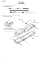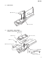
1
MC-S50 SERVICE MANUAL AEP Model Ver 1.0 2001.03 SPECIFICATIONS Audio specifications Frequency response 20 – 20,000 Hz Signal-to-noise ratio (S/N) 85 dB Memory capacity 64 MB (including the system software: 61.1 MB available for music) Available file format ATRAC3 MP3 Bit rate*: 32–256 kbps Sampling rate: 32/44.1/48 kHz * Variable bit rate files are not supported. Bit rate higher than 128 kbps is not guaranteed when you select the sampling rate 32 or 48 kHz. WMA** Bit rate: 64–160 kbps **The files applied with the Microsoft Windows Media Right Manage are not supported. Output Headphones jack Stereo mini jack Connector (special mini jack) USB 1.0 compliant Power consumption Approx. 145 mW Dimensions (approx.) Approx. 22.4 × 99.0 × 25.9 mm (29/32× 4 ×1 inches) (w/h/d) Mass Approx. 33g (1.2 oz ) (including battery) Operating temperature 5°C to 35°C (41°F to 95°F) (not condensed) Environment temperature –20°C to 60°C (–4°F to 140°F) (not condensed) Supplied accessories • LR03 (Size AAA) alkaline battery (1) • Headphones (1) • Headphones/earphones extension cord (1) • Neck strap (1) • USB cable (1) • CD-ROM (OpenMG Jukebox installation disc) (1) • MC-S50 Operating Instructions (1) • OpenMG Jukebox Operating Instructions (1) Design and specifications are subject to change without notice. General Power requirements LR03 (Size AAA) alkaline battery × 1 USB bus power Battery life Approx. 6 hours (varies depending on bit rate, volume, etc.) 9-873-098-11 Sony Corporation 2001C0500-1 C 2001.3 Audio Entertainment Group General Engineering Dept. PERSONAL NETWORK PLAYER MC-S50 TABLE OF CONTENTS 1. SERVICING NOTES .................................................. 3 2. GENERAL ...................................................................... 9 3. DISASSEMBLY 3-1. 3-2. 3-3. 3-4. Disassembly Flow ............................................................ 10 Case Assy, Upper ............................................................. 10 Power Board ..................................................................... 11 “LOGIC Board”, “AUDIO Board”, “FLEXIBLE (JACK) Board, Jack (J301)” ...................... 11 3-5. “LOGIC Board”, “Display Panel, Liquid Crystal (LCD901)” .................... 12 4. DIAGRAMS 4-1. Block Diagram ................................................................. 13 4-2. Note for Printed Wiring Boards and Schematic Diagrams ........................................................ 14 4-3. Printed Wiring Board – LOGIC Board – ........................ 14 4-4. Schematic Diagram – LOGIC Board – .......................... 15 4-5. Printed Wiring Board – AUDIO Board – ....................... 16 4-6. Schematic Diagram – AUDIO Board – .......................... 17 4-7. Printed Wiring Board – POWER Board – ...................... 18 4-8. Schematic Diagram – POWER Board – ......................... 19 4-9. IC Pin Function Description ............................................ 22 5. EXPLODED VIEWS 5-1. Upper Case Assy .............................................................. 26 5-2. Board Assy ....................................................................... 27 6. ELECTRICAL PARTS LIST ................................ 28 Sony, VAIO, the VAIO logo, Music Clip, OpenMG and the OpenMG logo are trademarks of Sony Corporation. Microsoft, Windows, Windows NT, Windows Media, Windows Millennium Edition and their logos are trademarks or registered trademarks of Microsoft Corporation in the United States and/or other countries. US and foreign patents licensed from Dolby Laboratories. All other trademarks and registered trademarks are trademarks or registered trademarks of their respective holders. 2 Flexible Circuit Board Repairing • Keep the temperature of the soldering iron around 270 ˚C during repairing. • Do not touch the soldering iron on the same conductor of the circuit board (within 3 times). • Be careful not to apply force on the conductor when soldering or unsoldering. Notes on chip component replacement • Never reuse a disconnected chip component. • Notice that the minus side of a tantalum capacitor may be damaged by heat. UNLEADED SOLDER Boards requiring use of unleaded solder are printed with the leadfree mark (LF) indicating the solder contains no lead. (Caution: Some printed circuit boards may not come printed with the lead free mark due to their particular size) : LEAD FREE MARK Unleaded solder has the following characteristics. • Unleaded solder melts at a temperature about 40 ˚C higher than ordinary solder. Ordinary soldering irons can be used but the iron tip has to be applied to the solder joint for a slightly longer time. Soldering irons using a temperature regulator should be set to about 350 ˚C . Caution: The printed pattern (copper foil) may peel away if the heated tip is applied for too long, so be careful! • Strong viscosity Unleaded solder is more viscous (sticky, less prone to flow) than ordinary solder so use caution not to let solder bridges occur such as on IC pins, etc. • Usable with ordinary solder It is best to use only unleaded solder but unleaded solder may also be added to ordinary solder. MC-S50 SECTION 1 SERVICING NOTES 1-1. Introduction This document describes the “operation check for inspection (Test mode)” and “adjustment after board replacement for repair”. In performing these works, connect this set to the PC via a USB cable and use the following tool. Tool list Ref. No. Tool name Part code Application 1 Service Tool 9140 (FD) J-2507-037-1 Board check (Test mode) and readjustment after board replacement 1-2. Board Repair 1. 2. 3. 4. In performing the work, the set should be in a complete state (all components assembled). Install the “OpenMG Jukebox” and “WMP7 Plug-in” (CD-ROM) in the PC in advance. Do not start up other applications in the PC. This set has the Test mode, and the use of exclusive application (Service Tool) on the PC side enables various function checks and the voltage adjustment. 5. For the LOGIC board in this set, if either part listed in Table 1 is faulty, be sure to replace the board block. Also, when a part on the POWER board was replaced or a combination of LOGIC board and POWER board was changed due to the board replacement, perform 1-5 "Adjustment When Board was Replaced/Repaired". 6. The data in Table 1-2 have been written to the LOGIC board. 7. In repairing other than above parts, repair as usual. Table 1-1. Board name Ref. No LOGIC board IC601, IC602, IC603, IC901 Table 1-2. Board name Stored data LOGIC board Music data, Battery adjustment value, Equalizer initial values, CODEC programs, and ID/IK codes 1-3. Operation Check for Inspection (Test Mode) Precautions 1. Be sure to remove the battery from this set. (The power is supplied via USB cable) Operating the set in the Test mode with the battery loaded could clear necessary information. 2. If operation check was performed for inspection, execute “Play Info Initialize” in qd (see page 7) to return respective functions to initial positions (see Table 1-5 on page 7). In such a case, record current position of each function before executing “Play Info Initialize” in qd, if necessary. 3 MC-S50 Work procedure Preparation: 1. Make sure that no battery is loaded in the set. 2. Start up the test mode “apollo_service.exe” of the service tool (J-2507-037-1) from the PC, and check that the following screen appears. 3. Connect PC to this set with a USB cable. Check that the block 1 of the following screen “open”, and “1PC” is displayed on the LCD of the set. (The block 1 will “close” if the set is disconnected again) At this time, a sine wave is outputted from the headphone. Also, the model name is displayed in the block qd of the screen. 1 Note: If the block 1 does not “open”, the circuits in LOGIC board will be faulty. Audio signals are outputted from the reference signal in the DSP of the set. 4 MC-S50 Operational description of Test mode qd qa 2 9 3 4 0 6 5 7 qs 8 1. Audio Block Function Check Clicking the UP or Down button in block 2 of the screen allows you to check with various output frequencies. Also, clicking the UP or Down button in block 3 can check variations of volume. Clicking the L, Stereo, R, or Mute button in block 4 can change audio output status. 2. Battery Threshold Value Reading and Measurement Connect an exclusive USB cable to the set, and available battery threshold values (converted values corresponding to voltage values) written to the set at the shipment will be displayed at 5. (See Table 1-3) These threshold values are inherent values of the set, but if they were readjusted during the board repair, newly set threshold values (converted values corresponding to voltage values) are displayed. Table 1-3. Condition OFF Scale 1→2 Scale 2→3 Scale 3→4 Voltage set value 1.00 V 1.15 V 1.25 V 1.35 V Converted value (ref.) 320 368 400 432 Note: The threshold values (converted values corresponding to voltage values) are different every set. 3. LCD Test Clicking FULL (full lit), COL1 (column 1), COL2 (column 2), or OFF (full off) in block 8 results in all ON, column 1 ON, column 2 ON, or all OFF of the LCD on the set respectively. 4. CODEC Info Check The CODEC programs and their versions written to the set can be checked. (block 9) The CODEC programs written to the set at the shipment are “MP3”, “ATRAC3”, and “WMA” and their versions are as listed below. (Versions will vary if updated) Program No. Name Version CODEC1 MP3 96 CODEC2 AT3 96 CODEC3 WMA 96 CODEC4 blank 0 5 MC-S50 5. Firmware Info Check The DSP program version and the flash memory capacity can be checked. (block 0) The version at the shipment is as follows. (Versions will vary if updated) Version 51 Flash memory size 64094208 6. Sub-CPU Info Check The Sub-CPU program version can be checked. (block qa) The version at the shipment is as follows. (Versions will vary if updated) Version 30 7. Key Check Click the block qs while pressing a key on the set, and “ON” is displayed in the block associated with the pressed key, so that the key operation can be checked. 1-4. Required System Configuration • IBM PC/AT and compatibles CPU: MMX Pentium 233 MHz and above (Pentium II 400 MHz and above recommended) Hard disk drive space: 20 MB and above (Free space is required, depending on the version of Windows 98 and the size of the audio data you are using.) RAM: 64 MB and above CD-ROM drive Sound Board: Creative SoundBlaster 16 compatible Default built-in USB port • Operating system: The default installation of Windows 98 English version (The product does not work on Windows 95/3.1 or Windows NT. Not assured trouble-free if you use an upgrade version from Windows 95/3.1 to Windows 98.) • Display: SVGA (800 × 600 pixel) (supports High Color (16 bit) and above) • Internet access 1-5. Adjustment When Board was Replaced/Repaired When a part on the POWER board was replaced due to the repair or a combination of LOGIC board and POWER board was changed due to the board replacement, perform 1. "Readjustment of Voltage for Battery Threshold Value" and 2. "Execution of Play Info Initialize" in [Work Procedure]. Replacing the board in this set will cause the status as shown in Table 1-4. Table 1-4. Board name Set status after board replacement LOGIC board Music data and music information data stored in the set are cleared and not restored. Precautions 1. Do not disconnect the USB cable in the midway of work. 2. If the operation on the PC side is not accepted during work, disconnect the USB cable and close the “apollo_service.exe” file, then restart from the beginning. 6 MC-S50 Work Procedure 1. Readjustment of Voltage for Battery Threshold Value Readjust the voltage through the steps given below. (1) Start up the Test Mode "apollo_service.exe" in the Service Tool (J-2507-037-1) from the PC, and connect the set to the PC with an excusive USB cable, and the following screen will appear. At this time, the battery threshold values of available voltage written to the board are displayed at 5. qd qa 2 9 3 4 0 6 5 7 qs 8 (2) Apply the specified set voltage in Table 1-5 to the battery terminals from regulated DC power supply. Then, click the button 6, and the converted values (threshold values) corresponding to the applied voltage will be displayed. Under this condition, click the button 7 and newly converted values (threshold values) will be written in the "AD Level" at 5. (3) For each step in Table 5, apply the specified set voltage so as to write the converted value (threshold value). Table 1-5. Condition OFF Scale 1→2 Scale 2→3 Scale 3→4 Voltage set value 1.00 V 1.15 V 1.25 V 1.35 V Converted value (ref.) 320 368 400 432 Note: The threshold values (converted values corresponding to voltage values) are different every set. Precautions 1. The regulated DC power supply to be applied should have as less ripple as possible within the voltage accuracy +/–0.01 V. 2. Use properly calibrated measuring instrument for the measurement of voltage to be applied. 3. Do not solder directly the battery terminals when applying the voltage. Use clips, etc. to connect to the battery terminals. 7 MC-S50 2. Execution of Play Info Initialize If the LOGIC board was replaced for repair, execute “Play Info Initialize” in block qd to return respective functions to initial positions (see Table 1-6). Table 1-6. Function Position Play position Head of first music VOL level 25 MEGA BASS OFF PLAY MODE OFF AVLS OFF 3. Checking after Repair (1) After work, check that the set operates normally through the operation in 1-3. “Operation Check for Inspection (Test Mode)” (see page 3). (2) Make sure that the check-out and check-in can be made using the PC applications “OpenMG Jukebox” (CODEC programs “MP3” and “ATRAC3”) and “Windows Media Player 7” (CODEC program “WMA”). Also, make sure that the checked out data can be played normally. Note: Do not start up the “OpenMG Jukebox” and the “Windows Media Player 7” simultaneously. (3) For an installation and acquisition method of “Windows Media Player 7” (CODEC program “WMA”), refer to the following instruction. Using Music Clip player in combination with Windows MediaTM Player 7 If you install Microsoft Windows MediaTM Player 7, you can transfer a WMA file to your Music Clip player and play it back. Refer to the online help for Windows Media Player 7 for detailed operations. Playing back WMA files with Music Clip player Installing Windows Media Player 7 and the dedicated plug-ins • Refer to Microsoft download website for the details on how to obtain Windows Media Player 7. • To use Windows Media Player 7 in combination with your Music Clip player, you need to install the dedicated plug-in software. This software has been already installed when the NW-S4 driver was installed using the enclosed OpenMG Jukebox CDROM. Transferring (copying) a WMA file to your Music Clip player Music Clip player can only playback those WMA files that are listed in the "Available File Formats" in the "Options" dialog box on Windows Media Player 7 and are of 64 to 160 kbps. Notes • Songs checked-out using the OpenMG Jukebox (ATRAC3 and MP3) can also be listened on the Portable Device screen of Windows Media Player 7, but they can not be played back nor checked-in to Windows Media Player 7. • The transferred (copied) WMA files to Music Clip player from Windows Media Player 7 are shown on the OpenMG Jukebox with a ( ) mark and you can not playback nor check-in them to the OpenMG Jukebox. 1 Start Windows Media Player 7 and click on the "Portable Device" tab. The "Portable Device" screen appears. Copy Music button Portable Device tab 2 Portable Device screen Connect your Music Clip player to the computer (See page 9). The computer recognizes your Music Clip player and the songs downloaded in Music Clip player are shown on the "Music On Device" window of Windows Media Player 7. If the computer can not recognize your Music Clip player, press the F5 key. 3 Transfer (copy) the songs to your Music Clip player. Select a WMA file you want to transfer (copy) to your Music Clip player and click on the "Copy Music" button on Windows Media Player 7 window. This starts copying the selected song and its title is added to the "Music On Device" window. Notes • If you check "Enable Personal Rights Management" on the "CD Audio" tab in the "Options" dialog box when recording a CD using Windows Media Player 7, the music cannot be transferred to Music Clip player. To enable the music transfer, remove the check mark when recording the CD. • It may be impossible to transfer the music contents with copyright management information such as those purchased via EMD. 16 8 Refer to the online help of Windows Media Player 7 for details on copying music to a portable device. 17 MC-S50 SECTION 2 GENERAL This section is extracted from instruction manual. Parts and controls Refer to the page numbers indicated in parentheses for details. 1 VOL (volume) +/– (page 10) 2 Display (page 11) 7 Battery compartment (page 7) 3 MODE button (pages 12) 8 Clip 4 N/x (play/stop) button (page 10) 9 Headphones jack (page 10) 5 ./> buttons (pages 11) qa USB connector (page 9) 0 HOLD switch (page 15) 6 MEGA BASS/AVLS button (page 13, 14) 6 9 MC-S50 SECTION 3 DISASSEMBLY • This set can be disassembled in the order shown below. 3-1. DISASSEMBLY FLOW Set Case assy, upper Power board “LOGIC board”, “Audio board”, “Flexible (jack) board, Jack (J301)” “LOGIC board”, “Display panel, liquid crystal (LCD901)” Note: Follow the disassembly procedure in the numerical order given. 3-2. CASE ASSY, UPPER 1 screw (1.7 × 4) 2 lid, battery case Note 1: Use something like a thin board when disconnected claws. Note 2: Take care not to damage the cabinet. 9 claw 8 claw 7 claw 0 case assy, upper 5 claw 6 claw 4 claw 3 claw 10 MC-S50 3-3. POWER BOARD 2 POWER board 1 connector (CN601) 3-4. “LOGIC BOARD”, “AUDIO BOARD”, “FLEXIBLE (JACK) BOARD, JACK (J301)” 4 LOGIC board 5 connector (CN302) 6 AUDIO board 3 connector (CN301) 7 screw (1.7 × 4) 2 8 flexible (jack) board, jack (J301) 1 claw case assy, lower Note: Disconnect the claw warping the “case assy, lower”. 11 MC-S50 3-5. “LOGIC BOARD”, “DISPLAY PANEL, LIQUID CRYSTAL (LCD901)” LCD case 1 Remove two solders. 6 display panel, liquid crystal (LCD901) 4 conductive board convex 5 BL unit 2 3 LOGIC board 12 MC-S50 SECTION 4 DIAGRAMS BLOCK DIAGRAM STATUS/ CONTROL 1 6 USB CONNECTOR XIN OSC 7 APPLICATION INTERFACE XOUT X901 48MHz D903 END POINT FIFO/ 8 BYTE SET-UP REGISTER DPLL AD0 – AD7 USB CONTROLLER IC901 I/O1 – I/O8 32 – 25 29 – 32, 41 – 44 A0 – A7 D0 – D7 44 – 41, 38 – 35 • SIGNAL PATH 512M BIT FLASH ROM IC602 : PLAYBACK WE CE CLE ALE R/B USB SWITCH Q901 WR 10 RD 9 CS 8 INTR 12 RESET 11 19 8 18 9 16 17 7 CE CLE ALE R/B DATA BUS ADDRESS BUS J301 2B 14 2A 2Y3 2Y2 2Y1 2Y0 9 10 11 12 SDATA LRCK BCLK CE CLE ALE R/B 13 2G D0 – D7 i A0 – A7 15 2 TO 4 DECODER IC604 66 22 11 23 81 25 120 58 69 45 A0 – A7 INT2 IS A15 R/W HD2 IOSTRB HD4 HD0 HD1 BDR0 BCLKR1 INT1 BDX2 INT3 BDR2 BCLKX2 BFSX2 96 38 65 60 67 47 49 54 SEG1 – SEG15 LIQUID CRYSTAL DISPLAY LCD901 11 98 124 BDXO BFSXO BCLKX0 BCLKX1 HD6 HD7 SDATA LRCK BCLK ACLK 59 53 48 71 135 6 2 1 3 5 SDATA LRCK SCLK SERIAL PORT & DEEMPHASIS DIGITAL VOLUME CONTROL, BASS/ TREBLE BOOST, LIMITING DIGITAL FILTER & D/A CONVERTER ANALOG FILTER & ANALOG VOLUME CONTROL D/A CONVERTER, HEADPHONE AMP IC302 MUTING Q302 MUTING Q101, 201 MUTING CONTROL SWITCH Q301(1/2) MUTING CONTROL SWITCH Q301(2/2) EEPROM IC603 3 RXD 58 TXD 59 SCK 57 7 SI 4 SO 8 SCK WP 5 D802 RESET SIGNAL GENERATOR IC802 RES 8 VBATT B+ VOLTAGE DETECT IC403 IRQ1 1 D/A CONVERTER (IC302) B+ 49 P90 LCD BACK LIGHT AUDIO OUTPUT SWITCH Q102, 202 P36 14 23 COM1 22 COM2 D801 HP B 14 HEADPHONE AMP HP A 10 MCLK 16 RST (HEADPHONE) CS 60 SEG9 – SEG22 X601 16.9344MHz P33 X1 97 IRQ0 X2/CLKIN DIGITAL SIGNAL PROCESSOR IC601 HD5 131 – 134, 136 – 139 D0 – D7 RS 99 – 104, 113, 114 HD3 ACLK 95 +1.8V REGULATOR IC301 CPU IC801 V1 CPU (IC801) B+ D405 L301 VOLTAGE DETECT IC402 D/A CONVERTER (IC302) B+ D402 S801 – 807 BATTERY/USB CHANGE-OVER SWITCH Q401 L402 L401 8 OUT 5 EN LX 7 LBI P32 10 B+ SWITCH Q403 LBO# V2 DSP (IC601), 256M/512M BIT EEPROM (IC602), EEPROM (IC603), USB CONTROLLER (IC901) B+ WKP6 – WKP0 3 PROTOCOL ENGINE 42 – 48 D+ USB D+ TRANSCEIVER D0 – D7 2 D– D– A0 – A7 2 WP RE CN901 (1/2) 40 – 26 4-1. 3 2 DRY BATTERY SIZE “AAA” IEC DESIGNATION LR03 1PC. 1.5V SWITCHING REGULATOR IC401 6 OSC1 X802 8MHz V1 B+ S808 HOLD OFF HOLD VCORE DSP (IC601) B+ 5 OSC2 B+ SWITCH Q405 L404 DC/DC CONVERTER IC404, L403 +3.2V REGULATOR IC405 D403 P37 15 Q402 2 X1 THP401 CN901 (2/2) 1 WKP7 41 X801 32.768kHz 3 X2 AN0 62 VBUS GND VBATT B+ 4 USB CONNECTOR 13 13 MC-S50 4-3. 4-2. PRINTED WIRING BOARD – LOGIC Board – NOTE FOR PRINTED WIRING BOARDS AND SCHEMATIC DIAGRAMS Note on Printed Wiring Board: • Y : parts extracted from the conductor side. f • : internal component. : Pattern from the side which enables seeing. • (The other layers' patterns are not indicated.) Caution: Pattern face side: (Conductor Side) Parts face side: (Component Side) Parts on the pattern face side seen from the pattern face are indicated. Parts on the parts face side seen from the parts face are indicated. • AUDIO, LOGIC and POWER boards are multi-layer printed board. However, the patterns of intermediate-layer have not been included in this diagrams. * Lead Layouts (IC601 and IC901) surface : Uses unleaded solder. 2 1 Ref. No. 4 Location D801 D802 D901 D902 D903 B-5 C-2 C-2 C-2 D-3 IC601 IC602 IC603 IC604 IC801 IC901 D-4 B-3 A-3 C-3 B-4 D-2 Q901 D-3 A (NOT SUPPLIED) B Lead layout of conventional IC 3 • Semiconductor Location (NOT SUPPLIED) CSP (chip size package) (Page 18) Note on Schematic Diagram: • All capacitors are in µF unless otherwise noted. pF: µµF 50 WV or less are not indicated except for electrolytics and tantalums. • All resistors are in Ω and 1/4 W or less unless otherwise specified. • % : indicates tolerance. f • : internal component. • C : panel designation. • A : B+ Line. • Power voltage is dc 1.5 V and fed with regulated dc power supply from battery terminal. • Voltages and waveforms are dc with respect to ground in playback mode. no mark : PLAYBACK : Impossible to measure ∗ • Voltages are taken with a VOM (Input impedance 10 MΩ). Voltage variations may be noted due to normal production tolerances. • Waveforms are taken with a oscilloscope. Voltage variations may be noted due to normal production tolerances. • Circled numbers refer to waveforms. • Signal path. F : PLAYBACK * The voltage and waveform of CSP (chip size package) cannot be measured, because its lead layout is different form that of conventional IC. C (NOT SUPPLIED) (NOT SUPPLIED) D C E B (Page 16) 14 14 5 MC-S50 4-4. SCHEMATIC DIAGRAM – LOGIC Board – • See page 20 for IC Block Diagrams. • See page 21 for Waveforms. (Page 17) (Page 19) 15 15 MC-S50 4-5. PRINTED WIRING BOARD – AUDIO Board – • Semiconductor Location Ref. No. 1 Location D101 D201 D804 C-3 C-3 A-4 IC301 IC302 C-4 C-4 Q101 Q102 Q201 Q202 Q301 Q302 C-3 A-3 C-3 A-3 A-4 A-4 : Uses unleaded solder. 2 3 4 A E2 C1 C2 B E1 C2 C1 B2 E B1 B (Page 14) C 16 16 MC-S50 4-6. SCHEMATIC DIAGRAM – AUDIO Board – • See page 20 for IC Block Diagram. • See page 21 for Waveforms. (Page 15) 17 17 MC-S50 4-7. PRINTED WIRING BOARD – POWER Board – : Uses unleaded solder. 1 2 3 • Semiconductor Location Ref. No. Location D401 D402 D403 D405 D809 D810 B-3 A-3 A-3 C-3 B-2 B-3 IC401 IC402 IC403 IC404 IC405 IC802 B-3 B-3 B-3 B-3 C-3 A-3 Q401 Q402 Q403 Q405 B-3 B-3 B-3 A-3 A E1 B1 B2 C2 E2 E2 C2 B2 B1 C1 E1 (Page 14) B C B C 18 18 C1 E MC-S50 4-8. SCHEMATIC DIAGRAM – POWER Board – • See page 20 for IC Block Diagrams. • See page 21 for Waveforms. (Page 15) 19 19 MC-S50 ZERO CROSSING AMP – + EN + + – + – – + – 3 SYNC CELL 4 PFM CURRENT COMPARATOR NEGLIM COMPARATOR LIM COMPARATOR REF + SLOPE COMPENSATION FB REF CONTROL AND DRIVER LOGIC 2Y2 2Y3 Y0 Y1 Y2 Y3 A B Y0 Y1 Y2 Y3 2 3 4 5 6 1Y0 1Y1 1Y2 SDATA 2 0.1X SENS FET SCLK 3 ADSEL ALE 8 9 10 11 CS4343-KSR DIGITAL VOLUME CONTROL SERIAL PORT DEEMPHASIS BASS/TREBLE BOOST ∆∑ DAC + – – + OVERVOLTAGE COMPARATOR ANALOG FILTER ANALOG VOLUME CONTROL ANALOG FILTER ANALOG VOLUME CONTROL DIGITAL FILTERS LIMITING ∆∑ DAC HEADPHONE AMP 14 13 12 11 10 HP B VA HP VA GND HP A VD/IO 4 8 SHDN SCL 6 SYNC/ 7 PWM VQ HP 7 REF GND 8 6 LIM 7 8 1Y3 7 LRCK 1 GND 2Y1 B 1B 1G (ENABLE) 1 A 1A G 2B 9 2Y0 14 13 12 11 10 2A VCC 2G (ENABLE) 16 15 3 4 5 6 MCLK 5 PWM ON REF SIGNAL SELECT DATA OUTPUTS 2 9 LX SN74LV139ADGVR G OSC 16 RST 15 SDA – LOGIC Board – IC604 USB TRANSCEIVER D8 D9 D10 D11 VCC5 GND D12 D13 D14 D15 INTR 10 PGND – P 40mV ON + – PFM COMPARATOR IC302 5mA 2N PFM ADJ.IN PWM 0.1X SENS FET + – + – + – FB 5 DPLL 1 PWM COMPARATOR PWM FB PROTOCOL ENGINE N CHIP SUPPLY 2 APPLICATION INTERFACE 22 21 20 19 18 17 16 15 14 13 12 – AUDIO Board – 1 REFERENCE VOLTAGE REF 5 SHDN MAX1692EUB-TG069 RAMP GEN GND 41 42 43 44 REFERENCE 120mV BP AD3 AD2 AD1 AD0 + – 12mV IN STATUS/ CONTROL GND 39 VCC5 40 6 GND CURRENT-LIMIT AMP END POINT FIFO/ 8BYTE SET-UP REGISTER CS RD WR RESET R Q Q TRIG ONE-SHOT LOW-BATTERY COMPARATOR REF 4 IC404 F/F 34 35 36 37 38 D+ LBO 3 7 LX MAXIMUM ON-TIME OFF-SHOT – + DREQ AD7 AD6 AD5 AD4 XOUT LBI 2 S 24 23 D– FB 1 32 31 30 29 28 27 26 25 8 OUT Q TRIG ONE-SHOT ERROR AMP – + 33 1 VCC3 TEST1 TEST2 XIN MINIMUM OFF-TIME ONE-SHOT A0 A1 A2 A3 A4 A5 A6 A7 MAX1674EUA-TG069 + – IC401 DACK IC901 ML60851CLBZ060 (Not supplied part) • IC Block Diagrams – POWER Board – SELECT DATA OUTPUTS 20 20 9 FILT+ CONTROL PORT MC-S50 • Waveforms – LOGIC Board – 1 IC801 2 X1 6 IC601 ua (BCLKX1) 3.2 Vp-p 2 Vp-p 30.5 µs 0 IC302 5 (MCLK) 3.2 Vp-p 59.1 ns 2 IC801 5 (OSC1) (When power on) 59.1 ns 7 IC601 oj (X2/CLKIN) 3.2 Vp-p 1.2 Vp-p – POWER Board – 59.1 ns 125 ns qa IC401 7 (LX) 3 IC901 6 (XIN) (When power on) 3 Vp-p 4 Vp-p – AUDIO Board – 20.8 ns 8 IC302 1 (LRCK) 4 IC601 rk (BCLKX0) 3.4 Vp-p qs IC404 9 (LX) 5 IC601 td (BFSX0) 4 Vp-p 3.4 Vp-p 3.4 µs 22.7 µs 709 ns 9 IC302 3 (SCLK) 3.4 Vp-p 3.4 Vp-p 22.7 µs 13.8 µs 709 ns 21 MC-S50 4-9. IC PIN FUNCTION DESCRIPTION • LOGIC BOARD IC601 TMS320DA150GGU120 (DIGITAL SIGNAL PROCESSOR) (Not supplied part) Pin No. Pin Name I/O 1 CVSS — Ground terminal 2 A22 — Address signal terminal Not used (open) 3 CVSS — Ground terminal 4 DVDD — Power supply terminal (+3.2V) 5 A10 — Address signal terminal Not used (open) 6 HD7 O Muting control signal output terminal “L”: muting 7 to 10 A11 to A14 I Address signal input terminal Not used (open) Description 11 A15 O Read/write signal output to the 2 to 4 decoder (IC604) 12 CVDD — Power supply terminal (+1.5V) 13 HAS I 14 DVSS — Ground terminal 15 CVSS — Ground terminal 16 CVDD — Power supply terminal (+1.5V) 17 HCS I Chip select signal input terminal Not used (fixed at “H”) 18 HR/W I Read/write signal input terminal Not used (fixed at “H”) 19 READY I Data ready signal input terminal Not used (fixed at “H”) 20 PS O Program space select signal output terminal Not used (open) 21 DS O Data space select signal output terminal Not used (open) 22 IS O I/O space select signal output to the USB controller (IC901) 23 R/W O Read/write signal output to the 2 to 4 decoder (IC604) 24 MSTRB O Memory strobe signal output terminal Not used (open) 25 IOSTRB O I/O strobe signal output to the 2 to 4 decoder (IC604) 26 MSC O Microstate complete signal output terminal Not used (open) 27 XF O External flag signal output terminal Not used (open) 28 HOLDA O Hold acknowledge signal output terminal Not used (open) 29 IAQ O Instruction acquisition signal output terminal Not used (open) 30 HOLD I Hold signal input terminal Not used (fixed at “H”) 31 BIO I Branch control signal input terminal Not used (fixed at “H”) 32 MP/MC I Mode select signal input terminal Not used (fixed at “L”) 33 DVDD — Power supply terminal (+3.2V) 34 CVSS — Ground terminal 35 BDR1 I Serial data receive signal input terminal Not used (fixed at “H”) 36 BFSR1 I Frame synchronization pulse signal input terminal Not used (fixed at “H”) 37 CVSS — Ground terminal 38 BCLKR1 O Serial clock signal output to the CPU (IC801) 39 HCNTL0 I Control signal input terminal Not used (fixed at “H”) 40 DVSS — 41, 42 BCLKR0, BCLKR2 I Data receive clock input terminal Not used (fixed at “H”) 43, 44 BFSR0, BFSR2 I Frame synchronization pulse signal input terminal Not used (fixed at “H”) 45 BDR0 I Serial data receive signal input from the flash ROM (IC602) 46 HCNTL1 I Control signal input terminal Not used (fixed at “H”) 47 BDR2 I Serial data receive signal input from the EEPROM (IC603) and CPU (IC801) 48 BCLKX0 O Serial clock signal output to the D/A converter (IC302) 49 BCLKX2 O Serial clock signal output to the EEPROM (IC603) and CPU (IC801) 50 CVSS — Ground terminal 22 Address strobe signal input terminal Not used (fixed at “H”) Ground terminal MC-S50 Pin No. Pin Name I/O 51 HINT O Interrupt request signal output terminal Not used (open) 52 CVDD — Power supply terminal (+1.5V) 53 BFSX0 O LR frame signal output to the D/A converter (IC302) 54 BFSX2 O Chip select signal output to the EEPROM (IC603) Description 55 HRDY O Ready signal output terminal Not used (open) 56 DVDD — Power supply terminal (+3.2V) 57 DVSS — Ground terminal 58 HD0 O Enable signal output to the flash ROM (IC602) 59 BDX0 O Serial data transmit signal output to the D/A converter (IC302) 60 BDX2 O Serial data transmit signal output to the EEPROM (IC603) and CPU (IC801) 61 IACK O Interrupt request signal output terminal Not used (open) 62 HBIL — Not used (fixed at “H”) 63 NMI I Nonmaskable interrupt request signal input terminal Not used (fixed at “H”) 64 INT0 I Interrupt request signal input terminal Not used (fixed at “H”) 65 INT1 I Interrupt request signal input from the CPU (IC801) 66 INT2 I Interrupt request signal input from the USB controller (IC901) 67 INT3 I 68 CVDD — Power supply terminal (+1.5V) 69 HD1 O Enable signal output to the flash ROM (IC602) 70 CVSS — Ground terminal 71 BCLKX1 O Serial clock signal output to the D/A converter (IC302) 72 DVSS — Ground terminal 73 BFSX1 O Serial data receive signal output terminal Not used (fixed at “H”) Interrupt request signal input terminal (connected to pin y; (BDX2)) 74 BDX1 O Serial data transmit signal output terminal Not used (open) 75 DVDD — Power supply terminal (+3.2V) 76 DVSS — Ground terminal 77 CLKMD1 I Clock mode signal output terminal Not used (fixed at “L”) 78 CLKMD2 I Clock mode signal output terminal Not used (fixed at “H”) 79 CLKMD3 I Clock mode signal output terminal Not used (fixed at “L”) 80 HPI16 — Not used (fixed at “L”) 81 HD2 O Reset signal output to the USB controller (IC901) “L”: reset 82 TOUT O Timer signal output terminal Not used (open) 83 EMU0 I Emulator signal input terminal 84 EMU1/OFF O Emulator signal output terminal 85 TDO O Test data signal output terminal 86 TDI I Test data signal input terminal 87 TRST I Test reset signal input terminal 88 TCK I Test clock input terminal 89 TMS I 90 CVSS — Ground terminal 91 CVDD — Power supply terminal (+1.5V) 92 HPIENA I 93 DVSS — Ground terminal 94 CLKOUT O Master clock output terminal Not used (open) 95 HD3 O USB ON/OFF control signal output terminal “L”: ON Test mode select signal input terminal HPI module select signal input terminal Not used (fixed at “L”) 23 MC-S50 Pin No. Pin Name I/O 96 X1 O System clock output terminal (16.9344MHz) 97 X2/CLKIN I System clock input terminal (16.9344MHz) 98 RS I Reset signal input to the CPU (IC801) “L”: reset 99 to 104 D0 to D5 I/O Two-way data bus with the flash ROM (IC602) and USB controller (IC901) 105 A16 — Address signal terminal 106 DVSS — Ground terminal 107 to 110 A17 to A20 — Address signal terminal 111 CVSS — Ground terminal Description Not used (open) Not used (open) 112 DVDD — Power supply terminal (+3.2V) 113, 114 D6, D7 I/O Two-way data bus with the flash ROM (IC602) and USB controller (IC901) 115 to 119 D8 to D12 I/O Two-way data bus Not used (open) 120 HD4 O Chip select signal output to the flash ROM (IC602) 121 to 123 D13 to D15 I/O Two-way data bus 124 HD5 O Audio system power ON/OFF control signal output terminal “H”: ON 125 CVDD — Power supply terminal (+1.5V) 126 CVSS — 127 HDS1 I 128 DVSS — 129 HDS2 I Not used (open) Ground terminal Data signal input terminal Not used (fixed at “H”) Ground terminal Data signal input terminal Not used (fixed at “H”) 130 DVDD — Power supply terminal (+3.2V) 131 to 134 A0 to A3 O Address signal output to the USB controller (IC901) 135 HD6 O Reset signal output to the D/A converter (IC302) “L”: reset 136 to 139 A4 to A7 O Address signal output to the USB controller (IC901) 140, 141 A8, A9 — Address signal terminal 142 CVDD — Power supply terminal (+1.5V) 143 A21 — Address signal terminal 144 DVSS — Ground terminal 24 Not used (open) Not used (open) MC-S50 • LOGIC BOARD IC801 HD6433800A02FP (CPU) Pin No. Pin Name I/O 1 IRQ1 I Voltage detect input terminal 2 X1 I Sub system clock input terminal (32.768kHz) 3 X2 O Sub system clock output terminal (32.768kHz) 4 VSS — Ground terminal 5 OSC1 O Main system clock output terminal (8MHz) 6 OSC2 I Main system clock input terminal (8MHz) 7 TEST I Test mode signal input terminal 8 RES I System reset signal input from the reset signal generator (IC802) “L”: reset For several hundreds msec. after the power supply rises, “L” is input, then it changes to “H” Description Not used (fixed at “L” ) 9 P31 — Not used (open) 10 P32 O Power supply (V2) ON/OFF control signal output terminal “L”: ON 11 P33 O Interrupt request signal output to the digital signal processor (IC601) 12, 13 P34, P35 — Not used (fixed at “L” ) 14 P36 O Reset signal output to the digital signal processor (IC601) and EEPROM (IC603) “L”: reset 15 P37 O Power supply (VCORE) ON/OFF control signal output terminal “L”: ON 16 VCC — Power supply terminal (+3.2V) 17 V1 — Power supply terminal for the liquid crystal display (open in this set) 18 V2 — Power supply terminal for the liquid crystal display (connected to pin ql (V3)) 19 V3 — Power supply terminal for the liquid crystal display (connected to pin qk (V2)) 20, 21 COM4, COM3 O Common signal output to the liquid crystal display 22, 23 COM2, COM1 O Common signal output to the liquid crystal display (LCD901) 24, 25 SEG25, SEG24 O Segment signal output to the liquid crystal display 26 to 40 SEG23 to SEG9 O Segment signal output to the liquid crystal display (LCD901) 41 WKP7 I USB connection detect signal input terminal 42 WKP6 I MEGA BASS/AVLS switch (S807) input terminal “L”: NORM 43 WKP5 I . key (S806) input terminal 44 WKP4 I > key (S805) input terminal 45 WKP3 I Nx key (S804) input terminal 46 WKP2 I MODE key (S803) input terminal 47 WKP1 I VOL - key (S802) input terminal 48 WKP0 I VOL + key (S801) input terminal Not used (open) Not used (open) 49 P90 O LCD back light (D801) ON/OFF control signal output terminal “H”: LED ON 50 to 54 P91 to P95 — Not used (open) 55 VSS — Ground terminal 56 IRQACE I Interrupt request signal input terminal 57 SCK I Serial clock signal input from the digital signal processor (IC601) 58 RXD I Serial data receive signal input from the digital signal processor (IC601) 59 TXD O Serial data transmit signal output to the digital signal processor (IC601) 60 IRQ0 I Serial clock signal input from the digital signal processor (IC601) 61 AVCC — 62 AN0 I Battery voltage detect input terminal 63, 64 PB1, PB2 I Not used (fixed at “L” ) Not used (fixed at “L” ) Power supply terminal (+3.2V) (for the analog) 25 MC-S50 SECTION 5 EXPLODED VIEWS NOTE: • -XX and -X mean standardized parts, so they may have some difference from the original one. • Color Indication of Appearance Parts Example: KNOB, BALANCE (WHITE) . . . (RED) ↑ ↑ Parts Color Cabinet's Color 5-1. • Items marked “*” are not stocked since they are seldom required for routine service. Some delay should be anticipated when ordering these items. • The mechanical parts with no reference number in the exploded views are not supplied. • Accessories and packing materials are given in the last of the electrical parts list. UPPER CASE ASSY 13 11 13 14 3 6 24 5 Ref. No. 3 5 6 11 26 Part No. Description 4-649-908-02 4-649-902-01 X-4623-190-1 4-649-910-01 BUTTON, PLAY WINDOW, LCD CASE ASSY, UPPER TERMINAL (+), BATTERY Remark Ref. No. 13 14 24 Part No. Description 3-893-942-31 SCREW (1.7X4), TAPPING (B) 4-649-911-01 TERMINAL (-), BATTERY 4-649-905-01 BUTTON, VOLUME Remark MC-S50 5-2. BOARD ASSY 77 59 69 76 81 80 74 75 63 54 J301 73 79 53 52 54 LCD901 Ref. No. 78 Remark Ref. No. Part No. Description 4-649-913-01 4-649-909-21 3-228-267-01 3-228-357-01 3-230-336-01 RIBBON, BATTERY LID, BATTERY CASE SHEET, LIGHT INTERCEPTION SHEET, DSP SHEET (LARGE), ELECTROMAGNETIC Part No. Description 52 53 54 59 63 4-649-896-01 4-649-901-01 1-694-771-11 X-4623-191-2 1-680-151-11 CASE, LCD BL UNIT CONDUCTIVE BOARD CASE ASSY, LOWER FLEXIBLE (JACK) BOARD 76 77 78 79 80 69 73 74 75 4-649-895-01 A-3323-698-A A-3323-696-A A-3323-697-A COVER, USB POWER BOARD, COMPLETE LOGIC BOARD, COMPLETE AUDIO BOARD, COMPLETE 81 3-230-337-01 SHEET (SMALL), ELECTROMAGNETIC J301 1-815-117-11 JACK (i (HEADPHONE)) LCD901 1-804-249-11 DISPLAY PANEL, LIQUID CRYSTAL Remark 27 MC-S50 AUDIO SECTION 6 ELECTRICAL PARTS LIST JACK NOTE: • Due to standardization, replacements in the parts list may be different from the parts specified in the diagrams or the components used on the set. • -XX and -X mean standardized parts, so they may have some difference from the original one. • RESISTORS All resistors are in ohms. METAL: Metal-film resistor. METAL OXIDE: Metal oxide-film resistor. F: nonflammable Ref. No. Part No. • Items marked “*” are not stocked since they are seldom required for routine service. Some delay should be anticipated when ordering these items. • SEMICONDUCTORS In each case, u: µ, for example: uA. . : µA. . uPA. . : µPA. . uPB. . : µPB. . uPC. . : µPC. . uPD. . : µPD. . • CAPACITORS uF: µF • COILS uH: µH Description Remark Ref. No. L201 L301 A-3323-697-A AUDIO BOARD, COMPLETE ********************** Part No. C101 C102 C201 C202 C301 1-119-923-11 1-135-868-11 1-119-923-11 1-135-868-11 1-125-777-11 CERAMIC CHIP TANTALUM CHIP CERAMIC CHIP TANTALUM CHIP CERAMIC CHIP 0.047uF 220uF 0.047uF 220uF 0.1uF 10% 20% 10% 20% 10% 10V 2.5V 10V 2.5V 10V C302 C303 C304 C305 C306 1-125-777-11 1-117-919-11 1-127-895-11 1-125-777-11 1-127-895-11 CERAMIC CHIP TANTALUM CHIP TANTALUM CHIP CERAMIC CHIP TANTALUM CHIP 0.1uF 10uF 22uF 0.1uF 22uF 10% 20% 20% 10% 20% 10V 6.3V 4V 10V 4V C307 C310 C311 C312 C313 1-125-777-11 1-125-837-11 1-135-337-11 1-135-337-11 1-125-837-11 CERAMIC CHIP CERAMIC CHIP TANTALUM CHIP TANTALUM CHIP CERAMIC CHIP 0.1uF 1uF 1uF 1uF 1uF 10% 10% 20% 20% 10% 10V 6.3V 6.3V 6.3V 6.3V C314 C315 1-125-777-11 CERAMIC CHIP 1-125-777-11 CERAMIC CHIP 0.1uF 0.1uF 10% 10% 10V 10V 1-815-120-21 CONNECTOR, BOARD TO BOARD 24P 1-815-118-21 CONNECTOR, FPC (ZIF) 5P < DIODE > D101 D201 D804 8-719-056-59 DIODE MAZS120008SO 8-719-056-59 DIODE MAZS120008SO 8-719-056-59 DIODE MAZS120008SO < FERRITE BEAD > * FB301 * FB302 1-469-229-22 FERRITE 1-469-230-21 INDUCTOR 0uH 0uH Remark 47uH 10uH < TRANSISTOR > < CAPACITOR > CN301 CN302 Description 1-469-527-11 INDUCTOR 1-412-991-31 INDUCTOR 3-230-337-01 SHEET (SMALL), ELECTROMAGNETIC < CONNECTOR > When indicating parts by reference number, please include the board. Q101 Q102 Q201 Q202 Q301 8-729-047-68 8-729-046-45 8-729-047-68 8-729-046-45 8-729-426-06 TRANSISTOR TRANSISTOR TRANSISTOR TRANSISTOR TRANSISTOR Q302 8-729-012-78 TRANSISTOR 2SK1830-TE85L SI2302DS-T1 2SK1830-TE85L SI2302DS-T1 XP1110-TXE XP2501-TX < RESISTOR > R101 R102 R103 R104 R105 1-218-942-11 1-218-942-11 1-218-965-11 1-220-803-81 1-218-977-11 RES-CHIP RES-CHIP RES-CHIP RES-CHIP RES-CHIP 120 120 10K 4.7 100K 5% 5% 5% 5% 5% 1/16W 1/16W 1/16W 1/16W 1/16W R106 R201 R202 R203 R204 1-218-990-11 1-218-942-11 1-218-942-11 1-218-965-11 1-220-803-81 SHORT RES-CHIP RES-CHIP RES-CHIP RES-CHIP 0 120 120 10K 4.7 5% 5% 5% 5% 1/16W 1/16W 1/16W 1/16W R205 R206 R301 R302 R303 1-218-977-11 1-218-990-11 1-218-965-11 1-218-973-11 1-218-972-11 RES-CHIP SHORT RES-CHIP RES-CHIP RES-CHIP 100K 0 10K 47K 39K 5% 1/16W 5% 5% 5% 1/16W 1/16W 1/16W R304 R305 R306 1-218-989-11 RES-CHIP 1-218-985-11 RES-CHIP 1-218-969-11 RES-CHIP 1M 470K 22K 5% 5% 5% 1/16W 1/16W 1/16W < SWITCH > S808 1-771-449-11 SWITCH, SLIDE (HOLD) ************************************************************** (Not supplied) JACK BOARD *********** < IC > 1-680-151-11 PWB, FLEXIBLE (JACK) IC301 IC302 8-759-656-53 IC MM1426CNLE 8-759-656-51 IC CS4343-KSR < JACK > J301 1-815-117-11 JACK (i (HEADPHONE)) ************************************************************** < COIL > L101 28 1-469-527-11 INDUCTOR 47uH MC-S50 LOGIC Ref. No. Part No. Description Remark A-3323-696-A LOGIC BOARD, COMPLETE ********************** 1-694-771-11 3-228-357-01 3-230-336-01 4-649-896-01 4-649-901-01 CONDUCTIVE BOARD SHEET, DSP SHEET (LARGE), ELECTROMAGNETIC CASE, LCD BL UNIT Ref. No. Part No. Description Remark IC801 8-759-713-59 IC HD6433800A02FP IC901 (Not supplied) IC ML60851CLBZ060 < LIQUID CRYSTAL DISPLAY > LCD901 1-804-249-11 DISPLAY PANEL, LIQUID CRYSTAL < TRANSISTOR > < CAPACITOR > Q901 C601 C602 C603 C608 C609 1-117-919-11 1-127-895-11 1-125-777-11 1-125-777-11 1-125-777-11 TANTALUM CHIP TANTALUM CHIP CERAMIC CHIP CERAMIC CHIP CERAMIC CHIP 10uF 22uF 0.1uF 0.1uF 0.1uF 20% 20% 10% 10% 10% 6.3V 4V 10V 10V 10V C613 C615 C618 C619 C620 1-164-848-11 1-125-777-11 1-164-874-11 1-125-777-11 1-125-777-11 CERAMIC CHIP CERAMIC CHIP CERAMIC CHIP CERAMIC CHIP CERAMIC CHIP 8PF 0.1uF 100PF 0.1uF 0.1uF 0.5PF 10% 5% 10% 10% 16V 10V 16V 10V 10V C621 C622 C623 C801 C802 1-125-777-11 1-125-777-11 1-125-837-11 1-117-919-11 1-164-843-11 CERAMIC CHIP CERAMIC CHIP CERAMIC CHIP TANTALUM CHIP CERAMIC CHIP 0.1uF 0.1uF 1uF 10uF 3PF 10% 10% 10% 20% 0.25PF 10V 10V 6.3V 6.3V 16V C804 C805 C806 C807 C808 1-125-777-11 1-164-937-11 1-164-937-11 1-164-937-11 1-164-937-11 CERAMIC CHIP CERAMIC CHIP CERAMIC CHIP CERAMIC CHIP CERAMIC CHIP 0.1uF 0.001uF 0.001uF 0.001uF 0.001uF 10% 10% 10% 10% 10% 10V 16V 16V 16V 16V C809 C810 C811 C812 C813 1-164-937-11 1-164-937-11 1-125-777-11 1-125-777-11 1-125-777-11 CERAMIC CHIP CERAMIC CHIP CERAMIC CHIP CERAMIC CHIP CERAMIC CHIP 0.001uF 0.001uF 0.1uF 0.1uF 0.1uF 10% 10% 10% 10% 10% 16V 16V 10V 10V 10V C814 C815 C816 C901 C902 1-164-937-11 1-125-777-11 1-125-777-11 1-125-777-11 1-125-777-11 CERAMIC CHIP CERAMIC CHIP CERAMIC CHIP CERAMIC CHIP CERAMIC CHIP 0.001uF 0.1uF 0.1uF 0.1uF 0.1uF 10% 10% 10% 10% 10% 16V 10V 10V 10V 10V C903 1-125-777-11 CERAMIC CHIP 0.1uF 10% 10V 8-729-037-61 TRANSISTOR UN9113J- (K8).SO < RESISTOR > R601 R602 R603 R604 R605 1-218-965-11 1-218-965-11 1-218-990-11 1-218-965-11 1-218-985-11 RES-CHIP RES-CHIP SHORT RES-CHIP RES-CHIP 10K 10K 0 10K 470K 5% 5% 1/16W 1/16W 5% 5% 1/16W 1/16W R607 R609 R610 R612 R801 1-218-953-11 1-218-965-11 1-218-965-11 1-218-961-11 1-218-944-11 RES-CHIP RES-CHIP RES-CHIP RES-CHIP RES-CHIP 1K 10K 10K 4.7K 180 5% 5% 5% 5% 5% 1/16W 1/16W 1/16W 1/16W 1/16W R802 R803 R804 R805 R806 1-218-961-11 1-218-961-11 1-218-961-11 1-218-961-11 1-218-961-11 RES-CHIP RES-CHIP RES-CHIP RES-CHIP RES-CHIP 4.7K 4.7K 4.7K 4.7K 4.7K 5% 5% 5% 5% 5% 1/16W 1/16W 1/16W 1/16W 1/16W R808 R809 R810 R811 R812 1-218-965-11 1-218-965-11 1-218-965-11 1-218-977-11 1-218-941-11 RES-CHIP RES-CHIP RES-CHIP RES-CHIP RES-CHIP 10K 10K 10K 100K 100 5% 5% 5% 5% 5% 1/16W 1/16W 1/16W 1/16W 1/16W R813 R814 R815 R817 R818 1-218-941-11 1-218-946-11 1-218-989-11 1-218-961-11 1-218-961-11 RES-CHIP RES-CHIP RES-CHIP RES-CHIP RES-CHIP 100 270 1M 4.7K 4.7K 5% 5% 5% 5% 5% 1/16W 1/16W 1/16W 1/16W 1/16W R819 R820 R821 R822 R823 1-218-941-11 1-218-941-11 1-218-941-11 1-218-941-11 1-218-941-11 RES-CHIP RES-CHIP RES-CHIP RES-CHIP RES-CHIP 100 100 100 100 100 5% 5% 5% 5% 5% 1/16W 1/16W 1/16W 1/16W 1/16W R824 R825 R826 R827 R829 1-218-941-11 1-218-941-11 1-218-961-11 1-218-961-11 1-218-941-11 RES-CHIP RES-CHIP RES-CHIP RES-CHIP RES-CHIP 100 100 4.7K 4.7K 100 5% 5% 5% 5% 5% 1/16W 1/16W 1/16W 1/16W 1/16W R830 R831 R901 R902 R903 1-218-985-11 1-218-953-11 1-208-643-11 1-208-643-11 1-218-955-11 RES-CHIP RES-CHIP RES-CHIP RES-CHIP RES-CHIP 470K 1K 22 22 1.5K 5% 5% 5% 5% 5% 1/16W 1/16W 1/16W 1/16W 1/16W R904 R905 R906 R907 R908 1-218-989-11 1-218-990-11 1-218-990-11 1-218-953-11 1-218-985-11 RES-CHIP SHORT SHORT RES-CHIP RES-CHIP 1M 0 0 1K 470K 5% 1/16W 5% 5% 1/16W 1/16W R909 1-218-985-11 RES-CHIP 470K 5% 1/16W < CONNECTOR > CN601 CN602 CN901 1-815-119-21 CONNECTOR, BOARD TO BOARD 24P 1-815-119-21 CONNECTOR, BOARD TO BOARD 24P 1-793-642-21 CONNECTOR (USB) (4P), SQUARE < DIODE > D801 D802 D901 D902 D903 8-719-082-67 8-719-069-29 8-719-056-59 8-719-056-59 8-719-069-29 LED FY1111C-634-TR (LCD BACK LIGHT) DIODE RB520S-30TE61 DIODE MAZS120008SO DIODE MAZS120008SO DIODE RB520S-30TE61 < IC > IC601 IC602 IC603 IC604 (Not supplied) (Not supplied) (Not supplied) 8-759-713-60 IC IC IC IC TMS320DA150GGU120 TH58512FTI (ELY) 25LC640XT-I/ST SN74LV139ADGVR 29 MC-S50 LOGIC Ref. No. POWER Part No. Description Remark Ref. No. Part No. S803 S804 S805 S806 S807 VDR801 VDR802 VDR803 VDR804 VDR805 1-762-333-21 1-762-333-21 1-762-333-21 1-762-333-21 1-762-333-21 1-803-742-21 1-803-742-21 1-803-742-21 1-803-742-21 1-803-742-21 Description Remark < IC > < SWITCH > SWITCH, TACTILE (MODE) SWITCH, TACTILE (Bx) SWITCH, TACTILE (>) SWITCH, TACTILE (.) SWITCH, TACTILE (MEGA BASS/AVLS) IC401 IC402 IC403 IC404 IC405 8-759-656-52 8-759-572-21 8-759-530-11 8-759-713-51 8-759-676-78 IC IC IC IC IC MAX1674EUA-TG069 S-80808ANNP-E7Y-T2 S-80809ANNP-E7Z-T2 MAX1692EUB-TG069 MM1320FNLE < VARISTOR > IC802 8-759-659-13 IC PST3428UL < COIL > VARISTOR, CHIP VARISTOR, CHIP VARISTOR, CHIP VARISTOR, CHIP VARISTOR, CHIP L401 L402 L403 L404 1-416-944-21 1-414-398-11 1-419-627-21 1-414-398-11 COIL, CHOKE INDUCTOR INDUCTOR INDUCTOR 15uH 10uH 10uH 10uH < VIBRATOR > < TRANSISTOR > X601 1-781-746-21 VIBRATOR, CRYSTAL (16.9344MHz) X801 1-767-994-23 VIBRATOR, CRYSTAL (32.768kHz) X802 1-795-100-21 VIBRATOR, CERAMIC (8MHz) X901 1-781-620-21 VIBRATOR, CERAMIC (48MHz) ************************************************************** Q401 Q402 Q403 Q405 8-729-046-75 8-729-037-74 8-729-425-25 8-729-425-25 TRANSISTOR TRANSISTOR TRANSISTOR TRANSISTOR SI2301DS-T1 UN9213J- (K8).SO XN4604-TX XN4604-TX < RESISTOR > A-3323-698-A POWER BOARD, COMPLETE *********************** < CAPACITOR > C402 C404 C406 C407 C408 1-125-817-11 1-125-777-11 1-137-763-21 1-137-763-21 1-137-763-21 CERAMIC CHIP CERAMIC CHIP TANTALUM CHIP TANTALUM CHIP TANTALUM CHIP 10uF 0.1uF 33uF 33uF 33uF 10% 10% 20% 20% 20% 6.3V 10V 6.3V 6.3V 6.3V C409 C410 C411 C412 C413 1-125-777-11 1-128-964-11 1-119-923-11 1-125-777-11 1-125-777-11 CERAMIC CHIP TANTALUM CHIP CERAMIC CHIP CERAMIC CHIP CERAMIC CHIP 0.1uF 100uF 0.047uF 0.1uF 0.1uF 10% 20% 10% 10% 10% 10V 6.3V 10V 10V 10V C414 C415 C416 C417 C418 1-137-763-11 1-125-777-11 1-164-866-11 1-125-817-11 1-125-817-11 TANTALUM CHIP CERAMIC CHIP CERAMIC CHIP CERAMIC CHIP CERAMIC CHIP 33uF 0.1uF 47PF 10uF 10uF 20% 10% 5% 10% 10% 6.3V 10V 16V 6.3V 6.3V C420 C421 C422 C423 C424 1-128-964-11 1-125-837-11 1-164-874-11 1-125-777-11 1-125-777-11 TANTALUM CHIP CERAMIC CHIP CERAMIC CHIP CERAMIC CHIP CERAMIC CHIP 100uF 1uF 100PF 0.1uF 0.1uF 20% 10% 5% 10% 10% 6.3V 6.3V 16V 10V 10V C427 1-125-777-11 CERAMIC CHIP 0.1uF 10% 10V R402 R403 R404 R405 R406 1-218-970-11 1-208-691-11 1-218-990-11 1-218-878-11 1-218-977-11 METAL CHIP METAL CHIP SHORT METAL CHIP RES-CHIP 27K 2.2K 0 20K 100K 0.5% 0.5% 1/16W 1/16W 0.5% 5% 1/16W 1/16W R408 R409 R410 R411 R412 1-218-965-11 1-218-965-11 1-218-965-11 1-218-954-11 1-218-980-11 RES-CHIP RES-CHIP RES-CHIP RES-CHIP RES-CHIP 10K 10K 10K 1.2K 180K 5% 5% 5% 5% 5% 1/16W 1/16W 1/16W 1/16W 1/16W R414 R415 R416 R417 R418 1-218-990-11 1-218-892-11 1-208-670-11 1-218-990-11 1-208-955-11 SHORT METAL CHIP METAL CHIP SHORT METAL CHIP 0 75K 300K 0 680K 0.5% 0.5% 1/16W 1/16W 0.5% 1/16W R419 R420 R421 R422 R423 1-208-947-11 1-218-977-11 1-218-953-11 1-218-990-11 1-218-965-11 METAL CHIP RES-CHIP RES-CHIP SHORT RES-CHIP 330K 100K 1K 0 10K 0.5% 5% 5% 1/16W 1/16W 1/16W 5% 1/16W R424 R426 R428 R429 R430 1-218-965-11 1-208-920-11 1-218-965-11 1-218-954-11 1-218-980-11 RES-CHIP METAL CHIP RES-CHIP RES-CHIP RES-CHIP 10K 24K 10K 1.2K 180K 5% 0.5% 5% 5% 5% 1/16W 1/16W 1/16W 1/16W 1/16W R431 R435 R436 1-218-990-11 SHORT 1-218-977-11 RES-CHIP 1-218-977-11 RES-CHIP 0 100K 100K 5% 5% 1/16W 1/16W < CONNECTOR > CN401 1-815-120-21 CONNECTOR, BOARD TO BOARD 24P < DIODE > < SWITCH > D401 D402 D403 D405 D809 8-719-056-59 8-719-071-34 8-719-069-29 8-719-069-29 8-719-056-59 D810 8-719-056-59 DIODE MAZS120008SO 30 DIODE DIODE DIODE DIODE DIODE MAZS120008SO RB521S-30-TE61 RB520S-30TE61 RB520S-30TE61 MAZS120008SO S801 S802 1-762-333-21 SWITCH, TACTILE (VOL +) 1-762-333-21 SWITCH, TACTILE (VOL -) < THERMISTOR (POSITIVE) > THP401 1-803-870-21 THERMISTOR, POSITIVE ************************************************************** MC-S50 Ref. No. Part No. Description Remark Ref. No. Part No. Description Remark ACCESSORIES & PACKING MATERIALS ******************************* 1-757-592-11 CORD (WITH PLUG) (HEADPHONES/EARPHONES EXTENSION) 1-792-297-12 CABLE, CONNECTION (USB) 3-226-925-11 MANUAL, INSTRUCTION (ENGLISH) 3-226-925-21 MANUAL, INSTRUCTION (FRENCH) 3-226-925-31 MANUAL, INSTRUCTION (GERMAN) 3-227-797-11 3-227-797-21 3-227-797-31 3-228-278-21 4-650-235-01 MANUAL, INSTRUCTION (ENGLISH) MANUAL, INSTRUCTION (FRENCH) MANUAL, INSTRUCTION (GERMAN) SOFT (CD-ROM), APPLICATION STRAP, NECK 8-953-218-92 RECEIVER,EAR MDRE838SP/SK1 31 MC-S50 REVISION HISTORY Clicking the version allows you to jump to the revised page. Also, clicking the version at the upper right on the revised page allows you to jump to the next revised page. Ver. 1.0 Date 2001.03 Description of Revision New