1
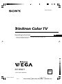
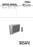
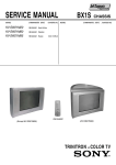
SERVICE MANUAL
MODEL
COMMANDER DEST.
KV-HW21M80
KV-HW21M83
CHASSIS NO.
RM-W101 E
SCC-U98N-A
RM-W101 E
SCC-U98M-A
(KV-HW21M80)
MODEL
BX1S
CHASSIS
COMMANDER DEST. CHASSIS NO.
(KV-HW21M83)
TRINITRON ® COLOR TV
KV-HW21M80/HW21M83
RM-W101
TABLE OF CONTENTS
Section
Title
Page
Section
SELF DIAGNOSTIC FUNCTION .............................. 3
1. DISASSEMBLY
1-1. 3D Speaker Removal ................................................ 6
1-2. Rear Cover Removal ................................................. 6
1-3. Speaker Removal ...................................................... 6
1-4. Chassis Assy Removal .............................................. 6
1-5. Service Position ........................................................ 6
1-6. Terminal Bracket Removal ....................................... 6
1-7. J Board Removal ....................................................... 7
1-8. A Board Removal ...................................................... 7
1-9. Picture Tube Removal ............................................... 7
2. SET-UP ADJUSTMENTS
2-1. Beam Landing ........................................................... 9
2-2. Convergence ............................................................ 10
2-3. Focus Adjustment .................................................... 12
2-4. G2 (SCREEN) Adjustment ..................................... 12
2-5 White Balance Adjustment ..................................... 12
2-6 Sub Bright Adjustment ........................................... 12
Title
Page
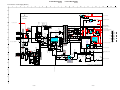
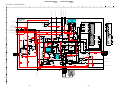
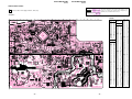
4. DIAGRAMS
4-1. Block Diagram ........................................................ 32
4-2. Circuit Boards Location .......................................... 33
4-3. Schematic Diagram Information ............................ 33
4-3-1. C Board Schematic Diagram ..................... 34
4-3-2. A Board — Processor (Block A) ............... 35
4-3-3. A Board — Audio (Block B) ..................... 37
4-3-4. A Board — Power Supply (Block C) ........ 39
4-3-5. A Board — Deflection (Block D) .............. 41
4-3-6. A Board — Tuner (Block E) ...................... 43
4-3-7. A Board — Jack (Block F) ........................ 45
4-3-8. J Board Schematic Diagram ....................... 47
4-4. Voltage Measurement and Waveforms ................... 49
4-5. Printed Wiring Boards and Parts Location ............. 52
4-6. Semiconductors ....................................................... 55
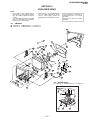
5. EXPLODED VIEWS
5-1. Chassis ..................................................................... 57
5-2. 3D Box Assy ........................................................... 57
6. ELECTRICAL PARTS LIST .................................... 59
3. CIRCUIT ADJUSTMENTS
3-1. Adjustment With Commander ................................ 13
3-2. Adjustment Method ................................................ 14
3-3. Picture Quality Adjustments ................................... 29
3-4. Deflection Adjustment ............................................ 29
3-5. Drive Adjustment .................................................... 30
3-6. Picture Distortion Adjustment ................................ 31
OPERATING INSTRUCTIONS
CAUTION
SAFETY-RELATED COMPONENT WARNING!!
SHORT CIRCUIT THE ANODE OF THE PICTURE TUBE AND
THE ANODE CAP TO THE METAL CHASSIS, CRT SHIELD,
OR CARBON PAINTED ON THE CRT, AFTER REMOVING THE
ANODE.
COMPONENTS IDENTIFIED BY SHADING AND MARK ! ON
THE SCHEMATIC DIAGRAMS, EXPLODED VIEWS AND IN
THE PARTS LIST ARE CRITICAL TO SAFE OPERATION.
REPLACE THESE COMPONENTS WITH SONY PARTS
WHOSE PART NUMBERS APPEAR AS SHOWN IN THIS
MANUAL OR IN SUPPLEMENTS PUBLISHED BY SONY.
–2–
KV-HW21M80/HW21M83
RM-W101
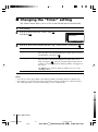
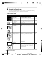
SELF DIAGNOSTIC FUNCTION
The units in this manual contain a self diagnostic function. If an error occurs, the STANDBY (1) indicator will
automatically begin to flash. A description of the self-diagnosis function is explained in the instruction manual. The
number of times the STANDBY (1) indicator flashes translates to a probable source of the problem. If an error
symptom cannot be reproduced, the remote commander can be used to review the failure occurrence data stored in
memory to reveal past problems and how often these problems occur.
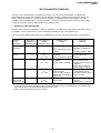
1. DIAGNOSTIC TEST INDICATORS
When an errors occurs, the STANDBY (1) indicator will flash a set number of times to indicate the possible cause of
the problem. If there is more than one error, the indicator will identify the first of the problem areas.
Result for all of the following diagnosis items are displayed on screen. No error has occured if the screen displays a
"0".
Diagnosis
Item
Description
No. of timer
STANDBY (1)
indicator flashes
Self-Diagnostic
display/
Diagnosis result
Probable Cause
Location
Detected
Symptoms
Power does
not turn on
Does not light
–
• Power cord is not plugged
in.
• Fuse is burned out (F600)
A board.
• Power does not turn on.
• No power is supplied on
TV.
• AC Power supply is faulty.
+B overcurrent
(OCP)*
2 times
2:0
or
2:1 ~ 255
• H OUT (Q805) is shorted. • Power does not turn on.
(A board)
• Load on power line is
• IC751 is shorted. (C board) shorted.
V-Protect
4 times
4:0
or
4:1 ~ 255
• +13V is not supplied.
(A board)
• IC804 is faulty. (A board)
• Has entered standby state
after horizontal raster.
• Vertical deflection pulse is
stopped.
• Power line is shorted or
power supply is shorted.
IK (AKB)
5 times
5:0
or
5:1 ~ 255
• Video OUT (IC1545) is
faulty. (A board)
• IC001 is faulty. (A board)
• Screen (G2) is improperly
adjusted.**
• No raster is generated.
• CRT Cathode current
detection reference pulse
output is small.
Power supply
NG (+5V) for
Video Processor
8 times
8:0
or
8:1 ~ 255
• IC604 faulty.
• IC602 faulty.
• No power supply to CRT
ANODE.
• No RASTER is generated.
If a +B overcurrent is detected, stoppage of the vertical deflection is detected simultaneously. The symptom that is
diagnosed first by the micro controller is displayed on the screen.
** Refer to Screen (G2) Adjustment in this manual.
*
–3–
KV-HW21M80/HW21M83
RM-W101
2. DISPLAY OF STANDBY (1) INDICATOR
FLASH COUNT
Diagnostic Item
Flash Count*
+B overcurrent
V-Protect
IK (AKB)
Power Supply NG (+5V)
for Video processor
2 times
4 times
5 times
8 times
* One flash count is not used for self-diagnosis.
Lamp ON 300ms
Lamp OFF 3 sec
Lamp OFF 300ms
STANDBY (1) indicator
3. STOPPING THE STANDBY (1) INDICATOR FLASH
Turn off the power switch on the TV main unit or unplug the power cord from the outlet to stop the STANDBY (1)
indicator from flashing.
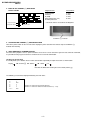
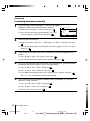
4. SELF-DIAGNOSTIC SCREEN DISPLAY
For errors with symptoms such as "power sometimes shuts off" or "screen sometimes goes off" that cannot be confirmed,
it is possible to bring up past occurrences of failure on the screen for confirmation.
[To Bring Up Screen Test]
In standby mode, press buttons on the remote commander sequentially in rapid succession as shown below:
Display
/ Channel 5 / Volume
/ Power
/ TV
˘
Note that this differs from entering the service mode (volume [+]).
The following screen will be displayed indicating the error count.
SELF DIAGNOSTIC
2:
3:
4:
5:
8:
0
N/A
0
1
0
101 :
N/A
Numeral "0" means that no fault was detected.
Numeral "1" means the number of a fault occurrence (1 ~ 255).
–4–
KV-HW21M80/HW21M83
RM-W101
5. HANDLING OF SELF-DIAGNOSTIC SCREEN DISPLAY
Since the diagnostic results displayed on the screen are not automatically cleared, always check the self-diagnostic
screen during repairs. When you have completed the repairs, clear the result display to "0".
Unless the result display is cleared to "0", the self-diagnosis function will not be able to detect subsequent faults after
completion of the repairs.
[Clearing the result display]
To clear the result display to "0", press buttons on the remote commander subsequent as shown below when the
self-diagnostic screen is being displayed.
8,[Quitting Self-diagnostic screen]
To quit the entire self-diagnostic screen, turn off the power switch on the remote commander or the main unit.
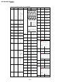
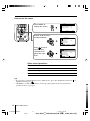
6. SELF-DIAGNOSTIC CIRCUIT
A BOARD
IC001
Y/CHROMA JUNGLE
FROM
C BOARD
IC751 PIN 5
A BOARD
FROM
Q816
COLLECTOR
A BOARD
IC804
V.OUT
A BOARD
IC001
SYSTEM
A BOARD
IC003
MEMORY
SDA1
84 IK
F.B-PLS
3
99
13
5 SDA
V.GUARD
RED LED 122
32 EHTO
DISPLAY
[+B overcurrent $OCP%]
Occurs when an overcurrent on the +B(135V) line is detected by pin 32 of IC001 (A board).
If the voltage of pin 32 of IC001 (A board) is more than 4V, the unit will automatically go
to standby.
[V-PROTECT]
Occurs when an absence of the vertical deflection pulse is detected by pin 13 of IC001
(A board).
[IK $AKB%]
If the RGB levels* do not balance within 15 sec after the power is turned on, this error will
be detected by IC001 (A board). TV will stay on, but there will be 5 times LED blinking.
POWER SUPPLY NG (+5V)
for VIDEO PROCESSOR
Occurs when IC001 internal HV protect detects an abnormal H-Pulse (frequency) due to
improper power supply to IC001. TV cuts off high voltage power of anode CRT. No picture
will be detected. eg: IC602, IC604 go faulty.
* (Refers to the RGB levels of the AKB detection Ref pulse that detects IK.)
–5–
KV-HW21M80/HW21M83
RM-W101
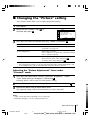
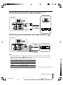
SECTION 1
DISASSEMBLY
1-2. REAR COVER REMOVAL
1-1. 3D SPEAKER REMOVAL
1 3D Speaker box assy
(KV-HW21M83)
1 Eight screws
(+BVTP 4 × 16 TYPE 2 IT-3)
2 Rear cover
2 Rear cover
1-4. CHASSIS ASSY REMOVAL
1-3. SPEAKER REMOVAL
1 Two screws
(WH DIA.16)
(+P4 x 16)
1-6. TERMINAL BRACKET REMOVAL
1-5. SERVICE POSITION
1 One screw
(+BVTP 3x12
TYPE2 IT-2)
2 Terminal
bracket
–6–
3 One screw
(+BVTP 4x16
TYPE2 IT-3)
KV-HW21M80/HW21M83
RM-W101
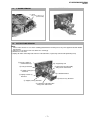
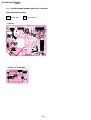
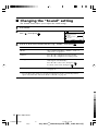
1-7. J BOARD REMOVAL
1-8. A BOARD REMOVAL
1 J Board
Two screws (+BVTP 3x12)
(KV-HW21M83)
A Board
1-9. PICTURE TUBE REMOVAL
Note:
• Please make sure the TV set is not in standing position before removing necessary CRT support located on bottom
right and left.
1) Place the TV set with the CRT face down on a cushion jig.
2) Remove the rear cover.
3) Unplug all under connecting leads from the Deflection Yoke, Degaussing Coil and CRT grounding strap.
qd Screw, Tapping 5
+ Crown washer (4)
4 Degaussing Coil
qs DGC(2) Removal
6 Loosen the Neck Assembly
fixing screw and removal
qa Holder, DGC(2)
Removal
5 C Board Removal
q; Spring Tension (2)
Removal
8 Chassis Assy Removal
9 Support, CRT(2) Removal
7 Loosen the Deflection Yoke
fixing screw and remove
–7–
KV-HW21M80/HW21M83
RM-W101
• REMOVAL OF ANODE-CAP
Note:
• After removing the anode, short circuit the anode of the picture tube and the anode cap to the metal chassis, CRT
shield or carbon paint on the CRT.
•
c
REMOVING PROCEDURES
a
anode button
a
turning up the rubber cap and pulling it up in the
direction of the arrow C.
•
1 Turn up one side of the rubber cap in the direction
indicated by the arrow A.
HOW TO HANDLE AN ANODE-CAP
1 Do not damage the surface of anode-caps with
sharp shaped objects.
2 Do not press the rubber too hard so as not to
damage the inside of anode-cap.
A metal fitting called the shatter-hook terminal is
built into the rubber.
3 Do not turn the foot of rubber over too hard.
The shatter-hook terminal will stick out or damage
the rubber.
b
b
2 Using a thumb pull up the rubber cap firmly in the direction indicated by the arrow B.
3 When one side of the rubber cap is separated from
the anode button, the anode-cap can be removed by
–8–
KV-HW21M80/HW21M83
RM-W101
SECTION 2
SET-UP ADJUSTMENTS
•
The following adjustments should be made when a
complete realignment is required or a new picture
tube is installed.
Set the controls as follows unless otherwise noted:
VIDEO model ..................................................... Standard
PICTURE control .................................................. normal
BRIGHTNESS control .......................................... normal
Perform the adjustments in the following order :
1. Beam Landing
2. Convergence
3. Focus
4. Screen(G2)
5. White Balance
Note : Test Equipment Required.
1. Pattern Generator
2. Degausser
3. DC Power Supply
4. Digital Multimeter
5. Oscilloscope
......................................................................................................................................................................................................................
Preparation :
• In order to reduce the influence of geomagnetism on
the set's picture tube, face it east or west.
• Switch on the set's power and degauss with the
degausser.
2-1.
Purity control
BEAM LANDING
Picture Mode: DYNAMIC
1. Input a white signal with the pattern generator.
Contrast
normal
Brightness
2. Set the pattern generator raster signal to a green
raster.
3. Move the deflection yoke to the rear and adjust with
purity control so that the green is at the center and
the blue and the red take up equally sized areas on
each side. (See Figures 2-1 through 2-4.)
4. Move the deflection yoke forward and adjust so that
the entire screen is green. (See Figure 2-1.)
5. Switch the raster signal to blue then to red and verify
the condition.
6. When the position of the deflection yoke has been
decided fasten the deflection yoke with the screws
and DY spacers.
7. If the beam does not land correctly in all the corners,
use a magnet to adjust it. (See Figure 2-4.)
Fig. 2-2
}
Blue
Red
Green
Fig. 2-3
Purity control
corrects this area.
b
a
c
d
Disk magnets or rotatable
disk magnets correct these
areas (a-d).
Deflection yoke positioning
corrects these areas.
b
c
a
d
Fig. 2-4
Fig. 2-1
–9–
KV-HW21M80/HW21M83
RM-W101
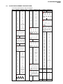
2-2.
•
•
•
Operation of V.STAT magnet
If the V.Stat magnet is moved in the “A” and “B” arrows,
the red, green and blue dots moves as shown below.
CONVERGENCE
Before starting this adjustment, adjust the focus,
horizontal size and vertical size.
Receive dot/hatch signal.
Pic mode: Soft.
A
B
(1) Horizontal and Vertical Static Convergence
Center dot
A
B
B
B
G
G
R
R
R
G
B
R
G
B
Moved RV750 H.STAT.
the red, green and blue dots move as shown below.
V. STAT
Magnet
H. STAT VR
A
R
B
B
G
R
4. BMC (Hexapole) Magnet.
If the red, green and blue dots are not balanced or
aligned, then use the BMC magnet to adjust in the
manner described below.
RV750
H. STAT
C Board
1. (Moving vertically), adjust the V.STAT magnet so that
the red, green and blue dots are on top of each other
at the center of the screen.
2. (Moving horizontally), adjust the H.STAT control so
that the red, green and blue dots are on top of each
other at the center of the screen.
3. If the H.STAT variable resistor cannot bring the red,
green and blue dots together at the center of the
screen, adjust the horizontal convergence with the
H.STAT variable resistor and the V.STAT magnet in
the manner given below.
(In this case, the H.STAT variable resistor and the
V.STAT magnet influence each other, so be sure to
perform adjustments while tracking.)
Purity
G
B
BMC
BMC (Hexapole)
Purity
DY pocket
V.STAT
V.STAT
– 10 –
R G
B
R
B
G
R
G
B
R
G
B
R
G B
G
R
B
KV-HW21M80/HW21M83
RM-W101
(2) Convergence Rough Adjustment
Preparation:
• Before starting this adjustment, adjust the horizontal
static convergence and the vertical static
convergence
RB
B
R
TLH
TLV
RB
R
B
XCV
YCH
TLH
Insert
TLH
Correction Plate to DY Pocket
YCH Insert
YCH
VOL on DY
ON DY:
(Left or Right)
TLV
Rotate TLV
VOL on DY
XCV
Rotate XCV
Adj core on DY
TLV
YCH
DY pocket
TLH Plate
(3) Screen corner Convergence
TLV
XCV
1. Affix a Piece A (90), conv. correct corresponding to
the misconverged areas.
XCV
DY pocket
b
b
a
a-d : screen-corner
misconvergence
a
c
d
d
Piece A (90), conv. correct
– 11 –
c
KV-HW21M80/HW21M83
RM-W101
2-3.
FOCUS ADJUSTMENT
2-5.
FOCUS adjustment should be completed before the W/B
adjustment:
1. Receive digital monoscope pattern.
2. Set picture mode: DYNAMIC.
3. Adjust focus VR to obtain a just focus at the center of
the screen.
4. Change receiving signal to white pattern and blue
back.
5. Confirm MAGENTA RING is not noticeable. Incase
magenta ring is obvious, then adjust FOCUS VR to
balance magenta ring and FOCUS.
2-6.
SUB BRIGHT ADJUSTMENT
1. Set to service mode.
2. Brightness set to 50%, Picture....Minimum
3. Select WHBL SBRT (10) with 1 and 4 and adjust
SBRT (10) data with 3 and 6 so that the third stripe
from right dimly lit.
4. Write into the memory by pressing [MUTING] then -.
5. GA models C/O: 20 IRE
S/G: 30 IRE
FOCUS
SCREEN
FLYBACK TRANSFORMER (T802-14")
FLYBACK TRANSFORMER (T801-21")
2-4.
WHITE BALANCE ADJUSTMENT
1. Set to Service Mode (Refer Section 3-1:
ADJUSTMENTS WITH COMMANDER)
2. Input white raster signal.
3. Set Picture to <DYNAMIC mode>
4. Select RDRV (02) with 1 and 4 and fixed the value
to 25 with 3 and 6.
5. Adjust WHBL GDRV (03) and BDRV (04) with 1 and
4 and adjust the data with 3 and 6 for best white
balance in Highlight condition.
6. Write into the memory by pressing [MUTING] then -.
7. Adjust WHBL BKOR (00) and BKOG (01) with 1 and
4 and adjust the level with 3 and 6 for best white
balance cut-off condition.
8. Write into memory by pressing [MUTING] then -.
9. US model need to apply only for colour temperature
in Neutral.
G2 (SCREEN) ADJUSTMENT
1. Set the PICTURE & BRIGHTNESS to STANDARD.
2. Put the Video input mode signal.
3. Connect R,G,B of the C board cathode to
oscilloscope.
4. Adjust Brightness to obtain the cathode value to
value below.
5. Adjust G2 (screen) on the FBT until picture shows
the point before cut off.
165 ± 2VDC
– 12 –
KV-HW21M80/HW21M83
RM-W101
SECTION 3
CIRCUIT ADJUSTMENTS
3-1.
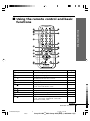
ADJUSTMENT WITH COMMANDER
Service adjustments to this model can be performed using the supplied remote commander RM-W101.
a. ENTERING SERVICE MODE
With the unit on standby
t [DISPLAY] t 5 t [VOL $+% ] t [POWER]
This operation sequence puts the unit into service mode.
This screen display is:
item no.
in decimal
item name
service data
in decimal
NVM
NG
service command
field
frequency
channel no./
video input name
GEOM
006
HSIZ
031
x
SERVICE
60
S VIDEO 1
release ID
software
version
service data
in binary
reserved
for factory
color system
power on time
(decimal?)
0.69U
0001 1111
FF FF
NTSC3
65535
category
SUS01
Flash DCXO
111 11 11 1 7 11
FG
xy 111
Status Byte
#1 SSD
Status Byte
#2 SSD
000000
000000
VDSP_C Flag
CO_LOCKED
VDSP
Detected Stereo Type (Direct Value from CZ_ Stereo_Mode)
S : for Sony
A : Aiwa
U S : US/Latin/Taiwan
E U : Europe
G A : General Area
J P : Japan
0 1 : serial no. of the M/P release
for each destination
111
Needed for Nicam DCXO aligment Purpose
xy
Value of x = 0 - Unknown, 1 - BTSC, 2 - A2, 3 - NICAM,
4 - KOREAN, 5 - Japan, 6 - AV Stereo
Value of y = 0 - Mono, 1 - Stereo, 2 - Bilingual, 4 - SAP/Single
b. METHOD OF CANCELLATION FROM SERVICE MODE
Set the standby condition (Press [POWER] button on the commander), then press [POWER] button again, hereupon it
becomes TV mode.
c.
1.
2.
3.
4.
5.
METHOD OF WRITE INTO MEMORY
Set to Service Mode.
Press 1 (UP) and 4 (DOWN), to select the adjustment item.
Change item by pressing 3, 6.
Press [MUTING] button to indicate WRITE on the screen.
Press - button to write into memory.
1, 4
r
3, 6
r
[MUTING]
r
-
d.
1.
2.
3.
Select the adjustment item.
Raise/lower the data value.
Writes.
Executes the writing.
MEMORY WRITE CONFIRMATION METHOD
After adjustment, pull out the plug from AC outlet, and then plug into AC outlet again.
Turn the power switch ON and set to Service Mode.
Call the adjusted items again to confirm adjustments were made.
– 13 –
KV-HW21M80/HW21M83
RM-W101
e. OTHER FUNCTION VIA REMOTE COMMANDER
7, All the data becomes the values in memory.
8, All user control goes to the standard state.
Display, - Service data initialization (Be sure not to use usually.)
2, 5
Select Device or Category
3-2.
ADJUSTMENT METHOD
Item Number 000 HPOS
This explanation uses H POSITION as an example.
1. Select "000 HPOS" with the 1 and 4 buttons, or 2 and 5.
2. Raise/lower the data with the 3 and 6 buttons.
3. Select the optimum state. (The standard is IF for PAL reception.)
4. Write with the [MUTING] button. (The display changes to WRITE.)
5. Execute the writing with the - button. (The WRITE display will be changed to red color while excuting, and back to
SERVICE.)
Example on screen display :GREEN
GEOM
000
HPOS
039
SERVICE
50 VIDEO 1
Adjusted with [3] and [6] buttons.
GREEN
GEOM
000
HPOS
039
WRITE
50
VIDEO
1
50
VIDEO
1
write with [MUTING].
RED
GEOM
000
HPOS
039
WRITE
The WRITE display
then returns to green
SERVICE
Write executed with [0].
Use the same method for all Items. Use 1 and 4 to select the adjustment item, use 3 and 6 to adjust, write with
[MUTING], then execute the write with -.
Note : 1. In [WRITE], the data for all items are written into memory together.
2. For adjustment items that have different standard data between 50Hz or 60Hz, be sure to use the respective
input signal after adjustment.
– 14 –
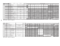
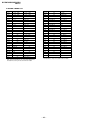
Adjustment Item Table
TVJ
Category
GEOM
Functionality
Init.
Range
No.
Name
Dec
Dec
000
HPOS
031
063
ADJUST
Horizontal Shift (HS)
001
HPAR
031
063
ADJUST
002
HBOW
031
063
003
VLIN
031
004
VSCR
005
DATA
Function
Table & Note
Device Name
(Slave Address)
NVM Address / Initial Value (Detailed)
Common
50
60
w50
w60
– 15 –
50/60/w50/w60 (+JPN RGB)
TV-Processor
42
42
42
42
Horizontal Parallelogram
50/60/w50/w60
(8Ah)
31
31
31
31
ADJUST
Horizontal Bow
50/60/w50/w60
31
31
31
31
063
ADJUST
Vertical Linearity
50/60/w50/w60
31
31
31
31
031
063
ADJUST
Vertical Scroll
50/60/w50/w60
31
31
31
31
HSIZ
031
063
ADJUST
EW Width (EW)
50/60/w50/w60
25
25
25
25
006
EWPW
031
063
ADJUST
EW Parabola/Width (PW)
50/60/w50/w60 (+JPN RGB)
31
31
31
31
007
UCOP
017
063
ADJUST
EW Upper Corner Parabola
50/60/w50/w60
31
31
31
31
008
LCOP
017
063
ADJUST
EW Lower Corner Parabola
50/60/w50/w60
31
31
31
31
009
EWTZ
031
063
ADJUST
EW Trapezium
50/60/w50/w60
31
31
31
31
010
VSLP
031
063
ADJUST
Vertical Slope (VS)
50/60/w50/w60
31
31
31
31
011
VSIZ
015
063
ADJUST
Vertical Amplitude
50/60/w50/w60
15
15
15
15
012
SCOR
014
063
ADJUST
S-Correction (SC)
50/60/w50/w60
25
25
25
25
013
VPOS
031
063
ADJUST
Vertical Shift (VSH)
50/60/w50/w60
31
31
31
31
014
HBL
000
001
FIX
RGB Blanking Mode
50/60/w50/w60
01
01
01
01
015
WBF
007
015
FIX
Timing of Wide Blanking (WBF)
50/60/w50/w60
07
07
07
07
016
WBR
007
015
FIX
Timing of Wide Blanking (WBR)
50/60/w50/w60
10
10
10
10
017
SBL
000
001
FIX
Service Blanking
none
00
018
COPY
000
001
FIX
Copy the GEO data to all 50/60Hz NVM area
none
00
RM-W101
KV-HW21M80/HW21M83
Functionality
Init.
Range
No.
Name
Dec
Dec
WHBL
000
BKOR
031
063
ADJUST Black Level Offset R
col temp (HIGH/LOW/Normal)*(UV/RGB/Others)
TV-Processor
31
001
BKOG
031
063
ADJUST Black Level Offset G
col temp (HIGH/LOW/Normal)*(UV/RGB/Others)
(8Ah)
31
002
RDRV
037
063
col temp (HIGH/LOW/Normal)*(UV/RGB/Others)
TV-Pro (8AH)
37
003
GDRV
037
063
ADJUST White Point G
col temp (HIGH/LOW/Normal)*(UV/RGB/Others)
004
BDRV
037
063
ADJUST White Point B
col temp (HIGH/LOW/Normal)*(UV/RGB/Others)
DATA
Function
Table & Note
Device Name
(Slave Address)
FIX
White Point R
NVM Address / Initial Value (Detailed)
Common
LPG
000
001
FIX
RGB Gain Preset
none
01
PGR
031
127
FIX
Preset Gain R (PGR)
none
**
007
PGG
031
127
FIX
Preset Gain G (PGG)
none
**
008
PGB
031
127
FIX
Preset Gain B (PGB)
none
**
FIX
Preset Gain Offset
009
GNOF
000
015
010
SBRT
031
063
011
SBRO
000
003
none
ADJUST Sub-Brightness
FIX
Sub-Brightness Offset (Intelligent Pic)
CCC loop
Col Temp
(LOW other)
Col Temp
(NORM other)
Col Temp
(HIGH YUV)
Col Temp
(LOW YUV)
Col Temp
(NORMAL YUV)
Col Temp
(HIGH RGB)
Col Temp
(LOW RGB)
Col Temp
(NORM RGB)
31
31
31
31
31
31
31
31
31
31
31
31
31
31
31
31
37
37
37
37
37
37
37
37
31
31
31
31
31
31
31
31
31
31
31
31
31
31
31
31
31
31
Others
RGB
YUV
31
31
31
Pic mode
0
Pic mode
1
Pic mode
2
Pic mode
3
00
01
02
01
RM-W101
005
006
Col Temp
(HIGH other)
15
Others/RGB/YUV
none
00
012
EGL
000
001
FIX
Enable Gain Loop in CCC System
none
01
013
SGL
000
003
FIX
Selection of High Current in CCC System
none
00
014
AKB
000
001
FIX
Black Current Stabilization
none
00
015
CBS
000
001
FIX
Control Sequence of Beam Current Limiting
none
00
016
RGBB
000
003
FIX
RGB Blanking
none
00
017
BLBG
000
001
FIX
Blanking of Blue & Green Output
none
00
018
OFB
000
001
FIX
Black Level Offset Blue
none
01
019
NSBR
000
015
FIX
Non Standard Brightness Offset
none
05
020
WBP
000
003
FIX
Color Temp Setting (0:High, 1:Normal, 2,3:Low)
Picture Mode
021
OUV
000
001
FIX
Offset Control On UV Input signals
Others/YUV
00
00
– 16 –
Item remarks ** please refer page 24.
Functionality
Init. Range
Category
TVJ
No.
Name
Dec
DATA
Function
SADJ
000
PMAX
063
063
ADJUST Picture Maximum
001
SHUE
007
015
ADJUST Sub-Hue
Table & Note
Device Name
NVM Address / Initial Value (Detailed)
(Slave Address) Common YUV 50pal 50pal 50secam 50secam 60TV 60Video 50YUV 60YUV 50RGB 60RGB Pic mode Pic mode Pic mode Pic mode
(TV) (Video) (TV)
(Video)
0
1
2
3
Dec
002
SSHP
015
063
FIX
Sub-Sharpness
003
SSHO
000
003
FIX
Sub-Sharpness Offset (Intelligent Pic)
ADJUST Sub-Color
(TV / Video)*(Normal / Wide) / <Normal / Wide> (+JPN RGB)
Dynamic*Eco
much (Jpn)
Standard*Eco
std (Jpn)
Standard*Eco Eco std Eco much TV Video TV Video AVM AV Wide
much (Jpn)
(Jpn)
(Jpn)
Wide Wide (Jpn) (Jpn)
TV-Processor
TV / Video
**
TV / Video / YUV (+JPN RGB)
none
02
004
SCOL
031
063
005
SCOO
000
003
FIX
Sub-Color Offset (Intelligent Pic)
006
PIC
031
127
FIX
Picture Control [GA:0-100(valid), >100(invalid);
Others:0-63(valid); ignore bit 6(invalid)]
Picture Model(GA: Personal = User Reset Data)
100
80
65
100
007
COL
031
127
FIX
Color Control [GA:0-100(valid), >100(invalid);
Others:0-63(valid); ignore bit 6(invalid)]
Picture Model(GA: Personal = User Reset Data)
56
50
40
50
008
BRT
031
127
FIX
Brightness Control [GA:0-100(valid),
>100(invalid); Others:0-63(valid); ignore bit
6(invalid)]
Picture Model(GA: Personal = User Reset Data)
50
50
60
50
50pal(tv)/50pal(video)/50secam(tv)/50secam(video)/
60TV/60video/50YUV/60YUV/50RGB/60RGB
none
31
31
31
31
31
31
31
31
31
31
02
009
HUE
031
127
FIX
Hue Control [GA:0-100(valid), >100(invalid);
Others:0-63(valid); ignore bit 6(invalid)]
Picture Model(GA: Personal = User Reset Data)
50
50
50
50
010
SHP
031
127
FIX
Sharpness Control [GA:0-100(valid),
>100(invalid); Others:0-63(valid); ignore bit
6(invalid)]
Picture Model(GA: Personal = User Reset Data)
60
50
50
50
011
PECO
002
003
FIX
Picture data in power save mode
(valid for JAPAN only)
Picture Mode * (Eco std/ Eco much)
012
PRLV
002
003
FIX
Coefficient of power save mode
(valid for JAPAN only)
Eco std / Eco much
Item remarks ** please refer page 24.
Dynamic*Eco
std (Jpn)
00
00
00
00
00
00
37
37
07
07
**
**
37
37
00
00
KV-HW21M80/HW21M83
TVJ
Category
TVJ
Functionality
Init.
Range
Category
No.
Name
Dec
Dec
YC
000
PFRQ
000
003
FIX
Peaking Center Frequency and Delay
001
RPA
####
003
FIX
Ratio Pre & Over Shoot
TV/other
02
02
002
RPO
0 02
003
FIX
Ratio of Positive & Negative Peaks
TV/other
02
02
DATA
Function
Table & Note
003
YDLY
012
015
FIX
Y-Delay
004
CMAT
000
003
FIX
PAL-SECAM or NTSC (Japan/USA) Matrix
005
ACL
001
001
FIX
Automatic Color Limiting
006
CB
000
001
FIX
Chroma Bandpass Center Frequency
Device Name
NVM Address / Initial Value (Detailed)
(Slave Address)
Common
TV-Processor
**
Others
RGB
(PAL/NTSC/SECAM)*(TV/VIDEO)+YUV/S-INPUT
YUV
**
(JPN RGB)
00
valid only with TV (*Video:0 fix)
01
PAL(TV) NTSC(TV) SECAM(TV)
**
**
PAL(Video) NTSC(Video) SECAM(Video) S-INPUT SECAM NTSC
**
**
**
**
TV
**
01
007
SBO
001
003
FIX
SECAM Black Offset
008
CHSE
001
003
FIX
PAL/NTSC Ident Sensitivity
02
009
CLO
000
001
FIX
Center Frequency of Cloche(Bell) Filter
00
00
010
CTRP
000
001
FIX
Chroma Trap Mode
011
BPS
000
001
FIX
Bypass of Chroma Base-band Delay Line
012
FCO
000
001
FIX
Forced Color On
013
TINT
031
063
FIX
Base-Band Tint Control
014
TUV
000
001
FIX
Tint Control on UV Signals
SECAM/others
00
NTSC/others
**
01
**
00
YUV/others
31
31
00
Item remarks ** please refer page 24.
– 17 –
TVJ
Category
SYNC
Functionality
Init.
Range
No.
Name
Dec
Dec
000
SYS
000
001
DATA
Function
Table & Note
Device Name
(Slave Address)
FIX
Synchronization on YSYNC Input
001
FO
000
003
FIX
Phase 1 Time Constant
0 02
VID
00 0
001
FIX
Video Ident Mode
NVM Address / Initial Value (Detailed)
Common
50
60
00
00
00
00
others
YUV
TV
Video
Teletext
TV-ip
No signal
03
03
01
00
00
00
TV IP ON/TV IP OFF/Video/Teletext/Auto Tuning or No signal(RF)
50/60
003
FS L
000
001
FIX
Forced Slicing Level for Vertical Sync
004
SSL
000
001
FIX
Slicing Level Sync Separator
005
SVID
001
007
FIX
Source Selection for Video Identification
006
FORF
000
003
FIX
Forced Field Frequency
03
00
50/60
YUV/Others
00
007
MVK
000
001
FIX
Macro Vision Keying
01
008
AFCT
000
003
FIX
AFC Timing Switch Control
(GA ,US : Pin116, EURO,JPN : Pin128)
#
07
RM-W101
KV-HW21M80/HW21M83
# Note : AFCT For ES5.2D, data is 00
For ES7.2D, data is 03
Category
PICT
Functionality
Init.
Range
DATA
Function
Table & Note
Device Name
(Slave Address)
Name
Dec
Dec
000
CADL
007
015
FIX
Cathode Drive Level
001
CFA
000
003
FIX
Comb Filter Mode
002
SOC
002
003
FIX
Soft Clipping Level
Others
RGB
Live
00
01
TV
(Dyn)
TV
(Others)
Video
(Dyn)
00
00
00
Video ColorTemp
(Others)
(HIGH)
ColorTemp
(Others)
Color
Temp(LOW)
Color Temp
(NORMAL)
01
01
00
**
(8Ah)
00
RM-W101
No.
NVM Address / Initial Value (Detailed)
Common
003
PWL
001
001
FIX
Peak White Limiting Switch
004
WHTL
006
015
FIX
Peak White Limiting
**
005
GAM
001
001
FIX
Gamma
00
006
WTS
001
003
FIX
Gamma Control and White Stretch
Live/Others
#
007
TFR
000
001
FIX
DC Transfer Ratio of Luminance Signal
Live/Others (+JPN RGB)
01
(TV/Video)*(Dyna/others)
01
008
COR
003
003
FIX
Coring
009
CORO
000
001
FIX
Coring Offset (Intelligent Pic)
010
BKS
003
003
FIX
Black Stretch
011
AAS
001
001
FIX
Black Area to Switch off the Black Stretch
012
DSK
000
001
FIX
Dynamic Skin Control
013
BLS
000
001
FIX
Blue Stretch
014
NBLS
000
001
FIX
Operation Blue Stretch Circuit
015
NRR
000
001
FIX
Non Red Reduction
#
00
00
RGB/others
02
02
#
00
col temp (HIGH/OTHERS)
00
00
00
col temp (HIGH/LOW/NORMAL)
01
– 18 –
Item remarks ** please refer page 24.
# : For WTS : Data is 01 (ES5.2D)
Data is 02 (ES7.2D)
TVJ
Category
SW
# : For AAS : Data is 00 (ES5.2D)
Data is 01 (ES7.2D)
Functionality
Init.
Range
No.
Name
Dec
Dec
000
CV2
000
001
FIX
CVBS2 Input Signal Selection
001
SVO
001
003
FIX
Function of IFVO/SVO/CVBSI Pin @ 48
002
DFL
000
001
FIX
Flash Protection
DATA
Function
Table & Note
Device Name
(Slave Address)
NVM Address / Initial Value (Detailed)
Common
YUV
TV
Video
02
01
01
00
TV/Video/YUV
01
KV-HW21M80/HW21M83
TVJ
TVJ
Category
V IF
Functionality
Init.
Range
No.
Name
Dec
Dec
000
OIFD
036
063
FIX
Offset IF Demodulator
001
AGCT
031
063
FIX
AGC Take-over
002
STM
000
001
FIX
Search Tuning Mode
01
003
GD
000
001
FIX
Group Delay on CVBS1 Signal
00
004
AGCS
001
003
FIX
IF AGC Speed
01
005
FFI
000
001
FIX
Fast Filter IF PLL
00
006
OAMP
003
003
FIX
Video Output Signal Amplitude (only L & L'System)
03
007
VAI
000
001
FIX
System I Output Signal Amplitude Correction (only L & L'System)
00
DATA
Function
Table & Note
Device Name
Common
(Slave Address)
TV-Processor
36
(8Ah)
31
– 19 –
TVJ
Functionality
Init.
Range
Category
No.
Name
Dec
Dec
VM
000
RGBD
003
007
FIX
Delayof RGB Output to VM Output
001
VMA
003
003
FIX
Amplitude of VM Output
002
VMAP
002
003
FIX
VM setting (0:High, 1:Low, 2,3:OFF)
003
VMMO
003
003
FIX
VM Mode
DATA
Function
Table & Note
Device Name
NVM Address / Initial Value (Detailed)
(Slave Address)
Common
none
TV-Processor
#
none
(8Ah)
**
Picture Mode
Pic mode
0
Pic mode
1
Piv mode
2
Pic mode
3
00
01
02
00
01
# Note : RGBD for ES5.2D : 02
for ES7.2D :04
RM-W101
KV-HW21M80/HW21M83
Item remarks ** please refer page 24.
Category
SDEM
Functionality
Init.
Range
No.
Name
Dec
Dec
000
FMWS
000
003
FIX
Window Selection for FM Demodulator
001
QSS
001
001
FIX
Quasi Split Sound (QSS) Amplifier Mode (except GA Model)
002
BPB
000
001
FIX
Bypass of Sound Bandpass Filter
00
003
AMLO
000
001
FIX
Audio Output Signal for AM Sound
00
004
HPVC
000
001
FIX
Head Phone Volume Control
00
DATA
Function
Table & Note
Device Name
Common
(Slave Address)
02
(8Ah)
**
Item remarks ** please refer page 24.
– 20 –
TVJ
Category
TXT
Functionality
Init.
Range
No .
Name
Dec
Dec
000
TXV
039
063
FIX
Teletext Vertical Position for Philips
001
THD
005
127
FIX
Teletext H-sync Active Edge Shift
05
002
TBR
004
015
FIX
Teletext RGB Brightness
11
003
LCB
000
001
FIX
Teletext LCB 0 : disable 1: enable (setting for FASTEX)
00
DATA
Function
Table & Note
Device Name
Common
(Slave Address)
Text Decoder
39
RM-W101
TV-Processor
KV-HW21M80/HW21M83
TVJ
TVJ
Functionality
Init.
Range
Category
No.
Name
Dec
Dec
SDSP
000
AVM
002
007
FIX
DATA
Function
Table & Note
Device Name
(Slave Address)
NVM Address / Initial Value (Detailed)
Common
AVL Mode
SSD
02
(B0h)
09
001
AVV
005
015
FIX
AVL Reference Level
002
BBL
000
015
FIX
BBE Contour
**
003
BBH
000
015
FIX
BBE Process
**
004
BBLW
000
015
FIX
BBE Contour Offset
005
SVOF
000
015
FIX
Surround /Effect Mode Volume Offset
006
IVOF
000
007
FIX
Master Volume Positive Offset
06
007
EVOF
000
007
FIX
Master Volume Negative Offset
06
008
LAD
000
031
FIX
Decoder Level Adjust
05
009
LAM
000
031
FIX
Mono Level Adjust
05
010
LAN
000
031
FIX
Nicam Level Adjust
22
011
LAS
000
031
FIX
SAP Level Adjust
08
012
LAA
000
031
FIX
ADC Level Adjust
TV-L(Euro)
TV
Video
Off
SRS/WOW
Trusurround
Istereo
Imono
**
**
**
**
**
05
03
**
Off(SRS/WOW)/Trusurround/Istereo/Imono
Tv/Video(Non Euro)I TV-L/TV-non L/Video
00
– 21 –
013
SEF
003
007
FIX
Incredible Mono/Stereo Effect
014
A1L
000
255
FIX
AUX1 Volume Left
00
015
A1R
000
255
FIX
AUX1 Volume Right
00
Istereo/Imono
016
BAS
008
015
FIX
Main Bass Offset
**
017
TRE
008
015
FIX
Main Treble Offset
**
018
EQ1
008
015
FIX
Equalizer Main Channel Band (100 Hz) Offset
**
019
EQ2
008
015
FIX
Equalizer Main Channel Band (300 Hz) Offset
**
020
EQ3
008
015
FIX
Equalizer Main Channel Band (1000 Hz) Offset
**
021
EQ4
008
015
FIX
Equalizer Main Channel Band (3000 Hz) Offset
**
022
EQ5
008
015
FIX
Equalizer Main Channel Band (8000 Hz) Offset
**
023
BFCT
005
007
FIX
DBE, DUB and BBE Control
**
024
SCEN
001
015
FIX
SRS3D Center Control
04
01
SSPA
000
015
FIX
SRS3D Space Control
BBHW
000
015
FIX
BBE process offset in WOW mode
**
027
STRE
002
007
FIX
Treble Offset for surround mode
**
00
028
BBHT
000
015
FIX
BBE Offset in TV mode
029
DWA
000
000
FIX
DWA???
00
030
TTRE
002
007
FIX
Treble Offset in TV Mode
02
00
Item remarks ** please refer page 25.
RM-W101
KV-HW21M80/HW21M83
025
026
00
SDEC
Functionality
Init.
Range
No.
Name
Dec
Dec
000
MPTU
003
015
DATA
FIX
Function
Table & Note
Device Name
(Slave Address)
Common
Upper Threshold for MPX pilot detection (BTSC)
SSD
02
(B0h)
001
MPTL
009
015
FIX
Lower Threshold for MPX pilot detection (BTSC)
002
SPTU
003
015
FIX
Upper Threshold for SAP carrier detection
08
003
SPTL
006
015
FIX
Lower Threshold for SAP carrier detection
15
05
C1TH
000
031
FIX
Normal Threshold for detection of SC1
00
C1AP
000
031
FIX
Auto Program Threshold for detection of SC1
00
006
SPTH
000
031
FIX
Noise Threshold for automute of SAP
00
007
SPHY
004
015
FIX
Hysteresis size for automute of SAP
03
008
FMTH
000
031
FIX
Noise Threshold for automute of SC2 in FM A2 standard
18
009
FMHY
004
015
FIX
Hysteresis size for automute of SC2 in FM A2 standard
07
010
BTTH
000
031
FIX
Noise Threshold for automute of BTSC stereo carrier
00
011
BTHY
004
015
FIX
Hysteresis size for automute of BTSC stereo
03
012
EJTH
000
031
FIX
Noise Threshold for automute of EIAJ FM subcarrier
00
013
EJHY
004
015
FIX
Hysteresis size for automute of EIAJ FM subcarrier
04
– 22 –
014
ONLY
000
001
FIX
Reproduce only related NICAM on DEC output
00
015
EXAM
000
001
FIX
Fall back source in case of automute in standard L (DDEP)
00
016
NIMT
000
001
FIX
NICAM auto mute function depend on bit error rate (DDEP)
00
017
NILE
100
255
FIX
NICAM lower error limit (DDEP)
50
018
NIUE
200
255
FIX
NICAM upper error limit (DDEP)
200
019
EPMD
001
003
FIX
DEMDEC Easy Programming (DDEP)
02
020
STDS
019
031
FIX
Bits multiplexed for ASD and SSS modes
31
021
OVMA
001
001
FIX
FM overmodulation adaption
00
022
FLBW
000
003
FIX
FM/AM demodulator filter bandwidth
03
023
IDMD
000
003
FIX
FM ident speed in SSS mode
00
024
FPAL
000
001
FIX
Line fequency for BTSC decoding
00
025
OVMT
001
002
FIX
Overmodulation level threshold relative to nominal
03
026
DCXI
000
001
FIX
NICAM DCXO Scaling Control Inverter
**
027
DCXG
000
007
FIX
NICAM DCXO Scaling Control Gain
**
028
DCLL
011
015
FIX
NICAM DCXO Scaling Control Limit (L)
00
029
DCLH
000
031
FIX
NICAM DCXO Scaling Control Limit (H)
**
030
IDEU
001
003
FIX
IDMOD setting for European A2 STD
00
031
IDKR
001
003
FIX
IDMOD setting for Korean M STD
00
032
IDJP
001
003
FIX
IDMOD setting for EIAJ STD
01
Item remarks ** please refer page 25.
RM-W101
004
005
KV-HW21M80/HW21M83
TVJ
Category
TVJ
Category
OPTM
Functionality
Init.
Range
No.
Name
Dec
Dec
000
ASHT
006
007
DATA
FIX
Function
Table & Note
Device Name
(Slave Address)
Auto shut off timer (data * 5 min)
NVM Address / Initial Value (Detailed)
Common
50
60
63
31
00
001
OSDB
000
015
FIX
OSD brightness
MMR/Micro 60h
05
002
OSDH
005
015
FIX
OSD Horizontal Position
MMR/Micro 60h
05
003
OSDV
037
063
FIX
OSD Vertical Position
004
MUTE
000
001
FIX
No Signal Mute Switch (1=enabled)
00
04
50 / 60
MMR/Micro 60h
005
RFUL
015
015
FIX
RF Signal Change Counter after Unlocked (Disable when 0fh)
006
RFLK
015
015
FIX
RF Signal Change Counter after Locked (Disable when 0fh)
00
007
AVUL
015
015
FIX
AV Signal Change Counter after Unlocked (Disable when 0Fh)
04
00
008
AVLK
015
015
FIX
AV Signal Change Counter after Locked (Disable when 0Fh)
009
LANG
000
003
FIX
OSD language shipping condition
010
HTXT
000
001
FIX
Sync seperator sw
00
TV-Processor(8A)
00
TV-Processor(8A)
01
011
CMSS
000
001
FIX
Sync sw
012
DCXO
060
295
FIX
DCXO Value
013
EXBL
000
015
FIX
Extended Blanking Timer to Eliminate White Noise
014
TSYS
000
003
FIX
Memorize TV Sys in NVM at Test Reset [0:B/G, 1:I, 2:M, 3:D/K] (GA Model)
**
015
TVOU
001
001
FIX
TV out mute Condition 0: Always mute off, 1: mute without signal
00
016
LBL
001
001
FIX
Brightness Reduction At No signal Condition
00
SFR/Micro 60h/DSP
**
07
– 23 –
Item remarks ** please refer page 25.
TVJ
Category
OPTB
Functionality
Init.
Range
No.
Name
Dec
Dec
000
IALL
000
001
FIX
Standard Write Switch (not memorized in NVM)
001
OPB1
000
255
FIX
Option 1 (System related)
*****
For remark *****
002
OPB2
000
255
FIX
Option 2 (Video Signal related)
*****
Refer to option
003
OPB3
000
255
FIX
Option 3 (Stereo Decoding related)
*****
Bit setting on
004
OPB4
000
255
FIX
Option 4 (Miscellaneous)
*****
Page 26 to
005
OPB5
000
255
FIX
Option 5 (Miscellaneous)
*****
Page 28
006
OPB6
000
255
FIX
Option 6 (OSD Language related)
*****
DATA
Function
Table & Note
Device Name
(Slave Address)
Common
Note
00
RM-W101
KV-HW21M80/HW21M83
NOTE
• Standard data listed on the Adjustment Item Table are reference values, therefore it may be different for each model and for each mode.
• Note for Different Data Those are the standard data values written on the microprocessor. Therefore, the data values of the modes and stored respectively in the memory.
In case of a device replacement, adjustment by rewriting the data value is necessary for some items.
KV-HW21M80/HW21M83
RM-W101
Data variant depend on models
NOTE: This data with remark **
Category
No
Name
WHBL
006
PGR
with VM
69
50
007
PGG
without VM
with VM
61
69
45
50
008
PGB
without VM
with VM
61
69
45
50
without VM
61
45
Category
No
Model
Name
Data (ES5.2D)
Data (ES7.2~)
Model
Table
Video
35
38
TV
35
35
SADJ
002
SSHP
Category
No
Name
Model
YC
000
PFRQ
Comb models
01
00
Non-Comb modeis
00
00
Category No
YC
003
Category
YC
Name
YDLY
No
011
21" Comb Model
21" Non-Comb Model
All 14" models
Data (ES5.2D)
Model
Comb Model
Non-Comb Model
Name
BPS
Model
Table
NTSC
01
Comb Model
Non-Comb modeis
Category
No
Name
PICT
001
CFA
Data (ES7.2D)
Table
NTSC(TV) SECAM(TV) PAL(VIDEO) NTSC(VIDEO) SECAM(VIDEO)
08
08
11
09
11
02
10
2
2
2
PAL(TV)
08
02
00
Model
Data
Comb models
00
Non-Comb modeis
01
Category
No
Name
14" models
21" models
PICT
004
WHTL
09
00
Category
No
Name
Model
Data
VM
001
VMA
with VM
03
without VM
00
Category
No
Name
Mono & AV
Stereo models
Steteo, China
& India
SDEM
001
QSS
00
01
– 24 –
Yuv
35
35
Others
00
00
YUV
09
09
S-Input
09
09
KV-HW21M80/HW21M83
RM-W101
Category
No
Name
AR21 series
BT21
(AV Stereo)
HW21-3D
AR14 series
HW21
non-3D
BM14/21
& BT21
SDSP
002
BBL
01
00
00
01
00
00
003
BBH
05
00
00
04
00
00
004
BBLW
06
06
06
06
06
06
016
BAS
13
14
11
00
13
00
017
TRE
15
14
12
13
14
00
018
EQ1
12
09
00
07
11
00
019
EQ2
04
10
00
00
00
020
EQ3
10
09
00
00
00
00
021
EQ4
09
10
11
10
00
00
022
EQ5
10
11
12
00
12
00
023
BFCT
05
00
00
05
00
00
026
BBHW
00
00
00
00
00
00
027
STRE
01
01
01
01
01
01
Category
No
Name
Stereo
models
Non-stereo
models
SDEC
026
DCXI
01
00
027
DCXG
03
00
029
DCLH
06
00
Category
No
Name
Other Country
Hong Kong
model
China
model
OPTM
014
TSYS
00
01
02
Category
No
Name
Model
SDSP
005
SVOF
Off
SRS/WOW
Table
Trusurround
AR21 Series
04
11
04
06
04
BT21 AV Stereo
04
11
04
06
04
HW21-30 Model
04
11
04
06
04
AR14 series
05
12
05
07
05
HW21 non-3D model
04
11
04
06
04
BM14/21 and BT21
mono
00
07
00
02
00
Category
No
Name
GA stereo
GA AV ST/US NTSC ST/
GA NTSC
GA Mono/US
OPTM
012
DCXO
50
70
61
– 25 –
I Stereo l Mono
KV-HW21M80/HW21M83
RM-W101
ITEM INFORMATION
No. OPB1
Item
KV-HW21M80
KV-HW21M83
Speed Search
0
1
0
M/N(US)
L’
M
B/G
I
D/K
DEC
0
0
1
1
1
1
79
0
0
1
1
1
1
79
1
SPEED SEARCH (Time of speed search)
00 = disabled (original cycle speed)
01 = 4 time speed from the original
10 = 6 time speed from the original
11 = 8 time speed from the original
0 = disabled, 1 = enabled
TV System Selection
No. OPB2
Item
AV Multi/ Component Composite (SCART)
PAM(GA)
1
1
0
1
1
1
0
1
D1(JPN)
KV-HW21M80
0
KV-HW21M83
0
D1
AV Multi/
PAM
Component
Composite
(D1 Terminal)
(AV Multi Terminal) - JP
Portable Audio Mode - GA
(Component [YCbCr] Terminals)
(No. of Composite Terminals)
(SCART)
(No. of SCART Terminals)
SECAM
Color decoding
(SECAM Color System)
(Color Crystal Selection)
SECAM
Color Decording
DEC
1
0
0
116
1
0
0
116
0 = not available, 1 = available
0 = not available, 1 = available
0 = not available, 1 = available
0 = not available, 1 = available
00 = no composite terminal
(Euro:no Scart) BX1L:No Video
01 = 1 composite terminal
(Euro:1 Scart) BX1L:2 Video in
10 = 2 composite terminals
(Euro:2 Scart) BX1L:3 Video in
11 = 3 composite terminals
(Euro:no terminal) BX1L:4 Video in
0 = not available, 1 = available
00 = PAL/NTSC/SECAM (Multi)
01 = NTSC (3.58MHz)
10 = PAL/NTSC/SECAM (4.43MHz)
11 = PAL/NTSC (Tri-Norma)
No. OPB3
Item
HDEV
NICAM ST NICAM BI
A2 ST
Thai Bilingual JP/US ST Korean ST
MONO
DEC
KV-HW21M80
0
0
0
0
0
0
0
0
00
KV-HW21M83
0
0
0
0
0
0
0
0
00
HDEV
NICAM ST
NICAM BI
A2 ST/BI
Thai Bilingual
JP/US ST
Korean ST
MONO
(High Deviation Mode)
(NICAM Stereo)
(NICAM Bilingual)
(A2 [West German]
Stereo/Bilingual)
(A2 [Thai] Bilingual)
or Force SAP if JP/US ST is active
(JP/US Stereo)
(Korean Stereo)
(Monaural Model)
– 26 –
0 = disabled, 1 = enabled
0 = disabled, 1 = enabled
0 = disabled, 1 = enabled
0 = disabled, 1 = enabled
0 = disabled, 1 = enabled
0 = disabled, 1 = enabled
0 = disabled, 1 = enabled
0 = Stereo (SSD) Model
1 = Monuaral Model
KV-HW21M80/HW21M83
RM-W101
No. OPB4
Firmware/
SMAT
1 spk
Models
VM
KV-HW21M80
1
0
0
1
KV-HW21M83
1
0
0
1
Item
Equalizer Surround
Firmware
SMAT
1 spk Models
(SSD Firmware Downloading)
Surround Matrix
1 Speaker Models
VM
Equalizer
Surround
(Velocity Modulation)
(5-band Equalizer Model)
(US/GA Surround Selection)
V-Chip
(V-Chip Model)
TOP
TEXT
(Forced TOP)
(Teletext Model)
V-Chip
Top
Text
DEC
0
0
0
0
144
0
0
0
0
144
0 = disabled, 1 = enabled
0 = Active, 1 = Passive
0 = 2 or 3 Speaker Models,
1 = 1 speaker Models
0 = disabled, 1 = enabled
0 = Bass/Treble Model, 1 = Equalizer Model
0 = Off/Simulated/Surround
1 = Off/Simulated/WOW/TruSurround (US)
1 = Off/Simulated/SRS (3D) Surround (GA)
0 = Channel Block Model (no rating)
1 = Parental Control Model (rating)
0 = Auto Mode (TOP/FLOF), 1 = Forced TOP
0 = Non-Teletext Model, 1 = Teletext Model
No. OPB5
Item
KV-HW21M80
KV-HW21M83
Full
No
Forced 60
Surround Surround
0
0
0
0
0
0
ASD
Tilt
IP Plus
IP
Wide
DEC
0
0
1
1
1
07
0
0
1
1
1
07
Full Surround
(Full Surround option)
No Surround
Forced 60
ASD
Tilt
IP Plus
IP
Wide
(No Surround Model)
(Forced 60Hz in no signal)
(Automatic Standard Detection)
(Tilt Correction/PIC Rotation)
(Intelligent Picture Plus)
(Intelligent Picture)
(Wide Mode/V-Compressed)
– 27 –
0 = Normal Surround Model
1 = Full Surround Model
(Off/simulated/surround/
SRS/WOW/TruSurround)
0 = Surround Model, 1 = Non-Surround Model
0 = 50Hz, 1 = 60Hz
0 = disabled, 1 = enabled
0 = disabled, 1 = enabled
0 = disabled, 1 = enabled
0 = disabled, 1 = enabled
0 = disabled, 1 = enabled
KV-HW21M80/HW21M83
RM-W101
No. OPB6
Item
OSD Language Selection
GA US
Latin
KV-HW21M80
1
0
Feature 2 Feature 1
0
0
0
1
0
0
132
KV-HW21M83
1
0
0
0
0
1
0
0
132
GA US
(US Model Destination)
Latin
(US Model Latin Destination)
Feature 2
(Temporary for BX1L)
Feature 1
(Temporary for BX1L)
OSD Language Selection
(English always available except JP)
0 = US/CANADA/Latin
1 = Taiwan/Korea/Philippine
(Wake-up timer enable)
(GA Surround Spec:OFF,
SIMULATED, SRS)
0 = US/CANADA (No Volume Figure Display)
1 = Latin (Volume Figure Display)
0 = Comb Not available
1 = Comb available
0 = PiP Not Available
1 = PiP available
US
01xx = French
0x1x = Spanish
0xx1 = Portuguese
US
(GA NTSC)
1x1x = Complicated Chinese
1xx1 = Korean
GA
EU
– 28 –
DEC
1xxx = Simplified Chinese
x1xx = Arabic
xx1x = Thai
xxx1 = Vietnamese
0000 = Destination ADE
0001 = Destination BL
0010 = Destination KR
0011 = Destination U
KV-HW21M80/HW21M83
RM-W101
3-3.
PICTURE QUALITY ADJUSTMENTS
SUB HUE ADJUSTMENT
PMX/CONTRAST ADJUSTMENT
1.
2.
3.
4.
Select Video Mode.
Input PAL CB to TV set.
Set PICT 03 "PWL" to 00h and WHBL 21 "BLBG" to 01h.
Set the following condition:
PICTURE 100%, COLOR 0%, BRIGHTNESS 50%.
5. Connect an oscilloscope to pin 4 (R output) of CN004.
6. Set to Service Mode "PWL" to 00h, "BLBG" to 01h.
7. Select SADJ00 "PMX" with 1 and 4 of the
commander then adjust VR within spec with 3 and 6.
1. Select Video.
2. Input a NTSC 3.58 Color Bar to TV set.
3. Set the following condition:
PICTURE 100%, COLOR 50%, BRIGHTNESS 50%
4. Connect an oscilloscope to pin 2 (B output) of CN004.
5. Set to Service and adjust SADJ01 "SHUE" with 1
and 4 of commander then adjust to VB1 = VB2 =
VB3 = VB4 with 3 and 6.
6. Then press [MUTING] t - to write the data.
VB1
VB2
VR
Black
The highest level of VB1, VB2, VB3, VB4 must be
aligned at the same time.
The ideal difference between VB2 and VB3 is within
±110mV.
1.46 ± 0.03 Vp-p = without VM models
1.65 ± 0.03 Vp-p = with VM models
8. Then press [MUTING] t - to write the data
9. Set "PWL" and "BLBG" back to initial data repectively.
(PWL: 01h and BLGG: 00h)
Select Video and set Picture mode.
Input PAL 100% CB to TV set.
Set PICT 06 "WTS" to 00h.
Set the following condition:
PICTURE 100%, COLOR 50%, BRIGHTNESS 50%.
5. Connect an oscilloscope to pin 2 (B output) of CN004.
6. Select to Service Mode and adjust SADJ04 "SCOL"
with 1 and 4 of commander then adjust to
VB2 = VB3 = VB4 with 3 and 6.
VB1
For single system with NTSC 4.43 select TV channel
with NTSC 4.43 and repeat 4 t 6.
3-4.
SUB COLOR ADJUSTMENT
1.
2.
3.
4.
VB3 VB4
DEFLECTION ADJUSTMENT
H-TRAPEZOID ADJUSTMENT
1. Receive cross hatch/dotsignal.
2. Adjust on to make H-Trapezoid distortion best.
NORMAL MODE (50Hz)
1. Set to Service Mode.
2. Input SPCB Signal (Select Video Mode for USA).
3. Using the 1 and 4 button select GEO (Service
Mode).
4. Rasie/lower data using the 3 and 6 buttons adjust
the following items:-
VB2 VB3 VB4
GEOM :
VB2 = VB3 = VB4
(Difference is within 70mV)
7. Then press [MUTING] t - to write the data.
8. Set "WTS" back to original data.
000
001
002
003
004
005
006
007
008
009
010
011
012
013
014
015
016
017
018
HPOS
HPAR
HBOW
VLIN
VSCR
HSIZ
EWPW
UCOP
LCOP
EWTZ
VSLP
VSIZ
SCOR
VPOS
HBL
WBF
WBR
SBL
COPY
Horizontal Shift (HS)
Horizontal Parallelogram
Horizontal Bow
Vertical Linearity
Vertical Scroll
EW Width (EW)
EW Parabola/Width (PW)
EW Upper Corner Parabola
EW Lower Corner Parabola
EW Trapezium
Vertical Slope (VS)
Vertical Amplitude
S-Correction (SC)
Vertical Shift (VSH)
RGB Blanking Mode
Timing of Wide Blanking (WBF)
Timing of Wide Blanking (WBR)
Service Blanking
Copy the GEO data to all
50/60Hz NVM area
5. Write into memory by pressing [MUTING] then - on
the remote commander.
– 29 –
KV-HW21M80/HW21M83
RM-W101
WIDE MODE (50Hz)
WIDE MODE (60Hz)
(V-Compression Adjustment)
1. Input SPCB signal.
2. Adjust condition change to WIDE MODE : ON
3. Copy (Item from normal mode 50Hz) all Normal
Mode adjusted data.
(V-Compression Adjustment)
1. Input mono scope signal.
2. Adjust condition change to WIDE MODE : ON
3. "COPY" is set to 1, then [MUTE] + -
3-5.
NORMAL MODE (60Hz)
1. Input signal
1. Input 525/60Hz signal.
2. They can copy 50Hz first.
("COPY" under GEOM is set to 1, then [MUTE] + -)
3. Using the 1 and 4 button, select category GEO
(Service Mode).
4. Raise/lower data using the 3 and 6 buttons to
obtain optimum image.
GEOM :
000
001
002
003
004
005
006
007
008
009
010
011
012
013
014
015
016
017
018
HPOS
HPAR
HBOW
VLIN
VSCR
HSIZ
EWPW
UCOP
LCOP
EWTZ
VSLP
VSIZ
SCOR
VPOS
HBL
WBF
WBR
SBL
COPY
DRIVE ADJUSTMENT
Horizontal Shift (HS)
Horizontal Parallelogram
Horizontal Bow
Vertical Linearity
Vertical Scroll
EW Width (EW)
EW Parabola/Width (PW)
EW Upper Corner Parabola
EW Lower Corner Parabola
EW Trapezium
Vertical Slope (VS)
Vertical Amplitude
S-Correction (SC)
Vertical Shift (VSH)
RGB Blanking Mode
Timing of Wide Blanking (WBF)
Timing of Wide Blanking (WBR)
Service Blanking
Copy the GEO data to all
50/60Hz NVM area
2.
3.
4.
5.
70% Color Bar (USA)
100% Color Bar (Other)
Make sure only red is active.
Set following condition :PICTURE 100%, COLOR 0%, Other 50%
Select SADJ00 "PMAX" with 1 and 4 then adjust
until voltage in R out X gain [recorded] = SPEC
Then press [MUTING] t - to write data.
X±2VDC (R Cathode on C or CV board)
Model
14”
21”
GA
83.0
88.0 - Non VM Models
99.0 - VM Models
6. Set VIDP 36 BLBG back to 00.
– 30 –
KV-HW21M80/HW21M83
RM-W101
3-6.
PICTURE DISTORTION ADJUSTMENT
H. CENTER ADJUSTMENT (HPOS)
1. Input NTSC Monoscope signal.
2. Activate the Service Adjustment Mode.
3. Select the HPOS item with 1 and 4.
4. Adjust the value of HPOS with 3 and 6 for the best
vertical center.
5. Press [MUTING] then - to save into the memory.
V. LINEARITY (VLIN), V. CORRECTION (SCOR), PIN
AMP (EWPW), AND HORIZONTAL TRAPEZOID
(EWTZ) ADJUSTMENTS
1. Input NTSC Monoscope signal.
2. Activate the Service Adjustment Mode.
3. Select VLIN, SCOR, EWPW, and EWTZ with 1 and
4.
4. Adjust with 3 and 6 for the best horizontal size.
5. Press [MUTING] then - to save into the memory.
V LINEARITY (VLIN)
H. SIZE ADJUSTMENT (HSIZ)
1. Input NTSC Monoscope signal.
2. Activate the Service Adjustment Mode.
3. Select HSIZ with 1 and 4.
4. Adjust with 3 and 6 for the best horizontal size.
5. Press [MUTING] then - to save into the memory.
V CORRECTION (SCOR)
PIN AMP (EWPW)
HORIZONTAL TRAPEZOID (EWTZ)
V. SIZE ADJUSTMENT (VSIZ)
1. Input NTSC Monoscope signal.
2. Activate the Service Adjustment Mode.
3. Select the VSIZ item with 1 and 4.
4. Adjust value of VPOS with 3 and 6 for the best
vertical center.
5. Press [MUTING] then - to save into the memory.
V. ANGLE (HPAR), H. BOW (HBOW), UPPER PIN
(UCOP) AND LOW PIN (LCOP) ADJUSTMENTS
1. Input NTSC Monoscope signal.
2. Activate the Service Adjustment Mode.
3. Select HPAR, HBOW, UCOP, and LCOP with 1 and
4.
4. Adjust with 3 and 6 for the best picture.
5. Press [MUTING] then - to save into the memory.
V. CENTER ADJUSTMENT (VPOS)
1. Input NTSC Monoscope signal.
2. Activate the Service Adjustment Mode.
3. Select the VPOS item with 1 and 4.
4. Adjust value of VPOS with 3 and 6 for the best
vertical center.
5. Press [MUTING] then - to save into the memory.
V ANGLE (HPAR)
V BOW (HBOW)
UPPER PIN (UCOP)
LOW PIN (LCOP)
– 31 –
VIF SAW
3.3V
RESET
FSS TUNER
3.3/5V
AGCin
12C
SIF SAW
5V
5V
AUDIO VCC
8V
33.SNDIF
Audio Amp
115.P3.0
44.Intco
VIF & SIF
Color
Decoder
36,37.OutL, R1
RGB Amp
POWER
43.IFVO
62,63.HPL, R
48.SV0
Audio Amp
DGC
24-5.VIF1~2
YUV
Processor
RGB
85~87
RGBout
84.lk
RGB
1k
65.SVM
VM
+B
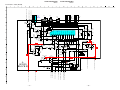
SECTION 4
DIAGRAMS
Mon
out
3.3V
8V
Relay
29~30.SIF1~2
31.AGCout
Video
L(Mono)
R
Video
L(Mono)
R
STBY
3.3V
30V
TV
out
TV
out
+B line
111.P2.0(S1)
AV1
AV2
23. V+
22. V-
58.CV/Y3
59.C3
56, 57InL,R3
55.CV/Y2
53,54.InL,R2
I/O Port
Micro
Text
CC & V-chip
DVD/RGB
Jungle
21.EWD
67.Hout
Pin out
H-drive
H-out
EW, Hd
Hp
66.Fbiso
32.EHTO/OVP
83.BCKin
78~80.RGB3
34.InL5
EHT, ABL
+/-15V
Hout
FBT
feedback
Audio Amp
Fbl(RGBin)
77.Fbl3
70-72.RGB2 in
74~76.YUVout
10.Xtalin
I/O Port
PLL
24.576MHz
11.Xtalout
102.P0.4
122~3.P2.4~5
G/Y
B/PB
R/PR
L
R
Rot. cct
On/Off
120.P3.3(S2)
RGB/
DVD
in
HV
V-out
V+, V-
112.PWMO
113.P2.2
ONE CHIP
126.INT2
98, 99. SDA1, SCL1
08, 109. SDA0, SCL0
AV2
in
CV/YC
L(Mono)
R
CV/YC
L(Mono)
R
119.ADC2
– 32 –
AV1
in
RM-W101
IF
30V
A
D
C
60,61
LSL,R
Stereo,
DSP
L, R
DAC
L
10W
R
10W
2ch
mute
106.P0.2
105.P0.1
stdby
LED
I
B-INT
Key buttons
Device 12C
SIRCS
R
VAR
12C
NVM
HP
ATT
L,R
KV-HW21M80/HW21M83
MAIN
Power
Supply
4-1. BLOCK DIAGRAM
CISPR/
PFC
AC in ~
110-220V
KV-HW21M80/HW21M83
RM-W101
4-2.
CIRCUIT BOARDS LOCATION
C Board
A Board
4-3.
J Board (KV-HW21M83)
SCHEMATIC DIAGRAM INFORMATION
Note:
• All capacitors are in µF unless otherwise noted.
• All electrolytic capacitors are rated at 50V unless otherwise
noted.
• All resistors are in ohms.
kΩ = 1000Ω, MΩ = 1000kΩ
• Indication of resistance which does not have rating
electrical power is as follows.
Reference information
RESISTOR
: RN
: RC
: FPRD
: FUSE
: RS
: RB
: RW
Pitch: 5 mm
Rating electrical power 1/4W (CHIP: 1/10W)
: nonflammable resistor.
•
•
•
•
•
•
•
•
•
•
•
•
•
•
•
: fusible resistor
: internal component.
: panel designation or adjustment for repair.
All variable and adjustable resistors have characteristic
curve B unless otherwise noted.
Readings are taken with a color-bar signal input.
no mark
: Common
(
)
: PAL
[
]
: NTSC 3.58
Readings are taken with a 10 MΩ digital multimeter.
Voltage are dc with respect to ground unless otherwise
noted.
Voltage variations may be noted due to normal
production tolerances.
All voltage are in Volt.
✽
: Cannot be measured.
Circled numbers are waveform references.
: B +bus.
: B –bus.
k : signal path.
COIL
CAPACITOR
¢
Note: The reference number which starts with Wxxx
(eg: W003) indicates a wire to wire connection.
Note: Components marked as XX are not fitted on this
model.
– 33 –
Note:
:✽
: LF-8L
: TA
: PS
: PP
: PT
: MPS
: MPP
: ALB
: ALT
: ALR
METAL FILM
SOLID
NONFLAMMABLE CARBON
NONFLAMMABLE FUSIBLE
NONFLAMMABLE METAL
OXIDE
NONFLAMMABLE CEMENT
NONFLAMMABLE
WIREWOUND
ADJUSTMENT RESISTOR
MICRO INDUCTOR
TANTALUM
STYROL
POLYPROPYLENE
MYLAR
METALIZED POLYESTER
METALIZED POLYPROPYLENE
BIPOLAR
HIGH TEMPERATURE
HIGH RIPPLE
The component identified by shading and
mark ! are critical for safety. Replace only
with part number specified.
Note: “A” board schematic diagram is divided into 6 blocks.
Each block is named by its function and block
“alphabet”. eg: Processor (Block A)
Joint connection between boards can be identified
using the block alphabet followed by sequence
numbering.
eg: -<HOUT-DEFL (A10) To D11
Meaning: Block A joint A10 is connected to Block D
joint D11
4
RCV
R773
560k
1/2W
5
6
R774
150
3W
RS
9 8 7
RV750
110M
L780
22uH
+200V
R781
0.56
RS
D750
GP08D
6
7
8
9
9V
GND 1
B 2
G 3
R 4
GND 5
1K 6
9V 7
CN701
7P
WHT
TO A BOARD
(PROCESSOR)
CN004
4 R763
100
1/2W
R766 XX
C788
XX
R767 XX
R768 XX
C789
R754 680 CHIP
XX
R-OUT
C790 R753 R-IN
XX
680
CHIP
R752 680 CHIP
+9V
L750
XX
C759
XX
CH
R786
XX
C
R764
100
D754
HSS82-TJ 1/2W
D755
HSS82-TJ
C787
1000p
500V
R765
100
D756
1/2W HSS82-TJ
C753
XX
500V
B
R784
XX
R777
XX
CHIP
9V
R775
XX
CHIP
R785
XX
(VIDEO AMP)
XX
5
JW1781
5
L782
B OUT
4
1
L781 XX
G OUT
3
R OUT
R IN
2
VDD
G IN
1
GND
B IN
– 34 –
R783
100
1/2W
IK
3
2
R757
1k
1/2W
R756
1k
1/2W
6
5
IC751
TDA6108AJF/N1
C786
1000p
B:CHIP
R778
XX
CHIP
Q701
XX
D782
UDZSTE-175.6B
C751
10
250V
L783
XX JW1782 5
D781
1SS119-25
C782
1000p
B
200V
NC
GND
H1
NC
C752
4700p
2kV
E
R760
XX
1/2W C754
4.7
250V
3
CN703
5P
WHT
TO A BOARD
(DEFLECTION)
CN801
R758
1k
1/2W
H
CV KR G1 G4 HV
JW1783
5
200V
R794
0.47
1
GND
CN705
1P
JW702
XX
C781
4.7
250V
R780
470k
1/2W
R713
0 :CHIP
C783
1000p
B:CHIP
KGKB G2
R776
XX
CHIP
B-BX1S12310-E.-C..-HW21M83
TO EARTH
COATING ASSY
PICTURE TUBE
A51LPT70X
1
D780
1SS119-25
1
2
3
4
5
1000V
GND
GND 13
11
10
1000V
CN704
1P
RM-W101
1
1
KV-HW21M80/HW21M83
R795
100K
1/2W
FPRD
J751
145154411
4-3-1. C Board Schematic Diagram
FV
KV-HW21M80/HW21M83
KV-HW21M80/HW21M83
RM-W101
RM-W101
4-3-2. A Board — Processor (Block A)
D066
GP08D
LSL-AUDIO (A13) To B2
13
R377
1.5k
CHIP
V IN
Y IN
HOUT-DEFL (A10) To D11
AFC-DEFL (A11) To D2
CN003
XX
4P
WHT
TO C BOARD
CN711
LSR-AUDIO (A12) To B3
+B (A9) To C11,D15,E11
Y IN / G
GND
U IN / B
V IN / R
GND
1
2
3
4
5
U IN
+B
NC
GND
VM OUT
Y OUT
GND
U OUT / FB
GND
V OUT
1
2
3
4
5
GND
B OUT
G OUT
R OUT
GND
IK
9V
TO C BOARD
CN701
1
2
3
4
5
6
7
CN004
XX
WHT
12
1
2
3
4
CN009
XX
5P
YEL
TO A BOARD
(JACK)
CN905
11
9V
B
G
U OUT
R
C004
100
16V
V IN
5V
R394
4.7k
CHIP
L003
10uH
U IN
B
10
V OUT
3.3V
9
CN007
XX
WHT
C005
100
16V
C006
470
10V
PROCESSOR
(BLOCK A)
8
Y OUT
A
MOMUTE-AUDIO
(A7) To B8
3.3V (A3) To C1,D18
A
7
D1_JP/MODE2_
EU/MONSW-MONO
(A8) To F24
6
SDA-0 (A5) To E14
5
SCL-0 (A6) To E15
4
5V (A4) To C9,D12,E16,F1
3
9V (A2) To B4,B14,C8,
D14,E13,F6
2
PWR-OFF-MUTE
(A1) To B6
1
D068
UDZSTE-175.6B
C308
0.01 25V
B:CHIP
3.3V
R030
100
CHIP
R015
1.5k
CHIP
R380
100
CHIP
R322
4.7k
CHIP
R392
10K
CHIP
R098
220
CHIP
C314
470
10V
C090
100p
CH:CHIP D070
XX
L013
10uH
G
R
G
D069
XX
R023
1.5K
CHIP
Q006
UN2216
G LED SW
Q007
UN2216
R LED SW
C018
0.22
16V
B:CHIP
TP02
C325
0.022
25V:CHIP
D914
SPB-25MVWF
LED
1.8V MAIN
C022 C024
0.22 22
16V
B:CHIP
3.3V
L033
10uH
W060
R397
1.5M
:CHIP
1.8V AUDIO
L032
10uH
H
D004
XX
PROTECTION
VOUT
UOUT
YOUT
YSYNC
YIN
UIN
VIN
VDDCOMB
VSSCOMB
HOUT
AFC
VM
9
VP3
GND3
B-Y/BIN
Y/GIN
R-Y/RIN
SCARTFBL
R039 100 CHIP
R041 100 CHIP
R042 2.2k CHIP
ROT_CTRL
To D16 (A33)
ROT_SW
To D17 (A34)
D076
MMDL914T1
R024 100 CHIP
JR1011
0
CHIP
C013
100 16V
R026
100
CHIP
R025
100
CHIP
C014
0.22
16V
B:CHIP
L012
10uH
D072
MMDL914T1
Q013
MSD601-RT1
C333
470
10V
C011
XX
B
10
11
IC001
TDA12067H/N1B0B0PX
SYSTEM CONTROLLER
- VIDEO PROCESSOR
- AUDIO PROCESSOR
(
W004
CVBS0 64
SCARTHPR 63
SCARTHPL 62
LSR 61
LSL 60
C1 59
CVBS1/Y1 58
INR1 57
INL1 56
CVBS3 55
INR3 54
INL3 53
C2 52
CVBS2/Y2 51
INR2 50
INL2 49
5
MON-OUT 48
VP2 47
AGC2SIF 46
VCC8V 45
INTC0-IF 44
IFVO/IF_MON_OUT 43
SIFAGC/SCART 42
PLLIF 41
GND2 40
MONO_OUTL 39
DECSDEM 38
C063
OUTR 37 0.1
OUTL 36 16V B
D1 RIN 35
D1 LIN 34
AVL/2SIF 33
)
1
2
3
4
CVBSO (A15) To F23
SCARTHPR (A16) To F22
SCARTHPL (A17) To B1,F21
JW1088
XX
5V
C1 (A18) To F8
CVBS1/Y1 (A19) To F10
INR1 (A20) To F12
INL1 (A21) To F11
CVBS3 (A22) To F13
INR3 (A23) To F15
INL3 (A24) To F14
C072
0.01
25V
B:CHIP
L004
47uH
C303
100
16V
C319
47p
CHIP
C069
0.1
16V
B:CHIP
CVBS2/Y2 (A25) To F20
INR2 (A26) To F18
INL2 (A27) To F19
MON-OUT (A28) To F5
W033
W034
C320
47p
CHIP
IFVO/IF_MON_OUT (A29) To E5
PLL1F (A65) To E18
MONO_OUTL (A30) To E19,F2
C316
0.47
10V
B:CHIP
TV-R
TV-L
W032
C309
W030
W031XX
25V
C064
B
R379
2.2
68k
CHIP
OUTR (A31) To F4
OUTL (A32) To F3
W010
C065
13 14 15 16 17 18 19 20 21 22 23 24 25 26 27 28 29 30 31 32
3.3
R312
C048
C089
C304
0.22 C052
1000p
100
1M :CHIP
R060
D074
16V 1000p
16V
R051
B
100
B
B
CHIP
39k
MMDL914T1
CHIPCHIP
CHIP
CHIP
C046
C300
R048 C055
6800p
R313
0.22
25V
100 0.15
R011 16V
150K:CHIP
B CHIP
CHIP 250V
C323
1K B:CHIP
C058
CHIP
0.001
1000p
B:CHIP B:CHIP
R046
C044 C049 C050
100
2.2 0.022 10
25V B
16V
CHIP
C321
W022
3.3V
F:CHIP CHIP
XX
C081
D065
C317
1000p
B
UDZSTE-175.6B
C041
220 16V B:CHIP
4700p
PROTECTION
C042
B:CHIP
C080
0.22
1000p
16V 5V
D064
B:CHIP
B:CHIP
C322
UDZSTE-175.6B
0.001
R314
PROTECTION
R316
B :CHIP
6.8k
R315
XX
CHIP
6.8k
CHIP
CHIP
D063
MMDL914T1
OCP
3.3V
5V
L008 10uH
R087
220
CHIP
R029
100
CHIP
C311
2.2
R319
XX
CHIP
D071
MMDL914T1
R398
10
CHIP
F
C091
100p
CHIP
R320
4.7k
CHIP
L009
10uH
97 SIRSC
98 SCL1
99 SDA1
100 VDDC2
101 VSSC2
102 B INT
103 D1_JP/MODE2_EU/MONSW-MONO
104 MOMUTE-AUDIO
105AUDIO STDBY
106 AUDIO MUTE
107 HD SW
108 SCL0
109SDA0
110VDDP(3.3V)
111S1/VC(GA)
112ROT CTRL
113ROT SW
114 STBY_SW
115 DGC RELAY
116 D1_JP/MODE1_EU
117VDDC1(1.8V)
118 DECV1V8
119KEY
120 S2
121VSSC1/P
122 RED LED
123 GREEN LED
124 VDDC3(1.8V)
125 VSSC3
126 AGC-MUTE
127 SECAM L-L
128 M-SYS-IF
W003
R395
100k TP04
CHIP
2.2
R338
4.7k
CHIP
C020
0.1
16V
B:CHIP
1.8V MAIN
SCARTFBL/A16 (A14) To F16
R317
3.3k
CHIP
R045
100 CHIP
R340
10k
CHIP
3.3V
R324
0
CHIP
R014
100
CHIP
R097 220 CHIP
5V
D007
D009
XX
XX
PROTECTION PROTECTION
R044 12k CHIP
B_DAT
AUDIO-STDBY
To B7 (A61)
R336
4.7k
CHIP
R020
100 CHIP
C021
100p CHIP
C012
0.22
16V
C313 B:CHIP R012 2.2k CHIP
1000p
B:CHIP
R337 470 CHIP
R339 100 CHIP
R341 100 CHIP
R018 100 CHIP
C312
1000p
B:CHIP
R096
220 CHIP
C051
XX
16V
F
VREF_POS_HPR
XTALIN
XTALOUT
VSSA1
VGUARD
DECDIG
VP1
PH2LF
PH1LF
GND1
SECPLL
DECBG
EWD
VDVD+
VIFIN1
VIFIN2
VSC
IREF
GNDIF
SIFIN1
SIFIN2
AGCOUT
EHT0
L011
10uH
L037 XX
C032 XX
To F28 (A62) B_DAT
R323
100
CHIP
L010 10uH
E
C328
0.01
25V:CHIP
R010
10k
CHIP
R001
4.7k
CHIP
To F27 (A64) B_CLK
To F29 (A63) B_INT
D003
MMDL914T1
Q016
UN2211
GNDA
VREFAD
VREFAD_PO
VREFAD_NE
VDDA(3.3V)
B OUT
G OUT
R OUT
IK
ABL
R363 C009
XX
0
CHIP B
C029 470 10V
R003
4.7k
CHIP
R362
XX
CHIP
1.8V AUDIO
L036 10uH
C031 XX
R361
XX
CHIP
D002
MMDL914T1
VCC OUT
GND
C098
XX
16V C068
XX
F
16V
F
C097
XX
16V
F
Q010
MSB709-RT1
C071
XX
16V
F
C056
D006
100
R364
XX
16V
D008
1k
PROTECTION
L006
XX
L005
3.3V
CHIP
10uH
PROTECTION
10uH
R356
C054
C025
C036
CHIP
0
C026
C030
0.1
16V
0.22 16V
100
C094
47
0.22
D005
16V
0.1
B:CHIP
C038
35V
16V
XX
16V B C095
0.1
B R058
0.1
B
16VC302R386PROTECTION
100
16V
CHIP
C301 B 2.2 100
L031
C053
B
R056 CHIP R059
470p CHIP 16VCHIP
0.022
10uH
1k
F
100
CH
25V B
C028
CHIP
R385 R384 C092 C093
CHIP
R038
C023
0.1
100 100
0.1 0.1
C096
16V B:CHIP 100
CHIP CHIP
8 7 6
16V 16V
TP03 2.2
0.1
CHIP
16V
B
B
16V B
B:CHIP
96 95 94 93 92 91 90 89 88 87 86 85 84 83 82 81 80 79 78 77 76 75 74 73 72 71 70 69 68 67 66 65
VDDADC(1.8)
VSSADC
VDDA2
VDDA(1.8)
R099
220
CHIP
IC002
RPM7240-SH5
IC RECEIVER
C008
47
35V
2 1
3.3V
R360
0
CHIP
R331
100
CHIP
C010
470p
CHIP
D023
UDZSTE17-9.1B
PROTECTION
L035
10uH
VSSP2
VSSC4
VDDC4(1.8V)
VDDA3(3.3V)
VREF_POS_LSL
VREF_NEG_LSL+LSR
VREF_POS_LSR+HPL
vREF_NEG_HPL+HPR
4
3
IC003
M24C16-WMN6T(A)
NVM
JR1010
XX
CHIP
B_INT
CN005
3P
WHT
TO TOP CONTROL
PANEL
R006
XX
CHIP
C002
R393 470
100 16V
CHIP
1
2
3
D056
MMDL914T1
PROTECTION
D054
UDZSTE-175.6B
PROTECTION
D
GND
NC
KEY
D025
UDZSTE17-9.1B
PROTECTION
D067
XX
D055
UDZSTE-175.6B
PROTECTION
C318
0.1
16V
B:CHIP
C015
XX
2
5V
R004
100
CHIP
R002
100
CHIP C001
100p
CHIP
5V
C003
100p
CHIP
1
3.3V
D024
UDZSTE17-9.1B
PROTECTION
D059
MMDL914T1
B-MUTE
L007 10uH
3.3V
C034 XX CH
X001
24.5MHz
C
C099
XX
16V
F
D058
MMDL914T1
G-MUTE
D075 UDZS-TE-179.1B
C037 4.7
5V
C073
Q001
UN2211
RGB-MUTE
(SPOT)
Y IN
5V
D057
MMDL914T1
R-MUTE
3.3V
3.3V
W008
1.8V AUDIO
I
R309
1M :CHIP
R310 R311
1k
47k
CHIP CHIP
D060
UDZSTE-175.6B
ABL
D061
MMDL914T1
C079
XX
Q009
XX
ABL-BUFFER
R326
XX
RN-CP
C084
XX R327
B
XX
RN-CP
W009
1.8V AUDIO
W011
D062
UDZSTE-175.6B
SLICER
1.8V MAIN
FB001
1.1uH
J
– 35 –
To E3 (A35) 2SIF
To D8 (A38) OVP-DEFL
To D10 (A37) OCP-PROTECT
To E10 (A36) TUAGC-IF
To E1 (A39) SIFIN2-IF
To E2 (A40) SIFIN1-IF
To E8 (A42) VIFIN1-IF
To E7 (A41) VIFIN2-IF
To D1 (A45) EWD-DEFL
To D7 (A44) VD--DEFL
To D5 (A43) VD+-DEFL
To D4 (A47) ABL
To D3 (A46) VGUARD-DEFL
To E20 (A67) VDDC4_CAP
To D19 (A66) PH2LF
To C2 (A49) 1.8V_MAIN
1.8V_AUDIO
To B13,C10 (A50)
To E12 ( A51) AGC-MUTE
To E21 (A68) VDDC3_CAP
To F9 (A53) S1/VC
D1_JP/MODE1_EU
To F25 (A52)
To F17 (A54) S2
To C13 (A58) STBY_SW
To C15 (A57) DGC-RELAY
To E6 (A56) SECAM-L-L
To E9 (A55) M-SYS-IF
(A59) RESET
To B9 (A60) AUDIO-MUTE
B-BX1S12310-E.-A..PROCESSOR-HW21M83
– 36 –
5
5
5
5
5
JW1092
XX
JW1089
XX
JW1090
XX
JW1091
XX
14
KV-HW21M80/HW21M83
KV-HW21M80/HW21M83
RM-W101
RM-W101
4-3-3. A Board — Audio (Block B)
R210
*
CHIP
C225
XX
G
R225
*
CHIP
C228
*
R229
*
CHIP
SP
GND
GND
1
3
SP R
STBY
OUTR/NC
Q200
UN2211
R215
10k
CHIP
R212
0
CHIP
R224
*
CHIP
D207
XX
R236
*
CHIP
W041
W040
C220
10
C215
2200
9V
Q202
MSB709-RT1
D205
AC MUTE
MMDL914T1
Q201
MSB709-RT1
R216
10k
CHIP
C232
0.047
PT
C219
220
16V
R218
0
CHIP
D203
MMDL914T1
R221
1k
CHIP
R220
0
CHIP
D211
DA204K
9V
D212
MMDL914T1
D214
MMDL914T1
FB2607
*
PS2601
5A
FB2602
*
C2631
470p
500V
B
L2601
10uH
D2625
C2648
*
1000
35V
C2636
D2626
1000
*
C2602
C2601
470P
XX
B
R2646
1
FPRD
R2647
10k
FPRD
R2645
XX
FPRD
To A1 (B6) PWR-OFF-MUTE
To A61 (B7) AUDIO-STDBY
To A7 (B8) MOMUTE-AUDIO
To A60 (B9) AUDIO-MUTE
To C6 (B10) AUDIO_GND
To C5 (B11) AUDIO_2
To C4 (B12) AUDIO_1
To A50,C10 (B13) 1.8V_AUDIO
To A2,B4,C8,D14,E13,F6 (B14) 9V
9V
C221
XX
25V
D204
MMDL914T1
B-BX1S12310-E.-A..-AUDIO-HW21M83
– 37 –
D206
XX
D208
MMDL914T1
D213
MMDL914T1
R242
2.2k
CHIP
C212 C213
0.1
XX
1000
B
25V CHIP
R219
330
C218
22
C216
22
R214
15k CHIP
I
J
2
GND
4
VCC
12
R213
15k
CHIP
C224 C211
*
*
C229
R230
XX
*
CHIP
Q206
UN2211
A
AUDIO
(BLOCK B)
GND
11
D201
MMDL914T1
R241
2.2k
CHIP
H
3
PW_GND
10
C231
0.047
PETP
D210
XX
C227 R228
*
*
F:CHIP CHIP
9V
SP L
9
D209
XX
R232
*
CHIP
Q204
*
MIXER
R222
*
CHIP
C226
R227
*
*
F:CHIP CHIP
2
8
D202
MMDL914T1
R223
*
CHIP
Q205
*
MIXER
F
1
2
7
R240
XX
CHIP
R235
47
FPRD
– 38 –
To A2,B14,C8,D14,E13,F6 (B4) 9V
C206
*
B:CHIP
6
R217
330
C214
1000
25V
R234
47
FPRD
To F7 (B5) MON-MUTE-AUDIO
C237
*
PT
5
9V
R226
*
CHIP
13
CN202
XX
WHT
C210
100
R211
*
CHIP
C209
*
MUTE
C208
*
B:CHIP
C207
*
MPS
OUTL
R208
*
CHIP
IC200
*
AUDIO AMP
IN C/NC
D200
DA204K
PROTECT
R207
*
CHIP
C204
*
MPS
12
C217
1000
25V
R204 * CHIP
E
CN200
4P
WHT
S-MICRO
11
C223
*
R201
*
CHIP
C203 C236
*
B:CHIP
*
R205
*
CHIP
10
IN L
R203
*
CHIP
3
1
4
3
4
5
1
2
7
6
8
9
6
7
2
1
5
4
3
R202
*
CHIP
C200
*
B:CHIP
9
J202
XX
S_GND
D
R233
*
FPRD
C202 C230
*
PT
*
R200 B:CHIP
*
CHIP
C201
*
F:CHIP
J200
*
8
RF
JR1256
XX
CHIP
J201
*
IN R/NC
C
CN201
*
WHT
TO J BOARD
CN3400
7
OUTC/NC
R237
100
C234 CHIP
470p
C235
CHIP
470P
CHIP
6
C205 *
R239
XX
CHIP
R238
100
CHIP
2 GND
B
LSL-AUDIO (B2) To A13
A
5
3 GND/3D OUT-
4
LSR-AUDIO (B3) To A12
3
1 3D OUT+
2
SCARTHPL (B1) To A17,F21
1
14
KV-HW21M80/HW21M83
KV-HW21M80/HW21M83
RM-W101
RM-W101
4-3-4. A Board — Power Supply (Block C)
1
2
3
4
5
6
7
8
9
10
11
12
13
14
A
A
VCC OUT
GND C641
100
16V
IC606
BA033T
D635
3.3V REG
UDZSTE-173.6B
POWER SUPPLY
(BLOCK C)
C605
4700p
500V
E
F
FH603
XX
S600
C668
4.7
10V
CHIP
Q601
MSD601-RT1
RELAY SW
SPARK GAP
C643
0.47
10V
B:CHIP
C600
4700p W002
250V
E
JW1604
W001 XX
SPARK GAP
SPARK GAP SPARK GAP
E
D600
MMDL914T1
PROTECT
Q606
R618
MSD601-RT1 18K
JW1632
XX
JW1605
XX
VDR600
VARISTOR
T600
145635411
JW1633
XX
1
2
&
1
JW1602
XX
FB601
XX
JW1611
5
C611
330
450V
C658
XX
450V C673
XX
CH
IC601
STR-F6267S LF1357
SWITCHING
REGULATOR
D636
XX
4
T604
XX
C624
47
R627
2.2
D623
10ERB20-TB3
C626
PS602 D622
470p
5A 11EQS10-TB5
500V
14
B
C654
D624
470p
FB603
500V
S3L20UF4
1.1uH
B
13
C634
C682 C632
D620
PS605
2200
1000
470
XX
35V
16V
D639 5A
25V
12
D3S6M-F C650
C630 C628 1500p 2kV
3300
XX
35V
11
C680
D621
470p
RU4AM-T3
CHIP
10
8
9
C619
0.15
PT
C670
330p
250V
B
R646
1.5k
RN-CP
G
AUDIO_1 (C4) To B12
AUDIO_2 (C5) To B11
AUDIO_GND (C6) To B10
C635
470
W018
IC605
SE135N-LF38
ERROR
AMP
G
C
C665
330
160V
R633
XX
R636
2.2k
IC604
TA7805S
5V-REG
11V (C7) To C16,D13
9V (C8) To A2,B4,B14,D14,E13,F6
5V
C639
100
W024 16V
G
9V C638
100
16V
C674
R669 XX
B
XX
C647
470
16V
O
D629
RD5.1ESB2
REG
C683
XX
JW1683
5
R647
1k
CHIP
JW1615
XX
JW1616
XX
JW1617
XX
L602
22uH
C649
100
R665 16V
XX
C668
JR1602
100
XX
16V
D637
MA2ZD14001S0
C679
XX
R666
XX
TP601
R655
100
CHIP
XX
JR1601
XX
CHIP
IC603
PQ018EF01SZH
1.8V-REG
C678
2.2
16V
F:CHIP
+B (C11) To A9,D15,E11
L600
47uH
HOLD_DOWN (C12) To D9
C646
XX
100V
C661
XX
25V
B
Q609
MSD601-RT1
SW
(C14) HS-A007
J
– 39 –
1.8V_AUDIO (C10) To A50,B13
R631
4.7k
Q608
MSD601-RT1
SW
JW1612
XX
JW1613
XX
R654 XX CHIP
R635
10k
CHIP
R634
4.7K
CHIP
B-BX1S12310-E.-A..-POWER SUPPLY-HW21M83
I
5V (C9) To A4,D12,E16,F1
JW1614
R640
XX
JW1653
5
R645
150k
RN-CP
PH600
PC123Y22JOOF
PHOTO
COUPLER
11V
C637
100
16V
FB608
0uH
R672
XX
CHIP
R625
0
C621 CHIP
4.7
T605
XX
1.8V MAIN
R667 R668
11V L601 1k 33k
47uH CHIP CHIP
D614
MTZJ-T-77-15
REG
C625
330p
250V B
1
C657
330p
250V
B
JW1630
XX
JW1631
XX
5
1.8V_MAIN (C2) To A49
C685
220
16V
IC607
BA18BC0FP-E2
1.8V-REG
15
7
C644
470p
CH
C652
C653
470p
470p
500V B
500V B
T602
D618
(SRT)
D1NL20U
1-439-694-11
RECT
C616
R623
R620
D619
220p
D615
0.27
18K
CH
2W RS
D1NL20U 10ERB20-TA2B5
RN-CP
RECT
RECT
& R653
R624
XX
2.2k
1/2W
RN
D617
FPRD
10ERB20-TA2B5
R650
RECT
8.2M
R619
R621
C623
0.22
1W
220
0.0033
2W
RN
B:CHIP
RS
4
JW1603
XX
H
T603
145635411
4
C669
XX
275V C602
PT 0.1
PP
C666
0.1
PP
JW1666
5
JW1667
5
4
FH602
FH601
F600
5A
250V
1
1
G
AC IN
AC IN
CN602
2P
C610
R651
4700p
XX
D604
500V
2W
D3SB60F3
E
RS
AC-RECT
D602
AM01AV1
RECTIFY
D603
Q605 R658 R660
AM01AV1
FN155 120K 470K
RECTIFY
RN
BUFFER RN
R659 R661
220K 560K
RN RN R675
XX
R612
D608
D605
1.5K
RD5.1ESB2 RD5.1ESB2
RN
REG
REG
C612
1500P
1.2kV
MPS
JW1665
20.0
D638
IC602
MMDL914T1 PQ09RDISJ00H
9V-REG
PS603
5A
JW1654
XX
C606
4700p
500V
E
RY600
R609
10k
CHIP
FB610
XX
JW1661 JW1663
(10MM)
XX
VCC OUT
GND
18
17
FB605 XX
2
1
DGC 2
DGC 1
CN601
DGC
R602
2P
4.7k
CHIP
To A57 (C15) DGC-RELAY
1
C622
2200p
250V
E
PS604
5A
D
DGCT
DGCT
CN600
2P
JW1660
(10MM)
THP600
11V 180453011
C660
0.22
275V
PP
R616
1
10W
RB
3.3V (C1) To A3,D18
1.8V AUDIO
C
R639
XX
10W
RB
3.3V
R656
1
R638
0.68
10W
RB
JW1662
XX
C609
4700p
500V
E
To C7,D13 (C16) 11V
C662
0.1
16V
B
D633
MTZJ-T-77-15
B
C672
0.01
25V
B
C675
XX
– 40 –
STBY_SW (C13) To A58
JW1618
XX
KV-HW21M80/HW21M83
KV-HW21M80/HW21M83
RM-W101
RM-W101
4-3-5. A Board — Deflection (Block D)
Q804
2SA1091-O
STOPPER
C811
100
16V
R835
220k
9V
R801
XX
CHIP
R800
XX
CHIP
R803
XX
CHIP
R824
33k
CHIP
D808
1SS119-25
STOPPER
9V
R806
XX
CHIP
R807
XX
CHIP
F
Q802
XX
BUFFER
R814
XX
CHIP
C879
XX
B
NS+
7
6
5
R817
XX
CHIP
11V
11V
JW1839
12.5
D807
1SS119-25
STOPPER
C828
100
16V
9V
R846
2.2k
CHIP
REF-VOLT
VCC (OUT)
DRV-IN
9V
C831 R868
C830
C840
10
0.01
0.1
0.013
FPRD
16V
25V
R882
1.2kV
2.2k
B:CHIP B:CHIP
C836
PP
C833
CHIP
0.1 XX
C826
C846
R852
16V
0.022 R865
2kV
330p
B:CHIP
10k
1k
R423
25V
B
2kV
Q806
CHIP
B:CHIP CHIP
0 CHIP
C847
MSD601-RT1
0.01
R869
200V
R861
R834
C841
1
PT C848
2.2k
180k
0.1
CHIP
FPRD
0.01
R883
400V
RN
Q807
C832
D817 2.2k 200V
PP
R857 220p MSB709-RT1
FPRD PT
IC801
EGP20G
9V
15
XX CHIP PIN DRIVE
LM2903DT
C842 JW1834 7.5
CHIP
COMPARATOR
0.022
L800
400V
C829
R424
JW1842
R858 XX
S
COIL
PP
1
2
3
4
R829
150k
10
XX 16V
W026Q808
CHIP
1k
CHIP B
C834
IRF614-037
3W
R843
R866
XX
100k
H-OUT
RS
0 CHIP
B
CHIP
C809
C822
C835 R879
0.01
1000p
R828
C825
0.01
25V
B:CHIP B:CHIP
0.01
25V 220k
1k
B:CHIP RN
25V
3W
B:CHIP
RS
R876
IC802
R880
10k
R873
R859
220k
CHIP
R856
33k CHIP TJM4558CDT
47k
R825
PIN
RN
10k
CHIP
AMPLIFIER
1k
CHIP
9V
3W
RS
C810
R864
R884
R840
R877
R872
5.6k
XX
C808 1000p
100k
XX
0
CHIP
FPRD 13
RN-CP CHIP
220p 500V
CHIP
R820
500V B
2.2k
B
C837
CHIP
R870
Q805
4 1 2
1
4700p
3.3K
2SC5885
JW1837
B:CHIP R8015
CHIP
5
C838
XX
R830
2
FB800
RN-CP
0.1
C805
2.2k
1.1uH
100V
1
14 1/2W
R871
PT
R878
R821
FPRD
220
R886
1
22k
W027
1W
CHIP
XX
1W
C806
RS
CHIP
RS
T800
C807
0.022
HDT
1000p
200V
5V
143537411
B:CHIP
PT
R827
1
2W
RS
Q803
2SC3209LK
5V
D804
1SS119-25
5V
4
3.3V
H
R422
XX
1W
RS
D824
EL1Z
C857
220
25V
R401
0.47
1/2W
FPRD
C864
XX
500V
B
R402
XX
2W RS
14
T802
XX
1
T801-4
T801-4
T801-2
T801-2
HV
T801-1
1
4
T801-4
4
2
T801-2
2
GND_1
GND_1
6
GND_1
6
T801-5
T801-5
5
T801-5
5
C865
XX
PT
11V
R8007
XX
C849
0.022
200V
PT
C867
33
160V
R896
XX
2W
RS
D819
10ERB20-TB3
C852
0.33 250V
PP
C851 R889
100
1
450V 3W RS
W025 R897
XX
RN
IC803
XX
1
2
3
C853
XX
25V
4
R894
XX
RN-CP
R417
XX
RN
C859
XX
C856
XX
25V B
R892
XX
CHIP
R899
XX
RN-CP
SV
13
GND_1
GND_1
11
T801-11
T801-11
D828
XX
R403
XX
CHIP
R8014
XX
CHIP
C866
XX R898
XX
CHIP
R416
4.7k
1/2W
L805
2.2mH
C882
XX
R8001
XX
CHIP
Q809
XX
MIXER
9
T801-9
GND_1
GND_1
8
GND_1
7
T801-7
T801-7
7
T801-7
1
2
3
4
5
200V
NC
GND
H1
NC
CN801
XX
WHT
TO C BOARD
CN703
OVP-DEFL (D8) To A38
HOLD_DOWN (D9) To C12
3.3V
5V
5V
5V
OCP-PROTECT (D10) To A37
12
5V
To A10 (D11) HOUT-DEFL
J
– 41 –
HHH+
H+
B-BX1S12310-E.-A..-DEFLECTION-HW21M83
DY800
6P
DY
V+
V-
1
2
3
4
5
6
I
!
H.DY
H.DY V.DY
V.DY
– 42 –
T801-11
8
Q816
XX
MIXER
D831
XX
11
T801-9
T801-9
200V
R8010
R8009
120k
6.8k
RN
CHIP
C869
C870 R414
R8013
0.068 4.7k
33
100k R8011
200V 1/2W
250V
RN
47k
Q8010
PT FPRD
2SC3209LK
CHIP
SWITCH
R408
XX
R8002
CHIP
C875 R8012
XX
XX
R8000 C874
47k
CHIP
XX
CH
XX
CHIP
CHIP 25V B
GND_1
9
Q8009
2SA1091-O
R419
XX
RN
13
10
R413
15K
RN
C868
470p
500V
B
R406
220k
1/2W
11V
C872
XX
R411
68K
1/2W
RN
R412
22K
RN
R405
0.47
1/2W
FPRD
D827
EL1Z
200V-RECT
L803
4.7mH
FV
10
R400
0.47
1/2W
FPRD
R8008
XX
L802
D821
22mH 10ERB20-TB3
H-CENT-1
S800
R890
68 3W RS
HV
SV
JW1841
7.5
L804
XX
C860
1000p
500V
B
T801-1
T801-1
FV
3
R816
XX
CHIP
C804
XX
R812
XX
CHIP
R813
XX
CHIP
D818
D830
MMDL914T1 RD5.1ESB2
PROTECTOR CLAMP
C861
220
25V
-13V
2
CN800
XX
RED
TO NS COIL
8
L806
XX
D800
XX
STOPPER
D801
XX
STOPPER
R818
XX
CHIP
D812
XX
R887
22k
CHIP
C845
1000p
B:CHIP
R895
3.3K
:CHIP
1
NC
NS-
1
2
3
R815
XX
CHIP
IC800
XX
ROTATION
AMP
R823
180k
RN
R845
XX
CHIP
C816
XX
R853
3.3k
CHIP
R855 10KCHIP
R809
XX
CHIP
R810
XX
CHIP
R808
XX
CHIP
R842
XX
CHIP
R847 10k CHIP
W019 Q801
XX
C803 BUFFER
XX
R805
XX
CHIP
R831
4.7k
R822 CHIP
1k
FPRD
R420
4.7k
CHIP
D816
BY228/23
C800
XX
R826
330k
R844
6.8k
CHIP
C812
XX
16V B R421
10k
CHIP
R839
0 CHIP
D809
1SS119-25
D829 STOPPER
UDZSTE-175.6B
R891
2.2
FPRD
C862
R893 1000p
10K
500V
:CHIP
C876
B
1000p
C878
B:CHIP 0.01
D823
25V
EL1Z
B:CHIP
C850
0.1
100V
PT
D815
UDZSTE-179.1B
PROTECT
Q800
XX
PIN DRIVE
5V
E
R804
XX
CHIP
R848
XX
CHIP
R851 1k CHIP
R802
XX
CHIP
D805
1SS119-25
STOPPER
R833
150k 1/2W
R425
XX
CHIP
C815
XX
R841 16V
XX
B
CHIP
R838
27k
CHIP
Q814
MSD601-RT1
C813
XX
16V B
C863
0.047
16V
B:CHIP
C854
100 35V
C877
0.01 25V
B:CHIP
To A4,C9,E16,F1 (D12) 5V
5V
D820
GP08D
V-DRIVE
-13V
5V
3.3V
G
C844
0.047
16V
B:CHIP
11V
R854 18k CHIP
D
C855
220
35V
R881
10K
:CHIP
11V
13
IC804
STV9302A
V-OUT
D826
XX
R8003
XX
RN-CP
To A9,C11,E11 (D15) +B
To A2,B4,B14,C8,E13,F6 (D14) 9V
To C7,C16 (D13) 11V
5V
16
Q810
XX BUFFER
To A33 (D16) ROT_CTRL
R8005
XX
RN-CP
12
T801
NX-4751//M3A4
R888 47k CHIP
To A34 (D17) ROT_SW
17
Q008
MSD601-RT1
R306
XX
CHIP
R301 C077 R304
1.5M 0.047 100k
CHIP
CHIP
16V
B:CHIP
R8004
XX
RN-CP
To A3,C1 (D18) 3.3V
11
JW1840
5
R303
2.2M
CHIP
R302
XX
CHIP
C
R307
0
CHIP
TH800
XX
To A66 (D19) PH2LF
C078
68p
CHIP
R300
100
CHIP
VCC (+13V)
R305
XX
CHIP
(BLOCK D)
10
C858
0.47 MPS
A
DEFLECTION
9
R308
XX
CHIP
B
AFC-DEFL (D2) To A11
EWD-DEFL (D1) To A45
A
8
OUTPUT
7
F.B-PLS
6
VSS (-13V)
5
VD--DEFL (D7) To A44
4
VD+-DEFL (D5) To A43
3
VGUARD-DEFL (D3) To A46
ABL (D4) To A47
2
C839
2200p
B:CHIP
1
KV-HW21M80/HW21M83
KV-HW21M80/HW21M83
RM-W101
RM-W101
4-3-6. A Board — Tuner (Block E)
9
10
I
G
A
5V
R106
4.7K
CHIP
30V
CT131
IF
30V
5V
JR1109
XX
CHIP
F
5V
R149
0
:CHIP
9V
G
R355
22k
CHIP
R061
680
CHIP
C057
0.01
25V
B:CHIP
H
Q111
MSD601-RT1
BUFFER
R146
XX
CHIP
C061
0.0047
B:CHIP
– 43 –
To A55 (E9) M-SYS-IF
To A9,C11,D15 (E11) +B
To A36 (E10) TUAGC-IF
To A51 (E12) AGC-MUTE
To A68 (E21) VDDC3_CAP
To A2,B4,B14,C8,D14,F6 (E13) 9V
J
To A6 (E15) SCL-0
To A5 (E14) SDA-0
I
To A4,C9,D12,F1 (E16) 5V
B-BX1S12310-E.-A..-TUNER-HW21M83
R088
1.5K
CHIP
To A30,F2 (E19) MONO_OUTL
C101
10
To A42 (E8) VIFIN1-IF
To A41 (E7) VIFIN2-IF
JR1050
XX
R128
0
CHIP
14
A
TUNER
(BLOCK E)
R127
XX
CHIP
R126
XX
CHIP
C109
4700p
B:CHIP
To F30 (E17) TU-AGC
FB101
1.1UH
To A67 (E20) VDDC4_CAP
1
R116 100 CHIP
L106 100uH
TP101
1P
XX
E
R115 100 CHIP
C100
1000p R104
B:CHIP XX
CHIP
D
5V
AS
SCL
SDA
AGC
JR1101
0 CHIP
D102
XX
MA77-TX
JR1100
XX
CHIP
13
SWF101
FILTER SURFACE
WAVE
1-767-302-11
1
3
2
4
5
SWF100
FILTER SURFACE
WAVE (K082)
1-781-040-11
L101
1.2UH
C116
R108 R110 4700p
470
1K B:CHIP
JR1102
RN-CP CHIP
C111
XX
C115
0.0047
CHIP
0.01
Q102
R103 B:CHIP
25V
2SC3779C,D-AA
L102
33
D100
B:CHIP
CHIP
XX
R113
MA77
2.2K
L103
R119
CHIP
C140
0.33uH
33
0.001
JR1111
CHIP
R107
XX CHIP
CHIP C104
JR1110
3.9K
C112
*
100p
CHIP
5P
CHIP
C102
CH
B:CHIP CT139
C135
D109
100p
:CHIP
R109
0.01
UDZSTE-175.6B
CH
Q103
Q104
C117
56
9V
D108
25V
:CHIP
UN2216
UN2216
56P
CHIP
UDZSTE-175.6B
SWITCH B:CHIP
CH SWITCH
C120 Q100
30V
MSD601-RT1
470
BUFFER
16V
C106
9V
R118
L100
10
100
100uH
CHIP
C137
R152
1000p
L105
0 CHIP R100
C107
D105
B:CHIP
XX
470
XX
1k
16V
CHIP
C108
D106
D107
470
XX
XX
30V
16V
R121
C133
22k
C1019
0.01
3W
0.47 10V
25V
RS
CHIP
CHIP
R131
100
D103
CHIP
UPC574J
C1329
REGULATOR
XX
C119 C118
16V
0.01
22
B
B:CHIP
TU101 XX
C
C138
R111 R112
0.01 25V 10K 6.8K
B:CHIP CHIP CHIP
R114 2.2K CHIP
IF
TU2
AS
SCL
SDA
MB
MB
AGC
9V
12
O SWF103
XX
O SWF
TU102
169363611 FSS (TEDE9)
B
11
R148
XX
RN-CP
C132
XX R153
C131
25V 470K
XX
B RN-CP
25V B
CF100
XX
BPF
FILTER
R147
XX
CHIP
G
C129
R150
XX
R141
CF101
100
16V
XX
C070 CHIP
XX
B
CHIP
0.1
16V
C1233
B
2.2
CHIP
– 44 –
To A39 (E1) SIFIN2-IF
8
To A40 (E2) SIFIN1-IF
7
To A35 (E3) 2SIF
6
To F26 (E4) IFVO
5
To A26 (E5) IFVO/IF_MON_OUT
4
To A65 (E18) PLLIF
3
To A56 (E6) SECAM-L-L
2
JR1112
XX
CHIP
1
KV-HW21M80/HW21M83
KV-HW21M80/HW21M83
RM-W101
RM-W101
4-3-7. A Board — Jack (Block F)
R9031
100
CHIP
C966
XX
B
R902
1.0K
CHIP
5V
C979
0.001
:CHIP
To A52 (F25) D1_JP/MODE1_EU
C975
1000p
B:CHIP
D1_JP/MODE2_EU/MONSW-MONO
To A8 (F24)
To A15 (F23) CVBSO
R9034
XX
CHIP
C953
XX
16V
B
R9047
XX
CHIP R9041
XX
CHIP
C977
XX
To A16 (F22) SCARTHPR
To A17,B1 (F21) SCARTHPL
F
Q911
XX
AUDIO
MONO
BUFFER
R9044
XX
CHIP
V OUT
GND
U OUT / FB
GND
Y OUT
MON-MUTE-AUDIO
(F7) To B5
C900
2.2
16V
F:CHIP
D901
UDZSTE-179.1B
C925
470P
CHIP
R9016
XX
CHIP
5V
CN905
XX
TO A BOARD
(PROCESSOR)
CN007
R9059
XX
CHIP
R906
470
CHIP
C967
2.2
16V
F:CHIP
D900
UDZSTE-179.1B
PROTECTION
W005
R932
0
CHIP
FB902
XX
R933
0
CHIP
Q902
UN2216
AUDIO MUTE
C903
470
16V
J901
11P
R9008
XX
CHIP
R924
470K
CHIP
1
2
3
4
5
W006
C060 R925
0.1 16V 220
B:CHP CHIP
W007
D912
UDZSTE-175.6B
PROTECTION
C062 R926
0.1 16V 220
B:CHIP CHIP
R927
C067
220
0.1
CHIP
16V
B:CHIP
W028
R9053
75
CHIP
– 45 –
R9036 100 CHIP
R929
75
CHIP
P10
P14
14
P11 P12
13
12
P10
11
P11
R930
75
CHIP
P7
P10
C914
R920
C909
470P
220K
116V
P9
CHIP
F:CHIP CHIP
P7
P9
R921
R908
C915
C908
220K
39K
470P
1 16V
CHIP
CHIP
CHIP
F:CHIP
P9
R918
R922
C904
XX C912
XX R9009 XX
P5
CHIP 470p
25V XX CHIP
CHIP
CHIP
P3 P3
R909
R9061
C907
R915
39K
XX
1 16V
220k
P5 P5
CHIP
F:CHIP CHIP
R9010
XX
R916
R905
C913
C906
39K
CHIP
220K
470P
1 16V
P1 P1
CHIP F:CHIP CHIP
CHIP
R911
220
CHIP
R9006
0
CHIP
R917
75
CHIP
R944
XX
CHIP
10
8
9
7
6
4
5
3
J905
XX
P12
R OUT
P11
L OUT
To A18 (F8) C1
R9017
100
CHIP
D910
XX
PROTECTION
C905
XX
25V
B
R919
XX
CHIP
V
11
U
U
P9
P5
P3
Y
V1
P5
2
L1
P1
1
R OUT
P15
2
L OUT
P14
1
MON OUT
R1
P1
1
V1
J908
XX
J904
XX
P5
S IN
TERMINAL, S
Y
R923
XX
CHIP
B-BX1S12310-E.-A..JACK-HW21M83
– 46 –
3
2
1
V1
J907
XX
4
5
3
L1
P3
1
R1
P18
P16
4
5
3
R1
L1
4
5
3
L(YUV)
6
2
L(YUV)
P5
P3
R(YUV)
P5
R(YUV)
2
J906
XX
Y
MON OUT 10
8
P9
9
V P7
7
J900 Terminal
8P
VIDEO IN 1
XX
C
13
12
P10
VIDEO IN 1
To A53 (F9) S1/VC
To A19 (F10) CVBS1/Y1
R9020 100 CHIP
R9018 100 CHIP
L
V
J
To A21 (F11) INL1
To A25 (F20) CVBS2/Y2
F3
R9019
100
CHIP
To A20 (F12) INR1
R9049
XX
CHIP
R9027
27k R9026
R9025 CHIP
27K
100
CHIP
CHIP
R9021 100 CHIP
R9048
XX
CHIP
To A24 (F14) INL3
F2
C955
47
35V
To A22 (F13) CVBS3
D918
UDZSTE-175.6B
P11
15
P15 P15
P14
P12
R928
75
CHIP
R907
39K
CHIP
C902
0.22
D908
UDZSTE-175.6B
PROTECTION
W027
D909
XX
PROTECTION
R990
XX
CHIP
JW1900
XX
R9022 100 CHIP
J909
XX
R989
10k
CHIP
R9023 100 CHIP
V
D931
D932
UDZSTE-173.6B UDZSTE-173.6B
W016
To A23 (F15) INR3
L
VIDEO2
5V
To A14 (F16) SCARTFBL/A16
R
L2
To A54 (F17) S2
R2
C918
R9050
1
R945
D915
0 C917
16V 10k UDZSTE-175.6B
CHIP 470p
F:CHIP CHIP PROTECTION
F1 F1
CHIP
F2 F2
R940 C919
R9060
R9051
220k 1 16V
XX
XX
CHIP F:CHIP
CHIP
R946 10K CHIP
F3 F3
R941
D916
220K JW1901 UDZSTE-175.6B
C916
PROTECTION
470P R9052 CHIP W035 5
CHIP XX
F4 F4
D917
R9005 CHIP
C921
XX
0
XX PROTECTION
CHIP
25V
To A27 (F19) INL2
To A26 (F18) INR2
J903
3P
JACK
D902
UDZSTE-175.6B
PROTECTION
C969
XX CH
D903
UDZSTE-175.6B
PROTECTION
D904
XX
PROTECTION
C970
XX CH
D906
UDZSTE-175.6B
PROTECTION
C971
XX
CH
W017
D907
UDZSTE-175.6B
PROTECTION
17
18
16
P18 P18
P16 P16
R931
68
CHIP
P12
G
I
C911
470P
CHIP
D911
UDZSTE-175.6B
PROTECTION
C968
XX CH
VIDEO IN 2
R914
470K
CHIP
FB903
XX
R9015
XX
CHIP
D913
UDZSTE-175.6B
PROTECTION
H
R913
470K
CHIP
C910
470P
CHIP
R9007
XX
CHIP
D905
UDZS-TE17-9.1B
PROTECTION
R9038
XX
CHIP
R9046
XX
CHIP
R910
470
CHIP
2
E
R9043
XX
CHIP
Q912
XX
AMP GAIN
ADJUST
C978
XX
R9058
XX
CHIP
Q910
XX
AMP
C901
2.2
16V
F:CHIP
C922
470P
CHIP
R9045
XX
CHIP
13
R904
1.0K
CHIP
Q900
MSB709-RT1
MONITOR OUT
BUFFER
R9042
XX
CHIP
12
A
4
D
R9040
XX
CHIP
11
JACK
(BLOCK F)
C956
100
16V
Q901
UN2216
AUDIO MUTE
To E4 (F26) IFVO
10
L902
47uH
R9028
100
CHIP
9V
C
9
9V (F6) To A2,B4,B14,
C8,D14,E13
OUTR (F4) To A31
MON-OUT (F5) To A28
AGC
GND
B INT
B DAT
B CLK
8
1
2
3
4
5
CN904
5P
:VH
7
3
B
To E17 (F30) TU-AGC
To A63 (F29) B_INT
To A62 (F28) B_DAT
To A64 (F27) B_CLK
1
2
3
4
GND
B INT
B DAT
B CLK
CN903
XX
JR1903
0
CHIP
6
R9030 100 CHIP
A
5
OUTL (F3) To A32
4
MONO_OUTL
(F2) To A30,E19
3
5V (F1) To A4,C9,D12,E16
2
1
1
L1 P16
V1P15
3
2
L OUT
1
MON OUT
14
KV-HW21M80/HW21M83
RM-W101
4-3-8. J Board Schematic Diagrams
1
2
3
4
5
6
(KV-HW21M83)
A
C
D
3D + IN
GND
GND/3D - IN
CN3400
3P
WHT
E
TO A BOARD
(AUDIO)
CN201
1
2
3
D3401
MTZJ-30A
D3400
MTZJ-30A
B
2
J3400
2P
1
D3402
XX
D3403
XX
J
(3D TERMINAL)
B-BX1S12310-E.-J..-HW21M83
F
G
H
I
J
– 47 –
7
KV-HW21M80/HW21M83
RM-W101
A BOARD ✽ MARK LIST
C200
KV-HW21M80
KV-HW21M83
0.1 16V :CHIP
1 6.3V :CHIP
JR1110
KV-HW21M80
XX
0 :CHIP
KV-HW21M83
MSD601-RT1
C201
0.1 16V :CHIP
1 6.3V :CHIP
Q204
XX
C202
0.047 16V :CHIP
0.068 16V :CHIP
Q205
XX
C203
0.047 16V :CHIP
0.068 16V :CHIP
R200
8.2K :RN-CP
C204
0.1 :PT
0.047 :PT
R201
3.3K :RN-CP
4.7K :RN-CP
C205
0.47
R202
5.6K :RN-CP
33K :RN-CP
C206
0.0068 25V :CHIP
0.15 10V :CHIP
R203
8.2K :RN-CP
0 :CHIP
C207
0.1 :PT
0.047 :PT
R204
3.3K :RN-CP
4.7K
C208
0.0068 25V :CHIP
0.15 10V :CHIP
R205
5.6K :RN-CP
33K :RN-CP
C209
0.47
C211
4.7
XX
XX
MSD601-RT1
0 :CHIP
R207
6.8K :RN-CP
1.5K :RN-CP
10
R208
6.8K :RN-CP
1.5K :RN-CP
4.7K :RN-CP
C223
XX
2200
R210
15K :CHIP
C224
XX
1 6.3V :CHIP
R211
15K :CHIP
C226
XX
1 10V :CHIP
R222
XX
470 :RN-CP
C227
XX
1 10V :CHIP
R223
XX
10K :RN-CP
C228
XX
2.2
R224
XX
4.7K :RN-CP
C230
XX
0.047 :PT
R225
XX
4.7K :RN-CP
C236
XX
0.1 :PT
R226
XX
6.8K :RN-CP
C237
XX
0.1 :PT
R227
XX
12K :RN-CP
CN201
XX
3P
R228
XX
12K :RN-CP
R229
XX
1.5K :RN-CP
D2625
S3L20UF4
XX
4.7K :RN-CP
D2626
XX
RN4Z
R230
XX
0 :CHIP
FB2602
XX
1.1UH
R232
XX
3.3K :RN-CP
FB2607
1.1UH
IC200
AN5276T
XX
J200
1-770-786-22
XX
J201
XX
1-817-294-11
AN17803A
Note: The parts indicated as "XX" in this circuit diagram are
not listed here, as they are not used for these models.
R233
XX
R236
10K :RN-CP
3.3K :RN-CP
47
T602
1-439-695-11
1-439-694-11
Note: The parts indicated as "XX" in this circuit diagram are
not listed here, as they are not used for these models.
– 48 –
KV-HW21M80/HW21M83
RM-W101
4-4.
VOLTAGE MEASUREMENT AND WAVEFORMS
A BOARD VOLTAGE LIST AND WAVEFORM
Ref
IC001
Pin No.
1
2
3
4
5
6
7
8
9
10
11
12
13
14
15
16
17
18
19
20
21
Voltage[v]
0
0
1.7
3.3
3.3
0
3.3
0
3.3
1.4
*
0
0.1
2.5
4.9
(1.7)[1.8]
(2.3)[2.2]
0
2.3
2.3
(3.9)[3.8]
Ref
Pin No.
49
50
51
52
53
54
55
56
57
58
59
60
61
62
63
64
65
66
Voltage[v]
2.2
2.2
1.4
1.5
2.1
2.1
1.4
2.2
2.2
1.4
1.5
7.5
7.4
3.2
3.2
1.3
3.3
0.4
Ref
Pin No.
86
Voltage[v]
1.5
10
1.960V
87
(1.4)[1.5]
11 PAL
1.860V
11 NTSC
7 PAL
2
1.680V
216.0mV
7 NTSC
920.0mV
22
1.7
3
5.440V
67
1.4
8
1.800V
23
1.8
4
3.120V
2.040V
24
25
26
27
28
29
30
31
32
33
34
35
36
37
38
39
40
41
42
43
44
45
46
47
48
5
1.9
1.9
2.3
1.9
0
(1.9)[0.2]
(1.9)[0.2]
(2.7)[2.8]
0.4
*
2.1
2.1
3.2
3.2
2.1
2.4
0
1.9
(1.9)[1.4]
(0.5)[0.4]
(0.5)[0.4]
8.4
(1.8)[1.9]
4.8
1.3
68
69
70
71
72
73
74
75
76
77
78
79
80
81
82
83
84
85
0
4.9
1.2
1.2
1.2
(1.8)[1.9]
(1.8)[1.7]
1.2
0
4.9
1.2
1.2
1.2
0
4.9
(2.2)[2.3]
3.2
1.6
9 PAL
2.240V
IC002
9 NTSC
IC003
2.480V
2.160V
– 49 –
88
89
90
91
92
93
94
95
96
97
98
99
100
101
102
103
104
105
106
107
108
109
110
111
112
113
114
115
116
117
118
119
120
121
122
123
124
125
126
127
128
I
G
O
1
2
3
4
5
6
7
8
3.3
0
3.3
1.6
0
1.7
3.3
0
1.7
3
0.4
3.3
1.7
0
3.3
0
2.4
2.7
0
3.3
4.4
3.6
3.3
4.9
0
0
0.4
0
0.4
1.7
1.7
2.8
(0.5)[0.4]
0
0
3.3
1.7
0
3.3
3.3
0
(3.1)[3.3]
0
3
0
0
0
0
3.6
4.4
0
3.3
KV-HW21M80/HW21M83
RM-W101
A BOARD VOLTAGE LIST AND WAVEFORM
Ref
IC200
IC601
IC602
IC603
IC604
IC605
IC606
IC607
IC800
IC801
IC802
IC803
Pin No.
1
2
3
4
5
6
7
8
9
10
11
12
1
2
3
4
5
I
G
O
I
G
O
I
G
O
1
2
3
1
2
3
1
2
3
4
5
1
2
3
4
5
6
7
8
1
2
3
4
5
6
7
8
1
2
3
4
5
6
7
8
1
2
3
4
5
6
7
8
Voltage[v]
10.9
0
(23)[23.1]
0
0
0
(11.3)[11.4]
0.5
0
23.9
10.4
11.2
0.5
0
(0.3)[0.2]
19.8
2.8
10.3
0
8.9
3.2
0
1.7
8.9
5
0
134.4
21.7
0
24.3
0
3.3
3.2
0
3.2
1.2
1.7
0
*
*
*
*
*
*
*
2.2
0.8
1.5
0
(2.7)[2.8]
2.2
5.9
8.9
2.9
3.2
3.2
0
3.1
3.1
4
8.9
*
*
*
0
*
*
*
10.3
Ref
IC804
Pin No.
1
Voltage[v]
0.4
Ref
Q201
17 PAL
Q202
Q204
664.0mVp-p
17 NTSC
Q205
Q601
744.0mVp-p
2
3
4
5
16
13.5
(–12.3)[–11.9] Q605
–13.5
20.1
Q606
Q608
51.2Vp-p
PH600
Q001
Q006
Q007
Q008
Q009
Q010
Q012
Q015
Q016
Q100
Q102
Q103
Q104
Q200
6
7
1
2
3
4
B
C
E
B
C
E
B
C
E
B
C
E
B
C
E
B
C
E
B
C
E
B
C
E
B
C
E
B
C
E
B
C
E
B
C
E
B
C
E
B
C
E
– 50 –
Q609
(13.7)[13.9]
0.4
24
23
0
2.5
0
(2.5)[2.4]
0
0
3.2
0
0
3.3
0.2
(0.1)[–0.1]
0
0
*
*
(2.3)[2.2]
3.4
0
4
*
*
0
3.3
2
1.9
2.5
0
0
(2.8)[2.7]
8.9
(2.2)[2.1]
3.2
2.4
8.8
*
1.7
0
3.2
0
0
1.9
0
0
Q800
Q801
Q803
Pin No.
B
C
E
B
C
E
B
C
E
B
C
E
B
C
E
B
C
E
B
C
E
B
C
E
B
C
E
B
C
E
B
C
E
B
Voltage[v]
23.2
23.9
(24)[23.9]
8.9
–0.3
8.8
5.5
8.9
4.8
2.7
5.5
(0.2)[2.2]
0
10.4
0
23.3
0.2
22.8
*
23.3
19.9
0
20.4
0
0.6
0
0
*
*
0
*
*
0
0
14
1.440V
C
E
B
C
E
B
C
Q804
Q805
0
0
(133.3)[133.4]
0
133.5
0
137.4
13
314.0V
E
B
C
E
B
C
E
S
G
Q806
Q807
Q808
0
5.9
8.9
5.6
5.9
0
5.6
0
5.6
15
9.400V
D
(9.8)[10.1]
KV-HW21M80/HW21M83
RM-W101
A BOARD VOLTAGE LIST AND WAVEFORM
Ref
Q809
Q814
Q900
Q901
Q902
Pin No.
B
C
E
B
C
E
B
C
E
B
C
E
B
C
E
Voltage[v]
*
*
0
0
4.9
0.1
1.3
0
2
–0.1
0
0
–0.1
0
0
Ref
Q911
Q8009
Q8010
DY800
Pin No.
B
C
E
B
C
E
B
C
E
Voltage[v]
*
8.9
*
197
198.3
198.5
0.5
0
0
12
1.320V
C BOARD VOLTAGE LIST AND WAVEFORM
Ref
IC751
Pin No.
1
Voltage[v]
1.7
1
Ref
Pin No.
4
5
6
7
Voltage[v] Ref
0
4.6
197.6
(138.6)[144.4]
Pin No.
9
Voltage[v]
(146.5)[134.1]
6
4 PAL
1.660V
2
102.0V
1.7
J751
128.0V
2
4 NTSC
1.800V
3
1.8
Q701
126.0V
8
3
(145.1)[149.1]
5
1.840V
110.0V
– 51 –
4
5
6
7
8
9
10
B
C
E
(0)
(0)
(0)
(0)
(151)[145]
(149)[147]
(141.5)[139.5]
(4.7)[4.6]
0
0
KV-HW21M80/HW21M83
RM-W101
4-5.
PRINTED WIRING BOARDS AND PARTS LOCATION
PRINTED WIRING BOARDS
C
J
[VIDEO AMP]
[3D TERMINAL]
– C Board –
B
GND
R
G
C788
R754
R753
C789
L780
G1-2
C759
Q701
6
R752
C790
R784
R776
R785
D782
G1-1
C781
H1
R777
R774
R760
R795
H2
5
1 A705
R775
R780
R773
D750
CN703
R781
CN701
7
C783
R713 L750
R778 JW1750
CN704
GND
1
C754
C752
1K
9V
NC
200V
H1
GND
5
NC
A703
R786
EY706
R768
R767
7
R794
4
G2
KB
RV750
RCV
R766
8
3
A701
1
KG
C751
B IN
13
2
R758
9
G IN
C753
R IN
C787
R OUT
L782
R764
JW1782
G OUT
R765
B OUT
G4
D780
R763
EY707
9
8
R756
R783
D781
1
D754
(1-722-473-15)
GND
IK
VDD
L783
G1-3
1-687-880-15
D755
GND
R5
R757
11
J751
D756
KR
CN705
C786
10
IC751
A704
EY703
JW1781
L781
C782
A702
EY701
– J Board – (KV-HW21M83)
CN3400
D3402
3
D3400
D3401
1-687-882-12 (1-722-475-12)
3D + IN
R2
GND
J3400
1
GND/3D - IN
D3403
– 52 –
KV-HW21M80/HW21M83
KV-HW21M80/HW21M83
RM-W101
RM-W101
PRINTED WIRING BOARDS
A
NOTE:
The circuit indicated at left contains high voltage of over
1220 Vp-p. Please pay attention when inspecting or
repairing it to prevent an electric shock.
[Processor, Audio, Power Supply, Deflection, Tuner, Jack ]
– A Board –
3
4
5
C210
C232
JR300
R232
C208
C206
C219
1
JR018
D202
A010
R224
D209
C227
R228
D917
R8005
R233
A016
C919
C918
R940
R217
R219
C240
5
C239
1
CN201
-
3D
OUT+
GND
J200
J201
FB2607
A018
2
B
D914
C009
R
C657
D055
R362
R633
D603
R361
R360
2
1
D633
R624
4
PH600
S600
R619
R651
R831
R833
T603
T605
R658
CN602
R660
D618
AC IN
W001
C600
FH601
C669
Q606
D605
D614
C616
FB601
C621
C878
R612
C854
T604
FH603
R621
R623
IC804
R650
PS604
C876
1
D636
6
7
T600
E
F600
B
R618
D608
VDR600
C844
C619
2
C602
C673
R661
R659
R645
R891
AC IN
FH602
C863
R893
C845
D818
D615
B
D830
C855
R888
Q605
IC601
– 53 –
A007
FB610
JW1667
D617
C623
E
R8008
C857
C644
R895
D820
C861
D824
C624
R646
C877
C860
FB605
JW1666
R625
C625
R400
A012
D619
C612
C858
D828
C864
J
C866
Q8010
R8007
D823
C862
R419
R8013
Q8009
R401
R8010
R406
B
200V
NC
H1
NC
GND
13
C850
Q804
1
CN801
12
R414
C870
C882
L805
-13V
E
5
GND
A006
B
R416
+13V
R824
R8012
C875
R8009
3
R672
E
D827
C868
R653
R627
R835
R826
C811
C869
IC002
R620
IC605
R887
7
R8011
L804
9
FBT
T801
T802
R405
GND 6
8
R413
I
H1
10
VCC
R647
C666
(1-722-473-15)
O
1
1-687-879-15
R363
C008
C622
JR045
R631
R636
R822
R878
C865
R411
FB800
5
ABL
D054
C680
C652
D623
C658
C611
T602
R640
R402
Q805
R655
C661
E
Q608
D629
C837
R870
D805
C838
D056
D602
G
A015
R331
THP600
J202
3
FB2602
GND/3D
OUT-
C605
R675
R412
R
4
D604
C606
R63
8
DGC
C660
J903
J909
CN202
SP L
GND
GND
SP R
1
PS603
L600
L
C916
CN203
NC
SP L/SP
GND 3
GND
SP R
DGCT
CN600
1
+
CN200
SP
GND
GND
CN601
0
C67 610
C
DGCT
9
R63
R616
D2625 PS2601
D2626
D622
C853
R899
L803
C836
R840
JR044
D200
R941
R9060
Q007 L201
C223
D600
C646
Q609
V
R9052
R946
R945
C678
D637
R087
C917
R9050
TP602
R5
C867
C217
Q006
C686
R666 C649
JR601
G JR1602 R656
PS602
D624
C665
200V 4
11
D915
R240
R667
R665
R654
I
D211
C872
R827
R098
RY600
TP601
JR020
R9005
IC607
DGC
C682
C2631
PS605
C650
C653
C626
C654
D620
D639
R884
TH800
D638
C609
W025
8
R871
R609
C662
W019
D621
C058
R8002
R312
R408
R8000
C856
R892
R889
C848
C852
C859
R308
D210
C214
G
C674
C630
C628
FB608
R881
R829
Q008 R307
C643
C668
R398
R635
C2601
L601
JR602
Q816
Q810
R8014
D831
C851
R890
1
R894
C2602
R2645
L602
O
C333 Q601
C2636
C634
C635
R301
C077
C833
Q806
R869
D821
L802
R828
C849
S800
R882
C847
R877
C846
D816
C806
R886
R668
L2601
R669
I
IC604
R812
C637
C647
C639
R807
Q802
JR600
FB603
D063 R309
R313 R060
IC603
R806
D800
D801
R818
1
R868
R422
JW1839
G
C840
R830
C808
T800
C874
R8001
IC803 5
O
IC602
R305
R898
V+ 6
Q801
C679
R813
C2648
R303
Q809
R897
R817
R814
JR001
I
R306
D826
A004
A005
R634
O
R425 R804
5 R815
R300 R302
C230
W026
C638
Q800
R801
R856
C816
R842
R859
8
C078
C803
C804
R802
R805 R800
R9051
W035
C218
R602
R227
Q205
D916
R803
C800
C879
3
R844
R847
R423
R851
R852
CN800
C831
C830
C822
R843
R855
R864
4
W034
C921
C226
C099
D006
D005
A003
R810 R809
L806 R816
IC800
1
NS+
NC
NS-
R304
D808
D931
D932
C675
A002
W057
R223
C-6
H-13
A-5
B-8
J-8
E-9
D-11
E-8
I-6
C-8
E-12
E-7
E-5
E-5
G-6
J-6
I-7
TRANSISTOR
Q204
R225
C672
Q001
JR1256
C200
C632
Q009
C098
C097
D004
C094
D007
C068
D008
C071
C051
D009
Y OUT
GND
U OUT
GND
Y IN/G
GND
U IN/B
GND
V IN/R
W054
CN007
JR040 JR041
R403
C832
V-
C228
C225
C216
W018
W011
JR047
JR049
R417
H-
R229
R200 C201
IC606
C641
D635
D205
7
C005
C084
R311
L007
R421
R222
R221 D206
C301
JR017
C093
C220
R420
R808
R208 C202
R207 R201
R204 R202
C203 R203
R205
CN004 C221
1 D025
D058
D057
R038
L006
D075
C030
C028
C025
C026
JR005
R241
R327
A008
A009
Q016
Q206
D204
JR1601
L031
JR016
C023
R317
V OUT
Q807
H-
12
C213
R216
D213
JR025
C006 D023
R336
R322
L011
R323
R020
C090
C091
C021
R056
C977
C978
R237
R238
R9058
C812
R839
D807
R8015
3
C231
C312
C313
D215
R394
R338
R340
JR009
JR024 R9034
JR051
JR1011
C054
R9019
R9020
R9021
1
8
5
5
1
8
R896
2
+B
R215
C211
R236
R010
R024
C311
R026
D918
1
4
1
H
C229
R230
R226
5
5
R883
H+ 1
C207
C224
Q814
4
DY800
R8004
R025
C022
X001
C1019
C064
C883
R853
D809
4
R879
H+
R9048
1
R823
R834
H+
C204
L005
C828
L800
L039
R018
R319
R320
C314
D071
R023
L012
L013
JR037
R380 R392
JR036 C018 JR302
L033
L036
JR043
R011
R058
C809
IC802
D819
B
D060
C236
C205
R220
TUO B
TUO G
TUO R
DNG
KI
V9
R310
R326
IC001
IC002
IC003
IC200
IC601
IC602
IC603
IC604
IC605
IC606
IC607
IC800
IC801
IC802
IC803
IC804
PH600
R2647
JR046
C237 R211
C209
Q202
R242
D062
D061
A BOARD
13
R235
R210
C096
R846
Q803
C810
JR027
CN009
R848 R857 R424
D812 C829
R880
JR804
E
C049
R9022
R9023
W028
R838
JR803
D815
C841
D817
R2646
L035 R042 R041
C092
R059
R858 R845
R841
R356
12
IC200 R218
R9049
R9017
D829
W024
C095
65
S
C842
C905
R820
D804
R825
C834
R384 R386
R385
C056
64
R395
W003
C815
C036
TP04
R239
C234
C235
W009 R876
R866
C683
JW1683
R944 D909
R821
C825
R854
C826 R872
R861C839
D066
C813
Q010
JR800
CN003
Q808
C955
IC801
4
D059
R364
JR1015
W016
A001
G
R9053
L003
R9026
C319
R9027
D203
C015
D024
W030 C010
C079
C038
JR026
C053
C328
W053
R039
R9025
C320
R9059
+135V
NC
1
GND
4 VM OUT
1
C807
C322
C303
C069
R146 C004
R141
C129
R377
C805
W052
F
Q111
W027
D906
C970
D908
D910
J900
R919
R923
JR015
C131
R148
C309
R088
R9028
C073
R865
R873
C835
R990
R917 R9006 R911
W051
IC001
C302 C037
R9018
R121
W010
R9061
C912
R915
J906
R9010
Q902
R905
R909
W017
C902
96
C070
R9016
D905
C910
R913
Q901
C906
C907
D907
R922
R9009
C971
C968
R907
D902
C909
C914
R920 J904
1 Y OUT
GND
W007
U OUT/FB
GND
5 V OUT
CN905
W006
D904
C969 R918
5
C904
JR805
C966
R914
C911
R927
C067
D913
1
R153
R147
R379
C925
C967
C062
R926
D912
C060
R925
D903
R908
C908
C915
R921
W005
R916
C913
E
D911
J905
C055
JR1012
JR007
D212
97
R150
C065
R931
R930
R929 R928
D
R904
C900
R906 C901
R9007 R910
32
33
D074 FB002
C063 C061
R213
D214
JR301
R012
C975
Q900
C316
C903
L105
CF101
C922
R9030
C132
L004
D900
C050
C048
D070 D069
C012
TP03
C323
CF100
C1233
JR014
JR1006
R9031
R9047 C072
R924
C011
30
R902
J901
JR013
C013
R9036
Q201
JR019
R030
R8003
R051
C137
C057
L902
R9044
C956
FB903
D901
R932
R9015
R933
R9008
D103
J908
J907
C979
JR012
11
R214
C212
R029
D076
128
R234
C215
A019 R015
SWF101
C109
Q100
Q912
R212
D201
D207
D208
W059
20
R045
CT131
C118
I
C112
D068
L009
10
Q200
C685
C308
9
IC
FB003 L038 CN005 1 GND
JR1013
NC
1
3 KEY
C020
3
R341 R014
R339 R324
D067 JR1014
R337 FB004
JR038
C014
C041
R108
C115
R103
JR1110
C111
R061 C106
R9040
R9042
C107
C101
L102
8
D072
TP02
1
C034
10
7
Q013
C046
C052
B
R048
SWF100 SWF103 C135
JR1102JR1100JR1112
D102
R128
R127
JR1109
Q910
C300 R044
C042
CT139
R107
C044
C
R119
R113
C108
Q911
W060
C089
R046
W033
D065
C119 11
R355
C032 L010
C304
W031
R111
L101
R110 R114 Q104
C138 W032 D064
R112
R126
D100
L100
R397
C081
R314
A011C325
C140
R989
C321
C080
R315
L106
D105
C133
R149
R100
FB101
JR1050
JR042
W002 R9043
C953
R9046 R9041
R9045 R9038
D107
FB902
JR1903 L103 JR1111
Q102
C116
A017
R118
W058
C
D106
R152
R109
JR1101
C100
B
C102
C117
D109 C104
D108
R116
R104
1
B INT
B DAT
R106
B CLK R115
TU101 TU102
R316 FB001
8
5
C029
Q103
C120 JR1010
1
C024
C318
R131
C317
4
JR004
R096
1
IC003
JR008
L032
C1329
R004
L008
R006
R393
R002
C001
C003
D002
R099
D003
R001
R003
R097
AGC
CN904
CN903
TP101 5
GND
A
C002
C324
6
O
2
I
1
– 54 –
Q001
Q006
Q007
Q008
Q009
Q010
Q013
Q016
Q100
Q102
Q103
Q104
Q111
Q200
Q201
Q202
Q204
Q205
Q206
Q601
Q605
Q606
Q608
Q609
Q800
Q801
Q802
Q803
Q804
Q805
Q806
Q807
Q808
Q809
Q810
Q814
Q816
Q900
Q901
Q902
Q910
Q911
D-8
E-12
E-12
G-7
D-8
D-3
A-6
B-8
C-1
B-2
A-3
B-2
D-3
A-8
A-8
C-8
D-9
D-9
B-8
D-12
I-9
J-9
H-7
G-7
E-8
E-9
E-9
F-2
I-6
H-1
F-5
F-5
F-3
F-6
F-6
D-8
F-6
C-3
D-2
D-2
C-2
C-1
Q912 C-2
Q8009 I-4
Q8010 I-5
DIODE
D002
D003
D004
D005
D006
D007
D008
D009
D023
D024
D025
D054
D055
D056
D057
D058
D059
D060
D061
D062
D063
D064
D065
D066
D067
D068
D069
D070
D071
D072
D074
D075
D100
D102
D103
D105
D106
D107
D108
D109
D200
D201
D202
D203
D204
D205
D206
D207
D208
D209
D210
D211
D212
D213
D214
D600
D602
D603
A-4
A-3
D-7
D-8
D-8
D-7
D-7
D-7
B-7
B-7
C-7
G-13
H-13
G-13
C-7
C-7
C-7
D-6
C-7
C-7
G-7
B-2
B-3
D-4
A-7
A-7
B-6
B-6
A-6
A-6
C-4
C-6
B-2
B-2
C-2
B-2
B-1
C-1
B-2
B-2
E-13
B-8
C-8
B-8
B-8
C-8
C-7
B-8
B-7
D-9
D-12
E-10
B-7
B-8
B-7
G-13
G-11
H-11
D604
D605
D608
D614
D615
D617
D618
D619
D620
D621
D622
D623
D624
D625
D626
D629
D633
D635
D636
D637
D638
D639
D800
D801
D804
D805
D807
D808
D809
E812
D815
D816
D817
D818
D819
D820
D821
D823
D824
D826
D827
D828
D829
D830
D831
D900
D901
D902
D903
D904
D905
D906
D907
D908
D909
D910
D911
D912
D913
D914
D915
D916
D917
D918
F-11
J-9
J-9
J-9
I-7
I-8
I-8
I-8
G-8
G-7
F-9
H-8
G-8
F-9
F-9
H-7
I-9
C-8
J-8
E-11
E-11
G-8
E-8
E-8
F-2
G-6
E-6
H-5
E-4
E-4
F-3
G-2
F-2
I-6
F-4
J-5
F-4
J-4
J-3
G-5
I-4
J-5
E-3
I-6
F-6
D-2
C-2
E-1
D-1
D-2
D-3
E-2
E-2
E-2
E-2
F-1
D-2
D-2
D-2
G-13
D-13
D-13
D-13
C-4
KV-HW21M80/HW21M83
RM-W101
4-6.
SEMICONDUCTORS
DIODE
CATHODE
CATHODE
ANODE
(GRN)
ANODE
BY228/23
CATHODE
ANODE
(GRN)
SPB-25MVWF
ANODE
AM01AV1
D1NL20U
D3S6M-F
EGP20G
EL1Z
GP08D
RU4AM-T3
HSS82-TJ
MTZJ-T-77-15
RD5.1ESB2
1SS119-25
MTZJ-30A
UPC574J
D3SB60F3
S3L20UF4
RN4Z
10ERB20-TA2B5
10ERB20-TB3
11EQS10-TB5
TRANSISTOR
3
ANODE
C
2
1
3
CATHODE
B
ANODE
E
CATHODE
2
E C
B
1
MA2ZD14001S0
MA77
UDZSTE-175.6B
UDZSTE-179.1B
UDZSTE-173.6B
DA204K
MMDL914T1
MSB709-RT1
MSD601-RT1
UN2211
UN2216
2SC3209LK
IRF614-037
IC
SOP
1
TOP VIEW
Small Outline L-leaded
Package
Pin 8~98
FN155
2SA1091-O
2SC3779C,D-AA
1
2SC5885
LM2903DT
TJM4558CDT
1
9
TDA6108AJF/N1
TOP VIEW
7
STV9302A
BA033T
TA7805S
TDA12067H/
N1B0B0PX
AN17803A
AN5276TA
– 55 –
RPM7240-H5
PQ018EF01SZH
PQ09RD1SJ00H
KV-HW21M80/HW21M83
RM-W101
IC
TOP VIEW
STR-F6267S LF1357 BA18BC0FP-E2
SE135N-LF38
– 56 –
KV-HW21M80/HW21M83
RM-W101
SECTION 5
EXPLODED VIEWS
NOTE:
• Items with no part number and no
description are not stocked because
they are seldom required for routine
service.
• The construction parts of an assembled
par t are indicated with a collation
number in the remark column.
5-1.
•
Items marked " ∗ " are not stocked since
they are seldom required for routine
ser vice. Some delay should be
anticipated when ordering these items.
The components identified by
shading and mark ! are critical
for safety.
Replace only with part number
specified.
CHASSIS
r : 7-685-648-79 SCREW +BVTP 3 × 12 TYPE2 IT-3
p : 7-685-663-71 SCREW +BVTP 4 × 16 TYPE2 IT-3
8
7
16
9
19
13
17
28
29
28
14
11
12
10
18
26
30
27
25
10
15
24
31
22
14
29
6
23
28
21
2
20
18
4
5
5-2.
3
3D BOX ASSY
4 : 7-685-661-14 SCREW +BVTP 4 × 12 TYPE2 IT-3
1
52
51
53
4 x 12
56
– 57 –
55
54
KV-HW21M80/HW21M83
RM-W101
REF. NO. PART NO.
DESCRIPTION
REMARK
REF. NO. PART NO.
DESCRIPTION
1
BEZNET ASSY (KV-HW21M80)
BEZNET ASSY (KV-HW21M83)
GUIDE LIGHT
CONTROL DOOR
BUTTON POWER
SPRING COMPRESSION
PICTURE TUBE (A51LPT70X)
2-5, 31
22
23
2
3
4
5
6
X-2021-419-1
X-2021-418-1
* 4-092-367-01
4-093-772-01
4-092-366-01
4-036-405-11
! 8-738-809-05
TUNER (TEDE 9)
BRACKET TERMINAL (ICON)
(KV-HW21M80)
BRACKET TERMINAL (ICON)
(KV-HW21M83)
CORD, AC POWER (WITH CONNECTOR)
7
8
9
10
11
1-452-032-00
! 4-098-330-01
4-084-918-01
4-046-600-11
4-057-714-01
MAGNET DISC
REAR COVER ( p 8 Screws)
HOLDER HV CABLE
SPACER DY
PIECE TLH CONVERGENCE
12
13
14
15
16
! 8-451-505-11
* A-1405-749-A
4-057-862-11
4-095-706-01
! 1-456-280-11
DEFLECTION YOKE (Y21RSA-S)
MOUNTED PWB (VAR), C
SCREW, TAPPING 5 + CROWN WASHER
SPRING EXTENSION
DEGAUSSING COIL
17
18
19
20
4-093-607-01
1-825-039-11
4-094-690-01
* A-1056-602-A
* A-1056-614-A
! 1-453-329-41
HOLDER DGC
SPEAKER (15 X 6.5CM)
PIECE A (90) CONV. CORRECT
COMPLETE PWB, A (KV-HW21M80)
COMPLETE PWB, A (KV-HW21M83)
TRANSFORMER ASSY FLYBACK
(NX-4751//M3A4)
21
1-693-636-11
*! 4-095-890-21
*! 4-095-890-01
24
! 1-823-551-11
25
26
! 4-022-115-21 HOLDER AC CORD
* A-1405-751-A MOUNTED PWB, J (KV-HW21M83)
27
28
29
30
31
1-477-678-32
* 4-046-981-03
4-095-941-01
*! 4-092-370-02
* 4-093-771-01
REMARK
TOP SWITCH BLOCK
BRACKET, SPEAKER
SCREW (WH DIA.16) (+P4 X 16)
BRACKET, FBT
COVER, FRONT PANEL
5-2. 3D BOX ASSY
51
52
53
54
55
*
*
*
*
56
* 4-068-528-01
– 58 –
1-825-352-12
4-093-711-02
4-093-712-02
4-093-713-02
4-096-279-01
LOUD SPEAKER (10CM) (KV-HW21M83)
3D BOX, TOP (KV-HW21M83)
3D BOX, BOTTOM (KV-HW21M83)
SPEAKER DUCT (KV-HW21M83)
CUSHION, DUCT (125x5) (KV-HW21M83)
FOOT (KV-HW21M83)
KV-HW21M80/HW21M83
RM-W101
The components identified by shading
and mark ! are critical for safety.
Replace only with part number specified.
REF NO. PART NO.
NOTE:
SECTION 6
ELECTRICAL PARTS LIST
DESCRIPTION
The components identified by shading
and mark ! are critical for safety.
Replace only with part number specified.
When indicating par ts by reference
number, please include the board name.
REF NO. PART NO.
REMARK
REF NO. PART NO.
DESCRIPTION
REMARK
• All resistors are in ohms
• Items marked " ∗ " are not stocked since
• F : nonflammable
they are seldom required for routine
service. Some delay should be anticiCAPACITORS
pated when ordering these items.
• MF : µF, PF : µµF
• All variable and adjustable resistors have
COILS
characteristic curve B, unless otherwise
• MMH : mH, UH : µH
noted.
DESCRIPTION
REMARK
* A-1056-602-A COMPLETE PWB, A (KV-HW21M80)
* A-1056-614-A COMPLETE PWB, A (KV-HW21M83)
******************
* 4-055-304-11
* 4-102-022-01
4-382-854-01
4-382-854-21
* A017
* A019
4-102-022-01
4-102-022-01
A
HOLDER, LED
PIN(30), WIRE
SCREW (M3X8), P, SW (+)
SCREW (M3X14), P, SW (+)
PIN(30), WIRE
PIN(30), WIRE
COMMON PARTS LISTS
<CAPACITOR>
REF NO. PART NO.
DESCRIPTION
REMARK
C055
C056
C057
C058
C060
1-100-829-31
1-126-933-11
1-162-970-11
1-162-964-11
1-107-826-11
FILM
ELECT
CERAMIC CHIP
CERAMIC CHIP
CERAMIC CHIP
0.15UF
100UF
0.01UF
0.001UF
0.1UF
5%
20.00%
10.00%
10.00%
10.00%
250V
16V
25V
50V
16V
C061
C062
C063
C064
C065
1-162-968-11
1-107-826-11
1-107-826-11
1-126-961-11
1-126-962-11
CERAMIC CHIP
CERAMIC CHIP
CERAMIC CHIP
ELECT
ELECT
0.0047UF
0.1UF
0.1UF
2.2UF
3.3UF
10.00%
10.00%
10.00%
20.00%
20.00%
50V
16V
16V
50V
50V
C067
C069
C070
C072
C073
1-107-826-11
1-107-826-11
1-107-826-11
1-162-970-11
1-126-961-11
CERAMIC CHIP
CERAMIC CHIP
CERAMIC CHIP
CERAMIC CHIP
ELECT
0.1UF
0.1UF
0.1UF
0.01UF
2.2UF
10.00%
10.00%
10.00%
10.00%
20.00%
16V
16V
16V
25V
50V
C001
C002
C003
C004
C005
1-162-927-11
1-126-935-11
1-162-927-11
1-126-933-11
1-126-933-11
CERAMIC CHIP
ELECT
CERAMIC CHIP
ELECT
ELECT
100PF
470UF
100PF
100UF
100UF
5.00%
20.00%
5.00%
20.00%
20.00%
50V
16V
50V
16V
16V
C077
C078
C080
C081
C089
1-165-176-11
1-162-925-11
1-162-964-11
1-162-964-11
1-162-964-11
CERAMIC CHIP
CERAMIC CHIP
CERAMIC CHIP
CERAMIC CHIP
CERAMIC CHIP
0.047UF
68PF
0.001UF
0.001UF
0.001UF
10.00%
5.00%
10.00%
10.00%
10.00%
16V
50V
50V
50V
50V
C006
C008
C010
C012
C013
1-126-925-91
1-126-947-11
1-164-315-11
1-127-715-91
1-126-933-11
ELECT
ELECT
CERAMIC CHIP
CERAMIC CHIP
ELECT
470UF
47UF
470PF
0.22UF
100UF
20.00%
20.00%
5.00%
10%
20.00%
10V
35V
50V
16V
16V
C090
C091
C092
C093
C094
1-162-927-11
1-162-927-11
1-107-826-11
1-107-826-11
1-107-826-11
CERAMIC CHIP
CERAMIC CHIP
CERAMIC CHIP
CERAMIC CHIP
CERAMIC CHIP
100PF
100PF
0.1UF
0.1UF
0.1UF
5.00%
5.00%
10.00%
10.00%
10.00%
50V
50V
16V
16V
16V
C014
C018
C020
C021
C022
1-127-715-91
1-127-715-91
1-107-826-11
1-162-927-11
1-127-715-91
CERAMIC CHIP
CERAMIC CHIP
CERAMIC CHIP
CERAMIC CHIP
CERAMIC CHIP
0.22UF
0.22UF
0.1UF
100PF
0.22UF
10%
10%
10.00%
5.00%
10%
16V
16V
16V
50V
16V
C095
C096
C100
C101
C102
1-107-826-11
1-107-826-11
1-162-964-11
1-126-964-11
1-162-927-11
CERAMIC CHIP
CERAMIC CHIP
CERAMIC CHIP
ELECT
CERAMIC CHIP
0.1UF
0.1UF
0.001UF
10UF
100PF
10.00%
10.00%
10.00%
20.00%
5.00%
16V
16V
50V
50V
50V
C023
C024
C025
C026
C028
1-164-505-11
1-126-965-91
1-127-715-91
1-126-947-11
1-107-826-11
CERAMIC CHIP
ELECT
CERAMIC CHIP
ELECT
CERAMIC CHIP
2.2UF
22UF
0.22UF
47UF
0.1UF
20.00%
10%
20.00%
10.00%
16V
50V
16V
35V
16V
C104
C106
C107
C108
C109
1-162-927-11
1-126-964-11
1-126-935-11
1-126-935-11
1-162-968-11
CERAMIC CHIP
ELECT
ELECT
ELECT
CERAMIC CHIP
100PF
10UF
470UF
470UF
0.0047UF
5.00%
20.00%
20.00%
20.00%
10.00%
50V
50V
16V
16V
50V
C029
C030
C036
C037
C038
1-126-925-91
1-127-715-91
1-126-933-11
1-126-963-11
1-107-826-11
ELECT
CERAMIC CHIP
ELECT
ELECT
CERAMIC CHIP
470UF
0.22UF
100UF
4.7UF
0.1UF
20.00%
10%
20.00%
20.00%
10.00%
10V
16V
16V
50V
16V
C111
C112
C115
C116
C117
1-162-970-11
1-162-910-11
1-162-968-11
1-162-968-11
1-162-924-11
CERAMIC CHIP
CERAMIC CHIP
CERAMIC CHIP
CERAMIC CHIP
CERAMIC CHIP
0.01UF
5PF
0.0047UF
0.0047UF
56PF
10.00%
0.25PF
10.00%
10.00%
5.00%
25V
50V
50V
50V
50V
C041
C042
C044
C046
C048
1-162-968-11
1-127-715-91
1-164-505-11
1-162-969-11
1-127-715-91
CERAMIC CHIP
CERAMIC CHIP
CERAMIC CHIP
CERAMIC CHIP
CERAMIC CHIP
0.0047UF
0.22UF
2.2UF
0.0068UF
0.22UF
10.00% 50V
10%
16V
16V
10.00% 25V
10%
16V
C118
C119
C120
C133
C135
1-126-965-91
1-163-021-91
1-126-935-11
1-162-970-11
1-162-970-11
ELECT
CERAMIC CHIP
ELECT
CERAMIC CHIP
CERAMIC CHIP
22UF
0.01UF
470UF
0.01UF
0.01UF
20.00%
10.00%
20.00%
10.00%
10.00%
50V
50V
16V
25V
25V
C049
C050
C052
C053
C054
1-164-227-11
1-126-964-11
1-162-964-11
1-164-227-11
1-107-826-11
CERAMIC CHIP
ELECT
CERAMIC CHIP
CERAMIC CHIP
CERAMIC CHIP
0.022UF
10UF
0.001UF
0.022UF
0.1UF
10.00%
20.00%
10.00%
10.00%
10.00%
C137
C138
C140
C210
C213
1-162-964-11
1-162-970-11
1-162-964-11
1-126-968-11
1-115-339-11
CERAMIC CHIP
CERAMIC CHIP
CERAMIC CHIP
ELECT
CERAMIC CHIP
0.001UF
0.01UF
0.001UF
100UF
0.1UF
10.00%
10.00%
10.00%
20.00%
10.00%
50V
25V
50V
50V
50V
25V
50V
50V
25V
16V
– 59 –
KV-HW21M80/HW21M83
RM-W101
The components identified by shading
and mark ! are critical for safety.
Replace only with part number specified.
A
REF NO. PART NO.
DESCRIPTION
REMARK
REF NO. PART NO.
C214
C215
C216
C217
C218
1-126-942-61
1-128-550-11
1-126-965-91
1-126-942-61
1-126-965-91
ELECT
ELECT
ELECT
ELECT
ELECT
1000UF
2200UF
22UF
1000UF
22UF
20.00%
20.00%
20.00%
20.00%
20.00%
25V
50V
50V
25V
50V
C652
C653
C654
C657
C660
1-102-228-00
1-102-228-00
1-102-228-00
! 1-127-942-51
! 1-165-539-11
CERAMIC
CERAMIC
CERAMIC
CERAMIC
FILM
470PF
470PF
470PF
330PF
0.22UF
10.00%
10.00%
10.00%
10%
10%
500V
500V
500V
250V
275V
C219
C220
C231
C232
C234
1-126-934-11
1-126-964-11
1-137-374-11
1-137-374-11
1-164-315-11
ELECT
ELECT
MYLAR
MYLAR
CERAMIC CHIP
220UF
10UF
0.047UF
0.047UF
470PF
20.00%
20.00%
5.00%
5.00%
5.00%
16V
50V
50V
50V
50V
C662
C665
C666
C668
C670
1-107-826-11
1-110-626-11
! 1-165-538-11
1-126-933-11
! 1-127-942-51
CERAMIC CHIP
ELECT
FILM
ELECT
CERAMIC
0.1UF
330UF
0.1UF
100UF
330PF
10.00%
20.00%
10%
20.00%
10%
16V
160V
0V
16V
250V
C235
C300
C301
C302
C303
1-164-315-11
1-127-715-91
1-164-315-11
1-164-505-11
1-126-933-11
CERAMIC CHIP
CERAMIC CHIP
CERAMIC CHIP
CERAMIC CHIP
ELECT
470PF
0.22UF
470PF
2.2UF
100UF
5.00%
10%
5.00%
50V
16V
50V
16V
20.00% 16V
C672
C678
C680
C682
C685
1-162-970-11
1-164-505-11
1-164-315-11
1-115-466-91
1-126-934-11
CERAMIC CHIP
CERAMIC CHIP
CERAMIC CHIP
ELECT
ELECT
0.01UF
2.2UF
470PF
1000UF
220UF
10.00% 25V
16V
5.00% 50V
20.00% 16V
20.00% 16V
C304
C308
C311
C312
C313
1-126-933-11
1-162-970-11
1-126-961-11
1-162-964-11
1-162-964-11
ELECT
CERAMIC CHIP
ELECT
CERAMIC CHIP
CERAMIC CHIP
100UF
0.01UF
2.2UF
0.001UF
0.001UF
20.00%
10.00%
20.00%
10.00%
10.00%
16V
25V
50V
50V
50V
C686
C805
C806
C807
C808
1-117-720-11
1-126-960-11
1-106-375-12
1-162-964-11
1-102-244-00
CERAMIC CHIP
ELECT
MYLAR
CERAMIC CHIP
CERAMIC 220PF
4.7UF
1UF
0.022UF
0.001UF
10.00%
10V
20.00% 50V
5.00% 200V
10.00% 50V
500V
C314
C316
C317
C318
C319
1-126-925-91
1-125-891-11
1-126-934-11
1-107-826-11
1-162-923-11
ELECT
CERAMIC CHIP
ELECT
CERAMIC CHIP
CERAMIC CHIP
470UF
0.47UF
220UF
0.1UF
47PF
20.00%
10.00%
20.00%
10.00%
5.00%
10V
10V
16V
16V
50V
C809
C810
C811
C822
C825
1-162-964-11
1-162-318-11
1-126-933-11
1-162-970-11
1-162-970-11
CERAMIC CHIP
CERAMIC
ELECT
CERAMIC CHIP
CERAMIC CHIP
0.001UF
0.001UF
100UF
0.01UF
0.01UF
10.00%
10.00%
20.00%
10.00%
10.00%
50V
500V
16V
25V
25V
C320
C322
C323
C325
C328
1-162-923-11
1-162-964-11
1-162-964-11
1-164-227-11
1-162-970-11
CERAMIC CHIP
CERAMIC CHIP
CERAMIC CHIP
CERAMIC CHIP
CERAMIC CHIP
47PF
0.001UF
0.001UF
0.022UF
0.01UF
5.00%
10.00%
10.00%
10.00%
10.00%
50V
50V
50V
25V
25V
C826
C828
C830
C831
C832
1-164-227-11
1-126-933-11
1-162-970-11
1-107-826-11
1-164-230-11
CERAMIC CHIP
ELECT
CERAMIC CHIP
CERAMIC CHIP
CERAMIC CHIP
0.022UF
100UF
0.01UF
0.1UF
220PF
10.00%
20.00%
10.00%
10.00%
5.00%
25V
16V
25V
16V
50V
C333
C600
C602
C605
C606
1-126-925-91
! 1-119-895-51
! 1-165-538-11
1-161-830-00
1-161-830-00
ELECT
CERAMIC
FILM
CERAMIC
CERAMIC
470UF
4700PF
0.1UF
0.0047UF
0.0047UF
20.00%
20.00%
10%
99%
99%
10V
250V
0V
500V
500V
C833
C835
C837
C838
C839
1-107-826-11
1-162-970-11
1-162-968-11
1-106-220-00
1-162-966-11
CERAMIC CHIP
CERAMIC CHIP
CERAMIC CHIP
MYLAR
CERAMIC CHIP
0.1UF
0.01UF
0.0047UF
0.1UF
0.0022UF
10.00%
10.00%
10.00%
10.00%
10.00%
16V
25V
50V
100V
50V
C609
C610
C611
C612
C616
1-161-830-00
1-161-830-00
1-117-752-11
1-117-623-21
1-164-230-11
CERAMIC
CERAMIC
ELECT(BLOCK)
FILM
CERAMIC CHIP
0.0047UF
0.0047UF
330UF
1500PF
220PF
99%
99%
20.00%
3.00%
5.00%
500V
500V
450V
1.2KV
50V
C840
C841
C842
C844
C845
! 1-117-647-11
1-107-846-11
1-100-122-21
1-165-176-11
1-162-964-11
FILM
FILM
FILM
CERAMIC CHIP
CERAMIC CHIP
13000PF
0.1UF
0.022UF
0.047UF
0.001UF
3.00%
5.00%
5%
10.00%
10.00%
1.2KV
400V
400V
16V
50V
C619
C621
C622
C623
C624
1-136-167-00
1-126-963-11
! 1-119-894-51
1-162-967-11
1-126-967-11
FILM
ELECT
CERAMIC
CERAMIC CHIP
ELECT
0.15UF
4.7UF
2200PF
0.0033UF
47UF
5.00%
20.00%
20.00%
10.00%
20.00%
50V
50V
250V
50V
50V
C846
C847
C848
C849
C850
1-117-767-91
1-107-364-11
1-107-364-11
1-106-375-12
1-106-220-00
CERAMIC
MYLAR
MYLAR
MYLAR
MYLAR
330PF
0.01UF
0.01UF
0.022UF
0.1UF
10.00%
10.00%
10.00%
5.00%
10.00%
2KV
200V
200V
200V
100V
C625
C626
C628
C630
C632
! 1-127-942-51
1-102-228-00
1-125-772-91
1-128-549-11
1-126-953-11
CERAMIC
CERAMIC
CERAMIC
ELECT
ELECT
330PF
470PF
1500PF
3300UF
2200UF
10%
10.00%
10.00%
20.00%
20.00%
250V
500V
2KV
35V
35V
C851
C852
C854
C855
C857
1-107-675-11
1-117-665-11
1-126-948-11
1-107-894-11
1-104-666-11
ELECT
FILM
ELECT
ELECT
ELECT
1UF
0.33UF
100UF
220UF
220UF
20.00%
5.00%
20.00%
20.00%
20.00%
450V
250V
35V
35V
25V
C634
C635
C637
C638
C639
1-126-941-11
1-126-971-11
1-126-933-11
1-126-933-11
1-126-933-11
ELECT
ELECT
ELECT
ELECT
ELECT
470UF
470UF
100UF
100UF
100UF
20.00%
20.00%
20.00%
20.00%
20.00%
25V
50V
16V
16V
16V
C858
C860
C861
C862
C863
1-137-194-81
1-162-318-11
1-104-666-11
1-162-318-11
1-165-176-11
FILM
CERAMIC
ELECT
CERAMIC
CERAMIC CHIP
0.47UF
0.001UF
220UF
0.001UF
0.047UF
5.00%
10.00%
20.00%
10.00%
10.00%
50V
500V
25V
500V
16V
C641
C643
C644
C647
C649
1-126-933-11
1-117-720-11
1-164-315-11
1-126-935-11
1-126-933-11
ELECT
CERAMIC CHIP
CERAMIC CHIP
ELECT
ELECT
100UF
4.7UF
470PF
470UF
100UF
20.00% 16V
10V
5.00% 50V
20.00% 16V
20.00% 16V
C867
C868
C869
C870
C876
1-165-441-51
1-102-228-00
1-107-654-11
1-106-387-00
1-162-964-11
ELECT
CERAMIC
ELECT
MYLAR
CERAMIC CHIP
33UF
470PF
33UF
0.068UF
0.001UF
20%
10.00%
20.00%
10.00%
10.00%
160V
500V
250V
200V
50V
– 60 –
DESCRIPTION
REMARK
KV-HW21M80/HW21M83
RM-W101
The components identified by shading
and mark ! are critical for safety.
Replace only with part number specified.
A
REF NO. PART NO.
DESCRIPTION
REMARK
C877
C878
C900
C901
C902
1-162-970-11
1-162-970-11
1-164-505-11
1-164-505-11
1-126-957-11
CERAMIC CHIP
CERAMIC CHIP
CERAMIC CHIP
CERAMIC CHIP
ELECT
0.01UF
0.01UF
2.2UF
2.2UF
0.22UF
10.00% 25V
10.00% 25V
16V
16V
20.00% 50V
C903
C906
C907
C908
C909
1-126-935-11
1-164-346-11
1-164-346-11
1-164-346-11
1-164-346-11
ELECT
CERAMIC CHIP
CERAMIC CHIP
CERAMIC CHIP
CERAMIC CHIP
470UF
1UF
1UF
1UF
1UF
20.00% 16V
16V
16V
16V
16V
C910
C911
C912
C913
C914
1-164-315-11
1-164-315-11
1-164-315-11
1-164-315-11
1-164-315-11
CERAMIC CHIP
CERAMIC CHIP
CERAMIC CHIP
CERAMIC CHIP
CERAMIC CHIP
470PF
470PF
470PF
470PF
470PF
5.00%
5.00%
5.00%
5.00%
5.00%
50V
50V
50V
50V
50V
C915
C916
C917
C918
C919
1-164-315-11
1-164-315-11
1-164-315-11
1-164-346-11
1-164-346-11
CERAMIC CHIP
CERAMIC CHIP
CERAMIC CHIP
CERAMIC CHIP
CERAMIC CHIP
470PF
470PF
470PF
1UF
1UF
5.00%
5.00%
5.00%
50V
50V
50V
16V
16V
C922
C925
C955
C956
C967
1-164-315-11
1-164-315-11
1-126-947-11
1-126-933-11
1-164-505-11
CERAMIC CHIP
CERAMIC CHIP
ELECT
ELECT
CERAMIC CHIP
470PF
470PF
47UF
100UF
2.2UF
5.00%
5.00%
20.00%
20.00%
50V
50V
35V
16V
16V
C975
C979
C1019
C1233
C2602
1-162-964-11
1-162-964-11
1-125-891-11
1-126-961-11
1-102-114-00
CERAMIC CHIP
CERAMIC CHIP
CERAMIC CHIP
ELECT
CERAMIC
0.001UF
0.001UF
0.47UF
2.2UF
470PF
10.00%
10.00%
10.00%
20.00%
10.00%
50V
50V
10V
50V
50V
C2631
C2636
C2648
1-102-228-00
1-126-972-11
1-126-952-11
CERAMIC
ELECT
ELECT
470PF
1000UF
1000UF
10.00% 500V
20.00% 50V
20.00% 35V
<CONNECTOR>
* CN005
* CN200
* CN600
* CN601
* CN602 !
1-564-506-11
1-564-507-11
1-508-786-00
1-691-134-11
1-580-843-11
PLUG, CONNECTOR 3P
PLUG, CONNECTOR 4P
PIN, CONNECTOR (5MM PITCH) 2P
PIN, CONNECTOR (PC BOARD) 2P
PIN, CONNECTOR (POWER)
* CN904
CT131
CT139
1-508-743-00
1-767-774-22
1-767-775-22
PIN, CONNECTOR 5P
TRAP, CERAMIC
TRAP, CERAMIC
<DIODE>
D002
D003
D023
D024
D025
8-719-081-97
8-719-081-97
8-719-069-60
8-719-069-60
8-719-069-60
DIODE MMDL914T1
DIODE MMDL914T1
DIODE UDZSTE-179.1B
DIODE UDZSTE-179.1B
DIODE UDZSTE-179.1B
D054
D055
D056
D057
D058
8-719-069-55
8-719-069-55
8-719-081-97
8-719-081-97
8-719-081-97
DIODE UDZSTE-175.6B
DIODE UDZSTE-175.6B
DIODE MMDL914T1
DIODE MMDL914T1
DIODE MMDL914T1
D059
D060
D061
8-719-081-97
8-719-069-55
8-719-081-97
DIODE MMDL914T1
DIODE UDZSTE-175.6B
DIODE MMDL914T1
REF NO. PART NO.
DESCRIPTION
D062
D063
8-719-069-55
8-719-081-97
DIODE UDZSTE-175.6B
DIODE MMDL914T1
D064
D065
D066
D068
D071
8-719-069-55
8-719-069-55
8-719-908-03
8-719-069-55
8-719-081-97
DIODE UDZSTE-175.6B
DIODE UDZSTE-175.6B
DIODE GP08D
DIODE UDZSTE-175.6B
DIODE MMDL914T1
D072
D074
D075
D076
D100
8-719-081-97
8-719-081-97
8-719-069-60
8-719-081-97
8-719-421-40
DIODE MMDL914T1
DIODE MMDL914T1
DIODE UDZSTE-179.1B
DIODE MMDL914T1
DIODE MA77
D103
D108
D109
D200
D201
8-759-157-40
8-719-069-55
8-719-069-55
8-719-914-42
8-719-081-97
IC UPC574J
DIODE UDZSTE-175.6B
DIODE UDZSTE-175.6B
DIODE DA204K
DIODE MMDL914T1
D202
D203
D204
D205
D208
8-719-081-97
8-719-081-97
8-719-081-97
8-719-081-97
8-719-081-97
DIODE MMDL914T1
DIODE MMDL914T1
DIODE MMDL914T1
DIODE MMDL914T1
DIODE MMDL914T1
D211
D212
D213
D214
D600
8-719-914-42
8-719-081-97
8-719-081-97
8-719-081-97
8-719-081-97
DIODE DA204K
DIODE MMDL914T1
DIODE MMDL914T1
DIODE MMDL914T1
DIODE MMDL914T1
D602
D603
D604
D605
D608
6-500-481-31
6-500-481-31
8-719-077-77
8-719-109-85
8-719-109-85
DIODE AM01AV1
DIODE AM01AV1
DIODE D3SB60F3
DIODE RD5.1ESB2
DIODE RD5.1ESB2
D614
D615
D617
D618
D619
8-719-923-86
8-719-063-70
6-500-567-11
8-719-063-70
6-500-567-11
DIODE MTZJ-T-77-15
DIODE D1NL20U
DIODE 10ERB20-TA2B5
DIODE D1NL20U
DIODE 10ERB20-TA2B5
D621
D622
D623
D624
D629
8-719-312-10
8-719-085-37
6-500-567-31
8-719-510-73
8-719-109-85
DIODE RU4AM-T3
DIODE 11EQS10-TB5
DIODE 10ERB20-TB3
DIODE S3L20UF4
DIODE RD5.1ESB2
D633
D635
D637
D638
D639
8-719-923-86
8-719-083-57
8-719-072-70
8-719-081-97
8-719-027-22
DIODE MTZJ-T-77-15
DIODE UDZSTE-173.6B
DIODE MA2ZD14001S0
DIODE MMDL914T1
DIODE D3S6M-F
D804
D805
D807
D808
D809
8-719-911-19
8-719-911-19
8-719-911-19
8-719-911-19
8-719-911-19
DIODE 1SS119-25
DIODE 1SS119-25
DIODE 1SS119-25
DIODE 1SS119-25
DIODE 1SS119-25
D815
D816
D817
D818
D819
8-719-069-60
6-500-764-11
8-719-979-85
8-719-109-85
6-500-567-31
DIODE UDZSTE-179.1B
DIODE BY228/23
DIODE EGP20G
DIODE RD5.1ESB2
DIODE 10ERB20-TB3
D820
D821
8-719-908-03
6-500-567-31
DIODE GP08D
DIODE 10ERB20-TB3
– 61 –
REMARK
KV-HW21M80/HW21M83
RM-W101
The components identified by shading
and mark ! are critical for safety.
Replace only with part number specified.
A
REF NO. PART NO.
DESCRIPTION
REMARK
D823
D824
D827
8-719-302-43
8-719-302-43
8-719-302-43
DIODE EL1Z
DIODE EL1Z
DIODE EL1Z
D829
D830
D900
D901
D902
8-719-069-55
8-719-081-97
8-719-069-60
8-719-069-60
8-719-069-55
DIODE UDZSTE-175.6B
DIODE MMDL914T1
DIODE UDZSTE-179.1B
DIODE UDZSTE-179.1B
DIODE UDZSTE-175.6B
D903
D905
D906
D907
D908
8-719-069-55
8-719-069-60
8-719-069-55
8-719-069-55
8-719-069-55
DIODE UDZSTE-175.6B
DIODE UDZSTE-179.1B
DIODE UDZSTE-175.6B
DIODE UDZSTE-175.6B
DIODE UDZSTE-175.6B
D911
D912
D913
D914
D915
8-719-069-55
8-719-069-55
8-719-069-55
8-719-083-18
8-719-069-55
DIODE UDZSTE-175.6B
DIODE UDZSTE-175.6B
DIODE UDZSTE-175.6B
DIODE SPB-25MVWF
DIODE UDZSTE-175.6B
D916
D918
D931
D932
8-719-069-55
8-719-069-55
8-719-083-57
8-719-083-57
DIODE UDZSTE-175.6B
DIODE UDZSTE-175.6B
DIODE UDZSTE-173.6B
DIODE UDZSTE-173.6B
1-580-798-11
J901
J903
! 1-576-232-21
CONNECTOR PIN (DY)
FUSE
6P
5A
250V
<FERRITE BEAD>
FB001
FB101
FB603
FB608
FB800
1-410-397-21
1-414-229-11
1-410-397-21
1-412-911-31
1-410-397-21
FERRITE
FERRITE
FERRITE
FERRITE
FERRITE
1.1UH
0UH
1.1UH
0UH
1.1UH
<FUSE HOLDER>
FH601
FH602
1-533-223-11
1-533-223-11
FUSE HOLDER
FUSE HOLDER
REMARK
0A
0A
<IC>
IC001
IC002
IC003
IC601
IC602
6-705-434-21
6-704-532-01
8-759-714-06
6-704-263-01
6-703-479-01
IC TDA12067H/N1B0B0PX
IC RPM7240-H5
IC M24C16-WMN6T(A)
IC STR-F6267S LF1357
IC PQ09RD1SJ00H
IC603
IC604
IC605
IC606
IC607
6-703-478-01
8-759-231-53
6-705-063-01
8-759-445-59
8-759-832-05
IC PQ018EF01SZH
IC TA7805S
IC SE135N-LF38
IC BA033T
IC BA18BC0FP-E2
IC801
IC802
IC804
6-703-708-01
6-701-937-01
6-703-470-01
IC LM2903DT
IC TJM4558CDT
IC STV9302A
1-817-299-11
1-770-329-13
PHONO JACK 11P
JACK, PIN 3P
<CHIP CONDUCTOR>
<FUSE>
F600
DESCRIPTION
<JACK>
<DY CONNECTOR>
* DY800
REF NO. PART NO.
0V
0V
JR001
JR004
JR005
JR007
JR008
1-216-864-11
1-216-864-11
1-216-864-11
1-216-864-11
1-216-864-11
SHORT CHIP
SHORT CHIP
SHORT CHIP
SHORT CHIP
SHORT CHIP
0
0
0
0
0
JR009
JR012
JR013
JR014
JR015
1-216-864-11
1-216-864-11
1-216-864-11
1-216-864-11
1-216-864-11
SHORT CHIP
SHORT CHIP
SHORT CHIP
SHORT CHIP
SHORT CHIP
0
0
0
0
0
JR016
JR017
JR018
JR019
JR020
1-216-864-11
1-216-864-11
1-216-864-11
1-216-864-11
1-216-864-11
SHORT CHIP
SHORT CHIP
SHORT CHIP
SHORT CHIP
SHORT CHIP
0
0
0
0
0
JR024
JR025
JR026
JR027
JR036
1-216-864-11
1-216-864-11
1-216-864-11
1-216-864-11
1-216-864-11
SHORT CHIP
SHORT CHIP
SHORT CHIP
SHORT CHIP
SHORT CHIP
0
0
0
0
0
JR037
JR038
JR040
JR041
JR042
1-216-864-11
1-216-864-11
1-216-864-11
1-216-864-11
1-216-864-11
SHORT CHIP
SHORT CHIP
SHORT CHIP
SHORT CHIP
SHORT CHIP
0
0
0
0
0
JR043
JR046
JR047
JR049
JR051
1-216-864-11
1-216-864-11
1-216-864-11
1-216-864-11
1-216-864-11
SHORT CHIP
SHORT CHIP
SHORT CHIP
SHORT CHIP
SHORT CHIP
0
0
0
0
0
JR300
JR301
JR302
JR600
JR601
1-216-864-11
1-216-864-11
1-216-864-11
1-216-864-11
1-216-864-11
SHORT CHIP
SHORT CHIP
SHORT CHIP
SHORT CHIP
SHORT CHIP
0
0
0
0
0
JR602
JR1006
JR1011
JR1012
JR1013
1-216-864-11
1-216-864-11
1-216-864-11
1-216-864-11
1-216-864-11
SHORT CHIP
SHORT CHIP
SHORT CHIP
SHORT CHIP
SHORT CHIP
0
0
0
0
0
JR1014
JR1101
JR1903
1-216-864-11
1-216-864-11
1-216-864-11
SHORT CHIP
SHORT CHIP
SHORT CHIP
0
0
0
<COIL>
L003
L004
L005
L006
L007
1-414-856-11
1-414-187-11
1-414-856-11
1-414-856-11
1-414-856-11
INDUCTOR
INDUCTOR
INDUCTOR
INDUCTOR
INDUCTOR
10UH
47UH
10UH
10UH
10UH
L008
L009
1-414-856-11
1-414-856-11
INDUCTOR
INDUCTOR
10UH
10UH
– 62 –
KV-HW21M80/HW21M83
RM-W101
The components identified by shading
and mark ! are critical for safety.
Replace only with part number specified.
A
REF NO. PART NO.
DESCRIPTION
REMARK
L010
L011
L012
1-469-525-91
1-469-525-91
1-412-058-11
INDUCTOR
INDUCTOR
INDUCTOR
10UH
10UH
10UH
L013
L031
L032
L033
L035
1-469-525-91
1-469-525-91
1-469-525-91
1-469-525-91
1-469-525-91
INDUCTOR
INDUCTOR
INDUCTOR
INDUCTOR
INDUCTOR
10UH
10UH
10UH
10UH
10UH
L036
L100
L101
L103
L106
1-469-525-91
1-414-857-11
1-410-498-11
1-410-987-42
1-414-189-31
INDUCTOR
INDUCTOR
INDUCTOR
INDUCTOR
INDUCTOR
10UH
100UH
1.2UH
0.33UH
100UH
L600
L601
L602
L800
L802
1-412-533-21
1-412-533-21
1-412-529-11
1-424-796-11
1-406-679-11
INDUCTOR
47UH
INDUCTOR
47UH
INDUCTOR
22UH
COIL, HORIZONTAL LINEARITY
INDUCTOR
22MH
L803
L805
L902
L2601
1-414-493-41
1-408-947-00
1-414-187-11
1-412-525-31
INDUCTOR
INDUCTOR
INDUCTOR
INDUCTOR
4.7MH
2.2MH
47UH
10UH
1-533-597-41
1-533-597-41
1-533-597-41
1-533-597-41
1-533-597-41
REMARK
Q807
Q808
Q814
Q900
Q901
8-729-010-05
8-729-053-33
8-729-010-25
8-729-010-05
8-729-424-67
TRANSISTOR MSB709-RT1
TRANSISTOR IRF614-037
TRANSISTOR MSD601-RT1
TRANSISTOR MSB709-RT1
TRANSISTOR UN2216
Q902
Q8009
Q8010
8-729-424-67
8-729-200-17
8-729-140-50
TRANSISTOR UN2216
TRANSISTOR 2SA1091-O
TRANSISTOR 2SC3209LK
R001
R002
R003
R004
R010
1-216-829-11
1-216-809-11
1-216-829-11
1-216-809-11
1-216-833-11
METAL CHIP
METAL CHIP
METAL CHIP
METAL CHIP
METAL CHIP
4.7K
100
4.7K
100
10K
5%
5%
5%
5%
5%
1/10W
1/10W
1/10W
1/10W
1/10W
R011
R012
R014
R015
R018
1-216-821-11
1-216-825-11
1-216-809-11
1-216-823-11
1-216-809-11
METAL CHIP
METAL CHIP
METAL CHIP
METAL CHIP
METAL CHIP
1K
2.2K
100
1.5K
100
5%
5%
5%
5%
5%
1/10W
1/10W
1/10W
1/10W
1/10W
R020
R023
R024
R025
R026
1-216-809-11
1-216-823-11
1-216-809-11
1-216-809-11
1-216-809-11
METAL CHIP
METAL CHIP
METAL CHIP
METAL CHIP
METAL CHIP
100
1.5K
100
100
100
5%
5%
5%
5%
5%
1/10W
1/10W
1/10W
1/10W
1/10W
R029
R030
R038
R039
R041
1-216-809-11
1-216-809-11
1-216-809-11
1-216-809-11
1-216-809-11
METAL CHIP
METAL CHIP
METAL CHIP
METAL CHIP
METAL CHIP
100
100
100
100
100
5%
5%
5%
5%
5%
1/10W
1/10W
1/10W
1/10W
1/10W
R042
R044
R045
R046
R048
1-216-825-11
1-216-834-11
1-216-809-11
1-216-809-11
1-216-809-11
METAL CHIP
METAL CHIP
METAL CHIP
METAL CHIP
METAL CHIP
2.2K
12K
100
100
100
5%
5%
5%
5%
5%
1/10W
1/10W
1/10W
1/10W
1/10W
R051
R056
R058
R059
R060
1-218-885-11
1-216-809-11
1-216-809-11
1-216-821-11
1-216-809-11
METAL CHIP
METAL CHIP
METAL CHIP
METAL CHIP
METAL CHIP
39K
100
100
1K
100
0.50%
5%
5%
5%
5%
1/10W
1/10W
1/10W
1/10W
1/10W
R061
R087
R088
R096
R097
1-216-819-11
1-216-813-11
1-216-823-11
1-216-813-11
1-216-813-11
METAL CHIP
METAL CHIP
METAL CHIP
METAL CHIP
METAL CHIP
680
220
1.5K
220
220
5%
5%
5%
5%
5%
1/10W
1/10W
1/10W
1/10W
1/10W
R098
R099
R100
R103
R106
1-216-813-11
1-216-813-11
1-216-821-11
1-211-981-11
1-216-829-11
METAL CHIP
METAL CHIP
METAL CHIP
METAL CHIP
METAL CHIP
220
220
1K
33
4.7K
5%
5%
5%
0.50%
5%
1/10W
1/10W
1/10W
1/10W
1/10W
R107
R108
R109
R110
R111
1-216-828-11
1-218-839-11
1-216-019-00
1-216-821-11
1-216-833-11
METAL CHIP
METAL CHIP
RES-CHIP
METAL CHIP
METAL CHIP
3.9K
470
56
1K
10K
5%
0.50%
5%
5%
5%
1/10W
1/10W
1/10W
1/10W
1/10W
R112
R113
R114
R115
R116
1-218-867-11
1-216-825-11
1-216-825-11
1-216-809-11
1-216-809-11
METAL CHIP
METAL CHIP
METAL CHIP
METAL CHIP
METAL CHIP
6.8K
2.2K
2.2K
100
100
0.50%
5%
5%
5%
5%
1/10W
1/10W
1/10W
1/10W
1/10W
PHOTO COUPLER PC123Y22JOOF
<IC LINK>
PS602 !
PS603 !
PS604
PS605 !
PS2601 !
DESCRIPTION
<RESISTOR>
<PHOTO COUPLER>
PH600 ! 6-600-187-01
REF NO. PART NO.
IC LINK
IC LINK
IC LINK
IC LINK
IC LINK
5A
5A
5A
5A
5A
90V
90V
90V
90V
90V
<TRANSISTOR>
Q001
Q006
Q007
Q008
Q010
8-729-421-22
8-729-424-67
8-729-424-67
8-729-010-25
8-729-010-05
TRANSISTOR UN2211
TRANSISTOR UN2216
TRANSISTOR UN2216
TRANSISTOR MSD601-RT1
TRANSISTOR MSB709-RT1
Q013
Q016
Q100
Q102
Q103
8-729-010-25
8-729-421-22
8-729-010-25
8-729-022-54
8-729-424-67
TRANSISTOR MSD601-RT1
TRANSISTOR UN2211
TRANSISTOR MSD601-RT1
TRANSISTOR 2SC3779C,D-AA
TRANSISTOR UN2216
Q104
Q111
Q200
Q201
Q202
8-729-424-67
8-729-010-25
8-729-421-22
8-729-010-05
8-729-010-05
TRANSISTOR UN2216
TRANSISTOR MSD601-RT1
TRANSISTOR UN2211
TRANSISTOR MSB709-RT1
TRANSISTOR MSB709-RT1
Q206
Q601
Q605
Q606
Q608
8-729-421-22
8-729-010-25
6-550-572-01
8-729-010-25
8-729-010-25
TRANSISTOR UN2211
TRANSISTOR MSD601-RT1
TRANSISTOR FN155
TRANSISTOR MSD601-RT1
TRANSISTOR MSD601-RT1
Q609
Q803
Q804
Q805
Q806
8-729-010-25
8-729-140-50
8-729-200-17
6-550-410-01
8-729-010-25
TRANSISTOR MSD601-RT1
TRANSISTOR 2SC3209LK
TRANSISTOR 2SA1091-O
TRANSISTOR 2SC5885
TRANSISTOR MSD601-RT1
– 63 –
KV-HW21M80/HW21M83
RM-W101
The components identified by shading
and mark ! are critical for safety.
Replace only with part number specified.
A
REF NO. PART NO.
DESCRIPTION
REMARK
R118
R119
R121
R128
R131
1-216-809-11
1-211-981-11
1-215-925-11
1-216-864-11
1-216-809-11
METAL CHIP
METAL CHIP
METAL OXIDE
SHORT CHIP
METAL CHIP
100
33
22K
0
100
R149
R150
R152
R153
R212
1-216-864-11
1-216-809-11
1-216-864-11
1-216-853-11
1-216-864-11
SHORT CHIP
METAL CHIP
SHORT CHIP
METAL CHIP
SHORT CHIP
0
100
0
470K
0
R213
R214
R215
R216
R217
1-216-835-11
1-216-835-11
1-216-833-11
1-216-833-11
1-249-411-11
METAL CHIP
METAL CHIP
METAL CHIP
METAL CHIP
CARBON
15K
15K
10K
10K
330
R218
R219
R220
R221
R234
1-216-295-91
1-249-411-11
1-216-864-11
1-216-821-11
1-249-401-11
SHORT CHIP
CARBON
SHORT CHIP
METAL CHIP
CARBON
0
330
0
1K
47
R235
R237
R238
R241
R242
1-249-401-11
1-216-809-11
1-216-809-11
1-216-825-11
1-216-825-11
CARBON
METAL CHIP
METAL CHIP
METAL CHIP
METAL CHIP
R300
R301
R303
R304
R307
1-216-809-11
1-216-859-11
1-216-861-11
1-216-845-11
1-216-864-11
R309
R310
R311
R312
R313
REF NO. PART NO.
DESCRIPTION
REMARK
5%
0.50%
5%
1/10W
1/10W
3W
R394
R395
R397
1-216-829-11
1-216-845-11
1-216-125-00
METAL CHIP
METAL CHIP
RES-CHIP
4.7K
100K
1.5M
5%
5%
5%
1/10W
1/10W
1/10W
5%
1/10W
5%
1/10W
R398
R400
R401
R405
R406
1-216-797-11
1-260-288-11
1-260-288-11
1-260-288-11
1-260-127-11
METAL CHIP
CARBON
CARBON
CARBON
CARBON
10
0.47
0.47
0.47
220K
5%
5%
5%
5%
5%
1/10W
1/2W
1/2W
1/2W
1/2W
5%
1/10W
R411
R412
R413
R414
R416
1-214-909-00
1-214-761-00
1-215-449-00
1-260-336-11
1-260-107-11
METAL
METAL
METAL
CARBON
CARBON
68K
22K
15K
4.7K
4.7K
1%
1%
1%
5%
5%
1/2W
1/4W
1/4W
1/2W
1/2W
R420
R421
R423
R424
R602
1-216-829-11
1-216-833-11
1-216-864-11
1-218-899-11
1-216-829-11
METAL CHIP
METAL CHIP
SHORT CHIP
METAL CHIP
METAL CHIP
4.7K
10K
0
150K
4.7K
5%
5%
1/10W
1/10W
0.50%
5%
1/16W
1/10W
R609
R612
R616
R618
R619
1-216-833-11
1-215-425-00
1-245-527-11
1-249-432-11
1-216-361-00
METAL CHIP
METAL
METAL
CARBON
METAL OXIDE
10K
1.5K
1
18K
0.22
5%
1%
5%
5%
5%
1/10W
1/4W
10W
1/4W
2W
R620
R621
R623
R624
R625
1-216-362-21
1-249-409-11
1-218-877-11
1-215-429-00
1-216-864-11
METAL OXIDE
CARBON
METAL CHIP
METAL
SHORT CHIP
0.27
220
18K
2.2K
0
5%
5%
0.50%
1%
2W
1/4W
1/10W
1/4W
R627
R631
R634
R635
R636
1-249-385-11
1-249-425-11
1-216-829-11
1-216-833-11
1-249-421-11
CARBON
CARBON
METAL CHIP
METAL CHIP
CARBON
2.2
4.7K
4.7K
10K
2.2K
5%
5%
5%
5%
5%
1/4W
1/4W
1/10W
1/10W
1/4W
R638
R645
R646
R647
R650
1-245-526-11
1-218-899-11
1-218-851-11
1-216-821-11
! 1-240-917-91
METAL
METAL CHIP
METAL CHIP
METAL CHIP
METAL
0.68
150K
1.5K
1K
8.2M
5%
0.50%
0.50%
5%
5%
10W
1/16W
1/10W
1/10W
1W
R655
R656
R658
R659
R660
1-216-809-11
1-249-381-11
1-245-464-21
1-245-470-21
1-245-478-21
METAL CHIP
CARBON
METAL
METAL
METAL
100
1
120K
220K
470K
5%
5%
1%
1%
1%
1/10W
1/4W
1/4W
1/4W
1/4W
R661
R667
R668
R820
R821
1-245-480-21
1-216-821-11
1-216-839-11
1-216-825-11
1-216-837-11
METAL
METAL CHIP
METAL CHIP
METAL CHIP
METAL CHIP
560K
1K
33K
2.2K
22K
1%
5%
5%
5%
5%
1/4W
1/10W
1/10W
1/10W
1/10W
R822
R823
R824
R825
R826
1-249-417-11
1-245-468-21
1-216-839-11
1-243-606-71
1-247-891-00
CARBON
METAL
METAL CHIP
METAL OXIDE
CARBON
1K
180K
33K
1K
330K
5%
1%
5%
5%
5%
1/4W
1/4W
1/10W
3W
1/4W
R827
R828
R829
R830
R831
1-216-369-00
1-243-606-71
1-243-606-71
1-260-332-51
1-216-829-11
METAL OXIDE
METAL OXIDE
METAL OXIDE
CARBON
METAL CHIP
1
1K
1K
2.2K
4.7K
5%
5%
5%
5%
5%
2W
3W
3W
1/2W
1/10W
R833
R834
R835
1-260-125-11
1-245-468-21
1-260-127-11
CARBON
METAL
CARBON
150K
180K
220K
5%
1%
5%
1/2W
1/4W
1/2W
5%
5%
5%
5%
5%
1/10W
1/10W
1/10W
1/10W
1/4W
5%
1/4W
5%
5%
1/10W
1/4W
47
100
100
2.2K
2.2K
5%
5%
5%
5%
5%
1/4W
1/10W
1/10W
1/10W
1/10W
METAL CHIP
METAL CHIP
METAL CHIP
METAL CHIP
SHORT CHIP
100
1.5M
2.2M
100K
0
5%
5%
5%
5%
1/10W
1/10W
1/10W
1/10W
1-216-857-11
1-216-821-11
1-216-841-11
1-216-857-11
1-216-847-11
METAL CHIP
METAL CHIP
METAL CHIP
METAL CHIP
METAL CHIP
1M
1K
47K
1M
150K
5%
5%
5%
5%
5%
1/10W
1/10W
1/10W
1/10W
1/10W
R314
R315
R317
R320
R322
1-218-867-11
1-218-867-11
1-216-827-11
1-218-863-11
1-218-863-11
METAL CHIP
METAL CHIP
METAL CHIP
METAL CHIP
METAL CHIP
6.8K
6.8K
3.3K
4.7K
4.7K
0.50%
0.50%
5%
0.50%
0.50%
1/10W
1/10W
1/10W
1/10W
1/10W
R323
R324
R331
R336
R337
1-216-809-11
1-216-864-11
1-216-809-11
1-216-829-11
1-216-817-11
METAL CHIP
SHORT CHIP
METAL CHIP
METAL CHIP
METAL CHIP
100
0
100
4.7K
470
5%
1/10W
5%
5%
5%
1/10W
1/10W
1/10W
R338
R339
R340
R341
R355
1-216-825-11
1-216-809-11
1-216-833-11
1-216-809-11
1-216-837-11
METAL CHIP
METAL CHIP
METAL CHIP
METAL CHIP
METAL CHIP
2.2K
100
10K
100
22K
5%
5%
5%
5%
5%
1/10W
1/10W
1/10W
1/10W
1/10W
R356
R360
R363
R364
R377
1-216-864-11
1-216-864-11
1-216-864-11
1-216-821-11
1-216-823-11
SHORT CHIP
SHORT CHIP
SHORT CHIP
METAL CHIP
METAL CHIP
0
0
0
1K
1.5K
5%
5%
1/10W
1/10W
R379
R380
R384
R385
R386
1-216-843-11
1-216-809-11
1-216-809-11
1-216-809-11
1-216-809-11
METAL CHIP
METAL CHIP
METAL CHIP
METAL CHIP
METAL CHIP
68K
100
100
100
100
5%
5%
5%
5%
5%
1/10W
1/10W
1/10W
1/10W
1/10W
R392
R393
1-216-833-11
1-216-809-11
METAL CHIP
METAL CHIP
10K
100
5%
5%
1/10W
1/10W
– 64 –
KV-HW21M80/HW21M83
RM-W101
The components identified by shading
and mark ! are critical for safety.
Replace only with part number specified.
A
REF NO. PART NO.
DESCRIPTION
REMARK
R838
R839
1-216-838-11
1-216-864-11
METAL CHIP
SHORT CHIP
27K
0
R843
R844
R846
R847
R851
1-216-864-11
1-218-867-11
1-216-825-11
1-216-833-11
1-216-821-11
SHORT CHIP
METAL CHIP
METAL CHIP
METAL CHIP
METAL CHIP
0
6.8K
2.2K
10K
1K
0.50%
5%
5%
5%
1/10W
1/10W
1/10W
1/10W
R852
R853
R854
R855
R856
1-218-871-11
1-218-859-11
1-218-877-11
1-218-871-11
1-218-871-11
METAL CHIP
METAL CHIP
METAL CHIP
METAL CHIP
METAL CHIP
10K
3.3K
18K
10K
10K
0.50%
0.50%
0.50%
0.50%
0.50%
1/10W
1/10W
1/10W
1/10W
1/10W
R859
R861
R864
R865
R866
1-218-883-11
1-216-825-11
1-218-865-11
1-216-821-11
1-218-895-11
METAL CHIP
METAL CHIP
METAL CHIP
METAL CHIP
METAL CHIP
33K
2.2K
5.6K
1K
100K
0.50%
5%
0.50%
5%
0.50%
1/10W
1/10W
1/10W
1/10W
1/10W
R868
R869
R870
R871
R872
1-249-393-11
1-249-381-11
1-218-859-11
1-243-692-71
1-216-864-11
CARBON
CARBON
METAL CHIP
METAL OXIDE
SHORT CHIP
10
1
3.3K
220
0
5%
5%
0.50%
5%
1/4W
1/4W
1/10W
1W
R873
R876
R877
R878
R879
1-216-841-11
1-216-833-11
1-218-895-11
1-216-349-00
1-245-470-21
METAL CHIP
METAL CHIP
METAL CHIP
METAL OXIDE
METAL
47K
10K
100K
1
220K
5%
5%
0.50%
5%
1%
1/10W
1/10W
1/10W
1W
1/4W
R880
R881
R882
R883
R887
1-245-470-21
1-218-871-11
1-216-825-11
1-249-421-11
1-216-837-11
METAL
METAL CHIP
METAL CHIP
CARBON
METAL CHIP
220K
10K
2.2K
2.2K
22K
1%
0.50%
5%
5%
5%
1/4W
1/10W
1/10W
1/4W
1/10W
R888
R889
R890
R891
R893
1-218-887-11
1-243-531-71
1-215-910-00
1-249-385-11
1-218-871-11
METAL CHIP
METAL OXIDE
METAL OXIDE
CARBON
METAL CHIP
47K
100
68
2.2
10K
0.50%
5%
5%
5%
0.50%
1/10W
3W
3W
1/4W
1/10W
R895
R902
R904
R905
R906
1-218-859-11
1-216-821-11
1-216-821-11
1-216-840-11
1-216-817-11
METAL CHIP
METAL CHIP
METAL CHIP
METAL CHIP
METAL CHIP
3.3K
1K
1K
39K
470
0.50%
5%
5%
5%
5%
1/10W
1/10W
1/10W
1/10W
1/10W
R907
R908
R909
R910
R911
1-216-840-11
1-216-840-11
1-216-840-11
1-216-817-11
1-216-813-11
METAL CHIP
METAL CHIP
METAL CHIP
METAL CHIP
METAL CHIP
39K
39K
39K
470
220
5%
5%
5%
5%
5%
1/10W
1/10W
1/10W
1/10W
1/10W
R913
R914
R915
R916
R917
1-216-853-11
1-216-853-11
1-216-849-11
1-216-849-11
1-218-285-11
METAL CHIP
METAL CHIP
METAL CHIP
METAL CHIP
METAL CHIP
470K
470K
220K
220K
75
5%
5%
5%
5%
5%
1/10W
1/10W
1/10W
1/10W
1/10W
R920
R921
R924
R925
R926
1-216-849-11
1-216-849-11
1-216-853-11
1-216-813-11
1-216-813-11
METAL CHIP
METAL CHIP
METAL CHIP
METAL CHIP
METAL CHIP
220K
220K
470K
220
220
5%
5%
5%
5%
5%
1/10W
1/10W
1/10W
1/10W
1/10W
R927
R928
R929
R930
R931
1-216-813-11
1-218-285-11
1-218-285-11
1-218-285-11
1-216-807-11
METAL CHIP
METAL CHIP
METAL CHIP
METAL CHIP
METAL CHIP
220
75
75
75
68
5%
5%
5%
5%
5%
1/10W
1/10W
1/10W
1/10W
1/10W
5%
REF NO. PART NO.
1/10W
DESCRIPTION
REMARK
R932
R933
R940
R941
R945
1-216-864-11
1-216-864-11
1-216-849-11
1-216-849-11
1-216-833-11
SHORT CHIP
SHORT CHIP
METAL CHIP
METAL CHIP
METAL CHIP
0
0
220K
220K
10K
5%
5%
5%
1/10W
1/10W
1/10W
R946
R989
R2646
R2647
R8009
1-216-833-11
1-216-833-11
1-249-381-11
1-249-429-11
1-218-867-11
METAL CHIP
METAL CHIP
CARBON
CARBON
METAL CHIP
10K
10K
1
10K
6.8K
5%
5%
5%
5%
0.50%
1/10W
1/10W
1/4W
1/4W
1/10W
R8010
R8011
R8012
R8013
R9005
1-245-464-21
1-216-841-11
1-216-841-11
1-245-462-21
1-216-864-11
METAL
METAL CHIP
METAL CHIP
METAL
SHORT CHIP
120K
47K
47K
100K
0
1%
5%
5%
1%
1/4W
1/10W
1/10W
1/4W
R9006
R9017
R9018
R9019
R9020
1-216-864-11
1-216-809-11
1-216-809-11
1-216-809-11
1-216-809-11
SHORT CHIP
METAL CHIP
METAL CHIP
METAL CHIP
METAL CHIP
0
100
100
100
100
5%
5%
5%
5%
1/10W
1/10W
1/10W
1/10W
R9021
R9022
R9023
R9025
R9026
1-216-809-11
1-216-809-11
1-216-809-11
1-216-809-11
1-216-838-11
METAL CHIP
METAL CHIP
METAL CHIP
METAL CHIP
METAL CHIP
100
100
100
100
27K
5%
5%
5%
5%
5%
1/10W
1/10W
1/10W
1/10W
1/10W
R9027
R9028
R9030
R9031
R9036
1-216-838-11
1-216-809-11
1-216-809-11
1-216-809-11
1-216-809-11
METAL CHIP
METAL CHIP
METAL CHIP
METAL CHIP
METAL CHIP
27K
100
100
100
100
5%
5%
5%
5%
5%
1/10W
1/10W
1/10W
1/10W
1/10W
R9050
R9053
1-216-864-11
1-218-285-11
SHORT CHIP
METAL CHIP
0
75
5%
1/10W
<RELAY>
RY600 ! 1-755-198-12
RELAY, AC POWER
<SWITCH>
S600 !
S800
SWF100
SWF101
1-571-433-21
1-572-707-11
1-781-040-11
1-767-302-11
SWITCH, AC POWER PUSH
SWITCH, LEVER
FILTER, SURFACE WAVE (K082)
FILTER, SURFACE WAVE
<TRANSFORMER>
T600
T603
T800
T801
! 1-456-354-11
! 1-456-354-11
1-435-374-11
! 1-453-329-41
LINE FILTER COIL
LINE FILTER COIL
TRANSFORMER, FERRITE (HDT)
TRANSFORMER ASSY FLYBACK
(NX-4751//M3A4)
<THERMISTOR>
THP600!
TP02
TP03
TP04
TP601
1-804-530-11
1-536-354-00
1-536-354-00
1-536-354-00
1-536-354-00
THERMISTOR, POSITIVE
POST PIN
POST PIN
POST PIN
POST PIN
TP602
1-536-354-00
POST PIN
– 65 –
KV-HW21M80/HW21M83
RM-W101
The components identified by shading
and mark ! are critical for safety.
Replace only with part number specified.
A
REF NO. PART NO.
TU102
1-693-636-11
DESCRIPTION
REMARK
REF NO. PART NO.
<TUNER>
C230
1-137-374-11
TUNER (TEDE9)
C236
1-130-495-00
C237
1-130-495-00
<VARISTOR>
VDR600
1-804-995-11
DESCRIPTION
MYLAR
(KV-HW21M83)
MYLAR
(KV-HW21M83)
MYLAR
(KV-HW21M83)
REMARK
0.047UF 5.00%
50V
0.1UF
5.00%
50V
0.1UF
5.00%
50V
VARISTOR
<CONNECTOR>
<CRYSTAL>
X001
1-795-839-21
* CN201
1-564-506-11
PLUG, CONNECTOR 3P (KV-HW21M83)
QUARTZ CRYSTAL UNIT
<DIODE>
VARIANT PARTS LISTS
D2625
D2626
8-719-510-73
8-719-067-18
DIODE S3L20UF4 (KV-HW21M80)
DIODE RN4Z (KV-HW21M83)
<CAPACITOR>
<FERRITE BEAD>
C200
1-107-826-11
C200
1-125-837-91
C201
1-107-826-11
C201
1-125-837-91
C202
1-165-176-11
C202
1-110-563-11
C203
1-165-176-11
C203
1-110-563-11
C204
1-130-495-00
C204
1-137-374-11
C205
1-126-959-11
C206
1-162-969-11
C206
1-131-664-91
C207
1-130-495-00
C207
1-137-374-11
C208
1-162-969-11
C208
1-131-664-91
C209
1-126-959-11
C211
1-126-963-11
C211
1-126-964-11
C223
1-128-550-11
C224
1-125-837-91
C226
1-109-982-11
C227
1-109-982-11
C228
1-126-961-11
CERAMIC CHIP
(KV-HW21M80)
CERAMIC CHIP
(KV-HW21M83)
CERAMIC CHIP
(KV-HW21M80)
CERAMIC CHIP
(KV-HW21M83)
CERAMIC CHIP
(KV-HW21M80)
0.1UF
10.00% 16V
1UF
10%
0.1UF
10.00% 16V
1UF
10%
CERAMIC CHIP
(KV-HW21M83)
CERAMIC CHIP
(KV-HW21M80)
CERAMIC CHIP
(KV-HW21M83)
MYLAR
(KV-HW21M80)
MYLAR
(KV-HW21M83)
0.068UF 10.00% 16V
ELECT
(KV-HW21M80)
CERAMIC CHIP
(KV-HW21M80)
CERAMIC CHIP
(KV-HW21M83)
MYLAR
(KV-HW21M80)
MYLAR
(KV-HW21M83)
CERAMIC CHIP
(KV-HW21M80)
CERAMIC CHIP
(KV-HW21M83)
ELECT
(KV-HW21M80)
ELECT
(KV-HW21M80)
ELECT
(KV-HW21M83)
ELECT
(KV-HW21M83)
CERAMIC CHIP
(KV-HW21M83)
CERAMIC CHIP
(KV-HW21M83)
CERAMIC CHIP
(KV-HW21M83)
ELECT
(KV-HW21M83)
6.3V
FB2602
FB2607
1-410-397-21
1-410-397-21
FERRITE
FERRITE
1.1UH (KV-HW21M83)
1.1UH (KV-HW21M80)
<IC>
6.3V
0.047UF 10.00% 16V
0.047UF 10.00% 16V
IC200
IC200
6-703-475-01
6-703-476-01
IC AN5276T (KV-HW21M80)
IC AN17803A (KV-HW21M83)
<JACK>
J200
J201
1-770-786-22
1-817-294-11
JACK (KV-HW21M80)
JACK (KV-HW21M83)
0.068UF 10.00% 16V
0.1UF
5.00%
50V
0.047UF 5.00%
50V
0.47UF
<CHIP CONDUCTOR>
JR1110
1-216-864-11
20.00% 50V
0.0068UF 10.00% 25V
SHORT CHIP
0 (KV-HW21M83)
<TRANSISTOR>
Q204
Q205
8-729-010-25
8-729-010-25
0.15UF
10%
10V
0.1UF
5.00%
50V
0.047UF 5.00%
50V
R200
1-216-832-11
0.0068UF 10.00% 25V
R200
R201
1-216-864-11
1-216-827-11
0.15UF
10%
10V
R201
1-216-829-11
0.47UF
20.00% 50V
R202
1-216-830-11
4.7UF
20.00% 50V
R202
1-216-839-11
10UF
20.00% 50V
R203
1-216-832-11
R203
R204
1-216-864-11
1-216-827-11
R204
1-216-829-11
TRANSISTOR MSD601-RT1 (KV-HW21M83)
TRANSISTOR MSD601-RT1 (KV-HW21M83)
<RESISTOR>
2200UF
20.00% 50V
1UF
10%
1UF
10.00% 10V
1UF
10.00% 10V
R205
1-216-830-11
2.2UF
20.00% 50V
R205
1-216-839-11
6.3V
– 66 –
METAL CHIP
(KV-HW21M80)
SHORT CHIP
METAL CHIP
(KV-HW21M80)
METAL CHIP
(KV-HW21M83)
METAL CHIP
(KV-HW21M80)
METAL CHIP
(KV-HW21M83)
METAL CHIP
(KV-HW21M80)
SHORT CHIP
METAL CHIP
(KV-HW21M80)
METAL CHIP
(KV-HW21M83)
METAL CHIP
(KV-HW21M80)
METAL CHIP
(KV-HW21M83)
8.2K
5%
1/10W
0 (KV-HW21M83)
3.3K
5%
1/10W
4.7K
5%
1/10W
5.6K
5%
1/10W
33K
5%
1/10W
8.2K
5%
1/10W
0 (KV-HW21M83)
3.3K
5%
1/10W
4.7K
5%
1/10W
5.6K
5%
1/10W
33K
5%
1/10W
KV-HW21M80/HW21M83
RM-W101
The components identified by shading
and mark ! are critical for safety.
Replace only with part number specified.
A C
REF NO. PART NO.
DESCRIPTION
R207
1-218-867-11
6.8K
0.50%
1/10W
R207
1-216-823-11
1.5K
5%
1/10W
R208
1-218-867-11
METAL CHIP
(KV-HW21M80)
METAL CHIP
(KV-HW21M83)
METAL CHIP
(KV-HW21M80)
6.8K
0.50%
1/10W
METAL CHIP
(KV-HW21M83)
METAL CHIP
(KV-HW21M80)
METAL CHIP
(KV-HW21M83)
METAL CHIP
(KV-HW21M80)
METAL CHIP
(KV-HW21M83)
1.5K
5%
1/10W
15K
5%
1/10W
4.7K
5%
1/10W
15K
5%
1/10W
4.7K
5%
1/10W
METAL CHIP
(KV-HW21M83)
METAL CHIP
(KV-HW21M83)
METAL CHIP
(KV-HW21M83)
METAL CHIP
(KV-HW21M83)
METAL CHIP
(KV-HW21M83)
470
5%
1/10W
10K
5%
1/10W
4.7K
5%
1/10W
4.7K
5%
1/10W
6.8K
0.50%
1/10W
R208
1-216-823-11
R210
1-216-835-11
R210
1-216-829-11
R211
1-216-835-11
R211
1-216-829-11
R222
1-216-817-11
R223
1-216-833-11
R224
1-216-829-11
R225
1-216-829-11
R226
1-218-867-11
R227
1-216-834-11
R228
1-216-834-11
R229
1-216-823-11
R230
R232
1-216-864-11
1-216-827-11
R233
1-249-401-11
R236
1-216-833-11
R236
1-216-827-11
METAL CHIP
(KV-HW21M83)
METAL CHIP
(KV-HW21M83)
METAL CHIP
(KV-HW21M83)
SHORT CHIP
METAL CHIP
(KV-HW21M83)
CARBON
(KV-HW21M83)
METAL CHIP
(KV-HW21M80)
METAL CHIP
(KV-HW21M83)
REMARK
REF NO. PART NO.
C783
C786
C787
1-162-964-11
1-162-964-11
1-164-645-11
DESCRIPTION
CERAMIC CHIP
CERAMIC CHIP
CERAMIC
REMARK
0.001UF 10.00% 50V
0.001UF 10.00% 50V
1000PF 10.00% 500V
<CONNECTOR>
* CN701
* CN703
CN704
CN705
1-564-510-11
1-564-508-11
1-695-915-11
1-695-915-11
PLUG, CONNECTOR 7P
PLUG, CONNECTOR 5P
TAB (CONTACT)
TAB (CONTACT)
<DIODE>
D750
D754
D755
D756
D780
8-719-908-03
8-719-970-83
8-719-970-83
8-719-970-83
8-719-911-19
DIODE GP08D
DIODE HSS82-TJ
DIODE HSS82-TJ
DIODE HSS82-TJ
DIODE 1SS119-25
D781
D782
8-719-911-19
8-719-069-55
DIODE 1SS119-25
DIODE UDZSTE-175.6B
<IC>
IC751
12K
5%
1/10W
12K
5%
1/10W
1.5K
5%
1/10W
6-703-482-01
IC TDA6108AJF/N1
<JACK>
J751
! 1-451-544-11
0 (KV-HW21M83)
3.3K
5%
1/10W
<COIL>
L780
47
5%
1/4W
10K
5%
1/10W
3.3K
5%
1/10W
SOCKET, CRT
1-410-667-31
INDUCTOR
22UH
<RESISTOR>
R713
R752
R753
R754
R756
1-216-864-11
1-216-819-11
1-216-819-11
1-216-819-11
1-219-746-11
SHORT CHIP
METAL CHIP
METAL CHIP
METAL CHIP
METAL
0
680
680
680
1K
5%
5%
5%
5%
1/10W
1/10W
1/10W
1/2W
R757
R758
R763
R764
R765
1-219-746-11
1-219-746-11
1-260-087-11
1-260-087-11
1-260-087-11
METAL
METAL
CARBON
CARBON
CARBON
1K
1K
100
100
100
5%
5%
5%
5%
5%
1/2W
1/2W
1/2W
1/2W
1/2W
R773
R774
R780
R781
R783
1-260-132-11
1-215-912-11
1-260-131-11
1-243-950-71
1-260-087-11
CARBON
560K
5%
METAL OXIDE
150
5%
CARBON
470K
5%
RES, OXIDE METAL FILM 0.56
CARBON
100
5%
1/2W
3W
1/2W
1/2W
R794
R795
1-249-377-11
1-260-352-11
CARBON
CARBON
1/4W
1/2W
<TRANSFORMER>
T602
! 1-439-695-11
T602
! 1-439-694-11
CONVERTER
(KV-HW21M80)
CONVERTER
(KV-HW21M83)
TRANSFORMER
(SRT)
TRANSFORMER
(SRT)
**************************************************************
* A-1405-749-A MOUNTED PWB(VAR), C
**********************
* 4-042-408-02
* 4-102-022-01
4-382-854-01
PIN(45), WIRE
PIN(30), WIRE
SCREW (M3X8), P, SW (+)
1-107-961-91
1-115-350-51
1-107-651-11
1-107-651-11
1-102-074-00
ELECT
CERAMIC
ELECT
ELECT
CERAMIC
RV750
10UF
0.0047UF
4.7UF
4.7UF
0.001UF
5%
5%
<VARIABLE RESISTOR>
<CAPACITOR>
C751
C752
C754
C781
C782
0.47
100K
20.00% 250V
2KV
20.00% 250V
20.00% 250V
10.00% 50V
1-241-656-11
RES, ADJ, METAL FILM 110M
**************************************************************
– 67 –
KV-HW21M80/HW21M83
RM-W101
The components identified by shading
and mark ! are critical for safety.
Replace only with part number specified.
C J
REF NO. PART NO.
DESCRIPTION
REMARK
REF NO. PART NO.
* A-1405-751-A MOUNTED PWB, J (KV-HW21M83)
*****************
1-564-518-11
REMARK
ACCESSORIES AND PACKING MATERIALS
***************************************
<CONNECTOR>
* CN3400
DESCRIPTION
PLUG, CONNECTOR 3P
2-023-449-11
3-701-910-00
4-059-705-01
4-392-003-21
* 4-037-760-01
MANUAL, INSTRUCTION
SCREW, SPECIAL (DIA. 3.8X20)
CLIP
BAND, HOLDING
BAG, PROTECTION
*
*
*
*
*
4-091-756-02
4-091-646-01
4-091-757-02
4-091-647-01
4-096-714-01
CUSHION, LOWER (KV-HW21M80)
CUSHION, LOWER (KV-HW21M83)
CUSHION, UPPER (KV-HW21M80)
CUSHION, UPPER (KV-HW21M83)
INDIVIDUAL CARTON (KV-HW21M80)
* 4-096-472-01
INDIVIDUAL CARTON (KV-HW21M83)
<DIODE>
D3400
D3401
8-719-982-19
8-719-982-19
DIODE MTZJ-30A
DIODE MTZJ-30A
<JACK>
J3400
1-694-467-11
TERMINAL, PUSH (2P)
**************************************************************
**************************************************************
REMOTE COMMANDER
**********************
1-478-009-11
4-084-290-01
REMOTE COMMANDER (RM-W101)
REMOTE COMMANDER BATTERY COVER
Sony Corporation
9-872-440-01
Sony Technology Malaysia Sdn. Bhd.
Visual Products
– 68 –
English
2004.3
2-023-449-11(1)
Trinitron Color TV
GB
Operating Instructions
• Before operating the unit, please read this manual thoroughly and
retain it for future reference.
KV-HW21
M83
M80
© 2004 Sony Corporation
01GB01COV-MIX.p65
1
Black
2/10/04, 1:32 PM
Sony KV-HW21M83 Group A35 (GB) _2-023-449-11(1)
WARNING
• Dangerously high voltages are present inside the TV.
• TV operating voltage: 110 – 240 V AC.
• Do not plug in the power cord until you have completed making all other
connections; otherwise a minimum leakage current might flow through the antenna
and other terminals to ground.
• To avoid battery leakage and damage to the remote, remove the batteries from the
remote if you are not going to use it for several days. If any liquid leaks from the
batteries and touches your skin, immediately wash it away with water.
For your own safety, do not touch any part of the
TV, the power cord and the antenna cable during
lightning storms.
For children’s safety, do not leave children alone
with the TV. Do not allow children to climb onto it.
Do not place any objects on the TV. The apparatus
shall not be exposed to dripping or splashing and
that no objects filled with liquids, such as vases,
shall be placed on the apparatus.
Do not operate the TV if any liquid or solid object
falls into it. Have it checked immediately by
qualified personnel only.
Do not block the ventilation openings of the TV.
Do not install the TV in a confined space, such as a
bookcase or built-in cabinet.
Clean the TV with a dry and soft cloth.
Do not use benzine, thinner, or any other chemicals to
clean the TV. Do not attach anything (e.g., adhesive
tape, cellophane tape, glue) on the painted cabinet of
the TV. Do not scratch the picture tube.
Do not open the cabinet and the rear cover of the
TV as high voltages and other hazards are present
inside the TV. Refer servicing and disposal of the
TV to qualified personnel.
Your TV is recommended for home use only.
Do not use the TV in any vehicle or where it may be
subject to excessive dust, heat, moisture or
vibrations.
2
01GB02WAR-MIX.p65
2
Black
2/10/04, 1:39 PM
Sony KV-HW21M83 Group A35 (GB) _2-023-449-11(1)
To prevent fire or shock hazard, do not expose the
TV to rain or moisture.
Install the TV on a stable TV stand and floor which
can support the TV set weight. Ensure that the TV
stand surface is flat and its area is larger than the
bottom area of the TV.
Do not plug in too many appliances to the same
power socket. Do not damage the power cord.
Pull the power cord out by the plug. Do not pull
the power cord itself. Even if your TV is turned
off, it is still connected to the AC power source
(mains) as long as the power cord is plugged in.
Unplug the TV before moving it or if you are not
going to use it for several days.
3
01GB02WAR-MIX.p65
3
Black
2/10/04, 1:39 PM
Sony KV-HW21M83 Group A35 (GB) _2-023-449-11(1)
x Securing the TV
To prevent the TV from falling, use the supplied screws, clamps and band to
secure the TV.
20 mm
3.8 mm
screws
clamps
band
Screw the band to the TV stand and to the
provided hole at the rear of your TV.
or
(1) Put a cord or chain through the clamps.
(2) Screw one clamp to a wall or pillar and
the other clamp to the provided hole at
the rear of your TV.
Note
• Use only the supplied screws. Use of other screws may damage the TV.
4
01GB02WAR-MIX.p65
4
Black
2/10/04, 1:39 PM
Sony KV-HW21M83 Group A35 (GB) _2-023-449-11(1)
Table of Contents
Installation
Additional Information
Getting Started ..................................... 6
Setting up your TV
(“Initial Setup”) .................................... 7
Connecting the 3D WOOFER
(KV-HW21M83 only) ......................... 22
Connecting optional components ... 22
Troubleshooting ................................. 24
Specifications ...................... Back cover
Overview of Controls
TV top control, front and
rear panels ............................................. 8
Using the remote control and
basic functions ...................................... 9
GB
Advanced Operations
Selecting the picture and sound
modes .................................................. 11
Menu Adjustment
Introducing the menu system .......... 12
Changing the “Picture” setting ........ 15
Changing the “Sound” setting ......... 16
Changing the “Timer” setting .......... 18
Changing the “Channel Setup”
setting .................................................. 19
Changing the “Setup” setting .......... 21
5
01GB03TOC-MIX.p65
5
Black
2/10/04, 2:16 PM
Sony KV-HW21M83 Group A35 (GB) _2-023-449-11(1)
Installation
x Getting Started
1Step 1
Insert the batteries (supplied) into the remote.
b
Note
• Do not use old or different types of batteries together.
Step 2
Connect the antenna cable (not supplied) to 8
(antenna input) at the rear of the TV.
Tip
• You can also connect your TV to other optional components
(see page 22).
Step 3
b
Plug in the power cord, then press ! on the TV to
turn it on.
Note
• The 1 (standby) indicator flashes green for a few seconds
when turning on the TV. This does not indicate a
malfunction.
Step 4
Set up the TV by following the instructions of the
“Initial Setup” menu (see page 7).
6
Installation
01GB04INS-MIX.p65
6
Black
2/10/04, 2:24 PM
Sony KV-HW21M83 Group A35 (GB) _2-023-449-11(1)
x Setting up your TV
(“Initial Setup”)
When you turn on your TV for the first time, the “Initial Setup” menu will appear.
You may change the menu language and preset the TV channels automatically using
the buttons on the top control panel.
Tip
1
Press 2 +/– to select the desired menu
language, then press t.
Installation
and V/v/B/b buttons on the remote control can also be used for the
• The MENU,
operations below.
The selected menu language appears.
2
Press 2 +/– to select “Yes”, then press t
to preset the channels automatically or
select “No” to skip automatic channel
presetting.
Once you select “Yes”, your TV will start
searching for all the available channels.
If the message “No channel found. Please
connect cable/antenna.” appears, check your
TV connections, then press t.
3
Press 2 +/– to select “No”, then press
t. This menu will not appear again the
next time you turn on the TV by pressing
!.
To allow this menu to appear again, select
“Yes”, then press t.
Tips
• You can immediately go to the end of the ”Initial Setup” menu by pressing MENU.
• You can also set up your TV by pressing the MENU button on the top control panel for about
five seconds or using the menu system (see page 12).
Installation
01GB04INS-MIX.p65
7
Black
2/10/04, 2:24 PM
Sony KV-HW21M83 Group A35 (GB) _2-023-449-11(1)
7
Overview of Controls
x TV top control, front and rear panels
TV top control panel
SOUND MODE
MENU
0
9
PROG
8
7
6
TV rear
panel
qg
1
2
Y
CB
TV front panel
(MONO)
L
L
2
R
L (MONO)
R
qa
R
5
4
32 1
qf
qd
qs
Button/Terminal
1 !
Function
Turn off or turn on the TV.
2
Remote control sensor.
–
3
3
4
5
6
7
8
Wake Up indicator.
18
Page
6
1
Standby indicator.
6
i
Headphone jack.
–
t2
Video input terminal 2.
22
PROG +/–
Select program number.
–
2 +/–
Adjust volume.
–
t
Select TV or video input.
22
Menu operations
7 2 +/–
8 t
9 MENU
8
(MONO)
CR
Select and adjust items.
–
Confirm selected items.
–
Display or cancel the menu.
–
0 SOUND MODE
Select sound mode options with a
5-Band Graphic Equalizer display.
11
qa
qs
qd
qf
qg
8
Antenna input terminal.
22
T
Monitor output terminal.
23
Component video input terminal.
23
t1
Video input terminal 1.
22
WOOFER
(KV-HW21M83 only)
Enjoy high quality sound.
22
Overview of Controls
01GB04INS-MIX.p65
8
Black
2/10/04, 2:24 PM
Sony KV-HW21M83 Group A35 (GB) _2-023-449-11(1)
x Using the remote control and basic
functions
qd
1
Overview of Controls
9
0
qa
qs
A/B
2
1
2
3
4
5
6
7
8
9
0
3
PROG
qf
4
5
qg
MENU
qh
6
qj
7
qk
ql
8
TV
Button
1 ?/1
Description
Turn off temporarily or turn on the TV.
2 a
3
Display the TV program.
–
Jump to last programs number that has been
watched for at least five seconds.
–
4 PROG +/–
5 2 +/–
8
9
0
qs t
qd 0 – 9, ÷
qh
Page
–
Select program number.
–
Adjust volume.
–
Change the picture size:
“On” (16:9 wide-mode), “Off”.
–
Mute the sound.
–
Display on-screen information.
Select TV or video input.
–
22
Input numbers.
–
Select surround mode options:
“On” (surround), “Simulated” (stereo-like
monaural sound), “Off”.
–
continue
Overview of Controls
01GB04INS-MIX.p65
9
Black
2/10/04, 2:24 PM
Sony KV-HW21M83 Group A35 (GB) _2-023-449-11(1)
9
continued
Button
qk
Description
Select sound mode options with a 5-Band Graphic
Equalizer display.
Page
11
ql
Select picture mode options.
11
6 MENU
7
Display or cancel the menu.
14
Confirm selected items.
14
qj V, v, B, b
Select and adjust items.
14
Menu operations
Timer operations
qf
qg
Set TV to turn on automatically.
–
Set TV to turn off automatically.
–
Stereo/bilingual operations
qa A/B
Not function for your TV.
10
–
Overview of Controls
01GB04INS-MIX.p65
10
Black
2/10/04, 2:24 PM
Sony KV-HW21M83 Group A35 (GB) _2-023-449-11(1)
Advanced Operations
x Selecting the picture and sound
modes
You can select picture and sound modes and adjust the setting to your
preference in the “Personal” option.
Selecting the picture mode
Press
A/B
1
2
3
4
5
6
7
8
9
0
to select the desired picture mode.
Select
To view
“Dynamic”
high contrast pictures.
“Standard”
normal pictures.
“Soft”
mild pictures.
“Personal”
the last adjusted picture setting
from the “Picture Adjustment”
option in the menu (see page 15).
PROG
MENU
TV
Selecting the sound mode
Press (or SOUND MODE on the top control panel) to select the desired sound
mode with a 5-Band Graphic Equalizer display.
Select
To listen to
“Dynamic”
Dynamic
dynamic and clear sound that emphasizes both the low
and high tones.
100 300 1k 3k 8k
“Drama”
sound that emphasizes voice and high tones.
Drama
100 300 1k 3k 8k
“Soft”
soft, natural and relaxing sounds.
Soft
100 300 1k 3k 8k
“Personal”
Personal
the last adjusted sound setting from the
“Sound Adjustment” option in the menu (see page 17).
100 300 1k 3k 8k
Advanced Operations
01GB05AVD-MIX.p65
11
Black
2/10/04, 2:26 PM
Sony KV-HW21M83 Group A35 (GB) _2-023-449-11(1)
11
Menu Adjustment
x Introducing the menu system
The MENU button lets you open a menu and change the settings of your TV.
The following is an overview of the menu system.
Return icon
Name of the current
menu
Picture icon
Sound icon
Setup
Language:
English
Wide Mode:
Video Label
Color System:
Portable Audio Mode:
Timer icon
Channel Setup icon
Setup icon
Menu level 1
Select
Confirm
Menu level 3
Menu level 2
End
User Guidance
Level 1
Level 2
Level 3/Function
“Picture”
“Mode”
Select the picture mode:
“Dynamic” t “Standard” t “Soft” t “Personal”
Page
15
“Picture Adjustment” Adjust the “Personal” option:
“Picture” t “Brightness” t “Color” t
“Hue” t “Sharpness” t “Reset”
“Color Temperature” Adjust white color tint:
“Cool” t “Neutral” t “Warm”
“Intelligent Picture” Optimize picture quality:
“On” t “Off”
“Sound”
Select the sound mode:
“Dynamic” t “Drama” t “Soft” t “Personal”
“Mode”
16
“Sound Adjustment” Adjust sound frequency settings of “Personal”
option:
“Adjust” t “Reset”
Select to emphasize the left and right speakers.
“Balance”
“Intelligent Volume” Adjust volume automatically:
“On” t “Off”
“Surround”
12
Select the surround mode:
“On” t “Simulated” t “Off”
Menu Adjustment
01GB05AVD-MIX.p65
12
Black
2/10/04, 2:26 PM
Sony KV-HW21M83 Group A35 (GB) _2-023-449-11(1)
Page
Level 1
Level 2
Level 3/Function
“Timer”
“Sleep Timer”
Set TV to turn off automatically.
“Wake Up Timer”
Set TV to turn on automatically.
“Channel Setup” “Auto Program”
18
Preset channels automatically.
“Manual Program”
Preset channels manually.
“TV System”
Select the TV system:
19
“B/G” t “ I” t “D/K” t “M”
“Setup”
“Program Label”
Label the program number.
“Program Block”
Block unwanted programs.
“Language”
Change the menu language:
“English” t “
”(Arabic)
“Wide Mode”
Change the picture size:
“On” (16:9 wide-mode) t “Off”
“Video Label”
Label the connected equipment.
“Color System”
Select the color system:
“Auto” t “PAL” t “SECAM” t“NTSC3.58” t
“NTSC4.43”
“Portable Audio
Mode”
Select the input connected to your audio
equipment:
“Video1” t “Video2” t “Off”
21
Menu Adjustment
01GB05AVD-MIX.p65
13
Black
2/10/04, 2:26 PM
Sony KV-HW21M83 Group A35 (GB) _2-023-449-11(1)
13
How to use the menu
0
PROG
Picture
Mode:
Dynamic
Picture Adjustment
Color Temperature: Cool
Intelligent Picture:
On
Press MENU to
display the menu.
MENU
Select
Press V or v to select
the desired item.
Channel Setup
Auto Program
Manual Program
TV System:
Program Label
TV
End
Confirm
B/G
Program Block
Select
(or b) to
Press
confirm your
selection and
go to the next
level.
End
Confirm
Channel Setup
Auto Program
Manual Program
TV System:
Program Label
Program Block
Select
Confirm
B/G
End
Other menu operations
To
Press
Adjust the setting value
V, v, B or b.
Move to the next/previous menu level
B or b.
Cancel the menu
MENU.
Tips
• If you want to exit from Menu level 2 to Menu level 1, press V or v until the return icon ( ) is
highlighted, then press
.
• The MENU, t and 2 +/– buttons on the top control panel can also be used for the
operations above (see page 8).
14
Menu Adjustment
01GB05AVD-MIX.p65
14
Black
2/10/04, 2:26 PM
Sony KV-HW21M83 Group A35 (GB) _2-023-449-11(1)
x Changing the “Picture” setting
The “Picture” menu allows you to adjust the picture settings.
1
2
Press MENU.
Make sure the “Picture” icon (
selected, then press .
) is
Picture
Mode:
Dynamic
Picture Adjustment
Color Temperature: Cool
Intelligent Picture:
On
Select
3
End
Confirm
Press V or v to select the desired item (e.g., “Mode”), then press
.
Select
To
“Mode”
choose either “Dynamic”, “Standard”, “Soft” or
“Personal”* (see page 11).
“Color Temperature”
adjust white color tint.
Choose either “Cool” (blue tint), “Neutral” (neutral
tint) or “Warm” (red tint).
“Intelligent Picture”
optimize picture quality.
Press V or v to select “On”, then press
To cancel, select “Off”, then press
.
.
* You can adjust the setting to your personal preference in the “Picture Adjustment” and
“Color Temperature” options only when the “Personal” mode is selected.
Adjusting the “Picture Adjustment” items under
“Personal” mode
1
Press V or v to select either “Picture” (contrast), “Brightness”, “Color”,
“Hue” (color tones) or “Sharpness”, then press .
Selecting “Reset” will set your TV to the factory setting.
2
3
Press V,v,B or b to adjust the setting of your selected item, then press
.
Repeat the above steps to adjust other items.
The adjusted settings will be received when you select “Personal”.
Notes
• “Hue” can be adjusted for the NTSC color system only.
• Reducing “Sharpness” can also reduce picture noise.
Menu Adjustment
01GB05AVD-MIX.p65
15
Black
2/10/04, 2:26 PM
Sony KV-HW21M83 Group A35 (GB) _2-023-449-11(1)
15
x Changing the “Sound” setting
The “Sound” menu allows you to adjust the sound settings.
1
2
Press MENU.
Press V or v to select the “Sound”
icon ( ), then press .
Sound
Mode:
Dynamic
Sound Adjustment
Balance
Intelligent Volume: Off
Surround:
Off
Select
3
End
Confirm
Press V or v to select the desired item (e.g., “Mode”), then press
.
Select
To
“Mode”
choose either “Dynamic”, “Drama”, “Soft” or
“Personal”* (see page 11).
“Balance”
Press v or B to emphasize the left speaker.
Press V or b to emphasize the right speaker.
“Intelligent Volume”
adjust the volume of all program numbers and
video inputs automatically.
Press V or v to select “On”, then press
.
To cancel, select “Off”, then press
“Surround”
.
choose either “On”, “Simulated” or “Off”
(see page 9).
* You can adjust the setting to your personal preference in the “Sound Adjustment”
option only when the “Personal” mode is selected (see page 17).
16
Menu Adjustment
01GB06ADJ-MIX.p65
16
Black
2/10/04, 2:27 PM
Sony KV-HW21M83 Group A35 (GB) _2-023-449-11(1)
Adjusting the “Sound Adjustment” item under
“Personal” mode
The 5-Band Graphic Equalizer feature allows you to adjust sound frequency settings
of “Personal” mode in the menu.
1
Make sure that “Adjust” is selected,
then press .
Adjustment: Personal
Adjust
Reset
Selecting “Reset” will set your TV to
the factory setting.
100 300 1k
Select
2
Confirm
3k
8k
End
Press B or b to select the desired sound frequency, then press V or v to
adjust the setting and press .
The adjusted settings will be received when you select “Personal”.
Notes
• Adjusting higher frequency will affect higher pitched sound and adjusting lower frequency
will affect lower pitched sound.
• You may display the settings directly using the SOUND MODE button on the top control
panel (see page 8) or button on the remote control (see page 10).
Menu Adjustment
01GB06ADJ-MIX.p65
17
Black
2/10/04, 2:27 PM
Sony KV-HW21M83 Group A35 (GB) _2-023-449-11(1)
17
x Changing the “Timer” setting
The “Timer” menu allows you to set TV to turn off and turn on automatically.
1
2
Press MENU.
Press V or v to select the “Timer” icon ( ),
then press
.
Timer
Sleep Timer:
Off
Wake Up Timer: Off
Select
3
Confirm
Press V or v to select the desired item (e.g., “Sleep Timer”), then press
End
.
Select
To
“Sleep Timer”
set TV to turn off automatically.
Press V or v to select the desired period of time (max. of 1 hour
and 30 minutes), then press
.
“Wake Up Timer”
set TV to turn on automatically.
Press V or v to select the desired period of time (max. of 12
hours), then press
. After the selected length of time, the TV
switches on automatically and “Wake Up Timer” will appear on
the screen.
indicator on the TV lights up amber once you set the
The
“Wake Up Timer”.
Notes
• You can also cancel “Sleep Timer” and “Wake Up Timer” by turning off the TV’s main power.
• If no buttons or controls are pressed for more than one hour after the TV is turned on using
the “Wake Up Timer”, the TV automatically goes into standby mode.
18
Menu Adjustment
01GB06ADJ-MIX.p65
18
Black
2/10/04, 2:27 PM
Sony KV-HW21M83 Group A35 (GB) _2-023-449-11(1)
x Changing the “Channel Setup”
setting
The “Channel Setup” menu allows you to preset channels automatically,
manually preset channels, select the TV system, label the program number and
block unwanted programs.
1
2
Press MENU.
Press V or v to select the “Channel Setup”
icon ( ), then press .
Channel Setup
Auto Program
Manual Program
TV System:
Program Label
Program Block
Select
3
B/G
End
Confirm
Press V or v to select the desired item (e.g., “Auto Program”), then press
.
Select
To
“Auto Program”
preset channels automatically.
“Manual Program”
manually preset desired channels and channels that cannot be
preset automatically (see Presetting channels manually on
page 20).
“TV System”
select the TV system.
Press V or v to select either “B/G”, “I”, “D/K” or “M”, then
.
press
“Program Label”
label the program number.
(1) Select “Program” and press
.
Press V or v to select the program number, then press
(2) Select “Label” and press
. Press V or v to select
alphanumeric characters for the label, then press
.
“Program Block”
.
block unwanted programs.
.
(1) Select “Program” and press
Press V or v to select the program number, then press
.
(2) Select “Block” and press
, then press V or v to choose
either “On” or “Off”.
If you preset a blocked program number, that program number
will be unblocked automatically.
Note
• During automatic channel presetting, your TV screen will indicate “B/G”, “I”, “D/K” or “M” for
the “TV System”.
continue
Menu Adjustment
01GB06ADJ-MIX.p65
19
Black
2/10/04, 2:27 PM
Sony KV-HW21M83 Group A35 (GB) _2-023-449-11(1)
19
continued
Presetting channels manually
1
After selecting “Manual Program”, select the program
number to which you want to preset a channel.
.
(1) Make sure “Program” is selected, then press
(2) Press V or v until the program number you want
to preset appears on the menu, then press .
2
Manual Program
01
Program:
B/G
TV System:
VHF Low
Fine:
Auto
Skip:
Off
Select
Confirm
End
Select the desired channel.
(1) Make sure either “VHF Low”, “VHF High” or “UHF” is selected, then press
.
(2) Press V or v until the desired channel’s broadcast appears on the TV screen,
then press .
3
If the sound of the desired channel is abnormal, select the appropriate TV
system.
(1) Press V or v to select “TV System”, then press
.
(2) Press V or v until the sound becomes normal, then press
4
.
If you are not satisfied with the picture and sound quality, you may be able
to improve them by using the “Fine” tuning feature.
(1) Press V or v to select “Fine”, then press
.
(2) Press V or v to select “Manual”, then press
.
(3) Press V,v,B or b until the picture and sound quality are optimal, then press
.
The + or – icon on the menu flashes while tuning.
5
If you want to skip this program number when using PROG +/–, you can
select the “Skip” feature.
(1) Press V or v to select “Skip”, then press
(2) Press V or v to select “On”, then press
To cancel, select “Off”, then press
20
.
.
.
Menu Adjustment
01GB06ADJ-MIX.p65
20
Black
2/10/04, 2:27 PM
Sony KV-HW21M83 Group A35 (GB) _2-023-449-11(1)
x Changing the “Setup” setting
The “Setup” menu allows you to change the menu language, change the picture
size, label the connected equipment, select the color system and enjoy audio
equipment sound.
1
2
Press MENU.
Press V or v to select the “Setup” icon
( ), then press .
Setup
Language:
Wide Mode:
Video Label
Color System:
Portable Audio Mode:
Select
3
To
“Language”
change the menu language.
Press V or v to select either “English” or “
.
Auto
Off
End
Confirm
Press V or v to select the desired item (e.g., “Language”), then press
Select
English
Off
.
” (Arabic), then press
“Wide Mode”
choose either “On” or “Off” (see page 9).
“Video Label”
label the connected equipment.
(1) Select “Video Input” and press
.
Press V or v to select the input you want to label, then press
.
(2) Select “Label” and press
, then press V or v to select the label
options: ”Video 1/Video 2/DVD”, “VCR”, “SAT”, “Game” or
“Edit”*.
* You may edit the video label. Press V or v to select
alphanumeric characters for the label, then press
.
“Color System”
select the color system.
Press V or v to select either “Auto”, “PAL”, “SECAM”, “NTSC3.58”
. Normally, set this to “Auto”.
or “NTSC4.43”, then press
“Portable Audio
Mode”
enjoy the sound of audio equipment through the TV speakers while
viewing picture from other inputs.
Press V or v to select the input connected to your audio equipment:
“Video1” or “Video2”, then press
. You may change the picture
while listening to the fixed audio input.
To cancel Portable Audio Mode, select “Off” or turn off the TV.
Menu Adjustment
01GB06ADJ-MIX.p65
21
Black
2/10/04, 2:27 PM
Sony KV-HW21M83 Group A35 (GB) _2-023-449-11(1)
21
Additional Information
x Connecting the 3D WOOFER
B KV-HW21M83 only
You can enjoy high quality sound by connecting the 3D WOOFER as follows:
Step 1
3D WOOFER
Step 2
Red wire
Black
wire
Notes
• Connect only the supplied 3D WOOFER; otherwise your TV may malfunction.
• Unplug your TV from the wall outlet when connecting the 3D WOOFER.
• To prevent a malfunction caused by a short circuit of the terminals, make sure that none of the 3D
WOOFER wire strands stick out, making contact with the neighbouring 3D WOOFER terminal.
x Connecting optional components
Connecting to the video input terminal ( t )
Audio/Video cable
(not supplied)
TV front panel
2
L (MONO)
Audio cable
(not supplied)
R
Camcorder
TV rear panel
Walkman
Antenna cable
(not supplied)
1
Y
CB
(MONO)
L
L
CR
R
(MONO)
Audio/Video cable
(not supplied)
R
VCR
Note
• If you connect a VCR to 8 (antenna input), preset the signal output from the VCR to the
program number 0 on the TV (see page 20).
22
Additional Information
01GB07ADJ-MIX.p65
22
Black
2/10/04, 2:28 PM
Sony KV-HW21M83 Group A35 (GB) _2-023-449-11(1)
Connecting to the monitor output terminal ( T )
TV rear panel
Audio system
1
Y
CB
(MONO)
L
L
Audio/Video
cable
(not supplied)
(MONO)
CR
R
R
VCR
Connecting to the component video input terminal (
)
TV rear panel
Component video
cable
(not supplied)
1
Y
CB
(MONO)
L
L
(MONO)
CR
R
DVD player
R
Audio cable
(not supplied)
Notes
• If your DVD player can output interlace and progressive mode signals, select the interlace
(component video input) on your TV. Your TV can receive
output when connecting to
either 525i/60Hz or 625i/50Hz interlace signals.
• Some DVD player terminals may be labeled differently:
Connect
To (on the DVD player)
Y (green)
Y
CB (blue)
CB, PB, Cb or B-Y
CR (red)
CR, PR, Cr or R-Y
• If you select “DVD” on your TV screen, the signal from the T (monitor output) jacks will not
be output properly. This does not indicate a malfunction.
Additional Information
01GB07ADJ-MIX.p65
23
Black
2/10/04, 2:28 PM
Sony KV-HW21M83 Group A35 (GB) _2-023-449-11(1)
23
x Troubleshooting
If you find any problem while viewing your TV, please check the following
guide. If any problem persists, contact your Sony dealer.
Troubleshooting guide
Symptom
Snowy picture
Noisy sound
Possible cause
Solutions
• The connection is loose • Check the antenna cable and connection
on the TV, VCR and at the wall.
or the cable is
damaged.
Page
22
• The antenna setup is
inappropriate.
• Check the antenna setup.
Contact a Sony dealer for advice.
–
• Channel presetting is
inappropriate or
incomplete.
• Display the “Channel Setup” menu and
select “Manual Program” to preset the
channel again.
20
• Signal transmission is
low.
• Try using a booster.
–
• Turn off or disconnect the booster if it is in
use.
–
Distorted picture • Broadcast signals are
too strong.
Noisy sound
Good picture
• The TV system setting • Display the “Channel Setup” menu and
select the appropriate “TV System”.
is inappropriate.
20
Noisy sound
No picture
• The power cord,
antenna or VCR is not
connected.
• Check the power cord, antenna and VCR
connections.
22
• The TV is not turned
on.
• Press ?/1 (power).
9
• Press ! (main power) on the TV to turn
off the TV for about five seconds, then
turn it on again.
8
No sound
24
Additional Information
01GB08ADV-MIX.p65
24
Black
2/10/04, 2:28 PM
Sony KV-HW21M83 Group A35 (GB) _2-023-449-11(1)
Symptom
Possible cause
Solutions
Page
• The volume level is too • Press 2 + to increase the volume level.
low.
9
• The sound is muted.
• Press
9
No sound or
inappropriate
sound
• The Portable Audio
Mode is functioning.
• Display the “Setup” menu and set the
“Portable Audio Mode” to “Off”.
Dotted lines or
stripes
• Do not use a hair dryer or other
• There is local
interference from cars,
equipment near the TV.
neon signs, hair dryers,
power generators, etc. • Check the antenna setup. Contact a Sony
dealer for advice.
Good picture
to cancel the muting.
No sound
–
–
• Use a highly directional antenna.
–
• Use the fine tuning (“Fine”) function.
20
• The antenna setup is
inappropriate.
• Check the antenna setup. Contact a Sony
dealer for advice.
–
• Use of a booster is
inappropriate.
• Turn off or disconnect the booster if it is in
use.
–
• The color level setting
is too low.
• Display the “Picture” menu and select
“Personal” of “Mode”, then adjust the
“Color” level in “Picture Adjustment”.
15
• The color system
setting is
inappropriate.
• Display the “Setup” menu and check the
“Color System” setting (usually set this to
“Auto”).
21
• The antenna setup is
inappropriate.
• Check the antenna setup. Contact a Sony
dealer for advice.
–
Double images or • Broadcast signals are
“ghosts”
reflected by nearby
mountains or
buildings.
No color
21
continue
Additional Information
01GB08ADV-MIX.p65
25
Black
2/10/04, 2:28 PM
Sony KV-HW21M83 Group A35 (GB) _2-023-449-11(1)
25
continued
Symptom
Solutions
Page
–
Abnormal color
patches
• Keep external speakers or other
• The magnetic
equipment away from the TV. Do not
disturbance from
move the TV while the TV is turned on.
external speakers or
Press ! (main power) on the TV to turn
other equipment, or the
off the TV for about 15 minutes, then turn
direction of the earth’s
it on again to demagnetize the TV.
magnetic field may
affect the TV.
–
The 1 (standby)
indicator on
your TV flashes
red several
times after
every three
seconds.
• Your TV’s selfdiagnosis function
indicates the possible
problems.
• Count the number of times the 1
(standby) indicator flashes. Press !
(main power) to turn off your TV.
Contact your nearest Sony service center.
–
TV cabinet
creaks.
• Changes in room
temperature sometimes
make the TV cabinet
expand or contract,
causing a noise. This
does not indicate a
malfunction.
—
–
Good mo
rning!
A small “boom”
sound is heard
when the TV is
turned on.
26
Possible cause
• Keep external speakers or other electrical
equipment away from the TV.
Picture slant
• The magnetic
disturbance from
external speakers or
other equipment, or
the direction of the
earth’s magnetic field
may affect the TV.
• The TV’s demagnetizing
function is working.
This does not indicate a
malfunction.
—
–
Additional Information
01GB08ADV-MIX.p65
26
Black
2/10/04, 2:28 PM
Sony KV-HW21M83 Group A35 (GB) _2-023-449-11(1)
x Specifications
KV-HW21M83
Power requirements
110-240 V AC, 50/60 Hz
Power consumption (W)
Indicated on the rear of the TV
Television system
B/G, I, D/K, M
Color system
PAL, PAL 60, SECAM, NTSC3.58, NTSC4.43
Channel coverage
B/G
Note
KV-HW21M80
VHF : E2 to E12
UHF : E21 to E69
CATV : S01 to S03, S1 to S41
I
UHF : B21 to B68
CATV : S01 to S03, S1 to S41
D/K
VHF : C1 to C12, R1 to R12
UHF : C13 to C57, R21 to R60
CATV : S01 to S03, S1 to S41, Z1 to Z39
M
VHF : A2 to A13
UHF : A14 to A79
CATV : A-8 to A-2, A to W+4, W+6 to W+84
75-ohm external terminal
8 (Antenna)
Audio output (Speaker)
3W+3W
5W+5W
9W
––
3D Woofer
Number of terminal
(Video)
Input: 2
Output: 1
(Audio)
Input: 2
Output: 1
(Component
Video)
i (Headphone)
Input: 1
Phono jacks; 1 Vp-p, 75 ohms
Phono jacks; 500 mVrms
Phono jacks;
Y: 1 Vp-p, 75 ohms,
sync negative
CB: 0.7 Vp-p, 75 ohms
CR: 0.7 Vp-p, 75 ohms
Audio: 500 mVrms
Output: 1
Stereo minijack
21 in.
Picture tube
Tube size (cm)
54
Screen size (cm)
51
Dimensions (w/h/d, mm)
Measured diagonally
Measured diagonally
630 × 470 × 492
630 × 460 × 492
27
25
Mass (kg)
Design and specifications are subject to change without notice.
Sony Corporation
Additional Information
01GB08ADV-MIX.p65
27
Black
2/10/04, 2:28 PM
Sony KV-HW21M83 Group A35 (GB) _2-023-449-11(1)
27