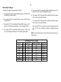
1
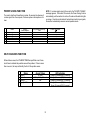
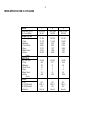
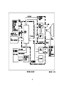
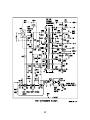
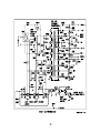
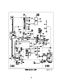
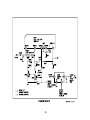
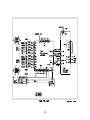
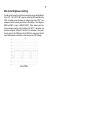
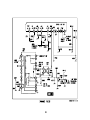
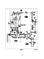
S CPD-420GS D98 Chassis Computer Monitor Circuit Description and Troubleshooting Course: MON-03 Training Manual Table of Contents D98 Chassis Specifications 1 OVP (Over Voltage Protection 21 Power Saving Function 2 UVP (Under Voltage Protection) 21 Self Diagnosis Function 2 OCP (Over Current Protection) 21 Timing Specification for CPD-420GS 3 Troubleshooting Protection Circuits 21 Troubleshooting Safety 4 No Power Troubleshooting 23 Overall Block 5 Feedback Circuit Troubleshooting 23 N Board 5 The AN8037 Power supply Controller 25 A Board 5 Troubleshooting Short Circuit Protection 27 H Board 5 Troubleshooting Secondary Circuits 29 D Board 7 Rectifier Section Troubleshooting 29 Power Supply 9 Troubleshooting Horizontal Centering 29 AC Input 9 +5V Standby Circuit 31 AC Input Troubleshooting 9 Troubleshooting +5V Standby Circuit 31 EMI Filter 9 +12V Regulator 31 9 Troubleshooting +12V Regulator 31 Degauss Circuit Heater Voltage Regulator 33 Degauss Troubleshooting 9 Start Up and “Active On” Operation 11 Troubleshooting Heater Voltage 33 Regulation 13 N Board 35 Secondary Voltages 15 Micro Standby and Reset (N Board) 35 “Active Off” and “Suspend/Standby” Operation 17 DSP Regulator 35 Secondary Voltages 19 Video and OSD Processing 37 Power Supply Protection Circuits 21 RGB Preamp 37 RGB Drive 39 Horizontal AFC 61 RGB OUT 39 Horizontal Size Control 63 RGB CUTOFF 41 Pin Keystone, Bow and Geometric Corrections 65 On Screen Display (OSD) 43 Horizontal Centering (Raster only) 67 ASC (Auto Size and Center) 43 Horizontal Linearity 69 Sub Contrast (Cutoff) control 45 Impedance Matching (S CAPS) 71 Brightness and Contract control 45 Horizontal Deflection Shutdown 73 G2 control and Spot Killer 47 Protection 73 Color Restoration 49 High Voltage Circuit 75 Color Restoration Circuit (Red only) 49 High Voltage 75 Color Restoration Function (Red only) 49 High Voltage Regulation 75 GPE Graphic Picture Enhancement 51 G2 (Screen) Voltage 75 Standard Mode 51 ABL (Auto Brightness Limiting) 77 Presentation Mode 51 HV Protection 79 Graphic/Video Mode 51 HV Shutdown 79 Plug and Play 53 ABL Shutdown 79 VGA 53 Dynamic Focus (DF) Circuit 81 What is Plug and Play? 54 Horizontal DF 81 Display Data Channel Circuit 55 Vertical DF 83 DDC1 55 Vertical Deflection 85 DDC2B and DDC2AB 55 Vertical Drive 85 DDC Data Format (EDID) 57 Vertical Geometric Corrections 85 Horizontal Deflection 59 Vertical Centering 87 Horizontal Drive 59 Vertical Feedback Pulse 87 Vertical Protection 89 Rotation and Vertical Key Circuits 91 Rotation 91 Vertical Key 91 Convergence Circuits 93 Static Convergence IC704 93 Dynamic Convergence IC701 95 1 D98 Chassis Specifications Picture tube 0.25 - 0.27 mm aperture grill pitch 19 inches measured diagonally 90 - degree deflection Trinitron Video image area Resolution (18" maximum viewing image) Approx. 365 x 274 mm (w/h) (14 3/8 x 10 7/8 inches) Horizontal: Max 1600 dots Vertical: Max 1200 lines Standard image area Approx. 352 x 264 mm (w/h) (13 7/8 x 10 1/2 inches) Input Signal Video Sync Analog RGB (75 ohms typical) 0.7 V p-p, Positive External HD/VD, Composite Polarity Free TTL Video Composite (Sync on Green) 0.3 V p-p, Negative Power Consumption Maximum Nominal Deflection frequency 130W 100W Horizontal: 30 to 96 kHz Vertical: 48 to 120 Hz AC input voltage / current 100 to 120V, 50/60 Hz, 1.7 A 220 to 240V, 50/60 Hz, 1.2 A Dimensions 444 x 467 x 455 (w/h/d) (17 1/2 x 18 1/2 x 18 inches) Mass Approx. 26 kg (57 lb 5 oz) Plug and Play DDC/DDC2B (Front/Rear input) DDC2Bi (Rear input only) Design and specifications are subject to change without notice. NOTE: If no video signal is input to the monitor, the “NO INPUT SIGNAL” message appears. After about 30 seconds, the Power Saving function automatically puts the monitor into active-off mode and the indicator lights up orange. Once the monitor detects horizontal and vertical sync signals, the monitor automatically resumes normal operation mode. POWER SAVING FUNCTION The monitor has three Power Saving modes. By sensing the absence of a video signal from the computer, it reduces power consumption as follows: S ta te 1 2 3 4 5 6 N o r m a l O p e ra tio n st S ta n d b y (1 m o d e ) nd S u s p e n d (2 m o d e ) rd A c tiv e - o ff (3 m o d e ) P o w e r- o ff F a ilu re m o d e s Pow er C o n s u m p t io n R e q u ir e d R e c o v e r y T im e P o w e r In d ic a to r ≤130W ≤ 15W ≤ 15W ≤ 8W 0W — — A p p ro x . 5 se c . A p p ro x . 5 se c . A p p ro x . 5 se c . — — G re e n o n G r e e n a n d o ra n g e a lte r n a te G r e e n a n d o ra n g e a lte r n a te O ra n g e O ff S e e S e lf D ia g n o s is F u n c tio n SELF DIAGNOSIS FUNCTION When a failure occurs, the STANDBY/TIMER lamp will flash a set of number of times to indicate the possible cause of the problem. If there is more than one error, the lamp will identify the first of the problem areas. Status 1 2 3 4 Failure 1 Failure 2 Failure 3 Aging/Self Test Area of Failure LED Indication HV or B+ H Stop, V Stop, Thermal ABL Orange (0.5 second)/Off (0.5 second) Orange (1.5 second)/Off (0.5 second) Orange (0.5 second)/Off (1.5 second) Orange (0.5 second)/Off (0.5 second) Green (0.5 second)/Off (0.5 second) 2 3 TIMING SPECIFICATION for CPD-420GS MODE R esolution (H x V ) D ot C lock (M H z) 1 2 3 720 x 400 28.321 1280 x 960 148.500 1600 x 1200 202.500 31.468 31.779 6.356 0.636 3.178 2.542 25.423 85.938 11.636 3.017 0.431 1.077 1.508 8.620 93.750 10.667 2.765 0.316 0.948 1.501 7.901 70.084 449 49 13 2 34 400 85.002 1011 51 1 3 47 960 75.000 1250 50 1 3 46 1200 NO Y E S -/+ NO N on Int NO Y E S -/+ NO N on Int NO Y E S -/+ NO N on Int H O R IZO N TA L H or. Freq. (kH z) H -Total H -B lanking H -Front P orch H -S ync. H -B ack P orch H -A ctive (usec) V E R TIC A L V er. Freq. (H z) V -Total B -B lanking V -Front P orch V -S ync. V -B ack Porch V -A ctive (lines) SYNC. Int (G ) E xt (H /V )/P olarity E xt (C S )/P olarity Int/N on Int Troubleshooting HINT: Troubleshooting Safety Visual inspection can play an essential part in any troubleshooting technique. A Visual inspection of components can lead to the problem area and the repair of the circuit at fault. Your eyes may be your best troubleshooting tools to use. WARNING: Before attempting to repair the power supply or any other circuit, safety should be considered first. Never connect test probes to the primary side circuits unless proper isolation has been provided. If isolation for the AC main input is not provided, serious harm can result. Never assume you are safe. 4 5 Overall Block N Board The N Board is mounted to the D Board via connectors CN1001 and CN801. The Microprocessor IC1001, EEPROM IC1005 and the DSP (Digital Signal Processor) IC1002 are located on the N board. IC1001 receives control inputs from the front panel buttons (H board) and the front and rear video inputs via the A board. IC1001 responds to the Timing and Sync parameters of the video inputs. IC1001 communicates with IC1005 via the I2C bus. IC1005 contains the operation, set up, factory preset and user preset data and is utilized by IC1001 to control the monitor circuits and to match the operating parameters to the input signals. IC1001 also controls IC1002 via the I2C bus and provides IC1002 with the necessary timing and sync parameters. IC1001 directly controls Input switching, Rotation, H. Cent, H Lin Bal, Degauss, Power Shutdown, Heaters, Remote On/Off and S Caps (Impedance Matching). IC1001 controls the Power Save Function, OSD (On Screen Display) and RGB DRIVE (A board). IC1001 also provides communication with DAS (Digital Alignment Software), CATS (Color Adjustment Tool for Service) and the DDC (Display Data Channel). IC1002 outputs Deflection Drive, Convergence and Geometry Correction Waveforms to their respective circuits located on the D board. A Board The main function of the A Board is to receive incoming video signals and process them into RGB video drives for the CRT. Video signals can be received either from the conventional 15 D-sub connector or via an additional 15 D-sub female connector input located on the front of the monitor. The purpose of this second input is to allow easy hookup to a laptop computer (video cable provided). The A Board circuitry buffers the Sync timing signals and provides OSD video. The Timing Analysis for the ASC (Auto Size Center) function and the Analog to Digital conversion for the Color Restoration function are also processed. Additional functions include the DDC information to the DDC equipped host computer and all CRT cathode operating voltages such as Heater, G2 (Screen) and Focus are either processed or passed to the CRT. H Board The User controls are located on the front bezel assembly of the monitor and provide the user with control of various monitor operations and functions. The LED provides the user with feedback as to the Power Saving and Failure condition of the monitor. 6 7 D Board (Power Supply) (Convergence) The Power Supply, which is located on the D Board, operates very similar to previous monitor chassis design such as the D1 chassis. This unit incorporates the use of a switch mode power supply. It has both PWM and RCC characteristics. The Power Supply has four modes of operation. Except for the AC power switch, three modes are controlled by IC1001 (N Board). The modes of operation are ‘Off’, ‘Active Off’, ‘Suspend/Standby’ and ‘Active On’. These modes are related to the Power Saving and Self Diagnosis functions. The Power supply provides all the necessary operating voltages along with Horizontal Centering and CRT Heater voltages. (High Voltage) (Deflection) The Horizontal and Vertical deflection circuits along with Horizontal Centering, Size, Rotation and Tilt are located on the D Board. The N Board provides these circuits with the necessary size, position and geometry parameters as required by the different video timing conditions and user adjustments. Impedance matching (S Caps) and Horizontal Linearity are also performed in the Horizontal deflection circuit as required by the different video timing conditions. Both Static and Dynamic Convergence circuits are located on the D Board. The N Board provides these circuits with the necessary geometry parameters as required by the different video timing conditions and user adjustments. The convergence circuits provide two-dimensional (H and V) correction patterns that are applied to the convergence yoke. The HV generation and regulation circuits are located on the D Board. The N Board provides the HV circuits with the necessary drive parameters required by the different video timing conditions. The HV circuit provides the CRT with Anode, Focus and Screen voltages required for proper CRT operation. The D98 chassis is also equipped with Dynamic Focus circuitry located on the D Board. The Dynamic Focus circuit, controlled by the N Board, provides the necessary focus control voltage for the outer edge areas of the screen as required by the different video timing conditions. 8 9 Power Supply Overview The power supply in this unit is a switch mode power supply. The power supply is rated to operate with an AC input voltage range of 100V - 240V. Current input is 1.2 - 1.7 A. The output of the power supply produces +180V, +80V, ±16V, +12V and +5V DC from the AC input. In addition, it provides +6.3V DC for the CRT Heater and an isolated ±8V DC output to the Horizontal Centering circuits. It has a fold back mode used for the Power Saving and Failure (Shutdown) operations. This chassis incorporates the use of a single power supply control IC601. IC601 provides most of the power supply control except for output power switching provided by Q602 (POWER SWITCH). AC Input The AC input section provides EMI filtering, input protection, surge limiting and CRT degauss operation. AC Input Troubleshooting For No Power or Dead Set condition, the AC Input circuitry should be checked. F601 should be checked for continuity. CN603 to the H Board and the AC power switch S601 should be checked for continuity. Further checks should be made to R602, TH600 and D601 respectively if no problems can be identified. EMI Filter The EMI filter comprises X - capacitors C601 and C602, Y - capacitors C603, C604, C605 and C606 and the line filter transformer LF602. Input protection is provided by F601 and surge current limiting by thermistor TH600 and resistors R602 and R603. Degauss Circuit The Degauss Circuit is used to demagnetize or degauss the CRT. During ‘Active On’ mode, the Micro IC1001/5 (N Board) sets the Degauss signal to digital H (+5V). The Degauss signal via CN1001 pin 25 to CN801 pin 25 (D Board) is applied to Q670 (DEGAUSS SW). Q670 turns ON and activates relay RY601. This allows AC current to flow to the degauss coil through posistor THP602. The current heats up THP602 posistor and its affective resistance increases. This dampens the current in the degauss coil to nearly zero allowing the magnetic field to decay gradually. After approximately 5 seconds, IC1001/5 sets the Degauss signal to digital L (0V). The Degauss signal via CN1001/25 to CN801/25 (D Board) is applied to Q670 (DEGAUSS SW). Q670 turns OFF and deactivates relay RY601. The degauss coil should sufficiently demagnetize the CRT. Degauss Troubleshooting The malfunction of the degauss circuit can be a loss of the degauss signal from the N Board. The +5V DC degauss signal can be checked at CN801/ 25 and should be present for approximately five seconds once AC power is applied. The activation of RY601 through Q670 can also be heard. Further checks to THP602 and VA601 should be checked respectively. Another method of verifying the degauss circuit operation is to use the manual degauss operation found in the OSD menu. DEGAUSS COIL N BOARD IC1001/5 2 5 CN1001 D BOARD ! VA601 1 1 4 DEGAUSS CN601 1 1 THP602 1 12V 25 RY601 D670 R672 F601 4A 250V + C601 C606 L + 3 C602 G C605 FB608 1 R601 AC IN + 2 C604 + + + FB607 D601 C603 4 R602 CN610 GND R670 R671 LF602 N Q670 CN 801 4 FB609 CN603 1 E1 4 R603 TO T601 + Q602 TH600 F1 CN2003 1 S602 H BOARD 10 POWER SWITCH AC INPUT D98MON 11 Start Up and ‘Active On’ Operation The Power Supply uses a flywheel type switch mode supply. It has both PWM and RCC (Resistor and Capacitor) characteristics. The PWM controls the pulse width of the gate drive. The RCC portion insures that the next conduction cycle starts at zero volts. Therefore, the gate pulse width varies and the switching frequency varies. Once start up voltage is applied, IC601/6 (OUT) outputs PWM drive to the gate of Q602 (POWER SWITCH). The PWM frequency will vary between 65kHz to 120kHz depending upon input voltage and power level. The PWM drive from Q602 is applied to T601/2. T601 develops all the secondary operating voltages. After start up, the output from T601/8 through R623 is rectified by D605 and provides VCC +17V DC through D624 and D657 to IC601/7 during normal ‘Active On’ operation. When Power switch S601 (H Board) is closed, AC (100V - 240V) is applied to D601 full wave rectifier. +160V DC (110V AC in) is applied through R603, L604 and R615 to T601/5 (SWITCHING TRANSFORMER). Start up current is supplied from D601 (half wave rectified), through R613 to IC601/7 (VCC). Start up voltage at IC601/7 is approximately +12V DC. Q602/Drain IC601/6 PWM 12 13 Regulation Overall regulation is accomplished by varying the feedback voltage to IC601/9 (FB). The secondary +16V DC supply via R631, D614 and R658 provide IC603/1 with a reference voltage. The secondary +180V DC supply is voltage divided by R659, R663 and R660 to provide IC652/1 (ERROR AMP) with a sample of the +180V DC supply. IC652/3 is applied to IC603/2 to control the feedback output of IC603/4 while maintaining electrical isolation between chassis ground and AC input ground. The signal at IC603/4 is applied to IC601/9 (FB). As a result, IC601/6 responds accordingly to adjust the duty cycle and frequency output applied to Q602 by regulating the secondary B+ (+180V DC) voltage. IC1001/7 (N Board) ‘REMOTE ON/OFF’ command is set H (+5V) which turns Q656 ON and turns Q658 OFF, this allows IC652/3 to control feedback. IC652 is a shunt regulator and controls the current through IC603 pin 1 and pin 2. Any change in the B+ voltage will cause IC652 pin 3 to vary in voltage inversely proportional to the B+. Q602/Drain IC601/6 PWM 14 15 Secondary Voltages The following voltages are produced by T601 SRT. 5. The output at T601/18 is rectified by D653 and D656 to produce -16V DC and -16V-2 DC used for the deflection circuits. 1. The output at T601/13 is rectified by D650 to produce +183V DC used for deflection and video circuits. 6. The output at T601/10 through R621 is rectified by D648 to produce the H+ used for Horizontal Centering. 2. The output at T601/14 is rectified by D651 to produce +80V DC used for video circuits. · The output at T601/12 through R622 is rectified by D649 to produce the H- used for Horizontal Centering. 3. The output at T601/16 is rectified by D652 and D655 to produce +16V DC and +16V-2 DC used for deflection, +5/+12V Regulator IC605. · The output at T601/11 is used for the H+ and H- floating ground reference. The H+ and H- voltages in reference to floating ground are ±8V. 4. The output at T601/17 is rectified by D654 to produce +7V DC used for +5/+12V Regulator IC605 and +6.3V Heater regulator IC604. NOTE: Care should be taken not to short the floating ground to the secondary ground. SECONDARY VOLTAGES OUTPUT B+ +80V +16V -16V +12V +8V +5V Heaters H. Centering OFF 0 0 0 0 0 0 0 0 0 'Active OFF' +145V +62V +9V -12V 0 +5.5V +5V 0 ±5V 'Suspend/Standby' +145V +62V +9V -12V 0 +5.5V +5V +3.2V ±5V 'Active ON' +183V +80V +16V -16V +12V +7V +5V +6.3V ±8V 16 17 ‘Active Off’ and ‘Suspend/Standby’ Operation The power supply enters the ‘Active Off’ and ‘Suspend/Standby’ mode under the following conditions… 1. Loss of H and/or V Input Sync signals · LED illuminates Orange 2. Loss of Horizontal Deflection feedback · LED illuminates Orange (1.5 seconds) / Off (0.5 seconds) The ‘Active Off’ and ‘Suspend/Standby’ modes are controlled by the ‘REMOTE ON/OFF’ signal from the Micro IC1001/7 (N Board). Feedback is provided by circuit elements IC603, D631, D632, R662, Q656 and Q658. During ‘Active Off’ and ‘Suspend/Standby’ modes, the ‘REMOTE ON/OFF’ signal from IC1001/7 is L (0V) and is applied to Q656 turning it OFF, thus turning Q658 on to disable IC652. Current flows through Q658 (E - B), R662 and D632 biasing Q658. This allows standby current to flow through IC603 pin 1 and pin 2, D631 and Q658 (C - E). The output of IC603/4 outputs sink current from IC601/9 (FB). As a result, IC601/6 responds accordingly to adjust the duty cycle and frequency output applied to Q602 in order to produce the reduced unregulated output voltages. 3. Loss of Vertical Deflection feedback · LED illuminates Orange (1.5 seconds) / Off (0.5 seconds) 4. If Beam current (ABL) becomes excessive · LED illuminates Orange (0.5 seconds) / Off (1.5 seconds) 5. If HV becomes excessive · LED illuminates Orange (0.5 seconds) / Off (0.5 seconds) IC601/6 PWM 6. Loss of secondary voltages · LED illuminates Orange (0.5 seconds) / Off (0.5 seconds) Q602/Drain 18 19 Secondary Voltages Under ‘Active Off’ and ‘Suspend/Standby’ modes, the following voltages are produced by T601. 5. The output at T601/18 is rectified by D653 and D656 to produce -12V DC and -12V-2 DC used for the deflection circuits. 1. The output at T601/13 is rectified by D650 to produce +145V DC used for deflection and video circuits. 6. The output at T601/10 through R621 is rectified by D648 to produce the H+ used for Horizontal Centering. 2. The output at T601/14 is rectified by D651 to produce +62V DC used for video circuits. · The output at T601/12 through R622 is rectified by D649 to produce the H- used for Horizontal Centering. 3. The output at T601/16 is rectified by D652 and D655 to produce +9V DC and +9V-2 DC used for deflection, +5/+12V Regulator IC605. · The output at T601/11 is used for the H+ and H- floating ground reference. The H+ and H- voltages in reference to floating ground are ±5V. 4. The output at T601/17 is rectified by D654 to produce +5.5V DC used for +5/+12V Regulator IC605 and +6.3V Heater regulator IC604. NOTE: Care should be taken not to short the floating ground to the secondary ground. SECONDARY VOLTAGES OUTPUT B+ +80V +16V -16V +12V +8V +5V Heaters H. Centering OFF 0 0 0 0 0 0 0 0 0 'Active OFF' +145V +62V +9V -12V 0 +5.5V +5V 0 ±5V 'Suspend/Standby' +145V +62V +9V -12V 0 +5.5V +5V +3.2V ±5V 'Active ON' +183V +80V +16V -16V +12V +7V +5V +6.3V ±8V 20 21 Power Supply Protection Circuits OVP (Over Voltage Protection) During normal ‘Active On’ operation, the output of T601/8 through R623 is rectified by D605 and provides +17V DC through D624 and D657 to IC601/ 7 (VCC). In the event that the regulation or feedback loops fail, the secondary output voltages may rise rapidly. The output of T601/8 would also rise and is sensed at IC601/7 (VCC) which internally has a threshold of approximately +19V DC. Once this threshold is reached, IC601/6 will latch to eliminate drive to Q602, resulting in power supply shut down. Once IC601 is latched, you must turn the AC power OFF and ON again to restart the power supply. UVP (Under Voltage Protection) The input at IC601/7 (VCC) is also used to sense an Under Voltage condition. Under Voltage occurs when the input at pin 7 (VCC) is less than +9.5V DC. Once this threshold is reached, IC601 will latch and disable the output at pin 6 (OUT) going to Q602 resulting in power supply shut down. Once IC601 is latched, you must turn the AC power OFF and ON again to restart the power supply. OCP (Over Current Protection) OCP is activated if there is excessive current passing through Q602 (POWER SWITCH). R609 is used for current sensing. Current through R609 will cause a negative voltage drop in reference to HOT ground. R608, R606 and C615 couples this voltage drop to IC601/4 (CLM). Should this voltage level exceeds -0.18V, IC601 will enter the cycle by cycle current limiting mode. To prevent premature OCP sensing, Q605 and IC606 provide a Soft Start to IC601/2 (CCP) to prevent OCP during start up. Troubleshooting Protection Circuits Each protection circuit can be isolated to their respective defect. The power supply can be operated in the “Active Off’ mode to better troubleshoot each circuit under reduced voltage condition by simply removing the N Board. 22 23 No Power Troubleshooting (IC601 Troubleshooting) First apply AC to the monitor and check IC601/6 output. If the output at pin 6 is not present or briefly appears there could be problems with Q602 and related components. Check VCC at IC601/7. If the voltage is less than +9V DC, IC601 could be in the latch mode. If the voltage is very low, R613, R623, D605, D624 and D657 should also be checked respectively. If no problems can be identified, in reference to Hot ground, check the impedance of each pin at IC601. If any of these pins are shorted, replace IC601 and check components connected to the related pins. Take care that C616 and C619 are fully discharged before replacing IC601. (Q602 Troubleshooting) Q602 can be damaged in various ways such as voltage, current and temperature. Check Q602 for shorts. Further checks to F601, R609 and R615. Additional components to check are D603, D604 and IC601. There is also a clamp circuit, which is used to clip the turn off spike found on Q602 (D). Check D615, C624 and R619. Q602/Drain Feedback Circuit Troubleshooting IC601/6 PWM Problems with the feedback circuits can cause power supply shut down or low voltages. First determine whether the power supply is operating in ‘Active Off’, ‘Active On’ modes or not at all. The power supply can be stuck in ‘Active Off’ mode. The Remote ON/ OFF signal from the N Board, Q656, Q658, IC603 and IC652 can affect this condition. In addition, check the protection circuits. 24 25 The AN8037 Power Supply Controller IC601 The heart or the primary section is the AN8037 Power Supply Controller, IC601. The following table describes the function of each pin. Pin 1 TR This is TR or Transform er R eset. Sim ilar to a dem agnetization function, this pin detects the falling edge of the prim ary waveform during relaxation period. It allows the next conduction pulse only after reaching the bottom of the ringing waveform . Pin 2 O CP Pin 3 CF Pin 4 CLM O ver current protection. U sed to determ ine the overload level at w hich the tim er latch is activated. Pin 5 G ND Pin 6 O UT Pin 7 VC C IC ground term inal. Pin 8 SD Pin 9 FB O scillator. W ith a capacitor, determ ines the switching frequencies. (On/O ff tim es) O ver current protection. If the voltage on this pin (prim ary current feedback) exceeds -0.18V, the pow er supply w ill enter cycle by cycle current lim iting m ode. O utput driver for switching transistor Q 602. IC 601 supply voltage term inal. This voltage is norm ally +17.5V D C during 'A ctive O n' m ode and +12V D C during 'A ctive O ff' and 'S uspend/Standby' m ode. The IC receives starting current via startup resistor R 613 until the auxiliary supply is available from T601 VC C w inding. If the voltage on this pin exceeds +19.4V DC , O VP is activated and the power supply shuts off and can only be restarted by disconnecting and reconnecting the A C line. Under voltage lock out (UV P) occurs w hen the voltage is less than +9.5V DC . U sed for the O VP and tim er latch functions. A capacitor determ ines the tim ing for O VP function. Feedback term inal. 26 27 Secondary Short Circuit Protection Short Circuit Protection for the secondary low voltage supplies are detected in different ways. 1. The “B+ DET” line is used to detect the loss of the -16V DC supply through circuit elements R611 and R612. R611 is connected to the +5V DC from IC605 and R612 is connected to the -16V DC supply from T601. The node voltage between R611 and R612 is monitored by the Micro IC1001/14 (N Board). If the node voltage exceeds +2V DC, IC1001/6 goes H (+5V) turning Q657 ON, shunting normal regulation feedback. This causes IC601 to increase the drive output to the point of OVP latch via pin 7(VCC). Note: LED illuminates Orange (0.5 seconds) / Off (0.5 seconds) 2. The +16V, +12V and +5V DC secondary voltages are monitored through circuit elements D641, Q640 and R641. The +80V DC from T601 through R641 is applied to Q640 (C). Normally the +5V DC from IC605 and D641 turns Q640 ON and Q657 OFF. If there is a substantial short circuit on any of the secondary low voltage supplies, the +5V DC standby supply can be attenuated. If it goes lower than +3V DC, Q640 will turn OFF. With Q640 OFF, Q657 turns ON to bypass the feedback voltage from IC603. This causes IC601 to increase the drive output to the point of OVP latch via pin 7. Troubleshooting Short Circuit Protection The power supply can be operated in the “Active Off’ mode to better troubleshoot each circuit under reduced voltages by simply disabling the ‘REMOTE ON/OFF’ line from the N Board by lifting pin 16 of CN801. Q640 and Q657 should be check respectively. 28 29 Troubleshooting Secondary Circuits Troubleshooting Horizontal Centering Failures in these sections are interrelated and one circuit can affect another. Consequently, some failures will also affect the primary circuit. A loss of the Horizontal Centering adjustment can be caused by the failures of rectifier diodes, fusible resistors, IC502 and related components. Measure the +/- voltages in reference to the horizontal centering ground (HN). Typically, the voltages are ±8V DC. However, the adjustment setting can reduce the voltages by approximately 1V. If there are no problems found at the Horizontal Centering supply, troubleshoot the Horizontal Centering circuitry. Rectifier Section Troubleshooting Rectifier diode failures are not common, but do occur. Deflection (D Board), Video (A Board) and N Board failures contribute to diode damage. In the event, a voltage is not present, check for shorts to ground or open or shorted diodes. Also, check for any open fusible resistor and shorted zener diodes found on the supply lines. 30 31 +5V Standby Circuit +12V Regulator During ‘Active Off’ and ‘Suspend/Standby’ modes, the +8V DC secondary supply applied to IC605/1 (INPUT1) and Q601/C is reduced to +5.5V DC. In order to prevent loss of the +5V DC Standby, it is necessary to supply a back up voltage. During ‘Active Off’ and ‘Suspend/Standby” modes, the +16V DC supply is reduced to +9V DC and is applied to IC605/2 (INPUT2). The ‘REMOTE ON/OFF’ control signal from IC1001/7 is L and is routed to IC605/3 (DISABLE), which disables the +12V DC regulated output. During ‘Active Off’ mode, the +16V DC secondary supply source is reduced to +9V DC and is applied Q601/E. Q607 is OFF which turns Q606 and Q601 ON. Q601 then outputs +9V DC to provide power to IC605/1 (INPUT1). Finally, at the same time, IC605/7 (OUTPUT1) outputs regulated +5V DC. During ‘Active On’ modes, the +16V DC supply is applied to IC605/2 (INPUT2). The ‘REMOTE ON/OFF’ control signal from IC1001/7 is H (+5V) and is routed to IC605/3 (DISABLE) to enable the +12V DC output at pin 6 (OUTPUT2). Troubleshooting +12V Regulator During normal operation, the +8V DC supply is used to provide VCC voltage to IC605/1. The “Back-up” supply circuit (Q601) is shut down via the ‘REMOTE ON/OFF’ command from IC1001/7. Troubleshooting +5V Standby Circuit The loss of the +5V DC Standby voltage may appear as a no power symptom. Check the +16V DC source, R617, Q601, Q606, Q607, IC605 and related components. Check the +8V DC source, D654, R654 and D610. During the ‘Active On’ mode, confirm the presence of +12V DC at IC605/ 6 (OUTPUT2). If missing, verify that a H is present at IC605/3 (DISABLE). 32 33 Heater Voltage Regulator Troubleshooting Heater Voltage Heater filament voltage is developed by the +8V DC supply to IC604/1 (I). During ‘Active On’ mode, IC1001/8 (N Board) outputs the “HEATER” control line H (+5V) which is routed to IC604/4 (VC) to enable the +6.3V DC Heater supply voltage output at pin 2. A loss of Heater Voltage will result in a no picture condition. During ‘Active On’ mode, confirm IC1001/8 (N Board) outputs ‘HEATER’ control line H (+5V) to IC604/4 (VC) to enable the +6.3V DC Heater supply voltage. Also check for shorts or an open on the A Board and the CRT. During ‘Standby/Suspend’ mode, the power supply is operated at reduced voltages. As a result, the input voltage to IC604/4 (VC) is +5.5V DC. The output from IC604/2 is also reduced to +3.2V DC keeping the heaters of the CRT active on during the power saving function. This allows the CRT to quickly display the information or video during the ‘Standby/Suspend’ to ‘Active On’ transition. During ‘Active Off’ mode, IC1001/8 (N Board) outputs a L (0V) to IC604/4 (VC) disabling the +6.3V DC Heater supply voltage. 34 35 N Board Micro Standby and Reset (N Board) The +5V DC Standby supply from IC605 (D Board) is routed to IC1001 pin 11 and pin 31 providing VCC operating voltage. The +5V DC standby supply is also applied to the RESET IC1003/1. IC1003 produces a “Reset” pulse at pin 3 when the unit is first turned ON. The 8Mhz master clock is developed by X1001 IC1001 pin 44 and pin 45. When the unit is first powered ON, the Degauss command line of IC1001/ 5 goes H (+5V) for approximately 5 seconds then returns to a logic L (0V). At the same time, the ‘REMOTE ON/OFF’ command from IC1001/7 goes H (+5V). This signal is routed to the D Board via CN801/16 to enable the ‘Active On’ mode of the power supply. DSP Regulator The DSP IC1002 requires +3.3V DC for proper operating. IC1006/3 (O) outputs regulated +3.3V DC to IC1002 pins 9,12, 28 and 52. IC1003 provides IC1002/54 (RESET) with a delayed “RESET” H (+5V) via R1105. The DSP outputs Deflection Drive, Convergence and Geometry Correction Waveforms to their respective circuits located on the D board. NOTE: With AC power applied, the output waveforms from the Micro and DSP should always be present. 36 37 Video and OSD Processing RGB PREAMP The V OUT Sync signal from IC008/21 (V OUT) is routed to the N Board. The H OUT Sync signal from IC008/22 (H OUT) is input to the H DRIVE BUFFER IC006 pin 8 and pin 9. IC006 buffers the H OUT signal which is output at pin 4 is routed to the N Board. The RGB PREAMP IC008 receives the RGB and Sync signals from two sources. One is the conventional 15 D-sub connector and the other is the 15 D-sub female connector input located on the front of the monitor. The purpose of this second input is to allow easy hookup to a laptop computer. The RGB signals from the conventional 15 D-Sub connector are input to IC008 pin 2 (B), pin 5 (G) and pin 7 (R). The Sync signals are input to IC008 pin 8 (H) and pin 9 (V). The RGB signals from the additional 15 D-Sub female connector are input to IC008 pin 11 (B), pin 13 (G) and pin 16 (R). The Horizontal and Vertical Sync signals are input to IC008 pin 17 (H) and pin 18 (V). IC008 switches between inputs selected by the user via the front panel button. IC1001/1 (N Board) logic output selects the input source via CN1004/2 to CN309/2 ‘INPUT SW’ to the A Board. The ‘INPUT SW’ signal is routed to IC008/19 (SW) to select the conventional 15 D-Sub connector input or to select the 15 D-Sub female connector from the front panel. CN309/7 H SYNC The R G B input signals are then buffered and output from IC008 pin 27 (R OUT), pin 30 (G OUT) and pin 35 (B OUT) to IC001. IC008/27 R OUT CN309/5 VS OUT 38 39 RGB DRIVE RGB OUT The RGB outputs from IC008 are input to the RGB DRIVE IC001 pin 7 (B IN), pin 9 (G IN) and pin 11 (R IN). The G signal is also low pass filtered and input to IC001/10 (SYNC IN). The Sync on Green signal is processed and output at IC001/30 (C.SYNC) as composite sync which is routed to the N Board. IC1001 (N Board) also provides IC001 pin 12 (CLAMP) and pin 18 (BLK) with the necessary Clamping and Blanking signals required from the Timing and Sync parameters of the video input. IC001 outputs the R G B signals at pin 20 (R OUT), pin 24 (G OUT) and pin 27 (B OUT). The RGB outputs from IC001 are applied to RGB OUT IC002 pin 8 (R. IN), pin 9 (G. IN) and pin 11 (B. IN). IC002 provides the final amplifier stage for the RGB video signals. The output of IC002 pin 1 (B. OUT), pin 3 (G. OUT) and pin 5 (R. OUT) drive the CRT cathodes via AC coupling. The output drive levels are approximately 45V p-p. IC001/20 R OUT CN309/1 C BLK IC002/5 R OUT CN309/3 CLP 40 41 RGB CUTOFF The RGB Cutoff levels can only be adjusted via the DAS/CATS software or by the Color Restoration function (explained later). IC1001 on the N board, via the I2C data bus controls IC001 D/A outputs at pin 3 (R BKG), pin 4 (G BKG) and pin 5 (B BKG). The D/A outputs from IC001 are input to CUTOFF AMP IC004 pin 1 (B.IN), pin 3 (G.IN) and pin 4 (R.IN) which sets the CRT Red, Green and Blue cathode DC cutoff level. The output of IC004 pin 7 (R.CUT), pin 10 (G.CUT) and pin 13 (B.CUT) clamp the CRT Red, Green and Blue cathodes. The +180V DC with pull-up resistors R109, R209 and R309 and D106, D206 and D306 form the voltage divider network for the R G B cutoffs respectively. 42 43 On Screen Display (OSD) ASC (Auto Size and Center) IC003 (OSD) is the On Screen Display character and graphic generator. IC1001 (N Board) via the I2C data bus controls IC003 at pin 3 (SDA) and pin 4 (SCL). The N Board also provides IC003 pin 5 (HSYNC), pin 6 (VSYNC) and pin 7 (HFLY) with the necessary sync timing signals. IC003 provides OSD R, G, B and Fast Blanking to RGB DRIVE IC001 for mixing the OSD with the main video signal. The OSD R G B signal is output from IC003 pin 14 (ROUT), pin 15 (GOUT) and pin 16 (BOUT) and is input to IC001 pin 13 (B OSD), pin 14 (G OSD) and pin 15 (R OSD). The Fast Blanking signal is output from IC003/17 (FBLK) and is input to IC001/17 (OSD BLK) which blanks the area where the OSD is to be displayed. The ASC function automatically adjusts for proper size and centering of the video image on the screen. This is provided by IC003 (OSD). The HSYNC, V.SYNC and HRTRC signals from the N Board are input to IC003 pin 5 (HSYNC), pin 6 (VSYNC) and pin 7 (HFLY). When the ASC function is selected, IC001/16 (V DET) outputs composite blanking to IC003/8 (AV). This signal is processed by IC003, which outputs correction data via the I2C data bus to the N Board for proper Size and Centering calculations. This corrects the H Phase/H Size and V Size/Centering of the video signal. IC003/8 AV IC001/17 OSD BLK The +12V DC supply from the D Board is input to IC009/1. IC901/3 outputs regulated +5V DC to IC003 pin 9 and pin 19 providing VCC operating voltage. IC003/7 HFLY 44 45 Sub Contrast (Cutoff) control Brightness and Contract control The Sub Contrast levels can only be set by the DAS/CATS software for White Balance adjustment. When Sub Contrast is adjusted, the Micro IC1001 (N Board) via the I2C bus instructs IC001 to vary the DC level of pin 3 (R BKG), pin 4 (G BKG) and pin 5 (B BKG). The DC levels are then input to CUTOFF AMP IC004 pin 1 (B.IN), pin 3 (G.IN) and pin 4 (R.IN). The output of IC004 pin 7 (R.OUT), pin 10 (G.OUT) and pin 13 (B.OUT) are used to set the DC level of the R G B cathodes respectively. The +180V DC with pull-up resistors R109, R209 and R309 and D106, D206 and D306 form the voltage divider network for the R G B cutoffs respectively. The Brightness and Contrast levels can be controlled either by the user or via DAS/CATS software. When Brightness is adjusted, the Micro IC1001 (N Board) via the I2C bus instructs IC001 to vary the DC pedestal level of the RGB outputs. When Contrast is adjusted, IC001 varies the P-P amplitude of the RGB outputs. IC001 outputs the RGB signal at pin 20 (R OUT), pin 24 (G OUT) and pin 27 (B OUT). IC001/20 R OUT 46 47 G2 control and Spot Killer The G2 source voltage from the D board enters the A board via CN301/1 via R048 and R064. The node between R048 and R064 is connected to the CUTOFF CTRL circuit comprised of IC005 and Q001. The G2 adjustment can only be performed using the DAS/CATS Software or the Color Restoration function (explained later). The Micro IC1001 (N Board) via the I2C bus instructs IC001 to vary the DC level of pin 6 (G2). This voltage is routed to the non-inverting input of IC005/5 (CUTOFF CTRL). The DC output from pin 7 (OUT) is input to Q001/E and output at Q001/C configured as a common base amplifier. Q001/C is connected to the node between R048 and R064. By varying the DC voltage at this node, the DC level at J001/10 G2 of the CRT can be adjusted. C028 provides bias to Spot Killer Q001/B during power OFF, reducing the G2 voltage to minimum. 48 49 Color Restoration OVERVIEW The Color Restoration function can be performed by the user to restore the White Balance of the CRT. The CRT beam current is measured when White Balance is performed via the DAS/CATS software. The CRT beam current is converted to a voltage and stored in registers. During the Color Restoration function, these registers are sampled and the CRT beam current is adjusted until they equal the values stored in the registers. The Color restoration function can only be accessed via the OSD menu and activated after an initial warm up period of approximately 30 minutes. Color Restoration Circuit (Red only) The Color Restoration circuit is comprised of the Micro IC1001 (N Board), IC001 (RGB DRIVE), IC003 (OSD), IC004 (CUTOFF AMP), CRT and the current sensing components. Each of the Red, Green and Blue cathode beam current sensing circuits are identical and only the Red cathode beam current circuit will be explained. As the video image changes, the Red cathode beam current also changes. This current change flows through R116, R122 and R108 to CUTOFF AMP IC004/6 (R.B.C.F.). The P-P video level is AC coupled by C121, DC clamped by D120 and rectified by D108. This voltage level is input to IC003/22 (RCI) where it is A/D converted by IC003. This digital value of the Red cathode beam current is stored in an individual register. During the White Balance adjustment via the DAS/CATS software, the average DC level is sensed and stored in the registers. Color Restoration Function (Red only) The Color Restoration function is activated via the OSD menu only after an initial warm up period of approximately 30 minutes. When the Color Restoration function is activated, the Micro IC1001 (N Board) via the I2C bus instructs IC003 (OSD) to output an all white pattern to be displayed on the screen. IC003/22 (RCI) samples the Red beam current input and compares this DC level to the level stored in the register. If the levels are not the same, IC003 outputs correction data via the I2C data bus to IC1001 (N Board). IC1001 (N Board) via the I2C data bus instructs IC001 to vary the DC level output at pin 3 (R BKG) and the P-P level output at pin 20 (R OUT). The DC and P-P levels are varied until the measured beam current is equal with the level stored in IC003 register. Once the Color Restoration function is completed, the input video signal is displayed. 50 51 GPE Graphic Picture Enhancement Overview Through the front panel GPE control, this unit provides the user with the ability to choose three preset modes of picture quality. Presentation Mode When the Presentation Mode is selected, IC1001 (N Board) via the I2C data bus communicates with IC001 (RGB DRIVE). IC001 increases the P-P levels approximately 200mV (5%) of the RGB output signal at pin 20 (R OUT), pin 24 (G OUT) and pin 27 (B OUT). In addition, IC001 decreases the R BKG, G BKG and B BKG DC level approximately 100mV. 1. Standard Mode Graphic/Video Mode 2. Presentation Mode When the Graphic/Video Mode is selected, IC1001 (N Board) via the I2C data bus communicates with IC001 (RGB DRIVE). IC001 increases the P-P levels and via internal detail amp increases the high frequency response of the R G B output signal at pin 20 (R OUT), pin 24 (G OUT) and pin 27 (B OUT). 3. Graphics/Video Mode When the GPE button is pressed, IC003 (OSD) displays to the user, that Standard, Presentation or Graphics/Video mode has been selected. The result is a change in picture brightness in Presentation mode, to a change in picture brightness and sharpness in the Graphics/Video mode. Standard Mode In the Standard Mode, no effects to the RGB signals are performed. The unit defaults to the Standard Mode upon power on and power save modes. IC001/20 R OUT 52 53 Plug and Play VGA (VESA DDC) VGA = Video Graphics Adapter or Video Graphics Array VESA = Video Electronics Standards Association DDC = Display Data Channel (At the video card) (At the monitor cable) 15 PIN HIGHDENSITY D-SUB FEMALE at the video card. 15 PIN HIGHDENSITY D-SUB MALE at the monitor cable. Pin Name 1 2 3 4 5 6 7 8 9 10 11 12 13 14 15 RED GREEN BLUE RES GND RGND GGND BGND +5V SGND ID0 SDA HSYNC or CSYNC VSYNC SCL Dir → → → → ← ↔ → → ↔ Description Red Video (75 ohm, 0.7V p-p) Green Video (75 ohm, 0.7V p-p) Blue Video (75 ohm, 0.7 V p-p) Reserved Ground Red Ground Green Ground Blue Ground +5V DC Sync Ground Monitor ID Bit 0 (optional) DDC Serial Data Line Horizontal Sync (or Composite Sync) Vertical Sync DDC Data Clock Line Note: Direction is Computer relative Monitor. What is Plug and Play Currently there are several levels of Plug and Play compliance. DDC1 (Display Data Channel 1) capable monitors can communicate with the display adapter in only one direction through an unused line on the standard VGA cable. The DDC1 type of communication is the type of data channel from the display to the host, continuously transmitting Extended Display Identification (EDID) information. The video adapter is told what monitor is connected and its maximum resolutions and refresh rates. DDC2B goes one step further by offering bi-directional communications through two unused VGA lines between the monitor and the video adapter. The DDC2B communication channel is based on the I2C protocol. The host (graphics card) can request EDID or VDIF (Video Information) information over the DDC2B channel. Not only is DDC2B faster, it allows the operating system to query the monitor for supported features and inform you of any configuration changes. For your monitor to be fully Plug and Play compatible, it must have both DDC1 and DDC2B capabilities. With a Plug and Play video adapter, you are able to change resolutions and colors without having to restart your computer. Since the ACCESS.bus conveys information directly to your system, mice and keyboards as well as other compatible components can be plugged and unplugged without having to restart your computer. Especially useful for monitors, the ACCESS.bus allows you to adjust your screens image using a mouse and keyboard. This not only eliminates the need to push buttons on the display, it allows you to store monitor settings under meaningful names that are easily recalled. The newest standard, USB (Universal Serial Bus), includes all the capabilities of ACCESS.bus, but transmits and receives data at a much faster rate. Instead of 400K/sec., USB will be able to communicate at an incredibly fast 12MB of data per second, which makes it ideal for digital video and telephony. Because of its transmission capabilities, USB is expected to win over the current ACCESS.bus standard and will be the one to watch as Plug and Play continues to mature. Designers are developing innovations to keep pace with Plug and Play, such as a communication cable that plugs into a port similar to a telephone jack on the monitor. With the introduction of the ACCESS.bus (or DDC2AB compatibility), include DDC2B bi-directional communication and to add connectivity between many devices. ACCESS.bus peripherals can be daisy chained in any order so that everything plugs into one port on the back of your computer system. 54 55 Display Data Channel Circuit DDC1 The front input supports DDC1 communications. The front input cable pin 12 (SDA) and pin 15 (SCL) are connected to CN312 pin 1 (DDCSCL) and pin 2 (DDCSDA) on the A Board. IC007 EEPROM pin 5 (SDA) and pin 6 (SCL) provides the host with DDC1 communication. The V Sync input to IC007/7 (VCLK) is used to synchronize the timing of the data reading cycle. DDC2B and DDC2AB The rear input supports DDC2B and DDC2AB communications. The rear input cable pin 12 (SDA) and pin 15 (SCL) are connected to CN310 pin 2 (DDCSCL) and pin 3 (DDCSDA) on the A Board. The data is passed through the A Board to CN311 pin 2 (DDCSCL) and pin 3 (DDCSDA). CN311 is connected to the N Board via connector CN1003 pin 2 (DDCCLK) and pin 3 (DDCDATA) and are input to IC1001 pin 34 (DDCCLK) and pin 35 (DDCDATA). IC007/7 VCLK CN311/3 DDCSDA 56 57 DDC Data Format (EDID) Number 8 Bytes 10 Bytes 2 Bytes 5 Bytes 10 Bytes 3 Bytes 16 Bytes 72 Bytes 1 Byte 1 Byte Basic EDID consist of 128 bytes Description Header Vendor / Product Identification EDID Version / Revision Basic Display Parameters / Features Color Characteristics Established Timings Standard Timings Detailed Timing Description Extension Flag Checksum NOTES 58 59 Horizontal Deflection Overview The Micro IC1001 and DSP IC1002 (N Board) respond to the Timing and Sync parameters of the video inputs and provide the necessary Horizontal Drive and Geometric correction waveforms for the Horizontal Deflection circuit on the D Board. Horizontal Deflection and High Voltage is controlled by IC805 HV / H SIZE REG CTRL. IC805 produces PWM (Pulse Width Modulation) drive outputs to control for Size, Bow, Pincushion and Keystone. Control for linearity, centering and impedance matching are also part of the Horizontal Deflection circuit. CN801/26 HD OUT Horizontal Drive IC1002 (N Board) outputs Horizontal Drive on pin 25 (H-OUT) via CN101/ 26 to CN801/26 (HD OUT) on the D Board. The HD OUT signal is applied to Q501 H Drive buffer. Q501 shapes, amplifies and inverts the HD OUT signal and is applied to Q502 and Q503 Push-Pull H Drive buffer. Q502 and Q503 amplify the HD OUT signal and is applied to Q504 H Drive. The -16V DC supply is applied to Q504/S and the Drain of Q504 is at 0V DC via T501 to ground. Q504 drives T501 HDT (Horizontal Drive Transformer) which provides base current to Q505 H OUT. Q505 collector produces approximately 1kV P-P spike to drive the positive side of the Horizontal Deflection Yoke (H DY+) through T504 HST (Horizontal Size Transformer). The negative side of the Horizontal Deflection Yoke (H DY-) is AC coupled to ground via L502 HLC (Horizontal Linearity Coil), T503 LCT (Linearity Coil Transformer), L505, R522 and C513. Q505/C 60 61 Horizontal AFC The horizontal output pulse of Q505 H OUT is coupled to Q514 H RTRC and buffered. The horizontal pulse H FBP via CN801/ 32 to CN1001/2 (N Board) is input to IC1002/27 (FBP-IN). IC1002 utilizes the H FBP to phase lock the HD OUT signal at pin 25 (HD OUT). CN801/32 H. FBP 62 63 Horizontal Size Control The HD OUT signal from Q502 and Q503 Push-Pull H Drive buffer is also input to IC805/8. IC805 utilizes the HD OUT signal to produce the proper PWM output frequency at pin 20. The DSP IC1002/64 (E/W) output through CN1001/27 to CN801/27 (H.SHAPE) is input to IC805/2. The H.SHAPE parabola waveform is utilized by IC805 to control the H SIZE by altering the duty cycle of the PWM drive output at pin 20. The PWM output is applied to Q506 H SIZE REG OUT. Q506 controls the amount of B+ (approximately +70V) through T502 HOC (Horizontal Output Coil) that is applied to Q505 H OUT to adjust for correct screen (raster) size. T504 HST (Horizontal Size Transformer) is utilized to sense the deflection current through the H DY. The voltage on the secondary of T504 is rectified by D508 and buffered by Q518 and is input to IC805/3. IC805 utilizes this feedback input voltage to mix with the H.SHAPE waveform to maintain and control correct screen (raster) size. IC805/3 Size Feedback IC805/20 PWM IC805/2 H.SHAPE 64 65 Pin, Keystone, Bow and Geometric Corrections The DSP IC1002 (N Board) pin 64 (E/W) output is also used for Pin, Keystone, Bow and Geometric corrections. IC1002 alters the parabola waveform (H.SHAPE) that is input to IC805/2. IC805/20 outputs the necessary PWM drive to Q506 H SIZE REG OUT to control the amount of B+ that is applied to Q505 H OUT. By adjusting the amount of B+, the circuit can correct for Pin, Keystone and Bow. IC805/20 PWM IC805/2 H. SHAPE 66 67 Horizontal Centering (Raster only) The Micro IC1001 (N Board) controls the Raster position via the Horizontal Centering circuit comprised of Q517, Q515 and IC502 (H CENT OUT). The Horizontal Centering (Raster only) can only be adjusted using the DAS Software. IC1001 outputs Horizontal Centering voltage on pin 4 via CN1001/30 to CN801/30 (H.CENT) on the D Board. The H.CENT voltage is applied to Q517 buffer and is then applied to Q515 H CTR CTRL. Q515 inverts and amplifies the H.CENT voltage and is input to IC502/2 (). When Horizontal Centering is adjusted, the voltage input to IC502/2 () varies and as a result the output of IC502/4 (O) also varies. The output of IC502/4 (O) via R541, R546 and L503 applies a positive or negative DC offset to the Drain of Q506 H SIZE REG OUT. This DC offset moves the Raster position left or right of center. Q802 and Q516 are controlled by the ‘REMOTE ON/OFF’ command to mute the input to IC502 during power save. Caution: IC502 is powered by a floating supply. Do not attempt to check voltages at IC502 with an O-Scope by attaching a ground lead to T601/17 (floating ground). This may result in damage to IC502. Use a DVM when verifying voltages around IC502. 68 69 Horizontal Linearity The Micro IC1001/2 (N Board) outputs Horizontal Linearity control via CN1001/28 to CN801/28 (H. LIN BAL) on the D Board. The Horizontal Linearity circuit is comprised of L502 HLC (Horizontal Linearity Coil), T503 LCT (Linearity Coil Transformer) and Q507 HLC CTRL. Horizontal Linearity can only be adjusted using the DAS Software. The H. LIN BAL control is applied to Q507. L502 HLC and the primary of T503 LCT are in parallel. The secondary of T503 is controlled by the conduction of Q507, which varies the voltage across the winding. This voltage across the secondary winding changes the inductance of the primary winding of T503. Therefore, the Horizontal Linearity is controlled by varying the primary inductance of T503. Horizontal Linearity is also maintained through each of the Timing and Sync parameters of the video inputs. 70 71 Impedance Matching (S CAPS) S CAP Tables The Micro IC1001 (N Board) controls the Impedance Matching (S CAPS) circuit to match the Timing and Sync parameters of the video inputs. The S CAPS are utilized to switch different capacitors into the horizontal deflection yoke, thus changing the impedance. IC1001 pin 46 S5, pin 47 S4, pin 48 S3, pin 49 S2, pin 50 S1 and pin 53 S0 control the S CAP circuits comprised of circuit elements Q508, Q509, Q510, Q511, Q512, Q513 and associated components respectively. IC1001 outputs a H (+5V) to switch the respective S CAP into the circuit. Note: With No Video Input, the H freq. Is 69.696kHz and the S Cap logic outputs are all +5V. S CAP Switching S0 Q513 S1 Q512 S2 Q511 S3 Q510 S4 Q509 S5 Q508 H Freq. 640 X 480 H +5V H +5V L 0V H +5V H +5V L 0V 43.284 kHz 800 X 600 H +5V H +5V H +5V H +5V L 0V L 0V 53.545 kHz Resolution (Dots x Lines) 1024 X 768 1152 X 864 H H +5V +5V H H +5V +5V H H +5V +5V L L 0V 0V L L 0V 0V L L 0V 0V 68.740 kHz 67.523 kHz Micro IC1001 Pin 53 Pin 50 Pin 49 Pin 48 Pin 47 Pin 46 N Board 1280 X 1024 L 0V H +5V L 0V L 0V L 0V L 0V 90.894 kHz S CAP Switching S0 Q513 S1 Q512 S2 Q511 S3 Q510 S4 Q509 S5 Q508 H Freq. 1600 X 1200 H +5V L 0V H +5V L 0V L 0V L 0V 74.268 kHz Picture resolutions were generated using Windows 95 “Display Properties” for the CPD-420GS. No Sync Input H +5V H +5V H +5V H +5V H +5V H +5V 69.696 kHz DOS Prompt H +5V H +5V H +5V L 0V H +5V H +5V 31.496 kHz 72 73 Horizontal Deflection Shutdown Protection The horizontal output pulse of Q505 H OUT is coupled to Q514 (H RTRC) and buffered. The buffered horizontal pulses H FBP via CN801/32 to CN1001/2 (N Board) is input to IC1002/27 (FBP-IN). IC1002 utilizes the H FBP to phase lock the HD OUT signal at pin 25 (HD OUT). The H FBP signal is also input to IC1001/32. IC1001 monitors the H FBP pulses and if the pulses are missing, IC1001/7 ‘REMOTE ON/OFF’ goes L (0V) to set the power supply in the ‘Active Off’ mode. CN801/32 H.FBP NOTE: LED illuminates Orange (1.5 seconds) / Off (0.5 seconds). 74 75 High Voltage Circuit Overview The HV (High Voltage) circuit is comprised of circuit elements IC805 (HV / H SIZE REG CTRL), Q901 (HV REG OUT), Q902 (HV OUT) and T901 (FBT). These circuits develop regulated CRT Anode voltage, G2 (Screen) voltage and Focus voltage. In addition, there are High Voltage and Beam Current protection circuits. High Voltage IC805 (HV / H SIZE REG CTRL), utilizes the HD OUT input signal at pin High Voltage Regulation A sample of the HV produced by T901 is output at pin 17. This voltage is divided by (R810, R902, R903, R906, R907, R923 and RV904) and input to IC805/12. This sampled feedback voltage is mixed with the internal triangle OSC and output as PWM drive at pin 18. The PWM correction drive output is applied to Q901 (HV REG OUT) which controls the amount of B+ (approximately +48V) applied through T902 HRC to Q902 to maintain and regulate the HV. The feedback voltage is inversely proportional to the B+ that is applied to Q902. RV904 is incorporated into the HV voltage divider network to set the HV level produced. RV904 varies the HV sampled feedback voltage to IC805/ 12. 8 to produce the proper HV Drive PWM output frequency at pin 19. The HV Drive PWM is applied to Q902 (HV OUT), which produces approximately 700V P-P pulses and drives the input of T901 (FBT). The secondary of T901 internally rectifies the pulses and generates the necessary HV for the CRT Anode. IC805/19 PWM G2 (Screen) Voltage IC805/19 PWM The G2 Screen voltage is produced by T901/8 FBT via R917 and rectified by D905 to produce the 1000V DC. The G2 voltage is then routed via CN510 to the A Board to the G2 control circuit. 76 77 ABL (Auto Brightness Limiting) The ABL circuit is used to control the overall beam current and brightness of the CRT. The T901/11 FBT output is rectified by D904 and filtered by C929. As beam current increases, the voltage output from T901/11 decreases (current is inversely proportional to the voltage). This voltage via D802 and D801 is input to IC805/13 (REF). When beam current becomes excessive and the output voltage from T901/11 decreases, the reference voltage at IC805 pin 13 and pin 14 is decreased. As a result, the duty cycle of the PWM output from IC805/18 is reduced and the HV output is decreased to limit beam current and prevent CRT damage. IC805/18 PWM 78 79 HV Protection HV Shutdown High Voltage protection is performed by monitoring the +300V DC output source from T901/8 FBT via R917 and rectifier D905. The +300V DC source is voltage divided by R921 and R922. When the HV rises above the threshold of D908, the HV DET line of IC1001/16 will rises above +5V DC. This results in IC1001/7 ‘REMOTE ON/OFF’ to go L (0V) causing the power supply to enter the ‘Active Off’ mode. NOTE: If HV becomes excessive, LED illuminates Orange (0.5 seconds) / Off (0.5 seconds). ABL Shutdown ABL Shutdown is activated when CRT beam current becomes excessive. T901/11 FBT output is rectified by D904 and filtered by C929. As beam current increases, the voltage output from T901/11 decreases (current is inversely proportional to the voltage). In extreme cases when beam current becomes excessive and the output voltage from T901/11 decreases to 0V, IC1001/7 ‘REMOTE ON/OFF’ responds by going L (0V) and as a result, the power supply enters the ‘Active Off’ mode. NOTE: If Beam current (ABL) becomes excessive, LED illuminates Orange (0.5 seconds) / Off (1.5 seconds). 80 81 Dynamic Focus (DF) Circuit Overview Two separate Dynamic Focus circuits (Horizontal and Vertical) are incorporated to provide an increase in the overall sharpness of the picture, especially in the corners of the CRT. Each of these circuits provide their own respective correction waveform. Previous chassis designs used a single correction waveform to create Dynamic Focus control. Horizontal DF IC703/4 H.DF The Horizontal Dynamic Focus circuit is comprised of circuit elements IC703 (H DF OUT) and T701 (DFT). IC1002 DSP (N Board) pin 10 (HDF1) outputs the H.DF correction waveform and is input to IC703/4 (+IN A). The output of IC703/6 (OUT A) drives the primary of T701 DFT. T701 secondary steps up the HDF waveform and via R908 and is applied to the Focus voltage at T901/14 FBT. IC703/6 H.DF OUT 82 83 Vertical DF The Vertical Dynamic Focus circuit is comprised of circuit elements Q706 and Q707. IC1002 DSP (N BOARD) pin 58 (VDF1) outputs the V.DF correction waveform and is applied to Q707, buffered and applied to Q706. Q706 inverts and amplifies the V.DF waveform and via R909 is applied to the Focus voltage at T901/15 FBT. NOTE: IC703/11 (STBY) is controlled by the ‘REMOTE ON/OFF’ logic to disable the outputs of IC703 in the ‘Active Off’ and ‘Standby/Suspend’ modes. Q707/B V.DF NOTE: T901 FBT has two Focus controls that can be individually adjusted to perform overall Horizontal and Vertical Focus respectively. Q706/C V.DF 84 85 Vertical Deflection Vertical Drive The DSP IC1002 (N Board) pin 1 (VSAWN) outputs the vertical sawtooth waveform signal. The vertical sawtooth waveform is buffered by IC1007 (1/2) and is routed to the D Board. The vertical sawtooth waveform is then input to IC401/7 (V IN). IC401 current amplifies the vertical sawtooth waveform and outputs drive at pin 5 to the Vertical Deflection Yoke via CN501/6. IC1002/2 (DCC2) provides a DC reference voltage via IC1007 (2/2) buffer and is applied to IC401/1. Vertical Geometric Corrections Vertical Geometric Corrections can only be performed via the DAS Software. Vertical Size and Centering are the only adjustments that can be accessed by the user via the OSD menu. The Micro IC1001 via the I2C bus communicates with the DSP IC1002. IC1002/ 1 (V SAWN) outputs the necessary vertical sawtooth waveform to IC401 to be applied to the Vertical Deflection Yoke. CN801/13 VSAWN · The V SAWN waveform controls the Vertical Size by varying the amplitude. · The V SAWN waveform controls the Vertical Linearity by varying the shape. CN801/13 VSAWN IC401/5 V DRIVE 86 87 Vertical Centering Vertical Feedback Pulse Vertical Centering is performed by varying the DC offset of the V SAWN waveform in respects to the DCC2 reference voltage. The DC shift is proportional to the direction of the raster. As the DC shift is more positive, the raster is moved upwards and as the DC shift is made less positive, the raster is moved downwards. The vertical flyback pulse from IC401/3 through R407 is rectified by D405 and filtered by C409. The DC voltage (V.FBP) is routed to the N Board to IC1002/39 (V-FBK). IC1002 monitors the DC voltage to confirm that Vertical Deflection is operating. When the DC voltage is 0V, IC1002/40 (BLK) disables the blanking pulse to the A Board to mute the video. CN801/13 VSAWN · Remember the V SAWN waveform controls the Vertical Centering by varying the DC Offset with respects to the DCC2 reference voltage. 88 89 Vertical Protection Vertical Protection The vertical flyback pulse from IC401/3 through R407 is rectified by D405 and filtered by C409. The DC voltage (V.FBP) is routed to the N Board to Micro IC1001/42. IC1001 monitors the DC voltage to confirm that Vertical Deflection is operating. When the DC voltage reaches 0V, IC1001/7 ‘REMOTE ON/OFF’ goes L (0V) to set the power supply in the ‘Active Off’ mode. NOTE: LED illuminates Orange (1.5 seconds) / Off (0.5 seconds) 90 91 Rotation and Vertical Key Circuits Rotation Rotation adjustments can be made via the user OSD menu and via the DAS Software. The Micro IC1001/3 (N Board) outputs the ‘ROTATION’ PWM control waveform and is routed to the D Board. The PWM waveform is filtered by R729 and C705 and the DC level is applied to IC702/2 (-). IC702 current amplifies the DC level and the output at pin 4 (O) drives the Rotation Coil via CN702. When the Rotation adjustment is performed, the PWM duty cycle changes which results in a change of the DC level applied to IC702/2 (-). The output of IC702/4 (O) varies from approximately +11V DC to -11V DC. The input to IC702/1 (+) is set to a DC reference source. · The ‘ROTATION’ PWM waveform controls the Rotation by varying the duty cycle of the waveform. Vertical Key The Vertical Key adjustment can only be performed via the DAS Software. The DSP IC1002/59 (VDF2) outputs the ‘D.TILT’ triangle waveform and is routed to the D Board. The D.TILT waveform via R736 is applied to the DC reference source, which is input to IC702/1 (+). When the Vertical Key adjustment is performed, the D.TILT triangle waveform varies in shape and as a result the DC reference source is varied by the D.TILT waveform. · The D.TILT waveform controls the Vertical Key by varying the shape of the waveform. 92 93 Convergence Circuits Overview The Static Convergence adjustments can be performed by the DAS Software or the user OSD menu. The Dynamic Convergence adjustments can only be performed using the DAS Software. The DSP IC1002 (N Board) provides the Static Convergence IC704 (S CONV OUT) and the Dynamic Convergence IC701 (D CONV OUT) with the complex two-dimensional convergence waveforms and DC bias. The Static Convergence circuit provides correction for the R G B beam landing in the center areas of the CRT. And the Dynamic Convergence circuit provides correction for the R G B beam landing in the outer areas of the CRT via a separate convergence yoke on the CRT. The DSP IC1002/61 (XSC) outputs the complex convergence waveform and is routed to the D Board. The XSC signal is input to IC704/3 (INA-). IC704 current amplifies the XSC signal and the output at pin 1 (IOUTA) is applied to the convergence yoke. When the Static Convergence adjustment is performed, IC1002 varies the DC reference level of the XSC signal positive or negative. The XSC signal is applied to the convergence yoke to shift the R and B beam landing in the vertical direction. Static Convergence IC704 The DSP IC1002/60 (YSC) outputs the complex convergence waveform and is routed to the D Board. The YSC signal is input to IC704/7 (INB-). IC704 current amplifies the YSC signal and the output at pin 9 (IOUTB) is applied to the convergence yoke. When the Static Convergence adjustment is performed, IC1002 varies the DC reference level of the YSC signal positive or negative. The YSC signal is applied to the convergence yoke to shift the R and B beam landing in the horizontal direction. IC704/7 YSC IC704/3 XSC The voltage divider network on the N Board comprised of circuit elements R1102, R1103 and R1007 is routed to the D Board to provide IC704 pin 4 (INA+) and pin 6 (INB+) with a DC bias voltage offset (DAC REF). 94 95 Dynamic Convergence IC701 The DSP IC1002/8 (YDC) outputs the complex convergence waveform and is routed to the D Board. The YDC signal is input to IC701/2 (+IN B). IC701 current amplifies the YDC signal and the output at pin 1 (OUT B) is applied to the convergence yoke. When the Dynamic Convergence adjustment is performed, IC1002 varies the DC reference level, shape and size of the YDC signal. The YSC signal is applied to the convergence yoke to shift the R and B beam landing in the horizontal direction in the outer areas of the CRT. IC701/6 XDC The DSP IC1002/7 (DCC) output is routed to the D Board to provide IC701 pin 3 (+IN B) and pin 4 (+IN A) with a DC bias voltage offset (REF DC). The Micro IC1001/7 ‘REMOTE ON/OFF’ output is routed to the D Board and is input to IC701/11 (STBY) to mute the outputs of IC701 when in the ‘Active Off’ and ‘Standby/Suspend’ modes. IC701/2 YDC The DSP IC1002/6 (XDC) outputs the complex convergence waveform and is routed to the D Board. The XDC signal is input to IC701/5 (-IN A). IC701 current amplifies the XDC signal and the output at pin 6 (OUT A) is applied to the convergence yoke. When the Dynamic Convergence adjustment is performed, IC1002 varies the DC reference level, shape and size of the XDC signal. The XDC signal is applied to the convergence yoke to shift the R and B beam landing in the vertical direction in the outer areas of the CRT. 96