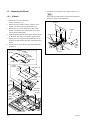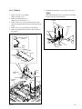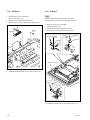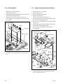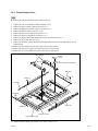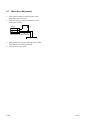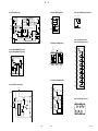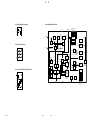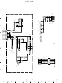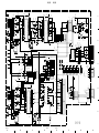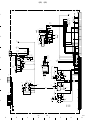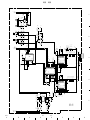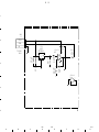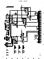
1
FLAT WIDE DISPLAY
FWD-50PX1
FWD-50PX1N
FLAT PANEL DISPLAY SPEAKER SYSTEM
SS-SP50FW
TV STAND
SU-50FW
SERVICE MANUAL
1st Edition
! WARNING
This manual is intended for qualified service personnel only.
To reduce the risk of electric shock, fire or injury, do not perform any servicing other than that
contained in the operating instructions unless you are qualified to do so. Refer all servicing to
qualified service personnel.
! WARNUNG
Die Anleitung ist nur für qualifiziertes Fachpersonal bestimmt.
Alle Wartungsarbeiten dürfen nur von qualifiziertem Fachpersonal ausgeführt werden. Um die
Gefahr eines elektrischen Schlages, Feuergefahr und Verletzungen zu vermeiden, sind bei
Wartungsarbeiten strikt die Angaben in der Anleitung zu befolgen. Andere als die angegeben
Wartungsarbeiten dürfen nur von Personen ausgeführt werden, die eine spezielle Befähigung
dazu besitzen.
! AVERTISSEMENT
Ce manual est destiné uniquement aux personnes compétentes en charge de l’entretien. Afin
de réduire les risques de décharge électrique, d’incendie ou de blessure n’effectuer que les
réparations indiquées dans le mode d’emploi à moins d’être qualifié pour en effectuer d’autres.
Pour toute réparation faire appel à une personne compétente uniquement.
Power cord plug should be pulled out from the wall before starting the service operation.
If power switch is turned OFF only, you may receive an electric shock, because the unit may have an
electric inside.
Therefore, you should pull out the power cord plug from the wall before starting the service operation.
FWD-50PX1
ADVARSEL!
Lithiumbatteri-Eksplosionsfare ved fejlagtig
håndtering.
Udskiftning må kun ske med batteri
af samme fabrikat og type.
Levér det brugte batteri tilbage til leverandøren.
CAUTION
Danger of explosion if battery is incorrectly replaced.
Replace only with the same or equivalent type
recommended by the manufacturer.
Dispose of used batteries according to the
manufacturer’s instructions.
Vorsicht!
Explosionsgefahr bei unsachgemäßem Austausch
der Batterie.
Ersatz nur durch denselben oder einen vom
Hersteller empfohlenen ähnlichen Typ. Entsorgung
gebrauchter Batterien nach Angaben des
Herstellers.
ADVARSEL
Lithiumbatteri - Eksplosjonsfare.
Ved utskifting benyttes kun batteri som
anbefalt av apparatfabrikanten.
Brukt batteri returneres
apparatleverandøren.
VARNING
Explosionsfara vid felaktigt batteribyte.
Använd samma batterityp eller en likvärdig typ
som rekommenderas av apparattillverkaren.
Kassera använt batteri enligt gällande
föreskrifter.
VAROITUS
ATTENTION
Il y a danger d’explosion s’il y a remplacement
incorrect de la batterie.
Remplacer uniquement avec une batterie du même
type ou d’un type équivalent recommandé par le
constructeur.
Mettre au rebut les batteries usagées conformément
aux instructions du fabricant.
FWD-50PX1
Paristo voi räjähtää jos se on virheellisesti
asennettu.
Vaihda paristo ainoastaan laitevalmistajan
suosittelemaan tyyppiin.
Hävitä käytetty paristo valmistajan ohjeiden
mukaisesti.
1 (P)
For the customers in the Netherlands
Voor de klanten in Nederland
Hoe u de batterijen moet verwijderen, leest u in de tekst
van deze handleiding.
Gooi de batterij niet weg maar lever deze in als klein
chemisch afval (KCA).
Für Kunden in Deutschland
Entsorgungshinweis: Bitte werfen Sie nur entladene
Batterien in die Sammelboxen beim Handel oder den
Kommunen. Entladen sind Batterien in der Regel dann,
wenn das Gerät abschaltet und signalisiert “Batterie
leer” oder nach längerer Gebrauchsdauer der Batterien
“nicht mehr einwandfrei funktioniert”. Um
sicherzugehen, kleben Sie die Batteriepole z.B. mit
einem Klebestreifen ab oder geben Sie die Batterien
einzeln in einen Plastikbeutel.
For the customers in the U.S.A. and Canada
RECYCLING LITHIUM-ION BATTERIES
Lithium-Ion batteries are recyclable.
You can help preserve our environment
by returning your used rechargeable
batteries to the collection and recycling
location nearest you.
For more information regarding recycling of rechargeable batteries, call toll free
1-800-822-8837, or visit http://www.rbrc.org/
Caution: Do not handle damaged or leaking Lithium-Ion
batteries.
2 (P)
FWD-50PX1
Table of Contents
1. Service Overview
1-1.
1-2.
1-3.
1-4.
1-5.
1-6.
1-7.
1-8.
1-9.
Board Location ............................................................................................ 1-1
Installing/Removing the Cabinet ................................................................. 1-2
1-2-1. Rear Cover Assembly ................................................................ 1-2
1-2-2. Bezel Assembly .......................................................................... 1-3
Replacing the Board .................................................................................... 1-4
1-3-1. Q Board ...................................................................................... 1-4
1-3-2. B Board ...................................................................................... 1-5
1-3-3. SP Board ..................................................................................... 1-6
1-3-4. S Board ....................................................................................... 1-6
1-3-5. Y Drive Board ............................................................................ 1-7
1-3-6. X Drive Board ............................................................................ 1-8
1-3-7. Digital Video Board/Interface Board ......................................... 1-8
Replacing the Main Parts ............................................................................ 1-9
1-4-1. Power Unit/DC Fan (For Power Supply) ................................... 1-9
1-4-2. DC Fan (For Q/B Mount) ......................................................... 1-10
1-4-3. Plasma Display Panel ............................................................... 1-11
Service Position ......................................................................................... 1-12
1-5-1. Service Position of the B and Q Boards ................................... 1-12
Packaging of the Plasma Display Panel When It Is Shipped to
Pioneer Corporation .................................................................................. 1-13
Backup Battery Replacement .................................................................... 1-14
Unleaded Solder ........................................................................................ 1-14
Warning on Power Connection ................................................................. 1-14
2. Electrical Adjustments
2-1.
2-2.
2-3.
2-4.
2-5.
2-6.
2-7.
Equipment Required .................................................................................... 2-1
Electrical Adjustments Using the Service Mode ........................................ 2-1
White Balance Adjustment ....................................................................... 2-20
AD Calibration Adjustment ...................................................................... 2-20
Sub Color and Sub Hue Adjustments ........................................................ 2-21
Video Decoder Adjustment ....................................................................... 2-21
Watch Error Adjustment ........................................................................... 2-22
3. Troubleshooting
3-1.
3-2.
FWD-50PX1
Judging Method When Image Does Not Appear ........................................ 3-1
Self Diagnosis Function .............................................................................. 3-2
3-2-1. Overview .................................................................................... 3-2
3-2-2. Abnormality Judgment Criterion ............................................... 3-2
1
4. Circuit Description
4-1.
4-2.
4-3.
4-4.
Outline ......................................................................................................... 4-1
Q Board ....................................................................................................... 4-1
B Board ....................................................................................................... 4-2
S Board ........................................................................................................ 4-2
5. Semiconductors
6. Spare Parts
6-1.
6-2.
6-3.
6-4.
6-5.
Notes on Repair Parts .................................................................................. 6-1
Exploded Views .......................................................................................... 6-2
Electrical Parts List ..................................................................................... 6-8
Packing Materials & Supplied Accessories .............................................. 6-24
SS-SP50FW............................................................................................... 6-24
7. Block Diagrams
B (1/3), Q (1/2), SP ..................................................................................... 7-1
B (2/3) ......................................................................................................... 7-2
B (3/3), Q (2/2), H1, H2, S .......................................................................... 7-3
8. Schematic Diagrams
B .................................................................................................................. 8-2
H1, H2, SP ................................................................................................. 8-14
Q ................................................................................................................ 8-15
S ................................................................................................................. 8-20
U1 (FWD-50PX1) ..................................................................................... 8-21
Frame Wiring ............................................................................................ 8-22
9. Board Layouts
B .................................................................................................................. 9-2
Q .................................................................................................................. 9-4
H1 ................................................................................................................ 9-6
H2 ................................................................................................................ 9-6
S ................................................................................................................... 9-6
SP ................................................................................................................ 9-6
U1 (FWD-50PX1) ....................................................................................... 9-7
2
FWD-50PX1
Section 1
Service Overview
1-1. Board Location
S board
X drive board
Power unit board
Digital video board
S boards
H2 board
SP board
Y drive board
Interface board
Q board
B board
U1 board
(FWD-50PX1)
FWD-50PX1
H1 board
1-1
1-2. Installing/Removing the Cabinet
n
When installing/removing the cabinet and replacing the board, place the unit on the conductive cushion.
1-2-1. Rear Cover Assembly
1. Loosen the two panel securing screws, then remove the U1 block assembly. (FWD-50PX1 only)
2. Remove the four screws (PSW M6 x 20), then remove the four nylon washers and four knobs.
3. Remove the fourteen screws (PSW3 x 20) and eight screws (PSW3 x 8), then remove the rear cover
assembly while holding the handle.
Handle
PSW
M6 x 20
Knob
Rear cover assembly
Nylon washer
PSW3 x 8
Handle
PSW
3 x 20
Handle
U1 block
assembly
(FWD-50PX1)
PSW3 x 8
Handle
Panel securing
screws
Conductive cushion
4. Attach the rear cover assembly in the reverse order of steps 1 to 3.
1-2
FWD-50PX1
1-2-2. Bezel Assembly
m
. Be sure to remove the chassis assembly with more than two persons.
. Place the removed chassis assembly on the conductive cushion.
1.
2.
3.
4.
5.
6.
7.
8.
Remove the rear cover assembly. (Refer to Section 1-2-1.)
Remove the two screws (BVTP3 x 8), then remove the control button panel.
Disconnect the harness from the connector on the H2 board.
Remove the three screws (BVTP3 x 8), then remove the control button and H2 board.
Remove the screw (BVTP3 x 8), then remove the light tube and H1 board.
Disconnect the harness from the connector on the H1 board.
Remove the twenty-six screws (BVTP4 x 16).
Remove the chassis assembly while holding the portions A of the main bracket.
Chassis assembly
BVTP4 x 16
Main bracket
Portions A
BVTP4 x 16
Main bracket
BVTP
4 x 16
Portions A
Control button panel
BVTP
3x8
Harness
Control button
H2 board
BVTP
3x8
Conductive
cushion
BVTP
3x8
Bezel assembly
Harness
Light tube
H1 board
9. Attach the bezel assembly in the reverse order of steps 1 to 8.
FWD-50PX1
1-3
1-3. Replacing the Board
7. Install the Q board in the reverse order of steps 1 to 6.
n
Place and fix the harnesses to connect the Q board and
B board as shown in the illustration.
1-3-1. Q Board
1. Remove the rear cover assembly.
(Refer to Section 1-2-1.)
2. Remove the bolt, cushion (15x25), and two screws
(PSW3 x 8), then remove the Q/B shield cover.
3. Remove the two screws (PSW3 x 6), three screws
(PSW3 x 8) (black) and six hexagonal screws, then
remove the Q terminal plate.
4. Move the Q terminal plate slowly in the direction shown
by the arrow, then remove it from the copper foil tape.
5. Remove the two UL tapes, then disconnect the seven
harnesses and the flexible flat cable connected to the Q
board.
6. Remove the six screws, then remove the Q board and
partition Q.
CN3005 CN3008
CN3007
UL tapes
B board
Harnesses
Q board
CN3012
CN3011
CN3001
CN3006
CN3003
Q board
CN3002
Cushion
(15x25)
M8 x 16
Q/B shield cover
PSW
3x6
Flexible flat
cable
PSW
3x6
PSW
3x6
Harnesses
Q terminal
plate
Q board
Hexagonal
screw
PSW
3x8
(black)
Partition Q
UL tapes
Conductive
cushion
Copper foil tape
1-4
FWD-50PX1
1-3-2. B Board
1. Remove the rear cover assembly.
(Refer to Section 1-2-1.)
2. Remove the Q/B shield cover.
(Refer to step 2 of Section 1-3-1.)
3. Remove the two UL tapes, then disconnect the eight
harnesses and the flexible flat cable connected to the B
board.
4. Remove the six screws, then remove the B board.
5. Remove the lithium battery from the battery holder on
the B board.
6. Install the B board in the reverse order of steps 1 to 5.
n
Place and fix the harnesses to connect the Q board and
B board as shown in the illustration.
UL tapes
B board
Harnesses
Lithium battery
(CR1220)
Battery
holder
Q board
CN7002
CN7001
B board
CN1004
CN1005
CN1001
CN101
CN401
CN402
Harnesses
PSW
3x6
Flexible flat
cable
B board
Harnesses
Conductive
cushion
FWD-50PX1
UL tapes
1-5
1-3-3. SP Board
1-3-4. S Board
1. Remove the rear cover assembly.
(Refer to Section 1-2-1.)
2. Remove the harness from the SP board.
3. Remove the two screws, then remove the SP board.
n
The three S boards are installed in this unit. When
replacing them, remove/install in the same procedure.
Harness
SP board
BVTP
3x8
1. Remove the rear cover assembly.
(Refer to Section 1-2-1.)
2. Disconnect the harness from the S board.
3. Remove the screw, then remove the S board.
Harness
PSW
3x6
PSW
3x6
Harness
S board
S board
Conductive cushion
4. Install the SP board in the reverse order of steps 1 to 3.
Harness
PSW
3x6
S board
4. Install the S board in the reverse order of steps 1 to 3.
1-6
FWD-50PX1
1-3-5. Y Drive Board
1. Remove the rear cover assembly.
(Refer to Section 1-2-1.)
2. Remove the five connectors.
3. Remove the harness from the eight clampers.
4. Remove the bolt (M8 x 16) and four screws (PSW3 x
6), then remove the QB block assembly in the
direction shown by the arrow.
5. Remove the three screws (PSW3 x 6), then remove
the side frame and board cover assembly.
Connectors
PSW
3x6
Clamper
M8 x 16
PSW
3x6
6. Remove the four screws, then remove the option case
bracket assembly.
7. Disconnect the harness and flexible flat cable from the
connectors on the Y drive board.
8. Remove the two connectors from the scan A board and
scan B board.
9. Remove the two screws [B], six screws [A], five
screws [C] and four board holders, then remove the Y
drive board.
PSW
3x6
Option case bracket
assembly
Connector
Flexible flat cable
Harness
Screw
[B]
Screw
[A]
Connectors
Clampers
Connector
QB block
assembly
Y drive board
Screw
[C]
Clampers
Conductive
cushion
PSW
3x6
Side frame
Board cover
assembly
Scan B board
Board holders
Scan A board
Board
holders
10. Install the Y drive board in the reverse order of steps 1
to 9.
FWD-50PX1
1-7
1-3-6. X Drive Board
1-3-7. Digital Video Board/Interface Board
1. Remove the rear cover assembly.
(Refer to Section 1-2-1.)
2. Disconnect the harness and flexible flat cable from the
connectors on the X drive board.
3. Remove the two screws [A], six screws [C], five
screws [B] and four board holders, then remove the X
drive board.
1. Remove the rear cover assembly.
(Refer to Section 1-2-1.)
2. Remove the QB block assembly.
3. Remove the power unit.
(Refer to steps 2 and 3 of Section 1-4-1.)
4. Disconnect all harnesses and flexible flat cables from
the connectors on the digital board.
5. Remove the six board holders, then remove the digital
video board.
6. Disconnect all harnesses and flexible flat cables from
the connectors on the interface board.
7. Remove the six board holders, then remove the
interface board.
Screw [B]
Screw [A]
Screw [C]
X drive board
Board holders
Flexible flat cable
Flexible flat cable
Harnesses
Conductive cushion
Flexible flat cables
Harnesses
Flexible flat
cables
Board holders
Harness Interface board
Digital video
board
Board holders
4. Install the X drive board in the reverse order of steps 1
to 3.
Board holders
Board holders
8. Install the digital video board and interface board in
the reverse order of steps 1 to 7.
1-8
FWD-50PX1
1-4. Replacing the Main Parts
1-4-1. Power Unit/DC Fan (For Power Supply)
n
When attaching the DC fan, make sure that the orientation
of imprinting is correct.
1. Remove the rear cover assembly.
(Refer to Section 1-2-1.)
2. Disconnect the nine harnesses from the connectors on
the power unit.
3. Remove the bolt (M8 x 16) and four screws (PSW3 x
6), then remove the QB block assembly.
4. Remove the four connectors [A].
5. Remove the three connectors [B].
6. Disconnect the three harnesses from the connectors on
the interface board.
7. Disconnect the harness from the connector on the SP
board.
8. Remove the harness from the four purse locks.
9. Remove the four screws, then remove the K board
bracket assembly.
10. Remove the four screws (BVTT3 x 6), then remove
the G bracket.
11. Remove the two screws (PSW4 x 25), then remove
the DC fan.
12. Remove the four screws (PSW4 x 35), then remove
the two DC fans.
13. Remove the seven screws, then remove the power unit.
PSW
3x6
Power unit
Imprinting
DC fan
Purse lock
PSW
4 x 25
M8 x 16
DC fan
QB block assembly
PSW
3x6
Imprinting
G bracket
PSW
4 x 35
BVTT
3x8
PSW
3x6
DC fan
Connectors [B]
Harness
Connector [B]
K board bracket
assembly
Conductive cushion
Conductive
cushion
Purse
locks
SP board
Connectors [A]
Harness
Harnesses
14. Attach the power unit and DC fan in the reverse order
of steps 1 to 13.
Interface board
FWD-50PX1
1-9
1-4-2. DC Fan (For Q/B Mount)
n
When attaching the DC fan, make sure that the orientation
of imprinting is correct.
1. Remove the rear cover assembly.
(Refer to Section 1-2-1.)
2. Remove the connector and two screws, then remove
the DC fan.
Imprinting
PSW
4 x 25
DC fan
Connector
Conductive cushion
3. Attach the DC fan in the reverse order of steps 1 and 2.
1-10
FWD-50PX1
1-4-3. Plasma Display Panel
n
Be sure to replace the plasma display panel with two persons.
1.
2.
3.
4.
5.
6.
7.
8.
9.
Remove the rear cover assembly. (Refer to Section 1-2-1.)
Remove the bezel assembly. (Refer to Section 1-2-2.)
Remove the QB block assembly. (Refer to Section 1-4-1.)
Remove the S board. (Refer to Section 1-3-4.)
Remove the Y drive board. (Refer to Section 1-3-5.)
Remove the X drive board. (Refer to Section 1-3-6.)
Remove the digital video board and interface board. (Refer to Section 1-3-7.)
Remove the power unit. (Refer to 1-4-1.)
Remove the cushions (15x25) attached to the heads of the three bolts on the right side as viewed
from backside.
10. Remove the five bolts (M8 x 16), then remove the two main brackets.
11. Remove the four screws (PSW3 x 8), then remove the two frames (H).
12. Remove the six screws (PSW3 x 8), then remove the two side frames.
Main brackets
M8 x 16
Cushion
(15x25)
M8 x 16
(Right side as viewed from backside)
Side frame
PSW3 x 6
PSW3 x 6
Frame (H)
PSW3 x 6
PSW
3x6
Frame (H)
Side frame
Conductive cushion
Plasma display panel
13. Attach the plasma display panel in the reverse order of steps 1 to 12.
FWD-50PX1
1-11
1-5. Service Position
1-5-1. Service Position of the B and Q Boards
m
. Be sure to attach the stand with more than two persons.
. When attach the stand to the unit, check that four knobs are attached to the holes of the stand.
1.
2.
3.
4.
5.
Remove the rear cover assembly. (Refer to Section 1-2-1.)
Remove the two cushions (15x25) attached to the two screws.
Remove the bolt (M8 x 16) and two screws, then remove the QB shield assembly.
Attach the four knobs to the unit by the four screws.
Attach the four knobs to the holes of the each stand.
B board
Unit
Q board
Knobs
PSW
M6 x 20
Q/B shield
cover
Bolt
(M8 x 16)
Knobs
PSW
M6 x 20
Unit
Atacch the two knobs
to the each stand.
PSW
3x6
Cushion
(15x25)
Unit
Stands
Stands
1-12
FWD-50PX1
1-6. Packaging of the Plasma Display Panel When It Is Shipped to Pioneer Corporation
Carton (Upper)
Pad R (Upper)
Pad L (Upper)
Individual inner case
Pad R (Under)
Pad L (Under)
POSITIONING
SCREWS
Carton (Under)
PP bands
FRONT LID
SERVICE
MODULE
FWD-50PX1
Screws (12 pcs)
Individual inner case
1-13
1-7. Backup Battery Replacement
1-8. Unleaded Solder
The B board contain the lithium battery for the clock.
c
When replacing the part, be sure to use the specified one
below.
Replacement with a part other than the specified part will
result in fire hazards and electric hazards.
Boards requiring use of unleaded solder are printed with a
lead free mark (LF) indicating the solder contains no lead.
(Caution: Some printed circuit boards may not come
printed with the lead free mark due to their particular size.)
Replacement part
m
. Be sure to use the unleaded solder for the printed circuit
board printed with the lead free mark.
. The unleaded solder melts at a temperature about 40 dC
higher than the ordinary solder, therefore, it is recommended to use the soldering iron having a temperature
regulator.
. The ordinary soldering iron can be used but the iron tip
has to be applied to the solder joint for a slightly longer
time. The printed pattern (copper foil) may peel away if
the heated tip is applied for too long, so be careful.
Part description: Lithium battery (CR1220)
Part No.:
! 1-756-157-11
Replacement
1. For removing the lithium battery, refer to steps 1 to 5
in Section 1-5-3.
2. Attach the lithium battery in the reverse order of steps.
: LEAD FREE MARK
1-9. Warning on Power Connection
Use the proper power cord for your local power supply.
FWD-50PX1
United States,
Canada
Continental
Europe
United Kingdom, Ireland,
Australia, New Zealand
Japan
Plug type
VM0233
COX-07
636
_ a)
VM1296
Female end
VM0089
COX-02
VM0310B
VM0303B
VM1313
Cord type
SVT
H05VV-F
CEE (13) 53rd (O.C)
HVCTF
Minimum cord set rating
10A/125V
10A/250V
10A/250V
10A/125V
Safety approval
UL/CSA
VDE
VDE
DENAN-HO
a) Note : Use an appropriate rating plug which is applied to local regulations.
1-14
FWD-50PX1
Section 2
Electrical Adjustments
2-1. Equipment Required
. Oscilloscope
Tektronix 2465 or equivalent
(band width : 350 MHz or more)
. VG (Programmable video signal generator)
VG814 or equivalent
. Frequency counter
Advantest TR5821AK or equivalent
. Digital voltmeter
Advantest TR6845 or equivalent
. Potential transformer
. Regulated DC power supply
. Remote commander (RM-980C)
n
Perform the following adjustments at least 5 minutes after
turning on the power.
2-2. Electrical Adjustments Using the
Service Mode
The electrical adjustments can be performed using the remote
commander RM-980C supplied with the FWD-50PX1. The
remote commander has the Service Mode. Select the Service
Mode to perform the electrical adjustments as listed below.
. Service Mode
When the machine enters the service mode, the “Service
Mode” submenu is displayed in addition to the ordinary
user menu. The electrical adjustment is executed using the
“Service Mode” submenu.
Press the [STBY] key once and back on to enter the STANDBY state or turn off the main power to exit the Service Mode.
. Operation of remote commander in the Service
Mode
The six keys of MENU, ENTER, ←, →, ↑ and ↓ are the
basic operation keys in the same manner as in the user
adjustment. The other keys can be operated in the same
manner as in the user adjustment.
. The electrical adjustments using the Service
Mode become necessary in the following cases.
When one of the following adjustments is made,
adjustment using the service mode becomes necessary.
When any repair related to picture
quality is executed.
Chroma Decoder
AD Converter
White Balance
When IC403/B board and its
peripheral part is replaced.
AD Converter
When PDP is replaced.
White Balance
When memory (IC1007) on the
B board is replaced.
EEPROM Initialize
Chroma Decoder
AD Converter
White Balance
General
Service Status
When any of the circuit boards
below is replaced.
B board
Service Mode
EEPROM Initialize
Chroma Decoder
AD Converter
White Balance
General
Manual Control
Preset Edit
Service Status
Initializes the EEPROM
Chroma decoder adjustment
A/D converter adjustment
White balance adjustment
Other adjustments and the
functions required for check
Factory check menu (Not used in service)
Editing the preset signal
Internal status check
Q board
Chroma Decoder
AD Converter
Service Status
S board
Service Status
Operation check only
How to enter the Service Mode using the RM-980C :
In the STAND-BY state, press the keys in the following
order.
[DISPLAY] → [5] → [VOL+] → [POWER|ON]
FWD-50PX1
2-1
Service Mode
1. EEPROM Initialize
EEPROM Configuration
Table 1 (page 2-13) shows the configuration of EEPROM.
The entire area or the respective areas of the EEPROM can
be separately initialized.
Menu Structure
Select the desired area of EEPROM to be initialized using
the following menu.
Service Mode
EEPROM Initialize
Whole Area
Common
White Balance
Prog. Gamma
Prog. Preset
Last Memory
User Memory
Factory
To initialize the desired area, firstly select the desired item
from the EEPROM RESET menu. Change the selected
item from “CANCEL” to “OK”. Then press “ENTER”.
a) Whole Area
It initializes whole area of EEPROM.
This command is identical to carrying out the all items
of “Common”, “White Balance”, “Prog. Gamma”,
“Prog. Preset”, “Last Memory”, “User Memory” and
“Factory”.
Execute this command only when the memory
(IC1007) on the B board is replaced.
b) Common
It initializes “Common (1)”, “Common (2)” and
“Common (3)” of the “COMMON DATA AREA”
shown in Table 1.
It initializes the data unique to the machine and the
common data (various setup values of the user menu).
Do not carry out this command because it initializes
the serial number and accumulative operation hours.
2-2
c) White Balance
It initializes “Color Temp (1)” and “ Color Temp (2)”
of the “COMMON DATA AREA” shown in Table 1.
It initializes the color temperature “High”, “Mid” and
“Low”, and all data of user setup 1 to 3 to 00.
It also initializes the user name to “User1”, “User2”
and “User3”.
d) Prog. Gamma
This command is not used in this machine.
e) Prog. Preset
It initializes the “PRESET DATA AREA” (page 2-13)
shown in Table 1.
It resets the backup preset area.
f) Last Memory
It initializes “LAST MEMORY AREA” (pages 2-13,
14) shown in Table 1.
It initializes the last memory data that user has adjusted for each signal.
g) User Memory
This command is not used in this machine.
h) Factory
It resets the EEPROM to the factory default status.
All of the EEPROM areas except the following are
initialized by this command.
Items that are not initialized by the “FACTORY”
RESET function.
In the COMMON DATA AREA
1 Index Number stored in the Common (1) [General]
2 Watch Error and Serial Number data stored in the
Common (2) [General]
3 Service (1) [AD Converter] (Adjustment data of 2-4.
AD Calibration Adjustment)
4 Service (2) [Chroma Decoder] (Adjustment data of 25. Sub Color, Sub Hue adjustment and 2-6. Video
Decoder Adjustment)
5 Adjustment data in Color Temp (1) [Data & Name] at
the factory except user adjustment value. (Adjustment
data of 2-3. White Balance Adjustment)
FWD-50PX1
2. Chroma Decoder
Menu structure
Hue and color of the video signal are adjusted.
Service Mode
Chroma Decoder
Hue
Sub Contrast
Sub Color
Sharp Gain
Sharp f0
Y Out Level
C Out Level
Y Delay
Cb Offset
Cr Offset
By Adj (SECAM)
Ry Adj (SECAM)
:
8
:
:
:
:
8
3
18
10
:
:
:
:
8
8
8
8
a) Hue
To adjust NTSC signal hue, adjust “Hue (NTSC)” in
the lower layer below this sub menu.
To adjust NTSC4.43 signal hue, adjust “Hue (NT443)”
in the lower layer below this sub menu.
Adjustment range is from 0 to 63.
b) Sub Contrast
Adjustment range is from 0 to 63.
Fixed value : 8
c) Sub Color
Adjust “Col (NTSC)”, “Col (PAL)” and “Col (SECAM)” for the respective signals of NTSC, PAL and
SECAM.
Adjustment range is from 0 to 15.
Fixed value for Col (NTSC) only : 6
d) Sharp Gain
Adjustment range is from 0 to 15.
Fixed value : 8
e) Sharp f0
Adjustment range is from 0 to 3.
Fixed value : 3
f) Y Out Level
Adjustment range is from 0 to 63.
Fixed value : 18
g) C Out Level
Receive the NTSC signal and adjust color. The color
adjustment of PAL and SECAM signals are performed
in c) Sub Color upon completion of the NTSC signal
adjustment.
Adjustment range is from 0 to 63.
FWD-50PX1
h) Y Delay
Y delay for the respective signals can be adjusted by
“YDL (NTSC)”, “YDL (PAL)”, “YDL (SECAM),
“YDL (NT443)”, “YDL (PALM)” and “YDL
(PALN)”.
Adjustment range is from 0 to 15.
Fixed value : 5
i) Cb Offset
Adjustment range is from 0 to 15.
Fixed value : 8
j) Cr Offset
Adjustment range is from 0 to 15.
Fixed value : 8
k) By Adj (SECAM)
The blue offset when receiving the SECAM signal is
adjusted.
Adjustment range is from 0 to 15.
l) Ry Adj (SECAM)
The red offset when receiving the SECAM signal is
adjusted.
Adjustment range is from 0 to 15.
Sub Color and Sub Hue Adjustments
Refer to Section “2-5. Sub Color and Sub Hue Adjustment”.
Video Decoder Adjustment
Refer to Section “2-6. Video Decoder Adjustment”.
2-3
3. AD Converter
4. White Balance
Menu structure
Menu structure
This adjustment corrects non-uniformity among RGB (or
YCbCr) channels of AD converter (IC403).
White balance of PDP panel is adjusted.
Service Mode
AD Converter
Cal Mode
RGB Calibration
YUV Calibration
Video Calibration
:
off
a) Cal Mode
Set to “On” to enter the calibration mode.
Off : Normal operation
On : Calibration mode
b) RGB Calibration
The RGB signals are calibrated.
The RGB signals are calibrated by “Sub Cont RGB”,
“Red Gain”, “Green Gain”, “Blue Gain”, “Red Bias”,
“Green Bias” and “Blue Bias” that are located in the
lower layer below this sub menu.
Adjustment range is from 0 to 255 in each adjustment
item.
c) YUV Calibration
The component video signal is calibrated.
The component video signal is calibrated by “Sub
Cont YUV”, “Sub Brt YUV”, “Cb Offset YUV” and
“Cr Offset YUV” that are located in the lower layer
below this sub menu.
Adjustment range is from 0 to 255 for “Sub Cont
YUV” and “Sub Brt YUV”, and from 0 to 63 for “Cb
Offset YUV” and “Cr Offset YUV”.
d) Video Calibration
The composite video signal is calibrated.
The composite video signal is calibrated by “Sub Cont
Video”, “Sub Brt Video”, “Cb Offset Video” and “Cr
Offset Video” that are located in the lower layer below
this sub menu.
Adjustment range is from 0 to 255 for “Sub Cont
Video” and “Sub Brt Video”, and from 0 to 63 for “Cb
Offset Video” and “Cr Offset Video”.
Service Mode
White Balance
Window
Color Temp.
Red Gain
Green Gain
Blue Gain
:
:
Off
High
llllllllll
llllllllll
llllllllll
a) Window
This machine has the built-in window signal for white
balanced adjustment. Select large window for suitable
adjustment.
Off :
Window is not displayed.
Small : Small window is displayed.
Large : All white is displayed.
b) Color Temp.
Select the desired color temperature that you want to
adjust located in the lower layer below this submenu.
Select the desired color temperature from “High”,
“Mid”, “Low”, “User 1”, “User 2” and “User 3”.
n
“User 1”, “User 2” and “User 3” can be adjusted from
the user menu, therefore they are not adjusted here.
c) Red Gain
Red gain of the selected “Color Temp.” is adjusted.
Adjustment range is from 0 to 255.
d) Green Gain
Green gain of the selected “Color Temp.” is adjusted.
Adjustment range is from 0 to 255.
e) Blue Gain
Blue gain of the selected “Color Temp.” is adjusted.
Adjustment range is from 0 to 255.
White Balance Adjustment
Refer to Section “2-3. White Balance Adjustment ”.
AD Calibration Adjustment
Refer to Section “2-4. AD Calibration Adjustment”.
2-4
FWD-50PX1
5. General
g) Fan Status
Menu structure
Menu structure
The data unique to the machine and the fan control are
checked.
Service Mode
General
Blue Only
:
0
AGC Wide
:
14
AGC Narrow :
13
32k Clock Out :
Off
Watch Error : 32.76800
Serial Number: 2000001
Fan Status
Vs/Va Setting
a) Blue Only
When “1” is set, all colors of RGB displayed on the
PDP become blue data level.
b) AGC Wide
This command is not used in this machine.
c) AGC Narrow
This command is not used in this machine.
d) 32k Clock Out
The clock signal that is used for the Watch Error
adjustment is output.
Off : Not output.
On : Output
e) Watch Error
It corrects error of the built-in watch.
Set the measurement value of the frequency counter
connected.
Adjustment range is from 32.76180 to 32.77420 kHz.
f) Serial Number
It sets serial number.
FWD-50PX1
Service Mode
General
Fan Status
Fan Control
Ref Voltage
F/B Voltage
Drive Data
P/S Temp
Temp1
Temp2
Temp3
: Manual
:
:
:
:
:
:
8.0[V]
8.0[V]
2B5F
43[dC]
43[dC]
43[dC]
43[dC]
Fan Control : You can set the 8.0 to 12.0 V to the fan
drive voltage using [Ref Voltage]. Use this
command for checking operation of the fan
drive circuit.
(Factory default setting: 8.0 V)
Ref Voltage : You can set the any desired voltage to the
fan drive voltage. Range of setting is from
8.0 V to 12.0 V, the setting value is saved.
F/B Voltage : It indicates the fan drive voltage. The
voltage that is actually driving the fan is
displayed as the setting voltage is being
supplied.
Drive Data : It indicates the fan drive data.
P/S Temp : It indicates the temperature that is measured
by the temperature sensor built in the power
board.
Temp1 :
It indicates the temperature that is measured
by the S board attached on top of the BQ
block assembly.
Temp2 :
It indicates the temperature that is measured
by the S board attached on top of the power
board.
Temp3 :
It indicates the temperature that is measured
by the S board attached on the right side as
viewed from backside.
2-5
6. Manual Control
7. Preset Edit
This submenu is used in factory for operation checks.
Do not operate this function.
Preset data structure
You can add the preset signals in addition to the default
preset data.
The additional preset data are stored in [PROGRAM1] to
[PROGRAM12] of [PRESET DATA AREA]. [PROGRAM13] to [PROGRAM30] are not used.
Menu structure
Service Mode
Preset Edit
Original Data Select
Data Edit
Save Area Select
Editing procedure
An independent memory area (editing RAM) is assigned for
data editing inside the system controller as shown below.
First, copy the source data for editing to the editing RAM.
Then modify the data on the editing RAM and save the
editing contents to the specified preset area of EEPROM.
In addition to the default preset data that has been set
already when shipped from the factory, you can edit the
various data from the already saved data in EEPROM or
the signal data that is being input at this moment.
(The following example shows the case the data stored in
the EEPROM preset area No.2 is used for editing and the
edited data is stored in the area No.11.)
EEPROM
preset data area
PROGRAM1
PROGRAM2
PROGRAM3
PROGRAM4
PROGRAM5
PROGRAM6
PROGRAM7
PROGRAM8
PROGRAM9
PROGRAM10
PROGRAM11
PROGRAM12
2-6
System controller
Editing RAM
Editing
FWD-50PX1
a) Original Data Select
Menu structure
You can select the original data that is used for editing and
copy the selected original data to the editing RAM.
Service Mode
Preset Edit
Original Data Select
Current Data Select
Table
(1) The signal data that is being
input at this moment, is used
as the original data for editing.
(2) The data stored in the preset
area is used for editing.
(1) Current Data Select
When you select the signal data that is being input at
this moment for editing, move the cursor to this item
and press ENTER.
The selected data is copied to the editing RAM.
This mode is prepared for the case that the signal
specification is unknown, and you can make editing by
checking the image on screen.
Select the respective adjustment items and change the
data as desired using the ↑/↓ key or the ←/→ key. The
changed data are reflected on screen.
(If you press the ENTER key again, the screen returns
to the previous menu.)
Among the adjustment items, the three types of
adjustment [H Freq], [V Freq] and [Sync Pol] cannot
be modified.
(2) Table
When you select the data stored in the preset area,
move the cursor to this item and press ENTER. Select
the desired data using the ↑/↓ key. The selected data is
copied to the editing RAM.
This mode is prepared for the case that the signal
specification is already known. You can make adjustment and edit data of all items but the modified data
are not reflected to the actual picture images.
FWD-50PX1
2-7
b) Data Edit
Menu structure
You can edit the data contents of the editing RAM.
Service Mode
Preset Edit
Data Edit
H Freq
V Freq
Sync Pol
H. Total Pixel
H. Active Pixel
H. Sync Pixel
H. BP Pixel
V. total Line
V. Active Line
V. Sync Line
V. BP Line
Clamp Posi
Clamp Width
Format Flag
Picture Mode
Color Matrix
Zoom Mode
: 031.469[kHz]
: 059.94[Hz]
:
N/N
:
800
:
640
:
96
:
48
:
525
:
480
:
2
:
33
:
60
:
8
:
:
:
Standard
12
4/3
(1) Horizontal frequency
(2) Vertical frequency
(3) Sync signal polarity
(4) Total number of dots within horizontal
(5) Horizontal resolution power
(6) Number of dots of horizontal sync signal
(7) Number of dots during the horizontal back porch
(8) Total number of vertical lines
(9) Vertical resolution power (number of lines)
(10) Total number of lines of vertical sync signal
(11) Number of lines during the vertical back porch
(12) Clamp pulse position
(13) Clamp pulse width (number of dots)
(14) Format flag
(15) Picture quality mode
(16) Color difference matrix
(17) Wide selection
(1) H Freq
It sets the horizontal frequency.
n
When “Current Data Select” is selected in the Original
Data Select, this item cannot be modified because the
presently entered signal is selected for editing.
(2) V Freq
It sets the vertical frequency.
n
When “Current Data Select” is selected in the Original
Data Select, this item cannot be modified because the
presently entered signal is selected for editing.
(3) Sync Pol
It sets the sync signal polarity. Sync polarities are
displayed in the order of “Horizontal/Vertical”.
Sync Pol
:
Horizontal sync polarity
Vertical sync polarity
N/N
When you set the sync signal polarity, set it as shown
below.
Negative polarity : N
Positive polarity : P
SOG :
SOG
n
When “Current Data Select” is selected in the Original
Data Select, this item cannot be modified because the
presently entered signal is selected for editing.
(4) H. Total Pixel
It sets the total number of dots within a single horizontal cycle.
This setup value becomes the default value of the user
menu “Total H Pixel”.
n
You should set in a way that number of H. Total Pixels
is equal or more than sum of (H. Active Pixel +H.
Sync Pixel +H. BP Pixel).
2-8
FWD-50PX1
(5) H. Active Pixel
It sets the horizontal resolution power.
(6) H. Sync Pixel
It sets the number of dots of horizontal sync signal.
(7) H. BP Pixel
It sets the number of dots during the horizontal back
porch.
(8) V. total Line
It sets the total number of vertical lines.
n
You should set in a way that number of V. Total Line
is equal or more than sum of (V. Active Line + V.
Sync Line + V. BP Line).
(9) V. Active Pixel
It sets the vertical resolution power.
(10)V. Sync Line
It sets the total number of lines of vertical sync signal.
(11)V. BP Pixel
It sets the number of lines during the vertical back
porch.
(12)Clamp Posi
It sets clamp pulse position.
The clamp pulse position is set starting (when data is
0) from the trailing edge of the horizontal sync signal.
When this value is increased, picture moves toward the
picture area.
The clamp pulse generation position Tcp is given by
the equation below starting from the trailing edge of
sync signal.
Tcp = Clamp Posi/(Horizontal sync frequency x H.
Total Pixel) [seconds]
(13)Clamp Width
It sets the clamp pulse width.
The clamp pulse width increases starting from the
position that is set by the Clamp Posi. When this value
is increased, the clamp pulse width is widened in the
direction toward picture area.
The clamp pulse width Wcp is given by the equation
below.
Wcp = Clamp Width/(Horizontal sync frequency x H.
Total Pixel) [seconds]
FWD-50PX1
(14)Format Flag
It sets ON/OFF of the following respective items in
units of bit.
0
0
0
0
0 0 0 0
1 2 3 4
Upper 4 bits are not used.
1 : ON
0 : OFF
1 Setting the IP converter
Set to OFF during normal operation.
2 Setting interlace
It sets the interlace input.
ON : When the input signal is the interlaced signal.
OFF : When the input signal is the progressive signal.
3 Setting to enable the “dot adjustment”
It enables or disables the “dot adjustment” in the user
menu.
ON : The “dot adjustment” is enabled in the user
menu.
OFF : The “dot adjustment” is disabled in the user
menu.
If the actual input signal specification is different from
the setups of “H. Total Pixel” and “H. Active Pixel”
due to fetching the interlace, set this item to OFF.
4 Frame synchronization setting
It sets synchronization setting of the picture input to
scan converter.
ON : Vertical sync of PDP panel synchronizes with
the input signal.
OFF : The PDP panel display signal is no more
synchronized with the input signal. When the
motion picture is going to be displayed, set this
item to ON.
n
This item can be set to ON only when the vertical
frequency of input signal is in the range from 50 to 60
Hz.
(15)Picture Mode
It sets the picture quality mode. Select the desired
mode from “Standard”, “Vivid”, “User1”, “User2” or
“User3”.
This setting becomes the default value of the “Picture
Mode” of user menu.
2-9
(16)Color Matrix
It sets the color difference matrix when the color
difference component signal is input.
Either “12” or “13” can be set.
12 : In the case when the signal conforms to
SMPTE293M.
13 : In the case when the signal conforms to
SMPTE274M.
(17)Zoom Mode
It sets the wide selection. Select the desired mode from
“Expd. 4/3”, “Letterbx”, “Restore”, “Subtitle” or “4/
3”.
This setting becomes the default value of the “Zoom
Mode” of user menu.
8. Service Status
Menu structure
You can check the internal status of this unit.
Service Mode
Service Status
Signal/Sync
Power Supply
Fan & Temp Status
Warning Status
Operation Time :*****H
Software Version :
*.**
PLD Version
:
***
a) Signal/Sync
c) Save Area Select
Menu structure
Menu structure
It saves the data of the editing RAM to the preset area.
Service Mode
Preset Edit
Save Area Select
Save Are
:
Data Save
1
(1) Selects the preset data area
that stores the data.
(2) Executes saving of the data.
(1) Save Area
It selects the preset data area that saves contents of the
editing RAM.
Select the desired area from “PROGRAM1” to
“PROGRAM12”.
(2) Data Save
It carries out saving of the data into the area that is
selected by the Save Area.
Change the menu item from [Cancel] to [OK] and
press [ENTER].
n
You can judge coincidence of the preset data with the input
signal using the sync signal polarity of horizontal/vertical
frequencies.
If the same sync signal data exists within a preset area, the
specification that has the smaller preset number has
priority.
2-10
Service Mode
Service Status
Signal/Sync
Format
: 640 x 480/60
H Freq
: 031.469[kHz]
V Freq
:
059.94[Hz]
Sync Pol :
N/N
Condition :
Stable
Signal specification
Horizontal frequency
Vertical frequency
Sync signal polarity
Sync signal status
The sync signal status of the input signal is displayed.
Format :
The preset signal name for the input signal is
displayed.
H Freq :
Horizontal frequency of the input is displayed
in 6 digits.
V Freq :
Vertical frequency of the input is displayed in
5 digits.
Sync Pol : Sync signal polarity is displayed.
Horizontal sync signal/Vertical sync signal
N: NEGA
P: POSI
Conditions : Sync signal status is displayed.
Stable :
Stable
Insecure : Unstable
No Sync : Sync signal does not exist.
FWD-50PX1
b) Power Supply
Menu structure
Service Mode
Service Status
Power Supply
Digital 5 V
Digital 3 V
Analog 6 V
:
:
:
5.0[V]
3.3[V]
6.0[V]
5 V for digital circuit
3 V for digital circuit
6 V for analog circuit
Main DC voltages of the machine are displayed.
Digital 5 V : Internal 5 V power supply voltage is displayed.
Digital 3 V : Internal 3.3 V power supply voltage is
displayed.
Analog 6 V : Internal 6 V power supply voltage is displayed.
c) Fan & Temp Status
Menu structure
Service Mode
Service Status
Fan&Temp Status
Fan Drive
:
Fan
:
P/S Temp
:
P/S Temp
NO ACK DEV
When the value that is displayed on the PDP panel is
converted to the binary number, each bit has the following
meaning.
Bit 0 : Audio Processor
Each bit 0 : OK, 1 : NG
Bit 1 : Audio Switch
Bit 2 : AV Switch
Bit 3 : Closed Caption Decoder
Bit 4 : 3D Comb filter
Bit 5 : Chroma Decoder
Bit 6 : PDP
Bit 7 : Tuner (No Use for PFM)
Bit 8 : Auto Wide Decoder
Bit 9 : AD Converter
Bit 10 : EEPROM
Bit 11 : IP Converter (System IC)
Bit 12 : OSD (No Use for PFM)
Bit 13 : PLD (No Use for PFM)
Bit 14 : RTC (No Use for PFM)
Bit 15 : Scan Converter (No Use for PFM)
n
This machine is not equipped with the AV switch,
therefore bit 2 always goes to 1.
OK
OK
OK
: 44[dC]
: 0004
The internal temperature of the machine and the fan
operating status are displayed.
Fan Drive :
Operating status of the fan drive circuit is
displayed. [OK] appears when it operates
normally. [NG] appears when it does not
operate normally.
Fan :
Operating status of the fan is displayed.
[OK] appears when all fans operate
normally. [NG] appears when any one of
the fans does not operate normally.
P/S Temp :
Temperature status inside the power
supply block is displayed. [OK] appears
when temperature is normal. [NG]
appears when temperature is abnormal.
P/S Temp :
Temperature inside the power supply
block is displayed.
NO ACK DEV : Status whether the communication with the
respective devices that are controlled by the
I2C bus is established or not is displayed.
FWD-50PX1
2-11
d) Warning Status
Menu structure
Service Mode
Service Status
Warning Status
EEP ID
EEP Save
EEP Load
RTC Init
RTC VDET
RTC XSTOP
PDP Init
DEC Init
DC Init
Power Off
:
:
:
:
:
:
:
:
:
:
OK
OK
OK
OK
OK
OK
OK
OK
OK
OK
The warning information is displayed.
EEP ID :
ID CODE error
EEP Save :
Data write error
EEP Load :
Data read error
RTC Init :
Watch initialization error
RTC VDET : Watch power voltage error (1.8 V or less)
RTC XSTOP : Watch oscillator error
PDP Init :
PDP initialization error
DEC Init :
Chroma decoder initialization error
DC Init :
Power voltage (digital system 5 V, digital
system 3.3 V, analog system 6 V) error
Power Off :
Power-off sequence error
e) Operation Time
Accumulative operating hours are indicated. (In units
of hour)
f) Software Version
Software version is indicated.
g) PLD Version
PLD version is indicated.
2-12
FWD-50PX1
Table 1. EEPROM memory map
Name
Name
Address
Area 1
Address
COMMON
Common (1) [General]
0x0000 to 0x001F
LAST
0x0600 to 0x061F
DATA
Common (2) [General]
0x0020 to 0x003F
MEMORY
0x0620 to 0x063F
AREA
Common (3) [Parental Control] 0x0040 to 0x005F
AREA
0x0640 to 0x065F
0x0660 to 0x067F
System
0x0060 to 0x007F
Service (1) [AD Converter]
0x0080 to 0x009F
Service (2) [Chroma Decoder]
0x00A0 to 0x00BF
0x06A0 to 0x06BF
Service (3) [IP Converter]
0x00C0 to 0x00DF
0x06C0 to 0x06DF
Reserved
0x00E0 to 0x00FF
0x06E0 to 0x06FF
Reserved
0x0100 to 0x011F
Area 2
Area 3
0x0680 to 0x069F
0x0700 to 0x071F
Color Temp (1) [Data & Name] 0x0120 to 0x013F
0x0720 to 0x073F
Reserved
0x0140 to 0x015F
0x0740 to 0x075F
Programmable Gamma
0x0160 to 0x017F
0x0760 to 0x077F
Area 4
0x0780 to 0x079F
PRESET
PROGRAM1
0x0240 to 0x025F
DATA
PROGRAM2
0x0260 to 0x027F
0x07A0 to 0x07BF
AREA
PROGRAM3
0x0280 to 0x029F
0x07C0 to 0x07DF
PROGRAM4
0x02A0 to 0x02BF
0x07E0 to 0x07FF
PROGRAM5
0x02C0 to 0x02DF
FWD-50PX1
Area 5
0x0800 to 0x081F
PROGRAM6
0x02E0 to 0x02FF
0x0820 to 0x083F
PROGRAM7
0x0300 to 0x031F
0x0840 to 0x085F
PROGRAM8
0x0320 to 0x033F
0x0860 to 0x087F
PROGRAM9
0x0340 to 0x035F
Area 6
0x0880 to 0x089F
PROGRAM10
0x0360 to 0x037F
0x08A0 to 0x08BF
PROGRAM11
0x0380 to 0x039F
0x08C0 to 0x08DF
PROGRAM12
0x03A0 to 0x03BF
0x08E0 to 0x08FF
Reserved
0x03C0 to 0x03DF
Reserved
0x03E0 to 0x03FF
0x0920 to 0x093F
Reserved
0x0400 to 0x041F
0x0940 to 0x095F
Reserved
0x0420 to 0x043F
0x0960 to 0x097F
Reserved
0x0440 to 0x045F
Reserved
0x0460 to 0x047F
0x09A0 to 0x09BF
Reserved
0x0480 to 0x049F
0x09C0 to 0x09DF
Reserved
0x04A0 to 0x04BF
0x09E0 to 0x09FF
Reserved
0x04C0 to 0x04DF
Reserved
0x04E0 to 0x04FF
0x0A20 to 0x0A3F
Reserved
0x0500 to 0x051F
0x0A40 to 0x0A5F
Reserved
0x0520 to 0x053F
Area 7
Area 8
Area 9
0x0900 to 0x091F
0x0980 to 0x099F
0x0A00 to 0x0A1F
0x0A60 to 0x0A7F
Area 10
0x0A80 to 0x0A9F
Reserved
0x0540 to 0x055F
Reserved
0x0560 to 0x057F
0x0AA0 to 0x0ABF
Reserved
0x0580 to 0x059F
0x0AC0 to 0x0ADF
Reserved
0x05A0 to 0x05BF
0x0AE0 to 0x0AFF
Reserved
0x05C0 to 0x05DF
Reserved
0x05E0 to 0x05FF
2-13
Name
LAST
Area 11
Address
Name
Area 22
Address
0x0B00 to 0x0B1F
LAST
MEMORY
0x0B20 to 0x0B3F
MEMORY
0x10A0 to 0x10BF
AREA
0x0B40 to 0x0B5F
AREA
0x10C0 to 0x10DF
0x0B60 to 0x0B7F
Area 12
Area 13
Area 14
Area 15
0x0B80 to 0x0B9F
0x10E0 to 0x10FF
Area 23
Area 17
Area 18
Area 19
Area 20
Area 21
2-14
0x1100 to 0x111F
0x0BA0 to 0x0BBF
0x1120 to 0x113F
0x0BC0 to 0x0BDF
0x1140 to 0x115F
0x0BE0 to 0x0BFF
0x1160 to 0x117F
0x0C00 to 0x0C1F
Area 24
0x1180 to 0x119F
0x0C20 to 0x0C3F
0x11A0 to 0x11BF
0x0C40 to 0x0C5F
0x11C0 to 0x11DF
0x0C60 to 0x0C7F
0x11E0 to 0x11FF
0x0C80 to 0x0C9F
Area 25
0x1200 to 0x121F
0x0CA0 to 0x0CBF
0x1220 to 0x123F
0x0CC0 to 0x0CDF
0x1240 to 0x125F
0x0CE0 to 0x0CFF
0x1260 to 0x127F
0x0D00 to 0x0D1F
Area 26
0x1280 to 0x129F
0x0D20 to 0x0D3F
0x12A0 to 0x12BF
0x0D40 to 0x0D5F
0x12C0 to 0x12DF
0x0D60 to 0x0D7F
Area 16
0x1080 to 0x109F
0x0D80 to 0x0D9F
0x12E0 to 0x12FF
Area 27
0x1300 to 0x131F
0x0DA0 to 0x0DBF
0x1320 to 0x133F
0x0DC0 to 0x0DDF
0x1340 to 0x135F
0x0DE0 to 0x0DFF
0x1360 to 0x137F
0x0E00 to 0x0E1F
Area 28
0x1380 to 0x139F
0x0E20 to 0x0E3F
0x13A0 to 0x13BF
0x0E40 to 0x0E5F
0x13C0 to 0x13DF
0x0E60 to 0x0E7F
0x13E0 to 0x13FF
0x0E80 to 0x0E9F
Area 29
0x1400 to 0x141F
0x0EA0 to 0x0EBF
0x1420 to 0x143F
0x0EC0 to 0x0EDF
0x1440 to 0x145F
0x0EE0 to 0x0EFF
0x1460 to 0x147F
0x0F00 to 0x0F1F
Area 30
0x1480 to 0x149F
0x0F20 to 0x0F3F
0x14A0 to 0x14BF
0x0F40 to 0x0F5F
0x14C0 to 0x14DF
0x0F60 to 0x0F7F
0x14E0 to 0x14FF
0x0F80 to 0x0F9F
Area 31
0x1500 to 0x151F
0x0FA0 to 0x0FBF
0x1520 to 0x153F
0x0FC0 to 0x0FDF
0x1540 to 0x155F
0x0FE0 to 0x0FFF
0x1560 to 0x157F
0x1000 to 0x101F
Area 32
0x1580 to 0x159F
0x1020 to 0x103F
0x15A0 to 0x15BF
0x1040 to 0x105F
0x15C0 to 0x15DF
0x1060 to 0x107F
0x15E0 to 0x15FF
FWD-50PX1
Name
Reserved
Area 1
Area 2
Area 3
Area 4
Area 5
Address
0x1600 to 0x161F
Name
Reserved
Area 12
Area 7
Area 8
Area 9
Area 10
0x1B80 to 0x1B9F
0x1620 to 0x163F
0x1BA0 to 0x1BBF
0x1640 to 0x165F
0x1BC0 to 0x1BDF
0x1660 to 0x167F
0x1BE0 to 0x1BFF
0x1680 to 0x169F
Area 13
0x1C00 to 0x1C1F
0x16A0 to 0x16BF
0x1C20 to 0x1C3F
0x16C0 to 0x16DF
0x1C40 to 0x1C5F
0x16E0 to 0x16FF
0x1C60 to 0x1C7F
0x1700 to 0x171F
Area 14
0x1C80 to 0x1C9F
0x1720 to 0x173F
0x1CA0 to 0x1CBF
0x1740 to 0x175F
0x1CC0 to 0x1CDF
0x1760 to 0x177F
0x1CE0 to 0x1CFF
0x1780 to 0x179F
Area 15
0x1D00 to 0x1D1F
0x17A0 to 0x17BF
0x1D20 to 0x1D3F
0x17C0 to 0x17DF
0x1D40 to 0x1D5F
0x17E0 to 0x17FF
0x1D60 to 0x1D7F
0x1800 to 0x181F
Area 16
0x1D80 to 0x1D9F
0x1820 to 0x183F
0x1DA0 to 0x1DBF
0x1840 to 0x185F
0x1DC0 to 0x1DDF
0x1860 to 0x187F
Area 6
Address
0x1880 to 0x189F
0x1DE0 to 0x1DFF
Area 17
0x1E00 to 0x1E1F
0x18A0 to 0x18BF
0x1E20 to 0x1E3F
0x18C0 to 0x18DF
0x1E40 to 0x1E5F
0x18E0 to 0x18FF
0x1E60 to 0x1E7F
0x1900 to 0x191F
Area 18
0x1E80 to 0x1E9F
0x1920 to 0x193F
0x1EA0 to 0x1EBF
0x1940 to 0x195F
0x1EC0 to 0x1EDF
0x1960 to 0x197F
0x1EE0 to 0x1EFF
0x1980 to 0x199F
Area 19
0x1F00 to 0x1F1F
0x19A0 to 0x19BF
0x1F20 to 0x1F3F
0x19C0 to 0x19DF
0x1F40 to 0x1F5F
0x19E0 to 0x19FF
0x1F60 to 0x1F7F
0x1A00 to 0x1A1F
Area 20
0x1F80 to 0x1F9F
0x1A20 to 0x1A3F
0x1FA0 to 0x1FBF
0x1A40 to 0x1A5F
0x1FC0 to 0x1FDF
0x1A60 to 0x1A7F
0x1FE0 to 0x1FFF
0x1A80 to 0x1A9F
0x1AA0 to 0x1ABF
0x1AC0 to 0x1ADF
0x1AE0 to 0x1AFF
Area 11
0x1B00 to 0x1B1F
0x1B20 to 0x1B3F
0x1B40 to 0x1B5F
0x1B60 to 0x1B7F
FWD-50PX1
2-15
Table 2. Factory Preset Data
Format
Name
Resolution
Signal
Scanning
H(dot) x V(line)
Type
Format
640 x 350
Clock
Horizontal (dots)
[MHz] H-FREQ H.
[kHz] TOTAL
160
H. FP
H.
H. BP
H.
SYNC
ACTIV
16
96
1
VGA
640x350@70Hz
2
VESA
640x350@85Hz
3
VESA
640x400@85Hz
640 x 400
4
VESA
640x480@60Hz
640 x 480
5
MAC
13inch
RGB
Progressive 30.240
35.000 864
224
64
6
VESA
640x480@72Hz
RGB
Progressive 31.500
37.861 832
192
24
7
VESA
640x480@75Hz
RGB
Progressive 31.500
37.500 840
200
16
64
8
VESA
640x480@85Hz
RGB
Progressive 36.000
43.269 832
192
56
56
80
640
9
VGA
720x400@70Hz
RGB
Progressive 28.321
31.469 900
180
18
108
54
720
720 x 400
31.469 800
H.
BLK
RGB
Progressive 25.174
48
640
RGB
Progressive 31.500
37.861 832
192
32
64
96
640
RGB
Progressive 31.500
37.861 832
192
32
64
96
640
RGB
Progressive 25.175
31.469 800
160
16
96
48
640
64
96
640
40
128
640
120
640
10 VESA
720x400@85Hz
RGB
Progressive 35.500
37.927 936
216
36
72
108
720
11 IO_DATA
852x480@60Hz
852 x 480
RGB
Progressive 34.304
32.000 1072
220
28
128
64
852
12 MATROX_S1 856x480@60Hz
856 x 480
RGB
Progressive 33.627
30.240 1112
256
48
104
104
856
13 MATROX_S2 856x480@60Hz
RGB
Progressive 31.500
30.057 1048
192
32
64
96
856
14 MATROX_S3 856x480@60Hz
RGB
Progressive 31.500
30.057 1048
192
32
64
96
856
RGB
Progressive 36.000
35.156 1024
224
24
72
128
800
800 x 600
15 VESA
800x600@56Hz
16 VESA
800x600@60Hz
RGB
Progressive 40.000
37.879 1056
256
40
128
88
800
17 VESA
800x600@72Hz
RGB
Progressive 50.000
48.077 1040
240
56
120
64
800
18 VESA
800x600@75Hz
RGB
Progressive 49.500
46.875 1056
256
16
80
160
800
19 VESA
800x600@85Hz
RGB
Progressive 56.250
53.674 1048
248
32
64
152
800
20 VESA
848x480@60Hz
848 x 480
RGB
Progressive 33.750
31.020 1088
240
16
112
112
848
21 MAC
16inch
832 x 624
RGB
Progressive 57.285
49.724 1152
320
32
64
224
832
22 SPECIAL
1024x576@60Hz 1024 x 576
RGB
Progressive 48.375
36.427 1328
304
48
128
128
1024
23 VESA
1024x768@60Hz 1024 x 768
RGB
Progressive 65.000
48.363 1344
320
24
136
160
1024
24 VESA
1024x768@70Hz
RGB
Progressive 75.000
56.476 1328
304
24
136
144
1024
25 VESA
1024x768@75Hz
RGB
Progressive 78.750
60.023 1312
288
16
96
176
1024
26 VESA
1024x768@85Hz
RGB
Progressive 94.500
68.677 1376
352
48
96
208
1024
27 VESA
1360x768@60Hz 1360 x 768
RGB
Progressive 85.500
47.712 1792
432
64
112
256
1360
28 VESA
1152x864@75Hz 1152 x 864
RGB
Progressive 108.000 67.500 1600
448
64
128
256
1152
29 MAC
21inch
1152 x 870
RGB
Progressive 100.000 68.681 1456
304
32
128
144
1152
30 VESA
1280x960@60Hz 1280 x 960
RGB
Progressive 108.000 60.000 1800
520
96
112
312
1280
31 VESA
1280x960@85Hz
RGB
Progressive 148.500 85.938 1728
448
64
160
224
1280
32 VESA
1280x1024@60Hz 1280 x 1024
RGB
Progressive 108.500 63.981 1688
408
48
112
248
1280
33 SUN
1280x1024@67Hz
RGB
Progressive 117.000 71.691 1632
352
16
112
224
1280
34 VESA
1280x1024@75Hz
RGB
Progressive 135.000 79.976 1688
408
16
144
248
1280
35 SUN
1280x1024@76Hz
RGB
Progressive 135.000 81.130 1664
384
32
64
288
1280
36 VESA
1280x1024@85Hz
RGB
Progressive 157.500 91.146 1728
448
64
160
224
1280
37 VESA
1600x1200@60Hz 1600 x 1200
RGB
Progressive 162.000 75.000 2160
560
64
192
304
1600
38 VESA
1280x768@60Hz 1280 x 768
RGB
Progressive 79.500
47.776 1664
384
64
128
192
1280
39 VESA
1280x768@60Hz 1280 x 768
Reduced Blanking
RGB
Progressive 68.250
47.396 1440
160
48
32
80
1280
40 VESA
1600x1200@60Hz 1600 x 1200
Reduced Blanking
RGB
Progressive 130.250 74.006 1760
160
48
32
80
1600
41 PFM
852x480 @60
852 x 480
RGB
Progressive 33.740
31.469 1072
220
322
124
64
852
42 PFM
1024x1024 @60
1024 x 1024
RGB
Progressive 85.050
67.500 1260
236
40
60
136
1024
43 PFM
1280x768 @56
1280 x 768
RGB
Progressive 77.040
45.000 1712
432
80
92
260
1280
2-16
FWD-50PX1
Vertical (lines)
SYNC
Clamp
Format Flag
Default Data
V. FREQ V.
V.
V.
V. V. FP V. BP INT(G) EXT(H/V)/ Position Width Frame PLL Interface IP
Pic Mode COLOR ZOOM
[Hz] TOTAL BLK ACTIV SYNC
or CS POLARITY
Lock Enable
Converter
MATRIX MODE
70.086
449
99
350
2
37
60
NO
YES P/N
62
8
OFF
ON
OFF
OFF
STANDARD 293M
NORMAL
85.080
445
95
350
3
32
60
NO
YES P/N
36
8
OFF
ON
OFF
OFF
STANDARD 293M
NORMAL
85.080
445
45
400
3
1
41
NO
YES N/P
36
8
OFF
ON
OFF
OFF
STANDARD 293M
NORMAL
59.940
525
45
480
2
10
33
NO
YES N/N
60
8
OFF
ON
OFF
OFF
STANDARD 293M
NORMAL
66.667
525
45
480
3
3
39
NO
YES N/N
39
8
OFF
ON
OFF
OFF
STANDARD 293M
NORMAL
72.809
520
40
480
3
9
28
NO
YES N/N
29
8
OFF
ON
OFF
OFF
STANDARD 293M
NORMAL
75.000
500
20
480
3
1
16
NO
YES N/N
41
8
OFF
ON
OFF
OFF
STANDARD 293M
NORMAL
85.008
509
29
480
3
1
25
NO
YES N/N
24
8
OFF
ON
OFF
OFF
STANDARD 293M
NORMAL
70.087
449
49
400
2
12
35
NO
YES N/P
61
8
OFF
ON
OFF
OFF
STANDARD 293M
NORMAL
85.039
446
46
400
3
1
42
NO
YES N/P
37
8
OFF
ON
OFF
OFF
STANDARD 293M
NORMAL
60.000
529
49
480
3
12
34
YES
NO
60
8
OFF
ON
OFF
OFF
STANDARD 293M
NORMAL
60.000
504
24
480
3
1
20
NO
YES N/N
56
8
OFF
ON
OFF
OFF
STANDARD 293M
NORMAL
59.637
504
24
480
3
1
20
NO
YES N/N
37
8
OFF
ON
OFF
OFF
STANDARD 293M
NORMAL
60.115
500
20
480
8
1
11
NO
YES N/N
37
8
OFF
ON
OFF
OFF
STANDARD 293M
NORMAL
56.250
625
25
600
2
1
22
NO
YES P/P
39
8
OFF
ON
OFF
OFF
STANDARD 293M
NORMAL
60.317
628
28
600
4
1
23
NO
YES P/P
53
8
OFF
ON
OFF
OFF
STANDARD 293M
NORMAL
72.188
666
66
600
6
37
23
NO
YES P/P
35
8
OFF
ON
OFF
OFF
STANDARD 293M
NORMAL
75.000
625
25
600
3
1
21
NO
YES P/P
32
8
OFF
ON
OFF
OFF
STANDARD 293M
NORMAL
85.061
631
31
600
3
1
27
NO
YES P/P
21
8
OFF
ON
OFF
OFF
STANDARD 293M
NORMAL
60.000
517
37
480
8
6
23
NO
YES P/P
66
8
OFF
ON
OFF
OFF
STANDARD 293M
FULL
74.550
667
43
624
3
3
37
NO
YES N/N
27
8
OFF
ON
OFF
OFF
STANDARD 293M
NORMAL
60.210
605
29
576
3
1
25
YES
NO
47
8
OFF
ON
OFF
OFF
STANDARD 293M
NORMAL
60.004
806
38
768
6
3
29
NO
YES N/N
36
8
OFF
ON
OFF
OFF
STANDARD 293M
NORMAL
70.069
806
38
768
6
3
29
NO
YES N/N
29
8
OFF
ON
OFF
OFF
STANDARD 293M
NORMAL
75.029
800
32
768
3
1
28
NO
YES P/P
20
8
OFF
ON
OFF
OFF
STANDARD 293M
NORMAL
84.997
808
40
768
3
1
36
NO
YES P/P
17
8
OFF
ON
OFF
OFF
STANDARD 293M
NORMAL
60.015
795
27
768
6
3
18
NO
YES P/P
25
8
OFF
ON
OFF
OFF
STANDARD 293M
FULL
75.000
900
36
864
3
1
32
NO
YES P/P
21
8
OFF
ON
OFF
OFF
STANDARD 293M
NORMAL
75.061
915
45
870
3
3
39
NO
YES N/N
17
8
OFF
ON
OFF
OFF
STANDARD 293M
NORMAL
60.000
1000 40
960
3
1
36
NO
YES P/P
21
8
OFF
ON
OFF
OFF
STANDARD 293M
NORMAL
85.002
1011 51
960
3
1
47
NO
YES P/P
15
8
OFF
ON
OFF
OFF
STANDARD 293M
NORMAL
60.020
1066 42
1024 3
1
38
NO
YES P/P
19
8
OFF
ON
OFF
OFF
STANDARD 293M
NORMAL
67.189
1067 43
1024 8
2
33
NO
YES N/N
15
8
OFF
ON
OFF
OFF
STANDARD 293M
NORMAL
75.025
1066 42
1024 3
1
38
NO
YES P/P
16
8
OFF
ON
OFF
OFF
STANDARD 293M
NORMAL
76.107
1066 42
1024 8
2
32
NO
YES N/N
7
8
OFF
ON
OFF
OFF
STANDARD 293M
NORMAL
85.024
1072 48
1024 3
1
44
NO
YES P/P
13
8
OFF
ON
OFF
OFF
STANDARD 293M
NORMAL
60.000
1250 50
1200 3
1
46
NO
YES P/P
18
8
OFF
ON
OFF
OFF
STANDARD 293M
NORMAL
59.870
798
30
768
7
3
20
NO
YES N/P
30
8
OFF
ON
OFF
OFF
STANDARD 293M
NORMAL
59.995
790
22
768
7
3
12
NO
YES P/P
6
8
OFF
ON
OFF
OFF
STANDARD 293M
NORMAL
59.924
1235 35
1200 4
3
28
NO
YES P/P
0
8
OFF
ON
OFF
OFF
STANDARD 293M
NORMAL
60.000
525
10
2
33
480
NO
YES P/N
59
8
OFF
ON
OFF
OFF
STANDARD 293M
FULL
60.000
1125 101
48
5
48
1024 NO
YES P/N
8
8
OFF
ON
OFF
OFF
STANDARD 293M
FULL
56.000
804
3
7
26
768
YES P/N
26
8
OFF
ON
OFF
OFF
STANDARD 293M
FULL
FWD-50PX1
45
36
NO
2-17
Table 2. Factory Preset Data
Format
Name
Resolution
Signal
Scanning
H(dot) x V(line)
Type
Format
Clock
Horizontal (dot)
[MHz] H-FREQ H.
[kHz] TOTAL
H.
BLK
H. FP
H.
H. BP
H.
SYNC
ACTIV
44 VIDEO
525_60
720 x 483
YUV
Interlace
28.322
15.734 968
218
135
32
51
750
45 VIDEO
625_50
720 x 575
YUV
Interlace
28.125
15.625 1000
250
113
32
105
750
46 DTV
575/50p
YUV/RGB Progressive 27.000
31.250 1000
250
54
60
136
750
47 DTV
480/60p
720 x 483
YUV/RGB Progressive 27.000
31.469 968
218
55
63
100
750
48 DTV
1080/24psf
1920 x 1080
YUV/RGB Interlace
74.250
27.000 2750
930
662
44
224
1820
49 DTV
1080/50i
YUV/RGB Interlace
74.250
28.125 2640
820
552
44
224
1820
50 DTV
1080/60i
YUV/RGB Interlace
74.250
33.750 2200
380
112
44
224
1820
51 DTV
1035/60i
1920 x 1035
YUV/RGB Interlace
74.250
33.750 2200
300
66
44
190
1900
52 DTV
720/60p
1280 x 720
YUV/RGB Progressive 74.250
45.000 1650
434
117
40
277
1216
53 SDTV
NTSC_TV
720 x 483
YUV
Interlace
28.322
15.734 968
218
132
32
54
750
54 SDTV
NTSC_
COMPOSITE
YUV
Interlace
28.322
15.734 968
218
132
32
54
750
55 SDTV
PAL_
COMPOSITE
YUV
Interlace
28.125
15.625 1000
250
113
32
105
750
56 SDTV
SECAM_
COMPOSITE
YUV
Interlace
28.125
15.625 1000
250
113
32
105
750
57 SDTV
443NT_
COMPOSITE
720 x 483
YUV
Interlace
28.322
15.734 968
218
132
32
54
750
58 SDTV
PAL-M_
COMPOSITE
720 x 575
YUV
Interlace
28.125
15.734 968
218
132
32
54
750
59 SDTV
PAL-N_
COMPOSITE
YUV
Interlace
28.125
15.625 1000
250
113
32
105
750
60 SDTV
BW_
COMPOSITE60
YUV
Interlace
28.322
15.734 968
218
132
32
54
750
61 SDTV
BW_
COMPOSITE50
YUV
Interlace
28.322
15.625 1000
250
113
32
105
750
62 SDTV
NTSC_YC
YUV
Interlace
28.322
15.734 968
218
132
32
54
750
63 SDTV
PAL_YC
YUV
Interlace
28.125
15.625 1000
250
113
32
105
750
64 SDTV
SECAM_YC
YUV
Interlace
28.125
15.625 1000
250
113
32
105
750
65 SDTV
443NT_YC
720 x 483
YUV
Interlace
28.322
15.734 968
218
132
32
54
750
66 SDTV
PAL-M_YC
720 x 575
YUV
Interlace
28.125
15.734 968
218
132
32
54
750
67 SDTV
PAL-N_YC
YUV
Interlace
28.125
15.625 1000
250
113
32
105
750
68 SDTV
BW_YC60
720 x 483
YUV
Interlace
28.322
15.734 968
218
132
32
54
750
69 SDTV
BW_YC50
YUV
Interlace
28.322
15.625 1000
250
113
32
105
750
70 SDTV
PAL60
YUV
Interlace
28.322
15.734 968
218
132
32
54
750
71
OTHERS
RGB
Progressive 25.175
31.469 800
160
16
96
48
640
72
NO_SYNC
RGB
Progressive 25.175
31.469 800
160
16
96
48
640
2-18
720 x 575
720 x 483
720 x 575
640 x 480
FWD-50PX1
Vertical (lines)
SYNC
Clamp
Format Flag
Default Data
V. FREQ V.
V.
V.
V. V. FP V. BP INT(G) EXT(H/V)/ Position Width Frame PLL Interface IP
Pic Mode COLOR ZOOM
[Hz] TOTAL BLK ACTIV SYNC
or CS POLARITY
Lock Enable
Converter
MATRIX MODE
60.000
525
71
22
2
47
454
SOG
NO
96
39
ON
OFF
ON
ON
STANDARD 293M
NORMAL
50.000
625
91
27
2
62
534
SOG
NO
96
39
ON
OFF
ON
ON
STANDARD 293M
NORMAL
50.000
625
91
26
3
62
534
SOG
NO
42
12
ON
OFF
OFF
OFF
STANDARD 293M
NORMAL
60.000
525
71
22
6
43
454
SOG
NO
38
12
ON
OFF
OFF
OFF
STANDARD 293M
NORMAL
48.000
1125 101
34
10
57
1024 SOG
NO
19
12
ON
OFF
ON
OFF
STANDARD 274M
FULL
50.000
1125 101
34
10
57
1024 SOG
NO
19
12
ON
OFF
ON
OFF
STANDARD 274M
FULL
60.000
1125 101
34
10
57
1024 SOG
NO
19
12
ON
OFF
ON
OFF
STANDARD 274M
FULL
60.000
1125 101
14
10
77
1024 SOG
NO
18
12
ON
OFF
ON
OFF
STANDARD 274M
FULL
60.000
750
66
23
5
38
684
SOG
NO
22
12
ON
OFF
OFF
OFF
STANDARD 274M
FULL
59.940
525
71
24
2
45
454
SOG
NO
30
58
ON
OFF
ON
ON
STANDARD 293M
NORMAL
59.940
525
71
24
2
45
454
SOG
NO
30
58
ON
OFF
ON
ON
STANDARD 293M
NORMAL
50.000
625
91
27
2
62
534
SOG
NO
30
58
ON
OFF
ON
ON
STANDARD 293M
NORMAL
50.000
625
91
27
2
62
534
SOG
NO
30
58
ON
OFF
ON
ON
STANDARD 293M
NORMAL
60.000
525
71
24
2
45
454
SOG
NO
30
58
ON
OFF
ON
ON
STANDARD 293M
NORMAL
60.000
525
71
24
2
45
454
SOG
NO
30
58
ON
OFF
ON
ON
STANDARD 293M
NORMAL
50.000
625
91
27
2
62
534
SOG
NO
30
58
ON
OFF
ON
ON
STANDARD 293M
NORMAL
60.000
525
71
24
2
45
454
SOG
NO
30
58
ON
OFF
ON
ON
STANDARD 293M
NORMAL
50.000
625
91
27
2
62
534
SOG
NO
30
58
ON
OFF
ON
ON
STANDARD 293M
NORMAL
59.940
525
71
24
2
45
454
SOG
NO
30
58
ON
OFF
ON
ON
STANDARD 293M
NORMAL
59.940
525
45
10
2
33
480
NO
YES N/N
30
58
OFF
OFF
OFF
OFF
STANDARD 293M
NORMAL
59.940
525
45
10
2
33
480
NO
YES N/N
64
16
OFF
OFF
OFF
OFF
STANDARD 293M
NORMAL
FWD-50PX1
2-19
2-3. White Balance Adjustment
2. AD Adjustment of RGB Input
1. Enter the Service Mode as follows. Generate the builtin adjustment signal.
Select [Service Mode] → [White Balance] → [Window], and select [Large].
2. Set the color temperature to [High] as follows.
Select [Color Temp.] → [High].
3. Adjust white balance using the R, G and B gain
adjustments as follows.
Adjust white balance by adjusting [Red Gain], [Green
Gain] and [Blue Gain] until color temperature satisfies
the specification of 9300 K. During this adjustment,
set [Blue Gain] to 255 normally.
4. Set the color temperature to [Mid] as follows.
Select [Color Temp.] → [Mid].
5. Adjust white balance using the R, G and B gain
adjustments as follows.
Adjust white balance by adjusting [Red Gain], [Green
Gain] and [Blue Gain] until color temperature satisfies
the specification of 6500 K. During this adjustment,
set [Red Gain] to 255 normally.
6. Set the color temperature to [Low] as follows.
Select [Color Temp.] → [Low].
7. Adjust white balance using the R, G and B gain
adjustments as follows.
Adjust white balance by adjusting [Red Gain], [Green
Gain] and [Blue Gain] until color temperature satisfies
the specification of 3200 K. During this adjustment,
set [Red Gain] to 255 normally.
W/B setting value
1) High 9300 K
x = 0.283
y = 0.298
2) Mid 6500 K
x = 0.313
y = 0.329
3) Low 3200 K
x = 0.423
y = 0.399
1) Input the RGB signal VGA (640 x 480 /60) all white
90 IRE to INPUT1.
2) Adjust the [Sub Cont RGB] of the [RGB Calibration]
until the G detection value becames the setup value.
(Setup value = 220 ± 3)
3) Adjust the [Red Gain] and [Blue Gain] until the R and
B detection values become the G detection value.
4) Set the RGB signal to the VGA (640 x 480 /60) all
gray 20 IRE.
5) Adjust [Red Bias], [Green Bias] and [Blue Bias] until
the R, B and G detection values become the setup
value. (Setup value = 48 ± 2)
6) Repeat the above steps 1) to 5) until all the adjustment
values are satisfied at the same time.
1) Set INPUT1 to the Component input.
2) Input the component signal 1080/60i all white 90 IRE
to INPUT1.
3) Adjust [Sub Cont YUV] of [YUV Calibration] until
the G detection value becomes the setup value. (Setup
value = 220 ± 3)
4) Set the component signal to the 1080/60i all gray 20
IRE.
5) Adjust [Sub Brt YUV] until the G detection value
becomes the setup value. (Setup value = 48 ± 2)
6) Adjust [Cb Offset YUV] until the B detection value
agrees with the G detection value.
7) Adjust [Cr Offset YUV] until the R detection value
agrees with the G detection value.
8) Repeat the above steps 5) to 7) until all adjustment
values are set to the setup value of step 5).
9) Repeat the above steps 2) to 8) until all adjustment
values are set to the setup values of steps 3) and 5).
2-4. AD Calibration Adjustment
4. AD Adjustment of Video Input (When the
Video Input connector is installed)
1. Adjustment Preparation
1) Set the [RGB Mode] of the Custom Setup menu to
[PC].
2) Set [Cal Mode] of [AD Converter] of the Service
Mode menu to [On].
2-20
3. AD Adjustment of Component Input
1) Set the INPUT to the Video input.
2) Set the video signal to the NTSC all white 90 IRE.
3) Adjust [Sub Cont Video] of [Video Calibration] until
the G detection value becomes the setup value. (Setup
value = 220 ± 3)
4) Set the video signal to the NTSC all gray 20 IRE.
5) Adjust [Sub Brt Video] until the G detection value
becomes the setup value. (Setup value = 48 ± 2)
FWD-50PX1
6) Adjust [Cb Offset Video] until the B detection value
agrees with the G detection value.
7) Adjust [Cr Offset Video] until the R detection value
agrees with the G detection value.
8) Repeat the above steps 5) to 7) until all adjustment
values are set to the setup value of step 5).
9) Repeat the above steps 2) to 8) until all adjustment
values are set to the setup values of steps 3) and 5).
5. Set [Cal Mode] to [Off].
n
The above described adjustment items 2, 3 and 4 must be
performed while the picture quality mode User1 is in the
standard condition.
2-5. Sub Color and Sub Hue
Adjustments
1. Connect the NTSC SMPTE color bar signal to Video
Input.
(1)
(2)
(3)
(4)
(A)
(B)
(C)
(D)
SMPTE color bars
2. Set the picture quality setting User1 in the standard
condition as follows.
Select [Picture Mode] → [User1]. Then set [Reset] of
[Adjust Picture] to [OK].
3. Enter the Service Mode and then select the Blue Only
mode as follows.
Select [Service Mode] → [General] → [Blue Only],
and set [1].
FWD-50PX1
4. While observing the screen display, adjust the NTSC
Sub Color and Sub Hue as follows.
Select [Service Mode] → [Chroma Decoder] → [Sub
Color], and set [Col (NTSC)] to [6].
Adjust [C Out Level] of [Chroma Decoder] until (1)
has the same brightness as (A), and (4) has the same
brightness as (D).
Select [Hue] of [Chroma Decoder] and adjust [Hue
(NTSC)] until (2) has the same brightness as (B), and
(3) has the same brightness as (C).
Repeat the above described adjustments until all the
adjustment values are satisfied at the same time.
(Tracking)
5. Input the PAL SMPTE color bar signal to Video Input.
6. While observing the screen display, adjust the PAL
Sub Color as follows.
Select [Service Mode] → [Chroma Decoder] → [Sub
Color].
Adjust [Col (PAL)] of [Chroma Decoder] until (1) has
the same brightness as (A), and (4) has the same
brightness as (D).
7. Input the SECAM SMPTE color bar signal to Video
Input.
8. While observing the screen display, adjust the SECAM
Sub Color as follows.
Select [Service Mode] → [Chroma Decoder] → [Sub
Color].
Adjust [Col (SECAM)] of [Chroma Decoder] until (1)
has the same brightness as (A), and (4) has the same
brightness as (D).
2-6. Video Decoder Adjustment
1. Connect the SECAM all gray 30 IRE signal to Video
Input.
2. Set [Cal Mode] of [AD Converter] of the Service
Mode menu to [On].
3. Adjust [By Adj (SECAM)] of [Chroma Decoder] of
the Service Mode menu until the Blue detection value
has the same value as the Green value.
4. Adjust [Ry Adj (SECAM)] of [Chroma Decoder] of
the Service Mode menu until the Red detection value
has the same value as the Green value.
5. Repeat steps 3 and 4 until the detection values of R, G
and B are within the range (± 2) of tolerance error.
6. Set [Cal Mode] of [AD Converter] of the Service
Mode menu to [Off].
2-21
2-7. Watch Error Adjustment
1. Select [32k Clock Out] in [General] of the Service
Mode menu and set it to [On].
2. Connect a frequency counter as shown below and
measure the frequency.
CN1003
VCC
CLOCK
GND
10kΩ
1
2
3
Make the cable as short as possible.
Frequency counter
3. Select [Watch Error] in [General] of the Service Mode
menu and enter the measurement result.
4. Set [32k Clock Out] to [Off].
2-22
FWD-50PX1
Section 3
Troubleshooting
3-1. Judging Method When Image Does
Not Appear
1. Flow chart
Picture does not appear
Check the indication on the indicator
in the lower right of the front panel. (STAND BY)
STBY LED flashes
When error code is detected from the panel.
2 times
When temperature increase of the power supply block or temperature
increase inside the unit due to the sensor board is detected.
3 times
When a fan stop or failure of the fan drive circuit is detected.
4 times
When 3.3 V digital system power voltage decreases (1.6 V or less)
or becomes excess voltage (4 V or more), and 5 V digital system
power voltage decreases (2.5 V or less or becomes excess voltage
(6 V or more)
5 times
6 times
1
2
3
6
1
When 6 V analog system power voltage decreases (3 V or less)
or becomes excess voltage (7.2 V or more)
2
0.3 0.3
0.3 0.3
3
When the STBY LED does not flash, the power supply circuit is defective.
2. How to find PDP unit trouble
1) The power voltage for the PDP is supplied correctly.
The power voltages are supplied from each connector
on the switching regulator board to the panel.
. CN8, 9: 6.5 V, 16.5 V, 220 V
. CN12: 6.5 V, 61 V
. CN11: 3.3 V, 6.5 V
. CN10: 12 V
FWD-50PX1
2) The input signal is supplied to the PDP panel correctly.
The LVDS signal is supplied to CN01 of the circuit
board in the center of the PDP panel correctly.
If no image appears when the above conditions are
satisfied, the PDP unit is considered defective.
3-1
3-2. Self Diagnosis Function
3-2-2. Abnormality Judgment Criterion
3-2-1. Overview
1. Detecting stoppage of fans and shutting it
down, and detecting failure of the fan drive
circuit
The self-diagnosis function of this model detects abnormality by checking the power voltages, detecting temperature, detecting operation of fans and by checking EEPROM register and the watch timer using the A/D converter. When any abnormality is detected, the self-diagnosis
function displays the abnormality by flashing the Standby
indicator and displays the detected data on the service
menu.
If the abnormal condition exceeds the allowable limit, it
forcibly activates the shutdown operation.
The self-diagnosis function detects the following items.
1. Detecting stoppage of fans and shutting it down, and
detecting failure of the fan drive circuit
2. Detecting temperature increase of the power supply
block and shutting it down
3. Detecting temperature at the sensor board
4. Detecting the communication error with each device
5. Detecting the EEPROM error
6. Detecting decrease of the watch backup power voltage
and detecting abnormal oscillation
7. Detecting chroma decoder initialization error
8. Detecting abnormal voltage of the internal power
supply and shutting power supply down
9. Detecting abnormal power-off sequence
If any abnormality is detected, the Standby indicator
flashes at the interval of 0.4 seconds continuously.
At the same time, the corresponding item shows the NG
indication in the service menu.
The NG indication is not reset and is accumulated unless
the AC cord is disconnected.
If the abnormal condition exceeds the allowable limit, it
forcibly activates the shutdown operation and picture will
not be displayed any more.
At this time, the Standby indicator flashes to indicate that
the PDP unit is in the error mode as shown in Section 3-1.
3-2
Service Mode
Service Status
Fan & Temp Status
Fan Drive
:
Fan
:
P/S Temp
:
P/S Temp
NO ACK DEV
OK
OK
OK
(1)
(2)
: 44[dC]
: 0004
(1) Fan Drive: When the fan drive circuit is in normal
operation, “OK” is displayed.
(2) Fan:
When all the four built-in fans are in
normal operation, “OK” is displayed.
If the fan drive circuit is defective or if any
of the built-in fans stops its rotation, the
shutting down is activated.
2. Detecting temperature increase of the power
supply block and shutting it down
Service Mode
Service Status
Fan & Temp Status
Fan Drive
:
Fan
:
P/S Temp
:
P/S Temp
NO ACK DEV
OK
OK
OK
(1)
: 44[dC]
: 0004
(1) P/S Temp: If temperature inside the power supply
block exceeds 66dC, “NG” is displayed
and the Standby indicator flashes at the
interval of 0.4 seconds continuously. If
temperature exceeds 71dC, the shutting
down is activated.
FWD-50PX1
3. Detecting temperature at the sensor board
Service Mode
General
Fan Status
Fan Control
Ref Voltage
F/B Voltage
Drive Data
P/S Temp
Temp1
Temp2
Temp3
Service Mode
Service Status
Fan & Temp Status
Fan Drive
:
Fan
:
P/S Temp
:
: Manual
:
:
:
:
:
:
8.0[V]
8.0[V]
2B5F
43[dC]
43[dC]
43[dC]
43[dC]
4. Detecting the communication error with each
device
(1)
(2)
(3)
(1) Temp1 : The temperature measured by the S board
installed in the top of the Q block assembly
is displayed.
(2) Temp2 : The temperature measured by the S board
installed in the top of the power supply
board is displayed.
(3) Temp3 : The temperature measured by the S board
installed in the vicinity of the upper left side
of the panel is displayed.
If any of Temp 1, 2 or 3 value exceeds 66dC,
the Standby indicator flashes at the interval
of 0.4 seconds continuously. If temperature
exceeds 71dC, the shutting-down is activated.
P/S Temp
NO ACK DEV
OK
OK
OK
: 44[dC]
: 0004
(1)
(1) NO ACK DEV : It indicates if the communication with
the respective devices controlled by
the I2C bus is correctly established or
not.
Bit 0 : Audio Processor
Each bit : 0 : OK 1 : NG
Bit 1 : Audio Switch
Bit 2 : AV Switch
Bit 3 : Closed Caption Decoder
Bit 4 : 3D Combfilter
Bit 5 : Chroma Decoder
Bit 6 : PDP (No Use for PFM-50C1/E)
Bit 7 : Tuner (No Use for PFM)
Bit 8 : Auto Wide Decoder
Bit 9 : AD Converter
Bit 10 : EEPROM
Bit 11 : IP Converter (System IC)
Bit 12 : OSD (No Use for PFM)
Bit 13 : PLD (No Use for PFM)
Bit 14 : RTC (No Use for PFM)
Bit 15 : Scan Converter (No Use for PFM)
n
This model does not have the AV switch, therefore bit 2
always goes to 1 (high).
This function detects the device containing error. It does
not activate displaying the warning nor shutting-down
operation.
FWD-50PX1
3-3
5. Detecting the EEPROM error
Service Mode
Service Status
Warning Status
EEP ID
EEP Save
EEP Load
RTC Init
RTC VDET
RTC XSTOP
PDP Init
DEC Init
DC Init
Power Off
:
:
:
:
:
:
:
:
:
:
7. Detecting chroma decoder initialization error
OK
OK
OK
OK
OK
OK
OK
OK
OK
OK
(1)
(2)
(3)
If communication with EEPROM is not established
correctly, “NG” is displayed on the corresponding item.
(1) EEP ID : ID CODE error
(2) EEP Save : Data write error
(3) EEP Load : Data read error
6. Detecting decrease of the watch backup
power voltage and detecting abnormal
oscillation
Service Mode
Service Status
Warning Status
EEP ID
EEP Save
EEP Load
RTC Init
RTC VDET
RTC XSTOP
PDP Init
DEC Init
DC Init
Power Off
:
:
:
:
:
:
:
:
:
:
OK
OK
OK
OK
OK
OK
OK
OK
OK
OK
(1)
(2)
(3)
If the watch IC does not work correctly, “NG” is displayed
on the corresponding item.
(1) RTC Init :
Watch initialization error
(2) FTC VDET : Watch power voltage error (1.8 V or
less)
(3) RTC XSTOP : Watch oscillator error
3-4
Service Mode
Service Status
Warning Status
EEP ID
EEP Save
EEP Load
RTC Init
RTC VDET
RTC XSTOP
PDP Init
DEC Init
DC Init
Power Off
:
:
:
:
:
:
:
:
:
:
OK
OK
OK
OK
OK
OK
OK
OK
OK
OK
(1)
(1) DEC Init :In the case of the chroma decoder unit
initialization error, “NG” is displayed.
8. Detecting abnormal voltage of the internal
power supply and shutting power supply
down
Service Mode
Service Status
Warning Status
EEP ID
EEP Save
EEP Load
RTC Init
RTC VDET
RTC XSTOP
PDP Init
DEC Init
DC Init
Power Off
:
:
:
:
:
:
:
:
:
:
OK
OK
OK
OK
OK
OK
OK
OK
OK
OK
(1)
(1) DC Init : When the internal power supply (digital
system 5 V, digital system 3.3 V or analog
system 6 V) does not start up, “NG” is
displayed.
If any one of these power supplies does not
start up, the shutting-down operation is
activated and this indication is stored in log
after the PDP unit returns to the normal
operation.
FWD-50PX1
9. Detecting abnormal power-off sequence
Service Mode
Service Status
Warning Status
EEP ID
EEP Save
EEP Load
RTC Init
RTC VDET
RTC XSTOP
PDP Init
DEC Init
DC Init
Power Off
:
:
:
:
:
:
:
:
:
:
OK
OK
OK
OK
OK
OK
OK
OK
OK
OK
(1)
(1) Power Off : If the power-off sequence is not performed correctly, “NG” is displayed.
Failure of the power supply block or the
PDP is suspected.
FWD-50PX1
3-5
Section 4
Circuit Description
4-1. Outline
4-2. Q Board
The main functions of each board are as follows.
The Q board has the three input channels for the video and
sound signals, two HD15 connectors (J3001 and J3002) to
input RGB/YUV signals and one connector (CN3000) to
input the signal by connecting with the optional board.
Q board
Input terminal and selector of video/sound system,
preamplifier of sound system, power amplifier of sound
system and fan control, etc.
B board
Signal processing of video system such as color decoder,
sync separation, A/D converter, IP conversion, scan
converter, PDP panel interface and OSD composition.
S board
Temperature sensor to detect the temperature inside the
unit.
H1 board
Two-color LED driver and SIRCS photoreceptor.
H2 board
User interface having the five keys, “MENU”, “UP”,
“DOWN”, “ENTER” and “POWER”.
FWD-50PX1
The video signals input from the INPUT2 connector and
optional board are switched by VIDEO SW (IC3003). The
output signal switched by VIDEO SW (IC3003) and the
input video signal from the INPUT1 connector are
switched by VIDEO SW (IC3004). The selection of with/
without LPF for the switched signals is performed by
VIDEO SW (IC3006), then the signals are output to the B
board from CN3001. The H/V SYNC signal at the time of
RGB signal input is input to Selector (IC3005). In the same
way, the selected SYNC signal is output from CN3001.
These SW controls are performed by the port control from
the microcomputer.
The sound signals input from the two mini-jack connectors
(J3003 and J3004) placed beside the HD15 connector and
from the connector connected to the optional board are
input to AUDIO SW (IC3022). It is controlled by IIC from
the microcomputer and switched to the specified sound.
Then, the switched sound is input to Surround Processor
(IC3012). In the Surround Processor, various controls of
VOL, BALANCE, BASS and TREBLE, and processing of
“Hall” and “Simulation” in the surround mode are
performed. The L and R signals from the preamplifier are
input to the D class power amplifier (IC3014, IC3015)
respectively. In this amplifier, each input signal is PWM
modulated into square wave of about one hundred and
several tens KHz and then output. The output signal is
integrated through LPF that is constituted by L and C, and
it drives the speaker as an analog waveform.
4-1
4-3. B Board
The B board has the main two input channels, Composite/
Y/C for the color system signals such as NTSC/PAL/
SECAM and YUV/RGB for the DTV and PC signals.
The Composite/Y/C signal input from the optional board is
decoded to the YUV signal by Color Decoder (IC2). At
that time, when the Composite signal is NTSC, it is Y/C
separated by 3D-Comb Filter (IC206) and when the
Composite signal is PAL, SECAM, etc., it is Y/C separated
by 3Line-Comb Filter (IC205). Each output is selected by
Selector (IC208, IC209) and then returned to Color
Decoder (IC2), decoded to YUV signal and output to AD
converter (IC403). In the case that it is compliant with
Closed Caption, the RGB signal from Closed Caption
Decoder (IC4) is added and output.
The AD converter (IC403) has the two input channels and
it is provided with a built-in broad band video switch. The
YUV signal passed through the color decoder is input to
INPUT 1 (#124/133/13 pins) and RGB/YUV signal is
directly input to INPUT 2 (#126/136/141 pins). The builtin video switch has the amplifier that is capable of
adjusting the gain and bias. By adjusting the gain and bias
of this amplifier, the AD calibration is performed to adjust
the digital data of three colors. The video signal is AD
converted after passing through the amplifier, and then all
three channels are converted into a total of 48 bit digital
data of dual-phase output.
This AD converter has a built-in PLL. When HD of the
video signal is input, CLK is generated by this built-in
PLL. 1/2CLK (#101 pin) is output to System IC because
the digital data is dual-phase.
In the Scan Converter (IC801), the resolution is converted
according to the PDP panel resolution. In this unit, the
progressive signal of 1280 x 768 is output. Also, wide and
zoom function settings can be performed as required. The
input signal is input in digital dual-phase (48 bit), however,
it is output to PLD (IC7102) in single-phase (24 bit).
PLD (IC7102) performs White Balance adjustment, error
diffusion, Blue Only function, test signal generation and
gamma curve correction besides superimposing of the
OSD signal from OSD IC (IC1205). The signal input in
digital single-phase (24 bit) is converted into digital dualphase (48 bit) and output. Also the port control for the
output control of panel is performed by PLD (IC7102).
The digital dual-phase (48 bit) signal after being controlled
is input to LVDS Transmitter (IC7001) and formatted, and
then it is LVDS transferred to the PDP panel.
4-4. S Board
The voltage detected from the temperature sensor IC
(IC1501) is changed to linear with respect to the ambient
temperature. Then, it is amplified by OP-AMP and
connected to the B board.
The signal converted into the digital data by the AD
converter is input to System IC (IC601) in which the
interlace signal of 15 KHz is IP converted into progressive
of 31.5 KHz. The signal processed by YUV is controlled in
color, hue, chroma transient improvement, sharpness,
brightness, contrast, etc., and it is converted into the RGB
signal by the built-in OUTPUT Matrix and output. This
Matrix is 3 x 3, that is, nine registers in total. The Hue
control, Color control, etc. are enabled by calculating and
changing the values using microcomputer. As for the RGB
input, it is output as it is.
4-2
FWD-50PX1
IC
Section 5
Semiconductors
BA033F-E2
BA033FP-E2
BR24C21F-E2
CXA1211M-T4
LM1881M
LM1881MX
M24C64-WMN6T(B)
NJM2903M
NJM2903M-TE2
NJM4558E(TE2)
SI-3025LSA-TL
SN74CBTD3306PWR-12
TC4W53FU(TE12R)
TC7W126FU(TE12R)
TC7W14FU(TE12R)
TC7W241FU-TE12R
UPC358G2-E2
CXD9606Q
1
208pin QFP
DS90C387VJDX
UPD64083GF-3BA
MSM56V16160F-10TS-K
1
TOP VIEW
1
TOP VIEW
50pin SOP
TOP VIEW
20pin SOP
PQ07VZ012ZP
M52758FP
1
1
TOP VIEW
100pin QFP
HD64F2633TE
1
M52347FP-TE
TC74VHC541FT(EL)
TC74VHCT541AFT(EL)
TOP VIEW
8pin SOP
BA05FP-E2
BA12FP-E2
1
TOP VIEW
1
TOP VIEW
36pin SOP
MAX202CSE
MAX202CSE-T
MC74HC4052F
SN74LV4053APWR
TC74HC123AF
TC74HC123AF(EL)
TC74HC4052AF(EL)
2
3
PST3629NR
PST9229NL
5
4
1
2
3
RS5C348A-E2-FB
120pin QFP
IP00C713
1
1
1
2
3
TOP VIEW
TOP VIEW
1
TOP VIEW
16pin SOP
10pin SOP
MC141627FT
RS-50-T
256pin QFP
CXA2163AQ-T6
L88M05T-FA-TL
1
TOP VIEW
1
48pin QFP
1
3
LM35DZ
1
MM74HC32MTCX
SN74HC32APWR
SN74LV123APWR
TC74HC125AF
TC74HC125AF(EL)
TC74VHC86FT
TC74VHCT14AFT(EL)
TK15452V
S-80828CNNB-B8NT2G
S-80842CNNB-B83T2G
1
4pin CHIP
TOP VIEW
144pin QFP
CXD2057M-T6
MB90098APF-A-130-BND-ER
TEA6422DT
OUT
48pin QFP
TOP VIEW
CXA3516R
GND
Vcc
SC7S04F
TC7S04F(TE85R)
TC7S08FU(TE85R)
1
32
1
TOP VIEW
14pin SSOP
1
1
5pin CHIP
TOP VIEW
28pin SOP
FWD-50PX1
5-1
IC, Transistor, Diode
TA78M09F(TE16L)
1
2
3
TA8776N
2SA1037AK-T146-R
2SA1462-Y33
2SA1462-T1Y33Y34
2SA1774R
2SA1774TL-QR
2SB709A-QRS-TX
2SC1623-L5L6
2SC2412K-T-146-QR
2SC4617R
2SC4617TL-QR
B
TOP VIEW
E
30pin DIP
TC7W125FU-TE12R
HN1D03FU-TE85L
HN1D03FU-TE85R
3
4
5
6
2
3
1
2
3
1
2
4
5
1
6
3
2
1SS184
DAN202K
DAN202K-T-146
MA151WK-TX
C
1
02CZ12-TE85L
1
MA3075WA-(TX)
3
3
2SJ377(TE16L)
2
2
1
1
3
3
2
1
2
1
8pin CHIP
1
TDA7480
G
1SS362-TE85L
1SS226
MA157-TX
D
MTZJ4.7C
MTZJ-T-77-4.7B
S
1
3
TOP VIEW
CATHODE
20pin DIP
XC18V02-VQ44C1
DTA144EE
DTA144EE-TL
DTC144EE
DTC144EE-TL
2
1
3
2
OUT
1
1
BRPG1211C-34-TR
IN
TOP VIEW
ANODE
GND
3
4
44pin QFP
NSQ03A06-TE16L
2
XC2S150-5PQG208C
DTC114EU
DTC114EUA-T106
1
A
4
DAP222
DAP222-TL
MA3130WA-TX
GND
CATHODE
SSM6N15FU(TE85R)
BOTTOM VIEW
3
208pin FQFP
TOP VIEW
2
OUT
IN
Z8622912SSC-00TR
ANODE
3
1
1
1
D1
G2
1SS387-TPL3
DTZ10B
MA2S111-(K8)
UDZSTE-1710B
UDZS-TE1712B
UDZS-TE17-33B
UDZSTE-174.7B
18pin SOP
S2
2
1
3
S1
G1
D2
2
1
UDZS-TE17-5.6B
ANODE
DTZ10B
MA111-TX
MA113-(TX)
RD5.6SB-T1
ANODE
CATHODE
CATHODE
ANODE
CATHODE
5-2
FWD-50PX1
Section 6
Spare Parts
6-1. Notes on Repair Parts
1. Safety Related Components Warning
w
Components marked ! are critical to safe operation.
Therefore, specified parts should be used in the case of
replacement.
2. Standardization of Parts
Some repair parts supplied by Sony differ from those
used for the unit. These are because of parts commonality and improvement.
Parts list has the present standardized repair parts.
3. Stock of Parts
Parts marked with “o” at SP (Supply Code) column of
the spare parts list may not be stocked. Therefore, the
delivery date will be delayed.
4. Harness
Harnesses with no part number are not registered as
spare parts.
In need of repair, get components shown in the list and
repair using them.
FWD-50PX1
6-1
Cover Block
6-2. Exploded Views
PSW
WASHER 6.0, M6 x 20
NYLON
11
15
PSW
3x8
PSW
3 x 20
5
PSW
3x8
12
10
8
PSW
3x6
PSW
3x6
PSW
3x6
9
1
3
14
17
18
PSW
3x6
PSW
3x6
13
14
6
13
16
FWD-50PX1
PSW
3x8
PSW
3x6
PSW
3x8
2
7
PSW
3x8
BVTP
3x8
4
PSW
3x6
7
6-2
FWD-50PX1
Cover Block
No.
Part No.
1
2
SP Description
!
A-1062-627-A o MOUNTED CIRCUIT BOARD, Q
A-1063-069-A o MOUNTED CIRCUIT BOARD, U1
(FOR FWD-50PX1)
A-1070-525-A o MOUNTED CIRCUIT BOARD, B
X-2022-899-1 s PANEL ASSY U1
(FOR FWD-50PX1)
X-2022-906-1 s ASSY, REAR COVER
!
X-2023-679-2
X-2024-621-1
X-2024-710-1
1-469-778-11
1-756-157-11
s
o
o
o
s
ASSY, TERMINAL Q
ASSY, FRAME SIDE
ASSY, QB SHIELD COVER
CLAMP, FERRITE
BATTERY, LITHIUM (CR1220)
11
12
13
14
15
2-159-508-01
2-159-533-01
3-680-613-11
4-035-160-01
4-081-315-02
s
s
o
s
s
CABLE COVER BOTTOM
BOLT(+) M8X16
SUPPORT, PC BOARD
PURSE LOCK (S) (DIA. 12)
KNOB
16
17
18
4-083-966-01 s SCREW, HEXAGON
4-090-178-01 o SHEET,THERM B-1
4-090-179-01 o SHEET,THERM B-2
3
4
5
6
7
8
9
10
7-623-927-01
7-628-000-10
7-682-947-01
7-682-948-09
7-682-953-09
s
s
s
s
s
WASHER,PLASTIC (6X0.5)
SCREW +PSW M6X20
SCREW +PSW 3X6
SCREW +PSW 3X8
SCREW +PSW 3X20
7-685-646-79 s SCREW +BVTP 3X8
FWD-50PX1
6-3
Chassis Block
103 PSW
4x8
110
PSW
3x6
PSW
4 x 25
PSW
3x6
PSW
3x6
115
114
104
PSW
3x6
BVTP
3x8
104
107
PSW
3x8
106
PSW
3x6
114
PSW
3x6
PSW
4 x 25
107
BVTT
3x8
119
PSW
3x6
120
108
104
118
B
A
C
PSW
3x6
PSW
4 x 35
117
BVTP
4 x 16
BVTP
4 x 16
BVTP
4 x 16
PSW
3x6
BVTP
4 x 16
B
C
A
116
102
112
109
BVTP
3x8
113
BVTP
3x8
105
BVTP
3x8
111
101
6-4
FWD-50PX1
Chassis Block
No.
Part No.
101
102
103
104
105
!
!
!
A-1062-628-A
A-1062-794-A
A-1063-073-A
A-1068-935-A
X-2022-898-2
X-2024-389-1
X-2024-390-1
o
o
o
o
s
s
s
MOUNTED CIRCUIT BOARD, H1
MOUNTED CIRCUIT BOARD, H2
MOUNTED CIRCUIT BOARD, SP
MOUNTED CIRCUIT BOARD, S
BEZEL ASSY (SILVER)
BEZEL ASSY (PEARL WHITE)
BEZEL ASSY (BLACK)
!
!
!
!
!
1-468-872-11
1-787-088-11
1-787-243-11
1-805-676-11
1-816-887-12
s
s
s
s
s
POWER UNIT
D.C. FAN
D.C. FAN
DISPLAY PANEL, PLASMA
AC INLET (WITH NOISE FILTER)
2-159-493-02
2-159-494-01
2-159-495-01
2-159-533-01
2-990-241-02
s
s
s
s
s
LIGHT GUIDE
PANEL,BUTTON CONTROL
BUTTON, CONTROL
BOLT(+) M8X16
HOLDER (A), PLUG
3-225-496-01
9-885-061-43
9-885-061-44
9-885-061-45
9-885-061-46
o
s
s
s
s
CLAMP (FLAT CLAMP 45)
X DRIVE BOARD
Y DRIVE BOARD
DIGITAL VIDEO BOARD
INTERFACE BOARD
7-682-667-09
7-682-947-01
7-682-948-09
7-682-961-01
7-682-969-09
s
s
s
s
s
SCREW,+PS 4X25(EP-FE/ZNBK/CM2)
SCREW +PSW 3X6
SCREW +PSW 3X8
SCREW +PSW 4X8
SCREW +PSW 4X35(EP-FE/ZNBK/CM2)
106
107
108
109
110
111
112
113
114
115
116
117
118
119
120
!
!
!
SP Description
7-685-646-79 s SCREW +BVTP 3X8
7-685-663-71 s SCREW,+BVTP4X16
FWD-50PX1
6-5
Overall
SS-SP50FW
BVTP
4 x 12
BVTP
4 x 12
BVTP
4 x 12
BVTP
4 x 12
PSW
4 x 10
PSW
4 x 10
202
201
No.
Part No.
201
A-1080-534-A s SPEAKER (50R) ASSY (RP)
(FOR SS-SP50FW/W (PEARL WHITE))
A-1080-536-A s SPEAKER (50R) ASSY (RP)
(FOR SS-SP50FW/S (SILVER))
A-1080-535-A s SPEAKER (50L) ASSY (RP)
(FOR SS-SP50FW/W (PEARL WHITE))
A-1080-537-A s SPEAKER (50L) ASSY (RP)
(FOR SS-SP50FW/S (SILVER))
202
SP Description
7-685-661-79 s SCREW,+BVTP4X12(EP-FE/ZNBK/CM2)
6-6
FWD-50PX1
Overall
SU-50FW
302
No.
Part No.
301
302
2-148-620-01 o REAR COVER
4-092-541-02 s FOOT
FWD-50PX1
301
SP Description
6-7
6-3. Electrical Parts List
------B BOARD
------Ref. No.
or Q'ty Part No.
(B BOARD)
Ref. No.
or Q'ty Part No.
SP Description
1pc
A-1070-525-A o MOUNTED CIRCUIT BOARD, B
BAT500
1-756-156-11 o HOLDER, BATTERY
C1
C2
C3
C5
C6
1-162-970-11
1-115-566-11
1-164-227-11
1-107-823-11
1-162-970-11
s
s
s
s
s
CAPACITOR CERAMIC
CAPACITOR,CERAMIC
CAPACITOR,CERAMIC
CAPACITOR,CERAMIC
CAPACITOR CERAMIC
C7
C8
C9
C10
C11
1-107-826-11
1-125-889-11
1-126-392-11
1-126-392-11
1-162-970-11
s
s
s
s
s
CAPACITOR,CHIP CERAMIC 0.1MF
CAPACITOR, CERAMIC 2.2MF
CAPACITOR,CHIP ELECT100MF/6.3V
CAPACITOR,CHIP ELECT100MF/6.3V
CAPACITOR CERAMIC 0.01MF/25V B
C12
C13
C14
C15
C16
1-162-970-11
1-162-970-11
1-115-566-11
1-126-392-11
1-107-826-11
s
s
s
s
s
CAPACITOR CERAMIC 0.01MF/25V B
CAPACITOR CERAMIC 0.01MF/25V B
CAPACITOR,CERAMIC 4.7MF B/6.3V
CAPACITOR,CHIP ELECT100MF/6.3V
CAPACITOR,CHIP CERAMIC 0.1MF
C17
C18
C19
C20
C21
1-162-915-11
1-126-394-11
1-107-826-11
1-107-826-11
1-107-826-11
s
s
s
s
s
CAPACITOR,CERAMIC 10PF/50V CH
CAPACITOR,ELECT 10MF/16V(CHIP)
CAPACITOR,CHIP CERAMIC 0.1MF
CAPACITOR,CHIP CERAMIC 0.1MF
CAPACITOR,CHIP CERAMIC 0.1MF
C22
C23
C24
C25
C26
1-115-467-11
1-107-826-11
1-162-970-11
1-162-970-11
1-162-970-11
s
s
s
s
s
CAPACITOR CERAMIC 0.22MF/10V
CAPACITOR,CHIP CERAMIC 0.1MF
CAPACITOR CERAMIC 0.01MF/25V
CAPACITOR CERAMIC 0.01MF/25V
CAPACITOR CERAMIC 0.01MF/25V
C27
C28
C29
C30
C31
1-107-826-11
1-107-826-11
1-107-826-11
1-115-566-11
1-115-340-11
s
s
s
s
s
CAPACITOR,CHIP CERAMIC 0.1MF
CAPACITOR,CHIP CERAMIC 0.1MF
CAPACITOR,CHIP CERAMIC 0.1MF
CAPACITOR,CERAMIC 4.7MF B/6.3V
CAPACITOR CERAMIC 0.22MF/25V B
C32
C33
C34
C35
C36
1-115-340-11
1-115-340-11
1-127-760-11
1-164-813-11
1-127-760-11
s
s
s
s
s
CAPACITOR CERAMIC
CAPACITOR CERAMIC
CAPACITOR,CERAMIC
CAPACITOR,CERAMIC
CAPACITOR,CERAMIC
C37
C38
C39
C40
C41
1-107-826-11
1-164-344-11
1-164-315-11
1-107-826-11
1-162-969-11
s
s
s
s
s
CAPACITOR,CHIP CERAMIC 0.1MF
CAPACITOR CERAMIC 68000PF (M-)
CAPACITOR,CERAMIC 470PF/50V CH
CAPACITOR,CHIP CERAMIC 0.1MF
CAPACITOR,CERAMIC 6800PF/25V B
C42
C43
C44
C45
C46
1-162-928-11
1-126-391-11
1-107-826-11
1-126-394-11
1-126-394-11
s
s
s
s
s
CAPACITOR,CERAMIC 120PF/50V CH
CAPACITOR ELECT 47MF/6.3V(105)
CAPACITOR,CHIP CERAMIC 0.1MF
CAPACITOR,ELECT 10MF/16V(CHIP)
CAPACITOR,ELECT 10MF/16V(CHIP)
C47
C48
C49
C50
C51
1-126-391-11
1-107-826-11
1-107-826-11
1-107-826-11
1-127-692-11
s
s
s
s
s
CAPACITOR ELECT 47MF/6.3V(105)
CAPACITOR,CHIP CERAMIC 0.1MF
CAPACITOR,CHIP CERAMIC 0.1MF
CAPACITOR,CHIP CERAMIC 0.1MF
CAP, CHIP CERAMIC 10MF B 3216
C52
C53
C54
C55
C56
1-126-391-11
1-131-661-11
1-164-315-11
1-163-233-91
1-126-394-11
s
s
s
s
s
CAPACITOR ELECT 47MF/6.3V(105)
CAPACITOR,ELECT 100MF/10V CHIP
CAPACITOR,CERAMIC 470PF/50V CH
CAPACITOR,CHIP CERAMIC 18PF/50
CAPACITOR,ELECT 10MF/16V(CHIP)
6-8
0.01MF/25V B
4.7MF B/6.3V
0.022MF/25V
0.47MF/16V
0.01MF/25V B
B
B
B
B
0.22MF/25V B
0.22MF/25V B
4.7MF/6.3V
15PF/50V CH
4.7MF/6.3V
SP Description
C57
C58
C59
C60
C61
1-109-982-11
1-107-826-11
1-162-970-11
1-162-970-11
1-107-826-11
s
s
s
s
s
CAPACITOR,CHIP CERAMIC 1MF/10V
CAPACITOR,CHIP CERAMIC 0.1MF
CAPACITOR CERAMIC 0.01MF/25V B
CAPACITOR CERAMIC 0.01MF/25V B
CAPACITOR,CHIP CERAMIC 0.1MF
C62
C63
C64
C65
C66
1-107-826-11
1-126-391-11
1-107-826-11
1-164-813-11
1-164-813-11
s
s
s
s
s
CAPACITOR,CHIP CERAMIC 0.1MF
CAPACITOR ELECT 47MF/6.3V(105)
CAPACITOR,CHIP CERAMIC 0.1MF
CAPACITOR,CERAMIC 15PF/50V CH
CAPACITOR,CERAMIC 15PF/50V CH
C67
C68
C69
C70
C71
1-131-661-11
1-107-826-11
1-137-993-11
1-107-826-11
1-126-391-11
s
s
s
s
s
CAPACITOR,ELECT 100MF/10V CHIP
CAPACITOR,CHIP CERAMIC 0.1MF
CAPACITOR CHIP ELECT 470MF
CAPACITOR,CHIP CERAMIC 0.1MF
CAPACITOR ELECT 47MF/6.3V(105)
C72
C74
C75
C76
C78
1-165-585-21
1-162-927-11
1-162-927-11
1-162-927-11
1-162-927-11
s
s
s
s
s
CAPACITOR, CHIP ELECT 47MF
CAPACITOR,CERAMIC 100PF/50V
CAPACITOR,CERAMIC 100PF/50V
CAPACITOR,CERAMIC 100PF/50V
CAPACITOR,CERAMIC 100PF/50V
C79
C80
C81
C82
C83
1-162-927-11
1-162-927-11
1-125-891-11
1-131-661-11
1-127-692-11
s
s
s
s
s
CAPACITOR,CERAMIC 100PF/50V CH
CAPACITOR,CERAMIC 100PF/50V CH
CAPACITOR CERAMIC 0.47MF/10V
CAPACITOR,ELECT 100MF/10V CHIP
CAP, CHIP CERAMIC 10MF B 3216
C84
C86
C88
C89
C90
1-126-392-11
1-162-967-11
1-162-964-11
1-164-505-11
1-107-826-11
s
s
s
s
s
CAPACITOR,CHIP ELECT100MF/6.3V
CAPACITOR,CERAMIC 3300PF/50V B
CAPACITOR,CERAMIC 1000PF/50V B
CAPACITOR,CHIP CERAMIC 2.2MF
CAPACITOR,CHIP CERAMIC 0.1MF
C201
C202
C203
C204
C205
1-107-826-11
1-126-392-11
1-107-826-11
1-126-392-11
1-107-826-11
s
s
s
s
s
CAPACITOR,CHIP
CAPACITOR,CHIP
CAPACITOR,CHIP
CAPACITOR,CHIP
CAPACITOR,CHIP
C206
C207
C208
C209
C210
1-126-391-11
1-126-391-11
1-115-670-11
1-162-970-11
1-126-392-11
s
s
s
s
s
CAPACITOR ELECT 47MF/6.3V(105)
CAPACITOR ELECT 47MF/6.3V(105)
CAPACITOR ELECT 220MF/35V(CHIP
CAPACITOR CERAMIC 0.01MF/25V B
CAPACITOR,CHIP ELECT100MF/6.3V
C211
C212
C214
C216
C218
1-162-964-11
1-162-970-11
1-107-826-11
1-107-826-11
1-126-391-11
s
s
s
s
s
CAPACITOR,CERAMIC 1000PF/50V B
CAPACITOR CERAMIC 0.01MF/25V B
CAPACITOR,CHIP CERAMIC 0.1MF
CAPACITOR,CHIP CERAMIC 0.1MF
CAPACITOR ELECT 47MF/6.3V(105)
C220
C221
C222
C223
C224
1-107-826-11
1-126-394-11
1-162-975-11
1-126-391-11
1-162-975-11
s
s
s
s
s
CAPACITOR,CHIP CERAMIC 0.1MF
CAPACITOR,ELECT 10MF/16V(CHIP)
CAPACITOR,CERAMIC 24PF/50V CH
CAPACITOR ELECT 47MF/6.3V(105)
CAPACITOR,CERAMIC 24PF/50V CH
C225
C226
C227
C228
C229
1-107-826-11
1-107-826-11
1-107-826-11
1-107-826-11
1-107-826-11
s
s
s
s
s
CAPACITOR,CHIP
CAPACITOR,CHIP
CAPACITOR,CHIP
CAPACITOR,CHIP
CAPACITOR,CHIP
CERAMIC
CERAMIC
CERAMIC
CERAMIC
CERAMIC
C230
C231
C232
C233
1-107-826-11
1-126-392-11
1-107-826-11
1-107-826-11
s
s
s
s
CAPACITOR,CHIP
CAPACITOR,CHIP
CAPACITOR,CHIP
CAPACITOR,CHIP
CERAMIC 0.1MF
ELECT100MF/6.3V
CERAMIC 0.1MF
CERAMIC 0.1MF
CH
CH
CH
CH
CERAMIC 0.1MF
ELECT100MF/6.3V
CERAMIC 0.1MF
ELECT100MF/6.3V
CERAMIC 0.1MF
0.1MF
0.1MF
0.1MF
0.1MF
0.1MF
FWD-50PX1
(B BOARD)
(B BOARD)
Ref. No.
or Q'ty Part No.
Ref. No.
or Q'ty Part No.
SP Description
SP Description
C234
C235
C236
C237
C238
1-109-982-11
1-107-826-11
1-107-826-11
1-126-392-11
1-107-826-11
s
s
s
s
s
CAPACITOR,CHIP
CAPACITOR,CHIP
CAPACITOR,CHIP
CAPACITOR,CHIP
CAPACITOR,CHIP
CERAMIC 1MF/10V
CERAMIC 0.1MF
CERAMIC 0.1MF
ELECT100MF/6.3V
CERAMIC 0.1MF
C422
C423
C424
C425
C426
1-107-826-11
1-107-826-11
1-107-826-11
1-107-826-11
1-107-826-11
s
s
s
s
s
CAPACITOR,CHIP
CAPACITOR,CHIP
CAPACITOR,CHIP
CAPACITOR,CHIP
CAPACITOR,CHIP
C239
C240
C241
C242
C243
1-107-826-11
1-107-826-11
1-107-826-11
1-126-391-11
1-162-970-11
s
s
s
s
s
CAPACITOR,CHIP CERAMIC 0.1MF
CAPACITOR,CHIP CERAMIC 0.1MF
CAPACITOR,CHIP CERAMIC 0.1MF
CAPACITOR ELECT 47MF/6.3V(105)
CAPACITOR CERAMIC 0.01MF/25V B
C427
C428
C429
C431
C432
1-107-826-11
1-107-826-11
1-115-670-11
1-107-826-11
1-109-982-11
s
s
s
s
s
CAPACITOR,CHIP CERAMIC 0.1MF
CAPACITOR,CHIP CERAMIC 0.1MF
CAPACITOR ELECT 220MF/35V(CHIP
CAPACITOR,CHIP CERAMIC 0.1MF
CAPACITOR,CHIP CERAMIC 1MF/10V
C244
C245
C247
C249
C250
1-162-970-11
1-109-982-11
1-165-872-21
1-107-826-11
1-107-826-11
s
s
s
s
s
CAPACITOR CERAMIC 0.01MF/25V B
CAPACITOR,CHIP CERAMIC 1MF/10V
CAPACITOR,SOLID ELECT 47MF
CAPACITOR,CHIP CERAMIC 0.1MF
CAPACITOR,CHIP CERAMIC 0.1MF
C433
C434
C435
C436
C437
1-107-826-11
1-107-826-11
1-109-982-11
1-107-826-11
1-107-826-11
s
s
s
s
s
CAPACITOR,CHIP
CAPACITOR,CHIP
CAPACITOR,CHIP
CAPACITOR,CHIP
CAPACITOR,CHIP
CERAMIC
CERAMIC
CERAMIC
CERAMIC
CERAMIC
0.1MF
0.1MF
1MF/10V
0.1MF
0.1MF
C251
C252
C253
C254
C255
1-107-826-11
1-126-391-11
1-107-826-11
1-107-826-11
1-107-826-11
s
s
s
s
s
CAPACITOR,CHIP CERAMIC 0.1MF
CAPACITOR ELECT 47MF/6.3V(105)
CAPACITOR,CHIP CERAMIC 0.1MF
CAPACITOR,CHIP CERAMIC 0.1MF
CAPACITOR,CHIP CERAMIC 0.1MF
C438
C439
C440
C441
C442
1-107-826-11
1-107-826-11
1-107-826-11
1-107-826-11
1-107-826-11
s
s
s
s
s
CAPACITOR,CHIP
CAPACITOR,CHIP
CAPACITOR,CHIP
CAPACITOR,CHIP
CAPACITOR,CHIP
CERAMIC
CERAMIC
CERAMIC
CERAMIC
CERAMIC
0.1MF
0.1MF
0.1MF
0.1MF
0.1MF
C256
C257
C258
C259
C260
1-107-826-11
1-107-826-11
1-107-826-11
1-107-826-11
1-109-982-11
s
s
s
s
s
CAPACITOR,CHIP
CAPACITOR,CHIP
CAPACITOR,CHIP
CAPACITOR,CHIP
CAPACITOR,CHIP
0.1MF
0.1MF
0.1MF
0.1MF
1MF/10V
C443
C444
C445
C446
C447
1-107-826-11
1-107-826-11
1-115-566-11
1-115-566-11
1-162-970-11
s
s
s
s
s
CAPACITOR,CHIP CERAMIC 0.1MF
CAPACITOR,CHIP CERAMIC 0.1MF
CAPACITOR,CERAMIC 4.7MF B/6.3V
CAPACITOR,CERAMIC 4.7MF B/6.3V
CAPACITOR CERAMIC 0.01MF/25V B
C261
C262
C263
C264
C265
1-107-826-11
1-107-826-11
1-107-826-11
1-107-826-11
1-127-692-11
s
s
s
s
s
CAPACITOR,CHIP CERAMIC
CAPACITOR,CHIP CERAMIC
CAPACITOR,CHIP CERAMIC
CAPACITOR,CHIP CERAMIC
CAP, CHIP CERAMIC 10MF
0.1MF
0.1MF
0.1MF
0.1MF
B 3216
C448
C449
C450
C451
C452
1-162-970-11
1-164-230-11
1-115-566-11
1-115-566-11
1-115-566-11
s
s
s
s
s
CAPACITOR CERAMIC
CAPACITOR,CERAMIC
CAPACITOR,CERAMIC
CAPACITOR,CERAMIC
CAPACITOR,CERAMIC
C266
C270
C271
C272
C273
1-162-970-11
1-131-661-11
1-126-391-11
1-107-826-11
1-107-826-11
s
s
s
s
s
CAPACITOR CERAMIC 0.01MF/25V B
CAPACITOR,ELECT 100MF/10V CHIP
CAPACITOR ELECT 47MF/6.3V(105)
CAPACITOR,CHIP CERAMIC 0.1MF
CAPACITOR,CHIP CERAMIC 0.1MF
C453
C454
C455
C456
C457
1-107-826-11
1-107-826-11
1-126-394-11
1-107-826-11
1-126-391-11
s
s
s
s
s
CAPACITOR,CHIP CERAMIC 0.1MF
CAPACITOR,CHIP CERAMIC 0.1MF
CAPACITOR,ELECT 10MF/16V(CHIP)
CAPACITOR,CHIP CERAMIC 0.1MF
CAPACITOR ELECT 47MF/6.3V(105)
C274
C275
C276
C401
C402
1-107-826-11
1-127-692-11
1-126-391-11
1-115-670-11
1-162-959-11
s
s
s
s
s
CAPACITOR,CHIP CERAMIC 0.1MF
CAP, CHIP CERAMIC 10MF B 3216
CAPACITOR ELECT 47MF/6.3V(105)
CAPACITOR ELECT 220MF/35V(CHIP
CAPACITOR,CERAMIC 330PF/50V SL
C458
C459
C460
C461
C462
1-107-826-11
1-162-927-11
1-164-230-11
1-162-919-11
1-107-826-11
s
s
s
s
s
CAPACITOR,CHIP CERAMIC 0.1MF
CAPACITOR,CERAMIC 100PF/50V CH
CAPACITOR,CERAMIC 220PF/50V
CAPACITOR,CERAMIC 22PF/50V CH
CAPACITOR,CHIP CERAMIC 0.1MF
C403
C404
C405
C406
C407
1-125-898-91
1-125-898-91
1-125-898-91
1-125-898-91
1-110-501-11
s
s
s
s
s
C-CAP, 0.22-50 Z F
C-CAP, 0.22-50 Z F
C-CAP, 0.22-50 Z F
C-CAP, 0.22-50 Z F
CAPACITOR CERAMIC 0.33MF/16V
C463
C464
C465
C466
C467
1-137-993-11
1-107-826-11
1-164-227-11
1-164-227-11
1-164-227-11
s
s
s
s
s
CAPACITOR CHIP ELECT 470MF
CAPACITOR,CHIP CERAMIC 0.1MF
CAPACITOR,CERAMIC 0.022MF/25V
CAPACITOR,CERAMIC 0.022MF/25V
CAPACITOR,CERAMIC 0.022MF/25V
C408
C409
C410
C411
C412
1-162-927-11
1-125-898-91
1-125-898-91
1-162-927-11
1-125-898-91
s
s
s
s
s
CAPACITOR,CERAMIC 100PF/50V CH
C-CAP, 0.22-50 Z F
C-CAP, 0.22-50 Z F
CAPACITOR,CERAMIC 100PF/50V CH
C-CAP, 0.22-50 Z F
C468
C469
C604
C605
C606
1-107-826-11
1-107-826-11
1-107-826-11
1-107-826-11
1-107-826-11
s
s
s
s
s
CAPACITOR,CHIP
CAPACITOR,CHIP
CAPACITOR,CHIP
CAPACITOR,CHIP
CAPACITOR,CHIP
CERAMIC
CERAMIC
CERAMIC
CERAMIC
CERAMIC
0.1MF
0.1MF
0.1MF
0.1MF
0.1MF
C413
C414
C415
C416
C417
1-125-898-91
1-107-826-11
1-107-826-11
1-115-670-11
1-126-391-11
s
s
s
s
s
C-CAP, 0.22-50 Z F
CAPACITOR,CHIP CERAMIC 0.1MF
CAPACITOR,CHIP CERAMIC 0.1MF
CAPACITOR ELECT 220MF/35V(CHIP
CAPACITOR ELECT 47MF/6.3V(105)
C607
C608
C609
C610
C611
1-107-826-11
1-107-826-11
1-107-826-11
1-107-826-11
1-107-826-11
s
s
s
s
s
CAPACITOR,CHIP
CAPACITOR,CHIP
CAPACITOR,CHIP
CAPACITOR,CHIP
CAPACITOR,CHIP
CERAMIC
CERAMIC
CERAMIC
CERAMIC
CERAMIC
0.1MF
0.1MF
0.1MF
0.1MF
0.1MF
C418
C419
C420
C421
1-107-826-11
1-107-826-11
1-107-826-11
1-107-826-11
s
s
s
s
CAPACITOR,CHIP
CAPACITOR,CHIP
CAPACITOR,CHIP
CAPACITOR,CHIP
C612
C613
C614
C615
1-107-826-11
1-107-826-11
1-128-360-11
1-107-826-11
s
s
s
s
CAPACITOR,CHIP CERAMIC 0.1MF
CAPACITOR,CHIP CERAMIC 0.1MF
CAPACITOR,ELECT 220MF/10V CHIP
CAPACITOR,CHIP CERAMIC 0.1MF
FWD-50PX1
CERAMIC
CERAMIC
CERAMIC
CERAMIC
CERAMIC
CERAMIC
CERAMIC
CERAMIC
CERAMIC
0.1MF
0.1MF
0.1MF
0.1MF
CERAMIC
CERAMIC
CERAMIC
CERAMIC
CERAMIC
0.1MF
0.1MF
0.1MF
0.1MF
0.1MF
0.01MF/25V B
220PF/50V
4.7MF B/6.3V
4.7MF B/6.3V
4.7MF B/6.3V
6-9
(B BOARD)
(B BOARD)
Ref. No.
or Q'ty Part No.
Ref. No.
or Q'ty Part No.
SP Description
SP Description
C616
C617
C618
C619
C620
1-128-304-11
1-128-304-11
1-107-826-11
1-126-392-11
1-107-826-11
s
s
s
s
s
CAPACITOR, CHIP ELECT 330MF
CAPACITOR, CHIP ELECT 330MF
CAPACITOR,CHIP CERAMIC 0.1MF
CAPACITOR,CHIP ELECT100MF/6.3V
CAPACITOR,CHIP CERAMIC 0.1MF
C847
C848
C849
C850
C851
1-107-826-11
1-107-826-11
1-107-826-11
1-107-826-11
1-126-391-11
s
s
s
s
s
CAPACITOR,CHIP CERAMIC 0.1MF
CAPACITOR,CHIP CERAMIC 0.1MF
CAPACITOR,CHIP CERAMIC 0.1MF
CAPACITOR,CHIP CERAMIC 0.1MF
CAPACITOR ELECT 47MF/6.3V(105)
C621
C624
C625
C626
C627
1-107-826-11
1-107-826-11
1-128-360-11
1-107-826-11
1-107-826-11
s
s
s
s
s
CAPACITOR,CHIP CERAMIC 0.1MF
CAPACITOR,CHIP CERAMIC 0.1MF
CAPACITOR,ELECT 220MF/10V CHIP
CAPACITOR,CHIP CERAMIC 0.1MF
CAPACITOR,CHIP CERAMIC 0.1MF
C852
C853
C1001
C1005
C1007
1-107-826-11
1-107-826-11
1-126-391-11
1-126-391-11
1-107-826-11
s
s
s
s
s
CAPACITOR,CHIP CERAMIC 0.1MF
CAPACITOR,CHIP CERAMIC 0.1MF
CAPACITOR ELECT 47MF/6.3V(105)
CAPACITOR ELECT 47MF/6.3V(105)
CAPACITOR,CHIP CERAMIC 0.1MF
C628
C629
C630
C801
C802
1-115-412-11
1-107-826-11
1-162-964-11
1-126-391-11
1-107-826-11
s
s
s
s
s
CAPACITOR,CERAMIC 680PF/25V CH
CAPACITOR,CHIP CERAMIC 0.1MF
CAPACITOR,CERAMIC 1000PF/50V B
CAPACITOR ELECT 47MF/6.3V(105)
CAPACITOR,CHIP CERAMIC 0.1MF
C1008
C1009
C1010
C1011
C1012
1-107-826-11
1-107-826-11
1-126-391-11
1-126-391-11
1-107-826-11
s
s
s
s
s
CAPACITOR,CHIP CERAMIC 0.1MF
CAPACITOR,CHIP CERAMIC 0.1MF
CAPACITOR ELECT 47MF/6.3V(105)
CAPACITOR ELECT 47MF/6.3V(105)
CAPACITOR,CHIP CERAMIC 0.1MF
C803
C804
C805
C806
C807
1-107-826-11
1-107-826-11
1-107-826-11
1-107-826-11
1-107-826-11
s
s
s
s
s
CAPACITOR,CHIP
CAPACITOR,CHIP
CAPACITOR,CHIP
CAPACITOR,CHIP
CAPACITOR,CHIP
CERAMIC
CERAMIC
CERAMIC
CERAMIC
CERAMIC
0.1MF
0.1MF
0.1MF
0.1MF
0.1MF
C1013
C1014
C1015
C1016
C1017
1-107-826-11
1-107-826-11
1-125-889-11
1-162-915-11
1-107-826-11
s
s
s
s
s
CAPACITOR,CHIP CERAMIC 0.1MF
CAPACITOR,CHIP CERAMIC 0.1MF
CAPACITOR, CERAMIC 2.2MF
CAPACITOR,CERAMIC 10PF/50V CH
CAPACITOR,CHIP CERAMIC 0.1MF
C808
C809
C810
C811
C812
1-107-826-11
1-107-826-11
1-107-826-11
1-107-826-11
1-107-826-11
s
s
s
s
s
CAPACITOR,CHIP
CAPACITOR,CHIP
CAPACITOR,CHIP
CAPACITOR,CHIP
CAPACITOR,CHIP
CERAMIC
CERAMIC
CERAMIC
CERAMIC
CERAMIC
0.1MF
0.1MF
0.1MF
0.1MF
0.1MF
C1018
C1019
C1020
C1021
C1022
1-107-826-11
1-107-826-11
1-162-915-11
1-107-826-11
1-107-826-11
s
s
s
s
s
CAPACITOR,CHIP CERAMIC 0.1MF
CAPACITOR,CHIP CERAMIC 0.1MF
CAPACITOR,CERAMIC 10PF/50V CH
CAPACITOR,CHIP CERAMIC 0.1MF
CAPACITOR,CHIP CERAMIC 0.1MF
C813
C814
C815
C816
C817
1-107-826-11
1-107-826-11
1-107-826-11
1-107-826-11
1-107-826-11
s
s
s
s
s
CAPACITOR,CHIP
CAPACITOR,CHIP
CAPACITOR,CHIP
CAPACITOR,CHIP
CAPACITOR,CHIP
CERAMIC
CERAMIC
CERAMIC
CERAMIC
CERAMIC
0.1MF
0.1MF
0.1MF
0.1MF
0.1MF
C1023
C1024
C1025
C1026
C1027
1-164-315-11
1-107-826-11
1-107-826-11
1-107-826-11
1-107-826-11
s
s
s
s
s
CAPACITOR,CERAMIC 470PF/50V CH
CAPACITOR,CHIP CERAMIC 0.1MF
CAPACITOR,CHIP CERAMIC 0.1MF
CAPACITOR,CHIP CERAMIC 0.1MF
CAPACITOR,CHIP CERAMIC 0.1MF
C818
C819
C820
C821
C822
1-107-826-11
1-107-826-11
1-107-826-11
1-107-826-11
1-107-826-11
s
s
s
s
s
CAPACITOR,CHIP
CAPACITOR,CHIP
CAPACITOR,CHIP
CAPACITOR,CHIP
CAPACITOR,CHIP
CERAMIC
CERAMIC
CERAMIC
CERAMIC
CERAMIC
0.1MF
0.1MF
0.1MF
0.1MF
0.1MF
C1028
C1029
C1030
C1032
C1033
1-107-826-11
1-107-826-11
1-107-826-11
1-126-392-11
1-107-826-11
s
s
s
s
s
CAPACITOR,CHIP
CAPACITOR,CHIP
CAPACITOR,CHIP
CAPACITOR,CHIP
CAPACITOR,CHIP
CERAMIC 0.1MF
CERAMIC 0.1MF
CERAMIC 0.1MF
ELECT100MF/6.3V
CERAMIC 0.1MF
C823
C824
C825
C826
C827
1-107-826-11
1-107-826-11
1-107-826-11
1-107-826-11
1-107-826-11
s
s
s
s
s
CAPACITOR,CHIP
CAPACITOR,CHIP
CAPACITOR,CHIP
CAPACITOR,CHIP
CAPACITOR,CHIP
CERAMIC
CERAMIC
CERAMIC
CERAMIC
CERAMIC
0.1MF
0.1MF
0.1MF
0.1MF
0.1MF
C1034
C1035
C1036
C1037
C1038
1-107-826-11
1-107-826-11
1-107-826-11
1-107-826-11
1-107-826-11
s
s
s
s
s
CAPACITOR,CHIP
CAPACITOR,CHIP
CAPACITOR,CHIP
CAPACITOR,CHIP
CAPACITOR,CHIP
CERAMIC
CERAMIC
CERAMIC
CERAMIC
CERAMIC
0.1MF
0.1MF
0.1MF
0.1MF
0.1MF
C828
C829
C830
C831
C832
1-107-826-11
1-107-826-11
1-107-826-11
1-107-826-11
1-107-826-11
s
s
s
s
s
CAPACITOR,CHIP
CAPACITOR,CHIP
CAPACITOR,CHIP
CAPACITOR,CHIP
CAPACITOR,CHIP
CERAMIC
CERAMIC
CERAMIC
CERAMIC
CERAMIC
0.1MF
0.1MF
0.1MF
0.1MF
0.1MF
C1039
C1042
C1043
C1044
C1045
1-107-826-11
1-107-826-11
1-107-826-11
1-107-826-11
1-107-826-11
s
s
s
s
s
CAPACITOR,CHIP
CAPACITOR,CHIP
CAPACITOR,CHIP
CAPACITOR,CHIP
CAPACITOR,CHIP
CERAMIC
CERAMIC
CERAMIC
CERAMIC
CERAMIC
0.1MF
0.1MF
0.1MF
0.1MF
0.1MF
C833
C834
C835
C836
C837
1-107-826-11
1-107-826-11
1-107-826-11
1-107-826-11
1-107-826-11
s
s
s
s
s
CAPACITOR,CHIP
CAPACITOR,CHIP
CAPACITOR,CHIP
CAPACITOR,CHIP
CAPACITOR,CHIP
CERAMIC
CERAMIC
CERAMIC
CERAMIC
CERAMIC
0.1MF
0.1MF
0.1MF
0.1MF
0.1MF
C1046
C1047
C1048
C1049
C1052
1-107-826-11
1-107-826-11
1-107-826-11
1-107-826-11
1-125-889-11
s
s
s
s
s
CAPACITOR,CHIP CERAMIC 0.1MF
CAPACITOR,CHIP CERAMIC 0.1MF
CAPACITOR,CHIP CERAMIC 0.1MF
CAPACITOR,CHIP CERAMIC 0.1MF
CAPACITOR, CERAMIC 2.2MF
C838
C839
C840
C841
C842
1-107-826-11
1-107-826-11
1-107-826-11
1-107-826-11
1-107-826-11
s
s
s
s
s
CAPACITOR,CHIP
CAPACITOR,CHIP
CAPACITOR,CHIP
CAPACITOR,CHIP
CAPACITOR,CHIP
CERAMIC
CERAMIC
CERAMIC
CERAMIC
CERAMIC
0.1MF
0.1MF
0.1MF
0.1MF
0.1MF
C1053
C1054
C1055
C1056
C1234
1-107-826-11
1-107-826-11
1-107-826-11
1-107-826-11
1-107-826-11
s
s
s
s
s
CAPACITOR,CHIP
CAPACITOR,CHIP
CAPACITOR,CHIP
CAPACITOR,CHIP
CAPACITOR,CHIP
C843
C844
C845
C846
1-107-826-11
1-107-826-11
1-107-826-11
1-107-826-11
s
s
s
s
CAPACITOR,CHIP
CAPACITOR,CHIP
CAPACITOR,CHIP
CAPACITOR,CHIP
CERAMIC
CERAMIC
CERAMIC
CERAMIC
0.1MF
0.1MF
0.1MF
0.1MF
C1235
C1236
C1238
C1239
1-107-826-11
1-107-826-11
1-164-315-11
1-107-682-11
s
s
s
s
CAPACITOR,CHIP CERAMIC 0.1MF
CAPACITOR,CHIP CERAMIC 0.1MF
CAPACITOR,CERAMIC 470PF/50V CH
CAPACITOR,CHIP 1MF/16V (3216)
6-10
CERAMIC
CERAMIC
CERAMIC
CERAMIC
CERAMIC
0.1MF
0.1MF
0.1MF
0.1MF
0.1MF
FWD-50PX1
(B BOARD)
(B BOARD)
Ref. No.
or Q'ty Part No.
Ref. No.
or Q'ty Part No.
SP Description
SP Description
CLP1
4-042-408-02 o PIN, COATING LEAD
CN101
CN102
CN103
CN401
CN1001
1-695-209-21
1-779-992-11
1-764-081-21
1-695-889-21
1-779-339-21
s
s
s
s
s
PIN, CONNECTOR (PC BOARD) 15P
PIN, CONNECTOR (PWB) 8P
PIN, CONNECTOR (PC BOARD) 9P
PIN, CONNECTOR (PC BOARD) 10P
CONNECTOR, FFC/FPC 30P
CN1002
CN1003
CN1004
CN1005
CN1006
1-764-080-21
1-785-946-41
1-764-079-21
1-750-635-21
1-764-078-11
o
s
s
o
s
PIN, CONNECTOR
CONNECTOR 3P
PIN, CONNECTOR
PIN, CONNECTOR
PIN, CONNECTOR
CN7001
CN7002
CN7025
1-691-591-11 o PIN,CONNECTOR (8P)(SMD)(1.5MM)
1-815-161-21 s CONNECTOR, BOARD TO WIRE 31P
1-764-080-21 o PIN, CONNECTOR (PC BOARD) 8P
CERAMIC 0.1MF
CERAMIC 0.1MF
CERAMIC 0.1MF
ELECT100MF/6.3V
CERAMIC 0.1MF
D1
D401
D402
D403
D1002
8-719-056-23
8-719-056-23
8-719-914-43
8-719-914-43
8-719-056-23
s
s
s
s
s
DIODE
DIODE
DIODE
DIODE
DIODE
MA2S111-(K8)
MA2S111-(K8)
DAN202K
DAN202K
MA2S111-(K8)
CAPACITOR,CHIP
CAPACITOR,CHIP
CAPACITOR,CHIP
CAPACITOR,CHIP
CAPACITOR,CHIP
CERAMIC
CERAMIC
CERAMIC
CERAMIC
CERAMIC
0.1MF
0.1MF
0.1MF
0.1MF
0.1MF
D1003
D1004
D1005
D1006
D1007
8-719-056-23
8-719-024-77
8-719-056-23
8-719-056-23
8-719-421-59
s
s
s
s
s
DIODE
DIODE
DIODE
DIODE
DIODE
MA2S111-(K8)
HN1D03FU-TE85L
MA2S111-(K8)
MA2S111-(K8)
MA3130WA-TX
s
s
s
s
s
CAPACITOR,CHIP
CAPACITOR,CHIP
CAPACITOR,CHIP
CAPACITOR,CHIP
CAPACITOR,CHIP
CERAMIC
CERAMIC
CERAMIC
CERAMIC
CERAMIC
0.1MF
0.1MF
0.1MF
0.1MF
0.1MF
F1
F2
F3
F4
1-576-604-11
1-576-788-21
1-576-604-11
1-576-788-21
s
s
s
s
FUSE
FUSE
FUSE
FUSE
1-107-826-11
1-107-826-11
1-107-826-11
1-107-826-11
1-107-826-11
s
s
s
s
s
CAPACITOR,CHIP
CAPACITOR,CHIP
CAPACITOR,CHIP
CAPACITOR,CHIP
CAPACITOR,CHIP
CERAMIC
CERAMIC
CERAMIC
CERAMIC
CERAMIC
0.1MF
0.1MF
0.1MF
0.1MF
0.1MF
FB83
FB85
FB401
FB801
FB802
1-400-392-21
1-400-392-21
1-414-234-11
1-414-921-11
1-414-921-11
s
s
s
s
s
INDUCTOR, FERRITE BEAD
INDUCTOR, FERRITE BEAD
INDUCTOR,FERRITE BEAD
INDUCTOR, FERRITE BEAD
INDUCTOR, FERRITE BEAD
C7221
C7222
C7223
C7224
C7225
1-107-826-11
1-107-826-11
1-107-826-11
1-107-826-11
1-107-826-11
s
s
s
s
s
CAPACITOR,CHIP
CAPACITOR,CHIP
CAPACITOR,CHIP
CAPACITOR,CHIP
CAPACITOR,CHIP
CERAMIC
CERAMIC
CERAMIC
CERAMIC
CERAMIC
0.1MF
0.1MF
0.1MF
0.1MF
0.1MF
FB803
FB1205
FB1206
FB1207
FB7001
1-414-235-22
1-216-864-11
1-216-864-11
1-216-864-11
1-414-864-11
s
s
s
s
s
INDUCTOR, FERRITE BEAD
CONDUCTOR, CHIP (1608)
CONDUCTOR, CHIP (1608)
CONDUCTOR, CHIP (1608)
INDUCTOR, MICRO (CHIP TYPE)
C7226
C7227
C7228
C7229
C7230
1-107-826-11
1-107-826-11
1-107-826-11
1-107-826-11
1-107-826-11
s
s
s
s
s
CAPACITOR,CHIP
CAPACITOR,CHIP
CAPACITOR,CHIP
CAPACITOR,CHIP
CAPACITOR,CHIP
CERAMIC
CERAMIC
CERAMIC
CERAMIC
CERAMIC
0.1MF
0.1MF
0.1MF
0.1MF
0.1MF
FB7002
FB7003
FB7011
FB7016
FB7105
1-414-445-11
1-414-864-11
1-414-864-11
1-414-864-11
1-414-864-11
s
s
s
s
s
FERRITE, EMI (SMD)
INDUCTOR, MICRO (CHIP
INDUCTOR, MICRO (CHIP
INDUCTOR, MICRO (CHIP
INDUCTOR, MICRO (CHIP
C7231
C7234
C7235
C7236
C7237
1-107-826-11
1-107-826-11
1-107-826-11
1-107-826-11
1-107-826-11
s
s
s
s
s
CAPACITOR,CHIP
CAPACITOR,CHIP
CAPACITOR,CHIP
CAPACITOR,CHIP
CAPACITOR,CHIP
CERAMIC
CERAMIC
CERAMIC
CERAMIC
CERAMIC
0.1MF
0.1MF
0.1MF
0.1MF
0.1MF
FB7111
FB7113
1-469-379-11 s FERRITE, EMI (SMD)
1-414-864-11 s INDUCTOR, MICRO (CHIP TYPE)
C7238
C7239
C7240
C7241
C7244
1-107-826-11
1-107-826-11
1-107-826-11
1-107-826-11
1-126-392-11
s
s
s
s
s
CAPACITOR,CHIP
CAPACITOR,CHIP
CAPACITOR,CHIP
CAPACITOR,CHIP
CAPACITOR,CHIP
CERAMIC 0.1MF
CERAMIC 0.1MF
CERAMIC 0.1MF
CERAMIC 0.1MF
ELECT100MF/6.3V
FL1
FL2
FL3
FL400
FL7001
1-233-505-21
1-233-505-21
1-233-505-21
1-239-558-11
1-234-177-11
s
s
s
s
s
FILTER,
FILTER,
FILTER,
FILTER,
FILTER,
C7245
C7246
C7247
C7248
1-126-392-11
1-126-392-11
1-126-392-11
1-126-392-11
s
s
s
s
CAPACITOR,CHIP
CAPACITOR,CHIP
CAPACITOR,CHIP
CAPACITOR,CHIP
ELECT100MF/6.3V
ELECT100MF/6.3V
ELECT100MF/6.3V
ELECT100MF/6.3V
IC1
IC2
IC3
IC4
IC5
8-759-443-08
8-752-107-30
8-759-082-61
8-759-638-04
8-752-053-21
s
s
s
s
s
IC
IC
IC
IC
IC
IC6
IC7
8-752-390-35 s IC CXD2057M-T6
8-759-533-85 s IC L88M05T-FA-TL
C1240
C1241
C7001
C7002
C7003
1-107-826-11
1-107-826-11
1-107-826-11
1-107-826-11
1-107-826-11
s
s
s
s
s
CAPACITOR,CHIP
CAPACITOR,CHIP
CAPACITOR,CHIP
CAPACITOR,CHIP
CAPACITOR,CHIP
CERAMIC
CERAMIC
CERAMIC
CERAMIC
CERAMIC
0.1MF
0.1MF
0.1MF
0.1MF
0.1MF
C7004
C7005
C7006
C7007
C7008
1-107-826-11
1-107-826-11
1-107-826-11
1-107-826-11
1-107-826-11
s
s
s
s
s
CAPACITOR,CHIP
CAPACITOR,CHIP
CAPACITOR,CHIP
CAPACITOR,CHIP
CAPACITOR,CHIP
CERAMIC
CERAMIC
CERAMIC
CERAMIC
CERAMIC
0.1MF
0.1MF
0.1MF
0.1MF
0.1MF
C7009
C7010
C7011
C7012
C7013
1-126-392-11
1-107-826-11
1-107-826-11
1-107-826-11
1-107-826-11
s
s
s
s
s
CAPACITOR,CHIP
CAPACITOR,CHIP
CAPACITOR,CHIP
CAPACITOR,CHIP
CAPACITOR,CHIP
ELECT100MF/6.3V
CERAMIC 0.1MF
CERAMIC 0.1MF
CERAMIC 0.1MF
CERAMIC 0.1MF
C7015
C7022
C7027
C7030
C7203
1-107-826-11
1-107-826-11
1-107-826-11
1-126-392-11
1-107-826-11
s
s
s
s
s
CAPACITOR,CHIP
CAPACITOR,CHIP
CAPACITOR,CHIP
CAPACITOR,CHIP
CAPACITOR,CHIP
C7204
C7205
C7206
C7207
C7208
1-107-826-11
1-107-826-11
1-107-826-11
1-107-826-11
1-107-826-11
s
s
s
s
s
C7209
C7210
C7211
C7212
C7213
1-107-826-11
1-107-826-11
1-107-826-11
1-107-826-11
1-107-826-11
C7214
C7215
C7218
C7219
C7220
FWD-50PX1
!
!
!
!
1A
5A
1A
5A
(PC BOARD) 8P
(PC BOARD) 4P
(PC BOARD) 5P
(PC BOARD) 3P
72V
72V
72V
72V
TYPE)
TYPE)
TYPE)
TYPE)
LOW PASS
LOW PASS
LOW PASS
CHIP EMI
CHIP EMI (1.0MF.B)
TC7W241FU (TE12R)
CXA2163AQ-T6
TC4W53FU
Z8622912SSC-00TR
CXA1211M
6-11
(B BOARD)
(B BOARD)
Ref. No.
or Q'ty Part No.
Ref. No.
or Q'ty Part No.
SP Description
SP Description
IC8
IC9
IC201
IC202
IC204
8-759-523-96
8-759-239-55
8-749-018-41
8-749-018-41
8-759-031-84
s
s
s
s
s
IC
IC
IC
IC
IC
TC74VHC86FT (EL)
TC74HC123AF
SI-3025LSA-TL
SI-3025LSA-TL
SC7S04F
L602
L603
L604
L801
L7001
1-412-030-11
1-412-058-11
1-412-030-11
1-500-451-11
1-781-667-12
s
s
s
s
s
INDUCTOR,CHIP 22UH (3225)
INDUCTOR,SMALL TYPE 10UH
INDUCTOR,CHIP 22UH (3225)
MICRO INDUCTOR (CHIP) 41P750S
COIL, COMMON MODE CHOKE
IC205
IC206
IC207
IC208
IC209
8-759-436-89
6-700-960-01
8-759-987-27
8-759-082-61
8-759-082-61
s
s
s
s
s
IC
IC
IC
IC
IC
MC141627FT
UPD64083GF-3BA
LM1881M
TC4W53FU
TC4W53FU
L7002
L7003
L7004
L7005
L7006
1-781-667-12
1-781-667-12
1-781-667-12
1-781-667-12
1-781-667-12
s
s
s
s
s
COIL,
COIL,
COIL,
COIL,
COIL,
IC401
IC402
IC403
IC404
IC405
8-759-533-85
8-759-460-72
8-752-095-84
8-759-646-02
8-759-596-34
s
s
s
s
s
IC
IC
IC
IC
IC
L88M05T-FA-TL
BA033FP
CXA3516R
M52347FP-TE
SN74LV4053APWR
L7007
L7008
L7009
1-781-667-12 s COIL, COMMON MODE CHOKE
1-781-667-12 s COIL, COMMON MODE CHOKE
1-781-667-12 s COIL, COMMON MODE CHOKE
IC406
IC601
IC603
IC604
IC801
8-759-058-62
8-759-837-36
8-759-676-70
8-759-549-00
6-700-681-01
s
s
s
s
s
IC
IC
IC
IC
IC
TC7S08FU-TE85R
CXD9606Q
MSM56V16160F-10TS-K
SN74LV123APWR
IP00C713
Q1
Q2
Q3
Q4
Q5
8-729-026-49
8-729-026-49
8-729-927-99
8-729-026-49
8-729-216-22
s
s
s
s
s
TRANSISTOR
TRANSISTOR
TRANSISTOR
TRANSISTOR
TRANSISTOR
2SA1037AK-T146-R
2SA1037AK-T146-R
2SC4617R
2SA1037AK-T146-R
2SA1162-G
IC802
IC803
IC804
IC1003
IC1004
8-759-676-70
8-759-676-70
8-759-676-70
8-759-560-17
8-759-648-10
s
s
s
s
s
IC
IC
IC
IC
IC
MSM56V16160F-10TS-K
MSM56V16160F-10TS-K
MSM56V16160F-10TS-K
RS5C348A-E2
HD64F2633TE
Q6
Q7
Q8
Q9
Q10
8-729-927-99
8-729-928-81
8-729-927-99
8-729-216-22
8-729-927-99
s
s
s
s
s
TRANSISTOR
TRANSISTOR
TRANSISTOR
TRANSISTOR
TRANSISTOR
2SC4617R
DTC144EE
2SC4617R
2SA1162-G
2SC4617R
IC1005
IC1006
IC1007
IC1009
IC1010
6-703-224-01
8-759-058-62
6-702-688-01
8-759-443-08
8-759-524-50
s
s
s
s
s
IC
IC
IC
IC
IC
S-80828CNNB-B8NT2G
TC7S08FU-TE85R
M24C64-WMN6T(B)
TC7W241FU (TE12R)
TC74VHC541FT(EL)
Q11
Q12
Q13
Q14
Q15
8-729-927-99
8-729-216-22
8-729-216-22
8-729-216-22
8-729-928-19
s
s
s
s
s
TRANSISTOR
TRANSISTOR
TRANSISTOR
TRANSISTOR
TRANSISTOR
2SC4617R
2SA1162-G
2SA1162-G
2SA1162-G
2SA1774R
IC1011
IC1012
IC1016
IC1017
IC1019
8-759-490-41
8-759-599-01
8-759-277-63
8-759-652-56
8-759-669-50
s
s
s
s
s
IC
IC
IC
IC
IC
TC74VHCT541AFT(EL)
TC74VHCT14AFT(EL)
TC7W14FU (TE12R)
BA033F-E2
SN74CBTD3306PWR-12
Q16
Q17
Q18
Q19
Q20
8-729-928-19
8-729-927-99
8-729-928-81
8-729-928-19
8-729-927-99
s
s
s
s
s
TRANSISTOR
TRANSISTOR
TRANSISTOR
TRANSISTOR
TRANSISTOR
2SA1774R
2SC4617R
DTC144EE
2SA1774R
2SC4617R
IC1020
IC1205
IC7001
IC7002
IC7003
6-704-319-01
6-700-683-01
6-700-592-01
6-701-680-01
8-749-015-18
s
s
s
s
s
IC
IC
IC
IC
IC
S-80842CNNB-B83T2G
MB90098APF-A-130-BND-ER
DS90C387VJDX
PST3629NR
PQ07VZ012P
Q21
Q22
Q23
Q24
Q25
8-729-927-99
8-729-927-99
8-729-927-99
8-729-927-99
8-729-927-99
s
s
s
s
s
TRANSISTOR
TRANSISTOR
TRANSISTOR
TRANSISTOR
TRANSISTOR
2SC4617R
2SC4617R
2SC4617R
2SC4617R
2SC4617R
IC7026
IC7101
8-759-666-13 s IC PST9229NL
6-804-668-01 s IC XC18V02-VQG44C1
Q26
Q27
Q28
Q29
Q30
8-729-927-99
8-729-928-19
8-729-026-49
8-729-026-49
8-729-026-49
s
s
s
s
s
TRANSISTOR
TRANSISTOR
TRANSISTOR
TRANSISTOR
TRANSISTOR
2SC4617R
2SA1774R
2SA1037AK-T146-R
2SA1037AK-T146-R
2SA1037AK-T146-R
L1
L2
L3
L4
L5
1-412-052-21
1-412-052-21
1-412-052-21
1-412-052-21
1-412-058-11
s
s
s
s
s
INDUCTOR, SMALL TYPE 1.00UH
INDUCTOR, SMALL TYPE 1.00UH
INDUCTOR, SMALL TYPE 1.00UH
INDUCTOR, SMALL TYPE 1.00UH
INDUCTOR,SMALL TYPE 10UH
Q31
Q32
Q33
Q201
Q203
8-729-112-48
8-729-112-48
8-729-112-48
8-729-928-19
8-729-928-19
s
s
s
s
s
TRANSISTOR
TRANSISTOR
TRANSISTOR
TRANSISTOR
TRANSISTOR
2SA1462-T1Y33
2SA1462-T1Y33
2SA1462-T1Y33
2SA1774R
2SA1774R
L6
L7
L8
L201
L202
1-412-058-11
1-412-058-11
1-412-061-11
1-419-098-21
1-412-063-21
s
s
s
s
s
INDUCTOR,SMALL TYPE 10UH
INDUCTOR,SMALL TYPE 10UH
INDUCTOR (SMALL TYPE) 33UH
INDUCTORS (POWER)
INDUCTOR, SMALL TYPE 68UH
Q204
Q205
Q206
Q207
Q208
8-729-927-99
8-729-928-19
8-729-927-99
8-729-927-99
8-729-927-99
s
s
s
s
s
TRANSISTOR
TRANSISTOR
TRANSISTOR
TRANSISTOR
TRANSISTOR
2SC4617R
2SA1774R
2SC4617R
2SC4617R
2SC4617R
L204
L205
L207
L208
L401
1-412-052-21
1-412-052-21
1-412-052-21
1-412-052-21
1-412-052-21
s
s
s
s
s
INDUCTOR,
INDUCTOR,
INDUCTOR,
INDUCTOR,
INDUCTOR,
Q209
Q210
Q211
Q212
Q213
8-729-928-19
8-729-927-99
8-729-928-19
8-729-927-99
8-729-928-19
s
s
s
s
s
TRANSISTOR
TRANSISTOR
TRANSISTOR
TRANSISTOR
TRANSISTOR
2SA1774R
2SC4617R
2SA1774R
2SC4617R
2SA1774R
L601
1-412-058-11 s INDUCTOR,SMALL TYPE 10UH
6-12
SMALL
SMALL
SMALL
SMALL
SMALL
TYPE
TYPE
TYPE
TYPE
TYPE
1.00UH
1.00UH
1.00UH
1.00UH
1.00UH
COMMON
COMMON
COMMON
COMMON
COMMON
MODE
MODE
MODE
MODE
MODE
CHOKE
CHOKE
CHOKE
CHOKE
CHOKE
FWD-50PX1
(B BOARD)
(B BOARD)
Ref. No.
or Q'ty Part No.
Ref. No.
or Q'ty Part No.
SP Description
SP Description
Q214
Q215
Q216
Q217
Q218
8-729-928-81
8-729-927-99
8-729-927-99
8-729-928-19
8-729-928-19
s
s
s
s
s
TRANSISTOR
TRANSISTOR
TRANSISTOR
TRANSISTOR
TRANSISTOR
DTC144EE
2SC4617R
2SC4617R
2SA1774R
2SA1774R
R33
R34
R35
R36
R37
1-218-867-11
1-216-819-11
1-216-821-11
1-216-821-11
1-216-821-11
s
s
s
s
s
RESISTOR,CHIP
RESISTOR,CHIP
RESISTOR,CHIP
RESISTOR,CHIP
RESISTOR,CHIP
Q401
Q402
Q403
Q404
Q405
8-729-928-19
8-729-927-99
8-729-927-99
8-729-928-81
8-729-928-81
s
s
s
s
s
TRANSISTOR
TRANSISTOR
TRANSISTOR
TRANSISTOR
TRANSISTOR
2SA1774R
2SC4617R
2SC4617R
DTC144EE
DTC144EE
R38
R39
R40
R41
R42
1-216-817-11
1-216-830-11
1-216-813-11
1-216-821-11
1-218-712-11
s
s
s
s
s
RESISTOR,CHIP 470 1/10W 1608
RESISTOR,CHIP 5.6K 1/10W 1608
RESISTOR, CHIP 220 1/10W 1608
RESISTOR,CHIP 1.0K 1/10W(1608)
RESISTOR,METAL 6.8K 1/16W
Q406
Q407
Q408
Q409
Q410
8-729-928-81
8-729-927-99
8-729-927-99
8-729-927-99
8-729-927-99
s
s
s
s
s
TRANSISTOR
TRANSISTOR
TRANSISTOR
TRANSISTOR
TRANSISTOR
DTC144EE
2SC4617R
2SC4617R
2SC4617R
2SC4617R
R43
R44
R45
R46
R47
1-216-819-11
1-216-819-11
1-218-692-11
1-218-684-11
1-218-716-11
s
s
s
s
s
RESISTOR,CHIP
RESISTOR,CHIP
RESISTOR,CHIP
RESISTOR,CHIP
RESISTOR,CHIP
Q411
Q412
Q413
Q414
Q415
8-729-928-19
8-729-928-19
8-729-928-19
8-729-928-19
8-729-928-19
s
s
s
s
s
TRANSISTOR
TRANSISTOR
TRANSISTOR
TRANSISTOR
TRANSISTOR
2SA1774R
2SA1774R
2SA1774R
2SA1774R
2SA1774R
R48
R49
R50
R51
R52
1-216-818-11
1-216-809-11
1-216-809-11
1-216-815-11
1-216-819-11
s
s
s
s
s
RESISTOR, CHIP 560 1/10W 1608
RESISTOR,CHIP 100 1/10W 1608
RESISTOR,CHIP 100 1/10W 1608
RESISTOR,CHIP 330 1/10W 1608
RESISTOR,CHIP 680 1/10W 1608
Q416
Q417
Q418
Q419
Q1001
8-729-928-81
8-729-928-81
8-729-928-81
8-729-928-81
8-729-927-99
s
s
s
s
s
TRANSISTOR
TRANSISTOR
TRANSISTOR
TRANSISTOR
TRANSISTOR
DTC144EE
DTC144EE
DTC144EE
DTC144EE
2SC4617R
R53
R54
R55
R56
R57
1-216-809-11
1-216-830-11
1-216-818-11
1-216-821-11
1-218-700-11
s
s
s
s
s
RESISTOR,CHIP 100 1/10W 1608
RESISTOR,CHIP 5.6K 1/10W 1608
RESISTOR, CHIP 560 1/10W 1608
RESISTOR,CHIP 1.0K 1/10W(1608)
RESISTOR,CHIP 2.2K 1/16W(1608)
Q1002
8-729-928-19 s TRANSISTOR 2SA1774R
R1
R2
R3
R4
R5
1-216-809-11
1-216-809-11
1-216-805-11
1-216-809-11
1-216-864-11
s
s
s
s
s
RESISTOR,CHIP 100 1/10W 1608
RESISTOR,CHIP 100 1/10W 1608
RESISTOR,CHIP 47 1/10W 1608
RESISTOR,CHIP 100 1/10W 1608
CONDUCTOR, CHIP (1608)
R58
R59
R60
R61
R62
1-216-845-11
1-216-809-11
1-218-724-11
1-218-698-11
1-216-825-11
s
s
s
s
s
RESISTOR,CHIP
RESISTOR,CHIP
RESISTOR,CHIP
RESISTOR,CHIP
RESISTOR,CHIP
100K 1/10W(1608)
100 1/10W 1608
22K 1/16W(1608)
1.8K 1/16W(1608)
2.2K 1/10W 1608
R6
R7
R8
R9
R10
1-216-825-11
1-218-726-11
1-216-805-11
1-216-855-11
1-216-828-11
s
s
s
s
s
RESISTOR,CHIP 2.2K 1/10W 1608
RESISTOR CHIP 27K 1/16W (1608)
RESISTOR,CHIP 47 1/10W 1608
RESISTOR, CHIP 680K 1/10W 1608
RESISTOR, CHIP 3.9K 1/10W 1608
R64
R65
R66
R67
R68
1-216-825-11
1-216-829-11
1-216-809-11
1-218-710-11
1-216-821-11
s
s
s
s
s
RESISTOR,CHIP
RESISTOR,CHIP
RESISTOR,CHIP
RESISTOR,CHIP
RESISTOR,CHIP
2.2K 1/10W 1608
4.7K 1/10W(1608)
100 1/10W 1608
5.6K 1/16W(1608)
1.0K 1/10W(1608)
R11
R12
R13
R14
R15
1-218-692-11
1-216-805-11
1-216-855-11
1-216-809-11
1-216-833-11
s
s
s
s
s
RESISTOR,CHIP 1.0K 1/16W(1608)
RESISTOR,CHIP 47 1/10W 1608
RESISTOR, CHIP 680K 1/10W 1608
RESISTOR,CHIP 100 1/10W 1608
RESISTOR,CHIP 10K 1/10W (1608)
R69
R70
R71
R72
R73
1-216-821-11
1-218-708-11
1-218-714-11
1-218-702-11
1-216-821-11
s
s
s
s
s
RESISTOR,CHIP
RESISTOR,CHIP
RESISTOR,CHIP
RESISTOR CHIP
RESISTOR,CHIP
1.0K
4.7K
8.2K
2.7K
1.0K
R16
R17
R18
R19
R20
1-216-805-11
1-216-809-11
1-218-713-11
1-216-809-11
1-216-809-11
s
s
s
s
s
RESISTOR,CHIP 47 1/10W 1608
RESISTOR,CHIP 100 1/10W 1608
RESISTOR,METAL 7.5K 1/16W
RESISTOR,CHIP 100 1/10W 1608
RESISTOR,CHIP 100 1/10W 1608
R74
R75
R76
R77
R78
1-216-809-11
1-218-692-11
1-218-692-11
1-216-820-11
1-218-676-11
s
s
s
s
s
RESISTOR,CHIP 100 1/10W 1608
RESISTOR,CHIP 1.0K 1/16W(1608)
RESISTOR,CHIP 1.0K 1/16W(1608)
RESISTOR, CHIP 820 1/10W 1608
RESISTOR,CHIP 220 1/16W(1608)
R21
R22
R23
R24
R25
1-216-809-11
1-216-819-11
1-216-818-11
1-216-819-11
1-216-829-11
s
s
s
s
s
RESISTOR,CHIP 100 1/10W 1608
RESISTOR,CHIP 680 1/10W 1608
RESISTOR, CHIP 560 1/10W 1608
RESISTOR,CHIP 680 1/10W 1608
RESISTOR,CHIP 4.7K 1/10W(1608)
R79
R80
R81
R82
R83
1-216-864-11
1-218-692-11
1-218-692-11
1-216-809-11
1-218-693-11
s
s
s
s
s
CONDUCTOR, CHIP (1608)
RESISTOR,CHIP 1.0K 1/16W(1608)
RESISTOR,CHIP 1.0K 1/16W(1608)
RESISTOR,CHIP 100 1/10W 1608
RESISTOR,CHIP 1.1K 1/16W(1608)
R26
R27
R28
R29
R30
1-216-819-11
1-216-829-11
1-216-819-11
1-216-830-11
1-216-829-11
s
s
s
s
s
RESISTOR,CHIP
RESISTOR,CHIP
RESISTOR,CHIP
RESISTOR,CHIP
RESISTOR,CHIP
R84
R85
R86
R89
R90
1-218-704-11
1-218-704-11
1-216-833-11
1-216-833-11
1-218-684-11
s
s
s
s
s
RESISTOR,CHIP
RESISTOR,CHIP
RESISTOR,CHIP
RESISTOR,CHIP
RESISTOR,CHIP
3.3K 1/16W(1608)
3.3K 1/16W(1608)
10K 1/10W (1608)
10K 1/10W (1608)
470 1/16W (1608)
R31
R32
1-216-839-11 s RESISTOR,CHIP 33K 1/10W 1608
1-216-841-11 s RESISTOR, CHIP 47K 1/10W 1608
R91
R92
R93
R94
1-218-694-11
1-216-821-11
1-218-672-11
1-218-708-11
s
s
s
s
RESISTOR,CHIP
RESISTOR,CHIP
RESISTOR,CHIP
RESISTOR,CHIP
1.2K1/16W(1608)
1.0K 1/10W(1608)
150 1/16W(1608)
4.7K 1/16W(1608)
FWD-50PX1
680 1/10W 1608
4.7K 1/10W(1608)
680 1/10W 1608
5.6K 1/10W 1608
4.7K 1/10W(1608)
6.8K 1/10W(1608)
680 1/10W 1608
1.0K 1/10W(1608)
1.0K 1/10W(1608)
1.0K 1/10W(1608)
680 1/10W 1608
680 1/10W 1608
1.0K 1/16W(1608)
470 1/16W (1608)
10K 1/16W(1608)
1/10W(1608)
1/16W(1608)
1/16W(1608)
1/16W(1608)
1/10W(1608)
6-13
(B BOARD)
(B BOARD)
Ref. No.
or Q'ty Part No.
Ref. No.
or Q'ty Part No.
SP Description
SP Description
R95
R96
R97
R98
R99
1-218-702-11
1-216-809-11
1-216-809-11
1-218-668-11
1-216-864-11
s
s
s
s
s
RESISTOR CHIP 2.7K 1/16W(1608)
RESISTOR,CHIP 100 1/10W 1608
RESISTOR,CHIP 100 1/10W 1608
RESISTOR,CHIP 100 1/16W (1608)
CONDUCTOR, CHIP (1608)
R256
R257
R258
R260
R261
1-216-809-11
1-216-839-11
1-216-836-11
1-216-813-11
1-216-809-11
s
s
s
s
s
RESISTOR,CHIP 100 1/10W 1608
RESISTOR,CHIP 33K 1/10W 1608
RESISTOR, CHIP 18K 1/10W 1608
RESISTOR, CHIP 220 1/10W 1608
RESISTOR,CHIP 100 1/10W 1608
R100
R101
R102
R103
R104
1-216-805-11
1-216-805-11
1-216-805-11
1-216-821-11
1-216-821-11
s
s
s
s
s
RESISTOR,CHIP
RESISTOR,CHIP
RESISTOR,CHIP
RESISTOR,CHIP
RESISTOR,CHIP
47 1/10W 1608
47 1/10W 1608
47 1/10W 1608
1.0K 1/10W(1608)
1.0K 1/10W(1608)
R262
R263
R265
R266
R269
1-216-821-11
1-218-692-11
1-216-821-11
1-218-690-11
1-216-821-11
s
s
s
s
s
RESISTOR,CHIP
RESISTOR,CHIP
RESISTOR,CHIP
RESISTOR,CHIP
RESISTOR,CHIP
R105
R106
R107
R108
R109
1-216-821-11
1-216-813-11
1-216-813-11
1-216-805-11
1-216-805-11
s
s
s
s
s
RESISTOR,CHIP 1.0K 1/10W(1608)
RESISTOR, CHIP 220 1/10W 1608
RESISTOR, CHIP 220 1/10W 1608
RESISTOR,CHIP 47 1/10W 1608
RESISTOR,CHIP 47 1/10W 1608
R271
R272
R273
R274
R275
1-216-816-11
1-218-688-11
1-218-712-11
1-216-809-11
1-216-809-11
s
s
s
s
s
RESISTOR, CHIP 390 1/10W 1608
RESISTOR,CHIP 680 1/16W(1608)
RESISTOR,METAL 6.8K 1/16W
RESISTOR,CHIP 100 1/10W 1608
RESISTOR,CHIP 100 1/10W 1608
R110
R112
R113
R118
R119
1-216-805-11
1-216-864-11
1-216-864-11
1-216-857-11
1-216-857-11
s
s
s
s
s
RESISTOR,CHIP 47 1/10W 1608
CONDUCTOR, CHIP (1608)
CONDUCTOR, CHIP (1608)
RESISTOR,CHIP 1M 1/10W(1608)
RESISTOR,CHIP 1M 1/10W(1608)
R276
R277
R279
R280
R281
1-216-809-11
1-216-855-11
1-216-823-11
1-216-809-11
1-216-823-11
s
s
s
s
s
RESISTOR,CHIP 100 1/10W 1608
RESISTOR, CHIP 680K 1/10W 1608
RESISTOR, CHIP 1.5K 1/10W
RESISTOR,CHIP 100 1/10W 1608
RESISTOR, CHIP 1.5K 1/10W
R120
R121
R122
R123
R124
1-216-845-11
1-216-845-11
1-216-809-11
1-216-809-11
1-216-833-11
s
s
s
s
s
RESISTOR,CHIP
RESISTOR,CHIP
RESISTOR,CHIP
RESISTOR,CHIP
RESISTOR,CHIP
R282
R283
R284
R285
R286
1-218-867-11
1-216-825-11
1-216-821-11
1-218-684-11
1-216-815-11
s
s
s
s
s
RESISTOR,CHIP
RESISTOR,CHIP
RESISTOR,CHIP
RESISTOR,CHIP
RESISTOR,CHIP
R125
R126
R127
R128
R129
1-216-809-11
1-216-809-11
1-216-809-11
1-216-809-11
1-216-841-11
s
s
s
s
s
RESISTOR,CHIP 100 1/10W 1608
RESISTOR,CHIP 100 1/10W 1608
RESISTOR,CHIP 100 1/10W 1608
RESISTOR,CHIP 100 1/10W 1608
RESISTOR, CHIP 47K 1/10W 1608
R287
R288
R289
R290
R291
1-216-839-11
1-216-836-11
1-218-708-11
1-216-821-11
1-216-821-11
s
s
s
s
s
RESISTOR,CHIP 33K 1/10W 1608
RESISTOR, CHIP 18K 1/10W 1608
RESISTOR,CHIP 4.7K 1/16W(1608)
RESISTOR,CHIP 1.0K 1/10W(1608)
RESISTOR,CHIP 1.0K 1/10W(1608)
R130
R131
R132
R133
R134
1-216-809-11
1-216-853-11
1-216-845-11
1-216-809-11
1-216-845-11
s
s
s
s
s
RESISTOR,CHIP
RESISTOR,CHIP
RESISTOR,CHIP
RESISTOR,CHIP
RESISTOR,CHIP
100 1/10W 1608
470K 1/16W(1608)
100K 1/10W(1608)
100 1/10W 1608
100K 1/10W(1608)
R292
R293
R294
R295
R296
1-218-686-11
1-218-684-11
1-218-688-11
1-218-720-11
1-216-809-11
s
s
s
s
s
RESISTOR CHIP
RESISTOR,CHIP
RESISTOR,CHIP
RESISTOR,CHIP
RESISTOR,CHIP
560
470
680
15K
100
R201
R202
R204
R205
R207
1-218-867-11
1-216-840-11
1-216-813-11
1-216-825-11
1-218-678-11
s
s
s
s
s
RESISTOR,CHIP 6.8K 1/10W(1608)
RESISTOR,CHIP 39K 1/10W 1608
RESISTOR, CHIP 220 1/10W 1608
RESISTOR,CHIP 2.2K 1/10W 1608
RESISTOR CHIP 270 1/16W (1608)
R298
R299
R301
R302
R303
1-216-809-11
1-216-821-11
1-216-809-11
1-216-817-11
1-216-817-11
s
s
s
s
s
RESISTOR,CHIP
RESISTOR,CHIP
RESISTOR,CHIP
RESISTOR,CHIP
RESISTOR,CHIP
100 1/10W 1608
1.0K 1/10W(1608)
100 1/10W 1608
470 1/10W 1608
470 1/10W 1608
R213
R214
R215
R216
R217
1-216-809-11
1-218-661-11
1-216-864-11
1-218-853-11
1-218-853-11
s
s
s
s
s
RESISTOR,CHIP 100 1/10W 1608
RESISTOR,CHIP 51 1/16W (1608)
CONDUCTOR, CHIP (1608)
RESISTOR,CHIP 1.8K 1/10W(1608)
RESISTOR,CHIP 1.8K 1/10W(1608)
R304
R305
R306
R307
R308
1-216-817-11
1-216-823-11
1-216-823-11
1-216-823-11
1-216-823-11
s
s
s
s
s
RESISTOR,CHIP 470 1/10W 1608
RESISTOR, CHIP 1.5K 1/10W
RESISTOR, CHIP 1.5K 1/10W
RESISTOR, CHIP 1.5K 1/10W
RESISTOR, CHIP 1.5K 1/10W
R218
R219
R220
R223
R232
1-218-853-11
1-218-853-11
1-216-864-11
1-218-731-11
1-216-833-11
s
s
s
s
s
RESISTOR,CHIP 1.8K 1/10W(1608)
RESISTOR,CHIP 1.8K 1/10W(1608)
CONDUCTOR, CHIP (1608)
RESISTOR,METAL 43K 1/16
RESISTOR,CHIP 10K 1/10W (1608)
R401
R402
R403
R404
R405
1-216-827-11
1-216-864-11
1-216-864-11
1-216-845-11
1-218-703-11
s
s
s
s
s
RESISTOR, CHIP 3.3K 1/10W 1608
CONDUCTOR, CHIP (1608)
CONDUCTOR, CHIP (1608)
RESISTOR,CHIP 100K 1/10W(1608)
RESISTOR,CHIP 3.0K 1/16(1608)
R233
R236
R239
R240
R245
1-216-864-11
1-216-864-11
1-216-864-11
1-216-835-11
1-216-813-11
s
s
s
s
s
CONDUCTOR, CHIP (1608)
CONDUCTOR, CHIP (1608)
CONDUCTOR, CHIP (1608)
RESISTOR,CHIP 15K 1/10W
RESISTOR, CHIP 220 1/10W 1608
R406
R407
R409
R410
R411
1-218-690-11
1-216-864-11
1-218-690-11
1-218-690-11
1-216-805-11
s
s
s
s
s
RESISTOR,CHIP 820 1/16W (1608)
CONDUCTOR, CHIP (1608)
RESISTOR,CHIP 820 1/16W (1608)
RESISTOR,CHIP 820 1/16W (1608)
RESISTOR,CHIP 47 1/10W 1608
R246
R248
R252
R255
1-216-809-11
1-216-809-11
1-216-822-11
1-218-853-11
s
s
s
s
RESISTOR,CHIP 100 1/10W 1608
RESISTOR,CHIP 100 1/10W 1608
RESISTOR, CHIP 1.2K 1/10W 1608
RESISTOR,CHIP 1.8K 1/10W(1608)
R412
R413
R414
R415
1-216-809-11
1-216-809-11
1-216-817-11
1-216-817-11
s
s
s
s
RESISTOR,CHIP
RESISTOR,CHIP
RESISTOR,CHIP
RESISTOR,CHIP
6-14
100K 1/10W(1608)
100K 1/10W(1608)
100 1/10W 1608
100 1/10W 1608
10K 1/10W (1608)
1.0K 1/10W(1608)
1.0K 1/16W(1608)
1.0K 1/10W(1608)
820 1/16W (1608)
1.0K 1/10W(1608)
6.8K 1/10W(1608)
2.2K 1/10W 1608
1.0K 1/10W(1608)
470 1/16W (1608)
330 1/10W 1608
100
100
470
470
1/16W (1608)
1/16W (1608)
1/16W(1608)
1/16W(1608)
1/10W 1608
1/10W
1/10W
1/10W
1/10W
1608
1608
1608
1608
FWD-50PX1
(B BOARD)
(B BOARD)
Ref. No.
or Q'ty Part No.
Ref. No.
or Q'ty Part No.
SP Description
SP Description
R416
R417
R418
R419
R420
1-216-817-11
1-216-823-11
1-216-805-11
1-218-722-11
1-216-845-11
s
s
s
s
s
RESISTOR,CHIP 470 1/10W 1608
RESISTOR, CHIP 1.5K 1/10W
RESISTOR,CHIP 47 1/10W 1608
RESISTOR, CHIP 18K 1/16W 1608
RESISTOR,CHIP 100K 1/10W(1608)
R629
R630
R631
R632
R633
1-216-805-11
1-216-805-11
1-216-833-11
1-216-833-11
1-216-833-11
s
s
s
s
s
RESISTOR,CHIP
RESISTOR,CHIP
RESISTOR,CHIP
RESISTOR,CHIP
RESISTOR,CHIP
47 1/10W 1608
47 1/10W 1608
10K 1/10W (1608)
10K 1/10W (1608)
10K 1/10W (1608)
R421
R423
R424
R425
R426
1-218-722-11
1-218-744-11
1-218-707-11
1-218-740-11
1-218-700-11
s
s
s
s
s
RESISTOR, CHIP 18K
RESISTOR,CHIP 150K
RESISTOR,CHIP 4.3K
RESISTOR,CHIP 100K
RESISTOR,CHIP 2.2K
1/16W 1608
1/16W
1/16W(1608)
1/16W(1608)
1/16W(1608)
R634
R635
R636
R637
R638
1-216-833-11
1-216-801-11
1-216-801-11
1-218-724-11
1-218-700-11
s
s
s
s
s
RESISTOR,CHIP
RESISTOR,CHIP
RESISTOR,CHIP
RESISTOR,CHIP
RESISTOR,CHIP
10K 1/10W (1608)
22 1/10W (1608)
22 1/10W (1608)
22K 1/16W(1608)
2.2K 1/16W(1608)
R427
R428
R429
R430
R431
1-218-700-11
1-218-700-11
1-218-692-11
1-218-744-11
1-218-744-11
s
s
s
s
s
RESISTOR,CHIP
RESISTOR,CHIP
RESISTOR,CHIP
RESISTOR,CHIP
RESISTOR,CHIP
2.2K
2.2K
1.0K
150K
150K
1/16W(1608)
1/16W(1608)
1/16W(1608)
1/16W
1/16W
R801
R802
R803
R804
R805
1-216-809-11
1-216-805-11
1-216-805-11
1-216-805-11
1-216-845-11
s
s
s
s
s
RESISTOR,CHIP
RESISTOR,CHIP
RESISTOR,CHIP
RESISTOR,CHIP
RESISTOR,CHIP
100 1/10W 1608
47 1/10W 1608
47 1/10W 1608
47 1/10W 1608
100K 1/10W(1608)
R432
R433
R434
R435
R440
1-218-660-91
1-218-724-11
1-218-724-11
1-216-805-11
1-218-867-11
s
s
s
s
s
RESISTOR,CHIP
RESISTOR,CHIP
RESISTOR,CHIP
RESISTOR,CHIP
RESISTOR,CHIP
47 1/16W (1608)
22K 1/16W(1608)
22K 1/16W(1608)
47 1/10W 1608
6.8K 1/10W(1608)
R806
R1001
R1002
R1003
R1004
1-216-805-11
1-216-821-11
1-216-809-11
1-216-833-11
1-216-809-11
s
s
s
s
s
RESISTOR,CHIP
RESISTOR,CHIP
RESISTOR,CHIP
RESISTOR,CHIP
RESISTOR,CHIP
47 1/10W 1608
1.0K 1/10W(1608)
100 1/10W 1608
10K 1/10W (1608)
100 1/10W 1608
R441
R442
R443
R444
R445
1-216-825-11
1-216-825-11
1-216-821-11
1-216-821-11
1-216-821-11
s
s
s
s
s
RESISTOR,CHIP
RESISTOR,CHIP
RESISTOR,CHIP
RESISTOR,CHIP
RESISTOR,CHIP
2.2K
2.2K
1.0K
1.0K
1.0K
1/10W 1608
1/10W 1608
1/10W(1608)
1/10W(1608)
1/10W(1608)
R1005
R1006
R1007
R1008
R1009
1-216-809-11
1-216-809-11
1-216-841-11
1-216-833-11
1-216-841-11
s
s
s
s
s
RESISTOR,CHIP 100 1/10W 1608
RESISTOR,CHIP 100 1/10W 1608
RESISTOR, CHIP 47K 1/10W 1608
RESISTOR,CHIP 10K 1/10W (1608)
RESISTOR, CHIP 47K 1/10W 1608
R446
R447
R448
R449
R450
1-218-899-11
1-216-827-11
1-216-827-11
1-216-827-11
1-216-826-11
s
s
s
s
s
RESISTOR,CHIP 150K 1/10W(1608)
RESISTOR, CHIP 3.3K 1/10W 1608
RESISTOR, CHIP 3.3K 1/10W 1608
RESISTOR, CHIP 3.3K 1/10W 1608
RESISTOR,CHIP 2.7K 1/10W(1608)
R1010
R1011
R1013
R1015
R1016
1-216-841-11
1-216-805-11
1-216-833-11
1-216-833-11
1-216-809-11
s
s
s
s
s
RESISTOR, CHIP 47K 1/10W 1608
RESISTOR,CHIP 47 1/10W 1608
RESISTOR,CHIP 10K 1/10W (1608)
RESISTOR,CHIP 10K 1/10W (1608)
RESISTOR,CHIP 100 1/10W 1608
R451
R452
R453
R454
R455
1-216-829-11
1-216-829-11
1-216-829-11
1-216-797-11
1-216-809-11
s
s
s
s
s
RESISTOR,CHIP
RESISTOR,CHIP
RESISTOR,CHIP
RESISTOR,CHIP
RESISTOR,CHIP
4.7K 1/10W(1608)
4.7K 1/10W(1608)
4.7K 1/10W(1608)
10 1/10W 1608
100 1/10W 1608
R1017
R1018
R1019
R1020
R1021
1-216-838-11
1-216-833-11
1-216-809-11
1-218-675-11
1-218-703-11
s
s
s
s
s
RESISTOR CHIP
RESISTOR,CHIP
RESISTOR,CHIP
RESISTOR,CHIP
RESISTOR,CHIP
R456
R457
R458
R459
R460
1-216-843-11
1-216-843-11
1-216-843-11
1-216-833-11
1-216-830-11
s
s
s
s
s
RESISTOR,CHIP
RESISTOR,CHIP
RESISTOR,CHIP
RESISTOR,CHIP
RESISTOR,CHIP
68K 1/10W (1608)
68K 1/10W (1608)
68K 1/10W (1608)
10K 1/10W (1608)
5.6K 1/10W 1608
R1022
R1023
R1024
R1025
R1026
1-216-841-11
1-216-821-11
1-216-797-11
1-216-797-11
1-216-825-11
s
s
s
s
s
RESISTOR, CHIP 47K 1/10W 1608
RESISTOR,CHIP 1.0K 1/10W(1608)
RESISTOR,CHIP 10 1/10W 1608
RESISTOR,CHIP 10 1/10W 1608
RESISTOR,CHIP 2.2K 1/10W 1608
R604
R607
R608
R609
R610
1-216-809-11
1-216-809-11
1-216-833-11
1-216-833-11
1-216-801-11
s
s
s
s
s
RESISTOR,CHIP
RESISTOR,CHIP
RESISTOR,CHIP
RESISTOR,CHIP
RESISTOR,CHIP
100 1/10W 1608
100 1/10W 1608
10K 1/10W (1608)
10K 1/10W (1608)
22 1/10W (1608)
R1027
R1028
R1029
R1030
R1031
1-216-825-11
1-216-797-11
1-216-797-11
1-216-833-11
1-216-833-11
s
s
s
s
s
RESISTOR,CHIP
RESISTOR,CHIP
RESISTOR,CHIP
RESISTOR,CHIP
RESISTOR,CHIP
R611
R612
R613
R614
R615
1-216-801-11
1-216-801-11
1-216-801-11
1-216-801-11
1-216-833-11
s
s
s
s
s
RESISTOR,CHIP
RESISTOR,CHIP
RESISTOR,CHIP
RESISTOR,CHIP
RESISTOR,CHIP
22 1/10W (1608)
22 1/10W (1608)
22 1/10W (1608)
22 1/10W (1608)
10K 1/10W (1608)
R1032
R1033
R1034
R1035
R1036
1-216-845-11
1-216-845-11
1-216-841-11
1-216-833-11
1-216-833-11
s
s
s
s
s
RESISTOR,CHIP 100K 1/10W(1608)
RESISTOR,CHIP 100K 1/10W(1608)
RESISTOR, CHIP 47K 1/10W 1608
RESISTOR,CHIP 10K 1/10W (1608)
RESISTOR,CHIP 10K 1/10W (1608)
R616
R620
R621
R622
R623
1-216-833-11
1-216-833-11
1-216-833-11
1-216-833-11
1-216-833-11
s
s
s
s
s
RESISTOR,CHIP
RESISTOR,CHIP
RESISTOR,CHIP
RESISTOR,CHIP
RESISTOR,CHIP
10K
10K
10K
10K
10K
1/10W
1/10W
1/10W
1/10W
1/10W
(1608)
(1608)
(1608)
(1608)
(1608)
R1037
R1038
R1041
R1044
R1045
1-216-864-11
1-218-871-11
1-216-805-11
1-216-841-11
1-216-841-11
s
s
s
s
s
CONDUCTOR, CHIP (1608)
RESISTOR,CHIP 10K 1/10W (1608)
RESISTOR,CHIP 47 1/10W 1608
RESISTOR, CHIP 47K 1/10W 1608
RESISTOR, CHIP 47K 1/10W 1608
R624
R625
R626
R627
1-216-833-11
1-216-833-11
1-216-833-11
1-216-833-11
s
s
s
s
RESISTOR,CHIP
RESISTOR,CHIP
RESISTOR,CHIP
RESISTOR,CHIP
10K
10K
10K
10K
1/10W
1/10W
1/10W
1/10W
(1608)
(1608)
(1608)
(1608)
R1046
R1047
R1048
R1050
1-216-821-11
1-216-841-11
1-216-837-11
1-216-864-11
s
s
s
s
RESISTOR,CHIP 1.0K 1/10W(1608)
RESISTOR, CHIP 47K 1/10W 1608
RESISTOR,CHIP 22K 1/16W 1608
CONDUCTOR, CHIP (1608)
FWD-50PX1
27K 1/10W(1608)
10K 1/10W (1608)
100 1/10W 1608
200 1/16W (1608)
3.0K 1/16(1608)
2.2K 1/10W 1608
10 1/10W 1608
10 1/10W 1608
10K 1/10W (1608)
10K 1/10W (1608)
6-15
(B BOARD)
(B BOARD)
Ref. No.
or Q'ty Part No.
Ref. No.
or Q'ty Part No.
SP Description
R1052
R1053
R1056
R1061
R1062
1-216-864-11
1-216-864-11
1-216-864-11
1-216-825-11
1-216-825-11
s
s
s
s
s
CONDUCTOR, CHIP (1608)
CONDUCTOR, CHIP (1608)
CONDUCTOR, CHIP (1608)
RESISTOR,CHIP 2.2K 1/10W 1608
RESISTOR,CHIP 2.2K 1/10W 1608
R1068
R1069
R1072
R1073
R1210
1-216-838-11
1-216-833-11
1-216-864-11
1-216-864-11
1-216-805-11
s
s
s
s
s
RESISTOR CHIP 27K 1/10W(1608)
RESISTOR,CHIP 10K 1/10W (1608)
CONDUCTOR, CHIP (1608)
CONDUCTOR, CHIP (1608)
RESISTOR,CHIP 47 1/10W 1608
R1218
R1223
R1224
R1225
R1226
1-218-740-11
1-216-864-11
1-216-864-11
1-216-864-11
1-216-864-11
s
s
s
s
s
RESISTOR,CHIP 100K 1/16W(1608)
CONDUCTOR, CHIP (1608)
CONDUCTOR, CHIP (1608)
CONDUCTOR, CHIP (1608)
CONDUCTOR, CHIP (1608)
R1227
R1228
R7002
R7005
R7006
1-216-864-11
1-216-864-11
1-216-864-11
1-216-864-11
1-216-833-11
s
s
s
s
s
CONDUCTOR, CHIP (1608)
CONDUCTOR, CHIP (1608)
CONDUCTOR, CHIP (1608)
CONDUCTOR, CHIP (1608)
RESISTOR,CHIP 10K 1/10W (1608)
R7007
R7008
R7009
R7010
R7011
1-218-692-11
1-218-692-11
1-216-809-11
1-216-845-11
1-216-845-11
s
s
s
s
s
RESISTOR,CHIP
RESISTOR,CHIP
RESISTOR,CHIP
RESISTOR,CHIP
RESISTOR,CHIP
1.0K 1/16W(1608)
1.0K 1/16W(1608)
100 1/10W 1608
100K 1/10W(1608)
100K 1/10W(1608)
R7015
R7063
R7064
R7066
R7067
1-216-809-11
1-216-825-11
1-218-853-11
1-216-809-11
1-216-809-11
s
s
s
s
s
RESISTOR,CHIP
RESISTOR,CHIP
RESISTOR,CHIP
RESISTOR,CHIP
RESISTOR,CHIP
100 1/10W 1608
2.2K 1/10W 1608
1.8K 1/10W(1608)
100 1/10W 1608
100 1/10W 1608
R7068
R7069
R7070
R7071
R7072
1-216-809-11
1-216-809-11
1-216-825-11
1-218-853-11
1-216-825-11
s
s
s
s
s
RESISTOR,CHIP
RESISTOR,CHIP
RESISTOR,CHIP
RESISTOR,CHIP
RESISTOR,CHIP
100 1/10W 1608
100 1/10W 1608
2.2K 1/10W 1608
1.8K 1/10W(1608)
2.2K 1/10W 1608
R7073
R7074
R7075
R7186
R7190
1-218-853-11
1-216-809-11
1-216-809-11
1-216-864-11
1-216-864-11
s
s
s
s
s
RESISTOR,CHIP 1.8K 1/10W(1608)
RESISTOR,CHIP 100 1/10W 1608
RESISTOR,CHIP 100 1/10W 1608
CONDUCTOR, CHIP (1608)
CONDUCTOR, CHIP (1608)
R7191
R7200
R7202
R7203
R7222
1-216-864-11
1-216-864-11
1-216-864-11
1-216-864-11
1-216-805-11
s
s
s
s
s
CONDUCTOR, CHIP (1608)
CONDUCTOR, CHIP (1608)
CONDUCTOR, CHIP (1608)
CONDUCTOR, CHIP (1608)
RESISTOR,CHIP 47 1/10W 1608
R7223
R7224
R7225
R7237
R7239
1-216-805-11
1-216-805-11
1-216-805-11
1-216-864-11
1-216-864-11
s
s
s
s
s
RESISTOR,CHIP 47 1/10W 1608
RESISTOR,CHIP 47 1/10W 1608
RESISTOR,CHIP 47 1/10W 1608
CONDUCTOR, CHIP (1608)
CONDUCTOR, CHIP (1608)
R7257
R7258
R7259
R7273
R7279
1-216-829-11
1-216-815-11
1-216-829-11
1-216-864-11
1-216-864-11
s
s
s
s
s
RESISTOR,CHIP 4.7K 1/10W(1608)
RESISTOR,CHIP 330 1/10W 1608
RESISTOR,CHIP 4.7K 1/10W(1608)
CONDUCTOR, CHIP (1608)
CONDUCTOR, CHIP (1608)
R7285
R7287
R7288
R7290
1-216-864-11
1-216-864-11
1-216-864-11
1-216-864-11
s
s
s
s
CONDUCTOR,
CONDUCTOR,
CONDUCTOR,
CONDUCTOR,
6-16
CHIP
CHIP
CHIP
CHIP
(1608)
(1608)
(1608)
(1608)
SP Description
R7291
R7292
R7294
R7295
1-216-864-11
1-216-864-11
1-216-864-11
1-216-864-11
s
s
s
s
CONDUCTOR,
CONDUCTOR,
CONDUCTOR,
CONDUCTOR,
CHIP
CHIP
CHIP
CHIP
(1608)
(1608)
(1608)
(1608)
RB201
RB202
RB203
RB204
RB205
1-234-371-11
1-234-371-11
1-234-371-11
1-234-375-21
1-234-375-21
s
s
s
s
s
RES,
RES,
RES,
RES,
RES,
NETWORK
NETWORK
NETWORK
NETWORK
NETWORK
47X4
47X4
47X4
1KX4
1KX4
(1005)
(1005)
(1005)
(1005)
(1005)
RB206
RB401
RB402
RB403
RB404
1-234-375-21
1-234-371-11
1-234-371-11
1-234-371-11
1-234-371-11
s
s
s
s
s
RES,
RES,
RES,
RES,
RES,
NETWORK
NETWORK
NETWORK
NETWORK
NETWORK
1KX4
47X4
47X4
47X4
47X4
(1005)
(1005)
(1005)
(1005)
(1005)
RB405
RB406
RB407
RB408
RB409
1-234-371-11
1-234-371-11
1-234-371-11
1-234-371-11
1-234-371-11
s
s
s
s
s
RES,
RES,
RES,
RES,
RES,
NETWORK
NETWORK
NETWORK
NETWORK
NETWORK
47X4
47X4
47X4
47X4
47X4
(1005)
(1005)
(1005)
(1005)
(1005)
RB410
RB411
RB412
RB601
RB602
1-234-371-11
1-234-371-11
1-234-371-11
1-234-371-11
1-234-371-11
s
s
s
s
s
RES,
RES,
RES,
RES,
RES,
NETWORK
NETWORK
NETWORK
NETWORK
NETWORK
47X4
47X4
47X4
47X4
47X4
(1005)
(1005)
(1005)
(1005)
(1005)
RB603
RB604
RB605
RB606
RB607
1-234-371-11
1-234-371-11
1-234-371-11
1-234-371-11
1-234-371-11
s
s
s
s
s
RES,
RES,
RES,
RES,
RES,
NETWORK
NETWORK
NETWORK
NETWORK
NETWORK
47X4
47X4
47X4
47X4
47X4
(1005)
(1005)
(1005)
(1005)
(1005)
RB608
RB609
RB610
RB611
RB612
1-234-371-11
1-234-371-11
1-234-371-11
1-234-371-11
1-234-371-11
s
s
s
s
s
RES,
RES,
RES,
RES,
RES,
NETWORK
NETWORK
NETWORK
NETWORK
NETWORK
47X4
47X4
47X4
47X4
47X4
(1005)
(1005)
(1005)
(1005)
(1005)
RB801
RB802
RB803
RB804
RB805
1-234-371-11
1-234-371-11
1-234-371-11
1-234-371-11
1-234-371-11
s
s
s
s
s
RES,
RES,
RES,
RES,
RES,
NETWORK
NETWORK
NETWORK
NETWORK
NETWORK
47X4
47X4
47X4
47X4
47X4
(1005)
(1005)
(1005)
(1005)
(1005)
RB806
RB807
RB1001
RB1002
RB1003
1-234-371-11
1-234-371-11
1-234-369-21
1-234-369-21
1-234-369-21
s
s
s
s
s
RES,
RES,
RES,
RES,
RES,
NETWORK
NETWORK
NETWORK
NETWORK
NETWORK
47X4
47X4
10X4
10X4
10X4
(1005)
(1005)
(1005)
(1005)
(1005)
RB1004
RB1005
RB1006
RB1007
RB1008
1-234-369-21
1-234-371-11
1-234-371-11
1-234-371-11
1-234-371-11
s
s
s
s
s
RES,
RES,
RES,
RES,
RES,
NETWORK
NETWORK
NETWORK
NETWORK
NETWORK
10X4
47X4
47X4
47X4
47X4
(1005)
(1005)
(1005)
(1005)
(1005)
RB1009
RB1010
RB1011
RB1012
RB1013
1-234-371-11
1-234-371-11
1-234-371-11
1-234-371-11
1-234-371-11
s
s
s
s
s
RES,
RES,
RES,
RES,
RES,
NETWORK
NETWORK
NETWORK
NETWORK
NETWORK
47X4
47X4
47X4
47X4
47X4
(1005)
(1005)
(1005)
(1005)
(1005)
RB1014
RB1211
RB1212
1-234-371-11 s RES, NETWORK 47X4
1-234-371-11 s RES, NETWORK 47X4
1-234-371-11 s RES, NETWORK 47X4
(1005)
(1005)
(1005)
TH401
1-809-350-21 s THERMISTOR
FWD-50PX1
-------H1 BOARD
-------Ref. No.
or Q'ty Part No.
(B BOARD)
Ref. No.
or Q'ty Part No.
SP Description
TP1
TP2
TP3
TP4
TP5
1-535-757-11
1-535-757-11
1-535-757-11
1-535-757-11
1-535-757-11
s
s
s
s
s
CHIP,
CHIP,
CHIP,
CHIP,
CHIP,
CHECKER
CHECKER
CHECKER
CHECKER
CHECKER
(CONNECTOR)
(CONNECTOR)
(CONNECTOR)
(CONNECTOR)
(CONNECTOR)
TP6
TP7
TP8
TP9
TP201
1-535-757-11
1-535-757-11
1-535-757-11
1-535-757-11
1-535-757-11
s
s
s
s
s
CHIP,
CHIP,
CHIP,
CHIP,
CHIP,
CHECKER
CHECKER
CHECKER
CHECKER
CHECKER
(CONNECTOR)
(CONNECTOR)
(CONNECTOR)
(CONNECTOR)
(CONNECTOR)
TP202
TP401
TP402
TP403
TP608
1-535-757-11
1-535-757-11
1-535-757-11
1-535-757-11
1-535-757-11
s
s
s
s
s
CHIP,
CHIP,
CHIP,
CHIP,
CHIP,
CHECKER
CHECKER
CHECKER
CHECKER
CHECKER
(CONNECTOR)
(CONNECTOR)
(CONNECTOR)
(CONNECTOR)
(CONNECTOR)
TP609
TP611
TP612
TP613
TP614
1-535-757-11
1-535-757-11
1-535-757-11
1-535-757-11
1-535-757-11
s
s
s
s
s
CHIP,
CHIP,
CHIP,
CHIP,
CHIP,
CHECKER
CHECKER
CHECKER
CHECKER
CHECKER
(CONNECTOR)
(CONNECTOR)
(CONNECTOR)
(CONNECTOR)
(CONNECTOR)
TP615
TP801
TP802
TP803
TP804
1-535-757-11
1-535-757-11
1-535-757-11
1-535-757-11
1-535-757-11
s
s
s
s
s
CHIP,
CHIP,
CHIP,
CHIP,
CHIP,
CHECKER
CHECKER
CHECKER
CHECKER
CHECKER
(CONNECTOR)
(CONNECTOR)
(CONNECTOR)
(CONNECTOR)
(CONNECTOR)
TP805
1-535-757-11 s CHIP, CHECKER (CONNECTOR)
X1
X2
X601
X801
X802
1-781-914-21
1-760-502-11
1-795-283-22
1-781-579-21
1-767-365-21
X1001
X1002
1-579-886-11 s VIBRATOR, CRYSTAL
1-781-659-11 s VIBRATOR, CRYSTAL
FWD-50PX1
s
s
s
s
s
VIBRATOR, CRYSTAL
VIBRATOR, CRYSTAL
OSCILLATOR, CRYSTAL
OSCILLATOR, CRYSTAL
OSCILLATOR, CRYSTAL
SP Description
1pc
A-1062-628-A o MOUNTED CIRCUIT BOARD, H1
C9300
C9301
1-126-205-11 s CAPACITOR,ELECT 47MF/6.3
1-131-992-11 s CAP, CERAMIC 100000PF F 1608
CN8551
1-580-756-21 s PIN, CONNECTOR 7P
D9300
D9301
D9306
D9307
D9308
8-719-069-55
8-719-069-55
8-719-073-01
8-719-073-01
6-500-470-11
D9309
D9310
8-719-073-01 s DIODE MA111-(K8).S0
8-719-073-01 s DIODE MA111-(K8).S0
IC9300
8-759-177-23 s IC RS-50-T
Q9300
Q9301
8-729-907-00 s TRANSISTOR DTC114EU
8-729-907-00 s TRANSISTOR DTC114EU
R9300
R9302
R9304
R9305
R9306
1-216-805-11
1-216-813-11
1-216-808-11
1-216-864-11
1-216-864-11
-------H2 BOARD
-------Ref. No.
or Q'ty Part No.
s
s
s
s
s
s
s
s
s
s
DIODE
DIODE
DIODE
DIODE
DIODE
UDZS-TE17-5.6B
UDZS-TE17-5.6B
MA111-(K8).S0
MA111-(K8).S0
BRPG1211C-34-TR
RESISTOR,CHIP 47 1/10W 1608
RESISTOR, CHIP 220 1/10W 1608
RESISTOR,CHIP 82 1/16W 1608
CONDUCTOR, CHIP (1608)
CONDUCTOR, CHIP (1608)
SP Description
1pc
A-1062-794-A o MOUNTED CIRCUIT BOARD, H2
C8651
C8652
1-115-566-11 s CAPACITOR,CERAMIC 4.7MF B/6.3V
1-162-915-11 s CAPACITOR,CERAMIC 10PF/50V CH
CN8651
1-794-848-21 o CONNECTOR,BOARD TO CABLE(4 PIN
R8651
R8652
R8653
R8654
R8655
1-216-839-11
1-216-833-11
1-216-829-11
1-216-833-11
1-216-826-11
R8656
1-218-853-11 s RESISTOR,CHIP 1.8K 1/10W(1608)
S8651
S8652
S8653
S8654
S8657
1-692-829-11
1-692-829-11
1-692-829-11
1-692-829-11
1-692-829-11
s
s
s
s
s
s
s
s
s
s
RESISTOR,CHIP
RESISTOR,CHIP
RESISTOR,CHIP
RESISTOR,CHIP
RESISTOR,CHIP
SWITCH,
SWITCH,
SWITCH,
SWITCH,
SWITCH,
33K 1/10W 1608
10K 1/10W (1608)
4.7K 1/10W(1608)
10K 1/10W (1608)
2.7K 1/10W(1608)
TACTILE
TACTILE
TACTILE
TACTILE
TACTILE
6-17
------Q BOARD
------Ref. No.
or Q'ty Part No.
(Q BOARD)
Ref. No.
or Q'ty Part No.
SP Description
1pc
A-1062-627-A o MOUNTED CIRCUIT BOARD, Q
C3003
C3004
C3005
C3006
C3007
1-162-970-11
1-162-970-11
1-162-970-11
1-162-970-11
1-162-970-11
s
s
s
s
s
CAPACITOR
CAPACITOR
CAPACITOR
CAPACITOR
CAPACITOR
C3008
C3009
C3010
C3011
C3012
1-162-970-11
1-126-206-11
1-126-206-11
1-126-206-11
1-126-206-11
s
s
s
s
s
CAPACITOR CERAMIC 0.01MF/25V B
CAPACITOR, ELECT 100MF/6.3V
CAPACITOR, ELECT 100MF/6.3V
CAPACITOR, ELECT 100MF/6.3V
CAPACITOR, ELECT 100MF/6.3V
C3013
C3014
C3015
C3016
C3017
1-126-206-11
1-126-206-11
1-127-692-11
1-115-459-11
1-115-459-11
s
s
s
s
s
CAPACITOR, ELECT 100MF/6.3V
CAPACITOR, ELECT 100MF/6.3V
CAP, CHIP CERAMIC 10MF B 3216
CAPACITOR,ELECT 47MF/6.3V(BP)
CAPACITOR,ELECT 47MF/6.3V(BP)
C3018
C3019
C3020
C3021
C3022
1-127-692-11
1-107-826-11
1-107-826-11
1-107-826-11
1-107-826-11
s
s
s
s
s
CAP, CHIP CERAMIC 10MF
CAPACITOR,CHIP CERAMIC
CAPACITOR,CHIP CERAMIC
CAPACITOR,CHIP CERAMIC
CAPACITOR,CHIP CERAMIC
C3023
C3024
C3033
C3034
C3035
1-107-826-11
1-107-826-11
1-126-205-11
1-126-205-11
1-164-004-11
s
s
s
s
s
CAPACITOR,CHIP CERAMIC 0.1MF
CAPACITOR,CHIP CERAMIC 0.1MF
CAPACITOR,ELECT 47MF/6.3
CAPACITOR,ELECT 47MF/6.3
CAPACITOR,CERAMIC 0.1MF/25V
C3036
C3037
C3038
C3039
C3040
1-107-826-11
1-107-826-11
1-107-826-11
1-107-826-11
1-126-205-11
s
s
s
s
s
CAPACITOR,CHIP CERAMIC 0.1MF
CAPACITOR,CHIP CERAMIC 0.1MF
CAPACITOR,CHIP CERAMIC 0.1MF
CAPACITOR,CHIP CERAMIC 0.1MF
CAPACITOR,ELECT 47MF/6.3
C3041
C3042
C3043
C3044
C3045
1-107-826-11
1-107-826-11
1-107-826-11
1-107-826-11
1-126-205-11
s
s
s
s
s
CAPACITOR,CHIP CERAMIC 0.1MF
CAPACITOR,CHIP CERAMIC 0.1MF
CAPACITOR,CHIP CERAMIC 0.1MF
CAPACITOR,CHIP CERAMIC 0.1MF
CAPACITOR,ELECT 47MF/6.3
C3046
C3047
C3048
C3049
C3050
1-126-206-11
1-126-206-11
1-126-206-11
1-162-923-11
1-162-923-11
s
s
s
s
s
CAPACITOR, ELECT 100MF/6.3V
CAPACITOR, ELECT 100MF/6.3V
CAPACITOR, ELECT 100MF/6.3V
CAPACITOR,CERAMIC 47PF/50V CH
CAPACITOR,CERAMIC 47PF/50V CH
C3051
C3052
C3053
C3054
C3055
1-126-206-11
1-162-923-11
1-162-923-11
1-162-923-11
1-162-923-11
s
s
s
s
s
CAPACITOR, ELECT 100MF/6.3V
CAPACITOR,CERAMIC 47PF/50V CH
CAPACITOR,CERAMIC 47PF/50V CH
CAPACITOR,CERAMIC 47PF/50V CH
CAPACITOR,CERAMIC 47PF/50V CH
C3056
C3057
C3058
C3059
C3060
1-126-205-11
1-126-205-11
1-126-206-11
1-126-205-11
1-126-206-11
s
s
s
s
s
CAPACITOR,ELECT 47MF/6.3
CAPACITOR,ELECT 47MF/6.3
CAPACITOR, ELECT 100MF/6.3V
CAPACITOR,ELECT 47MF/6.3
CAPACITOR, ELECT 100MF/6.3V
C3061
C3062
C3063
C3064
C3065
1-107-826-11
1-107-826-11
1-107-826-11
1-162-964-11
1-162-964-11
s
s
s
s
s
CAPACITOR,CHIP CERAMIC 0.1MF
CAPACITOR,CHIP CERAMIC 0.1MF
CAPACITOR,CHIP CERAMIC 0.1MF
CAPACITOR,CERAMIC 1000PF/50V B
CAPACITOR,CERAMIC 1000PF/50V B
C3066
C3067
1-162-964-11 s CAPACITOR,CERAMIC 1000PF/50V B
1-162-964-11 s CAPACITOR,CERAMIC 1000PF/50V B
6-18
CERAMIC
CERAMIC
CERAMIC
CERAMIC
CERAMIC
0.01MF/25V
0.01MF/25V
0.01MF/25V
0.01MF/25V
0.01MF/25V
B
B
B
B
B
B 3216
0.1MF
0.1MF
0.1MF
0.1MF
SP Description
C3068
C3069
C3070
C3072
C3074
1-162-964-11
1-162-964-11
1-126-205-11
1-107-826-11
1-107-826-11
s
s
s
s
s
CAPACITOR,CERAMIC 1000PF/50V B
CAPACITOR,CERAMIC 1000PF/50V B
CAPACITOR,ELECT 47MF/6.3
CAPACITOR,CHIP CERAMIC 0.1MF
CAPACITOR,CHIP CERAMIC 0.1MF
C3076
C3077
C3078
C3079
C3080
1-107-826-11
1-107-826-11
1-126-204-11
1-107-826-11
1-126-205-11
s
s
s
s
s
CAPACITOR,CHIP CERAMIC 0.1MF
CAPACITOR,CHIP CERAMIC 0.1MF
CAPACITOR, ELECT 47MF/16V(CHIP
CAPACITOR,CHIP CERAMIC 0.1MF
CAPACITOR,ELECT 47MF/6.3
C3081
C3082
C3083
C3084
C3085
1-117-681-11
1-107-826-11
1-107-826-11
1-117-681-11
1-107-826-11
s
s
s
s
s
CAPACITOR, ELECT 100MF/16V
CAPACITOR,CHIP CERAMIC 0.1MF
CAPACITOR,CHIP CERAMIC 0.1MF
CAPACITOR, ELECT 100MF/16V
CAPACITOR,CHIP CERAMIC 0.1MF
C3086
C3087
C3088
C3089
C3090
1-107-826-11
1-117-681-11
1-165-176-11
1-165-176-11
1-117-681-11
s
s
s
s
s
CAPACITOR,CHIP CERAMIC 0.1MF
CAPACITOR, ELECT 100MF/16V
CAPACITOR,CERAMIC 47000PF/16V
CAPACITOR,CERAMIC 47000PF/16V
CAPACITOR, ELECT 100MF/16V
C3091
C3092
C3093
C3094
C3095
1-124-779-00
1-124-779-00
1-124-779-00
1-124-779-00
1-107-826-11
s
s
s
s
s
CAPACITOR,ELECT 10MF/16V
CAPACITOR,ELECT 10MF/16V
CAPACITOR,ELECT 10MF/16V
CAPACITOR,ELECT 10MF/16V
CAPACITOR,CHIP CERAMIC 0.1MF
C3096
C3097
C3098
C3099
C3100
1-162-970-11
1-126-395-11
1-107-826-11
1-107-826-11
1-162-970-11
s
s
s
s
s
CAPACITOR CERAMIC 0.01MF/25V B
CAPACITOR,ELECT 22MF/16V(CHIP)
CAPACITOR,CHIP CERAMIC 0.1MF
CAPACITOR,CHIP CERAMIC 0.1MF
CAPACITOR CERAMIC 0.01MF/25V B
C3101
C3102
C3103
C3104
C3105
1-107-826-11
1-104-661-91
1-104-661-91
1-104-661-91
1-104-661-91
s
s
s
s
s
CAPACITOR,CHIP CERAMIC 0.1MF
CAPACITOR, ELECT 330MF/16V
CAPACITOR, ELECT 330MF/16V
CAPACITOR, ELECT 330MF/16V
CAPACITOR, ELECT 330MF/16V
C3106
C3107
C3108
C3109
C3110
1-104-661-91
1-104-661-91
1-124-779-00
1-124-779-00
1-107-826-11
s
s
s
s
s
CAPACITOR, ELECT 330MF/16V
CAPACITOR, ELECT 330MF/16V
CAPACITOR,ELECT 10MF/16V
CAPACITOR,ELECT 10MF/16V
CAPACITOR,CHIP CERAMIC 0.1MF
C3111
C3112
C3113
C3114
C3115
1-124-779-00
1-126-206-11
1-117-681-11
1-162-970-11
1-126-206-11
s
s
s
s
s
CAPACITOR,ELECT 10MF/16V
CAPACITOR, ELECT 100MF/6.3V
CAPACITOR, ELECT 100MF/16V
CAPACITOR CERAMIC 0.01MF/25V B
CAPACITOR, ELECT 100MF/6.3V
C3116
C3117
C3118
C3119
C3120
1-126-205-11
1-162-970-11
1-126-206-11
1-162-587-11
1-162-970-11
s
s
s
s
s
CAPACITOR,ELECT 47MF/6.3
CAPACITOR CERAMIC 0.01MF/25V B
CAPACITOR, ELECT 100MF/6.3V
CAPACITOR,CHIP CERAMIC 0.039MF
CAPACITOR CERAMIC 0.01MF/25V B
C3121
C3122
C3123
C3124
C3125
1-127-573-11
1-127-573-11
1-162-587-11
1-162-587-11
1-126-602-11
s
s
s
s
s
CAPACITOR,CERAMIC 1MFB(2012)
CAPACITOR,CERAMIC 1MFB(2012)
CAPACITOR,CHIP CERAMIC 0.039MF
CAPACITOR,CHIP CERAMIC 0.039MF
CAPACITOR,ELECT 3.3MF/50V(CHIP
C3126
C3127
C3128
C3129
1-124-779-00
1-163-135-00
1-127-573-11
1-127-573-11
s
s
s
s
CAPACITOR,ELECT 10MF/16V
CAPACITOR,CHIP CERAMIC 560PF
CAPACITOR,CERAMIC 1MFB(2012)
CAPACITOR,CERAMIC 1MFB(2012)
FWD-50PX1
(Q BOARD)
(Q BOARD)
Ref. No.
or Q'ty Part No.
Ref. No.
or Q'ty Part No.
SP Description
SP Description
C3130
C3131
C3132
C3133
C3134
1-124-779-00
1-124-779-00
1-124-779-00
1-124-779-00
1-117-681-11
s
s
s
s
s
CAPACITOR,ELECT 10MF/16V
CAPACITOR,ELECT 10MF/16V
CAPACITOR,ELECT 10MF/16V
CAPACITOR,ELECT 10MF/16V
CAPACITOR, ELECT 100MF/16V
C3192
C3197
C3198
C3199
C3200
1-107-826-11
1-126-205-11
1-107-826-11
1-126-205-11
1-126-205-11
s
s
s
s
s
CAPACITOR,CHIP CERAMIC 0.1MF
CAPACITOR,ELECT 47MF/6.3
CAPACITOR,CHIP CERAMIC 0.1MF
CAPACITOR,ELECT 47MF/6.3
CAPACITOR,ELECT 47MF/6.3
C3135
C3136
C3137
C3138
C3139
1-117-681-11
1-124-779-00
1-124-779-00
1-162-968-11
1-162-968-11
s
s
s
s
s
CAPACITOR, ELECT 100MF/16V
CAPACITOR,ELECT 10MF/16V
CAPACITOR,ELECT 10MF/16V
CAPACITOR,CERAMIC 4700PF/50V B
CAPACITOR,CERAMIC 4700PF/50V B
C3201
C3202
C3203
C3204
C3205
1-107-826-11
1-107-826-11
1-107-826-11
1-107-826-11
1-107-826-11
s
s
s
s
s
CAPACITOR,CHIP
CAPACITOR,CHIP
CAPACITOR,CHIP
CAPACITOR,CHIP
CAPACITOR,CHIP
C3140
C3141
C3142
C3143
C3144
1-115-416-11
1-115-416-11
1-164-505-11
1-164-505-11
1-162-927-11
s
s
s
s
s
CAPACITOR,CERAMIC 1000PF/25V
CAPACITOR,CERAMIC 1000PF/25V
CAPACITOR,CHIP CERAMIC 2.2MF
CAPACITOR,CHIP CERAMIC 2.2MF
CAPACITOR,CERAMIC 100PF/50V CH
C3206
C3207
C3208
C3209
C3210
1-117-681-11
1-107-826-11
1-124-778-00
1-126-204-11
1-126-204-11
s
s
s
s
s
CAPACITOR, ELECT 100MF/16V
CAPACITOR,CHIP CERAMIC 0.1MF
CAPACITOR,ELECT 22MF/6.3V
CAPACITOR, ELECT 47MF/16V(CHIP
CAPACITOR, ELECT 47MF/16V(CHIP
C3145
C3147
C3148
C3150
C3151
1-162-927-11
1-107-884-11
1-107-884-11
1-107-826-11
1-107-826-11
s
s
s
s
s
CAPACITOR,CERAMIC 100PF/50V CH
CAPACITOR,ELECT 1000MF/16V
CAPACITOR,ELECT 1000MF/16V
CAPACITOR,CHIP CERAMIC 0.1MF
CAPACITOR,CHIP CERAMIC 0.1MF
C3211
C3212
C3213
C3214
C3215
1-126-204-11
1-124-779-00
1-124-779-00
1-127-573-11
1-127-573-11
s
s
s
s
s
CAPACITOR, ELECT 47MF/16V(CHIP
CAPACITOR,ELECT 10MF/16V
CAPACITOR,ELECT 10MF/16V
CAPACITOR,CERAMIC 1MFB(2012)
CAPACITOR,CERAMIC 1MFB(2012)
C3152
C3153
C3154
C3155
C3157
1-107-826-11
1-107-826-11
1-115-339-11
1-115-339-11
1-107-826-11
s
s
s
s
s
CAPACITOR,CHIP CERAMIC 0.1MF
CAPACITOR,CHIP CERAMIC 0.1MF
CAPACITOR,CERAMIC 0.1MF/50V
CAPACITOR,CERAMIC 0.1MF/50V
CAPACITOR,CHIP CERAMIC 0.1MF
C3216
C3217
C3218
C3219
C3220
1-124-779-00
1-124-779-00
1-126-205-11
1-162-970-11
1-126-206-11
s
s
s
s
s
CAPACITOR,ELECT 10MF/16V
CAPACITOR,ELECT 10MF/16V
CAPACITOR,ELECT 47MF/6.3
CAPACITOR CERAMIC 0.01MF/25V B
CAPACITOR, ELECT 100MF/6.3V
C3158
C3159
C3160
C3161
C3162
1-107-826-11
1-107-884-11
1-107-826-11
1-107-884-11
1-126-395-11
s
s
s
s
s
CAPACITOR,CHIP CERAMIC 0.1MF
CAPACITOR,ELECT 1000MF/16V
CAPACITOR,CHIP CERAMIC 0.1MF
CAPACITOR,ELECT 1000MF/16V
CAPACITOR,ELECT 22MF/16V(CHIP)
C3221
C3222
C3223
C3224
C3225
1-126-206-11
1-162-970-11
1-126-206-11
1-162-970-11
1-104-661-91
s
s
s
s
s
CAPACITOR, ELECT 100MF/6.3V
CAPACITOR CERAMIC 0.01MF/25V B
CAPACITOR, ELECT 100MF/6.3V
CAPACITOR CERAMIC 0.01MF/25V B
CAPACITOR, ELECT 330MF/16V
C3163
C3164
C3165
C3166
C3167
1-104-661-91
1-107-826-11
1-162-970-11
1-163-135-00
1-107-826-11
s
s
s
s
s
CAPACITOR, ELECT 330MF/16V
CAPACITOR,CHIP CERAMIC 0.1MF
CAPACITOR CERAMIC 0.01MF/25V B
CAPACITOR,CHIP CERAMIC 560PF
CAPACITOR,CHIP CERAMIC 0.1MF
C3226
C3227
C3228
C3229
1-107-826-11
1-107-826-11
1-107-826-11
1-107-826-11
s
s
s
s
CAPACITOR,CHIP
CAPACITOR,CHIP
CAPACITOR,CHIP
CAPACITOR,CHIP
C3168
C3169
C3170
C3171
C3172
1-163-135-00
1-137-980-91
1-137-980-91
1-162-970-11
1-137-980-91
s
s
s
s
s
CAPACITOR,CHIP CERAMIC 560PF
CAPACITOR,CHIP CERAMIC 0.47MF
CAPACITOR,CHIP CERAMIC 0.47MF
CAPACITOR CERAMIC 0.01MF/25V B
CAPACITOR,CHIP CERAMIC 0.47MF
CLP302
CLP303
CLP305
4-042-408-02 o PIN, COATING LEAD
4-042-408-02 o PIN, COATING LEAD
4-042-408-02 o PIN, COATING LEAD
C3173
C3174
C3175
C3176
C3177
1-137-980-91
1-126-395-11
1-137-980-91
1-137-980-91
1-137-980-91
s
s
s
s
s
CAPACITOR,CHIP CERAMIC 0.47MF
CAPACITOR,ELECT 22MF/16V(CHIP)
CAPACITOR,CHIP CERAMIC 0.47MF
CAPACITOR,CHIP CERAMIC 0.47MF
CAPACITOR,CHIP CERAMIC 0.47MF
CN3001
CN3002
CN3004
CN3005
CN3006
1-764-095-11
1-784-625-11
1-764-080-21
1-564-528-11
1-779-992-11
o
o
o
s
s
PIN, CONNECTOR
CONNECTOR, FFC
PIN, CONNECTOR
PLUG,CONNECTOR
PIN, CONNECTOR
C3178
C3179
C3180
C3181
C3182
1-137-980-91
1-137-980-91
1-137-980-91
1-162-970-11
1-162-970-11
s
s
s
s
s
CAPACITOR,CHIP CERAMIC 0.47MF
CAPACITOR,CHIP CERAMIC 0.47MF
CAPACITOR,CHIP CERAMIC 0.47MF
CAPACITOR CERAMIC 0.01MF/25V B
CAPACITOR CERAMIC 0.01MF/25V B
CN3007
CN3008
CN3011
CN3012
CN3014
1-695-210-21
1-568-942-11
1-764-090-11
1-764-094-21
1-564-509-11
o
o
o
o
o
PIN, CONNECTOR (PC BOARD) 15P
PIN,CONECTOR (4P)
PIN, CONNECTOR (PC BOARD) 5P
PIN, CONNECTOR (PC BOARD) 9P
PLUG,CONNECTOR (6P)
CN3015
1-564-509-11 o PLUG,CONNECTOR (6P)
C3183
C3184
C3185
C3186
C3187
1-107-826-11
1-162-970-11
1-107-826-11
1-107-826-11
1-107-826-11
s
s
s
s
s
CAPACITOR,CHIP CERAMIC 0.1MF
CAPACITOR CERAMIC 0.01MF/25V B
CAPACITOR,CHIP CERAMIC 0.1MF
CAPACITOR,CHIP CERAMIC 0.1MF
CAPACITOR,CHIP CERAMIC 0.1MF
D3005
D3006
D3007
D3008
D3009
8-719-069-55
8-719-069-55
8-719-069-55
8-719-069-55
8-719-800-76
s
s
s
s
s
DIODE
DIODE
DIODE
DIODE
DIODE
UDZS-TE17-5.6B
UDZS-TE17-5.6B
UDZS-TE17-5.6B
UDZS-TE17-5.6B
1SS226
C3188
C3189
C3190
C3191
1-107-826-11
1-107-826-11
1-107-826-11
1-107-826-11
s
s
s
s
CAPACITOR,CHIP
CAPACITOR,CHIP
CAPACITOR,CHIP
CAPACITOR,CHIP
D3010
D3011
D3012
D3013
D3014
8-719-800-76
8-719-800-76
8-719-800-76
8-719-800-76
8-719-800-76
s
s
s
s
s
DIODE
DIODE
DIODE
DIODE
DIODE
1SS226
1SS226
1SS226
1SS226
1SS226
FWD-50PX1
CERAMIC
CERAMIC
CERAMIC
CERAMIC
0.1MF
0.1MF
0.1MF
0.1MF
CERAMIC
CERAMIC
CERAMIC
CERAMIC
CERAMIC
CERAMIC
CERAMIC
CERAMIC
CERAMIC
0.1MF
0.1MF
0.1MF
0.1MF
0.1MF
0.1MF
0.1MF
0.1MF
0.1MF
(PC BOARD) 10P
(ZIF) 30P
(PC BOARD) 8P
(13P)(L-TYPE)
(PWB) 8P
6-19
(Q BOARD)
(Q BOARD)
Ref. No.
or Q'ty Part No.
SP Description
Ref. No.
or Q'ty Part No.
SP Description
D3015
D3016
D3017
D3018
D3019
8-719-083-82
8-719-083-82
8-719-083-82
8-719-083-82
8-719-921-40
s
s
s
s
s
DIODE
DIODE
DIODE
DIODE
DIODE
UDZS-TE17-12B
UDZS-TE17-12B
UDZS-TE17-12B
UDZS-TE17-12B
MTZJ4.7C
FB3030
FB3031
FB3032
FB3033
FB3034
1-216-864-11
1-216-864-11
1-216-864-11
1-216-864-11
1-216-864-11
s
s
s
s
s
CONDUCTOR,
CONDUCTOR,
CONDUCTOR,
CONDUCTOR,
CONDUCTOR,
D3020
D3021
D3022
D3023
D3024
8-719-921-40
8-719-083-60
8-719-083-60
8-719-921-40
8-719-921-40
s
s
s
s
s
DIODE
DIODE
DIODE
DIODE
DIODE
MTZJ4.7C
UDZSTE-174.7B
UDZSTE-174.7B
MTZJ4.7C
MTZJ4.7C
IC3001
IC3002
IC3003
IC3004
IC3005
8-759-697-54
8-759-697-54
8-759-541-25
8-759-541-25
8-759-011-64
s
s
s
s
s
IC
IC
IC
IC
IC
BR24C21F-E2
BR24C21F-E2
M52758FP
M52758FP
MC74HC4052F
D3025
D3026
D3027
D3028
D3029
8-719-083-60
8-719-083-60
8-719-036-94
8-719-059-22
8-719-921-40
s
s
s
s
s
DIODE
DIODE
DIODE
DIODE
DIODE
UDZSTE-174.7B
UDZSTE-174.7B
RD5.6SB-T1
NSQ03A06-TE16L
MTZJ4.7C
IC3006
IC3007
IC3008
IC3009
IC3010
8-759-541-25
8-759-700-07
8-759-460-81
8-759-011-64
6-700-571-01
s
s
s
s
s
IC
IC
IC
IC
IC
M52758FP
NJM2903M
BA12FP-E2
MC74HC4052F
TK15452V
D3035
D3036
D3037
D3038
D3042
8-719-977-28
8-719-977-28
8-719-977-28
8-719-977-28
8-719-073-01
s
s
s
s
s
DIODE
DIODE
DIODE
DIODE
DIODE
DTZ10B
DTZ10B
DTZ10B
DTZ10B
MA111-(K8).S0
IC3011
IC3012
IC3014
IC3015
IC3016
8-759-331-71
8-759-172-60
6-700-481-01
6-700-481-01
8-759-335-28
s
s
s
s
s
IC
IC
IC
IC
IC
NJM4558E (TE2)
TA8776N
TDA7480
TDA7480
TA78M09F (TE16L)
D3043
D3044
D3048
D3049
D3050
8-719-041-97
8-719-991-00
8-719-025-47
8-719-025-47
8-719-025-47
s
s
s
s
s
DIODE
DIODE
DIODE
DIODE
DIODE
MA113-TX
DAP222
02CZ12-TE85L
02CZ12-TE85L
02CZ12-TE85L
IC3017
IC3018
IC3019
IC3020
IC3022
8-759-232-44
8-759-252-59
8-759-439-67
8-759-327-60
8-759-351-01
s
s
s
s
s
IC
IC
IC
IC
IC
TC74HC125AF
MAX202CSE
TC7W126FU(TE12R)
TC7W125FU-TE12R
TEA6422DT
D3051
D3052
D3053
D3054
D3055
8-719-025-47
8-719-069-55
8-719-069-55
8-719-025-47
8-719-025-47
s
s
s
s
s
DIODE
DIODE
DIODE
DIODE
DIODE
02CZ12-TE85L
UDZS-TE17-5.6B
UDZS-TE17-5.6B
02CZ12-TE85L
02CZ12-TE85L
IC3023
IC3024
IC3025
IC3026
IC3027
8-759-673-52
8-759-669-50
8-759-669-50
8-759-669-50
8-759-232-44
s
s
s
s
s
IC
IC
IC
IC
IC
MM74HC32MTCX
SN74CBTD3306PWR-12
SN74CBTD3306PWR-12
SN74CBTD3306PWR-12
TC74HC125AF
D3056
D3057
D3060
D3061
D3062
8-719-025-47
8-719-025-47
8-719-977-28
8-719-977-28
8-719-056-23
s
s
s
s
s
DIODE
DIODE
DIODE
DIODE
DIODE
02CZ12-TE85L
02CZ12-TE85L
DTZ10B
DTZ10B
MA2S111-(K8)
J3001
J3002
J3003
J3004
J3005
1-793-183-11
1-793-183-11
1-566-822-21
1-566-822-21
1-563-330-11
s
s
s
s
s
CONNECTOR, D SUB 15P
CONNECTOR, D SUB 15P
JACK
JACK
JACK (3.5MM)
D3063
D3064
D3065
D3066
D3067
8-719-083-87
8-719-083-87
8-719-083-87
8-719-083-87
8-719-083-82
s
s
s
s
s
DIODE
DIODE
DIODE
DIODE
DIODE
UDZSTE-1733B
UDZSTE-1733B
UDZSTE-1733B
UDZSTE-1733B
UDZS-TE17-12B
J3006
J3007
1-563-330-11 s JACK (3.5MM)
1-565-269-31 s SOCKET,CONNECTOR(D-DUB,L)9P
JR3002
1-216-295-91 s CONDUCTOR, CHIP (2012)
D3068
D3069
D3070
D3071
8-719-801-78
8-719-069-55
8-719-801-78
8-719-069-55
s
s
s
s
DIODE
DIODE
DIODE
DIODE
1SS184
UDZS-TE17-5.6B
1SS184
UDZS-TE17-5.6B
L3001
L3002
L3003
L3004
L3005
1-406-666-21
1-406-666-21
1-412-029-11
1-416-857-11
1-416-857-11
1-576-788-21
1-576-788-21
1-576-604-11
1-576-604-11
1-576-775-21
s
s
s
s
s
FUSE
FUSE
FUSE
FUSE
FUSE
L3006
1-412-029-11 s CHIP INDUCTOR 10UH (3225)
FB3001
FB3002
FB3003
FB3004
FB3005
1-469-407-22
1-414-234-11
1-414-234-11
1-414-234-11
1-414-234-11
s
s
s
s
s
INDUCTOR, FERRITE BEAD
INDUCTOR,FERRITE BEAD
INDUCTOR,FERRITE BEAD
INDUCTOR,FERRITE BEAD
INDUCTOR,FERRITE BEAD
FB3006
FB3007
FB3012
FB3013
FB3029
1-414-234-11
1-410-396-41
1-400-392-21
1-400-392-21
1-216-864-11
s
s
s
s
s
INDUCTOR,FERRITE BEAD
FERRITE BEAD INDUCTOR (0.45UH)
INDUCTOR, FERRITE BEAD
INDUCTOR, FERRITE BEAD
CONDUCTOR, CHIP (1608)
F3001
F3002
F3004
F3005
F3006
6-20
!
!
!
!
!
5A 72V
5A 72V
1A 72V
1A 72V
(2A) 72V
PS3000
PS3001
!
!
s
s
s
s
s
CHIP
CHIP
CHIP
CHIP
CHIP
(1608)
(1608)
(1608)
(1608)
(1608)
COIL, CHOKE 150UH
COIL, CHOKE 150UH
CHIP INDUCTOR 10UH (3225)
COIL, CHOKE (TROIDAL) 65UH
COIL, CHOKE (TROIDAL) 65UH
1-576-122-21 s CIRCUIT PROTECTOR 0.4A(IC LINK
1-576-122-21 s CIRCUIT PROTECTOR 0.4A(IC LINK
Q3001
Q3002
Q3003
Q3004
Q3005
6-550-014-01
6-550-014-01
8-729-112-48
8-729-112-48
8-729-112-48
s
s
s
s
s
TRANSISTOR
TRANSISTOR
TRANSISTOR
TRANSISTOR
TRANSISTOR
SSM6N15FU(TE85R)
SSM6N15FU(TE85R)
2SA1462-T1Y33
2SA1462-T1Y33
2SA1462-T1Y33
Q3006
Q3009
Q3010
Q3011
Q3017
8-729-928-81
8-729-026-49
8-729-927-99
8-729-041-37
8-729-928-81
s
s
s
s
s
TRANSISTOR
TRANSISTOR
TRANSISTOR
TRANSISTOR
TRANSISTOR
DTC144EE
2SA1037AK-T146-R
2SC4617R
2SJ377(TE16L)
DTC144EE
FWD-50PX1
(Q BOARD)
(Q BOARD)
Ref. No.
or Q'ty Part No.
Ref. No.
or Q'ty Part No.
SP Description
Q3019
Q3021
Q3024
Q3025
Q3029
8-729-216-22
8-729-928-81
8-729-120-28
8-729-120-28
8-729-928-81
Q3030
Q3032
8-729-927-99 s TRANSISTOR 2SC4617R
8-729-928-27 s TRANSISTOR DTA144EE
R3001
R3002
R3003
R3004
R3005
1-216-805-11
1-216-841-11
1-216-805-11
1-216-805-11
1-216-841-11
s
s
s
s
s
RESISTOR,CHIP 47 1/10W 1608
RESISTOR, CHIP 47K 1/10W 1608
RESISTOR,CHIP 47 1/10W 1608
RESISTOR,CHIP 47 1/10W 1608
RESISTOR, CHIP 47K 1/10W 1608
R3006
R3007
R3008
R3009
R3010
1-216-805-11
1-216-805-11
1-218-666-11
1-218-666-11
1-218-666-11
s
s
s
s
s
RESISTOR,CHIP
RESISTOR,CHIP
RESISTOR,CHIP
RESISTOR,CHIP
RESISTOR,CHIP
47
47
82
82
82
1/10W
1/10W
1/16W
1/16W
1/16W
1608
1608
(1608)
(1608)
(1608)
R3011
R3012
R3013
R3014
R3015
1-218-666-11
1-218-666-11
1-218-666-11
1-216-805-11
1-216-805-11
s
s
s
s
s
RESISTOR,CHIP
RESISTOR,CHIP
RESISTOR,CHIP
RESISTOR,CHIP
RESISTOR,CHIP
82
82
82
47
47
1/16W
1/16W
1/16W
1/10W
1/10W
(1608)
(1608)
(1608)
1608
1608
R3016
R3017
R3018
R3019
R3020
1-216-805-11
1-216-805-11
1-216-805-11
1-216-825-11
1-216-825-11
s
s
s
s
s
RESISTOR,CHIP
RESISTOR,CHIP
RESISTOR,CHIP
RESISTOR,CHIP
RESISTOR,CHIP
47 1/10W 1608
47 1/10W 1608
47 1/10W 1608
2.2K 1/10W 1608
2.2K 1/10W 1608
R3021
R3022
R3023
R3024
R3025
1-216-825-11
1-216-825-11
1-216-805-11
1-216-805-11
1-216-813-11
s
s
s
s
s
RESISTOR,CHIP 2.2K 1/10W 1608
RESISTOR,CHIP 2.2K 1/10W 1608
RESISTOR,CHIP 47 1/10W 1608
RESISTOR,CHIP 47 1/10W 1608
RESISTOR, CHIP 220 1/10W 1608
R3026
R3027
R3028
R3029
R3030
1-216-813-11
1-216-805-11
1-216-805-11
1-216-805-11
1-216-805-11
s
s
s
s
s
RESISTOR, CHIP 220 1/10W 1608
RESISTOR,CHIP 47 1/10W 1608
RESISTOR,CHIP 47 1/10W 1608
RESISTOR,CHIP 47 1/10W 1608
RESISTOR,CHIP 47 1/10W 1608
R3031
R3032
R3033
R3034
R3035
1-216-805-11
1-216-805-11
1-216-805-11
1-216-805-11
1-216-805-11
s
s
s
s
s
RESISTOR,CHIP
RESISTOR,CHIP
RESISTOR,CHIP
RESISTOR,CHIP
RESISTOR,CHIP
R3036
R3038
R3039
R3041
R3042
1-216-805-11
1-216-864-11
1-216-864-11
1-216-811-11
1-216-811-11
s
s
s
s
s
RESISTOR,CHIP 47 1/10W 1608
CONDUCTOR, CHIP (1608)
CONDUCTOR, CHIP (1608)
RESISTOR, CHIP 150 1/16W(1608)
RESISTOR, CHIP 150 1/16W(1608)
R3043
R3044
R3045
R3046
R3047
1-216-811-11
1-216-809-11
1-216-811-11
1-216-811-11
1-216-811-11
s
s
s
s
s
RESISTOR, CHIP 150 1/16W(1608)
RESISTOR,CHIP 100 1/10W 1608
RESISTOR, CHIP 150 1/16W(1608)
RESISTOR, CHIP 150 1/16W(1608)
RESISTOR, CHIP 150 1/16W(1608)
R3048
R3049
R3050
R3051
R3052
1-216-809-11
1-216-805-11
1-216-817-11
1-216-817-11
1-216-817-11
s
s
s
s
s
RESISTOR,CHIP
RESISTOR,CHIP
RESISTOR,CHIP
RESISTOR,CHIP
RESISTOR,CHIP
R3053
1-216-805-11 s RESISTOR,CHIP 47 1/10W 1608
FWD-50PX1
s
s
s
s
s
TRANSISTOR
TRANSISTOR
TRANSISTOR
TRANSISTOR
TRANSISTOR
2SA1162-G
DTC144EE
2SC1623-L5L6
2SC1623-L5L6
DTC144EE
47
47
47
47
47
1/10W
1/10W
1/10W
1/10W
1/10W
1608
1608
1608
1608
1608
100 1/10W 1608
47 1/10W 1608
470 1/10W 1608
470 1/10W 1608
470 1/10W 1608
SP Description
R3054
R3055
R3056
R3057
R3058
1-216-805-11
1-216-805-11
1-216-805-11
1-216-805-11
1-216-864-11
s
s
s
s
s
RESISTOR,CHIP 47 1/10W
RESISTOR,CHIP 47 1/10W
RESISTOR,CHIP 47 1/10W
RESISTOR,CHIP 47 1/10W
CONDUCTOR, CHIP (1608)
1608
1608
1608
1608
R3059
R3060
R3061
R3062
R3063
1-216-864-11
1-216-864-11
1-216-819-11
1-216-819-11
1-216-819-11
s
s
s
s
s
CONDUCTOR, CHIP (1608)
CONDUCTOR, CHIP (1608)
RESISTOR,CHIP 680 1/10W 1608
RESISTOR,CHIP 680 1/10W 1608
RESISTOR,CHIP 680 1/10W 1608
R3064
R3065
R3066
R3067
R3068
1-216-837-11
1-216-833-11
1-216-836-11
1-216-832-11
1-216-839-11
s
s
s
s
s
RESISTOR,CHIP 22K 1/16W 1608
RESISTOR,CHIP 10K 1/10W (1608)
RESISTOR, CHIP 18K 1/10W 1608
RESISTOR,CHIP 8.2K 1/16W 1608
RESISTOR,CHIP 33K 1/10W 1608
R3069
R3070
R3072
R3073
R3074
1-216-809-11
1-216-826-11
1-216-841-11
1-249-381-11
1-216-833-11
s
s
s
s
s
RESISTOR,CHIP 100 1/10W 1608
RESISTOR,CHIP 2.7K 1/10W(1608)
RESISTOR, CHIP 47K 1/10W 1608
RES,CARBON 1 (1/4W)
RESISTOR,CHIP 10K 1/10W (1608)
R3075
R3076
R3077
R3078
R3079
1-216-797-11
1-216-833-11
1-216-797-11
1-216-825-11
1-216-833-11
s
s
s
s
s
RESISTOR,CHIP
RESISTOR,CHIP
RESISTOR,CHIP
RESISTOR,CHIP
RESISTOR,CHIP
R3080
R3081
R3082
R3083
R3084
1-216-841-11
1-216-825-11
1-216-841-11
1-216-841-11
1-216-845-11
s
s
s
s
s
RESISTOR, CHIP 47K
RESISTOR,CHIP 2.2K
RESISTOR, CHIP 47K
RESISTOR, CHIP 47K
RESISTOR,CHIP 100K
1/10W 1608
1/10W 1608
1/10W 1608
1/10W 1608
1/10W(1608)
R3085
R3086
R3087
R3088
R3089
1-216-849-11
1-216-849-11
1-216-849-11
1-216-849-11
1-216-845-11
s
s
s
s
s
RESISTOR,CHIP
RESISTOR,CHIP
RESISTOR,CHIP
RESISTOR,CHIP
RESISTOR,CHIP
220K
220K
220K
220K
100K
1/16W 1608
1/16W 1608
1/16W 1608
1/16W 1608
1/10W(1608)
R3090
R3091
R3092
R3093
R3094
1-216-845-11
1-216-845-11
1-218-867-11
1-218-869-11
1-218-839-11
s
s
s
s
s
RESISTOR,CHIP
RESISTOR,CHIP
RESISTOR,CHIP
RESISTOR,CHIP
RESISTOR,CHIP
100K 1/10W(1608)
100K 1/10W(1608)
6.8K 1/10W(1608)
8.2K 1/10W(1608)
470 1/10W (1608)
R3095
R3096
R3097
R3098
R3099
1-218-825-11
1-218-825-11
1-218-839-11
1-218-867-11
1-218-871-11
s
s
s
s
s
RESISTOR,CHIP
RESISTOR,CHIP
RESISTOR,CHIP
RESISTOR,CHIP
RESISTOR,CHIP
120 1/10W (1608)
120 1/10W (1608)
470 1/10W (1608)
6.8K 1/10W(1608)
10K 1/10W (1608)
R3100
R3101
R3102
R3103
R3104
1-216-845-11
1-216-827-11
1-216-830-11
1-216-827-11
1-216-830-11
s
s
s
s
s
RESISTOR,CHIP 100K 1/10W(1608)
RESISTOR, CHIP 3.3K 1/10W 1608
RESISTOR,CHIP 5.6K 1/10W 1608
RESISTOR, CHIP 3.3K 1/10W 1608
RESISTOR,CHIP 5.6K 1/10W 1608
R3105
R3106
R3107
R3108
R3109
1-218-825-11
1-218-839-11
1-218-867-11
1-218-869-11
1-216-845-11
s
s
s
s
s
RESISTOR,CHIP
RESISTOR,CHIP
RESISTOR,CHIP
RESISTOR,CHIP
RESISTOR,CHIP
R3110
R3111
R3112
R3113
1-216-864-11
1-216-829-11
1-216-829-11
1-216-826-11
s
s
s
s
CONDUCTOR, CHIP (1608)
RESISTOR,CHIP 4.7K 1/10W(1608)
RESISTOR,CHIP 4.7K 1/10W(1608)
RESISTOR,CHIP 2.7K 1/10W(1608)
10 1/10W 1608
10K 1/10W (1608)
10 1/10W 1608
2.2K 1/10W 1608
10K 1/10W (1608)
120 1/10W (1608)
470 1/10W (1608)
6.8K 1/10W(1608)
8.2K 1/10W(1608)
100K 1/10W(1608)
6-21
(Q BOARD)
(Q BOARD)
Ref. No.
or Q'ty Part No.
Ref. No.
or Q'ty Part No.
SP Description
SP Description
R3114
R3115
R3116
R3117
R3118
1-216-826-11
1-216-797-11
1-216-837-11
1-216-837-11
1-216-837-11
s
s
s
s
s
RESISTOR,CHIP
RESISTOR,CHIP
RESISTOR,CHIP
RESISTOR,CHIP
RESISTOR,CHIP
2.7K 1/10W(1608)
10 1/10W 1608
22K 1/16W 1608
22K 1/16W 1608
22K 1/16W 1608
R3188
R3189
R3190
R3191
R3192
1-216-833-11
1-216-833-11
1-216-833-11
1-216-833-11
1-216-821-11
s
s
s
s
s
RESISTOR,CHIP
RESISTOR,CHIP
RESISTOR,CHIP
RESISTOR,CHIP
RESISTOR,CHIP
10K 1/10W (1608)
10K 1/10W (1608)
10K 1/10W (1608)
10K 1/10W (1608)
1.0K 1/10W(1608)
R3119
R3120
R3121
R3122
R3123
1-216-837-11
1-216-834-11
1-216-864-11
1-216-864-11
1-216-829-11
s
s
s
s
s
RESISTOR,CHIP 22K 1/16W 1608
RESISTOR,CHIP 12K 1/16W 1608
CONDUCTOR, CHIP (1608)
CONDUCTOR, CHIP (1608)
RESISTOR,CHIP 4.7K 1/10W(1608)
R3193
R3194
R3195
R3196
R3197
1-216-809-11
1-216-825-11
1-216-821-11
1-216-825-11
1-216-821-11
s
s
s
s
s
RESISTOR,CHIP
RESISTOR,CHIP
RESISTOR,CHIP
RESISTOR,CHIP
RESISTOR,CHIP
100 1/10W 1608
2.2K 1/10W 1608
1.0K 1/10W(1608)
2.2K 1/10W 1608
1.0K 1/10W(1608)
R3125
R3126
R3127
R3128
R3129
1-216-829-11
1-216-837-11
1-216-829-11
1-216-829-11
1-216-857-11
s
s
s
s
s
RESISTOR,CHIP
RESISTOR,CHIP
RESISTOR,CHIP
RESISTOR,CHIP
RESISTOR,CHIP
4.7K 1/10W(1608)
22K 1/16W 1608
4.7K 1/10W(1608)
4.7K 1/10W(1608)
1M 1/10W(1608)
R3200
R3201
R3202
R3203
R3204
1-216-833-11
1-216-821-11
1-216-833-11
1-216-845-11
1-216-809-11
s
s
s
s
s
RESISTOR,CHIP
RESISTOR,CHIP
RESISTOR,CHIP
RESISTOR,CHIP
RESISTOR,CHIP
10K 1/10W (1608)
1.0K 1/10W(1608)
10K 1/10W (1608)
100K 1/10W(1608)
100 1/10W 1608
R3132
R3133
R3134
R3135
R3136
1-216-809-11
1-216-809-11
1-216-845-11
1-216-845-11
1-216-852-11
s
s
s
s
s
RESISTOR,CHIP
RESISTOR,CHIP
RESISTOR,CHIP
RESISTOR,CHIP
RESISTOR,CHIP
100 1/10W 1608
100 1/10W 1608
100K 1/10W(1608)
100K 1/10W(1608)
390K 1/16W 1608
R3205
R3206
R3207
R3212
R3213
1-216-809-11
1-216-864-11
1-216-864-11
1-216-845-11
1-216-845-11
s
s
s
s
s
RESISTOR,CHIP 100 1/10W 1608
CONDUCTOR, CHIP (1608)
CONDUCTOR, CHIP (1608)
RESISTOR,CHIP 100K 1/10W(1608)
RESISTOR,CHIP 100K 1/10W(1608)
R3137
R3138
R3139
R3141
R3142
1-216-839-11
1-216-833-11
1-216-839-11
1-216-834-11
1-216-832-11
s
s
s
s
s
RESISTOR,CHIP
RESISTOR,CHIP
RESISTOR,CHIP
RESISTOR,CHIP
RESISTOR,CHIP
33K 1/10W 1608
10K 1/10W (1608)
33K 1/10W 1608
12K 1/16W 1608
8.2K 1/16W 1608
R3214
R3215
R3216
R3217
R3218
1-216-845-11
1-216-845-11
1-216-845-11
1-216-845-11
1-216-805-11
s
s
s
s
s
RESISTOR,CHIP
RESISTOR,CHIP
RESISTOR,CHIP
RESISTOR,CHIP
RESISTOR,CHIP
100K 1/10W(1608)
100K 1/10W(1608)
100K 1/10W(1608)
100K 1/10W(1608)
47 1/10W 1608
R3143
R3144
R3145
R3146
R3147
1-218-823-11
1-218-823-11
1-218-823-11
1-216-845-11
1-216-811-11
s
s
s
s
s
RESISTOR,CHIP 100 1/10W (1608)
RESISTOR,CHIP 100 1/10W (1608)
RESISTOR,CHIP 100 1/10W (1608)
RESISTOR,CHIP 100K 1/10W(1608)
RESISTOR, CHIP 150 1/16W(1608)
R3219
R3220
R3221
R3222
R3223
1-216-805-11
1-216-805-11
1-216-805-11
1-216-805-11
1-216-805-11
s
s
s
s
s
RESISTOR,CHIP
RESISTOR,CHIP
RESISTOR,CHIP
RESISTOR,CHIP
RESISTOR,CHIP
47
47
47
47
47
R3148
R3149
R3150
R3151
R3152
1-216-811-11
1-216-809-11
1-216-809-11
1-216-809-11
1-216-845-11
s
s
s
s
s
RESISTOR, CHIP 150 1/16W(1608)
RESISTOR,CHIP 100 1/10W 1608
RESISTOR,CHIP 100 1/10W 1608
RESISTOR,CHIP 100 1/10W 1608
RESISTOR,CHIP 100K 1/10W(1608)
R3224
R3225
R3226
R3227
R3228
1-216-805-11
1-216-805-11
1-216-864-11
1-216-864-11
1-216-864-11
s
s
s
s
s
RESISTOR,CHIP 47 1/10W 1608
RESISTOR,CHIP 47 1/10W 1608
CONDUCTOR, CHIP (1608)
CONDUCTOR, CHIP (1608)
CONDUCTOR, CHIP (1608)
R3153
R3154
R3155
R3156
R3157
1-216-809-11
1-216-841-11
1-216-841-11
1-216-809-11
1-216-845-11
s
s
s
s
s
RESISTOR,CHIP 100 1/10W 1608
RESISTOR, CHIP 47K 1/10W 1608
RESISTOR, CHIP 47K 1/10W 1608
RESISTOR,CHIP 100 1/10W 1608
RESISTOR,CHIP 100K 1/10W(1608)
R3229
R3230
R3231
R3236
R3237
1-216-864-11
1-216-864-11
1-216-864-11
1-216-864-11
1-216-864-11
s
s
s
s
s
CONDUCTOR,
CONDUCTOR,
CONDUCTOR,
CONDUCTOR,
CONDUCTOR,
CHIP
CHIP
CHIP
CHIP
CHIP
(1608)
(1608)
(1608)
(1608)
(1608)
R3158
R3159
R3160
R3161
R3162
1-216-845-11
1-216-829-11
1-216-829-11
1-216-809-11
1-216-809-11
s
s
s
s
s
RESISTOR,CHIP
RESISTOR,CHIP
RESISTOR,CHIP
RESISTOR,CHIP
RESISTOR,CHIP
100K 1/10W(1608)
4.7K 1/10W(1608)
4.7K 1/10W(1608)
100 1/10W 1608
100 1/10W 1608
R3238
R3239
R3240
R3241
R3242
1-216-864-11
1-216-864-11
1-216-864-11
1-216-864-11
1-216-864-11
s
s
s
s
s
CONDUCTOR,
CONDUCTOR,
CONDUCTOR,
CONDUCTOR,
CONDUCTOR,
CHIP
CHIP
CHIP
CHIP
CHIP
(1608)
(1608)
(1608)
(1608)
(1608)
R3163
R3164
R3165
R3168
R3169
1-218-668-11
1-218-668-11
1-216-809-11
1-216-825-11
1-216-825-11
s
s
s
s
s
RESISTOR,CHIP
RESISTOR,CHIP
RESISTOR,CHIP
RESISTOR,CHIP
RESISTOR,CHIP
100 1/16W (1608)
100 1/16W (1608)
100 1/10W 1608
2.2K 1/10W 1608
2.2K 1/10W 1608
S3001
1-553-510-11 s SWITCH, SLIDE
R3170
R3171
R3172
R3173
R3183
1-216-825-11
1-216-825-11
1-216-797-11
1-216-797-11
1-216-864-11
s
s
s
s
s
RESISTOR,CHIP 2.2K 1/10W 1608
RESISTOR,CHIP 2.2K 1/10W 1608
RESISTOR,CHIP 10 1/10W 1608
RESISTOR,CHIP 10 1/10W 1608
CONDUCTOR, CHIP (1608)
R3184
R3185
R3186
R3187
1-216-797-11
1-216-797-11
1-216-797-11
1-216-797-11
s
s
s
s
RESISTOR,CHIP
RESISTOR,CHIP
RESISTOR,CHIP
RESISTOR,CHIP
6-22
10
10
10
10
1/10W
1/10W
1/10W
1/10W
1/10W
1/10W
1/10W
1/10W
1/10W
1608
1608
1608
1608
1608
1608
1608
1608
1608
FWD-50PX1
------S BOARD
------Ref. No.
or Q'ty Part No.
----------------------U1 BOARD: FOR FWD-50PX1
----------------------Ref. No.
or Q'ty Part No.
SP Description
SP Description
3pcs
A-1068-935-A o MOUNTED CIRCUIT BOARD, S
1pc
A-1063-069-A o MOUNTED CIRCUIT BOARD, U1
C1501
C1502
C1503
C1504
1-126-392-11
1-163-021-91
1-127-573-11
1-163-021-91
C1
C2
C3
C4
C5
1-162-970-11
1-127-573-11
1-128-994-11
1-107-826-11
1-128-994-11
s
s
s
s
s
CAPACITOR CERAMIC 0.01MF/25V B
CAPACITOR,CERAMIC 1MFB(2012)
CAP, ELECT 47MF/10V
CAPACITOR,CHIP CERAMIC 0.1MF
CAP, ELECT 47MF/10V
CN1501
1-564-506-11 o PLUG,CONNECTOR (3P)
IC1501
IC1502
8-759-947-34 s IC LM35DZ
8-759-144-72 s IC UPC358G2-E2
R1501
R1502
R1503
R1504
1-216-627-11
1-216-659-11
1-216-671-11
1-216-049-11
C6
C7
C8
C10
C12
1-127-573-11
1-162-970-11
1-162-970-11
1-162-970-11
1-162-970-11
s
s
s
s
s
CAPACITOR,CERAMIC
CAPACITOR CERAMIC
CAPACITOR CERAMIC
CAPACITOR CERAMIC
CAPACITOR CERAMIC
C13
C19
C21
C22
C23
1-162-970-11
1-125-891-11
1-127-715-11
1-127-715-11
1-126-204-11
s
s
s
s
s
CAPACITOR CERAMIC 0.01MF/25V B
CAPACITOR CERAMIC 0.47MF/10V
CAPACITOR,CERAMIC 0.22MF B1608
CAPACITOR,CERAMIC 0.22MF B1608
CAPACITOR, ELECT 47MF/16V(CHIP
C24
1-126-204-11 s CAPACITOR, ELECT 47MF/16V(CHIP
CN1
CN2
CN3
1-793-303-11 o CONNECTOR, ROUND TYPE (SVIDEO)
1-793-303-11 o CONNECTOR, ROUND TYPE (SVIDEO)
1-794-223-11 o CONNECTOR, BOARD TO BOARD 40P
D1
D2
D3
D4
D5
8-719-977-28
8-719-977-28
8-719-977-28
8-719-977-28
8-719-977-28
D21
D22
D23
8-719-024-71 s DIODE 1SS362-TE85L
8-719-024-71 s DIODE 1SS362-TE85L
8-719-024-71 s DIODE 1SS362-TE85L
-------SP BOARD
-------Ref. No.
or Q'ty Part No.
s
s
s
s
s
s
s
s
CAPACITOR,CHIP ELECT100MF/6.3V
CAPACITOR, CERAMIC 0.01MF/50V
CAPACITOR,CERAMIC 1MFB(2012)
CAPACITOR, CERAMIC 0.01MF/50V
RESISTOR,CHIP 100 1/10W (2012)
RESISTOR,CHIP 2.2K 1/10W(2012)
RESISTOR,CHIP 6.8K 1/10W(2012)
RESISTOR, CHIP 1K 1/10W(2012)
1MFB(2012)
0.01MF/25V
0.01MF/25V
0.01MF/25V
0.01MF/25V
B
B
B
B
SP Description
s
s
s
s
s
DIODE
DIODE
DIODE
DIODE
DIODE
DTZ10B
DTZ10B
DTZ10B
DTZ10B
DTZ10B
1pc
A-1063-073-A o MOUNTED CIRCUIT BOARD, SP
CN9500
1-568-942-11 o PIN,CONECTOR (4P)
FB9500
FB9501
FB9502
FB9503
1-469-869-21
1-469-869-21
1-469-869-21
1-469-869-21
FL9500
1-233-895-11 s FILTER, EMI (ZJY51R5-4P)
FB1
1-414-445-11 s FERRITE, EMI (SMD)
TB9500
1-537-238-11 s TERMINAL BOARD
J2
1-794-623-11 s JACK, PIN 2P
Q1
Q2
Q4
Q6
Q7
8-729-120-28
8-729-120-28
8-729-120-28
8-729-120-28
8-729-120-28
s
s
s
s
s
TRANSISTOR
TRANSISTOR
TRANSISTOR
TRANSISTOR
TRANSISTOR
R1
R2
R3
R4
R5
1-218-285-11
1-218-285-11
1-218-285-11
1-216-864-11
1-216-864-11
s
s
s
s
s
RESISTOR,CHIP 75 1/16W (1608)
RESISTOR,CHIP 75 1/16W (1608)
RESISTOR,CHIP 75 1/16W (1608)
CONDUCTOR, CHIP (1608)
CONDUCTOR, CHIP (1608)
R6
R7
R8
R9
R10
1-216-864-11
1-216-864-11
1-216-864-11
1-216-864-11
1-216-864-11
s
s
s
s
s
CONDUCTOR,
CONDUCTOR,
CONDUCTOR,
CONDUCTOR,
CONDUCTOR,
R11
R12
R13
R14
R16
1-216-864-11
1-216-864-11
1-216-864-11
1-216-864-11
1-216-841-11
s
s
s
s
s
CONDUCTOR, CHIP (1608)
CONDUCTOR, CHIP (1608)
CONDUCTOR, CHIP (1608)
CONDUCTOR, CHIP (1608)
RESISTOR, CHIP 47K 1/10W 1608
R18
R22
R23
R24
R25
1-216-853-11
1-216-853-11
1-216-821-11
1-216-809-11
1-216-809-11
s
s
s
s
s
RESISTOR,CHIP
RESISTOR,CHIP
RESISTOR,CHIP
RESISTOR,CHIP
RESISTOR,CHIP
FWD-50PX1
s
s
s
s
INDUCTOR
INDUCTOR
INDUCTOR
INDUCTOR
(EMI
(EMI
(EMI
(EMI
FERRITE)
FERRITE)
FERRITE)
FERRITE)
(2012)
(2012)
(2012)
(2012)
2SC1623-L5L6
2SC1623-L5L6
2SC1623-L5L6
2SC1623-L5L6
2SC1623-L5L6
CHIP
CHIP
CHIP
CHIP
CHIP
(1608)
(1608)
(1608)
(1608)
(1608)
470K 1/16W(1608)
470K 1/16W(1608)
1.0K 1/10W(1608)
100 1/10W 1608
100 1/10W 1608
6-23
6-4. Packing Materials & Supplied
Accessories
(U1 BOARD: FOR FWD-50PX1)
Ref. No.
or Q'ty Part No.
SP Description
---------------------------------------PACKING MATERIALS & SUPPLIED ACCESSORIES
---------------------------------------Ref. No.
or Q'ty Part No.
SP Description
R26
R27
R28
R29
R30
1-216-821-11
1-216-809-11
1-216-825-11
1-216-825-11
1-216-841-11
s
s
s
s
s
RESISTOR,CHIP 1.0K 1/10W(1608)
RESISTOR,CHIP 100 1/10W 1608
RESISTOR,CHIP 2.2K 1/10W 1608
RESISTOR,CHIP 2.2K 1/10W 1608
RESISTOR, CHIP 47K 1/10W 1608
R31
R32
R33
R34
R35
1-216-841-11
1-216-827-11
1-216-815-11
1-216-841-11
1-216-841-11
s
s
s
s
s
RESISTOR, CHIP 47K 1/10W 1608
RESISTOR, CHIP 3.3K 1/10W 1608
RESISTOR,CHIP 330 1/10W 1608
RESISTOR, CHIP 47K 1/10W 1608
RESISTOR, CHIP 47K 1/10W 1608
R36
R39
R41
R42
R43
1-216-864-11
1-216-827-11
1-216-815-11
1-216-864-11
1-216-815-11
s
s
s
s
s
CONDUCTOR, CHIP (1608)
RESISTOR, CHIP 3.3K 1/10W 1608
RESISTOR,CHIP 330 1/10W 1608
CONDUCTOR, CHIP (1608)
RESISTOR,CHIP 330 1/10W 1608
R44
R45
R48
R50
R52
1-216-841-11
1-216-841-11
1-216-821-11
1-216-809-11
1-216-841-11
s
s
s
s
s
RESISTOR, CHIP 47K 1/10W 1608
RESISTOR, CHIP 47K 1/10W 1608
RESISTOR,CHIP 1.0K 1/10W(1608)
RESISTOR,CHIP 100 1/10W 1608
RESISTOR, CHIP 47K 1/10W 1608
R53
R54
R55
R56
R57
1-216-841-11
1-216-821-11
1-216-809-11
1-216-841-11
1-216-841-11
s
s
s
s
s
RESISTOR, CHIP 47K 1/10W 1608
RESISTOR,CHIP 1.0K 1/10W(1608)
RESISTOR,CHIP 100 1/10W 1608
RESISTOR, CHIP 47K 1/10W 1608
RESISTOR, CHIP 47K 1/10W 1608
6-5. SS-SP50FW
R58
R59
R60
R61
R62
1-216-821-11
1-216-809-11
1-216-864-11
1-216-845-11
1-216-845-11
s
s
s
s
s
RESISTOR,CHIP 1.0K 1/10W(1608)
RESISTOR,CHIP 100 1/10W 1608
CONDUCTOR, CHIP (1608)
RESISTOR,CHIP 100K 1/10W(1608)
RESISTOR,CHIP 100K 1/10W(1608)
---------------------------------------PACKING MATERIALS & SUPPLIED ACCESSORIES
---------------------------------------Ref. No.
or Q'ty Part No.
SP Description
VDR1
VDR2
VDR3
1-803-974-11 s VARISTOR, CHIP
1-803-974-11 s VARISTOR, CHIP
1-803-974-11 s VARISTOR, CHIP
----FRAME
----Ref. No.
or Q'ty Part No.
1-478-917-11
9-885-014-97
1-469-241-11
2-148-132-01
2-176-804-01
6pcs
1pc
2-176-808-01 o HOLDER,CABLE
2-348-601-01 s MANUAL (MAIN), INSTRUCTION
(CORE ATTACHING FOR HD15 AND AUDIO
MINI JACK CABLE)
2-348-602-01 s MANUAL (U1), INSTRUCTION
(CORE ATTACHING FOR BKM-FW10 CABLE)
2-990-242-01 s HOLDER (B),PLUG
3-613-640-01 o HOLDER (C), PLUG
1pc
1pc
1pc
4pcs
6pcs
1pc
2pcs
1pc
!
s
s
s
o
s
REMOTE COMMANDER RM-980C
BATTERY COVER
CORE, FERRITE (RFC-8 BK)
BAG, PROTECTION
MANUAL, INSTRUCTION
(JAPANESE, ENGLISH, FRENCH,
GERMAN, SPANISH, ITALIAN,
SIMPLIFIED CHINESE)
3-674-673-01 o STOPPER (A)
3-701-748-00 s HOLDER, WIRE
------------ CORD, POWER
(See 1-9.WARNING ON POWER CONNECTION)
2-176-597-01 o COVER(50),TERMINAL
2-176-601-02 o OPERATING,INSTRUCTIONS
SP Description
1pc
1pc
1pc
1pc
1pc
1-910-004-09
1-910-004-11
1-910-008-13
1-910-008-14
1-910-008-59
1pc
1-910-008-60 s MAIN HARNESS ASSY
6-24
1pc
1pc
6pcs
1pc
1pc
s
s
s
s
s
FFC CONNECTOR ASSY 30P
LVDS CONNECTOR ASSY 31P
CONNECTOR ASSY 12P
CONNECTOR ASSY (H1) 7P
10P DFCONNECTOR ASSY
FWD-50PX1
B (1/3), Q (1/2), SP
B (1/3), Q (1/2), SP
Section 7
Block Diagrams
B (1/3)
Q (1/2)
IC3004
VIDEO SW
IC3001
DOC
2 IR1
6 SCL
5 SDA
IC3006
VIDEO SW
RO 35
2 IR1
RO 35
11 IR2
BUFF
Q3004
5 IG1
7 VCLK
11 IR2
13 IG2
J3002
INPUT1
(COLOR DECODER)
5 IG1
GO 30
7 IB1
RGB/
YUV
16 IB2
BUFF
Q3003
BO 27
IC3003
VIDEO SW
IC3002
DOC
11 IR2
6 SCL
5 SDA
RO 35
13 IG2
7 IB1
BUFF
Q3005
SW
19
7 VCLK
R/V
2
R/V
2/3
4
G/Y
G/Y
4
G/Y
2/3
6
B/U
B/U
6
B/U
2/3
BUFF
Q28
V R-Y
2/3
BUFF
Q30
VY
2/3
BUFF
Q29
V B-Y
2/3
VID H
2/3
VID V
2/3
FSC
3/3
BUFF
Q4
COM IN
3/3
BUFF
Q14
COM Y
3/3
BUFF
Q13
COM C
3/3
V SOG
2/3
SYNC_IRQ
3/3
8
DSUB_H
DSUB_H
8
10
DSUB_V
DSUB_V
10
1
CN3014
R/V
3
BO 27
16 IB2
SW
19
2 IR1
13 IG2
GO 30
CN3001
R/V
CN401
2
B/U
5
CN3015
R/V
3
G/Y
1
B/U
INPUT2
RGB/
YUV
BUFF
Q31
19 Y1
BUFF
Q32
18 CB1
1
Y OUT 21
1
1 CVBS/Y1
Y_SIG
3
44 CVBS/Y2
C_SIG
5
7 IB1
BUFF
Q15
43 C2
SDA LS
14 SDA
3/3
SCL LS
13 SCL
3/3
14 SDA
R 18
Q10
5V-3
IC1
G 2
B14
8
G/Y
A15
14
12
B/Pb
B15
4
6
34 G2
Q8
HS 9
5
3
IC1
10
5 H IN
IC3005
SYNC SW
2
6
FSC OUT 46
Q11
13
15
B16
33 B2
Q6
BOX 17
14
OPTION
B 3
VS 4
7 VIDEO
12
HS
36 YS/YM
11
IC3
1
BUFF
Q3
5
2
INPUT SEL
8
10 A
RGB3
29
9
LPF
3/3
B
A10
Y
B19
C
A19
AU_L1
A8
AU_R1
B7
D4_LINE3
A13
Q SENSE1
B5
Q SENSE2
A5
3
1
5
7
IC3022
AUDIO MATRIX
4 L1
LO1 12
J3004
24 R2
INPUT2
AUDIO
23 R3
CN3002 (2/4)
SDA LS
16
SCL LS
15
Y_SIG
5
C_SIG
IC3012
SURROUND PROC
6 LIN LOUT 20
11 IN
12 STB
RO1 13
IC3014
SP AMP
7 RIN
ROUT 19
11 IN
12 STB
28 S SDA
28 SDA
27 S SCL
29 SCL
OUT 4
FL9500
CN3008
1
L SP(+)
CN9500
1
8
AMP
Q21
2
L SP(-)
2
7
2
3
R SP(-)
3
6
3
4
R SP(+)
4
5
4
1
L
X2
14.318MHz
SPEAKER
R
IC8
QUAD EXCLUSIVE
OR GATES
26 XI
12
14
BUFF
Q415
BUFF AMP
Q407-414
BUFF
Q401
4 GREEN H POL 18
H STATUS
3/3
V POL 19
V STATUS
3/3
HD 14
RGB H
2/3
VD 13
RGB V
2/3
DUTY
SWITCH
Q404,405
IC405(2/3)
Q3021
5
4
3
TH401
6 C/H
D5V-2
12
2
3
SIRCS OUT
Q3029
B9
Q_SENSE
A9
2/2
IC3016
A12V
FWD-50PX1
9V
REG
SIRCS 1
SIRCS IN
Q3032
8 V IN
D5V-2
10
J3005
V AMP
Q403
SIRCS
(IN)
CN3009
Q_SENSE
15
1
14
SIRCS
H AMP
Q402
IC405(3/3)
10
BUFF
Q3030
5
IC404
SYNC SEP
IC405(1/3)
9
13
10
8
OUT 4
12
MUTE CONT
Q3017,3019
IC3009
ANALOG
MALTIPLEXER
IC9
BUFF
13
25 XO
11
10
FL2
LPF
6 ADIN
11 IO
16 SDA
15 SCL
TB9500
13
AUDIO MUTE 12
D3 DETECT
3
SP
IC3015
SP AMP
6 IL3
30
BUFF
Q5
38 XTAL
37 BPH FLL
BUFF
Q17,19
25 R1
28
CN3006
VID_SIG
FL3
LPF
IC6
AUTO WIDE
INPUT1
AUDIO
CONT1
1
IC3011
AUDIO AMP
5 L2
Q_SENSE
BUFF
Q9,12
COMB C 7
X1
16.2MHz
J3003
B BOARD
CN1001
2 SYNC IN
COMB Y 5
Q7
CC VID/YUV
11
VIDEO
FL1
LPF
11 Y FCR SYNC
5
CN3000 (2/3)
OPTION
7
4
CN3002 (1/4)
B BOARD
CN1001
BUFF
Q2
CVBS OUT 3
6
1
3
A17
VS
BUFF
Q27
CB OUT 22
35 R2
Q3001
IC3010
R/Pr
AMP
Q25,26
PIC AGC SW
IC4
MAIN V CHIP/CC
15 SCL
RGB
DRIVE
AMP
Q16,20,22
Q18
3/3
SW
19
CN3000 (1/3)
BUFF
Q24
LIMIT
Q23
VID_SIG
BO 27
3
2
5V-3
CN102 (2/3)
Q3006
5 IG1
17 CR1 CR OUT 23
G/Y
5
J3001
16 IB2
BUFF
Q33
IC5
Q3002
GO 30
IC2
COLOR DECODER
J3006
3/3
SYNC SW
3/3
SOG DUTY1
3/3
SOG DUTY2
Q406
SIRCS
(OUT)
A9V
7-1
7-1
IC7
A6V
5V
REG
A5V-3
B (2/3)
B (2/3)
IC403
A/D CONV
1/3
R/V
141 R/CR IN2
1/3
G/Y
126 G/Y IN2
148
RRI0
154
. RRI7
158
RR7 41
135 SOG IN2
1/3
B/U
RL0
136 B/CB IN2
RL7
1/3
V R-Y
1/3
VY
1/3
1/3
139 R/CR IN1
GR0
133 B/CB IN1
V SOG
24
28
.
31
78
.
81
RL0
166 RL7
RL7
174 GR7
GL0 68
184 GL0
GL7 75
191 GL7
2
BR0 58
.
BR7 60
128 G/Y CLP
1
BUFF
Q417
IC406
113 CLP IN
9 SDA
SCL HS
10 SCL
206 R0
199 R7
214
. G7 OD
211 G0 OD
208
R10
3
R17
136
POD12
POD19
138
.
140
.
142
172
. G0
168
G7
162
GA0
187
.
180
150
POD22 152
.
POD29 155
159
GA7
178 B0
.
176 B7
IC802-804
226
.
225
. G7 EV
223 G0 EV
GL0 65
.
GL7 67
10
27
.
29
145
217
2.
1.
G10
100
.
30
.
31
.
33
99
.
96
37
.
41
CN7002
A0-
OUT0- 50
3
OUT0+ 49
4
A0+
OUT1- 47
6
A1-
OUT1+ 46
7
A1+
OUT2- 45
9
A2-
OUT2+ 44
10
A2+
A3-
OUT3- 39
15
OUT3+ 38
16
A3+
CLK OUT- 42
12
CLK-
CLKOUT+ 41
13
CLK+
G17
93
173
SDRAM
218
BA0 42
92
B10
BA7 49
85
B17
PLASMA DISPLAY
PANEL UNIT
54
BR0 59
.
BR7 61
.
207 BL7
234 B7 OD
227 B0 OD
62
200 BL0
53
SDA HS
90
.
92
63
199 BR7
BL0 49
.
BL7 51
129 B/CB CLP
3/3
86
18
.
RA0 20
RA7 24
.
192 BR0
64
4
3/3
203
. R7 EV
201
. R0 EV
199
.
198
71
45
15K RGB
207
83
.
84
.
GR0 77
.
GR7 80
82
56
3/3
190 R0 OD
125
ROD2 .
127
ROD9 .
129
.
131
88
130 R/CR CLP
BUFF
Q416
197 R7 OD
101
159 RL0
167 GR0
85
GR7 .
87
.
132 SOG IN1
BUFF
Q418
21
.
22
.
RR0 96
.
RR7 98
73
124 G/Y IN1
V B-Y
122
93
RR0 34
IC7001
LVDS
IC7102
PLD
IC801
PICTURE PROC
IC601
SYSTEM IC
(SYSTEM CONTROL,PDF I/F)
B (2/3)
244
BL0 43
B7 EV
238
. B0 EV
235
BL7 50
1/2 CLK 101
181 ADCLK
UNLOCK 104
7 COAST
177 IHD
SYNC/DIV OUT 103
178 IVD
IC604
SYNC IN1 111
5
SYNC IN2 112
13
VIBRATOR
10
33 VDO
2
4 PLL HD
12 SDA
O CLK 36
248 PICLK
O HD 38
246 PIHS
O VD 39
245 PIVS
O FLD 37
250 PIFLD
1/3
VID H
14 HCS1
1/3
RGB H
17 HCS2
POVS 116
181 PE
195 SRX
POACT 186
SO 1
IC1205
OSD
2 SIN
DA0 28
7 D0
3 SCLK
DA1 27
6 D1
13 RESET
1 CS
118
MBA0 119
24
. ADDR0
27
ADDR10
32
.
DQ0
20
DQ15
19 ADDR11
18 CS
A10
116
.
114
107
1/3
VID V
15 V1
RMCS 121
1/3
RGB V
18 V2
RMRAS 122
17 RAS
RMCAS 123
16 CAS
179 RESET
RMWE 124
15 WE
180 STNBY
RMDOM 120
147 DS CLK
DA2 26
5 D2
DA3 25
11 CLK IN
HSYNC 97
54 HSYNC
VSYNC 96
55 VSYNC
56 DE
DE 95
22 PDWNL
4 D3
23 DUAL
DUAL 16
V BLK
VOBA 24
3 VOB
DCLKI 5
8 DCLK
HSYNC 10
9 HS
VSYNC 11
10 VS
RB0
14 DISP
RB7
IC603
SDRAM
21
GCK2 17
PDWNL 15
DISP 12
DQ0 132
.
DQ15 129
126
A0
193 STX
194 SCK
SI 254
SCLK 252
143
13 SCL
3 CLAMP
189 HS
191 VS
POHS 115
3/3
57
84
.
81
63
.
67
75
OUT0- 37
18
B0-
OUT0+ 36
19
B0+
R20
OUT1- 34
21
B1-
R27
OUT1+ 33
22
B1+
192 CS
151 V MUTE
2. 39
.
3. 40
.
5. 42
.
D3.3V
IC7026
6. 43
.
8. 45
.
9. 46
.
5
11
.
. 48
12 49
RESET
GB0
4
106 PROGRAM X
GB7
68
.
71
.
OUT2- 32
24
B2-
OUT2+ 31
25
B2+
OUT3- 29
27
B3-
OUT3+ 28
28
B3+
4
CN7025
TDO
74
73
75
.
82
69
.
66
.
65
G20
64
B20
57
B27
G27
253 SS
99 MCLKSEL
105 POCLK
14 LDQM
97 MCLK
36 UDOM
100 RST
BB0
BB7
35 CLK
83
.
84
.
86
90
.
94
H SO 29
V SO 30
D3.3V-2
D3.3V-2
X601
70MHz
X801
74.179MHz
77 GCK1
PDP_STATUS 3/3
PDP_STATUS 122
X802
100MHz
3/3
SYS RESET
3/3
IC401
A6V
5V
REG
SC PLL
IC402
3/3
SRX 4W
3.3V
REG
3/3
STX 4W
3/3
SCK 4W
3.3V
3/3
TDI
6
TCK
TMS 2
5
TMS
136
MAX_PLS1 .
138
1
CN7001
MAX_PLS1
139
.
140
2
MAX_PLS2
3
DITHER
5
PNL_MUTE
CS SC
3/3
A5V-4
3
TCK 207
DIN 153
CS OSD
3/3
CS PLD
3/3
V MUTE
43 CLK
DONE 104
15 CE
INITX 107
13 OE
DITHER 146
PNL_MUTE 148
SYS VS
7-2
MASK
IC7003
3/3
D3.3V-2
3/3
7-2
VCC
REG
2.5V
40 DIN TDO 31
CCLK 155
MAX_PLS2
SYS HS
IC7101
PROGRAM ROM
141
.
142
JIG
TDI 3
TCK 7
TMS 5
7
MASK
8
STATUS
PLASMA DISPLAY
PANEL UNIT
STATUS 149
FWD-50PX1
B (3/3), Q (2/2), H1, H2, S
B (3/3), Q (2/2), H1, H2, S
B (3/3)
CN1002
CPU RESET
TOOL
IC3017
12
11
J3007
1 IC1006
IC3017
2
3
SCL HS 58
FLASH MODE 22
120 MD2
FWE
T1I 11
13 R1I
R1O 12
21
74 FWE
SDA LS 53
2 SDA5
SDA3 3
SDA LS
1/3
UART TX
UART TX
18
22 TXD2
SCL LS 55
5 SCL5
SCL3 6
SCL LS
1/3
UART RX
19
23 RXD2
STBY STBY
3.3V
5V
IC1005
CN3004
CPU RESET
2
IC3019
3
5
IC3020
2
6
7
IC3019
2
6
1
IC3020
3
5
1
RESET
PDP CPU 1
7
6
3
RESET
UART TX
4
UART RX
1/3
H STATUS
65 H STATUS
8
CONTROL
1/3
V STATUS
66 V STATUS
2
CN3009 (3/3)
OP_TX
5
A14
2
B14
OP_RX
A8
232C-SHON
OPTION
1.
7
1
CN8551
3
POWER
GREEN
4
CN3003
3
LED RED
LED GREEN
CN101 (2/2)
POWER
2
CN1006
PSO
2/3
SYS HS
2/3
SYS VS
2/3
V BLK
6
4
5
CN3002 (4/4)
LED B
LED B
LED A
LED A
CN7001 (1/2)
POWER
87 D5 IRQ
3
4
1
5
2/3 PDP_STATUS
D9308
3
4
PDP ACT 2
TOOL
2
IC1002
STBY5V
2/3
1
D5V-2
FWE
15K RGB
OE 39
IC1020
IC3024
POWER
RED
2/3
UART RX
6
14 T1O
2/3
SCL HS
19
7 FLASH MODE
S3001
SDA HS
IC1019
BUS SW
18
5
IC3018
RS-232C I/F
5 SDA
6 SCL
SDA HS 57
22 FLASH MODE
FWE
8 VCC
CURRENT
SOURCE
Q1001
4
WDTOVF 67
71 RES
4
BUFF
Q3025
STBY
+5V-2
2
4
CN1001 (1/2)
CPU RESET 20
21
1
IC3017
5
6
UART TX
UART RX
2
IC1004
MAIN CPU
6
CN3002 (3/4)
CPU RESET
20
13
BUFF
Q3024
REMOTE
(RS-232C)
FWE
REG
Q1002
(MAIN CPU)
5
FLASH MODE 7
Q (2/2)
IC1007
EEPROM
STBY 5V
2
6
IC1016
3
17
6
CN1001 (2/2)
SDA LS
15
SCL LS
29
RGB3
INPUT SEL 14
8
INPUT SEL
LPF SW 17
11
A MUTE 16
12 AUDIO MUTE
L MUTE 15
13
RGB3 85
29 H SYNC
33 V SYNC
30 V BLK
IC1016
2
5
SIRCS 18
6 PDP IRQ
100 LED RED
5
16
3
SIRCS
Q SENS 101
28
Q-SENSE
CONT1 86
30
CONT1
TU TX 61
1
CN103
SI
TU RX 60
2
SO
3
IC1012
10
11
TU CLK 59
99 LED GREEN
LPF
LINE MUTE
IC1012
8
9
SYNC_IRQ
TU CS 62
3
CLK
5
RESET
2
CN1003
CLOCK
1/3
TU RST 84
12 POWER SW
IC9300
REMOTE
CONTROL
RECEIVER
H1
SIRCS
6
SIRCS1
6
CN3007
FAN 1
FAN 2
FAN 3
FAN 4
FAN DRV
SWITCH
Q3011
1
FAN 1
2
FAN DRV
4
FAN 2
5
13
12
CC VID/YUV
1/3
PIC AGC 45
PIC AGC SW
1/3
SYNC SW
1/3
SOG DUTY1 64
SOG DUTY1
1/3
SOG DUTY2 63
SOG DUTY2
1/3
SYS RESET
2/3
CS SC
2/3
SC PLL
2/3
SRX 4W
2/3
SYNC SW 40
12V
FAN DRV
CC VID/YUV 43
1/2
FAN DRV
CONT
Q3009,3010
11
IC3007
7
5
25
FAN FB
FAN FB
25
24
FAN DRIVE
FAN DRIVE
24
102 FAN LIMIT
SYSTEM RESET 3
9 PWM0
SC CS 114
7
FAN 3
8
FAN DRV
10
IC3008
FAN 4
11
12V
REG
FAN DRV
13
FAN 5
14
8
1
5
6
4
IC1009
6
2
4W RX 116
FAN DRV
9
IC1010
3
17
SC PLL SW 19
IC3023
10
IC1010
9
11
2
3
FAN DETECT 26
26 FAN DETECT
13V
1
89 FAN DET
4W TX 117
OSD CS 112
X1002
12.288MHz
5
IC1010
15
6
14
4
4W CLK 115
12V
IC1011
18
2
16
PLD CS 113
75 XTAL
VIDEO MUTE 4
STX 4W
2/3
SCK 4W
2/3
CS OSD
2/3
CS PLD
2/3
V MUTE
2/3
77 EXTAL
IC1003
PLL
STBY
5V
IC1501
TEMP
SENSOR
STBY
5V
IC1501
TEMP
SENSOR
S
IC1502
3
1
4 SI
2
CN1501
THERMO
CN3012
TEM P1
2
TEM P2
5
TEM P3
8
2
CN3011
TEM P1
CN1005
TEM P1
2
94 TEMP1
3
TEM P2
TEM P2
3
96 TEMP2
RTC CS 111
4
TEM P3
TEM P3
4
98 TEMP3
RTC IRQ 90
S
IC1502
3
1
2
CN1501
THERMO
H2
IC1501
TEMP
SENSOR
S8652
S
IC1502
3
1
IC1009
5
3
32k OUT 1
OSCO 8
X1001
32.768kHz
7 CE
6 INTR
IC205
3LINE COMB
OSCI 9
VEH1 48
33 D7
VEH2 49
34 D6
VEH3 50
35 D5
CN8651
2
4
KEY SENSE
POWER
27 C5
97 KEY
29 C3
4
7
COM Y
1/3
1
COM C
1/3
IC209
AMP
Q206,209
C OUT 8
6
7
5
46 N/M
COL SYS N/M 47
S8654
47 PAL/NTSC
NTSC/PAL 46
ENTER
1/3
COM IN
BUFF
Q210
AMP
Q208
15 V IN
BUFF
Q203
14 RBT
IC206
3D COMP
60 SDA
AMP
Q204
S8657
1/3
FSC
BUFF
Q201
2
IC204
4
AYO 84
IC201
BUFF
Q212,217
D3.3V-2
59 SCL
ACO 83
45 FSCI
POWER
3V
REG
52 FSCI
POWER
UNIT
CN7
CN101 (1/2)
POWER
3
THERMO
4
IC1016
2
6
IC1016
7
1
BUFF
Q216
28 POWER
106 TEMP
3.3V
REG
STBY
3.3V
88 AYI
IC207
2
IC1017
STBY
5V
BUFF
Q213
COMF SW 51
7-3
7-3
SYNC
1
SEP
76 CSI
3V
REG
A3V
IC202
BUFF
Q215,218
Q214
FWD-50PX1
1
5
31 C1
DOWN
STBY
5V
6
30 C2
S8653
CN1501
THERMO
AMP
Q207,211
26 C6
CN1004
2
UP
2
IC208
BUFF
Q205
Y OUT 6
25 C7
S8651
MENU
STBY
5V
SO 3
2 SCLK
D3V
TO POWER UNIT
CN7
TO POWER UNIT
CN5
TO PLASMA DISPLAY
PANEL UNIT
CN7
Q BOARD
CN3002
Section 8
Schematic Diagrams
Index
FWD-50PX1
Board Name
Page
B
8-2
H1
8-14
H2
8-14
Q
8-15
SP
8-14
S
8-20
U1 (FWD-50PX1)
8-21
Frame Wiring
8-22
8-1
8-1
B (1/8)
B (1/8)
DIG
3.3V-2
R7
R6
R5
R4
G3
G2
G1
G0
G4
G5
G6
G7
B3
B2
B1
B0
123
POD2
VDD
122
R2_EV
VDD
POD1
120
GND
119
R3_EV
R4_EV
POD0
POFLD
118
R5_EV
R6_EV
R7_EV
G0_OD
G1_OD
G2_OD
G3_OD
GND
VDD
POVS
POHS
116
GND
VDD
OSDDT3
OSDDT2
OSDDT1
AVDD
AGND
114
OSDDT0
OSDEN
POCLK
107
PODMD
TESTH
104
TEST1
TEST0
102
C841
0.1
16V
B:CHIP
RB807
47x4
117
218
219
220
221
222
223
224
225
226
228
229
B2_OD
230
B3_OD
231
B4_OD
232
236
B5_OD
B6_OD
B7_OD
B0_EV
GND
237
VDD
238
B1_EV
B2_EV
233
234
235
239
241
B3_EV
B4_EV
242
B5_EV
243
B6_EV
240
247
B7_EV
PIVS
PIHS
GND
248
PICLK
249
VDD
244
PIVS
245
PIHS
246
253
254
SI
69
68
67
255
GND
256
VDD
3
5
7
8
2
4
6
MD37
GND
VDD
MD38
MD39
MD40
MD41
1
OUT
MA0
C838
0.1
16V
B:CHIP
X802
100MHz
R804
47
1/16W
:CHIP
C830
0.1
16V
B:CHIP
MA3
MA2
MA1
MA0
CAS
MD0
MD1
MD2
RAS
WE
MD3
BA
MD4
MD5
C831
0.1
16V
B:CHIP
C834
0.1
16V
B:CHIP
MD6
MD7
MD47
MD46
MD45
MD44
LDQM
WE
MD43
CAS
C835
0.1
16V
B:CHIP
RAS
CS
BA
MA10
MA0
MD42
C832
0.1
16V
B:CHIP
MA1
MA2
MA3
C819
0.1
16V
B:CHIP
8-2
A
B
C
D
VDD
DQ0
DQ1
VSSQ
VSS
DQ15
DQ14
VSSQ
DQ9
DQ8
VDDQ
LDQM N.C/RFU
UDQM
WE
CAS
CLK
RAS
CKE
CS
N.C
BA
A9
A10/AP
A8
A0
A7
A1
A6
A2
A5
A3
A4
VSS
VDD
DQ2
DQ13
DQ3
DQ12
VDDQ
DQ4
DQ5
DQ6
VDDQ
DQ11
DQ10
VSSQ
DQ9
DQ7
DQ8
VSSQ
VDDQ
VDDQ
LDQM N.C/RFU
UDQM
WE
CLK
CAS
RAS
CKE
CS
N.C
BA
A9
A10/AP
A0
A1
A2
A3
VDD
A8
A7
A6
A5
A4
VSS
5
6
VDD
DQ0
DQ1
VSSQ
VSS
DQ15
DQ14
VSSQ
DQ2
DQ13
DQ3
DQ12
VDDQ
DQ4
DQ5
VDDQ
DQ11
DQ10
VSSQ
DQ9
MD15
MD32
MD14
MD33
MD13
MD34
MD12
MD35
C839
0.1
16V
B:CHIP MD11
MD10
MD9
MD8
C840
0.1
16V
B:CHIP
UDQM
MD36
MD37
C846
0.1
16V
B:CHIP
MD38
MD39
LDQM
WE
C847
0.1
16V
B:CHIP
CAS
RAS
MA6
MA5
CS
BA
MA10
MA0
MA1
MA2
MA4
MA3
MA9
MA8
MA7
MD27
MD26
C849
0.1
16V
B:CHIP
MD25
MD24
C850
0.1
16V
B:CHIP
UDQM
MA9
MA8
MA7
MA6
MA5
MA4
C851
47
6.3V
:AL-CP
VSSQ
DQ6
DQ7
DQ8
VDDQ
VDDQ
LDQM N.C/RFU
UDQM
WE
CAS
CLK
RAS
CKE
CS
N.C
BA
A9
A10/AP
A0
A1
A2
A3
VDD
A8
A7
A6
A5
A4
VSS
MD47
MD46
MD45
MD44
C852
0.1
16V
B:CHIP
MD43
MD42
MD41
MD40
C853
0.1
16V
B:CHIP
UDQM
MA9
MA8
MA7
MA6
MA5
MA4
C848
0.1
16V
B:CHIP
C823
0.1
16V
B:CHIP
C821
0.1
16V
B:CHIP
VSSQ
MD29
MD28
MD41
MD40
MD39
MD38
MD35
MD36
MD37
MD34
MD33
MD32
MD31
MD30
MD29
MD28
MD26
MD27
MD25
MD23
MD22
MD19
MD20
MD21
MD14
MD15
MD16
MD17
MD18
MD11
MD12
MD13
MD9
MD10
MD8
MD5
MD6
MD7
MD4
MD0
MD1
MD2
MD3
CS
LDQM
UDQM
MD24
C817
0.1
16V
B:CHIP
DQ11
DQ10
MD31
MD30
C845
0.1
16V
B:CHIP
C836
0.1
16V
B:CHIP
C815
0.1
16V
B:CHIP
DQ12
VDDQ
IC804
MSM56V16160F
C833
0.1
16V
B:CHIP
SRX_4W
TO 2/8,4/8
C813
0.1
16V
B:CHIP
7
MA3
IC802
MSM56V16160F
MA4
5
C811
0.1
16V
B:CHIP
8
MA1
MA2
DQ14
VSSQ
DQ13
C844
0.1
16V
B:CHIP
9 10 11 12 13 14 15 16 17 18 19 20 21 22 23 24 25 26 27 28 29 30 31 32 33 34 35 36 37 38 39 40 41 42 43 44 45 46 47 48 49 50 51 52 53 54 55 56 57 58 59 60 61 62 63 64
C809
0.1
16V
B:CHIP
3
4
MA10
MA8
MA7
MA6
MA5
66
GND 65
MD36
C806
0.1
16V
B:CHIP
R805
100k
1/16W
:CHIP
VDD
MA9
84
MD44
MD43
VDD
MD42
CONT
MCLK
MA10
86
85
SCLK
SS
252
MD35
TO 4/8,5/8
SCK_4W
TO 4/8
CS_SC
STX_4W
TO 4/8,5/8
RAS
CS
TP802
C829
0.1
16V
B:CHIP
89
88
87
71
70
C843
0.1
16V
B:CHIP
BA
C828
0.1
16V
B:CHIP
92
91
90
MD46
MD45
251
3.3V-2
FB802
BK1608TS601
:CHIP
101
PIFLD
PIVSGO
250
MD34
C805
0.1
16V
B:CHIP
DIG
LDQM
WE
CAS
R802
47
1/16W
:CHIP
103
BA0 76
BA1 75
VDD 74
MD47 73
GND 72
GND
MD33
VDD
BL1
BL0
MD31
MD32
BL2
MD30
BL3
105
83
82
81
80
CAS 79
RAS 78
MWR 77
MD19
MD20
MD21
MD22
MD23
GND
VDD
MD24
MD25
MD26
MD27
MD28
GND
VDD
MD29
BL4
GND
VDD
BL6
BL5
MD18
C804
0.1
16V
B:CHIP
MD16
MD17
BL7
MD10
MD11
MD12
MD13
GND
VDD
MD14
MD15
BR2
BR1
BR0
MA10
MA9
MA8
MA7
MA6
MA5
MA4
VDD
GND
MA3
MA2
MA1
MA0
MD9
BR4
BR3
MD22
MD23
TP801
GND 96
GND 95
VDD 94
MA11 93
SCAN CONVERTER
VDD
BR5
G6_EV
G7_EV
B0_OD
B1_OD
227
IC801
IP00C713
GND
GL1
GL0
BR7
BR6
G5_EV
GND
MD4
VDD
MD5
MD6
MD7
MD8
GL2
C837
0.1
16V
B:CHIP
X801
74.175MHz
OCLK
MD20
MD21
106
RST 100
MCLKSEL 99
VDD 98
MCLK 97
MD1
MD2
MD3
GND
GL3
G3_EV
G4_EV
MD0
GL5
GL4
108
VDD
OUT
C842
0.1
16V
B:CHIP
25 24 23 22 21 20 19 18 17 16 15 14 13 12 11 10 9
217
C827
0.1
16V
B:CHIP
109
MD18
MD19
1
216
GR0
GL7
GL6
G4_OD
G5_OD
G6_OD
G7_OD
G0_EV
G1_EV
G2_EV
110
DQ15
2
215
R803
47
1/16W
:CHIP
CONT
111
VSS
DQ0
DQ1
VSSQ
DQ2
DQ3
VDDQ
DQ4
DQ5
VSSQ
DQ6
DQ7
VDDQ
3
214
112
VDD
8
213
GND
VDD
GR3
GR2
GR1
212
FB801
BK1608TS601
:CHIP
C826
0.1
16V
B:CHIP
113
1
211
C803
0.1
16V
B:CHIP
115
2
210
GR4
DQMO
DQM1
GR5
MD16
MD17
3
209
3.3V-2
IC803
MSM56V16160F
25 24 23 22 21 20 19 18 17 16 15 14 13 12 11 10 9
204
C825
0.1
16V
B:CHIP
26 27 28 29 30 31 32 33 34 35 36 37 38 39 40 41 42 43 44 45 46 47 48 49 50
203
R0
121
4
202
R1
26 27 28 29 30 31 32 33 34 35 36 37 38 39 40 41 42 43 44 45 46 47 48 49 50
POD3
26 27 28 29 30 31 32 33 34 35 36 37 38 39 40 41 42 43 44 45 46 47 48 49 50
R0_EV
R1_EV
GND
1
198
R3
R2
2
124
4
POD4
5
R7_OD
125
6
197
RB806
47x4
126
7
GND
POD10
POD9
POD8
POD7
POD11
VDD
POD12
POD13
POD14
VDD
POD15
GND
POD16
POD17
POD18
POD20
VDD
GND
POD19
POD21
GND
POD24
POD23
POD22
VDD
POD25
POD26
POD29
POD28
POD27
VDD
GND
POD30
POD32
POD31
GND
POD34
POD33
VDD
R6_OD
208
GR6
PIFLD
GND
196
207
GR7
PICLK
POACT
127
195
206
RL0
TO
8/8
POD47
POD46
POD45
VDD
POD44
GND
POD43
POD42
POD41
POD40
VDD
GND
POD39
POD38
POD37
POD36
POD35
128
POD6
GND
POD5
205
RL1
4
R0_OD
POEXT
VDD
VDD
R4_OD
R5_OD
DIG
RL2
3
R1_OD
R2_OD
R3_OD
201
TO 2/8
SC_PLL
TO 4/8
194
SO
CS
2
POHS
POCLK
C824
0.1
16V
B:CHIP
5
C802
0.1
16V
SCCLK
TO 4/8,5/8,8/8
SYS_RESET
193
200
RL4 B:CHIP
RL3
TP805
192 191 190 189 188 187 186 185 184 183 182 181 180 179 178 177 176 175 174 173 172 171 170 169 168 167 166 165 164 163 162 161 160 159 158 157 156 155 154 153 152 151 150 149 148 147 146 145 144 143 142 141 140 139 138 137 136 135 134 133 132 131 130 129
199
RL5
C820
0.1
16V
B:CHIP
6
RL6
POVS
TP804
C822
0.1
16V
B:CHIP
7
RL7
C818
0.1
16V
B:CHIP
8
RR2
RR1
RR0
C814
0.1
16V
B:CHIP
RB805
47x4
25 24 23 22 21 20 19 18 17 16 15 14 13 12 11 10 9
RR3
C812
0.1
16V
B:CHIP
C810
0.1
16V
B:CHIP
C808
0.1
16V
B:CHIP
RB804
47x4
RB803
47x4
C816
0.1
16V
B:CHIP
SCVS
SCHS
TP803
R806
47
1/10W
:CHIP
C801
47
6.3V
:AL-CP
RR4
RB802
47x4
RB801
47x4
C807
R801
0.1
100
16V
1/16W
:CHIP B:CHIP
L801
0µH
B4
POACT
RR5
RR6
RR7
1
B7
B6
B5
IP2PLD_RGB TO 2/8
RGB_STC
TO 8/8
B(1/8)
8-2
FWD-50PX1
E
F
G
H
B (2/8)
DIG 3.3V-2
PROG_X
MAX_PLS1
C7206 C7207 C7208
0.1
0.1
0.1
16V
16V
16V
B:1608 B:1608 B:1608
G2
G1
C7230 0.1 16V B:1608
C7228 0.1 16V B:1608
G0
B7
B6
B5
B4
B3
B2
JL7010
#
B1
POACT
92
91
I/O
I/O
I/O
166
I/O
167
I/O,VREF
168
169
170
VCCO
I/O,VREF
VCCINT
171
VCCINT
I/O
172
I/O
I/O
173
I/O
I/O
174
I/O
I/O
175
I/O
I/O
176
I/O
177
GND
178
I/O,VREF
179
I/O
180
I/O
181
I/O
GND
I/O,VREF
I/O
I/O
BINT
GCK0
GCK2
GND
79
GND
VCCO
VCCO
GCK1
78
77
185
GCK3
186
VCCINT
187
I/O
188
I/O
189
I/O,VREF
GND
190
GND
I/O
191
I/O
I/O
192
CS
I/O
193
STX
I/O
194
SCK
I/O
VCCINT
76
I/O
75
I/O
74
73
72
R7222 47 1/16W :CHIP
C7227
0.1
16V
B:1608
SRX
VCCINT
197
VCCO
198
GND
199
I/O
200
I/O,VREF
I/O
201
I/O
I/O
202
I/O
203
I/O,VREF
204
I/O
205
I/O
206
I/O
PWDN_X
207
TCK
M2
55
54
208
VCCO
VCCO
53
GND
I/O
STATUS
56
R7294
0
:1608
C7218
0.1
16V
B:1608
34
36
35
VCCO
VCC
38
37
5
DIG
3.3V-2
B(2/8)
C7247
100
6.3V
:AL-CP
8-3
D
BA6
BA7
BA4
BA5
BA3
BA1
BA2
C7211
0.1 C7210
16V 0.1
B:1608 16V
B:1608
GA7
BA0
GA5
GA6
GA2
GA3
GA4
GA0
GA1
C7212
0.1
16V
B:1608
RA7
C7213
0.1
16V
B:1608
RA6
RA5
RA4
RA2
RA3
RA1
RA0
DUAL
39
R7227
# :1608
R7285
0 :1608
R7286
# :1608
R7287
0
:1608
FWD-50PX1
C
VCC
RB2
M0
GND
M1
I/O
I/O
I/O
I/O
I/O,VREF
I/O
I/O
I/O,VREF
I/O
GND
VCCO
VCCINT
I/O
I/O
I/O
I/O
I/O
GND
I/O,VREF
I/O
I/O
VCCINT
I/O,TRDY
VCCO
GND
I/O,IRDY
I/O
I/O
I/O
I/O,VREF
R7203
0 :CHIP
R7202
0 :CHIP
DIS
B
RB4
JL7206
#
JL7207
#
JL7208
#
C7215 C7214
0.1
0.1
16V
16V
B:1608 B:1608
DISP
PDWNL
OSD VS
OSD R
OSD CLK
OSD HS
OSD G
TMS
VOB
OSD I
OSD B
OSD
TO 5/8
GND
9 10 11 12 13 14 15 16 17 18 19 20 21 22 23 24 25 26 27 28 29 30 31 32 33 34 35 36 37 38 39 40 41 42 43 44 45 46 47 48 49 50 51 52
I/O
8
I/O
7
I/O
6
I/O
5
I/O
I/O,VREF
4
VCCINT
I/O
3
VCCO
I/O
2
GND
I/O,VREF
1
I/O
I/O
C7248
100
6.3V
:AL-CP
I/O
TCK
C7219
0.1
16V
B:1608
I/O
DIG
3.3V-2
C7223
0.1 16V B:1608
C7221
0.1 16V B:1608
RB1
RB0
TMS
R1
R0
4
R7075
100
1/16W
:CHIP
GB0
RB7
59
58
57
I/O
C7204
0.1
16V
B:1608
VBLK TO 4/8
GB3
GB2
GB1
RB3
I/O,VREF
3
GB5
GB4
61
60
GND
R4
R3
R2
C7209
0.1
16V
B:1608
CLKIN-2 TO 5/8
RB6
RB5
I/O
I/O,VREF
TDO
R7295
0
:1608
R7279
0
:1608
64
63
62
C7220 0.1 16V B:1608
R7
R6
R5
D5
CF_X
R7221
#
:1608
R7293
#
C7225
0.1 16V B:1608 GB6
67
VCCINT
66
VCCO 65
196
2
R7273
0 :1608
71
70
69
68
195
GND
BB1
BB0
GB7
R7223 47 1/16W :CHIP
R7225 47 1/16W :CHIP
C7222 0.1 16V B:1608
TCK
MODE
C7205
0.1
16V
B:1608
BB4
BB3
BB2
81
80
184
D3
VCCO
BB6
BB5
83
82
183
R7224 47 1/16W :CHIP
3
DE
BB7
C7231
0.1
16V
B:1608
C7229
0.1
16V
B:1608
86
85
84
182
POHS
A
HSYNC
VSYNC
R7274 #
I/O,VREF
PROG_X
R7298
#
:CHIP
90
89
88
87
D4
23 24 25 26 27 28 29 30 31 32 33
93
VCCO
I/O,VREF
165
VCCO
RGB_B
CEO_X
GND
GND
I/O
164
R7291 0 :1608
JL7011 #
POVS
TMS
22
I/O
163
TCK
C7203 0.1 16V B:1608
TO 5/8
20
21
I/O
98 #
JL7202
97 #
JL7203
#
96 JL7204
95 #
JL7205
#
94
C7226 0.1 16V B:1608
JL7012 #
R7290 0 :1608
C7224 0.1 16V B:1608
TO 1/8
SRX_4W
TO 1/8,4/8
99 JL7201
D1
GND
PROGRAM ROM
D7
I/O
I/O,VREF
100
IC7101
XC18V02VQG44C1
GND
I/O
PLD
GND
TCK
VCC
101
IC7102
XC2S150-5PQ208C1
TMS
TDO
4
102
I/O
I/O
5
VCCO
PROGRAM_X
I/O
I/O,(D7)
I/O(INIT_X)
I/O
I/O
I/O
I/O,VREF
GND
I/O,VREF
VCCO
I/O,(D6)
I/O
VCCINT
I/O
I/O,(D5)
I/O
I/O
GND
I/O,VREF
I/O
VCCINT
I/O,(D4)
I/O,TRDY
GND
VCCO
I/O,IRDY
I/O
I/O
I/O(D3)
I/O,VREF
GND
I/O
I/O
I/O
I/O
VCCO
VCCINT
I/O(D2)
GND
I/O(D1)
I/O,VREF
I/O
I/O
I/O
I/O,VREF
I/O
I/O(DIN,D0)
CCLK
VCCO
I/O
I/O(CS_X)
R7282
#
:1608
R7283
#
:1608
R7284
#
:1608
R7275 #
R7292 0 :1608
B0
TO 4/8 CS_PLD
STX
TO 5/8
SCK
TDI
I/O(WRITE_X)
TMS
TDI
18
19
G3
103
162
TDI
DONE
DONE 104
GND
161
TDI
TDO
5
6
FB7105
BLM11P300S
2
C7246
100
6.3V
:AL-CP
17
G4
160
3
4
DIN
CLK
1
R7186
0
:1608
R7187
#
:1608
DIN
41
40
44
43
42
CCLK
R7257
4.7k 1/16W :CHIP
VCCO
G5
159
R7258
330 1/16W :CHIP
CE_X
G6
GND
PROG_X
OE/RESET_X
G7
TDO
158
R7259
4.7k 1/16W :CHIP
12
13
14
R7239
0
:1608
R7237
0
:1608
157
DONE
GND
DIG
3.3V-2
INIT_X
TO 1/8
IP2PLD_RGB
R7242
#
:1608
I/O(DOUT,BUSY)
TDO
TCK
VCC
NC
DIG
3.3V-2
D0/DATA
C7234
0.1
16V
B:1608
C7235
0.1
16V
B:1608
156 155 154 153 152 151 150 149 148 147 146 145 144 143 142 141 140 139 138 137 136 135 134 133 132 131 130 129 128 127 126 125 124 123 122 121 120 119 118 117 116 115 114 113 112 111 110 109 108 107 106 105
C7245
100
6.3V
:AL-CP
CCLK
INIT_X
6
DIG
3.3V-2
C7236
0.1
16V
B:1608
JL7004
#
JL7005
#
JL7006
#
1
2
7
8
C7238
0.1
16V
B:1608
C7237
0.1
16V
B:1608
TDI
TDO
TMS
R7002
0
:CHIP
7
JL7009
#
JL7003
#
CN7001
8P
8
C7241
0.1
16V
B:1608
CN7025
8P
C7256
#
R7001
#
PDP_GO
TO 4/8
C7240 C7239
0.1
0.1
16V
16V
B:1608 B:1608
FB7113
BLM11P300S
3
D2
R7200 0 :1608
2
D6
R7063 2.2k 1/10W :CHIP
R7064 1.8k 1/10W :CHIP
JL7014
#
JL7015
#
RESET
1
15
16
MASK
DITHER
MAX_PLS2
R7073 1.8k 1/10W :CHIP
R7072 2.2k 1/10W :CHIP
R7201
#
7
8
1
DIG
3.3V-2
4
IC7026
PST9229NL
11 10 9
FB7111
BLM21P600SG
MASK
STATUS
MAX_PLS1
MAX_PLS2
DITHER
POWER
PNL_MUTE
GND
MASK
STATUS
PROG_X
DIG
3.3V-2
C7244
100
6.3V
:AL-CP
5
6
INIT_X
#
3
4
PNL_MUTE
R7188 # :1608
R7007
1k
1/16W
:RN-CP
DITHER
JL7007
JL7002
1
2
MAX_PLS2
R7189 # :1608
C7030
100
6.3V
:AL-HT
TO 4/8
VMUTE
#
JL7001
R7008
1k
1/16W
:RN-CP
C7022
0.1
16V
B:1608
5
MAX_PLS1
#
FB7016
BLM11P300S
R7190 0 :1608
5
4
DIN
GND
3
R7191
0 :1608
OUT
ADJ
2
CCLK
VC
1
C7027
0.1
16V
B:1608
R7246 # :1608
FB7011
BLM11P300S
IN
VCC
R7071 1.8k 1/10W :CHIP
IC7003
PQ07VZ012P
R7070 2.2k 1/10W :CHIP
DIG
3.3V-2
R7069 100 1/16W :CHIP
R7036
#
R7068 100 1/16W :CHIP
8
7
C7058
#
R7066 100 1/16W :CHIP
5
6
R7037
#
JL7210
R7074
100
1/16W
:CHIP
STATUS
9 10 11 12 13 14
1
2
3
4
R7035
#
JL7209
FB7024
#
DONE
PDP_STATUS
TO 4/8
BUF
PNL_MUTE
IC7010
#
R7067 100 1/16W :CHIP
POCLK
TO 1/8
B (2/8)
R7288
0
:1608
TO 5/8
RGB_A
8-3
E
F
G
H
B (3/8)
B (3/8)
AN 5V-3
1
TO 4/8
VEH1
VEH2
VEH
VEH3
L207
1µH
:CHIP
C238
0.1
16V
B:CHIP
C237
100
6.3V
:AL-CP
AN 5V-3
Q203
2SA1774
RB202
47x4
L204
1µH
:CHIP
Q208
2SC4617
AMP
AMP
R252
1.2k
1/16W
:CHIP
R245
220
1/16W
:CHIP
Q210
2SC4617
C247
47
6.3V
:AL-CP
BUF
COM.IN TO 6/8
BUF
RB201
47x4
R269
1k
1/16W
:CHIP
C243
0.01
25V
B:CHIP
RB203
47x4
C220
0.1
16V
B:CHIP
C218
47
6.3V
:AL-CP
Q204
2SC4617
C240
0.1
16V
B:CHIP
C242
47
6.3V
:AL-CP
R274
100
1/16W
:CHIP
R264
#
1/16W
R260
220
1/16W
:CHIP
GND
TP202
R210 #
R237 # 1/16W
C7
TE1 24
TE0 23
MODE1 22
IC205
MC141627FT
3 LINE COMB
TO 4/8 N/M
TO 4/8 NT/PAL
5V-2
L202
C201 68µH
0.1 :CHIP
16V
B:CHIP
C204
100
6.3V
:AL-CP
R213
100
1/16W
:CHIP
L205
1µH
:CHIP
Y OUT
DA VCC
C OUT
DA REF
6
3
5
7
8
R214
51
1/16W
:RN-CP
AD VCC
FILIN
DA GND
4
2
I BIAS
AD GND
PCO
O VCC
BIAS
1
R262
1k
1/16W
:CHIP
R257
33k
1/16W
:CHIP
C235
0.1
16V
B:CHIP
C244
0.01
25V
B:CHIP
9 10 11 12
R248
100
1/16W
:CHIP
C236
0.1
16V
B:CHIP
C233
0.1
16V
B:CHIP
C228
0.1
16V R223
B:CHIP 43k
1/16W
:RN-CP
C261
0.1
16V
B:CHIP
R268
#
8
5
IC208
TC4W53FU
R258
18k
1/16W
:CHIP
3
4
COM.Y TO 6/8
BUF
R271
390
1/16W
:CHIP
C246
#
R263
1k
1/16W
:RN-CP
C230
C232 R232
0.1
0.1
10k
16V
16V 1/16W
B:CHIP B:CHIP :CHIP
2
R270
#
R267
#
C262
0.1
16V
B:CHIP
8
7
6
Q214
DTC144EE
5
SW
1
2
3
COMF_2D/3D TO 4/8
IC209
TC4W53FU
4
MULTIPLEXER
C206
47
6.3V
IC201
SI-3025LSA
DIG
3.3V-2
COM.C TO 6/8
IC202
SI-3025LSA
V OUT
37
38
39
C274
0.1
16V
B:CHIP
C214
0.1
16V
B:CHIP
TEST05
TEST04
TEST03
TEST02
TEST01
TESTIC2
TESTIC1
DGND
TEST08
TEST07
TEST06
TEST12
TEST11
TEST10
TEST09
TEST24
DVDD
AVDD
XI
AGND
AGND
CBPY
AYO
XO
99
98
Q213
2SA1774
C264
0.1
16V
C250
B:CHIP
0.1
16V
B:CHIP
C251
0.1 16V B:CHIP
C252
47 6.3V :AL-CP
C253
0.1 16V B:CHIP
C254
0.1 16V B:CHIP
C255
0.1 16V B:CHIP
97
96
95
94
93
92
91
90
89
ACO
84
83
CBPC
AVDD
82
81
C257
0.1
C249 16V
0.1 B:CHIP
16V
B:CHIP
FSC
RB206
1kx4
RB205
1kx4
C245
1
10V
B:CHIP
RB204
1kx4
7
6
SYNC SEP
1
2
INV
3
C270
100
10V
:AL-CP
Q217
2SA1774
Q212
2SC4617
BUF
R294
680
1/16W
:RN-CP
R285
470
1/16W
:RN-CP
R281
1.5k
1/16W
:CHIP
C267
#
R286
330
1/16W
:CHIP
R287
33k
1/16W
:CHIP
C266
0.01
25V
B:CHIP
R295
15k
1/16W
:RN-CP
R290
1k
1/16W
:CHIP
Q218
2SA1774
R301
100
1/16W
:CHIP
BUF
BUF
R288
18k
1/16W
:CHIP
R277
680k
1/16W
:CHIP
R291
1k
1/16W
:CHIP
5
PAR
CR
BP
VCC
8
IN
VS
GND
5
4
IC204
TC7S04F
R220
0
1/16W
:CHIP
TP201
R298
100
1/16W
:CHIP
Q215
2SC4617
C263
0.1
16V
B:CHIP
R233
0
1/16W
:CHIP
R240
15k
1/16W
:CHIP
C239
0.1
16V
B:CHIP
R279
1.5k
1/16W
:CHIP
R293
470
1/16W
:RN-CP
R284
1k
1/16W
:CHIP
C275
10
16V
CS
R209
#
:CHIP
C231
100
6.3V
:AL-CP
R289
4.7k
1/16W
:RN-CP
C276
47
C256 6.3V
0.1 :AL-CP
16V
B:CHIP
51 52 53 54 55 56 57 58 59 60 61 62 63 64 65 66 67 68 69 70 71 72 73 74 75 76 77 78 79 80
C229
0.1
16V
B:CHIP
C265
10
6.3V
B:CHIP
BUF
87
86
85
R296
100
R292 1/16W
560 :CHIP
1/16W
:RN-CP
C268
#
BUF
88
CSI
RPLL
LINE
KIL
DGND
ALTF
Q202
#
DYCO8
DYCO9
AGND
FSCO
AGND
R212
#
2
C215
#
CH:CHIP
TEST14
TEST13
44
45
46
3
R207
270
1/16W
:RN-CP
EXTDYCO2
EXTDYCO1
EXTDYCO0
EXTALTF
:CHIP
1
TO 4/8,6/8
SCL_LS
SDA_LS
R205
2.2k
1/16W
:CHIP
VRBY
VCLY
AYI
BUF
R202
39k
1/16W
:CHIP
3D COMB
TEST22
R239 0 1/16W :CHIP
Q201
2SA1774
C209
0.01
25V
B:CHIP
AVDD
VRTY
TEST23
47
48
BUF
R283
2.2k
1/16W
:CHIP
R208
#
L206
#
FSC
TO 6/8
IC206
µPD64083
43
C234 1 10V B:CHIP
C211
0.001
B:CHIP
AVDD
TEST20
DGND
TEST21
Q216
2SC4617
DVDD 100
:CHIP
BUF
R204
220
1/16W
:CHIP
C260
1
10V
B:CHIP
1
:CHIP
:CHIP
49
50
R201
6.8k
1/16W
:CHIP
2
40
41
42
C226
0.1 16V B:CHIP
C224
24p CH:CHIP
C222
24p CH:CHIP
C219
#
3
DVDDIO
DYCO5
DYCO6
DYCO7
1.8k
4
VRTC
DYCO1
DYCO2
DYCO3
DYCO4
1.8k
5
TEST19
DVDD
DYCO0
1.8k
6
TEST25
AGND
ACI
VRBC
SDA
ST0
ST1
NSTD
1.8k
7
TEST26
SLA0
SCL
R216
1/16W
R217
1/16W
R218
1/16W
R219
1/16W
8
32 DVDDRAM
33 TEST15
34 TEST16
35 TEST17
36 TEST18
L201
47µH
4
EXTDYCO4
EXTDYCO3
8
7
31
C208
220
35V
:AL-CP
6
GND
GND
30 29 28 27 26 25 24 23 22 21 20 19 18 17 16 15 14 13 12 11 10 9
C225
0.1
16V
B:CHIP
CKMD
DGND
CLK8
RSTB
C273
0.1
16V
B:CHIP
VOUT
VOUT
5
1
2
VIN
CTL
4
VIN
NC
3
C202
100
6.3V
:AL-CP
R236 0 1/16W :CHIP
R238 # 1/16W :CHIP
5
C207
47
6.3V
:AL-CP
DGNDRAM
EXTDYC09
EXTDYCO8
EXTDYCO7
EXTDYCO6
EXTDYCO5
GND
DGNDRAM
7
6
CTL
FSCI
AVDD
8
2
VOUT
GND
C227 0.1 16V B:CHIP
VOUT
NC
VIN
DVDDRAM
1
VIN
3
C271
47
6.3V
:AL-CP
L208
1µH
:CHIP
4
V OUT
C272
0.1
16V
B:CHIP
5
6
BUF
Q206
2SC4617
R261
100
1/16W
:CHIP
1
R275
100
1/16W
:CHIP
Q209
2SA1774
3
C203
0.1
16V
B:CHIP
7
MULTIPLEXER
RBT 14
RTP 13
C223
47
6.3V
:AL-CP
C221
10
16V
:AL-CP
C205
0.1
16V
B:CHIP
R234
#
:CHIP
OUT
DIG
C210
100
6.3V
:AL-CP
R246
100
1/16W
:CHIP
R282
6.8k
1/16W
:CHIP
R273
6.8k
1/16W
:RN-CP
C248
#
R266
820
1/16W
:RN-CP
BUF
CLC 17
CLOUT 16
VIN 15
47 PAL/NTSC
48 COMB/BPF
C212
0.01
25V
B:CHIP
BUF
R272
680
1/16W
:RN-CP
OUT
44 D VCC
45 FSC
46 N/M
C216
0.1
16V
B:CHIP
BUF
R256
100
1/16W
:CHIP
Q205
2SA1774
MODE0 21
AD CLK 20
D GND 19
NC 18
R276
100
1/16W
:CHIP
Q211
2SA1774
IN1
40 D0
41 BYPASS
42 VH
43 D GND
2
R265
1k
1/16W
:CHIP
Q207
2SC4617
IN0
C5
C6
C1
C2
C3
C4
D7
C0
D4
D5
D6
37 D3
38 D2
39 D1
R255
1.8k
1/16W
:CHIP
IN1
C241
0.1
16V
B:CHIP
36 35 34 33 32 31 30 29 28 27 26 25
IN0
R211 #
C258
0.1
16V
B:CHIP
R299
1k
1/16W
:CHIP
C269
#
R300
#
R297
#
IC207
LM1881M
B(3/8)
SYNC SEP
4
C259
0.1
16V
B:CHIP
R280
100
1/16W
:CHIP
R215
0
1/16W
:CHIP
8-4
A
B
C
D
8-4
FWD-50PX1
E
F
G
H
1
3
JL71 #
2
1
3
4
5
6
7
8
10 9
A1
A2
A3
A4
A5
A6
A7
A8
GND
VCC
G2
Y1
Y2
Y3
Y4
Y5
Y6
Y7
Y8
45
C1020 10p CH:CHIP
C1014 0.1 16V B:CHIP
C1016 10p CH:CHIP
V.SYNC
#
38
37
36
JL1012
#
JL1013
#
JL1014
#
35
34
33
JL1015
#
8
JL1024
#
C1034
0.1
16V
B:CHIP
C1013
0.1
16V
B:CHIP
JL1016
#
32
31
RB1009
47x4
RB1005
47x4
RB1006
47x4
R1011
47
1/16W
:CHIP
R1009
47k
1/16W
:CHIP
RB1008
47x4
DIG 5V-2
C1035 R1038
10k
0.1
16V 1/10W
B:CHIP :CHIP
PDP_GO
TO 2/8
2
3
1
GND
PSO
P-FAIL
F_MODE
VCC
1Y
INV
JL88 #
1
IC1016
TC7W14FU
TO 2/8 CS_PLD
TO 1/8 CS_SC
TO 2/8 VMUTE
8
6
5
7
1
2
3
TO 7/8
R1049
#
1Y
2A
2Y
3A
3Y
6A
6Y
5A
5Y
4A
GND
4Y
C1030
0.1
16V
B:CHIP
C1047
0.1
16V
B:CHIP
R1052
0
:1608
R1050
0
:1608
R1051
#
C1046
0.1
16V
B:CHIP
4
TU_CLK TO 6/8
INV
VBLK
TO 2/8
TO 8/8
STBY 5V
R1054
#
C1049
0.1
16V
B:CHIP
R1072
0
1608
R1053
0
:1608
R1055
#
C1048
0.1
16V
B:CHIP
R1056
0
:1608
5
5
7
6
R1074
#
1A
3Y
JL87 #
UR_RX
RES
FWE
2
3A
2Y
8
JL86 #
R1032
100k
1/16W
:CHIP
3
2A
GND
GND
R1033
100k
1/16W
:CHIP
SYNC_SW
15KRGB
POWER TO 6/8
4
UR_TX
VCC
5V
R1073
0
1608
SCL5
SCL_LS TO
3/8,
SDA_LS 6/8
SYS_HS
SYS_VS
R1008
10k
1/16W
:CHIP
R1012
#
:CHIP
R1002
100
:CHIP
JL85 #
1A
IC1012
TC74VHCT14AFT
C1037
0.1
16V
B:CHIP
STBY
R1010
47k
1/16W
:CHIP
GND
3
C1029
0.1
16V
B:CHIP
TO 6/8
RB1014
47x4
9 10 11 12 13 14 15 16 17 18 19 20 21 22 23 24 25 26 27 28 29 30
STBY
3.3V
JL1025
#
OE
STBY 5V
9 10 11 12 13 14
7
6
VCC
DEC_ENA TO 6/8
JL1011
8
5
4
SCL3
R1062
2.2k
1/16W
:CHIP
RB1012
47x4
1
3
2
SDA3
R1061
2.2k
1/16W
:CHIP
RB1013
47x4
CN1002
8P
JL84 #
PICAGC.SW
CC_VID/YUV
C1027
0.1
16V
B:CHIP
3
1
SDA5
TO
N/M
NT/PAL 3/8
H.SYNC
V.BLK
4W_TX
MD0
MD1
MD2
OE
4
48
4
R1005
100
1/16W
:CHIP
STBY 5V
1
2
3
4
5
6
7
8
6
5
VEH2
VEH1
39
R1006
100
:CHIP
STBY5V
UART TX
GND
UART RX
CPU RESET
FWE
FLASH MODE
7
1
2
VCC
GND
VEH3
50
49
BUS SW
COMF_2D/3D
TO 6/8
40
POWER
R1013
10k
1/16W
:CHIP
117
118
119
120
RB1011
47x4
2
LINE DRIVER
TO 1/8,2/8 SRX_4W
PDP_STATUS
TO 2/8
R1007
47k
1/16W
:CHIP
STBY 5V
IC1011
TC74VHCT541AFT
G1
5V
OSD_CS
PLD_CS
SC_CS
4W_CLK
4W_RX
DIG
5V-2
IC1019
SN74CBTD3306
TO 3/8
VEH
51
5
GND
STBY
112
113
114
115
116
R1029
10
1/16W
:CHIP
C1026
0.1 16V B:CHIP
6
2
Y2
A2
F_MODE
4
A1
Y1
3
8
7
G2
6
C1032
100
6.3V
:AL-CP
5
C1008
0.1
16V
B:CHIP
G1
1
BUF
VCC
RB1004
10x4
7
IC1009
TC7W241FU
D1005
ISS387
R1071
#
54
53
PVCC1 44
43
CC VID/YUV
VSS 42
41
107
108
109 AVSS
110
111 RTC_CS
#
R1028
10
1/16W
:CHIP
56
55
#
6
5
4
R1036
10k
1/16W
:CHIP
R1025 10 1/16W :CHIP
47
46
COL SYS N/M
NTSC/PAL
PICTURE AGC
IC1004
HD64F2633TE
MAIN CPU
NC
VSS
C1054 C1055
0.1
0.1
16V
16V
B:CHIP B:CHIP
VEH2
VEH1
TXD2(FWR)
RXD2(FWR)
3
JL1023
102
103
104
105
106
UR_RX
1
2
C1045
0.1
16V
B:CHIP
57
SIRCS
STBY 5V
GND
STBY
3.3V
JL1022
COMF SW
VEH3
AMUTE
SYS_RESET
TO 1/8,5/8,8/8
A5
A6
A7
A8
Y4
Y5
Y6
Y7
Y8
THERMO
TO 6/8
8
STX_4W
TO 5/8 CS_OSD
G1
A1
A2
A3
A4
G2
Y1
Y2
Y3
59
58
R1027
2.2k
1/16W
:CHIP
R1031
10k
1/16W
:CHIP
R1030
10k
1/16W
:CHIP
7
RB1003
10x4
10 9
11 12 13 14 15 16 17 18 19 20
TO 1/8 SC_PLL
SCK_4W
TO 1/8,5/8
VCC
R1024
10
1/16W
:CHIP
60
52
100
101
LPF_SW
SIRCS
SC PLL SW
NC
C1044
0.1
16V
B:CHIP
SDA_LS
99
RB1002
10x4
LINE DRIVER
C1033
0.1
16V
B:CHIP
R1034
47k
1/16W
:CHIP
C1043
0.1
16V
B:CHIP
C1042
0.1
16V
B:CHIP
IC1010
TC74VHC541FT
LEDA
LEDB
Q_SENS
FAN_FB
97
98
#
INPUT SELECT
LINE MUTE
DIG
3.3V-2
R1047
47k
1/16W
:CHIP
C1053
0.1
16V
B:CHIP
95
96
#
LMUTE
AMUTE
LPF
R1045
47k
1/16W
:CHIP
JL1017
JL1018
R1048
22k
1/16W
:CHIP
R1046
1k
1/16W
:CHIP
C1056
0.1
16V
B:CHIP
5V-2
INPUT_SEL
PROTECT
DIG
SDA_HS
VSS
SCL_LS
PVCC2
POWER SW
PVCC1
R1044
47k
1/16W
:CHIP
D1007
MA3075WA
R1037
0
:CHIP
DIG
3.3V-2
C1059
# B:CHIP
D3_DET
C1017 0.1 16V B:CHIP
4
SCL_HS
VSS
POWER
R1218
100k
1/16W
:RN-CP
AN 6V
FB1207
0
1/16W
:CHIP
R1026
2.2k
1/16W
:CHIP
TU_RX
TU_CLK
94
POW_SW
3
91 AVCC
92 VREF
93
VCC
GND
TO 6/8
TU_RX
90 89 88 87 86 85 84 83 82 81 80 79 78 77 76 75 74 73 72 71 70 69 68 67 66 65 64 63 62 61
PWM0
PWM1
1
2
C1001
47
6.3V
:AL-CP
5V
TU_TX
JL1019 #
11 12 13 14 15 16 17 18 19 20
STBY5V
KEY
STBY
FB1206
0
1/16W
:CHIP
2
TO
7/8,
4/8
STBY 5V
C1012
0.1
16V
B:CHIP
C1057
#
B:CHIP
RB1001
10x4
JL1020 #
C1058
#
B:CHIP
STBY 5V
FB1205
0
1/16W
:CHIP
C1038
0.1
16V
B:CHIP
SDA_HS
SYNC_IRQ
H STATUS
C1011
47
6.3V
:AL-CP
R1004
100
1/16W
:CHIP
SCL_HS
C1023
470p
CH:CHIP
SOG DUTY1
SOG DUTY2
C1009
0.1
16V
B:CHIP
RB1010
47x4
R1020
200
1/16W
:RN-CP
R1021
3k
1/16W
:RN-CP
C1010
47
6.3V
:AL-CP
C1039
0.1
16V
B:CHIP
FAN_DRV
30
TO 7/8
SOG_DUTY2
WDTOVF
V STATUS
OP_SW1
OP_SW2
H_STATUS
SOG_DUTY1
PLLCAP
PLLVCC
R1035
10k
1/16W
:CHIP
Q_SENS
JL67 #
RB1007
47x4
C1022
0.1
16V
B:CHIP
FWE
STBY
NMI
RES
FEN_DET
JL66 #
R1003
10k
1/16W
:CHIP
STBY 3.3V
XTAL
1
C1021
0.1
16V
B:CHIP
TU_RES TO 6/8
C1018
0.1
16V
B:CHIP
EXTAL
VCC
2
GND
NC
OUT
NC
VSS
PDP_IRQ
26
27
28
29
5V
NC
NC
NC
VCC
R1041
47
1/16W
:CHIP
OSC1
VSS
GND
R1015
10k
1/16W
:CHIP
3.3V REG
4
STBY
SDA
V_STATUS
RES
FWE
/INTR
SI
IC1017
BA033F-E2
5V
OSC2
BAT500
3V
CE
STBY
JL63 #
FAN_DRV
JL64 #
FAN_FB
WC
SCL
GND
D1008
#
C1024
0.1
C1019
16V
0.1
B:CHIP
16V
B:CHIP
PVCC1
3
SO
VSS
F_MODE
SCLK
TUNER RESET
OSC_OUT
OSC_IN
SYSTEM_RESET
VIDEO_MUTE
21
22
23
24
25
X1001
32.768K
32KOUT
OP_SW2
OP_SW1
R1001
1k
1/16W
:CHIP
VCC
E2
X1002
12.288MH
FEN_DET
C1005
47
6.3V
:AL-CP
UR_RX
RES
FWE
PLL
NC
NC
CONT1
RGB3
D1003
ISS387
UR_TX
IC1003
RS5C348A
C1007
0.1
16V
B:CHIP
D1002
ISS387
Q1001
2SC4617
3
VCC
E1
4
RTC-IRQ
NC
TO 3/8,6/8
8
17
18
19
20
CN1004
4P
R1019
100
1/16W
:CHIP
R1018
10k
1/16W
:CHIP
R1016
100
1/16W
:CHIP
STBY 5V
SCL_LS
SDA_LS
2
E0
3
STBY 5V
RESET
VOLTAGE DETECTOR
JL70 #
PLLVSS
GND
JL69 #
PDP_CPU
PDP_ACT
CONT1
2
JL57 #
JL65 #
FAN DETECT
GND
Q SENS
RGB3
4
1
7
FWE
FLASH MODE
GND
FAN DRIVE
FAN FB
3
CLOCK
LMUTE
3
IC1020
S-80842CNNB
STBY5V
SERIAL 12C EEPROM
COMPARATOR
6
16
AMUTE
IC1006
TC7S08FU
IC1007
M24C64-WMN6T(B)
SW
1
15
SDA LS
GND
JL55 #
JL56 #
14
SCL LS
UART TX
UART RX
CPU RESET
D3_DET
JL54 #
LPF
R1022
47k
1/16W
:CHIP
5V
2
13
GND
JL53 #
1
C1028
0.1
16V
B:CHIP
R1023
1k
1/16W
:CHIP
4
1
2
STBY
CN1003
3P
3
LINE MUTE
JL72 #
INPUT_SEL
4
12
POW_SW
1
5
C1015
2.2
10V
B:CHIP
D1004
HN1D03FU
1
11
R1069
10k
1/16W
:CHIP
2
LPF
AUDIO MUTE
JL52 #
R1014
#
3
INPUT SEL
GND
D3 DETECT
7
8
9
10
STBY 5V
C1052
2.2
10V
B:CHIP
4
POWER SW
LEDA
LEDB
JL51 #
5
6
D1006
1SS387
9 10
LED B
R1068
27k
1/16W
:CHIP
2
R1017
27k
1/16W
:CHIP
JL90
#
SIRCS
8
LED A
4
5
JL50 #
UR_TX
3
7
GND
C1025
0.1
16V
B:CHIP
DIG 5V-2
JL91
#
2
6
GND
TEMP2
TEMP1
1
Q1002
2SA1774
REG
RESET
VOLTAGE DETECTOR
STBY 5V
JL49 #
SIRCS
STBY 5V
STBY 3.3V
IC1005
S-80828CNNB
5
STBY5V
STBY 5V
CN1005
5P
4
STBY 5V
B (4/8)
1
5
4
CN1001
30P
3
2
GND
TEMP3
B (4/8)
8
STBY
5V
C1036
0.1
16V
B:CHIP
B(4/8)
CN1006
3P
JL89 #
8-5
FWD-50PX1
A
B
C
D
8-5
E
F
G
H
B (5/8)
1
B (5/8)
BB6
BB7
DE
VSYNC
HSYNC
BB5
BB2
BB3
BB4
C7007
0.1
16V
B
BB1
BB0
GB6
GB7
GB0
GB1
GB2
GB3
GB4
DIG
3.3V-2
GB5
TO 2/8
RGB_B
R7015
100
:CHIP
C7008
0.1
16V
B
IC1205
MB90098-130
JL7016
#
OSD CONTROLLER
1
4
2
3
GND
C7001
0.1
16V
B
HSYNC
DB2
VSYNC
DB3
DISP
VOBB
RESET
BUSY
TEST
C1234
0.1
16V
B:CHIP
RB7
RB6
RB5
RB4
RB3
RB2
RB1
RB0
SYS_RESET
TO 1/8,4/8,8/8
DISP
OSD VS
OSD HS
OSD CLK
BA7
BA6
BA5
BA4
BA3
BA2
RB1212
47x4
76
77
78
79
80
81
82
C7005
0.1
16V
B
83
84
85
86
87
88
89
90
91
92
93
BA1
BA0
GA7
GA6
94
GA5
3
95
96
97
98
GA4
GA3
GA2
C7006
0.1
16V
B
99
100
R26
R25
R24
R23
R22
R21
VCC
GND
R20
B17
B16
B15
B14
B13
B12
B11
B10
G17
G16
G15
G14
VCC
GND
G13
G12
IC7001
DS90C387VJDX
GA1
1
2
3
4
5
6
7
8
4
3
48
47
46
1
2
4
3
45
44
1
41
40
C7003
0.1
16V
B L7008
0µH
32
1
4
31
30
29
28
2
3
27
26
JL7017
#
4
3
1
2
4
3
L7007
0µH
JL7018
#
4
3
14
15
16
17
18
19
20
21
22
23
24
L7009
0µH
1
2
12
13
L7005
0µH
1
2
1
2
8
9
10
11
3
L7004
0µH
L7006
0µH
37
36
35
34
33
4
3
4
2
39
38
6
7
L7003
0µH
1
2
L7002
0µH
C7002
0.1
16V
B
43
42
4
5
25
4
3
C7004
0.1
16V
B
26
27
28
29
30
31
GND
GND
A0A0+
GND
A1A1+
GND
A2A2+
GND
CLKCLK+
GND
A3A3+
GND
B0B0+
GND
B1B1+
GND
B2B2+
GND
B3B3+
GND
GND
GND
FB7001
0UH
PDWNL
R7005
0
:CHIP
EMI
RGB_A
TO 2/8
1
2
FB7003
0UH
FL7001
4
50
49
9 10 11 12 13 14 15 16 17 18 19 20 21 22 23 24 25
C7012
C7010
0.1 C7011 0.1
16V 0.1 16V
16V
B
B
B
1
2
3
L7001
0µH
A0M
A0P
LVDSVCC
A1M
A1P
A2M
A2P
LVDSGND
CLK1M
CLK1P
LVDSVCC
A3M
A3P
A4M
A4P
LVDSGND
A5M
A5P
A6M
A6P
LVDSVCC
A7M
A7P
CLK2M/NC
CLK2P/NC
R7003
#
R7004
#
DIG
3.3V-2
R7010
100k
:CHIP
R7011
100k
:CHIP
R7006
10k
1/10W
1608
R7009
100
:CHIP
IC7002
PST3629NR
3
C7009
100
6.3V
C7013
0.1
16V
B
4
2
1
FB7002
0UH
R7013
#
5
VCC
DB1
CN7002
31P
BLK
75 74 73 72 71 70 69 68 67 66 65 64 63 62 61 60 59 58 57 56 55 54 53 52 51
LVDSGND
TCLKI
VCC
DB0
C1236
0.1
16V
B:CHIP
DUAL
6
VCC
TO 2/8 CLKIN-2
GND
DCLKO
RA2
RA1
RA0
DCLKI
GND
RA3
VOBA
7
5
SCK TO 2/8
RA6
RA5
RA4
R1210
47 1/16W :CHIP
VOB
SCLK
DA3
R27
G20
G21
G22
G23
G24
G25
GND
VCC
G26
G27
B20
B21
B22
B23
B24
B25
B26
B27
DE
VSYNC
HSYNC
VCC
GND
LVDSGND
2
C1235
0.1
16V
B:CHIP
R
G
B
I
SIN
DA2
G11
G10
R17
R16
R15
R14
R13
R12
R11
R10
CLKIN
PLLVcc
GND
PRE
PLLSEL
PLLGND
PLLGND
PLLVCC
PLLGND
R_FB
R_FDE
PD
DUAL
BAL
OSD
OSD
OSD
OSD
CS_OSD TO 4/8
STX_4W
TO 1/8,4/8
SCK_4W
GA0
RA7
RB1211
47x4
DIS
DA1
8
TO 2/8
CS
14 13 12 11 10 9
OSD
15 16 17 18 19 20 21 22 23 24 25 26 27 28
STX TO 2/8
DA0
C7015
0.1
16V
B
C7014
#
5
B(5/8)
8-6
A
B
C
D
8-6
FWD-50PX1
E
F
G
H
B (6/8)
B (6/8)
AN 5V-3
AN 5V-3
L4
1µH
:CHIP
R1223
AN
5V-3
Q34
#
JL11 #
GND
8
AN5V
7
GND
C_SIG
GND
6
5
4
Y_SIG
GND
VID_SIG
3
JL10 #
SW
DEC SW
R1224
E-A4
C43
47
6.3V
:AL-CP
Q7
DTC144EE
R1225
E-A4
0
1/16W
:CHIP
R1226
E-A4
0
1/16W
:CHIP
R1227
E-A4
0
1/16W
:CHIP
E-A4
0
1/16W
:CHIP
0
1/16W
:CHIP
R100
47
1/16W
:CHIP
SDA_LS
TO 3/8,4/8,6/8
SCL_LS
AN 5V-3
R30
4.7k
1/16W
:CHIP
R33
6.8k
1/16W
:CHIP
SDA
SCL
R112
0
1/16W
:CHIP
A1
Y2
GND
AN6V
A13V
9
10
11
12
13
14
15
A2
3
2
18
1
LPF
9 10
R66
100
1/16W
:CHIP
12
8
JL27 #
DIG
POWER TO 4/8
3.3V-2
TO 4/8
FB83
0UH
F2
5A
JL21
#
F3
1A
F4
5A
C82
100
FB84 10V
0UH
TU_RX
TU_CLK
JL28 #
JL29 #
THERMO TO 4/8
JL30 #
TU_RES
JL20 #
C81
0.47
10V
B:CHIP
JL31 #
JL32 #
JL33 #
DIG 5V-2
JL22 # JL23 #
C83
AN 6V
10
16V
FB85
JL24 #
0UH
IC7
BA05FP
R93
150
1/16W
:RN-CP
R90
470
1/16W
:RN-CP
R83
1.1k
1/16W
:RN-CP
R48
560
1/16W
:CHIP
C35
15p
CH:CHIP
R23
560
1/16W
:CHIP
1
2
3
4
5
6
12
Q9
2SB709A
BUF
FL1
H355LNK7849
LPF
10 9
Q4
2SA1037AK
7
R43
680
1/16W
:CHIP
R36
1k
1/16W
:CHIP
C42
120p
CH:CHIP
R45
1k
1/16W
:RN-CP
BUF
TP5
GND
Q27
2SA1774
TL BUFF
TL BUFF
C62
0.1
16V
B:CHIP
R91
1.2k
1/16W
:RN-CP
1
2
SI
SO
3
4
5
6
7
8
CLK
CPSL
RESET
GND
GND
A13V
9
A6V
C58
0.1
16V
B
R29
5.6k
1/16W
:CHIP
Q12
2SB709A
Q19
2SA1774
R74
100
1/16W
:CHIP
R95
2.7k
1/16W
:RN-CP
V_SOG TO 7/8
JL2 #
JL3 #
R73
1k
1/16W
:CHIP
C52
47
6.3V
:AL-CP
Q21
R69 2SC4617
TL AMP
R77
820
1/16W
:CHIP
C54
470p
CH:CHIP
C59
0.01
25V
B:CHIP
R82
100
1/16W
:CHIP
6
5
4
3
2
C60
0.01
25V
B:CHIP
R86
10k
1/16W
:CHIP
1
R56
1k
1/16W
:CHIP
R54
5.6k
1/16W
:CHIP
7
LPF
9 10
12
R55
560
1/16W
:CHIP
BUF
COM.C
L6
10µH
:CHIP
3
C64
0.1
16V
B
C63
47
6.3V
:AL-CP
IC6
CXD2057M
AUTO WIDE
OAW1
OAW2
OED
XI
OWSS
XO
TL BUF
R53
100
1/16W
:CHIP
R51
330
1/16W
:CHIP
R46
470
1/16W
:RN-CP
R68
1k
1/16W
:CHIP
1k
1/16W
:CHIP
FL3
H355LNK7849
BUF
2
C76
100p
CH:CHIP
R94
4.7k
1/16W
:RN-CP
TL AMP
Q18
DTC144EE
Y
V.Y
C80
100p
CH:CHIP
R98
100
1/16W
:RN-CP
Q26
2SC4617
1
4
FL2
H355LNK7849
COMB Y
R16
47
1/16W
:CHIP
TU_TX
JL18 #
R92
1k
1/16W
:CHIP
2
5
TL BUF
CN103
9P
FB86
0UH
JL19 #
Q25
2SC4617
L5
10µH
:CHIP
Q17
2SC4617
5V
FB82
0UH
R76
1k
1/16W
:RN-CP
R81
1k
1/16W
:RN-CP
SW
R52
680
1/16W
:CHIP
TP4
R21
100
1/16W
:CHIP
FB81
0UH
C50
0.1
16V
B:CHIP
D1
ISS387
Q13
2SB709A
R22
680
1/16W
:CHIP
VRB
OLBX
O169
VSS
ADIN
VSS
AVSS
VSS
AVDD
VDD
VRT
AVDD
IO
AVSS
VDD
VDD
XRST
I2CAD
ISET
SDA
TST
SCL
JL4 #
JL5 #
X2
14.318MHz
C77
#
Q35
#
SW
R99
0
1/16W
:CHIP
C65
15p
CH:CHIP
DEC_ENA
TO 4/8,6/98
C66
15p
CH:CHIP
R96 100 1/16W :CHIP
R97 100 1/16W :CHIP
4
SDA_LS
TO 3/8,4/8,6/8
SCL_LS
L8
33µH
:CHIP
Q14
2SB709A
BUF
COM.Y
R59
100
1/16W
:CHIP
B(6/8)
COM.IN
5
AN 5V-3
5V REG
VCC
OUT
GND
C69
470
10V
:AL-CP
C70
0.1
16V
B:CHIP
C71
47
6.3V
:AL-CP
C72
47
25V
:AL-CP
8-7
FWD-50PX1
A
6
7
BUF
STBY
R72
2.7k
1/16W
:RN-CP
C57
1
10V
B:CHIP
Y
PICAGC.SW TO 4/8
TP2
Q2
2SA1037AK
DIG5V
DIG5V
GND
GND
AN6V
R42
6.8k
1/16W
:RN-CP
R67
5.6k
1/16W
:RN-CP
16V
:AL-CP
C44
0.1
16V
B:CHIP
R47
10k
1/16W
:RN-CP
VS
VID_V
GND
GND
VSS
RREF
7
VCC
G
Y1
G
VID_H
THERMO
DIG3.3V
DIG3.3V
LPF
6
1
2
3
4
R15
10k
1/16W
:CHIP
R39
5.6k
1/16W
:CHIP
BUF
TO 8/8
3
4
5
6
7
8
Q15
2SA1774 C46
10
TL BUFF
CSYNC
R65
4.7k
1/16W
:CHIP
R102
47
1/16W
:CHIP
TL AMP
C56
10
16V
:AL-CP
Q5
2SB709A
R17
100
1/16W
:CHIP
IC1
TC7WH241FU
BUFF
R12
47
1/16W
:CHIP
POWER
VDD
R50
100
1/16W
:CHIP
TP8
R110
47
1/16W
:CHIP
TL BUFF
R89
10k
1/16W
:CHIP
Q22
2SC4617
R78
220
1/16W
:RN-CP
R71
8.2k
1/16W
:RN-CP
5
R14
100
1/16W
:CHIP
TP1
HS
1
2
VIDEO
INTRO
TL AMP
R34
680
1/16W
:CHIP
COMB C
C13
0.01
25V
B:CHIP
Q1
2SA1037AK
STBY5V
GND
SMS
C40
0.1 16V B:CHIP
C38
0.068
25V
B:CHIP
SDA
HIN
TL AMP
Q16
2SA1774
R49
100 1/16W :CHIP
BUFF
VIDEO
TO 7/8
Q36
#
R8
47
1/16W
:CHIP
R3
47
1/16W
:CHIP
SCL
Q20
2SC4617
R105
1k
1/16W
:CHIP
AN 5V-3
5
JL1
#
SEN
C12
0.01
25V
B:CHIP
C10
100
6.3V
:AL-CP
R6
2.2k
1/16W
:CHIP
R40
220
1/16W
:CHIP
C39
470p
CH:CHIP
C37
0.1
16V
B:CHIP
C41
0.0068
25V
B:CHIP
TP3
L2
1µH
:CHIP
R38
470
1/16W
:CHIP
R35
1k
1/16W
:CHIP
R107
220
1/16W
:CHIP
SDO
C61
0.1
16V
B:CHIP
R80
1k
1/16W
:RN-CP
Q24
2SC4617
C79
100p
CH:CHIP
Q30
2SA1037AK
Q23
2SC4617
R85
3.3k
1/16W
:RN-CP
C55
18p
CH:CHIP
R75
1k
1/16W
:RN-CP
C75
100p
CH:CHIP
TL BUFF
C51
10
6.3V
B:CHIP
R70
4.7k
1/16W
:RN-CP
R64
2.2k
1/16W
:CHIP
C53
100
10V
:AL-CP
4
3
C25
0.01
25V
B:CHIP
C34
4.7
6.3V
B:CHIP
R20
100
1/16W
:CHIP
B
C48
0.1
16V
B:CHIP
3
4
SYNC-Vcc
Y FOR SYNC
SCP
HS
C24
0.01
25V
B:CHIP
R31
33k
1/16W
:CHIP
R32
47k
1/16W
:CHIP
Q3
2SC4617
9 10 11 12 13 14
4
R58
100k
1/16W
:CHIP
R57
2.2k
1/16W
:RN-CP
R114
#
:CHIP
CB
V.B-Y
R109
47
1/16W
:CHIP
R88
#
6
8
C32
0.22
25V
B:CHIP
3
R113
0
1/16W
:CHIP
AMP
2
R84
3.3k
1/16W
:RN-CP
R79
0
1/16W
:CHIP
7
C19
0.1
16V
B:CHIP
D-GND
COMB C/FORCED S
7
2
R
BOX
R87
#
1/16W
:CHIP
5
8
L1
1µH
:CHIP
6
R/V
C33
0.22
25V
B:CHIP
1
C31
0.22
25V
B:CHIP
AS
G
6
R101
47
1/16W
:CHIP
14 13 12 11 10 9
C9
100
6.3V
:AL-CP
D-VDD
5
R119
1M
1/16W
:CHIP
AN 5V-3
C84
100
6.3V
:AL-CP
R118
1M
1/16W
:CHIP
4
YS3
R19 100 1/16W :CHIP
R13
680k
1/16W
:CHIP
3
SYNC-GND
R18 7.5k 1/16W :RN-CP
C14
4.7
10V
B:CHIP
2
C22 0.22 10V B:CHIP
1
C4 #
R4
100
1/16W
:CHIP
SYNC IN
C3 0.022 25V B:CHIP
COMB Y
C1
CVBS/Y1
R10 3.9k 1/16W :CHIP
AFC.Fi
Y SELECT
R63
#
1/16W
:CHIP
R61
1.8k
1/16W
:RN-CP
C85
#
7
IC5
CXA1211M
1
17
Cr1
G/Y
B/U
19
18
17
16
15
IC3
TC4W53FU
16
Cb1
FSC OUT
C36
4.7
6.3V
B:CHIP
15
COMB SYS
APL FIL
5
14
Y1
C2
22
21
20
6
13
CVBS/Y2
Y OUT
IC2
CXA2163AQ-T6
VS
C2 4.7 10V B:CHIP
R9
R2 100 1/16W :CHIP
680k
1/16W
R5 0 1/16W :CHIP
:CHIP
C8 2.2 10V B:CHIP
Cb out
ADD(8EH)
CVBS OUT(2VPpp)
C7 0.1 16V B:CHIP
C1 0.01 25V B:CHIP
7
12
44
45
46
47
48
C30
4.7
10V
B:CHIP
C6 0.01 25V B:CHIP
R1
100
1/16W
:CHIP
8
11
CVBS/Y3
24
23
10
41
42
43
YS1
Cr out
APC-Fil
8
R62
2.2k
1/16W
:CHIP
R60
22k
1/16W
:RN-CP
R41
1k
1/16W
:CHIP
R115
#
:CHIP
IC4
Z8622912SSC-00TR
MAIN V CHIP/CC
IN0
IN1
C3
OUT
39
40
R106
220
1/16W
:CHIP
R44
680
1/10W
:CHIP
TP7 B-Y
BUFF
C47
47
6.3V
:AL-CP
Q10
2SC4617
R37
1k
1/16W
:CHIP
B1
G1
R1
Y/C GND
Y2
Cr2
Cb2
Y/C Vcc
R2
B2
G2
Xtal
BPH-Fil
YS/YM
R7
27k
1/16W
:RN-CP
TL CLAMP
1
C29
0.1
16V
B:CHIP
38 37 36 35 34 33 32 31 30 29 28 27 26 25
C5
0.47
16V
B:CHIP
Q8
2SC4617
Q6
2SC4617
TL CLAMP
2
R28
680
1/16W
:CHIP
3
R26
680
1/16W
:CHIP
4
R24
680
1/16W
:CHIP
5
C23
0.1
16V
B:CHIP
6
X1
16.2MHz
C27
0.1 16V B:CHIP C28
0.1 16V B:CHIP
CR
C78
100p
CH:CHIP
R104
1k
1/16W
:CHIP
Q29
2SA1037AK
C49
0.1
16V
B:CHIP
AN 5V-3
TL CLAMP
7
R111
#
Q11
2SC4617
8
C17
10p
CH:CHIP
R11
1k
C11 1/16W
0.01 :RN-CP
25V
B:CHIP
C45
10
16V
:AL-CP
R25 4.7k 1/16W :CHIP
R27 4.7k 1/16W :CHIP
C21 0.1 16V B:CHIP
JL15 #
C26
0.01
25V
B:CHIP
C20 0.1 16V B:CHIP
C16
0.1
16V
B:CHIP
C15
100
6.3V
:AL-CP
9
C18 10 16V :AL-CP
L3
1µH
:CHIP
R-Y
V.R-Y
R108
47
1/16W
:CHIP
C74
100p
CH:CHIP
TP9 Y
JL14 #
F1
1A
BUFF
C73
#
JL13 #
2
1
CN101
15P
Q28
2SA1037AK
1
C68
0.1
16V
B:CHIP
C67
100
10V
:AL-CP
TP6
R103
1k
1/16W
:CHIP
CC_VID/YUV TO 4/8
TO 4/8,6/8
DEC_ENA
JL12 #
FSC
TO 3/8
L7
10µH
:CHIP
R1228
E-A4
0
1/16W
:CHIP
15 16 17 18 19 20 21 22 23 24 25 26 27 28
CN102
8P
TO 7/8
RGBYUV
B
C
D
8-7
E
F
G
H
B (7/8)
B (7/8)
TO 6/8 VIDEO
AN 5V-4
COAST
IP_HD
TO 6/8 RGBYUV
OUT
TO 8/8
PLLHD
4
Z
X1
Z0
X0
INH
A
VEE
B
GND
C
TO 6/8
V_SOG
C427
0.1
16V
B:CHIP
IREF
122
DPGND
AGNDIR
G/YIN1
AVCCAMPG
GNDAD3
BR2
59
123
126
R442
2.2k
1/16W
:CHIP
C1241
0.1
B:CHIP
R449
3.3k
1/16W
:CHIP
C418 0.1 16V B:CHIP
128
C419 0.1 16V B:CHIP
C420 0.1 16V B:CHIP
129
C403 0.22 B:CHIP
131
C425
0.1
16V
B:CHIP
C405 0.22 B:CHIP
C410 0.22 B:CHIP
R309
#
133
SOGIN1
B/CBIN1
BL4
BL3
134
AVCCAMPB
BL2
135
137
SOGIN2
B/CBIN2
AGNDAMPB
BL1
BL0
DGNDADTTL
138
DPGND
139
R/CRIN1
AVCCAMPR
R/CRIN2
AGNDAMPR
140
141
DIG 3.3V-2
C452
4.7
10V
B:CHIP
COMPARATOR
R459
10k
1/16W
:CHIP
R431
150k
1/16W
:RN-CP
R430
150k
1/16W
:RN-CP
SOG_DUTY1
GND
DIG
C468
0.1
16V
B:CHIP
DUTY SW
C457
47
6.3V
:AL-CP
SOG_DUTY2
TO 4/8
Q405
DTC144EE
R/CROUT
C/YOUT
DACTESTOUT
R409
820
1/16W
:RN-CP
4
5
7
6
R410
820
1/16W
:RN-CP
BUF
Q417
DTC144EE
C458
0.1
16V
B:CHIP
R458
68k
1/16W
:CHIP
BUF
C467
0.022
25V
B:CHIP
R412
100
1/16W
:CHIP
DUTY SW
Q403
2SC4617
C451
4.7
10V
B:CHIP
3
4
C/H DET
V IN
V DET
CLAMP
VCC
HD
HD
VD
VS/S OUT
VTIMING
GATESW
C456
0.1
16V
B:CHIP
C455
C454
10
0.1
16V
16V
B:CHIP :AL-CP
D403
DAN202K
R415
470
1/16W
:CHIP
C/H
H.POL
VS/S IN
V AMP
C448
0.01
25V
B:CHIP
R434
22k
1/16W
:RN-CP
GND
V.POL
IC404
M52347
SYNC SEP
11 12 13 14 15 16 17 18 19 20
R421
18k
1/16W
:RN-CP
2
1
5
5
D402
DAN202K
C450
4.7
10V
B:CHIP
CLAMPSW
GREENIN
6
H AMP
V.STATE
7
Q402
2SC4617
CLAMP
TIMING
H.STATE
8
C453
0.1
16V
B:CHIP
10 9
R419
18k
1/16W
:RN-CP
C447
0.01
25V
B:CHIP
R424
4.3k
1/16W
:RN-CP
C460
220p
CH:CHIP
B
67
GL0
C442
0.1
16V
B:CHIP
RB408
47x4
BR7
BR6
BR5
BR4
60
BR3
BR2
58
57
56
55
54
53
BR1
BR0
C443
0.1
16V
B:CHIP
RB407
47x4
BL7
BL6
52
BL5
51
BL4
50
49
RB406
47x4
48
BL3
BL2
47
46
BL1
BL0
45
44
43
42
C444
0.1
16V
B:CHIP
RB405
47x4
RR7
RR6
RR5
41
40
39
RR4
38
37
RB404
47x4
R
TP403
BUF
R427
2.2k
1/16W
:RN-CP
R428
2.2k
1/16W
:RN-CP
SCL_HS
SDA_HS
TO 4/8,8/8
RB401
47x4
RB402
47x4
RB403
47x4
RGB_H
R429
1k
1/16W
:RN-CP
TH401
TO 8/8
C461
22p
CH:CHIP
RGB_V
R432
47
1/16W
:RN-CP
R425
100k
1/16W
:RN-CP
B(7/8)
C459
100p
CH:CHIP
C446
4.7
10V
B:CHIP
8-8
A
B
TP402
R413
100
1/16W
:CHIP
RL0
RL1
RL2
RL3
Q418
DTC144EE
R426
2.2k
1/16W
:RN-CP
C445
4.7 10V B:CHIP
R414
470
1/16W
:CHIP
GL1
9 10 11 12 13 14 15 16 17 18 19 20 21 22 23 24 25 26 27 28 29 30 31 32 33 34 35 36
Q416
DTC144EE
H_STATUS
V_STATUS
R433
22k
1/16W
:RN-CP
8
RR4
RR3
GL2
69
68
C466
0.022
25V
B:CHIP
5V-2
FB401
BK2125HM601T
Q404
DTC144EE
DGNDAD3
DVCCADTTL
RR7
RR6
RR5
ADDRESS
B/CBOUT
1 2 3
R457
68k
1/16W
:CHIP
5
VCC
3
R460
5.6k
1/16W
:CHIP
TO 7/8,8/8
CLP
144
C465
0.022
25V
B:CHIP
4
R423
150k
1/16W
:RN-CP
BUF
15KRGB
TO 4/8
4
R456
68k
1/16W
:CHIP
1
Q401
2SA1774
IC406
TC7S08FU
2
SYNC SW
SYNC_SW
TO 4/8
142
R406
820
1/16W
:RN-CP
A/D CONVERTER
BL5
DGNDAD3
143
R418
47
1/16W
:CHIP
DGNDADTTL
DVCCADTTL
R/CRCLP
DPGND
C409 0.22 B:CHIP
C426
0.1
16V
B:CHIP
G/YIN2
AGNDAMPG
BL7
BL6
132
V.B-Y
BR1
BR0
IC403
CXA3516R
G/YCLP
B/CBCLP
130
Q415
2SA1774
C449
220p
CH:CHIP
GL4
121
125
TP401 G
Q419
DTC144EE
GL5
AVCCIR
62
61
136
R416
470
1/16W
:CHIP
GL7
GL6
120
BR5
BR4
BR3
C406 0.22 B:CHIP
Q406
DTC144EE
C440 0.1 16V B:CHIP
RC2
124
C424
0.1
16V
B:CHIP
C404 0.22 B:CHIP
V.R-Y
R420
100k
:CHIP
DVCCADTTL
GL7
GL6
GL5
119
127
Q413
2SA1774
R417
1.5k
1/16W
:CHIP
GR0
DGNDADTTL
64
63
C413 0.22 B:CHIP
Q410
2SC4617
R454
10
1/16W
:CHIP
R450
2.7k
1/16W
:CHIP
C407
0.33
16V
B:CHIP
C423
0.1
16V
B:CHIP
R405
3k
1/16W
:RN-CP
C412 0.22 B:CHIP
Q409
2SC4617
C464
0.1
16V
B:CHIP
GR1
BR7
BR6
GL3
RR3
3
X
9 10 11 12 13 14 15 16
1
2
Y
Z1
6
VCC
Y0
7
Y1
8
R404
100k
:CHIP
5
H/V SW
R444
1k
1/16W
R308 :CHIP
1.5k
1/16W
:CHIP
AGNDAD3
DGNDAD3
118
AGNDVCO
RC1
RR2
IC405
SN74LV4053APWR
R447
3.3k
1/16W
:CHIP
R401
3.3k
1/16W
:CHIP
C411 100p CH:CHIP
C1240
0.1
B:CHIP
R446
150k
1/16W
:CHIP
GR4
GR3
GR2
66
65
117
V.Y
R451
4.7k
1/16W
:CHIP
Q411
2SA1774
Q412
2SA1774
GR5
DGNDAD3
DVCCADTTL
116
RR0
RR1
3
R441
2.2k
1/16W
:CHIP
C1239
1
16V
B:CHIP
C469
0.1
16V
B
R440
6.8k
1/16W
:CHIP
C402
330p
CH:CHIP
R453
4.7k
1/16W
:CHIP
R448
3.3k
1/16W
:CHIP
R452
4.7k
1/16W
:CHIP
Q408
2SC4617
DGNDAD3
DGNDPLL
AVCCVCO
115
C422
0.1
16V
B:CHIP
C408
100p
CH:CHIP
RL7
DVCCADTTL
DGNDADTTL
RR0
RR1
RR2
STBY 5V
C1238
470p
CH:CHIP
R133
100
1/10W
CHIP
114
RB409
47x4
C441 0.1 16V B:CHIP
D401
1SS387
R445
1k
1/16W
:CHIP
R455
100
1/16W
:CHIP
1/16W
:CHIP
AGNDAD3
DGNDAD3
R443
1k
1/16W
:CHIP
Q407
2SC4617
R131
470k
1/10W
CHIP
Q414
2SA1774
Q407-Q415 BUF
GR7
GR6
GR5
GR4
GL0
DGNDADTTL
113
C421
0.1
16V
B:CHIP
RL6
R132
100k
1/10W
CHIP
CLP
TO 7/8,8/8 R403
0
TO 4/8
SYNC_IRQ
RL6
RL7
R124
10k
1/10W
CHIP
C86
3300p
50V
B
GR7
GR6
CLPIN
DVCCPLL
8
RL5
R121
R120 100k
100k 1/10W
1/10W CHIP
CHIP
C90
0.1
16V
B
7
RL4
6
RL3
RL4
RL5
5
DGNDAD3
RL2
4
RL0
RL1
3
DGNDADTTL
2
C437 0.1 16V B:CHIP
1
R123
100
1/10W
CHIP
C439 0.1 16V B:CHIP
7
C436 0.1 16V B:CHIP
GL2
GL1
C435 1 10V B:CHIP
6
R436 #
SYNCIN1
SYNCIN2
C431 0.1 16V B:CHIP
5
R438 #
111
C433 0.1 16V B:CHIP
4
71
70
CLKIN
SEROUT
3WIRE/I2C
DPGND
AVCCADREF
AVCCAD3
VRT
DVCCAD3
DVCCADTTL
3
72
GL3
XCLKIN
110
X SENABLE
2
GL4
109
112
1
DGNDADTTL
R402
0
1/16W
:CHIP
IC9
TC74HC123AF
99 98 97 96 95 94 93 92 91 90 89 88 87 86 85 84 83 82 81 80 79 78 77 76 75 74 73
AVCCAD3
VRB
DVCCAD3
DVCCAD
DVCCADTTL
9
AGNDADREF
10
XCLK
DGNDPLLTTL
DVCCPLLTTL
11
C430 #
GND
2Y
2B
2A
1Y
1B
1A
12
DPGND
1/2CLK
1/2XCLK
CLK
13
DGNDREG
DVCCREG
SDA
SCL
14
UNLOCK
DSYNC/DIVOUT
15
R122
100
1/10W
CHIP
2
108 107 106 105 1044 103 102 101 100
EVEN/ODO
16
RB410
47x4
R408
#
R407
0
1/16W
:CHIP
C414
0.1
16V
B:CHIP
NC
XPOWERSAVE
IC8
TC74VHC86FT
C87
#
2A
8
2B
9
GND
10
2RX/CX
11
2Q
12
2CLR
13
2CX
14
RB411
47x4
C417
47
6.3V
:AL-CP
L401
1µH
:CHIP
BUF
1Q
R128
100
1/10W
CHIP
R/V
R130
100 JL82 #
1/10W
CHIP
2Q
R126
100
1/10W
CHIP
R129
47k
1/10W
CHIP
R307
1.5k
1/16W
:CHIP
R304
Q33
470
1/16W 2SA1462
:CHIP
R134
100k
1/10W
:CHIP
1CX
R125
100
1/10W
CHIP
C88
1000p
50V
B
XTLOAD
HOLD
SOGOUT
C89
2.2
16V
F
NC
FB803
0UH
1Q
JL81 #
R127
100
1/10W
CHIP
RGB_ATS
TO 8/8
C438 0.1 16V B:CHIP
DIG
5V-2
C432 1 10V B:CHIP
C434 0.1 16V B:CHIP
B/U
R437 #
C463
470
10V
C428
0.1
16V
B:CHIP
EMI
R306
1.5k
1/16W
:CHIP
Q32
2SA1462
RB412
47x4
GND
GR1
GR0
VCC
C416
220
35V
:AL-CP
C415
0.1
16V
B:CHIP
TO 8/8
DATACK
GR3
GR2
OUT
GND
C429
220
35V
:AL-CP
5V
1CLR
STBY
VCC
JL80 #
3.3V REG
C401
220
35V
:AL-CP
BUF
1RX/CX
DSUB_V
5V REG
G/Y
BUF
JL79 #
1
8
9
10
IC402
BA033FP
VCC
Q31
2SA1462
R303
470
1/16W
:CHIP
1A
DSUB_H
GND
AN 6V
JL78 #
3Y
6
7
3A
B/U
GND
3B
4
5
R302
470
1/16W
:CHIP
JL77 #
4Y
G/Y
GND
JL76 #
4A
1
2
3
4B
GND
R/V
GND
VCC
1
C462
0.1
16V
B:CHIP
R305
1.5k
1/16W
:CHIP
R435 47 1/16W :CHIP
FL400
NFM51R10P
CN401
10P
IC401
BA05FP
R411 47 1/16W :CHIP
AN 5V-3
C
D
8-8
FWD-50PX1
E
F
G
H
B (8/8)
B (8/8)
DIG 3.3V-2
IC604
SN74LV123APSR
BL0
BL1
RB601
47x4
BL2
BL3
BL4
BL5
RB602
47x4
BL6
BL7
RL0
RR7
159
158
157
RL0
RR7
VDD
RL2
RL1
160
RL1
RL3
161
162
163
RL3
RL2
164
RL7
RL6
RL5
RL4
166
167
165
RL6
RL5
RL4
GR0
RL7
GR3
GR4
GR2
GR1
GR0
168
169
GR2
GR1
170
171
GR4
GR3
GR7
JL603 #
GR6
GR5
172
173
GR6
GR5
174
175
JL601 #
JL602 #
177
176
IFLD
ICLMP
GR7
178
179
181
180
STNBY
RESET
IVD
IHD
182
GL0
184
183
VDD
GND
ADCLK
185
GL1
GL0
GL4
GL5
GL3
GL2
GL1
186
187
GL3
GL2
188
189
191
190
GL6
GL5
GL4
BR0
GL7
192
BR2
BR1
BR0
GL7
GL6
193
BR3
195
194
BR2
BR1
BR6
BR5
BR4
196
197
198
BL0
BR7
199
200
201
BR7
BR6
BR5
BR4
BR3
202
BL1
BL0
BL2
BL1
203
BL2
BL5
BL4
BL3
204
205
RMCAS
RMRAS
OCLK
RMCS
OFLD
RMDQM
MBA0
OHD
OVD
ACTIV
A0
A1
VDD
AMC
BL0
A2
VDD
BL1
BL2
A4
A5
BL3
BL4
A6
A7
BL5
BL6
BL7
A8
A9
A10
GND
GND
A3
GND
GND
GND
DQ1
DQ2
DQ3
DQ4
DQ5
C620
0.1
16V
B:CHIP
DIG 3.3V-2
DQ6
DQ7
L603
10µH
:CHIP
DQ8
DQ9
C619
100
6.3V
:AL-CP
DQ10
IC603
MSM56V16160F
SDRAM
VCC
VSS
DQ0
DQ15
DQ1
DQ14
VSSQ
VSSQ
DQ2
DQ13
DQ3
DQ12
VCCQ
VCCQ
DQ4
DQ11
DQ5
DQ10
VSSQ
VSSQ
DQ6
DQ9
DQ7
DQ8
VCCQ
VCCQ
LDQM
NC
WE
UDOM
CAS
CLK
RAS
CKE
CS
NC
ADDR11
ADDR9
ADDR10
ADDR8
ADDR0
ADDR7
ADDR1
ADDR6
ADDR2
ADDR5
ADDR3
ADDR4
VCC
VSS
DQ0
DQ1
DQ2
DQ3
DQ11
DQ4
C613
0.1
16V
B:CHIP
DQ5
C621
0.1 16V B:CHIP
DQ12
DQ13
DQ6
DQ7
DQ14
DQ15
A10
A0
A0
A1
A1
A2
A3
A2
A3
26 27 28 29 30 31 32 33 34 35 36 37 38 39 40 41 42 43 44 45 46 47 48 49 50
R620 10k 1/16W :CHIP
CBLNK
VDO
PULSE
GND
DQ0
1
ACTV
DQ15
GND
RMWE
RR1
RR0
2
C605 0.1 16V B:CHIP
CSO
RR3
RR2
3
R614 22 1/16W :CHIP
TP609
DQ13
DQ14
2
RR5
RR4
4
R613 22 1/16W :CHIP
OUT
RR6
5
TO 1/8 PIFLD
VDD
GND
C615
L601
0.1
10µH
16V
B:CHIP :CHIP
6
R612
22 1/16W :CHIP
HSO
VSO
C614
220
10V
:AL-CP
7
PULSE
OE/ST
C626
0.1
16V
B:CHIP
DQ15
DQ14
3
DQ13
DQ12
DQ11
DQ10
DQ9
DQ8
C627
0.1
16V
B:CHIP
A9
A8
A7
A6
A5
A4
4
A4
A5
A6
A7
A8
A9
A10
VDD
TP611
C625
220
10V
:AL-CP
104
JL606 #
R610 22 1/16W :CHIP
VDO TP608
DQ12
I/P TRANS
SCK
PLMOD
JL605 #
FLD
103
R636 22 1/16W :CHIP
DQ11
GND
VDD
IC601
CXD9606Q
SYSTEM IC
102
SYS_VS
SOG4
GND
VDD
RR7
SYS_HS
TO 4/8
DQ9
DQ10
101
R635 22 1/16W :CHIP
HCS4
V4
96 RR3
97 TEB
98 RR4
99 RR5
100 RR6
OFLD
DQ7
DQ8
94 RR1
95 RR2
C606
0.1
16V
B:CHIP
V3
SOG3
RL4
RL5
RL6
91 GND
92 RL7
93 RR0
R616 10k 1/16W :CHIP
DQ4
DQ5
DQ6
RL3
R609 10k 1/16W :CHIP
DQ3
V2
SOG2
HCS3
87
88
89
90
R608 10k 1/16W :CHIP
HCS2
85 BUNRI
86 RL2
R615 10k 1/16W :CHIP
DQ0
DQ1
DQ2
81 GR6
82 GR7
83 RL0
84 RL1
R631 10k 1/16W :CHIP
V1
SOG1
76 GR3
77 GR4
78 VDD
79 GND
80 GR5
R632 10k 1/16W :CHIP
HCS1
72 TMC1
73 GR0
74 GR1
75 GR2
R633 10k 1/16W :CHIP
AGND
AVDD
GND
69 GL5
70 GL6
71 GL7
RGB_V
DSCLK
66 GND
67 GL3
68 GL4
RGB_H
TO 7/8
GND
RRI6
RRI5
VDD
SDA
SCL
63 GL0
64 GL1
65 GL2
R634 10k 1/16W :CHIP
GND
RRI1
RRI0
53 VDD
54 BR0
55 BR1
R607 100 1/16W :CHIP
C624
0.1
16V
B:CHIP
C618
0.1
16V
B:CHIP
DIG 3.3V-2
RRI2
GCLMP
BCLMP
C617
330
16V
:AL-CP
FB601
#
RRI4
RRI3
58 BR4
59 BR5
60 TMC2
61 BR6
62 BR7
8
R604 100 1/16W :CHIP
52 51 50 49 48 47 46 45 44 43 42 41 40 39 38 37 36 35 34 33 32 31 30 29 28 27 26 25 24 23 22 21 20 19 18 17 16 15 14 13 12 11 10 9
C604
0.1
16V
B:CHIP
C616
330
16V
:AL-CP
8
SCS
COAST
RCLMP
X601
70MHz
C611
0.1
16V
B:CHIP
25 24 23 22 21 20 19 18 17 16 15 14 13 12 11 10 9
SMC
C609
0.1
16V
B:CHIP
105 106 107 108 109 110 111 112 113 114 115 116 117 118 119 120 121 122 123 124 125 126 127 128 129 130 131 132 133 134 135 136 137 138 139 140 141 142 143 144 145 146 147 148 149 150 151 152 153 154 155 156
1
2
3
CLAMP
PLLHD
7
4
R621
10k
1/16W
:CHIP
TO 7/8
COAST
GND
5
TO 7/8
CLP
GND
6
VDD
BL7
BL6
208
C607
0.1
16V
B:CHIP
BL5
BL4
BL3
RGB_ATS
TO 7/8
TO SDA_HS
4/8,
7/8 SCL_HS
VID_H
TO 6/8
VID_V
L604
22µH
:CHIP
L602
22µH
:CHIP
56 BR2
57 BR3
2A
DIG 3.3V-2
PLLHD TO 7/8
C630
0.001
B:CHIP
BL7
BL6
2CLR
2B
DIG 3.3V-2
206
C628
680p
25V
CH:CHIP
1Q
2Q
SYS_RESET
TO 1/8,4/8,5/8
DATACK
TO 7/8
R638
2.2k
1/16W
:RN-CP
207
4
5
8
GND
6
7
2Q
2C
2R/C
VCC
1R/C
1C
9 10 11 12 13 14 15 16
1
1B
1CLR
1Q
3
R637
22k
1/16W
:RN-CP
2
VIBRATOR
1A
1
TO 7/8 IP_HD
C629
0.1
16V
B:CHIP
C610
0.1
16V
B:CHIP
R625
10k 1/16W :CHIP
RB605
47x4
R624
10k 1/16W :CHIP
C608
0.1
16V
B:CHIP
R623
10k 1/16W :CHIP
R622
10k 1/16W :CHIP
TP612
RB610
47x4
RB611
47x4
R627
10k
1/16W
:CHIP
C612
0.1
16V
B:CHIP
R626
10k
1/16W
:CHIP
5
RB612
47x4
RR6
RR7
RR5
RR4
RR2
RR3
RR0
RR1
RL7
RL6
RL4
RL5
RL2
RL3
RL0
RL1
GR6
GR7
RB609
47x4
GR4
GR5
RB608
47x4
GR1
GR2
GR3
GR0
GL6
GL7
RB607
47x4
GL5
GL4
RB606
47x4
GL3
GL0
GL1
GL2
BR5
BR6
BR7
BR2
BR3
BR4
RB604
47x4
BR0
BR1
RB603
47x4
RGB_STC
IPHS
IPVS
IPCLK
TP613
PIHS
TP614
R629 47 1/16W :CHIP
TP615
R630 47 1/16W :CHIP
TO 1/8
B(8/8)
PIVS
PICLK
R611 22 1/16W :CHIP
8-9
FWD-50PX1
A
B
C
D
8-9
E
F
G
H
B
B
B (7/8) BA033FP-E2 (IC402)
B (4/8) BA033F-E2 (IC1017) (IC1017: VCC → 4 pin, OUT → 6 pin)
B (6/8), (7/8) BA05FP-E2 (IC7, IC401)
B (3/8) LM1881M (IC207)
REFFERENCE
VOLTAGE
VCC 1
8 SUPPLY
VOLTAGE
REC
COMPOSITE 1
SYNC
Q
VA
Q
CLK
CLK
VB
GND 2
Q
V1
COMPOSITE 2
VIDEO
3 OUT
7 ODD/EVEN
FILED INDEX
CLR
V
4
Q
S
Q
R
3 VERTICAL
SYNC
V2
+1
OSC
VCC
RESET 6
B (6/8) CXA1211M (IC5)
CAPACITOR
CHARGE
CURRENT
V1
BURST GATE/
5 BACK PORCH
CLAMP
V2
Vcc
8
IN 2
7
CONT 2 OUT 2
6
5
VCA 2
VCA 1
2
1
IN 1
3
B (7/8) M52347FP (IC404)
4
CONT 1 OUT 1
GND
CLAMP+
TIMING
V. POL
H. POL
CLAMP+
OUT
VCC
HD–
OUT
HD+
OUT
VD+
OUT
V S/S
OUT
V S/S
IN
20
19
18
17
16
15
14
13
12
11
B (6/8) CXA2163Q-T6 (IC2)
EDGE
SW
X’TAL
BPH-FIL
YS2/YM
(RGB2-IN)
R2-IN
G2-IN
B2-IN
Y/C-Vcc
Y2-IN
CB2-IN
CR2-IN
Y/C-GND
R1-IN
G1-IN
B1-IN
CLAMP
GEN
38
37
36
35
34
33
32
31
30
29
28
27
26
25
V TIME
GATE
V. SYNC
SEP
LOGIC
CLAMP
VCXO
39
3
3
CVBS2/Y2-IN
44
SW
(C-MUTE)
2
P/N
DEMO
P/N ID
SECAM
DEMO
BLACK
ADJ
Y DL
BELL
SECAM
ID
EQ
46
C1-IN
48
SET-UP
AMP
LPF
3
COLOR
SYSTEM
AGC
CR-OUT
22
CB-OUT
21
Y-OUT
20
APL-FIL
19
YL-IN
18
CBL-IN
17
CRL-IN
16
SYNC-GND
15
YS3
(RGB1-IN)
H
DET
V
SHAPE
V
DET
1
2
3
4
5
6
7
8
9
10
H. STATE
V. STATE
CLAMP
SW
GREEN
IN
GND
COMP/H
IN
COMP/H
DET
V IN
V DET
V TIME GATE
SW
CHROMA
ID
C CVBS/YC
SELECT
SW
S DOUBLE
TRAP
V C/D
V
SEPA
V
INTEC
CHROMA
TRAP
Y
2
2
SYNC
SEPA
NOISE
DET
MASK
BPF/
TOF
47
23
H
SHAPE
SYNC
SEP
DL
SUBCONTRAST
2
45
AFC-FIL
SHARPNESS
DEEMPHASIS
2
2
FSC-OUT
YS1
(YCBCR2-IN)
LPF
CLAMP
43
BS
Y
SW
1H
DL
DC
REST
SW
42
2
COMB SYS
CB/CR
2
HALFTONE
2
SUBCOLOR
41
C2-IN
24
MATRIX
40
BASEBAND SW
ADDRESS
LOGIC
3
SW
CVBS3/Y3-IN
OFFSET2
MATRIX
CW
PHASE
APC
APC-FIL
CLAMP
CLAMP
TINT
OFFSET1
C3-IN
fsc
H C/D
H VCO
AFC
1
2
3
4
5
6
7
8
9
10
11
12
13
14
CVBS1/Y1-IN
SYNC-IN
CVBS-OUT
VS
COMB Y-IN
DIGITAL-VDD
COMB C-IN
/FORCED-S
DIGITAL-GND
HS
SCP
YVI-OUT
SYNC-Vcc
SCL
SDA
FC BUS
CONTROL
8-10
8-10
FWD-50PX1
B
Vdd
Vdd
Vdd
B (5/8) MB90098APF-A-130-BND-ER (IC1205)
7
9 21
B (1/8), (8/8) MSM56V16160F-10TS-K (IC603, IC802, IC803, IC804)
DISP 12
RESET 13
VSYNC 11
HSYNC 10
CS 1
SIN 2
SCLK 3
28
27
26
25
24
EVEN
DISPLAY
INPUT
CONTROL
DISPLAY
CONTROL
CKE
CLK
CS
RAS
CAS
WE
UDQM
LDQM
DA0
DA1
DA2
DA3
VOBA
SERIAL
OUTPUT
CONTROL
20
19
18
17
16
ODD
DISPLAY
OUTPUT
CONTROL
FONT
ROM
DB0
DB1
DB2
DB3
VOBB
Programing
Register
Latency
& Burst
Controller
I/O
Controller
Timing
Register
Bank
Controller
32
DOT CLOCK CONTROL
DCLKI 5
Input
Data
Register
24
A0 A11 .
27
CLOCK
COMMAND
ROM
Internal
Col.
Address
Counter
12
TEST 14
TCLKI 8
34
35
18
17
16
15
36
14
A11
MEMORY
FOR
DISPLAY
VRAM
COMMAND
TRANSFER
CONTROL
BUSY 15
B
22 DCLKO
8
8
Vss
Vss
Vss
4 6 23
Column
Address
Buffers
Input
Buffers
16
Column
Decoders
Sense
Amplifiers
Internal
Row
Address
Counter
16
Row
Decoders
Word
Drivers
8Mb
Memory
Cells
Row
Decoders
Word
Drivers
8Mb
Memory
Cells
16
16
Read
Data
Register
16
Output
Buffers
2, 3
5, 6
8, 9
11, 12 DQ1
39, 40
DQ16
42, 43
45, 46
48, 49
B (3/8) MC141627FT (IC205)
Noise Level 1(D4)
Noise Level 2(D5)
Noise Level 3(D6)
Noise Level 4(D7)
White Level 1(C0)
White Level 2(C1)
White Level 3(C2)
White Level 4(C3)
Black Level 1(C4)
Black Level 2(C5)
Black Level 3(C6)
Black Level 4(C7)
12
36
35
34
33
32
31
30
29
28
27
26
25
Row
Address
Buffers
12
Sense
Amplifiers
1
37
Bypass
41
42
DGnd
43
DVcc
44
Fsc
APCF-II
PRCESSING
Adaptive
Vertical
Enhancer
Vertical-Dot
PRCESSING
memory
mode
CONTROL
LOGIC
VH
MODE
40
45
PAL N/M
46
PAL/NTSC
47
FWD-50PX1
DAC
TE1
23
TE0
22
MODE1
21
MODE0
20
ADCLK
19
DGnd
18
NC
17
CLC
16
Column
Decoders
B (2/8) PQ07VZ012P (IC7003)
IN
1
15
VIN
14
RBT
13
RTP
5
GND
IBIPAS
1
2
3
4
5
6
7
8
9
10
11
12
PCO
OVcc
Bias
FILIN
DAGnd
YOUT
DAVcc
COUT
DAREF
1BIAS
ADGnd
ADVcc
B (5/8) PST3629NR (IC7002)
VCC
5
RD
EXCLUSIVE
IC(STABILIZER,
OVER CURRENT &
HEAT PROTECTION,
ON/OFF CONTROL)
CLOUT
ADJ 4
ADC
48
24
ON/OFF 2
CLKBUF
CLOCK
GEN
Comb/BPF
CLKBUF
NC(D0)
CLAMF
39
CONTROL
LOGIC
NC(D1)
1H/2H
38
PORT
1H/2H
NC(D2)
PORT
DAC
NC(D3)
–
+
4
Vref
3
OUT
GND 3
1
CD
8-11
8-11
OUT
B
B (4/8) RS5C348A (IC1003)
32KOUT 1
B (4/8) SN74CBTD3306 (IC1019)
32kHz
OUTPUT
CONTROL
ALARM_W REGISTER
(WEEK, MIN, HOUR)
COMPARATOR_W
ALARM_W REGISTER
(MIN, HOUR)
COMPARATOR_D
OSCIN 9
OSC
DIVIDER
CORRECTION
B
10E 1
ADDRESS
REGISTER
6 2B
5 2A
VCC
1 REXT/CEXT
CEXT 1
1Q
2Q
2 CLR
2B
2A
16
15
14
13
12
11
10
9
Q
CLR
2
Q
1
2
3
4
5
6
7
8
1B
1 CLR
1Q
2Q
CEXT 2
2 REXT/CEXT
GND
Q
1A
OUT
VREF
VSS
2
3
4
INH
VEE
VSS
B (4/8) TC74VHC541FT (IC1010)
B (4/8) TC74VHCT541AFT (IC1011)
G1
1
20 VDD
A1
2
19 G2
A2
3
18 Y1
A3
4
17 Y2
A4
5
16 Y3
A5
6
15 Y4
A6
7
14 Y5
A7
8
13 Y6
A8
9
12 Y7
GND 10
11 Y8
Q
CLR
1
1
COM
7 CE
SHIFT REGISTER
B (4/8) S-80828CNNB-B8NT2G (IC1005)
B (4/8) S-80842CNNB-B83T2G (IC1020)
DELAY
5
4 SI
3 SO
B (8/8) SN74LV123APWR (IC604)
VDD
ADR
6
2 SCLK
I/O
CONTROL
/INTR 6
INTERRUPT CONTROL
CH0
7
7 2OE
5 VSS
OSCOUT 8
ADDRESS
DECODER
CH1
8
1A 2
1B 3
VOLTAGE
DETECT
GND 4
OSC
DETECT
VCC
10 VDD
TIME COUNTER
(SEC, MIN, HOUR, WEEK, DAY, MONTH, YEAR)
DIV
8 VCC
B (3/8), (6/8) TC4W53FU (IC208, IC209, IC3)
4
5
CD
B (7/8) SN74LV4053APWR (IC405)
B (3/8) SI-3025LSA (IC201, IC202)
IN (PTR)
1
X1
1
X0
2
Y1
3
14 ZC
YC
4
13 Z1
Y0
5
IN (MIC) 3
7,8 VOUT
16 VDD
OPEN
15 XC
12 Z0
B (4/8) TC74VHCT14AFT (IC1012)
OPEN
EN
6
11 AZ
+
VEE
7
10 AX
_
GND
8
9
VDD
14
13
12
11
10
9
8
1
2
3
4
5
6
7
GND
VC 4
TSD
AY
OPEN
5,6 GND
8-12
8-12
FWD-50PX1
B
IIC SEL
13
6
5 15 14 16
1
OUT Y
SLICED
DATA
VIDEO 7
DATA
SLICER
BUFFER
SDA
12
DATA LINE
DATA CLK
RECOVERY
SERIAL
CONTROL PORT
ADDR BUS
4
V IN/INTRO
SDO
IN A 2
GND 3
VDD
Vcc
SCK
5
SEN
IN B 1
B (6/8) Z8622912SSC-00TR (IC4)
SMS
B (4/8) TC7S08FU-TE85R (IC1006)
B
DATA BUS
DUAL
CLAMP
AW
SIG
DIGITAL
II LOCK
PG
B (4/8) TC7W14FU (IC1016)
10
DOT CLK
DIV
V LOCK
CG
LOGIC
O/S
OSC
DISPLAY
RAM
CHAR CLK
CW
MSGR
CHAR
CIR
PH2
LS
FWD-50PX1
1
8
VCC
A1
2
7
G
Y2
3
6
Y1
GND
4
5
A2
SLS
FR
V/I
REF
5
9
11
10
HIN
LPF
VSS (A)
RREF
8-13
4
LINE &
FIELD
CONTROL
LINE & FID
DECODES
8-13
CHARACTER
GENERATOR
OUTPUT
LOGIC
FLD
CONTROL
SFLD
G
13
FLD
SS CTR
I DRIVE
& MUX
ADDR
DEC
DISPLAY 8
LATCH
PH1
B (4/8), (6/8) TC7W241FU-TE12R (IC1009, IC1)
ADDRESS
MUX
6
POR
CKT
17 3
2 18
RED
CG LINES
DOT CLK
GREEN
5 2Y
4
BOX
2A 3
GND 4
ROW
LATCH
BLUE
6 3A
SLICE LEVEL
COMP SYNC
3Y 2
SYNC
SLICER
MSYNC
1A 1
TEST REG
COMMAND
PROCESSOR
CSYNC 8
8 VCC
7 1Y
ROW
STATUS REG
FEW
VW
LOCK
ADDR
DECODER
H1, H2, SP
H1, H2, SP
1
CN8651
4P
BRN
R8654
10k
1/10W
CHIP
R9300
47
1/10W
1608
C9300
47
6.3V
2
IC9300
RS-50-T
1 VCC
C9301
0.1 2 OUT
25V
F
3 GND
C8652
10p
50V
CH
1608
MENU
S8651
R8651
33k
1/10W
CHIP
C9304
#
25V
1608
S8657
POWER
STBY5V
2
KEY_SENSE
3
GND
4
POWER
TO B BOARD
CN1004
UP
S8652
R8652
10k
1/10W
CHIP
CN8551
7P
STBY+5V
GND
LED_RED
LED_GREEN
STBY3.3V
SIRCS
GND
C8651
4.7
10V
B
3216
1
DOWN
1
2
3
4
5
6
7
S8653
R8653
4.7k
1/10W
CHIP
STBY+5V
OK
SIRCS
S8654
R8655
2.7k
1/10W
CHIP
D9308
BRPG1211C-34-TR
STBY3.3V
LED_RED
Q9301
DTC114EUA-T106
R8656
1.8k
1/10W
CHIP
LED_GREEN
R9301
#
1/10W
1608
3
D9304
#
R9302
220
1/10W
1608
D9302
#
1
4
2
H2
D9309
MA111-TX
D9306
MA111-TX
D9307
MA111-TX
C9302
#
50V
1608
D9300
UDZSTE-175.6B
3
R9305
0
CHIP
D9301
UDZSTE-175.6B
4
D9310
MA111-TX
R9306
0
1608
R9304
82
1/10W
1608
1
4
2
R_SP(+)
CN9500
4P
3
R_SP(-)
3
2
5
3
6
L_SP(-)
2
D9305
#
4
1
R9303
#
1/10W
1608
4
7
C9303
#
50V
1608
FB9500
0uH
L_SP(+)
8
D9303
#
FB9501
0uH
FB9502
0uH
FB9503
0uH
1
TB9500
FL9500
Q9300
DTC114EUA-T106
SP
5
H1
8-14
A
B
C
D
8-14
FWD-50PX1
E
F
G
H
Q (1/3)
Q (1/3)
A 5V
A 5V
VCC2(B)
IN1(V)
OUT(B)
GND
GND
IN2(R)
OUT(SONG)
GND
VCC
IN2(G)
N.C.
N.C.
GND
OUT(H)
IN2(B)
OUT(V)
IN2(H)
GND
IN2(V)
SW
R3042
150
1/16W
:CHIP
R3045
150
1/16W
:CHIP
C3053
47p
CH:CHIP
C3041
0.1
16V
B:CHIP
R3079
10k
1/10W
:CHIP
D1
R3001
47
1/10W
:CHIP
G2
C3052
47p
CH:CHIP
S2
R3047
150
1/16W
:CHIP
R3198
#
5
S1
IC3001
BR24C21F-E2
STBY
C3016
47
6.3V
1
C3002
#
A
B
C3163
330
16V
2
3
4
5
CN3018
#
GND
7 8
6
R3039
0
1/16W
:CHIP
1
R
2
GND
3
4
R3040
#
R3036
47
1/16W
:CHIP
CN3019
#
5
VCC2(R)
2
IN1(R)
OUT(R)
3
4
N.C.
IN1(G)
N.C.
6
N.C.
5
GND
VCC1(G)
VCC1(B)
VCC2(G)
IN1(B)
IN1(H)
GND
IN1(V)
VCC2(B)
GND
IN2(R)
GND
IN2(G)
N.C.
OUT(G)
OUT(B)
GND
OUT(SONG)
VCC
N.C.
GND
OUT(H)
IN2(B)
OUT(V)
IN2(H)
GND
IN2(V)
SW
C3039
0.1
16V
B:CHIP
5
B
6
GND
R2
C3047
100
6.3V
:AL-CP
G2
C3046
100
6.3V
:AL-CP
C3037
0.1
16V
B:CHIP
C3036
0.1
16V
B:CHIP
B/U
5
R/V
4
GND
4
GND
3
G/Y
3
G/Y
2
GND
2
GND
1
R/V
1
B/U
3
G
4
GND
5
B
6
GND
C3077
0.1
16V
B:CHIP
3
4
5
3
GND
4
GND
5
AUDIO-12V
JR3003
#
6
AUDIO GND
JR3004
#
7
AUDIO GND
8
AUDIO+12V
9
9V
S2
G1
D2
GND
11
STBY3.3V
12
GND
1
9V
C
2
GND
JL3009
#
JL3008
#
JL3007
#
TO 2/3 CONT1
CN3010
#
FAN_FB
IC3010
TK15452V
FAN_DRV
R3145
100
1/16W C3156
#
:RN-CP
F_MODE
FWE
C3118
100
6.3V
CPU_RES
R3105 R3106
120
470 C3200
47
1/16W 1/16W
:RN-CP :RN-CP 6.3V
TO
2/3
C3221
100
6.3V
:AL-CP
Q SENS
27
GND
26
FAN DETECT
25
FAN FB
24
FAN DRIVE
23
GND
22
FLASH MODE
21
FWE
CPU RESET
UART RX
UART_TX
18
UART TX
17
GND
C3208
22 A 5V
6.3V
R3107
6.8k
1/16W
:RN-CP
16
FB3030
0
E-A4
FB3031
0
E-A4
R3186
10
1/16W
:CHIP
R3187
10
1/16W
:CHIP
C3203
0.1
16V
B:CHIP
C3083
0.1
16V
B:CHIP
FB3020
0UH
R3211
#
FB3021
0UH
R3110
0
:CHIP
C3204
0.1
16V
B:CHIP
FB3032
0
E-A4
FB3033
0
E-A4
FAN-DRV
2
FAN1
3
GND
4
FAN-DRV
5
FAN2
6
GND
7
FAN-DRV
8
FAN3
9
GND
10
FAN-DRV
11
FAN4
12
GND
13
FAN-DRV
14
FAN5
15
GND
3
A 5V
CN3006
8P
D3077
#
FB3022
0UH
FB3034
-3 0
E-A4
Y_SIG
TO 2/3
8
GND
7
AN5V
6
GND
5
C_SIG
4
GND
3
VID_SIG
Y_SIG
SCL LS
14
GND
AMUTE
13
LINE MUTE
12
AUDIO MUTE
LPF
11
LPF
10
D3 DETECT
VID_SIG
1
STBY5V
2
UART TX
3
GND
4
UART RX
5
CPU RESET
6
FWE
Q3008
#
LEDB
R3206
0
1/16W
:CHIP
LEDB
Q3007
#
LEDA
LEDA
R3207
0
1/16W
:CHIP
SIRCS1
C3080
47
6.3V
:AL-CP
STBY
5V-2
FB3023
0UH
CN3003
7P
1
STBY5V
2
GND
3
LED R
4
LED G
5
STBY3.3V
6
SIRCS
7
GND
TX
TO 2/3
RX
CPU_RES
FWE
F_MODE
TO 2/3 CONTROL
4
CN3004
8P
7
FLASH MODE
8
CONTROL
R3072
47k
1/16W
:CHIP
CONTROL TO 3/3
JL3010
#
Q_SENS2
TO 2/3
GND
1
STBY
5V-2
SDA LS
15
2
C3218
47
6.3V
:AL-CP
TO 3/3 SIRCS1
INPUT_SEL
C3224
0.01
25V
B:CHIP
RGB3
28
19
TO
3/3
R3108
8.2k
1/16W
:RN-CP
CONT1
29
20
SCL_LS
C3207
0.1
16V
B:CHIP
30
UART_RX
SDA_LS
9
GND
8
INPUT SEL
7
R3140
#
LEDB
LEDA
5V-2
6
LED B
5
LED A
4
GND
3
SIRCS
2
GND
1
STBY5V
5
C3223
100
6.3V
:AL-CP
C3220
100
6.3V
:AL-CP
D
R3210
#
D3075
#
CN3002
30P
FAN_DET
8-15
B
R3185
10
1/16W
:CHIP
1
D3.3V
Q_SENS
TO 2/3
C3117
0.01
25V
B:CHIP
FB3019
0UH
C_SIG
FB3029
0
E-A4
Q(1/3)
TO 2/3
RGB3
A
R3209
#
JR3006
#
10
F3004
1A
F3003
#
FB3018
0UH
R3184
10
1/16W
:CHIP
STBY
3.3V
F3005
1A
FWD-50PX1
R3208
#
D3076
#
R3082
47k
1/10W
:CHIP
C3222
0.01
25V
B:CHIP
D3074
#
CN3007
15P
FB3017
0UH
R3191
10k
1/16W
:CHIP
C3201 C3202
0.1
0.1
16V
16V
B:CHIP B:CHIP
TO 3/3 SIRCS2
C3219
0.01
25V
B:CHIP
D3073
#
2
JR3005
#
STBY
G2
OUT
GND
-3
R3077
10
1/16W
:CHIP
JR3002
0
D3072
#
4
C3086 C3087
100
0.1
16V
16V
B:CHIP :AL-CP
R3188
R3190
10k
10k
1/16W
1/16W
:CHIP
:CHIP
R3189
R3076
A 5V
10k
10k
1/16W
1/16W
:CHIP
:CHIP
C3101
0.1
16V
B:CHIP
2
3
IC3008
BA12FP
JR3001
#
GND
8
1
C3081 C3082
100
0.1
16V
16V
:AL-CP B:CHIP
D3027
RD5.6SB
INPUT_SEL
FB3016
0UH
R3130
#
D1
S
1
AUD
9V
-3
VCC
IC3023
SN74HC32APWR
A13V
R3083
47k
1/10W
:CHIP
R3080
47k
1/10W
:CHIP
4
GND
A 5V R3092
6.8k
1/16W
R3131
#
:RN-CP
R3093
8.2k
1/16W
:RN-CP
C3100 C3070 R3094
470
0.01
47 1/16W
25V
B:CHIP 6.3V :RN-CP
R3144
100
1/16W
:RN-CP
R3095
120
C3112
100 A 5V 1/16W
C3149
6.3V
:RN-CP
# R3143
C3114
100
0.01
1/16W
25V
:RN-CP
B:CHIP
C3115
100
C3146
6.3V
#
R3097 R3096
120
C3116 470
47 1/16W 1/16W
6.3V :RN-CP :RN-CP
A 5V
R3098
6.8k
1/16W
:RN-CP
R3099
10k
1/16W
:RN-CP
C3048
100
6.3V
:AL-CP
C3038
0.1
16V
B:CHIP
R
2
DIG
3.3V-2
GND
C3040
47
6.3V
:AL-CP
S1
3
5
2
13
B2
1
VCC1(R)
19 20 21 22 23 24 25 26 27 28 29 30 31 32 33 34 35 36
C3026
#
C3025
#
IC3003
M52758FP
VIDEO SW
7
R3015
47
1/16W
:CHIP
FB3003
BK2125HM102T
1
F3002
5A AUDIO FB3013
12V
0UH
FB3014
#
C3225 STBY
330 3.3V
FB3015
16V
0UH
G
Q3001
SSM6N15FU
2
2
FB3012
0UH
9
IC3002
BR24C21F-E2
1
GND
2
X X0 X3
8
R3032
47
1/16W
:CHIP
C3020R3
0.1
16V
B:CHIP
C3019 G3
0.1
16V
B:CHIP
R3034
B3
47
1/16W
C3028
#
:CHIP
C3027
#
D3017
UDZSTE-1712B
D3015
UDZSTE-1712B
R3199
#
F3006
2A
FB3011
0UH
F3001
5A
Y Y3 Y1
D3025
UDZS-TE-174.7B
R3031
47
1/16W
:CHIP
R3006
47 1/16W :CHIP
R3005
47k
1/16W :CHIP
R3004
47 1/10W
:CHIP
Q3009
R3069
100 2SA1037AK
13V
1/16W
:CHIP
C3085
0.1
16V
B:CHIP
IC3007(1/2)
NJM2903M
R3075
10
1/16W
:CHIP
7
6
Y0 Y2
FB3001
0UH
D3010
MA157-TX
PROTECT
R3014
47 1/16W :CHIP
D3070
MA151WK-TX
16V
6
C3079
0.1
16V
B:CHIP
CN3005
13P
1
IC3005
TC74HC4052AF(EL)
D3026
UDZS-TE-174.7B
R3025
220
1/16W
:CHIP
R3017
47
1/16W
:CHIP
D3009
MA157-TX
PROTECT
6
GND
C3084
100
16V
:AL-CP
L3002
150µH
FB3007
0.45UH
IC3007(2/2)
NJM2903M
CN3015
6P
6
Q3010
2SC4617
6
DSUB_V
7
5V X2 X1
C3021 C3033
47
0.1
6.3V
16V
B:CHIP :AL-CP
C3009
100
6.3V
:AL-CP
7
GND
R3048
100
1/16W
:CHIP
R3037
#
16 15 14 13 12 11 10
R3038
0
1/16W
:CHIP
D3011
MA157-TX R3018
47
PROTECT 1/16W
:CHIP
C3005
0.01
25V
B:CHIP
8
9
FAN_DRV
R3201
1k
1/16W
:CHIP
G3
C3157
0.1 D3001
16V
#
B PROTECT
DSUB_H
R3064
22k
1/16W
:CHIP
R3200
10k
1/16W
:CHIP
R3
STBY
5V-2
GND
L3001
150µH
D3028
NSQ03A06
R3067
8.2k
1/16W
-3:CHIP
FAN_FB
R3044
100
1/16W
:CHIP
18 17 16 15 14 13 12 11 10 9
JL3039
B/U
8
B3
D3021
UDZS-TE-174.7B
STBY
5V-2
C3099
0.1 STBY
16V 5V-2
B
A 5V
C3078
47
16V
:AL-CP
5
CN3014
6P
R3074
10k
R3073 1/16W
1 :CHIP
R3068
33k
1/16W
:CHIP
7
10
Q3011
2SJ377-TE16L
R3070
2.7k
1/16W
:CHIP
6
LPF
AUDIO
-12V
D3022
UDZS-TE-174.7B
R3026
220
1/16W
:CHIP
D3005
UDZ-TE-17-5.6B
D3007
UDZ-TE-17-5.6B
SW
C3071
#
Q3006
DTC144EE
A 5V
D3002
#
PROTECT
GND
IN2(V)
R3029
47
1/16W
:CHIP
TO 2/3 VS3
R3008
82
1/16W
:RN-CP
D3071
UDZ-TE-17-5.6B
OUT(V)
IN2(H)
13V
C3035
0.1
25V
B:CHIP
VS3
C3003
0.01
25V
B:CHIP
IN2(B)
C3072
0.1
16V
B:CHIP
C3198
0.1
16V
B:CHIP
7
R3019
2.2k
1/16W
:CHIP
C3010
100
6.3V
:AL-CP
OUT(H)
GND
6
C3015
10
6.3V
B:CHIP
R3020
2.2k
1/16W
:CHIP
R3009
82
1/16W
:RN-CP
N.C.
GND
D3024
UDZJ-T77-4.7B
D3019
UDZJ-T77-4.7B
C3017
47
6.3V
C3004
0.01
25V
B:CHIP
N.C.
R3058
0
1/16W
:CHIP
Q3005
2SA1462
C3055
47p
CH:CHIP
R3027
47
1/16W
:CHIP
D3023
UDZJ-T77-4.7B
JL3001
#
VCC
G/Y
C3193
#
D3029
UDZJ-T77-4.7B
R3028
47
1/16W
:CHIP
R3242
0
C3011
100
6.3V
:AL-CP
OUT(SONG)
IN2(G)
GND
5
R3061
680
1/16W
:CHIP
5
R3021
2.2k
1/16W
:CHIP
R3010
82
1/16W
:RN-CP
GND
4
R3241
0
JL3002
#
GND
IN2(R)
R/V
3
4
3
R3022
2.2k
1/16W
:CHIP
PS3001
OUT(B)
2
R3062
680
1/16W
:CHIP
2
C3018
10
6.3V
B:CHIP
R3240
0
JL3003
#
GND
:CHIP
GND
FAN_DET
TO 2/3 HS3
J3001
VCC2(B)
R3059
0 1/16W
1
5V-2
D3020
UDZJ-T77-4.7B
INPUT2
GND
IN1(V)
R3060
0
1/16W C3074
:CHIP
0.1
16V
C3073
B:CHIP
#
R3063
680
1/16W
:CHIP
D2
R3202
10k
1/16W
:CHIP
4
IN1(H)
C3075
#
1
3
OUT(G)
8
2
VCC2(G)
IN1(B)
9
1
GND
VCC1(B)
10
R3238
0
G1
C3194
#
C3059
47
6.3V
:AL-CP
N.C.
11
6
R3055
47
1/16W
:CHIP
R3052
470
1/16W
:CHIP
R3041
150
1/16W
:CHIP
R3057
47
1/16W
:CHIP
OUT(R)
#
C3195 #
Q3003
2SA1462
N.C.
IN1(G)
12
7
C3058
100
6.3V
:AL-CP
C3196
N.C.
13
8
C3001
#
R3239
0
C3056
47
6.3V
:AL-CP
Q3002
SSM6N15FU
D3068
MA151WK-TX
16V
R3237
0
R3046
Q3004
150
C3054 2SA1462
1/16W
47p
:CHIP
CH:CHIP
C3060
100
R3050
6.3V
470
:AL-CP
1/16W
:CHIP
C3049
47p
CH:CHIP
C3042
0.1
16V
B:CHIP
3
GND
VCC1(G)
4
OUT(G)
IN1(H)
R3054
47
1/16W
:CHIP
C3061
0.1
16V
B:CHIP
R3053
47
1/16W
:CHIP
R3056
47
1/16W
:CHIP
IN1(R)
5
IN1(B)
R3051
470
1/16W
:CHIP
6
VCC2(G)
C3050
47p
CH:CHIP
VCC2(R)
7
1
2
N.C.
IN1(G)
VCC1(B)
R3043
150
1/16W
:CHIP
C3043
0.1
16V
B:CHIP
VCC1(R)
1
R3065
10k
1/16W
:CHIP
9 10 11 12 13 14
C3030
#
C3029
#
GND
N.C.
C3062
0.1
16V
B:CHIP
C3057
47
6.3V
:AL-CP
CN3001
10P
C3076
0.1
16V
B:CHIP
8
R3035
47
1/16W
:CHIP
B2
B2
N.C.
IC3006
M52758FP
VIDEO SW
1
R3030
47
1/16W
:CHIP
VCC1(G)
C3197
47
6.3V
:AL-CP
14
D3003
#
PROTECT
G2
G2
D3069
UDZ-TE-17-5.6B
R3003
47
1/16W
:CHIP
R3007
47 1/16W :CHIP
R3002
47k 1/16W :CHIP
JL3038
OUT(R)
C3063
0.1
16V
B:CHIP
R3049
47
1/16W
:CHIP
R3066
18k
1/16W
:CHIP
C3199
47
6.3V
:AL-CP
19 20 21 22 23 24 25 26 27 28 29 30 31 32 33 34 35 36
C3012
R3016
100
47
6.3V
1/16W
:CHIP
R3011 :AL-CP
82
1/16W
:RN-CP
D3016
UDZSTE-1712B
D3018
UDZSTE-1712B
VCC2(R)
IN1(R)
C3051
100
6.3V
:AL-CP
FB3006
BK2125HM102T
8
R2
R2
D3006
UDZ-TE-175.6B
C3032
#
C3031
#
R3033
47
1/16W
:CHIP
D3008
UDZ-TE-17-5.6B
STBY
5V-2
C3098
0.1
16V
B
C3022
0.1
16V
B:CHIP
D3012
MA157-TX
PROTECT
C3006
0.01
25V
B:CHIP
D3004
#
PROTECT
C3095
0.1
16V STBY
5V-2
B
C3013
100
6.3V
:AL-CP
VCC1(R)
C3044
0.1
16V
B:CHIP
19 20 21 22 23 24 25 26 27 28 29 30 31 32 33 34 35 36
R3023
47
1/16W
:CHIP
R3012
82
1/16W
:RN-CP
STBY
5V-2
C3023
0.1
16V
B:CHIP
3
JL3004
#
PS3000
C3024
0.1
16V
B:CHIP
R3024
47
1/16W
:CHIP
4
C3014
100
6.3V
:AL-CP D3013
C3007
MA157-TX
0.01
PROTECT
25V
B:CHIP
5
R3013
82
1/16W
:RN-CP
FB3005
BK2125HM102T
C3045
47
6.3V
:AL-CP
IC3004
M52758FP
VIDEO SW
6
JL3005
#
C3034
47
6.3V
:AL-CP
7
JL3006
#
FB3004
BK2125HM102T
8
J3002
C3008
0.01
25V
B:CHIP
18 17 16 15 14 13 12 11 10 9
INPUT1
FB3002
BK2125HM102T
18 17 16 15 14 13 12 11 10 9
D3014
MA157-TX
PROTECT
8-15
E
F
G
H
Q (2/3)
Q (2/3)
A5V
CN3000
FB3008
0UH
DIG 3.3V-2
FB3010
0UH
1
RGB3
TO 1/3
C_SIG
Y_SIG
VID_SIG
232C_TX
232C_RX
R3164
100
1/16W
:RN-CP
R3163
100
1/16W
:RN-CP
IC3020(1/2)
TC7W125FU
R3203
100k
1/16W
:CHIP
Q_SENS2
TO 1/3
TO 1/3
TO 2/3
C3191
0.1
16V
B:CHIP
BUFF
8
AUD 9V
FB3009
0UH
R3162 100 1/16W :CHIP
6
TX
TO 1/3
CONTROL
C3185
0.1
16V
B:CHIP
C3190
0.1
16V
B:CHIP
STBY
5V-2
5
TO 2/3
C2+
C2VT2 OUT
T2 IN
R2 IN
R2 OUT
VCC
GND
TO 1/3
T1 OUT
R1 IN
R1 OUT
T1 IN
UART_RX
2
5
IC3019(2/2)
TC7W126FU
R3156
100
1/16W
:CHIP
D3055
02CZ12-TE85L
GND3
B6
A7
AU_R2(AVM)
AU_L2(AVM)
B7
A8
AU_R1
B8
GND3
AU_L1
B18 S2_SW
A19 C
B19 Y
D3057
02CZ12-TE85L
STBY
11
7
1
C3110
0.1
16V
B
IC3017(4/4)
TC74HC125AF
4
AUD 9V
CONTROL
6
7
IC3024
SN74CBTD3306PWR
8
R3109
100k
1/10W
:CHIP
R3100
100k
1/10W
:CHIP
2A
3G
2Y
3A
GND
3Y
1A
2OE
TX
1B
2B
GND
2A
C3226
0.1
16V
STBY
5V-2
RX
TX
TO 1/3
R3204
100
1/16W
:CHIP
OP_RX
OP_TX
STBY
5V-2
R3213
100k
TO 2/3
OP_FWE
CPU_RES
1OE
VCC
1A
2OE
1B
2B
GND
2A
R3218 47
7
5V_CPU_RST TO 2/3
R3205
100
1/16W
:CHIP
STBY
5V-2
8
IC3025
SN74CBTD3306PWR
C3227
0.1
16V
R3215
100k
R3220 47
R3229 0
5V_FWE
R3219 47
F_MODE
5V_CPU_RST TO 2/3
R3228 0
STBY
5V-2
7
8
9
8
STBY 5V
TEM P3
GND
1A
2OE
7
5
6
VCC
1B
2B
6
TEM P2
GND
1OE
GND
2A
5
1
4
JL3013
STBY
5V-2
2
STBY 5V
IC3026
SN74CBTD3306PWR
3
2
3
A11
B11
A12
B12
A13
B13
A14
B14
A15
B15
A16
B16
A17
B17
A18
B18
A21
B21
A22
R3222 47
C3228
0.1
16V
STBY
5V-2
R3223 47
B22
A23
B23
R3216
100k
R3224 47
R3236
0
A24
B24
A25
JL3014
B25
A26
B26
A27
JL3011
R3225 47
B27
A28
B28
A29
B29
Q(2/3)
JR3007
#
A6
B6
B20
4
R3214
100k
1
B5
A19
B19
A20
R3221 47
R3231 0
TEM P1
GND
A5
B10
OP_FWE
TO 2/3
R3233 #
FWE
STBY 5V
B4
A9
STBY
5V-2
R3230 0
CN3012
9P
A3
B3
A4
B9
A10
R3232
#
R3234 #
6
4Y
9 10 11 12 13 14
1
2
4A
2G
5
1Y
6
3
4G
4
1A
VCC
R3227 0
C3229
0.1
16V
8
R3235
#
Vcc
7
R3217
100k
1G
RX
STBY
5V-2
IC3027
TC74HC125AF
STBY
5V-2
1OE
R3226 0
R3091
100k
1/10W
:CHIP
STBY
5V-2
R3212
100k
8
5
7
4
TO 1/3
R3090
100k
1/10W
:CHIP
1
4
5
3
6
CN3011
5P
TEM P3
GND
2
B2
B7
A8
B8
5
1
R3089
100k
1/10W
:CHIP
B1
A7
STBY 5V-2
S3001
2
3
FB3028
0UH
IC3009
TC74HC4052AF(EL)
C3181
0.01
25V
B:CHIP
TEM P1
TEM P2
FB3027
0UH
16 15 14 13 12 11 10 9
FWE
6
STBY 5V-2
FB3026-2
0UH
R3152
100k
1/10W
:CHIP
5
5
FB3025
0UH
STBY
3.3V
1
D3052
UDZSTE-175.6B
R3157
100k
1/16W
:CHIP
F_MODE
3
A1
A2
TO 1/3
CONT1 TO 1/3
HS3
VS3
2
2
R3154
47k
1/16W
:CHIP
D3049
02CZ12-TE85L
D3048
02CZ12-TE85L
R3146
100k
1/10W
:CHIP
IC3017(3/4)
TC74HC125AF
Q3025
2SC2412K
DIG
3.3V-2
B3
R3165
100
1/10W
:CHIP
3
12
STBY
5V-2
CPU_RES
CN3009
FB3024
0UH
G3
Q_SENS1 TO 2/3
14
C3183
0.1
16V
B:CHIP
IC3017(1/4)
TC74HC125AF
Q_SENS TO 1/3
C3184
0.01
25V
B:CHIP
8
4
Q3024
2SC2412K
R3159
4.7k
1/16W
:CHIP
9
1
13
D3053
UDZSTE-175.6B
10
D3054
02CZ12-TE85L
2
R3160
4.7k
1/16W
:CHIP
A20 STBY5V
B20 GND1
R3
D4_L3 TO 2/3
3
D3051
02CZ12-TE85L
D3050
02CZ12-TE85L
C3182
0.01
25V
B:CHIP
A 5V
IC3017(2/4)
TC74HC125AF
4
3
R3158
100k
1/16W
:CHIP
R3149
100 1/10W :CHIP
R3150
100 1/10W :CHIP
R3151
100 1/10W :CHIP
D3056
02CZ12-TE85L
5V-2
JR3008
#
A30
B30
8-16
A
Qsense1
A6
B17 GND1
A18 S_SW
R3155
47k
1/16W
:CHIP
5
B5
A16 GND1
B16 HS
A17 VS
232C_TX
232C_RX
R3153
100
1/16W
:CHIP
4
GND1
Qsense2
A15 G/Y
B15 B/Pb
BUFF
J3007
STBY 5V
B4
A5
A13 D4_LINE3
B13 D4_LINE2
A14 D4_LINE1
B14 R/Pr
IC3019(1/2)
1 TC7W126FU
BUFF
7
4
A4
GND1
3.3V
3.3V
GND1
A12 AVM_R
B12 GND1
TO 2/3
D4_L3
6
3
GND1
B2
5V
9V
B9 9V
A10 VIDEO
B10 GND1
A11 AVM_B
B11 AVM_G
UART_TX
8
9 10 11 12 13 14 15 16
1
2
3
4
C3189
0.1
16V
B:CHIP
C1-
5
C3186
0.1
16V
B:CHIP
V+
6
TO 1/3
CONTROL
C1+
7
C3187
0.1
16V
B:CHIP
C3192
0.1
16V
B:CHIP
RS-232C INTERFACE
8
C3188
0.1
16V
B:CHIP
A2
A9
1
7 IC3020(2/2)
3 TC7W125FU
4
IC3018
MAX202CSE
2
2
R3161 100 1/16W :CHIP
RX
5V
A3
B3
R3084
100k
1/10W
:CHIP
Q_SENS1 TO 2/3
AUDIO_L TO 3/3
AUDIO_R
A1
B1
B
C
D
8-16
5V
5V
GND
GND
3.3V
3.3V
GND
GND
STBY5V
STBY3.3V
STBY3.3V
GND3
9V
OP_CPU_RST
232C-SHON
MS_ACDET
Qsense2
Qsense1
H8_ALM
OP_GM_H8
OP_FWE
RST_DEV
SIRCUS_OUT
SIRCUS_IN
CTL_2
CTL_1
OP_RX
OP_TX
MS_SUB_CV
MS_MAIN_CV
GND
SDA
SCL
SDA_5V
SCL_5V
AU_R1
AU_L1
GND3
D_UV0
D_UV1
D_UV2
D_UV3
D_UV4
D_UV5
D_UV6
D_UV7
GND
DV_HS
DV_VS
DV_CLK
GND
DV_Y0
DV_Y1
DV_Y2
DV_Y3
DV_Y4
DV_Y5
DV_Y6
DV_Y7
GND
FWD-50PX1
E
F
G
H
Q (3/3)
Q (3/3)
STBY
5V-2
TO 1/3
SIRCS1
SIRCS2
R3194
2.2k
1/16W
:CHIP
R3196
2.2k
1/16W
:CHIP
C3111
10
16V
:AL-CP
R3171
2.2k
1/16W
:CHIP
AMUTE
SDA_LS
SCL_LS
R3133
100
1/16W
:CHIP
R3132
100
1/16W
:CHIP
Q3021
DTC144EE
R3138
10k
1/16W
:CHIP
R3142
8.2k
1/16W
:CHIP
AUDIO
12V
I
G
C3102
330
16V
L3005
65µH
C3170 C3173
0.47
0.47
B:CHIP B:CHIP
C3176 C3178
0.47
0.47
B:CHIP B:CHIP
C3180
0.47
B:CHIP
C3103
330
16V
CN3008
4P
JL3028
#
C3119
0.039
25V
B:CHIP C3120
C3123 C3124
0.01
0.039 0.039
25V
25V 25V
B:CHIP
B:CHIP B:CHIP
C3122
1
16V
B:CHIP
R3139
33k
1/16W
:CHIP
9 10 11 12 13 14 15
C3130
10
L3006
16V
10µH
:AL-CP
C3131
C3128
10
C3134
1 C3129
16V
1
100
16V
16V
B:CHIP 16V :AL-CP C3133
10 :AL-CP
B:CHIP
16V
:AL-CP
R3136
390k
1/16W
:CHIP
C3137
10
16V
R3103
3.3k
1/16W
:CHIP
IC3011
NJM4558E
R3113
2.7k
1/16W
:CHIP
8
7
6
C3214
1
16V
B:CHIP
R3118
22k
1/16W
:CHIP
R3127
4.7k
1/16W
:CHIP
C3212
10
16V
:AL-CP
C3215
1
16V
B:CHIP
R3128
4.7k
1/16W
:CHIP
C3216
10
16V
:AL-CP
R3123
4.7k
1/16W
:CHIP
R3112
4.7k
1/16W
:CHIP
R3119
22k
1/16W
:CHIP
5
4
R3117
22k
1/16W
:CHIP
2
R3111
4.7k
1/16W
:CHIP
R3115
10
1/16W
:CHIP
C3210
47
16V
:AL-CP
3
1
C3209
47
16V
:AL-CP
C3217
10
16V
:AL-CP
AUDIO_L
OUT
-VCC
-VCC
-VCC
-VCC
3
JL3030
#
JL3029
#
D3065
UDZSTE-1733B
D3063
UDZSTE-1733B
D3066
UDZSTE-1733B
D3064
UDZSTE-1733B
C3105
330
16V
C3138
4700p
B:CHIP
R3141 C3150
0.1
12k
16V
1/16W
:CHIP B:CHIP
8
R3137
33k
1/16W
:CHIP
7
6
5
L3004
65µH
4
3
2
1
C3159
1000
16V
C3169 C3172 C3175 C3177 C3179
0.47
0.47
0.47
0.47
0.47
B:CHIP B:CHIP B:CHIP B:CHIP B:CHIP
C3106
330
16V
4
C3166
560p
CH:CHIP
C3107
330
16V
R3147
150
1/16W
:CHIP
IC3014
TDA7480
C3158
0.1
16V
B:CHIP
11 12 13 14 15 16 17 18 19 20
C3164
0.1
16V
B:CHIP
C3154
0.1
B:CHIP
R3104
5.6k
1/16W
:CHIP
C3109
10
16V
R_SP(-)
R_SP(+)
C3153
0.1
16V
B:CHIP
AUD 9V
R3116
22k
1/16W
:CHIP
L_SP(-)
3
4
C3144
100p
CH:CHIP
10 9
R3135
100k
1/16W
:CHIP
C3160
0.1
16V
B:CHIP
L_SP(+)
2
AUDIO
-12V
C3143 C3148
2.2
1000
16V
16V
F:CHIP
IN
C3121
1
16V
B:CHIP
R3134
100k
1/16W
:CHIP
8
C3104
330
16V
R3148
150
1/16W
:CHIP
1
C3155
0.1
B:CHIP
-VCC
7
C3135
100
16V
:AL-CP
+12V
6
JL3027
#
C3167
0.1
16V
B:CHIP
-VCC
5
R.IN
4
L.IN
3
GND04
C3168
560p
CH:CHIP
11 12 13 14 15 16 17 18 19 20
OUT
GND
+9V
L-R
L.OUT
R.OUT
GND
SCL
SDA
IC3012
TA8776N
2
1
R3102
5.6k
1/16W
:CHIP C3141
1000p
C3108 25V
10 CH:CHIP
16V
30 29 28 27 26 25 24 23 22 21 20 19 18 17 16
1
2
-VCC
-VCC
R3101
3.3k
1/16W
:CHIP
C3136
10
16V
C3068
0.001
B:CHIP
NC
GND
JL3019
#
C3069
0.001
B:CHIP
C3067
0.001
B:CHIP
3
-VCC
-VCC
JL3020
#
4
-VCC
-VCC
9 10 11 12 13 14
5
+VCC
VREG
+VCC
-VCC
8
NC
7
6
NC
6
STB
L3
5
7
C3161
1000
16V
IC3015
TDA7480
IN
L2
4
C3132
10
16V
:AL-CP
GND
L1
3
AUD 9V
STB
9V
2
LOUT2
C
1
C3097
22
16V
:AL-CP
C3126
10
16V
:AL-CP
C3125
C3127
3.3
560p
:AL-CP
CH:CHIP
8
BOOT
ROUT2
S-SCL
S-SDA
R6
10 9
IC3022
TEA6422DT
C3096
0.01
25V
B:CHIP
C3174
22
16V
:AL-CP
28 27 26 25 24 23 22 21 20 19 18 17 16 15
L3003
10µH
:CHIP
C3090
100
16V
:AL-CP
O
C3165
0.01
25V
B:CHIP
C3151
0.1
16V
B:CHIP
C3171
0.01
25V
B:CHIP
IC3016
TA78M09F
C3162
22
16V
:AL-CP
C3139
4700p
B:CHIP
AUD 9V
R3081
2.2k
1/16W
:CHIP
AUD 9V
C3145
100p
CH:CHIP
A 5V
C3066
0.001
B:CHIP
R3173
10
1/16W
:CHIP
R3172
10
1/16W
:CHIP
R3078
2.2k
1/16W
:CHIP
R3129
1M
1/16W
:CHIP
C3065
0.001
B:CHIP
C3064
0.001
B:CHIP
D3044
DAP222
MUTE
BOOT
D3035
UDZS10B
GND
TO 1/3
JL3017 R3085
#
220k
1/16W
:CHIP
2
Q3019
2SB709A
R3126
22k
1/16W
:CHIP
D3036
UDZS10B
C3091
10
16V
:AL-CP
C3113
100
16V
:AL-CP
D3042
MA111TX
Q3017
DTC144EE
LOUT3
C3088
0.047
16V
B:CHIP
R3170
2.2k
1/16W
:CHIP
ROUT3
R3086
220k
1/16W
:CHIP
INPUT1
D3037 1/16W
UDZS10B :CHIP
ROUT1
JL3018
#
R3122
0
1/16W
:CHIP
R3120
12k
1/16W
:CHIP
R3169
2.2k
C3092
10
16V
:AL-CP
R3124
#
D3043
MA113
R5
J3003
R3087
220k
1/16W
:CHIP
AUD 9V
D3038
UDZS10B
C3093
10
16V
:AL-CP
LOUT1
C3089
0.047
16V
B:CHIP
R3088
220k
1/16W
:CHIP
JL3015
#
R3121
0
1/16W
:CHIP
R3168
2.2k
1/16W
:CHIP
L6
INPUT2
C3094
10
16V
:AL-CP
JL3016
#
AUDIO
12V
R4
J3004
R3197
1k
1/16W
:CHIP
D3062
1SS387
D3061
UDZS10B
L5
JL3036
#
Q3032
DTA144EE
R3195
1k
1/16W
:CHIP
+VCC
VREG
+VCC
-VCC
R3193
100
1/16W
:CHIP
NC
D3060
UDZS10B
L4
2
1
3
Q3029
DTC144EE
R3
J3006
R3192
1k
1/16W
:CHIP
R2
JL3037
#
R3183
0
1/16W
:CHIP
JL3012
#
R1
2
1
3
ADDR
J3005
1
C3205 C3206
0.1
100
16V
16V
B:CHIP :AL-CP
Q3030
2SC4617
AUDIO
C3140
1000p
25V
CH:CHIP
C3142 C3147
2.2
1000
16V
16V
F:CHIP
C3152
0.1
16V
B:CHIP
-12V
C3211
47
16V
:AL-CP
5
D3067
UDZSTE-1712B
R3114
2.7k
1/16W
:CHIP
C3213
10
16V
:AL-CP
Q(3/3)
R3125
4.7k
1/16W
:CHIP
TO 2/3
AUDIO_R
8-17
FWD-50PX1
A
B
C
D
8-17
E
F
G
H
Q
Q
Q (1/3) BR24C21F (IC3001, IC3002)
Q (3/3) NJM4558E(TE2) (IC3011)
A OUT 1
8 VCC
A IN– 2
8 BIT
7 BIT
NC 1
ADDRESS
DECODER
7 B OUT
A
– +
1k BIT EEPROM ARRAY
SUB WORD
ADDRESS REGISTER
8 VCC
DATA
REGISTER
B
+ –
A IN+ 3
6 B IN–
VEE 4
5 B IN+
7 VCLK
NC 2
START
STOP
CONTROL
CIRCUIT
NC 3
6 SCL
ACK
GND 4
HIGH-VOLTAGE
GENERATING CIRCUIT
POWER SUPPLY
VOLTAGE DETECTION
5 SDA
Q (2/3) SN74CBTD3306PWR-12 (IC3024, IC3025, IC3026)
10E 1
8 VCC
1A 2
1B 3
7 2OE
Q (1/3) M52758FP (IC3003, IC3004, IC3006)
6 2B
5 2A
BOUT
GND
GOUT
Vcc
N.C.
HOUT
VOUT
GND
SW
GOUT
GND
Vcc
N.C.
Vcc
GND
N.C.
Vcc
ROUT
GND 4
36 35 34 33 32 31 30 29 28 27 26 25 24 23 22 21 20 19
Q (1/3) SN74HC32APWR (IC3023)
4A
4Y
3B
3A
3Y
13
12
11
10
9
8
GND
Bin2
Hin2
Vin2
Bin1
Hin1
Vin1
GND
Ain2
GND
Gin2
N.C.
N.C.
Gin1
Vcc
Vcc
4B
14
7 8 9 10 11 12 13 14 15 16 17 18
1 2 3 4 5 6
Ain1
Vcc
VCC
1
2
3
4
5
6
7
1A
1B
1Y
2A
2B
2Y
GND
Q (2/3) MAX202CSE (IC3018)
Vcc
15
GND
3
14
T1 OUT
C2+
4
13
R1 IN
C2-
5
12
R1 OUT
V-
6
11
T1 IN
T2 OUT
7
10
T2 IN
R2 IN
8
9
R2 OUT
V+
2
C1-
VOLTAGE
INVERTER
1
VOLTAGE
DOUBLER
16
C1+
8-18
8-18
FWD-50PX1
Q
Q
Q (3/3) TA8776N (IC3012)
D IN
5
4ø
PHASE
SHIFT
LPF
L-R
LOGIC
DAC
1ø
6
L IN
BUFFER
INPUT
SWITCH
R IN
7
FILTER ADJ
TP R
TP L
BASS FILTER
MUTE
L-R FILTER
L+R FILTER
VCC 12V
8
9
10
11
12
13
14
15
BASS
TREBLE
CONTROL
GND(DIGTAL)
SCL
SDA
VOLUME FILTER
BALANCE FILTER
LPF C
24
23
DAC2 OUT
DAC1 OUT
22
21
L+R OUT
L-R OUT
20
L OUT
VCCSIGN
14
16
STBY/MUTE 12
6 BOOT
IN 1 11
PRE
PWM
8
15 VREG
R OUT
SGN-GND 10
18
17
16
9
1 - 3, 18 - 20
17
FREQ
VCC
VCC
TREBLE FILTER
GND(ANALOG)
VCC 9V
Q (3/3) TEA6422DT (IC3022)
R1
25
R2
24
R3
23
R4
20
R5
19
R6
18
NC
21
NC
22
13 R OUT1
15 R OUT2
Q (2/3) TC74HC125AF (IC3027)
Vcc
4G
4A
4Y
3G
3A
3Y
14
13
12
11
10
9
8
17 R OUT3
Vs
C
GND
3
2
1
SUPPLY
28 SDA
27 SCL
26 ADDR
BUS DECODER
12 L OUT1
14 L OUT2
16 L OUT3
1
2
3
4
5
6
7
1G
1A
1Y
2G
2A
2Y
GND
4
L1
5
L2
6
L3
9
L4
10
L5
11
L6
7
NC
8
NC
Q (1/3) TK15452V (IC3010)
Q (1/3), (2/3) TC74HC4052AF(EL) (IC3005, IC3009)
Y0 1
Y1 2
Y 3
0
2
3
Y3 4
1
Y1 5
INH 6
VEE 7
VSS 8
VCC 1
14 + INPUT3
STANDBY 2
13 _ INPUT3
16 VDD
2
15 X2
1
14 X1
13 X
0
12 X0
+ INPUT1 4
3
11 X3
SELECT A
10 A
_ INPUT1 5
SELECT B
9
GND 3
75 Z
DRIVER
12 OUTPUT3
11 VCC
75 Z
DRIVER
10 OUTPUT2
B
OUTPUT1 6
GND 7
FWD-50PX1
4 OUT
5 BOOTDIODE
FEEDCAP
VOLUME
BALANCE
19
VCCPOW
NC
7, 13
_ +
1
2
3
4
30
29
28
27
26
25
_ +
C1
C2
C3
C4
Q (3/3) TDA7480 (IC3014, IC3015)
8-19
8-19
75 Z
DRIVER
9 _ INPUT2
8 + INPUT2
S
S
1
CN1501
3P
2
STBY+5V
THERMO
GND
1
2
3
IC1501
LM35DZ
TO B BOARD
CN3012
TEMP SENSOR
AMP
1
I
O
2
G
C1501
100
6.3V
:CHIP
3
C1504
0.01
50V
IC1502(1/2)
R1501
100
1/10W
:CHIP
C1503
1
16V
:CHIP
3
C1502
0.01
50V
R1502
2.2k
1/10W
:CHIP
3+
2-
R1504
1k
1/10W
:CHIP
8
1
4
R1503
6.8k
1/10W
:CHIP
IC1502(2/2)
5 +
6 -
7
4
S
5
8-20
A
B
C
D
8-20
FWD-50PX1
E
F
G
H
U1 (FWD-50PX1)
U1 (FWD-50PX1)
5V
Mount Mecha
FB1
0uH
215951001
A001
GND_7
R42
0
CHIP
C23
47
16V
1
R46
XX
R4
0
CHIP
CN3
40P
BLK
C11
XX
TX24-40R-LT-H1
C21
0.22
16V
B
1608
Y
C3
47
10V
R6
0
CHIP
C
3
4
1
VDR2
AVR-M1608C270M
VDR3
AVR-M1608C270M
2
A20 STBY5V
C12
0.01
25V
B
1608
R52
47k
1/10W
RN-CP
D5
UDZS-TE17-10B
C4
0.1
16V
B
1608
R54
1k
1/10W
RN-CP
R36
0
CHIP
R25
100
1/10W
RN-CP
R16
47k
1/10W
RN-CP
Q6
2SC1623-T1-L5L6
R53
47k
1/10W
RN-CP
R24
100
1/10W
RN-CP
C9
XX
R37
XX
IN
C1
0.01
25V
B
1608
R7
0
CHIP
S VIDEO
CN1
10P
BLK
3
R26
1k
1/10W
RN-CP
D2
UDZS-TE17-10B
Q3
XX
R38
XX
R43
330
1/10W
RN-CP
R44
47k
1/10W
RN-CP
R45
47k
1/10W
RN-CP
R40
XX
R8
0
CHIP
C22
0.22
16V
B
1608
4
1
R27
100
1/10W
RN-CP
C5
47
10V
B20 GND1
STBY5V
R51
XX
R49
XX
VDR1
AVR-M1608C270M
R5
0
CHIP
Q5
XX
R47
XX
R23
1k
1/10W
RN-CP
R55
100
1/10W R56
RN-CP 47k
1/10W
RN-CP
R57
47k
1/10W
RN-CP
C13
0.01
25V
B
1608
Q7
2SC1623-T1-L5L6
2
C
B18
S2SW
A18
SSW
A17
VS
B16
HS
2
A16 GND1
R59
100
R58
1k 1/10W
1/10W RN-CP
RN-CP
B15
B/Pb
A15
G/Y
B14
R/Pr
A14
D4_LINE1
B13
D4_LINE2
A13
D4_LINE3
B12 GND1
Q4
2SC1623-T1-L5L6
R48
1k
1/10W
RN-CP
Y
A19
B17 GND1
C10
0.01
25V
B
1608
D3
UDZS-TE17-10B
B19
R50
100
1/10W
RN-CP
A12
AVM_R
B11
AVM_G
A11
AVM_B
B10 GND1
9V
9V
OUT
A10
VIDEO
B9
9V
A9
9V
3
B8 GND3
FB2
0uH
CN2
10P
BLK
R2
75
1/10W
RN-CP
R1
75
1/10W
RN-CP
IN
VIDEO
OUT
R9
0
CHIP
C6
1
16V
B
2012
1
R10
0
CHIP
2
C19
0.47
10V
B
1608
3
5
4
J1
BLK
5P
R3
75
1/10W
RN-CP
R18
470k
1/10W
RN-CP
R14
0
CHIP
L
L
R
R32
R33
3.3k 330
1/10W 1/10W
RN-CP RN-CP
GND_3
R34
47k
1/10W
RN-CP
R35
47k
1/10W
RN-CP
R29
2.2k
C2
1
16V
B
2012
D4
1/10W
UDZS-TE17-10B RN-CP
D1
UDZS-TE17-10B
AUDIO IN
R
GND_3
R22
470k
1/10W
RN-CP
R60
0
CHIP
C8
0.01
25V
B
1608
GND_3
R62
100k
1/10W
RN-CP
R61
100k
1/10W
RN-CP
GND_3
AU_R1
A7
AU_L2(AVM)
B6
AU_R2(AVM)
B5
QSENSE1
A5
QSENSE2
B4 GND1
A4 GND1
B3
3.3V
A3
3.3V
3.3V
4
B2 GND1
Q2
2SC1623-T1-L5L6
R39
3.3k
1/10W
RN-CP
GND_3
AU_L1
B7
A6 GND3
Q1
2SC1623-T1-L5L6
R31
47k
1/10W
RN-CP
R28
2.2k
1/10W
RN-CP
C24
47
16V
GND_3
C7
0.01
25V
B
1608
GND_3
R30
47k
1/10W
RN-CP
GND_3
A8
A2 GND1
R41
330
1/10W
RN-CP
B1
5V
A1
5V
5V
1
GND_3
D21
1SS362-TE85L
D22
1SS362-TE85L
D23
1SS362-TE85L
J2
GND_7
R11
0
CHIP
GND_3
GND_7
GND_7
R13
0
CHIP
R12
0
CHIP
FB009
0uH
GND_7
GND_3
5
FB012
0uH
FB006
0uH
FB010
0uH
FB007
0uH
GND_7
GND_7
GND_7
FB011
0uH
FB013
0uH
GND_7
GND_3
U1
FB008
0uH
FWD-50PX1
8-21
FWD-50PX1
A
B
C
D
8-21
E
F
G
H
Frame Wiring
Frame Wiring
PLASMA DISPLAY PANEL
1
2
1
3
4
5
6
7
8
9
10
11
12
13
14
1
2
3
4
5
6
7
8
9
10
11
2
12
1
2
3
4
5
6
7
8
9
10
11
1
2
3
4
5
6
7
8
9
3
10
11
NC
NC
ND_STB
STBY3.3V
GND_VCC
GND_VCC
6.5V
6.5V
GND_VCC
NC
GND_VCC
GND_VCC
NC
NC
16.5V
GND_VCC
6.5V
GND_VCC
NC
NC
VSUS
VSUS
NC
GND_SUS
GND_SUS
NC
16.5V
GND_VCC
6.5V
GND_VCC
NC
NC
VSUS
VSUS
NC
GND_SUS
GND_SUS
12V
12V
GND_VCC
GND_VCC
EXT_PD
VSUS_ADJ
PS_PD
RELAY
NC
AC_DET
PULL_UP
INTERFACE
GND
GND
A0A0+
GND
A1A1+
GND
A2A2+
GND
CLKCLK+
GND
A3A3+
GND
B0B0+
GND
B1B1+
GND
B2B2+
GND
B3B3+
GND
GND
GND
CN4001
14P
X DRIVE
CN4007
31P
CN1201
12P
Y DRIVE
CN2203
11P
CN4006
8P
MAX_PLS1
MAX_PLS2
DITHER
POWER
PNL_MUTE
GND
MASK
STATUS
1
1
2
2
3
4
3
4
5
5
6
6
7
8
7
8
9
10
9
10
11
11
12
13
12
13
14
15
14
15
LVDS CABLE
16
16
17
18
17
18
19
19
20
20
21
21
22
23
22
23
24
25
26
24
25
26
27
27
28
29
30
28
29
30
31
31
1
2
1
2
3
4
3
4
5
6
5
6
7
8
7
8
7
8
9
10
11
12
13
14
4
1
2
3
4
5
6
7
8
9
10
11
12
1
2
3
4
5
6
7
8
9
10
5
11
1
2
3
4
5
6
7
8
9
10
11
16.5V
GND_VCC
6.5V
GND_VCC
NC
NC
VSUS
VSUS
NC
GND_SUS
GND_SUS
NC
16.5V
GND_VCC
6.5V
GND_VCC
NC
NC
VSUS
VSUS
NC
GND_SUS
GND_SUS
12V
12V
GND_VCC
GND_VCC
EXT_PD
VSUS_ADJ
PS_PD
RELAY
NC
AC_DET
PULL_UP
2
3
3
4
4
CN5602
7P
VADR
VADR
NC
GND_ADR
GND_ADR
6.5V
GND_VCC
1
2
3
4
TOOL
5
6
7
8
CN102
8P
CN7001
8P
VID_SIG
GND
Y_SIG
GND
C_SIG
GND
AN5V
GND
1
2
1
2
3
4
3
4
5
6
7
8
5
6
7
8
STBY5V
UART TX
GND
UART RX
CPU RESET
FWE
FLASH MODE
CONTROL
VID_SIG
GND
Y_SIG
GND
C_SIG
GND
AN5V
GND
Q
CN8551
7P
CN3004
8P
CN3003
7P
STBY5V
GND
LED_R
LED_G
P ON
SIRCS
GND
1
1
2
2
3
3
4
5
4
5
6
6
7
7
1
1
2
3
4
2
3
4
STBY5V
GND
LED_R
LED_G
P ON
SIRCS
GND
H1
CN3006
8P
CN9500
4P
L-SP(+)
L-SP(-)
R-SP(-)
R-SP(+)
R-SP(-)
L-SP(-)
L-SP(+)
1
2
3
4
5
6
7
CN401
10P
5
6
7
8
CN12
7P
CN11
14P
CN5
3P
CN8
12P
CN7
15P
CN9
11P
H2
CN7002
31P
VADR
VADR
NC
GND_ADR
GND_ADR
6.5V
GND_VCC
STBY5V
UART TX
GND
UART RX
CPU RESET
FWE
FLASH MODE
GND
CN1002
8P
2
3
4
5
6
7
P-FAIL
PSO
GND
3
3
2
1
2
1
A13V
AN6V
AN6V
GND
GND
DIG5V
DIG5V
GND
GND
DIG3.3V
DIG3.3V
THERMO
POWER
GND
STBY5V
15
14
13
15
14
13
12
11
12
11
10
9
10
9
8
7
8
6
5
6
5
4
3
4
3
2
1
2
1
7
P-FAIL
PSO
GND
A13V
AN6V
AN6V
GND
GND
DIG5V
DIG5V
GND
GND
DIG3.3V
DIG3.3V
THERMO
POWER
GND
STBY5V
CN1006
3P
CN101
15P
CN1005
5P
CN1
2P
AC(N)
AC(L)
GND
R/V
GND
G/Y
GND
B/U
GND
DSUB_H
GND
DSUB_V
CONT1
RGB3
Q SENS
GND
FAN DETECT
FAN FB
FAN DRIVE
GND
FLASH MODE
FWE
CPU RESET
UART RX
UART TX
GND
SDA LS
CN1001
SCL LS
30P
GND
LINE MUTE
AUDIO MUTE
LPF
D3 DETECT
GND
INPUT SEL
POWER SW
LED B
LED A
GND
SIRCS
GND
STBY5V
1
1
2
GND
TEMP3
TEMP2
TEMP1
STBY
1
2
3
1
2
3
4
5
4
5
6
7
8
6
7
8
9
10
9
10
30
29
28
30
29
28
27
26
25
24
27
26
25
24
23
22
21
20
23
22
21
20
19
19
18
17
16
18
17
16
FFC
15
14
15
14
13
12
13
12
11
10
11
10
9
8
9
8
7
6
5
7
6
5
4
4
3
2
1
3
2
1
5
4
3
5
4
3
2
1
2
1
GND
R/V
GND
G/Y
GND
B/U
GND
DSUB_H
GND
DSUB_V
STBY5V
GND
SIRCS
GND
LED A
LED B
POWER SW
INPUT SEL
GND
D3 DETECT
LPF
AUDIO MUTE
LINE MUTE
GND
SCL LS
SDA LS
GND
UART TX
UART RX
CPU RESET
FWE
FLASH MODE
GND
FAN DRIVE
FAN FB
FAN DETECT
GND
Q SENS
RGB3
CONT1
GND
TEMP3
TEMP2
TEMP1
STBY
CN1501
3P
CN3001
10P
1
2
3
STBY1
TEMP1
GND1
S
STBY1
TEMP1
GND1
STBY2
TEMP2
GND2
STBY3
TEMP3
GND3
CN3012
9P
1
2
3
4
5
1
2
6
3
CN1501
3P
STBY2
EEMP2
GND2
7
8
9
S
CN1501
3P
1
2
3
STBY3
TEMP3
GND3
S
CN3002
30P
CN3007
15P
GND
FAN5
FANDRV
GND
FAN4
FANDRV
GND
FAN3
FAN-DRV
GND
FAN2
FAN-DRV
GND
FAN1
FAN-DRV
15
14
13
5V
5V
A1
B1
STBY5V
GND1
A20
B20
5V
5V
A1
DV_Y7
GND
A30
B30
12
11
10
FAN5
FAN4
FAN3
FAN2
FAN1
9
8
7
6
5
4
3
2
1
CN3011
5P
AC INLET
CN3000
CN14
13P
CN10
11P
A13V
GND
GND
GND
AUDIO-12V
1
2
3
4
5
1
A13V
2
3
4
5
GND
GND
GND
AUDIO-12V
AUDIO GND
AUDIO GND
AUDIO+12V
9V
6
7
8
9
6
7
8
9
AUDIO GND
AUDIO GND
AUDIO+12V
9V
GND
10
10
GND
STBY3.3V
GND
D3.3V
11
12
13
11
12
13
STBY3.3V
GND
D3.3V
8-22
A
2
STBY5V
KEY
GND
POWER
SP
CN5601
11P
POWER UNIT
5
6
CN1004
4P
1
R-SP(+)
3
4
3
4
B
1
CN3008
4P
TOOL
NC
NC
ND_STB
STBY3.3V
GND_VCC
GND_VCC
6.5V
6.5V
GND_VCC
NC
GND_VCC
GND_VCC
NC
NC
MAX_PLS1
MAX_PLS2
DITHER
POWER
PNL_MUTE
GND
MASK
STATUS
CN8651
4P
STBY5V
KEY
GND
POWER
DIGITAL
VIDEO
1
2
1
2
GND
GND
A0A0+
GND
A1A1+
GND
A2A2+
GND
CLKCLK+
GND
A3A3+
GND
B0B0+
GND
B1B1+
GND
B2B2+
GND
B3B3+
GND
GND
GND
B
C
D
CN3005
13P
B1
OPTION UNIT
BKM-FW10
BKM-FW11
BKM-FW12
BKM-FW31
CN3009
Frame Wiring
8-22
FWD-50PX1
E
F
G
H
Section 9
Board Layouts
Index
FWD-50PX1
Board Name
Page
B
9-2
H1
9-6
H2
9-6
Q
9-4
SP
9-6
S
9-6
U1 (FWD-50PX1)
9-7
9-1
9-1
B
A
B
C
B
D
E
F
G
H
1
2
3
B -A SIDESUFFIX: -11
---------------------B BOARD (1-864-069-11)
---------------------*:B SIDE
D1
D401
D402
D403
D1002
D1003
D1004
D1005
D1006
D1007
*C-1
*C-2
*C-2
D-1
F-1
G-1
E-1
E-1
*F-1
F-1
IC1
IC2
IC3
IC4
IC5
IC6
IC7
IC8
IC9
IC201
IC202
IC204
IC205
A-2
B-2
B-1
B-1
B-2
*B-1
C-1
A-1
A-2
C-3
D-3
*D-3
A-3
IC206
IC207
IC208
IC209
IC401
IC402
IC403
IC404
IC405
IC406
IC601
IC603
IC604
IC801
IC802
IC803
IC804
IC1003
IC1004
IC1005
IC1006
IC1007
IC1009
IC1010
C-3
B-2
B-3
B-3
C-1
D-1
D-2
D-1
*C-1
*D-2
*D-2
E-3
D-2
*F-1
F-2
F-2
G-1
*G-1
*E-1
*E-1
*E-1
*D-1
*F-1
E-2
IC1011
IC1012
IC1016
IC1017
IC1019
IC1020
IC1205
IC7001
IC7002
IC7003
IC7026
IC7101
E-2
*D-1
*E-2
*F-1
D-1
*F-1
F-3
H-3
G-3
G-1
*H-1
H-1
Q1
Q2
Q3
Q4
Q5
Q6
Q7
Q8
Q9
Q10
Q11
*B-2
*A-2
*B-1
*B-2
*B-2
B-2
B-1
B-1
*B-2
B-1
B-1
Q12
Q13
Q14
Q15
Q16
Q17
Q18
Q19
Q20
Q21
Q22
Q23
Q24
Q25
Q26
Q27
Q28
Q29
Q30
Q31
Q32
Q33
Q201
Q203
*B-2
*B-2
*B-2
*C-2
*C-2
B-1
*B-2
B-1
*C-2
B-1
*B-2
C-2
C-2
*C-2
*C-2
*C-2
C-2
C-2
C-2
*C-1
*C-1
*C-1
*C-3
A-3
Q204
Q205
Q206
Q207
Q208
Q209
Q210
Q211
Q212
Q213
Q214
Q215
Q216
Q217
Q218
Q401
Q402
Q403
Q404
Q405
Q406
Q407
Q408
Q409
*A-3
*B-3
*B-3
*B-3
*A-2
*B-3
B-2
*B-3
*B-3
*B-3
B-2
*B-2
*B-3
*B-3
*B-2
*D-1
*D-1
D-1
*D-1
*D-1
*C-1
*C-1
*C-1
*C-1
Q410
Q411
Q412
Q413
Q414
Q415
Q416
Q417
Q418
Q419
Q1001
Q1002
*C-1
*C-1
*C-1
*C-1
*C-1
*C-1
*D-2
*D-2
*B-2
C-1
*D-1
*D-1
TP1
TP2
TP3
TP4
TP5
TP6
TP7
TP8
TP9
TP201
TP202
A-2
A-2
B-2
B-2
B-2
B-2
B-2
B-2
B-2
A-3
B-3
TP401
TP402
TP403
TP608
TP609
TP611
TP612
TP613
TP614
TP615
TP801
TP802
TP803
TP804
TP805
C-2
C-3
C-3
E-2
E-2
E-2
E-2
E-2
E-2
E-2
F-2
F-2
F-2
G-2
G-3
9-2
9-2
FWD-50PX1
B
H
G
F
E
B
D
C
B
A
1
2
3
B -B SIDESUFFIX: -11
FWD-50PX1
9-3
9-3
Q
Q
---------------------Q BOARD (1-864-066-11)
---------------------*:B SIDE
D3005
D3006
D3007
D3008
D3009
D3010
D3011
D3012
D3013
D3014
D3015
D3016
D3017
D3018
D3019
D3020
D3021
D3022
D3023
D3024
D3025
D3026
D3027
D3028
D3029
D3035
D3036
D3037
D3038
D3042
D3043
D3044
D3048
D3049
D3050
D3051
D3052
D3053
D3054
D3055
D3056
D3057
D3060
D3061
D3062
D3063
D3064
D3065
D3066
D3067
D3068
D3069
D3070
D3071
C-4
A-4
C-4
A-4
C-4
B-4
B-4
A-4
A-4
A-4
C-4
B-4
C-4
A-4
C-3
C-3
C-3
C-3
C-3
C-3
C-3
C-3
A-1
A-2
C-3
B-4
B-4
C-4
C-4
D-3
D-3
D-3
D-4
D-4
D-4
D-4
E-4
D-4
D-4
E-4
E-4
E-4
D-4
D-4
C-4
C-1
C-1
C-1
D-1
D-3
A-4
A-4
C-4
C-4
IC3001
IC3002
IC3003
IC3004
IC3005
IC3006
IC3007
IC3008
IC3009
IC3010
IC3011
IC3012
IC3014
IC3015
IC3016
IC3017
IC3018
IC3019
IC3020
IC3022
IC3023
IC3024
IC3025
IC3026
IC3027
B-4
C-4
C-3
A-3
C-3
B-3
B-2
B-1
H-2
G-2
D-3
C-1
D-1
E-1
B-2
D-4
F-2
F-2
F-2
C-3
B-1
H-2
H-2
H-2
H-1
Q3001
Q3002
Q3003
Q3004
Q3005
Q3006
Q3009
Q3010
Q3011
B-3
A-3
A-2
A-3
B-3
B-3
A-2
A-2
A-2
Q3017
Q3019
Q3021
Q3024
Q3025
Q3029
Q3030
Q3032
D-3
D-3
D-3
D-4
D-4
D-4
D-4
D-4
A
B
C
D
E
F
G
H
1
2
3
4
Q -A SIDESUFFIX: -11
9-4
9-4
FWD-50PX1
Q
H
G
F
E
Q
D
C
B
A
1
2
3
4
Q -B SIDESUFFIX: -11
FWD-50PX1
9-5
9-5
H1, H2, SP, S
H1, H2, SP, S
CN9001
R9004
R9003
FL9001
R8655
R8653
R8652
R8651
D8651
C8652
R8654
S8651
SUFFIX: -11
S8652
SUFFIX: -11
S8653
H1 -B SIDE-
S8654
S8655
S8656
R9001
R9002
R8656
H1 -A SIDE-
J9001
SP -A SIDE-
SP -B SIDE-
SUFFIX: -11
SUFFIX: -11
C8651
CN8651
H2 -A SIDESUFFIX: -11
S -A SIDE-
S -B SIDE-
SUFFIX: -11
SUFFIX: -11
H2 -B SIDESUFFIX: -11
9-6
9-6
FWD-50PX1
U1 (FWD-50PX1)
FWD-50PX1
U1 (FWD-50PX1)
U1 -A SIDE-
U1 -B SIDE-
SUFFIX: -11
SUFFIX: -11
FWD-50PX1
FWD-50PX1
9-7
9-7
SAFETY CHECK-OUT
After correcting the original service problem,
perform the following safety checks before
releasing the set to the customer :
Check the metal trim, “metallized” knobs,
screws, and all other exposed metal parts for AC
leakage. Check leakage as described below.
LEAKAGE TEST
The AC leakage from any exposed metal part to
earth ground and from all exposed metal parts to
any exposed metal part having a return to
chassis, must not exceed 0.5 mA. Leakage
current can be measured by any one of three
methods.
1. A commercial leakage tester, such as the
Simpson 229 or RCA WT-540A. Follow the
manufacturers’ instructions to use these
instruments.
2. A battery-operated AC milliammeter. The
Data Precision 245 digital multimeter is
suitable for this job.
3. Measuring the voltage drop across a resistor
by means of a VOM or battery-operated AC
voltmeter. The “limit” indication is 0.75 V, so
analog meters must have an accurate lowvoltage scale. The Simpson 250 and Sanwa
SH-63Trd are examples of a passive VOM
that is suitable. Nearly all battery operated
digital multimeters that have a 2 V AC range
are suitable. (See Fig. A)
To Exposed Metal
Parts on Set
0.15 µF
1.5 kZ
AC
voltmeter
(0.75V)
Earth Ground
Fig A. Using an AC voltmeter to check AC leakage.
FWD-50PX1
FWD-50PX1 (SY)
FWD-50PX1N (SY) E
9-968-064-01
Sony Corporation
B&P Company
Printed in Japan
2004. 10 22
©2004