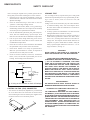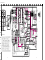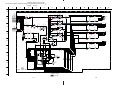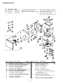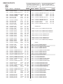
1
GDM-F500/F500T9 SERVICE MANUAL GDM-F500 US Model Canadian Model AEP Model REVISED Chassis No. SCC-L03C-A GDM-F500T9 AEP Model Chassis No. SCC-L03CA N3P CHASSIS SPECIFICATIONS TRINITRON COLOR GRAPHIC DISPLAY ® MICROFILM GDM-F500/F500T9 SAFETY CHECK-OUT After correcting the original service problem, perform the following safety checks before releasing the set to the customer: 1. Check the area of your repair for unsoldered or poorly-soldered connections. Check the entire board surface for solder splashes and bridges. 2. Check the interboard wiring to ensure that no wires are “pinched” or contact high-wattage resistors. 3. Check that all control knobs, shields, covers, ground straps, and mounting hardware have been replaced. Be absolutely certain that you have replaced all the insulators. 4. Look for unauthorized replacement parts, particularly transistors, that were installed during a previous repair. Point them out to the customer and recommend their replacement. 5. Look for parts which, though functioning, show obvious signs of deterioration. Point them out to the customer and recommend their replacement. 6. Check the line cords for cracks and abrasion. Recommend the replacement of any such line cord to the customer. 7. Check the B+ and HV to see if they are specified values. Make sure your instruments are accurate; be suspicious of your HV meter if sets always have low HV. 8. Check the antenna terminals, metal trim, “metallized” knobs, screws, and all other exposed metal parts for AC Leakage. Check leakage as described below. To Exposed Metal Parts on Set 0.15 µF 1.5 k Ω AC Voltmeter (0.75 V) Earth Ground LEAKAGE TEST The AC leakage from any exposed metal part to earth ground and from all exposed metal parts to any exposed metal part having a return to chassis, must not exceed 0.5 mA (500 microampers). Leakage current can be measured by any one of three methods. 1. A commercial leakage tester, such as the Simpson 229 or RCA WT-540A. Follow the manufacturers’ instructions to use these instruments. 2. A battery-operated AC milliammeter. The Data Precision 245 digital multimeter is suitable for this job. 3. Measuring the voltage drop across a resistor by means of a VOM or battery-operated AC voltmeter. The “limit” indication is 0.75 V, so analog meters must have an accurate lowvoltage scale. The Simpson 250 and Sanwa SH-63Trd are examples of a passive VOMs that are suitable. Nearly all battery operated digital multimeters that have a 2 V AC range are suitable. (See Fig. A) WARNING!! NEVER TURN ON THE POWER IN A CONDITION IN WHICH THE DEGAUSS COIL HAS BEEN REMOVED. SAFETY-RELATED COMPONENT WARNING!! COMPONENTS IDENTIFIED BY SHADING AND MARK ¡ ON THE SCHEMATIC DIAGRAMS, EXPLODED VIEWS AND IN THE PARTS LIST ARE CRITICAL FOR SAFE OPERATION. REPLACE THESE COMPONENTS WITH SONY PARTS WHOSE PART NUMBERS APPEAR AS SHOWN IN THIS MANUAL OR IN SUPPLEMENTS PUBLISHED BY SONY. CIRCUIT ADJUSTMENTS THAT ARE CRITICAL FOR SAFE OPERATION ARE IDENTIFIED IN THIS MANUAL. FOLLOW THESE PROCEDURES WHENEVER CRITICAL COMPONENTS ARE REPLACED OR IMPROPER OPERATION IS SUSPECTED. AVERTISSEMENT!! NE JAMAIS METTRE SOUS TENSION QUAND LA BOBINE DE DEMAGNETISATION EST ENLEVÉE. Fig. A. Using an AC voltmeter to check AC leakage. CAUTION ON DAS (ECS) CONNECTOR • The connector for DAS (ECS) adjustment is provided inside the cover shown below. Be careful with an electrical shock when connecting the connector with the power supplied. Also, return the removed cover to the home position. ATTENTION AUX COMPOSANTS RELATIFS À LA SÉCURITÉ!! LES COMPOSANTS IDENTIFIÉS PAR UNE TRAME ET UNE MARQUE ¡ SONT CRITIQUES POUR LA SÉCURITÉ. NE LES REMPLACER QUE PAR UNE PIÈCE PORTANT LE NUMÉRO SPECIFIÉ. LES RÉGLAGES DE CIRCUIT DONT L’IMPORTANCE EST CRITIQUE POUR LA SÉCURITÉ DU FONCTIONNEMENT SONT IDENTIFIÉS DANS LE PRÉSENT MANUEL. SUIVRE CES PROCÉDURES LORS DE CHAQUE REMPLACEMENT DE COMPOSANTS CRITIQUES, OU LORSQU’UN MAUVAIS FONCTIONNE-MENT EST SUSPECTÉ. STAND –2– GDM-F500/F500T9 POWER SAVING FUNCTION This monitor meets the power-saving guidelines set by VESA, ENERGY STAR, and NUTEK. If the monitor is connected to a computer or video graphics board that is DPMS (Display Power Management Signaling) compliant, the monitor will automatically reduce power consumption in three stages as shown below. Power mode Power consumption* 1 (power) indicator normal operation ≤ 160 W green 1 standby ≤ 100 W green and orange alternate 2 suspend ≤ 15 W green and orange alternate 3 active off** ≤1W orange power off 0W off * Figures reflect power consumption when no USB compatible peripherals are connected to the monitor. **When your computer enters the “active off” mode, the input signal is cut and NO INPUT SIGNAL appears on the screen. After the time set in “Changing the power saving delay time.” (page 1-6) has elapsed, the monitor enters the power saving mode. To change the power saving delay time See page 1-6. DIAGNOSIS This monitor is equipped with a self-diagnosis function. If there is a problem with your monitor or computer(s), the screen will go blank and the 1 (power) indicator will either light up green or flash orange. If the 1 (power) indicator is lit in orange, the computer is in power saving mode. Try pressing any key on the keyboard. If all four color bars appear (white, red, green, blue), the monitor is working properly. Reconnect the video input cables and check the condition of your computer(s). If the color bars do not appear, there is a potential monitor failure. Inform your authorized Sony dealer of the monitor’s condition. If the 1 (power) indicator is flashing orange RESET ASC INPUT HD15 BNC MENU 1 (power) indicator If the 1 (power) indicator is green 1 Remove any plugs from the video input 1 and 2 connectors, or turn off the connected computer(s). 2 Press the 1 (power) button to turn the monitor off and on. Press the 1 (power) button to turn the monitor off and on. If the 1 (power) indicator lights up green, the monitor is working properly. If the 1 (power) indicator is still flashing, there is a potential monitor failure. Count the number of seconds between orange flashes of the 1 (power) indicator and inform your authorized Sony dealer of the monitor’s condition. Be sure to note the model name and serial number of your monitor. Also note the make and model of your computer and video board. 3 Move the joystick to the right for 2 seconds before the monitor enters power saving mode. –3– GDM-F500/F500T9 TIMING SPECIFICATION MODE AT PRODUCTION MODE 1 MODE 2 MODE 3 MODE 4 MODE 5 738 X 414 1600 X 1200 1800 X 1440 1800 X 1350 1364 X 1201 28.322 MHZ 229.500 MHZ 299.436 MHZ 299.000 MHZ 195.500 MHZ 31.469 kHz 106.250 kHz 120.740 kHz 120.565 kHz 106.250 kHz usec usec usec usec usec H. TOTAL 31.777 9.412 8.282 8.294 9.412 H. BLK 5.720 2.440 2.271 2.274 2.435 H. FP 0.318 0.279 0.668 0.669 0.276 H. SYNC 3.813 0.837 0.481 0.482 0.839 RESOLUTION CLOCK — HORIZONTAL — H-FREQ H. BP 1.589 1.325 1.122 1.124 1.320 H. ACTIV 26.057 6.972 6.011 6.020 6.977 70.087 Hz 85.000 Hz 80.120 Hz 85.084 Hz 85.000 Hz lines lines lines lines lines V. TOTAL 449 1250 1507 1417 1250 V. BLK 35 50 67 67 49 V. FP 5 1 1 1 1 V. SYNC 2 3 3 3 3 — VERTICAL — V. FREQ(HZ) V. BP 28 46 63 63 45 V. ACTIV 414 1200 1440 1350 1201 — SYNC — INT(G) EXT(H/V)/POLARITY EXT(CS) /POLARITY INT/NON INT SIZE (21") NO NO NO NO NO YES N/P YES P/P YES P / P YES P / P YES P/P NO NO NO NO NO NON INT NON INT NON INT NON INT NON INT 388 X 291mm 388 X 291mm 364 X 291mm 388 X 291mm 388 X 291 mm 98. 4.27 VER. –4– GDM-F500/F500T9 TABLE OF CONTENTS Section Title Page 1. GENERAL ................................................................. 1-1 2. DISASSEMBLY 2-1. 2-2. 2-3. 2-4. 2-5. 2-6. 2-7. 2-8. 2-9. 2-10. Cabinet Removal ............................................... D Board Removal .............................................. G Board Removal .............................................. A Board Removal .............................................. L Board Removal .............................................. Service Position .................................................. H1, H2 and J Boards Removal .......................... US Board Removal ............................................. Picture Tube Removal ....................................... Harness Location ................................................ 2-1 2-1 2-2 2-2 2-3 2-3 2-4 2-4 2-5 2-6 3. SAFETY RELATED ADJUSTMENT ............. 3-1 4. ADJUSTMENTS ..................................................... 4-1 5. DIAGRAMS 5-1. 5-2. 5-3. 5-4. (1) (2) (3) (4) (5) 5-5. Block Diagrams .................................................. Frame Shcematic Diagram ................................. Circuit Boards Location ..................................... Schematic Diagrams and Printed Wiring Boards ................................................................. Schematic Diagrams of D (1/2, 2/2) Board ...... Schematic Diagrams of G, H1, H2, J and L Boards ............................................................ Schematic Diagram of A Board ........................ Schematic Diagram of US Board (-11) (OLD) ................................................................ Schematic Diagram of US Board (-12, -13) (NEW) .............................................................. Semiconductors ................................................. 5-1 5-7 5-9 5-9 5-13 5-17 5-24 5-29 5-33 5-35 6. EXPLODED VIEWS 6-1. 6-2. 6-3. Chassis ............................................................... 6-1 Picture Tube ...................................................... 6-2 Packing Materials .............................................. 6-3 7. ELECTRICAL PARTS LIST ............................ 7-1 Note: Hand degauss must be used on stand-by or power-off condition. This model has an automatic earth magnetism correction function by using an earth magnetism sensor and a LCC coil. When using a hand degauss while monitor (LCC coil) is being operated, it sometimes gets magnetized, and the system may not work properly as a result. –5– SECTION 1 The operating instructions mentioned here are partial abstracts from the Operating Instruction Manual. The page numbers of the Operating Instruction Manual remain as in the manual. GENERAL Use of the tilt-swivel Precautions Warning on power connections • Use the supplied power cord. If you use a different power cord, be sure that it is compatible with your local power supply. For the customers in the U.S.A. If you do not use the appropriate cord, this monitor will not conform to mandatory FCC standards. This monitor can be adjusted within the angles shown below. To turn the monitor vertically or horizontally, hold it at the bottom with both hands. Identifying parts and controls See the pages in parentheses for further details. GDM-F500 is used for illustration purposes throughout this manual. GDM-F400 Front Rear 90˚ 12˚ Example of plug types 90˚ 5˚ for 100 to 120 V AC RESET for 200 to 240 V AC • Before disconnecting the power cord, wait at least 30 seconds after turning off the power to allow the static electricity on the screen’s surface to discharge. • After the power is turned on, the screen is demagnetized (degaussed) for about 3 seconds. This generates a strong magnetic field around the screen which may affect data stored on magnetic tapes and disks placed near the monitor. Be sure to keep magnetic recording equipment, tapes, and disks away from the monitor. 1-1 The equipment should be installed near an easily accessible outlet. Installation Do not install the monitor in the following places: • on surfaces (rugs, blankets, etc.) or near materials (curtains, draperies, etc.) that may block the ventilation holes • near heat sources such as radiators or air ducts, or in a place subject to direct sunlight • in a place subject to severe temperature changes • in a place subject to mechanical vibration or shock • on an unstable surface • near equipment which generates magnetism, such as a transformer or high voltage power lines • near or on an electrically charged metal surface Maintenance • Clean the screen with a soft cloth. If you use a glass cleaning liquid, do not use any type of cleaner containing an anti-static solution or similar additive as this may scratch the screen’s coating. • Do not rub, touch, or tap the surface of the screen with sharp or abrasive items such as a ballpoint pen or screwdriver. This type of contact may result in a scratched picture tube. • Clean the cabinet, panel and controls with a soft cloth lightly moistened with a mild detergent solution. Do not use any type of abrasive pad, scouring powder or solvent, such as alcohol or benzene. Transportation When you transport this monitor for repair or shipment, use the original carton and packing materials. 4 R (HD15) ASC INPUT HD15 BNC G B HD VD (BNC) MENU GDM-F500 90˚ 15˚ 90˚ 5˚ 1 RESET button (page 14) This button resets the adjustments to the factory settings. 9 Video input 1 connector (HD15) (page 6) This connector inputs RGB video signals (0.700 Vp-p, positive) and sync signals. 2 ASC (auto sizing and centering) button (page 9) This button automatically adjusts the size and centering of the picture. 3 INPUT button and HD 15/BNC indicators (page 9) This button selects the HD15 or BNC video input signal. The input signal and corresponding input indicator change each time you press this button. 5 4 3 2 1 10 9 8 7 6 15 14 13 12 11 Pin No. Signal 1 Red 2 Green (Composite Sync on Green) 3 Blue 4 ID (Ground) 5 1 (power) switch and indicator (pages 7, 15, 18) This button turns the monitor on and off. The power indicator lights up in green when the monitor is turned on, and either flashes in green and orange, or lights up in orange when the monitor is in power saving mode. 5 DDC Ground* 6 Red Ground 7 Green Ground 8 Blue Ground 6 AC IN connector (page 7) This connector provides AC power to the monitor. 9 DDC + 5V* 10 Ground 11 ID (Ground) 12 Bi-Directional Data (SDA)* 13 H. Sync 14 V. Sync 15 Data Clock (SCL)* 4 Joystick (page 11) The joystick is used to display the menu and make adjustments to the monitor, including brightness and contrast adjustments. 7 USB (universal serial bus) upstream connector (page 8) Use this connector to link the monitor to a USB compliant computer. 8 USB (universal serial bus) downstream connectors (page 8) Use these connectors to link USB peripheral devices to the monitor. EN * DDC (Display Data Channel) is a standard of VESA. q; Video input 2 connector (BNC) (page 6) This connector inputs RGB video signals (0.700 Vp-p, positive) and sync signals. 5 x Connecting to a Macintosh or compatible computer Setup Before using your monitor, check that the following accessories are included in your carton: • Power cord (1) • HD15 video signal cable (1) • USB cable (1) • Macintosh adapter (1) • Windows Monitor Information Disk (1) • Warranty card (1) • Notes on cleaning the screen’s surface (1) • This instruction manual (1) Step 1: Connect your monitor to your computer With the monitor and computer switched off, first connect the power cord to the monitor, then connect it to a power outlet. Use the supplied Macintosh adapter. R G B (HD15) Step 2: Connect the power cord HD R (HD15) G B HD (BNC) R (HD15) G B HD VD (BNC) The installation of your monitor is complete. If necessary, use the monitor’s controls to adjust the picture. If no picture appears on your screen to AC IN to HD15 Macintosh adapter (supplied)* HD15 video signal cable (supplied) to video Macintosh or compatible computer output * Connect the supplied Macintosh adapter to the computer before connecting the cable. This adapter is compatible with Macintosh LC, Performa, Quadra, Power Macintosh and Power Macintosh G3 series computers. Macintosh II series and some older versions of PowerBook models may need an adapter with micro switches (not supplied). VD (BNC) x Connecting to the five BNC connectors to HD15 R G (HD15) B HD VD (BNC) 1-2 to video output IBM PC/AT or compatible computer HD15 video signal cable (supplied) Refer to the preceding examples to connect to your computer. to a power outlet power cord (supplied) • Check that the monitor is correctly connected to the computer. • If NO INPUT SIGNAL appears on the screen, try changing the input signal (page 9), and confirm that your computer’s graphic board is completely seated in the correct bus slot. • If you are replacing an old monitor with this model and OUT OF SCAN RANGE appears on the screen, reconnect the old monitor. Then adjust the computer’s graphic board so that the horizontal frequency is between 30 – 107 kHz (GDM-F400) or 30 – 121 kHz (GDM-F500), and the vertical frequency is between 48 – 160 Hz. For more information about the on-screen messages, see “Trouble symptoms and remedies” on page 16. For customers using Windows 95/98 To maximize the potential of your monitor, install the new model information file from the supplied Windows Monitor Information Disk onto your PC. This monitor complies with the “VESA DDC” Plug & Play standard. If your PC/graphics board complies with DDC, select “Plug & Play Monitor (VESA DDC)” or this monitor’s model name as the monitor type in the “Control Panel” of Windows 95/98. If your PC/graphics board has difficulty communicating with this monitor, load the Windows Monitor Information Disk and select this monitor’s model name as the monitor type. For customers using Windows NT4.0 Monitor setup in Windows NT4.0 is different from Windows 95/98 and does not involve the selection of monitor type. Refer to the Windows NT4.0 instruction manual for further details on adjusting the resolution, refresh rate, and number of colors. to VIDEO IN R/G/B If your PC system is not compatible with Plug & Play (DDC2AB or DDC2B+) This monitor uses the No.9 pin in the video signal connector for Plug & Play (DDC2AB or DDC2B+) compatibility. See page 5 for the location of the No.9 pin. • If your computer accepts the No.9 pin, use the supplied HD15 video signal cable. • If your computer does not accept the No.9 pin, please consult your dealer for advice on obtaining an HD15 adapter. First turn on the monitor, then turn on the computer. VD Turn off the monitor and computer before connecting. x Connecting to an IBM PC/AT or compatible computer Step 3: Turn on the monitor and computer to SYNC IN HD/VD video signal cable (SMF-400, not supplied)* * Connect the cables from left to right in the following order: Red-GreenBlue-HD-VD. Adjusting the monitor’s resolution and color number Adjust the monitor’s resolution and color number by referring to your computer’s instruction manual. The color number may vary according to your computer or video board. The color palette setting and the actual number of colors are as follows: • High Color (16 bit) t 65,536 colors • True Color (24 bit) t about 16.77 million colors In true color mode (24 bit), speed may be slower. Notes • Do not touch the pins of the video cable connector as this might bend the pins. • Plug & Play (DDC) does not apply to the five BNC connectors. If you want to use Plug & Play, connect your computer to the HD15 connector using the supplied video signal cable. 6 7 EN Connecting Universal Serial Bus (USB) compliant peripherals Selecting the on-screen menu language (LANG) Your monitor has one upstream and four downstream USB connectors. They provide a fast and easy way to connect USB compliant peripheral devices (such as keyboards, mice, printers and scanners) to your computer using a standardized USB cable. To use your monitor as a hub for your peripheral devices, connect the USBs as illustrated below. English, French, German, Spanish, Italian, and Japanese versions of the on-screen menus are available. The default setting is English. 1 Press the joystick See page 11 for more information on using the joystick. MENU to USB compliant peripheral devices CENTER SCREEN GEOM EXIT ZOOM LANG SIZE OPTION 2 Move the joystick to highlight LANG and press the joystick again. to USB compliant peripheral devices LANGUAGE ENGLISH FRANÇAIS DEUTSCH ESPAÑOL I TA LIANO 1 Turn on the monitor and computer. 2 Connect your computer to the square upstream You can connect two computers to this monitor using the HD15 and BNC connectors. To switch between the two computers, use the INPUT button. Press the INPUT button. The input signal and corresponding input indicator change each time you press this button. Automatically sizing and centering the picture You can easily adjust the picture to fill the screen by pressing the ASC (auto sizing and centering) button. Press the ASC button. The picture automatically fills the screen. MENU COLOR to a USB compliant computer Selecting the input signal INPUT HD15 BNC Notes • If no signal is input to the selected connector, the monitor automatically switches to the other connector. • If you restart the computer you want to view, or that computer is in power saving mode, the monitor may automatically switch to the other connector’s signal. If this happens, manually select the desired signal using the INPUT button. ASC Notes • This function is intended for use with a computer running Windows or similar graphic user interface software that provides a full-screen picture. It may not work properly if the background color is dark or if the input picture does not fill the screen to the edges (such as an MSDOS prompt). • Pictures with an aspect ratio of 5:4 (resolution: 1280 × 1024, 1800 × 1440*) are displayed at their actual resolution and do not fill the screen to the edges. • The screen may go blank for a few seconds when the ASC button is pressed. This is not a malfunction. * GDM-F500 only connector using the supplied USB cable. For customers using Windows If a message appears on your screen, follow the on-screen instructions and select Generic USB Hub as the default setting. 3 Connect your USB compliant peripheral devices to 1-3 the rectangular downstream USB connectors. Notes • Not all computers and /or operating systems support USB configurations. Check your computer’s instruction manual to see if you can connect USB devices. • In most cases, USB driver software needs to be installed on the host computer. Refer to the peripheral device’s instruction manual for further details. • The monitor functions as a USB hub as long as the monitor is either “on” or in power saving mode. • If you connect a keyboard or mouse to the USB connectors and then boot your computer for the first time, the peripheral devices may not function. First connect the keyboard and mouse directly to the computer and set up the USB compliant devices. Then connect them to this monitor. • Do not lean on the monitor when plugging in the USB cables. The monitor may suddenly shift and cause injury. 8 3 Move the joystick up or down to select a language and press the joystick again. • ENGLISH • FRANÇAIS: French • DEUTSCH: German • ESPAÑOL: Spanish • ITALIANO: Italian • : Japanese To close the menu Press the joystick once to return to the main menu, and twice to return to normal viewing. If no buttons are pressed, the menu closes automatically after about 30 seconds. To reset to English Press the RESET button while the LANGUAGE menu is displayed on the screen. 9 EN Customizing Your Monitor You can make numerous adjustments to your monitor using the on-screen menu. x Using the joystick 6 SCREEN (page 13) Select the SCREEN menu to adjust the picture’s quality. You can adjust the vertical and horizontal convergence, landing, and moire cancellation effect. SCREEN 7 LANG (page 8) Select LANG to choose the onscreen menu’s language. LANGUAGE 1 Select the menu you want to adjust. TOP BOT 26 ADJ Move the joystick up, down, left, or right to highlight the desired menu. Press the joystick to select the menu item. H CONVERGENCE Navigating the menu Press the joystick to display the main MENU on your screen. See page 11 for more information on using the joystick. b ENGLISH FRANÇAIS DEUTSCH ESPAÑOL I TA LIANO Adjusting the brightness and contrast Brightness and contrast adjustments are made using a separate BRIGHTNESS/CONTRAST menu. These settings are stored in memory for all input signals. 1 Move the joystick in any direction. The BRIGHTNESS/CONTRAST menu appears on the screen. BRIGHTNESS/CONTRAST 2 Adjust the menu. MENU COLOR 8 OPTION (page 14) Select OPTION to adjust the monitor’s options. The options include: • degaussing the screen • changing the on-screen menu position • changing the power saving delay time • locking the controls MENU CENTER SCREEN GEOM EXIT ZOOM LANG SIZE OPTION OPTION ON ZZ... 26 Move the joystick up, down, left, or right to make the adjustment. the horizontal and vertical frequencies of the current input signal 5 SEC UNLOCK 2 Move the joystick up or down to adjust the MANUAL DEGAUSS brightness ( ), and left or right to adjust the contrast (6). The menu automatically disappears after about 3 seconds. 3 Close the menu. 9 EXIT Select EXIT to close the menu. Use the joystick to select one of the following menus. 1 CENTER (page 11) Select the CENTER menu to adjust the picture’s centering. CENTER 26 80.0kHz/ 75Hz Press the joystick once to return to the main menu, and twice to return to normal viewing. If no buttons are pressed, the menu closes automatically after about 30 seconds. 73 Adjusting the centering of the picture (CENTER) EN This setting is stored in memory for the current input signal. 26 1 Press the joystick. The main MENU appears on the screen. 1-4 2 SIZE (page 11) Select the SIZE menu to adjust the picture’s horizontal and vertical size. SIZE x Resetting the adjustments 73 Press the RESET button. See page 14 for more information on resetting the adjustments. 26 2 Move the joystick to highlight CENTER and press the joystick again. The CENTER menu appears on the screen. 3 Move the joystick up or down to adjust the vertical 3 GEOM (page 12) Select the GEOM menu to adjust the picture’s rotation and shape. centering, and left or right to adjust the horizontal centering. GEOMETRY RESET Adjusting the size of the picture (SIZE) 26 ROTATION This setting is stored in memory for the current input signal. 4 ZOOM (page 12) Select the ZOOM menu to enlarge or reduce the picture. ZOOM 1 Press the joystick. The main MENU appears on the screen. H V 5 COLOR (page 12) Select the COLOR menu to adjust the picture’s color temperature. You can use this to match the monitor’s colors to a printed picture’s colors. 10 26 73 2 Move the joystick to highlight SIZE and press the joystick again. The SIZE menu appears on the screen. COLOR 5000K R G B R G B B I AS B I AS B I AS GAIN GAIN GAIN 6500K 9300K 50 50 50 50 50 50 3 Move the joystick up or down to adjust the vertical size, and left or right to adjust the horizontal size. 11 Adjusting the shape of the picture (GEOM) Adjusting the color of the picture (COLOR) Adjusting the quality of the picture (SCREEN) The GEOM settings allow you to adjust the rotation and shape of the picture. The rotation setting is stored in memory for all input signals. All other settings are stored in memory for the current input signal. The COLOR settings allow you to adjust the picture’s color temperature by changing the color level of the white color field. Colors appear reddish if the temperature is low, and bluish if the temperature is high. This adjustment is useful for matching the monitor’s colors to a printed picture’s colors. This setting is stored in memory for all input signals. The SCREEN settings allow you to adjust the quality of the picture by controlling the convergence, moire, and landing. • If you see red or blue shadows around letters or lines, adjust the convergence. • If elliptical or wavy patterns appear on the screen, cancel the moire. • If the color is irregular at the corners of the screen, adjust the landing. The CANCEL MOIRE and MOIRE ADJUST settings are stored in memory for the current input signal. All other settings are stored in memory for all input signals. 1 Press the joystick. The main MENU appears on the screen. 1 Press the joystick. 2 Move the joystick to highlight GEOM and press the joystick again. The GEOMETRY menu appears on the screen. 3 First move the joystick up or down to select the desired adjustment item. Then move the joystick left or right to make the adjustment. Select To ROTATION rotate the picture PINCUSHION expand or contract the picture sides PIN BALANCE shift the picture sides to the left or right KEYSTONE adjust the picture width at the top of the screen KEY BALANCE shift the picture to the left or right at the top of the screen The main MENU appears on the screen. 2 Move the joystick to highlight COLOR and press the joystick again. The COLOR menu appears on the screen. 1-5 This setting is stored in memory for the current input signal. 1 Press the joystick. The main MENU appears on the screen. 2 Move the joystick to highlight ZOOM and press the joystick again. The ZOOM menu appears on the screen. 3 Move the joystick left or right to enlarge or reduce the picture. Note Adjustment stops when either the horizontal or vertical size reaches its maximum or minimum value. 12 To CANCEL MOIRE* ADJ MOIRE ADJUST turn the moire cancellation function ON or OFF ADJ (MOIRE ADJUST) appears in the menu when you select ON adjust the degree of moire cancellation until the moire is at a minimum * Moire is a type of natural interference which produces soft, wavy lines on your screen. It may appear due to interference between the pattern of the picture on the screen and the phosphor pitch pattern of the monitor. Example of moire 1 Press the joystick. The main MENU appears on the screen. 3 Move the joystick left or right to select a color temperature. The preset color temperatures are 5000K, 6500K, and 9300K. Since the default setting is 9300K, the whites will change from a bluish hue to a reddish hue as the temperature is lowered to 6500K and 5000K. 4 If necessary, fine tune the color temperature. First move the joystick up or down to select the desired adjustment item. Then move the joystick left or right to make the adjustment. R G B R G B B I AS B I AS B I AS GAIN GAIN GAIN 2 Move the joystick to highlight SCREEN and press the joystick again. The SCREEN menu appears on the screen. 3 First move the joystick up or down to select the desired adjustment item. Then move the joystick left or right to make the adjustment. Select Note The picture may become fuzzy when CANCEL MOIRE is set to ON. EN To horizontally shift red or blue shadows H CONVERGENCE COLOR 1 Enlarging or reducing the picture (ZOOM) Select 6500K 9300K 76 50 50 50 50 50 1 Adjusting the BIAS (black level) This changes the brightness of both the dark and light areas of an image. 2 Adjusting the GAIN (white level) This changes the contrast of just the light areas of an image. You can adjust the R(Red), G(Green), and B(Blue) component of the input signal when making changes to items 1 and 2. vertically shift red or blue shadows V CONVERGENCE TOP V CONVER TOP vertically shift red or blue shadows at the top of the screen BOT V CONVER BOT vertically shift red or blue shadows at the bottom of the screen LANDING select one of the four corners of the screen :top right :top left ADJ LANDING ADJUST reduce any irregularities in the color of the corner selected in LANDING to a minimum :bottom left :bottom right If you fine tune the color temperature, the new color settings are stored in memory for each of the three color temperatures and item 3 of the on-screen menu changes as follows: • [5000K] t [1] • [6500K] t [2] • [9300K] t [3] 13 Additional settings (OPTION) Resetting the adjustments You can manually degauss (demagnetize) the monitor, change the menu position, set the power saving delay time, and lock the controls. This monitor has the following three reset methods. Use the RESET button to reset the adjustments. 1 Press the joystick. RESET The main MENU appears on the screen. 2 Move the joystick to highlight OPTION and press the joystick again. The OPTION menu appears on the screen. Resetting a single adjustment item Use the joystick to select the adjustment item you want to reset, and press the RESET button. 3 Move the joystick to highlight the desired adjustment item. Adjust the selected item according to the following instructions. Degaussing the screen The monitor is automatically demagnetized when the power is turned on. To manually degauss the monitor, first move the joystick up or down to select (MANUAL DEGAUSS). Then move the joystick to the right. The screen is degaussed for about 3 seconds. If a second degauss cycle is needed, allow a minimum interval of 20 minutes for the best result. Changing the menu’s position. 1-6 Change the menu’s position if it is blocking an image on the screen. To change the menu’s on-screen position, first move the joystick up or down to select (OSD H POSITION) for horizontal adjustment, or (OSD V POSITION) for vertical adjustment. Then move the joystick to the left or right to shift the on-screen menu. Changing the power saving delay time. To adjust the time it takes to enter the power saving mode, first move the joystick up or down to select ZZ... (PWR SAVE DELAY). Then move the joystick to the left or right to select the desired time. If you select OFF, the monitor does not enter power saving mode. See page 15 for more information about the monitor’s power saving capabilities. Locking the controls. To protect adjustment data by locking the controls, first move the joystick up or down to select (CONTROL LOCK). Then move the joystick to the right to select LOCK. Only the 1 (power) switch, EXIT, and (CONTROL LOCK) of the OPTION menu will operate. If any other items are selected, the mark appears on the screen. To cancel the control lock Repeat the procedure above and set UNLOCK. 14 Resetting all of the adjustment data for the current input signal Press the RESET button when no menu is displayed on the screen. Note that the following items are not reset by this method: • on-screen menu language (page 8) • on-screen menu position (page 14) • power saving delay time (page 14) • control lock (page 14) Technical Features Preset and user modes When the monitor receives an input signal, it automatically matches the signal to one of the factory preset modes stored in the monitor’s memory to provide a high quality picture at the center of the screen. (See page i for a list of the factory preset modes.) For input signals that do not match one of the factory preset modes, the digital Multiscan technology of this monitor ensures that a clear picture appears on the screen for any timing in the monitor’s frequency range (horizontal: 30 – 107 kHz (GDMF400) or 30 – 121 kHz (GDM-F500), vertical: 48 – 160 Hz) . If the picture is adjusted, the adjustment data is stored as a user mode and automatically recalled whenever the same input signal is received. Power saving function This monitor meets the power-saving guidelines set by VESA, ENERGY STAR, and NUTEK. If the monitor is connected to a computer or video graphics board that is DPMS (Display Power Management Signaling) compliant, the monitor will automatically reduce power consumption in three stages as shown below. (CONTROL LOCK) The lines you are experiencing on your screen are normal for the Trinitron monitor and are not a malfunction. These are shadows from the damper wires used to stabilize the aperture grille and are most noticeable when the screen’s background is light (usually white). The aperture grille is the essential element that makes a Trinitron picture tube unique by allowing more light to reach the screen, resulting in a brighter, more detailed picture. Damper wires For Windows users, check your video board manual or the utility program which comes with your graphic board and select the highest available refresh rate to maximize monitor performance. Press and hold the reset button for more than two seconds. is set to LOCK. If thin lines appear on your screen (damper wires) Note for Windows users Resetting all of the adjustment data for all input signals Note The RESET button does not function when Troubleshooting Before contacting technical support, refer to this section. On-screen messages EN If there is something wrong with the input signal, one of the following messages appears on the screen. To solve the problem, see “Trouble symptoms and remedies” on page 16. INFORMATION OUT OF SCAN RANGE 1 (power) indicator Power mode Power consumption* normal operation ≤ 160 W (GDM-F500) green ≤ 140 W (GDM-F400) 1 standby ≤ 100 W (GDM-F500) green and orange ≤ 80 W (GDM-F400) alternate 2 suspend ≤ 15 W (GDM-F500) ≤ 10 W (GDM-F400) green and orange alternate 3 active off** ≤ 1 W (GDM-F500) ≤ 3 W (GDM-F400) orange power off 0W off * Figures reflect power consumption when no USB compatible peripherals are connected to the monitor. **When your computer enters the “active off” mode, the input signal is cut and NO INPUT SIGNAL appears on the screen. After the time set in “Changing the power saving delay time.” (page 14) has elapsed, the monitor enters the power saving mode. INPUT : HD15 1 The input signal condition OUT OF SCAN RANGE indicates that the input signal is not supported by the monitor’s specifications. NO INPUT SIGNAL indicates that no signal is input, or that no signal is input from the selected connector (HD15 or BNC). 2 The connector indicator This message indicates which connector is receiving the wrong signal. If there is something wrong with the signal from both connectors, HD15 and BNC are displayed alternately. To change the power saving delay time See page 14. (CONTROL LOCK) to 15 Trouble symptoms and remedies If the problem is caused by the connected computer or other equipment, please refer to the connected equipment’s instruction manual. Use the self-diagnosis function (page 18) if the following recommendations do not resolve the problem. Symptom If the 1 (power) indicator is not lit • Check that the power cord is properly connected. • Check that the 1 (power) switch is in the “on” position. If the NO INPUT SIGNAL message appears on the screen, or if the 1 (power) indicator is either orange or alternating between green and orange • Check that the video signal cable is properly connected and all plugs are firmly seated in their sockets. If you are using the five BNC connectors, connect them in the correct order (from left to right: Red-Green-Blue-HD-VD) (page 6). • Check that the input select setting is correct (page 9). • Check that the HD15 video input connector’s pins are not bent or pushed in. xProblems caused by the connected computer or other equipment • The computer is in power saving mode. Try pressing any key on the computer keyboard. • Check that the computer’s power is “on.” • Check that the graphic board is completely seated in the proper bus slot. xProblems caused by the connected computer or other equipment • Check that the video frequency range is within that specified for the monitor. If you replaced an old monitor with this monitor, reconnect the old monitor and adjust the frequency range to the following. Horizontal: 30 – 107 kHz (GDM-F400), 30 – 121 kHz (GDM-F500) Vertical: 48 – 160 Hz 1-7 If no message is displayed and the 1 (power) indicator is green or flashing orange • Use the Self-diagnosis function (page 18). If using Windows 95/98 • If you replaced an old monitor with this monitor, reconnect the old monitor and do the following. Install the Windows Monitor Information Disk (page 7) and select this monitor (“GDM-F400” or “GDM-F500”) from among the Sony monitors in the Windows 95/98 monitor selection screen. If you choose to select “Plug and Play,” connect the monitor to the computer with the HD15 video signal cable. You cannot use the five BNC connectors. If using a Macintosh system • Check that the Macintosh adapter and the video signal cable are properly connected (page 6). Picture flickers, bounces, oscillates, or is scrambled • Eliminate the use of video cable extensions and/or video switch boxes. • Check that all plugs are firmly seated in their sockets. Picture is not centered or sized properly • Press the ASC button (page 9). • Adjust the size (page 11) or centering (page 11). Note that some video modes do not fill the screen to the edges. Edges of the image are curved • Adjust the geometry (page 12). Wavy or elliptical pattern (moire) is visible • Cancel the moire (page 13). Color is not uniform • Degauss the monitor* (page 14). If you place equipment that generates a magnetic field, such as a speaker, near the monitor, or if you change the direction the monitor faces, color may lose uniformity. • Adjust the landing (page 13). White does not look white • Adjust the color temperature (page 12). • Check that the five BNC connectors are connected in the correct order (from left to right: Red-Green-Blue-HD-VD) (page 6). Letters and lines show red or blue shadows at the edges • Adjust the convergence (page 13). • Adjust the brightness and contrast (page 11). • Degauss the monitor* (page 14). • If CANCEL MOIRE is ON, the picture may become fuzzy. Decrease the moire cancellation effect or set CANCEL MOIRE to OFF (page 13). xProblems caused by the connected computer or other equipment • Change your desktop pattern. Monitor buttons do not operate • If the control lock is set to LOCK, set it to UNLOCK (page 14). USB peripherals do not function • Check that the appropriate USB connectors are securely connected (page 8). • Check that the 1 (power) switch is in the “on” position. xProblems caused by the connected computer or other equipment • Check that the power of any self-powered USB compliant peripheral devices is “on.” • Install the latest version of the device driver on your computer. Contact your device’s manufacturer for information about the appropriate device driver. • If your USB compliant keyboard or mouse does not function, connect them directly to your computer, reboot your computer, and make any necessary adjustments to the USB settings. Then reconnect the keyboard or mouse to the monitor. • For customers using Windows 95 1. Right-click on My Computer and select Properties. 2. Click on the Device Manager tab. Scroll down and select Universal Serial Bus Controller. ,If Universal Serial Bus Controller does not appear, you need to load a USB supplement disk. Contact your computer’s manufacturer for more information about obtaining a USB supplement disk. 3. Select Generic USB Device from the USB controller list and click on Properties. 4. If there is a check in the box next to “Disable in this hardware profile,” remove the check. 5. Click on Refresh. • Isolate and eliminate any potential sources of electric or magnetic fields such as other monitors, laser printers, electric fans, fluorescent lighting, or televisions. • Move the monitor away from power lines or place a magnetic shield near the monitor. • Try plugging the monitor into a different AC outlet, preferably on a different circuit. • Try turning the monitor 90° to the left or right. xProblems caused by the connected computer or other equipment • Check your graphics board manual for the proper monitor setting. • Confirm that the graphics mode (VESA, Macintosh 21" Color, etc.) and the frequency of the input signal are supported by this monitor (page i). Even if the frequency is within the proper range, some video boards may have a sync pulse that is too narrow for the monitor to sync correctly. • Adjust the computer’s refresh rate (vertical frequency) to obtain the best possible picture. Picture is fuzzy Check these items Picture is ghosting Check these items No picture If the OUT OF SCAN RANGE message appears on the screen Symptom A hum is heard right after the power is turned on • This is the sound of the auto-degauss cycle. When the power is turned on, the monitor is automatically degaussed for three seconds. * If a second degauss cycle is needed, allow a minimum interval of 20 minutes for the best result. A humming noise may be heard, but this is not a malfunction. Displaying this monitor’s name, serial number, and date of manufacture. While the monitor is receiving a video signal, press and hold the joystick for more than three seconds to display this monitor’s information box. If the problem persists, call your authorized Sony dealer and give the following information. • Model name: GDM-F400, GDM-F500 • Serial number • Name and specifications of your computer and graphics board. Example INFORMATION MODEL : GDM F500 SER NO : 1234567 MANUFACTURED : 1998-52 16 17 EN Self-diagnosis function This monitor is equipped with a self-diagnosis function. If there is a problem with your monitor or computer(s), the screen will go blank and the 1 (power) indicator will either light up green or flash orange. If the 1 (power) indicator is lit in orange, the computer is in power saving mode. Try pressing any key on the keyboard. Specifications GDM-F400 CRT Viewable image size RESET ASC INPUT HD15 BNC MENU Resolution 1 (power) indicator Standard image area If the 1 (power) indicator is green 1 Remove any plugs from the video input 1 and 2 connectors, or turn off the connected computer(s). 2 Press the 1 (power) button to turn the monitor off and on. 3 Move the joystick to the right for 2 seconds before the monitor enters power saving mode. Deflection frequency* AC input voltage/current Power consumption Dimensions Mass Plug and Play Supplied accessories 0.22 mm aperture grille pitch 19 inches measured diagonally 90-degree deflection FD Trinitron Approx. 364.8 × 273.6 mm (w/h) (14 3/8 × 10 7/8 inches) 18.0" viewing image Horizontal: Max. 1600 dots Vertical: Max. 1200 lines Approx. 352 × 264 mm (w/h) (13 7/8 × 10 1/2 inches) or Approx. 330 × 264 mm (w/h) (13 × 10 1/2 inches) Horizontal: 30 to 107 kHz Vertical: 48 to 160 Hz 100 to 240 V, 50 – 60 Hz, 1.8 – 1.0 A Max. 140 W (with no USB devices connected) Approx. 444 × 476 × 455 mm (w/h/d) (17 1/2 × 18 3/4 × 18 inches) Approx. 28 kg (61 lb 12 oz) DDC1/DDC2B/DDC2Bi/DDC2B+ See page 6 GDM-F500 CRT 1-8 If all four color bars appear (white, red, green, blue), the monitor is working properly. Reconnect the video input cables and check the condition of your computer(s). Viewable image size Resolution If the color bars do not appear, there is a potential monitor failure. Inform your authorized Sony dealer of the monitor’s condition. Standard image area If the 1 (power) indicator is flashing orange Press the 1 (power) button to turn the monitor off and on. If the 1 (power) indicator lights up green, the monitor is working properly. Deflection frequency* If the 1 (power) indicator is still flashing, there is a potential monitor failure. Count the number of seconds between orange flashes of the 1 (power) indicator and inform your authorized Sony dealer of the monitor’s condition. Be sure to note the model name and serial number of your monitor. Also note the make and model of your computer and video board. Dimensions AC input voltage/current Power consumption Mass Plug and Play Supplied accessories 0.22 mm aperture grille pitch 21 inches measured diagonally 90-degree deflection FD Trinitron Approx. 403.8 × 302.2 mm (w/h) (16 × 12 inches) 19.8" viewing image Horizontal: Max. 1800 dots Vertical: Max. 1440 lines Approx. 388 × 291 mm (w/h) (15 3/8 × 11 1/2 inches) or Approx. 364 × 291 mm (w/h) (14 3/8 × 11 1/2 inches) Horizontal: 30 to 121 kHz Vertical: 48 to 160 Hz 100 to 240 V, 50 – 60 Hz, 2.0 – 1.0 A Max. 160 W (with no USB devices connected) Approx. 502 × 511 × 486.3 mm (w/h/d) (19 7/8 × 20 1/8 × 19 1/4 inches) Approx. 34 kg (74 lb 15 oz) DDC1/DDC2B/DDC2AB/DDC2B+ See page 6 * Recommended horizontal and vertical timing condition • Horizontal sync width duty should be more than 4.8% of total horizontal time or 0.8 µs, whichever is larger. • Horizontal blanking width should be more than 2.5 µsec. • Vertical blanking width should be more than 450 µsec. Design and specifications are subject to change without notice. 18 GDM-F500/F500T9 SECTION 2 DISASSEMBLY 2-1. CABINET REMOVAL 3 5 6 7 1 Four screws (+ BVTT 4 x 8) Four screws (+ BVTP 4 x 16) Screw cover Two screws (+ BVTT 4 x 8) Top cover 2 4 8 9 Screw cover Cabinet Three screws (+ BVTT 4 x 8) Video shield Attachment 2-2. D BOARD REMOVAL 4 Two screws (+ BVTP 3 x 10) 1 5 D board Screw (+ BVTT 4 x 8) 2 Two screws (+ BVTT 4 x 8) B GND Three hooks A Side cover (D) assembly 3 2-1 Open the D block in the direction of the arrow A and remove of the arrow B . GDM-F500/F500T9 2-3. G BOARD REMOVAL 4 1 2 Two screws (+ BVTP 3 x 10) Screw (+ BVTT 4 x 8) Two screws (+ BVTT 4 x 8) 5 G shield 6 Two screws (+ BVTP 3 x 10) 7 Screw (+ P 3.5 x 20) 9 G board GND B GND A Three hooks 3 Side cover (G) assembly Open the G block in the direction of the arrow A and remove of the arrow B . 8 Two printed circuit board holders 2-4. A BOARD REMOVAL 3 Rear shield assembly A board (2/2) Two screws (+BVTT 4 x 8) 2 A board (1/2) 2-2 1 Three screws (+BVTT 4 x 8) GDM-F500/F500T9 2-5. L BOARD REMOVAL CN5001 CN5004 CN5002 CN5003 2 1 L board Four printed circuit board holders 2-6. SERVICE POSITION CAUTION : SHORT D,G boards Rear shield If the claw is hooked, opening and closing the board is impossible. Do not try to do it by force. D board (Refer to 2-2. ) A board (Refer to 2-4. ) If the claw is hooked, opening and closing the board is impossible. Do not try to do it by force. G board (Refer to 2-3.) 2-3 GDM-F500/F500T9 2-7. H1, H2 AND J BOARDS REMOVAL 1 Four screws (Tapping screw 5) 5 Two screws (+ BVTP 3 x 10) 6 H2 board Claw 7 Claw CN891 CN801 8 J board Claw 3 Two screws Knob 2 (+ BVTP 3 x 10) H1 board Bezel assembly 4 2-8. US BOARD REMOVAL 5 US board 2 Stand cover 3 4 Six screws (+ BVTP 3 x 10) Shield case Claw Cushion CN2601 1 2-4 Three screws (+ BVTP 3 x 10) GDM-F500/F500T9 2-9. PICTURE TUBE REMOVAL 1 4 Open the D block (Refer to 2-2.) 6 Four screws (+ BVTT 4 x 8) Three connectors GND (DY) 6P (DY) 3 A board 10P (DY) 5 Anode cap 2 8 9 7 Open the G block (Refer to 2-3.) EMI spring (4) Neck assembly Deflection yoke Picture tube • REMOVAL OF ANODE-CAP NOTE: Short circuit the anode of the picture tube and the anode cap to the metal chassis, CRT shield or carbon painted on the CRT, after removing the anode. • REMOVING PROCEDURES c b a Anode Button 1 Turn up one side of the rubber cap in the direction indicated by the arrow a. 2 Using a thumb pull up the rubber cap firmly in the direction indicated by the arrow b. • HOW TO HANDLE AN ANODE-CAP 1 Don’t hurt the surface of anode-caps with shartp shaped material! 2 Don’t press the rubber hardly not to hurt inside of anode-caps! A material fitting called as shatter-hook terminal is built in the rubber. 3 Don’t turn the foot of rubber over hardly! The shatter-hook terminal will stick out or hurt the rubber. 2-5 3 When one side of the rubber cap is separated from the anode button, the anode-cap can be removed by turning up the rubber cap and pulling up it in the direction of the arrow c. GDM-F500/F500T9 2-10. HARNESS LOCATION H1 board H2 board CN802 Stand assembly J board CN801 CN803 CN891 CN2601 CN5003 CN5004 CN5002 CN5001 CN604 CN501 FBT CN509 D board G board L board Rear shield AC inlet CN409 CN408 CN402 CN401 A board 2-6 CN405 CN406 CN403 CN407 I/O terminal board assembly CN502 CN508 CN513 CN512 CN901 CN510 CN503 CN504 CN520 CN511 CN506 CN673 CN690 CN603 CN671 CN672 CN605 US board Picture tube GDM-F500/F500T9 SECTION 3 SAFETY RELATED ADJUSTMENT When replacing or repairing the shown below table, the following operational checks must be performed as a safety precaution against X-rays emissions from the unit. d) Beam Current Protector Circuit Check-1 (Hardware) Connect a variable resistor (20 kΩ or more) and an ammeter in series between pin !¡ of T901 (FBT) and –15 V line. Decrease gradually the resistance of the variable resistor from maximum to minimum, and confirm that the Beam Current Protector Circuit works and TV Raster disappears. The current must be within the range shown below. Check Condition • Input signal : White Cross Hatch at 120.7 kHz • Beam control : BRT = 0, CONT = 0 • Standard : 1.49 mA Part Replaced (]) HV Regulator Circuit Check G Board IC901, T901 • Mounted G board HV Protector Circuit Check G Board Q907, Q908, D913, D916, C923, R920, R927, R952, T901 • Mounted G board Beam Current Protector Circuit Check D Board R011, R1068 • Mounted D board G Board IC901, IC902, Q907, Q908, D902, D918, D919, R923, R928, R933, R934, R942, R944, R945, R947, R948, R951, R952, T901 • Mounted G board e) Beam Current Protector Circuit Check-2 (Software) 1) Short between + of C937 and GND. 2) Connect a variable resistor (20 kΩ or more) and an ammeter in series between pin !¡ of T901 (FBT) and –15 V line. Decrease gradually the resistance of the variable resistor from maximum to minimum, and confirm that the Beam Current Protector Circuit works and TV Raster disappears. The current must be within the range shown below. Check Condition • Input signal : White Cross Hatch at 120.7 kHz • Beam control : BRT = 0, CONT = 0 • Standard : 1.59 mA * Confirm one minute later turning on the power. a) B+ Voltage Check Check Condition • Input voltage : 100 ~ 240 VAC • Input signal : White Cross Hatch at 120.7 kHz • Beam control : BRT and CONT → MAX • Standard : 200 ± 3.0 V DC b) HV Regulator Circuit Check 1) Confirm that the voltage of the + side of C910 on G board is within the voltage range shown below. Standard: 8.940 ~ 9.065 V DC c) HV Protector Circuit Check 1) Confirm that the voltage between cathode of D913 on G board and GND is more than 26.5 V DC. 2) Confirm that the HV protector circuit works and TV Raster disappears when apply the voltage as shown below between cathode of D913 and GND using an external DC power supply. Check Condition • Input voltage : 100 ~ 240 VAC • Input signal : White Cross Hatch at 120.7 kHz • Beam control : BRT and CONT → MIN • Standard : Less than 34.20 V DC 3-1 SECTION 4 GDM-F500/F500T9 ADJUSTMENTS Note: Hand degauss must be used on stand-by or power-off condition. This model has an automatic earth magnetism correction function by using an earth magnetism sensor and a LCC coil. When using a hand degauss while monitor (LCC coil) is being operated, it sometimes gets magnetized, and the system may not work properly as a result. • Landing Rough Adjustment 1. Enter the full white signal. (or the full black dots signal). 2. Adjust the contrast to the maximum. 3. Make the screen monogreen. Note: Off the outputs from R ch and B ch of SG. 4. Reverse the DY, and adjust coarsely the purity magnet so that a green raster positions in the center of screen. 5. Adjust the tilt of DY, and fix lightly with a clamp. Note: “TILT” shall be set at 128. <Specifications> Adjust so that the green is within the specification given right. Adjust target : within ± 1 The red and blue must be within the specification given right with respect to the green. • Landing Fine Adjustment 1. Put the set inside the Helmholtz coil. (“LCC SW” = “12”) 2. Input the single green signal and set the CONT control to MAX. Note: After the W/B adjustment with 9300K, measure an average of ΣIk when a full white signal is entered in the CONT MAX/BRT CENT status. Then make adjustment so that the specified screen can be attained after aging for 2 hours with Ik equivalent to 30% of the average value. 3. Demagnetize the metal part of the chassis with the hand degausser and coil degausser, and the CRT surface with the hand degausser. Input AC 230V to AC IN, turn on and off the power to perform auto degaussing. (Perform auto degaussing by setting “MON CON REG2”=152. Return to the original value after use.) Demagnetize the CRT surface with the hand degausser again. Note: (1) Hand degauss must be used on stand-by or power-off condition. This model has an automatic earth magnetism correction function by using an earth magnetism sensor and a LCC coil. When using a hand degauss while monitor (LCC coil) is being operated, it sometimes gets magnetized, and the system may not work properly as a result. (2) Adjust in a non-magnetic field. BV=45uT. (3) If adjusting in a magnetic fields, add the shift from the nonmagnetic field in your estimation. 4. Attach the wobbling coil to the designated part of the CRT neck. 5. Attach the sensor of the landing adjustment unit on the CRT surface. 6. Adjust the DY position and purity, and the DY tilt, and landing of the center and 4 corners with the landing checker. • Write terrestrial magnetism sensor reading VX and VY to “LCC VX” and LCC VY” respectively. Adjust the landing by moving “LCC NS”, “LCC LT”, “LCC LB”, “LCC RT” and “LCC RB”. However, the register adjustment must be limited within the following range. “LCC NS” 128 ± 15 “LCC LT”, “LCC LB”, “LCC RT”, “LCC RB” 128 ± 40 After adjustment, set “LCC SW” to “13” and save the service data. A difference between red and blue must be within the specification given right. (µm) 0 ± 3 0 ± 7.5 0 ± 3 0±5 0±5 0±5 0 ± 3 0 ± 7.5 0 ± 3 ±6 ±6 (µm) ±6 ±6 ±4 ±6 ±6 ±6 ±6 10 10 10 7 10 10 10 10 (µm) 10 * Adjustment and measurement should be made at the points one inch inside the fluorescent screen. 7. Insert wedges to make the DY neck stand upright without moving it. At this time, without shaking the DY, firmly insert the wedges. 8. Check the landing of each corner, and if it does not satisfy the specification, adjust the landing of four corners using “LCC LT“, “LCC LB”, “LCC RT” and “LCC RB”. However, the register adjustment must be limited within the following range. “LCC NS” 128 ± 15 “LCC LT”, “LCC LB”, “LCC RT”, “LCC RB” 128 ± 40 After adjustment, save the service data. If it does not yet satisfy the specification, paste a Disk-Mg onto the funnel and adjust. Note: (1) Do not paste more than two magnets on one corner. (2) Magnets will be placed in a range 80 ~ 100 mm from the DY along diagonal lines. (3) After placing magnets, absolutely hand degauss and check the results. (Hand degauss must be used on stand-by or power-off condition.) 9. Remove the sensor and wobbling coil. 10. Switch the signal to R.G.B., and check that each color is pure. 11. Check that the DY is not tilting, and fix the purity Mg with a white pen. 4-1 GDM-F500/F500T9 Connect the communication cable of the computer to the connector located on the D board or US board on the monitor. Run the service software and then follow the instruction. 1 1-690-391-21 2 A-1500-819-A Interface Unit 3 3-702-691-01 Connector Attachment IBM AT Computer as a Jig To BUS CONNECTOR D-sub (9 Pin [female]) mini Din (8Pin) *The parts above ( 1 4 Pin • Convergence Specification YBH YCH TLV A XBV XCV APH * Set so that the protruding parts of the 2 magnet rings agree with each other. 60kHz 60kHz 0.24 mm 0.24 mm B Zone 0.28 mm 0.32 mm C Zone 0.32 mm 0.36 mm • Vertical and Horizontal Position and Size Specification TLH XBV fH A Zone • White Balance Adjustment Specification 1. 9300K x=0.283 ± 0.005 y=0.298 ± 0.005 (All White) 2. 6500K x=0.313 ± 0.005 y=0.329 ± 0.005 (All White) 3. 5000K x=0.346 ± 0.005 y=0.359 ± 0.005 (All White) Fig. 2 XCV Picture C 60° Fig. 3 Bezel opening B TLH correction plate (Put in one side only) * 4 Pin 3 ) are necessary for DAS adjustment. • Convergence Rough Adjustment (1) Receive an image of the white crosshatch signals (white lines on black). (2) Place the protrusions of the 6-fold poles magnet attached to the CRT neck upon each other. (Fig. 1) (3) Make rough adjustment of the H and V direction convergence by using 4-fold poles magnet. Protrusions Fig. 1 4 Pin or A B B R TLV b R B B R YCH R YBH B a R B B R MODE 1, 2, 4, 5 b a a b R B R 3 A 388 mm 364 mm B 291 mm 291 mm 3.2 mm 3.2 mm • Focus adjustment Adjust the focus volume 1 and 2 for the optimum focus. B HDK Focus 2 Focus 1 4-2 SECTION 5 DIAGRAMS 5-1. BLOCK DIAGRAMS 5-1 5-2 5-3 5-4 5-2. FRAME SCHEMATIC DIAGRAM CONNECTOR PANEL OLD MODEL N FOR BUS CN2601 USB 7V USB 7V UPSTREAM +5V USB TX USB RX STBY +5V R R G G B B IN GND IN GND IN GND 1 1 1 1 1 1 1 2 3 4 5 6 7 R R G G IN GND IN GND NC B IN B GND 2 2 2 2 CN2902 1 2 5 6 1 2 3 7 8 5 10 V BUS1 D-1 D+1 2 3 4 9 15 8 14 VIDEO AMP, RGB OUT 1 2 3 2 2 G2 GND G2 GND C BLOCK 1 12 11 1 SYNC_DET 2 CLP 3 C.BLK 4 SYNC_ON_G CN403 5 GND 10P 6 GND WHT-L :S-MICRO 7 VIDEO 8 KT_DRI 9 HSTAT_V_GAIN 10 HSTAT_H/V_GAIN HD15 CN2903 CN2906 STBY +5V 2 RX D 3 TX D 4 CN402 7P WHT-L :S-MICRO 6 7 13 A CN401 6P WHT-L :S-MICRO 5BNC F500(U/C) : S/N 2,700,001 to 2,701,030 : S/N 2,800,001 to 2,801,280 ) ( F500(AEP) D 1 2 3 4 5 6 V BUS2 D-2 D+2 KB GND KG GND KR GND HEATER + HEATER- 1 2 3 4 5 6 7 8 1 2 3 4 5 6 7 8 KB GND KG GND KR GND HEATER + HEATER- CN408 8P RCV H KB KR G2 G4 KG G1 GM HV CN409 8P CN2901 CN2904 1 2 3 V BUS3 D-3 D+3 FC CN407 11P BLK :S-MICRO CN405 7P WHT-L :S-MICRO CN406 2P WHT :VH V BUS4 D-4 D+4 1 2 3 4 5 6 7 1 2 3 1.5KV NC 1 2 CN2905 FV 200V NC +80V GND +15V STBY+7V GND 1 INPUT_SW 2 ASC_SW 3 KT_DRI_RESET 4 HEATER_SW 5 STBY+5V 6 OSD_SEL 7 MOSI 8 CLK 9 DAC_SEL 10 HFBP 11 VRET V BUS1 1 D- 2 D+ 3 TO SHIELD TO SHIELD CN509 ROTATION CN2904 D2607 I IC2606 STBY OVER C DET Q2603 CN2901 OVER C SW Q2606 BUS1 1 D- 2 D+ 3 +5V VOLT SW Q2605 1 2 3 O IC2604 REG H.STA V BUS3 D-3 D+3 V.STA ROTATION+ ROTATIONH STATH STAT+ V STATV STAT+ 6 5 4 3 2 1 CN520 6P WHT :S-MICRO 1 ROTATION2P WHT 2 ROTATION+ :S-MICRO CN2905 CN501 10P YEL :S-MICRO D2608 I OVER C DET Q2604 POWER SW Q2607 O IC2605 REG 1 2 3 V BUS4 D-4 D+4 CN510 4P WHT :S-MICRO G CN605 3P CN690 5P WHT :S-MICRO CN603 4P WHT :VH CN604 3P WHT :VH 4 DM0 DP0 X2901 +5V XTAL1 DM2 DP2 XTAL2 DM3 DP3 DM4 DP4 22 18 1 3 RST 8 7 12 LCC-LT 11 15 LCC-LB 14 17 LCC-RT 16 IC2902 RESET LCC-RB LCC-NS LCC-LT(+) LCC-LT(-) LCC-LB(+) LCC-LB(-) CN5003 10P LCC-RT(+) WHT LCC-RT(-) :S-MICRO LCC-RB(+) LCC-RB(-) LCC-NS(+) LCC-NS(-) CN5002 6P WHT :S-MICRO L CN801 12P :XA V.STAT,H.STAT,LCC, GEO MAGNETIC SENSOR CN5004 4P WHT :S-MICRO H1 AC INLET CN2601 9P :XA LED2 LED3 KEY_DET 1 2 3 KEY_DET_SUB 4 STBY+5V 5 6 D GND CN802 6P WHT-L :S-MICRO (USER CONTROL) 1 LED2 2 LED3 3 KEY_DET 4 KEY_DET_SUB 5 STBY+5V 6 D GND CN803 6P WHT-L :S-MICRO H2 US CN2906 4P WHT D GND STBY+5V RXD TXD 1 2 3 4 (USB CONTROL) (USER CONTROL) V V H H B-SS3447<U/C>-BD3-05 1 2 3 4 5 6 7 8 9 10 5-5 5-6 5-7 1 B-SS3447<J..>-KESSENZU USB 7V USB 7V GND GND CN5001 9P WHT :S-MICRO 1W_+5V 1 1W_SW 2 LED0 3 LED1 4 LED2 5 LED3 6 KEY_DET 7 D GND 8 STBY+5V 9 ENV_DRI 10 11 GND 12 GND 1 2 3 4 5 6 7 8 9 +15V GND -15V GND LCC_RB LCC_RT LCC_LB LCC_LT LCC_NS 20 1 2 3 4 UP STREAM+5V 5 USB_TX 6 USB_RX 7 STBY+5V 8 9 D GND 5 23 POWER1 POWER2 POWER3 POWER4 DM1 IC2901 DP1 USB CONTROL STAT+ STATSTAT+ STAT- 19 OVR1 OVR2 OVR3 OVR4 1 2 3 AC L OUT NC AC L IN POWER SW J (POWER SW) TO SHIELD 2 28 25 AC L OUT 1 2 NC AC L IN 3 (POWER SUPPLY) CN673 11P WHT :S-MICRO DGC 3 1 26 GND 1 GND MV 1 2 3 4 5 6 7 200V NC +80V GND +15V STBY+7V GND HV 1 2 1 GND CN514 # :S-MICRO 1.5KV NC 1 GND INPUT_SW 1 ASC_SW 2 KT_DRI_RESET 3 HEATER_SW 4 STBY+5V 5 OSD_SEL 6 MOSI 7 8 CLK DAC_SEL 9 HFBP 10 VRET 11 12 NC 1 2 3 4 5 6 7 8 HSTAT_V_GAIN 9 HSTAT_H/V_GAIN 10 SYNC_DET CLP C.BLK SYNC_ON_G GND GND VIDEO KT_DRI 1 2 3 4 CN512 9P WHT :S-MICRO CN601 CN891 3P WHT :VH AC L NC AC N V BUS2 D-2 D+2 1 DGUS SW 2 POWER SW 3 STBY SW 4 STBY+7V 5 GND 6 HVD 7 +B_DET 8 ABL_DET 9 HV_DET 10 CHOP_PROT 11 PROT_DET CN902 CN671 12P WHT :S-MICRO 1 2 3 1 2 3 DGUS SW 1 POWER SW 2 STBY SW 3 STBY+7V 4 5 GND HVD OUT 6 +B_ DET 7 ABL_DET 8 HV_DET 9 CHOP_PROT 10 PROT_DET 11 FBT CN672 7P WHT :S-MICRO DGC NC NC DGC D2606 1 2 3 CN901 2P WHT :VH 1 2 3 4 2 O IC2603 REG +15V GND -15V 1 H CENT H 2 H CENT N 3 H CENT L 4 +200V 5 +200V 6 NC 7 +80V 8 GND 9 GND 10 +15V 11 GND 12 -15V 1 USB 7V 2 USB 7V 3 GND 4 GND 5 UP STREAM+5V OVER C DET Q2602 CN504 11P YEL :S-MICRO USB_TX USB_RX STBY+5V D GND 3 DEFLECTION H H 1 2 3 4 I O D µ-COM, LUMI STBY+5V GND VCC VC IC2601 5V REG CN508 10P :VH 1 2 3 I CN2906 STBY +5V 2 RX D 3 TX D 4 C C CN513 3P WHT :S-MICRO 1W_+5V 1W_SW LED0 LED1 LED2 LED3 KEY_DET D GND STBY+5V ENV_DRI CN2903 +5V 7 8 V.DY FASTEN C H 1 2 3 4 5 6 7 8 9 10 D2605 V.DY V BUS1 D-1 D+1 CN502 9P WHT :S-MICRO +15V GND -15V GND LCC_RB LCC_RT LCC_LB LCC_LT LCC_NS IC2602 REG 1 2 3 CN551 1 2 3 4 5 6 7 8 9 OVER C DET Q2601 O CN550 CN503 12P BLK :S-MICRO H CENT H 1 H CENT N 2 H CENT L 3 4 +200V 5 +200V 6 NC 7 +80V 8 GND 9 GND 1 2 3 4 FOR BUS I CN506 10P WHT :S-MICRO GND H CONV V CONV VX VY GND N 2 GND V.DY V.DY NC H.DY H.DY NC NC H.DY H.DY CN505 4P WHT 1 2 3 4 5 6 D CN2902 T2601 1 1 2 3 4 5 6 7 8 9 10 D GND STBY+5V RXD TXD CN511 11P WHT :S-MICRO H.DY 1 2 5 6 MV FOCUS US(USB CONTROL) CN2601 USB 7V USB 7V UPSTREAM +5V USB TX USB RX STBY +5V C.SYNC_1 1 V.SYNC_1 2 C.SYNC_2 3 V.SYNC_2 4 5 GND DDC_SDA_1 6 HOST+5V_1 7 DDC_SCL_1 8 DDC_SDA_2 9 HOST+5V_2 10 DDC_SCL_2 11 ) 1 2 3 4 5 6 F500(U/C) : S/N 2,701,031 and later F500(AEP) : S/N 2,801,281 and later F500T9 : All units GND H CONV V CONV VX VY GND ( FV NEW MODEL FC TO SHIELD 5-8 5-3. CIRCUIT BOARDS LOCATION D • D BOARD SEMICONDUCTOR LOCATION Note: The components identified by shading and mark ! are critical for safety. Replace only with part number specified. A Component ( Conductor Side ) ( Side ) — D BOARD (Conductor Side) — 1 2 3 4 5 Note: Les composants identifiés per un tramé et une marque ! sont critiques pour la sécurité. Ne les remplacer que par une pièce portant le numéro spécifié. G L • • • • US • • • • H2 H1 J 5-4. SCHEMATIC DIAGRAMS AND PRINTED WIRING BOARDS 2 3 Pitch: 5 mm Rating electrical power 1/4 W (CHIP : 1/10 W) 4 • All resistors are in ohms. • f : nonflammable resistor. • Ï : fusible resistor. ¢ : internal component. • • p : panel designation, and adjustment for repair. • All variable and adjustable resistors have characteristic curve B, unless otherwise noted. e : earth-ground. • E : earth-chassis. • • The components identified by [ in this basic schematic diagram have been carefully factory-selected for each set in order to satisfy regulations regarding X-ray radiation. Should replacement be required, replace only with the value originally used. • When replacing components identified by ] , make the necessary adjustments indicated. (See page 3-1) • When replacing the part in below table, be sure to perform the related adjustment. G Board HV Protector Circuit Check G Board D Board 5 G Board Transistor Transistor Collector Base Diode Emitter Emitter Cathode Anode Cathode Diode Anode (NC) Diode Anode (NC) C Common 6 Diode 7 Diode 8 9 0 !¡ IC901, T901 • Mounted G board Anode Cathode Common Anode Cathode Common Diode Anode Anode Common Diode Anode Anode Common Diode Cathode Cathode Common Diode !™ Diode !£ Transistor (FET) Cathode Anode Anode Cathode Drain D Cathode Cathode Anode Anode Source Gate D D G Q907, Q908, D913, D916, C923, R920, R927, R952, T901 • Mounted G board R011, R1068 • Mounted D board IC901, IC902, Q907, D902, D918, D919, R928, R933, R934, R944, R945, R947, R951, R952, T901 • Mounted D board Q001 Q003 Q004 Q005 Q006 Q007 Q501 Q502 Q503 Q504 Q505 Q506 Q507 Q508 Q509 Q510 Q511 Q512 Q514 Q516 Q517 Q518 Q519 Q520 Q521 Q522 Q523 Q524 Q525 Q526 Q527 Q528 Q529 Q702 Q709 Q710 Q711 Q712 Q713 Q714 Q1001 Q1002 Q1003 Q1004 Q1006 B Circuit Terminal name Collector Transistor (FET) !∞ Transistor (FET) Source Drain Gate Transistor Emitter Collector Base !§ – Q908, R923, R942, R948, Source Gate !¢ Drain G S S D D G G S IC001 IC002 IC003 IC004 IC005 IC006 IC007 IC008 IC010 IC011 IC013 IC014 IC016 IC502 IC505 IC701 IC702 IC703 IC1004 C-4 C-5 C-4 C-4 B-1 D-4 C-5 A-1 B-4 A-5 A-5 — D BOARD (Component Side) — B-2 C-1 C-1 B-1 C-2 B-2 C-2 C-1 A-5 E-2 A-1 Component ( Conductor Side ) ( Side ) * B-3 B-2 B-2 B-4 D-1 B-2 B-5 A-2 A-5 A-3 B-5 C-4 D-3 A-3 B-5 C-3 C-3 C-3 C-3 B-3 B-3 C-3 C-3 C-3 C-3 C-3 C-3 C-3 C-3 B-3 C-3 C-2 C-2 C-2 C-2 C-2 C-1 C-2 D-4 D-4 D-4 D-4 D-4 µ-COM, DEFLECTION DIODE D-1 B-1 B-1 B-1 A-4 A-4 A-3 A-1 A-3 C-2 A-3 B-1 C-4 C-2 D 1 1 1 D-4 D-4 D-9 C-1 D-5 B-4 TRANSISTOR Cathode Part Replaced (]) HV Regulator Circuit Check * Printed symbol Base • All capacitors are in µF unless otherwise noted. (pF: µµF) Capacitors without voltage indication are all 50 V. • Indication of resistance, which does not have one for rating electrical power, is as follows. A Terminal name of semiconductors in silk screen printed circuit ( ) 1 Note: Beam Current Protector Circuit Check All voltages are in V. Readings are taken with a 10 M digital multimeter. Readings are taken with a color-bar signal input. Voltage variations may be noted due to normal production tolerances. * : Can not be measured. Circled numbers are waveform references. s : B + bus. S : B – bus. Device Q1007 Q1008 Q1009 IC C-4 C-4 C-4 C-4 C-4 1 2 2 1 2 2 1 1 1 1 1 – – – 1 1 – 1 – 2 1 2 2 1 2 – – – – – – – 2 – – – – – – 1 1 1 1 1 1 1 Component ( Conductor Side ) ( Side ) * D004 D006 D012 D013 D014 D015 D016 D019 D020 D025 D026 D027 D028 D029 D032 D035 D050 D501 D502 D503 D504 D505 D506 D507 D508 D509 D510 D511 D513 D514 D516 D517 D518 D519 D521 D701 D702 D703 D704 D705 D706 D707 D708 D709 D710 D711 D921 D924 D1001 D1002 D1003 D1004 D1005 D1006 D1007 D1501 D1502 D1503 D-1 C-5 D-5 D-4 D-2 D-2 D-1 D-5 D-1 B-3 C-1 C-1 D-1 D-1 D-5 D-5 B-1 A-1 B-2 A-4 A-3 B-2 B-1 B-1 B-1 B-3 B-2 C-2 B-3 A-1 B-3 C-4 A-2 E-4 C-2 C-2 D-4 B-5 C-2 A-5 C-1 C-2 A-3 B-4 B-5 B-5 B-5 B-3 B-4 C-4 A-5 B-5 A-4 B-5 C-4 C-4 D-3 C-4 C-5 A-1 C-5 D-1 C-4 D-2 D-4 D-4 D-4 D-5 C-1 D-1 D-4 D-4 D-4 7 – 6 6 7 7 7 6 7 3 7 7 7 7 3 8 3 3 – 3 – – – – – – – – 3 – 3 3 3 – 3 3 – – 3 3 3 – – – – 3 3 3 3 3 3 3 3 – 9 3 3 3 2 3 4 A B C D CRYSTAL Component ( Conductor Side ) ( Side ) X001 C-4 C-2 E E S *: Refer to Terminal name of semiconductors in silk screen printed circuit (see page 5-9) Discrete semiconductot (Chip semiconductors that are not actually used are included.) Ver.1.5 NOTE: The circuit indicated as left contains high voltage of over 600 Vp-p. Care must be paid to prevent an electric shock in inspection or repairing. 5-9 5-10 5-11 5-12 5 (1) Schematic Diagrams of D (1/2, 2/2) Board 11 12 14 13 15 ROTATION+ ROTATION-0.6 OUT1 V.S2 -0.6 OUT2 2.8 - 2.8 + - + 0 VEE R568 1.5k :RN-CP 4 4 5 6 7 R1039 10k :CHIP D1003 MA111 0.5 0.1 Q1004 2SC2412K SYNC DRIVE 0.4 R1040 100k :CHIP R1043 R1044 220k 1k :CHIP :CHIP C1029 0.1 25V B:CHIP C039 10 SCL_D R1045 1k :CHIP C038 0.1 25V B:CHIP ≠≠≠≠ VRET ≠≠≠ HFBP2 ≠≠≠≠ HFLB ≠≠≠ HFBP1 VS1 VS2 C541 47p CH:CHIP 15V C542 47p CH:CHIP D025 UDZ-TE-17-5.1B 9.3 D1004 MA111 Q001 DTA124EKA N R041 4.7k :CHIP C025 1 C036 0.1 25V B:CHIP C037 220 16V 4.9 C035 120p CH:CHIP D513 MA111 6 2 1 4 2 1 +VIN 41.4 -VIN 41.4 VEE 33.7 OUT 42.3 VCC 5 2.3 HFREQ HDOUT 10 2.5 VCC4 HVDOUT HVD IC013 TC74HCT04AF(EL) INVER 14 13 12 11 10 9 0.8 HSYNC GND1 STBY+5 GND2 4.8 3.7 SDA VDFIN 5V R037 C031 30k 0.01 :RN-CP B:CHIP 5.1 4.8 SCL 5.1 DFOUT 0 GND3 SOFTSTR 5.4 1.0 HSAW PWMOUT VCC2 PWMFIL 4.5 4.5 5.4 PWMREF PWMNF R013 10k :RN-CP 5.7 R038 27k :RN-CP R083 2.2k :CHIP HDF VS2 R068 100 :CHIP 1 2 8 C082 10 R1011 10k :CHIP 3 4 5 6 6 50.0 Vp-p (H) H VDC VSHPLVL PEAKDET VCC2(5V) INPUT_SEL PWMOUT SONG TESTMODE HSOUT 1 2 3 4 5 6 7 8 9 10 11 12 GND2 I +9V J 24 23 22 21 20 19 18 17 16 15 14 13 HDF VDF C059 0.01 B:CHIP R057 15k :RN-CP C062 0.1 25V B:CHIP C060 10 HDF VDF TO PICTURE TUBE HSOUT FVH MV FV HSOUT K CP701 C063 0.1 :PT C085 0.1 :PT D(2/2) MVin F2out F1out (FOCUS) C065 22 DF2H DF2V DF1V GND C066 0.01 B:CHIP ID DO VSOUT HBLK HBLK2 HSHAPEBAL VSHAPE VS2 10 C074 1000p B:CHIP L001 100µH :LHL10 C067 47p CH:CHIP C069 0.01 B:CHIP SG703 C703 22 100V C015 1000 25V +80V 37.7 R712 15 2W :RS -2 D708 RGP02-17 Q709 2SA1358 H DF OUT R744 680k 1/2W :SURGE SG704 R736 1k 1/2W :SURGE R746 10M 1W 0.2 R747 27k :CHIP Q711 2SA1049-GR H DF OUT +15V +15V 1000V N R757 4.7k :CHIP -0.5 R760 22k :RN-CP C721 10 R761 1k :CHIP VDF Q713 D710 C720 Q714 RGP02-17 470p 2SC4686A(LBSOY) 2SA1037K 2kV V DF OUT -5.0 V DF OUT B R763 120k :RN-CP D711 UDZ-TE-17-5.1B CN513 3P WHT :S-MICRO M 5.7 R735 1k 5.1 :CHIP 1000V 420.0 HDF Q712 2SC2362K H DF OUT 36.7 0.6 -2 HCENT H HCENT N HCENT L +200V +200V NC +80V GND GND D707 1SS119 37.4 R745 270k 1/2W :SURGE L D703 1SS119 R740 680k 1/2W :SURGE PS503 2.0A 1 2 3 4 5 6 7 8 9 2 3 4 5 +80V D702 1SS119 -15V PS502 2.0A CN502 9P WHT :S-MICRO 12 11 10 9 R713 0.47 :FPRD R716 470 R714 :FPRD 0.47 :FPRD R718 1.5k L002 100µH :LHL10 200V 38.1 37.7 PS701 1.0A Q710 2SC2459-GR 38.6 7 B-SS3447<J..>-D..-P1-05 -2 Q702 2SC3421 H DF OUT T702 DFT R711 1k 1/2W :SURGE +15V R042 47k :CHIP R043 4.7k :CHIP 80V R717 12k C719 47 100V R059 4.7k :CHIP C072 1 PINDRV L701 100µ :LHL08 +80V R058 3.3k :RN-CP C089 100p CH:CHIP C014 1000 25V 2.0 Vp-p (V) 2 GND1 VCONV VDF HSHPBAL HSIZE HSHAPE HCENT VS1 7 PIN_FB 55.0 Vp-p (V) 8 C516 0.1 :PT VSHAPE R070 10k :RN-CP R071 1k :CHIP R060 100 :CHIP R072 1k :RN-CP R073 0 :CHIP R074 10k :RN-CP R081 10k :RN-CP HSHAPEBAL VDF V CONV VDC MOIRE ROTATION HCENT R006 1k :CHIP IC007 CXA2043Q DPU HS/CS2 Q003 2SA1037K R053 10k :RN-CP TILT VSHPC GND R054 10k :RN-CP C021 0.015 B:CHIP VSHPR HS/CS1 DI 4.1 R047 10k :CHIP VCCP(9V-2) CLK -0.1 G 7 5 R056 6.8k :RN-CP VSPDM VIDEOOUT FBP * AFC1 25 4.0 2.8 6 600 Vp-p (H) C058 10 CLPOUT VIDEO 28 27 4.7 26 IREF DUTYDET C087 0.1 25V R069 47 INPUT_SEL_D :CHIP B:CHIP S_ON_G HTRIG VSOUT R066 100 C088 R065 HSOUT :CHIP 100p 100 CS1 :CHIP CH:CHIP R067 HBLK CS2 100 VS1 :CHIP HD C068 +15V O 3 4.0 Vp-p (H) 4.3 Vp-p (H) C052 0.047 25V B:CHIP C056 0.047 25V B:CHIP C050 0.047 25V B:CHIP VCC1(9V-2) CBLKOUT FBPIN 4.1 AFC2 R055 C084 47k 0.1 :CHIP 25V B:CHIP C028 C030 2200p 0.1 25V B:CHIP CH:CHIP 4 R564 82k :RN-CP IREF1 VCC3(5V) Q007 2SC2412K GNDP MOIRE -10.0 AFC2 3 2 C051 1.0 IREF2 C027 0.1 25V B:CHIP +9V +15V +200V 1 HCENT HSIZEFB 37 38 39 40 41 42 43 44 45 46 47 48 4.9 R045 C029 10k 1 :CHIP 1 5 T504 (2MH) HCC 1 R032 10k :RN-CP FIK32 MOIRE H.DY 5.0 Vp-p (4MHz) 4 R520 2.2 3W :RS DMP_DI DMP_DO DMP_ID 3 C093 10 HFBP2 VIDEO ASC DMP_CLK 2 4.4 VCC1 R061 4.7k :CHIP L007 100µH :LHL08 C092 0.01 B:CHIP HTIM 1 4.0 3.0 STBY+5V SDA_D C026 0.022 :PT 4.0 R051 15k C022 :RN-CP 100 16V C077 C040 0.1 4.7 25V B:CP STBY+5V-P2 R048 1k :CHIP SLOPE HPHASE 0.6 IC1004 TC74HCT04AF(EL) INVERTER R519 2.2 3W :RS -15V C1023 0.01 B:CHIP 2 36 35 34 33 32 31 30 29 28 27 26 25 R928 HSIZEFB 4.7k :RN-CP HPLL R044 82k :CHIP F • D BOARD WAVEFORMS 1 2 3 CS2 Q1003 2SC2412K SYNC DRIVE C046 0.1 25V B:CP HSOUT GND D1002 MA111 C048 0.0022 CH:CP C047 220 16V C049 680p CH:CP 7 R1038 1k :CHIP R064 100 :CHIP +15V C1028 0.1 25V B:CHIP HTIM 8 C547 47 R558 25V 22k :RN-CP R063 100 :CHIP CBLK CLP 0.6 9 C920 1000p B:CHIP 0 10 R1513 1k :CHIP STBY+5V 100k :CHIP R562 47 :FPRD 4 0 24 R1016 1k Q005 :CHIP 2SA1037K R1009 3 R596 22k :RN-CP R579 7.5k :RN-CP 5.7 11 C513 0.0047 B:CHIP R551 2.2k :RN-CP R549 R547 10k 3.3k :RN-CP :RN-CP C551 0.001 B:CHIP C076 0.047 25V B:CHIP C055 4.7 C054 4.7 C090 1 10V B:CHIP +15V GND -15V M 12 2 -15V IC010 CXA2044M-T6 JUNGLE 11 R1033 100k :CHIP 13 5V 4.9 D1001 MA111 0 R1036 R1037 220k 1k :CHIP :CHIP C1026 0.1 25V B:CHIP 0 0 Q1002 2SC2412K SYNC DRIVE 0.5 R1032 10k :CHIP 0.1 0 CS1 Q1001 2SC2412K SYNC DRIVE 0 R052 10k :CHIP 8 14 C1025 C1024 47 0.1 25V 25V B:CHIP 4.5 23 25V 2.5 B:CHIP 0 R518 C514 IC502 0.01 LA6500-FA 100k POWER_OP_AMP :CHIP B:CHIP Q511 2SC3209LK H CENT CONT 2.6 JR501 0 :CHIP R046 10k :RN-CP C003 0.0068 B:CHIP 22 C080 47 25V 5 V.DY 3.2 DTC124EUA S-CAP CHANGE IC505 NJM4558M-TE2 OP_AMP 21 C079 47 25V STBY+5V 4.5 L R1081 2.2k :CHIP 4.5 R1080 Q1009 2.2k DTC124EUA :CHIP SYNC SW D1007 MA151WK-TX C099 0.1 D003 # R528 100 1/2W :RN R517 4.7k :CHIP C540 0.001 200V :PT R548 8.2k :RN D518 MA111 R569 47k R086 1k :CHIP 20 3.1 -2 R570 100k C560 :CHIP 0.01 Q516 B:CHIP R573 C531 R530 100k 0.01 47k :CHIP B:CHIP 19 -2 D514 RD6.2ES-T1B2 C569 0.3 400V :PP C537 1.2 250V :PP 18 G 0 6.3 O G 9V-2 R515 10k :RN-CP C515 220 25V C538 0.3 400V :PP R595 47k 5 17 O R516 220 33.5 0 16 I C041 1 1 R1079 1k :CHIP R527 100 1/2W :RN R545 22k :RN-CP R005 10k :CHIP 2 R1078 1k :CHIP 5V-P2 9V-1 I L502 1mH L505 :LHL10 4.7mH :LHL10 R529 56 R541 1/2W 68 :FPRD 1/2W :FPRD C529 2.2 C539 250V 4.7 :HR:HT 250V S C032 0.0068 B:CHIP 6 0 1 3 6.8 R556 9.1k :RN-CP 7 9V 4 C1030 47 25V 6.8 C523 0.01 :PT C512 220 25V R594 47k R565 R563 6.8k 3k :RN-CP :RN-CP C045 IC011 680p TA78L05S R1010 CH:CP 5V-REG # IC003 NJM78L09A-T3 9V-REG 1.1 6.8 S DTC124EUA S-CAP CHANGE C505 100p CH:CHIP -2 S R576 100k C534 R531 :CHIP 0.01 47k Q519 B:CHIP C545 47 25V 5 ≠≠≠≠≠≠≠≠ SYNC_DET ≠≠≠≠≠≠≠ R539 1k 13.7 :CHIP Q514 2SK2518-01 S-CAP CHANGE R590 10k :RN-CP 6 +9V 0.1 R526 100 1/2W :RN 6 T503 :HST GND V.DY C V.DY H NC H.DY C H.DY C NC NC H.DY H H.DY H 4 R550 0.47 1/2W :FPRD CLPW Q520 DTC124EUA S-CAP CHANGE C533 0.01 R532 B:CHIP 47k R543 680 :CHIP C042 47 25V D508 RD5.1ESB2 -2 R546 0.47 1/2W :FPRD BKGPOUT Q521 DTC124EUA S-CAP CHANGE R554 10k :RN-CP O G C057 47 -225V V.DY C CN508 10P :VH 1 C524 0.056 C565 400V 0.027 :PP R1505 400V 4.7k R592 :PP 32.3 0 :CHIP 1k 0 0 :CHIP S1 R575 100k :CHIP 9 6.8 I Q1008 DTA124EUA SYNC SW 7 -2 1 2 3 4 5 6 7 8 9 10 RY501 R542 100 1W :RS 0 S 10 -2 R1002 220k :CHIP D507 1SS119 D509 1SS119 R525 18k :RN-CP E C517 4700p 2kV B D510 ERA91-02 D511 1SS119 R1506 4.7k :CHIP 0 0 12 Q1006 DTA124EUA SYNC SW R1068 39k :RN-CP C559 470p 2kV B C521 22p 500V :CH HTIM 0 R536 C532 1k 0.01 R533 :CHIP B:CHIP47k 9V-1-P2 C525 0.1 250V :PP C526 R1507 0.22 4.7k 250V :CHIP :PP R538 1k 13.7 :CHIP 0 S R1015 0 :CP R544 68 1/2W 0.2 Q518 DTC124EUA Q522 S-CAP CHANGE 2SK2518-01 +15V Q523 2SK2518-01 S-CAP CHANGE 7 R521 470 1/2W :FPRD R524 1k 1W :RS GND3 :PP :CHIP R537 1k 13.7 :CHIP S 100µH :LHL08 R523 2.2k :FPRD R577 2.2k :CHIP C535 0.01 B:CHIP S0 Q524 2SK2518-01 S-CAP CHANGE R941 100 :CHIP +15V L503 :HLC C536 100 25V -2 -2 Q508 2SC5047S H-OUT R522 27 1W :RS 5.1 10k :CHIP 0.8 5 1000V D506 1SS119 4 R574 100k :CHIP IC008 NJM78M09FA 9V-REG L008 D D505 RGP02-17 C522 100p 2kV :HR C519 100p 2kV :HR 4.6 R585 22k :CHIP 9 VSENCE2 9V-2 Q517 2SA1037K PIN AMP -2 S6 8 Q1007 D1005 DTA114TUA MA111-TX SYNC SW C556 0.001 B:CHIP 8 VOUT2 CURRENT CONTROLLED CIRCUIT 3 C520 0.0015 630V :PP -15V O C1019 47 25V R582 10k :CHIP 9V-1 5 C562 R591 0.01 10k B:CHIP :RN-CP +15V CURRENT CONTROLLED CIRCUIT -VIN1 VEE -VIN2 +9V Q509 DTC114GKA R540 RELAY DRIVE 15 +9V 6 R725 1.8 1/2W :RN C555 R580 0.022 10k B:CHIP :CHIP 4.9 9.4 9.4 DTC124EUA S-CAP CHANGE +VIN2 10 (GND) TO SHIELD R729 220 1W :RS 4.5 R583 10k :RN-CH D517 UDZ-TE-17-6.2B C530 13.2 0.01 B:CHIP R1509 4.7k 0 :CHIP R724 1.8 1/2W :RN R584 22k :CHIP R581 10k :CHIP C554 0.022 B:CHIP T501 HDT C083 47 25V D1006 RD5.1ESB2 D504 SB560 S2 R1510 C549 0 4.7k 0.01 :CHIP B:CHIP VCC 4 CN551 D709 RGP15G L504 :HLC -15V R535 R572 0 1k 100k :CHIP:CHIP R587 C550 1k 0.01 :CHIP B:CHIP R534 Q529 47k VSENCE1 1 C707 0.01 B:CHIP C711 220 35V R731 C709 10k 0.1 :CHIP :PT VOUT1 2 C518 D519 3900p FMQG5GS 1.8kV DAMP :PP R567 100 :RN-CP S +VIN1 C -2 5 2 4 1 9 13.8 10 4 13.6 34.0 200V 2 G IC006 PQ05RD1B 5V-REG VDC VCC V.S1 470 25V :HT 13.6 15V ABL_DET TH_DET PINDRV HD I 7 8 Q528 Q527 Q526 Q525 2SK2518-01 2SK2518-01 C528 C527 2SK2518-01 2SK2518-01 S-CAP CHANGES-CAP CHANGE 0.82 R1508 250V S-CAP CHANGES-CAP CHANGE 0.39 250V 4.7k 0 0 :PP S 7 -1.4 R511 2.4 10W :RN D006 D1NS4-TR C044 47 25V 3 8 R514 1 1/2W :FUSE C564 4.7 R589 100k :CHIP µ-COM. DEFLECTION 5 TH502 R586 R588 1k 100k :CHIP:CHIP 5 D706 UDZ-TE-17-5.1B ROTATION D503-14.0 MA111 C509 R552 2.2k :CHIP 3 IC701 LA6510 C710 0.0068 B:CHIP 6 3 R513 33 1W :RS IC016 NJM7806FA 7V REG G 30 13.6 1.1 -13.0 R723 3.3k :RN-CP 3.9 C544 0.0047 :PT D516 UDZ-TE-17-6.2B VRET USB_RX USB_TX DO_A CLK_A DMP_DI TXD RXD DMP_CLK DMP_DO OSD_SEL ≠≠≠≠≠≠≠ ≠≠≠≠≠≠ DMP_ID C510 0.0047 :PT Q512 2SC2412K 4.8 4 9 1 R555 4.7k :CHIP R553 1.5k :RN-CP 1 R721 4.7k :RN-CP Q510 2SC2412K S4 4 2 10 PIN_FB 3 1 R566 39 1W :RS S3 EEP_SDA 2 T502 (5MH) HOC R571 0.22 3W :RS TH501 POMP UP L507 4.7mH :LHL10 D502 YG911S3R R509 2.2k :CHIP C561 0.47 :MPS INV. IN +9V CHOPPER Q506 2SC3746 H DRIVE OUT VCC • D BOARD D(1/2) R728 1.0 :FPRD 6 NON INV. VCC IN VEE C706 R726 0.01 10k C751 B:CHIP :RN-CP 0.01 -2 -2 B:CHIP R779 1k :CHIP 0 4.8 4.8 4.8 WP EEP_SCL 1 29 28 -2 VSHAPE :PT R508 0.47 100 :MPS :CHIP C553 4.7 R722 47k :RN-CP 4 R719 1.5 :FPRD FB502 1.1UH 3 -14.0 R512 100 :RN-CP 3 4 OUT -2 Q507 G2SJ449(2) C508 0.022 B:CHIP 34.0 C012 C013 47 0.1 25V 25V B:CHIP 27 B C713 1000 25V -2 2 -2 C503 0.22 :MPS 2.5 C507 5 R710 10k :CHIP 13.6 R507 4.7k :CHIP C747 0.01 B:CHIP 1.1 R732 10k :CHIP Q503 2SA1036K PIN DRIVE 9.4 C506 0.22 :MPS STBY+5V R1049 1.8k :CHIP 9 10 11 12 13 14 15 16 3 4 5 6 7 8 SDA_D D704 MA111 2 C712 0.22 100V :PT -2 -15V R778 4.7k :RN-CP Q501 C504 2SC2412K 0.01 PIN DRIVE 250V 12.0 Q504 2SC2412K H DRIVE R777 18k :RN-CP R709 56 3W :RS R506 22 :FPRD D521 MA111 S5 C078 0.1 25V B:CHIP 6 5 D S R510 4.7k :CHIP Q505 VSS R1001 10k :CHIP 7 26 25 R727 1 1/2W :FPRD 0.4 C705 1000 25V 1 D501 UDZ-TE-17-13B H DRIVE 8 4 5 VRET 2 2SA1036K R027 10k :CHIP 3 15V 2.5 IIC_SCL Q502 2SC1623 PIN DRIVE JR002 0 :CHIP 2 6 R720 1 1/2W :FPRD R715 C714 15k 47 :CHIP 25V A B R504 R505 2.2k :CHIP 470 :CHIP SCL_D R026 10k :CHIP STBY+5V 24 -15V IC702 LA7841L V-OUT C746 0.001 B:CHIP -2 CONT C511 33 250V :HR 2.5 DDC_SDA_1 C IIC_SDA R089 2.2k :CHIP 1 -0.2 P52/SDA1 P51/SCL0 P50/SDA0 C P47 P46/ADTG EEP_SCL VCC DMP_DI EEP_SDA DMP_DO 2 9V-2 1 TMODE S1 S0 MD2 HSTX P72/IRQ2 P73/IRQ3 P74/IRQ4 P75/IRQ5 P76/IRQ6 P77/IRQ7 VCC P45/SIN1 P44/SOT1 P43/SCK1 P41/SOT0 P42/SIN0 RXD TXD DMP_CLK DMP-ID LED3 OSD_SEL LED2 VSS L501 100µH :LHL08 R501 4.7k R502 :CHIP 2.2k :CHIP R503 470 :CHIP 6 BRT 9.1 R088 2.2k :CHIP R017 R084 10k 10k :CHIP :CHIP R1077 22k :CHIP INH X3 0.2 VEE A 0 VSS B 0.2 9 10 11 12 13 14 15 16 17 18 19 20 21 22 23 24 25 26 27 28 29 30 LED1 C501 47 25V :HT C502 220p CH:CHIP C008 C020 C070 C081 0.1 0.01 0.01 0.01 25V B:CHIP B:CHIP B:CHIP B:CHIP A2 R087 1.0k :CHIP P53/SCL1 D701 UDZ-TE-17-5.6B Vcc 4.0 NC Vclk 4.2 NC SCL * Vss SDA NC TVPP1 HSTX MD2 TAUX3 S6 S5 S4 S3 S2 HFBP HS P80/TIN0 P81/TIN1 P82/TOT0 P83/TOT1 P84/IN0 P85/IN1 P37/CLK P40/SCK0 P36/RDY P35/HAKX P34/HRQ P33/WRHX P32/WRLX VSS P31/RDX P30/ALE 8 LED0 7 DAC_SEL 6 P27/A23 P26/A22 5 ASC_SW 4 P25/A21 P24/A20 P54/SDA2 23 1 2 +15V GND -15V GND LCC_RB LCC_RT LCC_LB LCC_LT LCC_NS 1 2 3 4 5 6 7 8 9 VX VY H_CONV LC_SDA_1 HFBP1 HTRIG VSOUT VS VS VRET P86/IN2 P55/SCL2 VDD 0.4 X2 4.8 X1 0.2 X 0 X0 190.4 D921 MA111 7 C735 0.1 :PT R708 10k :CHIP 13 K P87/IN3 AVCC Y0 4.0 Y2 3.4 Y 4.0 Y3 2.6 Y1 FB501 1.1UH PS501 1.6A 8 7 R776 1k :CHIP 2.8 15V IC703 NJM4558M-TE2 OP-AMP IC701 LA6510 POWER_OP_AMP ENV_DRI HPLL R101 1k :CHIP VX KEY_DET 9 IC014 MC74HC4052 SW C1501 R1503 0.01 2.2M B:CHIP :CHIP R1502 ≠≠≠≠≠≠ ≠≠≠≠≠ 10k :CHIP+B_DET R011 100k :CHIP 8 D705 MA111 14 -2 P90/OUT0 AVRH 3 STBY+5V R1017 4.7k :CHIP R1069 18k :RN-CP P91/OUT1 P92/PPG0 P93/PPG1 P94/PPG2 P95/PPG3 P96/PPG4 P97/PPG5 PA0 AVSS AVRL VY IC004 M24C16-MN6T EEP ROM R1059 100 :CHIP R1060 100 :CHIP C1005 0.01 B:CHIP 10 ≠≠≠≠≠≠≠≠≠ SELF_DOWN ≠≠≠≠≠≠≠≠ D520 C043 D1NS4-TR 47 25V R1062 100 :CHIP R1058 100 :CHIP O ASC LCC_LT LCC_RT LCC_LB LCC_RB H_CONV LCC_NS WDT RESET PA1 PA2 P60/AN0 2.7 R705 2.2 R561 22k :RN-CP I KT_DRI R1504 D1501 100k UDZ-TE-17-5.1B :CHIP D1503 C1502 D1502 R1501 2.2k MA111 2200 10V MA111 :CHIP C1003 0.01 B:CHIP L702 5.6µH :LHL08 R704 1.5 :FPRD R703 33k :CHIP C702 0.1 :PT HOST+5V_2 R082 1k :CHIP 22 A R701 1.5 :FPRD R707 R706 68k :CHIP 2.2k DIGITAL GND R1055 470 :CHIP 1W_SW J L003 100µH :LHL08 R1514 1k :CHIP R1007 1k :CHIP R1006 1k :CHIP R1003 1k :CHIP R1004 1k :CHIP R1005 1k :CHIP R1028 47k :CHIP TRES P61/AN1 R035 1k :CHIP +7V PS504 2.0A P63/AN3 50 MD1 49 MD0 R1054 48 10k :CHIP 47 VY 46 45 44 C1001 # 43 42 VSS C1002 # 41 HPLL 40 VX KEY_DET 39 38 ABL_DET 37 AVSS 36 AVRC071 35 AVR+ 0.01 B:CHIP 34 AVCC 33 DDC_SCL_2 32 DDC_SDA_2 31 A1 TMODE TAUX3 TVPP1 TRES TAUX TCK 1 2 3 4 5 6 VSS JR001 0 :CHIP CN507 6P R1070 100 :CHIP R1071 100 :CHIP R1072 100 :CHIP R1073 100 :CHIP R1074 100 :CHIP R1075 100 :CHIP P64/AN4 P62/AN2 KT_DRI_RESET C007 0.01 B:CHIP RSTX PA4/CKOT PA3 P65/AN5 2 R702 2.2k :CHIP 4 R1021 1k :CHIP R1020 1k :CHIP R1056 10k :CHIP MD1 IC001 MB90F553APF -G-N01 U-COM CN504 11P YEL :S-MICRO 1 DGC SW POWER SW 2 STBY SW 3 STBY+7V 4 5 GND TO G BOARD HVD OUT 6 CN673 +B_DET 7 ABL_DET 8 HV_DET 9 CHOP_PROT 10 PROT_DET 11 R1053 10k :CHIP 21 CN509 2P WHT :S-MICRO -2 LCC_RB LCC_RT LCC_LB LCC_LT LCC_NS HBLK2 DGC 3 20 +15V C701 47 25V 5 19 15V C096 0.01 B:CHIP P66/AN6 LED0 LED1 KT_DRI_RESET 3 R1066 100 :CHIP HEATER_SW 4 STBY+5V 5 R085 100 :CHIP TO A BOARD OSD_SEL 6 R034 100 :CHIP 7 CN407 MOSI R036 100 :CHIP 8 CLK R050 100 :CHIP DAC_SEL 9 R001 100 :CHIP 10 HFLB R012 100 :CHIP 11 VRET 12 NC 6 2 C1008 C1009 0.01 1 B:CHIP P67/AN7 KT_DRI_RESET R1064 100 :CHIP 7 TO L BOARD CN5001 18 -15V V CONV IC002 24LC21A ROM 1 VCC TMODE TAUX3 TVPP1 TRES TAUX VIDEO KT_DRI INPUT_SEL_A ASC_SW KT_DRI_RESET HEATER_SW ≠≠≠≠≠≠≠ OSD_SEL ≠≠≠≠≠≠ DO_A CLK_A DAC_SEL ≠≠≠≠ HFLB ≠≠≠ ≠≠≠≠ VRET ≠≠≠ C1503 220p B:CHIP P70/IRQ0 STBY5V-D D050 MA111 R1063 100 :CHIP R008 47k :CHIP D035 MA151WK-TX A0 SYNC_DET ≠≠≠≠≠≠≠≠ ≠≠≠≠≠≠≠ CLP CBLK S_ON_G CN503 12P BLK :S-MICRO ASC B A H_CONV LCC_NS LCC_RB LCC_LB LCC_RT LCC_LT 8 7 6 C075 C005 C001 C097 0.01 0.01 0.01 0.01 B:CHIP B:CHIP B:CHIP B:CHIP CONT BRT STBY+5V 1 2 3 4 5 TO A BOARD R023 100 6 CN403 -2 :CHIP 7 R062 100 :CHIP 8 HSTAT_V_GAIN 9 HSTAT_V_GAIN HSTAT_H/V_GAIN 10 HSTAT_H/V_GAIN R1065 100 :CHIP I INPUT_SEL RXD TXD SYNC_DET CLP C.BLK SYNC_ON_G GND GND VIDEO KT_DRI R024 47k :CHIP P71/IRQ1 SCL_D2 CN506 10P WHT :S-MICRO INPUT_SW 1 ASC_SW 2 1k :CHIP C034 0.01 B:CHIP 1 R039 1k :CHIP R040 1k :CHIP C086 10 R1027 4.7k :CHIP MD0 SDA_D2 SCL_D2 D020 1PS226 81 VSS C010 22p CH:CHIP XTAL0 82 X0 1 XTAL1 83 X1 R096 C011 22p CH:CHIP 0 :CHIP VCC 84 VCC TAUX 85 P00/AD00 86 P01/AD01 R1052 87 P02/AD02 10k :CHIP 88 P03/AD03 89 P04/AD04 90 P05/AD05 91 P06/AD06 PHASE_SW PHASE_SW 92 P07/AD07 R004 ≠≠≠≠≠≠ HV_DET ≠≠≠≠≠ HV_DET 1k :CHIP 93 P10/AD08 R1013 94 P11/AD09 1k :CHIP TH_DET 95 P12/AD10 R002 ≠≠≠≠≠≠≠≠ PROT_DET ≠≠≠≠≠≠≠ 1k :CHIP PROT_DET 96 P13/AD11 D924 UDZ-TE-17-5.1B 97 P14/AD12 R018 POWER_SW 1k :CHIP POWER 98 P15/AD13 R1067 1k :CHIP HEATER_SW HEATER_SW 99 P16/AD14 DGC DGC 100 P17/AD15 R020 P23/A19 C098 0.01 B:CHIP VSS P22/A18 ENV_DRI X001 4MHz SDA_D2 1 2 3 4 Q006 2SC2412K R025 0 :CHIP P21/A17 LED0 LED1 CONT BRT KEY_DET D019 1PS226 C017 0.1 25V B:CHIP C019 47 25V +7V CN505 4P WHT R010 22k :CHIP CN512 9P WHT :S-MICRO -2 80 79 78 77 76 75 74 73 72 71 70 69 68 67 66 65 64 63 62 61 60 59 58 57 56 55 54 53 52 51 R015 1k:CHIP P20/A16 L005 R1061 100µH 1k :LHL08 :CHIP R1014 H GND VCC DDC5V_DET_2 FB002 R1008 1.1UH 1M :CHIP R1031 1M :CHIP FB003 1.1UH D012 1k 1PS226 :CHIP G R1012 C016 1k 0.001 :CHIP C009 B:CHIP R031 0.1 25V 10k :CHIP B:CHIP STBY+5V-D USB_TX USB_RX 1 2 3 4 1 1W_+7V C004 0.01 B:CHIP 2 1W_SW R075 1k :CHIP 3 LED0 R076 1k :CHIP 4 LED1 R077 1k :CHIP 5 LED2 R078 1k :CHIP 6 LED3 R003 1k :CHIP KEY_DET 7 C061 0.01 B:CHIP 8 D GND STBY+5V 9 ENV_DRI 10 D GND STBY+5V RXD TXD 1.5 D010 UDZ-TE-17-5.1B D032 L006 UDZ-TE-17-5.1B 100µH D009 R014 UDZ-TE-17-5.1B FB001 1k:CHIP 1.1UH D013 D015 D004 1PS226 D014 1PS226D016 1PS226 1PS226 1PS226 TO ECS TC RESET 0.4 VS 0 CK RCT 5 C018 0.1 25V B:CHIP C1007 0.01 B:CHIP L004 100µH F 1 2 HOST+5V_2 HOST+5V_2 E VRET 4.8 R1076 # R094 R097 2.2k 2.2k :CHIP :CHIP C1011 # C1012 # C1013 # C1014 C1015 0.1 # 25V B:CHIP ST R090 R092 2.2k 2.2k :CHIP:CHIP CN501 10P YEL :S-MICRO TO H1 BOARD CN801 OP C1010 # 8 C023 0.001 B:CHIP -2 R030 47 :CHIP R1025 4.7 :FPRD FB1025 BK2125HS43 1 IC005 MM1170BFB WDT R1023 R1024 0 0 :CHIP :CHIP S-DET USB_TX USB_RX STBY+5V D GND R009 100 :CHIP S001 ASC_SW DAC_SEL -2 C1004 0.01 B:CHIP SELF_DOWN TO US BOARD CN2601 6 - 9 PIN D C002 0.001 B:CHIP R033 47 :CHIP CN510 4P WHT :S-MICRO CS1 VS1 CS2 VS2 R007 100 :CHIP 3 C.SYNC_1 1 V.SYNC_1 2 C.SYNC_2 3 V.SYNC_2 4 5 GND TO CONNECTOR DDC_SDA_1 6 PANNEL HOST+5V_1 7 DDC_SCL_1 8 DDC_SDA_2 9 HOST+5V_2 10 DDC_SCL_2 11 4 C -2 D018 MA151WK-TX HVD POWER_SW ABL_DET ≠≠≠≠≠≠ HV_DET ≠≠≠≠≠ ≠≠≠≠≠≠ +B_DET ≠≠≠≠≠ ≠≠≠≠≠≠≠≠ PROT_DET ≠≠≠≠≠≠≠ B R1022 0 :CHIP VCLK1 INPUT_SEL_A INPUT_SEL_D CN511 11P WHT :S-MICRO GND H CONV V CONV VX VY GND TO L BOARD CN5002 D026 D027 D028 D029 D017 MA151WK-TX 1PS226 1PS226 1PS226 1PS226 1 2 3 4 5 6 CN520 6P WHT :S-MICRO 17 ROTATION+ ROTATION- 6 5 A 16 3.6 10 4.8 9 Q004 2SA1037K 8 1.1 7 6 1.6 1.6 5 13.6 4 5 4 3 3 1 2 2 1 R758 2.2k :CHIP V.DY C R762 12k :CHIP -15V -15V B-SS3447<J..>-D..-P2-05 TO G BOARD CN671 1 - 9 PIN 5-13 5-14 TO G BOARD CN671 10 - 12 PIN 5-15 5-16 CN550 (GND) TO SHIELD O (2) Schematic Diagrams of G, H1, H2, J and L Boards 1 2 3 4 5 7 6 8 9 10 11 12 14 13 15 16 17 18 19 20 21 22 23 24 26 25 27 29 28 30 A A D612 RM11A 5.8 B D670 D4SBL40 R626 10k R633 330k :RN C640 470p 1kV :HR R611 0.33 3W :RS D671 D1NL20-TR R650 100k 1W :RS 4 9 3 10 C647 0.027 630V :PP 2 0.2 R618 220k :RN C663 22 50V R636 68k :CHIP C619 0.1 :MPS 7.7 DRIVE 1 15V +15V 1 2 3 3 2.4 2.4 C601 C602 470p 470p 250V 250V B:CP B:CP VDR601 4 C631 2200p B:CHIP R608 10k :CHIP R606 470 :CHIP 1.4 C617 0.22 R638 C618 :MPS 10k 1000p :RN-CP B:CHIP R607 8.2k :RN-CP Q602 2SC2412K PROT D603 RD22ES-T1B2 16.0 R603 100 :CHIP 0 R644 1M 1/2W 3 0 DGC C693 0.1 :PT 1 RY602 DGC NC NC DGC 15V D616 ERC04-06SE C628 0.0047 125V D617 ERC04-06SE R696 470k :RN R694 10k :CHIP THP601 1 2 3 4 R693 4.7k :CHIP C627 0.0047 125V D661 UF4005 Q607 2SC4015 SRT DRIVE 0 0.1 R646 R655 470k 470k :CHIP :CHIP C660 100 50V D607 1SS119 VDR602 7 1 470k :RN C629 0.47 450V 8 R697 470k :RN Q611 R698 5.0 2SA1037AK R691 22k C622 1000p B:CHIP 1.8 6 5 2 3 R659 27k :RN-CP 8 3 6 4 5 C696 6800p 10V 14.0 Q680 2SC2603TP-EF D681 POWER SW 1SS119 0.8 0.2 C625 470p B:CHIP R657 10k :CHIP R670 R682 4.7k 4.7k :CHIP :CHIP 10 L902 15µH R660 22k :CHIP PH660 PC123FY2 61.1 2 FB901 1.1UH C608 R689 0.1 4.7k :PT :CHIP R680 2.2k :CHIP R686 1k :CHIP 7 R909 10k :CHIP R911 22k :CHIP 8 9 10 0 R917 22 :FPRD 1 3 2 R669 22k :CHIP 5.8 O VCC O 7 - 8.3 7.2 + - 8.8 C917 1000p B:CHIP C932 0.1 25V B:CHIP C935 0.1 25V B:CHIP R946 2.7k :CHIP R931 12k :CHIP 5 + MV PH601 PC123FY2 R678 R677 100k :CHIP 3.9 3 5 4 3 2 1 22k 0.9 :CHIP 1 2 D609 1SS119 +200V (POWER SUPPLY) IC902 BA10393F-E2 C933 R936 0.1 10k 25V B:CHIP :CHIP USB_UP5V GND GND USB 7V USB 7V C924 0.0033 200V :PT C925 0.1 100V :PT 11 6 R923 1.5k :RN-CP R928 1.5k :RN-CP D911 UDZ-TE-17-24B 5 7 R927 R935 10k 47k :CHIP :RN-CP D913 EGP10G C936 47 50V R952 1k :CHIP TO H2 BOARD CN803 R933 56k :RN-CP R5001 1.5 :FPRD CN5002 6P WHT :S-MICRO GND H CONV V CONV VX VY GND Q908 DTC114GKA PROT DET G B-SS3447<J..>-H2. 8 C5306 0.1 25V B:CHIP R5301 C5301 1.5 0.1 :FPRD 25V B:CHIP GS5001 GEO MAGNETIC SENSOR 3 4 5 6 R5005 39k :CHIP IC5301 LA6510 AMP R5010 0 :CHIP R5003 0 :CHIP 1 2 3 4 5 6 +15V GND -15V GND LCC-RB LCC-RT LCC-LB LCC-LT LCC-NS CN5001 9P WHT :S-MICRO +VIN1 VCC +VIN2 4 10 6 TO D BOARD CN512 1 2 3 4 5 6 7 8 9 C5005 47 25V R5401 R5402 1.5 1.5 :FPRD :FPRD 3 4 5 R5203 1.5 :FPRD C5205 0.22 16V B:CHIP C5202 47 25V 1 R5408 4.7 :CHIP C5404 0.1 25V B:CHIP R5411 4.7 :CHIP 10 R5117 4.7 :CHIP 9 8 7 2 3 4 R5415 100 2W :RS R5417 4.7 :CHIP R5407 18k :CHIP C5410 47 25V R5420 1.5 C5409 :FPRD 0.1 25V B:CHIP C5310 47 25V R5320 1.5 :FPRD R5319 10k :CHIP +15V R5114 100k :FPRD 7 2 3 R5108 4.7 :CHIP 4 C5109 0.1 25V B:CHIP C5408 330p B:CHIP 5-19 R5423 220k :CHIP C5403 0.01 B:CHIP LCC-LT(+) LCC-LT(-) LCC-LB(+) LCC-LB(-) LCC-RT(+) LCC-RT(-) LCC-RB(+) LCC-RB(-) LCC-NS(+) LCC-NS(-) LCC-LT K LCC-LB LCC-RT LCC-RB LCC-NS L R5115 22 2W :RS 6 D5103 1PS226-115 R5121 C5111 100k 0.1 :FPRD :PT M 5 C5110 47 25V -15V R5122 22 2W :RS C5108 0.1 25V B:CHIP C5103 0.1 25V B:CHIP R5119 10k :CHIP R5120 1.5 :FPRD L V.STAT,H.STAT,LCC, GEO MAGNETIC SENSOR CN5004 4P WHT :S-MICRO D5403 1PS226-115 R5421 100k :FPRD 1 2 3 4 V V H H STAT(+) STAT(-) STAT(+) STAT(-) N B-SS3447<J..>-L.. 1 2 3 4 V V H H STAT(+) STAT(-) STAT(+) STAT(-) V.STAT H.STAT O R5422 68 2W :RS 7 -VIN1 VEE -VIN2 1 2 3 4 5 6 7 8 9 10 C5107 0.1 :PT C5104 0.1 25V B:CHIP 8 C5407 0.1 :PT 6 5 9 CN5003 10P WHT :S-MICRO R5116 10k :CHIP R5414 100k :FPRD R5406 39k :CHIP R5322 22 2W :RS R5113 10k :CHIP R5111 4.7 :CHIP 10 R5412 1.5 :FPRD R5321 C5311 100k 0.1 :FPRD :PT 5 R5109 4.7 :CHIP C5105 47 25V R5206 22 1W :RS J D5303 1PS226-115 R5112 1.5 :FPRD R5110 10k :CHIP R5505 5.6k :CHIP R5413 100k :CHIP C5303 0.1 25V B:CHIP C5106 0.1 25V B:CHIP C5204 0.1 :PT C5201 R5205 47 10k 25V :CHIP 4 C5309 0.1 25V B:CHIP C5308 0.1 25V B:CHIP C5101 0.1 25V B:CHIP D5201 1PS226-115 C5203 0.1 25V B:CHIP R5315 22 2W :RS C5304 0.1 25V B:CHIP 6 C5307 0.1 :PT D5101 1PS226-115 R5506 6.2k :RN-CP R5204 100k :FPRD R5504 68k :RN-CP +15V C5401 R5410 0.1 1k 25V :CHIP B:CHIP C5406 0.1 25V B:CHIP C5412 0.1 25V B:CHIP 5 2 R5308 4.7 :CHIP R5101 R5102 1.5 1.5 :FPRD :FPRD R5503 18k :RN-CP 7 3 R5502 18k :RN-CP D5401 1PS226-115 R5416 15k :CHIP 3 D5501 UDZ-4.7B C5501 220 10V 8 2 R5317 4.7 :CHIP IC5101 LA6510 A,P IC5401 LA6510 AMP Schematic diagrams IC5201 LA6500-FA AMP 1 C5206 0.1 25V B:CHIP R5208 6.2k :RN-CP R5207 10k :CHIP 8 VOUT2 9 VSENCE2 R5501 2.2k :CHIP V.S1 VCC 0.6 0.4 OUT1 V.S2 0.6 0.4 - OUT2 3.4 1.8 + 3.4 1.8 VEE + CURRENT CONTROLLED CIRCUIT R5316 10k :CHIP R5202 1.5 :FPRD 1 GND VSENCE1 1 CURRENT CONTROLLED CIRCUIT R5011 10k :CHIP -15V R5409 4.7 :CHIP VOUT1 2 5-18 C5002 10 50V R5201 1.5 :FPRD R945 22k :CHIP G(h1)(h2) JL boards l C5003 100 16V C5009 0.1 25V B:CHIP TO D BOARD CN520 R953 6.8k :RN-CP CN902 C5004 47 25V 9 R5314 100k :FPRD R5313 10k :CHIP R5311 4.7 :CHIP R5309 4.7 :CHIP C5305 47 25V 7 D5301 1PS226-115 R5312 1.5 :FPRD R5302 1.5 :FPRD 1 C938 0.01 B:CHIP R944 22k :CHIP DGUS SW 1 POWER SW 2 STBY SW 3 STBY+7V 4 5 GND 6 HVD +B_DET 7 ABL_DET 8 HV_DET 9 CHOP_PROT 10 PROT_DET 11 14 13 12 11 10 9 R5310 10k :CHIP 10 O 5-17 TO H1 BOARD CN802 R5015 1k :CHIP 1 Ò D (1/2) D (2/2) board F CN803 6P WHT-L :S-MICRO C5405 47 25V Schematic diagrams R824 22k (USER CONTROL) 2 N TO D BOARD CN504 INPUT 0.7 R817 22k H2 CONTROL) D5002 MA151WK C923 0.1 100V :PT TO SHIELD ASC B-SS3447<J..>-H1.-05 CN802 6P WHT-L :S-MICRO STBY+7V CN673 11P WHT :S-MICRO H1(USER TO A BOARD CN406 • L BOARD IC5101, 5301, 5401 LA6510 C931 10 50V C805 47 16V C5008 47 25V 3.2 C937 47 25V M D919 RD5.1ESB2 R819 100k 1.5KV NC R950 39k :RN D916 UDZ-TE-17-33B R920 4.7 :FPRD RESET Q803 2SC3311A LED DRIVE I Q907 DTA114GKA PROT DET 3.2 R949 360k :RN D915 1SS119 G TO US BOARD CN2601 1 - 5 PIN 3.2 10 12 BRT- R5007 1k :CHIP 0 R940 47k :CHIP R926 100 :CHIP C908 4700p B:CHIP H R5006 10k :CHIP C922 0.22 R942 R934 100V 3.3k 1.2k :PT :RN-CP :RN-CP R938 47k :CHIP G 2 R818 10k :RN R930 47k :CHIP R924 330k 1/2W :RC G Q804 2SC3311A LED DRIVE R816 22k R825 22k G CN901 2P WHT :VH G C902 0.1 25V B:CHIP 3 4 6.6 GND 9 0.7 B-SS3447<J..>-G..-05 R925 10k :CHIP R921 4.7k 1/2W :RC 3.6 BRT+ CN690 5P WHT :S-MICRO D608 1SS119 S D912 RD16ESB2 0.8 R948 1k :RN-CP :PP 8 D813 SLR-325YCT H 13 C909 0.1 25V B:CHIP 0.4 R951 10k :CHIP D914 RD16ESB2 6 R947 10k :RN-CP C910 220 16V Q902 DTC114GKA START PROT R937 R922 100 10k :CHIP :CHIP 7.5 F TH801 2 Q906 C920 2SK1120 61.3 1600p HV OUT 1.2kV D812 SLR-325YCT R667 3.3k :RN-CP SG902 Q901 R914 Q903 D908 2SC1623 10k HV DRIVE :CHIP 1SS119 2SA1036K HV DRIVE R943 4.7k :CHIP C916 4700p 2kV :E 7.5 0.2 R907 4.7k :CHIP R905 3.3k :CHIP 13.6 R912 R916 2.2k 220 :CHIP :CHIP C914 R913 7.8 0.047 100 7.7 B:CHIP :CHIP 2 6 0.1 9.0 1.1 5 11 C918 0.1 B:CHIP 8 12 IC901 BA9756FS-E2 HV CONT 4.6 4 13 C913 47 50V C911 220p 8.8 CH:CHIP R903 220 :RF S807 INPUT2 1 1 2 HV 15 6 D 14 D909 UDZ-TE-17-10B C927 1000p B:CHIP 3 14 C912 C929 0.047 0.047 200V 250V :PT :PT 5 D917 YG911S3R D910 RD13ESB2 Q904 2SC2412 HV DRIVE 3 R902 100k :CHIP D903 1SS119 2 C903 0.1 25V B:CHIP 1 C905 1500p CH:CHIP 9.0 C901 2.2 50V 15 11.0 16 1.1 17 0.4 18 7.3 19 8.8 20 C907 1000p CH:CHIP R904 10k :CHIP L D906 1SS119 C904 47p CH:CHIP 5.3 K C928 100 25V R915 4.7k :CHIP 4 R901 4.7k :CHIP R908 22 :FPRD 1 D907 1SS119 C906 0.01 B:CHIP C 1 +7V C921 0.022 :PT D904 ERA34-10TP1 D920 ERA34-10TP1 B 0 C926 0.33 250V :PP 197.5 C915 33 400V :HR R906 330k :CHIP 1 INPUT1 S808 E R813 220 R665 220 :CHIP 4 R664 100k :CHIP Q608 2SA1037AK SW T901 FBT STBY+5V R812 220 TO SHIELD R679 R687 C626 12k 12k 4700p :RN-CP :RN-CP 2.5 5.0 D918 UDZ-TE-17-12B 1 R807 3.3k :RN C1 E CONT- L691 22µH 2 2.5 D902 UDZ-TE-17-12B FB902 1.1UH 200.0 L901 100µH S PS901 1.6A C919 0.0047 :PT R919 68 10W R808 330 :RN 0.1 Q612 DTC114EKA T902 :HRT R802 4.7k :RN R809 330 :RN 0.8 R939 R918 220 :CHIP 220 :CHIP Q905 2SJ449(1) HV REG SW R801 R803 2.2k 3.3k :RN :RN R804 1k :RN R810 470 :RN S801 5.8 3 D615 RD9.1ESB 4 0 R828 1k :RN R805 680 :RN A STBY+7V IC691 µPC1093J-T REG R668 1 2W :RS 4.9 4.4 C623 2200p B:CHIP R658 6.8k :RN-CP R656 6.8k :CHIP S IC602 FA13842P R685 REG 1k 4 2 144.6 5.0 D618 RD6.8ESB2 R910 4.7 3W :RS D810 SPR-325MVW CN672 7P WHT :S-MICRO D TO D BOARD CN501 0.1 D694 D10SC9M Q609 2SK2647-01MR REG SW 4.6 6.4 C630 R699 0.1 100k 25V :CHIP B:CHIP J 0.7 R826 470 R688 10k :CHIP D662 AG01AV0 R666 22 R647 100k :CHIP Q683 2SA1309A SOFT START 1 R654 27k 2W :RS R653 470k 70.8 2.5 14.5 2 R815 10k 3.7 S809 R681 1k :CHIP C684 0.01 :PT T660 SRT D660 P6KE200AG23 FB612 0.45UH C624 0.01 :PT Q690 2SC3311A RELAY DRIVE D692 1SS119 5 I Q606 2SC4015 SRT DRIVE 0.6 C604 1.0 275V AC INLET CN603 4P WHT :VH D606 Q605 2SC2412K 0 RD20ESB2 SRT DRIVE C609 100 400V R643 100k :CHIP 4 0 R827 150 1W_+7V 1W_SW LED0 LED1 LED2 LED3 KEY_DET D GND STBY+5V ENV_DRI GND GND CONT+ Q681 R683 100 2SC2458 :CHIP POWER SW C681 22 50V R690 27k 2W :RS 144.0 68.6 R645 1M 1/2W 3 6 14.0 1 2 3 4 5 6 7 8 9 10 11 12 D684 RD22ES-T1B2 6.2 D602 D4SB60L C613 0.0047 125V SG601 R684 10k :CHIP 11.4 Q682 2SA1309A POWER SW STBY+7V 1.8 5.0 H AC L 1 NC 2 AC N 3 D678 1SS119 R814 10k R806 470 :RN 6.9 4 Q802 2SC3311A LED DRIVE 4.4 TO A BOARD CN405 C811 47 16V C2 R635 47k :CHIP Q603 2SC2412K PROT R609 10k :CHIP CN801 12P :XA Q801 2SC3311A LED DRIVE POWER 1SS119 71.1 R692 68 1/2W 6 7 STBY+5V R822 1.5k R823 680 +200V NC +80V GND +15V STBY+7V GND R821 100 R631 100 16.0 D604 C614 0.0047 125V F601 6.3A C680 2200 10V 5 T601 :LFT CN604 3P WHT :VH D674 D2S4MTA1 C646 0.15 :MPS C603 1.0 275V 2 C679 2200 PS673 10V 2.0A D677 1SS119 3 R634 10k :CHIP R661 3.3 :FPRD 1 D673 D2S4MTA1 4 R630 47k :CHIP C621 0.1 25V B:CHIP Q601 2SA1037AK PROT C620 0.1 25V B:CHIP C615 0.01 B:CHIP 0.1 0.6 2.1 7 8 2 0.7 R601 330k 1/2W :SURGE G PRT C644 470p 1kV :HR -15V PS671 2.0A T641 C645 0.15 :MPS PS670 2.0A C678 47 25V L673 22µH 5 0.1 IC601 MC33262P SENSOR TO J BOARD CN891 2 C677 2200 25V C685 47 50V C616 47 50V 2.1 F V SENCE 4 CN605 3P AC L OUT NC AC L IN R604 68 1/2W D683 1SS119 +15V 2.3 6 CMPNS D605 1SS119 7 VCC D663 RD8.2ESB2 3 RY601 C643 0.33 :MPS 1 8 TH601 C642 0.33 :MPS R629 47k :RN R695 D682 0.47 D1NL20 :FPRD R605 10k :CHIP R663 10k :CHIP Q660 2SC3311A RELAY DRIVE R621 330k :RN TO D BOARD CN513 1 2 3 KEY_DET_SUB 4 STBY+5V 5 6 D GND E R632 10k :CHIP R613 220k :RN 0.8 R620 470k :RN +15V C676 47 25V C675 2200 25V C 0.7 V.S1 VCC -0.2 0.4 OUT1 V.S2 -0.2 0.4 - OUT2 1.2 1.2 + 1.2 1.2 VEE + C662 R602 R662 10k 0.1 22 1/2W :CHIP :PT R651 2.2 1W :RS 1W :RS B-SS3447<J..>-J.. V.S1 VCC 1.0 -0.2 OUT1 V.S2 1.0 -0.2 - OUT2 1.2 1.2 + 1.2 1.2 VEE + 2 L672 22µH 190.0 R648 -1.8 2.2 0.1 4.6 5 16.0 3 R612 220k :RN STBY+7V GND D601 1SS119 R625 4.7 R637 10k :CHIP 1 L SENCE 6 +80V D672 D4SBS4 12 1 2 3 4 5 6 7 R820 10k 2.8 2.8 Q604 2SA1037AK PROT RY603 4 R619 470k :RN R675 1 1/2W :FPRD 11 +7V Q805 2SC3311A LED DRIVE VCC 1 I SENSE GND TO SHIELD AC SENSE D D614 UDZ-TE-1710B Q806 2SC3311A LED DRIVE PS674 2.0A 1 C607 470p 250V B:CP C674 4.7 100V C673 330 100V C806 47 16V VO 1.1 R610 0.33 3W :RS 390.0 J (POWER SW) 0.7 VEE 0.1 190.0 188.1 CN601 15V L671 22µH TO D BOARD CN502 VT(-) 1.2 S +200V 8 R641 100k 1W :RS R642 100k 1W :RS R628 330k :RN 7.7 D613 RD18ES-T1B2 R617 330k :RN 7 C672 3.3 250V LED2 LED3 KEY_DET C612 0.47 50V Q640 MX0841AB-F CONV OUT R627 270k :RN R649 100k 1W :RS 96.3 R622 1k :CHIP R623 1k :RN-CHIP C611 330 450V Q610 2SK2195 BOOST CONV OUT C641 470p 1kV :HR C671 220 250V B TO G BOARD CN605 H CENT H H CENT N H CENT L +200V +200V NC +80V GND GND +15V GND -15V 1 2 3 KEY_DET_SUB 4 STBY+5V 5 6 D GND R616 150k :RN L670 22µH 1 2 3 4 5 6 7 8 9 10 11 12 R674 0.47 :FPRD VT(+) 1.2 R624 6.8k :RN-CHIP R615 150k :RN R673 470 :FPRD 6 FB611 0.45UH C610 1.0 400V C670 0.01 :PT R639 5MM S891 POWER AC L OUT 1 NC 2 AC L IN 3 CN671 12P WHT :S-MICRO 1 G R614 150k :RN 2 R671 C683 R672 470k 2200p 1k :CHIP 500V :CHIP 5 FB610 0.45UH C606 0.0047 125V C R640 0.1 1/2W :RF D611 D5L60 2.5 3 LED2 LED3 KEY_DET L610 L611 68µH 4 T640 PIT 9 8 6 5 4 C605 0.0047 125V 3 1 D610 D4SB60L AC RECT 2 5 CN891 3P WHT :VH R 10 12 13 14 15 16 17 IC630 DM-60 +200V REG R676 470 R5419 47k :CHIP 5-20 G POWER SUPPLY (h1) (h2) USER CONTROL USER CONTROL J L POWER SW V.STAT, H.STAT, LCC, GEO MAGNETIC SENSOR — G BOARD — 1 2 3 4 5 — L BOARD (Conductor Side) — — H1 BOARD — 1 2 1 3 — L BOARD (Component Side) — 1 2 2 A A A A B B C C B — H2 BOARD — 1 2 3 C A D — J BOARD — L BOARD Terminal name of semiconductors in silk screen printed circuit (*) 1 E Ref. G BOARD Terminal name of semiconductors in silk screen printed circuit (*) Ref. A * Q601–Q605, Q608, Q611 Q612, Q901–Q904, Q907, Q908 1 D614, D902, D911, D916, D918 3 * D5501 3 D5101, D5103, D5201, D5301, D5303, D5401, D5403 6 D5002 8 *: Refer to Terminal name of semiconductors in silk screen printed circuit (see page 5-9) Schematic diagram *: Refer to Terminal name of semiconductors A in silk screen printed circuit (see page 5-9) 5-21 5-22 5-23 board l (3) Schematic Diagram of A Board 23 22 21 INPUT SW B_GND1 B_GND2 G_VCC1 G_OUT 2.7 2.8 G_IN 3.8 G_DRV 1.1 G_VCC2 4.4 G_HOLD OSDG_DRV G_OSD G_GND2 G_GND1 2.7 R_VCC1 R_OUT 2.8 R_IN 3.8 R_VCC2 4.4 R_DRV NC R_HOLD NC NC NC NC NC NC OSDR_DRV 1.1 NC R_OSD R_GND2 R_GND1 3.3 MAIN CONT 0.7 1.2 BLK 2.4 CLP BRT R434 4.7k :CHIP R408 3.4 100k :CHIP R410 1k :CHIP 0.6 C411 0.01 B:CHIP C405 10p CH:CHIP Q402 2SC2412K G.SYNC Q405 2SC2412K VIDEO OUT Q403 2SB709A G.SYNC R432 100 :CHIP SS MOSI CLK PWM10 DMP_CLK DMP_DATA DAC_SEL R1405 100 :CHIP PWM8 INT VFLB VDD PWM11 PWM9 PWM6 PWM7 PWM4 PWM5 PWM2 PWM3 PWM0 PWM1 B_DRV R339 10k :CHIP BRT R477 22k :CHIP 1 2 3 AO4 AO1 4 28 27 OSD_BLK GND AO2 AO5 MOSI CLK AO6 AO7 AO8 AO9 AO12 AO10 AO11 VDD LD MISO Vcc 11 12 13 14 15 16 17 18 19 20 FBKG AO3 5 HFLB B_OSD R126 100k :CHIP R_CUTOFF R226 100k :CHIP G_CUTOFF R326 100k :CHIP B_CUTOFF R_DRV R139 10k :CHIP G_DRV R239 10k :CHIP Vss 6 B G_OSD R1402 470 :CHIP 7 VDDA 26 G 10 R433 10k :CHIP RP R_OSD R117 4.7k :CHIP C111 4700p B:CHIP R308 120k :CHIP C451 47 25V C452 0.01 B:CHIP +5V R331 12V 4 2.2k :CHIP 2 1 3 11 IC409(1/4) R340 2.2M :CHIP LM324M-FL63 B CUT OFF AMP 12V 6 5 R240 2.2M :CHIP R231 2.2k :CHIP 7 R1418 100k :CHIP SG201 FB201 0 :CHIP R125 56k :CHIP 12V 9 10 12V R108 120k :CHIP C127 0.01 B:CHIP VCC 3.5 2.9 53.0 L102 0.15µH :ALI Q414 2SB709A R1423 0:CHIP R484 R482 4.7k 18k :CHIP :CHIP R414 R483 220k 4.7k :CHIP :CHIP R485 10k :CHIP D411 1PS226-115 R140 2.2M :CHIP 8 TO D BOARD FBT SG101 C SG403 *V901 21TRG C417 10000p 2kV F C485 10 250V IC406 NJM7812FA 12V REG 8 R461 100k C465 47 25V C435 0.22 16V B:CHIP C461 0.01 7V B:CHIP FB401 1.1UH FB402 1.1UH FB403 1.1UH E TO G BOARD CN672 R400 Q205 2SC4015 G CUT OFF CONT. C418 10 50V R470 4.7k :CHIP C487 47 25V :CHIP C486 0.01 B:CHIP 7V R_CUTOFF C120 2.2 250V :HT Q416 2SC2412K HEATER SW 4.8 IC407 SI-3050F HEATER REG C442 47 25V 5 2 4.2 Q105 2SC4015 R CUT OFF CONT. R468 10k :CHIP +200V C445 0.01 B:CHIP R495 1k :CHIP 4.2 R498 22k :CHIP R481 22k :CHIP C478 4700p 2kV F 5.0 Q417 2SB709A SW R499 47k :CHIP C481 0.01 B:CHIP C428 0.22 16V B:CHIP R416 5.2 22k R480 R476 :CHIP C432 100k 2.2k 0.47 :CHIP :CHIP :MPS C431 0.1 25V 6 B:CHIP 1 R467 220k 16V :CHIP 5 R474 470k :CHIP KT DRIVE 11.0 R465 220 :CHIP D406 UDZ-TE-17-4.7B 7 IC405(2/4) LM324M-FL63 KT DRIVE G D409 1SS355TE-17 D408 12V 1SS355TE-17 Q410 2SC5022-02 G2 CONT. R442 R454 2.2M :CHIP C460 1000 16V C457 0.01 B:CHIP 13 12 C426 0.22 B:CHIP TO G BOARD CN901 R458 2.2M 1W :RN R459 10M :RN 12V R497 820 :RN-CHIP R1414 1k :CHIP R457 10M :RN 12V C444 R496 47 180 25V :RN-CHIP 3 4 1 R456 47k :CHIP R463 100k :CHIP F 1.5KV N.C. 1 2 1.5KV R471 4.7k :CHIP Q106 2SA1091O BUFF CN406 2P WHT :VH Q407 DTA114TUA REG 12V 112.0 11.4 R1404 IC405(1/4) 100 LM324M-FL63 :CHIP R479 1 :FPRD FB405 1.1UH PS401 1A +15V O +12V I G +200V NC +80V GND +15V STBY+7V GND 1 2 3 4 5 6 7 FB404 1.1UH D405 47k 1SS355TE-17 :CHIP Q206 2SA1091O BUFF C220 2.2 250V :HT R137 100k :CHIP R131 2.2k :CHIP 12V C464 47 25V CN405 7P WHT-L :S-MICRO C484 1000p R478 500V 1 B :FPRD FB406 1.1UH +200V +80V 110.0 C433 0.22 16V B:CHIP 2 3 D R230 100k R233 R234 100k :CHIP :CHIP 1k 110.4 R236 100k :CHIP :CHIP G_CUTOFF 3.3k 8.5 :CHIP R466 10k 8.0 :CHIP 14 IC409(4/4) LM324M-FL63 G2 CONT. R464 2.2k :CHIP 8.0 Q406 2SB709A G2 CONT. C454 100 25V 12V R428 100 :CHIP 9.0 D403 UDZ-TE-17-3.3B H R453 2.2k :CHIP C470 0.01 B:CHIP B-SS3447<J..>-A..-05 Q415 2SC2412K KT DRI. RESET R487 470 :CHIP C440 0.1 25V B:CHIP C438 0.1 25V B:CHIP 13 12 IC405(4/4) LM324M-FL63 KT DRIVE C436 0.1 25V B:CHIP R491 470 :CHIP 14 9 10 11R426 1k :CHIP I R486 220k :CHIP 12V R494 4.7k :CHIP HV 87.0 0 C462 0.01 B:CHIP R1425 1.5k :CHIP KB KR G2 G4 KG G1 GM (G2) D105 1SS376 L101 0.15µH :ALI IC409(3/4) LM324M-FL63 R CUT OFF AMP Q409 2SB709A KT DRI. RESET R109 270k :CHIP KT_DRI_RESET VIDEO AMP, RGB OUT C463 1000p G2 FB101 0 :CHIP R121 100k :CHIP Q306 2SA1091O BUFF C320 2.2 250V :HT 12V 5V C468 100 16V B SG402 R418 220k 1/2W 113.1 R167 1M :CHIP DMP_DATA DMP_CLK DAC_SEL R1419 270k :CHIP 10 L201 0.15µH :ALI IC409(2/4) R130 LM324M-FL63 100k R133 R134 100k :CHIP R225 G CUT OFF AMP :CHIP 1k 112.4 R136 100k :CHIP R129 56k :CHIP 1M :CHIP 5V A D205 1SS376 L202 0.15µH H 9 +200V R333113.7 R334 100k :CHIP 1k R336 100k :CHIP :CHIP B_CUTOFF R267 1M :CHIP 12V R1401 470 :CHIP C467 0.01 B:CHIP G1 V901 PICTURE TUBE 6.5 500V 6 G1 B 7 KR IMR 9 8 G2 KB KG 475.0 7 RCV L402 22µH H1 4 H2 5 GND 11 HEATER SW C466 47 25V G1 3 FC 13 CN409 8P Q305 2SC4015 B CUT OFF CONT. R229 R237 1M :CHIP 100k :CHIP C217 0.01 B:CHIP CONT R473 10k :CHIP R_OUT R_E.P. GND R_IN 3.4 9.8 VBB VBB 9.8 G_E.P. 53.0 G_OUT GND 2.8 53.0 R330 100k :CHIP R329 R337 1M :CHIP 100k :CHIP R367 1M :CHIP G2 OSD_CONT FV 1 R221 100k :CHIP :CHIP 250V D107 1SS376 R209 270k :CHIP R475 10k :CHIP FGND R220 100k :CHIP D106 1SS376 R111 C115 220 0.22 R325 56k :CHIP R462 47k :CHIP C419 1000p 500V B SG401 SK401 (G2) R113 22 :CHIP IC410 MB88346BPFV-EF D/A CONV. 8 R441 1k :CHIP R VSS SG301 R120 100k :CHIP R208 120k :CHIP 10 9 C447 0.22 16V B:CHIP C443 100p CH:CHIP R430 1k :CHIP VCO 25 R431 1k :CHIP C450 47p CH:CHIP VSSA 24 C448 0.47 16V B:CHIP C409 22p CH:CHIP 23 R429 1k :CHIP 22 R438 R439 1.5k 1.5k :CHIP:CHIP PS402 1A STBY+5V IC404 LSC4380DW2R2 OSD D305 1SS376 1 2 3 4 5 6 7 8 TO D BOARD FC C112 0.1 25V B:CHIP 12V 21 L404 100µH R435 1M :CHIP R436 C446 5.6k 0.1 :CHIP 25V B:CHIP 20 5V L403 100µH C416 47 25V 19 R1412 10k :CHIPKT_DRI_RESET R1413 10k :CHIP HEATER SW R321 100k :CHIP KB GND KG GND KR GND HEATER + HEATER- CN408 8P D207 1SS376 FV 12V HSTAT_V_GAIN 5V C315 0.22 250V R211 C215 220k 0.22 :CHIP 250V R119 22 :CHIP R309 270k :CHIP L401 100µH (GND) KB GND KG GND KR GND HEATER + HEATER- 1 2 3 4 5 6 7 8 FB301 0 :CHIP L301 0.15µH D206 1SS376 Q101 2SA1738 BUFF R423 1k :CHIP +200V D306 :ALI 1SS376 D307 1SS376 R104 R102 R319 100 100 22 :CHIP:CHIP :CHIP R213 22 :CHIP R115 270 :CHIP R127 270 :CHIP R116 R132 3.4 47 270 :CHIP :CHIP R415 4.7k :CHIP 22 A R324 47 1/2W :SURGE R224 47 1/2W :SURGE R124 22 1/2W :SURGE R320 100k :CHIP L302 0.15µH Q201 2SA1738 BUFF R217 4.7k :CHIP C211 R114 4700p 270 B:CHIP :CHIP C415 47 100V R118 R112 2.7k 47 :CHIP :RN-CP C110 C109 1000p 33p CH:CHIP CH:CHIP R219 22 :CHIP (GND) +80V C482 0.1 :CHIP C483 0.1 :CHIP R311 220 :CHIP R444 2.2k :CHIP R216 R232 3.4 47 270 :CHIP :CHIP 2.7 C317 0.01 B:CHIP INPUT SW R1411 1k :CHIP ASC SW H R421 100k :CHIP C414 5p CH:CHIP R212 47 :RN-CP R218 2.7k :CHIP C489 0.1 C209 27p 25V CH:CHIP B:CHIP R227 270 :CHIP 12V +12V ASC SW C408 0.01 B:CHIP Q401 2SB709A G.SYNC C212 0.1 25V B:CHIP R215 270 :CHIP D103 1SS355TE-17 R412 1.5k :CHIP 9 10 11 12 13 14 R443 470 :CHIP 2.7 R413 4.7k :CHIP R1409 470 R1410:CHIP 1k :CHIP TO D BOARD CN503 R335 330 :CHIP D203 1SS355TE-17 R409 R411 1k 4.7k :CHIP 4.0 :CHIP Q404 DTC124EUA INV. 8 12V R214 270 :CHIP R122 120 :CHIP R123 120 :CHIP C459 22 100V :HT 6 7 R141 100 C210 :CHIP 1000p CH:CHIP 12V D303 1SS355TE-17 R406 1k :CHIP 5 R241 R204 R202 100 100 100 :CHIP :CHIP :CHIP C108 0.47 16V B:CHIP D401 1SS355TE-17 R440 4.7k :CHIP R450 220k :CHIP R318 R312 2.7k 47 :CHIP :RN-CP C310 C309 1000p 27p CH:CHIP CH:CHIP C208 0.47 16V B:CHIP C488 47 25V C122 0.1 25V B:CHIP R317 4.7k :CHIP C311 4700p B:CHIP 5 6 2.9 R223 120 :CHIP :CHIP:CHIP:CHIP:CHIP R316 47 R235 330 :CHIP :CHIP C222 0.1 25V B:CHIP 4 21 C BLOCK 3 R222 120 :CHIP R322 120 :CHIP R341 R304 R302 R323 12V 100 100 100 120 D410 1SS355TE-17 12V 3 3.4 2.7 C453 R417 0.01 22k B:CHIP :CHIP BRT 2 20 87.0 OSDB_DRV B_OSD C308 0.47 16V B:CHIP B_OUT NC 4 B_E.P NC NC B_IN 2 NC R135 330 :CHIP R313 3.4 1 22 :CHIP Q301 2SA1738 BUFF D402 UDZ-TE-175.1B R407 47k :CHIP R1408 470 :CHIP NC 1 C410 0.01 B:CHIP C407 0.1 25V B:CHIP R446 0 :CHIP R427 100 R489 0 :CHIP :CHIP 3 1 R_DRV R455 R449 4.7k 220k C425 :CHIP :CHIP 0.1 R1416 25V 4.7k B:CHIP C424 :CHIP 0.1 R448 10k 25V B:CHIP :CHIP Q413 R424 100 :CHIP R425 0 :CHIP NC NC 2 19 87.0 26 25 24 C121 0.01 B:CHIP C130 0.01 B:CHIP C413 0.01 B:CHIP Q408 2SB709A 2SB709A SYNC DET NC R315 270 :CHIP R327 270 :CHIP R332 270 :CHIP C312 0.1 25V B:CHIP C458 47 25V 18 687.0 SW B_DRV C322 0.1 25V B:CHIP 17 6.5 V_IN1 27 28 29 30 31 32 33 34 35 36 37 38 39 40 41 42 43 44 45 46 47 48 49 50 51 52 2.8 27 G_DRV C107 0.1 25V B:CHIP 20 GND 4.4 4 36 35 34 33 32 31 29 28 30 1 2 3 4 14 C230 0.01 B:CHIP R228 1M :CHIP R128 1M :CHIP R403 R401 220k 10k :CHIP :CHIP R1417 47k :CHIP R422 100 :CHIP CN407 11P BLK-L :S-MICRO I VS.OUT 18 G C106 0.01 B:CHIP B_HOLD B_OUT 17 KT_DRI_RESET 3 HEATER_SW 4 5 +5V OSD_SEL 6 7 MOSI 8 CLK DAC_SEL 9 10 HFBP 11 VRET H_IN1 HS.OUT 16 INPUT_SW 1 ASC_SW 2 R_IN1 C404 47 25V SYNC_DET CLP C.BLK SYNC_ON_G GND GND VIDEO KT_DRI IC402 M52722P NC C221 0.01 B:CHIP R_OSD R1415 4.7k C420 :CHIP 0.1 25V B:CHIP C421 0.1 25V B:CHIP NC GND 18 R419 47k 1.8 :CHIP VCC +7V R404 4.7k :CHIP 6.3 R445 10k :CHIP 11 1 2 3 4 5 6 7 8 HSTAT_V_GAIN 9 HSTAT_H/V_GAIN 10 TO D BOARD CN506 G_IN1 G.SYNC 15 R402 220k :CHIP CN403 10P WHT-L :S-MICRO 3.0 Vp-p (H) • A BOARD D202 1PS226-115 D102 1PS226-115 Q411 2SB709A SYNC DET R1406 100 :CHIP TO D BOARD CN511 GND 16 C104 47 25V 1 5 GND 17 R103 82 :RN 6 12 Q202 2SA1738 BUFF B_VCC2 1.1 B_OSD 19 C103 R106 0.01 47 B:CHIP:CHIP B_IN1 G R C207 0.1 B:CHIP B_VCC1 2.8 B_IN 3.7 R314 270 :CHIP 16 IC403 FA4111 RGB OUT 12V 15 13 5 6 R203 C204 82 47 :RN 25V R_OUT 1 14 7 GND 2 8 GND C321 0.01 B:CHIP C330 0.01 B:CHIP C319 47 25V 2.1 R_VCC2 3 15 2 3 4 V_IN2 11 C203 R206 0.01 47 B:CHIP :CHIP Q412 2SB709A SYNC DET 9 H_IN2 B_DRV G_OSD R306 47 :CHIP R303 C304 82 47 :RN 25V C422 47 25V 5 D302 0.01 1PS226-115 B:CHIP 12 B 1.8 10 G_OUT 4 40.0 Vp-p (H) 40.0 Vp-p (H) R_IN2 13 6 5 4 3 2 1 D 40.0 Vp-p (H) G_VCC2 C105 7V 9 R_VCC1 5 4 D101 1PS226-115 C303 0.01 B:CHIP R447 100k :CHIP 3.0 Vp-p (H) R105 47 :CHIP 7 C102 47 25V NC G_IN2 8 R101 82 :RN NC C206 0.01 B:CHIP R243 220 :CHIP R1407 220 :CHIP 2.1 OSD CONT 2.7 OSDBLK 15 B:CHIP +12V 1.1 14 13 IC402 C412 M52722P RGB PRE-AMP 0.01 +12V 5V 6 8 NC B_OUT GND 7 40.0 Vp-p (H) B GND 1 B IN 1 G GND 1 G IN 1 R GND 1 R IN 1 G_VCC1 9 R C205 0.01 B:CHIP C101 0.01 B:CHIP CN401 6P WHT-L :S-MICRO CONNECTOR PANEL 3 R201 82 :RN 40.0 Vp-p (H) 7 40.0 Vp-p (H) G D201 1PS226-115 R205 47 :CHIP 8 2 C201 0.01 C202 B:CHIP 47 25V B_IN2 9 3.0 Vp-p (H) R305 47 :CHIP 11 B B R301 82 :RN B_VCC2 12 6 7 6 5 4 3 2 1 B_VCC1 13 B GND 2 B IN 2 NC G GND 2 G IN 2 R GND 2 R IN 2 C301 0.01 C302 B:CHIP 47 25V C305 0.01 B:CHIP 12 G_IN 11 C306 0.01 B:CHIP C307 OSD_BLK 0.1 25V B:CHIP 1MR328 :CHIP STBY+5V C402 47 25V D301 1PS226-115 14 1 F 10 10 CN402 7P WHT-L :S-MICRO • A BOARD WAVEFORMS E 9 5 8 IC401 5V +5V M52755FP-TP INPUT SELECT A C 7 6 6 5 7 4 8 3 26 25 24 23 22 21 20 19 18 17 16 15 14 13 12 11 10 9 2 HSTAT_H/V_GAIN 1 R492 470k :CHIP R490 220k :CHIP 8 IC405(3/4) LM324M-FL63 KT DRIVE J J 5-24 5-25 5-26 A — A BOARD (Conductor Side) — 1 2 3 4 VIDEO AMP RGB OUT • A BOARD SEMICONDUCTOR LOCATION — A BOARD (Component Side) — 1 2 IC Component ( Conductor Side ) ( Side ) IC401 IC402 IC403 IC404 IC406 IC408 IC409 IC410 A A–1 B–1 B–1 A–2 A–3 A–3 C–1 A–2 B–3 B–3 A–1 A–1 A TRANSISTOR Component ( Conductor Side ) ( Side ) Q101 Q105 Q106 Q201 Q202 Q205 Q206 Q301 Q305 Q306 Q401 Q402 Q403 Q404 Q405 Q406 Q407 Q408 Q409 Q410 Q411 Q412 Q413 Q415 Q416 Q417 B C * A-2 A-4 A-4 A-2 A-1 A-3 A-3 A-2 A-3 A-3 A-1 A-1 A-1 A-1 A-1 A-1 A-3 B-3 B-3 B-2 C-4 A-1 B-4 C-1 C-4 B-1 B-1 C-1 B-4 C-1 A-4 B-1 1 – – 1 1 – – 1 – – 1 1 1 1 1 1 1 1 1 – 1 1 1 1 1 1 B C DIODE ( D NOTE: The circuit indicated as left contains high voltage of over 600 Vp-p. Care must be paid to prevent an electric shock in inspection or repairing. 5-27 D101 D102 D103 D105 D106 D107 D201 D202 D203 D205 D206 D207 D301 D302 D303 D305 D306 D307 D401 D402 D403 D405 D406 D408 D409 D410 Conductor Side ) (Component Side ) * A-4 A-4 A-2 A-3 A-2 A-2 A-4 A-4 A-2 A-3 A-2 A-3 A-4 A-4 A-2 A-3 A-2 A-2 A-1 B-3 A-2 C-1 A-1 C-1 C-4 B-3 B-2 D 7 7 3 3 3 3 7 7 3 3 3 3 3 3 3 3 3 3 3 3 3 3 3 3 3 3 *: Refer to Terminal name of semiconductors in silk screen printed circuit (see page 5-9) 5-28 3 4 (4) Schematic Diagram of US Board (Old) F500 (U/C) :S/N 2,700,001 to 2,701,030 F500 (AEP):S/N 2,800,001 to 2,801,280 ( 1 2 3 4 ) 5 7 6 8 9 10 11 12 13 A R2608 3.3 2W :RS R2944 0 :CHIP IC2602 µCC38531N REG 15 R2947 0 :CHIP 14 D2910 UDZ-TE-17-3.9B EN_D VREG OC_D 5VOUT_D D2902 UDZ-TE-17-3.9B E 1 2 1 C2613 220 10V FB2916 0:CHIP R2934 22 :CHIP V BUS3 D-3 D+3 GND3 D2906 UDZ-TE-17-5.6B C2615 220 10V R2612 2.2M :CHIP R2935 22 :CHIP R2611 0:CHIP R2949 0 :CHIP R2618 2.2M :CHIP FB2911 1.1UH CN2904 Q2604 5V DTA124EUA -T106 R2619 2.2M :CHIP Q2601 5V DTA124EUA -T106 Q2603 5V DTA124EUA -T106 Q2602 5V DTA124EUA -T106 D2912 UDZ-TE-17-3.9B D2913 UDZ-TE-17-3.9B R2948 0 :CHIP D2602 D2604 1SS355TE-17 1SS355TE-17 CN2905 FB2906 1.1UH 3.3V R2950 0 :CHIP R2627 2.2k :CHIP R2609 2.2k :CHIP R2626 2.2k :CHIP FB2917 0:CHIP R2951 0 :CHIP 1 FB2925 0:CHIP FB2915 0:CHIP D2911 UDZ-TE-17-3.9B FB2905 1.1UH D2603 1SS355TE-17 R2931 22 :CHIP V BUS2 D-2 D+2 GND2 R2933 22 :CHIP 13 C2603 0.1 25V B:CHIP 2 3 3 D2905 UDZ-TE-17-5.6B C2602 0.1 25V B:CHIP 2 5VOUT_C FB2914 0:CHIP R2928 22 :CHIP 3 VREF R2945 0 :CHIP 4 EN_C 1 19 18 17 VFIL CN2903 2 GND 4 OC_C 12 1 VHUB 11 CN2901 16 2 R2614 R2605 47k 47k :CHIP :CHIP D2601 1SS355TE-17 R2617 2.2M :CHIP D2903 UDZ-TE-17-3.9B UP STREAM 3 R2615 47k :CHIP FB2901 1.1UH R2930 22 :CHIP 4 R2616 47k :CHIP C2610 47 25V FB2924 0:CHIP VDRV FB2913 0:CHIP D2909 UDZ-TE-17-3.9B FB2904 1.1UH C2611 220 10V 5V C2903 47 25V IC2601 PQ05DZ5U 5V REG OC_A 3.3VOUT 9 C2911 47 25V 1 2 3 4 EN_B 5 C2904 47 25V 6 NC O G EN_A 10 VC I CN2906 4P WHT OC_B 7 5V 5VOUT_A GND 8 D2609 UDZ-TE-17-5.6B D2908 UDZ-TE-17-3.9B C2608 47 25V 2 VREG 3 5VOUT_B FB2935 1.1UH V BUS1 D-1 D+1 GND1 R2927 22 :CHIP 4 1 R2604 2.2 2W :RS R2625 2.2k :CHIP FB2918 0:CHIP R2941 22 :CHIP 3 FB2933 1.1UH FB2934 1.1UH C2601 0.01 B:CHIP 4 C2609 220 10V R2603 3.3 2W :RS FB2932 1.1UH FB2912 0:CHIP R2901 22 :CHIP D2904 UDZ-TE-17-5.6B 20 3 4 FB2601 1.1UH V BUS1 D 1 2 R2601 2.2k :CHIP D GND STBY+5V RXD TXD CN2902 R2943 0 :CHIP R2602 3.3 2W :RS D- C 1 2 3 4 UPSTREAM+5V 5 USB_TX 6 USB_RX 7 STBY+5V 8 9 D GND TO G BOARD CN690 FB2903 1.1UH R2607 3.3 2W :RS T2601 CM08RB04 7V 7V GND GND D+ B R2606 3.3 2W :RS C2617 0.01 B:CHIP 4 CN2601 9P V BUS4 D-4 D+4 GND4 D2907 UDZ-TE-17-5.6B POW C2908 1 10V B:CHIP POW_3 OVR_4 R2905 0 :CHIP I R2956 0 :CHIP C2912 12p R2959 0 :CHIP C2910 1000p L2901 5.6µH R2902 2.2k :CHIP R2920 R2923 R2924 R2925 R2926 R2932 15k 15k 15k 15k 15k 15k :CHIP :CHIP :CHIP :CHIP :CHIP :CHIP POW OVR C2906 1 10V B:CHIP C2905 0.22 16V B:CHIP DM4 DP4 SUSPEND DM3 DP3 VCC RST R2904 0 :CHIP C2909 47p VCC OUT GND IC2902 PST600J-T US (USB CONTROL) DWN_DP_2 DWN_DM_2 C2901 0.1 25V B:CHIP R2955 0 :CHIP R2958 0 :CHIP 13 14 15 16 17 18 19 20 21 22 23 24 DM2 GANGED DP2 R2912 0 :CHIP 12 11 10 9 H POW_4 BUSPOWER FB2919 0:CHIP 1 5 6 7 OSCOFF IC2901 TUSB2040PT USB CONT R2903 3.3k :CHIP 3 XTA21 DM1 D2915 UDZ-TE-17-3.9B 2 XTAL1 GND 25 26 27 28 29 30 31 32 33 34 35 36 OVR_3 VCC POW_2 OVR_2 POW_1 2 DM0 3 OVR_1 1 GND DP1 D2914 UDZ-TE-17-3.9B R2953 0 :CHIP R2957 0 :CHIP X2901 48MHz DP0 8 DWN_DP_1 DWN_DM_1 R2916 R2919 15k 15k :CHIP :CHIP OVR 4 UP_DP UP_DM R2954 0 :CHIP 48 47 46 45 44 43 42 41 40 39 38 37 R2915 1.5k :CHIP C2914 1 10V B:CHIP VCC OVR POW OVR C2915 1 10V B:CHIP POW F G R2942 22 :CHIP R2952 0 :CHIP DWN_DP_3 DWN_DM_3 C2902 47 25V B-SS3447<J..>-US.-05 DWN_DP_4 DWN_DM_4 Schematic diagram (us) 5-29 board l 5-30 14 15 (us) (OLD) USB CONTROL (U/C) :S/N 2,700,001 to 2,701,030 ( F500 F500 (AEP):S/N 2,800,001 to 2,801,280 ) — US BOARD (Component Side) — — US BOARD (Conductor Side) — US BOARD (OLD) Terminal name of semiconductors in silk screen printed circuit (*) Ref. D2601–D2604, D2609, D2902–D2915 (NEW) USB CONTROL ( F500 (U/C) :S/N 2,701,031 and later F500 (AEP):S/N 2,801,281 and later F500T9 :All units US BOARD (NEW) Terminal name of semiconductors in silk screen printed circuit (*) Ref. * * 2 3 D2605 – D2610, D2902 – D2915 3 in silk screen printed circuit (see page 5-9) ) — US BOARD (Component Side) — — US BOARD (Conductor Side) — Q2605 – Q2607 *: Refer to Terminal name of semiconductors 5-31 (us) *: Refer to Terminal name of semiconductors in silk screen printed circuit (see page 5-9) 5-32 (5) Schematic Diagram of US Board (New) 1 ( F500 (U/C) :S/N 2,701,031 and later F500 (AEP):S/N 2,801,281 and later F500T9 :All units 2 3 4 ) 5 7 6 8 9 10 11 12 13 A D2601 1SS119 VC I C2612 R2607 1k :CHIP IC2606 47 µPC1093J-T 25V NC O CN2901 1 GND 4 VC I 2 R2610 1k :CHIP R26011 1.5 2W :RS FB2925 0 :CHIP R2616 10k :CHIP R2931 22 :CHIP D2903 UDZ-TE-17-3.9B VC I R2613 1k :CHIP D2902 UDZ-TE-17-3.9B C2610 220 10V NC O 1 2 V BUS3 D-3 D+3 GND3 D2906 UDZ-TE-17-5.6B FB2917 0 :CHIP R2935 47 :CHIP IC2605 PQ05TZ1U 5V REG D2608 1SS355 D2912 UDZ-TE-17-3.9B D2913 UDZ-TE-17-3.9B Q2605 DTA114TUA Q2606 DTC124EUA E CN2904 FB2916 0 :CHIP R2934 47 :CHIP G C2606 47 25V R2615 10k :CHIP D2911 UDZ-TE-17-3.9B FB2905 1.1UH C2609 220 10V Q2604 2SA1309A R2622 2.2M :CHIP D2910 UDZ-TE-17-3.9B D2604 1SS119 R2612 0.56 1W :RS R2614 10k :CHIP D2610 1SS355 IC2604 PQ05TZ1U 5V REG 1 R2930 22 :CHIP FB2915 0 :CHIP R2933 47 :CHIP G C2605 47 25V Q2603 2SA1309A D2607 1SS355 NC O V BUS2 D-2 D+2 GND2 2 1 R2619 10k :RN-CP R2609 0.56 1W :RS R2608 1.5 2W :RS D3 FB2914 0 :CHIP R2928 47 :CHIP D2603 1SS119 2 D+ UP STREAM 3 C2903 47 25V IC2601 PQ05DZ5U 5V REG FB2901 1.1UH FB2924 0 :CHIP CN2903 1 IC2603 PQ05TZ1U 5V REG D2905 UDZ-TE-17-5.6B R2618 3.3k :RN-CP C2911 47 25V 3 4 FB2904 1.1UH C2608 220 10V G 1 2 3 4 D2909 UDZ-TE-17-3.9B D2606 1SS355 NC O G C2603 47 25V FB2913 0 :CHIP R2927 47 :CHIP 2 5V C2601 0.01 B:CHIP VC I Q2602 2SA1309A R2617 22 2W :RS IC2602 PQ05TZ1U 5V REG V BUS1 D-1 D+1 GND1 3 D2609 UDZ-TE-17-5.6B D2904 UDZ-TE-17-5.6B D2908 UDZ-TE-17-3.9B R2606 0.56 1W :RS R2605 1.5 2W :RS V BUS1 D R2604 1k :CHIP CN2906 4P WHT D GND STBY+5V RXD TXD C2607 220 10V D2602 1SS119 R2601 2.2k :CHIP C G C2602 47 25V Q2601 2SA1309A FB2912 0 :CHIP R2901 47 :CHIP 4 3 4 CN2902 D2605 1SS355 NC O 3 1 2 VC I FB2903 1.1UH 4 1 2 3 4 UPSTREAM+5V 5 FB2601 1.1UH USB_TX 6 FB2932 1.1UH USB_RX 7 FB2933 1.1UH STBY+5V 8 FB2934 1.1UH 9 D GND FB2935 TO D BOARD 1.1UH CN501 R2603 0.56 1W :RS CN2905 FB2906 1.1UH 5V 1 B C2617 0.01 B:CHIP T2601 10UH 7V 7V GND GND R2602 1.5 2W :RS 2 FB2911 1.1UH R2941 47 :CHIP FB2918 0 :CHIP 4 R2620 1k :CHIP 3 CN2601 9P RED :S-MICRO V BUS4 D-4 D+4 GND4 D2907 UDZ-TE-17-5.6B Q2607 DTA124EUA R2621 1k :CHIP R2942 47 :CHIP F XTAL2 DM1 OSCOFF BUSPOWER POW_4 GANGED XTAL1 OVR_4 DP2 RST DM2 DM4 VCC DP4 DP3 DM3 IC2901 TUSB2040N USB CONT X2901 R2903 48MHz 5.6k :CHIP C2909 47p C2910 C2912 1000p 12p L2901 5.6µH R2902 2.2k POW-4 :CHIP R2920 R2923 R2924 R2925 R2926 R2932 15k 15k 15k 15k 15k 15k :CHIP :CHIP :CHIP :CHIP :CHIP :CHIP OVR-4 1 DP1 GND R2916 R2919 15k 15k :CHIP :CHIP 3 GND POW_3 D2915 UDZ-TE-17-3.9B C2905 0.22 16V B:CHIP VCC OUT GND IC2902 PST600J-T RESET 2 5 DM0 OVR-3 POW-3 POW-2 4 DP0 15 16 17 18 19 20 21 22 23 24 25 26 27 28 1 2 3 OVR_3 POW_2 C2916 0.1 25V B:CHIP DWN_DM_3 DWN_DP_4 DWN_DM_4 DWN_DP_3 DWN_DM_2 DWN_DP_2 H VCC OVR_1 6 DWN_DP_1 DWN_DM_1 POW_1 7 UP_DP UP_DM OVR_2 8 G C2914 0.22 16V B:CHIP 14 13 12 11 10 9 R2915 1.5k :CHIP VCC OVR-1 POW-1 OVR-2 D2914 UDZ-TE-17-3.9B FB2919 0 :CHIP US I (USB CONTROL) C2901 0.1 25V B:CHIP B-SS3467<J..>-US. C2902 47 25V Schematic diagram (us) 5-33 board l 5-34 5-5. SEMICONDUCTORS BA10393F-E2 NJM4558M µPC4558G2 24LC21AT/SN LA6500-FA M52722P 2SA1049-GR 2SC2458-YGR 2SC2603-EF 2SC2603TP-EF n n 1 TOP VIEW 1 3 1 52 pin DIP 5 1 SI-3050F 2 TOP VIEW M52755FP-TP LA6510 4 5 TUSB2040PT E C B 8 pin SOP n n BA9756FS-E2 MB88346BPFV MB88346BPFV-EF 1 2SA1091-O TOP VIEW 1 n 1 TOP VIEW 10 28 pin DIP 36 pin SOP 1 E C B µPC1093J LA7841L TOP VIEW NJM082BM-T1 20 pin SOP NJM7806FA µPC24M06HF MARKING SIDE VIEW CXA2043Q 48 37 1 1 36 7 pin SIP 1 25 12 13 24 TOP VIEW LM324M TC74HCT04AF 6 12 n NJM78L09A TA78L05S TA78L09S CXA2044M-T6 LSC4380DW2R2 1 n UCC38531N 13 DTC124EUA-T106 1 TOP VIEW OUT IN TOP VIEW GND 14 pin SOP 20 pin DIP MB90F553APF-G-N01 1 2 n 80 TOP VIEW 51 81 50 28 pin SOP DM-60 INDEX 31 100 1 1 N MARKING SIDE VIEW • pin 1 N • Mt (one side, both side) 3 2 1 NJM78M09FA TA7805S TA7812S 30 FA13842P MC33262P MM1170BFB M24C16-MN6T n FA4111 DTA114GKAT146 DTA114TUA-T106 DTA124EKA-T146 DTA124EUA-T106 DTC114EK DTC114EKA-T146 DTC114GKA DTC114GKAT146 2SA1036K-Q 2SA1036K-T-146-Q 2SA1037AK-T146-QR 2SA1037AK-T146-R 2SA1162-G 2SA1462-Y33 2SA1738-TX 2SB709A-QRS-TX 2SC1623-L5L6 2SC2412K-T-146-QR MX0841AB-F PST600J-T 1 C TOP VIEW B 2SA1175-HFE 2SA1309A-QRSTA 2SC2459-GR-TPE4 2SC2784 2SC2785-HFE 2SC3311A-QRSTA LETTER SIDE E C B 2SA1358-Y 2SC3421-Y E MARKING SIDE VIEW 8 pin DIP MC74HC4052F n 1 14 pin SIP 1 1 2 3 EC TOP VIEW 16 pin SOP 5-35 B 2SC2362K-G 2SC2362KG-AA 2SK2195F04 E C E C B B 2SK2647-01MR-F91 2SC3209LK D1NL20-TR D1NS4 RD13ES-B2 RD26ES-B2 RD22ES-B2 RD16ES-B3 RD18ES-B2 RD22ES-B2 RD5.1ES-B2 RD6.2ESB2 RD6.8ES-B2 RD8.2ES-B2 RD9.1ES-L RD9.1ES-T1B S2LA20F 1SS119-25TD 1SS119-25 FMQ-G5GS D5L60 SB560 CATHODE MARK YG911S3R MA151WK-TX 1SS184 CATHODE CATHODE E C B ANODE 2SC3746 2SC4686A (LBSONY) 2SJ449 2SJ449 (1) 2SJ449 (2) AG01A-V0 ERA91-02 EGP10D EGP10GPKG23 CATHODE 1PS226-115 ANODE ON3171-R PC123F2 PC123FY2 D2S4MF D2S4MTA1 3 1 2 CATHODE ANODE 1SS376TE-17 ANODE 2SC4015TV2 2SC5047S-SONY-CA B C E 2SK1120LBSONY2 DTZ-TT11-3.3B DTZ10B DTZ13B DTZ24B DTZ33B DTZ4.7C DTZ5.1B DTZ9.1 MA111 MA111-TX MA8039 RD12SB2 RD5.6S-B RD6.2M-B1 UDZ-TE-17-10B UDZ-TE-17-12B UDZ-TE-17-13B UDZ-TE-17-24B UDZ-TE-17-33B UDZ-TE-17-3.3B UDZ-TE-17-3.9B UDZ-TE-17-4.7B UDZ-TE-17-5.1B UDZ-TE-17-5.6B UDZ-TE-17-6.2B UDZ-TE-17-9.1B 1SS355 1SS355TE-17 ANODE CATHODE G D S ANODE P6KE200AG23 UF4005PKG23 D4SBS4 D4SBS4-F D4SBL40 D4SB60L CATHODE CATHODE + ~ SLR-325YCT31 ~ – ANODE + ~ ~ – RD9.1ES-L2 D10SC9M ANODE RM11A RM11C EGP20G ERC04-06SE RGP02-17EL-6433 RGP02-17PKG23 RGP02-20EG23 RGP15GPKG23 CATHODE CATHODE ANODE ANODE 5-36 CATHODE GDM-F500/F500T9 SECTION 6 EXPLODED VIEWS • Items with no part number and no description are not stocked because they are seldom required for routine service. • The construction parts of an assembled part are indicated with a collation number in the remark column. • Items marked " * " are not stocked since they are seldom required for routine service. Some delay should be anticipated when ordering these items. The components identified by shading and mark ¡ are critical for safety. Replace only with part number specified. Les composants identifiés per un tramé et une marque ¡ sont critiques pour la sécurité. Ne les remplacer que par une piéce portant le numéro spécifié. 6-1. CHASSIS 4 p ¢ 7-685-647-79 7-685-663-71 7-685-881-09 +BVTP 3X10 +BVTP 4X16 +BVTT 4X8 26 25 9 23 22 8 10 25 20 7 17 18 24 21 19 16 6 15 14 12 1 9 13 2 10 11 4 3 5 REF.NO. PART NO. DESCRIPTION 1 2 3 4 5 X-4035-841-1 4-065-308-01 3-653-339-01 * 8-933-324-00 4-065-309-01 BEZEL ASSY BUTTON, POWER SPRING, COMPRESSION H1, H2 BOARD, COMPLETE KNOB (MENU) 6 7 8 9 10 2-132-434-01 4-365-808-01 * 8-933-319-00 * 3-701-903-11 * 4-382-848-01 11 12 13 14 * 3-703-141-00 * 4-060-359-01 * 8-933-320-00 ! X-4034-094-1 REMARK REF.NO. PART NO. 2, 3 DESCRIPTION REMARK 15 16 17 18 19 4-062-115-01 4-389-025-01 ! 1-251-382-12 4-052-345-01 * 8-933-318-00 CLIP, WIRE SCREW (5), TAPPING D BOARD, COMPLETE HOLDER, PRINTED CIRCUIT BOARD HOLDER, PRINTED CIRCUIT BOARD 20 21 22 23 24 1-694-456-11 4-065-315-01 * 4-063-711-01 1-900-215-90 4-065-325-01 TERMINAL BOARD ASSY, I/O ATTACHMENT SUPPORT, HV CABLE CONNECTOR ASSY CABINET HOLDER, PRINTED CIRCUIT BOARD HOLDER, PRINTED CIRCUIT BOARD G BOARD, COMPLETE TRANSFORMER ASSY, FLYBACK (NX-4202//J1D4) 25 26 26 26 4-065-304-01 * 4-066-155-01 * 4-066-156-01 * 4-066-156-11 COVER, SCREW LABEL, INFORMATION [F500 (U/C)] LABEL, INFORMATION [F500 (AEP)] LABEL, INFORMATION [F500T9] 6-1 SCREW +P 3.5X20 TYPE2 SCREW (M4) (EXT TOOTH WASHER) INLET, AC 3P (WITH NOISE FILTER) SCREW, (3X8) (+K), TAPPING A BOARD, COMPLETE GDM-F500/F500T9 6-2. PICTURE TUBE 4 p ¢ 7-685-647-79 7-685-663-71 7-685-881-09 The components identified by shading and mark ¡ are critical for safety. Replace only with part number specified. +BVTP 3X10 +BVTP 4X16 +BVTT 4X8 Les composants identifiés per un tramé et une marque ¡ sont critiques pour la sécurité. Ne les remplacer que par une piéce portant le numéro spécifié. 60 62 61 72 73 57 58 74 67 75 54 64 59 52 68 57 55 56 65 63 53 66 69 51 70 71 76 REF.NO. PART NO. DESCRIPTION REMARK REF.NO. PART NO. 51 52 53 54 55 ! 8-738-804-81 ! 1-452-912-31 ! 8-451-502-12 4-050-492-01 * 4-047-316-01 ITC ASSY (21TRG-R1) 52-54 NECK ASSY, PICTURE TUBE (NA2914) DEFLECTION YOKE (Y21TRL-M) SPACER, DEFLECTION YOKE SPRING, EXTENSION 66 66 67 68 69 56 57 58 59 60 ! 1-416-792-11 ! 1-416-794-11 ! 1-416-793-11 4-062-670-01 * 8-933-325-00 COIL, DEMAGNETIC COIL, LANDING CORRECTION COIL, LANDING CORRECTION SPACER, PICTURE TUBE L BOARD, COMPLETE 70 71 61 62 63 64 65 * 4-321-929-00 * 3-703-141-00 4-065-310-01 * 8-933-322-00 4-065-302-01 X-4035-843-1 X-4036-738-1 4-061-396-01 4-060-339-01 4-047-474-01 DESCRIPTION REMARK STAND ASSY [F500] STAND ASSY [F500T9] STOPPER (A) RING, TILT SWIVEL FOOT, RUBBER 67-69 67-69 4-062-381-01 STOPPER (B) * 8-933-321-00 US BOARD, COMPLETE Note: Old model and new model of US complete board have interchangeability, and only new model of US complete board is supplied. HOLDER, PRINTED CIRCUIT BOARD HOLDER, PRINTED CIRCUIT BOARD CAP, POWER J BOARD, COMPLETE COVER, ECS 6-2 72 73 74 4-308-870-00 CLIP, LEAD WIRE 1-452-032-00 MAGNET, DISK: 10mm φ 1-452-094-00 MAGNET, ROTATABLE DISK; 15mm φ 75 76 4-051-736-21 PIECE A (90), CONV. CORRECT 1-543-798-11 FILTER, CLAMP (FERRITE CORE) GDM-F500/F500T9 6-3. PACKING MATERIALS 106 The components identified by shading and mark ¡ are critical for safety. Replace only with part number specified. 107 108 109 110 111 Les composants identifiés per un tramé et une marque ¡ sont critiques pour la sécurité. Ne les remplacer que par une piéce portant le numéro spécifié. 105 101 103 102 104 REF.NO. PART NO. DESCRIPTION REMARK REF.NO. PART NO. 108 109 110 110 101 102 102 102 103 * 4-065-176-01 * 4-066-792-01 * 4-066-791-01 * 4-070-119-01 * 4-041-927-31 104 105 106 * 4-065-177-01 CUSHION (LOWER) (ASSY) * 4-066-347-01 PAD FOR TILT FIXING 1-777-743-11 CABLE ASSY (15P DSUB X2 CONNECTOR) 1-759-641-14 DISK, INFORMATION (for Windows) 107 CUSHION (UPPER) (ASSY) INDIVIDUAL CARTON [F500 (U/C)] INDIVIDUAL CARTON [F500 (AEP)] INDIVIDUAL CARTON [F500T9] BAG, POLYETHYLENE 6-3 111 111 111 111 1-790-081-21 1-785-429-11 ! 1-782-783-11 ! 1-782-784-11 DESCRIPTION REMARK CABLE, USB ADAPTOR, CONVERSION (for Macintosh) CORD SET, POWER [F500 (U/C)] CORD SET, POWER [F500 (AEP)/F500T9] 3-864-156-11 MANUAL, INSTRUCTION [F500 (AEP)] 3-864-156-22 MANUAL, INSTRUCTION [F500 (U/C)] 3-864-156-31 MANUAL, INSTRUCTION [F500T9] (ENGLISH, FRENCH, GERMAN, SPANISH, ITALIAN) 3-864-156-41 MANUAL, INSTRUCTION [F500T9] (RUSSIAN, POLISH, SLOVENE, HUNGARIAN, CZECK) GDM-F500/F500T9 MEMO 6-4 The components identified by shading and mark ¡ are critical for safety. Replace only with part number specified. REF.NO. PART NO. NOTE: GDM-F500/500T9 GDM-F500/F500T9 Les composants identifiés per un tramé et une marque ¡ sont critiques pour la sécurité. Ne les remplacer que par une piéce portant le numéro spécifié. SECTION 7 A ELECTRICAL PARTS LIST DESCRIPTION The components identified by shading and mark ¡ are critical for safety. Replace only with part number specified. Les composants identifiés per un tramé et une marque ¡ sont critiques pour la sécurité. Ne les remplacer que par une piéce portant le numéro spécifié. REMARK REF.NO. PART NO. DESCRIPTION REMARK • All variable and adjustable resistors have • Items marked " * " are not stocked since characteristic curve B, unless otherwise they are seldom required for routine noted. service. Some delay should be anticipated when ordering these items. RESISTORS • All resistors are in ohms • CAPACITORS • F : nonflammable MF : µF • COILS UH : µH When indicating parts by reference number, please include the board name. REF.NO. PART NO. DESCRIPTION REMARK REF.NO. PART NO. * 8-933-318-00 A BOARD, COMPLETE **************************** 4-382-854-11 SCREW (M3X10), P, SW (+) (IC403, IC407) DESCRIPTION REMARK C221 C222 1-163-021-91 CERAMIC CHIP 0.01µF 1-164-004-11 CERAMIC CHIP 0.1µF 10% 50V 10% 25V C230 C301 C302 C303 C304 1-163-021-91 1-163-021-91 1-104-664-11 1-163-021-91 1-104-664-11 CERAMIC CHIP 0.01µF CERAMIC CHIP 0.01µF ELECT 47µF CERAMIC CHIP 0.01µF ELECT 47µF 10% 10% 20% 10% 20% 50V 50V 25V 50V 25V C305 C306 C307 C308 C309 1-163-021-91 1-163-021-91 1-164-004-11 1-107-823-11 1-163-237-11 CERAMIC CHIP 0.01µF CERAMIC CHIP 0.01µF CERAMIC CHIP 0.1µF CERAMIC CHIP 0.47µF CERAMIC CHIP 27pF 10% 10% 10% 10% 5% 50V 50V 25V 16V 50V C310 C311 C312 C315 C317 1-163-275-11 1-163-017-00 1-164-004-11 1-104-514-11 1-163-021-91 CERAMIC CHIP 0.001µF CERAMIC CHIP 0.0047µF CERAMIC CHIP 0.1µF FILM 0.22µF CERAMIC CHIP 0.01µF 5% 10% 10% 10% 10% 50V 50V 25V 250V 50V C319 C320 C321 C322 C330 1-107-888-11 1-107-958-11 1-163-021-91 1-164-004-11 1-163-021-91 ELECT 47µF ELECT 2.2µF CERAMIC CHIP 0.01µF CERAMIC CHIP 0.1µF CERAMIC CHIP 0.01µF 20% 20% 10% 10% 10% 25V 250V 50V 25V 50V C402 C404 C405 C407 C408 1-104-664-11 1-104-664-11 1-163-227-11 1-164-004-11 1-163-021-91 ELECT 47µF ELECT 47µF CERAMIC CHIP 10pF CERAMIC CHIP 0.1µF CERAMIC CHIP 0.01µF 20% 20% 0.5pF 10% 10% 25V 25V 50V 25V 50V C409 C410 C411 C412 C413 1-163-235-11 1-163-021-91 1-163-021-91 1-163-021-91 1-163-021-91 CERAMIC CHIP 22pF CERAMIC CHIP 0.01µF CERAMIC CHIP 0.01µF CERAMIC CHIP 0.01µF CERAMIC CHIP 0.01µF 5% 10% 10% 10% 10% 50V 50V 50V 50V 50V C414 C415 C416 C417 C418 1-163-222-11 CERAMIC CHIP 5pF 1-128-562-11 ELECT 47µF 1-104-664-11 ELECT 47µF 1-115-349-51 CERAMIC 0.01µF 1-126-964-11 ELECT 10µF 0.25pF 50V 20% 100V 20% 25V 2KV 20% 50V C419 C420 C421 C422 1-162-318-11 1-164-004-11 1-164-004-11 1-104-664-11 10% 10% 10% 20% <CAPACITOR> C101 C102 C103 C104 C105 1-163-021-91 1-104-664-11 1-163-021-91 1-104-664-11 1-163-021-91 CERAMIC CHIP 0.01µF ELECT 47µF CERAMIC CHIP 0.01µF ELECT 47µF CERAMIC CHIP 0.01µF 10% 20% 10% 20% 10% 50V 25V 50V 25V 50V C106 C107 C108 C109 C110 1-163-021-91 1-164-004-11 1-107-823-11 1-163-239-11 1-163-275-11 CERAMIC CHIP 0.01µF CERAMIC CHIP 0.1µF CERAMIC CHIP 0.47µF CERAMIC CHIP 33pF CERAMIC CHIP 0.001µF 10% 10% 10% 5% 5% 50V 25V 16V 50V 50V C111 C112 C115 C120 C121 1-163-017-00 1-164-004-11 1-104-514-11 1-107-958-11 1-163-021-91 CERAMIC CHIP 0.0047µF CERAMIC CHIP 0.1µF FILM 0.22µF ELECT 2.2µF CERAMIC CHIP 0.01µF 10% 10% 10% 20% 10% 50V 25V 250V 250V 50V C122 C127 C130 C201 C202 1-164-004-11 1-163-021-91 1-163-021-91 1-163-021-91 1-104-664-11 CERAMIC CHIP 0.1µF CERAMIC CHIP 0.01µF CERAMIC CHIP 0.01µF CERAMIC CHIP 0.01µF ELECT 47µF 10% 10% 10% 10% 20% 25V 50V 50V 50V 25V C203 C204 C205 C206 C207 1-163-021-91 1-104-664-11 1-163-021-91 1-163-021-91 1-164-004-11 CERAMIC CHIP 0.01µF ELECT 47µF CERAMIC CHIP 0.01µF CERAMIC CHIP 0.01µF CERAMIC CHIP 0.1µF 10% 20% 10% 10% 10% 50V 25V 50V 50V 25V C208 C209 C210 C211 C212 1-107-823-11 1-163-237-11 1-163-275-11 1-163-017-00 1-164-004-11 CERAMIC CHIP 0.47µF CERAMIC CHIP 27pF CERAMIC CHIP 0.001µF CERAMIC CHIP 0.0047µF CERAMIC CHIP 0.1µF 10% 5% 5% 10% 10% 16V 50V 50V 50V 25V C215 C217 C220 1-104-514-11 FILM 0.22µF 1-163-021-91 CERAMIC CHIP 0.01µF 1-107-958-11 ELECT 2.2µF 10% 250V 10% 50V 20% 250V 7-1 CERAMIC 0.001µF CERAMIC CHIP 0.1µF CERAMIC CHIP 0.1µF ELECT 47µF 500V 25V 25V 25V GDM-F500/F500T9 A REF.NO. PART NO. DESCRIPTION The components identified by shading and mark ¡ are critical for safety. Replace only with part number specified. Les composants identifiés per un tramé et une marque ¡ sont critiques pour la sécurité. Ne les remplacer que par une piéce portant le numéro spécifié. REMARK C424 1-164-004-11 CERAMIC CHIP 0.1µF 10% 25V C425 C426 C428 C431 C432 1-164-004-11 1-164-489-11 1-164-489-11 1-164-004-11 1-137-194-81 CERAMIC CHIP 0.1µF CERAMIC CHIP 0.22µF CERAMIC CHIP 0.22µF CERAMIC CHIP 0.1µF FILM 0.47µF 10% 10% 10% 10% 5% 25V 16V 16V 25V 50V C433 C435 C436 C438 C440 1-164-489-11 1-164-489-11 1-164-004-11 1-164-004-11 1-164-004-11 CERAMIC CHIP 0.22µF CERAMIC CHIP 0.22µF CERAMIC CHIP 0.1µF CERAMIC CHIP 0.1µF CERAMIC CHIP 0.1µF 10% 10% 10% 10% 10% 16V 16V 25V 25V 25V C442 C443 C444 C445 C446 1-104-664-11 1-163-251-11 1-104-664-11 1-163-021-91 1-164-004-11 ELECT 47µF CERAMIC CHIP 100pF ELECT 47µF CERAMIC CHIP 0.01µF CERAMIC CHIP 0.1µF 20% 5% 20% 10% 10% 25V 50V 25V 50V 25V C447 C448 C450 C451 C452 1-164-489-11 1-107-823-11 1-163-243-11 1-104-664-11 1-163-021-91 CERAMIC CHIP 0.22µF CERAMIC CHIP 0.47µF CERAMIC CHIP 47pF ELECT 47µF CERAMIC CHIP 0.01µF 10% 10% 5% 20% 10% 16V 16V 50V 25V 50V C453 C454 C457 C458 C459 1-163-021-91 1-104-665-11 1-163-021-91 1-104-664-11 1-107-930-91 CERAMIC CHIP 0.01µF ELECT 100µF CERAMIC CHIP 0.01µF ELECT 47µF ELECT 22µF 10% 20% 10% 20% 20% 50V 25V 50V 25V 100V C460 C461 C462 C463 C464 1-126-767-11 1-163-021-91 1-163-021-91 1-162-318-11 1-104-664-11 ELECT 1000µF CERAMIC CHIP 0.01µF CERAMIC CHIP 0.01µF CERAMIC 0.001µF ELECT 47µF 20% 10% 10% 10% 20% 16V 50V 50V 500V 25V C465 C466 C467 C468 C470 1-104-664-11 1-104-664-11 1-163-021-91 1-126-933-11 1-163-021-91 ELECT 47µF ELECT 47µF CERAMIC CHIP 0.01µF ELECT 100µF CERAMIC CHIP 0.01µF 20% 20% 10% 20% 10% 25V 25V 50V 16V 50V C478 C481 C482 C483 C484 1-115-350-51 1-163-021-91 1-115-339-11 1-115-339-11 1-162-318-11 CERAMIC 0.0047µF CERAMIC CHIP 0.01µF CERAMIC CHIP 0.1µF CERAMIC CHIP 0.1µF CERAMIC 0.001µF 10% 10% 10% 10% 2KV 50V 50V 50V 500V C485 C486 C487 C488 C489 1-107-652-11 1-163-021-91 1-104-664-11 1-104-664-11 1-164-004-11 ELECT 10µF CERAMIC CHIP 0.01µF ELECT 47µF ELECT 47µF CERAMIC CHIP 0.1µF 20% 10% 20% 20% 10% 250V 50V 25V 25V 25V REF.NO. PART NO. DESCRIPTION REMARK <DIODE> D101 D102 D103 D105 D106 8-719-062-51 8-719-062-51 8-719-988-61 8-719-052-12 8-719-052-12 DIODE 1PS226-115 DIODE 1PS226-115 DIODE 1SS355TE-17 DIODE 1SS376TE-17 DIODE 1SS376TE-17 D107 D201 D202 D203 D205 8-719-052-12 8-719-062-51 8-719-062-51 8-719-988-61 8-719-052-12 DIODE 1SS376TE-17 DIODE 1PS226-115 DIODE 1PS226-115 DIODE 1SS355TE-17 DIODE 1SS376TE-17 D206 D207 D301 D302 D303 8-719-052-12 8-719-052-12 8-719-062-51 8-719-062-51 8-719-988-61 DIODE 1SS376TE-17 DIODE 1SS376TE-17 DIODE 1PS226-115 DIODE 1PS226-115 DIODE 1SS355TE-17 D305 D306 D307 D401 D402 8-719-052-12 8-719-052-12 8-719-052-12 8-719-988-61 8-719-976-99 DIODE 1SS376TE-17 DIODE 1SS376TE-17 DIODE 1SS376TE-17 DIODE 1SS355TE-17 ZENER DIODE DTZ-5.1B D403 D405 D406 D408 D409 8-719-978-04 8-719-988-61 8-719-976-96 8-719-988-61 8-719-988-61 ZENER DIODE DTZ-TT11-3.3B DIODE 1SS355TE-17 ZENER DIODE DTZ4.7C DIODE 1SS355TE-17 DIODE 1SS355TE-17 D410 D411 8-719-988-61 DIODE 1SS355TE-17 8-719-062-51 DIODE 1PS226-115 <FERRITE BEAD> 1-216-295-91 1-216-295-91 1-216-295-91 1-412-911-11 1-412-911-11 SHORT SHORT SHORT FERRITE FERRITE 0 0 0 1.1µH 1.1µH FB403 FB404 FB405 FB406 1-412-911-11 1-412-911-11 1-412-911-11 1-412-911-11 FERRITE FERRITE FERRITE FERRITE 1.1µH 1.1µH 1.1µH 1.1µH <IC> <CONNECTOR> CN401*1-564-521-11 CN402*1-564-522-11 CN403*1-564-525-11 CN405*1-564-522-11 CN406*1-766-179-11 FB101 FB201 FB301 FB401 FB402 PLUG, CONNECTOR 6P PLUG, CONNECTOR 7P PLUG, CONNECTOR 10P PLUG, CONNECTOR 7P PIN, CONNECTOR (PC BOARD) 2P CN407*1-564-526-11 PLUG, CONNECTOR 11P 7-2 IC401 IC402 IC403 IC404 IC405 8-759-522-86 8-759-468-63 8-749-013-74 8-759-566-26 8-759-502-82 IC M52755FP-TP IC M52722P IC FA4111 IC LSC4380DW2AR2 IC LM324M IC406 IC407 IC409 IC410 8-759-701-79 8-749-011-42 8-759-502-82 8-759-064-36 IC NJM7812FA IC SI-3050F IC LM324M IC MB88346BPFV The components identified by shading and mark ¡ are critical for safety. Replace only with part number specified. REF.NO. PART NO. GDM-F500/F500T9 Les composants identifiés per un tramé et une marque ¡ sont critiques pour la sécurité. Ne les remplacer que par une piéce portant le numéro spécifié. DESCRIPTION REMARK REF.NO. PART NO. <COIL> L101 L102 L201 L202 L301 1-412-478-11 1-412-478-11 1-412-478-11 1-412-478-11 1-412-478-11 INDUCTOR INDUCTOR INDUCTOR INDUCTOR INDUCTOR 0.15µH 0.15µH 0.15µH 0.15µH 0.15µH L302 L401 L402 L403 L404 1-412-478-11 1-408-615-31 1-412-529-11 1-412-537-31 1-408-615-31 INDUCTOR INDUCTOR INDUCTOR INDUCTOR INDUCTOR 0.15µH 100µH 22µH 100µH 100µH A DESCRIPTION REMARK R109 R111 R112 1-216-107-00 RES,CHIP 1-216-033-00 RES,CHIP 1-216-619-11 METAL CHIP 270K 220 47 5% 1/10W 5% 1/10W 0.50%1/10W R113 R114 R115 R116 R117 1-216-009-91 1-216-035-00 1-216-035-00 1-216-017-91 1-216-065-91 RES,CHIP RES,CHIP RES,CHIP RES,CHIP RES,CHIP 22 270 270 47 4.7K 5% 5% 5% 5% 5% 1/10W 1/10W 1/10W 1/10W 1/10W R118 R119 R120 R121 R122 1-216-059-00 1-216-009-91 1-216-097-91 1-216-097-91 1-216-027-00 RES,CHIP RES,CHIP RES,CHIP RES,CHIP RES,CHIP 2.7K 22 100K 100K 120 5% 5% 5% 5% 5% 1/10W 1/10W 1/10W 1/10W 1/10W R123 R124 R125 R126 R127 1-216-027-00 1-219-497-11 1-216-091-00 1-216-097-91 1-216-035-00 RES,CHIP CARBON RES,CHIP RES,CHIP RES,CHIP 120 22 56K 100K 270 5% 5% 5% 5% 5% 1/10W 1/2W 1/10W 1/10W 1/10W R128 R129 R130 R131 R132 1-216-121-91 1-216-121-91 1-216-097-91 1-216-057-00 1-216-035-00 RES,CHIP RES,CHIP RES,CHIP RES,CHIP RES,CHIP 1M 1M 100K 2.2K 270 5% 5% 5% 5% 5% 1/10W 1/10W 1/10W 1/10W 1/10W R133 R134 R135 R136 R137 1-216-049-91 1-216-097-91 1-216-037-00 1-216-097-91 1-216-097-91 RES,CHIP RES,CHIP RES,CHIP RES,CHIP RES,CHIP 1K 100K 330 100K 100K 5% 5% 5% 5% 5% 1/10W 1/10W 1/10W 1/10W 1/10W R139 R140 R141 R167 R201 1-216-073-00 1-216-129-00 1-216-025-91 1-216-121-91 1-215-395-00 RES,CHIP RES,CHIP RES,CHIP RES,CHIP METAL 10K 2.2M 100 1M 82 5% 5% 5% 5% 1% 1/10W 1/10W 1/10W 1/10W 1/4W R202 R203 R204 R205 R206 1-216-025-91 1-215-395-00 1-216-025-91 1-216-017-91 1-216-017-91 RES,CHIP METAL RES,CHIP RES,CHIP RES,CHIP 100 82 100 47 47 5% 1% 5% 5% 5% 1/10W 1/4W 1/10W 1/10W 1/10W R208 R209 R211 R212 R213 1-216-099-00 1-216-107-00 1-216-033-00 1-216-619-11 1-216-009-91 RES,CHIP RES,CHIP RES,CHIP METAL CHIP RES,CHIP 120K 270K 220 47 22 5% 1/10W 5% 1/10W 5% 1/10W 0.50%1/10W 5% 1/10W R214 R215 R216 R217 R218 1-216-035-00 1-216-035-00 1-216-017-91 1-216-065-91 1-216-059-00 RES,CHIP RES,CHIP RES,CHIP RES,CHIP RES,CHIP 270 270 47 4.7K 2.7K 5% 5% 5% 5% 5% 1/10W 1/10W 1/10W 1/10W 1/10W R219 R220 R221 R222 R223 1-216-009-91 1-216-097-91 1-216-097-91 1-216-027-00 1-216-027-00 RES,CHIP RES,CHIP RES,CHIP RES,CHIP RES,CHIP 22 100K 100K 120 120 5% 5% 5% 5% 5% 1/10W 1/10W 1/10W 1/10W 1/10W R224 R225 R226 1-219-742-11 CARBON 1-216-091-00 RES,CHIP 1-216-097-91 RES,CHIP 47 56K 100K 5% 5% 5% 1/2W 1/10W 1/10W <IC LINK> PS401!1-533-590-31LINK, IC (1A/90V AC, 60V DC) PS402!1-533-590-31LINK, IC (1A/90V AC, 60V DC) <TRANSISTOR> Q101 Q105 Q106 Q201 Q202 8-729-112-65 8-729-041-66 8-729-200-17 8-729-112-65 8-729-112-65 TRANSISTOR 2SA1462-Y33 TRANSISTOR 2SC4015TV2 TRANSISTOR 2SA1091-O TRANSISTOR 2SA1462-Y33 TRANSISTOR 2SA1462-Y33 Q205 Q206 Q301 Q305 Q306 8-729-041-66 8-729-200-17 8-729-112-65 8-729-041-66 8-729-200-17 TRANSISTOR 2SC4015TV2 TRANSISTOR 2SA1091-O TRANSISTOR 2SA1462-Y33 TRANSISTOR 2SC4015TV2 TRANSISTOR 2SA1091-O Q401 Q402 Q403 Q404 Q405 8-729-216-22 8-729-120-28 8-729-216-22 8-729-029-06 8-729-120-28 TRANSISTOR 2SA1162-G TRANSISTOR 2SC1623-L5L6 TRANSISTOR 2SA1162-G TRANSISTOR DTC124EΜA-T106 TRANSISTOR 2SC1623-L5L6 Q406 Q407 Q408 Q409 Q410 8-729-216-22 8-729-028-74 8-729-216-22 8-729-216-22 8-729-032-61 TRANSISTOR 2SA1162-G TRANSISTOR DTA114TΜA-T106 TRANSISTOR 2SA1162-G TRANSISTOR 2SA1162-G TRANSISTOR 2SC5022-02 Q411 Q412 Q413 Q414 Q415 8-729-216-22 8-729-216-22 8-729-216-22 8-729-216-22 8-729-120-28 TRANSISTOR 2SA1162-G TRANSISTOR 2SA1162-G TRANSISTOR 2SA1162-G TRANSISTOR 2SA1162-G TRANSISTOR 2SC1623-L5L6 Q416 Q417 8-729-120-28 TRANSISTOR 2SC1623-L5L6 8-729-216-22 TRANSISTOR 2SA1162-G <RESISTOR> R101 R102 R103 R104 R105 1-215-395-00 1-216-025-91 1-215-395-00 1-216-025-91 1-216-017-91 METAL RES,CHIP METAL RES,CHIP RES,CHIP R106 R108 1-216-017-91 RES,CHIP 1-216-099-00 RES,CHIP 82 100 82 100 47 1% 5% 1% 5% 5% 1/4W 1/10W 1/4W 1/10W 1/10W 47 120K 5% 5% 1/10W 1/10W 7-3 GDM-F500/F500T9 Les composants identifiés per un tramé et une marque ¡ sont critiques pour la sécurité. Ne les remplacer que par une piéce portant le numéro spécifié. A REF.NO. PART NO. DESCRIPTION REMARK R227 R228 1-216-035-00 RES,CHIP 1-216-121-91 RES,CHIP 270 1M 5% 5% 1/10W 1/10W R229 R230 R231 R232 R233 1-216-121-91 1-216-097-91 1-216-057-00 1-216-035-00 1-216-049-91 RES,CHIP RES,CHIP RES,CHIP RES,CHIP RES,CHIP 1M 100K 2.2K 270 1K 5% 5% 5% 5% 5% 1/10W 1/10W 1/10W 1/10W 1/10W R234 R235 R236 R237 R239 1-216-097-91 1-216-037-00 1-216-097-91 1-216-097-91 1-216-073-00 RES,CHIP RES,CHIP RES,CHIP RES,CHIP RES,CHIP 100K 330 100K 100K 10K 5% 5% 5% 5% 5% 1/10W 1/10W 1/10W 1/10W 1/10W R240 R241 R243 R267 R301 1-216-129-00 1-216-025-91 1-216-033-00 1-216-121-91 1-215-395-00 RES,CHIP RES,CHIP RES,CHIP RES,CHIP METAL 2.2M 100 220 1M 82 5% 5% 5% 5% 1% 1/10W 1/10W 1/10W 1/10W 1/4W R302 R303 R304 R305 R306 1-216-025-91 1-215-395-00 1-216-025-91 1-216-017-91 1-216-017-91 RES,CHIP METAL RES,CHIP RES,CHIP RES,CHIP 100 82 100 47 47 5% 1% 5% 5% 5% 1/10W 1/4W 1/10W 1/10W 1/10W R308 R309 R311 R312 R313 1-216-099-00 1-216-107-00 1-216-033-00 1-216-619-11 1-216-009-91 RES,CHIP RES,CHIP RES,CHIP METAL CHIP RES,CHIP 120K 270K 220 47 22 5% 1/10W 5% 1/10W 5% 1/10W 0.50%1/10W 5% 1/10W R314 R315 R316 R317 R318 1-216-035-00 1-216-035-00 1-216-017-91 1-216-065-91 1-216-059-00 RES,CHIP RES,CHIP RES,CHIP RES,CHIP RES,CHIP 270 270 47 4.7K 2.7K 5% 5% 5% 5% 5% 1/10W 1/10W 1/10W 1/10W 1/10W R319 R320 R321 R322 R323 1-216-009-91 1-216-097-91 1-216-097-91 1-216-027-00 1-216-027-00 RES,CHIP RES,CHIP RES,CHIP RES,CHIP RES,CHIP 22 100K 100K 120 120 5% 5% 5% 5% 5% 1/10W 1/10W 1/10W 1/10W 1/10W R324 R325 R326 R327 R328 1-219-742-11 1-216-091-00 1-216-097-91 1-216-035-00 1-216-121-91 CARBON RES,CHIP RES,CHIP RES,CHIP RES,CHIP 47 56K 100K 270 1M 5% 5% 5% 5% 5% 1/2W 1/10W 1/10W 1/10W 1/10W R329 R330 R331 R332 R333 1-216-121-91 1-216-097-91 1-216-057-00 1-216-035-00 1-216-049-91 RES,CHIP RES,CHIP RES,CHIP RES,CHIP RES,CHIP 1M 100K 2.2K 270 1K 5% 5% 5% 5% 5% 1/10W 1/10W 1/10W 1/10W 1/10W R334 R335 R336 R337 R339 1-216-097-91 1-216-037-00 1-216-097-91 1-216-097-91 1-216-073-00 RES,CHIP RES,CHIP RES,CHIP RES,CHIP RES,CHIP 100K 330 100K 100K 10K 5% 5% 5% 5% 5% 1/10W 1/10W 1/10W 1/10W 1/10W R340 R341 R367 R400 1-216-129-00 1-216-025-91 1-216-121-91 1-216-089-91 RES,CHIP RES,CHIP RES,CHIP RES,CHIP 2.2M 100 1M 47K 5% 5% 5% 5% 1/10W 1/10W 1/10W 1/10W REF.NO. PART NO. 7-4 The components identified by shading and mark ¡ are critical for safety. Replace only with part number specified. DESCRIPTION REMARK R401 1-216-073-00 RES,CHIP 10K 5% 1/10W R402 R403 R404 R406 R407 1-216-105-91 1-216-105-91 1-216-065-91 1-216-049-91 1-216-089-91 RES,CHIP RES,CHIP RES,CHIP RES,CHIP RES,CHIP 220K 220K 4.7K 1K 47K 5% 5% 5% 5% 5% 1/10W 1/10W 1/10W 1/10W 1/10W R408 R409 R410 R411 R412 1-216-097-91 1-216-049-91 1-216-049-91 1-216-065-91 1-216-053-00 RES,CHIP RES,CHIP RES,CHIP RES,CHIP RES,CHIP 100K 1K 1K 4.7K 1.5K 5% 5% 5% 5% 5% 1/10W 1/10W 1/10W 1/10W 1/10W R413 R414 R415 R416 R417 1-216-065-91 1-216-105-91 1-216-065-91 1-216-081-00 1-216-081-00 RES,CHIP RES,CHIP RES,CHIP RES,CHIP RES,CHIP 4.7K 220K 4.7K 22K 22K 5% 5% 5% 5% 5% 1/10W 1/10W 1/10W 1/10W 1/10W R418 R419 R421 R422 R423 1-260-127-11 1-216-089-91 1-216-097-91 1-216-025-91 1-216-049-91 CARBON RES,CHIP RES,CHIP RES,CHIP RES,CHIP 220K 47K 100K 100 1K 5% 5% 5% 5% 5% 1/2W 1/10W 1/10W 1/10W 1/10W R424 R425 R426 R427 R428 1-216-025-91 1-216-295-91 1-216-049-91 1-216-025-91 1-216-025-91 RES,CHIP SHORT RES,CHIP RES,CHIP RES,CHIP 100 0 1K 100 100 5% 1/10W 5% 5% 5% 1/10W 1/10W 1/10W R429 R430 R431 R432 R433 1-216-049-91 1-216-049-91 1-216-049-91 1-216-025-91 1-216-073-00 RES,CHIP RES,CHIP RES,CHIP RES,CHIP RES,CHIP 1K 1K 1K 100 10K 5% 5% 5% 5% 5% 1/10W 1/10W 1/10W 1/10W 1/10W R434 R435 R436 R438 R439 1-216-065-91 1-216-121-91 1-216-067-00 1-216-053-00 1-216-053-00 RES,CHIP RES,CHIP RES,CHIP RES,CHIP RES,CHIP 4.7K 1M 5.6K 1.5K 1.5K 5% 5% 5% 5% 5% 1/10W 1/10W 1/10W 1/10W 1/10W R440 R441 R442 R443 R444 1-216-065-91 1-216-049-91 1-216-061-00 1-216-041-00 1-216-057-00 RES,CHIP RES,CHIP RES,CHIP RES,CHIP RES,CHIP 4.7K 1K 3.3K 470 2.2K 5% 5% 5% 5% 5% 1/10W 1/10W 1/10W 1/10W 1/10W R445 R446 R447 R448 R449 1-216-073-00 1-216-295-91 1-216-097-91 1-216-073-00 1-216-105-91 RES,CHIP SHORT RES,CHIP RES,CHIP RES,CHIP 10K 0 100K 10K 220K 5% 1/10W 5% 5% 5% 1/10W 1/10W 1/10W R450 R453 R454 R455 R456 1-216-105-91 1-216-057-00 1-216-129-00 1-216-065-91 1-216-089-91 RES,CHIP RES,CHIP RES,CHIP RES,CHIP RES,CHIP 220K 2.2K 2.2M 4.7K 47K 5% 5% 5% 5% 5% 1/10W 1/10W 1/10W 1/10W 1/10W R457 R458 R459 R461 R462 1-211-895-11 1-211-885-21 1-211-895-11 1-249-441-11 1-216-089-91 METAL METAL METAL CARBON RES,CHIP 10M 2.2M 10M 100K 47K 10% 5% 10% 5% 5% 1/4W 1W 1/4W 1/4W 1/10W The components identified by shading and mark ¡ are critical for safety. Replace only with part number specified. REF.NO. PART NO. GDM-F500/F500T9 Les composants identifiés per un tramé et une marque ¡ sont critiques pour la sécurité. Ne les remplacer que par une piéce portant le numéro spécifié. DESCRIPTION REMARK AG REF.NO. PART NO. DESCRIPTION REMARK <SPARK GAP> R463 R464 R465 R466 R467 1-216-097-91 1-216-057-00 1-216-033-00 1-216-073-00 1-216-105-91 RES,CHIP RES,CHIP RES,CHIP RES,CHIP RES,CHIP 100K 2.2K 220 10K 220K 5% 5% 5% 5% 5% 1/10W 1/10W 1/10W 1/10W 1/10W R468 R470 R471 R473 R474 1-216-073-00 1-216-065-91 1-216-065-91 1-216-073-00 1-216-113-00 RES,CHIP RES,CHIP RES,CHIP RES,CHIP RES,CHIP 10K 4.7K 4.7K 10K 470K 5% 5% 5% 5% 5% 1/10W 1/10W 1/10W 1/10W 1/10W R475 R476 R477 R478 R479 1-216-073-00 1-216-057-00 1-216-081-00 1-249-381-11 1-249-381-11 RES,CHIP RES,CHIP RES,CHIP CARBON CARBON 10K 2.2K 22K 1 1 5% 5% 5% 5% 5% 1/10W 1/10W 1/10W 1/4W F 1/4W F R480 R481 R482 R483 R484 1-216-097-91 1-216-081-00 1-216-681-11 1-216-065-91 1-216-065-91 RES,CHIP RES,CHIP METAL CHIP RES,CHIP RES,CHIP 100K 22K 18K 4.7K 4.7K 5% 1/10W 5% 1/10W 0.50%1/10W 5% 1/10W 5% 1/10W R485 R486 R487 R489 R490 1-216-073-00 1-216-105-91 1-216-041-00 1-216-295-91 1-216-105-91 RES,CHIP RES,CHIP RES,CHIP SHORT RES,CHIP 10K 220K 470 0 220K 5% 5% 5% 1/10W 1/10W 1/10W 5% 1/10W R491 R492 R494 R495 R496 1-216-041-00 1-216-113-00 1-216-065-91 1-216-049-91 1-216-633-11 RES,CHIP RES,CHIP RES,CHIP RES,CHIP METAL CHIP 470 470K 4.7K 1K 180 5% 1/10W 5% 1/10W 5% 1/10W 5% 1/10W 0.50%1/10W R497 R498 R499 R1401 R1402 1-216-649-11 1-216-081-00 1-216-089-91 1-216-041-00 1-216-041-00 METAL CHIP RES,CHIP RES,CHIP RES,CHIP RES,CHIP 820 22K 47K 470 470 0.50%1/10W 5% 1/10W 5% 1/10W 5% 1/10W 5% 1/10W R1404 R1405 R1406 R1407 R1408 1-216-025-91 1-216-025-91 1-216-025-91 1-216-033-00 1-216-041-00 RES,CHIP RES,CHIP RES,CHIP RES,CHIP RES,CHIP 100 100 100 220 470 5% 5% 5% 5% 5% 1/10W 1/10W 1/10W 1/10W 1/10W R1409 R1410 R1411 R1412 R1413 1-216-041-00 1-216-049-91 1-216-049-91 1-216-073-00 1-216-073-00 RES,CHIP RES,CHIP RES,CHIP RES,CHIP RES,CHIP 470 1K 1K 10K 10K 5% 5% 5% 5% 5% 1/10W 1/10W 1/10W 1/10W 1/10W R1414 R1415 R1416 R1417 R1418 1-216-049-91 1-216-065-91 1-216-065-91 1-216-089-91 1-216-097-91 RES,CHIP RES,CHIP RES,CHIP RES,CHIP RES,CHIP 1K 4.7K 4.7K 47K 100K 5% 5% 5% 5% 5% 1/10W 1/10W 1/10W 1/10W 1/10W R1419 R1422 R1423 R1425 1-216-107-00 1-216-295-91 1-216-295-91 1-216-053-00 RES,CHIP SHORT SHORT RES,CHIP 270K 0 0 1.5K 5% 1/10W 5% 1/10W SG101 SG201 SG301 SG401 SG402 1-517-499-21 1-517-499-21 1-517-499-21 1-517-499-21 1-519-422-11 GAP, SPARK GAP, SPARK GAP, SPARK GAP, SPARK GAP, SPARK SG403 1-517-499-21 GAP, SPARK <SOCKET> SK401!1-251-640-1 SOCKET, PICTURE TUBE ******************************************************************************* * 8-933-320-00 G BOARD, COMPLETE *************************** 1-533-223-11 HOLDER, FUSE (F601) 4-047-285-01 SHEET, INSULATING 4-382-854-11 SCREW (M3X10), P, SW (+) (Q609, Q610, Q640, Q905, Q906, D610, D611, D672, D694, R919) * 7-322-065-72 RUBBER, RTV (SE-9168) (130G) (C671) <CAPACITOR> C601! 1-117-697-51 C602! 1-117-697-51 C603! 1-113-513-11 C604! 1-113-513-11 C605! 1-113-942-91 CERAMIC CERAMIC FILM FILM CERAMIC 470pF 470pF 1mF 1mF 0.0047mF C606! 1-113-942-91 CERAMIC 0.0047mF C607 1-113-900-11 CERAMIC 470pF C608 1-130-495-00 FILM 0.1µF C609 1-125-917-11 ELECT(BLOCK) 100µF C610 1-137-479-11 FILM 1µF 10% 10% 20% 20% 10% 5% 20% 10% 250V 250V 250V 250V 250V 250V 250V 50V 400V 400V C611 1-117-849-11 ELECT 330µF 20% 450V C612 1-126-959-11 ELECT 0.47µF 20% 50V C613! 1-113-942-91 CERAMIC 0.0047mF 250V C614! 1-113-942-91 CERAMIC 0.0047mF 250V C615 1-163-021-91 CERAMIC CHIP 0.01µF 10% 50V 7-5 C616 C617 C618 C619 C620 1-107-909-11 1-136-169-00 1-163-009-11 1-136-165-00 1-164-004-11 ELECT 47µF FILM 0.22µF CERAMIC CHIP 0.001µF FILM 0.1µF CERAMIC CHIP 0.1µF C621 C622 C623 C624 C625 1-164-004-11 CERAMIC CHIP 0.1µF 1-163-009-11 CERAMIC CHIP 0.001µF 1-164-161-11 CERAMIC CHIP 0.0022µF 1-137-370-11 FILM 0.01µF 1-163-005-11 CERAMIC CHIP 470pF C626 C627 C628 1-137-368-11 FILM 1-113-926-11 CERAMIC 1-113-926-11 CERAMIC 20% 5% 10% 5% 10% 50V 50V 50V 50V 25V 10% 10% 10% 5% 10% 25V 50V 50V 50V 50V 0.0047µF 5% 0.0047µF 0.0047µF 50V 250V 250V GDM-F500/F500T9 G REF.NO. PART NO. The components identified by shading and mark ¡ are critical for safety. Replace only with part number specified. Les composants identifiés per un tramé et une marque ¡ sont critiques pour la sécurité. Ne les remplacer que par une piéce portant le numéro spécifié. DESCRIPTION REMARK REF.NO. PART NO. DESCRIPTION REMARK C629 C630 1-107-674-91 ELECT 0.47µF 1-164-004-11 CERAMIC CHIP 0.1µF 20% 450V 10% 25V C631 C640 C641 C642 C643 1-164-161-11 1-104-330-91 1-104-330-91 1-136-171-00 1-136-171-00 CERAMIC CHIP 0.0022µF CERAMIC 470pF CERAMIC 470pF FILM 0.33µF FILM 0.33µF 10% 10% 10% 5% 5% 50V 1KV 1KV 50V 50V C644 C645 C646 C647 C660 1-104-330-91 1-136-167-00 1-136-167-00 1-129-719-00 1-107-910-11 CERAMIC FILM FILM FILM ELECT 470pF 0.15µF 0.15µF 0.027µF 100µF 10% 5% 5% 5% 20% 1KV 50V 50V 630V 50V C662 C663 C670 C671 C672 1-130-495-00 1-126-965-11 1-137-370-11 1-107-966-51 1-107-959-11 FILM ELECT FILM ELECT ELECT 0.1µF 22µF 0.01µF 220µF 3.3µF 5% 20% 5% 20% 20% 50V 50V 50V 250V 250V C673 C674 C675 C676 C677 1-107-935-11 1-107-928-11 1-107-890-11 1-107-888-11 1-107-890-11 ELECT ELECT ELECT ELECT ELECT 330µF 4.7µF 2200µF 47µF 2200µF 20% 20% 20% 20% 20% 100V 100V 25V 25V 25V C678 C679 C680 C681 C683 1-107-888-11 1-126-927-11 1-126-927-11 1-126-965-11 1-164-646-11 ELECT ELECT ELECT ELECT CERAMIC 47µF 2200µF 2200µF 22µF 2200pF 20% 20% 20% 20% 10% 25V 10V 10V 50V 500V C684 C685 C693 C696 C901 1-137-370-11 1-107-909-11 1-130-495-00 1-111-025-51 1-126-961-11 FILM ELECT FILM ELECT ELECT 0.01µF 47µF 0.1µF 0.0068F 2.2µF 5% 20% 5% 20% 20% 50V 50V 50V 10V 50V D601 8-719-911-19 D602! 8-719-510-53 D603 8-719-110-57 D604 8-719-911-19 D605 8-719-911-19 DIODE 1SS119-25 DIODE D4SB60L ZENER DIODE RD22ESB2 DIODE 1SS119-25 DIODE 1SS119-25 C902 C903 C904 C905 C906 1-164-004-11 1-164-004-11 1-163-243-11 1-163-145-00 1-163-021-91 CERAMIC CHIP 0.1µF CERAMIC CHIP 0.1µF CERAMIC CHIP 47pF CERAMIC CHIP 0.0015µF CERAMIC CHIP 0.01µF 10% 10% 5% 5% 10% 25V 25V 50V 50V 50V D606 8-719-110-53 D607 8-719-911-19 D608 8-719-911-19 D609 8-719-911-19 D610! 8-719-510-53 ZENER DIODE RD20ESB2 DIODE 1SS119-25 DIODE 1SS119-25 DIODE 1SS119-25 DIODE D4SB60L C907 C908 C909 C910 C911 1-163-275-11 1-163-017-00 1-164-004-11 1-126-934-11 1-163-259-91 CERAMIC CHIP 0.001µF CERAMIC CHIP 0.0047µF CERAMIC CHIP 0.1µF ELECT 220µF CERAMIC CHIP 220pF 5% 10% 10% 20% 5% 50V 50V 25V 16V 50V D611 D612 D613 D614 D615 8-719-029-04 8-719-304-63 8-719-110-49 8-719-977-28 8-719-121-26 DIODE D5L60 DIODE RM11C ZENER DIODE RD18ESB2 ZENER DIODE DTZ10B ZENER DIODE RD9.1ESL2 C912 C913 C914 C915 C916 1-106-383-00 1-126-967-11 1-104-760-11 1-119-748-11 1-162-114-00 MYLAR 0.047µF ELECT 47µF CERAMIC CHIP 0.047µF ELECT 33µF CERAMIC 0.0047µF 10% 20% 10% 20% 200V 50V 50V 400V 2KV D616 D617 D618 D660 D661 8-719-068-00 8-719-068-00 8-719-109-97 8-719-059-23 8-719-979-64 DIODE ERC04-06SE DIODE ERC04-06SE ZENER DIODE RD6.8ESB2 DIODE P6KE200AG23 DIODE UF4005PKG23 C917 C918 C919 C920 C921 1-163-009-11 1-164-004-11 1-137-368-11 1-117-624-11 1-137-372-11 CERAMIC CHIP 0.001µF CERAMIC CHIP 0.1µF FILM 0.0047µF FILM 1600pF FILM 0.022µF 10% 10% 5% 3% 5% 50V 25V 50V 1.2KV 50V D662 D663 D670 D671 D672 8-719-058-91 8-719-110-08 8-719-064-49 8-719-510-64 8-719-052-91 DIODE AG01A-V0 ZENER DIODE RD8.2ESB2 DIODE D4SBL40 DIODE S2LA20F DIODE D4SBS4-F C922 C923 C924 C925 1-106-228-00 1-106-220-00 1-106-355-12 1-106-220-00 MYLAR MYLAR MYLAR MYLAR 10% 10% 10% 10% 100V 100V 200V 100V D673 D674 D677 D678 8-719-022-97 8-719-022-97 8-719-911-19 8-719-911-19 DIODE D2S4MF DIODE D2S4MF DIODE 1SS119-25 DIODE 1SS119-25 0.22µF 0.1µF 0.0033µF 0.1µF C926 1-115-516-11 FILM C927 C928 C929 C931 C932 1-163-009-11 1-104-665-11 1-136-187-11 1-107-906-11 1-164-004-11 C933 C935 C936 C937 C938 1-164-004-11 1-164-004-11 1-107-909-11 1-104-664-11 1-163-021-91 0.33µF 5% 250V CERAMIC CHIP 0.001µF ELECT 100µF FILM 0.047µF ELECT 10µF CERAMIC CHIP 0.1µF 10% 20% 10% 20% 10% 50V 25V 250V 50V 25V CERAMIC CHIP 0.1µF CERAMIC CHIP 0.1µF ELECT 47µF ELECT 47µF CERAMIC CHIP 0.01µF 10% 10% 20% 20% 10% 25V 25V 50V 25V 50V <CONNECTOR> CN603*1-784-222-11 PIN, CONNECTOR (WITH PWB) CN604 1-691-960-11 PIN, CONNECTOR (PC BOARD) 3P CN605 1-785-294-11 PIN, CONNECTOR (PC BOARD) 3P CN671*1-564-515-11 PLUG, CONNECTOR 12P CN672*1-564-510-11 PLUG, CONNECTOR 7P CN673*1-764-334-11 PLUG, CONNECTOR 11P CN690*1-564-508-11 PLUG, CONNECTOR 5P CN901 1-764-101-11 PIN, CONNECTOR (PC BOARD) 2P <DIODE> 7-6 REF.NO. PART NO. GDM-F500/F500T9 Les composants identifiés per un tramé et une marque ¡ sont critiques pour la sécurité. Ne les remplacer que par une piéce portant le numéro spécifié. The components identified by shading and mark ¡ are critical for safety. Replace only with part number specified. DESCRIPTION REMARK G REF.NO. PART NO. DESCRIPTION REMARK D681 8-719-911-19 DIODE 1SS119-25 D682 D683 D684 D692 D694 8-719-510-64 8-719-911-19 8-719-110-57 8-719-911-19 8-719-510-41 DIODE S2LA20F DIODE 1SS119-25 ZENER DIODE RD22ESB2 DIODE 1SS119-25 DIODE D10SC9M D902 D903 D904 D906 D907 8-719-158-49 8-719-911-19 8-719-018-82 8-719-911-19 8-719-911-19 ZENER DIODE RD12SB2 DIODE 1SS119-25 DIODE RGP02-20EL6394 DIODE 1SS119-25 DIODE 1SS119-25 D908 D909 D910 D911 D912 8-719-911-19 8-719-977-28 8-719-110-36 8-719-977-69 8-719-110-46 DIODE 1SS119-25 ZENER DIODE DTZ10B ZENER DIODE RD13ESB2 ZENER DIODE DTZ24B ZENER DIODE RD16ESB3 D913 D914 D915 D916 D917 8-719-979-58 8-719-110-46 8-719-911-19 8-719-977-81 8-719-063-89 DIODE EGP10D ZENER DIODE RD16ESB3 DIODE 1SS119-25 ZENER DIODE DTZ33B DIODE YG911S3R Q601 Q602 Q603 Q604 Q605 8-729-026-49 8-729-120-28 8-729-120-28 8-729-026-49 8-729-120-28 TRANSISTOR 2SA1037AK-T146-R TRANSISTOR 2SC1623-L5L6 TRANSISTOR 2SC1623-L5L6 TRANSISTOR 2SA1037AK-T146-R TRANSISTOR 2SC1623-L5L6 D918 D919 D920 8-719-158-49 ZENER DIODE RD12SB2 8-719-109-85 ZENER DIODE RD5.1ESB2 8-719-018-82 DIODE RGP02-20EL6394 Q606 Q607 Q608 Q609 Q610 8-729-041-66 8-729-041-66 8-729-026-49 8-729-045-03 8-729-041-65 TRANSISTOR 2SC4015TV2 TRANSISTOR 2SC4015TV2 TRANSISTOR 2SA1037AK-T146-R TRANSISTOR 2SK2647-01MR-F91 TRANSISTOR 2SK2195F04 Q611 Q612 Q640 Q660 Q680 8-729-026-49 8-729-900-53 8-729-041-12 8-729-119-78 8-729-620-05 TRANSISTOR 2SA1037AK-T146-R TRANSISTOR DTC114EK TRANSISTOR MX0841AB-F TRANSISTOR 2SC2785-HFE TRANSISTOR 2SC2603-EF Q681 Q682 Q683 Q690 Q901 8-729-230-45 8-729-119-76 8-729-119-76 8-729-119-78 8-729-120-28 TRANSISTOR 2SC2458-YGR TRANSISTOR 2SA1175-HFE TRANSISTOR 2SA1175-HFE TRANSISTOR 2SC2785-HFE TRANSISTOR 2SC1623-L5L6 Q902 Q903 Q904 Q905 Q906 8-729-033-25 8-729-901-97 8-729-120-28 8-729-035-54 8-729-033-91 TRANSISTOR DTC114GKA TRANSISTOR 2SA1036K-Q TRANSISTOR 2SC1623-L5L6 TRANSISTOR 2SJ449 TRANSISTOR 2SK1120LBSONY2 Q907 Q908 8-729-033-26 TRANSISTOR DTA114GKAT146 8-729-033-25 TRANSISTOR DTC114GKA L902 1-406-660-41 INDUCTOR 15µH <PHOTO COUPLER> PH601 8-749-010-64 PHOTO COUPLER PC123F2 PH660 8-749-010-64 PHOTO COUPLER PC123F2 <IC LINK> PS670!1-533-593-31LINK, IC (2A/90V AC, 60V DC) PS671!1-533-593-31LINK, IC (2A/90V AC, 60V DC) PS673!1-533-593-31LINK, IC (2A/90V AC, 60V DC) PS674!1-533-593-31LINK, IC (2A/90V AC, 60V DC) PS901!1-533-592-31LINK, IC (1.6A/90V AC, 60V DC) <TRANSISTOR> <FUSE> F601 ! 1-576-233-11 FUSE (H.B.C.) (6.3A/250V) <FERRITE BEAD> FB610 FB611 FB612 FB901 FB902 1-410-396-41 1-410-396-41 1-410-396-41 1-410-397-21 1-410-397-21 FERRITE FERRITE FERRITE FERRITE FERRITE 0.45µH 0.45µH 0.45µH 1.1µH 1.1µH <IC> IC601 8-759-482-62 IC602 8-759-535-32 IC630 8-749-013-03 IC691 8-759-140-85 IC901!8-759-467-70 IC MC33262P IC FA13842P IC DM-60 IC µPC1093J IC BA9756FS-E2 IC902 8-759-510-73 IC BA10393F-E2 <RESISTOR> <COIL> L610 L611 L670 L671 L672 1-416-409-11 1-411-674-11 1-412-529-11 1-412-529-11 1-412-529-11 COIL, CHOKE COIL, CHOKE INDUCTOR INDUCTOR INDUCTOR L673 L691 L901 1-412-529-11 INDUCTOR 1-412-529-11 INDUCTOR 1-412-537-31 INDUCTOR 68µH 22µH 22µH 22µH 22µH 22µH 100µH 7-7 R601! 1-220-825-91 CARBON R602 1-260-079-11 CARBON R603 1-216-025-91 RES,CHIP R604 1-260-085-11 CARBON R605 1-216-073-00 RES,CHIP 330K 22 100 68 10K 5% 5% 5% 5% 5% R606 R607 R608 R609 R610 470 8.2K 10K 10K 0.33 5% 1/10W 0.50%1/10W 5% 1/10W 5% 1/10W 5% 3W F 1-216-041-00 1-216-673-11 1-216-073-00 1-216-073-00 1-216-383-11 RES,CHIP METAL CHIP RES,CHIP RES,CHIP METAL OXIDE 1/2W 1/2W 1/10W 1/2W 1/10W GDM-F500/F500T9 Les composants identifiés per un tramé et une marque ¡ sont critiques pour la sécurité. Ne les remplacer que par une piéce portant le numéro spécifié. G REF.NO. PART NO. DESCRIPTION REMARK REF.NO. PART NO. R611 R612 R613 R614 R615 1-216-383-11 1-215-477-00 1-215-477-00 1-215-473-00 1-215-473-00 METAL OXIDE METAL METAL METAL METAL 0.33 220K 220K 150K 150K 5% 1% 1% 1% 1% 3W F 1/4W 1/4W 1/4W 1/4W R616 R617 R618 R619 R620 1-215-473-00 1-215-481-00 1-215-477-00 1-215-485-00 1-215-485-00 METAL METAL METAL METAL METAL 150K 330K 220K 470K 470K 1% 1% 1% 1% 1% 1/4W 1/4W 1/4W 1/4W 1/4W R621 R622 R623 R624 R625 1-215-481-00 1-216-049-91 1-216-651-11 1-216-671-11 1-249-389-11 METAL RES,CHIP METAL CHIP METAL CHIP CARBON 330K 1K 1K 6.8K 4.7 1% 1/4W 5% 1/10W 0.50%1/10W 0.50%1/10W 5% 1/4W R626 R627 R628 R629 R630 1-249-429-11 1-215-479-00 1-215-481-00 1-215-461-00 1-216-089-91 CARBON METAL METAL METAL RES,CHIP 10K 270K 330K 47K 47K 5% 1% 1% 1% 5% 1/4W 1/4W 1/4W 1/4W 1/10W R631 R632 R633 R634 R635 1-247-807-31 1-216-073-00 1-215-481-00 1-216-073-00 1-216-089-91 CARBON RES,CHIP METAL RES,CHIP RES,CHIP 100 10K 330K 10K 47K 5% 5% 1% 5% 5% 1/4W 1/10W 1/4W 1/10W 1/10W R636 R637 R638 R640 R641 1-216-093-91 1-216-073-00 1-216-675-11 1-202-933-61 1-218-642-11 RES,CHIP RES,CHIP METAL CHIP FUSIBLE METAL OXIDE 68K 10K 10K 0.1 100K 5% 1/10W 5% 1/10W 0.50%1/10W 10% 1/2W F 5% 1W F R642 R643 R644 R645 R646 1-218-642-11 1-216-097-91 1-260-135-11 1-260-135-11 1-216-113-00 METAL OXIDE RES,CHIP CARBON CARBON RES,CHIP 100K 100K 1M 1M 470K 5% 5% 5% 5% 5% 1W F 1/10W 1/2W 1/2W 1/10W R647 R648 R649 R650 R651 1-216-097-91 1-216-353-00 1-218-642-11 1-218-642-11 1-216-353-00 RES,CHIP METAL OXIDE METAL OXIDE METAL OXIDE METAL OXIDE 100K 2.2 100K 100K 2.2 5% 5% 5% 5% 5% 1/10W 1W F 1W F 1W F 1W F R653 R654 R655 R656 R657 1-247-895-91 1-216-465-11 1-216-113-00 1-216-069-00 1-216-073-00 CARBON METAL OXIDE RES,CHIP RES,CHIP RES,CHIP 470K 27K 470K 6.8K 10K 5% 5% 5% 5% 5% 1/4W 2W F 1/10W 1/10W 1/10W R658 R659 R660 R661 R662 1-216-671-11 1-216-685-11 1-216-081-00 1-249-387-11 1-216-073-00 METAL CHIP METAL CHIP RES,CHIP CARBON RES,CHIP 6.8K 27K 22K 3.3 10K 0.50%1/10W 0.50%1/10W 5% 1/10W 5% 1/4W F 5% 1/10W R663 R664 R669 R670 R671 1-216-073-00 1-216-097-91 1-216-081-00 1-216-065-91 1-216-113-00 RES,CHIP RES,CHIP RES,CHIP RES,CHIP RES,CHIP 10K 100K 22K 4.7K 470K 5% 5% 5% 5% 5% 1/10W 1/10W 1/10W 1/10W 1/10W 7-8 The components identified by shading and mark ¡ are critical for safety. Replace only with part number specified. DESCRIPTION REMARK R672 R673 R674 R675 R676 1-216-049-91 1-249-413-11 1-249-377-11 1-260-292-11 1-249-413-11 RES,CHIP CARBON CARBON CARBON CARBON 1K 470 0.47 1 470 5% 5% 5% 5% 5% 1/10W 1/4W F 1/4W F 1/2W 1/4W R677 R678 R679 R680 R681 1-216-097-91 1-216-081-00 1-216-677-11 1-216-057-00 1-216-049-91 RES,CHIP RES,CHIP METAL CHIP RES,CHIP RES,CHIP 100K 22K 12K 2.2K 1K 5% 1/10W 5% 1/10W 0.50%1/10W 5% 1/10W 5% 1/10W R682 R683 R684 R685 R686 1-216-065-91 1-216-025-91 1-216-073-00 1-249-417-11 1-216-049-91 RES,CHIP RES,CHIP RES,CHIP CARBON RES,CHIP 4.7K 100 10K 1K 1K 5% 5% 5% 5% 5% R687 R688 R689 R690 R691 1-216-677-11 1-216-073-00 1-216-065-91 1-216-465-11 1-247-863-91 METAL CHIP RES,CHIP RES,CHIP METAL OXIDE CARBON 12K 10K 4.7K 27K 22K 0.50%1/10W 5% 1/10W 5% 1/10W 5% 2W F 5% 1/4W R692 R693 R694 R695 R696 1-260-085-11 1-216-065-91 1-216-073-00 1-249-443-11 1-215-485-00 CARBON RES,CHIP RES,CHIP CARBON METAL 68 4.7K 10K 0.47 470K 5% 5% 5% 5% 1% 1/2W 1/10W 1/10W 1/4W F 1/4W R697 R698 R699 R901 R902 1-215-485-00 1-215-485-00 1-216-097-91 1-216-065-91 1-216-097-91 METAL METAL RES,CHIP RES,CHIP RES,CHIP 470K 470K 100K 4.7K 100K 1% 1% 5% 5% 5% 1/4W 1/4W 1/10W 1/10W 1/10W R903 R904 R905 R906 R907 1-211-791-11 1-216-073-00 1-216-061-00 1-216-109-00 1-216-065-91 FUSIBLE RES,CHIP RES,CHIP RES,CHIP RES,CHIP 220 10K 3.3K 330K 4.7K 5% 5% 5% 5% 5% 1/4W F 1/10W 1/10W 1/10W 1/10W R908 R909 R910 R911 R912 1-249-397-11 1-216-073-00 1-216-397-11 1-216-081-00 1-216-057-00 CARBON RES,CHIP METAL OXIDE RES,CHIP RES,CHIP 22 10K 4.7 22K 2.2K 5% 5% 5% 5% 5% 1/4W F 1/10W 3W F 1/10W 1/10W R913 R914 R915 R916 R917 1-216-025-91 1-216-073-00 1-216-065-91 1-216-033-00 1-249-397-11 RES,CHIP RES,CHIP RES,CHIP RES,CHIP CARBON 100 10K 4.7K 220 22 5% 5% 5% 5% 5% 1/10W 1/10W 1/10W 1/10W 1/4W F R918 R919 R920 R921 R922 1-216-033-00 1-219-727-11 1-249-389-11 1-219-748-11 1-216-073-00 RES,CHIP METAL CARBON CARBON RES,CHIP 220 68 4.7 4.7K 10K 5% 5% 5% 5% 5% 1/10W 10W 1/4W F 1/2W 1/10W R923 R924 R925 R926 R927 1-216-655-11 1-220-825-11 1-216-073-00 1-216-025-91 1-216-073-00 METAL CHIP CARBON RES,CHIP RES,CHIP RES,CHIP 1.5K 330K 10K 100 10K 0.50%1/10W 5% 1/2W 5% 1/10W 5% 1/10W 5% 1/10W R928 1-216-655-11 METAL CHIP 1.5K 0.50%1/10W 1/10W 1/10W 1/10W 1/4W 1/10W The components identified by shading and mark ¡ are critical for safety. Replace only with part number specified. REF.NO. PART NO. DESCRIPTION REMARK R930 R931 R933 R934 1-216-089-91 1-216-075-00 1-216-693-11 1-216-653-11 RES,CHIP RES,CHIP METAL CHIP METAL CHIP 47K 12K 56K 1.2K 5% 1/10W 5% 1/10W 0.50%1/10W 0.50%1/10W R935 R936 R937 R938 R939 1-216-691-11 1-216-073-00 1-216-025-91 1-216-089-91 1-216-033-00 METAL CHIP RES,CHIP RES,CHIP RES,CHIP RES,CHIP 47K 10K 100 47K 220 0.50%1/10W 5% 1/10W 5% 1/10W 5% 1/10W 5% 1/10W R940 R942 R943 R944 R945 1-216-089-91 1-216-663-11 1-216-065-91 1-216-081-00 1-216-081-00 RES,CHIP METAL CHIP RES,CHIP RES,CHIP RES,CHIP 47K 3.3K 4.7K 22K 22K 5% 1/10W 0.50%1/10W 5% 1/10W 5% 1/10W 5% 1/10W R946 R947 R948 R949 R950 1-216-059-00 1-216-675-11 1-216-651-11 1-215-482-00 1-215-459-00 RES,CHIP METAL CHIP METAL CHIP METAL METAL 2.7K 10K 1K 360K 39K 5% 1/10W 0.50%1/10W 0.50%1/10W 1% 1/4W 1% 1/4W R951 R952 R953 1-216-073-00 RES,CHIP 1-216-049-91 RES,CHIP 1-216-671-11 METAL CHIP 10K 1K 6.8K 5% 1/10W 5% 1/10W 0.50%1/10W DESCRIPTION REMARK * 8-933-319-00 D BOARD, COMPLETE **************************** 4-040-992-01 SPRING (AA), TR RETAINER (IC502, IC507) 4-382-854-11 SCREW (M3X10), P, SW (+) (IC702, Q508, Q702, Q709, D519, R511) 7-685-647-79 SCREW +BVTP 3X10 TYPE2 TT(B) (IC502, Q507) <CAPACITOR> RY601!1-515-849-11RELAY RY602!1-755-031-11RELAY RY603!1-755-261-11RELAY, AC POWER <SPARK GAP> SG601!1-533-982-21GAP, SPARK SG902 1-517-499-21GAP, SPARK <TRANSFORMER> T601 ! 1-429-180-11 TRANSFORMER, LINE FILTER T640 1-431-538-11 TRANSFORMER, CONVERTER (PIT) T641 1-429-992-11 TRANSFORMER, CONVERTER (PRT) T660 1-431-565-31 TRANSFORMER, CONVERTER (SRT) T901 ! X-4034-094-1 TRANSFORMER ASSY, FLYBACK (NX-4202//J1D4) 1-415-934-11 COIL, CHOKE GD REF.NO. PART NO. <RELAY> T902 GDM-F500/F500T9 Les composants identifiés per un tramé et une marque ¡ sont critiques pour la sécurité. Ne les remplacer que par une piéce portant le numéro spécifié. 500mH <THERMISTOR> TH601 !1-809-260-11 THERMISTOR, POWER THP601!1-809-827-11 THERMISTOR, POSITIVE <VARISTOR> VDR601!1-801-268-51 VARISTOR ERZV14D471 VDR602!1-810-622-21 VARISTOR ******************************************************************************* 7-9 C001 C002 C003 C004 C005 1-163-021-91 CERAMIC CHIP 0.01µF 1-163-009-11 CERAMIC CHIP 0.001µF 1-163-019-00 CERAMIC CHIP 0.0068µF 1-163-021-91 CERAMIC CHIP 0.01µF 1-163-021-91 CERAMIC CHIP 0.01µF 10% 10% 10% 10% 10% 50V 50V 50V 50V 50V C007 C008 C009 C010 C011 1-163-021-91 CERAMIC CHIP 0.01µF 1-164-004-11 CERAMIC CHIP 0.1µF 1-164-004-11 CERAMIC CHIP 0.1µF 1-163-235-11 CERAMIC CHIP 22pF 1-163-235-11 CERAMIC CHIP 22pF 10% 10% 10% 5% 5% 50V 25V 25V 50V 50V C012 C013 C014 C015 C016 1-164-004-11 1-104-664-11 1-126-942-61 1-126-942-61 1-163-009-11 CERAMIC CHIP 0.1µF ELECT 47µF ELECT 1000µF ELECT 1000µF CERAMIC CHIP 0.001µF 10% 20% 20% 20% 10% 25V 25V 25V 25V 50V C017 C018 C019 C020 C021 1-164-004-11 CERAMIC CHIP 0.1µF 1-164-004-11 CERAMIC CHIP 0.1µF 1-104-664-11 ELECT 47µF 1-163-021-91 CERAMIC CHIP 0.01µF 1-163-023-00 CERAMIC CHIP 0.015µF 10% 10% 20% 10% 10% 25V 25V 25V 50V 50V C022 C023 C025 C026 C027 1-126-933-11 ELECT 100µF 1-163-009-11 CERAMIC CHIP 0.001µF 1-126-960-11 ELECT 1µF 1-137-372-11 FILM 0.022µF 1-164-004-11 CERAMIC CHIP 0.1µF 20% 10% 20% 5% 10% 16V 50V 50V 50V 25V C028 C029 C030 C031 C032 1-164-695-11 1-126-960-11 1-164-004-11 1-163-021-91 1-163-019-00 CERAMIC CHIP 0.0022µF ELECT 1µF CERAMIC CHIP 0.1µF CERAMIC CHIP 0.01µF CERAMIC CHIP 0.0068µF 5% 20% 10% 10% 10% 50V 50V 25V 50V 50V C034 C035 C036 C037 C038 1-163-021-91 1-163-253-11 1-164-004-11 1-126-934-11 1-164-004-11 CERAMIC CHIP 0.01µF CERAMIC CHIP 120pF CERAMIC CHIP 0.1µF ELECT 220µF CERAMIC CHIP 0.1µF 10% 5% 10% 20% 10% 50V 50V 25V 16V 25V C039 C040 C041 C042 C043 1-126-964-11 ELECT 1-126-963-11 ELECT 1-126-960-11 ELECT 1-104-664-11 ELECT 1-104-664-11 ELECT 20% 20% 20% 20% 20% 50V 50V 50V 25V 25V C044 C045 C046 C047 C048 1-104-664-11 1-163-137-00 1-164-004-11 1-126-934-11 1-164-695-11 20% 5% 10% 20% 5% 25V 50V 25V 16V 50V 10µF 4.7µF 1µF 47µF 47µF ELECT 47µF CERAMIC CHIP 680pF CERAMIC CHIP 0.1µF ELECT 220µF CERAMIC CHIP 0.0022µF GDM-F500/F500T9 D REF.NO. PART NO. DESCRIPTION The components identified by shading and mark ¡ are critical for safety. Replace only with part number specified. Les composants identifiés per un tramé et une marque ¡ sont critiques pour la sécurité. Ne les remplacer que par une piéce portant le numéro spécifié. REMARK C049 C050 C051 C052 C054 1-163-137-00 1-163-809-11 1-126-960-11 1-163-809-11 1-126-963-11 CERAMIC CHIP 680pF CERAMIC CHIP 0.047µF ELECT 1µF CERAMIC CHIP 0.047µF ELECT 4.7µF 5% 10% 20% 10% 20% 50V 25V 50V 25V 50V C055 C056 C057 C058 C059 1-126-963-11 1-163-809-11 1-104-664-11 1-126-964-11 1-163-021-91 ELECT 4.7µF CERAMIC CHIP 0.047µF ELECT 47µF ELECT 10µF CERAMIC CHIP 0.01µF 20% 10% 20% 20% 10% 50V 25V 25V 50V 50V C060 C061 C062 C063 C065 1-126-964-11 1-163-021-91 1-164-004-11 1-130-495-00 1-126-965-11 ELECT 10µF CERAMIC CHIP 0.01µF CERAMIC CHIP 0.1µF FILM 0.1µF ELECT 22µF 20% 10% 10% 5% 20% 50V 50V 25V 50V 50V C066 C067 C068 C069 C070 1-163-021-91 1-163-243-11 1-126-964-11 1-163-021-91 1-163-021-91 CERAMIC CHIP 0.01µF CERAMIC CHIP 47pF ELECT 10µF CERAMIC CHIP 0.01µF CERAMIC CHIP 0.01µF 10% 5% 20% 10% 10% 50V 50V 50V 50V 50V C071 C072 C074 C075 C076 1-163-021-91 1-126-960-11 1-163-009-11 1-163-021-91 1-163-809-11 CERAMIC CHIP 0.01µF ELECT 1µF CERAMIC CHIP 0.001µF CERAMIC CHIP 0.01µF CERAMIC CHIP 0.047µF 10% 20% 10% 10% 10% 50V 50V 50V 50V 25V C077 C078 C079 C080 C081 1-164-004-11 1-164-004-11 1-104-664-11 1-104-664-11 1-163-021-91 CERAMIC CHIP 0.1µF CERAMIC CHIP 0.1µF ELECT 47µF ELECT 47µF CERAMIC CHIP 0.01µF 10% 10% 20% 20% 10% 25V 25V 25V 25V 50V C082 C083 C084 C085 C086 1-126-964-11 1-104-664-11 1-164-004-11 1-130-495-00 1-126-964-11 ELECT 10µF ELECT 47µF CERAMIC CHIP 0.1µF FILM 0.1µF ELECT 10µF 20% 20% 10% 5% 20% 50V 25V 25V 50V 50V C087 C088 C089 C090 C092 1-164-004-11 1-163-251-11 1-163-251-11 1-109-982-11 1-163-021-91 CERAMIC CHIP 0.1µF CERAMIC CHIP 100pF CERAMIC CHIP 100pF CERAMIC CHIP 1µF CERAMIC CHIP 0.01µF 10% 5% 5% 10% 10% 25V 50V 50V 10V 50V C093 C096 C097 C098 C099 1-126-964-11 1-163-021-91 1-163-021-91 1-163-021-91 1-164-004-11 ELECT 10µF CERAMIC CHIP 0.01µF CERAMIC CHIP 0.01µF CERAMIC CHIP 0.01µF CERAMIC CHIP 0.1µF 20% 10% 10% 10% 10% 50V 50V 50V 50V 25V C501 C502 C503 C504 C505 1-107-888-11 1-163-259-91 1-136-169-00 1-137-605-11 1-163-251-11 ELECT 47µF CERAMIC CHIP 220pF FILM 0.22µF FILM 0.01µF CERAMIC CHIP 100pF 20% 5% 5% 10% 5% 25V 50V 50V 250V 50V C506 C507 C508 C509 C510 1-136-169-00 1-136-173-00 1-163-037-11 1-111-063-11 1-137-368-11 FILM 0.22µF FILM 0.47µF CERAMIC CHIP 0.022µF ELECT 470µF FILM 0.0047µF 5% 5% 10% 20% 5% 50V 50V 50V 25V 50V REF.NO. PART NO. 7-10 DESCRIPTION REMARK C511 C512 C513 C514 C515 1-117-398-11 1-104-666-11 1-163-017-00 1-163-021-91 1-104-666-11 ELECT 33µF ELECT 220µF CERAMIC CHIP 0.0047µF CERAMIC CHIP 0.01µF ELECT 220µF 20% 20% 10% 10% 20% 250V 25V 50V 50V 25V C516 C517 C518 C519 C520 1-130-495-00 1-104-574-11 1-125-924-11 1-107-444-11 1-117-948-91 FILM CERAMIC FILM CERAMIC FILM 0.1µF 0.0047µF 3900pF 100pF 1500pF 5% 10% 3% 5% 5% 50V 2KV 1.8KV 2KV 630V C521 C522 C523 C524 C525 1-107-597-11 1-107-444-11 1-137-370-11 1-113-694-11 1-107-846-11 CERAMIC CERAMIC FILM FILM FILM 22pF 100pF 0.01µF 0.056µF 0.1µF 5% 5% 5% 5% 5% 500V 2KV 50V 400V 250V C526 C527 C528 C529 C530 1-115-514-11 1-115-517-11 1-115-521-11 1-107-683-11 1-163-021-91 FILM 0.22µF FILM 0.39µF FILM 0.82µF ELECT 2.2µF CERAMIC CHIP 0.01µF 5% 5% 5% 0 10% 250V 250V 250V 250V 50V C531 C532 C533 C534 C535 1-163-021-91 1-163-021-91 1-163-021-91 1-163-021-91 1-163-021-91 CERAMIC CHIP 0.01µF CERAMIC CHIP 0.01µF CERAMIC CHIP 0.01µF CERAMIC CHIP 0.01µF CERAMIC CHIP 0.01µF 10% 10% 10% 10% 10% 50V 50V 50V 50V 50V C536 C537 C538 C539 C540 1-104-665-11 1-115-523-21 1-125-979-11 1-107-651-11 1-106-343-00 ELECT FILM FILM ELECT MYLAR 20% 5% 5% 20% 10% 25V 250V 400V 250V 200V C541 C542 C544 C545 C547 1-163-243-11 1-163-243-11 1-137-368-11 1-104-664-11 1-104-664-11 CERAMIC CHIP 47pF CERAMIC CHIP 47pF FILM 0.0047µF ELECT 47µF ELECT 47µF 5% 5% 5% 20% 20% 50V 50V 50V 25V 25V C549 C550 C551 C553 C554 1-163-021-91 1-163-021-91 1-163-009-11 1-126-963-11 1-163-037-11 CERAMIC CHIP 0.01µF CERAMIC CHIP 0.01µF CERAMIC CHIP 0.001µF ELECT 4.7µF CERAMIC CHIP 0.022µF 10% 10% 10% 20% 10% 50V 50V 50V 50V 50V C555 C556 C559 C560 C561 1-163-037-11 1-163-009-11 1-162-134-11 1-163-021-91 1-136-173-00 CERAMIC CHIP 0.022µF CERAMIC CHIP 0.001µF CERAMIC 470pF CERAMIC CHIP 0.01µF FILM 0.47µF 10% 10% 10% 10% 5% 50V 50V 2KV 50V 50V C562 C564 C565 C569 C701 1-163-021-91 1-126-963-11 1-125-925-11 1-125-979-11 1-104-664-11 CERAMIC CHIP 0.01µF ELECT 4.7µF FILM MELF 0.027µF FILM 0.3µF ELECT 47µF 10% 20% 5% 5% 20% 50V 50V 400V 400V 25V C702 C703 C705 C706 C707 1-130-495-00 1-128-560-11 1-126-942-61 1-163-021-91 1-163-021-91 FILM 0.1µF ELECT 22µF ELECT 1000µF CERAMIC CHIP 0.01µF CERAMIC CHIP 0.01µF 5% 20% 20% 10% 10% 50V 100V 25V 50V 50V C709 1-130-495-00 FILM 5% 50V 100µF 1.2µF 0.3µF 4.7µF 0.001µF 0.1µF The components identified by shading and mark ¡ are critical for safety. Replace only with part number specified. REF.NO. PART NO. GDM-F500/F500T9 Les composants identifiés per un tramé et une marque ¡ sont critiques pour la sécurité. Ne les remplacer que par une piéce portant le numéro spécifié. DESCRIPTION REMARK D REF.NO. PART NO. DESCRIPTION C710 C711 C712 C713 1-163-019-00 1-126-949-11 1-106-228-00 1-126-942-61 CERAMIC CHIP 0.0068µF ELECT 220µF MYLAR 0.22µF ELECT 1000µF 10% 20% 10% 20% 50V 35V 100V 25V D006 D009 D010 D012 8-719-510-02 8-719-976-99 8-719-976-99 8-719-062-51 DIODE D1NS4 ZENER DIODE DTZ5.1B ZENER DIODE DTZ5.1B DIODE 1PS226-115 C714 C719 C720 C721 C735 1-104-664-11 1-128-562-11 1-162-134-11 1-126-964-11 1-130-495-00 ELECT ELECT CERAMIC ELECT FILM 20% 20% 10% 20% 5% 25V 100V 2KV 50V 50V D013 D014 D015 D016 D017 8-719-062-51 8-719-062-51 8-719-062-51 8-719-062-51 8-719-801-78 DIODE 1PS226-115 DIODE 1PS226-115 DIODE 1PS226-115 DIODE 1PS226-115 DIODE 1SS184 C746 C747 C751 C920 C1003 1-163-009-11 1-163-021-91 1-163-021-91 1-163-009-11 1-163-021-91 CERAMIC CHIP 0.001µF CERAMIC CHIP 0.01µF CERAMIC CHIP 0.01µF CERAMIC CHIP 0.001µF CERAMIC CHIP 0.01µF 10% 10% 10% 10% 10% 50V 50V 50V 50V 50V D018 D019 D020 D025 D026 8-719-801-78 8-719-062-51 8-719-062-51 8-719-976-99 8-719-062-51 DIODE 1SS184 DIODE 1PS226-115 DIODE 1PS226-115 ZENER DIODE DTZ5.1B DIODE 1PS226-115 C1004 C1005 C1007 C1008 C1009 1-163-021-91 1-163-021-91 1-163-021-91 1-163-021-91 1-126-960-11 CERAMIC CHIP 0.01µF CERAMIC CHIP 0.01µF CERAMIC CHIP 0.01µF CERAMIC CHIP 0.01µF ELECT 1µF 10% 10% 10% 10% 20% 50V 50V 50V 50V 50V D027 D028 D029 D032 D035 8-719-062-51 8-719-062-51 8-719-062-51 8-719-976-99 8-719-801-78 DIODE 1PS226-115 DIODE 1PS226-115 DIODE 1PS226-115 ZENER DIODE DTZ5.1B DIODE 1SS184 C1015 C1019 C1023 C1024 C1025 1-164-004-11 1-104-664-11 1-163-021-91 1-104-664-11 1-164-004-11 CERAMIC CHIP 0.1µF ELECT 47µF CERAMIC CHIP 0.01µF ELECT 47µF CERAMIC CHIP 0.1µF 10% 20% 10% 20% 10% 25V 25V 50V 25V 25V D050 D501 D502 D503 D504 8-719-404-49 8-719-977-40 8-719-063-89 8-719-404-49 8-719-984-73 DIODE MA111 ZENER DIODE DTZ13B DIODE YG911S3R DIODE MA111 DIODE SB560 C1026 C1028 C1029 C1030 C1501 1-164-004-11 1-164-004-11 1-164-004-11 1-104-664-11 1-163-021-91 CERAMIC CHIP 0.1µF CERAMIC CHIP 0.1µF CERAMIC CHIP 0.1µF ELECT 47µF CERAMIC CHIP 0.01µF 10% 10% 10% 20% 10% 25V 25V 25V 25V 50V D505 D506 D507 D508 D509 8-719-028-72 8-719-911-19 8-719-911-19 8-719-109-85 8-719-911-19 DIODE RGP02-17EL-6433 DIODE 1SS119-25 DIODE 1SS119-25 ZENER DIODE RD5.1ESB2 DIODE 1SS119-25 20% 10V 10% 50V D510 D511 D513 D514 D516 8-719-951-30 8-719-911-19 8-719-404-49 8-719-109-93 8-719-105-99 DIODE ERA91-02 DIODE 1SS119-25 DIODE MA111 ZENER DIODE RD6.2ESB2 ZENER DIODE RD6.2M-B1 47µF 47µF 470pF 10µF 0.1µF C1502 1-117-722-11 ELECT 2200µF C1503 1-163-001-11 CERAMIC CHIP 220pF <CONNECTOR> CN501*1-564-513-11 CN502*1-564-512-11 CN503*1-564-515-11 CN504*1-564-514-11 CN505*1-508-879-11 PLUG, CONNECTOR 10P PLUG, CONNECTOR 9P PLUG, CONNECTOR 12P PLUG, CONNECTOR 11P BASE POST D517 D518 D519 D520 D521 8-719-105-99 8-719-404-49 8-719-066-36 8-719-510-02 8-719-404-49 DIODE RD6.2M-B1 DIODE MA111 DIODE FMQ-G5GS DIODE D1NS4 DIODE MA111 CN506 1-564-513-11 CN507*1-695-207-21 CN508*1-778-955-11 CN509 1-564-505-11 CN510*1-564-507-11 PLUG, CONNECTOR 10P PIN, CONNECTOR (PC BOARD) 6P PIN, CONNECTOR (PC BOARD) 10P PLUG, CONNECTOR 2P PLUG, CONNECTOR 4P D701 D702 D703 D704 D705 8-719-158-15 8-719-911-19 8-719-911-19 8-719-404-49 8-719-404-49 ZENER DIODE RD5.6SB DIODE 1SS119-25 DIODE 1SS119-25 DIODE MA111 DIODE MA111 CN511*1-564-514-11 CN512*1-564-512-11 CN513*1-564-506-11 CN520*1-564-509-11 PLUG, CONNECTOR 11P PLUG, CONNECTOR 9P PLUG, CONNECTOR 3P PLUG, CONNECTOR 6P D706 D707 D708 D709 D710 8-719-976-99 8-719-911-19 8-719-028-72 8-719-979-85 8-719-028-72 ZENER DIODE DTZ5.1B DIODE 1SS119-25 DIODE RGP02-17EL-6433 DIODE EGP20G DIODE RGP02-17EL-6433 D711 D921 D924 D1001 D1002 8-719-976-99 ZENER DIODE DTZ5.1B 8-719-404-49 DIODE MA111 8-719-976-99 ZENER DIODE DTZ5.1B 8-719-404-49 DIODE MA111 8-719-404-49 DIODE MA111 <COMPOSITION CIRCUIT BLOCK> CP701!1-453-271-11RESISTER ASSY, HV (WF-722,HK) <DIODE> D004 D1003 8-719-404-49 DIODE MA111 D1004 8-719-404-49 DIODE MA111 8-719-062-51 DIODE 1PS226-115 7-11 REMARK GDM-F500/F500T9 D REF.NO. PART NO. DESCRIPTION REMARK REF.NO. PART NO. D1005 8-719-404-49 DIODE MA111 D1006 8-719-109-85 ZENER DIODE RD5.1ESB2 D1007 8-719-801-78 DIODE 1SS184 D1501 8-719-976-99 ZENER DIODE DTZ5.1B D1502 8-719-404-49 DIODE MA111 D1503 8-719-404-49 DIODE MA111 1-410-397-21 1-410-397-21 1-410-397-21 1-410-397-21 1-410-397-21 FERRITE FERRITE FERRITE FERRITE FERRITE DESCRIPTION L503 L504 L505 L507 L701 1-416-455-11 1-416-836-11 1-406-675-11 1-406-675-11 1-412-537-31 L702 1-412-522-41 INDUCTOR <FERRITE BEAD> FB001 FB002 FB003 FB501 FB502 The components identified by shading and mark ¡ are critical for safety. Replace only with part number specified. Les composants identifiés per un tramé et une marque ¡ sont critiques pour la sécurité. Ne les remplacer que par une piéce portant le numéro spécifié. REMARK COIL, HORIZONTAL LINEARITY COIL, HORIZONTAL LINEARITY COIL, CHOKE 4.7mH COIL, CHOKE 4.7mH INDUCTOR 100µH 5.6µH <IC LINK> 1.1µH 1.1µH 1.1µH 1.1µH 1.1µH PS501!1-533-592-31 LINK, IC (1.6A/90V AC, 60V DC) PS502!1-532-984-91 LINK, IC (2A/90V) PS503!1-532-984-91 LINK, IC (2A/90V) PS504!1-532-984-91 LINK, IC (2A/90V) PS701!1-533-590-31 LINK, IC (1A/90V AC, 60V DC) FB10251-414-232-11 INDUCTOR CHIP <TRANSISTOR> <IC> IC001 IC002 IC003 IC004 IC005 8-759-545-58 8-759-442-20 8-759-168-20 8-759-527-77 8-759-162-80 IC MB90F553APF-G-N01 IC 24LC21AT/SN IC TA78L09S IC M24C16-MN6T IC MM1170BFB IC006 IC007 IC008 IC010 IC011 8-759-470-65 8-752-078-46 8-759-701-59 8-752-083-83 8-759-239-14 IC PQ05RD1B IC CXA2043Q IC NJM78M09FA IC CXA2044M-T6 IC TA78L05S IC013 IC014 IC016 IC502 IC505 8-759-233-66 8-759-011-64 8-759-332-39 8-759-803-42 8-759-100-96 IC TC74HCT04AF IC MC74HC4052F IC µPC24M06HF IC LA6500-FA IC µPC4558G2 IC701 IC702 IC703 IC1004 8-759-822-38 8-759-444-82 8-759-100-96 8-759-233-66 IC LA6510 IC LA7841L IC µPC4558G2 IC TC74HCT04AF <CHIP CONDUCTOR> JR001 1-216-295-91 SHORT JR002 1-216-295-91 SHORT JR501 1-216-295-91 SHORT 0 0 0 <COIL> L001 L002 L003 L004 L005 1-406-665-11 1-406-665-11 1-412-537-31 1-412-537-31 1-412-537-31 COIL, CHOKE COIL, CHOKE INDUCTOR INDUCTOR INDUCTOR 100µH 100µH 100µH 100µH 100µH L006 L007 L008 L501 L502 1-410-482-31 1-412-537-31 1-412-537-31 1-412-537-31 1-406-671-11 INDUCTOR INDUCTOR INDUCTOR INDUCTOR COIL, CHOKE 100µH 100µH 100µH 100µH 1.0mH 7-12 Q001 Q003 Q004 Q005 Q006 8-729-027-31 8-729-216-22 8-729-216-22 8-729-216-22 8-729-120-28 TRANSISTOR DTA124EKA-T146 TRANSISTOR 2SA1162-G TRANSISTOR 2SA1162-G TRANSISTOR 2SA1162-G TRANSISTOR 2SC1623-L5L6 Q007 Q501 Q502 Q503 Q504 8-729-120-28 8-729-120-28 8-729-120-28 8-729-901-97 8-729-120-28 TRANSISTOR 2SC1623-L5L6 TRANSISTOR 2SC1623-L5L6 TRANSISTOR 2SC1623-L5L6 TRANSISTOR 2SA1036K-Q TRANSISTOR 2SC1623-L5L6 Q505 Q506 Q507 Q508 Q509 8-729-901-97 8-729-820-73 8-729-035-54 8-729-045-36 8-729-033-25 TRANSISTOR 2SA1036K-Q TRANSISTOR 2SC3746 TRANSISTOR 2SJ449 TRANSISTOR 2SC5047S-SONY-CA TRANSISTOR DTC114GKA Q510 Q511 Q512 Q514 Q516 8-729-120-28 8-729-140-50 8-729-120-28 8-729-045-94 8-729-029-06 TRANSISTOR 2SC1623-L5L6 TRANSISTOR 2SC3209LK TRANSISTOR 2SC1623-L5L6 TRANSISTOR 2SK2518-01MR-F119 TRANSISTOR DTC124EUA-T106 Q517 Q518 Q519 Q520 Q521 8-729-216-22 8-729-029-06 8-729-029-06 8-729-029-06 8-729-029-06 TRANSISTOR 2SA1162-G TRANSISTOR DTC124EUA-T106 TRANSISTOR DTC124EUA-T106 TRANSISTOR DTC124EUA-T106 TRANSISTOR DTC124EUA-T106 Q522 Q523 Q524 Q525 Q526 8-729-045-94 8-729-045-94 8-729-045-94 8-729-045-94 8-729-045-94 TRANSISTOR 2SK2518-01MR-F119 TRANSISTOR 2SK2518-01MR-F119 TRANSISTOR 2SK2518-01MR-F119 TRANSISTOR 2SK2518-01MR-F119 TRANSISTOR 2SK2518-01MR-F119 Q527 Q528 Q529 Q702 Q709 8-729-045-94 8-729-045-94 8-729-029-06 8-729-207-82 8-729-207-89 TRANSISTOR 2SK2518-01MR-F119 TRANSISTOR 2SK2518-01MR-F119 TRANSISTOR DTC124EUA-T106 TRANSISTOR 2SC3421-Y TRANSISTOR 2SA1358-Y Q710 Q711 Q712 Q713 Q714 8-729-178-43 8-729-204-91 8-729-800-32 8-729-020-07 8-729-216-22 TRANSISTOR 2SC2784-E TRANSISTOR 2SA1049-GR TRANSISTOR 2SC2362K-G TRANSISTOR 2SC4686A(LBSONY) TRANSISTOR 2SA1162-G The components identified by shading and mark ¡ are critical for safety. Replace only with part number specified. REF.NO. PART NO. Q1001 Q1002 Q1003 Q1004 Q1006 8-729-120-28 8-729-120-28 8-729-120-28 8-729-120-28 8-729-028-83 GDM-F500/F500T9 Les composants identifiés per un tramé et une marque ¡ sont critiques pour la sécurité. Ne les remplacer que par une piéce portant le numéro spécifié. DESCRIPTION REMARK D REF.NO. PART NO. TRANSISTOR 2SC1623-L5L6 TRANSISTOR 2SC1623-L5L6 TRANSISTOR 2SC1623-L5L6 TRANSISTOR 2SC1623-L5L6 TRANSISTOR DTA124EUA-T106 Q1007 8-729-028-74 TRANSISTOR DTA114TUA-T106 Q1008 8-729-028-83 TRANSISTOR DTA124EUA-T106 Q1009 8-729-029-06 TRANSISTOR DTC124EUA-T106 DESCRIPTION REMARK R052 1-216-073-00 RES,CHIP 10K 5% 1/10W R053 R054 R055 R056 R057 1-216-675-11 1-216-675-11 1-216-089-91 1-216-671-11 1-216-679-11 METAL CHIP METAL CHIP RES,CHIP METAL CHIP METAL CHIP 10K 10K 47K 6.8K 15K 0.50%1/10W 0.50%1/10W 5% 1/10W 0.50%1/10W 0.50%1/10W R058 R059 R060 R061 R062 1-216-663-11 1-216-065-91 1-216-025-91 1-216-065-91 1-216-025-91 METAL CHIP RES,CHIP RES,CHIP RES,CHIP RES,CHIP 3.3K 4.7K 100 4.7K 100 0.50%1/10W 5% 1/10W 5% 1/10W 5% 1/10W 5% 1/10W R063 R064 R065 R066 R067 1-216-025-91 1-216-025-91 1-216-025-91 1-216-025-91 1-216-025-91 RES,CHIP RES,CHIP RES,CHIP RES,CHIP RES,CHIP 100 100 100 100 100 5% 5% 5% 5% 5% R068 R069 R070 R071 R072 1-216-025-91 1-216-017-91 1-216-675-11 1-216-049-91 1-216-651-11 RES,CHIP RES,CHIP METAL CHIP RES,CHIP METAL CHIP 100 47 10K 1K 1K 5% 1/10W 5% 1/10W 0.50%1/10W 5% 1/10W 0.50%1/10W R073 R074 R075 R076 R077 1-216-295-91 1-216-675-11 1-216-049-91 1-216-049-91 1-216-049-91 SHORT METAL CHIP RES,CHIP RES,CHIP RES,CHIP 0 10K 1K 1K 1K 0.50%1/10W 5% 1/10W 5% 1/10W 5% 1/10W R078 R081 R082 R083 R084 1-216-049-91 1-216-675-11 1-216-049-91 1-216-057-00 1-216-073-00 RES,CHIP METAL CHIP RES,CHIP RES,CHIP RES,CHIP 1K 10K 1K 2.2K 10K 5% 1/10W 0.50%1/10W 5% 1/10W 5% 1/10W 5% 1/10W R085 R086 R087 R088 R089 1-216-025-91 1-216-049-91 1-216-049-91 1-216-057-00 1-216-057-00 RES,CHIP RES,CHIP RES,CHIP RES,CHIP RES,CHIP 100 1K 1K 2.2K 2.2K 5% 5% 5% 5% 5% 1/10W 1/10W 1/10W 1/10W 1/10W R090 R092 R094 R096 R097 1-216-057-00 1-216-057-00 1-216-057-00 1-216-295-91 1-216-057-00 RES,CHIP RES,CHIP RES,CHIP SHORT RES,CHIP 2.2K 2.2K 2.2K 0 2.2K 5% 5% 5% 1/10W 1/10W 1/10W 5% 1/10W R101 R501 R502 R503 R504 1-216-049-91 1-216-065-91 1-216-057-00 1-216-041-00 1-216-057-00 RES,CHIP RES,CHIP RES,CHIP RES,CHIP RES,CHIP 1K 4.7K 2.2K 470 2.2K 5% 5% 5% 5% 5% 1/10W 1/10W 1/10W 1/10W 1/10W R505 R506 R507 R508 R509 1-216-041-00 1-249-397-11 1-216-065-91 1-216-025-91 1-216-057-00 RES,CHIP CARBON RES,CHIP RES,CHIP RES,CHIP 470 22 4.7K 100 2.2K 5% 5% 5% 5% 5% 1/10W 1/4W F 1/10W 1/10W 1/10W R510 R511 R512 R513 R514 1-216-065-91 1-219-731-11 1-216-627-11 1-215-860-11 1-211-796-11 RES,CHIP METAL METAL CHIP METAL OXIDE FUSIBLE 4.7K 2.4 100 33 1 5% 1/10W 1% 10W 0.50%1/10W 5% 1W F 5% 1/2W F <RESISTOR> R001 R002 R003 R004 R005 1-216-025-91 1-216-049-91 1-216-049-91 1-216-049-91 1-216-073-00 RES,CHIP RES,CHIP RES,CHIP RES,CHIP RES,CHIP 100 1K 1K 1K 10K 5% 5% 5% 5% 5% 1/10W 1/10W 1/10W 1/10W 1/10W R006 R007 R008 R009 R010 1-216-049-91 1-216-025-91 1-216-089-91 1-216-025-91 1-216-081-00 RES,CHIP RES,CHIP RES,CHIP RES,CHIP RES,CHIP 1K 100 47K 100 22K 5% 5% 5% 5% 5% 1/10W 1/10W 1/10W 1/10W 1/10W R011 R012 R013 R014 R015 1-216-097-91 1-216-025-91 1-216-675-11 1-216-049-91 1-216-049-91 RES,CHIP RES,CHIP METAL CHIP RES,CHIP RES,CHIP 100K 100 10K 1K 1K 5% 1/10W 5% 1/10W 0.50%1/10W 5% 1/10W 5% 1/10W R017 R018 R020 R023 R024 1-216-073-00 1-216-049-91 1-216-049-91 1-216-025-91 1-216-089-91 RES,CHIP RES,CHIP RES,CHIP RES,CHIP RES,CHIP 10K 1K 1K 100 47K 5% 5% 5% 5% 5% R025 R026 R027 R030 R031 1-216-295-91 1-216-073-00 1-216-073-00 1-216-017-91 1-216-073-00 SHORT RES,CHIP RES,CHIP RES,CHIP RES,CHIP 0 10K 10K 47 10K 5% 5% 5% 5% R032 R033 R034 R035 R036 1-216-675-11 1-216-017-91 1-216-025-91 1-216-049-91 1-216-025-91 METAL CHIP RES,CHIP RES,CHIP RES,CHIP RES,CHIP 10K 47 100 1K 100 0.50%1/10W 5% 1/10W 5% 1/10W 5% 1/10W 5% 1/10W R037 R038 R039 R040 R041 1-216-686-11 1-216-685-11 1-216-049-91 1-216-049-91 1-216-065-91 METAL CHIP METAL CHIP RES,CHIP RES,CHIP RES,CHIP 30K 27K 1K 1K 4.7K 0.50%1/10W 0.50%1/10W 5% 1/10W 5% 1/10W 5% 1/10W R042 R043 R044 R045 R046 1-216-089-91 1-216-065-91 1-216-095-00 1-216-073-00 1-216-675-11 RES,CHIP RES,CHIP RES,CHIP RES,CHIP METAL CHIP 47K 4.7K 82K 10K 10K 5% 1/10W 5% 1/10W 5% 1/10W 5% 1/10W 0.50%1/10W R047 R048 R050 R051 1-216-073-00 1-216-049-91 1-216-025-91 1-216-679-11 RES,CHIP RES,CHIP RES,CHIP METAL CHIP 10K 1K 100 15K 5% 1/10W 5% 1/10W 5% 1/10W 0.50%1/10W 1/10W 1/10W 1/10W 1/10W 1/10W 1/10W 1/10W 1/10W 1/10W 7-13 1/10W 1/10W 1/10W 1/10W 1/10W GDM-F500/F500T9 Les composants identifiés per un tramé et une marque ¡ sont critiques pour la sécurité. Ne les remplacer que par une piéce portant le numéro spécifié. D REF.NO. PART NO. DESCRIPTION REMARK R515 R516 R517 R518 R519 1-216-675-11 1-247-815-91 1-216-065-91 1-216-097-91 1-216-393-00 METAL CHIP CARBON RES,CHIP RES,CHIP METAL OXIDE 10K 220 4.7K 100K 2.2 0.50%1/10W 5% 1/4W 5% 1/10W 5% 1/10W 5% 3W F R520 R521 R522 R523 R524 1-216-393-00 1-260-324-11 1-216-423-11 1-249-421-11 1-215-869-11 METAL OXIDE CARBON METAL OXIDE CARBON METAL OXIDE 2.2 470 27 2.2K 1K 5% 5% 5% 5% 5% R525 R526 R527 R528 R529 1-216-681-11 1-214-840-00 1-214-840-00 1-214-840-00 1-260-313-51 METAL CHIP METAL METAL METAL CARBON 18K 100 100 100 56 0.50%1/10W 1% 1/2W 1% 1/2W 1% 1/2W 5% 1/2W R530 R531 R532 R533 R534 1-249-437-11 1-249-437-11 1-249-437-11 1-249-437-11 1-249-437-11 CARBON CARBON CARBON CARBON CARBON 47K 47K 47K 47K 47K 5% 5% 5% 5% 5% 1/4W 1/4W 1/4W 1/4W 1/4W R535 R536 R537 R538 R539 1-216-049-91 1-216-049-91 1-216-049-91 1-216-049-91 1-216-049-91 RES,CHIP RES,CHIP RES,CHIP RES,CHIP RES,CHIP 1K 1K 1K 1K 1K 5% 5% 5% 5% 5% 1/10W 1/10W 1/10W 1/10W 1/10W R540 R541 R542 R543 R544 1-216-073-00 1-260-314-11 1-215-863-11 1-216-647-11 1-260-085-11 RES,CHIP CARBON METAL OXIDE METAL CHIP CARBON 10K 68 100 680 68 5% 1/10W 5% 1/2W 5% 1W F 0.50%1/10W 5% 1/2W R545 R546 R547 R548 R549 1-216-683-11 1-260-288-11 1-216-663-11 1-215-443-00 1-216-675-11 METAL CHIP CARBON METAL CHIP METAL METAL CHIP 22K 0.47 3.3K 8.2K 10K 0.50%1/10W 5% 1/2W 0.50%1/10W 1% 1/4W 0.50%1/10W R550 R551 R552 R553 R554 1-260-288-11 1-216-659-11 1-216-057-00 1-216-655-11 1-216-675-11 CARBON METAL CHIP RES,CHIP METAL CHIP METAL CHIP 0.47 2.2K 2.2K 1.5K 10K 5% 1/2W 0.50%1/10W 5% 1/10W 0.50%1/10W 0.50%1/10W R555 R556 R558 R561 R562 1-216-065-91 1-216-674-11 1-216-683-11 1-216-683-11 1-249-401-11 RES,CHIP METAL CHIP METAL CHIP METAL CHIP CARBON 4.7K 9.1K 22K 22K 47 5% 1/10W 0.50%1/10W 0.50%1/10W 0.50%1/10W 5% 1/4W F R563 R564 R565 R566 R567 1-216-662-11 1-216-697-91 1-216-671-11 1-216-424-11 1-216-627-11 METAL CHIP METAL CHIP METAL CHIP METAL OXIDE METAL CHIP 3K 82K 6.8K 39 100 0.50%1/10W 0.50%1/10W 0.50%1/10W 5% 1W F 0.50%1/10W R568 R569 R570 R571 R572 1-216-655-11 1-249-437-11 1-216-097-91 1-216-381-11 1-216-097-91 METAL CHIP CARBON RES,CHIP METAL OXIDE RES,CHIP 1.5K 47K 100K 0.22 100K 0.50%1/10W 5% 1/4W 5% 1/10W 5% 3W F 5% 1/10W 3W 1/2W 1W 1/4W 1W REF.NO. PART NO. F F F F 7-14 The components identified by shading and mark ¡ are critical for safety. Replace only with part number specified. DESCRIPTION REMARK R573 R574 R575 R576 R577 1-216-097-91 1-216-097-91 1-216-097-91 1-216-097-91 1-216-057-00 RES,CHIP RES,CHIP RES,CHIP RES,CHIP RES,CHIP 100K 100K 100K 100K 2.2K 5% 5% 5% 5% 5% 1/10W 1/10W 1/10W 1/10W 1/10W R579 R580 R581 R582 R583 1-216-672-11 1-216-073-00 1-216-073-00 1-216-073-00 1-216-675-11 METAL CHIP RES,CHIP RES,CHIP RES,CHIP METAL CHIP 7.5K 10K 10K 10K 10K 0.50%1/10W 5% 1/10W 5% 1/10W 5% 1/10W 0.50%1/10W R584 R585 R586 R587 R588 1-216-081-00 1-216-081-00 1-216-049-91 1-216-049-91 1-216-097-91 RES,CHIP RES,CHIP RES,CHIP RES,CHIP RES,CHIP 22K 22K 1K 1K 100K 5% 5% 5% 5% 5% R589 R590 R591 R592 R594 1-216-097-91 1-216-675-11 1-216-675-11 1-216-049-91 1-249-437-11 RES,CHIP METAL CHIP METAL CHIP RES,CHIP CARBON 100K 10K 10K 1K 47K 5% 1/10W 0.50%1/10W 0.50%1/10W 5% 1/10W 5% 1/4W R595 R596 R701 R702 R703 1-249-437-11 1-216-683-11 1-249-383-11 1-216-057-00 1-216-085-00 CARBON METAL CHIP CARBON RES,CHIP RES,CHIP 47K 22K 1.5 2.2K 33K 5% 1/4W 0.50%1/10W 5% 1/4W F 5% 1/10W 5% 1/10W R704 R705 R706 R707 R708 1-249-383-11 1-249-385-11 1-216-093-00 1-249-421-11 1-216-073-00 CARBON CARBON RES,CHIP CARBON RES,CHIP 1.5 2.2 68K 2.2K 10K 5% 5% 5% 5% 5% 1/4W F 1/4W 1/10W 1/4W 1/10W R709 R710 R711 R712 R713 1-216-473-11 1-216-073-00 1-219-746-11 1-215-881-11 1-249-377-11 METAL OXIDE RES,CHIP CARBON METAL OXIDE CARBON 56 10K 1K 15 0.47 5% 5% 5% 5% 5% 3W F 1/10W 1/2W 2W F 1/4W F R714 R715 R716 R717 R718 1-249-377-11 1-216-077-00 1-249-413-11 1-249-430-11 1-249-419-11 CARBON RES,CHIP CARBON CARBON CARBON 0.47 15K 470 12K 1.5K 5% 5% 5% 5% 5% 1/4W F 1/10W 1/4W F 1/4W 1/4W R719 R720 R721 R722 R723 1-249-383-11 1-260-292-11 1-216-667-11 1-216-691-11 1-216-663-11 CARBON CARBON METAL CHIP METAL CHIP METAL CHIP 1.5 1 4.7K 47K 3.3K 5% 1/4W F 5% 1/2W 0.50%1/10W 0.50%1/10W 0.50%1/10W R724 R725 R726 R727 R728 1-214-798-21 1-214-798-21 1-216-675-11 1-260-292-11 1-249-381-11 METAL METAL METAL CHIP CARBON CARBON 1.8 1.8 10K 1 1 1% 1/2W 1% 1/2W 0.50%1/10W 5% 1/2W 5% 1/4W F R729 R731 R732 R735 R736 1-215-865-11 1-216-073-00 1-216-073-00 1-216-049-91 1-219-746-11 METAL OXIDE RES,CHIP RES,CHIP RES,CHIP CARBON 220 10K 10K 1K 1K 5% 5% 5% 5% 5% 1W F 1/10W 1/10W 1/10W 1/2W R740 1-219-754-11 CARBON 680K 5% 1/2W 1/10W 1/10W 1/10W 1/10W 1/10W The components identified by shading and mark ¡ are critical for safety. Replace only with part number specified. REF.NO. PART NO. DESCRIPTION REMARK R744 R745 R746 R747 1-219-754-11 1-220-824-11 1-219-720-11 1-216-083-00 CARBON CARBON METAL RES,CHIP 680K 270K 10M 27K 5% 5% 5% 5% R757 R758 R760 R761 R762 1-216-065-91 1-216-057-00 1-216-683-11 1-216-049-91 1-216-075-00 RES,CHIP RES,CHIP METAL CHIP RES,CHIP RES,CHIP 4.7K 2.2K 22K 1K 12K 5% 1/10W 5% 1/10W 0.50%1/10W 5% 1/10W 5% 1/10W R763 R776 R777 R778 R779 1-218-754-11 1-216-049-91 1-216-681-11 1-216-667-11 1-216-049-91 METAL CHIP RES,CHIP METAL CHIP METAL CHIP RES,CHIP 120K 1K 18K 4.7K 1K 0.50%1/10W 5% 1/10W 0.50%1/10W 0.50%1/10W 5% 1/10W R928 R941 R1001 R1002 R1003 1-216-667-11 1-216-025-91 1-216-073-00 1-216-105-91 1-216-049-91 METAL CHIP RES,CHIP RES,CHIP RES,CHIP RES,CHIP 4.7K 100 10K 220K 1K 0.50%1/10W 5% 1/10W 5% 1/10W 5% 1/10W 5% 1/10W R1004 R1005 R1006 R1007 R1008 1-216-049-91 1-216-049-91 1-216-049-91 1-216-049-91 1-216-121-91 RES,CHIP RES,CHIP RES,CHIP RES,CHIP RES,CHIP 1K 1K 1K 1K 1M 5% 5% 5% 5% 5% 1/10W 1/10W 1/10W 1/10W 1/10W R1009 R1011 R1012 R1013 R1014 1-216-097-91 1-216-073-00 1-216-049-91 1-216-049-91 1-216-049-91 RES,CHIP RES,CHIP RES,CHIP RES,CHIP RES,CHIP 100K 10K 1K 1K 1K 5% 5% 5% 5% 5% 1/10W 1/10W 1/10W 1/10W 1/10W R1015 R1016 R1017 R1020 R1021 1-216-295-91 1-216-049-91 1-216-065-91 1-216-049-91 1-216-049-91 SHORT RES,CHIP RES,CHIP RES,CHIP RES,CHIP 0 1K 4.7K 1K 1K R1022 R1023 R1024 R1025 R1027 1-216-295-91 1-216-295-91 1-216-295-91 1-249-389-11 1-216-065-91 SHORT SHORT SHORT CARBON RES,CHIP 0 0 0 4.7 4.7K 5% 5% 1/4W F 1/10W R1028 R1031 R1032 R1033 R1036 1-216-089-91 1-216-121-91 1-216-073-00 1-216-097-91 1-216-049-91 RES,CHIP RES,CHIP RES,CHIP RES,CHIP RES,CHIP 47K 1M 10K 100K 1K 5% 5% 5% 5% 5% 1/10W 1/10W 1/10W 1/10W 1/10W R1037 R1038 R1039 R1040 R1043 1-216-105-91 1-216-049-91 1-216-073-00 1-216-097-91 1-216-049-91 RES,CHIP RES,CHIP RES,CHIP RES,CHIP RES,CHIP 220K 1K 10K 100K 1K 5% 5% 5% 5% 5% 1/10W 1/10W 1/10W 1/10W 1/10W R1044 R1045 R1049 R1052 R1053 1-216-105-91 1-216-049-91 1-216-055-00 1-216-073-00 1-216-073-00 RES,CHIP RES,CHIP RES,CHIP RES,CHIP RES,CHIP 220K 1K 1.8K 10K 10K 5% 5% 5% 5% 5% 1/10W 1/10W 1/10W 1/10W 1/10W 10K 470 5% 5% 1/10W 1/10W 5% 5% 5% 5% D REF.NO. PART NO. 1/2W 1/2W 1W 1/10W 1/10W 1/10W 1/10W 1/10W DESCRIPTION REMARK R1056 1-216-073-00 RES,CHIP R1058 1-216-025-91 RES,CHIP R1059 1-216-025-91 RES,CHIP 10K 100 100 5% 5% 5% 1/10W 1/10W 1/10W R1060 R1061 R1062 R1063 R1064 1-216-025-91 1-216-049-91 1-216-025-91 1-216-025-91 1-216-025-91 RES,CHIP RES,CHIP RES,CHIP RES,CHIP RES,CHIP 100 1K 100 100 100 5% 5% 5% 5% 5% 1/10W 1/10W 1/10W 1/10W 1/10W R1065 R1066 R1067 R1068 R1069 1-216-025-91 1-216-025-91 1-216-049-91 1-216-689-11 1-216-681-11 RES,CHIP RES,CHIP RES,CHIP METAL CHIP METAL CHIP 100 100 1K 39K 18K 5% 1/10W 5% 1/10W 5% 1/10W 0.50%1/10W 0.50%1/10W R1070 R1071 R1072 R1073 R1074 1-216-025-91 1-216-025-91 1-216-025-91 1-216-025-91 1-216-025-91 RES,CHIP RES,CHIP RES,CHIP RES,CHIP RES,CHIP 100 100 100 100 100 5% 5% 5% 5% 5% 1/10W 1/10W 1/10W 1/10W 1/10W R1075 R1077 R1078 R1079 R1080 1-216-025-91 1-216-081-00 1-216-049-91 1-216-049-91 1-216-057-00 RES,CHIP RES,CHIP RES,CHIP RES,CHIP RES,CHIP 100 22K 1K 1K 2.2K 5% 5% 5% 5% 5% 1/10W 1/10W 1/10W 1/10W 1/10W R1081 R1501 R1502 R1503 R1504 1-216-057-00 1-216-057-00 1-216-073-00 1-216-129-00 1-216-097-91 RES,CHIP RES,CHIP RES,CHIP RES,CHIP RES,CHIP 2.2K 2.2K 10K 2.2M 100K 5% 5% 5% 5% 5% 1/10W 1/10W 1/10W 1/10W 1/10W R1505 R1506 R1507 R1508 R1509 1-216-065-91 1-216-065-91 1-216-065-91 1-216-065-91 1-216-065-91 RES,CHIP RES,CHIP RES,CHIP RES,CHIP RES,CHIP 4.7K 4.7K 4.7K 4.7K 4.7K 5% 5% 5% 5% 5% 1/10W 1/10W 1/10W 1/10W 1/10W R1510 1-216-065-91 RES,CHIP R1513 1-216-049-91 RES,CHIP R1514 1-216-049-91 RES,CHIP 4.7K 1K 1K 5% 5% 5% 1/10W 1/10W 1/10W <RELAY> RY501 1-755-137-11 RELAY <SWITCH> S001 R1054 1-216-073-00 RES,CHIP R1055 1-216-041-00 RES,CHIP GDM-F500/F500T9 Les composants identifiés per un tramé et une marque ¡ sont critiques pour la sécurité. Ne les remplacer que par une piéce portant le numéro spécifié. 1-572-922-11 SWITCH, SLIDE (OP/ST) <SPARK GAP> SG703 1-519-422-11 GAP, SPARK SG704 1-519-422-11 GAP, SPARK <TRANSFORMER> T501 T502 T503 T504 7-15 1-429-303-21 1-416-401-11 1-431-413-11 1-416-257-11 TRANSFORMER, FERRITE (HDT) COIL, CHOKE 5.0mH TRANSFORMER, FERRITE (HST) COIL, CHOKE 2.0mH GDM-F500/F500T9 D(h1)(h2)J REF.NO. PART NO. T702 The components identified by shading and mark ¡ are critical for safety. Replace only with part number specified. Les composants identifiés per un tramé et une marque ¡ sont critiques pour la sécurité. Ne les remplacer que par une piéce portant le numéro spécifié. DESCRIPTION REMARK REF.NO. PART NO. 1-431-414-11 TRANSFORMER, FERRITE (DFT) R827 R828 DESCRIPTION 1-249-407-11 CARBON 1-215-421-00 METAL REMARK 150 1K 5% 1% 1/4W 1/4W <THERMISTOR> <SWITCH> TH501 1-807-796-11 THERMISTOR TH502 1-807-796-11 THERMISTOR S801 1-771-464-11 SWITCH, STICK (CONT +/-, BRT +/-) <CRYSTAL> <THERMISTOR> X001 1-567-781-61 VIBRATOR, CRYSTAL (4MHz) TH801 1-807-796-11 THERMISTOR ******************************************************************************* ******************************************************************************* * 8-933-324-00 H1 BOARD, COMPLETE (included H2) ***************************** * 8-933-324-00 H2 BOARD, COMPLETE (included H1) ***************************** <CAPACITOR> <DIODE> C805 C806 C811 1-124-589-11 ELECT 1-124-589-11 ELECT 1-124-589-11 ELECT 47µF 47µF 47µF 20% 16V 20% 16V 20% 16V D812 D813 <CONNECTOR> <TRANSISTOR> CN801 1-784-970-11 PIN, CONNECTOR (PC BOARD) 12P Q803 Q804 <DIODE> D810 8-719-064-11 DIODE SPR-325MVW 8-729-119-78 8-729-119-78 8-729-119-78 8-729-119-78 8-729-119-78 TRANSISTOR 2SC2785-HFE 8-729-119-78 TRANSISTOR 2SC2785-HFE <RESISTOR> <TRANSISTOR> Q801 Q802 Q805 Q806 8-719-060-26 DIODE SLR-325YCT31 8-719-060-26 DIODE SLR-325YCT31 TRANSISTOR 2SC2785-HFE TRANSISTOR 2SC2785-HFE TRANSISTOR 2SC2785-HFE TRANSISTOR 2SC2785-HFE R807 R808 R809 R810 R812 1-215-433-00 1-215-409-00 1-215-409-00 1-215-413-00 1-247-815-91 METAL METAL METAL METAL CARBON 3.3K 330 330 470 220 1% 1% 1% 1% 5% 1/4W 1/4W 1/4W 1/4W 1/4W R813 R816 R817 R824 R825 1-247-815-91 1-247-863-91 1-247-863-91 1-247-863-91 1-247-863-91 CARBON CARBON CARBON CARBON CARBON 220 22K 22K 22K 22K 5% 5% 5% 5% 5% 1/4W 1/4W 1/4W 1/4W 1/4W <RESISTOR> <SWITCH> R801 R802 R803 R804 R805 1-215-429-00 1-215-437-00 1-215-433-00 1-215-421-00 1-215-417-00 METAL METAL METAL METAL METAL 2.2K 4.7K 3.3K 1K 680 1% 1% 1% 1% 1% 1/4W 1/4W 1/4W 1/4W 1/4W R806 R814 R815 R818 R819 1-215-413-00 1-249-429-11 1-249-429-11 1-215-445-00 1-249-441-11 METAL CARBON CARBON METAL CARBON 470 10K 10K 10K 100K 1% 5% 5% 1% 5% 1/4W 1/4W 1/4W 1/4W 1/4W R820 R821 R822 R823 R826 1-249-429-11 1-247-807-31 1-249-419-11 1-249-415-11 1-249-413-11 CARBON CARBON CARBON CARBON CARBON 10K 100 1.5K 680 470 5% 5% 5% 5% 5% 1/4W 1/4W 1/4W 1/4W 1/4W S807 S808 S809 1-554-303-21 SWITCH, KEY BOARD(INPUT) 1-554-303-21 SWITCH, KEY BOARD(ASC) 1-554-303-21 SWITCH, KEY BOARD(RESET) ******************************************************************************* * 8-933-322-00 J BOARD, COMPLETE *************************** <CONNECTOR> CN891 1-691-960-11 PIN, CONNECTOR (PC BOARD) 3P 7-16 The components identified by shading and mark ¡ are critical for safety. Replace only with part number specified. REF.NO. PART NO. GDM-F500/F500T9 Les composants identifiés per un tramé et une marque ¡ sont critiques pour la sécurité. Ne les remplacer que par une piéce portant le numéro spécifié. DESCRIPTION REMARK JL REF.NO. PART NO. <SWITCH> DESCRIPTION REMARK <CONNECTOR> S891 ! 1-571-433-31 SWITCH, PUSH (AC POWER) CN5001*1-564-512-11 PLUG, CONNECTOR 9P CN5002*1-564-509-11 PLUG, CONNECTOR 6P CN5003 1-564-513-11 PLUG, CONNECTOR 10P CN5004*1-564-507-11 PLUG, CONNECTOR 4P ******************************************************************************* <DIODE> * 8-933-325-00 L BOARD, COMPLETE *************************** <CAPACITOR> C5002 C5003 C5004 C5005 C5008 1-126-964-11 1-126-933-11 1-104-664-11 1-104-664-11 1-104-664-11 ELECT ELECT ELECT ELECT ELECT 10µF 100µF 47µF 47µF 47µF 20% 20% 20% 20% 20% 50V 16V 25V 25V 25V C5009 C5101 C5103 C5104 C5105 1-164-004-11 1-164-004-11 1-164-004-11 1-164-004-11 1-104-664-11 CERAMIC CHIP 0.1µF CERAMIC CHIP 0.1µF CERAMIC CHIP 0.1µF CERAMIC CHIP 0.1µF ELECT 47µF 10% 10% 10% 10% 20% 25V 25V 25V 25V 25V C5106 C5107 C5108 C5109 C5110 1-164-004-11 1-130-495-00 1-164-004-11 1-164-004-11 1-104-664-11 CERAMIC CHIP 0.1µF FILM 0.1µF CERAMIC CHIP 0.1µF CERAMIC CHIP 0.1µF ELECT 47µF 10% 5% 10% 10% 20% 25V 50V 25V 25V 25V C5111 C5201 C5202 C5203 C5204 1-130-495-00 1-104-664-11 1-104-664-11 1-164-004-11 1-130-495-00 FILM 0.1µF ELECT 47µF ELECT 47µF CERAMIC CHIP 0.1µF FILM 0.1µF 5% 20% 20% 10% 5% 50V 25V 25V 25V 50V C5205 C5206 C5301 C5303 C5304 1-164-489-11 1-164-004-11 1-164-004-11 1-164-004-11 1-164-004-11 CERAMIC CHIP 0.22µF CERAMIC CHIP 0.1µF CERAMIC CHIP 0.1µF CERAMIC CHIP 0.1µF CERAMIC CHIP 0.1µF 10% 10% 10% 10% 10% 16V 25V 25V 25V 25V C5305 C5306 C5307 C5308 C5309 1-104-664-11 1-164-004-11 1-130-495-00 1-164-004-11 1-164-004-11 ELECT 47µF CERAMIC CHIP 0.1µF FILM 0.1µF CERAMIC CHIP 0.1µF CERAMIC CHIP 0.1µF 20% 10% 5% 10% 10% 25V 25V 50V 25V 25V C5310 C5311 C5401 C5403 C5404 1-104-664-11 1-130-495-00 1-164-004-11 1-163-021-91 1-164-004-11 ELECT 47µF FILM 0.1µF CERAMIC CHIP 0.1µF CERAMIC CHIP 0.01µF CERAMIC CHIP 0.1µF 20% 5% 10% 10% 10% 25V 50V 25V 50V 25V C5405 C5406 C5407 C5408 C5409 1-104-664-11 1-164-004-11 1-130-495-00 1-163-003-11 1-164-004-11 ELECT 47µF CERAMIC CHIP 0.1µF FILM 0.1µF CERAMIC CHIP 330pF CERAMIC CHIP 0.1µF 20% 10% 5% 10% 10% 25V 25V 50V 50V 25V C5410 1-104-664-11 ELECT 47µF C5412 1-164-004-11 CERAMIC CHIP 0.1µF C5501 1-126-934-11 ELECT 220µF D5002 D5101 D5103 D5201 D5301 8-719-801-78 8-719-062-51 8-719-062-51 8-719-062-51 8-719-062-51 DIODE 1SS184 DIODE 1PS226-115 DIODE 1PS226-115 DIODE 1PS226-115 DIODE 1PS226-115 D5303 D5401 D5403 D5501 8-719-062-51 8-719-062-51 8-719-062-51 8-719-976-96 DIODE 1PS226-115 DIODE 1PS226-115 DIODE 1PS226-115 ZENER DIODE DTZ4.7C <SENSOR> GS50011-475-592-11 SENSOR UNIT, MAGNETIC <IC> IC5101 IC5201 IC5301 IC5401 8-759-822-38 8-759-803-42 8-759-822-38 8-759-822-38 IC LA6510 IC LA6500-FA IC LA6510 IC LA6510 <RESISTOR> 20% 25V 10% 25V 20% 10V 7-17 R5001 R5003 R5005 R5006 R5007 1-249-383-11 1-216-295-91 1-216-689-11 1-216-073-00 1-216-049-91 CARBON SHORT RES,CHIP RES,CHIP RES,CHIP 1.5 0 39K 10K 1K 5% 1/4W F 5% 5% 5% 1/10W 1/10W 1/10W R5010 R5011 R5015 R5101 R5102 1-216-295-91 1-216-073-00 1-216-049-91 1-249-383-11 1-249-383-11 SHORT RES,CHIP RES,CHIP CARBON CARBON 0 10K 1K 1.5 1.5 5% 5% 5% 5% 1/10W 1/10W 1/4W F 1/4W F R5108 R5109 R5110 R5111 R5112 1-216-308-00 1-216-308-00 1-216-073-00 1-216-308-00 1-249-383-11 RES,CHIP RES,CHIP RES,CHIP RES,CHIP CARBON 4.7 4.7 10K 4.7 1.5 5% 5% 5% 5% 5% 1/10W 1/10W 1/10W 1/10W 1/4W F R5113 R5114 R5115 R5116 R5117 1-216-073-00 1-249-441-11 1-215-882-00 1-216-073-00 1-216-308-00 RES,CHIP CARBON METAL OXIDE RES,CHIP RES,CHIP 10K 100K 22 10K 4.7 5% 5% 5% 5% 5% 1/10W 1/4W F 2W F 1/10W 1/10W R5119 R5120 R5121 R5122 R5201 1-216-073-00 1-249-383-11 1-249-441-11 1-215-882-00 1-249-383-11 RES,CHIP CARBON CARBON METAL OXIDE CARBON 10K 1.5 100K 22 1.5 5% 5% 5% 5% 5% 1/10W 1/4W F 1/4W F 2W F 1/4W F GDM-F500/F500T9 L(us) REF.NO. PART NO. The components identified by shading and mark ¡ are critical for safety. Replace only with part number specified. Les composants identifiés per un tramé et une marque ¡ sont critiques pour la sécurité. Ne les remplacer que par une piéce portant le numéro spécifié. DESCRIPTION REMARK R5202 R5203 R5204 R5205 R5206 1-249-383-11 1-249-383-11 1-249-441-11 1-216-073-00 1-215-859-00 CARBON CARBON CARBON RES,CHIP METAL OXIDE 1.5 1.5 100K 10K 22 5% 5% 5% 5% 5% R5207 R5208 R5301 R5302 R5308 1-216-073-00 1-216-670-11 1-249-383-11 1-249-383-11 1-216-308-00 RES,CHIP METAL CHIP CARBON CARBON RES,CHIP 10K 6.2K 1.5 1.5 4.7 5% 1/10W 0.50%1/10W 5% 1/4W F 5% 1/4W F 5% 1/10W R5309 R5310 R5311 R5312 R5313 1-216-308-00 1-216-073-00 1-216-308-00 1-249-383-11 1-216-073-00 RES,CHIP RES,CHIP RES,CHIP CARBON RES,CHIP 4.7 10K 4.7 1.5 10K 5% 5% 5% 5% 5% 1/10W 1/10W 1/10W 1/4W F 1/10W R5314 R5315 R5316 R5317 R5319 1-249-441-11 1-215-882-00 1-216-073-00 1-216-308-00 1-216-073-00 CARBON METAL OXIDE RES,CHIP RES,CHIP RES,CHIP 100K 22 10K 4.7 10K 5% 5% 5% 5% 5% 1/4W F 2W F 1/10W 1/10W 1/10W R5320 R5321 R5322 R5401 R5402 1-249-383-11 1-249-441-11 1-215-882-00 1-249-383-11 1-249-383-11 CARBON CARBON METAL OXIDE CARBON CARBON 1.5 100K 22 1.5 1.5 5% 5% 5% 5% 5% 1/4W 1/4W 2W 1/4W 1/4W R5406 R5407 R5408 R5409 R5410 1-216-689-11 1-216-079-00 1-216-308-00 1-216-308-00 1-216-049-91 RES,CHIP RES,CHIP RES,CHIP RES,CHIP RES,CHIP 39K 18K 4.7 4.7 1K 5% 5% 5% 5% 5% 1/10W 1/10W 1/10W 1/10W 1/10W R5411 R5412 R5413 R5414 R5415 1-216-308-00 1-249-383-11 1-216-097-91 1-249-441-11 1-215-886-11 RES,CHIP CARBON RES,CHIP CARBON METAL OXIDE 4.7 1.5 100K 100K 100 5% 5% 5% 5% 5% 1/10W 1/4W F 1/10W 1/4W F 2W F R5416 R5417 R5419 R5420 R5421 1-216-077-00 1-216-308-00 1-216-089-91 1-249-383-11 1-249-441-11 RES,CHIP RES,CHIP RES,CHIP CARBON CARBON 15K 4.7 47K 1.5 100K 5% 5% 5% 5% 5% 1/10W 1/10W 1/10W 1/4W F 1/4W F R5422 R5423 R5501 R5502 R5503 1-215-885-00 1-216-105-91 1-216-057-00 1-216-681-11 1-216-681-11 METAL OXIDE RES,CHIP RES,CHIP METAL CHIP METAL CHIP 68 220K 2.2K 18K 18K 5% 2W F 5% 1/10W 5% 1/10W 0.50%1/10W 0.50%1/10W 68K 5.6K 6.2K 5% 1/10W 5% 1/10W 0.50%1/10W REF.NO. PART NO. 1/4W F 1/4W F 1/4W F 1/10W 1W F DESCRIPTION REMARK * 8-933-321-00 US BOARD, COMPLETE ****************************** F500(U/C) : S/N 2,700,001 to 2,701,030 F500(AEP) : S/N 2,800,001 to 2,801,280 * 8-933-321-00 US BOARD, COMPLETE (NEW) ****************************** F500(U/C) : S/N 2,701,031 and later F500(AEP) : S/N 2,801,281 and later F500T9 : All units Note: Old model and new model of US complete board have interchangeability, and only new model of US complete board is supplied. <CAPACITOR> C2601 1-163-021-91 CERAMIC CHIP 0.01uF C2602 1-104-664-11 ELECT 47µF C2602 1-164-004-11 CERAMIC CHIP 0.1µF R5504 1-216-093-91 RES,CHIP R5505 1-216-067-00 RES,CHIP R5506 1-216-670-11 METAL CHIP F F F F F C2603 1-104-664-11 ELECT 47µF C2603 1-164-004-11 CERAMIC CHIP 0.1µF C2605 1-104-664-11 ELECT 47µF C2606 1-104-664-11 ELECT 47µF C2607 1-126-934-11 ELECT 220µF C2608 1-104-664-11 ELECT 47µF C2608 1-126-934-11 ELECT 220µF C2609 1-126-934-11 ELECT C2610 1-104-664-11 ELECT 220µF 47µF C2610 1-126-934-11 ELECT 220µF C2611 1-126-934-11 ELECT 220µF C2612 1-104-664-11 ELECT 47µF C2613 1-126-934-11 ELECT 220µF C2615 1-126-934-11 ELECT 220µF C2617 1-163-021-91 CERAMIC CHIP 0.01µF C2901 1-164-004-11 CERAMIC CHIP 0.1µF C2902 1-104-664-11 ELECT 47µF ******************************************************************************* C2903 1-104-664-11 ELECT C2904 1-104-664-11 ELECT 47µF 47µF C2905 1-164-489-11 CERAMIC CHIP 0.22µF C2906 1-109-982-11 CERAMIC CHIP 1µF C2908 1-109-982-11 CERAMIC CHIP 1µF 7-18 (OLD) 10% 50V 20% 25V (NEW) 10% 25V (OLD) 20% 25V (NEW) 10% 25V (OLD) 20% 25V (NEW) 20% 25V (NEW) 20% 10V (NEW) 20% 25V (OLD) 20% 10V (NEW) 20% 10V 20% 25V (OLD) 20% 10V (NEW) 20% 10V (OLD) 20% 25V (NEW) 20% 10V (OLD) 20% 10V (OLD) 10% 50V 10% 25V 20% 25V 20% 25V 20% 25V (OLD) 10% 16V 10% 10V (OLD) 10% 10V (OLD) The components identified by shading and mark ¡ are critical for safety. Replace only with part number specified. REF.NO. PART NO. GDM-F500/F500T9 Les composants identifiés per un tramé et une marque ¡ sont critiques pour la sécurité. Ne les remplacer que par une piéce portant le numéro spécifié. DESCRIPTION REMARK (us) REF.NO. PART NO. DESCRIPTION REMARK <FERRITE BEAD> C2909 C2910 C2911 C2912 C2914 1-163-243-11 1-163-275-11 1-104-664-11 1-163-229-11 1-109-982-11 CERAMIC CHIP 47pF CERAMIC CHIP 0.001µF ELECT 47µF CERAMIC CHIP 12pF CERAMIC CHIP 1µF C2914 1-164-489-11 CERAMIC CHIP 0.22µF C2915 1-109-982-11 CERAMIC CHIP 1µF C2916 1-164-004-11 CERAMIC CHIP 0.1µF 5% 5% 20% 5% 10% 50V 50V 25V 50V 10V (OLD) 10% 16V (NEW) 10% 10V (OLD) 10% 25V (NEW) <CONNECTOR> CN2601 CN2901 CN2902 CN2903 CN2904 1-785-120-11 PIN, CONNECTOR (PC BOARD) 9P 1-779-677-11 CONNECTOR, USB (B) 1-779-642-12 CONNECTOR, USB (A) 1-779-642-12 CONNECTOR, USB (A) 1-779-642-12 CONNECTOR, USB (A) CN2905 1-779-642-12 CONNECTOR, USB (A) CN2906 * 1-508-879-11 BASE POST FB2601 FB2901 FB2903 FB2904 FB2905 1-412-911-11 1-412-911-11 1-412-911-11 1-412-911-11 1-412-911-11 FERRITE FERRITE FERRITE FERRITE FERRITE 1.1µH 1.1µH 1.1µH 1.1µH 1.1µH FB2906 FB2911 FB2912 FB2913 FB2914 1-412-911-11 1-412-911-11 1-216-295-91 1-216-295-91 1-216-295-91 FERRITE FERRITE SHORT SHORT SHORT 1.1µH 1.1µH 0 0 0 FB2915 FB2916 FB2917 FB2918 FB2919 1-216-295-91 1-216-295-91 1-216-295-91 1-216-295-91 1-216-295-91 SHORT SHORT SHORT SHORT SHORT 0 0 0 0 0 FB2924 FB2925 FB2932 FB2933 FB2934 1-216-295-91 1-216-295-91 1-412-911-11 1-412-911-11 1-412-911-11 SHORT SHORT FERRITE FERRITE FERRITE 0 0 1.1µH 1.1µH 1.1µH FB2935 1-412-911-11 FERRITE 1.1µH <DIODE> <IC> D2601 D2601 D2602 D2602 D2603 8-719-911-19 8-719-988-62 8-719-911-19 8-719-988-62 8-719-911-19 DIODE 1SS119-25 (NEW) DIODE 1SS355 (OLD) DIODE 1SS119-25 (NEW) DIODE 1SS355 (OLD) DIODE 1SS119-25 (NEW) D2603 D2604 D2604 D2605 D2606 8-719-988-62 8-719-911-19 8-719-988-62 8-719-988-61 8-719-988-61 DIODE 1SS355 (OLD) DIODE 1SS119-25 (NEW) DIODE 1SS355 (OLD) DIODE 1SS355TE-17 (NEW) DIODE 1SS355TE-17 (NEW) D2607 D2608 D2609 D2610 D2902 8-719-988-61 8-719-988-61 8-719-158-15 8-719-988-61 8-719-422-12 DIODE 1SS355TE-17 (NEW) DIODE 1SS355TE-17 (NEW) ZENER DIODE RD5.6SB DIODE 1SS355TE-17 (NEW) DIODE MA8039 D2903 D2904 D2905 D2906 D2907 8-719-422-12 8-719-158-15 8-719-158-15 8-719-158-15 8-719-158-15 DIODE MA8039 ZENER DIODE RD5.6SB ZENER DIODE RD5.6SB ZENER DIODE RD5.6SB ZENER DIODE RD5.6SB D2908 D2909 D2910 D2911 D2912 8-719-422-12 8-719-422-12 8-719-422-12 8-719-422-12 8-719-422-12 DIODE MA8039 DIODE MA8039 DIODE MA8039 DIODE MA8039 DIODE MA8039 IC2601 IC2602 IC2602 IC2603 IC2604 8-759-521-90 8-759-157-22 8-759-535-22 8-759-157-22 8-759-157-22 IC PQ05DZ5U IC PQ05TZ1U IC µCC38531N IC PQ05TZ1U IC PQ05TZ1U IC2605 IC2606 IC2901 IC2902 8-759-157-22 8-759-140-85 8-759-542-53 8-759-165-87 IC PQ05TZ1U (NEW) IC µPC1093J (NEW) IC TUSB2040PT (OLD) IC PST600J-T (NEW) (OLD) (NEW) (NEW) <COIL> L2901 1-412-003-41 INDUCTOR CHIP 5.6µH <TRANSISTOR> D2913 8-719-422-12 DIODE MA8039 D2914 8-719-422-12 DIODE MA8039 D2915 8-719-422-12 DIODE MA8039 Q2601 Q2601 Q2602 Q2602 Q2603 8-729-028-83 8-729-119-76 8-729-028-83 8-729-119-76 8-729-028-83 TRANSISTOR DTA124EUA-T106 (OLD) TRANSISTOR 2SA1175-HFE (NEW) TRANSISTOR DTA124EUA-T106 (OLD) TRANSISTOR 2SA1175-HFE (NEW) TRANSISTOR DTA124EUA-T106 (OLD) Q2603 Q2604 Q2604 Q2605 Q2606 8-729-119-76 8-729-028-83 8-729-119-76 8-729-028-74 8-729-029-06 TRANSISTOR 2SA1175-HFE (NEW) TRANSISTOR DTA124EUA-T106 (OLD) TRANSISTOR 2SA1175-HFE (NEW) TRANSISTOR DTA114TUA-T106 (NEW) TRANSISTOR DTC124EUA-T106 (NEW) Q2607 8-729-028-83 TRANSISTOR DTA124EUA-T106 (NEW) 7-19 GDM-F500/F500T9 Les composants identifiés per un tramé et une marque ¡ sont critiques pour la sécurité. Ne les remplacer que par une piéce portant le numéro spécifié. (us) REF.NO. PART NO. DESCRIPTION REMARK REF.NO. PART NO. <RESISTOR> DESCRIPTION REMARK R2617 1-216-882-00 METAL OXIDE 22 R2601 1-216-057-00 RES,CHIP 2.2K R2602 1-216-371-00 METAL OXIDE 1.5 5% 5% R2602 1-216-375-00 METAL OXIDE 3.3 5% R2603 1-216-346-00 METAL OXIDE 0.56 5% R2603 1-216-375-00 METAL OXIDE 3.3 5% R2604 1-216-049-91 RES,CHIP 1K 5% R2604 1-216-373-11 METAL OXIDE 2.2 5% R2605 1-216-089-91 RES,CHIP 5% 47K R2605 1-216-371-00 METAL OXIDE 1.5 5% R2606 1-216-346-00 METAL OXIDE 0.56 5% R2606 1-216-375-00 METAL OXIDE 3.3 5% R2607 1-216-049-91 RES,CHIP 1K 5% R2607 1-216-375-00 METAL OXIDE 3.3 5% R2608 1-216-371-00 METAL OXIDE 1.5 5% R2608 1-216-375-00 METAL OXIDE 3.3 5% R2609 1-216-057-00 RES,CHIP The components identified by shading and mark ¡ are critical for safety. Replace only with part number specified. 2.2K 5% R2609 1-216-346-00 METAL OXIDE 0.56 5% R2610 1-216-049-91 RES,CHIP 5% 1K R2611 1-216-295-91 SHORT 0 R2611 1-216-371-00 METAL OXIDE 1.5 5% R2612 1-216-129-00 RES,CHIP 2.2M 5% R2612 1-216-346-00 METAL OXIDE 0.56 5% R2613 1-216-049-91 RES,CHIP 1K 5% R2614 1-216-073-00 RES,CHIP 10K 5% R2614 1-216-089-91 RES,CHIP 47K 5% R2615 1-216-073-00 RES,CHIP 10K 5% R2615 1-216-089-91 RES,CHIP 47K 5% R2616 1-216-073-00 RES,CHIP 10K 5% R2616 1-216-089-91 RES,CHIP 47K 5% R2617 1-216-129-00 RES,CHIP 2.2M 5% 1/10W 2W F (NEW) 2W F (OLD) 1W F (NEW) 2W F (OLD) 1/10W (NEW) 2W F (OLD) 1/10W (OLD) 2W F (NEW) 1W F (NEW) 2W F (OLD) 1/10W (NEW) 2W F (OLD) 2W F (NEW) 2W F (OLD) 1/10W (OLD) 1W F (NEW) 1/10W (NEW) (OLD) 2W F (NEW) 1/10W (OLD) 1W F (NEW) 1/10W (NEW) 1/10W (NEW) 1/10W (OLD) 1/10W (NEW) 1/10W (OLD) 1/10W (NEW) 1/10W (OLD) 1/10W (OLD) 7-20 5% 2W F (NEW) 5% 1/10W (OLD) 0.50%1/10W (NEW) 5% 1/10W (OLD) 0.50%1/10W (NEW) R2618 1-216-129-00 RES,CHIP 2.2M R2618 1-216-663-11 METAL CHIP 3.3K R2619 1-216-129-00 RES,CHIP 2.2M R2619 1-216-675-11 METAL CHIP 10K R2620 1-216-049-91 RES,CHIP 1K 5% R2621 1-216-049-91 RES,CHIP 1K 5% R2622 1-216-129-00 RES,CHIP 2.2M 5% R2625 1-216-057-00 RES,CHIP 2.2K 5% R2626 1-216-057-00 RES,CHIP 2.2K 5% R2627 1-216-057-00 RES,CHIP 2.2K 5% R2901 1-216-009-00 RES,CHIP 22 5% R2901 1-216-017-91 RES,CHIP 47 5% R2902 1-216-057-00 RES,CHIP R2903 1-216-061-00 RES,CHIP 2.2K 3.3K 5% 5% R2903 1-216-067-00 RES,CHIP 5.6K 5% R2904 R2905 R2912 R2915 1-216-295-91 1-216-295-91 1-216-295-91 1-216-053-00 SHORT SHORT SHORT RES,CHIP 0 0 0 1.5K 5% 1/10W (NEW) (OLD) (OLD) (OLD) 1/10W R2916 R2919 R2920 R2923 R2924 1-216-077-00 1-216-077-00 1-216-077-00 1-216-077-00 1-216-077-00 RES,CHIP RES,CHIP RES,CHIP RES,CHIP RES,CHIP 15K 15K 15K 15K 15K 5% 5% 5% 5% 5% 1/10W 1/10W 1/10W 1/10W 1/10W R2925 1-216-077-00 RES,CHIP R2926 1-216-077-00 RES,CHIP R2927 1-216-009-00 RES,CHIP 15K 15K 22 5% 5% 5% R2927 1-216-017-91 RES,CHIP 47 5% R2928 1-216-009-00 RES,CHIP 22 5% 1/10W 1/10W 1/10W (OLD) 1/10W (NEW) 1/10W (OLD) R2928 1-216-017-91 RES,CHIP 47 5% R2930 R2931 R2932 R2933 22 22 15K 22 5% 5% 5% 5% R2933 1-216-017-91 RES,CHIP 47 5% R2934 1-216-009-00 RES,CHIP 22 5% 1-216-009-91 1-216-009-91 1-216-077-00 1-216-009-00 RES,CHIP RES,CHIP RES,CHIP RES,CHIP 1/10W (NEW) 1/10W (NEW) 1/10W (NEW) 1/10W (OLD) 1/10W (OLD) 1/10W (OLD) 1/10W (OLD) 1/10W (NEW) 1/10W 1/10W (OLD) 1/10W (NEW) 1/10W 1/10W 1/10W 1/10W (OLD) 1/10W (NEW) 1/10W (OLD) REF.NO. PART NO. GDM-F500/F500T9 Les composants identifiés per un tramé et une marque ¡ sont critiques pour la sécurité. Ne les remplacer que par une piéce portant le numéro spécifié. The components identified by shading and mark ¡ are critical for safety. Replace only with part number specified. DESCRIPTION REMARK R2934 1-216-017-91 RES,CHIP 47 5% R2935 1-216-009-00 RES,CHIP 22 5% R2935 1-216-017-91 RES,CHIP 47 5% R2941 1-216-009-00 RES,CHIP 22 5% R2941 1-216-017-91 RES,CHIP 47 5% R2942 1-216-009-00 RES,CHIP 22 5% R2942 1-216-017-91 RES,CHIP 47 5% R2943 1-216-295-91 SHORT 0 1/10W (OLD) 1/10W (NEW) 1/10W (OLD) 1/10W (NEW) (OLD) R2944 R2945 R2947 R2948 R2949 1-216-295-91 1-216-295-91 1-216-295-91 1-216-295-91 1-216-295-91 SHORT SHORT SHORT SHORT SHORT 0 0 0 0 0 (OLD) (OLD) (OLD) (OLD) (OLD) R2950 R2951 R2952 R2953 R2954 1-216-295-91 1-216-295-91 1-216-295-91 1-216-295-91 1-216-295-91 SHORT SHORT SHORT SHORT SHORT 0 0 0 0 0 (OLD) (OLD) (OLD) (OLD) (OLD) R2955 R2956 R2957 R2958 R2959 1-216-295-91 1-216-295-91 1-216-295-91 1-216-295-91 1-216-295-91 SHORT SHORT SHORT SHORT SHORT 0 0 0 0 0 (OLD) (OLD) (OLD) (OLD) (OLD) REF.NO. PART NO. 1/10W (NEW) 1/10W (OLD) 1/10W (NEW) <TRANSFORMER> T2601 1-416-762-11 COIL, CHOKE <CRYSTAL> X2901 1-767-587-31 VIBRATOR, CRYSTAL (48MHz) 7-21 (us) DESCRIPTION REMARK GDM-F500/F500T9 DESCRIPTION REMARK REF.NO. PART NO. The components identified by shading and mark ¡ are critical for safety. Replace only with part number specified. DESCRIPTION REMARK GDM-F500/F500T9 REF.NO. PART NO. Les composants identifiés per un tramé et une marque ¡ sont critiques pour la sécurité. Ne les remplacer que par une piéce portant le numéro spécifié. 9-978-620-12 99CL05247-1 Sony Corporation 9-978-620-12 Display Company Computer Display Dept. –7-22 84 – English 99CL05247-1 Printed in Japan 1999.3