1
Getting Started with the
AT91SAM9263 Microcontroller
1. Introduction
This application note is aimed at helping the reader become familiar with the Atmel
ARM® Thumb®-based AT91SAM9263 microcontroller.
It describes in detail a simple project that uses several important features present on
AT91SAM9263 chips. This includes how to setup the microcontroller prior to executing the application, as well as how to add the functionalities themselves. After going
through this guide, the reader should be able to successfully start a new project from
scratch.
AT91 ARM
Thumb
Microcontrollers
Application Note
This document also explains how to setup and use a GNU ARM toolchain in order to
compile and run a software project.
Note that the Getting Started example has been ported and is included in IAR ®
EWARM 4.41A; the reader should disregard the section “Building the Project” on page
17 when using this version.
To be able to use this document efficiently, the reader should be experienced in using
the ARM core. For more information about the ARM core architecture, please refer to
the appropriate documents available from http://www.arm.com.
2. Requirements
The software provided with this application notes requires several components:
• The AT91SAM9263 Evaluation Kit
• A computer running Microsoft® Windows® 2000/XP
• An ARM cross-compiler toolchain (such as YAGARTO)
• AT91-ISP V1.8 or later
6299A–ATARM–27-Mar-07
3. Getting Started with a Software Example
This section describes how to program a basic application that helps you to become familiar with
AT91SAM9263 microcontrollers. It is divided into two main sections: the first one covers the
specification of the example (what it does, what peripherals are used); the other details the programming aspect.
3.1
3.1.1
Specification
Features
The demonstration program makes two LEDs on the board blink at a fixed rate. This rate is generated by using a timer for the first LED; the second one uses a Wait function based on a 1 ms
tick. The blinking can be stopped using two buttons (one for each LED).
While this software may look simple, it uses several peripherals which make up the basis of an
operating system. As such, it makes a good starting point for someone wanting to become familiar with the AT91SAM microcontroller series.
3.1.2
Peripherals
In order to perform the operations described in the previous section, the software example uses
the following set of peripherals:
• Parallel Input/Output (PIO) controller
• Timer Counter (TC)
• Periodic Interval Timer (PIT)
• Advanced Interrupt Controller (AIC)
• Debug Unit (DBGU)
LEDs and buttons on the board are connected to standard input/output pins of the chip; those
are managed by a PIO controller. In addition, it is possible to have the controller generate an
interrupt when the status of one of its pins changes; buttons are configured to have this
behavior.
The TC and PIT are used to generate two time bases, in order to obtain the LED blinking rates.
They are both used in interrupt mode: the TC triggers an interrupt at a fixed rate, each time toggling the LED state (on/off). The PIT triggers an interrupt every millisecond, incrementing a
variable by one tick; the Wait function monitors this variable to provide a precise delay for toggling the second LED state.
Using the AIC is required to manage interrupts. It allows the configuration of a separate vector
for each source; three different functions are used to handle PIO, TC and PIT interrupts.
Finally, an additional peripheral is used to output debug traces on a serial line: the DBGU. Having the firmware send debug traces at key points of the code can greatly help the debugging
process.
3.1.3
3.1.3.1
Evaluation Kit
Booting
The AT91SAM9263 features an internal 80 KB SRAM. In addition, it also provides an External
Bus Interface (EBI), enabling the connection of external memories; a 64 MB SDRAM chip is
present on the AT91SAM9263 Evaluation Kit. The Getting Started example can be compiled
and loaded on both memories.
2
Application Note
6299A–ATARM–27-Mar-07
3.1.3.2
Buttons
The AT91SAM9263 Evaluation Kit features two pushbuttons, connected to pins PC4 and PC5.
When pressed, they force a logical low level on the corresponding PIO line.
The Getting Started example uses both buttons (PC4 and PC5).
3.1.3.3
LEDs
There are two general-purpose green LEDs on the AT91SAM9263-EK, as well as a yellow
power LED; they are wired to pins PB8, PC29 and PB7, respectively. Setting a logical low level
on a green LED PIO line turns it on; conversely, setting a logical high level on the yellow power
LED PIO line turns it off.
The example application uses the two green LEDs (PB8 and PC29).
3.1.3.4
Debug Unit
On the AT91SAM9263, the Debug Unit uses pins PC30 and PC31 for the DRXD and DTXD signals, respectively.
3.2
Implementation
As stated previously, the example defined above requires the use of several peripherals. It must
also provide the necessary code for starting up the microcontroller. Both aspects are described
in detail in this section, with commented source code when appropriate.
3.2.1
C-Startup
Most of the code of an embedded application is written in C. This makes the program easier to
understand, more portable and modular. However, using the C language requires the initialization of several components. These initialization procedures must be performed using assembly
language, and are grouped into a file referred to as C-startup. The C-startup code must:
• Provide exception vectors
• Initialize critical peripherals
• Initialize stacks
• Initialize memory segments
These steps are described in the following paragraphs. More information about startup code can
be found in the AT91 Assembler Code Startup Sequence for C Code Applications Software
application note (literature no. 2644), available on http://www.atmel.com.
3.2.1.1
Exception Vectors
When an exception occurs (e.g., data abort, undefined instruction, IRQ, etc.), the core instantly
jumps to one of the 8 instructions located between addresses 0x00 and 0x1C.
If the program does not need to handle an exception, then the corresponding instruction can
simply be set to an infinite loop, i.e. a branch to the same address. For vectors which are to be
handled, a branch instruction to a function must be provided. Since address 0x00 is used after a
Reset, the associated branch must always jump to the beginning of the code.
In this example, the only relevant vector is the one for IRQs (excluding the Reset vector). It must
simply branch to the IRQ handler, which is described in Section 3.2.1.2 on page 4.
The code for all eight vectors looks like this:
reset_vector:
3
Application Note
6299A–ATARM–27-Mar-07
ldr pc, =reset_handler
undef_vector:
b undef_vector /* Undefined Instruction */
swi_vector:
b swi_vector /* Software Interrupt */
pabt_vector:
ldr pc, =pabt_handler /* Prefetch Abort */
dabt_vector:
ldr pc, =dabt_handler /* Data Abort */
rsvd_vector:
b rsvd_vector /* reserved */
irq_vector:
b irq_handler /* IRQ : read the AIC */
fiq_vector:
b fiq_vector /* FIQ */
3.2.1.2
Exception Vectors: IRQ Handler
The main purpose of the IRQ handler is to fetch the correct jump address for the pending interrupt. This information is held in the Interrupt Vector Register (IVR) of the AIC (see Section 3.2.3
on page 10 for more information about the AIC). Once the address is loaded, the handler just
branches to it. This is done as follows:
ldr r14, =AT91C_BASE_AIC
ldr r0, [r14, #AIC_IVR]
bx r0
Registers r0 to 12 are not banked, which means they are shared between (almost) all modes.
Since r0-r3 and r12 are defined as scratch registers by the ARM C calling convention, they must
be saved prior to the jump. In addition, r14 contains the interrupt handler return address plus 4,
so it must also be decremented and then saved. The following code saves registers on the stack
and jumps to the interrupt vector:
sub r14, r14, #4
stmfd sp!, {r0-r3, r12, r14}
ldr r14, =AT91C_BASE_AIC
ldr r0, [r14, #AIC_IVR]
bx r0
The final step is to acknowledge the pending interrupt in the AIC (by writing anything in the End
Of Interrupt Command Register), restore registers and then jump back to the main program:
ldr r14, =AT91C_BASE_AIC
str r14, [r14, #AIC_EOICR]
ldmfd sp!, {r0-r3, r12, pc}^
Note that such a handler does not allow for nested interrupts (since IRQs are masked when the
core enters the IRQ mode).
3.2.1.3
Low-Level Initialization
The first step of the initialization process is to configure critical peripherals:
• Main oscillator and its PLL
• Advanced Interrupt Controller
4
Application Note
6299A–ATARM–27-Mar-07
• Watchdog
These operations are often grouped into one C function. Since it is likely the function tries to
access the stack, the stack pointer (r13) must be set to the top memory address before the call:
ldr sp, =STACK_ADDR
ldr r0, =AT91C_LowLevelInit
mov lr, pc
bx r0
After carrying out all of these actions, the program can jump to the main application.
The following sections explain why these peripherals are considered critical, and detail the
required operations to configure them properly.
3.2.1.4
Low-Level Initialization: Main Oscillator and PLL
After reset, the chip is running using a slow clock, which is cadenced at 32 kHz. The main oscillator and its Phase Lock Loop A (PLLA) must be configured in order to run at full speed. Both
can be configured in the Power Management Controller (PMC).
The first step is to enable the main oscillator and wait for it to stabilize. Writing the oscillator startup time and the MOSCEN bit in the Main Oscillator Register (MOR) of the PMC starts the
oscillator; stabilization occurs when bit MOSCS of the PMC Status Register becomes set. The
following piece of code performs these two operations:
AT91C_BASE_PMC->PMC_MOR = (AT91C_CKGR_OSCOUNT & (0x40 << 8))
| AT91C_CKGR_MOSCEN;
while (!(AT91C_BASE_PMC->PMC_SR & AT91C_PMC_MOSCS));
Calculation of the correct oscillator startup time value is done by looking at the DC characteristics given in the datasheet of the product. Here are example values for the AT91SAM9263:
Oscillator frequency range: 3 ≤f Osc ≤20
Oscillator frequency on EK:
f Osc = 16.36766MHz
Oscillator startup time: 1ms ≤t Startup ≤4ms
× 0.0014- = 6
Value for a 1.4 ms startup: OSCOUNT = 32768
----------------------------------------8
× 0.002
Value for a 2 ms startup: OSCOUNT = 32768
--------------------------------------- = 8
8
Value for a 4 ms startup:
× 0.004- = 16
OSCOUNT = 32768
-------------------------------------8
Once the oscillator is started and stabilized, the PLLA can be configured. However, it is best to
switch to the main oscillator before that, to accelerate the remaining operations:
// Switch to Main Oscillator
AT91C_BASE_PMC->PMC_MCKR = AT91C_PMC_CSS_MAIN_CLK;
The PLLA is made up of two chained blocks: the first one divides the input clock, while the second one multiplies it. The MULA and DIVA factors are set in the PLLA Register (PLLAR) of the
PMC. These two values must be chosen according to the main oscillator (input) frequency and
the desired main clock (output) frequency. In addition, the multiplication block has a minimum
input frequency, and the master clock has a maximum allowed frequency; these two constraints
have to be taken into account. Several tools are available on http://www.atmel.com to help compute the correct MULA and DIVA values. Example values on the AT91SAM9263-EK:
5
Application Note
6299A–ATARM–27-Mar-07
f Input = 18.432
f Input = 16.36766MHz
DIV = 9
MUL = ( 97 – 1 ) = 96
MUL = ( 110 – 1 ) = 109
18.432
f Output = ------------------ × 97 = 198.656MHz
9
16.36766
------------------------ × 110 = 200.049MHz
f Output =
9
Like the main oscillator, a PLLA startup time must also be provided. Again, it can be calculated
by looking at the DC characteristics given in the datasheet of the corresponding microcontroller.
After PLLAR is modified with the PLLA configuration values, the software must wait for the PLLA
to become locked; this is done by monitoring the Status Register of the PMC.
AT91C_BASE_PMC->PMC_PLLAR = AT91C_CKGR_SRCA
| AT91C_CKGR_OUTA_0
| (0xBF << 8)
| (AT91C_CKGR_MULA & (0x6D << 16))
| (AT91C_CKGR_DIVA & 9);
while(!(AT91C_BASE_PMC->PMC_SR & AT91C_PMC_LOCKA));
Finally, the prescaling value of the main clock must be set, and the PLL output selected. Note
that the prescaling value must be set first, to avoid having the chip run at a frequency higher
than the maximum operating frequency defined in the AC characteristics. As such, this step is
done using two register writes, with two loops to wait for the main clock to be ready:
AT91C_BASE_PMC->PMC_MCKR = AT91C_PMC_PRES_CLK | AT91C_PMC_MDIV_2;
while (!(AT91C_BASE_PMC->PMC_SR & AT91C_PMC_MCKRDY));
AT91C_BASE_PMC->PMC_MCKR |= AT91C_PMC_CSS_PLLA_CLK;
while (!(AT91C_BASE_PMC->PMC_SR & AT91C_PMC_MCKRDY));
At this point, the chip is configured to run on the main clock with the PLLA, at the desired
frequency.
3.2.1.5
Low-Level Initialization: Advanced Interrupt Controller
How to set up the AIC properly is described in Section 3.2.3 on page 10.
3.2.1.6
Low-Level Initialization: Watchdog
The Watchdog peripheral is enabled by default after a processor reset. If the application does
not use it, which is the case in this example, then it shall be disabled in the Watchdog Mode
Register (WDMR):
AT91C_BASE_WDTC->WDTC_WDMR = AT91C_WDTC_WDDIS;
3.2.1.7
6
Initializing Stacks
Each ARM mode has its own stack pointer (register sp); thus, each mode which is used in the
application must have its stack initialized.
Application Note
6299A–ATARM–27-Mar-07
Since stacks are descending, i.e. the stack pointer decreases in value when data is stored, the
first stack pointer is located at the top of the internal SRAM. A particular length is reserved for
each mode, depending on its uses. Supervisor and user modes usually have big stacks, IRQ
and FIQ modes have a medium-sized stack, and other modes most often have only a few bytes.
In this example, only the Supervisor (SVC) and IRQ modes are used.
Stack initialization is done by entering each mode one after another, setting r13 to the correct
value. The top memory address is stored in a register, and decremented each time the stack
pointer is set. Note that interrupts are masked (i.e., I and F bits set) during this whole process,
except for the last mode (only F bit set). This results in the following code:
/*- Load top memory address in r0
ldr r0, =IRAMEND
/*- Enter Interrupt mode, setup stack */
msr CPSR_c, #ARM_MODE_IRQ | I_BIT | F_BIT
mov r13, r0
sub r0, r0, #IRQ_STACK_SIZE
/*- Enter Supervisor mode, setup stack, IRQs unmasked */
msr CPSR_c, #ARM_MODE_SVC | F_BIT
mov r13, r0
3.2.1.8
Initializing BSS and Data Segments
A binary file is usually divided into two segments: the first one holds the executable code of the
application, as well as read-only data (declared as const in C). The second segment contains
read/write data, i.e., data that can be modified. These two sections are called text and data,
respectively.
Variables in the data segment are said to be either uninitialized or initialized. In the first case, the
programmer has not set a particular value when declaring the variable; conversely, variables fall
in the second case when they have been declared with a value. Unitialized variables are held in
a special subsection called BSS (for Block Started by Symbol).
Whenever the application is loaded in the internal Flash memory of the chip, the Data segment
must be initialized at startup. This is necessary because read/write variables are located in
SRAM or SDRAM, not in Flash. Depending on the toolchain used, there might be library function
for doing this; for example, IAR Embedded Workbench® provides __segment_init().
Initialized data is contained in the binary file and loaded with the rest of the application in the
memory. Usually, it is located right after the text segment. This makes it easy to retrieve the
starting and ending address of the data to copy. To load these addresses faster, they are explicitly stored in the code using a compiler-specific instruction. Here is an example for the GNU
toolchain:
_lp_data:
.word _etext
.word _sdata
.word _edata
The actual copy operation consists of loading these values and several registers, and looping
through the data:
_init_data:
ldr
r2, =_lp_data
ldmia r2, {r1, r3, r4}
7
Application Note
6299A–ATARM–27-Mar-07
cmp
r1, r3
beq
_branch_main
cmp
r3, r4
ldrcc
r2, [r1], #4
1:
strcc r2, [r3], #4
bcc
1b
In addition, it is both safer and more useful for debug purposes to initialize the BSS segment by
filling it with zeroes. Theoretically, this operation is unneeded; however, it can have several benefits. For example, it makes it easier when debugging to see which memory regions have been
modified. This can be a valuable tool for spotting stack overflow and similar problems.
Initialization of the BSS and Data segments are similar, except register r2 is initialized at zero
after the ldmia instruction and never modified (c.f. the above code).
3.2.1.9
Remapping Exception Vectors and Handlers
Several microcontrollers of the AT91SAM family feature an External Bus Interface, enabling the
connection of external memories. Those can be used to store an application and run it from
there, instead of using internal flash or internal SRAM.
The ARM core always fetches exception vectors at address 0. It is possible to boot on the first
EBI peripheral (Chip Select CS0) by forcing a low level on the BMS pin. However, this poses a
problem for other memories: the exceptions vectors of the application, located at the beginning
of the memory space, are never read by the core.
In addition, having exception vectors in SRAM benefits performance, even when running from
the internal Flash. Indeed, since the SRAM is accessed at processor speed, this reduces interrupt latency. As such, a memory remap operation is performed in the software example
regardless of which memory model is used.
Placing exception vectors in SRAM can be done simply by putting them at the beginning of the
Data segment. Since it is itself located at the beginning of the SRAM, this means that exception
vectors is automatically copied during the segment initialization.
Figure 3-1 and Figure 3-2 show the memory mapping after loading an application in SDRAM,
and after the Data segment has been initialized and the remap command executed.
Figure 3-1.
8
Memory Mapping with Application in External Memory (SDRAM in this case)
Application Note
6299A–ATARM–27-Mar-07
Figure 3-2.
Memory Mapping with Application in SDRAM - After Data Segment Initialization & Remap
In practice, the eight exception vectors must be copied along with the IRQ handler. Indeed, the
branch operation of the IRQ vector is relative, so it cannot directly jump to high address. The
interrupt handler fetches the absolute jump address in the AIC, which makes the jump possible
from there.
There is one pitfall with the above method when using an assembly instruction such as this one:
ldr r14, =AT91C_BASE_AIC
Depending on the constant to load, the compiler may need to place it into a literal pool, i.e., a
memory space in/from which to store/read the value.
The difficulty is that reserved memory space can be located anywhere; usually, it is at the very
end of the current segment. This is not convenient for copying only exception vectors and handlers, so one solution is to explicitly declare those values in the code, using a compiler-specific
instruction.
Another workaround would be to declare a specific code section (e.g. “vectors”) to hold exception vectors and handlers; this would force the literal pool to be placed in that same section.
3.2.2
3.2.2.1
Generic Peripheral Usage
Initialization
Most peripherals are initialized by performing three actions
• Enabling the peripheral clock in the PMC
• Enabling the control of the peripheral on PIO pins
• Configuring the interrupt source of the peripheral in the AIC
• Enabling the interrupt source at the peripheral level
Most peripherals are not clocked by default. This makes it possible to reduce the power consumption of the system at startup. However, it requires that the programmer explicitly enable the
peripheral clock. This is done in the Power Management Controller (PMC). Exception is made
for the System Controller (which comprises several different controllers), as it is continuously
clocked.
For peripherals which need to use one or more pins of the chip as external inputs/outputs, it is
necessary to configure the Parallel Input/Output controller first. This operation is described in
more detail in Section 3.2.6 on page 13.
9
Application Note
6299A–ATARM–27-Mar-07
Finally, if an interrupt is to be generated by the peripheral, then the source must be configured
properly in the Advanced Interrupt Controller. Please refer to Section 3.2.3 on page 10 for more
information.
3.2.3
3.2.3.1
Using the Advanced Interrupt Controller
Purpose
The AIC manages all internal and external interrupts of the system. It enables the definition of
one handler for each interrupt source, i.e., a function which is called whenever the corresponding event occurs. Interrupts can also be individually enabled or masked, and have several
different priority levels.
In the example software, using the AIC is required because several interrupt sources are
present (see Section 3.1.2 on page 2).
3.2.3.2
Initialization
Unlike most other peripherals, the AIC is always clocked and cannot be shut down. Therefore,
there is no need to enable its peripheral clock in the PMC.
The only mandatory action to perform at this point is to disable and clear all interrupts. This is
done with these two instructions:
// Disable all interrupts
AT91C_BASE_AIC->AIC_IDCR = 0xFFFFFFFF;
// Clear all interrupts
AT91C_BASE_AIC->AIC_ICCR = 0xFFFFFFFF;
For debug purposes, it is good practice to use dummy handlers (i.e., which loop indefinitely) for
all interrupt sources. This way, if an interrupt is triggered before being configured, the debugger
is stuck in the handler instead of jumping to a random address.
In addition, an application which may perform a processor reset (i.e., reset of the ARM core without resetting peripherals) must write the End Of Interrupt Command Register (EOICR) of the AIC
eight times. This is necessary to clear any interrupt which may have been pushed on the internal
hardware stack of the AIC during a previous execution of the program.
3.2.3.3
Configuring an Interrupt
Configuring an interrupt source requires five steps:
• Disable the interrupt in case it was enabled
• Configure the interrupt Source Mode Register
• Configure the interrupt Source Vector Register
• Enable the interrupt at the peripheral level
• Enable the interrupt at AIC level
The first step is to disable the interrupt source. An interrupt triggering at the same time that its
mode or vector registers are read may result in unpredictable behavior of the system. The Interrupt Disable Command Register (IDCR) of the AIC must be written with the interrupt source ID to
mask it. Please refer to the corresponding datasheet for a list of peripheral IDs.
There are two parameters to set in the Source Mode Register: the interrupt priority and trigger
mode. The former is completely up to the programmer; the interrupt can have a priority between
0 (lowest) and 7 (highest). Internal interrupts (i.e., coming from peripherals) must always be con-
10
Application Note
6299A–ATARM–27-Mar-07
figured as level-sensitive; external interrupt (i.e., IRQ[0..3], FIQ) shall be setup depending on
how they have been wired to the chip.
The Source Vector Register contains the address of the handler function for the interrupt. A
function pointer must be cast as an unsigned long value in C to avoid generating a warning
when setting SVR.
Finally, the interrupt source can be enabled, both on the peripheral (in a mode register usually)
and in the Interrupt Enable Command Register (IECR) of the AIC. At this point, the interrupt is
fully configured and operational.
3.2.4
3.2.4.1
Using the Timer Counter
Purpose
Timer Counters on AT91SAM chips can perform several functions, e.g., frequency measurement, pulse generation, delay timing, Pulse Width Modulation (PWM), etc.
In this example, a single Timer Counter channel is going to provide a fixed-period delay. An
interrupt is generated each time the timer expires, toggling the associated LED on or off. This
makes the LED blink at a fixed rate.
3.2.4.2
Initialization
In order to reduce power consumption, most peripherals are not clocked by default. Writing the
ID of a peripheral in the Peripheral Clock Enable Register (PCER) of the Power Management
Controller (PMC) activates its clock. This is the first step when initializing the Timer Counter.
The TC is then disabled, in case it has been turned on by a previous execution of the program.
This is done by setting the CLKDIS bit in the corresponding Channel Control Register (CCR). In
the example, timer channel 0 is used.
The next step is to configure the Channel Mode Register (CMR). TC channels can operate in
two different modes. The first one, which is referred to as the Capture mode, is normally used for
performing measurements on input signals. The second one, the Waveform mode, enables the
generation of pulses. In the example, the purpose of the TC is to generate an interrupt at a fixed
rate. Actually, such an operation is possible in both the Capture and Waveform mode. Since no
signal is being sampled or generated, there is no reason to choose one mode over the other.
However, setting the TC in Waveform mode and outputting the tick on TIOA or TIOB can be
helpful for debugging purpose.
Setting the CPCTRG bit of the CMR resets the timer and restarts its clock every time the counter
reaches the value programmed in the TC Register C. Generating a specific delay is thus done
by choosing the correct value for RC. It is also possible to choose between several different
input clocks for the channel, which in practice makes it possible to prescale MCK. Since the
timer resolution is 16 bits, using a high prescale factor may be necessary for bigger delays.
Consider the following example: the timer must generate a 500 ms delay with a 48 MHz main
clock frequency. RC must be equal to the number of clock cycles generated during the delay
period; here are the results with different prescaling factors:
MCK
Clock = -------------, RC = 24000000 × 0.5 = 12000000
2
MCK
Clock = -------------, RC = 6000000 × 0, 5 = 3000000
8
MCK
Clock = -------------, RC = 375000 × 0, 5 = 187500
128
11
Application Note
6299A–ATARM–27-Mar-07
MCK
Clock = -------------, RC = 46875 × 0, 5 = 23437.5
1024
Clock = 32kHz, RC = 32768 × 0.5 = 16384
Since the maximum value for RC is 65535, it is clear from these results that using MCK divided
by 1024 or the internal slow clock is necessary for generating long (about 1s) delays. In the
example, a 250 ms delay is used; this means that the slowest possible input clock is selected in
the CMR, and the corresponding value written in RC. The following two operations configure a
250 ms period by selecting the slow clock and dividing its frequency by 4:
AT91C_BASE_TC0->TC_CMR = AT91C_TC_CLKS_TIMER_DIV5_CLOCK
| AT91C_TC_CPCTRG;
AT91C_BASE_TC0->TC_RC = AT91B_SLOW_CLOCK >> 2;
The last initialization step is to configure the interrupt whenever the counter reaches the value
programmed in RC. At the TC level, this is easily done by setting the CPCS bit of the Interrupt
Enable Register. Refer to Section 3.2.3.3 on page 10 for more information on configuring interrupts in the AIC.
3.2.4.3
Interrupt Handler
The first action to do in the handler is to acknowledge the pending interrupt from the peripheral.
Otherwise, the latter continues to assert the IRQ line. In the case of a Timer Counter channel,
acknowledging is done by reading the corresponding Status Register (SR).
Special care must be taken to avoid having the compiler optimize away a dummy read to this
register. In C, this is done by declaring a volatile local variable and setting it to the register content. The volatile keyword tells the compiler to never optimize accesses (read/write) to a
variable.
The rest of the interrupt handler is straightforward. It simply toggles the state (on or off) of one of
the blinking LED. Refer to Section 3.2.6 on page 13 for more details on how to control LEDs with
the PIO controller.
3.2.5
3.2.5.1
Using the Periodic Interval Timer
Purpose
The primary goal of the Peripheral Interval Timer (PIT) is to generate periodic interrupts. This is
most often used to provide the base tick of an operating system. The PIT uses MCK divided by
16 as its input clock, as well as a 20-bit counter. Each time the counter reaches a programmable
value, an interrupt is generated, and a second counter increments. The latter makes it possible
to never miss a tick, even when the system is overloaded.
The getting started example uses the PIT to provide a 1 ms time base. Each time the PIT interrupt is triggered, a 32-bit counter is incremented. A Wait function uses this counter to provide a
precise way for an application to suspend itself for a specific amount of time.
3.2.5.2
Initialization
Since the PIT is part of the System Controller, it is continuously clocked. As such, there is no
need to enable its peripheral clock in the PMC.
The Mode Register contains the Periodic Interval Value (PIV) which indicates to the PIT when to
reset the internal counter. It must be programmed to the number of ticks generated by MCK/16
in one millisecond:
12
Application Note
6299A–ATARM–27-Mar-07
MCK
PIV = ------------- × 0, 001
16
This is done with the following line of code:
AT91C_BASE_PITC->PITC_PIMR = AT91B_MCK / (16 * 1000) - 1;
Before starting the timer, the interrupt must be configured in the AIC. Please refer to Section
3.2.3.3 on page 10 for more information about that step. Once the AIC configuration is done, the
interrupt can be enabled in the PIT Mode Register by setting bit PITIEN; the PIT can also be
started in the same operation by setting bit PITEN.
3.2.5.3
Interrupt Handler
Acknowledging the interrupt is implicitly done when reading the PIT Value Register. This register
contains two values: the current value of the internal counter (CPIV), and the number of ticks
that have been generated since the last read of PIVR (Periodic Interval Counter, PICNT). A second register, the PIT Image Register, contains the same values but does not acknowledge the
pending interrupt.
The interrupt handler for the PIT is thus very simple. First, the PIVR value is read to retrieve
PICNT. A global variable is incremented with the number of ticks read.
Note that it is necessary to check whether there really is a pending interrupt on the PIT; since the
system controller interrupt is shared by several peripheral, any of them can have triggered it.
This is verified by reading the Status Register of the PIT; bit PITS is set when an interrupt is
pending.
Finally, using a 32-bit counter may not be always appropriate, depending on how long the system should stay up and on the tick period. In the example, a 1 ms tick overflows the counter after
about 50 days; this may not be enough for a real application. In that case, a larger counter can
be implemented.
3.2.5.4
Wait Function
Using the global counter, a wait function taking a number of milliseconds as its parameter is very
easy to implement.
When called, the function first saves the current value of the global counter in a local variable. It
adds the requested number of milliseconds which has been given as an argument. Then, it simply loops until the global counter becomes equal to or greater than the computed value.
For proper implementation, the global counter must be declared with the volatile keyword in C.
Otherwise, the compiler might decide that being in a empty loop prevents the modification of the
counter; obviously, this is not the case since it can be altered by the interrupt handler.
3.2.6
3.2.6.1
Using the Parallel Input/Output controller
Purpose
Most pins on AT91SAM microcontrollers can either be used by a peripheral function (e.g.
USART, SPI, etc.) or used as generic input/outputs. All those pins are managed by one or more
Parallel Input/Output (PIO) controllers.
A PIO controller enables the programmer to configure each pin as used by the associated
peripheral or as a generic IO. In the second case, the level of the pin can be read/written using
several registers of the PIO controller. Each pin can also have an internal pull-up activated
individually.
13
Application Note
6299A–ATARM–27-Mar-07
In addition, the PIO controller can detect a status change on one or more pins, optionally triggering an interrupt whenever this event occurs. Note that the generated interrupt is considered
internal by the AIC, so it must be configured as level-sensitive (see Section 3.2.3.3).
In this example, the PIO controller manages two LEDs and two buttons. The buttons are configured to trigger an interrupt when pressed (as defined in Section 3.1.1 on page 2).
3.2.6.2
Initialization
There are two step for initializing the PIO controller. First, its peripheral clock must be enabled in
the PMC. After that, its interrupt source can be configured in the AIC.
3.2.6.3
Configuring LEDs
The two PIOs connected to the LEDs must be configured as outputs, in order to turn them on or
off. First, the PIOC control must be enabled in PIO Enable Register (PER) by writing the value
corresponding to a logical OR between the two LED IDs.
PIO direction is controlled using two registers: Output Enable Register (OER) and Output Disable Register (ODR). Since in this case the two PIOs must be output, the same value as before
shall be written in OER.
Note that there are individual internal pull-ups on each PIO pin. These pull-ups are enabled by
default. Since they are useless for driving LEDs, they should be disabled, as this reduces power
consumption. This is done through the Pull Up Disable Register (PUDR) of the PIOC.
Here is the code for LED configuration:
/* Configure the pins as outputs */
AT91C_BASE_PIOB->PIO_OER = LED_A;
AT91C_BASE_PIOC->PIO_OER = LED_B;
/* Enable PIO control on the pins*/
AT91C_BASE_PIOB->PIO_PER = LED_A;
AT91C_BASE_PIOC->PIO_PER = LED_B;
/* Disable pull-ups */
AT91C_BASE_PIOB->PIO_PPUDR = LED_A;
AT91C_BASE_PIOC->PIO_PPUDR = LED_B;
3.2.6.4
Controlling LEDs
LEDs are turned on or off by changing the level on the PIOs to which they are connected. After
those PIOs have been configured, their output values can be changed by writing the pin IDs in
the Set Output Data Register (SODR) and the Clear Output Data Register (CODR) of the PIO
controller.
In addition, a register indicates the current level on each pin (Pin Data Status Register, PDSR).
It can be used to create a toggle function, i.e. when the LED is ON according to PDSR, then it is
turned off, and vice-versa.
/* Turn LED off */
AT91C_BASE_PIOB->PIO_SODR = LED_A;
/* Turn LED on */
AT91C_BASE_PIOB->PIO_CODR = LED_A;
14
Application Note
6299A–ATARM–27-Mar-07
3.2.6.5
Configuring Buttons
As stated previously, the two PIOs connected to the switches on the board shall be inputs. Also,
a “state change” interrupt is configured for both buttons. This triggers an interrupt when a button
is pressed or released.
After the PIOC control has been enabled on the PIOs (by writing PER), they are configured as
inputs by writing their IDs in ODR. Conversely to the LEDs, it is necessary to keep the pull-ups
enabled.
Enabling interrupts on the two pins is simply done in the Interrupt Enable Register (IER). However, the PIO controller interrupt must be configured as described in Section 3.2.3.3 on page 10.
3.2.6.6
Interrupt Handler
The interrupt handler for the PIO controller must first check which button has been pressed.
PDSR indicates the level on each pin, so it can show if each button is currently pressed or not.
Alternatively, the Interrupt Status Register (ISR) reports which PIOs have had their status
changed since the last read of the register.
In the example software, the two are combined to detect a state change interrupt as well as a
particular level on the pin. This corresponds to either the press or the release action on the
button.
As said in the application description (Section 3.1.1 on page 2), each button enables or disables
the blinking of one LED. Two variables are used as boolean values, to indicate if either LED is
blinking. When the status of the LED which is toggled by the Timer Counter is modified, the TC
clock is either stopped or restarted by the interrupt handler as well.
Note that the interrupt must be acknowledged in the PIOC. This is done implicitly when ISR is
read by the software. However, conversely to the Timer Counter (see Section 3.2.4.3 on page
12), since the ISR value is actually used in several operations, there is no need to worry about
the compiler inadvertantly
3.2.7
3.2.7.1
Using the Debug Unit
Purpose
The Debug Unit provides a two-pins Universal Asynchronous Receiver and Transmitter (UART)
as well as several other debug functionalities. The UART is ideal for outputting debug traces on
a terminal, or as an In-System Programming (ISP) communication port. Other features include
chip identification registers, management of debug signals from the ARM core, and so on.
The DBGU is used in the example to output a single string of text whenever the application
starts. It is configured with a baudrate of 115200, 8 bits of data, no parity, one stop bit and no
flow control.
3.2.7.2
Initialization
As the Debug Unit is part of the System Controller peripheral, there is no need to enable its clock
in the PMC. The DBGU is continuously clocked and cannot be disabled. However, it is necessary to configure its two pins (DTXD and DRXD) in the PIO controller.
Writing both pin IDs in the PIO Disable Register (PDR) of the corresponding PIO controller
enables peripheral control on those pins. However, some PIOs are shared between two different
peripherals; Peripheral A Select Register (ASR) and Peripheral B Selected Register (BSR) are
used to switch control between the two.
15
Application Note
6299A–ATARM–27-Mar-07
The very next action to perform is to disable the receiver and transmitter logic, as well as disable
interrupts. This enables smooth reconfiguration of the peripheral in case it had already been initialized during a previous execution of the application. Setting bits RSTRX and RSTTX in the
Control Register (CR) of the DBGU resets and disables the received and transmitter, respectively. Setting all bits of the Interrupt Disable Register (IDR) disable all interrupts coming from the
Debug Unit.
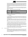
The baud rate clock must now be set up. The input clock is equal to MCK divided by a programmable factor. The Clock Divisor value is held in the Baud Rate Generate Register (BRGR). The
following values are possible:
Table 3-1.
Possible Values for the Clock Divisor field of BRGR
Value
Comment
0
Baud rate clock is disabled
1
Baud rate clock is MCK divided by 16
2 to 65535
Baud rate clock is MCK divided by (CD x 16)
The following formula can be used to compute the value of CD given the microcontroller operating frequency and the desired baud rate:
MCK
CD = -------------------------------------16 × Baudrate
For example, a 115200 baud rate can be obtained with a 48MHz master clock frequency by writing a value of 26 in CD. Obviously, there is a slight deviation from the desired baudrate; these
values yield a true rate of 115384 bauds. However, it is a mere 1.6% error, so it does not have
any impact in practice.
The Mode Register (MR) has two configurable values. The first one is the Channel Mode in
which the DBGU is operating. Several modes are available for testing purpose; in this example,
only the normal mode is of interest. Setting the CHMODE field to a null-value selects the normal
mode.
It is also possible to configure a parity bit in the Mode Register. Even, odd, mark and space parity calculations are supported. In the example, no parity bit is being used (PAR value of 1xx).
The DBGU features its own Peripheral DMA Controller. It enables faster transfer of data and
reduces the processor overhead by taking care of most of the transmission and reception operations. The PDC is not used in this example, so it should be disabled by setting bits RXTDIS and
TXTDIS in the PDC Transfer Control Register (PTCR) of the DBGU.
At this point the DBGU is fully configured. The last step is to enable the transmitter; the received
is not being used in this demo application, so it is useless (but not harmful) to enable it as well.
Transmitter enabling is done by setting bit TXEN in the Control Register.
3.2.7.3
Sending a Character
Transmitting a character on the DBGU line is simple: writing the character value in the Transmit
Holding Register (THR) starts the transfer. However, the transmitter must be ready at this time.
Two bits in the DBGU Status Register (SR) indicate the transmitter state. Bit TXEMPTY indicates if the transmitter is enabled and sending characters. If it is set, no character is being
currently sent on the DBGU line.
16
Application Note
6299A–ATARM–27-Mar-07
The second meaningful bit is TXRDY. When this bit is set, the transmitter has finished copying
the value of THR in its internal shift register that it uses for sending the data. In practice, this
means that THR can be written when TXRDY is set, regardless of the value of TXEMPTY. When
TXEMPTY rises, the whole transfer is finished.
3.2.7.4
String Print Function
A dbgu_print_ascii() function is defined in the example application. It takes a string pointer as an
argument, and sends it across the DBGU.
Its operation is quite simple. C-style strings are simple byte arrays terminated by a null (0) value.
Thus, the function just loops and outputs all the characters of the array until a zero is
encountered.
3.2.7.5
Hexadecimal Print Function
Another print function, dbgu_print_hex8(), outputs a word (32 bits) value in hexadecimal format.
This C function takes an unsigned int value as an argument. A loop displays each byte, starting
with the upper one. This is done by shifting the byte to the rightmost (lowest) position and masking it.
4. Building the Project
The development environment for this getting started is a PC running Microsoft® Windows® OS.
The required software tools for building the project and loading the binary file are:
• an ARM cross-compiler toolchain
• AT91-ISP v1.8 or later (available at www.atmel.com).
The connection between the PC and the board is achieved with a USB cable.
4.1
ARM Compiler Toolchain
To generate the binary file to be downloaded into the target, we use the YAGARTO GNU ARM
compiler toolchain (www.yagarto.de).
This toolchain provides ARM assembler, compiler, and linker tools. Useful programs for debug
are also included.
We also require another software that is not included into the Yagarto package: the make utility.
We get it by installing the unxutils package available at unxutils.sourceforge.net.
4.1.1
Makefile
The Makefile contains rules indicating how to assemble, compile and link the project source files
to create a binary file ready to be downloaded on the target.
The makefile is divided into two parts, one for variables settings, and the other for rules
implementation.
4.1.1.1
Variables
The first part of the Makefile contains variables (uppercase), used to set up some environment
parameters, such as the compiler toolchain prefix and program names, and options to be used
with the compiler.
17
Application Note
6299A–ATARM–27-Mar-07
CROSS_COMPILE=arm-elf-
• Defines the cross-compiler toolchain prefix.
OUTFILE=at91sam9263_getting_started
• Outfile name (without extension).
INCL=./../include
• Paths for header files.
OPTIM = -Os
• Level of optimization used during compilation (-Os optimizes for size).
AS=$(CROSS_COMPILE)gcc
CC=$(CROSS_COMPILE)gcc
LD=$(CROSS_COMPILE)gcc
NM= $(CROSS_COMPILE)nm
SIZE=$(CROSS_COMPILE)size
OBJCOPY=$(CROSS_COMPILE)objcopy
OBJDUMP=$(CROSS_COMPILE)objdump
• Names of cross-compiler toolchain binutils (assembler, compiler, linker, symbol list extractor,
etc.).
CCFLAGS=-g -mcpu=arm9 -Wall -I$(INCL)
• Compiler options:
– -g: generate debugging information for GDB usage.
– -mcpu = arm9 type of ARM CPU core.
– -c: indicates to gcc to only compile the file, and to not link it (link is done later, when
all code files are compiled).
– -Wall: displays all warnings.
– -I$(INCL): set paths for include files.
ASFLAGS=-D__ASSEMBLY__ -g -mcpu=arm9 -c -Os -Wall -I$(INCL)
• Assembler options:
– -D__ASSEMBLY__ : defines the __ASSEMBLY__ symbol, which is used in header
files to distinguish inclusion of the file in assembly code or in C code.
LDFLAGS+=-nostartfiles -Wl,--cref
LDFLAGS+=-lc -lgcc
LDFLAGS+=-T elf32-littlearm.lds
• Linker options:
– -nostartfile: Do not use the standard system startup files when linking.
18
Application Note
6299A–ATARM–27-Mar-07
– -Wl,--cref: Pass the --cref option to the linker (generates cross-reference in map file if
this one is requested).
– -lc: use standard C library.
– -lgcc: use gcc library.
– -T elf32-littlearm.lds: use the file elf32-littlearm.lds as linker file.
OBJS=cstartup.o
OBJS+= lowlevel.o \
main.o
• List of all object file names.
For more detailed information about gcc options, please refer to gcc documentation
(gcc.gnu.org).
4.1.1.2
Rules
The second part contains rules. Each rule is composed on the same line by a target name, and
the files needed to create this target.
The following rules create the 3 object files from the 3 corresponding source files. The option -c
tells gcc to run the compiler and assembler, but not the linker.
main.o: main.c
$(CC) -c $(CCFLAGS) main.c -o main.o
lowlevel.o: lowlevel.c
$(CC) -c $(CCFLAGS) lowlevel.c -o lowlevel.o
cstartup.o: cstartup.S
$(AS) $(ASFLAGS) cstartup.S -o cstartup.o
The ‘all’ rule is the default rule used by make when none is specified in the command line. It
describes how to compile source files and link object files together to generate the final binary
file. The first line calls the linker with the previously defined flags, and the addresses of the text
and the data segments via the -Ttext address and -Tdata address options. This generates an elf
format file, which is converted to a binary file without any debug information by using the objcopy
program.
all: $(OBJS)
$(LD) $(LDFLAGS) -Ttext 0x20000000 -Tdata 0x300000 -n -o $(OUTFILE).elf $(OBJS)
$(OBJCOPY) --strip-debug --strip-unneeded $(OUTFILE).elf -O binary $(OUTFILE).bin
4.1.2
Linker File
At link stage, the elf32-littlearm.lds file is sent in option to the linker.
19
Application Note
6299A–ATARM–27-Mar-07
This file describes the order in which the linker must put the different memory sections into the
binary file. The addresses are indicated via the -Ttext and -Tdata options of the linker command
line (see the Makefile chapter).
4.1.2.1
Header
OUTPUT_FORMAT("elf32-littlearm", "elf32-littlearm", "elf32-littlearm")
Set the object file format to elf32-littlearm.
OUTPUT_ARCH(arm)
Specify the machine architecture.
ENTRY(reset)
Set the symbol ‘reset’ as the entry point of the program.
4.1.2.2
Section Organization
The SECTION part deals with the different sections of code used in the project. It tells the linker
where to put the sections it finds while parsing all the project object files.
• .vectors: exception vector table and IRQ handler
• .text: code
• .data: initialized data
• .bss: uninitialized data
SECTIONS
{
.text : {
_stext = .;
*(.text)
*(.rodata)
*(.rodata*)
. = ALIGN(4);
_etext = . ;
}
/* collect all initialized .data sections that go into FLASH */
.data : AT ( ADDR (.text) + SIZEOF (.text) ) {
_sdata = .;
*(.vectors)
*(.data)
_edata = .;
}
/* collect all uninitialized .bss sections that go into FLASH */
.bss (NOLOAD) : {
. = ALIGN(4);
_sbss = .;
*(.bss)
_ebss = .;
20
Application Note
6299A–ATARM–27-Mar-07
Application Note
}
}
end = .;
In the .text section, the _stext symbol is set in order to retrieve this address at runtime, then all
.text, and .rodata sections found in all object file are placed here, and finally the _etext symbol is
set and aligned on a 4 byte address.
The same operation is done with the .data and .bss sections.
In the .data section, the AT (ADDR (.text) + SIZEOF(.text)) command specifies that the load
address (the address in the binary file after link step) of this section is just after the .text section.
Thus there is no hole between these two sections.
The .vectors section (defined in the cstartup.S file) is placed just before the .data section. Providing a link address set at the beginning of the internal RAM allows this section to be
automatically copied at the right place when the reset handler copies the .data section in RAM.
4.2
Loading the Code
Once the build step is completed, one .bin file is available and ready to be loaded into the board.
The AT91-ISP solution offers an easy way to download files into AT91 products on Atmel Evaluation Kits through a USB, COM or J-TAG link. Target programming is done here via SAM-BA™
tools.
One DOS batch file (prog_sdram.bat) and TCL script file (prog_sdram.tcl) are provided to process the loading of the binary file.
The .bat file launches SAM-BA in command line mode. Parameters provided to SAM-BA are: the
connection link used, the target board, and the .tcl script file to use.
The .tcl script file contains indications about the name of the file to load, which memory module
is used, the address of code loading, and operates a go command at the code start address. A
log file is displayed at the end of the loading process.
Follow the steps below to load the code:
• Execute the prog_sdram.bat file to test the code running in external SDRAM.
The code then starts running, and the LEDs are now controlled by two push buttons.
4.3
Debug Support
When debugging the Getting Started example with GDB, it is best to disable compiler optimizations. Otherwise, the source code will not correctly match the actual execution of the program.
To do that, simply comment out (with a ‘#’) the “OPTIM = -Os” line of the makefile and rebuild the
project.
In addition, a GDB command file is provided in the package to enable debugging in SDRAM.
The script is named "init_sdram.gdb" and can be executed by typing “source init_sdram.gdb” at
the GDB command prompt. It initializes the main oscillator, the PLL and the SDRAM controller,
enabling the program to be correctly uploaded to the target with the “load” command.
For more information on debugging with GDB, refer to the Atmel application note GNU-Based
Software Development and to the GDB manual available on gcc.gnu.org.
21
6299A–ATARM–27-Mar-07
5. Revision History
Table 5-1.
Document Ref.
Comments
6299A
First issue.
22
Change Request Ref.
Application Note
6299A–ATARM–27-Mar-07
Atmel Corporation
2325 Orchard Parkway
San Jose, CA 95131, USA
Tel: 1(408) 441-0311
Fax: 1(408) 487-2600
Regional Headquarters
Atmel Europe
Le Krebs
8, rue Jean-Pierre Timbaud
BP 309
78054 Saint-Quentin-en-Yvelines
Cedex
France
Tel: (33) 1-30-60-70-00
Fax: (33) 1-30-60-71-11
Asia
Room 1219
Chinachem Golden Plaza
77 Mody Road Tsimshatsui
East Kowloon
Hong Kong
Tel: (852) 2721-9778
Fax: (852) 2722-1369
Japan
9F, Tonetsu Shinkawa Bldg.
1-24-8 Shinkawa
Chuo-ku, Tokyo 104-0033
Japan
Tel: (81) 3-3523-3551
Fax: (81) 3-3523-7581
Atmel Operations
Memory
2325 Orchard Parkway
San Jose, CA 95131, USA
Tel: 1(408) 441-0311
Fax: 1(408) 436-4314
RF/Automotive
Theresienstrasse 2
Postfach 3535
74025 Heilbronn, Germany
Tel: (49) 71-31-67-0
Fax: (49) 71-31-67-2340
Microcontrollers
2325 Orchard Parkway
San Jose, CA 95131, USA
Tel: 1(408) 441-0311
Fax: 1(408) 436-4314
La Chantrerie
BP 70602
44306 Nantes Cedex 3, France
Tel: (33) 2-40-18-18-18
Fax: (33) 2-40-18-19-60
1150 East Cheyenne Mtn. Blvd.
Colorado Springs, CO 80906, USA
Tel: 1(719) 576-3300
Fax: 1(719) 540-1759
Biometrics
Avenue de Rochepleine
BP 123
38521 Saint-Egreve Cedex, France
Tel: (33) 4-76-58-47-50
Fax: (33) 4-76-58-47-60
ASIC/ASSP/Smart Cards
Zone Industrielle
13106 Rousset Cedex, France
Tel: (33) 4-42-53-60-00
Fax: (33) 4-42-53-60-01
1150 East Cheyenne Mtn. Blvd.
Colorado Springs, CO 80906, USA
Tel: 1(719) 576-3300
Fax: 1(719) 540-1759
Scottish Enterprise Technology Park
Maxwell Building
East Kilbride G75 0QR, Scotland
Tel: (44) 1355-803-000
Fax: (44) 1355-242-743
Literature Requests
www.atmel.com/literature
Disclaimer: The information in this document is provided in connection with Atmel products. No license, express or implied, by estoppel or otherwise, to any
intellectual property right is granted by this document or in connection with the sale of Atmel products. EXCEPT AS SET FORTH IN ATMEL’S TERMS AND CONDITIONS OF SALE LOCATED ON ATMEL’S WEB SITE, ATMEL ASSUMES NO LIABILITY WHATSOEVER AND DISCLAIMS ANY EXPRESS, IMPLIED OR STATUTORY
WARRANTY RELATING TO ITS PRODUCTS INCLUDING, BUT NOT LIMITED TO, THE IMPLIED WARRANTY OF MERCHANTABILITY, FITNESS FOR A PARTICULAR
PURPOSE, OR NON-INFRINGEMENT. IN NO EVENT SHALL ATMEL BE LIABLE FOR ANY DIRECT, INDIRECT, CONSEQUENTIAL, PUNITIVE, SPECIAL OR INCIDENTAL DAMAGES (INCLUDING, WITHOUT LIMITATION, DAMAGES FOR LOSS OF PROFITS, BUSINESS INTERRUPTION, OR LOSS OF INFORMATION) ARISING OUT
OF THE USE OR INABILITY TO USE THIS DOCUMENT, EVEN IF ATMEL HAS BEEN ADVISED OF THE POSSIBILITY OF SUCH DAMAGES. Atmel makes no
representations or warranties with respect to the accuracy or completeness of the contents of this document and reserves the right to make changes to specifications
and product descriptions at any time without notice. Atmel does not make any commitment to update the information contained herein. Unless specifically provided
otherwise, Atmel products are not suitable for, and shall not be used in, automotive applications. Atmel’s products are not intended, authorized, or warranted for use
as components in applications intended to support or sustain life.
© 2007 Atmel Corporation. All rights reserved. Atmel®, logo and combinations thereof, Everywhere You Are® and others are registered trademarks, SAM-BA ™ and others are trademarks of Atmel Corporation or its subsidiaries. ARM ®, the ARMPowered ® logo, Thumb® and others are the
registered trademarks or trademarks of ARM Ltd. Windows ® is the registered trademark of Microsoft Corporation in the US and/or other countries. Other terms and product names may be trademarks of others.
6299A–ATARM–27-Mar-07