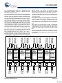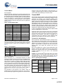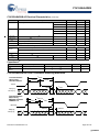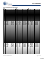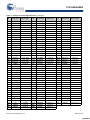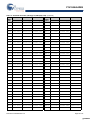
1
CYV15G0404DXB
Independent Clock Quad HOTLink II™
Transceiver with Reclocker
Features
■
Quad channel transceiver for 195 to 1500 MBaud serial
signaling rate
❐ Aggregate throughput of up to 12 Gbits/second
Synchronous LVTTL parallel interface
■
JTAG boundary scan
■
Built In Self Test (BIST) for at-speed link testing
■
■
Second-generation HOTLink® technology
■
Compliant to multiple standards
❐ SMPTE-292M, SMPTE-259M, DVB-ASI, Fibre Channel, ESCON, and Gigabit Ethernet (IEEE802.3z)
❐ 10 bit uncoded data or 8B/10B coded data
■
■
Link quality indicator by channel
Analog signal detect
❐ Digital signal detect
❐
Truly independent channels
❐ Each channel is able to:
• Perform reclocker function
• Operate at a different signaling rate
• Transport a different data format
■
Low power 3W at 3.3V typical
■
Single 3.3V supply
■
256 ball thermally enhanced BGA
■
0.25μ BiCMOS technology
■
JTAG device ID ‘0C811069’x
Functional Description
■
Internal phase-locked loops (PLLs) with no external PLL
components
■
Selectable differential PECL compatible serial inputs per
channel
❐ Internal DC restoration
■
Redundant differential PECL compatible serial outputs per
channel
❐ No external bias resistors required
❐ Signaling rate controlled edge rates
❐ Source matched for 50Ω transmission lines
■
MultiFrame™ Receive Framer provides alignment options
❐ Comma or full K28.5 detect
❐ Single or multibyte Framer for byte alignment
❐ Low latency option
■
Selectable input and output clocking options
The CYV15G0404DXB Independent Clock Quad HOTLink II™
Transceiver is a point-to-point or point-to-multipoint communications building block enabling the transfer of data over a variety of
high speed serial links including SMPTE 292, SMPTE 259, and
DVB-ASI video applications. The signaling rate can be anywhere
in the range of 195 to 1500 MBaud for each serial link. Each
channel operates independently with its own reference clock
allowing different rates. Each transmit channel accepts parallel
characters in an input register, encodes each character for
transport, and then converts it to serial data. Each receive
channel accepts serial data and converts it to parallel data,
decodes the data into characters, and presents these characters
to an output register. The received serial data can also be
reclocked and retransmitted through the serial outputs. Figure 1
illustrates typical connections between independent video
coprocessors and corresponding CYV15G0404DXB chips.
Figure 1. HOTLink II™ System Connections
10
10
Serial Links
10
10
Video Coprocessor
10
10
Independent
Channel
CYV15G0404DXB
Reclocker
Serial Links
Independent
Channel
CYV15G0404DXB
Reclocker
10
10
10
Serial Links
10
10
Serial Links
10
Video Coprocessor
10
10
10
10
Cable
Connections
Cypress Semiconductor Corporation
Document #: 38-02097 Rev. *B
•
198 Champion Court
•
San Jose, CA 95134-1709
•
408-943-2600
Revised December 14, 2007
[+] Feedback
CYV15G0404DXB
The CYV15G0404DXB satisfies the SMPTE-259M and
SMPTE-292M compliance according to SMPTE EG34-1999
Pathological Test Requirements.
8B/10B decoded, and checked for transmission errors.
Recovered decoded characters are then written to an internal
elasticity buffer, and presented to the destination host system.
As a second generation HOTLink device, the CYV15G0404DXB
extends the HOTLink family with enhanced levels of integration and
faster data rates, while maintaining serial link compatibility (data,
command, and BIST) with other HOTLink devices. The transmit
(TX) section of the CYV15G0404DXB Quad HOTLink II consists of
four independent byte-wide channels. Each channel accepts
either 8-bit data characters or preencoded 10-bit transmission
characters. Data characters may be passed from the transmit
input register to an integrated 8B/10B Encoder to improve their
serial transmission characteristics. These encoded characters
are then serialized and output from dual Positive ECL (PECL)
compatible differential transmission-line drivers at a bit rate of
either 10 or 20 times the input reference clock for that channel.
The integrated 8B/10B encoder or decoder may be bypassed for
systems that present externally encoded or scrambled data at
the parallel interface.
The receive (RX) section of the CYV15G0404DXB Quad
HOTLink II consists of four independent byte wide channels.
Each channel accepts a serial bit stream from one of two
PECL-compatible differential line receivers, and using a
completely integrated Clock and Data Recovery PLL, recovers
the timing information necessary for data reconstruction. Each
recovered bit stream is deserialized and framed into characters,
The parallel IO interface may be configured for numerous forms
of clocking to provide the highest flexibility in system architecture. In addition to clocking the transmit path with a local
reference clock, the receive interface may also be configured to
present data relative to a recovered clock or to a local reference
clock.
Each transmit and receive channel contains an independent
BIST pattern generator and checker. This BIST hardware allows
at speed testing of the high speed serial data paths in each
transmit and receive section, and across the interconnecting
links.
The CYV15G0404DXB is ideal for port applications where
different data rates and serial interface standards are necessary
for each channel. Some applications include multi-format routers
and switchers.
TXDD[7:0]
TXCTD[1:0]
x11
x10
x11
Phase
Align
Buffer
Elasticity
Buffer
Phase
Align
Buffer
Elasticity
Buffer
Phase
Align
Buffer
Elasticity
Buffer
Phase
Align
Buffer
Elasticity
Buffer
Encoder
8B/10B
Decoder
8B/10B
Encoder
8B/10B
Decoder
8B/10B
Encoder
8B/10B
Decoder
8B/10B
Encoder
8B/10B
Decoder
8B/10B
TX
RX
TX
RX
TX
RX
INB1±
INB2±
OUTC1±
OUTC2±
INC1±
INC2±
Document #: 38-02097 Rev. *B
Serializer
TX
Deserializer
RX
IND1±
IND2±
Deserializer
OUTB1±
OUTB2±
Deserializer
Serializer
INA1±
INA2±
Serializer
Deserializer
OUTA1±
OUTA2±
Serializer
Framer
Framer
OUTD1±
OUTD2±
Framer
Framer
RXDD[7:0]
RXSTD[2:0]
RXDC[7:0]
RXSTC[2:0]
x10
REFCLKD±
TXDC[7:0]
TXCTC[1:0]
x11
REFCLKC±
RXDB[7:0]
RXSTB[2:0]
x10
REFCLKB±
TXDB[7:0]
TXCTB[1:0]
x11
REFCLKA±
x10
TXDA[7:0]
TXCTA[1:0]
RXDA[7:0]
RXSTA[2:0]
CYV15G0404DXB Transceiver Logic Block Diagram
Page 2 of 44
[+] Feedback
CYV15G0404DXB
Transmit Path Block Diagram
REFCLKA+
RECLCK[A..D] are Internal Reclocker Signals
TXLB[A..D] are Internal Serial Loopback Signals
Bit-Rate Clock
REFCLKA–
= Internal Signal
Transmit
Transmit PLL
PLL
Clock Multiplier
A
Clock
Multiplier
TXRATEA
SPDSELA
TXCLKOA
OEA[2..1]
ENCBYPA
Character-Rate Clock A
TXERRA
TXCLKA
RECLCKA
10
10
OUTA1+
OUTA1–
Shifter
2
TXCTA[1:0]
10
BIST
BIST LFSR
LFSR
Input
Register
8
TXDA[7:0]
Encoder
8B/10B
Encoder
1
Phase-Align
Phase-Align
Buffer
Buffer
TXCKSELA
OEA[2..1]
TXBISTA
PABRSTA
0
10
OUTA2+
OUTA2–
TXLBA
REFCLKB+
Bit-Rate Clock
REFCLKB–
Transmit PLL
Clock Multiplier B
TXRATEB
SPDSELB
TXCLKOB
OEB[2..1]
Character-Rate Clock B
ENCBYPB
RECLCKB
TXERRB
0
10
10
OUTB1+
OUTB1–
Shifter
2
10
BIST
BIST LFSR
LFSR
TXDB[7:0]
10
Encoder
8B/10B
Encoder
Input
Register
8
OEB[2..1]
1
Phase-Align
Phase-Align
Buffer
Buffer
TXCKSELB
TXCTB[1:0]
TXBISTB
PABRSTB
TXCLKB
OUTB2+
OUTB2–
TXLBB
REFCLKC+
Bit-Rate Clock
REFCLKC–
Transmit PLL
Clock Multiplier C
TXRATEC
SPDSELC
TXCLKOC
OEC[2..1]
RECLCKC
ENCBYPC
Character-Rate Clock C
TXERRC
10
10
10
OUTC1+
OUTC1–
Shifter
2
TXCTC[1:0]
10
BIST LFSR
Input
Register
8
TXDC[7:0]
8B/10B
Encoder
1
Phase-Align
Buffer
0
TXCKSELC
OEC[2..1]
TXBISTC
PABRSTC
TXCLKC
OUTC2+
OUTC2–
TXLBC
REFCLKD+
Bit-Rate Clock
REFCLKD–
Transmit PLL
Clock Multiplier D
TXRATED
RECLCKD
OED[2..1]
SPDSELD
ENCBYPD
TXCLKOD
OED[2..1]
Character-Rate Clock D
TXERRD
Document #: 38-02097 Rev. *B
10
10
OUTD1+
OUTD1–
Shifter
10
BIST LFSR
2
10
8B/10B
Encoder
TXDD[7:0]
1
Phase-Align
Buffer
8
0
Input
Register
TXCKSELD
TXCTD[1:0]
TXBISTD
PABRSTD
TXCLKD
OUTD2+
OUTD2–
TXLBD
Page 3 of 44
[+] Feedback
CYV15G0404DXB
Receive Path Block
RECLCK[A..D] are Internal Reclocker Signals
TXLB[A..D] are Internal Serial Loopback Signals
= Internal Signal
RESET
TRST
JTAG
Boundary
Scan
Controller
SPDSELA
RXPLLPDA
RCLKENA
RECLCKA
TMS
TCLK
TDI
TDO
Receive
Signal
Monitor
Elasticity
Buffer
Output
Register
TXLBA
ULCA
Clock &
Data
Recovery
PLL
10B/8B
BIST
INA2+
INA2–
LFIA
Framer
INA1+
INA1–
Shifter
LPENA
INSELA
8
3
RXDA[7:0]
RXSTA[2:0]
SPDSELB
Receive
Signal
Monitor
SPDSELC
RXPLLPDC
Receive
Signal
Monitor
TXLBC
ULCC
SPDSELD
Clock &
Data
Recovery
PLL
RXPLLPDD
Receive
Signal
Monitor
IND2+
IND2–
TXLBD
ULCD
Clock &
Data
Recovery
PLL
SDASEL[A..D][1:0]
LDTDEN
RFMODE[A..D][1:0]
RFEN[A..D]
FRAMCHAR[A..D]
DECMODE[A..D]
RXBIST[A..D]
RXCKSEL[A..D]
DECBYP[A..D]
RXRATE[A..D]
Document #: 38-02097 Rev. *B
Framer
IND1+
IND1–
Output
Register
3
÷2
RXDB[7:0]
RXSTB[2:0]
RXCLKB+
RXCLKB–
8
3
÷2
RXDC[7:0]
RXSTC[2:0]
RXCLKC+
RXCLKC–
LFID
Shifter
INSELD
Clock
Select
RECLCKD
RCLKEND
LPEND
10B/8B
BIST
INC2+
INC2–
Framer
INC1+
INC1–
8
LFIC
Shifter
INSELC
10B/8B
BIST
LPENC
Elasticity
Buffer
Clock
Select
RECLCKC
RCLKENC
Output
Register
ULCB
RXCLKA+
RXCLKA–
Clock
Select
Output
Register
TXLBB
Clock &
Data
Recovery
PLL
Elasticity
Buffer
INB2+
INB2–
10B/8B
BIST
INB1+
INB1–
÷2
LFIB
Framer
INSELB
Shifter
LPENB
Clock
Select
RECLCKB
Elasticity
Buffer
RXPLLPDB
RCLKENB
÷2
8
3
RXDD[7:0]
RXSTD[2:0]
RXCLKD+
RXCLKD–
Page 4 of 44
[+] Feedback
CYV15G0404DXB
Device Configuration and Control Block
WREN
ADDR[3:0]
DATA[7:0]
Device Configuration and Control
Interface
Document #: 38-02097 Rev. *B
= Internal Signal
RFMODE[A..D][1:0]
RFEN[A..D]
FRAMCHAR[A..D]
DECMODE[A..D]
RXBIST[A..D]
RXCKSEL[A..D]
DECBYP[A..D]
RXRATE[A..D]
SDASEL[A..D][1:0]
RXPLLPD[A..D]
TXRATE[A..D]
TXCKSEL[A..D]
PABRST[A..D]
TXBIST[A..D]
OE[A..D][2..1]
ENCBYP[A..D]
GLEN[11..0]
FLEN[2..0]
Page 5 of 44
[+] Feedback
CYV15G0404DXB
Pin Configuration (Top View)
A
B
C
D
E
F
G
H
J
K
L
M
N
P
R
T
U
V
W
Y
1
2
3
4
5
6
7
8
9
10
11
12
13
14
15
16
17
18
19
20
IN
C1–
OUT
C1–
IN
C2–
OUT
C2–
VCC
IN
D1–
OUT
D1–
GND
IN
D2–
OUT
D2–
IN
A1–
OUT
A1–
GND
IN
A2–
OUT
A2–
VCC
IN
B1–
OUT
B1–
IN
B2–
OUT
B2–
IN
C1+
OUT
C1+
IN
C2+
OUT
C2+
VCC
IN
D1+
OUT
D1+
GND
IN
D2+
OUT
D2+
IN
A1+
OUT
A1+
GND
IN
A2+
OUT
A2+
VCC
IN
B1+
OUT
B1+
IN
B2+
OUT
B2+
TDI
TMS
INSELC INSELB
VCC
ULCD
ULCC
GND
DATA
[7]
DATA
[5]
DATA
[3]
DATA
[1]
GND
RCLK
ENB
SPD
SELD
VCC
LDTD
EN
TRST
LPEND
TDO
INSELD INSELA
VCC
ULCA
SPD
SELC
GND
DATA
[6]
DATA
[4]
DATA
[2]
DATA
[0]
GND LPENB ULCB
VCC
LPENA
VCC
SCAN TMEN3
EN2
VCC
TCLK
VCC
VCC
VCC
VCC
VCC
RX
DC[6]
RX
DC[7]
TX
DC[0]
RCLK
END
RCLK
ENA
TX
DC[7]
WREN
TX
DC[4]
TX
DC[1]
SPD
SELB
LP
ENC
SPD
SELA
RX
DB[1]
GND
GND
GND
GND
GND
GND
GND
GND
TX
CTC[1]
TX
DC[5]
TX
DC[2]
TX
DC[3]
RX
STB[2]
RX
DB[0]
RX
DB[5]
RX
DB[2]
RX
DB[4]
RX
DB[7]
LFIB
RX
DC[2]
REF
TX
CLKC– CTC[0]
TX
CLKC
RX
DB[3]
RX
DC[3]
REF
CLKC+
LFIC
TX
DC[6]
RX
DB[6]
RX
DC[4]
RX
DC[5]
RCLK
ENC
TX
ERRC
GND
GND
GND
GND
GND
RX
DC[1]
RX
DC[0]
RX
RX
STC[0] STC[1]
RX
TX
RX
RX
STC[2] CLKOC CLKC+ CLKC–
VCC
VCC
VCC
TX
DD[0]
TX
DD[1]
TX
DD[2]
TX
CTD[1]
VCC
RX
DD[2]
RX
DD[1]
GND
TX
CTA[1]
ADDR
REF
[0]
CLKD–
TX
DD[3]
TX
DD[4]
TX
CTD[0]
RX
DD[6]
VCC
RX
DD[3]
RX
STD[0]
GND
RX
STD[2]
TX
DD[5]
TX
DD[7]
LFID
RX
CLKD–
VCC
RX
DD[4]
RX
STD[1]
GND
TX
DD[6]
TX
CLKD
RX
DD[7]
RX
CLKD+
VCC
RX
DD[5]
RX
DD[0]
GND
Document #: 38-02097 Rev. *B
TX
DA[1]
VCC
RX
TX
RX
STB[1] CLKOB STB[0]
RX
RX
CLKB+ CLKB–
REF
REF
CLKB+ CLKB–
VCC
VCC
TX
DB[6]
TX
ERRB
TX
CLKB
GND
GND
GND
TX
DB[5]
TX
DB[4]
TX
DB[3]
TX
DB[2]
TX
DB[1]
TX
DB[0]
TX
CTB[1]
TX
DB[7]
VCC
VCC
VCC
VCC
GND
TX
DA[4]
TX
CTA[0]
VCC
RX
DA[2]
TX
RX
CTB[0] STA[2]
RX
STA[1]
ADDR
REF
TX
[2]
CLKD+ CLKOA
GND
TX
DA[3]
TX
DA[7]
VCC
RX
DA[7]
RX
DA[3]
RX
DA[0]
RX
STA[0]
ADDR
[3]
ADDR
[1]
RX
CLKA+
TX
ERRA
GND
TX
DA[2]
TX
DA[6]
VCC
LFIA
REF
CLKA+
RX
DA[4]
RX
DA[1]
TX
CLKOD
NC[1]
TX
CLKA
RX
CLKA–
GND
TX
DA[0]
TX
DA[5]
VCC
TX
ERRD
REF
CLKA–
RX
DA[6]
RX
DA[5]
Page 6 of 44
[+] Feedback
CYV15G0404DXB
Pin Configuration (Bottom View)
20
19
18
17
16
15
14
13
12
11
10
9
8
7
6
5
4
3
2
1
A
OUT
B2–
IN
B2–
OUT
B1–
IN
B1–
VCC
OUT
A2–
IN
A2–
GND
OUT
A1–
IN
A1–
OUT
D2–
IN
D2–
GND
OUT
D1–
IN
D1–
VCC
OUT
C2–
IN
C2–
OUT
C1–
IN
C1–
B
OUT
B2+
IN
B2+
OUT
B1+
IN
B1+
VCC
OUT
A2+
IN
A2+
GND
OUT
A1+
IN
A1+
OUT
D2+
IN
D2+
GND
OUT
D1+
IN
D1+
VCC
OUT
C2+
IN
2+
OUT
C1+
IN
C1+
C
TDO
LP
END
TRST
LDTD
EN
VCC
SPD
SELD
RCLK
ENB
GND
DATA
[1]
DATA
[3]
DATA
[5]
DATA
[7]
GND
ULCC
ULCD
VCC
IN
SELB
IN
SELC
TMS
TDI
VCC
LP
ENA
VCC
ULCB
LP
ENB
GND
DATA
[0]
DATA
[2]
DATA
[4]
DATA
[6]
GND
SPD
SELC
ULCA
VCC
IN
SELA
IN
SELD
RESET
TCLK
VCC
VCC
VCC
VCC
VCC
VCC
D
E
TMEN3 SCAN
EN2
VCC
VCC
F
RX
TX
RX
STB[0] CLKOB STB[1]
RCLK
ENA
RCLK
END
TX
DC[0]
RX
DC[7]
Rx
DC[6]
G
RX
DB[1]
SPD
SELA
LP
ENC
SPD
SELB
TX
DC[1]
TX
DC[4]
WREN
TX
DC[7]
H
GND
GND
GND
GND
GND
GND
GND
GND
J
RX
DB[2]
RX
DB[5]
RX
DB[0]
RX
STB[2]
TX
DC[3]
TX
DC[2]
TX
DC[5]
TX
CTC[1]
K
LFIB
RX
DB[7]
RX
DB[4]
RX
DB[3]
TX
CLKC
L
TX
DB[6]
RX
RX
CLKB– CLKB+
RX
DB[6]
TX
DC[6]
LFIC
REF
CLKC+
RX
DC[3]
M
TX
CLKB
TX
ERRB
REF
REF
CLKB– CLKB+
TX
ERRC
RCLK
ENC
RX
DC[5]
RX
DC[4]
N
GND
GND
GND
GND
GND
GND
GND
GND
P
TX
DB[2]
TX
DB[3]
TX
DB[4]
TX
DB[5]
RX
RX
STC[1] STC[0]
RX
DC[0]
RX
DC[1]
R
TX
DB[7]
TX
CTB[1]
TX
DB[0]
TX
DB[1]
RX
RX
TX
RX
CLKC– CLKC+ CLKOC STC[2]
T
VCC
VCC
VCC
VCC
U
RX
STA[1]
RX
TX
STA[2] CTB[0]
RX
DA[2]
VCC
TX
CTA[0]
TX
DA[4]
GND
V
RX
STA[0]
RX
DA[0]
RX
DA[3]
RX
DA[7]
VCC
TX
DA[7]
TX
DA[3]
GND
W
RX
DA[1]
RX
DA[4]
REF
CLKA+
LFIA
VCC
TX
DA[6]
TX
DA[2]
GND
TX
ERRA
RX
CLKA+
Y
RX
DA[5]
RX
DA[6]
REF
CLKA–
TX
ERRD
VCC
TX
DA[5]
TX
DA[0]
GND
RX
CLKA–
TX
CLKA
TX
DA[1]
REF
ADDR
CLKD–
[0]
TX
REF
CTC[0] CLKC–
RX
DC[2]
VCC
VCC
VCC
VCC
TXC
TA[1]
GND
RX
DD[1]
RX
DD[2]
VCC
TX
CTD[1]
TX
DD[2]
TX
DD[1]
TX
DD[0]
RX
STD[2]
GND
RX
STD[0]
RX
DD[3]
VCC
RX
DD[6]
TX
CTD[0]
TX
DD[4]
TX
DD[3]
ADDR
[1]
ADDR
[3]
GND
RX
STD[1]
RX
DD[4]
VCC
RX
CLKD–
LFID
TX
DD[7]
TX
DD[5]
NC[1]
TX
CLKOD
GND
RX
DD[0]
RX
DD[5]
VCC
RX
CLKD+
RX
DD[7]
TX
CLKD
TX
DD[6]
TX
REF
ADDR
CLKOA CLKD+
[2]
Note
1. NC=Do Not Connect
Document #: 38-02097 Rev. *B
Page 7 of 44
[+] Feedback
CYV15G0404DXB
Pin Definitions
CYV15G0404DXB Quad HOTLink II Transceiver
Name
I/O Characteristics Signal Description
Transmit Path Data and Status Signals
TXDA[7:0]
LVTTL Input,
Transmit Data Inputs. TXDx[7:0] data inputs are captured on the rising edge of the
TXDB[7:0]
synchronous,
transmit interface clock. The transmit interface clock is selected by the TXCKSELx
TXDC[7:0]
sampled by the
latch via the device configuration interface, and passed to the encoder or Transmit
TXDD[7:0]
associated
Shifter. When the Encoder is enabled, TXDx[7:0] specifies the specific data or
TXCLKx↑ or
command character sent.
REFCLKx↑[2]
TXCTA[1:0]
LVTTL Input,
Transmit Control. TXCTx[1:0] inputs are captured on the rising edge of the transmit
TXCTB[1:0]
synchronous,
interface clock. The transmit interface clock is selected by the TXCKSELx latch
TXCTC[1:0]
sampled by the
through the device configuration interface, and passed to the encoder or transmit
TXCTD[1:0]
associated
shifter. The TXCTA[1:0] inputs identify how the associated TXDx[7:0] characters are
TXCLKx↑ or
interpreted. When the encoder is bypassed, these inputs are interpreted as data bits.
REFCLKx↑ [2]
When the encoder is enabled, these inputs determine if the TXDx[7:0] character is
encoded as data, a special character code, or replaced with other special character
codes. See Table 3 for details.
Transmit Path Error. TXERRx is asserted HIGH to indicate detection of a transmit
TXERRA
LVTTL Output,
phase align buffer underflow or overflow. If an underflow or overflow condition is
TXERRB
synchronous to
detected, TXERRx, for the channel in error, is asserted HIGH and remains asserted
TXERRC
REFCLKx↑ [3],
until either a word sync sequence is transmitted on that channel, or the transmit
TXERRD
synchronous to
phase align buffer is recentered with the PABRSTx latch through the device configuRXCLKx when
ration interface. When TXBISTx = 0, the BIST progress is presented on the
selected as
associated TXERRx output. The TXERRx signal pulses HIGH for one transmit
REFCLKx,
character clock period to indicate a pass through the BIST sequence once every 511
asynchronous to
or 527 (depending on RXCKSELx) character times. If RXCKSELx = 1, a one
transmit channel
character pulse occurs every 527 character times. If RXCKSELx = 0, a one character
enable/disable,
asynchronous to loss pulse occurs every 511 character times.
or return of
TXERRx is also asserted HIGH, when any of these conditions is true:
REFCLKx±
■ The TXPLL for the associated channel is powered down. This occurs when OE2x
and OE1x for a given channel are simultaneous disabled by setting OE2x = 0 and
OE1x = 0.
■
Transmit Path Clock Signals
REFCLKA±
Differential LVPECL
REFCLKB±
or single ended
REFCLKC±
LVTTL input clock
REFCLKD±
TXCLKA
TXCLKB
TXCLKC
TXCLKD
LVTTL Clock Input,
internal pull down
The absence of the REFCLKx± signal.
Reference Clock. REFCLKx± clock inputs are used as the timing references for the
transmit and receive PLLs. These input clocks may also be selected to clock the
transmit and receive parallel interfaces. When driven by a single ended LVCMOS or
LVTTL clock source, connect the clock source to either the true or complement
REFCLKx input, and leave the alternate REFCLKx input open (floating). When driven
by an LVPECL clock source, the clock must be a differential clock, using both inputs.
Transmit Path Input Clock. When configuration latch TXCKSELx = 0, the
associated TXCLKx input is selected as the character-rate input clock for the
TXDx[7:0] and TXCTx[1:0] inputs. In this mode, the TXCLKx input must be
frequency-coherent to its associated TXCLKOx output clock, but may be offset in
phase by any amount. Once initialized, TXCLKx is allowed to drift in phase as much
as ±180 degrees. If the input phase of TXCLKx drifts beyond the handling capacity
of the phase align buffer, TXERRx is asserted to indicate the loss of data, and remains
asserted until the phase align buffer is initialized. The phase of the TXCLKx input
clock relative to its associated REFCLKx± is initialized when the configuration latch
PABRSTx is written as 0. When the associated TXERRx is deasserted, the phase
align buffer is initialized and input characters are correctly captured.
Notes
2. When REFCLKx± is configured for half rate operation, these inputs are sampled relative to both the rising and falling edges of the associated REFCLKx±.
3. When REFCLKx± is configured for half rate operation, these outputs are presented relative to both the rising and falling edges of the associated REFCLKx±.
Document #: 38-02097 Rev. *B
Page 8 of 44
[+] Feedback
CYV15G0404DXB
Pin Definitions (continued)
CYV15G0404DXB Quad HOTLink II Transceiver
Name
TXCLKOA
TXCLKOB
TXCLKOC
TXCLKOD
I/O Characteristics Signal Description
LVTTL Output
Transmit Clock Output. TXCLKOx output clock is synthesized by each channel’s
transmit PLL and operates synchronous to the internal transmit character clock.
TXCLKOx operates at either the same frequency as REFCLKx± (TXRATE = 0), or at
twice the frequency of REFCLKx± (TXRATE = 1). The transmit clock outputs have no
fixed phase relationship to REFCLKx±.
Receive Path Data and Status Signals
Parallel Data Output. RXDx[7:0] parallel data outputs change relative to the receive
RXDA[7:0]
LVTTL Output,
interface clock. The receive interface clock is selected by the RXCKSELx latch. If
RXDB[7:0]
synchronous to the
RXCLKx± is a full rate clock, the RXCLKx± clock outputs are complementary clocks
RXDC[7:0]
selected RXCLK±
RXDD[7:0]
output or REFCLKx± operating at the character rate. The RXDx[7:0] outputs for the associated receive
channels follow rising edge of RXCLKx+ or falling edge of RXCLKx–. If RXCLKx± is
input
a half rate clock, the RXCLKx± clock outputs are complementary clocks operating at
half the character rate. The RXDx[7:0] outputs for the associated receive channels
follow both the falling and rising edges of the associated RXCLKx± clock outputs.
RXSTA[2:0]
LVTTL Output,
Parallel Status Output. RXSTA[2:0] status outputs change relative to the receive
RXSTB[2:0]
synchronous to the
interface clock. The receive interface clock is selected by the RXCKSELx latch. If
RXSTC[2:0]
selected RXCLK±
RXCLKx± is a full rate clock, the RXCLKx± clock outputs are complementary clocks
RXSTD[2:0]
output or REFCLKx± operating at the character rate. The RXSTAx[2:0] outputs for the associated receive
input
channels follow rising edge of RXCLKx+ or falling edge of RXCLKx–. If RXCLKx± is
a half rate clock, the RXCLKx± clock outputs are complementary clocks operating at
half the character rate. The RXSTAx[2:0] outputs for the associated receive channels
follow both the falling and rising edges of the associated RXCLKx± clock outputs.
When the decoder is bypassed, RXSTx[1:0] become the two low-order bits of the
10-bit received character. RXSTx[2] = HIGH indicates the presence of a Comma
character in the Output Register. When the decoder is enabled, RXSTx[2:0] provide
status of the received signal. See Table 11 for a list of received character status.
Receive Path Clock Signals
RXCLKA±
LVTTL Output Clock Receive Clock Output. RXCLKx± is the receive interface clock used to control timing
RXCLKB±
of the RXDx[7:0] and RXSTA[2:0] parallel outputs. The source of the RXCLKx±
RXCLKC±
outputs is selected by the RXCKSELx latch via the device configuration interface.
RXCLKD±
These true and complement clocks are used to control timing of data output transfers.
These clocks are output continuously at either the dual-character rate (1/20th the
serial bit-rate) or character rate (1/10th the serial bit-rate) of the data being received,
as selected by RXRATEx. When configured such that the output data path is clocked
by the REFCLKx± instead of a recovered clock, the RXCLKx± output drivers present
a buffered or divided form (depending on RXRATEx) of the associated REFCLKx±
that are delayed in phase to align with the data. This phase difference allows the user
to select the optimal clock (REFCLKx± or RXCLK±) for setup or hold timing for their
specific system.
When REFCLKx± is a full rate clock, the RXCLKx± rate depends on the value of
RXRATEx.
When REFCLKx± is a half rate clock and RXCKSELx = 0, the RXCLKx± rate depends
on the value of RXRATEx.
When REFCLKx± is a half rate clock and RXCKSELx=1, the RXCLKx± rate does not
depend on the value of RXRATEx and operates at the same rate as REFCLKx±.
Device Control Signals
RESET
LVTTL Input,
asynchronous,
internal pull up
Document #: 38-02097 Rev. *B
Asynchronous Device Reset. RESET initializes all state machines, counters, and
configuration latches in the device to a known state. RESET must be asserted LOW
for a minimum pulse width. When the reset is removed, all state machines, counters,
and configuration latches are at an initial state. As per the JTAG specifications, the
device RESET cannot reset the JTAG controller. Therefore, the JTAG controller has
to be reset separately. Refer to JTAG Support on page 23 for the methods to reset
the JTAG state machine. See Table 9 for the initialize values of the device configuration latches.
Page 9 of 44
[+] Feedback
CYV15G0404DXB
Pin Definitions (continued)
CYV15G0404DXB Quad HOTLink II Transceiver
Name
LDTDEN
RCLKENA
RCLKENB
RCLKENC
RCLKEND
I/O Characteristics Signal Description
LVTTL Input,
Level Detect Transition Density Enable. When LDTDEN is HIGH, the signal level
internal pull up
detector, range controller, and transition density detector are all enabled to determine
if the RXPLL tracks REFCLKx± or the selected input serial data stream. If the signal
level detector, range controller, or transition density detector are out of their
respective limits while LDTDEN is HIGH, the RXPLL locks to REFCLK± until such a
time they become valid. The (SDASEL[A..D][1:0]) configure the trip level of the signal
level detector. The transition density detector limit is one transition in every 60
consecutive bits. When LDTDEN is LOW, only the range controller determines if the
RXPLL tracks REFCLKx± or the selected input serial data stream. For the cases
when RXCKSELx = 0 (recovered clock), it is recommended to set LDTDEN = HIGH.
LVTTL Input,
Reclocker Enable. When RCLKENx is HIGH, the RXPLL performs clock and data
internal pull down
recovery functions on the input serial data stream and routes the deserialized data
to the RXDx[7:0] and RXSTA[2:0] parallel data outputs as configured by DECBYPx.
It also presents the reclocked serial data to the enabled differential serial outputs.
When RCLKENx is LOW, the receive reclocker is disabled and the TXDx[7:0] parallel
data inputs and TXCTx[1:0] inputs are interpreted (as configured by ENCBYPx) to
generate appropriate 10-bit characters that are presented to the differential serial
outputs.
ULCA
ULCB
ULCC
ULCD
LVTTL Input,
internal pull up
SPDSELA
SPDSELB
SPDSELC
SPDSELD
3-Level Select[4]
static control input
The reclocker feature is optimized to be used for SMPTE video applications.
Use Local Clock. When ULCx is LOW, the RXPLL is forced to lock to REFCLKx±
instead of the received serial data stream. While ULCx is LOW, the LFIx for the
associated channel is LOW indicating a link fault.
When ULCx is HIGH, the RXPLL performs Clock and Data Recovery functions on
the input data streams. This function is used in applications in which a stable
RXCLKx± is needed. In cases when there is an absence of valid data transitions for
a long period of time, or the high-gain differential serial inputs (INx±) are left floating,
there may be brief frequency excursions of the RXCLKx± outputs from REFCLKx±.
Serial Rate Select. The SPDSELx inputs specify the operating signaling rate range
of each channel’s transmit and receive PLL.
LOW = 195 – 400 MBd
MID = 400 – 800 MBd
INSELA
INSELB
INSELC
INSELD
LVTTL Input,
asynchronous
LPENA
LPENB
LPENC
LPEND
LVTTL Input,
asynchronous,
internal pull down
HIGH = 800 – 1500 MBd.
Receive Input Selector. The INSELx input determines which external serial bit
stream is passed to the receiver’s clock and data recovery circuit. When INSELx is
HIGH, the primary differential serial data input, INx1±, is selected for the associated
receive channel. When INSELx is LOW, the secondary differential serial data input,
INx2±, is selected for the associated receive channel.
Loop Back Enable. The LPENx input enables the internal serial loop back for the
associated channel. When LPENx is HIGH, the transmit serial data from the
associated channel is internally routed to the associated receive Clock and Data
Recovery (CDR) circuit. All enabled serial drivers on the channel are forced to differential logic-1, and the serial data inputs are ignored. When LPENx is LOW, the
internal serial loop back function is disabled.
Notes
4. 3-Level Select inputs are used for static configuration. These are ternary inputs that make use of logic levels of LOW, MID, and HIGH. The LOW level is usually
implemented by direct connection to VSS (ground). The HIGH level is usually implemented by direct connection to VCC (power). The MID level is usually
implemented by not connecting the input (left floating), which allows it to self bias to the proper level.
5. See Device Configuration and Control Interface for detailed information on the operation of the Configuration Interface.
Document #: 38-02097 Rev. *B
Page 10 of 44
[+] Feedback
CYV15G0404DXB
Pin Definitions (continued)
CYV15G0404DXB Quad HOTLink II Transceiver
Name
LFIA
LFIB
LFIC
LFID
I/O Characteristics Signal Description
LVTTL Output,
Link Fault Indication Output. LFIx is an output status indicator signal. LFIx is the
asynchronous
logical OR of five internal conditions. LFIx is asserted LOW when any of these conditions are true:
■
Received serial data rate outside expected range
■
Analog amplitude below expected levels
■
Transition density lower than expected
■
Receive channel disabled
■
ULCx is LOW
■ No REFCLKx±.
Device Configuration and Control Bus Signals
WREN
LVTTL input,
Control Write Enable. The WREN input writes the values of the DATA[7:0] bus into
asynchronous,
the latch specified by the address location on the ADDR[3:0] bus.[5]
internal pull up
ADDR[3:0]
LVTTL input
Control Addressing Bus. The ADDR[3:0] bus is the input address bus used to
asynchronous,
configure the device. The WREN input writes the values of the DATA[7:0] bus into the
internal pull up
latch specified by the address location on the ADDR[3:0] bus.[5] Table 9 lists the
configuration latches within the device, and the initialization value of the latches upon
the assertion of RESET. Table 10 shows how the latches are mapped in the device.
Control Data Bus. The DATA[7:0] bus is the input data bus used to configure the
DATA[7:0]
LVTTL input
device. The WREN input writes the values of the DATA[7:0] bus into the latch
asynchronous,
internal pull up
specified by address location on the ADDR[3:0] bus.[5] Table 9 lists the configuration
latches within the device, and the initialization value of the latches upon the assertion
of RESET. Table 10 shows how the latches are mapped in the device.
Internal Device Configuration Latches
RFMODE[A..D][1:0] Internal Latch[6]
Reframe Mode Select.
[6]
FRAMCHAR[A..D] Internal Latch
Framing Character Select.
DECMODE[A..D] Internal Latch[6]
Receiver Decoder Mode Select.
DECBYP[A..D]
Internal Latch[6]
Receiver Decoder Bypass.
[6]
Receive Clock Select.
RXCKSEL[A..D]
Internal Latch
RXRATE[A..D]
Internal Latch[6]
Receive Clock Rate Select.
SDASEL[A..D][1:0] Internal Latch[6]
Signal Detect Amplitude Select.
[6]
Transmit Encoder Bypass.
ENCBYP[A..D]
Internal Latch
TXCKSEL[A..D]
Internal Latch[6]
Transmit Clock Select.
TXRATE[A..D]
Internal Latch[6]
Transmit PLL Clock Rate Select.
[6]
RFEN[A..D]
Internal Latch
Reframe Enable.
Receive Channel Power Control.
RXPLLPD[A..D]
Internal Latch[6]
RXBIST[A..D]
Internal Latch[6]
Receive Bist Disabled.
[6]
TXBIST[A..D]
Internal Latch
Transmit Bist Disabled.
Differential Serial Output Driver 2 Enable.
OE2[A..D]
Internal Latch[6]
OE1[A..D]
Internal Latch[6]
Differential Serial Output Driver 1 Enable.
[6]
Transmit Clock Phase Alignment Buffer Reset.
PABRST[A..D]
Internal Latch
GLEN[11..0]
Internal Latch[6]
Global Latch Enable.
FGLEN[2..0]
Internal Latch[6]
Force Global Latch Enable.
Note
6. See Device Configuration and Control Interface for detailed information on the internal latches.
Document #: 38-02097 Rev. *B
Page 11 of 44
[+] Feedback
CYV15G0404DXB
Pin Definitions (continued)
CYV15G0404DXB Quad HOTLink II Transceiver
Name
I/O Characteristics
Factory Test Modes
SCANEN2
LVTTL input,
internal pull down
TMEN3
LVTTL input,
internal pull down
Analog I/O
OUTA1±
CML Differential
OUTB1±
Output
OUTC1±
OUTD1±
OUTA2±
CML Differential
OUTB2±
Output
OUTC2±
OUTD2±
INA1±
Differential Input
INB1±
INC1±
IND1±
INA2±
Differential Input
INB2±
INC2±
IND2±
JTAG Interface
TMS
LVTTL Input,
internal pull up
TCLK
LVTTL Input,
internal pull down
TDO
3-State LVTTL Output
TDI
LVTTL Input,
internal pull up
LVTTL Input,
TRST
internal pull up
Power
VCC
GND
Signal Description
Factory Test 2. SCANEN2 input is for factory testing only. Leave this input as a NO
CONNECT or GND only.
Factory Test 3. TMEN3 input is for factory testing only. Leave this input as a NO
CONNECT or GND only.
Primary Differential Serial Data Output. The OUTx1± PECL-compatible CML
outputs (+3.3V referenced) are capable of driving terminated transmission lines or
standard fiber-optic transmitter modules, and must be AC coupled for PECL
compatible connections.
Secondary Differential Serial Data Output. The OUTx2± PECL-compatible CML outputs
(+3.3V referenced) are capable of driving terminated transmission lines or standard fiber
optic transmitter modules, and must be AC coupled for PECL compatible connections.
Primary Differential Serial Data Input. The INx1± input accepts the serial data
stream for deserialization and decoding. The INx1± serial stream is passed to the
receive CDR circuit to extract the data content when INSELx = HIGH.
Secondary Differential Serial Data Input. The INx2± input accepts the serial data
stream for deserialization and decoding. The INx2± serial stream is passed to the
receiver CDR circuit to extract the data content when INSELx = LOW.
Test Mode Select. Used to control access to the JTAG Test Modes. If maintained
high for ≥5 TCLK cycles, the JTAG test controller is reset.
JTAG Test Clock.
Test Data Out. JTAG data output buffer. High-Z while JTAG test mode is not selected.
Test Data In. JTAG data input port.
JTAG reset signal. When asserted (LOW), this input asynchronously resets the
JTAG test access port controller.
+3.3V Power.
Signal and Power Ground for all internal circuits.
CYV15G0404DXB HOTLink II Operation
When the encoder is bypassed, the control bits are part of the
preencoded 10-bit character.
The CYV15G0404DXB is a highly configurable, independent
clocking, quad-channel transceiver designed to support reliable
transfer of large quantities of data, using high speed serial links
from multiple sources to multiple destinations. This device
supports four single byte channels.
When the encoder is enabled, the TXCTx[1:0] bits are interpreted along with the associated TXDx[7:0] character to
generate a specific 10-bit transmission character.
CYV15G0404DXB Transmit Data Path
Data from each input register is passed to the associated phase
align buffer, when the TXDx[7:0] and TXCTx[1:0] input registers
are clocked using TXCLKx¦ (TXCKSELx = 0 and TXRATEx = 0).
When the TXDx[7:0] and TXCTx[1:0] input registers are clocked
using REFCLKx± (TXCKSELx = 1) and REFCLKx± is a full rate
clock, the associated phase alignment buffer in the transmit path
is bypassed. These buffers are used to absorb clock phase
differences between the TXCLKx input clock and the internal
character clock for that channel.
Input Register
The bits in the Input Register for each channel support different
assignments, based on if the input data is encoded or
unencoded. These assignments are shown in Table 1.
When the ENCODER is enabled, each input register captures
eight data bits and two control bits on each input clock cycle.
Document #: 38-02097 Rev. *B
Phase Align Buffer
Page 12 of 44
[+] Feedback
CYV15G0404DXB
Once initialized, TXCLKx is allowed to drift in phase as much as
±180 degrees. If the input phase of TXCLKx drifts beyond the
handling capacity of the phase align buffer, TXERRx is asserted
to indicate the loss of data, and remains asserted until the phase
align buffer is initialized. The phase of the TXCLKx relative to its
associated internal character rate clock is initialized when the
configuration latch PABRSTx is written as 0. When the
associated TXERRx is deasserted, the phase align buffer is
initialized and input characters are correctly captured.
Table 1. Input Register Bit Assignments[7]
Depending on the operational mode, the generated transmission
character may be
■
The 10-bit preencoded character accepted in the input register.
■
The 10-bit equivalent of the 8-bit Data character accepted in
the input register
■
The 10-bit equivalent of the 8-bit Special Character code
accepted in the input register
■
The 10-bit equivalent of the C0.7 violation character if a phase
align buffer overflow or underflow error is present
Signal Name
Unencoded
Encoded
TXDx[0] (LSB)
DINx[0]
TXDx[0]
■
A character that is part of the 511-character BIST sequence
TXDx[1]
DINx[1]
TXDx[1]
■
TXDx[2]
DINx[2]
TXDx[2]
A K28.5 character generated as an individual character or as
part of the 16-character Word Sync Sequence
TXDx[3]
DINx[3]
TXDx[3]
Data Encoding
TXDx[4]
DINx[4]
TXDx[4]
TXDx[5]
DINx[5]
TXDx[5]
TXDx[6]
DINx[6]
TXDx[6]
Raw data, as received directly from the transmit input register, is
seldom in a form suitable for transmission across a serial link.
The characters must usually be processed or transformed to
guarantee
TXDx[7]
DINx[7]
TXDx[7]
TXCTx[0]
DINx[8]
TXCTx[0]
TXCTx[1] (MSB)
DINx[9]
TXCTx[1]
■
a minimum transition density (to allow the receive PLL to extract
a clock from the serial data stream)
■
A DC-balance in the signaling (to prevent baseline wander)
Note
7. LSB shifted out first.
■
Run length limits in the serial data (to limit the bandwidth
requirements of the serial link)
If the phase offset between the initialized location of the input
clock and REFCLKx exceeds the skew handling capabilities of
the phase align buffer, an error is reported on that channel’s
TXERRx output. This output indicates an error continuously until
the phase align buffer for that channel is reset. While the error
remains active, the transmitter for that channel outputs a
continuous C0.7 character to indicate to the remote receiver that
an error condition is present in the link.
■
the remote receiver a way of determining the correct character
boundaries (framing)
Each phase align buffer may be individually reset with minimal
disruption of the serial data stream. When a phase align buffer
error is present, the transmission of a word sync sequence
recenters the phase align buffer and clears the error indication.
Note. K28.5 characters may be added or removed from the data
stream during the phase align buffer reset operation. When used
with non-Cypress devices that require a complete 16-character
word sync sequence for proper receive elasticity buffer
operation, follow the phase alignment buffer reset by a word sync
sequence to ensure proper operation.
Encoder
Each character received from the Input register or phase align
buffer is passed to the encoder logic. This block interprets each
character and any associated control bits, and outputs a 10-bit
transmission character.
When the encoder is enabled (ENCBYPx = 1), the characters
transmitted are converted from data or special character codes
to 10-bit transmission characters, using an integrated 8B/10B
encoder. When directed to encode the character as a special
character code, the encoder uses the special character encoding
rules listed in Table 15. When directed to encode the character
as a data character, it is encoded using the data character
encoding rules in Table 14.
The 8B/10B encoder is standards compliant with ANSI/NCITS
ASC X3.230-1994 Fibre Channel, IEEE 802.3z Gigabit Ethernet,
the IBM® ESCON® and FICON™ channels, ETSI DVB-ASI, and
ATM Forum standards for data transport.
Many of the special character codes listed in Table 15 may be
generated by more than one input character. The
CYV15G0404DXB is designed to support two independent (but
non-overlapping) special character code tables. This allows the
CYV15G0404DXB to operate in mixed environments with other
Cypress HOTLink devices using the enhanced Cypress
command code set, and the reduced command sets of other
non-Cypress devices. Even when used in an environment that
normally uses non-Cypress Special Character codes, the
selective use of Cypress command codes can permit operation
where running disparity and error handling must be managed.
Following conversion of each input character from eight bits to a
10-bit transmission character, it is passed to the transmit shifter
and is shifted out LSB first, as required by ANSI and IEEE
standards for 8B/10B coded serial data streams.
Document #: 38-02097 Rev. *B
Page 13 of 44
[+] Feedback
CYV15G0404DXB
Transmit Modes
sequence. At the end of this sequence, if the TXCTx[1:0] = 11
condition is sampled again, the sequence restarts and remains
uninterruptible for the following 15 character clocks.
Encoder Bypass
When the Encoder is bypassed, the character captured from the
TXDx[7:0] and TXCTx[1:0] input register is passed directly to the
transmit shifter without modification. With the encoder bypassed,
the TXCTx[1:0] inputs are considered part of the data character
and do not perform a control function that would otherwise
modify the interpretation of the TXDx[7:0] bits. The bit usage and
mapping of these control bits when the Encoder is bypassed is
shown in Table 2.
Table 2. Encoder Bypass Mode
Signal Name
Bus Weight
10B Name
0
a[7]
TXDx[0] (LSB)
2
TXDx[1]
21
TXDx[2]
22
c
TXDx[3]
23
d
TXDx[4]
24
e
TXDx[5]
25
i
TXDx[6]
26
f
TXDx[7]
27
g
TXCTx[0]
28
h
TXCTx[1] (MSB)
29
j
b
When the encoder is enabled, the TXCTx[1:0] data control bits
control the interpretation of the TXDx[7:0] bits and the characters
generated by them. These bits are interpreted as listed in
Table 3.
Table 3. Transmit Modes
TXCTx[1]
TXCTx[0]
Characters Generated
0
0
Encoded data character
0
1
K28.5 fill character
1
0
Special character code
1
1
16-character Word Sync Sequence
Word Sync Sequence
When TXCTx[1:0] = 11, a 16-character sequence of K28.5
characters, known as a word sync sequence, is generated on the
associated channel. This sequence of K28.5 characters may
start with either a positive or negative disparity K28.5 (as determined by the current running disparity and the 8B/10B coding
rules). The disparity of the second and third K28.5 characters in
this sequence are reversed from what normal 8B/10B coding
rules would generate. The remaining K28.5 characters in the
sequence follow all 8B/10B coding rules. The disparity of the
generated K28.5 characters in this sequence follow a pattern of
either ++––+–+–+–+–+–+– or ––++–+–+–+–+–+–+.
The generation of this sequence, once started, cannot be
stopped until all 16 characters have been sent. The content of
the associated input registers are ignored for the duration of this
Document #: 38-02097 Rev. *B
Transmit BIST
Each transmit channel contains an internal pattern generator that
can be used to validate both the link and device operation. These
generators are enabled by the associated TXBISTx latch
through the device configuration interface. When enabled, a
register in the associated transmit channel becomes a signature
pattern generator by logically converting to a Linear Feedback
Shift Register (LFSR). This LFSR generates a 511-character (or
526-character) sequence that includes all data and special
character codes, including the explicit violation symbols. This
provides a predictable yet pseudo-random sequence that can be
matched to an identical LFSR in the attached Receiver(s).
A device reset (RESET sampled LOW) presets the BIST enable
latches to disable BIST on all channels.
All data and data-control information present at the associated
TXDx[7:0] and TXCTx[1:0] inputs are ignored when BIST is
active on that channel. If the receive channels are configured for
reference clock operation, each pass is preceded by a
16-character word sync sequence to allow elasticity buffer
alignment and management of clock frequency variations.
Transmit PLL Clock Multiplier
Each Transmit PLL Clock Multiplier accepts a character rate or
half character-rate external clock at the associated REFCLKx±
input, and that clock is multiplied by 10 or 20 (as selected by
TXRATEx) to generate a bit rate clock for use by the transmit
shifter. It also provides a character rate clock used by the
transmit paths, and outputs this character rate clock as
TXCLKOx.
Each clock multiplier PLL is able to accept a REFCLKx± input
between 19.5 MHz and 150 MHz, however, this clock range is
limited by the operating mode of the CYV15G0404DXB clock
multiplier (TXRATEx) and by the level on the associated
SPDSELx input.
SPDSELx are 3-level select[4] inputs that select one of three
operating ranges for the serial data outputs and inputs of the
associated channel. The operating serial signaling rate and
allowable range of REFCLKx± frequencies are listed in Table 4.
Table 4. Operating Speed Settings
REFCLKx±
Frequency
(MHz)
Signaling
Rate (MBaud)
1
reserved
195 – 400
0
19.5 – 40
1
20 – 40
0
40 – 80
SPDSELx
TXRATE
LOW
MID (Open)
HIGH
1
40 – 75
0
80 – 150
400 – 800
800 – 1500
Page 14 of 44
[+] Feedback
CYV15G0404DXB
The REFCLKx± inputs are differential inputs with each input
internally biased to 1.4V. If the REFCLKx+ input is connected to
a TTL, LVTTL, or LVCMOS clock source, the input signal is
recognized when it passes through the internally biased
reference point. When driven by a single-ended TTL, LVTTL, or
LVCMOS clock source, connect the clock source to either the
true or complement REFCLKx input, and leave the alternate
REFCLKx input open (floating).
When both the REFCLKx+ and REFCLKx– inputs are
connected, the clock source must be a differential clock. This can
either be a differential LVPECL clock that is DC- or AC-coupled
or a differential LVTTL or LVCMOS clock.
By connecting the REFCLKx– input to an external voltage
source, it is possible to adjust the reference point of the
REFCLKx+ input for alternate logic levels. When doing so,
ensure that the input differential crossing point remains within the
parametric range supported by the input.
Serial Output Drivers
The serial output interface drivers use differential Current Mode
Logic (CML) drivers to provide source matched drivers for transmission lines. These drivers accept data from the transmit
shifters. They have signal swings equivalent to that of standard
PECL drivers, and are capable of driving AC-coupled optical
modules or transmission lines. When configured for local
loopback (LPENx = HIGH), all enabled serial drivers are
configured to drive a static differential logic 1.
Transmit Channels Enabled
Each driver can be enabled or disabled separately using the
device configuration interface.
When a driver is disabled through the configuration interface, it
is internally powered down to reduce device power. If both serial
drivers for a channel are in this disabled state, the associated
internal logic for that channel is also powered down. A device
reset (RESET sampled LOW) disables all output drivers.[8]
CYV15G0404DXB Receive Data Path
The local internal loopback (LPENx) allows the serial transmit
data outputs to be routed internally back to the clock and data
recovery circuit associated with each channel. When configured
for local loopback, the associated transmit serial driver outputs
are forced to output a differential logic-1. This prevents local
diagnostic patterns from being broadcast to attached remote
receivers.
Signal Detect/Link Fault
Each selected line receiver (that is routed to the clock and data
recovery PLL) is simultaneously monitored for:
■
Analog amplitude above amplitude level selected by SDASELx
■
Transition density above the specified limit
■
Range controls report the received data stream inside normal
frequency range (±1500 ppm)
■
Receive channel enabled
■
The presence of a reference clock
■
ULCx is not asserted.
All of these conditions must be valid for the signal detect block
to indicate a valid signal is present. This status is presented on
the LFIx (Link Fault Indicator) output associated with each
receive channel, which changes synchronous to the selected
receive interface clock.
Analog Amplitude
While most signal monitors are based on fixed constants, the
analog amplitude level detection is adjustable to allow operation
with highly attenuated signals, or in high noise environments.
The analog amplitude level detection is set by the SDASELx
latch via device configuration interface. The SDASELx latch sets
the trip point for the detection of a valid signal at one of three
levels, as listed in Table 5. This control input affects the analog
monitors for all receive channels.
Table 5. Analog Amplitude Detect Valid Signal Levels[9]
SDASEL Typical Signal with Peak Amplitudes Above
Serial Line Receivers
00
Analog Signal Detector is disabled
Two differential line receivers, INx1± and INx2±, are available on
each channel for accepting serial data streams. The active serial
line receiver on a channel is selected using the associated
INSELx input. The serial line receiver inputs are differential, and
can accommodate wire interconnect and filtering losses or transmission line attenuation greater than 16 dB. For normal
operation, these inputs should receive a signal of at least VIDIFF>
100 mV, or 200 mV peak-to-peak differential. Each Line Receiver
can be DC- or AC-coupled to +3.3V powered fiber optic interface
modules (any ECL/PECL family, not limited to 100K PECL) or
AC-coupled to +5V powered optical modules. The common
mode tolerance of these line receivers accommodates a wide
range of signal termination voltages. Each receiver provides
internal DC-restoration, to the center of the receiver’s common
mode range, for AC-coupled signals.
01
140 mV p-p differential
10
280 mV p-p differential
11
420 mV p-p differential
The analog signal detect monitors are active for the line receiver
as selected by the associated INSELx input. When configured
for local loopback, no input receivers are selected, and the LFIx
output for each channel reports only the receive VCO frequency
out-of-range and transition density status of the associated
transmit signal. When local loopback is active, the associated
analog signal detect monitor is disabled.
Notes
8. When a disabled transmit channel (i.e., both outputs disabled) is re-enabled, the data on the serial outputs may not meet all timing specifications for up to 250 ms.
9. The peak amplitudes listed in this table are for typical waveforms that have generally 3 – 4 transitions for every ten bits. In a worse case environment the signals may
have a sign-wave appearance (highest transition density with repeating 0101...). Signal peak amplitudes levels within this environment type could increase the values
in the table above by approximately 100 mV.
Document #: 38-02097 Rev. *B
Page 15 of 44
[+] Feedback
CYV15G0404DXB
Transition Density
The transition detection logic checks for the absence of transitions spanning greater than six transmission characters (60 bits).
If no transitions are present in the data received, the detection
logic for that channel asserts LFIx.
Each CDR accepts a character rate (bit-rate ÷ 10) or
half-character rate (bit-rate ÷ 20) reference clock from the
associated REFCLKx± input. This REFCLKx± input is used to
■
Ensure that the VCO (within the CDR) is operating at the correct
frequency (rather than a harmonic of the bit-rate)
Range Controls
■
Reduce PLL acquisition time
The CDR circuit includes logic to monitor the frequency of the
PLL Voltage Controlled Oscillator (VCO) used to sample the
incoming data stream. This logic ensures that the VCO operates
at, or near the rate of the incoming data stream for two primary
cases:
■
Limit unlocked frequency excursions of the CDR VCO when
there is no input data present at the selected serial line receiver.
■
When the incoming data stream resumes after a time in which
it has been “missing.”
■
When the incoming data stream is outside the acceptable
signaling rate range.
To perform this function, the frequency of the RXPLL VCO is
periodically compared to the frequency of the REFCLKx± input.
If the VCO is running at a frequency beyond ±1500 ppm, as
defined by the REFCLKx± frequency, it is periodically forced to
the correct frequency (as defined by REFCLKx±, SPDSELx, and
TXRATEx) and then released in an attempt to lock to the input
data stream.
The sampling and relock period of the range control is calculated
in
the
following
manner:
RANGE_CONTROL_
SAMPLING_PERIOD = (RECOVERED BYTE CLOCK PERIOD)
* (4096).
During the time that the range control forces the RXPLL VCO to
track REFCLKx±, the LFIx output is asserted LOW. After a valid
serial data stream is applied, it may take up to one RANGE
CONTROL SAMPLING PERIOD before the PLL locks to the
input data stream, after which LFIx should be HIGH.
Receive Channel Enabled
The CYV15G0404DXB contains four receive channels that can
be independently enabled and disabled. Each channel can be
enabled or disabled separately through the RXPLLPDx input
latch as controlled by the device configuration interface. When
the RXPLLPDx latch = 0, the associated PLL and analog circuitry
of the channel is disabled. Any disabled channel indicates a
constant link fault condition on the LFIx output. When
RXPLLPDx = 1, the associated PLL and receive channel is
enabled to receive and decode a serial stream.
Note. When a disabled receive channel is reenabled, the status
of the associated LFIx output and data on the parallel outputs for
the associated channel may be indeterminate for up to 2 ms.
Clock/Data Recovery
The extraction of a bit-rate clock and recovery of bits from each
received serial stream is performed by a separate CDR block
within each receive channel. The clock extraction function is
performed by an integrated PLL that tracks the frequency of the
transitions in the incoming bit stream and align the phase of the
internal bit rate clock to the transitions in the selected serial data
stream.
Document #: 38-02097 Rev. *B
Regardless of the type of signal present, the CDR attempts to
recover a data stream from it. If the signalling rate of the
recovered data stream is outside the limits set by the range
control monitors, the CDR tracks REFCLKx± instead of the data
stream. Once the CDR output (RXCLK±) frequency returns close
to REFCLKx± frequency, the CDR input is switched back to the
input data stream. If no data is present at the selected line
receiver, this switching behavior may result in brief RXCLK±
frequency excursions from REFCLKx±. However, the validity of
the input data stream is indicated by the LFIx output. The
frequency of REFCLKx± is required to be within ±1500 ppm of
the frequency of the clock that drives the REFCLKx± input of the
remote transmitter to ensure a lock to the incoming data stream.
For systems using multiple or redundant connections, the LFIx
can be output to select an alternate data stream. When an LFIx
indication is detected, external logic can toggle selection of the
associated INx1± and INx2± input through the associated
INSELx input. When a port switch takes place, it is necessary for
the receive PLL for that channel to reacquire the new serial
stream and frame to the incoming character boundaries.
Reclocker
The CYV15G0404DXB contains a reclocker mode on each
receive channel that can be independently enabled and
disabled. When the reclocker mode is enabled by RCLKENx, the
received serial data is reclocked and transmitted through the
enabled differential serial outputs of the selected channel. In the
reclocker mode, the RXPLL performs clock and data recovery
functions on the input serial data stream and the reclocked serial
data is routed to the enabled differential serial outputs. The serial
data is also routed to the deserializer and the deserialized data
is presented to the RXDx[7:0] and RXSTA[2:0] parallel data
outputs as configured by DECBYPx. When the reclocker is
enabled, the data on the TXDx[7:0] and TXCT[1:0] is ignored and
not transmitted through the enabled serial outputs.
Deserializer/Framer
Each CDR circuit extracts bits from the associated serial data
stream and clocks these bits into the shifter/framer at the bit clock
rate. When enabled, the framer examines the data stream
looking for one or more COMMA or K28.5 characters at all
possible bit positions. The location of this character in the data
stream determines the character boundaries of all following
characters.
Framing Character
The CYV15G0404DXB allows selection of different framing
characters on each channel. Two combinations of framing
characters are supported to meet the requirements of different
interfaces. The selection of the framing character is made
Page 16 of 44
[+] Feedback
CYV15G0404DXB
through the FRAMCHARx latches through the configuration
interface.
characters, received as consecutive characters, on identical
10-bit boundaries, before character framing is adjusted.
The specific bit combinations of these framing characters are
listed in Table 6. When the specific bit combination of the
selected framing character is detected by the framer, the boundaries of the characters present in the received data stream are
known.
10B/8B Decoder Block
Table 6. Framing Character Selector
FRAMCHARx
Bits Detected in Framer
Character Name
Bits Detected
0
COMMA+
COMMA–
00111110XX[10]
or 11000001XX
1
–K28.5
+K28.5
0011111010 or
1100000101
Framer
The framer on each channel operates in one of three different
modes. Each framer is enabled or disabled using the RFENx
latches using the configuration interface. When the framer is
disabled (RFENx = 0), no combination of received bits alters the
frame information.
When the low latency framer is selected (RFMODEx[1:0] = 00),
the framer operates by stretching the recovered character clock
until it aligns with the received character boundaries. In this
mode the framer starts its alignment process on the first
detection of the selected framing character. To reduce the impact
on external circuits that use the recovered clock, the clock period
is not stretched by more than two bit periods in any one clock
cycle. When operated with a character rate output clock, the
output of properly framed characters may be delayed by up to
nine character clock cycles from the detection of the selected
framing character. When operated with a half character rate
output clock, the output of properly framed characters may be
delayed by up to 14 character clock cycles from the detection of
the framing character.
When RFMODEx[1:0] = 10, the Cypress-Mode Multi-Byte framer
is selected. The required detection of multiple framing characters
makes the associated link much more robust to incorrect framing
due to aliased SYNC characters in the data stream. In this mode,
the framer does not adjust the character clock boundary, but
instead aligns the character to the already recovered character
clock. This ensures that the recovered clock does not contain
any significant phase changes or hops during normal operation
or framing, and allows the recovered clock to be replicated and
distributed to other external circuits or components using
PLL-based clock distribution elements. In this framing mode the
character boundaries are only adjusted if the selected framing
character is detected at least twice within a span of 50 bits, with
both instances on identical 10-bit character boundaries.
When RFMODEx[1:0] = 01, the Alternate-mode Multi-Byte
Framer is enabled. Like the Cypress-mode Multi-Byte Framer,
multiple framing characters must be detected before the
character boundary is adjusted. In this mode, the data stream
must contain a minimum of four of the selected framing
The decoder logic block performs two primary functions:
■
Decoding the received transmission characters to data and
special character codes
■
Comparing generated BIST patterns with received characters
to permit at-speed link and device testing
The framed parallel output of each deserializer shifter is passed
to its associated 10B/8B Decoder where, if the decoder is
enabled, the input data is transformed from a 10-bit transmission
character back to the original data or special character code.
This block uses the 10B/8B decoder patterns in Table 14 and
Table 15. Received special code characters are decoded using
Table 15. Valid data characters are indicated by a 000b bit
combination on the associated RXSTx[2:0] status bits, and
special character codes are indicated by a 001b bit combination
of these status outputs. Framing characters, invalid patterns,
disparity errors, and synchronization status are presented as
alternate combinations of these status bits.
When DECBYPx = 0, the 10B/8B decoder is bypassed through
the configuration interface. When bypassed, raw 10-bit
characters are passed through the receiver and presented at the
RXDx[7:0] and the RXSTA[1:0] outputs as 10-bit wide
characters.
When the decoder is enabled by setting DECBYPx = 1 through
the configuration interface, the 10-bit transmission characters
are decoded using Table 14 and Table 15. Received Special
characters are decoded using Table 15. The columns used in
Table 15 are determined by the DECMODEx latch through the
device configuration interface. When DECMODEx = 0 the
ALTERNATE table is used and when DECMODEx = 1 the
CYPRESS table is used.
Receive BIST Operation
The receiver channel contains an internal pattern checker that
can be used to validate both device and link operation. These
pattern checkers are enabled by the associated RXBISTx latch
using the device configuration interface. When enabled, a
register in the associated receive channel becomes a signature
pattern generator and checker by logically converting to a Linear
Feedback Shift Register (LFSR). This LFSR generates a
511-character or 526-character sequence that includes all data
and special character codes, including the explicit violation
symbols. This provides a predictable yet pseudo random
sequence that can be matched to an identical LFSR in the
attached transmitters. When synchronized with the received
data stream, the associated Receiver checks each character in
the Decoder with each character generated by the LFSR and
indicates compare errors and BIST status at the RXSTx[2:0] bits
of the Output Register.
When BIST is first recognized as being enabled in the Receiver,
the LFSR is preset to the BIST-loop start code of D0.0. This code
D0.0 is sent only once per BIST loop. The status of the BIST
progress and any character mismatches are presented on the
RXSTx[2:0] status outputs.
Note
10. The standard definition of a Comma contains only seven bits. However, since all valid Comma characters within the 8B/10B character set also have the eighth
bit as an inversion of the seventh bit, the compare pattern is extended to a full eight bits to reduce the possibility of a framing error.
Document #: 38-02097 Rev. *B
Page 17 of 44
[+] Feedback
CYV15G0404DXB
Code rule violations or running disparity errors that occur as part
of the BIST loop do not cause an error indication. RXSTx[2:0]
indicates 010b or 100b for one character period per BIST loop to
indicate loop completion. This status can be used to check test
pattern progress. These same status values are presented when
the decoder is bypassed and BIST is enabled on a receive
channel.
The specific status reported by the BIST state machine are listed
in Table 11. These same codes are reported on the receive
status outputs.
The specific patterns checked by each receiver are described in
detail in the Cypress application note “HOTLink Built-In
Self-Test.” The sequence compared by the CYV15G0404DXB is
identical to that in the CY7B933, CY7C924DX, and
CYP(V)15G0401DXB, allowing interoperable systems to be built
when used at compatible serial signaling rates.
If the number of invalid characters received ever exceeds the
number of valid characters by 16, the receive BIST state
machine aborts the compare operations and resets the LFSR to
the D0.0 state to look for the start of the BIST sequence again.
When Receive BIST is enabled on a channel, do not enable the
low latency framer. The BIST sequence contains an aliased
K28.5 framing character, which causes the receiver to update its
character boundaries incorrectly.
The receive BIST state machine requires the characters to be
correctly framed for it to detect the BIST sequence. If the low
latency framer is enabled, the framer misaligns to an aliased
SYNC character within the BIST sequence. If the alternate
multi-byte framer is enabled and the receiver outputs are clocked
relative to a recovered clock, it is generally necessary to frame
the receiver before BIST is enabled. If the receive outputs are
clocked relative to REFCLKx±, the transmitter precedes every
511 character BIST sequence with a 16 character word sync
sequence.[11]
A device reset (RESET sampled LOW) presets the BIST enable
latches to disable BIST on all channels.
Receive Elasticity Buffer
Each receive channel contains an elasticity buffer that is
designed to support multiple clocking modes. These buffers
allow data to be read using a clock that is asynchronous in both
frequency and phase from the elasticity buffer write clock, or to
be read using a clock that is frequency coherent but with uncontrolled phase relative to the elasticity buffer write clock.
If the chip is configured for operation with a recovered clock, the
elasticity buffer is bypassed.
Each elasticity buffer is 10 characters deep, and supports and an
11 bit wide data path. It is capable of supporting a decoded
character and three status bits for each character present in the
buffer. The write clock for these buffers is always the recovered
clock for the associated read channel.
Receive Modes
When the receive channel is clocked by REFCLKx±, the
RXCLKx± outputs present a buffered or divided (depending on
RXRATEx) and delayed form of REFCLKx±. In this mode, the
receive elasticity buffers are enabled. For REFCLKx± clocking,
the elasticity buffers must be able to insert K28.5 characters and
delete framing characters as appropriate.
The insertion of a K28.5 or deletion of a framing character can
occur at any time on any channel. However, the actual timing of
these insertions and deletions is controlled in part by how the
transmitter sends its data. Insertion of a K28.5 character can only
occur when the receiver has a framing character in the elasticity
buffer. Likewise, to delete a framing character, one must also be
in the elasticity buffer. To prevent a buffer overflow or underflow
on a receive channel, a minimum density of framing characters
must be present in the received data streams.
When the receive channel output register is clocked by a
recovered clock, no characters are added or deleted and the
receiver elasticity buffer is bypassed.
Power Control
The CYV15G0404DXB supports user control of the powered up
or down state of each transmit and receive channel. The receive
channels are controlled by the RXPLLPDx latch through the
device configuration interface. When RXPLLPDx = 0, the
associated PLL and analog circuitry of the channel is disabled.
The transmit channels are controlled by the OE1x and the OE2x
latches through the device configuration interface. When a driver
is disabled through the configuration interface, it is internally
powered down to reduce device power. If both serial drivers for
a channel are in this disabled state, the associated internal logic
for that channel is powered down as well.
Device Reset State
When the CYV15G0404DXB is reset by assertion of RESET, all
state machines, counters, and configuration latches in the device
are initialized to a reset state, and the elasticity buffer pointers
are set to a nominal offset. Additionally, the JTAG controller must
also be reset to ensure valid operation (even if JTAG testing is
not performed). See the JTAG Support section for JTAG state
machine initialization. See Table 9 for the initialize values of the
configuration latches.
Following a device reset, it is necessary to enable the transmit
and receive channels used for normal operation. This is done by
sequencing the appropriate values on the device configuration
interface.[5]
Output Bus
Each receive channel presents an 11-signal output bus
consisting of
■
An 8-bit data bus
■
A 3-bit status bus.
The signals present on this output bus are modified by the
present operating mode of the CYV15G0404DXB as selected by
the DECBYPx configuration latch. This mapping is shown in
Table 7.
Note
11. When the receive paths are configured for REFCLKx± operation, each pass must be preceded by a 16-character Word Sync Sequence to allow management
of clock frequency variations.
Document #: 38-02097 Rev. *B
Page 18 of 44
[+] Feedback
CYV15G0404DXB
Signal Name
BYPASS ACTIVE
(DECBYPx = 0)
DECODER
(DECBYP = 1)
RXSTx[2] (LSB)
COMDETx
RXSTx[2]
This adjustment only occurs when the framer is enabled. When
the framer is disabled, the clock boundaries are not adjusted,
and COMDETx may be asserted during the rising edge of
RXCLKx– (if an odd number of characters were received
following the initial framing).
RXSTx[1]
DOUTx[0]
RXSTx[1]
Receive Status Bits
RXSTx[0]
DOUTx[1]
RXSTx[0]
RXDx[0]
DOUTx[2]
RXDx[0]
RXDx[1]
DOUTx[3]
RXDx[1]
When the 10B/8B decoder is enabled, each character presented
at the output register includes three associated status bits.
These bits are used to identify
RXDx[2]
DOUTx[4]
RXDx[2]
■
If the contents of the data bus are valid
RXDx[3]
DOUTx[5]
RXDx[3]
■
The type of character present
RXDx[4]
DOUTx[6]
RXDx[4]
■
The state of receive BIST operations
RXDx[5]
DOUTx[7]
RXDx[5]
■
Character violations
RXDx[6]
DOUTx[8]
RXDx[6]
RXDx[7] (MSB)
DOUTx[9]
RXDx[7]
These conditions often overlap; for example, a valid data
character received with incorrect running disparity is not reported
as a valid data character. It is instead reported as a decoder
violation of some specific type. This implies a hierarchy or priority
level to the various status bit combinations. The hierarchy and
value of each status are listed in Table 11.
Table 7. Output Register Bit Assignments
When the 10B/8B decoder is bypassed, the framed 10-bit value
is presented to the associated output register, along with a status
output signal indicating if the character in the output register is
one of the selected framing characters. The bit usage and
mapping of the external signals to the raw 10B transmission
character is shown in Table 8.
Table 8. Decoder Bypass Mode
BIST Status State Machine
Signal Name
Bus Weight
RXSTx[2] (LSB)
COMDETx
RXSTx[1]
20
a
RXSTx[0]
21
b
RXDx[0]
22
c
RXDx[1]
23
d
RXDx[2]
24
e
RXDx[3]
25
i
RXDx[4]
2
6
f
RXDx[5]
27
g
RXDx[6]
28
h
RXDx[7] (MSB)
29
j
10 Bit Name
The COMDETx status output operates the same regardless of
the bit combination selected for character framing by the
FRAMCHARx latch. COMDETx is HIGH when the character in
the output register contains the selected framing character at the
proper character boundary, and LOW for all other bit combinations.
When the low-latency framer and half rate receive port clocking
are also enabled, the framer stretches the recovered clock to the
nearest 20-bit boundary such that the rising edge of RXCLKx+
occurs when COMDETx is present on the associated output bus.
When the Cypress or alternate mode framer is enabled and half
rate receive port clocking is also enabled, the output clock is not
modified when framing is detected, but a single pipeline stage
may be added or subtracted from the data stream by the framer
logic such that the rising edge of RXCLKx+ occurs when
COMDETx is present on the associated output bus.
Document #: 38-02097 Rev. *B
A second status mapping, listed in Table 11, is used when the
receive channel is configured for BIST operation. This status is
used to report receive BIST status and progress.
When a receive path is enabled to look for and compare the
received data stream with the BIST pattern, the RXSTx[2:0] bits
identify the present state of the BIST compare operation.
The BIST state machine has multiple states, as shown in
Figure 2 and Table 11. When the receive PLL detects an
out-of-lock condition, the BIST state is forced to the Start-of-BIST
state, regardless of the present state of the BIST state machine.
If the number of detected errors ever exceeds the number of
valid matches by greater than 16, the state machine is forced to
the WAIT_FOR_BIST state where it monitors the receive path for
the first character of the next BIST sequence (D0.0). Also, if the
Elasticity Buffer ever hits an overflow/underflow condition, the
status is forced to the BIST_START until the buffer is re-centered
(approximately nine character periods).
To ensure compatibility between the source and destination
systems when operating in BIST modes, the sending and
receiving ends of the link must use the same receive clock
configuration.
Device Configuration and Control Interface
The CYP(V)15G0404DX is highly configurable through the
configuration interface. The configuration interface allows the
device to be configured globally or allows each channel to be
configured independently. Table 9 lists the configuration latches
within the device including the initialization value of the latches
upon the assertion of RESET. Table 10 shows how the latches
are mapped in the device. Each row in the Table 10 maps to a
8-bit latch bank. There are 16 such write-only latch banks. When
WREN = 0, the logic value in the DATA[7:0] is latched to the latch
bank specified by the values in ADDR[3:0]. The second column
of Table 10 specifies the channels associated with the corresponding latch bank. For example, the first three latch banks (0,1
and 2) consist of configuration bits for channel A. The latch banks
Page 19 of 44
[+] Feedback
CYV15G0404DXB
12, 13, and 14 consist of global configuration bits and the last
latch bank (15) is the mask latch bank that can be configured to
perform bit-by-bit configuration.
Global Enable Function
The global enable function, controlled by the GLENx bits, is a
feature that is used to reduce the number of write operations
needed to setup the latch banks. This function is beneficial in
systems that use a common configuration in multiple channels.
The GLENx bit is present in bit 0 of latch banks 0 through 11 only.
Its default value (1) enables the global update of the latch bank's
contents. Setting the GLENx bit to 0 disables this functionality.
Latch Banks 12, 13, and 14 load values in the related latch banks
in a global manner. A write operation to latch bank 12 could do
a global write to latch banks 0, 3, 6, and 9 depending on the value
of GLENx in these latch banks; latch bank 13 could do a global
write to latch banks 1, 4, 7, and 10; and latch banks 14 could do
a global write to latch banks 2, 5, 8, and 11. The GLENx bit
cannot be modified by a global write operation.
Force Global Enable Function
FGLENx forces the global update of the target latch banks, but
does not change the contents of the GLENx bits. If FGLENx = 1
for the associated global channel, FGLENx forces the global
update of the target latch banks.
Mask Function
An additional latch bank (15) is used as a global mask vector to
control the update of the configuration latch banks on a bit-by-bit
basis. A logic 1 in a bit location allows for the update of that same
location of the target latch bank(s), whereas a logic 0 disables it.
The reset value of this latch bank is FFh, thereby making its use
optional by default. The mask latch bank is not maskable. The
FGLEN functionality is not affected by the bit 0 value of the mask
latch bank.
Latch Types
There are two types of latch banks: static (S) and dynamic (D).
Each channel is configured by two static and one dynamic latch
bank. The S type contain those settings that normally do not
change for a given application, while the D type controls the
settings that could change dynamically during the application's
lifetime.The first row of latches for each channel (address
numbers 0, 3, 7, and 10) are the static receiver control latches.
The second row of latches for each channel (address numbers
1, 4, 8, and 11) are the static transmitter control latches. The third
row of latches for each channel (address numbers 2, 5, 9, and
12) are the dynamic control latches that are associated with
enabling dynamic functions within the device.
Latch Bank 14 is also useful for those users that do not need the
latch-based programmable feature of the device. This latch bank
could be used in those applications that do not need to modify
the default value of the static latch banks, and that can afford a
global (that is, not independent) control of the dynamic signals.
In this case, this feature becomes available when ADDR[3:0] is
left unchanged with a value of “1110” and WREN is left asserted.
The signals present in DATA[7:0] effectively become global
control pins, and for the latch banks 2, 5, 8, and 11.
Table 9. Device Configuration and Control Latch Descriptions
Name
Signal Description
RFMODEA[1:0]
RFMODEB[1:0]
RFMODEC[1:0]
RFMODED[1:0]
Reframe Mode Select. The initialization value of the RFMODEx [1:0] latches = 10. RFMODEx is used to select
the operating mode of the framer. When RFMODEx[1:0] = 00, the low-latency framer is selected. This frames
on each occurrence of the selected framing character(s) in the received data stream. This mode of framing
stretches the recovered clock for one or multiple cycles to align that clock with the recovered data. When
RFMODEx[1:0] = 01, the alternate mode Multi-Byte parallel framer is selected. This requires detection of the
selected framing character(s) in the received serial bit stream, on identical 10-bit boundaries, on four directly
adjacent characters. The recovered character clock remains in the same phasing regardless of character
offset. When RFMODEx[1:0] =10, the Cypress-mode Multi-Byte parallel framer is selected. This requires a
pair of the selected framing character(s), on identical 10-bit boundaries, within a span of 50 bits, before the
character boundaries are adjusted. The recovered character clock remains in the same phasing regardless of
character offset. RFMODEx[1:0] = 11 is reserved for test.
FRAMCHARA
FRAMCHARB
FRAMCHARC
FRAMCHARD
Framing Character Select. The initialization value of the FRAMCHARx latch = 1. FRAMCHARx is used to
select the character or portion of a character used for framing of each channel’s received data stream. When
FRAMCHARx = 1, the framer looks for either disparity of the K28.5 character. When FRAMCHARx = 0, the
framer looks for either disparity of the 8-bit Comma characters. The specific bit combinations of these framing
characters are listed in Table 6.
DECMODEA
DECMODEB
DECMODEC
DECMODED
Receiver Decoder Mode Select. The initialization value of the DECMODEx latch = 1. DECMODEx selects
the Decoder Mode used for the associated channel. When DECMODEx = 1 and decoder is enabled, the
Cypress Decoding Mode is used. When DECMODEx = 0 and decoder is enabled, the Alternate Decoding
mode is used. When the decoder is enabled (DECBYPx = 1), the 10-bit transmission characters are decoded
using Table 14 and Table 15. The column used in the Special Characters Table 15 is determined by the
DECMODEx latch.
DECBYPA
DECBYPB
DECBYPC
DECBYPD
Receiver Decoder Bypass. The initialization value of the DECBYPx latch = 1. DECBYPx selects if the
Receiver Decoder is enabled or bypassed. When DECBYPx = 1, the decoder is enabled and the Decoder
Mode is selected by DECMODEx. When DECBYPx = 0, the decoder is bypassed and raw 10-bit characters
are passed through the receiver.
Document #: 38-02097 Rev. *B
Page 20 of 44
[+] Feedback
CYV15G0404DXB
Table 9. Device Configuration and Control Latch Descriptions (continued)
Name
Signal Description
RXCKSELA
RXCKSELB
RXCKSELC
RXCKSELD
Receive Clock Select. The initialization value of the RXCKSELx latch = 1. RXCKSELx selects the receive
clock source used to transfer data to the Output Registers and the clock source for the RXCLK± output. When
RXCKSELx = 1, the associated Output Registers, are clocked by REFCLKx± at the associated RXCLKx±
output buffer. When RXCKSELx = 0, the associated Output Registers, are clocked by the Recovered Byte
clock at the associated RXCLKx± output buffer. These output clocks may operate at the character-rate or half
the character-rate as selected by RXRATEx.
RXRATEA
RXRATEB
RXRATEC
RXRATED
Receive Clock Rate Select. The initialization value of the RXRATEx latch = 1. RXRATEx is used to select the
rate of the RXCLKx± clock output.
When RXRATEx = 1 and RXCKSELx = 0, the RXCLKx± clock outputs are complementary clocks that follow
the recovered clock operating at half the character rate. Data for the associated receive channels should be
latched alternately on the rising edge of RXCLKx+ and RXCLKx–.
When RXRATEx = 0 and RXCKSELx = 0, the RXCLKx± clock outputs are complementary clocks that follow
the recovered clock operating at the character rate. Data for the associated receive channels should be latched
on the rising edge of RXCLKx+ or falling edge of RXCLKx–.
When RXRATEx = 1 with RXCKSELx = 1 and REFCLKx± is a full rate clock, the RXCLKx± clock outputs are
complementary clocks that follow the reference clock operating at half the character rate. Data for the
associated receive channels should be latched alternately on the rising edge of RXCLKx+ and RXCLKx–.
When RXRATEx = 0 with RXCKSELx = 1 and REFCLKx± is a full rate clock, the RXCLKx± clock outputs are
complementary clocks that follow the reference clock operating at the character rate. Data for the associated
receive channels should be latched on the rising edge of RXCLKx+ or falling edge of RXCLKx–.
When RXCKSELx = 1 and REFCLKx± is a half rate clock, the value of RXRATEx is not interpreted and the
RXCLKx± clock outputs are complementary clocks that follow the reference clock operating at half the
character rate. Data for the associated receive channels should be latched alternately on the rising edge of
RXCLKx+ and RXCLKx–.
SDASEL1A[1:0]
SDASEL1B[1:0]
SDASEL1C[1:0]
SDASEL1D[1:0]
Primary Serial Data Input Signal Detector Amplitude Select. The initialization value of the SDASEL1x[1:0]
latch = 10. SDASEL1x[1:0] selects the trip point for the detection of a valid signal for the INx1± Primary
Differential Serial Data Inputs.
When SDASEL1x[1:0] = 00, the Analog Signal Detector is disabled.
When SDASEL1x[1:0] = 01, the typical p-p differential voltage threshold level is 140 mV.
When SDASEL1x[1:0] = 10, the typical p-p differential voltage threshold level is 280 mV.
When SDASEL1x[1:0] = 11, the typical p-p differential voltage threshold level is 420 mV.
SDASEL2A[1:0]
SDASEL2B[1:0]
SDASEL2C[1:0]
SDASEL2D[1:0]
Secondary Serial Data Input Signal Detector Amplitude Select. The initialization value of the
SDASEL2x[1:0] latch = 10. SDASEL2x[1:0] selects the trip point for the detection of a valid signal for the INx2±
Secondary Differential Serial Data Inputs.
When SDASEL2x[1:0] = 00, the Analog Signal Detector is disabled
When SDASEL2x[1:0] = 01, the typical p-p differential voltage threshold level is 140 mV.
When SDASEL2x[1:0] = 10, the typical p-p differential voltage threshold level is 280 mV.
When SDASEL2x[1:0] = 11, the typical p-p differential voltage threshold level is 420 mV.
ENCBYPA
ENCBYPB
ENCBYPC
ENCBYPD
Transmit Encoder Bypassed. The initialization value of the ENCBYPx latch = 1. ENCBYPx selects if the
Transmit Encoder is enabled or bypassed. When ENCBYPx = 1, the Transmit encoder is enabled. When
ENCBYPx = 0, the Transmit Encoder is bypassed and raw 10-bit characters are transmitted.
TXCKSELA
TXCKSELB
TXCKSELC
TXCKSELD
Transmit Clock Select. The initialization value of the TXCKSELx latch = 1. TXCKSELx selects the clock
source used to write data into the Transmit Input Register. When TXCKSELx = 1, the associated input register,
TXDx[7:0] and TXCTx[1:0], is clocked by REFCLKx↑. In this mode, the phase alignment buffer in the transmit
path is bypassed. When TXCKSELx = 0, the associated TXCLKx↑ is used to clock in the input registers,
TXDx[7:0] and TXCTx[1:0].
Document #: 38-02097 Rev. *B
Page 21 of 44
[+] Feedback
CYV15G0404DXB
Table 9. Device Configuration and Control Latch Descriptions (continued)
Name
Signal Description
TXRATEA
TXRATEB
TXRATEC
TXRATED
Transmit PLL Clock Rate Select. The initialization value of the TXRATEx latch = 0. TXRATEx is used to select
the clock multiplier for the Transmit PLL. When TXRATEx = 0, each transmit PLL multiples the associated
REFCLKx± input by 10 to generate the serial bit-rate clock. When TXRATEx = 0, the TXCLKOx output clocks
are full rate clocks and follow the frequency and duty cycle of the associated REFCLKx± input. When
TXRATEx = 1, each Transmit PLL multiplies the associated REFCLKx± input by 20 to generate the serial
bit-rate clock. When TXRATEx = 1, the TXCLKOx output clocks are twice the frequency rate of the REFCLKx±
input. When TXCKSELx = 1 and TXRATEx = 1, the Transmit Data Inputs are captured using both the rising
and falling edges of REFCLKx. TXRATEx = 1 and SPDSELx is LOW, is an invalid state and this combination
is reserved.
RFENA
RFENB
RFENC
RFEND
Reframe Enable. The initialization value of the RFENx latch = 1. RFENx selects if the receiver framer is
enabled or disabled. When RFENx = 1, the associated channel’s framer is enabled to frame per the presently
enabled framing mode and selected framing character. When RFENx = 0, the associated channel’s framer is
disabled, and no received bits alters the frame offset.
RXPLLPDA
RXPLLPDB
RXPLLPDC
RXPLLPDD
Receive Channel Enable. The initialization value of the RXPLLPDx latch = 0. RXPLLPDx selects if the
associated receive channel is enabled or powered-down. When RXPLLPDx = 0, the associated PLL and
analog circuitry is powered-down. When RXPLLPDx = 1, the associated PLL and analog circuitry is enabled.
RXBISTA
RXBISTB
RXBISTC
RXBISTD
Receive Bist Disabled. The initialization value of the RXBISTx latch = 1. RXBISTx selects if receive BIST is
disabled or enabled. When RXBISTx = 1, the receiver BIST function is disabled. When RXBISTx = 0, the
receive BIST function is enabled.
TXBISTA
TXBISTB
TXBISTC
TXBISTD
Transmit Bist Disabled. The initialization value of the TXBISTx latch = 1. TXBISTx selects if the transmit BIST
is disabled or enabled. When TXBISTx = 1, the transmit BIST function is disabled. When TXBISTx = 0, the
transmit BIST function is enabled.
OE2A
OE2B
OE2C
OE2D
Secondary Differential Serial Data Output Driver Enable. The initialization value of the OE2x latch = 0.
OE2x selects if the OUT2± secondary differential output drivers are enabled or disabled. When OE2x = 1, the
associated serial data output driver is enabled allowing data to be transmitted from the transmit shifter. When
OE2x = 0, the associated serial data output driver is disabled. When a driver is disabled via the configuration
interface, it is internally powered down to reduce device power. If both serial drivers for a channel are in this
disabled state, the associated internal logic for that channel is also powered down. A device reset (RESET
sampled LOW) disables all output drivers.
OE1A
OE1B
OE1C
OE1D
Primary Differential Serial Data Output Driver Enable. The initialization value of the OE1x latch = 0. OE1x
selects if the OUT1± primary differential output drivers are enabled or disabled. When OE1x = 1, the associated
serial data output driver is enabled allowing data to be transmitted from the transmit shifter. When OE1x = 0,
the associated serial data output driver is disabled. When a driver is disabled via the configuration interface,
it is internally powered down to reduce device power. If both serial drivers for a channel are in this disabled
state, the associated internal logic for that channel is also powered down. A device reset (RESET sampled
LOW) disables all output drivers.
PABRSTA
PABRSTB
PABRSTC
PABRSTD
Transmit Clock Phase Alignment Buffer Reset. The initialization value of the PABRSTx latch = 1. The
PABRSTx is used to re-center the Transmit Phase Align Buffer. When the configuration latch PABRSTx is
written as a 0, the phase of the TXCLKx input clock relative to its associated REFCLKx+/- is initialized. PABRST
is an asynchronous input, but is sampled by each TXCLKx↑ to synchronize it to the internal clock domain.
PABRSTx is a self clearing latch. This eliminates the requirement of writing a 1 to complete the initialization of
the Phase Alignment Buffer.
GLEN[11..0]
Global Enable. The initialization value of the GLENx latch = 1. The GLENx is used to reconfigure several
channels simultaneously in applications where several channels may have the same configuration. When
GLENx = 1 for a given address, that address is allowed to participate in a global configuration. When GLENx
= 0 for a given address, that address is disabled from participating in a global configuration.
FGLEN[2..0]
Force Global Enable. The initialization value of the FGLENx latch is NA. The FGLENx latch forces a GLobal
ENable no matter what the setting is on the GLENx latch. If FGLENx = 1 for the associated Global channel,
FGLEN forces the global update of the target latch banks.
Document #: 38-02097 Rev. *B
Page 22 of 44
[+] Feedback
CYV15G0404DXB
4. Set the dynamic bank of latches for the target channel. Enable
the Receive PLLs and transmit channels. May be performed
using a global operation, if the application permits it.
[Required step.]
5. Reset the Phase Alignment Buffer for the target channel. May
be performed using a global operation, if the application
permits it. [Optional if phase align buffer is bypassed.]
Device Configuration Strategy
The following is a series of ordered events needed to load the
configuration latches on a per channel basis:
1. Pulse RESET Low after device power up. This operation
resets all four channels. Initialize the JTAG state machine to
its reset state as detailed in the JTAG Support section.
2. Set the static receiver latch bank for the target channel. May
be performed using a global operation, if the application
permits it. [Optional step if the default settings match the
desired configuration.]
3. Set the static transmitter latch bank for the target channel.
May be performed using a global operation, if the application
permits it. [Optional step if the default settings match the
desired configuration.]
When a receive channel is configured with the decoder
bypassed and the receive clock selected as recovered clock in
half rate mode (DECBYPx = 0, RXRATEx = 0, RXCKSELx = 0),
the channel cannot be dynamically reconfigured to enable the
decoder with RXCLKx selected as the REFCLKx (DECBYPx =
1, RXCKSELx = 1). If such a change is desired, a global reset
should be performed and all channels should be reconfigured to
the desired settings.
Table 10. Device Control Latch Configuration Table
ADDR Channel Type
DATA7
DATA6
DATA5
DATA4
DATA3
DATA2
DATA1
DATA0
Reset
Value
0
(0000b)
A
S
RFMODEA[1]
RFMODEA[0]
FRAMCHARA
DECMODEA
DECBYPA
RXCKSELA
RXRATEA
GLEN0
10111111
1
(0001b)
A
S
SDASEL2A[1]
SDASEL2A[0]
SDASEL1A[1]
SDASEL1A[0]
ENCBYPA
TXCKSELA
TXRATEA
GLEN1
10101101
2
(0010b)
A
D
RFENA
RXPLLPDA
RXBISTA
TXBISTA
OE2A
OE1A
PABRSTA
GLEN2
10110011
3
(0011b)
B
S
RFMODEB[1]
RFMODEB[0]
FRAMCHARB
DECMODEB
DECBYPB
RXCKSELB
RXRATEB
GLEN3
10111111
4
(0100b)
B
S
SDASEL2B[1]
SDASEL2B[0]
SDASEL1B[1]
SDASEL1B[0]
ENCBYPB
TXCKSELB
TXRATEB
GLEN4
10101101
5
(0101b)
B
D
RFENB
RXPLLPDB
RXBISTB
TXBISTB
OE2B
OE1B
PABRSTB
GLEN5
10110011
6
(0110b)
C
S
RFMODEC[1]
RFMODEC[0]
FRAMCHARC
DECMODEC
DECBYPC
RXCKSELC
RXRATEC
GLEN6
10111111
7
(0111b)
C
S
SDASEL2C[1]
SDASEL2C[0]
SDASEL1C[1]
SDASEL1C[0]
ENCBYPC
TXCKSELC
TXRATEC
GLEN7
10101101
8
(1000b)
C
D
RFENC
RXPLLPDC
RXBISTC
TXBISTC
OE2C
OE1C
PABRSTC
GLEN8
10110011
9
(1001b)
D
S
RFMODED[1]
RFMODED[0]
FRAMCHARD
DECMODED
DECBYPD
RXCKSELD
RXRATE D
GLEN9
10111111
10
(1010b)
D
S
SDASEL2D[1]
SDASEL2D[0]
SDASEL1D[1]
SDASEL1D[0]
ENCBYPD
TXCKSELD
TXRATED
GLEN10
10101101
11
(1011b)
D
D
RFEND
RXPLLPDD
RXBISTD
TXBISTD
OE2D
OE1D
PABRSTD
GLEN11
10110011
12
GLOBAL
(1100b)
S
RFMODEGL[1]
RFMODE
GL[0]
FRAMCHARGL DECMODEGL DECBYPGL RXCKSELGL RXRATEG
L
FGLEN0
N/A
13
GLOBAL
(1101b)
S
SDASEL2GL[1] SDASEL2GL[ SDASEL1GL[1] SDASEL1GL[0 ENCBPGL
0]
]
14
GLOBAL
(1110b)
D
RFENGL
RXPLLPDGL
RXBISTGL
TXBISTGL
15
(1111b)
D
D7
D6
D5
D4
MASK
JTAG Support
The CYV15G0404DXB contains a JTAG port to allow system
level diagnosis of device interconnect. Of the available JTAG
modes, boundary scan, and bypass are supported. This
capability is present only on the LVTTL inputs and outputs and
the REFCLKx± clock input. The high-speed serial inputs and
outputs are not part of the JTAG test chain.
To ensure valid device operation after power up (including
non-JTAG operation), the JTAG state machine must also be
initialized to a reset state. This is done in addition to the device
Document #: 38-02097 Rev. *B
TXCKSELGL
TXRATEG
L
FGLEN1
N/A
OE2GL
OE1GL
PABRSTG
L
FGLEN2
N/A
D3
D2
D1
D0
11111111
reset (using RESET). The JTAG state machine is initialized using
TRST (asserting it LOW and de-asserting it or leaving it
asserted), or by asserting TMS HIGH for at least five consecutive
TCLK cycles. This is necessary to ensure that the JTAG
controller does not enter any of the test modes after device
power up. In this JTAG reset state, the rest of the device is in
normal operation.
Note. The order of device reset (using RESET) and JTAG initialization does not matter.
Page 23 of 44
[+] Feedback
CYV15G0404DXB
3-Level Select Inputs
Each 3-Level select inputs reports as two bits in the scan register.
These bits report the LOW, MID, and HIGH state of the
associated input as 00, 10, and 11 respectively.
JTAG ID
The JTAG device ID for the CYV15G0404DXB is ‘0C811069’x
.
Receive Character Status Bits
Description
RXSTx[2:0] Priority
Normal Status
Receive BIST Status
(Receive BIST = Enabled)
000
7
Normal character received. The valid Data
character on the output bus meets all the
formatting requirements of Data characters
listed in Table 14.
BIST Data Compare. Character compared correctly.
001
7
Special code detected. The valid special
character on the output bus meets all the
formatting requirements of Special Code
characters listed in Table 15, but is not the
presently selected framing character or a
decoder violation indication.
BIST Command Compare. Character compared
correctly.
010
2
Receive Elasticity buffer underrun/overrun
error. The receive buffer was not able to
add/drop a K28.5 or framing character
BIST Last Good. Last Character of BIST sequence
detected and valid.
011
5
Framing character detected. This indicates
that a character matching the patterns identified
as a framing character (as selected by
FRAMCHARx) was detected. The decoded
value of this character is present in the
associated output bus.
100
4
BIST Last Bad. Last Character of BIST sequence
Codeword violation. The character on the
output bus is a C0.7. This indicates that the
detected invalid.
received character cannot be decoded into any
valid character.
101
1
Loss of sync. This indicates a PLL Out of Lock BIST Start. Receive BIST is enabled on this channel,
condition
but character compares have not yet commenced. This
also indicates a PLL Out of Lock condition, and
Elasticity Buffer overflow/underflow conditions.
110
6
Running disparity error. The character on the BIST Error. While comparing characters, a mismatch
output bus is a C4.7, C1.7, or C2.7.
was found in one or more of the decoded character bits.
111
3
Reserved
Document #: 38-02097 Rev. *B
BIST Wait. The receiver is comparing characters. but
has not yet found the start of BIST character to enable
the LFSR.
Page 24 of 44
[+] Feedback
CYV15G0404DXB
Figure 2. Receive BIST State Machine
Monitor Data
Received
RX PLL
Out of Lock
RXSTx =
BIST_START (101)
RXSTx =
BIST_WAIT (111)
Elasticity
Buffer Error
Yes
No
Receive BIST
Detected LOW
RXSTx =
BIST_START (101)
Start of
BIST Detected
No
Yes, RXSTx =
BIST_DATA_COMPARE (000) / BIST_COMMAND_COMPARE (001)
Compare
Next Character
RXSTx =
Match BIST_COMMAND_COMPARE (001)
Mismatch
Yes
Command
Auto-Abort
Condition
Data or
Command
No
Data
End-of-BIST
State
End-of-BIST
State
Yes, RXSTx =
BIST_LAST_BAD (100)
Yes, RXSTx =
BIST_LAST_GOOD (010)
RXSTx =
BIST_DATA_COMPARE (000)
No
No, RXSTx =
BIST_ERROR (110)
Document #: 38-02097 Rev. *B
Page 25 of 44
[+] Feedback
CYV15G0404DXB
Maximum Ratings
Static Discharge Voltage.......................................... > 2000 V
(according to MIL-STD-883, Method 3015)
Exceeding maximum ratings may impair the useful life of device.
These user guidelines are not tested.
Latch-up Current..................................................... > 200 mA
Storage Temperature .................................. –65°C to +150°C
Power Up Requirements
Ambient Temperature with
Power Applied ............................................ –55°C to +125°C
The CYP(V)15G0404DXB requires one power supply. The
Voltage on any input or IO pin cannot exceed the power pin
during power up.
Supply Voltage to Ground Potential................–0.5V to +3.8V
Operating Range
DC Voltage Applied to LVTTL Outputs
in High-Z State....................................... –0.5V to VCC + 0.5V
Range
Commercial
Industrial
Output Current into LVTTL Outputs (LOW) ................. 60 mA
DC Input Voltage ................................... –0.5V to VCC + 0.5V
Ambient Temperature
0°C to +70°C
–40°C to +85°C
VCC
+3.3V ±5%
+3.3V ±5%
CYV15G0404DXB DC Electrical Characteristics
Parameter
Description
Test Conditions
Min.
Max.
Unit
LVTTL-compatible Outputs
VOHT
Output HIGH Voltage
IOH = − 4 mA, VCC = Min.
VOLT
Output LOW Voltage
IOL = 4 mA, VCC = Min.
0.4
V
IOST
Output Short Circuit Current
VOUT = 0V[12], VCC = 3.3V
–20
–100
mA
IOZL
High-Z Output Leakage Current
VOUT = 0V, VCC
–20
20
µA
2.4
V
LVTTL-compatible Inputs
VIHT
Input HIGH Voltage
2.0
VCC + 0.3
V
VILT
Input LOW Voltage
–0.5
0.8
V
IIHT
Input HIGH Current
IILT
Input LOW Current
REFCLKx Input, VIN = VCC
1.5
mA
Other Inputs, VIN = VCC
+40
µA
REFCLKx Input, VIN = 0.0V
–1.5
mA
Other Inputs, VIN = 0.0V
–40
µA
IIHPDT
Input HIGH Current with internal pull down
VIN = VCC
+200
µA
IILPUT
Input LOW Current with internal pull up
VIN = 0.0V
–200
µA
VCC
mV
LVDIFF Inputs: REFCLKx±
VDIFF[13]
Input Differential Voltage
400
VIHHP
Highest Input HIGH Voltage
1.2
VCC
V
VILLP
Lowest Input LOW voltage
0.0
VCC/2
V
Common Mode Range
1.0
VCC – 1.2V
V
VCOMREF
[14]
3-Level Inputs
VIHH
Three-Level Input HIGH Voltage
Min. ≤ VCC ≤ Max.
0.87 * VCC
VCC
V
VIMM
Three-Level Input MID Voltage
Min. ≤ VCC ≤ Max.
0.47 * VCC
0.53 * VCC
V
VILL
Three-Level Input LOW Voltage
Min. ≤ VCC ≤ Max.
0.0
0.13 * VCC
V
IIHH
Input HIGH Current
VIN = VCC
200
µA
IIMM
Input MID current
VIN = VCC/2
IILL
Input LOW current
VIN = GND
–50
50
µA
–200
µA
Notes
12. Tested one output at a time, output shorted for less than one second, less than 10% duty cycle.
13. This is the minimum difference in voltage between the true and complement inputs required to ensure detection of a logic-1 or logic-0. A logic-1 exists when the
true (+) input is more positive than the complement (-) input. A logic-0 exists when the complement (-) input is more positive than true (+) input.
14. The common mode range defines the allowable range of REFCLKx+ and REFCLKx- when REFCLKx+ = REFCLKx-. This marks the zero-crossing between the
true and complement inputs as the signal switches between a logic-1 and a logic-0.
Document #: 38-02097 Rev. *B
Page 26 of 44
[+] Feedback
CYV15G0404DXB
CYV15G0404DXB DC Electrical Characteristics
Parameter
Description
(continued)
Test Conditions
Min.
Max.
Unit
Differential CML Serial Outputs: OUTA1±, OUTA2±, OUTB1±, OUTB2±, OUTC1±, OUTC2±, OUTD1±, OUTD2±
VOHC
Output HIGH Voltage
(Vcc Referenced)
100Ω differential load
VCC – 0.5
VCC – 0.2
V
150Ω differential load
VCC – 0.5
VCC – 0.2
V
VOLC
Output LOW Voltage
(VCC Referenced)
100Ω differential load
VCC – 1.4
VCC – 0.7
V
150Ω differential load
VCC – 1.4
VCC – 0.7
V
VODIF
Output Differential Voltage
|(OUT+) − (OUT−)|
100Ω differential load
450
900
mV
150Ω differential load
560
1000
mV
1200
mV
VCC
V
1350
μA
Differential Serial Line Receiver Inputs: INA1±, INA2±, INB1±, INB2±, INC1±, INC2±, IND1±, IND2±
VDIFFs[13]
Input Differential Voltage |(IN+) − (IN−)|
VIHE
Highest Input HIGH Voltage
100
VILE
Lowest Input LOW Voltage
IIHE
Input HIGH Current
IILE
Input LOW Current
VIN = VILE Min.
–700
VICOM[15]
Common Mode input range
((VCC – 2.0V) + 0.5)min,
(VCC – 0.5V) max.
+1.25
+3.1
Typ.
Max.
VCC – 2.0
Power Supply
ICC
[16, 17]
Max Power Supply Current
ICC [16, 17]
V
VIN = VIHE Max.
Typical Power Supply Current
REFCLKx = Commercial
MAX
Industrial
910
REFCLKx = Commercial
125 MHz
Industrial
900
μA
V
1270
mA
1320
mA
1270
mA
1320
mA
AC Test Loads and Waveforms
3.3V
RL = 100Ω
R1
R1 = 590Ω
R2 = 435Ω
CL
CL ≤ 7 pF
(Includes fixture and
probe capacitance)
RL
(Includes fixture and
probe capacitance)
R2
(b) CML Output Test Load
[18]
[18]
(a) LVTTL Output Test Load
3.0V
Vth = 1.4V
GND
2.0V
2.0V
0.8V
0.8V
VIHE
VIHE
Vth = 1.4V
≤ 1 ns
VILE
≤ 1 ns
(c) LVTTL Input Test Waveform
[19]
80%
80%
20%
≤ 270 ps
20%
VILE
≤ 270 ps
(d) CML/LVPECL Input Test Waveform
Notes
15. The common mode range defines the allowable range of INPUT+ and INPUT- when INPUT+ = INPUT-. This marks the zero-crossing between the true and
complement inputs as the signal switches between a logic-1 and a logic-0.
16. Maximum ICC is measured with VCC = MAX, RFENx = 0,TA = 25°C, with all channels and Serial Line Drivers enabled, sending a continuous alternating 01
pattern, and outputs unloaded.
17. Typical ICC is measured under similar conditions except with VCC = 3.3V, TA = 25°C, RFENx = 0, with all channels enabled and one Serial Line Driver per
transmit channel sending a continuous alternating 01 pattern. The redundant outputs on each channel are powered down and the parallel outputs are unloaded.
18. Cypress uses constant current (ATE) load configurations and forcing functions. This figure is for reference only.
19. The LVTTL switching threshold is 1.4V. All timing references are made relative to where the signal edges cross the threshold voltage.
Document #: 38-02097 Rev. *B
Page 27 of 44
[+] Feedback
CYV15G0404DXB
CYV15G0404DXB AC Electrical Characteristics
Parameter
Description
Min.
Max
Unit
CYV15G0404DXB Transmitter LVTTL Switching Characteristics Over the Operating Range
fTS
TXCLKx Clock Cycle Frequency
19.5
150
MHz
tTXCLK
TXCLKx Period=1/fTS
6.66
51.28
ns
tTXCLKH[20]
TXCLKx HIGH Time
2.2
tTXCLKL[20]
tTXCLKR [20, 21, 22]
tTXCLKF [20, 21, 22]
TXCLKx LOW Time
2.2
TXCLKx Rise Time
0.2
1.7
ns
TXCLKx Fall Time
0.2
1.7
ns
tTXDS
Transmit Data Set-up Time to TXCLKx↑ (TXCKSELx ≠ 0)
2.2
ns
ns
ns
tTXDH
Transmit Data Hold Time from TXCLKx↑ (TXCKSELx ≠ 0)
1.0
fTOS
TXCLKOx Clock Frequency = 1x or 2x REFCLKx Frequency
19.5
150
MHz
tTXCLKO
TXCLKOx Period=1/fTOS
6.66
51.28
ns
tTXCLKOD
TXCLKO Duty Cycle centered at 60% HIGH time
–1.9
0
ns
ns
CYV15G0404DXB Receiver LVTTL Switching Characteristics Over the Operating Range
fRS
RXCLKx± Clock Output Frequency
9.75
150
MHz
tRXCLKP
RXCLKx± Period = 1/fRS
6.66
102.56
ns
tRXCLKD
RXCLKx± Duty Cycle Centered at 50% (Full Rate and Half Rate when
RXCKSELx = 0)
–1.0
+1.0
ns
tRXCLKR [20]
RXCLKx± Rise Time
0.3
1.2
ns
tRXCLKF [20]
RXCLKx± Fall Time
0.3
1.2
ns
tRXDv–[23]
Status and Data Valid Time to RXCLKx± (RXRATEx = 0, RXCKSELx = 0)
(Full Rate)
5UI–2.0[24]
ns
Status and Data Valid Time to RXCLKx± (RXRATEx = 1, RXCKSELx = 0)
(Half Rate)
5UI–1.3[24]
ns
Status and Data Valid Time to RXCLKx± (RXRATEx = 0, RXCKSELx = 0)
(Full Rate)
5UI–1.8[24]
ns
Status and Data Valid Time to RXCLKx± (RXRATEx = 1, RXCKSELx =0)
(Half Rate)
5UI–2.6[24]
ns
tRXDv+[23]
CYV15G0404DXB REFCLKx Switching Characteristics Over the Operating Range
fREF
REFCLKx Clock Frequency
19.5
150
MHz
tREFCLK
REFCLKx Period = 1/fREF
6.6
51.28
ns
tREFH
REFCLKx HIGH Time (TXRATEx = 1)(Half Rate)
5.9
ns
REFCLKx HIGH Time (TXRATEx = 0)(Full Rate)
2.9[20]
ns
REFCLKx LOW Time (TXRATEx = 1)(Half Rate)
5.9
ns
REFCLKx LOW Time (TXRATEx = 0)(Full Rate)
2.9[20]
tREFL
tREFD[25]
tREFR
[20, 21, 22]
tREFF[20, 21, 22]
REFCLKx Duty Cycle
30
ns
70
%
REFCLKx Rise Time (20%–80%)
2
ns
REFCLKx Fall Time (20%–80%)
2
ns
Notes
20. Tested initially and after any design or process changes that may affect these parameters, but not 100% tested.
21. The ratio of rise time to falling time must not vary by greater than 2:1.
22. For a given operating frequency, neither rise or fall specification can be greater than 20% of the clock-cycle period or the data sheet maximum time.
23. Parallel data output specifications are only valid if all outputs are loaded with similar DC and AC loads.
24. Receiver UI (Unit Interval) is calculated as 1/(fREF * 20) (when TXRATEx = 1) or 1/(fREF * 10) (when TXRATEx = 0). In an operating link this is equivalent to tB.
25. The duty cycle specification is a simultaneous condition with the tREFH and tREFL parameters. This means that at faster character rates the REFCLKx± duty cycle
cannot be as large as 30%–70%.
Document #: 38-02097 Rev. *B
Page 28 of 44
[+] Feedback
CYV15G0404DXB
CYV15G0404DXB AC Electrical Characteristics
Parameter
tTREFDS
tTREFDH
(continued)
Description
Unit
2.4
ns
Transmit Data Set-up Time to REFCLKx - Half Rate
(TXRATEx = 1, TXCKSELx = 1)
2.3
ns
Transmit Data Hold Time from REFCLKx - Full Rate
(TXRATEx = 0, TXCKSELx = 1)
1.0
ns
Transmit Data Hold Time from REFCLKx - Half Rate
(TXRATEx = 1, TXCKSELx = 1)
1.6
ns
Receive Data Access Time to REFCLKx (RXCKSELx = 1)
tRREFDW
Receive Data Valid Time Window (RXCKSELx = 1)
tREFxDV–
tREFRX[28]
Max
Transmit Data Set-up Time to REFCLKx - Full Rate
(TXRATEx = 0, TXCKSELx = 1)
tRREFDA
tREFxDV+
Min.
9.7[26]
ns
10UI – 5.8
ns
Received Data Valid Time to RXCLK when RXCKSELx = 1
(TXRATEx = 0, RXRATEx = 0)
10UI[24 ]– 6.16
ns
Received Data Valid Time to RXCLK when RXCKSELx = 1
(TXRATEx = 0, RXRATEx = 1)
5UI – 2.53[27]
ns
Received Data Valid Time to RXCLK when RXCKSELx = 1 (TXRATEx = 1) 10UI – 5.86[27]
ns
Received Data Valid Time from RXCLK when RXCKSELx = 1
(TXRATEx = 0, RXRATEx = 0)
1.4
ns
Received Data Valid Time from RXCLK when RXCKSELx = 1
(TXRATEx = 0, RXRATEx = 1)
5UI – 1.83[27]
ns
Received Data Valid Time from RXCLK when RXCKSELx = 1
(TXRATEx = 1)
1.0[27]
ns
REFCLKx Frequency Referenced to Received Clock Period
–0.15
+0.15
%
CYV15G0404DXB Bus Configuration Write Timing Characteristics Over the Operating Range
tDATAH
Bus Configuration Data Hold
0
ns
tDATAS
Bus Configuration Data Setup
10
ns
tWRENP
Bus Configuration WREN Pulse Width
10
ns
CYV15G0404DXB JTAG Test Clock Characteristics Over the Operating Range
fTCLK
JTAG Test Clock Frequency
tTCLK
JTAG Test Clock Period
20
MHz
50
ns
30
ns
CYV15G0404DXB Device RESET Characteristics Over the Operating Range
tRST
Device RESET Pulse Width
CYV15G0404DXB Transmit Serial Outputs and TX PLL Characteristics Over the Operating Range
Parameter
tB
Description
Bit Time
Condition
Min.
Max.
Unit
5128
666
ps
Notes
26. Since this timing parameter is greater than the minimum time period of REFCLK it sets an upper limit to the frequency in which REFCLKx can be used to clock
the receive data out of the output register. For predictable timing, users can use this parameter only if REFCLK period is greater than sum of tRREFDA and set-up
time of the upstream device. When this condition is not true, RXCLKx± (a buffered or divided version of REFCLK when RXCKSELx = 1) could be used to clock
the receive data out of the device.
27. Measured using a 50% duty cycle reference clock
28. REFCLKx± has no phase or frequency relationship with the recovered clock(s) and only acts as a centering reference to reduce clock synchronization time.
REFCLKx± must be within ±1500 PPM (±0.15%) of the transmitter PLL reference (REFCLKx±) frequency. Although transmitting to a HOTLink II receiver necessitates the frequency difference between the transmitter and receiver reference clocks to be within ±1500-PPM, the stability of the crystal needs to be within the
limits specified by the appropriate standard when transmitting to a remote receiver that is compliant to that standard. For example, to be IEEE 802.3z Gigabit
Ethernet compliant, the frequency stability of the crystal needs to be within ±100 PPM.l.
29. While sending continuous K28.5s, outputs loaded to a balanced 100Ω load, measured at the cross point of differential outputs, over the operating range.
30. While sending continuous K28.7s, after 100,000 samples measured at the cross point of differential outputs, time referenced to REFCLKx± input, over the
operating range.
31. Total jitter is calculated at an assumed BER of 1E -12. Hence: Total Jitter (tJ) = (tRJ * 14) + tDJ.
32. Also meets all Jitter Generation and Jitter Tolerance requirements as specified by SMPTE 259, SMPTE 292, ESCON, FICON, Fibre Channel, and DVB-ASI.
Document #: 38-02097 Rev. *B
Page 29 of 44
[+] Feedback
CYV15G0404DXB
CYV15G0404DXB AC Electrical Characteristics
Parameter
tRISE[20]
tFALL[20]
tDJ
[20, 29, 31]
(continued)
Description
CML Output Rise Time 20−80% (CML Test Load)
CML Output Fall Time 80−20% (CML Test Load)
[32]
Min.
Max
Unit
SPDSELx = HIGH
60
270
ps
SPDSELx = MID
100
500
ps
SPDSELx =LOW
180
1000
ps
SPDSELx = HIGH
60
270
ps
SPDSELx = MID
100
500
ps
SPDSELx =LOW
180
1000
ps
Deterministic Jitter (peak-peak)
IEEE 802.3z
27
ps
ZRJ[20, 30, 31]
Random Jitter (σ)[32]
IEEE 802.3z
11
ps
tREFJ[20]
REFCLKx jitter tolerance / Phase noise limits
TBD
tTXLOCK
Transmit PLLx lock to REFCLKx±
200
μs
CYV15G0404DXB Receive Serial Inputs and CDR PLL Characteristics Over the Operating Range
tRXLOCK
Receive PLL lock to input data stream (cold start)
376k
UI
Receive PLL lock to input data stream
376k
UI
46
UI
tRXUNLOCK
Receive PLL Unlock Rate
tJTOL[20]
Total Jitter Tolerance[32]
IEEE 802.3z
600
ps
Deterministic Jitter Tolerance[32]
IEEE 802.3z
370
ps
tDJTOL
[20]
Capacitance[20]
Max.
Unit
CINTTL
Parameter
TTL Input Capacitance
Description
TA = 25°C, f0 = 1 MHz, VCC = 3.3V
Test Conditions
7
pF
CINPECL
PECL input Capacitance
TA = 25°C, f0 = 1 MHz, VCC = 3.3V
4
pF
CYV15G0404DXB HOTLink II Transmitter Switching Waveforms
Transmit Interface
Write Timing
TXCLKx selected
tTXCLK
tTXCLKH
tTXCLKL
TXCLKx
tTXDS
tTXDH
TXDx[7:0],
TXCTx[1:0],
Transmit Interface
Write Timing
REFCLKx selected
TXRATEx = 0
tREFCLK
tREFH
tREFL
REFCLKx
tTREFDS
TXDx[7:0],
TXCTx[1:0],
Document #: 38-02097 Rev. *B
tTREFDH
Page 30 of 44
[+] Feedback
CYV15G0404DXB
CYV15G0404DXB HOTLink II Transmitter Switching Waveforms
Transmit Interface
Write Timing
REFCLKx selected
TXRATEx = 1
(continued)
tREFCLK
tREFH
tREFL
REFCLKx
Note 33
tTREFDS
TXDx[7:0],
TXCTx[1:0],
tTREFDH
tTREFDS
tTREFDH
Note
33. When REFCLKx± is configured for half rate operation (TXRATE = 1) and data is captured using REFCLKx instead of a TXCLKx clock. Data is captured using
both the rising and falling edges of REFCLKx.
Transmit Interface
TXCLKOx Timing
tREFCLK
tREFH
TXRATEx = 1
tREFL
REFCLKx
Note 34
tTXCLKO
Note 35
TXCLKOx
(internal)
Transmit Interface
TXCLKOx Timing
tREFCLK
tREFH
TXRATEx = 0
tREFL
Note 34
REFCLKx
tTXCLKO
Note 35
tTXOH
tTXOL
TXCLKOx
Document #: 38-02097 Rev. *B
Page 31 of 44
[+] Feedback
CYV15G0404DXB
Switching Waveforms for the CYV15G0404DXB HOTLink II Receiver
Receive Interface
Read Timing
REFCLKx Selected
full rate RXCLKx±
tREFCLK
tREFH
tREFL
REFCLKx
tRREFDA
tRREFDW
tRREFDW
RXDx[7:0],
RXSTx[2:0],
[36]
TXERRx
tREFxDV+
tREFxDV–
RXCLKx
Notes
34. The TXCLKOx output remains at the character rate regardless of the state of TXRATE and does not follow the duty cycle of REFCLKx±.
35. The rising edge of TXCLKOx output has no direct phase relationship to the REFCLKx± input.
36. TXERRx is synchronous to RXCLKx only when RXCLKx is selected as REFCLK.
Receive Interface
Read Timing
REFCLKx Selected
half rate RXCLKx±
tREFCLK
tREFH
tREFL
REFCLKx
tRREFDA
tRREFDW
tRREFDA
tRREFDW
RXDx[7:0],
RXSTx[2:0],
TXERRx
[36]
tREFxDV+
tREFxDV–
Note 37
RXCLKx
Receive Interface
Read Timing
Recovered Clock selected
RXRATEx = 0
tRXCLKP
RXCLKx+
RXCLKxRXDx[7:0],
RXSTx[2:0],
tRXDV–
tRXDV+
Document #: 38-02097 Rev. *B
Page 32 of 44
[+] Feedback
CYV15G0404DXB
Switching Waveforms for the CYV15G0404DXB HOTLink II Receiver
Receive Interface
Read Timing
Recovered Clock selected
RXRATEx = 1
tRXCLKP
RXCLKx+
RXCLKx-
tRXDV–
RXDx[7:0],
RXSTx[2:0]
tRXDV+
Note
37. When operated with a half rate REFCLKx±, the setup and hold specifications for data relative to RXCLKx are relative to both rising and falling edges of the
respective clock output
Bus Configuration
Write Timing
ADDR[3:0]
DATA[7:0]
tWRENP
WREN
tDATAS
tDATAH
Document #: 38-02097 Rev. *B
Page 33 of 44
[+] Feedback
CYV15G0404DXB
Table 11. Package Coordinate Signal Allocation
Ball
ID
A01
Signal Name
Signal Type
Signal Name
Signal Type
CML IN
Ball
ID
C07
INC1–
A02
A03
A04
A05
A06
A07
A08
A09
A10
A11
A12
A13
A14
A15
A16
A17
A18
A19
A20
B01
B02
B03
B04
B05
B06
B07
B08
B09
B10
B11
B12
B13
B14
B15
B16
B17
B18
B19
B20
C01
C02
C03
OUTC1–
INC2–
OUTC2–
VCC
IND1–
OUTD1–
GND
IND2–
OUTD2–
INA1–
OUTA1–
GND
INA2–
OUTA2–
VCC
INB1–
OUTB1–
INB2–
OUTB2–
INC1+
OUTC1+
INC2+
OUTC2+
VCC
IND1+
OUTD1+
GND
IND2+
OUTD2+
INA1+
OUTA1+
GND
INA2+
OUTA2+
VCC
INB1+
OUTB1+
INB2+
OUTB2+
TDI
TMS
INSELC
ULCC
CML OUT
CML IN
CML OUT
POWER
CML IN
CML OUT
GROUND
CML IN
CML OUT
CML IN
CML OUT
GROUND
CML IN
CML OUT
POWER
CML IN
CML OUT
CML IN
CML OUT
CML IN
CML OUT
CML IN
CML OUT
POWER
CML IN
CML OUT
GROUND
CML IN
CML OUT
CML IN
CML OUT
GROUND
CML IN
CML OUT
POWER
CML IN
CML OUT
CML IN
CML OUT
LVTTL IN PU
LVTTL IN PU
LVTTL IN
C08
C09
C10
C11
C12
C13
C14
C15
C16
C17
C18
C19
C20
D01
D02
D03
D04
D05
D06
D07
D08
D09
D10
D11
D12
D13
D14
D15
D16
D17
D18
D19
D20
E01
E02
E03
E04
E17
E18
E19
E20
F01
GND
DATA[7]
DATA[5]
DATA[3]
DATA[1]
GND
RCLKENB
SPDSELD
VCC
LDTDEN
TRST
LPEND
TDO
TCLK
RESET
INSELD
INSELA
VCC
ULCA
SPDSELC
GND
DATA[6]
DATA[4]
DATA[2]
DATA[0]
GND
LPENB
ULCB
VCC
LPENA
VCC
SCANEN2
TMEN3
VCC
VCC
VCC
VCC
VCC
VCC
VCC
VCC
RXDC[6]
Document #: 38-02097 Rev. *B
Signal Name
Signal Type
LVTTL IN PU
Ball
ID
F17
RCLKENA
LVTTL IN PD
GROUND
LVTTL IN PU
LVTTL IN PU
LVTTL IN PU
LVTTL IN PU
GROUND
LVTTL IN PD
3-LEVEL SEL
POWER
LVTTL IN PU
LVTTL IN PU
LVTTL IN PD
LVTTL 3-S OUT
LVTTL IN PD
LVTTL IN PU
LVTTL IN
LVTTL IN
POWER
LVTTL IN PU
3-LEVEL SEL
GROUND
LVTTL IN PU
LVTTL IN PU
LVTTL IN PU
LVTTL IN PU
GROUND
LVTTL IN PD
LVTTL IN PU
POWER
LVTTL IN PD
POWER
LVTTL IN PD
LVTTL IN PD
POWER
POWER
POWER
POWER
POWER
POWER
POWER
POWER
LVTTL OUT
F18
F19
F20
G01
G02
G03
G04
G17
G18
G19
G20
H01
H02
H03
H04
H17
H18
H19
H20
J01
J02
J03
J04
J17
J18
J19
J20
K01
K02
K03
K04
K17
K18
K19
K20
L01
L02
L03
L04
L17
L18
L19
RXSTB[1]
TXCLKOB
RXSTB[0]
TXDC[7]
WREN
TXDC[4]
TXDC[1]
SPDSELB
LPENC
SPDSELA
RXDB[1]
GND
GND
GND
GND
GND
GND
GND
GND
TXCTC[1]
TXDC[5]
TXDC[2]
TXDC[3]
RXSTB[2]
RXDB[0]
RXDB[5]
RXDB[2]
RXDC[2]
REFCLKC–
TXCTC[0]
TXCLKC
RXDB[3]
RXDB[4]
RXDB[7]
LFIB
RXDC[3]
REFCLKC+
LFIC
TXDC[6]
RXDB[6]
RXCLKB+
RXCLKB–
LVTTL OUT
LVTTL OUT
LVTTL OUT
LVTTL IN
LVTTL IN PU
LVTTL IN
LVTTL IN
3-LEVEL SEL
LVTTL IN PD
3-LEVEL SEL
LVTTL OUT
GROUND
GROUND
GROUND
GROUND
GROUND
GROUND
GROUND
GROUND
LVTTL IN
LVTTL IN
LVTTL IN
LVTTL IN
LVTTL OUT
LVTTL OUT
LVTTL OUT
LVTTL OUT
LVTTL OUT
PECL IN
LVTTL IN
LVTTL IN PD
LVTTL OUT
LVTTL OUT
LVTTL OUT
LVTTL OUT
LVTTL OUT
PECL IN
LVTTL OUT
LVTTL IN
LVTTL OUT
LVTTL OUT
LVTTL OUT
Page 34 of 44
[+] Feedback
CYV15G0404DXB
Table 11. Package Coordinate Signal Allocation (continued)
Ball
ID
Signal Name
Signal Type
Ball
ID
Signal Name
Signal Type
Ball
ID
Signal Name
Signal Type
C04
C05
C06
M03
M04
M17
M18
M19
M20
N01
N02
N03
N04
N17
N18
N19
N20
P01
P02
P03
P04
P17
P18
P19
P20
R01
R02
R03
R04
R17
R18
R19
R20
T01
T02
T03
T04
T17
INSELB
VCC
ULCD
RCLKENC
TXERRC
REFCLKB+
REFCLKB–
TXERRB
TXCLKB
GND
GND
GND
GND
GND
GND
GND
GND
RXDC[1]
RXDC[0]
RXSTC[0]
RXSTC[1]
TXDB[5]
TXDB[4]
TXDB[3]
TXDB[2]
RXSTC[2]
TXCLKOC
RXCLKC+
RXCLKC–
TXDB[1]
TXDB[0]
TXCTB[1]
TXDB[7]
VCC
VCC
VCC
VCC
VCC
LVTTL IN
POWER
LVTTL IN PU
LVTTL IN PD
LVTTL OUT
PECL IN
PECL IN
LVTTL OUT
LVTTL IN PD
GROUND
GROUND
GROUND
GROUND
GROUND
GROUND
GROUND
GROUND
LVTTL OUT
LVTTL OUT
LVTTL OUT
LVTTL OUT
LVTTL IN
LVTTL IN
LVTTL IN
LVTTL IN
LVTTL OUT
LVTTL OUT
LVTTL OUT
LVTTL OUT
LVTTL IN
LVTTL IN
LVTTL IN
LVTTL IN
POWER
POWER
POWER
POWER
POWER
F02
F03
F04
U03
U04
U05
U06
U07
U08
U09
U10
U11
U12
U13
U14
U15
U16
U17
U18
U19
U20
V01
V02
V03
V04
V05
V06
V07
V08
V09
V10
V11
V12
V13
V14
V15
V16
V17
RXDC[7]
TXDC[0]
RCLKEND
TXDD[2]
TXCTD[1]
VCC
RXDD[2]
RXDD[1]
GND
TXCTA[1]
ADDR [0]
REFCLKD–
TXDA[1]
GND
TXDA[4]
TXCTA[0]
VCC
RXDA[2]
TXCTB[0]
RXSTA[2]
RXSTA[1]
TXDD[3]
TXDD[4]
TXCTD[0]
RXDD[6]
VCC
RXDD[3]
RXSTD[0]
GND
RXSTD[2]
ADDR [2]
REFCLKD+
TXCLKOA
GND
TXDA[3]
TXDA[7]
VCC
RXDA[7]
LVTTL OUT
LVTTL IN
LVTTL IN PD
LVTTL IN
LVTTL IN
POWER
LVTTL OUT
LVTTL OUT
GROUND
LVTTL IN
LVTTL IN PU
PECL IN
LVTTL IN
GROUND
LVTTL IN
LVTTL IN
POWER
LVTTL OUT
LVTTL IN
LVTTL OUT
LVTTL OUT
LVTTL IN
LVTTL IN
LVTTL IN
LVTTL OUT
POWER
LVTTL OUT
LVTTL OUT
GROUND
LVTTL OUT
LVTTL IN PU
PECL IN
LVTTL OUT
GROUND
LVTTL IN
LVTTL IN
POWER
LVTTL OUT
L20
M01
M02
W03
W04
W05
W06
W07
W08
W09
W10
W11
W12
W13
W14
W15
W16
W17
W18
W19
W20
Y01
Y02
Y03
Y04
Y05
Y06
Y07
Y08
Y09
Y10
Y11
Y12
Y13
Y14
Y15
Y16
Y17
TXDB[6]
RXDC[4]
RXDC[5]
LFID
RXCLKD–
VCC
RXDD[4]
RXSTD[1]
GND
ADDR [3]
ADDR [1]
RXCLKA+
TXERRA
GND
TXDA[2]
TXDA[6]
VCC
LFIA
REFCLKA+
RXDA[4]
RXDA[1]
TXDD[6]
TXCLKD
RXDD[7]
RXCLKD+
VCC
RXDD[5]
RXDD[0]
GND
TXCLKOD
NC
TXCLKA
RXCLKA–
GND
TXDA[0]
TXDA[5]
VCC
TXERRD
LVTTL IN
LVTTL OUT
LVTTL OUT
LVTTL OUT
LVTTL OUT
POWER
LVTTL OUT
LVTTL OUT
GROUND
LVTTL IN PU
LVTTL IN PU
LVTTL OUT
LVTTL OUT
GROUND
LVTTL IN
LVTTL IN
POWER
LVTTL OUT
PECL IN
LVTTL OUT
LVTTL OUT
LVTTL IN
LVTTL IN PD
LVTTL OUT
LVTTL OUT
POWER
LVTTL OUT
LVTTL OUT
GROUND
LVTTL OUT
NO CONNECT
LVTTL IN PD
LVTTL OUT
GROUND
LVTTL IN
LVTTL IN
POWER
LVTTL OUT
T18
T19
T20
U01
U02
VCC
VCC
VCC
TXDD[0]
TXDD[1]
POWER
POWER
POWER
LVTTL IN
LVTTL IN
V18
V19
V20
W01
W02
RXDA[3]
RXDA[0]
RXSTA[0]
TXDD[5]
TXDD[7]
LVTTL OUT
LVTTL OUT
LVTTL OUT
LVTTL IN
LVTTL IN
Y18
Y19
Y20
REFCLKA–
RXDA[6]
RXDA[5]
PECL IN
LVTTL OUT
LVTTL OUT
Document #: 38-02097 Rev. *B
Page 35 of 44
[+] Feedback
CYV15G0404DXB
X3.230 Codes and Notation Conventions
Information transmitted over a serial link is encoded eight bits at
a time into a 10-bit Transmission Character and then sent
serially, bit-by-bit. Information received over a serial link is
collected ten bits at a time, and those transmission characters
that are used for data characters are decoded into the correct
8-bit codes. The 10-bit transmission code supports all 256 8-bit
combinations. Some of the remaining transmission characters
(special characters) are used for functions other than data transmission.
The primary use of a transmission code is to improve the transmission characteristics of a serial link. The encoding defined by
the transmission code ensures that sufficient transitions are
present in the serial bit stream to make clock recovery possible
at the receiver. Such encoding also greatly increases the
likelihood of detecting any single or multiple bit errors that may
occur during transmission and reception of information. In
addition, some special characters of the transmission code
selected by Fibre Channel Standard contain a distinct and easily
recognizable bit pattern that assists the receiver in achieving
character alignment on the incoming bit stream.
Notation Conventions
The documentation for the 8B/10B Transmission Code uses
letter notation for the bits in an 8-bit byte. Fibre Channel Standard
notation uses a bit notation of A, B, C, D, E, F, G, H for the 8-bit
byte for the raw 8-bit data, and the letters a, b, c, d, e, i, f, g, h, j
for encoded 10-bit data. There is a correspondence between bit
A and bit a, B and b, C and c, D and d, E and e, F and f, G and
g, and H and h. Bits i and j are derived, respectively, from
(A,B,C,D,E) and (F,G,H).
The bit labeled A in the description of the 8B/10B Transmission
Code corresponds to bit 0 in the numbering scheme of the FC-2
specification, B corresponds to bit 1, as shown below.
FC-2 bit designation—76543210
HOTLink D/Q designation—76543210
8B/10B bit designation—HGFEDCBA
To clarify this correspondence, the following example shows the
conversion from an FC-2 Valid Data Byte to a Transmission
Character.
FC-2 45H
Bits: 7654 3210
0100 0101
Converted to 8B/10B notation, note that the order of bits has
been reversed):
Data Byte Name D5.2
Bits: ABCDE FGH
10100 010
Translated to a transmission Character in the 8B/10B Transmission Code:
Bits: abcdei fghj
101001 0101
Each valid transmission character of the 8B/10B Transmission
Code has been given a name using the following convention:
cxx.y, where c is used to show whether the Transmission
Character is a Data Character (c is set to D, and SC/D = LOW)
or a special character (c is set to K, and SC/D = HIGH). When c
Document #: 38-02097 Rev. *B
is set to D, xx is the decimal value of the binary number
composed of the bits E, D, C, B, and A in that order, and the y is
the decimal value of the binary number composed of the bits H,
G, and F in that order. When c is set to K, xx and y are derived
by comparing the encoded bit patterns of the Special Character
to those patterns derived from encoded valid data bytes and
selecting the names of the patterns most similar to the encoded
bit patterns of the special character.
Using these conventions, the transmission character used for
the examples above, is referred to by the name D5.2. The special
character K29.7 is so named because the first six bits (abcdei)
of this character make up a bit pattern similar to that resulting
from the encoding of the unencoded 11101 pattern (29), and
because the second four bits (fghj) make up a bit pattern similar
to that resulting from the encoding of the unencoded 111 pattern
(7).
Note. This definition of the 10-bit transmission code is based on
the following references, which describe the same 10-bit transmission code.
■
A.X. Widmer and P.A. Franaszek. “A DC-Balanced, Partitioned-Block, 8B/10B Transmission Code” IBM Journal of
Research and Development, 27, No. 5: 440-451 (September, 1983).
■
U.S. Patent 4,486,739. Peter A. Franaszek and Albert X.
Widmer. “Byte-Oriented DC Balanced (0.4) 8B/10B Partitioned
Block Transmission Code” (December 4, 1984).
■
Fibre Channel Physical and Signaling Interface (ANS
X3.230-1994 ANSI FC-PH Standard).
■
IBM Enterprise Systems Architecture/390 ESCON I/O
Interface (document number SA22-7202).
8B/10B Transmission Code
The following information describes how the tables are used for
both generating valid transmission characters (encoding) and
checking the validity of received transmission characters
(decoding). It also specifies the ordering rules followed when
transmitting the bits within a character and the characters within
any higher level constructs specified by a standard.
Transmission Order
Within the definition of the 8B/10B transmission code, the bit
positions of the transmission characters are labeled a, b, c, d, e,
i, f, g, h, j. Bit “a” is transmitted first followed by bits b, c, d, e, i,
f, g, h, and j in that order.
Note that bit i is transmitted between bit e and bit f, rather than
in alphabetical order.
Valid and Invalid Transmission Characters
The following tables define the valid data characters and valid
special characters (K characters), respectively. The tables are
used for both generating valid transmission characters and
checking the validity of received transmission characters. In the
tables, each valid-data-byte or special-character-code entry has
two columns that represent two transmission characters. The
two columns correspond to the current value of the running
disparity. Running disparity is a binary parameter with either a
negative (–) or positive (+) value.
After powering on, the transmitter may assume either a positive
or negative value for its initial running disparity. Upon transPage 36 of 44
[+] Feedback
CYV15G0404DXB
transmitted, a new value of the running disparity is calculated.
This new value is used as the transmitter’s current running
disparity for the next valid data byte or Special Character byte
encoded and transmitted. Table 12 shows naming notations and
examples of valid transmission characters.
mission of any transmission character, the transmitter selects the
proper version of the transmission character based on the
current running disparity value, and the transmitter calculates a
new value for its running disparity based on the contents of the
transmitted character. Special character codes C1.7 and C2.7
can be used to force the transmission of a specific special
character with a specific running disparity as required for some
special sequences in X3.230.
Use of the Tables for Checking the Validity of Received
Transmission Characters
After powering on, the receiver may assume either a positive or
negative value for its initial running disparity. Upon reception of
any transmission character, the receiver decides whether the
transmission character is valid or invalid according to the
following rules and tables and calculates a new value for its
running disparity based on the contents of the received
character.
The column corresponding to the current value of the receiver’s
running disparity is searched for the received transmission
character. If the received transmission character is found in the
proper column, then the transmission character is valid and the
associated data byte or special character code is determined
(decoded). If the received transmission character is not found in
that column, then the transmission character is invalid. This is a
code violation. Independent of the transmission character’s
validity, the received transmission character is used to calculate
a new value of running disparity. The new value is used as the
receiver’s current running disparity for the next received transmission character.
The following rules for running disparity are used to calculate the
new running disparity value for transmission characters that
have been transmitted and received.
Running disparity for a transmission character is calculated from
subblocks, where the first six bits (abcdei) form one subblock and
the second four bits (fghj) form the other subblock. Running
disparity at the beginning of the 6-bit subblock is the running
disparity at the end of the previous transmission character.
running disparity at the beginning of the 4-bit subblock is the
running disparity at the end of the 6-bit subblock. Running
disparity at the end of the transmission character is the running
disparity at the end of the 4-bit subblock.
Table 12. Valid Transmission Characters
Data
Byte Name
Running disparity for the subblocks is calculated as follows:
1. Running disparity at the end of any subblock is positive if the
subblock contains more ones than zeros. It is also positive at
the end of the 6-bit subblock if the 6-bit subblock is 000111,
and it is positive at the end of the 4-bit subblock if the 4-bit
subblock is 0011.
2. Running disparity at the end of any subblock is negative if the
subblock contains more zeros than ones. It is also negative
at the end of the 6-bit subblock if the 6-bit subblock is 111000,
and it is negative at the end of the 4-bit subblock if the 4-bit
subblock is 1100.
3. Otherwise, running disparity at the end of the subblock is the
same as at the beginning of the subblock.
Use of the Tables for Generating Transmission
Characters
DIN or QOUT
Hex Value
765
43210
D0.0
000
00000
00
D1.0
000
00001
01
D2.0
000
00010
02
.
.
.
.
.
.
.
.
D5.2
010
00101
45
.
.
.
.
.
.
.
.
D30.7
111
11110
FE
D31.7
111
11111
FF
Detection of a code violation does not necessarily show that the
transmission character in which the code violation was detected
is in error. Code violations may result from a prior error that
altered the running disparity of the bit stream which did not result
in a detectable error at the transmission character in which the
error occurred. Table 12 shows an example of this behavior.
The appropriate entry in Table 14 for the valid data byte or
Table 15 for Special Character byte identify which transmission
character is generated. The current value of the transmitter’s
running disparity is used to select the transmission character
from its corresponding column. For each transmission character
Table 13. Code Violations Resulting from Prior Errors
RD
Character
RD
Character
RD
Character
RD
Transmitted data character
–
D21.1
–
D10.2
–
D23.5
+
Transmitted bit stream
–
101010 1001
–
010101 0101
–
111010 1010
+
Bit stream after error
–
101010 1011
+
010101 0101
+
111010 1010
+
Decoded data character
–
D21.0
+
D10.2
+
Code Violation
+
Document #: 38-02097 Rev. *B
Page 37 of 44
[+] Feedback
CYV15G0404DXB
Table 14. Valid Data Characters (TXCTx[0] = 0, RXSTx[2:0] = 000)
Data
Byte
Name
Bits
Current RD−
Current RD+
Bits
Current RD−
Current RD+
abcdei fghj
Data
Byte
Name
HGF EDCBA
abcdei fghj
HGF EDCBA
abcdei fghj
abcdei fghj
D0.0
000 00000
100111 0100
011000 1011
D0.1
001 00000
100111 1001
011000 1001
D1.0
000 00001
011101 0100
100010 1011
D1.1
001 00001
011101 1001
100010 1001
D2.0
000 00010
101101 0100
010010 1011
D2.1
001 00010
101101 1001
010010 1001
D3.0
000 00011
110001 1011
110001 0100
D3.1
001 00011
110001 1001
110001 1001
D4.0
000 00100
110101 0100
001010 1011
D4.1
001 00100
110101 1001
001010 1001
D5.0
000 00101
101001 1011
101001 0100
D5.1
001 00101
101001 1001
101001 1001
D6.0
000 00110
011001 1011
011001 0100
D6.1
001 00110
011001 1001
011001 1001
D7.0
000 00111
111000 1011
000111 0100
D7.1
001 00111
111000 1001
000111 1001
D8.0
000 01000
111001 0100
000110 1011
D8.1
001 01000
111001 1001
000110 1001
D9.0
000 01001
100101 1011
100101 0100
D9.1
001 01001
100101 1001
100101 1001
D10.0
000 01010
010101 1011
010101 0100
D10.1
001 01010
010101 1001
010101 1001
D11.0
000 01011
110100 1011
110100 0100
D11.1
001 01011
110100 1001
110100 1001
D12.0
000 01100
001101 1011
001101 0100
D12.1
001 01100
001101 1001
001101 1001
D13.0
000 01101
101100 1011
101100 0100
D13.1
001 01101
101100 1001
101100 1001
D14.0
000 01110
011100 1011
011100 0100
D14.1
001 01110
011100 1001
011100 1001
D15.0
000 01111
010111 0100
101000 1011
D15.1
001 01111
010111 1001
101000 1001
D16.0
000 10000
011011 0100
100100 1011
D16.1
001 10000
011011 1001
100100 1001
D17.0
000 10001
100011 1011
100011 0100
D17.1
001 10001
100011 1001
100011 1001
D18.0
000 10010
010011 1011
010011 0100
D18.1
001 10010
010011 1001
010011 1001
D19.0
000 10011
110010 1011
110010 0100
D19.1
001 10011
110010 1001
110010 1001
D20.0
000 10100
001011 1011
001011 0100
D20.1
001 10100
001011 1001
001011 1001
D21.0
000 10101
101010 1011
101010 0100
D21.1
001 10101
101010 1001
101010 1001
D22.0
000 10110
011010 1011
011010 0100
D22.1
001 10110
011010 1001
011010 1001
D23.0
000 10111
111010 0100
000101 1011
D23.1
001 10111
111010 1001
000101 1001
D24.0
000 11000
110011 0100
001100 1011
D24.1
001 11000
110011 1001
001100 1001
D25.0
000 11001
100110 1011
100110 0100
D25.1
001 11001
100110 1001
100110 1001
D26.0
000 11010
010110 1011
010110 0100
D26.1
001 11010
010110 1001
010110 1001
D27.0
000 11011
110110 0100
001001 1011
D27.1
001 11011
110110 1001
001001 1001
D28.0
000 11100
001110 1011
001110 0100
D28.1
001 11100
001110 1001
001110 1001
D29.0
000 11101
101110 0100
010001 1011
D29.1
001 11101
101110 1001
010001 1001
D30.0
000 11110
011110 0100
100001 1011
D30.1
001 11110
011110 1001
100001 1001
D31.0
000 11111
101011 0100
010100 1011
D31.1
001 11111
101011 1001
010100 1001
Document #: 38-02097 Rev. *B
Page 38 of 44
[+] Feedback
CYV15G0404DXB
Table 14. Valid Data Characters (TXCTx[0] = 0, RXSTx[2:0] = 000) (continued)
Data
Byte
Name
Bits
Current RD−
Current RD+
Bits
Current RD−
Current RD+
abcdei fghj
Data
Byte
Name
HGF EDCBA
abcdei fghj
HGF EDCBA
abcdei fghj
abcdei fghj
D0.2
010 00000
100111 0101
011000 0101
D0.3
011 00000
100111 0011
011000 1100
D1.2
010 00001
011101 0101
100010 0101
D1.3
011 00001
011101 0011
100010 1100
D2.2
010 00010
101101 0101
010010 0101
D2.3
011 00010
101101 0011
010010 1100
D3.2
010 00011
110001 0101
110001 0101
D3.3
011 00011
110001 1100
110001 0011
D4.2
010 00100
110101 0101
001010 0101
D4.3
011 00100
110101 0011
001010 1100
D5.2
010 00101
101001 0101
101001 0101
D5.3
011 00101
101001 1100
101001 0011
D6.2
010 00110
011001 0101
011001 0101
D6.3
011 00110
011001 1100
011001 0011
D7.2
010 00111
111000 0101
000111 0101
D7.3
011 00111
111000 1100
000111 0011
D8.2
010 01000
111001 0101
000110 0101
D8.3
011 01000
111001 0011
000110 1100
D9.2
010 01001
100101 0101
100101 0101
D9.3
011 01001
100101 1100
100101 0011
D10.2
010 01010
010101 0101
010101 0101
D10.3
011 01010
010101 1100
010101 0011
D11.2
010 01011
110100 0101
110100 0101
D11.3
011 01011
110100 1100
110100 0011
D12.2
010 01100
001101 0101
001101 0101
D12.3
011 01100
001101 1100
001101 0011
D13.2
010 01101
101100 0101
101100 0101
D13.3
011 01101
101100 1100
101100 0011
D14.2
010 01110
011100 0101
011100 0101
D14.3
011 01110
011100 1100
011100 0011
D15.2
010 01111
010111 0101
101000 0101
D15.3
011 01111
010111 0011
101000 1100
D16.2
010 10000
011011 0101
100100 0101
D16.3
011 10000
011011 0011
100100 1100
D17.2
010 10001
100011 0101
100011 0101
D17.3
011 10001
100011 1100
100011 0011
D18.2
010 10010
010011 0101
010011 0101
D18.3
011 10010
010011 1100
010011 0011
D19.2
010 10011
110010 0101
110010 0101
D19.3
011 10011
110010 1100
110010 0011
D20.2
010 10100
001011 0101
001011 0101
D20.3
011 10100
001011 1100
001011 0011
D21.2
010 10101
101010 0101
101010 0101
D21.3
011 10101
101010 1100
101010 0011
D22.2
010 10110
011010 0101
011010 0101
D22.3
011 10110
011010 1100
011010 0011
D23.2
010 10111
111010 0101
000101 0101
D23.3
011 10111
111010 0011
000101 1100
D24.2
010 11000
110011 0101
001100 0101
D24.3
011 11000
110011 0011
001100 1100
D25.2
010 11001
100110 0101
100110 0101
D25.3
011 11001
100110 1100
100110 0011
D26.2
010 11010
010110 0101
010110 0101
D26.3
011 11010
010110 1100
010110 0011
D27.2
010 11011
110110 0101
001001 0101
D27.3
011 11011
110110 0011
001001 1100
D28.2
010 11100
001110 0101
001110 0101
D28.3
011 11100
001110 1100
001110 0011
D29.2
010 11101
101110 0101
010001 0101
D29.3
011 11101
101110 0011
010001 1100
D30.2
010 11110
011110 0101
100001 0101
D30.3
011 11110
011110 0011
100001 1100
D31.2
010 11111
101011 0101
010100 0101
D31.3
011 11111
101011 0011
010100 1100
Document #: 38-02097 Rev. *B
Page 39 of 44
[+] Feedback
CYV15G0404DXB
Table 14. Valid Data Characters (TXCTx[0] = 0, RXSTx[2:0] = 000) (continued)
Data
Byte
Name
Bits
Current RD−
Current RD+
Bits
Current RD−
Current RD+
abcdei fghj
Data
Byte
Name
HGF EDCBA
abcdei fghj
HGF EDCBA
abcdei fghj
abcdei fghj
D0.4
100 00000
100111 0010
011000 1101
D0.5
101 00000
100111 1010
011000 1010
D1.4
100 00001
011101 0010
100010 1101
D1.5
101 00001
011101 1010
100010 1010
D2.4
100 00010
101101 0010
010010 1101
D2.5
101 00010
101101 1010
010010 1010
D3.4
100 00011
110001 1101
110001 0010
D3.5
101 00011
110001 1010
110001 1010
D4.4
100 00100
110101 0010
001010 1101
D4.5
101 00100
110101 1010
001010 1010
D5.4
100 00101
101001 1101
101001 0010
D5.5
101 00101
101001 1010
101001 1010
D6.4
100 00110
011001 1101
011001 0010
D6.5
101 00110
011001 1010
011001 1010
D7.4
100 00111
111000 1101
000111 0010
D7.5
101 00111
111000 1010
000111 1010
D8.4
100 01000
111001 0010
000110 1101
D8.5
101 01000
111001 1010
000110 1010
D9.4
100 01001
100101 1101
100101 0010
D9.5
101 01001
100101 1010
100101 1010
D10.4
100 01010
010101 1101
010101 0010
D10.5
101 01010
010101 1010
010101 1010
D11.4
100 01011
110100 1101
110100 0010
D11.5
101 01011
110100 1010
110100 1010
D12.4
100 01100
001101 1101
001101 0010
D12.5
101 01100
001101 1010
001101 1010
D13.4
100 01101
101100 1101
101100 0010
D13.5
101 01101
101100 1010
101100 1010
D14.4
100 01110
011100 1101
011100 0010
D14.5
101 01110
011100 1010
011100 1010
D15.4
100 01111
010111 0010
101000 1101
D15.5
101 01111
010111 1010
101000 1010
D16.4
100 10000
011011 0010
100100 1101
D16.5
101 10000
011011 1010
100100 1010
D17.4
100 10001
100011 1101
100011 0010
D17.5
101 10001
100011 1010
100011 1010
D18.4
100 10010
010011 1101
010011 0010
D18.5
101 10010
010011 1010
010011 1010
D19.4
100 10011
110010 1101
110010 0010
D19.5
101 10011
110010 1010
110010 1010
D20.4
100 10100
001011 1101
001011 0010
D20.5
101 10100
001011 1010
001011 1010
D21.4
100 10101
101010 1101
101010 0010
D21.5
101 10101
101010 1010
101010 1010
D22.4
100 10110
011010 1101
011010 0010
D22.5
101 10110
011010 1010
011010 1010
D23.4
100 10111
111010 0010
000101 1101
D23.5
101 10111
111010 1010
000101 1010
D24.4
100 11000
110011 0010
001100 1101
D24.5
101 11000
110011 1010
001100 1010
D25.4
100 11001
100110 1101
100110 0010
D25.5
101 11001
100110 1010
100110 1010
D26.4
100 11010
010110 1101
010110 0010
D26.5
101 11010
010110 1010
010110 1010
D27.4
100 11011
110110 0010
001001 1101
D27.5
101 11011
110110 1010
001001 1010
D28.4
100 11100
001110 1101
001110 0010
D28.5
101 11100
001110 1010
001110 1010
D29.4
100 11101
101110 0010
010001 1101
D29.5
101 11101
101110 1010
010001 1010
D30.4
100 11110
011110 0010
100001 1101
D30.5
101 11110
011110 1010
100001 1010
D31.4
100 11111
101011 0010
010100 1101
D31.5
101 11111
101011 1010
010100 1010
Document #: 38-02097 Rev. *B
Page 40 of 44
[+] Feedback
CYV15G0404DXB
Table 14. Valid Data Characters (TXCTx[0] = 0, RXSTx[2:0] = 000) (continued)
Data
Byte
Name
Bits
Current RD−
Current RD+
Bits
Current RD−
Current RD+
abcdei fghj
Data
Byte
Name
HGF EDCBA
abcdei fghj
HGF EDCBA
abcdei fghj
abcdei fghj
D0.6
110 00000
100111 0110
011000 0110
D0.7
111 00000
100111 0001
011000 1110
D1.6
110 00001
011101 0110
100010 0110
D1.7
111 00001
011101 0001
100010 1110
D2.6
110 00010
101101 0110
010010 0110
D2.7
111 00010
101101 0001
010010 1110
D3.6
110 00011
110001 0110
110001 0110
D3.7
111 00011
110001 1110
110001 0001
D4.6
110 00100
110101 0110
001010 0110
D4.7
111 00100
110101 0001
001010 1110
D5.6
110 00101
101001 0110
101001 0110
D5.7
111 00101
101001 1110
101001 0001
D6.6
110 00110
011001 0110
011001 0110
D6.7
111 00110
011001 1110
011001 0001
D7.6
110 00111
111000 0110
000111 0110
D7.7
111 00111
111000 1110
000111 0001
D8.6
110 01000
111001 0110
000110 0110
D8.7
111 01000
111001 0001
000110 1110
D9.6
110 01001
100101 0110
100101 0110
D9.7
111 01001
100101 1110
100101 0001
D10.6
110 01010
010101 0110
010101 0110
D10.7
111 01010
010101 1110
010101 0001
D11.6
110 01011
110100 0110
110100 0110
D11.7
111 01011
110100 1110
110100 1000
D12.6
110 01100
001101 0110
001101 0110
D12.7
111 01100
001101 1110
001101 0001
D13.6
110 01101
101100 0110
101100 0110
D13.7
111 01101
101100 1110
101100 1000
D14.6
110 01110
011100 0110
011100 0110
D14.7
111 01110
011100 1110
011100 1000
D15.6
110 01111
010111 0110
101000 0110
D15.7
111 01111
010111 0001
101000 1110
D16.6
110 10000
011011 0110
100100 0110
D16.7
111 10000
011011 0001
100100 1110
D17.6
110 10001
100011 0110
100011 0110
D17.7
111 10001
100011 0111
100011 0001
D18.6
110 10010
010011 0110
010011 0110
D18.7
111 10010
010011 0111
010011 0001
D19.6
110 10011
110010 0110
110010 0110
D19.7
111 10011
110010 1110
110010 0001
D20.6
110 10100
001011 0110
001011 0110
D20.7
111 10100
001011 0111
001011 0001
D21.6
110 10101
101010 0110
101010 0110
D21.7
111 10101
101010 1110
101010 0001
D22.6
110 10110
011010 0110
011010 0110
D22.7
111 10110
011010 1110
011010 0001
D23.6
110 10111
111010 0110
000101 0110
D23.7
111 10111
111010 0001
000101 1110
D24.6
110 11000
110011 0110
001100 0110
D24.7
111 11000
110011 0001
001100 1110
D25.6
110 11001
100110 0110
100110 0110
D25.7
111 11001
100110 1110
100110 0001
D26.6
110 11010
010110 0110
010110 0110
D26.7
111 11010
010110 1110
010110 0001
D27.6
110 11011
110110 0110
001001 0110
D27.7
111 11011
110110 0001
001001 1110
D28.6
110 11100
001110 0110
001110 0110
D28.7
111 11100
001110 1110
001110 0001
D29.6
110 11101
101110 0110
010001 0110
D29.7
111 11101
101110 0001
010001 1110
D30.6
110 11110
011110 0110
100001 0110
D30.7
111 11110
011110 0001
100001 1110
D31.6
110 11111
101011 0110
010100 0110
D31.7
111 11111
101011 0001
010100 1110
Document #: 38-02097 Rev. *B
Page 41 of 44
[+] Feedback
CYV15G0404DXB
Table 15. Valid Special Character Codes and Sequences (TXCTx = special character code or RXSTx[2:0] = 001)[38, 39]
S.C. Byte Name
Cypress
S.C. Code Name
S.C. Byte
Name[40]
Bits
HGF EDCBA
Alternate
S.C. Byte
Name[40]
Bits
HGF EDCBA
Current RD−
abcdei fghj
Current RD+
abcdei fghj
K28.0
C0.0
(C00)
000 00000
C28.0
(C1C)
000 11100
001111 0100
110000 1011
K28.1[41]
C1.0
(C01)
000 00001
C28.1
(C3C)
001 11100
001111 1001
110000 0110
K28.2
C2.0
(C02)
000 00010
C28.2
(C5C)
010 11100
001111 0101
110000 1010
K28.3
C3.0
(C03)
000 00011
C28.3
(C7C)
011 11100
001111 0011
110000 1100
K28.4[41]
C4.0
(C04)
000 00100
C28.4
(C9C)
100 11100
001111 0010
110000 1101
K28.5[41, 42]
C5.0
(C05)
000 00101
C28.5
(CBC)
101 11100
001111 1010
110000 0101
K28.6[41]
C6.0
(C06)
000 00110
C28.6
(CDC)
110 11100
001111 0110
110000 1001
K28.7[41, 43]
C7.0
(C07)
000 00111
C28.7
(CFC)
111 11100
001111 1000
110000 0111
K23.7
C8.0
(C08)
000 01000
C23.7
(CF7)
111 10111
111010 1000
000101 0111
K27.7
C9.0
(C09)
000 01001
C27.7
(CFB)
111 11011
110110 1000
001001 0111
K29.7
C10.0
(C0A)
000 01010
C29.7
(CFD)
111 11101
101110 1000
010001 0111
K30.7
C11.0
(C0B)
000 01011
C30.7
(CFE)
111 11110
011110 1000
100001 0111
(C22)
001 00010
C2.1
(C22)
001 00010
[41]
End of Frame Sequence
EOFxx
C2.1
−K28.5,Dn.xxx0[44] +K28.5,Dn.xxx1[44]
Code Rule Violation and SVS Tx Pattern
Exception[43, 45]
C0.7
(CE0)
111 00000
C0.7
(CE0)
111 00000
−K28.5[46]
C1.7
(CE1)
111 00001
C1.7
(CE1)
111 00001
001111 1010
001111 1010
+K28.5[47]
C2.7
(CE2)
111 00010
C2.7
(CE2)
111 00010
110000 0101
110000 0101
111 00100
C4.7
(CE4)
111 00100
110111 0101
001000 1010
100111 1000
011000 0111
Running Disparity Violation Pattern
Exception[48]
C4.7
(CE4)
Notes
38. All codes not shown are reserved.
39. Notation for Special Character Code Name is consistent with Fibre Channel and ESCON naming conventions. Special Character Code Name is intended to
describe binary information present on I/O pins. Common usage for the name can either be in the form used for describing Data patterns (i.e., C0.0 through
C31.7), or in hex notation (i.e., Cnn where nn = the specified value between 00 and FF).
40. Both the Cypress and alternate encodings may be used for data transmission to generate specific Special Character Codes. The decoding process for received
characters generates Cypress codes or Alternate codes as selected by the BOE[7:0] configuration inputs.
41. These characters are used for control of ESCON interfaces. They can be sent as embedded commands or other markers when not operating using ESCON
protocols.
42. The K28.5 character is used for framing operations by the receiver. It is also the pad or fill character transmitted to maintain the serial link when no user data is
available.
43. Care must be taken when using this Special Character code. When a C7.0 or a C0.7 is followed by a D11.x or D20.x, an alias K28.5 sync character is created.
These sequences can cause erroneous framing and should be avoided while RFENx = 1.
44. C2.1 = Transmit either –K28.5+ or +K28.5– as determined by Current RD and modify the Transmission Character that follows, by setting its least significant bit
to 1 or 0. If Current RD at the start of the following character is plus (+) the LSB is set to 0, and if Current RD is minus (–) the LSB becomes 1. This modification
allows construction of X3.230 “EOF” frame delimiters wherein the second data byte is determined by the Current RD.
For example, to send “EOFdt” the controller could issue the sequence C2.1–D21.4– D21.4–D21.4, and the HOTLink Transmitter sends either
K28.5–D21.4–D21.4–D21.4 or K28.5–D21.5– D21.4–D21.4 based on Current RD. Likewise to send “EOFdti” the controller could issue the sequence
C2.1–D10.4–D21.4–D21.4, and the HOTLink Transmitter sends either K28.5–D10.4–D21.4– D21.4 or K28.5–D10.5–D21.4–D21.4 based on Current RD.
The receiver never outputs this Special Character, since K28.5 is decoded as C5.0, C1.7, or C2.7, and the subsequent bytes are decoded as data.
45. C0.7 = Transmit a deliberate code rule violation. The code chosen for this function follows the normal Running Disparity rules. Transmission of this Special
Character has the same effect as asserting TXSVS = HIGH. The receiver only outputs this Special Character if the Transmission Character being decoded is
not found in the tables.
46. C1.7 = Transmit Negative K28.5 (−K28.5+) disregarding Current RD. The receiver only outputs this Special Character if K28.5 is received with the wrong running
disparity. The receiver outputs C1.7 if −K28.5 is received with RD+, otherwise K28.5 is decoded as C5.0 or C2.7.
47. C2.7 = Transmit Positive K28.5 (+K28.5−) disregarding Current RD. The receiver only outputs this Special Character if K28.5 is received with the wrong running
disparity. The receiver outputs C2.7 if +K28.5 is received with RD−, otherwise K28.5 is decoded as C5.0 or C1.7.
48. C4.7 = Transmit a deliberate code rule violation to indicate a Running Disparity violation. The receiver only outputs this Special Character if the Transmission
Character being decoded is found in the tables, but Running Disparity does not match. This might indicate that an error occurred in a prior byte.
Document #: 38-02097 Rev. *B
Page 42 of 44
[+] Feedback
CYV15G0404DXB
Ordering Information
Speed
Ordering Code
Package Name
Package Type
Operating
Range
Standard
CYV15G0404DXB-BGC
BL256
256-Ball Thermally Enhanced Ball Grid Array
Commercial
Standard
CYV15G0404DXB-BGI
BL256
256-Ball Thermally Enhanced Ball Grid Array
Industrial
Package Diagram
256-Lead L2 Ball Grid Array (27 x 27 x 1.57 mm) BL256
51-85123-*E
Document #: 38-02097 Rev. *B
Page 43 of 44
[+] Feedback
CYV15G0404DXB
Document History Page
Document Title: CYV15G0404DXB Independent Clock Quad HOTLink II™ Transceiver with Reclocker
Document Number: 38-02097
REV.
ECN NO.
ISSUE
DATE
ORIG. OF
CHANGE
**
231494
See ECN
BCD
New Data Sheet
*A
384307
See ECN
AGT
Revised setup and hold times (tTXDH, tTXDS, tTREFDH, tRXDv+, tTXCLKOD,
tRXDv–, tRXDv+, tTREFDS, tREFxDV–, tREFxDV+, tRST, tRISE, tFALL, tDJ)
*B
1845306
See ECN
UKK/VED
Added clarification for the necessity of JTAG controller reset and the
methods to implement it.
DESCRIPTION OF CHANGE
© Cypress Semiconductor Corporation, 2005-2007. The information contained herein is subject to change without notice. Cypress Semiconductor Corporation assumes no responsibility for the use of
any circuitry other than circuitry embodied in a Cypress product. Nor does it convey or imply any license under patent or other rights. Cypress products are not warranted nor intended to be used for
medical, life support, life saving, critical control or safety applications, unless pursuant to an express written agreement with Cypress. Furthermore, Cypress does not authorize its products for use as
critical components in life-support systems where a malfunction or failure may reasonably be expected to result in significant injury to the user. The inclusion of Cypress products in life-support systems
application implies that the manufacturer assumes all risk of such use and in doing so indemnifies Cypress against all charges.
Any Source Code (software and/or firmware) is owned by Cypress Semiconductor Corporation (Cypress) and is protected by and subject to worldwide patent protection (United States and foreign),
United States copyright laws and international treaty provisions. Cypress hereby grants to licensee a personal, non-exclusive, non-transferable license to copy, use, modify, create derivative works of,
and compile the Cypress Source Code and derivative works for the sole purpose of creating custom software and or firmware in support of licensee product to be used only in conjunction with a Cypress
integrated circuit as specified in the applicable agreement. Any reproduction, modification, translation, compilation, or representation of this Source Code except as specified above is prohibited without
the express written permission of Cypress.
Disclaimer: CYPRESS MAKES NO WARRANTY OF ANY KIND, EXPRESS OR IMPLIED, WITH REGARD TO THIS MATERIAL, INCLUDING, BUT NOT LIMITED TO, THE IMPLIED WARRANTIES
OF MERCHANTABILITY AND FITNESS FOR A PARTICULAR PURPOSE. Cypress reserves the right to make changes without further notice to the materials described herein. Cypress does not
assume any liability arising out of the application or use of any product or circuit described herein. Cypress does not authorize its products for use as critical components in life-support systems where
a malfunction or failure may reasonably be expected to result in significant injury to the user. The inclusion of Cypress’ product in a life-support systems application implies that the manufacturer
assumes all risk of such use and in doing so indemnifies Cypress against all charges.
Use may be limited by and subject to the applicable Cypress software license agreement.
Document #: 38-02097 Rev. *B
Revised December 14, 2007
Page 44 of 44
IBM and ESCON are registered trademarks, and FICON is a trademark, of International Business Machines. HOTLink is a registered trademark and HOTLink II and MultiFrame are trademarks of
Cypress Semiconductor. All product and company names mentioned in this document may be the trademarks of their respective holders.
[+] Feedback