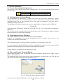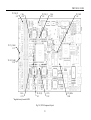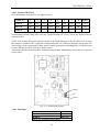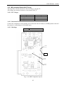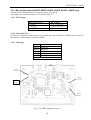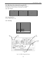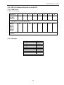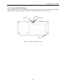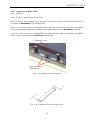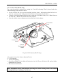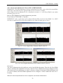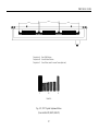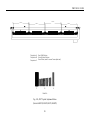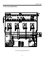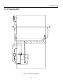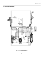
1
TITLE: Kx67E Technical Service Guide DOC. NO.: FSK/TSG/001 PREPARED BY: LM AUTHORIZED: JR DISTRIBUTION: Tegningsarkiv, Svendborg DD ISSUE REVISION: DATE: (1) (1) 1.7 110908 This document is the property of Contex A/S. The data contained herein, in whole or in part, may not be duplicated, used or disclosed outside the Recipient for any purpose other than to conduct technical evaluation. This restriction does not limit the Recipients right to use information contained in the data if it is obtained from another source without restriction. FSK/TSG/001 Document Revision Record REV. DATE CHANGED BY PAGES AFFECTED 1.0 1.1 051130 060505 LM LM All All 1.2 1.3 061003 070131 LM LM All All 1.4 1.5 080410 100520 LM LM All All 1.6 1.7 100622 110908 LM LM All All 2 DRR BRIEF DESCRIPTION OF CHANGE Original issue of document ATAC adjustment added List of Error Codes updated Major update KC67E added Minor updates/corrections KD67E to KM67E added Various minor error corrections The following chapters have been added: - 2.5 Switch Settings - 2.6 Boot Mode - 2.7 Board Overview - 5. Scanner Maintenance Camera adjustment using SCA Tool added KN67e (HD5430) added FSK/TSG/001 110908 Table of Contents 1. Introduction ............................................................................................................................9 2. General Information ............................................................................................................10 2.1 2.2 2.3 2.4 2.5 SCREWS SECURED BY SEALING LACQUER ........................................................................................................... 10 MARKING CODES FOR CIRCUIT BOARDS .............................................................................................................. 10 DOWNLOADING SCANNER FIRMWARE ................................................................................................................. 10 ERASE AND RESTORE PARAMETER BLOCKS......................................................................................................... 10 SWITCH SETTINGS................................................................................................................................................ 11 2.5.1 Scanner ID Switch ......................................................................................................................................... 11 2.5.2 Smart Card Reader Switch Settings .............................................................................................................. 11 2.6 SETTING SCANNER IN BOOT MODE ...................................................................................................................... 12 2.7 BOARD OVERVIEW .............................................................................................................................................. 13 2.8 BLOCK DIAGRAMS ............................................................................................................................................... 14 2.8.1 Block Diagram, KA67E ................................................................................................................................. 14 2.8.2 Block Diagram, KC67E, KM67E .................................................................................................................. 15 2.8.3 Block Diagram, KD67E, KE67E, KF67E, KH67E, KK67E, KN67E ............................................................ 16 2.8.4 Block Diagram, KL67E ................................................................................................................................. 17 3. Electrical Check and Adjustments .....................................................................................18 3.1 SMPS, SWITCH MODE POWER SUPPLY ................................................................................................................ 19 AC Voltages ................................................................................................................................................... 19 DC Voltages .................................................................................................................................................. 19 Adjustments ................................................................................................................................................... 19 Fuses ............................................................................................................................................................. 19 3.2 LMF, LAMP AND MOTOR DRIVER BOARD ........................................................................................................... 20 3.2.1 DC Voltages .................................................................................................................................................. 20 3.2.2 Lamp Driver Adjustment (KL67E only) ........................................................................................................ 20 3.2.3 Signal LED's on the LMF Board ................................................................................................................... 21 3.2.4 Stepper Motor Driver .................................................................................................................................... 21 3.2.5 Functional Tests ............................................................................................................................................ 21 3.2.6 Fuses ............................................................................................................................................................. 21 3.2.7 Markings ....................................................................................................................................................... 21 3.2.8 Jumper Settings ............................................................................................................................................. 22 3.2.9 Hints .............................................................................................................................................................. 22 3.3 CBK, CAMERA BOARD (KA67E ONLY) ............................................................................................................... 24 3.3.1 DC Voltages .................................................................................................................................................. 24 3.3.2 Functional Test.............................................................................................................................................. 24 3.3.3 Markings ....................................................................................................................................................... 24 3.3.4 Hints .............................................................................................................................................................. 25 3.4 CBM, CAMERA BOARD (ALL EXCEPT KA67E AND KL67E) ............................................................................... 26 3.4.1 DC Voltages .................................................................................................................................................. 26 3.4.2 Functional Test.............................................................................................................................................. 26 3.4.3 Markings ....................................................................................................................................................... 26 3.4.4 Hints .............................................................................................................................................................. 27 3.5 CBI, CAMERA BOARD (KL67E ONLY) ................................................................................................................. 28 3.5.1 DC Voltages .................................................................................................................................................. 28 3.5.2 Functional Test.............................................................................................................................................. 28 3.5.3 Markings ....................................................................................................................................................... 28 3.5.4 Hints .............................................................................................................................................................. 29 3.6 SUD, SCANNER CONTROLLER BOARD (KA67E ONLY) ....................................................................................... 30 3.6.1 DC Voltages .................................................................................................................................................. 30 3.6.2 Adjustments ................................................................................................................................................... 30 3.6.3 Functional Test.............................................................................................................................................. 30 3.6.4 Markings ....................................................................................................................................................... 30 3.6.5 Signal LEDs on the SUD Board .................................................................................................................... 30 3.6.6 Replacing the SUD Board ............................................................................................................................. 30 3.1.1 3.1.2 3.1.3 3.1.4 3 FSK/TSG/001 110908 3.7 SUF, SCANNER CONTROLLER BOARD (KL67E ONLY)......................................................................................... 32 DC Voltages .................................................................................................................................................. 32 Functional Test.............................................................................................................................................. 32 Markings ....................................................................................................................................................... 32 Signal LED's on the SUF Board ................................................................................................................... 32 Hints .............................................................................................................................................................. 32 3.8 SUG, SCANNER CONTROLLER BOARD (KC67E AND KM67E ONLY) .................................................................. 34 3.8.1 DC Voltages .................................................................................................................................................. 34 3.8.2 Adjustments ................................................................................................................................................... 34 3.8.3 Functional Test.............................................................................................................................................. 34 3.8.4 Markings ....................................................................................................................................................... 34 3.8.5 Signal LEDs on the SUG Board .................................................................................................................... 34 3.8.6 Replacing the SUG Board ............................................................................................................................. 34 3.9 SUH, SCANNER CONTROLLER BOARD (KD67E, KE67E, KF67E, KH67E, KK67E, KN67E) ............................ 36 3.9.1 DC Voltages .................................................................................................................................................. 36 3.9.2 Functional Test.............................................................................................................................................. 36 3.9.3 Markings ....................................................................................................................................................... 36 3.9.4 Signal LED's on the SUH Board ................................................................................................................... 36 3.9.5 Hints .............................................................................................................................................................. 36 3.10 SKF, OPERATORS PANEL (KA67E, KC67E AND KM67E ONLY) ........................................................................ 38 3.10.1 DC Voltages .................................................................................................................................................. 38 3.10.2 Functional Test.............................................................................................................................................. 38 3.10.3 Scanner ID Switch ......................................................................................................................................... 39 3.10.4 Markings ....................................................................................................................................................... 39 3.10.5 Operator Panel Layout ................................................................................................................................. 40 3.11 SKD, OPERATORS PANEL (ALL EXCEPT KA67E, KC67E AND KM67E) .............................................................. 41 3.11.1 DC Voltages .................................................................................................................................................. 41 3.11.2 Functional Test.............................................................................................................................................. 41 3.11.3 Markings ....................................................................................................................................................... 41 3.11.4 Switch Setting (Scanner ID) .......................................................................................................................... 41 3.12 IMH, INTERFACE BOARD (KL67E ONLY) ............................................................................................................ 43 3.12.1 DC Voltages .................................................................................................................................................. 43 3.12.2 Functional Test.............................................................................................................................................. 43 3.12.3 Markings ....................................................................................................................................................... 43 3.13 IMK, INTERFACE BOARD (KD67E, KE67E, KF67E, KH67E, KK67E , KN67E ONLY) ...................................... 44 3.13.1 DC Voltages .................................................................................................................................................. 44 3.13.2 Functional Test.............................................................................................................................................. 44 3.13.3 Markings ....................................................................................................................................................... 44 3.14 MDA, MOTOR DRIVER BOARD (ALL EXCEPT KL67E) ........................................................................................ 45 3.14.1 DC Voltages .................................................................................................................................................. 45 3.14.2 Functional Test.............................................................................................................................................. 45 3.14.3 Markings ....................................................................................................................................................... 45 3.15 CRB, CARD READER BOARD (ALL EXCEPT KL67E) ........................................................................................... 46 3.15.1 CRB Switch.................................................................................................................................................... 46 3.15.2 Markings ....................................................................................................................................................... 46 3.15.3 Signal LED on CRB Board ........................................................................................................................... 47 3.16 SCR, SMART CARD READER (KL67E ONLY) ....................................................................................................... 48 3.16.1 DC Voltages .................................................................................................................................................. 48 3.16.2 DIP Switch Setting ........................................................................................................................................ 48 3.16.3 Signal LED on the SCR-Board ...................................................................................................................... 48 3.16.4 Functional Test.............................................................................................................................................. 48 3.16.5 Markings ....................................................................................................................................................... 48 3.17 OSB, LAMP SENSOR BOARD (KL67E ONLY) ....................................................................................................... 50 3.17.1 Functional Test.............................................................................................................................................. 50 3.17.2 Markings ....................................................................................................................................................... 50 3.18 OIB, OPTOINTERRUPTER BOARD (KL67E ONLY) ............................................................................................... 50 3.18.1 Functional Test.............................................................................................................................................. 50 3.18.2 Markings ....................................................................................................................................................... 50 3.19 SSU, SCANNER STORAGE UNIT (KC67E AND KM67E ONLY) ............................................................................. 51 3.19.1 Functional Test.............................................................................................................................................. 51 3.19.2 Markings ....................................................................................................................................................... 51 3.19.3 Replacing the Scanner Storage Unit ............................................................................................................. 51 3.7.1 3.7.2 3.7.3 3.7.4 3.7.5 4 FSK/TSG/001 110908 3.20 CHECK AND ADJUSTMENT OF ORIGINAL GUIDE SENSORS (ATAC) ..................................................................... 52 3.20.1 Adjustment of Roller Sensor .......................................................................................................................... 55 3.20.2 Top Position Sensor ...................................................................................................................................... 56 3.20.3 Adjustment of Top Position Sensor, Type 1 (KA67E,KC67E,KD67E,KM67E,KN67E) ................................ 57 3.20.4 Adjustment of Top Position Sensor, Type 2 (KE67E, KF67E, KH67E, KK67E) .......................................... 58 3.20.5 Check of ATAC Position Sensors .................................................................................................................. 60 3.21 ADJUSTMENT OF ORIGINAL SENSORS (ALL EXCEPT KL67E) ............................................................................... 61 3.22 ADJUSTMENT OF ORIGINAL SENSORS (KL67E ONLY).......................................................................................... 61 3.22.1 Adjustment of Switch Point ........................................................................................................................... 61 3.22.2 Functional Test.............................................................................................................................................. 61 3.22.3 Hints .............................................................................................................................................................. 61 3.23 LCA, LAMP CARTRIDGE (ALL EXCEPT KL67E) ................................................................................................... 63 4. Camera Adjustment .............................................................................................................64 4.1 4.2 4.3 CAMERA BOARD TILT .......................................................................................................................................... 64 SETTING INITIAL POSITION OF THE VERTICAL ALIGNMENT ARM (ALL EXCEPT KL67E) ...................................... 65 ADJUSTING THE CAMERA TILT ............................................................................................................................ 66 4.3.1 Camera Tilt, All Models Except KL67E ........................................................................................................ 66 4.3.2 Camera Tilt (KL67E only)............................................................................................................................. 67 4.4 CCD-CAMERA CHECK AND ADJUSTMENT ........................................................................................................... 68 4.4.1 Check of Light Profiles, 3C36" (KA67E, KH67E, KK67E)........................................................................... 69 4.4.2 Check of Light Profiles, 4C42" (KC67E, KE67E, KF67E, KM67E)............................................................. 70 4.4.3 Check of Light Profiles, 4C54" (KD67E, KN67E) ........................................................................................ 71 4.4.4 Check of Light Profiles, 1C25" (KL67E) ...................................................................................................... 72 4.4.5 Check and Adjustment of Focus, 3C36" (KA67E, KH67E, KK67E) ............................................................. 73 4.4.6 Check and Adjustment of Focus, 4C42" (KC67E, KE67E, KF67E, KM67E) ............................................... 74 4.4.7 Check and Adjustment of Focus, 4C54" (KD67E, KN67E) .......................................................................... 75 4.4.8 Check and Adjustment of Focus, 1C25" (KL67E) ......................................................................................... 76 4.4.9 Check and Adjustment of Scan-Width ........................................................................................................... 77 4.4.10 Check and Adjustment of CCD-Centering .................................................................................................... 78 4.4.11 Check and Adjustment of Vertical Positioning.............................................................................................. 79 4.4.12 Final Check ................................................................................................................................................... 79 4.4.13 Camera Adjustment Screen Dumps, 3C36” (KA67E, KH67E, KK67E) ....................................................... 80 4.4.14 Camera Adjustment Screen Dumps, 4C42” (KC67E, KE67E, KF67E, KM67E) ......................................... 82 4.4.15 Camera Adjustment Screen Dumps, 4C54” (KD67E, KN67E) ..................................................................... 84 4.4.16 Camera Adjustment Screen Dumps, 1C25” (KL67E) ................................................................................... 86 5. Scanner Maintenance ...........................................................................................................91 6. SCANtest ...............................................................................................................................95 6.1 6.2 TEST 1, SCANNER INFORMATION ......................................................................................................................... 96 TEST 2, LED AND LCD DISPLAY TEST ................................................................................................................ 96 6.2.1 Scanners with LED Display .......................................................................................................................... 96 6.2.2 Scanners without LED Display ..................................................................................................................... 96 6.3 TEST 3, KEY TEST ................................................................................................................................................ 96 6.3.1 Scanners with LED Display .......................................................................................................................... 96 6.3.2 Scanners without LED Display ..................................................................................................................... 97 6.4 TEST 4, ORIGINAL SENSOR TEST.......................................................................................................................... 97 6.4.1 Scanners with LED Display .......................................................................................................................... 97 6.4.2 Scanners without LED Display ..................................................................................................................... 97 6.5 TEST 5, LAMP TEST.............................................................................................................................................. 97 6.6 TEST 6, MOTOR TEST ........................................................................................................................................... 97 6.7 TEST 7, COMPLETE HARDWARE TEST .................................................................................................................. 98 6.8 TEST 9, CAMERA ADJUSTMENT ........................................................................................................................... 98 6.9 TEST 11, STITCHING AND VERTICAL ALIGNMENT ................................................................................................ 98 6.10 TEST 12, ADJUSTMENT OF Y-AXIS SCALING........................................................................................................ 98 6.11 TEST 13, SWITCH SCANNER TO TEST MODE ........................................................................................................ 99 6.12 TEST 20, NOISE TEST ........................................................................................................................................... 99 6.13 TEST 21, SCANDUMP ........................................................................................................................................ 100 6.14 TEST 27, CAMERA ADJUSTMENT WIZARD ......................................................................................................... 100 6.15 TEST 28, ORIGINAL GUIDE SENSOR TEST (ALL EXCEPT KL67E)........................................................................ 100 6.16 TEST 30, CALIBRATE ATAC (ALL EXCEPT KL67E) ........................................................................................... 100 6.17 TEST 31, LMX COMMUNICATION TEST (ALL EXCEPT KL67E) ........................................................................... 100 5 FSK/TSG/001 110908 7. Special Service Tools ..........................................................................................................101 8. Wiring Diagrams ................................................................................................................102 8.1 8.2 8.3 8.4 8.5 8.6 8.7 8.8 8.9 8.10 8.11 8.12 3C36” PRIMARY WIRING (KA67E) ................................................................................................................... 103 3C36” SECONDARY WIRING (KA67E).............................................................................................................. 104 4C42” PRIMARY WIRING (KC67E, KM67E) ..................................................................................................... 105 4C42” SECONDARY WIRING (KC67E, KM67E) ................................................................................................ 106 3C36” PRIMARY WIRING (KH67E, KK67E) ..................................................................................................... 107 3C36” SECONDARY WIRING (KH67E, KK67E) ................................................................................................ 108 4C42” PRIMARY WIRING (KE67E, KF67E) ...................................................................................................... 109 4C42” SECONDARY WIRING (KE67E, KF67E) ................................................................................................. 110 4C54" PRIMARY WIRING (KD67E, KN67E) ..................................................................................................... 111 4C54" SECONDARY WIRING (KD67E, KN67E) ................................................................................................ 112 1C25" PRIMARY WIRING (KL67E) .................................................................................................................... 113 1C25" SECONDARY WIRING (KL67E) ............................................................................................................... 114 9. Appendix 1, Camera Adjustment using the SCA Tool ...................................................115 9.1 ADJUSTING VP, TILT AND CCD CENTERING USING THE SCA TOOL ................................................................. 115 10. Appendix 2, Error Codes ...................................................................................................118 6 FSK/TSG/001 110908 List of Figures Fig. 1-1, Location of Model Number ................................................................................................... 9 Fig. 2-1, Erase and Restore Parameter Blocks ................................................................................... 10 Fig. 2-2, Block Diagram KA67E ....................................................................................................... 14 Fig. 2-3, Block Diagram KC67E, KM67E ......................................................................................... 15 Fig. 2-4, Block Diagram KD67E, KE67E, KF67E, KH67E, KK67E, KN67E.................................. 16 Fig. 2-5, Block Diagram KL67E ........................................................................................................ 17 Fig. 3-1, SMPS Component Layout ................................................................................................... 19 Fig. 3-2, LMF Component Layout ..................................................................................................... 23 Fig. 3-3, CBK Component Layout ..................................................................................................... 24 Fig. 3-4, CBM Component Layout .................................................................................................... 26 Fig. 3-5, CBI Component Layout....................................................................................................... 28 Fig. 3-6, SUD Component Layout ..................................................................................................... 31 Fig. 3-7, SUF Component Layout ...................................................................................................... 33 Fig. 3-8, SUG Component Layout ..................................................................................................... 35 Fig. 3-9, SUH Component Layout ..................................................................................................... 37 Fig. 3-10, SKF Component Layout .................................................................................................... 38 Fig. 3-11, Scanner ID Switch ............................................................................................................. 39 Fig. 3-12, Operator Panel Layout ....................................................................................................... 40 Fig. 3-13, SKD Component Layout ................................................................................................... 42 Fig. 3-14, IMH Component Layout ................................................................................................... 43 Fig. 3-15, IMK Component Layout ................................................................................................... 44 Fig. 3-16, MDA Component Layout .................................................................................................. 45 Fig. 3-17, CRB Component Layout ................................................................................................... 47 Fig. 3-18, SCR Component Layout .................................................................................................... 49 Fig. 3-19, OSB Component Layout ................................................................................................... 50 Fig. 3-20, OIBA Component Layout ................................................................................................. 50 Fig. 3-21, Original Guide Plate Sensors............................................................................................. 52 Fig. 3-22, Elevation Motor and Spindle ............................................................................................. 54 Fig. 3-23, Adjustment of Roller Sensor ............................................................................................. 55 Fig. 3-24, Adjustment Tool for Roller Sensor ................................................................................... 55 Fig. 3-25, Type 1 and Type 2 Original Guide Plate with ATAC ....................................................... 56 Fig. 3-26, Adjustment of Top Position Sensor (Type 1) .................................................................... 57 Fig. 3-27, Adjustment of Top Position Sensor (Type 2) .................................................................... 58 Fig. 3-28, Adjustment Tool for Top Position Sensor ......................................................................... 59 Fig. 3-29, Adjustment of Original-Sensors ........................................................................................ 62 Fig. 4-1, Adjustable Spacer for Camera Board Tilt ........................................................................... 64 Fig. 4-2, Lock Nut for Camera Board Tilt ......................................................................................... 64 Fig. 4-3, CCD Camera (all except KL67E) ........................................................................................ 65 Fig. 4-4, CCD Camera (KL67E only) ................................................................................................ 67 Fig. 4-5, Uncorrected Light Profiles, KA67E, KH67E, KK67E ........................................................ 69 Fig. 4-6, Corrected Light Profiles, KA67E, KH67E, KK67E ............................................................ 69 Fig. 4-7, Uncorrected Light Profile, KC67E, KE67E, KF67E, KM67E ............................................ 70 Fig. 4-8, Corrected Light Profile, KC67E, KE67E, KF67E, KM67E ................................................ 70 Fig. 4-9, Uncorrected Light Profile, KD67E, KN67E ....................................................................... 71 Fig. 4-10, Corrected Light Profile, KD67E, KN67E ......................................................................... 71 Fig. 4-11, Uncorrected Light Profile, KL67E .................................................................................... 72 Fig. 4-12, Corrected Light Profile, KL67E ........................................................................................ 72 Fig. 4-13, Focus Signal (Blue Channel), KA67E, KH67E, KK67E .................................................. 73 Fig. 4-14, Focus Signals (Red and Green Channel), KA67E, KH67E, KK67E ................................ 73 7 FSK/TSG/001 110908 List of Figures cont. Fig. 4-15, Focus Signal (Blue Channel), KC67E, KE67E, KF67E, KM67E ..................................... 74 Fig. 4-16, Focus Signals (Red and Green Channel), KC67E, KE67E, KF67E, KM67E ................... 74 Fig. 4-17, Focus Signal (Blue Channel), KD67E, KN67E ................................................................ 75 Fig. 4-18, Focus Signals (Red and Green Channel), KD67E, KN67E .............................................. 75 Fig. 4-19, Focus Signal (Blue Channel), KL67E ............................................................................... 76 Fig. 4-20, Focus Signals (Red and Green Channel), KL67E ............................................................. 76 Fig. 4-21, Camera A Screen Dump, 3C36”........................................................................................ 80 Fig. 4-22, Camera B Screen Dump, 3C36” ........................................................................................ 80 Fig. 4-23, Camera C Screen Dump, 3C36” ........................................................................................ 81 Fig. 4-24, Camera A Screen Dump, 4C42”........................................................................................ 82 Fig. 4-25, Camera B Screen Dump, 4C42” ........................................................................................ 82 Fig. 4-26, Camera C Screen Dump, 4C42” ........................................................................................ 83 Fig. 4-27, Camera D Screen Dump, 4C42”........................................................................................ 83 Fig. 4-28, Camera A Screen Dump, 4C54”........................................................................................ 84 Fig. 4-29, Camera B Screen Dump, 4C54” ........................................................................................ 84 Fig. 4-30, Camera C Screen Dump, 4C54” ........................................................................................ 85 Fig. 4-31, Camera D Screen Dump, 4C54”........................................................................................ 85 Fig. 4-32, Camera A Screen Dump, 1C25”........................................................................................ 86 Fig. 4-33, 3C36” Optical Adjustment Pattern .................................................................................... 87 Fig. 4-34, 4C42” Optical Adjustment Pattern .................................................................................... 88 Fig. 4-35, 4C54” Optical Adjustment Pattern .................................................................................... 89 Fig. 4-36, 1C25” Optical Adjustment Pattern .................................................................................... 90 Fig. 5-1, SM Calibration Sheet, 25” ................................................................................................... 92 Fig. 5-2, SM Calibration Sheet, 36/40/42"......................................................................................... 93 Fig. 5-3, SM Calibration Sheet, 54” ................................................................................................... 94 Fig. 6-1, Scanner Test Program Menu ............................................................................................... 95 Fig. 6-2, Noise Test, Example ............................................................................................................ 99 Fig. 6-3, Fans and Lamp Feed-Back ................................................................................................ 100 Fig. 8-1, 3C36” Primary Wiring (KA67E) ....................................................................................... 103 Fig. 8-2, 3C36” Secondary Wiring (KA67E) ................................................................................... 104 Fig. 8-3, 4C42” Primary Wiring (KC67E, KM67E) ........................................................................ 105 Fig. 8-4, 4C42” Secondary Wiring (KC67E, KM67E) .................................................................... 106 Fig. 8-5, 3C36” Primary Wiring (KH67E, KK67E) ........................................................................ 107 Fig. 8-6, 3C36” Secondary Wiring (KH67E, KK67E) .................................................................... 108 Fig. 8-7, 4C42” Primary Wiring (KE67E, KF67E).......................................................................... 109 Fig. 8-8, 4C42” Secondary Wiring (KE67E, KF67E)...................................................................... 110 Fig. 8-9, 4C54" Primary Wiring (KD67E, KN67E)......................................................................... 111 Fig. 8-10, 4C54" Secondary Wiring (KD67E, KN67E)................................................................... 112 Fig. 8-11, 1C25" Primary Wiring (KL67E) ..................................................................................... 113 Fig. 8-12, 1C25" Secondary Wiring (KL67E) ................................................................................. 114 Fig. 9-1, Placing the SCA Tool ........................................................................................................ 115 Fig. 9-2, Position of the SCA Tools in a 3 Camera Scanner ............................................................ 116 8 FSK/TSG/001 110908 1. Introduction The purpose of this Technical Service Guide is to supply the information necessary to service the following scanner models: Model Type Optical Res. KA67E KC67E KD67E KE67E KF67E KH67E KK67E KL67E KM67E KN67E 3C36" 4C42" 4C54" 4C42" 4C42" 3C36" 3C36" 1C25" 4C42" 4C54" 600 600 508 600 600 600 600 424 600 508 Note: Throughout this TSG the abbreviation Kx67E will be used when referring to all of the above listed scanner models The scanner model is identified by the model number on the number plate placed on the back of the scanner Fig. 1-1, Location of Model Number 9 FSK/TSG/001 110908 2. General Information 2.1 Screws Secured by Sealing Lacquer Some screws, nuts or the like are sealed by sealing lacquer. The color of the sealing lacquer signals the following: RED Lacquer Factory adjusted. DO NOT ALTER WHITE Lacquer Adjustment which may be altered 2.2 Marking Codes for Circuit Boards All circuit boards are identified by a 4-letter code, where the fourth letter designates a specific variant of the board. The board identification code is followed by a board revision number (functional level) and for newer boards also an extra letter in parenthesis. This extra letter is unimportant in this connection. The marking of all printed circuit boards may be exemplified by the marking of the SUD Board: SUDA02(B) which designates SUD Board, variant A, revision 02. The (B) is of no importance and should be neglected. The revision number is updated only if the functionality of the board has been changed. Updated boards will always be backwards compatible. 2.3 Downloading Scanner Firmware The scanner firmware is stored in Flash Memory on the SUx Board. Firmware is downloaded to the scanner through the USB 2.0 interface, please refer to any readme.txt for download instructions. The download program is started by double-clicking the self extracting firmware file. It is recommended to disable WIDEsystem before upgrading the firmware to prevent any possible problems caused this program accessing the scanner during the upgrade. Scanner firmware is available on the support home page. 2.4 Erase and Restore Parameter Blocks When trouble shooting it may be advisable to clear the parameter blocks in the scanner to reset these to default values. The parameter blocks can be erased from Scanner Maintenance by right-click on the Title Bar and select Erase Parameter Blocks from the pull-down menu. Fig. 2-1, Erase and Restore Parameter Blocks Note: Always run Scanner Maintenance after Erasing Parameter Blocks. 10 FSK/TSG/001 110908 2.5 Switch Settings 2.5.1 Scanner ID Switch 2.5.1.1 Scanner ID Switch, all except KA67E, KC67E and KM67E SKD switch settings, see Fig. 3-13, SKD Component Layout: Scanner Model KD67E KE67E KF67E KH67E KK67E KN67E SW1 SW2 SW3 SW4 SW5 SW6 SW7 SW8 HEX OFF OFF OFF OFF OFF OFF ON ON ON ON ON ON OFF OFF OFF OFF OFF OFF ON ON ON ON ON ON OFF OFF OFF ON ON ON ON ON ON OFF OFF ON OFF OFF ON OFF OFF OFF OFF ON OFF OFF ON ON 0x54 0x55 0x56 0x58 0x59 0x5D 2.5.1.2 Scanner ID Switch, KA67E, KC67E and KM67E only SKF switch settings ,see Fig. 3-10, SKF Component Layout: Switch No: 1 2 3 4 5 6 7 8 HEX KA67E OFF OFF OFF OFF OFF ON OFF OFF 0x04 KC67E OFF OFF OFF OFF ON OFF OFF ON 0x09 KM67E OFF ON OFF ON ON ON ON 0x5B OFF 2.5.2 Smart Card Reader Switch Settings The switch on the smart card reader has formerly been referred to as the "SCSI ID". As none of the Kx67E scanners have SCSI interface the SCSI related switch settings (SW no. 1, 2, 3, 4, and 5) do not apply to these scanners. 2.5.2.1 CRB, all except KL67E CRB switch settings, see Fig. 3-17, CRB Component Layout: Switch No: KA67E KC67E KM67E KD67E KE67E KF67E KH67E KK67E KN67E 1 2 3 4 5 6 7 8 OFF OFF OFF OFF OFF OFF OFF OFF ON OFF ON ON OFF OFF OFF OFF 11 FSK/TSG/001 110908 2.5.2.2 SCR, KL67E only SCR switch settings, see Fig. 3-18, SCR Component Layout: Switch No: 1 2 3 4 5 6 7 8 KL67E ON OFF ON ON OFF OFF OFF OFF 2.6 Setting Scanner in Boot Mode The scanner can be set in to boot mode as described in the table below. Model KA67E* KC67E* KM67E* Setting Scanner in Boot Mode fw < 1.2.1: n/a fw ≥ 1.2.1: - Switch off the scanner - Press and hold STOP + ENTER Key - Switch power on - Wait until display reads “Requesting download” - Release STOP + ENTER Keys * Firmware must be loaded using the USB interface KD67E To set the scanner in boot mode: KE67E - Switch off the scanner KF67E - Press and hold POWER Key KH67E - Switch power on KK67E - Wait until scanner blink indicates that scanner is in boot mode KL67E - Release POWER Key KN67E 12 FSK/TSG/001 110908 Part Number 0080A064R01 6834A001R01 6834A003R01 6742D001R01 6749D001R01 6733E002R01 6732E001R01 6748D002RA1 6736E001R01 6750D001R01 6750D002R01 6750D003R01 6750D004R01 6845A003R01 6746D001R01 6733D001R01 6733D007R01 6836A001R01 6831A003R01 6753A104R01 6738D003R01 6336A001R01 3132A003R01 Designation CTX-Z07H, 68W SMPS, Triple Output LMFA, Lamp and Motor Driver Board LMFB, Lamp and Motor Driver Board CBKA Camera Board CBMA Camera Board CBIB Camera Board SUDA, Controller Board SUFB, Controller Board SUGA, Controller Board SUHA Controller Board SUHB Controller Board SUHC Controller Board SUHD Controller Board IMKC, Interface Module (USB2.0 only) IMHA, Interface Module, IEEE 1394 and USB SKDA, Operator Panel, Contex SKDG, Operator Panel (Dark Grey) SKFA, Operator Panel CRBC, Smart Card Reader SCR, Smart Card Reader, assembly MDAC, Elevation Motor Driver Board OIBA, Optical Interrupter Board OSBC, Optical Sensor Board 13 3.1 3.2 3.2 3.3 3.4 3.5 3.6 3.7 3.8 3.9 3.9 3.9 3.9 0 3.12 3.11 3.11 3.10 3.15 3.16 3.14 3.18 3.17 KA67E KC67E KD67E KE67E KF67E KH67E KK67E KL67E KM67E KN67E Type SMPS LMFA LMFB CBKA CBMA CBIB SUDA SUFB SUGA SUHA SUHB SUHC SUHD IMKC IMHA SKDA SKDG SKFA CRBC SCRA MDAC OIBA OSBC Section 2.7 Board Overview The table below gives an overview of the printed circuit boards used in the different models with reference to the appropriate section in this manual. x x x x x x x - x x x x x x x - x x x x x x x x - x x x x x x x x - x x x x x x x x - x x x x x x x x - x x x x x x x x - x x x x - - x x - x - x - - - - - x x - - x - x x - x x x - x x x x x x x x - FSK/TSG/001 110908 2.8 Block Diagrams 2.8.1 Block Diagram, KA67E The Block Diagram for the following models is shown below. Model Type KA67E 3C36" Fig. 2-2, Block Diagram KA67E 14 FSK/TSG/001 110908 2.8.2 Block Diagram, KC67E, KM67E The Block Diagram for the following models is shown below. Model Type KC67E 4C42" KM67E Fig. 2-3, Block Diagram KC67E, KM67E 15 FSK/TSG/001 110908 2.8.3 Block Diagram, KD67E, KE67E, KF67E, KH67E, KK67E, KN67E The Block Diagram for the following models is shown below. Model KD67E KN67E KE67E KF67E KH67E KK67E Type 4C54" 4C42" 3C36" Fig. 2-4, Block Diagram KD67E, KE67E, KF67E, KH67E, KK67E, KN67E 16 FSK/TSG/001 110908 2.8.4 Block Diagram, KL67E The Block Diagram for the following models is shown below. Model Type KL67E 1C25" Fig. 2-5, Block Diagram KL67E 17 FSK/TSG/001 110908 3. Electrical Check and Adjustments Required Test Equipment: Multimeter, Ri > 10 MOhm PC with the following installed: • SCANtest • Scanner Maintenance • USB Interface SCANtest is described in Chapter 6, page 95. On the following pages tests of the individual printed circuit boards are described as well as the adjustment of various sensors. 18 FSK/TSG/001 110908 3.1 SMPS, Switch Mode Power Supply 3.1.1 AC Voltages CAUTION: The connector TB1 and the components in the hatched area are connected directly to the mains voltage and constitute a risk of electric shock, or injury to persons 3.1.2 DC Voltages Ref. on Fig. 3-1 TB2, pin 1,2 TB2, pin 3,4,5,6 TB2, pin 7 TB2, pin 8 DC Voltage +5.3 V +0/-0.1 V GND +12.5 V ± 0.5 V +24 V ± 1 V 3.1.3 Adjustments IMPORTANT: The output voltages of the SMPS are all factory set and should normally not be adjusted. The 5.3V output voltage should be no more than 5.3 V measured between GND and TB2, pin 1,2 (5.3V) on the SMPS, and no less than 5.1 V measured between GND and D3, bottom on the CBK board. If the voltage is not within these limits, it may be adjusted by potentiometer VR1 on the SMPS. 3.1.4 Fuses No service replaceable fuses L N 5.3V TB2, pin 1-2 5.3V +5.3V +0/-0.1 GND GND TB2, pin 3-6 GND GND GND TB2, pin 7 12.5V +12.5V±0.5 24V TB2, pin 8 +24V±1 VR1 +5.3V Adjust Fig. 3-1, SMPS Component Layout 19 FSK/TSG/001 110908 3.2 LMF, Lamp and Motor Driver Board All test points referred to below are shown in Fig. 3-2, page 23. All DC voltages are measured relative to test point GND. CAUTION: Connectors J1, J7 and all the components in the hatched area are connected to the line voltage and constitute a risk of electric shock, or injury to persons. 3.2.1 DC Voltages Ref. on Fig. 3-2 Test point GND TP8 - GND TP9 - GND TP10 - GND TP18 - GND TP16 - GND TP15 - GND TP5 – TP7 * TP7 – TP6* DC Voltage GND +3.3 V ± 0.1 V +5.3 V +0/-0.2 V +12.0 V + 1/-0 V +24.0 V ± 1 V +5.0 V ± 0.15 V +12.0 V ± 0.3 V +200 V ± 20 V −200 V ± 20 V * Caution: These test points are at high voltage level and constitute a risk of electric shock, or injury to persons. 3.2.2 Lamp Driver Adjustment (KL67E only) For all models except KL67E the LMF board is designed to work with calibrated Lamp Cartridges which means that there is no adjustment of the lamp driver. KL67E does not use a Lamp Cartridge and on this model the lamp driver must be adjusted. To ensure a constant predefined light level in the scanners throughout the lifetime of the lamp, the lamp driver should only be adjusted when the lamp is new. This means that the lamp driver is only adjusted when changing either: • the Lamp • the Lamp Driver Board, LMF • the Lamp Sensor Board, OSB and in order to do so the lamp must be new Adjustment Procedure: Note: The voltage on TP11 is clamped to approximately 5V. It may be necessary to turn P11 several turns CCW to bring the voltage below the clamp voltage. The Lamp Driver should be adjusted immediately after the scanner has been switched on and the lamp must be new and “cold”. 1. Make sure that the lamp is new. If not it should be replaced. 2. Remove the front cover of the scanner 3. Switch on the scanner 4. While the scanner boots, wait for the lamp to switch on for the second time (after approx. 30 seconds) 5. Turn P11 CW until LED1 switches ON and then slowly CCW until LED1 switches OFF 6. Leave the scanner on for 1 minute 20 FSK/TSG/001 110908 7. Turn P11 CW until LED1 switches ON and then slowly CCW until LED1 switches OFF 8. Replace the front cover 9. Reset the lamp counter: • Start SCANtest • Select Test 1 (Scanner Information) • Press the button “Reset Lamp Counter” • Type the password “xetnoc” and press “Reset Lamp Counter” 10. Run Scanner Maintenance to ensure correct Basic- and Color Calibration 3.2.3 Signal LED's on the LMF Board The two indicators, LED1 and LED2 indicate the status of the stabilization circuit of the Lamp Driver and are controlled by the feedback voltage on TP11. The following can be read from the status of the LED's: LED1: The status of this LED is of no importance. LED2: ON: Stabilization circuit is close to or outside the active range and the lamp should be replaced OFF: Stabilization circuit within the active range 3.2.4 Stepper Motor Driver There are no adjustments to the Stepper Motor Driver on the LMF board 3.2.5 Functional Tests SCANtest: Test 5, Lamp Test Test 6, Motor Test 3.2.6 Fuses The type and rating of the fuse on the LMFA board is: F1: T2.0AH/250V, type IEC 127- 2/5, UL R/C IMPORTANT: For continued protection against risk of fire, replace only with same type and rating of fuse. 3.2.7 Markings KA67E LMFAdd KC67E LMFAdd KD67E LMFAdd KE67E LMFAdd KF67E LMFAdd KH67E LMFAdd KK67E LMFAdd KL67E LMFBdd KM67E LMFAdd KN67E LMFAdd where dd = board revision number. 21 FSK/TSG/001 110908 3.2.8 Jumper Settings Jumper: 3.2.9 Hints Jumper on JP1: JP1 not installed Not installed: Lamp controlled by SUF Installed: Lamp constant ON Control signals on J6: pin 2: Lamp ON/OFF, LOW = ON pin 8: Feed-Motor Step Pulse pin 11: Feed-Motor Direction, LOW = FORWARD Fan Speed Control: A NTC Temperature Sensor located under the End Cover at the Operator Panel end of the scanner controls the speed of the fans connected to J13 and J14. 22 FSK/TSG/001 110908 +3.3V +5.3VΔ TP8 TP9 +12VΔ 24VΔ GND TP10 TP18 TP4,12,13,17 JP1 +5V TP16 LED2 LED1 NOTE: The components in the hatched area are connected to the mains voltage and represents risk of electrical shock +12V TP15 P1 (KL67E only) Δ Supplied directly from the SMPS + 200V – + 200V – TP7 TP6 TP5 Fig. 3-2, LMF Component Layout 23 J4 Lamp Feed-Back TP11 (KL67E only) FSK/TSG/001 110908 3.3 CBK, Camera Board (KA67E only) All test points referred to are shown in Fig. 3-3, page 24. All voltages are measured relative to test point GND. 3.3.1 DC Voltages Ref. on Fig. 3-3 D3, bottom D3, top D2, top D4, bottom DC Voltage +5.3 V +0/-0.2 V +5.0 V ± 0.2 V +5.0 V ± 0.2 V +12.0 V +1/-0 V D4, top C301, bottom D308, bottom +11.6 V ± 0.6 V +3.3 V ± 0.1 V +1.8 V ± 0.1 V +5V D3,top Camera Motor Output Remarks From SUx / SMPS Derived from +5.3V Derived from +5.3V From SUx / SMPS, used for CCD and Camera Motor Derived from +12V From SUx / LMF Derived from +3.3V +11.6V +12V +5V D4,top D4,bottom D2,top +1.8V D308,bottom +5.3V GND D3,bottom J701, pin3,4 +3.3V C301, bottom Fig. 3-3, CBK Component Layout 3.3.2 Functional Test SCANtest: Test 7, Complete Hardware Test Test 9, Camera Adjustment 3.3.3 Markings CBKAdd KA67E where dd = board revision number 24 FSK/TSG/001 110908 3.3.4 Hints +3.3 V is supplied from the LMF via the SUx Board. +5.3 V and +12 V is supplied from the SMPS via the SUx Board. CCD The lines of pixels on the CCD are arranged as follows: Upper line on the CCD: 2nd line on the CCD: 3rd line on the CCD: Lower line on the CCD: Red Green Blue B/W As the image is mirrored an even number of times (mirror chassis and lens), the Red line remains upper line when referred to the original. Control of Camera Motor The Camera Motor for Vertical Alignment is driven from a controller IC on the CBK Board. The supply voltage for the motor is +12 V. The motor can be tested using test 9, Camera Adjustment (Forward / Reverse controls for the Camera Motor) After replacement of CBK Board, do: • CCD-Centering, see 4.4.10. • Vertical Positioning, see 4.4.11. • Check Scan-Width, if it is within the limits given in 4.4.9, Focus will also be OK, and no further adjustments are required. • Run Scanner Maintenance. These adjustments can be made without loosening the Camera Fixing Screws and without loosening the Focus Lock Ring / Lock Screw. 25 FSK/TSG/001 110908 3.4 CBM, Camera Board (All except KA67E and KL67E) All test points referred to are shown in Fig. 3-4, page 26. All voltages are measured relative to test point GND. 3.4.1 DC Voltages Ref. on Fig. 3-4 D3, bottom D3, top D2, top D4, bottom DC Voltage +5.3 V +0/-0.2 V +5.0 V ± 0.2 V +5.0 V ± 0.2 V +12.0 V +1/-0 V D4, top C301, bottom D308, bottom +11.6 V ± 0.6 V +3.3 V ± 0.1 V +1.8 V ± 0.1 V +5V D3,top Camera Motor Output Remarks From SUx / SMPS Derived from +5.3V Derived from +5.3V From SUx / SMPS, used for CCD and Camera Motor Derived from +12V From SUx / LMF Derived from +3.3V +11.6V +12V +5V D4,top D4,bottom D2,top +1.8V D308,bottom +5.3V GND D3,bottom J701, pin3,4 +3.3V C301, bottom Fig. 3-4, CBM Component Layout 3.4.2 Functional Test SCANtest: Test 7, Complete Hardware Test Test 9, Camera Adjustment 3.4.3 Markings KC67E KD67E KE67E KF67E KH67E KK67E KM67E KN67E where dd = board revision number 26 CBMAdd CBMAdd CBMAdd CBMAdd CBMAdd CBMAdd CBMAdd CBMAdd FSK/TSG/001 110908 3.4.4 Hints +3.3 V is supplied from the LMF via the SUx Board. +5.3 V and +12 V is supplied from the SMPS via the SUx Board. CCD The lines of pixels on the CCD are arranged as follows: Upper line on the CCD: 2nd line on the CCD: 3rd line on the CCD: Lower line on the CCD: Red Green Blue B/W As the image is mirrored an even number of times (mirror chassis and lens), the Red line remains upper line when referred to the original. Control of Camera Motor The Camera Motor for Vertical Alignment is driven from a controller IC on the CBK Board. The supply voltage for the motor is +12 V. The motor can be tested using test 9, Camera Adjustment (Forward / Reverse controls for the Camera Motor) After replacement of CBM Board, do: • CCD-Centering, see 4.4.10. • Vertical Positioning, see 4.4.11. • Check Scan-Width, if it is within the limits given in 4.4.9, Focus will also be OK, and no further adjustments are required. • Run Scanner Maintenance. These adjustments can be made without loosening the Camera Fixing Screws and without loosening the Focus Lock Ring / Lock Screw. 27 FSK/TSG/001 110908 3.5 CBI, Camera Board (KL67E only) All test points referred to are shown in Fig. 3-5, page 28. All voltages are measured relative to test point GND. 3.5.1 DC Voltages Ref. on Fig. 3-3 D3, bottom D3, top D2, top D4, bottom D4, top C301, bottom D308, bottom DC Voltage +5.3 V +0/-0.2 V +5.0 V ± 0.2 V +5.0 V ± 0.2 V +12.0 V +1/-0 V +11.6 V ± 0.6 V +3.3 V ± 0.1 V +1.8 V ± 0.1 V +5V +11.6V +12V +5V D4,top D4,bottom D2,top D3,top Remarks From SUx / SMPS Derived from +5.3V Derived from +5.3V From SUx / SMPS, used for CCD Derived from +12V From SUx / LMF Derived from +3.3V +1.8V D308,bottom +5.3V GND D3,bottom J701, pin3,4 Fig. 3-5, CBI Component Layout 3.5.2 Functional Test SCANtest: Test 7, Complete Hardware Test 3.5.3 Markings KL67E CBIBdd where dd = board revision number 28 +3.3V C301, bottom FSK/TSG/001 110908 3.5.4 Hints +3.3 V is supplied from the LMF via the SUx Board. +5.3 V and +12 V is supplied from the SMPS via the SUx Board. CCD The lines of pixels on the CCD are arranged as follows: Upper line on the CCD: Center line on the CCD: Lower line on the CCD: Blue Green Red As the image is mirrored an even number of times (mirror chassis and lens), the Blue line remains upper line when referred to the original. After replacement of CBI Board, do: • CCD-Centering, see 4.4.10. • Vertical Positioning, see 4.4.11. • Check Scan-Width, if it is within the limits given in 4.4.9, Focus will also be OK, and no further adjustments are required. • Run Scanner Maintenance These adjustments can be made without loosening the Camera Fixing Screws and without loosening the Focus Lock Ring / Lock Screw. 29 FSK/TSG/001 110908 3.6 SUD, Scanner Controller Board (KA67E only) All test points referred to below are shown in Fig. 3-6, page 31. All voltages are measured relative to test point TP_GND6. 3.6.1 DC Voltages Ref. on Fig. 3-6 TP+12V_CAM1 DC Voltage +12 V + 1/-0V TP+5V_CAM1 +5.3 V +0/-0.2 V TP+1V5_D TP+5V0_D1 C168+ C184+ C901+ C197+ TP+1V8D TP+2V5_D +1.5 V ± 0.1 V +5.1 V +0.1/-0.2 V +1.25V ± 0.1 V Remarks Supply for Camera Board, Elevation Motor (ATAC) Supply for Camera Board, MDA Board (ATAC) Derived from 5.3V +1.8 V ± 0.1 V +2.5 V ± 0.1 V 3.6.2 Adjustments No adjustments. 3.6.3 Functional Test SCANtest: Test 1 Scanner Information Test 7, Complete Hardware Test 3.6.4 Markings Note: SUD variant depends on scanner model. KA67E SUDAdd where dd = board revision number. 3.6.5 Signal LEDs on the SUD Board The three signal LEDs on the SUD board are for debugging purposes only. The ON/OFF pattern displayed by these LEDs is not intended for general troubleshooting. 3.6.6 Replacing the SUD Board When installing a new SUD board the scanner serial number is read from the smart card. IMPORTANT: You must confirm to use the read number within 30 seconds by pressing the “Enter” key on the operators panel, otherwise the scanner will display an error (100-50303, No serialnumber). In this case either reboot the scanner or use SCANtest to enter the serial number found on the marking label on back of the scanner. A spare SUD board may not contain the correct firmware. Install the correct firmware from the CD which comes with the board. After replacement of SUD Board run Scanner Maintenance. 30 FSK/TSG/001 110908 TP+5V0_D1 5.0V C168+ 1.25V TP+2V5_D 2.5V TP+1V8D 1.8V C184+ 1.25V TP+5V_CAM1 5.3VΔ TP+12V_CAM1 12.5VΔ C901+ 1.25V Δ Supplied directly from the SMPS TP+1V5_D 1.5V C197+ 1.25V Fig. 3-6, SUD Component Layout 31 TP_GND6 GND FSK/TSG/001 110908 3.7 SUF, Scanner Controller Board (KL67E only) All test points referred to below are shown in Fig. 3-7, page 33. All voltages are measured relative to test point GND2. 3.7.1 DC Voltages Ref. on Fig. 3-7 12V_CAM DC Voltage +12 V + 1/-0V 5V_CAM +5.3 V +0/-0.2 V +3 +5V APEX_SUP APEX_PLL +3.3 V ± 0.1 V +5.1 V +0.1/-0.2 V +1.8 V ± 0.1 V +1.8 V ± 0.05 V Remarks Supply for Camera Board, Elevation Motor (ATAC) Supply for Camera Board, MDA Board (ATAC) Derived from 5.3V on SUF 3.7.2 Functional Test SCANtest: Test 1 Scanner Information Test 7, Complete Hardware Test 3.7.3 Markings Note: SUF variant depends on scanner model. KL67E SUFBdd where dd = board revision number. 3.7.4 Signal LED's on the SUF Board The three signal LEDs on the SUF board are for debugging purposes only. The ON/OFF pattern displayed by these LEDs is not intended for general troubleshooting. 3.7.5 Hints After replacement of SUF board: As all scanner parameters are stored in the Flash Memory on the SUF board, the following steps should be carried out after replacement of the SUF board: • Download Firmware • Run Scanner Maintenance • Enter Serial Number of scanner into Flash Memory (SCANtest, Test 1). The serial number of the scanner is found on the marking label on back of the scanner 32 FSK/TSG/001 110908 +3.3V±0.1V "+3" +5.1V+0.1/-0.2V "+5" +5.3V+0/-0.2V "5V_CAM" +12V+1/-0V +1.8V±0.05V "12V_CAM" "APEX_PLL" +1.8±0.1V GND "APEX_SUP" "GND2" Fig. 3-7, SUF Component Layout 33 FSK/TSG/001 110908 3.8 SUG, Scanner Controller Board (KC67E and KM67E only) All test points referred to below are shown in Fig. 3-8, page 35. All voltages are measured relative to test point TP_GND6. 3.8.1 DC Voltages Ref. on Fig. 3-8 TP+12V_CAM1 DC Voltage +12 V + 1/-0V TP+5V_CAM1 +5.3 V +0/-0.2 V TP+1V5_D TP+5V0_D1 C168+ C184+ C901+ C197+ TP+1V8D TP+2V5_D +1.5 V ± 0.1 V +5.1 V +0.1/-0.2 V +1.25V ± 0.1 V Remarks Supply for Camera Board, Elevation Motor (ATAC) Supply for Camera Board, MDA Board (ATAC) Derived from 5.3V +1.8 V ± 0.1 V +2.5 V ± 0.1 V 3.8.2 Adjustments No adjustments. 3.8.3 Functional Test SCANtest: Test 1 Scanner Information Test 7, Complete Hardware Test 3.8.4 Markings Note: SUG variant depends on scanner model. KC67E SUGAdd KM67E SUGAdd where dd = board revision number. 3.8.5 Signal LEDs on the SUG Board The three signal LEDs on the SUD board are for debugging purposes only. The ON/OFF pattern displayed by these LEDs is not intended for general troubleshooting. 3.8.6 Replacing the SUG Board Important note on scanners with installed smart card: When replacing the SUG board in a scanner with a smart card installed, the scanner serial number is read from the smart card. You must confirm to use the read number within 30 seconds by pressing the “Enter” key on the operators panel, otherwise the scanner will display an error (100-50303, No serialnumber). In this case either reboot the scanner or use SCANtest to enter the serial number found on the marking label on back of the scanner. A spare SUG board may not contain the correct firmware. Install the correct firmware from the CD which comes with the board. After replacement of the SUG Board run Scanner Maintenance. 34 FSK/TSG/001 110908 TP+5V0_D1 5.0V C168+ 1.25V TP+2V5_D 2.5V TP+1V8D 1.8V C184+ 1.25V TP+5V_CAM1 5.3VΔ TP+12V_CAM1 12.5VΔ C901+ 1.25V Δ Supplied directly from the SMPS TP+1V5_D 1.5V C197+ 1.25V Fig. 3-8, SUG Component Layout 35 TP_GND6 GND FSK/TSG/001 110908 3.9 SUH, Scanner Controller Board (KD67E, KE67E, KF67E, KH67E, KK67E, KN67E) All test points referred to below are shown in Fig. 3-9, page 37. All voltages are measured relative to test point GND2. 3.9.1 DC Voltages Ref. on Fig. 3-7 12V_CAM DC Voltage +12 V + 1/-0V 5V_CAM +5.3 V +0/-0.2 V +3.3V_D +5V APEX_SUP APEX_PLL +3.3 V ± 0.1 V +5.1 V +0.1/-0.2 V +1.8 V ± 0.1 V +1.8 V ± 0.05 V Remarks Supply for Camera Board, Elevation Motor (ATAC) Supply for Camera Board, MDA Board (ATAC) Derived from 5.3V on SUF 3.9.2 Functional Test SCANtest: Test 1 Scanner Information Test 7, Complete Hardware Test 3.9.3 Markings Note: SUH variant depends on scanner model. KD67E SUHBdd KE67E SUHBdd KF67E SUHAdd KH67E SUHCdd KK67E SUHDdd KN67E SUHAdd where dd = board revision number. 3.9.4 Signal LED's on the SUH Board The three signal LEDs on the SUH board are for debugging purposes only. The ON/OFF pattern displayed by these LEDs is not intended for general troubleshooting. 3.9.5 Hints After replacement of SUH board: As all scanner parameters are stored in the Flash Memory on the SUH board, the following steps should be carried out after replacement of the SUH board: • Download Firmware • Run Scanner Maintenance • Enter Serial Number of scanner into Flash Memory (SCANtest, Test 1). The serial number of the scanner is found on the marking label on back of the scanner 36 FSK/TSG/001 110908 12V_CAM 12.5VΔ APEX_SUP 1.8V 5V_CAM 5.3VΔ +3.3V_D 3.3V GND2 GND APEX_PLL 1.8V Fig. 3-9, SUH Component Layout 37 Δ Supplied directly from the SMPS FSK/TSG/001 110908 3.10 SKF, Operators Panel (KA67E, KC67E and KM67E only) 3.10.1 DC Voltages All test points referred to are shown in Fig. 3-10 page 38 All voltages are measured relative to TP1 (GND) Ref. on Fig. 3-10 TP6 TP4 C32+ TP5 DC Voltage +3.3V ± 0.1V +5.0V ± 0.15V +5.0V ± 0.15V +5.3V Remarks Generated from +5.3V Generated from +5.3V Generated from +5.3V Supplied from SMPS via SUD . TP6 3.3V TP5 5.25V TP1 GND C32 + 5V TP4 +5V Switch 1 S19 Switch 8 Fig. 3-10, SKF Component Layout 3.10.2 Functional Test SCANtest: Test 1, Scanner ID Switch Test 2, LED test Test 3, Key test 38 FSK/TSG/001 110908 3.10.3 Scanner ID Switch SKF, DIP Switch settings (S19, see figure below): Switch No: 1 2 3 4 5 6 7 8 HEX KA67E OFF OFF OFF OFF OFF ON OFF OFF 0x04 KC67E OFF OFF OFF OFF ON OFF OFF ON 0x09 KM67E OFF ON OFF ON ON ON ON 0x5B OFF An undefined switch setting may cause the ‘Invalid Scanner ID’ Error Code to be displayed on the Operator Panel. NOTE: The Scanner ID Switch setting is stored in the Flash Memory on the SUx Board. Every time the scanner is switched ON, it reads the switch setting and if it is different from the stored value, the new setting will be stored and all other stored scanner parameters (including Basic Calibration and Color Calibration) will be cleared to default values. This means that the scanner must be calibrated using Scanner Maintenance afterwards to restore the actual values. Switch 1 S19 Switch 8 Fig. 3-11, Scanner ID Switch 3.10.4 Markings SKFAdd KA67E SKFAdd KC67E SKFAdd KM67E where dd = board revision number. 39 FSK/TSG/001 110908 3.10.5 Operator Panel Layout LCD Display Control Buttons Menu Button Stop Button Size Button ATAC Button Ready LED Scan Option Area Forward Button Reverse Button Copy Option Area Fig. 3-12, Operator Panel Layout • • • • • • • The LCD Display contains the current selections as you make them and useful messages from the scanner regarding maintenance and operation. Forward/Reverse Buttons can be used to feed paper. When the scanner is in Automatic Thickness Adjustment Control (ATAC) mode the paper forward and paper reverse keys become “Pressure-Platen Up” and “Pressure-Platen Down” buttons The Menu Button leads to a options for copy settings and an advanced submenu for configuration settings. The Control Buttons Arrow Up, Arrow Down, Back and Enter are for navigating the menus and for selecting menu options. The Stop Button is for interrupting a copy or scan process. The Size Button is for setting the original’s size (input size) for both copy and scan jobs. Below the control and menu buttons, are a Copy Option Area and a Scan Option Area, each with its own set of quick option buttons. For a detailed description of the individual buttons and functions please refer to the scanners operators guide 40 FSK/TSG/001 110908 3.11 SKD, Operators Panel (all except KA67E, KC67E and KM67E) All test points referred to are shown in Fig. 3-13, page 42. All voltages are measured relative to PCB Ground Plane. 3.11.1 DC Voltages Ref. on Fig. 3-13 J2,pin 3 C1,top DC Voltage +3.3 V ± 0.1 V +5.1 V +0.1/-0.2 V 3.11.2 Functional Test SCANtest: Test 1, Scanner ID Switch Test 2, LED test Test 3, Key test 3.11.3 Markings KD67E SKDGdd KE67E SKDGdd KF67E SKDGdd KH67E SKDGdd KK67E SKDGdd KL67E SKDAdd KN67E SKDGdd where dd = board revision number 3.11.4 Switch Setting (Scanner ID) DIP Switch Setting: Scanner Model KD67E KE67E KF67E KH67E KK67E KN67E SW1 SW2 SW3 SW4 SW5 SW6 SW7 SW8 HEX OFF OFF OFF OFF OFF OFF ON ON ON ON ON ON OFF OFF OFF OFF OFF OFF ON ON ON ON ON ON OFF OFF OFF ON ON ON ON ON ON OFF OFF ON OFF OFF ON OFF OFF OFF OFF ON OFF OFF ON ON 0x54 0x55 0x56 0x58 0x59 0x5D An undefined switch setting may cause the ‘Invalid Scanner ID’ Error Code to be displayed on the Operator Panel. IMPORTANT: The Scanner ID Switch setting is stored in the Flash Memory on the SUx board. Every time the scanner is switched ON, it reads the switch setting and if it is different from the stored value, the new setting will be stored and all other stored scanner parameters (including Stitching, Basic Calibration and Color Calibration) will be cleared to default values. This means that the scanner must be calibrated using Scanner Maintenance afterwards to restore the actual values. 41 FSK/TSG/001 110908 Switch 1 Scanner ID Switch 3.3V Switch 8 J2,pin3 5.1V C1,top GND Bottom View Power LED Red/Green Power Diagnostics LED Red Wait LED Yellow Forward/ Up (ATAC) Appl. 1 Ready LED Red/Green ATAC Appl. 2 Stop/Reverse/ Down (ATAC) Appl. 3 Top View, GY67D Only Top View, All except GY67D Fig. 3-13, SKD Component Layout 42 FSK/TSG/001 110908 3.12 IMH, Interface Board (KL67E only) All test points referred to below are shown in Fig. 3-14, page 43. All voltages are measured relative to test points GND_T1. 3.12.1 DC Voltages Ref. on Fig. 3-14 R34, top +5V0_D1 +3V3_D1 DC Voltage +5.3 V +0/-0.2 V +5.2 V +0/-0.2 V +3.3 V ± 0.1 V 3.12.2 Functional Test Connect the computer to each separate port in turn and start SCANtest or WIDEsystem to check if the scanner is connecting on all available ports. 3.12.3 Markings KL67E IMHAdd where dd = board revision number +3.3V 3V3_01 GND GND_T1 +5.2V 5V0_01 +5.3V R34,top Fig. 3-14, IMH Component Layout 43 FSK/TSG/001 110908 3.13 IMK, Interface Board (KD67E, KE67E, KF67E, KH67E, KK67E , KN67E only) All test points referred to below are shown in Fig. 3-15, page 44. All voltages are measured relative to test points GND_T1. 3.13.1 DC Voltages Ref. on Fig. 3-15 R34, top +5V0_D1 +3V3_D1 DC Voltage +5.3 V +0/-0.2 V +5.2 V +0/-0.2 V +3.3 V ± 0.1 V 3.13.2 Functional Test Connect the computer to each separate port in turn and start SCANtest or WIDEsystem to check if the scanner is connecting on all ports available. 3.13.3 Markings KD67E IMKCdd KE67E IMKCdd KF67E IMKCdd KH67E IMKCdd KK67E IMKCdd KN67E IMKCdd where dd = board revision number +3.3V 3V3_01 +5.2V 5V0_01 GND GND_T1 +5.3V R34,top Fig. 3-15, IMK Component Layout 44 FSK/TSG/001 110908 3.14 MDA, Motor Driver Board (All except KL67E) All test points referred to below are shown in Fig. 3-16, page 45. All voltages are measured relative to test points TP1 (GND). 3.14.1 DC Voltages Ref. on Fig. 3-16 C2, left C4, top TP2 TP4 DC Voltage +12.0 V +1/-0 V +5.3 V +0/-0.2 V +5.0 V ± 0.15 V +3.3 V ± 0.1 V Remarks SUx, 12V_CAM SUx, 5V_CAM Regulator on MDA Regulator on MDA 3.14.2 Functional Test Test 28, Original Sensor Test 3.14.3 Markings KA67E MDACdd KC67E MDACdd KD67E MDACdd KE67E MDACdd KF67E MDACdd KH67E MDACdd KK67E MDACdd KM67E MDACdd KN67E MDACdd where dd = board revision number. TP2 5V TP1 GND TP4 3.3V C4,Top +5.3V C2, Left +12V Fig. 3-16, MDA Component Layout 45 FSK/TSG/001 110908 3.15 CRB, Card Reader Board (All except KL67E) 3.15.1 CRB Switch Default Switch Setting: Switch No: 1 2 3 4 5 6 7 8 OFF OFF OFF OFF OFF OFF OFF OFF KA67E* KC67E* KM67E* * This switch is not used at the moment and is reserved for future use. However, it is important to set all switches to OFF OFF OFF OFF OFF OFF KD67E ON ON ON KE67E KF67E KH67E KK67E KN67E Note that SCSI related switch settings (SW No. 1, 2, 3, 4, and 5) do not apply to these scanners 3.15.2 Markings KA67E CRBCdd KC67E CRBCdd KD67E CRBCdd KE67E CRBCdd KF67E CRBCdd KH67E CRBCdd KK67E CRBCdd KM67E CRBCdd KN67E CRBCdd where dd = board revision number. 46 FSK/TSG/001 110908 3.15.3 Signal LED on CRB Board The signal LED (LED1) on the CRB Board turns ON when a Smart Card is inserted. It only signals, that a Smart Card has been inserted, it does not show whether the card is valid or not. SW1 Switch 8 Switch 1 LED1 Fig. 3-17, CRB Component Layout 47 FSK/TSG/001 110908 3.16 SCR, Smart Card Reader (KL67E only) All test points referred to below are shown in Fig. 3-18, page 49. All DC voltages are measured relative to test point GND (DIP Switch, right-side pins). 3.16.1 DC Voltages Ref. on Fig. 3-18 R2, top DC Voltage +5.1 V +0.1/-0.2 V 3.16.2 DIP Switch Setting SCSI related switch settings (SW No. 1, 2, 3, 4, and 5) do not apply to KL67E Default DIP Switch Setting: Switch No: 1 2 3 4 5 6 7 8 KL67E ON OFF ON ON OFF OFF OFF OFF 3.16.3 Signal LED on the SCR-Board The signal LED on the SCR-Board turns ON when the Smart Card is inserted. It only signals, that a Smart Card has been inserted, it does not show whether the card is valid or not. 3.16.4 Functional Test SCANtest: Test 1, Scanner Model (Smart Card) 3.16.5 Markings SCRAdd KL67E where dd = board revision number 48 FSK/TSG/001 110908 +5.1V+0.1/-0.2V R2,top GND S1,right pins Switch no. 1 SCSI ID Switch Switch no. 8 Fig. 3-18, SCR Component Layout 49 FSK/TSG/001 110908 3.17 OSB, Lamp Sensor Board (KL67E only) The OSB Component Layout is shown in Fig. 3-19, page 50. 3.17.1 Functional Test SCANtest 6: Test 5, Lamp Test Connect a voltmeter to TP11 on the LMF board Switch the Lamp OFF / ON The voltage on TP11 should change to approx. 5V when the lamp is switched OFF. When the lamp is ON the voltage should be in the range 1 to 4.8V depending on the age of the lamp. 3.17.2 Markings OSBCdd KL67E where dd = board revision number Fig. 3-19, OSB Component Layout 3.18 OIB, Optointerrupter Board (KL67E only) The OIB Component Layout is shown in Fig. 3-20, page 50. 3.18.1 Functional Test SCANtest: Test 4, Original-Sensor Test 3.18.2 Markings OIBAdd KL67E where dd = board revision number Fig. 3-20, OIBA Component Layout 50 FSK/TSG/001 110908 3.19 SSU, Scanner Storage Unit (KC67E and KM67E only) The Scanner Storage Unit is used as temporary storage when making multiple copies or when making WEB scans. When the scanner boots the temporary storage area is reformatted and all files deleted. Settings made using the iJET Panel are saved on a different area of the Scanner Storage Unit. These settings are permanent. 3.19.1 Functional Test The Scanner Storage Unit is tested as a part of the SUx board (Test 7, Complete Hardware Test) 3.19.2 Markings No marking 3.19.3 Replacing the Scanner Storage Unit When replacing the Scanner Storage Unit configuration and setup made using the iJET Panel will be lost. 51 FSK/TSG/001 110908 3.20 Check and Adjustment of Original Guide Sensors (ATAC) The ATAC system has three sensors of which two can be adjusted plus a Tacho Sensor for the Elevation Motor. Down Position Sensor (Extended Thickness)* Top Position Sensor* Roller Sensor Motor Tacho * Depending on ATAC type these sensors are either at the LHS (Type 1) or the RHS (Type 2) Fig. 3-21, Original Guide Plate Sensors Down Position Sensor Top Position Sensor Roller Sensor Motor Tacho Detects when the Guide Plate is raised approx. 2mm Paper handling is switched to "Extended Thickness" Adjustable Detects when the Top Position is reached and switches off the motor Adjustable Detects when the Guide Plate has reached the surface of the original and switches off the motor Detects that the Elevation Motor is actually running When Test 28 (SCANtest) is started, the status of three of the sensors is shown on the PC screen as well as on the keyboard LED display (KA67E, KC67E, KM67E only) and by the LED's on the keyboard: Scanners with LED display: Test Mode low:0 up:0 roll:0 and by the three green LED's on the keyboard: Down Position Top Position Sensor Sensor (Extended LED 52 Thickness) Fast Normal Roller Sensor Best FSK/TSG/001 110908 Scanners without LED display: Down Position Sensor LED (Extended Thickness) Wait Top Position Sensor Roller Sensor Power Ready The sensors are located under the Top Profile of the Original Guide. To get access to the sensors: • Remove the Ruler from the Original Guide • Remove the 4 fixing screws behind the Ruler • Open the Top Profile (Lid) • Release the lock screw in one of the bearings of the Top Profile • Slide the bearing off and lift off the Top Profile Note 1: All sensors are click-mounted on brackets. The position of the sensor brackets are secured by means of two fixing screws. To make the sensor adjustment easier, the left fixing screw goes through a round and the right through an oblong hole. The bracket for the tacho sensor is secured by only one fixing screw Note 2: For safety reasons, the current to the Elevation Motor is constantly monitored. If the currents exceeds a predetermined value, the drive circuit will be switched OFF and the motor stops and can no longer be controlled from the Operator Panel. To reset the OFF condition, the power must be removed from the MDA Board, either by disconnection of the power cable (connector J1 on MDA) or by switching the scanner OFF/ON. Note 3: When moving the Original Guide towards ”top position”, the motor should be manually stopped before the spindle-nut reaches the left end of the spindle. Allow for a clearance of about 1-2 mm as shown below. If the UP Key is pressed until the spindle-nut hits the endstop of the spindle, the motor will be switched OFF by the current limit circuit and can no longer be controlled from the Operator Panel, see note 2 above. 53 FSK/TSG/001 110908 Play: 1 mm min. 1- 2 mm (normally approx. 10mm) Fig. 3-22, Elevation Motor and Spindle 54 FSK/TSG/001 110908 3.20.1 Adjustment of Roller Sensor Start SCANtest Select Test 28, Original Guide Sensor Test Press UP Key to move Original Guide up at the least until the rollers of the Guide Plate slips the Feed Rollers (Best/Ready LED is turned OFF). Insert the 1.5 mm end of the two Adjustment Tools under the roller shaft on both sides of the Roller Sensor, and adjust the position of the Roller Sensor just to turn the green Best/Ready LED ON. Insert the 1 mm end of the two Adjustment Tools under the roller shaft on both sides of the Roller Sensor, and check that the green Best/Ready LED is OFF. Adjustment Tools Fixing Screws for Roller Sensor Fig. 3-23, Adjustment of Roller Sensor Fig. 3-24, Adjustment Tool for Roller Sensor 55 FSK/TSG/001 110908 3.20.2 Top Position Sensor The Original Guide Plate exists in two types/constructions, Type 1 to Type 2: OGP Type Type 1 Type 2 Scanner Model KA67E KC67E KD67E KM67E KN67E KE67E KF67E KH67E KK67E When opening the Guide Plate the two versions can be distinguished by the following two characteristics, see images below: 1. On Type 1 the spring for the Release Handle is omitted 2. The Lid End Pieces has been moved to the Guide Plate 1. Spring for Release Handle 2. Lid End Piece Type 1 Type 2 Fig. 3-25, Type 1 and Type 2 Original Guide Plate with ATAC 56 FSK/TSG/001 110908 3.20.3 Adjustment of Top Position Sensor, Type 1 (KA67E,KC67E,KD67E,KM67E,KN67E) Make sure the Original Guide is closed and properly locked Start SCANtest Select Test 28, Original Guide Sensor Test Loosen the fixing screws of the Top Position Sensor bracket Move the sensor to its uppermost position and fasten the fixing screws Up Fixing Screws for Top Position Sensor Fig. 3-26, Adjustment of Top Position Sensor (Type 1) Press the UP Key to move Original Guide to Top Position. Make sure to stop the motor before the spindle-nut reach the left end of the spindle (see note 3 above). Open the Original Guide Orientate the two adjustment guides (see Fig. 3-28 page 59) for 16 mm spacing and place the guides under the Original Guide at either end of the scan area. The surface marked “16” must be facing the White Background Plate. The cut out must be centred over the light aperture of the glass plate not to damage the White Background Plate when the Original Guide is moved down against the adjustment guide. Close the Original Guide and make sure that both Release Handles lock Press the Down Key to move the Original Guide down until it automatically stops against the adjustment guides. If the Down Key is pressed after the Original Guide has stopped, the MDA Board ends up in the OFF condition described in note 2 above. 57 FSK/TSG/001 110908 Adjust the position of the Top Position sensor just to turn the Normal/Power LED ON Open the Original Guide Orientate the two adjustment guides for 15.5 mm spacing and place the guides under the Original Guide at either end of the scan area. The surface marked “15.5” must be facing the White Background Plate. The cut out must be centred over the light aperture of the glass plate not to damage the White Background Plate when the Original Guide is moved down against the adjustment guide. Close the Original Guide and make sure that both Release Handles lock. Press the Down Key to move the Original Guide down until it automatically stops against the adjustment guides. The Normal/Power LED should now have switched OFF. If not repeat this adjustment and be careful not to "over adjust" the Top Position sensor. 3.20.4 Adjustment of Top Position Sensor, Type 2 (KE67E, KF67E, KH67E, KK67E) Make sure the Original Guide is closed and properly locked Start SCANtest Select Test 28, Original Guide Sensor Test Loosen the fixing screws of the Top Position Sensor bracket Move the sensor to its uppermost position and fasten the fixing screws Down Fixing Screws for Top Position Sensor Fig. 3-27, Adjustment of Top Position Sensor (Type 2) 58 FSK/TSG/001 110908 Press the UP Key to move Original Guide to Top Position. Make sure to stop the motor before the spindle-nut reach the left end of the spindle (see note 3 above). Open the Original Guide Orientate the two adjustment guides (see Fig. 3-28 page 59) for 16 mm spacing and place the guides under the Original Guide at either end of the scan area. The surface marked “16” must be facing the White Background Plate. The cut out must be centred over the light aperture of the glass plate not to damage the White Background Plate when the Original Guide is moved down against the adjustment guide. Close the Original Guide and make sure that both Release Handles lock Press the Down Key to move the Original Guide down until it automatically stops against the adjustment guides. If the Down Key is pressed after the Original Guide has stopped, the MDA Board ends up in the OFF condition described in note 2 above. Adjust the position of the Top Position sensor just to turn the Power LED ON Open the Original Guide Orientate the two adjustment guides for 15.5 mm spacing and place the guides under the Original Guide at either end of the scan area. The surface marked “15.5” must be facing the White Background Plate. The cut out must be centred over the light aperture of the glass plate not to damage the White Background Plate when the Original Guide is moved down against the adjustment guide. Close the Original Guide and make sure that both Release Handles lock. Press the Down Key to move the Original Guide down until it automatically stops against the adjustment guides. The Power LED should now have switched OFF. If not repeat this adjustment and be careful not to "over adjust" the Top Position sensor. Fig. 3-28, Adjustment Tool for Top Position Sensor 59 FSK/TSG/001 110908 3.20.5 Check of ATAC Position Sensors Start SCANtest Select Test 28, Original Guide Sensor Test Press the UP Key to move Original Guide to Top Position Move the Original Guide down by pressing the Down Key and observe that the LED's go OFF/ON in following sequence as shown in the table below: Position Fully up Moved "a little" down Almost fully down Fully down Fast/ Wait OFF OFF ON ON Normal/ Power ON OFF OFF OFF *) The Down Position Sensor cannot be adjusted 60 Best/ Ready OFF OFF OFF ON Comment Top Position Sensor Down Position Sensor * Roller Sensor FSK/TSG/001 110908 3.21 Adjustment of Original Sensors (all except KL67E) The Original Sensor comes complete with Mounting Bracket. Please replace the whole unit. No adjustment is needed. 3.22 Adjustment of Original Sensors (KL67E only) The Original Sensors are located under the End Cover at the Operator Panel end of the scanner. 3.22.1 Adjustment of Switch Point See Fig. 3-29, page 62. To adjust the Original Sensors: • • Remove the Guard Plate over the Optical Interrupter Board Loosen the screws that hold the bracket with the Optical Interrupter Board Adjust the switch point by shifting the OIB-Board up/down until the peak of the curved Original Sensor Actuator is: 3.9 mm +/- 0.5 mm above the top of the Feed Rollers Note that the Shutter must rest on top of the one leg of the Optical Interrupter. All Original Sensor Actuators must be within the above tolerance. Check: • That the Original Sensor Shutter moves freely in the gap of the opto-interrupter, when the Sensor Actuator is activated. • That the Entry Original Sensor Shutter does not touch the press nut for the Glass Plate bearing, when the Sensor Actuator is activated. • That the Torsion Springs are correctly mounted. 3.22.2 Functional Test SCANtest: Test 4, Original Sensor Test 3.22.3 Hints The Exit Sensor determines the Start of Scan position of the original. The original is first moved forward to activate the Exit Sensor and after that moved a pre-defined distance backwards to the Start of Scan position. End of Scan is determined by a pre-defined distance form the position where the original releases the Entry Sensor. The points of Start of Scan and End of Scan may be offset from WIDEimage (Scanner Setup / Media Offset). 61 FSK/TSG/001 110908 Clearance 2 Clearance 1 Clearance 1 Fixing Screws Exit Sensor Actuator Press Nut Entry Sensor Actuator Torsion Springs Clerance 1: Make sure that the shutter plates do not touch the legs of the optointerrupter when moving (clearance >0.5 mm) Clerance 2: Make sure that the shutter plates do not touch the press-nut when moving (clearance > 0.5mm) 3.9±0.5 Feed Roller (not on 25" scanners) Rear View Fig. 3-29, Adjustment of Original-Sensors 62 3.9±0.5 FSK/TSG/001 110908 3.23 LCA, Lamp Cartridge (all except KL67E) The Lamp Cartridge consists of a lamp and a light sensor. Each Lamp Cartridge is factory calibrated which means that the Lamp Cartridge can be replaced without the need for adjustment. IMPORTANT: Do not try to disassemble the Lamp Cartridge in order to replace the lamp. This will ruin the calibration resulting in either reduced scanning quality or reduced lamp life. Attempting to replace the lamp tube will violate safety and constitute a risk of electric shock, or injury to person 63 FSK/TSG/001 110908 4. Camera Adjustment For a detailed description of basic camera adjustment procedures please refer to FSG/TSM/001. An alternative camera adjustment can be done using the SCA (Simple Camera Adjustment) tool, see Appendix 1, Camera Adjustment using the SCA Tool. 4.1 Camera Board Tilt On some models it has been necessary to introduce a factory adjustment of the camera board tilt (CCD) relative to the focal plane of the lens. The tilt system consist of an adjustable spacer at the end opposite to the camera motor (Fig. 4-1) and a lock nut at the motor end (Fig. 4-2). • Do not change the position of the Lock Nut or the length of the Spacer • Do not interchange Spacer between cameras. Adjustable Spacer (Factory Adjusted) Camera Board Fixing Nut Fig. 4-1, Adjustable Spacer for Camera Board Tilt Camera Board Fixing Nut Lock Nut (Factory Adjusted) Fig. 4-2, Lock Nut for Camera Board Tilt 64 FSK/TSG/001 110908 4.2 Setting Initial Position of the Vertical Alignment Arm (all except KL67E) If the Vertical Alignment Arm has moved almost to one of the outer positions, it needs to be returned to its initial position. A reason for this could be that the arm is not fixed properly to the Vertical Adjustment Screw or because the vertical position of the fixed camera has changed significantly. The vertical position of the cameras should therefore be checked/adjusted at the same time. Refer to Fig. 4-3 page 65. • Loosen the lock screw for the Vertical Alignment Arm (located under the camera housing opposite to the Vertical Alignment Arm) • Loosen (and just loosen) the assembly screw for the Vertical Alignment Arm • Push the lower half of the arm forward (1) until the assembly screw is free of the upper half of the arm and then swing the upper half upwards (2) • Detach the upper half of the arm from the Spindle Nut (3) and let the lower part swing backwards • Rotate the Spindle Nut to position it in the center of the motor spindle • Attach the upper half of the Vertical Alignment Arm using the reverse order of the above description • Tighten the assembly screw for the Vertical Alignment Arm • Tighten the lock screw for the Vertical Alignment Arm Fig. 4-3, CCD Camera (all except KL67E) 65 FSK/TSG/001 110908 4.3 Adjusting the Camera Tilt If the correct vertical position during camera adjustment can not be obtained by means of the tilt levers (see section 4.4.11) the camera tilt must be changed as described below. Important: On cameras with motor set the Vertical Alignment Arm to its initial position before adjusting the camera tilt as described above. 4.3.1 Camera Tilt, All Models Except KL67E The vertical position is adjusted by turning the Vertical Adjustment Screw (located under the camera housing) which tilts the camera. The screw must be turned using a special spanner and as it can be seen in Fig. 4-3 page 65 the spanner is the one end of the upper half of the Vertical Alignment Arm. However, even when the Vertical Alignment Arm is not fixed to the Vertical Adjustment Screw the camera tilt will change slightly when turning the Vertical Alignment Arm. Because of this the Vertical Alignment Arm has to be installed and set to its initial position when adjusting the vertical position of the camera. As this rules out using the upper half of the Vertical Alignment Arm of the camera which is adjusted, this part is attached to the spindle console of the fixed camera (camera B). The sole purpose of this part is to be used when adjusting the camera tilt. • • • • • • On cameras with motor: Loosen the lock screw for the Vertical Alignment Arm (located under the camera housing opposite to the Vertical Alignment Arm) On the fixed camera (camera B) locate the “upper half of the Vertical Alignment Arm” which is attached to the spindle console. Loosen the fixing screw and remove the arm. The end opposite to the spindle end is now used as a spanner for adjusting the Vertical Position, see Fig. 4-3 page 65. Set the Vertical Tilt Levers to their nominal positions, that is, horizontal position for the lever near the “connector end” of the camera board and vertical position for the other. Turn the Vertical Adjustment Screw using the “spanner” to get as total sum of 16 Black Lines (f.ex. 5 Black Lines at the start and 11 Black Lines at the end of the scanline). On cameras with motor: Tighten the lock screw for the Vertical Alignment Arm and proceed with the camera adjustment as described later in this chapter. After replacement of the Camera Board (CBx) do: • CCD-Centering • Vertical Positioning • Check Scan-Width. If it is within the limits given in 4.4.9, Focus will also be OK, and no further adjustments are required. • Run Scanner Maintenance These adjustments can be made without loosening the Camera Fixing Screws and without loosening the Focus Lock Ring / Lock Screw. 66 FSK/TSG/001 110908 4.3.2 Camera Tilt (KL67E only) The vertical position is adjusted by turning the Vertical Positioning Wheel (located under the camera housing) which tilts the camera. • Set the Vertical Tilt Levers to their nominal positions, that is, horizontal position for the lever near the “connector end” of the camera board and vertical position for the other. • Turn the Vertical Positioning Wheel to get as total sum of 16 Black Lines (f.ex. 5 Black Lines at the start and 11 Black Lines at the end of the scanline). • Proceed with the camera adjustment as described later in this chapter Vertical Tilt Lever Vertical Tilt Lever Vertical Positioning Wheel Fig. 4-4, CCD Camera (KL67E only) After replacement of the Camera Board (CBx) do: • CCD-Centering • Vertical Positioning • Check Scan-Width. If it is within the limits given in 4.4.9, Focus will also be OK, and no further adjustments are required. • Run Scanner Maintenance These adjustments can be made without loosening the Camera Fixing Screws and without loosening the Focus Lock Ring / Lock Screw. 67 FSK/TSG/001 110908 4.4 CCD-Camera Check and Adjustment To get access to the CCD Cameras the Top Cover must be removed. For a detailed description of basic camera adjustment procedures please refer to FSG/TSM/001. Equipment needed: • PC with SCANtest and Scanner Maintenance installed • Service tools as listed in the table below: Optical Adjustment Pattern 3C36 6779D138R01 Type KA67E KH67E KK67E KC67E 4C42 6779D144R01 KE67E KF67E KM67E KD67E 4C54 6779D130R01 KN67E KL67E 1C25 6779D105R01 68 6779D216R01 Calibration Sheet 6799D171 6779D216R01 6799D171 6779D228R01 6799D165 6779D215R01 6799D115 Focus Pattern FSK/TSG/001 110908 4.4.1 Check of Light Profiles, 3C36" (KA67E, KH67E, KK67E) The uncorrected and corrected light profiles are shown for reference below. Fig. 4-5, Uncorrected Light Profiles, KA67E, KH67E, KK67E Fig. 4-6, Corrected Light Profiles, KA67E, KH67E, KK67E 69 FSK/TSG/001 110908 4.4.2 Check of Light Profiles, 4C42" (KC67E, KE67E, KF67E, KM67E) The uncorrected and corrected light profiles are shown for reference below. Fig. 4-7, Uncorrected Light Profile, KC67E, KE67E, KF67E, KM67E Fig. 4-8, Corrected Light Profile, KC67E, KE67E, KF67E, KM67E 70 FSK/TSG/001 110908 4.4.3 Check of Light Profiles, 4C54" (KD67E, KN67E) The uncorrected and corrected light profiles are shown for reference below. Fig. 4-9, Uncorrected Light Profile, KD67E, KN67E Fig. 4-10, Corrected Light Profile, KD67E, KN67E 71 FSK/TSG/001 110908 4.4.4 Check of Light Profiles, 1C25" (KL67E) The uncorrected and corrected light profiles are shown for reference below. Fig. 4-11, Uncorrected Light Profile, KL67E Fig. 4-12, Corrected Light Profile, KL67E 72 FSK/TSG/001 110908 4.4.5 Check and Adjustment of Focus, 3C36" (KA67E, KH67E, KK67E) IMPORTANT: The focus adjustment is factory optimized for all three colors (Red, Green and Blue) which may cause that the focus signal for Blue is not as even as it could be. Only change the focus adjustment if it is absolutely necessary, i.e. if the Scan-Width is not within the limits given in 4.4.9. Refer to FSG/TSM/001 for adjustment procedure IMPORTANT: After replacement of the Camera Board (CBx) check the Scan-Width. It is ONLY necessary to adjust the focus if the Scan-Width is not within the limits given in 4.4.9. Fig. 4-13, Focus Signal (Blue Channel), KA67E, KH67E, KK67E Fig. 4-14, Focus Signals (Red and Green Channel), KA67E, KH67E, KK67E Interaction The Focus adjustment has a big influence on the Scan-Width adjustment. Therefore the Scan-Width must be checked and readjusted if necessary when the Focus adjustment has been changed. On the other hand, the Focus adjustment is relative tolerant to changes in the Scan-Width adjustment and as a rule of thumb, the Scan-Width adjustment can be changed ±1 SWU without the need for refocusing. When all camera adjustments have been completed, run Scanner Maintenance. 73 FSK/TSG/001 110908 4.4.6 Check and Adjustment of Focus, 4C42" (KC67E, KE67E, KF67E, KM67E) IMPORTANT: The focus adjustment is factory optimized for all three colors (Red, Green and Blue) which may cause that the focus signal for Blue is not as even as it could be. Only change the focus adjustment if it is absolutely necessary, i.e. if the Scan-Width is not within the limits given in 4.4.9. Refer to FSG/TSM/001 for adjustment procedure IMPORTANT: After replacement of the Camera Board (CBx) check the Scan-Width. It is ONLY necessary to adjust the focus if the Scan-Width is not within the limits given in 4.4.9. Fig. 4-15, Focus Signal (Blue Channel), KC67E, KE67E, KF67E, KM67E Fig. 4-16, Focus Signals (Red and Green Channel), KC67E, KE67E, KF67E, KM67E Interaction The Focus adjustment has a big influence on the Scan-Width adjustment. Therefore the Scan-Width must be checked and readjusted if necessary when the Focus adjustment has been changed. On the other hand, the Focus adjustment is relative tolerant to changes in the Scan-Width adjustment and as a rule of thumb, the Scan-Width adjustment can be changed ±1 SWU without the need for refocusing. When all camera adjustments have been completed, run Scanner Maintenance. 74 FSK/TSG/001 110908 4.4.7 Check and Adjustment of Focus, 4C54" (KD67E, KN67E) IMPORTANT: The focus adjustment is factory optimized for all three colors (Red, Green and Blue) which may cause that the focus signal for Blue is not as even as it could be. Only change the focus adjustment if it is absolutely necessary, i.e. if the Scan-Width is not within the limits given in 4.4.9. Refer to FSG/TSM/001 for detailed adjustment procedure Focus Pattern 6779D228R01 (3.3lp/mm) IMPORTANT: After replacement of the Camera Board (CBx) check the Scan-Width. It is ONLY necessary to adjust the focus if the Scan-Width is not within the limits given in 4.4.9. Fig. 4-17, Focus Signal (Blue Channel), KD67E, KN67E Fig. 4-18, Focus Signals (Red and Green Channel), KD67E, KN67E Interaction The Focus adjustment has a big influence on the Scan-Width adjustment. Therefore the Scan-Width must be checked and readjusted if necessary when the Focus adjustment has been changed. On the other hand, the Focus adjustment is relative tolerant to changes in the Scan-Width adjustment and as a rule of thumb, the Scan-Width adjustment can be changed ±1 SWU without the need for refocusing. When all camera adjustments have been completed, run Scanner Maintenance. 75 FSK/TSG/001 110908 4.4.8 Check and Adjustment of Focus, 1C25" (KL67E) IMPORTANT: The focus adjustment is factory optimized for all three colors (Red, Green and Blue) which may cause that the focus signal for Blue is not as even as it could be. Only change the focus adjustment if it is absolutely necessary, i.e. if the Scan-Width is not within the limits given in 4.4.9. Refer to FSG/TSM/001 for detailed adjustment procedure Focus Pattern 6779D215R01 (3.3lp/mm) IMPORTANT: After replacement of the Camera Board (CBx) check the Scan-Width. It is ONLY necessary to adjust the focus if the Scan-Width is not within the limits given in 4.4.9. Fig. 4-19, Focus Signal (Blue Channel), KL67E Fig. 4-20, Focus Signals (Red and Green Channel), KL67E Interaction The Focus adjustment has a big influence on the Scan-Width adjustment. Therefore the Scan-Width must be checked and readjusted if necessary when the Focus adjustment has been changed. On the other hand, the Focus adjustment is relative tolerant to changes in the Scan-Width adjustment and as a rule of thumb, the Scan-Width adjustment can be changed ±1 SWU without the need for refocusing. When all camera adjustments have been completed, run Scanner Maintenance. 76 FSK/TSG/001 110908 4.4.9 Check and Adjustment of Scan-Width Refer to FSG/TSM/001 for adjustment procedure Model Type Camera Adj. Screen Dumps KA67E KH67E KK67E KC67E KE67E KF67E KM67E KD67E KN67E KL67E 3C36" Fig. 4-21 to Fig. 4-23 Optical Adjustment Pattern Fig. 4-33 4C42" Fig. 4-25 to Fig. 4-27 Fig. 4-34 4C54" Fig. 4-28 to Fig. 4-31 Fig. 4-35 1C25" Fig. 4-32 Fig. 4-36 The aim of this adjustment is to obtain a camera Scan-Width of: 1C25" 3C36" 4C42" 4C54" 635 mm 311,15/317,5/311,15 mm 273,05/279,40/279,40/273,05 mm 350.9/358.9/358.9/350.9 mm The Scan-Width is correct if the total sum of Scan-Width Units (SWU) at the start and at the end of the scanline is as shown in the table below (1 SWU is either 1 Black Line or 1 White Space of the Scan-Width Pattern (A)). Model Type Optical Adjustment Pattern KA67E 3C36" 6779D138, sub-pattern A KH67E KK67E KC67E 4C42" 6779D144, sub-pattern A KE67E KF67E KM67E KD67E 4C54" 6779D130, sub-pattern A KN67E KL67E 1C25" 6779D105, sub-pattern A Total sum of Scan-Width Units 6 Tolerance ±0.5 SWU 6 ±0.5 SWU 6 ±0.5 SWU 6 ±0.5 SWU The tolerance corresponds to approximately 0.10% on the Scan-Width (scaling error). When all camera adjustments have been completed, run Scanner Maintenance. 77 FSK/TSG/001 110908 4.4.10 Check and Adjustment of CCD-Centering Refer to FSG/TSM/001 for adjustment procedure Model Type Camera Adj. Screen Dumps KA67E KH67E KK67E KC67E KE67E KF67E KM67E KD67E KN67E KL67E 3C36" Fig. 4-21 to Fig. 4-23 Optical Adjustment Pattern Fig. 4-33 4C42" Fig. 4-25 to Fig. 4-27 Fig. 4-34 4C54" Fig. 4-28 to Fig. 4-31 Fig. 4-35 1C25" Fig. 4-32 Fig. 4-36 The aim of this adjustment is to position the field of vision of the CCD-Camera symmetrically with respect to the Scan-Width Adjustment Patterns. The Black Lines and White Spaces of the Scan-Width Patterns should be distributed symmetrically with the following number of Scan-Width Units at both ends of the scanline: 6779D138, sub-pattern A No of Scan-Width Units, start 3 No of Scan-Width Units, end 3 ± 1 SWU 4C42" 6779D144, sub-pattern A 3 3 ± 1 SWU 4C54" 6779D130, sub-pattern A 3 3 ± 1 SWU 1C25" 6779D105, sub-pattern A 3 3 ± 1 SWU Model Type Optical Adjustment Pattern KA67E KH67E KK67E KC67E KE67E KF67E KM67E KD67E KN67E KL67E 3C36" The tolerance on the CCD-Centering means that the image may be shifted ± 1 SWU. Note: The total number of Scan Width Units must be 6 ± 0.5, see section 4.4.9. Interaction Check Vertical Position. After completing all camera adjustments, run Scanner Maintenance. 78 Tolerance FSK/TSG/001 110908 4.4.11 Check and Adjustment of Vertical Positioning Refer to FSG/MTM/001 for adjustment procedure Model Type Camera Adj. Screen Dumps KA67E KH67E KK67E KC67E KE67E KF67E KM67E KD67E KN67E KL67E 3C36" Fig. 4-21 to Fig. 4-23 Optical Adjustment Pattern Fig. 4-33 4C42" Fig. 4-25 to Fig. 4-27 Fig. 4-34 4C54" Fig. 4-28 to Fig. 4-31 Fig. 4-35 1C25" Fig. 4-32 Fig. 4-36 Fig. 4-21 to Fig. 4-27 show screen dumps of the camera adjustments Fig. 4-33 to Fig. 4-34 shows the Optical Adjustment Patterns The aim of this adjustment is to place the scanline in the correct “Vertical Position” within the scanarea, and to ensure that the scanline is “horizontal”. The Vertical Positioning of the CCD-Cameras is based on the number of black lines of the Vertical Position Pattern that crosses the scanline. The step height of the Black Lines in the Vertical Position Pattern is shown in the table following: Model Type Optical Adjustment Pattern KA67E KH67E KK67E KC67E KE67E KF67E KM67E KD67E KN67E KL67E 3C36" 6779D138, sub-pattern B Step Height of Black Lines 0,15 mm Step Height 0 through 16 Black Lines 2,25 mm 4C42" 6779D144, sub-pattern B 0,15 mm 2,25 mm 4C54" 6779D130, sub-pattern B 0,15 mm 2,25 mm 1C25" 6779D105, sub-pattern B 0,15 mm 2,25 mm The cameras are adjusted to 8 Black Lines of the Vertical Position Pattern at both ends of the scanlines. Interaction After completing all camera adjustments, run Scanner Maintenance. 4.4.12 Final Check As the above adjustments interact: Check, and if necessary readjust steps 4.4.5 through 4.4.11 79 FSK/TSG/001 110908 4.4.13 Camera Adjustment Screen Dumps, 3C36” (KA67E, KH67E, KK67E) Fig. 4-21, Camera A Screen Dump, 3C36” (Scan-Width, CCD-Centering and Vertical Positioning) Fig. 4-22, Camera B Screen Dump, 3C36” (Scan-Width, CCD-Centering and Vertical Positioning) 80 FSK/TSG/001 110908 Camera Adjustment Screen Dumps, 3C36” (KA67E, KH67E, KK67E) continued Fig. 4-23, Camera C Screen Dump, 3C36” (Scan-Width, CCD-Centering and Vertical Positioning) 81 FSK/TSG/001 110908 4.4.14 Camera Adjustment Screen Dumps, 4C42” (KC67E, KE67E, KF67E, KM67E) Stitching Wire 3 SWU (A) 8 Black Lines (B) 3 SWU (A) Fig. 4-24, Camera A Screen Dump, 4C42” (Scan-Width, CCD-Centering and Vertical Positioning) Stitching Wire 3 SWU (A) Stitching Wire 8 Black Lines (B) 3 SWU (A) Fig. 4-25, Camera B Screen Dump, 4C42” (Scan-Width, CCD-Centering and Vertical Positioning) 82 FSK/TSG/001 110908 Camera Adjustment Screen Dumps, 4C42” (KC67E, KE67E, KF67E, KM67E) continued Stitching Wire 3 SWU (A) Stitching Wire 8 Black Lines (B) 3 SWU (A) Fig. 4-26, Camera C Screen Dump, 4C42” (Scan-Width, CCD-Centering and Vertical Positioning) Stitching Wire 3 SWU (A) 8 Black Lines (B) 3 SWU (A) Fig. 4-27, Camera D Screen Dump, 4C42” (Scan-Width, CCD-Centering and Vertical Positioning) 83 FSK/TSG/001 110908 4.4.15 Camera Adjustment Screen Dumps, 4C54” (KD67E, KN67E) Fig. 4-28, Camera A Screen Dump, 4C54” (Scan-Width, CCD-Centering and Vertical Positioning) Fig. 4-29, Camera B Screen Dump, 4C54” (Scan-Width, CCD-Centering and Vertical Positioning) 84 FSK/TSG/001 110908 Camera Adjustment Screen Dumps, 4C54” (KD67E, KN67E) continued Fig. 4-30, Camera C Screen Dump, 4C54” (Scan-Width, CCD-Centering and Vertical Positioning) Fig. 4-31, Camera D Screen Dump, 4C54” (Scan-Width, CCD-Centering and Vertical Positioning) 85 FSK/TSG/001 110908 4.4.16 Camera Adjustment Screen Dumps, 1C25” (KL67E) Fig. 4-32, Camera A Screen Dump, 1C25” (Scan-Width, CCD-Centering and Vertical Positioning) 86 FSK/TSG/001 110908 CAMERA B CAMERA C CAMERA A Sub-pattern A: Scan-Width Patterns Sub-pattern B: Vertical Position Patterns Sub-pattern C: Focus Pattern (used for coarse Focus adjustment) C B A Detail A-A Fig. 4-33, 3C36” Optical Adjustment Pattern (Used with KA67E, KH67E, KK67E) 87 FSK/TSG/001 110908 CAMERA D CAMERA B CAMERA C Sub-pattern A: Scan-Width Patterns Sub-pattern B: Vertical Position Patterns Sub-pattern C: Focus Pattern (used for coarse Focus adjustment) C B A Detail A-A Fig. 4-34, 4C42” Optical Adjustment Pattern (Used with KC67E, KE67E, KF67E, KM67E) 88 CAMERA A FSK/TSG/001 110908 CAME RA D CAME RA C Sub-pattern A: Sub-pattern B: Sub-pattern C: C CAMERA B Scan-Width Patterns Vertical Position Patterns Focus Pattern (used for coarse Focus adjustment) B A Detail A-A Fig. 4-35, 4C54” Optical Adjustment Pattern (Used with KD67E, KN67E) 89 CAMERA A FSK/TSG/001 110908 CAMERA A A B C B A A C B B A-A Sub-pattern A: Sub-pattern B: Sub-pattern C: C Scan-Width Patterns Vertical Position Patterns Focus Pattern (used for coarse Focus adjustment) B A Detail A-A Fig. 4-36, 1C25” Optical Adjustment Pattern (Used with KL67E) 90 A FSK/TSG/001 110908 5. Scanner Maintenance When running Scanner Maintenance, the cameras are first automatically Vertically Aligned* and Horizontally Stitched*, next the scanner is Basic Calibrated using the White and Black Calibration Areas of the SM Calibration Sheet, and finally the scanner is Color Calibrated** using the IT8 Chart of the SM Calibration Sheet. * Vertical Alignment and Horizontal Stitching are not performed on 1-Camera scanners. ** Color Calibration is performed on color scanners only. The SM Calibration Sheets are shown on: Fig. 5-1, SM Calibration Sheet, 25” ......................................... page 92 Fig. 5-2, SM Calibration Sheet, 36/40/42" ............................... page 93 Fig. 5-3, SM Calibration Sheet, 54” ......................................... page 94 To avoid vertical lines in the scanned image, the Glass Plate and the White Background Plate must be thoroughly cleaned before running Scanner Maintenance, see SCANtest 6, Test 20, Noise Test on page 99. Procedure: Start Scanner Maintenance Insert SM Calibration Sheet Follow the instructions given on the screen. 91 FSK/TSG/001 110908 Down W: xx.x: -x.x:x.x B:xx.x: -x.x:x.x C90701xx.it8 IT8 AGFACOLOR IT8-Sheet and patterns faces outwards when folded White Calibration Area Must not contain dirt or scratches Black Calibration Area Must not contain dirt or scratches Fig. 5-1, SM Calibration Sheet, 25” 92 FSK/TSG/001 110908 Down W: xx.x: -x.x:x.x B:xx.x: -x.x:x.x C90701xx.it8 IT8 AGFACOLOR White Calibration Area Must not contain dirt or scratches Black Calibration Area Must not contain dirt or scratches Gray Calibration Area Must not contain dirt or scratches Gray Calibration Area Must not contain dirt or scratches Gray Calibration Area Must not contain dirt or scratches Fig. 5-2, SM Calibration Sheet, 36/40/42" 93 IT8-Sheet and patterns faces outwards when folded FSK/TSG/001 110908 Down W: xx.x: -x.x:x.x B:xx.x: -x.x:x.x C90701xx.it8 IT8 AGFACOLOR White Calibration Area Must not contain dirt or scratches Black Calibration Area Must not contain dirt or scratches Gray Calibration Areas Must not contain dirt or scratches Fig. 5-3, SM Calibration Sheet, 54” 94 IT8-Sheet and patterns faces outwards when folded FSK/TSG/001 110908 6. SCANtest The purpose of the scanner test program, SCANtest, is to support troubleshooting and adjustment. When SCANtest has been started, the scanner is switched into Test Mode, and the Diagnostics LED on the Operators Panel will turn on. On scanners with LED display this will read "Test Mode". Fig. 6-1, Scanner Test Program Menu Test 1: Test 2: Test 3: Test 4: Test 5: Test 6: Test 7: Test 9: Test 11: Test 12: Test 13: Test 20: Test 21: Test 27: Test 28: Test 30: Test 31: Scanner Information LED Test Key Test Original Sensor Test Lamp Test Motor Test Complete Hardware Test Camera Adjustment Stitching and Vrtical Alignment Adjust Y-Axis Scaling Switch Scanner to Test Mode Noise Test Scan Dump Camera Adjustment Wizard Original Guide Sensor Test Calibrate ATAC LMx Communication Test If SCANtest is started when the scanner is in Error Mode, the Error Code Number and a short description of the error will be displayed on the screen. 95 FSK/TSG/001 110908 6.1 Test 1, Scanner Information Purpose: This test displays various scanner data and allows for changing one or more of the following: Change Serial Number Reset Lamp Counter Setting OEM * * Password for reset of counter is “xetnoc” 6.2 Test 2, LED and LCD Display Test 6.2.1 Scanners with LED Display Purpose: To test the LED Indicators and LCD Display on the Operator Panel. Description: Until Test 2 is terminated the following is performed: • All LEDs are sequentially switched ON/OFF. The ATAC LED will display 3 different colors (red, green , yellow sequentially) • Eight patterns will be shown one after the other on the LCD display. Check that all eight patterns are right and that no pixel is wrong. The patterns looks like this (■: black pixel, □ white pixel): ■■■■■■■■■■■■■■■■■■■■■■■■■ ■■■■■■■■■■■■■■■■■■■■■■■■■ ■■■■■■■■■■■■■■■■■■■■■■■■■ ■■■■■■■■■■■■■■■■■■■■■■■■■ ■■■■■■■■■■■■■■■■■■■■■■■■■ ■■■■■■■■■■■■■■■■■■■■■■■■■ ■■■■■■■■■■■■■■■■■■■■■■■■■ ■■■■■■■■■■■■■■■■■■■■■■■■■ □□□□□□□□□□□□□□□□□□□□□□□□□ □□□□□□□□□□□□□□□□□□□□□□□□□ □□□□□□□□□□□□□□□□□□□□□□□□□ □□□□□□□□□□□□□□□□□□□□□□□□□ □□□□□□□□□□□□□□□□□□□□□□□□□ □□□□□□□□□□□□□□□□□□□□□□□□□ □□□□□□□□□□□□□□□□□□□□□□□□□ □□□□□□□□□□□□□□□□□□□□□□□□□ ■■■■■■■■■■■■■■■■■■■■■■■■■ □□□□□□□□□□□□□□□□□□□□□□□□□ ■■■■■■■■■■■■■■■■■■■■■■■■■ □□□□□□□□□□□□□□□□□□□□□□□□□ ■■■■■■■■■■■■■■■■■■■■■■■■■ □□□□□□□□□□□□□□□□□□□□□□□□□ ■■■■■■■■■■■■■■■■■■■■■■■■■ □□□□□□□□□□□□□□□□□□□□□□□□□ □□□□□□□□□□□□□□□□□□□□□□□□□ ■■■■■■■■■■■■■■■■■■■■■■■■■ □□□□□□□□□□□□□□□□□□□□□□□□□ ■■■■■■■■■■■■■■■■■■■■■■■■■ □□□□□□□□□□□□□□□□□□□□□□□□□ ■■■■■■■■■■■■■■■■■■■■■■■■■ □□□□□□□□□□□□□□□□□□□□□□□□□ ■■■■■■■■■■■■■■■■■■■■■■■■■ □■□■□■□■□■□■□■□■□■□■□■□■□ □■□■□■□■□■□■□■□■□■□■□■□■□ □■□■□■□■□■□■□■□■□■□■□■□■□ □■□■□■□■□■□■□■□■□■□■□■□■□ □■□■□■□■□■□■□■□■□■□■□■□■□ □■□■□■□■□■□■□■□■□■□■□■□■□ □■□■□■□■□■□■□■□■□■□■□■□■□ □■□■□■□■□■□■□■□■□■□■□■□■□ ■□■□■□■□■□■□■□■□■□■□■□■□■ ■□■□■□■□■□■□■□■□■□■□■□■□■ ■□■□■□■□■□■□■□■□■□■□■□■□■ ■□■□■□■□■□■□■□■□■□■□■□■□■ ■□■□■□■□■□■□■□■□■□■□■□■□■ ■□■□■□■□■□■□■□■□■□■□■□■□■ ■□■□■□■□■□■□■□■□■□■□■□■□■ ■□■□■□■□■□■□■□■□■□■□■□■□■ □■□■□■□■□■□■□■□■□■□■□■□■□ ■□■□■□■□■□■□■□■□■□■□■□■□■ □■□■□■□■□■□■□■□■□■□■□■□■□ ■□■□■□■□■□■□■□■□■□■□■□■□■ □■□■□■□■□■□■□■□■□■□■□■□■□ ■□■□■□■□■□■□■□■□■□■□■□■□■ □■□■□■□■□■□■□■□■□■□■□■□■□ ■□■□■□■□■□■□■□■□■□■□■□■□■ ■□■□■□■□■□■□■□■□■□■□■□■□■ □■□■□■□■□■□■□■□■□■□■□■□■□ ■□■□■□■□■□■□■□■□■□■□■□■□■ □■□■□■□■□■□■□■□■□■□■□■□■□ ■□■□■□■□■□■□■□■□■□■□■□■□■ □■□■□■□■□■□■□■□■□■□■□■□■□ ■□■□■□■□■□■□■□■□■□■□■□■□■ □■□■□■□■□■□■□■□■□■□■□■□■□ 6.2.2 Scanners without LED Display Purpose: To test the LED Indicators on the Operator Panel. Description: All LEDs are sequentially switched ON/OFF until Test 2 is terminated. 6.3 Test 3, Key Test 6.3.1 Scanners with LED Display Purpose: To test the Keys on the Operator Panel. Description: Press all keys, one at a time, and check that the three LED's (FAST/NORMAL/BEST) turns on whenever a key is pushed. Furthermore, the first line of the display shows the hexadecimal IDnumber of the key when it is pushed. The second line of the display shows all the pushed keys IDnumbers logically OR’ed together. When all keys have been pushed a star (*) will be shown to the right of the second line. Current: 000000 Tested: 03FFFF* 96 FSK/TSG/001 110908 6.3.2 Scanners without LED Display Purpose: To test the Keys on the Operator Panel. Description Each key on the Operator Panel will turn a LED ON when pressed. Key Forward and Reverse Appl. (E-mail, Scan, and Copy) Power ATAC LED Ready (Green) Wait Wait Ready (Green) 6.4 Test 4, Original Sensor Test 6.4.1 Scanners with LED Display Purpose: To test the Original Sensors . Description: When the test is started the display will look like this: Test mode input:0 output:0 Insert a piece of paper and feed it using the Forward Key. The table below shows how to verify that an activated sensor is recognized by the scanner: Sensor Entry/Input Exit/Output Display Status when Activated "input:" changes to "1" "output:" changes to "1" LED Status when Activated FAST LED is switched on BEST LED is switched on 6.4.2 Scanners without LED Display Purpose: To test the Original Sensors and the Media Thickness Detector. Description: The following LEDs turn ON when one of the Original-Sensors is activated, or when one or both Adjustment Sliders for Media Thickness are pulled out from Normal position: Actuator Original Entry Sensor Original Exit Sensor Adjustment Slider for Media Thickness LED Ready (Green) Ready (Green) Wait 6.5 Test 5, Lamp Test Purpose: To test the Lamp and associated electronics. Description: A message on the screen will inform whether the Lamp is turned ON or OFF (Lamp power is turned ON/OFF) and whether the Light is ON/OFF (Light is detected or not). The Lamp is delayed approx. 2 seconds when switched ON. 6.6 Test 6, Motor Test Purpose: To test the Stepper Motor and associated electronics. Description: From the menu the motor speed and the direction of rotation can be selected. 97 FSK/TSG/001 110908 6.7 Test 7, Complete Hardware Test Purpose: To test various functions on the SUx and CBx boards. 6.8 Test 9, Camera Adjustment See also Test 27, Camera Adjustment Wizard Purpose: To support CCD-Camera evaluation and adjustments. Description: Test 9 contains a “Software Oscilloscope” for check and adjustment of the cameras. The following functions can be selected from the Test Program Menu. • • • • • • • • Uncorrected or Corrected Light Profile Red, Green, Blue, or Gray Color Channel (Selections depend on scanner model) Special Detail Views for Light Profile, Scan Width, and Vertical Positioning Forward / Reverse controls for the Camera Motor Save screen images Print screen images Load saved images Camera adjustment using the SCA tool (lower left detail window), see Appendix 1, Camera Adjustment using the SCA Tool The contents of Detail Views are marked on the upper overview window by red vertical lines. The continuous lines refer to the left Detail View and the dashed lines to the right Detail View. Note: The horizontal lines represent 20 graytone values 6.9 Test 11, Stitching and Vertical Alignment Purpose: Performs Automatic Vertical Alignment and Horizontal Stitching. Description: After Test 11 has been started: • • • Insert Select Select SM Calibration Sheet Vertical Alignment to align the cameras Horizontal Stitching to stitch the cameras The screen image may be saved or printed. Test 11 allows manual setting of the Stitch Values. The Stitch Values are stored in the Flash Memory on the SUx board. The Vertical Alignment may be adjusted manually by controlling the Camera Motor from the control field The two buttons marked "<<" respectively ">>" are used to start the motor and to determine the direction of rotation. When stated, the motor runs for dddd mili-seconds as entered into the control field. 6.10 Test 12, Adjustment of Y-Axis Scaling Purpose: To adjust the Y-Axis Scaling. Description: The scaling (dpi) in the mechanical scan direction (Y-Axis) depends on the speed of the stepper motor relative to the scanline Exposure Time. The default motor speed can be changed ± 1%, either from Test 12 or by using the ‘Scanner Setup/Correction factor …’ option of WIDEimage. The correction factor is stored in the Flash Memory on the SUx Board. 98 FSK/TSG/001 110908 6.11 Test 13, Switch Scanner to Test Mode Purpose: To switch the scanner back to Test Mode. Useful if the scanner gets out of Test Mode, e.g. if it has to be turned OFF/ON during troubleshooting. 6.12 Test 20, Noise Test Purpose: To detect and locate the possible cause (dust, dirt, scratches,..) of vertical lines running from top to bottom of the scanned image. Description: Test 20 scans the White Calibration Area of the SM Calibration Sheet and displays, for each color channel, the graytone values of each separate pixel averaged over the scanned band. The displayed image of the SM Calibration Sheet will be superimposed by low level noise caused by the CCD chip, and larger spikes most likely caused by dust, dirt, scratches, or similar defects on the Glass Plate. In rare cases, larger spikes may be caused by dust, dirt, or pixel faults on the CCD chip. The positions of larger spikes are shown by the numbers (cm or inch units) opposite to the spikes. The numbers refer to the Sideload-ruler on the scanner. • Downward spikes often show up as darker vertical lines in the scanned image, see Fig. 6-2. Larger spikes are often caused by dust, dirt, scratches, or similar defects on the Glass Plate and may be remove by cleaning the Glass Plate. • Upward spikes show up as very bright vertical lines in the scanned image, see Fig. 6-2. Larger spikes are often caused by dust or dirt present on the Glass Plate during the last calibration with Scanner Maintenance. These defects are memorized by the Light Profiles stored in Flash Memory and can only be removed by cleaning of the Glass Plate followed by running Scanner Maintenance again. White vertical lines in the scanned image may be found even if Noise Test shows a perfectly ‘clean’ scanner. In this case, the cause may be white dust or particles on the backside of the Glass Plate having the same color as the white background. In this case, the Light Profiles of Test 9 may show upwards going spikes when a dark original is placed in the scan-area. Scanned Image Fig. 6-2, Noise Test, Example 99 FSK/TSG/001 110908 6.13 Test 21, SCANdump Purpose: To create a file, SCANdump.con, which contains Light Profiles and other scanner data for diagnostics purposes. Description: The file SCANdump.con will be placed in the directory pointed to by the SET TEMP environment variable. The files contained in SCANdump.con may be unpacked by SCANview by double clicking on SCANdump.con. The unpacked Light Profiles may be viewed by SCANview. If other files are included use an appropriate reader or viewer. 6.14 Test 27, Camera Adjustment Wizard See also Test 9, Camera Adjustment Purpose: To support CCD-Camera adjustments. Description: The Camera Wizard provides a guide for a complete adjustment of all cameras of the actual scanner, just start Test 27 and follow the instructions given by the Wizard. 6.15 Test 28, Original Guide Sensor Test (all except KL67E) Purpose: To support check and adjustment of the sensors located in the Original Guide with ATAC. Description: see Section 3.20, page 52. 6.16 Test 30, Calibrate ATAC (all except KL67E) Purpose: To set the current level at which the ATAC will stop if something is preventing the guide plate from moving. To calibrate the ATAC simply run Test 30. If the calibration fails this is most likely because the tacho sensor is not functioning. In this case please refer to FSG/TSB/003 which describes how to correct this problem. 6.17 Test 31, LMx Communication Test (all except KL67E) Purpose: To check that the sensors attached to the LMx board are working. Description: When started the status of the sensors on the LMx board will be displayed. All should have a green check-mark () to their left. Advanced testing: 1) Detach the lamp and see that "Lamp Attached" and "Light Level" changes to a red X. Attach the lamp again and see that both signals changes to a green check-mark () 2) Detach connector J4 on the LMx board (protective cover must be removed, pay attention to high voltage area, see Fig. 3-2 page 23 and see that the "Light Level" changes to a red X Connect J4 again and see that "Light Level" changes to a green check-mark () 3) Stop Fan 4* and see that "Fan 4" changes to a red X 4) Stop Fan 3* and see that "Fan 3" changes to a red X * If the fans do not start automatically after unblocking them the scanner must be rebooted to start them again. J4 Fan 3 Fan 4 Fig. 6-3, Fans and Lamp Feed-Back 100 FSK/TSG/001 110908 7. Special Service Tools Adjustment Patterns and tools KA67E Part Number KH67E KK67E (3C36") Optical Adjustment Pattern, 1C25” 6779D105R01 Optical Adjustment Pattern, 3C36” 6779D138R01 Optical Adjustment Pattern, 4C42” 6779D144R01 Optical Adjustment Pattern, 4C54” 6779D130R01 Focus Pattern, 25” 6779D215R01 Focus Pattern, 54” 6779D228R01 Focus Pattern, 40/42” 6779D216R01 SM Calibration Sheet, 25” 6799D115 SM Calibration Sheet, 42” 6799D171 KC67E KE67E KD67E KL67E KF67E KN67E (1C25") KM67E (4C54") (4C42") x x x x x x x x x x x SM Calibration Sheet, 54” 6799D165 Adjustment Tool for Roller Sensor 6779D133R01 x x x Adjustment Tool for Top Sensor 6779D246R01 x x x 101 x FSK/TSG/001 110908 8. Wiring Diagrams Fig. 8-1, 3C36” Primary Wiring (KA67E) ..................................................................... page 103 Fig. 8-2, 3C36” Secondary Wiring (KA67E) ................................................................. page 104 Fig. 8-3, 4C42” Primary Wiring (KC67E, KM67E) ..................................................... page 105 Fig. 8-4, 4C42” Secondary Wiring (KC67E, KM67E) .................................................. page 106 Fig. 8-5, 3C36” Primary Wiring (KH67E, KK67E) ...................................................... page 107 Fig. 8-6, 3C36” Secondary Wiring (KH67E, KK67E) .................................................. page 108 Fig. 8-7, 4C42” Primary Wiring (KE67E, KF67E)........................................................ page 109 Fig. 8-8, 4C42” Secondary Wiring (KE67E, KF67E).................................................... page 110 Fig. 8-9, 4C54" Primary Wiring (KD67E, KN67E)....................................................... page 111 Fig. 8-10, 4C54" Secondary Wiring (KD67E, KN67E)................................................. page 112 Fig. 8-11, 1C25" Primary Wiring (KL67E) ................................................................... page 113 Fig. 8-12, 1C25" Secondary Wiring (KL67E) ............................................................... page 114 102 FSK/TSG/001 110908 8.1 3C36” Primary Wiring (KA67E) Fig. 8-1, 3C36” Primary Wiring (KA67E) 103 FSK/TSG/001 110908 8.2 3C36” Secondary Wiring (KA67E) WARNING WARNING Components shielded by this cover represent risk of electric shock. Disconnect power plug and allow for 3 minutes discharge time before touching Components shielded by this cover represent risk of electric shock. Disconnect power plug and allow for 3 minutes discharge time before touching Fig. 8-2, 3C36” Secondary Wiring (KA67E) 104 FSK/TSG/001 110908 8.3 4C42” Primary Wiring (KC67E, KM67E) Fig. 8-3, 4C42” Primary Wiring (KC67E, KM67E) 105 FSK/TSG/001 110908 8.4 4C42” Secondary Wiring (KC67E, KM67E) WARNING WARNING Components shielded by this cover represent risk of electric shock. Disconnect power plug and allow for 3 minutes discharge time before touching Components shielded by this cover represent risk of electric shock. Disconnect power plug and allow for 3 minutes discharge time before touching Fig. 8-4, 4C42” Secondary Wiring (KC67E, KM67E) 106 FSK/TSG/001 110908 8.5 3C36” Primary Wiring (KH67E, KK67E) Fig. 8-5, 3C36” Primary Wiring (KH67E, KK67E) 107 FSK/TSG/001 110908 8.6 3C36” Secondary Wiring (KH67E, KK67E) Fig. 8-6, 3C36” Secondary Wiring (KH67E, KK67E) 108 FSK/TSG/001 110908 8.7 4C42” Primary Wiring (KE67E, KF67E) Fig. 8-7, 4C42” Primary Wiring (KE67E, KF67E) 109 FSK/TSG/001 110908 8.8 4C42” Secondary Wiring (KE67E, KF67E) Fig. 8-8, 4C42” Secondary Wiring (KE67E, KF67E) 110 FSK/TSG/001 110908 8.9 4C54" Primary Wiring (KD67E, KN67E) Fig. 8-9, 4C54" Primary Wiring (KD67E, KN67E) 111 FSK/TSG/001 110908 8.10 4C54" Secondary Wiring (KD67E, KN67E) WARNING WARNING Components shielded by this cover represent risk of electric shock. Disconnect power plug and allow for 3 minutes discharge time before touching Components shielded by this cover represent risk of electric shock. Disconnect power plug and allow for 3 minutes discharge time before touching Fig. 8-10, 4C54" Secondary Wiring (KD67E, KN67E) 112 FSK/TSG/001 110908 8.11 1C25" Primary Wiring (KL67E) Fig. 8-11, 1C25" Primary Wiring (KL67E) 113 FSK/TSG/001 110908 8.12 1C25" Secondary Wiring (KL67E) WARNING Components shielded by this cover represent risk of electric shock. Disconnect power plug and allow for 3 minutes discharge time before touching Fig. 8-12, 1C25" Secondary Wiring (KL67E) 114 FSK/TSG/001 110908 9. Appendix 1, Camera Adjustment using the SCA Tool The SCA (Simple Camera Adjustment) Tool can be used to make a camera adjustment which is considered to be OK in most cases. But it should be noted that it cannot replace a camera adjustment made using the Optical Adjustment Pattern, if the highest possible precision is required. The following can be adjusted: • • • VP (Vertical Position) Tilt CCD Centering IMPORTANT: The Scan Width (horizontal scaling) cannot be adjusted. This requires the use of the Optical Adjustment Pattern. Also, if there after replacement of a camera board and subsequent adjustment of the camera using the SCA tool, are problems with focus and/or horizontal scaling, the camera must be adjusted using the Focus Pattern and the Optical Adjustment Pattern. 9.1 Adjusting VP, Tilt and CCD Centering Using the SCA Tool 1. Remove the Glass Plate 2. Place the tools as indicated on the cardboard (and described below) and with the top edge pressed against the rear roller shield. Make sure the tool is not "tilted". • Outermost positions: Tool is facing feed roller (different on 36" and 42") • Camera Transitions: Align hole in cardboard above stitching wire Stitching Wire visible through hole Placement in 42" scanners Placement in 36" scanners Fig. 9-1, Placing the SCA Tool 115 FSK/TSG/001 110908 Below is shown how to place the tool in a 3 camera scanner (the red dotted lines indicate the position of the stitching wires). Note that “Camera Start” is to the right and “Camera End” is to the left! End Camera A Start Camera A Camera B End Start Camera B Camera C End Start Camera C Fig. 9-2, Position of the SCA Tools in a 3 Camera Scanner 3. 4. Close the Lid Start SCANtest and select Test 9 116 FSK/TSG/001 110908 5. Select SCA. The lower left detail window now changes like shown. 6. The aim of the adjustment is to bring the red triangles to face each other (CCD Centering) and to bring the green line on top of the red (circled with orange dotted lines) (VP and Tilt). The adjustment is considered OK if the lower red triangle is within the green area and the green line is within the 2 blue lines. If the green line is "outside the screen" this will be indicated with green arrows as seen in the lower left corner in the above image. Clicking Red, Green or Blue radio button will change to classic look with only one color shown at a time. 117 FSK/TSG/001 110908 10. Appendix 2, Error Codes As we continuously try to improve the error system, error codes and/or corrective actions may differ from the list below. You can get the latest error list by typing WS /errorlist from a command prompt in the WIDEsystem install folder (C:\Program Files\Contex\WIDEsystem) or find the latest error lists on the support home page. Please note that not all errors may apply to the actual scanner. Error List WIDEsystemApplication 3.4.5, Build 11561. Mon Dec 11 11:28:55 2006 Error Code Corrective Action Legend (U) = UserCorrectable (S) = Support Correctable (R) = R&D Correctable (W) = Warnings Description Scanner API (ctx_scan_2000) 51-1 51-2 51-3 51-4 51-5 51-6 51-7 51-8 51-9 51-10 51-11 51-12 51-13 51-14 51-15 51-16 51-17 51-18 (U) (R) (R) (R) (R) (R) (R) (R) (R) (R) (R) (U) (R) (R) (R) (R) (R) (U) 51-19 51-20 51-21 51-22 51-23 51-24 51-25 51-26 51-27 51-28 51-29 51-30 (U) (R) (R) (R) (R) (R) (R) (U) (U) (U) (U) (U) 51-31 (U) 51-32 (U) Incorrect scanner status. Please check the paper path and reload the media. Check Sense Info Unknown ASPI error Unexpected number of byte received from scanner ASPI call never completed WaitForObject failed ASPI abandoned It was not possible to allocate a sync object It was not possible to get/set the timeout inside the ASPI driver Parameter error in CTX_SCAN call CTX_SCAN could not find a SCSI interface board The driver for the scanner can not be found. Please reinstall the software to correct the issue. A SCSI protocol error was detected An operating system error was detected The IO command has not yet completed An internal CTX_xxx driver error occured The driver specified was to old No supported scanner was found. Please verify that your scanner is properly connected, and then retry the operation. The driver for the scanner can not be found. Please reinstall the software to correct the issue. It was not possible to close the library, because a scanner is not closed The calling program tried to open an already open scanner The calling program tried to do I/O on a closed scanner The calling program tried to close an already closed scanner The calling program tried to open an unknown handle The STI thread failed to return within 30 secs Internal command error in driver. Please restart application or system. Windows failed to lock STI/WIA device. Please reboot your system. Windows failed to unlock STI/WIA device. Please reboot your system. The connection to the scanner have been lost. Please restart the application. Unable to find scanner. Please check cabling between scanner and PC and restart the application. Alternatively restart your system. The scanner is currently reserved by another application or user. Please wait for the reservation to expire. The operation was aborted due to an internal Windows Error. Please restart the application. 118 Error Code Corrective Action FSK/TSG/001 110908 Description WIDEsystem (WS) 57-1 (U) 57-2 57-3 (R) (U) 57-4 57-5 57-6 57-7 57-8 57-9 57-10 57-11 57-12 57-13 (U) (R) (R) (R) (R) (U) (U) (U) (U) (W) Unable to read the timer settings in the scanner. Please remove any loaded media from the scanner, and switch back and forth between this tab and another tab. Cannot read timer settings. The current timer values stored in the scanner are invalid. Please select new values and press the Apply button. The On time must be before the Off time. Please make a new selection. Scanner timer write operation failed. Scanner timer read operation failed. Scanner timer write operation failed. The scanner does not support software controlled powering up/down. Unable to read the time from the scanner. Please remove any loaded media from the scanner. Unable to write the time to the scanner. Please remove any loaded media from the scanner. ASPI must be installed for %s to work on NT The driver for the scanner can not be found. Please reinstall the software to correct the issue. The language file is not the correct version. Please reinstall the software to correct the issue. Scanner 100-118 (U) 100-119 (R) 100-120 (R) 100-121 (R) 100-122 (R) 100-123 (R) 100-124 (R) 100-125 (U) 100-126 (R) 100-127 (U) Unable to communcate with the scanner. Please check the connection to the scanner. Troubleshooting sequence: 1. User interaction. 2. PC (cable, PC hardware/software etc.) 3. Interface board (IMx). Invalid SCSI command Troubleshooting sequence: 1. PC (cable, PC hardware/software etc.) 2. Firmware. Invalid value in SCSI CDB Troubleshooting sequence: 1. PC (cable, PC hardware/software etc.) 2. Firmware. Invalid SCSI parameter list length Troubleshooting sequence: 1. PC (cable, PC hardware/software etc.) 2. Firmware. Invalid SCSI parameter field Troubleshooting sequence: 1. PC (cable, PC hardware/software etc.) 2. Firmware. Unsupported SCSI parameter Troubleshooting sequence: 1. PC (cable, PC hardware/software etc.) 2. Firmware. Invalid SCSI parameter value Troubleshooting sequence: 1. PC (cable, PC hardware/software etc.) 2. Firmware. Incorrect scanner status. Please check the paper path and reload the media. Troubleshooting sequence: 1. PC (cable, PC hardware/software etc.) 2. Firmware. SCSI time-out Troubleshooting sequence: 1. PC (cable, PC hardware/software etc.) 2. Firmware. The scanner keyboard was used during communication with the scanner. Troubleshooting sequence: 119 Error Code Corrective Action FSK/TSG/001 110908 100-128 (U) 100-129 (U) 100-130 (U) 100-131 (U) 100-132 (U) 100-133 (U) 100-134 (U) 100-135 (R) 100-136 (U) 100-137 (R) 100-138 (R) 100-139 (R) 100-140 (R) 100-141 (R) 100-142 (R) 100-143 (R) Description 1. User interaction. The scanner has paper jam. Please reload the media. Troubleshooting sequence: 1. User interaction. 2. Related mechanical parts. 3. Lamp and Motor driver board (LMx) 4. Switch Mode Power Supply (SMPS) 5. Main controller board (SUx). The scanner does not support this test command in normal mode. Please restart test program. Troubleshooting sequence: 1. User interaction. The scanner does not support this command in test mode. Please turn off the scanner, and turn it on again. Troubleshooting sequence: 1. User interaction. The scanner is initializing. Please retry the operation when the scanner has finished initializing. Troubleshooting sequence: 1. User interaction. The scanner is warming up. Please retry the operation when the scanner has finished warming up. Troubleshooting sequence: 1. User interaction. The scanner cannot reverse the media while the paper guide is in extended position. Please reload the media manually. Troubleshooting sequence: 1. User interaction. The scanner is calibrating. Please retry the operation when the scanner has finished calibrating. Troubleshooting sequence: 1. User interaction. Invalid firmware CRC Troubleshooting sequence: 1. User interaction. 2. Main controller board (SUx). The scanner is on standby. Please turn on the scanner and retry the operation when the scanner is ready. Troubleshooting sequence: 1. User interaction. Invalid identify message Troubleshooting sequence: 1. Firmware. Logical unit not supported Troubleshooting sequence: 1. PC (cable, PC hardware/software etc.) 2. Firmware. PROCESSOR EXCEPTION 0, divide by zero Troubleshooting sequence: 1. Firmware. PROCESSOR EXCEPTION 1, debug Troubleshooting sequence: 1. Firmware. PROCESSOR EXCEPTION 2, non-maskable interrupt Troubleshooting sequence: 1. Firmware. PROCESSOR EXCEPTION 3, break point Troubleshooting sequence: 1. Firmware. PROCESSOR EXCEPTION 4, overflow 120 Error Code Corrective Action FSK/TSG/001 110908 100-144 (R) 100-145 (R) 100-146 (R) 100-147 (R) 100-148 (R) 100-149 (R) 100-150 (R) 100-151 (R) 100-152 (R) 100-153 (R) 100-214 (U) 100-1000 100-1001 (R) (U) 100-1002 (U) 100-1003 (U) 100-1004 (U) 100-1005 (U) Description Troubleshooting sequence: 1. Firmware. PROCESSOR EXCEPTION 5, bound Troubleshooting sequence: 1. Firmware. PROCESSOR EXCEPTION 6, invalid opcode Troubleshooting sequence: 1. Firmware. PROCESSOR EXCEPTION 7, device not available Troubleshooting sequence: 1. Firmware. PROCESSOR EXCEPTION 8, double fault Troubleshooting sequence: 1. Firmware. PROCESSOR EXCEPTION 9, coprocessor segment overrun Troubleshooting sequence: 1. Firmware. PROCESSOR EXCEPTION 10, invalid TSS Troubleshooting sequence: 1. Firmware. PROCESSOR EXCEPTION 11, segment not present Troubleshooting sequence: 1. Firmware. PROCESSOR EXCEPTION 12, stack fault Troubleshooting sequence: 1. Firmware. PROCESSOR EXCEPTION 13, protection fault Troubleshooting sequence: 1. Firmware. PROCESSOR EXCEPTION 14, page fault Troubleshooting sequence: 1. Firmware. The scanner's smart card is either invalid or missing. Check that the smart card has been correctly inserted into the card slot, and that it is a valid type for the scanner. Troubleshooting sequence: 1. User interaction. 2. Smart Card Reader board (CRx). 3. Main controller board (SUx). 4. Related cabling. No sense information Please insert media in the scanner. Troubleshooting sequence: 1. User interaction. Please reload the media. Troubleshooting sequence: 1. User interaction. The scanner operation was interrupted by a user. Troubleshooting sequence: 1. User interaction. Media is currently being loaded by the scanner. Please retry the operation when the media has been loaded. Troubleshooting sequence: 1. User interaction. Media is currently being positioned by the scanner. Please retry the operation when the media has been positioned. Troubleshooting sequence: 1. User interaction. 121 Error Code Corrective Action FSK/TSG/001 110908 100-1006 (U) 100-1007 (U) 100-1008 (U) 100-1009 (U) 100-1010 (R) 100-1011 (R) 100-2000 (U) 100-2001 (U) 100-2002 (U) 100-2003 (U) 100-2004 100-2005 (R) (R) 100-2006 100-2007 100-2008 100-2009 (R) (R) (R) (R) 100-2010 100-2011 (R) (R) 100-2012 (U) 100-2013 (U) 100-2014 (U) Description The scanner has paper jam. Please reload the media. Troubleshooting sequence: 1. User interaction. The scanner cannot reverse the media while the paper guide is in extended position. Please reload the media manually. Troubleshooting sequence: 1. User interaction. The scanner is calibrating. Please retry the operation when the scanner has finished calibrating. Troubleshooting sequence: 1. User interaction. The scanner's reject bin is either full or closed. Please inspect it before retrying the operation. Troubleshooting sequence: 1. User interaction. Read past end of medium Troubleshooting sequence: 1. User interaction. Read past beginning of medium Troubleshooting sequence: 1. User interaction. The scanner is powering up. Please wait until the scanner is ready and retry the operation. Troubleshooting sequence: 1. User interaction. Incorrect scanner status. Please check the paper path and reload the media. Troubleshooting sequence: 1. User interaction. The scanner does not support this test command in normal mode. Please restart test program. Troubleshooting sequence: 1. User interaction. The scanner does not support this command in test mode. Please turn off the scanner, and turn it on again. Troubleshooting sequence: 1. User interaction. Read past end of tile Time-out on request Troubleshooting sequence: 1. PC (cable, PC hardware/software etc.) 2. Firmware. SOEM time-out No active PCEPC mode Error in PCEPC communication Fatal error in OS Troubleshooting sequence: 1. Firmware. Fatal error in SCSI-system Fatal Error in firmware Troubleshooting sequence: 1. Firmware. The scanner's smart card is either invalid or missing. Check that the smart card has been correctly inserted into the card slot, and that it is a valid type for the scanner. Troubleshooting sequence: 1. User interaction. The scanner's smart card is not a valid type for this scanner. Please replace it with a valid card. Troubleshooting sequence: 1. User interaction. The scanner is on standby. Please turn on the scanner and retry the operation when the scanner is ready. Troubleshooting sequence: 122 Error Code Corrective Action FSK/TSG/001 110908 100-2015 (U) 100-2016 (U) 100-3000 (U) 100-3001 (U) 100-3002 (U) 100-3003 (U) 100-3004 (U) 100-3005 (U) 100-3006 (U) 100-3007 (U) 100-3008 (U) 100-3009 (U) 100-3010 (U) 100-3011 (U) 100-3012 (U) Description 1. User interaction. The scanner did not find any Hollerith data on the aperture card. Please check that the card is valid and correctly inserted. Troubleshooting sequence: 1. User interaction. The scanner cover is open. Close it before retrying the operation. Troubleshooting sequence: 1. User interaction. The firmware was not downloaded properly. Please try to download the firmware again. Troubleshooting sequence: 1. User interaction. 2. Main controller board (SUx). Unknown firmware error Troubleshooting sequence: 1. User interaction. Unable to adjust camera A up. Please clean the white background and the glass plate. Then run your maintenance software. Troubleshooting sequence: 1. User interaction. Unable to adjust camera B up. Please clean the white background and the glass plate. Then run your maintenance software. Troubleshooting sequence: 1. User interaction. Unable to adjust camera C up. Please clean the white background and the glass plate. Then run your maintenance software. Troubleshooting sequence: 1. User interaction. Unable to adjust camera D up. Please clean the white background and the glass plate. Then run your maintenance software. Troubleshooting sequence: 1. User interaction. Unable to adjust camera E up. Please clean the white background and the glass plate. Then run your maintenance software. Troubleshooting sequence: 1. User interaction. Unable to adjust camera F up. Please clean the white background and the glass plate. Then run your maintenance software. Troubleshooting sequence: 1. User interaction. Unable to adjust camera A down. Please clean the white background and the glass plate. Then run your maintenance software. Troubleshooting sequence: 1. User interaction. Unable to adjust camera B down. Please clean the white background and the glass plate. Then run your maintenance software. Troubleshooting sequence: 1. User interaction. Unable to adjust camera C down. Please clean the white background and the glass plate. Then run your maintenance software. Troubleshooting sequence: 1. User interaction. Unable to adjust camera D down. Please clean the white background and the glass plate. Then run your maintenance software. Troubleshooting sequence: 1. User interaction. Unable to adjust camera E down. Please clean the white background and the glass plate. Then run your maintenance software. Troubleshooting sequence: 123 Error Code Corrective Action FSK/TSG/001 110908 100-3013 (U) 100-3014 (U) 100-3015 (U) 100-3016 (U) 100-3017 (U) 100-3018 (U) 100-3019 (U) 100-3020 (U) 100-3021 (U) 100-3022 (U) 100-3023 (U) 100-3024 (U) 100-3025 (U) 100-3026 (U) 100-3027 (U) Description 1. User interaction. Unable to adjust camera F down. Please clean the white background and the glass plate. Then run your maintenance software. Troubleshooting sequence: 1. User interaction. Unable to stitch cameras A and B. Please clean the white background and the glass plate. Then run your maintenance software. Troubleshooting sequence: 1. User interaction. Unable to stitch cameras B and C. Please clean the white background and the glass plate. Then run your maintenance software. Troubleshooting sequence: 1. User interaction. Unable to stitch cameras C and D. Please clean the white background and the glass plate. Then run your maintenance software. Troubleshooting sequence: 1. User interaction. Unable to stitch cameras D and E. Please clean the white background and the glass plate. Then run your maintenance software. Troubleshooting sequence: 1. User interaction. Unable to stitch cameras E and F. Please clean the white background and the glass plate. Then run your maintenance software. Troubleshooting sequence: 1. User interaction. Error calibrating. Please clean the white background and the glass plate. Then run your maintenance software. Troubleshooting sequence: 1. User interaction. Error calibrating camera A, red. Please clean the white background and the glass plate. Then run your maintenance software. Troubleshooting sequence: 1. User interaction. Error calibrating camera A, green. Please clean the white background and the glass plate. Then run your maintenance software. Troubleshooting sequence: 1. User interaction. Error calibrating camera A, blue. Please clean the white background and the glass plate. Then run your maintenance software. Troubleshooting sequence: 1. User interaction. Error calibrating camera B, red. Please clean the white background and the glass plate. Then run your maintenance software. Troubleshooting sequence: 1. User interaction. Error calibrating camera B, green. Please clean the white background and the glass plate. Then run your maintenance software. Troubleshooting sequence: 1. User interaction. Error calibrating camera B, blue. Please clean the white background and the glass plate. Then run your maintenance software. Troubleshooting sequence: 1. User interaction. Error calibrating camera C, red. Please clean the white background and the glass plate. Then run your maintenance software. Troubleshooting sequence: 1. User interaction. Error calibrating camera C, green. Please clean the white background and the glass plate. 124 Error Code Corrective Action FSK/TSG/001 110908 100-3028 (U) 100-3029 (U) 100-3030 (U) 100-3031 (U) 100-3032 (U) 100-3033 (U) 100-3034 (U) 100-3035 (U) 100-3036 (U) 100-3037 (U) 100-3038 100-3039 100-3040 100-3041 100-3042 100-3043 100-3044 100-3045 100-3046 100-3047 100-3048 100-3049 100-3050 100-3051 (R) (R) (R) (R) (R) (R) (R) (R) (R) (R) (R) (R) (R) (S) Description Then run your maintenance software. Troubleshooting sequence: 1. User interaction. Error calibrating camera C, blue. Please clean the white background and the glass plate. Then run your maintenance software. Troubleshooting sequence: 1. User interaction. Error calibrating camera D, red. Please clean the white background and the glass plate. Then run your maintenance software. Troubleshooting sequence: 1. User interaction. Error calibrating camera D, green. Please clean the white background and the glass plate. Then run your maintenance software. Troubleshooting sequence: 1. User interaction. Error calibrating camera D, blue. Please clean the white background and the glass plate. Then run your maintenance software. Troubleshooting sequence: 1. User interaction. Error calibrating camera E, red. Please clean the white background and the glass plate. Then run your maintenance software. Troubleshooting sequence: 1. User interaction. Error calibrating camera E, green. Please clean the white background and the glass plate. Then run your maintenance software. Troubleshooting sequence: 1. User interaction. Error calibrating camera E, blue. Please clean the white background and the glass plate. Then run your maintenance software. Troubleshooting sequence: 1. User interaction. Error calibrating camera F, red. Please clean the white background and the glass plate. Then run your maintenance software. Troubleshooting sequence: 1. User interaction. Error calibrating camera F, green. Please clean the white background and the glass plate. Then run your maintenance software. Troubleshooting sequence: 1. User interaction. Error calibrating camera F, blue. Please clean the white background and the glass plate. Then run your maintenance software. Troubleshooting sequence: 1. User interaction. Error programming multiplier FLASH Controller error: Dither RAM R/W error Controller error: Amp. RAM R/W error Controller error: Unexpected external int Controller error: Unexpected serial port int Controller error: Unexpected software timer int Controller error: Unexpected HSO int Controller error: Unexpected HSI DATA int Controller error: Unexpected ad int Controller error: Unexpected timer overflow int Controller error: Unexpected shftfull int Controller error: Program terminated Controller error: In main state machine The scanner's ID switch has been set to an invalid value. Please change switch setting. Troubleshooting sequence: 125 Error Code Corrective Action FSK/TSG/001 110908 100-3052 100-3053 100-3054 (S) (S) (S) 100-3055 100-3056 100-3057 100-3058 (S) (S) (S) (S) 100-3059 (S) 100-3060 100-3061 (S) (S) 100-3062 (U) 100-3063 (U) 100-3064 (R) 100-3065 (R) 100-3066 100-3067 100-3068 (R) (R) (S) 100-3069 (U) 100-4001 (U) 100-4002 (R) Description 1. Smart Card Reader board (CRx). 2. Main controller board (SUx). 3. Related cabling. SCB board error CCB/CCE board error Unable to write to EEPROM/FLASH Troubleshooting sequence: 1. Main controller board (SUx). Flash error: Vpp low Flash error: Unable to erase Flash error: Unable to program SCU board error Troubleshooting sequence: 1. Main controller board (SUx). CBx board error Troubleshooting sequence: 1. Camera board (CBx). 2. Main controller board (SUx). 3. Related cabling. PPU board error IMx board error Troubleshooting sequence: 1. Interface board (IMx). Fan error Troubleshooting sequence: 1. User interaction. 2. Related mechanical parts. 3. Lamp and Motor driver board (LMx) The scanner's replacable lamp cartridge is detached. Check that it is intact and correctly inserted. Troubleshooting sequence: 1. User interaction. 2. Related mechanical parts. LMx board error Troubleshooting sequence: 1. Lamp and Motor driver board (LMx) 2. Main controller board (SUx). 3. Related cabling. Unable to communicate with MDx board. Troubleshooting sequence: 1. ATAC controller board (MDx). 2. Main controller board (SUx). 3. Related cabling. Unable to use DSP DSP hardware error SKx, SKx board error Troubleshooting sequence: 1. Operator Panel board (SKx). The scanner lamp cover is open. Please close it and retry the operation. Troubleshooting sequence: 1. User interaction. No supported scanner could be found. Check that the scanner is turned on and connected. Troubleshooting sequence: 1. User interaction. Parameter list length error Troubleshooting sequence: 1. PC (cable, PC hardware/software etc.) 126 Error Code Corrective Action FSK/TSG/001 110908 100-4003 (R) 100-4004 (R) 100-4005 (R) 100-4006 (R) 100-4007 (R) 100-4008 (R) 100-4009 (R) 100-5000 (R) 100-5001 (R) 100-5002 (U) 100-8147 (U) 100-8149 (U) 100-8208 (U) 100-8220 (U) 100-8223 (U) 100-20086 (S) Description 2. Firmware. Invalid command operation code Troubleshooting sequence: 1. PC (cable, PC hardware/software etc.) 2. Firmware. Logical unit not supported Troubleshooting sequence: 1. PC (cable, PC hardware/software etc.) Invalid value in CDB Troubleshooting sequence: 1. PC (cable, PC hardware/software etc.) An invalid field in the parameter list was set to a value Troubleshooting sequence: 1. PC (cable, PC hardware/software etc.) An unsupported field in the parameter list was set to a value Troubleshooting sequence: 1. PC (cable, PC hardware/software etc.) A field in the parameter list was set to an invalid value Troubleshooting sequence: 1. PC (cable, PC hardware/software etc.) Invalid bits in identify message Troubleshooting sequence: 1. Firmware. Command phase error Troubleshooting sequence: 1. Firmware. 2. PC (cable, PC hardware/software etc.) 3. Interface board (IMx). Overlapped commands attempted Troubleshooting sequence: 1. Firmware. 2. PC (cable, PC hardware/software etc.) 3. Interface board (IMx). The scanner operation was interrupted by a user. Troubleshooting sequence: 1. User interaction. The scanner's ID switch has been set to an invalid value. Please change switch setting. Troubleshooting sequence: 1. Smart Card Reader board (CRx). 2. Main controller board (SUx). 3. Related cabling. The scanner's smart card is not a valid type for this scanner. Please replace it with a valid card. Troubleshooting sequence: 1. User interaction. Keyboard check failed. Troubleshooting sequence: 1. User interaction. The scanner's replacable lamp cartridge is detached. Check that it is intact and correctly inserted. Troubleshooting sequence: 1. User interaction. 2. Related mechanical parts. The scanner lamp cover is open. Please close it and retry the operation. Troubleshooting sequence: 1. User interaction. 2. Related mechanical parts. Unable to communicate with MDx board. 127 Error Code Corrective Action FSK/TSG/001 110908 100-20087 (U) 100-20219 (S) 100-20221 (S) 100-30140 (U) 100-30141 (U) 100-30142 (U) 100-30143 (U) 100-30222 (U) 100-30240 (U) Description Troubleshooting sequence: 1. ATAC controller board (MDx). 2. Main controller board (SUx). 3. Related cabling. Unable to perform paper guide movement (ATAC). Please turn scanner off and on. Troubleshooting sequence: 1. User interaction. 2. ATAC controller board (MDx). 3. Main controller board (SUx). Fan error. Troubleshooting sequence: 1. Related mechanical parts. 2. Lamp and Motor driver board (LMx) LMx, board error. Troubleshooting sequence: 1. Lamp and Motor driver board (LMx) 2. Main controller board (SUx). 3. Related cabling. Correction of Camera A failed. Please clean the white background and the glass run your maintenance software. Troubleshooting sequence: 1. User interaction. 2. Related mechanical parts. 3. Camera board (CBx). 4. Main controller board (SUx). Correction of Camera B failed. Please clean the white background and the glass run your maintenance software. Troubleshooting sequence: 1. User interaction. 2. Related mechanical parts. 3. Camera board (CBx). 4. Main controller board (SUx). Correction of Camera C failed. Please clean the white background and the glass run your maintenance software. Troubleshooting sequence: 1. User interaction. 2. Related mechanical parts. 3. Camera board (CBx). 4. Main controller board (SUx). Correction of Camera D failed. Please clean the white background and the glass run your maintenance software. Troubleshooting sequence: 1. User interaction. 2. Related mechanical parts. 3. Camera board (CBx). 4. Main controller board (SUx). The scanner lamp needs replacement. Troubleshooting sequence: 1. User interaction. 2. Related mechanical parts. Correction of Camera A failed. Please clean the white background and the glass run your maintenance software. Troubleshooting sequence: 1. User interaction. 2. Related mechanical parts. 3. Camera board (CBx). 4. Main controller board (SUx). 128 plate. Then plate. Then plate. Then plate. Then plate. Then Error Code Corrective Action FSK/TSG/001 110908 100-30241 (U) 100-30242 (U) 100-30243 (U) 100-32144 (U) 100-32145 (U) 100-32146 (U) 100-32244 (U) 100-32245 (U) 100-32246 (U) Description Correction of Camera B failed. Please clean the white background and the glass plate. run your maintenance software. Troubleshooting sequence: 1. User interaction. 2. Related mechanical parts. 3. Camera board (CBx). 4. Main controller board (SUx). Correction of Camera C failed. Please clean the white background and the glass plate. run your maintenance software. Troubleshooting sequence: 1. User interaction. 2. Related mechanical parts. 3. Camera board (CBx). 4. Main controller board (SUx). Correction of Camera D failed. Please clean the white background and the glass plate. run your maintenance software. Troubleshooting sequence: 1. User interaction. 2. Related mechanical parts. 3. Camera board (CBx). 4. Main controller board (SUx). Stitching between Camera A and B failed. Please clean the white background and the plate. Then run your maintenance software. Troubleshooting sequence: 1. User interaction. 2. Related mechanical parts. 3. Camera board (CBx). 4. Main controller board (SUx). Stitching between Camera B and C failed. Please clean the white background and the plate. Then run your maintenance software. Troubleshooting sequence: 1. User interaction. 2. Related mechanical parts. 3. Camera board (CBx). 4. Main controller board (SUx). Stitching between Camera C and D failed. Please clean the white background and the plate. Then run your maintenance software. Troubleshooting sequence: 1. User interaction. 2. Related mechanical parts. 3. Camera board (CBx). 4. Main controller board (SUx). Stitching between Camera A and B failed. Please clean the white background and the plate. Then run your maintenance software. Troubleshooting sequence: 1. User interaction. 2. Related mechanical parts. 3. Camera board (CBx). 4. Main controller board (SUx). Stitching between Camera B and C failed. Please clean the white background and the plate. Then run your maintenance software. Troubleshooting sequence: 1. User interaction. 2. Related mechanical parts. 3. Camera board (CBx). 4. Main controller board (SUx). Stitching between Camera C and D failed. Please clean the white background and the 129 Then Then Then glass glass glass glass glass glass Error Code Corrective Action FSK/TSG/001 110908 100-40035 (S) 100-40036 (S) 100-40037 (S) 100-40038 (S) 100-40039 (S) 100-40040 (S) 100-40041 (S) 100-40042 (S) 100-40043 (S) 100-40044 (S) 100-40045 (S) Description plate. Then run your maintenance software. Troubleshooting sequence: 1. User interaction. 2. Related mechanical parts. 3. Camera board (CBx). 4. Main controller board (SUx). CBx, Camera A not found Troubleshooting sequence: 1. Camera board (CBx). 2. Main controller board (SUx). 3. Related cabling. CBx, Camera B not found Troubleshooting sequence: 1. Camera board (CBx). 2. Main controller board (SUx). 3. Related cabling. CBx, Camera C not found Troubleshooting sequence: 1. Camera board (CBx). 2. Main controller board (SUx). 3. Related cabling. CBx, Camera D not found Troubleshooting sequence: 1. Camera board (CBx). 2. Main controller board (SUx). 3. Related cabling. CBx, Camera A AMP RAM error Troubleshooting sequence: 1. Camera board (CBx). 2. Main controller board (SUx). 3. Related cabling. CBx, Camera B AMP RAM error Troubleshooting sequence: 1. Camera board (CBx). 2. Main controller board (SUx). 3. Related cabling. CBx, Camera C AMP RAM error Troubleshooting sequence: 1. Camera board (CBx). 2. Main controller board (SUx). 3. Related cabling. CBx, Camera D AMP RAM error Troubleshooting sequence: 1. Camera board (CBx). 2. Main controller board (SUx). 3. Related cabling. CBx, Camera A EVEN LINE RAM error Troubleshooting sequence: 1. Camera board (CBx). 2. Main controller board (SUx). 3. Related cabling. CBx, Camera B EVEN LINE RAM error Troubleshooting sequence: 1. Camera board (CBx). 2. Main controller board (SUx). 3. Related cabling. CBx, Camera C EVEN LINE RAM error 130 Error Code Corrective Action FSK/TSG/001 110908 100-40046 (S) 100-40047 (S) 100-40048 (S) 100-40049 (S) 100-40050 (S) 100-40075 (S) 100-40076 (S) 100-40084 (S) 100-40134 (S) 100-40135 (S) 100-40136 (S) Description Troubleshooting sequence: 1. Camera board (CBx). 2. Main controller board (SUx). 3. Related cabling. CBx, Camera D EVEN LINE RAM error Troubleshooting sequence: 1. Camera board (CBx). 2. Main controller board (SUx). 3. Related cabling. CBx, Camera A ODD LINE RAM error Troubleshooting sequence: 1. Camera board (CBx). 2. Main controller board (SUx). 3. Related cabling. CBx, Camera B ODD LINE RAM error Troubleshooting sequence: 1. Camera board (CBx). 2. Main controller board (SUx). 3. Related cabling. CBx, Camera C ODD LINE RAM error Troubleshooting sequence: 1. Camera board (CBx). 2. Main controller board (SUx). 3. Related cabling. CBx, Camera D ODD LINE RAM error Troubleshooting sequence: 1. Camera board (CBx). 2. Main controller board (SUx). 3. Related cabling. CBx, FPGA CB status error Troubleshooting sequence: 1. Camera board (CBx). 2. Main controller board (SUx). 3. Related cabling. CBx, FPGA CB done error Troubleshooting sequence: 1. Camera board (CBx). 2. Main controller board (SUx). 3. Related cabling. CBx, Camera cables misplaced Troubleshooting sequence: 1. Camera board (CBx). 2. Main controller board (SUx). 3. Related cabling. Unable to basic calibrate Troubleshooting sequence: 1. Switch Mode Power Supply (SMPS) 2. Camera board (CBx). 3. Main controller board (SUx). 4. Related cabling. Unable to calibrate analog offset Troubleshooting sequence: 1. Switch Mode Power Supply (SMPS) 2. Camera board (CBx). 3. Main controller board (SUx). 4. Related cabling. Unable to calibrate analog gain 131 Error Code Corrective Action FSK/TSG/001 110908 100-40137 (S) 100-40138 (S) 100-40139 (S) 100-40170 (S) 100-40171 (S) 100-40172 (S) 100-40173 (S) 100-40174 (S) 100-40175 (S) Description Troubleshooting sequence: 1. Switch Mode Power Supply (SMPS) 2. Camera board (CBx). 3. Main controller board (SUx). 4. Related cabling. Unable to calibrate pixel offset Troubleshooting sequence: 1. Switch Mode Power Supply (SMPS) 2. Camera board (CBx). 3. Main controller board (SUx). 4. Related cabling. Timed-out on calibrating analog part Troubleshooting sequence: 1. Switch Mode Power Supply (SMPS) 2. Camera board (CBx). 3. Main controller board (SUx). 4. Related cabling. An IT8 white patch was 0 Troubleshooting sequence: 1. Switch Mode Power Supply (SMPS) 2. Camera board (CBx). 3. Main controller board (SUx). 4. Related cabling. Camera A, Unable to calibrate analog offset Troubleshooting sequence: 1. Switch Mode Power Supply (SMPS) 2. Camera board (CBx). 3. Main controller board (SUx). 4. Related cabling. Camera B, Unable to calibrate analog offset Troubleshooting sequence: 1. Switch Mode Power Supply (SMPS) 2. Camera board (CBx). 3. Main controller board (SUx). 4. Related cabling. Camera C, Unable to calibrate analog offset Troubleshooting sequence: 1. Switch Mode Power Supply (SMPS) 2. Camera board (CBx). 3. Main controller board (SUx). 4. Related cabling. Camera D, Unable to calibrate analog offset Troubleshooting sequence: 1. Switch Mode Power Supply (SMPS) 2. Camera board (CBx). 3. Main controller board (SUx). 4. Related cabling. Camera A, Unable to calibrate analog gain Troubleshooting sequence: 1. Switch Mode Power Supply (SMPS) 2. Camera board (CBx). 3. Main controller board (SUx). 4. Related cabling. Camera B, Unable to calibrate analog gain Troubleshooting sequence: 1. Switch Mode Power Supply (SMPS) 2. Camera board (CBx). 132 Error Code Corrective Action FSK/TSG/001 110908 100-40176 (S) 100-40177 (S) 100-40178 (S) 100-40179 (S) 100-40180 (S) 100-40181 (S) 100-40182 (S) 100-40183 (S) 100-40184 (S) 100-40185 (S) Description 3. Main controller board (SUx). 4. Related cabling. Camera C, Unable to calibrate analog gain Troubleshooting sequence: 1. Switch Mode Power Supply (SMPS) 2. Camera board (CBx). 3. Main controller board (SUx). 4. Related cabling. Camera D, Unable to calibrate analog gain Troubleshooting sequence: 1. Switch Mode Power Supply (SMPS) 2. Camera board (CBx). 3. Main controller board (SUx). 4. Related cabling. Camera A, Unable to calibrate pixel offset Troubleshooting sequence: 1. Switch Mode Power Supply (SMPS) 2. Camera board (CBx). 3. Main controller board (SUx). 4. Related cabling. Camera B, Unable to calibrate pixel offset Troubleshooting sequence: 1. Switch Mode Power Supply (SMPS) 2. Camera board (CBx). 3. Main controller board (SUx). 4. Related cabling. Camera C, Unable to calibrate pixel offset Troubleshooting sequence: 1. Switch Mode Power Supply (SMPS) 2. Camera board (CBx). 3. Main controller board (SUx). 4. Related cabling. Camera D, Unable to calibrate pixel offset Troubleshooting sequence: 1. Switch Mode Power Supply (SMPS) 2. Camera board (CBx). 3. Main controller board (SUx). 4. Related cabling. Camera A, Timed-out, calibrating analog part Troubleshooting sequence: 1. Switch Mode Power Supply (SMPS) 2. Camera board (CBx). 3. Main controller board (SUx). 4. Related cabling. Camera B, Timed-out, calibrating analog part Troubleshooting sequence: 1. Switch Mode Power Supply (SMPS) 2. Camera board (CBx). 3. Main controller board (SUx). 4. Related cabling. Camera C, Timed-out, calibrating analog part Troubleshooting sequence: 1. Switch Mode Power Supply (SMPS) 2. Camera board (CBx). 3. Main controller board (SUx). 4. Related cabling. Camera D, Timed-out, calibrating analog part 133 Error Code Corrective Action FSK/TSG/001 110908 100-40186 (S) 100-40187 (S) 100-40188 (S) 100-40189 (S) 100-50017 (S) 100-50018 (S) 100-50019 (S) 100-50020 (S) 100-50021 (S) 100-50022 (S) 100-50023 (S) 100-50024 (S) 100-50025 (S) 100-50026 (S) Description Troubleshooting sequence: 1. Switch Mode Power Supply (SMPS) 2. Camera board (CBx). 3. Main controller board (SUx). 4. Related cabling. Camera A, Unable to calibrate ext. DAC Troubleshooting sequence: 1. Switch Mode Power Supply (SMPS) 2. Camera board (CBx). 3. Main controller board (SUx). 4. Related cabling. Camera B, Unable to calibrate ext. DAC Troubleshooting sequence: 1. Switch Mode Power Supply (SMPS) 2. Camera board (CBx). 3. Main controller board (SUx). 4. Related cabling. Camera C, Unable to calibrate ext. DAC Troubleshooting sequence: 1. Switch Mode Power Supply (SMPS) 2. Camera board (CBx). 3. Main controller board (SUx). 4. Related cabling. Camera D, Unable to calibrate ext. DAC Troubleshooting sequence: 1. Switch Mode Power Supply (SMPS) 2. Camera board (CBx). 3. Main controller board (SUx). 4. Related cabling. SUx, Register 1 error Troubleshooting sequence: 1. Main controller board (SUx). SUx, Register 2 error Troubleshooting sequence: 1. Main controller board (SUx). SUx, Register 3 error Troubleshooting sequence: 1. Main controller board (SUx). SUx, Register 6 error Troubleshooting sequence: 1. Main controller board (SUx). SUx, Register 8 error Troubleshooting sequence: 1. Main controller board (SUx). SUx, FPGA01 register error Troubleshooting sequence: 1. Main controller board (SUx). SUx, FPGA03 register error Troubleshooting sequence: 1. Main controller board (SUx). SUx, FPGA04 register error Troubleshooting sequence: 1. Main controller board (SUx). SUx, FPGA05 register error Troubleshooting sequence: 1. Main controller board (SUx). SUx, FPGA06 register error 134 Error Code Corrective Action FSK/TSG/001 110908 100-50027 (S) 100-50028 (S) 100-50051 (S) 100-50052 (S) 100-50053 (S) 100-50054 (S) 100-50055 (S) 100-50056 (S) 100-50057 (S) 100-50058 (S) 100-50059 (S) 100-50060 (S) 100-50061 (S) 100-50062 (S) 100-50063 (S) 100-50064 (S) 100-50065 (S) 100-50066 (S) 100-50067 (S) Description Troubleshooting sequence: 1. Main controller board (SUx). SUx, FPGA07 register error Troubleshooting sequence: 1. Main controller board (SUx). SUx, FPGA08 register error Troubleshooting sequence: 1. Main controller board (SUx). SUx, DB 0 reset error Troubleshooting sequence: 1. Main controller board (SUx). SUx, DB 0 count error Troubleshooting sequence: 1. Main controller board (SUx). SUx, DB 0 data error Troubleshooting sequence: 1. Main controller board (SUx). SUx, DB 1 reset error Troubleshooting sequence: 1. Main controller board (SUx). SUx, DB 1 count error Troubleshooting sequence: 1. Main controller board (SUx). SUx, DB 1 data error Troubleshooting sequence: 1. Main controller board (SUx). SUx, CNTL RAM error Troubleshooting sequence: 1. Main controller board (SUx). SUx, LIN RAM error Troubleshooting sequence: 1. Main controller board (SUx). SUx, GAMMA RAM error Troubleshooting sequence: 1. Main controller board (SUx). SUx, INDEX RAM error Troubleshooting sequence: 1. Main controller board (SUx). SUx, LUT ATBS error Troubleshooting sequence: 1. Main controller board (SUx). SUx, LUT A error Troubleshooting sequence: 1. Main controller board (SUx). SUx, LUT B error Troubleshooting sequence: 1. Main controller board (SUx). SUx, LUT C error Troubleshooting sequence: 1. Main controller board (SUx). SUx, Color space converter data error Troubleshooting sequence: 1. Main controller board (SUx). SUx, Color space converter coefficient error Troubleshooting sequence: 1. Main controller board (SUx). SUx, Position counter reset error 135 Error Code Corrective Action FSK/TSG/001 110908 100-50068 (S) 100-50069 (S) 100-50070 (S) 100-50071 (S) 100-50072 (S) 100-50073 (S) 100-50074 (S) 100-50077 (S) 100-50078 (S) 100-50079 (S) 100-50080 (S) 100-50081 (S) 100-50088 (S) 100-50089 (U) 100-50090 (S) 100-50091 (S) 100-50092 (S) 100-50093 (S) 100-50094 (S) Description Troubleshooting sequence: 1. Main controller board (SUx). SUx, Position counter count error Troubleshooting sequence: 1. Main controller board (SUx). SUx, Data path error Troubleshooting sequence: 1. Main controller board (SUx). SUx, Data path length error Troubleshooting sequence: 1. Main controller board (SUx). SUx, FPGA 8k status error Troubleshooting sequence: 1. Main controller board (SUx). SUx, FPGA 8k done error Troubleshooting sequence: 1. Main controller board (SUx). SUx, FPGA 10k status error Troubleshooting sequence: 1. Main controller board (SUx). SUx, FPGA 10k done error Troubleshooting sequence: 1. Main controller board (SUx). SUx, FPGA 6k status error Troubleshooting sequence: 1. Main controller board (SUx). SUx, FPGA 6k done error Troubleshooting sequence: 1. Main controller board (SUx). SUx, FPGA 20k status error Troubleshooting sequence: 1. Main controller board (SUx). SUx, FPGA 20k done error Troubleshooting sequence: 1. Main controller board (SUx). SUx, FPGA03 function error Troubleshooting sequence: 1. Main controller board (SUx). Hardware identification error. Troubleshooting sequence: 1. Main controller board (SUx). Invalid firmware for this type of scanner. Please download new firmware Troubleshooting sequence: 1. User interaction. SUx, Sector in writeable area of FLASH locked Troubleshooting sequence: 1. Main controller board (SUx). SUx, Parameter block erasure failed Troubleshooting sequence: 1. Main controller board (SUx). SUx, Parameter block write failed Troubleshooting sequence: 1. Main controller board (SUx). SUx, Profile block erasure failed Troubleshooting sequence: 1. Main controller board (SUx). SUx, Profile block write failed 136 Error Code Corrective Action FSK/TSG/001 110908 100-50095 (S) 100-50096 (S) 100-50099 (S) 100-50100 (R) 100-50101 (R) 100-50102 (R) 100-50103 (R) 100-50104 (R) 100-50105 (R) 100-50106 (R) 100-50107 (R) 100-50108 (R) 100-50109 (R) 100-50110 (R) 100-50111 (R) 100-50112 (R) 100-50113 (R) 100-50114 (R) 100-50115 (R) Description Troubleshooting sequence: 1. Main controller board (SUx). SUx, Flash block erasure failed Troubleshooting sequence: 1. Main controller board (SUx). SUx, Flash block write failed Troubleshooting sequence: 1. Main controller board (SUx). SUx, Unknown flash device type Troubleshooting sequence: 1. Main controller board (SUx). pad task creation failed Troubleshooting sequence: 1. Firmware. pcd task creation failed Troubleshooting sequence: 1. Firmware. pbl task creation failed Troubleshooting sequence: 1. Firmware. err task creation failed Troubleshooting sequence: 1. Firmware. pio task creation failed Troubleshooting sequence: 1. Firmware. pop task creation failed Troubleshooting sequence: 1. Firmware. psn task creation failed Troubleshooting sequence: 1. Firmware. psc task creation failed Troubleshooting sequence: 1. Firmware. psi task creation failed Troubleshooting sequence: 1. Firmware. psp task creation failed Troubleshooting sequence: 1. Firmware. pts task creation failed Troubleshooting sequence: 1. Firmware. pto task creation failed Troubleshooting sequence: 1. Firmware. mbPad creation failed Troubleshooting sequence: 1. Firmware. mbPbl creation failed Troubleshooting sequence: 1. Firmware. mbPcd creation failed Troubleshooting sequence: 1. Firmware. mbPio creation failed 137 Error Code Corrective Action FSK/TSG/001 110908 100-50116 (R) 100-50117 (R) 100-50118 (R) 100-50119 (R) 100-50120 (R) 100-50121 (R) 100-50122 (R) 100-50123 (R) 100-50124 (R) 100-50125 (R) 100-50126 (R) 100-50127 (R) 100-50128 (R) 100-50130 (R) 100-50131 (R) 100-50132 (R) Description Troubleshooting sequence: 1. Firmware. mbPsi creation failed Troubleshooting sequence: 1. Firmware. mbPsp creation failed Troubleshooting sequence: 1. Firmware. mbPts creation failed Troubleshooting sequence: 1. Firmware. mbPio pending Troubleshooting sequence: 1. Firmware. hmm out of memory Troubleshooting sequence: 1. Firmware. hmm un-allocated memory block Troubleshooting sequence: 1. Firmware. pop request failed, position unknown Troubleshooting sequence: 1. PC (cable, PC hardware/software etc.) 2. Firmware. pop request failed, invalid command Troubleshooting sequence: 1. PC (cable, PC hardware/software etc.) 2. Firmware. pio event Troubleshooting sequence: 1. Firmware. 2. Related mechanical parts. psi event Troubleshooting sequence: 1. PC (cable, PC hardware/software etc.) 2. Firmware. 3. Interface board (IMx). pcd event Troubleshooting sequence: 1. Firmware. psc event Troubleshooting sequence: 1. Firmware. psi message event Troubleshooting sequence: 1. PC (cable, PC hardware/software etc.) 2. Firmware. 3. Interface board (IMx). semPsp posted more than once Troubleshooting sequence: 1. Firmware. psp received unknown mail Troubleshooting sequence: 1. Firmware. mrsErrorTbl missing entry Troubleshooting sequence: 1. Firmware. 138 Error Code Corrective Action FSK/TSG/001 110908 100-50133 (R) 100-50190 (R) 100-50191 (R) 100-50192 (R) 100-50193 (R) 100-50194 (R) 100-50195 (R) 100-50196 (R) 100-50197 (R) 100-50198 (R) 100-50199 (S) 100-50200 (R) 100-50201 (R) 100-50202 (R) 100-50203 (R) 100-50204 (R) 100-50206 (R) 100-50207 (R) Description unknown reboot command Troubleshooting sequence: 1. Firmware. pbl received invalid mail Troubleshooting sequence: 1. Firmware. mbPss creation failed Troubleshooting sequence: 1. Firmware. pss task creation failed Troubleshooting sequence: 1. Firmware. mbPss pending Troubleshooting sequence: 1. Firmware. pss event Troubleshooting sequence: 1. Firmware. stitch write failed Troubleshooting sequence: 1. Main controller board (SUx). pmb validation failed Troubleshooting sequence: 1. Main controller board (SUx). pointer out of range Troubleshooting sequence: 1. Firmware. Incorrect camera board. Please check all camera board types. Troubleshooting sequence: 1. Firmware. Incorrect SUx/CBx combination. Please validate the combination for this scanner. Troubleshooting sequence: 1. Camera board (CBx). 2. Main controller board (SUx). 3. Related cabling. 4. Firmware. invalid timeout task Troubleshooting sequence: 1. Firmware. invalid data length Troubleshooting sequence: 1. PC (cable, PC hardware/software etc.) 2. Firmware. semPsp already owned by this SCSI unit Troubleshooting sequence: 1. Firmware. semPsp not released Troubleshooting sequence: 1. Firmware. new failed, out of memory Troubleshooting sequence: 1. Firmware. Light profile flash space overrun Troubleshooting sequence: 1. Firmware. pkb task creation failed Troubleshooting sequence: 139 Error Code Corrective Action FSK/TSG/001 110908 100-50209 (R) 100-50210 (R) 100-50211 (R) 100-50212 (R) 100-50213 (R) 100-50214 (R) 100-50215 (R) 100-50216 (R) 100-50217 (R) 100-50300 (R) 100-50301 (R) 100-50302 (U) 100-50303 (U) 100-50500 (S) 100-50501 (S) 100-50502 (S) Description 1. Firmware. ppw task creation failed Troubleshooting sequence: 1. Firmware. mbPpw creation failed Troubleshooting sequence: 1. Firmware. pus task creation failed Troubleshooting sequence: 1. Firmware. mbPus creation failed Troubleshooting sequence: 1. User interaction. 2. PC (cable, PC hardware/software etc.) 3. Firmware. 4. Interface board (IMx). pus event Troubleshooting sequence: 1. Firmware. psp task delete failed Troubleshooting sequence: 1. Firmware. pfi task creation failed Troubleshooting sequence: 1. Firmware. mbPfi creation failed Troubleshooting sequence: 1. User interaction. 2. PC (cable, PC hardware/software etc.) 3. Firmware. 4. Interface board (IMx). pfi event Troubleshooting sequence: 1. User interaction. 2. Related mechanical parts. 3. Camera board (CBx). 4. Main controller board (SUx). Unable to set scanner model Troubleshooting sequence: 1. Firmware. Unable to set lost pixels Troubleshooting sequence: 1. Firmware. Invalid FRAM contents. Try downloading new firmware. Troubleshooting sequence: 1. User interaction. Scanner has no serial number. Troubleshooting sequence: 1. User interaction. SUx, 386 CPU error Troubleshooting sequence: 1. Main controller board (SUx). SUx, CPU FIFO error Troubleshooting sequence: 1. Main controller board (SUx). SUx, Ethernet PHY chip error Troubleshooting sequence: 140 Error Code Corrective Action FSK/TSG/001 110908 100-50503 (S) 100-50504 (S) 100-50505 (S) 100-50506 (S) 100-50507 (S) 100-50508 (S) 100-50509 (S) 100-50510 (S) 100-50511 (S) 100-50512 (S) 100-50513 (S) 100-60029 (S) 100-60030 (S) 100-60031 (S) 100-60032 (S) 100-60033 (S) 100-60034 (S) Description 1. Main controller board (SUx). SUx, USB2 chip error Troubleshooting sequence: 1. Main controller board (SUx). SKx, SKx board error Troubleshooting sequence: 1. Operator Panel board (SKx). SUx. FRAM Error. Try downloading new firmware. Troubleshooting sequence: 1. User interaction. 2. Main controller board (SUx). SUx, DoubleBuffer DMA Error Troubleshooting sequence: 1. Main controller board (SUx). SUx, Main FPGA load failed Troubleshooting sequence: 1. Main controller board (SUx). SUx, Camera FPGA load failed Troubleshooting sequence: 1. Main controller board (SUx). SUx, Main FPGA register error Troubleshooting sequence: 1. Main controller board (SUx). SUx, Invalid Ethernet MAC address Troubleshooting sequence: 1. Main controller board (SUx). SUx, Ethernet PHY connector error or missing loopback plug Troubleshooting sequence: 1. Main controller board (SUx). SUx, Ethernet MAC-PHY interface error Troubleshooting sequence: 1. Main controller board (SUx). SUx. RTC chip error Troubleshooting sequence: 1. Main controller board (SUx). IMx, SCSI 0 reset error Troubleshooting sequence: 1. Interface board (IMx). 2. Main controller board (SUx). IMx, SCSI 0 register error Troubleshooting sequence: 1. Interface board (IMx). 2. Main controller board (SUx). IMx, SCSI 0 FIFO error Troubleshooting sequence: 1. Interface board (IMx). 2. Main controller board (SUx). IMx, SCSI 1 reset error Troubleshooting sequence: 1. Interface board (IMx). 2. Main controller board (SUx). IMx, SCSI 1 register error Troubleshooting sequence: 1. Interface board (IMx). 2. Main controller board (SUx). IMx, SCSI 1 FIFO error Troubleshooting sequence: 141 Error Code Corrective Action FSK/TSG/001 110908 100-60082 (S) 100-60083 (S) 100-60085 (S) Description 1. Interface board (IMx). 2. Main controller board (SUx). IMx, USB chip error Troubleshooting sequence: 1. Interface board (IMx). 2. Main controller board (SUx). IMx, wrong board version installed Troubleshooting sequence: 1. Interface board (IMx). 2. Main controller board (SUx). IMx, 1394 chip error Troubleshooting sequence: 1. Interface board (IMx). 2. Main controller board (SUx). 142