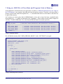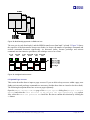
1
Engineer-to-Engineer Note a EE-326 Technical notes on using Analog Devices DSPs, processors and development tools Visit our Web resources http://www.analog.com/ee-notes and http://www.analog.com/processors or email [email protected] or [email protected] for technical support. Blackfin® Processor and SDRAM Technology Contributed by Fabian Plepp Rev 1 – May 12, 2008 Introduction The Analog Devices Blackfin® family of processors provides an External Bus Interface Unit (EBIU) with which to interface to SDRAM. This EE-Note covers the following topics: Register settings and their meaning SDRAM initialization SDRAM hardware design Using less than 16MB of SDRAM Performance optimization Power optimization This EE-Note discusses SDR-SDRAM (not DDR-SDRAM). This EE-Note applies only to ADSP-BF53x, ADSP-BF52x, and ADSP-BF561 processors. It does not apply to ADSP-BF54x processors. Although this document covers basic aspects of SDRAM functionality, you should read The ABCs of SDRAM (EE-126)[1] for more information. This document is separated into different topics, so you do not need to read the entire document when you are looking for specific information. Copyright 2008, Analog Devices, Inc. All rights reserved. Analog Devices assumes no responsibility for customer product design or the use or application of customers’ products or for any infringements of patents or rights of others which may result from Analog Devices assistance. All trademarks and logos are property of their respective holders. Information furnished by Analog Devices applications and development tools engineers is believed to be accurate and reliable, however no responsibility is assumed by Analog Devices regarding technical accuracy and topicality of the content provided in Analog Devices Engineer-to-Engineer Notes. a Table of Contents Introduction .................................................................................................................................................................................................1 Table of Contents......................................................................................................................................................................................2 1 Brief Introduction to SDRAM .........................................................................................................................................................5 1.1 Basics of SDRAM............................................................................................................................................................................5 1.2 SDRAM Parameters in Blackfin Registers .....................................................................................................................6 1.2.1 EBCAW (SDRAM External Bank Column Address Width) ...................................................................................6 1.2.2 EBSZ (SDRAM External Bank Size)............................................................................................................................6 1.2.3 SDRAM Timing.........................................................................................................................................................................6 1.3 Multiprocessor Environment Options...............................................................................................................................7 1.3.1 BGSTAT (Bus Grant Status)..........................................................................................................................................7 1.3.2 PUPSD (Power-Up Startup Delay) ..............................................................................................................................7 1.3.3 CDDBG (Control Disable During Grant)................................................................................................................7 1.4 Mobile/ Low-Power SDRAM Options......................................................................................................................................8 1.4.1 PASR (Partial Array Self Refresh) .......................................................................................................................8 1.4.2 TCSR (Temperature-Compensated Self-Refresh) ...............................................................................................8 1.5 Options to Fit the SDRAM Timing......................................................................................................................................8 1.5.1 Blackfin Output / SDRAM Input Equation (Write) ........................................................................................9 1.5.2 Blackfin Input / SDRAM Output Equation (Read)...........................................................................................9 2 SDRAM Initialization........................................................................................................................................................................10 2.1 SDRAM Initialization Via an Emulator and VisualDSP++ .XML Files........................................................10 2.2 Initialization Using Memory-Mapped Registers.....................................................................................................12 2.3 Initialization Using System Services........................................................................................................................14 2.4 SDRAM Initialization by the Values in the OTP Memory ..................................................................................16 2.5 Initializing Memory via Initialization Code Before Loading the Application..............................17 3 Using an .LDF File to Place Data and Program Code in Memory ...........................................................................20 4 SDRAM Hardware Design .....................................................................................................................................................................22 4.1 Connecting SDRAM to a Blackfin Processor (Schematics)................................................................................22 4.1.1 ADSP-BF53x Series Processors.................................................................................................................................22 4.1.2 ADSP-BF561 Processors (16-bit SDRAM)..............................................................................................................22 4.1.3 ADSP-BF561 Processors (32-bit SDRAM)..............................................................................................................23 4.2 High-Speed Design.....................................................................................................................................................................24 4.2.1 Effects that Impact Signal Quality...................................................................................................................24 4.2.2 Avoid Reflections...........................................................................................................................................................25 4.3 Design Guidelines for the SDRAM Connection..........................................................................................................26 4.3.1 Component Placement Considerations...................................................................................................................26 4.3.2 Using the Rounding Function of Your Layout Tool at Trace Edges ................................................27 4.3.3 Placing the VCC and GND Planes with as Little Distance as Possible.......................................27 Blackfin® Processor and SDRAM Technology (EE-326) Page 2 of 53 a 4.3.4 Insulating Critical Signals by Placing Them in the Inner Layers ..............................................28 4.3.5 Placing the Series Resistor Close to the SDRAM ......................................................................................28 4.3.6 Avoiding Trenches in the GND Plane...................................................................................................................28 4.3.7 Minimizing Back-Current Paths from Vias.......................................................................................................29 5 Using a Blackfin Processor with Less than 16 MB of SDRAM ..................................................................................30 5.1 System Settings..........................................................................................................................................................................30 5.2 Changing the .LDF File .........................................................................................................................................................31 5.2.1 Excursus: Background....................................................................................................................................................31 5.3 SDRAMs with 2 Banks ................................................................................................................................................................32 6 Increasing the SDRAM Performance of Your System........................................................................................................33 6.1 Optimal Multi-Bank Accesses .............................................................................................................................................33 6.2 Optimal Pages Accesses .........................................................................................................................................................34 Pages for the ADSP-BF53x Processors ..............................................................................................................................35 Pages for ADSP-BF561 Processors........................................................................................................................................36 6.3 SDRAM Performance Items for Core Accesses ............................................................................................................37 6.3.1 Code Overlays ....................................................................................................................................................................38 6.4 SDRAM Performance Items When Using Cache ..............................................................................................................38 Code........................................................................................................................................................................................................38 Data........................................................................................................................................................................................................38 7 Optimizing Power Consumption.....................................................................................................................................................39 7.1 Introduction: Power-Consumption Figures.................................................................................................................39 7.2 Tips for Lowering SDRAM Power Consumption ............................................................................................................39 7.3 Mobile SDRAM.................................................................................................................................................................................40 7.4 Going into Hibernate and Recover .................................................................................................................................40 Step 1 ...................................................................................................................................................................................................40 Step 2 ...................................................................................................................................................................................................41 Step 3 ...................................................................................................................................................................................................41 7.5 Structuring Data for Low Power Consumption..........................................................................................................41 Appendices ....................................................................................................................................................................................................42 Appendix A: Glossary .......................................................................................................................................................................42 Appendix B: Code Examples, Schematics, and Excursus..............................................................................................45 Initialization Code (Chapter 2)........................................................................................................................................45 Schematics to Interface SDRAM to the Blackfin Processor (Chapter 4)...................................................46 ADSP-BF561 in 16-Bit Mode ......................................................................................................................................................47 ADSP-BF561 in 32-Bit Mode ......................................................................................................................................................48 Excursus: Calculating Z0 (Chapter 4)..............................................................................................................................49 Calculating the Inductance of a Microstrip Trace................................................................................................50 Calculating the Capacitance .................................................................................................................................................50 Blackfin® Processor and SDRAM Technology (EE-326) Page 3 of 53 a IPC’s and Douglas Brooks’ approach of Z0 (Chapter 4)........................................................................................51 Microstrip Trace ...........................................................................................................................................................................51 Embedded Microstrip Trace ......................................................................................................................................................51 Stripline Trace..............................................................................................................................................................................51 Asymmetric Stripline Trace....................................................................................................................................................51 Dielectric Constants of Printed Circuit Boards (PCBs) (Chapter 4) .......................................................52 Several Commonly Available Woven Glass Reinforces Laminates......................................................................52 List of Non-Woven or Very-Low Glass Content Laminate Materials ..............................................................52 References ....................................................................................................................................................................................................53 Readings.........................................................................................................................................................................................................53 Document History ......................................................................................................................................................................................53 Blackfin® Processor and SDRAM Technology (EE-326) Page 4 of 53 a 1 Brief Introduction to SDRAM This section describes SDRAM (Synchronous Dynamic Random Access Memory) parameters and SDRAM-related system setups. This provides a base on which to build a better understanding of the EBIU (External Bus Interface Unit) register variables. Further, it will give you a foundation from which to base other decisions. It is not a detailed discussion of SDRAM; refer to The ABCs of SDRAM (EE-126)[1] for more details. 1.1 Basics of SDRAM Although SRAM stores binary data using transistors, DRAM uses a capacitor and a transistor: The capacitor is the storage itself; when charged, it will be a logical 1, otherwise a logical 0. The transistor acts as a gate that controls access to the cell and traps the charge. The disadvantage of this technology is that capacitors discharge over time. To prevent the loss of data, the DRAM must be refreshed periodically to restore the charge on the memory cells. Thus, a read and write operation must be performed to every memory location in the memory array at least once during the refresh rate period, which is typically specified in milliseconds. Figure 1. SDRAM The DRAM cells are organized in an array of rows and columns. Every single cell can be accessed by a well-defined row and column address. The row is often called the page, and the number of columns is referred to as the page size. The address is time multiplexed; the row address is transmitted first, then the column address is transmitted. The /RAS (row access strobe) and by the /CAS (column access strobe) signals control the time multiplexing of the row and column address. The /RAS signal indicates that a row address is available to be loaded into the address buffer and decoded by the internal row address decoder. After a short delay, the /CAS signal indicates that the column address, which is available in the address buffer, is forwarded to the column address decoder. If /WE is high, a read command is processed. The cells that are addressed by a row are read out completely, amplified, and written back to the cells. The columns that are addressed are transmitted over the data bus. Blackfin® Processor and SDRAM Technology (EE-326) Page 5 of 53 a If the /WE is low, a write command is processed. The isolated writing of a single cell is not possible; thus, a complete row is first read into a buffer. In the buffer, the elements to be changed are written, and the complete row is written back to the array. 1.2 SDRAM Parameters in Blackfin Registers 1.2.1 EBCAW (SDRAM External Bank Column Address Width) Often, the external bank column address width is called the page size of the SDRAM. Blackfin processors support page sizes of 512 bytes (8 bits), 1 Kbytes (9 bits), 2 Kbytes (10 bits), and 4 Kbytes (11 bits). Besides the byte address bit, which is the least significant bit (LSB), these bits are the least significant bits of the logical address. Depended on the width of the column address, the row address and bank have different bits positions in the logical address. For example, with a column addressing width (CAW) of 11 bits, the row address has its LSB at bit 12 of the logical 32-bit address[31:0]. This is a very important parameter if you want to access the SDRAM consciously. The number of the row address depends on the size of the SDRAM. To determine the column addressing width in the data sheet, find how many address pins are dedicated to column addressing. For a detailed overview, refer to the EBIU chapter of the Blackfin processor’s Hardware Reference. 1.2.2 EBSZ (SDRAM External Bank Size) The SDRAM external bank size can be determined by the following formula: MemorySize = Bank size x Number of Data pins x Number of Banks 8 For example, the MT48LC32M16A2 has 8 Mbytes x 16 pins x 4 banks, which is 536,870,912 bits, equaling 64 Mbytes. To use less than 16 MB, refer to Using a Blackfin Processor with Less than 16 MB of SDRAM. 1.2.3 SDRAM Timing Clock Cmd Pre ACTIV Address ACTIV READ Row Column Data Data t RAS t RP t RCD CL Figure 2. SDRAM Timing Blackfin® Processor and SDRAM Technology (EE-326) Page 6 of 53 a The SDRAM timing of SDRAM CAS Latency ( CL ), SDRAM bank activate command delay ( t RAS ), SDRAM bank precharge delay ( t RP ), RAS to CAS delay ( t RCD ), and write to precharge delay ( t WR ) are described in detail in the EBIU chapter of your processor’s Hardware Reference. 1.3 Multiprocessor Environment Options Blackfin processors can be used in a multiprocessor environment. One approach to interfacing the processors with one another is to share external memory and pass the messages via external memory to the other processors. In order to provide arbitration functionality, Blackfin processors have dedicated pins for this purpose. To use the Blackfin processor in a multiprocessor environment with shared memory, you must connect the /BR, /BG, and /BGH pins to provide an access control. When the external device requires access to the bus, it asserts the Bus Request (/BR pin) signal. If no other request is pending, the external bus request will be granted. The processor will three-state the data and address bus, and the bus grant (/BG pin) signal will be asserted. When the bus is granted to another external device, any data or instruction fetch from the external memory will stop the processor until the bus is released and the access can be executed. When the external device releases /BR, the processor deasserts /BG and continues execution from the point at which it stopped. The processor asserts the /BGH pin when it is ready to start another external port access, but is held off because the bus was previously granted. 1.3.1 BGSTAT (Bus Grant Status) When the bus has been granted, the BGSTAT bit in the SDSTAT register is set. This bit can be used by the processor to check the bus status to avoid initiating a transaction that would be delayed by the external bus grant. 1.3.2 PUPSD (Power-Up Startup Delay) This option sets a delay of 15 system clock cycles for the power-up start sequence. If one processor passes the SDRAM to another processor, it has to send the SDRAM into self-refresh mode. Once self refresh mode is engaged, the SDRAM provides its own internal clocking, causing it to perform its own autorefresh cycles. The SDRAM must remain in self-refresh mode for a minimum period equal to t RAS . The procedure for exiting self-refresh mode requires a sequence of commands. First, CLK must be stable (stable clock is defined as a signal cycling within timing constraints specified for the clock pin) prior to CKE going back high. When CKE is high, the SDRAM must have NOP commands issued for t XSR because this length of time is required for the completion of any internal refresh in progress. To take the time period t XSR into account, a delay of 15 cycles will occur until the Blackfin processor starts its power-up sequence. 1.3.3 CDDBG (Control Disable During Grant) If you are working in a multiprocessor environment with shared memory, where other devices than the Blackfin processor have access to memory, this feature enables the external memory interface of the processor to additionally three-state the address and data pins, its memory control pins (SRAS, SCAS, SWE, SA10, and SCKE), and its clock pin (CLKOUT). Blackfin® Processor and SDRAM Technology (EE-326) Page 7 of 53 a 1.4 Mobile/ Low-Power SDRAM Options Blackfin processors support mobile SDRAM chips (also called low-power SDRAM). Depending on the series of Blackfin processors, you can use 3.3V, 2.5V, and 1.8V SDRAM. In order to use 2.5V and 1.8V chips, verify in the processor’s data sheet (electrical specifications) that the processor is able to have an output low voltage of 0.3 V (maximum). The mobile SDRAM archives low power consumption not only by its lower voltage, but also by its low currents. Another advantage of mobile SDRAM is the ability to deactivate the self-refresh of the several banks you are not using and to reduce the self-refresh rate by defining the temperature. These features enable you to optimize power consumption for your specific application. If not otherwise stated in the Blackfin data sheet, at 1.8V VDDEXT (the maximal frequency of the system clock) is limited to 100 MHz. To use the extended registers of mobile SDRAM, you must set the EMREN bit. 1.4.1 PASR (Partial Array Self Refresh) Every refresh consumes power. If the application does not need to store the complete memory in special modes, this feature provides a way to disable the refresh of several banks of the SDRAM. The benefit of this feature is lower power consumption. Take for example, an application that stores data (e.g., a picture) into SDRAM, does some signal processing, transmits the data or stores it to a non-volatile memory(e.g., flash), and goes back into sleep mode. Most of the SDRAM is needed only for the signal processing. The data is absolved after processing, so the banks in which the data is placed does not need to be refreshed. 1.4.2 TCSR (Temperature-Compensated Self-Refresh) In standard SDRAMs, the self-refresh rate is set to the worst-case scenario: A high temperature will cause a higher discharge of the capacitors, which requires a higher refresh rate to maintain the data. But a higher refresh rate will effect higher power consumption. By means of the TCSR bit, the user application is able to set the self-refresh rate according to the temperature, which it is measuring. 1.5 Options to Fit the SDRAM Timing Sometimes the timing parameter specification of an SDRAM does not fit the specification of the EBIU. Therefore, the PLL control register provides an option to delay the output signal and shift the input latch mechanism for 200 ps. Figure 3. PLL_CTL register (copied from Hardware Reference) Blackfin® Processor and SDRAM Technology (EE-326) Page 8 of 53 a Bit 6 and bit 7 (Figure 3) provide a delay to the SDRAM signals. Apply the output delay when the specification of a write access will be violated. It will delay the data hold for 200 ps. The input delay must be applied when the specification of a read access will be violated. It delays the latch of the incoming data signal by 200 ps. t sclk CLKOUT Period t SSDAT Data Setup Before CLKOUT (BF data sheet) t AC Access time from CLK (SDRAM data sheet) t DH Input Hold time (SDRAM data sheet) t HSDAT Data Hold after CLKOUT (BF data sheet) t OH Output Hold time (SDRAM data sheet) t OLZ Delay to the output high impedance from CLK (SDRAM data sheet) t OHZ Delay from high impedance to signal from CLK (SDRAM data sheet) 1.5.1 Blackfin Output / SDRAM Input Equation (Write) For SDRAM input, the following equation must be valid: t DH < t HSDAT t SCLK t HSDAT t DH Figure 4. Timing 1.5.2 Blackfin Input / SDRAM Output Equation (Read) This case applies especially when setting the SDRAM clock to 133 MHz, which places the timing parameters at the limit of the specification. t SCLK Clock DQ Data tOLZ t SSDAT tOH Data tOHZ t AC Figure 5. Timing To verify that the read operation processed correctly, ensure that t sclk > t SSDAT + t AC Blackfin® Processor and SDRAM Technology (EE-326) Page 9 of 53 a 2 SDRAM Initialization SDRAM initialization impacts application performance and SDRAM power consumption. Therefore, a better understanding of the settings is highly desirable. This section describes how to set up the EBIU (External Bus Interface Unit) registers in order to run your application. In order to initialize the SDRAM, use one of the following approaches: SDRAM initialization via an emulator and VisualDSP++® .XML files SDRAM initialization by setting the registers within the application SDRAM initialization by using the VisualDSP++ system service model SDRAM initialization by an initialization file before loading the actual application SDRAM initialization by the values in the OTP (One Time Programmable) memory 2.1 SDRAM Initialization Via an Emulator and VisualDSP++ .XML Files In the early stages of software development, you upload your software via an in-circuit emulator (ICE). The emulator can set up the EBIU registers automatically when you upload a program to the processor. To enable this functionality, from the VisualDSP++ Settings menu, chose Target Options. From the resulting Target Options dialog box (Figure 6), select the Use XML reset values option. Figure 6. Target Options dialog box For VisualDSP++ release 4.5 or lower the values are taken from an .xml file (extensible markup language) named ADSP-BF5XX-proc.xml (where XX stands for the architecture; e.g., ADSP-BF537proc.xml or ADSP-BF561-proc.xml). These files are located in the <install_path>\Analog Devices\VisualDSP X.X\System\ArchDef directory. By changing these values, you can configure the settings of the EBIU. Figure 7 shows a portion of a processor .XML file. For more information, refer to “custom board support” in VisualDSP++ Help. Blackfin® Processor and SDRAM Technology (EE-326) Page 10 of 53 a Figure 7: A portion of the ADSP-BF5xx-proc.xml file (VisualDSP++ 4.5) The processor .xml file is read at startup only. Any editing while VisualDSP++ IDDE is up and running will not take effect. Ensure that you have edited the values before invoking VisualDSP++ development tools. When VisualDSP++ tools are running, the values in the .XML files are used to set the corresponding SDRAM values of the Analog Devices EZ-KIT Lite® development board. For VisualDSP++ release 5.0 or higher, it’s not recommended to modify the .XML files in the ArchDef folder directly. Use the custom board support which is described in the following paragraph. With custom board support in VisualDSP++ release 5.0 or higher, it is easier to set reset values in an application: This feature enables developers to have multiple sets of reset settings and to change between them without having to start up VisualDSP++ tools again. Open a text editor and place code like the following into a file and save it. In this example (Listing 1), the filename is My_custom_board_reset_settings.xml: <?xml version="1.0" standalone="yes"?> <custom-visualdsp-proc-xml xmlns:xsi="http://www.w3.org/2001/XMLSchema-instance" xsi:noNamespaceSchemaLocation="\Program Files\Analog Devices\VisualDSP 5.0\System\ArchDef\ADSP-custom-board.xsd" processor-family="BLACKFIN" file="My_custom_board_reset_settings.xml"> <!-- ************************************************************************* --> <!-- ******* My_custom_board_reset_settings.xml --> <!-- ************************************************************************* --> <custom-register-reset-definitions> <register name="EBIU_SDRRC" reset-value="0x03A0" core="Common" /> <register name="EBIU_SDBCTL" reset-value="0x25" core="Common" /> <register name="EBIU_SDGCTL" reset-value="0x0091998D" core="Common" /> </custom-register-reset-definitions> </custom-visualdsp-proc-xml> Listing 1. Example custom board reset settings (VisualDSP++ 5.0) Blackfin® Processor and SDRAM Technology (EE-326) Page 11 of 53 a To enable this feature in VisualDSP++ development tools, perform the following steps: 1. From the Settings menu, choose Session. 2. In the Session Settings dialog box, select Enable customizations. 3. In Custom board support file name, navigate to the “My_custom_board_reset_settings.xml” that contains the SDRAM reset values. file named Whenever the processor is reset by VisualDSP++ tools, these reset values will be set in the registers. 2.2 Initialization Using Memory-Mapped Registers The classical approach to initializing the SDRAM controller is to assign the values directly to the memory-mapped registers (MMRs). As an example, we take a mobile SDRAM data sheet1. Figure 8. Example: portion of a data sheet for mobile SDRAM Figure 9: Address configuration specification in the data sheet Before setting the SDRAM registers, we must first configure the PLL. For our example, we are using a system clock frequency of 133 MHz. First, we calculate the refresh rate: RDIV = 1 f SCLK ⋅ t REF − (t RAS + t RP ) NRA Samsung K4M56163 R(B)N/G/L/F Mobile SDRAM Blackfin® Processor and SDRAM Technology (EE-326) Page 12 of 53 a From the data sheet (-75), we get the following information: f SCLK = 133MHz t REF = 64 ms NRA = 8192 t RAS = 45ns at 133 MHz: t RAS = 6 cycles t RP = 18ns at 133 MHz: t RP = 3 cycles RDIV = 133 ⋅ 10 6 ⋅ 64 ⋅ 10 −3 − (6 + 3) = 1030.0625 ≈ 1030 in Hex : 0x406 8192 Further, we need to calculate following values: t RCD = 18ns at 133 MHz: t RCD = 3 cycles At Samsung, t WR is called t RDL . t WR = t RDL = 2 cycles Additionally, we have to enable the extended register to set the temperature and the partial self-refresh. The PASR can be set to following settings: PASR_ALL – All four SDRAM banks refreshed in self-refresh PASR_B0_B1 – SDRAM banks 0 and 1 are refreshed in self-refresh PASR_B0 – Only SDRAM bank 0 is refreshed in self-refresh Listing 2 shows the initialization in C. //SDRAM Refresh Rate Setting *pEBIU_SDRRC = 0x406; //SDRAM Memory Bank Control Register *pEBIU_SDBCTL = EBCAW_9 | //Page size 512 EBSZ_64 | //64 MB of SDRAM EBE; //SDRAM enable //SDRAM Memory Global Control Register *pEBIU_SDGCTL = ~CDDBG & // Control disable during bus grant off ~FBBRW & // Fast back to back read to write off ~EBUFE & // External buffering enabled off ~SRFS & // Self-refresh setting off ~PSM & // Powerup sequence mode (PSM) first ~PUPSD & // Powerup start delay (PUPSD) off TCSR | // Temperature compensated self-refresh at 85 EMREN | // Extended mode register enabled on PSS | // Powerup sequence start enable (PSSE) on TWR_2 | // Write to precharge delay TWR = 2 (14-15 ns) TRCD_3 | // RAS to CAS delay TRCD =3 (15-20ns) TRP_3 | // Bank precharge delay TRP = 2 (15-20ns) TRAS_6 | // Bank activate command delay TRAS = 4 PASR_B0 | // Partial array self refresh Only SDRAM Bank0 CL_3 | // CAS latency SCTLE ; // SDRAM clock enable Listing 2. Initialization via registers Blackfin® Processor and SDRAM Technology (EE-326) Page 13 of 53 a The code in assembly language can be found in Initialization Code (Chapter 2). What will happen if we need to change the PLL settings later in the application? To obtain the best memory performance, we have to change our settings as well. If memory performance does not matter, we have to calculate the values at the worst-case scenario. Examples of initializing the SDRAM on the ADSP-BF537 EZ-KIT Lite (in assembler and C) and on the ADSP-BF561 EZ-KIT Lite (in C) are included together with this EE-Note. 2.3 Initialization Using System Services Another way to initialize the SDRAM is to handle the setup in the application itself. The most comfortable way to change the EBIU settings is by means of system services. The main advantage of using the EBIU system service is that you can set the EBIU without any calculations. And second benefit is that the changes to the EBIU are in accordance to the PLL changes, so you do not need to be concerned about the actual system clock frequency. The initialization is done by the adi_ebiu_init function. We will take the same SDRAM as in the section above. To perform an initialization using the system services, we have to pass the SDRAM parameters to the system. Therefore, we are using a command structure called ADI_EBIU_COMMAND_PAIR. (Table 1). To initialize the structure in our example, we set the variables (for the -75) as shown in Listing 3. // set the sdram to 64 MB ADI_EBIU_SDRAM_BANK_VALUE bank_size = {0, ADI_EBIU_SDRAM_BANK_64MB}; //set the sdram to 9 bit Column Address Width (like we see in the Address //Configuration) // A0-A8 -> 9bits Column Address ADI_EBIU_SDRAM_BANK_VALUE bank_caw = {0, (ADI_EBIU_SDRAM_BANK_SIZE)ADI_EBIU_SDRAM_BANK_COL_9BIT}; // 9bit CAW //set the twr to 2 sclk + no time ADI_EBIU_TIMING_VALUE MyTWR = { 2, // 2 cycle {0, ADI_EBIU_TIMING_UNIT_PICOSEC}}; // 0 ns //set refresh rate to 64ms at 8192 rows as seen in the data sheet ADI_EBIU_TIMING_VALUE Refresh = { // SDRAM Refresh rate: 8192, // 8192 cycles {64, ADI_EBIU_TIMING_UNIT_MILLISEC }}; // 64ms //set TRAS to 45ns ADI_EBIU_TIME MyTRAS = {45, ADI_EBIU_TIMING_UNIT_NANOSEC}; //set TRP to 18ns ADI_EBIU_TIME MyTRP = {18, ADI_EBIU_TIMING_UNIT_NANOSEC}; //set TRCD to 18ns ADI_EBIU_TIME MyTRCD = {18, ADI_EBIU_TIMING_UNIT_NANOSEC}; //set CAS threshold frequency u32 MyCAS = 133; //Enable Extended Mode Register because we are using Mobile SDRAM ADI_EBIU_SDRAM_EMREN MyEMREN = ADI_EBIU_SDRAM_EMREN_ENABLE; //Refresh only the first bank ADI_EBIU_PASR MyPASR = ADI_EBIU_PASR_INT0_ONLY; //Temperature Compensation at 85°C ADI_EBIU_SDRAM_TCSR MyTCSR = ADI_EBIU_SDRAM_TCSR_85DEG; //we don't have any registered buffer ADI_EBIU_SDRAM_EBUFE MyEBUFE = ADI_EBIU_SDRAM_EBUFE_DISABLE; Blackfin® Processor and SDRAM Technology (EE-326) Page 14 of 53 a //no fast-back-to-back read/write ADI_EBIU_SDRAM_FBBRW MyFBBRW = ADI_EBIU_SDRAM_FBBRW_DISABLE; //Do not disable the control during bus grant ADI_EBIU_SDRAM_CDDBG MyCDDBG = ADI_EBIU_SDRAM_CDDBG_DISABLE; //We don't need any delay at Power Up ADI_EBIU_SDRAM_PUPSD MyPUPSD = ADI_EBIU_SDRAM_PUPSD_NODELAY; //Do first the refresh ADI_EBIU_SDRAM_PSM MyPSM = ADI_EBIU_SDRAM_PSM_REFRESH_FIRST; Listing 3.Initialization of the EBIU structure Table 1. Overview of EBIU commands After setting up the parameters, we need to initialize the service. Therefore, we bundle the parameters to a command table and afterwards call the adi_EBIU_init function. ADI_EBIU_COMMAND_PAIR Sdram_Values[] = { { ADI_EBIU_CMD_SET_SDRAM_BANK_SIZE, { ADI_EBIU_CMD_SET_SDRAM_BANK_COL_WIDTH, { ADI_EBIU_CMD_SET_SDRAM_CL_THRESHOLD, { ADI_EBIU_CMD_SET_SDRAM_TRASMIN, { ADI_EBIU_CMD_SET_SDRAM_TRPMIN, { ADI_EBIU_CMD_SET_SDRAM_TRCDMIN, { ADI_EBIU_CMD_SET_SDRAM_TWRMIN, { ADI_EBIU_CMD_SET_SDRAM_REFRESH, { ADI_EBIU_CMD_SET_SDRAM_FBBRW, { ADI_EBIU_CMD_SET_SDRAM_EMREN, { ADI_EBIU_CMD_SET_SDRAM_PASR, { ADI_EBIU_CMD_SET_SDRAM_TCSR, { ADI_EBIU_CMD_SET_SDRAM_EBUFE, { ADI_EBIU_CMD_SET_SDRAM_CDDBG, { ADI_EBIU_CMD_SET_SDRAM_PUPSD, { ADI_EBIU_CMD_SET_SDRAM_PSM, { ADI_EBIU_CMD_END, 0} (void*)&bank_size (void*)&bank_caw (void*)&MyCAS (void*)&MyTRAS (void*)&MyTRP (void*)&MyTRCD (void*)&MyTWR (void*)&Refresh (void*)&MyFBBRW (void*)&MyEMREN (void*)&MyPASR (void*)&MyTCSR (void*)&MyEBUFE (void*)&MyCDDBG (void*)&MyPUPSD (void*)&MyPSM }, }, }, }, }, }, }, }, }, }, }, }, }, }, }, }, }; //Init the service and ensure that the Refresh rate is reset if fsclk is changing Result = adi_ebiu_Init( Sdram_Values, true); // true enables automatic adjustment Listing 4. Initialization of the EBIU Blackfin® Processor and SDRAM Technology (EE-326) Page 15 of 53 a Code examples that demonstrate the use of system services for the ADSP-BF537 and the ADSP-BF561 processors are located in the .ZIP file attached to this EE-Note. 2.4 SDRAM Initialization by the Values in the OTP Memory Devices with One-Time-Programmable (OTP) memory (ADSP-BF52x and ADSP-BF54x processors) offer an additional approach to initializing the EBIU register settings. During booting, the boot ROM program is able to initialize the EBIU settings by the programmed values in the OTP. The OTP consists of a region called the Preboot Settings (PBS) block, which must be programmed via the OTP_write function. The PBS02L page contains the EBIU settings. Refer to your processor’s Hardware Reference for an overview. After setting up the EBIU control registers, the boot process accesses the SDRAM at address 0x00000000 in order to initialize the SDRAM. By default, setting a read access will be performed. Since a read access consumes more time than a write access, this access can be customized by the OTP_EBIU_POWERON_DUMMY_WRITE bit (Figure 10), which replaces the read access with a write access and saves time. By using this option, you must ensure that no important data is stored at this address before going to reset or hibernate. Figure 10. Dummy write option /* Declare local variable */ DU64 Data; . . /* Enable the EBIU Init settings */ Data.h = 0x04000000 | //use the content of PBS02L for the EBIU ... | //other settings Data.l = ... otp_write(0x18, OTP_LOWER_HALF, &Data); /* Assign SDRAM values */ /* The low data byte is the EBIU_SDGCTL register */ Data.l = ~CDDBG & // Control disable during bus grant off ~FBBRW & // Fast back to back read to write off ~EBUFE & // External buffering enabled off ~SRFS & // Self-refresh setting off ~PSM & // Powerup sequence mode (PSM) first ~PUPSD & // Powerup start delay (PUPSD) off TCSR | // Temperature compensated self-refresh at 85 EMREN | // Extended mode register enabled on Blackfin® Processor and SDRAM Technology (EE-326) Page 16 of 53 a PSS TWR_2 TRCD_3 TRP_3 TRAS_6 PASR_B0 CL_3 SCTLE; | | | | | | | // // // // // // // Powerup sequence start enable (PSSE) on Write to precharge delay TWR = 2 (14-15 ns) RAS to CAS delay TRCD =3 (15-20ns) Bank precharge delay TRP = 2 (15-20ns) Bank activate command delay TRAS = 4 Partial array self refresh Only SDRAM Bank0 CAS latency /* The upper 32 bit are EBIU_SDBCTL(0-15) and EBIU_SDRRC (16-27). Further we will Set the dummy write bit (32), which will speed up the initialization */ Data.h = 0x80000000 (0x406)<<16 EBCAW_9 EBSZ_64 EBE; | | | | // dummy write bit // Refresh rate //Page size 512 //64 MB of SDRAM //SDRAM enable ; otp_write(0x1A, OTP_LOWER_HALF, &Data); Listing 5. Initialization via PBS 2.5 Initializing Memory via Initialization Code Before Loading the Application If you want to place instruction and data sections into your SDRAM at initialization time, you must use an initialization file that initializes the SDRAM before the application is loaded. Therefore, start a project and code an initialization file. Build this project into a .DXE file. The initialization .DXE file can be included into a loader file of your actual application via the Project Options dialog box (Project:Load:Options page). Figure 11. Specifying project load options Listing 6 shows an example of how initialization code can be implemented. Blackfin® Processor and SDRAM Technology (EE-326) Page 17 of 53 a #include <defBF537.h> .section program; //save all registers on the stack [--SP] = ASTAT; ... [--SP] = L3; //Setup the PLL Settings //Ensure no other interrupt will disturb us CLI R1; //Setup the voltage regulator P0.L = lo(VR_CTL); P0.H = hi(VR_CTL); R0 = 0x40DB (z); w[P0] = R0; //Wait the VR settings are done idle; //Setup the DIV of ssclk and cclk P0.L = lo(PLL_DIV); R0 = 0x0003 (z); w[P0] = R0; //Setup wait cycles until PLL is set P0.L = lo(PLL_LOCKCNT); R0 = 0x200 (z); w[P0] = R0; //Setup the PLL P0.L = lo(PLL_CTL); R0 = 0x2000 (z); w[P0] = R0; //Wait the PLL settings are done idle; //restore interrupts STI R1; //Our program needs 4 MBs of RAM P0.L = lo(EBIU_AMGCTL); P0.H = hi(EBIU_AMGCTL); //Asynchronous Memory Global Control Register //Uncomment your setting R0 = 0x00F0 // |AMBEN_NONE(Z); //No Asynchronous Memory // |AMBEN_B0(Z); //1MB Asynchronous Memory // |AMBEN_B0_B1(Z); //2MB Asynchronous Memory // |AMBEN_B0_B1_B2(Z); //3MB Asynchronous Memory |AMBEN_ALL(Z); //4MB Asynchronous Memory W[P0] = R0; //Setup the SDRAM //SDRAM Refresh Rate Setting P0.H = hi(EBIU_SDRRC); P0.L = lo(EBIU_SDRRC); R0 = 0x406 (z); w[P0] = R0; Blackfin® Processor and SDRAM Technology (EE-326) Page 18 of 53 a //SDRAM Memory Bank Control Register P0.H = hi(EBIU_SDBCTL); P0.L = lo(EBIU_SDBCTL); R0 = EBCAW_9 | //Page size 512 EBSZ_64 | //64 MB of SDRAM EBE; //SDRAM enable w[P0] = R0; //SDRAM Memory Global Control Register P0.H = hi(EBIU_SDGCTL); P0.L = lo(EBIU_SDGCTL); R0.H= hi( ~CDDBG & // Control disable during bus grant off ~FBBRW & // Fast back to back read to write off ~EBUFE & // External buffering enabled off ~SRFS & // Self-refresh setting off ~PSM & // Powerup sequence mode (PSM) first ~PUPSD & // Powerup start delay (PUPSD) off TCSR | // Temperature compensated self-refresh at 85 EMREN | // Extended mode register enabled on PSS | // Powerup sequence start enable (PSSE) on TWR_2 | // Write to precharge delay TWR = 2 (14-15 ns) TRCD_3 | // RAS to CAS delay TRCD =3 (15-20ns) TRP_3 | // Bank precharge delay TRP = 2 (15-20ns) TRAS_6 | // Bank activate command delay TRAS = 4 PASR_B0 | // Partial array self refresh Only SDRAM Bank0 CL_3 | // CAS latency SCTLE ); // SDRAM clock enable R0.L= lo( ~CDDBG ~FBBRW ~EBUFE ~SRFS ~PSM ~PUPSD TCSR EMREN PSS TWR_2 TRCD_3 TRP_3 TRAS_6 PASR_B0 CL_3 SCTLE & & & & & & | | | | | | | | | ) ; // // // // // // // // // // // // // // // // Control disable during bus grant off Fast back to back read to write off External buffering enabled off Self-refresh setting off Powerup sequence mode (PSM) first Powerup start delay (PUPSD) off Temperature compensated self-refresh at 85 Extended mode register enabled on Powerup sequence start enable (PSSE) on Write to precharge delay TWR = 2 (14-15 ns) RAS to CAS delay TRCD =3 (15-20ns) Bank precharge delay TRP = 2 (15-20ns) Bank activate command delay TRAS = 4 Partial array self refresh Only SDRAM Bank0 CAS latency SDRAM clock enable [P0] = R0; ssync; //Restore registers from the stack L3 = [SP++]; ... ASTAT = [SP++]; RTS; Listing 6. Initialization via an initialization file Blackfin® Processor and SDRAM Technology (EE-326) Page 19 of 53 a 3 Using an .LDF File to Place Data and Program Code in Memory If the SDRAM is initialized before the application is loaded (see SDRAM Initialization by the Values in the OTP Memory), you can place data and code into the memory sections. Therefore, you must define a memory region in the Linker Description File (.LDF) and inform the linker as to the data or code that is to be placed into memory. Let’s assume we want to place data in SDRAM bank 1. If we take a closer look into a standard Linker Description File (.LDF) which is generated by the VisualDSP++ Expert Linker wizard (in this example we will have 512 MB of SDRAM), we see the internal SDRAM banks are named separately: MEMORY { MEM_SYS_MMRS […] MEM_SDRAM0_BANK0 MEM_SDRAM0_BANK1 MEM_SDRAM0_BANK2 MEM_SDRAM0_BANK3 } /* MEMORY */ { TYPE(RAM) START(0xFFC00000) END(0xFFDFFFFF) WIDTH(8) } { { { { TYPE(RAM) TYPE(RAM) TYPE(RAM) TYPE(RAM) START(0x00000004) START(0x08000000) START(0x10000000) START(0x18000000) END(0x07ffffff) END(0x0fffffff) END(0x17ffffff) END(0x1fffffff) WIDTH(8) WIDTH(8) WIDTH(8) WIDTH(8) } } } } Listing 7.Assigning memory We will find the memory label “MEM_SDRAM0_BANK1” in the “SECTIONS” area again: PROCESSOR p0 { OUTPUT($COMMAND_LINE_OUTPUT_FILE) RESOLVE(start, 0xFFA00000) KEEP(start, _main) SECTIONS { [...] sdram0_bank1 { INPUT_SECTION_ALIGN(4) INPUT_SECTIONS($OBJECTS(sdram0) $LIBRARIES(sdram0)) INPUT_SECTIONS($OBJECTS(sdram0_bank1) $LIBRARIES(sdram0_bank1)) INPUT_SECTIONS($OBJECTS(sdram0_data) $LIBRARIES(sdram0_data)) INPUT_SECTIONS($OBJECTS(cplb) $LIBRARIES(cplb)) INPUT_SECTIONS($OBJECTS(data1) $LIBRARIES(data1)) INPUT_SECTIONS($OBJECTS(voldata) $LIBRARIES(voldata)) INPUT_SECTIONS($OBJECTS(constdata) $LIBRARIES(constdata)) INPUT_SECTIONS($OBJECTS(cplb_data) $LIBRARIES(cplb_data)) INPUT_SECTIONS($OBJECTS(.edt) $LIBRARIES(.edt)) INPUT_SECTIONS($OBJECTS(.cht) $LIBRARIES(.cht)) } > MEM_SDRAM0_BANK1 [...] } /* SECTIONS */ } /* p0 */ Listing 8. Specifying memory sections Blackfin® Processor and SDRAM Technology (EE-326) Page 20 of 53 a We see that several libraries and objects are mapped into this memory space. You can map an object or library to more than one memory section. In this case, the linker decides which part of the data or code is placed into each section of memory. To place data explicitly in one memory section if using C/C++, use the pragma section directive. In our case, we want to place the global variable x into internal SDRAM bank 1. The label sdram0_bank1 is only mapped to internal SDRAM bank 1 and no other section. So we will use this label to map our variable. //define a variable which lies in SDRAM Bank 1 #pragma section ("sdram0_bank1") long int x = 0; We can do the same with our instruction code by assigning the prototypes of our functions to a section: //define a function prototype of a function which lies in SDRAM Bank 1 #pragma section ("sdram0_bank1") void foo(); As described in Increasing the SDRAM Performance of Your System, sometimes it is useful to map a data section manually to prevent delays caused by opening and closing a page. Therefore, we define our own memory section in the .LDF file: MEM_SDRAM0_BANK2 MEM_SDRAM0_BANK3 //define my own page MEM_SDRAM0_BANK3_PAGE0 { TYPE(RAM) START(0x02000000) END(0x02ffffff) WIDTH(8) } { TYPE(RAM) START(0x03000800) END(0x03ffffff) WIDTH(8) } { TYPE(RAM) START(0x03000000) END(0x030007FF) WIDTH(8) } In the SECTIONS part of the Linker Description File, we will link all objects labeled MyDefinedMemory into this memory space. sdram0_bank3_page_0 { INPUT_SECTION_ALIGN(4) INPUT_SECTIONS($OBJECTS(MyDefinedMemory) ) } > MEM_SDRAM0_BANK3_PAGE0 Afterwards, in our C/C++ file, we place our array into this memory section. //define an array which lies in my own defined memory space (Bank 3 Page 0) #pragma section ("MyDefinedMemory") long int MyArray[100]; Blackfin® Processor and SDRAM Technology (EE-326) Page 21 of 53 a 4 SDRAM Hardware Design Since the SDRAM is driven by frequencies greater than 50 MHz, the hardware layout must fulfill the requirements of high-speed design. Nowadays, hardware designs satisfy many standards concerning EMI and EMC. They have to ensure the signal integrity at high frequencies, and many of them are set in a low power environment. Therefore, the right printed circuit board (PCB) design is a key factor. This section explains how to design the connection between the Blackfin processor and the SDRAM on a PCB. 4.1 Connecting SDRAM to a Blackfin Processor (Schematics) Blackfin processors provide a glueless interface to SDRAM. Depending on the Blackfin processor, SDRAMs with a power supply requirement of 1.8V to 3.3V are supported. A common design mistake occurs when is the Blackfin processor address pins are not connected to the SDRAM correctly. The address lines must be connected as described next. 4.1.1 ADSP-BF53x Series Processors Connect Blackfin processor’s ADDR1 to the SDRAM A0, ADDR2 to A1, etc. Do not use the ADDR11 of the Blackfin; connect SA10 to A10 Connect ADDR18 to the SDRAM’s BA0 Connect ADDR19 to the SDRAM’s BA1 Connect /ABE0 to the DQML pin (for 16-bit SDRAM) or to DQM of the chip(s) connected to D0-D7 Connect /ABE1 to the DQMH pin (for 16-bit SDRAM) or to DQM of the chip(s) connected to D8-D15 Figure 12. ADSP-BF53x processors: connections between the Blackfin processor and SDRAM 4.1.2 ADSP-BF561 Processors (16-bit SDRAM) Connect the Blackfin processor’s ADDR2 to the SDRAM’s A1, ADDR3 to A2, etc. Connect the Blackfin processor’s SDQM3 to the SDRAM’s A0 Do not use the ADDR11 of the Blackfin processor; connect SA10 to A10 Connect ADDR18 to the SDRAM’s BA0 Blackfin® Processor and SDRAM Technology (EE-326) Page 22 of 53 a Connect ADDR19 to the SDRAM’s BA1 Connect SDQM0 to DQML or to DQM (see above) Connect SDQM1 to DQMH or to DQM (see above) Connect the /SMSx to the /CS lines (when using x16 and are using more than one SDRAM: to each chip one /SMS line) (when using x8 and are using more than two SDRAMs: to each pair of two one /SMS line) BF561 SDQM3 A2-A10, A12-A17 SA10 A18 A19 D0-D15 SDQM0 SDQM1 SRAS SCAS SWE SMS0-SMS3 SCKE CLK0_OUT SCLK SDRAM A0 A1-A9, A11-A16 A10 BA0 BA1 DQ0-DQ15 DQML DQMH RAS CAS WE CS CKE CLK Figure 13. ADSP-BF561 processors: connections between the Blackfin processor and 16-bit SDRAM 4.1.3 ADSP-BF561 Processors (32-bit SDRAM) Connect the Blackfin processor’s ADDR2 to the SDRAM’s A0, ADDR3 to A1, etc. Do not use the ADDR12 of the Blackfin; connect SA10 to A10 Connect ADDR18 to the SDRAM’s BA0 Connect ADDR19 to the SDRAM’s BA1 Connect SDQM0 to DQML of SDRAM1(D0-D15) Connect SDQM1 to DQMH of SDRAM1 Connect SDQM3 to DQML of SDRAM2(D16-D31) Connect SDQM4 to DQMH of SDRAM2 If you are using 8-bit SDRAM Connect SDQM0 to DQM of SDRAM1(D0-D7) Connect SDQM0 to DQM of SDRAM2(D8-D15) Connect SDQM0 to DQM of SDRAM3 (D16-D23) Connect SDQM0 to DQM of SDRAM4 (D24-D31) Blackfin® Processor and SDRAM Technology (EE-326) Page 23 of 53 a Figure 14. ADSP-BF561 processors: connections between the Blackfin processor and 32-bit SDRAM Another problem is caused when the /BR pin is left floating. The Blackfin processor interprets the signal as bus request and will answer with the /BG signal, which will block the parallel bus for an infinite time. So always put a pull-up resistor on the /BR pin. Use decoupling capacitors to decouple the SDRAM power supply. Add a series resistor close to each data pin of the SDRAM. The next section explains how to determine the resistance. 4.2 High-Speed Design The layout of the SDRAM connection is a critical factor, especially on low-power designs. This section explains how to optimize the design of the SDRAM layout to fit your application’s requirements. The most critical connections are the clock, the lower address lines, the DQM, and the data lines. 4.2.1 Effects that Impact Signal Quality This section describes effects that are influenced by your hardware design. Reflection If the impedance of a connection line is equivalent to the input resistance of the receiver, the energy will be fully absorbed by the resistance. Otherwise, the transmission’s energy will be thrown back. This will interfere with the desired signal by superposition. Coupling The currents conducted through different traces influence each other. When a changing current flows down trace A, it creates a changing magnetic field that couples into trace B. The coupling generates a current in trace B that is dependent upon the coupling factor. The inducted current’s direction is opposite to the current in trace A; this effect is negative if two signal traces influence each other (crosstalk). But the effect can also be positive when the influence is between the signal line and its return line (GND). The coupled signal helps to boost the return signal, and the returning signal boosts the primary signal. Blackfin® Processor and SDRAM Technology (EE-326) Page 24 of 53 a 4.2.2 Avoid Reflections Calculate the characteristic impedance to add the correct termination resistor. There are several ways to terminate a transmission line: Series termination Parallel termination Thevenin termination Termination by diodes AC termination The most important techniques for SDRAM devices are described next. Series Termination For SDRAM, use a series termination (Figure 15). Place the series resistor close to the output pin of the transmitter. The advantage is that there will not be any DC current draw (like if you are using a parallel termination). This is essential for low-power designs. The disadvantage is that there will be a nearly 100% refection at the receiver, which is thrown back to the transmitter. Since the lengths of SDRAM traces are short and the traces of one signal from the Blackfin processor to each of the SDRAM chips have nearly the same length, this effect will not impact the SDRAM’s functionality. Figure 15. Using series termination To avoid a second reflection from the driver (transmitter), the resistor must have the right value. The value for the series termination resistor has to be set so that the sum of it and the output impedance of the driver equals the impedance of the trace. As an equation, we get the following: R S = Z 0 − Z OUT , whereby ZOUT is the output impedance of the transmitter The read command is more critical than a write command. Thus, place the resistor of the data line as close as possible to the SDRAM data pin. Parallel Termination The alternative is to use a parallel termination (Figure 16). As mentioned earlier, this is not necessary for standard SDRAM when you follow the design guidelines at the end of this chapter. Blackfin® Processor and SDRAM Technology (EE-326) Page 25 of 53 a Figure 16. Using parallel termination Reflection coefficent ρ = ZL − Z0 ZL + Z0 To keep the reflection as low as possible, the parallel termination resistor (ZL) should be equivalent to Z0. Consider whether you even need termination. An additional resistor emits further EMI. 4.3 Design Guidelines for the SDRAM Connection With regard to EMC and signal integrity, the following design guidelines are recommended. When you start your SDRAM PCB layout, do not treat all signals the same, consider the importance of each signal and place the traces of the most critical signals first. The following succession is suggested: 1. Clock distribution 2. Data lines and DQM lines, command lines including SA10 3. Address lines 4. Other signals (e.g., CKE) 4.3.1 Component Placement Considerations Consider the following points while laying out your PCB: Place the SDRAM chips close to the Blackfin processor. Keep the traces as short as possible. When you are distributing a signal, all traces should have the same path length (Figure 17) to the devices (if possible). Avoid loops like the one shown in Figure 18. Figure 17. Right: spread traces and make their lengths equal Blackfin® Processor and SDRAM Technology (EE-326) Page 26 of 53 a S D R A M S D R A M Figure 18. Wrong: traces that loop around 4.3.2 Using the Rounding Function of Your Layout Tool at Trace Edges Figure 19 shows a PCB trace edge that does not use rounding. Figure 20 shows the same trace edge when the rounding feature is enabled. Figure 19. Wrong: Trace edges lack rounding Figure 20. Right: Trace edges are rounded 4.3.3 Placing the VCC and GND Planes with as Little Distance as Possible Figure 21 shows a 4-layer PCB, which does not insulate the critical signals. Figure 22 shows proper insulation of a 4-layer PCB.. critical signals other signals VCC GND Figure 21. Wrong: VCC and GND planes are too far apart other signals VCC GND critical signals Bold layer As thin as possible Figure 22. Right: VCC and GND planes are close together Blackfin® Processor and SDRAM Technology (EE-326) Page 27 of 53 a 4.3.4 Insulating Critical Signals by Placing Them in the Inner Layers Figure 23 shows a 6-layer PCB, in which critical signals are not insulated. Figure 24 shows proper insulation. Figure 23. Wrong: critical signals not properly insulated Figure 24. Right: minimize the distance between critical signals and the ground plane 4.3.5 Placing the Series Resistor Close to the SDRAM Figure 25 shows a signal path that with too many vias; the series resistor is too far from the SDRAM. Figure 26 shows a short signal path without vias an a series resistor that is next to the SDRAM. Figure 25. Wrong: too many vias in critical signal path and series resistor is too far away Figure 26. Right: the series resistor is close to the SDRAM 4.3.6 Avoiding Trenches in the GND Plane Figure 27 shows a GND plane with a trench. The GND plane in Figure 28 avoids having a trench. Blackfin® Processor and SDRAM Technology (EE-326) Page 28 of 53 a Figure 27. Wrong: ground plane with a trench Figure 28. Right: ground plane without a trench 4.3.7 Minimizing Back-Current Paths from Vias If you are not able to avoid a direction change in a via from one layer to another, try to minimize the way of the back current. Figure 29 shows a signal path that runs in two directions from the via. The direction change in Figure 30 is better. Figure 29. Wrong: layer-to-layer direction change Figure 30. Right: avoiding a direction change Blackfin® Processor and SDRAM Technology (EE-326) Page 29 of 53 a 5 Using a Blackfin Processor with Less than 16 MB of SDRAM Using less than 16 MBs (128 Mbits) of SDRAM is especially important for low-power applications. This section provides guidance for applications that use less than 16 MBs. 5.1 System Settings On the hardware side, there are no special settings. Just connect the address lines as described in SDRAM Hardware Design. The first step in using less than 16 MB is setting the SDRAM external bank size bits of the EBIU_SDBCTL (SDRAM memory bank control) register to 16 Mbytes. This configures the Blackfin processor's internal address to expect 16 Mbytes, and the address space will be fragmented as shown in Figure 31. Figure 31. Address space The “aliased” address space’s content is a copy of the according bank, and every write access to this space results in a write access into the “real” bank. This must be considered by the Linker Description File (.LDF), or the Blackfin processor will place instructions and data into addresses that do not exist. This type of address failure cannot be detected by the Blackfin processor. There is no functionality that tests whether an address is valid. This will cause failures later in your application when the core is tries to read from a non-existent address space, getting dummy values, and then interprets this as valid instruction code or data. Blackfin® Processor and SDRAM Technology (EE-326) Page 30 of 53 a 5.2 Changing the .LDF File First, ensure that the .LDF file will not be changed by the Expert Linker wizard. Therefore, open the Project Options dialog box (Project -> Project Options) to the Remove Startup Code/LDF page and select the Leave the files in the project, but stop regenerating them option (Figure 32). Figure 32. Ensuring that the .LDF file will not be changed Doing so allows you to change the .LDF file manually. For example, if we use a 64-Mbit SDRAM (8 MB), the address space in the Linker Description File has: MEM_SDRAM0_BANK0 MEM_SDRAM0_BANK1 MEM_SDRAM0_BANK2 MEM_SDRAM0_BANK3 { { { { TYPE(RAM) TYPE(RAM) TYPE(RAM) TYPE(RAM) START(0x00000000) START(0x00400000) START(0x00800000) START(0x00C00000) END(0x001FFFFF) END(0x005FFFFF) END(0x009FFFFF) END(0x00DFFFFF) WIDTH(8) WIDTH(8) WIDTH(8) WIDTH(8) } } } } Figure 33. Ensuring that the .LDF file will not be changed As shown in Figure 33, there are gaps of 2 MB in our address space. 5.2.1 Excursus: Background The .LDF file specifies where code and data are placed in memory space. The EBIU settings configure the SDRAM controller of the Blackfin processor and specify size, timing, and features of the SDRAM. Since the EBIU settings cannot set to that of an 8 MB SDRAM, we have to set the SDRAM size to 16 MB. What does this mean to the addressing? We are using an SDRAM with a column address width (CAW) of 10 bits, which means we can address 2^10 = 1024 columns. With each column and row address, we are addressing 2 bytes (for x16 SDRAM). Now, we have set the RAM to 16 MBs (=16777216 bytes), which means we have a row address width of 13 (memory size / (data width * 2^addresses) = 16777216/(2 bytes * 2^10)= 8192= 2^13), but we are using only a 8 MB RAM, which has a row address width of 12. But the controller has calculated a row address width of 13. The row address and the column address are sent to the SDRAM time multiplexed. Looking at your SDRAM, you see 12 address lines and 2 bank address lines. But the controller has calculated 13 and is using 13. Since the 13th address line is not connected, you will address the same physical address independent of the state of bit 13 of the row address. This is why the memory space is mirrored. Blackfin® Processor and SDRAM Technology (EE-326) Page 31 of 53 a For example, row address 0x1000 will access the same data as row address 0x0000. It is critical when you place something into aliased memory space, because you overwrite something in the other address space. Therefore, we define the .LDF file that way, so we will not place anything into the mirrored RAM: MEM_SDRAM0_BANK0 MEM_SDRAM0_BANK1 MEM_SDRAM0_BANK2 MEM_SDRAM0_BANK3 { { { { TYPE(RAM) TYPE(RAM) TYPE(RAM) TYPE(RAM) START(0x00000000) START(0x00400000) START(0x00800000) START(0x00C00000) END(0x001FFFFF) END(0x005FFFFF) END(0x009FFFFF) END(0x00DFFFFF) WIDTH(8) WIDTH(8) WIDTH(8) WIDTH(8) } } } } 5.3 SDRAMs with 2 Banks Several SDRAMs have only two banks. The hardware connection has to be like Figure 34. Addr[1] Blackfin Addr[18] Addr[19] A0 SDRAM BA Figure 34. Hardware connection for SDRAM with two banks BA is the bank selection pin of the SDRAM. It must be connected with the Addr[18] of the Blackfin processor. Leave Addr[19] floating. Connect the other addresses as described in SDRAM Hardware Design. Set the EBIU_SDBCTL (SDRAM memory bank control) register to 16 Mbytes. The logical address space will be fragmented as shown in Figure 35. Figure 35. Fragmented logical address space So we have to use adjust the .LDF file again to set up the memory space. Proceed as described above. Figure 36 shows an example memory space for a 16-Mbit (2 MB) SDRAM. MEM_SDRAM0_BANK0 { TYPE(RAM) START(0x00000000) END(0x000FFFFF) WIDTH(8) } MEM_SDRAM0_BANK1 { TYPE(RAM) START(0x00400000) END(0x004FFFFF) WIDTH(8) } Figure 36. Example: Memory space for a 16-Mbit (2-MB) SDRAM As shown, there is a 3-MB gap in our address space. Blackfin® Processor and SDRAM Technology (EE-326) Page 32 of 53 a 6 Increasing the SDRAM Performance of Your System In many applications, execution time is one of the key factors. The placement of data and instructions can have a significant impact to the processing speed of your application. This section presents an overview of the possible ways of increasing SDRAM performance. For a system approach, refer to System Optimization Techniques for Blackfin Processors (EE-324)[2]. 6.1 Optimal Multi-Bank Accesses It is time-consuming to open a page via the activate command or close a page via the precharge command. Thus, reducing page changeovers results in better SDRAM performance. A case that applies to many applications is coping data from one array to another via memory DMA. The problem occurs when both arrays are on the same internal bank. If this happens within a page, it will not be a problem, but if the dimension of the two arrays exceeds the page size, the DMA will access at least two pages. Figure 37 shows how the DMA works within a bank (single bank access). Figure 37. Accesses to one memory bank The data is placed on different pages on the same bank. An activate and precharge must be executed after each switch between source and destination DMA. Additionally, we need to take into account that the core (or the cache) is may access the bank as well. There is a delay every time between the reads and the writes. This delay can be enlarged by the internal DMA architecture: The DMA is designed as a feedback control state machine, which introduces additional wait states under special circumstances. To avoid such a time-consuming case, organize the memory in a way that allows inter-bank DMA copies. Figure 38 shows such an approach. Blackfin® Processor and SDRAM Technology (EE-326) Page 33 of 53 a Figure 38. Multi-banking approach via DMA and core The core gets its code from bank 0, and the MDMA transfer runs from bank 3 to bank 2. Figure 39 shows the sequence of the data transfer between two banks. As shown, the number of precharge commands and activate commands decreases significantly. As discussed earlier, because precharge and activate commands are time-intensive procedures, this technique saves a lot of time. Figure 39. Intelligent bank accesses 6.2 Optimal Pages Accesses This section describes how to improve page accesses. If you are able to keep accesses within a page, now further activate and precharge commands are necessary (besides those that are issued to do the refresh). The following description shows how to access pages separately. Open the Remove Startup Code/LDF page of the Project Options dialog box (Project -> Project Options) and select the Leave the files in the project, but stop regenerating them option. Also, select the Remove the generated LDF check box. Be sure to confirm the selections by clicking the OK button. Blackfin® Processor and SDRAM Technology (EE-326) Page 34 of 53 a Figure 40. Project Options dialog box settings Now we are able to change the Linker Description File (.LDF). Pages for the ADSP-BF53x Processors ADSP-BF53x processors have a 16-bit memory interface. The address mapping scheme is defined in Figure 41. Figure 41. ADSP-BF53x memory mapping scheme There are different page sizes, depending on the SDRAM being used. Table 2 shows 16-bit EBIU page size with regard to the EBCAW bits. EBCAW Page bytes in Hex 8 bits 0x200 9 bits 0x400 10 bits 0x800 11 bits 0x1000 Table 2. Page sizes for 16-bit EBIU Consider a column address width of 10 bits. Every page has 0x800 bytes, and we are able to define our memory mapping in the .LDF file (Listing 9). Blackfin® Processor and SDRAM Technology (EE-326) Page 35 of 53 a MEMORY {... /* We define 10 pages in bank 0 of a 10-bit memory of a BF53x SDRAM_BANK_0_PAGE_0 SDRAM_BANK_0_PAGE_1 SDRAM_BANK_0_PAGE_2 SDRAM_BANK_0_PAGE_3 SDRAM_BANK_0_PAGE_4 SDRAM_BANK_0_PAGE_5 SDRAM_BANK_0_PAGE_6 SDRAM_BANK_0_PAGE_7 SDRAM_BANK_0_PAGE_8 SDRAM_BANK_0_PAGE_9 { { { { { { { { { { TYPE(RAM) TYPE(RAM) TYPE(RAM) TYPE(RAM) TYPE(RAM) TYPE(RAM) TYPE(RAM) TYPE(RAM) TYPE(RAM) TYPE(RAM) START(0x00000000) START(0x00000800) START(0x00001000) START(0x00001800) START(0x00002000) START(0x00002800) START(0x00003000) START(0x00003800) START(0x00004000) START(0x00004800) END(0x000007FF) END(0x00000FFF) END(0x000017FF) END(0x00001FFF) END(0x000027FF) END(0x00002FFF) END(0x000037FF) END(0x00003FFF) END(0x000047FF) END(0x00004FFF) WIDTH(8) WIDTH(8) WIDTH(8) WIDTH(8) WIDTH(8) WIDTH(8) WIDTH(8) WIDTH(8) WIDTH(8) WIDTH(8) //if we would define a section for each page we have to define 8192... //so we define sections only for the amount of pages which are performance //relevant SDRAM_BANK_0_OTHER{ TYPE(RAM) START(0x00005000) END(0x00FFFFFF) WIDTH(8) } /* the pages on the second bank… */ SDRAM_BANK_1_PAGE_0 { TYPE(RAM) START(0x01000000) END(0x010007FF) WIDTH(8) SDRAM_BANK_1_PAGE_1 { TYPE(RAM) START(0x01000800) END(0x01000FFF) WIDTH(8) SDRAM_BANK_1_PAGE_2 { TYPE(RAM) START(0x01001000) END(0x010017FF) WIDTH(8) SDRAM_BANK_1_PAGE_3 { TYPE(RAM) START(0x01001800) END(0x01001FFF) WIDTH(8) SDRAM_BANK_1_PAGE_4 { TYPE(RAM) START(0x01002000) END(0x010027FF) WIDTH(8) SDRAM_BANK_1_PAGE_5 { TYPE(RAM) START(0x01002800) END(0x01002FFF) WIDTH(8) SDRAM_BANK_1_PAGE_6 { TYPE(RAM) START(0x01003000) END(0x010037FF) WIDTH(8) ... } } } } } } } } } } } } } } } } } } PROCESSOR p0 { SECTIONS { ... sdram0_page_0 { INPUT_SECTION_ALIGN(4) INPUT_SECTIONS($OBJECTS(sdram0page0) ) } > SDRAM_BANK_0_PAGE_0 ... } } Listing 9. Splitting memory into pages Pages for ADSP-BF561 Processors ADSP-BF561 processors have a 32-bit memory interface. When using the 16-bit interface, addressing is the same as for ADSP-BF53x processors. The 32-bit address mapping scheme of the ADSP-BF561 processor is defined in Figure 42. Figure 42. ADSP-BF561 memory mapping scheme Table 3 shows page size for 32-bit EBIU with regard to the EBCAW bits. Blackfin® Processor and SDRAM Technology (EE-326) Page 36 of 53 a EBCAW Page bytes in Hex 8 bits 0x400 9 bits 0x800 10 bits 0x1000 11 bits 0x2000 Table 3. Page sizes for 32-bit EBIU What’s the advantage of accessing the pages separately? If we can ensure that we stay within a page, no additional precharge and activate commands are needed, saving time. Figure 43 shows a peripheral DMA approach to avoid page switches. The DMA writes the incoming data to pages to different banks. Figure 43. Open page DMA approach 6.3 SDRAM Performance Items for Core Accesses Core accesses are the most performance-critical SDRAM accesses. So, if you do not use data cache for any reason, you must have a strategy to organize accesses to the SDRAM. This section describes the reason for this bottleneck and how to handle it. Buffers are used to handle the data transfer between the system clock domain and the core clock domain. These buffers are organized as a state machine, which enables you to change the core and system clock without concern for internal processes. Depended on the core/system clock ratio, wait states are introduced to organize reads and writes by the core to and from the system domain. One approach to solving this problem is to work with DMA transfers. Therefore, we are using DMA to transfer data that we want to process into internal memory. DMA has an internal FIFO buffer structure and can read from SDRAM without additional time penalties. Software planning and design is essential, especially when working with very large (size of the array >> internal data memory) multi-dimensional arrays. In this case, your algorithm must access this array in different manners. You can use DMA to order the array optimally for your algorithm. Blackfin® Processor and SDRAM Technology (EE-326) Page 37 of 53 a 6.3.1 Code Overlays A disadvantage of using cache is that the cache expects a program flow that may not fit to your program; thus, it results often in cache misses. Another approach is to load the necessary code into internal memory by DMA transfer; the code will be organized by an intelligent overlay manager that can predict which piece of code is needed next. Whether there are any performance improvements by using an overlay manager depends very much on your system design and on program flow. For most applications, an optimization of the cache will be a better and easier approach to improve system performance. The first challenge is to identify the modules of your program that are relatively independent and do not need to call each other directly. Separate the overlays from the program, and place their machine code in the larger memory. Develop an overlay manager that organizes intelligent DMA transfers of the overlays from the SDRAM to the internal memory. 6.4 SDRAM Performance Items When Using Cache Code Optimizing memory for cache access means reducing cache misses. We have to organize the code and data in a way that minimizes cache misses. When optimizing the code for cache accesses, keep the code straight as possible and declare functions that are not often used in the program code as inline. This keeps the code compact and minimizes the number of cache misses. Functions that are often called should be placed into internal memory, if possible. Data Look at the algorithm and try to find a way to perform sequential data accesses. An example for a Fast Fourier Transformation (FFT) that accesses the data sequentially is shown in Writing Efficient FloatingPoint FFTs for ADSP-TS201 TigerSHARC® Processors (EE-218)[8]. In C, a multi-dimensional array has the following order in memory (here a 3-D array): A 0,0,0 , A 0,0,1 , A 0,0,2 , A 0,1,0 , A 0,1,1 , A 0,1,2 , A 0,2,0 , A 0,2,1 , A 0,2,´2 , A1,0,0 , A1,0,1 , A1,0,2 , A1,1,0 , A1,1,1 , A1,1,2 , A 1,2,0 , A 1,2,1 , A 1,2,´2 , A 2,0,0 , A 2,0,1 , A 2,0,2 , A 2,1,0 , A 2,1,1 , A 2,1,2 , A 2,2,0 , A 2,2,1 , A 2,2,´2 Listing 10 shows the code to fill an array by the sequential access. for (i=0;i<3; i++) { for (j=0;j<3; j++) { for (k=0;k<3; k++) { MyArray[i][j][k] = getValue(); } } }; Listing 10. Accessing an array optimal Blackfin® Processor and SDRAM Technology (EE-326) Page 38 of 53 a 7 Optimizing Power Consumption Blackfin processors are used often in portable applications or low-power applications. In such applications, it is essential to drive the power consumption as low as possible. The SDRAM boosts power consumption by a high percentage. Therefore, the right choice, use of, and configuration of SDRAM are fundamental to low-power design. This section provides an overview of ways to minimize power consumption. 7.1 Introduction: Power-Consumption Figures Although various standard symbols (Table 4) are used by device manufacturers to define power consumption, the procedures used to measure these figures vary. Thus, there are differences in interpreting these values. Symbo l Meaning I CC1 Operating current in active mode I CC2 Precharge standby current I CC3 No operating/ standby current I CC4 Operating current in burst mode / all banks activated I CC5 Auto-refresh current I CC6 Self-refresh current Table 4. Power consumption measurement symbols 7.2 Tips for Lowering SDRAM Power Consumption Following are tips toward lowering SDRAM power consumption. Use as less SDRAM as possible. Use 1.8V or 2.5V mobile SDRAM (this is not possible for all Blackfin processors, see Brief Introduction to SDRAM). Lower the refresh rate in a low-temperature environment. The refresh rate of 64 ms is specified for the worst-case scenario – high temperature. Thus, you still have room left to lower it when you are operating in a standard environment. Try to do data transfers between memory banks (not within memory banks). Enable the self-refresh bit (SRFS) in the EBIU_SDGCTL register. In this mode, the power dissipation of the SDRAM is at the lowest point. Blackfin® Processor and SDRAM Technology (EE-326) Page 39 of 53 a 7.3 Mobile SDRAM Use mobile SDRAM or low-power SDRAM for embedded applications with high power-consumption requirements. In these applications, the SDRAM is used very infrequently; thus, most of the time it is in the idle state. Mobile SDRAM offers special modes that reduce the power consumption when the SDRAM is in idle mode. Features that are supported by Blackfin processors are temperature-compensated self-refresh (TCSR) and partial-array self-refresh. The temperature-compensated self-refresh feature allows you to reduce the self-refresh frequency while it is in the idle state at temperatures below 45°C. The leakage of the memory cells is very temperature dependent; when the temperature is high, the leakage is higher than when the temperature is low. The self-refresh rate for standard SDRAM is set to a worstcase value for the highest temperature, and the SDRAM is specified. At the Blackfin processor, you can set the temperature via the TCSR bit of the EBIU_SDGCTL register. The value of TCSR indicates the temperature border (for example, 45°C means you are operating below 45°C). Many applications use most of the SDRAM devices only to buffer data arrays, which occurs after the processing. For these applications, the partial-array self-refresh feature is a good approach to saving power. This feature enables your application to select the memory banks that are to be refreshed during idle mode. If you have any code on the SDRAM, place it at SDRAM bank 0 and bank 1; otherwise, it will be lost. For this application, use a low-voltage (1.8V or 2.5V) Blackfin processor. 7.4 Going into Hibernate and Recover ADSP-BF537, ADSP-BF54x, and ADSP-BF52x processors preserve SDRAM content while the processor is sent to hibernate mode. Therefore, the CKELOW bit in the VR_CTL register must be set to 1 to maintain the CKE signal low during hibernate, which will prevent the SDRAM from losing data. The content of internal memory and all registers (except the VR_CTL register) will be lost. Therefore, the program has to write all the register settings and the internal memory content to SDRAM. The following steps are used to go into hibernate mode and recover the data. Step 1 Save all important registers to the SDRAM. Save the important data of your internal memory to the SDRAM. Ensure that the CKELOW bit is set in the VR_CTL register and the self-refresh bit in the SDGCTL register. Send the processor into hibernate mode (Figure 44 and Listing 11). Figure 44. Going into Hibernate mode Blackfin® Processor and SDRAM Technology (EE-326) Page 40 of 53 a SaveTheMemory(); SaveTheRegister(); //Let's setup the RTC to wake up SetupRTC(); IntMask = cli(); *pVR_CTL = ( WAKE | //wake by CKELOW | //keeps the content of the SDRAM CANWE | //ensures that the CAN RX can wake up the BF (*pVR_CTL & ~FREQ)); // Send to hibernate Listing 11. Going into Hibernate mode Step 2 The processor is in hibernate mode (Figure 45). The content of all registers except VR_CTL are lost. The data is stored in SDRAM. Figure 45. Hibernate mode Step 3 After waking up the processor from hibernate mode (Figure 46), the processor boots in the initialization file. By checking the CKELOW bit, the processor determines whether it is coming from hibernate or from reset. When the Blackfin processor is coming from reset, the processor continues the boot process; otherwise, it calls a routine to restore the internal memory and the registers and then jumps to the execution code. Figure 46. Recovering from hibernate mode 7.5 Structuring Data for Low Power Consumption Not only are the precharge and activate operations time consuming, they also have a massive impact on power consumption. Therefore, keep the number of these operations as low as possible. A precharge operation during the application will be executed at page breaks and SDRAM refreshes. Therefore, organize the data in a way that keeps the number of page breaks as low as possible. Refer to Increasing the SDRAM Performance of Your System for examples. Blackfin® Processor and SDRAM Technology (EE-326) Page 41 of 53 a Appendices Appendix A: Glossary access time The time from the start of one device access to the time when the next access can be started. array Memory area for data storage. The array consists of rows and columns, where each memory cell is located at an address where an intersection occurs. Each bit in memory is found by its row and column coordinates asynchronous A process where operations proceed independently. auto precharge An SDRAM function that closes a page at the end of a burst operation. auto refresh A mode where an internal oscillator establishes the refresh rate, and an internal counter keeps track of the address to be refreshed. bank A bank can mean the number of physical banks (same as rows) on the SDRAM module. It can also mean the number of internal logical banks (usually 4 banks nowadays) within an individual SDRAM device. burst mode Bursting is a rapid transfer of data to a series of memory cell locations. bypass capacitor A capacitor with the primary function of stabilizing a power supply voltage, especially for an adjacent device or circuit bus cycle A single transaction between a memory device and the system domain of the Blackfin processor. CAS Column address strobe. A control signal that latches a column address into the SDRAM control register. CAS-before-RAS (CBR) Column address strobe before row address strobe. CBR is a fast refresh function that keeps track of the next row to be refreshed. column Part of the memory array. A bit is stored where a row and column intersect. crosstalk A signal induced in one wire or trace by current in another wire or trace DDR Double data rate. The data is transferred on the rising and falling edge of the clock. Since the address lines keep the same, data of sequential addresses are transferred. DQM Data mask signal used for masking during a write cycle. There is one DQM signal per eight I/Os. DRAM Dynamic Random Access Memory. A type of memory device usually used for mass storage in computer systems. The term dynamic refers to the constant refresh the memory must have to retain data. EBIU External Bus Interface Unit. It provides mainly the synchronous external memory interface to SDRAM which is compliant to the PC100 and PC133 standard and an asynchronous interface to SRAM, ROM, FIFO, flash memory, and FPGA/ASIC designs. Blackfin® Processor and SDRAM Technology (EE-326) Page 42 of 53 a EMC Compliance to rules and regulations controlling EMI EMI Interference caused by electromagnetic radiation external buffer An external buffer is needed to drive the SDRAM command, clock, clock enable, and address pins, if they have a higher load than 50 pF. The resulting capacitance is the number of input pins multiplied by the capacitance of a SDRAM input pin (an input pin of the SDRAM has around 4.5 pF [consult your SDRAM data sheet]) plus the capacitance of the PCB track. FBBRW Fast back-to-back read-to-write. In the standard application, the write command is delayed by one clock cycle after a read command is processed. Fast-back-to-back-read-to-write enables to write directly after the read command processing without the 1-cycle delay. Due to the fact that your data bus has to switch quickly between the read and write data, this feature is very dependent on the capacity of your data bus. This includes the number of SDRAM chips and the design of the data bus circuit paths. FPM Fast page mode. A common SDRAM data access scheme. hibernate A special power mode of the Blackfin processor that provided the lowest power dissipation. The I/O supply keeps established while the core is powered down. The Blackfin processor can be awoken by several external events. interleaving The process of read/writing data alternately from two or more pages in the SDRAM. JEDEC Joint Electron Device Engineering Council latency The length of time, usually expressed in clock cycles, from a request to read a memory location and when the data is actually ready. memory cycle time The time it takes for a complete memory operation (such as a read or write) to take place. microstrip A trace configuration where there is a reference plane on only one side of a signal trace page The number of bytes that can be accessed with one row address. page mode An operation that takes place when RAS is taken logic low and a column address is strobed in. The SDRAM remembers the last row address and stays on that row and moves to the new column address. PCB Printed circuit board RAS Row address strobe. The control signal that latches the row address into the SDRAM. It is used in conjunction with the column address to select an individual memory location. RAS to CAS delay The time between a row access strobe and a column address strobe. Blackfin® Processor and SDRAM Technology (EE-326) Page 43 of 53 a read time The time required for data to appear at the output once the row and column address become valid. Read time is also referred to as access time. refresh A periodic restoration of an SDRAM cell charge needed to maintain data. refresh cycle The time period in which one row of an SDRAM is refreshed refresh period The minimum time that each row in the SDRAM must be refreshed row Part of the memory array. A bit is stored where a row and column intersect. SDR Single data rate. The data is transferred only once at one clock cycle. This definition was introduced to differentiate this SDRAM from DDR. SDRAM self-refresh In normal operating mode, the Blackfin processor will control the refresh of the data cells by sending an auto-refresh command. But if the application has a need to give up control over the SDRAM )for example, when the processor is going into hibernate mode or in a multiprocessor application), the SDRAM has to take over the responsibility of its data consistency. Another case to send the SDRAM in self-refresh is reducing power consumption. When the Blackfin processor is sending a self-refresh command, the SDRAM will clock itself and will do self-refresh cycles. The disadvantage is the delay when you want to access a SDRAM in selfrefresh. strobe An input control signal that latches data synchronously into the SDRAM stripline A circuit board configuration in which a signal trace is placed between two reference planes synchronous memory A memory device that has its signals synchronized to a reference clock. termination One or more components used in conjunction with a transmission line to control signal reflections write time The time from which data is latched into the SDRAM until it is actually stored in a memory location. Blackfin® Processor and SDRAM Technology (EE-326) Page 44 of 53 a Appendix B: Code Examples, Schematics, and Excursus Initialization Code (Chapter 2) Listing 12 shows an example of initialization in assembly language. //SDRAM Refresh Rate Setting P0.H = hi(EBIU_SDRRC); P0.L = lo(EBIU_SDRRC); R0 = 0x406 (z); w[P0] = R0; //SDRAM Memory Bank Control Register P0.H = hi(EBIU_SDBCTL); P0.L = lo(EBIU_SDBCTL); R0 = EBCAW_9 | //Page size 512 EBSZ_64 | //64 MB of SDRAM EBE; //SDRAM enable w[P0] = R0; //SDRAM Memory Global Control Register P0.H = hi(EBIU_SDGCTL); P0.L = lo(EBIU_SDGCTL); R0.H= hi( ~CDDBG & // Control disable during bus grant off ~FBBRW & // Fast back to back read to write off ~EBUFE & // External buffering enabled off ~SRFS & // Self-refresh setting off ~PSM & // Powerup sequence mode (PSM) first ~PUPSD & // Powerup start delay (PUPSD) off TCSR | // Temperature compensated self-refresh at 85 EMREN | // Extended mode register enabled on PSS | // Powerup sequence start enable (PSSE) on TWR_2 | // Write to precharge delay TWR = 2 (14-15 ns) TRCD_3 | // RAS to CAS delay TRCD =3 (15-20ns) TRP_3 | // Bank precharge delay TRP = 2 (15-20ns) TRAS_6 | // Bank activate command delay TRAS = 4 PASR_B0 | // Partial array self refresh Only SDRAM Bank0 CL_3 | // CAS latency SCTLE ); // SDRAM clock enable R0.L= lo( ~CDDBG ~FBBRW ~EBUFE ~SRFS ~PSM ~PUPSD TCSR EMREN PSS TWR_2 TRCD_3 TRP_3 TRAS_6 PASR_B0 CL_3 SCTLE & & & & & & | | | | | | | | | ) ; // // // // // // // // // // // // // // // // Control disable during bus grant off Fast back to back read to write off External buffering enabled off Self-refresh setting off Powerup sequence mode (PSM) first Powerup start delay (PUPSD) off Temperature compensated self-refresh at 85 Extended mode register enabled on Powerup sequence start enable (PSSE) on Write to precharge delay TWR = 2 (14-15 ns) RAS to CAS delay TRCD =3 (15-20ns) Bank precharge delay TRP = 2 (15-20ns) Bank activate command delay TRAS = 4 Partial array self refresh Only SDRAM Bank0 CAS latency SDRAM clock enable [P0] = R0; Listing 12. Initialization code example in assembly language Blackfin® Processor and SDRAM Technology (EE-326) Page 45 of 53 U1A J14 K14 L14 J13 K13 L13 K12 L12 M12 M13 M14 N14 N13 N12 M11 N11 P13 P12 P11 Blackfin® Processor and SDRAM Technology (EE-326) D14 N10 P10 B13 E12 D13 C14 D12 C13 B14 G12 F13 F14 E14 G13 G14 H14 E13 ADSP-BF537 BR BGH BG SCKE SA10 SRAS SCAS SWE SMS CLKOUT_SCLK AMS3 AMS2 AMS1 AMS0 AOE ARE AWE ARDY D15 D14 D13 D12 D11 D10 D09 D08 D07 D06 D05 D04 D03 D02 D01 D00 P4 P5 N5 M5 P6 N6 M6 P7 N7 M7 P8 N8 M8 P9 N9 M9 ABE0 H12 H13 ABE1 A01 A02 A03 A04 A05 A06 A07 A08 A09 A10 A11 A12 A13 A14 A15 A16 A17 A18 A19 VDD R17 10k VDD VDD 1 14 27 3 9 43 49 6 12 46 52 17 37 15 39 18 16 19 38 23 24 25 26 29 30 31 32 33 34 22 35 36 20 21 DQ0 DQ1 DQ2 DQ3 DQ4 DQ5 DQ6 DQ7 DQ8 DQ9 DQ10 DQ11 DQ12 DQ13 DQ14 DQ15 2 4 5 7 8 10 11 13 42 44 45 47 48 50 51 53 MT48LC16M16/TSOP54 VDD VDD VDD VDDQ VDDQ VDDQ VDDQ VSSQ VSSQ VSSQ VSSQ CAS CKE DQML DQMH RAS WE CS CLK A0 A1 A2 A3 A4 A5 A6 A7 A8 A9 A10 A11 A12 BA0 BA1 U2 R10 TBD R9 TBD Date: Size A Title R2 TBD R1 TBD R12 TBD R4 TBD R13 TBD R5 TBD R14 TBD R6 TBD Wednesday , September 13, 2006 Sheet Document Number <Doc> Interf ace the Blackf in to SDRAM R11 TBD R3 TBD 1 R15 TBD R7 TBD of 1 Rev 1.0 R16 TBD R8 TBD a Schematics to Interface SDRAM to the Blackfin Processor (Chapter 4) The next few pages show implementation examples. These schematics are given to illustrate the right connection between SDRAM and the Blackfin processor (rather than as an approach to signal integrity). Page 46 of 53 a ADSP-BF561 in 16-Bit Mode 52 46 12 6 49 43 9 3 27 14 1 VDD U13A A25 A24 A23 A22 A21 A20 A19 A18 A17 A16 A15 A14 A13 A12 A11 A10 A9 A8 A7 A6 A5 A4 A3 A2 ABE3SDQM3 ABE2SDQM2 ABE1SDQM1 ABE0SDQM0 D31 D30 D29 D28 D27 D26 D25 D24 D23 D22 D21 D20 D19 D18 D17 D16 D15 D14 D13 D12 D11 D10 D9 D8 D7 D6 D5 D4 D3 D2 D1 D0 AMS3 AMS2 AMS1 AMS0 AOE ARE AWE ARDY SCLK0_CLKOUT SCLK1_CLKOUT SCKE SA10 SRAS SCAS SWE SMS3 SMS2 SMS1 SMS0 BR BG BGH VDD C3 A2 D4 B2 F5 A3 C4 B3 F6 B4 E5 A5 E6 B5 C6 A6 D7 F11 C14 B14 G10 B15 G11 D13 SWE SRAS ABE1SDQM1 ABE0SDQM0 SCKE SCAS 38 21 20 36 35 22 34 33 32 31 30 29 26 25 24 23 A13 A12 SA10 A10 A9 A8 A7 A6 A5 A4 A3 A2 ABE3SDQM3 A15 A14 B13 E11 MT48LC16M16/TSOP54 CS WE RAS DQMH DQML CKE CAS CLK BA1 BA0 A12 A11 A10 A9 A8 A7 A6 A5 A4 A3 A2 A1 A0 DQ15 DQ14 DQ13 DQ12 DQ11 DQ10 DQ9 DQ8 DQ7 DQ6 DQ5 DQ4 DQ3 DQ2 DQ1 DQ0 53 51 50 48 47 45 44 42 13 11 10 8 7 5 4 2 D15 D14 D13 D12 D11 D10 D9 D8 D7 D6 D5 D4 D3 D2 D1 D0 U5 M15 J12 L16 K12 L15 K13 K15 K14 J16 J13 J15 H14 H16 H13 H15 H12 MT48LC16M16/TSOP54 VDD G12 G13 G15 F14 F16 F12 F15 F13 E15 D16 D15 E14 C16 E12 C15 B16 VDD 52 46 12 6 49 43 9 3 27 14 1 19 SWE 16 SRAS 18 ABE1SDQM139 ABE0SDQM015 SCKE 37 SCAS 17 38 21 20 A13 36 A12 35 SA10 22 A10 34 A9 33 A8 32 A7 31 A6 30 A5 29 A4 26 A3 25 A2 24 ABE3SDQM3 23 A7 E7 B7 C8 C7 B8 A8 D9 A11 A12 B10 D11 C10 D10 E10 A10 C9 B9 E9 B12 A13 C12 19 16 18 39 15 37 17 VSSQ VSSQ VSSQ VSSQ VDDQ VDDQ VDDQ VDDQ VDD VDD VDD VSSQ VSSQ VSSQ VSSQ VDDQ VDDQ VDDQ VDDQ VDD VDD VDD CS WE RAS DQMH DQML CKE CAS CLK BA1 BA0 A12 A11 A10 A9 A8 A7 A6 A5 A4 A3 A2 A1 A0 DQ15 DQ14 DQ13 DQ12 DQ11 DQ10 DQ9 DQ8 DQ7 DQ6 DQ5 DQ4 DQ3 DQ2 DQ1 DQ0 53 51 50 48 47 45 44 42 13 11 10 8 7 5 4 2 D15 D14 D13 D12 D11 D10 D9 D8 D7 D6 D5 D4 D3 D2 D1 D0 U14 R37 VDD 10k ADSP-BF561_BGA Blackfin® Processor and SDRAM Technology (EE-326) Page 47 of 53 a ADSP-BF561 in 32-Bit Mode 52 46 12 6 49 43 9 3 27 14 1 VDD U15A A25 A24 A23 A22 A21 A20 A19 A18 A17 A16 A15 A14 A13 A12 A11 A10 A9 A8 A7 A6 A5 A4 A3 A2 ABE3SDQM3 ABE2SDQM2 ABE1SDQM1 ABE0SDQM0 D31 D30 D29 D28 D27 D26 D25 D24 D23 D22 D21 D20 D19 D18 D17 D16 D15 D14 D13 D12 D11 D10 D9 D8 D7 D6 D5 D4 D3 D2 D1 D0 AMS3 AMS2 AMS1 AMS0 AOE ARE AWE ARDY SCLK0_CLKOUT SCLK1_CLKOUT SCKE SA10 SRAS SCAS SWE SMS3 SMS2 SMS1 SMS0 BR BG BGH VDD C3 A2 D4 B2 F5 A3 C4 B3 F6 B4 E5 A5 E6 B5 C6 A6 D7 F11 C14 B14 G10 B15 G11 D13 SWE SRAS ABE1SDQM3 ABE0SDQM2 SCKE SCAS 19 16 18 39 15 37 17 To Blackfin To SDRAM 38 A14 A13 SA10 A11 A10 A9 A8 A7 A6 A5 A4 A3 A2 A15 A14 B13 E11 21 20 36 35 22 34 33 32 31 30 29 26 25 24 23 To Blackfin CLK BA1 BA0 A12 A11 A10 A9 A8 A7 A6 A5 A4 A3 A2 A1 A0 DQ15 DQ14 DQ13 DQ12 DQ11 DQ10 DQ9 DQ8 DQ7 DQ6 DQ5 DQ4 DQ3 DQ2 DQ1 DQ0 53 51 50 48 47 45 44 42 13 11 10 8 7 5 4 2 D31 D30 D29 D28 D27 D26 D25 D24 D23 D22 D21 D20 D19 D18 D17 D16 MT48LC16M16/TSOP54 52 46 12 6 49 43 9 3 27 14 1 VDD To SDRAM 1 VDD SWE SRAS ABE1SDQM1 ABE0SDQM0 SCKE SCAS 19 16 18 39 15 37 17 To Blackfin 38 A7 E7 B7 C8 C7 B8 A8 D9 B12 A13 C12 CS WE RAS DQMH DQML CKE CAS To Blackfin M15 J12 L16 K12 L15 K13 K15 K14 J16 J13 J15 H14 H16 H13 H15 H12 A11 A12 B10 D11 C10 D10 E10 A10 C9 B9 E9 MT48LC16M16/TSOP54 U16 To SDRAM 2 G12 G13 G15 F14 F16 F12 F15 F13 E15 D16 D15 E14 C16 E12 C15 B16 VSSQ VSSQ VSSQ VSSQ VDDQ VDDQ VDDQ VDDQ VDD VDD VDD A14 A13 SA10 A11 A10 A9 A8 A7 A6 A5 A4 A3 A2 To SDRAM To Blackfin 21 20 36 35 22 34 33 32 31 30 29 26 25 24 23 VSSQ VSSQ VSSQ VSSQ VDDQ VDDQ VDDQ VDDQ VDD VDD VDD CS WE RAS DQMH DQML CKE CAS CLK BA1 BA0 A12 A11 A10 A9 A8 A7 A6 A5 A4 A3 A2 A1 A0 DQ15 DQ14 DQ13 DQ12 DQ11 DQ10 DQ9 DQ8 DQ7 DQ6 DQ5 DQ4 DQ3 DQ2 DQ1 DQ0 53 51 50 48 47 45 44 42 13 11 10 8 7 5 4 2 D15 D14 D13 D12 D11 D10 D9 D8 D7 D6 D5 D4 D3 D2 D1 D0 To Blackfin U17 R40 VDD 10k ADSP-BF561_BGA Blackfin® Processor and SDRAM Technology (EE-326) Page 48 of 53 a Excursus: Calculating Z0 (Chapter 4) This section describes the Telegrapher’s equation approach. The SDRAM connection is a transmission line. This is the reason the telegrapher’s equations accurately model the propagation of electrical currents and voltages along the structure. The trace is not an ideal conductor, so we have to use an equivalent circuit diagram (Figure 47) that includes the influence of the trace itself. Input L Rs C Rp Figure 47. Equivalent circuit including the influence of the trace itself But a trace consists not only of one of these structures. We can imagine a connection line (Figure 48) as a nearly infinite series of them. Input L L Rs Rs C Rp C Rp Figure 48. A connection line made up of infinite traces The variable ZC is a function of the impedance and depends on the frequency. If you want to write it mathematically correct, you have to write ZC(ω). The variable Z0 is a single-valued constant showing the value of characteristic impedance at a particular frequency ω0. We simplify the model by defining the impedances Y and Z: Z = jωL+Rs Y = jωC+1/Rp The resulting impedance is the sum of the impedance of Z and the impedance of Y and all the other stages in parallel. We assume we have n elements each with the same Rp, Rs, C, and L. Blackfin® Processor and SDRAM Technology (EE-326) Page 49 of 53 a Z 1 ~ Zc = + 1 Y n ~ + Zc n Multiply both sides by (1 + Y~ Zc ) n Y~ Z Y~ ~ ~ Z c (1 + Z c ) = (1 + Z c ) + Z c ⇔ n n n ~ 2 Z Z~ Zc = + Zc ⇔ Y n Z Z~ ~ + Zc Zc = Y n Assuming a transmission line consists of infinite elements with the length 0: Z c = lim n →∞ Z Z~ + Zc = Y n Z = Y jωL + Rs jωΧ + 1/Rp As you increase the frequency, the terms R and G may eventually be neglected as they are overwhelmed by jωL and jωC, respectively, leading to a steady plateau in impedance. The fine balance between the inductive impedance jωL and the capacitive admittance jωC holds the impedance constant at high frequencies. This constant-impedance plateau greatly aids the design of high-speed digital circuits, as it makes possible the termination of transmission lines with a single resistor. The value of characteristic impedance at the plateau is called Z0. Z 0 = lim ( Z C (ω )) = ω →∞ L C Calculating the Inductance of a Microstrip Trace It is strongly recommended to measure these values, but to estimate the value you can use the following formulas: ⎛ 2π ⋅ h ⎞ L ≅ 5 ⋅ ln⎜ ⎟ ⎝ w ⎠ whereby: L is the inductance in nH/inch h ís the height above the plane (mils) w is the trace width (mils) Calculating the Capacitance C=ε 0 * ε r * A d Blackfin® Processor and SDRAM Technology (EE-326) Page 50 of 53 a whereby: A is the length times the width of the trace d is the distance between ground and the trace This must be calculated for every ground plane. IPC’s and Douglas Brooks’ approach of Z0 (Chapter 4) IPC and Douglas Brooks offer some equations for PCBs, which are very easy to use. Microstrip Trace Z0 = ⎛ 5.98 ⋅ H ⎞ ln⎜ ⎟ ε r + 1.41 ⎝ 0.8 ⋅ W + T ⎠ 87 Embedded Microstrip Trace Z0 = ⎛ 5.98 ⋅ H ⎞ ln⎜ ⎟ ( −1.55⋅ H 1) ⎝ 0.8 ⋅ W + T ⎠ ⎡ ⎤ ε r ⎢1 − e H ⎥ ⎣ ⎦ 60 Stripline Trace Z0 = ⎛ 1.9 ⋅ (2 H + T ) ⎞ ln⎜ ⎟ ε r ⎝ 0.8 ⋅ W + T ⎠ 60 Asymmetric Stripline Trace Z0 = H ⎞ ⎛ 1.9 ⋅ (2 H + T ) ⎞⎛ ln⎜ ⎟⎜1 − ⎟ ε r ⎝ 0.8 ⋅ W + T ⎠⎝ 4 ⋅ H 1 ⎠ 80 whereby H1 > H Blackfin® Processor and SDRAM Technology (EE-326) Page 51 of 53 a Dielectric Constants of Printed Circuit Boards (PCBs) (Chapter 4) The tables are taken from A Survey and Tutorial of Dielectric Materials Used in the Manufacture of Printed Circuit Boards[7]. Several Commonly Available Woven Glass Reinforces Laminates List of Non-Woven or Very-Low Glass Content Laminate Materials Blackfin® Processor and SDRAM Technology (EE-326) Page 52 of 53 a References [1] The ABCs of SDRAM (EE-126), Rev. 1, March 2002. Analog Devices, Inc. [2] System Optimization Techniques for Blackfin Processors (EE-324), Rev. 1, July 2007. Analog Devices, Inc. [3] ADSP-BF533 Blackfin Processor Hardware Reference. Rev 3.2, July 2006. Analog Devices, Inc. [4] ADSP-BF537 Blackfin Processor Hardware Reference. Rev 3.0, December 2007. Analog Devices, Inc. [5] ADSP-BF561 Blackfin Processor Hardware Reference. Rev 1.1, February 2007. Analog Devices, Inc. [6] ADSP-BF534/ADSP-BF536/ADSP-BF537 Blackfin Embedded Processor Data Sheet. Rev E, March 2008. Analog Devices, Inc. [7] A Survey and Tutorial of Dielectric Materials Used in the Manufacture of Printed Circuit Boards - By Lee W. Ritchey, Speeding Edge, for publication in November 1999 issue of Circuitree magazine. Copyright held by Lee Ritchey of Speeding Edge, September 1999. [8] Writing Efficient Floating-Point FFTs for ADSP-TS201 TigerSHARC® Processors (EE-218), Rev. 2, March 2004 [9] Micron Technical Note 48-09 LVTTL DERATING FOR SDRAM SLEW RATE VIOLATIONS [10] High Speed Digital Design – A Handbook of Black Magic by Howard W. Johnson and Martin Graham, 1993 PTR Prentice Hall, ISBN 0-13-395724-1 [11] High-Speed Signal Propagation – Advanced Black Magic by Howard W. Johnson and Martin Graham, 2003, PTR Prentice Hal, ISBN 0-13-084408-X [12] EMV-Design Richtlinien by Bernd Föste and Stefan Öing, 2003 Franzis’ Verlag GmbH, ISBN 3-7723-5499-8 Readings [13] ADSP-BF53x/ADSP-BF56x Blackfin Processor Programming Reference. Rev 1.2, February 2007. Analog Devices, Inc. Document History Revision Description Rev 1 – May 12, 2008 by Fabian Plepp Initial release. Blackfin® Processor and SDRAM Technology (EE-326) Page 53 of 53