1
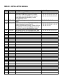
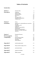
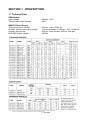
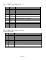
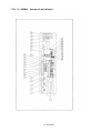
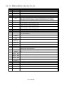
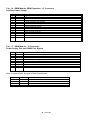
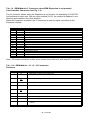
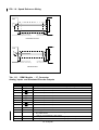
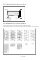
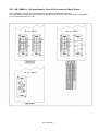
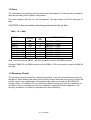
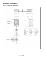
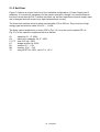
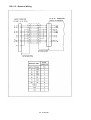
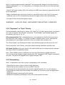
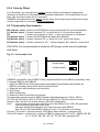
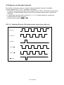
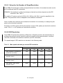
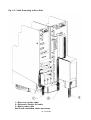
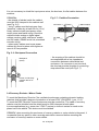
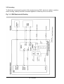
DBM 03
Installation Manual
GB-4501 Rev.4 - July/98
DBM 03 - INSTALLATION MANUAL
Rev. Date
June/96
0
18/Oct/96
1
2
3
4
Description
New Release with EMC
Add Appendix D (serial link multidrop); add
Appendix E (DBTALK program); update
personality card with WP jumper; update
wiring drawings with shielding; correct
miscellaneous errors
19/Dec/96 Add CE-marking; correct miscellaneous
errors
23/May/97 Update standards with EN 61800-3, EMC
product standard; correct fig.3.8
(EMC/Equipotential bonding); update 220Vac
with 230Vac; correct the leakage current of
EMC filters; correct miscellaneous errors
6/July/98
Add default values for keyboard setup; add
thermal sizing; correct miscellaneous errors
Updated Pages
All
1, 2, 5, 11, 13, 16, 18, 19, 20,
21, 23, 24, 25, 26, 27, 32, 33,
34, 38, 44, 49, 50, 54, 55, 56
1, 2, 19, 31, 38, 43, 51
2, 4, 5, 8, 10, 17, 21, 26, 28,
29, 30, 34, 35, 38, 41, 42, 43,
45, 48, 49, 55, 56
29, 34, 40, 43, 45, 50, 52, 53
Table of Contents
Introduction
2
Section 1
Description
technical data
interfaces
system wiring
internal jumpers
dimensions
fans
recovery circuit
standard configurations
configurations
5
6
7
11
25
26
26
27
27
Section 2
Installation
wiring
transformer or autotransformer connection
soft start
connection to PC
installation
keyboard or opto priority
autophasing
personality card jumpers
resolver to encoder (optional)
operation
29
29
30
34
34
35
35
38
39
42
Section 3
Electromagnetic
Compatibility
European Directive
filtering
wiring and grounding
recovery resistor
screening
safety aspects
43
43
46
48
49
50
Appendix A
module replacement
51
Appendix B
sizing of power supply circuit
52
Appendix C
mechanical brake
53
Appendix D
serial link multidrop
54
Appendix E
Dbtalk program
55
1 - 6/July/98
Introduction
This manual provides the necessary information for a proper installation of DBM 03 Digital
Drives in the possible different configurations.
The safety instructions provided in this Manual are included to prevent injury to personnel
(WARNINGS) or damage to equipment (CAUTIONS).
To emphasize the differences between new DBM 03 User's Manual and old DBM 01 User's
Manual, a vertical line in the left margin of the text indicates new items.
Accident Protection
WARNING: High Voltage. L+ and L- pins and BUS BAR can have voltage
≥300Vdc even after switching off (capacitive voltage). Discharge
Time Approx. 6 Minutes.
WARNING: High Voltage. The recovery resistor is connected to the Bus Bar’s
and can have voltage ≥300Vdc.
WARNING: do not touch recovery resistor during operation to avoid scalds.
WARNING: when required for an emergency stop, opening motor phases must
be preceded by disabling the axis. The delay time must be at least
30 ms.
WARNING: the drive should be located in an environment that is free from dust,
corroding fumes and fluids. In condensing atmospheres, the cabinet
must be provided with an anti-condensation device.
CE-Marking
Starting from Jan/97, DBM03 drives have CE-marking according to Low Voltage Directive.
Starting from Apr/97 the CE-marking refers also to EMC Directive (see Section 6).
A Declaration of Conformity is available.
The Low Voltage Directive applies to all electrical equipment designed to use with a voltage
rating of between 50 Vac and 1000 Vac and between 75 Vdc and 1500 Vdc.
The CE-marking states that the electrical equipment has been constructed in accordance
with good engineering practice in safety matters in force in the European Community and it
does not endanger the safety of persons, domestic animals or property when properly
installed and maintained and used in applications for which it was made.
DBM03 drives meet the following standard related to Low Voltage Directive:
CEI EN 60204-1 (1993)
par. 6.2.3, 20.3, 20.4
2 - 6/July/98
Component Parts
The DBM component parts are listed below.
The number of such elements depends on the system configuration.
* DBM-PS POWER SUPPLY MODULE
* DBM DRIVE MODULE
* FAN HOUSING
* RECOVERY RESISTOR
* ANCILLARY ITEMS AS FOLLOWS:
-
75 mm (2.95 in) Bus Bars (connection between DBM-PS and DBM...)
90 mm (3.54 in) Bus Bars (connection between DBM... and DBM... or EBM)
flat 13-way cable for auxiliary voltage
flat 9-way cable for serial line
37-contact D shell, solder type, male connector
Cover for 37-contact D shell connector
9-contact D shell, solder type, male connector
Cover for 9-contact connector
18-way plug in connector
Motor connector (16-contact for DBM, 4-contact for EBM)
Housing for motor connector
3.9 ohm, 370 W recovery resistor, with wiring
Assembly And Fixing
Fig. 1.10 (dimensions in mm) shows the drilling jig between power supply and drive module. The
modules must be mounted vertically, with the fan housing at the bottom. Leave a clear space of
at least 50 cm (19.7 in) over and under the system for air circulation.
Drill for m5 screws
Note: for 180 mm module, dimensions are the same as two side by side standard modules.
Mounting Steps
REMARK: we suggest paying particular attention to the mechanical alignment of the modules,
thus allowing a proper fixing of the bus-bars into the connector slots.
• fan housing
• power supply module
• drive module(s)
Note: the fan housings can be used as a support for the modules, and the modules themselves
as a drilling template for their fixing.
3 - 6/July/98
• Connect the bus-bars between the power supply module and the drive module(s), tightening
the screws at 3 Nm (26.5 lb in), to make a good electric contact.
• Connect the recovery resistor on the RR terminals of the power supply module (see Fig. 4.1).
It is recommended to mount this resistor vertically and away from the heatsinks.
• Arrange the connecting cables to the other parts of the system according to the instructions
given in the following sections.
Connections
Make the following connections (see Fig. 1.1)
• Flat conductor cable for auxiliary power supply (on J1)
• RS 485 serial flat conductor cable between DBM-PS (on J2) and the first DBM module
(on J2)
• Keyboard or PC connection on J10 of DBM-PS
- D shell 37-contact connector on J7 of DBM module
- 18-contact connector on J8 of DBM module
- Motor connector on J9 of DBM module
- D shell 9-contact connectors on J4, J5, J6 of DBM module
REMARK: J4, J5, J6 connections must correspond to J9 connections (every resolver must
correspond to his own motor, J4 to M1, J5 to M2 and J6 to M3, see Fig. 5.5, 5.6 and Fig. 6.1)
Tightening Torque
CAUTION: do not exceed the tightening torque of the table
Screw
Thread
M3
M4
M5
M6
M8
Tightening torque
[Nm]
[lb in]
1.00
8.85
3.00
26.55
6.00
53.10
8.00
70.80
20.0
177.0
4 - 6/July/98
SECTION 1 - DESCRIPTION
1.1 Technical Data
DBM Module
Input voltage
Three-phase output voltage
: 300Vdc, ±10%
: 180V
DBM-PS Power Supply
Three-phase input voltage
Auxiliary power supply input voltage
Auxiliary input power
BUS BAR output voltage
: 230Vac, ±10%, 50/60 Hz
: 110Vac (optional) or 230Vac, ±10%, 50/60 Hz
: 55W for 3-axis module, 60W for fans pair
: 300Vdc
230
230
5 - 6/July/98
1.2 Interfaces
Digital
• Output for simulated encoder (optional)
• Serial Link RS485(1200-19200 Baud) full-duplex to manage:
- Acceleration limits
- Autophasing
- Control parameters
- Monitoring of internal parameters
- Range of analog interface
- System status
• Output for Drive OK axis 1, axis 2, axis 3 (TTL compatible)
On-Off (Optoisolated)
• Drive OK
• Drive Enable
• Motor OK
• Reference Enable
Analog
• Input velocity (see MR command)
• Resolver differential input signals
• Peak current limit input
• Output tachometer (see ET command)
• Max current, velocity reference, velocity error outputs (see ES, SO commands)
1.3 Protection
Module
• Auxiliary voltage out of tolerance
• BUS BAR overvoltage
• BUS BAR undervoltage
• Motor phase grounded
• Motor overtemperature
• Module overtemperature
• IT protection
• Abnormal resolver signal
• Short circuit on motor phases
• Non-coherent three-phase sequence
• Actual speed versus reference error
Power Supply
• Overtemperature
• Recovery unit not OK
6 - 6/July/98
1.4 System Wiring
All of the analog and digital signal connectors, auxiliary power supplies and I/O interfaces are
front-connected to the unit.
Connectors for auxiliary power supply are made via Molex type connectors. Motor power are
connected via a Harting type connector, while I/O connectors use a Weildmuller type
connector.
All other connectors are made via D-type connectors.
All signals are positive logic:
active
= +15V
not active = 0V (or not connected)
1.5 DBM Configurations
Three configurations are possible for the module:
DBM-3A:
DBM-2A:
DBM-2E:
DBM-L3A:
DBM-L2A:
3-axis module (see Fig. 1.3)
2-axis module (see Fig. 1.4)
2-axis module with expansion (see Fig. 1.5)
3-axis 180 mm module (see Fig. 1.6)
2-axis 180 mm module (see Fig.1.7)
7 - 6/July/98
FIG. 1.1 - Inter module wiring
230 VAC
3 x 230 Vac
8 - 6/July/98
FIG. 1.2 - DBM-PS Power Supply
9 - 6/July/98
Tab. 1.1 - DBM-PS Power Supply (See Fig. 1.2)
Pos.
1
2
3
4
5
6
7
8
9
10
11
12
13
14
15
16
17
18
19
Name
R
S
T
GND
RR
RR
AUX
AUX
Yellow LED
PWR-BUS
Red LED DBR
FAULT
N.C.
Red LED OVER
TEMP
Green LED AUX
POWER
J2
J10
J1
GND
LL+
"L1" phase, three-phase input voltage 230Vac
"L2" phase, three-phase input voltage 230Vac
"L3" phase, three-phase input voltage 230Vac
Ground
Recovery resistor
Recovery resistor
Auxiliary power supply 230Vac (110Vac as option)
Auxiliary power supply 230Vac (110Vac as option)
BUS BAR voltage > 40Vdc
Recovery unit fault
Module overtemperature via PTC (threshold 80 °C)
Auxiliary power supply OK
RS485 output port to drives and power control fault
RS485 input port
Auxiliary power supply flat connector
Ground
BUS BAR -HV 300Vdc
BUS BAR +HV 300Vdc
Tab. 1.2 - DBM-PS Power Supply - J1 Connector
Auxiliary Power Supply
Pos.
1
2
3
4
5
6
7
8
9
10
11
12
13
Name
N.C. (Not connected)
N.C.
- 15Vdc referred to -HV (300Vdc)
+18Vdc referred to -HV (300Vdc)
150kHz square wave to high side drives
N.C.
+18Vdc referred to logic 0V
- 18Vdc referred to logic 0V
+8Vdc referred to logic 0V
+8Vdc referred to logic 0V
Logic 0V
Resolver 0V
10 kHz sinusoidal wave for resolver and synchronism (carrier)
10 - 6/July/98
Tab. 1.3 - DBM-PS Power Supply - J2 Connector
RS485 Port Signal and PWRS Control
Pos.
1
2
3
4
5
6
7
8
9
Name
+ Rx (RS485 serial link)
N.C.
+ Tx (RS485 serial link)
PWRS fault 1 - power supply binary coded faults (level 1)
+ 5Vdc input referred to logic 0V
- Rx (RS485 serial link)
Logic 0V
- Tx (RS485 serial link)
PWRS fault 2 - power supply binary coded faults (level 2)
Note: Rx and Tx are the receiving and transmitting signals with reference to the drive. In the
rest of the manual "RS485 serial link", referring to Rx and Tx, will not be specified anymore.
In case of fault, the type of fault is as follows:
J2/pos. 4
0
0
1
1
J2/pos. 9
0
1
0
1
OK
DBR FAULT. Recovery fault
OVER TEMP. Overtemperature
PHASE FAULT.
Tab. 1.4 - DBM-PS Power Supply - J10 Connector
RS485 Port
Pos.
1
2
3
4
5
6
7
8
9
Name
+Rx
N.C.
+Tx
N.C.
+5Vdc output referred to logic 0V for power supply
-Rx
Logic 0V
-Tx
N.C.
1.6 DBM-PS Internal Card Jumpers
FIG. 1.A - DBM-PS Card Jumpers
JP1 closed (default) = connects a 120 Ω
resistor between RX+ and RX-.
JP2 closed (default) = connects TX- of
serial link to 0V via pull-down resistor
JP3 closed (default) = connects TX+ of
serial link to +5V via pull-up resistor
11 - 6/July/98
FIG. 1.3 - DBM03 - Standard 3-Axis Module
13 - 6/July/98
FIG. 1.4 - EBM Expansion Module (optional)
14 - 6/July/98
Tab. 1.5 - DBM Axis Module (See Fig. 1.3 to 1.4)
Pos.
1
2
3
4
5
6
7
Name
J9
J6 M3
J5 M2
J4 M1
J8
J7
Red LED
DRFV
8
9
Red LED WTD
Red LED RF3
10
Red LED RF2
11
Red LED RF1
12
13
14
15
Red LED OVT3
Red LED OVT2
Red LED OVT1
Trimmer ILIMIT
16
Push button
RESET
Red LED DRV
OVT
Red LED
SHRT CCT
Red LED
SHRT CCT
Red LED
SHRT CCT
J2
J3
17
18
19
20
21
22
23
24
25
26
27
Green LED
REF EN
Green LED
DRIVE EN 1
Green LED
DRIVE EN 2
Green LED
DRIVE EN 3
Green LED
POWER OK
28
29
30
31
32
J1
GND
LL+
33
J10
Motor phases (M1-M2-M3) connector
Resolver M3 connector
Resolver M2 connector
Resolver M1 connector
I/O signals connector
connector for analog references and simulated encoder output
generic fault: the fault can correspond, according to the type, to a LED on the front
end; if other red LED's are not on, out of the considered one, it is necessary to
interrogate the drive via serial link to know the fault reason (see FA command)
Watch dog - signal; microprocessor circuit faults; this LED is on during reset
Resolver 3 fault - signal; resolver M3 fault, sin /cos signals interrupted, short circuit
between signals or 10kHz carrier abnormal
Resolver 2 fault - signal; resolver M2 fault, sin /cos signals interrupted, short circuit
between signals or 10kHz carrier abnormal
Resolver 1 fault - signal; resolver M1 fault, sin /cos signals interrupted, short circuit
between signals or 10kHz carrier abnormal
Motor M3 overtemperature
Motor M2 overtemperature
Motor M1 overtemperature
all axes peak current control (only for setup technicians); if current limit is required see
IL, DL, AL commands
digital control card reinitialization
module overtemperature
short circuit on axis 1 (motor phases)
short circuit on axis 2 (motor phases)
short circuit on axis 3 (motor phases)
RS485 input port and PWRS-fault signals connector
Expansion connector for two axis module; on three axis module some pins of this
connector are used as test points
Reference enabled - signal: three - axis speed reference enable (see Tab. 1.12/ pos.
16)
Axis 1 enable (see also ON command)
Axis 2 enable (see also ON command)
Axis 3 enable (see also ON command)
Auxiliary power OK
Personality card: it contains drive setup in a non volatile memory
Auxiliary power supply flat connector
Ground
BUS BAR -HV 300Vdc
BUS BAR +HV 300Vdc
Motor phases (M1-M2-M3) connector for DBM-L module
15 - 6/July/98
Tab. 1.6 - DBM Module, EBM Expansion - J1 Connector
Auxiliary Power Supply
Pos.
1
2
3
4
5
6
7
8
9
10
11
12
13
Name
N.C.
N.C.
- 15Vdc referred to -HV (300Vdc)
+ 18Vdc referred to -HV (300Vdc)
150kHz square wave to high side drives
N.C.
+ 18Vdc referred to logic 0V
- 18Vdc referred to logic 0V
+ 8Vdc referred to logic 0V
+ 8Vdc referred to logic 0V
Logic 0V
Resolver 0V
10kHz sinusoidal wave for resolver and synchronism (carrier)
Tab. 1.7 - DBM Module - J2 Connector Power Supply Flat and RS485 Port Signals
Pos.
1
2
3
4
5
6
7
8
9
Name
+Rx
N.C.
+Tx
PWRS fault 1 - power supply binary coded faults
+5Vdc output referred to logic 0V
-Rx
logic 0V
-Tx
PWRS fault 2 - power supply binary coded faults
Note: In case of fault, the type of fault is as follows:
J2/pos. 4
0
0
1
1
J2/pos. 9
0
1
0
1
OK
DBR FAULT. Recovery fault
OVER TEMP. Overtemperature
PHASE FAULT.
16 - 6/July/98
Tab. 1.8 - DBM Module - J3 Connector
Expansion Connection
Pos.
1
2
3
4
5
6
7
8
9
10
11
12
13
14
15
Name
0V common
Auxiliary voltages referred to logic 0V not OK input signal
Phase U reference current output signal
Torque enabled output signal
Short circuit input signal
Overtemperature input signal
Expansion present input signal
Overtemperature output signal
N.C.
Phase V reference current, output signal
Overtemperature input signal
Non - coherent current input signal
BUS BAR fault input signal
Auxiliary voltages referred to - HV (300Vdc) not OK, input signal
N.C.
FIG. 1.5 - Limit Switches Wiring
DB M 04
1
0V
2
C W L im it s w itch a x is 1
5
C C W L im it sw itc h a x is 1
6
C W L im it s w itc h a xis 2
12
C C W L im it s w itc h a x is 2
13
C W L im it s w itch a x is 3
14
C C W L im it sw itc h a x is 3
ca b le s h ield m u st b e R F *
co n ne cte d to g ro un d
*=see Section 3
J3
g r o u n d in g o f s h ie ld
v ia co n n e c to r s h e ll
17 - 6/July/98
Tab. 1.9 - DBM Module J3 Connector (when EBM Expansion is not present)
Limit Switches Connection (see Fig. 1.9)
The J3 connector allows, when the Expansion is not present, the availability of CW/CCW
limit switches for each axis. With the input enabled (to 0V), the rotation is disabled in one
direction and enabled in the other direction.
When the Expansion is present, the J3 connector is used for signal connection to the
Expansion module.
Pos.
1
2
3
4
5
6
7
8
9
10
11
12
13
14
15
Name
0V common
CW limit switch, axis 1
N.C.
N.C.
CCW limit switch, axis 1
CW limit switch, axis 2
N.C.
N.C.
N.C.
N.C.
N.C.
CCW limit switch, axis 2
CW limit switch, axis 3
CCW limit switch, axis 3
0V common
Note: CW means clockwise rotation when viewed from shaft end, with default DI command.
Tab. 1.10 - DBM Module - J4 - J5 - J6 Connectors
Resolvers
Pos.
1
Name
cos
2
Differential cos signal non-inverted input
Differential cos signal inverted input
cos
3
Shield
Internally connected to 0V common
4
sin
Differential sin signal non-inverted input
5
Differential sin signal inverted input
sin
6
PTC
Motor PTC input
7
0V
0V common. Special for 10kHz carrier
8
PTC
Motor PTC input
9
V ref
20 Vpp/ 10kHz sinusoidal output signal for supplying primary resolver winding
(carrier)
18 - 6/July/98
FIG. 1.6 - Speed Reference Wiring
D B M 04
CNC
REF
REF
0 V
0 V
J7
c a b l e s h ie l d m u s t b e R F
c o n n e cte d to th e h o u s in g
g ro u n d in g o f sh ie l d
v ia co n n e c to r sh e ll
D IF F E R E N T IA L IN P U T
D BM 04
CN C
REF
0 V
REF
0 V
J7
c a b le sh i e ld m u s t b e R F
c o n n e c te d to th e h o u s i n g
gro u ndin g o f s hi eld
v ia c on n ec to r s h ell
U N IP O L A R IN P U T
Tab. 1.11 - DBM Module - J7 Connector
Analog Inputs and Simulated Encoder Outputs
Pos.
1
2
Name
10
A1
B1
C1
A2
B2
C2
A3
B3
C3
11
12
TP2
ILIMIT3
13
14
ILIMIT2
ILIMIT1
3
4
5
6
7
8
9
Logic 0V (it can be used as common for analog output supplies ±15V)
encoder output: inverted phase A - motor 1
encoder output: inverted phase B - motor 1
encoder output: inverted phase C - motor 1
encoder output: inverted phase A - motor 2
encoder output: inverted phase B - motor 2
encoder output: inverted phase C - motor 2
encoder output: inverted phase A - motor 3
encoder output: inverted phase B - motor 3
encoder output: inverted phase C - motor 3
Testing point 2
Analog input I limit axis 3, referred to analog 0V
0V = zero current
+10V (or not connected) = max current
Analog input I limit axis 2, referred to analog 0V (0 to +10V )
Analog input I limit axis 1, referred to analog 0V (0 to +10V )
19 - 6/July/98
15
16
REF3
17
REF2
18
REF1
19
20
21
22
23
24
25
26
27
28
29
30
A1
B1
C1
A2
B2
C2
A3
B3
C3
TP1
31
DRIVE
OK 1
32
DRIVE
OK 2
33
DRIVE
OK 3
34
REF3
35
REF2
36
REF1
37
Shield. Internally connected to 0V
Differential inverting analog input for the speed reference signal (or torque ref.
signal, see TC command) axis 3, max range ±10V (see MR command). See
Fig. 1.6.
Differential inverting analog input for the speed reference signal (or torque ref.
signal, see TC command) axis 2, max range ±10V (see MR command). See
Fig. 1.6.
Differential inverting analog input for the speed reference signal (or torque ref.
signal, see TC command) axis 1, max range ±10V (see MR command). See
Fig. 1.6.
+15Vdc output (I max = 30mA)
encoder output: phase A - motor 1
encoder output: phase B - motor 1
encoder output: phase C - motor 1
encoder output: phase A - motor 2
encoder output: phase B - motor 2
encoder output: phase C - motor 2
encoder output: phase A - motor 3
encoder output: phase B - motor 3
encoder output: phase C - motor 3
Testing point 1
Shield. Internally connected to 0V
Drive OK output, axis 1. Imax=5mA.
0V=not OK
+5V=OK
Drive OK output, axis 2. Imax=5mA.
0V=not OK
+5V=OK
Drive OK output, axis 3. Imax=5mA.
0V=not OK
+5V=OK
Differential non-inverting analog input for the speed reference signal (or torque ref.
signal, see TC command) axis 3, max range ±10V (see MR command). See
Fig. 1.6.
Differential non-inverting analog input for the speed reference signal (or torque ref.
signal, see TC command) axis 2, max range ±10V (see MR command). See
Fig. 1.6.
Differential non-inverting analog input for the speed reference signal (or torque ref.
signal, see TC command) axis 1, max range ±10V (see MR command). See
Fig. 1.6.
- 15Vdc output (I max = 30mA)
REMARK: in DBM 01 version positions 31, 32 and 33 were assigned to differential inverting
I Limit analog inputs. If this option was used, to change DBM 01 with DBM 03 it is necessary
to properly specify differential analog I Limit input in the order.
20 - 6/July/98
FIG. 1.7- Input/Output Wiring
+24V
+ 24V Pow er Supply
0V
DBM
CNC
+2 4 V
0V
8
O p to isola te d inp u t co m m o n
D rive E n ab le
*
D rive E n ab le
R e f. E n a b le
16
D rive O K
10
M o to r O K
12
R e fe re nce E n a b le
D rive OK
O p to iso la te d O u tp u t
9
M o to r O K
O p to iso la te d O u tp u t
11
g ro u n d in g o f sh ie ld
via h o se cla m p
ca b le sh ie ld m u st b e R F
co n n e cte d to th e h o u sin g
J8
* = p in n u m b e r is a xis de pe n de n t
+ 24V P O W ER SU P PLY
DBM
6
0V C om m o n
7
+ 15 V d c o u tp u t
8
O p to isola te d inp u t co m m o n
*
D rive E n ab le
16
R e fe re nce E n a b le
J8
* = pin n u m b e r is a xis d ep e nd e n t
+ 1 5 V IN T E R N A L SU P P L Y
(fo r d rive te st)
21 - 6/July/98
Tab. 1.12 - DBM Module J8 Connector
I/O Commands and Signals
Pos.
1
2
Name
TACHO TEST 1
TACHO TEST 2
3
4
TACHO TEST 3
ANALOG OUT 1
5
ANALOG OUT 2
6
7
8
9
10
11
12
13
14
15
16
0V
+15V
OPTO 0V
DRIVE OK
DRIVE OK
MOTOR OK
MOTOR OK
DRIVE EN1
DRIVE EN2
DRIVE EN3
REF EN
17
18
REM RESET
tachometer analog output, axis 1. Range: see ET command
tachometer analog output, axis 2. Range: see ET command
tachometer analog output, axis 3. Range: see ET command
analog output 1. Max current, velocity reference or velocity
error outputs. See ES and SO commands.
analog output 2. Max current, velocity reference or velocity
error outputs. See ES and SO commands.
0V common
+15Vdc output (Imax = 30mA)
Optoisolated 0V
Collector of Drive OK optoisolator
Emitter of Drive OK optoisolator
Collector of Motor OK optoisolator
Emitter of Motor OK optoisolator
Drive enable 1: optoisolated input for axis 1 torque enable. See Fig. 1.7.
Drive enable 2: optoisolated input for axis 2 torque enable. See Fig. 1.7.
Drive enable 3: optoisolated input for axis 3 torque enable. See Fig. 1.7.
Reference enable: optoisolated input for the confirmation of the common
reference to the three axis (REF EN not active means no speed reference or
zero torque)
N.C.
Remote reset: optoisolated input for logic section reset, equivalent to push
button on the front panel
22 - 6/July/98
Tab. 1.13 - EBM Expansion (optional) - J3 Connector
(See Fig. 1.8)
Pos.
1
2
3
4
5
6
7
8
9
10
11
12
13
14
15
Name
0V common
Auxiliary voltages referred to logic 0V not OK output signal
Phase U reference current input signal
Torque enabled input signal
Short circuit output signal
Overtemperature output signal
Expansion present input signal
Overtemperature input signal
NC
Phase V reference current, input signal
Overtemperature output signal
Non - coherent current output signal
BUS BAR fault output signal
Auxiliary voltages referred to +HV (300Vdc) not OK output signal
N.C.
Tab. 1.14 - Input/Output Characteristics
Optoisolated inputs
Drive enable 1,2,3
Reference enable
Remote reset
Optoisolated outputs
Drive OK
Motor OK
Analog tacho outputs 1,2,3
Analog outputs
Analog Out1
Analog Out2
Velocity reference inputs
1,2,3
Drive OK outputs
1, 2, 3
Simulated Encoder
differential output
z in =1.2 kΩ
I nom = 10 mA
Imax = 20 mA
Vnom = 15Vdc
Vmax = 25V
z out = 1.2 kΩ
I max = 20 mA
Vnom < 25 Vdc
z out = 100 Ω
I max = 5 mA
Range: see ET command
Gain error = ±10% over production spread
Max linearity error: ±2% over full range
z out = 100 Ω
I max = 10 mA
Range: see ES command
Full scale = ±10V
z in > 20 kΩ
Range = see MR command
Vmax = 12 V
TTL compatible
Fan-out = 5 LS-loads
I max = 5 mA
z out = 100 Ω
Full scale = 7V (differential)
23 - 6/July/98
FIG. 1.8 - Motor Phases Wiring (only one axis shown)
DB M 04
M otor
U
U
V
V
W
W
g ro und
g ro und
J9/J 10 /J1 1
grounding of shield
via connector clamp
(or RF connection to
the ground screw in
case of terminal board)
g r o u n d in g o f s h ie ld
v ia co nne cto r clam p
FIG. 1.9A DBM03 Module. J9 Connector. Motor Power
The configuration of this connector depends on the different combinations of sizes .
Notes: M1 always corresponds to the more powerful axis. M3 must not be connected in 2 axis configuration.
24 - 6/July/98
FIG. 1.9B DBM03-L (180 mm) Module. J9 and J10 connectors. Motor Power
The configuration of these connectors depend on the different combinations of sizes .
Notes: M2 always corresponds to the more powerful axis. M3 must not be connected in 2 axis configuration.
For U-V-W positions see Fig. 1.9A.
25 - 6/July/98
1.7 Dimensions
FIG. 1.10 - Dimensions (in mm).
Note: for DBM-L modules (180 mm), dimensions are the same as two side by side standard modules
26 - 6/July/98
1.8 Fans
The ventilation is provided by fans mounted under the modules. The size and the number of
fans are according to the system configuration.
Fan input voltage is 230 Vac (or 110 Vac optional). The input power is 60 W for each pair of
fans.
CAUTION: a free circulation must be guaranteed for the air flow.
TAB. 1.15 - FANS.
MODEL
DBM F2
DBM F3
DBM F4
DBM F5
DBM F2 (110V)
DBM F3 (110V)
DBM F4 (110V)
DBM F5 (110V)
INPUT
VOLTAGE
(V∼)
PAIR
OF
FANS
230
230
230
230
110
110
110
110
1
1
2
3
1
1
2
3
CONFIGURATION
DBM-PS + 1 DBM
DBM-PS + 2 DBM
DBM-PS + 3 DBM
DBM-PS + 4 DBM
DBM-PS + 1 DBM
DBM-PS + 2 DBM
DBM-PS + 3 DBM
DBM-PS + 4 DBM
Note: to size the fans a DBM-L (180 mm) module counts as two DBM modules.
Example: DBM-PS, one DBM module and one DBM-L (180 mm) module, requires a DBM F4
fan type.
1.9 Recovery Circuit
The recovery circuit is formed by a switching regulator, a recovery transistor and a recovery
resistance. While braking the motor returns energy which cannot be sent to the line since the
rectifier circuit is not regenerative. Returned energy tends to increase the BUS BAR DC
voltage. When HV reaches 375V the switching regulator brings the recovery transistor into
conduction, thus connecting the recovery resistance in parallel with filter capacitors. The
recovery resistance is formed by enameled wire fixed resistor(s).
27 - 6/July/98
If the recovery resistance works for intervals shorter than the time necessary to reach
thermal equilibrium, the resistor can temporarily handle power levels up to 10 times the
nominal power rating of the resistor (short time overload).
If not specifically requested, systems are provided with standard 3.9 Ω, 370W recovery
resistor.
An oversized Power Supply with three 8.2 Ω, 370 W (parallel configuration) is available.
WARNING: an unusual application with motor driven by the load, a large portion
of the time, could result in overheating of the recovery resistor.
An unusual application with motor driven by high inertial load from
high velocity in very short deceleration time could result in the
explosion of the input capacitor.
It is suggested contacting our Customer Service.
WARNING: do not touch recovery resistor during operation to avoid scalds.
Ventilated enclosures containing dynamic braking resistors shall
provide a degree of protection of at least IP22 (according to EN
60204-1, par. 13.3).
28 - 6/July/98
Section 2 - Installation
FIG. 2.1 - Transformer Connections
230 VAC
28 - 6/July/98
2.1 Wiring
This section provides the necessary information to properly wiring the digital brushless
system.
1.
2.
3.
4.
Mains connections via transformer or autotransformer.
Resolver and motor power wiring.
Signals wiring.
Other wiring.
2.1.1 Transformer or Autotransformer Connection
Figure 2.1 shows the electric diagram for transformer or autotransformer connection (from
three-phase mains voltage to 230V). See Appendix B for a correct sizing.
If a transformer is used it is recommended to set the - HV to the ground, the secondary
neutral remaining floating. It is recommended to use star primary winding and delta
secondary winding.
If an autotrasformer is used, the -AT must not be connected to the ground.
REMARK:
the auxiliary supply must be independent from the power supply, if the fault
information (see FA command) is to be retained in case of a mains failure.
29 - 6/July/98
FIG. 2.2 - Soft Start
30 - 6/July/98
2.1.2 Soft Start
Figure 2.2 shows a current limit circuit for a standard configuration (1 Power Supply and 3
modules): it is not strictly necessary for the system operation, though it is recommended to
limit the current through R-S-T phases on power up, as filter capacitors at power supply input
are uncharged and can require very high instantaneous current.
The three limit resistors must be short-circuited after 150 to 200 ms. They must be of high
energy type and must be rated 10 to 20 Ω, 100W.
The delay can be achieved by a timer (CR2 in Fig. 2.2) or by the circuit marked CR1 in
Fig. 2.2. In this case the component list is as follows:
Cc
Cd
F1, F2
K1
Rc
Rd
T2
: capacitor 0.1 µF, 250V
: electrolytic capacitor 20 µF, 250V
: fuse 315 mA,- 250V
: bridge rectifier 1A, 400V
: resistor 22 Ω, 5 W
: resistor 10 kΩ, 5 W
: relay SPST 5A, 220V, coil 110 V, 10 kΩ
31 - 6/July/98
FIG. 2.3 - Resolver Wiring
grounding of shield
via connector shell
grounding of shield
via connector clamp
32 - 6/July/98
2.1.3 Resolver Wiring
Each DBM module can be connected up to 3 resolvers via the following connectors:
J4 M1 : axis 1 resolver
J5 M2 : axis 2 resolver
J6 M3 : axis 3 resolver
A cable with 4 pair, each pair twisted and individually shielded with an independent overall
shield is recommended. 22 AWG ( 0.38mm2 ) to 20 AWG ( 0.6 mm2 ) can be used.
Resolver cables must be separated from power cables by a distance of 30cm (12 inches)
by using a independent duct (conduit). It is recommended to avoid intermediary connections
for resolver cables.
Figure 2.3 shows the wiring lay-out of the resolver with differential output.
2.1.4 Motor Power Wiring
Motor power cables must be shielded (see fig.1.8). There are seven different motor power
connections, depending on module configuration (see fig. 1.9A and 1.9B).
2.1.5 Signals Wiring
Signals cable must be shielded (see fig.1.9, 1.10 and 1.11).
REMARK: it is suggested to connect the isolated output "DRIVE OK" to a remote control
switch so that, if a fault occurs, the power supply is disconnected to avoid system
damages.
2.1.5.1 Simulated Encoder Signals Wiring
For lengths in excess of 5 m (16 ft.) the cable must have 3 pairs, each pair twisted.
REMARK: in noisy environments it is suggested to connect a 220 ÷ 680 Ω resistor between
A and A, B and B, C and C at the receiver input.
2.1.6 Serial Link Wiring
CAUTION: the serial link must be shielded and must be separated from the
power cable through the use of independent duct (conduit).
33 - 6/July/98
2.1.7 Serial Link Connection
REMARK: for the first installation it is strongly recommended to use either the
optional keypad or the DBTALK communication program.
2.1.7.1 Keypad
The keypad is an optional accessory product which can be used for drive setup and
monitoring. It must be connected to J10 connector.
If problems occur when attempting to communicate, the keypad is most likely set incorrectly.
To start the setup procedure press <CTRL>, then <CR>. For each parameter the current
setting is displayed, together with a question asking if you want to change it.
The correct setting is:
BAUD = 9600
WORD = 8D+E+1 STOP
BLOCK MODE
SINGLE LINE MODE
FLASHING OFF
KEY REPEAT ON SLOW
Be sure to save at the end of the procedure by pressing <Y> when the display shows: "Make
changes permanent Y/N".
2.1.7.2 DBTALK Communication Program
See Appendix D.
2.1.8 Other Wiring
•
•
•
•
the braking resistor
the flat cable for auxiliary supplies
the keyboard (or PC)
all the analog references
2.2 Installation
2.2.1 Starting Sequence
• Connect 230 Vac (or 110 Vac) single phase power supply.
• Multimodule configuration only. Disconnect the first module from the serial link and assign
basic address to the second module and so on for the next modules (all the modules from
factory being usually configured with address 1,2,3 if 3-axis or with address 1,2 if 2-axis).
Example of basic address assignment for the 2nd module, the first module being triple-axis:
FROM KEYBOARD (see User's Manual for a detailed description of commands)
1 SA 4 <CR>
Assign basic address 4 to the second module (its primary axis)
4 SV <CR>
Save the address configuration
34 - 6/July/98
Note: a module programmed as "address 4" will automatically assign for the other axes the
following addresses, i.e. 5 - 6 (if triple-axis) or 5 (if double-axis); and so on for the next basic
addresses.
• Check if NP (pole number), MV (max velocity) and MR (max reference) parameters are OK
for the application.
• Make a hardware reset via button on drive or via positive logic on pin 18 of J8 connector
(software reset via FA command being useless for digital control card reinitialization).
• Connect 230Vac three phase power supply.
WARNING: HIGH VOLTAGE - DISCHARGE TIME APPROX. 6 MINUTES.
2.2.2 "Keyboard" or "Opto" Priority
On the personality card there is a jumper (G2) (See Fig. 2.4) which gives priority to keyboard
or to opto to execute "Drive Enable" command. " Drive Enable" opto isolated signals are
connected to J8/ pos.13, 14, 15.
G2 opened (position 2-3) = keyboard priority = the keyboard (or the device connected to
the serial link) is the master, i.e. it allows to enable or disable motor current, whereas the
optocouplers can only disable (protection); they can enable after resetting only.
The "Drive Enable" and "Reference Enable" opto-isolated signals must be driven at +15V.
Such a procedure, set in factory, should be followed during installation and drive test.
G2 closed (position 1-2) =opto priority =the optocouplers are the master and the keyboard
can only be used for parameters setup.
Note: "Drive Enable" priority is different from the use of the analog or digital reference.
You can choose an analog or digital reference by "AR" (Analog) or "DR" (Digital) commands,
and save. The drives are supplied set to digital reference "DR".
2.2.3 Autophasing
Note: it is possible to limit the current in autophasing via IL command.
• Check that the motor is free to rotate in both directions.
• Check that no fault condition occurs (red DRVF leds off).
•The jumper G2 on the personality card must be opened (position 2-3, as set in factory).
• Check that all module axes have analog drive enable on via positive logic and digital drive
enable off.
• Send the password command for the module.
• Send the autophasing command for every axis of the module and save.
35 - 6/July/98
Example for a double module with axis 4 and axis 5:
FROM KEYBOARD
4 PW91 <CR>
PASSWORD ON
<CR>
4 AP <CR>
AUTOPHASING IN PROGRESS
AXIS PHASED
5 AP <CR>
AUTOPHASING IN PROGRESS
AXIS PHASED
4 SV <CR>
Enter the password for 2nd module (primary axis = 4)
The correct answer is displayed
Only for the optional keypad
Allow axis 4 autophasing.
Allow axis 5 autophasing.
Save module 4 phasing.
• Repeat the password and autophasing procedures for subsequent modules (if applicable).
• Make a hardware reset via button on drive or via positive logic on pin 18 of J8 connector.
2.2.4 Wiring Checks
After phasing each axis, it is possible to check the wiring by rotating the motor via its digital
reference.
• Enable analog Drive Enable and Reference Enable via positive logic.
• Check that G2 is in position 2-3, for keyboard priority.
• Send to every axis the ON command (to enable digital Drive Enable) , the VE command
(for CW slow rotation), the VE- command (for CCW slow rotation), the OF command (to
disable the digital Drive Enable).
Example of checking axis 5 rotation:
FROM KEYBOARD
5 ON <CR>
O
5 VE 50 <CR>
5 VE-50 <CR>
5 OF <CR>
O
Enable digital Drive Enable for axis 5
Drive Enable led will be on
Set CW rotation at 50 rpm
Set CCW rotation at 50 rpm
Disable digital Drive Enable for axis 5
Drive Enable led will be off
36 - 6/July/98
2.2.5 CNC Priority
With CNC, the following procedures must be followed. This way the CNC is the master and
the keyboard is the slave, as follows:
• Parameters managed by CNC: Drive Enable, Reference Enable, Speed References
• Parameters managed by keyboard (or PC): all dynamic parameters (acceleration, KI, KP,
etc.), Status and Fault.
2.2.5.1 Setting of Analog References
To set the modules to use the analog references from the CNC, it is necessary to enter the
password, to send the AR command to every axis and to save. ST command can be entered
to check if the commands have been accepted.
Note that:
• AR command can be sent via global address (∗).
• If there are two or more modules, PW (password) and SV (save) commands can be sent to
each module (not only to each axis).
Example of enabling all the analog references for two modules with axes 1,2,3 and 4,5:
FROM KEYBOARD
1 PW91 <CR>
PASSWORD ON
4 PW91 <CR>
PASSWORD ON
* AR <CR>
1 SV <CR>
4 SV <CR>
1 ST <CR>
A1 ST___ E___ I_0___
...
Enter the password for 1st module (primary axis= 1)
The correct answer is displayed
Enter the password for 2nd module (primary axis = 4)
The correct answer is displayed
Enable analog reference for all axes
Save the configuration for 1st module
Save the configuration for 2nd module
Ask the status for axis 1
Axis 1 status is displayed. Check the 0 in the 2nd bit
after I (bit i)
Repeat ST command and check other axes
2.2.5.2 Drive Enable with CNC Priority
To give the priority for enabling and disabling the drive from the CNC, it is necessary to pull
out the personality card from the module, install G2 jumper in position 1-2 (closed) and to
pull in the card.
REMARK: if there are more than one module, do not swap the personality cards, this will
swap the module data.
37 - 6/July/98
2.2.6 Velocity Offset
If it is necessary you can adjust the analog velocity offset by providing 0 analog speed
reference and setting VO command for an automatic adjustment. A fine adjustment can be
done with successive steps via OV command.
REMARK: the adjustment of the digital velocity offset must not be used to adjust the analog
velocity offset and it is reserved to setup technicians.
2.2.7 Personality Card Jumpers
WP (default: open): if closed, the EEPROM is write protected and SV command disabled
G1 (default: open) : if closed, connects TX- of serial link to 0V via pull-down resistor
: if closed, gives priority to "opto" , if open gives priority to "keyboard"
G2
G3 (default: open) : if closed, set 9600 Baud rate and basic address 1
G4 (default: open) : if closed, connects TX+ of serial link to 5V via pull-up resistor
G5 (default: open) : if closed, connects a 120 Ω resistor between RX+ and RX- of serial link
CAUTION: it is recommended to close the WP jumper at the end of installation
and setup.
Fig. 2.4 - Personality Card
Jumper open
Jumper closed
REMARK: personality card of DBM 03 has a software different from DBM 01 personality card.
To change DBM 01 with DBM 03:
1. Switch on DBM 03 with 230V mono-phase and replace the personality card with the old
DBM 01 personality card with G2 and G3 jumpers closed
2. Reset the drive with reset button on front panel
3. Wait 30 sec
4. Switch off the drive
5. Restore G2 and G3 as before the removal
The personality card is now set to DBM 03 format. New parameters are: 1SO=1; 2SO=2;
CU=128; CV=128; DF=0; ES=16; ET=80; PW=91, RN=RX=12; PR=3 and VS=0 for 2 pole
resolver; PR=1 and VS=1 for 6 pole resolver; SE=1024 (if applicable).
Note: - if the number of pulses per revolution has to be different from 1024, SE parameter
must be properly specified in the order
- after this setting the personality card cannot be used with DBM 01.
- with G2 and G3 closed DBM 03 does not work. The situation is as follows:
G2 open, G3 closed = keyboard priority, 9600 Baud, base address 1, password ON.
G2 and G3 closed = opto priority, reading of DBM 01 parameters (AC, AL/DL, AR/DR, BR, DE,
IL, IT, KI, KP, MR, MV, NP, OC, PC, RS, SA), password OFF.
38 - 6/July/98
2.2.8 Resolver to Encoder (optional)
For position sensing a resolver to encoder option (simulated encoder) is available.
Encoder signals are 7V, 100 Ω impedance, as follows:
• 2 channels of square wave output with a resolution from 128 to 1024 pulses per electrical
revolution. Channel B leads channel A by 90° for clockwise rotation when viewed from
shaft end.
• 1 marker pulse per electrical revolution (i.e. 1∗ 3 = 3 marker pulses per mechanical
revolution with a 6 pole resolver).
• complementary outputs A, B and C .
FIG. 2.5 - Simulated Encoder (CW rotation when viewed from shaft end)
C h a n n el A
Channel B
C M a rk e r
Channel A
Channel B
C M a rk e r
39 - 6/July/98
2.2.8.1 Setup for the Number of Steps/Revolution
From DBM 03 version the number of steps/electrical revolution of simulated encoder can be
set via software (see SE commands).
REMARK: the maximum number of pulses per electrical revolution depends on the R/D
resolution. See Tab.2.1.
The width of C marker can be A (360°), A/2 (180°) or A/4 (90°); it must be specified in the
order. This parameter does not depend on the software commands.
Note: to obtain the resolution per mechanical revolution it is necessary to multiply the pole
pairs by the electrical resolution.
Example: if a FAS T motor with 6 pole resolver is used, 1024 pulses per electrical revolution
mean 1024 ∗ 3 = 3072 pulses per mechanical revolution.
2.2.8.2 R/D Resolution
From DBM 03 version the resolution of Resolver to Digital converter will automatically be
switched according to actual speed for optimum system performance between minimum
(see RN command) and maximum resolution (see RX command).
The speed range of R/D resolution is included in the following table.
Tab. 2.1 - Max speed and max ppr versus R/D resolution
Resolution (bit)
10
12
14
16
256
1024
4096
16384
Max speed with 2 pole
resolver (rpm)
24000
12000
3510
877
Max speed with 6 pole
resolver (rpm)
8000
4600
1170
292
Max speed with 8 pole
resolver (rpm)
6000
3510
877
219
Max number of pulses per
electrical revolution
40 - 6/July/98
FIG. 2.6 - Starting Sequence, Timing Chart
Note: T1 = 8 to 10 s, T2 ≥ 1 s, T3 ≥ 20 ms, T4 ≈ 3 s, T5 ≥ 0.5 s.
230 Vac
230 Vac
41 - 6/July/98
2.3 Operation
After system wiring and installation, it is possible to start the system according to the
sequence shown in figure 2.6.
Action
Effect
• Connect 230Vac single phase
power supply (or 110Vac
optional)
• Digital and diagnostics circuits
are fed
- Green LED on DBM PS, AUX PWR = ON
- Opto output MOTOR OK is enabled
• Connect 230Vac three phase
power supply
• 300V Bus Bars are fed
- Yellow LED on DBM PS, PWR BUS = ON
- Green LED on DBM, POWER OK = ON
• Reset protections by pushing
the RESET button on front
panel or by sending a 20ms
pulse to REM RESET opto input
• Possible faults are reset
- After 3s the opto output DRIVE OK is enabled
• Enable analog Drive Enable
for each axis and Reference
Enable via positive logic
• Green LED's on DBM, DRIVE EN = ON
and REF EN = ON
WARNING: HIGH VOLTAGE - DISCHARGE TIME APPROX. 6 MINUTES.
42 - 6/July/98
Section 3 - Electromagnetic Compatibility (EMC)
3.1 European Directive (89/336/EC)
Compliance with the European Directive 89/336/EEC is required for all electric and electronic
products brought onto the European market after December 31st, 1995.
DBM03 drives with FASTACT motors meet the following EMC product standard related to
the Directive:
EN 61800-3 (1996) and EN 61800-3/A11 (2000): "Adjustable speed electrical power drive
systems. Part 3: EMC product standard including specific test methods".
Second environment (industrial) compatibility levels.
Remark: equipments not intended to be used on a low-voltage public network which supplies
domestic premises. May cause radio frequency interference.
Tests have been made in an independent, competent body, test house.
The installer of the drive is responsible for ensuring compliance with the EMC regulations
that apply where the drive is to be used. We recommend filtering as per par.3.2 and wiring,
grounding and screening as per par.3.3 and 3.4.
3.2 Filtering
3.2.1 Filter Types
Code
Trade-mark
AT6008
Schaffner
FN 250-6/07
Schaffner
FN 258-7/07
Schaffner
FN 258-16/07
Schaffner
FN 258-30/07
Schaffner
FN 258-42/07
Schaffner
FN 258-55/07
Schaffner
FN 258-75/34
Schaffner
FN 258-100/35
AT6009
AT6010
AT6011
AT6012
AT6013
AT6014
AT6015
Rated Current [A] Drive type
at 50°C (40°C)
(6)
DBM03 PS (Aux)
7 (8.4)
16 (19.2)
30 (36)
42 (50.4)
55 (66)
75 (85)
100 (120)
DBM03 PS
43 - 6/July/98
3.2.2 Filter Sizing
The filter/drive coupling in the previous table is a standard coupling. The filter can be
undersized according to the rms input current of the actual application. This should be done
not only because, as a matter of fact, undersizing the filter means less money, but because
the undersized filter provides better performance to EMC.
Example:
- DBM 03 PS + DBM 03 5-5-5 + DBM 03 5-5-5 and contemporaneity factor of 0.8.
For this application it is not necessary to use the 100A filter of the table.
The reference current is Iin = 6 ∗ 5 ∗ 0.8 = 24 A
A 30A filter (FN 258-30/7) can safely be used.
3.2.3. Filter Dimensions
Code
Trade-mark
AT6008
Schaffner
FN 250-6/07*
Schaffner
FN 258-7/07
Schaffner
FN 258-16/07
Schaffner
FN 258-30/07
Schaffner
FN 258-42/07
Schaffner
FN 258-55/07
Schaffner
FN 258-75/34
Schaffner
FN 258-100/35
AT6009
AT6010
AT6011
AT6012
AT6013
AT6014
AT6015
L1
85
L2
75
L3
54
Dimensions
[mm]
L4
0
Weight
255
240
50
25
305
290
55
30
335
320
60
35
305
329
314
70
45
329
314
80
329
314
379±1.5
364
L5
65
L6
30
l7
300
[kg]
0.24
225±0.8 126±0.8
300
1.1
275±0.8 142±0.8
300
1.7
150
400
1.8
300
185
500
2.8
55
300
185
500
3.1
80
55
300
220
90±0.8
65
terminal
block
350±1.2 220±1.5 terminal
block
4
5.5
*= the FN250-6/07 filter has wiring leads (length=300mm) at both sides.
TOP VIEW
SIDE VIEW
L5
L1
L2
L6
L3
L4
44 - 6/July/98
L7
3.2.4 Filter Installation
- The filter must be mounted on the same panel as the drive.
CAUTION: leave a clear space of at least 60mm around the filter for air circulation when the
cabinet does not have forced ventilation.
- The filter must be connected as close as possible to the drive input. If the separation
between filter and drive exceeds around 30 cm (1 ft.) then a flat cable should be used for
the RF connection between filter and drive
REMARK: when mounting the drive and the filter to the panel, it is essential that any paint or
other covering material be removed before mounting the drive and the filter.
- The maximum torque of mounting screws
is as follows:
FILTER
FN 250 - 6/07
FN 258 - 7/07
FN 258 - 16/07
FN 258 - 30/07
FN 258 - 42/07
FN 258 - 55/07
FN 258 - 75/34
FN 258 - 100/35
Max
torque
0.8 Nm
0.8 Nm
0.8 Nm
1.8 Nm
1.8 Nm
3.0 Nm
3.0 Nm
4.0 Nm
- The capacitors within the filters have
discharge resistors.
- The filter can produce high leakage
currents (see Table)
FILTER
FN 250 - 6/07
FN 258 - 7/07
FN 258 - 16/07
FN 258 - 30/07
FN 258 - 42/07
FN 258 - 55/07
FN 258 - 75/34
FN 258 - 100/35
Leakage current*
1.3 mA
17 mA
19 mA
25 mA
26 mA
26 mA
26 mA
26 mA
* Note: if two phases are interrupted, worst case
leakage current could reach 6 times higher levels
Fig. 3.1 - FN 250-6/07 Filter Installation
on DBM 03 Drive
CAUTION: the filter must be connected
to ground before connecting the supply
WARNING: HIGH VOLTAGE DISCHARGE TIME APPROX. 10
seconds
To
Fans
- Where single phase power supply is
needed, the single phase filter can be
installed on the fan housing.
Figure 3.1 shows installation and wiring
of FN 250 6/07 filter on fan housing of
DBM 03 drive.
230V G
N
D
45 - 6/July/98
3.3 Wiring And Grounding
Fig. 3.3 - Grounding of Shield to
Connectors at Motor Side
All the following cables must be shielded,
with 85% minimum shielding coverage:
- power motor cable (see Fig.3.2 and 3.3)
NOTES: if a power terminal board is used
at motor side, the shield must be RF
connected to the ground screw via the
proper clip.
- connectors at motor side can have a
threaded clamp. Cable shield must be
grounded in the same way as in Fig.3.3.
- resolver cable (see Fig.2.3 and 3.3 motor
side)
Fig. 3.2 - Grounding of Shield to Motor
Connector at Drive Side
In case of Sub-D connector, cable shield
must be grounded to the metallic hood.
When there is not connector at drive side,
a kit with stand-off, screws and hose
clamps is provided.
The shield of the cable must be uncovered
from insulation coating and RF connected
to the stand-off through the hose clamp, as
in Fig.3.4.
- recovery resistor cable (BRD drive
excluded)
Fig. 3.4 - Grounding of Shield without
Connector
- Reference, Enable and OK cable
- RS485 cable (flat cable between modules
excluded)
- simulated encoder cable (if applicable)
The shields of the cables must be
connected at both ends to the proper
housing via full circumferential bond to
metallic connectors or hose clamps.
46 - 6/July/98
Fig. 3.5 - Cable Grounding at Drive Side
1 = Recovery resistor cable
2 = Reference, Enable, OK cable
3 = Motor power cable
Sub-D and unshielded cables not shown
47 - 6/July/98
It is not necessary to shield the input power wires, the bus bars, the flat cables between the
modules.
REMARKs:
- the shields of cables inside the cabinet
must be 360° clamped to the cabinet wall
(see Fig. 3.6).
- "noisy" cables must be kept away from
"sensitive" cables by at least 30 cm (12 in).
Noisy cables include input-power wires,
motor power and brake wiring. Sensitive
cables include analog or digital signal
cables: resolver cable; reference, enable
and OK cable; RS485 serial link; simulated
encoder wiring.
- where noisy cables must cross power
cables, this must be done with angles as
near to 90° as possible.
Fig. 3.7 - Partition Penetration
Fig. 3.6 - Backpanel Connection
Backpanel
(earth)
- the crossing of the cabinet should be
accomplished with a low impedance
connection between cable shield and
enclosure. If a connector is not involved,
the shortest practical lengths of connecting
strap should be used (see Fig.3.7).
Screen is effectively
earthed 360° of its
radius
3.4 Recovery Resistor / Motor Choke
To meet the Machinery Directive "the ventilated enclosures containing dynamic braking
resistors shall provide a degree of protection of at least IP22" (EN 60204-1, par. 13.3).
To meet the EMC Directive, these enclosures must be conductive. The cable of recovery
resistor must be shielded and the shield must be 360° clamped at both sides.
In some applications (e.g. some size 3 FAS T motors) a choke in series for each motor
phase has to be added. This choke must be shielded.
REMARK: when mounting the enclosure of recovery resistor or motor choke to the panel, it
is essential that any paint or other covering material be removed before mounting the
enclosure of recovery resistor or motor choke.
48 - 6/July/98
3.5 Screening
To effectively screening the system all the single screens (CNC, electronic cabinet, machine,
motor housing, cables) must be connected together to effectively form one screen.
Fig. 3.8 - EMC/Equipotential Bonding
49 - 6/July/98
3.6 Safety Aspects
Noise suppression of Motor and Drive systems involves consideration of the earthing
system, and its effectiveness at high frequencies. It should not be forgotten that is the safety
system too and that the safety must take priority over EMC.
To reduce the radiated emissions, the use of capacitance to earth is very effective. In fact
DBM03 drives have Y-type capacitors near the input power supply connector and Schaffner
filters also include them. These capacitors conduct current from phase to earth; this can be
in the order of hundreds of milliamperes.
WARNING: appropriate safety measures should be taken to ensure that this
potentially dangerous current flows to earth.
CAUTION: it is recommended to disconnect the drive and the EMC filters to carry out
the "AC Voltage Test" of the EN 60204-1 (par.20.4), according to the Machinery
Directive (89/392/EEC) and to the Low Voltage Directive (73/23/EEC) in order not to
damage the Y-type capacitors between phases and ground while parts of circuits can
be floating and possibly damaged during the test.
To make anyway this test it is recommended contacting our Service Centers.
50 - 6/July/98
APPENDIX A - MODULE REPLACEMENT
Once DBM module to be replaced has been identified, it is necessary to follow this procedure:
• Disconnect the power.
• Remove the Bus Bars (+AT, -AT and GND) and disconnect all connectors and flat cables (see
Fig. 1.1).
• Unscrew the anchor screw on the top of the module and remove the module.
• Only for same DBM versions:
Remove the Personality Card, at the left of J1 connector, by loosening the two screws. After
removing the card, disconnect the flat cable.
REMARK: on the personality card a EEPROM is mounted. All dynamic parameters (dynamic
settings, autophasing, analog interfaces, ...) are stored in this EEPROM after every reset.
In case of module replacement, it is recommended to save all parameters with the save (SV)
command before removing the Personality Card ready for installation in the replacement module.
This retains and transfers all the previous module information's.
Remove the Personality Card from the new module and replace with the old one.
•
•
•
•
Mount the new module and tighten the anchor screw at the top.
Reassemble the Bus Bars, all the connectors and flat cables.
Check all connections.
Enable the auxiliary voltage and check by the optional keypad or PC all application dependent
parameters. In particular: pole number, max velocity, max reference voltage, Ilimit, internal ramp
generator.
CAUTION: personality card of DBM 03 has a software different from DBM 01
personality card. Do not swap personality cards between the two versions.
To change DBM 01 with DBM 03 see Par.2.2.7.
51 - 6/July/98
APPENDIX B - INPUT SIZING
B.1 Sizing of Power Transformer/Autotransformer
It is necessary to refer to the rated output power of the motors (the output power with 65K
winding overtemperature is included in the Technical Data table of catalogs of servomotors), to
sum the power of single axes, to multiply the sum by the contemporaneity factor (factors often
utilized are Kc=0.63 for 2 axes, Kc=0.5 for 3 axes, Kc=0.38 for 4 axes, Kc=0.33 for 5 axes, Kc=0.28
for 6 axes), and by a correction coefficient (=1.2), accounting for the losses of the motor/drive
system.
P = Σ Pim ∗ Kc ∗ 1.2
[W]
B.2 Sizing of Fuses
It is necessary to divide the above calculated power by the 300 V DC Bus.
If = P / 300
[A; W, V]
Fuses must be the delay type because of high peak current inrush of the internal capacitors.
B.3 Auxiliary Power Transformer
Auxiliary power (55 W for each 3-axis module) and fan power (60 W for each pair of fans) must
be added.
B.4 Thermal sizing of cabinet
To calculate cabinet cooling requirements, table below provides estimated equipment power
dissipation values. If the application employs continuous braking, it is necessary to include
the recovery resistor power dissipation (use the nominal power of recovery resistor if actual
application recovery dissipation is unknown).
Power
Supply
25 W
Power Dissipation
Module
IGBT's
50 W
16 W/A
Input
Bridge
1 W/A
Example: with one Power Supply, two modules, a total output current of 60 Arms and continuous
uncalculated braking, the dissipated power is as follows.
Pd = 25 + (2 ∗ 50) + (16 ∗ 60[A]) + (1 ∗ 60[A]) + 370 [recovery resistor power] = 1515 W
52 - 6/July/98
APPENDIX C - MECHANICAL BRAKE
FAS series servomotors have as option a 24 Vdc electromagnetic safety brake.
CAUTION: safety brake must be clamped and released with motor at standstill.
Dynamic brakings can seriously damage the brake and reduce the braking torque.
The release of the brake (from 0V to +24V) and the clamp (from +24V to 0V) must follow the
sequence in Fig. C.1.
FIG. C.1 - Braking Sequence, Timing Chart
Note: T1 ≥ 200 ms, T2 = application dependent, T3 = 100 ms, T4 ≥ 200 ms
T1
T2
T3
T4
ON
OFF
D RIV E E N A BL E
ON
OFF
B RA KE 2 4V
P O W E R SU P PL Y
RELEASE
CLAMP
BRAKE
0V
R E FE R E N C E
E N AB L E
0 rpm
M O TO R SP EE D
53 - 6/July/98
APPENDIX D - SERIAL LINK MULTIDROP
D.1 DBM-PS Internal Jumpers (see par. 1.6)
In case of multidrop, the following configuration must be used.
To user
JP1,JP2,JP3
JP1,JP2,JP3
JP1,JP2,JP3
JP1,JP2,JP3
open
open
open
closed
Power
Supply
Power
Supply
Power
Supply
Power
Supply
D.2 Personality Card Jumpers (see par.2.2.7.1)
By default G1, G4 and G5 jumpers on the personality card are open (no link termination's on
modules). In fact, usually, it is not necessary to close G1, G4 and G5 jumpers because the
link termination's are already closed on the power supply; anyway, in specially noisy
environments, could be necessary to close them also, as follows.
• Environment without noise
To user
JP1,JP2,JP3
(see par.D.1)
Power
Supply
G1,G4,G5
G1,G4,G5
G1,G4,G5
G1,G4,G5
open
open
open
open
Module
Module
Module
Module
G1,G4,G5
G1,G4,G5
G1,G4,G5
G1,G4,G5
open
open
open
closed
Module
Module
Module
Module
• Specially noisy environment
To user
JP1,JP2,JP3
(see par.D.1)
Power
Supply
54 - 6/July/98
APPENDIX E - DBTALK PROGRAM
• MANUAL to
⇒ See/Reset Faults
To help you communicate with DBM/DBS
drives quickly and easily, DBTALK provides
several features:
• SETUP to choose
⇒ Language: Italian or English
⇒ Serial link : COM1 or COM2
If the fault condition is not present anymore, the fault
will be reset automatically. To reset the fault on the
screen, go to the next screen with the arrow keys
⇒ Display the Status
• UTILITY to
⇒ Scan Baud rates
⇒ Scan Faults
⇒ See/Change parameters
To change one parameter type the command string
(see Drive Manual) on the PC keyboard. Example:
3VE3000
⇒ Restore/store Personality Card parameters
To save the actual parameter set, select STORAGE
PARAMETER, select the file (e.g. ST1), press <TAB> to
change the description and press <CR>
⇒ Set Baud rates
⇒ Start the Autophasing procedure
⇒ Set Defluxing (see DBS User's Manual)
55 - 6/July/98
• INTERFACE REQUIREMENTS
The RS422 interface wiring is based on one-toone, no multidrop, principle. Four wires are
used. With RS422, you can transmit and
receive data simultaneously (full-duplex).
The RS485 half-duplex uses only two wires. It
allows multidrop communication. With RS485
half-duplex, you cannot transmit and receive
simultaneously.
DBM03 supports RS485 full-duplex with four
wires (RS422 compatible). Up to 99 DBM and
up to 15 DBS drives can be connected in
multidrop configuration.
⇒ RS232/485 CONVERTER KIT
This very small external converter provides a
full-duplex interface between PC and
DBM/DBS.
The converter must be fit directly into a COM
port (RS232) of a PC. This way the link
becomes purely RS485, less susceptible to
noise and able to transmit over much longer
distances than RS232.
The kit includes:
- the converter to fit into DB25-S connector of
the PC (COM port)
The DTE/DCE switch of the converter must be set to DCE
(Data Communications Equipment)
• PC REQUIREMENTS
- 80286, 80386, 80486 microprocessor or
better
- Hard disk and one diskette drive. You need 2
Mbytes of disk space and 512 kbytes of RAM
- CGA, EGA, VGA, MCGA graphics card (color
VGA recommended)
- MS-DOS 6.2 or later
- ANSI.SYS in CONFIG.SYS
• DBTALK PROGRAM
The DBTALK program is available on floppy
disk
• INSTALL PROGRAM
- Insert diskette into drive A or drive B
- Type <a:install> (or <b:install>)
The installation program will create the Directory
C:\DBTALK, will copy all the files in this new directory
and will start the program
• START PROGRAM (after the first
installation)
- Type <cd dbtalk>
- Type <start>
• MOVE IN THE PROGRAM
- a DB25 to DB9 interface (to be used if the PC
COM port is DB9-S)
- a 2 m cable to connect the converter to DBM
J10 connector or DBS J2 connector
Start the selected procedure
Select the field
Space
⇒ An opto-isolated PC card RS 485 full-duplex
is also available. The following wiring must
be used.
Move up/down
Go to previous/next screen
Esc
RS485 full duplex
Connector
Exit/Go to previous menu
DBM J10 Connector
DBS J2 Connector
Male
(+Tx)
(-Tx)
(+Rx)
(-Rx)
(Gnd)
Reread parameters
1 (+Rx)
2
3 (+Tx)
4-5
6 (-Rx)
7 (Gnd)
8 (-Tx)
9
Female
• SELECT PROGRAM
⇒ DBM linker
⇒ DBS linker
⇒ PDBS Linker (see PDBS Application Manual)
⇒ Setup
56 - 6/July/98
Moog Italiana S.r.l.
Electric Division
Via Avosso, 94
16015 Casella GE
Italy
Phone: (+39) 010 9671
Fax: (+39) 010 9671 280
GB-4501 Rev.4 - July/98
Moog Italiana Srl reserves the right to alter any dimensions or data without prior notice
Printed in Italy