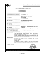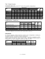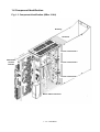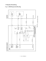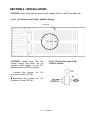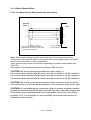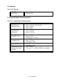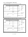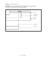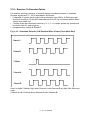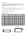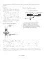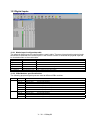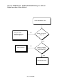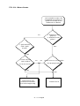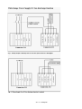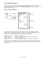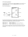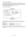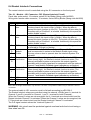
1
IDBM 04
User's
and
Installation
Manual
GB-4537 Rev.3 – Feb/03
IDBM 04 - USER'S MANUAL
Rev.
0
1
2
Date
Jan 01
Mar 01
July 02
3
Feb 03
Description
First Release
Upgrade Section 5; correct pictures
Add Section 8; correct miscellaneous errors
Updated Pages
Section 5, Various
I - all; II – 5, 7, 8, 16, 17, 18, 19, 22, 28, 29, 34,
35, 36, 39; III - 1, 2, 3, 7; IV - 1; VI - 4, 8; VIII - all
Add PS-U with oversized DBU; upgrade Section I – 3, 4, 6, 9-11, 13, 19, 20; II – 5, 7, 14, 35; VIII –
8 according to the requests of the Competent
1, 2, 4 to 14
Body; correct miscellaneous errors
TABLE OF CONTENTS
SECTION 1
Description
description
electrical data
dimensions
component identification
system grounding
options
rating plate
SECTION 2
Installation
fuses
soft start
transformers
thermal sizing of cabinet
recovery circuit
fan assembly
wire type
power supply - wiring
power supply - led's
power supply - internal card jumpers
module wiring
resolver wiring
motor phases wiring
module - leds
potemtiometer/button
input/output characteristics
serial link connection
starting sequence
resolver to encoder option
mechanical brake
module replacement
II - 2
2
3
3
4
5
6
9
12
12
17
20
27
30
33
33
34
39
43
45
46
SECTION 3
EMC
European Directive
filtering
wiring and grounding
recovery resistor
screening
safety aspects
III - 1
1
4
6
7
7
I - 1 – 21/Feb/03
I – 11
11
14
17
18
19
19
SECTION 4
Protections
power supply
drive module
IV - 1
2
SECTION 5
Commands
general features
(description in the sections)
V-1
SECTION 6
Troubleshooting
IDBm-PS troubleshooting
IDBm module troubleshooting
VI - 1
4
SECTION 7
Application
Notes
IDBm-PS-U auxiliary functions
VII - 1
SECTION 8
RIC
Restart Interlock Function
I - 2 – 21/Feb/03
VIII 1
Accident Protection
The safety instructions provided in this Manual are included to prevent injury to personnel
(WARNINGS) or damage to equipment (CAUTIONS).
See Section 8 for safety instructions related to the Restart Interlock Function.
WARNING: L+ and L- pins and Bus Bar's can have voltage
≥810Vdc even after switching off (capacitive voltage).
High Voltage - Discharge Time approx. 6 Minutes.
WARNING: High Voltage. The recovery resistor is connected to
the Bus Bar’s and can have voltage ≥810Vdc.
WARNING: do not touch recovery resistor during operation to
avoid scalds.
CAUTION: make sure that the correct input voltage, 400V or 460V, has been set.
CAUTION: it is recommended to disconnect the drive and the EMC filters to carry
out the AC Voltage Tests of EN 60204-1 (1997), par.19.4, in order to not damage
the Y-type capacitors between phases and ground. Moreover the DC voltage
dielectric test required by EN 50178 (1997), product family standard, has been
carried out in factory as a routine test. The DC Insulation Resistance Tests of EN
60204-1 (1997), par.19.3, may be carried out without disconnecting the drive and
the EMC filters.
CAUTION: when required for an emergency stop, opening U2-V2-W2 pins and
closing motor phases to resistors, must be preceded by disabling the axis. The
delay time must be at least 30 ms.
CAUTION: in case of repetitive switching on and off, wait 1 minute between on
and on.
CAUTION: it is recommended to close the WP jumper on the Personality Card at
the end of installation and setup.
CAUTION: do not exceed the tightening torque of the table (but see proper data
sheets for the tightening torque of input capacitors and power modules and see
Section 2 of this Manual for the tightening torque of terminal blocks)
Screw
Thread
M3
M4
M5
M6
M8
Tightening torque
[Nm]
[lb in]
1.00
8.85
3.00
26.55
6.00
53.10
8.00
70.80
20.0
177.0
I - 3 – 21/Feb/03
I - 4 – 21/Feb/03
CE Requirements
• Cautionary Marking. See Accident Protection page.
• Protection against electric shock. Electronic Equipment intended for installation in
closed electrical operating areas kept locked. The lock shall be only opened by
authorized person and the access only allowed to skilled persons whilst energized.
Where the equipment requires manual intervention, 412.2.1 of HD 384.4.41 S2 shall
be consulted.
• Fixed connection for protection. The equipment may have a continuous leakage
current of more than a.c. 3.5 mA or d.c. 10 mA in normal use and a fixed ground
connection is required for protection.
• RCD. When the protection in installations, with regard to indirect contact, is achieved
by means of an RCD, their appropriate function/combination shall be verified. In any
case only a residual-current-operated protective device (RCD) of Type B is allowed.
In fact a d.c. component can occur in the fault current in the event of a fault
connection to earth.
• Climatic Conditions. Equipment intended to operate within its performance
specification over the range of Class 3K3, as defined in table 1 of EN 60721-3-1, EN
60721-3-2, EN 60721-3-3, EN 60721-3-4, partly modified.
• Pollution Degree 2 Installation - The equipment shall be placed in a pollution
degree 2 environment, where normally only non-conductive pollution occurs.
Occasionally, however, a temporary conductivity caused by condensation is to be
expected, when the electronic equipment is out of operation.
• EMC Requirements. The installer of the equipment is responsible for ensuring
compliance with the EMC standards that apply where the equipment is to be used.
Product conformity is subjected to filters installation and to recommended
procedures, as from Section 3 of this Manual.
• Second Environment (EMC). Equipment intended to be connected to an industrial
low-voltage power supply network, or public network which does not supply buildings
used for domestic purposes (second environment, according to EMC Standards).
It is not intended to be used on a low-voltage public network which supplies domestic
premises (first environment). Radio frequency interference is expected if used on
such a network.
• Recovery Resistor Cable. Shielding of the external recovery resistor cable,
provided in kit for test purposes, is recommended for ensuring compliance with the
EMC standards.
I - 5 – 21/Feb/03
I - 6 – 21/Feb/03
UL Requirements
• These Brushless Servo-Drives shall be assembled with the guidelines specified in
this Manual. Only the configurations with the components tested and described in the
UL Report, file E194181, Vol.2, Sec.1, Issue date 03-28-01 and following Revisions
can bear the Recognized Component (R/C) Mark. Each assembled configuration
shall be evaluated in the UL Listed end-use application.
• The Component – Power Conversion Equipment “DBM 04 Series” is considered UL
Recognized in the complete configurations after the assembly of the three main parts
of the Drive, that is the Power Supply, the Modules and the Fan Assembly. The
Marking, including the R/C Mark and the Drive Model No., shall consider the
equipment in its complete configuration.
• These drives shall be used within their ratings, as specified in the marking of the
equipment. In particular:
- rated input voltage, input current, system duty cycle, auxiliary input voltage,
auxiliary input power, fan input voltage, fan input power on the label affixed on the
fan assembly
- rated axis continuous output current, axis max output current, module duty cycle on
the label affixed on the module
• Cautionary Marking. See Accident Protection page.
• Duty Cycle. The maximum continuous Drive output current shall be limited to 65 A
and to the Maximum Module Current, due to the rated current of the Power Supply
and of the Module. According to this reason, the Drive shall be used with a Duty
Cycle, as specified in the marking of the equipment.
• Surrounding Air Temperature - "Maximum Surrounding Air Temperature 40°C". In
the final installation considerations shall be given for the need of repeating
Temperature test if the unit is mounted with a different Surrounding Air conditions.
• Pollution degree 2 Installation - The drive must be placed in a pollution degree 2
Environment.
• Environmental designation - “Open Type Equipment”.
• Short Circuit Ratings. “Equipment suitable for use on a circuit capable of delivering
not more than 5000 rms Symmetrical Amperes, 460 V ac +10% maximum”
• Branch Circuit Protection. The Branch Circuit Protection for Short Circuit shall be
provided in the end-use applications by external R/C Fuses (JFHR2), manufactured
by Bussmann Div Cooper (UK) Ltd, Semiconductor fuse type, Mod.No. 160 FEE,
rated 160 A, 660 Vac, 200 kA A.I.C.
I - 7 – 21/Feb/03
• Overspeed Protection. The Power Conversion Equipment is incorporating an
Overspeed Protection. See MV command in Section 6 of this Manual.
• Overvoltage Control. In the equipment the Overvoltage is controlled by a Transient
Suppressive device, with 1500 V Clamping Voltage and min 120 J (10x1000 us or 2
ms) Energy Handling Capability. See also “Bus not normal” protection in Section 4.
of this Manual
• Overload Protection. The equipment does not incorporate internal overload
protection for the motor load. The drive is intended to be used with motors that must
have integral thermal protection through a PTC. The overtemperature fault of the
drive will trip when the PTC reaches 1.2 kΩ. See J4-J5-J6 connectors in Section 2 of
this Manual for wiring.
• Over-Current Protection. The drive is provided with a current limiting circuitry. See
IL and IT commands in Section 6 of this Manual.
• Factory Wiring. These equipments are suitable only for Factory Wiring only, that is
the Terminal Blocks and the Connectors for Power Connection Wiring are not
suitable for Field Wiring. In particular the DC-Bus Terminal Blocks for the Power
Supply and Modules Interconnection shall be usable only with the DC-Bus
Interconnection Cables provided by the manufacturer.
• Wiring. Wiring shall be made by stranded and/or solid, copper (Cu), 60/75°C
(140/167°F) conductor only, and, for terminal blocks, the tightening torque values
specified in Section 2 of this Manual shall be applied. These requirements do not
pertain to control circuit terminals.
• Wiring of Recovery Resistor. The Dynamic Brake Unit Recovery Resistor shall
have the connection wiring made with R/C (AVLV2) or insulated with R/C (YDPU2) or
R/C (UZCW2) in the end-use installation.
I - 8 – 21/Feb/03
I - 9 – 21/Feb/03
Safety (Restart Interlock Function) Requirements
• Controlled Stop Time. The final machine must be able to stop the motors in less
than 360 ms. The hazard/risk assessment of the application must demonstrate that
within this time persons cannot be injured. The drive can provide the Anti Free
Wheeling function to perform the controlled stop.
• Free-Wheeling Detection. The external system must be able to detect freewheeling when the axis does not stop within 360 ms after the Module Enable signal
goes away. This system must have the motor velocity available.
WARNING: The designer must evaluate the machine stopping time during the
risk assessment even in case of failure. The machine can present a dangerous
overrun in case of failure of the drive. Other protective measure are needed to
achieve a safe condition.
• Environmental Conditions. Equipment intended to operate within the following
environmental conditions:
◊ Ambient temperature: 0 to 40°C
◊ Supply voltage interruptions: 10, 20, 500 ms dip time
◊ EMC immunity: according to EN 61000-6-2:1999 (Generic Standard - Immunity for
industrial environment)
◊ Vibration: 2 to 9Hz, 3.0 mm amplitude (peak); 9 to 200Hz, 1 g acceleration
◊ Shock: 10 g, half sine, 6 ms
• Enclosure. Electronic Equipment intended for installation in an enclosure providing
at least IP54 protection.
• Pollution Degree 2 Installation - The equipment shall be placed in a pollution
degree 2 environment, where normally only non-conductive pollution occurs.
Occasionally, however, a temporary conductivity caused by condensation is to be
expected, when the electronic equipment is out of operation.
• WARNING: When the Restart Interlock Circuit is activated, the motor can no
longer generate a torque. Motors which are not automatically clamped when
powered down (e.g. vertical/inclined axes), must be clamped using a
mechanical brake
I - 10 – 21/Feb/03
SECTION 1 - DESCRIPTION
1.1 Description
IDBm, four quadrant servodrives, provide unrivaled compactness and flexibility through
the integration of three axes in a single module.
A power supply is connected directly to the power distribution line at 400 or 460/480V
and can supply up to 4 modules (12 axes). The result is a very suitable solution for all
multi-axis applications like machine tools, robotics, packaging, special material working
(wood, plastics, glass, rubber, leather, paper).
A microprocessor based structure allows high servo performances with FASTACT
servomotors all equipped with a resolver feedback. Drive tuning and configuration are
performed via digital parameters (not potentiometers) and stored in non-volatile
memory (Flash Disk).
Drive set up is possible via a PC, therefore simplifying installation and providing easy
fault diagnosis.
General features:
• digital speed loop
• sinusoidal current waveform
• SMD technology with boards automatically assembled and tested
• automatic Resolver to Digital (R/D) resolution switching (from 16 to 10 bit) to achieve
high motion accuracy in the whole speed range (from 0 to 10000 RPM).
• maximum case depth of 310 mm
• 10 kHz switching frequency
• operating temperature: 0 to +40°C (exceeding Class 3K3)
• relative humidity: 5% to 85% (no condensation, no formation of ice) (Class 3K3)
• air pressure: 86 kPa to 106 kPa (Class 3K3)
• storage temperature: -25 to +55°C (Class 1K4)
• transportation temperature: -25 to +70°C (Class 2K3)
• immunity to vibrations: 3.0 mm (peak) from 5 to 9 Hz, 1 g from 9 to 200 Hz (Class
3M4)
• immunity to shocks: 10 g, half-sine, 6 ms (Class 3M4)
• Fieldbus CAN OPEN
1.2 Electrical Data
PS-Standard Power Supply
• 3-phase power input voltage: 400 or 460 Vac (selectable via switch), ±10%, 50/60 Hz
• 1-phase auxiliary input voltage: 110 or 230 Vac (selectable via jumper), ±10%,
50/60 Hz, max 240 W (60 W per module)
• input current: 65 A rms
• output current: see tab 1.1
• max number of modules supplied: 4
I - 11 – 21/Feb/03
PS-6M Power Supply (Standard Plus)
• 3-phase power input voltage: 400 or 460 Vac (selectable via switch), ±10%, 50/60 Hz
• 1-phase auxiliary input voltage: 110 or 230 Vac (selectable via jumper), ±10%,
50/60 Hz, max 360 W (60 W per module)
• input current: 65 A rms
• output current: see tab 1.1
• max number of modules supplied: 6
PS-Standalone Power Supply
• 3-phase power input voltage: 400 Vac or 460 Vac (set in factory), ±10%, 50/60 Hz
• 1-phase auxiliary input voltage (for data saving): 230 Vac, ±10%, 50/60 Hz, max
360 W (60 W per module)
• input current: 65 A rms
• output current: see tab 1.1
• max number of modules supplied: 4
PS-120 Power Supply (Powered Standalone)
• 3-phase power input voltage: 400 Vac or 460 Vac (set in factory), ±10%, 50/60 Hz
• 1-phase auxiliary input voltage (for data saving): 230 Vac, ±10%, 50/60 Hz, max
360 W (60 W per module)
• input current: 120 A rms
• output current: see tab 1.1
• max number of modules supplied: 4
PS-U Power Supply (Special Standalone)
• 3-phase power input voltage: 400 to 480 Vac, ±10 %, 50/60 Hz
• auxiliary input voltage (for data saving): 24 Vdc, ±10 %
• advanced functions for “safety requirements on IMM machine” as described in
Section 7
• input current: 65 A rms
• output current: see tab 1.1
• max number of modules supplied: 4
IDBm Module
• BUS BAR rated voltage: 540 Vdc with 400 Vac or 620 Vdc with 460 Vac (set in
factory)
• three-phase output voltage: 325 Vac with 400 Vac or 375 Vac with 460 Vac (set in
factory)
• output current: see tab 1.1
IDBM 04 Fan Assembly
• fan input voltage: 230 Vac or 115 Vac, +0%/-10%, 50/60 Hz, or 24 Vdc, +/-4%
• input power: see tab. 2.1
I - 12 – 21/Feb/03
Tab 1.1 Output Currents
STANDARD MODULES (see tab.2.27 for the other possible configurations)
Model
Rated
(Arms)
IDBm 3-3
IDBm 6-6
IDBm 8-8
IDBm 15-15
IDBm 25-25
IDBm 35-35*
IDBm 3-3-3
IDBm 6-6-6
IDBm 8-8-8
IDBm 15-15-15
Output Current
Axis 2
Axis 1
Max
(Arms)
(A)
3
6
8
15
25
35
3
6
8
15
6.4
10.6
15.6
29.7
49.5
63.6
6.4
10.6
15.6
29.7
9
15
22
42
70
90
9
15
22
42
Rated
(Arms)
3
6
8
15
25
35
3
6
8
15
Axis 3
Max
(Arms)
(A)
6.4
10.6
15.6
29.7
49.5
63.6
6.4
10.6
15.6
29.7
Rated
(Arms)
9
15
22
42
70
90
9
15
22
42
3
6
8
15
Width
Max
(Arms)
(A)
6.4
10.6
15.6
29.7
9
15
22
42
Weight
(mm)
(kg)
120
120
120
120
180
270
120
120
120
180
8
8
8
9
13
18
9
9
9
14
* a duty cycle of 92 % applies.
POWER SUPPLY - 400/460 Vac
Currents
Output
Rated
(A)
Output
Max
(A)
Braking
(A)
PS-Standard Power Supply
65
100
100
PS-6M Power Supply (Standard Plus)
65
100
PS-Standalone Power Supply
PS-120 Power Supply (Powered Standalone)
PS-U Power Supply (Special Standalone)
65
120
65
100
280
100
Model
Auxiliary
Input
Voltage
(V)
110/230
Vac
100
110/230
Vac
100
230 Vac*
175
230 Vac*
100/145** 24 Vdc*
Width
Weight
(mm)
(kg)
120
13
120
13
120
180
120
13
20
13
* it is not necessary for normal operations but only for data saving
** 145A with the DBM04 PS-U special version with oversized Dynamic Brake Unit.
EXPANSIONS
An external expansion module should be used for some configurations, including an
axis rated over 35A. This is due to thermal constrictions.
Available expansions modules are shown in the table. To specify an expansion module,
please replace the third axis rating number with E, this ensures that the drive is
configured for use with an expansion module (e.g. IDBm 15-15-E).
Output Currents
Model
EBM 04 50/140
EBM 04 60/180
Rated
(Arms)
Width
Weight
(A)
Max
(A)
(mm)
(kg)
50
60
99
127
140
180
270
270
18
18
I - 13 – 21/Feb/03
1.3 Dimensions
Fig. 1.1 and 1.2 (dimensions in mm) show the drilling jig between power supply and drive
module. The modules must be mounted vertically, with the fan housing at the bottom.
Leave a clear space of at least 50 cm (19.7 in) over and under the system for air
circulation.
Fig. 1.1 Front View (Drill For M5 Screws)
Power
Supply
120 mm
IDBm
IDBm
IDBm
120 mm
Module
180 mm
Module
270 mm
Module
I - 14 – 21/Feb/03
Summary Table of drive dimensions
Configuration
1 IDBm PS + 1 IDBm 120 mm
1 IDBm PS + 1 IDBm 180 mm
1 IDBm PS + 2 IDBm 120 mm
1 IDBm PS + 1 IDBm 270 mm
1 IDBm PS + 1 IDBm 120 mm + 1 IDBm 180 mm
1 IDBm PS + 2 IDBm 180 mm
1 IDBm PS + 3 IDBm 120 mm
1 IDBm PS + 1 IDBm 120 mm + 1 IDBm 270 mm
1 IDBm PS + 2 IDBm 120 mm + 1 IDBm 180 mm
1 IDBm PS + 1 IDBm 180 mm + 1 IDBm 270 mm
1 IDBm PS + 1 IDBm 120 mm + 2 IDBm 180 mm
1 IDBm PS + 4 IDBm 120 mm
L
L1
L2
241
301.5
362
391
422.5
483
483
512
543.5
572.5
604
604
266
326
387
416
447
508
508
537
568
597
629
629
282
342
403
432
463
524
524
553
584
613
645
645
Note: the width of the Power Supply PS-120 is 180 mm.
Contact our Sales Locations or Service Centers for the available configurations and
dimensions with this Power Supply.
I - 15 – 21/Feb/03
Fig. 1.2 Side View (Drill For M5 Screws)
I - 16 – 21/Feb/03
1.4 Component Identification
Fig. 1.3 Component Identification (IDBm 15-8-8)
Housing
Heatsink
Power section axis 3
Removable
Control
Boards
Power section axis 2
Power section axis 1
Motor Cable connector
I - 17 – 21/Feb/03
1.5 System Grounding
Fig. 1.4 EMC/Equipotential Bonding
IDBm
I - 18 – 21/Feb/03
1.6 Options
- ADR function: external 24 Vdc UPS with added capacitance to recover braking
energy. See Application Note GB-4528
- DRC (Dual-channel Restart interlock Circuit) safety function. See Section 8.
- SRC (Single-channel Restart interlock Circuit) safety function. See Section 8.
1.7 Rating Plate
The following informations are supplied on the rating plate of IDBm.
1.7.1 Power Supply
CODE:
S/N:
CY2ZZZXX
where CY2ZZZ=model code, XX=option code
AASS NNNNZZ where AA=year, SS=week, NNNNZZ=serial number (ZZ
may not be typed)
Vin:
xxx V
nominal three phase input voltage 50/60 Hz 3-phase
Iin:
xxx Arms
nominal rms input current
nominal rms output current
Iout nom: xxx Arms
Iout max: xxx A
peak output current
I - 19 – 21/Feb/03
1.7.2 Module
Code:
S/N:
CY1ZZZ XX
AASS NNNNZZ
3-phase D.C. xxx%
Axis 1 – BBB C1C2C3-C4
Iout nom XX Arms
Iout max YYY A
Axis 2 – BBB C1C2C3-C4
Iout nom XX Arms
Iout max YYY A
Axis 3 – BBB C1C2C3-C4
Iout nom XX Arms
Iout max YYY A
where 1ZZZ=model code; XX=option code
where AA=year, SS=week, NNNNZZ=serial number. ZZ
may not be typed
where xxx% =Duty Cycle
code for RIC, motor, resolver, simulated encoder (see
note below). BBB may not be typed
nominal rms output current
peak output current
code for RIC, motor, resolver, simulated encoder (see
note below). BBB may not be typed
nominal rms output current
peak output current
code for RIC, motor, resolver, simulated encoder (see
note below). BBB may not be typed
nominal rms output current
peak output current
Note
BBB
C1C2C3-C4
Channels of the optional RIC (SRC=Single-channel Restart interlock
Circuit, DRC=Dual-channel Restart interlock Circuit)
C1=pulses per electrical revolution (C=64, D=128, E=256, F=512,
G=1024, H=2048, I=4096, L=8192, M=16384)
C2=motor poles (A=2, B=4, C=6, D=8, E=10, F=12)
C3=resolver poles (A=2, B=4, C=6, D=8, E=10, F=12)
C4 =marker width (A=1, B=1/2, C=1/4, D=no marker)
1.7.3 UL Rating Plate
To comply with the UL requirements, the following data are shown on the rating plate of
the Fan Assembly. These data are referred to the complete IDBm 04 system, UL
Recognized, that is Power Supply, one or more modules, fan assembly.
The Duty Cycle is related to the max nominal current of the Power Supply (65A for PSStandard, PS-Standalone and PS-U).
The Flow Rate (F.R.) is the sum of the fan flow rates of the fan assembly.
Power Supplies and modules intended to be part of a complete DBM 04 system, UL
Recognized, are marked “Part of a Recognized System”.
Example:
CODE
CY2000 - CY2007 A0 - CY1200 A2 - CY1200 A9 - CY1200 A9 - CY4200
Vin 400 Vac
3-phase
50/60Hz
27 Arms - Duty Cycle 100 %
Iin
Vin 110/230 Vac
Auxiliary Input
Pin 240 W
Pin
Vin 115 Vac
Fan Assembly
56 W
F.R. 560 m3/h
I - 20 – 21/Feb/03
SECTION 2 - INSTALLATION
CAUTION: make sure that the correct input voltage, 400V or 460V, has been set.
Fig.2.1 PS-Standard and PS-6M - 400/460V Setting
Top Panel
CAUTION: make sure that the
correct wiring has been set for
auxiliary input voltage on the PSStandard and PS-6M front panel.
Fig.2.2 PS-Standard and PS-6M 110/230V Jumper
- connect the jumper on J12
connector to use 110 Vac
or
- disconnect the jumper on J12
connector to use 230 Vac
II - 1 – 21/Feb/03
2.1 Fuses
2.1.1 Internal Auxiliary Fuses
2.1.1.1 PS-Standard and PS-6M
A delayed type fuse, rated 4A/250V, is provided on the front panel, to protect the
auxiliary power circuit. The following types are approved:
- Mod.No.SPT 0001.2510 by Schurter AG
- Mod.No. ST520240 by Bussmann Div Cooper (UK) Ltd
2.1.1.2 PS-Standalone and PS-120
A delayed type fuse, rated 3.15A/250V, is provided on the internal base card, to protect
the auxiliary power circuit. The following types are approved:
- Mod.No.SPT 0001.2509 by Schurter AG
- Mod.No. ST520231 by Bussmann Div Cooper (UK) Ltd
2.1.1.3 PS-U
A delayed type fuse, external, rated 10A/250V, have to be provided outside the power
supply, to protect the auxiliary power circuit input (24VoltDC).
2.1.2 External Power Fuses (one in each phase of the power line)
2.1.2.1 PS Standard, PS-6M, PS-U and PS-Standalone
CAUTION: equipment suitable for use on a circuit capable of delivering not more
than 5000 RMS symmetrical Amperes, 460V +10% maximum, when protected by
semiconductor type fuses, mod.No.160-FEE, manufactured by Bussmann
Div.Cooper (UK) Ltd
2.1.2.2 PS-120
Semiconductor type fuses, mod.No.315-FM (315A/660Vac), manufactured by
Bussmann Div.Cooper (UK) Ltd, are recommended.
2.2 Soft Start
The soft start circuit (inrush current limiting) is built-in.
II - 2 – 21/Feb/03
2.3 Transformers
2.3.1 Power Transformer
The system is designed to allow direct operation from a 400/460 Vac three phase power
line, without isolation transformer. An isolation transformer may still be required to meet
local safety regulations. It is the user responsibility to determine if an isolation transformer
is required to meet these requirements.
To size the power transformer It is necessary to refer to the rated output power of the
motors (the output power with 65K winding overtemperature is included in the Technical
Data table of catalogs of servomotors), to sum the power of single axes, to multiply the
sum by the contemporaneity factor (factors often utilized are Kc=0.63 for 2 axes, Kc=0.5
for 3 axes, Kc=0.38 for 4 axes, Kc=0.33 for 5 axes, Kc=0.28 for 6 axes), and by a
correction coefficient (=1.2), accounting for the losses of the motor/drive system.
P = Σ Pim ∗ Kc ∗ 1.2
[W]
2.3.2 Auxiliary Power Transformer - PS-Standard and PS-6M
A transformer for the auxiliary line is not necessary.
No transformer is required for the PS-U
2.3.3 Auxiliary Power Transformer - PS-Standalone and PS-120
If data need to be saved in case of three phase power line failure, a 230 Vac single phase
auxiliary line must be connected, via isolation transformer, to the PS-Standalone and PS120 versions of Power Supply. This is not necessary for normal duty but only for data
saving.
CAUTION: do not connect directly the auxiliary line but only through a dedicated,
isolation transformer with 230Vac ±10%, 50/60 Hz secondary voltage. Rated power
must be 60VA for each module (e.g. 240VA for 4 modules)
II - 3 – 21/Feb/03
2.4 Electrical cabinet thermal sizing
To calculate cabinet cooling requirements, table below provides estimated equipment
power dissipation values. If the application employs continuous braking, it is necessary
to include the recovery resistor power dissipation (use the nominal power of recovery
resistor if actual application recovery dissipation is unknown).
Power Dissipation
PS-U
PS-Standard,
PS-6M and PSStandalone
PS-120
25 W
25 W
50 W
Module IGBT's
50 W
16 W/A
Input
Bridge
1 W/A
Example: with one PS-Standard, two modules, a total output current of 60 Arms and
continuous unknown braking, the dissipated power is as follows.
Pd = 25 + (2 ∗ 50) + (16 ∗ 60[A]) + (1 ∗ 60[A]) + 750 [recovery resistor power] = 1895 W
Fan dissipation is not included in this table.
II - 4 – 21/Feb/03
2.5 Recovery Circuit
The recovery circuit is formed by a switching regulator, a recovery transistor and a
recovery resistance. While braking the motor returns energy which cannot be sent to
the line since the rectifier circuit is not regenerative. Returned energy tends to increase
the BUS BAR DC voltage. When HV reaches 680V (for 400Vac version) or 790V (for
460/480Vac version) the switching regulator brings the recovery transistor into
conduction, thus connecting the recovery resistance in parallel with filter capacitors.
The recovery resistance is formed by enameled wire fixed resistor(s).
If the recovery resistance works for intervals shorter than the time necessary to reach
thermal equilibrium, the resistor can temporarily handle power levels up to 10 times the
nominal power rating of the resistor (short time overload).
If not specifically requested, PS-Standard, PS-6M, PS-Standalone are provided with 8.2
Ω, 750W recovery resistor, while PS-U is provided with 12 Ω, 750W recovery resistor
and PS-120 with 3.9 Ω, 1000W recovery resistor. A special version PS-U with oversized
Dynamic Brake Unit is provided with 8.9 Ω, 750W recovery resistor.
WARNING: High Voltage. The recovery resistor is connected to the Bus Bar’s
and can have voltage ≥810Vdc
WARNING: do not touch recovery resistor during operation to avoid scalds.
CAUTION: an unusual application with motor driven by the load, a large portion
of the time, could result in overheating of the recovery resistor.
An unusual application with motor driven by high inertial load from high velocity in
very short deceleration time could require a non standard recovery resistor.
It is suggested contacting our Service Centers.
CAUTION: shielding of the recovery resistor cable, provided in kit for test
purposes, is recommended for ensuring compliance with the EMC standards.
CAUTION: for UL approval in the end-use installation, the Dynamic Brake Unit
Recovery Resistor shall have the connection wiring made with R/C (AVLV2) or
insulated with R/C (YDPU2) or R/C (UZCW2)
II - 5 – 21/Feb/03
2.6 Fan Assembly
The ventilation is provided by fans mounted under the modules. The size and the
number of fans are according to the system configuration. Selection of the correct Fan
Assembly is due by matching Fan Assembly width to the total of the IDBm drives
package (i.e. Fan = Power Supply and IDBm module(s) and IDBm expansion
module(s)).
Fan input voltage is 230 Vac or 115 Vac.
TAB. 2.1 - FAN ASSEMBLY
Model Code
Fan Assembly
Width
mm
Input
Voltage
V
Input
Power
W
CY4300, CY4318, CY4359, CY4360
CY4301, CY4323, CY4337, CY4338
CY4302, CY4319, CY4339, CY4340
CY4303, CY4341, CY4342
CY4304, CY4320, CY4334, CY4343, CY4344
CY4305, CY4321, CY4331, CY4335, CY4345, CY4346
CY4306, CY4316, CY4347, CY4348
CY4307, CY4311, CY4349, CY4350
CY4308, CY4351, CY4352
CY4309, CY4312, CY4324, CY4336, CY4353, CY4354
CY4310, CY4355, CY4356
CY4315, CY4357, CY4358
CY4100, CY4118, CY4159, CY4160
CY4101, CY4123, CY4137, CY4138
CY4102, CY4119, CY4139, CY4140
CY4103, CY4141, CY4142
CY4104, CY4120, CY4134, CY4143, CY4144
CY4105, CY4121, CY4131, CY4135, CY4145, CY4146
CY4106, CY4116, CY4147, CY4148
CY4107, CY4111, CY4149, CY4150
CY4108, CY4151, CY4152
CY4109, CY4112, CY4124, CY4136, CY4153, CY4154
CY4110, CY4155, CY4156
CY4115, CY4157, CY4158
CY4200, CY4213, CY4214
CY4201, CY4215, CY4216
CY4202, CY4217, CY4218
CY4203, CY4219, CY4220
CY4204, CY4221, CY4222
CY4205, CY4211, CY4223, CY4224
CY4206, CY4225, CY4226
CY4207, CY4227, CY4228
CY4208, CY4229, CY4230
CY4209, CY4212, CY4231, CY4232
CY4210, CY4233, CY4234
CY4235, CY4236
240
300
360
390
420
480
510
540
570
600
750
660
240
300
360
390
420
480
510
540
570
600
750
660
240
300
360
390
420
480
510
540
570
600
750
660
24 Vdc
24 Vdc
24 Vdc
24 Vdc
24 Vdc
24 Vdc
24 Vdc
24 Vdc
24 Vdc
24 Vdc
24 Vdc
24 Vdc
230 Vac
230 Vac
230 Vac
230 Vac
230 Vac
230 Vac
230 Vac
230 Vac
230 Vac
230 Vac
230 Vac
230 Vac
115 Vac
115 Vac
115 Vac
115 Vac
115 Vac
115 Vac
115 Vac
115 Vac
115 Vac
115 Vac
115 Vac
115 Vac
23
46
46
46
57
69
69
69
69
92
92
92
64
128
128
128
147
192
192
192
192
256
256
256
56
112
112
112
130
168
168
168
168
224
224
224
CAUTION: a free circulation must be guaranteed for the air flow.
II - 6 – 21/Feb/03
Total
Flow
Rate
m3/h
520
1040
1040
1040
1200
1560
1560
1560
1560
2080
2080
2080
485
970
970
970
1130
1455
1455
1455
1455
1940
1940
1940
560
1120
1120
1120
1300
1680
1680
1680
1680
2240
2240
2240
2.7 Wire Type
2.7.1 Sizing of Wires
It is recommended to use Cu, stranded and/or solid wires, 75°C (167°F), UL approved,
per the following table.
Tab. 2.2 - Sizing of Wires
Notes
IDBm04 Model
Power Line and ground
wiring (No.of wires x
AWG)
Auxiliary Line wiring
(No. of wires x AWG)
Motor Power wiring
(No.of wires x AWG)
Recovery Resistor
wiring
(No.of wires x AWG)
Dc-Bus (+/-AT)
Power Supply
PS-Sandard, PS-6M,
PS-U, PS-Standalone
4x
6 AWG
2x
14 AWG
.
PS-120
4x
2 AWG
2x
10 AWG
.
.
2x
10 AWG
2x
6 AWG
Axis
25/70
-
-
35/90 to
60/180
-
.
.
-
-
4x
14 AWG
.
8x
14 AWG
.
4x
6 AWG
.
3/9 to
15/42
-
8 AWG (provided in kit)
Resolver wiring
(No.of wires x AWG)
-
-
shielded
shielded
with 4 pair, each
pair twisted and
individually
shielded with an
independent
overall shield
4 x 2 x 22/20 AWG
Tab. 2.3 - AWG/mm2 Conversion Table
AWG
mm2
22
0.3
20
0.5
18
0.8
16
1.3
14
2.1
12
3.3
10
5.3
8
8.4
6
13
4
21
3
27
2
34
Tab. 2.4 - Tightening torque of Power Connectors/Terminal Blocks
lb in
Nm
Phoenix Contact Gmbh
HDFK 4
HDFK 10
HDFK 25
5-7
13.2-16
35
0.6-0.8
1.5-1.8
4
Harting Kgaa
Han16E HanK 4/0
4.4
7
0.5
0.8
Wago Gmbh
231-104
-
Moog
DC BUS
53
6
Tab. 2.5 - Wire stripping length for Power Connectors/Terminal Blocks
in
mm
Phoenix Contact Gmbh
HDFK 4
HDFK 10
HDFK 25
0.35
0.43
0.75
9
11
19
Harting Kgaa
Han16E
HanK 4/0
0.28
0.55
7
14
II - 7 – 21/Feb/03
Wago Gmbh
231-104
0.33
8-9
1
42
1/0
54
Fig. 2.3A Power Supply - Front Panels
PS-Standalone
PS-Standard and PS-6M
flat
flat
cable
cable
II - 8 – 21/Feb/03
Fig. 2.3B Power Supply PS-120 - Front Panel
II - 9 – 21/Feb/03
Fig. 2.3C Power Supply PS-U and ADR Unit - Front Panel
II - 10 – 21/Feb/03
2.8 Power Supply - Wiring
See Par.2.7 for sizing of power wires, tightening torque and wire stripping length. See
Section 3 for shielding procedures according to EMC Directive.
2.8.1 Signal/ Auxiliary Wiring
Tab. 2.6 - Power Supply - J1 Conn. - Auxiliary Power Supply (to Modules)
Panel side: shrouded header with 13 male contacts
Wiring side: connector with 13 female contacts (provided in kit with cable)
Pos.
1
2
3
4
5
6
7
8
9
10
11
12
13
Function
Not connected (N.C.)
+18Vdc referred to -HV (540/620 Vdc)
-HV (540/620 Vdc)
158kHz square wave to high side drives
N.C.
N.C.
+18Vdc referred to logic 0V
- 18Vdc referred to logic 0V
+8Vdc referred to logic 0V
+8Vdc referred to logic 0V
Logic 0V
Resolver 0V
10 kHz sinusoidal wave for resolver and synchronism (carrier)
Tab. 2.7 - Power Supply - J2 Conn. - RS485 Port/Fault signals (to Modules)
Panel side: Sub-D with 9 male contacts
Wiring side: Sub-D with conductive shell, 9 female contacts (supplied with cable)
Pos.
1
2
3
4
5
6
7
8
9
Function
+ Rx (RS485 serial link)
N.C.
+ Tx (RS485 serial link)
Power supply binary coded faults (see Tab.2.8)
+ 5Vdc input referred to logic 0V
- Rx (RS485 serial link)
Logic 0V
- Tx (RS485 serial link)
Power supply binary coded faults (see Tab.2.8)
Tab. 2.8 - Power Supply binary coded faults
J2/pos. 4
0
0
1
1
J2/pos. 9
0
1
0
1
OK
DBR FAULT. Recovery fault or VBUS Not Ok(PS-U Only)
OVER TEMP. Overtemperature
Not Used.
II - 11 – 21/Feb/03
Tab. 2.9 - Power Supply - J10 Connector - RS485 Port (to keypad or to converter)
Panel side: Sub-D with 9 female contacts
Wiring side: Sub-D with 9 male contacts (supplied with the optional RS232/485
converter kit or with the optional keypad)
Pos.
1
2
3
4
5
6
7
8
9
Function
+Rx (RS485 serial link)
N.C.
+Tx (RS485 serial link)
N.C.
+5Vdc output referred to logic 0V for power supply
-Rx (RS485 serial link)
Logic 0V
-Tx (RS485 serial link)
N.C.
2.8.2 Power Wiring
2.8.2.1 PS-Standard and PS-6M
Tab. 2.10 - J11 Connector - Power
Power: Terminal Blocks Mod.No.HDFK 10 by Phoenix Contact Gmbh
See Par.2.7 for sizing of power wires, tightening torque and wire stripping length
Name
U1
V1
W1
Function
"L1" phase, three-phase input voltage 400Vac (or 460Vac)
"L2" phase, three-phase input voltage 400Vac (or 460Vac)
"L3" phase, three-phase input voltage 400Vac (or 460Vac)
Ground
R.R.
R.R.
Recovery resistor
Recovery resistor
Tab. 2.11 - J12 Connector - Aux Power
Panel side: shrouded open end header with 4 male contacts
Wiring side: connector Mod.No.231-104/026-000 by Wago Gmbh (provided in kit)
See Par.2.7 for sizing of power wires, tightening torque and wire stripping length
Name
AUX PWR
JUMPER
JUMPER
AUX PWR
Function
Auxiliary power supply 230Vac/110Vac
Jumper (see Fig.2.2)
Open=230Vac - Closed=110Vac
Auxiliary power supply 230Vac/110Vac
II - 12 – 21/Feb/03
2.8.2.2 PS-Standalone
Tab. 2.12 - J11 Connector - Power
Aux Power: Terminal Blocks Mod.No.HDFK 4 by Phoenix Contact Gmbh
Power: Terminal Blocks Mod.No.HDFK 10 by Phoenix Contact Gmbh
See Par.2.7 for sizing of power wires, tightening torque and wire stripping length
Name
AUX PWR
AUX PWR
U1
V1
W1
Function
Auxiliary power supply 230Vac
Auxiliary power supply 230Vac
"L1" phase, three-phase input voltage 400Vac (or 460Vac)
"L2" phase, three-phase input voltage 400Vac (or 460Vac)
"L3" phase, three-phase input voltage 400Vac (or 460Vac)
Ground
R.R.
R.R.
Recovery resistor
Recovery resistor
2.8.2.3 PS-120
Tab. 2.13 - J11 Connector - Power
Aux Power: Terminal Blocks Mod.No.HDFK 4 by Phoenix Contact Gmbh
Power: Terminal Blocks Mod.No.HDFK 25 by Phoenix Contact Gmbh
See Par.2.7 for sizing of power wires, tightening torque and wire stripping length
Name
AUX PWR
AUX PWR
U1
V1
W1
Function
Auxiliary power supply 230Vac
Auxiliary power supply 230Vac
"L1" phase, three-phase input voltage 400Vac (or 460Vac)
"L2" phase, three-phase input voltage 400Vac (or 460Vac)
"L3" phase, three-phase input voltage 400Vac (or 460Vac)
Ground
R.R.
R.R.
Recovery resistor
Recovery resistor
II - 13 – 21/Feb/03
2.8.2.4 PS-U
Tab. 2.14 - J11 Connector - Power
Aux Power: Terminal Blocks Mod.No.HDFK 4 by Phoenix Contact Gmbh
Power: Terminal Blocks Mod.No.HDFK 10 by Phoenix Contact Gmbh
See Par.2.7 for sizing of power wires, tightening torque and wire stripping length
Name
0V
24 Vdc
U1
V1
W1
Function
Auxiliary power supply 24Vdc, “-“ input terminal
Auxiliary power supply 24Vdc, “+” input terminal
"L1" phase, three-phase input voltage 400Vac (or 460Vac)
"L2" phase, three-phase input voltage 400Vac (or 460Vac)
"L3" phase, three-phase input voltage 400Vac (or 460Vac)
Ground
R.R.
R.R.
Recovery resistor
Recovery resistor
Tab. 2.15 - J12 Connector - Safety
Panel side: shrouded open end header with 6 male contacts
Wiring side: connector Mod.No.231-106/026-000 by Wago Gmbh (provided in kit)
Pos.
1
2
3
4
Name
OUTPUT
SAFE 24V-1A
SIGNAL
DC-BUS LOW
5
AUX EXT
6
CONTACT
Function
24Vdc (max 1A) output to feed an external relay during
the anti-freewheeling. See Fig.2.4
Output signal for safety. When the opto is OFF (∞ Ω) the DCBus is over 48V. When the opto is ON (2.7kΩ) the DC-Bus is
under 48V. See Fig.2.4
Input signal for safety. Normally connected to 24 Vdc. When
not
connected to 24 Vdc, the DC-Bus is discharged via the
recovery resistor. See Fig.2.4
Fig. 2.4 J12 Connector, Internal Circuit
II - 14 – 21/Feb/03
2.9 Power Supply - Led's
Tab. 2.16 - Power Supply - Led's
Name
Yellow LED - PWR-BUS
Function
BUS BAR voltage > 40Vdc
WARNING: with PS-Standard and PS-6M, active only
if the aux power supply is ON
Red LED - DBR FAULT
Recovery unit fault (or problems in the PS-U Controls)
Red LED - OVER TEMP
Module overtemperature via PTC (threshold 70 °C)
Green LED - AUX POWER Auxiliary power supply OK
2.10 Power Supply - Internal Card Jumpers
JP1 closed (default) = connects a 120 Ω resistor between RX+ and RX- of serial link.
JP2 closed (default) = connects TX- of RS485 serial link to 0V via pull-down resistor
JP3 closed (default) = connects TX+ of RS485 serial link to +5V via pull-up resistor
Fig. 2.4 - Power Supply - Card Jumpers
In case of multidrop, the following configuration must be used.
To user
JP1,JP2,JP3
open
JP1,JP2,JP3
open
JP1,JP2,JP3
open
JP1,JP2,JP3
closed
Power
Supply
Power
Supply
Power
Supply
Power
Supply
II - 15 – 21/Feb/03
Fig. 2.5 Module - Removable Control Panels
II - 16 – 21/Feb/03
Fig. 2.6 Expansion-EBM - Removable Control Panel
II - 17 – 21/Feb/03
Fig. 2.7 Module (120 mm/180 mm) - Fixed Panels
II - 18 – 21/Feb/03
Fig. 2.8 Module/ Expansion (270 mm) - Fixed Panel
Note: the grey connectors are mounted only in some configurations (see tab.2.22)
II - 19 – 21/Feb/03
2.11 Module Wiring
See previous paragraph for sizing of power wires, tightening torque and wire stripping
length.
See Section 3 for shielding procedures according to EMC Directive.
Tab. 2.14 - Module - J1 Connector - Auxiliary Power Supply (to PS/Modules)
Panel side: shrouded header with 13 male contacts
Wiring side: connector with 13 female contacts (supplied in kit with cable)
Pos.
1
2
3
4
5
6
7
8
9
10
11
12
13
Function
Not connected (N.C.)
+18Vdc referred to -HV (540/620 Vdc)
-HV (540/620 Vdc)
158kHz square wave to high side drives
N.C.
N.C.
+18Vdc referred to logic 0V
- 18Vdc referred to logic 0V
+8Vdc referred to logic 0V
+8Vdc referred to logic 0V
Logic 0V
Resolver 0V
10 kHz sinusoidal wave for resolver and synchronism (carrier)
Tab. 2.15 - Module - J2 Connector - RS485 Port/Fault signals (to PS/Modules)
Panel side: Sub-D with 9 male contacts
Wiring side: Sub-D with conductive shell, 9 female contacts (supplied by with cable)
Pos.
1
2
3
4
5
6
7
8
9
+Rx
N.C.
+Tx
Power supply binary coded faults (see Tab.2.16)
+5Vdc output referred to logic 0V
-Rx
logic 0V
-Tx
Power supply binary coded faults (see Tab.2.16)
II - 20 – 21/Feb/03
Tab. 2.16 - Module - Power supply binary coded faults
J2/pos. 4 J2/pos. 9
0
0
OK
0
1
DBR FAULT. Recovery fault or Problems in PS U Control
1
0
OVER TEMP. Overtemperature
1
1
Not Used
2.11.1 Expansion Wiring
The J3 connector allows the connection of an Expansion module.
Tab. 2.18 - Module/Expansion - J3 Connector - Expansion Connection
Panel side: Sub-D with 15 female contacts
Wiring side: Sub-D with conductive shell, 15 male solder contacts
Pos.
1
2
3
4
5
6
7
8
9
10
11
12
13
14
15
0V common
Auxiliary voltages referred to logic 0V not OK signal
Phase U reference current signal
Torque enabled signal
Short circuit signal
Overtemperature signal
Expansion present signal
Overtemperature signal
N.C.
Phase V reference current signal
Overtemperature signal
N.C.
BUS BAR fault signal
Auxiliary voltages referred to - HV (540/620 Vdc) not OK signal
N.C.
II - 21 – 21/Feb/03
2.11.2 Resolver Wiring
Fig. 2.10 - Resolver Wiring
cosϕ
cosϕ
sinϕ
sinϕ
PTC
PTC
0V
V-Ref
grounding of shield via
connector shell
grounding of shield via
connector clamp
RESOLVER CONNECTOR,
MOTOR SIDE
Signal
FAS T/ FAS N
Type
FAS K
Pos.
Pos.
C
1
cosϕ
E
2
cosϕ
V-Ref
D
10
0V
B
7
PTC
N
8
PTC
A
9
G
11
sinϕ
H
12
sinϕ
shield
S
3
Note: For Other motors connectors, make reference to the motor catalogue too.
II - 22 – 21/Feb/03
Each IDBm module can be connected up to 3 resolvers. Axis 1 resolver must be
connected to J4 M1 connector, axis 2 resolver to J5 M2 and axis 3 resolver to J6 M3.
Figure 2.11 shows the wiring lay-out of the resolver with differential output.
We recommend to use 4 pair cables, each pair twisted and individually shielded with an
independent overall shield. 20 AWG (0.60 mm²) or 22 AWG (0.38 mm²) wire with low
capacitance can be used. We suggest to use ground connections as shown in Fig. 2.10.
Cable length should not exceed 30 m (100 ft.). It is recommended that the signal cable
and power cable be separated, if possible, through the use of independent duct (conduit)
or by a distance of 12 inches (30 cm).
See Section 3 for shielding procedures according to EMC Directive.
Tab. 2.19 J4-J5-J6 Connectors - Resolvers
Panel side: Sub-D with 9 female contacts
Wiring side: Sub-D with conductive shell, 9 male solder contacts
Pos.
1
Name
cos
2
3
4
Differential cos signal inverted input
cos
Shield
sin
5
6
7
8
9
Differential cos signal non-inverted input
Internally connected to 0V common
Differential sin signal non-inverted input
Differential sin signal inverted input
sin
PTC
0V
PTC
V ref
Motor PTC input
0V common. Special for 10kHz carrier
Motor PTC input
20 Vpp/ 10kHz sinusoidal output signal for supplying
primary resolver winding (carrier)
II - 23 – 21/Feb/03
2.11.3 I/O Wiring
All the signal cables must be separated from power cables by a distance ≥30 cm.
See Section 3 for shielding procedures according to EMC Directive.
REMARS:
• DRIVE OK (J7 connector): it is suggested to connect the isolated output " DRIVE OK
" to a remote control switch so that, if a fault occurs, the power supply is
disconnected to avoid system damages.
• SIMULATED ENCODER SIGNALS (J7 connector):
- in specially noisy environments it is suggested to connect a 220 ÷ 680 Ω resistor
between A and A, B and B, C and C at the receiver input.
- for lengths in excess of 5 m (16 ft.) the cable must have 3 pairs, each pair twisted.
Fig. 2.11 - Analog Input Wiring
DBM04
IDBm
CNC
REF
Analog input
REF+
Analog Inp t
0V
0V
J7
c able sh iel d m us t b e R F
c on n e cte d to th e ho u s i ng
g ro u ndin g of sh iel d
v ia c o n ne c to r sh e ll
DIFFERENTIAL INPUT
IDBm
DBM04
CNC
REF
Analog input
0V
REF+
Analog Inp t
0V
J7
c ab le sh ield m u s t b e R F
c on n ecte d to th e hou s ing
grounding of shield
via connector shell
UNIPOLAR INPUT
II - 24 – 21/Feb/03
Tab. 2.20 - J7 Connector - I/O Commands, Signals and Encoder Outputs
Panel side: Sub-D with 37 female contacts
Wiring side: Sub-D with conductive shell, 37 male solder contacts
Pos.
1
Name
0V
2
3
4
5
6
7
8
9
10
11
12
A1
B1
C1
A2
B2
C2
A3
B3
C3
TP2
ILIMIT3
13
ILIMIT2
14
ILIMIT1
15
16
REF3
17
REF2
18
REF1
19
20
21
22
23
24
25
26
27
28
29
+15V
A1
B1
C1
A2
B2
C2
A3
B3
C3
TP1
Logic 0V (it can be used as common for analog output
supplies ±15V)
Encoder output: inverted phase A - motor 1
Encoder output: inverted phase B - motor 1
Encoder output: inverted phase C - motor 1
Encoder output: inverted phase A - motor 2
Encoder output: inverted phase B - motor 2
Encoder output: inverted phase C - motor 2
Encoder output: inverted phase A - motor 3
Encoder output: inverted phase B - motor 3
Encoder output: inverted phase C - motor 3
Testing point 2
Analog input input axis 3
0V = zero current
+10V (or not connected) = max current
Analog input input axis 2
(0 to +10V )
Analog input input axis 1
(0 to +10V )
Shield. Internally connected to 0V
Differential inverting analog input for the analog input signal
axis 3, max range ±10V (see related command). See Fig.
2.11
Differential inverting analog input for the analog input signal
axis 2, max range ±10V (see related command). See Fig.
2.11
Differential inverting analog input for the analog input signal
axis 1, max range ±10V (see related command). See Fig.
2.11
+15Vdc output (I max = 30mA)
Encoder output: phase A - motor 1
Encoder output: phase B - motor 1
Encoder output: phase C - motor 1
Encoder output: phase A - motor 2
Encoder output: phase B - motor 2
Encoder output: phase C - motor 2
Encoder output: phase A - motor 3
Encoder output: phase B - motor 3
Encoder output: phase C - motor 3
Testing point 1
II - 25 – 21/Feb/03
30
31
34
DRIVE
OK 1 *
DRIVE
OK 2 *
DRIVE
OK 3 *
REF3
35
REF2
36
REF1
37
-15V
32
33
Shield. Internally connected to 0V
Drive OK output, axis 1. Imax=5mA.
0V=not OK +5V=OK
Drive OK output, axis 2. Imax=5mA.
0V=not OK +5V=OK
Drive OK output, axis 3. Imax=5mA.
0V=not OK +5V=OK
Differential non-inverting analog input for the analog input
signal axis 3, max range ±10V (see related command). See
Fig. 2.11
Differential non-inverting analog input for the analog input
signal axis 2, max range ±10V (see related command). See
Fig. 2.11
Differential non-inverting analog input for the analog input
signal axis 1, max range ±10V (see related command). See
Fig. 2.11
- 15Vdc output (I max = 30mA)
* Note: Differential Analog Inputs (three) available on request instead of DRIVE OK
outputs
II - 26 – 21/Feb/03
Fig. 2.12 - Input/Output Wiring
+24V
+ 24V Power Supply
CNC
0V
IDBm04
DBM
04
+24V
0V
9
Drive Enable
Output
1 3
Output
0
Ref. Enable
*
17
Optoisolated input common
DrIve Enable
Input
1 3
Output
0 (enable)
Reference
Enable
Drive
OK
Module
Ok
Optoisolated Output
10
Drive
Module
OkOK
11
Input Ok
Motor OK
Optoisolated Output
12
InputMotor
Ok OK
13
2 .5 mm
Gro u n d
2
m in
19
cable shield must be RF
grounding of shield
connected to the housing
via hose clamp
+ 24V POWER SUPPLY
IDBm04
DBM 04
7
0V Common
8
+15V dc output
9
Optoisolated input common
*
Not Used
Drive
Enable
17
Reference
Enable
Input 0 Module
Enable
J8
* = pin number is axis dependent
+ 15V INTERNAL SUPPLY
(for drive test)
II - 27 – 21/Feb/03
Gro u n d
J8
* = pin number is axis dependent
Tab. 2.21 - J8 Connector - I/O Commands and Signals
Panel side: shrouded open end header with 20 male contacts
Wiring side: connector with 20 female contacts, screw termination
Pos.
Name
1
TACHO TEST 1 Programmable output 1, see related command
2
TACHO TEST 2 Programmable output 2, see related command
3
TACHO TEST 3 Programmable output 3, see related command
4
ANALOG OUT 1 Programmable output 4, see related command
5
ANALOG OUT 2 Programmable output 5, see related command
6
ANALOG OUT 3 Programmable output 6, see related command
7
0L
logic 0V
8
+15V
+15Vdc output (Imax = 30mA)
9
OPTO 0V
Optoisolated 0V
10
DRIVE OK
Collector of Drive OK optoisolator (see Fig.2.12)
11
Emitter of Drive OK optoisolator (see Fig.2.12)
DRIVE OK
12
MOTOR OK
Collector of Motor OK optoisolator (see Fig.2.12)
13
Emitter of Motor OK optoisolator (see Fig.2.12)
MOTOR OK
14
DRIVE EN1
Input Enable 1: optoisolated programmable input. See Fig.
2.12
15
DRIVE EN2
Input Enable 2: optoisolated programmable input. See Fig.
2.12
16
DRIVE EN3
Input Enable 3: optoisolated programmable input. See Fig.
2.12
17
REF EN
PWM enable: optoisolated input for the confirmation of the
common enable to the three axis
18
REM RESET
Remote reset: optoisolated input for logic section reset,
equivalent to push button on the front panel
19
GROUND
Ground. It must be connected to CNC ground with 2.5 mm2
wire as short as possible
20
GROUND
Ground (connected to 19)
II - 28 – 21/Feb/03
2.11.4 Motor Phases Wiring
Fig. 2.13 - Motor Phases Wiring (only one axis shown)
Motor
IDBm
U
U
V
V
W
W
ground
ground
J9
J9/J10/J11
grounding
shield
grounding of shield
viaofconnector
connector to
clamp
clamp (or RF via
connection
PG gland
(or RF connection to
in case of terminal board)
grounding of shield
via connector clamp
the ground screw in
case of terminal board)
Note: All the motor phases must be connected from J9 connector(s) to motor
connector(s). Note that M1 always corresponds to the more powerful axis, while M3
must not be connected in 2 axis configuration.
There several motor power connections, depending on module configuration (see
Tab.2.22).
See Section 3 for shielding procedures according to EMC Directive.
CAUTION: the resolver wiring must match the motor wiring, i.e:
the resolver cable running from M1 motor must be connected to J4 M1 connector,
the resolver cable running from M2 motor must be connected to J5 M2 connector,
the resolver cable running from M3 motor must be connected to J6 M3 connector.
CAUTION: the U-V-W motor phase sequence of the connector at the drive side
must match the U-V-W motor phase sequence of the connector at the motor side.
CAUTION: do not parallel power connection cables to achieve requested section:
this will increase the capacitance value at levels that may irreversibly damage the
drive. If the value of capacitance of motor and cables, seen from drive output,
exceeds 30 nF it is necessary to verify with Moog technicians the need of an
adequate choke in series.
II - 29 – 21/Feb/03
Tab. 2.22A - J9 Connector(s) - Motor Phases (1/2)
16 pins connector: Mod.No. Han16E by Harting Kgaa
4 pins connector: Mod.No.HanK 4/0 by Harting Kgaa
See Par.2.7 for sizing of power wires, tightening torque and wire stripping length
Wiring side connector view and IDBm Configurations
J9
J9
J9A
II - 30 – 21/Feb/03
J9B
J9A
J9B
Tab.2.22B - J9 Connector(s) - Motor Phases (2/2)
16 pins connector: Mod.No. Han16E by Harting Kgaa
4 pins connector: Mod.No.HanK 4/0 by Harting Kgaa
See Par.2.7 for sizing of power wires, tightening torque and wire stripping length
Wiring side connector view and IDBm Configurations
J9A
J9B
J9A
II - 31 – 21/Feb/03
J9B
J9
2.12 Module - Led's
Tab. 2.23 - Module - Led's
Name
Red LED
DRF
Red LED
WTD
Red LED
RF1
Red LED
RF2
Red LED
RF3
Red LED
OT1
Red LED
OT2
Red LED
OT3
Red LED
DR.OVT
Red LED
PWRF1
Red LED
PWRF2
Red LED
PWRF3
Green LED
REF.EN
Green LED
DR.EN 1
Green LED
DR.EN 2
Green LED
DR.EN 3
Green LED
PWR OK
Function
generic fault: the fault can correspond, according to the
type, to a LED on the front end; if other red LED's are not
on, out of the considered one, it is necessary to interrogate
the module via MCD Commander to know the fault reason
Watch dog - signal; microprocessor circuit faults; this LED
is on during reset
Resolver 1 fault - signal; resolver M1 fault, sin /cos signals
interrupted, short circuit between signals or 10kHz carrier
abnormal
Resolver 2 fault - signal; resolver M2 fault, sin /cos signals
interrupted, short circuit between signals or 10kHz carrier
abnormal
Resolver 3 fault - signal; resolver M3 fault, sin /cos signals
interrupted, short circuit between signals or 10kHz carrier
abnormal
Motor M1 overtemperature
Motor M2 overtemperature
Motor M3 overtemperature
Module overtemperature
Intelligent Power Module axis 1 fault
Intelligent Power Module axis 2 fault
Intelligent Power Module axis 3 fault
Reference enable
Axis 1 enable
Axis 2 enable
Axis 3 enable
Auxiliary power OK
II - 32 – 21/Feb/03
2.14 Button
Tab. 2.24 - Button
RESET
BUTTON
Digital control card reinitialization and reset
of protections.
2.15 Input/Output Characteristics
Tab. 2.25 - Input/Output Characteristics
OPTOISOLATED
INPUTS 0 3
Module Reset
OPTOISOLATED
OUTPUTS 0
Motor OK
Analog
Outputs 1,2,3
Analog
Outputs 4,5,6
Analog differential
Input 1,2,3,4,5,6
Simulated Encoder
differential output
signals
z in =1.2 kΩ
I nom = 10 mA (8 to 20 mA)
Vmin = 15Vdc
Vmax = 25V
z out = 1.2 kΩ
I max = 20 mA
Vnom < 25 Vdc
z out = 100 Ω
I max = 5 mA
Full Scale +/- 10 Volt
z out = 100 Ω
I max = 10 mA
Full scale = ±10V
z in > 20 kΩ
Full scale = ±10V
z out = 100 Ω
Full scale = 7V (RS422/RS485 compatible)
II - 33 – 21/Feb/03
Fig.2.15 - STARTING SEQUENCE - TIMING CHART
1. PS-Standard and PS-6M: t1 = 8 to 10 s, t2 ≥ 1 s, t3 ≥ 20 ms, t4 = 3 s, t5 ≥ 0.5 s
t1
t2
t3
t4
t5
110/230 Vac
1-phase
400/460 Vac
3-phase
Drive
Enable
Remote Reset (*)
Motor OK
Drive OK
2. PS-Standalone and PS-120: t1 ≥ 20 ms, t2 ≥ 1 s, t3 ≥ 20 ms, t4 = 3 s, t5 ≥ 0.5 s
t1
t2
t3
t4
t5
400/460 Vac
3-phase
230 Vac 1-phase
(if applicable)
Drive
Enable
Remote Reset (*)
Motor OK
Drive OK
(*) CAUTION: the Remote Reset must be a single no repetitive signal. Otherwise it must be filtered with 500 Hz cutoff frequency.
II - 34 – 21/Feb/03
3. PS-U: t1 = 6 s, t2 = 2 to 4 s, t3 = 4 s
CAUTION: make sure that the AUX EXT CONTACT (pos.5 and 6 of J12
connector) is connected to 24Vdc before starting.
t1
t2
t3
24 Vdc
400-480 Vac
3-phase
Drive
Enable
Motor OK
Drive OK
II - 35 – 21/Feb/03
2.17 Starting Sequence
The starting sequence depends on the type of Power Supply. See Fig.2.15 for the Timingchart.
∗ PS-Standalone and PS-120
1. Apply the 400Vac (or 460Vac) three phase power voltage
2. Apply (if applicable) the 230 Vac single phase auxiliary voltage via dedicated
transformer
∗ PS-Standard and PS-6M
1. Apply the 230 Vac (or 110Vac) single phase auxiliary voltage
2. Apply the 400Vac (or 460Vac) three phase power voltage
∗ PS-U
1. Apply the 24 Vdc auxiliary voltage
2. Apply the 400Vac (or 460Vac) three phase power voltage
WARNING:
High Voltage - Discharge time approx. 6 minutes.
2.17.1 Autophasing
• Check that the motor is free to rotate in both directions.
• Check that no fault condition occurs (red drive-fault leds off).
• Perform AUTOPHASING routine using MCD Commander
II - 36 – 21/Feb/03
2.18 - Resolver To Encoder Option
For position sensing a resolver to encoder option (simulated encoder) is available.
Encoder signals are 7V, 100 Ω impedance, as follows:
• 2 channels of square wave output with a resolution from 128 to 16384 pulses per
electrical revolution. Channel B leads channel A by 90° for clockwise rotation when
viewed from shaft end.
• 1 marker pulse per electrical revolution (i.e. 1∗ 3 = 3 marker pulses per mechanical
revolution with a 6 pole resolver).
•. complementary outputs A, B and C.
Fig. 2.16 - Simulated Encoder (CW Rotation When Viewed From Shaft End)
Channel A
Channel B
CMarker
Channel A
Channel B
Note: to make C Marker high when Channel A and Channel B are high (like Siemens),
swap
Channel A with Channel A and Channel B with Channel B.
II - 37 – 21/Feb/03
2.18.1 Setup For Encoder Resolution
REMARK: the maximum number of pulses per electrical revolution depends on the R/D
resolution. See Tab.2.26.
The width of C marker can be A (360°), A/2 (180°) or A/4 (90°); it must be specified in
the order. This parameter does not depend on the software commands.
Note: to obtain the resolution per mechanical revolution it is necessary to multiply the
pole pairs by the electrical resolution.
Example: if a FAS T motor with 6 pole resolver is used, 1024 pulses per electrical
revolution mean 1024 ∗ 3 = 3072 pulses per mechanical revolution.
2.18.2 R/D Resolution
The resolution of Resolver to Digital converter will automatically be switched according
to actual speed for optimum system performance between minimum and maximum
resolution (using MCD Commander).
The speed range of R/D resolution is included in the following table.
Tab. 2.26 - Max speed and max ppr versus R/D resolution
Resolution (bit)
12
14
10
Max number of pulses per
electrical revolution
Max speed with 2 pole
resolver (rpm)
Max speed with 6 pole
resolver (rpm)
Max speed with 8 pole
resolver (rpm)
16
256
1024
4096
16384
24000
12000
3510
877
8000
4600
1170
292
6000
3510
877
219
II - 38 – 21/Feb/03
2.19 Mechanical Brake
FASTACT servomotors have as option a 24 Vdc (24 to 26Vdc) electromagnetic safety
brake.
CAUTION: safety brake must be clamped and released with motor at standstill.
Premature failure of the brake will result if brake is used for dynamic stopping of
the motor.
The release of the brake (from 0V to +24V) and the clamp (from +24V to 0V) must
follow the sequence in Fig. 2.17.
FIG. 2.17 - BRAKING SEQUENCE, TIMING CHART (for external brake control)
Notes:
1) T1 ≥ 300 ms, T2 = application depending, T3 = 100 ms, T4 ≥ 200 ms
2) T1 ≥ 1000 ms for FAS size 3 and size 4
Make reference to the MCD Manual for the Internal (module) brake control sequence.
T1
OFF
T2
T3
T4
ON
DRIVE ENABLE
ON
OFF
BRAKE 24V
POWER SUPPLY
RELEASE
CLAMP
BRAKE
0V
REFERENCE
ENABLE
0 rpm
MOTOR SPEED
II - 39 – 21/Feb/03
SECTION 3 - ELECTROMAGNETIC COMPATIBILITY (EMC)
3.1 European Directive (89/336/EEC)
Compliance with the European Directive 89/336/EEC is required for all electric and electronic
products brought onto the European market after December 31st, 1995.
DBM04 drives with FASTACT motors meet the following EMC product standard related to
the Directive:
EN 61800-3 (1996) and EN 61800-3/A11 (2000): "Adjustable speed electrical power drive
systems. Part 3: EMC product standard including specific test methods".
Second environment (industrial) compatibility levels.
Remark: equipments not intended to be used on a low-voltage public network which
supplies domestic premises. May cause radio frequency interference.
Tests have been made in an independent test house.
The installer of the drive is responsible for ensuring compliance with the EMC regulations
that apply where the drive is to be used. We recommend filtering as per par.3.2 and wiring,
grounding and screening as per par.3.3 and 3.4.
3.2 Filtering
The following filters are recommended.
3.2.1 Filter Types
Code
Trade-mark
AT6008
Schaffner
FN 250-6/07
-
Schaffner
FN 250-12/07
Schaffner
FN 258-7/07
Schaffner
FN 258-16/07
Schaffner
FN 258-30/07
Schaffner
FN 258-42/07
Schaffner
FN 258-55/07
Schaffner
FN 258-75/34
Schaffner
FN 258-100/35
AT6009
AT6010
AT6011
AT6012
AT6013
AT6014
AT6015
Rated Current
[A]
at 50°°C (40°°C)
(6)
Max Voltage
[Vac]
at 50°°C
250
(12)
250
7 (8.4)
3 x 480
16 (19.2)
3 x 480
30 (36)
3 x 480
42 (50.4)
3 x 480
55 (66)
3 x 480
75 (85)
3 x 480
100 (120)
3 x 480
III - 1 - 1/Aug/02
Drive type
DBM04 PS-Standard, PS-Standalone,
PS-6M, PS-120 (Aux Pwr)
DBM04 PS-U (Aux Pwr)
DBM04 PS Standard, PS-6M, PS-U and
PS-Standalone
DBM04 PS120
3.2.2 Filter Sizing
The filter/drive coupling in the previous table is a standard coupling. The filter can be
undersized according to the rms input current of the actual application. This should be done
not only because, as a matter of fact, undersizing the filter means less money, but because
the undersized filter provides better performance to EMC.
Example:
- IDBM04 PS-Standard + IDBM04 6-6-6 + IDBM04 6-6-6 and contemporaneity factor of 0.8.
For this application it is not necessary to use the 55A filter of the table.
The reference current is Iin = 6 ∗ 6 ∗ 0.8 = 28.8 A
A 30A filter (FN 258-30/7) can safely be used.
3.2.3 Filter Dimensions
Code
Trade-mark
AT6008
Schaffner
FN 250-6/07*
Schaffner
FN 250-12/07*
Schaffner
FN 258-7/07
Schaffner
FN 258-16/07
Schaffner
FN 258-30/07
Schaffner
FN 258-42/07
Schaffner
FN 258-55/07
Schaffner
FN 258-75/34
Schaffner
FN 258-100/35
AT6009
AT6010
AT6011
AT6012
AT6013
AT6014
AT6015
L1
85
L2
75
L3
54
Dimensions
[mm]
L4
0
Weight
85
75
54
0
255
240
50
25
225±0.8 126±0.8
300
1.1
305
290
55
30
275±0.8 142±0.8
300
1.7
335
320
60
35
305
150
400
1.8
329
314
70
45
300
185
500
2.8
329
314
80
55
300
185
500
3.1
329
314
80
55
300
220
379±1.5
364
90±0.8
65
L5
65
L6
30
l7
300
[kg]
0.24
65
40
300
0.31
terminal
block
350±1.2 220±1.5 terminal
block
4
5.5
*= the FN250-6/07 filter has wiring leads (length=300mm) at both sides.
TOP VIEW
SIDE VIEW
L5
L1
L2
L6
L3
L4
III - 2 - 1/Aug/02
L7
3.2.4 Filter Installation
- The filter must be mounted on the same drive panel.
CAUTION: leave a clear space of at least 60mm around the filter for air circulation
when the cabinet does not have forced ventilation.
- The filter must be connected as close as possible to the drive input. If the separation
between filter and drive exceeds around 30 cm (1 ft.) then a flat cable should be used for
the RF connection between filter and drive
REMARK: when mounting the drive and the filter to the panel, it is essential that any paint or
other covering material be removed before mounting the drive and the filter.
- The maximum torque of mounting screws is as follows:
FILTER
FN 258 - 7/07
FN 258 - 16/07
FN 258 - 30/07
FN 258 - 42/07
FN 258 - 55/07
FN 258 - 75/34
FN 258 - 100/35
Max
torque
0.8 Nm
0.8 Nm
1.8 Nm
1.8 Nm
3.0 Nm
3.0 Nm
4.0 Nm
CAUTION: the filter must be connected to ground before connecting the supply
WARNING: High Voltage - Discharge time approx. 10 seconds
WARNING: the filter can produce high leakage currents (see Filter Data Sheets)
- The single phase filter can be installed on the left shoulder of the fan housing (Power
Supply side), as in the following figure:
To 220 Vac
(110 Vac)
main supply
To
AUX PWR
connector
III - 3 - 1/Aug/02
Fig. 3.2 - Grounding Of Shield To
Connectors At Motor Side
3.3 Wiring And Grounding
All the following cables must be shielded,
with 85% minimum shielding coverage:
- power motor cable (see Fig.3.1 and 3.2)
NOTES: if a power terminal board is used at motor
side, the shield must be RF connected to a metallic
PG gland.
- connectors at motor side can have a threaded
clamp. Cable shield must be grounded in the same
way as in Fig.3.2.
- resolver cable (see Fig.2.11 and Fig.3.2
motor side)
Fig. 3.1 - Grounding Of Shield To Motor
Connector At Drive Side
In case of Sub-D connector, cable shield
must be grounded to the metallic hood.
When there is not connector at drive side,
a kit with stand-off, screws and hose
clamps is provided.
The shield of the cable must be uncovered
from insulation coating and RF connected
to the stand-off through the hose clamp, as
in Fig.3.3.
Fig. 3.3 - Grounding Of Shield Without
Connector
- recovery resistor cable.
CAUTION: the recovery resistor cable
provided in kit is only for test purposes
and not EMC compliant.
- Reference, Enable and OK cable
- RS485 cable (flat cable between modules
excluded)
- simulated encoder cable (if applicable)
The shields of the cables must be
connected at both ends to the proper
housing via full circumferential bond to
metallic connectors or hose clamps.
III - 4 - 1/Aug/02
Fig. 3.4 - Cable Grounding At Drive Side
1 = Recovery resistor cable
2 = Signal Cables
3 = Motor power cable
Sub-D and unshielded cables not shown
III - 5 - 1/Aug/02
It is not necessary to shield the input power wires, the bus bars, the flat cables between the
modules.
REMARKs:
- the shields of cables inside the cabinet
must be 360° clamped to the cabinet wall
(see Fig. 3.5).
- "noisy" cables must be kept away from
"sensitive" cables by at least 30 cm (12 in).
Noisy cables include input-power wires,
motor power and brake wiring. Sensitive
cables include analog or digital signal
cables: resolver cable; reference, enable
and OK cable; RS485 serial link; simulated
encoder wiring.
- where noisy cables must cross power
cables, this must be done with angles as
near to 90° as possible.
Fig. 3.5 - Clamping To Cabinet
Backpanel
(earth)
Fig. 3.6 - Partition Penetration
- the crossing of the cabinet should be
accomplished with a low impedance
connection between cable shield and
enclosure. If a connector is not involved,
the shortest practical lengths of connecting
strap should be used (see Fig.3.6).
Screen is effectively
earthed 360° of its
radius
3.4 Recovery Resistor/ Motor Choke
To meet the EMC Directive, the ventilated enclosures containing dynamic braking resistors
must be conductive. The cable of recovery resistor must be shielded and the shield must be
360° clamped at both sides.
In some applications (e.g. some size 3 FAS T motors) a choke in series for each motor
phase has to be added. This choke must be shielded.
REMARK: when mounting the enclosure of recovery resistor or motor choke to the panel, it is
essential that any paint or other covering material be removed before mounting the enclosure
of recovery resistor or motor choke.
III - 6 - 1/Aug/02
3.5 Screening
To effectively screening the system all the single screens (CNC, electronic cabinet, machine,
motor housing, cables) must be connected together to effectively form one screen (see
Fig.1.4).
3.6 Safety Aspects
Noise suppression of Motor and Drive systems involves consideration of the earthing system,
and its effectiveness at high frequencies. It should not be forgotten that is the safety system
too and that the safety must take priority over EMC.
To reduce the radiated emissions, the use of capacitance to earth is very effective. In fact
DBM 04 drives have Y-type capacitors near the input power supply connector and Schaffner
filters also include them. These capacitors conduct current from phase to earth; this can be
in the order of hundreds of milliamperes.
WARNING: appropriate safety measures should be taken to ensure that this
potentially dangerous current flows to earth.
CAUTION: it is recommended to disconnect the drive and the EMC filters to carry out
the AC Voltage Tests of EN 60204-1 (1997), par.19.4, in order to not damage the Ytype capacitors between phases and ground. Moreover the DC voltage dielectric test
required by EN 50178 (1997), product family standard, has been carried out in factory
as a routine test. The DC Insulation Resistance Tests of EN 60204-1 (1997), par.19.3,
may be carried out without disconnecting the drive and the EMC filters.
III - 7 – 1/Aug/02
SECTION 4 - PROTECTIONS
4.1 Power Supply
Recovery not ok (or wrong input sequence in the PS-U).
Indicated by: LED's DRF (drive fault) on all modules, LED DBR FAULT, optoisolated output
Module OK,
Set condition: when recovery circuit is active for longer than 2 s (PS-U) or broken resistance
(others PS).
Effect: all drives inhibit torque
Reset condition: if the condition is not present anymore, power off and on single phase
voltage (PS-Standard and PS-6M) or 24Vdc (PS-U) or 3-phase voltage (PS-Standalone and
PS-120). For the PS-U, please read the Application Notes diagrams in Section 7.
Power supply overtemperature.
Indicated by: LED's DRF (drive fault) on all drives, LED OVER TEMP, optoisolated output
DRIVE OK, bit I of the FA string (see FA command).
Set condition: when a limit temperature is reached.
Effect: all drives inhibit torque.
Reset condition: if the condition is not present anymore, power off and on single phase
voltage (PS-Standard and PS-6M) or 3-phase voltage (PS-Standalone and PS-120) or 24
Vdc (PS-U).
IV - 1 - 1/Aug/02
4.2 Drive Module
Resolver not ok.
Indicated by: LED RF1/RF2/RF3 (Resolver Fault), optoisolated output DRIVE OK.
Set condition: when the resolver is not connected or in short circuit at the power up, when the
resolver fails or is disconnected during running.
Effect: the drive inhibit torque of fault axis.
Reset condition: if the condition is not present anymore, reset button on drive or send reset
commands on CAN Network (a.e. using MCD Commander)
Motor over temperature.
Indicated by: LED DRF, LED OT1/OT2/OT3, optoisolated outputs DRIVE OK and MOTOR
OK.
Set condition: when a limit temperature is reached inside the motor.
Effect: the drive inhibit torque of all axes of the module.
Reset condition: if the condition is not present anymore, reset button on drive or send reset
commands on CAN Network (a.e. using MCD Commander)
Notes: the fault information via LEDS and opto is reset when the motor temperature goes
down the limit, while the drive is disabled until the reset condition has been met.
Power fault.
Indicated by: LED DRF, LED PWRF1/PWRF2/PWRF3, optoisolated output MODULE OK.
Set conditions:
1. When a short circuit is detected between motor phases, phase and ground, phase and
HV.
2. When overcurrent is detected in motor phases.
3. Overheating of power modules (locked rotor condition).
4. Undervoltage of internal supply of power modules
Effect: the drive inhibit torque.
Reset condition: if the condition is not present anymore, power off and on the power supply.
In case of condition 3. (overheating) wait at least 3 minutes before power up the drive.
IV - 2 - 1/Aug/02
Auxiliary voltages not normal
Indicated by: LED DRF, optoisolated output DRIVE OK
Set condition: when the level of +/- 15V or 5V becomes out of tolerance.
Effect: inhibit torque of all axes of the module.
Reset condition: if the condition is not present anymore, reset button on drive or send reset
commands on CAN Network (a.e.using MCD Commander)
IV - 3 - 1/Aug/02
Bus not normal.
Indicated by: LED DRF, LED POWER OK, optoisolated output DRIVE OK.
Set condition: See figure 4.1.
Effect: inhibit torque of all axes of the module .
Reset condition: if the condition is not present anymore at analog level (with hysteresis),
reset button on drive or send reset commands on CAN Network (a.e.using MCD Commander
FIG. 4.1 Bus Bar Voltage
810 V (overvoltage)
790 V (Recovery circuit enabled)
690 V (Reset max voltage)
540 V (Bus nominal voltage)
440 V (Reset min voltage)
410 V (Undervoltage)
IV - 4 - 1/Aug/02
Auxiliary HV referred voltages not norm.
Indicated by: LED DRF, optoisolated output MODULE OK.
Set condition: when the level of auxiliary voltages referred to power stage (-HV) becomes out
of tolerance.
Effect: inhibit torque of all axes of the module.
Reset condition: if the condition is not present anymore at analog level (with hysteresis) reset
button on drive or send reset commands on CAN Bus Network (a.e.using MCD Commander)
.
Module overtemperature.
Indicated by: LED's DRF and DR.OVT, optoisolated output Module OK
Set condition: when a limit temperature is reached on the heatsink.
Effect: inhibit torque of all axes of the module.
Reset condition: if the condition is not present anymore power off and on monophase
voltage.
Notes: the temperature limit is detected by thermo-switch.
Overload
Check on MCD Commander specifications how could be managed this condition.
Watchdog.
Indicated by: LED DRF, LED WTD, optoisolated output DRIVE OK.
Set condition: when the micro controller or DSP fails.
Effect: inhibit torque or all axes of the module.
Reset condition: if the condition is not present anymore reset button on drive or send reset
commands on CAN Network (a.e.using MCD Commander)
IV - 5 - 1/Aug/02
Section 5 MCD Commander commands and functions
Table of Contents
0
1
1.1
1.2
1.3
1.4
1.5
1.6
1.7
1.7.1
2
2.1
2.2
2.3
2.4
3
3.1
3.2
3.3
3.4
3.5
3.6
4
4.1
4.2
4.3
4.4
5
5.1
5.1.1
5.1.2
5.1.3
5.1.4
5.2
5.3
5.3.1
5.3.2
5.4
6
6.1
6.1.1
6.1.2
6.1.3
6.1.4
6.2
6.2.1
6.2.2
6.2.3
6.2.4
VERSION DOCUMENTATION
COMMUNICATION SERVICES
GENERAL
NETWORK MANAGEMENT NMT
SYNCHRONIZATION OBJECT SYNC
NODE GUARDING OBJECT
EMERGENCY OBJECT
SERVICE DATA OBJECT SDO
PROCESS DATA OBJECT PDO
Transmission types
MODULE IDENTIFICATION (NODE ID)
IDENTIFIER DISTRIBUTION
MODULE ADDRESS (NODE ID)
MODULE BAUD RATE
IDBX CODE-BOX
OBJECT DICTIONARY
COMMUNICATION ENTRIES
MANUFACTURER SPECIFIC PROFILE DEFINITIONS
IDBX-MODULE SET PARAMETERS
IDBX-MODULE ACTUAL PARAMETERS
IDBX-AXES SET PARAMETERS
IDBX-AXES ACTUAL PARAMETERS
MOTION CONTROL MODE
MOTION CONTROL MODE 0 : VELOCITY / TORQUE CONTROL
MOTION CONTROL MODE 1 : POSITION CONTROL
MOTION CONTROL MODE 2 : PROFILE CONTROL
MOTION CONTROL MODE 3 : TRAJECTORY CONTROL
SPECIAL FUNCTION
POSITION CONTROL SHAPE TYPE
Shape Parameter
Shape Restriction: Type 0 (Standard)
Shape Restriction: Type 1..3 (S-, Bell-, Sin²-Shape)
Shape comparison table
POSITION REFERENCING
MOTOR SAFETY BRAKE
Time chart
Time setting parameters
AUTOPHASING
MOTION-CONTROL-MODE 0 VELOCITY / TORQUE MODE
RXPDO: RECEIVE PDO FOR ONE AXIS OF THE MCD-MODULE
Control Command: Control
Torque Limitation : TrqLim
Velocity / Torque Command: Vel/Trq
Position Value: Position
TXPDO: TRANSMIT PDO FOR ONE AXIS OF THE MCD-MODULE
Control Status: Status
Torque Output: Torque
Actual Velocity: Velocity
Position
V - 1 – 13/May/02
5
6
6
6
6
6
7
7
7
7
8
8
8
8
9
10
10
11
12
12
13
15
16
16
16
16
16
17
17
17
17
17
18
18
19
19
19
19
20
20
20
20
20
20
20
20
20
20
20
7
7.1
7.1.1
7.1.2
7.1.3
7.1.4
7.2
7.2.1
7.2.2
7.2.3
7.2.4
8
8.1
8.1.1
8.1.2
8.1.3
8.1.4
8.1.5
8.2
8.2.1
8.2.2
8.2.3
8.2.4
9
9.1
9.1.1
9.1.2
9.1.3
9.1.4
9.2
9.2.1
9.2.2
9.2.3
9.2.4
10
10.1
10.1.1
10.1.2
10.2
10.2.1
10.2.2
10.3
10.3.1
10.3.2
10.3.3
10.3.4
10.4
10.4.1
10.4.2
MOTION-CONTROL-MODE 1 POSITION CONTROL MODE
RXPDO: RECEIVE PDO FOR ONE AXIS OF THE MCD-MODULE
Control Command: Control
Torque Limitation : TrqLim
Velocity Command: Velocity
Position Value: Position
TXPDO: TRANSMIT PDO FOR ONE AXIS OF THE MCD MODULE
Control Status: Status
Torque Output: Torque
Actual Velocity: Velocity
Position
MOTION-CONTROL-MODE 2 PROFILE CONTROL MODE
RXPDO: RECEIVE PDO FOR ONE AXIS OF THE MCD MODULE
Control Command: Control
Torque Limitation : TrqLim
Profile Scale Factor : ProfScale
Velocity outside profile range: ProfVel
Position Value: Position
TXPDO: TRANSMIT PDO FOR ONE AXIS OF THE MCD-MODULE
Control Status: Status
Torque Output: Torque
Actual Velocity: Velocity
Position
MOTION-CONTROL-MODE 3 TRAJECTORY CONTROL MODE
RXPDO: RECEIVE PDO FOR ONE AXIS OF THE MCD-MODULE
Control Command: Control
Torque Limitation : TrqLim
Velocity Limitation: Velocity
Position Value: Position
TXPDO: TRANSMIT PDO FOR ONE AXIS OF THE MCD MODULE
Control Status: Status
Torque Output: Torque
Actual Velocity: Velocity
Position
ERROR / WARNING MESSAGES
MODULE ERRORS / WARNINGS
Error Messages:
Warning Messages
AXIS ERRORS / WARNINGS
Error Messages
Warning Messages
EMERGENCY TELEGRAM
Transmit PDO structure :
Error Code :
Error Register :
MCD manufacturer specific error field :
PRE-DEFINE ERROR FIELD (ERROR HISTORY)
16 bit Error Code :
16 bit Additional error information field :
V - 2 – 13/May/02
21
21
21
21
21
21
21
21
21
21
21
22
22
22
22
22
22
22
22
22
22
22
22
23
23
23
23
23
23
23
23
23
23
23
24
24
24
24
24
24
24
25
25
25
25
25
26
26
26
11
11.1
11.1.1
11.1.2
11.1.3
11.1.4
11.1.5
11.1.6
11.1.7
11.1.8
11.2
11.2.1
11.2.2
11.2.3
11.2.4
11.2.5
11.2.6
11.2.7
11.2.8
11.2.9
12
12.1
12.1.1
12.1.2
12.2
12.2.1
12.2.2
12.3
12.3.1
12.3.2
13
13.1
13.1.1
13.1.2
14
IDBX-MODULE CONNECTORS
IDBS-MODULE
J1-Connector I/O-Signals
J2-Connector RS485 Port Signals
J3-Connector Encoder Outputs and I/O-Signals
J4-Connector Resolver
J20-Connector I/O-Port (LPT)
J21-Connector CAN 1/2
J22-Connector RS232 Port
J24-Connector +24VDC Auxiliary Power Supply
IDBM-MODULE
J1-Connector Auxiliary Power Supply
J2-Connector RS485 Port/Fault Signals
J3-Connector Expansion Module
J4/5/6-Connector Resolver
J7-Connector Encoder Outputs and I/O-Signals
J8-Connector I/O-Signals
J20-Connector I/O-Port (LPT)
21-Connector CAN 1/2
J22-Connector RS232 Port
IDBX-MODULE CONFIGURATION
ANALOG OUTPUTS
Configuration table
IDBx-Modules and DSP-Versions specific definition
DIGITAL OUTPUTS
Matrix-Output-Configuration table
IDBx-Modules specific definition
DIGITAL INPUTS
Matrix-Input-Configuration table
IDBx-Modules specific definition
PROJECT UP- / DOWNLOAD
MCD-COMMANDER
Upload/Backup
Download
HARDWARE-DEFINITION
V - 3 – 13/May/02
27
27
27
27
27
28
28
29
29
29
30
30
30
30
31
32
33
33
34
34
35
35
35
35
36
36
36
37
37
37
38
38
38
38
39
0 Version documentation
3.31
RELEASED :
Docu extended:
Changes:
SDO extensions:
Find auto. SYNC Period time
Set auto. micro interpolation time
RELEASED :
Docu extended:
Sep. 2001 Stephan Schwarz, ProControl AG
MCD Mode 3 (Trajectory Control)
SDO extensions:
0x20?1.12
Trajectory micro interpolation
3.20
RELEASED :
SDO extensions:
June 2001
0x100500
0x100600
0x100700
0x20?0.1D
0x20?1.11
Stephan Schwarz, ProControl AG
Synchronization COB-ID
Synchronization cycle period
Synchronization window length
Anti-Take-Off current test pulse
Roll-Over position
3.10
RELEASED :
Docu extended:
Jan. 2001 Stephan Schwarz, ProControl AG
IDBx Code Box
Motor safety brake
SDO extensions:
0x20?0.1B
0x20?0.1C
0x20?1.0E
0x20?1.0F
0x20?1.10
RELEASED :
Docu extended:
Feb. 2000 Stephan Schwarz, ProControl AG
Error / Warning Messages
SDO extensions:
0x2009.01
0x20?1.0E
IDBx Module digital software input param.
Position interpolation time base
RELEASED :
Jan. 2000
Stephan Schwarz, ProControl AG
3.30
3.08
3.07
Jan. 2002
Stephan Schwarz, ProControl AG
KP factor during motor turn off
KI factor during motor turn off
Set input filter time constant factor
Shape control type
Shape switching time period
V - 4 – 13/May/02
1 Communication Services
1.1 General
The MCD profile provides the following communication services according to CANopen. Some of
these services are available in particular device operation modes. After power-on and startup of the
application program the device is in mode „Pre-Operational“.
Services supported by the MCD devices:
Node state
Communication service provided by the IDBx devices
Disconnected
Connecting
Preparing
Prepared
Pre-Operational
Operational
None
Node-Guarding
Node-Guarding, NMT, 1.SDO, 2.SDO
Node-Guarding, NMT, 1.SDO, 2.SDO, EMERENCY
Node-Guarding, NMT, 1.SDO, 2.SDO, EMERENCY, SYNC
Node-Guarding, NMT, 1.SDO, 2.SDO, EMERENCY, SYNC, TxPDO, RxPDO
1.2 Network Management NMT
The MCD device is supporting the following NMT commands. After execution of the commands the
application remains in the node state as defined to wait for other NMT commands:
NMT command
NMT command number Node state after execution of command
Reset Communication
Reset Remote Node
Initialization Remote Node
Stop Remote Node
Start Remote Node
130
129
128
2
1
Pre-Operational
Pre-Operational
Pre-Operational
Prepared
Operational
1.3 Synchronization Object SYNC
The MCD device is supporting synchronization object. The synchronization object is broadcasted
periodically by the SYNC producer. This SYNC provides the basic network clock. The time period
between the SYNCs is specified by the standard parameter communication cycle period (see
Object 1006h: Communication Cycle Period), which may be written by a configuration tool to the
application devices during the boot-up process.
If the cycle period is set to zero the module will try to find the cycle period automatically after 5
received SYNC messages. The cycle period must by between 1..30ms
A node guarding will be active, if the cycle period is set by manually or automatically.
1.4 Node Guarding Object
The CAN bus master uses the node guard telegram to determine the current node state of the IDBx
device. This is done by a periodical transmission of the Request Telegramm to the device. Based
on this telegram a network timeout control for both master and slave may be implemented.
The IDBx device returns the following node state indications:.
Mode
Number
Disconnected
Connecting
Preparing
Prepared
Operational
Pre-Operational
1
2
3
4
5
127
V - 5 – 13/May/02
1.5 Emergency Object
Internal error conditions (Hardware, Software) of the device are submitted to the master by the
Emergency Telegramm.
1.6 Service Data Object SDO
The Service Data Object SDO provides access to the device’s object dictionary using index and
sub-index. The MCD device supports two SDO channels.
1.7 Process Data Object PDO
With the MCD device in the state Operational, up to 4 Receive PDO and 4 Transmit-PDO are
active. These telegrams provide the exchange of process data, usually at high priority as a non
confirmed service. The data structure within these PDO may vary based on the current device node
state.
1.7.1
Transmission types
Type Transmission
0
1..24
0
252
253
254
255
Synchronous, acyclic
Synchronous, cyclic
Synchronous, RTR only
Asynchronous, RTR only
Asynchronous, manufacture specific
Asynchronous, device specific
V - 6 – 13/May/02
2 Module Identification (Node ID)
2.1 Identifier Distribution
The CAN Communication Object Identifiers COB-ID are usually based on the Node ID of the
device. However, the COB-IDs may still be modified after device startup by SDO access. As soon
as the Node ID of a IDBx device is changed, the COB-IDs are initialized as follows:
Communication Objects
COB-ID
NMT
SYNC
EMERGENCY
Nodeguard
1. TxPDO
1. RxPDO
2. TxPDO
2. RxPDO
3. TxPDO
3. RxPDO
4. TxPDO
4. RxPDO
1. TxSDO
1. RxSDO
2. TxSDO
2. RxSDO
0x000
0x080
0x080 + Module address
0x700 + Module address
0x180 + Module address
0x200 + Module address
0x280 + Module address
0x300 + Module address
0x380 + Module address
0x400 + Module address
0x480 + Module address
0x500 + Module address
0x580 + Module address
0x600 + Module address
0x680 + Module address
0x780 + Module address
Assignment
Module
Axis 1
Axis 2
Axis 3
Reserve
1. SDO-Cannel for the module
2. SDO-Cannel for the module
2.2 Module Address (Node ID)
The MCD device node ID is to be set using the IDBx Code-Box, MCD Commander or Term
(RS232 terminal program). The Node ID value must be between 1 and 127. The default value is
between 57(39 h ) and 63d (3Fh ).
2.3 Module Baud Rate
Communication speed can be selected within the IDBx Code-Box, MCD Commander or Term
(RS232 terminal program). The maximum baud rate is determined by the actual CAN bus length.
The baud rate is initially set to 500 kBit/s. The following speed settings are supported by CANopen:
CANopen Index
0
1
2
3
4
5
6
7
Baud rate [kBit/s]
1000
800
500
250
125
50
20
10
Max. Bus Length [m]
25
50
100
250
500
1000
2500
5000
V - 7 – 13/May/02
Bit-Time [us]
1.00
1.25
2.00
4.00
8.00
20.00
50.00
100.00
2.4 IDBx Code-Box
The node ID and communication baud rate will be selected by the IDH/IDL- and BR-SwitchSelector. Connect the IDBx Code-Box to the RS485 connector J2 and restart the MCD module by
pressing the reset button and wait for flashing the green state LED.
Label
Assignment
Description
IDH
IDL
Node ID selector
(HEX switch
selector)
To select the node ID 63d, set the IDH-Switch to 3
and the IDL-Switch to F. (63d = 3Fh)
2.2 Module Address (Node ID)
STATE
Three color LED
Red:
Error exist (wrong ID, BR or com.)
Yellow: Wait for reposing
Green: ID and BR accepted and initialized
BR
Baud rate selector
(HEX switch
selector)
To select the baud rate 500[kBit/s] set the BRSwitch to number 2.3 Module Baud Rate
2.3 Module Baud Rate
V - 8 – 13/May/02
3 Object dictionary
3.1 Communication Entries
Index
[h]
1000
1001
1002
1003
1004
1005
1006
1007
1008
1009
100A
100B
100C
100D
100E
100F
1010
1011
1014
1020
1021
1022
Nr. of
Sub [h]
2
7
7
2
Deskription
Device type
Error register
Manufacturer status register
Pre-defined error field
Number of PDOs supported
COB-ID SYNC message
Communication cycle period
Synchronous window length
Manufacturer device name
Manufacturer hardware version
Manufacturer software version
Node-ID
Guard time
Life time factor
COB-ID Node guarding
Number of SDOs supported
Store parameters
Restore default parameters
COB-ID Emergency message
Verify configuration
Store EDS
Storage EDS format
Error Register :
Pre-defined Error Field (Error History)
1200
1201
2
2
1. Server SDO parameter
2. Server SDO parameter
1400
2
1. Receive PDO communication parameter
1401
2
2. Receive PDO communication parameter
1402
1403
2
2
3. Receive PDO communication Parameter
4. Receive PDO communication parameter
1800
1801
1802
1803
2
2
2
2
1. Transmit PDO communication parameter
2. Transmit PDO communication parameter
3. Transmit PDO communication parameter
4. Transmit PDO communication parameter
1F50
14
Download program data table
V - 9 – 13/May/02
3.2 Manufacturer Specific Profile Definitions
2000
2001
2002
2003
2004
2005
2006
2007
2008
2009
6
3
3
3
3
3
3
4
6
1
IDBx-Module set parameters
IDBx-Module analog output 1. configuration parameter structure
IDBx-Module analog output 2. configuration parameter structure
IDBx-Module analog output 3. configuration parameter structure
IDBx-Module analog output 4. configuration parameter structure
IDBx-Module analog output 5. configuration parameter structure
IDBx-Module analog output 6. configuration parameter structure
IDBx-Module digital output configuration parameter structure
IDBx-Module digital input configuration parameter structure
IDBx-Module digital software input configuration parameter structure
2010
2011
2012
1D
12
3F
IDBx-Axis 1 set parameters ( e. g. resolver poles, speed gain KP ..)
IDBx-Axis 1 motion control parameters (MotionCtrlMode,SetPos, Accel,Posgain, prof# ..)
IDBx-Axis 1 motion profile table (velocty profile tables: motor angle, SetRPM, Acceleration )
2020
2021
2022
1D
12
3F
IDBx-Axis 2 set parameters
IDBx-Axis 2 motion control parameters
IDBx-Axis 2 motion profile table
2030
2031
2032
1D
12
3F
IDBx-Axis 3 set parameters
IDBx-Axis 3 motion control parameters
IDBx-Axis 3 motion profile table
2100
2101
5
3
IDBx-Module actual values
IDBx-Module common values
2110
2111
9
4
IDBx-Axis 1 actual values
IDBx-Axis 1 auto phasing
2120
2121
9
4
IDBx-Axis 2 actual values
IDBx-Axis 2 auto phasing
2130
2131
9
4
IDBx-Axis 3 actual values
IDBx-Axis 3 auto phasing
V - 10 – 13/May/02
3.3 IDBx-Module Set Parameters
Index
[h]
2000
Sub
[h]
00
01
02
03
04
05
06
07
IDBx-Module set parameters
IDBx-Model description
IDBx-Module type
Number of axes at IDBx-Module
Date and Time
Hardware defintion table
Drive data base
Motor data base
7[h]
127 Characters
1: IDBm, 2: IDBs 3kHz, 3: IDBs 9kHz
1..3
sec. elapsed since midnight 00:00:00, 1. 1. 1970
HWdefine,INI
IDBxDrv,INI
IDBxMot,INI
Uns8
Visible String
Int32
Int32
Int32
Domain
Domain
Domain
2001
2002
2003
2004
2005
2006
00
00
00
00
00
00
01
02
03
IDBx-Module analog output 1. Parameter
IDBx-Module analog output 2. Parameter
IDBx-Module analog output 3. Parameter
IDBx-Module analog output 4. Parameter
IDBx-Module analog output 5. Parameter
IDBx-Module analog output 6. Parameter
Analog output value
Analog output address
Analog output gain
3[h]
3[h]
3[h]
3[h]
3[h]
3[h]
-32768..32767
0x00..0x2FF
0..31
Uns8
Uns8
Uns8
Uns8
Uns8
Uns8
Int32
Int32
Int32
2007
00
01
02
03
04
IDBx-Module digital output Parameter
Dout 0
IDBm J1pin13,
IDBs J1pin14
Dout 1
IDBm J7pin31,
IDBs J1pin14
Dout 2
IDBm J7pin32,
IDBs J3pin8
Dout 3
IDBm J7pin33
4[h]
Bit 0..29 Matrix, Bit 30 Inverter, Bit 31 Output
Bit 0..29 Matrix, Bit 30 Inverter, Bit 31 Output
Bit 0..29 Matrix, Bit 30 Inverter, Bit 31 Output
Bit 0..29 Matrix, Bit 30 Inverter, Bit 31 Output
Uns8
Uns32
Uns32
Uns32
Uns32
2008
00
01
02
03
04
05
06
IDBx-Module digital input Parameter
Dinp 0
IDBm J8pin17,
IDBs J1pin16
Dinp 1
IDBm J8pin14,
IDBs J1pin15
Dinp 2
IDBm J8pin15,
IDBs J1pin18
Dinp 3
IDBm J8pin16,
IDBs J3pin1
Dinp 4
IDBs J3pin12
Dinp 5
IDBs J3pin7
6[h]
Bit 0..29 Matrix, Bit 30 Inverter, Bit 31 Input (RO)
Bit 0..29 Matrix, Bit 30 Inverter, Bit 31 Input (RO)
Bit 0..29 Matrix, Bit 30 Inverter, Bit 31 Input (RO)
Bit 0..29 Matrix, Bit 30 Inverter, Bit 31 Input (RO)
Bit 0..29 Matrix, Bit 30 Inverter, Bit 31 Input (RO)
Bit 0..29 Matrix, Bit 30 Inverter, Bit 31 Input (RO)
Uns8
Uns32
Uns32
Uns32
Uns32
Uns32
Uns32
2009
00
01
IDBx-Module digital software input Para.
Dswi
1[h]
Bit 0..29 Matrix, Bit 30 Inverter, Bit 31 Input (RO)
Uns8
Uns32
Description
3.4 IDBx-Module Actual Parameters
Index
[h]
2100
Sub
[h]
00
01
02
03
04
05
IDBx-Module actual values
Error register
Warning register
DSP version number
Matrix input signals for digital outputs
Matrix output signals for digital inputs
5[h]
Error Messages:
Warning Messages
Uns8
Uns32
Uns32
Uns32
Uns32
Uns32
2101
00
01
02
03
IDBx-Module common values
Start up date
Customer name
Module series number
3[h]
40 Characters
40 Characters
40 Characters
Uns8
Visible String
Visible String
Visible String
Description
V - 11 – 13/May/02
3.5 IDBx-Axes Set Parameters
Index
[h]
2010
2020
2030
Sub
[h]
00
00
00
01
02
03
04
05
06
07
08
09
0A
0B
0C
0D
0E
0F
10
11
12
13
14
15
16
17
18
19
1A
1B
1C
1D
2011
2021
2031
00
00
00
01
02
03
04
05
06
07
08
09
0A
0B
0C
0D
0E
0F
10
11
12
Description
IDBx-Axis 1 set parameters
IDBx-Axis 2 set parameters
IDBx-Axis 3 set parameters
Axis description
Drive type (3/9)
Motor type (FASW2-K8-031)
Max. Motor velocity
Error motor velocity
DSP command ramp up
DSP command ramp down
Motor current peak limit
Drive current peak limit
Velocity filter KF1
Velocity filter KF2
Velocity control P-Gain during motor on
Velocity control I-Gain during motor on
Current control Gain
Resolver angle offset
Resolver poles
Motor poles to Resolver poles
Max. Resolver resolution
Simulated Encoder output
Motor turn direction
Velocity Torque Mode
Drive load level scale factor
Motor load level scale factor
Brake release, open time
Brake nominal activation time
Brake maximal activation time
Velocity control P-Gain during motor off
Velocity control I-Gain during motor off
Anti -Take-Off current test pulse
1D[h]
1D[h]
1D[h]
127 Characters
20 Characters
20 Characters
0..30000 [¹/min]
0..MaxVel [¹/min]
0..3000 [¹/min/111us] PFOC -3000..0 [¹/min /0.1s]
0..3000 [¹/min/111us] PFOC -3000..0 [¹/min /0.1s]
0..100 [%]
0..100 [%]
0..30
0..30
0..30
0..30
0..3
-32768..32767
2, 4, 6, 8, 12
1..4
0: 10, 1: 12, 2: 14, 3: 16Bit
0..7 (128, 256..16384) [counts/U]
0 : clockwise, 1: counter clockwise
0: Velocity, 1: Torque
600..2000 [0.1%] (default 1000)
600..2000 [0.1%] (default 1000)
0..1000 [ms]
0 = default value 200ms
0..1000 [ms]
0 = default value 200ms
0..2000 [ms]
0 = default value 500ms
0..30
0..30
-100..100 [%], 0=Disabled
Uns8
Uns8
Uns8
Visible String
Visible String
Visible String
Int32
Int32
Int32
Int32
Int32
Int32
Int32
Int32
Int32
Int32
Int32
Int32
Int32
Int32
Int32
Int32
Int32
Int32
Int32
Int32
Int32
Int32
Int32
Int32
Int32
Int32
IDBx-Axis 1 motion control parameters
IDBx-Axis 2 motion control parameters
IDBx-Axis 3 motion control parameters
Motion Control Mode
Position
Position tolerance window
Velocity, Torque command
Torque limit
Acceleration
Deceleration
Position gain
Variable profile set position
Profile number
Profile velocity scale
Profile min velocity outside profile
Profile dynamic compensation time
Input command filter time constant
for MCD mode 0 and 1
Shape type
for MCD mode 1
Shape switching period time
for MCD mode 1
Roll-Over position
Trajectory micro interpolation (linear,
square)
for MCD mode 3
11[h]
11[h]
11[h]
0..7
-PosRange..+PosRange [counts]
0..PosRange [counts]
+/-32767 [1/min, 15BitDAC]
0..127 [7BitDAC] = 0..100%
0..10000 [¹/min /ms]
0..10000 [¹/min /ms]
5..1000 [1/s]
0, 1
0..3
0..100 [%]
0..255 [¹/min]
0..10000 [us]
Uns8
Uns8
Uns8
Int32
Int32
Int32
Int32
Int32
Int32
Int32
Int32
Int32
Int32
Int32
Int32
Int32
0..14: 2x [ms]
Int32
0 : Standard, 1 :S-, 2 :Bell-, 3 :Sin²Shape
Int32
0..10000 [ms]
Int32
0..PosRange [counts]
Int32
0.. +/-32767 [ms], (+):linear (-)square
Int32
V - 12 – 13/May/02
2012
00
IDBx-Axis 1 motion profile tables
2022
00
IDBx-Axis 2 motion profile tables
2032
00
IDBx-Axis 3 motion profile tables
01
02
03
04
05
06
07
08
0F
Profile description
Profile size
Profile move direction
Profile move time
Profile position gain
Profile stroke
Profile start position
Profile end position
Profile table
0x3F:
0x01..0x0F = Profile 1
0x10..0x1F = Profile 2
0x20..0x2F = Profile 3
0x30..0x3F = Profile 4
0x3F:
0x01..0x0F = Profile 1
0x10..0x1F = Profile 2
0x20..0x2F = Profile 3
0x30..0x3F = Profile 4
0x3F:
0x01..0x0F = Profile 1
0x10..0x1F = Profile 2
0x20..0x2F = Profile 3
0x30..0x3F = Profile 4
127 Characters
0 = not exist, 1..
-1: negative, +1: positive
[ms]
[1/s]
[counts]
[counts]
[counts]
V - 13 – 13/May/02
Uns8
Uns8
Uns8
Visible String
Int32
Int32
Int32
Int32
Int32
Int32
Int32
Domain
3.6 IDBx-Axes Actual Parameters
Index
[h]
2110
2120
2130
Sub
[h]
00
00
00
01
02
03
04
05
06
07
08
09
IDBx-Axis 1 actual values
IDBx-Axis 2 actual values
IDBx-Axis 3 actual values
Error register
Warning register
Position
Velocity
Torque
Motor load level
Drive section load level
PWM Water valve output
Torque resolution
9[h]
9[h]
9[h]
Error Messages
Warning Messages
[counts]
[1/min]
[0.1 Nm]
[0.1 %]
[0.1 %]
[0.1 %]
[0.1 Nm/ max Irms]
Uns8
Uns8
Uns8
Uns32
Uns32
Int32
Int32
Int32
Int32
Int32
Int32
Int32
2111
2121
2131
00
00
00
01
02
03
04
IDBx-Axis 1 Autophasing
IDBx-Axis 2 Autophasing
IDBx-Axis 3 Autophasing
Start, Finish, Abort sequence
State
Error
Resolver offset
4[h]
4[h]
4[h]
Start = 1, Finish = 2, Abort = 0
0..8
0..3
-32768..32767 = -180..180° electric angle
Uns8
Uns8
Uns8
Int32
Int32
Int32
Int32
Description
V - 14 – 13/May/02
4 Motion Control Mode
4.1 Motion Control Mode 0 :
Velocity / Torque Control
The RxPDO contains the set speed and the set torque of the axis. With the axis in torque mode
only Motion Control Mode 0 is allowed.
4.2 Motion Control Mode 1 :
Position Control
The RxPDO contains set speed, set position and the torque limit. Position control type (Standard-,
S-, Bell-, Sin²-Shape), acceleration, deceleration and position gain are to be set by SDO
communication. All parameters for the position control algorithm (v, s, a, kp) may modified any time,
even during movement..
4.3 Motion Control Mode 2 :
Profile Control
This operation mode allows to choose from four different velocity profiles for each axis. The profile
data are generated from the ProControl Motion Control Analysis Program (BAP). The profile data
are stored on the Flash disk using the following file names:
1. Motion Profile
2. Motion Profile
3. Motion Profile
4. Motion Profile
AX1_PROF.I_1
AX1_PROF.I_2
AX1_PROF.I_3
AX1_PROF.I_4
AX2_PROF.I_1
AX2_PROF.I_2
AX2_PROF.I_3
AX2_PROF.I_4
AX3_PROF.I_1
AX3_PROF.I_2
AX3_PROF.I_3
AX3_PROF.I_4
The RxPDO is used to select the Profile Number, Velocity Scaling Factor, Position and Torque
Limit.
4.4 Motion Control Mode 3 :
Trajectory Control
A master PLC must send periodical together with the SYNC-Message a new position (Trajectory
Control). To get a smooth velocity between tow SYNC-Message it is possible to activate a linear or
square position interpolation.
V - 15 – 13/May/02
5 Special Function
5.1 Position Control Shape Type
In the Motion Control Mode 1 (Position Control Mode) are different selectable position control
shape types available. The shape type for each axis is set by SDO communication (0x20?1.0F).
5.1.1
Shape Parameter
Parameters
Shape Type support Limits, Units
SDO index, sub index
Position
0..3
-PosRange..+PosRange
[counts]
Velocity
0..3
-32768..+32767
[’/min ]
Acceleration
0..3
0..10000
[’/min/ms]
Deceleration
0
0..10000
[’/min/ms]
Switching period time
1..3
0..10000
[ms]
Position gain
0..3
5..1000
[’/s]
5.1.2
•
•
•
•
•
0x2011.02
0x2021.02
0x2031.02
0x2011.04
0x2021.04
0x2031.04
0x2011.06
0x2021.06
0x2031.06
0x2011.07
0x2021.07
0x2031.07
0x2011.10
0x2021.10
0x2031.10
0x2011.08
0x2021.08
0x2031.08
Shape Restriction: Type 0 (Standard)
The switching period time is not supported.
Acceleration and deceleration parameter can be different and are maximum values
5.1.3
•
•
•
Axis 1
Axis 2
Axis 3
Axis 1
Axis 2
Axis 3
Axis 1
Axis 2
Axis 3
Axis 1
Axis 2
Axis 3
Axis 1
Axis 2
Axis 3
Axis 1
Axis 2
Axis 3
Shape Restriction: Type 1..3 (S-, Bell-, Sin²-Shape)
Deceleration parameter is not supported.
Acceleration parameter is used also for deceleration and are average values
Switching period time = 0 and Acceleration = 0
This settings produce no moving and are normally not used.
Switching period time = 0 and Acceleration > 0
The system changes the velocity with the acceleration parameter (average).
Switching period time > 0 and Acceleration = 0
This system changes the velocity in exactly the switch period time.
Switching period time > 0 and Acceleration > 0
The effective switch period time conforms with the set one or a multiple of the switch period
time. The acceleration parameter (average) give a maximum limit for the acceleration.
V - 16 – 13/May/02
5.1.4
Shape comparison table
Shape Type
Switch period time
Maximum Jerk
Maximum Torque
0 : Standard
1 : S-Shape
2 : Bell-Shape
3 : Sin2-Shape
No
Yes
Yes
Yes
∞
100%
113%
123%
100%
200%
150%
157%
Type 1: S-Shape
200
200
150
150
100
100
50
50
Amplitude[%]
Amplitude[%]
Type 0: Standard
0
-50
-100
velocity
jerk
acceleration
velocity
-150
position
position
-200
-200
0
10
20
30
40
50
Time
60
70
80
90
0
100
Type 2: Bell-Shape
200
150
150
100
100
50
50
0
-50
jerk
-100
20
30
40
50
Time
60
70
80
90
100
50
Time
60
70
80
90
100
0
-50
jerk
-100
acceleration
velocity
-150
10
Type 3: Sin²-Shape
200
Amplitude[%]
Amplitude[%]
-50
-100
acceleration
-150
0
acceleration
velocity
-150
position
-200
position
-200
0
10
20
30
40
50
Time
60
70
80
90
100
0
10
20
30
40
5.2 Position Referencing
Position Referencing is applicable in Motion Control Mode 0 and Motion Control Mode 1 only. The
direction of the movement is determined by the sign of the set speed and set torque. Based on the
Referencing Mode the following actions are possible:
Mode
0
1
2
3
Description
Referencing not active.
Axis is working in the selected Motion Control Mode.
Referencing active.
Axis moves based on set velocity and torque limit.
Referencing in manual mode.
Uses the actual position of the axis as reference position. Returns automatically to previously used Motion Control Mode.
Referencing using Limit Switch Signal
A limit switch signal is used to define the reference position. Returns to previously used Motion Control Mode after
completion.
As soon as Position Referencing is selected, the internal reference position is being erased.
Therefore when activating the axis afterwards, the Referencing Mode immediately becomes active.
V - 17 – 13/May/02
5.3 Motor safety brake
The motor brake signal can be mapped by Matrix-Output-Configuration table to a external periphery
output. The following chart shows the MCD Standard-Profile motor safety braking sequence over
the time.
5.3.1
Time chart
motor
enable
torque
command
velocity
enable
brake
signal
tanom
tr
tamax
5.3.2
Time setting parameters
Legend Description
tr
Brake release, open time
Tanom
Brake nominal activation time
Tamax
Brake maximal activation time
SDO index, sub index
Axis 1
Axis 2
Axis 3
Axis 1
Axis 2
Axis 3
Axis 1
Axis 2
Axis 3
0x2010.18
0x2020.18
0x2030.18
0x2010.19
0x2020.19
0x2030.19
0x2010.1A
0x2020.1A
0x2030.1A
5.4 Autophasing
When Autophasing is being activated, Motion Control Mode 0 is selected automatically. While
Autophasing is active, TxPDO.Control.Bit_3 is set. After completion, TxPDO.Control.Bit_3 is
cleared and the previously used Motion Control Mode is activated again.
V - 18 – 13/May/02
6 Motion-Control-Mode 0
Velocity / Torque Mode
6.1 RxPDO: Receive PDO for one axis of the MCD-Module
Byte 1
Byte 2
Byte 3,4
Byte 5..8
Control
TrqLim
Vel/Trq
Position
6.1.1
Control Command: Control
Bit 0..2
Mode 0..7
0 = Velocity / Torque mode
Bit 3
Input velocity- or torque command filter enable
Bit 4,5
Position reference mode 0..3
0: Position reference cycle disabled
1: Position reference cycle enable
2: Preset the reference position at current position immediately
3: Preset the reference position whit limit switch signal
Bit 6
Clear error messages and switch motor on if axis enabled.
Bit 7
Axis enable, if no error exist motor will switch on.
6.1.2
Torque Limitation : TrqLim
0..127
Torque PWM output limitation
6.1.3
6.1.4
Velocity / Torque Command: Vel/Trq
+/-32767
Velocity mode
Torque mode
[torque_low_res]
[1/min]
[torque_high_res]
Position Value: Position
+/-PosRange Preset for the reference position
[counts]
6.2 TxPDO: Transmit PDO for one axis of the MCD-Module
Byte 1
Byte 2
Byte 3,4
Byte 5..8
Status
Torque
Velocity
Position
6.2.1
Control Status: Status
Bit 0..2
Mode 0..7
0 = Velocity / Torque mode
Bit 3
Autophasing selected
Bit 4
Reference limit switch signal
Bit 5
Reference cycle done, reference position valid
Bit 6
Error exist
Bit 7
Axis enabled
6.2.2
Torque Output: Torque
+/-127
Torque PWM output
6.2.3
6.2.4
[torque_low_res]
Actual Velocity: Velocity
+/-32767
Actuel velocity
[1/min]
Position
+/- PosRange Actual position
[counts]
Position Range:
PosRange = 2147483647 * 2 / Resolver Pools
V - 19 – 13/May/02
7 Motion-Control-Mode 1
Position Control Mode
7.1 RxPDO: Receive PDO for one axis of the MCD-Module
Byte 1
Byte 2
Byte 3,4
Byte 5..8
Control
TrqLim
Velocity
Position
7.1.1
Control Command: Control
Bit 0..2
Mode 0..7
1 = Position control mode
Bit 3
Input velocity command filter enable
Bit 4,5
Position reference mode 0..3
0: Position reference cycle disabled
1: Position reference cycle enable
2: Preset the reference position at current position immediately
3: Preset the reference position whit limit switch signal
Bit 6
Clear error messages and switch motor on if axis enabled.
Bit 7
Axis enable, if no error exist motor will switch on.
7.1.2
Torque Limitation : TrqLim
0..127
Torque PWM output limitation
7.1.3
7.1.4
[torque_low_res]
Velocity Command: Velocity
0..32767
Reference position set :
Set velocity for position control
+/-32767
Reference position not set : Set velocity and direction
[1/min]
[1/min]
Position Value: Position
+/-PosRange Reference position set :
Set position for position control [counts]
+/-PosRange Reference position not set : Preset for the reference position [counts]
7.2 TxPDO: Transmit PDO for one axis of the MCD Module
Byte 1
Byte 2
Byte 3,4
Byte 5..8
Status
Torque
Velocity
Position
7.2.1
Control Status: Status
Bit 0..2
Mode 0..7
1 = Position control mode
Bit 3
Position tolerance window reached
Bit 4
Reference limit switch signal
Bit 5
Reference cycle done, reference position valid
Bit 6
Error exist
Bit 7
Axis enabled
7.2.2
Torque Output: Torque
+/-127
Torque PWM output
7.2.3
7.2.4
[torque_low_res]
Actual Velocity: Velocity
+/-32767
Actuel velocity
[1/min]
Position
+/- PosRange Actual position
[counts]
Position Range:
PosRange = 2147483647 * 2 / Resolver Pools
V - 20 – 13/May/02
8 Motion-Control-Mode 2
Profile Control Mode
8.1 RxPDO: Receive PDO for one axis of the MCD Module
Byte 1
Byte 2
Byte 3
Byte 4
Byte 5..8
Control
TrqLim
ProfScale
ProfVel
Position
8.1.1
Control Command: Control
Bit 0..2
Mode 0..7
2 = Profile control mode
Bit 3
Variable profile set position
Bit 4, 5
Profile number 0..3
Bit 6
Clear error messages and switch motor on if axis enabled.
Bit 7
Axis enable, if no error exist motor will switch on.
8.1.2
Torque Limitation : TrqLim
0..127
Torque PWM output limitation
8.1.3
8.1.4
8.1.5
[torque_low_res]
Profile Scale Factor : ProfScale
0..100
Set velocity [1/min] = Profile velocity * ProfScale / 100
[%]
Velocity outside profile range: ProfVel
0..255
Velocity command outside profile range
Position Value: Position
+/-PosRange TxPDO.Control.Bit_3 = 0
+/-PosRange TxPDO.Control.Bit_3 = 1
[1/min]
no function
Variable profile set position
[counts]
8.2 TxPDO: Transmit PDO for one axis of the MCD-Module
Byte 1
Byte 2
Byte 3,4
Byte 5..8
Status
Torque
Velocity
Position
8.2.1
Control Status: Status
Bit 0..2
Mode 0..7
2 = Profile control mode
Bit 3
Position tolerance window reached
Bit 4
Profile status
Bit 6 = 0:
Set position outside profile table
Bit 6 = 1:
Profile table not exits
Bit 5
Reference cycle done, reference position valid
Bit 6
Error exist
Bit 7
Axis enabled
8.2.2
Torque Output: Torque
+/-127
Torque PWM output
8.2.3
8.2.4
[torque_low_res]
Actual Velocity: Velocity
+/-32767
Actuel velocity
[1/min]
Position
+/- PosRange Actual position
[counts]
Position Range:
PosRange = 2147483647 * 2 / Resolver Pools
V - 21 – 13/May/02
9 Motion-Control-Mode 3
Trajectory Control Mode
9.1 RxPDO: Receive PDO for one axis of the MCD-Module
Byte 1
Byte 2
Byte 3,4
Byte 5..8
Control
TrqLim
Velocity
Position
9.1.1
Control Command: Control
Bit 0..2
Mode 0..7
3 = Trajectory control mode
Bit 3
Micro interpolation enable
Bit 4,5
Position reference mode 0..3
0: Position reference cycle disabled
1: Position reference cycle enable
2: Preset the reference position at current position immediately
3: Preset the reference position whit limit switch signal
Bit 6
Clear error messages and switch motor on if axis enabled.
Bit 7
Axis enable, if no error exist motor will switch on.
9.1.2
Torque Limitation : TrqLim
0..127
Torque PWM output limitation
9.1.3
9.1.4
[torque_low_res]
Velocity Limitation: Velocity
0..32767
Reference position set :
Set velocity limit
+/-32767
Reference position not set : Set velocity and direction
[1/min]
[1/min]
Position Value: Position
+/-PosRange Reference position set :
Set position for trajectory
[counts]
+/-PosRange Reference position not set : Preset for the reference position [counts]
9.2 TxPDO: Transmit PDO for one axis of the MCD Module
Byte 1
Byte 2
Byte 3,4
Byte 5..8
Status
Torque
Velocity
Position
9.2.1
Control Status: Status
Bit 0..2
Mode 0..7
1 = Position control mode
Bit 3
Position tolerance window reached
Bit 4
Reference limit switch signal
Bit 5
Reference cycle done, reference position valid
Bit 6
Error exist
Bit 7
Axis enabled
9.2.2
Torque Output: Torque
+/-127
Torque PWM output
9.2.3
9.2.4
[torque_low_res]
Actual Velocity: Velocity
+/-32767
Actuel velocity
[1/min]
Position
+/- PosRange Actual position
[counts]
Position Range:
PosRange = 2147483647 * 2 / Resolver Pools
V - 22 – 13/May/02
10 Error / Warning Messages
10.1 Module Errors / Warnings
10.1.1 Error Messages:
Index, sub index at object dictionary
Bit
0
1
2
3
4
5..7
8
9..14
15
7: System observation error exist
16: Wrong DSP program version
10.1.2 Warning Messages
Index, sub index at object dictionary
Bit
0
1..7
8
9..13
14
15
2100[h] 01[h]
Message
1: Recovery resister circuit error
2: Over temperature at power supply
3: Aux.low voltage not ok +/-15V(GND)
4: Aux.high voltage not ok +/-15V(AT)
5: Over temperature at module
2100[h] 02[h]
Message
1: Bus voltage out of range
7: Copyright verification error
15: RTC not set
16: RTC-Battery low
10.2 Axis Errors / Warnings
10.2.1 Error Messages
Index, sub index at object dictionary
Index, sub index at object dictionary
Index, sub index at object dictionary
Bit
0
1
2
3
4
5
6
7
8..12
13
14
15
Axis 1
Axis 2
Axis 3
2110[h] 02[h]
2120[h] 02[h]
2130[h] 02[h]
Axis 1
Axis 2
Axis 3
Message
1: Motor phase / IGBT power failure
2: Resolver not connected
3: Motor over temperature
4: Motor load level stop
5: Drive load level stop
6: Bus voltage out of range
7: Axis input enable interrupted
8: Anti Take Off stop
14: Axis parameter wrong
15: Motor parameter wrong
16: Drive parameter wrong
10.2.2 Warning Messages
Index, subindex at object dictionary
Index, subindex at object dictionary
Index, subindex at object dictionary
Bit
0
1
2
3
4
5
6
7..15
2110[h] 01[h]
2120[h] 01[h]
2130[h] 01[h]
Message
1: Axis enable not present
2: Motor off
3: Resolver phasing is activated
4: Motor velocity error limit reached
5: Motor load level warning
6: Drive load level warning
7: Reference position not set
V - 23 – 13/May/02
10.3 EMERGENCY Telegram
Emergency objects are triggered by the occurrence of a device internal error situation and are
transmitted from an emergency producer on the device. Emergency objects are suitable for
interrupt type error alerts. An emergency object is transmitted only once per 'error event'. As long
as no new errors occur on a device no further emergency objects will be transmitted.
10.3.1 Transmit PDO structure :
Byte 1, 2
Byte 3
Byte 4..8
Error Code
Error Register
MCD manufacturer specific error field
10.3.2 Error Code :
[h]
0000
1000
1001
1002
1003
1010
1011
1012
1013
Message
Error reset or no error
Generic module error
For details see MCD manufacturer specific error field
Generic axis 1 error
For details see MCD manufacturer specific error field
Generic axis 2 error
For details see MCD manufacturer specific error field
Generic axis 3 error
For details see MCD manufacturer specific error field
Generic user main application error
For details see user application manufacturer specific error field documentation.
Generic user axis 1 application error
For details see user application manufacturer specific error field documentation.
Generic user axis 2 application error
For details see user application manufacturer specific error field documentation.
Generic user axis 3 application error
For details see user application manufacturer specific error field documentation.
10.3.3 Error Register :
Bit
0
1
2
3
4
5
6
7
Message
Generic error
Current
Voltage
Temperature
Communication error (overrun, error state)
Device profile specific
Reserved (always 0)
Manufacturer specific
10.3.4 MCD manufacturer specific error field :
Byte 4, 5
Byte 6
Byte 7, 8
MCD error register
MCD error additional Index MCD error additional Value
10.3.4.1 MCD error register :
Error Code
1000
1001
1002
1003
MCD error register
See Module Error Messages
See Axis 1 Error Messages
See Axis 2 Error Messages
See Axis 3 Error Messages
10.3.4.2 MCD error additional Index, Value :
For debugging or special function it’s possible to send together with the error message a additional
16 bit value with the corresponding index number (0..255).
V - 24 – 13/May/02
10.4 Pre-define Error Field (Error History)
The object at index 1003h holds the errors that have occurred on the device and have been
signaled via the Emergency Object. In doing so it provides an error history.
1. The entry at sub-index 0 contains the number of actual errors that are recorded in the array
starting at sub-index 1.
2. Every new error is stored at sub-index 1, the older ones move down the list.
3. Writing a “0” to sub-index 0 deletes the entire error history (empties the array).
4. The error numbers are of type UNSIGNED32 and are composed of a 16 bit error code and a 16
bit additional error information field which is manufacturer specific. The error code is contained in
the lower 2 bytes (LSB) and the additional information is included in the upper 2 bytes (MSB).
10.4.1 16 bit Error Code :
See : Error Code
10.4.2 16 bit Additional error information field :
See : MCD error register
V - 25 – 13/May/02
11 IDBx-Module Connectors
11.1 IDBs-Module
11.1.1 J1-Connector I/O-Signals
Connector type at panel side :
Connector type at wiring side :
WAGO 231-450
WAGO 231-120/026-000
Pin Definition
1
ANALOG INP (+) 1
Description
Differential analog input 1
2
ANALOG INP (-) 1
Differential analog input 1
3
ANALOG INP 2
Analog input 2 referred to ANALOG GND
±10 Voltage range
4
ANALOG OUT 1
Analog output 1 referred to ANALOG GND
±10 Voltage range
5
ANALOG OUT 2
Analog output 2 referred to ANALOG GND
±10 Voltage range
6
ANALOG GND
Analog ground for pin 3..5
7
+15VDC OUT
Output power supply +15 Voltage (Imax = 100 mA)
8
INPUT COMMON
Input power supply common for DIGITAL INPUT 0, 1, 2 signals
9
+24VDC INPUT
10
MODULE OK
Input power supply +24 Voltage to drive the MODULE OK signal
Digital output signal MODULE OK
+24 Voltage (optoisolated)
11
+24VDC INPUT
12
DIGITAL OUT 0
Input power supply +24 Voltage to drive the DIGITAL OUT 0 signal
Digital output signal 0
+24 Voltage (optoisolated)
13
+24VDC INPUT
Input power supply +24 Voltage to drive the DIGITAL OUT 1 signal
14
DIGITAL OUT 1
15
DIGITAL INP 1
Digital output signal 1
Digital input signal 1
+24 Voltage (optoisolate)
+24 Voltage (optoisolated)
16
DIGITAL INP 0
Digital input signal 0
+24 Voltage (optoisolated)
17
MODULE RESET
Digital input signal for reset module
+24 Voltage (optoisolated)
18
DIGITAL INP 2
Digital input signal 2
+24 Voltage (optoisolated)
19
GND
Connect to ground with >= 2.5 mm2
20
GND
Connect to ground with >= 2.5 mm2
±10 Voltage range
11.1.2 J2-Connector RS485 Port Signals
Connector type at panel side :
SUB-D 9 contacts, male
Connector type at wiring side :
SUB-D 9 contacts, female
Pin Definition
1
(+)Rx
Description
Differential receive single
2
n.c.
3
(+)Tx
4
n.c.
5
+5VDC(0V)
+5 VDC output power supply referred to 0 V
6
(-)Rx
Differential receive single
7
0V (logic)
0 V logic circuit
8
(-)Tx
Differential transmit signal
9
n.c.
Differential transmit signal
11.1.3 J3-Connector Encoder Outputs and I/O-Signals
Connector type at panel side :
SUB-D 15 contacts, female
Connector type at wiring side :
SUB-D 15 contacts, male
Pin Definition
1
DIGITAL INP 3
Description
Digital input signal 3, referred to 0 V (logic)
2
(-) B1
Differential encoder phase B, axis 1 output signal
3
(+) A1
Differential encoder phase A, axis 1 output signal
4
(+) C1
Differential encoder phase C, axis 1 output signal
5
-15VDC(0V)
-15 VDC output power supply referred to 0 V (Imax = 30mA)
V - 26 – 13/May/02
+5 VDC (not opto-isolated)
6
+15VDC(0V)
+15 VDC output power supply referred to 0 V (Imax = 30mA)
7
DIGITAL INP 4
Digital input signal 4, referred to 0 V (logic)
+5 VDC (not opto-isolated)
8
DIGITAL OUT 2
Digital output signal 2, referred to 0 V (logic)
+5 VDC (not opto-isolated)
9
(+) B1
Differential encoder phase B, axis 1 output signal
10
(-) A1
Differential encoder phase A, axis 1 output signal
11
(-) C1
Differential encoder phase C, axis 1 output signal
12
DIGITAL INP 3
Digital input signal 3, referred to 0 V (logic)
13
DIGITAL Test Pin 1 Digital test pin 1 for DSP-Processor
+5 VDC (not opto-isolated)
14
DIGITAL Test Pin 2 Digital test pin 2 for DSP-Processor
+5 VDC (not opto-isolated)
15
0V (logic)
+5 VDC (not opto-isolated)
0 V logic circuit
11.1.4 J4-Connector Resolver
Connector type at panel side :
Connector type at wiring side :
SUB-D 9 contacts, female
SUB-D 9 contacts, male
Pin Definition
1
(+) cos
Description
Differential cosine input signal
2
(-) cos
Differential cosine input signal
3
Shield
Shield of twisted cable
4
(+) sin
Differential sinus input signal
5
(-) sin
Differential sinus input signal
6
PTC
Motor winding PTC resistor
7
0V (resolver)
0 V resover circuit
8
PTC
Motor winding PTC resistor
9
10kHz (resolver)
10 kHz, 20 Vpp output sinusoidal wave for supplying primary resolver winding
11.1.5 J20-Connector I/O-Port (LPT)
Connector type at panel side :
MINI-SUB-D 20 contacts, female
Connector type at wiring side :
MINI-SUB-D 20 contacts, male
Pin Definition
1
0V (logic)
Description
0 V logic circuit
LPT-Connector SUB-D 25 contacts
LPT Ground
18..25
2
I/O 8
Bi-directional data line 8
LPT Out (-)Strobe
3
I/O 0
Bi-directional data line 0
LPT Data 0
2
4
I/O 9
Bi-directional data line 9
LPT Out (-)Auto Line Feed
14
5
I/O 1
Bi-directional data line 1
LPT Data 1
3
6
I/O 10
Bi-directional data line 10
LPT Out (-)Initialisation
16
7
I/O 2
Bi-directional data line 2
LPT Data 2
4
8
I/O 11
Bi-directional data line 11
LPT Out (-)Select
17
9
I/O 3
Bi-directional data line 3
LPT Data 3
5
10
I/0 Interrupt
Interrupt line
LPT Inp (-)Acknowledge
10
11
I/O 4
Bi-directional data line 4
LPT Data 4
6
12
I/O 16
Bi-directional data line 16
LPT Inp (-)Error
15
13
I/O 5
Bi-directional data line 5
LPT Data 5
7
14
I/O 12
Bi-directional data line 12
LPT Inp (+)On line
13
1
15
I/O 6
Bi-directional data line 6
LPT Data 6
8
16
I/O 13
Bi-directional data line 13
LPT Inp (+)Paper empty
12
17
I/O 7
Bi-directional data line 7
LPT Data 7
9
18
I/O 14
Bi-directional data line 14
LPT Inp (-)Acknowledge
10
19
0V (logic)
0 V logic circuit
LPT Ground
18..25
20
I/O 15
Bi-directional data line 15
LPT Inp (+)Busy
11
V - 27 – 13/May/02
11.1.6 J21-Connector CAN 1/2
Connector type at panel side :
Connector type at wiring side :
Pin Definition
1
(-) can 2
SUB-D 9 contacts, male
SUB-D 9 contacts, female
Description
Differential can 2 signal
2
(-) can 1
Differential can 1 signal
3
0V (logic)
0 V logic circuit
4
n.c.
5
n.c.
6
0V (logic)
0 V logic circuit
7
(+) can 1
Differential can 1 signal
8
(+) can 2
Differential can 2 signal
9
n.c.
11.1.7 J22-Connector RS232 Port
Connector type at panel side :
SUB-D 9 contacts, male
Connector type at wiring side :
SUB-D 9 contacts, female
Pin Definition
1
-DCD
Description
Data carrier dedect
2
RXD
Receive signal
3
TXD
Transmit signal
4
-DTR
Data terminal ready
5
0V (logic)
0 V logic circuit
6
-DSR
Data set ready
7
-TRS
Request to send
8
-CTS
Clear to send
9
-RI
Ring indikator
11.1.8 J24-Connector +24VDC Auxiliary Power Supply
Connector type at panel side :
WAGO 231-432
Connector type at wiring side :
WAGO 231-102/026-000
Pin Definition
1
+24 VDC
2
Description
Input power supply +24 Voltage for drive internal auxiliary power supplies
-24 VDC
V - 28 – 13/May/02
11.2 IDBm-Module
11.2.1 J1-Connector Auxiliary Power Supply
Pin Definition
1
n.c.
Description
2
+18VDC(-HV)
+18 VDC input power supply referred to (-)High-Voltage-Bus
3
- HV
(-)High-Voltage-Bus
4
158kHz (±18V(-HV)) 158 kHz square wave signal for drives IGBT-Power supply
5
n.c.
6
n.c.
7
+18VDC(0V)
+18 VDC input power supply referred to 0 V
8
-18VDC(0V)
-18 VDC input power supply referred to 0 V
9
+8VDC(0V)
+8 VDC input power supply referred to 0 V
10
+8VDC(0V)
+8 VDC input power supply referred to 0 V
12
0V (logic)
0 V logic circuit
13
0V (resolver)
0 V resolver circuit
13
10kHz (resover)
10 kHz input sinusoidal wave for supplying primary resolver winding
11.2.2 J2-Connector RS485 Port/Fault Signals
Connector type at panel side :
SUB-D 9 contacts, male
Connector type at wiring side :
SUB-D 9 contacts, female
Pin Definition
1
(+)Rx
Description
Differential receive single
2
n.c.
3
(+)Tx
Differential transmit signal
4
Fault signal Bit 1
Power supply binary fault code, bit 1
5
+5VDC(0V)
+5 VDC output power supply referred to 0 V
6
(-)Rx
Differential receive single
7
0V (logic)
0 V logic circuit
8
(-)Tx
Differential transmit signal
9
Fault signal Bit 0
Power supply binary fault code, bit 0
11.2.3 J3-Connector Expansion Module
Connector type at panel side :
SUB-D 15 contacts, female
Connector type at wiring side :
SUB-D 15 contacts, male
Pin Definition
1
0V (logic)
Description
0 V logic circuit
2
Aux. Voltage not ok
Auxiliary voltage at expansion module not ok
3
U-Current reference Reference signal for phase U current
4
IGBT-Enable
Enable signal for IGBT-Power module
5
IGBT-Fault
Fault exist at IGBT-Power module
6
Over temperature
Over temperature at expansion module
7
Expansion pressent Expansion module pressent
8
LED over temp.
Over temperature LED signal
9
Current gain Bit 1
Current control gain binary selector, bit 1
10
V-Current reference Reference signal for phase V current
11
Current gain Bit 0
12
n.c.
13
HV-Bus not ok
Current control gain binary selector, bit 0
High voltage bus not ok, out of tolerance
14
Aux. (-HV) not ok
Auxiliary voltage (-HT) at expansion module not ok
15
0V (logic)
0 V logic circuit
V - 29 – 13/May/02
11.2.4 J4/5/6-Connector Resolver
Connector type at panel side :
SUB-D 9 contacts, female
Connector type at wiring side :
SUB-D 9 contacts, male
Pin Definition
1
(+) cos
Description
Differential cosine input signal
2
(-) cos
Differential cosine input signal
3
Shield
Shield of twisted cable
4
(+) sin
Differential sinus input signal
5
(-) sin
Differential sinus input signal
6
PTC
Motor winding PTC resistor
7
0V (resover)
0 V resover circuit
8
PTC
Motor winding PTC resistor
9
10kHz (resover)
10 kHz, 20 Vpp output sinusoidal wave for supplying primary resolver winding
V - 30 – 13/May/02
11.2.5 J7-Connector Encoder Outputs and I/O-Signals
Connector type at panel side :
SUB-D 37 contacts, female
Connector type at wiring side :
SUB-D 37 contacts, male
Pin Definition
1
0V (logic)
Description
0 V logic circuit
2
(-) A1
Differential encoder phase A, axis 1 output signal
3
(-) B1
Differential encoder phase B, axis 1 output signal
4
(-) C1
Differential encoder phase C, axis 1 output signal
5
(-) A2
Differential encoder phase A, axis 2 output signal
6
(-) B2
Differential encoder phase B, axis 2 output signal
7
(-) C2
Differential encoder phase C, axis 2 output signal
8
(-) A3
Differential encoder phase A, axis 3 output signal
9
(-) B3
Differential encoder phase B, axis 3 output signal
10
(-) C3
Differential encoder phase C, axis 3 output signal
11
DIGITAL Test Pin 2 Digital input test pin 2 for DSP-Processor
+5 VDC (not optoisolated)
12
ANALOG INP 6
Analog input 6
±10 Voltage range
13
ANALOG INP 5
Analog input 5
±10 Voltage range
14
ANALOG INP 4
Analog input 6
±10 Voltage range
16
ANALOG INP (-) 3
Differential analog input 3
17
ANALOG INP (-) 2
Differential analog input 2
18
ANALOG INP (-) 1
Differential analog input 1
19
+15VDC(0V)
+15 VDC output power supply referred to 0 V (Imax = 30mA)
20
(+) A1
Differential encoder phase A, axis 1 output signal
21
(+) B1
Differential encoder phase B, axis 1 output signal
22
(+) C1
Differential encoder phase C, axis 1 output signal
23
(+) A2
Differential encoder phase A, axis 2 output signal
24
(+) B2
Differential encoder phase B, axis 2 output signal
25
(+) C2
Differential encoder phase C, axis 2 output signal
26
(+) A3
Differential encoder phase A, axis 3 output signal
27
(+) B3
Differential encoder phase B, axis 3 output signal
28
(+) C3
Differential encoder phase C, axis 3 output signal
29
DIGITAL Test Pin 1 Digital input test pin 1 for DSP-Processor
30
Shield
15
+5 VDC (not opto-isolated)
31
DIGITAL OUT 1
Digital output signal 1
+5 VDC (not opto-isolated)
32
DIGITAL OUT 2
Digital output signal 2
+5 VDC (not opto-isolated)
33
DIGITAL OUT 3
Digital output signal 3
+5 VDC (not opto-isolated)
34
ANALOG INP (+) 3
Differential analog input 3
±10 Voltage range
35
ANALOG INP (+) 2
Differential analog input 2
±10 Voltage range
36
ANALOG INP (+) 1
Differential analog input 1
±10 Voltage range
37
-15VDC(0V)
-15 VDC output power supply referred to 0 V (Imax = 30mA)
V - 31 – 13/May/02
11.2.6 J8-Connector I/O-Signals
Connector type at panel side :
Connector type at wiring side :
WAGO 231-450
WAGO 231-120/026-000
Pin Definition
1
ANALOG OUT 1
Description
Analog output 1 referred to ANALOG GND
±10 Voltage range
2
ANALOG OUT 2
Analog output 2 referred to ANALOG GND
±10 Voltage range
3
ANALOG OUT 3
Analog output 3 referred to ANALOG GND
±10 Voltage range
4
ANALOG OUT 4
Analog output 4 referred to ANALOG GND
±10 Voltage range
5
ANALOG OUT 5
Analog output 5 referred to ANALOG GND
±10 Voltage range
6
ANALOG OUT 6
Analog output 6 referred to ANALOG GND
±10 Voltage range
7
ANALOG GND
Analog ground for pin 1..8
8
+15VDC OUT
Output power supply +15 Voltage (Imax = 100 mA)
9
INPUT COMMON
Input power supply common for DIGITAL INPUT 0, 1, 2, 3 signals
10
+24VDC INPUT
Input power supply +24 Voltage to drive the MODULE OK signal
11
MODULE OK
Digital output signal MODULE OK
12
+24VDC INPUT
Input power supply +24 Voltage to drive the DIGITAL OUT 0 signal
13
DIGITAL OUT 0
Digital output signal 0
+24 Voltage (opto-isolated)
14
DIGITAL INP 1
Digital input signal 1
+24 Voltage (opto-isolated)
15
DIGITAL INP 2
Digital input signal 2
+24 Voltage (opto-isolated)
16
DIGITAL INP 3
Digital input signal 3
+24 Voltage (opto-isolated)
17
DIGITAL INP 0
Digital input signal 0
+24 Voltage (opto-isolated)
18
MODULE RESET
Input signal for reset module
+24 Voltage (opto-isolated)
19
GND
Connect to ground with >= 2.5 mm2
20
GND
Connect to ground with >= 2.5 mm2
+24 Voltage (opto-isolated)
11.2.7 J20-Connector I/O-Port (LPT)
Connector type at panel side :
MINI-SUB-D 20 contacts, female
Connector type at wiring side :
MINI-SUB-D 20 contacts, male
Pin Definition
1
0V (logic)
Description
0 V logic circuit
LPT-Connector SUB-D 25 contacts
LPT Ground
18..25
2
I/O 8
Bi-directional data line 8
LPT Out (-)Strobe
3
I/O 0
Bi-directional data line 0
LPT Data 0
2
4
I/O 9
Bi-directional data line 9
LPT Out (-)Auto Line Feed
14
5
I/O 1
Bi-directional data line 1
LPT Data 1
3
6
I/O 10
Bi-directional data line 10
LPT Out (-)Initialisation
16
7
I/O 2
Bi-directional data line 2
LPT Data 2
4
8
I/O 11
Bi-directional data line 11
LPT Out (-)Select
17
9
I/O 3
Bi-directional data line 3
LPT Data 3
5
10
I/0 Interrupt
Interrupt line
LPT Inp (-)Acknowledge
10
11
I/O 4
Bi-directional data line 4
LPT Data 4
6
12
I/O 16
Bi-directional data line 16
LPT Inp (-)Error
15
13
I/O 5
Bi-directional data line 5
LPT Data 5
7
14
I/O 12
Bi-directional data line 12
LPT Inp (+)On line
13
1
15
I/O 6
Bi-directional data line 6
LPT Data 6
8
16
I/O 13
Bi-directional data line 13
LPT Inp (+)Paper empty
12
17
I/O 7
Bi-directional data line 7
LPT Data 7
9
18
I/O 14
Bi-directional data line 14
LPT Inp (-)Acknowledge
10
19
0V (logic)
0 V logic circuit
LPT Ground
18..25
20
I/O 15
Bi-directional data line 15
LPT Inp (+)Busy
11
V - 32 – 13/May/02
11.2.8 21-Connector CAN 1/2
Connector type at panel side :
Connector type at wiring side :
Pin Definition
1
(-) can 2
SUB-D 9 contacts, male
SUB-D 9 contacts, female
Description
Differential can 2 signal
2
(-) can 1
Differential can 1 signal
3
0V (logic)
0 V logic circuit
4
n.c.
5
n.c.
6
0V (logic)
0 V logic circuit
7
(+) can 1
Differential can 1 signal
8
(+) can 2
Differential can 2 signal
9
n.c.
11.2.9 J22-Connector RS232 Port
Connector type at panel side :
SUB-D 9 contacts, male
Connector type at wiring side :
SUB-D 9 contacts, female
Pin Definition
1
-DCD
Description
Data carrier dedect
2
RXD
Receive signal
3
TXD
Transmit signal
4
-DTR
Data terminal ready
5
0V (logic)
0 V logic circuit
6
-DSR
Data set ready
7
-TRS
Request to send
8
-CTS
Clear to send
9
-RI
Ring indikator
V - 33 – 13/May/02
12 IDBx-Module Configuration
12.1 Analog Outputs
12.1.1 Configuration table
The analog outputs are configured by an address and a gain value. The gain value is a power
((Gain-16) / 2)
and will be written to
number with the following effect. The actual value is multiplied by 2
the specified output.
Address 0 ..4 allows to manually write to the outputs.
Address
0x3A
0x3B
0x3C
Gain
21
21
21
0x37
0x38
0x39
16
16
16
0x00
0x01
0x02
0x03
0x04
15
16
17
Description
Axis 1: Filtered actual velocity
Axis 2: Filtered actual velocity
Axis 3: Filtered actual velocity
2pol Resolver : 10 Volt = 15'910 [rpm]
4pol Resolver : 10 Volt = 7'955 [rpm]
6pol Resolver : 10 Volt = 5'303 [rpm]
8pol Resolver : 10 Volt = 3'977 [rpm]
Axis 1: Output current command
Axis 2: Output current command
Axis 3: Output current command
10 Volt = 100% of maximum drive current
User output value
Value : 23169 = 10 Volts
Value : 32767 = 10 Volts
Value : 46339 = 10 Volts
12.1.2 IDBx-Modules and DSP-Versions specific definition
The following analog outputs are exist at different IDBx modules and will be supported at different
DSP-Versions.
Modul
IDBs
DSP-Version
Description
ANALOG OUT 1, 2
IDBm
bis 02.99
ANALOG OUT 4, 5
ab 03.00
ANALOG OUT 1..6
V - 34 – 13/May/02
12.2 Digital Outputs
12.2.1 Matrix-Output-Configuration table
The physical digital outputs are configured by a matrix table. There are internal matrix input signals
which can be selected to the matrix outputs. If the inverter function is selected the matrix output will
be inverted written to the physical output.
If no matrix mask for a digital output selected, it is allows to manually write to the output.
Matrix-Inputs
Ax_1 disabled
Matrix-Bit-Mask
0000’0000’0000’0001
Description
Axis 1: disabled, IGBT off
Ax_2 disabled
0000’0000’0000’0010
Axis 2: disabled, IGBT off
Ax_3 disabled
0000’0000’0000’0100
Axis 3: disabled, IGBT off
Ax_1 ok
0000’0000’0000’1000
Axis 1: No error exist at axis
Ax_2 ok
0000’0000’0001’0000
Axis 2: No error exist at axis
Ax_3 ok
0000’0000’0010’0000
Axis 3: No error exist at axis
Ax_1 brake
0000’0000’0100’0000
Axis 1: Motor safety brake open signal
Ax_2 brake
0000’0000’1000’0000
Axis 2: Motor safety brake open signal
Ax_3 brake
0000’0001’0000’0000
Axis 3: Motor safety brake open signal
Ax_1 water valve
0000’0010’0000’0000
Axis 1: PWM output for water motor cooling valve
Ax_2 water valve
0000’0100’0000’0000
Axis 2: PWM output for water motor cooling valve
Ax_3 water valve
0000’1000’0000’0000
Axis 3: PWM output for water motor cooling valve
12.2.2 IDBx-Modules specific definition
The following physical digital outputs are exist at different IDBx modules.
Modul
IDBs
IDBm
Connecter
J1 Pin 12
Description
DIGITAL OUT 0
+24 VDC (optoisolated)
J1 Pin 14
DIGITAL OUT 1
+24 VDC (optoisolated)
J3 Pin 8
DIGITAL OUT 2
J7 Pin 13
DIGITAL OUT 0
J7 Pin 31
DIGITAL OUT 1
+5 VDC (not optoisolated)
J7 Pin 32
DIGITAL OUT 2
+5 VDC (not optoisolated)
J7 Pin 33
DIGITAL OUT 3
+5 VDC (not optoisolated)
default:: AXIS DISABLED
+5 VDC (not optoisolated)
+24 VDC (optoisolated)
V - 35 – 13/May/02
default:: AXES DISABLED
12.3 Digital Inputs
12.3.1 Matrix-Input-Configuration table
The physical digital inputs are configured by a matrix table. There are internal matrix output signals
which can be selected to the matrix inputs. If the inverter function is selected the physical input will
be inverted written to the matrix table.
Matrix-Outputs
Ax_1 enable
Matrix-Bit-Mask
0000’0000’0000’0001
Description
Axis 1: Enable for switch axis on
Ax_2 enable
0000’0000’0000’0010
Axis 2: Enable for switch axis on
Ax_3 enable
0000’0000’0000’0100
Axis 3: Enable for switch axis on
Ax_1 reference
0000’0000’0000’1000
Axis 1: Reference limit switch signal
Ax_2 reference
0000’0000’0001’0000
Axis 2: Reference limit switch signal
Ax_3 reference
0000’0000’0010’0000
Axis 3: Reference limit switch signal
12.3.2 IDBx-Modules specific definition
The following physical digital inputs are exist at different IDBx modules.
Modul
IDBs
IDBm
Connecter
J1 Pin 16
Description
DIGITAL INP 0
+24 VDC (optoisolated)
J1 Pin 15
DIGITAL INP 1
+24 VDC (optoisolated)
J1 Pin 18
DIGITAL INP 1
+24 VDC (optoisolated)
J3 Pin 1
DIGITAL INP 2
+5 VDC (not optoisolated)
J3 Pin 12
DIGITAL INP 3
+5 VDC (not optoisolated)
J3 Pin 7
DIGITAL INP 4
J8 Pin 17
DIGITAL INP 0
+24 VDC (optoisolated)
J8 Pin 14
DIGITAL INP 1
+24 VDC (optoisolated)
J8 Pin 15
DIGITAL INP 2
+24 VDC (optoisolated)
J8 Pin 16
DIGITAL INP 3
+24 VDC (optoisolated)
default:: AXIS 1 ENABLE
+5 VDC (not optoisolated)
V - 36 – 13/May/02
default: AXIS 1..3 ENABLE
13 Project Up- / Download
Following the step by step instructions for project up- or download.
13.1 MCD-Commander
13.1.1 Upload/Backup
• Start the MCD-Commander and select the IDBx-Module with the right
ID number (default 63)
• Select Transfer-Popup (Ctrl & F4) and press Select Backup Directory to select the
directory to store the project files.
• Press IDBx Backup to activate project upload.
• Press Start to start the project upload transferring.
13.1.2 Download
• Start the MCD-Commander and select the IDBx-Module with the right
ID number (default 63)
• Select Transfer-Popup (Ctrl & F4) and press Select Project… to select the project directory
where the right project is stored with the existing ????.PRJ file.
• Press Download All to select all project files download.
• Press Start to start the project download transferring.
• After completely download press Reset for restart the IDBx-Module. If was’t before a MCDProfile compatible project installed, press the reset button at IDBx-Module.
V - 37 – 13/May/02
14 Hardware-Definition
On the MCD-Startup side (MCD-Commander) there is the button to define the hardware. To change
the hardware parameter the Device must be in the Restart, Pre-Operational or Preparing mode. For
edit the hardware the password must be set. If all hardware parameter defined press the button
send for download the new definition. The new definition will be valid after a IDBx-Module reset.
V - 38 – 13/May/02
SECTION 6 - TROUBLESHOOTING
FIG. 6.1 - IDBM-PS Power Supply - OVER TEMP red LED on
Overtemperature
Red LED OVERTEMP = ON
YES
Verify the correct
cooling of cabinet
Ambient temperature
> 40 °C ?
NO
Power the fans
NO
Fans powered?
YES
Output current >
nominal current
VI - 1- 1/Aug/02
FIG. 6.2 - IDBM-PS Power Supply - DBR FAULT red LED on
Recovery Fault
Red LED DBR FAULT = ON
Connect the
recovery resistance
NO
Recovery
resistance
connected?
YES
YES
Replace the recovery
resistance
Recovery
resistance open or
short-circuited?
NO
Correctly tighten at
3 Nm (26 Lb in) the
Bus Bars
NO
Bus Bars tightening
OK?
YES
Too much recovery
energy. Undersize the
duty cycle or oversize
the recovery resistance
With the PS-Wide
Range check the proper
Starting Sequence and
Control signals
VI - 2- 1/Aug/02
FIG. 6.3 - IDBM-PS Power Supply - PWR BUS yellow LED off
Yellow LED PWR BUS = OFF
Connect 3-phase
400 or 460 Vac
NO
Is three-phase
ac-line connected to
DBM-PS?
YES
NO
Voltage of Fig.4.1
present on Bus Bars?
Fault of 3-phase input
rectifier circuit
YES
Fault of detecting fault
circuit
VI - 3- 1/Aug/02
FIG. 6.4 - IDBM PS-Standard and PS-6M Power Supply - AUX PWR green LED off
Green LED AUX PWR = OFF
Connect single phase
230 Vac (or 110 Vac)
+/-10%
NO
Auxiliary power
supply on IDBM-PS
Standard present?
Or 24Vdc +/-10% for
the WR
YES
Oversize the auxiliary
power supply
(transformer, cable
size,..)
Aux Input Power
sufficient? (60W for
1 module)
NO
YES
NO
Replace the fuse
AUX fuse
iis OK?
YES
Fault of auxiliary power
circuit
VI - 4- 1/Aug/02
FIG. 6.5 - IDBM Module - POWER OK green LED off
Green LED POWER OK = OFF
NO
See Fig 6.4
Green LED
AUX PWR on
IDBM-PS
lit ?
YES
Correctly tighten at
3 Nm (26 Lb in) the
Bus Bars
NO
Bus Bars
tightening
OK?
YES
NO
Change flat cable
Flat cable between
IDBM-PS and IDBM
module OK?
YES
Fault on module power
circuit
VI - 5- 1/Aug/02
FIG. 6.6 - IDBM Module - DR.EN1/DR.EN2/DR.EN3 green LED off
Digital Input Axis 1/Axis 2/Axis 3
Green LED DR.EN = OFF
Verify that 15Vdc
voltage with 8 mA min
current is applied
NO
Internal +15V used?
(J8/pin 13)
YES
NO
Make connection
J8/pin 7 (common)
connected to J8/pin 9
(opto common)?
YES
Fault on input circuit
VI - 6- 1/Aug/02
FIG. 6.7 - IDBM Module - REF.EN green LED off
Module Enable
Green LED REF.EN = OFF
Verify that 15Vdc
voltage with 8 mA min
current is applied
NO
Internal +15V used?
(J8/pin 8)
YES
NO
Make connection
J8/pin 7 (common)
connected to J8/pin 9
(opto common)?
YES
Fault on input circuit
VI - 7- 1/Aug/02
FIG. 6.8 - IDBM Module - DR.OVT red LED on
IDBM Overtemperature
Red LED DR.OVT = ON
Power the fan
NO
Fan powered?
YES
Verify the correct
cooling of cabinet
YES
Ambient temperature
> 40°C ?
NO
Undersize the duty
cycle(s)
VI - 8- 1/Aug/02
FIG. 6.9 - IDBM Module - PWRF1/PWRF2/PWRF3 red LED on
Power Circuit Fault Axis 1/Axis 2/Axis 3
Red LED PWRF = ON
YES
Change motor
Motor phases
short circuited or
grounded?
NO
Change DBM-PS
power supply
NO
Auxiliary
voltages on
J1 connector
OK?
YES
NO
Flat cable on J1 OK?
Change flat cable
YES
Fault on power stage
VI - 9- 1/Aug/02
FIG. 6.10 - IDBM Module - OT1/OT2/OT3 red LED on
Motor Overtemperature Axis 1/Axis 2/Axis 3
Red LED OT = ON
NO
Connect PTC
Motor PTC
connected to J4,
J5, J6?
YES
NO
Fault on motor PTC
PTC value at 20°C
correct?
(100 to 400 ohm)
YES
Undersize the duty
cycle
VI - 10- 1/Aug/02
FIG. 6.11 - IDBM Module - RF1/RF2/RF3 red LED on
Resolver Fault Axis 1/Axis 2/Axis 3
Red LED RF = ON
NO
Is the resolver
shield connection
OK?
YES
YES
Random fault ?
NO
NO
Make correct
connection
Other resolver
connection OK?
YES
NO
Vref carrier present on J4, J5,
J6 (20 Vpp, 10 kHz)?
Fault on oscillator
circuit
YES
Resolver fault or
connection not OK at
motor side
NO
Sin and cos signals
present on J4, J5, J6
(6.5 Vpp max, 10 kHz
for resolver)?
YES
Internal fault
VI - 11- 1/Aug/02
FIG. 6.12 - IDBM Module - WTD red LED on
Watch Dog
Red LED W TD = ON
Resetvia:
-Pushbutton on front
panel
YES
Faultcaused by noise
Red LED W TD =
OFF ?
NO
386 or DSP fault
VI - 12- 1/Aug/02
FIG. 6.13 - IDBM Module - DRF red LED on
Module Fault
Red LED DRF = ON
NO
Other red LEDs lit ?
Check viaMCD
commander the fault not
reported by LEDs.
It can be:
YES
- CAN Bus communic.
problems
-Bus Bars overvoltage/
undervoltage.
See the figure with
the proper LED/fault
VI - 13- 1/Aug/02
FIG. 6.14 - Motor vibrates
Axis enabled.M otor with
overspeed or running ata
speed notrelated to the
reference or vibrates
6 resolver/m otor
poles or
8 resolver/m otor
poles ?
NO
2 pole resolver
with 6 pole
m otor?
YES
YES
Check via M CD
com m and.er
NO
NO
The M otor Phasing
Check via M CD com m ander.
The M otor phasing ?
YES
YES
Check power and
resolver connections.
Rem ake Autophasing.
VI - 14- 1/Aug/02
Internalfault.
FIG. 6.15 – MCD Commander Fault
M CD Com m ander does not w ork
NO
CAN cable and/or
J10 cable O K?
M ake the correct
connection
YES
YES
W rong CAN baud rate
Set Proper B aud
Rate
NO
NO
SET right param eters
M CD Can B aud Rate
and other
param eters
correct?
YES
Internalfault.
VI - 15- 1/Aug/02
FIG. 6.16 - Motor at zero speed
Axis enabled. Motor at zero
speed with speed reference
not zero
NO
REF EN = ON ?
Make Mod. EN = ON
on J8/pin 17
YES
YES
Check
Axis
enable
NO
Check viaMCD
command. Use
coherent reference.
NO
YES
Gains are right ?
NO
Set correct value for KI
Internal fault.
VI - 16- 1/Aug/02
SECTION 7 – APPLICATION NOTES
7.1 PS-U: Auxiliary Functions Descriptions
7.1.1 DC BUS Discharge
As safety function, it is possible to have a controlled discharge of the DC Bus, using as
inputs the K3+ and common.
With the internal jumper J4 it is possible to select between a delay of 300ms (opened) or 1 s.
(closed) from the opening of the Aux. Contact.
For the connection, make reference to the next page diagrams
7.1.2 DC BUS LOW
It is available on N.A. contact an output on pins DC-Bus Low. (50 ma and 30 Vdc max).
If the voltage value of the DC Bus is lower than 50 Vdc, the contact is closed to allow the
operations inside than machine in safe conditions
For the connection, make reference to the next page diagrams
VII - 1 – 13/May/02
VII - 2 – 13/May/02
SECTION 8 - RESTART INTERLOCK CIRCUIT (Optional)
8.1 Safety Requirements
• Controlled Stop Time. The final machine must be able to stop the motors in less than
360 ms. The hazard/risk assessment of the application must demonstrate that within this
time persons cannot be injured. The drive can provide the Anti Free Wheeling function to
perform the controlled stop.
• Free-Wheeling Detection. The external system must be able to detect free-wheeling
when the axis does not stop within 360 ms after the Module Enable signal goes away.
This system must have the motor velocity available.
WARNING: The designer must evaluate the machine stopping time during the risk
assessment even in case of failure. The machine can present a dangerous overrun
in case of failure of the drive. Other protective measure are needed to achieve a
safe condition.
• Environmental Conditions. Equipment intended to operate within the following
environmental conditions:
◊ Ambient temperature: 0 to 40°C
◊ Supply voltage interruptions: 10, 20, 500 ms dip time
◊ EMC immunity: according to EN 61000-6-2:1999 (Generic Standard - Immunity for
industrial environment)
◊ Vibration: 5 to 9Hz, 3.0 mm amplitude (peak); 9 to 200Hz, 1 g acceleration
◊ Shock: 10 g, half sine, 6 ms
• Enclosure. Electronic Equipment intended for installation in an enclosure providing at
least IP54 protection.
• Pollution Degree 2 Installation - The equipment shall be placed in a pollution degree 2
environment, where normally only non-conductive pollution occurs. Occasionally, however,
a temporary conductivity caused by condensation is to be expected, when the electronic
equipment is out of operation.
• WARNING: When the Restart Interlock Circuit is activated, the motor can no longer
generate a torque. Motors which are not automatically clamped when powered
down (e.g. vertical/inclined axes), must be clamped using a mechanical brake
VIII - 1 – 21/Feb/03
8.2 Restart Interlock Function
The "Restart Interlock" function is included in the drive modules as an option.
The power feed from the converter to the motor is interrupted with the restart interlock (motor
rotation). This is based on standard EN 60204-1:1997.
The restart interlock prevents motor unexpectedly starting from standstill. This circuit macro
can be used in the "Safe stand-stilI" machine function. However, beforehand, a complete
standstill must be achieved and ensured using the external machine control.
This is especially valid for vertical axes without any self-locking mechanical system or without
weight equalization.
The dual-channel restart interlock circuit has been validated by demonstrating that a single
fault does not lead to the loss of the safety function (Category 3 according to EN 9541:1996). The remaining risk is in this case, if two errors/faults occur simultaneously in the
power section; the motor briefly rotates through a small angle (Fastact motors: 6-pole 60°, 8pole 45°, 12-pole 30°, 16-pole 22.5°).
The marking DRC identifies the dual-channel restart interlock circuit.
A single-channel restart interlock circuit is also available as an option when only Category 2,
according to EN-954-1:1996, is required. With this circuit a single fault can lead to the loss of
the safety function. The marking SRC identifies the single-channel restart interlock circuit.
The restart interlock function does not provide electrical isolation. It does not provide
protection against "electric shock".
The complete machine or system must always be electrically isolated from the line supply
through the main disconnection device (main switch) before any work is carried out on the
machine or system, e.g. maintenance, service or cleaning work (refer to EN 60204-1:1997,
par. 5.3).
When correctly used, the restart interlock function must be looped in in the line contactor
circuit or EMERGENCY STOP circuit. The associated drive must be electrically isolated from
the supply if the restart interlock relay function is not plausible, referred to the machine
operating mode. The restart interlock and the associated operating mode may only be used
again after the fault has been removed.
As a result of a hazard analysis/risk analysis which must be carried out according to the
Machinery Directive 98/37/EC modified and referring to standards EN 292 1/2; EN 954-1;
and EN 1050, the machinery manufacturer must configure the safety circuit for the complete
machine taking into account alI of the integrated components for his machine types and
versions of them. This also includes the electric drives.
VIII - 2 – 21/Feb/03
8.3 Dual-Channel Restart Interlock Circuit
WARNING: When the Dual-Channel Restart Interlock Circuit is activated, the motor
can no longer generate a torque. Motors which are not automatically clamped when
powered down (e.g. vertical/inclined axes), must be clamped using a mechanical
brake
Three redundant interlocking devices with mutual observation acting on the input power as
well as on the signal path to the power control devices.
Fig. 8.1 Block Diagram of Dual-Channel Restart Interlock Circuit
Interlocking System I
Channel 2
Interlocking System II
Channel 1
VIII - 3 – 21/Feb/03
Interlocking System III
8.3.1 Interlocking System I
Interlocking System I disconnects the power supply for Channel 2 (Upper Arm IGBT). A self
contained auxiliary contactor disconnects the Module Enable signal when Interlocking
System I becomes active.
Fig. 8.2 Interlocking System I
Channel 2
For observing Interlocking System I the input signal Channel 2 door (Upper Arm IGBT
Enable) and the output signal Channel 2 verification (Upper Arm IGBT disabled) must be
checked to have the appropriate status under the following conditions:
Channel 2 door = 0
Channel 2 door = 0->1
Channel 2 door = 1
Channel 2 door = 1->0
Channel 2 verification = 1
Channel 2 verification (after a delay of max 100 ms) = 0
Channel 2 verification = 0
Channel 2 verification (after a delay of 600 ms ± 100 ms) = 1
When monitoring a wrong signal status, the line contactor must disconnect the drive supply
(see par.8.5). An error message must be available to make the malfunction of the safety
circuit visible.
VIII - 4 – 21/Feb/03
8.3.2 Interlocking System II
Interlocking System II disconnects the power supply for Channel 1 (Lower Arm IGBT). A self
contained auxiliary contactor disconnects the Module Enable signal when Interlocking
System II becomes active.
Fig. 8.3 Interlocking System II
Channel 1
For observing Interlocking System II the input signal Channel 1 door (Lower Arm IGBT
Enable) and the output signal Channel 1 verification (Lower Arm IGBT disabled) must be
checked to have the appropriate status under the following conditions:
Channel 1 door = 0
Channel 1 door = 0->1
Channel 1 door = 1
Channel 1 door = 1->0
Channel 1 verification = 1
Channel 1 verification (after a delay of max 100 ms) = 0
Channel 1 verification = 0
Channel 1 verification (after a delay of 600 ms ± 100 ms) = 1
When monitoring a wrong signal status, the line contactor must disconnect the drive supply
(see par.8.5). An error message must be available to make the malfunction of the safety
circuit visible.
VIII - 5 – 21/Feb/03
8.3.3 Interlocking System III
Interlocking System III interrupts the signal path based on the Module Enable signal. The
control changes automatically to velocity control, whereas the set velocity becomes zero.As
soon that all axes are at complete stop and all IGBT PWM Enable signals are switched off,
the signal Module Disabled becomes active.
The Module Disabled signal is available at pos.13 of J7 connector.
Fig. 8.4 Interlocking System III
For observing Interlocking System III the input signal Module Enable and the output signal
Module Disabled must be checked to have the appropriate status under the following
conditions:
Module Enable = 0
Module Enable = 0->1
Module Enable = 1
Module Enable = 1->0
Module Disabled = 1
Module Disabled (after a delay of max 50 ms) = 0
Module Disabled = 0
Module Disabled (after a delay of 380 ± 20 ms) = 1
When monitoring a wrong signal status, the line contactor must disconnect the drive supply
(see par.8.5). An error message must be available to make the malfunction of the safety
circuit visible.
VIII - 6 – 21/Feb/03
8.4 Restart Interlock Connections
The restart interlock circuit is controlled using the JS1 connector on the front panel.
Tab. 8.1 - Module - JS1 Connector - RIC (Restart Interlock Circuit)
Panel side: male socket, 12 contacts, series 581 by Binder (Moog code AK5500)
Wiring side: female cable connector, 12 contacts, series 680 by Binder (Moog code AK4500)
Pos.
A
Name
+ Channel 2
door
B
+ Channel 1
door
C
GND
D
E
Module
Enable
F
Channel 1
Verification
G
H
Channel 2
Verification
J
K
L
M
Function
Input to bobbin of the first relay of Channel 2 from door/gate. With
the door closed, this input is high (+24Vdc). When the door is
opened this input changes to low (0V). The switch off time delay for
the safety relay of Channel 2 is invoked. Additionally this opens the
module enable contact
Input to bobbin of the first relay of Channel 1 from door/gate. With
the door closed, this input is high (+24Vdc). When the door is
opened this input changes to low (0V). The switch off time delay for
the safety relay of Channel 1 is invoked. Additionally this opens the
module enable contact
Ground common to the above mentioned bobbins. This ground must
be referred to 0V(logic) or floating
Series of NO contacts of Channel 1 and Channel 2. These contacts
must be connected in series to the Module Enable input wiring.
This way, when a door is opened, also the Interlock System III is
activated.
NC contact of the safety relay of Channel 1. Feedback of RIC.
When closed (high), the Restart Interlock function is active. The
external verification system must monitor this output signal for
plausibility with its input signal and for comparison with the status of
Channel 2 and Module Disabled signal (redundancy verification)
NC contact of the safety relay of Channel 2. Feedback of RIC.
When closed (high), the Restart Interlock function is active. The
external verification system must monitor this output signal for
plausibility with its input signal and for comparison with the status of
Channel 1 and Module Disabled signal (redundancy verification)
N.C.
N.C.
N.C.
Note: with the single-channel RIC, only Channel 1 is active. The positions related only to Channel 2 are not
connected.
The external cable to JS1 connector must be fail-safe according to prEN 954-2.
The Restart Interlock relays are controlled using the external +24Vdc (pos.A + terminal for
Channel 2, pos.B + terminal for Channel 1, pos.C - terminal for both Channels).
When the Channel 2 relays are de-energized, the H-J terminals are closed-circuit and the
Restart Interlock Channel 2 is activated. When the Channel 1 relays are de-energized, the
F-G terminals are closed-circuit and the Restart Interlock Channel 1 is activated.
The D-E signal contact actives the “Interlock System III”.
WARNING: this circuit must be protected against overload and short-circuit using a
fuse rated max 2A.
VIII - 7 – 21/Feb/03
8.5 Sequence and Procedure using the Restart Interlock
The motor must be stopped before “+Channel 1 door” and/or “+Channel 2 door” are inhibited
and the Restart Interlock is activated.
WARNING: If a fault occurs when actuating the Restart Interlock, then this fault must
be removed before the mechanically isolating protective guards to the working zone of
the machine or plant are opened. After the fault has been removed, this procedure
must be repeated for the Restart Interlock. Under fault conditions, alI of the drives,
machine and plant must be shut down.
If one of the following faults should occur with “+Channel 1 door” or “+Channel 2 door” deenergized and the protective guards withdrawn, then the EMERGENCY STOP must be
immediately initiated:
- The acknowledgement contacts “Channel 1 verification” or “Channel 2 verification” remains
open, the Restart Interlock is not activated.
- There is wrong Module Disabled signal status.
- There is a fault in the external control circuit itself.
- There is a fault in the signal lines of the acknowledge contacts.
AlI of the drives associated with the machine/plant must be disconnected and isolated from
the line supply through the line contactor. The de-energized status of the contactor must be
monitored.
WARNING: the line contactor must have a NC contact linked to safety NO contacts.
If the Restart Interlock control has been correctly integrated into the external safety-related
drive control and has been checked to ensure correct functioning, then the drives in the
separate working zone of the machine are protected against undesirable starting, and
personnel can enter or operate in the hazardous zone which has been defined.
CAUTION: where the equipment requires manual intervention the relevant
regulations must be taken into account
VIII - 8 – 21/Feb/03
8.6 Anti Freewheeling Stop Function
The Anti Freewheeling Stop Function is integrated in the RIC function. This means that,
when this function is activated, a motor in movement performs a controlled stop. This
function is still alive also in case of power shut down.
WARNING: The designer must evaluate the machine stopping time during the risk
assessment even in case of failure. The machine can present a dangerous overrun in
case of failure of the drive. Other protective measure are needed to achieve a safe
condition.
Integrated in the Restart Interlock function, the Anti Freewheeling Stop Sequence is:
• The closed safety gate is opened while the motor is stili moving
• The Module Enable signal is then switched off via the axis enable signals (D-E contacts of
connector JS1)
• The microprocessor (Iatches the stop request and) performs a controlled antifreewheeling
stop
• Aiso the hardware timer starts to provide the extra (min) 500 ms to allow the braking
• The IGBT are turned off via software (Interlocking System III) when the motion has
stopped (but at the latest within 360 ms) to allow the switching off of PWM logic for the
IGBTs
• The output signal Module Disabled switches on
• The hardware timer elapses and the power supply to the IGBT is turned off on both the
Channel 1 and Channel 2 (Interlocking System I and II)
• The outputs “Channel 2 verification” and “Channel 1 verification” switch on
VIII - 9 – 21/Feb/03
Fig. 8.4 Anti Freewheeling Timing Chart
min.
door opened
VIII - 10 – 21/Feb/03
8.7 Checking the Restart Interlock
The following checks must always be made at the first start-up and when possible must be
repeated at certain intervals during the operating lifetime.
A check should also be made after longer production standstills. Each individuai module
must be checked.
The check must be made by qualified personnel taking into account the necessary safety
measures:
- The IGBT drivers must be inhibited by withdrawing the voltage at positions A-C (Channel 2
door) and B-C (Channel 1 door) of JS1 connector. Furthermore, the acknowledge contacts
J-H (Channel 2 verification) and F-G (Channel 1 verification) of JS1 connector of the Restart
Interlock must close after a delay of 600 ± 100 ms. The drive then does not provide output
current.
- Disabling the protective devices, e.g. opening the protective doors while the drive is
running. The motor must be braked in a time < 360 ms and then powered down. This must
not result in a hazardous condition.
- AlI possible fault situations, which could occur, must be individually simulated in the signal
lines between the verification contacts and the external control as well as the signal
plausibility functions of this control e.g. by disconnecting the Restart Interlock monitoring
circuit at positions J-H and F-G of JS1 connector.
- The timing chart of the antifreewheeling function must be verified (see fig.8.4)
For alI of the simulated fault situations, the line contactor must disconnect alI of the machine
or plant drives from the line supply.
The correct starting sequence shown in Fig.8.5 must be checked to verify external faults (e.g.
wiring short circuit at terminals Channel Verification F-G and H-J).
Fig. 8.5 Starting Sequence Timing Chart
max 100 ms
max 50 ms
door closed
off
on
Axis Enable (from PLC)
off
on
on
off
Module Disabled
on
off
Channel 1/2 Verification
VIII - 11 – 21/Feb/03
8.8 External Plausibility Tests
The following tests of plausibility must be made outside of the drive (e.g. by a PLC).
• The external system must be able to detect free-wheeling when the axis does not stop
within 360 ms after the Module Enable signal goes away. The information about the motor
velocity is available at J21 connector CAN 1/2
• Channel 1 verification. The external system must monitor this output signal for plausibility
with its input signal (see par.8.3.2) and for comparison with the status of Channel 2 and
with the status of Module Disabled (redundancy verification)
• Channel 2 verification. The external system must monitor this output signal for plausibility
with its input signal (see par.8.3.1) and for comparison with the status of Channel 1 and
with the status of Module Disabled (redundancy verification)
• Module Disabled. The external system must monitor this output signal for plausibility with
its input signal (see par.8.3.3) and for comparison with the status of Channel 1 and with
the status of Channel 2 (redundancy verification)
• Monitoring by a standard Programmable Electronic System
• Minimum functional requirements
- The automatic monitoring shall, at discovered fault, disconnect the line contactor and
prevent a new start until fault has been removed
- The change of the monitoring signal shall be checked automatically:
- at the start up and
- during each stopping (Fig. 8.4) and starting (Fig. 8.5) sequence.
• Wiring requirements to avoid common mode failures
- Each signal shall be connected to its own input module or
- If a single input module is used the signals of antivalent logic from different position
switches shall be inputted as well.
• Software verification
- Following safety related principles, it is necessary to verify the software and give
instructions on periodic maintenance
• Modification of software
- The manufacturer shall write a warning in the software close to the part of program
concerning the monitoring that this part must not be deactivated or modified for safety
reasons (see also clause 3.7.7 of EN 292-2)
• Other requirements
- The output of the PLC to the line contactor shall be periodically tested by monitoring the
plausibility of the NC contact of the line contactor
• Protection of program
- The program shall be monitored by e.g. a watchdog
- The program shall be in permanent memory protected against electrical interference and
shall be equipped with a start-up test procedure
VIII - 12 – 21/Feb/03
8.9 Application Example
Fig. 8.5 Block Diagram, Application Example
Axis
Actual
Position
Module
Module
E0
E0
VIII - 13 – 21/Feb/03
E0
8.9.1 Description of Application Example
The application of Fig.8.5 uses both the dual-channel and the single-channel Restart
Interlock circuits. This choice has been done after a hazard/risk assessment of the
application, which requires Category 3 (dual-channel) restart interlock function according to
EN 954-1:1996 for the motor clamp axis and Category 2 (single-channel) for the motor
handling axis.
The Category 3 according to EN 954-1:1996 requires that a single fault does not lead to the
loss of the safety function. The Category 2 requires well-tried safety principles but a single
fault can lead to the loss of the safety function
The PLC (Control & Verification in Fig.8.5) handles the coordinated drive control using logical
interlocking functions.
8.9.2 Functions of Application Example
Referring to dual-channel circuit of Fig.8.5, the two channel system structure is achieved:
First shutdown path: the energy from the drive to the motors is disconnected via Channel 2.
Shutdown is realized via REL1 (A-C pos. of JS1 connector) and REL3. The contact of the
Restart Interlock relay via D-E pos. of JS1 switches off the Module Enable input signal. The
antifreewheeling stop function is activated and both the software (Interlock System III) and
hardware (Interlock System I) timer start. When the motion has stopped (after max 360 ms)
the IGBT are turned off. This must be cyclically monitored.
Refer to par.8.6 and 8.7 for the detailed timing chart.
Second shutdown path: the energy from to the motors is disconnected via Channel 1.
Shutdown is realized via REL2 (B-C pos. of JS1 connector) and REL4. The contact of the
Restart Interlock relay via D-E pos. of JS1 switches off the Module Enable input signal. The
antifreewheeling stop function is activated and both the software (Interlock System III) and
hardware (Interlock System II) timer start. When the motion has stopped (after max 360 ms)
the IGBT are turned off. This must be cyclically monitored.
Refer to par.8.6 and 8.7 for the detailed timing chart.
The drive is shutdown, e.g. when stopping in an emergency, as a result of fault messages/
signals from the drive system or the Restart Interlock monitoring when a fault condition
develops.
For an EMERGENCY STOP, the drives are stopped in Stop Category 1 according to EN
60204-1:1997, 9.2.2: "Controlled stopping", the energy feed is interrupted when the drive has
come to a standstill.
VIII - 14 – 21/Feb/03
Moog Italiana S.r.l.
Electric Division
Via Avosso, 94
16015 Casella GE
Italy
Phone: (+39) 010 9671
Fax: (+39) 010 9671 280
GB-4537 Rev.3 – Feb/03
Printed in Italy
Moog Italiana S.r.l. reserves the right to alter any dimensions or data without prior notice