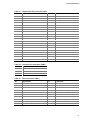
1
Intel® Desktop Board D815EEA Technical Product Specification May 2000 Order Number A16964 –001 The Intel® Desktop Board D815EEA may contain design defects or errors known as errata that may cause the product to deviate from published specifications. Current characterized errata are documented in the Intel Desktop Board D815EEA Specification Update. Revision History Revision Revision History Date -P1 First review draft of the Intel Desktop Board D815EEA Technical Product Specification March 2000 -P2 Second review draft of the Intel Desktop Board D815EEA Technical Product Specification April 2000 -P3 Third review draft of the Intel Desktop Board D815EEA Technical Product Specification June 2000 -001 First release of the Intel Desktop Board D815EEA Technical Product Specification June 2000 This product specification applies to only standard D815EEA boards with BIOS identifier EA81510A.86A. Changes to this specification will be published in the Intel Desktop Board D815EEA Specification Update before being incorporated into a revision of this document. Information in this document is provided in connection with Intel® products. No license, express or implied, by estoppel or otherwise, to any intellectual property rights is granted by this document. Except as provided in Intel’s Terms and Conditions of Sale for such products, Intel assumes no liability whatsoever, and Intel disclaims any express or implied warranty, relating to sale and/or use of Intel products including liability or warranties relating to fitness for a particular purpose, merchantability, or infringement of any patent, copyright or other intellectual property right. Intel products are not intended for use in medical, life saving, or life sustaining applications. Intel may make changes to specifications and product descriptions at any time, without notice. The Intel® Desktop Board D815EEA may contain design defects or errors known as errata that may cause the product to deviate from published specifications. Current characterized errata are available on request. Contact your local Intel sales office or your distributor to obtain the latest specifications before placing your product order. Copies of documents which have an ordering number and are referenced in this document, or other Intel literature, may be obtained from: Intel Corporation P.O. Box 5937 Denver, CO 80217-9808 or call in North America 1-800-548-4725, Europe 44-0-1793-431-155, France 44-0-1793-421-777, Germany 44-0-1793-421-333, other Countries 708-296-9333. † Third-party brands and names are the property of their respective owners. Copyright 2000, Intel Corporation. All rights reserved. Preface This Technical Product Specification (TPS) specifies the board layout, components, connectors, power and environmental requirements, and the BIOS for the Intel Desktop Board D815EEA. It describes the standard product and available manufacturing options. Intended Audience The TPS is intended to provide detailed, technical information about the D815EEA board and its components to the vendors, system integrators, and other engineers and technicians who need this level of information. It is specifically not intended for general audiences. What This Document Contains Chapter 1 2 3 4 5 Description A description of the hardware used on the D815EEA board A map of the resources of the board The features supported by the BIOS Setup program The contents of the BIOS Setup program’s menus and submenus A description of the BIOS error messages, beep codes, POST codes, and diagnostic LEDs Typographical Conventions This section contains information about the conventions used in this specification. Not all of these symbols and abbreviations appear in all specifications of this type. Notes, Cautions, and Warnings ✏ NOTE Notes call attention to important information. CAUTION Cautions are included to help you avoid damaging hardware or losing data. WARNING Warnings indicate conditions, which if not observed, can cause personal injury. iii Intel® Desktop Board D815EEA Technical Product Specification Other Common Notation iv # Used after a signal name to identify an active-low signal (such as USBP0#) (NxnX) When used in the description of a component, N indicates component type, xn are the relative coordinates of its location on the D815EEA board, and X is the instance of the particular part at that general location. For example, J5J1 is a connector, located at 5J. It is the first connector in the 5J area. GB Gigabyte (1,073,741,824 bytes) KB Kilobyte (1024 bytes) Kbit Kilobit (1024 bits) kbits/sec 1000 bits per second MB Megabyte (1,048,576 bytes) MB/sec Megabytes per second Mbit Megabit (1,048,576 bits) Mbit/sec Megabits per second xxh An address or data value ending with a lowercase h indicates a hexadecimal value. x.x V Volts. Voltages are DC unless otherwise specified. † This symbol is used to indicate third-party brands and names that are the property of their respective owners. Contents 1 Product Description 1.1 1.2 1.3 1.4 1.5 1.6 1.7 1.8 1.9 1.10 1.11 1.12 1.13 Overview ................................................................................................................... 12 1.1.1 Feature Summary ....................................................................................... 12 1.1.2 Manufacturing Options ................................................................................ 13 1.1.3 D815EEA Board Layout .............................................................................. 14 1.1.4 Block Diagram ............................................................................................. 15 Online Support........................................................................................................... 16 Design Specifications ................................................................................................ 16 Processor .................................................................................................................. 19 System Memory......................................................................................................... 20 Intel® 815E Chipset ................................................................................................... 22 1.6.1 Intel® 82815E Graphics and Memory Controller Hub (GMCH) .................... 23 1.6.2 Intel® 82801BA I/O Controller Hub (ICH2)................................................... 23 1.6.3 Intel® 82802AB 4 Mbit Firmware Hub (FWH) .............................................. 25 I/O Controller ............................................................................................................. 26 1.7.1 Serial Ports.................................................................................................. 26 1.7.2 Infrared Support .......................................................................................... 26 1.7.3 Parallel Port................................................................................................. 27 1.7.4 Diskette Drive Controller.............................................................................. 27 1.7.5 Keyboard and Mouse Interface ................................................................... 27 Graphics Subsystem ................................................................................................. 28 1.8.1 Integrated Graphics Controller .................................................................... 28 1.8.2 Digital Video Output (DVO) Connector ........................................................ 30 1.8.3 AGP Universal Connector ........................................................................... 31 Audio Subsystem (Optional) ...................................................................................... 32 1.9.1 Basic Audio Subsystem............................................................................... 32 1.9.2 Enhanced PCI Audio Subsystem................................................................. 33 1.9.3 Audio Connectors........................................................................................ 34 LAN Subsystem......................................................................................................... 35 1.10.1 Intel® 82562ET Platform LAN Connect Device (Optional) ........................... 36 1.10.2 RJ-45 LAN Connector LEDs........................................................................ 36 1.10.3 LAN Subsystem Software............................................................................ 36 CNR (Optional) .......................................................................................................... 36 Hardware Management Subsystem (Optional) .......................................................... 37 1.12.1 Hardware Monitor Component .................................................................... 38 1.12.2 Chassis Intrusion Detect Connector ............................................................ 38 1.12.3 Fan Control and Monitoring ......................................................................... 38 Power Management .................................................................................................. 39 1.13.1 Software Support ........................................................................................ 39 1.13.2 Hardware Support ....................................................................................... 42 v Intel® Desktop Board D815EEA Technical Product Specification 2 Technical Reference 2.1 2.2 2.3 2.4 2.5 2.6 2.7 2.8 2.9 2.10 2.11 2.12 2.13 2.14 2.15 Introduction................................................................................................................ 47 Memory Map ............................................................................................................. 47 I/O Map ..................................................................................................................... 48 DMA Channels .......................................................................................................... 50 PCI Configuration Space Map ................................................................................... 50 Interrupts ................................................................................................................... 51 PCI Interrupt Routing Map ......................................................................................... 51 Connectors ................................................................................................................ 53 2.8.1 Back Panel Connectors ............................................................................... 54 2.8.2 Internal I/O Connectors ............................................................................... 58 2.8.3 External I/O Connectors .............................................................................. 69 Jumper Block............................................................................................................. 73 Mechanical Considerations........................................................................................ 75 2.10.1 Form Factor................................................................................................. 75 2.10.2 I/O Shield .................................................................................................... 76 Electrical Considerations ........................................................................................... 77 2.11.1 Power Consumption .................................................................................... 77 2.11.2 Add-in Board Considerations....................................................................... 78 2.11.3 Standby Current Requirements ................................................................... 78 2.11.4 Fan Connector Current Capability ............................................................... 79 2.11.5 Power Supply Considerations...................................................................... 80 Thermal Considerations............................................................................................. 80 Reliability ................................................................................................................... 82 Environmental............................................................................................................ 83 Regulatory Compliance ............................................................................................. 84 2.15.1 Safety Regulations ...................................................................................... 84 2.15.2 EMC Regulations ........................................................................................ 84 2.15.3 Certification Markings.................................................................................. 85 3 Overview of BIOS Features 3.1 3.2 3.3 3.4 3.5 3.6 3.7 3.8 vi Introduction................................................................................................................ 87 BIOS Flash Memory Organization ............................................................................. 88 Resource Configuration ............................................................................................. 88 3.3.1 PCI Autoconfiguration ................................................................................. 88 3.3.2 PCI IDE Support.......................................................................................... 88 System Management BIOS (SMBIOS) ...................................................................... 89 USB Legacy Support ................................................................................................. 90 BIOS Updates............................................................................................................ 90 3.6.1 Language Support....................................................................................... 91 3.6.2 Custom Splash Screen................................................................................ 91 Recovering BIOS Data .............................................................................................. 91 Boot Options.............................................................................................................. 92 3.8.1 CD-ROM and Network Boot ........................................................................ 92 3.8.2 Booting Without Attached Devices .............................................................. 92 Contents Fast Booting Systems with Intel® Rapid BIOS Boot ................................................... 92 3.9.1 Peripheral Selection and Configuration ....................................................... 93 3.9.2 Intel Rapid BIOS Boot ................................................................................. 93 3.9.3 Operating System ....................................................................................... 94 3.10 BIOS Security Features ............................................................................................. 94 3.9 4 BIOS Setup Program 4.1 4.2 4.3 4.4 4.5 4.6 4.7 4.8 Introduction................................................................................................................ 97 Maintenance Menu .................................................................................................... 98 4.2.1 Extended Configuration Submenu............................................................... 99 Main Menu............................................................................................................... 100 Advanced Menu....................................................................................................... 101 4.4.1 PCI Configuration Submenu...................................................................... 102 4.4.2 Boot Configuration Submenu .................................................................... 103 4.4.3 Peripheral Configuration Submenu............................................................ 104 4.4.4 IDE Configuration Submenu...................................................................... 106 4.4.5 Diskette Configuration Submenu ............................................................... 109 4.4.6 Event Log Configuration Submenu............................................................ 110 4.4.7 Video Configuration Submenu................................................................... 111 Security Menu.......................................................................................................... 112 Power Menu ............................................................................................................ 113 Boot Menu ............................................................................................................... 114 4.7.1 IDE Drive Configuration Submenu............................................................. 115 Exit Menu ................................................................................................................ 116 5 Error Messages and Beep Codes 5.1 5.2 5.3 5.4 5.5 5.6 BIOS Error Messages.............................................................................................. 116 Port 80h POST Codes ............................................................................................. 119 Bus Initialization Checkpoints .................................................................................. 123 Speaker ................................................................................................................... 124 BIOS Beep Codes ................................................................................................... 124 Diagnostic LEDs ...................................................................................................... 125 Figures 1. 2. 3. 4. 5. 6. 7. 8. 9. 10. 11. 12. 13. D815EEA Board Components ................................................................................... 14 Block Diagram ........................................................................................................... 15 Intel 815E Chipset Block Diagram ............................................................................. 22 Block Diagram of Basic Audio Subsystem ................................................................. 33 Block Diagram of Enhanced PCI Audio Subsystem ................................................... 33 ICH2 and CNR Signal Interface ................................................................................. 37 Using the Wake on LAN Technology Connector ........................................................ 44 Location of Standby Power Indicator LED ................................................................. 45 Back Panel Connectors ............................................................................................. 54 Audio, Video, Hardware Control, and Fan Connectors .............................................. 59 Add-in Board and Peripheral Interface Connectors.................................................... 63 External I/O Connectors ............................................................................................ 69 Location of the Jumper Block .................................................................................... 73 vii Intel® Desktop Board D815EEA Technical Product Specification 14. 15. 16. 17. D815EEA Board Dimensions..................................................................................... 75 I/O Shield Dimensions ............................................................................................... 76 Localized High Temperature Zones ........................................................................... 81 Diagnostic LEDs ...................................................................................................... 125 Tables 1. 2. 3. 4. 5. 6. 7. 8. 9. 10. 11. 12. 13. 14. 15. 16. 17. 18. 19. 20. 21. 22. 23. 24. 25. 26. 27. 28. 29. 30. 31. 32. 33. 34. 35. 36. 37. 38. 39. 40. viii Feature Summary...................................................................................................... 12 Manufacturing Options............................................................................................... 13 Specifications ............................................................................................................ 16 Supported Processors ............................................................................................... 19 Supported Memory Configurations ............................................................................ 21 Supported Graphics Refresh Frequencies................................................................. 29 LAN Connector LED States ....................................................................................... 36 Effects of Pressing the Power Switch ........................................................................ 40 Power States and Targeted System Power ............................................................... 41 Wake Up Devices and Events ................................................................................... 42 Fan Connector Descriptions ...................................................................................... 43 System Memory Map................................................................................................. 47 I/O Map ..................................................................................................................... 48 DMA Channels .......................................................................................................... 50 PCI Configuration Space Map ................................................................................... 50 Interrupts ................................................................................................................... 51 PCI Interrupt Routing Map ......................................................................................... 52 PS/2 Mouse/Keyboard Connectors............................................................................ 55 LAN Connector .......................................................................................................... 55 USB Connectors........................................................................................................ 55 VGA Port Connector .................................................................................................. 56 Parallel Port Connector.............................................................................................. 56 Serial Port A Connector ............................................................................................. 56 MIDI/Game Port Connector ....................................................................................... 57 Audio Line Out Connector ......................................................................................... 57 Audio Line In Connector ............................................................................................ 57 Mic In Connector ....................................................................................................... 57 Chassis Fan Connector (J3F1) .................................................................................. 60 CD-ROM Legacy Style Connector (J2F2).................................................................. 60 ATAPI CD-ROM Connector (J2F1) ............................................................................ 60 Auxiliary Line In Connector (J2G1) ............................................................................ 60 Telephony Connector (J2G2)..................................................................................... 60 Digital Video Out Connector (J3H1)........................................................................... 61 Processor Fan Connector (J3M1).............................................................................. 61 Power Connector (J8K1) ........................................................................................... 61 Wake on LAN Technology Connector (J6B1) ............................................................ 62 Chassis Intrusion Connector (J7B1) .......................................................................... 62 Chassis Fan Connector (J8B1).................................................................................. 62 CNR Connector (J3A1).............................................................................................. 64 PCI Bus Connectors (J4A1, J4B1, J4C1, J4D1, J4E1) .............................................. 65 Contents 41. 42. 43. 44. 45. 46. 47. 48. 49. 50. 51. 52. 53. 54. 55. 56. 57. 58. 59. 60. 61. 62. 63. 64. 65. 66. 67. 68. 69. 70. 71. 72. 73. 74. 75. 76. 77. 78. 79. 80. 81. 82. 83. 84. 85. 86. 87. AGP Universal Connector (J5E1) .............................................................................. 66 Diskette Drive Connector (J8G3) ............................................................................... 67 PCI IDE Connectors (J8G2, Primary and J6G1, Secondary) ..................................... 68 Front Panel USB Connector (J8C1)........................................................................... 70 Serial Port B Connector (J8E1).................................................................................. 70 SCSI LED Connector (J7A1) ..................................................................................... 70 Auxiliary Front Panel Power LED Connector (J8C2).................................................. 70 Front Panel Connector (J8C3) ................................................................................... 71 States for a Single-Colored Power LED..................................................................... 72 States for a Dual-Colored Power LED ....................................................................... 72 BIOS Setup Configuration Jumper Settings (J7B1) ................................................... 74 Power Usage For Board with Basic Audio and Onboard LAN.................................... 77 Power Usage For Board with Enhanced PCI Audio Subsystem and no Onboard LAN subsystem...................................................................................... 78 Standby Current Requirements ................................................................................. 79 Thermal Considerations for Components .................................................................. 82 D815EEA Board Environmental Specifications .......................................................... 83 Safety Regulations .................................................................................................... 84 EMC Regulations....................................................................................................... 84 Supervisor and User Password Functions ................................................................. 95 BIOS Setup Program Menu Bar................................................................................. 97 BIOS Setup Program Function Keys ......................................................................... 98 Maintenance Menu .................................................................................................... 98 Extended Configuration Submenu ............................................................................. 99 Main Menu............................................................................................................... 100 Advanced Menu....................................................................................................... 101 PCI Configuration Submenu .................................................................................... 102 Boot Configuration Submenu................................................................................... 103 Peripheral Configuration Submenu .......................................................................... 104 IDE Configuration Submenu .................................................................................... 106 Primary/Secondary IDE Master/Slave Submenus.................................................... 107 Diskette Configuration Submenu ............................................................................. 109 Event Log Configuration Submenu .......................................................................... 110 Video Configuration Submenu ................................................................................. 111 Security Menu.......................................................................................................... 112 Power Menu ............................................................................................................ 113 Boot Menu ............................................................................................................... 114 IDE Drive Configuration Submenu ........................................................................... 115 Exit Menu ................................................................................................................ 116 BIOS Error Messages.............................................................................................. 116 Uncompressed INIT Code Checkpoints................................................................... 119 Boot Block Recovery Code Checkpoints ................................................................. 119 Runtime Code Uncompressed in F000 Shadow RAM ............................................. 120 Bus Initialization Checkpoints .................................................................................. 123 Upper Nibble High Byte Functions ........................................................................... 123 Lower Nibble High Byte Functions ........................................................................... 124 Beep Codes............................................................................................................. 125 Diagnostic LED Codes............................................................................................. 126 ix Intel® Desktop Board D815EEA Technical Product Specification x 1 Product Description What This Chapter Contains 1.1 1.2 1.3 1.4 1.5 1.6 1.7 1.8 1.9 1.10 1.11 1.12 1.13 Overview ................................................................................................................... 12 Online Support........................................................................................................... 16 Design Specifications ................................................................................................ 16 Processor .................................................................................................................. 19 System Memory......................................................................................................... 20 Intel® 815E Chipset ................................................................................................... 22 I/O Controller ............................................................................................................. 26 Graphics Subsystem ................................................................................................. 28 Audio Subsystem (Optional) ...................................................................................... 32 LAN Subsystem......................................................................................................... 35 CNR (Optional) .......................................................................................................... 36 Hardware Management Subsystem (Optional) .......................................................... 37 Power Management .................................................................................................. 39 11 Intel® Desktop Board D815EEA Technical Product Specification 1.1 Overview 1.1.1 Feature Summary Table 1 summarizes the D815EEA board’s major features. Table 1. Feature Summary Form Factor ATX (12.0 inches by 8.2 inches) Processor Support for either an Intel® Pentium® III processor in a Flip Chip Pin Grid Array (FC-PGA) package or an Intel® Celeron™ processor in an FCPGA package or a PPGA package Memory • Three 168-pin SDRAM Dual Inline Memory Module (DIMM) sockets • Support for up to 512 MB system memory • Single- or double-sided DIMMs supported Chipset Intel® 815E Chipset, consisting of: • Intel® 82815E Graphics and Memory Controller Hub (GMCH) • Intel® 82801BA I/O Controller Hub (ICH2) • Intel® 82802AB 4 Mbit Firmware Hub (FWH) I/O Control SMSC LPC47M102 LPC bus I/O controller Video • Intel® 82815E integrated graphics support • AGP universal connector supporting 1X, 2X, and 4X AGP cards or a Graphics Performance Accelerator (GPA) • Digital video output (DVO) connector Peripheral Interfaces • Four Universal Serial Bus (USB) ports • Two serial ports • One parallel port • Two IDE interfaces with Ultra DMA, ATA-66/100 support • One diskette drive interface • MIDI/game port • PS/2† keyboard and mouse ports Expansion Capabilities • Five PCI bus add-in card connectors (SMBus routed to PCI bus connector 2) BIOS • Intel/AMI BIOS (resident in the Intel 82802AB 4 Mbit FWH) • One AGP universal connector • Support for Advanced Power Management (APM), Advanced Configuration and Power Interface (ACPI), Plug and Play, and SMBIOS Diagnostic LEDs Four dual-color LEDs on back panel Instantly Available PC • Support for PCI Local Bus Specification Revision 2.2 • Suspend to RAM support • Wake on PS/2 keyboard and USB ports Wake on LAN† Technology Connector 12 Support for system wake up using an add-in network interface card with remote wake up capability For information about Refer to The board’s compliance level with APM, ACPI, Plug and Play, and SMBIOS. Section 1.3, page 16 Product Description 1.1.2 Manufacturing Options Table 2 describes the D815EEA board’s manufacturing options. Table 2. Manufacturing Options Audio Two separate Audio Codec ’97 (AC ’97) compatible audio subsystem options: • A basic audio subsystem that includes the ICH2 component and an Analog Devices AD1885 analog codec, or • An enhanced audio subsystem that includes a Creative Labs ES1373 AC ’97 digital controller and a Crystal Semiconductor CS4297 stereo audio codec. LAN Intel® 82562ET 10/100 Mbit/sec Platform LAN Connect (PLC) device Hardware Monitor Subsystem • Voltage sense to detect out of range values • Chassis intrusion detect connector • Two fan sense inputs used to monitor fan activity Communication and Networking Riser (CNR) One CNR connector (slot shared with PCI bus connector 5) 13 Intel® Desktop Board D815EEA Technical Product Specification 1.1.3 D815EEA Board Layout Figure 1 shows the location of the major components on the D815EEA board. A B CD E F U G T S R H Q P O N M L K J I OM10041 A Creative Labs ES1373 Digital Controller (optional) B C D E F AD1885 audio codec (optional) AGP universal connector DVO connector Back panel connectors Intel 82815E Graphics and Memory Controller Hub (GMCH) G H I J Processor socket DIMM sockets Power connector Diskette drive connector K L M N O P Q R S T U IDE connectors Serial port B connector Intel 82801BA I/O Controller Hub (ICH2) SMSC LPC47M102 I/O Controller Front panel connectors Intel 82802AB 4 Mbit Firmware Hub (FWH) Battery Front panel USB connector Speaker PCI bus add-in card connectors Communication and Networking Riser (CNR) connector (optional) Figure 1. D815EEA Board Components 14 Product Description 1.1.4 Block Diagram Figure 2 is a block diagram of the major functional areas of the D815EEA board. Diagnostic LEDs Primary/ Secondary IDE ATA-33/66/100 USB Processor Socket USB Ports 0 and 1 System Bus USB Ports 2 and 3 815E Chipset SDRAM Bus DIMM Banks (3) 82815E Graphics and Memory Controller Hub (GMCH) AHA Bus 82801BA I/O Controller Hub (ICH2) 82802AB Firmware Hub (FWH) LPC Bus DVO Connector AGP Universal Connector Digital video output Diskette Drive Connector LPC I/O Controller AGP / Display Cache Interface Hardware Monitor (Optional) SMBus Serial Port A Serial Port B Parallel Port PS/2 Mouse PS/2 Keyboard Optional Analog Codec AC Link PCI Bus PCI Slot 1 CSMA/CD Unit Interface PCI Slot 2 Physical Layer Interface CNR Connector LAN Connector PCI Slot 3 PCI Slot 4 Optional PCI Slot 5 Audio Digital Controller AC Link AC ’97 Audio Codec CD-ROM Line In Line Out Mic In Auxiliary Line In Telephony OM10090 Figure 2. Block Diagram 15 Intel® Desktop Board D815EEA Technical Product Specification 1.2 Online Support Find information about the Intel® D815EEA board under “Product Info” or “Customer Support” at these World Wide Web sites: http://www.intel.com/design/motherbd http://support.intel.com/support/motherboards/desktop Find “Processor Data Sheets” or information about “Proper Date Access in Systems with Intel® Motherboards” at these World Wide Web sites: http://www.intel.com/design/litcentr http://support.intel.com/support/year2000 Find information about the ICH addressing at this World Wide Web site: http://developer.intel.com/design/chipsets/datashts/ 1.3 Design Specifications Table 3 lists the specifications applicable to the D815EEA board. Table 3. Specifications Reference Name Specification Title Version, Revision Date, and Ownership The information is available from… AC ‘97 Audio Codec ‘97 Version 2.1, May 1998, Intel Corporation. ftp://download.intel.com/ pc-supp/platform/ac97 ACPI Advanced Configuration and Power Interface Specification Version 1.0b, February 1, 1999, Intel Corporation, Microsoft Corporation, and Toshiba Corporation. http://www.teleport.com/~acpi/ AGP Accelerated Graphics Port Interface Specification Version 2.0, May 4, 1998, Intel Corporation. the Accelerated Graphics Implementers Forum at: http://www.agpforum.org/ AIMM AGP Inline Memory Module Version 0.9, March 2000, Intel Corporation http://developer.intel.com/ technology/memory/aimm/ index.htm (for Graphics Performance Accelerator cards) Intel document order number 298177-003 AMI BIOS American Megatrends BIOS Specification AMIBIOS 99, 1999 American Megatrends, Inc. http://www.amibios.com, or http://www.ami.com/download/ amibios99.pdf APM Advanced Power Management BIOS Interface Specification Version 1.2, February 1996, Intel Corporation, Microsoft Corporation. http://www.microsoft.com/ hwdev/busbios/amp_12.htm continued 16 Product Description Table 3. Specifications (continued) Specification Title Version, Revision Date and Ownership The information is available from… ATA-3 Information Technology AT Attachment-3 Interface, X3T10/2008D Version 6, October 1995, ASC X3T10 Technical Committee. ATA Anonymous FTP Site: ftp://www.dt.wdc.com/ata/ ata-3/ ATAPI Information Technology AT Attachment with Packet Interface Extensions T13/1153D Version 18, August 19, 1998, Contact: T13 Chair, Seagate Technology. T13 Anonymous FTP Site: ftp://fission.dt.wdc.com/ x3t13/project/ d1153r18.pdf ATX ATX Specification Version 2.01, February 1997, Intel Corporation. http://developer.intel.com/ design/motherbd/atx.htm CNR Communication and Network Riser (CNR) Specification Version 1.0, February 7, 2000, Intel Corporation http://developer.intel.com/ technology/cnr/index.htm EPP Enhanced Parallel Port IEEE std 1284.1-1997 Version 1.7, 1997, Institute of Electrical and Electronic Engineers. http://standards.ieee.org/ reading/ieee/std_public/ description/busarch/ 1284.1-1997_desc.html El Torito Bootable CD-ROM format specification Version 1.0, January 25, 1995, Phoenix Technologies Ltd., and IBM Corporation. the Phoenix Web site at: http://www.ptltd.com/techs/ specs.html IrDA† Serial Infrared Physical Layer Link specification Version 1.1, October 17, 1995, Infrared Data Association. Phone: (510) 943-6546 Fax: (510) 943-5600 E-mail: [email protected] LPC Low Pin Count Interface Specification Version 1.0, September 29, 1997, Intel Corporation. http://www.intel.com/ design/chipsets/industry/ lpc.htm PCI PCI Local Bus Specification Version 2.2, December 18, 1998, PCI Special Interest Group. http://www.pcisig.com/ PCI Bus Power Management Interface Specification Version 1.1, December 18, 1998, PCI Special Interest Group. http://www.pcisig.com/ Plug and Play BIOS specification Version 1.0a, May 5, 1994, Compaq Computer Corp., Phoenix Technologies Ltd., and Intel Corporation. http://www.microsoft.com/ hwdev/respec/ pnpspecs.htm Description GPA (see AIMM) Plug and Play continued 17 Intel® Desktop Board D815EEA Technical Product Specification Table 3. Specification Title Version, Revision Date and Ownership The information is available from… PC SDRAM Unbuffered DIMM Specification Revision 1.0, February, 1998, Intel Corporation. http://www.intel.com/ design/chipsets/memory PC SDRAM DIMM Specification Revision 1.5, November, 1997, Intel Corporation. http://www.intel.com/ design/chipsets/memory PC Serial Presence Detect (SPD) Specification Revision 1.2A, December, 1997 Intel Corporation. http://www.intel.com/ design/pcisets/memory SMBIOS System Management BIOS Version 2.3, August 12, 1998, Award Software International Inc., Dell Computer Corporation, Hewlett-Packard Company, Intel Corporation, International Business Machines Corporation, Phoenix Technologies Limited, American Megatrends Inc., and SystemSoft Corporation. http://developer.intel.com/ ial/wfm/design/smbios UHCI Universal Host Controller Interface Design Guide Version 1.1, March 1996, Intel Corporation. http://www.usb.org/ developers USB Universal Serial Bus Specification Version 1.1, September 23, 1998, Compaq Computer Corporation, Intel Corporation, Microsoft Corporation, and NEC. http://www.usb.org/ developers WfM Wired for Management Baseline Version 2.0, December 18, 1998, Intel Corporation. http://developer.intel.com/ ial/WfM/wfmspecs.htm Description SDRAM 18 Specifications (continued) Product Description 1.4 Processor CAUTION The D815EEA board supports processors that have an 18.2 A maximum current draw with a 1.65 to 2.0 V core voltage. Using a processor not in compliance with the above guidelines can damage the processor, the D815EEA board, and the power supply. See the processor’s data sheet for voltage and current usage requirements. The D815EEA board supports a single Pentium III or Celeron processor. The system bus speed is automatically selected. The D815EEA board supports the processors listed in Table 4. Table 4. Supported Processors Type Designation System Bus Frequency L2 Cache Size Pentium III processor in an FC-PGA package 533EB, 600EB, 667, 733, 800EB, 866, and 933 133 MHz 256 KB 500E, 550E, 600E, 650, 700, 750, 800, and 850 100 MHz 256 KB Celeron processor in an FC-PGA package 533A, 566, and 600 66 MHz 128 KB Celeron processor in a PPGA package 500 and 533 66 MHz 128 KB All supported onboard memory can be cached, up to the cachability limit of the processor. See the processor’s data sheet for cachability limits. For information about Refer to Processor support Section 1.2, page 16 Processor data sheets Section 1.2, page 16 19 Intel® Desktop Board D815EEA Technical Product Specification 1.5 System Memory The D815EEA board has three DIMM sockets and supports the following memory features: • 3.3 V (only) 168-pin SDRAM DIMMs with gold-plated contacts • Unbuffered single- or double-sided DIMMs • Maximum system memory: 512 MB; minimum system memory: 32 MB • 133 MHz SDRAM or 100 MHz SDRAM • Serial Presence Detect (SPD) and non-SPD memory • Non-ECC and ECC DIMMs (ECC DIMMs will operate in non-ECC mode only) • Suspend to RAM Table 5 lists the supported DIMM configurations. In the second column of Table 5: • • “DS” refers to double-sided memory modules (containing two rows of SDRAM) “SS” refers to single-sided memory modules (containing one row of SDRAM). When installing memory, note the following: • Non-SPD DIMMs will always revert to a 100 MHz with 3-3-3 timing SDRAM bus. • Mixing Non-SPD DIMMs with SPD DIMMs will always revert to a 100 MHz with 3-3-3 timing SDRAM bus. • The BIOS will not initialize installed memory above 512 MB. At boot, the BIOS displays a message indicating that any installed memory above 512 MB has not been initialized. • Mixed memory speed configurations (133 and 100 MHz) will default to 100 MHz. • 133 MHz SDRAM operation requires a 133 MHz system bus frequency processor. • The board should be populated with no more than four rows of 133 MHz SDRAM (two double-sided or one double-sided plus two single-sided DIMMs) • 100 MHz SDRAM may be populated with six rows of SDRAM (three double-sided DIMMs). ✏ NOTE If more than four rows of 133 MHz SDRAM are populated, the BIOS will initialize installed memory up to 512 MB at 100 MHz. 20 Product Description Table 5. Supported Memory Configurations DIMM Capacity Number of Sides SDRAM Density SDRAM Organization Front-side/Back-side Number of SDRAM devices 32 MB DS 16 Mbit 2MX8/2MX8 16 (Note 1) 32 MB SS 64 Mbit 4 M X 16 / empty 4 48 MB DS 64 / 16 Mbit 4 M X 16 / 2 M X 8 12 (Notes 1 and 2) 64 MB DS 64 Mbit 4 M X 16 / 4 M X 16 8 64 MB SS 64 Mbit 8 M X 8 / empty 8 64 MB SS 128 Mbit 8 M X 16 / empty 4 96 MB DS 64 Mbit 8 M X 8 / 4 M x 16 12 (Notes 1 and 2) 96 MB DS 128 / 64 Mbit 8 M X 16 / 4 M x 16 8 (Notes 1 and 2) 128 MB DS 64 Mbit 8MX8/8MX8 16 (Note 1) 128 MB DS 128 Mbit 8 M X 16 / 8 M X 16 8 (Notes 1 and 2) 128 MB SS 128 Mbit 16 M X 8 / empty 8 128 MB SS 256 Mbit 16 M X 16 / empty 4 192 MB DS 128 Mbit 16 M X 8 / 8 M x 16 12 (Notes 1 and 2) 192 MB DS 128 / 64 Mbit 16 M X 8 / 8 M x 8 16 (Notes 1 and 2) 256 MB DS 128 Mbit 16 M X 8 / 16 M X 8 16 (Notes 1 and 2) 256 MB DS 256 Mbit 16 M X 16 / 16 M X 16 8 (Notes 1 and 2) 256 MB SS 256 Mbit 32 M X 8 / empty 8 512 MB DS 256 Mbit 32 M X 8 / 32 M X 8 16 (Notes 1 and 2) Notes 1. If the number of SDRAM devices is greater than nine, the DIMM will be double sided. 2. Front side population / back side population indicated for SDRAM density and SDRAM organization. CAUTION To be fully compliant with all applicable Intel® SDRAM memory specifications, the motherboard should be populated with DIMMs that support the Serial Presence Detect (SPD) data structure. If your memory modules do not support SPD, you will see a notification to this effect on the screen at power up. The BIOS will attempt to configure the memory controller for normal operation. However, DIMMs may not function under the determined frequency. You can access the PC Serial Presence Detect Specification at: http://www.intel.com/design/pcisets/memory/ 21 Intel® Desktop Board D815EEA Technical Product Specification 1.6 Intel® 815E Chipset The Intel 815E chipset consists of the following devices: • 82815E Graphics and Memory Controller Hub (GMCH) with Accelerated Hub Architecture (AHA) bus • 82801BA I/O Controller Hub (ICH2) with AHA bus • 82802AB Firmware Hub (FWH). The GMCH is a centralized controller for the system bus, the memory bus, the AGP bus, and the Accelerated Hub Architecture interface. The ICH2 is a centralized controller for the board’s I/O paths. The FWH provides the nonvolatile storage of the BIOS as well as hardware-dependent security features. The chipset provides the interfaces shown in Figure 3. ATA-33/66/100 Network System Bus USB SDRAM Bus 815E Chipset 82815E Graphics and Memory Controller Hub (GMCH) Digital video output AGP Interface 82801BA I/O Controller Hub (ICH2) AHA Bus 82802AB Firmware Hub (FWH) LPC Bus SMBus PCI Bus AC Link OM10202 Figure 3. Intel 815E Chipset Block Diagram 22 For information about Refer to The Intel 815E chipset Http://developer.intel.com The resources used by the chipset Chapter 2 The chipset’s compliance with ACPI, APM, AC ‘97 Section 1.3, page 16 Product Description 1.6.1 Intel® 82815E Graphics and Memory Controller Hub (GMCH) The GMCH provides the following: • An integrated Synchronous DRAM memory controller with autodetection of SDRAM • An interface for a single AGP device or a Graphics Performance Accelerator (GPA) card • An interface for a digital video output (DVO) connector for a flat panel, digital CRT, or TV-out • Support for ACPI Rev 1.0 and APM Rev 1.2 compliant power management 1.6.2 Intel® 82801BA I/O Controller Hub (ICH2) The ICH2 provides the following: • 33 MHz PCI bus interface • Support for up to six PCI master devices • Low Pin Count (LPC) interface that supports an LPC-compatible I/O controller • Support for two Master/DMA devices • Integrated IDE controller that supports Ultra DMA (33 MB/sec) and ATA-66/100 mode (66 MB/sec, 100 MB/sec) • Integrated LAN Media Access Controller • Universal Serial Bus interface with two USB controllers providing four ports in a UHCI Implementation • Power management logic for ACPI Rev 1.0b compliance • System Management Bus (SMBus clock and data lines also routed to PCI bus connector 2) • Real-Time Clock with 256-byte battery-backed CMOS RAM • AC’97 digital link for Audio and telephony codecs, including: AC’97 2.1 compliance Logic for PCM in, PCM out, Mic input, Modem in, and Modem out Separate PCI functions for audio and modem Communications Network Riser (CNR) interface 1.6.2.1 IDE Interfaces The ICH2’s IDE controller has two independent bus-mastering IDE interfaces that can be independently enabled. The IDE interfaces support the following modes: • Programmed I/O (PIO): CPU controls data transfer • 8237-style DMA: DMA offloads the CPU, supporting transfer rates of up to 16 MB/sec • Ultra DMA: DMA protocol on IDE bus supporting host and target throttling and transfer rates of up to 33 MB/sec. • Ultra ATA-66: DMA protocol on IDE bus supporting host and target throttling and transfer rates of up to 66 MB/sec. ATA-66 protocol is similar to ATA-33 and is device driver compatible. ATA-66 uses faster timings and requires a specialized cable to reduce reflections, noise, and inductive coupling. • Ultra ATA-100: DMA protocol on IDE bus allows host and target throttling. The ICH2 Ultra ATA-100 logic can achieve read transfer rates up to 100 MB/sec and write transfer rates up to 88 MB/sec. The higher quality cable used for ATA-66 DMA support is adequate to reduce reflections, noise, and inductive coupling for ATA-100 operation. 23 Intel® Desktop Board D815EEA Technical Product Specification The IDE interfaces also support ATAPI devices (such as CD-ROM drives) and ATA devices using the transfer modes listed in Table 70 on page 107. The BIOS supports logical block addressing (LBA) and extended cylinder head sector (ECHS) translation modes. The drive reports the transfer rate and translation mode to the BIOS. The D815EEA board supports laser servo (LS-120) diskette technology through its IDE interfaces. The LS-120 drive can be configured as a boot device by setting the BIOS Setup program’s Boot menu to one of the following: • ARMD-FDD (ATAPI removable media device – floppy disk drive) • ARMD-HDD (ATAPI removable media device – hard disk drive) For information about Refer to The location of the IDE connectors Figure 11, page 63 The signal names of the IDE connectors Table 43, page 68 BIOS Setup program’s Boot menu Table 76, page 114 1.6.2.2 USB The ICH2 contains two separate USB controllers. The D815EEA board has four USB ports; one USB peripheral can be connected to each port. For more than four USB devices, an external hub can be connected to any of the ports. Two of the USB ports are implemented with stacked back panel connectors; the other two are accessible via the front panel USB connector at location J8C1. The D815EEA board fully supports UHCI and uses UHCI-compatible software drivers. ✏ NOTE Computer systems that have an unshielded cable attached to a USB port may not meet FCC Class B requirements, even if no device or a low-speed USB device is attached to the cable. Use shielded cable that meets the requirements for full-speed devices. For information about 24 Refer to The location of the USB connectors on the back panel Figure 9, page 54 The signal names of the back panel USB connectors Table 20, page 55 The location of the front panel USB connector Figure 12, page 69 The signal names of the front panel USB connector Table 44, page 70 The USB specification and UHCI Section 1.3, page 16 Product Description 1.6.2.3 Real-Time Clock, CMOS SRAM, and Battery The real-time clock provides a time-of-day clock and a multicentury calendar with alarm features. The real-time clock supports 256 bytes of battery-backed CMOS SRAM in two banks that are reserved for BIOS use. A coin-cell battery (CR2032) powers the real-time clock and CMOS memory. When the computer is not plugged into a wall socket, the battery has an estimated life of three years. When the computer is plugged in, the standby current from the power supply extends the life of the battery. The clock is accurate to ± 13 minutes/year at 25 ºC with 3.3 VSB applied. The time, date, and CMOS values can be specified in the BIOS Setup program. The CMOS values can be returned to their defaults by using the BIOS Setup program. ✏ NOTE If the battery and AC power fail, standard defaults, not custom defaults, will be loaded into CMOS RAM at power-on. ✏ NOTE The recommended method of accessing the date in systems with D815EEA boards is indirectly from the Real-Time Clock (RTC) via the BIOS. The BIOS on D815EEA boards contains a century checking and maintenance feature. This feature checks the two least significant digits of the year stored in the RTC during each BIOS request (INT 1Ah) to read the date and, if less than 80 (i.e., 1980 is the first year supported by the PC), updates the century byte to 20. This feature enables operating systems and applications using the BIOS date/time services to reliably manipulate the year as a four-digit value. For information about Refer to Proper date access in systems with D815EEA boards Section 1.2, page 16 1.6.3 Intel® 82802AB 4 Mbit Firmware Hub (FWH) The FWH provides the following: • System BIOS • System security and manageability logic that enables protection for storing and updating of platform information 25 Intel® Desktop Board D815EEA Technical Product Specification 1.7 I/O Controller The SMSC LPC47M102 I/O Controller provides the following features: • Low pin count (LPC) interface • 3.3 V operation • Two serial ports • One parallel port with Extended Capabilities Port (ECP) and Enhanced Parallel Port (EPP) support • Serial IRQ interface compatible with serialized IRQ support for PCI systems • PS/2-style mouse and keyboard interfaces • Interface for one 1.2 MB, 1.44 MB, or 2.88 MB diskette drive • Intelligent power management, including a programmable wake up event interface • PCI power management support • IrDA† 1.0 compliant • Fan control: Two fan control outputs Two fan tachometer inputs The BIOS Setup program provides configuration options for the I/O controller. For information about Refer to SMSC LPC47M102 I/O controller http://www.smsc.com 1.7.1 Serial Ports The D815EEA board has two serial ports. Serial port A is located on the back panel. Serial port B is accessible using the connector at location J8E1. The serial ports’ NS16C550-compatible UARTs support data transfers at speeds up to 115.2 kbits/sec with BIOS support. The serial ports can be assigned as COM1 (3F8h), COM2 (2F8h), COM3 (3E8h), or COM4 (2E8h). For information about Refer to The location of the Serial port A connector Figure 9, page 54 The signal names of the Serial port A connector Table 23, page 56 The location of the Serial port B connector Figure 12, page 69 The signal names of the Serial port B connector Table 45, page 70 1.7.2 Infrared Support The front panel connector includes four pins that support Hewlett-Packard HSDL-1000 compatible infrared (IR) transmitters and receivers. In the BIOS Setup program, Serial port B can be directed to a connected IR device. The IR connection can be used to transfer files to or from portable devices like laptops, PDAs, and printers. The Infrared Data Association (IrDA) specification supports data transfers of 115.2 kbits/sec at a distance of 1 meter. 26 Product Description For information about Refer to The location of the front panel connector Figure 12, page 69 The signal names of the front panel connector Table 48, page 71 Configuring serial port B for infrared applications Section 4.4.3, page 104 The IrDA specification Section 1.3, page 16 1.7.3 Parallel Port The connector for the multimode bidirectional parallel port is a 25-pin D-Sub connector located on the back panel. In the BIOS Setup program, the parallel port can be configured for the following: • Output only (PC AT†-compatible mode) • Bi-directional (PS/2 compatible) • EPP • ECP For information about Refer to The location of the parallel port connector Figure 9, page 54 The signal names of the parallel port connector Table 22, page 56 1.7.4 Diskette Drive Controller The I/O controller supports one diskette drive that is compatible with the 82077 diskette drive controller and supports both PC-AT and PS/2 modes. For information about Refer to The location of the diskette drive connector Figure 11, page 63 The signal names of the diskette drive connector Table 42, page 67 The supported diskette drive capacities and sizes Table 71, page 109 1.7.5 Keyboard and Mouse Interface PS/2 keyboard and mouse connectors are located on the back panel. The +5 V lines to these connectors are protected with a PolySwitch† circuit that, like a self-healing fuse, reestablishes the connection after an overcurrent condition is removed. ✏ NOTE The keyboard is supported in the bottom PS/2 connector and the mouse is supported in the top PS/2 connector. Power to the computer should be turned off before a keyboard or mouse is connected or disconnected. The keyboard controller contains the AMI keyboard and mouse controller code, provides the keyboard and mouse control functions, and supports password protection for power-on/reset. A power-on/reset password can be specified in the BIOS Setup program. The keyboard controller also supports the hot-key sequence <Ctrl><Alt><Del> for a software reset (operating system dependent). This key sequence resets the computer’s software by jumping to the beginning of the BIOS code and running the power-on self-test (POST). 27 Intel® Desktop Board D815EEA Technical Product Specification For information about Refer to The location of the keyboard and mouse connectors Figure 9, page 54 The signal names of the keyboard and mouse connectors Table 18, page 55 1.8 Graphics Subsystem The 815E chipset contains two separate, mutually exclusive graphics options. Either the integrated graphics controller (contained within the 82815E GMCH) is used, or an add-in AGP adapter can be used. The GMCH includes an integrated display cache SDRAM controller that supports a Graphics Performance Accelerator (GPA) card. The GPA card is a 32-bit 133 MHz 4 MB SDRAM array for enhanced integrated 2D and 3D graphics performance. This interface is multiplexed between the display cache interface and the AGP connector. When an AGP card is installed, the integrated graphics controller is disabled and the display cache interface is not used. For information about Refer to GPA support Section 1.8.3.1, page 31 1.8.1 Integrated Graphics Controller The GMCH features the following: • Integrated graphics controller 3-D Hyper pipelined architecture Full 2-D hardware acceleration Motion video acceleration • 3-D graphics visual and texturing enhancement • Display Integrated 24-bit 230 MHz RAMDAC Display Data Channel Standard, Version 3.0, Level 2B protocols compliant • Video • Hardware motion compensation for software MPEG2 decode Software DVD at 30 fps Integrated graphics memory controller Table 6 lists the refresh frequencies supported by the graphics subsystem. 28 Product Description Table 6. Supported Graphics Refresh Frequencies Resolution Color Palette Available Refresh Frequencies (Hz) Notes 320 x 200 256 colors 70 D 64 K colors 70 D3 16 M colors 70 D 256 colors 70 D 64 K colors 70 D3 320 x 240 352 x 480 352 x 576 400 x 300 512 x 384 640 x 400 640 x 480 16 M colors 70 D 256 colors 70 D 64 K colors 70 D3 16 M colors 70 D 256 colors 70 D 64 K colors 70 D3 16 M colors 70 D 256 colors 70 D 64 K colors 70 D3 16 M colors 70 D 256 colors 70 D 64 K colors 70 D3 16 M colors 70 D 256 colors 70 D 64 K colors 70 D3 16 M colors 70 D 256 colors 60, 70, 72, 75, 85 KDO 64 K colors 60, 75, 85 KD3O 64 K colors 70, 72 KDO 640 x 480 16 M colors 60, 70, 72, 75, 85 KDO 800 x 600 256 colors 60, 70, 72, 75, 85 KDO 64 K colors 60, 70, 72, 75, 85 KD3O 16 M colors 60, 70, 72, 75, 85 KDO 256 colors 60, 70, 75, 85 KDO 64 K colors 60, 70, 75 KD3O 64 K colors 85 KD3 16 M colors 60, 70, 75, 85 KD 1024 x 768 continued 29 Intel® Desktop Board D815EEA Technical Product Specification Table 6. Supported Graphics Refresh Frequencies (continued) Resolution Color Palette Available Refresh Frequencies (Hz) Notes 1152 x 864 256 colors 60, 70, 72, 75 KDO 256 colors 85 KD 64 K colors 60, 70 KD3O 64 K colors 72, 75, 85 KD3 16 M colors 60 KDO 16 M colors 75, 85 KD 256 colors 60 (reduced blanking) KDOF 64 K colors 60 (reduced blanking) KD3F 1280 x 768 1280 x 1024 1600 x 1200 Notes: 16 M colors 60 (reduced blanking) KDF 256 colors 60 KDO 256 colors 70, 72, 75, 85 KD 64 K colors 60, 70, 72, 75, 85 KD3 16 M colors 60, 70, 75, 85 KD 256 colors 60, 70, 72, 75 KD K = Desktop D = DirectDraw 3 = Direct3D and OpenGL O = Overlay F = Digital Display Device only. A mode will be supported on both analog CRTs and digital display devices (the KD3O flags above apply to both types of displays), unless indicated otherwise. For information about Refer to Obtaining graphics software and utilities Section 1.2, page 16 1.8.2 Digital Video Output (DVO) Connector The board routes the Intel 82815E GMCH DVO port to an onboard 40-pin DVO connector. The DVO connector can be cabled to a DVI or TV out card to enable digital displays or TV out functionality. The Digital Visual Interface (DVI) specification provides a high-speed digital connection for visual data types when using the integrated graphics controller. This interface is active only when the integrated graphics controller is enabled. The DVI interface allows interfacing with a discrete Transmission Minimized Differential Signaling (TMDS) transmitter to enable platform support for DVI compliant digital displays or with a discrete TV encoder for TV Out functionality. 30 For information about Refer to The location of the DVO connector Figure 10, page 59 The signal names of the DVO connector Table 33, page 61 Product Description 1.8.3 AGP Universal Connector The AGP universal connector supports either: • Graphics Performance Accelerator (GPA) cards with 133 MHz SDRAM display cache • AGP add-in cards with either 3.3 V or 1.5 V I/O For information about Refer to The location of the AGP universal connector Figure 11, page 63 The signal names of the AGP universal connector Table 41, page 66 1.8.3.1 Graphics Performance Accelerator (GPA) Support The Intel 815E GMCH display cache is a single channel 32-bit wide SDRAM interface. The 4 MB display cache resides on a GPA card that plugs into the AGP connector. The BIOS detects a GPA card if present in the AGP port and initializes it as display cache memory. When a GPA card is initialized, the BIOS allocates 1 MB of system memory to support the internal display device operation. 1.8.3.2 Dynamic Video Memory Technology (DVMT) DVMT enables enhanced graphics and memory performance through Direct AGP, and highly efficient memory utilization. DVMT ensures the most efficient use of all available memory for maximum 2D/3D graphic performance. DVMT is implemented on the D815EEA board with a GPA (Graphics Performance Accelerator) card installed in the AGP port. ✏ NOTE In earlier documentation, the GPA card was referred to as the AGP Inline Memory Module (AIMM). DVMT technology uses 1 MB of system physical memory for compatibility with legacy applications. An example of this would be when using VGA graphics under DOS. Once loaded, the operating system and graphics drivers allocate the buffers needed for performing graphics functions. When the 4 MB GPA card is installed, the Z-buffer and GDI data are managed directly from this dedicated graphics memory thereby avoiding operating system memory manager calls and improving performance. At system BIOS POST, the BIOS displays either the amount of physical memory allocated for display cache or the size of the GPA card (4 MB) if installed. Operating systems such as Windows NT† 4.0 and Windows† 2000 may display the maximum amount of frame buffer memory possible based on the system memory configuration. 31 Intel® Desktop Board D815EEA Technical Product Specification 1.8.3.3 AGP Add-in Card Support AGP is a high-performance interface for graphics-intensive applications, such as 3D applications. While based on the PCI Local Bus Specification, Rev. 2.1, AGP is independent of the PCI bus and is intended for exclusive use with graphical display devices. AGP overcomes certain limitations of the PCI bus related to handling large amounts of graphics data with the following features: • Pipelined memory read and write operations that hide memory access latency • Demultiplexing of address and data on the bus for nearly 100 percent efficiency For information about Refer to Obtaining the Accelerated Graphics Port Interface Specification Section 1.3, page 16 1.9 Audio Subsystem (Optional) The D815EEA board offers two separate audio subsystems. Both audio subsystems include these features: • Split digital/analog architecture for improved S/N (signal-to-noise) ratio: ≥ 85 dB • Power management support for APM 1.2 and ACPI 1.0 (driver dependant) • 3-D stereo enhancement Both audio subsystems support the following audio connectors: • Inputs: Three analog line-level stereo inputs for connection from line in, CD, and auxiliary line in Two analog line-level inputs for speakerphone One mono microphone input • Outputs: Stereo line-level output Mono output for speakerphone 1.9.1 Basic Audio Subsystem The basic audio subsystem consists of the following: • • Intel 82801BA I/O Controller Hub (ICH2) Analog Devices AD1885 analog codec Figure 4 is a block diagram of the basic audio subsystem. The basic audio subsystem supports the following features: • 94 dB signal-to-noise ratio sound quality • Playback sample rates up to 48 kHz • 64 voice synthesizer • Software compatible with Windows 98 Gold and SE, Windows 2000, and Windows NT 4.0 • Full-duplex operation at asynchronous hardware record/playback samples rates • Frequency response: 20 Hz to 20 kHz (+- 0.1 dB) • ACPI and APM power management compliant 32 Product Description 82801BA I/O Controller Hub (ICH2) LPC Bus SMSC LPC47M102 I/O Controller Analog Devices AD1885 Analog Codec AC ’97 Link Game Port MIDI Interface CD-ROM Line In Audio In Mic In Modem Audio Line Out OM10226 Figure 4. Block Diagram of Basic Audio Subsystem 1.9.2 Enhanced PCI Audio Subsystem The D815EEA board offers an optional subsystem of AC ’97 V 1.03 compliant audio features supported by the Creative Labs ES1373 digital controller with Crystal Semiconductor CS4297 (A) codec. Figure 5 is a block diagram of the enhanced PCI audio subsystem. Analog Codec (Crystal Semiconductor CS4297(A)) 82801BA I/O Controller Hub (ICH2) CNR Connector AC ’97 Link CD-ROM Line In Audio In Mic In Modem Audio Line Out AC ’97 Link PCI Bus Digital Controller (Creative Labs ES1373) Game Port MIDI Interface OM10227 Figure 5. Block Diagram of Enhanced PCI Audio Subsystem The Creative Labs ES1373 digital controller with the Crystal Semiconductor CS4297 (A) codec support the following features: • Creative Labs ES1373 AC ’97 V1.03 Digital Controller: PCI 2.1 compliant PCI bus master for PCI audio 64-voice wavetable synthesizer Aureal A3D† API, Sound Blaster Pro†, Roland MPU-401 MIDI, and joystick compatible Ensoniq 3D positional audio and Microsoft† DirectSound† 3D support 33 Intel® Desktop Board D815EEA Technical Product Specification • Crystal Semiconductor CS4297 (A) Stereo Audio Codec: 20-bit stereo digital-to-analog and 18-bit stereo analog-to-digital converters High performance 18-bit stereo full-duplex audio codec with up to 48 kHz sampling rate Connects to the ES1373 digital controller using a five-wire digital interface For information about Refer to Obtaining audio software and utilities Section 1.2, page 16 1.9.3 Audio Connectors The audio connectors include the following: • CD-ROM (legacy-style 2-mm connector) • ATAPI-style connectors: CD-ROM Telephony • Auxiliary line in Back panel audio connectors: MIDI/Game Port Line out Line in Mic in For information about Refer to The back panel audio connectors Section 2.8.1, page 54 CAUTION The pins on both the legacy-style 2-mm and the ATAPI CD-ROM connectors are wired to the same inputs on the audio mixer. Do not attach CD-ROM drives to both connectors. Otherwise, the board could be damaged. 1.9.3.1 CD-ROM (Legacy-style 2-mm) Audio Connector A 1 x 4-pin legacy-style 2-mm connector connects an internal CD-ROM drive to the audio mixer. 34 For information about Refer to The location of the legacy-style 2-mm connector Figure 10, page 59 The signal names of the legacy-style 2-mm connector Table 39, page 60 Product Description 1.9.3.2 ATAPI CD-ROM Audio Connector A 1 x 4-pin ATAPI-style connector connects an internal ATAPI CD-ROM drive to the audio mixer. For information about Refer to The location of the ATAPI CD-ROM connector Figure 10, page 59 The signal names of the ATAPI CD-ROM connector Table 30, page 60 1.9.3.3 Telephony Connector A 1 x 4-pin ATAPI-style connector connects the monoaural audio signals of an internal telephony device to the audio subsystem. A monaural audio-in and audio-out signal interface is necessary for telephony applications such as speakerphones, fax/modems, and answering machines. For information about Refer to The location of the telephony connector Figure 10, page 59 The signal names of the telephony connector Table 32, page 60 1.9.3.4 Auxiliary Line In Connector A 1 x 4-pin ATAPI-style connector connects the left and right channel signals of an internal audio device to the audio subsystem. For information about Refer to The location of the auxiliary line in connector Figure 10, page 59 The signal names of the auxiliary line in connector Table 31, page 60 1.10 LAN Subsystem The Network Interface Controller subsystem consists of the ICH2 (with integrated LAN Media Access Controller) and a physical layer interface device. Feature of the LAN subsystem include: • PCI Bus Master Interface • CSMA/CD Protocol Engine • Serial CSMA/CD unit interface that supports the following physical layer interface devices: 82562ET onboard LAN 82562ET/MT (10/100 Mbit/sec Ethernet) on CNR bus • 82562EH (1 Mbit/sec HomePNA†) on CNR bus PCI Power Management Supports APM Supports ACPI technology Supports Wake up from suspend state (Wake on LAN† technology) 35 Intel® Desktop Board D815EEA Technical Product Specification 1.10.1 Intel® 82562ET Platform LAN Connect Device (Optional) The Intel 82562ET component provides an interface to the back panel RJ-45 connector with integrated LEDs. This physical interface may alternately be provided via the CNR connector. The Intel 82562ET provides the following functions: • Basic 10/100 Ethernet LAN Connectivity • Supports RJ-45 connector with status indicator LEDs • Full driver compatibility • Advanced Power Management support • Programmable transit threshold • Configuration EEPROM that contains the MAC address 1.10.2 RJ-45 LAN Connector LEDs Two LEDs are built into the RJ-45 LAN connector. Table 7 describes the LED states when the board is powered up and the LAN subsystem is operating. Table 7. LAN Connector LED States LED Color LED State Condition Green Off 10 Mbit/sec data rate is selected. On 100 Mbit/sec date rate is selected. Yellow Off LAN link is not established. On (steady state) LAN link is established. On (brighter and pulsing) The computer is communicating with another computer on the LAN. 1.10.3 LAN Subsystem Software LAN software and drivers are available from Intel’s World Wide Web site. For information about Refer to Obtaining LAN software and drivers Section 1.2, page 16 1.11 CNR (Optional) The CNR connector supports the audio, modem, USB, and LAN interfaces of the Intel 815E chipset. Figure 6 shows the signal interface between the riser and the ICH2. 36 AC ’97 Interface Intel 82801BA I/O Controller Hub (ICH2) LAN Interfaces SMBus USB Power CNR Connector Product Description Communication and Networking Riser (Up to two AC ’97 codecs and one LAN device) OM10412 Figure 6. ICH2 and CNR Signal Interface ✏ NOTE The USB interface from the ICH2 to the CNR is not supported on this board. The interfaces supported by the CNR connector include (but are not limited to) the following: • AC ’97 interface: supports audio and/or modem functions on the CNR board. • LAN interfaces: provides one of two LAN interfaces for networking functions. Interfaces include an eight-pin interface for use with Platform LAN Connection (PLC) based devices, and a 17-pin interface for Media Independent Interface (MII) based devices (commonly referred to as a PHY). • SMBus interface: provides Plug-and-Play functionality for the CNR board. The CNR connector includes power signals required for power management and for CNR board operation. 1.12 Hardware Management Subsystem (Optional) The hardware management features enable the board to be compatible with the Wired for Management (WfM) specification. The board has several hardware management features, including the following: • Hardware monitoring • Chassis intrusion detect connector • Fan control and monitoring (implemented on the SMSC LPC47M102 I/O controller) For information about Refer to The WfM specification Table 3, page 16 Fan control functions of the SMSC LPC47M102 I/O controller Section 1.11, page 36 37 Intel® Desktop Board D815EEA Technical Product Specification 1.12.1 Hardware Monitor Component The hardware monitor component provides low-cost instrumentation capabilities. The features of the component include: • Internal ambient temperature sensing • Remote thermal diode sensing for direct monitoring of processor temperature (if supported in the processor) • Power supply monitoring (+12, +5, +3.3, +2.5, 3.3 VSB, VCCP) to detect levels above or below acceptable values • SMBus interface 1.12.2 Chassis Intrusion Detect Connector The board supports a chassis security feature that detects if the chassis cover is removed and sounds an alarm through the onboard speaker. For the chassis intrusion circuit to function, the chassis’ power supply must be connected to AC power. The security feature uses a mechanical switch on the chassis that attaches to the chassis intrusion detect connector. The mechanical switch is closed for normal computer operation. For information about Refer to The location of the chassis intrusion detect connector Figure 10, page 59 The signal names of the chassis intrusion detect connector Table 37, page 62 1.12.3 Fan Control and Monitoring The SMSC LPC47M102 I/O controller provides two fan control outputs and two fan tachometer inputs. Monitoring and control can be implemented using third-party software. 38 For information about Refer to The functions of the fan connectors Section 1.13.2.2, page 43 The location of the fan connectors Figure 10, page 59 The signal names of the fan connectors Section 2.8.2.2, page 59 Product Description 1.13 Power Management Power management is implemented at several levels, including: • Software support: • Advanced Power Management (APM) Advanced Configuration and Power Interface (ACPI) Hardware support: Power connector Fan connectors Wake on LAN technology Instantly Available technology Resume on Ring Wake from USB Wake on Keyboard Wake on PME# 1.13.1 Software Support The software support for power management includes: • APM • ACPI If the D815EEA board is used with an ACPI-aware operating system, the BIOS can provide ACPI support. Otherwise, it defaults to APM support. 1.13.1.1 APM APM makes it possible for the computer to enter an energy-saving standby mode. The standby mode can be initiated in the following ways: • Time-out period specified in the BIOS Setup program • From the operating system, such as the Standby menu item in Windows 98 In standby mode, the D815EEA board can reduce power consumption by spinning down hard drives, and reducing power to, or turning off of, VESA† DPMS-compliant monitors. Power management mode can be enabled or disabled in the BIOS Setup program. While in standby mode, the system retains the ability to respond to external interrupts and service requests, such as incoming faxes or network messages. Any keyboard or mouse activity brings the system out of standby mode and immediately restores power to the monitor. 39 Intel® Desktop Board D815EEA Technical Product Specification The BIOS enables APM by default; but the operating system must support an APM driver for the power management features to work. For example, Windows 98 supports the power management features upon detecting that APM is enabled in the BIOS. For information about Refer to Enabling or disabling power management in the BIOS Setup program Section 4.6, page 112 The D815EEA board’s compliance level with APM Table 3, page 16 1.13.1.2 ACPI ACPI gives the operating system direct control over the power management and Plug and Play functions of a computer. The use of ACPI with the D815EEA board requires an operating system that provides full ACPI support. ACPI features include: • Plug and Play (including bus and device enumeration) and APM support normally contained in the BIOS • Power management control of individual devices, add-in boards (some add-in boards may require an ACPI-aware driver), video displays, and hard disk drives • Methods for achieving less than 30-watt system operation in the power-on/standby sleeping state • A Soft-off feature that enables the operating system to power-off the computer • Support for multiple wake up events (see Table 10 on page 42) • Support for a front panel power and sleep mode switch. Table 8 lists the system states based on how long the power switch is pressed, depending on how ACPI is configured with an ACPI-aware operating system. Table 8. Effects of Pressing the Power Switch If the system is in this state… …and the power switch is pressed for Off (ACPI G2/G5 – Soft off) Less than four seconds …the system enters this state Power-on (ACPI G0 – working state) On (ACPI G0 – working state) Less than four seconds Soft-off/Standby (ACPI G1 – sleeping state) On (ACPI G0 – working state) More than four seconds Fail safe power-off Sleep (ACPI G1 – sleeping state) Less than four seconds Wake up Sleep (ACPI G1 – sleeping state) More than four seconds (ACPI G2/G5 – Soft off) 40 (ACPI G0 – working state) Power-off (ACPI G2/G5 – Soft off) For information about Refer to The D815EEA board’s compliance level with ACPI Section 1.3, page 16 Product Description 1.13.1.2.1 System States and Power States Under ACPI, the operating system directs all system and device power state transitions. The operating system puts devices in and out of low-power states based on user preferences and knowledge of how devices are being used by applications. Devices that are not being used can be turned off. The operating system uses information from applications and user settings to put the system as a whole into a low-power state. Table 9 lists the power states supported by the D815EEA board along with the associated system power targets. See the ACPI specification for a complete description of the various system and power states. Table 9. Power States and Targeted System Power Targeted System Power (Note 1) Global States Sleeping States CPU States Device States G0 – working state S0 – working C0 – working D0 – working state Full power > 30 W G1 – sleeping state S1 – CPU stopped C1 – stop grant D1, D2, D3 – device specification specific. 5 W < power < 30 W G1 – sleeping state S3 – Suspend to RAM. Context saved to RAM. No power D3 – no power except for wake up logic. Power < 5 W (Note 2) G2/S5 S5 – Soft off. Context not saved. Cold boot is required. No power D3 – no power except for wake up logic. Power < 5 W (Note 2) G3 – mechanical off No power to the system. No power D3 – no power for wake up logic, except when provided by battery or external source. No power to the system so that service can be performed. AC power is disconnected from the computer. Notes: 1. Total system power is dependent on the system configuration, including add-in boards and peripherals powered by the system chassis’ power supply. 2. Dependent on the standby power consumption of wake-up devices used in the system. 41 Intel® Desktop Board D815EEA Technical Product Specification 1.13.1.2.2 Wake Up Devices and Events Table 10 lists the devices or specific events that can wake the computer from specific states. Table 10. These devices/events can wake up the computer… …from this state Power switch S1, S3, S5 RTC alarm S1, S3, S5 LAN S1, S3, S5 (Note) PME# S1, S3, S5 (Note) Modem (back panel Serial Port A) S1, S3 IR command S1, S3 USB S1, S3 PS/2 keyboard S1, S3 Note: ✏ Wake Up Devices and Events For LAN and PME#, S5 is disabled by default in the BIOS Setup program. Setting this option to Power On will enable a wake-up event from LAN in the S5 state. NOTE The use of these wake up events from an ACPI state requires an operating system that provides full ACPI support. In addition, software, drivers, and peripherals must fully support ACPI wake events. 1.13.1.2.3 Plug and Play In addition to power management, ACPI provides controls and information so that the operating system can facilitate Plug and Play device enumeration and configuration. ACPI is used only to enumerate and configure D815EEA board devices that do not have other hardware standards for enumeration and configuration. PCI devices on the D815EEA board, for example, are not enumerated by ACPI. 1.13.2 Hardware Support CAUTION If the Wake on LAN and Instantly Available technology features are used, ensure that the power supply provides adequate +5 V standby current. Failure to do so can damage the power supply. The total amount of standby current required depends on the wake devices supported and manufacturing options. Refer to Section 2.11.3 on page 78 for additional information. The board provides several hardware features that support power management, including: • Power connector • Fan connectors • Wake on LAN technology • Instantly Available technology • Resume on Ring • Wake from USB • Wake from PS/2 keyboard • PME# wakeup support 42 Product Description Wake on LAN technology and Instantly Available technology require power from the +5 V standby line. The sections discussing these features describe the incremental standby power requirements for each. Resume on Ring enables telephony devices to access the computer when it is in a power-managed state. The method used depends on the type of telephony device (external or internal) and the power management mode being used (APM or ACPI). ✏ NOTE The use of Resume on Ring, and Wake from USB technologies from an ACPI state requires an operating system that provides full ACPI support. 1.13.2.1 Power Connector When used with an ATX-compliant power supply that supports remote power on/off, the D815EEA board can turn off the system power through software control. To enable soft-off control in software, advanced power management must be enabled in the BIOS Setup program and in the operating system. When the system BIOS receives the correct APM command from the operating system, the BIOS turns off power to the computer. With soft-off enabled, if power to the computer is interrupted by a power outage or a disconnected power cord, when power resumes, the computer returns to the power state it was in before power was interrupted (on or off). The computer’s response can be set using the After Power Failure feature in the BIOS Setup program’s Boot menu. For information about Refer to The location of the power connector Figure 10, page 59 The signal names of the power connector Table 35, page 61 The BIOS Setup program’s Boot menu Table 76, page 114 The ATX specification Section 1.3, page 16 1.13.2.2 Fan Connectors The D815EEA board has three fan connectors. The functions of these connectors are described in Table 11. Table 11. Fan Connector Descriptions Connector Function System fan (fan 1) Provides +12 V DC for a system or chassis fan. The fan voltage can be switched on or off, depending on the power management state of the computer. A tachometer feedback connection is also provided. Power supply fan control (fan 2) Provides +12 V DC for a system or chassis fan. The fan voltage can be switched on or off, depending on the power management state of the computer. A tachometer feedback connection is also provided. Processor fan (fan 3) Provides +12 V DC for a processor fan or active fan heatsink. 43 Intel® Desktop Board D815EEA Technical Product Specification For information about Refer to The location of the fan connectors Figure 10, page 59 The signal names of the fan connectors Section 2.8.2.2, page 59 1.13.2.3 Wake on LAN Technology CAUTION For Wake on LAN technology, the 5-V standby line for the power supply must be capable of providing adequate +5 V standby current. Failure to provide adequate standby current when implementing Wake on LAN technology can damage the power supply. Refer to Section 2.11.3 on page 78 for additional information. Wake on LAN technology enables remote wakeup of the computer through a network. The LAN subsystem PCI bus network adapter monitors network traffic at the Media Independent Interface. Upon detecting a Magic Packet† frame, the LAN subsystem asserts a wakeup signal that powers up the computer. Depending on the LAN implementation, the D815EEA board supports Wake on LAN technology in the following ways: • Through the Wake on LAN technology connector (APM only) • Through the PCI bus PME# signal for PCI 2.2 compliant LAN designs (ACPI only) • Through the onboard LAN subsystem when enabled in Setup (ACPI only) The Wake on LAN technology connector can be used with PCI bus network adapters that have a remote wake up connector, as shown in Figure 7. Network adapters that are PCI 2.2 compliant assert the wakeup signal through the PCI bus signal PME# (pin A19 on the PCI bus connectors). Network Interface Card Remote Wake up connector Wake on LAN technology connector PCI Slot Desktop Board OM09129 Figure 7. Using the Wake on LAN Technology Connector For information about 44 Refer to The location of the Wake on LAN technology connector Figure 10, page 59 The signal names of the Wake on LAN technology connector Table 36, page 62 Product Description 1.13.2.4 Instantly Available Technology CAUTION For Instantly Available technology, the 5-V standby line for the power supply must be capable of providing adequate +5 V standby current. Failure to provide adequate standby current when implementing Instantly Available technology can damage the power supply. Refer to Section 2.11.3 on page 78 for additional information. Instantly Available technology enables the D815EEA board to enter the ACPI S3 (Suspend-toRAM) sleep-state. While in the S3 sleep-state, the computer will appear to be off (the power supply is off, the fans are off, and the front panel LED is amber if dual-color, or off if singlecolor.) When signaled by a wake-up device or event, the system quickly returns to its last known wake state. Table 10 on page 42 lists the devices and events that can wake the computer from the S3 state. The D815EEA board supports the PCI Bus Power Management Interface Specification. For information on the versions of this specification, see Section 1.3. Add-in boards that also support this specification can participate in power management and can be used to wake the computer. The use of Instantly Available technology requires operating system support and PCI 2.2 compliant add-in cards and drivers. The standby power indicator LED shows that power is still present at the DIMM and PCI bus connectors, even when the computer appears to be off. Figure 8 shows the location of the standby power indicator LED. CR5G1 OM10042 Figure 8. Location of Standby Power Indicator LED 45 Intel® Desktop Board D815EEA Technical Product Specification 1.13.2.5 Resume on Ring The operation of Resume on Ring can be summarized as follows: • Resumes operation from either the APM sleep mode or the ACPI S1 state • Requires only one call to access the computer • Detects incoming call similarly for external and internal modems • Requires modem interrupt be unmasked for correct operation 1.13.2.6 Wake from USB USB bus activity wakes the computer from an ACPI S1 or S3 state. ✏ NOTE Wake from USB requires the use of a USB peripheral that supports Wake from USB. 1.13.2.7 Wake from PS/2 Keyboard PS/2 keyboard activity wakes the computer from an ACPI S1 or S3 state. 1.13.2.8 PME# Wakeup Support When the PME# signal on the PCI bus is asserted, the computer wakes from an ACPI S1 or S3 state. 46 2 Technical Reference What This Chapter Contains 2.1 2.2 2.3 2.4 2.5 2.6 2.7 2.8 2.9 2.10 2.11 2.12 2.13 2.14 2.15 Introduction................................................................................................................ 47 Memory Map ............................................................................................................. 47 I/O Map ..................................................................................................................... 48 DMA Channels .......................................................................................................... 50 PCI Configuration Space Map ................................................................................... 50 Interrupts ................................................................................................................... 51 PCI Interrupt Routing Map ......................................................................................... 51 Connectors ................................................................................................................ 53 Jumper Block............................................................................................................. 73 Mechanical Considerations........................................................................................ 75 Electrical Considerations ........................................................................................... 77 Thermal Considerations............................................................................................. 80 Reliability ................................................................................................................... 82 Environmental............................................................................................................ 83 Regulatory Compliance ............................................................................................. 84 2.1 Introduction Sections 2.2 - 2.6 contain several standalone tables. Table 12 describes the system memory map, Table 13 shows the I/O map, Table 14 lists the DMA channels, Table 15 defines the PCI configuration space map, and Table 16 describes the interrupts. The remaining sections in this chapter are introduced by text found with their respective section headings. 2.2 Memory Map Table 12. System Memory Map Address Range (decimal) Address Range (hex) Size Description 1024 K - 524288 K 100000 - 1FFFFFFF 511 MB Extended memory 960 K - 1024 K F0000 - FFFFF 64 KB Runtime BIOS 896 K - 960 K E0000 - EFFFF 64 KB Reserved 800 K - 896 K C8000 - DFFFF 96 KB Available high DOS memory (open to the PCI bus) 640 K - 800 K A0000 - C7FFF 160 KB Video memory and BIOS 639 K - 640 K 9FC00 - 9FFFF 1 KB Extended BIOS data (movable by memory manager software) 512 K - 639 K 80000 - 9FBFF 127 KB Extended conventional memory 0 K - 512 K 00000 - 7FFFF 512 K Conventional memory 47 Intel® Desktop Board D815EEA Technical Product Specification 2.3 I/O Map Table 13. I/O Map Address (hex) Size Description 0000 - 000F 0020 - 0021 0040 - 0043 0060 0061 0064 0070 - 0071 0072 - 0073 0080 - 008F 0092 00A0 - 00A1 00B2 - 00B3 00C0 - 00DF 00F0 0170 - 0177 01F0 - 01F7 16 bytes 2 bytes 4 bytes 1 byte 1 byte 1 byte 2 bytes 2 bytes 16 bytes 1 byte 2 bytes 2 bytes 32 bytes 1 byte 8 bytes 8 bytes DMA controller Programmable Interrupt Control (PIC) System timer Keyboard controller byte—reset IRQ System speaker Keyboard controller, CMD / STAT byte System CMOS / Real Time Clock System CMOS DMA controller Fast A20 and PIC PIC APM control DMA Numeric data processor Secondary IDE channel Primary IDE channel One of these ranges: 0200 - 0207 0208 - 020F 0210 - 0217 0218 - 021F Can vary from 1 byte to 8 bytes Audio / game port One of these ranges: Audio (Sound Blaster Pro-compatible) 0220 - 022F 16 bytes 0240 - 024F 16 bytes 0228 - 022F* 0278 - 027F* 02E8 - 02EF* 02F8 - 02FF* One of these ranges: 0320 - 0327 0330 - 0337 0340 - 0347 0350 - 0357 0376 0377, bits 6:0 0378 - 037F 0388 - 038B 03B0 - 03BB 03C0 - 03DF 03E8 - 03EF 8 bytes 8 bytes 8 bytes 8 bytes 8 bytes LPT3 LPT2 COM4 / video (8514A) COM2 MPU-401 (MIDI) 1 byte 7 bits 8 bytes 6 bytes 12 bytes 32 bytes 8 bytes Secondary IDE channel command port Secondary IDE channel status port LPT1 AdLib† (FM synthesizer) Intel 82815E GMCH Intel 82815E GMCH COM3 continued 48 Technical Reference Table 13. I/O Map (continued) Address (hex) Size 03F0 - 03F5 6 bytes 03F6 1 byte 03F8 - 03FF 8 bytes 04D0 - 04D1 2 bytes One of these ranges: 8 bytes 0530 - 0537 0E80 - 0E87 0F40 - 0F47 LPTn + 400 8 bytes 0CF8 - 0CFB** 4 bytes 0CF9*** 1 byte 0CFC - 0CFF 4 bytes FFA0 - FFA7 8 bytes FFA8 - FFAF 8 bytes 96 contiguous bytes starting on a 128-byte divisible boundary 64 contiguous bytes starting on a 64-byte divisible boundary 64 contiguous bytes starting on a 64-byte divisible boundary 32 contiguous bytes starting on a 32-byte divisible boundary 16 contiguous bytes starting on a 16-byte divisible boundary 4096 contiguous bytes starting on a 4096-byte divisible boundary * ✏ Description Diskette channel 1 Primary IDE channel command port COM1 Edge/level triggered PIC Windows Sound System ECP port, LPTn base address + 400h PCI configuration address register Turbo and reset control register PCI configuration data register Primary bus master IDE registers Secondary bus master IDE registers ICH (ACPI + TCO) D815EEA board resource Onboard audio controller ICH (USB) ICH (SMBus) Intel 82801BA PCI bridge Default, but can be changed to another address range. ** Dword access only *** Byte access only NOTE Some additional I/O addresses are not available due to ICH addresses aliassing. For information about the ICH addressing, refer to Section 1.2 on page 16. 49 Intel® Desktop Board D815EEA Technical Product Specification 2.4 DMA Channels Table 14. DMA Channels DMA Channel Number Data Width System Resource 0 8- or 16-bits Audio 1 8- or 16-bits Audio / parallel port 2 8- or 16-bits Diskette drive 3 8- or 16-bits Parallel port (for ECP or EPP) / audio 4 8- or 16-bits DMA controller 5 16-bits Open 6 16-bits Open 7 16-bits Open 2.5 PCI Configuration Space Map Table 15. Bus Number (hex) Device Number (hex) Function Number (hex) Description 00 00 00 Memory controller of Intel 82815E component 00 01 00 PCI to AGP bridge 00 02 00 Intel 82815E GMCH (graphics memory controller hub) 00 1E 00 Hub link to PCI bridge 00 1F 00 1F 01 IDE controller 00 1F 02 USB 00 1F 03 SMBus controller 00 1F 04 USB 00 1F 05 AC ’97 audio controller (optional) 00 1F 06 AC ’97 modem controller (optional) 01 (Note) 00 00 Add-in AGP adapter card 01/02 Note 07 00 Creative Labs ES1373 digital controller 01/02 (Note) 08 00 LAN controller (optional) 01/02 (Note) 09 00 PCI bus connector 1 (J4E1) 01/02 (Note) 0A 00 PCI bus connector 2 (J4D1) 01/02 (Note) 0B 00 PCI bus connector 3 (J4C1) 01/02 (Note) 0C 00 PCI bus connector 4 (J4B1) 01/02 (Note) 0D 00 PCI bus connector 5 (J4A1) Note: 50 PCI Configuration Space Map Intel 82801BA ICH2 PCI to LPC bridge If an add-in AGP card is installed, it occupies PCI Bus 01 and the other devices occupy PCI Bus 02. If no add-in AGP card is installed, these PCI devices occupy PCI Bus 01. Technical Reference 2.6 Interrupts Table 16. Interrupts IRQ System Resource NMI I/O channel check 0 Reserved, interval timer 1 Reserved, keyboard buffer full 2 Reserved, cascade interrupt from slave PIC 3 COM2 (Note) 4 COM1 (Note) 5 LPT2 (Plug and Play option) / Audio / User available 6 Diskette drive 7 LPT1 (Note) 8 Real-time clock 9 Reserved for ICH system management bus 10 User available 11 User available 12 Onboard mouse port (if present, else user available) 13 Reserved, math coprocessor 14 Primary IDE (if present, else user available) 15 Secondary IDE (if present, else user available) Note: Default, but can be changed to another IRQ 2.7 PCI Interrupt Routing Map This section describes interrupt sharing and how the interrupt signals are connected between the PCI bus connectors and onboard PCI devices. The PCI specification specifies how interrupts can be shared between devices attached to the PCI bus. In most cases, the small amount of latency added by interrupt sharing does not affect the operation or throughput of the devices. In some special cases where maximum performance is needed from a device, a PCI device should not share an interrupt with other PCI devices. Use the following information to avoid sharing an interrupt with a PCI add-in card. PCI devices are categorized as follows to specify their interrupt grouping: • INTA: By default, all add-in cards that require only one interrupt are in this category. For almost all cards that require more than one interrupt, the first interrupt on the card is also classified as INTA. • INTB: Generally, the second interrupt on add-in cards that require two or more interrupts is classified as INTB. (This is not an absolute requirement.) • INTC and INTD: Generally, a third interrupt on add-in cards is classified as INTC and a fourth interrupt is classified as INTD. 51 Intel® Desktop Board D815EEA Technical Product Specification The ICH2 has eight programmable interrupt request (PIRQ) input signals. All PCI interrupt sources either onboard or from a PCI add-in card connect to one of these PIRQ signals. Some PCI interrupt sources are electrically tied together on the D815EEA board and therefore share the same interrupt. Table 17 shows an example of how the PIRQ signals are routed on the D815EEA board. For example, using Table 17 as a reference, assume an add-in card using INTA is plugged into PCI bus connector 4. In PCI bus connector 4, INTA is connected to PIRQB, which is already connected to the SMBus. The add-in card in PCI bus connector 4 now shares interrupts with these onboard interrupt sources. Table 17. PCI Interrupt Routing Map ICH PIRQ Signal Name PCI Interrupt Source PIRQF PIRQG PIRQH GMCH PIRQB Other INTB INTA to PIRQA ICH2 USB controller INTD to PIRQD SMBus controller INTB ICH2 USB controller INTC to PIRQC ICH2 Audio / Modem INTB ICH2 LAN INTA to PIRQE Creative Labs ES1373 digital controller ✏ INTA PCI Bus Connector 1 (J4E1) INTA INTB INTC INTD PCI Bus Connector 2 (J4D1) INTD INTA INTB INTC PCI Bus Connector 3 (J4C1) INTC INTD INTA INTB PCI Bus Connector 4 (J4B1) INTB INTC INTD INTA PCI Bus Connector 5 (J4A1) INTA INTB INTC INTD NOTE The ICH can connect each PIRQ line internally to one of the IRQ signals (3, 4, 5, 6, 7, 10, 11, 12, 14, and 15). Typically, a device that does not share a PIRQ line will have a unique interrupt. However, in certain interrupt-constrained situations, it is possible for two or more of the PIRQ lines to be connected to the same IRQ signal. 52 Technical Reference 2.8 Connectors CAUTION Only the back panel connectors of the D815EEA board have overcurrent protection. The D815EEA board’s internal connectors are not overcurrent protected and should connect only to devices inside the computer’s chassis, such as fans and internal peripherals. Do not use these connectors to power devices external to the computer’s chassis. A fault in the load presented by the external devices could cause damage to the computer, the interconnecting cable, and the external devices themselves. This section describes the board’s connectors. This section describes the board’s connectors. The connectors can be divided into the following groups: • Back panel I/O connectors (see page 54) PS/2 keyboard and mouse LAN • USB (2) Parallel port Serial port VGA MIDI/game port Audio (Line out, Line in, and Mic in) Internal I/O connectors (see page 58) Audio (ATAPI CD-ROM, legacy style CD-ROM, telephony, auxiliary line input) Digital video interface Fans (3) Power Chassis intrusion Wake on LAN technology Add-in boards (one CNR connector, one AGP universal connector, and five PCI bus connectors) • IDE (2) Diskette drive External I/O connectors (see page 69) SCSI LED Front panel USB Serial port B Front panel (power/sleep/message-waiting LED, power switch, hard drive activity LED, reset switch, infrared port, and auxiliary front panel LED) 53 Intel® Desktop Board D815EEA Technical Product Specification 2.8.1 Back Panel Connectors Figure 9 shows the location of the back panel connectors. The back panel connectors are colorcoded in compliance with PC 99 recommendations. The figure legend below lists the colors used. A B C I G F DE H J K L OM10043 Item Description Color For more information see: A PS/2 mouse port Green Table 18 B PS/2 keyboard port Purple Table 18 C LAN Black Table 19 D USB port 0 Black Table 20 E USB port 1 Black Table 20 F VGA port Dark blue Table 21 G Parallel port Burgundy Table 22 H Serial port A Teal Table 23 I MIDI / Game port Gold Table 24 J Audio line out Lime green Table 25 K Audio line in Light blue Table 26 L Mic in Pink Table 27 Figure 9. Back Panel Connectors 54 Technical Reference ✏ NOTE The back panel audio line out connector is designed to power headphones or amplified speakers only. Poor audio quality occurs if passive (non-amplified) speakers are connected to this output. Table 18. PS/2 Mouse/Keyboard Connectors Pin Signal Name 1 Data 2 Not connected 3 Ground 4 Fused +5 V 5 Clock 6 Not connected Table 19. LAN Connector Pin Signal Name 1 TX+ 2 TX- 3 RX+ 4 Ground 5 Ground 6 RX- 7 Ground 8 Ground Table 20. USB Connectors Pin Signal Name 1 +5 V (fused) 2 USBP0# [USBP1#] 3 USBP0 [USBP1] 4 Ground Signal names in brackets ([ ]) are for USB port 1. 55 Intel® Desktop Board D815EEA Technical Product Specification Table 21. Pin Signal Name Pin Signal Name Pin Signal Name 1 Red 6 Ground 11 No connect 2 Green 7 Ground 12 MONID1 3 Blue 8 Ground 13 HSYNC 4 No connect 9 Fused VCC 14 VSYNC 5 Ground 10 Ground 15 MONID2 Table 22. Parallel Port Connector Pin Standard Signal Name ECP Signal Name EPP Signal Name 1 STROBE# STROBE# WRITE# 2 PD0 PD0 PD0 3 PD1 PD1 PD1 4 PD2 PD2 PD2 5 PD3 PD3 PD3 6 PD4 PD4 PD4 7 PD5 PD5 PD5 8 PD6 PD6 PD6 9 PD7 PD7 PD7 10 ACK# ACK# INTR 11 BUSY BUSY#, PERIPHACK WAIT# 12 PERROR PE, ACKREVERSE# PE 13 SELECT SELECT SELECT 14 AUDOFD# AUDOFD#, HOSTACK DATASTB# 15 FAULT# FAULT#, PERIPHREQST# FAULT# 16 INIT# INIT#, REVERSERQST# RESET# 17 SLCTIN# SLCTIN# ADDRSTB# 18 - 25 GND GND GND Table 23. 56 VGA Port Connector Serial Port A Connector Pin Signal Name 1 DCD (Data Carrier Detect) 2 RXD# (Receive Data) 3 TXD# (Transmit Data) 4 DTR (Data Terminal Ready) 5 Ground 6 DSR (Data Set Ready) 7 RTS (Request to Send) 8 CTS (Clear to Send) 9 RI (Ring Indicator) Technical Reference Table 24. MIDI/Game Port Connector Pin Signal Name Pin Signal Name 1 +5 V (fused) 9 +5 V (fused) 2 JOY4 10 JOY6 3 JOYTIME0 11 JOYTIME2 4 Ground 12 MIDI-OUT 5 Ground 13 JOYTIME3 6 JOYTIME1 14 JOY7 7 JOY5 15 MIDI-IN 8 +5 V (fused) Table 25. Audio Line Out Connector Pin Signal Name Tip Audio left out Ring Audio right out Sleeve Ground Table 26. Audio Line In Connector Pin Signal Name Tip Audio left in Ring Audio right in Sleeve Ground Table 27. Pin Mic In Connector Signal Name Tip Mono in Ring Mic bias voltage Sleeve Ground 57 Intel® Desktop Board D815EEA Technical Product Specification 2.8.2 Internal I/O Connectors The internal I/O connectors are divided into the following functional groups: • Audio, video, power, and hardware control (see page 59) ATAPI CD-ROM Legacy style (2-mm) CD-ROM Telephony Auxiliary line in Digital video out Fans (3) Power Chassis intrusion Wake on LAN technology Add-in boards and peripheral interfaces (see page 62) CNR (communication and networking riser) PCI bus (5) AGP Universal IDE (2) Diskette drive • 2.8.2.1 Expansion Slots The board has the following expansion slots: • One Accelerated Graphics Port (ATX Expansion slot 6). A 4X AGP retention mechanism can be installed during board manufacturing (at OEM request). • Five PCI Local Bus slots (compliant with PCI rev 2.2 specification). The SMBus is routed to PCI bus connector 2 only (ATX Expansion slot 4). PCI add-in cards with SMBus support can access sensor data and other information residing on the desktop board. • One CNR (optional), shared with PCI bus connector 5 (ATX Expansion slot 1). ✏ NOTE This document references back-panel slot numbering with respect to processor location on the desktop board. The AGP slot is identified as “AGP” and is not numbered. PCI slots are identified as “PCI slot #x, starting with the slot closest to the processor. The CNR slot shares a PCI slot number. The ATX/MicroATX specifications identify expansion slot locations with respect to the far edge of a full-sized ATX chassis. The ATX specification and the board’s silkscreen are opposite and could cause confusion. The ATX numbering convention is made without respect to slot type (PCI vs AGP), but refers to an actual slot location on a chassis. Figure 11 on page 63 illustrates the board’s PCI slot numbering. 58 Technical Reference 2.8.2.2 Audio, Video, Power, and Hardware Control Connectors Figure 10 shows the location of the audio, video, power, and hardware control connectors. A B C D E F G 1 1 1 1 1 1 1 1 10 20 1 11 1 K J I H OM10044 Item Description Color Reference Designator For more information see: A Chassis Fan (Fan 2) N/A J3F1 Table 28 B CD-ROM, Legacy style, 2 mm White J2F2 Table 29 C ATAPI CD-ROM Black J2F1 Table 30 D Auxiliary line in, ATAPI style White J2G1 Table 31 E Telephony, ATAPI style Green J2G2 Table 32 F Digital video out N/A J3H1 Table 33 G Processor fan (Fan 3) N/A J3M1 Table 34 H Power N/A J8K1 Table 35 I Wake on LAN technology N/A J6B1 Table 36 J Chassis intrusion N/A J7B1 Table 37 K Chassis fan (Fan 1) N/A J8B1 Table 38 Figure 10. Audio, Video, Hardware Control, and Fan Connectors 59 Intel® Desktop Board D815EEA Technical Product Specification For information about The power connector Section 1.13.2.1, page 43 The functions of the fan connectors Section 1.13.2.2, page 43 Wake on LAN technology Section 1.13.2.3, page 44 Table 28. Chassis Fan Connector (J3F1) Pin Signal Name 1 FAN2_PWM 2 +12 V 3 FAN2_TACH Table 29. CD-ROM Legacy Style Connector (J2F2) Pin Signal Name 1 CD_Ground 2 CD_IN-Left 3 CD_Ground 4 CD_IN-Right Table 30. ATAPI CD-ROM Connector (J2F1) Pin Signal Name 1 Left audio input from CD-ROM 2 CD audio differential ground 3 CD audio differential ground 4 Right audio input from CD-ROM Table 31. Auxiliary Line In Connector (J2G1) Pin Signal Name 1 Left auxiliary line in 2 Ground 3 Ground 4 Right auxiliary line in Table 32. 60 Refer to Telephony Connector (J2G2) Pin Signal Name 1 Analog audio mono input 2 Ground 3 Ground 4 Analog audio mono output Technical Reference Table 33. Digital Video Out Connector (J3H1) Pin Signal Name Pin Signal Name 1 LTVCLKIN 2 +5 VDC 3 P_RST_SLOTS# 4 LTVCL_3V 5 Ground 6 LTVDA_3V 7 Ground 8 LTVVSYNC 9 Ground 10 LTVHSYNC 11 Ground 12 LTVDAT0 13 Ground 14 LTVDAT1 15 Ground 16 LTVDAT2 17 Ground 18 LTVDAT3 19 Ground 20 LTVDAT4 21 Ground 22 LTVDAT5 23 Ground 24 LTVDAT6 25 Ground 26 LTVDAT7 27 Ground 28 LTVDAT8 29 Ground 30 LTVDAT9 31 Ground 32 LTVDAT10 33 Ground 34 LTVDAT11 35 Ground 36 LTVCLKOUT0 37 Ground 38 LTVCLKOUT1 39 Ground 40 LTVBLNK# Table 34. Processor Fan Connector (J3M1) Pin Signal Name 1 Ground 2 +12 V 3 Ground Table 35. Power Connector (J8K1) Pin Signal Name Pin Signal Name 1 +3.3 V 11 +3.3 V 2 +3.3 V 12 -12 V 3 Ground 13 Ground 4 +5 V 14 PS-ON# (power supply remote on/off) 5 Ground 15 Ground 6 +5 V 16 Ground 7 Ground 17 Ground 8 PWRGD (Power Good) 18 TP_PWRCONN_18 9 +5 V (Standby) 19 +5 V 10 +12 V 20 +5 V 61 Intel® Desktop Board D815EEA Technical Product Specification Table 36. Wake on LAN Technology Connector (J6B1) Pin Signal Name 1 +5 VSB 2 Ground 3 WOL Table 37. Chassis Intrusion Connector (J7B1) Pin Signal Name 1 INTRUDER# 2 Ground Table 38. Chassis Fan Connector (J8B1) Pin Signal Name 1 FAN1_PWM 2 +12 V 3 FAN1_TACH For information about 62 Refer to The power connector Section 1.13.2.1, page 43 The functions of the fan connectors Section 1.13.2.2, page 43 Wake on LAN technology Section 1.13.2.3, page 44 Technical Reference 2.8.2.3 Add-in Board and Peripheral Interface Connectors Figure 11 shows the location of the add-in board connector and peripheral connectors. Note the following considerations for the PCI bus connectors: • All of the PCI bus connectors are bus master capable. • PCI bus connector 2 has SMBus signals routed to it. This enables PCI bus add-in boards with SMBus support to access sensor data on the board. The specific SMBus signals are as follows: The SMBus clock line is connected to pin A40 The SMBus data line is connected to pin A41 A B C D E F G 2 1 40 39 2 1 40 39 34 33 2 1 J I H OM10045 Item Description Reference Designator For more information see: A B C D E F G H I J Communication and networking riser (CNR) PCI bus connector 5 PCI bus connector 4 PCI bus connector 3 PCI bus connector 2 PCI bus connector 1 AGP universal connector Diskette drive Primary IDE Secondary IDE J3A1 J4A1 J4B1 J4C1 J4D1 J4E1 J5E1 J8G3 J8G2 J8G1 Table 39 Table 40 Table 40 Table 40 Table 40 Table 40 Table 41 Table 42 Table 43 Table 43 Figure 11. Add-in Board and Peripheral Interface Connectors 63 Intel® Desktop Board D815EEA Technical Product Specification Table 39. 64 CNR Connector (J3A1) Pin Signal Name Pin Signal Name A1 Reserved B1 Reserved A2 Reserved B2 Reserved A3 Ground B3 Reserved A4 Reserved B4 Ground A5 Reserved B5 Reserved A6 Ground B6 Reserved A7 LAN_TXD2 B7 Ground A8 LAN_TXD0 B8 LAN_TXD1 A9 Ground B9 LAN_RSTSYNC A10 LAN_CLK B10 Ground A11 LAN_RXD1 B11 LAN_RXD2 A12 Reserved B12 LAN_RXD0 A13 USB+ B13 Ground A14 GND B14 Reserved A15 USB- B15 +5VDUAL A16 +12V B16 USB_OC A17 GND B17 Ground A18 +3.3VDUAL B18 -12V A19 +5VD B19 +3.3VD A20 Ground B20 Ground A21 EEDI B21 EED0 A22 EECS B22 EECK A23 SMB_A1 B23 Ground A24 SMB_A2 B24 SMB_A0 A25 SMB_SDA B25 SMB_SCL A26 AC97_RESET B26 CDC_DWN_ENAB A27 Reserved B27 Ground A28 AC97_SDATA_IN1 B28 AC97_SYNC A29 AC97_SDATA_IN0 B29 AC97_SDATA_OUT A30 GND B30 AC97_BITCLK For information about Refer to The CNR Section 1.11, page 36 Technical Reference Table 40. PCI Bus Connectors (J4A1, J4B1, J4C1, J4D1, J4E1) Pin Signal Name Pin Signal Name Pin Signal Name Pin Signal Name A1 Ground (TRST#)* B1 -12 V A32 AD16 B32 AD17 A2 +12 V B2 Ground (TCK)* A33 +3.3 V B33 C/BE2# A3 +5 V (TMS)* B3 Ground A34 FRAME# B34 Ground A4 +5 V (TDI)* B4 no connect (TDO)* A35 Ground B35 IRDY# A5 +5 V B5 +5 V A36 TRDY# B36 +3.3 V A6 INTA# B6 +5 V A37 Ground B37 DEVSEL# A7 INTC# B7 INTB# A38 STOP# B38 Ground A8 +5 V B8 INTD# A39 +3.3 V B39 LOCK# A9 Reserved B9 no connect (PRSNT1#)* A40 Reserved ** B40 PERR# A10 +5 V (I/O) B10 Reserved Reserved *** B41 +3.3 V A11 Reserved B11 no connect (PRSNT2#)* A42 Ground B42 SERR# A12 Ground B12 Ground PAR B43 +3.3 V A13 Ground B13 Ground A44 AD15 B44 C/BE1# A14 +3.3 V aux B14 Reserved A45 +3.3 V B45 AD14 A15 RST# B15 Ground A46 AD13 B46 Ground A41 A43 A16 +5 V (I/O) B16 CLK A47 AD11 B47 AD12 A17 GNT# B17 Ground A48 Ground B48 AD10 A18 Ground B18 REQ# A49 AD09 B49 Ground A19 PME# B19 +5 V (I/O) A50 Key B50 Key A20 AD30 B20 AD31 A51 Key B51 Key A21 +3.3 V B21 AD29 A52 C/BE0# B52 AD08 A22 AD28 B22 Ground A53 +3.3 V B53 AD07 A23 AD26 B23 AD27 A54 AD06 B54 +3.3 V A24 Ground B24 AD25 A55 AD04 B55 AD05 A25 AD24 B25 +3.3 V A56 Ground B56 AD03 A26 IDSEL B26 C/BE3# A57 AD02 B57 Ground A27 +3.3 V B27 AD23 A58 AD00 B58 AD01 A28 AD22 B28 Ground A59 +5 V (I/O) B59 +5 V (I/O) A29 AD20 B29 AD21 A60 REQ64C# B60 ACK64C# A30 Ground B30 AD19 A61 +5 V B61 +5 V A31 AD18 B31 +3.3 V A62 +5 V B62 +5 V * These signals (in parentheses) are optional in the PCI specification and are not currently implemented. ** On PCI bus connector 2 (J4D1), this pin is connected to the SMBus clock line. *** On PCI bus connector 2 (J4D1), this pin is connected to the SMBus data line. 65 Intel® Desktop Board D815EEA Technical Product Specification Table 41. 66 AGP Universal Connector (J5E1) Pin Signal Name Pin Signal Name Pin Signal Name Pin Signal Name A1 +12V B1 No Connect A34 Vcc3.3 B34 Vcc3.3 A2 TYPEDET# B2 Vcc A35 AD22 B35 AD21 A3 Reserved B3 Vcc A36 AD20 B36 AD19 A4 No Connect B4 No Connect A37 Ground B37 Ground A5 Ground B5 Ground A38 AD18 B38 AD17 A6 INTA# B6 INTB# A39 AD16 B39 C/BE2# A7 RST# B7 CLK A40 Vcc3.3 B40 Vcc3.3 A8 GNT1# B8 REQ# A41 FRAME# B41 IRDY# A9 Vcc3.3 B9 Vcc3.3 A42 Reserved B42 +3.3 V aux A10 ST1 B10 ST0 A43 Ground B43 Ground A11 Reserved B11 ST2 A44 Reserved B44 Reserved A12 PIPE# B12 RBF# A45 Vcc3.3 B45 Vcc3.3 A13 Ground B13 Ground A46 TRDY# B46 DEVSEL# A14 WBF# B14 No Connect A47 STOP# B47 Vcc3.3 A15 SBA1 B15 SBA0 A48 PME# B48 PERR# A16 Vcc3.3 B16 Vcc3.3 A49 Ground B49 Ground A17 SBA3 B17 SBA2 A50 PAR B50 SERR# A18 SBSTB# B18 SB_STB A51 AD15 B51 C/BE1# A19 Ground B19 Ground A52 Vcc3.3 B52 Vcc3.3 A20 SBA5 B20 SBA4 A53 AD13 B53 AD14 A21 SBA7 B21 SBA6 A54 AD11 B54 AD12 A22 Key B22 Key A55 Ground B55 Ground A23 Key B23 Key A56 AD9 B56 AD10 A24 Key B24 +3.3 V aux A57 C/BE0# B57 AD8 A25 Key B25 Key A58 Vcc3.3 B58 Vcc3.3 A26 AD30 B26 AD31 A59 AD_STB0# B59 AD_STB0 A27 AD28 B27 AD29 A60 AD6 B60 AD7 A28 Vcc3.3 B28 Vcc3.3 A61 Ground B61 Ground A29 AD26 B29 AD27 A62 AD4 B62 AD5 A30 AD24 B30 AD25 A63 AD2 B63 AD3 A31 Ground B31 Ground A64 Vcc3.3 B64 Vcc3.3 A32 AD_STB1# B32 AD_STB1 A65 AD0 B65 AD1 A33 C/BE3# B33 AD23 A66 VRREFG_C B66 VREFC_G Technical Reference Table 42. Diskette Drive Connector (J8G3) Pin Signal Name Pin Signal Name 1 Ground 2 DENSEL 3 Ground 4 Reserved 5 Key 6 FDEDIN 7 Ground 8 FDINDX# (Index) 9 Ground 10 FDM00# (Motor Enable A) 11 Ground 12 No connect 13 Ground 14 FDDS0# (Drive Select A) 15 Ground 16 No connect 17 No connect 18 FDDIR# (Stepper Motor Direction) 19 Ground 20 FDSTEP# (Step Pulse) 21 Ground 22 FDWD# (Write Data) 23 Ground 24 FDWE# (Write Enable) 25 Ground 26 FDTRK0# (Track 0) 27 No connect 28 FDWPD# (Write Protect) 29 Ground 30 FDRDATA# (Read Data) 31 Ground 32 FDHEAD# (Side 1 Select) 33 Ground 34 DSKCHG# (Diskette Change) 67 Intel® Desktop Board D815EEA Technical Product Specification Table 43. Pin Signal Name Pin Signal Name 1 Reset IDE 2 Ground 3 Data 7 4 Data 8 5 Data 6 6 Data 9 7 Data 5 8 Data 10 9 Data 4 10 Data 11 11 Data 3 12 Data 12 13 Data 2 14 Data 13 15 Data 1 16 Data 14 17 Data 0 18 Data 15 19 Ground 20 Key 21 DDRQ0 [DDRQ1] 22 Ground 23 I/O Write# 24 Ground 25 I/O Read# 26 Ground 27 IOCHRDY 28 P_ALE (Cable Select pull-up) 29 DDACK0# [DDACK1#] 30 Ground 31 IRQ 14 [IRQ 15] 32 Reserved 33 DAG1 (Address 1) 34 GPIO_DMA66_Detect_Pri (GPIO_DMA66_Detect_Sec) 35 DAG0 (Address 0) 36 DAG2 (Address 2) 37 Chip Select 1P# [Chip Select 1S#] 38 Chip Select 3P# [Chip Select 3S#] 39 Activity# 40 Ground Note: 68 PCI IDE Connectors (J8G2, Primary and J6G1, Secondary) Signal names in brackets ([ ]) are for the secondary IDE connector. Technical Reference 2.8.3 External I/O Connectors Figure 12 shows the locations of the external I/O connectors. 1 10 7 1 2 1 8 15 2 1 2 9 1 16 A B C D E OM10046 Item Description Reference Designator For more information see: A B C D E SCSI LED Auxiliary front panel power LED Front panel Front panel USB Serial port B J7A1 J8C2 J8C3 J8C1 J8E1 Table 46 Table 47 Table 48 Table 44 Table 45 Figure 12. External I/O Connectors 69 Intel® Desktop Board D815EEA Technical Product Specification Table 44. Front Panel USB Connector (J8C1) Pin Signal Name Pin Signal Name 1 VREG_FP_USB_PWR 2 VREG_FP_USB_PWR 3 ICH_U_P2# 4 ICH_U_P3# 5 ICH_U_P2 6 ICH_U_P3 7 Ground 8 Ground 9 Key (no pin) 10 ICU_U_OC1_2# Table 45. Serial Port B Connector (J8E1) Pin Signal Name Pin Signal Name 1 DCD2 2 Serial In# (SIN2#) 3 Serial Out# (SOUT2#) 4 DTR2 5 Ground 6 DSR2 7 RTS2 8 CTS2 9 RI2 10 Key (no pin) 2.8.3.1 SCSI Hard Drive Activity LED Connector The SCSI hard drive activity LED connector is a 1 x 2-pin connector that allows add-in SCSI controller to use the same LED as the IDE controller. This connector can be connected to the LED output of the add-in controller card. The LED will indicate when data is being read or written using the add-in controller. Table 46 lists the signal names of the SCSI hard drive activity LED connector. Table 46. SCSI LED Connector (J7A1) Pin Signal Name 1 SCSI activity 2 Not connected 2.8.3.2 Auxiliary Front Panel Power LED Connector This connector duplicates the signals on pins 2 and 4 of the front panel connector. Table 47. 70 Auxiliary Front Panel Power LED Connector (J8C2) Pin Signal Name In/Out Description 1 HDR_BLNK_GRN Out Front panel green LED 2 No connect 3 HDR_BLNK_YEL Out Front panel yellow LED Technical Reference 2.8.3.3 Front Panel Connector This section describes the functions of the front panel connector. Table 48 lists the signal names of the front panel connector. Table 48. Front Panel Connector (J8C3) Pin Signal In/Out Description Pin Signal In/Out Description 1 HD_PWR Out Hard disk LED pullup (330 Ω) to +5 V 2 HDR_BLNK_ GRN Out Front panel green LED 3 HDA# Out Hard disk active LED 4 HDR_BLNK_ YEL Out Front panel yellow LED 5 GND Ground 6 FPBUT_IN In Power switch 7 FP_RESET# Reset switch 8 GND In Ground 9 +5 V Out IR Power 10 N/C 11 IRRX In IrDA serial input 12 GND Ground 13 GND Ground 14 (pin removed) Not connected 15 IRTX IrDA serial output 16 +5 V 2.8.3.3.1 Out Out Power Infrared Port Connector Serial port B can be configured to support an IrDA module connected to pins 9, 11, 13, and 15. For information about Refer to Infrared support Section 1.7.2, page 26 Configuring serial port B for infrared applications Section 4.4.3, page 104 2.8.3.3.2 Reset Switch Connector Pins 5 and 7 can be connected to a momentary SPST type switch that is normally open. When the switch is closed, the D815EEA board resets and runs the POST. 2.8.3.3.3 Hard Drive Activity LED Connector Pins 1 and 3 can be connected to an LED to provide a visual indicator that data is being read from or written to a hard drive. For the LED to function properly, an IDE drive must be connected to the onboard IDE interface. The LED will also show activity for devices connected to the SCSI hard drive activity LED connector. For information about Refer to The SCSI hard drive activity LED connector Section 2.8.3.1, page 70 2.8.3.3.4 Power/Sleep/Message Waiting LED Connector Pins 2 and 4 can be connected to a single- or dual-colored LED. Table 49 shows the possible states for a single-colored LED. Table 50 shows the possible states for a dual-colored LED. 71 Intel® Desktop Board D815EEA Technical Product Specification Table 49. LED State Description Off Power off/sleeping Steady Green Running Blinking Green Running/message waiting Table 50. ✏ States for a Single-Colored Power LED States for a Dual-Colored Power LED LED State Description Off Power off Steady Green Running Blinking Green Running/message waiting Steady Yellow Sleeping Blinking Yellow Sleeping/message waiting NOTE To use the message waiting function, ACPI must be enabled in the operating system and a message-capturing application must be invoked. 2.8.3.3.5 Power Switch Connector Pins 6 and 8 can be connected to a front panel momentary-contact power switch. The switch must pull the SW_ON# pin to ground for at least 50 ms to signal the power supply to switch on or off. (The time requirement is due to internal debounce circuitry on the D815EEA board.) At least two seconds must pass before the power supply will recognize another on/off signal. 72 Technical Reference 2.9 Jumper Block CAUTION Do not move any jumpers with the power on. Always turn off the power and unplug the power cord from the computer before changing a jumper setting. Otherwise, the board could be damaged. Figure 13 shows the location of the jumper block. This 3-pin jumper block determines the BIOS Setup program’s mode. Table 51 describes the jumper settings for the three modes: normal, configure, and recovery. When the jumper is set to configuration mode and the computer is powered-up, the BIOS compares the CPU version and the microcode version in the BIOS and reports if the two match. 3 1 J7C1 OM10047 Figure 13. Location of the Jumper Block 73 Intel® Desktop Board D815EEA Technical Product Specification Table 51. BIOS Setup Configuration Jumper Settings (J7B1) Function/Mode Jumper Setting Normal 1-2 3 Configuration The BIOS uses current configuration information and passwords for booting. 1 Configure 2-3 3 After the POST runs, Setup runs automatically. The maintenance menu is displayed. 1 Recovery None 3 The BIOS attempts to recover the BIOS configuration. A recovery diskette is required. 1 74 For information about Refer to How to access the BIOS Setup program Section 4.1, page 97 The maintenance menu of the BIOS Setup program Section 4.2, page 98 BIOS recovery Section 3.7, page 91 Technical Reference 2.10 Mechanical Considerations 2.10.1 Form Factor The D815EEA board is designed to fit into an ATX-form-factor chassis. Figure 14 illustrates the mechanical form factor for the D815EEA board. Dimensions are given in inches [millimeters]. The outer dimensions are 8.20 inches by 12.00 inches [208.20 millimeters by 304.80 millimeters]. Location of the I/O connectors and mounting holes are in compliance with the ATX specification (see Section 1.3). 3.10[78.74] 0.40[10.16] 0.00 0.90[22.86] 6.10[154.94] 7.80[198.12] 11.35[288.29] 0.65[16.51] 0.00 4.90[124.46] 11.10[281.94] OM10048 Figure 14. D815EEA Board Dimensions 75 Intel® Desktop Board D815EEA Technical Product Specification 2.10.2 I/O Shield The back panel I/O shield for the D815EEA board must meet specific dimension and material requirements. Systems based on this board need the back panel I/O shield to pass certification testing. Figure 15 shows the critical dimensions of the chassis-dependent I/O shield. Dimensions are given in inches, to a tolerance of ±0.02 inches. These figures also indicate the position of each cutout. Additional design considerations for I/O shields relative to chassis requirements are described in the ATX specification. See Section 1.3 for information about the ATX specification. ✏ NOTE An I/O shield compliant with the ATX chassis specification 2.01 is available from Intel. 6.390 Ref [162.30] 0.157 [4.00] 0.787 ± .01 Typ.[20.00] 0.61 Ref [15.49] 0.114 [2.90] 3x Dia 0.33[8.38] 0.00 [0.00] 0.94 Ref [23.87] 0.063 [1.60] 6.268 [159.20] 4.618[117.30] 0.88[22.35] 0.280 [7.10] 0.39 Dia [9.90] 0.00 [0.00] 0.450 [11.43] 1.89 Ref [48.00] 0.465 [11.80] 5.768 [146.50] 4.783 [121.50] 5.276 [134.00] 4.404 [111.85] 3.215 [81.65] 2.071 [52.60] 1.799 [45.68] 1.189 [30.20] 8x R .02 Min [0.50] 0.442 [11.22] 0.471 [11.95] 0.568 [14.43] 0.171[4.33] 0.321[8.14] 0.471[11.95] 0.621[15.76] Pictorial View OM10343 Figure 15. I/O Shield Dimensions 76 Technical Reference 2.11 Electrical Considerations 2.11.1 Power Consumption Table 52 and Table 53 list voltage and current measurements for a computer that contains the D815EEA board and the following: • 667 MHz Intel Pentium III processor with a 512 KB cache • 128 MB SDRAM • 3.5-inch diskette drive • 1.6 GB ATA-33 IDE hard disk drive • 24X IDE CD-ROM drive This information is provided only as a guide for calculating approximate power usage with additional resources added. Values for the Windows 98 desktop mode are measured at 640 x 480 x 256 colors and 60 Hz refresh rate. AC watts are measured with the computer is connected to a typical 200 W power supply, at nominal input voltage and frequency, with a true RMS wattmeter at the line input. ✏ NOTE Actual system power consumption depends upon system configuration. The power supply should comply with the recommendations found in the ATX Form Factor Specification document (see Table 3 on page 16 for specification information). Table 52 lists the power usage for a D815EEA board with the configuration listed above and including the basic audio subsystem and the onboard LAN subsystem. Table 52. Power Usage For Board with Basic Audio and Onboard LAN DC Current at: Mode AC Power +3.3 V +5 V +12 V -12 V +5 VSB Windows 98 APM full on 51 W 1.96 A 2.30 A 0.10 A 0.00 A 0.17 A Windows 98 APM Suspend 35 W 1.92 A 0.58 A 0.10 A 0.00 A 0.16 A Windows 98 ACPI S0 29 W 1.81 A 0.59 A 0.11 A 0.02 A 0.18 A Windows 98 ACPI S1 24 W 1.77 A 0.59 A 0.11 A 0.02 A 0.18 A Windows 98 ACPI S3 1W 0.0 A 0.0 A 0.0 A 0.0 A 0.31 A Windows 98 ACPI Off 0W 0.0 A 0.0 A 0.0 A 0.0 A 0.18 A Table 53 lists the power usage for a D815EEA board with the configuration listed above and including the enhanced PCI audio subsystem, but no onboard LAN subsystem. 77 Intel® Desktop Board D815EEA Technical Product Specification Table 53. Power Usage For Board with Enhanced PCI Audio Subsystem and no Onboard LAN subsystem DC Current at: Mode AC Power +3.3 V +5 V +12 V -12 V +5 VSB Windows 98 APM full on 43 W 1.80 A 2.81 A 0.18 A 0.00 A 0.09 A Windows 98 APM Suspend 25 W 1.72 A 0.68 A 0.18 A 0.00 A 0.09 A Windows 98 ACPI S0 30 W 1.82 A 0.68 A 0.18 A 0.02 A 0.09 A Windows 98 ACPI S1 25 W 1.73 A 0.68 A 0.18 A 0.02 A 0.09 A Windows 98 ACPI S3 1W 0.0 A 0.0 A 0.0 A 0.0 A 0.23 A Windows 98 ACPI Off 0W 0.0 A 0.0 A 0.0 A 0.0 A 0.09 A 2.11.2 Add-in Board Considerations The D815EEA board is designed to provide 2 A (average) of +5 V current for each add-in board. The total +5 V current draw for add-in boards in a fully-loaded D815EEA board (all six expansion slots filled) must not exceed 12 A. 2.11.3 Standby Current Requirements CAUTION Power supplies used with the board must provide enough standby current to support the Instantly Available (ACPI S3 sleep state) configuration. If the standby current necessary to support multiple wake events from the PCI and/or USB buses exceeds power supply capacity, the board may lose register settings stored in memory and may not awaken properly. To estimate the standby current required for a specific system configuration, the standby current requirements of all installed components must be combined. Refer to Table 54 and follow these steps: 1. List the board’s standby current requirement (767 mA). 2. List the PS/2 ports’ standby current requirement (see note below). 3. List, from the AGP and PCI 2.2 slots (wake enabled devices) row, the total number of wakeenabled devices installed and multiply by the standby current requirement. 4. List, from the AGP and PCI 2.2 slots (non-wake enabled devices) row, the total number of wake-enabled devices installed and multiply by the standby current requirement. 5. List all additional wake enabled devices’ and non-wake enabled devices’ standby current requirements as applicable. 6. Add all the listed standby current totals from steps 1 through 5 to determine the total estimated standby current power supply requirement. 78 Technical Reference Table 54. Instantly Available Current Support Requirements Description Standby Current Requirements (mA) Minimum Total for the board 767 Optional Onboard LAN (optional) 95 WOL header connected to wake enabled PCI LAN card 525 PS/2 ports (Note) 345 AGP and PCI 2.2 slots (wake enabled devices) (Note) 375 AGP and PCI 2.2 slots (non-wake enabled devices) (Note) 20 USB ports (Note) 517.5 (max) CNR (Note) 375 Note: ✏ Standby Current Requirements Dependent upon system configuration. See the note on the following page. NOTE AGP and PCI requirements are calculated by totaling the following: • One wake-enabled device @ 375 mA • Five non wake-enabled devices @ 20 mA each PS/2 Ports requirements per the IBM PS/2 Port Specification (Sept 1991): • Keyboard @ 275 mA (Actual measurements are 220 mA-300 mA, depending on the type of keyboard and the operational state of the keyboard’s LEDs.) • Mouse @ 70 mA USB requirements are calculated by totaling the following: • One wake-enabled device @ 500 mA • Three USB non-wake-enabled devices @ 2.5 mA each The USB ports are limited to a combined total of 700 mA. CNR requirements are calculated as follows: • One wake-enabled device @ 375 mA • Non wake-enabled devices @ 20 mA 2.11.4 Fan Connector Current Capability The D815EEA board is designed to supply a maximum of 225 mA per fan connector. 79 Intel® Desktop Board D815EEA Technical Product Specification 2.11.5 Power Supply Considerations CAUTION The 5-V standby line for the power supply must be capable of providing adequate +5 V standby current. Failure to do so can damage the power supply. The total amount of standby current required depends on the wake devices supported and manufacturing options. Refer to Section 2.11.3 on page 78 for additional information. System integrators should refer to the power usage values listed in Section 2.11.1, on page 77 when selecting a power supply for use with the D815EEA board. Measurements account only for current sourced by the D815EEA board while running in idle modes of the started operating systems. Additional power required will depend on configurations chosen by the integrator. The power supply must comply with the following recommendations found in the indicated sections of the ATX form factor specification. • The potential relation between 3.3 VDC and +5 VDC power rails (Section 4.2) • The current capability of the +5 VSB line (Section 4.2.1.2) • All timing parameters (Section 4.2.1.3) • All voltage tolerances (Section 4.2.2) For information about The ATX form factor specification Refer to Section 1.3, page 16 2.12 Thermal Considerations CAUTION An ambient temperature that exceeds the board’s maximum operating temperature by 5 oC to 10 oC could cause components to exceed their maximum case temperature and malfunction. For information about the maximum operating temperature, see the environmental specifications in Section 2.14. 80 Technical Reference CAUTION The processor voltage regulator area (item A in Figure 16) can reach a temperature of up to 85 oC in an open chassis. System integrators should ensure that proper airflow is maintained in the voltage regulator circuit. Failure to do so may result in damage to the voltage regulator circuit. Figure 16 shows the locations of the localized high temperature zones. E A B C D OM10049 A B C D E Processor voltage regulator area Processor Intel 82815E GMCH Intel 82801BA ICH2 Creative Labs ES1373 digital controller Figure 16. Localized High Temperature Zones 81 Intel® Desktop Board D815EEA Technical Product Specification Table 55 provides maximum case temperatures for D815EEA board components that are sensitive to thermal changes. Case temperatures could be affected by the operating temperature, current load, or operating frequency. Maximum case temperatures are important when considering proper airflow to cool the D815EEA board. Table 55. Thermal Considerations for Components Component Maximum Case Temperature Intel Pentium III processor Intel Celeron processor For processor case temperature, see processor datasheets and processor specification updates Intel 82815E GMCH 116 C (under bias) Intel 82801BA ICH2 109 C (under bias) Creative Labs ES1373 o o o 70 C For information about Intel Pentium III processor datasheets and specification updates Refer to Section 1.2, page 16 Intel Celeron processor datasheets and specification updates Section 1.2, page 16 2.13 Reliability The mean time between failures (MTBF) prediction is calculated using component and subassembly random failure rates. The calculation is based on the Bellcore Reliability Prediction Procedure, TR-NWT-000332, Issue 4, September 1991. The MTBF prediction is used to estimate repair rates and spare parts requirements. The Mean Time Between Failures (MTBF) data is calculated from predicted data at 35 ºC. D815EEA board MTBF: 417538 hours 82 Technical Reference 2.14 Environmental Table 56 lists the environmental specifications for the D815EEA board. Table 56. D815EEA Board Environmental Specifications Parameter Specification Temperature Non-Operating -40 °C to +70 °C Operating 0 °C to +55 °C Shock Unpackaged 30 g trapezoidal waveform Velocity change of 170 inches/second Packaged Half sine 2 millisecond Product Weight (pounds) Free Fall (inches) Velocity Change (inches/sec) <20 36 167 21-40 30 152 41-80 24 136 81-100 18 118 Vibration Unpackaged 5 Hz to 20 Hz : 0.01 g² Hz sloping up to 0.02 g² Hz 20 Hz to 500 Hz : 0.02 g² Hz (flat) Packaged 10 Hz to 40 Hz : 0.015 g² Hz (flat) 40 Hz to 500 Hz : 0.015 g² Hz sloping down to 0.00015 g² Hz 83 Intel® Desktop Board D815EEA Technical Product Specification 2.15 Regulatory Compliance This section describes the D815EEA board’s compliance with safety and EMC regulations. 2.15.1 Safety Regulations Table 57 lists the safety regulations the D815EEA board complies with when it is correctly installed in a compatible host system. Table 57. Safety Regulations Regulation Title UL 1950/CSA950, 3 Dated 07-28-95 rd edition, nd EN 60950, 2 Edition, 1992 (with Amendments 1, 2, 3, and 4) nd Bi-National Standard for Safety of Information Technology Equipment including Electrical Business Equipment. (USA and Canada) The Standard for Safety of Information Technology Equipment including Electrical Business Equipment. (European Community) IEC 950, 2 edition, 1991 (with Amendments 1, 2, 3, and 4) The Standard for Safety of Information Technology Equipment including Electrical Business Equipment. (International) EMKO-TSE (74-SEC) 207/94 Summary of Nordic deviations to EN 60950. (Norway, Sweden, Denmark, and Finland) 2.15.2 EMC Regulations Table 58 lists the EMC regulations with which the D815EEA board complies when it is correctly installed in a compatible host system. Table 58. EMC Regulations Regulation Title FCC Class B Title 47 of the Code of Federal Regulations, Parts 2 and 15, Subpart B, pertaining to unintentional radiators. (USA) nd 84 CISPR 22, 2 Edition, 1993 (Class B) Limits and methods of measurement of Radio Interference Characteristics of Information Technology Equipment. (International) VCCI Class B (ITE) Implementation Regulations for Voluntary Control of Radio Interference by Data Processing Equipment and Electronic Office Machines. (Japan) EN55022 (1994) (Class B) Limits and methods of measurement of Radio Interference Characteristics of Information Technology Equipment. (Europe) EN50082-1 (1992) Generic Immunity Standard; currently compliance is determined via testing to IEC 801-2, -3, and -4. (Europe) ICES-003 (1997) Interference-Causing Equipment Standard, Digital Apparatus, Class B (Including CRC c.1374). (Canada) AS/NZ 3548 Australian Communications Authority (ACA), Standard for Electromagnetic Compatibility. Technical Reference 2.15.3 Certification Markings This printed circuit assembly has the following markings related to product certification: • UL Joint Recognition Mark: Consists of small c followed by a stylized backward UR and followed by a small US (Component side) • Manufacturer’s recognition mark: Consists of a unique UL recognized manufacturer’s logo, along with a flammability rating (94V-0) (Solder side) • UL File Number for D815EEA boards: E139761 (Component side) • PB Part Number: Intel bare circuit board part number (Solder side) PBA10641-001 • Battery “+ Side Up” marking: located on the component side of the D815EEA board in close proximity to the battery holder • FCC Logo/Declaration: (Solder side) • ACA (C-Tick) mark: Consists of a unique letter C, with a tick mark; followed by N-232. Located on the component side of the D815EEA board and on the shipping container • CE Mark: (Component side) The CE mark should also be on the shipping container 85 Intel® Desktop Board D815EEA Technical Product Specification 86 3 Overview of BIOS Features What This Chapter Contains 3.1 3.2 3.3 3.4 3.5 3.6 3.7 3.8 3.9 3.10 Introduction................................................................................................................ 87 BIOS Flash Memory Organization ............................................................................. 88 Resource Configuration ............................................................................................. 88 System Management BIOS (SMBIOS) ...................................................................... 89 USB Legacy Support ................................................................................................. 90 BIOS Updates............................................................................................................ 90 Recovering BIOS Data .............................................................................................. 91 Boot Options.............................................................................................................. 92 Fast Booting Systems with Intel® Rapid BIOS Boot ................................................... 92 BIOS Security Features ............................................................................................. 94 3.1 Introduction The D815EEA board uses an Intel/AMI BIOS, which is stored in flash memory and can be updated using a disk-based program. In addition to the BIOS, the flash memory contains the BIOS Setup program, POST, APM, the PCI auto-configuration utility, and Plug and Play support. The D815EEA board supports system BIOS shadowing, allowing the BIOS to execute from 64-bit onboard write-protected DRAM. The BIOS displays a message during POST identifying the type of BIOS and a revision code. The initial production BIOS is identified as EA81510A.86A. When the D815EEA board jumper is set to configuration mode and the computer is powered-up, the BIOS compares the CPU version and the microcode version in the BIOS and reports if the two match. For information about Refer to The D815EEA board’s compliance level with APM and Plug and Play Section 1.3, page 16 87 Intel® Desktop Board D815EEA Technical Product Specification 3.2 BIOS Flash Memory Organization The Intel 82802AB Firmware Hub (FWH) includes a 4 Mbit (512 KB) symmetrical flash memory device. Internally, the device is grouped into eight 64-KB blocks that are individually erasable, lockable, and unlockable. 3.3 Resource Configuration 3.3.1 PCI Autoconfiguration The BIOS can automatically configure PCI devices. PCI devices may be onboard or add-in cards. Autoconfiguration lets a user insert or remove PCI cards without having to configure the system. When a user turns on the system after adding a PCI card, the BIOS automatically configures interrupts, the I/O space, and other system resources. Any interrupts set to Available in Setup are considered to be available for use by the add-in card. PCI interrupts are distributed to available ISA interrupts that have not been assigned to system resources. The assignment of PCI interrupts to ISA IRQs is non-deterministic. PCI devices can share an interrupt, but an ISA device cannot share an interrupt allocated to PCI or to another ISA device. Autoconfiguration information is stored in ESCD format. For information about the versions of PCI and Plug and Play supported by the BIOS, see Section 1.3. 3.3.2 PCI IDE Support If you select Auto in the BIOS Setup program, the BIOS automatically sets up the two PCI IDE connectors with independent I/O channel support. The IDE interface supports hard drives up to Ultra ATA-66/100 and recognizes any ATAPI devices, including CD-ROM drives, tape drives, and Ultra DMA drives (see Section 1.3 for the supported version of ATAPI). The BIOS determines the capabilities of each drive and configures them to optimize capacity and performance. To take advantage of the high capacities typically available today, hard drives are automatically configured for Logical Block Addressing (LBA) and to PIO Mode 3 or 4, depending on the capability of the drive. You can override the auto-configuration options by specifying manual configuration in the BIOS Setup program. To use Ultra ATA-66/100 features the following items are required: • • • ✏ An Ultra ATA-66/100 peripheral device An Ultra ATA-66/100 compatible cable Ultra ATA-66/100 operating system device drivers NOTE Ultra ATA-66/100 compatible cables are backward compatible with drives using slower IDE transfer protocols. If an Ultra ATA-66/100 disk drive and a disk drive using any other IDE transfer protocol are attached to the same cable, the maximum transfer rate between the drives is 33 MB/sec. 88 Overview of BIOS Features ✏ NOTE Do not connect an ATA device as a slave on the same IDE cable as an ATAPI master device. For example, do not connect an ATA hard drive as a slave to an ATAPI CD-ROM drive. 3.4 System Management BIOS (SMBIOS) SMBIOS is a Desktop Management Interface (DMI) compliant method for managing computers in a managed network. The main component of SMBIOS is the management information format (MIF) database, which contains information about the computing system and its components. Using SMBIOS, a system administrator can obtain the system types, capabilities, operational status, and installation dates for system components. The MIF database defines the data and provides the method for accessing this information. The BIOS enables applications such as Intel® LANDesk® Client Manager to use SMBIOS. The BIOS stores and reports the following SMBIOS information: • BIOS data, such as the BIOS revision level • Fixed-system data, such as peripherals, serial numbers, and asset tags • Resource data, such as memory size, cache size, and processor speed • Dynamic data, such as event detection and error logging Non-Plug and Play operating systems, such as Windows NT, require an additional interface for obtaining the SMBIOS information. The BIOS supports an SMBIOS table interface for such operating systems. Using this support, an SMBIOS service-level application running on a nonPlug and Play operating system can obtain the SMBIOS information. For information about Refer to The D815EEA board’s compliance level with SMBIOS Section 1.3, page 16 89 Intel® Desktop Board D815EEA Technical Product Specification 3.5 USB Legacy Support USB legacy support enables USB devices such as keyboards, mice, and hubs to be used even when no operating system USB drivers are in place. USB legacy support is used in accessing the BIOS Setup program and installing an operating system that supports USB. By default, USB legacy support is set to Auto. The Auto setting enables USB legacy support if a supported USB device is connected to the USB port. This sequence describes how USB legacy support operates in the Auto (default) mode. 1. When you power up the computer, USB legacy support is disabled. 2. POST begins. 3. USB legacy support is temporarily enabled by the BIOS. This allows you to use a USB keyboard to enter the BIOS Setup program or the maintenance mode. 4. POST completes and disables USB legacy support (unless it was set to Enabled or Auto while in the BIOS Setup program). 5. The operating system loads. While the operating system is loading, USB keyboards and mice are not recognized (unless USB legacy support was set to Enabled or Auto while in the BIOS Setup program). After the operating system loads the USB drivers, the USB devices are recognized by the operating system. To install an operating system that supports USB, enable USB Legacy support or set it to Auto in the BIOS Setup program and follow the operating system’s installation instructions. Once the operating system is installed and the USB drivers have been configured, USB legacy support is no longer used. USB Legacy support can be left enabled or set to Auto in the BIOS Setup program if needed. ✏ NOTE USB legacy support is for keyboards, mice, and hubs only. Other USB devices are not supported. 3.6 BIOS Updates A new version of the BIOS can be updated from a 1.44 MB diskette (from a legacy diskette drive or an LS-120 diskette drive) or a CD-ROM using the Intel® Flash Memory Update Utility that is available from Intel. This utility supports the following BIOS maintenance functions: • Updating the flash BIOS from a file on a diskette or a CD-ROM • Changing the language section of the BIOS • Verifying that the updated BIOS matches the target system to prevent accidentally installing an incompatible BIOS • Updating the BIOS boot block • Inserting a user logo Updating the flash BIOS from a file automatically updates both the BIOS boot block and the main BIOS. This process is fault tolerant to prevent boot block corruption. The BIOS boot block may also be updated separately if selected in the update menu. BIOS upgrades and the Intel Flash Memory Update Utility are available from Intel through the Intel World Wide Web site. 90 Overview of BIOS Features ✏ NOTE Please review the instructions distributed with the upgrade utility before attempting a BIOS update. For information about Refer to The Intel World Wide Web site Section 1.2, page 16 3.6.1 Language Support The BIOS Setup program and help messages are supported in five languages: US English, German, Italian, French, and Spanish. The default language is US English, which is present unless another language is selected in the BIOS Setup program. 3.6.2 Custom Splash Screen During POST, an Intel splash screen is displayed by default. This splash screen can be replaced with a custom splash screen. A utility is available from Intel to assist with creating a custom splash screen. The custom splash screen can be programmed into the flash memory using the BIOS upgrade utility. Information about this capability is available on the Intel Support World Wide Web site. See Section 1.2 for more information about this site. 3.7 Recovering BIOS Data Some types of failure can destroy the BIOS. For example, the data can be lost if a power outage occurs while the BIOS is being updated in flash memory. The BIOS can be recovered from a diskette using the BIOS recovery mode. When recovering the BIOS, be aware of the following: • Because of the small amount of code available in the non-erasable boot block area, there is no video support. You can only monitor this procedure by listening to the speaker or looking at the diskette drive LED. • The recovery process may take several minutes; larger BIOS flash memory devices require more time. • Two beeps and the end of activity in the diskette drive indicate successful BIOS recovery. • A series of continuous beeps indicates a failed BIOS recovery. To create a BIOS recovery diskette, a bootable diskette must be created and the BIOS update files copied to it. BIOS upgrades and the Intel Flash Memory Upgrade utility are available from Intel Customer Support through the Intel World Wide Web site. ✏ NOTE If the computer is configured to boot from an LS-120 diskette (in the Setup program’s Removable Devices submenu), the BIOS recovery diskette must be a standard 1.44 MB diskette not a 120 MB diskette. 91 Intel® Desktop Board D815EEA Technical Product Specification For information about Refer to The BIOS recovery mode jumper settings Table 51, page 12 The Boot menu in the BIOS Setup program Section 4.7, page 114 Contacting Intel customer support Section 1.2, page 16 3.8 Boot Options In the BIOS Setup program, the user can choose to boot from a diskette drive, hard drives, CD-ROM, or the network. The default setting is for the diskette drive to be the first boot device, the hard drive second, and the ATAPI CD-ROM third. The fourth device is disabled. 3.8.1 CD-ROM and Network Boot Booting from CD-ROM is supported in compliance to the El Torito bootable CD-ROM format specification. Under the Boot menu in the BIOS Setup program, ATAPI CD-ROM is listed as a boot device. Boot devices are defined in priority order. If the CD-ROM is selected as the boot device, it must be the first device with bootable media. The network can be selected as a boot device. This selection allows booting from a network add-in card with a remote boot ROM installed. For information about Refer to The El Torito specification Section 1.3, page 16 3.8.2 Booting Without Attached Devices For use in embedded applications, the BIOS has been designed so that after passing the POST, the operating system loader is invoked even if the following devices are not present: • Video adapter • Keyboard • Mouse 3.9 Fast Booting Systems with Intel® Rapid BIOS Boot There are three factors that affect system boot speed: • Selecting and configuring peripherals properly • Using an optimized BIOS, such as the Intel® Rapid BIOS • Selecting a compatible operating system The BIOS is not configured by default to boot at the fastest possible speed. Empirical measurements have shown that some Intel® Desktop boards, when optimized as described above, can complete POST (Power On Self Test) in six seconds or less and boot to an active Microsoft Windows Millennium† (Me) operating system in 21 seconds. 92 Overview of BIOS Features In addition to the appliance-like speed that benefits end users, fast booting systems can also increase an OEMs manufacturing line throughput. 3.9.1 Peripheral Selection and Configuration The following techniques will help speed system boot: • Choose a hard drive with parameters such as “power-up to data ready” less than eight seconds to minimize hard drive startup delays. The Western Digital Caviar AA or BA series are examples of drives that meet this parameter. • Select a CD-ROM drive with a fast initialization rate; variations can influence POST times. • Eliminate unnecessary features such as video-company-logo displaying, screen repaints, or mode changes. These all add time in the boot process. The Plug and Play communication between the video BIOS and the monitor shows time variances. • Try different monitors. Some monitors initialize more quickly, thereby enabling the system to boot more quickly. 3.9.2 Intel Rapid BIOS Boot There are several BIOS settings which, if adjusted, can reduce the execution time of the POST: • Set the hard disk drive as the first boot device. As a result, the POST will not seek a diskette drive (saving about one second from the POST time) or a CD-ROM drive (saving about two seconds). • Make sure that Quiet Boot is disabled, to eliminate the logo splash screen. This could save several seconds of painting complex graphic images and changing video modes. • Make sure the Intel Rapid BIOS Boot option (in the Boot menu of the BIOS Setup Program) is enabled (this is typically the default setting). This feature bypasses memory count and floppy seek. • Disable the LAN feature PXE (Preboot eXecutable Environment) if it will not be used. Doing so can reduce up to four seconds of option ROM boot time. ✏ NOTE It is possible to optimize the boot process to the point where the system boots so quickly that the Intel Logo Screen (or a custom logo splash screen) will not be seen. Monitors and hard disk drives with minimum initialization times can also contribute to a boot time that might be so fast that necessary logo screens and POST messages cannot be seen. If this should occur, it is possible to introduce a programmable delay ranging from 3 to 30 seconds using the Hard Disk Pre-Delay feature in the IDE Configuration Submenu of the BIOS Setup Program. For information about Refer to IDE Configuration Submenu in the BIOS Setup Program Table 69, page 106 93 Intel® Desktop Board D815EEA Technical Product Specification 3.9.3 3.9.3.1 Operating System Selection The Microsoft Windows Millennium Edition (Windows Me) operating system has built-in capabilities for making PCs boot more quickly. For additional information, see the following URL: http://www.microsoft.com/hwdev/newpc/fast-boot.htm 3.9.3.2 Optimization To speed operating system availability at boot time, limit the number of applications that load into the system tray or the task bar. 3.10 BIOS Security Features The BIOS includes security features that restrict access to the BIOS Setup program and who can boot the computer. A supervisor password and a user password can be set for the BIOS Setup program and for booting the computer, with the following restrictions: • The supervisor password gives unrestricted access to view and change all the Setup options in the BIOS Setup program. This is the supervisor mode. • The user password gives restricted access to view and change Setup options in the BIOS Setup program. This is the user mode. • If only the supervisor password is set, pressing the <Enter> key at the password prompt of the BIOS Setup program allows the user restricted access to Setup. • If both the supervisor and user passwords are set, users can enter either the supervisor password or the user password to access Setup. Users have access to Setup respective to which password is entered. • Setting the user password restricts who can boot the computer. The password prompt will be displayed before the computer is booted. If only the supervisor password is set, the computer boots without asking for a password. If both passwords are set, the user can enter either password to boot the computer. 94 Overview of BIOS Features Table 59 shows the effects of setting the supervisor password and user password. This table is for reference only and is not displayed on the screen. Table 59. Supervisor and User Password Functions Supervisor Password Set Mode User Mode Setup Options Password to Enter Setup Password During Boot Neither Can change all options (Note) Can change all None options (Note) None None Supervisor only Can change all options Can change a limited number of options Supervisor None User only N/A Can change all Enter Password options Clear User Password User User Supervisor and user set Can change all options Can change a limited number of options Supervisor or user Supervisor or user Note: Supervisor Password Supervisor Password Enter Password If no password is set, any user can change all Setup options. For information about Refer to Setting user and supervisor passwords Section 4.5, page 112 95 Intel® Desktop Board D815EEA Technical Product Specification 96 4 BIOS Setup Program What This Chapter Contains 4.1 4.2 4.3 4.4 4.5 4.6 4.7 4.8 Introduction................................................................................................................ 97 Maintenance Menu .................................................................................................... 98 Main Menu............................................................................................................... 100 Advanced Menu....................................................................................................... 101 Security Menu.......................................................................................................... 112 Power Menu ............................................................................................................ 113 Boot Menu ............................................................................................................... 114 Exit Menu ................................................................................................................ 116 4.1 Introduction The BIOS Setup program can be used to view and change the BIOS settings for the computer. The BIOS Setup program is accessed by pressing the <F2> key after the Power-On Self-Test (POST) memory test begins and before the operating system boot begins. The menu bar is shown below. Maintenance Main Advanced Security Power Boot Exit Table 60 lists the BIOS Setup program menu features. Table 60. ✏ BIOS Setup Program Menu Bar Maintenance Main Advanced Security Power Boot Exit Clears passwords and BIS credentials and enables extended configuration mode Allocates resources for hardware components Configures advanced features available through the chipset Sets passwords and security features Configures power management features Selects boot options and power supply controls Saves or discards changes to Setup program options NOTE In this chapter, all examples of the BIOS Setup Program menu bar include the maintenance menu; however, the maintenance menu is displayed only when the board is in configuration mode. Section 2.9 on page 73 tells how to put the board in configuration mode. 97 Intel® Desktop Board D815EEA Technical Product Specification Table 61 lists the function keys available for menu screens. Table 61. BIOS Setup Program Function Keys BIOS Setup Program Function Key Description <←> or <→> Selects a different menu screen (Moves the cursor left or right) <↑> or <↓> Selects an item (Moves the cursor up or down) <Tab> Selects a field (Not implemented) <Enter> Executes command or selects the submenu <F9> Load the default configuration values for the current menu <F10> Save the current values and exits the BIOS Setup program <Esc> Exits the menu 4.2 Maintenance Menu To access this menu, select Maintenance on the menu bar at the top of the screen. Maintenance Main Advanced Security Power Boot Exit Extended Configuration The menu shown in Table 62 is for clearing Setup passwords and enabling extended configuration mode. Setup only displays this menu in configuration mode. See Section 2.9 on page 73 for configuration mode setting information. Table 62. Maintenance Menu Feature Options Description Clear All Passwords No options Clears the user and administrative passwords. Clear BIS Credentials No options 98 Clears the Wired for Management Boot Integrity Service (BIS) credentials. Extended Configuration • Default (default) CPU Information No options Displays CPU Information. CPU Microcode Update Revision No options Displays CPU’s Microcode Update Revision. CPU Stepping Signature No options Displays CPU’s Stepping Signature. Invokes the Extended Configuration submenu. • User-Defined BIOS Setup Program 4.2.1 Extended Configuration Submenu To access this submenu, select Maintenance on the menu bar, then Extended Configuration. Maintenance Main Advanced Security Power Boot Exit Extended Configuration The submenu represented by Table 63 is for setting video memory cache mode. This submenu becomes available when User Defined is selected under Extended Configuration. Table 63. Extended Configuration Submenu Feature Options Description Extended Configuration • Default (default) User Defined allows setting memory control and video memory cache mode. If selected here, will also display in the Advanced Menu as: “Extended Menu: Used.” • User-Defined Video Memory Cache Mode SDRAM Auto-Configuration • USWC Selects Uncacheable Speculative Write-Combining (USWC) video memory cache mode. Full 32 byte contents of the Write Combining buffer are written to memory as required. Cache lookups are not performed. Both the video driver and the application must support Write Combining. • UC (default) Selects UnCacheable (UC) video memory cache mode. This setting identifies the video memory range as uncacheable by the processor. Memory writes are performed in program order. Cache lookups are not performed. Well suited for applications not supporting Write Combining. • Auto (default) Sets extended memory configuration options to auto or user defined. • User Defined CAS# Latency • 3 • 2 Selects the number of clock cycles required to address a column in memory. • Auto (default) SDRAM RAS# to CAS# Delay • 3 • 2 Selects the number of clock cycles between addressing a row and addressing a column. • Auto (default) SDRAM RAS# Precharge • 3 • 2 Selects the length of time required before accessing a new row. • Auto (default) 99 Intel® Desktop Board D815EEA Technical Product Specification 4.3 Main Menu To access this menu, select Main on the menu bar at the top of the screen. Maintenance Main Advanced Security Power Boot Exit Table 64 describes the Main Menu. This menu reports processor and memory information and is for configuring the system date and system time. Table 64. Main Menu Feature Options Description BIOS Version No options Displays the version of the BIOS. Processor Type No options Displays processor type. Processor Speed No options Displays processor speed. System Bus Frequency No options Displays the system bus frequency. Cache RAM No options Displays the size of second-level cache and whether it is ECC-capable. Total Memory No options Displays the total amount of RAM. Memory Bank 0 Memory Bank 1 Memory Bank 2 No options Displays the amount and type of RAM in the memory banks Language • English (default) Selects the current default language used by the BIOS. • Espanol • Deutsch 100 Processor Serial Number • Disabled (default) • Enabled Enables and disables the processor serial number. (Present only when a Pentium III processor is installed) System Time Hour, minute, and second Specifies the current time. System Date Day of week Month/day/year Specifies the current date. BIOS Setup Program 4.4 Advanced Menu To access this menu, select Advanced on the menu bar at the top of the screen. Maintenance Main Advanced Security Power Boot Exit PCI Configuration Boot Configuration Peripheral Configuration IDE Configuration Diskette Configuration Event Log Configuration Video Configuration Table 65 describes the Advanced Menu. This menu is used for setting advanced features that are available through the chipset. Table 65. Advanced Menu Feature Options Description Extended Configuration No options If Used is displayed, User-Defined has been selected in Extended Configuration under the Maintenance Menu. PCI Configuration No options Configures individual PCI slot’s IRQ priority. When selected, displays the PCI Configuration submenu. Boot Settings Configuration No options Configures Plug and Play and the Numlock key, and resets configuration data. When selected, displays the Boot Configuration submenu. Peripheral Configuration No options Configures peripheral ports and devices. When selected, displays the Peripheral Configuration submenu. IDE Configuration No options Specifies type of connected IDE device. Diskette Configuration No options When selected, displays the Diskette Configuration submenu. Event Log Configuration No options Configures Event Logging. When selected, displays the Event Log Configuration submenu. Video Configuration No options Configures video features. When selected, displays the Video Configuration submenu. 101 Intel® Desktop Board D815EEA Technical Product Specification 4.4.1 PCI Configuration Submenu To access this submenu, select Advanced on the menu bar, then PCI Configuration. Maintenance Main Advanced Security Power Boot Exit PCI Configuration Boot Configuration Peripheral Configuration IDE Configuration Diskette Configuration Event Log Configuration Video Configuration The submenu represented by Table 67 is for configuring the IRQ priority of PCI slots individually. Table 66. 102 PCI Configuration Submenu Feature Options Description PCI Slot 1 IRQ Priority • Auto (default) 9 10 11 Allows selection of IRQ priority. PCI Slot 2 IRQ Priority • Auto (default) 9 10 11 Allows selection of IRQ priority. PCI Slot 3 IRQ Priority • Auto (default) 9 10 11 Allows selection of IRQ priority. IRQ Priority selections for PCI slots 3 and 5 are linked. Selections made to PCI Slot 3 IRQ Priority are repeated in PCI Slot 5 IRQ Priority. PCI Slot 4 IRQ Priority • Auto (default) 9 10 11 Allows selection of IRQ priority. PCI Slot 5 IRQ Priority No options Always set to Auto BIOS Setup Program 4.4.2 Boot Configuration Submenu To access this submenu, select Advanced on the menu bar, then Boot Configuration. Maintenance Main Advanced Security Power Boot Exit PCI Configuration Boot Configuration Peripheral Configuration IDE Configuration Diskette Configuration Event Log Configuration Video Configuration The submenu represented by Table 67 is for setting Plug and Play options, resetting configuration data, and the power-on state of the Numlock key. Table 67. Boot Configuration Submenu Feature Options Description Plug & Play O/S • No (default) Specifies if manual configuration is desired. No lets the BIOS configure all devices. This setting is appropriate when using a Plug and Play operating system. Yes lets the operating system configure Plug and Play devices not required to boot the system. This option is available for use during lab testing. • Yes Reset Config Data • No (default) • Yes Numlock • Off • On (default) No does not clear the PCI/PnP configuration data stored in flash memory on the next boot. Yes clears the PCI/PnP configuration data stored in flash memory on the next boot. Specifies the power-on state of the Numlock feature on the numeric keypad of the keyboard. 103 Intel® Desktop Board D815EEA Technical Product Specification 4.4.3 Peripheral Configuration Submenu To access this submenu, select Advanced on the menu bar, then Peripheral Configuration. Maintenance Main Advanced Security Power Boot Exit PCI Configuration Boot Configuration Peripheral Configuration IDE Configuration Diskette Configuration Event Log Configuration Video Configuration The submenu represented in Table 68 is used for configuring computer peripherals. Table 68. Peripheral Configuration Submenu Feature Options Description Serial port A • Disabled Configures serial port A. • Enabled Auto assigns the first free COM port, normally COM1, the address 3F8h, and the interrupt IRQ4. • Auto (default) An * (asterisk) displayed next to an address indicates a conflict with another device. Base I/O address (This feature is present only when Serial Port A is set to Enabled) • 3F8 (default) Interrupt (This feature is present only when Serial Port A is set to Enabled) • IRQ 3 Serial port B • Disabled • 2F8 Specifies the base I/O address for serial port A, if serial port A is Enabled. • 3E8 • 2E8 • IRQ 4 (default) Specifies the interrupt for serial port A, if serial port A is Enabled. Configures serial port B. • Enabled Auto assigns the first free COM port, normally COM2, the address 2F8h, and the interrupt IRQ3. • Auto (default) An * (asterisk) displayed next to an address indicates a conflict with another device. Mode • Normal (default) • IrDA SIR-A Specifies the mode for serial port B for normal (COM 2) or infrared applications. This option is not available if serial port B has been disabled. • ASK_IR Base I/O address (This feature is present only when Serial Port B is set to Enabled) • 2F8 (default) Specifies the base I/O address for serial port B. • 3E8 • 2E8 continued 104 BIOS Setup Program Table 68. Peripheral Configuration Submenu (continued) Feature Options Description Interrupt (This feature is present only when Serial Port B is set to Enabled) • IRQ 3 (default) Specifies the interrupt for Serial port B. Parallel port • Disabled Configures the parallel port. • Enabled Auto assigns LPT1 the address 378h and the interrupt IRQ7. • IRQ 4 • Auto (default) An * (asterisk) displayed next to an address indicates a conflict with another device. Mode • Output Only • Bi-directional (default) Selects the mode for the parallel port. Not available if the parallel port is disabled. Output Only operates in AT†-compatible mode. • EPP Bi-directional operates in PS/2-compatible mode. • ECP EPP is Extended Parallel Port mode, a high-speed bi-directional mode. ECP is Enhanced Capabilities Port mode, a high-speed bidirectional mode. Base I/O address (This feature is present only when Parallel Port is set to Enabled) • 378 (default) Interrupt (This feature is present only when Parallel Port is set to Enabled) • IRQ 5 DMA Channel (This feature is present only when Parallel Port Mode is set to ECP) • 1 Audio Device • Disabled Specifies the base I/O address for the parallel port. • 278 Specifies the interrupt for the parallel port. • IRQ 7 (default) Specifies the DMA channel. • 3 (default) Enables or disables the onboard audio subsystem. • Enabled (default) LAN Device • Disabled Enables or disables the LAN device. • Enabled (default) Legacy USB Support • Disabled • Enabled Enables or disables USB legacy support. (See Section 3.5 on page 90 for more information.) • Auto (default) 105 Intel® Desktop Board D815EEA Technical Product Specification 4.4.4 IDE Configuration Submenu To access this submenu, select Advanced on the menu bar, then IDE Configuration. Maintenance Main Advanced Security Power Boot Exit PCI Configuration Boot Configuration Peripheral Configuration IDE Configuration Diskette Configuration Event Log Configuration Video Configuration The menu represented in Table 69 is used to configure IDE device options. Table 69. IDE Configuration Submenu Feature Options Description IDE Controller • Disabled Specifies the integrated IDE controller. Primary enables only the primary IDE controller. Secondary enables only the secondary IDE controller. Both enables both IDE controllers. • Primary • Secondary • Both (default) Hard Disk Pre-Delay • Disabled (default) Specifies the hard disk drive pre-delay. • 3 Seconds • 6 Seconds • 9 Seconds • 12 Seconds • 15 Seconds • 21 Seconds • 30 Seconds 106 Primary IDE Master No options Reports type of connected IDE device. When selected, displays the Primary IDE Master submenu. Primary IDE Slave No options Reports type of connected IDE device. When selected, displays the Primary IDE Slave submenu. Secondary IDE Master No options Reports type of connected IDE device. When selected, displays the Secondary IDE Master submenu. Secondary IDE Slave No options Reports type of connected IDE device. When selected, displays the Secondary IDE Slave submenu. BIOS Setup Program 4.4.4.1 Primary/Secondary IDE Master/Slave Submenus To access these submenus, select Advanced on the menu bar, then IDE Configuration and then the master or slave to be configured. Maintenance Main Advanced Security Power Boot Exit PCI Configuration Boot Configuration Peripheral Configuration IDE Configuration Primary IDE Master Primary IDE Slave Secondary IDE Master Secondary IDE Slave Diskette Configuration Event Log Configuration Video Configuration There are four IDE submenus: primary master, primary slave, secondary master, and secondary slave. Table 70 shows the format of the IDE submenus. For brevity, only one example is shown. Table 70. Primary/Secondary IDE Master/Slave Submenus Feature Options Description Drive Installed None Displays the type of drive installed Type • None Specifies the IDE configuration mode for IDE devices. • User User allows capabilities to be changed. • Auto (default) Auto fills-in capabilities from ATA/ATAPI device. • CD-ROM • ATAPI Removable • Other ATAPI • IDE Removable Maximum Capacity None Displays the capacity of the drive LBA Mode Control • Disabled Enables or disables LBA mode control. • Enabled (default) Multi-Sector Transfers • Disabled • 2 Sectors • 4 Sectors • 8 Sectors Specifies number of sectors per block for transfers from the hard disk drive to memory. Check the hard disk drive’s specifications for optimum setting. • 16 Sectors (default) continued 107 Intel® Desktop Board D815EEA Technical Product Specification Table 70. Primary/Secondary IDE Master/Slave Submenus (continued) Feature Options Description PIO Mode • Auto (default) Specifies the PIO mode. • 0 • 1 • 2 • 3 • 4 Ultra DMA • Disabled (default) Specifies the Ultra DMA mode for the drive. • Mode 0 • Mode 1 • Mode 2 • Mode 3 • Mode 4 • Mode 5 Cable Detected 108 None Displays the type of cable connected to the IDE interface: 40-conductor or 80-conductor (for Ultra ATA-66/100 devices) BIOS Setup Program 4.4.5 Diskette Configuration Submenu To access this menu, select Advanced on the menu bar, then Diskette Configuration. Maintenance Main Advanced Security Power Boot Exit PCI Configuration Boot Configuration Peripheral Configuration IDE Configuration Diskette Configuration Event Log Configuration Video Configuration The submenu represented by Table 71 is used for configuring the diskette drive. Table 71. Diskette Configuration Submenu Feature Options Description Diskette Controller • Disabled Disables or enables the integrated diskette controller. • Enabled (default) Floppy A • Not Installed • 360 KB 5¼" • 1.2 MB 5¼" • 720 KB 3½" Specifies the capacity and physical size of diskette drive A. • 1.44/1.25 MB 3½" (default) • 2.88 MB Diskette Write-Protect 3½" • Disabled (default) • Enabled Disables or enables write-protect for the diskette drive. 109 Intel® Desktop Board D815EEA Technical Product Specification 4.4.6 Event Log Configuration Submenu To access this menu, select Advanced on the menu bar, then Event Log Configuration. Maintenance Main Advanced Security Power Boot Exit PCI Configuration Boot Configuration Peripheral Configuration IDE Configuration Diskette Configuration Event Log Configuration Video Configuration The submenu represented by Table 72 is used to configure the event logging features. Table 72. Event Log Configuration Submenu Feature Options Description Event log No options Indicates if there is space available in the event log. Event log validity No options Indicates if the contents of the event log are valid. View event log [Enter] Displays the event log. Clear all event logs • No (default) Clears the event log after rebooting. • Yes Event Logging • Disabled Mark events as read [Enter] Enables logging of events. • Enabled (default) 110 Marks all events as read. BIOS Setup Program 4.4.7 Video Configuration Submenu To access this menu, select Advanced on the menu bar, then Video Configuration. Maintenance Main Advanced Security Power Boot Exit PCI Configuration Boot Configuration Peripheral Configuration IDE Configuration Diskette Configuration Event Log Configuration Video Configuration The submenu represented in Table 73 is for configuring the video features. Table 73. Video Configuration Submenu Feature Options Description Primary Video Adapter • AGP (default) Selects primary video adapter to be used during boot. • PCI 111 Intel® Desktop Board D815EEA Technical Product Specification 4.5 Security Menu To access this menu, select Security from the menu bar at the top of the screen. Maintenance Main Advanced Security Power Boot Exit The menu represented by Table 74 is for setting passwords and security features. Table 74. Security Menu If no password entered previously: Feature Options Description Supervisor Password Is No options Reports if there is a supervisor password set. User Password Is No options Reports if there is a user password set. Set Supervisor Password Password can be up to seven alphanumeric characters. Specifies the supervisor password. Set User Password Password can be up to seven alphanumeric characters. Specifies the user password. Clear User Password • Yes (default) Clears the user password. (Note 1) • No User Access Level • Limited (Note 2) • No Access Sets BIOS Setup Utility access rights for user level. • View Only • Full (default) Unattended Start • Enabled (Note 1) • Disabled (default) Enabled allows system to complete the boot process without a password. The keyboard remains locked until a password is entered. A password is required to boot from a diskette. Notes: 112 1. This feature appears only if a user password has been set. 2. This feature appears only if both a user password and a supervisor password have been set. BIOS Setup Program 4.6 Power Menu To access this menu, select Power from the menu bar at the top of the screen. Maintenance Main Advanced Security Power Boot Exit The menu represented in Table 75 is for setting the power management features. Table 75. Power Menu Feature Options Description Power Management • Disabled Enables or disables the BIOS power management feature. • Enabled (default) Inactivity Timer • Off • 1 Minute Specifies the amount of time before the computer enters standby mode. • 5 Minutes • 10 Minutes • 20 Minutes (default) • 30 Minutes • 60 Minutes • 120 Minutes Hard Drive • Disabled • Enabled (default) Enables power management for hard disks during standby modes. ACPI Suspend State • S1 State (default) Specifies the ACPI suspend state. Video Repost • Disabled (default) • S3 State • Enabled Allows the video BIOS to be initialized coming out of the S3 state. Some video controllers require this option to be enabled. This feature is present only if the ACPI suspend state is set to S3. 113 Intel® Desktop Board D815EEA Technical Product Specification 4.7 Boot Menu To access this menu, select Boot from the menu bar at the top of the screen. Maintenance Main Advanced Security Power Boot Exit IDE Drive Configuration The menu represented in Table 76 is used to set the boot features and the boot sequence. Table 76. Boot Menu Feature Options Description Quiet Boot • Disabled Disabled displays normal POST messages. • Enabled (default) Enabled displays OEM graphic instead of POST messages. Intel Rapid BIOS Boot • Disabled Enables the computer to boot without running certain POST tests. Scan User Flash Area • Disabled (default) • Enabled Enables the BIOS to scan the flash memory for user binary files that are executed at boot time. After Power Failure • Stay Off Specifies the mode of operation if an AC power loss occurs. • Last State (default) Stay Off keeps the power off until the power button is pressed. • Power On Last State restores the previous power state before power loss occurred. • Enabled (default) Power On restores power to the computer. On Modem Ring • Stay Off (default) • Power-On On LAN • Stay Off • Power-On (default) On PME • Stay Off (default) • Power-On On ACPI S5 • Stay Off (default) • Power-On In APM mode only, specifies how the computer responds to an incoming call on an installed modem when the power is off. In APM mode only, determines how the system responds to a LAN wake up event. In APM mode only, determines how the system responds to a PCI power management event. IN ACPI mode only, determines the action of the system when a LAN wake up event occurs. st • Floppy nd • ARMD-FDD (Note 1) rd • ARMD-HDD (Note 2) 1. 2. • IDE-HDD (Note 3) 1 Boot Device 2 Boot Device 3 Boot Device th 4 Boot Device • ATAPI CDROM • Intel UNDI, PXE 2.0 (Note 4) • Disabled Specifies the boot sequence from the available devices. To specify boot sequence: Select the boot device with <↑> or <↓>. Press <Enter> to set the selection as the intended boot device. The operating system assigns a drive letter to each boot device in the order listed. Changing the order of the devices changes the drive lettering. The default settings for the first through fifth boot devices are, respectively: • Floppy • IDE-HDD • ATAPI CDROM • Intel UNDI, PXE 2.0 • Disabled continued 114 BIOS Setup Program Table 76. Boot Menu (continued) Feature Options Description IDE Drive Configuration No Options Configures IDE drives. When selected, displays the IDE Drive Configuration submenu. Notes: 1. ARMD-FDD = ATAPI removable device - floppy disk drive 2. ARMD-HDD = ATAPI removable device - hard disk drive 3. HDD = Hard Disk Drive 4. This boot device is available only when the onboard LAN subsystem is present. 4.7.1 IDE Drive Configuration Submenu Maintenance Main Advanced Security Power Boot Exit IDE Drive Configuration The submenu represented in Table 77 is used to set the order in which the IDE drives boot. Changing the boot-order of a given drive causes the boot-order for the other drives to change automatically to accommodate your selection. Table 77. IDE Drive Configuration Submenu Feature Primary Master IDE Options st 1 IDE (default) 1 through 4 nd Primary Slave IDE 2 IDE (default) Secondary Master IDE 3 IDE (default) 1 through 4 rd 1 through 4 Secondary Slave IDE th 4 IDE (default) 1 through 4 Description Allows you to select the order in which the Primary Master IDE drive boots. Allows you to select the order in which the Primary Slave IDE drive boots. Allows you to select the order in which the Secondary Master IDE drive boots. Allows you to select the order in which the Secondary Slave IDE drive boots. 115 Intel® Desktop Board D815EEA Technical Product Specification 4.8 Exit Menu To access this menu, select Exit from the menu bar at the top of the screen. Maintenance Main Advanced Security Power Boot Exit The menu represented in Table 78 is for exiting the BIOS Setup program, saving changes, and loading and saving defaults. Table 78. Exit Menu Feature 116 Description Exit Saving Changes Exits and saves the changes in CMOS SRAM. Exit Discarding Changes Exits without saving any changes made in the BIOS Setup program. Load Setup Defaults Loads the factory default values for all the Setup options. Load Custom Defaults Loads the custom defaults for Setup options. Save Custom Defaults Saves the current values as custom defaults. Normally, the BIOS reads the Setup values from flash memory. If this memory is corrupted, the BIOS reads the custom defaults. If no custom defaults are set, the BIOS reads the factory defaults. Discard Changes Discards changes without exiting Setup. The option values present when the computer was turned on are used. 5 Error Messages and Beep Codes What This Chapter Contains 5.1 5.2 5.3 5.4 5.5 5.6 BIOS Error Messages.............................................................................................. 117 Port 80h POST Codes ............................................................................................. 119 Bus Initialization Checkpoints .................................................................................. 123 Speaker ................................................................................................................... 124 BIOS Beep Codes ................................................................................................... 124 Diagnostic LEDs ...................................................................................................... 125 5.1 BIOS Error Messages Table 79 lists the error messages and provides a brief description of each. Table 79. BIOS Error Messages Error Message Explanation GA20 Error An error occurred with Gate A20 when switching to protected mode during the memory test. Pri Master HDD Error Pri Slave HDD Error Sec Master HDD Error Sec Slave HDD Error Could not read sector from corresponding drive. Pri Master Drive - ATAPI Incompatible Pri Slave Drive - ATAPI Incompatible Sec Master Drive - ATAPI Incompatible Sec Slave Drive - ATAPI Incompatible Corresponding drive in not an ATAPI device. Run Setup to make sure device is selected correctly. A: Drive Error No response from diskette drive. Cache Memory Bad An error occurred when testing L2 cache. Cache memory may be bad. CMOS Battery Low The battery may be losing power. Replace the battery soon. CMOS Display Type Wrong The display type is different than what has been stored in CMOS. Check Setup to make sure type is correct. CMOS Checksum Bad The CMOS checksum is incorrect. CMOS memory may have been corrupted. Run Setup to reset values. CMOS Settings Wrong CMOS values are not the same as the last boot. These values have either been corrupted or the battery has failed. CMOS Date/Time Not Set The time and/or date values stored in CMOS are invalid. Run Setup to set correct values. DMA Error Error during read/write test of DMA controller. FDC Failure Error occurred trying to access diskette drive controller. HDC Failure Error occurred trying to access hard disk controller. continued 117 Intel® Desktop Board D815EEA Technical Product Specification Table 79. 118 BIOS Error Messages (continued) Error Message Explanation Checking NVRAM..... NVRAM is being checked to see if it is valid. Update OK! NVRAM was invalid and has been updated. Updated Failed NVRAM was invalid but was unable to be updated. Keyboard Error Error in the keyboard connection. Make sure keyboard is connected properly. KB/Interface Error Keyboard interface test failed. Memory Size Decreased Memory size has decreased since the last boot. If no memory was removed then memory may be bad. Memory Size Increased Memory size has increased since the last boot. If no memory was added there may be a problem with the system. Memory Size Changed Memory size has changed since the last boot. If no memory was added or removed then memory may be bad. No Boot Device Available System did not find a device to boot. Off Board Parity Error A parity error occurred on an off-board card. This error is followed by an address. On Board Parity Error A parity error occurred in onboard memory. This error is followed by an address. Parity Error A parity error occurred in onboard memory at an unknown address. NVRAM / CMOS / PASSWORD cleared by Jumper NVRAM, CMOS, and passwords have been cleared. The system should be powered down and the jumper removed. <CTRL_N> Pressed CMOS is ignored and NVRAM is cleared. User must enter Setup. Error Messages and Beep Codes 5.2 Port 80h POST Codes During the POST, the BIOS generates diagnostic progress codes (POST-codes) to I/O port 80h. If the POST fails, execution stops and the last POST code generated is left at port 80h. This code is useful for determining the point where an error occurred. Displaying the POST-codes requires an add-in card, often called a POST card (PCI not ISA). The POST card can decode the port and display the contents on a medium such as a seven-segment display. The tables below offer descriptions of the POST codes generated by the BIOS. Table 80 defines the Uncompressed INIT Code Checkpoints, Table 81 describes the Boot Block Recovery Code Checkpoints, and Table 82 lists the Runtime Code Uncompressed in F000 Shadow RAM. Some codes are repeated in the tables because that code applies to more than one operation. Table 80. Uncompressed INIT Code Checkpoints Code Description of POST Operation D0 NMI is Disabled. Onboard KBC, RTC enabled (if present). Init code Checksum verification starting. D1 Keyboard controller BAT test, CPU ID saved, and going to 4 GB flat mode. D3 Do necessary chipset initialization, start memory refresh, and do memory sizing. D4 Verify base memory. D5 Init code to be copied to segment 0 and control to be transferred to segment 0. D6 Control is in segment 0. To check recovery mode and verify main BIOS checksum. If either it is recovery mode or main BIOS checksum is bad, go to check point E0 for recovery else go to check point D7 for giving control to main BIOS. D7 Find Main BIOS module in ROM image. D8 Uncompress the main BIOS module. D9 Copy main BIOS image to F000 shadow RAM and give control to main BIOS in F000 shadow RAM. Table 81. Boot Block Recovery Code Checkpoints Code Description of POST Operation E0 Onboard Floppy Controller (if any) is initialized. Compressed recovery code is uncompressed in F000:0000 in Shadow RAM and give control to recovery code in F000 Shadow RAM. Initialize interrupt vector tables, initialize system timer, initialize DMA controller and interrupt controller. E8 Initialize extra (Intel Recovery) Module. E9 Initialize floppy drive. EA Try to boot from floppy. If reading of boot sector is successful, give control to boot sector code. EB Booting from floppy failed, look for ATAPI (LS120, Zip) devices. EC Try to boot from ATAPI. If reading of boot sector is successful, give control to boot sector code. EF Booting from floppy and ATAPI device failed. Give two beeps. Retry the booting procedure again (go to check point E9). 119 Intel® Desktop Board D815EEA Technical Product Specification Table 82. Runtime Code Uncompressed in F000 Shadow RAM Code Description of POST Operation 03 NMI is Disabled. To check soft reset/power-on. 05 BIOS stack set. Going to disable cache if any. 06 POST code to be uncompressed. 07 CPU init and CPU data area init to be done. 08 CMOS checksum calculation to be done next. 0B Any initialization before keyboard BAT to be done next. 0C KB controller I/B free. To issue the BAT command to keyboard controller. 0E Any initialization after KB controller BAT to be done next. 0F Keyboard command byte to be written. 10 Going to issue Pin-23,24 blocking/unblocking command. 11 Going to check pressing of <INS>, <END> key during power-on. 12 To init CMOS if "Init CMOS in every boot" is set or <END> key is pressed. Going to disable DMA and Interrupt controllers. 13 Video display is disabled and port-B is initialized. Chipset init about to begin. 14 8254 timer test about to start. 19 About to start memory refresh test. 1A Memory Refresh line is toggling. Going to check 15 µs ON/OFF time. 23 To read 8042 input port and disable Megakey GreenPC feature. Make BIOS code segment writeable. 24 To do any setup before Int vector init. 25 Interrupt vector initialization to begin. To clear password if necessary. 27 Any initialization before setting video mode to be done. 28 Going for monochrome mode and color mode setting. 2A Different buses init (system, static, output devices) to start if present. (See Section 5.3 for details of different buses.) 2B To give control for any setup required before optional video ROM check. 2C To look for optional video ROM and give control. 2D To give control to do any processing after video ROM returns control. 2E If EGA/VGA not found then do display memory R/W test. 2F EGA/VGA not found. Display memory R/W test about to begin. 30 Display memory R/W test passed. About to look for the retrace checking. 31 Display memory R/W test or retrace checking failed. To do alternate Display memory R/W test. 32 Alternate Display memory R/W test passed. To look for the alternate display retrace checking. 34 Video display checking over. Display mode to be set next. 37 Display mode set. Going to display the power-on message. 38 Different buses init (input, IPL, general devices) to start if present. (See Section 5.3 for details of different buses.) 39 Display different buses initialization error messages. (See Section 5.3 for details of different buses.) 3A New cursor position read and saved. To display the Hit <DEL> message. continued 120 Error Messages and Beep Codes Table 82. Runtime Code Uncompressed in F000 Shadow RAM (continued) Code Description of POST Operation 40 To prepare the descriptor tables. 42 To enter in virtual mode for memory test. 43 To enable interrupts for diagnostics mode. 44 To initialize data to check memory wrap around at 0:0. 45 Data initialized. Going to check for memory wrap around at 0:0 and finding the total system memory size. 46 Memory wrap around test done. Memory size calculation over. About to go for writing patterns to test memory. 47 Pattern to be tested written in extended memory. Going to write patterns in base 640k memory. 48 Patterns written in base memory. Going to find out amount of memory below 1M memory. 49 Amount of memory below 1M found and verified. Going to find out amount of memory above 1M memory. 4B Amount of memory above 1M found and verified. Check for soft reset and going to clear memory below 1M for soft reset. (If power on, go to check point # 4Eh). 4C Memory below 1M cleared. (SOFT RESET) Going to clear memory above 1M. 4D Memory above 1M cleared. (SOFT RESET) Going to save the memory size. (Go to check point # 52h). 4E Memory test started. (NOT SOFT RESET) About to display the first 64k memory size. 4F Memory size display started. This will be updated during memory test. Going for sequential and random memory test. 50 Memory testing/initialization below 1M complete. Going to adjust displayed memory size for relocation/ shadow. 51 Memory size display adjusted due to relocation/ shadow. Memory test above 1M to follow. 52 Memory testing/initialization above 1M complete. Going to save memory size information. 53 Memory size information is saved. CPU registers are saved. Going to enter in real mode. 54 Shutdown successful, CPU in real mode. Going to disable gate A20 line and disable parity/NMI. 57 A20 address line, parity/NMI disable successful. Going to adjust memory size depending on relocation/shadow. 58 Memory size adjusted for relocation/shadow. Going to clear Hit <DEL> message. 59 Hit <DEL> message cleared. <WAIT...> message displayed. About to start DMA and interrupt controller test. 60 DMA page register test passed. To do DMA#1 base register test. 62 DMA#1 base register test passed. To do DMA#2 base register test. 65 DMA#2 base register test passed. To program DMA unit 1 and 2. 66 DMA unit 1 and 2 programming over. To initialize 8259 interrupt controller. 7F Extended NMI sources enabling is in progress. 80 Keyboard test started. Clearing output buffer, checking for stuck key, to issue keyboard reset command. 81 Keyboard reset error/stuck key found. To issue keyboard controller interface test command. 82 Keyboard controller interface test over. To write command byte and init circular buffer. 83 Command byte written, global data init done. To check for lock-key. continued 121 Intel® Desktop Board D815EEA Technical Product Specification Table 82. Runtime Code Uncompressed in F000 Shadow RAM (continued) Code Description of POST Operation 84 Lock-key checking over. To check for memory size mismatch with CMOS. 85 Memory size check done. To display soft error and check for password or bypass setup. 86 Password checked. About to do programming before setup. 87 Programming before setup complete. To uncompress SETUP code and execute CMOS setup. 88 Returned from CMOS setup program and screen is cleared. About to do programming after setup. 89 Programming after setup complete. Going to display power-on screen message. 8B First screen message displayed. <WAIT...> message displayed. PS/2 Mouse check and extended BIOS data area allocation to be done. 8C Setup options programming after CMOS setup about to start. 8D Going for hard disk controller reset. 8F Hard disk controller reset done. Floppy setup to be done next. 91 Floppy setup complete. Hard disk setup to be done next. 95 Init of different buses optional ROMs from C800 to start. (See Section 5.3 for details of different buses.) 96 Going to do any init before C800 optional ROM control. 97 Any init before C800 optional ROM control is over. Optional ROM check and control will be done next. 98 Optional ROM control is done. About to give control to do any required processing after optional ROM returns control and enable external cache. 99 Any initialization required after optional ROM test over. Going to setup timer data area and printer base address. 9A Return after setting timer and printer base address. Going to set the RS-232 base address. 9B Returned after RS-232 base address. Going to do any initialization before Coprocessor test. 9C Required initialization before Coprocessor is over. Going to initialize the Coprocessor next. 9D Coprocessor initialized. Going to do any initialization after Coprocessor test. 9E Initialization after Coprocessor test is complete. Going to check extended keyboard, keyboard ID and num-lock. A2 Going to display any soft errors. A3 Soft error display complete. Going to set keyboard typematic rate. A4 Keyboard typematic rate set. To program memory wait states. A5 Going to enable parity/NMI. A7 NMI and parity enabled. Going to do any initialization required before giving control to optional ROM at E000. A8 Initialization before E000 ROM control over. E000 ROM to get control next. A9 Returned from E000 ROM control. Going to do any initialization required after E000 optional ROM control. AA Initialization after E000 optional ROM control is over. Going to display the system configuration. AB Put INT13 module runtime image to shadow. AC Generate MP for multiprocessor support (if present). AD Put CGA INT10 module (if present) in Shadow. continued 122 Error Messages and Beep Codes Table 82. Runtime Code Uncompressed in F000 Shadow RAM (continued) Code Description of POST Operation AE Uncompress SMBIOS module and init SMBIOS code and form the runtime SMBIOS image in shadow. B1 Going to copy any code to specific area. 00 Copying of code to specific area done. Going to give control to INT-19 boot loader. 5.3 Bus Initialization Checkpoints The system BIOS gives control to the different buses at several checkpoints to do various tasks. Table 83 describes the bus initialization checkpoints. Table 83. Bus Initialization Checkpoints Checkpoint Description 2A Different buses init (system, static, and output devices) to start if present. 38 Different buses init (input, IPL, and general devices) to start if present. 39 Display different buses initialization error messages. 95 Init of different buses optional ROMs from C800 to start. While control is inside the different bus routines, additional checkpoints are output to port 80h as WORD to identify the routines under execution. In these WORD checkpoints, the low byte of the checkpoint is the system BIOS checkpoint from which the control is passed to the different bus routines. The high byte of the checkpoint is the indication of which routine is being executed in the different buses. Table 84 describes the upper nibble of the high byte and indicates the function that is being executed. Table 84. Upper Nibble High Byte Functions Value Description 0 func#0, disable all devices on the bus concerned. 1 func#1, static devices init on the bus concerned. 2 func#2, output device init on the bus concerned. 3 func#3, input device init on the bus concerned. 4 func#4, IPL device init on the bus concerned. 5 func#5, general device init on the bus concerned. 6 func#6, error reporting for the bus concerned. 7 func#7, add-on ROM init for all buses. 123 Intel® Desktop Board D815EEA Technical Product Specification Table 85 describes the lower nibble of the high byte and indicates the bus on which the routines are being executed. Table 85. Lower Nibble High Byte Functions Value Description 0 Generic DIM (Device Initialization Manager) 1 On-board System devices 2 ISA devices 3 EISA devices 4 ISA PnP devices 5 PCI devices 5.4 Speaker A 47 Ω inductive speaker is mounted on the D815EEA board. The speaker provides audible error code (beep code) information during POST. For information about Refer to The location of the onboard speaker Figure 1, page 14 5.5 BIOS Beep Codes Whenever a recoverable error occurs during POST, the BIOS displays an error message describing the problem (see Table 86). The BIOS also issues a beep code (one long tone followed by two short tones) during POST if the video configuration fails (a faulty video card or no card installed) or if an external ROM module does not properly checksum to zero. An external ROM module (for example, a video BIOS) can also issue audible errors, usually consisting of one long tone followed by a series of short tones. For more information on the beep codes issued, check the documentation for that external device. There are several POST routines that issue a POST terminal error and shut down the system if they fail. Before shutting down the system, the terminal-error handler issues a beep code signifying the test point error, writes the error to I/O port 80h, attempts to initialize the video and writes the error in the upper left corner of the screen (using both monochrome and color adapters). If POST completes normally, the BIOS issues one short beep before passing control to the operating system. 124 Error Messages and Beep Codes Table 86. Beep Codes Beep Description 1 Refresh failure 2 Parity cannot be reset 3 First 64 KB memory failure 4 Timer not operational 5 Not used 6 8042 GateA20 cannot be toggled 7 Exception interrupt error 8 Display memory R/W error 9 Not used 10 CMOS Shutdown register test error 11 Invalid BIOS (e.g. POST module not found, etc.) 5.6 Diagnostic LEDs The enhanced diagnostics feature consists of a hardware decoder and four LEDs located between the audio connectors and the serial port connector on the back panel. This feature requires no modifications to the chassis (other than I/O back panel shield) or cabling. Figure 17 shows the location of the diagnostic LEDs. Table 87 lists the diagnostic codes displayed by the LEDs. 1 4 OM10051 Figure 17. Diagnostic LEDs 125 Intel® Desktop Board D815EEA Technical Product Specification Table 87. Diagnostic LED Codes Display BIOS Operation Display BIOS Operation Amber Amber Amber Amber Power on, starting BIOS Amber Amber Amber Green Undefined Green Amber Amber Amber Recovery mode Green Amber Amber Green Undefined Amber Green Amber Amber Processor, cache, etc. Amber Green Amber Green Undefined Green Green Amber Amber Memory, auto-size, shadow, etc. Green Green Amber Green Undefined Amber Amber Green Amber PCI bus initialization Amber Amber Green Green Undefined Green Amber Green Amber Video Green Amber Green Green Undefined Amber Green Green Amber IDE bus initialization Amber Green Green Green Undefined Green Green Green Amber USB initialization Green Green Green Green Booting operating system Note: Undefined states are reserved for future use. ✏ NOTE After the computer has booted, the diagnostic LEDs remain off during normal operation. 126