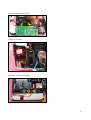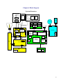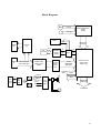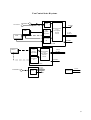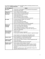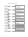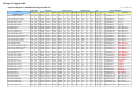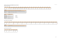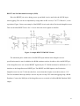
1
FILE NO. 330-200306 SERVICE MANUAL DLP DATA PROJECTOR TDP-D1 TDP-D2 AU TO NE YSTO KE L.VO AN /ST ON ON TO AU NU ME Y DB LA MP TEMP SET L.+ VO UT INP FAN TDP-D1. TDP-D2 Index Precaution 2 Chapter 1 Major Parts Location 6 Chapter 2 Assy and Disassy Drawing 8 Chapter 3 Parts Replacement 16 Chapter 4 Block Diagram 37 Chapter 5 Trouble Shooting Guide 40 Chapter 6 Firmware upgrade 50 Chapter 7 Factory OSD 55 Chapter 8 Alignment Procedure 56 Chapter 9 Signal Table 61 Chapter 10 Spare Parts List 66 Chapter 11 RS232C Codes 72 Appendix A Engineering Specification 75 Appendix B Circuit Operation Theory 80 Appendix C DMD Imege Quality 105 1 SAFETY PRECAUTION WARNING: Service should not be attempted by anyone unfamiliar with the necessary precautions on this projector. The following are the necessary precautions to be observed before servicing this chassis. 1 . An isolation Transformer should be connected in the power line between the projector and the AC Iine before any service is performed on the projector. 2. When replacing a chassis in the cabinet, always be certain that all the protective devices are put back in place, such as; non-metallic control knobs, insulating covers, shields, isolation resistor-capacitor network etc. 3. Before returning the set to the customer, always perform an AC Ieakage current check on the exposed metallic parts of the cabinet, such as terminals, screwheads, metal overlays, control shafts etc. to be sure the set is safe to operate without danger of electrical shock. Plug the AC Iine cord directly into a AC outlet (do not use a line isolation transformer during this check). Use an AC voltmeter having 5000ohm per volt or more sensitivity in the following manner: Connect a1500ohm 10W resistor, paralleled by a 0.15 µF, AC type capacitor, between a known good earth ground (water pipe, conduit, etc.) and the exposed metallic parts, one at a time. Measure the AC voltage across the combination of 1500ohm resistor and 0.15 µF capacitor. Reverse the AC plug at the AC outlet and repeat AC voltage measurements for each exposed metallic part. Voltage measured must not exceed 5.25V(rms). This corresponds to 3.5 mA(AC). Any value exceeding this limit constitutes a potential shock hazard and must be corrected immediately. PRODUCT SAFETY NOTICE Many electrical and mechanical parts in this chassis have special safety-related characteristics. These characteristics are often passed unnoticed by a visual inspection and the protection afforded by them cannot necessarily be obtained by using replacement components rated for higher voltage, wattage, etc. Replacement parts which have these special safety characteristics are identified in this manual and its supplements; electrical components having such features are identified by the international hazard symbols on the schematic diagram and the parts list. Before replacing any of these components, read the parts list in this manual carefully. The use of substitute replacement parts which do not have the same safety characteristics as specified in the parts list may create shock, fire or other hazards. ULTRAVIOLET DANGER IN SERVICE MODE Eye damage may result from directly viewing the light produced by the lamp used in this product. Always turn off lamp before opening this cover. Ultraviolet radiation eye protection required during servicing. 2 SAFETY PRECAUTIONS The lightning flash with arrowhead symbol, within an equilateral triangle, is intended to alert the user to the presence of uninsulated "dangerous voltage" within the product's enclosure that may be of sufficient magnitude to constitute a risk of electric shock to persons. The exclamation point within an equilateral triangle is intended to alert the user to the presence of important operating and maintenance (servicing) instructions in the literature accompanying the appliance. WARNING: TO REDUCE THE RISK OF FIRE OR ELECTRIC SHOCK, DO NOT EXPOSE THIS APPLIANCE TO RAIN OR MOISTURE. DANGEROUS HIGH VOLTAGES ARE PRESENT INSIDETHE ENCLOSURE. DO NOT OPEN THE CABINET. REFER SERVICING TO QUALIRED PERSONNEL ONLY. CAUTION: Laser beam is emitted when the laser button of the remote control is pressed. Do not look from the front of the remote control. Do not face toward a person or to a mirror. FCC Radio Frequency Interference Statement Note: This equipment has been tested and found to comply with the limits for a Class A digital device, pursuant to part 15 of the FCC Rules. These limits are designed to provide reasonable protection against harmful interference when the equipment is operated in a commercial environment. This equipment generates, uses, and can radiates radio frequency energy and, if not installed and used in accordance with the instruction manual, may cause harmful interference to radio communications. Operation of this equipment in a residential area is likely to cause harmful interference in which case the user will be required to correct the interference at his own expense. WARNING: Changes or modifications made to this equipment, not expressly approved by Toshiba, or parties authorized by Toshiba, could void the user's authority to operate the equipment. Notice: This Class A digital apparatus complies with Canadian ICES-003. Cet appareil numérique de la classe A est conforme à la norme NMB-003 du Canada. IMPORTANT PRECAUTIONS In the spaces provided below, record the Model and Serial No. Iocated at the rear of your projector. Save Original Packing Materials The original shipping carton and packing materials will come in handy if you ever have to ship your projector. For maximum protection, repack the set as it was originally packed at the factory. Mode No. Serial No. Retain this information for future reference. Avoid Volatile Liquid Do not use volatile liquids, such as an insect spray, near the unit. Do not leave rubber or plastic products touching the unit for a long time. They will mar the finish. Moisture Condensation Never operate this unit immediately after moving it from a cold location to a warm location. When the unit is exposed to such a change in temperature, moisture may condense on the crucial internal parts. To prevent the unit from possible damage, do not use the unit for at least 2 hours when there is an extreme or sudden change in temperature. TDP-T1 / TDP-S2 Service Manual 3 IMPORTANT SAFETY INSTRUCTIONS CAUTION: PLEASE READ AND OBSERVE ALLWARNINGS AND INSTRUCTIONS GIVEN IN THIS OWNER'S MANUAL AND THOSE MARKED ON THE UNIT. RETAIN THIS BOOKLET FOR FUTURE REFERENCE. This set has been designed and manufactured to assure personal safety. Improper use can result in electric shock or fire hazard. The safeguards incorporated in this unit will protect you if you observe the following procedures for installation, use and servicing. This unit is fully transistorized and does not contain any parts that can be repaired by the user. DO NOT REMOVE THE CABINET COVER, OR YOU MAY BE EXPOSED TO DANGEROUS VOLTAGE. REFER SERVICING TO QUALIFIED SERVICE PERSONNEL ONLY. 1. Read Owner's Manual After unpacking this product, read the owner's manual carefully, and follow all the operating and other instructions. 2. Power Sources This product should be operated only from the type of power source indicated on the marking label. If you are not sure of the type of power supply to your home, consult your product dealer or local power company. For products intended to operate from battery power, or other sources, refer to the operating instructions. 3. Source of Light Do not look into the lens while the lamp is on. The strong light from the lamp may cause damage to your eyes or sight. 4. Ventilation Openings in the cabinet are provided for ventilation and to ensure reliable operation of the product and to protect it from overheating, and these openings must not be blocked or covered. The openings should never be blocked by placing the product on a bed, sofa, rug or other similar surface. This product should not be placed in a built-in installation such as a bookcase or rack unless proper ventilation is provided or the manufacturer's instructions have been adhered to. IMPORTANT SAFETY INSTRUCTIONS 5. Heat The product should be situated away from heat sources such as radiators heat registers, stoves, or other products (including amplifiers) that produce heat. 7. Cleaning Unplug this product from the wall outlet before cleaning. Do not use liquid cleaners or aerosol cleaners. Use a damp cloth for cleaning. 9. Overloading Do not overload wall outlets; extension cords, or integral convenience receptacles as this can result in a risk of fire or electric shock. 6. Water and Moisture Do not use this product near water - for example, near a bath tub, wash bowl, kitchen sink, or laundry tub; in a wet basement; or near a swimming pool and the like . 8. 10. Lightning For added protection for this product during storm, or when it is left unattended and unused for long periods of time, unplug it from the wall outlet. This will prevent damage to the product due to lightning and power-line surges. TDP-T1 / TDP-S2 Service Manual Power-Cord Protection Power-supply cords should be routed so that they are not likely to be walked on or pinched by items placed upon or against them, paying particular attention to cords at plugs, convenience receptacles, and the point where they exit from the product. 4 IMPORTANT SAFETY INSTRUCTIONS 11. Object and Liquid Entry Never push objects of any kind into this product through openings as they may touch dangerous voltage points or short-out parts that could result in a fire or electric shock. Never spill liquid of any kind on the product. 13. Stack Inhibited Do not stack other equipment on this product or do not place this product on the other equipment. Top and bottom plates of this product develops heat and may give some undesirable damage to other unit. 12. Do not place the product vertically Do not use the product in the upright position to project the pictures at the ceiling, or any other vertical positions. It may fall down and dangerous. 14. Attachments Do not use attachments not recommended by the product manufacturer as they may cause hazards. 15. Accessories Do not place this product on an unstable cart, stand, tripod, bracket, or table. The product may fall, causing serious injury to a child or adult, and serious damage to the product. Use only with a cart, stand, tripod, bracket, or table recommended by the manufacturer, or sold with the product. Any mounting of the product should follow the manufacturer's instructions and should use a mounting accessory recommended by the manufacturer. A product and cart combination should be moved with care. Quick stops, excessive force, and uneven surfaces may cause the product and cart combination to overturn. IMPORTANT SAFETY INSTRUCTIONS 16. Damage Requiring Service Unplug this product from the wall outlet and refer servicing to qualified service personnel under the following conditions: a) When the power-supply cord or plug is damaged. b) If liquid has been spilled, or objects have fallen into the product. c) If the product has been exposed to rain or water. d) If the product does not operate normally by following the operating instructions. Adjust only those controls that are covered by the operating instructions as an improper adjustment of other controls may result in damage and will often require extensive work by a qualified technician to restore the product to its normal operation. e) If the product has been dropped or damaged in any way. f) When the product exhibits a distinct change in performance - this indicates a need for service. TDP-T1 / TDP-S2 Service Manual 17. Servicing Do not attempt to service this product yourself as opening or removing covers may expose you to dangerous voltage or other hazards. Refer all servicing to qualified service personnel. 18. Replacement Parts When replacement parts are required, be sure the service technician has used replacement parts specified by the manufacturer or have the same characteristics as the original part. Unauthorized substitutions may result in fire, electric shock, or other hazards. (Replacement of the lamp only should be made by users.) III 19. Safety Check Upon completion of any service or repairs to this product, ask the service technician to perform safety checks to determine that the product is in proper operating condition. 5 Chapter 1 Major Part Locations The top illustration shows the parts from the front of the projector. The illustration on the next page shows the parts visible from the rear of the projector. To see exploded views of the case parts, major components and optical engine, Main/Connector Back fan Ballast Power supply Optical engine Lamp blower 6 Input module Lamp box 7 Chapter 2 Assy and Disassy drawing 8 9 10 11 12 13 14 15 Chapter 3 Parts replacement 3.1 Lamp module The lamp module is located at bottom of the projector. The lamp module behinds the lamp cover with 3 captive screws. After you replace the lamp module, you should reset the lamp hour counter. The switch interrupts power supply output to the projector if you remove the lamp cover. WARNING Allow the projector to cool before removing the lamp module. The lamp module becomes very hot when the projector is in use. DO NOT touch any part of the lamp module that is located in the lamp box. Oils from your fingers will cause smudges and uneven heating of lamp surfaces, resulting in decreased image quality and premature lamp failure. If the lamp is ruptured or the lamp module is cracked or damaged, be careful of quartz or glass fragments that could cause personal injury. 1.Remove one screw of lamp cover which is a spring door. 2. Remove the 3 screws from the lamp module. 16 3. Grasp the handle on the lamp module and pull the module out of the lamp box. 3.2 Top Case The top case encloses the top half of the projector. It includes the keypad and speaker. When you just replace the top case only, you don’t remove the lamp module. 1. Remove the 4 long screws and 1 short screw. 17 2. Carefully turn the unit over and lift the top case from the projector. 3. Place the unit upside-down on the bench and detach the keypad and speaker cable from theirs connector on the PC board interface. 18 3.2.1 Keypad and Speaker The keypad and speaker fasten to the inside of the top case with 2 cables. 1. Remove the 6 screws. 2. Lift the keypad and speaker from the top case. 19 3.3 Front bezel The front bezel covers the front of the projector and helps secure the top case to the bottom case. 1. Remove the 2 screws under the projector. 2. Remove the right and left screw of the front bezel. There is a metal upon each connector and you don’t need to remove them. 20 3.4 Rear Bezel The rear bezel covers the rear of the projector and fits between the top case and the bottom case. It fastens to the 2 fans with 4 screws. You should remove 2 screws and 2 cables. WARNING Rear bezel provides the thermal solution with 2 fans. Dust within fans will reduce the effect on heating solution. 1. Remove the 2 screws. 2.Place the cables out of the hooks. 21 3.Remove 2 cables. 4.Lift the rear bezel. 22 3.5 Main/Connector Module The main/connector module is located beneath the top cover at right of the optical engine. It includes a connector cover, input board and the PC board interface. 1.Remove 3 cables. 2.Remove 3 screws. 23 3.Lift the black metal stick from the PC board interface. 4.Lift the ZIP connector form PC board interface and DMD board. 5.Remove 1 screw. 24 6.Lift the input rear cover. 7.Lift and pull whole main/connector module. 8. Remove the #4-40 jack screws from both sides of the connector. 25 9.Remove 4 screws. 10.Saparate the Input board from the PC board interface. 26 11.Thus you will get input board, PC board interface and connector cover. 3.6 Ballast and Power Supply The ballast is located on the side of the projector opposite the lens. The ballast receives power from the power supply, stepping it up to ignite the lamp module. 1.Remove 4 screws and 2 cables. 27 2.Lift the upper power board. 3.Remove 2 cables. 4.Remove 4 screws for ballast. 28 5.Lift the ballast. 3.6.1 Power Supply The power supply is located near the ballast at the front of the projector. It fastens to the bottom case and converts the 100-240 VAC supply voltage to various low voltage DC levels required internally by the projector. The power supply interfaces with the ballast to control lamp strike and operation and to detect the electrical condition of the safety interlock switch. 1.Remove 3 screws , 1 jack screw and 1 cable. 29 2.Lift the power supply board. 3.7 Optical Engine The optical engine is located beneath the main/connector board at the side of the projector opposite the ballast. It fastens to the bottom case and produces the projected image by directing focused light from the lamp module through the color wheel and onto the Digital Micromirror Device (DMD). 1.Remove 3 screws for optical engine and 1 screw for cable. 30 3.8 EMI Board The EMI board fastens to the power supply under the optical engine. It drains electro-magnetic interference away from AC inlet. 1.Remove 2 screws, 2 jack screws and 1 cable. 2.Lift EMI board. 31 3.9 Lamp Blower The lamp blower is fastens to lamp box on the bottom case. The blower directs cool air around the lamp. 1.Remove 2 screws. 2.Lift lamp blower. 32 3.10 Foot Adjust The foot adjust is located in the bottom case. The foot adjust stick slides up or down through the bottom case to raise or lower the front of the projector when you press the actuator button on the side of the bottom case. 1.Remove 1 screw. 2. Pull the release latch of the foot adjust outward to disengage the connection between the foot adjust and the bottom case. 33 3.11 Lamp Box The lamp box is fastens to AC inlet/thermal switch/power switch. It helps secure the lamp module to the bottom case. 1.There are 6 screws you need to remove. 2.Remove 1 screw in fornt of the lamp box. 34 3. Remove 1 screw and pick up the portion of lamp box. 4. Remove 2 screws. 5. Remove 1 screw for lamp cover switch and remove 1 screw for AC inlet cable. 35 3.12 Color Wheel Module The color wheel module is located on bottom case between lamp box and optical engine. CAUTION The color wheel is in the color wheel module. Take extreme care not to bump it with a tool or press against it because it is very delicate. Aviod any touching on color wheel and dust causes image quality decreasing. A broken color wheel requires engine replacement. 1. Remove 2 screws. 2. Carefully pull and lift the color wheel module from the bottom case. 36 Chapter 4 Block diagram System Structure Sensor1 Blower Door Sensor2 Lock FAN1 DMD Heatsink Thermal Breaker IR 8 Pin 3-1 Pin PFC BD 3 Pin IR Video Decoder DDP1000 Block Motor Control Block System Control PWxxx Function Block FPC Board Bias Adjust Jumper 30 Pin 30 Pin 18VPFC Ballast 3-1 Pin D_Sub In AD Converter D_Sub Out 14 Pin 2 Pin KeyPad & LED ` 380V/ GND Audio Block 2 Pin Goden Finger 2 Pin 15 pin Mouse / RS232 Function Block 2 Pin 380V/ GND 4 Pin 80 Pin 3-1 Pin S-Video Connector 80 Pin 5 Pin Sensor2 Audio Audio In Out 3 Pin Color Wheel sensor feedback Video Connector 15 pin Fan Ctrl Function Block DC/DC Block USB connector 80 Pin 3 Pin Autokeystone Block Lamp Control Sensor Board Color Wheel MiniD8 5 Pin FAN2 80 Pin Lamp Box Sensor3 2 Pin EMI Filter 14 Pin KEYPAD LED AC Inlet 37 Block Diagram YC Signal NTSC/PAL/SECAM Video Decoder VPX3226 CVBS Signal TX Ballast DSUB15 OUT YUV422 16bits Digital Signal Tripe Video Amp PC_TX 8-Pin Control Port PC_RX DSUB15 IN RX RGB Analog Signal YPbPr Analog Signal 140MSPS Analog Interface for FPD AD9883 TX RS232 DriverReceiver Sp232E MacroVision Protect Decoder Circuit TX Switch RX RX 2 Phase RBG888 48bits Digital Signal To Keypad Board XGA FPD Control IC Image Processor PW166 - 10TK KEY0~7 Stereo R USB Mouse output D- IR1 D+ IR to USB Mouse LED0~3 Stereo L Volume IR2 Mute Audio Processor TDA8551 RGB888 24bits Digital Signal To DMD Board 38 Fan Control Auto Keystone Transistor 1 ADC Transistor 2 ALERM Fan Speed Regulator FAN1 O pen/Closed Loop Fan-Speed Control Circuit 2-wire I2C Bus FAN2 Tacom eter IN STANDBY G768B Blower Fan Speed Regulator O pen/Closed Loop Fan-Speed Control Circuit Tacom eter IN 2-wire I2C Bus STANDBY G760A 2-wire I2C Bus Transistor 1 XO UT ADXL202 ADC YOUT ALERM G 767 39 Chapter 5 Trouble shooting guide 40 41 1. Final Assembly Trouble Shooting Guide System Trouble Shooting Flow Char Back-LIGHT OK? No Yes Power ON OK? (LAMP ON?) No STEP: 1.Check power core 2.Check power board and wire 1.Check lamp door. 2.Check thermal switch and wire 3.Check 12V Fan and wire 4.Check power board and wire 5.Check color wheel FPC 6.Check screws on color wheel 7.Check color wheel motor 8.Check DMD Block and 80 pins connector X2 9.Check FanCtrl board and wire and 30 pins connector 10.Check System Block Yes No Signal? No 1.Check input cable 2.Check OSD source set up Yes No Auto Power Off? Yes Video NG? No 1.Check OSD lamp hours 2.Check OSD Auto Off setup value 3.Check lamp door 4.Check 12V fan 5.Check thermal status 1.Check Video cable Yes Audio NG? No 1.Check System Block No 1.Check Remote module battery 2.Check Remote module 3.Check System Block Yes IR Remote Control NG? Yes Pixel Fail? No 1.Check DMD chip 2.Check DMD Block Yes Image NG? (Raindrops) No 1.Check color wheel and Sensor board 2.Check DMD chip and holder 3.Check DMD conductive elastomers assembling 4.Clean DMD conductive elastomers Yes A 42 A 1.Check DMD Block Image NG? (Blank) Yes 2.Check color wheel and Sensor board 3.Check DMD conductive elastomers 4.Check Main and Translation boards No Image NG? (Screen flashing) Yes 1.Check color wheel and Sensor board 2.Check DMD Block 3.Check System Block Yes 1.Check DMD Block 2.Check color wheel and Sensor board No Image NG? (Screen dimmish) No Image NG? (Freezing) Yes 1.Check color wheel 2.Check Sensor board color index signal Yes 1.Check DMD holder Yes 1.Check System Block 2.Check DMD Block No Image NG? (Missing column bar) No Image NG? (Screen overlap) 43 2. Engine Assembly Trouble Shooting Guide 1 K room stage Start OK Power ON Check Color Wheel connection Check FPC BD connection Check I/F Board NG OK NG Blue Edge Re-adjust Light Pipe NG Change New Light Pipe OK Pixel Failure NG Change DMD OK Dust NG Clean DMD OK Light Leakage NG Change DMD Baffle OK Focus NG Change Projection Lens OK Uniformity NG Rework FM Change New Lamp OK Brightess NG Change Lamp Check Engine component >1600 lumen >2000 lumen Output as D1 Output as D2 44 3. System no work Main Block Trouble Shooting Guide Yes No No data signal output to DMD BD No Yes The image display “No Signal” when the input is PC No The ghost image display output of Video input Yes a. PW164B bad soldiering b. Flash without softeare are inside c. Reset IC function abnormal d. PW164B no work 1. Check 3.3V or 2.5V 2. check MCLK and DCLK a. PW164B bad soldiering causing no work b. Check 3.3V or 2.5V c. Check ICS501 if there was MCLK and DCLK output to PW164B a. Check the voltage of AVDD,PVDD,VDD b. If voltage above are ok, then check VSYNC and HSYNC if there were these two signal or not c. Replace AD9888 No Couldn’t download new software to MainBD Yes a. VPX3226 bad soldiering b. PW164B bad soldiering c. Main System bad connection Yes a. Replace SPE232E b. PW164B Yes a. Check the mouse of PC is still working normally b. Check the mouse driver of PC is PS2 compatible mouse c. Replace IR Buffer No Remote mouse don’t work No Keypad working abnormally No Yes Lamp List signal abnormal No IR doesn’t work Check 74244 Yes Check 74373 Yes a. Check soldiering condition b. PW164B bad soldiering No Gray bar abnormal or image contour (PC input) Yes Check the resisters between IR and PW164B 45 4. Power Supply Trouble Shooting Guide PFC BOARD DX850 DC-DC BOARD 46 5. DMD Block Trouble Shooting Guide 47 48 49 Chapter 6 Firmware upgrade Step 1. Setup Flashloader in computer. Step 2. a. Connect download cable with computer and projector b. Connect power cord with projector and check Power switch is OFF. Step 3. Execute FLASH loder.exe 50 Step 4. Setting COM Port & Baud Rate 51 Step 5. a. Turn on the power switch of the projector, then the Program will target the Flash. b. HEX File Format choose Intel Extended c. File Name choose d. Operation choose Program 52 Step 6. Start download firmware 53 Step 7. Download finished. Step 8. Turn off the power switch. 54 Chapter 7 Factory OSD Special Key for TOSHIBA DLP Projector TDP-D1 Rev. F 2003.1.25 The following keys are effective when inserting a power cord plug in a power socket. Press keys until the LED becomes standby mode. Key1 ON/STANDBY AUTO SET INPUT ON/STANDBY Key2 INPUT AUTO KEYSTONE AUTO KEYSTONE AUTO SET Key3 MENU MENU MENU MENU Function Reset the user lamp time *1 Go to the special (factory) mode Ignore the error detection Reserved Key3 MENU Function Go to the special (factory) mode Key3 - Function Display the lamp time menu Display the ADC level alignment menu *2 Display the keystone calibration menu Display the color wheel delay menu Display the fan control menu Display the white peak menu Display the test pattern menu Display the video curtain & spoke light menu Display the burn in mode menu Display the RGB gain (DDP1000) menu Reserved Save the factory data, the lamp data and the error data The following keys are effective while displaying the volume menu. Key1 AUTO SET Key2 AUTO KEYSTONE The following keys are effective in the special (factory) mode. Key1 AUTO KEYSTONE AUTO KEYSTONE AUTO KEYSTONE AUTO KEYSTONE INPUT INPUT INPUT INPUT ON/STANDBY ON/STANDBY ON/STANDBY ON/STANDBY Key2 UP DOWN LEFT (VOL-) RIGHT (VOL+) UP DOWN LEFT (VOL-) RIGHT (VOL+) UP DOWN LEFT (VOL-) RIGHT (VOL+) The following keys are effective when inserting a power cord plug in a power socket. Press keys until the FlashUpgrader indicator begins to move. Key1 AUTO SET Key2 AUTO KEYSTONE FlashUpgrader Function Waiting charactors Start firmware upgrade *1 This operation method is opened to a user in the manual. *2 This menu is displayed only when a screen size is FULL mode and an input source is RGB/YPbPr. ON/STANDBY UP INPUT MENU (VOL-) LEFT AUTO KEYSTONE RIGHT (VOL+) DOWN AUTO SET 55 Chapter 8 Alignment Procedure 1. Optical Engine assembly procedures Basically the assembly of optical engine is exactly the same as SL700X series engines with following differences: A. Projector Lens assembly After finishing the assembly of DMD Housing, assembly the projection lens THAN assembly the Zoom Ring than Focus Ring. 2. Optical Alignment A. Light pipe adjustment procedure i. Equipment: PC or Pattern Generator (Chroma 2250) Screw Driver for M2 ii. Procedures: Project “Full white” pattern (from PC, or Chroma2250 pattern 41, or enter spoken light mode) on screen. Adjust the two light pips adjusting screws until “Dark Edge” disappear on all edges of screen. Sequence of adjust is: Left-Right screw first, then Up-Down screw. Apply glue on screws to fix the screw position. Apply silicon glue between “Clip” and Light Pipe. 56 3. Electronic Alignment Procedures A. DMD Bias Voltage Alignment Equipment: None Procedure: Watch DMD chip Label (Example: 9477000 0234B) Switch the DIP switch on Chip board according to the character on the DMD chip 00: B, 01: C, 10: D, 11: E 0 B 0 Color Wheel Delay Alignment Equipment: Battery Biased Silicon PIN Detector Oscilloscope Probe The default values let optical engine to get maximum contrast and brightness. Procedure: Open Factory OSD, and select color wheel delay item Leave the image pure red Put the detector on the screen that red image was projected. Watch the oscilloscope and notice the square waveform Use the “ ” and “” key to increment or decrement the color wheel delay alue Do not adjust too much, let the signal get ahead, if it happens, go back to step 5 and do it again. Change the input to pure blue and repeat the above procedures again. Change the input to pure green and repeat the above procedures again. Power Off (otherwise the value will not saved) 57 C PC Offset/Gain Alignment Procedure Equipment: Pattern generator (Chroma 2250) Procedure: Check the input source PC Change Timing and pattern of pattern generator: Timing: 1024x768@60Hz (H: 48Khz, V: 60Hz) Pattern: Full Black Send the Auto Sub Brightness Command to projector Command: STX A S B ETX Check the brightness value after alignment Change Timing and pattern of pattern generator: Timing: 1024x768@60Hz (H: 48Khz, V: 60Hz) Pattern: Full White Send the Auto Sub Contrast Command to projector Command: STX A S C ETX Check the contrast value after alignment Check the 32 levels of gray. All steps must appear Send Save Factory & Lamp Data Command Command: STX F S V ETX D. YpbPr Offset Alignment Procedure Equipment: Pattern generator (VG828) Procedure: Check the input source YPbPr Change Timing and pattern of pattern generator: Timing: 480P Pattern: Full Black Disable the Red & Blue channel signals (Only Green channel available) Send the Auto Sub Brightness Command to projector Command: STX A S B ETX Check the brightness value after alignment Check the 32 levels of gray. All steps must appear Send Save Factory & Lamp Data Command Command: STX F S V ETX 58 E. Auto Ketstone Alignment Procedure Equipment: Jig of ±3 Procedure: Set 0° angle of platform Put the projector on it (already power on) Send the Keystone Calibration 0 Command to projector Command: STX K C 0 ETX Check the keystone calibration 0 value after alignment 0° angle platform Set +30° angle of platform Send the Keystone Calibration 1 Command to projector Command: STX K C 1 ETX Check the keystone calibration 1 value after alignment Set -30° angle of platform Send the Keystone Calibration 2 Command to projector Command: STX K C 2 ETX Check the keystone calibration 2 value after alignment After 5 ~ 10 minutes power on Set 0° angle of platform Send the Keystone Calibration 3 Command to projector Command: STX K C 3 ETX Check the keystone calibration 3 value after alignment Send Save Factory & Lamp Data Command Command: STX F S V ETX F. PC and Component signal test Equipment: Pattern generator (Chroma 2250) Pattern generator (VG828) Procedure: Change the input signal to source PC Change the bellowing Timing and pattern of pattern generator: Timing: 640x480@60Hz 00x600@60Hz 24x768@60Hz 1280x1024@60Hz 1600x1200@60Hz Pattern: SMPTE RP-133 59 To check each above timing phase, H and V position, frequency is correct or not. Change the input signal to input YpbPr Timing: 1125i Pattern: Color Bar Check the signal formation, color and image quality. G. Menu Reset before output Equipment: N/A Procedure: The reset menu is shown by pressing the [MENU/ENTER] button during two seconds. Select item by [UP] or [DOWN] button. Computer Y/PB/PR Video S-video Horizontal reference value reset ○ ○ ○ ○ Reset all ○ ○ ○ ○ Fig. 8-1 Reset all setting value of the user menu Fig. 8-2 Execute menu of reset all 60 Chapter 9 Signal table Supported Signals for TOSHIBA DLP Projector TDP-D1 Format Computer Source VESA 640 x 480 @ 60Hz VGA Text 480 Lines @ 60Hz VGA Text 480 Lines @ 60Hz VESA 640 x 480 @ 72Hz VESA 640 x 480 @ 75Hz VESA 640 x 480 @ 85Hz 640 x 480 @ 70Hz 640 x 480 @ 90Hz DELL 640 x 480 @ 90Hz DELL 640 x 480 @ 100Hz DELL 640 x 480 @ 120Hz Macintosh 13 Inch Mode @ 67Hz NEC PC98 Standard @ 56Hz VGA Text 400 Lines @ 60Hz VGA Text 400 Lines @ 60Hz iMac 800x600@95Hz ASUS 640x480@150Hz VGA Graphic 350 Lines @ 70Hz VGA Graphic 400 Lines @ 70Hz VGA Text 350 Lines @ 70Hz VGA Text 400 Lines @ 70Hz ASUS 800x600@144Hz VESA 640 x 350 @ 85Hz VESA 640 x 400 @ 85Hz VESA 720 x 400 @ 85Hz Wide VGA @ 60Hz VESA 800 x 600 @ 56Hz VESA 800 x 600 @ 60Hz VESA 800 x 600 @ 72Hz VESA 800 x 600 @ 75Hz VESA 800 x 600 @ 85Hz 800 x 600 @ 80Hz 800 x 600 @ 90Hz 800 x 600 @ 100Hz 800 x 600 @ 110Hz 800 x 600 @ 120Hz DELL 800 x 600 @ 48Hz I DELL 800 x 600 @ 70Hz DELL 800 x 600 @ 100Hz DELL 800 x 600 @ 120Hz Active Video H Pixels V Lines 640 640 720 640 640 640 640 640 640 640 640 640 640 640 720 800 640 640 640 720 720 800 640 640 720 852 800 800 800 800 800 800 800 800 800 800 800 800 800 800 480 480 480 480 480 480 480 480 480 480 480 480 400 400 400 600 480 350 400 350 400 600 350 400 400 480 600 600 600 600 600 600 600 600 600 600 300 600 600 600 Rev. C 2003.1.28 Frequency H Timing (Pixels) V Timing (Lines) Sync Firmware Definition V Freq. H Freq. Pixel Clock Total F Porch Sync B Porch Total F Porch Sync B Porch H V No. 59.940 59.940 59.941 72.809 75.000 85.008 69.444 90.038 89.898 99.989 120.254 66.667 56.420 59.940 59.941 94.890 150.233 70.090 70.090 70.090 70.090 143.961 85.080 85.080 85.039 59.973 56.250 60.317 72.188 75.000 85.061 80.011 90.045 100.021 110.035 120.372 96.114 70.099 100.189 120.031 31.469 31.469 31.469 37.861 37.500 43.269 34.722 45.829 47.916 52.994 63.735 35.000 24.825 31.469 31.469 59.970 78.722 31.470 31.470 31.470 31.470 94.007 37.861 37.861 37.927 31.726 35.156 37.879 48.077 46.875 53.673 50.327 56.818 63.613 70.422 77.399 33.784 44.583 64.021 76.220 25.175 25.175 28.322 31.500 31.500 36.000 28.229 38.130 39.866 44.939 55.067 30.240 21.051 25.175 28.322 62.369 68.016 25.176 25.176 28.323 28.323 102.279 31.500 31.500 35.500 34.010 36.000 40.000 50.000 49.500 56.250 53.145 59.546 68.194 75.493 84.210 35.946 44.940 67.606 81.098 800 800 900 832 840 832 813 832 832 848 864 864 848 800 900 1040 864 800 800 900 900 1088 832 832 936 1072 1024 1056 1040 1056 1048 1056 1048 1072 1072 1088 1064 1008 1056 1064 16 16 18 24 16 56 29 56 56 32 48 64 59 16 18 18 42 14 14 18 18 58 32 32 36 58 24 40 56 16 32 16 32 56 56 72 48 24 40 48 96 96 108 40 64 56 96 56 56 96 96 64 64 96 108 82 72 96 96 108 108 88 64 64 72 108 72 128 120 80 64 80 64 64 64 64 64 96 64 64 48 48 54 128 120 80 48 80 80 80 80 96 85 48 54 140 110 50 50 54 54 142 96 96 108 54 128 88 64 160 152 160 152 152 152 152 152 88 152 152 525 525 525 520 500 509 500 509 533 530 530 525 440 525 525 632 524 449 449 449 449 653 445 445 446 529 625 628 666 625 631 629 631 636 640 643 351.5 636 639 635 10 10 10 9 1 1 3 6 2 1 1 3 0 50 50 1 1 38 13 38 13 1 32 1 1 14 1 1 37 1 1 1 1 6 10 13 4.5 4 9 5 2 2 2 3 3 3 2 3 3 3 3 3 8 2 2 3 3 2 2 2 2 3 3 3 3 2 2 4 6 3 3 3 3 3 3 3 3 4 3 3 33 33 33 28 16 25 15 20 48 46 46 39 32 73 73 28 40 59 34 59 34 49 60 41 42 33 22 23 23 21 27 25 27 27 27 27 44 28 27 27 N N N N N N P P P P P N N N N P P P N P N P P N N N P P P P P P P P P P P P P P N N N N N N P P P P P N N N N P P N P N P P N P P N P P P P P P P P P P P P P P 3 3 3 4 5 6 7 8 9 10 11 12 13 14 14 15 16 17 17 17 17 18 19 19 19 20 21 22 23 24 25 26 27 28 29 30 31 32 33 34 Mode Name sm640X480_60 *1 sm640X480_60 *1 sm640X480_60 *1 sm640X480_72 sm640X480_75 sm640X480_85 sm640X480_70 sm640X480_90A sm640X480_90B sm640X480_100 sm640X480_120 sm640X480_67 sm640X400_56 sm720X400_60 *1 sm720X400_60 *1 sm800X600_95 sm640X480_150 sm720X400_70 *1 sm720X400_70 *1 sm720X400_70 *1 sm720X400_70 *1 sm800X600_144 sm720X400_85 *1 sm720X400_85 *1 sm720X400_85 *1 sm852X480_60 sm800X600_56 sm800X600_60 sm800X600_72 sm800X600_75 sm800X600_85 sm800X600_80 sm800X600_90 sm800X600_100A sm800X600_110 sm800X600_120A sm800X600_48 sm800X600_70 sm800X600_100B sm800X600_120B OSD Name VGA_60 *1 VGA_60 *1 VGA_60 *1 VGA_72 VGA_75 VGA_85 640 X 480_70 640 X 480_90 A 640 X 480_90 B 640 X 480_100 640 X 480_120 640 X 480_67 640 X 400_56 720 X 400_60 *1 720 X 400_60 *1 800 X 600_95 640 X 480_150 720 X 400_70 *1 720 X 400_70 *1 720 X 400_70 *1 720 X 400_70 *1 800 X 600_144 720 X 400_85 *1 720 X 400_85 *1 720 X 400_85 *1 852 X 480_60 SVGA_56 SVGA_60 SVGA_72 SVGA_75 SVGA_85 800 X 600_80 800 X 600_90 800 X 600_100 A 800 X 600_110 800 X 600_120 A 57 800 X 600_48 800 X 600_70 800 X 600_100 B 800 X 600_120 B 61 Supported Signals for TOSHIBA DLP Projector TDP-D1 Format DELL 800 x 600 @ 160Hz DELL 800 x 600 @ 200Hz Macintosh 16 Inch Mode @ 75Hz 960 x 720 @ 60Hz 960 x 720 @ 75Hz 960 x 720 @ 85Hz VESA 1024 x 768 @ 43Hz VESA 1024 x 768 @ 60Hz VESA 1024 x 768 @ 70Hz VESA 1024 x 768 @ 75Hz VESA 1024 x 768 @ 85Hz Macintoshi 19 Inch Mode @ 75Hz 1024 x 768 @ 90Hz 1024 x 768 @ 110Hz A 1024 x 768 @ 110Hz B DELL 1024 x 768 @ 100Hz DELL 1024 x 768 @ 120Hz DELL 1024 x 768 @ 140Hz SUN 1024 x 800 @ 85Hz NEC 1120 x 750 @ 40Hz I CPQ 1152 x 864 @ 43Hz DMT 1152 x 864 @ 60Hz 1152 x 864 @ 70Hz VESA 1152 x 864 @ 75Hz DMT 1152 x 864 @ 85Hz 1152 x 864 @ 100Hz Macintosh 21 Inch Mode @ 75Hz SUN 1152 x 900 @ 66Hz SUN 1152 x 900 @ 76Hz 1280 x 720 @ 70Hz 1280 x 720 @ 72Hz 1280 x 720 @ 75Hz 1280 x 720 @ 85Hz 1280 x 720 @ 100Hz 1280 x 720 @ 120Hz 1280 x 720 @ 140Hz 1600 x 900 @ 60Hz 1600 x 900 @ 70Hz 1600 x 900 @ 72Hz 1600 x 900 @ 75Hz 1600 x 900 @ 85Hz Active Video H Pixels V Lines 800 800 832 960 960 960 1024 1024 1024 1024 1024 1024 1024 1024 1024 1024 1024 1024 1024 1120 1152 1152 1152 1152 1152 1152 1152 1152 1152 1280 1280 1280 1280 1280 1280 1280 1600 1600 1600 1600 1600 600 600 624 720 720 720 384 768 768 768 768 768 768 768 768 768 768 768 800 375 864 864 864 864 864 864 870 900 900 720 720 720 720 720 720 720 900 900 900 900 900 Rev. C 2003.1.28 Frequency H Timing (Pixels) V Timing (Lines) Sync Firmware Definition V Freq. H Freq. Pixel Clock Total F Porch Sync B Porch Total F Porch Sync B Porch H V No. 160.278 199.160 74.550 60.004 75.013 85.002 86.958 60.004 70.069 75.029 84.997 74.700 90.029 109.901 112.294 99.771 119.841 139.988 84.011 80.054 43.600 60.039 70.019 75.000 85.007 100.688 75.062 66.004 76.637 69.472 71.577 74.605 85.064 100.047 120.050 140.089 60.043 69.980 71.990 75.230 85.250 101.937 125.471 49.725 44.763 55.960 63.411 35.522 48.363 56.476 60.023 68.678 60.134 72.833 90.009 91.407 80.515 96.712 113.250 70.821 32.862 45.998 53.735 63.857 67.500 77.101 91.324 68.682 61.846 71.809 52.521 54.112 56.401 64.308 76.336 92.799 109.410 55.960 65.501 67.527 70.716 80.561 110.092 134.505 57.283 55.864 69.838 79.138 44.900 65.000 75.000 78.750 94.500 79.857 100.219 125.292 127.239 110.145 129.981 157.644 97.450 47.847 66.513 79.528 94.509 108.000 121.512 143.927 100.001 94.500 108.001 88.970 91.666 95.544 109.967 131.908 161.841 192.342 119.978 140.435 144.777 151.616 172.723 1080 1072 1152 1248 1248 1248 1264 1344 1328 1312 1376 1328 1376 1392 1392 1368 1344 1392 1376 1456 1446 1480 1480 1600 1576 1576 1456 1528 1504 1694 1694 1694 1710 1728 1744 1758 2144 2144 2144 2144 2144 64 56 26 40 40 40 8 24 24 16 48 36 48 64 64 40 16 64 48 38 48 52 22 64 40 40 28 40 32 48 22 22 38 56 248 78 94 108 108 96 96 64 64 64 108 108 108 176 136 136 96 96 96 96 96 96 96 96 96 96 112 116 128 128 128 128 128 128 128 128 112 144 144 144 144 64 144 180 168 168 168 168 152 152 230 140 140 140 56 160 144 176 208 172 208 208 208 208 208 208 208 186 130 148 178 256 256 256 148 208 192 254 248 248 248 248 152 256 270 268 268 280 280 636 630 667 746 746 746 408.5 806 806 800 808 805 809 819 814 807 807 809 843 410.5 1055 895 912 900 907 907 915 937 937 756 756 756 756 763 773 781 932 936 938 940 945 6 1 3 3 3 3 0 3 3 1 1 4 2 2 1 1 1 1 4 0.5 70 1 2 1 8 8 3 0 2 1 1 1 1 8 24 2 1 1 1 1 1 3 3 3 3 3 3 4 6 6 3 3 3 3 3 3 3 3 3 3 3 3 3 4 3 3 3 3 4 4 3 3 3 3 3 3 3 3 3 3 3 3 27 26 37 20 20 20 20.5 29 29 28 36 30 36 46 42 35 35 37 36 32 118 27 42 32 32 32 39 33 31 32 32 32 32 32 26 56 28 32 34 36 41 P P N P P P P N N P P N P P P P P P P N P P P P P P N C C P P P P P P P N N N N P P P N P P P P N N P P N P P P P P P P N P P P P P P N C C P P P P P P P P P P P P 35 36 37 38 39 40 41 42 43 44 45 46 47 48 49 50 51 52 53 54 55 56 57 58 59 60 61 62 63 64 65 66 67 68 69 70 71 72 73 74 75 Mode Name sm800X600_160 sm800X600_200 sm832X624_75 sm960X720_60 sm960X720_75 sm960X720_85 sm1024X768_43 sm1024X768_60 sm1024X768_70 sm1024X768_75A sm1024X768_85 sm1024X768_75B sm1024X768_90 sm1024X768_110A sm1024X768_110B sm1024X768_100 sm1024X768_120 sm1024X768_140 sm1024X800_85 sm1120X750_40 sm1152X864_43 sm1152X864_60 sm1152X864_70 sm1152X864_75 sm1152X864_85 sm1152X864_100 sm1152X870_75 sm1152X900_66 sm1152X900_76 sm1280X720_70 sm1280X720_72 sm1280X720_75 sm1280X720_85 sm1280X720_100 sm1280X720_120 sm1280X720_140 sm1600X900_60 sm1600X900_70 sm1600X900_72 sm1600X900_75 sm1600X900_85 OSD Name 800 X 600_160 800 X 600_200 MAC16" 960 X 720_60 960 X 720_75 960 X 720_85 XGA_43I XGA_60 XGA_70 XGA_75 XGA_85 MAC19" 1024 X 768_90 1024 X 768_110 A 1024 X 768_110 B 1024 X 768_100 1024 X 768_120 1024 X 768_140 1024 X 800_85 1120 X 750_40 1152 X 864_43 1152 X 864_60 1152 X 864_70 SXGA1_75 1152 X 864_85 1152 X 864_100 1152 X 870_75 1152 X 900_66 1152 X 900_76 1280 X 720_70 1280 X 720_72 1280 X 720_75 1280 X 720_85 1280 X 720_100 1280 X 720_120 1280 X 720_140 1600 X 900_60 1600 X 900_70 1600 X 900_72 1600 X 900_75 1600 X 900_85 62 Supported Signals for TOSHIBA DLP Projector TDP-D1 Format 1600 x 900 @ 100Hz VESA 1280 x 960 @ 60Hz 1280 x 960 @ 75Hz VESA 1280 x 960 @ 85Hz 1280 x 1024 @ 43Hz VESA 1280 x 1024 @ 60Hz 1280 x 1024 @ 72Hz VESA 1280 x 1024 @ 75Hz 1280 x 1024 @ 80Hz VESA 1280 x 1024 @ 85Hz 1280 x 1024 @ 90Hz 1280 x 1024 @ 100Hz 1600 x 1024 @ 60Hz 1600 x 1024 @ 70Hz 1600 x 1024 @ 72Hz 1600 x 1024 @ 75Hz 1600 x 1024 @ 85Hz DELL 1400 x 1050 @ 60Hz 1920 x 1080 @ 75Hz 1920 x 1080 @ 85Hz DELL 1600 x 1200 @ 52Hz VESA 1600 x 1200 @ 60Hz VESA 1600 x 1200 @ 65Hz VESA 1600 x 1200 @ 70Hz VESA 1600 x 1200 @ 75Hz VESA 1600 x 1200 @ 85Hz 1600 x 1200 @ 90Hz 1920 x 1200 @ 55Hz 1920 x 1200 @ 60Hz 1920 x 1200 @ 85Hz VESA 1792 x 1344 @ 60Hz VESA 1792 x 1344 @ 75Hz VESA 1856 x 1392 @ 60Hz VESA 1856 x 1392 @ 75Hz VESA 1920 x 1440 @ 60Hz VESA 1920 x 1440 @ 75Hz 2048 x 1536 @ 40Hz 2048 x 1536 @ 46Hz eMac 1152x864@80Hz 2048 x 1536 @ 60Hz A *2 2048 x 1536 @ 60Hz B Active Video H Pixels V Lines 1600 1280 1280 1280 1280 1280 1280 1280 1280 1280 1280 1280 1600 1600 1600 1600 1600 1400 1920 1920 1600 1600 1600 1600 1600 1600 1600 1920 1920 1920 1792 1792 1856 1856 1920 1920 2048 2048 1152 2048 2048 900 960 960 960 512 1024 1024 1024 1024 1024 1024 1024 1024 1024 1024 1024 1024 1050 1080 1080 1200 1200 1200 1200 1200 1200 1200 1200 1200 1200 1344 1344 1392 1392 1440 1440 1536 1536 864 1536 1536 Rev. C 2003.1.28 Frequency H Timing (Pixels) V Timing (Lines) Sync Firmware Definition V Freq. H Freq. Pixel Clock Total F Porch Sync B Porch Total F Porch Sync B Porch H V No. 100.530 60.000 75.019 85.002 86.872 60.020 72.037 75.025 80.003 85.024 90.063 100.072 60.012 70.350 72.513 75.051 85.067 60.060 74.640 85.040 51.868 60.000 65.000 70.000 75.000 85.000 89.989 54.959 60.040 85.244 60.000 74.997 59.995 75.000 60.000 75.000 40.009 46.021 79.523 60.060 59.978 95.805 60.000 75.019 85.937 49.908 63.981 76.863 79.976 85.763 91.146 97.088 108.578 63.613 74.571 76.864 79.554 90.171 64.024 84.194 96.435 74.794 75.000 81.250 87.500 93.750 106.250 112.486 66.226 74.570 107.066 83.640 106.271 86.333 112.500 90.000 112.500 61.614 70.872 72.048 95.435 95.785 205.406 108.000 126.032 148.500 79.853 108.000 132.820 135.000 149.571 157.500 169.321 191.097 136.386 159.880 164.796 170.564 193.327 108.457 218.904 193.642 161.554 162.000 175.500 189.000 202.500 229.500 242.970 139.868 193.881 215.204 204.751 261.001 218.249 288.000 234.000 297.000 138.015 158.754 112.395 265.310 201.723 2144 1800 1680 1728 1600 1688 1728 1688 1744 1728 1744 1760 2144 2144 2144 2144 2144 1694 2600 2008 2160 2160 2160 2160 2160 2160 2160 2112 2600 2010 2448 2456 2528 2560 2600 2640 2240 2240 1560 2780 2106 96 96 40 64 80 48 48 16 72 64 80 44 48 48 48 48 48 30 130 8 64 64 64 64 64 64 64 34 130 10 128 96 96 128 128 144 30 30 66 132 8 168 112 112 160 80 112 112 144 144 160 160 180 192 192 192 192 192 128 210 44 192 192 192 192 192 192 192 72 210 44 200 216 224 224 208 224 108 108 128 220 20 280 312 248 224 160 248 288 248 248 224 224 256 304 304 304 304 304 136 340 36 304 304 304 304 304 304 304 86 340 36 328 352 352 352 344 352 54 54 214 380 30 953 1000 1000 1011 574.5 1066 1067 1066 1072 1072 1078 1085 1060 1060 1060 1060 1060 1066 1128 1134 1442 1250 1250 1250 1250 1250 1250 1205 1242 1256 1394 1417 1439 1500 1500 1500 1540 1540 906 1589 1597 1 1 1 1 24 1 2 1 1 1 3 10 5 1 1 1 1 1 1 7 93 1 1 1 1 1 1 1 1 9 1 1 1 1 1 1 1 1 1 1 12 3 3 3 3 5 3 3 3 3 3 3 3 3 3 3 3 3 3 3 3 3 3 3 3 3 3 3 2 3 3 3 3 3 3 3 3 2 2 3 3 3 49 36 36 47 33.5 38 38 38 44 44 48 48 28 32 32 32 32 12 44 44 146 46 46 46 46 46 46 2 38 44 46 69 43 104 56 56 1 1 38 49 46 P P P P P P P P P P P P P P P P P P N P P P P P P P P P N P P P P P P P P P P N P P P P P P P P P P P P P P P P P P P P P P P P P P P P P P P P P P P P P P P P P P 76 77 78 79 80 81 82 83 84 85 86 87 88 89 90 91 92 93 94 95 96 97 98 99 100 101 102 103 104 105 106 107 108 109 110 111 112 113 114 115 115 Mode Name OSD Name sm1600X900_100 1600 X 900_100 sm1280X960_60 QUAD VGA_60 sm1280X960_75 1280 X 960_75 sm1280X960_85 QUAD VGA_85 sm1280X1024_43 1280 X 1024_43I sm1280X1024_60 SXGA3_60 sm1280X1024_72 1280 X 1024_72 sm1280X1024_75 SXGA3_75 sm1280X1024_80 1280 X 1024_80 sm1280X1024_85 SXGA3_85 sm1280X1024_90 1280 X 1024_90 sm1280X1024_100 1280 X 1024_100 sm1600X1024_60 1600 X 1024_60 sm1600X1024_70 1600 X 1024_70 sm1600X1024_72 1600 X 1024_72 sm1600X1024_75 1600 X 1024_75 sm1600X1024_85 1600 X 1024_85 sm1400X1050_60 SXGA+ sm1920X1080_75 1920 X 1080_75 sm1920X1080_85 1920 X 1080_85 sm1600X1200_52 1600 X 1200_52 sm1600X1200_60 UXGA_60 sm1600X1200_65 UXGA_65 sm1600X1200_70 UXGA_70 sm1600X1200_75 UXGA_75 sm1600X1200_85 UXGA_85 sm1600X1200_90 1600 X 1200_90 sm1920X1200_55 1920 X 1200_55 sm1920X1200_60 1920 X 1200_60 sm1920X1200_85 1920 X 1200_85 sm1792X1344_60 1792 X 1344_60 sm1792X1344_75 1792 X 1344_75 sm1856X1392_60 1856 X 1392_60 sm1856X1392_75 1856 X 1392_75 sm1920X1440_60 1920 X 1440_60 sm1920X1440_75 1920 X 1440_75 sm2048X1536_40 2048 X 1536_40 sm2048X1536_46 2048 X 1536_46 sm1152X864_80 1152 X 864_80 sm2048X1536_60B *1 2048 X 1536_60 *1 sm2048X1536_60B *1 2048 X 1536_60 *1 63 Supported Signals for TOSHIBA DLP Projector TDP-D1 Format Active Video H Pixels V Lines Rev. C 2003.1.28 Frequency V Freq. 2048 x 1536 @ 60Hz C 2048 1536 59.981 eMac 1280x960@72Hz 1280 960 71.939 2048 x 1536 @ 75Hz 2048 1536 75.020 2048 x 1536 @ 80Hz 2048 1536 79.216 *1 These modes are used by two or more formats. *2 This signal cannot be displayed on the whole screen. H Timing (Pixels) V Timing (Lines) Sync H Freq. Pixel Clock Total F Porch Sync B Porch Total F Porch Sync B Porch 95.970 72.083 120.482 126.904 238.772 122.253 255.904 357.362 2488 1696 2124 2816 80 44 4 96 112 102 48 224 248 270 24 448 1600 1002 1606 1602 15 1 1 1 3 3 3 3 46 38 66 62 H Firmware Definition V No. Mode Name P P P P P P P P 115 116 117 118 sm2048X1536_60B *1 2048 X 1536_60 *1 sm1280X960_72 1280 X 960_72 sm2048X1536_75 2048 X 1536_75 sm2048X1536_80 2048 X 1536_80 OSD Name Y/Pb/Pr Source DTV525i@60Hz DTV525p@60Hz DTV625i@50Hz DTV625p@50Hz DTV750p@50Hz DTV750p@60Hz DTV1250i@50Hz E DTV1125i@60Hz J DTV1125i@50Hz DTV1125i@60Hz DTV1125p@50Hz DTV1125p@60Hz 720 720 720 720 1280 1280 1920 1920 1920 1920 1920 1920 242.5 483 288 576 720 720 576 517.5 540 540 1080 1080 59.940 59.940 50.000 50.000 50.000 60.000 50.000 60.000 50.000 60.000 50.000 60.000 15.734 31.469 15.625 31.250 37.500 45.000 31.250 33.750 28.125 33.750 56.250 67.500 13.500 27.000 13.500 27.000 74.250 74.250 72.000 74.250 74.250 74.250 148.500 148.500 858 858 864 864 1980 1650 2304 2200 2640 2200 2640 2200 16 16 12 12 400 70 64 44 484 44 484 44 63 63 63 63 80 80 128 88 88 88 88 88 59 59 69 69 220 220 192 148 148 148 148 148 262.5 525 312.5 625 750 750 625 562.5 562.5 562.5 1125 1125 3 6 1 1 5 5 5 5 2.25 2.25 4 4 6 6 3 3 5 5 3 5 5 5 5 5 11 30 20.5 45 20 20 41 35 15.25 15.25 36 36 C C C C C C C C C C C C C C C C C C C C C C C C 130 131 132 133 134 135 136 137 138 139 140 141 sm525I sm525P sm625I sm625P sm750P_50 sm750P_60 sm1250I_50E sm1125I_60J sm1125I_50 sm1125I_60 sm1125P_50 sm1125P_60 480I(525I)@60 480P(525P)@60 576I(625I)@50 576P(625P)@50 720P(750P)@50 720P(750P)@60 1152I(1250I)@50 1035I(1125I)@60 1080I(1125I)@50 1080I(1125I)@60 1080P(1125P)@50 1080P(1125P)@60 Video/S-Video Source NTSC PAL SECAM PAL-M PAL-N PAL60 NTSC4.43 NTSC PAL 720 720 720 720 720 720 720 720 720 240 288 288 240 288 240 240 240 288 59.940 50.000 50.000 59.940 50.000 59.940 59.940 59.940 50.000 15.734 15.625 15.625 15.734 15.625 15.734 15.734 15.734 15.625 13.500 13.500 13.500 13.500 13.500 13.500 13.500 13.500 13.500 858 864 864 858 864 858 858 858 864 - - - 262.5 312.5 312.5 262.5 312.5 262.5 262.5 262.5 312.5 - - - C C C C C C C C C C C C C C C C C C 150 151 152 153 154 155 156 157 158 smNTSC smPAL smSECAM smPALM smPALN smPAL60 smNTSC443 smBW60 smBW50 NTSC PAL SECAM PAL-M PAL-N PAL60 NTSC4.43 NTSC PAL Internal Source TOSHIBA Logo Dot/Cross 32 Step 4x4 Black/White 1024 1024 1024 1024 768 768 768 768 - - - - - - - - - - - - - 160 161 162 163 smSPLASH0 smRAMP smSTEP smBW4X4 START UP START UP START UP START UP - - - - - - - - - - - - - - - 0 1 System (Not Source) Mode Is Not Determined No Signal smNOT_DETERMINED *** smNOSIGNAL NO SIGNAL 64 Supported Signals for TOSHIBA DLP Projector TDP-D1 Format Unsupported Signal Auto Detection Active Video H Pixels V Lines - - Rev. C 2003.1.28 Frequency H Timing (Pixels) V Timing (Lines) Sync Firmware Definition V Freq. H Freq. Pixel Clock Total F Porch Sync B Porch Total F Porch Sync B Porch H V No. - - - - - - - - - - - - - 2 255 Mode Name smUNSUPPORT smAUTO OSD Name UNSUPPORT SIGNAL - 65 Chapter 10 Spare parts list Toshiba Projector TDP-D1/D2 99.J5077.S15 NO. TSB P/N DESCRIPTION 1 23436818 ASSY FOOT ADJUSTER 2 23530967 ASSY BOTTOM COVER 3 23530968 ASSY TOP COVER 4 23530969 ASSY FRONT COVER Image (This is common for TDP-D1 and TDP-D2) 4A 23587243 NAME PLATE, TDP-D1 Photo will be available soon 4B 23587244 NAME PLATE, TDP-D2 Photo will be available soon 5 23530970 ASSY LAMP COVER 6 23530971 CONNECTOR COVER 7 23587040 PC BOARD INTERFACE 66 8 23587041 PC BOARD INPUT 9 23587042 PC BOARD USB 10 23587043 11 23587044 OPTICAL ENGINE 12 23587045 PC BOARD CHIP 13 23587046 ASSY HOUSING DMD 14 23587047 LENS 15 23587048 ASSY DMD CONTACT HOUSING FAN MOTOR 50×20 , 67 16 23587049 IC DMD CHIP 17 23587050 ASSY COLOR WHEEL 18 23587051 PC BOARD SENSOR 19 23587052 COLOR WHEEL 20 23587053 ASSY AC INLET/THERMAL SW/POWER SW 21 23587054 PC BOARD KEYPAD 22 23587055 ASSY SPEAKER+WIRE 100MM 23 23587056 24 23587057 LAMP POWER EUC250 ASSY REAR COVER+FANx2 68 25 26 23587058 POWER MODULE 23587245 EMI board is not included. 23587059 PC BOARD FAN This board is included in Loc. 25 23587245 26A 23587246 EMI BOARD 27 23587061 OWNER’S MANUAL 28 23587062 SHEET QUICK (JAP) 29 23587063 OWNDER’S MANUAL CD-ROM 30 23587064 POWER CORD W/G 31 23587065 CABLE RGB D-sub 15P 69 32 23587066 CABLE RCA(Y/Y) 33 23587067 CABLE RCA (AUDIO) 34 23587068 CABLE BLK (AUDIO) 35 23587069 36 23587074 SHEET QUICK (UK) 37 23587077 POWER CORD 38 23587078 39 23587079 POWER CORD 40 23589070 REMOCON HAND UNIT 41 23589071 BAG, SOFT CASE CABLE POWER CORD USB Reference to No.28 UK US/WO/SH CHINA 70 42 23589072 SHEET QUICK (US) Reference to No.28 43 23589073 SHEET QUICK (EU) Reference to No.28 44 23589075 SHEET QUICK (CH) Reference to No.28 45 23589076 POWER CORD EUR 46 23717119 LONG SCREW 47 23747034 ASSY STAND OFF 48 23890017 LENS CAP 49 23918352 CARTON BOX 50 23929988 ASSY TUNNEL 51 23946538 PACKING FRONT 52 23946539 PACKING REAR 71 Chapter 11 RS232 Codes control procedure RS232C Command List for TOSHIBA DLP Projector TDP-D1 Rev. K 2003.1.7 Command List Function in Standby Use Command Packet Ascii Char Char Char Data1 Data2 Data3 Data4 Ascii Byte Reply Packet Ascii Ascii Data 1 Data2 Byte Same Function in Menu & Key Adjustment Group (RS232C Adjustment State) Volume Up - User STX V L U - - - - ETX 5 ACK CR 0 - 31 - 3 Volume Menu Volume Down - User STX V L D - - - - ETX 5 ACK CR 0 - 31 - 3 Volume Menu Contrast - User STX V C N - - - - ETX 5 ACK CR 0 - 32 - 3 Image Adjustment Menu Brightness - User STX V B R - - - - ETX 5 ACK CR 0 - 32 - 3 Image Adjustment Menu Color - User STX V C L - - - - ETX 5 ACK CR 0 - 32 - 3 Image Adjustment Menu Tint - User STX V T N - - - - ETX 5 ACK CR 0 - 32 - 3 Image Adjustment Menu Sharpness - User STX V S H - - - - ETX 5 ACK CR 0-4 - 3 Image Adjustment Menu R Level - User STX V L R - - - - ETX 5 ACK CR 0 - 32 - 3 Image Adjustment Menu G Level - User STX V L G - - - - ETX 5 ACK CR 0 - 32 - 3 Image Adjustment Menu B Level - User STX V L B - - - - ETX 5 ACK CR 0 - 32 - 3 Image Adjustment Menu Up/Down Shift - User STX V S F - - - - ETX 5 ACK CR 0 - 16 - 3 Image Adjustment Menu Phase - User STX P P H - - - - ETX 5 ACK CR 0 - 31 - 3 Auto Setting Menu RGB/YPbPr Frequency - User STX P C K - - - - ETX 5 ACK CR 0 - 128 - 3 Auto Setting Menu RGB H Position - User STX P H P - - - - ETX 5 ACK CR 0 - 128 - 3 Auto Setting Menu RGB V Position - User STX P V P - - - - ETX 5 ACK CR 0 - 64 - 3 Auto Setting Menu RGB Keystone - User STX P K S - - - - ETX 5 ACK CR 0 - 90 - 3 Keystone Menu White Peak - Factory STX W H P - - - - ETX 5 ACK CR 0 - 10 - 3 White Peak Menu R Gain (DDP1000) - Factory STX D G R - - - - ETX 5 ACK CR 0 - 63 - 3 RGB Gain (DDP1000) Menu G Gain (DDP1000) - Factory STX D G G - - - - ETX 5 ACK CR 0 - 63 - 3 RGB Gain (DDP1000) Menu B Gain (DDP1000) - Factory STX D G B - - - - ETX 5 ACK CR 0 - 63 - 3 RGB Gain (DDP1000) Menu Burn In Time Setting - Factory STX B T S - - - - ETX 5 ACK CR 0 - 48 - 3 Burn In Mode Menu Burn In Time Setting (Direct) - Factory STX B T V Byte Data - - - ETX 6 ACK CR 0 - 48 - 3 Burn In Mode Menu Adjustment Left - User / Factory STX A L F - - - - ETX 5 ACK CR Byte Data - 3 - Adjustment Right - User / Factory STX A R G - - - - ETX 5 ACK CR Byte Data - 3 - Color Wheel Delay - Factory STX C W D - - - - ETX 5 ACK CR Word Data (MSB 1st) 4 Color Wheel Delay Menu - - ETX 5 ACK CR Word Data (MSB 1st) 4 Color Wheel Delay Menu - - ETX 7 ACK CR Word Data (MSB 1st) 4 Color Wheel Delay Menu - - - ETX 5 ACK CR Word Data (MSB 1st) 4 - - - - ETX 5 ACK CR Word Data (MSB 1st) 4 - Color Wheel Delay (Large Step) - Factory STX C W L Color Wheel Delay (Direct) - Factory STX C W V Word Data (MSB 1st) Adjustment Left (in CWD / CWL) - Factory STX A L F - Adjustment Right (in CWD / CWL) - Factory STX A R G - Setting Group (RS232C Setting State) Screen Size Full User STX M S F - - - - ETX 5 ACK CR 0 - 3 Display Setting Menu Screen Size Through - User STX M S T - - - - ETX 5 ACK CR 1 - 3 Display Setting Menu Screen Size Wide - User STX M S W - - - - ETX 5 ACK CR 2 - 3 Display Setting Menu Language English - User STX L E N - - - - ETX 5 ACK CR 0 - 3 Display Setting Menu Language French - User STX L F R - - - - ETX 5 ACK CR 1 - 3 Display Setting Menu Language German - User STX L G R - - - - ETX 5 ACK CR 2 - 3 Display Setting Menu Language Italian - User STX L I T - - - - ETX 5 ACK CR 3 - 3 Display Setting Menu Language Spanish - User STX L S P - - - - ETX 5 ACK CR 4 - 3 Display Setting Menu Language Portuguese - User STX L P O - - - - ETX 5 ACK CR 5 - 3 Display Setting Menu Language Japanese - User STX L J P - - - - ETX 5 ACK CR 6 - 3 Display Setting Menu Language Chinese S - User STX L P K - - - - ETX 5 ACK CR 7 - 3 Display Setting Menu Language Chinese T - User STX L K T - - - - ETX 5 ACK CR 8 - 3 Display Setting Menu Language Korean - User STX L K K - - - - ETX 5 ACK CR 9 - 3 Display Setting Menu Background Logo - User STX B G 0 - - - - ETX 5 ACK CR 0 - 3 Display Setting Menu Background Blue - User STX B G 1 - - - - ETX 5 ACK CR 1 - 3 Display Setting Menu Background Black - User STX B G 2 - - - - ETX 5 ACK CR 2 - 3 Display Setting Menu Icon On - User STX M O 0 - - - - ETX 5 ACK CR 1 - 3 Display Setting Menu Icon Off - User STX M O 1 - - - - ETX 5 ACK CR 0 - 3 Display Setting Menu Startup Screen On - User STX M S 0 - - - - ETX 5 ACK CR 1 - 3 Display Setting Menu Startup Screen Off - User STX M S 1 - - - - ETX 5 ACK CR 0 - 3 Display Setting Menu PJ Mode Standard - User STX P J 0 - - - - ETX 5 ACK CR 0 - 3 Default Setting Menu PJ Mode Rear - - User STX P J 1 - - - - ETX 5 ACK CR 1 - 3 Default Setting Menu PJ Mode Ceiling - User STX P J 2 - - - - ETX 5 ACK CR 2 - 3 Default Setting Menu PJ Mode Rear Ceiling - User STX P J 3 - - - - ETX 5 ACK CR 3 - 3 Default Setting Menu No Signal Off Off - User STX P N 0 - - - - ETX 5 ACK CR 0 - 3 Default Setting Menu No Signal Off 1 min. - User STX P N 1 - - - - ETX 5 ACK CR 1 - 3 Default Setting Menu No Signal Off 2 min. - User STX P N 2 - - - - ETX 5 ACK CR 2 - 3 Default Setting Menu No Signal Off 3 min. - User STX P N 3 - - - - ETX 5 ACK CR 3 - 3 Default Setting Menu No Signal Off 4 min. - User STX P N 4 - - - - ETX 5 ACK CR 4 - 3 Default Setting Menu No Signal Off 5 min. - User STX P N 5 - - - - ETX 5 ACK CR 5 - 3 Default Setting Menu No Signal Off 6 min. - User STX P N 6 - - - - ETX 5 ACK CR 6 - 3 Default Setting Menu No Signal Off 7 min. - User STX P N 7 - - - - ETX 5 ACK CR 7 - 3 Default Setting Menu No Signal Off 8 min. - User STX P N 8 - - - - ETX 5 ACK CR 8 - 3 No Signal Off 9 min. - User STX P N 9 - - - - ETX 5 ACK CR 9 - 3 Default Setting Menu No Signal Off 10 min. - User STX P N A - - - - ETX 5 ACK CR 10 - 3 Default Setting Menu No Signal Off 20 min. - User STX P N B - - - - ETX 5 ACK CR 11 - 3 Default Setting Menu No Signal Off 30 min. - User STX P - - - - ETX 5 ACK CR 12 - 3 Default Setting Menu N C No Signal Off 40 min. - User STX P N D - - - - ETX 5 ACK CR 13 - 3 Default Setting Menu No Signal Off 50 min. - User STX P N E - - - - ETX 5 ACK CR 14 - 3 Default Setting Menu Default Setting Menu No Signal Off 60 min. - User STX P N F - - - - ETX 5 ACK CR 15 - 3 Default Setting Menu Power On Manual - User STX A P 0 - - - - ETX 5 ACK CR 0 - 3 Default Setting Menu Power On Auto - User STX A P 1 - - - - ETX 5 ACK CR 1 - 3 Default Setting Menu Lamp Power Standard - User STX L P H - - - - ETX 5 ACK CR 1 - 3 Default Setting Menu Lamp Power Low - User STX L P L - - - - ETX 5 ACK CR 0 - 3 Default Setting Menu Burn In Mode Off/Stop *8 - Factory STX B O F - - - - ETX 5 ACK CR 0 - 3 Burn In Mode Menu Signal Mode Group (RS232C Signal Mode State) Signal Format Auto - User STX S G 0 - - - - ETX 5 ACK CR 0 - 3 Auto Setting Menu YPbPr Signal Format 480i@60 - User STX S G 1 - - - - ETX 5 ACK CR 1 - 3 Auto Setting Menu YPbPr Signal Format 480p@60 - User STX S G 2 - - - - ETX 5 ACK CR 2 - 3 Auto Setting Menu YPbPr Signal Format 576i@50 - User STX S G 3 - - - - ETX 5 ACK CR 3 - 3 Auto Setting Menu YPbPr Signal Format 576p@50 - User STX S G 4 - - - - ETX 5 ACK CR 4 - 3 Auto Setting Menu YPbPr Signal Format 720p@50 - User STX S G 5 - - - - ETX 5 ACK CR 5 - 3 Auto Setting Menu YPbPr Signal Format 720p@60 - User STX S G 6 - - - - ETX 5 ACK CR 6 - 3 Auto Setting Menu YPbPr Signal Format 1152i@50 - User STX S G 7 - - - - ETX 5 ACK CR 7 - 3 Auto Setting Menu YPbPr Signal Format 1035i@60 - User STX S G 8 - - - - ETX 5 ACK CR 8 - 3 Auto Setting Menu YPbPr Signal Format 1080i@50 - User STX S G 9 - - - - ETX 5 ACK CR 9 - 3 Auto Setting Menu YPbPr Signal Format 1080i@60 - User STX S G A - - - - ETX 5 ACK CR 10 - 3 Auto Setting Menu YPbPr Video Mode Auto - User STX K V 0 - - - - ETX 5 ACK CR 0 - 3 Auto Setting Menu Video Video Mode NTSC - User STX K V 1 - - - - ETX 5 ACK CR 1 - 3 Auto Setting Menu Video Video Mode PAL - User STX K V 2 - - - - ETX 5 ACK CR 2 - 3 Auto Setting Menu Video Video Mode SECAM - User STX K V 3 - - - - ETX 5 ACK CR 3 - 3 Auto Setting Menu Video Video Mode PAL-N - User STX K V 4 - - - - ETX 5 ACK CR 4 - 3 Auto Setting Menu Video Video Mode PAL-M - User STX K V 5 - - - - ETX 5 ACK CR 5 - 3 Auto Setting Menu Video Video Mode PAL60 - User STX K V 6 - - - - ETX 5 ACK CR 6 - 3 Auto Setting Menu Video Video Mode NTSC4.43 - User STX K V 7 - - - - ETX 5 ACK CR 7 - 3 Auto Setting Menu Video Jump Group (Jump to Existing State) Turn On P O N - - - - ETX 5 ACK CR 1 - 3 ON/STANDBY Key Turn Off - User STX P O F - - - - ETX 5 ACK CR 0 - 3 ON/STANDBY Key Shutdown Acceptable - User User STX STX P S D - - - - ETX 5 ACK CR 2 - 3 CALL Key Status Display - User STX D O N - - - - ETX 5 ACK CR 1 - 3 Erase OSD - User STX D O F - - - - ETX 5 ACK CR 0 - 3 - Input Source Up - User STX I N U - - - - ETX 5 ACK CR 0 - 3 INPUT UP Key Input Source Down - User STX I N D - - - - ETX 5 ACK CR 0 - 3 INPUT DOWN Key Auto Setting - User STX P A T - - - - ETX 5 ACK CR 0 - 3 Auto Setting Menu Auto Keystone - User STX P K A - - - - ETX 5 ACK CR 0 - 3 Keystone Menu H R Value Reset - User STX P K R - - - - ETX 5 ACK CR 0 - 3 Reset Menu Reset All - User STX D P R - - - - ETX 5 ACK CR 0 - 3 Reset Menu Mute - User STX M O N - - - - ETX 5 ACK CR 1 - 3 MUTE Key 72 RS232C Command List for TOSHIBA DLP Projector TDP-D1 Rev. K 2003.1.7 Command List Function Command Packet Data1 Data2 Byte Reply Packet Ascii Data 1 in Standby Use Ascii Char Char Char Data3 Data4 Ascii Cancel Muting - User STX M O F - - - - ETX 5 ACK CR 0 - 3 MUTE Key Freeze - User STX F O N - - - - ETX 5 ACK CR 1 - 3 FREEZE Key Cancel Freezing - User STX F O F - - - - ETX 5 ACK CR 0 - 3 FREEZE Key Resize Up - User STX R U P - - - - ETX 5 ACK CR 0 - 3 RESIZE UP Key Resize Down - User STX R D W - - - - ETX 5 ACK CR 0 - 3 RESIZE DOWN Key Move Up - User STX P O 1 - - - - ETX 5 ACK CR 0 - 3 UP Key Move Down - User STX P O 2 - - - - ETX 5 ACK CR 1 - 3 DOWN Key Move Left - User STX P O 3 - - - - ETX 5 ACK CR 2 - 3 LEFT Key Move Right - User STX P O 4 - - - - ETX 5 ACK CR 3 - 3 RIGHT Key Cancel Risizing - User STX R S 0 - - - - ETX 5 ACK CR 0 - 3 RESIZE OFF Key Burn In Mode On/Reset/Start *9 - Factory STX B O N - - - - ETX 5 ACK CR 1 - 3 Burn In Mode Menu Ascii Data2 Byte Same Function in Menu & Key Special Source Group (Next State After Execution = Select Input Source State) Input Source RGB STX I 1 - - - - ETX 5 ACK CR 1 - 3 Input Select Menu Input Source YPbPr - User STX I N 2 - - - - ETX 5 ACK CR 2 - 3 Input Select Menu Input Source Video - - User User STX I N N 3 - - - - ETX 5 ACK CR 3 - 3 Input Select Menu Input Source S-Video - User STX I N 4 - - - - ETX 5 ACK CR 4 - 3 Input Select Menu Special Test Pattern Group (Next State After Execution = Test Pattern State) Test Pattern Dot/Cross *7 - Factory STX T P 1 - - - - ETX 5 ACK CR 1 - 3 Test Pattern Menu Test Pattern 32 Step *7 - Factory STX T P 2 - - - - ETX 5 ACK CR 2 - 3 Test Pattern Menu Test Pattern 4x4 Black/White *7 - Factory STX T P 3 - - - - ETX 5 ACK CR 3 - 3 Test Pattern Menu Special Video Curtain Group (Next State After Execution = Video Curtain State) Video Curtain Red *7 - Factory STX V C Video Curtain Green *7 - Factory STX V C 2 - - - - ETX 5 ACK CR 2 - 3 Video Curtain Menu Video Curtain Blue *7 - Factory STX V C 3 1 - - - - - - - - ETX ETX 5 5 ACK ACK CR CR 3 1 - - 3 3 Video Curtain Menu Video Curtain Menu Video Curtain Black *7 - Factory STX V C 4 - - - - ETX 5 ACK CR 4 - 3 Video Curtain Menu Spoke Light *7 - Factory STX V C 5 - - - - ETX 5 ACK CR 5 - 3 Video Curtain Menu Special Group (Next State After Execution = Normal State / Standby State) Test Pattern Off *7 - Factory STX T P F - - - - ETX 5 ACK CR 0 - 3 Test Pattern Menu Video Curtain Off *7 - Factory STX V C F - - - - ETX 5 ACK CR 0 - 3 Video Curtain Menu Initialize Factory Data *4 Acceptable Factory STX I U A - - - - ETX 5 ACK CR 0 - 3 - Initialize Keystone Calibration Acceptable Factory STX I U K - - - - ETX 5 ACK CR 0 - 3 Keystone Calibration Menu Initialize ADC Level Alignment Acceptable Factory STX I U S - - - - ETX 5 ACK CR 0 - 3 ADC Level Alignment Menu Initialize CW Delay Alignment Acceptable Factory U C - - - - ETX 5 ACK CR 0 - 3 Color Wheel Delay Menu Initialize White Peak (All Data) Acceptable Factory STX I U W - - - - ETX 5 ACK CR 0 - 3 White Peak Menu (Each Data) Initialize RGB Gain (DDP1000) Acceptable Factory STX I U G - - - - ETX 5 ACK CR 0 - 3 RGB Gain (DDP1000) Initialize Lamp Time Acceptable Factory STX I U T - - - - ETX 5 ACK CR 0 - 3 Lamp Time Menu Initialize Error & Burn In Data Acceptable Factory STX I U E - - - - ETX 5 ACK CR 0 - 3 Burn In Mode Menu Save Data (Except User Data) Acceptable Factory STX F S V - - - - ETX 5 ACK CR 0 - 3 - Keystone Calibration 0 Acceptable Factory STX K C 0 - - - - ETX 5 ACK CR 0 - 3 Keystone Calibration Menu Keystone Calibration 1 Acceptable Factory STX K C 1 - - - - ETX 5 ACK CR 1 - 3 Keystone Calibration Menu Keystone Calibration 2 Acceptable Factory STX K C 2 - - - - ETX 5 ACK CR 2 - 3 Keystone Calibration Menu Keystone Calibration 3 Acceptable Factory STX K C 3 - - - - ETX 5 ACK CR 3 - 3 Keystone Calibration Menu Auto Sub Contrast *5 - Factory STX A S C - - - - ETX 5 ACK CR 0 - 3 ADC Level Alignment Menu Auto Sub Brightness *6 - Factory STX A S B - - - - ETX 5 ACK CR 0 - 3 ADC Level Alignment Menu STX I Acceptable Factory STX T M L - - - - ETX 5 ACK CR 11 Word Data *3 24 - Get Error List Acceptable Factory STX E R L - - - - ETX 5 ACK CR 19 Byte Data *3 21 Burn In Mode Menu Get Burn In Timer Acceptable Factory STX B T R - - - - ETX 5 ACK CR 4 Byte Data *3 6 Burn In Mode Menu Read PW164B Register Acceptable Factory STX Q 0 0 Word Addr (MSB 1st) 7 ACK CR Word Data (MSB 1st) 4 - Acceptable Factory STX N 0 0 Word Addr (MSB 1st) Word Data (MSB 1st) ETX Write PW164B Register ETX 9 ACK CR Read AD9888 Register - Factory STX Q 0 1 Word Addr (MSB 1st) ETX 7 ACK CR Write AD9888 Register - Factory STX N 0 1 Word Addr (MSB 1st) Word Data (MSB 1st) Read VPX3226E Register - Factory STX Q 0 2 Word Addr (MSB 1st) Get Lamp List Write VPX3226E Register - Factory STX N 0 2 Word Addr (MSB 1st) Read DDP1000 Register - Factory STX Q 0 3 Word Addr *1 Write DDP1000 Register Read G768B Register - Factory STX N 0 3 Word Addr (MSB 1st) Acceptable Factory STX Q 0 4 Word Addr (MSB 1st) Write G768B Register Acceptable Factory STX N 0 4 Word Addr (MSB 1st) Read G760 Register Acceptable Factory STX Q 0 5 Word Addr (MSB 1st) Write G760 Register Acceptable Factory STX N 0 5 Word Addr (MSB 1st) Read G767A Register Acceptable Factory STX Q 0 6 Word Addr (MSB 1st) Write G767A Register Acceptable Factory STX N 0 6 Word Addr (MSB 1st) Read AD5301 Register Acceptable Factory STX Q 0 7 Word Addr *1 Write AD5301 Register Acceptable Factory STX N 0 7 Word Addr *1 Read G751 Register Acceptable Factory STX Q 0 8 Word Addr (MSB 1st) Write G751 Register Acceptable Factory STX N 0 8 Word Addr (MSB 1st) Read AT24C16 Register Acceptable Factory STX Q 0 9 Word Addr (MSB 1st) Write AT24C16 Register Acceptable Factory STX N 0 9 Word Addr (MSB 1st) Read User Data Acceptable Factory STX X 0 Offset (MSB 1st) 0 ETX 9 ACK CR Word Data (MSB 1st) ETX 7 ACK CR ETX 9 ACK CR Word Data (MSB 1st) ETX 7 ACK CR ETX 9 ACK CR Word Data (MSB 1st) ETX 7 ACK CR ETX 9 ACK CR Word Data (MSB 1st) ETX 7 ACK CR ETX 9 ACK CR Word Data (MSB 1st) ETX 7 ACK CR ETX 9 ACK CR Word Data (MSB 1st) ETX 7 ACK CR ETX 9 ACK CR ETX 7 ACK CR ETX 9 ACK CR Word Data (MSB 1st) Word Data (MSB 1st) - - ETX 7 ACK CR ETX 9 ACK CR ETX 7 ACK CR 0 - Word Data (MSB 1st) 0 - Word Data (MSB 1st) 0 - 15 Byte Data *2 0 - Word Data (MSB 1st) 0 - Word Data (MSB 1st) 0 - Word Data (MSB 1st) 0 - Word Data (MSB 1st) 0 - Word Data (MSB 1st) 0 - Word Data (MSB 1st) 0 - Byte Data - 3 - 4 - 3 - 4 - 3 - 17 - 3 - 4 - 3 - 4 - 3 - 4 - 3 - 4 - 3 - 4 - 3 - 4 - 3 - 3 - Read Factory Data Acceptable Factory STX X 0 1 Offset (MSB 1st) - - ETX 7 ACK CR Byte Data - 3 - Read Lamp Data Acceptable Factory STX X 0 2 Offset (MSB 1st) - - ETX 7 ACK CR Byte Data - 3 - Read Error & Burn In Mode Data Acceptable Factory STX X 0 3 Offset (MSB 1st) - - ETX 7 ACK CR Byte Data - 3 - Read System Data RAM Acceptable Factory STX X 0 4 Offset (MSB 1st) - - ETX 7 ACK CR Byte Data - 3 - Get Firmware Version Acceptable Factory STX V E R - - - - ETX 5 ACK CR Firmware Version 4 Status Display Get GUI Version Acceptable Factory STX G U I - - - - ETX 5 ACK CR GUI Version 4 Status Display Reply Packet (Command Failure) *1 Device does not have a sub-address. Fix data to 0x0000. *2 DDP1000 returns 15-byte data. Ascii Ascii Data 1 Data2 *3 Timer list size is 11-word (22-byte). Error list size is 19-byte. Burn in timer is 4-byte. NAK - - - Byte 1 *4 Factory Data = Keystone Calibration, ADC Level Alignment, CW Delay Alignment, White Peak & RGB Gain (DDP1000) Reply Packet (Execution Failure) *5 This command is effective only when a screen size is FULL mode and an input source is RGB. *6 This command is effective only when a screen size is FULL mode and an input source is RGB/YPbPr. Ascii Ascii Data 1 Data2 *7 While displaying a test pattern or a video curtain, operation is not acceptable except TPF and VCF commands. ACK ESC - - Byte 2 *8 This command is acceptable only when the burn in mode is ON. *9 This command is acceptable only when the burn in mode is OFF. Execution of this command initializes burn in timer, error counters, error log and shutdown counter. Note: A command cannot be executed when a projector is busy. In this case, there is no reply or an escape code returns. Communication Examples Contrast Adjustment Order Command Reply Choose contrast adjustment 1 STX V C N ETX ACK CR 0 - 31 Increase contrast value 2 STX A R G ETX ACK CR 0 - 31 Decrease contrast value 2 STX A L F ETX ACK CR 0 - 31 Order Command Language Setting Reply Choose English - STX L E N ETX ACK CR 0 Choose Japanese - STX L J P ETX ACK CR 6 Order Command Read register - STX Q 0 1 Word Addr (MSB 1st) Write register - STX N 0 1 Word Addr (MSB 1st) AD9888 Register Control Reply ETX Word Data (MSB 1st) ETX ACK CR ACK CR Word Data (MSB 1st) 0 Communication Format RS232C, 9600bps, No Parity, Data Length: 8-bit, Stop Bit Length: 1-bit 73 RS232C Command List for TOSHIBA DLP Projector TDP-D1 Rev. K 2003.1.7 Reply of Error List Command Ascii Ascii Data1 CR Shutdown Count ACK Data2 Data3 Data4 Data5 Data6 Data7 Data8 Data9 Data10 Fan 3 Fan 2 Fan 1 Fan 1 Temp. Fan 2 Temp. Fan 3 Temp. Device Error Lamp Error Error Log 1 Speed Error Speed Error Speed Error Error Count Error Count Error Count Count Count Count Count Count Data11 Data12 Data13 Data14 Data15 Data16 Data17 Error Log 2 Error Log 3 Error Log 4 Error Log 5 Error Log 6 Error Log 7 Error Log 8 Data18 Data19 Error Log 9 Error Log 10 New <------ ------> Old Description Lamp Error Count The count of the lamp error. This error will occur, if the LAMPLIT signal is low. Fan X Speed Error Count The count of the fan speed error. This error will occur, if the speed of the fan x is too low. Fan X Temp Error Count The count of the fan temp error. This error will occur, if the temperature of the fan x is too high. Device Error Count The count of the device error. This error will occur, if devices are wrong. (ex: Video decoder reset error) Error Log [10] The log list of error. The error log [1] is the newest. Error Type Number for Error Log Lamp Error 1 Fan 1 Speed Error 2 Fan 2 Speed Error 3 : Lamp Fan : Ballast Fan Fan 3 Speed Error 4 : Blower Fan Fan 1 Temp. Error 5 : DMD Temp. Fan 2 Temp. Error 6 : Lamp Temp. Fan 3 Temp. Error 7 : Fan Board Temp. Device Error 8 Reply of Lamp (Time) List Command Ascii Ascii ACK CR Data1 Data2 Reset Count Data3 Data4 Reset Time 1 (MSB 1st) Data5 Data6 Reset Time 2 (MSB 1st) Data7 Data8 Reset Time 3 (MSB 1st) New <------ Data9 Data10 Reset Time 4 (MSB 1st) Data11 Data12 Reset Time 5 (MSB 1st) Data13 Data14 Reset Time 6 (MSB 1st) Data15 Data16 Reset Time 7 (MSB 1st) Data17 Data18 Reset Time 8 (MSB 1st) Data19 Data20 Reset Time 9 (MSB 1st) Data21 Data22 Reset Time 10 (MSB 1st) ------> Old Description Reset Count The count of user reset. Reset Time [10] The time list of user reset. This shows the time interval of reset. The reset time [1] is the newest. Reply of Burn In Timer Command Ascii Ascii ACK CR Data1 Data2 Hours (MSB 1st) Data3 Data4 Minutes Seconds 74 Appendix A Engineering Specification 1.0 Optical Performance 1.1 ANSI Brightness Tested under 40” (diagonal) image size with Wide projection lens position and “SPOKE mode” unless otherwise specified. Measurement Details refer to Appendix A. Spoke mode 1.1.1 Typical TBD (Toshiba wish 2000) (reference) 1.1.2 Minimum 1750 Lumens (Toshiba wish 1750+1~3% for measuring tolerance) 1.1.3 Eco mode Minimum TBD Lumens (Toshiba agreed this specification for reference and can have a large margin for good yield rate.) (Reference) 1.2 Brightness Uniformity (A2) Spoke mode 1.2.1 Typical >60% (reference) 1.2.2 Minimum >54% (before Brightness up solution phase in) >50% (after Brightness up solution phase in) 1.3 Contrast Ratio 1.3.1 ANSI Contrast 1.2.1.1 Typical 200:1 (reference) 1.3.1.2 Minimum 100:1 1.3.2 JBMA Contrast 1.3.1.1 Typical Spoke mode 800:1 (reference) 1.3.1.2 Minimum 700:1 1.4 Light Leakage 1.4.1 Light Leakage in Active Area (A22) <3 lux within 40” (diagonal) image size 1.4.2 Light Leakage out of Active Area <5 lux between of 40” (diagonal) image size and within 1.4.3 Blue Border (A23) <1 lux with 60” (diagonal) image size 1.4.4 Purple Border (A23) <2 lux with 60” (diagonal) image size 1.5 Customer Defined Color (A19) Spoke mode 1.5.1 White (TBD) Customer defined area (A17) Tentative values. Real specification will be modified after EPR data is collected! Min Typ Max 75 1.5.1.1 Color Temperature 1.5.1.2 Color Deviation 5600 7600 11000 -0.0050 0.010 0.0270 x (Toshiba CL-200) y (Toshiba CL-200) 1.5.4 Red (TBD) .640±.030 .340±.030 1.5.5 Green(TBD) .335±.035 .555±.040 1.5.6 Blue(TBD) .137±.030 .087±.030 1.6 Customer Defined Color duv Uniformity (A18) 1.6.1 White 0.020 1.6.2 Red 0.020 1.6.3 Green 0.020 1.6.4 Blue 0.020 2.0 Image Quality 2.1 Throw Ratio 60”±2” Diagonal at 2m, Wide 2.2 Zoom Ratio (tolerance applied) Distance Wide/Tele 1.50m(min) 45/37 2.00m 60/49 3.33m 100/82 6.00m(max) 180/148 2.3 Distortion 2.3.1 Keystone Distortion <1.0% 2.3.2 Vertical TV Distortion <1.0% 2.4 Projection Offset 132% ±5% 2.5 Focus Range 1.5~6m 2.6 Customer Defined Focus (A20) Refer to A20 2.7 Lateral Color (A21) Refer to A21 2.8 DMD Image Quality See Appendix D 2.9 Shading at edge of image, Dust and other image quality issue According to agreed limit sample under discussion between Customer and BenQ if problem happen 3.0 Mechanical Specification 3.1 Dimensions 248 x 200 x 75 mm (L x W x H) 3.2 Weight 2.3 kg ± 100g 3.3 Security Slot Kensington compatible slot 150N break away force 76 3.5 Lens Cover 3.6 Feet Detached Lens Cover Fast adjustable foot in front, Adjustable foot and Fixed foot in rear. Foot Tilt:0-6,right/left: 0-4. 3.7 Handle NA 4.0 Packaging Detail refer to C309 (Packing Description) 4.1 Outside Dimensions 460 x 455 x 292mm (L x W x H) (TBD, AT LEAST SMALLER THAN 4.1) 4.2 Weight 4.2 Kg (Including Accessories, Projector) (TBD, AT LEAST LIGHTER THAN 4.2) 4.3 Palletization 20 by Air; 728 / 40’ container, or 336/20’ container by sea (TBD, AT LEAST MORE THAN 4.3) 5.0 Thermal Specification Maximum temperature rise (Delta T) (UL1950) 5.1 Handles, knobs, grips, etc. and surface Held or touched for short periods only Metal Plastic 35°C 60°C 5.2 External surface or equipment which may be touched Metal Plastic 45°C 70°C 5.3 Exhaust Air 70°C 6.0 Environmental (TBD) 6.1 Temperature 6.2 Humidity 6.3 Audible Noise Level (Appendix C) Adhere to Appendix B Operating 10 - 40°C, without condensation Storage -10 - 60°C, without condensation Operating 10 - 90%RH, without condensation Storage 10 - 90%RH, without condensation Typical Normal mode: 37dBA at @ 25°C Eco mode: TBD dBA @ 25°C Maximum Normal mode: 38dBA at @ 25°C 6.4 Altitude 0 – 6000 feet above sea level 6.5 Shock 6.6 Drop Refer to Appendix B Refer to Appendix B 6.7 Vibration Refer to Appendix B 7.0 Regulatory (TBD) Safety EMC CE Marks UL Approved (UL 1950, CSA950), TUV-GS, CCIB, CB Report FCC Class B requirements, BSMI, VCCI, C-Tick Directive 73/23/EEC; Directive 89/336/EEC; 77 ESD BENQ ESD Specification 8.0 Reliability 8.1 General Failure Def. Adhere to Appendix B 8.2 MTBF 20000 hours except for DMD chip, Color wheel, Lamp and Fan 8.3 Lamp Lifetime (TBD) 1500 hours (50% brightness maintenance) 9.0 Power Requirements Adhere to Appendix F 9.1 Power Supply (Normal) VAC 100 – 240 Auto0-switch (50/60Hz), 3 Wire Grounded 9.2 Power Consumption Typical 340W Standby 15W 9.3 Power Connector IEC 10.0 Panel Specification 10.1 Type Single Chip 0.7” XGA 12° tilt DDR DMD 10.2 Pixels H: 1024 X V: 768 10.3 Color Depth 24 Bits (16770000 colors) 11.0 Compatibility 11.1 DDC 12.0 Image Interface 12.1 Analog RGB Input System firm ware is provided by Customer DDC 2B Adhere to Appendix E.2 15 pin D-Sub (Female) x 1 RGB: Video amplitude 1.0 Vp-p : Impedance 75Ω HD/VD/CS: TTL Level 12.2 Video Input RCA jack (Yellow) Video amplitude 1.0 Vp-p : Impedance 75Ω 12.3 S-Video Input 4 pin Mini-Din (Female) Y: Luminance amplitude 1.0 Vp-p : Impedance 75Ω C: Chroma amplitude 0.268 Vp-p : Impedance 75Ω 12.4 YPbPr Input 15 pin D-Sub (Female) x 1 Y: Luminance amplitude 1.0 Vp-p: Impedance 75Ω PbPr/CbCr: Chroma amplitude 0.7 Vp-p : Impedance 75Ω 12.5 Analog RGB Output 15 pin D-Sub (Female) x 1 RGB: Video amplitude 1.0Vp-p : Impedance 75Ω HD/VD/CS: TTL Level 13.0 Control Interface 13.1 IR Receiver IR Receiver x2 (Front, Rear) Angle: 15° 13.2 Serial Connector 15 pin D-Sub (Female) x 1 (the same as Analog RGB 78 Input) RS-232 Standard 13.3 USB Connector 14.0 User Interface B type USB terminal for mouse port Adhere to Appendix E.3 14.1 Operator Keypad 9 Keys: 14.2 Indicators 4 dual LEDs 14.3 Remote Control General Type Remote with Laser 15.0 Audio 15.1 PC Audio Input Φ3.5mm stereo mini jack 350mVrms 10 KΩ or more 15.2 PC Audio Output 300mVrms 10 KΩ or more 15.3 Speaker 4Ω 3W x 1 16.0 Others For any unspecified problem, Customer and BenQ shall discuss and/or use limit sample to determine the specification if needed. 79 Appendix B Circuit operation Theroy Main Frame Introduction This introduction provides detailed design information to assist in rapid development of a board design and layout, and covers the following topics: Analog RGB Interface Video Interface Microprocessor Interface ImageProcessor Interface Display Interface Power Considerations Analog RGB Interface The first area of concern when using an Analog RGB Interface is the proper, clean, non-interfering connection of DVI and analog RGB signals on the same circuit board. Second, with these high-speed, low-amplitude interfaces, any power supply interference must be removed or reduced as much as possible. Red, green, and blue analog data are typically received through a 15-pin “DIN” connector. This is carried over from the original computer-to-display interface systems developed in the early 1970s. While the system worked well then, it was never intended for the signals on today’s graphics cards that operate at 160MHz with 2.7mV per grayscale level performance. In addition, ESD and EMI considerations also influence interface decisions to improve system reliability. The designers of this original interface did, however, consider cross-talk issues. Therefore, care was taken to provide a separate signal ground pin for each signal pin whenever or wherever possible. This fact must be remembered when laying out components. 80 This section provides design guidelines for the RGB Analog interface, and describes: Input Signals Sync on Green (SOG) Power Clocks and Phase Lock Loop (PLL) Layout Input Signals Care must be taken to minimize input capacitance while reducing sensitivity to noise on the input. These are opposing themes when attempting to customize the input for specific performance. To attempt to satisfy these goals, consider the following guidelines: Keep the input termination impedance 75 at frequencies up to twice the display design goal. To do so, use an inductance to balance the board stray capacitance. This reduces unwanted termination reflections at the frequencies of interest. The actual termination resistor needs to have its ground return point as close to the 15-pin connector as possible. After this initial termination, the circuit board appears as a high-impedance subsystem with a large amount of stray capacitance. This stray capacitance comes primarily from the ESD protection devices and the input circuit to the display processor. This capacitance can again be balanced out with the proper amount of series inductance prior to the ESD protection device. Keep signal trace width as narrow as possible for these analog signals; the reason for this is that the wider the trace, the higher the stay capacitance. Also, after the initial 75 termination, the subsystem needs to be considered high impedance. 81 Figure 1 shows a generic approach to resolving input signal design considerations. Figure 1. Analog RGB Input Circuit Place L1 as close to the connector pin as possible to reduce reflections. The stray capacitance is not shown. R1 is the 75 termination resistance, and its ground point needs to be placed as close as possible to the input connector signal ground return. L2 becomes the balancing inductor for the high impedance subsystem. The undesignated diodes represent the ESD protection devices. C1 is used to match the impedance of the final input circuit to 75 at the frequency of interest, and to reduce signal bandwidth to remove frequencies above the input data rate. The inductor and capacitor values for each individual system will vary with layout and component choices. Typically, L1 and L2 are specified as 40 @ 100Mhz and C1 as 12pF. Sync on Green (SOG) Another carry -over from the past is Sync on Green (SOG). In this situation, an added input to the display processor is available. This needs to be connected to the green channel of the analog RGB, which adds capacitance to the green channel. Doing so typically affects L2 or C1 (shown in Figure 1) for the green channel only. As one might believe, matching the SOG subsystem capacitance improves system performance. The suggested circuit configuration shown in Figure 1 creates a specific element of phase delay. This delay is not harmful if all three channels have similar delay numbers. Any variation in the delay from one channel to the next greater than 2% of the maximum pixel cycle time influences apparent phase noise and can create improper color reproduction. This is especially true for the green channel, where the SOG burden influences its delay differently from the red or blue channels. 82 Many ADCs support SOG separation internally. If an external sync separation circuit is required, a National LM1881 (or equivalent) circuit works well up to XGA resolutions. Use a high-speed comparator for higher resolutions. Power The type of analog circuitry used for these high-speed interfaces can be sensitive to power supply variations. It has been determined through empirical experimentation that ripple on a given supply of only 5mV p-p can be seen in the display image. This ripple is typically at a resonant point for the RGB subsystem, such as the vertical, horizontal, or pixel frequency rates, or a sub-harmonic or harmonic frequency. To remove these effects, it is mandatory that you use low-ripple supplies with good L/C isolation decoupling circuits. These decoupling circuit grounds must be returned to the power supply subsystem and kept isolated from the input analog subsystem. Also, remember that the display processor has a large digital processing subsystem. These power supplies and their associated grounds also need to be isolated from anything analog. Many display designers use separate linear regulators for analog subsystems. These linear regulators can remove switching noise from the power planes. In general, using separate ground planes is not a proper way to isolate analog circuitry from the power supply or digital sections of a design. Instead, it is best to direct the decoupling return through the shortest possible path to its source. Power planes, however, should be kept out of areas where the power is not needed. For example, do not allow a power plane to lie below or above the RGB signal subsystem. This reduces stray capacitance while reducing possible noise injection. The critical power design considerations are: Isolate the power supplied to the ADC and PLL (analog power) from the power supplied to the digital portions of the circuit board. Isolate the power planes for these portions of the circuit board from the digital power plane, although they all can be on the same layer. Use a linear regulator to supply these voltages to reduce the risk of switching noise being present on the plane. 83 Clocks and Phase Lock Loop (PLL) Consider a PLL as a servo loop, such a person controlling the speed of a car with the accelerator. As more people talk in the car (or other distractions that may occur) the more the person instinctively attempts to block them out. In a sense, this shortens the loop between the mind and the foot of the driver, thus reducing noise influences. The PLL needs this same type of attention to path detail. The loop filter passive components must be kept as close to the VCO control pin as possible. They can be placed on either side of the board as long as no noise producing components are in the immediate vicinity. Video Interface This section provides design guidelines for the Video interface, and describes: Input Signals Power Clocks Output Signals Input Signals The AC-coupled video interface inputs may or may not need diodes, depending on the requirements of the video decoder used. Keep these signals on the outside surfaces of board next to the ground plane, as short as possible, and away from other signals. Power The critical power design considerations are: Isolate the power supplied to the analog portions of the video decoder from the power supplied to the digital portions of the circuit board. Isolate the power planes for the analog portions of the circuit board from the digital power plane, although they all can be on the same layer. Use a linear regulator to supply these voltages to reduce the risk of switching noise being present on the pane. 84 Clocks Carefully chose the crystal for the video decoder. Use the crystal specified on the decoder manufacturer’s data sheet. A crystal that operates at the correct frequency is critical for proper video decoding. Output Signals Use series terminating resistors on the clock, sync, and data outputs of the Video Decoder to greatly reduce EMI effects. These resistors reduce the amount of current the Video Decoder must source for these signals, which may increase its accuracy. Place the resistors as close to the source as possible, because there are up to 24 bits of data. Route these signals as directly as possible. If the decoder supports 16-bit YUV, use this mode instead of the 24-bit RGB. The 16-bit YUV mode uses fewer signals and has the same signal quality. Video Decoders have 2X or 1X output clocks. If a 2X clock is used, another signal (DEN) is required to indicate which phase of the 2X clock to use. Some Video Decoders have built-in image scaling capability. To take advantage of this capability, connect the DEN output from the Video Decoder to the VPEN input of the ImageProcessor so that the ImageProcessor knows which output pixels are valid. Microprocessor Interface This section provides design guidelines for the Microprocessor interface, and describes: Read-Only Memory (ROM) External SRAM (Optional) Nonvolatile RAM Debugger Interface ROM Emulator Connector Reset and NMI 85 Read-Only Memory (ROM) The ImageProcessor requires a ROM to hold firmware for the on-chip CPU. Typical ROM sizes are 4Mbits or 8Mbits.The ROM device can be Flash, OTP PROM, or Mask ROM. Flash devices allow in-system reprogramming. Connect the ROM address and data buses to the ImageProcessor address and data buses. Connect the OE pin of the ROM to the ImageProcessor ROMOE pin. For FLASH devices, connect the WE pin to the ImageProcessor ROMWE pin. A 16-bit data bus is required. ROMs used with Pixelworks ImageProcessors should have an access time of less than 150 ns. External SRAM (Optional) ImageProcessors can use external Static RAM (SRAM) for the processor’s local memory. This is required only for applications where extremely complex user interfaces or other custom software is used that requires more than the 32K of processor memory available on-chip. In these cases, the SRAM can be connected to the ImageProcessor without external glue logic. RAMs used with Pixelworks ImageProcessors should have an access time of less than 150 ns. Refer to the ImageProcessor Evaluation Board schematics for details about how this part is connected. Non-Volatile RAM The Pixelworks ImageProcessor requires a serial EEPROM for Non-Volatile Random Access Memory (NVRAM) to save user settings. Th e NVRAM is typically 16K-bits or 32K-bits. Debugger Interface ImageProcessor software development requires the use of a debugging system that employs a ROM emulator. The ROM emulator replaces the system ROM, which is disabled. The ROM emulator gets all the same signals as the system ROM. Debugging also requires a reset line and a Non Maskable Interrupt (NMI) line. 86 RESET and Non-Maskable Interrupts (NMI) Drive the RESET pin active during power up and hold it active until after the MCLK input starts toggling. This can be accomplished by using either an RC circuit, a TLC7733 Reset IC, or the equivalent. Figure 2 shows an example of the RESET circuit used with a Pixelworks ImageProcessor. This circuit holds RESET active for 2.1 ms to allow the clock signals to stabilize. Figure 2. Sample RESET/NMI/WE Circuit The minimum pulse width value of the RESET input defined in the ImageP rocessor specification must be met. In addition, the ROM emulator needs to be able to drive the RESET pin of the ImageProcessor. An external RESET signal may be 5V CMOS and must be buffered to 3V to interface to the ImageProcessor RESET pin. The RESET and NMI inputs to the Pixelworks ImageProcessor are not 5V tolerant, therefore, ensure that these inputs are not driven above 3.3V. The Non-maskable Interrupt (NMI) is used to stop the on-chip CPU when debugging using a ROM Emulator. Connect the NMI pin of the ImageProcessor to a switch or buffered ROM Emulator NMI output. 87 ImageProcessor Interface This section provides design guidelines for the ImageProcessor interface, and describes: Graphics Port (GPort) Video Port (VPort) Microprocessor Display Port (DPort) Clocks Power Miscellaneous Pins Graphics Port (GPort) Block diagrams showing the signal flow between the ImageProcessor Graphics Port (GPort), the ADC, and TMDS Receiver are presented for the following combinations: Integrated ADC, PLL, and SOG Separator Integrated ADC, PLL, plus Separate TMDS Receiver Integrated ADC, PLL, and SOG Separator Figure 3 shows an integrated ADC, PLL, and SOG Separator. Figure 3. Integrated ADC, PLL, and SOG Separator 88 In this figure, HSync and VSync are sent to the ImageProcessor. These signals must be buffered to 3.3V before goingto the ImageProcessor. The feedback signal (GFBK) is the HSync signal created by the PLL. After the PLL has locked on, GFBK is virtually identical to HSync, except for a phase delay. The ImageProcessor requires both of these HSync signals for two purposes: HSync is not synchronous to GCLK, so GFBK is needed to indicate the start of active data. GFBK is not stable until the PLL is locked, so GHS is required to measure the incoming signal so that the PLL can be initialized. The Coast signal is sent to the PLL to tell it to free-run and ignore edges on the reference input. This is used to ignore false transitions on HSync during vertical blanking that are often present in composite sync inputs. Video Port (VPort) Figure 5 illustrates a sample circuit for the Video Decoder interface to the Pixelworks ImageProcessor. Figure 5. Sample VPort Circuit The Video Port can receive data in 8-bit CCIR656, 16-bit YUV, 24-bit YUV, or 24-bit RGB formats. For YUV input modes, YUV to RGB conversion is performed in the Color Space Converter in the ImageProcessor. In addition, the data to the Video Port can be qualified with a VPEN input. This allows the clock to be run at a frequency faster than the data. 89 Microprocessor Items that support the Microprocessor include: General Purpose I/O (GPIO) Decoded Chip Select (CS) External Interrupts Infrared (IR) Receivers Universal Asynchronous Receiver Transmitter (UART) General Purpose I/O (GPIO) GPIO port pins can be used to implement a keypad interface and other general control functions. Pixelworks recommends using Port A0 and Port A1 as the default 2-wire serial bus. The GPIO ports are not 5V tolerant. Care should be taken to protect these pins from 5V inputs. GPIO outputs are 3.3V CMOS. These pins have 4mA output drivers. Therefore, they are not recommended to be used to directly drive LEDs or other high-current devices. Chip Select—I/O Expansion and Other Decoded Chip Selects (CS) are available to allow interfacing to additional external devices on the ImageProcessor bus. You can easily add additional GPIOs by using the CS line with an 8-bit latch or buffer, as shown in Figure 6. The processor bus is not 5V tolerant, so 3.3V devices or buffers must be used. Figure 6. I/O Expansion Examples 90 External Interrupts External interrupt inputs on the ImageProcessor allow the processors to be interrupted by external devices. The polarity and mode of these interrupts are programmable. Refer to the ImageProcessor Theory of Operations. These inputs are not 5V tolerant, so 3.3V devices or buffers must be used. Infrared (IR) Receivers The Infrared Receivers IR) inputs allow IR diodes to be directly connected to the ImageProcessor. This allows IR pulses to be converted into key codes. Decoding of the signals is then handled by the ImageProcessor. These inputs are not 5V tolerant, so use 3.3V devices or buffers. The IR receiver diode outputs 5V logic. However, since the output of this diode is an open collector, and the pull-up resistance is very large (approximately 10K ), the potential current injected into the ImageProcessor input is very small and will cause no damage. Universal Asynchronous Receiver Transmitter (UART) The UART is typically used for serial communications with a PC for FLASH download and debugging. Pull down RxD if no transceiver is mounted on the board. The RxD input is not 5V tolerant. Display Port (DPort) The ImageProcessor Display Port (DPort) provides fully programmable timing and control signals to the LCD device. The data outputs have sufficient current to drive short internal cables. An external TMDS or LVDS transmitter can also be driven with no glue logic. If a single pixel-wide interface is used it will come out on the evens pins only. The RGB data is most-significant justified when there is less than 8-bits per color. Proper series termination of all DPort signals is essential for good EMI performance. 91 Clocks The ImageProcessor requires memory (MCLK) and display (DCLK) clocks. The MCLK runs the internal memory system and the on-chip CPU. The DCLK is used to generate the output display timing. These clocks are typically generated by an internal PLL-based clock generator circuit. An external crystal is required. Because the ImageProcessor is a CMOS device, the power it consumes is proportional to the speed of the input clocks. The clock inputs to the ImageProcessor are not 5V tolerant. In addition, during DPMS power down modes, the clocks should be slowed down or stopped. Refer to Application Note # 15, Display Power Management (DPMS). Display Interface TTL Connect TTL compatible displays directly to the ImageProcessor display port. The display port has high current drivers to drive long traces or short cables. Use series termination near the ImageProcessor for good EMI performance. If long cabling is required, buffer the DPort signals with a high drive buffer. Fan Control Interface The Fan Control IC contains the precise digital thermometer, fan controllers, and a system-reset circuit. The thermometer reports the temperature of 2 remote sensors and its own package. The remote sensors are diode-connected transistors typically a low-cost, easily mounted 2N3904 NPN type that replace conventional thermistors or thermocouples. Remote accuracy is ±5°C for multiple transistor manufacturers, with no calibration needed. The remote channel can also measure the die temperature of other ICs, such as microprocessors, that contain an on-chip, diode-connected transistor. 92 The Fan control IC also contains a 2-channel fan speed controller. It connects directly to the fans and performs closed-loop control of the fan speed independently. The only external component required is a 10µF capacitor per channel. It determines the current fan speed based on the fan rotation pulses and an externally supplied 32.768KHz clock. It uses pulse width modulation (PWM) method and an on-chip MOSFET to control the fan speed to ±2% of the programmed speed. The desired fan speed is also programmed via SMBusTM. The actual fan speed and fan status can be ead via the SMBusTM. Short-circuit protection is implemented to prevent damages to the fan and this IC itself. The accepted frequency of fan rotation pulses is 100~1000Hz, which corresponds to 3,000 to 30,000 rpm for a typical fan that produces two pulses per revolution. The IC also turns on the fans by hardware watchdog system. The fan controller would fully turn on both fans when one of the following conditions happens. 1. when either of the remote temperature is higher than its own TMAX. 2.when either of these two remote diodes is open. 3.when both remote diodes are short Figure 7. Fan Control IC Operating Circuit 93 DMD Frame Overview The DLPTM DDP1000 based component set provides a highly integrated, high performance DLP solution, which enables manufacturers to create small size, high brightness projectors. The component set, when implemented with the proposed reference design, provides all the electronics required to drive and control the DLPTM display sub system on about 10 to 12 in2 of PWB. The DDP1000 ASIC integrates an embedded ARM7 microprocessor and FPGA/ASIC functionality on to a single chip. A single Flash memory is utilized for ARM7 code and DMD sequence information. With a Double-Data-Rate (DDR) DMD output up to 60MHz, the DDP1000 supports faster DMD load times giving more flexibility to system designers for color and brightness tradeoffs and improved video performance. To support the higher bandwidth DMD interface, the DDP1000 utilizes a high bandwidth single 128Mbit or 256Mbit Direct RDRAM memory. In addition to a more integrated DLP solution, the DDP1000 also offers improved image quality through advances in DLP image processing. As with prior DLP electronics solutions, image data is 100% digital from the input port to the image projected on the display screen. Digital input is accepted from the 24-bit RBG/YUV image input port up to the native DMD resolution. The DDP1000 processes the digital input and converts the data into a bitplane output format to drive the DMD image bus. The DDP1000 provides improved boundary dispersion and a new blue-noise spatial temporal multiplexing (STM) algorithm for improved low level noise performance. In addition to degamma, color space conversion, white peaking, contrast and brightness image adjustments, the DDP1000 offers enhanced color correction allowing independent adjustment of primary and secondary colors and white point. The DDP1000 also provides a new dark histogram function to enhance the contrast and brightness of certain images. The DDP1000 provides system level control for the lamp and color wheel and support for fan control. The DDP1000 based product offers 2x color wheel operation for RGWB and RGWBRGB color wheels and 3x color wheel operation for RGWB wheels. The 2x RGWBRGB and 3x RGWB configurations offer reduction in color 94 sequential artifacts. The DDP1000 supports DC, Osram VHP and Philips UHP type lamp interfaces. The DDP1000 offers improved support for Philips UHP lamp drivers. The DDP1000 provides 2 programmable PWM outputs that can be used for fan control or other applications. The DDP1000 is configured over an industry standard I2C bus up to 400KHz. The Flash memory can be reprogrammed over the I2C or the optional USB interface. Figure 8 Single DDP1000 Architecture DMD Formatting Electronics Block Diagram Digital Component Interface Input Clock - CLKIN The DDP1000 electronics requires a stable, free running input pixel clock (CLKIN) for displaying data on the screen. GY(7:0), BU(7:0), RV(7:0), HSYNCZ, OLACT and ACTDATA signals are sampled using the rising edge of CLKIN and they must be synchronous with CLKIN. If CLKIN drops out or is out of specification, the DDP1000 electronics will no longer display valid data until CLKIN is again stable. If CLKIN is not valid, signal SYNCVAL can be used to apply the Video Curtain to the screen until CLKIN is again valid. 95 Digital Component Data - GY(7:0), BU(7:0), and RV(7:0) GY(7:0), BU(7:0), and RV(7:0) are digital component video busses. Inputs can be Green, Red and Blue (RGB) or Luminance and color difference signals (YUV). Vertical and Horizontal Sync - VSYNCZ, HSYNCZ VSYNCZ indicates the basic display frame reference signal. The falling edge of VSYNCZ is detected and indicates the beginning of an image frame. VSYNCZ does not need to be synchronous with CLKIN. HSYNCZ indicates the basic display line reference signal. The falling edge of HSYNCZ is detected and indicates the beginning of an image line. HSYNCZ must be synchronous with the rising edge of CLKIN. Active Data Indicator - ACTDATA ACTDATA indicates when image data is valid on GY(7:0), BU(7:0), and RV(7:0). ACTDATA must be high for the same number of pixels for each line that contains active pixels. ACTDATA must be high for contiguous pixels within a line. ACTDATA does not have to be high for contiguous lines within a frame; some lines can be skipped between active lines. ACTDATA must be synchronous with the rising edge of CLKIN. Overlay Active Indicator - OLACT The OLACT signal indicates whether the active data on GY(7:0), BU(7:0), and RV(7:0) is video or overlay. OLACT should only be asserted high when ACTDATA is high. 96 Sync Valid Indicator - SYNCVAL SYNCVAL indicates when the data and control signals of the digital component interface are valid and the signals correspond to the configuration loaded over the control interface. If SYNCVAL is low, the signals on the digital component interface are ignored and a Video Curtain is displayed. The color of the video curtain is programmable via the control interface. When SYNCVAL is high the DDP1000 electronics will display an image corresponding to the digital component interface signals and the configuration loaded over the control interface. If the digital component interface signals or configuration is invalid when SYNCVAL is high erroneous data will be displayed. I2C Control Interface Definition The DDP1000 electronics control interface supports a single I2C interface up to 400KHz. This interface is used to control and configure the DDP1000 electronics. The DDP1000 electronics’ Flash memory can also be reprogrammed over the I2C interface. For Interface definition, see the I2C bus specification. The software command interface is defined in the DDP1000 Software Interface Control Document. USB Interface Definition The DDP1000 electronics supports an optional USB, slave only, version 1.1 interface for reprogramming the Flash memory via bulk data transfers. To utilize the USB interface a 48MHz clock must be provided on the USBCLK pin on the DDP1000 ASIC. See the Universal Serial Bus specification for further information. Master Clock The DDP1000 ASIC requires a 100MHz master clock. For single DDP1000 ASIC configurations, this clock can be generated either by a crystal or an oscillator. See the DDP1000 customer datasheet for detailed requirements. An oscillator and clock buffer are recommended for a 2 DDP1000 ASIC SXGA system. See reference design schematics for circuit details. 97 DMD Interface Considerations The DDP1000 electronics supports SVGA, XGA and SXGA resolution DDR type DMDs. All three DMDs can be driven with 1 DDP1000 ASIC. In addition, SXGA can be driven with 2 DDP1000 ASICs for higher performance applications. The DMD interface can be configured to derive its clock from the DDP1000 master clock (MOSC). In this case the DMD interface clock will be 50MHz. The DDP1000 electronics also supports supplying an external 60MHz oscillator to run the DMD interface. See DDP1000 customer datasheet for oscillator requirements. Using an external 60MHz oscillator provides the minimum DMD load time, which results in the best artifact performance. For XGA systems utilizing a 60MHz DMD clock, line spreading is required on the input interface to achieve the minimum load time at some pixel clock rates. Direct RambusTM Memory The DDP1000 utilizes a high speed Direct RambusTM (RDRAM) memory. To support the RDRAM a Direct RambusTM clock generator (DRCG) is utilized. This RDRAM interface is a very high speed and care must be taken in PWB layout to ensure success. While the user can leverage off of the TI reference design documentation, TI recommends the user follow the RambusTM design guides called out in the DDP1000 reference design layout guidelines. RDRAM Memory The DDP1000 ASIC utilizes a single RDRAM memory. Direct RambusTM Clock Generator The DDP1000 ASIC RambusTM interface requires an external Direct RambusTM clock generator (DRCG). Flash Memory The DDP1000 electronics utilizes a Flash memory for storage of ARM software, configuration and sequences. 98 Color Wheel Control Motor Drive The DDP1000 electronics supports driving three phase, 8 pole (preferred), 12 or 16 pole, Y configuration, brushless DC color wheel motors. The DDP1000 electronics uses a combination of back EMF from the motor and the CWINDEX to frequency and phase lock the color wheel revolution to a fixed factor of the VSYNCZ rate. The DDP1000 electronics provides a choice of 2X or 3X modes of operation. The DDP1000 electronics utilizes an Allegro 8902A or 8906 motor driver. Motor parameters must be carefully selected to insure compatibility with the motor driver. The following factors must be taken into account: - Motor driver power dissipation - Back EMF margin - Motor driver watchdog timing Maximum power dissipation typically occurs at the slowest speed and the highest supply voltage. Process variation of the motor parameters should also be considered. In order for the motor control loop to work there must be adequate back EMF margin. Process variation of the motor parameters should also be considered. The Allegro utilizes a watchdog capacitor to set a blanking time after the outputs are commutated. This blanking time is needed to ignore false zero crossing that can occur due to inductive recovery and voltage settling transients after the outputs are commutated. The watchdog capacitor is selected to blank the worst case transients at motor start up without being too large to blank real zero crossings at the maximum color wheel rate. The duration of the transients is related to the inductance and resistance of the motor. While TI strives to support a wide range of motors and color wheel sizes, some combinations of motors and color wheels might not be compatible with the DDP1000 reference design electronics. 99 Color Wheel Index - CWINDEX The DDP1000 electronics uses the CWINDEX to phase and frequency lock the color wheel to a multiple of the vertical sync (VSYNCZ). The DDP1000 electronics phases the display of the data on the DMD based on the CWINDEX signal. The CWINDEX indicates the beginning of the red light on the DMD device. The DDP1000 electronics can be configured over the command interface to delay the CWINDEX. This is useful for electronic alignment of the color wheel. The delay at a color wheel rate of 120Hz is specified over the I2C command interface. The DDP1000 electronics scales the delay based on the ratio of 120Hz divided by the actual wheel rate. The delayed color wheel index is available on a test point. Lamp Power Supply Control Signals The DDP1000 electronics can control DC, Philips UHP and Osram VHP type lamp ballasts. Other lamp ballasts with compatible interface can be supported. The DDP1000 electronics provides a lamp enable (LAMPEN) signal for lamp control and a lamp lit (LAMPLITZ) signal for status from the lamp ballast. 100 Lamp Enable - LAMPEN The DDP1000 electronics provides a lamp enable (LAMPEN) signal to control the projector lamp and ballast. The LAMPEN is used for on/off control as well as synchronization of AC lamps. The state of LAMPEN after a reset is low. This is normally the lamp off state of the lamp ballast. Once PWRGOOD and RESETZ are high and the color wheel is spinning at speed, the DPP1000 electronics drives the LAMPEN high. For AC and DC ballasts it is assumed that the lamp ballast will ignite the lamp when LAMPEN is driven from low to high. For AC lamps the ballast must drive the lamp with internal synchronization when LAMPEN is held high. The DDP1000 provides an I2C lamp disable command. The LAMPEN will be driven low as a result of this command. Lamp Disable Mode Note: If the End Item product is left in lamp disable mode and the product is unattended, the possibility of the building power recycling exists. This may cause the End Item Product to reset the DDP1000 electronics with signal RESETZ. When RESETZ goes back high (and PWRGOOD is high) the DDP1000 electronics will default LAMPEN to high. The LAMPEN signal can also be used to synchronize an AC lamp. Once the lamp is lit and stable a lamp synchronization I2C command can be sent to the DDP1000 electronics. The DDP1000 electronics will respond by outputting lamp synchronization timing on the LAMPEN. The DDP1000 electronics supports three types of lamp synchronization signaling: level, rising edge and rising edge with feedback. In the level synchronization mode, the level of the LAMPEN controls the direction of the current to the lamp (Figure 9). This mode typically supports Osram VHP lamp ballasts. The second type of synchronization is referred to as rising edge. In this mode, the rising edge of the LAMPEN causes the current to the lamp to alternate (Figure 10). This mode typically supports Philips Ballasts. The third option is rising edge with feedback. This mode typically supports Philips’ Ballasts that have capability to provide status on the LAMPLITZ signal. 101 Figure 9 Level Lamp Synchronization Mode Timing Figure 10 Rising Edge Lamp Synchronization Timing Lamp Lit - LAMPLITZ The LAMPLITZ signal shall be asserted to the DDP1000 electronics after successful ignition of the projector lamp. The transition of LAMPLITZ from high to low is used to reset the DDP1000 electronics, so the LAMPLITZ signal must transition from high to low after the lamp ignition EMI pulse is over to guarantee operation is not affected by the ignition EMI. No DDP1000 electronics configuration should be attempted until LAMPLITZ is low and stable. When the lamp is disabled the LAMPLITZ shall be driven high. See Figure 11 for detailed timing on the LAMPLITZ during power up. 102 Figure 11 Lamp Power Supply Interface Timing Power and Initialization Requirements Power Good - PWRGOOD DC supply voltages may be applied in any order at power-up and removed in any order at power down. The PWRGOOD signal shall be driven high to the DDP1000 electronics when all the input DC supply voltages are within the recommended operating limits. The DDP1000 electronics requires that PWRGOOD be driven low in advance of the DC power supplies dropping out of the recommended operating limits. This time is used to park the DMD. RESETZ When RESETZ is low the DDP1000 electronics goes into a reset default state and the DMD is parked. When RESETZ transitions from low to high the DDP1000 will begin initialization. Control Interface at Power-up At power-up, the DDP1000 electronics Control Interface is not functional for some period until the internal initialization is complete. Figure 12 indicates the requirements for the Control Interface commands at power-up. 103 Figure 12 Control Interface at Power-up DMD Bias Bin Each DMD is tested at TI and assigned a bias voltage bin. The bin must be properly set in the driving electronics to ensure DMD device reliability. The DDP1000 provides two methods for setting the DMD bias bin. The first method utilizes hardware jumpers. See reference design schematics for implementation details. The second method is to configure the bin over the I2C command interface. The bias bin must be configured each time the DDP1000 electronics is powered on or reset. See the DDP1000 electronics software ICD for programming information. 104 Appendix C DMD Image Quality This document is an excerpt from TI’s document 2501907 1. SCOPE This document specifies the image quality requirements applicable to the DLPTM XGA ComponentSet. The Component Set provides the DLPTM XGA Projector (herein referred to as the Projector),with digital imaging functionality based on Digital Micromirror Device (DMD) technology.. Otherrequirements for the Kit are specified in TI Drawing 4144756. 2. Definitions 2.1 Blemish A blemish is an obstruction, reflection, or refraction of light that is visible, but out offocus in the projected image under specified conditions of inspection (see Table 1). Itis caused by a particle, scratch, or other artifact located in the image illumination path. 2.2 Dark pixel A single pixel or mirror that is stuck in the OFF position and is visibly darker than thesurrounding pixels. 2.3 Bright pixel A single pixel or mirror that is stuck in the ON position and is visibly brighter than thesurrounding pixels. 2.4 Unstable pixel A single pixel or mirror that does not operate in sequence with parameters loaded intomemory. The unstable pixel appears to be flickering asynchronously with the image. 2.5 Adjacent pixel Two or more stuck pixels sharing a common border or common point, also referred to asa cluster. 2.6 Streaks Artifact resulting from localized variation in mirror tilt angle relative to surroundingmirrors. They are similar in appearance to window scratches but appear at the mirrorlevel. Streaks appear as faint diagonal or arcing patterns in the image. 2.7 Sea of Mirrors (SOM) SOM is a rectangular array of off-state mirrors surrounding the active area. 2.8 Eyecatcher A small localized light “spot” which has high spatial frequency and high differentialbrightness. These are due to various DMD window or window aperture “defects”including: digs, voids, particles and scratches. 105 2.9 Border Artifacts All variations of these artifacts are acceptable under this image quality specification.Border artifacts are a general category of image artifacts that may show up on screen inthe area outside of the active array. Border artifacts include: Exposed Bond Wires,Exposed Metal 2, and Reflective Edge. 2.9.1 Bond Wires Bond Wires attach the die to the superstructure. If visible, they will appear as short light parallel lines outside of the Sea of Mirrors (SOM). 2.9.2 Exposed Metal 2 Exposed Metal 2 is due to a shift in positioning of either the die or the window aperture, which may allow light to be reflected off of the layer of metal 2 that is below the super structure (mirrors). This defect is located at the outer edge of the SOM. 2.9.3 Reflective Edge Reflective Edge is light that may reflect from the edge of the DMD’s window aperture onto the projection screen. It will appear as a thin diffuse line outside of the SOM. 2.10 Two Zone Blue 60 Screen The Two Zone Blue 60 screen is used to test for major dark blemishes. Refer to Figure 1for configuration. All areas of the screen are colored a Microsoft Paintbrush blue 60(green and red set at 0, blue set at 60). NOTE: If linear degamma is not used then the Microsoft Paintbrush values must beadjusted to match the degamma table being used in order to generate an equivalent bluelevel on the test screen image. 2.11 Two Zone Gray 10 Screen The Two Zone Gray 10 screen is used to test for major light blemishes. Refer to Figure1 for configuration. All areas of the screen are colored a Microsoft Paintbrush gray 10(green, red, and blue set at 10). NOTE: If linear degamma is not used then the Microsoft Paintbrush values must be adjusted to match the degamma table being used in order to generate an equivalent gray level on the test screen image. The Kit shall provide digital imaging functionality, in accordance with the Projector system design allocations, such that it provides the Projector with the functional capability to project images that meet the image quality requirements specified in Table I and it shall not possess artifacts or other characteristics that cause projected images to fail to meet those same requirements. 106 1. ACCEPTANCE REQUIREMENTS 3.11 Conditions of Acceptance All DMD image quality defects must be determined under the following projected image test conditions: a. Projector degamma shall be linear. b. Projector error diffusion shall be “off.” c. Projector brightness and contrast settings shall be set to nominal. d. The diagonal size of the projected image shall be a minimum of 60 inches. e. The projection screen shall be 1X gain. f. The projected image shall be inspected from an 8 feet minimum viewing distance. g. The image shall be in focus during all Table 1 tests. h. Operator Vision Verification that projected images meet the specified acceptance criteria shall be performed by operators that: a. Have 20/20 or better natural or corrected vision as determined by Snellen chart or equivalent eye tests b. Are capable of distinguishing colors as determined by Ishihara or equivalent color blindness eye test. 107 3.2 Test Sequence Tests shall be run in the sequence listed in Table 1. TABLE 1. Image Quality Specification SEQ # TEST SCREEN ACCEPTANCE CRITERIA 1 Major Dark Blemish Two Zone Blue 1. No blemish will be darker than Microsoft 60 Blue 60 in the Critical Zone 2. 2 blemishes in the Non-Critical Zone 3. No blemish will be > ½” long/diameter 2 Major Light Blemish Two Zone Gray 10 1. No blemish will be lighter than Microsoft Eyecatcher Gray 10 1. No eyecatcher will be lighter than Microsoft 3 Gray 10 in the Critical Zone 2. 2 blemishes in the Non Critical Zone 3. No blemish will be > ½” long/diameter Gray 10 Streaks Projected Images Blue 60 Gray 10 White Any screen 1. No streaks 1. 2. 3. 4. 5. 6. No adjacent pixels No bright pixels (Active Area) 1 bright pixel (SOM) 4 dark pixels 6 minor blemishes No DMD window aperture shadowing on the Active Area 7. No unstable pixels in Active Area Notes: Tests shall be performed in the sequence indicated in Table I. 1. Projected blemish numbers include the count for the shadow of the artifact in addition to the artifact itself, so that the count usually represents a single artifact on the window. 2. No blemish shall be more than 5 inches long or have a total area of more than 5 square inches on a 60-inch diagonal projected image. (≒ ½ inch for Major Blemish tests) 3. During all Table 1 tests, projected images shall be inspected in accordance with the conditions of inspection specified in Section 3. 4. The rejection basis for all cosmetic DMD defects (scratches, nicks, particles) will be the projected image tests referenced in Table 1. 5. Any other image quality issue not specifically defined in this document shall be acceptable. 6. Black screens shall not be used as a basis for rejecting DMDs for image quality. 108 Figure 1. Major Blemish Two Zone Screen Non Critical Zone Critical Zone center 25% 109 1-1, SHIBAURA 1- CHOME, MINATO - KU, TOKYO 105 - 8001, JAPAN