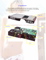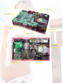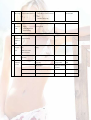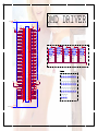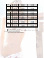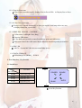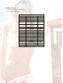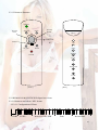
1
Contents
1.Safety Precautions
3
2.Servicing Precautions
4
3.Specifications
5
4.Exploded View
6
5.Replacement Parts List
8
6.Block Diagram
11
7.Packaging Description
12
8.Appearance Description
14
9.Alignment Procedure
16
10.How to disassemble the set
23
11.FAQ (Frequently Asked Questions)
32
12.Trouble Shooting Guide
33
13.Service Adjustment Guide
38
14.Firmware upgrade procedure
44
15.RS232 Codes
47
16.Schematics
49
4. Exploded View
The top illustration shows the parts from the front of the projector. The illustration
on the next page shows the parts visible from the rear of the projector. To see exploded
views of the case parts, major components and optical engine.
Upper case
Lamp Module
Main Board
Ballast Module
Front Fan
Lens
6
Lamp Blower
DC-DC Board
Power Board
Rear Fan
Sensor Board
Color Drum
Optical Engine
Chip Board
7
5. Replacement Parts List
LG RD-JT30
99.J4977.L31
NO.
BenQ P/N
LG P/N
DESCRIPTION
1
55.J4906.001
6871VSN256A PCBA CHIP/BD LG JT30
2
60.J4910.001
3680V00113A ASSY LENS C1,C2 JT30 PROT
3
60.J4911.001
5018V00071A ASSY FOLD MIRROR MODULE JT30
4
60.J4912.CL1
6912B22006A ASSY CSD RD-JT30 LAMP MODULE
4-1
35.81J49.001
3680V00111A
5
55.J4922.001
6871VSN257A PCBA SENSOR/BD LG JT30
6
65.J4905.011
3680V00112B COLOR DRUM 35MM 90DEG JT30
7
65.J4901.011
3680V00116A PROJECTION LENS ZOOM JT31 CO
8
71.07XGA.B00
9
42.J4918.001
3720V00206A CVR LEFT ABS Y7006C JT30
10
42.J4919.001
3720V00207A CVR RIGHT ABS Y7006C JT30
11
54.J4913.001
5020V00811A KEYPAD BD/JT30
12
55.J4901.001
6871VMN657B PCBA MAIN/BD LG JT30
13
55.J4905.001
6871VSN259A PCBA DC-DC/BD LG JT30
14
55.J4911.001
6871VSN261A PCBA PFC/BD LG JT30
15
55.J4924.001
6871VSN260A PCBA REAR IR/BD JT30
16
60.J4901.001
3580V00093B ASSY FRONT DOOR JT30
17
54.J4912.001
6316000005A
18
55.J4908.001
6871VSN260B PCBA IR/BD LG JT30
19
60.J4905.001
3110V00320B ASSY UPPER CASE JT30
20
60.J4906.001
3720V00205A ASSY REAR COVER JT30
21
60.J4907.001
3110V00321A ASSY LOWER CASE JT30
22
60.J4908.001
3580V00094A ASSY LAMP DOOR JT30
23
44.J0502.181
3890V01751C CTN 415X325X255 LG JT30
24
47.J4908.001
3920V00533B CSN RIGHT JT30
25
27.01218.191
6410VWH015D CORD H03VV-F3G(MI) 2500MM CEE
26
27.01418.011
6410VWH015H CORD H05VV-F(MI*3)6A250V S-AF
27
27.02718.201
6410VWH015E CORD H05VV-F(MI) 10A250V2500U
28
27.04318.031
6410VWH015F CORD VCTF3G(MI)7A125V 1800 T-
29
50.73213.501
6851V00021N CABLE 4P USB A-B 1800MM BLACK
30
50.J2401.001
6851V00021U CABLE D-SUB/RCA 1800MM/SL705X
31
50.J2403.501
6851V00021P SIGNAL/C 15/15P (-9) 2500MM
Glass front UVAR JT30 PROT
6871VSN271B IC DMD 0.7XGA DDR 12
BALLAST PHG151G14 USHIO JT30
8
32
50.72918.001
6851V00021R CABLE A/V RCA(R,W,Y)1500MM
33
50.72920.011
6851V00021V C.A MIN-DIN 4P S-VIDEO W/S 15
34
98.J5501.001
6710V00086E REMOTE CONTROLLER LG 6710V008
34-1
35
3550V00341A BATTERY COVER FOR REMORE CONTROL
98.J1302.041
3880VA0025A SOFT CASE SL705X LG
LG RD-JT31
99.J5577.L31
NO.
BenQ P/N
LG P/N
DESCRIPTION
1
55.J4906.001
6871VSN256A
PCBA CHIP/BD LG JT30
2
55.J4922.001
6871VSN257A
PCBA SENSOR/BD LG JT30
3
65.J4905.001
3680V00112A
COLOR DRUM 35MM 80DEG JT30
4
60.J4910.001
3680V00113A
ASSY LENS C1,C2 JT30 PROT
5
60.J4911.001
5018V00071A
ASSY FOLD MIRROR MODULE JT30
6
60.J4912.CL1
6912B220006A
ASSY CSD RD-JT30 LAMP MODULE
6-1
35.81J49.001
3680V00111A
Glass front UVAR JT30 PROT
7
65.J4901.011
3680V00116A
CTION LENS ZOOM JT31 CO
8
71.08060.000
6871VSN271A
IC DMD 0.6SVGA 8060-624C 12DD
9
42.J4918.001
3720V00206A
CVR LEFT ABS Y7006C JT30
10
42.J4919.001
3720V00207A
CVR RIGHT ABS Y7006C JT30
11
54.J4913.001
5020V00811A
KEYPAD BD/JT30
12
55.J4905.001
6871VSN259A
PCBA DC-DC/BD LG JT30
13
55.J4911.001
6871VSN261A
PCBA PFC/BD LG JT30
14
55.J4924.001
6871VSN260A
PCBA REAR IR/BD JT30
15
55.J5501.001
6871VMN657A
PCBA MAIN/BD JT31
16
60.J4901.011
3580V00093A
ASSY FRONT DOOR JT31
17
54.J4912.001
6316000005A
BALLAST PHG151G14 USHIO JT30
18
55.J4908.001
6871VSN260B
PCBA IR/BD LG JT30
19
60.J4905.011
3110V00320A
ASSY UPPER CASE JT31
20
60.J4906.001
3720V00205A
ASSY REAR COVER JT30
21
60.J4907.001
3110V00321A
ASSY LOWER CASE JT30
22
60.J4908.001
3580V00094A
ASSY LAMP DOOR JT30
23
44.J0502.181
3890V01751C
CTN 415X325X255 LG JT30
24
47.J4908.001
3920V00533B
CSN RIGHT JT30
25
27.01218.191
6410VWH015D
CORD H03VV-F3G(MI) 2500MM CEE
26
27.01418.011
6410VWH015H
CORD H05VV-F(MI*3)6A250V S-AF
27
27.02718.201
6410VWH015E
CORD H05VV-F(MI) 10A250V2500U
9
28
27.04318.031
6410VWH015F
CORD VCTF3G(MI)7A125V 1800 T-
29
50.73213.501
6851V00021N
CABLE 4P USB A-B 1800MM BLACK
30
50.J2401.001
6851V00021U
CABLE D-SUB/RCA 1800MM/SL705X
31
50.J2403.501
6851V00021P
SIGNAL/C 15/15P (-9) 2500MM
32
50.72918.001
6851V00021R
CABLE A/V RCA(R,W,Y)1500MM
33
50.72920.011
6851V00021V
C.A MIN-DIN 4P S-VIDEO W/S 15
34
98.J5501.001
6710V00086E
REMOTE CONTROLLER LG 6710V008
3550V00341A
BATTERY COVER FOR REMOTE CONTROL
3880VA0025A
SOFT CASE SL705X LG
34-1
35
98.J1302.041
10
6. Block Diagram
11
7. Packaging Description
12
13
8. Appearance Description
14
15
9. Alignment Procedure
1.DMD Bias Voltage Alignment
Equipment:None
Procedure:
Watch DMD “Bias Voltage Bin” Label (Example: 8060-7bbc DDDD XXXXXXX M)
Switch the DIP switch (SW2) on Main board according to the red character on the
DMD chip
3. 00: E
01: D
10: C
11: B
ON
0
0
16
2.Color Wheel Delay Alignment
Equipment:
Battery Biased Silicon PIN Detector
Oscilloscope
Probe
Procedure:
Probe impedance matches 50 ohm
Open Factory OSD, and select color wheel delay item
Leave the image pure red (DMD red curtain)
Put the detector on the screen that red image was projected.
Watch the oscilloscope and notice the square waveform
Use the “ ” and “ ” key to increment or decrement the color wheel delay value
No matter the waveform is square or not, let the waveform was lagged first
Lag
Exact
Ahead
Then increment or decrement the value to let the waveform to be square
Do not adjust too much, let the signal get ahead, if it happens, go back to step 7 and do
it again.
Change the input to pure blue and repeat the above procedures again.
3.PC Color Alignment Procedure
Equipment:
Pattern generator
Procedure:
Connect power, D-sub, into projector.
Change pattern generator to pattern 43 5-DISC.
Light on projector
Enter factory mode.
Choose ADC Brightness item to Press.
Choose ADC Contrast item to Press.
Change pattern generator to pattern 32 gray bar.
See if any gray level was abnormal, if the abnormality happened, went back to
step 4 and then redid it again.
Quit factory mode, after above adjustments finished.
17
4.HDTV Color Adjustment Procedure
Equipment:
Pattern generator (VG-828)
Lux meter ( CL-100)
Procedure:
(a). Offset adjustment:
Black coordinate spec:
Osram lamp Oshio lamp
x0
0.281 0.01 0.313 0.01
y0
0.311 0.01 0.329 0.01
The variance of color coordinate via Pb offset and Pr offset:
x
y
Pb offset
x
y
Pb offset
x
y
Pr offset
x
y
Pr offset
x
y
If we line the x and y, then the Pb offset is the shift action and the Pr offset is the
rotational action.
Connect power, YPbPr Video into projector.
Change Timing and pattern of pattern generator :
Timing : 480P(H:31.54 KHz,V:60.08 Hz)
pattern : black
Light on projector
Set user OSD values to default.
Enter factory mode.
Set Factory values to default.
Follow the PbPr offset adjustment flow chart:
18
19
5.Optical Engine Assembly Procedure
Note:
1.Every operator must check the dust/chip on every optical component before
assembly.
2.Dust remove procedure is defined in document 01.
No. Stop
Check
1.
Remove dust on ROD
ROD
Pull the clip backward by
Action
Review
Equipment
Assemble Clip Rod Btm
Screw driver
Put a little glue on ROD align surface
glue CA064
Assemble ROD
Screw driver
screw driver
Assemble clip rod top
2
Assy
Check the followed
C1C2
direction of C1C2 on SOP
Assemble clip rod side
Screw driver
Assemble c1c2 module
Screw driver
module
3.
Assy FM
make sure the direction of 1.Put glue 727 on three slot datum of
Glue 727 and Activator
on holder
mirror is precise
A649
holder
2.put A649 on the back of mirror
3.Assemble mirror on holder by glue
4.
5.
Assy FM
Assemble FM module on Dmd Hsg
Module
with spring and adjust screw washer
Screw driver
Keep the original position
Control the 1.65mm between Hsg
Screw driver
of fold mirror
and holder by jig or torgue
jig
Assy C3
Make sure Lens C3 is
Assemble lens C3 on holder
UV glue and UV gun
Lens on
exactly contacted on
Holder
related datum of holder
Assemble C3 module on hsg
Screw Driver
Lens C3
6.
Assemble
C3 module
on hsg
20
7.
Assemble
Make sure TIR is exactly
1.
TIR on Hsg contacted related datum of 2.
3.
Assemble
on bkt
Put CA064 on bottom surface of
Activator A649
Assemble TIR on Hsg
Follow the screw
Assemble color drum/ bd_sensor on Screw torgue 1kgf
torgue
bkt motor mount
1.
Color Drum
Glue 727
TIR
hsg
8.
put glue 727 on 4 Hsg Datum
2.
avoid straight load
toward bearing
9.
Assemble
Avoid interfere with ROD
Assemble Color drum module on Hsg
Screw driver
Color Drum during assembling
module on
HSG
Assemble
1.avoid interfere with color Assemble CVR Color drum module
cvr color
drum
drum
2. Make sure CVR’s
Screw driver
on Hsg
location is correct
Check interfere after
assembling
10.
DMD
Assemble DMD/DMD_BD/ projection DMD contact
Screw Driver(M2) for
Module/En
lens on Hsg
Cspring contact
DMD
gine Test
Over Fill adjust
Adjust three screws of
FM module
C/W delay adjust and Engine Test
Senserand Oscilloscope
Fix FM by glue
Screw Glue
21
6. Power Alignment
PFC Output voltage
Output voltage range: 340 ~ 410VDC
Output current: 0.025 ~ 0.45ADC
Input voltage: 110VAC or 220VAC, 50 or 60Hz
DC/DC Output voltage
Output voltage
Output voltage range
+3.3V
+5V
3.20 ~ 3.55V
4.75~ 5.25V
Output current
0.5 ~ 1.7A
0.1 ~ 0.15A
+12V
11.9~ 13.2V
0.1 ~ 0.8A
Input voltage (from Line and Neutral): 110VAC or 220VAC, 50 or 60Hz
3.
CY690, CY691 Only for reflow soldering. Please pay attention.
CY690, CY691 are in the 55.J4911.M01
22
10. How to disassemble the set
1. Lamp Module
The lamp module is located at bottom of the projector. The lamp module behinds
the lamp cover with 1 captive screw. After you replace the lamp module, you should
reset the lamp hour counter. The switch interrupts power supply output to the projector
if you remove the lamp cover.
WARNING Allow the projector to cool before removing the lamp module. The lamp module becomes
very hot when the projector is in use. DO NOT touch any part of the lamp module that is
located in the lamp box. Oils from your fingers will cause smudges and uneven heating of
lamp surfaces, resulting in decreased image quality and premature lamp failure. If the lamp
is ruptured or the lamp module is cracked or damaged, be careful of quartz or glass
fragments that could cause personal injury.
1.Remove two screws of lamp cover which is a spring door.
2. Remove the 1 screw from the lamp module.
23
3. Grasp the handle on the lamp module and pull the module out of the lamp box.
2. Covers
2.1 Side bezel
1. Remove 4 screws under the projector of left side bezel, then remove it out of
projector.
2. Remove 4 screws under the projector of right side bezel, then remove it out of
projector.
24
2.2 Front bezel
1. Remove the 2 screws under the projector of front bezel, then remove front bezel out
of projector.
2.3 Rear bezel
1. Remove 2 screws under the projector of bottom bezel.
2. Remove 8 screws and 2 jack screws on the rear bezel.
3. Pull the rear bezel out of projector.
25
2.4 Upper case
1. Pull the upper case out of projector.
2. Be sure to remove wire of keypad board, then the upper case can be removed.
26
3. Main board
1. Remove 5 screws and 10 wires.
2. Be sure to remove 1 wire, then the main board can be removed.
27
4. DC-DC Board
1. Remove 2 screws, 2 jack screws and 1 wire.
2. Be sure to remove connector from the power board.
28
5. Front Fan
1. Remove 2 screws, then the front fan can be removed.
6. Power Board
1. Remove 4 jack screws and 2 wires, then the power board can be removed.
7. Rear Fan
1. Remove 2 screws, then the rear fan can be removed.
29
8. Ballast Module
1. Remove golden screw.
2. Remove 3 wires.
3. Be sure to remove 1 wire, then the ballast module can be removed.
30
9. Lamp Blower
1. Remove 2 screws, then the lamp blower can be removed.
10. Optical engine
1. Remove 4 screws, then the optical engine can be removed.
31
11. Frequently Asked Questions
1. Why the unit doesn’t power on?
1) Make sure the power cord is inserted into the AC adapter socket.
2) Make sure the power cord is inserted into the power outlet.
3) Wait 90 seconds after the projector is turned off before turning the projector
back on.
2. Why the unit has no picture?
1) Check for the proper input source.
2) Ensure all cables are connected properly.
3) Adjust the brightness and contrast.
3. Why the unit has trapezoid image on the screen?
1) Reposition the unit to improve its angle on the screen.
2) Use the Keystone correction key on the remote control unit.
4. Why the unit has poor color?
1) Select the correct video system.
2) Adjust brightness, contrast, or saturation.
5. Why the unit has blurred image?
1) Press Auto on the control panel of the projector or the remote control unit to get
better picture quality.
2) Adjust the focus.
3) Reposition the unit to improve its projection angle.
4) Ensure the distance between the unit and screen is within the adjustment
range of the lens.
6. Why the remote control doesn’t work?
1) Replace the batteries with new one.
2) Make sure there is no obstacle between the remote control and the projector.
3) Make sure nothing is blocking the front and rear receivers.
32
12. Trouble Shooting Guide
Optical Engine trouble shooting guide
Debug Item
Trouble Shooting Guide
1. Brightness
1.Check EE setting / Follow up EE alignment procedure
2.Check fold mirror position / re-align fold mirror to be closer to design position.
3.Check Rod lens at datum surface / put rod lens at right datum surface
4.Check Green color / If too green and over spec., change color drum
5.Change lamp
2. Uniformity
1.Check fold mirror position / re-align fold mirror to be closer to design position
2.Check lamp / Re-assembly lamp
3. On/Off Contrast
1.Check projection lens clean / To clean projection lens
2.Check TIR and DMD clean / To clean TIR and DMD
4. ANSI Contrast
1.Check projection lens clean / To clean projection lens
2.Change projection lens
5. Color
1.Check Front glass
2.Check color drum 50% point for every segment
6. Color Uniformity
1.Check DMD
2.Check rod output surface
7. Focus
1.Check TIR at datum surface / Change HSG and TIR
2.Check focus by Focus formula Y=-0.00037X+0.002 (X at the front of Screen
is – and at rear of Screen is +)/ assembly slim metal sheet on projection lens
8. Dust
1.Clean rod output surface
2.Clean DMD surface
33
JT31 Electrical Debug Guide
1.chk voltage input from DC/B : 3.3V(TP23),5V(TP24),12V(TP34)
2.chk oscillator Y4,Y5 output frequency (Y4:16.257MHz, Y5:10MHz))
3.chk MCLK(U37-5,130MHz) and DCLK(U39-5,40MHz)
4.chk U38 whether S/W inside or bad soldering
5.chk Reset IC (U40)
6. change U35(bad soldering)
7.chk Abnorm al signal
8.chk Resetz(RN40),PW RGO OD(RN40) ,VSYNCZ(R182), HSYNCZ(R183),
ACTDAT A(R184), CLKIN(R181)
System no work
Yes
No
No data to
DDP1000
No
Yes
1.chk output from U32(RN16-RN21) [graphics input]
2.chk output from U109 (RN101 - RN104) [video input]
3.chk U1and its peripherals (as above block)
Yes
1.chk DDP1000 debug guide
No im age
No
No im age when graphics
is the current input
1.chk D_SUB cable and J103
2.chk VSYNC(U103-4),HSYNC(U105-4)
3.chk U32 voltage source U29-2(3.3V),U30-2(3.3V),L22(3.3V)
4.chk G HS1(R171), GVS1(R170), GCLK(R173)
5.chk U3 2soldering
6.change U32
Yes
No
No im age when video
is the current input
1.chk video input connector J12 and J102
2.chk U107 voltage source L110(5V), L111(3.3V),VSTBY(U107-59)
3.chk Y101 output frequency(20.25MHz)
4.chk U107 output signals to U109 (Y0~Y7, UV0~UV7)
5.chk U107 soldering
6.chagne U107
Yes
No
Unable to download
Yes
1.chk U20 enable pins(1,4)
2.change U20
No
Unable to save
OSD setting
Yes
1.change U41
1.chk R103~R106 soldering
2.chk U18(74AHC244)
No
Yes
Keypad
m alfunction
No
No
Image crossover
distortion or contour
Yes
1.chk soldering from RN16~RN21 (graphics input)
2.chk slodering from RN101~RN104 (video input)
34
DDP1000 Debug Guide
35
36
13. Service Adjustment Guide
1. How to enter factory menu:
1) Press keypad <Power> key, Enter Power Off check state (Fig-1).
(Fig-1).
2) Press keypad <Source> and <Auto> key simultaneously, enter
“Lamp Hour
Info” layer (Fig-2).
(Fig-2) Lamp Hours Info
3) Press keypad <Source> and <Auto> key simultaneously again, then enter
Factory menu.
WARNING
Note CW delay value in DMD layer and PbPr values in YpbPr Factory control before Upgrade
the Software.
38
2.Factory layer:
1) DMD layer (Fig-3):
(Fig-3) DMD layer
1.1) CW delay: adjust color wheel delay. (Note this value Before Upgrade
Software)
1.2) White peak: adjust DMD white peak. In PC mode default value set 10, in
Video mode is 0.Software auto set this value as source find.
1.3) DLP Brightness: adjust DLP Brightness. default setting is 36.Do not
change this value .
1.4) DLP Contrast: adjust DLP Contrast. Default setting is 30.Do not change
this value.
1.5) Burn-In Hour: set how many hours to burn-in. You can enable burn-in on
next selection.
1.6) Burn-In: after you set burn-in hours, set this selection to On and system
will going to burn-in immediately. You can see color change (red, green,
blue, black, white) on screen in turn. System will auto turn off after burn-in
hour count down to 0 and burn-in complete. (You can also cancel burn-in
sequence by set this selection to Off).
39
2) ADC layer (Fig-4): (only available when input source is analog RGB)
(Fig-4) ADC layer
2.1) ADC Brightness: ADC brightness auto calibration black.
2.2) ADC Contrast: ADC contrast auto calibration white.
2.3) ADC Offset RGB: value to tell you calibrate result.
2.4) ADC Gain RGB: value to tell you calibrate result.
2.5) Fac Brightness: adjust default brightness value in source PC.
2.6) Fac Contrast: adjust default contrast value in source PC.
3) Color layer (Fig-5):
(Fig-5) Color layer
40
3.1) FAN: enter system fan status info layer.
Lamp Sensor: lamp sensor temperature
Lamp Fan Speed: lamp fan speed in RPM
Blower Speed: Blower fan speed in RPM
Power Sensor: Power sensor temperature
Power Fan Speed: Power fan speed in RPM
Fixed Fan Speed: Disable auto fan speed control and fix fan speed
3.2) PbPr: enter PbPr color control Layer.
When Source is YPbPr (Never Change these setting)
(Note these values Before Upgrade Software)
PbPr G Offset : combine with user osd brightness in YPbPr
PbPr G Gain: combine with user osd contrast in YPbPr
PbPr R Offset: offset of color red
PbPr G Offset: offset of color green
PbPr R Gain: saturation R
PbPr B Gain: saturation B
3.3) V9300R,G, B: Reserve for future use.
3.4) Color Temp: Reserve for future use.
41
4) Optic layer (Fig-5):
(Fig-5) Optic layer
4.1) Test Pattern: system auto produce pattern for engineer test.
4.2) Spoke light: unit display full white.
4.3) Curtain Red: unit display full color red.
4.4) Curtain Green: unit display full color green.
4.5) Curtain Blue: unit display full color blue.
5) Lamp layer (Fig-6):
(Fig-6) Lamp layer
5.1 )Interpolation: De-interlace Mode
5.2) Filter: system auto select Filter.
5.3) Lamp Hour: value to tell you lamp usage hours.
5.4) Usage Hour: value to tell you unit usage hours.
5.5) Data Reset: Reset all data to default include factory assign value.
Never try to reset all data.
5.6) Version: software version.
42
6) Others layer (Fig-7):
(Fig-7) YPbPr layer
6.1) Gamma index: system auto select DLP gamma index
6.2) Gray value: adjust here to check DMD fail pixel.
6.3) Blue value: adjust here to check DMD fail pixel.
6.4) Scaling: tell you what scaling mode is using now.
6.5) Pc/PbPr Mode: index of input timing
6.6) RS232: Enable / Disable RS232 control
43
14. Firmware Upgrade Procedure
Step 1
Setup Flashloader in computer.
Step 2
a. Connect download cable with computer and projector
b. Connect power cord with projector and check power switch is OFF.
Step 3
Execute FLASH loder.exe
Step 4
Setting COM Port & Baud Rate
44
Step 5
a. Turn on the power switch of the projector, then the Program will target the Flash.
b. HEX File Format choose Intel Extended
c. File Name choose
d. Operation choose Program
Step 6
Start download firmware
45
Step 7
Download finished.
Step 8
Turn off the power switch.
46
15. RS232 Codes
Event Packet Type command:
Command
Power
Auto
Source
Menu
Left (-)
Right (+)
UP
Down
Blank
Still
Resize
Keystone (+)
Keystone (-)
Zoom (+)
Zoom (-)
Enter
Packet Header (7 bytes)
BE EF 02 06 00 97 CF
BE EF 02 06 00 AB CA
BE EF 02 06 00 98 CA
BE EF 02 06 00 7A CB
BE EF 02 06 00 2F CB
BE EF 02 06 00 CD CA
BE EF 02 06 00 FE CA
BE EF 02 06 00 1C CB
BE EF 02 06 00 AD CD
BE EF 02 06 00 1A CC
BE EF 02 06 00 85 CB
BE EF 02 06 00 D5 C7
BE EF 02 06 00 04 C6
BE EF 02 06 00 7C CC
BE EF 02 06 00 4F CC
BE EF 02 06 00 B3 C7
Packet Payload (6 bytes)
AE 00 00 00 00 00
92 00 00 00 00 00
9B 00 00 00 00 00
93 00 00 00 00 00
96 00 00 00 00 00
94 00 00 00 00 00
97 00 00 00 00 00
95 00 00 00 00 00
B4 00 00 00 00 00
B3 00 00 00 00 00
9C 00 00 00 00 00
CC 00 00 00 00 00
CD 00 00 00 00 00
B5 00 00 00 00 00
B6 00 00 00 00 00
CA 00 00 00 00 00
Operation Packet Type command
PC Picture Controls
Command
Packet Header (7 bytes)
Packet Payload (25 bytes)
Brightness +
BE EF 03 19 00 EE 68
03 CA 02 CC CC 00 00 00 00 CC×16
Brightness -
BE EF 03 19 00 80 C2
04 CA 02 CC CC 00 00 00 00 CC×16
Contrast +
BE EF 03 19 00 34 D9
07 C9 02 CC CC 00 00 00 00 CC×16
Contrast -
BE EF 03 19 00 11 8C
03 C9 02 CC CC 00 00 00 00 CC×16
YPbPr Picture Controls
Command
Packet Header (7 bytes) Packet Payload (25 bytes)
Brightness +
BE EF 03 19 00 44 81
03 D5 02 CC CC FF FF FF FF CC×16
Brightness -
BE EF 03 19 00 2A 2B
04 D5 02 CC CC FF FF FF FF CC×16
Contrast +
BE EF 03 19 00 BB 65
03 D6 02 CC CC FF FF FF FF CC×16
Contrast -
BE EF 03 19 00 D5 CF
04 D6 02 CC CC FF FF FF FF CC×16
47
S-Video / Composite Video Picture Controls
Command
Packet Header (7 bytes) Packet Payload (25 bytes)
Brightness +
BE EF 03 19 00 95 52
03 4B 02 CC CC 00 00 00 00 CC x16
Brightness -
BE EF 03 19 00 FB F8
04 4B 02 CC CC 00 00 00 00 CC x16
Contrast +
BE EF 03 19 00 BF C4
03 4C 02 CC CC 00 00 00 00 CC x16
Contrast -
BE EF 03 19 00 D1 6E
04 4C 02 CC CC 00 00 00 00 CC x16
Color +
BE EF 03 19 00 C0 EE
03 54 02 CC CC 00 00 00 00 CC X16
Color -
BE EF 03 19 00 AE 44
04 54 02 CC CC 00 00 00 00 CC x16
Tint +
BE EF 03 19 00 EA 78
03 53 02 CC CC 00 00 00 00 CC x16
Tint -
BE EF 03 19 00 84 D2
04 53 02 CC CC 00 00 00 00 CC x16
48
DMD DRIVER
DD [0:6 3]
DD [0:63]
J1
TP67
TP64
P3P3V
TP66
VCC2
TRC-L
TP70
TP72
D D3
D D9
TP74
TP76
D D5
D D 11
TP78
TP80
D D 21
D D 17
TP82
TP84
D D 19
D D 15
TP86
TP88
D D4
D D0
TP90
TP92
D D8
D D1
TP94
TP96
D D6
D D2
TP98
TP100
D D7
D D 13
TP102
TP104
D D 43
D D 51
TP106
TP108
D D 47
D D 53
TP110
TP112
D D 63
D D 57
TP114
TP116
D D 45
D D 55
TP118
TP120
D D 62
D D 59
TP122
TP124
D D 58
D D 50
TP126
TP153
D D 49
D D 61
TP128
TP130
D D 60
D D 48
P3P3V
TP134
TP132
LOAD B-LZ
TP136
D MDSER
TP137
TP139
MBRST14 TP141
TP143
MBRST12
MBRST10
MBRST8 TP145
TP147
MBRST6 TP149
TP151
MBRST4
MBRST2
MBRST0
1
3
5
7
9
11
13
15
17
19
21
23
25
27
29
31
33
35
37
39
41
43
45
47
49
51
53
55
57
59
61
63
65
67
69
71
73
75
77
79
81
83
85
87
89
91
93
95
97
99
101
103
105
107
109
111
113
115
117
119
121
123
125
127
129
131
133
135
137
139
1
3
5
7
9
11
13
15
17
19
21
23
25
27
29
31
33
35
37
39
41
43
45
47
49
51
53
55
57
59
61
63
65
67
69
71
73
75
77
79
81
83
85
87
89
91
93
95
97
99
101
103
105
107
109
111
113
115
117
119
121
123
125
127
129
131
133
135
137
139
2
4
6
8
10
12
14
16
18
20
22
24
26
28
30
32
34
36
38
40
42
44
46
48
50
52
54
56
58
60
62
64
66
68
70
72
74
76
78
80
82
84
86
88
90
92
94
96
98
100
102
104
106
108
110
112
114
116
118
120
122
124
126
128
130
132
134
136
138
140
20L1071140
MBRST[0:15]
MBRST[0:15]
2
4
6
8
10
12
14
16
18
20
22
24
26
28
30
32
34
36
38
40
42
44
46
48
50
52
54
56
58
60
62
64
66
68
70
72
74
76
78
80
82
84
86
88
90
92
94
96
98
100
102
104
106
108
110
112
114
116
118
120
122
124
126
128
130
132
134
136
138
140
SCTRL-L
TP68
TP71
TP65
D D 10
D D 23
TP75
TP69
D D 18
D D 12
TP79
TP73
D D 16
D D 22
TP83
TP77
D D 24
D D 20
TP87
TP81
D D 14
D D 27
TP91
TP85
D D 26
D D 25
TP95
5
TP89
D D 28
D D 29
TP99
TP93
D D 30
D D 31
TP103
TP107
TP111
TP115
TP119
TP123
TP127
TP125
TP131
TP146
TP148
TP150
TP152
MBRST7
MBRST5
MBRST3
MBRST1
3
7
3
7
2
6
6
5
9
5
9
5
9
4
8
4
8
4
8
3
7
3
7
3
7
2
6
2
6
2
6
H3
H4
H5
HOLE-V8
HOLE-V8
HOLE-V8
HOLE-V8
MARK1
OP
MARK2
OP
MARK3
OP
MARK4
OP
MARK5
OP
MARK6
OP
MARK7
OP
MARK8
OP
MARK9
OP
MARK10 MARK11 MARK12 MARK13 MARK14
OP
OP
OP
OP
OP
VCC2
SACBUS
SACCLK
MBRST15
MBRST13
MBRST11
MBRST9
8
HOLE-V8
D CLK-L
TP154
TP138
TP140
TP142
TP144
8
H1
TP133
TP135
9
4
H2
TP97
D D 32
D D 37
TP101
D D 33
D D 36
TP105
D D 34
D D 41
TP109
D D 46
D D 35
TP113
D D 38
D D 56
TP117
D D 39
D D 42
TP121
D D 40
D D 54
TP129
D D 52
D D 44
4
2
5
9
MARK15 MARK16 MARK17 MARK18 MARK19 MARK20 MARK21
OP
OP
OP
OP
OP
OP
OP
MARK22 MARK23 MARK24
OP
OP
OP
FLDATA[0:15]
U 1A
FLDATA0
FLDATA1
FLDATA2
FLDATA3
FLDATA4
FLDATA5
FLDATA6
FLDATA7
FLDATA8
FLDATA9
FLDATA10
FLDATA11
FLDATA12
FLDATA13
FLDATA14
FLDATA15
AE23
AE22
AC21
AF23
AE21
AD21
AC20
AF22
AE20
AD20
AF20
AD19
AC18
AE18
AF19
AD18
U2
FLDATA0
FLDATA1
FLDATA2
FLDATA3
FLDATA4
FLDATA5
FLDATA6
FLDATA7
FLDATA8
FLDATA9
FLDATA10
FLDATA11
FLDATA12
FLDATA13
FLDATA14
FLDATA15
FLADDR19
FLADDR18
FLADDR17
FLADDR16
FLADDR15
FLADDR14
FLADDR13
FLADDR12
FLADDR11
FLADDR10
FLADDR9
FLADDR8
FLADDR7
FLADDR6
FLADDR5
FLADDR4
FLADDR3
FLADDR2
FLADDR1
FLADDR0
AD12
AE13
AF12
AF13
AD14
AD13
AF14
AE14
AC15
AD15
AC14
AE15
AD16
AC16
AF17
AE16
AD17
AF18
AC17
AE17
FL_OE
FL_WE
FL_CS
AD23
AD22
AF24
FLADDR19
FLADDR18
FLADDR17
FLADDR16
FLADDR15
FLADDR14
FLADDR13
FLADDR12
FLADDR11
FLADDR10
FLAD DR 9
FLAD DR 8
FLAD DR 7
FLAD DR 6
FLAD DR 5
FLAD DR 4
FLAD DR 3
FLAD DR 2
FLAD DR 1
FLAD DR 0
D4
C3
B2
E6
D6
C6
A6
B6
D5
C5
A5
B5
A2
C2
D2
B1
A1
C1
D1
E1
PUM-ARSTZ
P3P3V
PUM-ARSTZ
FLASH INTERFACE
FL-OEZ
FL-WEZ
FL- CSZ
DDP1000
A19
A18
A17
A16
A15
A14
A13
A12
A11
A10
A9
A8
A7
A6
A5
A4
A3
A2
A1
A0
B4
P3P3V
VDD
G4
DQ15/A-1
DG14
DG13
DG12
DG11
DG10
DG9
DG8
DG7
DG6
DG5
DG4
DG3
DG2
DG1
DG0
NC
NC
NC
G6
F5
G5
F4
G3
F3
G2
F2
E5
H5
E4
H4
H3
E3
H2
E2
C4
D3
B3
GND
GND
H6
H1
RESET
F6
BYTE
G1
A4
F1
OE
WE
CE
RY/BY
A3
FLDATA15
FLDATA14
FLDATA13
FLDATA12
FLDATA11
FLDATA10
FLDATA9
FLDATA8
FLDATA7
FLDATA6
FLDATA5
FLDATA4
FLDATA3
FLDATA2
FLDATA1
FLDATA0
P3P3V
C1
0.1U K
16V
FLASH +3.3V DECOUPLING CAPS
FLASH-BUSYZ
FLASH-BUSYZ
AM29LV800BB-120 GND:H6,H1
P3P3V:G4
NC:C4,B3,D3
U 1B
VREF-RDRAM
VSYNCZ
H SYNCZ
C LKIN
ACTDATA
P3P3V
R1
110F
C2
0.1U K
16V
FSD16
LAMPLITZ
LAMPEN
C3
0.1U K
16V
R2
R3
47
47
PW RGOO D
RESETQ
P2P5V
TP1
TP2
R26
N25
N23
M23
M24
E23
N26
M26
P25
P24
RQ [0: 7]
D13
C12
A12
A13
C13
A14
C15
D15
R Q7
R Q6
R Q5
R Q4
R Q3
R Q2
R Q1
R Q0
D QA[0:8]
A3
B4
A4
B6
D7
A5
C7
D8
A7
DQA8
DQA7
DQA6
DQA5
DQA4
DQA3
DQA2
DQA1
DQA0
D QB[0:8]
DQB8
DQB7
DQB6
DQB5
DQB4
DQB3
DQB2
DQB1
DQB0
A20
C19
B18
A19
D17
A18
B16
A17
C16
DQB8
DQB7
DQB6
DQB5
DQB4
DQB3
DQB2
DQB1
DQB0
RD_SCK
RD_CMD
RD_SIO
RD_CFM
RD_CFMN
RD_CTM
RD_CTMN
PCLKM
SCLKN
REFCLK
A22
B20
C20
A8
C9
C10
A9
C21
B21
D20
VSYNCZ
HSYNCZ
WCLK
IVALID
OLACT
SYNCVALID2/DI2
CTRL
FLDSYNC
LAMPSTAT
LAMPCTRL
E1
G3
PWRGOOD
SYSRSTZ
D9
D11
B12
B10
RD_VREF1
RD_VREF0
RD_AVDD0
RD_AVDD1
C1
C23
M4
B24
C22
D5
C4
TDO2
TMS2
TDO1
TMS1
TDI
TRSTZ
TCK
B3
A24
AF2
AD2
K25
D19
PTSTENZ
ICTSENZ
IBMT_RI
IBMT_LT
POSTST
LSSDEN
RQ7
RQ6
RQ5
RQ4
RQ3
RQ2
RQ1
RQ0
DQA8
DQA7
DQA6
DQA5
DQA4
DQA3
DQA2
DQA1
DQA0
P3P3V
C4
0.1U K
16V
C5
68P J
50V
R4
10K
10K
R5
TMS2
TMS1
R6
TP8
TP9
P5V
OPDI ODE
R 10
180
R11
75K
R12
2K
C WINDEX
R14
10K
C6
0.1U K
R15
330K P5V
C WIN DEX
U3
1
2
INPUT
3
OUTPUT
V-
5
R13
10K
V+
INPUT+ INPUT-
4
2P5VREF
LMC7225
C7
10P J
C8
0.1U K
J2
TP10
R16
6.8K
TDO2
TP4
TDO1
TP5
TP6
TP7
TD1
TRSTZ
TCK
ICTSEN Z
10K
C WSENSOR
TP3
3
2
1
20L2021003
RAMBUS, JTAG, CUSTOMER INPUT
DDP1000
RQ [0:7]
D QA[0:8]
D QB[0:8]
SCK
C MD
SIO0
C FM
C FM N
CTM
CTMN
U5-C21
U5-B21
U5-D20
R7
39.2F
R8
39.2F
R9
39.2F
PCLKM
SCLKN
R EFCLK
VTERM
VDR C G
RN2
RN1
R17
10K
R18
10K
1
2
3
4
VTERM
R19
10K
8
7
6
5
8
7
6
5
39 1
VDR C G
C DC R83
U4
2
7
6
R EFCLK
SCLKN
PCLKM
MULT0
MULT1
P2P5V
D RC GPDZ
REFCLK
SYNCLKN
PCLKM
15
14
MULT0
MULT1
24
23
13
S0
S1
S2
12
11
STOPZ
1
CTM
20 U15-20
3
9
16
22
19
R20
110F
CTM
39
RN3
39
8
7
6
5
RN4
8
7
6
5
GND
GND
GND
GND
GND
VDDIPD
CLKB
39
CTM
D QB[0:8]
RQ [0:7]
RQ [0: 7]
U5
C9
10P J
50V
4
5
8
17
21
18 U15-18
1
2
3
4
R21
56.2F
U15-C76
VDDIR
10
C11
0.1U K
16V
CLK
VDD
VDD
VDD
VDD
NC
PWRDNB
STOPB
R22 10K
2
3
4
1
2
3
4
C10
0.1U K
16V
R23
56.2F
R24
110F
CTMN
C12
0.1U K
16V
CTMN
CTMN
SIO0
C MD
SCK
R26
10K
P2P5V
CTM
CTMN
CFM
R Q0
R Q1
R Q2
R Q3
R Q4
R Q5
R Q6
R Q7
G1
F2
F6
F7
F1
E7
E6
E2
RQ0
RQ1
RQ2
RQ3
RQ4
RQ5
RQ6
RQ7
SIO1
SIO0
C MD
SCK
J3
J5
A5
A3
SIO1
SIO0
CMD
SCK
CTM
CTMN
C FM
C FMN
E1
D1
C7
D7
D2
CTM
CTMN
CFM
CFMN
VREF
A2
J2
D6
B5
C3
E5
F3
G5
H5
VCMOS
VCMOS
VDDA
P2P5V
P2P5V
P2P5V
P2P5V
P2P5V
P2P5V
R28
39.2F
R29
75F
R30
75F
U7-C75
C13
0.1U K
16V
R31
39.2F
K4R271669D-TCS8
J1
J7
H2
H6
H7
H1
G2
G6
G7
DQB8
DQB7
DQB6
DQB5
DQB4
DQB3
DQB2
DQB1
DQB0
DQA0
DQA1
DQA2
DQA3
DQA4
DQA5
DQA6
DQA7
NC2
C1
C2
C6
B1
B7
B6
B2
A7
A1
DQA0
DQA1
DQA2
DQA3
DQA4
DQA5
DQA6
DQA7
DQA8
GNDA
GND
GND
GND
GND
GND
GND
GND
GND
GND
D5
A6
B3
C5
D3
E3
F5
G3
H3
J6
NC1
DQB7
DQB6
DQB5
DQB4
DQB3
DQB2
DQB1
DQB0
R33
75F
39.2F
R27
39.2F
RN5
8
7
6
5
1
2
3
4
39
RN6
C FM N
R32
75F
R25
8
7
6
5
P2P5V
1
2
3
4
39
P3P3V
VDR C G
VTERM
L1
R34
VREF-RDRAM
D QA[0:8]
36.5F
VDR C G
120 OHM
C15
0.1U K
16V
C16
10U
6.3V
C17
0.1U K
16V
C18
68P J
50V
C19
0.1U K
16V
C20
68P J
50V
C21
0.1U K
16V
C22
68P J
50V
C23
0.1U K
16V
C24
68P J
50V
R35
121F
C14
0.1U K
16V
P2P5V
C25
150U
6.3V
VTERM
P2P5V
U6
1
IN
VTERM
MIC39100-1.8BS
OUT
3
C30
0.1U K
16V
C31
0.1U K
16V
C32
0.1U K
16V
C33
0.1U K
16V
C34
0.1U K
16V
C41
0.1U K
16V
C42
0.1U K
16V
C43
0.1U K
16V
C44
0.1U K
16V
VTERM
C35
0.1U K
16V
VTERM
C36
10U
6.3V
C37
0.1U K
16V
C38
100U
6.3V
C39
100U
6.3V
C40
0.1U K
16V
C45
0.1U K
16V
C26
0.1U K
16V
C27
0.1U K
16V
C28
0.1U K
16V
C29
0.1U K
16V
P2P5V
P3P3V
U 1E
DDP1000 BULK DECOUPLING CAPS
DDP1000 DECOUPLING FOR +3.3V
P3P3V
P3P3V
AC2
AB17
AB16
AB15
AB12
AB11
AB10
U22
U5
T22
T5
R22
R5
R1
M22
M5
L22
L5
K22
K5
E21
E20
E19
E17
E16
E15
E12
E11
E10
E8
E7
E6
B15
DDP1000 DECOUPLING FOR+2.5V
P3P3V
P2P5V
P2P5V
P2P5V
P2P5V
P2P5V
P2P5V
P3P3V
C54
10U
6.3V
C46
0.1U K
16V
C55
10U
6.3V
C47
0.1U K
16V
P3P3V
C48
0.1U K
16V
P3P3V
C56
0.1U K
16V
P2P5V
C57
0.1U K
16V
C49
0.1U K
16V
P2P5V
C58
0.1U K
16V
C50
0.1U K
16V
P2P5V
C59
0.1U K
16V
C60
0.1U K
16V
C51
0.1U K
16V
P2P5V
C52
0.1U K
16V
P2P5V
C61
0.1U K
16V
C53
0.1U K
16V
P2P5V
C62
0.1U K
16V
C63
0.1U K
16V
P2P5V
P3P3V
C64
150U
6.3V
P3P3V
C65
0.1U K
16V
P2P5V
C66
0.1U K
16V
P2P5V
C67
0.1U K
16V
P2P5V
COSC Oscillator Configuration
R40
R39
DMD Clock
30MHz Oscillator Y2 Installed
N/A
N/A
60MHz DDR
P2P5V
C68
0.1U K
16V
C69
0.1U K
16V
P2P5V
P2P5V
C70
0.1U K
16V
P2P5V
C71
0.1U K
16V
C72
0.1U K
16V
P2P5V
C73
0.1U K
16V
C74
0.1U K
16V
P3P3V
60MHz Oscillator Y2 Installed
N/A
Yes
60MHz DDR
60MHz Oscillator Y2 Non-Installed
Yes
Yes
50MHz DDR
U 1D
R36
10K
R39
0
R37
10K
R38
10K
R40
0
J1
AE19
AC19
AC22
AE24
OPEN
OPEN
0
R41
SDA0
SCL0
USBCLK
USBDATP
USBDATN
SDA0
SCL0
SCL0
SCL
TP11
TP12
TP13
SW1 SCL1
2240138001
SDA1
J3
3
2
1
MOSC
C OSC
P2P5V
20L2021003
L2
PLL-VCCA
120 OHM
DDP1000 flash download
R44
C75
0.1U K
16V
0
C76
0.1U K
16V
R43
0
OPEN
U7
1
C77
4.7U Z
50V
IN
GND
4
R43
GND
2
Install
Non Install
MOSC Configuration
Crstal
Oscillator
P3P3V
MIC39100
R45 1K
P2P5V
R46
BINSEL0
BINSEL1
1K
MTRSELZ
MTRCLK
MTRDATA
FLASH-BUSYZ
C78
22U
6.3V
SW2
6240019001
R24
R23
P23
R25
T24
T23
U26
T25
U24
V26
U23
U25
V24
W26
V25
V23
W24
Y26
W25
W23
Y24
Y25
AB26
Y23
DIO0
DIO1
DIO2
DIO3
DIO4
DIO5
DIO6
DIO7
DIO8
DIO9
DIO10
DIO11
DIO12
DIO13
DIO14
DIO15
DIO16
DIO17
DIO18
DIO19
DIO20
DIO21
DIO22
DIO23
P2P5V GENERATION
DDP1000
0
0
1
1
0
1
0
1
B
C
D
E
H1
J3
SR16ADDR3
SR16ADDR2
SR16ADDR1
SR16ADDR0
SR16MODE1
SR16MODE0
G1
H3
J4
J2
H4
H2
SR16SEL1
SR16SEL0
K2
K4
SR16SEL1
SR16SEL0
E4
B1
C2
D3
D MD BIN3
D MD BIN2
D MD BIN1
D MD BIN0
L3
L4
K1
K3
L2
VCC2EN
VBIASEN
VRSTEN
DMDBIN3
DMDBIN2
DMDBIN1
DMDBIN0
SR16VCCEN
DMDVCCEN
VCC2EN
VBIASEN
VRSTEN
0
D RC GPDZ
OPEN
P3P3V
APLLMD1
APLLMD0
MOSCN
MOSC
COSC
PLL_VCCA
CRYSTALEN
R42
SDA0
SDA
AB23
AC24
F2
F3
AD25
AE26
CR YSTALEN
G4
SR16STRB
SR16OEZ
TSTPNT3
TSTPNT2
TSTPNT1
TSTPNT0
OCLKA
OCLKB
VSOUTZ
FSD16
DMDLD
DCLKREF
PUM_ARSTZ
EXT_ARSTZ
EXT_ARST
DIO31
DIO30
DIO29
DIO28
DIO27
DIO26
DIO25
DIO24
SR16STROBE
SR16OEZ
SR16ADDR3
SR16ADDR2
SR16ADDR1
SR16ADDR0
SR16MODE1
SR16MODE0
B23
B22
D21
A23
D2
E3
CKMTR1
P26
N24
M3
N2
FSD16
D1
F4
E2
PUM-ARSTZ
EXT-ARSTZ
AB24
AD26
AC25
AB25
AA23
AC26
AA25
AA24
C WTACH
C WIN DEX
SR16ADDR[0:3]
P2P5V
P2P5V
P2P5V
P2P5V
P2P5V
P2P5V
P2P5V
P2P5V
P2P5V
P2P5V
P2P5V
P2P5V
P2P5V
P2P5V
P2P5V
P2P5V
P2P5V
P2P5V
P2P5V
P2P5V
P2P5V
P2P5V
P2P5V
P2P5V
P2P5V
P2P5V
P2P5V
P2P5V
P2P5V
P2P5V
P2P5V
P2P5V
P2P5V
B26
B25
B19
B17
B14
B13
B11
B9
B8
B7
B5
B2
A26
A21
A16
A11
A6
A2
A1
GND
GND
GND
GND
GND
GND
GND
GND
GND
GND
GND
GND
GND
GND
GND
GND
GND
GND
GND
AB22
AB18
AB14
AB13
AB9
AB5
AA26
AA1
V22
V5
T26
T2
T1
P22
GND
GND
GND
GND
GND
GND
GND
GND
GND
GND
GND
GND
GND
GND
P11
P12
P13
P14
P15
P16
N11
N12
N13
N14
N15
N16
T11
T12
T13
T14
T15
T16
A10
A15
GND
GND
GND
GND
GND
GND
GND
GND
GND
GND
GND
GND
GND
GND
GND
GND
GND
GND
GND
GND
P3P3V
P3P3V
P3P3V
P3P3V
P3P3V
P3P3V
P3P3V
P3P3V
P3P3V
P3P3V
P3P3V
P3P3V
P3P3V
P3P3V
P3P3V
P3P3V
P3P3V
P3P3V
GND
GND
GND
GND
GND
GND
GND
GND
GND
GND
GND
GND
GND
GND
GND
DDP1000
AB21
AB20
AB19
AB8
AB7
AB6
AA22
AA5
Y22
Y5
W22
W5
H22
H5
G22
G5
F22
F5
AF26
AF25
AF21
AF16
AF15
AF11
AF6
AF1
AE25
AE2
AE1
AD24
AD3
AC23
AC4
GND
GND
GND
GND
GND
GND
GND
GND
GND
GND
GND
GND
GND
GND
GND
GND
P5
N22
N5
L26
L1
J22
J5
F26
F1
E22
E18
E14
E13
E9
E5
D23
GND
GND
GND
GND
GND
GND
GND
GND
GND
GND
GND
GND
GND
GND
GND
GND
D18
D16
D14
D12
D10
D6
D4
C24
C18
C17
C14
C11
C8
C6
C5
C3
GND
GND
GND
GND
GND
GND
GND
GND
GND
GND
GND
GND
GND
GND
GND
GND
GND
GND
R11
R12
R13
R14
R15
R16
M11
M12
M13
M14
M15
M16
L11
L12
L13
L14
L15
L16
DD [0:6 3]
DD [0:63]
U 1C
MBRST[0:15]
P5V
MBRST[0:15]
U8
DMDKSR16C
C79
0.1U K
16V
44
59
62
VBIAS
C80
1U Z
0805
50V
C81
1U Z
0805
50V
VRST
C82
1U Z
0805
50V
C83
1U Z
0805
50V
VCC2
C84
1U Z
0805
50V
C85
1U Z
0805
50V
75
71
67
34
30
26
15
11
7
VDD1
VDD2
VDD3
VBIAS8
VBISA7
VBIAS6
VBIAS5
VBIAS4
VBIAS3
VBIAS2
VBIAS1
VBIAS0
78
77
73
69
64
37
32
28
24
23
17
13
9
5
VRST13
VRST12
VRST11
VRST10
VRST9
VRST8
VRST7
VRST6
VRST5
VRST4
VRST3
VRST2
VRST1
VRST0
79
66
65
36
35
22
18
4
VDFF7
VDFF6
VDFF5
VDFF4
VDFF3
VDFF2
VDFF1
VDFF0
54
46
45
48
49
STROBE
MODE1
MODE0
SEL1
SEL0
SR16ADDR3
SR16ADDR2
SR16ADDR1
SR16ADDR0
53
52
51
50
A3
A2
A1
A0
SR16OEZ
55
SR16STROBE
SR16MODE1
SR16MODE0
SR16SEL1
SR16SEL0
GND
GND
GND
GND
GND
GND
GND
GND
GND
GND
GND
GND
GND
GND
GND
OUT15
OUT14
OUT13
OUT12
OUT11
OUT10
OUT09
OUT08
3
19
21
38
39
41
42
43
47
56
57
58
60
63
80
33
31
29
27
25
16
14
12
A25
D0
D22
D1
G Y[ 0:7]
G Y[ 0:7]
G Y7
G Y6
G Y5
G Y4
G Y3
G Y2
G Y1
G Y0
MBRST15
MBRST14
MBRST13
MBRST12
MBRST11
MBRST10
MBRST9
MBRST8
R V[0:7]
F24
F25
D26
F23
E25
D25
C26
E24
D24
C25
R V[0:7]
OUT07
OUT06
OUT05
OUT04
OUT03
OUT02
OUT01
OUT00
10
8
6
76
74
72
70
68
MBRST7
MBRST6
MBRST5
MBRST4
MBRST3
MBRST2
MBRST1
MBRST0
R V7
R V6
R V5
RV4
R V3
R V2
R V1
R V0
J25
J23
H24
G26
H25
H23
G24
G25
E26
G23
BU7
BU6
BU5
BU4
BU3
BU2
BU1
BU0
M25
L24
L23
K26
L25
K24
J26
K23
J24
H26
BU[0:7]
BU[0:7]
NC4
NC3
NC2
NC1
NC0
OEZ
61
40
20
2
1
A9
A8
A7
A6
A5
A4
A3
A2
A1
A0
B9
B8
B7
B6
B5
B4
B3
B2
B1
B0
C9
C8
C7
C6
C5
C4
C3
C2
C1
C0
P5V
SR16ADDR[0:3]
R47
10K
D MDSER
G2
DMDSERIN
INPUT AND DMD
DDP1000
DD63
DD62
DD61
DD60
DD59
DD58
DD57
DD56
DD55
DD54
DD53
DD52
DD51
DD50
DD49
DD48
DD47
DD46
DD45
DD44
DD43
DD42
DD41
DD40
DD39
DD38
DD37
DD36
DD35
DD34
DD33
DD32
DD31
DD30
DD29
DD28
DD27
DD26
DD25
DD24
DD23
DD22
DD21
DD20
DD19
DD18
DD17
DD16
DD15
DD14
DD13
DD12
DD11
DD10
DD9
DD8
DD7
DD6
DD5
DD4
DD3
DD2
DD1
DD0
P1
P2
R4
R3
P4
R2
T3
T4
U1
U3
V1
U4
U2
V3
W1
V2
V4
W3
Y1
W2
W4
Y3
Y2
AB1
Y4
AA3
AA2
AC1
AA4
AB2
AD1
AB3
AC3
AB4
AC5
AE3
AD4
AD5
AF3
AE4
AE5
AC6
AF4
AE6
AD6
AC7
AF5
AE7
AD7
AC8
AE8
AF7
AD8
AC9
AE9
AF8
AD9
AE10
AC10
AF9
AD10
AE11
AF10
AC11
U 5DD63
U 5DD62
U 5DD61
U 5DD60
U 5DD59
U 5DD58
U 5DD57
U 5DD56
U 5DD55
U 5DD54
U 5DD53
U 5DD52
U 5DD51
U 5DD50
U 5DD49
U 5DD48
U 5DD47
U 5DD46
U 5DD45
U 5DD44
U 5DD43
U 5DD42
U 5DD41
U 5DD40
U 5DD39
U 5DD38
U 5DD37
U 5DD36
U 5DD35
U 5DD34
U 5DD33
U 5DD32
U 5DD31
U 5DD30
U 5DD29
U 5DD28
U 5DD27
U 5DD26
U 5DD25
U 5DD24
U 5DD23
U 5DD22
U 5DD21
U 5DD20
U 5DD19
U 5DD18
U 5DD17
U 5DD16
U 5DD15
U 5DD14
U 5DD13
U 5DD12
U 5DD11
U 5DD10
U 5D D9
U 5D D8
U 5D D7
U 5D D6
U 5D D5
U 5D D4
U 5D D3
U 5D D2
U 5D D1
U 5D D0
DCLK_L
LOADB_LZ
SCTRL_L
TRC_L
DCLK_R
LOADB_RZ
SCTRL_R
TRC_R
SACBUS
SACCLK
AE12
AC12
AC13
AD11
P3
M1
N1
N3
M2
N4
U5-AE12
U5-AC12
U5-AC13
U5-AD11
U5-M2
U 5-N4
RN7
U 5DD36
U 5DD33
U 5DD27
U 5DD28
U 5DD25
U 5DD30
1
2
3
4
5
6
7
8
RN8
16
15
14
13
12
11
10
9
D D 36
D D 33
D D 27
D D 28
D D 25
D D 30
U5-M2
U 5-N4
U 5DD59
U 5DD57
U 5DD60
U 5DD61
U 5DD62
U 5DD63
1
2
3
4
5
6
7
8
22
1
2
3
4
5
6
7
8
U 5DD19
U 5DD22
U 5DD16
U 5DD15
U 5DD18
U 5DD13
U 5D D8
U 5DD12
1
2
3
4
5
6
7
8
U 5DD11
U 5DD14
U 5D D7
U 5D D9
U 5D D1
U 5D D4
U 5D D6
U 5DD10
1
2
3
4
5
6
7
8
D D 35
D D 21
D D 43
D D 23
D D 26
D D 17
D D 24
D D 20
U 5DD58
U 5DD51
U 5DD54
U 5DD48
U 5DD55
U 5DD50
U 5DD56
U 5DD52
1
2
3
4
5
6
7
8
16
15
14
13
12
11
10
9
D D 19
D D 22
D D 16
D D 15
D D 18
D D 13
D D8
D D 12
U 5DD53
U 5DD44
U 5DD47
U 5DD42
U 5DD46
U 5DD45
U 5DD41
U 5DD49
1
2
3
4
5
6
7
8
16
15
14
13
12
11
10
9
D D 11
D D 14
D D7
D D9
D D1
D D4
D D6
D D 10
U 5DD40
U 5DD34
U 5DD39
U 5DD37
U 5DD32
U 5DD31
U 5DD38
U 5DD29
1
2
3
4
5
6
7
8
16
15
14
13
12
11
10
9
D D 53
D D 44
D D 47
D D 42
D D 46
D D 45
D D 41
D D 49
16
15
14
13
12
11
10
9
D D 40
D D 34
D D 39
D D 37
D D 32
D D 31
D D 38
D D 29
22
RN14
22
22
RN15
16
15
14
13
12
11
10
9
22
D D 58
D D 51
D D 54
D D 48
D D 55
D D 50
D D 56
D D 52
22
RN12
22
RN13
1
2
3
4
5
6
7
8
16
15
14
13
12
11
10
9
RN10
16
15
14
13
12
11
10
9
22
RN11
U 5D D3
U 5D D5
U 5D D0
U 5D D2
U5-AD11
U5-AC13
U5-AC12
U5-AE12
D D 59
D D 57
D D 60
D D 61
D D 62
D D 63
22
RN9
U 5DD35
U 5DD21
U 5DD43
U 5DD23
U 5DD26
U 5DD17
U 5DD24
U 5DD20
16
15
14
13
12
11
10
9
D D3
D D5
D D0
D D2
TRC-L
SCTRL-L
LOAD B-LZ
D CLK-L
SACBUS
SACCLK
5
4
3
2
1
D
D
P12V
L3
80 OHM
C87
0.1U K
16V
C86
10U
16V
C88
0.1U K
16V
C89
0.1U K
16V
C90
0.1U K
16V
3
DN1
BAT54SW
3
DN4
BAT54SW
P5V
L4
3
DN2
BAT54SW
3
DN3
BAT54SW
ALVDD
80 OHM
C91
0.1U K
16V
ALVDD
C92
0.1U K
16V
P5V
CKMTR1
R53
1K
R54
1K
R55
1K
R56
1K
2
4
R57
1K
R52
U10
1
15
11
BRAKE
EXT-ARSTZ
MTRSELZ
MTRCLK
C98
4700P K
50V
C99
2700P K
50V
R49
150
C95
1000P J
50V
R50
150
16
20
21
22
23
OSC
RESETZ
CSZ
CLOCK
DATAIN
C D2
C WD
C D1
2
3
24
CD2
CWD
CD1
C R ES
CST
12
4
CRES
CST
C101
1U K
1206
25V
A8902
J4
TP14
VBB
VDD
BRAKEZ
EXT-ARSTZ
MTRSELZ
MTRCLK
MTRDATA
14
13
C100
0.22U K
1206
50V
C94
1000P J
50V
39.2F
74V1G14S
C
C97
2700P K
50V
R48
150
C93
1000P J
50V
U9
G2
C
5
OUTA
OUTA
R59
1.5
C W Y3
8
OUTB
R60
1.5
CW Y2
9
OUTC
R61
1.5
CW Y1
CNTRTAP
10
C WC TR
DATAOUT
17
OUTB
OUTC
SECDAT
FILTER
TP15
4
TP16
3
TP17
2
CWC TR
1
G1
CW TACH
20K2170004
C96
0.022U K
50V
6
7
18
19
GNDA
GNDB
GNDC
GNDD
(open)
See Motor Timing CAP. Chart
MFILT
2X Motor Timing Capacitor Selection Guide
R62
MFILT1
1.5MF
B
B
# of Poles
C102
0.022U K
50V
C103
0.33U Z
0805
50V
Include Guard Ring Around
these components on top and
buttom layers
C97
C98
C99
C96
0.0033uF
0.0056uF
0.0033uF
0.01uF
12
0.0027uF
0.0047uF
0.0027uF
Not Installed
16
0.0015uF
0.0033uF
0.0015uF
Not Installed
8
These combinations are recommended starting points.
A
A
5
4
3
2
1
5
4
3
2
1
D
D
P3P3V
L5
120 OHM
P3P3V
C104
0.1U K
16V
C105
0.1U K
16V
Y1
4
R606
3.3K
VDD
OUT
C OSCEN
1
3
CK60M
R63
39.2F
C OSC
EN
C
C
60MHz
P3P3V
L6
120 OHM
P3P3V
C106
0.1U K
16V
C107
0.1U K
16V
Y2
4
R607
3.3K
B
VDD
OUT
MOSC EN
1
3
CK100M
R65
B
39.2F
EN
100MHZ
A
A
5
4
3
2
1
5
4
3
2
1
VNEGRAIL
VNEG1
2
1
D1
MBR0540T1
C111
1U Z
50V
D
C109
4.7U Z
50V
D2
MBR0540T1
C110
4.7U Z
50V
D
P12V
D3
1
VPOS1
2
L7
22UH
C113
4.7U Z
50V
MBR0540T1
R68
100KF
C115
4.7P J
50V
P5V
4
C116
4.7U Z
50V
SW
GND
SHDN
FB
3
4
2
VPOSRAIL
Q1
IRFL9014PC
C114
4.7U Z
50V
UMT2907A
Q2
R 69
1 VPOS3
U12
VIN
VPOS2
27
C112
4.7U Z
50V
5
R67
1K
R70
27K
SW
1
2
FB
3
VPOS4
LT1613CS5
R71
4.32KF
R72
27K
C
C
VNEGRAIL
1
Q3
MMBT2222A
VNR S N8
R73
100KF
R74
27K
R75
24.3F
B
B
U 13
VREFN5
VRST
3
VNR S N6
1
4
R76 VNR S N7
24.3F
VNR S N9
OPA237
D4
LM4040
R77
1
R78
33
C117
4.7U Z
VNEGRAIL
C118
0.1U K
VNRSN10
Q5B
C119
0.01U M
MMDT2907A
Q5A
R79
1K
VNEGSENC
1
6
VNEGSENB
1
5
UMT2907A
Q4
VNEGRAIL
MMDT2907A
VNR S N5
R80
20KB
R81
4.75KB
A
A
5
4
3
2
5
4
3
VREF5
2
P12V
1
P12V
C120
0.1U K
16V
R82
27K
Q6
MMBT2222A
1
D
P12V
D
R83
24.3F
U 14
VCC2
3
1
VCC2N1 R84
24.3F
VCC2N2
R85
V C C2N4
1
VCC2
4
R86
27K
OPA237
R87
10
QP1A
MUN5215DW1T1
C121
0.1U K
0805
50V
R2
Q7
C122
4.7U Z
1210
50V
1
R1
UMT2907A
VCC 2EN Z
VCC2N6
QP1B
MUN5215DW1T1
R88
2KB
R89
4.99KF
R2
R1
P12V
C
C
R90
2K
VREF5
VPOSRAIL
VPOSRAIL
1
R91
27K
C123
1U Z
50V
0805
D5
LM4040
VPBSN6
R92
24.3F
U 15
VPOSRAIL
Q8
FZT649
VBIAS
3
1
VPBOPP
VPBSN4
R93
10
VPBSN5
VPBSN7
R96
27K
1
R95
24.3F
OPA237
QP2A
MUN5215DW1T1
R94
4
C124
4.7U Z
1210
50V
VPBSN8
Q9
R2
1
R1
C125
0.1U K
0805
50V
UMT2907A
VPBSEN
B
B
VPBOPN
R2
R97
20KB
QP2B
MUN5215DW1T1
R98
4.75KB
R1
BIN B
23V
VBIASEN
R99
825F
BIN C
24V
BIN D
25V VPBSN20
R100
523F
R101
249F
BIN E
26V
R102
0F
U17
SIL902DL
U16
SIL902DL
2
2
A
A
D MD BIN0
D MD BIN0
D MD BIN1
D MD BIN1
D MD BIN2
D MD BIN2
D MD BIN3
D MD BIN3
5
4
3
2
1
5
4
3
2
1
MAIN BOARD
P3P3V
C126
0.1U Z
J5
D
TP302
R107
L202
0
OPEN
P3P3V
R108
150
L201
TP23
R109
3.3K
OPEN
80 OHM
L8
P3P3V
20K2170005
P3P3V
LAMPLIT
80 OHM
L9
C128
C600
0.1U K
0.1U K
R110
P5V
3
4
5
C
6
7
8
80 OHM
1
J6
TP27
2
L10
3
P5V
1
2
3
4
5
P5V
80 OHM
4
C129
47U
25V
TP31
5
L11
6
C130
TP25
TP26
TP28
TP29
TP30
2K
LAMPLITZ
74AHC244
LIT
0 LIGHT
R113
P5V
0
R51
D OORLOCK
P3P3V
Q11
2N3904
1
2K
R114
R118
3.3K
LAMPEN
R115
3.3K
P5V
P12VDC
80 OHM
Q12
2N3904
TP34
L12
D112
ES1D
1
2
P12V
1
P12V
TP36
L13
2
3
4
C132
0.1U K
C
P3P3V
47
U 19
IR
1
IR
2
4
20L2021004
TP37
TP38
J9
TP39
1
R609
THERMAL-BREAK
80 OHM
C131
47U
25V
TP35
R608
1
2
3
4
R117
10K
R116
3.3K
TP32
TP33
J8
8
20D0038108
1G
2G
R112
4.7K
20L2021005
P12VDC
1
19
1Y1
1Y2
1Y3
1Y4
2Y1
2Y2
2Y3
2Y4
47
P5V
TP41
P5V
R120
4.7K
D OORLOCK
P5V
J10
TP40
G1
1
2
G2
B
CONTROL
LAMPDOOR
R581
R121
2K
2K
1
Q14
2N3904
P3P3V
R
2
R
3
G
G REEN/RED
R579
3.3K
RXD
7
U20A
74LVC125A
R122
330
R123
330
R124
330
G1
1
2
G2
R125
330
3
BAV99
TP42
J11
D N6
3
G
G REEN/RED
14
D N5
B
LED2
P3P3V
P5V
Q102
2N3904
1
20L2001002
LED1
P5V
IR R C V R
74AHC1G08
20L2021004
80 OHM
PC-RXD
D[0:15]
D0
D1
D2
D3
D4
D5
18
16
14
12
9
7
5
3
R111
510
0.1U K
L116
1A1
1A2
1A3
1A4
2A1
2A2
2A3
2A4
Q10
2N3904
1
OPEN
80 OHM
7
RESETQ
FRO NTLOC K
2
4
6
8
11
13
15
17
P5V
P3P3V
J201
D
U 18
K EY0
K EY1
K EY2
K EY3
CS0n
C127
47U
25V
TP24
2
4
5
G2
80 OHM
TP301
1
P3P3V
TP22
TP18
G1
TP19
1
TP20
2
TP21
3
BAV99
TP43
FRO N TDOORL29
L30
120 OHM
120 OHM
FRONTLOCK
20L2001002
P3P3V
14
6
PC-TXD
5
OPER-LED1
1
Q16
2N3904
WAR N-LED 1
1
Q17
2N3904
OPER-LED2
1
Q18
2N3904
WAR N-LED 2
1
Q19
2N3904
TXD
7
U20B
74LVC125A
A
5
4
3
A
2
1
5
4
3
2
1
D
D
P5V
U111
5
VCC
OE
A
R140
47
4
Y
GND
1
2
IR R C V R
3
74LVC1G126
U 25
VUSB
VR-A
C136
10U
16V
C137
TZMC5V1 0.1U K
These parts of this portion should be connected closely.
C
5
4
C138
4.7U
25V
The trace width of this portion should be
greater than 25 mils.
R584
1.5K
TP173
VCC
DATADATA+
GND
1
2
3
4
TP174
TP175
TP176
USB-V
U SB-D-A
USB-D+A
L14
L15
L16
80 OHM
80 OHM
80 OHM
VUSB
VUSB
12
data
C139
0.1U K
USB-DUSB-D+
20
RST
R142
RST-A
20K
VUSB
C
1
J13
VDD
VR
D8
6
7
10
9
8
VSS
19
18
17
16
15
14
13
11
KI0
KI1
KI2
KI3
K01
K02
DSW
NC
USBMD
Iclk
Idata
DD+
C140
0.1U K
MC68HC908JB8
D9
2210218261
D10
D11
TZMC5V1TZMC5V1TZMC5V1
L17
C142
47P J
80 OHM
C143
47P J
C144
0.1U Z
R143
C141 R144
20K
10U
4.7K
16V
VUSB-A
Y3
6MH Z
R145
C145
0.1U Z
U SB-GND
USB-X2
C146
20P J
10M
USB-X1
C147
20P J
B
B
A
A
5
4
3
2
1
5
4
3
2
P5V
U29
3
CAREFULY LAYOUT
D
R161
GHS1
1K
G HS
VIN
C172
0.1U Z
PVD D
1
A VD D
VOUT
P5V
2
U30
3
C169
22U
6.3V
LD1117-3.3V
C173
C174
C175
C176
C177
PVD D
VIN
VOUT
2
C178
C179
0.1U Z
0.1U Z 0.1U Z 0.1U Z 0.1U Z 0.1U Z 0.1U Z
LD1117-3.3V
C170
22U
6.3V
C180
C181
D
0.1U Z 0.1U Z
G HS
C182
C183
3900P K 39N K
R E F-A
R166
3.3K
P3P3V
GFILT
V33
L22
120 OHM
C186
G VMID
GCOAST
H S YN C
VSYNC
GBLKSPL
AVD D
C185
22U
6.3V
C187
C188
C189
C190
C191
0.1U Z 0.1U Z 0.1U Z 0.1U Z 0.1U Z 0.1U Z
V33
C192
0.1U Z
C
C
BAIN
GAIN
R168
68
R167
68
GGI N-A
R242
R A IN
G BIN-A C193
C194
1.5K
68
R169
C195
C196
C197
GR IN-A C198
C199
0.047U K G BIN
10P J
0.047U K G GIN
1000P J SO GIN1
10P J
0.047U K G R IN
10P J
SCL
SDA
G VREF
41
42
43
44
45
46
47
48
49
50
51
52
53
54
55
56
57
58
59
60
GND
VD
BAIN
GND
VD
VD
GND
GAIN
SOGIN
GND
VD
VD
GND
RAIN
A0
SCL
SDA
REF BYPASS
VD
GND
GND
B0
B1
B2
B3
B4
B5
B6
B7
VDD
GND
G0
G1
G2
G3
G4
G5
G6
G7
GND
U32
AD9883AKST-140
R N16
20
19
18
17
16
15
14
13
12
11
10
9
8
7
6
5
4
3
2
1
ADBE0
ADBE1
ADBE2
ADBE3
ADBE4
ADBE5
ADBE6
ADBE7
5
6
7
8
22
V33
ADGE0
ADGE1
ADGE2
ADGE3
ADGE4
ADGE5
ADGE6
ADGE7
R N18
5
6
7
8
22
4
3
2 R N17
1
5
6
7
8
4
3
2
1
GBE0
GBE1
GBE2
GBE3
GBE4
GBE5
GBE6
GBE7
4
3
2
1
GGE0
GGE1
GGE2
GGE3
GGE4
GGE5
GGE6
GGE7
22
4
3
2
1 R N19
5
6
7
8
G BE[0:7]
G GE[0:7]
22
C200
0.1U Z
B
B
R N20
ADRE0
ADRE1
ADRE2
ADRE3
ADRE4
ADRE5
ADRE6
ADRE7
V33
5
6
7
8
22
4
3
2
1 R N21
5
6
7
8
4
3
2
1
GRE0
GRE1
GRE2
GRE3
GRE4
GRE5
GRE6
GRE7
GR E [0:7]
22
GCLK
GFBK
GHS1
GVS
GCLK
GFBK
GHS1
GVS
C201
20P J
A
A
5
4
3
2
5
4
3
2
1
C222
10P J
GFBK
GCLK
R246
OPEN
GVS
G HS
H19
G20
J17
G19
D
GR E [0:7]
G GE[0:7]
G BE[0:7]
C
GCLK
GPENSOG
GVS
GHS
GRE0
GRE1
GRE2
GRE3
GRE4
GRE5
GRE6
GRE7
M20
N19
N18
N17
N20
P20
P19
R20
GGE0
GGE1
GGE2
GGE3
GGE4
GGE5
GGE6
GGE7
F18
E19
E20
J18
H20
J19
J20
K19
GGE0
GGE1
GGE2
GGE3
GGE4
GGE5
GGE6
GGE7
GBE0
GBE1
GBE2
GBE3
GBE4
GBE5
GBE6
GBE7
D16
A18
C17
B18
A19
B19
A20
D18
GBE0
GBE1
GBE2
GBE3
GBE4
GBE5
GBE6
GBE7
K20
L17
L18
L19
L20
M18
M17
M19
E17
C19
B20
C20
E18
F17
D19
D20
B15
A16
C15
D15
B16
A17
C16
B17
GFBK
GREF
GBLKSPL
GCOAST
V25
H17
H18
F19
F20
GBLKSPL
GCOAST
RESET_PW
E3
R186
MCKEXT
1M
DCKEXT
W13
Y13
P3P3V
GRE0
GRE1
GRE2
GRE3
GRE4
GRE5
GRE6
GRE7
X700
X701
R187
1M
R188
3.3K
R189
3.3K
C1
D3
RXD
TXD
E4
D2
IR R C V R
0
R190
SDA
SCL
USBSW
ALERT
FAN-SW
RST-SGN
D -FLIP
CONTROL
U35A
Graphics Port
GRO0
GRO1
GRO2
GRO3
GRO4
GRO5
GRO6
GRO7
5
6
7
8
VCLK
D12
VPEN
C13
VVS
VHS
A14
B14
A15
R195
VY[ 0:7]
GGO0
GGO1
GGO2
GGO3
GGO4
GGO5
GGO6
GGO7
VUV[0:7]
GBO0
GBO1
GBO2
GBO3
GBO4
GBO5
GBO6
GBO7
0
V Y0
V Y1
V Y2
V Y3
V Y4
V Y5
V Y6
V Y7
C2
B1
B2
A1
C4
D5
B3
A2
4
3
2
1
PB0
PB1
PB2
PB3
PB4
PB5
PB6
PB7
A3
C5
D6
B4
A4
C6
B5
A5
R N40
4 47
3
2
1 R N42
5
6
7
8
5
6
7
8
PW RGOO D
RESETZ
LAMPLIT-PW
VPC -STANDYBY
OPER-LED1
OPER-LED2
WAR N-LED 1
WAR N-LED 2
PW166-10TK
4
3
2
1
PA2
PA3
PA4
PA5
PA6
PA7
47
47 R N38
R191
R192
P3
P4
47
47
VCLK
PORTA0
PORTA1
PORTA2
PORTA3
PORTA4
D0
PORTA5
D1
U 35D
PORTA6
D2
PORTA7 PW166-10TKD3
D4
PORTB0
D5
Misc
PORTB1
D6
PORTB2
D7
PORTB3
D8
PORTB4
D9
PORTB5
D10
PORTB6
D11
PORTB7
D12
D13
D14
D15
P1
P2
N3
N4
R1
R2
T1
T2
R3
U1
U2
R4
T3
V1
W1
V2
T4
U3
Y1
W2
R180
A1
A2
A3
A4
A5
A6
A7
A8
A9
A10
A11
A12
A13
A14
A15
A16
A17
A18
A19
F4
F3
E1
F2
F1
G2
G1
H1
H4
H3
H2
J1
J2
J4
J3
K1
D0
D1
D2
D3
D4
D5
D6
D7
D8
D9
D10
D11
D12
D13
D14
D15
RD
WR
BHEN
ROMOE
ROMWE
RAMOE
RAMWE
CS0
CS1
M3
M4
N2
M1
L2
L1
K2
M2
N1
A0
A1
A2
A3
A4
A5
A6
A7
A8
A9
A10
A11
A12
A13
A14
A15
A16
A17
A18
A19
RESET
MCKEXT
DCKEXT
XTALI
XTALO
RXD
TXD
IRRCVR0
IRRCVR1
VPEN
VVS
VHS
VFIELD
D8
C8
B7
A7
B8
D9
C9
A8
VY0
VY1
VY2
VY3
VY4
VY5
VY6
VY7
VUV0 B9
VUV1 A9
VUV2 B10
VUV3 A10
VUV4 D11
VUV5 A11
VUV6 C12
VUV7 B13
U35B
R196
R197
0
0
D13
A6
CPUTMS
CPUTCK
W3
CPUTDO
PW166-10TK
V3P
Video Port
R199
R200 4.7K
R201 4.7K
R202
1M
VUV0
VUV1
VUV2
VUV3
VUV4
VUV5
VUV6
VUV7
0
X702
X703
X704
A13
U5
B6
MODE0
MODE1
MODE2
EXTINT
NMI
R204
4.7K
R193
WRn
R194
0
A1
A2
A3
A4
A5
A6
A7
A8
A9
A10
A11
A12
A13
A14
A15
A16
A17
A18
A19
Y15 D EN
DGE0
DGE1
DGE2
DGE3
DGE4
DGE5
DGE6
DGE7
DBE0
DBE1
PW166-10TK DBE2
DBE3
Display Port DBE4
DBE5
DBE6
DBE7
U 35C
0
TP44
0
ROMOEn
ROMWEn
TP45
TP46
CS0n
0
TP47
NM I
R203
1K
TD I
DEN
R19
T20
R18
R17
T18
U19
T17
V20
R R E0
R R E1
R R E2
RRE3
R R E4
R R E5
R R E6
R R E7
U18
V19
W20
W19
Y20
V17
U16
W18
RGE0
RGE1
RGE2
RGE3
RGE4
RGE5
RGE6
RGE7
V3P
Y19
Y18
V16
U15
Y16
V15
W16
W15
RBE0
RBE1
RBE2
RBE3
RBE4
RBE5
RBE6
RBE7
L27
V25
120 OHM
V3P
DRO0
DRO1
DRO2
DRO3
DRO4
DRO5
DRO6
DRO7
Y12
W11
Y11
U10
V10
W10
Y10
W9
1
C229
4.7U Z
50V
IN
GND
4
GND
2
C223
22U
6.3V
V3P
C225
0.1U Z
V3P
V3P
C224
22U
6.3V
C226
0.1U Z
V3P
V25
V25
V25
V25
V25
C228
0.1U Z
V25
22
R R E4
22
8
7
6
5
RGE6
RGE7
RGE4
RGE5
1
2
3
4 R N37
5
6
7
8
22
DGO0
DGO1
DGO2
DGO3
DGO4
DGO5
DGO6
DGO7
Y9
W8
V8
U8
Y8
Y7
W7
Y5
DBO0
DBO1
DBO2
DBO3
DBO4
DBO5
DBO6
DBO7
V6
U6
W5
Y4
V5
Y3
V4
Y2
4
3
2
1
G Y[ 0:7]
G Y0
G Y1
G Y2
G Y3
G Y6
G Y7
G Y4
G Y5
22
8
7
6
RBE6 5
RBE7
RBE4
RBE5
RBE3
4
3
2
1
1
2
3
4 R N41
5
6
7
8
22
4
3
2
1
D
BU[0:7]
BU0
BU1
BU2
BU6
BU7
BU4
BU5
BU3
C
P5V
VSYNCZ
H SYNCZ
C LKIN
RV[0:7]
V25
C227
0.1U Z
R R E7
RV[0:7]
R V1
R V0
R V2
R V3
R V7
R V5
R V6
R V4
R V7
R V6
R V5
R V4
R V3
R V2
R V1
R V0
G Y7
G Y6
G Y5
G Y4
G Y3
G Y2
G Y1
G Y0
BU7
BU6
BU5
BU4
BU3
BU2
BU1
BU0
TP201
TP202
TP203
1
TP204 2
TP205
3
TP206
4
TP207
5
TP208 6
TP209
7
TP210
8
TP211
9
TP21210
TP213
11
TP214
12
TP215
13
TP21614
TP217
15
TP218
16
TP219
17
TP22018
TP221
19
TP222
20
TP223
21
TP22422
TP225
23
TP226
24
TP227
25
TP22826
TP229
27
TP230
28
TP231
29
TP23230
31
32
J15
1
2
3
4
5
6
7
8
9
10
11
12
13
14
15
16
17
18
19
20
21
22
23
24
25
26
27
28
29
30
31
32
B
MIC39100
2P5V
PW166-10TK
U35E
C240
22U
6.3V
C230
0.1U Z
Power and Ground
V3P
4
C231
0.1U Z
V3P
C241
0.1U Z
A
5
V25
4
3
2
1 R N35
5
6
7
8
22
BU[0:7]
L28
V3P
120 OHM
U36
P3P3V
V3P
5
6
7
8
R N39
V25
P3P3V
C LKIN
VSYNCZ
H SYNCZ
ACTDATA
R N36
G Y[ 0:7]
B
2P5V
22
22
22
22
R181
R182
R183
R184
R N34
D[0:15]
R198
D1
W12 R D K
V13 R D V
U13 R D H
DRE0
DRE1
DRE2
DRE3
DRE4
DRE5
DRE6
DRE7
RAMOEn
RAMWEn
E2
DCLK
DVS
DHS
V3P
C242
0.1U Z
3
C232
0.1U Z
C233
0.1U Z
V3P
C243
0.1U Z
C234
0.1U Z
V25
C244
0.1U Z
V25
C245
0.1U Z
C235
0.1U Z
V25
C246
0.1U Z
C236
0.1U Z
V25
C247
0.1U Z
C237
0.1U Z
C238
0.1U Z
V25
C248
0.1U Z
20K2169032
C239
0.1U Z
V25
C249
0.1U Z
2
C250
0.1U Z
A
1
5
4
3
2
1
P3P3V
P3P3V
L301
120 OHM
D
4
3
7
U 38
SW3
1
2
6240019001
R208
3.3K
26
28
11
12
14
47
ROMOEn
ROMWEn
ROMOEn
ROMWEn
A1
A2
A3
A4
A5
A6
A7
A8
A9
A10
A11
A12
A13
A14
A15
A16
A17
A18
A19
A1
A2
A3
A4
A5
A6
A7
A8
A9
A10
A11
A12
A13
A14
A15
A16
A17
A18
A19
R209
3.3K
C
25
24
23
22
21
20
19
18
8
7
6
5
4
3
2
1
48
17
16
CE
OE
WE
RP
WP
BYTE
VPP
A0
A1
A2
A3
A4
A5
A6
A7
A8
A9
A10
A11
A12
A13
A14
A15
A16
A17
A18
R578
13
OPEN
OE
VDD
6
4
S0
S1
CLK
1
8
X1
X2
Y4
VCC
37
D1
D2
D3
D4
D5
D6
D7
D8
D9
D10
D11
D12
D13
D14
D15
D16
29
31
33
35
38
40
42
44
30
32
34
36
39
41
43
45
GND
GND
46
27
U18-X1
U18-X2
16.257MHZ
D[0:15]
D0
D1
D2
D3
D4
D5
D6
D7
D8
D9
D10
D11
D12
D13
D14
D15
C252
0.1U Z
U 37
C251
0.1U Z
R237
1M
P3P3V
R207
GND
D
2
4.7
RMCK R206
5
MCKEXT
3
ICS501
820K
C253
10P J
C254
10P J
P3P3V
L302
120 OHM
C255
0.1U Z
U 39
U17-X1
U17-X2
Y5
10MHZ
AT49BV8192A(T)
7
OE
VDD
2
6
4
S0
S1
CLK
5
X1
X2
GND
1
8
R210
22
R D CK
DCKEXT
C
3
R211
ICS501
820K
C256
10P J
C257
10P J
P5V
P5V
P5V
P3P3V
C258
0.1U Z
J16
A2
A4
A6
A9
A11
A12
A14
B
A17
A19
ROMOEn
A2
A4
A6
A9
A11
A12
A14
A17
A19
ROMOEn
D15
D14
D5
D4
D3
D2
D9
D8
D[0:15]
1
2
3
4
5
6
7
8
9
10
11
12
13
14
15
16
17
18
19
20
21
22
23
24
25
26
27
28
29
30
60
59
58
57
56
55
54
53
52
51
50
49
48
47
46
45
44
43
42
41
40
39
38
37
36
35
34
33
32
31
A1
A3
A5
A7
A8
A10
IRPn
R212 3.3K
R214 3.3K
A13
A15
A16
A18
IA20
IA21
R216 3.3K
R217 3.3K
ROMWEn
U 40
A1
A3
A5
A7
A8
A10
VSS
3
NC
VDD
5
RES
4
R213
RESET-I
RESET
1K
R215
2K
A13
A15
A16
A18
ROMWEn
D7
D6
D13
D12
R218
D11
D10
2K
P3P3V
U 41
1
2
3
4
D1
D0
D[0:15]
NC
NC
NC
GND
VCC
WP
SCL
SDA
AT24C16 16K
A
4
NC
2
V6300L
20L1023060
5
1
3
2
8
7
6
5
SCL
SDA
C259
0.1U Z
B
5
4
3
2
1
P5V
SI2315DS
P12V
Q106
3
2
R637
C609
10K
R615
2.2K
R616
2.2K
P12V
0.1U K
Q107
2N3904
Q112
1
R638
10K
FAN-SW
C262
10U
16V
4
D
R639
R220
680
SI4431DY-T1
R618
FAN1-P
22K
Q111
2N3904
1
Q110
2N3904
1
U 43
P5V
C602
10U Z
SCL
SDA
R617
R602
47
10K
R603
47
R614
4.7K
ALERT
SMBCLK
SMBDATA
11
ALERT
1
1
Q108
2N3904
DXN
RESET
DXP2
OUT1
10
C268
OUT2
FG2
GND
GND
FG1
9
CLK
0.1U K
R604
47
VCC
VCC
DXP1
1
Q109
2N3904
Q104
14
12
6
R631
15
2
C263
2200P K
4
16
13
7
8
R225
R157
0
FAN1-E
C264
2200P K
5
R629
47K
FAN2-B
R224
1K 1
10K
P5V
FAN S PIN2
Q26
2N3904
R227
1K
C270
0.1U K
5.6K 4
SI4431DY-T1
FAN1-B
3
G768B
R605
47
D
10K
FAN2-P
C269
10U Z
R244
820
FAN CLK
10K
R228
FAN SPIN1
P5V
C
C
TP48
TP49
TP50
P5V
J17
U 42
P5V
8
7
6
5
4
3
2
1
P5V
THERMAL-BREAK
TP51
R611
10K
FAN1-E
FAN1-B
FAN1-P
1
2
3
4
5
6
7
8
FAN CLK
R221
R222
U202
2
4
P12V
FAN S PIN1
2M
10M
Y6
74V1G14S
32.768KHZ
C265
10P J
20D0049108
TP53
TP52
R632
C271
10U
16V
0
C266
10P J
VDD
AR
A
BR
B
CR
C
VSS
NC
FR
F
NC
ER
E
DR
D
16
15
14
13
12
11
10
9
CD4049UBCM
R229
1K
Q105
R635
P5V
5.6K
4
SI4431DY-T1
R158
TP56
B
TP57
P5V
P5V
R636
1K
C272
FAN S PIN3
R234
0.1U K
B
J18
R612
10K
6
5
4
3
2
1
47K
U203
FAN2-P
2
Q28
2N3904
4
C275
10U Z
TP58
TP59
TP60
TP61
TP62
R245
1K
1K
R236
1K
U 45
FAN SW-LINE
1
OUT
VCC
8
2
F.G.
SDA
7
SDA
6
SCL
5
FAN CLK
C276
3
0.1U K
4
ON/OFF
GND
SCLK
CLK
C610
0.1U K
G760A
0
R633
1 R235
FAN S PIN2
74V1G14S
20D0049106
10K
P5V
P5V
J19
5
4
3
2
1
FAN1-E
FAN2-B
FAN3-P
R613
10K
U204
2
4
FAN S PIN3
74V1G14S
20D0049105
TP63
A
R634
5
A
0
4
3
2
6
5
4
P5V
P5V
3
2
1
P5V
D N101
D N102
3
D N103
3
BAV99
3
BAV99
BAV99
D
D
J103
TP159
TP164
11
TP161
12
TP162
13
TP16014
15
2
TP155
TP156
TP165
R ED -G ND
6
TP157
PC -RIN
1
G REEN -GND
7
TP166
PC -GIN
2
TP167
BLUE-GND
8
3 TP158 PC-BIN
PC-5VIN
9
TP163
4
PC-RXD
10
5
1N4148
D N104 BAV99
D203
2
1
RAIN -B
R A IN
G AIN-B
G AIN
BAIN-B
1
1N4148
1
P5V
R506
R507
R509
2
D102
D DC P 5V
2
D104
PC-TXD
B AIN
75
75
75
1N4148
R511
75
R513
75
0
R512
2024012015
1
0
R515
1
2
D105
5.1V
1
2
D106
5.1V
R514
4.7K
R516
P5V
D107
D108
5.1V
5.1V
4.7K
C503
U103
D109
D111
D110
0.1U
25V Z
U104
GSDA
5.1V 5.1V
5.1V
5
GSCL
SDA
6
C
7
8
VSS
SCL
A2
WP
A1
VCC
A0
VSYN 2
C-1
4
C608
3
240
74AHCT1G14
470P J
2
VSYNC
VSYNC
R517
C504
R66
470
10K
0.1U
25V Z
1
R58
4
C
P5V
AT24C02A
U105
H S YNC-1
C607
R518
150P J
10K
2
R64
4
240
H S YN C
C505
74AHCT1G14
0.1U
25V Z
R119
470
P12VDC
R571
0
J102
TP169
2210021551
Y
B
.
G2
L107
R519
3
18
LUMA
U106
PQ20WZ11
LUMA
1
10K
G2
P5V
TP172
2
C506
200P K
1
DN105
R570
J101
2210037091
1
VIN
VOUT
3
2
ON/OFF
V-ADJ
4
BEAD
1
R524
5.1K FC508
BAV99
TP170
.
2
C
4
0.1U
25V Z
L108
R521
18
C HRO MA
R522
1.5KF
C HROMA
BEAD
P5V
2
C507
200P K
1
D N106 BAV99
TP171
TP168
L109
J12
2
A
COMPOSIT1
R525
18
COMPOSIT
COMPOSIT
BEAD
1
2210278001
P5V
2
D N107
6
5
1
C509
200P K
BAV99
4
3
2
C585
10U K
3
B
6
5
P5V
4
3
2
1
V5
L110
P5V
P3P3V
L111
V3P3
D
D
1000 OHM
0.1U
0.1U
C511
22U
10V
C510
0.1U
C512
0.1U
C513
0.1U
C514
0.1U
C515
1000 OHM
U201
C584
2
4
VPC -STAND YBY
74V1G14S
R527
R528
R529
47
47
OPEN
R530
47
0.1U
VVS-IN
VHS-IN
C516
0.1U 0.1U 0.1U 0.1U 0.1U
C517
22U
C518 C519 C520 C521 C522
6.3V
INTLC-OUT
C523
3P C
Y101
C524
3P C
U V[0:7]
V3P3
20.25MHZ
V3P3
C525
22U
C526
0.1U Z
10V
C
V5
0.47U K
C HROMA
C527
LUMA
C528
COMPOSIT
C529
65
66
67
68
69
70
71
72
73
74
75
76
77
78
79
80
V5
0.47U K
0.47U K
C530
0.47U K
V5
GNDF
VRT
I2CSEL
ISGND
VSUPF
VOUT
CIN
VIN1
VIN2
VIN3
VIN4
VSUPAI
GNDAI
VREF
FB1IN
AISGND
Y0
Y1
Y2
Y3
VSUPY
GNDY
Y4
Y5
Y6
Y7
GNDLLC
VSUPLLC
LLC1
LLC2
VSUPPA
GNDPA
U107
C
Y[0:7]
Y0
Y1
Y2
Y3
40
39
38
37
36
35
34
33
32
31
30
29
28
27
26
25
V3P3
Y4
Y5
Y6
Y7
V3P3
R531
R532
C531
C532
0
OPEN
LLC1
C533
C587
200P K
VPC323XD
C534
22U
10V
C535
P5V
V3P3
B
R533
6.8K
C538
1
22U
0.1U Z
2
R535
Q101
2N3904
1500P J
390P K
R572
300
R539
100
RST-SGN
B
C586
100P K
C537
82 1
6.3V
R538
10K
B AIN
R534
C536
C539
C540
R536
R537
C541
0.22U K
C542
0.22U K
C543
0.22U K
75
C589
27P J
G AIN
R540
75
C590
27P J
R A IN
A
R541
75
C591
27P J
6
5
4
3
2
1
6
5
P3P3V
4
3
2
1
3P3V
L112
2P5V
L113
2P5VJ1
2P5V
L114
2P5VJ2
1000 OHM
D
D
C544
C546
C545
22U
6.3V
0.1U Z
C547
C548
C549
C550
C551
C552
1000 OHM
0.1U Z
2P5VJ2
2P5VJ1
3P3V
100
RST-SGN
Y[0:7]
R610
0
49
R547
0
53
46
R551
SDA
R552
SCL
100
47
48
0
0
LLC1
3P3V
R560
IFORMAT0
IFORMAT1
IFORMAT2
0
58
57
56
MODE
OFORMAT0
OFORMAT1
OFORMAT2
61
60
59
5
6
7
8
N/P/IN/OUT
62
OPEN
TEST0
TEST1
TEST2
TEST3
TEST4
TEST5
41
50
51
108
109
111
8
7
6
5
TESTO0
TESTO1
113
112
SDA
0
SCL
45
44
I2CADDR0
I2CADDR1
40
PIXCLK
52
NOMEM
R N107
5
6
7
8
OEB
CONTROL BLOCK
100
R555
R557
RESETB
C561
22U
6.3V
C563
C564
0.1U Z 0.1U Z 0.1U Z
C565
0.1U Z
C567
C566
22U
6.3V
C568
0.1U Z 0.1U Z
U109B
C601
100P K
3P3V
C562
2P5VJ1
U109A
C
1000 OHM
C560
0.1U Z 0.1U Z 0.1U Z 0.1U Z 0.1U Z 0.1U Z 0.1U Z
4
3
2
1
4
3
2
1
Y0
Y1
Y2
Y3
Y4
Y5
Y6
Y7
18
19
20
21
22
23
24
25
26
27
G/YIN0
G/YIN1
G/YIN2
G/YIN3
G/YIN4
G/YIN5
G/YIN6
G/YIN7
G/YIN8
G/YIN9
76
75
72
71
70
69
68
67
66
65
U V0
U V1
U V2
U V3
U V4
U V5
U V6
U V7
6
7
8
9
10
11
12
13
14
15
B/CbIN0
B/CbIN1
B/CbIN2
B/CbIN3
B/CbIN4
B/CbIN5
B/CbIN6
B/CbIN7
B/CbIN8
B/CbIN9
B/CbOUT0
B/CbOUT1
B/CbOUT2
B/CbOUT3
B/CbOUT4
B/CbOUT5
B/CbOUT6
B/CbOUT7
B/CbOUT8
B/CbOUT9
104
103
102
101
100
99
98
97
94
93
28
29
30
31
32
35
36
37
38
39
R/CrIN0
R/CrIN1
R/CrIN2
R/CrIN3
R/CrIN4
R/CrIN5
R/CrIN6
R/CrIN7
R/CrIN8
R/CrIN9
R/CrOUT0
R/CrOUT1
R/CrOUT2
R/CrOUT3
R/CrOUT4
R/CrOUT5
R/CrOUT6
R/CrOUT7
R/CrOUT8
R/CrOUT9
88
87
86
83
82
81
80
79
78
77
R N101 47
5
6
7
8
4
3
2
1
V Y0
V Y1
V Y2
V Y3
5
6
7
8
4
3
2
1
V Y4
V Y5
V Y6
V Y7
DEINTERLACER
UV[0:7]
3P3V
R N108
R N109
1
2
3
4
R559
G/YOUT0
G/YOUT1
G/YOUT2
G/YOUT3
G/YOUT4
G/YOUT5
G/YOUT6
G/YOUT7
G/YOUT8
G/YOUT9
R N102 47
R N103 47
5
6
7
8
4
3
2
1
VUV0
VUV1
VUV2
VUV3
5
6
7
8
4
3
2
1
VUV4
VUV5
VUV6
VUV7
R N104
0
VH S-IN
3
HSYNCREFI
CCLKO
116
VVS-IN
4
VSYNCREFI
YCLKO
117
INTLC-OUT
5
FLDIN
VREFO
89
B
HREFO
90
VSYNC/CREFO
91
H/CSYNCO
92
FILM
FLI2200
VY[ 0:7]
R561
8
7
6
5
47
OPEN
47
R N105
R562
C
VUV[0:7]
VCLK
47
1
2
3
4
VPEN
VVS
VHS
C592
200P K
B
110
A
A
6
5
4
3
2
1
6
5
P3P3V
L115
4
3
2
1
3V3M
1000 OHM
C569
0.1U Z
D
C571
C570
22U
6.3V
C572
C573
C574
C575
C576
C577
C578
C579
0.1U Z 0.1U Z 0.1U Z 0.1U Z 0.1U Z 0.1U Z 0.1U Z 0.1U Z 0.1U Z
D
D-ADD R[ 0:10]
3V3M
U 109C
D -ADDR0
D -ADDR1
D -ADDR2
D -ADDR3
D -ADDR4
D -ADDR5
D -ADDR6
D -ADDR7
D -ADDR8
D -ADDR9
D-ADDR10
C
V-BA
R563
0
0
R N110
5
6
7
8
VMEMCLK
3V3M
VWE
VCAS
VRAS
4
3
2
1
R568
0
R569
0
25
26
27
60
61
62
63
64
65
66
24
22
23
A0
A1
A2
A3
A4
A5
A6
A7
A8
A9
A10/AP
BA0
BA1
16
71
28
59
DQM0
DQM1
DQM2
DQM3
68
67
17
18
19
20
CLK
CKE
WE
CAS
RAS
CS
14
21
30
57
69
70
73
NC1
NC2
NC3
NC4
NC5
NC6
NC7
U110
K4S643232C-70
DQ0
DQ1
DQ2
DQ3
DQ4
DQ5
DQ6
DQ7
DQ8
DQ9
DQ10
DQ11
DQ12
DQ13
DQ14
DQ15
DQ16
DQ17
DQ18
DQ19
DQ20
DQ21
DQ22
DQ23
DQ24
DQ25
DQ26
DQ27
DQ28
DQ29
DQ30
DQ31
2
4
5
7
8
10
11
13
74
76
77
79
80
82
83
85
31
33
34
36
37
39
40
42
45
47
48
50
51
53
54
56
D-D ATA0
D-D ATA1
D-D ATA2
D-D ATA3
D-D ATA4
D-D ATA5
D-D ATA6
D-D ATA7
D-D ATA8
D-D ATA9
D-D ATA10
D-D ATA11
D-D ATA12
D-D ATA13
D-D ATA14
D-D ATA15
D-D ATA16
D-D ATA17
D-D ATA18
D-D ATA19
D-D ATA20
D-D ATA21
D-D ATA22
D-D ATA23
D-D ATA24
D-D ATA25
D-D ATA26
D-D ATA27
D-D ATA28
D-D ATA29
D -ADDR0
D -ADDR1
D -ADDR2
D -ADDR3
D -ADDR4
D -ADDR5
D -ADDR6
D -ADDR7
D -ADDR8
D -ADDR9
D-ADDR10
136
135
134
133
131
130
129
128
127
126
125
119
VWE
120
VRAS
ADDR0
ADDR1
ADDR2
ADDR3
ADDR4
ADDR5
ADDR6
ADDR7
ADDR8
ADDR9
ADDR10
SDRAM INTERFACE
WEN
RASN
VCAS
121
CASN
V-BA
122
BSEL
118
MEMCLKO
VMEMCLK
DATA0
DATA1
DATA2
DATA3
DATA4
DATA5
DATA6
DATA7
DATA8
DATA9
DATA10
DATA11
DATA12
DATA13
DATA14
DATA15
DATA16
DATA17
DATA18
DATA19
DATA20
DATA21
DATA22
DATA23
DATA24
DATA25
DATA26
DATA27
DATA28
DATA29
139
140
141
142
143
146
147
148
149
150
153
154
155
156
157
160
161
162
163
164
165
166
169
170
171
172
173
174
175
176
D-D ATA0
D-D ATA1
D-D ATA2
D-D ATA3
D-D ATA4
D-D ATA5
D-D ATA6
D-D ATA7
D-D ATA8
D-D ATA9
D-D ATA10
D-D ATA11
D-D ATA12
D-D ATA13
D-D ATA14
D-D ATA15
D-D ATA16
D-D ATA17
D-D ATA18
D-D ATA19
D-D ATA20
D-D ATA21
D-D ATA22
D-D ATA23
D-D ATA24
D-D ATA25
D-D ATA26
D-D ATA27
D-D ATA28
D-D ATA29
C
FLI2200
D -DATA[0:29]
B
B
A
6
5
4
3
2
R624
0
R640
0
P3P3V
U209A
14
2
D -FLIP
3
RESETZ
SN 74HC74PWR
7
VCC
D
Q
5
Q
6
P3P3V
U211
CLK
1
4
GND
2
P5V
74AHC1G32GW
U208
2
4
74V1G14S
RESET
R627
LAMPLIT-PW
R625
100
LAMPLIT
0
C603
0.1U K
P3P3V
P3P3V
U210
1
RESET_PW
P5V
4
74AHC1G08
P5V
R620
240K
2
U206
1N4148
2
U207
1
2
4
74V1G14S
C606
0.1U K
C605
D202
C604
10U
16V
2
4
74V1G14S
1
2
10U
16V
1N4148
R621
10K
D204
1
1
1
1
5
9
5
9
5
9
5
4
8
4
8
4
8
4
8
3
7
3
7
3
7
3
7
2
6
2
6
2
6
2
6
H1
H2
H3
H4
HOLE-V8
HOLE-V8
HOLE-V8
HOLE-V8
MARK1
OP
MARK2
OP
MARK3
OP
MARK4
OP
MARK5
OP
MARK6
OP
9
MARK7
OP
C2
0.1U K
U1
MARK9
OP
MARK11 MARK12 MARK14 MARK17 MARK18 MARK20
OP
OP
OP
OP
OP
OP
VS
GND
OUT
FM-6038LM
C1
0.1U K
3
2
1
R1
130
C3
4.7U Z
J1
G2
3
2
1
G1
20L1033003
MARK8
OP
MARK10 MARK13 MARK15 MARK16 MARK19 MARK21
OP
OP
OP
OP
OP
OP
MARK22 MARK23 MARK24
OP
OP
OP
A
K2
K3
PAD 1
G ND
1
1
1
K EY_IN3
2
OPTION
K EY_IN2
3
SOU RCE
BLANK
K EY_IN1
4
K1
K EY_IN0
5
FPCF_5P
K0
1
1
ENTER
POW ER
AUTO
5
9
5
9
5
9
5
9
4
8
4
8
4
8
4
8
3
7
3
7
3
7
3
7
2
6
2
6
2
6
2
6
H1
H2
H3
H4
HOLE-V8
HOLE-V8
HOLE-V8
HOLE-V8
MARK1
OP
MARK2
OP
MARK3
OP
MARK9
OP
MARK11 MARK12 MARK14 MARK17 MARK18 MARK20
OP
OP
OP
OP
OP
OP
MARK8
OP
MARK10 MARK13 MARK15 MARK16 MARK19 MARK21
OP
OP
OP
OP
OP
OP
MARK22 MARK23 MARK24
OP
OP
OP
MARK4
OP
MARK5
OP
MARK6
OP
MARK7
OP
Chapter 1 Engineering Specification
1.0 Optical Performance
Tested under 60” (diagonal) image size unless other specified.
Measurement Details refer to Appendix A.
1.1 ANSI Brightness
1.1.2 Minimum
650
1.2 Brightness Uniformity
1.2.2 Minimum
75%
1.3 Contrast Ratio
1.3.1 ANSI Contrast
250:1
1.3.2 FOFO Contrast
800:1
1.4 Light Leakage
1.4.1 Light Leakage in
<3.5 lux within 60” (diagonal) image size
Active Area
1.4.1 Light Leakage out
<3.5 lux between of 60” (diagonal) image size and 80”
of Active Area
(diagonal) area
1.5 Color
x
y
1.5.1 White
0.300
0.370
1.5.4 Red
0.650
0.320
1.5.5 Green
0.350
0.580
1.5.6 Blue
0.140
0.080
1.6 Color Uniformity
x
y
1.6.1 White
±0.04
±0.04
1.6.2 Red
±0.04
±0.04
1.6.3 Green
±0.04
±0.04
1.6.4 Blue
±0.04
±0.04
2.0 Image Quality
2.1 Throw Ratio
45” ±5% Diagonal at 2m
2.2 Zoom Ratio
1.3:1
2.3 Distortion
2.3.1 Keystone
<1.15%
Distortion
2.3.2 Vertical TV
<1.0%
Distortion
2.4 Projection Offset
128% ±5%
2.5 Focus Range
1.5~8m
2.6 Focus
Test Pattern: Croma 84 X pattern
Observation: 1m from observer to screen
Criteria:
2M
X clear all over screen
1
(Clear level specified by limit sample)
1.5M and 8M
X Visible all over screen
( Visible level specified by limit sample
Focus condition: uniformly focused by oberver
2.7 Lateral Color
<2/3 Pixel
2.8 DMD Image Quality
See Appendix D
3.0 Mechanical Specification
3.1 Dimensions
3.2 Weight
248.7L x 170.5W x 59H major (mm)
7.0 Regulatory
Safety
UL Approved (UL 1950, CSA950), TUV-GS,
CCC, CB Report
EMC
FCC Class B requirements, BSMI, VCCI,
C-Tick
CE Marks
Directive 73/23/EEC;
Directive 89/336/EEC;
ESD
Air 8KV, Contact 6KV, Criteria B
8.0 Reliability
8.1 General Failure Def.
Adhere to Appendix B
8.2 MTBF
12000 hours except for DMD panel, Lamp and Fan
8.3 Lamp lifetime
1000 (50% Brightness Maintenance)
9.0 Power Requirements
Adhere to Appendix F
9.1 Power Supply
VAC 100 – 240 Auto switch (50/60Hz), 3 Wire Grounded
9.2 Power Consumption
Normal
< 240W
operation
Standby
9.3 Power Connector
10.0 Panel and Lamp
< 15W
IEC320 C6
Spec. refer to Appendix D
Specification
10.1 DMD Type
0.55” DDR SVGA DMD chip
10.2 DMD Pixels
800x600
10.3 Aspect Ratio
4:3
10.4 Lamp Type
Ushio 150 Watt DC lamp
11.0 Compatibility
11.1 PC
PC Compatible VGA, SVGA, XGA, SXGA; Macintosh
11.2 Video
NTSC/ NTSC4.43/ PAL (Including PAL-M, PAL-N)/ SECAM/
PAL60/
11.3 YPbPr
480i, 480p, HDTV (720P/1080i)
11.4 Plug and Play
DDC 2b
12.0 Image Interface
12.1 D-Sub
See Appendix E
15 pin D-Sub (Female) x 1
RGB: Video amplitude 1.0 Vp-p : Impedance 75
H sync/V sync: TTL Level
3
12.2 Video Input
RCA jack (Yellow)
Video amplitude 1.0 Vp-p : Impedance 75
12.3 S-Video Input
4 pin Mini-Din (Female)
Y: Luminance amplitude 1.0 Vp-p : Impedance 75
C: Chroma amplitude 0.268 Vp-p : Impedance 75
13.0 Control Interface
13.1 IR Receiver
IR Receiver X 2 (Front, Rear)
Angle: 7m at 15
13.2 Mouse Emulation
B Type
USB Terminal for mouse support
14.0 User Interface
14.1 Operator Keypad
4 Keys
Power; Source; Blank; Auto
14.2 Indicators
2 LEDs:
1.
Power On/Off Status LED;
2.
Abnormal Status LED
14.3 On Screen Display
According to MRS
14.4 Image Inversion
Mirror, Upside-down, Mirror Upside-down
14.5 Electric Zoom
1X
14.6 Electric Keystone
32X (Depend on the input resolution) with Pan function
15
4
Appendix A
Optical Measurement
1.Scope:
This document describes critical optical related test definitions and Instructions for data or video
projectors. The other general terminologies are specified in ANSI IT7.228-1997.
2.General Requirements
1. The unit under test should be allowed to stabilize without further adjustment for a minimum of
5 minutes, at nominal ambient room temperature of 25 C, before making measurements.
2. Measurements shall take place in a light proof room, where the only source of illumination is
the projector. Less than 1 lux of the light on the screen shall be from any source other than the
projector.
3. All measurements shall be made on flat screens that do not provide any advantage to the
performance of the unit
4. All measurements shall be made at standard color temperature setting, 100% white image (per
ANSI IT7.228-1997), except where noted
3.Practical Requirements
1. When measuring contrast manually, operators should not wear white clothing since light
reflected from white clothing can influence the measurement.
2. Unless otherwise specified, the projection lens is set in the widest zoom position since zoom
function can influence the measurement.
3. Measurement should be performed with Minolta Chromameter, Model CL-100, or equivalent.
A1. ANSI BRIGHTNESS
ANSI Lumens = (L1+L2+L3+L4+L5+L6+L7+L8+L9)/9 (lux) x A(m^2)
A (Area) = W * H (m^2)
W: width of projected image (m)
H: height of projected image (m)
L11
L10
L1
L2
L3
L4
L5
L6
L7
L8
L13
L9
L12
Note: L10, L11, L12, L13 are located at 10% of the distance from corner itself to L5
5
A2. BRIGHTNESS UNIFORMITY
Brightness Uniformity = Minimum (L10,L11,L12,L13)/ Average (L1,L2,L3,L4,L5,L6,L7,L8,L9)
A3. JBMA UNIFORMITY
JBMA Uniformity = Average (L1,L3,L7,L9)/ L5
A4. ANSI CONTRAST
ANSI Contrast = Average lux value of the white rectangles/Average lux value of the black
rectangles
Contrast Ratio shall be determined from illuminance values obtained from a
black-and-white ”chessboard” pattern consisting of 16 equal rectangles. The white rectangles shall
be at 100% gray and the black rectangles at 0% gray. Illuminance measurements shall be made at the
center of each of the rectangles.
A5. FOFO CONTRAST
FOFO Contrast = Lux value at the center of a solid white screen/the lux value at the center of a solid
black screen
A6. JBMA CONTRAST
JBMA Contrast = Average (L1,L2,L3,L4,L5,L6,L7,L8,L9) under solid white / Average
(L1,L2,L3,L4,L5,L6,L7,L8,L9) under solid black
A7. LIGHT LEAKAGE
Leakage = The maximum light leakage under a solid black pattern in or outside of the projected
image
A8. IMAGE DISTORTION
Keystone = (W2-W1)/ (W1+W2) x 100%
Vertical TV dist = (H1+H2-2xH3)/2H2 x100%
Horizontal TV dist = (W1+W2-2xW3)/2W1 x100%
W1: image width at image bottom
W2: image width at image top
W3: image width at the half image height.
H1: image height at image left
H2: image height at image right
H3: image height at half image
Note:
1. Keystone and Vertical TV Distortion are recommended for Front Projection Display
2. Vertical and Horizontal TV Distortion are recommended for Rear Projection Display
6
A9. THROW RATIO
Throw ratio = projection distance / the width of the projected image
A10. ZOOM RATIO
Zoom ratio = maximum / minimum image diagonal size at a fixed projection distance
A10. FOCUS RANGE
The minimum/maximum focus distance is the minimum/maximum projection distance (The distance
between the outermost element of projection lens and screen), expressed in meter, at which the
image is still at its acceptable focus level.(acceptable focus level is specified by FOCUS LIMIT
SAMPLE approved by customer)
A11. COLOR
Color is expressed as (x, y) in 1931CIE chromaticity values
Note: Color is measured at the center of the screen that is entirely the measured color under default
brightness and contrast settings.
A12. ANSI COLOR
ANSI Color is expressed as (u, v) in 1976 CIE chromaticity values
Note: Color is measured at the center of the screen that is entirely the measured color under default
brightness and contrast settings.
A13. COLOR UNIFORMITY
Appendix B Design Verification Test Procedure
B1. Purpose
This standard establishes the environmental specification for projector related products, which
defines the level of product performance and reliability in the field. It is not necessary the intent of
these specification to simulate a typical user environment, but rather to provide for a level of product
robustness that when applied over a wide range of manufacturing variability and environmental
usage conditions, which is recommended for product assurance testing reference.
B2. Test Summary
Dynamic Testing
Drop
Specification
91cm, 1 drop per orientation, all 6 primary surfaces, plus a minimum of one selected corners,
and three selected edges, total of 10 drops
Vibration
Random, 0.01G2/Hz, 5~100Hz, all primary axis, 20 min per orientation, total of 60min
Sine, 0.5G, 5~200Hz, 1 octave/min, 15 min dwell on each resonant frequency, all primary axis,
one sweep (30min minimum) per orientation, total of 90+min
Shock, non-operating
50G, 20ms half-sine, all primary axis, 1 shock per orientation, total of 3 shocks
Bench Drop
Pivot, 90o , sitting on side opposite to handle, 1 drop per orientation, total of 2 drops
Flat, 50mm, wooden table, bottom and opposite, 1 drop per orientation, total of 2 drops
Security Lock
150N break away force
Fragility
Shock, 50G, 20ms half-sine, all primary axis, 1 shock per orientation, total of 3 shocks
Thermal shock (bare board), -65~125 oC, 48hr
Input Voltage, 90~264V
Input RGB signal, 0.7V±0.1
Atmospherics
Temperature/Humidity, operating
10~40 oC /10~90RH, 48hr
Temperature/Humidity, non-operating
-10~60oC/10~90RH, 48hr
Altitude, operation
0~6,000ft@30oC, 4hr
B3 Definition
Failure Criteria:
The product is expected to perform to its full potential without loss of function, performance,
critical parametric changes, and other undesirable anomalies, over the applied boundaries of this
specification. The following product failure are not allowed within the boundaries defined in this
specification:
1. Failure including permanent damage, critical parametic changes (optical performance
defined in Appendix A), and latent defects.
2. Failure requiring operator intervention.
3. Failure violating external laws, regulatory agency standards, and government directives.
4. Failure resulting in a safety, potential safety, issue.
Peak Acceleration Response divided by acceleration input peak
8
B4 Test Order
Atmospherics, Dynamic, and Safety test sets require separate units and can be processed in
parallel. EUT (EUT: Equipment under Test) testing shall be performed serially within each set.
Set 1 (2 units)
Set 2 (2 units)
Set 3
Dynamics:
Atmospherics:
Package Drop
Temperature/Humidity, Operating
Safety/EMC:
EFT
Package Vibration
Temperature/Humidity, Non-operating
Shock
Altitude, Operating
Bench Drop
Aging
ESD
EMI-Radiated
EMI-Conducted
EMI-Susceptibility
9
Appendix C Noise Testing Standard
(1)
Desk high is 75 cm
(2)
Projector have to closed to the edge of desk
(3)
Noise meter high is 150 cm & title 30 degree
(4)
The distance between noise meter and projector is 100 cm
(5)
Measured four surfaces and calculated the noise value by log average.
(6)
We have designed excel files to calculate this value. (Avg_Noise.xls)
We will define the typical value and maximum value for each face in the feature.
Step I: Please Input Measured Noise Value (dB)
(Input)
front
rear
Left
Right
(Data)
A
B
C
D
Step II: (A~D / 10)
(Process)
Step III: Power(10,(A~D/10))
(Process)
Step IV: Sum(Power(10,(ValueA~D/10))/4
(Process)
Step V: Log10 (StepIV) *10
(Result)
10
Appendix D DMD Image Quality
1. SCOPE
This document specifies the image quality requirements applicable to the DLPTM .6SVGA
Component Set. The Component Set provides the DLPTM .6SVGA Projector with digital imaging
functionality based on Digital Micromirror Device (DMD) technology.
2. Definitions
2.1 Blemish
A blemish is an obstruction, reflection, or refraction of light that is visible, but out of focus in
the projected image under specified conditions of inspection (see Table 1). It is caused by a particle,
scratch, or other artifact located in the image illumination path.
2.2 Dark pixel
A single pixel or mirror that is stuck in the OFF position and is visibly darker than the
surrounding pixels.
2.3 Bright pixel
A single pixel or mirror that is stuck in the ON position and is visibly brighter than the
surrounding pixels.
2.4 Unstable pixel
A single pixel or mirror that does not operate in sequence with parameters loaded into memory.
The unstable pixel appears to be flickering asynchronously with the image.
2.5 Adjacent pixel
Two or more stuck pixels sharing a common border or common point, also referred to as a
cluster.
2.6 Streaks
Artifact resulting from localized variation in mirror tilt angle relative to surrounding mirrors.
They are similar in appearance to window scratches but appear at the mirror level. Streaks appear as
faint diagonal or arcing patterns in the image.
2.7 Reset boundary artifact
The reset boundary artifact is a single row of pixels on the reset group boundaries that are
visibly darker or lighter than the neighboring rows of pixels.
11
2.8 Pond of Mirrors (POM)
POM is a rectangular array of off-state mirrors surrounding the active area.
2.9 Eyecatcher
Eyecatcher's are blemishes appearing in the area outside of the Active Area. These are due to
particles and various DMD window or window aperture “defects” including: digs, voids, and
scratches.
2.10 Border Artifacts
Border artifacts are a general category of image artifacts that may show up on screen in the area
outside of the active array. Border artifacts include: Exposed Bond Wires, Exposed Metal 2, and
Reflective Edge.
2.10.1 Bond Wires
Bond Wires are the electrical connections between the die and the DMD ceramic package. If
visible, they will appear as short light parallel lines outside of the Pond of Mirrors (POM).
2.10.2 Exposed Metal 2
Exposed Metal 2 is due to a shift in positioning of either the die or the window aperture, which
may allow light to be reflected off of the layer of metal 2 that is below the super structure (mirrors).
This defect is located outside of the POM.
2.10.3 Reflective Edge
Reflective Edge is light that may reflect from the edge of the DMD window aperture onto the
projection screen. It will appear as a thin diffuse line outside of the POM.
2.11 Two Zone Gray 10 Screen
The Two Zone Gray 10 screen is used to test for Major Light Blemishes, Streaks, Eyecatcher
and Border Artifacts. All areas of the screen are colored a Microsoft Paintbrush gray 10 (green, red,
and blue set at 10).
NOTE: If linear degamma is not used then the Microsoft Paintbrush values must be adjusted to
match the degamma table being used in order to generate an equivalent gray level on the test screen
image.
DRAWING NO 2503651 REV A SHEET 3
2.12 Two Zone Blue 60 Screen
The Two Zone Blue 60 screen is used to test for major dark blemishes. Refer to Figure 1 for
configuration. All areas of the screen are colored a Microsoft Paintbrush blue 60 (green and red set
at 0, blue set at 60).
12
NOTE: If linear degamma is not used then the Microsoft Paintbrush values must be adjusted to
match the degamma table being used in order to generate an equivalent blue level on the test screen
image.
2.13 Gray 30 Screen
The Gray 30 screen is used to test for the reset boundary artifact. Refer to Figure 1 for
configuration. All areas of the screen are colored a Microsoft Paintbrush gray 30 (green, red, and
blue set at 30).
NOTE: If linear degamma is not used then the Microsoft Paintbrush values must be adjusted to
match the degamma table being used in order to generate an equivalent gray level on the test screen
image.
3. ACCEPTANCE REQUIREMENTS
3.1 Conditions of Acceptance
All DMD image quality returns will be evaluated using the following projected image test
conditions:
a. Test Set degamma shall be linear.
b. Test Set brightness and contrast settings shall be set to nominal.
c. The diagonal size of the projected image shall be a minimum of 60 inches.
d. The projection screen shall be 1X gain.
e. The projected image shall be inspected from an 8 feet minimum viewing distance.
f. The image shall be in focus during all Table 1 tests.
3.2 Test Sequence
Tests shall be run in the sequence listed in Table 1.
DRAWING NO 2503651 REV A SHEET 4
TABLE 1. Image Quality Specification
SEQ #
TEST
SCREEN
ACCEPTANCE CRITERIA
1
Major Dark
Two Zone Blue 60
1. No blemish will be darker than Microsoft Blue 60 in the
Blemish
Critical Zone
2. __ 2 blemishes in the Non-Critical Zone
3. No blemish will be > ½” long/diameter in the
Non-Critical Zone
2
Major Light
Blemish
Two Zone Gray 10
1. No blemish will be lighter than Microsoft Gray 10 in the
Critical Zone
2. __ 2 blemishes in the Non-Critical Zone
3. No blemish will be > ½” long/diameter in the
Non-Critical Zone
13
3
Reset
Gray 30
boundary
1. No reset boundary artifact will be visible on Microsoft
Gray 30
artifact
4
Eyecatcher
Gray 10
1. No Eyecatcher or border artifact will be lighter than
Border
Microsoft Gray 10
Artifacts
2. All Eyecatcher's and border artifacts > 5 inches from the
POM are acceptable
5
Streaks
Blue 60
1. No streaks
Gray 10
White
6
Projected
Images
Any screen
1. No adjacent pixels
2. No bright pixels in Active Area
3. __ 1 bright pixel in the POM
4. __ 3 dark pixels
5. __ 6 minor blemishes
6. No DMD window aperture shadowing on the Active
Area
7. No unstable pixels in Active Area
Notes:
1. Projected blemish numbers include the count for the shadow of the window artifact in addition to
the artifact itself.
2. 3. 4. 5. 6.
No minor blemish shall be more than 5 inches long or have a total area of more than 5 square inches
on a 60-inch diagonal projected image.
During all Table 1 tests, projected images shall be inspected in accordance with the conditions of
inspection specified in Section 3.
The rejection basis for all cosmetic DMD defects (scratches, nicks, particles) will be the projected
image tests referenced in Table 1.
Any other image quality issue not specifically defined in this document shall be acceptable.
Screens < Gray7 shall not be used as a basis for rejecting a DMD for image quality.
Non-Critical Zone
Critical
Zone 25%
Figure 1. Major Blemish Two Zone Screen
14
Appendix E Electrical Specification
Content:
1. The Functions Of MICOM
1.1 General functions
1.2 System Control Functions
2. User Interface : Key Service
2.1 Local Keys
2.2 Remocon Keys
2.3 Features of Keys
15
1. The Functions of MICOM
1.1 General function
1.1.1 Input Signals
Terminology
In this Spec.
PC
YCbCr/YPbPr
AV
Input Signal Type
(OSD Terminolgy)
RGB
HD
Video
S-Video
Input Signal Format
Signal Path
Analog RGB
480i,480p, 720p,1080i
Composite
Y/C
D-Sub
D-Sub
Video RCA (AV Interface Board)
S-Video (A/V Interface Board)
1.1.2 Auto Detection of the Input Signal
No signal detection : BLUE Background,
- screen display : “ (Input Signal Type) No Signal ”
( fixed message position : center in the screen)
Input Channel Auto Change : changes to the channel that input signal is detected.
Detect the Change of Input Signal Format : If Input Signal Changes in Display Format,
Blank the Screen Temporally
Detect the not allowed V frequency : BLUE Background, OSD
PC Signal Format
VGAEGA
PC98
VGA
SVGA
Resolution
Vertical Frequency
Horizontal Frequency
640 x 350
70.090 Hz
31.468 kHz
640 x 350
85.080 Hz
37.861 kHz
640 x 400
85.080 Hz
37.861 kHz
720 x 400
70.082 Hz
31.469 kHz
720 x 400
85.039 Hz
37.927 kHz
640 x 480
59.940 Hz
31.469 kHz
640 x 480
66.667 Hz
35.00 kHz
640 x 480
72.800 Hz
37.861 kHz
640 x 480
75.00 Hz
37.500 kHz
640 x 480
85.008 Hz
43.269 kHz
640 x 480
100.040 Hz
53.011 kHz
800 x 600
56.250 Hz
35.156 kHz
800 x 600
60.317 Hz
37.879 kHz
800 x 600
72.188 Hz
48.077 kHz
800 x 600
75.00 Hz
46.875 kHz
800 x 600
85.061 Hz
53.674 kHz
800 x 600
90.00 Hz
56.00 kHz
800 x 600
100.00 Hz
64.016 kHz
16
XGA
1024 x 768
43.479 Hz
35.522 kHz
1024 x 768
60.004 Hz
48.363 kHz
1024 x 768
70.069 Hz
56.476 kHz
1024 x 768
75.029 Hz
60.023 kHz
1024 x 768
84.997 Hz
68.677 kHz
1152 x 864
60.053 Hz
54.348 kHz
1152 x 864
70.016 Hz
63.995 kHz
1152 x 864
75.00 Hz
67.500 kHz
1152 x 864
85.057 Hz
77.487 kHz
1280 x 960
60.00 Hz
60.00 kHz
1280 x 960
75.00 Hz
75.00 kHz
1280 x 1024
43.436 Hz
46.433 kHz
1280 x 1024
60.020 Hz
63.981 kHz
1280 x 1024
75.025 Hz
79.976 kHz
16"
832 x 624
74.550 Hz
49.725 kHz
19"
1024 x 768
60.004 Hz
48.363 kHz
1024 x 768
75.029 Hz
60.023 kHz
1152 x 870
75.062 Hz
68.681 kHz
SXGA
SXGA
MAC
21"
1.1.3
HD Signal: 480i, 480p, 720p, 1080i
A/V(Video/S-Video) Signal: NTSC / PAL / SECAM / NTSC4.43 / PAL M / PAL N
Image Scaling Up/Down (OSD; GUI)
RESIZE (Full Screen & Original Size Modes)
1.1.7
Other Functions
Flip Vertical/ Flip Horizontal
BLANK Mode Output Image Selection: Black, Green, Blue or LG Logo
LAMP TIME : display or initialize the lamp time.
Language : selects OSD Language, according to MRS
KEYSTONE : V Keystone correction
Screen LOGO : displays the LG logo image for blanking the screen when system starts
1.2 System Control Functions
1.2.1 POWER CONTROL
POWER ON FAN ON LAMP ON LG Logo ON Auto Image
POWER OFF LAMP OFF FAN OFF MAIN POWER OFF
1.2.2 LED’s color Definition
3 colors LED (Red/Green/Orange)
State
Stand-by
LEDs Display
Operatio
Status
n LED
LED
Description
Screen
Warinng
OSD
OFF
OFF
Blinks Operation LED For 30 seconds
OFF
OFF
Normal
Normal State
ON
OFF
Lamp On
Check whether the Lamp is lit or not.
OFF
OFF
ON
OFF
ON
OFF
ON
ON
Ready (Power
Orange :
Orange Toggle :
Red :
Red Toggle :
Green :
OFF state :
On)
Error
Lamp Time
over Error
Lamp Time < 1400 hours ( Normal State)
1400 hours < Lamp Time < 1500 hours
Lamp Time > 1500 hours
*You can change Temperature range according to your temperature condition.
1.2.2.1 Lamp On Error state
If Lamp is not lit normally, display the LEDs above , you have to turn the projector off.
1.2.2.2 Lamp Time over Error state
Lamp Time Display : On OSD Menu
Case 1: 1400 hours < Lamp Time < 1500 hours
- Display the Lamp Time over Error LEDs above.
Case 2: Over 1500 hours
- OSD Position : the left corner of the screen.
Lamp Time Initialization : After replacing the lamp, press the Remote Keys in the order as
bellows
Order : Fn. Up Fn. Down Volume Down Volume Up Enter Power
1.2.2.3 Temperature Error state
1.2.2.5 Fan On Error state
If Fan is not operated normally, displays Fan On Error LEDs & Display Fan on Error
OSD..
1.2.2.6 Lamp Case_Open state
If Lamp case is opened abnormally or when you replace used lamp with a new one,
it displays lamp case_open LEDs .
1.2.3 WIRELESS MOUSE CONTROL
16 Direction, Left/Right Click, Drag
Supports USB mouse
we use Remocon joystick to control both Mouse point and OSD menu.
When user controls the OSD menu, Mouse function should temporally be disabled.
1.2.4 DDC 2BI
24LC21 : System MICOM does not control this device.
1.2.5 DATA STORAGE
EEPROM(24C16, 16kBit), IICBUS
2. User Interface : Key Service
2.1 Local Keys
Key
Local KEY
I
R
Port (PW166B)
POWER
Port B0
Source (Key_In0)
Port B1
Auto (Key_In1)
Port B2
Blank (Key_In2)
Port B3
Power (Key_In3)
BLAN
SOURC
AUTO
I
Local Key Position
20
2.2 Remocon Key
2.2.1 Remocon Key Code & Structure
2.2.1.1 Remocon key code
No
1
2
3
4
5
6
7
8
9
10
11
12
13
14
15
16
17
18
KEYS
Function
POWER
SOURCE
MENU
MOUSE LEFT
CLICK
MOUSE RIGHT
CLICK
MOUSE DRAG
ENTER
BLANK
STILL
RESIZE
MUTE
VOLUME UP
VOLUME DOWN
AUTOTRACKING
ZOOM UP
ZOOM DOWN
KEYSTONE UP
KEYSTONE DOWN
Code
$AD
$0B
$43
$07
$06
$AE
$44
$84
$BC
$79
$09
$02
$03
$92
$40
$41
$A4
$A5
21
2.2.1.2 Remocon Structure
POWER
MOUSE
LEFT
SOURCE
MENU
R
L
ENTER
MOUSE
RIGHT
MOUSE
DRAG
JOYSTIC
K
BLANK
VOL
STILL
MUTE
RESIZE
LASER
AUTO
KEYSTONE
ZOOM
[ Front ]
[ Rear ]
2.2.2 REMOCON & JOYSTICK IR Signal wave form
2.2.2.1 Remocon waveform : NEC format
2.2.2.1.1 Configuration of Flame
START LG ID =
Inverse LG ID = $FB
Data
Inverse Data
22
2.2.2.1.2 Bit Description
Bit
STAR
500 s
9msec
4.5ms
Bit
500 s
1.125ms
2.25mse
2.2.2.1.3 Repeat code
STAR
9msec
2.25msec
2.2.2.1.4 Flame interval
Repeat code
First code
Repeat code
108ms @
2.2.2.2 Joystick waveform & directional pointing data
2.2.2.2.1 Configuration of Flame
START
LG ID =
SYSTEM : 0 = TV X DATA
1 = VCR
2 = Audio
3 = Direction
Y DATA
2.2.2.2.2 Bit Description
STAR
500 s
5msec
Bit
500 s 1.125ms
Bit
500 s
2.25mse
23
2.2.2.2.3 Flame interval
80ms @
455kHz
2.2.2.2.4 Directional Pointing Data
X
00
8
6,3
8,3
F
A,3
4,4
8
C,4
3,6
D,6
3,8
D,8
3,A
D,A
4,C
East
C,C
6,D
8,D
A,D
F
Y
South
2.2.2.2.4.1 Mouse Pointer
When we control Mouse Pointer, we use all 16 directions code differently.
But when we control Menu OSD, we only use 4 directions like below.
Key code
(6.3), (8,3), (A,3)
function
Function Up
(6,D), (8,D), (A,D)
Function Down
(3,6), (3,8), (3,A)
Volume Down
(D,6), (D,8), (D,A)
(4,4), (C,4), (4,C), (C,C)
Volume Up
Ignore
24
2.2.3 Operating ranges of the Keys
Stand By
keys
POWER
Service
Repeat
Menu On
No OSD
No Sync
GUI Builder
State(SDK1.9)
2.3.2 SOURCE Key (Local & Remocon)
Be set in the last selected mode when projector is turned on.
Source change order
Case 1 : A/V Board connected.
: RGB HD Video S-Video RGB
2.3.3 Menu Key
Main Menu On/Off
be able to clear MENU OSD by pressing Menu key in the first step of MENU OSD.
adjust items or select items by Volume +/ -, JOYSTICK
be able to enter the lower level of menu by pressing Volume (-) key or pushing JOYSTICK
right
OSD Time : Until being cleared.
2.3.3.1 VIDEO Menu
selected by pressing Volume + key or pushing JOYSTICK right on the position of VIDEO
Menu
be able to enter the lower level of menu by pressing Volume (+) key or pushing JOYSTICK
right
Volume +/ - key : move to lower level of Menu or CANCEL
JOYSTICK
: select items (move Cursor ) or adjust items (in lower level of menu)
Enter Key
: Save & Return
Be set in the last selected mode when projector is turned on.
Different MENU between RGB(PC) and AV(Video /S-Video)
case : RGB ( PC )
VIDEO menu
Contrast
Brightness
Color R
Color G
Color B
Reset
Range
0 ~ 100
0 ~ 100
0 ~ 100
0 ~ 100
0 ~ 100
Press Enter to Reset
26
case : AV ( VIDEO / S-VIDEO ) / HD
VIDEO menu
Range
Contrast
0 ~ 100
Brightness
0 ~ 100
Color
0 ~ 100
Tint
-50 ~ +50
Reset
Press Enter to Reset
Video sub-menu OSD Display time : Until being cleared.
2.3.3.2 POSITION Menu
selected by pressing Volume (+) key or pushing JOYSTICK right on the position of
POSITION Menu
be able to enter the lower level of menu by pressing Volume + key or pushing JOYSTICK
right
Volume +/ - key : move to lower level of Menu or CANCEL
JOYSTICK
: select items (move Cursor) or adjust items (in lower level of menu)
Enter key
: Save & Return
Be set in the last selected mode when projector is turned on.
Different MENU between RGB and AV / HD
POSITION MENU
Horizontal
Vertical
Keystone
Zoom
Resize
Range
-50 ~ +50 ( shift the screen horizontally. ) ( only PC / HD)
-50 ~ +50 ( shift the screen vertically. ) (only PC / HD )
-50 ~ +50
Press Enter to Start
Scaled / Original ( PC)
4:3 / 16:9
(HD / Video / S-Video)
Scaled : only in the smaller modes than XGA (1204X768)
Original : real size
Position sub menu OSD Display Time : Until being cleared.
2.3.3.3 SPECIAL Menu
selected by pressing Volume (+) key or pushing JOYSTICK right on the position of
SPECIAL
be able to enter the lower level of menu by pressing Volume (+) key or pushing
JOYSTICK right
27
Volume +/ - key : move to lower level of Menu or CANCEL
JOYSTICK
: select items (move Cursor ) or adjust items (in lower level of menu)
Enter key
: Save & Return
Be set in the last selected mode when projector is turned on.
Different MENU between RGB and AV
SPECIAL Menu
Selection
Language According to MRS
Flip Vertical
Press Enter to Flip
Flip Horizontal Press Enter to Flip
Blank Image
Black / Blue / Green / Logo
Lamp Time
0 Hour
VGA Text
640 400 / 720 400 ( only PC )
manually control
640 400 or 720 400 mode because two mode is very similar sync
and it is not easy to discriminate them.
Special sub-menu OSD Display Time : Until being cleared.
2.3.3.4 TRACKING Menu
Volume +/ - key : move to lower level of Menu or CANCEL
JOYSTICK
: select items (move Cursor ) or adjust items (in lower level of menu)
Enter Key
: Save & Return
TRACKING menu
Auto Tracking
Clock
Phase
Range
Press Enter to Start ( only PC)
0 ~ 50 ( manual clock adjusting ) (only PC)
0 ~ 50 ( manual phase adjusting )(only PC)
Tracking sub-menu OSD Time : Until being cleared.
2.3.4 – 5 Mouse Left / Right Key
Operates as a mouse left/right click button when remote mouse function is used.
But mouse drag function is implemented by other drag on/off toggle key in remote controller.
Operate as a zoom up/down key when zoom function is operating.
28
2.3.6 Mouse Drag Key
Operates as a mouse drag on/off toggle key when remote mouse function is used.
Once drag toggle key is pressed, moving joystick operates as mouse drag function.
Drag function can be released by toggling the key
2.3.7 ENTER Key
display the present source & mode
Enter OSD Display Time : 5 seconds.
Save & Return.
2.3.8 Blank Key (Local & Remocon)
VIDEO Mute On/Off Toggle key.
Make the screen entirely blue for blanking the input video.
When blank function is canceled, screen goes back to input video.
2.3.9 Still Key
Still function On / Off
Still function is to make the screen still.
2.3.10 Resize Key
Resize On/Off Toggle key.
It selects scaled video output up to SVGA resolution or original input size video output.
This function is allowed when input video resolution is lower than SVGA(800x600).
( only PC : Scaled / Original )
- HD / Video / S-Video : 4 : 3 / 16 : 9
2.3.14 Auto Tracking Key (Local & Remote)
Only PC source.
Auto Tracking function can be executed by Auto Tracking Key in remote controller.
And it makes screen look good and takes several seconds.
Auto Tracking item in OSD menu
Auto Tracking does following sub functions
1. Auto Positioning : Adjusting screen position automatically.
2. Auto Clock & Phase Adjustment : Adjust PLL Clock and Phase value automatically.
29
2.3.15-16 Zoom Up/Down Key
Zoom: 25 steps
Zooming up/down by Zoom Up/Down KEY
Scrolling by Joystick
Zoom OSD Display Time : 5 seconds.
2.3.18 JOYSTICK
Mouse 16 directions, Volume + / Moves cursor or adjusts selected item value when OSD menu is on.
Scrolls the screen when zoom function is on.
Moves mouse pointer when it used as a mouse key.
30
Appendix F Power Supply Specification
F.1 Input Power Specification
Specification
Input Voltage Range
Description
The unit shall meet all the operating requirements with the range 90 ~ 264
VAC
Frequency Range
The unit shall meet all the operating requirements with an input frequency
range 47 ~ 63 Hz
Power Consumption
Normal operation: 240 W max.
standby mode: 15W max.
Regulation Efficiency
80 % (typical) measuring at 115Vac and full load
F.2 Output Power Requirement
Chapter 2 Spare Parts List
LG Projector RD-JT31 99.J5577.L31
NO
PART NO
DESCRIPTION
1
35.80J49.041
LENS ROD 4.8X3.45 JT30 KEOC
2
55.J4906.001
PCBA CHIP/BD LG JT30
3
60.J4909.001
ASSY COLOR DRUM MODULE JT30
4
55.J4922.001
PCBA SENSOR/BD LG JT30
5
60.J4910.001
ASSY LENS C1,C2 JT30 PROT
6
60.J4911.001
ASSY FOLD MIRROR MODULE JT30
7
60.J4912.CG1
ASSY CSD RD-JT30 LAMP MODULE
8
65.J4901.011
PROJECTION LENS ZOOM JT31
9
54.J4913.001
KEYPAD BD/JT30
10
55.J4905.001
PCBA DC-DC/BD LG JT30
11
55.J4908.001
PCBA IR/BD LG JT30
12
55.J4911.001
PCBA PFC/BD LG JT30
13
55.J5501.001
PCBA MAIN/BD JT31
14
60.J4901.011
ASSY FRONT DOOR JT31
15
54.J4912.001
BALLAST PHG151G14 USHIO JT30
16
23.10094.001
FAN DC 12V35*35*7.5 AB3512HB-
17
60.J4919.001
ASSY FAN MODULE JT30
18
60.J4905.011
ASSY UPPER CASE JT31
19
60.J4906.001
ASSY REAR COVER JT30
20
60.J4907.001
ASSY LOWER CASE JT30
21
60.J4908.001
ASSY LAMP DOOR JT30
22
23.10095.001
FAN 12V 45*45*10 AD4512HB-G76
23
42.06639.001
BAG PE 450*310*0.04 5535
24
44.J0502.181
CTN 415X325X255 LG JT30
25
47.J4908.001
CSN RIGHT JT30
26
60.J5501.001
ASSY MANUAL + QS JT31
27
27.01218.191
CORD H03VV-F3G(MI) 2500MM CEE
28
27.02718.201
CORD H05VV-F(MI) 10A250V2500U
29
27.04318.031
CORD VCTF3G(MI)7A125V 1800 T-
30
50.73213.501
CABLE 4P USB A-B 1800MM BLACK
31
50.J2403.501
SIGNAL/C 15/15P (-9) 2500MM
32
50.J7111.501
CABLE A/V (G.B.R)1800 BLK 784
33
60.J5578.001
ASSY CABLE RCA+S-VIDEO
34
98.J5501.001
REMOTE CONTROLLER LG 6710V008
35
98.J1302.041
SOFT CASE SL705X LG
CO
32
LG Projector RD-JT30
99.J4977.L31
NO
PART NO
DESCRIPTION
1
35.80J49.091
LENS ROD 6.1X4.4X40 JT30
2
55.J4906.001
PCBA CHIP/BD LG JT30
3
60.J4911.001
ASSY FOLD MIRROR MODULE JT30
4
35.81J49.001
Glass front UVAR JT30 PROT
5
55.J4922.001
PCBA SENSOR/BD LG JT30
6
65.J4905.011
COLOR DRUM 35MM 90DEG JT30
7
65.J4901.011
PROJECTION LENS ZOOM JT31
8
65.J4903.001
ASSY TIR RPISM JT30 THALES
9
71.07XGA.B00
IC DMD 0.7XGA DDR 12
10
50.J4901.001
WIRE 8/8P 1007#24 60MM
11
50.J4902.001
WIRE 4/3P 1571 #28 140MM
12
50.J4903.001
WIRE 3/3P 1571 #28 60MM
13
50.J4904.001
WIRE 3/4P 1571 #28 60MM
14
50.J4905.001
ASSY SW+WIRE 155MM
15
50.J4906.001
ASSY SW+WIRE 60MM
16
50.J4907.001
WIRE 5/5P 1571 #28 73MM
17
50.J4908.001
WIRE 3/3P(-1) 1015 #24 185MM
18
54.J4913.001
KEYPAD BD/JT30
19
55.J4901.001
PCBA MAIN/BD LG JT30
20
55.J4905.001
PCBA DC-DC/BD LG JT30
21
55.J4911.001
PCBA PFC/BD LG JT30
22
55.J4924.001
PCBA REAR IR/BD JT30
23
60.J4901.001
ASSY FRONT DOOR JT30
24
54.J4912.001
BALLAST PHG151G14 USHIO JT30
25
55.J4908.001
PCBA IR/BD LG JT30
26
23.10094.001
FAN DC 12V35*35*7.5 AB3512HB-
27
23.10096.001
FAN DC12V 50*50*20 AFB0512HD
28
60.J4905.001
ASSY UPPER CASE JT30
29
60.J4906.001
ASSY REAR COVER JT30
30
60.J4907.001
ASSY LOWER CASE JT30
31
60.J4908.001
ASSY LAMP DOOR JT30
32
23.10095.001
FAN 12V 45*45*10 AD4512HB-G76
33
42.06639.001
BAG PE 450*310*0.04 5535
34
44.J0502.181
CTN 415X325X255 LG JT30
35
47.J4908.001
CSN RIGHT JT30
CO
33
36
49.J5501.001
MANUAL USER LG JT31/30
37
49.J5502.001
QUICK START GUIDE LG JT31/30
38
27.01218.191
CORD H03VV-F3G(MI) 2500MM CEE
39
27.01418.011
CORD H05VV-F(MI*3)6A250V S-AF
40
27.02718.201
CORD H05VV-F(MI) 10A250V2500U
41
27.04318.031
CORD VCTF3G(MI)7A125V 1800 T-
42
50.73213.501
CABLE 4P USB A-B 1800MM BLACK
43
50.J2401.001
CABLE D-SUB/RCA 1800MM/SL705X
44
50.J2403.501
SIGNAL/C 15/15P (-9) 2500MM
45
50.72918.001
CABLE A/V RCA(R,W,Y)1500MM
46
50.72920.011
C.A MIN-DIN 4P S-VIDEO W/S 15
47
98.J5501.001
REMOTE CONTROLLER LG 6710V008
48
98.J1302.041
SOFT CASE SL705X LG
34
Chapter 3 Production Description and operation
1. Shipping Content
35
2. Product Description
36
37
3. Remote Control Description
38
39
40
4. Installation
41
42
5. Operation
A. User OSD
43
44
45
46
47
6. Packing Description
48
49
50
7. Appearance Description
51
52
53
8. Lamp Replacement
54
9. Shutdown
55
Chapter 4 Circuit Operation Theory
JT31 DMD projector being using the SVGA DMD Engine made by BenQ, it includes
front end circuitry, DMD driver circuitry and other peripheral circuitry. The front end circuitry
digitizes the input analog VGA and TV signals and make a scaling processes. The DMD driver
circuitry is transferring the front-end circuitry to DMD chip. The peripheral circuitry include fan
control, LED control, thermal detect, and so on.
1. Whole system circuitry
1.1 Whole system block diagram
The video decoder VPC3230D process multi-standard TV video signal input. The TV video
signal support both of composite and S-video input and output YUV format to
de-interlace processor FLI2200. The FLI2200 is high performance to enhance video
quality.
The DDP1000 transfer signal from PW166 to DMD for driving DMD mirror operation.
Direct Rambus Memory
The DDP1000 utilizes a high speed Direct Rambus Memory. To support the RDRAM a
Direct Rambus clock generator CDCR83 is utilized. It can transfer input clock from
50MHz to 400MHz.
The color Drum motor driver A8904 is 3-phase, 8-pole,Y configuration brush-less DC
controller with back-EMF sensing. It provides a serial port to allow the user to program
various features
and modes of operation.
57
2. Frond end circuitry
2.1 Frond end block diagram
D_SUB
S-Video
RCA
DDC interface – Providing Digital Display Channel , which include VCC(Pin9) ,
SCL(Pin15) , SDA(Pin12) .
Analog Flat Panel Interface (ADC Converter) , AD9883
The ADC converter digitizes the input analog RGB data signal from D_SUB and output
the digital data streams to Image Processor.The normal voltage level of analog RGB
input signals is about 0.7V , while the ADC digital signal output to Image Processor is
LVTTL level , about 3.3V. The ADC , AD9883 could supports up to pixel rate at about
140MHZ , which is about SXGA 75HZ analog input signal. There are some other
interface signals related to AD9883
SOGIN – Sync On Green input from Image Processor, the signal enable the JT31 support
the very special VGA input signal.
GCOAST – Input signal from Image Processor, the signal enable the JT31 support the
Machintosh analog input format.
GCLK – Output to Image Processor as Pixel Clock, providing the reference clock for
Image Processor.
GHS – Providing the Horizontal Synchronization signal to Image Processor.
GVS - Providing the Vertical Synchronization signal to Image Processor.
GRE, GGE, GBE – Digital data stream to Image Processor which is higher than SXGA
75HZ .
Image Processor (PW166)
The most important IC is the image Processor, here below list its main function.
- Supporting input digital data stream up to UVGA and output digital data up to SXGA.
- Two input port , which are Graphic port ( VGA format ) and Video port ( video decoder
format ).
- Frame rate conversion , the output frame rate is independent from the input frame rate and
the
most important feature of the Image Processor is memory inside , there is no
need of external memory for frame rate convertion.
- Up and Down scaling of different input resolution, ensure the same output image size .
- Providing Bitmap OSD picture , which if more fancy than normal OSD chip .
- On chip Microprocessor
The Image Processor is a highly integrated circuit, it include MCU, Scaler, Memory, OSD. This
will increase the stability of the system.
There is some control signals list below
DCLK – pixel clock output to DDP1000, provided as a reference clock for DMD driver.
DVS – Vertical synchronization signal output to DDP1000, provided as Vertical reference
signal for DMD driver.
DHS – Horizontal synchronization signal output to DDP1000, provided as Horizontal reference
59
signal for DMD driver.
DEN – Data enable signal output to DMD BD, provided as a valid data indicator signal for
DMD driver.
VCLK – V-port pixel clock .
VPEN – V-port data enable .
VVS – V-port Vertical Synchronization .
VHS – V-port Horizontal Synchronization .
VFILED – V-port Even/Odd frame indicator .
RESETZ – Output to DDP1000 as RESETZ signal for DMD initialization operation .
LAMPLIT – Input signal as an indicator that the Lamp is ON or OFF
LED1, LED2 – Output to enable the LED ON or OFF .
IRRCVR0 – System IR input to CPU as remote control signals .
MCKEXT – Memory clock to CPU .
DCKEXT – Data clock to for Scaling .
I2C_SDA , I2C_SCL – I2C format data transfer line .
VPC3230 Video Decoder and FLI2200 de-interlace
The VPC3230 is high performance video decoder. The input is RCA video, S-video and 480i. It
decode PAL/NTSC/SECAM or YCbCr, and output to de-interlace FLI2200. The de-interlace do
some function to enhance the video performance. Such as, Motion-adaptive video de-interlacing,
Directional Correlational Deinterlacing (DCDi™) minimizes jaggies on angled lines,
Motion-weighted interpolation for video sources produces maximum resolution without introducing
motion artifacts, Film-mode for proper handling of 3:2 and 2:2. At last, It output YUV 422 to video
port of PW166.
60
3. DMD driver circuitry
3.1 DMD driver block diagram
4.. JT31 Lamp on Sequence
Signal
Voltage Change
PWRGOOD Low High
5.
Description
After the power key pressed
3 second continuously, the
POWERON signal will
activate.
RESETZ
Low High
DDP1000 will begin
initialization.
LAMPEN
Low High
Lamp lights up.
LAMPLITZ High Low
Lamp on indication for
DDP1000
LAMPLIT
Lamp on indication for
PW166
Low High
JT31 Normal Lamp off Sequence
Signal
Voltage Change
RESETZ
High Low
DDP1000 goes into a reset
state.
LAMPEN
High Low
Lamp turn off.
LAMPLIT
High Low
Indicate lamp off.
PWRGOOD High Low
6. Power
6.1. Block Diagram
Line
Input
EMI
filter
Description
Bridge
Rectifier
DMD is parked
6.2. general specification
Input voltage : AC 90~264V
Input Frequency: 47~63Hz
Input power: 230W max
The power circuit shall supply DC power outputs as followings:
Output Voltage
1
2
3
4
Typical load current
380V
3.3V
5V
12V
0.45A
1.8A
0.15A
0.8A
6.3. Circuit Operation Theory
6.3.1 EMI filter
L653
2
2
1
1
R651A
L651
C667
R651B
3
4
C651
C653
L652
4 3
C654
L654
EMI components include common choke L651.L652, X Capacitor C667.C651, Y
Capacitor C653.C654. and differential choke L653. L654 and discharge resistor R651A,
R651B, This circuit designed to inhibit electric and magnetic interference for meet FCC
class B and CISPR class B standard requirements.
6.3.2 Bridge rectifier and filter
D655A ~ D655D
3
~
4
1
-
+
~
2
C662
C655
D655A~D655D are bridge rectifier, the C662.C655 are filter Capacitor .The AC
voltage is rectifier to DC and filter the DC ripple voltage .
63
6.3.3
Power Factor Correction
The Power Factor Controller IC is L6561 , The function of each pins described as follow.
pin 1 : voltage feedback input
pin 5 : zero current detect input
pin 2 : compensation
pin 6 : gnd
pin 3 : multiplier input
pin 7 : drive output
pin 4 : current sense input
pin 8 : vcc
6.3.5 Transformer and snubber circuit of Sub Power Board
6.3.6 Power module IC
The power supply adapt a single feedback circuit of 12.7V. It used IC701 for voltage
regulation and IC691 for primary-secondary isolation. The output voltage will be controlled
by IC690 pin 1 (feedback) ,the duty cycle of MOSFET will be decided to control the output
voltage.
6.3.8 Secondary rectifier and filter
Chapter 5
Alignment Procedure
1.DMD Bias Voltage Alignment
Equipment:None
Procedure:
1. Watch DMD “Bias Voltage Bin” Label (Example: 8060-7bbc DDDD XXXXXXX M )
2.
Switch the DIP switch (SW2) on Main board according to the red character on the DMD
chip
ON
3. 00: E
01: D
10: C
11: B
0
0
68
2.Color Wheel Delay Alignment
Equipment:
- Battery Biased Silicon PIN Detector
- Oscilloscope
- Probe
Procedure:
1. Probe impedance matches 50 ohm
2. Open Factory OSD, and select color wheel delay item
3. Leave the image pure red (DMD red curtain)
4. Put the detector on the screen that red image was projected.
5. Watch the oscilloscope and notice the square waveform
6. Use the “ ” and “ ” key to increment or decrement the color wheel delay value
7. No matter the waveform is square or not, let the waveform was lagged first
Lag
Exact
Ahead
8.
9.
Then increment or decrement the value to let the waveform to be square
Do not adjust too much, let the signal get ahead, if it happens, go back to step 7 and do it
again.
10. Change the input to pure blue and repeat the above procedures again.
69
3.PC Color Alignment Procedure
Equipment:
- Pattern generator
Procedure:
1. Connect power, D-sub, into projector.
2. Change pattern generator to pattern 43 5-DISC.
3. Light on projector
4. Enter factory mode.
5. Choose ADC Brightness item to Press.
6. Choose ADC Contrast item to Press.
7. Change pattern generator to pattern 32 gray bar.
8. See if any gray level was abnormal, if the abnormality happened, went back to step 4 and
then redid it again.
9. Quit factory mode, after above adjustments finished.
70
4.HDTV Color Adjustment Procedure
Equipment:
- Pattern generator (VG-828)
- Lux meter ( CL-100)
Procedure:
(a). Offset adjustment:
1. Black coordinate spec:
x0
y0
Osram lamp
0.281 0.01
0.311 0.01
Oshio lamp
0.313 0.01
0.329 0.01
2. The variance of color coordinate via Pb offset and Pr offset:
Pb offset
Pb offset
Pr offset
Pr offset
x
x
x
x
x
y
y
y
y
y
If we line the x and y, then the Pb offset is the shift action and the Pr offset is the rotational
action.
3. Connect power, YPbPr Video into projector.
4. Change Timing and pattern of pattern generator :
Timing : 480P(H:31.54 KHz,V:60.08 Hz)
pattern : black
5.
6.
7.
8.
9.
Light on projector
Set user OSD values to default.
Enter factory mode.
Set Factory values to default.
Follow the PbPr offset adjustment flow chart:
71
5.Optical Engine Assembly Procedure
Note:
1.Every operator must check the dust/chip on every optical component before assembly.
2.Dust remove procedure is defined in document 01.
No. Stop
Check
1.
Remove dust on ROD
ROD
Action
Review
Equipment
Assemble Clip Rod Btm
Screw driver
Put a little glue on ROD align
glue CA064
surface
Pull the clip backward Assemble ROD
Screw driver
by screw driver
Assemble clip rod top
2
3.
Assy
Check the followed
C1C2
direction of C1C2 on
module
SOP
Assemble clip rod side
Screw driver
Assemble c1c2 module
Screw driver
Assy FM make sure the direction 1.Put glue 727 on three slot
on holder of mirror is precise
Glue 727 and Activator A649
datum of holder
2.put A649 on the back of
mirror
3.Assemble mirror on holder by
glue
4.
Assy FM
Assemble FM module on Dmd
Module
Hsg with spring and adjust
Screw driver
screw washer
Keep the original
Control the 1.65mm between
position of fold mirror Hsg and holder by jig or torgue
5.
Assy C3
Make sure Lens C3 is
Lens on
exactly contacted on
Holder
related datum of holder
Assemble lens C3 on holder
Screw driver
jig
UV glue and UV gun
Lens C3
73
6.
Assemble
Assemble C3 module on hsg
Screw Driver
1.
put glue 727 on 4 Hsg Datum
Glue 727
Put CA064 on bottom surface of
Activator A649
C3 module
on hsg
7.
Assemble
Make sure TIR is exactly
TIR on Hsg contacted related datum of 2.
hsg
TIR
3.
8.
Assemble
1.
Color Drum
on bkt
2.
Assemble TIR on Hsg
Follow the screw
Assemble color drum/ bd_sensor on Screw torgue 1kgf
torgue
bkt motor mount
avoid straight load
toward bearing
9.
Assemble
Avoid interfere with ROD
Color Drum during assembling
Assemble Color drum module on
Screw driver
Hsg
module on
HSG
Assemble
1.avoid interfere with color Assemble CVR Color drum module
cvr color
drum
drum
2. Make sure CVR’s
Screw driver
on Hsg
location is correct
Check interfere after
assembling
10.
DMD
Assemble DMD/DMD_BD/ projection DMD contact
Module/En
lens on Hsg
Cspring contact
gine Test
Over Fill adjust
Adjust three screws
Screw Driver(M2) for DMD
of FM module
C/W delay adjust and Engine Test
Senser and Oscilloscope
Fix FM by glue
Screw Glue
74
6. Power Alignment
1. PFC Output voltage
Output voltage range: 340 ~ 410VDC
Output current: 0.025 ~ 0.45ADC
Input voltage: 110VAC or 220VAC, 50 or 60Hz
2.
DC/DC Output voltage
Output voltage
Output voltage range
Output current
+3.3V
3.20 ~ 3.55V
0.5 ~ 1.7A
+5V
4.75~ 5.25V
0.1 ~ 0.15A
+12V
11.9~ 13.2V
0.1 ~ 0.8A
Input voltage (from Line and Neutral): 110VAC or 220VAC, 50 or 60Hz
Chapter 6 Trouble Shooting
76
Optical Engine trouble shooting guide
Debug Item
Trouble Shooting Guide
1. Brightness
1. Chk EE setting / Follow up EE alignment procedure
2. Chk fold mirror position / re-align fold mirror to be closer to design
position.
3. Chk Rod lens at datum surface / put rod lens at right datum surface
4. Chk Green color / If too green and over spec., change color drum
5. Change lamp
2. Uniformity
1. Chk fold mirror position / re-align fold mirror to be closer to design position
2. Chk lamp / Re-assembly lamp
3. On/Off Contrast 1. Chk projection lens clean / To clean projection lens
2. Chk TIR and DMD clean / To clean TIR and DMD
4. ANSI Contrast
1. Chk projection lens clean / To clean projection lens
2. Change projection lens
5. Color
Chk Front glass
Chk color drum 50% point for every segment
6. Color Uniformity Chk DMD
Chk rod output surface
7. Focus
1. Chk TIR at datum surface / Change HSG and TIR
2. Chk focus by Focus formula Y=-0.00037X+0.002 (X at the front of Screen
is – and at rear of Screen is +)/ assembly slim metal sheet on projection lens
8. Dust
1. Clean rod output surface
2. Clean DMD surface
77
JT31 Electrical Debug Guide
1.chk voltage input from DC/B : 3.3V(TP23),5V(TP24),12V (TP34)
2.chk oscillator Y4,Y5 output frequency (Y4:16.257MHz, Y5:10MHz))
3.chk MCLK (U37-5,130MHz) and DCLK(U39-5,40M Hz)
4.chk U38 whether S/W inside or bad soldering
5.chk Reset IC (U40)
6. change U35(bad soldering)
7.chk Abnorm al signal
8.chk Resetz(RN40),PW RGOOD(RN40) ,VSYNCZ(R182), HSYNCZ(R183),
ACTDATA(R184), CLKIN(R181)
System no work
Yes
No
No data to
DDP1000
No
Yes
1.chk output from U32(RN16-RN21) [graphics input]
2.chk output from U109 (RN101 - RN104) [video input]
3.chk U1and its peripherals (as above block)
Yes
1.chk DDP1000 debug guide
No im age
No
No image when graphics
is the current input
1.chk D_SUB cable and J103
2.chk VSYNC(U103-4),HSYNC(U105-4)
3.chk U32 voltage source U29-2(3.3V ),U30-2(3.3V),L22(3.3V )
4.chk G HS1(R171), GVS1(R170), GCLK(R173)
5.chk U3 2soldering
6.change U32
Yes
No
No im age when video
is the current input
1.chk video input connector J12 and J102
2.chk U107 voltage source L110(5V), L111(3.3V),VST BY(U107-59)
3.chk Y101 output frequency(20.25MHz)
4.chk U107 output signals to U109 (Y0~Y7, UV0~UV7)
5.chk U107 soldering
6.chagne U107
Yes
No
Unable to download
Yes
1.chk U20 enable pins(1,4)
2.change U20
No
Unable to save
OSD setting
Yes
1.change U41
1.chk R103~R106 soldering
2.chk U18(74AHC244)
No
Yes
Keypad
malfunction
No
No
Image crossover
distortion or contour
Yes
1.chk soldering from RN16~RN21 (graphics input)
2.chk slodering from RN101~RN104 (video input)
78
DDP1000 Debug Guide
79
80
81
POWER BOARD trouble shooting guide
5
D
4
3
J1
TP67
TP64
P3P3V
TP66
TP70
TP72
TP74
TP76
D D5
DD 11
TP78
TP80
DD 21
DD 17
TP82
TP84
DD 19
DD 15
TP86
TP88
D D4
D D0
TP90
TP92
D D8
D D1
C
TP94
TP96
D D6
D D2
TP98
TP100
D D7
DD 13
TP102
TP104
DD 43
DD 51
TP106
TP108
DD 47
DD 53
TP110
TP112
DD 63
DD 57
TP114
TP116
DD 45
DD 55
TP118
TP120
DD 62
DD 59
TP122
TP124
DD 58
DD 50
TP126
TP153
DD 49
DD 61
TP128
TP130
B
DD 60
DD 48
P3P3V
LOADB-LZ
TP134
TP132
TP136
DMDSER
D
V CC2
TRC-L
D D3
D D9
1
DMD DRIVER
DD [0: 63]
DD [0: 63]
2
TP137
TP139
MBRST14 TP141
TP143
MBRST12
MBRST10
MBRST8 TP145
TP147
MBRST6 TP149
TP151
MBRST4
MBRST2
MBRST0
1
3
5
7
9
11
13
15
17
19
21
23
25
27
29
31
33
35
37
39
41
43
45
47
49
51
53
55
57
59
61
63
65
67
69
71
73
75
77
79
81
83
85
87
89
91
93
95
97
99
101
103
105
107
109
111
113
115
117
119
121
123
125
127
129
131
133
135
137
139
1
3
5
7
9
11
13
15
17
19
21
23
25
27
29
31
33
35
37
39
41
43
45
47
49
51
53
55
57
59
61
63
65
67
69
71
73
75
77
79
81
83
85
87
89
91
93
95
97
99
101
103
105
107
109
111
113
115
117
119
121
123
125
127
129
131
133
135
137
139
2
4
6
8
10
12
14
16
18
20
22
24
26
28
30
32
34
36
38
40
42
44
46
48
50
52
54
56
58
60
62
64
66
68
70
72
74
76
78
80
82
84
86
88
90
92
94
96
98
100
102
104
106
108
110
112
114
116
118
120
122
124
126
128
130
132
134
136
138
140
2
4
6
8
10
12
14
16
18
20
22
24
26
28
30
32
34
36
38
40
42
44
46
48
50
52
54
56
58
60
62
64
66
68
70
72
74
76
78
80
82
84
86
88
90
92
94
96
98
100
102
104
106
108
110
112
114
116
118
120
122
124
126
128
130
132
134
136
138
140
SCTRL-L
TP68
TP71
TP65
DD 10
DD 23
TP75
TP69
DD 18
DD 12
TP79
TP73
DD 16
DD 22
TP83
TP77
Screw Holes
DD 24
DD 20
TP87
TP81
DD 14
DD 27
TP91
TP85
DD 26
DD 25
TP95
5
TP89
DD 28
DD 29
TP99
TP93
DD 30
DD 31
TP103
TP107
TP111
TP115
TP119
TP123
TP127
TP125
TP131
TP133
TP135
TP154
TP138
TP140
TP142
TP144
TP146
TP148
TP150
TP152
MBRST7
MBRST5
MBRST3
MBRST1
9
4
8
8
3
7
3
7
2
6
6
5
9
5
9
5
9
4
8
4
8
4
8
3
7
3
7
3
7
2
6
2
6
2
6
C
H2
H1
H3
H4
H5
HOLE-V8
HOLE-V8
HOLE-V8
HOLE-V8
HOLE-V8
Ñ°¬·½¿´ б·²¬-
MARK1
OP
MARK2
OP
MARK3
OP
MARK4
OP
MARK5
OP
MARK6
OP
MARK7
OP
MARK8
OP
MARK9
OP
MARK10 MARK11 MARK12 MARK13 MARK14
OP
OP
OP
OP
OP
V CC2
DCLK-L
B
SACBUS
SACCLK
MBRST15
MBRST13
MBRST11
MBRST9
4
2
TP97
DD 32
DD 37
TP101
DD 33
DD 36
TP105
DD 34
DD 41
TP109
DD 46
DD 35
TP113
DD 38
DD 56
TP117
DD 39
DD 42
TP121
DD 40
DD 54
TP129
DD 52
DD 44
5
9
MARK15 MARK16 MARK17 MARK18 MARK19 MARK20 MARK21
OP
OP
OP
OP
OP
OP
OP
MARK22 MARK23 MARK24
OP
OP
OP
20L1071140
MBRST[0:15]
A
MBRST[0:15]
Benq Corporation
Project Code
Model Name
JT31
99.J5577.001
Title
A
OEM/ODM Model Name
NA
MAIN BOARD
Size PC B P/N
<Size>
48.J5501.S02
P C B R ev. Do cu ment Number
S02
D a te: Wed nesd ay, Nove mber 20, 2002
Sheet
Pre pared By
Re vi ewed By
A NGEL HU
D A V I D HN L IN
R e v.
304-C01
1
of
20
A p proved By
H.C . TSOU
0
5
4
3
FLDATA0
FLDATA1
FLDATA2
FLDATA3
FLDATA4
FLDATA5
FLDATA6
FLDATA7
FLDATA8
FLDATA9
FLDATA10
FLDATA11
FLDATA12
FLDATA13
FLDATA14
FLDATA15
D
AE23
AE22
AC21
AF23
AE21
AD21
AC20
AF22
AE20
AD20
AF20
AD19
AC18
AE18
AF19
AD18
U2
FLDATA0
FLDATA1
FLDATA2
FLDATA3
FLDATA4
FLDATA5
FLDATA6
FLDATA7
FLDATA8
FLDATA9
FLDATA10
FLDATA11
FLDATA12
FLDATA13
FLDATA14
FLDATA15
FLADDR19
FLADDR18
FLADDR17
FLADDR16
FLADDR15
FLADDR14
FLADDR13
FLADDR12
FLADDR11
FLADDR10
FLADDR9
FLADDR8
FLADDR7
FLADDR6
FLADDR5
FLADDR4
FLADDR3
FLADDR2
FLADDR1
FLADDR0
AD12
AE13
AF12
AF13
AD14
AD13
AF14
AE14
AC15
AD15
AC14
AE15
AD16
AC16
AF17
AE16
AD17
AF18
AC17
AE17
FL_OE
FL_WE
FL_CS
AD23
AD22
AF24
FL A DDR19
FL A DDR18
FL A DDR17
FL A DDR16
FL A DDR15
FL A DDR14
FL A DDR13
FL A DDR12
FL A DDR11
FL A DDR10
FL A DDR9
FL A DDR8
FL A DDR7
FL A DDR6
FL A DDR5
FL A DDR4
FL A DDR3
FL A DDR2
FL A DDR1
FL A DDR0
PUM-ARSTZ
FLASH INTERFACE
PUM-ARSTZ
P3P3V
F L-OEZ
FL- WEZ
FL -CSZ
DDP1000
2
FLDATA[0:15]
U1A
D4
C3
B2
E6
D6
C6
A6
B6
D5
C5
A5
B5
A2
C2
D2
B1
A1
C1
D1
E1
A19
A18
A17
A16
A15
A14
A13
A12
A11
A10
A9
A8
A7
A6
A5
A4
A3
A2
A1
A0
B4
RESET
F6
BYTE
G1
A4
F1
OE
WE
CE
1
P3P3V
VDD
G4
DQ15/A-1
DG14
DG13
DG12
DG11
DG10
DG9
DG8
DG7
DG6
DG5
DG4
DG3
DG2
DG1
DG0
NC
NC
NC
G6
F5
G5
F4
G3
F3
G2
F2
E5
H5
E4
H4
H3
E3
H2
E2
C4
D3
B3
GND
GND
H6
H1
RY/BY
A3
FLDATA15
FLDATA14
FLDATA13
FLDATA12
FLDATA11
FLDATA10
FLDATA9
FLDATA8
FLDATA7
FLDATA6
FLDATA5
FLDATA4
FLDATA3
FLDATA2
FLDATA1
FLDATA0
P3P3V
D
C1
0.1U K
16V
FLASH +3.3V DECOUPLING CAPS
FL AS H- B USYZ
FL AS H- BUSYZ
AM29LV800BB-120 GND:H6,H1
P3P3V:G4
NC:C4,B3,D3
U1B
C
V REF-RDRAM
V S YN C Z
H S Y NC Z
C L KIN
ACTDATA
P3P3V
R1
110F
C2
0.1U K
16V
F SD16
LAMPLITZ
LAMPEN
C3
0.1U K
16V
R2
R3
47
47
PWR GOOD
RESETQ
P2P5V
TP1
TP2
R26
N25
N23
M23
M24
E23
N26
M26
P25
P24
RQ [0: 7]
PWRGOOD
SYSRSTZ
D9
D11
B12
B10
RD_VREF1
RD_VREF0
RD_AVDD0
RD_AVDD1
DQ A[ 0:8]
DQA8
DQA7
DQA6
DQA5
DQA4
DQA3
DQA2
DQA1
DQA0
A3
B4
A4
B6
D7
A5
C7
D8
A7
DQA8
DQA7
DQA6
DQA5
DQA4
DQA3
DQA2
DQA1
DQA0
DQ B[ 0:8]
DQB8
DQB7
DQB6
DQB5
DQB4
DQB3
DQB2
DQB1
DQB0
A20
C19
B18
A19
D17
A18
B16
A17
C16
DQB8
DQB7
DQB6
DQB5
DQB4
DQB3
DQB2
DQB1
DQB0
C1
C23
M4
B24
C22
D5
C4
TDO2
TMS2
TDO1
TMS1
TDI
TRSTZ
TCK
B3
A24
AF2
AD2
K25
D19
PTSTENZ
ICTSENZ
IBMT_RI
IBMT_LT
POSTST
LSSDEN
RD_SCK
RD_CMD
RD_SIO
RD_CFM
RD_CFMN
RD_CTM
RD_CTMN
PCLKM
SCLKN
REFCLK
A22
B20
C20
A8
C9
C10
A9
C21
B21
D20
RQ7
RQ6
RQ5
RQ4
RQ3
RQ2
RQ1
RQ0
P3P3V
C4
0.1U K
16V
C5
68P J
50V
R4
10K
TMS2
R5
10K
TMS1
TP3
TDO2
TP4
TDO1
TP5
TP6
TP7
TD1
TRSTZ
TCK
B
R6
ICT SENZ
10K
TP8
TP9
P5V
OP DI ODE
R10
180
R11
75K
R14
10K
A
3
2
1
DQ A[0:8]
DQ B[0:8]
B
SCK
CMD
SIO0
CFM
CF MN
CTM
CTMN
U5-C21
U5-B21
U5-D20
R7
39.2F
R8
39.2F
R9
39.2F
PCLKM
SCLKN
RE FCLK
RAMBUS, JTAG, CUSTOMER INPUT
DDP1000
20L2021003
R12
2K
C WINDEX
C6
0. 1U K
J2
TP10
C WSE NSOR
C
R Q7
R Q6
R Q5
R Q4
R Q3
R Q2
R Q1
R Q0
VSYNCZ
HSYNCZ
WCLK
IVALID
OLACT
SYNCVALID2/DI2
CTRL
FLDSYNC
LAMPSTAT
LAMPCTRL
E1
G3
RQ [0:7]
D13
C12
A12
A13
C13
A14
C15
D15
INP UT
R15
330K P5V
CW INDEX
U3
1
OUTPUT
V-
5
2
V+
3
INPUT+ INPUT-
4
R13
10K
Benq Corporation
2P5VREF
Project Code
C7
10P J
Title
C8
0.1U K
Model Name
JT31
99.J5577.001
LMC7225
R16
6.8K
A
OEM/ODM Model Name
NA
MAIN BOARD
Size PC B P/N
<Size>
48.J5501.S02
P C B R ev. Do cu ment Number
S02
D a te: Wed nesd ay, Nove mber 20, 2002
Sheet
Pre pared By
Re vi ewed By
A NGEL HU
D A V I D HN L IN
R e v.
304-C01
2
of
20
A p proved By
H.C . TSOU
0
5
4
3
2
1
VTERM
V DRC G
RN2
RN1
R17
10K
R18
10K
1
2
3
4
VTERM
R19
10K
D
8
7
6
5
8
7
6
5
39 1
V DRC G
CD CR 83
U4
2
7
6
RE FCLK
S CLKN
PCLKM
MULT0
MULT1
REFCLK
SYNCLKN
PCLKM
CLK
VDD
VDD
MULT0
VDD
MULT1
VDD
NC
GND:4,5,8,17,21
S0 VDRCG:3,9,16,22
S1 NC:19
S2
GND
PWRDNB
GND
STOPB
GND
GND
VDDIR
GND
15
14
24
23
13
P2P5V
DR CG PD Z
12
11
STOPZ
R22 10K
1
10
C11
0.1U K
16V
VDDIPD
CLKB
20 U15-20
3
9
16
22
19
R20
110F
CTM
RN4
8
7
6
5
39
RN3
CTM
1
2
3
4
39
CTM
DQ B[0:8]
R21
56.2F
RQ [0:7]
RQ [0: 7]
U15-C76
U5
C9
10P J
50V
4
5
8
17
21
C10
0.1U K
16V
R23
56.2F
18 U15-18
D
39
8
7
6
5
2
3
4
1
2
3
4
R24
110F
CTMN
C12
0.1U K
16V
CTMN
CTMN
SIO0
CM D
SCK
C
R26
10K
P2P5V
CTM
CTMN
CFM
R Q0
R Q1
R Q2
R Q3
R Q4
R Q5
R Q6
R Q7
G1
F2
F6
F7
F1
E7
E6
E2
RQ0
RQ1
RQ2
RQ3
RQ4
RQ5
RQ6
RQ7
S IO1
S IO0
C MD
S CK
J3
J5
A5
A3
SIO1
SIO0
CMD
SCK
CTM
CTMN
C FM
CF MN
E1
D1
C7
D7
D2
CTM
CTMN
CFM
CFMN
VREF
A2
J2
D6
B5
C3
E5
F3
G5
H5
VCMOS
VCMOS
VDDA
P2P5V
P2P5V
P2P5V
P2P5V
P2P5V
P2P5V
R28
39.2F
R29
75F
R30
75F
U7-C75
C13
0.1U K
16V
R31
39.2F
K4R271669D-TCS8
NC1
DQB7
DQB6
DQB5
DQB4
DQB3
DQB2
DQB1
DQB0
J1
J7
H2
H6
H7
H1
G2
G6
G7
DQB8
DQB7
DQB6
DQB5
DQB4
DQB3
DQB2
DQB1
DQB0
DQA0
DQA1
DQA2
DQA3
DQA4
DQA5
DQA6
DQA7
NC2
C1
C2
C6
B1
B7
B6
B2
A7
A1
DQA0
DQA1
DQA2
DQA3
DQA4
DQA5
DQA6
DQA7
DQA8
GNDA
GND
GND
GND
GND
GND
GND
GND
GND
GND
D5
A6
B3
C5
D3
E3
F5
G3
H3
J6
C
R33
75F
39.2F
R27
RN5
8
7
6
5
1
2
3
4
39
RN6
CF MN
R32
75F
39.2F
R25
8
7
6
5
P2P5V
1
2
3
4
39
P3P3V
V DRC G
VTERM
CDCR83 (DRCG) 3.3V DECOUPLING CAPS
L1
R34
V REF-RDRAM
DQ A[0:8]
36.5F
V DRC G
120 OHM
C15
0.1U K
16V
B
õ
C16
10U
6.3V
C17
0.1U K
16V
C18
68P J
50V
C19
0.1U K
16V
C20
68P J
50V
C21
0.1U K
16V
C22
68P J
50V
C23
0.1U K
16V
C24
68P J
50V
R35
121F
C14
0.1U K
16V
B
P2P5V
õ
C25
150U
6.3V
C26
0.1U K
16V
C27
0.1U K
16V
C28
0.1U K
16V
C29
0.1U K
16V
VTERM
RDRAM VDD DECOUPLING CAPS
P2P5V
U6
1
IN
VTERM
MIC39100-1.8BS
OUT
C30
0.1U K
16V
C31
0.1U K
16V
C32
0.1U K
16V
C33
0.1U K
16V
C34
0.1U K
16V
VTERM
3
C35
0.1U K
16V
VTERM
A
õ
C36
10U
6.3V
C37
0.1U K
16V
õ
C38
100U
6.3V
õ
C39
100U
6.3V
Model Name
JT31
99.J5577.001
C40
0.1U K
16V
VTERM BULK DECOUPLING CAPS
Benq Corporation
Project Code
C41
0.1U K
16V
VTERM
C42
0.1U K
16V
C43
0.1U K
16V
DECOUPLING CAPS
C44
0.1U K
16V
Title
C45
0.1U K
16V
A
OEM/ODM Model Name
NA
MAIN BOARD
Size PC B P/N
<Size>
48.J5501.S02
P C B R ev. Do cu ment Number
S02
D a te: Wed nesd ay, Nove mber 20, 2002
Sheet
Pre pared By
Re vi ewed By
A NGEL HU
D A V I D HN L IN
R e v.
304-C01
3
of
20
A p proved By
H.C . TSOU
0
5
4
3
2
1
P2P5V
P3P3V
U1E
DDP1000 BULK DECOUPLING CAPS
DDP1000 DECOUPLING FOR +3.3V
P3P3V
P3P3V
D
õ
AC2
AB17
AB16
AB15
AB12
AB11
AB10
U22
U5
T22
T5
R22
R5
R1
M22
M5
L22
L5
K22
K5
E21
E20
E19
E17
E16
E15
E12
E11
E10
E8
E7
E6
B15
DDP1000 DECOUPLING FOR+2.5V
P3P3V
P2P5V
P2P5V
P2P5V
P2P5V
P2P5V
P2P5V
P3P3V
õ
C54
10U
6.3V
C46
0.1U K
16V
C55
10U
6.3V
C47
0.1U K
16V
P3P3V
C48
0.1U K
16V
P3P3V
C56
0.1U K
16V
P2P5V
C57
0.1U K
16V
C49
0.1U K
16V
P2P5V
C58
0.1U K
16V
C50
0.1U K
16V
P2P5V
C59
0.1U K
16V
C60
0.1U K
16V
C51
0.1U K
16V
P2P5V
C52
0.1U K
16V
P2P5V
C61
0.1U K
16V
C53
0.1U K
16V
P2P5V
C62
0.1U K
16V
C63
0.1U K
16V
P2P5V
P3P3V
õ
C64
150U
6.3V
P3P3V
C65
0.1U K
16V
P2P5V
C66
0.1U K
16V
P2P5V
C67
0.1U K
16V
P2P5V
COSC Oscillator Configuration
C30MHz
Oscillator Y2 Installed
R40
R39
DMD Clock
N/A
N/A
60MHz DDR
P2P5V
C68
0.1U K
16V
C69
0.1U K
16V
P2P5V
P2P5V
C70
0.1U K
16V
P2P5V
C71
0.1U K
16V
C72
0.1U K
16V
P2P5V
C73
0.1U K
16V
C74
0.1U K
16V
P3P3V
60MHz Oscillator Y2 Installed
N/A
Yes
60MHz DDR
60MHz Oscillator Y2 Non-Installed
Yes
Yes
50MHz DDR
U1D
R36
10K
R39
0
R38
10K
J1
AE19
AC19
AC22
AE24
OPEN
OPEN
0
R41
SDA0
SCL0
USBCLK
USBDATP
USBDATN
SDA0
SCL0
SCL0
SCL
TP11
TP12
TP13
SW1 SCL1
2240138001
SDA1
J3
3
2
1
P2P5V
L2
PLL-VCCA
120 OHM
DDP1000 flash download
C75
0.1U K
16V
0
R44
C76
0.1U K
16V
R43
0
0
OPEN
D R CG PD Z
OPEN
U7
P3P3V
1
C77
4. 7U Z
50V
IN
GND
4
R43
GND
2
Install
Non Install
Crstal
Oscillator
R45 1K
P2P5V
R46
õ
MOSC Configuration
P3P3V
MIC39100
APLLMD1
APLLMD0
MOSCN
MOSC
COSC
PLL_VCCA
CRYSTALEN
R42
SDA0
SDA
AB23
AC24
F2
F3
AD25
AE26
CRY S TALEN G4
MOSC
CO S C
20L2021003
B
R37
10K
R40
0
B INSEL0
B INSEL1
1K
MTRSELZ
MTRCLK
MTRDATA
FL AS H- BUSYZ
C78
22U
6.3V
SW2
6240019001
R24
R23
P23
R25
T24
T23
U26
T25
U24
V26
U23
U25
V24
W26
V25
V23
W24
Y26
W25
W23
Y24
Y25
AB26
Y23
DIO0
DIO1
DIO2
DIO3
DIO4
DIO5
DIO6
DIO7
DIO8
DIO9
DIO10
DIO11
DIO12
DIO13
DIO14
DIO15
DIO16
DIO17
DIO18
DIO19
DIO20
DIO21
DIO22
DIO23
P2P5V GENERATION
A
SR16STRB
SR16OEZ
H1
J3
SR16ADDR3
SR16ADDR2
SR16ADDR1
SR16ADDR0
SR16MODE1
SR16MODE0
G1
H3
J4
J2
H4
H2
SR16SEL1
SR16SEL0
K2
K4
SR16SEL1
SR16SEL0
DMDBIN3
DMDBIN2
DMDBIN1
DMDBIN0
E4
B1
C2
D3
DM DBIN3
DM DBIN2
DM DBIN1
DM DBIN0
SR16VCCEN
DMDVCCEN
VCC2EN
VBIASEN
VRSTEN
L3
L4
K1
K3
L2
V CC2EN
VBIASEN
VRSTEN
TSTPNT3
TSTPNT2
TSTPNT1
TSTPNT0
OCLKA
OCLKB
VSOUTZ
FSD16
DMDLD
DCLKREF
PUM_ARSTZ
EXT_ARSTZ
EXT_ARST
DIO31
DIO30
DIO29
DIO28
DIO27
DIO26
DIO25
DIO24
SR16STROBE
SR16OEZ
S R16A DDR3
S R16A DDR2
S R16A DDR1
S R16A DDR0
SR16MODE1
SR16MODE0
B23
B22
D21
A23
D2
E3
CKMTR1
P26
N24
M3
N2
F SD16
D1
F4
E2
PUM-ARSTZ
EXT-ARSTZ
AB24
AD26
AC25
AB25
AA23
AC26
AA25
AA24
CW TAC H
CW INDEX
S R16 AD DR[0:3]
P2P5V
P2P5V
P2P5V
P2P5V
P2P5V
P2P5V
P2P5V
P2P5V
P2P5V
P2P5V
P2P5V
P2P5V
P2P5V
P2P5V
P2P5V
P2P5V
P2P5V
P2P5V
P2P5V
P2P5V
P2P5V
P2P5V
P2P5V
P2P5V
P2P5V
P2P5V
P2P5V
P2P5V
P2P5V
P2P5V
P2P5V
P2P5V
P2P5V
B26
B25
B19
B17
B14
B13
B11
B9
B8
B7
B5
B2
A26
A21
A16
A11
A6
A2
A1
GND
GND
GND
GND
GND
GND
GND
GND
GND
GND
GND
GND
GND
GND
GND
GND
GND
GND
GND
AB22
AB18
AB14
AB13
AB9
AB5
AA26
AA1
V22
V5
T26
T2
T1
P22
GND
GND
GND
GND
GND
GND
GND
GND
GND
GND
GND
GND
GND
GND
P11
P12
P13
P14
P15
P16
N11
N12
N13
N14
N15
N16
T11
T12
T13
T14
T15
T16
A10
A15
GND
GND
GND
GND
GND
GND
GND
GND
GND
GND
GND
GND
GND
GND
GND
GND
GND
GND
GND
GND
AF26
AF25
AF21
AF16
AF15
AF11
AF6
AF1
AE25
AE2
AE1
AD24
AD3
AC23
AC4
GND
GND
GND
GND
GND
GND
GND
GND
GND
GND
GND
GND
GND
GND
GND
GND
P5
N22
N5
L26
L1
J22
J5
F26
F1
E22
E18
E14
E13
E9
E5
D23
GND
GND
GND
GND
GND
GND
GND
GND
GND
GND
GND
GND
GND
GND
GND
GND
D18
D16
D14
D12
D10
D6
D4
C24
C18
C17
C14
C11
C8
C6
C5
C3
GND
GND
GND
GND
GND
GND
GND
GND
GND
GND
GND
GND
GND
GND
GND
GND
GND
GND
R11
R12
R13
R14
R15
R16
M11
M12
M13
M14
M15
M16
L11
L12
L13
L14
L15
L16
Model Name
JT31
99.J5577.001
Title
DMD Bin
B
C
D
E
GND
GND
GND
GND
GND
GND
GND
GND
GND
GND
GND
GND
GND
GND
GND
D
C
B
Benq Corporation
DDP1000
BINSEL0
0
1
0
1
AB21
AB20
AB19
AB8
AB7
AB6
AA22
AA5
Y22
Y5
W22
W5
H22
H5
G22
G5
F22
F5
DDP1000
Project Code
BINSEL1
0
0
1
1
P3P3V
P3P3V
P3P3V
P3P3V
P3P3V
P3P3V
P3P3V
P3P3V
P3P3V
P3P3V
P3P3V
P3P3V
P3P3V
P3P3V
P3P3V
P3P3V
P3P3V
P3P3V
A
OEM/ODM Model Name
NA
MAIN BOARD
Size PC B P/N
<Size>
48.J5501.S02
P C B R ev. Do cu ment Number
S02
D a te: Wed nesd ay, Nove mber 20, 2002
Sheet
Pre pared By
Re vi ewed By
A NGEL HU
D A V I D HN L IN
R e v.
304-C01
4
of
20
A p proved By
H.C . TSOU
0
5
4
3
2
1
DD [0: 63]
DD [0: 63]
U1C
MBRST[0:15]
P5V
MBRST[0:15]
U8
DMDKSR16C
C79
0.1U K
16V
D
44
59
62
VBIAS
C80
1U Z
0805
50V
C81
1U Z
0805
50V
VRST
C82
1U Z
0805
50V
C
C83
1U Z
0805
50V
V CC2
C84
1U Z
0805
50V
C85
1U Z
0805
50V
75
71
67
34
30
26
15
11
7
VDD1
VDD2
VDD3
VBIAS8
VBISA7
VBIAS6
VBIAS5
VBIAS4
VBIAS3
VBIAS2
VBIAS1
VBIAS0
78
77
73
69
64
37
32
28
24
23
17
13
9
5
VRST13
VRST12
VRST11
VRST10
VRST9
VRST8
VRST7
VRST6
VRST5
VRST4
VRST3
VRST2
VRST1
VRST0
79
66
65
36
35
22
18
4
VDFF7
VDFF6
VDFF5
VDFF4
VDFF3
VDFF2
VDFF1
VDFF0
54
46
45
48
49
STROBE
MODE1
MODE0
SEL1
SEL0
S R16A DDR3
S R16A DDR2
S R16A DDR1
S R16A DDR0
53
52
51
50
A3
A2
A1
A0
SR16OEZ
55
OEZ
SR16STROBE
SR16MODE1
SR16MODE0
SR16SEL1
SR16SEL0
GND
GND
GND
GND
GND
GND
GND
GND
GND
GND
GND
GND
GND
GND
GND
OUT15
OUT14
OUT13
OUT12
OUT11
OUT10
OUT09
OUT08
3
19
21
38
39
41
42
43
47
56
57
58
60
63
80
33
31
29
27
25
16
14
12
A25
D0
D22
D1
G Y[ 0:7]
G Y[ 0: 7]
G Y7
G Y6
G Y5
G Y4
G Y3
G Y2
G Y1
G Y0
MBRST15
MBRST14
MBRST13
MBRST12
MBRST11
MBRST10
MBRST9
MBRST8
RV [0 :7]
F24
F25
D26
F23
E25
D25
C26
E24
D24
C25
RV [0:7]
OUT07
OUT06
OUT05
OUT04
OUT03
OUT02
OUT01
OUT00
10
8
6
76
74
72
70
68
MBRST7
MBRST6
MBRST5
MBRST4
MBRST3
MBRST2
MBRST1
MBRST0
R V7
R V6
R V5
R V4
R V3
R V2
R V1
R V0
J25
J23
H24
G26
H25
H23
G24
G25
E26
G23
B U7
B U6
B U5
B U4
B U3
B U2
B U1
B U0
M25
L24
L23
K26
L25
K24
J26
K23
J24
H26
BU [0 :7]
BU [0:7]
NC4
NC3
NC2
NC1
NC0
61
40
20
2
1
A9
A8
A7
A6
A5
A4
A3
A2
A1
A0
B9
B8
B7
B6
B5
B4
B3
B2
B1
B0
C9
C8
C7
C6
C5
C4
C3
C2
C1
C0
P5V
SR 16 AD DR[0:3]
R47
10K
B
DMDSER
G2
DMDSERIN
DD63
DD62
DD61
DD60
DD59
DD58
DD57
DD56
DD55
DD54
DD53
DD52
DD51
DD50
DD49
DD48
DD47
DD46
DD45
DD44
DD43
DD42
DD41
DD40
DD39
DD38
DD37
DD36
DD35
DD34
DD33
DD32
DD31
DD30
DD29
DD28
DD27
DD26
DD25
DD24
DD23
DD22
DD21
DD20
DD19
DD18
DD17
DD16
DD15
DD14
DD13
DD12
DD11
DD10
DD9
DD8
DD7
DD6
DD5
DD4
DD3
DD2
DD1
DD0
P1
P2
R4
R3
P4
R2
T3
T4
U1
U3
V1
U4
U2
V3
W1
V2
V4
W3
Y1
W2
W4
Y3
Y2
AB1
Y4
AA3
AA2
AC1
AA4
AB2
AD1
AB3
AC3
AB4
AC5
AE3
AD4
AD5
AF3
AE4
AE5
AC6
AF4
AE6
AD6
AC7
AF5
AE7
AD7
AC8
AE8
AF7
AD8
AC9
AE9
AF8
AD9
AE10
AC10
AF9
AD10
AE11
AF10
AC11
U5 DD63
U5 DD62
U5 DD61
U5 DD60
U5 DD59
U5 DD58
U5 DD57
U5 DD56
U5 DD55
U5 DD54
U5 DD53
U5 DD52
U5 DD51
U5 DD50
U5 DD49
U5 DD48
U5 DD47
U5 DD46
U5 DD45
U5 DD44
U5 DD43
U5 DD42
U5 DD41
U5 DD40
U5 DD39
U5 DD38
U5 DD37
U5 DD36
U5 DD35
U5 DD34
U5 DD33
U5 DD32
U5 DD31
U5 DD30
U5 DD29
U5 DD28
U5 DD27
U5 DD26
U5 DD25
U5 DD24
U5 DD23
U5 DD22
U5 DD21
U5 DD20
U5 DD19
U5 DD18
U5 DD17
U5 DD16
U5 DD15
U5 DD14
U5 DD13
U5 DD12
U5 DD11
U5 DD10
U5 D D9
U5 D D8
U5 D D7
U5 D D6
U5 D D5
U5 D D4
U5 D D3
U5 D D2
U5 D D1
U5 D D0
DCLK_L
LOADB_LZ
SCTRL_L
TRC_L
DCLK_R
LOADB_RZ
SCTRL_R
TRC_R
SACBUS
SACCLK
AE12
AC12
AC13
AD11
P3
M1
N1
N3
M2
N4
U5-AE12
U5-AC12
U5-AC13
U5-AD11
RN7
U5 DD36
U5 DD33
U5 DD27
U5 DD28
U5 DD25
U5 DD30
1
2
3
4
5
6
7
8
RN8
16
15
14
13
12
11
10
9
U5-M2
U 5-N4
U5 DD59
U5 DD57
U5 DD60
U5 DD61
U5 DD62
U5 DD63
DD 36
DD 33
DD 27
DD 28
DD 25
DD 30
1
2
3
4
5
6
7
8
22
1
2
3
4
5
6
7
8
U5 DD19
U5 DD22
U5 DD16
U5 DD15
U5 DD18
U5 DD13
U5 D D8
U5 DD12
1
2
3
4
5
6
7
8
U5 DD11
U5 DD14
U5 D D7
U5 D D9
U5 D D1
U5 D D4
U5 D D6
U5 DD10
1
2
3
4
5
6
7
8
DD 59
DD 57
DD 60
DD 61
DD 62
DD 63
16
15
14
13
12
11
10
9
DD 58
DD 51
DD 54
DD 48
DD 55
DD 50
DD 56
DD 52
16
15
14
13
12
11
10
9
DD 53
DD 44
DD 47
DD 42
DD 46
DD 45
DD 41
DD 49
16
15
14
13
12
11
10
9
DD 40
DD 34
DD 39
DD 37
DD 32
DD 31
DD 38
DD 29
D
SACBUS
SACCLK
22
RN9
U5 DD35
U5 DD21
U5 DD43
U5 DD23
U5 DD26
U5 DD17
U5 DD24
U5 DD20
16
15
14
13
12
11
10
9
RN10
16
15
14
13
12
11
10
9
DD 35
DD 21
DD 43
DD 23
DD 26
DD 17
DD 24
DD 20
U5 DD58
U5 DD51
U5 DD54
U5 DD48
U5 DD55
U5 DD50
U5 DD56
U5 DD52
1
2
3
4
5
6
7
8
16
15
14
13
12
11
10
9
DD 19
DD 22
DD 16
DD 15
DD 18
DD 13
D D8
DD 12
U5 DD53
U5 DD44
U5 DD47
U5 DD42
U5 DD46
U5 DD45
U5 DD41
U5 DD49
1
2
3
4
5
6
7
8
16
15
14
13
12
11
10
9
DD 11
DD 14
D D7
D D9
D D1
D D4
D D6
DD 10
U5 DD40
U5 DD34
U5 DD39
U5 DD37
U5 DD32
U5 DD31
U5 DD38
U5 DD29
1
2
3
4
5
6
7
8
22
RN11
22
RN12
22
RN13
C
22
RN14
22
22
RN15
U5 D D3
U5 D D5
U5 D D0
U5 D D2
U5-AD11
U5-AC13
U5-AC12
U5-AE12
1
2
3
4
5
6
7
8
16
15
14
13
12
11
10
9
D D3
D D5
D D0
D D2
B
TRC-L
SCTRL-L
LOADB-LZ
DCLK-L
22
U5-M2
U 5-N4
INPUT AND DMD
DDP1000
A
Benq Corporation
Project Code
Model Name
JT31
99.J5577.001
Title
A
OEM/ODM Model Name
NA
MAIN BOARD
Size PC B P/N
<Size>
48.J5501.S02
P C B R ev. Do cu ment Number
S02
D a te: Wed nesd ay, Nove mber 20, 2002
Sheet
Pre pared By
Re vi ewed By
A NGEL HU
D A V I D HN L IN
R e v.
304-C01
5
of
20
A p proved By
H.C . TSOU
0
5
4
3
2
1
D
D
P12V
L3
80 OHM
C87
0.1U K
16V
õ
C88
0.1U K
16V
C86
10U
16V
C89
0.1U K
16V
C90
0.1U K
16V
3
DN1
BAT54SW
3
DN4
BAT54SW
P5V
L4
3
3
DN2
BAT54SW
DN3
BAT54SW
A LVDD
80 OHM
C91
0.1U K
16V
AL VDD
C92
0.1U K
16V
P5V
CKMTR1
R53
1K
R54
1K
R55
1K
R56
1K
2
4
R57
1K
R52
U10
EXT-ARSTZ
MTRSELZ
MTRCLK
MTRDATA
C98
4700P K
50V
C99
2700P K
50V
C100
0.22U K
1206
50V
C94
1000P J
50V
R49
150
C95
1000P J
50V
R50
150
39.2F
74V1G14S
BRAKE
1
15
11
VBB
VDD
BRAKEZ
EXT-ARSTZ
MTRSELZ
MTRCLK
MTRDATA
16
20
21
22
23
OSC
RESETZ
CSZ
CLOCK
DATAIN
C D2
C WD
C D1
2
3
24
CD2
CWD
CD1
CR ES
CST
12
4
CRES
CST
14
13
SECDAT
FILTER
C
C97
2700P K
50V
R48
150
C93
1000P J
50V
U9
C101
1U K
1206
25V
A8902
J4
TP14
G2
C
OUTA
5
OUTA
R59
1.5
CWY3
OUTB
8
OUTB
R60
1.5
CWY2
OUTC
9
OUTC
R61
1.5
CWY1
CNTRTAP
10
C WC TR
DATAOUT
17
TP15
4
TP16
3
TP17
2
C WC TR
1
G1
CWT ACH
20K2170004
C96
0.022U K
50V
6
7
18
19
GNDA
GNDB
GNDC
GNDD
(open)
See Motor Timing CAP. Chart
MFILT
Í»» Ó±¬±® Ì·³·²¹ ÝßÐò ݸ¿®¬
2X Motor Timing Capacitor Selection Guide
R62
MFILT1
1.5MF
B
C102
0.022U K
50V
B
C103
0. 33U Z
0805
50V
Include Guard Ring Around
these components on top and
buttom layers
# of Poles
C97
C98
C99
C96
8
0.0033uF
0.0056uF
0.0033uF
0.01uF
12
0.0027uF
0.0047uF
0.0027uF
Not Installed
16
0.0015uF
0.0033uF
0.0015uF
Not Installed
These combinations are recommended starting points.
Ì»-¬·²¹ ³«-¬ ¾» ¼±²» ¬± ½±²º·®³ ¬¸»-» ½±³°±²»²¬- ©·´´ ¾» -«·¬¿¾´» º±® ¿ °¿®¬·½«´¿® ³±¬±®ò
Benq Corporation
A
Project Code
Model Name
Title
MAIN BOARD
Size PC B P/N
<Size>
48.J5501.S02
P C B R ev. Do cu ment Number
S02
A NGEL HU
4
3
2
R e v.
304-C01
D a te: Wed nesd ay, Nove mber 20, 2002
Sheet
Pre pared By
Re vi ewed By
5
A
OEM/ODM Model Name
NA
JT31
99.J5577.001
D A V I D HN L IN
1
6
of
20
A p proved By
H.C . TSOU
0
5
4
3
2
1
D
D
P3P3V
L5
120 OHM
P3P3V
C104
0.1U K
16V
C105
0.1U K
16V
Y1
4
R606
3.3K
VDD
OUT
CO S CEN
1
3
CK60M
R63
39.2F
CO S C
EN
C
C
60MHz
P3P3V
L6
120 OHM
P3P3V
C106
0.1U K
16V
C107
0.1U K
16V
Y2
4
R607
3.3K
B
VDD
OUT
MOSCEN
1
3
CK100M
R65
39.2F
B
MOSC
EN
100MHZ
Benq Corporation
A
Project Code
Model Name
Title
MAIN BOARD
Size PC B P/N
<Size>
48.J5501.S02
P C B R ev. Do cu ment Number
S02
A NGEL HU
4
3
2
R e v.
304-C01
D a te: Wed nesd ay, Nove mber 20, 2002
Sheet
Pre pared By
Re vi ewed By
5
A
OEM/ODM Model Name
NA
JT31
99.J5577.001
D A V I D HN L IN
1
7
of
20
A p proved By
H.C . TSOU
0
5
4
3
2
1
V NEGRAIL
VNEG1
2
1
D1
MBR0540T1
C111
1U Z
50V
D
C109
4. 7U Z
50V
D2
MBR0540T1
C110
4. 7U Z
50V
D
P12V
D3
1
VPOS1
2
L7
22UH
C113
4. 7U Z
50V
MBR0540T1
R68
100KF
C115
4.7P J
50V
P5V
4
C116
4. 7U Z
50V
SW
1
GND
2
FB
3
SHDN
4
2
3
VPOSRAIL
Q1
IRFL9014PC
C114
4. 7U Z
50V
UMT2907A
Q2
R69
1 VPOS3
U12
VIN
VPOS2
27
C112
4. 7U Z
50V
5
R67
1K
R70
27K
SW
FB
VPOS4
LT1613CS5
R71
4.32KF
R72
27K
C
C
V NEGRAIL
1
Q3
MMBT2222A
V NR SN8
R73
100KF
R74
27K
R75
24.3F
B
B
U13
V REFN5
3
4
õ
ó
D4
LM4040
VRST
V NR SN6
1
R76 V NR SN7
24.3F
V NR SN9
OPA237
R77
1
R78
33
C117
4. 7U Z
V NEGRAIL
C118
0.1U K
V NRSN10
Q5B
C119
0.01U M
MMDT2907A
Q5A
VRSTEN
R79
1K
V NEGSENC
1
6
VNEGSENB
1
5
UMT2907A
Q4
V NEGRAIL
MMDT2907A
R80
20KB
V NR SN5
R81
4.75KB
Benq Corporation
A
Project Code
Model Name
Title
MAIN BOARD
Size PC B P/N
<Size>
48.J5501.S02
P C B R ev. Do cu ment Number
S02
A NGEL HU
4
3
2
R e v.
304-C01
D a te: Wed nesd ay, Nove mber 20, 2002
Sheet
Pre pared By
Re vi ewed By
5
A
OEM/ODM Model Name
NA
JT31
99.J5577.001
D A V I D HN L IN
1
8
of
20
A p proved By
H.C . TSOU
0
5
4
3
VREF5
2
P12V
1
P12V
C120
0.1U K
16V
R82
27K
Q6
MMBT2222A
1
D
D
P12V
R83
24.3F
U14
R86
27K
3
õ
4
ó
V CC2
1
V CC2N1 R84
24.3F
V CC2N2
R85
V CC2N4
1
V CC2
R87
10
OPA237
QP1A
MUN5215DW1T1
C121
0.1U K
0805
50V
R2
Q7
C122
4. 7U Z
1210
50V
1
R1
UMT2907A
V CC2 ENZ
R88
V CC2N6
2KB
R89
4.99KF
QP1B
MUN5215DW1T1
R2
R1
P12V
V CC2EN
C
C
R90
2K
VREF5
VPOSRAIL
VPOSRAIL
1
R91
27K
C123
1U Z
50V
0805
D5
LM4040
VPBSN6
R92
24.3F
U15
VPOSRAIL
VPBOPP
3
õ
4
ó
R96
27K
VBIAS
1
R93
VPBSN4
10
VPBSN5
1
R95
24.3F
C124
4. 7U Z
1210
50V
VPBSN8
Q9
ÍÑÌóîíóë
R2
R94
VPBSN7
OPA237
QP2A
MUN5215DW1T1
Q8
FZT649
1
R1
C125
0.1U K
0805
50V
UMT2907A
VPBSEN
B
B
R97
20KB
VPBOPN
R2
R98
4.75KB
QP2B
MUN5215DW1T1
R1
BIN B
23V
VBIASEN
R99
825F
BIN C
24V
BIN D
25V VPBSN20
R100
523F
R101
249F
BIN E
26V
R102
0F
U17
SIL902DL
U16
SIL902DL
2
2
Benq Corporation
A
Project Code
Model Name
DM D BIN0
DM DB IN0
Title
MAIN BOARD
DM D BIN1
DM DB IN1
Size PC B P/N
<Size>
48.J5501.S02
DM D BIN2
DM DB IN2
DM D BIN3
DM DB IN3
4
3
P C B R ev. Do cu ment Number
S02
2
R e v.
304-C01
D a te: Wed nesd ay, Nove mber 20, 2002
Sheet
Pre pared By
Re vi ewed By
A NGEL HU
5
A
OEM/ODM Model Name
NA
JT31
99.J5577.001
D A V I D HN L IN
1
9
of
20
A p proved By
H.C . TSOU
0
5
4
3
2
1
MAIN BOARD
P3P3V
C126
0. 1U Z
J5
D
TP302
0
R107
OPEN
P3P3V
L202
P3P3V
4
5
G2
80 OHM
TP301
R108
150
L201
TP23
R109
3.3K
OPEN
80 OHM
L8
P3P3V
20K2170005
P3P3V
LAMPLIT
L9
C128
C600
0. 1U K
0. 1U K
P5V
C
2
J6
3
3
4
4
5
5
6
6
7
7
8
8
TP27
L10
P5V
1
2
3
4
5
P5V
80 OHM
õ
TP31
L11
C129
47U
25V
C130
TP25
TP26
TP28
TP29
TP30
74AHC244
LIT
0 LIGHT
R113
P5V
0
R51
DO ORLOCK
P3P3V
Q11
2N3904
1
2K
R114
R118
3.3K
LAMPEN
R115
3.3K
P5V
P12VDC
80 OHM
Q12
2N3904
TP34
D112
ES1D
1
2
P12V
1
TP36
C131
47U
25V
P12V
L13
0. 1U K
U19
IR
1
IR
2
4
47
20L2021004
80 OHM
P5V
TP41
P5V
R120
4.7K
DO ORLOCK
P5V
J10
TP40
G1
1
2
G2
B
CONTROL
R581
R121
LAMPDOOR
2K
2K
Q14
2N3904
P3P3V
R
2
3
G
G REE N/RED
R579
3.3K
RXD
R122
330
R123
330
R124
330
G1
1
2
G2
R125
330
3
BAV99
TP42
J11
DN6
3
R
7
U20A
74LVC125A
DN5
G
G REE N /RED
14
P5V
B
LED2
P3P3V
P5V
Q102
2N3904
1
1
20L2001002
LED1
PC-RXD
I R RC V R
74AHC1G08
2
3
4
C132
C
P3P3V
47
20L2021004
TP37
TP38
J9
TP39
1
R609
THERMAL-BREAK
80 OHM
õ
TP35
R608
1
2
3
4
R117
10K
R116
3.3K
TP32
TP33
J8
L12
1G
2G
1Y1
1Y2
1Y3
1Y4
2Y1
2Y2
2Y3
2Y4
R112
4.7K
80 OHM
20D0038108
1
19
Q10
2N3904
1
OPEN
20L2021005
P12VDC
1A1
1A2
1A3
1A4
2A1
2A2
2A3
2A4
D[0 :15]
D0
D1
D2
D3
D4
D5
18
16
14
12
9
7
5
3
R111
510
0. 1U K
L116
2
4
6
8
11
13
15
17
P5V
P3P3V
2
2K
R110
80 OHM
1
RESETQ
FRONTLOCK
CS0n
õ C127
47U
25V
TP24
1
D
U18
K EY0
K EY1
K EY2
K EY3
LAMPLITZ
80 OHM
J201
TP22
TP18
G1
TP19
1
TP20
2
TP21
3
TP43
120 OHM
120 OHM
FR O NTDOORL29
L30
F RONTLOCK
20L2001002
BAV99
P3P3V
14
6
PC-TXD
5
OPER-LED1
1
Q16
2N3904
WARN- LED1
1
Q17
2N3904
OPER-LED2
1
Q18
2N3904
WARN- LED2
1
Q19
2N3904
TXD
Benq Corporation
7
U20B
74LVC125A
A
Project Code
Model Name
Title
MAIN BOARD
Size PC B P/N
<Size>
48.J5501.S02
P C B R ev. Do cu ment Number
S02
A NGEL HU
4
3
2
R e v.
304-C01
D a te: Wed nesd ay, Nove mber 20, 2002
Sheet
Pre pared By
Re vi ewed By
5
A
OEM/ODM Model Name
NA
JT31
99.J5577.001
D A V I D HN L IN
1
10
of
20
A p proved By
H.C . TSOU
0
5
4
3
2
1
D
D
P5V
U111
5
R140
47
OE
1
A
2
GND
3
VCC
4
Y
USBSW
I R RC V R
74LVC1G126
U25
VUSB
VR-A
õ C136
10U
16V
These parts of this portion should be connected closely.
C
5
4
C137
TZMC5V1 0. 1U K
ëòïÊ
õ C138
4.7 U
25V
C139
0. 1U K
The trace width of this portion should be
greater than 25 mils.
R584
1.5K
TP173
VCC
DATADATA+
GND
1
2
3
4
TP174
TP175
TP176
USB-V
U SB-D-A
USB-D+A
L14
L15
L16
80 OHM
80 OHM
80 OHM
VUSB
VUSB
data
12
RST
20
KI0
KI1
KI2
KI3
K01
K02
DSW
NC
19
18
17
16
15
14
13
11
U SB-DUSB-D+
R142
RST-A
20K
VUSB
C
1
J13
VDD
VR
D8
6
7
10
9
8
VSS
USBMD
Iclk
Idata
DD+
C140
0. 1U K
MC68HC908JB8
D9
2210218261
D10
D11
TZMC5V1TZMC5V1TZMC5V1
L17
C142
47P J
80 OHM
C143
47P J
C144
0. 1U Z
R143
õ C141
R144 20K
10U
4.7K
16V
VUSB-A
Y3
6MHZ
R145
C145
0. 1U Z
US B -GND
USB-X2
C146
20P J
10M
USB-X1
C147
20P J
B
B
Benq Corporation
A
Project Code
Model Name
Title
MAIN BOARD
Size PC B P/N
<Size>
48.J5501.S02
P C B R ev. Do cu ment Number
S02
A NGEL HU
4
3
2
R e v.
304-C01
D a te: Wed nesd ay, Nove mber 20, 2002
Sheet
Pre pared By
Re vi ewed By
5
A
OEM/ODM Model Name
NA
JT31
99.J5577.001
D A V I D HN L IN
1
11
of
20
A p proved By
H.C . TSOU
0
5
4
3
2
P5V
U29
3
CAREFULY LAYOUT
D
R161
GHS1
1K
G HS
VIN
C172
0. 1U Z
PV DD
1
AV DD
VOUT
P5V
U30
2
3
õ C169
22U
6.3V
LD1117-3.3V
C173
C174
C175
C176
C177
PV DD
VIN
2
VOUT
õ
C178
C179
0. 1U Z
0. 1U Z 0. 1U Z 0. 1U Z 0. 1U Z 0. 1U Z 0. 1U Z
LD1117-3.3V
C170
22U
6.3V
C180
C181
D
0. 1U Z 0. 1U Z
G HS
C182
C183
3900P K 39N K
RE F-A
R166
3.3K
P3P3V
GFILT
V33
L22
120 OHM
C186
õ C185
22U
6.3V
G VMID
GCOAST
H S Y NC
V S YN C
GBLKSPL
C187
C188
C189
C190
C191
0. 1U Z 0. 1U Z 0. 1U Z 0. 1U Z 0. 1U Z 0. 1U Z
V33
C192
0. 1U Z
A VDD
C
C
BA IN
GA IN
R168
68
R167
68
GGI N-A
R242
R A IN
GB IN-A C193
C194
1.5K
68
R169
C195
C196
C197
GRI N-A C198
C199
0.047U K G BIN
10P J
0.047U K G GIN
1000P J S O GIN1
10P J
0.047U K G RI N
10P J
SCL
SDA
G VREF
41
42
43
44
45
46
47
48
49
50
51
52
53
54
55
56
57
58
59
60
GND
VD
BAIN
GND
VD
VD
GND
GAIN
SOGIN
GND
VD
VD
GND
RAIN
A0
SCL
SDA
REF BYPASS
VD
GND
GND
B0
B1
B2
B3
B4
B5
B6
B7
VDD
GND
G0
G1
G2
G3
G4
G5
G6
G7
GND
U32
AD9883AKST-140
RN 16
20
19
18
17
16
15
14
13
12
11
10
9
8
7
6
5
4
3
2
1
ADBE0
ADBE1
ADBE2
ADBE3
ADBE4
ADBE5
ADBE6
ADBE7
5
6
7
8
22
V33
ADGE0
ADGE1
ADGE2
ADGE3
ADGE4
ADGE5
ADGE6
ADGE7
RN 18
5
6
7
8
22
4
3
2 RN 17
1
5
6
7
8
4
3
2
1
GBE0
GBE1
GBE2
GBE3
GBE4
GBE5
GBE6
GBE7
4
3
2
1
GGE0
GGE1
GGE2
GGE3
GGE4
GGE5
GGE6
GGE7
22
4
3
2
1 RN 19
5
6
7
8
GB E[0:7]
G GE[0:7]
22
C200
0. 1U Z
B
B
RN 20
A DRE0
A DRE1
A DRE2
A DRE3
A DRE4
A DRE5
A DRE6
A DRE7
V33
5
6
7
8
22
4
3
2
1 RN 21
5
6
7
8
4
3
2
1
GR E[0:7]
GRE0
GRE1
GRE2
GRE3
GRE4
GRE5
GRE6
GRE7
22
GCLK
GFBK
GHS1
GVS
GCLK
GFBK
GHS1
GVS
C201
20P J
Benq Corporation
A
Project Code
Model Name
Title
MAIN BOARD
Size PC B P/N
<Size>
48.J5501.S02
P C B R ev. Do cu ment Number
S02
A NGEL HU
4
3
2
R e v.
304-C01
D a te: Wed nesd ay, Nove mber 20, 2002
Sheet
Pre pared By
Re vi ewed By
5
A
OEM/ODM Model Name
NA
JT31
99.J5577.001
D A V I D HN L IN
1
12
of
20
A p proved By
H.C . TSOU
0
5
4
3
2
1
C222
10P J
GFBK
GCLK
R246
OPEN
GVS
G HS
H19
G20
J17
G19
D
GR E[0:7]
G GE[0:7]
G BE[0:7]
C
GCLK
GPENSOG
GVS
GHS
GRE0
GRE1
GRE2
GRE3
GRE4
GRE5
GRE6
GRE7
M20
N19
N18
N17
N20
P20
P19
R20
GRE0
GRE1
GRE2
GRE3
GRE4
GRE5
GRE6
GRE7
GGE0
GGE1
GGE2
GGE3
GGE4
GGE5
GGE6
GGE7
F18
E19
E20
J18
H20
J19
J20
K19
GGE0
GGE1
GGE2
GGE3
GGE4
GGE5
GGE6
GGE7
GBE0
GBE1
GBE2
GBE3
GBE4
GBE5
GBE6
GBE7
D16
A18
C17
B18
A19
B19
A20
D18
GBE0
GBE1
GBE2
GBE3
GBE4
GBE5
GBE6
GBE7
K20
L17
L18
L19
L20
M18
M17
M19
GRO0
GRO1
GRO2
GRO3
GRO4
GRO5
GRO6
GRO7
GFBK
GREF
GBLKSPL
GCOAST
V25
H17
H18
F19
F20
GBLKSPL
GCOAST
GGO0
GGO1
GGO2
GGO3
GGO4
GGO5
GGO6
GGO7
B15
A16
C15
D15
B16
A17
C16
B17
GBO0
GBO1
GBO2
GBO3
GBO4
GBO5
GBO6
GBO7
E3
R186
MCKEXT
1M
DCKEXT
W13
Y13
P3P3V
X700
X701
R187
1M
R188
3.3K
R189
3.3K
U35A
Graphics Port
VCLK
D12
VCLK
VPEN
C13
VPEN
VVS
VHS
A14
B14
A15
VVS
VHS
VFIELD
R195
VU V[0:7]
0
V Y0
V Y1
V Y2
V Y3
V Y4
V Y5
V Y6
V Y7
D8
C8
B7
A7
B8
D9
C9
A8
VY0
VY1
VY2
VY3
VY4
VY5
VY6
VY7
VUV0 B9
VUV1 A9
VUV2 B10
VUV3 A10
VUV4 D11
VUV5 A11
VUV6 C12
VUV7 B13
4 47
3
2
1 RN 42
5
6
7
8
47
4
3
2
1
4
3
2
1
PB0
PB1
PB2
PB3
PB4
PB5
PB6
PB7
A3
C5
D6
B4
A4
C6
B5
A5
PORTA0
PORTA1
PORTA2
PORTA3
PORTA4
D0
PORTA5
D1
U3 5D
PORTA6
D2
PORTA7 PW166-10TKD3
D4
PORTB0
D5
Misc
PORTB1
D6
PORTB2
D7
PORTB3
D8
PORTB4
D9
PORTB5
D10
PORTB6
D11
PORTB7
D12
D13
D14
D15
R196
R197
0
0
D13
A6
CPUTMS
CPUTCK
0
W3
CPUTDO
A13
U5
B6
MODE0
MODE1
MODE2
PW166-10TK
V3P
Video Port
R199
R200 4.7K
R201 4.7K
1M
R202
VUV0
VUV1
VUV2
VUV3
VUV4
VUV5
VUV6
VUV7
R204
X702
X703
X704
4.7K
RXD
TXD
C2
B1
B2
A1
C4
D5
B3
A2
47
U35B
XTALI
XTALO
PA2
PA3
PA4
PA5
PA6
PA7
0
RN 40
5
6
7
8
PWR GOOD
RESETZ
LAMPLIT-PW
VP C- ST AN DYBY
OPER-LED1
OPER-LED2
WARN- LED1
WARN- LED2
PW166-10TK
MCKEXT
DCKEXT
IRRCVR0
IRRCVR1
47
47 RN 38
5
6
7
8
A0
A1
A2
A3
A4
A5
A6
A7
A8
A9
A10
A11
A12
A13
A14
A15
A16
A17
A18
A19
RESET
E4
D2
I R RC V R
R191
R192
P3
P4
C1
D3
RXD
TXD
R190
SDA
SCL
USBSW
ALERT
FAN -SW
RST-SGN
D- FLIP
CONTROL
V Y[ 0:7 ]
E17
C19
B20
C20
E18
F17
D19
D20
RESET_PW
P1
P2
N3
N4
R1
R2
T1
T2
R3
U1
U2
R4
T3
V1
W1
V2
T4
U3
Y1
W2
R180
A1
A2
A3
A4
A5
A6
A7
A8
A9
A10
A11
A12
A13
A14
A15
A16
A17
A18
A19
F4
F3
E1
F2
F1
G2
G1
H1
H4
H3
H2
J1
J2
J4
J3
K1
D0
D1
D2
D3
D4
D5
D6
D7
D8
D9
D10
D11
D12
D13
D14
D15
RD
WR
BHEN
ROMOE
ROMWE
RAMOE
RAMWE
CS0
CS1
M3
M4
N2
M1
L2
L1
K2
M2
N1
EXTINT
E2
NMI
D1
R193
WRn
R194
0
A1
A2
A3
A4
A5
A6
A7
A8
A9
A10
A11
A12
A13
A14
A15
A16
A17
A18
A19
W12 R DK
V13 R DV
U13 R D H
DEN
Y15 D EN
DRE0
DRE1
DRE2
DRE3
DRE4
DRE5
DRE6
DRE7
R19
T20
R18
R17
T18
U19
T17
V20
RR E0
RR E1
RR E2
RR E3
RR E4
RR E5
RR E6
RR E7
DGE0
DGE1
DGE2
DGE3
DGE4
DGE5
DGE6
DGE7
U18
V19
W20
W19
Y20
V17
U16
W18
RGE0
RGE1
RGE2
RGE3
RGE4
RGE5
RGE6
RGE7
DBE0
DBE1
PW166-10TK DBE2
DBE3
DBE4
Display Port DBE5
DBE6
DBE7
Y19
Y18
V16
U15
Y16
V15
W16
W15
RBE0
RBE1
RBE2
RBE3
RBE4
RBE5
RBE6
RBE7
DRO0
DRO1
DRO2
DRO3
DRO4
DRO5
DRO6
DRO7
Y12
W11
Y11
U10
V10
W10
Y10
W9
DGO0
DGO1
DGO2
DGO3
DGO4
DGO5
DGO6
DGO7
Y9
W8
V8
U8
Y8
Y7
W7
Y5
DBO0
DBO1
DBO2
DBO3
DBO4
DBO5
DBO6
DBO7
V6
U6
W5
Y4
V5
Y3
V4
Y2
D[ 0:15]
U3 5C
0
TP44
0
ROMOEn
ROMWEn
TP45
TP46
CS0n
0
R198
TP47
NMI
R203
1K
5
6
7
8
V3P
22
RR E4
RGE6
RGE7
RGE4
RGE5
L27
V25
120 OHM
L28
V3P
120 OHM
1
C229
4. 7U Z
50V
IN
GND
4
GND
2
V3P
C223
22U
6.3V
C225
0. 1U Z
V3P
V3P
õ
C226
0. 1U Z
V3P
V25
V25
C224
22U
6.3V
V25
V25
V25
PW166-10TK
õ
U35E
C240
22U
6.3V
C230
0. 1U Z
Power and Ground
V3P
C231
0. 1U Z
V3P
C241
0. 1U Z
2.5V GENERATION
22
1
2
3
4 RN 41
5
6
7
8
22
4
3
2
1
BU [0:7]
B U0
B U1
B U2
B U6
B U7
B U4
B U5
B U3
C
P5V
V S YN C Z
H S Y NC Z
C L KIN
RV [0:7]
C228
0. 1U Z
V25
R V7
R V6
R V5
R V4
R V3
R V2
R V1
R V0
G Y7
G Y6
G Y5
G Y4
G Y3
G Y2
G Y1
G Y0
B U7
B U6
B U5
B U4
B U3
B U2
B U1
B U0
V3P
C242
0. 1U Z
C232
0. 1U Z
C233
0. 1U Z
V3P
C243
0. 1U Z
C234
0. 1U Z
V25
C244
0. 1U Z
V25
C245
0. 1U Z
C235
0. 1U Z
V25
C246
0. 1U Z
C236
0. 1U Z
V25
C247
0. 1U Z
C237
0. 1U Z
C238
0. 1U Z
TP201
TP202
TP203
1
TP204 2
TP205
3
TP206
4
TP207
5
TP208 6
TP209
7
TP210
8
TP211
9
TP21210
TP213
11
TP214
12
TP215
13
TP21614
TP217
15
TP218
16
TP219
17
TP22018
TP221
19
TP222
20
TP223
21
TP22422
TP225
23
TP226
24
TP227
25
TP22826
TP229
27
TP230
28
TP231
29
TP23230
J15
1
2
3
4
5
6
7
8
9
10
11
12
13
14
15
16
17
18
19
20
21
22
23
24
25
26
27
28
29
30
31
32
31
32
B
V25
C248
0. 1U Z
20K2169032
C239
0. 1U Z
V25
C249
0. 1U Z
C250
0. 1U Z
Benq Corporation
Project Code
Model Name
Title
MAIN BOARD
Size PC B P/N
<Size>
48.J5501.S02
P C B R ev. Do cu ment Number
S02
A NGEL HU
3
2
R e v.
304-C01
D a te: Wed nesd ay, Nove mber 20, 2002
Sheet
Pre pared By
Re vi ewed By
4
A
OEM/ODM Model Name
NA
JT31
99.J5577.001
5
G Y[ 0: 7]
G Y0
G Y1
G Y2
G Y3
G Y6
G Y7
G Y4
G Y5
22
V25
C227
0. 1U Z
4
3
2
1
D
MIC39100
2P5V
A
V25
22
RN 39
BU [0:7]
õ
U36
P3P3V
V3P
1
2
3
4 RN 37
5
6
7
8
8
7
6
RBE6 5
RBE7
RBE4
RBE5
RBE3
4
3
2
1
RV [0:7]
R V1
R V0
R V2
R V3
R V7
R V5
R V6
R V4
22
8
7
6
5
V25
V3P
4
3
2
1 RN 35
5
6
7
8
RR E7
G Y[ 0: 7]
P3P3V
C L KIN
V S YN C Z
H S Y NC Z
ACTDATA
RN 36
B
2P5V
22
22
22
22
R181
R182
R183
R184
RN 34
RAMOEn
RAMWEn
TDI
DCLK
DVS
DHS
D A V I D HN L IN
1
13
of
20
A p proved By
H.C . TSOU
0
5
4
3
2
1
P3P3V
P3P3V
L301
120 OHM
D
P3P3V
4
3
7
U38
SW3
1
2
6240019001
R208
3.3K
26
28
11
12
14
47
ROMOEn
ROMWEn
ROMOEn
ROMWEn
A1
A2
A3
A4
A5
A6
A7
A8
A9
A10
A11
A12
A13
A14
A15
A16
A17
A18
A19
A1
A2
A3
A4
A5
A6
A7
A8
A9
A10
A11
A12
A13
A14
A15
A16
A17
A18
A19
R209
3.3K
C
25
24
23
22
21
20
19
18
8
7
6
5
4
3
2
1
48
17
16
CE
OE
WE
RP
WP
BYTE
A0
A1
A2
A3
A4
A5
A6
A7
A8
A9
A10
A11
A12
A13
A14
A15
A16
A17
A18
VPP
13
VCC
37
D1
D2
D3
D4
D5
D6
D7
D8
D9
D10
D11
D12
D13
D14
D15
D16
29
31
33
35
38
40
42
44
30
32
34
36
39
41
43
45
GND
GND
46
27
OPEN
R578
U18-X1
U18-X2
16.257MHZ
D[0 :15]
OE
6
4
S0
S1
1
8
X1
X2
Y4
D0
D1
D2
D3
D4
D5
D6
D7
D8
D9
D10
D11
D12
D13
D14
D15
C252
0. 1U Z
U37
C251
0. 1U Z
R237
1M
R207
VDD
D
2
CLK
5
GND
3
4.7
RMCK R206
130MHz
MCKEXT
ICS501
820K
C253
10P J
C254
10P J
P3P3V
L302
120 OHM
C255
0. 1U Z
U39
U17-X1
U17-X2
Y5
10MHZ
AT49BV8192A(T)
7
OE
VDD
2
6
4
S0
S1
CLK
5
1
8
X1
X2
GND
3
R210
22
R DC K
65MHz
DCKEXT
C
R211
ICS501
820K
C256
10P J
C257
10P J
P5V
P5V
P5V
P3P3V
C258
0. 1U Z
J16
A2
A4
A6
A9
A11
A12
A14
B
A17
A19
ROMOEn
A2
A4
A6
A9
A11
A12
A14
A17
A19
ROMOEn
D15
D14
D5
D4
D3
D2
D9
D8
D[0 :15]
1
2
3
4
5
6
7
8
9
10
11
12
13
14
15
16
17
18
19
20
21
22
23
24
25
26
27
28
29
30
60
59
58
57
56
55
54
53
52
51
50
49
48
47
46
45
44
43
42
41
40
39
38
37
36
35
34
33
32
31
A1
A3
A5
A7
A8
A10
IRP n
R212 3.3K
R214 3.3K
A13
A15
A16
A18
IA20
IA21
R216 3.3K
R217 3.3K
ROMWEn
U40
A1
A3
A5
A7
A8
A10
1
NC
2
VSS
3
NC
VDD
5
RES
4
R213
RESET-I
RESET
1K
V6300L
R215
2K
A13
A15
A16
A18
B
ROMWEn
D7
D6
D13
D12
R218
D11
D10
2K
P3P3V
U41
1
2
3
4
D1
D0
D[0 :15]
NC
NC
NC
GND
VCC
WP
SCL
SDA
8
7
6
5
SCL
SDA
C259
0. 1U Z
AT24C16 16K
20L1023060
Benq Corporation
A
Project Code
Model Name
Title
MAIN BOARD
Size PC B P/N
<Size>
48.J5501.S02
P C B R ev. Do cu ment Number
S02
A NGEL HU
4
3
2
R e v.
304-C01
D a te: Wed nesd ay, Nove mber 20, 2002
Sheet
Pre pared By
Re vi ewed By
5
A
OEM/ODM Model Name
NA
JT31
99.J5577.001
D A V I D HN L IN
1
14
of
20
A p proved By
H.C . TSOU
0
5
4
3
2
1
P5V
SI2315DS
P12V
Q106
3
2
R637
C609
10K
R615
2.2K
R616
2.2K
P12V
0. 1U K
Q107
2N3904
Q112
1
R638
10K
FAN -SW
õ
4
D
R639
R220
680
SI4431DY-T1
22K
R618
F AN1-P
Q111
2N3904
1
Q110
2N3904
1
SCL
SDA
R617
R602
47
10K
R603
47
R614
4.7K
ALERT
Q109
2N3904
1
1
Q108
2N3904
C268
SMBCLK
SMBDATA
11
ALERT
6
RESET
VCC
VCC
15
2
DXP1
3
DXN
4
DXP2
5
OUT1
10
FG1
9
CLK
0. 1U K
R604
47
Q104
14
12
1
OUT2
FG2
GND
GND
R631
16
13
7
8
R157
0
F AN1-E
C264
2200P K
1K 1
P5V
FA NS PIN2
Q26
2N3904
R227
1K
C270
0.1U K
R629
47K
F AN2-B
R224
10K
R225
5.6K 4
SI4431DY-T1
F AN1-B
C263
2200P K
G768B
R605
47
D
10K
U43
P5V
C602
1 0U Z
C262
10U
16V
F AN2-P
C269
10 U Z
R244
820
FA NCLK
10K
R228
FA NS PIN1
P5V
C
C
TP48
TP49
TP50
P5V
J17
U42
P5V
8
7
6
5
4
3
2
1
P5V
THERMAL-BREAK
TP51
FA NCLK
R611
10K
F AN1-E
F AN1-B
FAN1-P
1
2
3
4
5
6
7
8
R221
R222
U202
2
4
P12V
FA NS PIN1
2M
10M
Y6
74V1G14S
20D0049108
TP53
TP52
C271
10U
16V
0
R632
32.768KHZ
C265
10P J
õ
open
VDD
AR
A
BR
B
CR
C
VSS
NC
FR
F
NC
ER
E
DR
D
16
15
14
13
12
11
10
9
CD4049UBCM
C266
10P J
R229
1K
Q105
R635
P5V
5.6K
4
SI4431DY-T1
R158
TP56
B
TP57
P5V
P5V
R636
1K
C272
FA NS PIN3
R234
0. 1U K
B
J18
47K
R612
10K
6
5
4
3
2
1
U203
F AN2-P
2
1K
U45
1
2
C275
1 0U Z
TP58
R245
1K
R236
1K
C276 3
0.1U K
4
OUT
F.G.
ON/OFF
GND
FA N SW-LINE
VCC
8
SDA
7
SDA
SCLK
6
SCL
CLK
5
FA NCLK
C610
0. 1U K
G760A
0
R633
1 R235
FA NS PIN2
74V1G14S
20D0049106
Q28
2N3904
F AN3-P
4
10K
open
TP59
TP60
TP61
TP62
P5V
P5V
J19
5
4
3
2
1
F AN1-E
F AN2-B
FAN3-P
R613
10K
U204
2
4
FA NS PIN3
74V1G14S
20D0049105
Benq Corporation
TP63
A
R634
0
Project Code
Model Name
open
Title
MAIN BOARD
Size PC B P/N
<Size>
48.J5501.S02
P C B R ev. Do cu ment Number
S02
A NGEL HU
4
3
2
R e v.
304-C01
D a te: Wed nesd ay, Nove mber 20, 2002
Sheet
Pre pared By
Re vi ewed By
5
A
OEM/ODM Model Name
NA
JT31
99.J5577.001
D A V I D HN L IN
1
15
of
20
A p proved By
H.C . TSOU
0
6
5
4
P5V
P5V
3
2
1
P5V
DN101
DN102
3
DN103
3
BAV99
3
BAV99
BAV99
D
D
J103
TP159
TP164
11
TP161
12
TP162
13
TP16014
15
2
TP155
TP156
TP165
RE D- GND
6
TP157
P C -RIN
1
G RE EN-GND
7
TP166
PC- GIN
2
BL UE-GNDTP167
8
3 TP158 PC -B IN
PC -5VIN
9
TP163
4
PC-RXD
10
5
1N4148
DN104 BAV99
2
D203
1
RAI N-B
R AI N
GA IN-B
G AIN
BA IN-B
1
1N4148
1
P5V
R506
R507
R509
2
D102
DD C P5V
2
D104
PC-TXD
2024012015
1
B A IN
75
75
75
1N4148
R511
75
R513
75
0
R512
0
R515
1
2
D105
5.1V
1
2
D106
5.1V
R514
4.7K
R516
P5V
D107
D108
5.1V
5.1V
4.7K
C503
U103
D109
D111
D110
0.1 U
25V Z
U104
GSDA
5.1V 5.1V
GSCL
5.1V
5
SDA
VSS
4
6
SCL
A2
3
WP
A1
2
VCC
A0
1
C
7
8
VS YNC2 1
C608
R58
4
240
C504
74AHCT1G14
470P J
V S YN C
V S YN C
R517
R66
470
10K
0.1 U
25V Z
C
P5V
AT24C02A
U105
H S YNC -1
2
R518
C607
R64
4
74AHCT1G14
10K
150P J
240
H S Y NC
H S Y NC
C505
0.1 U
25V Z
R119
470
P12VDC
R571
0
J102
TP169
2210021551
Y
B
.
G2
L107
R519
3
18
LUMA
U106
PQ20WZ11
LUMA
10K
G2
VIN
VOUT
3
2
ON/OFF
V-ADJ
4
BEAD
1
P5V
TP172
2
C506
200P K
1
DN105
R570
J101
2210037091
1
1
.
C
4
B
R524
5.1K FC508
BAV99
TP170
2
3
0.1 U
25V Z
C585
10U K
L108
R521
18
C HROMA
R522
1.5KF
CHROMA
BEAD
P5V
2
C507
200P K
1
DN106 BAV99
TP171
TP168
J12
Benq Corporation
L109
2
A
COMPOSIT1
R525
18
COMPOSIT
COMPOSIT
BEAD
1
P5V
Project Code
2
1
2210278001
DN107
C509
200P K
Model Name
BAV99
Title
MAIN BOARD
Size PC B P/N
<Size>
48.J5501.S02
P C B R ev. Do cu ment Number
S02
A NGEL HU
5
4
3
2
R e v.
304-C01
D a te: Wed nesd ay, Nove mber 20, 2002
Sheet
Pre pared By
Re vi ewed By
6
A
OEM/ODM Model Name
NA
JT31
99.J5577.001
D A V I D HN L IN
16
of
20
A p proved By
H.C . TSOU
1
0
6
5
P5V
4
3
2
1
V5
L110
P5V
P3P3V
V3P3
L111
D
D
1000 OHM
0.1 U
0.1 U
C511
22U
10V
C510
0.1 U
0.1 U
0.1 U
1000 OHM
U201
0.1 U
õ
C512
C513
C514
C515
C584
2
4
VP C- ST AN DYBY
74V1G14S
R527
R528
R529
47
47
OPEN
VV S-IN
VH S-IN
R530
47
INTLC-OUT
0.1 U
0.1 U 0.1 U 0.1 U 0.1 U 0.1 U
õ C517
C518 C519 C520 C521 C522
22U
6.3V
C516
C523
3P C
Y10 1
C524
3P C
UV [0:7]
20.25MHZ
õ
C525
22U
V3P3
V3P3
C526
0. 1U Z
10V
C
V5
0.47U K
CHROMA
C527
LUMA
C528
COMPOSIT
C529
65
66
67
68
69
70
71
72
73
74
75
76
77
78
79
80
V5
0.47U K
0.47U K
C530
0.47U K
V5
GNDF
VRT
I2CSEL
ISGND
VSUPF
VOUT
CIN
VIN1
VIN2
VIN3
VIN4
VSUPAI
GNDAI
VREF
FB1IN
AISGND
Y0
Y1
Y2
Y3
VSUPY
GNDY
Y4
Y5
Y6
Y7
GNDLLC
VSUPLLC
LLC1
LLC2
VSUPPA
GNDPA
U107
VPC3230D
C
Y [0 :7 ]
Y0
Y1
Y2
Y3
40
39
38
37
36
35
34
33
32
31
30
29
28
27
26
25
V3P3
Y4
Y5
Y6
Y7
V3P3
R531
R532
C531
C532
0
OPEN
LLC1
C533
C587
200P K
VPC323XD
C535
õ
C534
22U
10V
P5V
V3P3
B
R533
6.8K
C538
1
22U
0. 1U Z
2
R535
Q101
2N3904
1500P J
390P K
R572
300
R539
100
RST-SGN
B
C586
100P K
C537
82 1
6.3V
R538
10K
B A IN
R534
C536
C539
C540
R536
R537
C541
0.22U K
C542
0.22U K
C543
0.22U K
75
C589
27P J
G AIN
R540
75
C590
27P J
R AI N
A
R541
Benq Corporation
75
Project Code
Model Name
Title
MAIN BOARD
Size PC B P/N
<Size>
48.J5501.S02
P C B R ev. Do cu ment Number
S02
A NGEL HU
5
4
3
2
R e v.
304-C01
D a te: Wed nesd ay, Nove mber 20, 2002
Sheet
Pre pared By
Re vi ewed By
6
A
OEM/ODM Model Name
NA
JT31
99.J5577.001
C591
27P J
D A V I D HN L IN
17
of
20
A p proved By
H.C . TSOU
1
0
6
5
P3P3V
4
3
2
1
3P3V
L112
2P5V
L113
2P5VJ1
2P5V
L114
2P5VJ2
1000 OHM
D
D
C544
C546
õ C545
22U
6.3V
0. 1U Z
C547
C548
C549
C550
C551
C552
1000 OHM
0. 1U Z 0. 1U Z 0. 1U Z 0. 1U Z 0. 1U Z 0. 1U Z 0. 1U Z
0. 1U Z
2P5VJ2
2P5VJ1
3P3V
100
RST-SGN
U109A
C601
100P K
0
C
3P3V
R547
SDA
R551
100
SCL
R552
100
R555
R557
0
R560
OEB
46
MODE
47
SDA
48
SCL
45
44
I2CADDR0
I2CADDR1
40
PIXCLK
52
NOMEM
IFORMAT0
IFORMAT1
IFORMAT2
CONTROL BLOCK
0
0
LLC1
3P3V
53
0
õ C561
22U
6.3V
C563
C564
0. 1U Z 0. 1U Z 0. 1U Z
C565
0. 1U Z
C567
õ C566
22U
6.3V
C568
0. 1U Z 0. 1U Z
U109B
Y [0 :7 ]
RESETB
C562
2P5VJ1
R610
49
1000 OHM
C560
58
57
56
5
6
7
8
OFORMAT0
OFORMAT1
OFORMAT2
61
60
59
5
6
7
8
N/P/IN/OUT
62
OPEN
0
TEST0
TEST1
TEST2
TEST3
TEST4
TEST5
41
50
51
108
109
111
TESTO0
TESTO1
113
112
RN107
4
3
2
1
4
3
2
1
G/YIN0
G/YIN1
G/YIN2
G/YIN3
G/YIN4
G/YIN5
G/YIN6
G/YIN7
G/YIN8
G/YIN9
3P3V
RN108
U V0
U V1
U V2
U V3
U V4
U V5
U V6
U V7
6
7
8
9
10
11
12
13
14
15
28
29
30
31
32
35
36
37
38
39
1
2
3
4
76
75
72
71
70
69
68
67
66
65
B/CbIN0
B/CbIN1
B/CbIN2
B/CbIN3
B/CbIN4
B/CbIN5
B/CbIN6
B/CbIN7
B/CbIN8
B/CbIN9
B/CbOUT0
B/CbOUT1
B/CbOUT2
B/CbOUT3
B/CbOUT4
B/CbOUT5
B/CbOUT6
B/CbOUT7
B/CbOUT8
B/CbOUT9
104
103
102
101
100
99
98
97
94
93
R/CrIN0
R/CrIN1
R/CrIN2
R/CrIN3
R/CrIN4
R/CrIN5
R/CrIN6
R/CrIN7
R/CrIN8
R/CrIN9
R/CrOUT0
R/CrOUT1
R/CrOUT2
R/CrOUT3
R/CrOUT4
R/CrOUT5
R/CrOUT6
R/CrOUT7
R/CrOUT8
R/CrOUT9
88
87
86
83
82
81
80
79
78
77
RN101 47
5
6
7
8
4
3
2
1
V Y0
V Y1
V Y2
V Y3
5
6
7
8
4
3
2
1
V Y4
V Y5
V Y6
V Y7
VHS -IN
3
HSYNCREFI
CCLKO
116
VV S-IN
4
VSYNCREFI
YCLKO
117
INTLC-OUT
5
FLDIN
VREFO
89
B
HREFO
90
VSYNC/CREFO
91
H/CSYNCO
92
FILM
FLI2200
V Y[ 0:7 ]
RN102 47
RN103 47
5
6
7
8
4
3
2
1
VUV0
VUV1
VUV2
VUV3
5
6
7
8
4
3
2
1
VUV4
VUV5
VUV6
VUV7
RN104
0
R559
G/YOUT0
G/YOUT1
G/YOUT2
G/YOUT3
G/YOUT4
G/YOUT5
G/YOUT6
G/YOUT7
G/YOUT8
G/YOUT9
DEINTERLACER
UV [0:7]
RN109
8
7
6
5
Y0
Y1
Y2
Y3
Y4
Y5
Y6
Y7
18
19
20
21
22
23
24
25
26
27
R561
47
OPEN
47
RN105
R562
C
VU V[0:7]
8
7
6
5
VCLK
47
1
2
3
4
VPEN
VVS
VHS
B
C592
200P K
110
Benq Corporation
A
Project Code
Model Name
Title
MAIN BOARD
Size PC B P/N
<Size>
48.J5501.S02
P C B R ev. Do cu ment Number
S02
A NGEL HU
5
4
3
2
R e v.
304-C01
D a te: Wed nesd ay, Nove mber 20, 2002
Sheet
Pre pared By
Re vi ewed By
6
A
OEM/ODM Model Name
NA
JT31
99.J5577.001
D A V I D HN L IN
18
of
20
A p proved By
H.C . TSOU
1
0
6
5
P3P3V
L115
4
3
2
1
3V3M
1000 OHM
C569
0. 1U Z
D
C571
õ C570
22U
6.3V
C572
C573
C574
C575
C576
C577
C578
C579
0. 1U Z 0. 1U Z 0. 1U Z 0. 1U Z 0. 1U Z 0. 1U Z 0. 1U Z 0. 1U Z 0. 1U Z
D
D- ADD R[ 0:10]
3V3M
U109C
D- AD DR0
D- AD DR1
D- AD DR2
D- AD DR3
D- AD DR4
D- AD DR5
D- AD DR6
D- AD DR7
D- AD DR8
D- AD DR9
D- ADDR10
C
V-BA
R563
0
0
RN110
5
6
7
8
VMEMCLK
3V3M
VWE
VCAS
VRAS
4
3
2
1
R568
0
R569
0
25
26
27
60
61
62
63
64
65
66
24
22
23
A0
A1
A2
A3
A4
A5
A6
A7
A8
A9
A10/AP
BA0
BA1
16
71
28
59
DQM0
DQM1
DQM2
DQM3
68
67
17
18
19
20
CLK
CKE
WE
CAS
RAS
CS
14
21
30
57
69
70
73
NC1
NC2
NC3
NC4
NC5
NC6
NC7
U110
K4S643232C-70
DQ0
DQ1
DQ2
DQ3
DQ4
DQ5
DQ6
DQ7
DQ8
DQ9
DQ10
DQ11
DQ12
DQ13
DQ14
DQ15
DQ16
DQ17
DQ18
DQ19
DQ20
DQ21
DQ22
DQ23
DQ24
DQ25
DQ26
DQ27
DQ28
DQ29
DQ30
DQ31
2
4
5
7
8
10
11
13
74
76
77
79
80
82
83
85
31
33
34
36
37
39
40
42
45
47
48
50
51
53
54
56
D-DATA0
D-DATA1
D-DATA2
D-DATA3
D-DATA4
D-DATA5
D-DATA6
D-DATA7
D-DATA8
D-DATA9
D-DATA10
D-DATA11
D-DATA12
D-DATA13
D-DATA14
D-DATA15
D-DATA16
D-DATA17
D-DATA18
D-DATA19
D-DATA20
D-DATA21
D-DATA22
D-DATA23
D-DATA24
D-DATA25
D-DATA26
D-DATA27
D-DATA28
D-DATA29
D- AD DR0
D- AD DR1
D- AD DR2
D- AD DR3
D- AD DR4
D- AD DR5
D- AD DR6
D- AD DR7
D- AD DR8
D- AD DR9
D- ADDR10
136
135
134
133
131
130
129
128
127
126
125
ADDR0
ADDR1
ADDR2
ADDR3
ADDR4
ADDR5
ADDR6
ADDR7
ADDR8
ADDR9
ADDR10
VWE
119
WEN
VRAS
120
RASN
VCAS
121
CASN
V-BA
122
BSEL
118
MEMCLKO
VMEMCLK
DATA0
DATA1
DATA2
DATA3
DATA4
DATA5
DATA6
DATA7
DATA8
DATA9
DATA10
DATA11
DATA12
DATA13
DATA14
DATA15
DATA16
DATA17
DATA18
DATA19
DATA20
DATA21
DATA22
DATA23
DATA24
DATA25
DATA26
DATA27
DATA28
DATA29
SDRAM INTERFACE
139
140
141
142
143
146
147
148
149
150
153
154
155
156
157
160
161
162
163
164
165
166
169
170
171
172
173
174
175
176
D-DATA0
D-DATA1
D-DATA2
D-DATA3
D-DATA4
D-DATA5
D-DATA6
D-DATA7
D-DATA8
D-DATA9
D-DATA10
D-DATA11
D-DATA12
D-DATA13
D-DATA14
D-DATA15
D-DATA16
D-DATA17
D-DATA18
D-DATA19
D-DATA20
D-DATA21
D-DATA22
D-DATA23
D-DATA24
D-DATA25
D-DATA26
D-DATA27
D-DATA28
D-DATA29
C
FLI2200
D -DATA[0:29]
B
B
Benq Corporation
A
Project Code
Model Name
Title
MAIN BOARD
Size PC B P/N
<Size>
48.J5501.S02
P C B R ev. Do cu ment Number
S02
A NGEL HU
5
4
3
2
R e v.
304-C01
D a te: Wed nesd ay, Nove mber 20, 2002
Sheet
Pre pared By
Re vi ewed By
6
A
OEM/ODM Model Name
NA
JT31
99.J5577.001
D A V I D HN L IN
19
of
20
A p proved By
H.C . TSOU
1
0
5
4
3
2
1
D
D
OPEN
R624
0
R640
0
RESETQ
P3P3V
U209A
D- FLIP
RESETZ
SN74 HC74PWR
14
2
VCC
D
3
CLK
7
Q
5
Q
6
P3P3V
U211
1
4
GND
2
P5V
C
74AHC1G32GW
C
U208
2
4
74V1G14S
RESET
R627
LAMPLIT-PW
R625
100
LAMPLIT
0
C603
0.1U K
OPEN
P3P3V
P3P3V
U210
1
RESET_PW
P5V
4
74AHC1G08
P5V
R620
240K
2
U206
1N4148
2
U207
1
2
4
74V1G14S
B
A
C606
0.1U K
C605
D202
õ
C604
10U
16V
2
4
74V1G14S
1
2
10U
16V
1N4148
R621
10K
B
D204
Benq Corporation
Project Code
Model Name
JT31
99.J5577.001
Title
A
OEM/ODM Model Name
NA
MAIN BOARD
Size PC B P/N
<Size>
48.J5501.S02
P C B R ev. Do cu ment Number
S02
D a te: Wed nesd ay, Nove mber 20, 2002
Sheet
Pre pared By
Re vi ewed By
A NGEL HU
D A V I D HN L IN
R e v.
304-C01
20
of
20
A p proved By
H.C . TSOU
0
Form No: ACM0-0B-003-24 (010918)
Form No: ACM0-0B-003-24 (010918)
Form No: ACM0-0B-003-24 (010918)
Form No: ACM0-0B-003-24 (010918)
Form No: ACM0-0B-003-24 (010918)
Form No: ACM0-0B-003-24 (010918)
Form No: ACM0-0B-003-24 (010918)
Form No: ACM0-0B-003-24 (010918)
Form No: ACM0-0B-003-24 (010918)