1
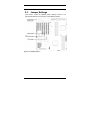
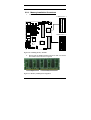
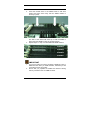
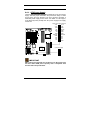
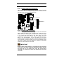
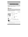
IWILL® DK8S2™
High Performance Server Board
User ’s Guide
FCC Compliance Statement
This equipment has been tested and found to comply with limits for a Class B digital
device, pursuant to Part 15 of the FCC rules. These limits are designed to provide
reasonable protection against harmful interference in residential installations. This
equipment generates, uses, and can radiate radio frequency energy, and if not
installed and used in accordance with the instructions, may cause harmful interference
to radio communications. However, there is no guarantee that interference will not
occur in a particular installation. If this equipment does cause interference to radio or
television equipment reception, which can be determined by turning the equipment off
and on, the user is encouraged to try to correct the interference by one or more of the
following measures:
1.
Reorient or relocate the receiving antenna
2.
Move the equipment away from the receiver
3.
Plug the equipment into an outlet on a circuit different from that to which the
receiver is connected
4.
Consult the dealer or an experienced radio/television technician for additional
suggestions
You are cautioned that any change or modifications to the equipment not expressly
approve by the party responsible for compliance could void Your authority to operate
such equipment.
This device complies with Part 15 of the FCC Rules. Operation is subjected to the
following two conditions
1.
This device may not cause harmful interference
2.
This device must accept any interference received, including interference that
may cause undesired operation.
The information in this document is subject to change without notice.
IWILL Corp. makes no warranty of any kind with regard to this material, including, but
not limited to, the implied warranties of merchantability and fitness for a particular
purpose.
IWILL Corp. shall not be liable for errors contained herein or for incidental or
consequential damages in connection with the furnishing, performance, or use of this
material.
IWILL Corp. assumes no responsibility for the use or reliability of its software on
equipment that is not furnished by IWILL Corp.
This document contains proprietary information that is protected by copyright. All rights
are reserved. No part of this publication may be reproduced, transcribed, stored in a
retrieval system, translated into any language or computer language, or transmitted in
any form whatsoever without the prior written consent of IWILL Corp.
Copyright© 2003 by IWILL Corp. All rights reserved.
Other products and companies referred to herein the trademarks or registered
trademarks of their respective companies or mark holders.
Printed in Taiwan
Revision Version: 1.10
Release Date: May 2003
Contents
Chapter 1
1-1
OVERVIEW……………………………………………………..1-1
1.1. Unpacking……………………………………………...1-2
1.2. Features Highlight……………………………………..1-2
1.3. About This User Guide………………………………..1-4
1.4. Getting Help……………………………………………1-5
1.5. DK8S2 Motherboard Layout…………………………1-6
1.6. Motherboard Layout………………………………….1-7
Chapter 2
2-8
HARDWARE INSTALLATION…………………………………...2-8
2.1. Jumper Settings………………………………………..2-9
2.1.1.
2.1.2.
2.1.3.
2.1.4.
Clear CMOS Header…………………………………2-10
Enable Onboard VGA Header………………………..2-11
PCI-X Slot Speed Select Header……………………..2-11
PCI-64 Slot Speed Select Header…………………….2-12
2.2. Install Memory……………………………………….2-13
2.2.1. Memory Installation Procedures……………………..2-14
2.3. Install CPU……………………………………………2-16
2.3.1. CPU Installation Procedures…………………………2-16
2.4. Attach Cable to Connectors………………………….2-18
2.4.1.
2.4.2.
2.4.3.
2.4.4.
2.4.5.
2.4.6.
ATX Power Supply…………………………………..2-19
Floppy Disk Drive Connector………………………..2-20
Primary IDE connectors……………………………...2-20
Front Panel Switches…………………………………2-21
Front/Back/CPU/Aux Fan Connectors……………….2-23
Rear Panel I/O Ports………………………………….2-24
2.5. Install Expansion Cards……………………………...2-25
2.5.1. Expansion Card Installation Procedure .......................2-25
2.5.2. Assigning IRQs for PCI Expansion Cards...................2-26
2.6. Powering on Your Computer ..................................... 2-27
Chapter 3
3-28
BIOS SETUP………………………………………………….3-28
3.1. Starting BIOS Setup.................................................... 3-29
3.2. Using Setup……………………………………………3-30
3.3. Main Menu……………………………………………3-32
3.4. Advanced Menu........................................................... 3-33
3.4.1.
3.4.2.
3.4.3.
3.4.4.
IDE Configuration.......................................................3-34
Super I/O Configuration..............................................3-35
Onboard Device Configuration…………………..…...3-36
The Rest Advanced Setting .........................................3-37
3.5. PCI PnP Menu............................................................. 3-38
3.6. Boot Menu.................................................................... 3-40
3.6.1. Boot Settings Configuration........................................3-41
3.7. Security Menu.............................................................. 3-43
3.8. Chipset Menu............................................................... 3-44
3.8.1.
3.8.2.
3.8.3.
3.8.4.
NorthBridge Configuration .........................................3-45
ECC Configuration......................................................3-46
SouthBridge Configuration .........................................3-47
PCI-X Configuration ...................................................3-48
3.9. Power Menu................................................................. 3-50
3.10.Exit Menu.................................................................... 3-51
Chapter 1
Overview
Thank you for choosing the DK8S2 high performance Server
motherboard. The DK8S2 is a dual AMD® Opteron micro-Socket
940 motherboard (M/B) based on the SSI form factor and is
configured with the AMD® HyperTransport I/O Hub 8111 and PCIX Tunnel 8131 chipsets. The board features a Hyper Transport
speed of 1600 MT (Mega Transfer per second).
For memory support, the DK8S2 provides eight sockets (four + four
configuration) accommodating up to 16 GB of memory using
registered PC3200/2700/2100 ECC DDR memory modules.
Flexibility and expandability are provided by two 64-bit/133MHz
PCI-X slots, two PCI 64-bit/66MHz PCI slots, and two 32-bit/33Mhz
PCI slots. This array of PCI slots enables numerous add-on cards
and provides Peer PCI transaction support to increase system
performance.
Other optional features such as onboard Silicon Image Serial ATA
RAID interfaces (available in DK8S2-SATA), dual INTEL® Gigabit
Ethernet controllers, and onboard ATI® RageXL video controller
with 8MB memory provide high system capabilities that meet a
wide range of demanding server applications.
1-1
1.1. Unpacking
Remove all items from the box and make sure you have these
following items:
1.
2.
3.
4.
5.
6.
7.
8.
One DK8S2 motherboard
Two ATA 100 IDE ribbon cable (one piece in DK8S2-SATA)
One floppy ribbon cable
One bag of spare jumpers
One CD containing drivers and utilities
One DK8S2 User Guide
Four Serial ATA ribbon cable (available in DK8S2-SATA)
Two Serial ATA power cable (available in DK8S2-SATA)
If you discover damaged or missing items, please contact your
retailer.
1.2. Features Highlight
CPU
1.
2.
Chipset
1.
2.
1-2
System
Memory
Support
1.
Expansion Slots
1.
2.
Supports dual AMD® Opteron
Socket 940 CPUs at 1600 MT per
second.
Built-in Memory Controller Hub
(MCH)
Uses the latest AMD® 8111 Hyper
Transport I/O hub and 8131 PCI-X
Tunnel
DK8S2 supports the newest
technologies: 32bit/33MHz PCI
slots,
64bit/66MHz
and
64
bit/133MHz PCI-X slots, USB
interface, Peer PCI Transaction
2
and I C Bus support and more.
DK8S2 provides 4+4 DIMM
sockets and supports total system
memory size up to 16GB.
Select from PC3200/2700/2100
ECC DDR registered DIMM
Provides two PCI-32-bit/33MHz,
two PCI 64-bit/66MHz, and two
PCI-X-64bit/133Mhz
expansion
slots
2.
64-bit/66MHz
PCI
technology
enables bandwidth up to 528MB/s.
ATI® RageXL video controller with 8MB
memory
Onboard
Chip
VGA
Onboard
LAN
Dual Dual Onboard Intel® 82541EI Gigabit
Super
Multi-I/O
Floppy Drive
Serial ATA RAID
(available in
DK8S2-SATA)
System
Management
PC99
Compliant
Dimension
Ethernet controllers.
1.
Winbond super I/O W83627HFAW
2. One UART 16550 serial port
3. One external serial port
4. Dual onboard USB 1.1 connectors
5. Four
extendable
USB
1.1
connectors by headers
6. PS/2
mouse
and
keyboard
connectors with Wake-up function
Supports 3.5” (1.44MB or 2.88MB) floppy
drive and Japanese standard “Floppy 3
mode” (3.5” disk drive: 1.44MB, 1.2MB,
720KB) and LS-120 floppy disk drives
(3.5” disk drive: 120 MB). BIOS supports
IDE CD-ROM boot-up.
1. Four Integrated Silicon Image
Sil3114 Serial ATA ports
2. Support RAID 0, 1, 0+1
1.
AMC connector for IWILL Server
Remote Management Controller
card (ISRM) (optional)
2. IPMI 1.5 (optional with ISRM)
3. Prevent from abnormal system
down/data loss
4. Alert on LAN ready
5. Remote system controller ready
The DK8S2 is fully compliant with the
Microsoft PC99 specification at both the
hardware and BIOS levels.
Extended SSI form factor-12”x13”
1-3
1.3. About This User Guide
This manual explains how to build your system with DK8S2 in
detail. Please follow the procedures of this User Manual carefully
and pay special attention to these icons.
IMPORTANT
WARNING
NOTE
TIP
1-4
This icon informs you for particularly
important details regarding the setup or
maintenance of your system. While we
point out the most vital paragraphs in a
chapter, you should always read every
word carefully. Failing to do so can cause
exasperation.
This icon alerted you for potential dangers
during setting up your system with DK8S2.
These warnings should not be regarded as
the whole of your safety regimen. Never
forget that computer are electronic devices
and are capable of delivering a shock.
Prevent damage to yourself and to your
board: always ensure that your system is
turned off and unplugged the power cords
whenever you are working with it, and that
you are equipped
This icon alerted you for notice during
setting up your system. It provides you can
useful alert during setting up a new system.
This icon will show you how to configure
your system with DK8S2 in an easy and
simple ways. This icon always provides
some useful description to help you
configure your system.
1.4. Getting Help
If a problem arises with yours system during Installation or OS
operating, you should ask your dealer for help first as your system
has most likely be configured by them. They always have the best
idea and quick response for your symptoms. If your dealer is near
to your locations, you should bring your system to them to have it
quickly serviced instead of attempting to solve the problem by
yourself.
1.
Go to IWILL website at www.iwill.net and navigate to this
product page which contain links to product updates such as
Jumper settings or BIOS updates.
2.
FAQ sections on IWILL Website are often helpful since other
user's questions are often your own.
3.
Email us at: [email protected] and we will try to answer your
questions within 24 hours.
1-5
1.5. DK8S2 Motherboard Layout
Figure 1-1: Motherboard features
ATI Rage XL
LAN1
VGA
LAN2
COM 1 USB
Mouse
Keyboard
COM 2
CPU 1
IPMI Connector
PCI 32
Memory
DIMM
2,3,0,1
PCI 64
PCI-X 133/100
Power
AMD 8111
AMD 8131
Slim Floppy
CPU 0
Floppy
IDE1,IDE0
Memory
DIMM
1,0,3,2
Silicon Image S-ATA Chip
S-ATA Port
4,2,1,3
1-6
(Available in DK8S2-SATA)
1.6. Motherboard Layout
Figure 1-2: Motherboard layout
NOTE
Refer to page 2-24 for the I/O port array layout.
1-7
Chapter 2
Hardware Installation
In this chapter, the Installation of the DK8S2 with the processor
and other hardware connected to your system is explained in detail.
Installation Procedures
Installation procedures will be broken up into six major parts.
Step 1: Set jumpers
Step 2: Install memory (DDR memory modules)
Step 3: Install AMD® Opteron CPU
Step 4: Attach cables to connectors
Step 5: Install expansion cards
Step 6: Connect power
WARNING
This motherboard contains sensitive electronic components
that can be easily damaged by static electricity. Follow the
instructions carefully to ensure correct Installation and to
avoid static damage.
2-8
2.1. Jumper Settings
This section covers the DK8S2 jumper settings. Refer to the
following illustration for the location of the DK8S2 jumpers.
Figure 2-1: DK8S2 jumpers
2-9
2.1.1. Clear CMOS Header
The onboard button cell battery powers the CMOS RAM. It
contains all the BIOS setup information. Normally, it is necessary to
keep the jumper connected to pin2 and pin3 (Default) to retain the
RTC data as shown below.
1
2
3
1-2 CMOS
enable (default)
1
2
3
2-3 clear
CMOS
Figure 2-2: DK8S2 clear COMS header
Follow these instructions to clear the CMOS RTC data:
1.
2.
3.
4.
5.
2-10
Turn off your computer.
Short pin2 and pin3 with a jumper for a few seconds.
Replace the jumper on pin1 and pin2.
Turn on your computer by pressing the power-on button.
Hold down <Delete> during boot and select either the <Load
Optimal Defaults> or <Load Failsafe Defaults> option in the
selection "Exit". Then re-enter BIOS setup to re-enter user
preferences. Refer to Chapter 2 BIOS SETUP for more
information.
2.1.2. Enable Onboard VGA Header
If you are going to use the onboard VGA feature, you must enable
the onboard VGA header. Refer to the following illustration:
1
2
3
1-2 VGA
enable (default)
1
2
3
2-3 disable
VGA
Figure 2-3: Onboard VGA header
2.1.3. PCI-X Slot Speed Select Header
This header lets you determine the bus speed of the PCI-X slots.
The speed can be set to either 133 MHz or 100 MHz (default).
Refer to the following illustration:
1
2
3
1
2
3
1-2 PCI-X
133 MHz enable
2-3 PCI-X
100 MHz enable
(default)
Figure 2-4: PCI-X speed selection
2-11
2.1.4. PCI 64-bit Slot Speed Select Header
This header lets you determine the bus speed of the PCI 64-bit
slots. The speed can be set to either 64 MHz (default) or 33 MHz.
Refer to the following illustration:
Figure 2-5: PCI 64-bit speed selection
2-12
2.2. Install Memory
DK8S2 uses Dual Inline Memory Modules (DIMM). Two 4-DIMM
socket banks are available, each bank supporting one CPU socket.
The
DIMM
sockets
accommodate
PC2100/2700/3200
(DDR266/DDR333/DDR400) and Double Data Rate Memory (DDR)
memory modules in 128MB, 256MB, 512MB, 1GB, and 2GB
combinations. Total memory size is between 128MB and 16GB.
IMPORTANT
The DK8S2 motherboard has strict memory type and timing
requirements. Before you buying DDR DIMM (Double Data
Rate) for use in the DK8S2, consult your local reseller to advise
you of the best memory to use with the DK8S2.
DK8S2 only
supports
Registered
PC3200/2100/2700
(DDR400/DDR333/DDR266) compliant modules. You must
populate HO DIMM modules 0~3 before the H1 modules 0~3.
2-13
2.2.1. Memory Installation Procedures
1.
Locate the DIMM modules on the DK8S2.
H1 DIMM modules 0 ~ 3
2
3
0
1
H0 DIMM modules 0 ~ 3
1
0
3
2
Figure 2-6: Installing memory modules
2.
Ensure that the DIMM module's pins face down and match
the socket's size as shown in Figure 8.
80 pins
104 pins
Figure 2-7: Memory module pin arrangement
2-14
3.
4.
Insert the module down to the DIMM socket in with both
hands and press down firmly until the DIMM module is
securely in place.
The tabs of the socket will close-up to hold the DIMM in
place when the DIMM touches the socket's bottom.
Repeat steps 1 to step 3 to add additional DIMM modules.
H0 DIMM 2
H0 DIMM 3
H0 DIMM 0
H0 DIMM 1
IMPORTANT
1.
2.
You have to insert two memory modules in DIMM 0/1 slots or
DIMM 2/3 slots when you install modules; otherwise you will
not be able to boot the system.
Ensure that you populate HO DIMM slots before inserting
memory modules in the H1 DIMM slot bank.
2-15
2.3. Install CPU
DK8S2 accommodates AMD® Opteron micro-PGA Socket 940
processors at 1600 MT (Mega Transfer per second). You must first
insert a CPU into CPU socket 0 (CPU0) before installing one in
CPU socket 1 (CPU1).
2.3.1. CPU Installation Procedures
Follow these instructions to install a CPU.
1.
Locate the pin 1 of the CPU socket and pin 1 of the CPU.
Pin 1
Figure 2-8: CPU pin 1 location
2.
Lift up the socket lever (A) and place the Socket 940 CPU
with the correct orientation (B) as shown in the following
illustrations.
Align the
pin 1 of
the CPU
with pin 1
of the
socket.
3.
4.
5.
2-16
Lower the socket-locking lever into place.
Apply thermal grease to the top of the CPU.
Mount the CPU heatsink to the top of the CPU and socket as
shown in the following illustration.
Secure
one
motherboard
side
to
the
fan
Secure the opposite side
power
cable
Repeat these steps to install the CPU1.
connector
YELLOW
7.
into
RED
Plug the 3-wire
FRONT_FAN1
BLACK
6.
2-17
2.4. Attach Cable to Connectors
This section covers connecting devices to the DK8S2. The
following illustration shows the location of the connectors.
Figure 2-9: Connector location
2-18
2.4.1. ATX Power Supply
These 24-pin connectors connect the mainboard to the ATX power
supply. Find the proper orientation and push down firmly to make
sure that the pins are aligned. The 8-pin connector provides a
dedicated power supply for the CPUs. For Wake on LAN support,
5-volt Stand-by lead (+5VSB) from ATX power supply must supply
at least 2A.
24-pin power supply connector
+3.3V
+3.3V
+3.3V
COM
-12V
+5V
COM
+5V
COM
PS_ON
COM
COM
COM
PWR_OK
COM
5VSB
+5V
+5V
+5V
COM
+12V
+12V
3.3V
Reserved
8-pin power supply
IMPORTANT
IWILL always recommends our customers use ATX Power that
has more than 300W power capacity and is compatible with
the Intel ATX 2.03 specification.
2-19
2.4.2. Floppy Disk Drive Connector
This 34-pin connector supports the provided floppy disk drive
ribbon cable. After connecting the single end to the board, connect
the plug on the other end to the floppy drive.
34-pin FDD connector
Pin 1
Slim type FDD
connector
2.4.3. Primary IDE connectors
These two 40-pin IDE connectors support 40-wire IDE hard disk
ribbon cables (provided). After connecting the single end to the
board, connect the two plugs at the other end to your hard disk(s).
If you connect two hard disks to the same cable, you must
configure the second drive to Slave mode by setting its jumpers.
Refer to the documentation of your hard disk for the jumper
settings. BIOS now support IDE HDD or IDE CD-ROM boot-up (Pin
20 is removed to prevent inserting in the wrong orientation when
using ribbon cables with pin 20 plugged in). Support for Ultra DMA
33/66/100 is also featured in the BIOS.
IMPORTANT
Ribbon cables should always be connected with the red stripe
on the Pin 1 side of the connector. IDE ribbon cables must be
less than 46 cm (18 inches) long, with the second drive
connector no more than 15 cm (6 inches) from the first
connector.
2-20
40-pin IDE connectors
Pin 1
IDE 1 IDE 2
2.4.4. Front Panel Switches
The front panel switches header connects the power button, front
panel speaker, reset button, and power/HDD/SCSI LEDs to the
motherboard.
2-21
The switches are described as follows. *
Reset Switch (2-pin RST) This 2-pin connector connects to
the case-mounted reset switch for rebooting your computer
without turning off and on your power switch. This is a
preferred method of rebooting to prolong the life of the
system's power supply.
SCSI Hard disk Card Activity LED (4-pin SCSI_HD) The
4-pin connector can be connected to the 4-pin activity LED
connector of SCSI card Read and Write activities by
devices connected to the SCSI card will cause the front
panel LED to light up.
Hard Disk Activity LED (2-pin HDD_LED) This connector
supplies power to the cabinet's hard disk or IDE activity
LED. Read and write activity by devices connected to the
Primary or Secondary IDE connectors will cause the LED to
light up.
Speaker Connector (4-pin SPEAKER) There is one
jumper cap over pin1 and pin2 (default setting) for internal
buzzer. If you want to use external case-mounted speaker
instead of internal buzzer, remove jumper cap and connect
speaker wire to the 4-pin connector.
ATX Power Switch / Soft Power Switch (2-pin PWR_SW)
A momentary switch connected to these connector controls
the system power. Pressing the button once will switch the
system between ON and SLEEP. The system power LED
shows the status of the system's power.
System Power LED (3-pin PWR_LED) This 3-pin
connector connects the system power LED, which lights up
when the system is powered on.
2-22
2.4.5. Front/Back/CPU/Aux Fan Connectors
There are nine 3-pin fan connectors in the DK8S2 motherboard.
Two fans are used for CPU0 and CPU1; seven are for auxiliary
power. These connectors support cooling fans of 500mA (6W) or
less. Depending on the fan manufacturer, the wiring and plug may
be different. Connect the fan's plug to the board taking into
consideration the polarity of this connector.
WARNING
The CPU and/or motherboard will overheat if there is not
enough airflow across the CPU and onboard heatsink.
Damage may occur to the motherboard and/or the CPU fan if
these pins are incorrectly used. These are not jumpers; do not
place jumper caps over these pins.
NOTE
9 The "Rotation" signal has to be used with fan specially designed with rotation
signal.
9 Only
the fan marked Front_Fan1, Front_Fan0, H0_Fan1, H0_Fan1, H1_Fan0
and H1_Fan1 can be monitored by BIOS.
2-23
2.4.6. Rear Panel I/O Ports
The following illustration displays the motherboard I/O port array.
Figure 2-10: I/O port array
These ports are described as follows.
PS/2 Mouse Connector (6-pin Female) The system will direct
IRQ12 to the PS/2 mouse if one is detected. If not detected,
expansion cards can use IRQ12.
PS/2 Keyboard Connector (6-pin Female) This connection is
for a standard keyboard using a PS/2 plug (mini DIN). This
connector will not allow standard AT size (large DIN) keyboard
plugs. You may use a DIN to mini DIN adapter on standard AT
keyboards.
Universal Serial BUS Ports I & 2 (Two 4-pin Female) Two
external USB 1.1 ports onboard are available for connecting 2
USB devices.
Serial Port 1 Connector (9-pin Male) The serial port COM1 can
be used for pointing devices or other serial devices. See the
BIOS Setup.
VGA Connector (15-pin Female) The VGA port connects
display device. See the BIOS Setup.
Parallel Printer Connector (25-pin Female) You can enable the
parallel port and choose the IRQ through the BIOS Setup. Only
with Parallel SKU.
Onboard LAN Ports (RJ-45) DK8S2 uses Intel® 82541 EI
Gigabit Ethernet Controller. It consists of both the Media Access
controller and Mbps Physical Layer (PHY) interface. Please
refer to the "Onboard LAN User Guide" for further information.
2-24
9-pin onboard COM 2 header
Onboard USB 0 header
USB pin assignment
PIN
Onboard USB 1 header
Description
1
VCC
2
DATA–
3
DATA+
4
GROUND
5
NC
2.5. Install Expansion Cards
WARNING
Power off your power supply completely when adding
removing any expansion cards or other system components.
Failure to do so may cause severe damage to both your
motherboard and expansion cards.
2.5.1. Expansion Card Installation Procedure
Read the documentation for your expansion card and make any
necessary hardware or software setting changes, such as jumpers.
1.
2.
3.
4.
Remove the bracket plate on the slot you intend to use.
Keep the bracket for possible future use.
Carefully align the card's connectors and press firmly.
Secure the card on the slot with the screw you removed
above.
Jump to step 6 to finish Installation, then set the IRQ and
DMA as follows.
2-25
2.5.2. Assigning IRQs for PCI Expansion Cards
An IRQ number is automatically assigned to PCI expansion cards.
In the PCI bus design, the BIOS automatically assigns an IRQ to a
PCI slot that contains a card requiring an IRQ. To install a PCI card,
you need to set the INT (interrupt) assignment. Since all the PCI
slots on this motherboard use an INTA #, set the jumpers on your
PCI cards to INTA.
2-26
2.6. Powering on Your Server
Follow these instructions to power on the computer after you have
installed the motherboard.
1.
2.
3.
4.
5.
6.
Be sure that all switches are off (in some systems, marked
with "O").
After finishing all jumper settings and connections, close the
system case cover.
Connect the power supply cord in the power supply located
on the back of your system case and connect the other end
of the power cord into a power outlet that is equipped with a
surge protector.
Turn on your devices in the following order:
− Monitor
− External SCSI devices (starting with the last device on
the chain)
− System power.
For ATX power supplies, you need to switch on the power
supply as well as press the ATX power switch on the front of
the case.
The power LED on the front panel of the system case will
light up. For ATX power supplies, the system LED will light
up when the ATX power switch is pressed. The monitor LED
may light up after the system's LED if it complies with
"green" standards or if it has a power standby feature. The
system will then run power-on tests. While the tests are
running, additional messages will appear on the screen. If
you do not see anything within 30 seconds from the time you
turn on the power, the system may have failed a power-on
test. Recheck your jumper settings and connections or call
your retailer for assistance.
During power-on, hold down <Delete> to enter BIOS setup.
Follow the instructions in the next chapter, BIOS Setup.
NOTE
Powering Off your computer. You have to first exit or shut down
your operating system before switching off the power switch. For
ATX power supplies, you can press the ATX power switch after
exiting or shutting down your operating system.
2-27
Chapter 3
BIOS Setup
This chapter discusses the AMI BIOS Setup program built into the
ROM BIOS. The Setup program allows users modifying the basic
system configurations according to their requirements. This special
information is then stored in battery-backed RAM so that it retains
the Setup information when the power is turned off.
The AMI BIOS installed in your computer system's ROM (Read
Only Memory) is a custom version of an industry standard BIOS.
The BIOS provides critical low-level support for standard devices
such as disk drives and serial and parallel ports.
The AMI BIOS has been customized by adding important, but nonstandard, features such as password protection as well as special
support for detailed fine-tuning of the chipset controlling the entire
system.
The rest of this chapter is intended to guide you through the
process of configuring your system using Setup.
3-28
3.1. Starting BIOS Setup
The AMI BIOS is immediately activated when you power on the
computer every time. The BIOS reads the system information
contained in the CMOS and begins the process of checking out the
system and configuring it. After finishing configuring the whole
system, then BIOS will continue to seek an operating system on
one of the disks, launch then turn control over to the operating
system.
While the AMI BIOS is in control, the Setup program can be
activated in the way:
By pressing the <F2> key when the following message appears
briefly at the bottom of the screen during the POST (Power On
Self-Test).
Press <F2> to enter SETUP.
3-29
3.2. Using Setup
In general, you use the arrow keys to highlight items, press
<Enter> to select, press <Esc> to quit. The following table provides
more details about how to navigate in the Setup program using the
keyboard.
Key
Function
Up Arrow(Ç) Key
Down Arrow(È) Key
Left Arrow(Å) Key
Right Arrow(Æ) Key
Esc key
Move to the previous item
Move to the next item
Move to the previous item
Move to the next item
In the Submenu: Exit the submenu.
In the BIOS main category: Quit Without
saving changes.
Enter Key
Select the item. A pop-up selection will display
on the screen to set the item value.
Previous page on Scrollable menus or jump to
the first interactive item listed
PgUp Key
PgDn Key
Next page on Scrollable menus or jump to the
last interactive item listed
F1 Key
F2/F3 Key
General Help on Setup navigation keys. Press
<F1> key to pop up a small help window that
describes the appropriate keys to use and the
possible selections for the highlighted item. To
exit the Help Window, press <ESC> key or
<F1> key again.
Change colors
F7 Key
F8 Key
F9 Key
F10 Key
Home
End
Esc
Discard changes
Load failsafe defaults
Load optimal defaults
Save and Exit
Go to top of screen
Go to bottom of screen
Exit
IMPORTANT
The BIOS does NOT automatically save values that you have modified. If you
3-30
do not save your values before you exit the BIOS Setup Utility, all your
changes will be lost.
If after making and saving system changes with the BIOS Setup Utility, you
discover that your computer is no longer able to boot, the AMI BIOS supports
an override, which will reset your system to the Failsafe defaults. If that fails,
it is possible to manually clear the present CMOS information through the
"Clear CMOS Header" on the motherboard (Refer to Jumper Settings for
more information).
The best advice is to ONLY alter settings which you thoroughly understand.
The default settings have been carefully chosen by AMIBIOS to provide the
maximum system performance and reliability. Even a slight change to the
chipset setup may cause potential and unpredictable failure to the system.
3-31
3.3. Main Menu
This is the first screen that is displayed when you enter the BIOS
Setup Utility. Each tab lined on the top of the screen represents
each different menu. The following picture shows the main menu.
Main menu shows the information of BIOS version, date and ID;
processor type, speed and count; system size. In addition, system
time and date is adjustable using + / - key or number keys.
3-32
3.4. Advanced Menu
You can make these modifications on the Advanced menu.
3-33
3.4.1 IDE Configuration
You can make the selections on IDE Configuration menu.
Feature
Options
Description
OnBoard PCI IDE
Controller
Disable
Primary
Secondary
Both
Disable:
disable
the
integrated IDE controller
Primary: enable only the
Primary IDE controller
Secondary: enable only the
Secondary IDE controller
Both: enable both IDE
controllers
Hard Disk
Protect
Disable
Enable
Disable/Enable the hard
disk write protection. This
will be effective only device
is accessed through BIOS
IDE Detect Time out
(sec)
0, 5, 10, 15, 20, 25,
30, 35
Select the time out value
for detecting ATA/ATAPI
device
ATA (PI) 80Pin
Cable Detection
Host & Device
Host
Device
Select the mechanism for
detecting 80 pin cable
3-34
Write
3.4.2 Super I/O Configuration
You can make the selections on Super I/O Configuration menu.
Feature
Options
Description
Onboard Game/Midi
Port
Disabled
Allows BIOS to enable or
disable floppy controller
Onboard Game/Midi
Port
Keyboard PowerOn
Function
Enabled
Disabled
200/300, 200/330
Allows BIOS to enable or
disable Game/Midi port
208/300, 208/330
Disabled
Any Key
3-35
3.4.3 Onboard Device Configuration
You can make the selections on Onboard Device Configuration.
Feature
Onboard
Controller
SATA
Description
Enabled
Enabled: Support Serial
ATA function
Disabled
Onboard
SATA
Mode Setting
Onboard 1
GIGA NIC
Onboard 2
GIGA NIC
Options
st
nd
Intel
RAID
Enabled: Support RAID
SATA
0, 1, 0+1
Enabled
Disabled
Intel
Enabled
Disabled
(Note: SATA function is only available in DK8S2-SATA.)
3-36
3.4.4 The Rest Advanced setting
Feature
Options
Description
Floppy
Configuration
Disabled
5 1/2” 360 KB
5 1/2” 1.2 MB
3 1/2” 720 KB
3 1/2” 1.44 MB
3 1/2” 2.88 MB
Select Floppy A or Floppy
B and then selects floppydiskette type installed in
your system.
Hardware Health
Configuration
Disable/Enable
hardware health
function and
hardware thermal
throttling
Enable/Disable hardware
health function
Thermal throttling allows
the user to reduce CPU
duty cycle to a user
defined percentage when
the temperature reaches a
user defined value
H/W health event
ACPI Configuration
ACPI Aware O/S
Yes/No
Enable: O/S supports ACPI
Disable: O/S doesn’t
support ACPI
Hyper Transport
Configuration
CPU0 : CPU1 HT
Link Speed/Width
Hyper Transport link
speed/width is adjustable
Remote Access
Configuration
Disable
Serial
Selects Remote Access
type
USB Configuration
Legacy USB
Support
Disabled/Enabled/A
uto
USB Mass Storage
Device
Configuration
Enable support for legacy
USB
Auto
option
disables
legacy support it no USB
device connected
Configure the USB mass
storage class devices
3-37
3.5. PCI PnP Menu
Feature
Options
Description
Plug & Play O/S
Yes
No
Yes: lets the O/S configure
PnP devices not required
for boot if your system has
a Plug and Play O/S
PCI Latency Timer
32, 64, 96, 128,
160, 192, 224, 248
Value in units of PCI clocks
for PCI device latency
timer register
3-38
Allocate IRQ to PCI
VGA
Yes
No
Yes: Assign IRQ to PCI
VGA card if card requests
IRQ
No: Doesn’t assign IRQ To
PCI VGA cars even if card
requests IRQ
Palette Snooping
Enabled
Disabled
Enabled: informs the PCI
devices that an ISA
graphics device is installed
in the system so the card
will function correctly
PCI IDE BusMaster
Enabled
Disabled
Enabled: BIOS uses PCI
busmastering for
reading/writing to IDE
drives
Offboard
IDE card
Auto
Some PCI IDE cards may
require this to be set to the
PCI slot number that is
holding the card
PCI/ISA
PCI Slot1
PCI Slot2
PCI Slot3
PCI Slot4
PCI Slot5
IRQ3~IRQ15
Available
Reserved
Available: specified IRQ is
available to be used by
PCI/PnP devices
Reserve: specified IRQ is
reserved for use by legacy
ISA devices
DMA Channel 0, 1,
3, 5, 6, 7
Available
Reserved
Available: specified DMA is
available to be used by
PCI/PnP devices
Reserve: specified DMA is
reserved for use by legacy
ISA devices
Reserved
Size
Memory
Disabled
16K
32K
64K
Size of memory block to
reserve for legacy ISA
devices
3-39
3.6. Boot Menu
Feature
Description
Boot Device Priority
Specify the boot device priority sequence
Hard Disk Drives
Specify the boot device priority sequence from
available hard drives
Removable Drives
Specify the boot device priority sequence from
available removable drives
ATAPI CDROM
Drives
Specify the boot device priority sequence from
available ATAPI CDROM drives
3-40
3.6.1 Boot Settings Configuration
Feature
Options
Description
Quick Boot
Disabled
Enabled
Allow BIOS to skip tests
while booting
Quiet Boot
Disabled
Enabled
Disabled: Display normal
POST messages
Enabled: Display OEM
logo
Add-on ROM
Display Mode
Force BIOS
Set display mode for option
ROM
Bootup Num-Lock
Off
Keep Current
On
PS/2 Mouse
Support
Disabled
Typematic Rate
Slow
Enabled
Fast
System Keyboard
Absent
Present
Parity Check
Disable
Enable
Select power on state for
Num-Lock
Select support for PS/2
mouse
Select keyboard typematic
rate
Enable/Disable
all
keyboards attached to the
system
Enable/Disable memory or
parity error check
3-41
Boot to OS/2
No
OS/2 compatibility mode
Yes
Wait for “ F1 “ if
error
Disabled
Hit “ DEL “ Message
Display
Disabled
Interrupt 19 Capture
Disabled
Enabled
Enabled
Enabled
3-42
Wait for F1 key to be
pressed if error occurs
Display “ Press DEL to run
Setup “ in POST
Enabled: allows option
ROMs to trap interrupt 19
3.7. Security Menu
Feature
Options
Description
Change User
Password
Install or
password
Clear User
Password
Setup: check password
while invoking setup
Always: check password
while invoking setup as
well as on each boot
Boot Sector Virus
Protection
Disabled
Enabled
change
the
Enable/Disable boot sector
virus protection
3-43
3.8. Chipset Menu
3-44
3.8.1 NorthBridge Configuration
Feature
Options
Description
Bank Interleaving
Auto
Disabled
Interleaving allows memory
accesses to be spread out
over BANKS on the same
node, or across NODES,
decreasing
access
contention
Node Interleaving
Auto
Interleaving allows memory
accesses to be spread out
over BANKS on the same
node, or across NODES,
decreasing
access
contention
Disabled
Burst Length
8 Beats
4 Beats
Burst length can be set to
8 or 4 beats. 64 bit Dq
must use the 4 beats
3-45
3.8.2 ECC Configuration
Feature
Options
Description
Master ECC Enable
Disabled
Enabled
Master
ECC
Enables
support on all nodes for
ECC error detect and
correction
3-46
3.8.3 SouthBridge Configuration
Feature
Options
2.0 SM Bus
Controller
Disabled
Enabled
HT Link 0 P-Comp
Mode
HT Link 0 N-Comp
Mode
HT Link 0 RZ-Comp
Mode
Auto
Data
Calcomp + Data
Calcomp - Data
Description
Auto causes hardware
compensation vales. Other
choices allow the user to
override
default
compensation
with
an
absolute value, add to the
hardware generated value,
or subtract a value from
the generated value
3-47
3.8.4 PCI-X Configuration
Feature
Options
Description
HT Link 0 P-Comp
Mode
Auto
Data
Calcomp+Data
Calcomp-Data
Auto causes hardware
compensation values.
HT Link 0 N-Comp
Mode
Auto
Data
Calcomp+Data
Calcomp-Data
Auto causes hardware
compensation values.
HT Link 0 NZ-Comp
Mode
Auto
Data
Calcomp+Data
Calcomp-Data
Auto causes hardware
compensation values.
3-48
HT Link 1 P-Comp
Mode
Auto
Data
Calcomp+Data
Calcomp-Data
Auto causes hardware
compensation values.
HT Link 1 N-Comp
Mode
Auto
Data
Calcomp+Data
Calcomp-Data
Auto causes hardware
compensation values.
HT Link 1 NZ-Comp
Mode
Auto
Data
Calcomp+Data
Calcomp-Data
Auto causes hardware
compensation values.
3-49
3.9. Power Menu
Feature
Options
Description
Change User
Password
Install or
password
Clear User
Password
Setup: check password
while invoking setup
Always: check password
while invoking setup as
well as on each boot
Boot Sector Virus
Protection
3-50
Disabled
Enabled
change
the
Enable/Disable boot sector
virus protection
3.10. Exit Menu
Feature
Description
Save Changes and
Exit
Exit system setup after saving the changes
F10 key can be used for this operation
Discard Changes
and Exit
Exit system setup without saving the changes
ESC key can be used for this operation
Discard Changes
Discard changes done so far to any of the setup
question
F7 key can be used for this operation
Load Optimal
Defaults
Load optimal default values for all the setup
questions
F9 key can be used for this operation
Load Failsafe
Defaults
Load Failsafe default values for all the setup
questions
F8 key can be used for this operation
3-51