1
!
"
!"!#
!
!
!
"
!
$!
#
%!
!
!!""##!#
!
!"
#
$"
"
% "
!"
!"
!" AXIOMTEK is a trademark of AXIOMTEK Co., Ltd.
IBM is a registered trademark of International Business
Machines Corporation.
MS-DOS, and Windows 98/NT/2000 are trademarks of
Microsoft Corporation.
Award is a trademark of Award Software, Inc.
IBM, PC/AT, PS/2, VGA are trademarks of International
Business Machines Corporation.
Intel and Celeron, Pentium 4 are trademarks of Intel
Corporation.
Other brand names and trademarks are the properties
and registered brands of their respective owners.
Chapter 1 Introduction ----------------------- 1 1.1 1.2 1.3 1.4 General Description ................................ 1 Specifications ......................................... 2 Utilities Supported .................................. 3 Board Dimensions................................... 4 Chapter 2 Jumpers and Connectors ----- 5 2.1 Board Layout .......................................... 6 2.2 Jumper Settings...................................... 7 2.2.1 2.2.2 2.2.3 2.2.4 CMOS Clear Jumper: JP9............................................... 7 Watchdog Trigger Mode Setting: JP10.......................... 8 DiskOnChip Memory Segment: JP6 ............................... 8 COM2 RS232/422/485 Settings: JP1,JP2,JP4 .................. 9 2.3 Connectors ........................................... 10 Chapter 3 Installation ---------------------- 11 3.1 System Memory .................................... 11 3.2 CPU Installation .................................... 11 3.3 Configuring Power Supply ..................... 12 3.3.1 3.3.2 ATX Power Supply......................................................... 12 AT Power Supply........................................................... 12 3.4 Ultra DMA/66/100 Drive Installation ........ 13 3.5 Completing Installation.......................... 14 Chapter 4 Hardware Description ------- 15 4.1 4.2 4.3 4.4 4.5 4.6 Microprocessors ...................................
BIOS .....................................................
I/O Port Address Map ............................
General Output Connector:CN3 .............
Enhanced IDE Interface Connector ........
Display Interface ...................................
4.6.1 4.6.2 4.6.3 4.6.4 4.6.5 15 15 16 17 18 18 Flat Panel/CRT Interface Controller ............................ 18 Features ........................................................................ 19 VGA/Flat Panel Connectors ........................................ 20 Flat Panel Connector Pin Description ......................... 22 Flat Panel Interface Pins for Color DSTN and Color TFT
LCD ............................................................................... 23 4.7 Floppy Disk Controller: CN22 ................. 25 4.8 Parallel Port Interface: CN1 ................... 26 4.9 Serial Port Interface .............................. 26 Table of Contents
v
4.9.1 Serial Ports IRQ Selection ............................................. 26 4.10 Keyboard and PS/2 Mouse Connectors ..
4.11 USB Connector .....................................
4.12 IrDA Connector .....................................
4.13 ATX SB5V Power Connector Connector..
4.14 ATX12V CPU Power Connector: CN7......
4.15 Mini-PCI Connector: CN12.....................
27 27 28 28 29 29 Chapter 5 Display Drivers ----------------- 31 5.1 5.2 5.3 5.4 5.5 5.6 Introduction ..........................................
Driver Disks’ Contents ...........................
Windows 98 VGA Driver Installation .......
NT 4.0 VGA Driver Installation................
Windows 2000 VGA Driver Installation ...
SMI Control Panel Program Setup..........
31 31 32 39 44 51 Chapter 6 Ethernet --------------------------- 55 6.1 Introduction .......................................... 55 6.2 Features ............................................... 55 6.3 Drivers Supported ................................. 55 Chapter 7 Award BIOS Utility ------------ 57 7.1 BIOS Introduction ..................................
7.2 BIOS Setup ...........................................
7.3 Standard CMOS Setup ..........................
7.4 Advanced BIOS Features.......................
7.5 Advanced Chipset Features...................
7.6 Integrated Peripherals ...........................
7.7 Power Management Setup ....................
7.8 PNP/PCI Configuration ...........................
7.9 PC Health Status ...................................
7.10 Frequency/Voltage Control ....................
7.11 Load Fail-Safe Defaults .........................
7.12 Load Optimized Defaults .......................
7.13 Set Supervisor/User Password ...............
7.14 Save & Exit Setup .................................
7.15 Exit Without Saving ...............................
57 57 59 62 67 70 74 76 79 80 81 82 83 84 85 Appendix A Watchdot Timer ---------------- 87 Appendix B Connector Pin Assignments89
Assignments 89
vi
Table of Contents
SBC81820 Socket478 All-in-One CPU Card Series User’s Manual
!"
"#$
"#$
%&%'(")
)*+,-*'.
/)*0&!1#"234
#"5
#"+
)'0%"#$
Introduction
!
SBC81820 Socket478 All-in-One CPU Card Series User’s Manual
#
"$
#" Chipset:
Intel 82845
#" CPU Socket:
Socket478
#" CPU: Intel Socket478 Celeron/Pentium 4
#" L2 Cache:
Integrated in CPU
#" BIOS: Award 4MB PnP Flash BIOS
#" System Memory:
!"3 x 168-pin DIMM sockets
!"Maximum up to 3GB SDRAM
#" IDE Interface:
2 bus mastering EIDE up to four
devices, Ultra DMA 100 supported
#" FDD Interface:
Supports up to 2 drives
#" Serial Ports:
Two 16550 UARTs ports with 16 byte as
one RS-232 and one RS-232/422/485
#" Parallel Ports:
One parallel port with ECP/EPP/SPP
supported
#" VGA Controller:
!"AGP interface controller with onboard 4MB SDRAM
!"VGA chipset SMI Lynx EM+ supporting CRT/LCD displays
!"Supports up to 1600x1200x64K colors resolution on noninterlaced CRT monitors
#" Ethernet:
!"Controller: Integrated in 82801BA I/O Controller Hub (ICH*2)
& dual Intel ® 82559
!"Supports triple LAN, each with 10BASE-T and 100BASE-TX,
triple RJ45 outpu !"Wake On LAN support
&
Introduction
SBC81820 Socket478 All-in-One CPU Card Series User’s Manual
#" USB Interface:
2 USB ports; USB Spec. Rev. 1.1
compliant
#" IrDA: 1 IrDA pin-header for wireless communication
#" Hardware Monitoring: Controller: Winbond W83627HFAW d
#" Watchdog Timer:
!"Generates a system reset
!"Software programmable time interval and jumper selectable
!"64 levels, 0.5~8/5~80/50~800/100~1600 seconds
#" SSD:
Supports M-Systems DiskOnChip 2000 serials
#" Dimensions:
NOTE:
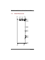
%
122(W) x 335(L) mm
Specifications are subject to change without
notice.
""
#"Intel 82845 Utility and Drivers
#"Ethernet Utility and Drivers
#"VGA Drivers
Introduction
6
SBC81820 Socket478 All-in-One CPU Card Series User’s Manual
&
'
Introduction
SBC81820 Socket478 All-in-One CPU Card Series User’s Manual
Jumpers and Connectors
(
5
# SBC81820 Socket478 All-in-One CPU Card Series User’s Manual
&'(
Jumpers and Connectors
SBC81820 Socket478 All-in-One CPU Card Series User’s Manual
# #
)"*
*7
7
8
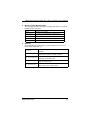
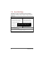
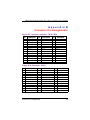
Jumper
Jumper Setting
Default Setting
JP1
COM2 Mode Setting: RS232
Short 1-2
JP2
COM2 Mode Setting: RS232
Short 3-5, 4-6
JP4
COM2 Mode Setting: RS232
Short 3-5, 4-6
JP6
DiskOnChip Memory Segment D6000-D7FFF
Short 7-8
JP9
CMOS Clear Jumper: Normal Mode
Short 1-2
JP10
Watchdog Trigger Mode: Disabled
Open
JP12
Reserved
Short 1-2
Options
Clear CMOS
Normal (default)
Settings
Short 2-3
Short 1-2
Jumpers and Connectors
0
SBC81820 Socket478 All-in-One CPU Card Series User’s Manual
"#$
9*"#$
Options
RESET
Disabled
%
Setting
Short 1-2
Short 2-3
Open (default)
NMI
!"
#
$
Options
Settings
D0000 D1FFF
D2000 D3FFF
D4000 D5FFF
D6000 D7FFF
Short
Short
Short
Short
1-2 (default)
3-4
5-6
7-8
Jumpers and Connectors
SBC81820 Socket478 All-in-One CPU Card Series User’s Manual
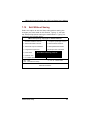
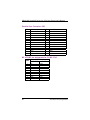
% &'%'%()
!**%
COM2
JP1
JP2
JP4
RS-232 (default)
Short 1-2
Short 3-4
Short 5-6, 7-8
Short 3-5, 4-6
Short 1-3, 2-4
Short 1-3, 2-4
Short 3-5, 4-6
Short 1-3, 2-4
Short 1-3, 2-4
RS-422
RS-485
Jumpers and Connectors
:
SBC81820 Socket478 All-in-One CPU Card Series User’s Manual
# %
"#$
)
-
"'
4
,
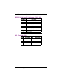
Connectors
Printer Port Connector
COM1
General Output Connector
USB Connector
CRT Connector
COM2
Ethernet Connector 1
(SBC81820VEE & VEEE Only)
Label
Connectors
Label
Primary IDE Connector
Secondary IDE Connector
FDD Connector
IrDA Connector
Fan Power Connector 1
Fan Power Connector 2
Fan Power Connector 3
CN19
Ethernet Connector 2
CN8
(SBC81820VE, VEE & VEEE Only)
168-Pin Memory Socket 1
DIMM1
Ethernet Connector 3
(SBC81820 VEEE Only)
ATX SB5V Power Connector
Mini-PCI Connetcor
PS/2 Mouse Connector
PS/2 Keyboard Connector
CN10
168-Pin Memory Socket 2
DIMM2
CN11
168-Pin Memory Socket 3
Socket 478 CPU Socket
System BIOS
DIMM3
U25
Keyboard/Mouse Connector
ATX12V CPU Power Connector
AXIOMTEK LCD Interface
CN16
DiskOnChip Socket
Internal Battery
Internal Buzzer
CN1
CN2
CN3
CN4
CN5
CN6
CN7
CN12
CN14
CN15
CN17
CN20
CN22
CN25
FAN1
FAN2
FAN3
U6
U16
BAT1
BU1
CN18
NOTE:
1. SBC81820VEEE lan1 and lan2 is intel 82559, lan3 is
intel 82562.
2. SBC81820VEE lan1 and lan2 is intel 82559.
3. SBC81820VE lan1 is intel 82562.
!;
Jumpers and Connectors
SBC81820 Socket478 All-in-One CPU Card Series User’s Manual
)'0%"#$
<
!"Power supply and passive backplane
!"IBM PC/AT keyboard
!"Display monitor
!"Floppy or hard disk with MS-DOS or Flash Disk emulator
% ((
"#$
!5%
**/**
1,
63
% #
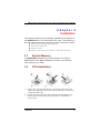
+
1.
Open the socket handle (B). Install the processor by
carefully aligning the pins to the socket (C). Close the
socket handle (D).
2. Install CPU heatsink on the retention mechanism (A)
following the heatsink manufacturer’s installation
instructions.
Installation
!!
SBC81820 Socket478 All-in-One CPU Card Series User’s Manual
% %
$**,""(
+,-
#
=4>
1.
Install the ATX Power Control Connector cable to
the designated ATX power control connector on
your backplane. The ATX Power Control Connector
cable is a 6-pin cable that comes with the
AXIOMTEK BACKPLANE packaging.
+-
#
4
4>#""
!&
Installation
SBC81820 Socket478 All-in-One CPU Card Series User’s Manual
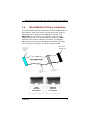
% -..-//0+
$*48558!;;
%;
/';
1
$*48558!;;
&$
*48558!;;
-"/1
%;
%;
!
ATA/33
Cable with
40 conductors
Installation
ATA/66/100
Cable with
80 conductors
!6
SBC81820 Socket478 All-in-One CPU Card Series User’s Manual
% 1
"*+
1. Make sure the power is OFF.
2. Set the configuration jumpers according to the jumper
settings on Chapter 2.
3. Install the SBC81820 CPU card into one of the slots on
the passive backplane. You may allow the SBC81820
to stand alone as a single board computer.
4. Connect the I/O cables and peripherals, i.e. floppy
disk, hard disk, monitor, keyboard, power supply and
etc. to the CPU board.
NOTE:
5.
!'
The color of pin one is usually red or blue,
while others are gray.
Turn ON the system power.
Installation
SBC81820 Socket478 All-in-One CPU Card Series User’s Manual
!
,
)'0%"#$
"
"8#'"#$
)
"#$
$9>
?)8&+, 98&;;;8># :%8*-
*)
?)
"#$
#
&+
?)
4
#
#
?)
'*=-#@?*
=
"%
?)
Hardware Description
!(
SBC81820 Socket478 All-in-One CPU Card Series User’s Manual
%
+-"
"#$
8?
!A
8?,
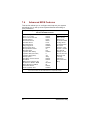
Address
000-01F
020-03F
040-05F
060-06F
070-07F
080-09F
0A0-0BF
0F0
0C0-0DF
0F1
0F8-0FF
120
121
122
1F0-1F8
200-207
300-31F
360-36F
378-37F
3B0-3BF
3C0-3CF
3D0-3DF
3F0-3F7
3F8-3FF
2F8-2FF
!5
Devices
DMA controller #1
Interrupt controller #1
Timer
Keyboard controller
Real time clock, NMI
DMA page register
Interrupt controller #2
Clear math coprocessor busy signal
DMA controller #2
Reset math coprocessor
Math processor
Disable watchdog timer operation (read)
Enable watchdog timer operation (read)
Watchdog
Fixed disk controller
Game port
Prototype card
Reserved
Parallel port #1
MDA video card (including LPT1)
EGA card
CGA card
Floppy disk controller
Serial port #1 (COM1)
Serial port #2 (COM2)
Hardware Description
SBC81820 Socket478 All-in-One CPU Card Series User’s Manual
!"23%
CN3
Power LED
6
+-
.
#+-
?9
External Speaker and Internal Buzzer Connector
BB
"#$
BB ,7
/.1
/1
Hardware Description
!0
SBC81820 Socket478 All-in-One CPU Card Series User’s Manual
System Reset Switch
C
?==
HDD Activity LED
,
+-
+-D
C
D+-
.
Reserved pins
1
4++$
#"
-
8
5'
'-
@4
,
.
"(+$
%$ .
'&/
0
+,-*'.8
234
'*234@4*
"@,
!&%;,!;&'5'A+,-*'.
)9
===
+,-*'.,:!&
!%&'
,&'65'%
!&%;,!;&'+,-*'.
=+"
!%
Hardware Description
SBC81820 Socket478 All-in-One CPU Card Series User’s Manual
%$ .
!
#"Fully compatible with IBM TM VGA
#"Flat panel and CRT monitor can be displayed
simultaneously
#"Onboard 4M bytes VGA RAM
#"Supports panel resolution up to 1280x1024
#"Supports non-interlaced CRT monitors with resolutions
up to 1280x1024 64K colors
#"SMARTMAP intelligent color to gray scale conversion
enhances text legibility
#"Integrated programmable linear address feature
accelerates GUI performance
#"Built-in 144 pins so-dimm connector for flat panel
display.
Hardware Description
!:
SBC81820 Socket478 All-in-One CPU Card Series User’s Manual
%$ 12+'.
!
"@
234
!5
"@234
)?**
B"
234
7
<
CN5: CRT/VGA Connector Pin Assignment
Pin
Signal
Pin
Signal
Pin
Signal
1
4
7
10
13
16
Red
N/A
N/A
AGND
AGND
No connector
2
5
8
11
14
AGND
Blue
DDC DAT
GND
Vertical Sync
3
6
9
12
15
Green
AGND
GND
Horizontal Sync
DDC CLK
CN18: SODIMM Connector for Flat Panel
Pin
Description
Pin
Description
Pin
Description
1
12V
2
12V
3
CMPS_IN
4
CMPS_OUT
5
LUMA_IN
6
LUMA_OUT
7
CRMA_IN
8
CRMA_OUT
9
VIDEO_GND
10
VIDEO_GND
11
BLUE_IN
12
BLUE_OUT
13
GREEN_IN
14
GREEN_OUT
15
RED_IN
16
RED_OUT
17
VCC3
18
VCC3
19
HSYNC_IN
20
VSYNC_IN
21
VP0
22
VP1
23
VP2
24
VP3
25
VP4
26
VP5
27
VP6
28
VP7
29
VP8
30
VP9
31
VP10
32
VP11
33
VCC3
34
VCC3
35
VP12
36
VP13
37
VP14
38
VP15
39
VRDY
"
&;
Hardware Description
SBC81820 Socket478 All-in-One CPU Card Series User’s Manual
Pin
Description
Pin
Description
Pin
Description
40
VREF
41
HRET
42
VPCLK
43
VCLK
44
ENAVDD
45
VCON
46
LP
47
FLM
48
ENABKL
49
M
50
SHFCLK
51
VCC
52
VCC
53
P0
54
P1
55
P2
56
P3
57
P4
58
P5
59
P6
60
P7
61
P8
62
P9
63
P10
64
P11
65
P12
66
P13
67
P14
68
P15
69
VCC
70
VCC
71
P16
72
P17
73
P18
74
P19
75
P20
76
P21
77
P22
78
P23
79
P24
80
P25
81
P26
82
P27
83
P28
84
P29
85
P30
86
P31
87
VCC
88
VCC
89
P32
90
P33
91
P34
92
P35
93
P36
94
P37
95
P38
96
P39
97
P40
98
P41
99
P42
100
P43
101
P44
102
P45
103
P46
104
P47
105
VSS
106
VSS
107
DCLKB+(TXC+)
108
DCLKA+
109
DCLKB-(TXC-)
110
DCLKA-
111
DINB2+
112
DINA2+
113
DINB2-
114
DINA2-
115
VSS
116
VSS
117
DINB1+(TX2+)
118
DINA1+
119
DINB1-(TX2-)
120
DINA1-
121
DINB0+(TX1+)
122
DINA0+
123
DINB0-(TX1-)
124
DINA0-
125
VSS
126
VSS
127
IDE_LED-
128
IRTX
129
BUZZER_OUT
130
IRRX
131
5VSB
132
HIRRX
133
LANACT_LED
134
AUDIO GND
135
LAN100_LED-
136
VOLUP
137
ATX PWRBT-
138
VOLDW
139
H/W RESET-
140
MIC_IN
141
SMBDATA
142
SPKL_OUT/LOUT_L
143
SMBCLK
144
SPKR_OUT/LOUT_R
Hardware Description
&!
SBC81820 Socket478 All-in-One CPU Card Series User’s Manual
%$% .
!
Name
P0~P47
ENABKL
SHFCLK
M
LP
FLM
+12VM
ENAVDD
&&
Description
Flat panel data output
Activity Indicator and Enable Backlight outputs
Shift clock. Pixel clock for flat panel data
M signal for panel AC drive control
Latch pulse. Flat panel equivalent of HSYNC
First line marker. Flat panel equivalent of VSYNC
+12V power controlled by chipset
Power sequencing controls for panel LCD Vcc
Hardware Description
SBC81820 Socket478 All-in-One CPU Card Series User’s Manual
%$) .
/
0
!0 3
.4 DSTN
Pin
LP
FLM
SHFCLK
M
ENAVDD
ENABLK
P23
P22
P21
P20
P19
P18
P17
P16
16-bit
24-bit
LP
FP
XCK
LP
FP
XCK
ENAVDD
ENABLK
ENAVDD
ENABLK
UD7
UD6
UD5
UD4
UD11
UD10
UD9
UD8
UD7
UD6
UD5
UD4
P15
P14
P13
P12
P11
P10
P9
P8
UD3
UD2
UD1
UD0
P7
P6
P5
P4
P3
P2
P1
P0
LD7
LD6
LD5
LD4
LD3
LD2
LD1
LD0
UD3
UD2
UD1
UD0
LD11
LD10
LD9
LD8
LD7
LD6
LD5
LD4
LD3
LD2
LD1
LD0
Hardware Description
TFT
9-bit
12-bit
18-bit
24-bit
12+12 bit
HSYNC
VSYNC
CK
DE
ENAVDD
ENABLK
HSYNC
VSYNC
CK
DE
ENAVDD
ENABLK
HSYNC
VSYNC
CK
DE
ENAVDD
ENABLK
HSYNC
VSYNC
CK
DE
ENAVDD
ENABLK
HSYNC
VSYNC
CK
DE
ENAVDD
ENABLK
R5
R4
R3
R2
R1
R0
R7
R6
R5
R4
R3
R2
R1
R0
RB3
RB2
RB1
RB0
RA3
RA2
RA1
RA0
G5
G4
G3
G2
G1
G0
G7
G6
G5
G4
G3
G2
G1
G0
GB3
GB2
GB1
GB0
GA3
GA2
GA1
GA0
B5
B4
B3
B2
B1
B0
B7
B6
B5
B4
B3
B2
B1
B0
BB3
BB2
BB1
BB0
BA3
BA2
BA1
BA0
R2
R1
R0
G2
G1
G0
B2
B1
B0
R3
R2
R1
R0
G3
G2
G1
G0
B3
B2
B1
B0
&6
SBC81820 Socket478 All-in-One CPU Card Series User’s Manual
Pin Name
LP
FLM
SHFCLK
M
ENAVDD
ENABLK
24+24 bit TFT
HSYNC
VSYNC
CK
DE
ENAVDD
ENABLK
18+18 bit TFT
HSYNC
VSYNC
CK
DE
ENAVDD
ENABLK
TFTs: FP1 + FP2
FPI_HSYNC
FPI_VSYNC
FPI_CK
FPI_DE
ENAVDD
ENABLK
P47
P46
P45
P44
P43
P42
P41
P40
RB7
RB6
RA7
RA6
GB7
GB6
GA7
GA6
FP2_R7
FP2_R6
FP2_R5
FP2_R4
FP2_R3
FP2_R2
FP2_R1
FP2_R0
P39
P38
P37
P36
P35
P34
P33
P32
BB7
BB6
BA7
BA6
RB5
RB4
RA5
RA4
RB5
RB4
RA5
RA4
FP2_G7
FP2_G6
FP2_G5
FP2_G4
FP2_G3
FP2_G2
FP2_G1
FP2_G0
P31
P30
P29
P28
P27
P26
P25
P24
GB5
GB4
GA5
GA4
BB5
BB4
BA5
BA4
GB5
GB4
GA5
GA4
BB5
BB4
BA5
BA4
FP2_B7
FP2_B6
FP2_B5
FP2_B4
FP2_B3
FP2_B2
FP2_B1
FP2_B0
Continued . . . . .
&'
Hardware Description
SBC81820 Socket478 All-in-One CPU Card Series User’s Manual
Pin Name
24+24 bit TFT
18+18 bit TFT
TFTs: FP1 + FP2
P23
P22
P21
P20
P19
P18
P17
P16
RB3
RB2
RB1
RB0
RA3
RA2
RA1
RA0
RB3
RB2
RB1
RB0
RA3
RA2
RA1
RA0
FP2_VSYNC
FP2_HSYNC
FP1_R5
FP1_R4
FP1-R3
FP1_R2
FP1_R1
FP1_R0
P15
P14
P13
P12
P11
P10
P9
P8
GB3
GB2
GB1
GB0
GA3
GA2
GA1
GA0
GB3
GB2
GB1
GB0
GA3
GA2
GA1
GA0
FP2_DE
FP2_CK
FP1_G5
FP1_G4
FP1_G3
FP1_G2
FP1_G1
FP1_G0
P7
P6
P5
P4
P3
P2
P1
P0
BB3
BB2
BB1
BB0
BA3
BA2
BA1
BA0
BB3
BB2
BB1
BB0
BA3
BA2
BA1
BA0
FP1_B5
FP1_B4
FP1_B3
FP1_B2
FP1_B1
FP1_B0
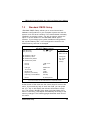
""(23##
6'
(&(E65;A8!&*
6(E
0&;A8!''*8&%%*
4
,
Hardware Description
&(
SBC81820 Socket478 All-in-One CPU Card Series User’s Manual
+$23
#" Standard mode:
IBM PC/XT, PC/AT and PS/2 TM
compatible with bi-directional
parallel port
#" Enhanced mode:
Enhance parallel port (EPP)
compatible with EPP 1.7 and EPP
1.9 (IEEE 1284 compliant)
#" High speed mode:
Microsoft and Hewlett Packard
extended capabilities port (ECP)
IEEE 1284 compliant
+#!/6"D1
?)"*?)
5
+$
"?*!
/1@)&6&
"?*&/1
@)
&6&8'&&8'%(
% !/&5
!;"?*!
"?*&@<"?*!
"?*&
@F'
@F64
?)@)&6&
"?*!
"?*&@)'%(
"?*&4
,
&5
Hardware Description
SBC81820 Socket478 All-in-One CPU Card Series User’s Manual
/ 6(7-#
#)8&
(9
#)8&
'
)
(
"#
$"
$
%&
CN15/14
CN16
&
$)/$)1
$)
!;$)
CN4
Hardware Description
&0
SBC81820 Socket478 All-in-One CPU Card Series User’s Manual
# +
!;4
CN25
% 89&1:,
5
ATX SB5V Power
CN11
&%
Hardware Description
SBC81820 Socket478 All-in-One CPU Card Series User’s Manual
89#:,23
4>!&2
"#$"2
*4>!&2
%4.!&2
!4
.(2
/.(2)1
&6; 6;; ,
<
1 +23#
#"
,
G
)")
+49
-
#"
)"%!%&;
=#"
Hardware Description
&:
6;
SBC81820 Socket478 All-in-One CPU Card Series User’s Manual
"
!
#!$
1 +
+,-*.)*H<
*"+,-*.
'*
)*H2@
1 #
0;
!" Win98 driver
!" NT4.0 diver
!" Win2000 driver
!" SMI Control Program
Display Drivers
31
1 %
<,5
:!0+
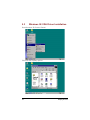
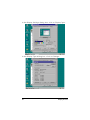
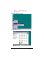
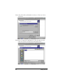
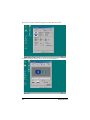
Run Windows 98 Control Panel.
Choose the Display option.
6&
Display Drivers
SBC81820 Socket478 All-in-One CPU Card Series User’s Manual
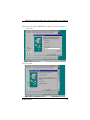
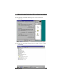
In the Display Settings dialog box, click on Advanced.
In the Adapter dialog box , click on Change.
Display Drivers
66
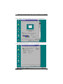
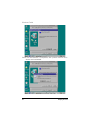
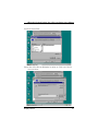
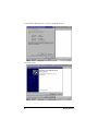
Click on Next
Click on Next
6'
Display Drivers
SBC81820 Socket478 All-in-One CPU Card Series User’s Manual
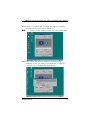
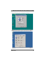
Place the VGA Driver Diskette in drive A. Click on Next to
continue.
Click on Next
Display Drivers
6(
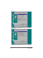
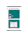
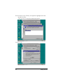
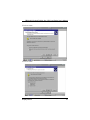
Click on Finish
Once the installation is complete, the system must be shut
down and restarted.
65
Display Drivers
SBC81820 Socket478 All-in-One CPU Card Series User’s Manual
When Driver is completely installed, proceed to Display
Settings and you will see 2 displays.
NOTE:
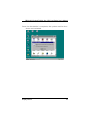
Make sure the resolution matches the installed LCD. Selecting 2 from the above screen will prompt you
whether or not you want to enable the 2 nd display.
Click on Yes to enable the 2nd display.
Display Drivers
60
You may now configure the settings of display 2.
6%
Display Drivers
SBC81820 Socket478 All-in-One CPU Card Series User’s Manual
1 38 /:!0+
Install Service Pack then run Windows NT Control Panel.
Choose the Display option.
Display Drivers
6:
In the Display Settings dialog box, click on Display Type.
In the Display Type dialog box, click on Change.
';
Display Drivers
SBC81820 Socket478 All-in-One CPU Card Series User’s Manual
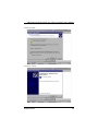
Click on Have Disk
Place the VGA Driver Diskette in drive A. Click on OK will
be continue.
Display Drivers
'!
Silicon Motion Lynx Family will appear highlighted in the
Models list box.
Click on OK to install the selected driver.
Click on Yes.
'&
Display Drivers
SBC81820 Socket478 All-in-One CPU Card Series User’s Manual
Once the installation is complete, the system must be shut
down and restarted.
Display Drivers
'6
1 1
<,#///:!0
+
Run Windows 2000 Control Panel.
Choose the System option.
''
Display Drivers
SBC81820 Socket478 All-in-One CPU Card Series User’s Manual
In the System Hardware dialog box, click on Device
Manager.
In the Device Manager dialog box, double click on Video
Controller.
Display Drivers
'(
In the Driver dialog box, click on Update Driver.
Click on Next.
'5
Display Drivers
SBC81820 Socket478 All-in-One CPU Card Series User’s Manual
Click on Next.
Click on Next.
Display Drivers
'0
Place the VGA Driver Diskette in drive A. Click on OK to
continue.
Smisetup will appear highlighted in the Models list box.
Click on Open to install the selected driver.
'%
Display Drivers
SBC81820 Socket478 All-in-One CPU Card Series User’s Manual
Click on Next.
Click on Finish.
Display Drivers
':
Installation completed
(;
Display Drivers
SBC81820 Socket478 All-in-One CPU Card Series User’s Manual
1 .
+*"
)-$#->-
,)*
-
=
)*"#
#"#)*
"#
1. DualApp - Display independent applications (CRT or LCD)
$"
on two different displays.
2. Rotation Mode - Display the screen content with 90, 180 or
$"
270 degrees rotation.
3. Stretch Mode – For LCD display:
$"
!"1) Stretch a lower resolution graphics mode (e.g. 800x600
on a 1024x768 panel) to fill the display.
!"2) Display lower resolution screen content (e.g. DOS game)
in full screen mode. See Stretch Mode.
NOTES:
1) For operating systems which natively support
multi-display capability (e.g. Windows 98),
DualApp and DualView capabilities will be
handled via the native support mechanism,
instead of the Control Panel program.
2) When in any of the special modes: Display
switching is disabled. Turn off the special mode
first before display switching.
3) Do not disable the Control Panel program while
in any of the special modes. Closing the Control
Panel program will turn off special modes
automatically.
Display Drivers
(!
Execute Control Panel Program under Windows 98
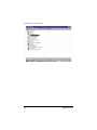
In the Settings dialog box, click on Advanced.
(&
Display Drivers
SBC81820 Socket478 All-in-One CPU Card Series User’s Manual
In the DualID dialog box, setting Second Panel.
Execute Control Panel Program under Windows 2000.
Display Drivers
(6
54
SBC81820 Socket478 All-in-One CPU Card Series User’s Manual
%
&
. +
<
#
#-
---%;&6
@I'(
. #
#"10Mb/s and 100Mb/s operations
#"Supports 10Mb/s and 100Mb/s N-Way auto negotiation
#"Full duplex capability
#"Full compliance with PCI Revision 2.1
#"PCI Bus Master data transfers
. %
0""
-
,7
99 &,
6,',*+49* 6! 9*+49
))"?$9>?9)
#
NOTE: Ethernet
Before you begin the driver software installation,
please see the detailed installation procedure from
the Product Information CD-ROM and be sure to
make installation and backup copies of the driver
files. ((
(5
SBC81820 Socket478 All-in-One CPU Card Series User’s Manual
'
( )*#
"%
4
?)"#$
4
?)
&++
4
?)/8?)1
@?*"
*48??)
#
&+"
4
?)
)
?)
@?*) ?9
4
?)
#JK
)JK
#?)/#?)1
)
)@
J"KJ4K
JK
G?==
?9
Press <DEL> to Enter Setup
J-KJ#$K
J#K
J=!K
J-K<
Award BIOS Utility
(0
)**
**
,
&
&
'(
)
#*+,(#
% &-% !" !"
!"
!"#
$%&
!"
!'
$(&
!" #
'
!
!" !" #
!)*+
!" ,'
*+- '!
*./0."#
12.!)*+
%&'←.#
3&,&435
**
4
**7
NOTE:
If you find that your computer cannot boot after
making and saving system changes with Setup, the
Award BIOS, via its built-in override feature, resets
your system to the CMOS default settings.
4
,
(%
Award BIOS Utility
SBC81820 Socket478 All-in-One CPU Card Series User’s Manual
%
"
)
"*?))
G
)
"*?)
"*?)
&
&
'(
)
#*+,(#
% &-% & " &
Date (mm:dd:yy)
Time (hh:mm:ss)
Thu, Jan 10 2002
2 : 31 : 24
Item Help
Menu Level #
IDE Primary Master
#"
IDE Primary Slave
#"
IDE Secondary Master
#"
IDE Secondary Slave
#"
Change the
Day, month,
Year and
Century
Drive A
Drive B
1.44M, 3.5 in.
None
LCD Type
TFT Format
DSTN Format
Expansion (Full Screen)
Disp Set(s) at POST/BOOT
640x480 TFT
9 Bits
16 Bits
Enabled
LCD Only
Halt On
All, But Keyboard
%&'( : Move Enter: Select +/-/PU/PD: Value F10: Save ESC: Exit F1: General Help
F5: Previous Values F6: Fail-Safe Defaults F7: Optimized Defaults
4
J=!K
7
Award BIOS Utility
(:
#" Date
3'67676'767
687
''
day
date
month
year
The day of week, from Sun to Sat, determined by the BIOS,
is read only
The date, from 1 to 31 (or the maximum allowed in the
month), can key in the numerical / function key
The month, Jan through Dec.
The year, depends on the year of BIOS
#" Time
3'6'76767'
443'9
':;%'%4+118.22.22
#" Primary Master/Primary Slave/Secondary
Master/Secondary Slave
3'''''!9
'3';<:
9*'#&*"#313
;<3%9
6
76=76
&76−79'
4'96*7>''
!'''!93'
'44
''#'4!'
3!
#349
'*'
'496*73''9
!''4!'
#',&&*&#&31'
#',&&#&>'
#',&&&%?&>'
CYLS.
number of cylinders
LANDZONE
landing zone
HEADS
number of heads
SECTORS
number of sectors
PRECOMP
write precom
MODE
HDD access mode
#''4!>>*
6*7
5;
Award BIOS Utility
SBC81820 Socket478 All-in-One CPU Card Series User’s Manual
#" Drive A type/Drive B type
3''4! !"
'
None
No floppy drive installed
360K, 5.25 in
5.25 inch PC-type standard drive; 360Kb capacity
1.2M, 5.25 in
5.25 inch AT-type high-density drive; 1.2MB capacity
720K, 3.5 in
3.5 inch double-sided drive; 720Kb capacity
1.44M, 3.5 in
3.5 inch double-sided drive; 1.44MB capacity
2.88M, 3.5 in
3.5 inch double-sided drive; 2.88MB capacity
#" Halt On
3'''''
No errors
All errors
All, But Keyboard
All, But Diskette
All, But Disk/Key
The system boot will halt on any error detected.
(default)
Whenever the BIOS detects a non-fatal error, the
system will stop and you will be prompted.
The system boot will not stop for a keyboard error;
it will stop for all other errors.
The system boot will not stop for a disk error; it will
stop for all other errors.
The system boot will not stop for a keyboard or disk
error; it will stop for all other errors.
Award BIOS Utility
5!
0&+
&
&
'(
)
#*+,(#
% &-% ".
/&
Virus Warning
CPU L1 & L2 Cache
Quick Power On Self Test
First Boot Device
Second Boot Device
Third Boot Device
Boot Other Device
Swap Floppy Drive
Boot Up Floppy Seek
Boot Up NumLock Status
Gate A20 Option
Typematic Rate Setting
Typematic Rate (Chars/Sec)
Typematic Delay (Msec)
Security Option
PS/2 Mouse Function Control
APIC Mode
MPS Version Control For OS
OS Select For DRAM > 64MB
Report No FDD For WIN 98
Video BIOS Shadow
Small Logo(EPA) Show
Disabled
Enabled
Enabled
Floppy
HDD-0
LS120
Enabled
Disabled
Enabled
On
Fast
Disabled
6
250
Setup
Enabled
Enabled
1.4
Non-OS2
No
Enabled
Disabled
Item Help
Menu Level #
Allows you to
choose the VIRUS
warning feature
for IDE Hard disk
boot sector
protection. If this
function is enable
and someone
attempts to write
data into this area,
BIOS will show
a warning
message on
screen and alarm
beep
%&'( : Move Enter: Select +/-/PU/PD: Value F10: Save ESC: Exit F1: General Help
F5: Previous Values F6: Fail-Safe Defaults F7: Optimized Defaults
5&
Award BIOS Utility
SBC81820 Socket478 All-in-One CPU Card Series User’s Manual
#" Virus Warning
3''99'
4#'
"#''#'
''
%!!'9
NOTE:
Many disk diagnostic programs, which attempt to
access the boot sector table, can cause the virus
warning. If you will run such a program, disable the
Virus Warning feature.
#" CPU L1 & L2 Cache
3',!
'
Enabled
Disabled
Enable cache
Disable cache
#" Quick Power On Self Test
3'
3@
3A
'#*9"#'4
'4
33'Enabled
Enabled
Disabled
Enable Quick POST
Normal POST
#" First/Second/Third Boot Device
3'''1 : 8 !
'''9%3'
$1:2B#
122,&&2C8
#&?
#" Boot Other Device
3''99'9!
'3'9!9!3'
Award BIOS Utility
56
#" Swap Floppy Drive
3'''9
&!- '9'"#!
'&! 9&!"&!"
9&! "'
#" Boot Up Floppy Seek
&
3"#'4!;2
D24'8E2F9;24
'G:2F91:"1;;"D243'
!Enabled
Enabled
BIOS searches for floppy disk drive to determine if it is 40 or 80
tracks. Note that BIOS can not tell from 720K, 1.2M or 1.44M drive
type as they are all 80 tracks.
Disabled
BIOS will not search for the type of floppy disk drive by track
number. There will be no warning message displayed if the drive
installed is 360K.
#" Boot Up NumLock Status
3'99'94'
43'!On
On
Keypad functions confine with numbers
Off
Keypad functions convert to special functions (i.e., left/right arrow
keys)
#" Gate A20 Option
3'!Fast
Normal
The A20 signal is controlled by keyboard controller or chipset
hardware.
Fast
Default: Fast. The A20 signal is controlled by Port 92 or
chipset specific method.
#" Typematic Rate Setting
3'''493'
!Disabled
5'
Enabled
Enable typematic rate and typematic delay programming
Disabled
Disable typematic rate and typematic delay programming. The
system BIOS will use default value of these 2 items and the
default is controlled by keyboard.
Award BIOS Utility
SBC81820 Socket478 All-in-One CPU Card Series User’s Manual
#" Typematic Rate (Chars/Sec)
3''9''49
3'!6
6
6 characters per second
8
8 characters per second
10
10 characters per second
12
12 characters per second
15
15 characters per second
20
20 characters per second
24
24 characters per second
30
30 characters per second
#" Typematic Delay (Msec)
3''!''
'''43'!250
250
250 msec
500
500 msec
750
750 msec
1000
1000 msec
#" Security Option
3''
H3'!Setup
System
The system will not boot and access to Setup will be denied if the
incorrect password is entered at the prompt.
Setup
The system will boot, but access to Setup will be denied if the
correct password is not entered at the prompt.
NOTE:
To disable security, select PASSWORD SETTING
at Main Menu and then you will be asked to
enter password. Do not type anything, just
press <Enter> and it will disable security. Once
the security is disabled, the system will boot
and you can enter Setup freely.
#" PS/2 mouse function control
3'9''
:
3'!9'Enabled Disabled
Award BIOS Utility
5(
#" APIC Mode
3'99' #D:<0
-
8
#" MPS Version Control For OS
3''!
9>3
;2
3''.111;
#" OS Select for DRAM > 64MB
3':'&? 'E;"#:&? 'E;"'!&:''
@%:A>>%:3'!
Non-OS2
#" Report No FDD For WIN 98
3'- 0D'#?/E@
4!A''''!
+3'No
#" Video BIOS Shadow
''!9'!
"#? ,!'
'3'!'Enabled
Enabled
Video BIOS shadowing is enabled
Disabled
Video BIOS shadowing is disabled
55
Award BIOS Utility
SBC81820 Socket478 All-in-One CPU Card Series User’s Manual
1
04"
)
"#$
B
&
&
'(
)
#*+,(#
% &-% ".
By SPD
DRAM Timing Selectable
Item Help
CAS Latency Time
1.5
Active to Precharge Delay
7
Menu Level #
DRAM RAS# to CAS# Delay
3
DRAM RAS# Precharge
3
DRAM Data Integrity Mode
Non-ECC
Memory Frequency For
Auto
Dram Read Thermal Mgmt
Disabled
System BIOS Cacheable
Enabled
Video BIOS Cacheable
Disabled
Video RAM Cacheable
Disabled
Memory Hole At 15M-16M
Disabled
Delayed Transaction
Enabled
Delay Prior to Thermal
16 Min
%&'( : Move Enter: Select +/-/PU/PD: Value F10: Save ESC: Exit F1: General Help
F5: Previous Values F6: Fail-Safe Defaults F7: Optimized Defaults
#" CAS Latency Time
- ''&? '94
'&? 3''.1<::<8
#" Active to Precharge Delay
3''9&? 43? 3''.GE<
#" DRAM RAS# to CAS# Delay
3'(9' ? 9'&? '!I!
93'''
&? '
Award BIOS Utility
50
3''.8:
#" DRAM RAS# Precharge
#9'? '9&? '''9
'&? !
I!9
3'''&? '
3''.:8
#" DRAM Data Integrity Mode
3'99'&? *
''!'9'%*
&? 3''.>%**
#" System BIOS Cacheable
Enabled''"#?
2222'%'9
,!'
3''.*9&9
#" Video BIOS Cacheable
*9''!"#
9,!
'
3''.*9&9
#" Video RAM Cacheable
*9'' "
9
3''.*9&9
#" Memory Hole at 15MB - 16MB
#!9
!# 3'!1<"
1E"# +3'
41<"!9'
*+1E""
'
#" Delayed Transaction
3'''98:%99
Enabled
'
#!:13'
#" Delay Prior to Thermal
3''9
;
5%
Award BIOS Utility
SBC81820 Socket478 All-in-One CPU Card Series User’s Manual
3'- '>3;2'9
!!''
3''.;D1E8:
Award BIOS Utility
5:
.
+*"4
&
&
'(
)
#*+,(#
% &-% " $ Enabled
On-Chip Primary PCI IDE
Item Help
Auto
IDE Primary Master PIO
IDE Primary Slave PIO
Auto
Menu Level #
IDE Primary Master UDMA
Auto
IDE Primary Slave UDMA
Auto
On-Chip Secondary PCI IDE
Enabled
IDE Secondary Master PIO
Auto
IDE Secondary Slave PIO
Auto
IDE Secondary Master UDMA
Auto
IDE Secondary Slave UDMA
Auto
USB Controller
Enabled
USB Keyboard Support
Disabled
Init Display First
PCI Slot
IDE HDD Block Mode
Enabled
Onboard Lan Boot ROM
Disabled
POWER ON Function
BUTTON ONLY
KB Power On Password
Enter
Hot Key Power On
Ctrl-F1
Onboard FDC COntroller
Enabled
Onboard Serial Port 1
3F8/IRQ4
Onboard Serial Port 2
2F8/IRQ3
UART Mode Select
Normal
RxD, TxD Active
Hi, Lo
IR Transmission delay
Enabled
Onboard Parallel Port
378/IRQ7
Parallel Port Mode
SPP
EPP Mode Select
EPP1.7
ECP Mode Use DMA
3
PWRON After PWR-Fail
Off
%&'( : Move Enter: Select +/-/PU/PD: Value F10: Save ESC: Exit F1: General Help
F5: Previous Values F6: Fail-Safe Defaults F7: Optimized Defaults
#" On-Chip Primary/Secondary PCI IDE
3''#&*
'#&*'Enabled !
''
3''.*9&9
0;
Award BIOS Utility
SBC81820 Socket478 All-in-One CPU Card Series User’s Manual
#" IDE Primary/Secondary Master/Slave PIO
3'#&*
#@
#A
#@2%;A''#&*!''9
#&*2'';!!
# '
'9'!
3''. 21:8;
#" IDE Primary/Secondary Master/Slave UDMA
& 889#&*'
!'!& !@- 0D'%#&*9!A#
'!9'
& 88 9"#
3''. &9
#" USB Controller
Enabled!"
@"A'!"'
3''.*9&9
#" USB Keyboard Support
Enabled!"
@"A'!"49
3''.*9&9
#" Init Display First
3'!''
#%
'J 3''.
#9
#" IDE HDD Block Mode
"494
##&*'!94
@!A*9
'994
'!
3''.*9&9
Award BIOS Utility
0!
#" POWER ON Function
3''>
'3'!ButtonOnly
BUTTONONLY
Follows the conventional way of turning OFF system power (via power
button).
Password
Upon selecting this option, the KB POWER ON Password line appears.
Press <Enter> and you’ll be prompted to enter and confirm a password of
your choice.
After setting the password, succeeding attempts to power ON the system
will result to null. For system to activate, user must input the password via
keyboard then press <Enter>.
Hot KEY
This option is very similar with that of Password. Hot-key combinations
range from Ctrl-F1 to Ctrl-F12. User may define this combination from the
Hot key Power ON option.
#" KB Power ON Password
#" Hot Key Power On
3'''4'49
3''.%1C1:
#" Onboard FDC Controller
*9'4@&A
'9'#
%&''!
&9'
)*
#" Onboard Serial Port 1/Port 2
'
3''.8D#?/;:*D#?/88*D#?/;:D#?/8&9
#" UART Mode Select
3' ?3
3''.#& F#?>
#" RxD, TxD Active
3''!?+&3+&
3''.&,,'&$$'&$,'&,$'
0&
Award BIOS Utility
SBC81820 Socket478 All-in-One CPU Card Series User’s Manual
#" IR Transmission delay
3'99#?
3''.*9&9
#" UR2 Duplex Mode
3''#?'+
3''.,
#" Use IR Pins
3'#?
?+&:3+&:@
A''#?%?+:3+:
3''.#?%?+:3+:?+&:3+&:
#" Onboard Parallel Port
3'9
'''#
3''.8"#?/G8GD#?/G:GD#?/<&9
#" Parallel Port Mode
'9@A
Normal, Compatible, SPP '9'''!9
3''.
*
*
*
=*
#" EPP Mode Select
*
1G10
3''.*
1G10
#" ECP Mode Use DMA
& ''*
3''.81
#" PWRON After PWR-Fail
3''
3''.%
Award BIOS Utility
06
,*"
#*)
?==
&
&
'(
)
#*+,(#
% &-% $%
" 0"
&
Disabled
ACPI Function
Item Help
ACPI Suspend Type
S1(POS)
Run VGABIOS if S3 Resume
Auto
Menu Level #
Power Management
Min Saving
Video Off Method
DPMS
Video Off In Suspend
Yes
Suspend Type
Stop Grant
MODEM Use IRQ
3
Suspend Mode
1 Hour
HDD Power Down
15 Min
Soft-Off by PWR-BTTN
Instant-Off
CPU THRM-Throttling
50.0%
Wake-up by PCI card
Enabled
Power On by Ring
Enabled
USB KB Wakeup From S3(S4)
Disabled
Resume by Alarm
Disabled
Date(of Month) Alarm
0
Time(hh:mm:ss) Alarm
0:0:0
** Reload Global Timer Events **
Primary IDE 0
Disabled
Primary IDE 1
Disabled
Secondary IDE 0
Disabled
Secondary IDE 1
Disabled
FDD, COM, LPT Port
Disabled
PCI PIRQ[A-D]#
Disabled
%&'( : Move Enter: Select +/-/PU/PD: Value F10: Save ESC: Exit F1: General Help
F5: Previous Values F6: Fail-Safe Defaults F7: Optimized Defaults
#" ACPI Function
3'99' !
@ #A -
0'
Award BIOS Utility
SBC81820 Socket478 All-in-One CPU Card Series User’s Manual
#" ACPI Suspend Type
3'' #
1@
AK7
8@3?AK73
&? 3''.1@
A8@3?A
#" Power Management
3''
3''.&!+!
#" Video Off Method
#''?3
' 3''."4,L>="4&
#" Video Off In Suspend
#'
'?3 3''.*9&9
#" Suspend Type
3''J
49#?/
4
9 #4!
3''.J
#" MODEM Use IRQ
1:
3''.> 8;<G01211
#" Suspend Mode
- '9'!
!+'
9'
3''.*9&9
#" HDD Power Down
- '9'!'
'4!9''!
!
3''.*9&9
#" Soft-Off by PWR-BTTN
'9';'
'%'''&''
3''.&;#%
Award BIOS Utility
0(
#" CPU THRM-Throttling
'
3,?%3'
3''.1:<M:<2M8G<M<22ME:<MG<2MDG<M
#" Power On by Ring
'?#@?#A@'
'A4'
3''.*9&9
#" USB KB Wakeup From S3 (S4)
3'94%'9"
49'''8
3''.*9&9
#" Resume by Alarm
- 'Enabled,''''?3
@%4A4'
3''.*9&9
#" Primary IDE 0
The default value is “Disabled”.
#" Primary IDE 1
The default value is “Disabled”.
#" Secondary IDE 0
The default value is “Disabled”.
#" Secondary IDE 1
The default value is “Disabled”.
#" FDD, COM, LPT Port
The default value is “Disabled”.
#" PCI PIRQ[A-D]#
The default value is “Disabled”.
3-+$*
#"#"
05
Award BIOS Utility
SBC81820 Socket478 All-in-One CPU Card Series User’s Manual
#"8?
"#$
,
&
&
'(
)
#*+,(#
% &-% $"$1$
"- "
No
PNP OS Installed
Item Help
Reset Configuration Data
Disabled
Menu Level #
Resources Controlled By
Auto (ESCD)
X IRQ Resources
Press Enter
Select Yes if you are
X DMA Resources
Press Enter
using a Plug and play
capable operating
PCI/VGA Palette Snoop
Disabled
system select No if
you need the BIOS to
configure non-boot
devices
%&'( : Move Enter: Select +/-/PU/PD: Value F10: Save ESC: Exit F1: General Help
F5: Previous Values F6: Fail-Safe Defaults F7: Optimized Defaults
#" PNP OS Installed
3'
3'
!9L>
#" Reset Configuration Data
>!'&9*9
*+&@*&A'+
'!%'
''''
93'!9
*9&9
Award BIOS Utility
00
#" Resource controlled by
3' "#''
'9
9!
,!'99'
'- 0D
3'!9 #" IRQ Resources
- ''
'!'
#" PCI/VGA Palette Snoop
$!'Disabled
3''.*9&9
0%
Award BIOS Utility
SBC81820 Socket478 All-in-One CPU Card Series User’s Manual
5
=4
#"4#"
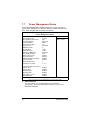
9L
#"
&
&
'(
)
#*+,(#
% &-% $
2 & Current System Temp.
Current CPU Temperature
Menu Level #
Current FAN1 Speed
Current FAN2 Speed
Cureent FAN3 Speed
Vcore
+3.3V
+5V
+12V
-12V
-5V
%&'( : Move Enter: Select +/-/PU/PD: Value F10: Save ESC: Exit F1: General Help
F5: Previous Values F6: Fail-Safe Defaults F7: Optimized Defaults
#" Current System Temp.
''
#" Current CPU Temperature
''
1
#" Current FAN1/FAN2/FAN3 Speed
3'%''
?
@!A'
'
9''#
#" +3.3V/+5V/+12V/-12V/-5V
''!=88=<=1:%1:%<
Award BIOS Utility
0:
/ >(-:*
#"4#"
9L
#"
&
&
'(
)
#*+,(#
% &-% 3".1! "
Auto Detect PCI Clk
Enabled
Spread Spectrum Modulated
Disabled
Menu Level #
%&'( : Move Enter: Select +/-/PU/PD: Value F10: Save ESC: Exit F1: General Help
F5: Previous Values F6: Fail-Safe Defaults F7: Optimized Defaults
#" Auto Detect PCI Clk
- '9''&#
#
4'!!4&#
#
!- '9'4&#
#4
3''.*9&9
#" Spread Spectrum Modulated
3'99'
3''.*9&9
%;
Award BIOS Utility
SBC81820 Socket478 All-in-One CPU Card Series User’s Manual
'$$
?)@?*
&
&
'(
)
% &-% !"
!" !"
!"#
$%&
!"
!'
$(&
!" #
'
!" !
(& -
4- 561789
7
!" #
!" ,'
*+- '!
*./
12.!)*+
%&'(.#
$%&
?)
"*?))@4*G
9
Award BIOS Utility
%!
# '"$
&
&
'(
)
% &-% !"
!" !"
!"#
$%&
!"
!'
$(&
!" #
'
!" !
0:
4- 561789
7
!" #
!" ,'
*+- '!
*./
12.!)*+
%&'(.#
$(&
)-$#
"*?))@4*G
9
%&
Award BIOS Utility
SBC81820 Socket478 All-in-One CPU Card Series User’s Manual
% "0-,
G
supervisor password: can enter and change the
options of the setup menus.
user password: just can enter but do not have the
right to change the options of the setup menus.
ENTER PASSWORD:
J-K
"*?)G
J-KGJ-K
7J-K
4
?
)
PASSWORD DISABLED.
)B
4
<
?)<
B
G
<
?)
=)*
))
)
<
))
)
Award BIOS Utility
%6
0?@"
G<
"*?)9
)
&
&
'(
)
% &-% !"
!" !"
!"#
$%&
!"
!'
$(&
!" #
'
!" !
&!
&
"
561789
6
!" #
!" ,'
*+- '!
*./
12.!)*+
%&'(.#
!&
%'
Award BIOS Utility
SBC81820 Socket478 All-in-One CPU Card Series User’s Manual
1 @<40*
),)
G<
)
9
)
&
&
'(
)
% &-% !"
!" !"
!"#
$%&
!"
!'
$(&
!" #
'
!" !
;
<
& "
561789
7
!" #
!" ,'
*./
12.!)*+
*+- '!
%&'(.#
9&
Award BIOS Utility
%(
%5
SBC81820 Socket478 All-in-One CPU Card Series User’s Manual
(+(
,
-
*4<4*
"#$
&;
/9*1
7=
Start
↓
Un-Lock WDT
:
OUT 120H 0AH ; enter WDT function
OUT 120H 0BH ; enable WDT function
↓
Set multiple (1~4)
:
OUT 120 0NH ; N=1,2,3 or 4
↓
Set base timer (0~F)
:
OUT 121 0MH ; M=0,1,2,…F
↓
re-set timer
:
OUT 121 0MH ; M=0,1,2,…F
↓
IF No re-set timer
:
WDT time-out, generate RESET or NMI
↓
IF to disable WDT
:
OUT 120 00H ; Can be disable at any time
↓
WDT counting
Watchdog Timer
%0
SBC81820 Socket478 All-in-One CPU Card Series User’s Manual
M
0
1
2
3
4
5
6
7
8
9
A
B
C
D
E
F
%%
N
1
0.5 sec.
1 sec.
1.5 secs.
2 secs.
2.5 secs.
3 secs.
3.5 secs.
4 secs.
4.5 secs.
5 secs.
5.5 secs.
6 secs.
6.5 secs.
7 secs.
7.5 secs.
8 secs.
5
10
15
20
25
30
35
40
45
50
55
60
65
70
75
80
2
secs.
secs.
secs.
secs.
secs.
secs.
secs.
secs.
secs.
secs.
secs.
secs.
secs.
secs.
secs.
secs.
50
100
150
200
250
300
350
400
450
500
550
600
650
700
750
800
3
secs.
secs.
secs.
secs.
secs.
secs.
secs.
secs.
secs.
secs.
secs.
secs.
secs.
secs.
secs.
secs.
100
200
300
400
500
600
700
800
900
1000
1100
1200
1300
1400
1500
1600
4
secs.
secs.
secs.
secs.
secs.
secs.
secs.
secs.
secs.
secs.
secs.
secs.
secs.
secs.
secs.
secs.
Watchdog Timer
SBC81820 Socket478 All-in-One CPU Card Series User’s Manual
(+
.(-
40-pin IDE Interface Connector: CN19/CN20
Pin
1
4
7
10
13
16
19
22
25
28
31
34
37
40
Description
Reset #
Data 8
Data 5
Data 11
Data 2
Data 14
GND
GND
IOR #
No connector
Interrupt
No connector
HDC CS0 #
GND
Pin
2
5
8
11
14
17
20
23
26
29
32
35
38
Description
Pin
GND
Data 6
Data 10
Data 3
Data 13
Data 0
No connector
IOW #
GND
No connector
No connector
SA0
HDC CSI #
Description
3
6
9
12
15
18
21
24
27
30
33
36
39
Data 7
Data 9
Data 4
Data 12
Data 1
Data 16
No connector
GND
IOCHRDY
GND-Default
SA1
SA2
HDD Active #
Floppy Disk Connector: CN22
Pin
1
4
7
10
13
16
19
22
25
28
31
34
Description
GND
No connector
GND
Motor enable A#
GND
Motor enable B#
GND
Write data#
GND
Write protect#
GND
Disk change#
Pin
Description
Pin
2
Reduce write current
GND
Index#
GND
Drive select A#
GND
STEP#
GND
Track 0 #
GND
Side 1 select#
3
5
8
11
14
17
20
23
26
29
32
Connector Pin Assignments
6
9
12
15
18
21
24
27
30
33
Description
GND
No connector
GND
Drive select B#
GND
Direction#
GND
Write gate#
GND
Read data#
GND
%:
SBC81820 Socket478 All-in-One CPU Card Series User’s Manual
Parallel Port Connector: CN1
Pin
1
2
3
4
5
6
7
8
9
10
11
12
13
Description
Pin
Strobe#
Data 0
Data 1
Data 2
Data 3
Data 4
Data 5
Data 6
Data 7
Acknowledge#
Busy
Paper Empty#
Printer Select
14
15
16
17
18
19
20
21
22
23
24
25
Description
Auto Form Feed#
Error#
Initialize#
Printer Select In#
GND
GND
GND
GND
GND
GND
GND
GND
26
RS-422/485 pin assignments for COM2: CN6
Pin #
1
2
3
4
5
6
7
8
9
10
:;
Signal Name
R2-422
TXNo connector
TX+
No connector
RX+
No connector
RXNo connector
GND
No connector
RS-485
DATANo connector
DATA+
No connector
No connector
No connector
No connector
No connector
GND
No connector
Connector Pin Assignments
SBC81820 Socket478 All-in-One CPU Card Series User’s Manual
RS-232 Serial Ports Pin Assignment: CN2, CN6
CN2/CN6 Pin
1
2
3
4
5
6
7
8
9
10
Description
Data Carrier Detect (DCD)/5V/12V
Data Set Ready (DSR)
Receive Data (RXD)
Request to Send (RTS)
Transmit Data (TXD)
Clear to Send (CTS)
Data Terminal Ready (DTR)
Ring Indicator (RI)/5V/12V
Ground (GND)
GND
USB Connector: CN4
Pin
1
3
5
7
9
Description
Pin
USB Vcc
USB P0USB P0+
GND
No connector
2
4
6
8
10
Description
USB Vcc
USB P1USB P1+
GND
No connector
Connector Pin Assignments
:!
:&