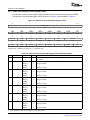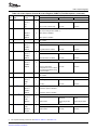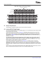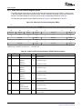
1
TMS320DM647/DM648
Video Port/VCXO Interpolated Control (VIC)
Port
User's Guide
Literature Number: SPRUEM1
May 2007
2
SPRUEM1 – May 2007
Submit Documentation Feedback
Contents
Preface.............................................................................................................................. 13
1
1.1
1.2
Overview ................................................................................................................. 16
Video Port ................................................................................................................ 17
Video Port FIFO ......................................................................................................... 19
1.2.1
EDMA Interface ................................................................................................. 19
1.2.2
Video Capture FIFO Configurations .......................................................................... 20
1.5
1.6
..........................................................................
Video Port Registers ..................................................................................................
Video Port Pin Mapping..............................................................................................
1.4.1 VDIN Bus Usage for Capture Modes ........................................................................
1.4.2 VDOUT Data Bus Usage for Display Modes................................................................
Video Port Pin Multiplexing ........................................................................................
VideoPort Clocking ....................................................................................................
2
2.1
Video Port ............................................................................................................... 29
Reset Operation ........................................................................................................ 30
1.2.3
1.3
1.4
2.1.1
2.4
3
3.1
3.2
3.3
23
25
26
27
28
28
28
Power-On Reset ................................................................................................ 30
.......................................................................................... 30
2.1.3 Software Port Reset ............................................................................................ 30
2.1.4 Capture Channel Reset ........................................................................................ 31
2.1.5 Display Channel Reset......................................................................................... 31
Interrupt Operation .................................................................................................... 31
EDMA Operation........................................................................................................ 32
2.3.1 Capture EDMA Event Generation ............................................................................ 32
2.3.2 Display EDMA Event Generation ............................................................................. 33
2.3.3 EDMA Size and Threshold Restrictions ..................................................................... 33
2.3.4 EDMA Interface Operation .................................................................................... 34
Video Port Control Registers ...................................................................................... 34
2.4.1 Video Port Control Register (VPCTL) ........................................................................ 35
2.4.2 Video Port Status Register (VPSTAT) ....................................................................... 37
2.4.3 Video Port Interrupt Enable Register (VPIE) ................................................................ 38
2.4.4 Video Port Interrupt Status Register (VPIS) ................................................................ 40
2.1.2
2.2
2.3
Video Display FIFO Configurations
Peripheral Bus Reset
Video Capture Port ................................................................................................... 45
Video Capture Mode Selection .................................................................................... 46
BT.656 Video Capture Mode........................................................................................ 46
3.2.1
BT.656 Capture Channels ..................................................................................... 46
3.2.2
BT.656 Timing Reference Codes ............................................................................. 46
3.2.3
BT.656 Image Window and Capture ......................................................................... 48
3.2.4
BT.656 Data Sampling ......................................................................................... 49
3.2.5
BT.656 FIFO Packing .......................................................................................... 49
Y/C Video Capture Mode ............................................................................................ 50
3.3.1
Y/C Capture Channels ......................................................................................... 50
3.3.2
Y/C Timing Reference Codes ................................................................................. 50
SPRUEM1 – May 2007
Submit Documentation Feedback
Table of Contents
3
3.4
3.3.3
Y/C Image Window and Capture ............................................................................. 50
3.3.4
Y/C FIFO Packing .............................................................................................. 51
BT.656 and Y/C Mode Field and Frame Operation .......................................................... 51
.....................................................................
3.4.2 Vertical Synchronization .......................................................................................
3.4.3 Horizontal Synchronization ....................................................................................
3.4.4 Field Identification ..............................................................................................
3.4.5 Short and Long Field Detect ..................................................................................
Video Input Filtering ..................................................................................................
3.5.1 Input Filter Modes ..............................................................................................
3.5.2 Chrominance Re-sampling Operation .......................................................................
3.5.3 Scaling Operation...............................................................................................
3.5.4 Edge Pixel Replication .........................................................................................
Ancillary Data Capture ...............................................................................................
3.6.1 Horizontal Ancillary (HANC) Data Capture ..................................................................
3.6.2 Vertical Ancillary (VANC) Data Capture .....................................................................
Raw Data Capture Mode .............................................................................................
3.7.1 Raw Data Capture Notification ................................................................................
3.7.2 Raw Data FIFO Packing .......................................................................................
TCI Capture Mode ......................................................................................................
3.8.1 TCI Capture Features ..........................................................................................
3.8.2 TCI Data Capture ...............................................................................................
3.8.3 TCI Capture Error Detection ..................................................................................
3.8.4 Synchronizing the System Clock .............................................................................
3.8.5 TCI Data Capture Notification .................................................................................
3.8.6 Writing to the FIFO .............................................................................................
3.8.7 Reading from the FIFO ........................................................................................
Capture Line Boundary Conditions ..............................................................................
Capturing Video in BT.656 or Y/C Mode .......................................................................
3.10.1 Handling FIFO Overrun in BT.656 or Y/C Mode ..........................................................
Capturing Video in Raw Data Mode .............................................................................
3.11.1 Handling FIFO Overrun Condition in Raw Data Mode ...................................................
Capturing Data in TCI Capture Mode ............................................................................
3.12.1 Handling FIFO Overrun Condition in TCI Capture Mode .................................................
Video Capture Registers ............................................................................................
3.13.1 Video Capture Channel x Status Register (VCASTAT, VCBSTAT) ....................................
3.13.2 Video Capture Channel A Control Register (VCACTL) ...................................................
3.13.3 Video Capture Channel x Field 1 Start Register (VCxSTRT1) ..........................................
3.13.4 Video Capture Channel x Field 1 Stop Register (VCxSTOP1) ..........................................
3.13.5 Video Capture Channel x Field 2 Start Register (VCxSTRT2) ..........................................
3.13.6 Video Capture Channel x Field 2 Stop Register (VCxSTOP2) ..........................................
3.13.7 Video Capture Channel x Vertical Interrupt Register (VCxVINT) .......................................
3.13.8 Video Capture Channel x Threshold Register (VCATHRLD, VCBTHRLD) ............................
3.13.9 Video Capture Channel x Event Count Register (VCxEVTCT)..........................................
3.13.10 Video Capture Channel B Control Register (VCBCTL) .................................................
3.13.11 TCI Capture Control Register (TCICTL) ..................................................................
3.13.12 TCI Clock Initialization LSB Register (TCICLKINITL) ...................................................
3.13.13 TCI Clock Initialization MSB Register (TCICLKINITM) ..................................................
3.4.1
3.5
3.6
3.7
3.8
3.9
3.10
3.11
3.12
3.13
4
Contents
Capture Determination and Notification
52
53
55
56
57
57
58
58
58
59
60
61
61
61
61
62
63
63
63
64
64
65
66
66
67
67
68
68
69
69
70
70
71
72
75
76
77
78
79
80
81
81
84
85
86
SPRUEM1 – May 2007
Submit Documentation Feedback
3.13.14 TCI System Time Clock LSB Register (TCISTCLKL) ................................................... 86
3.13.15 TCI System Time Clock MSB Register (TCISTCLKM).................................................. 87
3.13.16 TCI System Time Clock Compare LSB Register (TCISTCMPL)
......................................
88
3.13.17 TCI System Time Clock Compare MSB Register (TCISTCMPM) ..................................... 88
3.13.18 TCI System Time Clock Compare Mask LSB Register (TCISTMSKL) ............................... 89
3.13.19 TCI System Time Clock Compare Mask MSB Register (TCISTMSKM) .............................. 89
3.13.20 TCI System Time Clock Ticks Interrupt Register (TCITICKS) ......................................... 90
3.14
Video Capture FIFO Registers ..................................................................................... 91
4
4.1
Video Display Port .................................................................................................... 92
Video Display Mode Selection ..................................................................................... 93
4.2
4.1.1
Image Timing .................................................................................................... 93
4.1.2
Video Display Counters ........................................................................................ 96
4.1.3
Sync Signal Generation ........................................................................................ 98
4.1.4
External Sync Operation ....................................................................................... 98
4.1.5
Port Sync Operation ............................................................................................ 98
BT.656 Video Display Mode ........................................................................................ 98
............................................................................ 99
4.2.2 Blanking Codes ................................................................................................ 101
4.2.3 BT.656 Image Display ........................................................................................ 101
4.2.4 BT.656 FIFO Unpacking ..................................................................................... 101
4.3
Y/C Video Display Mode ........................................................................................... 102
4.3.1 Y/C Display Timing Reference Codes ...................................................................... 102
4.3.2 Y/C Blanking Codes .......................................................................................... 102
4.3.3 Y/C Image Display ............................................................................................ 102
4.3.4 Y/C FIFO Unpacking.......................................................................................... 103
4.4
Video Output Filtering .............................................................................................. 103
4.4.1 Output Filter Modes ........................................................................................... 103
4.4.2 Chrominance Re-sampling Operation ...................................................................... 104
4.4.3 Scaling Operation ............................................................................................. 104
4.4.4 Edge Pixel Replication ....................................................................................... 105
4.5
Ancillary Data Display .............................................................................................. 106
4.5.1 Horizontal Ancillary (HANC) Data Display ................................................................. 106
4.5.2 Vertical Ancillary (VANC) Data Display .................................................................... 106
4.6
Raw Data Display Mode ............................................................................................ 106
4.6.1 Raw Mode RGB Output Support ............................................................................ 107
4.6.2 Raw Data FIFO Unpacking .................................................................................. 107
4.7
Video Display Field and Frame Operation ................................................................... 108
4.7.1 Display Determination and Notification ..................................................................... 108
4.7.2 Video Display Event Generation ............................................................................ 109
4.8
Display Line Boundary Conditions............................................................................. 109
4.9
Display Timing Examples ......................................................................................... 110
4.9.1 Interlaced BT.656 Timing Example ......................................................................... 110
4.9.2 Interlaced Raw Display Example............................................................................ 113
4.9.3 Y/C Progressive Display Example .......................................................................... 116
4.10 Displaying Video in BT.656 or Y/C Mode ..................................................................... 119
4.11 Displaying Video in Raw Data Mode ........................................................................... 120
4.11.1 Handling Under-run Condition of the Display FIFO ..................................................... 121
4.2.1
Display Timing Reference Codes
SPRUEM1 – May 2007
Submit Documentation Feedback
Contents
5
........................................................................................... 122
4.12.1 Video Display Status Register (VDSTAT) ................................................................ 122
4.12.2 Video Display Control Register (VDCTL) ................................................................. 123
4.12.3 Video Display Frame Size Register (VDFRMSZ) ........................................................ 127
4.12.4 Video Display Horizontal Blanking Register (VDHBLNK) ............................................... 127
4.12.5 Video Display Field 1 Vertical Blanking Start Register (VDVBLKS1) ................................. 128
4.12.6 Video Display Field 1 Vertical Blanking End Register (VDVBLKE1) .................................. 129
4.12.7 Video Display Field 2 Vertical Blanking Start Register (VDVBLKS2) ................................. 130
4.12.8 Video Display Field 2 Vertical Blanking End Register (VDVBLKE2) .................................. 131
4.12.9 Video Display Field 1 Image Offset Register (VDIMGOFF1) .......................................... 132
4.12.10 Video Display Field 1 Image Size Register (VDIMGSZ1) ............................................. 133
4.12.11 Video Display Field 2 Image Offset Register (VDIMGOFF2) ......................................... 134
4.12.12 Video Display Field 2 Image Size Register (VDIMGSZ2) ............................................. 135
4.12.13 Video Display Field 1 Timing Register (VDFLDT1) .................................................... 135
4.12.14 Video Display Field 2 Timing Register (VDFLDT2) .................................................... 136
4.12.15 Video Display Threshold Register (VDTHRLD) ........................................................ 137
4.12.16 Video Display Horizontal Synchronization Register (VDHSYNC) .................................... 138
4.12.17 Video Display Field 1 Vertical Synchronization Start Register (VDVSYNS1) ...................... 138
4.12.18 Video Display Field 1 Vertical Synchronization End Register (VDVSYNE1) ....................... 139
4.12.19 Video Display Field 2 Vertical Synchronization Start Register (VDVSYNS2) ...................... 140
4.12.20 Video Display Field 2 Vertical Synchronization End Register (VDVSYNE2) ....................... 140
4.12.21 Video Display Counter Reload Register (VDRELOAD) ............................................... 141
4.12.22 Video Display Event Register (VDDISPEVT) ........................................................... 142
4.12.23 Video Display Clipping Register (VDCLIP) .............................................................. 142
4.12.24 Video Display Default Display Value Register (VDDEFVAL) ......................................... 143
4.12.25 Video Display Vertical Interrupt Register (VDVINT) ................................................... 144
4.12.26 Video Display Field Bit Register (VDFBIT) .............................................................. 145
4.12.27 Video Display Field 1 Vertical Blanking Bit Register (VDVBIT1) ..................................... 146
4.12.28 Video Display Field 2 Vertical Blanking Bit Register (VDVBIT2) ..................................... 147
4.13 Video Display Registers Recommended Values........................................................... 148
4.14 Video Display FIFO Registers .................................................................................... 149
4.12
Video Display Registers
5
5.1
General-Purpose I/O Operation ................................................................................. 150
GPIO Registers ........................................................................................................ 151
5.1.1
Video Port Peripheral Identification Register (VPPID) ................................................... 152
5.1.2
Video Port Peripheral Control Register (PCR) ............................................................ 153
5.1.3
Video Port Pin Function Register (PFUNC) ............................................................... 154
5.1.4
Video Port Pin Direction Register (PDIR) .................................................................. 156
5.1.5
Video Port Pin Data Input Register (PDIN) ................................................................ 158
5.1.6
Video Port Pin Data Output Register (PDOUT) ........................................................... 159
5.1.7
Video Port Pin Data Set Register (PDSET)
5.1.8
Video Port Pin Data Clear Register (PDCLR) ............................................................. 162
5.1.9
Video Port Pin Interrupt Enable Register (PIEN)
...............................................................
.........................................................
161
163
5.1.10 Video Port Pin Interrupt Polarity Register (PIPOL) ...................................................... 164
5.1.11 Video Port Pin Interrupt Status Register (PISTAT) ...................................................... 165
5.1.12 Video Port Pin Interrupt Clear Register (PICLR) ......................................................... 166
6
6.1
6.2
6
VCXO Interpolated Control Port ................................................................................ 167
Overview ................................................................................................................ 168
Interface ................................................................................................................. 168
Contents
SPRUEM1 – May 2007
Submit Documentation Feedback
6.3
6.4
6.5
Operational Details .................................................................................................. 169
Enabling VIC Port .................................................................................................... 170
VIC Port Registers ................................................................................................... 170
6.5.1
VIC Control Register (VICCTL).............................................................................. 171
6.5.2
VIC Input Register (VICIN) ................................................................................... 172
6.5.3
VIC Clock Divider Register (VICDIV) ....................................................................... 173
SPRUEM1 – May 2007
Submit Documentation Feedback
Contents
7
List of Figures
1-1
1-2
1-3
1-4
1-5
1-6
1-7
1-8
1-9
1-10
2-1
2-2
2-3
2-4
3-1
3-2
3-3
3-4
3-5
3-6
3-7
3-8
3-9
3-10
3-11
3-12
3-13
3-14
3-15
3-16
3-17
3-18
3-19
3-20
3-21
3-22
3-23
3-24
3-25
3-26
3-27
3-28
3-29
3-30
3-31
3-32
3-33
3-34
3-35
3-36
3-37
3-38
8
Video Port Block Diagram .................................................................................................
BT.656 Video Capture FIFO Configuration .............................................................................
8-Bit Raw Video Capture and TCI Video Capture FIFO Configuration..............................................
Y/C Video Capture FIFO Configuration .................................................................................
16-Bit Raw Video Capture FIFO Configuration .........................................................................
BT.656 Video Display FIFO Configuration ..............................................................................
8-Bit Raw Video Display FIFO Configuration ...........................................................................
8-Bit Locked Raw Video Display FIFO Configuration .................................................................
16-Bit Raw Video Display FIFO Configuration .........................................................................
Y/C Video Display FIFO Configuration ..................................................................................
Video Port Control Register (VPCTL) ...................................................................................
Video Port Status Register (VPSTAT) ...................................................................................
Video Port Interrupt Enable Register (VPIE) ...........................................................................
Video Port Interrupt Status Register (VPIS) ............................................................................
Video Capture Parameters ................................................................................................
8-Bit BT.656 FIFO Packing ...............................................................................................
8-Bit Y/C FIFO Packing....................................................................................................
VCOUNT Operation Example (EXC = 0)................................................................................
HCOUNT Operation Example (EXC = 0) ...............................................................................
HCOUNT Operation Example (EXC = 1) ...............................................................................
Field 1 Detection Timing...................................................................................................
Chrominance Re-sampling ................................................................................................
1/2 Scaled Co-Sited Filtering .............................................................................................
1/2 Scaled Chrominance Re-sampled Filtering ........................................................................
Edge Pixel Replication .....................................................................................................
Capture Window Not Requiring Edge Pixel Replication ..............................................................
8-Bit Raw Data FIFO Packing ............................................................................................
16-Bit Raw Data FIFO Packing ...........................................................................................
Parallel TCI Capture .......................................................................................................
Program Clock Reference (PCR) Header Format .....................................................................
System Time Clock Counter Operation .................................................................................
TCI FIFO Packing ..........................................................................................................
TCI Timestamp Format (Little Endian) ..................................................................................
Capture Line Boundary Example .........................................................................................
Video Capture Channel x Status Register (VCxSTAT)................................................................
Video Capture Channel A Control Register (VCACTL) ...............................................................
Video Capture Channel x Field 1 Start Register (VCxSTRT1) .......................................................
Video Capture Channel x Field 1 Stop Register (VCxSTOP1) .......................................................
Video Capture Channel x Field 2 Start Register (VCxSTRT2) .......................................................
Video Capture Channel x Field 2 Stop Register (VCxSTOP2) .......................................................
Video Capture Channel x Vertical Interrupt Register (VCxVINT) ....................................................
Video Capture Channel x Threshold Register (VCxTHRLD) .........................................................
Video Capture Channel x Event Count Register (VCxEVTCT) ......................................................
Video Capture Channel B Control Register (VCBCTL) ...............................................................
TCI Capture Control Register (TCICTL) .................................................................................
TCI Clock Initialization LSB Register (TCICLKINITL) .................................................................
TCI Clock Initialization MSB Register (TCICLKINITM) ................................................................
TCI System Time Clock LSB Register (TCISTCLKL) .................................................................
TCI System Time Clock MSB Register (TCISTCLKM) ................................................................
TCI System Time Clock Compare LSB Register (TCISTCMPL) .....................................................
TCI System Time Clock Compare MSB Register (TCISTCMPM) ...................................................
TCI System Time Clock Compare Mask LSB Register (TCISTMSKL) ..............................................
List of Figures
18
20
21
22
23
23
23
24
24
25
35
37
38
40
48
50
51
54
55
56
57
58
59
59
60
60
62
63
64
64
65
66
66
67
71
73
76
77
77
78
79
80
81
82
84
85
86
87
87
88
88
89
SPRUEM1 – May 2007
Submit Documentation Feedback
3-39
3-40
4-1
4-2
4-3
4-4
4-5
4-6
4-7
4-8
4-9
4-10
4-11
4-12
4-13
4-14
4-15
4-16
4-17
4-18
4-19
4-20
4-21
4-22
4-23
4-24
4-25
4-26
4-27
4-28
4-29
4-30
4-31
4-32
4-33
4-34
4-35
4-36
4-37
4-38
4-39
4-40
4-41
4-42
4-43
4-44
4-45
4-46
4-47
4-48
4-49
4-50
4-51
TCI System Time Clock Compare Mask MSB Register (TCISTMSKM) ............................................ 90
TCI System Time Clock Ticks Interrupt Register (TCITICKS)........................................................ 90
NTSC Compatible Interlaced Display .................................................................................... 93
SMPTE 296M Compatible Progressive Scan Display ................................................................. 94
Interlaced Blanking Intervals and Video Areas ......................................................................... 95
Progressive Blanking Intervals and Video Area ........................................................................ 96
Horizontal Blanking and Horizontal Sync Timing ...................................................................... 97
Vertical Blanking, Sync and Even/Odd Frame Signal Timing ........................................................ 97
Video Display Module Synchronization Chain .......................................................................... 98
BT.656 Output Sequence ................................................................................................. 98
525/60 BT.656 Horizontal Blanking Timing ............................................................................. 99
625/50 BT.656 Horizontal Blanking Timing ............................................................................. 99
Digital Vertical F and V Transitions..................................................................................... 100
8-Bit BT.656 FIFO Unpacking ........................................................................................... 101
Y/C Horizontal Blanking Timing (BT.1120 60I) ....................................................................... 102
8-Bit Y/C FIFO Unpacking ............................................................................................... 103
Chrominance Re-sampling .............................................................................................. 104
2x Co-Sited Scaling ...................................................................................................... 104
2x Interspersed Scaling .................................................................................................. 105
Output Edge Pixel Replication .......................................................................................... 105
Luma Edge Replication .................................................................................................. 105
Interspersed Chroma Edge Replication ................................................................................ 106
8-Bit Raw FIFO Unpacking .............................................................................................. 107
16-Bit Raw FIFO Unpacking............................................................................................. 107
8-Bit Raw FIFO Unpacking ........................................................................................... 107
Display Line Boundary Example ........................................................................................ 110
BT.656 Interlaced Display Horizontal Timing Example .............................................................. 111
BT.656 Interlaced Display Vertical Timing Example ................................................................. 113
Raw Interlaced Display Horizontal Timing Example ................................................................. 114
Raw Interlaced Display Vertical Timing Example..................................................................... 115
Y/C Progressive Display Horizontal Timing Example ................................................................ 117
Y/C Progressive Display Vertical Timing Example ................................................................... 118
Video Display Status Register (VDSTAT) ............................................................................. 123
Video Display Control Register (VDCTL) .............................................................................. 124
Video Display Frame Size Register (VDFRMSZ)..................................................................... 127
Video Display Horizontal Blanking Register (VDHBLNK) ........................................................... 128
Video Display Field 1 Vertical Blanking Start Register (VDVBLKS1) .............................................. 129
Video Display Field 1 Vertical Blanking End Register (VDVBLKE1) ............................................... 129
Video Display Field 2 Vertical Blanking Start Register (VDVBLKS2) .............................................. 130
Video Display Field 2 Vertical Blanking End Register (VDVBLKE2) ............................................... 131
Video Display Field 1 Image Offset Register (VDIMGOFF1) ....................................................... 132
Video Display Field 1 Image Size Register (VDIMGSZ1) ........................................................... 133
Video Display Field 2 Image Offset Register (VDIMGOFF2) ....................................................... 134
Video Display Field 2 Image Size Register (VDIMGSZ2) ........................................................... 135
Video Display Field 1 Timing Register (VDFLDT1) .................................................................. 136
Video Display Field 2 Timing Register (VDFLDT2) .................................................................. 136
Video Display Threshold Register (VDTHRLD) ....................................................................... 137
Video Display Horizontal Synchronization Register (VDHSYNC) .................................................. 138
Video Display Field 1 Vertical Synchronization Start Register (VDVSYNS1)..................................... 139
Video Display Field 1 Vertical Synchronization End Register (VDVSYNE1) ..................................... 139
Video Display Field 2 Vertical Synchronization Start Register (VDVSYNS2)..................................... 140
Video Display Field 2 Vertical Synchronization End Register (VDVSYNE2) ..................................... 141
Video Display Counter Reload Register (VDRELOAD) .............................................................. 141
SPRUEM1 – May 2007
Submit Documentation Feedback
List of Figures
9
4-52
4-53
4-54
4-55
4-56
4-57
4-58
4-59
5-1
5-2
5-3
5-4
5-5
5-6
5-7
5-8
5-9
5-10
5-11
5-12
6-1
6-2
6-3
6-4
6-5
10
Video Display Event Register (VDDISPEVT) .........................................................................
Video Display Clipping Register (VDCLIP) ............................................................................
Video Display Default Display Value Register (VDDEFVAL) .......................................................
Video Display Default Display Value Register (VDDEFVAL) - Raw Data Mode .................................
Video Display Vertical Interrupt Register (VDVINT) ..................................................................
Video Display Field Bit Register (VDFBIT) ............................................................................
Video Display Field 1 Vertical Blanking Bit Register (VDVBIT1) ...................................................
Video Display Field 2 Vertical Blanking Bit Register (VDVBIT2) ...................................................
Video Port Peripheral Identification Register (VPPID) ...............................................................
Video Port Peripheral Control Register (PCR) ........................................................................
Video Port Pin Function Register (PFUNC) ...........................................................................
Video Port Pin Direction Register (PDIR)..............................................................................
Video Port Pin Data Input Register (PDIN) ............................................................................
Video Port Pin Data Output Register (PDOUT).......................................................................
Video Port Pin Data Set Register (PDSET) ...........................................................................
Video Port Pin Data Clear Register (PDCLR).........................................................................
Video Port Pin Interrupt Enable Register (PIEN) .....................................................................
Video Port Pin Interrupt Polarity Register (PIPOL) ...................................................................
Video Port Pin Interrupt Status Register (PISTAT) ...................................................................
Video Port Pin Interrupt Clear Register (PICLR) .....................................................................
TCI System Block Diagram ..............................................................................................
Program Clock Reference (PCR) Header Format ....................................................................
VIC Control Register (VICCTL) .........................................................................................
VIC Input Register (VICIN) ..............................................................................................
VIC Clock Divider Register (VICDIV)...................................................................................
List of Figures
142
143
144
144
145
146
146
147
152
153
154
156
158
159
161
162
163
164
165
166
168
169
171
172
173
SPRUEM1 – May 2007
Submit Documentation Feedback
List of Tables
1-1
1-2
1-3
1-4
2-1
2-2
2-3
2-4
2-5
2-6
3-1
3-2
3-3
3-4
3-5
3-6
3-7
3-8
3-9
3-10
3-11
3-12
3-13
3-14
3-15
3-16
3-17
3-18
3-19
3-20
3-21
3-22
3-23
3-24
3-25
3-26
3-27
3-28
3-29
3-30
3-31
3-32
3-33
3-34
3-35
4-1
4-2
4-3
4-4
Video Capture Signal Mapping ........................................................................................... 26
Video Display Signal Mapping ............................................................................................ 26
VDIN Data Bus Usage for Capture Modes ............................................................................. 27
VDOUT Data Bus Usage for Display Modes ........................................................................... 28
Video Port Control Registers ............................................................................................. 34
Video Port Control Register (VPCTL) Field Descriptions ............................................................. 35
Video Port Operating Mode Selection ................................................................................... 36
Video Port Status Register (VPSTAT) Field Descriptions ............................................................ 37
Video Port Interrupt Enable Register (VPIE) Field Descriptions ..................................................... 38
Video Port Interrupt Status Register (VPIS) Field Descriptions ...................................................... 40
Video Capture Mode Selection ........................................................................................... 46
BT.656 Video Timing Reference Codes ................................................................................. 47
BT.656 Protection Bits ..................................................................................................... 47
Error Correction by Protection Bits ...................................................................................... 47
Common Video Source Parameters ..................................................................................... 49
BT.656 and Y/C Mode Capture Operation .............................................................................. 52
Vertical Synchronization Programming .................................................................................. 53
Horizontal Synchronization Programming ............................................................................... 55
Field Identification Programming ......................................................................................... 56
Input Filter Mode Selection ............................................................................................... 58
Raw Data Mode Capture Operation ..................................................................................... 62
TCI Capture Mode Operation ............................................................................................. 65
Video Capture Control Registers ........................................................................................ 70
Video Capture Channel x Status Register (VCxSTAT) Field Descriptions ......................................... 72
Video Capture Channel A Control Register (VCACTL) Field Descriptions ......................................... 73
Video Capture Channel x Field 1 Start Register (VCxSTRT1) Field Descriptions................................. 76
Video Capture Channel x Field 1 Stop Register (VCxSTOP1) Field Descriptions ................................ 77
Video Capture Channel x Field 2 Start Register (VCxSTRT2) Field Descriptions................................. 78
Video Capture Channel x Field 2 Stop Register (VCxSTOP2) Field Descriptions ................................ 78
Video Capture Channel x Vertical Interrupt Register (VCxVINT) Field Descriptions .............................. 79
Video Capture Channel x Threshold Register (VCxTHRLD) Field Descriptions ................................... 80
Video Capture Channel x Event Count Register (VCxEVTCT) Field Descriptions ................................ 81
Video Capture Channel B Control Register (VCBCTL) Field Descriptions ......................................... 82
TCI Capture Control Register (TCICTL) Field Descriptions .......................................................... 84
TCI Clock Initialization LSB Register (TCICLKINITL) Field Descriptions ........................................... 85
TCI Clock Initialization MSB Register (TCICLKINITM) Field Descriptions .......................................... 86
TCI System Time Clock LSB Register (TCISTCLKL) Field Descriptions ........................................... 87
TCI System Time Clock MSB Register (TCISTCLKM) Field Descriptions.......................................... 87
TCI System Time Clock Compare LSB Register (TCISTCMPL) Field Descriptions .............................. 88
TCI System Time Clock Compare MSB Register (TCISTCMPM) Field Descriptions ............................. 89
TCI System Time Clock Compare Mask LSB Register (TCISTMSKL) Field Descriptions ....................... 89
TCI System Time Clock Compare Mask MSB Register (TCISTMSKM) Field Descriptions ...................... 90
TCI System Time Clock Ticks Interrupt Register (TCITICKS) Field Descriptions ................................. 90
Video Capture FIFO Registers ........................................................................................... 91
Video Capture FIFO Registers Function ................................................................................ 91
Video Display Mode Selection ............................................................................................ 93
BT.656 Frame Timing .................................................................................................... 100
Output Filter Mode Selection ............................................................................................ 103
Display Operation ......................................................................................................... 108
SPRUEM1 – May 2007
Submit Documentation Feedback
List of Tables
11
4-5
4-6
4-7
4-8
4-9
4-10
4-11
4-12
4-13
4-14
4-15
4-16
4-17
4-18
4-19
4-20
4-21
4-22
4-23
4-24
4-25
4-26
4-27
4-28
4-29
4-30
4-31
4-32
4-33
4-34
4-35
4-36
5-1
5-2
5-3
5-4
5-5
5-6
5-7
5-8
5-9
5-10
5-11
5-12
5-13
6-1
6-2
6-3
6-4
6-5
6-6
12
Video Display Control Registers .......................................................................................
Video Display Status Register (VDSTAT) Field Descriptions .......................................................
Video Display Control Register (VDCTL) Field Descriptions ........................................................
Video Display Frame Size Register (VDFRMSZ) Field Descriptions ..............................................
Video Display Horizontal Blanking Register (VDHBLNK) Field Descriptions .....................................
Video Display Field 1 Vertical Blanking Start Register (VDVBLKS1) Field Descriptions........................
Video Display Field 1 Vertical Blanking End Register (VDVBLKE1) Field Descriptions ........................
Video Display Field 2 Vertical Blanking Start Register (VDVBLKS2) Field Descriptions........................
Video Display Field 2 Vertical Blanking End Register (VDVBLKE2) Field Descriptions ........................
Video Display Field 1 Image Offset Register (VDIMGOFF1) Field Descriptions .................................
Video Display Field 1 Image Size Register (VDIMGSZ1) Field Descriptions .....................................
Video Display Field 2 Image Offset Register (VDIMGOFF2) Field Descriptions .................................
Video Display Field 2 Image Size Register (VDIMGSZ2) Field Descriptions .....................................
Video Display Field 1 Timing Register (VDFLDT1) Field Descriptions ............................................
Video Display Field 2 Timing Register (VDFLDT2) Field Descriptions ............................................
Video Display Threshold Register (VDTHRLD) Field Descriptions ................................................
Video Display Horizontal Synchronization Register (VDHSYNC) Field Descriptions ............................
Video Display Field 1 Vertical Synchronization Start Register (VDVSYNS1) Field Descriptions ..............
Video Display Field 1 Vertical Synchronization End Register (VDVSYNE1) Field Descriptions ...............
Video Display Field 2 Vertical Synchronization Start Register (VDVSYNS2) Field Descriptions ..............
Video Display Field 2 Vertical Synchronization End Register (VDVSYNE2) Field Descriptions ...............
Video Display Counter Reload Register (VDRELOAD) Field Descriptions .......................................
Video Display Event Register (VDDISPEVT) Field Descriptions ...................................................
Video Display Clipping Register (VDCLIP) Field Descriptions ......................................................
Video Display Default Display Value Register (VDDEFVAL) Field Descriptions .................................
Video Display Vertical Interrupt Register (VDVINT) Field Descriptions ...........................................
Video Display Field Bit Register (VDFBIT) Field Descriptions ......................................................
Video Display Field 1 Vertical Blanking Bit Register (VDVBIT1) Field Descriptions .............................
Video Display Field 2 Vertical Blanking Bit Register (VDVBIT2) Field Descriptions .............................
Video Display Register Recommended Values ......................................................................
Video Display FIFO Registers...........................................................................................
Video Display FIFO Registers Function ...............................................................................
Video Port Registers .....................................................................................................
Video Port Peripheral Identification Register (VPPID) Field Descriptions .........................................
Video Port Peripheral Control Register (PCR) Field Descriptions..................................................
Video Port Pin Function Register (PFUNC) Field Descriptions .....................................................
Video Port Pin Direction Register (PDIR) Field Descriptions .......................................................
Video Port Pin Data Input Register (PDIN) Field Descriptions .....................................................
Video Port Pin Data Out Register (PDOUT) Field Descriptions ....................................................
Video Port Pin Data Set Register (PDSET) Field Descriptions .....................................................
Video Port Pin Data Clear Register (PDCLR) Field Descriptions ..................................................
Video Port Pin Interrupt Enable Register (PIEN) Field Descriptions ...............................................
Video Port Pin Interrupt Polarity Register (PIPOL) Field Descriptions.............................................
Video Port Pin Interrupt Status Register (PISTAT) Field Descriptions ............................................
Video Port Pin Interrupt Clear Register (PICLR) Field Descriptions ...............................................
VIC Port Interface Signals ...............................................................................................
Example Values for Interpolation Rate .................................................................................
VIC Port Registers ........................................................................................................
VIC Control Register (VICCTL) Field Descriptions ...................................................................
VIC Input Register (VICIN) Field Descriptions ........................................................................
VIC Clock Divider Register (VICDIV) Field Descriptions ............................................................
List of Tables
122
123
124
127
128
129
130
130
131
132
133
134
135
136
136
137
138
139
139
140
141
141
142
143
144
145
146
147
147
148
149
149
151
152
153
154
156
158
159
161
162
163
164
165
166
168
169
170
171
172
173
SPRUEM1 – May 2007
Submit Documentation Feedback
Preface
SPRUEM1 – May 2007
Read This First
About This Manual
This document describes the video port and VCXO interpolated control (VIC) port in the digital signal
processors (DSPs).
Notational Conventions
This document uses the following conventions.
• Hexadecimal numbers are shown with the suffix h. For example, the following number is 40
hexadecimal (decimal 64): 40h.
• Registers in this document are shown in figures and described in tables.
– Each register figure shows a rectangle divided into fields that represent the fields of the register.
Each field is labeled with its bit name, its beginning and ending bit numbers above, and its
read/write properties below. A legend explains the notation used for the properties.
– Reserved bits in a register figure designate a bit that is used for future device expansion.
Related Documentation From Texas Instruments
The following documents describe the TMS320DM647/DM648 Digital Signal Processor (DSP). Copies of
these documents are available on the Internet at www.ti.com. Tip: Enter the literature number in the
search box provided at www.ti.com.
SPRS372 — TMS320DM647/DM648 Digital Media Processor Data Manual describes the signals,
specifications and electrical characteristics of the device.
SPRU732 — TMS320C64x/C64x+ DSP CPU and Instruction Set Reference Guide describes the CPU
architecture, pipeline, instruction set, and interrupts for the TMS320C64x and TMS320C64x+ digital
signal processors (DSPs) of the TMS320C6000 DSP family. The C64x/C64x+ DSP generation
comprises fixed-point devices in the C6000 DSP platform. The C64x+ DSP is an enhancement of
the C64x DSP with added functionality and an expanded instruction set.
SPRUEK5 — TMS320DM647/DM648 DSP DDR2 Memory Controller User's Guide describes the DDR2
memory controller in the TMS320DM647/DM648 Digital Signal Processor (DSP). The DDR2/mDDR
memory controller is used to interface with JESD79D-2A standard compliant DDR2 SDRAM
devices and standard Mobile DDR SDRAM devices.
SPRUEK6 — TMS320DM647/DM648 DSP External Memory Interface (EMIF) User's Guide describes
the operation of the asynchronous external memory interface (EMIF) in the TMS320DM647/DM648
Digital Signal Processor (DSP). The EMIF supports a glueless interface to a variety of external
devices.
SPRUEK7 — TMS320DM647/DM648 DSP General-Purpose Input/Output (GPIO) User's Guide
describes the general-purpose input/output (GPIO) peripheral in the TMS320DM647/DM648 Digital
Signal Processor (DSP). The GPIO peripheral provides dedicated general-purpose pins that can be
configured as either inputs or outputs. When configured as an input, you can detect the state of the
input by reading the state of an internal register. When configured as an output, you can write to an
internal register to control the state driven on the output pin.
SPRUEM1 – May 2007
Submit Documentation Feedback
Preface
13
www.ti.com
Related Documentation From Texas Instruments
SPRUEK8 — TMS320DM647/DM648 DSP Inter-Integrated Circuit (I2C) Module User's Guide
describes the inter-integrated circuit (I2C) peripheral in the TMS320DM647/DM648 Digital Signal
Processor (DSP). The I2C peripheral provides an interface between the DSP and other devices
compliant with the I2C-bus specification and connected by way of an I2C-bus. External components
attached to this 2-wire serial bus can transmit and receive up to 8-bit wide data to and from the
DSP through the I2C peripheral. This document assumes the reader is familiar with the I2C-bus
specification.
SPRUEL0 — TMS320DM647/DM648 DSP 64-Bit Timer User's Guide describes the operation of the
64-bit timer in the TMS320DM647/DM648 Digital Signal Processor (DSP). The timer can be
configured as a general-purpose 64-bit timer, dual general-purpose 32-bit timers, or a watchdog
timer.
SPRUEL1 — TMS320DM647/DM648 DSP Multichannel Audio Serial Port (McASP) User's Guide
describes the multichannel audio serial port (McASP) in the TMS320DM647/DM648 Digital Signal
Processor (DSP). The McASP functions as a general-purpose audio serial port optimized for the
needs of multichannel audio applications. The McASP is useful for time-division multiplexed (TDM)
stream, Inter-Integrated Sound (I2S) protocols, and intercomponent digital audio interface
transmission (DIT).
SPRUEL2 — TMS320DM647/DM648 DSP Enhanced DMA (EDMA) Controller User's Guide describes
the operation of the enhanced direct memory access (EDMA3) controller in the
TMS320DM647/DM648 Digital Signal Processor (DSP). The EDMA3 controller’s primary purpose is
to service user-programmed data transfers between two memory-mapped slave endpoints on the
DSP.
SPRUEL4 — TMS320DM647/DM648 Peripheral Component Interconnect (PCI) User's Guide
describes the peripheral component interconnect (PCI) port in the TMS320DM647/DM648 Digital
Signal Processor (DSP). The PCI port supports connection of the C642x DSP to a PCI host via the
integrated PCI master/slave bus interface. The PCI port interfaces to the DSP via the enhanced
DMA (EDMA) controller. This architecture allows for both PCI master and slave transactions, while
keeping the EDMA channel resources available for other applications.
SPRUEL5 — TMS320DM647/DM648 DSP Host Port Interface (UHPI) User's Guide describes the host
port interface (HPI) in the TMS320DM647/DM648 Digital Signal Processor (DSP). The HPI is a
parallel port through which a host processor can directly access the CPU memory space. The host
device functions as a master to the interface, which increases ease of access. The host and CPU
can exchange information via internal or external memory. The host also has direct access to
memory-mapped peripherals. Connectivity to the CPU memory space is provided through the
enhanced direct memory access (EDMA) controller.
SPRUEL8 — TMS320DM647/DM648 DSP Universal Asynchronous Receiver/Transmitter (UART)
User's Guide describes the universal asynchronous receiver/transmitter (UART) peripheral in the
TMS320DM647/DM648 Digital Signal Processor (DSP). The UART peripheral performs
serial-to-parallel conversion on data received from a peripheral device, and parallel-to-serial
conversion on data received from the CPU.
SPRUEL9 — TMS320DM647/DM648 DSP VLYNQ Port User's Guide describes the VLYNQ port in the
TMS320DM647/DM648 Digital Signal Processor (DSP). The VLYNQ port is a high-speed
point-to-point serial interface for connecting to host processors and other VLYNQ compatible
devices. It is a full-duplex serial bus where transmit and receive operations occur separately and
simultaneously without interference.
SPRUEM1 — TMS320DM647/DM648 DSP Video Port/VCXO Interpolated Control (VIC) Port User's
Guide discusses the video port and VCXO interpolated control (VIC) port in the
TMS320DM647/DM648 Digital Signal Processor (DSP). The video port can operate as a video
capture port, video display port, or transport stream interface (TSI) capture port. The VIC port
provides single-bit interpolated VCXO control with resolution from 9 bits to up to 16 bits. When the
video port is used in TSI mode, the VIC port is used to control the system clock, VCXO, for MPEG
transport stream.
14
Read This First
SPRUEM1 – May 2007
Submit Documentation Feedback
www.ti.com
Related Documentation From Texas Instruments
SPRUEM2 — TMS320DM647/DM648 DSP Serial Port Interface (SPI) User's Guide discusses the
Serial Port Interface (SPI) in the TMS320DM647/DM648 Digital Signal Processor (DSP). This
reference guide provides the specifications for a 16-bit configurable, synchronous serial peripheral
interface. The SPI is a programmable-length shift register, used for high speed communication
between external peripherals or other DSPs.
Trademarks
SPRUEM1 – May 2007
Submit Documentation Feedback
Read This First
15
SPRUEM1 – May 2007
Overview
This chapter provides an overview of the video port peripheral in the digital signal
processors (DSPs). An overview of the video port functions, FIFO configurations, and
signal mapping are included.
Topic
1.1
1.2
1.3
1.4
1.5
1.6
16
Overview
..................................................................................................
Video Port ................................................................................
Video Port FIFO ........................................................................
Video Port Registers .................................................................
Video Port Pin Mapping .............................................................
Video Port Pin Multiplexing ........................................................
VideoPort Clocking ...................................................................
Page
17
19
25
26
28
28
SPRUEM1 – May 2007
Submit Documentation Feedback
www.ti.com
Video Port
1.1
Video Port
The video port peripheral can operate as a video capture port, video display port, or transport channel
interface (TCI) capture port.
It provides the following functions:
• Video capture mode:
– Capture rate of up to 80 MHZ.
– Two channels of 8-bit digital video input from a digital camera or an analog camera (using a video
decoder). Digital video input is in YCbCr 4:2:2 format with 8-bit resolution multiplexed in ITU-R
BT.656 format.
– One channel of Y/C 16-bit digital video input in YCbCr 4:2:2 format on separate Y and Cb/Cr inputs.
Supports SMPTE 260M, SMPTE 274M, SMPTE 296M, ITU-BT.1120, etc., as well as older
CCIR601 interfaces.
– YCbCr 4:2:2 to YCbCr 4:2:0 horizontal conversion and 1/2 scaling in 8-bit 4:2:2 modes.
– Direct interface for two channels of up to 8-bit or one channel of up to 16-bit raw video from A/D
converters.
• Video display mode:
– Display rate of up to 110 MHZ.
– One channel of continuous digital video output. Digital video output is YCbCr 4:2:2 co-sited pixel
data with 8-bit resolution multiplexed in ITU-R BT.656 format.
– One channel of Y/C 16-bit digital video output in YCbCr 4:2:2 format on separate Y and Cb/Cr
outputs. (Supports SMPTE 260M, SMPTE 274M, SMPTE 296M, ITU-BT.1120, etc.)
– YCbCr 4:2:0 to YCbCr 4:2:2 horizontal conversion and 2x scaling of output in 8-bit 4:2:2 modes.
– Programmable clipping of BT.656 and Y/C mode output values.
– One channel of raw data output up to 16-bits for interface to RAMDACs. Two channel synchronized
raw data output.
– Synchronizes to external video controller or another video display port.
– Using the external clock, the frame timing generator provides programmable image timing that
includes horizontal and vertical blanking, start of active video (SAV) and end of active video (EAV)
code insertion, and horizontal and frame timing pulses.
– Generates horizontal and vertical synchronization and blanking signals and a frame synchronization
signal.
• TCI capture mode: Transport channel interface (TCI) from a front-end device (such as demodulator) or
a forward error correction device in 8-bit parallel format at up to 30 Mbytes/sec.
• The port generates up to three events per channel in BT656 and Y/C Mode, one event per channel in
RAW and TCI mode and one interrupt to the DSP.
A high-level block diagram of the video port is shown in Figure 1-1. The port consists of two channels: A
and B. You can split a 5120-byte capture/display buffer between the two channels. The entire port (both
channels) is always configured for either video capture or display only. Separate data pipelines control the
parsing and formatting of video capture or display data for each of the BT.656, Y/C, raw video, and TCI
modes.
For video capture operation, the video port may operate as two 8-bit channels of BT.656 or raw video
capture; or as a single channel of 8-bit BT.656, 8-bit raw video, 8-bit Y/C video, 16-bit raw video, or 8-bit
TCI.
For video display operation, the video port may operate as a single channel of 8-bit BT.656, 8-bit raw
video, 8-bit Y/C video, or 16-bit raw video. It may also operate in a two channel 8-bit raw mode in which
the two channels are locked to the same timing. Channel B is not used during single channel operation.
It is important to note that the VideoPort Data pin numbering is compatible with TMS320DM642 DSP
chip.In case of a 8-bit channel the suffixes for the data pins are mentioned as VDOUT[9-2]for
display/output port and VDIN[9-2]for capture/input port. In case of a 16-bit channel the suffixes for the data
pins are mentioned as VDOUT[19-2]for display/output port and VDIN[19-2]for capture/input port.
SPRUEM1 – May 2007
Submit Documentation Feedback
Overview
17
www.ti.com
Video Port
This document describes the full feature set offered by the video port. See the device-specific datasheet
for details about I/O timing information.
Figure 1-1. Video Port Block Diagram
Internal peripheral bus
32
VCLK1
VCLK2
VCTL1
VCTL2
VCTL3
Timing and
control logic
Memory
mapped
registers
DMA interface
64
VDIN[19−2]
16
BT.656 capture
pipeline
8
Y/C video
capture pipeline
16
Raw video
capture pipeline
16
TSI capture
pipeline
8
8
Capture/display
buffer
(2560 bytes)
BT.656 display
pipeline
16
Y/C video
display pipeline
16
Raw video
display pipeline
VDOUT[19−2]
16
Channel A
BT.656 capture
pipeline
8
VDIN[19−12]
Raw video
capture pipeline
8
8
8
Raw video
display pipeline
Capture/display
buffer
(2560 bytes)
8
VDOUT[19−12]
Channel B
64
DMA interface
18
Overview
SPRUEM1 – May 2007
Submit Documentation Feedback
www.ti.com
Video Port FIFO
1.2
Video Port FIFO
The video port includes a FIFO to store data coming into or out from the video port. The video port
operates in conjunction with EDMA transfers to move data between the video port FIFO and external or
on-chip memory. You can program threshold settings so that EDMA events generate when the video port
FIFO reaches a certain fullness (for capture) or goes below a certain fullness (for display). You set up
EDMA Channels that are required to service the FIFO independently and are key to correct operation of
the video port. The FIFO size is relatively large to allow time for EDMA Channels to service the transfer
requests, since the device typically has many peripheral interfaces, including five video ports.
The following sections briefly describe the interaction with the EDMA and different FIFO configurations
that are used to support the various modes of the video port.
1.2.1 EDMA Interface
Video port data transfers take place using EDMA Channels. EDMA requests are based on buffer
thresholds. Since the video port does not directly source the transfer, it can not adjust the transfer size
based on buffer empty/full status. This means the EDMA transfer size is essentially fixed in the
user-programmed EDMA parameter table. The preferred transfer size is often one entire line of data
because this allows the most flexibility in terms of frame buffer line pitch (in RAM). Some modes of
operation for the highest display rates may require more frequent EDMA requests, such as on a half or
quarter line basis.
All requests are based on buffer thresholds. EDMA requests are made whenever the number of samples
in the buffer reaches the threshold value in video capture mode. In order to ensure that all data from a
capture field/frame gets emptied from the buffer, the transfer size must be equal to the threshold and the
total amount of field/frame data must be a multiple of the transfer size.
For video display operation, EDMA requests are made whenever there is at least the threshold number of
double words free in the FIFO. This means that the transfer size must be equal or smaller than the
threshold so that it fits into the available space. The field/frame size must still be a multiple of the transfer
size or there are pixels left in the buffer at the end of the field (which appear at the start of the next field).
SPRUEM1 – May 2007
Submit Documentation Feedback
Overview
19
www.ti.com
Video Port FIFO
1.2.2 Video Capture FIFO Configurations
During video capture operation, the video port FIFO has one of four configurations depending on the
capture mode. For BT.656 operation, the FIFO is split into channel A and B, as shown in Figure 1-2. Each
FIFO is clocked independently with the channel A FIFO receiving data from the VDIN[9-2] half of the bus
and the channel B FIFO receiving data from the VDIN[19-12] half of the bus. Each channel's FIFO is
further split into Y, Cb, and Cr buffers with separate write pointers and read registers (YSRCx, CBSRCx,
and CRSRCx).
Figure 1-2. BT.656 Video Capture FIFO Configuration
Capture FIFO A
64
8
YSRCA
Y Buffer A (1280 bytes)
VDIN[9−2]
Cb Buffer A (640 bytes)
64
CBSRCA
8
Cr Buffer A (640 bytes)
8
64
CRSRCA
Capture FIFO B
64
8
YSRCB
Y Buffer B (1280 bytes)
VDIN[19−12]
8
8
20
Overview
Cb Buffer B (640 bytes)
64
Cr Buffer B (640 bytes)
64
CBSRCB
CRSRCB
SPRUEM1 – May 2007
Submit Documentation Feedback
www.ti.com
Video Port FIFO
For 8-bit raw video, the FIFO is split into channel A and B, as shown in Figure 1-3. Each FIFO is clocked
independently with the channel A FIFO receiving data from the VDIN[9-2] half of the bus and the channel
B FIFO receiving data from the VDIN[19-12] half of the bus. Each channel's FIFO has a separate write
pointer and read register (YSRCx). The FIFO configuration is identical for TCI capture, but channel B is
disabled.
Figure 1-3. 8-Bit Raw Video Capture and TCI Video Capture FIFO Configuration
Capture FIFO A
VDIN[9−2]
8
64
YSRCA
Buffer A (2560 bytes)
Capture FIFO B
VDIN[19−12]
8
64
YSRCB
Buffer B (2560 bytes)
SPRUEM1 – May 2007
Submit Documentation Feedback
Overview
21
www.ti.com
Video Port FIFO
For Y/C video capture, the FIFO is configured as a single channel split into separate Y, Cb, and Cr buffers
with separate write pointers and read registers (YSRCA, CBSRCA, and CRSRCA). Figure 1-4 shows how
Y data is received on the VDIN[9-2] half of the bus and Cb/Cr data is received on the VDIN[19-12] half of
the bus and de-multiplexed into the Cb and Cr buffers.
Figure 1-4. Y/C Video Capture FIFO Configuration
Capture FIFO
YSRCA
64
VDIN[9−2]
8
8
Y Buffer (2560 bytes)
Cb Buffer (1280 bytes)
64
CBSRCA
VDIN[19−12]
8
22
Overview
Cr Buffer (1280 bytes)
64
CRSRCA
SPRUEM1 – May 2007
Submit Documentation Feedback
www.ti.com
Video Port FIFO
For 16-bit raw video, the FIFO is configured as a single buffer, as shown in Figure 1-5. The FIFO receives
16-bit data from the VDIN[19-2] bus. The FIFO has a single write pointer and read register (YSRCA).
Figure 1-5. 16-Bit Raw Video Capture FIFO Configuration
Capture FIFO
VDIN[19−2]
YSRCA
64
16
Data Buffer
(5120 bytes)
1.2.3 Video Display FIFO Configurations
During video display operation, the video port FIFO has one of five configurations depending on the
display mode. For BT.656 operation, a single output is provided on channel A, as shown in Figure 1-6,
with data output on VDOUT[9-2]. The channel's FIFO is split into Y, Cb, and Cr buffers with separate read
pointers and write registers (YDSTA, CBDST, and CRDST).
Figure 1-6. BT.656 Video Display FIFO Configuration
Display FIFO
YDSTA
64
Y Buffer
(2560 bytes)
8
VDOUT[9−2]
CBDST
CRDST
64
Cb Buffer
(1280 bytes)
8
64
Cr Buffer
(1280 bytes)
8
For 8-bit raw video, the FIFO is configured as a single buffer as shown in Figure 1-7. The FIFO outputs
data on the VDOUT[9-2] half of the bus. The FIFO has a single read pointer and write register (YDSTA).
Figure 1-7. 8-Bit Raw Video Display FIFO Configuration
Display FIFO
VDOUT[9−2]
YDSTA
8
64
Data Buffer
(5120 bytes)
SPRUEM1 – May 2007
Submit Documentation Feedback
Overview
23
www.ti.com
Video Port FIFO
For locked raw video, the FIFO is split into channel A and B. The channels are locked together and use
the same clock and control signals. Each channel uses a single buffer and write register (YDSTx) as
shown in Figure 1-8.
For 16-bit raw video, the FIFO is configured as a single buffer, as shown in Figure 1-9. The FIFO outputs
data on VDOUT[19-2]. The FIFO has a single read pointer and write register (YDSTA).
Figure 1-8. 8-Bit Locked Raw Video Display FIFO Configuration
Display FIFO A
YDSTA
VDOUT[9−2]
64
8
Buffer A (2560 bytes)
Display FIFO B
YDSTB
VDOUT[19−12]
64
8
Buffer B (2560 bytes)
Figure 1-9. 16-Bit Raw Video Display FIFO Configuration
Display FIFO
YDSTA
64
VDOUT[19−2]
16
Data Buffer (5120 bytes)
24
Overview
SPRUEM1 – May 2007
Submit Documentation Feedback
www.ti.com
Video Port Registers
For Y/C video display, the FIFO is configured as a single channel split into separate Y, Cb, and Cr buffers
with separate read pointers and write registers (YDSTA, CBDST, and CRDST). Figure 1-10 shows how Y
data is output on the VDOUT[9-2] half of the bus and Cb/Cr data is multiplexed and output on the
VDOUT[19-12] half of the bus.
Figure 1-10. Y/C Video Display FIFO Configuration
Display FIFO
VDOUT[9−2]
YDSTA
64
8
Y Buffer
(2560 bytes)
CBDST
CRDST
1.3
64
64
Cb Buffer
(1280 bytes)
Cr Buffer (1280
bytes)
8
VDOUT[19−12]
8
Video Port Registers
The video port configuration register space is divided into several different sections with registers grouped
by function including top-level video port control, video capture control, video display control, and GPIO.
The registers for controlling the video port are in Section 2.4.
The registers for controlling the video capture mode of operation are shown in Section 3.13. An additional
space is dedicated for FIFO read pseudo-registers as shown in Section 3.14. This space requires
high-speed access and is not mapped to the register access bus.
The registers for controlling the video display mode of operation are shown in Section 4.12. An additional
space is dedicated for FIFO write pseudo-registers as shown in Section 4.14. This space requires
high-speed access and is not mapped to the register access bus.
The registers for controlling the general-purpose input/output (GPIO) are shown in Section 5.1.
SPRUEM1 – May 2007
Submit Documentation Feedback
Overview
25
www.ti.com
Video Port Pin Mapping
1.4
Video Port Pin Mapping
The video port requires 21 external signal pins for full functionality. Pin usage and direction changes
depend on the selected operating mode. Pin functionality detail for video capture mode is listed in
Table 1-1. Pin functionality detail for video display mode is listed in Table 1-2. All unused port signals
(except VCLK1 and VCLK1) can be configured as general-purpose I/O (GPIO) pins.
Table 1-1. Video Capture Signal Mapping (1)
Usage
BT.656 Capture Mode
Raw Data Capture Mode
Video Port Signal
I/O
Dual Channel
Single
Channel
Y/C Capture
Mode
8-Bit
16-Bit
TCI Capture
Mode
VDATA[9-2]
I/O
VDIN[9-2]
(In) Ch A
VDIN[9-2]
(In) Ch A
VDIN[9-2]
(In) (Y)
VDIN[9-2]
(In) Ch A
VDIN[9-2]
(In)
VDIN[9-2]
(In)
VDATA[19-12]
I/O
VDIN[19-12]
(In) Ch B
Not Used
VDIN[19-12]
(In) (Cb/Cr)
VDIN[19-12]
(In) Ch B
VDIN[19-12]
(In)
Not Used
VCLK1
I
VCLKINA (In)
VCLKINA (In)
VCLKINA (In)
VCLKINA (In)
VCLKINA (In)
VCLKINA (In)
VCLK1
I/O
VCLKINB (In)
Not Used
Not Used
VCLKINB (In)
Not Used
Not Used
VCTL1
I/O
CAPENA
(In)
CAPENA/
AVID/HSYNC
(In)
CAPENA/
AVID/HSYNC
(In)
CAPENA
(In)
CAPENA
(In)
CAPENA
(In)
VCTL2
I/O
CAPENB
(In)
VBLNK/
VSYNC (In)
VBLNK/
VSYNC (In)
CAPENB
(In)
Not Used
PACSTRT
(In)
VCTL3
I/O
Not Used
FID
(In)
FID
(In)
FID (In)
Ch A
FID (In)
Ch A
PACERR
(In)
(1)
Legend: VCLKINA – Channel A capture clock; CAPENA – Channel A capture enable; VCLKINB – Channel B capture clock;
CAPENB – Channel B capture enable; AVID – Active video; HSYNC – Horizontal synchronization; VBLNK – Vertical blanking;
VSYNC – Vertical synchronization; FID – Field identification; PACSTRT – Packet start; PACERR – Packet error
Table 1-2. Video Display Signal Mapping
Usage
26
Raw Data Display Mode
BT.656 Display
Mode
Y/C Display
Mode
8-Bit
16-Bit
8-Bit Dual Sync
I/O
VDOUT[9-2]
(Out)
VDOUT[9-2]
(Out) (Y)
VDOUT[9-2]
(Out)
VDOUT[9-2]
(Out)
VDOUT[9-2]
(Out) (Ch A)
I/O
Not Used
VDOUT[19-12]
(Out) (Cb/Cr)
Not Used
VDOUT[19-12]
(Out)
VDOUT[19-12]
(Out) (Ch B)
Video Port Signal
I/O
VDATA[9-2]
VDATA[19-12]
VCLK1
I
VCLKIN (In)
VCLKIN (In)
VCLKIN (In)
VCLKIN (In)
VCLKIN (In)
VCLK1
I/O
VCLKOUT (Out)
VCLKOUT (Out)
VCLKOUT (Out)
VCLKOUT (Out)
VCLKOUT (Out)
VCTL1
I/O
HSYNC/HBLNK/
AVID/FLD (Out)
or HSYNC (In)
HSYNC/HBLNK/
AVID/FLD (Out)
or HSYNC (In)
HSYNC/HBLNK/
AVID/FLD (Out)
or HSYNC (In)
HSYNC/HBLNK/
AVID/FLD (Out)
or HSYNC (In)
HSYNC/HBLNK/
AVID/FLD (Out)
or HSYNC (In)
VCTL2
I/O
VSYNC/VBLNK/C VSYNC/VBLNK/C VSYNC/VBLNK/C VSYNC/VBLNK/C VSYNC/VBLNK/C
SYNC/FLD (Out) SYNC/FLD (Out) SYNC/FLD (Out) SYNC/FLD (Out) SYNC/FLD (Out)
or VSYNC (In)
or VSYNC (In)
or VSYNC (In)
or VSYNC (In)
or VSYNC (In)
VCTL3
I/O
CBLNK/FLD
(Out) or FLD (In)
Overview
CBLNK/FLD
(Out) or FLD (In)
CBLNK/FLD
(Out) or FLD (In)
CBLNK/FLD
(Out) or FLD (In)
CBLNK/FLD
(Out) or FLD (In)
SPRUEM1 – May 2007
Submit Documentation Feedback
www.ti.com
Video Port Pin Mapping
1.4.1 VDIN Bus Usage for Capture Modes
The alignment and usage of data on the VDIN bus depends on the capture mode as shown in Table 1-3.
Table 1-3. VDIN Data Bus Usage for Capture Modes (1)
Capture Mode
BT.656
Y/C
Data Bus
8-Bit
8-Bit
8-Bit
16-Bit
VDIN19
B
A (C)
B
A
VDIN18
B
A (C)
B
A
VDIN17
B
A (C)
B
A
VDIN16
B
A (C)
B
A
VDIN15
B
A (C)
B
A
VDIN14
B
A (C)
B
A
VDIN13
B
A (C)
B
A
VDIN12
B
A (C)
B
A
VDIN9
A
A (Y)
A
A
A
VDIN8
A
A (Y)
A
A
A
VDIN7
A
A (Y)
A
A
A
VDIN6
A
A (Y)
A
A
A
VDIN5
A
A (Y)
A
A
A
VDIN4
A
A (Y)
A
A
A
VDIN3
A
A (Y)
A
A
A
VDIN2
A
A (Y)
A
A
A
(1)
Raw Data
TCI Mode
Legend: A – Channel A capture; A(C) Channel A chroma; A(Y) Channel A luma; B – Channel B capture
SPRUEM1 – May 2007
Submit Documentation Feedback
Overview
27
www.ti.com
Video Port Pin Multiplexing
1.4.2 VDOUT Data Bus Usage for Display Modes
The alignment and usage of data on the VDOUT bus depends on the display mode as shown in
Table 1-4.
Table 1-4. VDOUT Data Bus Usage for Display Modes (1)
Display Mode
BT.656
Data Bus
Dual Sync Raw Data
Raw Data
8-Bit
16-Bit
8-Bit
VDOUT19
A (C)
(B)
A
VDOUT18
A (C)
(B)
A
VDOUT17
A (C)
(B)
A
VDOUT16
A (C)
(B)
A
VDOUT15
A (C)
(B)
A
VDOUT14
A (C)
(B)
A
VDOUT13
A (C)
(B)
A
VDOUT12
A (C)
(B)
A
(1)
1.5
8-Bit
Y/C
VDOUT9
A
A (Y)
A
A
VDOUT8
A
A (Y)
A
A
VDOUT7
A
A (Y)
A
A
VDOUT6
A
A (Y)
A
A
VDOUT5
A
A (Y)
A
A
VDOUT4
A
A (Y)
A
A
VDOUT3
A
A (Y)
A
A
VDOUT2
A
A (Y)
A
A
Legend: A – Channel A display; A(C) Channel A chroma; A(Y) Channel A luma; B – Optional locked channel B display
Video Port Pin Multiplexing
None of the five Video Port have dedicated pins associated with them. Each of the Video Port has its pins
multiplexed with other peripherals. In order to use a desired Video Port either in Capture or Display Mode,
the user would first need to program the Pin Mux Register (PINMUX) appropriately to ensure that the
multiplexed pins work as VideoPort pins. Refer to the device-specific data manual to know details of the
PINMUX Register.
1.6
VideoPort Clocking
Each of the Video Ports have a LPSC associated with them. The LPSC provides the module clock and
reset control. On power up, the LPSC's associated with Video Ports do not gate the clock required for the
Video Port to function. User would need to appropriately program the LPSC associated with Video Port to
provide the clock to the desired Video Port before trying a data transfer operation. Refer to the
device-specific manual to know LPSC Video Port association and details of LPSC registers.
28
Overview
SPRUEM1 – May 2007
Submit Documentation Feedback
SPRUEM1 – May 2007
Video Port
This chapter discusses the basic operation of the video port. Included is a discussion of
the sources and types of resets, interrupt operation, EDMA operation, external clock
inputs, video port throughput and latency, and the video port control registers.
Topic
2.1
2.2
2.3
2.4
..................................................................................................
Reset Operation ........................................................................
Interrupt Operation ....................................................................
EDMA Operation .......................................................................
Video Port Control Registers ......................................................
SPRUEM1 – May 2007
Submit Documentation Feedback
Page
30
31
32
34
Video Port
29
www.ti.com
Reset Operation
2.1
Reset Operation
The video port has several sources and types of resets. The actions performed by these resets and the
state of the port following the resets is described in the following sections.
2.1.1 Power-On Reset
Power-on reset is an asynchronous hardware reset caused by a chip-level reset operation. The reset is
initiated by a power-on reset input to the video port. When the input is active, the port places all I/Os
(VD[19-2], VCTL1, VCTL2, VCTL3, and VCLK1) in a high-impedance state.
2.1.2 Peripheral Bus Reset
Peripheral bus reset is a synchronous hardware reset caused by a chip-level reset operation. The reset is
initiated by a peripheral bus reset input to the video port. This reset can be used internally (continuously
asserted) to disable the video port for low-power operation. When the input is active, the port does the
following:
• Places (keeps) all I/Os (VD[19-2], VCTL1, VCTL2, VCTL3, and VCLK1) in a high-impedance state.
• Flushes the FIFOs (resets pointers)
• Resets all port, capture, display, and GPIO registers to their default values. These may not complete
until the appropriate module clock (VCLK1, STCLK) edges occur to synchronously release the logic
from reset.
• Clears PEREN bit in PCR to 0.
• Sets VPHLT bit in VPCTL to 1.
While the peripheral remains disabled (PEREN = 0):
• VCLK1, VCLK2, and STCLK are gated off to save peripheral power.
• Peripheral bus accesses are acknowledged (RREADY/WREADY returned) to prevent EDMA lock-up.
(Any value returned on reads, data accepted or discarded on writes.)
• Peripheral bus MMR interface allows access to GPIO registers only (PID, PCR, PFUNC, PDIR, PIN,
PDOUT, PDSET, PDCLR, PIEN, PIPOL, PISTAT, and PICLR).
• Port I/Os (VD[19-2], VCTL1, VCTL2, VCTL3, and VCLK2) remain in a high-impedance state unless
enabled as GPIO by the PFUNC bits.
If software sets the PEREN bit in PCR but the VPHLT bit in VPCTL remains set:
• VCLK1, VCLK2, and STCLK are enabled to the port (allowing logic reset to complete).
• Peripheral bus accesses are acknowledged (RREADY/WREADY returned) to prevent EDMA lock-up.
(Any value returned on reads, data accepted or discarded on writes.)
• Peripheral bus MMR interface allows access to all registers.
• Port I/Os (VD[19-2], VCTL1, VCTL2, VCTL3, and VCLK2) remain in a high-impedance state unless
enabled as GPIO by the PFUNC bits.
• VPCTL bits may be set (until the VPHLT bit is cleared).
2.1.3 Software Port Reset
A software port reset may be performed on the entire video port by setting the VPRST bit in VPCTL. This
behaves identically to the peripheral bus reset except that it does not clear the PEREN bit in PCR. This
reset:
• Performs a reset on all port logic (channel logic may stay in reset until port input clock pulses occur).
• Self-clears the VPRST bit to 0 but leaves the VPHLT bit set. The VCLK1 input must be clocking in
order for this reset to take effect.
30
Video Port
SPRUEM1 – May 2007
Submit Documentation Feedback
www.ti.com
Interrupt Operation
Note:
The VPRST bit may take several clock cycles to clear to 0. The VPRST bit should be
polled to make sure the bit is cleared prior to writing to the video port registers.
Once the port is configured and the VPHLT bit is cleared, the setting of other VPCTL bits
(except VPRST) is disabled. The VCLK2 output may also be driven at this time, if display
mode is selected. VCTL1-3 must remain in a high-impedance state unless enabled as
GPIO, since internal/external sync is selected through VDCTL.
2.1.4 Capture Channel Reset
A software reset may be performed on a single capture channel by setting the RSTCH bit in VCxCTL. This
reset requires that the channel VCLKIN be transitioning. On capture channel reset:
• No new EDMA events are generated.
• Peripheral bus accesses are acknowledged (RREADY returned) to prevent EDMA lock-up. (Any value
returned on reads).
• Channel capture registers are set to their default values.
• Channel capture FIFO is flushed (pointers reset).
• The VCEN bit in VCxCTL is cleared to 0.
• The RSTCH bit self-clears to 0 after completion of the above.
Once the port is configured and the VCEN bit is set, the setting of other VCxCTL bits (except VCEN,
RSTCH, and BLKCAP) is prohibited and the capture counters begin counting. When BLKCAP is cleared,
data capture and event generation may begin.
2.1.5 Display Channel Reset
A software reset may be performed on the display channel by setting the RSTCH bit in VDCTL. This reset
requires that the channel VCLKIN be transitioning. On display channel reset:
• No new EDMA events are generated.
• Peripheral bus accesses are acknowledged (WREADY returned) to prevent EDMA lock-up. (Write data
may be written into the FIFO or discarded.)
• Channel display registers are set to their default values.
• Channel display FIFO is flushed (pointers reset).
• The VDEN bit in VDCTL is cleared to 0.
• The RSTCH bit self-clears to 0 after completion of the above.
Once the port is configured and the VDEN bit is set, the setting of other VDCTL bits (except VDEN,
RSTCH, and BLKDIS) is prohibited and the display counters begin counting. Data outputs are driven (with
default value, blanking, and control codes as appropriate and any control outputs are driven). When the
BLKDIS bit is cleared, event generation may begin and FIFO data displayed.
2.2
Interrupt Operation
The video port generates an interrupt to the DSP core after any of the following events occur:
• Capture complete (CCMPx) bit is set.
• Capture overrun (COVRx) bit is set.
• Synchronization byte error (SERRx) bit is set.
• Vertical interrupt (VINTxn) bit is set.
• Short field detect (SFDx) bit is set.
• Long field detect (LFDx) bit is set.
• STC absolute time (STC) bit is set.
• STC tick counter expired (TICK) bit is set.
• Display complete (DCMP) bit is set.
• Display under-run (DUND) bit is set.
SPRUEM1 – May 2007
Submit Documentation Feedback
Video Port
31
www.ti.com
EDMA Operation
•
•
Display complete not acknowledged (DCNA) bit is set.
GPIO interrupt (GPIO) bit is set.
The interrupt signal is a pulse only and does not hold state. The interrupt pulse is generated only when the
number of set flags in VPIS transitions from none to one or more. Another interrupt pulse is not generated
by setting additional flag bits.
Interrupts can be masked via the video port interrupt enable register (VPIE) using individual interrupt
enables and the VIE global enable bit. The interrupts are cleared in the video port interrupt status register
(VPIS) using the individual status bits. Writing a 1 to the appropriate bit clears the interrupt. The clearing
of an interrupt flag reenables the generation of another interrupt pulse, if other flags are still set. In other
words, pulse generation is reenabled by writing a 1 to any set bit of VPIS.
Upon receiving an interrupt you should:
1. Read VPIS.
2. Perform the service routine for whatever bits are set.
3. Clear appropriate bits by writing a 1 to their VPIS locations.
4. Upon return from the ISR, if VPIS bits have been (or remain) set, then another interrupt will occur.
2.3
EDMA Operation
The video port uses up to three EDMA events per channel for a total of six possible events. Each EDMA
event uses a dedicated event output. The outputs are:
• VPYEVTA
• VPCbEVTA
• VPCrEVTA
• VPYEVTB
• VPCbEVTB
• VPCrEVTB
2.3.1 Capture EDMA Event Generation
Capture EDMA events are generated based on the state of the capture FIFO(s). If no EDMA event is
currently pending and the FIFO crosses the value specified by VCTHRLDn, an EDMA event is generated.
Once an event has been requested, another EDMA event may not be generated until the servicing of the
outstanding event has begun (as indicated by the first read of the FIFO by the EDMA event service). If the
capture FIFO level exceeds 2x the VCTHRLDn value before the requested EDMA event completes, then
another EDMA event may be generated. Thus, up to one EDMA event may be outstanding.
An outgoing data counter counts data read by the EDMA. This counter is loaded with the VCTHRLDn
value whenever a new EDMA service begins. The counter then counts down for each double-word read
from the FIFO by the EDMA. The EDMA is complete when the counter reaches zero.
For BT.656 and Y/C modes, there are three FIFOs, one for each of the Y, Cb, and Cr color components.
Each FIFO generates its own EDMA event; therefore, the EDMA event state and FIFO thresholds for each
FIFO are tracked independently. The Cb and Cr FIFOs use a threshold value of 1/2 (VCTHRLDn +
VCTHRLDnmod 2).
Because the capture FIFOs may hold multiple thresholds worth of data, a problem arises at the
boundaries between fields. Since Field 1 and Field 2 may have different threshold values, the amount of
data in the FIFO required to generate the EDMA event changes depending on the current capture field
and the field of any outstanding EDMA requests. Similarly, the threshold value loaded in the outgoing data
counter needs to change depending on which field's EDMA event is being serviced (not which field is
currently being captured). To prevent confusion at the field boundaries, the VCxEVTCT register is
programmed to indicate the number of events to generate for each field. An event counter tracks how
many events have been generated and indicates which threshold value to use in event generation and in
the outgoing data counter. After the last Field 1 event has been generated, the EDMA logic looks for FIFO
> THRSHLD1 + THRSHLD2 to pre-generate the first Field 2 event. Once the last Field 1 event completes,
the logic looks for FIFO > 2x THRSHLD2 (assuming a Field 2 event is outstanding).
32
Video Port
SPRUEM1 – May 2007
Submit Documentation Feedback
www.ti.com
EDMA Operation
2.3.2 Display EDMA Event Generation
Display EDMA events are generated based on the amount of room available in the FIFO. The VDTHRLDn
value indicates the level at which the FIFO has room to receive another EDMA. If the FIFO has at least
VDTHRLDn locations available, a EDMA event is generated. Once an E EDMA event has been
requested, another EDMA event may not be generated until the servicing of the first EDMA event has
begun (as indicated by the first write to the FIFO by the EDMA event service). If there is at least 2x the
threshold space still available in the FIFO after the first EDMA service is begun (and the display event
counter has not expired) then another EDMA event may be generated. Thus, up to one EDMA request
may be outstanding.
An incoming data counter is loaded with the VDTHRLDn (or VDTHRLDn/2 for Cb and Cr FIFOs) value at
the beginning of each EDMA event service and counts down the incoming EDMA double words When the
counter reaches 0, the EDMA event is complete.
An EDMA event counter is used to track the number of EDMA events generated in each field as
programmed in the VDDISPEVT register. The DISPEVT1 or DISPEVT2 value (depending on the current
display field) is loaded at the start of each field. The event counter then decrements with each EDMA
event generation until it reaches 0, at which point no more EDMA events are generated until the next field
begins. Once the last line of data for a field has been requested, the EDMA logic stops generating events
until the field is complete in case the CPU needs to modify the EDMA address pointers.
For BT.656 and Y/C modes, there are three FIFOs, one for each of the Y, Cb, and Cr color components.
Each FIFO generates its own EDMA event; therefore, the EDMA event state and FIFO thresholds for each
FIFO are tracked independently. (The Cb and Cr FIFOs use a threshold value of 1/2 VDTHRLD).
2.3.3 EDMA Size and Threshold Restrictions
The video port FIFOs are 64-bits wide and always read or write 64 bits at a time. For this reason, EDMA
accesses must always be an even number of words in length. It is expected that in most cases the
threshold size is set to the line length (rounded up to the next double word). This always works because
different lines are not packed together within a double word and the Cb and Cr thresholds
(1/2 VCTHRLDx/VDTHRLD) are always rounded up to the double word.
For example, in 8-bit BT.656 capture mode with a line length of 712 (Y), setting the threshold to the line
length results in a VCTHRLD of 712 pixels x 1 bytes/pixel x double word/8 bytes = 89 double words. The
Cb and Cr FIFOs contain half the data (44.5 double words) so their thresholds are set to 45 double words.
Therefore, the Cb and Cr EDMAs each transmit an extra 4 bytes at the end of each line.
If a multi-horizontal line length threshold is desired (2 lines, for example) then the chosen line length must
round up to an even number of double words so that it is evenly divisible by 2. If this is not the case, then
the Cb and Cr FIFO transfers are corrupted. For the multiline case, consider the same 8-bit BT.656
capture mode with a line length of 712 (Y). If the threshold is set for 2 lines, this results in a VCTHRLD
value of 2 x 89 = 178 double words. The actual Cb/Cr line length is 44.5 double words that requires a
length of 45. To transfer 2 lines requires 2 x 45 = 90 double words. However, for this VCTHRLD, the
EDMA logic would calculate the Cb/Cr threshold size as 178/2 = 89 double words, which is 1 double word
off. This can be corrected by increasing the line length to 720 pixels (and ignoring the extra captured
pixels) or decreasing it to 704 pixels.
Similarly if a sub-horizontal line length is desired (1/2 line, for example), then the line length and threshold
must be chosen such that the threshold is divisible by 2. (This can also be stated as the line length must
be an even multiple of #EDMAs/line x 8). For the subline case, consider the 8-bit BT.656 capture mode
with a line length of 624 (Y). If the threshold is set for 1/2 the line length, this results in VCTHRLD =
(624/2)/8 = 39 double words. The EDMA logic would calculate the Cb/Cr threshold as 39/2 = 20 double
words. However, two such Cb/Cr EDMA events would result in a transfer of 40 double words, which is
larger than the actual Cb/Cr line length of (624/2)/8 = 39 double words. This can be corrected by changing
the line size to 640 pixels or 608 pixels, or by changing the threshold to be 1/3 the line length (VCTHRLD
= (624/3)/8 = 26 double words and the Cb/Cr threshold is 26/2 = 13 double words. 3 x 13 = 39 double
words, which is exactly the Cb/Cr line length.)
SPRUEM1 – May 2007
Submit Documentation Feedback
Video Port
33
www.ti.com
Video Port Control Registers
2.3.4 EDMA Interface Operation
When the video port is configured for capture (or TCI) mode, it only accepts read requests from the EDMA
interface. Write requests are false acknowledged (so the bus does not stall) and the data is discarded.
When the video port is configured for display mode, it only accepts write requests. Read requests are
false acknowledged (so the bus does not stall) and an arbitrary data value is returned.
When the video port is in reset, is not enabled (PEREN bit cleared), halted (VPHALT bit is set), or the
active mode is not enabled (VCEN or VDEN bit is cleared), then the port will false acknowledge all EDMA
accesses to prevent bus lockup.
The video port EDMA event generation logic is very tightly coupled to the EDMA interface accesses. An
incorrectly programmed EDMA size causes the EDMA and FIFO to become misaligned causing
aberrations in the captured or displayed data and likely resulting in an eventual FIFO overflow or
underflow. In the same manner, if another system EDMA incorrectly addresses the video port during
active capture or display, the video port has no way of determining that this is an errant EDMA because all
it monitors is a EDMA access so it must perform the FIFO read or write. Such an errant EDMA eventually
causes the FIFO to be over-read or overwritten.
2.4
Video Port Control Registers
The video port control registers are listed in Table 2-1. See the device-specific datasheet for the memory
address of these registers.
Table 2-1. Video Port Control Registers
Offset
Address (1)
(1)
34
Acronym
Register Name
C0h
VPCTL
Video Port Control Register
Section 2.4.1
Section
C4h
VPSTAT
Video Port Status Register
Section 2.4.2
C8h
VPIE
Video Port Interrupt Enable Register
Section 2.4.3
CCh
VPIS
Video Port Interrupt Status Register
Section 2.4.4
The absolute address of the registers is device/port specific and is equal to the base address + offset address. See the
device-specific datasheet to verify the register addresses.
Video Port
SPRUEM1 – May 2007
Submit Documentation Feedback
www.ti.com
Video Port Control Registers
2.4.1 Video Port Control Register (VPCTL)
The video port control register (VPCTL) determines the basic operation of the video port.
Not all combinations of the port control bits are unique. The control bit encoding is shown in Table 2-3.
Additional mode options are selected using the video capture channel A control register (VCACTL) and
video display control register (VDCTL).
The video port control register (VPCTL) is shown in Figure 2-1 and described in Table 2-2.
Figure 2-1. Video Port Control Register (VPCTL)
31
16
Reserved
R-0
15
14
VPRST
VPHLT
13
Reserved
8
R/WS-0
R/WC-1
R-0
7
6
5
4
3
2
1
0
VCLK2P
VCT3P
VCT2P
VCT1P
Reserved
TCI
DISP
DCHNL
R/W-0
R/W-0
R/W-0
R/W-0
R-0
R/W-0
R/W-0
R/W-0
LEGEND: R/W = Read/Write; R = Read only; WC = Write a 1 to clear; WS = Write 1 to set, a write of 0 has no effect; -n = value after reset
Table 2-2. Video Port Control Register (VPCTL) Field Descriptions
Bit
field
(1)
31-16 Reserved
15
VPRST
symval
(1)
-
Value Description
0
OF(value)
DEFAULT
Reserved. The reserved bit location is always read as 0. A value written to this field
has no effect.
Video port software reset enable bit. VPRST is set by writing a 1. Writing 0 has no
effect.
0
No effect.
1
Flush all FIFOs and set all port registers to their initial values. VCLK1 and VCLK2 are
configured as inputs and all VDATA and VCTL pins are placed in high impedance.
Auto-cleared after reset is complete.
NO
RESET
The VPRST bit may take several clock cycles to clear to 0. The VPRST bit should be
polled to make sure the bit is cleared prior to writing to the video port registers.
14
VPHLT
OF(value)
Video port halt bit. This bit is set upon hardware or software reset. The other VPCTL
bits (except VPRST) can only be changed when VPHLT is 1. VPHLT is cleared by
writing a 1. Writing 0 has no effect.
NONE
0
No effect.
DEFAULT
1
VPHLT is cleared.
0
Reserved. The reserved bit location is always read as 0. A value written to this field
has no effect.
CLEAR
13-6
Reserved
-
7
VCLK2P
OF(value)
DEFAULT
VCLK2 pin polarity bit. Has no effect in capture mode.
0
NONE
REVERSE
6
VCT3P
1
OF(value)
DEFAULT
Inverts the VCLK2 output clock polarity in display mode.
VCTL3 pin polarity. Does not affect GPIO operation. If VCTL3 pin is used as a FLD
input on the video capture side, then the VCTL3 polarity is not considered; the field
inverse is controlled by the FINV bit in the video capture channel x control register
(VCxCTL).
0
Indicates the VCTL3 control signal (input or output) is active high.
1
Indicates the VCTL3 control signal (input or output) is active low.
NONE
ACTIVELOW
(1)
For CSL implementation, use the notation VP_VPCTL_field_symval
SPRUEM1 – May 2007
Submit Documentation Feedback
Video Port
35
www.ti.com
Video Port Control Registers
Table 2-2. Video Port Control Register (VPCTL) Field Descriptions (continued)
Bit
5
field
(1)
VCT2P
symval
(1)
Value Description
OF(value)
VCTL2 pin polarity bit. Does not affect GPIO operation.
DEFAULT
0
Indicates the VCTL2 control signal (input or output) is active high.
1
Indicates the VCTL2 control signal (input or output) is active low.
NONE
ACTIVELOW
4
VCT1P
OF(value)
VCTL1 pin polarity bit. Does not affect GPIO operation.
ACTIVEHIGH
0
Indicates the VCTL1 control signal (input or output) is active high.
NONE
ACTIVELOW
1
Indicates the VCTL1 control signal (input or output) is active low.
3
Reserved
-
0
Reserved. The reserved bit location is always read as 0. A value written to this field
has no effect.
2
TCI
OF(value)
TCI capture mode select bit.
DEFAULT
0
TCI capture mode is disabled.
1
TCI capture mode is enabled.
NONE
CAPTURE
1
DISP
OF(value)
Display mode select bit. VDATA pins are configured for output. VCLK2 pin is
configured as VCLKOUT output.
DEFAULT
0
Capture mode is enabled.
1
Display mode is enabled.
CAPTURE
DISPLAY
0
DCHNL
OF(value)
Dual channel operation select bit. If the DCDIS bit in VPSTAT is set, this bit is forced
to 0.
DEFAULT
0
Single-channel operation is enabled.
1
Dual-channel operation is enabled.
SINGLE
DUAL
Table 2-3. Video Port Operating Mode Selection
VPCTL Bit
36
TCI
DISP
DCHNL
0
0
0
Single channel video capture. BT.656, Y/C or raw mode as selected in VCACTL. Video
capture B channel not used.
0
0
1
Dual channel video capture. Either BT.656 or raw 8-bit as selected in VCACTL and
VCBCTL. Option is available only if DCDIS is 0.
0
1
x
Single channel video display. BT.656, Y/C or raw mode as selected in VDCTL. Video
display B channel is only used for dual channel sync raw mode.
1
x
x
Single channel TCI capture.
Video Port
Operating Mode
SPRUEM1 – May 2007
Submit Documentation Feedback
www.ti.com
Video Port Control Registers
2.4.2 Video Port Status Register (VPSTAT)
The video port status register (VPSTAT) indicates the current condition of the video port.
The video port status register (VPSTAT) is shown in Figure 2-2 and described in Table 2-4.
Figure 2-2. Video Port Status Register (VPSTAT)
31
16
Reserved
R-0
15
3
2
Reserved
4
DCDIS
HIDATA
1
Reserved
0
R-0
R-x
R-x
R-0
LEGEND: R = Read only; -n = value after reset
Table 2-4. Video Port Status Register (VPSTAT) Field Descriptions
Bit
31-4
3
field
(1)
symval
(1)
Reserved
-
DCDIS
OF(value)
DEFAULT
Value Description
0
Reserved. The reserved bit location is always read as 0. A value written to this field
has no effect.
Dual-channel disable bit. The default value is determined by the chip-level
configuration.
0
Dual-channel operation is enabled.
1
Port muxing selections prevent dual-channel operation.
ENABLE
DISABLE
2
HIDATA
OF(value)
DEFAULT
High data bus half. HIDATA does not affect video port operation but is provided to
inform you which VDATA pins may be controlled by the video port GPIO registers.
HIDATA is never set unless DCDIS is also set. The default value is determined by the
chip-level configuration.
0
NONE
1-0
(1)
Reserved
USE
1
Indicates that another peripheral is using VDATA[9-2] and the video port channel A
(VDIN[9-2] or VDOUT[9-2]) is muxed onto VDATA[19-12].
-
0
Reserved. The reserved bit location is always read as 0. A value written to this field
has no effect.
For CSL implementation, use the notation VP_VPSTAT_field_symval
SPRUEM1 – May 2007
Submit Documentation Feedback
Video Port
37
www.ti.com
Video Port Control Registers
2.4.3 Video Port Interrupt Enable Register (VPIE)
The video port interrupt enable register (VPIE) enables sources of the video port interrupt to the DSP.
The video port interrupt enable register (VPIE) is shown in Figure 2-3 and described in Table 2-5.
Figure 2-3. Video Port Interrupt Enable Register (VPIE)
31
24
Reserved
R-0
23
22
21
20
19
18
17
16
LFDB
SFDB
VINTB2
VINTB1
SERRB
CCMPB
COVRB
GPIO
R/W-0
R/W-0
R/W-0
R/W-0
R/W-0
R/W-0
R/W-0
R/W-0
9
15
14
13
12
11
10
Reserved
DCNA
DCMP
DUND
TICK
STC
Reserved
8
R-0
R/W-0
R/W-0
R/W-0
R/W-0
R/W-0
R-0
7
6
5
4
3
2
1
LFDA
SFDA
VINTA2
VINTA1
SERRA
CCMPA
COVRA
VIE
R/W-0
R/W-0
R/W-0
R/W-0
R/W-0
R/W-0
R/W-0
R/W-0
0
LEGEND: R/W = Read/Write; R = Read only; -n = value after reset
Table 2-5. Video Port Interrupt Enable Register (VPIE) Field Descriptions
Bit
field
(1)
31-24 Reserved
23
LFDB
symval
(1)
-
Value Description
0
OF(value)
DEFAULT
Reserved. The reserved bit location is always read as 0. A value written to this field
has no effect.
Long field detected on channel B interrupt enable bit.
0
Interrupt is disabled.
1
Interrupt is enabled.
DISABLE
ENABLE
22
SFDB
OF(value)
DEFAULT
Short field detected on channel B interrupt enable bit.
0
Interrupt is disabled.
1
Interrupt is enabled.
DISABLE
ENABLE
21
VINTB2
OF(value)
DEFAULT
Channel B field 2 vertical interrupt enable bit.
0
Interrupt is disabled.
1
Interrupt is enabled.
DISABLE
ENABLE
20
VINTB1
OF(value)
DEFAULT
Channel B field 1 vertical interrupt enable bit.
0
Interrupt is disabled.
1
Interrupt is enabled.
DISABLE
ENABLE
19
SERRB
OF(value)
DEFAULT
Channel B synchronization error interrupt enable bit.
0
Interrupt is disabled.
1
Interrupt is enabled.
DISABLE
ENABLE
18
CCMPB
OF(value)
DEFAULT
Capture complete on channel B interrupt enable bit.
0
Interrupt is disabled.
1
Interrupt is enabled.
DISABLE
ENABLE
(1)
38
For CSL implementation, use the notation VP_VPIE_field_symval
Video Port
SPRUEM1 – May 2007
Submit Documentation Feedback
www.ti.com
Video Port Control Registers
Table 2-5. Video Port Interrupt Enable Register (VPIE) Field Descriptions (continued)
(1)
Bit
field
17
COVRB
symval
(1)
Value Description
OF(value)
DEFAULT
Capture overrun on channel B interrupt enable bit.
0
Interrupt is disabled.
1
Interrupt is enabled.
DISABLE
ENABLE
16
GPIO
OF(value)
DEFAULT
Video port general purpose I/O interrupt enable bit.
0
Interrupt is disabled.
DISABLE
ENABLE
1
Interrupt is enabled.
15
Reserved
-
0
Reserved. The reserved bit location is always read as 0. A value written to this field
has no effect.
14
DCNA
OF(value)
DEFAULT
Display complete not acknowledged bit.
0
Interrupt is disabled.
1
Interrupt is enabled.
DISABLE
ENABLE
13
DCMP
OF(value)
DEFAULT
Display complete interrupt enable bit.
0
Interrupt is disabled.
1
Interrupt is enabled.
DISABLE
ENABLE
12
DUND
OF(value)
DEFAULT
Display under-run interrupt enable bit.
0
Interrupt is disabled.
1
Interrupt is enabled.
DISABLE
ENABLE
11
TICK
OF(value)
DEFAULT
System time clock tick interrupt enable bit.
0
Interrupt is disabled.
1
Interrupt is enabled.
DISABLE
ENABLE
10
STC
OF(value)
DEFAULT
System time clock interrupt enable bit.
0
Interrupt is disabled.
DISABLE
9-8
7
ENABLE
1
Interrupt is enabled.
Reserved
-
0
Reserved. The reserved bit location is always read as 0. A value written to this field
has no effect.
LFDA
OF(value)
DEFAULT
Long field detected on channel A interrupt enable bit.
0
Interrupt is disabled.
1
Interrupt is enabled.
DISABLE
ENABLE
6
SFDA
OF(value)
DEFAULT
Short field detected on channel A interrupt enable bit.
0
Interrupt is disabled.
1
Interrupt is enabled.
DISABLE
ENABLE
5
VINTA2
OF(value)
DEFAULT
Channel A field 2 vertical interrupt enable bit.
0
Interrupt is disabled.
1
Interrupt is enabled.
DISABLE
ENABLE
4
VINTA1
OF(value)
DEFAULT
Channel A field 1 vertical interrupt enable bit.
0
Interrupt is disabled.
1
Interrupt is enabled.
DISABLE
ENABLE
SPRUEM1 – May 2007
Submit Documentation Feedback
Video Port
39
www.ti.com
Video Port Control Registers
Table 2-5. Video Port Interrupt Enable Register (VPIE) Field Descriptions (continued)
Bit
3
field
(1)
symval
SERRA
(1)
Value Description
OF(value)
Channel A synchronization error interrupt enable bit.
DEFAULT
0
Interrupt is disabled.
1
Interrupt is enabled.
DISABLE
ENABLE
2
CCMPA
OF(value)
Capture complete on channel A interrupt enable bit.
DEFAULT
0
Interrupt is disabled.
1
Interrupt is enabled.
DISABLE
ENABLE
1
COVRA
OF(value)
Capture overrun on channel A interrupt enable bit.
DEFAULT
0
Interrupt is disabled.
1
Interrupt is enabled.
DISABLE
ENABLE
0
VIE
OF(value)
Video port global interrupt enable bit. Must be set for interrupt to be sent to DSP.
DEFAULT
0
Interrupt is disabled.
1
Interrupt is enabled.
DISABLE
ENABLE
2.4.4 Video Port Interrupt Status Register (VPIS)
The video port interrupt status register (VPIS) displays the status of video port interrupts to the DSP. The
interrupt is only sent to the DSP if the corresponding enable bit in VPIE is set. All VPIS bits are cleared by
writing a 1, writing a 0 has no effect.
The video port interrupt status register (VPIS) is shown in Figure 2-4 and described in Table 2-6.
Figure 2-4. Video Port Interrupt Status Register (VPIS)
31
24
Reserved
R-0
23
22
21
20
19
18
17
16
LFDB
SFDB
VINTB2
VINTB1
SERRB
CCMPB
COVRB
GPIO
R/WC-0
R/WC-0
R/WC-0
R/WC-0
R/WC-0
R/WC-0
R/WC-0
R/WC-0
9
15
14
13
12
11
10
Reserved
DCNA
DCMP
DUND
TICK
STC
Reserved
8
R-0
R/WC-0
R/WC-0
R/WC-0
R/WC-0
R/WC-0
R-0
7
6
5
4
3
2
1
0
LFDA
SFDA
VINTA2
VINTA1
SERRA
CCMPA
COVRA
Reserved
R/WC-0
R/WC-0
R/WC-0
R/WC-0
R/WC-0
R/WC-0
R/WC-0
R-0
LEGEND: R = Read only; WC = Write 1 to clear, a write of 0 has no effect; -n = value after reset
Table 2-6. Video Port Interrupt Status Register (VPIS) Field Descriptions
Bit
field
(1)
31-24 Reserved
(1)
40
symval
-
(1)
Value Description
0
Reserved. The reserved bit location is always read as 0. A value written to this field
has no effect.
For CSL implementation, use the notation VP_VPIS_field_symval
Video Port
SPRUEM1 – May 2007
Submit Documentation Feedback
www.ti.com
Video Port Control Registers
Table 2-6. Video Port Interrupt Status Register (VPIS) Field Descriptions (continued)
(1)
Bit
field
23
LFDB
symval
(1)
Value Description
OF(value)
Long field detected on channel B interrupt detected bit. (A long field is only detected
when the VRST bit in VCBCTL is cleared to 0; when VRST = 1, a long field is always
detected.)
BT.656 or Y/C capture mode - LFDB is set when long field detection is enabled and
VCOUNT is not reset before VCOUNT = YSTOP + 1.
Raw data mode, or TCI capture mode or display mode - Not used.
DEFAULT
0
No interrupt is detected.
1
Interrupt is detected. Bit is cleared.
NONE
CLEAR
22
SFDB
OF(value)
Short field detected on channel B interrupt detected bit.
BT.656 or Y/C capture mode - SFDB is set when short field detection is enabled and
VCOUNT is reset before VCOUNT = YSTOP.
Raw data mode, or TCI capture mode or display mode - Not used.
DEFAULT
0
No interrupt is detected.
1
Interrupt is detected. Bit is cleared.
NONE
CLEAR
21
VINTB2
OF(value)
Channel B field 2 vertical interrupt detected bit.
BT.656 or Y/C capture mode - VINTB2 is set when a vertical interrupt occurred in field
2.
Raw data mode or TCI capture mode - Not used.
DEFAULT
0
No interrupt is detected.
1
Interrupt is detected. Bit is cleared.
NONE
CLEAR
20
VINTB1
OF(value)
Channel B field 1 vertical interrupt detected bit.
BT.656 or Y/C capture mode - VINTB1 is set when a vertical interrupt occurred in field
1.
Raw data mode or TCI capture mode - Not used.
DEFAULT
0
No interrupt is detected.
1
Interrupt is detected. Bit is cleared.
NONE
CLEAR
19
SERRB
OF(value)
Channel B synchronization error interrupt detected bit.
BT.656 or Y/C capture mode - Synchronization parity error on channel B. An SERRB
typically requires resetting the channel (RSTCH) or the port (VPRST).
Raw data mode or TCI capture mode - Not used.
DEFAULT
0
No interrupt is detected.
1
Interrupt is detected. Bit is cleared.
NONE
CLEAR
18
CCMPB
OF(value)
Capture complete on channel B interrupt detected bit. (Data is not in memory until the
EDMA transfer is complete.)
BT.656 or Y/C capture mode - CCMPB is set after capturing an entire field or frame
(when F1C, F2C, or FRMC in VCBSTAT are set) depending on the CON, FRAME,
CF1, and CF2 control bits in VCBCTL.
Raw data mode - RDFE is not set, CCMPB is set when FRMC in VCBSTAT is set
(when the data counter = the combined VCYSTOP/VCXSTOP value).
TCI capture mode - CCMPB is set when FRMC in VCBSTAT is set (when the data
counter = the combined VCYSTOP/VCXSTOP value).
DEFAULT
0
No interrupt is detected.
1
Interrupt is detected. Bit is cleared.
NONE
CLEAR
SPRUEM1 – May 2007
Submit Documentation Feedback
Video Port
41
www.ti.com
Video Port Control Registers
Table 2-6. Video Port Interrupt Status Register (VPIS) Field Descriptions (continued)
(1)
Bit
field
17
COVRB
symval
(1)
Value Description
OF(value)
DEFAULT
Capture overrun on channel B interrupt detected bit. COVRB is set when data in the
FIFO was overwritten before being read out (by the EDMA).
0
No interrupt is detected.
1
Interrupt is detected. Bit is cleared.
NONE
CLEAR
16
GPIO
OF(value)
DEFAULT
Video port general purpose I/O interrupt detected bit.
0
No interrupt is detected.
CLEAR
1
Interrupt is detected. Bit is cleared.
0
Reserved. The reserved bit location is always read as 0. A value written to this field
has no effect.
NONE
15
Reserved
-
14
DCNA
OF(value)
DEFAULT
Display complete not acknowledged. Indicates that the F1D, F2D, or FRMD bit that
caused the display complete interrupt was not cleared prior to the start of the next
gating field or frame.
0
No interrupt is detected.
1
Interrupt is detected. Bit is cleared.
NONE
CLEAR
13
DCMP
OF(value)
Display complete. Indicates that the entire frame has been driven out of the port. The
EDMA complete interrupt can be used to determine when the last data has been
transferred from memory to the FIFO.
DCMP is set after displaying an entire field or frame (when F1D, F2D or FRMD in
VDSTAT are set) depending on the CON, FRAME, DF1, and DF2 control bits in
VDCTL.
DEFAULT
0
No interrupt is detected.
1
Interrupt is detected. Bit is cleared.
NONE
CLEAR
12
DUND
OF(value)
DEFAULT
Display under-run. Indicates that the display FIFO ran out of data.
0
No interrupt is detected.
1
Interrupt is detected. Bit is cleared.
NONE
CLEAR
11
TICK
OF(value)
System time clock tick interrupt detected bit.
BT.656, Y/C capture mode or raw data mode - Not used.
TCI capture mode -TICK is set when the TCKEN bit in TCICTL is set and the desired
number of system time clock ticks has occurred as programmed in TCITICKS.
DEFAULT
0
No interrupt is detected.
1
Interrupt is detected. Bit is cleared.
NONE
CLEAR
10
STC
OF(value)
System time clock interrupt detected bit.
BT.656, Y/C capture mode or raw data mode - Not used.
TCI capture mode - STC is set when the system time clock reaches an absolute time
as programmed in TCISTCMPL and TCISTCMPM registers and the STEN bit in
TCICTL is set.
DEFAULT
0
No interrupt is detected.
CLEAR
1
Interrupt is detected. Bit is cleared.
-
0
Reserved. The reserved bit location is always read as 0. A value written to this field
has no effect.
NONE
9-8
42
Reserved
Video Port
SPRUEM1 – May 2007
Submit Documentation Feedback
www.ti.com
Video Port Control Registers
Table 2-6. Video Port Interrupt Status Register (VPIS) Field Descriptions (continued)
(1)
Bit
field
7
LFDA
symval
(1)
Value Description
OF(value)
Long field detected on channel A interrupt detected bit. (A long field is only detected
when the VRST bit in VCACTL is cleared to 0; when VRST = 1, a long field is always
detected.)
BT.656 or Y/C capture mode - LFDA is set when long field detection is enabled and
VCOUNT is not reset before VCOUNT = YSTOP + 1.
Raw data mode, or TCI capture mode or display mode - Not used.
DEFAULT
0
No interrupt is detected.
1
Interrupt is detected. Bit is cleared.
NONE
CLEAR
6
SFDA
OF(value)
Short field detected on channel A interrupt detected bit.
BT.656 or Y/C capture mode - SFDA is set when short field detection is enabled and
VCOUNT is reset before VCOUNT = YSTOP.
Raw data mode, or TCI capture mode or display mode - Not used.
DEFAULT
0
No interrupt is detected.
1
Interrupt is detected. Bit is cleared.
NONE
CLEAR
5
VINTA2
OF(value)
Channel A field 2 vertical interrupt detected bit.
BT.656, or Y/C capture mode or any display mode - VINTA2 is set when a vertical
interrupt occurred in field 2.
Raw data mode or TCI capture mode - Not used.
DEFAULT
0
No interrupt is detected.
1
Interrupt is detected. Bit is cleared.
NONE
CLEAR
4
VINTA1
OF(value)
Channel A field 1 vertical interrupt detected bit.
BT.656, or Y/C capture mode or any display mode - VINTA1 is set when a vertical
interrupt occurred in field 1.
Raw data mode or TCI capture mode - Not used.
DEFAULT
0
No interrupt is detected.
1
Interrupt is detected. Bit is cleared.
NONE
CLEAR
3
SERRA
OF(value)
Channel A synchronization error interrupt detected bit.
BT.656 or Y/C capture mode - Synchronization parity error on channel A. An SERRA
typically requires resetting the channel (RSTCH) or the port (VPRST).
Raw data mode or TCI capture mode - Not used.
DEFAULT
0
No interrupt is detected.
1
Interrupt is detected. Bit is cleared.
NONE
CLEAR
2
CCMPA
OF(value)
Capture complete on channel A interrupt detected bit. (Data is not in memory until the
EDMA transfer is complete.)
BT.656 or Y/C capture mode - CCMPA is set after capturing an entire field or frame
(when F1C, F2C, or FRMC in VCASTAT are set) depending on the CON, FRAME,
CF1, and CF2 control bits in VCACTL.
Raw data mode - If RDFE bit is set, CCMPA is set when F1C, F2C, or FRMC in
VCASTAT is set (when the data counter = the combined VCYSTOP/VCXSTOP value)
depending on the CON, FRAME, CF1, and CF2 control bits in VCACTL. If RDFE bit is
not set, CCMPA is set when FRMC in VCASTAT is set (when the data counter = the
combined VCYSTOP/VCXSTOP value)
TCI capture mode - CCMPA is set when FRMC in VCASTAT is set (when the data
counter = the combined VCYSTOP/VCXSTOP value).
DEFAULT
0
No interrupt is detected.
1
Interrupt is detected. Bit is cleared.
NONE
CLEAR
SPRUEM1 – May 2007
Submit Documentation Feedback
Video Port
43
www.ti.com
Video Port Control Registers
Table 2-6. Video Port Interrupt Status Register (VPIS) Field Descriptions (continued)
Bit
1
field
(1)
COVRA
symval
(1)
Value Description
OF(value)
DEFAULT
Capture overrun on channel A interrupt detected bit. COVRA is set when data in the
FIFO was overwritten before being read out (by the EDMA).
0
No interrupt is detected.
CLEAR
1
Interrupt is detected. Bit is cleared.
-
0
Reserved. The reserved bit location is always read as 0. A value written to this field
has no effect.
NONE
0
44
Reserved
Video Port
SPRUEM1 – May 2007
Submit Documentation Feedback
SPRUEM1 – May 2007
Video Capture Port
Video capture works by sampling video data on the input pins and saving it to the video
port FIFO. When the amount of captured data reaches a programmed threshold level,
an EDMA is performed to move data from the FIFO into DSP memory. In some cases,
color separation is performed on the incoming video data requiring multiple FIFOs and
EDMAs to be used.
The video port enables capture of both interlaced and progressive scan data. Interlaced
capture can be performed on either a field-by-field or a frame-by-frame basis. A capture
window specifies the data to be captured within each field. Frame and field
synchronization can be performed using embedded sync codes or configurable control
inputs allowing glueless interface to various encoders and ADCs.
Topic
..................................................................................................
3.1
3.2
3.3
3.4
3.5
3.6
3.7
3.8
3.9
3.10
3.11
3.12
3.13
3.14
Video Capture Mode Selection ....................................................
BT.656 Video Capture Mode .......................................................
Y/C Video Capture Mode ............................................................
BT.656 and Y/C Mode Field and Frame Operation .........................
Video Input Filtering ..................................................................
Ancillary Data Capture ...............................................................
Raw Data Capture Mode.............................................................
TCI Capture Mode .....................................................................
Capture Line Boundary Conditions .............................................
Capturing Video in BT.656 or Y/C Mode .......................................
Capturing Video in Raw Data Mode .............................................
Capturing Data in TCI Capture Mode ...........................................
Video Capture Registers ............................................................
Video Capture FIFO Registers ....................................................
SPRUEM1 – May 2007
Submit Documentation Feedback
Page
46
46
50
51
57
60
61
63
67
67
68
69
70
91
Video Capture Port
45
www.ti.com
Video Capture Mode Selection
3.1
Video Capture Mode Selection
The video capture module operates in one of five modes as listed in Table 3-1. The transport channel
interface (TCI) selection is made using the TCI bit in the video port control register (VPCTL). The CMODE
bits are in the video capture channel x control register (VCxCTL). The Y/C and 16-bit raw capture modes
may only be selected for channel A and only if the DCDIS bit in VPCTL is cleared to 0.
When operating as a raw video capture channel, no data selection or data interpretation is performed. The
16-bit raw capture mode is designed to accept data from A/D converters with resolution higher than eight
bits (used, for example, in medical imaging).
Table 3-1. Video Capture Mode Selection
3.2
TCI Bit
CMODE Bits
Mode
Description
0
000
8-Bit ITU-R BT.656 Capture
Digital video input is in YCbCr 4:2:2 with 8-bit resolution
multiplexed in ITU-R BT.656 format.
0
010
8-Bit Raw Capture
Raw 8-bit data capture at sampling rates up to 80 MHZ.
0
100
8-Bit Y/C Capture
Digital video input is in YCbCr 4:2:2 with 8-bit resolution on
parallel Y and Cb/Cr multiplexed channels.
0
110
16-Bit Raw Capture
Raw 16-bit data capture at sampling rates up to 80 MHZ.
1
010
TCI Capture
8-bit parallel TCI capture at rates up to 30 MHZ.
BT.656 Video Capture Mode
The BT.656 capture mode captures 8-bit 4:2:2 luma and chroma data multiplexed into a single data
stream. Video data is conveyed in the order Cb, Y, Cr, Y, Cb, Y, Cr, etc. where the sequence Cb, Y, Cr
refers to co-sited luma and chroma samples and the following Y value corresponds to the next luminance
sample. The data stream is de-multiplexed and each component is written in packed form into separate
FIFOs for transfer into Y, Cb, and Cr buffers in DSP memory. (This is commonly called planar format).
In BT.656 video capture mode, data bytes in which the 8 bits are all set to 1 (FFh) or are all set to 0 (00h)
are reserved for data identification purposes and consequently, only 254 of the possible 256 8-bit words
may be used to express signal value.
3.2.1 BT.656 Capture Channels
In dual channel operation, the video port can support capture of two BT.656 data streams or one BT.656
data stream and one raw data stream. In the latter case, the BT.656 stream may occur on either Channel
A or Channel B. In either case, the BT.656 stream(s) must have embedded timing reference codes and
the appropriate VCTL input must be used as a CAPEN signal.
If the port is configured for single channel operation, capture will take place on Channel A only. The
unused half of the VDATA bus may be used for GPIO or for another peripheral function. For single
channel operation, non-standard BT.656 data streams without embedded timing reference codes are
supported through the use of the timing control (VCTL) input signals.
3.2.2 BT.656 Timing Reference Codes
For standard digital video, there are two reference signals, one at the beginning of each video data block
(start of active video, SAV), and one at the end of each video block (end of active video, EAV).
(Technically each line begins with the EAV code and ends just before the subsequent EAV code.) Each
timing reference signal consists of a four sample sequence in the following format: FFh, 00h, 00h, XYh.
(The FFh and 00h values are reserved for use in these timing reference signals.) The first three bytes are
a fixed preamble. The fourth byte contains information defining field identification, the state of field
blanking and state of line blanking. The assignment of these bits within the timing reference signal is listed
in Table 3-2.
46
Video Capture Port
SPRUEM1 – May 2007
Submit Documentation Feedback
www.ti.com
BT.656 Video Capture Mode
Table 3-2. BT.656 Video Timing Reference Codes
(1)
(2)
(3)
(4)
Data Bit
1st Byte (FFh)
2nd Byte (00h)
3rd Byte (00h)
4th Byte (XYh)
9 (MSB)
1
0
0
1
8
1
0
0
F (field) (1)
7
1
0
0
V (vertical blanking) (2)
6
1
0
0
H (horizontal blanking) (3)
5
1
0
0
P3 (protection bit 3) (4)
4
1
0
0
P2 (protection bit 2) (4)
3
1
0
0
P1 (protection bit 1) (4)
2
1
0
0
P0 (protection bit 0) (4)
F = 0 during Field 1; F = 1 during Field 2
V = 0 elsewhere; V = 1 during field blanking
H = 0 in SAV; H = 1 in EAV
P0, P1, P2, and P3: Depends on F, V, and H state.
Bits P0, P1, P2, and P3 have different states depending on the state of bits F, V, and H as shown in
Table 3-3.
Table 3-3. BT.656 Protection Bits
Line Information Bits
Protection Bits
F
V
H
P3
P2
P1
P0
0
0
0
0
0
0
0
0
0
1
1
1
0
1
0
1
0
1
0
1
1
0
1
1
0
1
1
0
1
0
0
0
1
1
1
1
0
1
1
0
1
0
1
1
0
1
1
0
0
1
1
1
0
0
0
1
The protection bits allow the port to implement a DEDSEC (double error detection, single error correction)
function on the received video timing reference code. The corrected values for the F, H, and V bits based
on the protection bit values are shown in Table 3-4. The - entries indicate detected double bit errors that
cannot be corrected. Detection of these errors causes the SERRx bit in the video port interrupt status
register (VPIS) to be set.
Table 3-4. Error Correction by Protection Bits
Received F, V, and H Bits
Received P3-P0 Bits
000
001
010
011
100
101
110
111
0000
000
000
000
-
000
-
-
111
0001
000
-
-
111
-
111
111
111
0010
000
-
-
011
-
101
-
-
0011
-
-
010
-
100
-
-
111
0100
000
-
-
011
-
-
110
-
0101
-
001
-
-
100
-
-
111
0110
-
011
011
011
100
-
-
011
0111
100
-
-
011
100
100
100
-
1000
000
-
-
-
-
101
110
-
1001
-
001
010
-
-
-
-
111
1010
-
101
010
-
101
101
-
101
SPRUEM1 – May 2007
Submit Documentation Feedback
Video Capture Port
47
www.ti.com
BT.656 Video Capture Mode
Table 3-4. Error Correction by Protection Bits (continued)
Received F, V, and H Bits
Received P3-P0 Bits
000
001
010
011
1011
1100
100
101
110
010
-
010
-
001
110
1101
001
001
1110
-
1111
-
111
010
-
101
010
-
-
110
-
110
110
-
001
-
001
110
-
-
-
011
-
101
110
-
001
010
-
100
-
-
-
3.2.3 BT.656 Image Window and Capture
The BT.656 format is an interlaced format consisting of two fields. The video port allows capture of one or
both fields. The captured image is a subset of each field and can be larger or smaller than the active video
region. The captured image position is defined by the VCxSTRT1 and VCxSTOP1 registers for field 1, and
the VCxSTRT2 and VCxSTOP2 registers for field 2. The VCXSTART and VCXSTOP bits set the
horizontal window position for the field relative to the HCOUNT pixel counter. The VCYSTART and
VCYSTOP bits set the vertical position relative to the VCOUNT line counter. This is shown in Figure 3-1.
HCOUNT increments on every chroma sample period (every other VCLKIN rising edge) for which capture
is enabled. Once VCOUNT = YSTART, line capture begins when HCOUNT = XSTART. It continues until
HCOUNT = XSTOP. A field's capture is complete when HCOUNT = VCXSTOP and VCOUNT =
VCYSTOP.
Figure 3-1. Video Capture Parameters
Hcount=0
Ycount=1
Ystart
Xstart
Capture Image
Ystop
Xstop
Field 1
Ycount=1
Ystart
Xstart
Capture Image
Ystop
Xstop
Field 2
Table 3-5 shows common digital camera standards and the number of fields per second, number of active
lines per field, and the number of active pixels per line.
48
Video Capture Port
SPRUEM1 – May 2007
Submit Documentation Feedback
www.ti.com
BT.656 Video Capture Mode
Table 3-5. Common Video Source Parameters
Number of Active Lines
(Field 1/Field 2)
Number of Active Pixels
Field Rate (Hz)
square pixel
60 Hz/525 lines
240/240
640
60
BT.601
60 Hz/525 lines
244/243
720
60
square pixel
50Hz/625 lines
288/288
768
50
BT.601
50 Hz/625 lines
288/288
720
50
Video Source
For the BT.656 video capture mode, the FIFO buffer is divided into three sections (three buffers). One
section is 1280 bytes deep and is dedicated for storage of Y data samples. The other two sections are
dedicated for storage of Cb and Cr data samples, respectively. The buffers for Cb and Cr samples are
each 640 bytes deep. The incoming video data stream is separated into Y, Cb, and Cr data streams,
scaled (if selected), and the Y, Cb, and Cr buffers are filled. Each of the three buffers has a
memory-mapped location associated with it; YSRC, CBSRC, and CRSRC. The YSRC, CBSRC, and
CRSRC locations are read only and are used by EDMAs to access video data samples stored in the
FIFOs.
If video capture is enabled (BLKCAP bit in VCxCTL is cleared), pixels in the capture window are captured
in the Y, Cb, and Cr buffers. The video capture module uses the YEVT, CbEVT, and CrEVT events to
notify the EDMA controller to copy data from the capture buffers to the DSP memory. The number of
double words required to generate the events is set by the VCTHRLDn bits in VCxTHRLD. On every
YEVT, the EDMA should move data from the Y buffer to DSP memory using the YSRC location as the
source address. On every CbEVT, the EDMA should move data from the Cb buffer to DSP memory using
the CBSRC location as the source address. On every CrEVT, the EDMA should move data from the Cr
buffer to DSP memory using the CRSRC location as the source address. Note that transfer size from the
Cb and Cr buffers is half of the transfer size from the Y buffer since for every four Y samples, there are
two Cb and two Cr samples.
3.2.4 BT.656 Data Sampling
Incoming data (including timing codes) are sampled and the HCOUNT counter advanced only on clock
cycles for which the CAPEN input is active. Inputs when CAPEN is inactive are ignored. The timing
reference codes are recognized only when three sequential samples with CAPEN valid are the FFh, 00h,
00h sequence. A non-00h sample after the FFh or after the first 00h causes the timing reference
recognition logic to be reset and to look for FFh again. (Unsampled data; those with CAPEN inactive; in
the middle of a timing reference do not cause the recognition logic to be reset since these are not
considered to be valid inputs.)
3.2.5 BT.656 FIFO Packing
Captured data is always packed into 64-bits before being written into the capture FIFO(s).By default, data
is packed into the FIFO from right to left.
The 8-bit BT.656 mode uses three FIFOs for color separation. Samples are packed into each word as
shown in Figure 3-2.
SPRUEM1 – May 2007
Submit Documentation Feedback
Video Capture Port
49
www.ti.com
Y/C Video Capture Mode
Figure 3-2. 8-Bit BT.656 FIFO Packing
VCLKINA / VCLKINB
VDIN[9−2] / VDIN[9−12]
56 55
63
Y FIFO
Cb 0
Y0
Cr 0
48 47
Y1
40
Cb 1
39
Y2
Cr 1
Y3
Cb 2
24 23
32 31
Y4
Cr 2
16 15
Y5
0
8 7
Y 31
Y 30
Y 29
Y 28
Y 27
Y 26
Y 25
Y 24
Y 23
Y 22
Y 21
Y 20
Y 19
Y 18
Y 17
Y 16
Y 15
Y7
Y 14
Y6
Y 13
Y5
Y 12
Y4
Y 11
Y3
Y 10
Y2
Y9
Y1
Y8
Y0
48 47
56 55
63
40 39
32 31
24 23
16 15
8 7
0
Cb 15
Cb 14
Cb 13
Cb 12
Cb 11
Cb 10
Cb 9
Cb 8
Cb 7
Cb 6
Cb 5
Cb 4
Cb 3
Cb 2
Cb 1
Cb 0
Cb FIFO
63
48 47
56 55
40 39
16
24 23
15
8 7
0
Cr 14
Cr 13
Cr 12
Cr 11
Cr 10
Cr 9
Cr 8
Cr 7
Cr 6
Cr 5
Cr 4
Cr 3
Cr 2
Cr 1
Cr 0
Cr FIFO
3.3
32 31
Cr 15
Little-Endian Packing
Y/C Video Capture Mode
The Y/C capture mode is similar to the BT.656 capture mode but captures 8-bit 4:2:2 data on separate
luma and chroma data streams. One data stream contains Y samples and the other stream contains
multiplexed Cb and Cr samples co-sited with every other Y sample. The Y samples are written into a Y
FIFO and the chroma samples are de-multiplexed and written into separate Cb and Cr FIFOs for transfer
into Y, Cb, and Cr buffers in DSP memory.
The Y/C capture mode supports HDTV standards such as SMPTE260, SMPTE296, and BT.1120 with
embedded EAV and SAV codes. It also supports SDTV YCbCr modes that use separate control signals
(sometimes called CCIR601 mode)
As with the BT.656 capture mode, data bytes where the 8 most-significant bits are all set to 1 (FFh) or are
all cleared to 0 (00h) are reserved for data identification purposes and consequentially only 254 of the
possible 256 8-bit words may be used to express signal value.
3.3.1 Y/C Capture Channels
Because Y/C mode requires the entire VDATA bus, only single channel operation is supported. If the
DCHDIS bit in VPCTL is set, then Y/C mode cannot be selected. Y/C capture takes place on channel A
only. Both embedded timing references and external control inputs are supported.
3.3.2 Y/C Timing Reference Codes
Many high-resolution Y/C interface standards provide for embedded timing reference codes. These codes
are identical to those used in the BT.656 standard except that they appear on both the luma (Y) and
chroma (CbCr) data streams in parallel.
3.3.3 Y/C Image Window and Capture
The SDTV Y/C format (CCIR601) is an interlaced format consisting of two fields just like BT.656. HDTV
Y/C formats may be interlaced or progressive scan. For interlaced capture, the capture windows are
programmed identically to BT.656 mode. For progressive scan formats, only field1 is used.
In Y/C mode, HCOUNT increments on every luma sample period (every VCLKINA rising edge) for which
capture is enabled. Once YCOUNT = YSTART, line capture begins when HCOUNT = XSTART. It
continues until HCOUNT = XSTOP. A field's capture is complete when HCOUNT = VCXSTOP and
VCOUNT = VCYSTOP.
50
Video Capture Port
SPRUEM1 – May 2007
Submit Documentation Feedback
www.ti.com
BT.656 and Y/C Mode Field and Frame Operation
For the Y/C video capture mode, the FIFO buffer is divided into three sections (three buffers). One section
is 2560 bytes deep and is dedicated for storage of Y data samples. The other two sections are dedicated
for storage of Cb and Cr data samples, respectively. The buffers for Cb and Cr samples are each 1280
bytes deep. The incoming video data stream is separated into Y, Cb, and Cr data streams, scaled (if
selected) and the Y, Cb, and Cr buffers are filled. Each of the three buffers has a memory-mapped
location associated with it; YSRC, CBSRC, and CRSRC. The YSRC, CBSRC, and CRSRC locations are
read only and are used by EDMAs to access video data samples stored in the FIFOs. Reads must always
be 64 bits.
If video capture is enabled, pixels in the capture window are captured in the Y, Cb, and Cr buffers. The
video capture module uses the YEVT, CbEVT, and CrEVT events to notify the EDMA controller to copy
data from the capture buffers to the DSP memory. The number of pixels required to generate the events is
set by the VCTHRLDn bits in VCxCTL (the VCTHRLDn value must be an even number for Y/C mode).
The capture module generates the events after VCTHRLD new pixels have been received. On every
YEVT, the EDMA should move data from the Y buffer to DSP memory using the YSRC register as the
source address. On every CbEVT, the EDMA should move data from the Cb buffer to DSP memory using
the CBSRC register as the source address. On every CrEVT, the EDMA should move data from the Cr
buffer to DSP memory using the CRSRC register as the source address. Note that transfer size from the
Cb and Cr buffers is half of the transfer size from the Y buffer since for every four Y samples, there are
two Cb and two Cr samples.
The three EDMA events are generated simultaneously when VCTHRLD is reached. Each event is
reenabled when the first read of the respective FIFO by the requested EDMA begins.
3.3.4 Y/C FIFO Packing
Captured data is always packed into 64 bits before being written into the capture FIFO(s). By default, data
is packed into the FIFO from right to left.
The 8-bit Y/C mode uses three FIFOs for color separation. Samples are packed into each word as shown
in Figure 3-3.
Figure 3-3. 8-Bit Y/C FIFO Packing
VCLKINA
VDIN[9−2]
VDIN[19−12]
63
63
Y3
Y4
Y5
Y6
Y7
Y8
Y9
Y 10
Y 11
Cb 0
Cr 0
Cb 1
Cr 1
Cb 2
Cr 2
Cb 3
Cr 3
Cb 4
Cb 4
Cb 5
Cr 5
48 47
56 55
63
Cr FIFO
Y2
Y 30
Y 22
Y 14
Y6
Cb 15
Cb 7
Cb FIFO
Y1
56 55
Y 31
Y 23
Y 15
Y7
Y FIFO
Y0
48 47
Cb 14
Cb 6
56 55
Cr 15
Cr 7
40 39
Y 29
Y 21
Y 13
Y5
40 39
Cb 13
Cb 5
48 47
Cr 14
Cr 6
32 31
Y 27
Y 19
Y 11
Y3
32 31
Cb 12
Cb 4
40 39
Cr 13
Cr 5
24 23
Y 28
Y 20
Y 12
Y4
24 23
Cb 11
Cb 3
32 31
Cr 12
Cr 4
16 15
Y 26
Y 18
Y 10
Y2
16 15
Cb 10
Cb 2
24 23
Cr 11
Cr 3
8 7
Y 25
Y 17
Y9
Y1
8 7
Cb 9
Cb 1
16 15
Cr 10
Cr 2
0
Y 24
Y 16
Y8
Y0
0
Cb 8
Cb 0
8 7
Cr 9
Cr 1
0
Cr 8
Cr 0
Little-Endian Packing
3.4
BT.656 and Y/C Mode Field and Frame Operation
Because EDMAs are used to transfer data from the capture FIFOs to memory, there is a large amount of
flexibility in the way that capture fields and frames are transferred and stored in memory. In some cases,
for example a EDMA structure can be created to provide a set of ping-pong or round-robin memory buffers
SPRUEM1 – May 2007
Submit Documentation Feedback
Video Capture Port
51
www.ti.com
BT.656 and Y/C Mode Field and Frame Operation
to which a continuous stream of fields are stored without DSP intervention. In other cases, the DSP may
need to modify EDMA pointer addresses after each field or frame is captured. In some applications, only
one field may be captured and the other ignored completely, or a frame may need to be ignored in order
to have time to process a previous frame. The video port addresses these issues by providing
programmable control over different aspects of the capture process.
3.4.1 Capture Determination and Notification
The video port treats the capture of every field as a separate operation. In order to accommodate various
capture scenarios, EDMA structures, and processing flows, the video port employs a flexible capture and
DSP notification method. This is programmed using the CON, FRAME, CF1, and CF2 bits in VCxCTL.
The CON bit controls the capture of multiple fields or frames. When CON = 1, continuous capture is
enabled, the video port captures incoming fields (assuming the VCEN bit is set) without the need for DSP
interaction. It relies on a EDMA structure with circular buffering capability to service the capture FIFOs.
When CON = 0, continuous capture is disabled, the video port sets a field or frame capture complete bit
(F1C, F2C, or FRMC) in VCxSTAT upon the capture of each field as determined by the state of the other
capture control bits (FRAME, CF1, and CF2). Once the capture complete bit is set, at most, one more field
or frame can be received before capture operation is halted. This prevents subsequent data from
overwriting previous fields until the DSP has a chance to update EDMA pointers or process those fields.
When a capture halt occurs, the video port stops capturing data (for the halted field). It then checks the
appropriate capture complete bit at the start of each subsequent field and resumes capture if the bit has
been cleared.
The CON, FRAME, CF1, and CF2 bits encode the capture operations as listed in Table 3-6.
Table 3-6. BT.656 and Y/C Mode Capture Operation
VCxCTL Bit
52
CON
FRAME
CF2
CF1
Operation
0
0
0
0
Reserved
0
0
0
1
Noncontinuous field 1 capture. Capture only field 1. F1C is set after field 1
capture and causes CCMPx to be set. The F1C bit must be cleared by the
DSP before capture can continue. (The DSP has the entire field 2 time to
clear F1C before next field 1 begins.) Can also be used for single progressive
frame capture. (The DSP has vertical blanking time to clear F1C before next
frame begins.)
0
0
1
0
Noncontinuous field 2 capture. Capture only field 2. F2C is set after field 2
capture and causes CCMPx to be set. The F2C bit must be cleared by the
DSP before capture can continue. (The DSP has the entire field 1 time to
clear F2C before next field 2 begins.)
0
0
1
1
Noncontinuous field 1 and field 2 capture. Capture both fields. F1C is set after
field 1 capture and causes CCMPx to be set. The F1C bit must be cleared by
the DSP before another field 1 capture can occur. (The DSP has the entire
field 2 time to clear F1C before next field 1 begins.) F2C is set after field 2
capture and causes CCMPx to be set. The F2C bit must be cleared by the
DSP before another field 2 capture can occur. (The DSP has the entire field 1
time to clear F2C before next field 2 begins.)
0
1
0
0
Noncontinuous frame capture. Capture both fields. FRMC is set after field 2
capture and causes CCMPx to be set. Capture halts upon completion of the
next frame unless the FRMC bit is cleared. (The DSP has the entire next
frame time to clear FRMC.)
0
1
0
1
Noncontinuous progressive frame capture. Capture field 1. FRMC is set after
field 1 capture and causes CCMPx to be set. Capture halts upon completion
of the next frame unless the FRMC bit is cleared. (The DSP has the entire
next frame time to clear FRMC.)
0
1
1
0
Reserved
0
1
1
1
Single frame capture. Capture both fields. FRMC is set after field 2 capture
and causes CCMPx to be set. Capture halts until the FRMC bit is cleared.
(The DSP has the field 2 to field 1 vertical blanking time to clear FRMC.)
1
0
0
0
Reserved
Video Capture Port
SPRUEM1 – May 2007
Submit Documentation Feedback
www.ti.com
BT.656 and Y/C Mode Field and Frame Operation
Table 3-6. BT.656 and Y/C Mode Capture Operation (continued)
VCxCTL Bit
CON
FRAME
CF2
CF1
Operation
1
0
0
1
Continuous field 1 capture. Capture only field 1. F1C is set after field 1
capture and causes CCMPx to be set (CCMPx interrupt can be disabled). The
video port continues capturing field 1 fields, regardless of the state of F1C.
1
0
1
0
Continuous field 2 capture. Capture only field 2. F2C is set after field 2
capture and causes CCMPx to be set (CCMPx interrupt can be disabled). The
video port continues capturing field 2 fields, regardless of the state of F2C.
1
0
1
1
Reserved
1
1
0
0
Continuous frame capture. Capture both fields. FRMC is set after field 2
capture and causes CCMPx to be set (CCMPx interrupt can be disabled). The
video port continues capturing frames, regardless of the state of FRMC.
1
1
0
1
Continuous progressive frame capture. Capture field 1. FRMC is set after field
1 capture and causes CCMPx to be set (CCMPx interrupt can be disabled).
The video port continues capturing frames, regardless of the state of FRMC.
(Functions identically to continuous field 1 capture mode except the FRMC bit
is used instead of the F1C bit.)
1
1
1
0
Reserved
1
1
1
1
Reserved
3.4.2 Vertical Synchronization
The video port uses a capture window to determine which incoming data samples to capture in each field.
The capture module uses a vertical line counter (VCOUNT) to track which video line is currently being
received. The line counter is compared to the appropriate capture window start (VCYSTART1 or
VCYSTART2) and stop (VCYSTOP1 or VCYSTOP2) values for the current field to determine if the current
line is within the capture window. In order to correctly align the capture window within the field, the capture
module must know which line should correspond to the first line of the field, that is, when to reset the line
counter. This point may vary depending on the type of capture being performed and the signals available
for vertical synchronization. The video port allows the vertical counter reset trigger to be determined by
programming the EXC and VRST bits in VCxCTL. The encoding of these bits is shown in Table 3-7. Note
that VModes 2 and 3 are only available for single channel operation (channel A).
Table 3-7. Vertical Synchronization Programming
VCxCTL Bit
VMode
EXC
VRST
Vertical Counter Reset Point
0
0
0
First EAV with V=1 after EAV with V=0 - beginning of vertical blanking period.
VCOUNT increments on each EAV.
1
0
1
First EAV with V=0 after EAV with V=1 - first active line. VCOUNT increments on each
EAV.
2
1
0
On HCOUNT reset after VCTL2 input active edge - beginning of vertical blanking or
vertical sync period. (VCTL2 must be configured as vertical control signal). VCOUNT
increments when HCOUNT is reset.
3
1
1
On HCOUNT reset after VCTL2 input inactive edge - end of vertical sync or first active
scan line. (VCTL2 must be configured as vertical control signal). VCOUNT increments
when HCOUNT is reset.
VMode 0 is used for BT.656 or Y/C capture (with embedded control) and corresponds to most digital video
standards that number lines beginning with the start of vertical blanking. VMode 1 can also be used for
BT.656 or Y/C capture but counts from the first active video line. This makes field detection more
straightforward in some instances (see Section 3.4.4) and allows the VCYSTARTn bit to be set to 1, but
also has the effect of associating vertical blanking periods with the end of the previous field rather than the
beginning of the current field. (This could be an issue when capturing VBI data.) VCOUNT operation for
VMode 0 and VMode 1 is shown in Figure 3-4.
SPRUEM1 – May 2007
Submit Documentation Feedback
Video Capture Port
53
www.ti.com
BT.656 and Y/C Mode Field and Frame Operation
VMode 2 and VMode 3 are used for BT.656 or Y/C capture without embedded EAV/SAV codes and allow
alignment with either the active or inactive edge of the vertical control signal on VCTL2. This can be a
VBLNK or VSYNC signal from the video decoder.
Figure 3-4. VCOUNT Operation Example (EXC = 0)
VRST=0
VRST=1
V F
Line
VCOUNT
FINV=0
Field
0 1
1 1
525
1
262
1
1
2
1 1
2
2
245
1 1
3
3
246
1 0
4
4
247
1 0
5
5
248
1 0
19
19
0 0
0 0
20
21
20
21
Field 1 Blanking
FINV=1
Field
VCOUNT
FINV=0
Field
FINV=1
Field
2
1
243
244
2
1
262
2
1
1
2
1
2
Field 1 Active
0 0
263
263
2
1
244
1 0
1 0
264
265
1
2
1
2
245
246
1 1
266
1 1
267
1 1
0 1
0 1
3
247
4
248
282
19
263
1
2
283
20
1
2
1
284
21
2
2
1
Field 2 Blanking
Field 2 Active
54
0 1
524
261
0 1
525
262
1
2
243
1 1
1
1
2
1
244
Video Capture Port
242
SPRUEM1 – May 2007
Submit Documentation Feedback
www.ti.com
BT.656 and Y/C Mode Field and Frame Operation
3.4.3 Horizontal Synchronization
Horizontal synchronization determines when the horizontal pixel/sample counter is reset. The EXC and
HRST bits in VCxCTL allow you to program the event that triggers the start of a line. The encoding of
these bits is shown in Table 3-8.
Table 3-8. Horizontal Synchronization Programming
VCxCTL Bit
HMode
EXC
HRST
Horizontal Counter Reset Point
0
0
0
EAV code (H=1) - beginning of horizontal blanking.
1
0
1
SAV code (H=0) - Start of active video.
2
1
0
VCTL1 input active edge - beginning of horizontal blanking or horizontal sync
period. (VCTL1 must be configured as a horizontal control signal.)
3
1
1
VCTL1 input inactive edge - first active pixel on line or end of horizontal sync.
(VCTL1 must be configured as a horizontal control signal.)
HMode 0 is used for BT.656 or Y/C capture (with embedded control) and corresponds to the idea that
each line begins with the horizontal blanking period. It does not align with most standards that start
counting with the first active pixel; therefore, is only useful if capturing of HANC data before the SAV code
is desired. HMode 1 is the default mode and corresponds to most digital video standards by making the
first active pixel pixel0. It has the effect of associating horizontal blanking periods with the end of the
previous line rather than the beginning of the line, but this is only an issue if you try to capture HANC data.
In either mode, HCOUNT increments on every VCLKIN edge for Y/C operation and on every other
VCLKIN edge for BT.656 operation but only when CAPEN is active. HCOUNT operation for HMode 1 and
HMode 2 is shown in Figure 3-5.
HMode 2 and HMode 3 are used for BT.656 or Y/C capture without embedded EAV/SAV code and allow
alignment with either the beginning of the horizontal blanking period or the first active pixel, or the
beginning or end of horizontal sync depending on the VCTL1 input. When VCTL1 is configured as a
horizontal control input, no external CAPEN signal is available so the CAPEN signal is considered to
always be active. HCOUNT operation for HMode 3 and HMode 4 is shown in Figure 3-6 for VCTL
operating as either HSYNC or AVID.
Figure 3-5. HCOUNT Operation Example (EXC = 0)
VCLKIN
268
4
1440
EAV
EXC=0
HRST=0 HCOUNT
EXC=0
HRST=1
Blanking Data
Active Video
80.0
10.0
FF.C
00.0
00.0
XY.0
Cb 0
Y0
Cr 0
Y1
Cb 1
Y2
VDIN[9−2]
FF.C
00.0
00.0
XY.0
80.0
10.0
80.0
10.0
Blanking
SAV
EAV
Next Line
One Line
720 721 722 723
855 856 857
HCOUNT
856 857
133 134 135 136 273 274
0
1
2
VCOUNT
n−1
One Line
SPRUEM1 – May 2007
Submit Documentation Feedback
0
1
Cb 359
Y 718
Cr 359
Y 719
FF.C
00.0
00.0
XY.0
80.0
10.0
80.0
10.0
4
718 719 720 721 722 723
Next Line
n
854 855 856 857
0
1
n+1
Video Capture Port
55
www.ti.com
BT.656 and Y/C Mode Field and Frame Operation
Figure 3-6. HCOUNT Operation Example (EXC = 1)
Active Video
Cb 0
Y 718
Cr 359
Y 719
80.0
10.0
80.0
10.0
80.0
10.0
Blanking
80.0
10.0
80.0
10.0
80.0
10.0
Cb 0
Y0
Cr 0
Y1
Cb 1
Y2
1440
10.0
80.0
276
10.0
80.0
VDIN[9−2]
80.0
10.0
80.0
10.0
80.0
10.0
80.0
10.0
VCLKIN
119 120 121 122 123 124
840 842 842 843 844
Blanking Data
HSYNC
EXC=1
HRST=0
HCOUNT
VCOUNT
EXC=1
HRST=1
HCOUNT
842 843 844
VCOUNT
EXC=1
HRST=1
HCOUNT
63 64
n
778 779 780
793 794
857 0
55 56 57 58 59 60
n−1
VCOUNT
AVID
EXC=1
HRST=0
HCOUNT
857 0
n−1
720 721 722
776 777 778 779 780
n
735 736
799 800
855 856 857 0
1
2
n−1
0
1
2
15 16
718 719 720 721 722
n
79 80
135 136 137 138 139 140
856 857 0
n
VCOUNT
1
2
n+1
3.4.4 Field Identification
In order to properly synchronize to the source data stream and capture the correct fields, field
identification needs to be performed. Field identification is made using one of three methods: EAV, field
indicator input, or field detect logic. The field identification method is determined by the EXC, FLDD, and
FINV bits in VCxCTL.
Table 3-9. Field Identification Programming
VCxCTL Bit
EXC
FLDD
0
0
Field Detect Method
EAV code
0
1
EAV code
1
0
Use FID input
1
1
Use field detect (from HSYNC and VSYNC inputs)
In the BT.656 standard and in many Y/C standards, a field identification (F) bit is contained in EAV and
SAV codes embedded in the data stream. In the EAV field detect method, the F bit in the EAV of the first
line of every field is checked. If F = 0, then the current field is defined as field 1. If F = 1, then the current
field is defined as field 2. Depending on how the first line of a field is defined (as determined by the VRST
bit in VCxCTL) and the video stream being captured, the F value at the start of a field may not reflect the
actual field being supplied. The FINV bit in VCxCTL allows the detected field value to be inverted. (For
example, in BT.656 525/60 operation, the F bit changes to 0 to indicate field 1 on the fourth line of the
field. If the VRST bit is set so the line counter begins counting at line 1 of the field (the first EAV where V
is 1), then the F bit still indicates field 2 (F = 1) and needs to be inverted. If the VRST bit is set to start
counting lines beginning with the first active line (the first EAV where V is 0), the F value will have already
changed to indicate field 1 (F = 0) and no inversion is necessary.)
56
Video Capture Port
SPRUEM1 – May 2007
Submit Documentation Feedback
www.ti.com
Video Input Filtering
The field indicator method uses the FID input directly to determine the current field. This is useful for Y/C
data streams that do not have embedded EAV and SAV codes. The FID input is sampled at the start of
each field. If FID = 0, then field 1 is starting; if FID = 1, then field 2 is starting. The start of each field is
defined by the VRST bit in VCxCTL and is either the start or end of vertical blanking as determined by the
VBLNK input. The FINV bit may be used in this method in systems where the FID input has the opposite
polarity or where the field identification change lags the start of the field.
The field detect method uses HYSNC and VSYNC based field detect logic. This is used for BT.656 or Y/C
systems that provide only HSYNC and VSYNC. The field detect logic samples the state of the HSYNC
input on the VSYNC active edge. If HSYNC is active on the active VSYNC edge, then field 1 is detected; if
HSYNC is inactive on the active VSYNC edge, then field 2 is detected. Because of slight timing variations,
the VSYNC transition may not coincide exactly with the HSYNC transition. The detection logic should
implement a ±64 clock detection window around HSYNC. If both HSYNC and VSYNC leading edges occur
within 64 cycles of each other, then field 1 is detected; otherwise, field 2 is assumed. This is shown in
Figure 3-7 for active-low sync signals.
ÇÇÇÇÇÇÇÇÇÇÇÇÇÇÇÇÇÇÇÇÇÇ
ÇÇÇÇÇÇÇÇÇÇÇÇÇÇÇÇÇÇÇÇÇÇ
ÇÇÇÇÇÇÇÇÇÇÇÇÇÇÇÇÇÇÇÇÇÇ
ÇÇÇÇÇÇÇÇÇÇÇÇÇÇÇÇÇÇÇÇÇÇ
Figure 3-7. Field 1 Detection Timing
VCLKIN
VSYNC#
(VCTL2)
64 Clocks
64 Clocks
HSYNC#
(VCTL1)
3.4.5 Short and Long Field Detect
The short and long field detect logic is used to notify the DSP when a captured field shorter or longer than
expected. Detection is enabled by the SFDE and LFDE bits in VCxCTL. The SFD and LFD bits in VPIS
indicate when a short or long field occurred and trigger an interrupt to the DSP if enabled.
If a vertical blanking period is detected before the end of the capture field, a short field is detected . If EAV
is used for vertical sync (EXC = 0), then a short field is detected when an EAV with V = 1 occurs on or
before VCOUNT = VCYSTOPn. If the VCTL2 input is used for vertical sync (EXC = 1), then a short field is
detected if a VCTL2 active edge occurs before VCOUNT = (VCYSTOPn).
If a vertical blanking period occurs more than 1 line past the end of the capture field, a long field is
detected. A long field is detected when VCOUNT = VCYSTOPn + 1. (A long field is only detected when
the VRST bit in VCxCTL is cleared to 0; when VRST = 1, a long field is always detected.) Long field
detection cannot be used if the capture window is a vertical subset of the field that crops lines at the
bottom. Such a window would always result in a long field detection. If VCTL2 is used for vertical sync,
then the VCTL2 signal must represent VBLNK (vertical blank) for proper long field detect. If VCTL2 is a
VSYNC (vertical sync) input, then a long field is always detected. (Even if VCYSTOPn is set to the last
active line, VCOUNT usually increments past VCYSTOPn + 1 while it counts the vertical front porch lines
that occur prior to VSYNC active.) Long field detection is only available when VRST is configured to be
reset at the start of vertical blanking(VRST=0 in VCX_CTL).
3.5
Video Input Filtering
The video input filter performs simple hardware scaling and re-sampling on incoming 8-bit BT.656 or 8-bit
Y/C data. Filtering hardware is always disabled during raw data capture modes. For proper filter operation,
the channel's EXC bit in VCxCTL must be cleared to 0 (embedded timing reference codes used) and the
CAPEN input must not go inactive during the active video window.
SPRUEM1 – May 2007
Submit Documentation Feedback
Video Capture Port
57
www.ti.com
Video Input Filtering
3.5.1 Input Filter Modes
The input filter has four modes of operation: no-filtering, ½ scaling, chrominance re-sampling, and ½
scaling with chrominance re-sampling. Filter operation is determined by the CMODE, SCALE, and
RESMPL bits of VCxCTL.
Table 3-10 shows the input filter mode selection. When 8-bit BT.656 or Y/C capture operation is selected
(CMODE = x00), scaling is selected by setting the SCALE bit and chrominance re-sampling is selected by
setting the RESMPL bit. If 8-bit BT.656 or Y/C capture is not selected (CMODE ≠ x00), filtering is
disabled.
Table 3-10. Input Filter Mode Selection
VCxCTL Bit
CMODE
RESMPL
SCALE
x00
0
0
Filter Operation
No filtering
x00
0
1
½ scaling
x00
1
0
Chrominance re-sampling (full scale)
x00
1
1
½ scaling with chrominance re-sampling
x01
x
x
No filtering
x10
x
x
No filtering
x11
x
x
No filtering
3.5.2 Chrominance Re-sampling Operation
Chrominance re-sampling computes chrominance values at sample points midway between the input
luminance samples based on the input co-sited chrominance samples. This filter performs the horizontal
portion of a conversion between YCbCr 4:2:2 format and YCbCr 4:2:0 format. The vertical portion of the
conversion must be performed in software.
The chrominance re-sampling filters calculate the implied value of Cb and Cr in between luminance
sample points based upon nearby co-sited Cb and Cr samples. The resulting values are clamped to
between 01h and FEh and sent to the Cb and Cr capture buffers. Chrominance re-sampling is shown in
Figure 3-8.
Figure 3-8. Chrominance Re-sampling
a
b
c
d
e
f
g
h
i
j
k
l
YCbCr 4:2:2 co-sited
input samples
chroma-resampled
capture results
Luma (Y)
sample
Chroma (Cb/Cr)
samples
Cb’ef = (-3Cbc+ 101Cbe+ 33Cbg-3Cbi ) / 128
Cr’ef = (-3Crc+ 101Cre+ 33Crg- 3Cri) / 128
3.5.3 Scaling Operation
The 1/2 scaling mode is used to reduce the horizontal resolution of captured luminance and chrominance
data by a factor of two. For applications that require only CIF or lower resolutions, this reduces the video
capture buffer memory requirements (and the bandwidth needed to write the buffer) by a factor of two.
Vertical scaling must be performed in software. (The bandwidth to load in the buffer is again reduced by
50% over the non-horizontal scaled case.)
58
Video Capture Port
SPRUEM1 – May 2007
Submit Documentation Feedback
www.ti.com
Video Input Filtering
The filtering for the luminance portion of the scaling filter changes depending on if chrominance
re-sampling is also enabled. (By changing the luminance filter, the chrominance filters can remain the
same.) The resulting values are clamped to between 01h and FEh and sent to the Y, Cb, and Cr capture
buffers. Scaling for co-sited capture is shown in Figure 3-9 and scaling for chrominance re-sampling is
shown in Figure 3-10.
Figure 3-9. 1/2 Scaled Co-Sited Filtering
a
b
c
d
e
f
g
h
i
j
k
l
YCbCr 4:2:2 co-sited
input samples
1/2 scaled co-sited
capture results
(Y)
- Luma
sample
Y’h = (-3Ye+ 32Yg+ 70Yh+ 32Yi - 3Yk) / 128
(Cb/Cr)
- Chroma
samples
Y’f = (-3Yc+ 32Ye+ 70Yf+ 32Yg - 3Yi) / 128
Cb’f = (-1Cbc+ 17Cbe+ 17Cbg - 1Cbi ) / 32
Cr’f = (-1Crc+ 17Cre+ 17Crg - 1Cri ) / 32
Figure 3-10. 1/2 Scaled Chrominance Re-sampled Filtering
a
b
c
d
e
f
g
h
i
j
k
l
YCbCr 4:2:2 co-sited
input samples
1/2 scaled
chroma-resampled
capture results
Luma (Y)
sample
Chroma (Cb/Cr)
samples
Y’g = (-3Yd + 32Yf + 70Yg + 32Yh -3Yj) / 128
Cb’f = (-1Cbc + 17Cbe + 17Cbg - 1Cbi) / 32
Cr’f = (-1Crc + 17Cre + 17Crg - 1Cri ) / 32
Note that because input scaling is limited to 1/2, true CIF horizontal resolution is not achieved if the full
BT.656 horizontal line (720 pixels) is captured. A CIF size line can be captured by selecting a 704
pixel-sized window within the BT.656 line. This window size and location on the line are programmed
using the VCXSTARTn and VCXSTOPn bits.
Note that when 1/2 scaling is selected, horizontal timing applies to the incoming data (before scaling). The
VCTHRLD value applies to the data written into the FIFO after scaling.
Also note when using the scalar, standard BT.601 values should be used for the luma and chroma
(16-240) data. Using values beyond this range may result in overflow and underflow. The scalar does not
saturate the data; therefore, data going below 00h or above FFh will not be clipped, resulting in image
degradation.
3.5.4 Edge Pixel Replication
Because the filters make use of preceding and trailing samples, filtering artifacts can occur at the
beginning of the BT.656 or Y/C active line because no samples exist before the SAV code, and at the end
of the BT.656 active line because no samples exist after the EAV code. In order to minimize artifacts, the
first m samples after sample 0 (where m is the maximum number of preceding samples used by any of the
filters) are mirrored to the left of sample 0 and the last m samples before the last sample are mirrored to
the right of the last sample.
Figure 3-11 shows edge pixel replication assuming an m value of 3. Sample a is the first sample after the
SAV code. Therefore, samples b-d are mirrored to the left of sample a to provide values for the filter
calculations on the first few pixels in the line. Likewise, samples n - 1 to n - 3 are mirrored to the right of
the last sample n to provide values for the last few pixels on the line.
SPRUEM1 – May 2007
Submit Documentation Feedback
Video Capture Port
59
www.ti.com
Ancillary Data Capture
Note that edge pixel replication only comes into effect when the full BT.656 stream is being captured. If
VCXSTART is greater than 0, then only some of the leading edge replicated pixels are used by the filter. If
VCXSTART is greater than m, then none of the leading edge replicated pixels are used. Similarly, if
VCXSTOP is less than the number of samples before EAV, then none or only some of the trailing edge
replicated pixels are used by the filters.
Figure 3-11. Edge Pixel Replication
SAV
a
b
c
d
e
n-4 n-3 n-2 n-1
n
n-4 n-3 n-2 n-1
n
EAV
Active line
d
c
b
a
b
c
d
e
Leading edge replicated pixels
n-1 n-2 n-3
Trailing edge replicated pixels
-
Luma (Y)
sample
-
Chroma (Cb/Cr)
samples
Figure 3-12 shows an example of a capture window that is smaller than the BT.656 active line. Sample a
is the first sample in the horizontal capture window and sample n is the last sample. In this case, any
filtering done on the first sample location uses the m leading edge captured pixels (m is 3 in this example),
and any filtering done on the last sample location uses the m trailing captured pixels. (From an
implementation standpoint, the mirroring and filtering can still begin and end with SAV and EAV, but the
samples before VCXSTART or after VCXSTOP must not be saved to the YCbCr buffers.)
Figure 3-12. Capture Window Not Requiring Edge Pixel Replication
XSTART
XSIZE
SAV
a-4 a-3 a-2 a-1
a
b
c
d
e
n-4 n-3 n-2 n-1
n
n+1 n+2 n+3 n+4
EAV
Active line
a-4 a-3 a-1
a
b
c
d
e
n-4 n-3 n-2 n-1
Leading edge replicated pixels
(Y)
- Luma
sample
3.6
n n+1 n+2 n+3
Trailing edge replicated pixels
-
Chroma (Cb/Cr)
samples
Ancillary Data Capture
The BT.656 and some Y/C specifications includes provision for carrying ancillary (non-video) data within
the horizontal and vertical blanking regions. Horizontal ancillary (HANC) data appears between the EAV
code and SAV codes. Vertical ancillary (VANC) data, also called vertical blanking interval (VBI) data,
appears during the active horizontal line portion of vertically blanking (for example, after an SAV with
V = 1). Ancillary data blocks are always preceded by an ancillary data header 00h, FFh, FFh.
60
Video Capture Port
SPRUEM1 – May 2007
Submit Documentation Feedback
www.ti.com
Raw Data Capture Mode
3.6.1 Horizontal Ancillary (HANC) Data Capture
No special provisions are made for the capture of HANC data. HANC data may be captured using the
normal video capture mechanism by programming VCXSTRT to occur before the SAV (when HCOUNT is
reset by the EAV code) or by programming VCXSTOP to occur past the EAV code (when HCOUNT is
reset by the SAV code). Note that the EAV code and any subsequent HANC data will still be YCbCr
separated. Software must parse the Y, Cb, and Cr memory buffers to determine any HANC data presence
and to reconstruct the HANC data. The VCTHRLD value and EDMA size must be programmed to
comprehend the additional samples. You must disable scaling and chroma re-sampling when including the
capture of HANC data to prevent data corruption.
3.6.2 Vertical Ancillary (VANC) Data Capture
VANC (or VBI) data is commonly used for such features as teletext and closed-captioning. No special
provisions are made for the capture of VBI data. VBI data may be captured using the normal capture
mechanism by programming VCYSTART to occur before the first line of active video on the first line of
desired VBI data. (VCOUNT must be reset by an EAV with V = 1). Note that the VBI data will be YCbCr
separated. Software must parse the Y, Cb, and Cr memory buffers to determine any VBI data presence
and to reconstruct the VBI data. You must disable scaling and chroma re-sampling when the capture of
VBI data is desired or the data will be corrupted by the filters.
3.7
Raw Data Capture Mode
In the raw data capture mode, the data is sampled by the interface only when the CAPEN signal is active.
Data is captured at the rate of the sender's clock, without any interpretation or start/stop of capture based
on the data values.
To ensure initial capture synchronization to the beginning of a frame, an optional setup synchronization
enable (SSE) bit is provided in VCxSTRT1. If the SSE bit is set, then when the VCEN bit is set to 1, the
video port will not start capturing data until after detecting two vertical blanking intervals. If the SSE bit is
cleared to 0, capture begins immediately when the VCEN bit is set.
The incoming digital video capture data is stored in the FIFO, which is 2560-bytes (in dual-channel
operation) or 5120-bytes deep (in single-channel operation). The memory-mapped location YSRCx is
associated with the Y buffer. The YSRCx location is a read-only register and is used to access video data
samples stored in the buffer.
The captured data set size(image size) is set by VCxSTOPn. The VCXSTOP and VCYSTOP bits set the
24-bits of data set size(VCXSTOP sets the lower 12 bits and VCYSTOP sets the upper 12 bits). Capture
is complete and the appropriate F1C, F2C, or FRMC bit is set when the captured data size reaches the
combined VCYSTOP and VCXSTOP value. The CAPEN signal must go inactive for a minimum of two
VPCLK cycles after the pixel count has expired. Keeping the CAPEN signal active after the pixel count
expires may cause a loss of pixels; therefore, it is not recommended to permanently enable the CAPEN
signal during raw data capture mode.
The video port generates a YEVT after the specified number of new samples has been captured in the
buffer. The number of samples required to generate YEVTx is programmable and is set in the VCTHRLDn
bits of VCxTHRLD. On every YEVT, the EDMA should move data from the buffer to the DSP memory.
When moving data from the buffer to the DSP memory, the EDMA should use the YSRCx location as a
source address.
3.7.1 Raw Data Capture Notification
Raw data mode captures a single data packet of information using only CAPEN for control. Field
information is available only for channel A operation using the FID input on VCTL3. If the RDFE bit in
VCACTL is set, then the video port samples the FID input at the start of each data block (when DCOUNT
= 0 and CAPENA is active) to determine the current field. In this case, the CON, FRAME, CF1, and CF2
bits in VCxCTL are used in a manner identical to BT.656 mode (see Section 3.4.1).
SPRUEM1 – May 2007
Submit Documentation Feedback
Video Capture Port
61
www.ti.com
Raw Data Capture Mode
For channel B operation or when the RDFE bit in VCACTL is not set, no field information is available.
Some flexibility in capture and DSP notification is still provided in order to accommodate various EDMA
structures and processing flows. Each raw data packet is treated similar to a progressive scan video
frame. The raw data mode uses the CON and FRAME bits of VCxCTL in a slightly different manner, as
listed in Table 3-11.
Table 3-11. Raw Data Mode Capture Operation
VCxCTL Bit
CON
FRAME
CF2
CF1
Operation
0
0
x
x
Noncontinuous frame capture. FRMC is set after data block capture and
causes CCMPx to be set. Capture will halt upon completion of the next frame
unless the FRMC bit is cleared. (DSP has the entire next frame time to clear
FRMC.)
0
1
x
x
Single frame capture. FRMC is set after data block capture and causes
CCMPx to be set. Capture is halted until the FRMC bit is cleared.
1
0
x
x
Continuous frame capture. FRMC is set after data block capture and causes
CCMPx to be set (CCMPx interrupt can be disabled). The port will continue
capturing frames regardless of the state of FRMC.
1
1
x
x
Reserved
The CON bit controls the capture of multiple frames. When CON = 1, continuous capture is enabled, the
video port captures incoming frames (assuming the VCEN bit is set) without the need for DSP interaction.
It relies on a EDMA structure with circular buffering capability to service the capture FIFO. When CON = 0,
continuous capture is disabled, the video port sets the frame capture complete bit (FRMC) in VCxSTAT
upon the capture of each frame. Once the capture complete bit is set, at most, one more frame can be
received before capture operation is halted (as determined by the FRAME bit state). This prevents
subsequent data from overwriting previous frames until the DSP has a chance to update EDMA pointers
or process those fields.
3.7.2 Raw Data FIFO Packing
Captured data is always packed into 64-bits before being written into the capture FIFO(s). By default, data
is packed into the FIFO from right to left.
The 8-bit raw-data mode stores all data in a single FIFO. Samples are packed together as shown in
Figure 3-13.
Figure 3-13. 8-Bit Raw Data FIFO Packing
VCLKINA / VCLKINB
VDIN[9−2] / VDIN[19−12] 63
Raw FIFO
5655
Raw 15
Raw 7
4847
Raw 14
Raw 6
4039
Raw 13
Raw 5
3231
Raw 12
Raw 4
2423
Raw 11
Raw 3
1615
Raw 10
Raw 2
87
Raw 9
Raw 1
0
Raw 8
Raw 0
Little-Endian Packing
The 16-bit raw data mode stores all data into a single FIFO. Samples are packed together as shown in
Figure 3-14.
62
Video Capture Port
SPRUEM1 – May 2007
Submit Documentation Feedback
www.ti.com
TCI Capture Mode
Figure 3-14. 16-Bit Raw Data FIFO Packing
VCLKINA
VDIN[19−12] / VDIN[9−2] 63
Raw FIFO
4847
Raw 11
Raw 7
Raw 3
3231
Raw 10
Raw 6
Raw 2
1615
0
Raw 9
Raw 5
Raw 1
Raw 8
Raw 4
Raw 0
Little-Endian Packing
3.8
TCI Capture Mode
The transport channel interface (TCI) capture mode captures MPEG-2 transport data.
3.8.1 TCI Capture Features
The video port TCI capture mode supports the following features:
• Supports SYNC detect using the PACSTRT input from a front-end device.
• Data capture at the rising edge of incoming VCLK1.
• Parallel data reception.
• Maximum data rate of 30 Mbytes/second.
• Programmable packet size.
• Hardware counter mechanism to timestamp incoming packet data.
• Programmable filtering of packets with errors.
• Interrupt to the DSP, based on absolute system time or system time clock cycles.
The video port does not perform following functions; these functions should be performed in software:
• PID filtering
• Data parsing
• De-scrambling of data
3.8.2 TCI Data Capture
Eight-bit parallel data is received on the input data bus. Data is captured on the rising edge of VCLKIN.
The data consists typically of 188-byte packets, with the first byte a SYNC byte (also called a preamble).
The capture packet length is determined by the value of VCASTOP.
Data on the data bus is considered valid and captured only when the CAPEN signal is active. TCI data
capture begins with a SYNC byte as indicated by PACSTRT (and CAPEN) active. (The SYNC byte may
have any value.) Data is captured on each VCLK rising edge when CAPEN is active until the entire packet
has been captured, irrespective of additional PACSTRT transitions. The end-of-packet condition occurs
when the 24-bit capture byte counter (as reflected by the VCYPOS and VCXPOS bits of VCASTAT)
equals the value in the VCYSTOP and VCXSTOP bits of VCASTOP. The captured data includes both
SYNC byte and the data payload as shown in Figure 3-15.
After a packet is captured, the video port waits for the next active PACSTRT to begin capture of another
packet. Received packet data is packed into 64 bits before being written to the FIFO.
SPRUEM1 – May 2007
Submit Documentation Feedback
Video Capture Port
63
www.ti.com
TCI Capture Mode
Figure 3-15. Parallel TCI Capture
VCLKIN
CAPEN
PACSTRT
VDIN[9:2]
ÉÉÉ
ÉÉÉ
ÉÉÉ
Sync Byte
Byte 1
Byte 2
Byte 3
ÉÉÉÉ
ÉÉÉÉ
ÉÉÉÉ
Byte 4
Start Capture
3.8.3 TCI Capture Error Detection
The video port checks for two types of errors during TCI capture. The first is a packet error on the
incoming packet as indicated by an active PACERR signal. If PACERR is active during any of the first
eight bytes of a packet and error packet filtering is enabled (ERRFILT bit in TCICTL is set), then the video
port will ignore (not capture) the incoming data until the next PACSTRT is received. If error packet filtering
is not enabled or if PACERR becomes active sometime after the first eight bytes of the packet, the entire
packet is captured and the PERR bit is set in the timestamp inserted at the end of the packet.
The second error detected is an early PACSTRT error. This occurs when an active PACSTRT is detected
before an entire packet (as determined by the packet size programmed in VCASTOP) has been captured.
The port will continue to capture the expected packet size but will set the PSTERR bit in the timestamp
inserted at the end of the packet. After capture completion, the port will wait for a subsequent PACSTRT
before beginning capture of another packet.
3.8.4 Synchronizing the System Clock
Note:
When you are using TCI capture mode, you must clock the STCLK input. If you do not
need to synchronize to the system clock, you should clock STCLK via the VPxCLK0 input.
Synchronization is an important aspect of decoding and presenting data in real-time digital data delivery
systems. This is addressed in MPEG-2 transport packets by transmitting timing information in the
adaptation fields of selected data packets. This value serves as a reference for timing comparison in the
receiving system. The program clock reference (PCR) header, shown in Figure 3-16, is a 48-bit field (six
bits are reserved). A 42-bit value is transmitted within the 48-bit stream and consists of a 33-bit PCR field
that represents a 90-kHz clock sample and a 9-bit PCR extension field that represents a 27-MHz clock
sample. The PCR indicates the expected time at the completion of reading the field from the bit stream at
the transport decoder. The transport data packets are in-sync with the encoder time clock.
Figure 3-16. Program Clock Reference (PCR) Header Format
47
15
PCR
14
9
Reserved
8
0
PCR extension
The video port, in conjunction with the VCXO interpolated control (VIC), allows a combined hardware and
software solution to synchronize the local system time clock (STC) with the encoder time clock reference
transmitted in the bit stream.
The video port maintains a hardware counter that counts the system time. The counter is driven by a
system time clock (STCLK) input driven by an external VCXO. The counter is split into two fields: a 33-bit
field (PCR base) that counts at 90 kHz and a 9-bit field (PCR extension) that counts at 27 MHz. The 9-bit
64
Video Capture Port
SPRUEM1 – May 2007
Submit Documentation Feedback
www.ti.com
TCI Capture Mode
counter counts from 0 to 299 at 27 MHz. Each time the 9-bit counter rolls over to 0, the 33-bit counter is
incremented by 1. This is equivalent to the PCR timestamp transmitted in the bit-stream. The 33-bit field
can also be programmed to count at 27 MHz for compatibility with the MPEG-1 32-bit PCR, by setting the
CTMODE bit in VCCTL to 1; in which case, the PCR extension portion of the counter is not used.
Figure 3-17 shows the system time clock counter operation.
Figure 3-17. System Time Clock Counter Operation
CTMODE
27 MHz
STCLK
1
Counter 233
External VCXO
Modulo 300
90 kHz
0
PCR Base
PCR Extension
On reception of a packet (during the sync byte), a snapshot of the counter is captured. This snapshot, or
timestamp, is inserted in the receiving FIFO at the end of each data packet. Software uses this timestamp,
to determine the deviation of the local system time clock from the encoder time clock. Any time a packet
with a PCR header is received, the timestamp for that packet is compared with the PCR value by
software. A PLL is implemented in software to synchronize the STCLK with the encoder time clock value
in the PCR. This algorithm then drives the VIC, which drives the VDAC output to the external VCXO,
which supplies STCLK.
The system time clock counter is initialized by software with the PCR of the first packet with a PCR
header. After initialization, the counter can be reinitialized by software upon detecting a discontinuity in
subsequent packet PCR header values.
The system time is made available to the DSP at any time through the system time clock registers
(TCISTCLKL and TCISTCLKM). The DSP can program the video port to interrupt the DSP whenever a
specific system time is reached or whenever a specific number of system time clock cycles have elapsed.
3.8.5 TCI Data Capture Notification
Since TCI mode captures only data packets, there is no need for field control. Some flexibility in capture
and DSP notification is still provided in order to accommodate various EDMA structures and processing
flows. Each TCI data packet is treated similar to a progressive scan video frame. The TCI mode uses the
CON and FRAME bits of VCACTL in a slightly different manner, as listed in Table 3-12.
The CON bit controls the capture of multiple packets. When CON = 1, continuous capture is enabled, the
video port captures incoming data packets (assuming the VCEN bit is set) without the need for DSP
interaction. It relies on a EDMA structure with circular buffering capability to service the capture FIFO.
When CON = 0, continuous capture is disabled, the video port sets the frame capture complete bit
(FRMC) in VCASTAT upon the capture of each packet. Once the capture complete bit is set, at most, one
more frame can be received before capture operation is halted (as determined by the FRAME bit state).
This prevents subsequent data from overwriting previous packets until the DSP has a chance to update
EDMA pointers or process those packets.
Table 3-12. TCI Capture Mode Operation
VCACTL Bit
CON
FRAME
CF2
CF1
0
0
x
x
SPRUEM1 – May 2007
Submit Documentation Feedback
Operation
Noncontinuous packet capture. FRMC is set after packet capture and causes
CCMPA to be set. Capture will halt upon completion of the next data packet
unless the FRMC bit is cleared. (DSP has the entire next data packet time to
clear FRMC.)
Video Capture Port
65
www.ti.com
TCI Capture Mode
Table 3-12. TCI Capture Mode Operation (continued)
VCACTL Bit
CON
FRAME
CF2
CF1
Operation
0
1
x
x
Single packet capture. FRMC is set after packet capture and causes CCMPA
to be set. Capture is halted until the FRMC bit is cleared.
1
0
x
x
Continuous packet capture. FRMC is set after packet capture and causes
CCMPA to be set (CCMPx interrupt can be disabled). The port will continue
capturing packets regardless of the state of FRMC.
1
1
x
x
Reserved
3.8.6 Writing to the FIFO
The captured TCI packet data and the associated time stamps are written into the receive FIFO. The
packet data is written first, followed by the timestamp. The FIFO controller controls both data writes and
timestamp writes into the FIFO. The FIFO data packing is shown in Figure 3-18.
Figure 3-18. TCI FIFO Packing
VCLKIN
VDIN[9−2] 63
TSI FIFO
56 55
TSI 15
TSI 7
48 47
TSI 14
TSI 6
40 39
TSI 13
TSI 5
32 31
TSI 12
TSI 4
24 23
TSI 11
TSI 3
16 15
TSI 10
TSI 2
87
TSI 9
TSI 1
0
TSI 8
TSI 0
Little-Endian Packing
The data capture circuitry signals to the synchronizing circuit when to take a timestamp of the hardware
counters. The FIFO write controller keeps track of the number of bytes received in a packet. It multiplexes
the timestamp data and the packet data onto the FIFO write data bus. The timestamp and packet error
information are inserted after each packet in the FIFO .The format for the timestamp is shown in
Figure 3-19.
Figure 3-19. TCI Timestamp Format (Little Endian)
63
62
PERR
PSTERR
61
42
Reserved
41
33
PCR extension
31
32
PCR
0
PCR
3.8.7 Reading from the FIFO
The YSRCA location is associated with the TCI capture buffer. The YSRCA location is a read-only
pseudo-register and is used to access the TCI data samples stored in the buffer.
The captured data packet size is set by VCASTOP. The VCXSTOP and VCYSTOP bits set the 24-bits of
TCI packet size (VCXSTOP sets the lower 12 bits and VCYSTOP sets the upper 12 bits). Capture is
complete and the FRMC bit is set when the data counter equals the combined VCYSTOP and VCXSTOP
value.
66
Video Capture Port
SPRUEM1 – May 2007
Submit Documentation Feedback
www.ti.com
Capture Line Boundary Conditions
The video port generates a YEVT after the specified number of new samples has been captured in the
buffer. The number of samples required to generate YEVT is programmable and is set in the VCTHRLD1
bits of VCATHRLD. VCTHRLD1 should be set to the packet size plus 8 bytes of timestamp. On every
YEVT, the EDMA should move data from the buffer to the DSP memory. When moving data from the
buffer to the DSP memory, the EDMA should use the memory address of the YSRCA location as a source
address.
3.9
Capture Line Boundary Conditions
In order to simplify EDMA transfers, FIFO double words must not contain data from more than one capture
line. This means that a FIFO write must be performed whenever 8 bytes have been received or when the
line complete condition (HCOUNT = VCXSTOP) occurs. Thus, every captured line begins on a double
word boundary and non-double word length lines are padded at the end. An example is shown in
Figure 3-20.
In Figure 3-20 (8-bit Y/C mode), the line length is not a double word. When the condition HCOUNT =
VCXSTOP occurs, the FIFO location is written even though 8 bytes have not been received. The next
capture line then begins in the next FIFO location at byte 0. This operation extends to all capture modes.
In the case of TCI and raw data modes, there are no lines. In these modes, a final write at the end of the
packet must be performed when the packet data count equals the 24-bit combined value of VCXCOUNT
and VCYCOUNT.
Figure 3-20. Capture Line Boundary Example
IPCOUNT = IMGHSIZE(78)
VCLKOUT
VDOUT[9−2]
VDOUT[19−12]
63
Y FIFO
56 55
48 47
Y6
Y 71
Y 70
40 39
Y5
Y 77
Y 69
32 31
Y4
Y 76
Y 68
24 23
Y3
Y 75
Y 67
16 15
Y2
Y 74
Y 66
8 7
Y1
Y 73
Y 65
0
Y0
Y 72
Y 64
Line n+1
Line n
56 55
48 47
40 39
32 31
24 23
16 15
8 7
0
Cb 6
Cb 5
Cb 4
Cb 3
Cb 2
Cb 1
Cb 0
Line n+1
Cb 38
Line n
Cb 37
Cb 36
Cb 35
Cb 34
Cb 33
Cb 32
56 55
48 47
40 39
32 31
24 23
16 15
8 7
0
Cr 6
Line n+1
Cr 5
Cr 4
Cr 3
Cr 2
Cr 1
Cr 0
Cr 38
Line n
Cr 37
Cr 36
Cr 35
Cr 34
Cr 33
Cr 32
Cb 7
Cb FIFO
63
Cb 36 Cr 36 Cb 37 Cr 37 Cb 38 Cr 38 CbDEF CrDEF CbDEF CrDEF CbDEF CrDEF
Y7
63
Cr 7
Cr FIFO
Little-Endian Packing
3.10 Capturing Video in BT.656 or Y/C Mode
In order to capture video in the BT.656 or Y/C format, the following steps are needed:
1. To use the desired Video Port, program the Pin Mux register (PINMUX) appropriately to ensure that
the multiplexed pins work as Video Port Pins. Refer to the device-specific data manual for details about
PINMUX register.
2. Program the VPx_CTL register appropriately to use the desired Video Port as a Capture Port.
3. Set the PEREN bit in the video port peripheral control register (PCR).
4. Set the last pixel to be captured in VCxSTOP1 and VCxSTOP2 (set the VCXSTOP and VCYSTOP
bits).
5. Set the first pixel to be captured in VCxSTRT1 and VCxSTRT2 (set the VCXSTART and VCYSTART
bits).
6. Write to VCxTHRLD to set the capture threshold. The threshold needs to be set in units of double
word. One double word is equal to 8 bytes. Every time the number of received bytes reaches the
SPRUEM1 – May 2007
Submit Documentation Feedback
Video Capture Port
67
www.ti.com
Capturing Video in Raw Data Mode
number specified by the threshold fields (VCTHRLDx) in the threshold register, a YEVTx, CbEVTx, and
CrEVTx are generated by the video capture module.
7. Configure an EDMA channel to move data from YSRCx to a destination in the DSP memory. The
channel transfers should be triggered by the YEVTx. The size of the transfers should be set
appropriately during the configuration of the EDMA channel parameters. The EDMA must start on a
double word boundary and move an even number of words.
8. Configure a EDMA channel to move data from CBSRCx to a destination in the DSP memory. The
channel transfers should be triggered by the CbEVTx. The size of the transfers should be set
appropriately during the configuration of the EDMA channel parameters. The EDMA must start on a
double word boundary and move an even number of words.
9. Configure a EDMA channel to move data from CRSRCx to a destination in the DSP memory. The
channel transfers should be triggered by the CrEVTx. The size of the transfers should be set
appropriately during the configuration of the EDMA channel parameters. The EDMA must start on a
double-word boundary and move an even number of words.
10. Write to the video port interrupt enable register (VPIE) to enable overrun (COVRx) and capture
complete (CCMPx) interrupts, if desired.
11. Write to VCxCTL to:
• Set capture mode (CMODE = 0x0 for BT.656 input, 0x4 for Y/C input).
• Set desired field/frame operation (CON, FRAME, CF2, CF1 bits).
• Set sync and field ID control (VRST, HRST, FDD, FINV, VCTL1 bits).
• Enable scaling (SCALE and RESMPL bits), if desired and using 8-bit data.
• Set VCEN bit to enable capture.
12. Capture is enabled at the start of the first frame after VCEN = 1 and begins at the start of the first
selected field. EDMA events are generated as triggered by VCxTHRLDx. When a selected field has
been captured (VCXPOS = VCXSTOP and VCYPOS = VCYSTOP), the F1C, F2C, or FRMC bits in
VCxSTAT are set and cause the CCMPx bit in VPIS to be set. This generates a DSP interrupt, if the
CCMPx bit is enabled in VPIE.
13. If continuous capture is enabled, the video port begins capturing again at the start of the next selected
field or frame. If noncontinuous field 1 and field 2 or frame capture is enabled, the next field or frame is
captured, during which the DSP must clear the appropriate completion status bit or further capture is
disabled. If single frame capture is enabled, capture is disabled until the DSP clears the FRMC bit.
3.10.1 Handling FIFO Overrun in BT.656 or Y/C Mode
In case of a FIFO overrun, the COVRx bit is set in VPIS. This condition initiates an interrupt to the DSP, if
the overrun interrupt is enabled (setting the COVR bit in VPIE enables overrun interrupt).
The overrun interrupt routine should set the BLKCAP bit in VCxCTL and it should reconfigure EDMA
channel settings. The EDMA channel must be reconfigured for capture of the next frame since the current
frame transfer failed. Setting the BLKCAP bit flushes the capture FIFO and blocks EDMA events for the
channel. As long as the BLKCAP bit is set, the video capture channel ignores the incoming data with
exception of SAV and EAV codes but the internal counters continue counting.
The BLKCAP bit should be cleared to 0 in order to continue capture. Clearing the BLKCAP bit takes effect
in the subsequent video field (EDMA events are still going to be blocked in the video field in which the
BLKCAP bit is cleared.)
3.11 Capturing Video in Raw Data Mode
In order to capture video in the raw data mode, the following steps are needed:
1. To use the desired Video Port, program the Pin Mux Register (PINMUX) appropriately to ensure that
the multiplexed pins work as Video Port Pins. Refer to the device-specific data manual for details about
PINMUX register.
2. Program the VPx_CTL Register appropriately to use the desired Video Port as a Capture Port.
3. Set the PEREN bit in the video port peripheral control register (PCR).
4. Set VCxSTOP1 to specify size of an image to be captured (VCXSTOP sets the lower 12 bits and
VCYSTOP sets the upper 12 bits of the captured image size in bytes).
68
Video Capture Port
SPRUEM1 – May 2007
Submit Documentation Feedback
www.ti.com
Capturing Data in TCI Capture Mode
5. Write to VCxTHRLD to set the capture threshold. The threshold needs to be set in units of double
word. One double word is equal to 8 bytes. Every time the number of received bytes reaches the
number specified by the threshold fields (VCTHRLDx) in the threshold register, a YEVTx is generated
by the video capture module.
6. Configure a EDMA channel to move data from YSRCx to a destination in the DSP memory. The
channel transfers should be triggered by the YEVTx. The size of the transfers should be set
appropriately during the configuration of the EDMA channel parameters. The EDMA must start on a
double word boundary and move an even number of words.
7. Write to the video port interrupt enable register (VPIE) to enable overrun (COVRx) and capture
complete (CCMPx) interrupts, if desired.
8. If raw data synchronization is desired, set the startup synchronization enable (SSE) bit in VCxSTRT1.
9. Write to VCxCTL to:
• Set capture mode (CMODE = x1x for raw data mode).
• Choose capture operation (CON, FRAME bits).
• Set VCEN bit to enable capture.
10. Capture starts when the ICAPEN signal is asserted and VCEN = 1. Data is captured on every
VCLKINx rising edge when CAPENx is active. EDMA events (YEVTx) are generated as triggered by
VCxTHRLD1. When a complete data block has been captured (DCOUNT = VCYSTOP and VCXSTOP
combined value), the FRMC bit in VCxSTAT is set causing the CCMPx bit in VPIS to be set. This
generates a DSP interrupt, if CCMPx is enabled in VPIE.
11. If continuous capture is enabled, the video port begins capturing again on the next VCLKIN rising
edge when CAPEN is valid. If noncontinuous capture is enabled, the next data block is captured during
which the DSP must clear the FRMC bit or further capture is disabled. If single frame capture is
enabled, capture is disabled until the DSP clears the FRMC bit (at which point, raw data sync must
again be performed if enabled).
3.11.1 Handling FIFO Overrun Condition in Raw Data Mode
In case of a FIFO overrun, the COVRx bit is set in VPIS. This condition initiates an interrupt to the DSP, if
the overrun interrupt is enabled (setting the COVRx bit in VPIE enables overrun interrupt).
The overrun interrupt routine should set the BLKCAP bit in VCxCTL and it should reconfigure EDMA
channel settings. The EDMA channel must be reconfigured for capture of the next frame since the current
frame transfer failed. Setting the BLKCAP bit flushes the capture FIFO and blocks EDMA events for the
channel. As long as the BLKCAP bit is set, the video capture channel ignores the incoming data but the
internal data counter continues counting.
The BLKCAP bit should be cleared to 0 in order to continue capture. Clearing the BLKCAP bit takes effect
in the subsequent frame after a raw data sync period is detected on CAPENx. (EDMA events are still
going to be blocked in the frame in which the BLKCAP bit is cleared.)
3.12 Capturing Data in TCI Capture Mode
In order to capture data in TCI capture mode, the following steps are needed:
1. Set VCASTOP1 to specify size of a data packet to be captured (VCXSTOP sets the lower 12 bits and
VCYSTOP sets the upper 12 bits of the data packet).
2. Write to VCxTHRLD to set the capture threshold to the data packet size. Every time the number of
received bytes reaches the number specified by the VCTHRLD1 bits, a YEVTx is generated by the
video capture module.
3. Configure an EDMA channel to move data from YSRCA to a destination in the DSP memory. The
channel transfers should be triggered by the YEVT. The size of the transfers should be set to the data
packet size + 8 bytes of timestamp information. The EDMA must start on a double-word boundary and
move an even number of words.
4. Write to TCICTL to:
• Set TCI capture mode (TCMODE = 0 for parallel data, 1 for serial data).
• Select counter mode (TCMODE).
• Enable error packet filtering (ERRFILT) if desired.
SPRUEM1 – May 2007
Submit Documentation Feedback
Video Capture Port
69
www.ti.com
Video Capture Registers
5. Write to TCISTCMPL, TCISTCMPM, TCISTMSKL, and TCISTMSKM if needed to initiate an interrupt,
based on STC absolute time.
6. Write to TCITICKS if an interrupt is desired every x cycles of STC.
7. Write to VPCTL to select TCI capture operation (TCI = 1).
8. Write to VPIE to enable overrun (COVRA) and capture complete (CCMPA) interrupts, if desired.
9. Write to VCACTL to set capture mode (CMODE = 010).
10. Set VCEN bit in VCACTL to enable capture.
11. Capture begins on the first VCLKINA rising edge when CAPENA and PACSTRT are valid. A EDMA
event is generated as triggered by VCATHRLD1. When the entire packet has been captured
(DCOUNT = VCYSTOP and VCXSTOP combined value), the FRMC bit in VCASTAT is set causing the
CCMPx bit in VPIS to be set. This generates a DSP interrupt, if CCMPx is enabled in VPIE.
12. If continuous capture is enabled, the video port begins capturing again on the next VCLKIN rising
edge when CAPEN and PACSTRT are valid. If noncontinuous capture is enabled, the next data packet
is captured during which the DSP must clear the FRMC bit or further capture is disabled. If single
frame capture is enabled, capture is disabled until the DSP clears the FRMC bit.
3.12.1 Handling FIFO Overrun Condition in TCI Capture Mode
In case of a FIFO overrun, the COVRx bit is set in VPIS. This condition initiates an interrupt to the DSP, if
the overrun interrupt is enabled (setting the COVRx bit in VPIE enables overrun interrupt).
The overrun interrupt routine should set the BLKCAP bit in VCxCTL and it should reconfigure EDMA
channel settings. The EDMA channel must be reconfigured for capture of the next frame since the current
frame transfer failed. Setting the BLKCAP bit flushes the capture FIFO and blocks EDMA events for the
channel. As long as the BLKCAP bit is set, the video capture channel ignores the incoming data but the
internal data counter continues counting.
The BLKCAP bit should be cleared to 0 in order to continue capture. Clearing the BLKCAP bit takes effect
on the next PACSTRT. (EDMA events are still going to be blocked in the TCI packet in which the BLKCAP
bit is cleared.)
3.13 Video Capture Registers
The registers for controlling the video capture mode of operation are listed in Table 3-13. See the
device-specific datasheet for the memory address of these registers.
Table 3-13. Video Capture Control Registers
(1)
70
Offset
Address (1)
Acronym
Register Name
100h
VCASTAT
Video Capture Channel A Status Register
Section 3.13.1
104h
VCACTL
Video Capture Channel A Control Register
Section 3.13.2
108h
VCASTRT1
Video Capture Channel A Field 1 Start Register
Section 3.13.3
10Ch
VCASTOP1
Video Capture Channel A Field 1 Stop Register
Section 3.13.4
110h
VCASTRT2
Video Capture Channel A Field 2 Start Register
Section 3.13.5
114h
VCASTOP2
Video Capture Channel A Field 2 Stop Register
Section 3.13.6
118h
VCAVINT
Video Capture Channel A Vertical Interrupt Register
Section 3.13.7
11Ch
VCATHRLD
Video Capture Channel A Threshold Register
Section 3.13.8
120h
VCAEVTCT
Video Capture Channel A Event Count Register
Section 3.13.9
140h
VCBSTAT
Video Capture Channel B Status Register
Section 3.13.1
144h
VCBCTL
Video Capture Channel B Control Register
Section 3.13.10
148h
VCBSTRT1
Video Capture Channel B Field 1 Start Register
Section 3.13.3
14Ch
VCBSTOP1
Video Capture Channel B Field 1 Stop Register
Section 3.13.4
150h
VCBSTRT2
Video Capture Channel B Field 2 Start Register
Section 3.13.5
Section
The absolute address of the registers is device/port specific and is equal to the base address + offset address. See the
device-specific datasheet to verify the register addresses.
Video Capture Port
SPRUEM1 – May 2007
Submit Documentation Feedback
www.ti.com
Video Capture Registers
Table 3-13. Video Capture Control Registers (continued)
Offset
Address (1)
Acronym
Register Name
Section
154h
VCBSTOP2
Video Capture Channel B Field 2 Stop Register
Section 3.13.6
158h
VCBVINT
Video Capture Channel B Vertical Interrupt Register
Section 3.13.7
15Ch
VCBTHRLD
Video Capture Channel B Threshold Register
Section 3.13.8
160h
VCBEVTCT
Video Capture Channel B Event Count Register
Section 3.13.9
180h
TCICTL
TCI Capture Control Register
Section 3.13.11
184h
TCICLKINITL
TCI Clock Initialization LSB Register
Section 3.13.12
188h
TCICLKINITM
TCI Clock Initialization MSB Register
Section 3.13.13
18Ch
TCISTCLKL
TCI System Time Clock LSB Register
Section 3.13.14
190h
TCISTCLKM
TCI System Time Clock MSB Register
Section 3.13.15
194h
TCISTCMPL
TCI System Time Clock Compare LSB Register
Section 3.13.16
198h
TCISTCMPM
TCI System Time Clock Compare MSB Register
Section 3.13.17
19Ch
TCISTMSKL
TCI System Time Clock Compare Mask LSB Register
Section 3.13.18
1A0h
TCISTMSKM
TCI System Time Clock Compare Mask MSB Register
Section 3.13.19
1A4h
TCITICKS
TCI System Time Clock Ticks Interrupt Register
Section 3.13.20
3.13.1 Video Capture Channel x Status Register (VCASTAT, VCBSTAT)
The video capture channel x status register (VCASTAT, VCBSTAT) indicates the current status of the
video capture channel.
In BT.656 capture mode, the VCXPOS and VCYPOS bits indicate the HCOUNT and VCOUNT values,
respectively, to track the coordinates of the most recently received pixel. The F1C, F2C, and FRMC bits
indicate completion of fields or frames and may need to be cleared by the DSP for capture to continue,
depending on the selected frame capture operation (see Section 3.4.1).
In raw data and TCI modes, the VCXPOS and VCYPOS bits reflect the lower and upper 12 bits,
respectively, of the 24-bit data counter that tracks the number of received data samples. The FRMC bit
indicates when an entire data packet has been received and may need to be cleared by the DSP for
capture to continue, depending on the selected frame operation (see Section 3.7.1 and Section 3.8.5).
The video capture channel x status register (VCxSTAT) is shown in Figure 3-21 and described in
Table 3-14.
Figure 3-21. Video Capture Channel x Status Register (VCxSTAT)
31
30
29
28
FSYNC
FRMC
F2C
F1C
R-0
27
R/WC-0 R/WC-0 R/WC-0
15
13
12
16
VCYPOS
R-0
11
0
Reserved
VCFLD
VCXPOS
R-0
R-0
R-0
LEGEND: R = Read only; WC = Write 1 to clear, a write of 0 has no effect; -n = value after reset
SPRUEM1 – May 2007
Submit Documentation Feedback
Video Capture Port
71
www.ti.com
Video Capture Registers
Table 3-14. Video Capture Channel x Status Register (VCxSTAT) Field Descriptions
Description
(1)
Bit
field
31
FSYNC
symval
(1)
Value
OF(value)
DEFAULT
30
FRMC
VCOUNT = VINT1 or Not used.
VINT2, as selected by
the FSCL2 bit in
VCxVINT.
Not used.
1
VCOUNT = 1 in field
1.
Not used.
0
Complete frame has
not been captured.
Complete data block has
not been captured.
Entire data packet has not been
captured.
1
Complete frame has
been captured.
Complete data block has
been captured.
Entire data packet has been
captured.
CLEAR
29
F2C
OF(value)
DEFAULT
Field 2 captured bit. Write 1 to clear the bit, a write of 0 has no effect.
0
Field 2 has not been
captured.
Not used.
Not used.
1
Field 2 has been
captured.
Not used.
Not used.
NONE
CAPTURED
CLEAR
28
F1C
OF(value)
DEFAULT
Field 1 captured bit. Write 1 to clear the bit, a write of 0 has no effect.
0
Field 1 has not been
captured.
Not used.
Not used.
1
Field 1 has been
captured.
Not used.
Not used.
NONE
CAPTURED
CLEAR
27-16 VCYPOS OF(value)
DEFAULT
15-13 Reserved 12
VCFLD
0-FFFh
Current VCOUNT
Upper 12 bits of the data
value and the line that counter.
is currently being
received (within the
current field).
Upper 12 bits of the data
counter.
0
0
OF(value)
DEFAULT
Not used.
Frame (data) captured bit. Write 1 to clear the bit, a write of 0 has no effect.
NONE
CAPTURED
TCI Mode
Current frame sync bit.
OF(value)
DEFAULT
Raw Data Mode
0
CLEARED
SET
BT.656 or Y/C Mode
Reserved. The reserved bit location is always read as 0. A value written to this field
has no effect.
VCFLD bit indicates which field is currently being captured. The VCFLD bit is updated
based on the field detection logic selected by the FLDD bit in VCACTL.
0
Field 1 is active.
Not used.
Not used.
1
Field 2 is active.
Not used.
Not used.
NONE
DETECTED
11-0
VCXPOS OF(value)
DEFAULT
(1)
0-FFFh
Current HCOUNT
Lower 12 bits of the data
value. The pixel index counter.
of the last received
pixel.
Lower 12 bits of the data
counter.
0
For CSL implementation, use the notation VP_VCxSTAT_field_symval
3.13.2 Video Capture Channel A Control Register (VCACTL)
Video capture is controlled by the video capture channel A control register (VCACTL) shown in
Figure 3-22 and described in Table 3-15.
72
Video Capture Port
SPRUEM1 – May 2007
Submit Documentation Feedback
www.ti.com
Video Capture Registers
Figure 3-22. Video Capture Channel A Control Register (VCACTL)
31
30
RSTCH
BLKCAP
Reserved
R/WS-0
R/W-1
R-0
23
29
22
24
21
20
19
18
17
16
Reserved
RDFE
FINV
EXC
FLDD
VRST
HRST
R-0
R/W-0
R/W-0
R/W-0
R/W-0
R/W-1
R/W-0
13
12
11
10
9
8
15
14
VCEN
Reserved
LFDE
SFDE
RESMPL
Reserved
SCALE
R/W-0
R-0
R/W-0
R/W-0
R/W-0
R-0
R/W-0
2
7
6
5
4
3
CON
FRAME
CF2
CF1
Reserved
CMODE
0
R/W-0
R/W-0
R/W-1
R/W-1
R-0
R/W-0
LEGEND: R/W = Read/Write; R = Read only; WS = Write 1 to reset, a write of 0 has no effect; -n = value after reset
Table 3-15. Video Capture Channel A Control Register (VCACTL) Field Descriptions
Description
(1)
Bit
field
31
RSTCH
symval
(1)
Value
OF(value)
DEFAULT
BT.656 or Y/C Mode
Raw Data Mode
TCI Mode
Reset channel bit. Write 1 to reset the bit, a write of 0 has no effect.
0
No effect.
1
Resets the channel by blocking further EDMA event generation and flushing the
FIFO upon completion of any pending EDMAs. Also clears the VCEN bit. All
channel registers are set to their initial values. RSTCH is auto-cleared after
channel reset is complete.
NONE
RESET
30
BLKCAP
OF(value)
Block capture events bit. BLKCAP functions as a capture FIFO reset without
affecting the current programmable register values.
The F1C, F2C, and FRMC status bits, in VCASTAT, are not updated. Field or
frame complete interrupts and vertical interrupts are also not generated.
Clearing BLKCAP does not enable EDMA events during the field where the bit
is cleared. Whenever BLKCAP is set and then cleared, the software needs to
clear the field and frame status bits (F1C, F2C, and FRMC) as part of the
BLKCAP clear operation.
CLEAR
0
Enables EDMA events in the video frame that follows the video frame where
the bit is cleared. (The capture logic must sync to the start of the next frame
after BLKCAP is cleared.)
DEFAULT
1
Blocks EDMA events and flushes the capture channel FIFOs.
0
Reserved. The reserved bit location is always read as 0. A value written to this
field has no effect.
BLOCK
29-22
21
Reserved
-
RDFE
OF(value)
DEFAULT
Field identification enable bit. (Channel A only)
0
Not used.
Field identification is
disabled.
Not used.
1
Not used.
Field identification is
enabled.
Not used.
DISABLE
ENABLE
20
FINV
OF(value)
DEFAULT
Detected field invert bit.
0
Detected 0 is field 1.
Not used.
Not used.
1
Detected 0 is field 2.
Not used.
Not used.
FIELD1
FIELD2
(1)
For CSL implementation, use the notation VP_VCACTL_field_symval
SPRUEM1 – May 2007
Submit Documentation Feedback
Video Capture Port
73
www.ti.com
Video Capture Registers
Table 3-15. Video Capture Channel A Control Register (VCACTL) Field Descriptions (continued)
Description
Bit
field
19
EXC
(1)
symval
(1)
Value
OF(value)
DEFAULT
BT.656 or Y/C Mode
Raw Data Mode
TCI Mode
External control select bit. (Channel A only)
0
Use EAV/SAV codes.
Not used.
Not used.
1
Use external control signals.
Not used.
Not used.
EAVSAV
EXTERN
18
FLDD
OF(value)
DEFAULT
Field detect method bit. (Channel A only)
0
1st line EAV or FID input.
Not used.
Not used.
1
Field detect logic.
Not used.
Not used.
EAVFID
FDL
17
VRST
OF(value)
VCOUNT reset method bit.
V1EAV
0
Start of vertical blank (1st V = 1 Not used.
EAV or VCTL2 active edge)
Not used.
DEFAULT
1
End of vertical blank (1st V = 0
EAV or VCTL2 inactive edge)
Not used.
Not used.
V0EAV
16
HRST
OF(value)
DEFAULT
HCOUNT reset method bit.
0
EAV or VCTL1 active edge.
Not used.
Not used.
1
SAV orVCTL1 inactive edge.
Not used.
Not used.
EAV
SAV
15
VCEN
OF(value)
DEFAULT
Video capture enable bit. Other bits in VCACTL (except RSTCH and BLKCAP
bits) may only be changed when VCEN = 0.
0
Video capture is disabled.
ENABLE
1
Video capture is enabled.
Reserved
-
0
Reserved. The reserved bit location is always read as 0. A value written to this
field has no effect.
LFDE
OF(value)
DISABLE
14-13
12
DEFAULT
Long field detect enable bit.
0
Long field detect is disabled.
Not used.
Not used.
1
Long field detect is enabled.
Not used.
Not used.
DISABLE
ENABLE
11
SFDE
OF(value)
DEFAULT
Short field detect enable bit.
0
Short field detect is disabled.
Not used.
Not used.
1
Short field detect is enabled.
Not used.
Not used.
DISABLE
ENABLE
10
RESMPL
OF(value)
DEFAULT
Chroma re-sampling enable bit.
0
Chroma re-sampling is
disabled.
Not used.
Not used.
ENABLE
1
Chroma is horizontally
re-sampled from 4:2:2 co-sited
to 4:2:0 interspersed before
saving to chroma buffers.
Not used.
Not used.
0
Reserved. The reserved bit location is always read as 0. A value written to this
field has no effect.
DISABLE
9
Reserved
-
8
SCALE
OF(value)
DEFAULT
Scaling select bit.
0
No scaling
Not used.
Not used.
1
½ scaling
Not used.
Not used.
NONE
HALF
74
Video Capture Port
SPRUEM1 – May 2007
Submit Documentation Feedback
www.ti.com
Video Capture Registers
Table 3-15. Video Capture Channel A Control Register (VCACTL) Field Descriptions (continued)
Description
Bit
7
field
(1)
CON (2)
symval
(1)
Value
OF(value)
DEFAULT
BT.656 or Y/C Mode
Raw Data Mode
TCI Mode
Continuous capture enable bit.
0
Continuous capture is disabled.
1
Continuous capture is enabled.
DISABLE
ENABLE
6
FRAME (2)
OF(value)
DEFAULT
Capture frame (data) bit.
0
Do not capture frame.
Do not capture single
data block.
Do not capture single
packet.
1
Capture frame.
Capture single data
block.
Capture single packet.
NONE
FRMCAP
5
CF2 (2)
OF(value)
Capture field 2 bit.
NONE
0
Do not capture field 2.
Do not capture field 2. Not used.
DEFAULT
1
Capture field 2.
Capture field 2.
Not used.
FLDCAP
4
CF1 (2)
OF(value)
Capture field 1 bit.
NONE
0
Do not capture field 1.
Do not capture field 1. Not used.
DEFAULT
1
Capture field 1.
Capture field 1.
0
Reserved. The reserved bit location is always read as 0. A value written to this
field has no effect.
Not used.
FLDCAP
3
Reserved
-
2-0
CMODE
OF(value)
0-7h
DEFAULT
0
Enables 8-bit BT.656 mode.
Not used.
RAWB
2h
Enables 8-bit raw data mode.
8-bit TCI mode.
YCB
4h
Enables 16-bit Y/C mode.
Not used.
RAW16
6h
Enables 16-bit raw mode.
Not used.
Capture mode select bit.
BT656B
(2)
For complete encoding of these bits, see Table 3-6, Table 3-11, and Table 3-12.
3.13.3 Video Capture Channel x Field 1 Start Register (VCxSTRT1)
The captured image is a subset of the incoming image. The video capture channel x field 1 start register
(VCASTRT1, VCBSTRT1) defines the start of the field 1 captured image. Note that the size is defined
relative to incoming data (before scaling).
In BT.656 or Y/C modes, the horizontal (pixel) counter is reset (to 0) by the horizontal event (as selected
by the HRST bit in VCxCTL) and the vertical (line) counter is reset (to 1) by the vertical event (as selected
by the VRST bit in VCxCTL). Field 1 capture starts when HCOUNT = VCXSTART, VCOUNT =
VCYSTART, and field 1 capture is enabled.
In raw capture mode, the VCVBLNKP bits defines the minimum vertical blanking period. If CAPEN stays
de-asserted longer than VCVBLNKP clocks, then a vertical blanking interval is considered to have
occurred. If the SSE bit is set when the capture first begins (the VCEN bit is set in VCxCTL), the capture
does not start until two intervals are counted. This allows the video port to synchronize its capture to the
top of a frame when first started.
In TCI capture mode, the capture starts when the CAPEN signal is asserted, the FRMC bit (in VCxSTAT)
is cleared, and a SYNC byte is detected.
The video capture channel x field 1 start register (VCxSTRT1) is shown in Figure 3-23 and described in
Table 3-16.
SPRUEM1 – May 2007
Submit Documentation Feedback
Video Capture Port
75
www.ti.com
Video Capture Registers
Figure 3-23. Video Capture Channel x Field 1 Start Register (VCxSTRT1)
31
15
28
27
16
Reserved
VCYSTART
R-0
R/W-0
14
12
11
0
SSE
Reserved
VCXSTART/VCVBLNKP
R/W-1
R-0
R/W-0
LEGEND: R/W = Read/Write; R = Read only; -n = value after reset
Table 3-16. Video Capture Channel x Field 1 Start Register (VCxSTRT1) Field Descriptions
Description
Bit
field
(1)
symval
(1)
Value
31-28 Reserved
-
27-16 VCYSTART
OF(value)
0-FFFh
DEFAULT
0
15
SSE
0
OF(value)
BT.656 or Y/C Mode
Starting line number.
Not used.
Not used.
Startup synchronization enable bit.
DISABLE
0
Not used.
Startup
synchronization is
disabled.
Not used.
DEFAULT
1
Not used.
Startup
synchronization is
enabled.
Not used.
0
Reserved. The reserved bit location is always read as 0. A value written to this
field has no effect.
14-12 Reserved
-
11-0
OF(value)
0-FFFh
DEFAULT
0
VCVBLNKP
(1)
TCI Mode
Reserved. The reserved bit location is always read as 0. A value written to this
field has no effect.
ENABLE
VCXSTART
Raw Data Mode
VCXSTART bits define the
starting pixel number. Must be
an even number (LSB is
treated as 0).
VCVBLNKP bits define Not used.
the minimum CAPEN
inactive time to be
interpreted as a
vertical blanking
period.
For CSL implementation, use the notation VP_VCxSTRT1_field_symval
3.13.4 Video Capture Channel x Field 1 Stop Register (VCxSTOP1)
The video capture channel x field 1 stop register (VCxSTOP1) defines the end of the field 1-captured
image or the end of the raw data or TCI packet.
In raw capture mode, the horizontal and vertical counters are combined into a single counter that keeps
track of the total number of samples received.
In TCI capture mode, the horizontal and vertical counters are combined into a single data counter that
keeps track of the total number of bytes received. The capture starts when a SYNC byte is detected. The
data counter counts bytes as they are received. The FRMC bit (in VCxSTAT) gets set each time a packet
has been received.
The video capture channel x field 1 stop register (VCxSTOP1) is shown in Figure 3-24 and described in
Table 3-17.
76
Video Capture Port
SPRUEM1 – May 2007
Submit Documentation Feedback
www.ti.com
Video Capture Registers
Figure 3-24. Video Capture Channel x Field 1 Stop Register (VCxSTOP1)
31
28
27
16
Reserved
VCYSTOP
R-0
R/W-0
15
12
11
0
Reserved
VCXSTOP
R-0
R/W-0
LEGEND: R/W = Read/Write; R = Read only; -n = value after reset
Table 3-17. Video Capture Channel x Field 1 Stop Register (VCxSTOP1) Field Descriptions
Description
Bit
field
(1)
symval
(1)
Value
31-28 Reserved
-
0
27-16 VCYSTOP
OF(value)
0-FFFh
DEFAULT
0
15-12 Reserved
-
0
11-0
OF(value)
0-FFFh
DEFAULT
0
(1)
VCXSTOP
BT.656 or Y/C Mode
Raw Data Mode
TCI Mode
Reserved. The reserved bit location is always read as 0. A value written to this
field has no effect.
Last captured line.
Upper 12 bits of the
data size (in data
samples).
Upper 12 bits of the
data size (in data
samples).
Reserved. The reserved bit location is always read as 0. A value written to this
field has no effect.
Last captured pixel (VCXSTOP Lower 12 bits of the
- 1). Must be an even value
data size (in data
(the LSB is treated as 0).
samples).
Lower 12 bits of the
data size (in data
samples).
For CSL implementation, use the notation VP_VCxSTOP1_field_symval
3.13.5 Video Capture Channel x Field 2 Start Register (VCxSTRT2)
The captured image is a subset of the incoming image. The video capture channel x field 2 start register
(VCASTRT2, VCBSTRT2) defines the start of the field 2 captured image. (This allows different window
alignment or size for each field.) Note that the size is defined relative to incoming data (before scaling).
In BT.656 or Y/C modes, the horizontal (pixel) counter is reset by the horizontal event (as selected by the
HRST bit in VCxCTL) and the vertical (line) counter is reset by the vertical event (as selected by the VRST
bit in VCxCTL). Field 2 capture starts when HCOUNT = VCXSTART, VCOUNT = VCYSTART, and field 2
capture is enabled.
These registers are not used in raw data mode or TCI mode because their capture sizes are completely
defined by the field 1 start and stop registers.
The video capture channel x field 2 start register (VCxSTRT2) is shown in Figure 3-25 and described in
Table 3-18.
Figure 3-25. Video Capture Channel x Field 2 Start Register (VCxSTRT2)
31
28
27
16
Reserved
VCYSTART
R-0
R/W-0
15
12
11
0
Reserved
VCXSTART
R-0
R/W-0
LEGEND: R/W = Read/Write; R = Read only; -n = value after reset
SPRUEM1 – May 2007
Submit Documentation Feedback
Video Capture Port
77
www.ti.com
Video Capture Registers
Table 3-18. Video Capture Channel x Field 2 Start Register (VCxSTRT2) Field Descriptions
Description
Bit
field
(1)
symval
(1)
Value
31-28 Reserved
-
27-16 VCYSTART
OF(value)
0-FFFh
DEFAULT
0
15-12 Reserved
-
0
11-0
OF(value)
0-FFFh
DEFAULT
0
(1)
VCXSTART
0
BT.656 or Y/C Mode
Raw Data Mode
TCI Mode
Reserved. The reserved bit location is always read as 0. A value written to this
field has no effect.
Starting line number.
Not used.
Not used.
Reserved. The reserved bit location is always read as 0. A value written to this
field has no effect.
Starting pixel number. Must be
an even number (LSB is
treated as 0).
Not used.
Not used.
For CSL implementation, use the notation VP_VCxSTRT2_field_symval
3.13.6 Video Capture Channel x Field 2 Stop Register (VCxSTOP2)
The video capture channel x field 2 stop register (VCxSTOP2) defines the end of the field 2-captured
image.
These registers are not used in raw data mode or TCI mode because their capture sizes are completely
defined by the field 1 start and stop registers.
The video capture channel x field 2 stop register (VCxSTOP2) is shown in Figure 3-26 and described in
Table 3-19.
Figure 3-26. Video Capture Channel x Field 2 Stop Register (VCxSTOP2)
31
28
27
16
Reserved
VCYSTOP
R-0
R/W-0
15
12
11
0
Reserved
VCXSTOP
R-0
R/W-0
LEGEND: R/W = Read/Write; R = Read only; -n = value after reset
Table 3-19. Video Capture Channel x Field 2 Stop Register (VCxSTOP2) Field Descriptions
Description
Bit
field
(1)
symval
(1)
Value
31-28 Reserved
-
0
27-16 VCYSTOP
OF(value)
0-FFFh
DEFAULT
0
15-12 Reserved
-
0
11-0
OF(value)
0-FFFh
DEFAULT
0
(1)
78
VCXSTOP
BT.656 or Y/C Mode
Raw Data Mode
TCI Mode
Reserved. The reserved bit location is always read as 0. A value written to this
field has no effect.
Last captured line.
Not used.
Not used.
Reserved. The reserved bit location is always read as 0. A value written to this
field has no effect.
Last captured pixel (VCXSTOP Not used.
- 1). Must be an even value
(the LSB is treated as 0).
Not used.
For CSL implementation, use the notation VP_VCxSTOP2_field_symval
Video Capture Port
SPRUEM1 – May 2007
Submit Documentation Feedback
www.ti.com
Video Capture Registers
3.13.7 Video Capture Channel x Vertical Interrupt Register (VCxVINT)
The video capture channel x vertical interrupt register (VCAVINT, VCBVINT) controls the generation of
vertical interrupts in each field.
In BT.656 or Y/C mode, an interrupt can be generated upon completion of the specified line in a field (end
of line when VCOUNT = VINTn). This allows the software to synchronize to the frame or field. The
interrupt can be programmed to occur in one or both fields (or not at all) using the VIF1 and VIF2 bits. The
VINTn bits also determine when the FSYNC bit in VCxSTAT is cleared. If FSCL2 is 0, then the FSYNC bit
is cleared in field 1 when VCOUNT = VINT1; if FSCL2 is 1, then the FSYNC bit is cleared in field 2 when
VCOUNT = VINT2.
The video capture channel x vertical interrupt register (VCxVINT) is shown in Figure 3-27 and described in
Table 3-20.
Figure 3-27. Video Capture Channel x Vertical Interrupt Register (VCxVINT)
31
30
VIF2
FSCL2
29
Reserved
28
27
VINT2
R/W-0
R/W-0
R-0
R/W-0
15
14
12
16
11
0
VIF1
Reserved
VINT1
R/W-0
R-0
R/W-0
LEGEND: R/W = Read/Write; R = Read only; -n = value after reset
Table 3-20. Video Capture Channel x Vertical Interrupt Register (VCxVINT) Field Descriptions
Description
Bit
field
31
VIF2
(1)
symval
(1)
Value
OF(value)
DEFAULT
30
FSCL2
TCI Mode
Setting of VINT in field 2 enable bit.
Setting of VINT in field 2 is
disabled.
Not used.
Not used.
1
Setting of VINT in field 2 is
enabled.
Not used.
Not used.
OF(value)
DEFAULT
Raw Data Mode
0
DISABLE
ENABLE
BT.656 or Y/C Mode
FSYNC bit cleared in field 2 enable bit.
0
FSYNC bit is not cleared.
Not used.
Not used.
FIELD2
1
FSYNC bit is cleared in field 2
instead of field 1.
Not used.
Not used.
29-28 Reserved
-
0
Reserved. The reserved bit location is always read as 0. A value written to this
field has no effect.
27-16 VINT2
OF(value)
0-FFFh
DEFAULT
0
NONE
15
VIF1
OF(value)
DEFAULT
Line that vertical interrupt
occurs if VIF2 bit is set.
Not used.
Not used.
Setting of VINT in field 1 enable bit.
0
Setting of VINT in field 1 is
disabled.
Not used.
Not used.
ENABLE
1
Setting of VINT in field 1 is
enabled.
Not used.
Not used.
14-12 Reserved
-
0
Reserved. The reserved bit location is always read as 0. A value written to this
field has no effect.
11-0
OF(value)
0-FFFh
DEFAULT
0
DISABLE
(1)
VINT1
Line that vertical interrupt
occurs if VIF1 bit is set.
Not used.
Not used.
For CSL implementation, use the notation VP_VCxVINT_field_symval
SPRUEM1 – May 2007
Submit Documentation Feedback
Video Capture Port
79
www.ti.com
Video Capture Registers
3.13.8 Video Capture Channel x Threshold Register (VCATHRLD, VCBTHRLD)
The video capture channel x threshold register (VCATHRLD, VCBTHRLD) determines when EDMA
requests are sent.
The VCTHRLD1 bits determine when capture EDMA events are generated. Once the threshold is
reached, generation of further EDMA events is disabled until service of the previous event(s) begins (the
first FIFO read by the EDMA occurs).
In BT.656 and Y/C modes, every two captured pixels represent 2 luma values in the Y FIFO and 2 chroma
values (1 each in the Cb and Cr FIFOs). Depending on the data size each value may be a byte (8-bit
BT.656 or Y/C) within the FIFOs. Therefore, the VCTHRLD1 double word number represents 8 pixels in
8-bit modes. Since the Cb and Cr FIFO thresholds are represented by ½ VCTHRLD1, certain restrictions
are placed on what VCTHRLD1 values are valid (see Section 2.3.3).
In raw data mode, each data sample may occupy a byte (8-bit raw mode), 2bytes (16-bit raw mode),
within the FIFO, depending on the data size. Therefore, the VCTHRLD1 double word number represents 8
samples, 4 samples respectively.
In TCI mode, VCTHRLD1 represents groups of 8 samples with each sample occupying a byte in the FIFO.
The VCTHRLD2 bits behave identically to VCTHRLD1, but are used during field 2 capture. It is only used
if the field 2 EDMA size needs to be different from the field 1 EDMA size for some reason (for example,
different captured line lengths in field 1 and field 2). If VT2EN is not set, then the VCTHRLD1 value is
used for both fields.
Note that the VCTHRLDn applies to data being written into the FIFO. In the case of 8-bit BT.656 or Y/C
modes, this means the output of any selected filter.
The video capture channel x threshold register (VCxTHRLD) is shown in Figure 3-28 and described in
Table 3-21.
Figure 3-28. Video Capture Channel x Threshold Register (VCxTHRLD)
31
26
25
16
Reserved
VCTHRLD2
R-0
R/W-0
15
10
9
0
Reserved
VCTHRLD1
R-0
R/W-0
LEGEND: R/W = Read/Write; R = Read only; -n = value after reset
Table 3-21. Video Capture Channel x Threshold Register (VCxTHRLD) Field Descriptions
Description
Bit
field
(1)
symval
(1)
Value
31-26 Reserved
-
25-16 VCTHRLD2
OF(value)
0-3FFh
DEFAULT
0
-
0
15-10 Reserved
9-0
(1)
80
VCTHRLD1
0
OF(value)
0-3FFh
DEFAULT
0
BT.656 or Y/C Mode
Raw Data Mode
TCI Mode
Reserved. The reserved bit location is always read as 0. A value written to this
field has no effect.
Number of field 2 double words Not used.
required to generate EDMA
events.
Not used.
Reserved. The reserved bit location is always read as 0. A value written to this
field has no effect.
Number of field 1 double words Number of raw data
required to generate EDMA
double words required
events.
to generate a EDMA
event.
Number of double
words required to
generate a EDMA
event.
For CSL implementation, use the notation VP_VCxTHRLD_VCTHRLDn_symval
Video Capture Port
SPRUEM1 – May 2007
Submit Documentation Feedback
www.ti.com
Video Capture Registers
3.13.9 Video Capture Channel x Event Count Register (VCxEVTCT)
The video capture channel x event count register (VCxEVTCT) is programmed with the number of EDMA
events to be generated for each capture field.
An event counter tracks how many events have been generated and indicates which threshold value
(VCTHRLD1 or VCTHRLD2 in VCxTHRLD) to use in event generation and in the outgoing data counter.
Once the CAPEVTCTn number of events have been generated, the EDMA logic switches to the other
threshold value. See Section 2.3.1.
The video capture channel x event count register (VCxEVTCT) is shown in Figure 3-29 and described in
Table 3-22.
Figure 3-29. Video Capture Channel x Event Count Register (VCxEVTCT)
31
28
27
16
Reserved
CAPEVTCT2
R-0
R/W-0
15
12
11
0
Reserved
CAPEVTCT1
R-0
R/W-0
LEGEND: R/W = Read/Write; R = Read only; -n = value after reset
Table 3-22. Video Capture Channel x Event Count Register (VCxEVTCT) Field Descriptions
Description
Bit
field
(1)
symval
(1)
Value
31-28 Reserved
-
0
27-16 CAPEVTCT2
OF(value)
0-FFFh
DEFAULT
0
15-12 Reserved
-
0
11-0
OF(value)
0-FFFh
DEFAULT
0
(1)
CAPEVTCT1
BT.656 or Y/C Mode
Raw Data Mode
TCI Mode
Reserved. The reserved bit location is always read as 0. A value written to this
field has no effect.
Number of EDMA event sets
(YEVT, CbEVT, CrEVT) to be
generated for field 2 capture.
Not used.
Not used.
Reserved. The reserved bit location is always read as 0. A value written to this
field has no effect.
Number of EDMA event sets
(YEVT, CbEVT, CrEVT) to be
generated for field 1 capture.
Not used.
Not used.
For CSL implementation, use the notation VP_VCxEVTCT_CAPEVTCTn_symval
3.13.10 Video Capture Channel B Control Register (VCBCTL)
Video capture is controlled by the video capture channel B control register (VCBCTL) shown in
Figure 3-30 and described in Table 3-23.
SPRUEM1 – May 2007
Submit Documentation Feedback
Video Capture Port
81
www.ti.com
Video Capture Registers
Figure 3-30. Video Capture Channel B Control Register (VCBCTL)
31
30
RSTCH
BLKCAP
29
Reserved
R/WS-0
R/W-1
R-0
23
24
21
15
17
16
Reserved
FINV
Reserved
VRST
HRST
R-0
R/W-0
R-0
R/W-1
R/W-0
14
20
13
19
12
18
11
10
9
8
VCEN
Reserved
LFDE
SFDE
RESMPL
Reserved
SCALE
R/W-0
R-0
R/W-0
R/W-0
R/W-0
R-0
R/W-0
3
2
1
7
6
5
4
CON
FRAME
CF2
CF1
Reserved
CMODE
0
R/W-0
R/W-0
R/W-1
R/W-1
R-0
R/W-0
LEGEND: R/W = Read/Write; R = Read only; WS = Write 1 to reset, a write of 0 has no effect; -n = value after reset
Table 3-23. Video Capture Channel B Control Register (VCBCTL) Field Descriptions
Description
(1)
Bit
field
31
RSTCH
symval
(1)
Value BT.656 or Y/C Mode
OF(value)
DEFAULT
Raw Data Mode
TCI Mode
Reset channel bit. Write 1 to reset the bit, a write of 0 has no effect.
0
No effect.
1
Resets the channel by blocking further EDMA event generation and flushing the FIFO
upon completion of any pending EDMAs. Also clears the VCEN bit. All channel
registers are set to their initial values. RSTCH is auto-cleared after channel reset is
complete.
NONE
RESET
30
BLKCAP
OF(value)
Block capture events bit. BLKCAP functions as a capture FIFO reset without affecting
the current programmable register values.
The F1C, F2C, and FRMC status bits, in VCBSTAT, are not updated. Field or frame
complete interrupts and vertical interrupts are also not generated.
Clearing BLKCAP does not enable EDMA events during the field where the bit is
cleared. Whenever BLKCAP is set and then cleared, the software needs to clear the
field and frame status bits (F1C, F2C, and FRMC) as part of the BLKCAP clear
operation.
CLEAR
0
Enables EDMA events in the video frame that follows the video frame where the bit is
cleared. (The capture logic must sync to the start of the next frame after BLKCAP is
cleared.)
DEFAULT
1
Blocks EDMA events and flushes the capture channel FIFOs.
0
Reserved. The reserved bit location is always read as 0. A value written to this field
has no effect.
BLOCK
29-21 Reserved
20
FINV
OF(value)
DEFAULT
Detected field invert bit.
0
Detected 0 is field 1.
Not used.
Not used.
FIELD2
1
Detected 0 is field 2.
Not used.
Not used.
-
0
Reserved. The reserved bit location is always read as 0. A value written to this field
has no effect.
FIELD1
19-18 Reserved
17
VRST
OF(value)
0
Start of vertical blank (1st V = 1
EAV or VCTL2 active edge)
Not used.
Not used.
DEFAULT
1
End of vertical blank (1st V = 0
EAV or VCTL2 inactive edge)
Not used.
Not used.
V0EAV
(1)
82
VCOUNT reset method bit.
V1EAV
For CSL implementation, use the notation VP_VCBCTL_field_symval
Video Capture Port
SPRUEM1 – May 2007
Submit Documentation Feedback
www.ti.com
Video Capture Registers
Table 3-23. Video Capture Channel B Control Register (VCBCTL) Field Descriptions (continued)
Description
(1)
Bit
field
16
HRST
symval
(1)
Value BT.656 or Y/C Mode
OF(value)
DEFAULT
Raw Data Mode
TCI Mode
HCOUNT reset method bit.
0
EAV or VCTL1 active edge.
Not used.
Not used.
1
SAV or VCTL1 inactive edge.
Not used.
Not used.
EAV
SAV
15
VCEN
OF(value)
DEFAULT
Video capture enable bit. Other bits in VCBCTL (except RSTCH and BLKCAP bits)
may only be changed when VCEN = 0.
0
Video capture is disabled.
ENABLE
1
Video capture is enabled.
-
0
Reserved. The reserved bit location is always read as 0. A value written to this field
has no effect..
DISABLE
14-13 Reserved
12
LFDE
OF(value)
DEFAULT
Long field detect enable bit.
0
Long field detect is disabled.
Not used.
Not used.
1
Long field detect is enabled.
Not used.
Not used.
DISABLE
ENABLE
11
SFDE
OF(value)
DEFAULT
Short field detect enable bit.
0
Short field detect is disabled.
Not used.
Not used.
1
Short field detect is enabled.
Not used.
Not used.
DISABLE
ENABLE
10
RESMPL
OF(value)
DEFAULT
Chroma re-sampling enable bit.
0
Chroma re-sampling is disabled.
Not used.
Not used.
ENABLE
1
Chroma is horizontally
Not used.
re-sampled from 4:2:2 co-sited to
4:2:0 interspersed before saving
to chroma buffers.
Not used.
0
Reserved. The reserved bit location is always read as 0. A value written to this field
has no effect.
DISABLE
9
Reserved
-
8
SCALE
OF(value)
DEFAULT
Scaling select bit.
0
No scaling
Not used.
Not used.
1
½ scaling
Not used.
Not used.
NONE
HALF
7
CON (2)
OF(value)
DEFAULT
Continuous capture enable bit.
0
Continuous capture is disabled.
1
Continuous capture is enabled.
DISABLE
ENABLE
6
FRAME (2)
OF(value)
DEFAULT
Capture frame (data) bit.
0
Do not capture frame.
Do not capture single
data block.
Do not capture single
packet.
1
Capture frame.
Capture single data
block.
Capture single packet.
NONE
FRMCAP
5
CF2 (2)
OF(value)
Capture field 2 bit.
NONE
0
Do not capture field 2.
Not used.
Not used.
DEFAULT
1
Capture field 2.
Not used.
Not used.
FLDCAP
(2)
For complete encoding of these bits, see Table 3-6, Table 3-11, and Table 3-12.
SPRUEM1 – May 2007
Submit Documentation Feedback
Video Capture Port
83
www.ti.com
Video Capture Registers
Table 3-23. Video Capture Channel B Control Register (VCBCTL) Field Descriptions (continued)
Description
Bit
field
(1)
CF1 (2)
4
symval
(1)
Value BT.656 or Y/C Mode
OF(value)
Raw Data Mode
TCI Mode
Capture field 1 bit.
NONE
0
Do not capture field 1.
Not used.
Not used.
DEFAULT
1
Capture field 1.
Not used.
Not used.
0
Reserved. The reserved bit location is always read as 0. A value written to this field
has no effect.
FLDCAP
3-2
Reserved
-
1-0
CMODE
OF(value)
0-3h
DEFAULT
0
Enables 8-bit BT.656 mode.
Not used.
2h
Enables 8-bit raw data mode.
Not used.
Capture mode select bit.
BT656B
RAWB
3.13.11 TCI Capture Control Register (TCICTL)
The ERRFILT, STEN, and TCKEN bits may be written at any time. To ensure stable counter operation,
writes to the CTMODE bit are disabled unless the system time counter is halted (ENSTC = 0).
The transport stream interface capture control register (TCICTL) controls TCI capture operation. TCICTL
is shown in Figure 3-31 and described in Table 3-24.
Figure 3-31. TCI Capture Control Register (TCICTL)
31
16
Reserved
R-0
15
5
4
3
2
1
0
Reserved
6
ENSTC
TCKEN
STEN
CTMODE
ERRFILT
Reserved
R-0
R/W-0
R/W-0
R/W-0
R/W-0
R/W-0
R/W-0
LEGEND: R/W = Read/Write; R = Read only; -n = value after reset
Table 3-24. TCI Capture Control Register (TCICTL) Field Descriptions
Description
Bit
31-6
5
field
(1)
symval
(1)
Reserved
-
ENSTC
OF(value)
DEFAULT
Value BT.656, Y/C Mode, or Raw Data Mode
0
System time clock enable bit.
0
Not used.
System time clock input is disabled (to
save power). The system time clock
counters and tick counter do not
increment.
1
Not used.
System time input is enabled. The system
time clock counters and tick counters are
incremented by STCLK.
HALTED
CLKED
4
TCKEN
OF(value)
DEFAULT
TCI Mode
Reserved. The reserved bit location is always read as 0. A value written to this field
has no effect.
Tick count interrupt enable bit.
0
Not used.
Setting of the TICK bit is disabled.
1
Not used.
The TICK bit in VPIS is set whenever the
tick count is reached.
DISABLE
SET
(1)
84
For CSL implementation, use the notation VP_TCICTL_field_symval
Video Capture Port
SPRUEM1 – May 2007
Submit Documentation Feedback
www.ti.com
Video Capture Registers
Table 3-24. TCI Capture Control Register (TCICTL) Field Descriptions (continued)
Description
Bit
3
field
(1)
STEN
symval
(1)
Value BT.656, Y/C Mode, or Raw Data Mode
OF(value)
TCI Mode
System time clock interrupt enable bit.
DEFAULT
0
Not used.
Setting of the STC bit is disabled.
Not used.
A valid STC compare sets the STC bit in
VPIS.
DISABLE
SET
2
CTMODE
OF(value)
Counter mode select bit.
DEFAULT
0
Not used.
The 33-bit PCR portion of the system time
counter increments at 90 kHz (when
PCRE rolls over from 299 to 0).
STCLK
Not used.
The 33-bit PCR portion of the system time
counter increments by the STCLK input.
OF(value)
Error filtering enable bit.
90KHZ
1
ERRFILT
DEFAULT
0
Not used.
Packets with errors are received and the
PERR bit is set in the timestamp inserted
at the end of the packet.
Not used.
Packets with errors are filtered out (not
received in the FIFO).
ACCEPT
REJECT
0
Reserved
-
0
Reserved. The reserved bit location is always read as 0. A value written to this field
has no effect.
3.13.12 TCI Clock Initialization LSB Register (TCICLKINITL)
The transport stream interface clock initialization LSB register (TCICLKINITL) is used to initialize the
hardware counter to synchronize with the system time clock. .
On receiving the first packet containing a program clock reference (PCR) and the PCR extension value,
the DSP writes the 32 least-significant bits (LSBs) of the PCR into TCICLKINITL. This initializes the
counter to the system time clock. TCICLKINITL should also be updated by the DSP whenever a
discontinuity in the PCR field is detected.
To ensure synchronization and prevent false compare detection, the software should disable the system
time clock interrupt (clear the STEN bit in TCICTL) prior to writing to TCICLKINITL. All bits of the system
time counter are initialized whenever either TCICLKINITL or TCICLKINITM are written.
The TCI clock initialization LSB register (TCICLKINITL) is shown in Figure 3-32 and described in
Table 3-25
Figure 3-32. TCI Clock Initialization LSB Register (TCICLKINITL)
31
0
INPCR
R/W-0
LEGEND: R/W = Read/Write; -n = value after reset
Table 3-25. TCI Clock Initialization LSB Register (TCICLKINITL) Field Descriptions
Description
Bit
31-0
(1)
field
symval
INPCR
OF(value)
DEFAULT
(1)
Value
BT.656, Y/C Mode, or Raw Data Mode
0-FFFF FFFFh Not used.
TCI Mode
Initializes the 32 LSBs of the system
time clock.
0
For CSL implementation, use the notation VP_TCICLKINITL_INPCR_symval
SPRUEM1 – May 2007
Submit Documentation Feedback
Video Capture Port
85
www.ti.com
Video Capture Registers
3.13.13 TCI Clock Initialization MSB Register (TCICLKINITM)
The transport stream interface clock initialization MSB register (TCICLKINITM) is used to initialize the
hardware counter to synchronize with the system time clock. .
On receiving the first packet containing a program clock reference (PCR) header, the DSP writes the
most-significant bit (MSB) of the PCR and the 9-bit PCR extension into TCICLKINITM. This initializes the
counter to the system time clock. TCICLKINITM should also be updated by the DSP whenever a
discontinuity in the PCR field is detected.
To ensure synchronization and prevent false compare detection, the software should disable the system
time clock interrupt (clear the STEN bit in TCICTL) prior to writing to TCICLKINITM. All bits of the system
time counter are initialized whenever either TCICLKINITL or TCICLKINITM are written.
The TCI clock initialization MSB register (TCICLKINITM) is shown in Figure 3-33 and described in
Table 3-26
Figure 3-33. TCI Clock Initialization MSB Register (TCICLKINITM)
31
16
Reserved
R-0
15
10
9
1
0
Reserved
INPCRE
INPCRM
R-0
R/W-0
R/W-0
LEGEND: R/W = Read/Write; R = Read only; -n = value after reset
Table 3-26. TCI Clock Initialization MSB Register (TCICLKINITM) Field Descriptions
Description
Bit
field
(1)
31-10 Reserved
(1)
9-1
INPCRE
0
INPCRM
symval
(1)
OF(value)
Value
0
0-1FFh
DEFAULT
0
OF(value)
0-1
DEFAULT
0
BT.656, Y/C Mode, or Raw Data
Mode
TCI Mode
Reserved. The reserved bit location is always read as 0. A value written to this
field has no effect.
Not used.
Initializes the extension portion of the
system time clock.
Not used.
Initializes the MSB of the system time
clock.
For CSL implementation, use the notation VP_TCICLKINITM_field_symval
3.13.14 TCI System Time Clock LSB Register (TCISTCLKL)
The transport stream interface system time clock LSB register (TCISTCLKL) contains the 32
least-significant bits (LSBs) of the program clock reference (PCR). The system time clock value is
obtained by reading TCISTCLKL and TCISTCLKM.
TCISTCLKL represents the current value of the 32 LSBs of the base PCR that normally counts at a
90-kHz rate. Since the system time clock counter continues to count, the DSP may need to read
TCISTCLKL twice in a row to ensure an accurate value.
The TCI system time clock LSB register (TCISTCLKL) is shown in Figure 3-34 and described in
Table 3-27.
86
Video Capture Port
SPRUEM1 – May 2007
Submit Documentation Feedback
www.ti.com
Video Capture Registers
Figure 3-34. TCI System Time Clock LSB Register (TCISTCLKL)
31
0
PCR
R/W-0
LEGEND: R/W = Read/Write; R = Read only; -n = value after reset
Table 3-27. TCI System Time Clock LSB Register (TCISTCLKL) Field Descriptions
Description
(1)
Bit
field
symval
31-0
PCR
OF(value)
Value
DEFAULT
(1)
BT.656, Y/C Mode, or Raw Data Mode
0-FFFF FFFFh Not used.
TCI Mode
Contains the 32 LSBs of the program
clock reference.
0
For CSL implementation, use the notation VP_TCISTCLKL_PCR_symval
3.13.15 TCI System Time Clock MSB Register (TCISTCLKM)
The transport stream interface system time clock MSB register (TCISTCLKM) contains the most-significant
bit (MSB) of the program clock reference (PCR) and the 9 bits of the PCR extension. The system time
clock value is obtained by reading TCISTCLKM and TCISTCLKL.
The PCRE value changes at a 27-MHz rate and is probably not reliably read by the DSP. The PCRM bit
normally changes at a 10.5-µHz rate (every 26 hours).
The TCI system time clock MSB register (TCISTCLKM) is shown in Figure 3-35 and described in
Table 3-28.
Figure 3-35. TCI System Time Clock MSB Register (TCISTCLKM)
31
16
Reserved
R-0
15
10
9
1
0
Reserved
PCRE
PCRM
R-0
R/W-0
R/W-0
LEGEND: R/W = Read/Write; R = Read only; -n = value after reset
Table 3-28. TCI System Time Clock MSB Register (TCISTCLKM) Field Descriptions
Description
Bit
field
(1)
31-10 Reserved
9-1
0
(1)
PCRE
PCRM
symval
(1)
-
Value
0
OF(value)
0-1FFh
DEFAULT
0
OF(value)
0-1
DEFAULT
0
BT.656, Y/C Mode, or Raw Data
Mode
TCI Mode
Reserved. The reserved bit location is always read as 0. A value written to this
field has no effect.
Not used.
Contains the extension portion of the
program clock reference.
Not used.
Contains the MSB of the program
clock reference.
For CSL implementation, use the notation VP_TCISTCLKM_field_symval
SPRUEM1 – May 2007
Submit Documentation Feedback
Video Capture Port
87
www.ti.com
Video Capture Registers
3.13.16 TCI System Time Clock Compare LSB Register (TCISTCMPL)
The transport stream interface system time clock compare LSB register (TCISTCMPL) is used to generate
an interrupt at some absolute time based on the STC. TCISTCMPL holds the 32 least-significant bits
(LSBs) of the absolute time compare (ATC). Whenever the value in TCISTCMPL and TCISTCMPM match
the unmasked bits of the time kept by the STC hardware counter and the STEN bit in TCICTL is set, the
STC bit in VPIS is set. .
To prevent inaccurate comparisons caused by changing register bits, the software should disable the
system time clock interrupt (clear the STEN bit in TCICTL) prior to writing to TCISTCMPL.
The TCI system time clock compare LSB register (TCISTCMPL) is shown in Figure 3-36 and described in
Table 3-29
Figure 3-36. TCI System Time Clock Compare LSB Register (TCISTCMPL)
31
0
ATC
R/W-0
LEGEND: R/W = Read/Write; -n = value after reset
Table 3-29. TCI System Time Clock Compare LSB Register (TCISTCMPL) Field Descriptions
Description
(1)
Bit
field
symval
31-0
ATC
OF(value)
DEFAULT
(1)
Value
BT.656, Y/C Mode, or Raw Data Mode
0-FFFF FFFFh Not used.
TCI Mode
Contains the 32 LSBs of the absolute
time compare.
0
For CSL implementation, use the notation VP_TCISTCMPL_ATC_symval
3.13.17 TCI System Time Clock Compare MSB Register (TCISTCMPM)
The transport stream interface system time clock compare MSB register (TCISTCMPM) is used to
generate an interrupt at some absolute time based on the STC. TCISTCMPM holds the most-significant
bit (MSB) of the absolute time compare (ATC). Whenever the value in TCISTCMPM and TCISTCMPL
match the unmasked bits of the time kept by the STC hardware counter and the STEN bit in TCICTL is
set, the STC bit in VPIS is set. .
To prevent inaccurate comparisons caused by changing register bits, the software should disable the
system time clock interrupt (clear the STEN bit in TCICTL) prior to writing to TCISTCMPM.
The TCI system time clock compare MSB register (TCISTCMPM) is shown in Figure 3-37 and described
in Table 3-30
Figure 3-37. TCI System Time Clock Compare MSB Register (TCISTCMPM)
31
16
Reserved
R-0
15
1
0
Reserved
ATC
R-0
R/W-0
LEGEND: R/W = Read/Write; R = Read only; -n = value after reset
88
Video Capture Port
SPRUEM1 – May 2007
Submit Documentation Feedback
www.ti.com
Video Capture Registers
Table 3-30. TCI System Time Clock Compare MSB Register (TCISTCMPM) Field Descriptions
Description
Bit
31-1
0
(1)
(1)
field
symval
Value BT.656, Y/C Mode, or Raw Data Mode
Reserved
-
ATC
OF(value)
0-1
DEFAULT
0
0
TCI Mode
Reserved. The reserved bit location is always read as 0. A value written to this field
has no effect.
Not used.
Contains the MSB of the absolute time
compare.
For CSL implementation, use the notation VP_TCISTCMPM_ATC_symval
3.13.18 TCI System Time Clock Compare Mask LSB Register (TCISTMSKL)
The transport stream interface system time clock compare mask LSB register (TCISTMSKL) holds the 32
least-significant bits (LSBs) of the absolute time compare mask (ATCM). This value is used with
TCISTMSKM to mask out bits during the comparison of the ATC to the system time clock for absolute
time. The bits that are set to one mask the corresponding ATC bits during the compare.
To prevent inaccurate comparisons caused by changing register bits, the software should disable the
system time clock interrupt (clear the STEN bit in TCICTL) prior to writing to TCISTMSKL.
The TCI system time clock compare mask LSB register (TCISTMSKL) is shown in Figure 3-38 and
described in Table 3-31.
Figure 3-38. TCI System Time Clock Compare Mask LSB Register (TCISTMSKL)
31
0
ATCM
R/W-0
LEGEND: R/W = Read/Write; -n = value after reset
Table 3-31. TCI System Time Clock Compare Mask LSB Register (TCISTMSKL) Field Descriptions
Description
Bit
31-0
(1)
field
symval
ATCM
OF(value)
DEFAULT
(1)
Value
BT.656, Y/C Mode, or Raw Data Mode
0-FFFF FFFFh Not used.
TCI Mode
Contains the 32 LSBs of the absolute
time compare mask.
0
For CSL implementation, use the notation VP_TCISTMSKL_ATCM_symval
3.13.19 TCI System Time Clock Compare Mask MSB Register (TCISTMSKM)
The transport stream interface system time clock compare mask MSB register (TCISTMSKM) holds the
most-significant bit (MSB) of the absolute time compare mask (ATCM). This value is used with
TCISTMSKL to mask out bits during the comparison of the ATC to the system time clock for absolute
time. The bits that are set to one mask the corresponding ATC bits during the compare. .
To prevent inaccurate comparisons caused by changing register bits, the software should disable the
system time clock interrupt (clear the STEN bit in TCICTL) prior to writing to TCISTMSKM.
The TCI system time clock compare mask MSB register (TCISTMSKM) is shown in Figure 3-39 and
described in Table 3-32
SPRUEM1 – May 2007
Submit Documentation Feedback
Video Capture Port
89
www.ti.com
Video Capture Registers
Figure 3-39. TCI System Time Clock Compare Mask MSB Register (TCISTMSKM)
31
16
Reserved
R-0
15
1
0
Reserved
ATCM
R-0
R/W-0
LEGEND: R/W = Read/Write; R = Read only; -n = value after reset
Table 3-32. TCI System Time Clock Compare Mask MSB Register (TCISTMSKM) Field Descriptions
Description
Bit
31-1
0
(1)
(1)
field
symval
Value BT.656, Y/C Mode, or Raw Data Mode
Reserved
-
ATCM
OF(value)
0-1
DEFAULT
0
0
TCI M ode
Reserved. The reserved bit location is always read as 0. A value written to this field
has no effect.
Not used.
Contains the MSB of the absolute time
compare mask.
For CSL implementation, use the notation VP_TCISTMSKM_ATCM_symval
3.13.20 TCI System Time Clock Ticks Interrupt Register (TCITICKS)
The transport stream interface system time clock ticks interrupt register (TCITICKS) is used to generate
an interrupt after a certain number of ticks of the 27-MHz system time clock. When the TICKCT value is
set to X and the TCKEN bit in TCICTL is set, the TICK bit in VPIS is set every X + 1 STCLK cycles. Note
that the tick interrupt counter and comparison logic function are separate from the PCR logic and always
count STCLK cycles regardless of the value of the CTMODE bit in TCICTL.
A write to TCITICKS resets the tick counter 0. Whenever the tick counter reaches the TICKCT value, the
TICK bit in VPIS is set and the counter resets to 0.
To prevent inaccurate comparisons caused by changing register bits, the software should disable the tick
count interrupt (clear the TCKEN bit in TCICTL) prior to writing to TCITICKS.
The TCI system time clock ticks interrupt register (TCITICKS) is shown in Figure 3-40 and described in
Table 3-33.
Figure 3-40. TCI System Time Clock Ticks Interrupt Register (TCITICKS)
31
0
TICKCT
R/W-0
LEGEND: R/W = Read/Write; -n = value after reset
Table 3-33. TCI System Time Clock Ticks Interrupt Register (TCITICKS) Field Descriptions
Description
Bit
31-0
(1)
field
symval
TICKCT
OF(value)
DEFAULT
(1)
90
Value
BT.656, Y/C Mode, or Raw Data
Mode
0-FFFF FFFFh Not used.
TCI Mode
Contains the number of ticks of the
27-MHz system time clock required to
generate a tick count interrupt.
0
For CSL implementation, use the notation VP_TCITICKS_TICKCT_symval
Video Capture Port
SPRUEM1 – May 2007
Submit Documentation Feedback
www.ti.com
Video Capture FIFO Registers
3.14 Video Capture FIFO Registers
The capture FIFO mapping registers are listed in Table 3-34. These registers provide read access to the
capture FIFOs. These pseudo-registers should be mapped into DSP memory space rather than
configuration register space in order to provide high-speed access. See the device-specific datasheet for
the memory address of these registers. The function of the video capture FIFO mapping registers is listed
in Table 3-35.
Table 3-34. Video Capture FIFO Registers
Offset Address (1) Acronym
(1)
Register Name
00h
YSRCA
Y FIFO Source Register A
20h
CBSRCA
Cb FIFO Source Register A
40h
CRSRCA
Cr FIFO Source Register A
00h
YSRCB
Y FIFO Source Register B
20h
CBSRCB
Cb FIFO Source Register B
40h
CRSRCB
Cr FIFO Source Register B
The absolute address of the registers is device/port specific and is equal to the FIFO base address
+ offset address. See the device-specific datasheet to verify the register addresses.
Table 3-35. Video Capture FIFO Registers Function
Capture Mode
Register
BT.656 or Y/C
Raw Data
TCI
YSRCx
Maps Y capture buffer into DSP
memory.
Maps data capture buffer into the
DSP memory.
Maps data capture buffer into the
DSP memory.
CBSRCx
Maps Cb capture buffer into DSP
memory.
Not used.
Not used.
CRSRCx
Maps Cr capture buffer into DSP
memory.
Not used.
Not used.
In BT.656 or Y/C capture mode, three EDMAs move data from the Y, Cb, and Cr capture FIFOs to the
DSP memory by using the memory-mapped YSRCx, CBSRCx, and CRSRCx registers. The EDMA
transfers are triggered by the YEVT, CbEVT, and CrEVT events, respectively.
In raw capture mode, one EDMA channel moves data from the Y capture FIFO to the DSP memory by
using the memory-mapped YSRCx register. The EDMA transfers are triggered by a YEVT event.
The video port packs receive data into 64-bit words in the FIFO and the EDMA should always move
64-bit-wide data from YSRCx, CBSRCx, and CRSRCx to the memory.
SPRUEM1 – May 2007
Submit Documentation Feedback
Video Capture Port
91
SPRUEM1 – May 2007
Video Display Port
The video port peripheral can operate as a video capture port, video display port, or
transport stream interface (TCI) capture port. This chapter discusses the video display
port.
Topic
..................................................................................................
4.1
4.2
4.3
4.4
4.5
4.6
4.7
4.8
4.9
4.10
4.11
4.12
4.13
4.14
92
Video Display Port
Page
Video Display Mode Selection .................................................... 93
BT.656 Video Display Mode ........................................................ 98
Y/C Video Display Mode ........................................................... 102
Video Output Filtering .............................................................. 103
Ancillary Data Display .............................................................. 106
Raw Data Display Mode............................................................ 106
Video Display Field and Frame Operation ................................... 108
Display Line Boundary Conditions ............................................ 109
Display Timing Examples ......................................................... 110
Displaying Video in BT.656 or Y/C Mode .................................... 119
Displaying Video in Raw Data Mode .......................................... 120
Video Display Registers ........................................................... 122
Video Display Registers Recommended Values .......................... 148
Video Display FIFO Registers ................................................... 149
SPRUEM1 – May 2007
Submit Documentation Feedback
www.ti.com
Video Display Mode Selection
4.1
Video Display Mode Selection
The video display module operates in one of three modes as listed in Table 4-1. The DMODE bits are in
the video display control register (VDCTL). The Y/C and 16-bit raw display modes may only be selected if
the DCDIS bit in the video port control register (VPCTL) is cleared to 0.
Table 4-1. Video Display Mode Selection
DMODE Bits
Mode
Description
000
8-Bit ITU-R BT.656 Display
Digital video output is in YCbCr 4:2:2 with 8-bit resolution multiplexed in ITU-R
BT.656 format.
010
8-Bit Raw Display
8-bit data output
100
8-Bit Y/C Display
Digital video is output in YCbCr 4:2:2 with 8-bit resolution on parallel Y and
Cb/Cr multiplexed channels.
110
16-Bit Raw Display
16-bit data output.
4.1.1 Image Timing
Display devices generate interlaced images by controlling the vertical retrace timing. The video display
module emits a data stream used to generate a displayed image. An NTSC-compatible interlaced image
with field and line information is shown in Figure 4-1. A progressive-scan image (SMPTE 296M
compatible) is shown in Figure 4-2.
The active video area represents the pixels visible on the display. The active video area begins after the
horizontal and vertical blanking intervals. The image area output by the video display module can be a
subset of the active area. The relationship between frame, active video area, and image area is presented
in Figure 4-3 for interlaced video and in Figure 4-4 for progressive video. The video display module
generates timing for frames, active video areas within frames, and images within the active video area.
Figure 4-1. NTSC Compatible Interlaced Display
Field 1
Field 2
Line 20
Line 282
Line 21
Line 283
Line 22
Line 284
Line 261
Line 523
Line 262
Line 263
SPRUEM1 – May 2007
Submit Documentation Feedback
Line 524
Line 525
Video Display Port
93
www.ti.com
Video Display Mode Selection
Figure 4-2. SMPTE 296M Compatible Progressive Scan Display
Field 1
Line 26
Line 27
Line 28
Line 29
Line 30
Line 741
Line 742
Line 743
Line 744
Line 745
94
Video Display Port
SPRUEM1 – May 2007
Submit Documentation Feedback
www.ti.com
Video Display Mode Selection
Figure 4-3. Interlaced Blanking Intervals and Video Areas
Field 1 Vertical Blanking
Field 1 Image Height
Field 1
Field 1 Active Video
Field 1 Image Horiz. Offset
Frame
Horizontal Blanking
Field 1 Image Vertical Offset
Field 1 Image Width
Field 2 Vertical Blanking
SPRUEM1 – May 2007
Submit Documentation Feedback
Field 2
Field 2 Image Height
Field 2 Active Video
Field 2 Image Horiz. Offset
Horizontal Blanking
Field 2 Image Vertical Offset
Field 2 Image Width
Video Display Port
95
www.ti.com
Video Display Mode Selection
Figure 4-4. Progressive Blanking Intervals and Video Area
Field 1 Vertical Blanking
Field 1
Field 1 Image Height
Field 1 Image Horizontal Offset
Horizontal Blanking
Frame
Field 1 Image Vertical Offset
Field 1 Active Video
Field 1 Image Width
4.1.2 Video Display Counters
To generate the image timing, the video display module uses five counters:
• Frame line counter (FLCOUNT)
• Frame pixel counter (FPCOUNT)
• Image line counter (ILCOUNT)
• Image pixel counter (IPCOUNT)
• Video clock counter (VCCOUNT)
The frame line counter (FLCOUNT) counts the total number of lines per frame including vertical blanking
intervals. The frame pixel counter (FPCOUNT) counts the total number of pixels per line including
horizontal blanking intervals. FLCOUNT begins counting at the start of the vertical blanking interval of the
first field. FPCOUNT begins counting at the end of the horizontal blanking interval of each line. They are
reset when they reach their stop values as specified in the video display frame size register (VDFRMSZ).
The image line counter (ILCOUNT) and the image pixel counter (IPCOUNT) track the visible image within
the field. ILCOUNT begins counting at the first display image line in each field. IPCOUNT begins counting
at the first displayed image pixel on each line. They stop counting when they reach the image height and
image width as specified in the video display field n image size register (VDIMGSZn).
The video clock counter (VCCOUNT) counts VCLKIN transitions to determine when to increment
FPCOUNT and IPCOUNT as determined by the video display mode. In Y/C mode, FPCOUNT and
IPCOUNT increment on each VCLKIN rising edge. In BT.656 mode, FPCOUNT and IPCOUNT increment
on every other VCLKIN rising edge. In raw mode, FPCOUNT and IPCOUNT increment on every 1 to 16
VCLKIN cycles as programmed by the INCPIX bits in the video display threshold register (VDTHRLD).
FPCOUNT and FLCOUNT are compared to various values to determine when to assert and negate
various control signals. The 12-bit FPCOUNT is used to determine where to enable and disable horizontal
sync and blanking information along each scan line. The state of FPCOUNT is reflected in the VDXPOS
bits of the video display status register (VDSTAT).
96
Video Display Port
SPRUEM1 – May 2007
Submit Documentation Feedback
www.ti.com
Video Display Mode Selection
Figure 4-5 shows how the horizontal blanking and horizontal synchronization signals are triggered.
(HBLNK and HSYNC are shown active high).
Figure 4-5. Horizontal Blanking and Horizontal Sync Timing
FPCOUNT
718 719 720
735 736
799 800
857
0
1
HBLNK
HSYNC
FPCOUNT = HBLNKSTOP
FPCOUNT = HSYNCSTOP
FPCOUNT = HSYNCSTART
FPCOUNT = HBLNKSTART
The 12-bit FLCOUNT counts which scan line is being generated. The FLCOUNT is reset to 1 after
reaching the count specified in VDFRMSZ. (For BT.656 operation, the FRMHIGHT would be set to 525
(525/60 operation) or 625 (625/50 operation).) The state of FLCOUNT is reflected in the VDYPOS bits of
VDSTAT. Figure 4-6 shows how the vertical blanking, vertical synchronization, and field identification
signals are triggered. (VBLNK and VSYNC are shown active high.)
Note that the signals can transition at any place along the video line (specified by the XSTART and
XSTOP bits of the appropriate registers). In this case, VBLNK starts at horizontal count VBLNKXSTART2
= 429 on scan line VBLNKYSTART2 = 263 (565/60 operation).
Figure 4-6. Vertical Blanking, Sync and Even/Odd Frame Signal Timing
524
525
1
2
3
4
5
282
283
284
One Frame
263
264
265
266
267
268
269
270
18
19
20
FLCOUNT
5
6
7
One Line
VBLNK
FLCOUNT = VBLNKYSTOP1 FLCOUNT = VBLNKYSTART2
FLCOUNT = VBLNKYSTOP2
FLCOUNT = VBLNKYSTART1
FPCOUNT = VBLNKXSTOP1 FPCOUNT = VBLNKXSTART2
FPCOUNT = VBLNKXSTOP2
FPCOUNT = VBLNKXSTART1
VSYNC
FLCOUNT = VSYNCYSTOP1
FLCOUNT = VSYNCYSTART2
FLCOUNT = VSYNCYSTOP2
FLCOUNT = VSYNCYSTART1
FPCOUNT = VSYNCXSTOP1
FPCOUNT = VSYNCXSTART2
FPCOUNT = VSYNCXSTOP2
FPCOUNT = VSYNCXSTART1
FLD
Field 1
Field 2
FLCOUNT = FLD2YSTART
FPCOUNT = FLD2XSTART
SPRUEM1 – May 2007
Submit Documentation Feedback
FLCOUNT = FLD1YSTART
FPCOUNT = FLD1XSTART
Video Display Port
97
www.ti.com
BT.656 Video Display Mode
4.1.3 Sync Signal Generation
The video display module must generate a number of control signals for both internal and external use. As
seen in Section 4.1.2, the HSYNC, HBLNK, VSYNC, VBLNK, and FLD signals are generated directly from
the pixel and line counters and comparison registers. Several additional signals are also generated
indirectly for use in external control.
A composite blank (CBLNK) signal is generated as the logical-OR of the HBLNK and VBLNK signals. A
composite sync (CSYNC) signal is also generated as the logical-OR of the HSYNC and VSYNC signals.
(This is not a true analog CSYNC, which must include serration pulses during VSYNC and equalization
pulses during vertical front and back porch periods.) Finally, an active video (AVID) signal is generated.
AVID is the inverted CBLNK signal indicating when active video data is being output.
Up to three of the eight sync signals may be output on VCTL1, VCTL2, and VCTL3 as selected by the
video display control register (VDCTL). Each signal may be output in its non-inverted or inverted form, as
selected by the VCTnP bits in the video port control register (VPCTL).
4.1.4 External Sync Operation
The video display module may be synchronized with an external video source using external sync signals.
VCTL1 may be configured as an external horizontal sync input. When the external HSYNC is asserted,
FPCOUNT is loaded with the HRLD value and VCCOUNT is loaded with the CRLD value. VCTL2 may be
configured as an external vertical sync input. When the external VSYNC is asserted during field 1,
FLCOUNT is loaded with the VRLD value. Field determination is made using either VCTL3 as an external
FLD input or by field detect logic using the VSYNC and HSYNC inputs.
4.1.5 Port Sync Operation
The video display module may be synchronized with the video display module of another video port on the
device. This mode is provided to enable the output of 24-bit RGB data (for example, 8 bits of R and 8 bits
of G on video port 0 operating in dual-channel synched 8-bit raw mode, and 8 bits of B on video port 1
operating in 8-bit raw mode with VP1 synched to VP0.) The slave port must have the same VCLKIN and
programmed register values as the master port. The master port provides the control signals necessary to
reset the slave port counters so that they maintain synchronization. Each video port may only synchronize
to the previous videoport(the one with a lower number). An example for a three port device is shown in
Figure 4-7.
Figure 4-7. Video Display Module Synchronization Chain
Video port 0
display
4.2
Video port 1
display
Can sync to
Video port 2
display
Can sync to
BT.656 Video Display Mode
The BT.656 display mode outputs 8-bit 4:2:2 co-sited luma and chroma data multiplexed into a single data
stream. Pixels are output in pairs with each pair consisting of two luma samples and two chroma samples.
The chroma samples are associated with the first luma pixel of the pair. Output pixels are valid on the
positive edge of VCLKOUT in the sequence CbYCrY as shown in Figure 4-8.
Figure 4-8. BT.656 Output Sequence
VCLKOUT
VDOUT[9−2]
98
Video Display Port
Cb0
Y0
Cr0
Y1
Cb1
Y2
Cr1
Y3
Cb2
Y4
SPRUEM1 – May 2007
Submit Documentation Feedback
www.ti.com
BT.656 Video Display Mode
4.2.1 Display Timing Reference Codes
The end active video (EAV) code and start active video (SAV) code are issued at the start of each video
line. EAV and SAV codes have a fixed format. The format is shown in Table 3-2 . The EAV and SAV
codes define the end and start of the horizontal-blanking interval, respectively, and they also indicate the
current field number and the vertical blanking interval. The SAV and EAV codes have a 4-bit protection
field to ensure valid codes. The video display module generates these protection bits as part of the SAV
and EAV codes. Table 3-3 shows possible combinations of valid SAV and EAV codes with their protection
bits. The video display pipeline generates SAV and EAV sync codes and inserts them into the output
video stream according to the BT.656 specification.
The BT.656 line timing is shown in Figure 4-9 and Figure 4-10. Each line begins with an EAV code, a
blanking interval, an SAV code, followed by the line of active video. The EAV code indicates the end of
active video for the previous line, and the SAV code indicates the start of active video for the current line.
Figure 4-9. 525/60 BT.656 Horizontal Blanking Timing
One Line
FPCOUNT
720 721 722 723
855 856 857
Next Line
0
1
2
718 719 720 721 722 723
VCLKOUT
268
4
1440
EAV
Active Video
80.0
10.0
FF.C
00.0
00.0
XY.0
Cb 0
Y0
Cr 0
Y1
Cb 1
Y2
VDOUT[9−2]
FF.C
00.0
00.0
XY.0
80.0
10.0
80.0
10.0
Blanking
Cb 359
Y 718
Cr 359
Y 719
FF.C
00.0
00.0
XY.0
80.0
10.0
80.0
10.0
4
Blanking Data
SAV
EAV
Figure 4-10. 625/50 BT.656 Horizontal Blanking Timing
One Line
FPCOUNT
720
721
722
723
861
862
863
Next Line
0
1
2
718
719
720
721
722
723
VCLKOUT
280
4
EAV
Blanking Data
SPRUEM1 – May 2007
Submit Documentation Feedback
Active Video
80.0
10.0
FF.C
00.0
00.0
XY.0
Cb 0
Y0
Cr 0
Y1
Cb 1
Y2
VDOUT[9−2]
FF.C
00.0
00.0
XY.0
80.0
10.0
80.0
10.0
Blanking
1440
SAV
Cb 359
Y 718
Cr 359
Y 719
FF.C
00.0
00.0
XY.0
80.0
10.0
80.0
10.0
4
EAV
Video Display Port
99
www.ti.com
BT.656 Video Display Mode
SAV and EAV codes are identified by a 3-byte preamble of FFh, 00h, and 00h. This combination must be
avoided in the video data output by the video port to prevent accidental generation of an invalid sync
code. The video display module provides programmable maximum and minimum value clipping on the
video data to prevent this possibility.
The typical values for H, V, and F on different lines are shown in Table 4-2 and Figure 4-11.
F and V are only allowed to change at EAV sequences. The EAV and SAV sequences must occupy the
first four words and the last four words of the digital horizontal-blanking interval, respectively. The EAV
code is inserted when FPCOUNT = HBLNKSTART. The SAV code is inserted when FPCOUNT =
HBLNKSTOP.
Table 4-2. BT.656 Frame Timing
Line Number
625/50
525/60
F
V
Description
624-625
1-3
1
1
Vertical blanking for field 1, EAV/SAV code still indicates field 2.
1-22
4-19
0
1
Vertical blanking for field 1. Change EAV/SAV code to field 1.
23-310
20-263
0
0
Active video, field 1.
311-312
264-265
0
1
Vertical blanking for field 2, EAV/SAV code still indicates field 1.
313-335
266-282
1
1
Vertical blanking for field 2. Change EAV/SAV code to field 2.
336-623
283-525
1
0
Active video, field 2.
Figure 4-11. Digital Vertical F and V Transitions
525 lines/60 Hz
Line 4
625 lines/50 Hz
1(V = 1)
Blanking
Optional blanking
Field 1
(F = 0)
Line 1
10 (V = X)
23 (V = 0)
20 (V = 0)
Field 1
(F = 0)
264 (V = 1)
Line
313
Image: Field 1
Line 266
Blanking
1(V = 1)
Blanking
Image: Field 1
311 (V = 1)
Blanking
273 (V = X)
336 (V = 0)
Optional blanking
Field 2
(F = 1)
Image: Field 2
283 (V = 0)
Field 2
(F = 1)
Image: Field 2
624 (V = 1)
Blanking
525 (V = 0)
Line 3
625 (V = 1)
Line 625
H = 0 (SAV)
H = 1 (EAV)
100
H = 0 (SAV)
H = 1 (EAV)
H
H
(EAV) (SAV)
Line Number
F
V
1-3
1
1
1
4-19
0
1
20-263
0
264-265
H
H
(EAV) (SAV)
Line Number
F
V
0
1-22
0
1
1
0
1
0
23-310
0
0
1
0
0
1
0
311-312
0
0
1
0
0
1
1
0
313-335
1
1
1
0
266-282
1
1
1
0
336-623
1
0
1
0
283-525
1
0
1
0
624-625
1
1
1
0
Video Display Port
SPRUEM1 – May 2007
Submit Documentation Feedback
www.ti.com
BT.656 Video Display Mode
4.2.2 Blanking Codes
The time between the EAV and SAV code on each line represents the horizontal blanking interval. During
this time, the video port outputs digital video blanking values. These values are 10.0h for luma (Y)
samples and 80.0h for chroma (Cb/Cr) samples. These values are also output during the active line period
of vertical blanking (between SAV and EAV when V = 1). In addition, if the DVEN bit in VDCTL is cleared
to 0, the blanking values are output during the portion of active video lines that are not a part of the
displayed image.
4.2.3 BT.656 Image Display
For BT.656 display mode, the FIFO buffer is divided into three sections. One FIFO is 2560-bytes deep and
is used for the storage of Y output samples; the other two FIFOs are each 1280-bytes deep and are
dedicated for storage of Cb and Cr samples. Each FIFO has a memory-mapped location associated with
it; YDST, CBDST, and CRDST. The pseudo-registers are write-only and are used by EDMAs to fill the
FIFOs with output data. The video display module multiplexes the data from the three FIFOs to generate
the output CbYCrY data stream.
If video display is enabled, the video display module uses the YEVT, CbEVT, and CrEVT events to notify
the EDMA controller that data needs to be placed into the display FIFOs. The number of pixels required to
generate the events is set by the threshold field bits in VDTHRLD register. The video display module
generates the event signals when the display buffer holds less than the threshold number of pixels and the
display event counter has not expired. On every YEVT, the EDMA should move data from DSP memory to
the Y buffer, using the Y FIFO destination register (YDST) content as the destination address. On every
CbEVT, the EDMA should move data from DSP memory to the Cb buffer, using the Cb FIFO destination
register (CBDST) content as the destination address. On every CrEVT, the EDMA should move data from
DSP memory to the Cr buffer, using the Cr FIFO destination register (CRDST) content as the destination
address. The EDMA transfer size for the Y buffer is twice the size of the EDMA for the Cb or Cr buffers.
4.2.4 BT.656 FIFO Unpacking
Display data is always packed into the FIFOs in 64-bit words and must be unpacked before being sent to
the video display data pipeline. By default, data is unpacked from right to left.
The 8-bit BT.656 mode uses three FIFOs for color separation. Samples are unpacked from each word as
shown in Figure 4-12.
Figure 4-12. 8-Bit BT.656 FIFO Unpacking
VCLKOUT
VDOUT[9−2]
63
Y FIFO
5655
Cr 0
4847
Y1
Cb 1
4039
Y2
Cr 1
Y3
3231
Cb 2
24 23
Y4
Cr 2
16 15
Y5
8 7
0
Y 30
Y 22
Y 29
Y 21
Y 28
Y 20
Y 27
Y 19
Y 26
Y 18
Y 25
Y 17
Y 24
Y 16
Y 15
Y 14
Y 13
Y 12
Y 11
Y 10
Y9
Y8
Y7
Y6
Y5
Y4
Y3
Y2
Y1
Y0
5655
4847
4039
3231
24 23
16 15
8 7
0
Cb 15
Cb 14
Cb 13
Cb 12
Cb 11
Cb 10
Cb 9
Cb 8
Cb 7
Cb 6
Cb 5
Cb 4
Cb 3
Cb 2
Cb 1
Cb 0
63
Cr FIFO
Y0
Y 31
Y 23
63
Cb FIFO
Cb 0
5655
4847
4039
3231
24 23
16 15
8 7
0
Cr 15
Cr 14
Cr 13
Cr 12
Cr 11
Cr 10
Cr 9
Cr 8
Cr 7
Cr 6
Cr 5
Cr 4
Cr 3
Cr 2
Cr 1
Cr 0
Little-Endian Unpacking
SPRUEM1 – May 2007
Submit Documentation Feedback
Video Display Port
101
www.ti.com
Y/C Video Display Mode
4.3
Y/C Video Display Mode
The Y/C display mode is similar to the BT.656 display mode but outputs 8-bit data on separate luma and
chroma data streams. One data stream contains Y samples and the other stream contains multiplexed Cb
and Cr samples co-sited with every other luminance sample. The Y samples are read from the Y FIFO
and the Cb and Cr samples are read from the Cb and Cr FIFOs and combined on the chroma output.
The Y/C display mode can generate HDTV standard output such as BT.1120, SMPTE260, or SMPTE296
with embedded EAV and SAV codes. It can also output separate control signals.
Because 16 bits are used for data output, the Y/C output mode requires both halves of the video port data
bus. If the DCHDIS bit in VPCTL is set, then Y/C mode cannot be selected.
4.3.1 Y/C Display Timing Reference Codes
The EAV and SAV embedded timing codes are identical to those output in BT.656 mode and timing is
controlled in the same manner. In Y/C mode, however, the codes must be output on both the Y and C
data streams (VDOUT[9-2] and VDOUT[19-12]). An example of BT.1120 line timing is shown in
Figure 4-13.
Figure 4-13. Y/C Horizontal Blanking Timing (BT.1120 60I)
1916
1917
1918
1919
1920
1921
1922
1923
1924
1925
1926
1927
Next Line
2194
2195
2196
2197
2198
2199
0
1
2
3
4
5
FPCOUNT
1920
1921
1922
1923
1924
1925
1926
1927
One Line
VCLKOUT
4
VDOUT[19−12]
Blanking Data
FF.C
00.0
00.0
XY.0
80.0
80.0
80.0
80.0
EAV
EAV
Blanking Data
10.0
10.0
FF.C
00.0
00.0
XY.0
Y0
Y1
Y2
Y3
Y4
Y5
Active Video
SAV
80.0
80.0
FF.C
00.0
00.0
XY.0
Cb 0
Cr 0
Cb 1
Cr 1
Cb 2
Cr 2
VDOUT[9−2]
FF.C
00.0
00.0
XY.0
10.0
10.0
10.0
10.0
Blanking
1920
SAV
Y 1916
Y 1917
Y 1918
Y 1919
FF.C
00.0
00.0
XY.0
10.0
10.0
10.0
10.0
272
EAV
Cb 958
Cr 958
Cb 959
Cr 959
FF.C
00.0
00.0
XY.0
80.0
80.0
80.0
80.0
4
EAV
4.3.2 Y/C Blanking Codes
The time between the EAV and SAV code on each line represents the horizontal blanking interval. During
this time, the video port outputs the digital video blanking values. These values are 10h for luma (Y)
samples and 80h for chroma (Cb/Cr) samples. These values are also output during the active line period
of vertical blanking (between SAV and EAV when V = 1), unless replaced by VBI data. In addition, if the
DVEN bit in VDCTL is 0, the blanking values are output during the portion of active video lines that are not
a part of the displayed image.
4.3.3 Y/C Image Display
Many of the standards supported by the Y/C display mode provide for both interlaced and progressive
scan formats. For interlaced display, the display controls are programmed identically to BT.656 mode. For
progressive scan formats, the frame size is programmed to the size of a single field and only field 1 is
used.
The Y/C display mode uses the same FIFO organization as the BT.656 display mode and generates
EDMA events in the same manner.
102
Video Display Port
SPRUEM1 – May 2007
Submit Documentation Feedback
www.ti.com
Video Output Filtering
4.3.4 Y/C FIFO Unpacking
Display data is always packed into the FIFOs in 64-bit words and must be unpacked before being sent to
the display data pipeline. By default, data is unpacked from right to left.
The 8-bit Y/C mode uses three FIFOs for color separation. Samples are unpacked as shown in
Figure 4-14.
Figure 4-14. 8-Bit Y/C FIFO Unpacking
VCLKOUT
Y0
Y1
Y2
Y3
Y4
Y5
Y6
Y7
Y8
Y9
Y 10
Y 11
Cb 0
Cr 0
Cb 1
Cr 1
Cb 2
Cr 2
Cb 3
Cr 3
Cb 4
Cr 4
Cb 5
Cr 5
VDOUT[9−2]
VDOUT[19−12]
63
Y FIFO
5655
32 31
2423
1615
87
0
Y 29
Y 28
Y 27
Y 26
Y 25
Y 24
Y 23
Y 15
Y 22
Y 14
Y 21
Y 13
Y 20
Y 12
Y 19
Y 11
Y 18
Y 10
Y 17
Y9
Y 16
Y8
Y7
Y6
Y5
Y4
Y3
Y2
Y1
Y0
5655
4847
4039
3231
2423
1615
87
0
Cb 15
Cb 14
Cb 13
Cb 12
Cb 11
Cb 10
Cb 9
Cb 8
Cb 7
Cb 6
Cb 5
Cb 4
Cb 3
Cb 2
Cb 1
Cb 0
63
Cr FIFO
4039
Y 30
63
Cb FIFO
4847
Y 31
5655
Cr 15
Cr 7
4847
Cr 14
Cr 6
4039
Cr 13
Cr 5
3231
Cr 12
Cr 4
2423
Cr 11
Cr 3
1615
Cr 10
Cr 2
87
Cr 9
Cr 1
0
Cr 8
Cr 0
Little-Endian Unpacking
4.4
Video Output Filtering
The video output filter performs simple hardware scaling and re-sampling on outgoing 8-bit BT.656 or 8-bit
Y/C data. Filtering hardware is disabled during raw data display modes.
4.4.1 Output Filter Modes
The output filter has four modes of operation: no-filtering, 2x scaling, chrominance re-sampling, and 2x
scaling with chrominance re-sampling. Filter operation is determined by the DMODE, SCALE, and
RESMPL bits of the VDCTL.
Table 4-3 shows the output filter mode selection. When 8-bit BT.656 or Y/C display operation is selected,
(DMODE = x00), scaling is selected by setting the SCALE bit and chrominance re-sampling is selected by
setting the RESMPL bit. If 8-bit BT.656 or Y/C display is not selected (DMODE ≠ x00), filtering is disabled.
Table 4-3. Output Filter Mode Selection
VDCTL Bit
DMODE
RESMPL
SCALE
x00
0
0
No filtering
x00
0
1
2x scaling
x00
1
0
Chrominance re-sampling (full scale)
x00
1
1
2x scaling with chrominance re-sampling
x01
x
x
No filtering
x10
x
x
No filtering
x11
x
x
No filtering
SPRUEM1 – May 2007
Submit Documentation Feedback
Filter Operation
Video Display Port
103
www.ti.com
Video Output Filtering
4.4.2 Chrominance Re-sampling Operation
Chrominance re-sampling computes chrominance values at sample points corresponding to output
luminance samples based on the input interspersed chrominance samples. This filter performs the
conversion between interspersed YCbCr 4:2:2 format and co-sited YCbCr 4:2:2 format. The vertical
portion of the conversion from YCbCr 4:2:0 to interspersed YCbCr 4:2:2 must be performed in software.
The chrominance re-sampling filters calculate the implied value of Cb and Cr co-sited with luminance
sample points based upon nearby interspersed Cb and Cr samples. The resulting values are clamped to
between 01h and FEh before being output. Chrominance re-sampling is shown in Figure 4-15.
Figure 4-15. Chrominance Re-sampling
a
YCbCr 4:2:2 interspersed
source pixels
b
c
d
e
f
g
h
i
j
k
l
YCbCr 4:2:2 co-sited
output results
- Luma (Y)
sample
- Chroma (Cb/Cr)
samples
Cb’f = (-3Cbab + 33Cbcd + 101Cbef - 3Cbgh ) / 128
Cr’f = (-3Crab + 33Crcd + 101Cref - 3Crgh ) / 128
4.4.3 Scaling Operation
The 2x -scaling mode is used to double the horizontal resolution of output luminance and chrominance
data. This allows processed CIF resolution images to be output at full size. Vertical scaling must be
performed in software. Scaling for co-sited source is shown in Figure 4-16 and scaling for interspersed
source is shown in Figure 4-17.
For a co-sited source, the source luminance pixels are output unchanged for every even pixel (a, b, c,
etc., in Figure 4-16). Odd luminance pixels (a', b', c', etc.) are generated from neighboring source (even)
pixels using a four tap filter. The chrominance source pixels are output unchanged for every other even
pixel (a, c, e, etc.). Other even output pixel (b, d, f, etc.) chrominance values are generated from
neighboring source chrominance pixels using a four tap filter.
For an interspersed source, the luminance is output identically to the co-sited case. Chrominance output is
generated using a four tap filter with one of two different coefficient sets depending on which source
chrominance pixel the output pixel is closest.
Note that because input scaling is limited to 2x, full BT.656 width output is not achieved from CIF source
images. The horizontal location of the reduced image can be adjusted using HOFFSET.
Figure 4-16. 2x Co-Sited Scaling
a
YCbCr 4:2:2 co-sited
source pixels
a
b
a’
b
c
b’
c
d
c’
d
e
d’
e
f
e’
f
g
f’
g
2× upscaled output
Y’b = Yb
- Luma (Y)
sample
104
Video Display Port
Cb’c = Cbc
Cr’c = Crc
- Chroma (Cb/Cr)
samples
Y’d’ = (-1Yc + 17Yd + 17Ye - 1Yf ) / 32
Cb’d = (-1Cba + 17Cbc + 17Cbe - 1Cbg ) / 32
Cr’d = (-1Cra + 17Crc + 17Cre - 1Crg ) / 32
SPRUEM1 – May 2007
Submit Documentation Feedback
www.ti.com
Video Output Filtering
Figure 4-17. 2x Interspersed Scaling
YCbCr 4:2:2
interspersed
source pixels
a
2x upscaled
YCbCr 4:2:2
co-sited output
Y’a = Ya
b
c
d
a a’ b b’ c
e
f
c’ d d’ e e’
g
f
f’
g h’
Y’e’ = (-1Yd + 17Ye + 17Yf - 1Yg ) / 32
Cb’d = (-3Cbab + 101Cbcd + 33Cbef - 3Cbgh ) / 128
Cr’d = (-3Crab + 101Crcd + 33Cref - 3Crgh ) / 128
(Y)
- Luma
sample
Cb’e = (-3Cbab + 33Cbcd + 101Cbef - 3Cbgh ) / 128
Cr’e = (-3Crab + 33Crcd + 101Cref - 3Crgh ) / 128
- Chroma (Cb/Cr)
samples
4.4.4 Edge Pixel Replication
Because four tap filters are used on the output, the first and last two pixels on each line must be mirrored.
An example of how the filter uses the mirrored pixels for the luminance filter (2x co-sited) is shown in
Figure 4-18.
Figure 4-18. Output Edge Pixel Replication
a
a
b
c
n-2
n-1
n
n
n-1
Horizontal Image Size
a
a’
b
b’
c
n-2 n-2’ n-1 n-1’
Trailing edge
replicated pixels
n’
n
Leading edge
replicated pixel
Y’a = Ya
Y’b = Yb
Y’n-2 =
Yn-2
Y’b’ = ƒ(Ya’, Yb’, Yc’, Yd)
Y’a’ = ƒ(Ya’, Ya’, Yb’, Yc)
Luma (Y)
- sample
Y’c = Yc
-
Y’n = Yn
Y’n-1 =
Yn-1
Y’n’ = ƒ(Yn-1, Yn, Yn, Yn-1)
Y’n-1’ = ƒ(Yn-2, Yn-1, Yn’, Yn)
Chroma (Cb/Cr)
samples
Y’n-2’ = ƒ(Yn-3, Yn-2, Yn-1’, Yn)
Examples of luma edge and chroma edge replication for 2x interspersed to co-sited output are shown in
Figure 4-19 and Figure 4-20, respectively.
Figure 4-19. Luma Edge Replication
a
a
b
c
x
y
z
z
y
Horizontal Image Size
Leading edge
replicated luma
a
Y’ a = Ya
a’
b
Y’ b = Yb
b’
c
Y’ c = Yc
x
Y’ x = Yx
Y’ b’ = (-1Ya + 17Yb + 17Yc - 1Yd) /32
x’
y
Y’ y= Yy
y’
z
z’
Trailing edge
replicated luma
Y’ z = Yz
Y’ z’ = (-1Yy + 17Yz + 17Yz - 1Yy) /32
Y’ y’ = (-1Yx + 17Yy + 17Yz - 1Yz ) /32
Y’ a’ = (-1Ya + 17Ya + 17Yb - 1Yc) /32
SPRUEM1 – May 2007
Submit Documentation Feedback
Y’ x’ = (-1Yw + 17Yx + 17Yy - 1Yz ) /32
Video Display Port
105
www.ti.com
Ancillary Data Display
Figure 4-20. Interspersed Chroma Edge Replication
cd
ab
a ab b
Leading edge
replicated chroma
samples
c cd d
y yz
z
y’
z
yz
wx
Horizontal Image Size
a
a’
b
b’
c
c’
d
Cb’a = (-3Cbcd + 33Cbab + 101Cbab -3Cbcd)/128
Cr’a = (-3Crcd + 33Crab + 101Crab -3Crcd)/128
Cb’b = (-3Cbab + 101Cbab + 33Cbcd -3Cbef)/128
Cr’b = (-3Crab + 101Crab + 33Crcd -3Cref)/128
Cb’c = (-3Cbab + 33Cbab + 101Cbcd -3Cbef)/128
Cr’c = (-3Crab + 33Crab + 101Crcd -3Cref)/128
Cb’d = (-3Cbab + 101Cbcd + 33Cbef -3Cbgh)/128
Cr’d = (-3Crab + 101Crcd + 33Cref -3Crgh)/128
4.5
w wx x
w
w’
x
x’
y
Trailing edge
replicated chroma
samples
z’
Cb’z = (-3Cbwx + 101Cbyz + 33Cbyz -3Cbwz)/128
Cr’z = (-3Crwx + 101Cryz + 33Cryz -3Cbwx)/128
Cb’y = (-3Cbuv + 33Cbwx + 101Cbyz -3Cbyz)/128
Cr’y = (-3Cruv + 33Crwx + 101Cryz -3Cbyz)/128
Cb’x = (-3Cbuv + 101Cbwx + 33Cbyz -3Cbyz)/128
Cr’x = (-3Cruv + 101Crwx + 33Cryz -3Cryz)/128
Cb’w = (-3Cbst + 33Cbuv + 101Cbwx -3Cbyz)/128
Cr’w = (-3Crst + 33Cruv + 101Crwx -3Cryz)/128
Ancillary Data Display
The following sections discuss ancillary data display. No special provisions are made for the display of
horizontal ancillary (HANC) or vertical ancillary (VANC), also called vertical blanking interval (VBI), data.
4.5.1 Horizontal Ancillary (HANC) Data Display
HANC data can be displayed using the normal video display mechanism by programming IMGHSIZEn to
occur prior to the SAV code. The HANC data including the ancillary data header must be part of the
YCbCr separated data in the FIFOs. The VCTHRLD value and EDMA size must be programmed to
comprehend the additional samples. You must disable scaling and chroma re-sampling when including the
display of HANC data to prevent data corruption.
4.5.2 Vertical Ancillary (VANC) Data Display
VANC (or VBI) data is commonly used for such features as teletext and closed-captioning. No special
provisions are made for the display of VBI data. VBI data may be displayed using the normal display
mechanism by programming IMGVOFF to occur before the first line of active video on the first line of
desired VBI data. Note that the VBI data must be YCbCr separated. You must disable scaling and chroma
re-sampling when the display of VBI data is desired or the data will be corrupted by the filters.
4.6
Raw Data Display Mode
The raw data display modes are intended to output data to a RAMDAC or other D/A-type device. This is
typically RGB formatted data. No timing information is inserted into the output data stream; instead,
selectable control signals are output to indicate timing. Raw data display includes a synchronized dual
channel option. This allows channel B to output a separate data stream using the same clock and control
as channel A. This mode is useful when used with a second video port in systems that require 24-bit RGB
output.
The raw data mode uses a single FIFO of 5120 bytes for storage of output data. The FIFO is filled by
EDMAs writing to the Y FIFO destination register A (YDSTA). EDMAs are requested using the YEVTA
event. In raw sync mode (RSYNC bit is set), the FIFO is split into 2560-byte channel A and B buffers. The
channel B FIFO is filled by EDMAs using the Y FIFO destination register B (YDSTB) as a destination.
Both YEVTA and YEVTB events are generated using the channel A timing control.
106
Video Display Port
SPRUEM1 – May 2007
Submit Documentation Feedback
www.ti.com
Raw Data Display Mode
4.6.1 Raw Mode RGB Output Support
The raw data display mode has a special pixel count feature that allows the FPCOUNT increment rate to
be set. FPCOUNT increments only when INCPIX samples have been sent out. This option allows proper
tracking of the display pixels when sending out sequential RGB samples. (INCPIX would be set to three in
this case, to indicate that a single pixel is represented by three output samples.)
Sequential RGB samples output are also supported through a special FIFO unpacking mode. When the
8-bit raw 3/4 unpacking is selected (RGBX bit in VDCTL), three output bytes are selected from each word
and the fourth byte is ignored. This allows the video port to correctly output data formatted as 24-bit RGB
(or RGBα) words in memory.
4.6.2 Raw Data FIFO Unpacking
Display data is always packed into the FIFOs in 64-bit words and must be unpacked before being sent to
the display data pipeline. By default, data is unpacked from right to left .
The 8-bit raw mode uses a single data FIFO. Samples are unpacked as shown in Figure 4-21.
Figure 4-21. 8-Bit Raw FIFO Unpacking
VCLKOUT
VDOUT[9−2] 63
Raw FIFO
5655
4847
4039
32 31
2423
1615
87
0
Raw 15
Raw 14
Raw 13
Raw 12
Raw 11
Raw 10
Raw 9
Raw 8
Raw 7
Raw 6
Raw 5
Raw 4
Raw 3
Raw 2
Raw 1
Raw 0
Little-Endian Unpacking
Figure 4-22 shows the 16-bit raw mode. Samples are unpacked from each word of the FIFO.
Figure 4-22. 16-Bit Raw FIFO Unpacking
VCLKOUT
VDOUT[19−12]/VDOUT[9−2] 63
4847
32 31
1615
0
Raw 11
Raw 10
Raw 9
Raw 8
Raw 7
Raw 6
Raw 5
Raw 4
Raw 3
Raw 2
Raw 1
Raw 0
Raw FIFO
Little-Endian Unpacking
In 8-bit raw 3/4 mode, three samples are unpacked from the FIFO and the remaining byte is ignored. This
is shown in Figure 4-23.
Figure 4-23. 8-Bit Raw FIFO Unpacking
VCLKOUT
VDOUT[9−2]
63
5655
4847
4039
32 31
Raw 11 (B3)
Raw 10 (G3)
Raw 9 (R3)
Raw 5 (B1)
Raw 4 (G1)
Raw 3 (R1)
Raw FIFO
SPRUEM1 – May 2007
Submit Documentation Feedback
2423
1615
87
0
Raw 8 (B2)
Raw 7 (G2)
Raw 6 (R2)
Raw 2 (B0)
Raw 1 (G0)
Raw 0 (R0)
Little-Endian Unpacking
Video Display Port
107
www.ti.com
Video Display Field and Frame Operation
4.7
Video Display Field and Frame Operation
As a video source, the video port always outputs entire frames of data and transmits continuous video
control signals. Depending on the EDMA structure, however, the video port may need to interrupt the DSP
on a field or frame basis to allow it to update video port registers or EDMA parameters. To achieve this,
the video port provides programmable control over the display process.
4.7.1 Display Determination and Notification
In order to accommodate various display scenarios, EDMA structures, and processing flows, the video
port employs a flexible display and DSP notification system. This is programmed using the CON, FRAME,
DF1, and DF2 bits in VDCTL.
The CON bit controls the display of multiple fields or frames. When CON = 1, continuous display is
enabled, the video port displays outgoing fields (assuming the VDEN bit is set) without the need for DSP
interaction. It relies on a single display buffer in memory or on a EDMA structure with circular buffering
capability to service the display FIFOs. When CON = 0, continuous display is disabled, the video port sets
a field or frame display complete bit (F1D, F2D, or FRMD) in VDSTAT upon the display of each field as
determined by the state of the other display control bits (FRAME, CD1, and CD2). Once the display
complete bit is set, the processor must update the appropriate EDMA parameters within the allotted time
frame or a subsequent field or frame may output invalid data. In this case, the video port continues to
generate EDMA requests but it issues a DCNA (display complete not acknowledged) interrupt to indicate
that the EDMA parameters may not have been updated and bad data is being sent to the video port.
When a field or frame has not been enabled for display, no EDMA events are sent for that field or frame.
The video port still generates all timings for the field but outputs the default data values rather than data
from the display FIFO during the display image window.
The CON, FRAME, DF1, and DF2 bits encode the display operations as listed in Table 4-4.
Table 4-4. Display Operation
VDCTL Bit
108
CON
FRAME
DF2
DF1
Operation
0
0
0
0
Reserved
0
0
0
1
Noncontinuous field 1 display. Display only field 1. F1D is set after field 1
display and causes DCMPx to be set. The F1D bit must be cleared by the DSP
or a DCNA interrupt occurs. (The DSP has the entire field 2 time to clear F1D
before next field 1 begins.) Can also be used for single progressive frame
display (internal timing codes only). (The DSP has vertical blanking time to
clear F1D before next frame begins.)
0
0
1
0
Noncontinuous field 2 display. Display only field 2. F2D is set after field 2
display and causes DCMPx to be set. The F2D bit must be cleared by the DSP
or a DCNA interrupt occurs. (The DSP has the entire field 1 time to clear F2D
before next field 2 begins.)
0
0
1
1
Noncontinuous field 1 and field 2 display. Display both fields. F1D is set after
field 1 display and causes DCMPx to be set. The F1D bit must be cleared by
the DSP before the next field 1 display or a DCNA interrupt occurs. (The DSP
has the entire field 2 time to clear F1D before next field 1 begins.) F2D is set
after field 2 display and also causes DCMPx to be set. The F2D bit must be
cleared by the DSP before the next field 2 display or a DCNA interrupt occurs.
(The DSP has the entire field 1 time to clear F2D before next field 2 begins.)
0
1
0
0
Noncontinuous frame display. Display both fields. FRMD is set after field 2
display and causes DCMPx to be set. A DCNA interrupt occurs upon
completion of the next frame unless the FRMD bit is cleared. (The DSP has
the entire next frame time to clear FRMD.)
0
1
0
1
Noncontinuous progressive frame display. Display field 1. FRMD is set after
field 1 display and causes DCMPx to be set. A DCNA interrupt occurs upon
completion of the next frame unless the FRMD bit is cleared. (The DSP has
the entire next frame time to clear FRMD.) If external control signals are used,
they must follow progressive format.
0
1
1
0
Reserved
Video Display Port
SPRUEM1 – May 2007
Submit Documentation Feedback
www.ti.com
Display Line Boundary Conditions
Table 4-4. Display Operation (continued)
VDCTL Bit
CON
FRAME
DF2
DF1
Operation
0
1
1
1
Single frame display. Display both fields. FRMD is set after field 2 display and
causes DCMPx to be set. A DCNA interrupt occurs unless the FRMD bit is
cleared. (The DSP has the field 2 to field 1 vertical blanking time to clear
FRMD.)
1
0
0
0
Reserved
1
0
0
1
Continuous field 1 display. Display only field 1. F1D is set after field 1 display
and causes DCMPx to be set (DCMPx interrupt can be disabled). No DCNA
interrupt occurs, regardless of the state of F1D.
1
0
1
0
Continuous field 2 display. Display only field 2. F2D is set after field 2 display
and causes DCMPx to be set (DCMPx interrupt can be disabled). No DCNA
interrupt occurs, regardless of the state of F2D.
1
0
1
1
Reserved
1
1
0
0
Continuous frame display. Display both fields. FRMD is set after field 2 display
and causes DCMPx to be set (DCMPx interrupt can be disabled. No DCNA
interrupt occurs, regardless of the state of FRMD.
1
1
0
1
Continuous progressive frame display. Display field 1. FRMD is set after field 1
display and causes DCMPx to be set (DCMPx interrupt can be disabled). No
DCNA interrupt occurs, regardless of the state of FRMD. (Functions identically
to continuous field 1 display mode except the FRMD bit is used instead of the
F1D bit.) If external control signals are used, they must follow progressive
format.
1
1
1
0
Reserved
1
1
1
1
Reserved
4.7.2 Video Display Event Generation
The display FIFOs are filled using EDMAs as requested by the video port EDMA events. The VDTHRLD
value indicates the level at which the FIFO has enough room to receive another EDMA block of data.
Depending on the size of the EDMA, the FIFO may have room for multiple transfers before reaching the
VDTHRLD level. Once the threshold is reached, another EDMA event is generated as soon as the FIFO
again falls below the VDTHRLD level.
Once an entire field worth of data has been sent to the FIFO, the video port may need to stop generating
events in order to allow the DSP to change EDMA. Since display may not yet be complete (the FIFO
continues to empty after falling below VDTHRLD), a display event counter (DEVTCT) is provided to track
the number of requested YEVT events. The counter is loaded with the number of events needed in a
display field (DISPEVT1 or DISPEVT2) and is decremented each time the event is requested. Once the
counter reaches 0, further display events are inhibited. At the start of the next field, DEVTCT is reloaded
and display events are reenabled.
4.8
Display Line Boundary Conditions
In order to simplify EDMA transfers, FIFO double words do not contain data from more than one display
line. This means that a FIFO read must be performed whenever 8-bytes have been output or when the
line complete condition (IPCOUNT = IMGHSIZE) occurs. Thus, every display line begins on a double word
boundary and non-double word length lines are truncated at the end. An example is shown in Figure 4-24.
In Figure 4-24 (8-bit Y/C mode), the line length is not a double word. When the condition IPCOUNT =
IMGHSIZE occurs, the remaining bytes of the FIFO double word are ignored and the output switches to
the default output value (or the EAV code followed by blanking, if the end of the active video line has been
reached). The next display line then begins in the next FIFO location at byte 0. This operation extends to
all display modes.
SPRUEM1 – May 2007
Submit Documentation Feedback
Video Display Port
109
www.ti.com
Display Timing Examples
Figure 4-24. Display Line Boundary Example
IPCOUNT = IMGSIZE(78)
Line n
VCLKOUT
VDOUT[9−2]
VDOUT[19−12]
63
Y FIFO
5655
4847
Y7
Y6
Y 71
Y 70
63
5655
Cb 7
63
4847
Cb 6
Cb 38
Cb FIFO
5655
Cr 7
Cr FIFO
4039
Y5
Y 77
Y 69
4039
Cb 5
Cb 37
4847
Cr 6
Cr 38
3231
Y4
Y 76
Y 68
3231
Cb 4
Cb 36
4039
Cr 5
Cr 37
2423
Y3
Y 75
Y 67
2423
Cb 3
Cb 35
3231
Cr 4
Cr 36
1615
Y2
Y 74
Y 66
1615
Cb 2
Cb 34
2423
Cr 3
Cr 35
87
Y1
Y 73
Y 65
87
Cb 1
Cb 33
1615
Cr 2
Cr 34
0
0
Line n+1
Line n
Cb 0
Cb 32
87
Cr 1
Cr 33
Line n+1
Line n
Y0
Y 72
Y 64
0
Cr 0
Cr 32
Line n+1
Line n
Little-Endian Packing
4.9
Display Timing Examples
The following are examples of display output for several modes of operation.
4.9.1 Interlaced BT.656 Timing Example
This section shows an example of BT.656 display output for a 704 x 408 interlaced output image as might
be generated by MPEG decoding.
The horizontal output timing is shown in Figure 4-25. This diagram assumes that there is a two VCLK
pipeline delay between the internal counter changing and the output on external pins. The actual delay
can be longer or shorter as long as it is consistent within any display mode. The BT.656 active line is
720-pixels wide. Figure 4-25 shows the 704-pixel image window centered in the screen that results in an
IMGHOFFx of 8 pixels.
The HBLNK and HSYNC signals are shown as they would be output for active-low operation. Note that
only one of the two signals is actually available externally. The HBLNK inactive edge occurs either on
sample 856 coincident with the start of SAV or on sample 0 (after SAV) if the HBDLA bit is set. For true
BT.656 operation, neither HBLNK nor HSYNC would be used.
The IPCOUNT operation follows the description in Section 4.1.2. IPCOUNT resets to 0 at the first
displayed pixel (FPCOUNT = IMGHOFFx) and stops counting at the last displayed pixel (IPCOUNT =
IMGHSIZEx). The operation during non-display time is not a requirement, it could continue counting until
the next FPCOUNT = IMGHOFFx point or it could reset immediately after IMGHSIZEx or when FPCOUNT
is reset.
VDOUT shows the output data and switching between EAV, Blanking Data, SAV, Default Data, and FIFO
Data. It is assumed that the DVEN bit in VDCTL is set to enable the default output.
110
Video Display Port
SPRUEM1 – May 2007
Submit Documentation Feedback
www.ti.com
Display Timing Examples
Figure 4-25. BT.656 Interlaced Display Horizontal Timing Example
VCLKIN
268
4
1440
4
One Line
FPCOUNT
720 721 722 723
735 736
799 800
IPCOUNT
703 703 703 703
703 703
703 703
Next
Line
855 856 857 0
1
703 703 703 703 703
7
703
8
0
9
10
710 711 712
718 719 720 721
1
2
702 703 703
703 703 703 703
(B)
VCTL1 (HBLNK)(A)(C)
VCTL1 (HSYNC)(A)(C)
VCLKOUT
Display
Image
EAV Blanking Data
FLCOUNT
FRMWIDTH = 858
HBLNKSTART = 720
HBLNKSTOP = 856
A
SAV
n−1
n
IMGHOFF1 = 8
IMGHSIZE1 = 704
IMGHOFF2 = 8
IMGHSIZE2 = 704
Def Cb
Def Y
Def Cr
Def Y
FF.C
00.0
00.0
XY.0
Cb351
Y702
Cr351
Y703
Def Cb
Def Y
Def Cr
Def Y
Cb0
Y0
Cr0
Y1
Cb1
Y2
Def Cr
Def Y
FF.C
00.0
00.0
XY.0
80.0
10.0
80.0
10.0
VDOUT[9−2]
Active Video
80.0
10.0
80.0
10.0
FF.C
00.0
00.0
XY.0
Def Cb
Def Y
Def Cr
Def Y
Blanking
EAV
n+1
HSYNCSTART = 736
HSYNCSTOP = 800
Assumes VCT0P bit in VPCTL is set to 1 (active-low output). HSYNC output when VCTL1S bit in VDCTL is set to 00, HBLNK output when VCTL1S bit is set 01.
B
HBLNK operation when HBDLA bit in VDHBLNK is set to 1.
C
Diagram assumes a two VCLK pipeline delay between internal counters and output signals.
SPRUEM1 – May 2007
Submit Documentation Feedback
Video Display Port
111
www.ti.com
Display Timing Examples
The interlaced BT.656 vertical output timing is shown in Figure 4-26. The BT.656 active field 1 is 244-lines
high and active field 2 is 243-lines high. This example shows the 480-line image window centered in the
screen. This results in an IMGVOFFn of 3 lines and also results in a non-data line at the end of field 1 due
to its extra active line.
The VBLNK and VSYNC signals are shown as they would be output for active-low operation. Note that
only one of the two signals is actually available externally. The VBLNK and VSYNC edges for field 1 occur
at the end of an active line so their XSTART/XSTOP values are set to 720 (start of blanking). For field 2,
VBLNK and VSYNC edges occur during the middle of the active horizontal line so their XSTART/XSTOP
values are set to 360. Note that, from an analog standpoint, vertical blanking begins a half-line before
digital blanking so that VBLNKYSTART2 is set to 263 (with VBLNKXSTART2 set to 360) while VBITSET2
is programmed to 264. For true BT.656 operation, neither VBLNK nor VSYNC would be used.
The FLD output is setup to transition at the start of each analog field (start of vertical blanking). Since
EAV[F] transitions on lines 4 and 266, this requires programming FBITCLR to 4, FBITSET to 266,
FLD1YSTART to 1, and FLD2YSTART to 263. Note that FLD2XSTRT is 360 so that the field indicator
output changes halfway through the line.
The ILCOUNT operation follows the description in Section 4.1.2. ILCOUNT resets to 1 at the first
displayed line (FLCOUNT = VBLNKSTOPx + IMGVOFFx) and stops counting at the last displayed pixel
(IPCOUNT = IMGVSIZEx). The operation during non-display time is not a requirement, it could continue
counting until the next FLCOUNT = VBLNKSTOPx + IMGVOFFx point or it could reset immediately after
IMGVSIZEx or when FLCOUNT is reset.
The active horizontal output column shows the output data during the active portion of the horizontal line.
It is assumed that the DVEN bit in VDCTL is set to enable the default output.
112
Video Display Port
SPRUEM1 – May 2007
Submit Documentation Feedback
www.ti.com
Display Timing Examples
525
V F
AB
VSYNC
ILCOUNT
FLD
EAV
FLCOUNT
VBLNK
AB
Figure 4-26. BT.656 Interlaced Display Vertical Timing Example
Active
horizontal
output
240
0
1
Blanking value
1
240
1
1
Blanking value
2
240
1
1
Blanking value
3
240
1
1
Blanking value
4
240
1
0
Blanking value
240
1
0
Blanking value
240
1
0
Blanking value
240
1
0
Blanking value
240
0
0
Default value§
240
0
0
Default value§
22
240
0
0
Default value§
23
1
0
0
FIFO data
2
0
0
FIFO data
239
0
0
FIFO data
262
240
0
0
263
240
0
0
Default value§
264
240
1
0
Blanking value
265
240
1
0
Blanking value
266
240
1
1
Blanking value
267
240
1
1
Blanking value
240
1
1
Blanking value
240
1
1
Blanking value
240
1
1
Blanking value
240
0
1
Default value§
240
0
1
Default value§
285
240
0
1
Default value§
286
1
0
1
FIFO data
2
0
1
FIFO data
524
239
0
0
525
240
0
1
FIFO data
1
240
1
1
Blanking value
240
1
1
Blanking value
5
Field 1 blanking
6
19
20
21
Field 1 active
Field 1 image
268
Field 2 blanking
269
282
283
284
Field 2 active
FIFO data
Field 2 image
FIFO data
IMGVOFF1 = 3
VBLNKXSTART1 = 720
VSYNCXSTART1 = 720
FLD1XSTART = 720
IMGVSIZE1 = 240
VBLNKYSTART1 = 1
VSYNCYSTART1 = 4
FLD1YSTART = 1
IMGVOFF2 = 3
VBLNKXSTOP1 - 720
VSYNCXSTOP1 = 720
FLD2XSTART = 360
IMGVSIZE2 = 240
VBLNKYSTOP1 - 20
VSYNCYSTOP1 = 7
FLD2YSTART = 263
FRMHEIGHT = 525
VBLNKXSTAR2 = 360
VSYNCXSTART2 = 360
VBITSET1 = 1
VBLNKYSTART2 = 263
VSYNCYSTART2 = 266
FBITSET = 266
VBITCLR1 = 20
VBLNKXSTOP2 = 360
VSYNCXSTOP2 = 360
FBITCLR = 4
VBITSET2 = 264
BLNKYSTOP2 = 283
VSYNCYSTOP2 = 269
VBITCLR2 = 283
A
Assumes VCT1P bit in VPCTL is set to 1 (active-low output). VSYNC output when VCTL2S bit in VDCTL is set to 00,
VBLNK output when VCTL2S bit is set 01.
B
If DVEN bit in VDCTL is set to 1; otherwise, blanking value is output.
4.9.2 Interlaced Raw Display Example
This section shows an example of raw display output for the same 704 x 408 interlaced image.
The horizontal output timing is shown in Figure 4-27. This diagram assumes that there is a two VCLK
pipeline delay between the internal counter changing and the output on external pins. The actual delay
can be longer or shorter as long as it is consistent within any display mode. The active line is 720-pixels
wide. Figure 4-27 shows the 704-pixel image window centered in the screen that results in an IMGHOFFx
of 8 pixels.
The HBLNK and HSYNC signals are shown as they would be output for active-low operation. Note that
only one of the two signals is actually available externally. The HBLNK inactive edge occurs on sample 0.
The IPCOUNT operation follows the description in Section 4.1.2. IPCOUNT resets to 0 at the first
displayed pixel (FPCOUNT = IMGHOFFx) and stops counting at the last displayed pixel (IPCOUNT =
IMGHSIZEx). Both the IPCOUNT and FPCOUNT counters increment on every third VCLKIN rising edge,
as programmed by the INCPIX bits in VDTHRLD with a value of 3.
VDOUT shows the output data and switching between Default Data, and FIFO Data. Three values are
output sequentially on VDOUT for each pixel count. Note that the default value is output during both the
blanking and non-display image active video regions.
SPRUEM1 – May 2007
Submit Documentation Feedback
Video Display Port
113
www.ti.com
Display Timing Examples
Figure 4-27. Raw Interlaced Display Horizontal Timing Example
VCLKIN
414
2112
One Line
FPCOUNT
720
721
735
736
799
800
857
0
1
7
8
9
711
712
719
Next
Line
720 721
IPCOUNT
703
703
703
703
703
703
703
703
703
703
0
1
703
703
703
703
703
VCTL1 (HBLNK)(A)(B)
n
114
IMGHOFF1 = 8
IMGHSIZE1 = 704
IMGHOFF2 = 8
IMGHSIZE2 = 704
Value
Value
Value
Value
Value
Value
Default
Default
Default
Default
Default
Default
Default
Default
Default
Default
Default
FRMWIDTH = 858
HBLNKSTART = 720
HBLNKSTOP = 0
Active Video
É
ÉÉ
É
ÉÉ
É
ÉÉ
É
ÉÉ
É
ÉÉ
É
ÉÉ
ÉÉÉ
ÉÉÉ
ÉÉ
É
É
ÉÉ
É
ÉÉ
É
ÉÉ
ÉÉÉ
ÉÉÉ
ÉÉ
É
n+1
Value
Value
Value
Value
Value
Value
n−1
Value
Value
Value
Value
Value
FLCOUNT
ÉÉ
É
ÉÉ
ÉÉ
ÉÉ
É
ÉÉ
É
ÉÉ
ÉÉ
ÉÉ
É
ÉÉÉÉ
É ÉÉ
ÉÉÉ
ÉÉ
É
ÉÉ
ÉÉ
ÉÉ
É
ÉÉÉÉ
É ÉÉ
ÉÉÉ
Display Image
Blanking
Default
Default
Default
Default
Default
Default
VDOUT[19−2](B)
ÉÉ
É
ÉÉ
É
ÉÉÉ
ÉÉ
É
ÉÉÉ
Raw2108 (B702)
Raw2109 (R703)
Raw2110 (G703)
Raw2111 (B703)
Default Value
Default Value
VCLKOUT
Default Value
Default Value
Default Value
Raw0 (R0)
Raw1 (G0)
Raw2 (B0)
Raw3 (R1)
Raw4 (G1)
Raw5 (B1)
VCTL1 (HSYNC)(A)(B)
HSYNCSTART = 736
HSYNCSTOP = 800
INCPIX = 3
A
Assumes VCT0P bit in VPCTL is set to 1 (active-low output). HSYNC output when VCTL1S bit in VDCTL is set to 00, HBLNK output when VCTL1S bit is set 01.
B
Diagram assumes a two VCLK pipeline delay between internal counters and output signals.
Video Display Port
SPRUEM1 – May 2007
Submit Documentation Feedback
www.ti.com
Display Timing Examples
The vertical output timing for raw mode is shown in Figure 4-28. This example outputs the same 480-line
window. Note that the raw display mode is typically noninterlaced for output to a monitor. This example
shows the more complex interlaced case. The active field 1 is 242.5-lines high and active field 2 is
242.5-lines high. This example shows the 480-line image window centered in the screen. This results in
an IMGVOFF1 of 2 lines and an IMGVOFF2 of 3 lines and also results in a non-data half-line at the end of
field 1 and at the beginning of field 2 due to their non-integer line lengths.
The VBLNK and VSYNC signals are shown as they would be output for active-low operation. Note that
only one of the two signals is actually available externally. The VBLNK and VSYNC edges for field 1 occur
at the end of an active line so their XSTART/XSTOP values are set to 720 (start of blanking). For field 2,
VBLNK and VSYNC edges occur during the middle of the active horizontal line so their XSTART/XSTOP
values are set to 360.
The FLD output is setup to transition at the start of each analog field (start of vertical blanking). There is
no EAV[F] bit in raw mode, so FLD1YSTRT is set to 1, FLD2YSTART is set to 263, FBITCLR and
FBITSET are ignored. Note that FLD2XSTRT is 360 so that the field indicator output changes halfway
through the line.
The active horizontal output column shows the output data during the active portion of the horizontal line.
Note that in raw mode there is no blanking data value so the default value is output for the active portion
of all non-image window lines.
A
VSYNC
VBLNK
FLD
A
Figure 4-28. Raw Interlaced Display Vertical Timing Example
Active
horizontal
output
FLCOUNT
ILCOUNT
525
1
2
3
4
5
6
240
240
240
240
240
240
240
Default value
Default value
Default value
Default value
Default value
Default value
Default value
240
240
240
240
1
2
Default value
Default value
Default value
Default value
FIFO data
FIFO data
239
240
240
240
240
240
240
240
240
FIFO data
FIFO data
Default value
Default value
Default value
Default value
Default value
Default value
Default value
240
240
240
240
1
2
Default value
Default value
Default value
Default value
FIFO data
FIFO data
239
240
240
240
FIFO data
FIFO data
Default value
Default value
19
20
21
22
23
Field 1 blanking
Field 1 active
Field 1 image
262
263
264
265
266
267
268
269
282
283
284
285
286
Field 2 blanking
Field 2 active
Field 2 image
524
525
1
IMGVOFF1 = 2
IMGVSIZE1 = 240
IMGVOFF2 = 3
IMGVSIZE2 = 240
FRMHEIGHT = 525
VBITSET1 = n/a
VBITCLR1 = n/a
VBITSET2 = n/a
VBITCLR2 = n/a
A
VBLNKXSTART1 = 720
VBLNKYSTART1 = 1
VBLNKXSTOP1 - 720
VBLNKYSTOP1 - 21
VBLNKXSTAR2 = 360
VBLNKYSTART2 = 263
VBLNKXSTOP2 = 360
BLNKYSTOP2 = 283
VSYNCXSTART1 = 720
VSYNCYSTART1 = 4
VSYNCXSTOP1 = 720
VSYNCYSTOP1 = 7
VSYNCXSTART2 = 360
VSYNCYSTART2 = 266
VSYNCXSTOP2 = 360
VSYNCYSTOP2 = 269
FLD1XSTART = 720
FLD1YSTART = 1
FLD2XSTART = 360
FLD2YSTART = 263
FBITSET = n/a
FBITCLR = n/a
Assumes VCT1P bit in VPCTL is set to 1 (active-low output). VSYNC output when VCTL2S bit in VDCTL is set to 00,
VBLNK output when VCTL2S bit is set 01.
SPRUEM1 – May 2007
Submit Documentation Feedback
Video Display Port
115
www.ti.com
Display Timing Examples
4.9.3 Y/C Progressive Display Example
This section shows an example of progressive display operation. The output format follows SMPTE
296M-2001 specifications for a 1280 x 720/60 system. The example is for a 1264 x 716 progressive output
image.
The horizontal output timing is shown in Figure 4-29. This diagram assumes that there is a two VCLK
pipeline delay between the internal counter changing and the output on external pins. The actual delay
can be longer or shorter as long as it is consistent within any display mode. The SMPTE 296M 60-Hz
active line is 1650-pixels wide. Figure 4-29 shows the 1264-pixel image window centered in the screen
that results in an IMGHOFFx of 8 pixels.
The HBLNK and HSYNC signals are shown as they would be output for active-low operation. Note that
only one of the two signals is actually available externally. The HBLNK inactive edge occurs either on
sample 1646 coincident with the start of SAV or on sample 0 (after SAV) if the HBDLA bit is set. For true
SMPTE 296M operation, neither HBLNK nor HSYNC would be used.
The IPCOUNT operation follows the description in Section 4.1.2. IPCOUNT resets to 0 at the first
displayed pixel (FPCOUNT = IMGHOFFx) and stops counting at the last displayed pixel (IPCOUNT =
IMGHSIZEx). The operation during non-display time is not a requirement, it could continue counting until
the next FPCOUNT = IMGHOFFx point or it could reset immediately after IMGHSIZEx or when FPCOUNT
is reset.
VDOUT shows the output data and switching between EAV, Blanking Data, SAV, Default Data, and FIFO
Data. It is assumed that the DVEN bit in VDCTL is set to enable the default output.
116
Video Display Port
SPRUEM1 – May 2007
Submit Documentation Feedback
www.ti.com
Display Timing Examples
Figure 4-29. Y/C Progressive Display Horizontal Timing Example
VCLKIN
4
4
362
1280
7
8
9
10
1263
1276
1277
1278
1279
1280
1281
1282
1283
1644
1645
1646
1647
1648
1649
0
1
2
3
1263
1263
1263
1263
1263
1263
1263
1263
1263
1263
1263
1263
1263
1263
1263
1263
1263
1263
1429
1430
1263
1263
1270
1271
1272
1273
1349
1350
1263
1263
Next
Line
1262
1263
1263
1263
1280
1281
1282
1283
1284
1285
1286
1287
IPCOUNT
VCTL1 (HBLNK)(A)(C)
0
1
2
FPCOUNT
1263
1263
1263
1263
1263
1263
1263
1263
One Line
(B)
VCTL1 (HSYNC)(A)(C)
É
É
É
É
É
Display Image
SAV
n−1
FRMWIDTH = 1650
HBLNKSTART = 1280
HBLNKSTOP = 1646
n
IMGHOFF1 = 8
IMGHSIZE1 = 1264
MGHOFF2 = n/a
IMGHSIZE2 = n/a
Def Y
Def Y
Def Y
Def Y
FF.C
00.0
00.0
XY.0
Def Cb
Def Cr
Def Cb
Def Cr
FF.C
00.0
00.0
XY.0
Def Cr
Def Cb
Cb0
Cr0
Cb1
FLCOUNT
Blanking Data
Y1260
Y1261
Y1262
Y1263
Def Y
Def Y
Def Y
Def Y
10.0
10.0
10.0
10.0
FF.C
00.0
00.0
XY.0
Def Cb
Def Cr
Def Cb
Def Cr
EAV
Cb630
Cr630
Cb631
Cr631
Def Cb
Def Cr
80.0
80.0
80.0
80.0
FF.C
00.0
00.0
XY.0
Def Y
Def Y
Def Y
Def Y
VDOUT[19−2](C)
Y0
Y1
Y2
Y3
Y4
Y5
Def Y
Def Y
FF.C
00.0
00.0
XY.0
80.0
80.0
80.0
80.0
Active Video
VDOUT[9−2](C)
Def Cb
Def Cr
FF.C
00.0
00.0
XY.0
10.0
10.0
10.0
10.0
Blanking
Cr1
Cb2
Cr2
VCLKOUT
EAV
n+1
HSYNCSTART = 1350
HSYNCSTOP = 1430
A
Assumes VCT0P bit in VPCTL is set to 1 (active-low output). HSYNC output when VCTL1S bit in VDCTL is set to 00, HBLNK output when VCTL1S bit is set 01.
B
HBLNK operation when HBDLA bit in VDHBLNK is set to 1.
C
Diagram assumes a two VCLK pipeline delay between internal counters and output signals.
SPRUEM1 – May 2007
Submit Documentation Feedback
Video Display Port
117
www.ti.com
Display Timing Examples
The vertical output timing is shown in Figure 4-30. SMPTE 296M has a single active field 1 that is
720-lines high. This example shows the 716-line image window with an IMGVOFFn of 3 lines and also
results in a non-data line at the end of the field.
The VBLNK and VSYNC signals are shown as they would be output for active-low operation. Note that
only one of the two signals is actually available externally. The VBLNK and VSYNC edges occur at the
end of an active line so their XSTART/XSTOP values are set to 1280 (start of blanking). The field 2
vertical timing start and stop registers are programmed to a value greater than 750. Since this value is
never reached by FLCOUNT, no extra VBLNK or VSYNC transitions occur. For true SMPTE 296M
operation, neither VBLNK nor VSYNC would be used.
The FLD output is setup to transition low at the start of each frame. Since the FLD2YSTART value is
never reached by FLCOUNT, the FLD output remains always low.
The ILCOUNT operation follows the description in Section 4.1.2. ILCOUNT resets to 1 at the first
displayed line (FLCOUNT = VBLNKSTOPx + IMGVOFFn) and stops counting at the last displayed pixel
(IPCOUNT = IMGVSIZEx). The operation during non-display time is not a requirement, it could continue
counting until the next FLCOUNT = VBLNKSTOPx + IMGVOFFn point or it could reset immediately after
IMGVSIZEx or when FLCOUNT is reset.
The active horizontal output column shows the output data during the active portion of the horizontal line.
It is assumed that the DVEN bit in VDCTL is set to enable the default output.
750
1
2
3
4
5
6
25
26
27
28
29
ÇÇÇÇÇÇ
ÉÉÉÉÉÉ
ÇÇÇÇÇÇ
ÉÉÉÉÉÉ
ÇÇÇÇÇÇ
ÉÉÉÉÉÉ
ÇÇÇÇÇÇ
ÉÉÉÉÉÉ
ÇÇÇÇÇÇ
ÉÉÉÉÉÉ
ÇÇÇÇÇÇ
ÉÉÉÉÉÉ
ÇÇÇÇÇÇ
Field 1 Blanking
Field 1 Active
EAV
VF
VSYNC(A)(B)
ILCOUNT
VBLNK(A)(B)
FLCOUNT
FLD
Figure 4-30. Y/C Progressive Display Vertical Timing Example
Active
Horizontal
Output
716
716
716
716
716
716
716
1
1
1
1
1
1
1
0
0
0
0
0
0
0
Blanking Value
Blanking Value
Blanking Value
Blanking Value
Blanking Value
Blanking Value
Blanking Value
716
716
716
716
1
2
1
0
0
0
0
0
0
0
0
0
0
0
Blanking Value
Default Value(B)
Default Value(B)
Default Value(B)
FIFO Data
FIFO Data
715
716
716
716
716
716
716
716
716
716
0
0
0
1
1
1
1
1
1
1
0
0
0
0
0
0
0
0
0
0
FIFO Data
FIFO Data
Default Value(B)
Blanking Value
Blanking Value
Blanking Value
Blanking Value
Blanking Value
Blanking Value
Blanking Value
Field 1 Image
744
745
746
747
748
749
750
1
118
Field 1 Blanking
A
Assumes VCT1P bit in VPCTL is set to 1 (active-low output). VSYNC output when VCTL2S bit in VDCTL is set to 00,
VBLNK output when VCTL2S bit is set 01.
B
If DVEN bit in VDCTL is set to 1; otherwise, blanking value is output
Video Display Port
SPRUEM1 – May 2007
Submit Documentation Feedback
www.ti.com
Displaying Video in BT.656 or Y/C Mode
4.10 Displaying Video in BT.656 or Y/C Mode
In order to display video in the BT.656 or Y/C format, the following steps are needed:
1. To use the desired Video Port, program the Pin Mux Register (PINMUX) appropriately to ensure that
the multiplexed pins work as Video Port Pins. Refer to the device-specific data manual for details about
PINMUX register.
2. Program the VPx_CTL Register appropriately to use the desired Video Port as a Display Port.
3. Set the PEREN bit in the video port peripheral control register (PCR).
4. Set the frame size in VDFRMSZ. Set the number of lines per frame (FRMHIGHT) and the number of
pixels per line (FRMWIDTH).
5. Set the horizontal blanking in VDHBLNK. Specify the frame pixel counter value where horizontal
blanking starts (HBLNKSTART) and pixel location where horizontal blanking stops (HBLNKSTOP).
6. Set the V bit timing for field 1 in VDVBIT1. Specify the line where the V bit is set (VBITSET1) and the
line where the V bit is cleared (VBITCLR1).
7. If external VBLNK signal is needed, set the VBLNK start for field 1 in VDVBLKS1. Specify the frame
line (VBLNKYSTART1) and frame pixel counter (VBLNKXSTART1) values for the pixel where VBLNK
goes active for field 1. Set the VBLNK end for field 1 in VDVBLKE1. Specify the frame line
(VBLNKYSTOP1) and frame pixel counter (VBLNKXSTOP1) values for the pixel where VBLNK goes
inactive for field 1.
8. Set the V bit timing for field 2 in VDVBIT2. Specify the line where the V bit is set (VBITSET2) and the
line where the V bit is cleared (VBITCLR2).
9. If external VBLNK signal is needed, set the VBLNK start for field 2 in VDVBLKS2. Specify the frame
line (VBLNKYSTART2) and frame pixel counter (VBLNKXSTART2) values for the pixel where VBLNK
goes active for field 2. Set the VBLNK end for field 2 in VDVBLKE2. Specify the frame line
(VBLNKYSTOP2) and frame pixel counter (VBLNKXSTOP2) values for the pixel where VBLNK goes
inactive for field 2.
10. Set VDIMGSZn. Adjust the displayed image size by setting the HSIZE and VSIZE bits.
11. Set VDIMOFF. Adjust the displayed image offset within the active video area (by setting HOFFSET
and VOFFSET).
12. Set the F bit timing in VDFBIT. Specify the line where the F bit is cleared (FBITCLR) and the line
where the F bit is set (FBITSET).
13. If external FLD output is required, set the video display field 1 timing. Specify the line and pixel where
FLD goes inactive (VDFLDT1). Set the video display field 2 timing. Specify the line and pixel where
FLD goes active (VDFLDT2).
14. Set VDCLIP. Default values for video clipping are 16 for the lower clipping, 235 for the higher clipping
of the Y values, and 240 for the higher clipping of the Cb and Cr values.
15. Configure an EDMA to move data from the Y buffer in the DSP memory to YDSTA (memory-mapped
Y display FIFO). The transfers should be triggered by the YEVT.
16. Configure an EDMA to move data from the Cb buffer in the DSP memory to CBDST
(memory-mapped Cb display FIFO). The transfers should be triggered by the CbEVT. The size of the
transfers should be set to 1/2 the Y transfer size.
17. Configure an EDMA to move data from the Cr buffer in the DSP memory to CRDST (memory-mapped
Cr display FIFO). The transfers should be triggered by the CrEVT. The size of the transfers should be
set to 1/2 the Y transfer size.
18. Set DISPEVT1 and DISPEVT2 bits in VDDISPEVT. Event count is total double words per field divided
by total double words per Y EDMA transfer size.
19. Write to VPIE to enable under-run (DUND) and display complete (DCMP) interrupts, if desired.
20. Write to VDTHRLD to set the display FIFO threshold (VDTHRLD bits).
21. Write to VDCTL to:
• Set display mode (DMODE = 00x for BT.656 output, 10x for Y/C output).
• Set desired field/frame operation (CON, FRAME, DF1, DF2 bits).
• Select control outputs (VCTL1S, VCTL2S, VCTL3S bits) or external sync inputs (HXS, VXS, FXS
bits).
• Enable scaling (SCALE and RESMPL bits), if desired and in 8-bit mode.
• Set VDEN bit to enable the display.
SPRUEM1 – May 2007
Submit Documentation Feedback
Video Display Port
119
www.ti.com
Displaying Video in Raw Data Mode
22. Wait for 2 or more frame times, to allow the display counters and control signals to become properly
synchronized.
23. Write to VDCTL to clear the BLKDIS bit.
24. Display is enabled at the start of the first frame after BLKDIS = 0 and begins with the first selected
field. EDMA events are generated as triggered by VDTHRLD and the DEVTCT counter. When a
selected field has been displayed (FLCOUNT = FRMHEIGHT and FPCOUNT = FRMWIDTH), the
appropriate F1D, F2D, or FRMD bits are set and cause the DCMP bit in VPIS to be set. This generates
a DSP interrupt, if the DCMP bit is enabled in VPIE.
25. If continuous display is enabled, the video port begins displaying again at the start of the next field or
frame. If noncontinuous field 1 and field 2 or frame display is enabled, the next field or frame is
displayed, during which the DSP must clear the appropriate completion status bit or a DCNA interrupt
occurs and incorrect data may be output.
4.11 Displaying Video in Raw Data Mode
In order to display video in the raw data mode, the following steps are needed:
1. To use the desired Video Port, program the Pin Mux Register (PINMUX) appropriately to ensure that
the multiplexed pins work as Video Port Pins. Refer to the device-specific data manual for details about
PINMUX register.
2. Program the VPx_CTL Register appropriately to use the desired Video Port as a Display Port.
3. Set the PEREN bit in the video port peripheral control register (PCR).
4. Set the frame size in VDFRMSZ. Set the number of lines per frame (FRMHIGHT) and the number of
pixels per line (FRMWIDTH).
5. Set the horizontal blanking in VDHBLNK. Specify the frame pixel counter value where horizontal
blanking starts (HBLNKSTART) and pixel location where horizontal blanking stops (HBLNKSTOP).
6. Set the vertical blanking start for field 1 in VDVBLKS1. Specify the frame line (VBLNKYSTART1) and
frame pixel counter (VBLNKXSTART1) values for the pixel where vertical blanking starts for field 1.
7. Set the vertical blanking end for field 1 in VDVBLKE1. Specify the frame line (VBLNKYSTOP1) and
frame pixel counter (VBLNKXSTOP1) values for the pixel where vertical blanking ends for field 1.
8. Set VDIMGSZn. Adjust the displayed image size by setting the HSIZE and VSIZE bits.
9. Set VDIMOFF. Adjust the displayed image offset within the active video area (by setting HOFFSET
and VOFFSET).
10. Set the vertical blanking start for field 2 in VDVBLKS2. Specify the frame line (VBLNKYSTART2) and
frame pixel counter (VBLNKXSTART2) values for the pixel where vertical blanking starts for field 2.
11. Set the vertical blanking end for field 2 in VDVBLKE2. Specify the frame line (VBLNKYSTOP2) and
frame pixel counter (VBLNKXSTOP2) values for the pixel where vertical blanking ends for field 2.
12. Set the vertical synchronization start for field 1 in VDVSYNS1. Specify the frame line
(VSYNCYSTART1) and frame pixel counter (VSYNCXSTART1) values for the pixel where vertical
synchronization starts for field 1.
13. Set the vertical synchronization end for field 1 in VDVSYNE1. Specify the frame line
(VSYNCYSTOP1) and frame pixel counter (VSYNCXSTOP1) values for the pixel where vertical
synchronization ends for field 1.
14. Set the vertical synchronization start for field 2 in VDVSYNS2. Specify the frame line
(VSYNCYSTART2) and frame pixel counter (VSYNCXSTART2) values for the pixel where vertical
synchronization starts for field 2.
15. Set the vertical synchronization end for field 2 in VDVSYNE2. Specify the frame line
(VSYNCYSTOP2) and frame pixel counter (VSYNCXSTOP2) values for the pixel where vertical
synchronization ends for field 2.
16. Set the horizontal synchronization in VDHSYNC. Specify the frame pixel counter value for a pixel
where HSYNC gets asserted (HSYNCYSTART) and width of the HSYNC pulse (HSYNCSTOP) in
frame pixel clocks.
17. Set the video display field 2 timing. Specify the first line and pixel of field 2 in VDFLDT2.
18. Configure a EDMA to move data from table in the DSP memory to YDSTA (memory-mapped display
FIFO). The transfers should be triggered by the YEVT.
19. Set DISPEVT1 and DISPEVT2 bits in VDDISPEVT. Event count is total double words per field divided
120
Video Display Port
SPRUEM1 – May 2007
Submit Documentation Feedback
www.ti.com
Displaying Video in Raw Data Mode
by total double words per Y EDMA.
20. Write to VPIE to enable under-run (DUND) and display complete (DCMP) interrupts, if desired.
21. Write to VDTHRLD to set the display FIFO threshold (VDTHRLD bits) and the FPCOUNT increment
rate (INCPIX bit).
22. Write to VDCTL to:
• Set display mode (DMODE =01x for 8-bit output, 11x for 16 bit output).
• Set desired field/frame operation (CON, FRAME, DF1, DF2 bits).
• Select control outputs (VCTL1S, VCTL2S, VCTL3S bits) or external sync inputs (HXS, VXS, FXS
bits).
• Select 10-bit unpacking mode (DPK bit), if appropriate.
• Set VDEN bit to enable the display.
23. Wait for 2 or more frame times, to allow the display counters and control signals to become properly
synchronized.
• In VPIE, poll for display complete (DCMP) interrupts.
• Write to clear DCMP.
• Poll for DCMP again.
• Write to clear DCMP again.
24. Write to VDCTL to clear the BLKDIS bit.
25. Set the video display field 1 timing. Specify the first line and pixel of field 1 in VDFLDT1.
26. Display is enabled at the start of the first frame after BLKDIS = 0 and begins with the first selected
field. EDMA events are generated as triggered by VDTHRLD and the DEVTCT counter. When a
selected field has been displayed (FLCOUNT = FRMHEIGHT and FPCOUNT = FRMWIDTH), the
appropriate F1D, F2D, or FRMD bits are set and cause the DCMP bit in VPIS to be set. This generates
a DSP interrupt, if the DCMP bit is enabled in VPIE.
27. If continuous display is enabled, the video port begins displaying again at the start of the next field or
frame. If noncontinuous field 1 and field 2 or frame display is enabled, the next field or frame is
displayed, during which the DSP must clear the appropriate completion status bit or a DCNA interrupt
occurs and incorrect data may be output.
4.11.1 Handling Under-run Condition of the Display FIFO
A FIFO under-run occurs when the display FIFO is empty during an active display line because a pending
EDMA request failed to load the data in time. In case of a FIFO under-run condition, the DUND bit in VPIS
is set. This condition initiates an interrupt to the DSP, if the under-run interrupt is enabled (the DUND bit in
VPIE is set).
Because video display is typically a continuous real-time output, data output is not halted when a FIFO
under-run occurs. (To output a blanking of default value is just as catastrophic to a display as outputting
an old data value.) Instead, the FIFO read pointer continues to advance and (old) data continues to be
output from the FIFO. This means that if the pending EDMA is only slightly late, the data transfer has a
chance to catch the FIFO back up to the read pointer and correct data output resumes. If the pending
EDMA does not complete service within a threshold's worth of output data, then the EDMA request
sequence is broken and the remainder of the display field is corrupted.
The under-run interrupt routine should set the BLKDIS bit in VDCTL and it should reconfigure the EDMA
channel settings. Setting the BLKDIS bit flushes the channel display FIFO and prevents channel EDMA
events from reaching the EDMA controller. The EDMA must be reconfigured correctly for the next frame
display since the current frame transfer failed. The frame line and frame pixel counters continue counting
and, from a pin standpoint, the video display module appears to continue to function normally (SAV/EAV
codes are generated in the BT.656 or Y/C mode and the default data value is sent out). The BLKDIS bit
should then be cleared to reenable EDMA events. Clearing the BLKDIS bit does not enable EDMA events
during the frame where the bit is cleared. Clearing this bit to zero enables EDMA events in the frame that
follows the frame where the bit is cleared.
SPRUEM1 – May 2007
Submit Documentation Feedback
Video Display Port
121
www.ti.com
Video Display Registers
4.12 Video Display Registers
The registers for controlling the video display mode of operation are listed in Table 4-5. See the
device-specific datasheet for the memory address of these registers.
Table 4-5. Video Display Control Registers
(1)
Offset
Address (1)
Acronym
Register Name
200h
VDSTAT
Video Display Status Register
Section 4.12.1
204h
VDCTL
Video Display Control Register
Section 4.12.2
Section
208h
VDFRMSZ
Video Display Frame Size Register
Section 4.12.3
20Ch
VDHBLNK
Video Display Horizontal Blanking Register
Section 4.12.4
210h
VDVBLKS1
Video Display Field 1 Vertical Blanking Start Register
Section 4.12.5
214h
VDVBLKE1
Video Display Field 1 Vertical Blanking End Register
Section 4.12.6
218h
VDVBLKS2
Video Display Field 2 Vertical Blanking Start Register
Section 4.12.7
21Ch
VDVBLKE2
Video Display Field 2 Vertical Blanking End Register
Section 4.12.8
220h
VDIMGOFF1
Video Display Field 1 Image Offset Register
Section 4.12.9
224h
VDIMGSZ1
Video Display Field 1 Image Size Register
Section 4.12.10
228h
VDIMGOFF2
Video Display Field 2 Image Offset Register
Section 4.12.11
22Ch
VDIMGSZ2
Video Display Field 2 Image Size Register
Section 4.12.12
230h
VDFLDT1
Video Display Field 1 Timing Register
Section 4.12.13
234h
VDFLDT2
Video Display Field 2 Timing Register
Section 4.12.14
238h
VDTHRLD
Video Display Threshold Register
Section 4.12.15
23Ch
VDHSYNC
Video Display Horizontal Synchronization Register
Section 4.12.16
240h
VDVSYNS1
Video Display Field 1 Vertical Synchronization Start Register
Section 4.12.17
244h
VDVSYNE1
Video Display Field 1 Vertical Synchronization End Register
Section 4.12.18
248h
VDVSYNS2
Video Display Field 2 Vertical Synchronization Start Register
Section 4.12.19
24Ch
VDVSYNE2
Video Display Field 2 Vertical Synchronization End Register
Section 4.12.20
250h
VDRELOAD
Video Display Counter Reload Register
Section 4.12.21
254h
VDDISPEVT
Video Display Event Register
Section 4.12.22
258h
VDCLIP
Video Display Clipping Register
Section 4.12.23
25Ch
VDDEFVAL
Video Display Default Display Value Register
Section 4.12.24
260h
VDVINT
Video Display Vertical Interrupt Register
Section 4.12.25
264h
VDFBIT
Video Display Field Bit Register
Section 4.12.26
268h
VDVBIT1
Video Display Field 1 Vertical Blanking Bit Register
Section 4.12.27
26Ch
VDVBIT2
Video Display Field 2 Vertical Blanking Bit Register
Section 4.12.28
The absolute address of the registers is device/port specific and is equal to the base address + offset address. See the
device-specific datasheet to verify the register addresses.
4.12.1 Video Display Status Register (VDSTAT)
The video display status register (VDSTAT) indicates the current display status of the video port.
The VDXPOS and VDYPOS bits track the coordinates of the most-recently displayed pixel. The F1D, F2D,
and FRMD bits indicate the completion of fields or frames and may need to be cleared by the DSP to
prevent a DCNA interrupt from being generated, depending on the selected frame operation. The F1D,
F2D, and FRMD bits are set when the final pixel from the appropriate field has been sent to the output
pad.
The video display status register (VDSTAT) is shown in Figure 4-31 and described in Table 4-6.
122
Video Display Port
SPRUEM1 – May 2007
Submit Documentation Feedback
www.ti.com
Video Display Registers
Figure 4-31. Video Display Status Register (VDSTAT)
31
30
29
28
Reserved
FRMD
F2D
F1D
R-0
27
16
VDYPOS
R/WC-0 R/WC-0 R/WC-0
15
14
R-0
13
12
Reserved
VBLNK
VDFLD
11
VDXPOS
0
R-0
R-0
R-0
R-0
LEGEND: R/W = Read/Write; R = Read only; -n = value after reset
Table 4-6. Video Display Status Register (VDSTAT) Field Descriptions
(1)
symval
(1)
Bit
field
31
Reserved
-
30
FRMD
OF(value)
DEFAULT
Value
0
Description
Reserved. The reserved bit location is always read as 0. A value written to this field
has no effect.
Frame displayed bit. Write 1 to clear the bit, a write of 0 has no effect.
0
Complete frame has not been displayed.
1
Complete frame has been displayed.
NONE
DISPLAYED
CLEAR
29
F2D
OF(value)
DEFAULT
Field 2 displayed bit. Write 1 to clear the bit, a write of 0 has no effect.
0
Field 2 has not been displayed.
1
Field 2 has been displayed.
NONE
DISPLAYED
CLEAR
28
F1D
OF(value)
DEFAULT
Field 1 displayed bit. Write 1 to clear the bit, a write of 0 has no effect.
0
Field 1 has not been displayed.
1
Field 1 has been displayed.
NONE
DISPLAYED
CLEAR
27-16 VDYPOS
15-14 Reserved
13
VBLNK
OF(value)
0-FFFh
DEFAULT
0
-
0
OF(value)
DEFAULT
Current frame line counter (FLCOUNT) value. Index of the current line in the current
field being displayed by the module.
Reserved. The reserved bit location is always read as 0. A value written to this field
has no effect.
Vertical blanking bit.
0
Video display is not in a vertical-blanking interval.
1
Video display is in a vertical-blanking interval.
EMPTY
NOTEMPTY
12
VDFLD
OF(value)
DEFAULT
VDFLD bit indicates which field is currently being displayed. The VDFLD bit is
updated at the start of the vertical blanking interval of the next field.
0
Field 1 is active.
1
Field 2 is active.
FIELD1ACT
FIELD2ACT
11-0
(1)
VDXPOS
OF(value)
0-FFFh
DEFAULT
0
Current frame pixel counter (FPCOUNT) value. Index of the most recently output
pixel.
For CSL implementation, use the notation VD_VDSTAT_field_symval
4.12.2 Video Display Control Register (VDCTL)
For video display mode, field detect is enabled automatically when the VXS bit is set to 1 and the FXS bit
is cleared to 0. Ensure that the FXS bit is not set to 1 because this causes the video port to expect a filed
input on the pin.
SPRUEM1 – May 2007
Submit Documentation Feedback
Video Display Port
123
www.ti.com
Video Display Registers
The video display is controlled by the video display control register (VDCTL).
The video display control register (VDCTL) is shown in Figure 4-32 and described in Table 4-7.
Figure 4-32. Video Display Control Register (VDCTL)
31
30
29
28
RSTCH
BLKDIS
Reserved
PVPSYN
27
Reserved
24
R/WS-0
R/W-1
R-0
R/W-0
R-0
23
22
21
20
FXS
VXS
HXS
VCTL3S
19
VCTL2S
18
17
VCTL1S
16
R/W-0
R/W-0
R/W-0
R/W-0
R/W-0
R/W-0
15
14
13
12
11
10
9
8
VDEN
Reserved
RGBX
RSYNC
DVEN
RESMPL
Reserved
SCALE
R/W-0
R-0
R/W-0
R/W-0
R/W-0
R/W-0
R-0
R/W-0
2
7
6
5
4
3
CON
FRAME
DF2
DF1
Reserved
DMODE
0
R/W-0
R/W-0
R/W-0
R/W-0
R-0
R/W-0
LEGEND: R/W = Read/Write; R = Read only; -n = value after reset
Table 4-7. Video Display Control Register (VDCTL) Field Descriptions
Description
(1)
Bit
field
31
RSTCH
symval
(1)
Value BT.656 and Y/C Mode
OF(value)
DEFAULT
Raw Data Mode
Reset channel bit. Write 1 to reset the bit, a write of 0 has no effect. 0 1
0
No effect.
1
Resets the video display module and sets its registers to their initial values. Also
clears the VDEN bit. The video display module automatically clears RSTCH after
software reset is completed.
NONE
RESET
30
BLKDIS
OF(value)
Block display events bit. BLKDIS functions as a display FIFO reset without affecting
the current programmable register values.
The video display module continues to function normally, the counters count, control
outputs are generated, EAV/SAV codes are generated for BT.656 and Y/C modes,
and default or blanking data is output during active display time. No data is moved to
the display FIFOs because no events occur. The F1D, F2D, and FRMD bits in
VDSTAT are still set when fields or frames are complete.
CLEAR
0
Clearing BLKDIS does not enable EDMA events during the field in which the bit is
cleared. EDMA events are enabled at the start of the next frame after the one in
which the bit is cleared. This allows the EDMA to always be synced to the proper
field.
DEFAULT
1
Blocks EDMA events and flushes the display FIFOs.
0
The reserved bit location is always read as 0. A value written to this field has no
effect.
BLOCK
29
Reserved
-
28
PVPSYN
OF(value)
DEFAULT
Previous video port synchronization enable bit. 0
0
DISABLE
27-24 Reserved
(1)
124
ENABLE
1
Output timing is locked to preceding video port (VP2 is locked to VP1 or VP1 is
locked to VP0, see Figure 4-7 .
-
0
Reserved. The reserved bit location is always read as 0. A value written to this field
has no effect.
For CSL implementation, use the notation VP_VDCTL_field_symval
Video Display Port
SPRUEM1 – May 2007
Submit Documentation Feedback
www.ti.com
Video Display Registers
Table 4-7. Video Display Control Register (VDCTL) Field Descriptions (continued)
Description
Bit
field
23
FXS
(1)
symval
(1)
Value BT.656 and Y/C Mode
OF(value)
DEFAULT
Raw Data Mode
Field external synchronization enable bit.
0
VCTL3 is an output.
1
VCTL3 is an external field sync input.
OUTPUT
FSINPUT
22
VXS
OF(value)
DEFAULT
Vertical external synchronization enable bit.
0
VCTL2 is an output.
1
VCTL2 is an external vertical sync input.
OUTPUT
VSINPUT
21
HXS
OF(value)
DEFAULT
Horizontal external synchronization enable bit.
0
VCTL1 is an output.
1
VCTL1 is an external horizontal sync input.
OUTPUT
HSINPUT
20
VCTL3S
OF(value)
DEFAULT
VCTL3 output select bit.
0
Output CBLNK
1
Output FLD
CBLNK
FLD
19-18 VCTL2S
OF(value)
0-3h
DEFAULT
0
VCTL2 output select bit.
Output VSYNC
VBLNK
1h
Output VBLNK
CSYNC
2h
Output CSYNC
3h
Output FLD
VYSYNC
FLD
17-16 VCTL1S
OF(value)
0-3h
DEFAULT
0
VCTL1 output select bit.
Output HSYNC
HBLNK
1h
Output HBLNK
AVID
2h
Output AVID
FLD
3h
Output FLD
HYSYNC
15
VDEN
OF(value)
DEFAULT
Video display enable bit. Other bits in VDCTL (except RSTCH and BLKDIS bits) may
only be changed when VDEN = 0.
0
Video display is disabled.
DISABLE
ENABLE
1
Video display is enabled.
14
Reserved
-
0
Reserved. The reserved bit location is always read as 0. A value written to this field
has no effect.
13
RGBX
OF(value)
DEFAULT
RGB extract enable bit.
0
Not used.
1
Not used.
DISABLE
ENABLE
12
RSYNC
OF(value)
DEFAULT
Perform FIFO unpacking.
Second, synchronized raw data channel enable bit.
0
Not used.
Second, synchronized raw data channel
is disabled.
1
Not used.
Second, synchronized raw data channel
is enabled.
DISABLE
ENABLE
SPRUEM1 – May 2007
Submit Documentation Feedback
Video Display Port
125
www.ti.com
Video Display Registers
Table 4-7. Video Display Control Register (VDCTL) Field Descriptions (continued)
Description
(1)
Bit
field
11
DVEN
symval
(1)
Value BT.656 and Y/C Mode
OF(value)
DEFAULT
Raw Data Mode
Default value enable bit.
0
Blanking value is output during
non-sourced active pixels.
Not used.
1
Default value is output during
non-sourced active pixels.
Not used.
BLANKING
DV
10
RESMPL
OF(value)
DEFAULT
Chroma re-sampling enable bit.
0
DISABLE
Not used.
Chroma re-sampling is disabled.
ENABLE
1
Chroma is horizontally re-sampled from
Not used.
4:2:0 interspersed to 4:2:2 co-sited before
output.
0
Reserved. The reserved bit location is always read as 0. A value written to this field
has no effect.
9
Reserved
-
8
SCALE
OF(value)
DEFAULT
Scaling select bit.
0
No scaling.
Not used.
1
2 × scaling.
Not used.
NONE
X2
CON (2)
7
OF(value)
DEFAULT
Continuous display enable bit.
0
Continuous display is disabled.
1
Continuous display is enabled.
DISABLE
ENABLE
FRAME (2)
6
OF(value)
DEFAULT
Display frame bit.
0
Do not display frame.
1
Display frame.
NONE
FRMDIS
DF2 (2)
5
OF(value)
DEFAULT
Display field 2 bit.
0
Do not display field 2.
1
Display field 2.
NONE
FLDDIS
DF1 (2)
4
OF(value)
DEFAULT
Display field 1 bit.
0
Do not display field 1.
NONE
FLDDIS
1
Display field 1.
3
Reserved
-
0
Reserved. The reserved bit location is always read as 0. A value written to this field
has no effect.
2-0
DMODE
OF(value)
0-7h
DEFAULT
0
Enables 8-bit BT.656 mode.
RAWB
2h
Enables 8-bit raw data mode.
YC16
4h
Enables 8-bit Y/C mode.
RAW16
6h
Enables 16-bit raw data mode.
Display mode select bit.
BT656B
(2)
126
For complete encoding of these bits, see Table 4-4.
Video Display Port
SPRUEM1 – May 2007
Submit Documentation Feedback
www.ti.com
Video Display Registers
4.12.3 Video Display Frame Size Register (VDFRMSZ)
The video display frame size register (VDFRMSZ) sets the display channel frame size by setting the
ending values for the frame line counter (FLCOUNT) and the frame pixel counter (FPCOUNT).
The FPCOUNT starts at 0 and counts to FRMWIDTH - 1 before restarting. The FLCOUNT starts at 1 and
counts to FRMHEIGHT before restarting.
The video display frame size register (VDFRMSZ) is shown in Figure 4-33 and described in Table 4-8.
Figure 4-33. Video Display Frame Size Register (VDFRMSZ)
31
28
27
16
Reserved
FRMHEIGHT
R-0
R/W-0
15
12
11
0
Reserved
FRMWIDTH
R-0
R/W-0
LEGEND: R/W = Read/Write; R = Read only; -n = value after reset
Table 4-8. Video Display Frame Size Register (VDFRMSZ) Field Descriptions
Bit
field
(1)
symval
(1)
Value
31-28
Reserved
-
27-16
FRMHEIGHT
15-12
Reserved
11-0
FRMWIDTH
OF(value)
0-FFFh
DEFAULT
0
(1)
Description
0
Reserved. The reserved bit location is always read as 0. A value written to this field
has no effect.
OF(value)
0-FFFh
Defines the total number of lines per frame. The number is the ending value of the
frame line counter (FLCOUNT).
For BT.656 operation, the FRMHIGHT is set to 525 (525/60 operation) or 625
(625/50 operation).
DEFAULT
0
-
0
Reserved. The reserved bit location is always read as 0. A value written to this field
has no effect.
Defines the total number of pixels per line including blanking. The number is the
frame pixel counter (FPCOUNT) ending value + 1.
For BT.656 operation, the FRMWIDTH is typically 858 or 864.
For CSL implementation, use the notation VP_VDFRMSZ_field_symval
4.12.4 Video Display Horizontal Blanking Register (VDHBLNK)
The video display horizontal blanking register (VDHBLNK) controls the display horizontal blanking.
Every time the frame pixel counter (FPCOUNT) is equal to HBLNKSTART, HBLNK is asserted.
HBLNKSTART also determines where the EAV code is inserted in the BT.656 and Y/C output.
Every time FPCOUNT = HBLNKSTOP, the HBLNK signal is de-asserted (this is shown in Figure 4-5). In
BT.656 and Y/C modes, HBLNKSTOP determines the SAV code insertion point and HBLNK de-assertion
point. The HBLNK inactive edge may optionally be delayed by 4 pixel clocks using the HBDLA bit.
The video display horizontal blanking register (VDHBLNK) is shown in Figure 4-34 and described in
Table 4-9
SPRUEM1 – May 2007
Submit Documentation Feedback
Video Display Port
127
www.ti.com
Video Display Registers
Figure 4-34. Video Display Horizontal Blanking Register (VDHBLNK)
31
28
27
16
Reserved
HBLNKSTOP
R-0
R/W-0
15
14
12
11
0
HBDLA
Reserved
HBLNKSTART
R/W-0
R-0
R/W-0
LEGEND: R/W = Read/Write; R = Read only; -n = value after reset
Table 4-9. Video Display Horizontal Blanking Register (VDHBLNK) Field Descriptions
Description
Bit
field
(1)
symval
(1)
Value
31-28 Reserved
-
27-16 HBLNKSTOP
OF(value)
0-FFFh
DEFAULT
0
15
HBDLA
0
OF(value)
DEFAULT
BT.656 and Y/C Mode
Raw Data Mode
Reserved. The reserved bit location is always read as 0. A value written to this
field has no effect.
Location of SAV code and HBLNK
inactive edge within the line. HBLNK
inactive edge may be optionally
delayed by 4 VCLKs.
Ending pixel (FPCOUNT) of blanking
video area (HBLNK inactive) within the
line.
Horizontal blanking delay enable bit.
0
Horizontal blanking delay is disabled.
Not used.
DELAY
1
HBLNK inactive edge is delayed by 4
VCLKs.
Not used.
14-12 Reserved
-
0
Reserved. The reserved bit location is always read as 0. A value written to this
field has no effect.
11-0
OF(value)
0-FFFh
DEFAULT
0
NONE
(1)
HBLNKSTART
Location of EAV code and HBLNK
active edge within the line.
Starting pixel (FPCOUNT) of blanking
video area (HBLNK active) within the
line.
For CSL implementation, use the notation VP_VDHBLNK_field_symval
4.12.5 Video Display Field 1 Vertical Blanking Start Register (VDVBLKS1)
In raw data mode, VBLNK is asserted whenever the frame line counter (FLCOUNT) is equal to
VBLNKYSTART1 and the frame pixel counter (FPCOUNT) is equal to VBLNKXSTART1 (this is shown in
Figure 4-6).
In BT.656 and Y/C mode, VBLNK is asserted whenever FLCOUNT = VBLNKYSTART1 and FPCOUNT =
VBLNKXSTART1. This VBLNK output control is completely independent of the timing control codes. The
V bit in the EAV/SAV codes for field 1 is controlled by the VDVBIT1 register.
The video display field 1 vertical blanking start register (VDVBLKS1) controls the start of vertical blanking
in field 1.
The video display field 1 vertical blanking start register (VDVBLKS1) is shown in Figure 4-35 and
described in Table 4-10.
128
Video Display Port
SPRUEM1 – May 2007
Submit Documentation Feedback
www.ti.com
Video Display Registers
Figure 4-35. Video Display Field 1 Vertical Blanking Start Register (VDVBLKS1)
31
28
27
16
Reserved
VBLNKYSTART1
R-0
R/W-0
15
12
11
0
Reserved
VBLNKXSTART1
R-0
R/W-0
LEGEND: R/W = Read/Write; R = Read only; -n = value after reset
Table 4-10. Video Display Field 1 Vertical Blanking Start Register (VDVBLKS1) Field Descriptions
Description
Bit
field
(1)
symval
(1)
Value
31-28 Reserved
-
0
27-16 VBLNKYSTART1
OF(value)
0-FFFh
DEFAULT
0
15-12 Reserved
-
0
11-0
OF(value)
0-FFFh
DEFAULT
0
(1)
VBLNKXSTART1
BT.656 and Y/C Mode
Raw Data Mode
Reserved. The reserved bit location is always read as 0. A value written to this
field has no effect.
Specifies the line (in FLCOUNT) where Specifies the line (in FLCOUNT) where
VBLNK active edge occurs for field 1.
vertical blanking begins (VBLNK active
Does not affect EAV/SAV V bit
edge) for field 1.
operation.
Reserved. The reserved bit location is always read as 0. A value written to this
field has no effect.
Specifies the pixel (in FPCOUNT)
where VBLNK active edge occurs for
field 1.
Specifies the pixel (in FPCOUNT)
where vertical blanking begins (VBLNK
active edge) for field 1.
For CSL implementation, use the notation VP_VDVBLKS1_field_symval
4.12.6 Video Display Field 1 Vertical Blanking End Register (VDVBLKE1)
In raw data mode, VBLNK is de-asserted whenever the frame line counter (FLCOUNT) is equal to
VBLNKYSTOP1 and the frame pixel counter (FPCOUNT) is equal to VBLNKXSTOP1 (this is shown in
Figure 4-6).
In BT.656 and Y/C mode, VBLNK is de-asserted whenever FLCOUNT = VBLNKYSTOP1 and FPCOUNT
= VBLNKXSTOP1. This VBLNK output control is completely independent of the timing control codes. The
V bit in the EAV/SAV codes for field 1 is controlled by the VDVBIT1 register.
The video display field 1 vertical blanking end register (VDVBLKE1) controls the end of vertical blanking in
field 1.
The video display field 1 vertical blanking end register (VDVBLKE1) is shown in Figure 4-36 and described
in Table 4-11.
Figure 4-36. Video Display Field 1 Vertical Blanking End Register (VDVBLKE1)
31
28
27
16
Reserved
VBLNKYSTOP1
R-0
R/W-0
15
12
11
0
Reserved
VBLNKXSTOP1
R-0
R/W-0
LEGEND: R/W = Read/Write; R = Read only; -n = value after reset
SPRUEM1 – May 2007
Submit Documentation Feedback
Video Display Port
129
www.ti.com
Video Display Registers
Table 4-11. Video Display Field 1 Vertical Blanking End Register (VDVBLKE1) Field Descriptions
Description
Bit
field
(1)
symval
(1)
Value
31-28 Reserved
-
0
27-16 VBLNKYSTOP1
OF(value)
0-FFFh
DEFAULT
0
15-12 Reserved
-
0
11-0
OF(value)
0-FFFh
DEFAULT
0
(1)
VBLNKXSTOP1
BT.656 and Y/C Mode
Raw Data Mode
Reserved. The reserved bit location is always read as 0. A value written to this
field has no effect.
Specifies the line (in FLCOUNT) where Specifies the line (in FLCOUNT) where
VBLNK inactive edge occurs for field 1. vertical blanking ends (VBLNK inactive
Does not affect EAV/SAV V bit
edge) for field 1.
operation.
Reserved. The reserved bit location is always read as 0. A value written to this
field has no effect.
Specifies the pixel (in FPCOUNT)
where VBLNK inactive edge occurs for
field 1.
Specifies the pixel (in FPCOUNT)
where vertical blanking ends (VBLNK
inactive edge) for field 1.
For CSL implementation, use the notation VP_VDVBLKE1_field_symval
4.12.7 Video Display Field 2 Vertical Blanking Start Register (VDVBLKS2)
The video display field 2 vertical blanking start register (VDVBLKS2) controls the start of vertical blanking
in field 2.
In raw data mode, VBLNK is asserted whenever the frame line counter (FLCOUNT) is equal to
VBLNKYSTART2 and the frame pixel counter (FPCOUNT) is equal to VBLNKXSTART2 (this is shown in
Figure 4-6.
In BT.656 and Y/C mode, VBLNK is asserted whenever FLCOUNT = VBLNKYSTART2 and FPCOUNT =
VBLNKXSTART2. This VBLNK output control is completely independent of the timing control codes. The
V bit in the EAV/SAV codes for field 2 is controlled by the VDVBIT2 register.
The video display field 2 vertical blanking start register (VDVBLKS2) is shown in Figure 4-37 and
described in Table 4-12.
Figure 4-37. Video Display Field 2 Vertical Blanking Start Register (VDVBLKS2)
31
28
27
16
Reserved
VBLNKYSTART2
R-0
R/W-0
15
12
11
0
Reserved
VBLNKXSTART2
R-0
R/W-0
LEGEND: R/W = Read/Write; R = Read only; -n = value after reset
Table 4-12. Video Display Field 2 Vertical Blanking Start Register (VDVBLKS2) Field Descriptions
Description
Bit
field
(1)
symval
(1)
Value
31-28 Reserved
-
27-16 VBLNKYSTART2
OF(value)
0-FFFh
DEFAULT
0
-
0
15-12 Reserved
(1)
130
0
BT.656 and Y/C Mode
Raw Data Mode
Reserved. The reserved bit location is always read as 0. A value written to this
field has no effect.
Specifies the line (in FLCOUNT) where Specifies the line (in FLCOUNT) where
VBLNK active edge occurs for field 2.
vertical blanking begins (VBLNK active
Does not affect EAV/SAV V bit
edge) for field 2.
operation.
Reserved. The reserved bit location is always read as 0. A value written to this
field has no effect.
For CSL implementation, use the notation VP_VDVBLKS2_field_symval
Video Display Port
SPRUEM1 – May 2007
Submit Documentation Feedback
www.ti.com
Video Display Registers
Table 4-12. Video Display Field 2 Vertical Blanking Start Register (VDVBLKS2) Field Descriptions
(continued)
Description
Bit
11-0
field
(1)
symval
VBLNKXSTART2
(1)
Value
OF(value)
0-FFFh
DEFAULT
0
BT.656 and Y/C Mode
Raw Data Mode
Specifies the pixel (in FPCOUNT)
where VBLNK active edge occurs for
field 2.
Specifies the pixel (in FPCOUNT)
where vertical blanking begins (VBLNK
active edge) for field 2.
4.12.8 Video Display Field 2 Vertical Blanking End Register (VDVBLKE2)
The video display field 2 vertical blanking end register (VDVBLKE2) controls the end of vertical blanking in
field 2.
In raw data mode, VBLNK is de-asserted whenever the frame line counter (FLCOUNT) is equal to
VBLNKYSTOP2 and the frame pixel counter (FPCOUNT) is equal to VBLNKXSTOP2 (this is shown in
Figure 4-6.
In BT.656 and Y/C mode, VBLNK is de-asserted whenever FLCOUNT = VBLNKYSTOP2 and FPCOUNT
= VBLNKXSTOP2. This VBLNK output control is completely independent of the timing control codes. The
V bit in the EAV/SAV codes for field 2 is controlled by the VDVBIT2 register.
The video display field 2 vertical blanking end register (VDVBLKE2) is shown in Figure 4-38 and described
in Table 4-13.
Figure 4-38. Video Display Field 2 Vertical Blanking End Register (VDVBLKE2)
31
28
27
16
Reserved
VBLNKYSTOP2
R-0
R/W-0
15
12
11
0
Reserved
VBLNKXSTOP2
R-0
R/W-0
LEGEND: R/W = Read/Write; R = Read only; -n = value after reset
Table 4-13. Video Display Field 2 Vertical Blanking End Register (VDVBLKE2) Field Descriptions
Description
Bit
field
(1)
symval
(1)
Value
31-28 Reserved
-
27-16 VBLNKYSTOP2
OF(value)
0-FFFh
DEFAULT
0
15-12 Reserved
-
0
11-0
OF(value)
0-FFFh
DEFAULT
0
(1)
VBLNKXSTOP2
0
BT.656 and Y/C Mode
Raw Data Mode
Reserved. The reserved bit location is always read as 0. A value written to this
field has no effect.
Specifies the line (in FLCOUNT) where Specifies the line (in FLCOUNT) where
VBLNK inactive edge occurs for field 2. vertical blanking ends (VBLNK inactive
Does not affect EAV/SAV V bit
edge) for field 2.
operation.
Reserved. The reserved bit location is always read as 0. A value written to this
field has no effect.
Specifies the pixel (in FPCOUNT)
where VBLNK inactive edge occurs for
field 2.
Specifies the pixel (in FPCOUNT)
where vertical blanking ends (VBLNK
inactive edge) for field 2.
For CSL implementation, use the notation VP_VDVBLKE2_field_symval
SPRUEM1 – May 2007
Submit Documentation Feedback
Video Display Port
131
www.ti.com
Video Display Registers
4.12.9 Video Display Field 1 Image Offset Register (VDIMGOFF1)
The video display field 1 image offset register (VDIMGOFF1) defines the field 1 image offset and specifies
the starting location of the displayed image relative to the start of the active display.
The image line counter (ILCOUNT) is reset to 1 on the first image line (when FLCOUNT =
VBLNKYSTOP1 + IMGVOFF1). If the NV bit is set, ILCOUNT is reset to 1 when FLCOUNT =
VBLNKYSTOP1 - IMGVOFF1. Display image pixels are output in field 1 beginning on the line where
ILCOUNT = 1. The default output values or blanking values are output during active lines prior to
ILCOUNT = 1. For a negative offset, IMGVOFF1 must not be greater than VBLNKYSTOP1. The field 1
active image must not overlap the field 2 active image.
The image pixel counter (IPCOUNT) is reset to 0 at the start of an active line image. Once ILCOUNT = 1,
image pixels from the FIFO are output on each line in field 1 beginning when FPCOUNT = IMGHOFF1. If
the NH bit is set, IPCOUNT is reset when FPCOUNT = FRMWIDTH - IMGHOFF1. The default output
values or blanking values are output during active pixels prior to IMGHOFF1.
The video display field 1 image offset register (VDIMGOFF1) is shown in Figure 4-39 and described in
Table 4-14.
Figure 4-39. Video Display Field 1 Image Offset Register (VDIMGOFF1)
31
30
28
27
16
NV
Reserved
IMGVOFF1
R/W-0
R-0
R/W-0
15
14
12
11
0
NH
Reserved
IMGHOFF1
R/W-0
R-0
R/W-0
LEGEND: R/W = Read/Write; R = Read only; -n = value after reset
Table 4-14. Video Display Field 1 Image Offset Register (VDIMGOFF1) Field Descriptions
Description
Bit
field
31
NV
(1)
symval
(1)
Value
OF(value)
DEFAULT
BT.656 and Y/C Mode
Raw Data Mode
Negative vertical image offset enable bit.
0
Not used.
NONE
NEGOFF
1
Display image window begins before the
first active line of field 1. (Used for VBI
data output.)
0
Reserved. The reserved bit location is always read as 0. A value written to this field
has no effect.
Specifies the display image vertical offset in lines from the first active line of field 1.
30-28
Reserved
-
27-16
IMGVOFF1
OF(value)
0-FFFh
DEFAULT
0
15
NH
OF(value)
DEFAULT
Not used.
Negative horizontal image offset.
0
Not used.
NONE
14-12
(1)
132
Reserved
NEGOFF
1
Display image window begins before the
start of active video. (Used for HANC
data output.)
Not used.
-
0
Reserved. The reserved bit location is always read as 0. A value written to this field
has no effect.
For CSL implementation, use the notation VP_VDIMGOFF1_field_symval.
Video Display Port
SPRUEM1 – May 2007
Submit Documentation Feedback
www.ti.com
Video Display Registers
Table 4-14. Video Display Field 1 Image Offset Register (VDIMGOFF1) Field Descriptions (continued)
Description
Bit
11-0
field
(1)
symval
IMGHOFF1
(1)
Value
OF(value)
0-FFFh
DEFAULT
0
BT.656 and Y/C Mode
Raw Data Mode
Specifies the display image horizontal
Specifies the display image horizontal
offset in pixels from the start of each line offset in pixels from the start of each line
of active video in field 1. This must be an of active video in field 1.
even number (the LSB is treated as 0).
4.12.10 Video Display Field 1 Image Size Register (VDIMGSZ1)
The video display field 1 image size register (VDIMGSZ1) defines the field 1 image area and specifies the
size of the displayed image within the active display.
The image pixel counter (IPCOUNT) counts displayed image pixel output on each of the displayed image.
Displayed image pixel output stops when IPCOUNT = IMGHSIZE1. The default output values or blanking
values are output for the remainder of the active line.
The image line counter (ILCOUNT) counts displayed image lines. Displayed image output stops when
ILCOUNT = IMGVSIZE1. The default output values or blanking values are output for the remainder of the
active field.
The video display field 1 image size register (VDIMGSZ1) is shown in Figure 4-40 and described in
Table 4-15.
Figure 4-40. Video Display Field 1 Image Size Register (VDIMGSZ1)
31
28
27
16
Reserved
IMGVSIZE1
R-0
R/W-0
15
12
11
0
Reserved
IMGHSIZE1
R-0
R/W-0
LEGEND: R/W = Read/Write; R = Read only; -n = value after reset
Table 4-15. Video Display Field 1 Image Size Register (VDIMGSZ1) Field Descriptions
Description
Bit
field
(1)
symval
(1)
Value
31-28
Reserved
-
0
27-16
IMGVSIZE1
OF(value)
0-FFFh
DEFAULT
0
0
15-12
Reserved
-
11-0
IMGHSIZE1
OF(value)
0-FFFh
DEFAULT
0
(1)
BT.656 and Y/C Mode
Raw Data Mode
Reserved. The reserved bit location is always read as 0. A value written to this field
has no effect.
Specifies the display image height in lines.
Reserved. The reserved bit location is always read as 0. A value written to this field
has no effect.
Specifies the display image width in
pixels. This number must be even (the
LSB is treated as 0).
Specifies the display image width in
pixels.
For CSL implementation, use the notation VP_VDIMGSZ1_field_symval
SPRUEM1 – May 2007
Submit Documentation Feedback
Video Display Port
133
www.ti.com
Video Display Registers
4.12.11 Video Display Field 2 Image Offset Register (VDIMGOFF2)
The video display field 2 image offset register (VDIMGOFF2) defines the field 2 image offset and specifies
the starting location of the displayed image relative to the start of the active display.
The image line counter (ILCOUNT) is reset to 1 on the first image line (when FLCOUNT =
VBLNKYSTOP2 + IMGVOFF2). If the NV bit is set, ILCOUNT is reset to 1 when FLCOUNT =
VBLNKYSTOP2 - IMGVOFF2. Display image pixels are output in field 2 beginning on the line where
ILCOUNT = 1. The default output values or blanking values are output during active lines prior to
ILCOUNT = 1. For a negative offset, IMGVOFF2 must not be greater than VBLNKYSTOP2. The field 2
active image must not overlap the field 2 active image.
The image pixel counter (IPCOUNT) is reset to 0 at the start of an active line image. Once ILCOUNT = 1,
image pixels from the FIFO are output on each line in field 2 beginning when FPCOUNT = IMGHOFF2. If
the NH bit is set, IPCOUNT is reset when FPCOUNT = FRMWIDTH - IMGHOFF2. The default output
values or blanking values are output during active pixels prior to IMGHOFF2.
The video display field 2 image offset register (VDIMGOFF2) is shown in Figure 4-41 and described in
Table 4-16.
Figure 4-41. Video Display Field 2 Image Offset Register (VDIMGOFF2)
31
30
28
27
16
NV
Reserved
IMGVOFF2
R/W-0
R-0
R/W-0
15
14
12
11
0
NH
Reserved
IMGHOFF2
R/W-0
R-0
R/W-0
LEGEND: R/W = Read/Write; R = Read only; -n = value after reset
Table 4-16. Video Display Field 2 Image Offset Register (VDIMGOFF2) Field Descriptions
Description
Bit
field
31
NV
(1)
symval
(1)
Value
OF(value)
DEFAULT
BT.656 and Y/C Mode
Raw Data Mode
Negative vertical image offset enable bit.
0
Not used.
NONE
NEGOFF
1
Display image window begins before the
first active line of field 2. (Used for VBI
data output.)
0
Reserved. The reserved bit location is always read as 0. A value written to this field
has no effect.
Specifies the display image vertical offset in lines from the first active line of field 2.
30-28
Reserved
-
27-16
IMGVOFF2
OF(value)
0-FFFh
DEFAULT
0
15
NH
OF(value)
DEFAULT
Not used.
Negative horizontal image offset.
0
Not used.
NONE
NEGOFF
1
Display image window begins before the
start of active video. (Used for HANC
data output.)
0
Reserved. The reserved bit location is always read as 0. A value written to this field
has no effect.
Specifies the display image horizontal
Specifies the display image horizontal
offset in pixels from the start of each line offset in pixels from the start of each line
of active video in field 2. This must be an of active video in field 2.
even number (the LSB is treated as 0).
14-12
Reserved
-
11-0
IMGHOFF2
OF(value)
0-FFFh
DEFAULT
0
(1)
134
Not used.
For CSL implementation, use the notation VP_VDIMGOFF2_field_symval
Video Display Port
SPRUEM1 – May 2007
Submit Documentation Feedback
www.ti.com
Video Display Registers
4.12.12 Video Display Field 2 Image Size Register (VDIMGSZ2)
The video display field 2 image size register (VDIMGSZ2) defines the field 2 image area and specifies the
size of the displayed image within the active display.
The image pixel counter (IPCOUNT) counts displayed image pixel output on each of the displayed image.
Displayed image pixel output stops when IPCOUNT = IMGHSIZE2. The default output values or blanking
values are output for the remainder of the active line.
The image line counter (ILCOUNT) counts displayed image lines. Displayed image output stops when
ILCOUNT = IMGVSIZE2. The default output values or blanking values are output for the remainder of the
active field.
The video display field 2 image size register (VDIMGSZ2) is shown in Figure 4-42 and described in
Table 4-17
Figure 4-42. Video Display Field 2 Image Size Register (VDIMGSZ2)
31
28
27
16
Reserved
IMGVSIZE2
R-0
R/W-0
15
12
11
0
Reserved
IMGHSIZE2
R-0
R/W-0
LEGEND: R/W = Read/Write; R = Read only; -n = value after reset
Table 4-17. Video Display Field 2 Image Size Register (VDIMGSZ2) Field Descriptions
Description
Bit
field
(1)
symval
(1)
Value
31-28
Reserved
-
0
27-16
IMGVSIZE2
OF(value)
0-FFFh
DEFAULT
0
0
15-12
Reserved
-
11-0
IMGHSIZE2
OF(value)
0-FFFh
DEFAULT
0
(1)
BT.656 and Y/C Mode
Raw Data Mode
Reserved. The reserved bit location is always read as 0. A value written to this field
has no effect.
Specifies the display image height in lines.
Reserved. The reserved bit location is always read as 0. A value written to this field
has no effect.
Specifies the display image width in
pixels. This number must be even (the
LSB is treated as 0).
Specifies the display image width in
pixels.
For CSL implementation, use the notation VP_VDIMGSZ2_field_symval
4.12.13 Video Display Field 1 Timing Register (VDFLDT1)
In raw data mode, the FLD signal is de-asserted to indicate field 1 display whenever the frame line
counter (FLCOUNT) is equal to FLD1YSTART and the frame pixel counter (FPCOUNT) is equal to
FLD1XSTART (this is shown in Figure 4-6.
In BT.656 and Y/C mode, the FLD signal is de-asserted to indicate field 1 display whenever FLCOUNT =
FLD1YSTART and FPCOUNT = FLD1XSTART. The FLD output is completely independent of the timing
control codes. The F bit in the EAV/SAV codes is controlled by the VDFBIT register.
The video display field 1 timing register (VDFLDT1) sets the timing of the field identification signal. The
VDFLDT1 is shown in Figure 4-43 and described in Table 4-18.
SPRUEM1 – May 2007
Submit Documentation Feedback
Video Display Port
135
www.ti.com
Video Display Registers
Figure 4-43. Video Display Field 1 Timing Register (VDFLDT1)
31
28
27
16
Reserved
FLD1YSTART
R-0
R/W-0
15
12
11
0
Reserved
FLD1XSTART
R-0
R/W-0
LEGEND: R/W = Read/Write; R = Read only; -n = value after reset
Table 4-18. Video Display Field 1 Timing Register (VDFLDT1) Field Descriptions
Bit
field
(1)
symval
(1)
Value
31-28
Reserved
-
0
27-16
FLD1YSTART
OF(value)
0-FFFh
DEFAULT
0
0
15-12
Reserved
-
11-0
FLD1XSTART
OF(value)
0-FFFh
DEFAULT
0
(1)
Description
Reserved. The reserved bit location is always read as 0. A value written to this field
has no effect.
Specifies the first line of field 1. (The line where FLD is asserted.)
Reserved. The reserved bit location is always read as 0. A value written to this field
has no effect.
Specifies the pixel on the first line of field 1 where the FLD output is asserted.
For CSL implementation, use the notation VP_VDFLDT1_field_symval
4.12.14 Video Display Field 2 Timing Register (VDFLDT2)
The video display field 2 timing register (VDFLDT2) sets the timing of the field identification signal.
In raw data mode, the FLD signal is asserted whenever the frame line counter (FLCOUNT) is equal to
FLD2YSTART and the frame pixel counter (FPCOUNT) is equal to FLD2XSTART (this is shown in
Figure 4-6.
In BT.656 and Y/C mode, the FLD signal is asserted to indicate field 2 display whenever FLCOUNT =
FLD2YSTART and FPCOUNT = FLD2XSTART. The FLD output is completely independent of the timing
control codes. The F bit in the EAV/SAV codes is controlled by the VDFBIT register.
The video display field 2 timing register (VDFLDT2) is shown in Figure 4-44 and described in Table 4-19.
Figure 4-44. Video Display Field 2 Timing Register (VDFLDT2)
31
28
27
16
Reserved
FLD2YSTART
R-0
R/W-0
15
12
11
0
Reserved
FLD2XSTART
R-0
R/W-0
LEGEND: R/W = Read/Write; R = Read only; -n = value after reset
Table 4-19. Video Display Field 2 Timing Register (VDFLDT2) Field Descriptions
Bit
field
(1)
symval
(1)
Value
31-28
Reserved
-
27-16
FLD2YSTART
OF(value)
0-FFFh
DEFAULT
0
-
0
15-12
(1)
136
Reserved
0
Description
Reserved. The reserved bit location is always read as 0. A value written to this field
has no effect.
Specifies the first line of field 2. (The line where FLD is asserted.)
Reserved. The reserved bit location is always read as 0. A value written to this field
has no effect.
For CSL implementation, use the notation VP_VDFLDT2_field_symval
Video Display Port
SPRUEM1 – May 2007
Submit Documentation Feedback
www.ti.com
Video Display Registers
Table 4-19. Video Display Field 2 Timing Register (VDFLDT2) Field Descriptions (continued)
Bit
11-0
field
(1)
symval
FLD2XSTART
(1)
Value
OF(value)
0-FFFh
DEFAULT
0
Description
Specifies the pixel on the first line of field 2 where the FLD output is asserted.
4.12.15 Video Display Threshold Register (VDTHRLD)
The video display threshold register (VDTHRLD) sets the display FIFO threshold to determine when to
load more display data.
The VDTHRLDn bits determines how much space must be available in the display FIFOs before the
appropriate EDMA event may be generated. The Y FIFO uses the VDTHRLDn value directly while the Cb
and Cr values use ½ the VDTHRLDn value rounded up to the next double word (½ (VDTHRLDn +
VTHRLDn mod 2). The EDMA transfer size must be less than the value used for each FIFO. Typically,
VDTHRLDn is set to the horizontal line length rounded up to the next double word boundary. For non-line
length thresholds, the display data unpacking mechanism places certain restrictions of what VDTHRLDn
values are valid (see Section 2.3.3).
The VDTHRLD2 bits behaves identically to VDTHRLD1, but are used during field 2 capture. It is used only
if the field 2 EDMA size needs to be different from the field 1 EDMA size for some reason (for example,
different display line lengths in field 1 and field 2).
In raw display mode, the INCPIX bits determine when the frame pixel counter (FPCOUNT) is incremented
. If, for example, each output value represents the R, G, or B portion of a display pixel, then the INCPIX
bits are set to 3h so that the pixel counter is incremented only on every third output clock. An INCPIX
value of 0h represents a count of 16 rather than 0.
The video display threshold register (VDTHRLD) is shown in Figure 4-45 and described in Table 4-20.
Figure 4-45. Video Display Threshold Register (VDTHRLD)
31
26
25
16
Reserved
VDTHRLD2
R-0
R/W-0
15
12
11
10
9
0
INCPIX
Reserved
VDTHRLD1
R/W-0001
R-0
R/W-0
LEGEND: R/W = Read/Write; R = Read only; -n = value after reset
Table 4-20. Video Display Threshold Register (VDTHRLD) Field Descriptions
Description
Bit
field
(1)
symval
(1)
31-26
Reserved
-
25-16
VDTHRLD2
OF(value)
15-12
INCPIX
(1)
Value
0
0-3FFh
DEFAULT
0
OF(value)
0-Fh
DEFAULT
1
BT.656 and Y/C Mode
Raw Data Mode
Reserved. The reserved bit location is always read as 0. A value written to this field
has no effect.
Field 2 threshold. Whenever there are at
least VDTHRLD double words of space
in the Y display FIFO, a new Y EDMA
event may be generated. Whenever
there are at least ½ VDTHRLD double
words of space in the Cb or Cr display
FIFO, a new Cb or Cr EDMA event may
be generated.
Field 2 threshold. Whenever there are at
least VDTHRLD double words of space
in the display FIFO, a new Y EDMA
event may be generated.
Not used.
FPCOUNT is incremented every INCPIX
output clocks.
For CSL implementation, use the notation VP_VDTHRLD_field_symval
SPRUEM1 – May 2007
Submit Documentation Feedback
Video Display Port
137
www.ti.com
Video Display Registers
Table 4-20. Video Display Threshold Register (VDTHRLD) Field Descriptions (continued)
Description
Bit
11-10
9-0
field
(1)
symval
(1)
Value
Reserved
-
0
VDTHRLD1
OF(value)
0-3FFh
DEFAULT
0
BT.656 and Y/C Mode
Raw Data Mode
Reserved. The reserved bit location is always read as 0. A value written to this field
has no effect.
Field 1 threshold. Whenever there are at
least VDTHRLD double words of space
in the Y display FIFO, a new Y EDMA
event may be generated. Whenever
there are at least ½ VDTHRLD double
words of space in the Cb or Cr display
FIFO, a new Cb or Cr EDMA event may
be generated.
Field 1 threshold. Whenever there are at
least VDTHRLD double words of space
in the display FIFO, a new Y EDMA
event may be generated.
4.12.16 Video Display Horizontal Synchronization Register (VDHSYNC)
The video display horizontal synchronization register (VDHSYNC) controls the timing of the horizontal
synchronization signal.
Generation of the horizontal synchronization is shown in Figure 4-5. The HSYNC signal is asserted to
indicate the start of the horizontal sync pulse whenever the frame pixel counter (FPCOUNT) is equal to
HSYNCSTART. The HSYNC signal is de-asserted to indicate the end of the horizontal sync pulse
whenever FPCOUNT = HSYNCSTOP.
Figure 4-46. Video Display Horizontal Synchronization Register (VDHSYNC)
31
28
27
16
Reserved
HSYNCSTOP
R-0
R/W-0
15
12
11
0
Reserved
HSYNCSTART
R-0
R/W-0
LEGEND: R/W = Read/Write; R = Read only; -n = value after reset
Table 4-21. Video Display Horizontal Synchronization Register (VDHSYNC) Field Descriptions
Bit
field
(1)
symval
(1)
Value
31-28
Reserved
-
27-16
HSYNCSTOP
OF(value)
0-FFFh
DEFAULT
0
15-12
Reserved
-
0
11-0
HSYNCSTART OF(value)
DEFAULT
(1)
0
0-FFFh
Description
Reserved. The reserved bit location is always read as 0. A value written to this field
has no effect.
Specifies the pixel where HSYNC is de-asserted.
Reserved. The reserved bit location is always read as 0. A value written to this field
has no effect.
Specifies the pixel where HSYNC is asserted.
0
For CSL implementation, use the notation VP_VDHSYNC_field_symval
4.12.17 Video Display Field 1 Vertical Synchronization Start Register (VDVSYNS1)
The video display field 1 vertical synchronization start register (VDVSYNS1) controls the start of vertical
synchronization in field 1.
Generation of the vertical synchronization is shown in Figure 4-6. The VSYNC signal is asserted
whenever the frame line counter (FLCOUNT) is equal to VSYNCYSTART1 and the frame pixel counter
(FPCOUNT) is equal to VSYNCXSTART1.
138
Video Display Port
SPRUEM1 – May 2007
Submit Documentation Feedback
www.ti.com
Video Display Registers
The video display field 1 vertical synchronization start register (VDVSYNS1) is shown in Figure 4-47 and
described in Table 4-22.
Figure 4-47. Video Display Field 1 Vertical Synchronization Start Register (VDVSYNS1)
31
28
27
16
Reserved
VSYNCYSTART1
R-0
R/W-0
15
12
11
0
Reserved
VSYNCXSTART1
R-0
R/W-0
LEGEND: R/W = Read/Write; R = Read only; -n = value after reset
Table 4-22. Video Display Field 1 Vertical Synchronization Start Register (VDVSYNS1) Field
Descriptions
Bit
field
(1)
symval
(1)
Value
31-28 Reserved
-
27-16 VSYNCYSTART1
OF(value)
0-FFFh
DEFAULT
0
15-12 Reserved
-
0
11-0
OF(value)
0-FFFh
DEFAULT
0
(1)
VSYNCXSTART1
0
Description
Reserved. The reserved bit location is always read as 0. A value written to this
field has no effect.
Specifies the line where VSYNC is asserted for field 1.
Reserved. The reserved bit location is always read as 0. A value written to this
field has no effect.
Specifies the pixel where VSYNC is asserted in field 1.
For CSL implementation, use the notation VP_VDVSYNS1_field_symval
4.12.18 Video Display Field 1 Vertical Synchronization End Register (VDVSYNE1)
The video display field 1 vertical synchronization end register (VDVSYNE1) controls the end of vertical
synchronization in field 1. The VDVSYNE1 is shown in Figure 4-48 and described in Table 4-23.
Generation of the vertical synchronization is shown in Figure 4-6. The VSYNC signal is de-asserted
whenever the frame line counter (FLCOUNT) is equal to VSYNCYSTOP1 and the frame pixel counter
(FPCOUNT) is equal to VSYNCXSTOP1.
Figure 4-48. Video Display Field 1 Vertical Synchronization End Register (VDVSYNE1)
31
28
27
16
Reserved
VSYNCYSTOP1
R-0
R/W-0
15
12
11
0
Reserved
VSYNCXSTOP1
R-0
R/W-0
LEGEND: R/W = Read/Write; R = Read only; -n = value after reset
Table 4-23. Video Display Field 1 Vertical Synchronization End Register (VDVSYNE1) Field
Descriptions
Bit
field
(1)
symval
(1)
Value
31-28 Reserved
-
27-16 VSYNCYSTOP1
OF(value)
0-FFFh
DEFAULT
0
(1)
0
Description
Reserved. The reserved bit location is always read as 0. A value written to this
field has no effect.
Specifies the line where VSYNC is de-asserted for field 1.
For CSL implementation, use the notation VP_VDVSYNE1_field_symval
SPRUEM1 – May 2007
Submit Documentation Feedback
Video Display Port
139
www.ti.com
Video Display Registers
Table 4-23. Video Display Field 1 Vertical Synchronization End Register (VDVSYNE1) Field Descriptions
(continued)
Bit
field
(1)
symval
(1)
Value
15-12 Reserved
-
11-0
OF(value)
0-FFFh
DEFAULT
0
VSYNCXSTOP1
0
Description
Reserved. The reserved bit location is always read as 0. A value written to this
field has no effect.
Specifies the pixel where VSYNC is de-asserted in field 1.
4.12.19 Video Display Field 2 Vertical Synchronization Start Register (VDVSYNS2)
The video display field 2 vertical synchronization start register (VDVSYNS2) controls the start of vertical
synchronization in field 2. The VDVSYNS2 is shown in Figure 4-49 and described in Table 4-24.
Generation of the vertical synchronization is shown in Figure 4-6. The VSYNC signal is asserted
whenever the frame line counter (FLCOUNT) is equal to VSYNCYSTART2 and the frame pixel counter
(FPCOUNT) is equal to VSYNCXSTART2.
Figure 4-49. Video Display Field 2 Vertical Synchronization Start Register (VDVSYNS2)
31
28
27
16
Reserved
VSYNCYSTART2
R-0
R/W-0
15
12
11
0
Reserved
VSYNCXSTART2
R-0
R/W-0
LEGEND: R/W = Read/Write; R = Read only; -n = value after reset
Table 4-24. Video Display Field 2 Vertical Synchronization Start Register (VDVSYNS2) Field
Descriptions
Bit
field
(1)
symval
(1)
Value
31-28 Reserved
-
27-16 VSYNCYSTART2
OF(value)
0-FFFh
DEFAULT
0
15-12 Reserved
-
0
11-0
OF(value)
0-FFFh
DEFAULT
0
(1)
VSYNCXSTART2
0
Description
Reserved. The reserved bit location is always read as 0. A value written to this
field has no effect.
Specifies the line where VSYNC is asserted for field 2.
Reserved. The reserved bit location is always read as 0. A value written to this
field has no effect.
Specifies the pixel where VSYNC is asserted in field 2.
For CSL implementation, use the notation VP_VDVSYNS2_field_symval
4.12.20 Video Display Field 2 Vertical Synchronization End Register (VDVSYNE2)
The video display field 2 vertical synchronization end register (VDVSYNE2) controls the end of vertical
synchronization in field 2. The VDVSYNE2 is shown in Figure 4-50 and described in Table 4-25.
Generation of the vertical synchronization is shown in Figure 4-6. The VSYNC signal is de-asserted
whenever the frame line counter (FLCOUNT) is equal to VSYNCYSTOP2 and the frame pixel counter
(FPCOUNT) is equal to VSYNCXSTOP2.
The video display field 2 vertical synchronization end register (VDVSYNE2) is shown in Figure 4-50 and
described in Table 4-25.
140
Video Display Port
SPRUEM1 – May 2007
Submit Documentation Feedback
www.ti.com
Video Display Registers
Figure 4-50. Video Display Field 2 Vertical Synchronization End Register (VDVSYNE2)
31
28
27
16
Reserved
VSYNCYSTOP2
R-0
R/W-0
15
12
11
0
Reserved
VSYNCXSTOP2
R-0
R/W-0
LEGEND: R/W = Read/Write; R = Read only; -n = value after reset
Table 4-25. Video Display Field 2 Vertical Synchronization End Register (VDVSYNE2) Field
Descriptions
Bit
field
(1)
symval
(1)
Value
Description
31-28 Reserved
-
27-16 VSYNCYSTOP2
OF(value)
0-FFFh
DEFAULT
0
15-12 Reserved
-
0
11-0
OF(value)
0-FFFh
DEFAULT
0
(1)
VSYNCXSTOP2
0
Reserved. The reserved bit location is always read as 0. A value written to this
field has no effect.
Specifies the line where VSYNC is de-asserted for field 2.
Reserved. The reserved bit location is always read as 0. A value written to this
field has no effect.
Specifies the pixel where VSYNC is de-asserted in field 2.
For CSL implementation, use the notation VP_VDVSYNE2_field_symval
4.12.21 Video Display Counter Reload Register (VDRELOAD)
When external horizontal or vertical synchronization are used, the video display counter reload register
(VDRELOAD) determines what values are loaded into the counters when an external sync is activated.
The video display counter reload register (VDRELOAD) is shown in Figure 4-51 and described in
Table 4-26.
Figure 4-51. Video Display Counter Reload Register (VDRELOAD)
31
28
27
16
Reserved
VRLD
R-0
R/W-0
15
12
11
0
CRLD
HRLD
R/W-0
R/W-0
LEGEND: R/W = Read/Write; R = Read only; -n = value after reset
Table 4-26. Video Display Counter Reload Register (VDRELOAD) Field Descriptions
field (1)
symval (1)
31-28
Reserved
-
27-16
VRLD
OF(value)
15-12
CRLD
Bit
11-0
(1)
HRLD
Value
0
0-FFFh
DEFAULT
0
OF(value)
0-Fh
DEFAULT
0
OF(value)
0-FFFh
DEFAULT
0
Description
Reserved. The reserved bit location is always read as 0. A value written to this field
has no effect.
Value loaded into frame line counter (FLCOUNT) when external VSYNC occurs.
Value loaded into video clock counter (VCCOUNT) when external HSYNC occurs.
Value loaded into frame pixel counter (FPCOUNT) when external HSYNC occurs.
For CSL implementation, use the notation VP_VDRELOAD_field_symval
SPRUEM1 – May 2007
Submit Documentation Feedback
Video Display Port
141
www.ti.com
Video Display Registers
4.12.22 Video Display Event Register (VDDISPEVT)
The video display event register (VDDISPEVT) is programmed with the number of EDMA events to be
generated for display field 1 and field 2.
The video display event register (VDDISPEVET) is shown in Figure 4-52 and described in Table 4-27.
Figure 4-52. Video Display Event Register (VDDISPEVT)
31
28
27
16
Reserved
DISPEVT2
R-0
R/W-0
15
12
11
0
Reserved
DISPEVT1
R-0
R/W-0
LEGEND: R/W = Read/Write; R = Read only; -n = value after reset
Table 4-27. Video Display Event Register (VDDISPEVT) Field Descriptions
Description
Bit
field
(1)
symval
(1)
Value
31-28
Reserved
-
27-16
DISPEVT2
OF(value)
0-FFFh
DEFAULT
0
15-12
Reserved
-
0
11-0
DISPEVT1
OF(value)
0-FFFh
DEFAULT
0
(1)
0
BT.656 and Y/C Mode
Raw Data Mode
Reserved. The reserved bit location is always read as 0. A value written to this field
has no effect.
Specifies the number of EDMA event
sets (YEVT, CbEVT, CrEVT) to be
generated for field 2 output.
Specifies the number of EDMA events
(YEVT) to be generated for field 2
output.
Reserved. The reserved bit location is always read as 0. A value written to this field
has no effect.
Specifies the number of EDMA event
sets (YEVT, CbEVT, CrEVT) to be
generated for field 1 output.
Specifies the number of EDMA events
(YEVT) to be generated for field 1
output.
For CSL implementation, use the notation VP_VDDISPEVT_DISPEVTn_symval
4.12.23 Video Display Clipping Register (VDCLIP)
The video display module in the BT.656 and Y/C modes performs programmable clipping. The clipping is
performed as the last step of the video pipeline. It is applied only on the image areas defined by
VDIMGSZn and VDIMGOFFn inside the active video area (blanking values are not clipped).
VDCLIP allows output values to be clamped within the specified values. The default values are the
BT.601-specified peak black level of 16 and peak white level of 235 for luma and the maximum
quantization levels of 16 and 240 for chroma. For 10-bit operation, the clipping is applied to the 8 MSBs of
the value with the 2 LSBs cleared. (For example, a Y value of FF.8h is clipped to EB.0h and a Y value of
0F.4h is clipped to 10.0h.)
The video display clipping register (VDCLIP) is shown in Figure 4-53 and described in Table 4-28.
142
Video Display Port
SPRUEM1 – May 2007
Submit Documentation Feedback
www.ti.com
Video Display Registers
Figure 4-53. Video Display Clipping Register (VDCLIP)
31
24
23
16
CLIPCHIGH
CLIPCLOW
R/W-1111-0000
R/W-0001-0000
15
8
7
0
CLIPYHIGH
CLIPYLOW
R/W-1110-1011
R/W-0001-0000
LEGEND: R/W = Read/Write; R = Read only; -n = value after reset
Table 4-28. Video Display Clipping Register (VDCLIP) Field Descriptions
Description
Bit
field
(1)
31-24 CLIPCHIGH
symval
(1)
OF(value)
DEFAULT
23-16 CLIPCLOW
OF(value)
DEFAULT
15-8
CLIPYHIGH
7-0
CLIPYLOW
OF(value)
DEFAULT
OF(value)
DEFAULT
(1)
Value BT.656 and Y/C Mode
Raw Data Mode
0-FFh A Cb or Cr value greater than
CLIPCHIGH is forced to the CLIPCHIGH
value.
Not used.
F0h
0-FFh A Cb or Cr value less than CLIPCLOW is
forced to the CLIPCLOW value.
Not used.
10h
0-FFh A Y value greater than CLIPYHIGH is
forced to the CLIPYHIGH value.
Not used.
EBh
0-FFh A Y value less than CLIPYLOW is forced
to the CLIPYLOW value.
Not used.
10h
For CSL implementation, use the notation VP_VDCLIP_field_symval
4.12.24 Video Display Default Display Value Register (VDDEFVAL)
The video display default display value register (VDDEFVAL) defines the default value to be output during
the portion of the active video window that is not part of the displayed image.
The default value is output during the non-image display window portions of the active video. This is the
region between ILCOUNT = 0 and ILCOUNT = IMGVOFFn vertically, and between IPCOUNT = 0 and
IPCOUNT = IMGHOFFn horizontally. In BT.656 mode, CBDEFVAL, YDEFVAL, and CRDEFVAL are
multiplexed on the output in the standard CbYCrY manner. In Y/C mode, YDEFVAL is output on the
VDOUT[9-2] bus and CBDEFVAL and CRDEFVAL are multiplexed on the VDOUT[19-12] bus. In all
cases, the default values are output on the 8 MSBs of the bus ([9-2] or [19-12]) and the 2 LSBs ([1-0] or
[11-10]) are driven as 0s.
In raw data mode, the least significant 8, 10, 16, or 20 bits of DEFVAL are output depending on the bus
width. The default value is also output during the horizontal and vertical blanking periods in raw data
mode.
The default value is also output during the entire active video region when the BLKDIS bit in VDCTL is set
and the FIFO is empty.
The video display default display value register (VDDEFVAL) is shown in Figure 4-54 for the BT.656 and
Y/C modes and in Figure 4-55 for the raw data mode, and described in Table 4-29.
SPRUEM1 – May 2007
Submit Documentation Feedback
Video Display Port
143
www.ti.com
Video Display Registers
Figure 4-54. Video Display Default Display Value Register (VDDEFVAL)
31
24
23
16
CRDEFVAL
CBDEFVAL
R/W-0
R/W-0
15
8
7
0
Reserved
YDEFVAL
R/W-0
R/W-0
LEGEND: R/W = Read/Write; R = Read only; -n = value after reset
Figure 4-55. Video Display Default Display Value Register (VDDEFVAL) - Raw Data Mode
31
20
19
16
Reserved
DEFVAL
R/W-0
R/W-0
15
0
DEFVAL
R/W-0
LEGEND: R/W = Read/Write; R = Read only; -n = value after reset
Table 4-29. Video Display Default Display Value Register (VDDEFVAL) Field Descriptions
Description
Bit
field
31-24
(1)
CRDEFVAL
symval
(1)
Value
BT.656 and Y/C Mode
Raw Data Mode
OF(value)
0-FFh
Specifies the 8 MSBs of the default Cr
display value.
Not used.
Not used.
Reserved. The reserved bit location is
always read as 0. A value written to this
field has no effect.
DEFAULT
0
31-20 (2)
Reserved
-
0
19-0 (2)
DEFVAL
OF(value)
0-FFFFFh Not used.
DEFAULT
0
OF(value)
0-FFh
23-16
CBDEFVAL
DEFAULT
0
15-8
Reserved
-
0
7-0
YDEFVAL
OF(value)
0-FFh
DEFAULT
0
(1)
(2)
Specifies the 8 MSBs of the default Cb
display value.
Specifies the default raw data display
value.
Not used.
Reserved. The reserved bit location is
Not used.
always read as 0. A value written to this
field has no effect.
Specifies the 8 MSBs of the default Y
display value.
Not used.
For CSL implementation, use the notation VP_VDDEFVAL_field_symval
Raw data mode only.
4.12.25 Video Display Vertical Interrupt Register (VDVINT)
The video display vertical interrupt register (VDVINT) controls the generation of vertical interrupts in field 1
and field 2.
An interrupt can be generated upon completion of the specified line in a field (when FLCOUNT = VINTn).
This allows the software to synchronize itself to the frame or field. The interrupt can be programmed to
occur in one, both, or no fields using the VIF1 and VIF2 bits.
The video display field bit register (VDVINT) is shown in Figure 4-56 and described in Table 4-30.
144
Video Display Port
SPRUEM1 – May 2007
Submit Documentation Feedback
www.ti.com
Video Display Registers
Figure 4-56. Video Display Vertical Interrupt Register (VDVINT)
31
30
28
27
16
VIF2
Reserved
VINT2
R/W-0
R-0
R/W-0
15
14
12
11
0
VIF1
Reserved
VINT1
R/W-0
R-0
R/W-0
LEGEND: R/W = Read/Write; R = Read only; -n = value after reset
Table 4-30. Video Display Vertical Interrupt Register (VDVINT) Field Descriptions
Bit
field
31
VIF2
(1)
symval
(1)
Value
OF(value)
DEFAULT
Description
Vertical interrupt (VINT) in field 2 enable bit.
0
Vertical interrupt (VINT) in field 2 is disabled.
DISABLE
ENABLE
1
Vertical interrupt (VINT) in field 2 is enabled.
30-28 Reserved
-
0
Reserved. The reserved bit location is always read as 0. A value written to this field
has no effect.
27-16 VINT2
OF(value)
0-FFFh
DEFAULT
0
15
VIF1
OF(value)
DEFAULT
Line where vertical interrupt (VINT) occurs, if VIF2 bit is set.
Vertical interrupt (VINT) in field 1 enable bit.
0
Vertical interrupt (VINT) in field 1 is disabled.
ENABLE
1
Vertical interrupt (VINT) in field 1 is enabled.
14-12 Reserved
-
0
Reserved. The reserved bit location is always read as 0. A value written to this field
has no effect.
11-0
OF(value)
0-FFFh
DEFAULT
0
DISABLE
(1)
VINT1
Line where vertical interrupt (VINT) occurs, if VIF1 bit is set.
For CSL implementation, use the notation VP_VDVINT_field_symval
4.12.26 Video Display Field Bit Register (VDFBIT)
The video display field bit register (VDFBIT) controls the F bit value in the EAV and SAV timing control
codes.
The FBITCLR and FBITSET bits control the F bit value in the EAV and SAV timing control codes. The F
bit is cleared to 0 (indicating field 1 display) in the EAV code at the beginning of the line whenever the
frame line counter (FLCOUNT) is equal to FBITCLR. It remains a 0 for all subsequent EAV/SAV codes
until the EAV at the beginning of the line when FLCOUNT = FBITSET where it changes to 1 (indicating
field 2 display). The F bit operation is completely independent of the FLD control signal.
For interlaced operation, FBITCLR and FBITSET are typically programmed such that the F bit changes
coincidently with or some time after the V bit transitions from 1 to 0 (as determined by VBITCLR1 and
VBITCLR2 in VDVBITn). For progressive scan operation no field 2 output occurs, so FBITSET should be
programmed to a value greater than FRMHEIGHT so that the condition FLCOUNT = FBITSET never
occurs and the F bit is always 0.
The video display field bit register (VDFBIT) is shown in Figure 4-57 and described in Table 4-31.
SPRUEM1 – May 2007
Submit Documentation Feedback
Video Display Port
145
www.ti.com
Video Display Registers
Figure 4-57. Video Display Field Bit Register (VDFBIT)
31
28
27
16
Reserved
FBITSET
R-0
R/W-0
15
12
11
0
Reserved
FBITCLR
R-0
R/W-0
LEGEND: R/W = Read/Write; R = Read only; -n = value after reset
Table 4-31. Video Display Field Bit Register (VDFBIT) Field Descriptions
Description
Bit
field
(1)
symval
(1)
Value
31-28
Reserved
-
0
27-16
FBITSET
OF(value)
0-FFFh
DEFAULT
0
0
15-12
Reserved
-
11-0
FBITCLR
OF(value)
0-FFFh
DEFAULT
0
(1)
BT.656 and Y/C Mode
Raw Data Mode
Reserved. The reserved bit location is always read as 0. A value written to this field
has no effect.
Specifies the first line with an EAV of F = Not used.
1 indicating field 2 display.
Reserved. The reserved bit location is always read as 0. A value written to this field
has no effect.
Specifies the first line with an EAV of F = Not used.
0 indicating field 1 display.
For CSL implementation, use the notation VP_VDFBIT_field_symval
4.12.27 Video Display Field 1 Vertical Blanking Bit Register (VDVBIT1)
The video display field 1 vertical blanking bit register (VDVBIT1) controls the V bit value in the EAV and
SAV timing control codes for field 1.
The VBITSET1 and VBITCLR1 bits control the V bit value in the EAV and SAV timing control codes. The
V bit is set to 1 (indicating the start of field 1 digital vertical blanking) in the EAV code at the beginning of
the line whenever the frame line counter (FLCOUNT) is equal to VBITSET1. It remains a 1 for all
EAV/SAV codes until the EAV at the beginning of the line on when FLCOUNT = VBITCLR1 where it
changes to 0 (indicating the start of the field 1 digital active display). The V bit operation is completely
independent of the VBLNK control signal.
The VBITSET1 and VBITCLR1 bits should be programmed so that FLCOUNT becomes set to 1 during
field 1 vertical blanking. The hardware only starts generating field 1 EDMA events when FLCOUNT = 1.
The video display field 1 vertical blanking bit register (VDVBIT1) is shown in Figure 4-58 and described in
Table 4-32.
Figure 4-58. Video Display Field 1 Vertical Blanking Bit Register (VDVBIT1)
31
28
27
16
Reserved
VBITCLR1
R-0
R/W-0
15
12
11
0
Reserved
VBITSET1
R-0
R/W-0
LEGEND: R/W = Read/Write; R = Read only; -n = value after reset
146
Video Display Port
SPRUEM1 – May 2007
Submit Documentation Feedback
www.ti.com
Video Display Registers
Table 4-32. Video Display Field 1 Vertical Blanking Bit Register (VDVBIT1) Field Descriptions
Description
Bit
field
(1)
symval
(1)
Value
31-28
Reserved
-
27-16
VBITCLR1
OF(value)
0-FFFh
DEFAULT
0
15-12
Reserved
-
0
11-0
VBITSET1
OF(value)
0-FFFh
DEFAULT
0
(1)
0
BT.656 and Y/C Mode
Raw Data Mode
Reserved. The reserved bit location is always read as 0. A value written to this field
has no effect.
Specifies the first line with an EAV of V = Not used.
0 indicating the start of field 1 active
display.
Reserved. The reserved bit location is always read as 0. A value written to this field
has no effect.
Specifies the first line with an EAV of V = Not used.
1 indicating the start of field 1 vertical
blanking.
For CSL implementation, use the notation VP_VDVBIT1_field_symval
4.12.28 Video Display Field 2 Vertical Blanking Bit Register (VDVBIT2)
The video display field 2 vertical blanking bit register (VDVBIT2) controls the V bit in the EAV and SAV
timing control words for field 2. The VDVBIT2 is shown in Figure 4-59 and described in Table 4-33.
The VBITSET2 and VBITCLR2 bits control the V bit value in the EAV and SAV timing control codes. The
V bit is set to 1 (indicating the start of field 2 digital vertical blanking) in the EAV code at the beginning of
the line whenever the frame line counter (FLCOUNT) is equal to VBITSET2. It remains a 1 for all
EAV/SAV codes until the EAV at the beginning of the line on when FLCOUNT = VBITCLR2 where it
changes to 0 (indicating the start of the field 2 digital active display). The V bit operation is completely
independent of the VBLNK control signal.
For correct interlaced operation, the region defined by VBITSET2 and VBITCLR2 must not overlap the
region defined by VBITSET1 and VBITCLR1. For progressive scan operation, VBITSET2 and VBITCLR2
should be programmed to a value greater than FRMHEIGHT.
Figure 4-59. Video Display Field 2 Vertical Blanking Bit Register (VDVBIT2)
31
28
27
16
Reserved
VBITCLR2
R-0
R/W-0
15
12
11
0
Reserved
VBITSET2
R-0
R/W-0
LEGEND: R/W = Read/Write; R = Read only; -n = value after reset
Table 4-33. Video Display Field 2 Vertical Blanking Bit Register (VDVBIT2) Field Descriptions
Description
Bit
field
(1)
symval
(1)
Value
31-28
Reserved
-
27-16
VBITCLR2
OF(value)
0-FFFh
DEFAULT
0
-
0
15-12
(1)
Reserved
0
BT.656 and Y/C Mode
Raw Data Mode
Reserved. The reserved bit location is always read as 0. A value written to this field
has no effect.
Specifies the first line with an EAV of V = Not used.
0 indicating the start of field 2 active
display.
Reserved. The reserved bit location is always read as 0. A value written to this field
has no effect.
For CSL implementation, use the notation VP_VDVBIT2_field_symval
SPRUEM1 – May 2007
Submit Documentation Feedback
Video Display Port
147
www.ti.com
Video Display Registers Recommended Values
Table 4-33. Video Display Field 2 Vertical Blanking Bit Register (VDVBIT2) Field Descriptions (continued)
Description
Bit
11-0
field
(1)
symval
VBITSET2
(1)
Value
OF(value)
0-FFFh
DEFAULT
0
BT.656 and Y/C Mode
Raw Data Mode
Specifies the first line with an EAV of V = Not used.
1 indicating the start of field 2 vertical
blanking.
4.13 Video Display Registers Recommended Values
Sample recommended values (decimal) for video display registers for BT.656 output are given in
Table 4-34.
Table 4-34. Video Display Register Recommended Values
Register
Field
525/60 Value
625/50 Value
VDFRMSZ
FRMWIDTH
858
864
FRMHEIGHT
525
625
HBLNKSTART
720
720
HBLNKSTOP
856
862
VBLNKXSTART1
720 (1)
720 (1)
VBLNKYSTART1
1 (1)
624 (1)
VBLNKXSTOP1
720 (1)
720 (1)
VBLNKYSTOP1
20 (1)
23 (1)
VBLNKXSTART2
360 (1)
360 (1)
VBLNKYSTART2
263 (1)
311 (1)
VBLNKXSTOP2
360 (1)
360 (1)
VBLNKYSTOP2
283 (1)
336 (1)
FLD1XSTART
720 (1)
720 (1)
FLD1YSTART
1 (1)
1 (1)
FLD2XSTART
360 (1)
360 (1)
FLD2YSTART
263 (1)
313 (1)
HSYNCSTART
736
732
HSYNCSTOP
800
782
VSYNCXSTART1
720 (1)
720 (1)
VSYNCYSTART1
4 (1)
1 (1)
VSYNCXSTOP1
720 (1)
360 (1)
VSYNCYSTOP1
7 (1)
3 (1)
VSYNCXSTART2
360 (1)
360 (1)
VSYNCYSTART2
266 (1)
313 (1)
VSYNCXSTOP2
360 (1)
720 (1)
VSYNCYSTOP2
269 (1)
316 (1)
VDHBLNK
VDVBLKS1
VDVBLKE1
VDVBLKS2
VDVBLKE2
VDFLDT1
VDFLDT2
VDHSYNC
VDVSYNS1
VDVSYNE1
VDVSYNS2
VDVSYNE2
VDFBIT
VDVBIT1
VDVBIT2
(1)
148
FBITCLR
4
1
FBITSET
266
313
1
624
VBITSET1
VBITCLR1
20
23
VBITSET2
264
311
VBITCLR2
283
336
Programming only required if external control signal is used.
Video Display Port
SPRUEM1 – May 2007
Submit Documentation Feedback
www.ti.com
Video Display FIFO Registers
4.14 Video Display FIFO Registers
The display FIFO mapping registers are listed in Table 4-35. These registers provide EDMA write access
to the display FIFOs. These pseudo-registers should be mapped into DSP memory space rather than
configuration register space in order to provide high-speed access. See the device-specific datasheet for
the memory address of these registers.
The function of the video display FIFO mapping registers is listed in Table 4-36.
Table 4-35. Video Display FIFO Registers
Offset
(1)
Address (1)
Acronym
Register Name
80h
YDSTA
Y FIFO Destination Register A
a0h
CBDSTA
Cb FIFO Destination Registern A
c0h
CRDSTA
Cr FIFO Destination Register A
80h
YDSTB
Y FIFO Destination Register B
a0h
CBDSTB
Cb FIFO Destination Register B
c0h
CRDSTB
Cr FIFO Destination Register B
The absolute address of the registers is device/port specific and is equal to the FIFO base address
+ offset address. See the device-specific datasheet to verify the register addresses.
Table 4-36. Video Display FIFO Registers Function
Display Mode
Register
BT.656 or Y/C
Raw Data
YDSTx
Maps Y display FIFO into the DSP memory.
Maps data display buffer into the DSP memory.
CBDST
Maps Cb display FIFO into the DSP memory.
Not used.
CRDST
Maps Cr display FIFO into the DSP memory.
Not used.
In BT.656 or Y/C display mode, three EDMAs move data from the DSP memory to Y, Cb, and Cr display
FIFOs by using the memory-mapped YDSTx, CBDST, and CRDST registers. The EDMA transfers are
triggered by the YEVT, CbEVT, and CrEVT events, respectively.
In raw display mode, one EDMA channel moves data from the DSP memory to the Y display FIFO by
using the memory-mapped YDSTx register. The EDMA transfers are triggered by a YEVT event.
The video display FIFO registers are write-only locations. Reads of these addresses returns arbitrary
values and do not affect the status of the display FIFOs.
SPRUEM1 – May 2007
Submit Documentation Feedback
Video Display Port
149
SPRUEM1 – May 2007
General-Purpose I/O Operation
Signals not used for video display or video capture can be used as general-purpose
input/output (GPIO) signals.
Topic
5.1
150
..................................................................................................
Page
GPIO Registers ....................................................................... 151
General-Purpose I/O Operation
SPRUEM1 – May 2007
Submit Documentation Feedback
www.ti.com
GPIO Registers
5.1
GPIO Registers
The GPIO register set includes required registers such as peripheral identification and emulation control.
The GPIO registers are listed in Table 5-1. See the device-specific datasheet for the memory address of
these registers.
Table 5-1. Video Port Registers
Offset Address (1)
(1)
Acronym
Register Name
Section
00h
VPPID
Video Port Peripheral Identification Register
Section 5.1.1
04h
PCR
Video Port Peripheral Control Register
Section 5.1.2
20h
PFUNC
Video Port Pin Function Register
Section 5.1.3
24h
PDIR
Video Port Pin Direction Register
Section 5.1.5
28h
PDIN
Video Port Pin Data Input Register
Section 5.1.6
2Ch
PDOUT
Video Port Pin Data Output Register
Section 5.1.7
30h
PDSET
Video Port Pin Data Set Register
Section 5.1.8
34h
PDCLR
Video Port Pin Data Clear Register
Section 5.1.8
38h
PIEN
Video Port Pin Interrupt Enable Register
Section 5.1.9
3Ch
PIPOL
Video Port Pin Interrupt Polarity Register
Section 5.1.10
40h
PISTAT
Video Port Pin Interrupt Status Register
Section 5.1.11
44h
PICLR
Video Port Pin Interrupt Clear Register
Section 5.1.12
The absolute address of the registers is device/port specific and is equal to the base address + offset address. See the
device-specific datasheet to verify the register addresses.
SPRUEM1 – May 2007
Submit Documentation Feedback
General-Purpose I/O Operation
151
www.ti.com
GPIO Registers
5.1.1 Video Port Peripheral Identification Register (VPPID)
The video port peripheral identification register (VPPID) is a read-only register used to store information
about the peripheral.
The video port peripheral identification register (VPPID) is shown in Figure 5-1 and described in Table 5-2.
Figure 5-1. Video Port Peripheral Identification Register (VPPID)
31
24
23
16
Reserved
TYPE
R-0
R-0000 0001
15
8
7
0
CLASS
REVISION
R-0000 1001
R-x(A)
LEGEND: R/W = Read/Write; R = Read only; -n = value after reset
A
See the device-specific datasheet for the default value of this field.
Table 5-2. Video Port Peripheral Identification Register (VPPID) Field Descriptions
Bit
field
(1)
symval
(1)
31-24 Reserved
-
23-16 TYPE
OF(value)
DEFAULT
15-8
CLASS
REVISION
0
01h
152
Video port.
Identifies class of peripheral.
09h
OF(value)
Video
Identifies revision of peripheral.
x
(1)
Reserved. The reserved bit location is always read as 0. A value written to this field
has no effect.
Identifies type of peripheral.
OF(value)
DEFAULT
7-0
Value Description
See the device-specific datasheet for the value.
For CSL implementation, use the notation VP_VPPID_field_symval
General-Purpose I/O Operation
SPRUEM1 – May 2007
Submit Documentation Feedback
www.ti.com
GPIO Registers
5.1.2 Video Port Peripheral Control Register (PCR)
The video port peripheral control register (PCR) determines operation during emulation.
Normal operation is to not halt the port during emulation suspend. This allows a displayed image to remain
visible during suspend. However, this will only work if one of the continuous capture/display modes is
selected because non-continuous modes require CPU intervention for EDMAs to continue indefinitely (and
the CPU is halted during emulation suspend).
When FREE = 0, emulation suspend can occur. Clocks and counters continue to run in order to maintain
synchronization with external devices. The video port waits until a field boundary to halt EDMA event
generation, so that upon restart the video port can begin generating events again at the precise point it left
off. After exiting suspend, the video port waits for the correct field boundary to occur and then reenables
EDMA events. The EDMA pointers will be at the correct location for capture/display to resume where it left
off. The emulation suspend operation is similar to the BLKCAP or BLKDISP operation with the difference
being that BLKCAP and BLKDISP operations take effect immediately rather than at field completion and
rely on you to reset the EDMA mechanism before they are cleared.
There is no separate emulation suspend mechanism on the video capture side. The field and frame
operation (see Table 3-6 ) can be used as emulation suspend.
The video port peripheral control register (PCR) is shown in Figure 5-2 and described in Table 5-3.
Figure 5-2. Video Port Peripheral Control Register (PCR)
31
16
Reserved
R-0
15
2
1
0
Reserved
3
PEREN
SOFT
FREE
R-0
R/W-0
R-0
R/W-1
LEGEND: R/W = Read/Write; R = Read only; -n = value after reset
Table 5-3. Video Port Peripheral Control Register (PCR) Field Descriptions
Bit
31-3
2
field
(1)
symval
(1)
Reserved
PEREN
Value Description
0
OF(value)
DEFAULT
Peripheral enable bit.
0
Video port is disabled. Port clock (VCLK1, VCLK2, STCLK) inputs are gated off to
save power. EDMA access to the video port is still acknowledged but indeterminate
read data is returned and write data is discarded.
1
Video port is enabled.
DISABLE
ENABLE
1
SOFT
OF(value)
DEFAULT
Soft bit enable mode bit. This bit is used in conjunction with FREE bit to determine
state of video port clock during emulation suspend. This bit has no effect if FREE = 1.
0
The current field is completed upon emulation suspend. After completion, no new
EDMA events are generated. The port clocks and counters continue to run in order to
maintain synchronization. No interrupts are generated. If the port is in display mode,
video control signals continue to be output and the default data value is output during
the active video window.
1
Is not defined for this peripheral; the bit is hardwired to 0.
STOP
COMP
0
(1)
FREE
Reserved. The reserved bit location is always read as 0. A value written to this field
has no effect.
OF(value)
Free-running enable mode bit. This bit is used in conjunction with SOFT bit to
determine state of video port during emulation suspend.
SOFT
0
Free-running mode is disabled. During emulation suspend, SOFT bit determines
operation of video port.
DEFAULT
1
Free-running mode is enabled. Video port ignores the emulation suspend signal and
continues to function as normal.
For CSL implementation, use the notation VP_PCR_field_symval
SPRUEM1 – May 2007
Submit Documentation Feedback
General-Purpose I/O Operation
153
www.ti.com
GPIO Registers
5.1.3 Video Port Pin Function Register (PFUNC)
The video port pin function register (PFUNC) selects the video port pins as GPIO. Each bit controls either
one pin or a set of pins. When a bit is set to 1, it enables the pin(s) that map to it as GPIO. The GPIO
feature should not be used for pins that are used as part of the capture or display operation. For pins that
have been muxed out for use by another peripheral, the PFUNC bits will have no effect.
The VDATA pins are broken into two functional groups: VDATA[9-2] and VDATA[19-12]. Thus, each entire
half of the data bus must be configured as either functional pins or GPIO pins. In the case of single
BT.656 or raw 8-bit mode, the upper 10 VDATA pins (VDATA[19-12]) can be used as GPIOs. If the video
port is disabled, all pins can be used as GPIO.
The video port pin function register (PFUNC) is shown in Figure 5-3 and described in Table 5-4.
Figure 5-3. Video Port Pin Function Register (PFUNC)
31
24
Reserved
R-0
23
22
21
20
Reserved
PFUNC22
PFUNC21
PFUNC20
Reserved
R-0
R/W-0
R/W-0
R/W-0
R/W-0
15
19
11
16
10
9
8
Reserved
PFUNC10
Reserved
R-0
R/W-0
R-0
7
1
0
Reserved
PFUNC0
R-0
R/W-0
LEGEND: R/W = Read/Write; R = Read only; -n = value after reset
Table 5-4. Video Port Pin Function Register (PFUNC) Field Descriptions
Bit
field
(1)
31-23 Reserved
22
PFUNC22
symval
(1)
-
Value Description
0
OF(value)
DEFAULT
Reserved. The reserved bit location is always read as 0. A value written to this field
has no effect.
PFUNC22 bit determines if VCTL3 pin functions as GPIO.
0
Pin functions normally.
1
Pin functions as GPIO pin.
NORMAL
VCTL3
21
PFUNC21
OF(value)
DEFAULT
PFUNC21 bit determines if VCTL2 pin functions as GPIO.
0
Pin functions normally.
1
Pin functions as GPIO pin.
NORMAL
VCTL2
20
PFUNC20
OF(value)
DEFAULT
PFUNC20 bit determines if VCTL1 pin functions as GPIO.
0
Pin functions normally.
VCTL1
1
Pin functions as GPIO pin.
-
0
Reserved. The reserved bit location is always read as 0. A value written to this field
has no effect.
NORMAL
19-11 Reserved
(1)
154
For CSL implementation, use the notation VP_PFUNC_field_symval
General-Purpose I/O Operation
SPRUEM1 – May 2007
Submit Documentation Feedback
www.ti.com
GPIO Registers
Table 5-4. Video Port Pin Function Register (PFUNC) Field Descriptions (continued)
(1)
Bit
field
10
PFUNC10
symval
(1)
Value Description
OF(value)
DEFAULT
PFUNC10 bit determines if VDATA[19-12] pins function as GPIO.
0
Pins function normally.
NORMAL
VDATA10TO19
1
Pins function as GPIO pin.
9-1
Reserved
-
0
Reserved. The reserved bit location is always read as 0. A value written to this field
has no effect.
0
PFUNC0
OF(value)
DEFAULT
PFUNC0 bit determines if VDATA[9-2] pins function as GPIO.
0
Pins function normally.
1
Pins function as GPIO pin.
NORMAL
VDATA0TO9
SPRUEM1 – May 2007
Submit Documentation Feedback
General-Purpose I/O Operation
155
www.ti.com
GPIO Registers
5.1.4 Video Port Pin Direction Register (PDIR)
The PDIR controls the direction of IO pins in the video port for those pins set by PFUNC. If a bit is set to
1, the relevant pin or pin group acts as an output. If a bit is cleared to 0, the pin or pin group functions as
an input. The PDIR settings do not affect pins where the corresponding PFUNC bit is not set.
The video port pin direction register (PDIR) is shown in Figure 5-4 and described in Table 5-5.
Figure 5-4. Video Port Pin Direction Register (PDIR)
31
24
Reserved
R-0
23
22
21
20
Reserved
PDIR22
PDIR21
PDIR20
Reserved
PDIR16
R-0
R/W-0
R/W-0
R/W-0
R-0
R/W-0
15
13
12
19
17
11
9
16
8
Reserved
PDIR12
Reserved
PDIR8
R-0
R/W-0
R-0
R/W-0
7
5
4
3
1
0
Reserved
PDIR4
Reserved
PDIR0
R-0
R/W-0
R-0
R/W-0
LEGEND: R/W = Read/Write; R = Read only; -n = value after reset
Table 5-5. Video Port Pin Direction Register (PDIR) Field Descriptions
Bit
field
(1)
31-23 Reserved
22
PDIR22
symval
(1)
-
Value Description
0
OF(value)
DEFAULT
Reserved. The reserved bit location is always read as 0. A value written to this
field has no effect.
PDIR22 bit controls the direction of the VCTL3 pin.
0
Pin functions as input.
1
Pin functions as output.
VCTL3IN
VCTL3OUT
21
PDIR21
OF(value)
DEFAULT
PDIR21 bit controls the direction of the VCTL2 pin.
0
Pin functions as input.
1
Pin functions as output.
VCTL2IN
VCTL2OUT
20
PDIR20
OF(value)
DEFAULT
PDIR20 bit controls the direction of the VCTL1 pin.
0
Pin functions as input.
VCTL1OUT
1
Pin functions as output.
-
0
Reserved. The reserved bit location is always read as 0. A value written to this
field has no effect.
VCTL1IN
19-17 Reserved
16
PDIR16
OF(value)
DEFAULT
PDIR16 bit controls the direction of the VDATA[19-16] pins.
0
Pins function as input.
VDATA16TO19OUT
1
Pins function as output.
-
0
Reserved. The reserved bit location is always read as 0. A value written to this
field has no effect.
VDATA16TO19IN
15-13 Reserved
(1)
156
For CSL implementation, use the notation VP_PDIR_field_symval
General-Purpose I/O Operation
SPRUEM1 – May 2007
Submit Documentation Feedback
www.ti.com
GPIO Registers
Table 5-5. Video Port Pin Direction Register (PDIR) Field Descriptions (continued)
(1)
Bit
field
12
PDIR12
symval
(1)
Value Description
OF(value)
DEFAULT
PDIR12 bit controls the direction of the VDATA[15–12] pins.
0
Pins function as input.
VDATA12TO15IN
11-9
8
VDATA12TO15OUT
1
Pins function as output.
Reserved
-
0
Reserved. The reserved bit location is always read as 0. A value written to this
field has no effect.
PDIR8
OF(value)
DEFAULT
PDIR8 bit controls the direction of the VDATA[9-8] pins.
0
Pins function as input.
VDATA8TO9IN
VDATA8TO9OUT
7-5
4
Reserved
-
PDIR4
OF(value)
DEFAULT
Pins function as output.
0
Reserved. The reserved bit location is always read as 0. A value written to this
field has no effect.
PDIR4 bit controls the direction of the VDATA[7-4] pins.
0
Pins function as input.
VDATA4TO7OUT
1
Pins function as output.
Reserved
-
0
Reserved. The reserved bit location is always read as 0. A value written to this
field has no effect.
PDIR0
OF(value)
VDATA4TO7IN
3-1
0
DEFAULT
PDIR0 bit controls the direction of the VDATA[3-2] pins.
0
Pins function as input.
1
Pins function as output.
VDATA0T32IN
VDATA0T32OUT
SPRUEM1 – May 2007
Submit Documentation Feedback
General-Purpose I/O Operation
157
www.ti.com
GPIO Registers
5.1.5 Video Port Pin Data Input Register (PDIN)
PDIN reflects the state of the video port pins. When read, PDIN returns the value from the pin's input
buffer (with appropriate synchronization) regardless of the state of the corresponding PFUNC or PDIR bit.
The read-only video port pin data input register (PDIN) is shown in Figure 5-5 and described in Table 5-6.
Figure 5-5. Video Port Pin Data Input Register (PDIN)
31
24
Reserved
R-0
23
22
21
20
19
18
17
16
Reserved
PDIN22
PDIN21
PDIN20
PDIN19
PDIN18
PDIN17
PDIN16
R-0
R-0
R-0
R-0
R-0
R-0
R-0
R-0
15
14
13
12
11
10
9
8
PDIN15
PDIN14
PDIN13
PDIN12
Reserved
Reserved
PDIN9
PDIN8
R-0
R-0
R-0
R-0
R-0
R-0
R-0
R-0
7
6
5
4
3
2
1
0
PDIN7
PDIN6
PDIN5
PDIN4
PDIN3
PDIN2
Reserved
Reserved
R-0
R-0
R-0
R-0
R-0
R-0
R-0
R-0
LEGEND: R/W = Read/Write; R = Read only; -n = value after reset
Table 5-6. Video Port Pin Data Input Register (PDIN) Field Descriptions
Bit
field
(1)
31-23 Reserved
22
PDIN22
symval
(1)
-
Value Description
0
OF(value)
DEFAULT
Reserved. The reserved bit location is always read as 0. A value written to this field
has no effect.
PDIN22 bit returns the logic level of the VCTL3 pin.
0
Pin is logic low.
1
Pin is logic high.
VCTL3LO
VCTL3HI
21
PDIN21
OF(value)
DEFAULT
PDIN21 bit returns the logic level of the VCTL2 pin.
0
Pin is logic low.
1
Pin is logic high.
VCTL2LO
VCTL2HI
20
PDIN20
OF(value)
DEFAULT
PDIN20 bit returns the logic level of the VCTL1 pin.
0
Pin is logic low.
1
Pin is logic high.
VCTL1LO
VCTL1HI
19-2
PDIN[19-2]
OF(value)
DEFAULT
PDIN[19-2] bit returns the logic level of the corresponding VDATA[n] pin.
0
Pin n is logic low.
1
Pin n is logic high.
VDATAnLO
VDATAnHI
(1)
158
For CSL implementation, use the notation VP_PDIN_PDINn_symval
General-Purpose I/O Operation
SPRUEM1 – May 2007
Submit Documentation Feedback
www.ti.com
GPIO Registers
5.1.6 Video Port Pin Data Output Register (PDOUT)
The bits of PDOUT determine the value driven on the corresponding GPIO pin, if the pin is configured as
an output. Writes do not affect pins not configured as GPIO outputs. The bits in PDOUT are set or cleared
by writing to this register directly. A read of PDOUT returns the value of the register not the value at the
pin (that might be configured as an input). An alternative way to set bits in PDOUT is to write a 1 to the
corresponding bit of PDSET. An alternative way to clear bits in PDOUT is to write a 1 to the corresponding
bit of PDCLR.
PDOUT has these aliases:
• PDSET — writing a 1 to a bit in PDSET sets the corresponding bit in PDOUT to 1; writing a 0 has no
effect and keeps the bits in PDOUT unchanged.
• PDCLR — writing a 1 to a bit in PDCLR clears the corresponding bit in PDOUT to 0; writing a 0 has no
effect and keeps the bits in PDOUT unchanged.
The video port pin data output register (PDOUT) is shown in Figure 5-6 and described in Table 5-7.
Figure 5-6. Video Port Pin Data Output Register (PDOUT)
31
24
Reserved
R-0
23
22
21
20
19
18
17
16
Reserved
PDOUT22
PDOUT21
PDOUT20
PDOUT19
PDOUT18
PDOUT17
PDOUT16
R-0
W-0
W-0
W-0
W-0
W-0
W-0
W-0
15
14
13
12
11
10
9
8
PDOUT15
PDOUT14
PDOUT13
PDOUT12
Reserved
Reserved
PDOUT9
PDOUT8
W-0
W-0
W-0
W-0
R-0
R-0
W-0
W-0
7
6
5
4
3
2
1
0
PDOUT7
PDOUT6
PDOUT5
PDOUT4
PDOUT3
PDOUT2
Reserved
Reserved
W-0
W-0
W-0
W-0
W-0
W-0
R-0
R-0
LEGEND: R/W = Read/Write; R = Read only; -n = value after reset
Table 5-7. Video Port Pin Data Out Register (PDOUT) Field Descriptions
Bit
field
(1)
31-23 Reserved
22
PDOUT22
symval
(1)
-
Value Description
0
OF(value)
DEFAULT
Reserved. The reserved bit location is always read as 0. A value written to this field
has no effect.
PDOUT22 bit drives the VCTL3 pin only when the GPIO is configured as output.
When reading data, returns the bit value in PDOUT22, does not return input from pin.
When writing data, writes to PDOUT22 bit.
0
Pin drives low.
1
Pin drives high.
VCTL3LO
VCTL3HI
21
PDOUT21
OF(value)
DEFAULT
PDOUT21 bit drives the VCTL2 pin only when the GPIO is configured as output.
When reading data, returns the bit value in PDOUT21, does not return input from pin.
When writing data, writes to PDOUT21 bit.
0
Pin drives low.
1
Pin drives high.
VCTL2LO
VCTL2HI
(1)
For CSL implementation, use the notation VP_PDOUT_PDOUTn_symval
SPRUEM1 – May 2007
Submit Documentation Feedback
General-Purpose I/O Operation
159
www.ti.com
GPIO Registers
Table 5-7. Video Port Pin Data Out Register (PDOUT) Field Descriptions (continued)
(1)
Bit
field
20
PDOUT20
symval
(1)
Value Description
OF(value)
DEFAULT
PDOUT20 bit drives the VCTL1 pin only when the GPIO is configured as output.
When reading data, returns the bit value in PDOUT20, does not return input from pin.
When writing data, writes to PDOUT20 bit.
0
Pin drives low.
1
Pin drives high.
VCTL1LO
VCTL1HI
19-2
PDOUT[19-2]
OF(value)
DEFAULT
PDOUT[19-2] bit drives the corresponding VDATA[19-2] pin only when the GPIO is
configured as output.
When reading data, returns the bit value in PDOUT[n], does not return input from pin.
When writing data, writes to PDOUT[n] bit.
0
Pin n drives low.
1
Pin n drives high.
VDATAnLO
VDATAnHI
160
General-Purpose I/O Operation
SPRUEM1 – May 2007
Submit Documentation Feedback
www.ti.com
GPIO Registers
5.1.7 Video Port Pin Data Set Register (PDSET)
PDSET is an alias of the video port pin data output register (PDOUT) for writes only and provides an
alternate means of driving GPIO outputs high. Writing a 1 to a bit of PDSET sets the corresponding bit in
PDOUT. Writing a 0 has no effect. Register reads return all 0s.
The video port pin data set register (PDSET) is shown in Figure 5-7 and described in Table 5-8.
Figure 5-7. Video Port Pin Data Set Register (PDSET)
31
24
Reserved
R-0
23
22
21
20
19
18
17
16
Reserved
PDSET22
PDSET21
PDSET20
PDSET19
PDSET18
PDSET17
PDSET16
R-0
W-0
W-0
W-0
W-0
W-0
W-0
W-0
15
14
13
12
11
10
9
8
PDSET15
PDSET14
PDSET13
PDSET12
Reserved
Reserved
PDSET9
PDSET8
W-0
W-0
W-0
W-0
R-0
R-0
W-0
W-0
7
6
5
4
3
2
1
0
PDSET7
PDSET6
PDSET5
PDSET4
PDSET3
PDSET2
Reserved
Reserved
W-0
W-0
W-0
W-0
W-0
W-0
R-0
R-0
LEGEND: R/W = Read/Write; R = Read only; -n = value after reset
Table 5-8. Video Port Pin Data Set Register (PDSET) Field Descriptions
Bit
field
(1)
31-23 Reserved
22
PDSET22
symval
(1)
-
Value Description
0
OF(value)
DEFAULT
Reserved. The reserved bit location is always read as 0. A value written to this field
has no effect.
Allows PDOUT22 bit to be set to a logic high without affecting other I/O pins controlled
by the same port.
0
No effect.
1
Sets PDOUT22 (VCTL3) bit to 1.
NONE
VCTL3HI
21
PDSET21
OF(value)
DEFAULT
Allows PDOUT21 bit to be set to a logic high without affecting other I/O pins controlled
by the same port.
0
No effect.
1
Sets PDOUT21 (VCTL2) bit to 1.
NONE
VCTL2HI
20
PDSET20
OF(value)
DEFAULT
Allows PDOUT20 bit to be set to a logic high without affecting other I/O pins controlled
by the same port.
0
No effect.
1
Sets PDOUT20 (VCTL1) bit to 1.
NONE
VCTL1HI
19-2
PDSET[19-2]
OF(value)
DEFAULT
Allows PDOUT[19-2] bit to be set to a logic high without affecting other I/O pins
controlled by the same port.
0
No effect.
1
Sets PDOUT[n] (VDATA[n]) bit to 1.
NONE
VDATAnHI
(1)
For CSL implementation, use the notation VP_PDSET_PDSETn_symval
SPRUEM1 – May 2007
Submit Documentation Feedback
General-Purpose I/O Operation
161
www.ti.com
GPIO Registers
5.1.8 Video Port Pin Data Clear Register (PDCLR)
PDCLR is an alias of the video port pin data output register (PDOUT) for writes only and provides an
alternate means of driving GPIO outputs low. Writing a 1 to a bit of PDCLR clears the corresponding bit in
PDOUT. Writing a 0 has no effect. Register reads return all 0s.
The video port pin data clear register (PDCLR) is shown in Figure 5-8 and described in Table 5-9.
Figure 5-8. Video Port Pin Data Clear Register (PDCLR)
31
24
Reserved
R-0
23
22
21
20
19
18
17
16
Reserved
PDCLR22
PDCLR21
PDCLR20
PDCLR19
PDCLR18
PDCLR17
PDCLR16
R-0
W-0
W-0
W-0
W-0
W-0
W-0
W-0
15
14
13
12
11
10
9
8
PDCLR15
PDCLR14
PDCLR13
PDCLR12
Reserved
Reserved
PDCLR9
PDCLR8
W-0
W-0
W-0
W-0
W-0
W-0
W-0
W-0
7
6
5
4
3
2
1
0
PDCLR7
PDCLR6
PDCLR5
PDCLR4
PDCLR3
PDCLR2
Reserved
Reserved
W-0
W-0
W-0
W-0
W-0
W-0
R-0
R-0
LEGEND: R/W = Read/Write; R = Read only; -n = value after reset
Table 5-9. Video Port Pin Data Clear Register (PDCLR) Field Descriptions
Bit
field
(1)
31-23 Reserved
22
PDCLR22
symval
(1)
-
Value Description
0
OF(value)
DEFAULT
Reserved. The reserved bit location is always read as 0. A value written to this field
has no effect.
Allows PDOUT22 bit to be cleared to a logic low without affecting other I/O pins
controlled by the same port.
0
No effect.
1
Clears PDOUT22 (VCTL3) bit to 0.
NONE
VCTL3CLR
21
PDCLR21
OF(value)
DEFAULT
Allows PDOUT21 bit to be cleared to a logic low without affecting other I/O pins
controlled by the same port.
0
No effect.
1
Clears PDOUT21 (VCTL2) bit to 0.
NONE
VCTL2CLR
20
PDCLR20
OF(value)
DEFAULT
Allows PDOUT20 bit to be cleared to a logic low without affecting other I/O pins
controlled by the same port.
0
No effect.
1
Clears PDOUT20 (VCTL1) bit to 0.
NONE
VCTL1CLR
19-2
PDCLR[19-2]
OF(value)
DEFAULT
Allows PDOUT[19-2] bit to be cleared to a logic low without affecting other I/O pins
controlled by the same port.
0
No effect.
1
Clears PDOUT[n] (VDATA[n]) bit to 0.
NONE
VDATAnCLR
(1)
162
For CSL implementation, use the notation VP_PDCLR_PDCLRn_symval
General-Purpose I/O Operation
SPRUEM1 – May 2007
Submit Documentation Feedback
www.ti.com
GPIO Registers
5.1.9 Video Port Pin Interrupt Enable Register (PIEN)
The GPIOs can be used to generate DSP interrupts or EDMA events. The PIEN selects which pins may
be used to generate an interrupt. Only pins whose corresponding bits in PIEN are set may cause their
corresponding PISTAT bit to be set.
Interrupts are enabled on a GPIO pin when the corresponding bit in PIEN is set, the pin is enabled for
GPIO in PFUNC, and the pin is configured as an input in PDIR.
The video port pin interrupt enable register (PIEN) is shown in Figure 5-9 and described in Table 5-10.
Figure 5-9. Video Port Pin Interrupt Enable Register (PIEN)
31
24
Reserved
R-0
23
22
21
20
19
18
17
16
Reserved
PIEN22
PIEN21
PIEN20
PIEN19
PIEN18
PIEN17
PIEN16
R-0
W-0
W-0
W-0
W-0
W-0
W-0
W-0
15
14
13
12
11
10
9
8
PIEN15
PIEN14
PIEN13
PIEN12
Reserved
Reserved
PIEN9
PIEN8
W-0
W-0
W-0
W-0
R-0
R-0
W-0
W-0
7
6
5
4
3
2
1
0
PIEN7
PIEN6
PIEN5
PIEN4
PIEN3
PIEN2
Reserved
Reserved
W-0
W-0
W-0
W-0
W-0
W-0
R-0
R-0
LEGEND: R/W = Read/Write; R = Read only; -n = value after reset
Table 5-10. Video Port Pin Interrupt Enable Register (PIEN) Field Descriptions
Bit
field
(1)
31-23 Reserved
22
PIEN22
symval
(1)
-
Value Description
0
OF(value)
DEFAULT
Reserved. The reserved bit location is always read as 0. A value written to this field
has no effect.
PIEN22 bit enables the interrupt on the VCTL3 pin.
0
Interrupt is disabled.
1
Pin enables the interrupt.
VCTL3LO
VCTL3HI
21
PIEN21
OF(value)
DEFAULT
PIEN21 bit enables the interrupt on the VCTL2 pin.
0
Interrupt is disabled.
1
Pin enables the interrupt.
VCTL2LO
VCTL2HI
20
PIEN20
OF(value)
DEFAULT
PIEN20 bit enables the interrupt on the VCTL1 pin.
0
Interrupt is disabled.
1
Pin enables the interrupt.
VCTL1LO
VCTL1HI
19-2
PIEN[19-2]
OF(value)
DEFAULT
PIEN[19-2] bits enable the interrupt on the corresponding VDATA[n] pin.
0
Interrupt is disabled.
1
Pin n enables the interrupt.
VDATAnLO
VDATAnHI
(1)
For CSL implementation, use the notation VP_PIEN_PIENn_symval
SPRUEM1 – May 2007
Submit Documentation Feedback
General-Purpose I/O Operation
163
www.ti.com
GPIO Registers
5.1.10 Video Port Pin Interrupt Polarity Register (PIPOL)
The PIPOL determines the GPIO pin signal polarity that generates an interrupt.
The video port pin interrupt polarity register (PIPOL) is shown in Figure 5-10 and described in Table 5-11.
Figure 5-10. Video Port Pin Interrupt Polarity Register (PIPOL)
31
24
Reserved
R-0
23
22
21
20
19
18
17
16
Reserved
PIPOL22
PIPOL21
PIPOL20
PIPOL19
PIPOL18
PIPOL17
PIPOL16
R-0
R/W-0
R/W-0
R/W-0
R/W-0
R/W-0
R/W-0
R/W-0
15
14
13
12
11
10
9
8
PIPOL15
PIPOL14
PIPOL13
PIPOL12
Reserved
Reserved
PIPOL9
PIPOL8
R/W-0
R/W-0
R/W-0
R/W-0
R-0
R-0
R/W-0
R/W-0
7
6
5
4
3
2
1
0
PIPOL7
PIPOL6
PIPOL5
PIPOL4
PIPOL3
PIPOL2
Reserved
Reserved
R/W-0
R/W-0
R/W-0
R/W-0
R/W-0
R/W-0
R-0
R-0
LEGEND: R/W = Read/Write; R = Read only; -n = value after reset
Table 5-11. Video Port Pin Interrupt Polarity Register (PIPOL) Field Descriptions
Bit
field
(1)
31-23 Reserved
22
PIPOL22
symval
(1)
-
Value Description
0
OF(value)
DEFAULT
Reserved. The reserved bit location is always read as 0. A value written to this field
has no effect.
PIPOL22 bit determines the VCTL3 pin signal polarity that generates an interrupt.
0
Interrupt is caused by a low-to-high transition on the VCTL3 pin.
1
Interrupt is caused by a high-to-low transition on the VCTL3 pin.
VCTL3ACTHI
VCTL3ACTLO
21
PIPOL21
OF(value)
DEFAULT
PIPOL21 bit determines the VCTL2 pin signal polarity that generates an interrupt.
0
Interrupt is caused by a low-to-high transition on the VCTL2 pin.
1
Interrupt is caused by a high-to-low transition on the VCTL2 pin.
VCTL2ACTHI
VCTL2ACTLO
20
PIPOL20
OF(value)
DEFAULT
PIPOL20 bit determines the VCTL1 pin signal polarity that generates an interrupt.
0
Interrupt is caused by a low-to-high transition on the VCTL1 pin.
1
Interrupt is caused by a high-to-low transition on the VCTL1 pin.
VCTL1ACTHI
VCTL1ACTLO
19-2
PIPOL[19-2]
OF(value)
DEFAULT
PIPOL[19-2] bit determines the corresponding VDATA[n] pin signal polarity that
generates an interrupt.
0
Interrupt is caused by a low-to-high transition on the VDATA[n] pin.
1
Interrupt is caused by a high-to-low transition on the VDATA[n] pin.
VDATAnACTHI
VDATAnACTLO
(1)
164
For CSL implementation, use the notation VP_PIPOL_PIPOLn_symval.
General-Purpose I/O Operation
SPRUEM1 – May 2007
Submit Documentation Feedback
www.ti.com
GPIO Registers
5.1.11 Video Port Pin Interrupt Status Register (PISTAT)
PISTAT is a read-only register that indicates the GPIO pin that has a pending interrupt.
A bit in PISTAT is set when the corresponding GPIO pin is configured as an interrupt (the corresponding
bit in PIEN is set, the pin is enabled for GPIO in PFUNC, and the pin is configured as an input in PDIR)
and the appropriate transition (as selected by the corresponding PIPOL bit) occurs on the pin. Whenever a
PISTAT bit is set to 1, the GPIO bit in VPIS is set. The PISTAT bits are cleared by writing a 1 to the
corresponding bit in PICLR. Writing a 0 has no effect. Clearing all the PISTAT bits does not clear the
GPIO bit in VPIS, it must be explicitly cleared. If any bits in PISTAT are still set when the GPIO bit is
cleared, the GPIO bit is set again.
The video port pin interrupt status register (PISTAT) is shown in Figure 5-11 and described in Table 5-12.
Figure 5-11. Video Port Pin Interrupt Status Register (PISTAT)
31
24
Reserved
R-0
23
22
21
20
19
18
17
16
Reserved
PISTAT22
PISTAT21
PISTAT20
PISTAT19
PISTAT18
PISTAT17
PISTAT16
R-0
R-0
R-0
R-0
R-0
R-0
R-0
R-0
15
14
13
12
11
10
9
8
PISTAT15
PISTAT14
PISTAT13
PISTAT12
Reserved
Reserved
PISTAT9
PISTAT8
R-0
R-0
R-0
R-0
R-0
R-0
R-0
R-0
7
6
5
4
3
2
1
0
PISTAT7
PISTAT6
PISTAT5
PISTAT4
PISTAT3
PISTAT2
Reserved
Reserved
R-0
R-0
R-0
R-0
R-0
R-0
R-0
R-0
LEGEND: R/W = Read/Write; R = Read only; -n = value after reset
Table 5-12. Video Port Pin Interrupt Status Register (PISTAT) Field Descriptions
Bit
field
(1)
31-23 Reserved
22
PISTAT22
symval
(1)
-
Value Description
0
OF(value)
DEFAULT
Reserved. The reserved bit location is always read as 0. A value written to this field
has no effect.
PISTAT22 bit indicates if there is a pending interrupt on the VCTL3 pin.
0
No pending interrupt on the VCTL3 pin.
1
Pending interrupt on the VCTL3 pin.
NONE
VCTL3INT
21
PISTAT21
OF(value)
DEFAULT
PISTAT21 bit indicates if there is a pending interrupt on the VCTL2 pin.
0
No pending interrupt on the VCTL2 pin.
1
Pending interrupt on the VCTL2 pin.
NONE
VCTL2INT
20
PISTAT20
OF(value)
DEFAULT
PISTAT20 bit indicates if there is a pending interrupt on the VCTL1 pin.
0
No pending interrupt on the VCTL1 pin.
1
Pending interrupt on the VCTL1 pin.
NONE
VCTL1INT
19-2
PISTAT[19-2]
OF(value)
DEFAULT
PISTAT[19-2] bit indicates if there is a pending interrupt on the corresponding
VDATA[n] pin.
0
No pending interrupt on the VDATA[n] pin.
1
Pending interrupt on the VDATA[n] pin.
NONE
VDATAnINT
(1)
For CSL implementation, use the notation VP_PISTAT_PISTATn_symval
SPRUEM1 – May 2007
Submit Documentation Feedback
General-Purpose I/O Operation
165
www.ti.com
GPIO Registers
5.1.12 Video Port Pin Interrupt Clear Register (PICLR)
PICLR is an alias of the video port pin interrupt status register (PISTAT) for writes only. Writing a 1 to a bit
of PICLR clears the corresponding bit in PISTAT. Writing a 0 has no effect. Register reads return all 0s.
The video port pin interrupt clear register (PICLR) is shown in Figure 5-12 and described in Table 5-13.
Figure 5-12. Video Port Pin Interrupt Clear Register (PICLR)
31
24
Reserved
R-0
23
22
21
20
19
18
17
16
Reserved
PICLR22
PICLR21
PICLR20
PICLR19
PICLR18
PICLR17
PICLR16
R-0
W-0
W-0
W-0
W-0
W-0
W-0
W-0
15
14
13
12
11
10
9
8
PICLR15
PICLR14
PICLR13
PICLR12
Reserved
Reserved
PICLR9
PICLR8
W-0
W-0
W-0
W-0
R-0
R-0
W-0
W-0
7
6
5
4
3
2
1
0
PICLR7
PICLR6
PICLR5
PICLR4
PICLR3
PICLR2
Reserved
Reserved
W-0
W-0
W-0
W-0
W-0
W-0
R-0
R-0
LEGEND: R/W = Read/Write; R = Read only; -n = value after reset
Table 5-13. Video Port Pin Interrupt Clear Register (PICLR) Field Descriptions
Bit
field
(1)
31-23 Reserved
22
PICLR22
symval
(1)
-
Value Description
0
OF(value)
DEFAULT
Reserved. The reserved bit location is always read as 0. A value written to this field
has no effect.
Allows PISTAT22 bit to be cleared to a logic low.
0
No effect.
1
Clears PISTAT22 (VCTL3) bit to 0.
NONE
VCTL3CLR
21
PICLR21
OF(value)
DEFAULT
Allows PISTAT21 bit to be cleared to a logic low.
0
No effect.
1
Clears PISTAT21 (VCTL2) bit to 0.
NONE
VCTL2CLR
20
PICLR20
OF(value)
DEFAULT
Allows PISTAT20 bit to be cleared to a logic low.
0
No effect.
1
Clears PISTAT20 (VCTL1) bit to 0.
NONE
VCTL1CLR
19-2
PICLR[19-2]
OF(value)
DEFAULT
Allows PISTAT[19-2] bit to be cleared to a logic low.
0
No effect.
1
Clears PISTAT[n] (VDATA[n]) bit to 0.
NONE
VDATAnCLR
(1)
166
For CSL implementation, use the notation VP_PICLR_PICLRn_symval
General-Purpose I/O Operation
SPRUEM1 – May 2007
Submit Documentation Feedback
SPRUEM1 – May 2007
VCXO Interpolated Control Port
This chapter provides an overview of the VCXO interpolated control (VIC) port.
Topic
..................................................................................................
6.1
6.2
6.3
6.4
6.5
Overview ................................................................................
Interface .................................................................................
Operational Details ..................................................................
Enabling VIC Port ....................................................................
VIC Port Registers ...................................................................
SPRUEM1 – May 2007
Submit Documentation Feedback
Page
168
168
169
170
170
VCXO Interpolated Control Port
167
www.ti.com
Overview
6.1
Overview
The VCXO interpolated control (VIC) port provides single-bit interpolated VCXO control with resolution
from 9 bits to up to 16 bits. The frequency of interpolation is dependent on the resolution needed.
When the video port is used in transport stream interface (TCI) mode, the VIC port is used to control the
system clock, VCXO, for MPEG transport stream (Figure 6-1).
The VIC port supports following features:
• Single-bit interpolated VCXO control
• Programmable precision from 9 to 16 bits
Figure 6-1. TCI System Block Diagram
VDATA[7−0] (TSI data in)
VCLK1 (TSI clock)
VCTL1 (CAPENA)
VCTL2 (PACSTRT)
VCTL3 (PACERR)
Video
port A
Satellite/
cable
decoder
with
FEC
5V DC
DSP
2.2 k Ω
VCXO
27 MHz
VIC
VDAC
22 k Ω
0.1
mF
100 pF
STCLK
6.2
Interface
The pin list for VIC port is shown in Table 6-1 (pins are 3.3V I/Os).
Table 6-1. VIC Port Interface Signals
168
VIC Port Signal
Direction
Description
VDAC
Output
VCXO control
STCLK
Input
System time clock
VCXO Interpolated Control Port
SPRUEM1 – May 2007
Submit Documentation Feedback
www.ti.com
Operational Details
6.3
Operational Details
Synchronization is an important aspect of decoding and presenting data in real-time digital data delivery
systems. This is addressed in the MPEG transport packets by transmitting timing information in the
adaptation fields of selected data packets. This serves as a reference for timing comparison in the
receiving system. A sample of the 27-MHz clock, the program clock reference (PCR) header is shown in
Figure 6-2, is transmitted within the bit stream, which indicates the expected time at the completion of
reading the field from the bit stream at the transport decoder. The sample is a 42-bit field, 9 bits cycle from
0 to 299 at 27 MHz, while the other 33-bit field is incremented by 1 each time the 9-bit field reaches a
value of 299. The transport data packets are in sync with the server system clock.
Figure 6-2. Program Clock Reference (PCR) Header Format
47
15
PCR
14
9
Reserved
8
0
PCR extension
The video port in conjunction with the VIC port uses a combined hardware and software solution to
synchronize the transport system time clock (STC) with the clock reference transmitted in the bit stream.
The video port maintains a hardware counter that counts the system time. The counter is driven by system
time clock (STCLK) input driven by an external VCXO, controlled by the VIC port.
On reception of a packet, the video port captures a snapshot of the counter. Software uses this timestamp
to determine the deviation of the system time clock from the server clock, and drives VCTL output of the
VIC port to keep it synchronized.
Any time a packet with a PCR is received, the timestamp for that packet is compared with the PCR value
in software. A PLL is implemented in software to synchronize the STCLK with the system time clock. The
DSP updates the VIC input register (VICIN) using the output from this algorithm, which in turn drives the
VCTL output that controls the system time clock VCXO.
If fis the frequency of PCRs in the incoming bit stream, the interpolation rate R of the VCTL output is given
in Equation 6-1, where k is determined by the precision β specified by you.
Equation 6-1. Relationship Between Interpolation Rate and Input Frequency
R + kf
Equation 6-2 gives the relation between k and the precision β.
Equation 6-2. Relationship of Frequency Multiplier to Precision
3
kuǸ
( (p 2(2b * 1)2)ń3)
Table 6-2 gives some k and R values for different β's with f fixed at 40 kHz. Once a suitable interpolation
frequency is determined, the clock divider can be set.
Table 6-2. Example Values for Interpolation Rate
SPRUEM1 – May 2007
Submit Documentation Feedback
β
k
9
96.0
3.8 MHz
10
151.0
6.0 MHz
11
240.0
9.6 MHz
12
381.0
15.2 MHz
13
605.0
24.2 MHz
14
960.0
38.4 MHz
15
1523.0
60.9 MHz
16
2418.0
96.7 MHz
R
VCXO Interpolated Control Port
169
www.ti.com
Enabling VIC Port
6.4
Enabling VIC Port
Perform the following steps to enable the VIC port.
1. Clear the GO bit in the VIC control register (VICCTL) to 0.
2. Set the PRECISION bits in VICCTL to the desired precision.
3. Set the VIC clock divider register (VICDIV) bits to appropriate value based on the precision and
interpolation frequency.
4. Set the GO bit in VICCTL to 1.
5. The VIC input register (VICIN) is written into every time a new input code is available for interpolation.
Repeat step Step 1 as often as needed.
6.5
VIC Port Registers
The VIC port registers are listed in Table 6-3. See the device-specific datasheet for the memory address
of these registers.
Table 6-3. VIC Port Registers
Offset
Address (1)
(1)
170
Acronym
Register Name
Section
00h
VICCTL
VIC Control Register
Section 6.5.1
04h
VICIN
VIC Input Register
Section 6.5.2
08h
VICDIV
VIC Clock Divider Register
Section 6.5.3
The absolute address of the registers is device specific and is equal to the base address + offset
address. See the device-specific datasheet to verify the register addresses.
VCXO Interpolated Control Port
SPRUEM1 – May 2007
Submit Documentation Feedback
www.ti.com
VIC Port Registers
6.5.1 VIC Control Register (VICCTL)
The VIC control register (VICCTL) is shown in Figure 6-3 and described in Table 6-4.
Figure 6-3. VIC Control Register (VICCTL)
31
16
Reserved
R-0
15
4
3
1
0
Reserved
PRECISION
GO
R-0
R/W-0
R/W-0
LEGEND: R/W = Read/Write; R = Read only; -n = value after reset
Table 6-4. VIC Control Register (VICCTL) Field Descriptions
Bit
(1)
field
symval
Value Description
31-4
Reserved
-
3-1
PRECISION
OF(value)
0-7h
DEFAULT
0
16 bits
15BITS
1h
15 bits
14BITS
2h
14 bits
13BITS
3h
13 bits
12BITS
4h
12 bits
11BITS
5h
11 bits
10BITS
6h
10 bits
9BITS
7h
9 bits
0
Reserved. The reserved bit location is always read as 0. A value written to this field
has no effect.
Precision bits determine the resolution of the interpolation. The PRECISION bits can
only be written when the GO bit is cleared to 0. If the GO bit is set to 1, a write to the
PRECISION bits does not change the bits.
16BITS
0
GO
OF(value)
DEFAULT
The GO bit can be written to at any time.
0
The VICDIV and VICCTL registers can be written to without affecting the operation of
the VIC port. All the logic in the VIC port is held in reset state and a 0 is output on the
VCTL output line. A write to VICCTL bits as well as setting GO to 1 is allowed in a
single write operation. The VICCTL bits change and the GO bit is set, disallowing any
further changes to the VICCTL and VICDIV registers.
1
The VICDIV and VICCTL (except for the GO bit) registers cannot be written. If a write
is performed to the VICDIV or VICCTL registers when the GO bit is set, the values of
these registers remain unchanged. If a write is performed that clears the GO bit to 0
and changes the values of other VICCTL bits, it results in GO = 0 while keeping the
rest of the VICCTL bits unchanged. The VIC port is in its normal working mode in this
state.
0
1
(1)
For CSL implementation, use the notation VIC_VICCTL_field_symval
SPRUEM1 – May 2007
Submit Documentation Feedback
VCXO Interpolated Control Port
171
www.ti.com
VIC Port Registers
6.5.2 VIC Input Register (VICIN)
The DSP writes the input bits for VCXO interpolated control in the VIC input register (VICIN). The DSP
decides how often to update VICIN. The DSP can write to VICIN only when the GO bit in the VIC control
register (VICCTL) is set to 1. The VIC module uses the MSBs of VICIN for precision values less than 16.
The VIC input register (VICIN) is shown in Figure 6-4 and described in Table 6-5.
Figure 6-4. VIC Input Register (VICIN)
31
16
Reserved
R-0
15
0
VICINBITS
R/W-0
LEGEND: R/W = Read/Write; R = Read only; -n = value after reset
Table 6-5. VIC Input Register (VICIN) Field Descriptions
Bit
field
symval
(1)
Value
31-16 Reserved
-
15-0
OF(value)
0-FFFFh
DEFAULT
0
(1)
172
VICINBITS
0
Description
Reserved. The reserved bit location is always read as 0. A value written to this field
has no effect.
The DSP writes the input bits for VCXO interpolated control to the VIC input bits.
For CSL implementation, use the notation VIC_VICIN_VICINBITS_symval
VCXO Interpolated Control Port
SPRUEM1 – May 2007
Submit Documentation Feedback
www.ti.com
VIC Port Registers
6.5.3 VIC Clock Divider Register (VICDIV)
The VIC clock divider register (VICDIV) defines the clock divider for the VIC interpolation frequency. The
VIC interpolation frequency is obtained by dividing the module clock. The divider value written to VICDIV
is:
Divider + RoundƪDCLKńR]
where DCLK is the CPU clock divided by 2, and R is the desired interpolation frequency. The interpolation
frequency depends on precision β.
The default value of VICDIV is 0001h; 0000h is an illegal value. The VIC module uses a value of 0001h
whenever 0000h is written to this register.
The DSP can write to VICDIV only when the GO bit in VICCTL is cleared to 0. If a write is performed when
the GO bit is set to 1, the VICDIV bits remain unchanged.
The VIC clock divider register (VICDIV) is shown in Figure 6-5 and described in Table 6-6.
Figure 6-5. VIC Clock Divider Register (VICDIV)
31
16
Reserved
R-0
15
0
VICCLKDIV
R/W-0001h
LEGEND: R/W = Read/Write; R = Read only; -n = value after reset
Table 6-6. VIC Clock Divider Register (VICDIV) Field Descriptions
Bit
field
symval (1)
Value
31-16 Reserved
-
15-0
OF(value)
0-FFFFh
DEFAULT
1h
(1)
VICCLKDIV
0
Description
Reserved. The reserved bit location is always read as 0. A value written to this field
has no effect.
The VIC clock divider bits define the clock divider for the VIC interpolation
frequency.
For CSL implementation, use the notation VIC_VICDIV_VICCLKDIV_symval
SPRUEM1 – May 2007
Submit Documentation Feedback
VCXO Interpolated Control Port
173
IMPORTANT NOTICE
Texas Instruments Incorporated and its subsidiaries (TI) reserve the right to make corrections, modifications, enhancements,
improvements, and other changes to its products and services at any time and to discontinue any product or service without notice.
Customers should obtain the latest relevant information before placing orders and should verify that such information is current and
complete. All products are sold subject to TI’s terms and conditions of sale supplied at the time of order acknowledgment.
TI warrants performance of its hardware products to the specifications applicable at the time of sale in accordance with TI’s
standard warranty. Testing and other quality control techniques are used to the extent TI deems necessary to support this
warranty. Except where mandated by government requirements, testing of all parameters of each product is not necessarily
performed.
TI assumes no liability for applications assistance or customer product design. Customers are responsible for their products and
applications using TI components. To minimize the risks associated with customer products and applications, customers should
provide adequate design and operating safeguards.
TI does not warrant or represent that any license, either express or implied, is granted under any TI patent right, copyright, mask
work right, or other TI intellectual property right relating to any combination, machine, or process in which TI products or services
are used. Information published by TI regarding third-party products or services does not constitute a license from TI to use such
products or services or a warranty or endorsement thereof. Use of such information may require a license from a third party under
the patents or other intellectual property of the third party, or a license from TI under the patents or other intellectual property of TI.
Reproduction of information in TI data books or data sheets is permissible only if reproduction is without alteration and is
accompanied by all associated warranties, conditions, limitations, and notices. Reproduction of this information with alteration is an
unfair and deceptive business practice. TI is not responsible or liable for such altered documentation.
Resale of TI products or services with statements different from or beyond the parameters stated by TI for that product or service
voids all express and any implied warranties for the associated TI product or service and is an unfair and deceptive business
practice. TI is not responsible or liable for any such statements.
TI products are not authorized for use in safety-critical applications (such as life support) where a failure of the TI product would
reasonably be expected to cause severe personal injury or death, unless officers of the parties have executed an agreement
specifically governing such use. Buyers represent that they have all necessary expertise in the safety and regulatory ramifications
of their applications, and acknowledge and agree that they are solely responsible for all legal, regulatory and safety-related
requirements concerning their products and any use of TI products in such safety-critical applications, notwithstanding any
applications-related information or support that may be provided by TI. Further, Buyers must fully indemnify TI and its
representatives against any damages arising out of the use of TI products in such safety-critical applications.
TI products are neither designed nor intended for use in military/aerospace applications or environments unless the TI products are
specifically designated by TI as military-grade or "enhanced plastic." Only products designated by TI as military-grade meet military
specifications. Buyers acknowledge and agree that any such use of TI products which TI has not designated as military-grade is
solely at the Buyer's risk, and that they are solely responsible for compliance with all legal and regulatory requirements in
connection with such use.
TI products are neither designed nor intended for use in automotive applications or environments unless the specific TI products
are designated by TI as compliant with ISO/TS 16949 requirements. Buyers acknowledge and agree that, if they use any
non-designated products in automotive applications, TI will not be responsible for any failure to meet such requirements.
Following are URLs where you can obtain information on other Texas Instruments products and application solutions:
Products
Applications
Amplifiers
amplifier.ti.com
Audio
www.ti.com/audio
Data Converters
dataconverter.ti.com
Automotive
www.ti.com/automotive
DSP
dsp.ti.com
Broadband
www.ti.com/broadband
Interface
interface.ti.com
Digital Control
www.ti.com/digitalcontrol
Logic
logic.ti.com
Military
www.ti.com/military
Power Mgmt
power.ti.com
Optical Networking
www.ti.com/opticalnetwork
Microcontrollers
microcontroller.ti.com
Security
www.ti.com/security
RFID
www.ti-rfid.com
Telephony
www.ti.com/telephony
Low Power
Wireless
www.ti.com/lpw
Video & Imaging
www.ti.com/video
Wireless
www.ti.com/wireless
Mailing Address: Texas Instruments, Post Office Box 655303, Dallas, Texas 75265
Copyright © 2007, Texas Instruments Incorporated