1
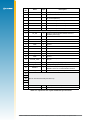
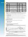
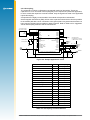
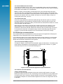
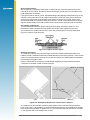
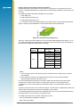
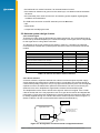
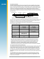
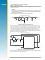
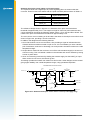
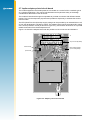
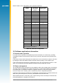
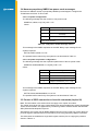
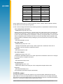
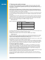
Jupiter 30 / 20
GPS receiver module
Integrator’s Manual
Related documents
•Jupiter Series Development kit guide
LA000645
• Navman NMEA reference manual
MN000315
• SiRF Binary Protocol reference manual
LA000577C © 2006 Navman New Zealand. All rights reserved. Proprietary information and specifications subject to change without notice.
Contents
1.0 Introduction........................................................................................................ 4
2.0 Hardware application information................................................................... 4
2.1 Electrical connections (SMT pad interface)................................................................... 4
2.2 Physical dimensions...................................................................................................... 6
2.3 Manufacturing process recommendations.................................................................... 6
2.3.1 Reflow recommendations...................................................................................... 6
2.3.2 Connection pad material....................................................................................... 6
2.3.3 Solder paste mask size......................................................................................... 7
2.3.4 Solder paste type.................................................................................................. 7
2.3.5 Coating.................................................................................................................. 7
2.3.6 Post reflow washing.............................................................................................. 7
2.3.7 Pre-baking............................................................................................................. 7
2.3.8 Rework.................................................................................................................. 7
2.4 Typical application circuit.............................................................................................. 7
2.4.1 Power for receiver and active antenna.................................................................. 7
2.4.2 Grounding............................................................................................................. 7
2.4.3 Decoupling............................................................................................................ 8
2.4.4 Serial RS232 data level shifter.............................................................................. 9
2.4.5 External RF filter................................................................................................... 9
2.5 PCB design recommendations...................................................................................... 9
2.5.1 Recommended PCB pad layout............................................................................ 9
2.5.2 General recommendations.................................................................................... 9
2.6 Antenna system design choices...................................................................................12
2.6.1 Antenna types......................................................................................................12
2.6.2 Active antenna.....................................................................................................12
2.6.3 Passive antenna...................................................................................................13
2.6.4 Jupiter module used as a GPS sensor................................................................13
2.6.5 DC supply protection for an active antenna.........................................................14
2.7 Jupiter adapter printed circuit board.............................................................................16
3.0 Software application information................................................................... 17
3.1 Normal mode operation................................................................................................17
3.2 Power management.....................................................................................................17
3.2.1 Adaptive TricklePower mode................................................................................18
3.2.2 Push-to-Fix mode................................................................................................18
3.3 Serial I/O......................................................................................................................18
3.3.1 Default settings.....................................................................................................18
3.3.2 NMEA input commands.......................................................................................18
3.3.3 Altitude output......................................................................................................19
3.4 Navman proprietary NMEA low power mode messages............................................ 20
3.4.1 Low power configuration...................................................................................... 20
3.4.2 Low power acquisition configuration................................................................... 20
3.5 Control of GPIO connections via serial commands (Jupiter 20)................................. 20
3.5.1 Configure port directions......................................................................................21
3.5.2 Set outputs...........................................................................................................21
3.5.3 Clear outputs........................................................................................................21
3.5.4 Read inputs..........................................................................................................21
3.6 GPS fix output..............................................................................................................21
3.7 Antenna power monitor messages.............................................................................. 22
3.8 Custom application software....................................................................................... 22
4.0 Glossary and acronyms.................................................................................. 23
LA000577C © 2006 Navman New Zealand. All rights reserved. Proprietary information and specifications subject to change without notice.
Figures
Figure 2-1: Lead-free and tin/lead reflow profile recommendation...................................... 6
Figure 2-2: Sample application circuit................................................................................. 8
Figure 2-3: Recommended application layout dimensions................................................. 9
Figure 2-4: Typical module layout......................................................................................10
Figure 2-5: Example PCB layout for external active antenna.............................................10
Figure 2-6: PCB microstrip dimensions..............................................................................11
Figure 2-7: Arrangement of active antenna and application board....................................12
Figure 2-8: Cross section of application board with passive patch antenna......................13
Figure 2-9: Simple current limiter circuit.............................................................................14
Figure 2-10: Active current limit using an IC.......................................................................14
Figure 2-11: Antenna short/open circuit sensor circuit (3.3 V supply only).........................15
Tables
Table 2-1: Jupiter 30 and Jupiter 20 Module pin functions.................................................. 5
Table 2-2: Summary of pin multi-functionality..................................................................... 6
Table 2-3: Decoupling recommendations............................................................................ 8
Table 2-4: PCB substrate thicknesses v track width..........................................................11
Table 2-5: Passive and active antenna features.................................................................12
Table 2-6: Recommended antenna characteristics............................................................13
Table 2-7: Antenna sense and control functions................................................................15
Table 2-8: Connector configuration....................................................................................17
Table 3-1: Low power modes message values................................................................. 20
Table 3-2: Low power acquisition input values.................................................................. 20
Table 3-3: Pin configuration of the GPIO lines...................................................................21
Table 3-4: Antenna status output message values........................................................... 22
LA000577C © 2006 Navman New Zealand. All rights reserved. Proprietary information and specifications subject to change without notice.
1.0 Introduction
The Navman Jupiter 30 and Jupiter 20 series of GPS receiver modules are complete GPS
receivers designed for surface mount assembly (SMT) integration. The modules provide a
simple, cost effective GPS solution for application designers. Application integration will vary
primarily with respect to antenna system design and EMI protective circuitry.
The Jupiter 30 is the successor to the established Jupiter 20, sharing the same form factor
(25.4 x 25.4 mm) and electrical compatibility. This provides a low risk migration path for existing
users, offering greater sensitivity, lower power consumption and a faster fix.
Fundamental operation requires a 3.3 VDC power supply, approximate current of 80 mA
(Jupiter 30) or 100 mA (Jupiter 20), GPS antenna system interface, relevant EMI protection, and
the design and layout of a custom PCB.
This document outlines the following design considerations and provides recommended
solutions:
Hardware application information
This section introduces the system interface and provides the following physical specifications:
a. electrical connections (SMT pad interface)
b. mounting (PCB pad layout dimensions)
c. manufacturing recommendations
d. application circuit interface
It also discusses the fundamental considerations when designing for RF, and presents the
antenna system design overview. This covers the following topics:
a. PCB layout
b. antenna system design choices
Software application information
This section provides answers to some common questions that may not have been covered in
the above topics.
A sample solution is presented and discussed for example purposes only. Due to the nature and
complexity of GPS signals, it is recommended that application integrators adhere to the design
considerations and criteria described in this document.
2.0 Hardware application information
The modules provide 30 Surface Mount pads for electrical connections. The sections that follow
introduce the physical and relative functional specifications for application integration.
Note: The electrical connections can carry very low level GPS signals at 1.57542 GHz. The
layout must be designed appropriately with consideration of the frequencies involved.
2.1 Electrical connections (SMT pad interface)
Details of the module connector configuration are shown in Table 2-1.
LA000577C © 2006 Navman New Zealand. All rights reserved. Proprietary information and specifications subject to change without notice.
Pin
No.
Name
Type
1
PWRIN
P
main power input (3.3 V)
2
GND
P
ground
3
BOOT
I
serial boot (high for serial boot, low or open circuit
for normal operation)
4
RXA
I
CMOS level asynchronous input for UART A
5
TXA
O
CMOS level asynchronous output for UART A
6
TXB
O
CMOS level asynchronous output for UART B
7
RXB
I
CMOS level asynchronous input for UART B
8
Description
pin 8 multi-functional (see table 2-2)
9
RF_ON
O
output to indicate whether the RF section is
enabled (active high)
10
GND
P
ground
11
GND
P
ground
12
GND
P
ground
13
GND
P
ground
14
GND
P
ground
15
GND
P
ground
16
GND
P
ground
17
RF_IN
I
RF input
18
GND
P
ground
19
ACTIVE_PWR
P
active power input, 70 mA current limit supply to
this pin
20
VCC_RF
O
RF Power (+2.85 V) supply output
21
V_BATT
P
backup battery input
22
NRESET
I
external reset (active low), voltage on PIN 22
NRESET must not exceed PWRIN at all times
23
GPS_FIX
O
GPS fix indication (active low)
24
25
26
pins 24-28 multi-functional (see table 2-2)
27
28
29
1PPS
O
1 pulse per second output
30
GND
P
ground
Table 2-1: Jupiter 30 and Jupiter 20 Module pin functions
LA000577C © 2006 Navman New Zealand. All rights reserved. Proprietary information and specifications subject to change without notice.
Jupiter 30
Pin
Jupiter 20
GPIO
Name and Description
GPIO
Standard &
XTrac name
DR function
24
13
reserved
6
GPIO (SDO)
not connected
25
4
reserved
5
GPIO (SDI)
ADC DOut
–
WAKEUP.
push-to-fix wakeup (active on +ve edge)
7
GPIO (SCK)
ADC Clk
27
15
ANT_OC.
antenna open circuit sensor input (active
high)
15
ANT_OC
FWD/REV.
fwd/rev input
(low=forward,
high=reverse)
28
1
ANT_CTRL.
active antenna control output
1
ANT_CTRL
WHEEL_TICKS.
wheel tick input
8
14
NANT_SC.
antenna short circuit sensor input (active
low)
3
NANT_SC
GYRO_IN.
gyro input
(analogue 0–5 V)
26
Table 2-2: Summary of pin multi-functionality
GPIO.
Note that the Jupiter 20 D (Dead Reckoning) does not support the active antenna supervisory
functionality and associated proprietary NMEA status messaging (see section 3.7).
SPI (Jupiter 20 only).
The Jupiter 20 (GSW2) and Jupiter 20 S (XTrac) do not support the SPI. These pins function
only as user GPIOs.
The SPI on the Jupiter 20 D is used to control an internal ADC, which interfaces to an
external gyro.
Implementation of the SPI for any other alternative function requires an SDK (Software
Development Kit) from SiRF.
2.2 Physical dimensions
The physical dimensions of the Jupiter 30 and Jupiter 20 modules are identical:
length: 25.4 mm ± 0.1 mm
width: 25.4 mm ± 0.1 mm
thickness: 3.0 mm max
weight: 4.0 g max
2.3 Manufacturing process recommendations
2.3.1 Reflow recommendations
For lead based solder pastes, the maximum reflow temperature is 225 °C for 10 seconds. For
lead-free solder pastes, the maximum reflow temperature is 265 °C for 10 seconds. Refer to
Figure 2-1.
Figure 2-1: Lead-free and tin/lead reflow profile recommendation
2.3.2 Connection pad material
The 30 surface mount connection pads have a base metal of copper with a gold flash finish.
This is suitable for a lead free manufacturing process.
LA000577C © 2006 Navman New Zealand. All rights reserved. Proprietary information and specifications subject to change without notice.
2.3.3 Solder paste mask size
This should be adjusted by experimentation according to the customer’s production process
requirements. A 1:1 (paste mask:pad size) ratio has been found to be successful.
2.3.4 Solder paste type
The module accepts all commonly used solder pastes. The solder paste can be lead based
or lead-free. If a lead-free process is introduced, factors such as circuit board thickness,
fabrication complexity, assembly process compatibility, and surface finish should be taken
into consideration.
2.3.5 Coating
The final PCB may be selectively coated with an acrylic resin, air/oven cured conformal
coating, clear lacquer or corresponding method, which gives electrical insulation and
sufficient resistance to corrosion.
2.3.6 Post reflow washing
It is recommended that a low residue solder paste is used to prevent the need for post reflow
washing. If a washing process is used, an aqueous wash is not recommended due to the
long drying time required and danger of contaminating the fine pitch internal components.
2.3.7 Pre-baking
The modules are delivered on a tape and reel package sealed in an airtight bag. The MSR
(Moisture Sensitivity Rating) is 3, therefore they should be loaded and reflowed within
168 hours. If the modules are in ambient humidity for longer than this, a pre-baking/drying
process will be required.
2.3.8 Rework
Navman recommends that rework and repair is carried out in accordance with the following
guidelines:
• IPC-7711 Rework of Electronic Assemblies
• IPC-7721 Repair and Modification of Printed Boards and Electronic Assemblies
Note: Jupiter 30 and Jupiter 20 modules are covered by a 12-month warranty.
2.4 Typical application circuit
The schematic in Figure 2-2 represents a very basic application circuit, with simple interfaces to
the module. It is subject to variations depending on application requirements.
Note: Refer to the Jupiter 20 Dead Reckoning Application Note (LA000433) for the Jupiter 20 D
reference design.
2.4.1 Power for receiver and active antenna
The receiver power connection requires a clean 3.3 VDC. Noise on this line may affect the
performance of the GPS receiver.
When an active antenna is used, the DC power is fed to it through the antenna coax. This
requires the user to apply the antenna DC voltage to pad 19 of the module. A 2.7 V 25 mA
supply is made available on pad 20 if the chosen antenna can accept that voltage. This
supply is under the command of the TricklePower energy control.
2.4.2 Grounding
Separate AGND (Analogue Ground) and DGND (Digital Ground) grounds are shown
in Figure 2-2. If this grounding method is used, the ground planes can be connected
underneath the module. In some applications with very small ground planes, separate ground
planes may not be required. This should be determined by the application integrator. See
Section 2.5.2 for ground plane recommendations and design considerations involving the
antenna input and the 50 Ω microstrip connection.
LA000577C © 2006 Navman New Zealand. All rights reserved. Proprietary information and specifications subject to change without notice.
2.4.3 Decoupling
The schematic in Figure 2-2 illustrates a suggested method of decoupling. These are
capacitors C1 to C7. This level of decoupling may not be required in a particular application,
in which case these capacitors could be omitted. Only the signal lines used in the application
require decoupling.
All capacitors are highly recommended if the module will experience substantial
electromagnetic interference (EMI). All low value capacitors should be as close as possible
to the module pad with a short connection to the ground plane. Any data lines that have not
been properly shielded are susceptible to data corruption. Refer to Table 2-3 for suggested
values of decoupling relative to the function desired.
J1 coaxial connector.
MCX, SMA or MMCX
I/P 1
GND 2
16 GND
17 RF_IN
18 GND
19 V_ANT
20 VCC_RF
C7
1nF
C3.
1nF
3 V RTC lithium.
backup battery
GND
1PPS
C4.
27pF
21 V_BATT
22
RESET
23
GPIO/GPS_FIX
24
GPIO
25
GPIO
26
GPIO/WAKE_UP
27 GPIO/ANT_OC
28 GPIO/ANT_CTRL
29 GPIO/1PPS
30
GND
RF
Digital
GND
GND
GND
GND
GND
15
14
GND
10
9
8
RF_ON
GPIO/NANT_SC
RXB
TXB
TXA
RXA
BOOT
GND
PWRIN
13
12
11
AGND
TPO
TPI
7
6
5
4
3
2
C5.
27pF
1
serial data ports.
to application processor.
or RS232 level converter
R2
10K
R1
10K
C6.
27pF
SDO
SDI
TP
POWER
Jupiter 30 or Jupiter 20 GPS Module
C1.
1µF
C2.
10nF
DGND
Figure 2-2: Sample application circuit
Function
Pad
Decoupling
PWRIN
1
1 µF||1 nF
BOOT
3
27 pF
RXA
4
27 pF
TXA
5
27 pF
TXB
6
27 pF
RXB
7
27 pF
NANT_SC
8
27 pF
RF_ON
9
27 pF
ACTIVE_PWR
19
1 nF
VCC_RF
20
1 nF
V_BATT
21
1 µF||1 nF
NRESET
22
27 pF
GPS_FIX
23
27 pF
GPIO13
24
27 pF
GPIO4
25
27 pF
WAKEUP
26
27 pF
ANT_OC
27
27 pF
ANT_CTRL
28
27 pF
1PPS
29
27 pF
Note: ‘||’ represents a parallel connection
Table 2-3: Decoupling recommendations
LA000577C © 2006 Navman New Zealand. All rights reserved. Proprietary information and specifications subject to change without notice.
2.4.4 Serial RS232 data level shifter
To connect the module to a PC comm. port, the serial data signals must be level shifted to
RS232 levels. This has not been shown in the reference design, but many single chip RS232
level shifters are available, such as MAX3232.
Note: It is highly recommended to provide test points on the serial data lines and ‘Boot’
signal (pad 3), even if the application circuit does not use these signals. This will allow the
user to connect to these signals if a firmware upload or new configuration is required. These
test points can take the form of an unfitted ‘through-hole’ connector. Refer to Figure 2‑2
showing test points TPO, TPI & TP.
2.4.5 External RF filter
If there is a high potential for interference (EMI) though the antenna system, an external
bandpass SAW filter may be added to the antenna input connection (pad 17) which will
attenuate interfering frequencies. (Many commercial active antennas have a filter so it would
not be necessary to add another).
When using an active antenna, the filter will not pass DC through to the antenna, so an
alternate power source would be required if an active antenna is used. Alternatively a
parallel RF choke across the filter will allow the antenna power to pass through, but choice
of components is important, for example using a choke of sufficiently high self-resonant
frequency. Care should also be taken not to exceed the filter maximum DC voltage.
2.5 PCB design recommendations
The modules are surface mounted devices, hence the layout of the application PCB plays an
integral part in the overall performance of the finished system.
It is not difficult to design such a PCB, despite the presence of high frequency, low level radio
signals. The following recommendations have been offered to allow the designer to create a
design that will meet the requirements of this product.
2.5.1 Recommended PCB pad layout
The layout in Figure 2-3 shows the recommended copper pad dimensions. The solder paste
mask needs to be adjusted to suit the application’s reflow process, however a 1:1 (paste
mask:pad size) ratio is the recommended starting point.
2.0
1.0
15
16
0.8
25.4 ±0.1
1.9
2.8
21
top view.
of pad layout.
10
(all measurements in mm)
1.277
30
1
1.5
25.4 ±0.1
Figure 2-3: Recommended application layout dimensions
2.5.2 General recommendations
Choice of PCB stack up.
In general, a two layer PCB substrate can be used, with all the RF signals on one side.
Multi-layer boards can also be used. These design recommendations here only address the
microstrip style of RF connection. Stripline designs can also be accommodated. However,
long lengths of stripline can cause excessive signal loss and vias in the signal track should
be avoided.
LA000577C © 2006 Navman New Zealand. All rights reserved. Proprietary information and specifications subject to change without notice.
Ground plane design.
We reccomend a complete ground plane is used under the PCB with signal tracks on the
same layer as the module. We also recommend having a ground plane on both sides of the
PCB underneath the module.
If the ground planes are very small, separate analogue and digital ground planes may not be
required. The ground return for any signal should have a clear path back to its source and
should not mix with other ground return signal paths. Hence the return path, which is the
ground underneath the microstrip antenna connection, should not be shared with any digital
signal or power supply return paths. Pads 16 and 18 are the RF signal Ground connections.
Decoupling components.
The recommended values for power and signal decoupling are listed in Table 2-3. The
placement of these components must ensure that the low value capacitors have very
short tracks to the module pad, and very close vias connecting them to the ground plane.
(Figure 2-4 shows a typical layout).
Figure 2-4: Typical module layout
Antenna connection.
The PCB layout design of the antenna input connection requires appropriate selection of
PCB track width, substrate material and careful attention to the layout geometry. If this overall
system is not implemented correctly, the module will receive poor GPS signals and therefore
provide inferior navigation data.
Figure 2-5 illustrates an example of a PCB design integrating an external active antenna
connected via an MCX or SMA coaxial connector.
Jupiter 30 / 20 outline
Through holes (vias)
(Top)
(Bottom)
Figure 2-5: Example PCB layout for external active antenna
The modules can be used with a passive patch antenna if the connection to the antenna
input is very short. It is possible to mount the patch antenna on the same PCB as the module,
but to reduce the possibility of digital noise, it is recommended that the antenna be mounted
on the opposite side of the board to the module.
LA000577C © 2006 Navman New Zealand. All rights reserved. Proprietary information and specifications subject to change without notice.
10
Design of 50 ohm microstrip antenna connection.
When designing the signal track from the antenna connection to the antenna input on the
module, a controlled impedance microstrip with a characteristic impedance of 50 ohms must
be used.
The PCB parameters that affect impedance are as follows:
1. Track width (W)
2. PCB substrate thickness (H)
3. PCB substrate permittivity (εr)
4. To a lesser extent, PCB copper thickness (T) and proximity of same layer ground plane.
Figure 2-6 shows a representation of the PCB microstrip and its parameters.
Figure 2-6: PCB microstrip dimensions
Table 2-4 shows typical track widths for an FR4 material PCB substrate (permittivity εr of 4.3
at 1.5 GHz) and different PCB thickness. The effect of track thickness (T) can be ignored for
the short track lengths associated with this design.
Substrate Permittivity
material
εr
FR4
4.3
Substrate
Track width
thickness H
W (mm)
(mm)
1.6
2.0
1.2
1.8
1.0
1.6
0.8
1.4
0.6
1.2
0.4
0.7
0.2
0.4
Table 2-4: PCB substrate thicknesses v track width
Notes:
1. If a multi-layer PCB is used, the thickness is the distance from signal track to nearest
ground plane.
2. If the antenna connection is routed under the module, the track width should be
approximately halved for that section only.
It is recommended that the antenna connection PCB track should be routed around the
outside of the module outline, kept on a single layer and have no bends greater than
45 degrees. It is not recommended, for production reasons, to route the track under the
module.
However, if the track has to route under the module, it should have a modified track width and
solder mask to avoid short circuits to the underside of the module.
To minimise signal loss and reduce the requirement for vias, it is not recommended to place
the signal track on an inner layer of a multi‑layer PCB.
The PCB track connection to the RF antenna input must:
• have a characteristic impedance of 50 ohm
• be as short as possible
LA000577C © 2006 Navman New Zealand. All rights reserved. Proprietary information and specifications subject to change without notice.
11
• be interfaced to a coaxial connector if an external antenna is used
• have maximum clearance to ground on the same layer, or at least be half the substrate
thickness
• be routed away from noise sources such as: switching power supplies, digital signals,
oscillators and transmitters
The PCB track connection to the RF antenna input must NOT have:
• vias
• sharp bends
• components overlaying the track
2.6 Antenna system design choices
2.6.1 Antenna types
There are two major types of GPS antenna: passive and active. The active antenna has a
built in LNA (Low Noise Amplifier) to increase the strength of the signal, and to compensate
for the signal loss in a long cable connection.
The features of each type of antenna are shown in Table 2-5, comparing an externally
mounted active antenna with a passive patch antenna mounted on the same PCB as the
module.
Feature
Passive antenna
Active antenna
requires short cable between antenna and receiver
yes
no
consumes power
no
yes
can be mounted remote from receiver
no
yes
gives good performance in poor signal situations
no
yes
has built in additional filtering
no
yes
low cost
yes
no
requires a coaxial connector
no
yes
Table 2-5: Passive and active antenna features
2.6.2 Active antenna
An active antenna is a passive antenna with a built in LNA that requires a power supply.
Active antennas are used when the antenna input is connected to the receiver through a
coaxial cable (usually longer than 3 m) or any high loss transmission path. The GPS signals
experience loss in the transmission path from the antenna. The loss is overcome by the
antenna’s LNA, which amplifies the signal before it enters the transmission path.
The amplification is also used to enhance the signal in areas of low signal. If the coaxial
cable is shorter than 3 m it may experience too much gain at the receiver and degrade the
performance. There are some variations as to how the antenna will receive its power but it
is usually supplied through the coaxial cable via the antenna input as shown in Figure 2-7.
(Refer to Table 2-6 for the recommended active antenna characteristics.)
Active GPS .
antenna
Application PCB
connecting coax carrying.
GPS signals and DC
power for amplification
Jupiter
module
coaxial connector
fitted to application
PCB
Figure 2-7: Arrangement of active antenna and application board
LA000577C © 2006 Navman New Zealand. All rights reserved. Proprietary information and specifications subject to change without notice.
12
2.6.3 Passive antenna
A passive antenna does not require any power because it has no amplifier. This is not the
best choice if signal strength is a concern, however, it may be sufficient if the signal path is
kept to a minimum (usually below 300 mm). An advantage to using a passive antenna is the
ability to mount directly onto the application. For best performance, a passive patch antenna
should have a metal ground plane (about 80 mm in diameter) placed directly under the
antenna, and it is advisable to screen the module and application circuits from the antenna.
For this reason the antenna and module should not be mounted on the same side of the PCB
(see Figure 2-8).
FR4 fibreglass PCB
ground plane
passive patch antenna
ground via
Jupiter module
50 ohm microstrip
Figure 2-8: Cross section of application board with passive patch antenna
Any cover close to the antenna (called the superstrate) will cause the resonant frequency and
efficiency of the antenna to drop. It is therefore recommended to keep any distance to the
superstrate to a minimum of 3 mm from the top surface of the patch.
See Table 2-6 for recommended characteristics of both passive patch and active antennas
for use with the Jupiter receiver.
Characteristic
Active antenna
Passive antenna
right-hand circular polarised
right-hand circular polarised
1.57542 GHz .
+/- 1.023 MHz
1.57542 GHz .
> +/- 1.023 MHz
3 V
–
< 10mA at 3 VDC
–
–
+2 to 5 dBi with 1 dB loss (max)
in connections
≤ 26 dBi (Jupiter 20)
≤18 dBi (Jupiter 30)
–
Axial ratio
< 3 dB
< 3 dB
Output VSWR
< 2.5
–
Polarisation
Receive frequency
Power supply
DC current
Antenna gain
Total gain (includes
antenna gain, LNA
gain and cable loss)
Table 2-6: Recommended antenna characteristics
Note: GPS active and passive antenna selection must include practical TTFF tests
in weak and strong outdoor environments – noting peak and average signal strength
measurements. This must be done in comparison with the antenna supplied in the
Development kit. Performance results and signal strength measurements must be
comparable to the reference antenna supplied. Passive antenna signal strength
measurements will be lower than an active antenna, but time to fix should be comparable.
2.6.4 Jupiter module used as a GPS sensor
The adapter board reference design shows how a Jupiter GPS receiver module can be used
with an external active antenna via a coax connector. The same design can be used with
a passive patch antenna on the same PCB. It follows the general arrangement described
in Section 2.6.3. The module is placed such that the connection between the antenna and
the antenna input pad is as short as possible. Also note the PCB should have a complete
ground plane on the patch side of the board. This serves as the ground plane required by the
antenna.
The serial data from the module must be connected to a local host processor, and care
should be taken such that noise from these devices cannot enter the signal path or GPS
antenna. It is recommended that all digital devices are placed on the opposite side of the
board to that of the antenna.
LA000577C © 2006 Navman New Zealand. All rights reserved. Proprietary information and specifications subject to change without notice.
13
2.6.5 DC supply protection for an active antenna
Antenna DC supply current limit.
When the Jupiter receiver is used with an external active antenna, the DC supply in the coax
cable is vulnerable to over-current if a fault occurs in the antenna or its cable gets crushed,
for example in a car door.
WARNING
It is important to note that the module antenna power feed does not have internal current
limiting. Damage can occur if unlimited current is permitted to flow through the module
antenna power feed components.
The circuit shown in Figure 2-9 will provide over‑current protection.
R1.
10R
70 mA Antenna supply current limit
SUPPLY_INPUT
3-5 VDC
C9.
100nF
BC857B
L3.
120R / 100 MHz
Q1
200 mW
C8.
100nF
GND
R10.
1K
Q2.
BC857B
GND
ANTENNA_SUPPLY
(V_ANT)
C7.
18pF
GND
GND
Figure 2-9: Simple current limiter circuit
Transistor Q1 serves as a series pass transistor. Q2 is used to sense the current in the
antenna circuit, turning off Q1 if the voltage across the current sense resistor R1 exceeds
0.6 V. This circuit does not turn off the supply to the antenna, but merely limits it to a safe
value. With the components shown the supply will be limited to approximately 70 mA.
Other options are available to provide this function. MAXIM can supply a current trip IC
that will turn off the load if a preset supply current is exceeded. The part number for this is
MAX4785. The circuit is shown in Figure 2-10.
Antenna current limit using an IC
antenna short circuit sense signal
C5.
100 nF
5
GND
4
ON
U3.
MAX4785EXK–T
IN
3
FLAG
OUT
GND
2
1
L2.
120R / 100 MHz
C4.
100 nF
C6.
18 pF
GND
GND
antenna power enable
16
15
17
14
18
13
19
12
20
11
21
10
22
9
23
24
8
7
25
6
26
5
27
4
28
3
29
2
30
1
GND
PWR_IN
Jupiter GPS Module
Figure 2-10: Active current limit using an IC
Electro-resistive fuses can be used to protect the supply over-current. These are available
from Bourns, Vitromon and other manufacturers.
LA000577C © 2006 Navman New Zealand. All rights reserved. Proprietary information and specifications subject to change without notice.
14
Antenna short/open sense inputs and control output.
The Jupiter receiver has a digital input to provide signalling when an antenna fault has
occurred. These functions are shared with the Jupiter 30 GPIO pads as shown in Table 2-7.
Antenna sense
functions
Jupiter GPIO function
ANT_CTRL
GPIO1 (ON=High)
ANT_OC
GPIO15 (Active High)
NANT_SC
GPIO3 (Active Low)
Table 2-7: Antenna sense and control functions
The reference design shown in figure 2-11 is indicative of an open-circuit switchover
threshold of approximately 3 mA. This maybe too high for some low-power antennae and
can be adjusted by changing the following resistor values – R7 to 12Ω and R3 to 2K2Ω. This
results in an open-circuit switchover threshold of approximately 2 mA.
The over current circuit consisting of Q1 and Q2 is the same as the simple current limit circuit
shown in Figure 2-9, providing a 70 mA current limit.
In addition, this design has the following features:
1. Q4-A and Q4-B form a low current sensor, thus providing a signal to indicate when the
antenna has become disconnected or open circuit. It is not mandatory to use a matched
pair of transistors, as shown in this design, but it will provide consistent results over a wide
temperature range.
2. Q3 provides a method for the receiver to turn off the active antenna supply in the event of
a fault occurring. This is a latched condition in the software and can be restored by issuing
a reset or power down.
3. Short circuit sensing is achieved by feeding the antenna supply into the NANT_SC input.
When a short circuit occurs, this line will go low.
This design provides the lowest cost solution for this function. Other designs can be created
giving higher stability over a wide temperature range, using operational amplifiers.
R6.
10R
Discrete antenna current monitor
SUPPLY_IN
C2.
100 nF
R7.
56R
BC857B
L1.
120R / 100 MHz
Q1
200 mW
C1.
100 nF
V_ANT
C3.
18 pF
GND
GND
GND
GND
NANT_SC
R2.
10K
Q3.
BC847B
R4.
10K
R8.
5K6
Q4-B.
BC857BS
R5.
5K6
Q4-A.
BC857BS
R3.
1K
R1.
10K
Q2.
BC857B
ANT_CTRL
GND
ANT_OC
Figure 2-11: Antenna short/open circuit sensor circuit (3.3 V supply only)
LA000577C © 2006 Navman New Zealand. All rights reserved. Proprietary information and specifications subject to change without notice.
15
2.7 Jupiter adapter printed circuit board
The module supplied in the Development kit is mounted on a carrier PCB in a method typical
of a customer application. This carrier PCB illustrates and implements many of the design
considerations discussed in this document.
The module is interfaced through two separate 20‑pin data connectors with different header
pitches. This is for development purposes and provides a simple way to evaluate the surface
mount module.
The RTC (Real-Time Clock) backup supply voltage can be provided by an onboard lithium cell,
or from the development unit backup supply. The adapter board carries the antenna DC supply
over-current protection circuits (as shown in Figure 2-11), and a switch de‑bounce IC to provide
reliable reset action from the development unit.
Figure 2-12 shows the adapter board with the positions of the connectors and indicators.
J1
J2 (not normally fitted)
GPS fix LED
RTC backup battery.
(not normally fitted)
power LED
Jupiter module
antenna
Figure 2-12: Adapter printed circuit board
LA000577C © 2006 Navman New Zealand. All rights reserved. Proprietary information and specifications subject to change without notice.
16
Refer to Table 2-8 for a description of the connector interfaces.
Jupiter
function
J2 (2.54 mm
pitch header)
pin no.
J1 (2 mm pitch
header) pin no.
V_ANT
1
1
VCC_RF
2
–
V_BATT
3
3
VDD
4
4
M_RST
5
5
GPIO/GYRO IN
6
6
GPIO/FR
7
7
BOOT
8
8
GPIO/W TICKS
9
9
RFON
10
–
GND
–
10
TXA
11
11
RXA
12
12
GPIO/SDI
13
–
GND
–
13
TXB
14
14
RXB
15
15
GPIO/SCK
16*
–
GND
17
16
GPIO/SDO
18
–
GND
–
17
GND
–
18
1PPS
19
19
GPS_FIX/GPIO
20
–
*Note: J2 Pin 16 on the adapter card is the wake-up line for
push to fix mode on the Jupiter 30
Table 2-8: Connector configuration
3.0 Software application information
3.1 Normal mode operation
In normal mode of operation, the baseband processor software runs continuously, providing
a navigation solution at the maximum rate of once per second. No power saving functions are
applied.
If the power to the module is disrupted, the restart time can be shortened to a warm or hot start
by keeping the RTC and SRAM contents valid with a backup battery on the VBATT input.
If the module has been turned off for greater than 2 hours, the unit will revert to a warm or cold
start. This is caused by the stored ephemeris data becoming invalid after 4 hours.
3.2 Power management
The TricklePower mode of operation can be enabled to reduce the average power consumption.
The main power is supplied to the module continuously. An internal timer wakes the processor
from sleep mode. The module computes a navigation position fix, after which the processor
reverts to sleep mode. The duty cycle is controlled by a user-configurable parameter.
If ephemeris data becomes outdated, the TricklePower mode will attempt to refresh the data set
within every 30 minute period, or for every new satellite that comes into view.
With TricklePower set to a 20% duty cycle, a power saving of 50% can easily be achieved with
minimal degradation in navigation performance.
LA000577C © 2006 Navman New Zealand. All rights reserved. Proprietary information and specifications subject to change without notice.
17
3.2.1 Adaptive TricklePower mode
In Adaptive TricklePower mode, the processor automatically returns to full power when signal
levels are below the level at which they can be tracked in TricklePower mode. This is the
default behaviour when TricklePower is active. Adaptive TricklePower is always enabled on
the Jupiter 30 and Jupiter 20 S (XTrac), and selectable on the Jupiter 20 standard module.
3.2.2 Push-to-Fix mode
Unlike TricklePower, the operation in this mode is not cyclic. This mode always forces the
GPS software to revert to a continuous sleep mode after a navigation position fix. It will
stay in sleep mode until woken by activation of the reset input (Jupiter 20) or wakeup input
(Jupiter 30), and compute a fresh position.
If the ephemeris data becomes invalid or new satellites come into view, the RTC has the
ability to self activate and refresh the data, thus keeping the restart TTFF very short.
This mode yields the lowest power consumption of the module, and is ideal where a battery
powered application requires very few position fixes.
For further information on the TricklePower and Push-To-Fix modes refer to the Low Power
Operating Modes application note (LA000513).
3.3 Serial I/O
The module can output serial data in the NMEA format or SiRF Binary format. The serial I/O
protocols are defined in the Navman NMEA reference manual (MN000315) and the SiRF Binary
Protocol reference manual. These describe the format of the serial data from the module, as well
as the structure of the commands. Navman has provided additional functionality to the NMEA
protocol as detailed in the following sections.
3.3.1 Default settings
The default protocol is NMEA, at a baud rate of 9600bps. The frame format is 8 data bits, no
parity bit and 1 stop bit.
The following messages are output by default, at a rate of once per second each:
$GPGGA, $GPGLL, $GPGSA, $GPGSV, $GPRMC, $GPVTG, $GPZDA
All output messages have checksums by default.
Note: message $GPZDA is not available for Jupiter 20 S, or Jupiter 20 D.
3.3.2 NMEA input commands
All NMEA input commands are in the form:
$PSRFxxx,…[*CS] <CR> <LF>
where xxx is a decimal number between 100 and 255 (inclusive).
Note: In each case, CS represents an NMEA checksum, <CR> is carraige return, <LF> is line
feed. These details are covered in the Navman NMEA reference manual MN000315.
Acknowledgements
All input commands other than the standard SiRF commands will be acknowledged with a
sentence of the form:
$PTTK,…*CS
Where the arguments provided to a command are invalid, the response will be the message:
$PTTK,NACK*CS
Checksums
All input commands are accepted whether or not they include a checksum, however if a
checksum is included it must be correct in order for the message to be accepted.
Incorrect checksums will result in the response:
$PTTK,CHECKSUM*CS
LA000577C © 2006 Navman New Zealand. All rights reserved. Proprietary information and specifications subject to change without notice.
18
Unused messages
Input messages where the message ID is not between 100 and 255, or where the message
ID does not correspond to a specified function, result in the response:
$PTTK,INVALID*CS
Errors
Errors in message receipt (other than checksum errors) result in the response:
$PTTK,ERROR,xx*CS
where xx is a hexadecimal error code.
Magnetic Variation (Declination)
The Jupiter 20 module calculates the magnetic variation (the Jupiter 30 does not).
Magnetic Variation fields in $GPRMC
The last two fields in the message $GPRMC are the magnetic variation. An Easterly variation
should be subtracted from, or a Westerly variation added to, the true heading to give the
magnetic heading (the heading given by a magnetic compass).
For example, the output might be:
$GPRMC,220137.250,A,4331.9077,S,17238.2308,E,0.075949,168.82,071004,23.1,E*4C
Standard SiRF output:
$GPRMC,220137.250,A,4331.9077,S,17238.2308,E,0.075949,168.82,071004,,*17
Magnetic Heading field in $GPVTG
The third field in the message $GPVTG is the magnetic heading (denoted by the ‘M’ in the
following field). This is the heading that would be reported by a magnetic compass.
For example, the output might be:
$GPVTG,168.82,T,145.70,M,0.08,N,0.14,K*41
The standard SiRF output:
$GPVTG,168.82,T,,M,0.08,N,0.14,K*58
3.3.3 Altitude output
The module outputs the correct altitude and geoid separation in the $GPGGA NMEA
message. Most SiRFstar-based modules output the height above the current datum (usually
WGS84) ellipsoid as the altitude, contrary to the NMEA specification, and older modules
omit the geoid separation. The Jupiter receiver outputs the height above mean sea level, as
required by the NMEA specification.
For example, the output might be:
$GPGGA,220137.869,4331.9077,S,17238.2308,E,1,06,1.6,61.7,M,11.3,M,0.0,0000*55
Standard SiRF output (v2.3 and earlier):
$GPGGA,220137.869,4331.9077,S,17238.2308,E,1,06,1.6,72.0,M,,M,0.0,0000*6D
Or (v2.3.1 and 2.3.2):
$GPGGA,220137.869,4331.9077,S,17238.2308,E,1,06,1.6,72.0,M,11.3,M,0.0,0000*50
LA000577C © 2006 Navman New Zealand. All rights reserved. Proprietary information and specifications subject to change without notice.
19
3.4 Navman proprietary NMEA low power mode messages
Navman has added a number of proprietary NMEA input messages to configure the
TricklePower and Push-To-Fix modes.
3.4.1 Low power configuration
The following message sets the receiver to low power mode:
$PSRF151,a,bbbb,cccc[*CS] <CR> <LF>
where:
Field
Description
a
Push-To-Fix* (1=on, 0=off)
b
TricklePower duty cycle (parts per
thousand)
c
TricklePower on time (milliseconds)
*Note that Push-To-FixTM does not require fields b and c
so they may be left blank
Table 3-1: Low power modes message values
This message is the NMEA equivalent of the SiRF Binary input message ID 151.
System response:
$PTTK,LPSET,a,bbbb,cccc*CS
The updated values returned by the system are as described in Table 3-1.
3.4.2 Low power acquisition configuration
The following message sets the acquisition parameters of the low power mode:
$PSRF167,aaaaaa,bbbbbb,cccc,d[*CS] <CR> <LF>
where:
Field
Description
a
maximum off time (milliseconds)
b
maximum search time (milliseconds)
c
Push-To-Fix period (seconds)
d
adaptive TricklePower (1=on, 0=off)
Table 3-2: Low power acquisition input values
This message is the NMEA equivalent of the SiRF Binary input message ID 167.
System response:
$PTTK,LPACQ,aaaaaa,bbbbbb,cccc,d*CS
The updated values returned by the system are as described in Table 3-2.
3.5 Control of GPIO connections via serial commands (Jupiter 20)
Note: The information in this section does not apply to the Jupiter 30 module.
The Jupiter 20 receiver has many unused GPIO (user programmable input output) signal pads.
These can be utilised in the application by introducing custom software written with the SiRF
SDK (Software Development Kit) tools.
Alternatively, the receiver has an NMEA default instruction protocol that can control these IO
ports through the standard serial communication ports using proprietary NMEA commands.
The GPIO lines are treated as a single 8-bit register, with the pins occupying the positions
shown in Table 3-3.
LA000577C © 2006 Navman New Zealand. All rights reserved. Proprietary information and specifications subject to change without notice.
20
Bit
Pad function
Pin
(LSB) 0
GPIO15/Fwd-Rev
27
1
GPIO1/Wheel Tick
28
2
GPIO3/Gyro In
8
3
GPIO5/SDI
25
4
GPIO6/SDO
24
5
GPIO7/SCLK
26
6
GPIO9/1PPS
29
(MSB) 7
GPIO10/GPS Fix
23
Table 3-3: Pin configuration of the GPIO lines
On the Jupiter 20 D, there is no control of GPIO15, GPIO1, GPIO3, GPIO5, GPIO6 or GPIO7,
and all references to these pins are ignored.
In each of the messages described in the following sections, x represents a hexadecimal digit.
3.5.1 Configure port directions
$PSRF225,xx,xx[*CS] <CR> <LF>
Sets the direction of the GPIO pins. The first octet is the mask (which ports to override), the
second the new direction. A zero represents an input, and a one an output. This command
must be sent before attempting to manipulate or read any the specified GPIO. It also has the
effect of suspending the normal port functions on the pins specified. Normal operation will
resume following a hardware reset (including any use of the reset line in Push-to-Fix mode).
Response:
$PTTK,GPIO,DIR,xx,xx*CS
3.5.2 Set outputs
$PSRF226,xx[*CS] <CR> <LF>
Changes the specified outputs to high. Other outputs are not affected. There are no
changes to any pins that are configured as inputs.
Response:
$PTTK,GPIO,SET,xx*CS
3.5.3 Clear outputs
$PSRF227,xx[*CS] <CR> <LF>
Changes the specified outputs to low. Other outputs are not affected. There are no changes
to any pins that are configured as inputs.
Response:
$PTTK,GPIO,CLEAR,xx*CS
3.5.4 Read inputs
$PSRF228[*CS] <CR> <LF>
Returns the values on the input pins. Pins configured as outputs read as zero.
Response:
$PTTK,GPIO,READ,xx*CS
This message is sometimes output automatically.
3.6 GPS fix output
The GPS fix output is an active low output on pin 23 of the module. Whenever the unit has
either a 2D or a 3D fix, this output will be low. When the unit has no fix, the output will be high.
This function can be overridden and the pin used as GPIO10 using the commands described in
Section 3.5. The GPS fix output function returns after a reset.
LA000577C © 2006 Navman New Zealand. All rights reserved. Proprietary information and specifications subject to change without notice.
21
3.7 Antenna power monitor messages
The Jupiter software includes antenna monitor messages driven by the state of the antenna
monitor inputs. The inputs NANT_SC (short circuit detect – active low) and ANT_OC (open
circuit detect – active high) are configured as inputs, and ANT_CTRL (active antenna control) is
configured as an output.
If the function of any of these pins is overridden using the procedure described in Section 3.6,
then this feature is disabled. However if an antenna short circuit has occurred before any pins
are overridden in this manner, the status will continue to be reported as ‘short circuit’ until such
time as the active antenna control output is overridden.
In normal operation, the active antenna control output is high. If the short circuit detect pin goes
low, the active antenna control signal will go low. This condition is latched until the user resets
the module.
The active antenna control pin output is low when the receiver enters a low power mode due to
TricklePower, Push-to-Fix or APM, and returns to its previous state when the receiver starts up
again. No checking of the antenna current is performed while the output is low for this reason.
The antenna status output message is an NMEA message in the form:
$PTTK,ANT,d*CS
Where d represents any of the following numbers:
d
Description
0
normal antenna operation
1
antenna open circuit
2
antenna short circuit - antenna disabled
-1
antenna sensing disabled (due to GPIO
override)
Table 3-4: Antenna status output message values
The antenna status message is output automatically in the event of a short circuit or open circuit
being detected, or an open circuit condition coming to an end.
In addition, this message is output on the receipt of the NMEA input message:
$PSRF199[*CS]
The antenna status is also output as the SiRF binary message with message ID 99. It contains
one byte of data, being the appropriate value from Table 3-4. This gives a payload length of
2 bytes, since the message ID is considered part of the payload.
The antenna status message is output automatically in the event of a short circuit, or open circuit
being detected, or an open circuit condition coming to an end.
In addition, this message is output on the receipt of the SiRF binary message with message ID
199. The output rate of this message is also under the normal control of the SiRF Binary Query/
Rate Control input message, however this message is not output at a regular rate by default.
3.8 Custom application software
The module provides custom modification of the firmware to use available CPU processing
capacities and I/O capabilities. The custom application software can be invoked internally or
externally, providing the ability to dedicate the module as the host application or an external
processor as the host. The module also provides the ability to communicate externally with
standard or customer specific communication protocols.
The custom application software has access to the flash memory, navigation data from the GPS
Navigation software, and access to various I/O lines used on the module.
This can be developed using the SiRF SDK. The SDK provides all the tools and resources
necessary for custom software development. Refer to http://www.sirf.com for more information
about the SDK.
LA000577C © 2006 Navman New Zealand. All rights reserved. Proprietary information and specifications subject to change without notice.
22
4.0 Glossary and acronyms
EMI: Electromagnetic Interference
FR4 substrate: Flame Retardant type 4.
The usual base material from which plated-through-hole and multi-layer printed circuit boards
are constructed. The type ‘4’ indicates woven glass reinforced epoxy resin.
GPS: Global Positioning System.
A space-based radio positioning system that provides accurate position, velocity, and time data.
NMEA: National Marine Electronics Association
RF: Radio Frequency
SRAM: Static Random Access Memory
TTFF: Time-To-First-Fix.
The actual time required by a GPS receiver to achieve a position solution. This specification
will vary with the operating state of the receiver, the length of time since the last position fix, the
location of the last position fix, and the specific receiver design.
© 2006 Navman New Zealand. All Rights Reserved.
SiRF and SiRF logo are registered trademarks of SiRF Technology, Inc. SiRFstar, SiRFLoc, Push-to-Fix, and TricklePower are trademarks of SiRF Technology, Inc. All other trademarks mentioned in this document are property of their
respective owners.
Information in this document is provided in connection with Navman New Zealand (‘Navman’) products. These materials
are provided by Navman as a service to its customers and may be used for informational purposes only. Navman
assumes no responsibility for errors or omissions in these materials. Navman may make changes to specifications and
product descriptions at any time, without notice. Navman makes no commitment to update the information and shall have
no responsibility whatsoever for conflicts or incompatibilities arising from future changes to its specifications and product
descriptions. No license, express or implied, by estoppel or otherwise, to any intellectual property rights is granted by
this document. Except as provided in Navman’s Terms and Conditions of Sale for such products, Navman assumes no
liability whatsoever.
THESE MATERIALS ARE PROVIDED ‘AS IS’ WITHOUT WARRANTY OF ANY KIND, EITHER EXPRESSED OR
IMPLIED, RELATING TO SALE AND/OR USE OF NAVMAN PRODUCTS INCLUDING LIABILITY OR WARRANTIES
RELATING TO FITNESS FOR A PARTICULAR PURPOSE, CONSEQUENTIAL OR INCIDENTAL DAMAGES,
MERCHANTABILITY, OR INFRINGEMENT OF ANY PATENT, COPYRIGHT OR OTHER INTELLECTUAL PROPERTY
RIGHT. NAVMAN FURTHER DOES NOT WARRANT THE ACCURACY OR COMPLETENESS OF THE INFORMATION,
TEXT, GRAPHICS OR OTHER ITEMS CONTAINED WITHIN THESE MATERIALS. NAVMAN SHALL NOT BE
LIABLE FOR ANY SPECIAL, INDIRECT, INCIDENTAL, OR CONSEQUENTIAL DAMAGES, INCLUDING WITHOUT
LIMITATION, LOST REVENUES OR LOST PROFITS, WHICH MAY RESULT FROM THE USE OF THESE MATERIALS.
Navman products are not intended for use in medical, lifesaving or life sustaining applications. Navman customers using
or selling Navman products for use in such applications do so at their own risk and agree to fully indemnify Navman
for any damages resulting from such improper use or sale. Product names or services listed in this publication are for
identification purposes only, and may be trademarks of third parties. Third-party brands and names are the property
of their respective owners. Additional information, posted at www.navman.com, is incorporated by reference. Reader
response: Navman strives to produce quality documentation and welcomes your feedback. Please send comments
and suggestions to [email protected]. For technical questions, contact your local Navman sales office or field
applications engineer.
LA000577C © 2006 Navman New Zealand. All rights reserved. Proprietary information and specifications subject to change without notice.
23