1
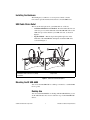
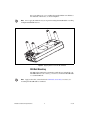
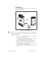
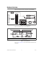
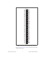
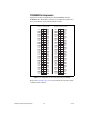
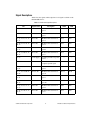
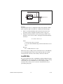
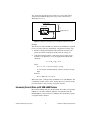
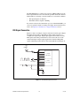
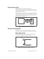
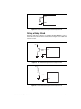
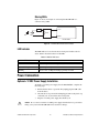
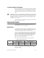
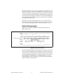
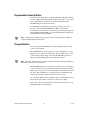
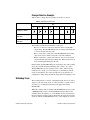
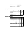
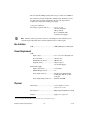
USER GUIDE AND SPECIFICATIONS NI USB-6509 This document contains information about using the National Instruments USB-6509 data acquisition (DAQ) device with NI-DAQmx 8.7 and later. The NI USB-6509 is a bus-powered 96-channel, digital input/output (I/O) device. The NI USB-6509 features 96 TTL/CMOS-compatible digital I/O lines, a watchdog timer, digital input filtering and change detection, and output programmable power-up states. The NI USB-6509 also features an optional external DC power supply that can increase the I/O drive strength. Contents Getting Started ........................................................................................ 2 Installing Software ........................................................................... 2 Installing the Hardware.................................................................... 3 USB Cable Strain Relief .................................................................. 3 Mounting the NI USB-6509 ............................................................ 3 Desktop Use.............................................................................. 3 DIN Rail Mounting................................................................... 4 Panel Mounting......................................................................... 5 Hardware Overview ................................................................................ 6 Programming Devices in Software ......................................................... 7 Related Documentation.................................................................... 8 I/O Connector.......................................................................................... 8 Pin Assignments .............................................................................. 8 SH100-100-F Pin Assignments ................................................ 8 R1005050 Pin Assignments...................................................... 10 Signal Descriptions .......................................................................... 11 Digital I/O ............................................................................................... 12 Static DIO on NI USB-6509 Devices .............................................. 12 Digital I/O Circuitry......................................................................... 12 I/O Protection................................................................................... 12 I/O State at Power-On/Power-Off/Suspend ..................................... 13 I/O Pull-Up/Pull-Down Resistor...................................................... 13 High DIO State ......................................................................... 13 Low DIO State.......................................................................... 14 Increasing Current Drive on NI USB-6509 Devices ....................... 15 DIO Signal Connection ....................................................................16 Protecting Inductive Loads...............................................................17 Sinking and Sourcing Examples.......................................................17 Driving a Relay <24 mA ...........................................................17 Driving a Relay >24 mA ...........................................................18 Driving SSRs.............................................................................19 LED Indicator...................................................................................19 Power Connection....................................................................................19 Optional +12 VDC Power Supply Installation.................................19 +5 V Power Available at I/O Connector ..........................................20 Industrial DIO Features ...........................................................................20 Digital Filtering ................................................................................20 Digital Filtering Example..........................................................21 Programmable Power-Up States.......................................................22 Change Detection .............................................................................22 Change Detection Example.......................................................23 Watchdog Timer...............................................................................23 Cables and Accessories ...........................................................................24 Specifications...........................................................................................24 Safety Guidelines.....................................................................................29 Where to Go for Support .........................................................................31 Getting Started NI USB-6509 devices feature up to 96 bidirectional per-port static DIO lines. If you have not already installed your device, refer to the NI-DAQmx for USB Devices Getting Started Guide. Before installing your DAQ device, you must install the software you plan to use with the device. Installing Software Software support for the NI USB-6509 for Windows is provided by NI-DAQmx. The NI-DAQmx CD contains example programs that you can use to get started programming with the NI USB-6509. Refer to the NI-DAQmx for USB Devices Getting Started Guide, that shipped with your device and is also accessible from Start»All Programs»National Instruments» NI-DAQ, for more information. Note For information about non-Windows operating system support, refer to ni.com/info and enter rddqld. NI 6509 User Guide and Specifications 2 ni.com Installing the Hardware The NI-DAQmx for USB Devices Getting Started Guide contains non-software-specific information about how to install USB devices. USB Cable Strain Relief The two strain relief options for your USB cable are as follows: • Cable Strain Relief Groove Method—Press the USB cable into one of the two grooves on the underside of the NI USB-6509. Choose the USB cable groove that matches your USB cable size, as shown in Figure 1. • Zip Tie Method—Thread a zip tie through the zip tie bar on the underside of the NI USB-6509 and tighten around the USB cable, as shown in Figure 1. 4 3 3 2 1 5 1 USB Cable Strain Relief Groove (Large) 2 USB Cable Strain Relief Groove (Small) 3 USB Cable 4 Zip Tie 5 Zip Tie Bar Figure 1. USB Cable Strain Relief Options Mounting the NI USB-6509 You can use the NI USB-6509 on a desktop or mount it to a standard DIN rail or a panel. Desktop Use You can use the NI USB-6509 on a desktop. The NI USB-6509 has grooves on the underside that allow it to be stacked on top of other NI USB-6509 devices. © National Instruments Corporation 3 NI 6509 User Guide and Specifications For secure desktop use, you can adhere the supplied rubber non-skid feet to the underside of the device, as shown in Figure 2. Do not apply the rubber feet if you are panel mounting the NI USB-6509 or stacking multiple NI USB-6509 devices. Note Figure 2. Applying Rubber Feet to the NI USB-6509 DIN Rail Mounting The DIN rail mounting kit (part number 779689-01, not included in your NI USB-6509 kit) is an accessory you can use to mount the NI USB-6509 to a standard DIN rail. Note Apply strain relief, as described in the USB Cable Strain Relief section, before mounting the NI USB-6509 to a DIN rail. NI 6509 User Guide and Specifications 4 ni.com Panel Mounting To mount the NI USB-6509 to a board or panel, complete the following steps while referring to Figure 3. Figure 3. Mounting the NI USB-6509 on a Panel Notes Do not apply the rubber feet to the NI USB-6509 when panel mounting the device. Apply strain relief, as described in the USB Cable Strain Relief section, before panel mounting the NI USB-6509. 1. Go to ni.com/info and enter the info code rd3233 to download and print the panel mounting template PDF. 2. Using the template, mark the bottom point and top point on the panel. The points will be 162 mm (6.375 in.) from each other. 3. Remove the USB cable from the connector on the NI USB-6509. 4. Screw a #8 or M4 screw into the bottom point on the panel. 5. Set the NI USB-6509 on the screw by fitting it into the bottom screw notch on the underside of the NI USB-6509. 6. Screw a #8 or M4 screw through the NI USB-6509 top screw hole into the panel. © National Instruments Corporation 5 NI 6509 User Guide and Specifications Hardware Overview Figure 4 shows the key functional components of the NI USB-6509. +5 V Fuse and Filter 24 mA DIO Tranceivers 12 VDC Input Port 0 12 V to 5 V Regulation Port 1 External Power I/O Connector Port 2 Port 3 96 DIO I/O Protection VBUS Current Sense Port 4 96 DIO VBUS Power Port 5 Industrial Digital I/O Control FPGA Port 6 Port 8 Port 9 96 DIO Port 10 Port 11 DIO Lines Port 7 Programmable Power-Up States Watchdog Timer Digital Filtering Data/Control USB Interface USB Data USB Port Change Detection Figure 4. NI USB-6509 Block Diagram Figure 5 shows the back panel of the NI USB-6509. 3 2 I/O LINE PULL 4 1 HIGH LOW – 12VDC 1 2 I/O Line Pull Switch LED 3 4 + , 1A Recessed USB Port DC Power Jack Figure 5. NI USB-6509 Back Panel Refer to the Safety Guidelines section of this document for important safety information. NI 6509 User Guide and Specifications 6 ni.com Programming Devices in Software National Instruments measurement devices for USB are packaged with NI-DAQ driver software, an extensive library of functions and VIs you can call from your application software, such as LabVIEW or LabWindows™/CVI™, to program all the features of your NI measurement devices. Driver software has an application programming interface (API), which is a library of VIs, functions, classes, attributes, and properties for creating applications for your device. NI-DAQ 8.x includes NI-DAQmx, which has its own API, hardware configuration, and software configuration. Refer to the NI-DAQmx for USB Getting Started Guide for more information. NI-DAQmx includes a collection of programming examples to help you get started developing an application. You can modify example code and save it in an application. You can use examples to develop a new application or add example code to an existing application. To locate LabVIEW and LabWindows/CVI examples, open the National Instruments Example Finder: • In LabVIEW, select Help»Find Examples. • In LabWindows/CVI, select Help»NI Example Finder. Measurement Studio, Visual Basic, and ANSI C examples are in the following directories: • • NI-DAQmx examples for Measurement Studio-supported languages are in the following directories: – MeasurementStudio\VCNET\Examples\NIDaq – MeasurementStudio\DotNET\Examples\NIDaq NI-DAQmx examples for ANSI C are in the NI-DAQ\Examples\ DAQmx ANSI C Dev directory For additional examples, refer to zone.ni.com. © National Instruments Corporation 7 NI 6509 User Guide and Specifications Related Documentation The following documents contain information that you may find helpful as you use this user guide: • NI-DAQmx for USB Getting Started Guide—This guide describes how to install the NI-DAQmx software, the DAQ device, and how to confirm that the device is operating properly. • NI-DAQmx Help—This help file contains information about using NI-DAQmx to program National Instruments devices. NI-DAQmx is the software you use to communicate with and control NI DAQ devices. • Measurement & Automation Explorer Help for NI-DAQmx—This help file contains information about configuring and testing DAQ devices using Measurement & Automation Explorer (MAX) for NI-DAQmx, and information about special considerations for operating systems. • DAQ Assistant Help—This help file contains information about creating and configuring channels, tasks, and scales using the DAQ Assistant. I/O Connector The 100-pin high-density SCSI connector on the NI USB-6509 provides access to 96 digital inputs and outputs. Use this connector to connect to external devices, such as solid-state relays (SSRs) and LEDs. For easy connection to the digital I/O connector, use the National Instruments SH100-100-F shielded digital I/O cable with the SCB-100 connector block, or use the R1005050 ribbon cable with the CB-50 or CB-50LP connector block. Caution Do not make connections to the digital I/O that exceed the maximum I/O specifications. Doing so may permanently damage the NI USB-6509 device and the computer. Refer to the Signal Descriptions and Specifications sections for information about maximum input ratings. Pin Assignments SH100-100-F Pin Assignments Figure 6 shows the pin assignments for the NI USB-6509 using the SH100-100-F cable. The naming convention for each pin is PX.Y, where X is the port (P) number, and Y is the line number or name. NI 6509 User Guide and Specifications 8 ni.com P2.7 1 51 P8.7 P5.7 2 52 P11.7 P2.6 3 53 P8.6 P5.6 4 54 P11.6 P2.5 5 55 P8.5 P5.5 6 56 P11.5 P2.4 7 57 P8.4 P5.4 8 58 P11.4 P2.3 9 59 P8.3 P5.3 10 60 P11.3 P2.2 11 61 P8.2 P5.2 12 62 P11.2 P2.1 13 63 P8.1 P5.1 14 64 P11.1 P2.0 15 65 P8.0 P5.0 16 66 P11.0 P1.7 17 67 P7.7 P4.7 18 68 P10.7 P1.6 19 69 P7.6 P4.6 20 70 P10.6 P1.5 21 71 P7.5 P4.5 22 72 P10.5 P1.4 23 73 P7.4 P4.4 24 74 P10.4 P1.3 25 75 P7.3 P4.3 26 76 P10.3 P1.2 27 77 P7.2 P4.2 28 78 P10.2 P1.1 29 79 P7.1 P4.1 30 80 P10.1 P1.0 31 81 P7.0 P4.0 32 82 P10.0 P0.7 33 83 P6.7 P3.7 34 84 P9.7 P0.6 35 85 P6.6 P3.6 36 86 P9.6 P0.5 37 87 P6.5 P3.5 38 88 P9.5 P0.4 39 89 P6.4 P3.4 40 90 P9.4 P0.3 41 91 P6.3 P3.3 42 92 P9.3 P0.2 43 93 P6.2 P3.2 44 94 P9.2 P0.1 45 95 P6.1 P3.1 46 96 P9.1 P0.0 47 97 P6.0 P3.0 48 98 P9.0 +5 V 49 99 +5 V GND 50 100 GND Figure 6. Pin Assignments for the NI USB-6509 using the SH100-100-F Refer to the Signal Descriptions section for information about the signals available on this connector. © National Instruments Corporation 9 NI 6509 User Guide and Specifications R1005050 Pin Assignments Figure 6 shows the pin assignments for the NI USB-6509 using the R1005050 cable. The naming convention for each pin is PX.Y, where X is the port (P) number, and Y is the line number or name. Positions 1 through 50 P2.7 P2.6 P2.5 P2.4 P2.3 P2.2 P2.1 P2.0 P1.7 P1.6 P1.5 P1.4 P1.3 P1.2 P1.1 P1.0 P0.7 P0.6 P0.5 P0.4 P0.3 P0.2 P0.1 P0.0 +5 V Positions 51 through 100 1 3 5 7 9 11 13 15 17 19 21 2 4 6 8 10 12 14 16 18 20 22 P5.7 P8.7 P5.6 P8.6 P5.5 P8.5 P5.4 P8.4 P5.3 P8.3 P5.2 P8.2 P5.1 P8.1 P5.0 P8.0 P4.7 P7.7 P4.6 P7.6 P4.5 P7.5 23 25 27 29 31 33 35 37 39 41 43 45 47 49 24 26 28 30 32 34 36 38 40 42 44 46 48 50 P4.4 P7.4 P4.3 P7.3 P4.2 P7.2 P4.1 P7.1 P4.0 P7.0 P3.7 P6.7 P3.6 P6.6 P3.5 P6.5 P3.4 P6.4 P3.3 P6.3 P3.2 P6.2 P3.1 P6.1 P3.0 P6.0 GND +5 V 1 3 5 7 9 11 13 15 17 19 21 2 4 6 8 10 12 14 16 18 20 22 P11.7 23 25 27 29 31 33 35 37 39 41 43 45 47 49 24 26 28 30 32 34 36 38 40 42 44 46 48 50 P10.4 P11.6 P11.5 P11.4 P11.3 P11.2 P11.1 P11.0 P10.7 P10.6 P10.5 P10.3 P10.2 P10.1 P10.0 P9.7 P9.6 P9.5 P9.4 P9.3 P9.2 P9.1 P9.0 GND Figure 7. Pin Assignments for the NI USB-6509 using the R1005050 Refer to the Signal Descriptions section for information about the signals available on this connector. NI 6509 User Guide and Specifications 10 ni.com Signal Descriptions Table 1 lists the signals and descriptions for all signals available on the NI USB-6509 device. Table 1. NI USB-6509 Signal Descriptions Pin Signal Name Description MSB LSB 1, 3, 5, 7, 9, 11, 13, 15 P2.<7..0> Bi-directional data lines for port 2 P2.7 P2.0 2, 4, 6, 8, 10, 12, 14, 16 P5.<7..0> Bi-directional data lines for port 5 P5.7 P5.0 17, 19, 21, 23, 25, 27, 29, 31 P1.<7..0> Bi-directional data lines for port 1 P1.7 P1.0 18, 20, 22, 24, 26, 28, 30, 32 P4.<7..0> Bi-directional data lines for port 4 P4.7 P4.0 33, 35, 37, 39, 41, 43, 45, 47 P0.<7..0> Bi-directional data lines for port 0 P0.7 P0.0 34, 36, 38, 40, 42, 44, 46, 48 P3.<7..0> Bi-directional data lines for port 3 P3.7 P3.0 49, 99 +5 V supply +5 Volts; provide +5 V power source — — 50, 100 GND Ground; connected to the computer ground signal — — 51, 53, 55, 57, 59, 61, 63, 65 P8.<7..0> Bi-directional data lines for port 8 P8.7 P8.0 52, 54, 56, 58, 60, 62, 64, 66 P11.<7..0> Bi-directional data lines for port 11 P11.7 P11.0 67, 69, 71, 73, 75, 77, 79, 81 P7.<7..0> Bi-directional data lines for port 7 P7.7 P7.0 68, 70, 72, 74, 76, 78, 80, 82 P10.<7..0> Bi-directional data lines for port 10 P10.7 P10.0 83, 85, 87, 89, 91, 93, 95, 97 P6.<7..0> Bi-directional data lines for port 6 P6.7 P6.0 84, 86, 88, 90, 92, 94, 96, 98 P9.<7..0> Bi-directional data lines for port 9 P9.7 P9.0 © National Instruments Corporation 11 NI 6509 User Guide and Specifications Digital I/O Static DIO on NI USB-6509 Devices You can use each of the NI USB-6509 DIO lines as a static digital input (DI) or digital output (DO) line. You can use static DIO lines to monitor or control digital signals. Each DIO port can be configured as a DI or DO port. All samples of static DI lines and updates of DO lines are software-timed. Digital I/O Circuitry The NI USB-6509 provides 96 lines of bidirectional DIO signals, P<0..11>.<0..7>. You can configure the direction as input or output on a per-port basis. Each I/O line has a 100 kΩ I/O pull resistor. For more information on the I/O pull resistor, refer to the I/O Pull-Up/Pull-Down Resistor section. Figure 8 shows the circuitry of one DIO line. +5 V GND Transceiver 100 kΩ I/O Protection PX.Y Figure 8. NI USB-6509 Digital I/O Circuitry The voltage input and output levels and the current drive levels of the DIO lines are listed in the Specifications section. I/O Protection You should avoid ESD events and overvoltage, undervoltage, and overcurrent fault conditions by following these guidelines. • If you configure a DIO line as an output, do not connect it to any external signal source, ground signal, or power supply. • If you configure a DIO line as an output, understand the current requirements of the load connected to these signals. Do not exceed the specified current output limits of the DAQ device. NI has several signal NI 6509 User Guide and Specifications 12 ni.com conditioning solutions for digital applications requiring high current drive. • If you configure a DIO line as an input, do not drive the line with voltages outside of its normal operating range. • Treat the DAQ device as you would treat any static sensitive device. Always properly ground yourself and the equipment when handling the DAQ device or connecting to it. I/O State at Power-On/Power-Off/Suspend After the device is powered on, the default state of all I/O lines is input. Using the I/O line pull switch located on the back panel, you can select to pull all I/O lines high or low. The pull-up or pull-down resistor provides a weak pull-high or pull-low logic level, respectively, on every I/O line. The selected I/O line pull setting takes effect regardless of the I/O direction. For more information about this feature, refer to the I/O Pull-Up/Pull-Down Resistor section. You can also configure the power-up state in software using the programmable power-up state feature. Each individual I/O line can be independently configured for high-impedance input, high output, or low output after power-up. For more information, refer to the Programmable Power-Up States section. When the device is powered off or in suspend state, all I/O lines are powered off. I/O Pull-Up/Pull-Down Resistor The NI USB-6509 facilitates user-configurable pull-up or pull-down tasks. Each DIO channel is connected to a 100 kΩ resistor and can be pulled high or low using the back-panel switch, shown in Figure 5. Using this switch pulls all 96 DIO lines high when set to HIGH or low when set to LOW. However, if all lines are high, you might want to pull some lines low. To do this properly, you must understand the nature of the drive current on those lines and adhere to TTL-logic levels. High DIO State If you select the pulled-high mode, each DIO line is pulled to Vcc (+5 V) with a 100 kΩ resistor. To pull a specific line low, connect a pull-down resistor (RL) whose value gives you a maximum of 0.8 V between the line and ground. Use the largest possible resistor so that you do not use more current than necessary to perform the pull-down task. Also, make sure the resistor value is not so large that leakage current from the DIO line drives the voltage at the resistor above a TTL low level of 0.8 V. © National Instruments Corporation 13 NI 6509 User Guide and Specifications NI USB-6509 +5 V Transceiver 100 kΩ Digital I/O Line RL GND Figure 9. DIO Channel Configured for High DIO State with External Load Example: At power up, the device is configured for input and, by default, all DIO lines are high. To pull one channel low, complete the following steps: 1. Install a load (RL). Remember that the smaller the resistance, the greater the current consumption and the lower the voltage (V). 2. Using the following formula, calculate the largest possible load to maintain a logic low level of 0.8 V and supply the maximum driving current (I). V = I * R L ⇒ RL = V / I where: V= 0.8 V is the voltage across RL I = 91 μA is the maximum leakage current from the device at low input therefore: RL = 8.8 kΩ is the 0.8 V / 91 μA This resistor value, 8.8 kΩ, provides a maximum of 0.8 V on the DIO line. You can substitute smaller resistor values, but they draw more current, leaving less drive current for other circuitry connected to this line. Low DIO State If you select pulled-low mode, each DIO line is pulled to GND (0 V) using a 100 kΩ resistor. If you want to pull a specific line high, connect a pull-up resistor that gives you a minimum of 2 V. Use the largest possible resistance value so that you do not use more current than necessary to perform the pull-up task. NI 6509 User Guide and Specifications 14 ni.com Also, make sure the pull-up resistor value is not so large that leakage current from the DIO line brings the voltage at the resistor below a TTL-high level of 2 V. NI USB-6509 +5 V Transceiver RL Digital I/O Line 100 kΩ GND Figure 10. DIO Channel Configured for Low DIO State with External Load Example: The switch is set in the low DIO state, which means all DIO lines are pulled low. If you want to pull one channel high, complete the following steps: 1. Install a load (RL). Remember that the smaller the resistance, the greater the current consumption and the lower the voltage (V). 2. Using the following formula, calculate the largest possible load to maintain a logic high level of 2 V and supply the maximum sink current (I). V = I * R L ⇒ RL = V / I where: V = 5 V – 2 V = 3 V is the voltage across RL I = 91 μA is the maximum leakage current to the device at high input therefore: RL = 33 kΩ is the 3 V / 91 μA This resistor value, 33 kΩ, provides a minimum of 2 V on the DIO line. You can substitute smaller resistor values, but they draw more current, leaving less sink current for other circuitry connected to this line. Increasing Current Drive on NI USB-6509 Devices Based on the USB specification, the maximum current that a bus-powered USB device can draw is limited to 500 mA. Consequently, when the NI USB-6509 is powered only from a USB port, the current drive capacity at output channels is limited. © National Instruments Corporation 15 NI 6509 User Guide and Specifications The NI USB-6509 has a current-sense circuit on VBUS (USB power rail). If the output channels source more than the specified current, the current is limited. The two following occurrences indicate an overcurrent condition: • The inputs/outputs are disabled • The LED on the back panel is blinking If you want to increase the current drive capacity on the NI USB-6509, you can use an optional external +12 VDC power supply. For more information, refer to the Optional +12 VDC Power Supply Installation section. DIO Signal Connection Figure 11 shows an example of signal connections for three typical digital I/O applications. Port 0 is configured for digital output, and port 7 is configured for digital input. Digital input applications include receiving TTL signals and sensing external device states such as the state of the switch in the figure. Digital output applications include sending TTL signals and driving external devices such as the LED shown in Figure 11. +5 V LED 41 43 Port 0 45 P0.<3..0> 47 67 TTL Signal +5 V 69 Port 7 71 P7.<7..4> 73 50, 100 GND NI USB-6509 Figure 11. NI USB-6509 Signal Connections NI 6509 User Guide and Specifications 16 ni.com Protecting Inductive Loads When inductive loads are connected to outputs, a large counter-electromotive force may occur at switching time because of the energy stored in the inductive load. These flyback voltages can damage the outputs and/or the power supply. To limit these flyback voltages at the inductive load, install a flyback diode across the inductive load. For best results, mount the flyback diode within 18 inches of the load. Figure 12 shows an example of using an external flyback diode to protect inductive loads. PX.Y Load GND NI USB-6509 Flyback Diode for Inductive Loads Figure 12. Limiting Flyback Voltages at the Inductive Load Sinking and Sourcing Examples The following sections provide examples of driving a relay less than 24 mA, driving a relay greater than 24 mA, and driving solid-state relays. Driving a Relay <24 mA Figures 13 and 14 show examples of connecting the NI USB-6509 to a relay that does not require more than 24 mA of current. Vcc PX.Y GND NI USB-6509 Figure 13. NI USB-6509 Sinking Connection Example, <24 mA © National Instruments Corporation 17 NI 6509 User Guide and Specifications PX.Y GND NI USB-6509 Figure 14. NI USB-6509 Sourcing Connection Example, <24 mA Driving a Relay >24 mA Figures 15 and 16 are examples of connecting the NI USB-6509 to a relay that requires more than 24 mA of current. These examples use an additional transistor circuit. Vcc PX.Y GND NI USB-6509 Figure 15. NI USB-6509 Sinking Connection Example, >24 mA Vcc PX.Y GND NI USB-6509 Figure 16. NI USB-6509 Sourcing Connection Example, >24 mA NI 6509 User Guide and Specifications 18 ni.com Driving SSRs Figure 17 shows an example of connecting the NI USB-6509 to a solid-state relay (SSR). Load DC + _ or AC PX.Y SSR GND NI USB-6509 Figure 17. NI USB-6509 SSR Connection Example LED Indicator The LED indicator, located on the device back panel, indicates device status. Table 2 shows the behavior of the LED. Table 2. PWR/ACT LED Status LED State Device Status Not lit Device not powered or in suspend state On, not blinking Operating normally Blinking Device error—USB power budget possibly exceeded Power Connection Optional +12 VDC Power Supply Installation To install a +12 VDC power supply into the NI USB-6509, complete the following steps: 1. Ensure that the device is powered off by unplugging the USB cable from the device. 2. After the device is powered off and unplugged, remove the plastic cap on the DC jack, located on the device back panel. 3. Plug the +12 VDC power supply into the DC jack. Do not remove external +12 VDC power supply when the device is powered on. Doing so may reboot the NI USB-6509 and cause device damage. Caution © National Instruments Corporation 19 NI 6509 User Guide and Specifications +5 V Power Available at I/O Connector Pins 49 and 99 supply +5 V power to the I/O connector. The power drawn from these two pins shares the power consumption with the transceivers. The I/O connector power has a fuse for overcurrent protection. This fuse is not customer replaceable. If the fuse is blown, return the device to NI for repair. The power pins, +5V and GND, connect to the computer power supply and are not isolated. Do not connect a +5V power pin directly to GND or connect a +5V or GND pin to any other voltage source. Doing so may cause injury or permanently damage the NI USB-6509 components. National Instruments is not liable for any damage or injury resulting from such a connection. Caution For more information on maximum power ratings and overcurrent limits, refer to the Specifications section. Industrial DIO Features The NI USB-6509 features digital filtering, programmable power-up states, change detection, and a watchdog timer. Digital Filtering Use the digital filter option available on the NI USB-6509 input lines to eliminate glitches on input data. When used with change detection, filtering can also reduce the number of changes to examine and process. You can configure the digital input channels to pass through a digital filter, and you can control the timing interval the filter uses. The filter blocks pulses that are shorter than half of the specified timing interval and passes pulses that are longer than the specified interval. Intermediate-length pulses—pulses longer than half of the interval but less than the interval—may or may not pass the filter. Table 3 lists the pulse widths guaranteed to be passed and blocked. Table 3. NI USB-6509 Digital Filtering Pulse Width Passed Pulse Width Blocked Filter Interval Low Pulse High Pulse Low Pulse High Pulse tinterval tinterval tinterval tinterval/2 tinterval/2 You can enable filtering on as many input lines as is necessary for your application. All filtered lines share the same timing interval, which ranges from 200 ns to 200 ms. NI 6509 User Guide and Specifications 20 ni.com Internally, the filter uses two clocks: the sample clock and the filter clock. The sample clock has a frequency of 48 MHz that corresponds to a period of 20.83 ns. The filter clock is generated by a counter and has a period equal to one half of the specified timing interval. The input signal is sampled on each rising edge of the sample clock. However, a change in the input signal is recognized only if it maintains its new state for at least two consecutive rising edges of the filter clock. The filter clock is programmable and allows you to control how long a pulse must last to be recognized. The sample clock provides a fast sample rate to ensure that input pulses remain constant between filter clocks. Digital Filtering Example Figure 18 shows a filter configuration with an 208 ns filter interval (104 ns filter clock). External Signal Filter Clock Sample Clock (20.83 ns) External Signal Sampled H L H L L H H L L H H L B H H H H H H C A Filtered Signal Figure 18. Digital Filtering Example In periods A and B, the filter blocks the glitches because the external signal does not remain steadily high from one rising edge of the filter clock to the next. In period C, the filter passes the transition because the external signal remains steadily high. Depending on when the transition occurs, the filter may require up to two filter clocks—one full filter interval—to pass a transition. Figure 18 shows a rising (0 to 1) transition. The same filtering applies to falling (1 to 0) transitions. © National Instruments Corporation 21 NI 6509 User Guide and Specifications Programmable Power-Up States At power-up, the output drives on the NI USB-6509 are disabled. All lines are user-configurable for high-impedance input, high output, or low output. User-configurable power-up states are useful for ensuring that the NI USB-6509 powers up in a known state. To use MAX (recommended) to program the power-up states, select the device and click the Properties button. Refer to the software documentation for information about how to program the power-up states using NI-DAQ with LabVIEW or other National Instruments application development environments (ADEs). Note Using the programmable power-up states feature overrides the state configured using the I/O pull-up/pull-down switch. Change Detection You can program the NI USB-6509 to send an interrupt when a change occurs on any input line. The NI USB-6509 can monitor changes on selected input lines or on all input lines. It can monitor for rising edges (0 to 1), falling edges (1 to 0), or both. When an input change occurs, the NI USB-6509 generates an interrupt, and the NI-DAQ driver then notifies the software. Excessive change detections can affect system performance. Use digital filtering to minimize the effects of noisy input lines. Note The NI USB-6509 sends a change detection when any one of the changes occurs, but it does not report which line changed or if the line was rising or falling. After a change, you can read the input lines to determine the current line states. The maximum rate of change detection is determined by the software response time, which varies from system to system. An overflow bit indicates that an additional rising or falling edge has been detected before the software could process the previous change. Refer to the software documentation for information about how to set up and implement the change detection. NI 6509 User Guide and Specifications 22 ni.com Change Detection Example Table 4 shows a change detection example for six bits of one port. Table 4. Change Detection Example Bit 7 6 5 4 Changes to detect 3 2 — — 1 0 Enable rising-edge detection yes yes yes yes no no yes no Enable falling-edge detection yes yes yes yes no no no yes This example assumes the following line connections: • Bits 7, 6, 5, and 4 are connected to data lines from a four-bit TTL output device. The NI USB-6509 detects any change in the input data so you can read the new data value. • Bit 1 is connected to a limit sensor. The NI USB-6509 detects rising edges on the sensor, which correspond to over-limit conditions. • Bit 0 is connected to a switch. The software can react to any switch closure, which is represented by a falling edge. If the switch closure is noisy, enable digital filtering for this line. In this example, the NI USB-6509 reports rising edges only on bit 1, falling edges only on bit 0, and rising and falling edges on bits 7, 6, 5, and 4. The NI USB-6509 reports no changes for bits 3 and 2. After receiving notification of a change, you can read the port to determine the current values of all eight lines. You cannot read the state of any lines that are configured for change detection until the change detection interrupt occurs. Watchdog Timer The watchdog timer is a software configurable feature used to set critical outputs to safe states in the event of a software failure, a system crash, or any other loss of communication between the application and the NI USB-6509. When the watchdog timer is enabled, if the NI USB-6509 does not receive a watchdog reset software command within the time specified for the watchdog timer, the outputs go to a user-defined safe state and remain in that state until the watchdog timer is disarmed by the application and new values are written, the NI USB-6509 is reset, or the computer is restarted. © National Instruments Corporation 23 NI 6509 User Guide and Specifications The expiration signal that indicates an expired watchdog continues to assert until the watchdog is disarmed. After the watchdog timer expires, the NI USB-6509 ignores any writes until the watchdog timer is disarmed. When the watchdog timer is enabled and the computer enters a fault condition, ports that are set to tri-state remain tri-stated and do not go to user-defined safe states. Note You can set the watchdog timer timeout period to specify the amount of time that must elapse before the watchdog timer expires. The counter on the watchdog timer is configurable up to (232 – 1) × 20.83 ns (approximately 1.5 minutes) before it expires. Cables and Accessories Table 5 lists the products available for use with the NI USB-6509. Table 5. NI USB-6509 Connectivity Options Cable Accessory SH100-100-F shielded cable—part number 185095-01 (1 m) or 185095-02 (2 m) SCB-100 connector block—part number 776990-01 R1005050 ribbon cable—part number 182762-0R5 (0.5 m), 182762-01 (1 m), or 182762-02 (2 m) CB-50 connector block, DIN-rail mount—part number 776164-90 CB-50LP connector block, panel mount—part number 777101-01 — CB-100 I/O kit (cable included in kit) (unshielded)—part number 777812-01 — +12 VDC power supply—part number 780308-0x (where the x indicates different regions or cable options) For more information about optional equipment available from National Instruments, visit ni.com. Specifications This section lists the specifications of the NI USB-6509 devices. These specifications are typical at 25 °C, unless otherwise stated. Number of channels................................96 input/output Compatibility ..........................................TTL/CMOS, single-ended GND referenced NI 6509 User Guide and Specifications 24 ni.com Power-on state........................................ Configured as inputs, pull-up/pull-down (selectable on the back panel switch) Pull-up/pull-down resistor...................... 100 kΩ ±5% Data transfers ......................................... Programmed I/O Digital Input Characteristics Level Min Max Input voltage 0V 5.0 V Input low voltage — 0.8 V Input high voltage 2.0 V — Input low current (Vin = 0 V) — –91.0 μA Input high current (Vin= 5 V) — 91.0 μA Digital Output Characteristics Level Min Typ Max Low-level output current (IOL) — — 24 mA High-level output current (IOH) — — –24 mA Output low voltage (VOL), at 100 μA — 0.0 V 0.2 V at 2 mA — 0.1 V — at 12 mA — 0.5 V — at 24 mA — 1.0 V 1.4 V 4.3 V 5.0 V — at –2 mA — 4.9 V — at –12 mA — 4.5 V — at –24 mA 2.8 V 4.0 V — Output high voltage (VOH), at –100 μA © National Instruments Corporation 25 NI 6509 User Guide and Specifications The total current sinking/sourcing from one port cannot exceed 100 mA. Total current sourced by all DO lines simultaneously should not exceed 215 mA for bus-powered configuration. If more sourcing current is required, use an optional external power supply +5V power available at I/O connector (pins 49 and 99) ...............+4.1 to +5.2 V; 215 mA, maximum (Bus-powered); 0.5 A, maximum (with external power supply) The I/O connector power has a fuse for overcurrent protection. This fuse is not customer replaceable. If the fuse is blown, return the device to NI for repair. Note Bus Interface USB ........................................................USB 2.0 Hi-Speed or full-speed1 Power Requirement USB Input voltage....................................4.5 to 5.25 V in configured state No load current ................................150 mA, max Maximum load current ....................500 mA, max Suspend current ...............................250 μA, typical (no external supply) External DC supply Input voltage range ..........................+12 V ±20% Maximum input current...................1 A Power input connector.....................DC input jack with threaded locking ring, 0.08 in. (2 mm) center pin Power input mating connector.........Switchcraft S760K Physical Dimensions .............................................17.78 × 10.30 × 3.34 cm (7.0 × 4.1 × 1.3 in.) I/O connector ..........................................100-pin female 0.050 series SCSI Weight ....................................................Approx. 239 g (8.4 oz) 1 If you are using the NI USB-6509 in full-speed mode, device performance is lower. NI 6509 User Guide and Specifications 26 ni.com Safety This product is designed to meet the requirements of the following standards of safety for electrical equipment for measurement, control, and laboratory use: • IEC 61010-1, EN 61010-1 • UL 61010-1, CSA 61010-1 Note For UL and other safety certifications, refer to the product label or visit ni.com/ certification, search by model number or product line, and click the appropriate link in the Certification column. Hazardous Locations The NI USB-6509 is not certified for use in hazardous locations. Environmental The NI USB-6509 device is intended for indoor use only. Operating temperature (IEC 60068-2-1 and IEC 60068-2-2) ..... 0 to 55 °C Operating humidity (IEC 60068-2-56) ................................... 10 to 90% RH, noncondensing Maximum altitude .................................. 2,000 m (at 25 °C ambient temperature) Storage temperature (IEC 60068-2-1 and IEC 60068-2-2) ..... –40 to 85 °C Storage humidity (IEC 60068-2-56) ................................... 5 to 90% RH, noncondensing Pollution Degree (IEC 60664) ............... 2 Electromagnetic Compatibility This product is designed to meet the requirements of the following standards of EMC for electrical equipment for measurement, control, and laboratory use: Note • EN 61326 EMC requirements; Minimum Immunity • EN 55011 Emissions; Group 1, Class A • CE, C-Tick, ICES, and FCC Part 15 Emissions; Class A For EMC compliance, operate this device according to product documentation. © National Instruments Corporation 27 NI 6509 User Guide and Specifications CE Compliance This product meets the essential requirements of applicable European Directives, as amended for CE marking, as follows: • 2006/95/EC; Low-Voltage Directive (safety) • 2004/108/EC; Electromagnetic Compatibility Directive (EMC) Refer to the Declaration of Conformity (DoC) for this product for any additional regulatory compliance information. To obtain the DoC for this product, visit ni.com/ certification, search by model number or product line, and click the appropriate link in the Certification column. Note Environmental Management NI is committed to designing and manufacturing products in an environmentally responsible manner. NI recognizes that eliminating certain hazardous substances from our products is beneficial not only to the environment but also to NI customers. For additional environmental information, refer to the NI and the Environment web page at ni.com/environment. This page contains the environmental regulations and directives with which NI complies, as well as other environmental information not included in this document. Waste Electrical and Electronic Equipment (WEEE) At the end of their life cycle, all products must be sent to a WEEE recycling center. For more information about WEEE recycling centers and National Instruments WEEE initiatives, visit ni.com/environment/weee.htm. EU Customers ⬉ᄤֵᙃѻક∵ᶧࠊㅵ⧚ࡲ⊩ ˄Ё RoHS˅ Ёᅶ᠋ National Instruments ヺড়Ё⬉ᄤֵᙃѻકЁ䰤ࠊՓ⫼ᶤѯ᳝ᆇ⠽䋼ᣛҸ (RoHS)DŽ ݇Ѣ National Instruments Ё RoHS ড়㾘ᗻֵᙃˈ䇋ⱏᔩ ni.com/environment/rohs_chinaDŽ (For information about China RoHS compliance, go to ni.com/environment/rohs_china.) NI 6509 User Guide and Specifications 28 ni.com Safety Guidelines Caution Operate the hardware only as described in these operating instructions. The following section contains important safety information that you must follow when installing and using the NI USB-6509. Do not operate the NI USB-6509 in a manner not specified in this document. Misuse of the device can result in a hazard. You can compromise the safety protection built into the device if the device is damaged in any way. If the device is damaged, contact National Instruments for repair. Do not substitute parts or modify the device except as described in this document. Use the device only with the chassis, modules, accessories, and cables specified in the installation instructions. You must have all covers and filler panels installed during operation of the device. Do not operate the device in an explosive atmosphere or where there may be flammable gases or fumes. If you must operate the device in such an environment, it must be in a suitably rated enclosure. If you need to clean the device, use a dry cloth. Make sure that the device is completely dry and free from contaminants before returning it to service. Operate the device only at or below Pollution Degree 2. Pollution is foreign matter in a solid, liquid, or gaseous state that can reduce dielectric strength or surface resistivity. The following is a description of pollution degrees: • Pollution Degree 1 means no pollution or only dry, nonconductive pollution occurs. The pollution has no influence. • Pollution Degree 2 means that only nonconductive pollution occurs in most cases. Occasionally, however, a temporary conductivity caused by condensation must be expected. • Pollution Degree 3 means that conductive pollution occurs, or dry, nonconductive pollution occurs that becomes conductive due to condensation. You must insulate signal connections for the maximum voltage for which the device is rated. Do not exceed the maximum ratings for the device. Do not install wiring while the device is live with electrical signals. Do not remove or add connector blocks when power is connected to the system. Avoid contact between your body and the connector block signal when hot swapping modules. Remove power from signal lines before connecting them to or disconnecting them from the device. © National Instruments Corporation 29 NI 6509 User Guide and Specifications Operate the device at or below the Measurement Category I1. Measurement circuits are subjected to working voltages2 and transient stresses (overvoltage) from the circuit to which they are connected during measurement or test. Measurement categories establish standard impulse withstand voltage levels that commonly occur in electrical distribution systems. The following is a description of measurement categories: • Measurement Category I is for measurements performed on circuits not directly connected to the electrical distribution system referred to as MAINS3 voltage. This category is for measurements of voltages from specially protected secondary circuits. Such voltage measurements include signal levels, special equipment, limited-energy parts of equipment, circuits powered by regulated low-voltage sources, and electronics. • Measurement Category II is for measurements performed on circuits directly connected to the electrical distribution system. This category refers to local-level electrical distribution, such as that provided by a standard wall outlet (for example, 115 V for U.S. or 230 V for Europe). Examples of Measurement Category II are measurements performed on household appliances, portable tools, and similar E Series devices. • Measurement Category III is for measurements performed in the building installation at the distribution level. This category refers to measurements on hard-wired equipment such as equipment in fixed installations, distribution boards, and circuit breakers. Other examples are wiring, including cables, bus-bars, junction boxes, switches, socket-outlets in the fixed installation, and stationary motors with permanent connections to fixed installations. Measurement Category IV is for measurements performed at the primary electrical supply installation (<1,000 V). Examples include electricity meters and measurements on primary overcurrent protection devices and on ripple control units. 1 2 3 Measurement Category as defined in electrical safety standard IEC 61010-1. Measurement Category is also referred to as Installation Category. Working Voltage is the highest rms value of an AC or DC voltage that can occur across any particular insulation. MAINS is defined as a hazardous live electrical supply system that powers equipment. Suitably rated measuring circuits may be connected to the MAINS for measuring purposes. NI 6509 User Guide and Specifications 30 ni.com Where to Go for Support The National Instruments Web site is your complete resource for technical support. At ni.com/support you have access to everything from troubleshooting and application development self-help resources to email and phone assistance from NI Application Engineers. A Declaration of Conformity (DoC) is our claim of compliance with the Council of the European Communities using the manufacturer’s declaration of conformity. This system affords the user protection for electronic compatibility (EMC) and product safety. You can obtain the DoC for your product by visiting ni.com/certification. If your product supports calibration, you can obtain the calibration certificate for your product at ni.com/calibration. National Instruments corporate headquarters is located at 11500 North Mopac Expressway, Austin, Texas, 78759-3504. National Instruments also has offices located around the world to help address your support needs. For telephone support in the United States, create your service request at ni.com/support and follow the calling instructions or dial 512 795 8248. For telephone support outside the United States, contact your local branch office: Australia 1800 300 800, Austria 43 662 457990-0, Belgium 32 (0) 2 757 0020, Brazil 55 11 3262 3599, Canada 800 433 3488, China 86 21 5050 9800, Czech Republic 420 224 235 774, Denmark 45 45 76 26 00, Finland 358 (0) 9 725 72511, France 01 57 66 24 24, Germany 49 89 7413130, India 91 80 41190000, Israel 972 3 6393737, Italy 39 02 41309277, Japan 0120-527196, Korea 82 02 3451 3400, Lebanon 961 (0) 1 33 28 28, Malaysia 1800 887710, Mexico 01 800 010 0793, Netherlands 31 (0) 348 433 466, New Zealand 0800 553 322, Norway 47 (0) 66 90 76 60, Poland 48 22 3390150, Portugal 351 210 311 210, Russia 7 495 783 6851, Singapore 1800 226 5886, Slovenia 386 3 425 42 00, South Africa 27 0 11 805 8197, Spain 34 91 640 0085, Sweden 46 (0) 8 587 895 00, Switzerland 41 56 2005151, Taiwan 886 02 2377 2222, Thailand 662 278 6777, Turkey 90 212 279 3031, United Kingdom 44 (0) 1635 523545 National Instruments, NI, ni.com, and LabVIEW are trademarks of National Instruments Corporation. Refer to the Terms of Use section on ni.com/legal for more information about National Instruments trademarks. Other product and company names mentioned herein are trademarks or trade names of their respective companies. For patents covering National Instruments products, refer to the appropriate location: Help»Patents in your software, the patents.txt file on your CD, or ni.com/patents. © 2008 National Instruments Corporation. All rights reserved. 372136A-01 Mar08