1
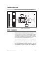
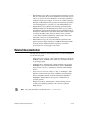
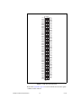
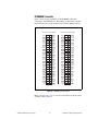
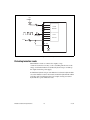
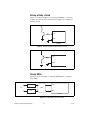
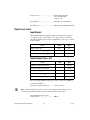
USER GUIDE AND SPECIFICATIONS NI 6509 The NI 6509 is a 96-bit, high-drive digital input/output (I/O) device for PCI, PXI, and CompactPCI chassis. The NI 6509 features 96 TTL/CMOS-compatible digital I/O lines, 24 mA high-drive output, a watchdog timer, digital filtering, and programmable power-up states. Contents Configuration .......................................................................................... 2 Programming Devices in Software .................................................. 3 Functional Overview............................................................................... 4 Safety Information .................................................................................. 4 Related Documentation........................................................................... 6 Features ................................................................................................... 7 Digital Filtering................................................................................ 7 Digital Filtering Example ......................................................... 8 Programmable Power-Up States ...................................................... 8 Change Detection............................................................................. 9 Change Detection Example ...................................................... 9 Watchdog Timer .............................................................................. 10 Digital I/O Connections .......................................................................... 11 Pin Assignments .............................................................................. 11 SH100-100-F Connector........................................................... 11 R1005050 Connector ................................................................ 13 Signal Descriptions .......................................................................... 14 Power Connections ................................................................................. 15 Signal Connections .......................................................................... 15 Protecting Inductive Loads .............................................................. 16 Sinking and Sourcing Examples ...................................................... 17 Driving a Relay <24 mA .......................................................... 17 Driving a Relay >24 mA .......................................................... 18 Driving SSRs ............................................................................ 18 Accessories.............................................................................................. 19 Specifications .......................................................................................... 19 Configuration The NI 6509 device is completely software configurable, so it is not necessary to set jumpers for I/O configuration. The PCI-6509 device is fully compliant with the PCI Local Bus Specification, Revision 2.2, and the PXI-6509 device is fully compliant with the PXI Hardware Specification, Revision 2.1. The PCI/PXI system automatically allocates all device resources, including the base address and interrupt level. The device base address is mapped into PCI memory space. It is not necessary to perform configuration steps after the system powers up. Refer to the application software documentation for configuration instructions. After the NI 6509 device and the software are installed, the DAQ device appears under the Devices and Interfaces branch of the MAX configuration tree. If the DAQ device does not appear in MAX, use the following troubleshooting guidelines. • Verify that you are using the correct version of NI-DAQ (NI-DAQ 7.1 or later). To download the most recent National Instruments drivers, go to ni.com/drivers. • Press <F5> to refresh the MAX window, or close and re-open MAX. • Reboot the computer. • Power off and unplug the computer or chassis, and install the device in a different slot. Refer to the DAQ Getting Started Guide for installation instructions and safety guidelines. • NI PCI-6509 devices must be installed into a slot that provides 3.3 V. Check that the 3.3 V LED (reference designator DS1—located on the visible edge of the underside of the installed device) is lit. If not, check that the PC motherboard provides 3.3 V to the PCI bus. NI 6509 User Guide and Specifications 2 ni.com Programming Devices in Software National Instruments measurement devices are packaged with NI-DAQ driver software, an extensive library of functions and VIs you can call from your application software, such as LabVIEW or LabWindows™/CVI™, to program all the features of your NI measurement devices. Driver software has an application programming interface (API), which is a library of VIs, functions, classes, attributes, and properties for creating applications for your device. NI-DAQ 8.x includes two NI-DAQ drivers, Traditional NI-DAQ (Legacy) and NI-DAQmx. Each driver has its own API, hardware configuration, and software configuration. Refer to the DAQ Getting Started Guide for more information about the two drivers. Traditional NI-DAQ (Legacy) and NI-DAQmx each include a collection of programming examples to help you get started developing an application. You can modify example code and save it in an application. You can use examples to develop a new application or add example code to an existing application. To locate LabVIEW and LabWindows/CVI examples, open the National Instruments Example Finder: • In LabVIEW, select Help»Find Examples. • In LabWindows/CVI, select Help»NI Example Finder. Measurement Studio, Visual Basic, and ANSI C examples are in the following directories: • NI-DAQmx examples for Measurement Studio-supported languages are in the following directories: – MeasurementStudio\VCNET\Examples\NIDaq – • MeasurementStudio\DotNET\Examples\NIDaq Traditional NI-DAQ (Legacy) examples for Visual Basic are in the following two directories: – NI-DAQ\Examples\Visual Basic with Measurement Studio directory contains a link to the ActiveX control examples for use with Measurement Studio – NI-DAQ\Examples\VBasic directory contains the examples not associated with Measurement Studio • NI-DAQmx examples for ANSI C are in the NI-DAQ\Examples\ DAQmx ANSI C Dev directory • Traditional NI-DAQ (Legacy) examples for ANSI C are in the NI-DAQ\Examples\VisualC directory For additional examples, refer to zone.ni.com. © National Instruments Corporation 3 NI 6509 User Guide and Specifications Functional Overview Figure 1 shows the key functional components of the NI 6509 device. 24 mA DIO Tranceivers Port 0 10 MHz Clock Port 1 Flash Memory Port 2 Industrial Digital I/O Control FPGA Port 4 96 DIO 96 DIO Port 6 DIO Lines I/O Connector Port 5 Programmable Power-Up States Watchdog Timer Digital Filtering Data/Control PCI Bus Interface Change Detection Port 7 Data/Control PCI/PXI/CompactPCI Bus Port 3 Port 8 Port 9 Configuration Control Port 10 Port 11 Figure 1. NI 6509 Block Diagram Safety Information The following section contains important safety information that you must follow when installing and using National Instruments DIO devices. Do not operate the device in a manner not specified in this help file. Misuse of the DIO device can result in a hazard. You can compromise the safety protection built into the DIO device if it is damaged in any way. If the DIO device is damaged, return it to National Instruments for repair. Do not substitute parts or modify the DIO device except as described in this help file. Use the DIO device only with the chassis, modules, accessories, and cables specified in the installation instructions. You must have all covers and filler panels installed during operation of the DIO device. Do not operate the DIO device in an explosive atmosphere or where there may be flammable gases or fumes. If you must operate the DIO device in such an environment, it must be in a suitably rated enclosure. NI 6509 User Guide and Specifications 4 ni.com If you need to clean the DIO device, use a soft, nonmetallic brush. Make sure that the DIO device is completely dry and free from contaminants before returning it to service. Operate the DIO device only at or below Pollution Degree 2. Pollution is foreign matter in a solid, liquid, or gaseous state that can reduce dielectric strength or surface resistivity. The following is a description of pollution degrees: • Pollution Degree 1 means no pollution or only dry, nonconductive pollution occurs. The pollution has no influence. • Pollution Degree 2 means that only nonconductive pollution occurs in most cases. Occasionally, however, a temporary conductivity caused by condensation must be expected. • Pollution Degree 3 means that conductive pollution occurs, or dry, nonconductive pollution occurs that becomes conductive due to condensation. You must insulate signal connections for the maximum voltage for which the DIO device is rated. Do not exceed the maximum ratings for the DIO device. Do not install wiring while the DIO device is live with electrical signals. Do not remove or add connector blocks when power is connected to the system. Avoid contact between your body and the connector block signal when hot swapping modules. Remove power from signal lines before connecting them to or disconnecting them from the DIO device. Operate the DIO device at or below the measurement category1 marked on the hardware label. Measurement circuits are subjected to working voltages2 and transient stresses (overvoltage) from the circuit to which they are connected during measurement or test. Installation categories establish standard impulse withstand voltage levels that commonly occur in electrical distribution systems. The following is a description of installation categories: • 1 2 3 Measurement Category I is for measurements performed on circuits not directly connected to the electrical distribution system referred to as MAINS3 voltage. This category is for measurements of voltages from specially protected secondary circuits. Such voltage measurements include signal levels, special equipment, limited-energy parts of equipment, circuits powered by regulated low-voltage sources, and electronics. Measurement categories, also referred to as installation categories, are defined in electrical safety standard IEC 61010-1. Working voltage is the highest rms value of an AC or DC voltage that can occur across any particular insulation. MAINS is defined as a hazardous live electrical supply system that powers equipment. Suitably rated measuring circuits may be connected to the MAINS for measuring purposes. © National Instruments Corporation 5 NI 6509 User Guide and Specifications • Measurement Category II is for measurements performed on circuits directly connected to the electrical distribution system. This category refers to local-level electrical distribution, such as that provided by a standard wall outlet (for example, 115 V for U.S. or 230 V for Europe). Examples of Measurement Category II are measurements performed on household appliances, portable tools, and similar DIO devices. • Measurement Category III is for measurements performed in the building installation at the distribution level. This category refers to measurements on hard-wired equipment such as equipment in fixed installations, distribution boards, and circuit breakers. Other examples are wiring, including cables, bus-bars, junction boxes, switches, socket-outlets in the fixed installation, and stationary motors with permanent connections to fixed installations. • Measurement Category IV is for measurements performed at the primary electrical supply installation (<1,000 V). Examples include electricity meters and measurements on primary overcurrent protection devices and on ripple control units. Related Documentation The following documents contain information that you may find helpful as you use this user guide: Note • DAQ Getting Started Guide—This guide describes how to install the NI-DAQ software, the DAQ device, and how to confirm that the device is operating properly. • NI-DAQmx Help—This help file contains information about using NI-DAQmx to program National Instruments devices. NI-DAQmx is the software you use to communicate with and control NI DAQ devices. • Measurement & Automation Explorer Help for NI-DAQmx—This help file contains information about configuring and testing DAQ devices using Measurement & Automation Explorer (MAX) for NI-DAQmx, and information about special considerations for operating systems. • DAQ Assistant Help—This help file contains information about creating and configuring channels, tasks, and scales using the DAQ Assistant. You can download these documents from ni.com/manuals. NI 6509 User Guide and Specifications 6 ni.com Features The NI 6509 features digital filtering, programmable power-up states, change detection, and a watchdog timer. Digital Filtering Use the digital filter option available on the NI 6509 input lines to eliminate glitches on input data. When used with change detection, filtering can also reduce the number of changes to examine and process. You can configure the digital input channels to pass through a digital filter, and you can control the timing interval the filter uses. The filter blocks pulses that are shorter than half of the specified timing interval and passes pulses that are longer than the specified interval. Intermediate-length pulses—pulses longer than half of the interval but less than the interval—may or may not pass the filter. Table 1 lists the pulse widths guaranteed to be passed and blocked. Table 1. NI 6509 Digital Filtering Pulse Width Passed Pulse Width Blocked Filter Interval Low Pulse High Pulse Low Pulse High Pulse tinterval tinterval tinterval tinterval/2 tinterval/2 You can enable filtering on as many input lines as necessary for your application. All filtered lines share the same timing interval, which ranges from 400 ns to 200 ms. Internally, the filter uses two clocks: the sample clock and the filter clock. The sample clock has a 100 ns period. The filter clock is generated by a counter and has a period equal to one half of the specified timing interval. The input signal is sampled on each rising edge of the sample clock, which is every 100 ns. However, a change in the input signal is recognized only if it maintains its new state for at least two consecutive rising edges of the filter clock. The filter clock is programmable and allows you to control how long a pulse must last to be recognized. The sample clock provides a fast sample rate to ensure that input pulses remain constant between filter clocks. © National Instruments Corporation 7 NI 6509 User Guide and Specifications Digital Filtering Example Figure 2 shows a filter configuration with an 800 ns filter interval (400 ns filter clock). External Signal Filter Clock Sample Clock (100 ns) External Signal Sampled H H L L H H L L B H H H H H H H C A Filtered Signal Figure 2. Digital Filtering Example In periods A and B, the filter blocks the glitches because the external signal does not remain steadily high from one rising edge of the filter clock to the next. In period C, the filter passes the transition because the external signal remains steadily high. Depending on when the transition occurs, the filter may require up to two filter clocks—one full filter interval—to pass a transition. The figure shows a rising (0 to 1) transition. The same filtering applies to falling (1 to 0) transitions. Programmable Power-Up States At power-up, the output drives on the NI 6509 are disabled. All lines are user-configurable for high-impedance input, high output, or low output. User-configurable power-up states are useful for ensuring that the NI 6509 powers up in a known state. To use MAX (recommended) to program the power-up states, select the device and click the Properties button. Refer to the software documentation for information about how to program the power-up states using NI-DAQ with LabVIEW or other National Instruments application development environments (ADEs). Note The response time of programmable power-up states is 400 ms. NI 6509 User Guide and Specifications 8 ni.com Change Detection You can program the NI 6509 to send an interrupt when a change occurs on any input line. The NI 6509 can monitor changes on selected input lines or on all input lines. It can monitor for rising edges (0 to 1), falling edges (1 to 0), or both. When an input change occurs, the NI 6509 generates an interrupt, and the NI-DAQ driver then notifies the software. Excessive change detections can affect system performance. Use digital filtering to minimize the effects of noisy input lines. Note The NI 6509 sends a change detection when any one of the changes occurs, but it does not report which line changed or if the line was rising or falling. After a change, you can read the input lines to determine the current line states. The maximum rate of change detection is determined by the software response time, which varies from system to system. An overflow bit indicates that an additional rising or falling edge has been detected before the software could process the previous change. Refer to the software documentation for information about how to set up and implement the change detection. Change Detection Example Table 2 shows a change detection example for six bits of one port. Table 2. Change Detection Example Bit 7 6 5 4 Changes to detect 3 2 — — 1 0 Enable rising-edge detection yes yes yes yes no no yes no Enable falling-edge detection yes yes yes yes no no no yes © National Instruments Corporation 9 NI 6509 User Guide and Specifications This example assumes the following line connections: • Bits 7, 6, 5, and 4 are connected to data lines from a four-bit TTL output device. The NI 6509 detects any change in the input data so you can read the new data value. • Bit 1 is connected to a limit sensor. The NI 6509 detects rising edges on the sensor, which correspond to over-limit conditions. • Bit 0 is connected to a switch. The software can react to any switch closure, which is represented by a falling edge. If the switch closure is noisy, enable digital filtering for this line. In this example, the NI 6509 reports rising edges only on bit 1, falling edges only on bit 0, and rising and falling edges on bits 7, 6, 5, and 4. The NI 6509 reports no changes for bits 3 and 2. After receiving notification of a change, you can read the port to determine the current values of all eight lines. You cannot read the state of any lines that are configured for change detection until the change detection interrupt occurs. Watchdog Timer The watchdog timer is a software configurable feature used to set critical outputs to safe states in the event of a software failure, a system crash, or any other loss of communication between the application and the NI 6509. When the watchdog timer is enabled, if the NI 6509 does not receive a watchdog reset software command within the time specified for the watchdog timer, the outputs go to a user-defined safe state and remain in that state until the watchdog timer is disarmed by the application and new values are written, the NI 6509 is reset, or the computer is restarted. The expiration signal that indicates an expired watchdog will continue to assert until the watchdog is disarmed. After the watchdog timer expires, the NI 6509 ignores any writes until the watchdog timer is disarmed. When the watchdog timer is enabled and the computer enters a fault condition, ports that are set to tri-state remain tri-stated and do not go to user-defined safe states. Note You can set the watchdog timer timeout period to specify the amount of time that must elapse before the watchdog timer expires. The counter on the watchdog timer is configurable up to (232 – 1) × 100 ns (approximately seven minutes) before it expires. NI 6509 User Guide and Specifications 10 ni.com Digital I/O Connections The 100-pin high-density SCSI connector on the NI 6509 provides access to 96 digital inputs and outputs. Use this connector to connect to external devices, such as solid-state relays (SSRs) and LEDs. For easy connection to the digital I/O connector, use the National Instruments SH100-100-F shielded digital I/O cable with the SCB-100 connector block, or use the R1005050 ribbon cable with the CB-50 or CB-50LP connector block. Do not make connections to the digital I/O that exceed the maximum I/O specifications. Doing so may permanently damage the NI 6509 device and the computer. Refer to the Signal Descriptions and Specifications sections for information about maximum input ratings. Caution Pin Assignments SH100-100-F Connector Figure 3 shows the 100-pin SCSI connector on the NI 6509 device. The naming convention for each pin is PX.Y, where X is the port (P) number, and Y is the line number. © National Instruments Corporation 11 NI 6509 User Guide and Specifications P2.7 1 51 P8.7 P5.7 2 52 P11.7 P2.6 3 53 P8.6 P5.6 4 54 P11.6 P2.5 5 55 P8.5 P5.5 6 56 P11.5 P2.4 7 57 P8.4 P5.4 8 58 P11.4 P2.3 9 59 P8.3 P5.3 10 60 P11.3 P2.2 11 61 P8.2 P5.2 12 62 P11.2 P2.1 13 63 P8.1 P5.1 14 64 P11.1 P2.0 15 65 P8.0 P5.0 16 66 P11.0 P1.7 17 67 P7.7 P4.7 18 68 P10.7 P1.6 19 69 P7.6 P4.6 20 70 P10.6 P1.5 21 71 P7.5 P4.5 22 72 P10.5 P1.4 23 73 P7.4 P4.4 24 74 P10.4 P1.3 25 75 P7.3 P4.3 26 76 P10.3 P1.2 27 77 P7.2 P4.2 28 78 P10.2 P1.1 29 79 P7.1 P4.1 30 80 P10.1 P1.0 31 81 P7.0 P4.0 32 82 P10.0 P0.7 33 83 P6.7 P3.7 34 84 P9.7 P0.6 35 85 P6.6 P3.6 36 86 P9.6 P0.5 37 87 P6.5 P3.5 38 88 P9.5 P0.4 39 89 P6.4 P3.4 40 90 P9.4 P0.3 41 91 P6.3 P3.3 42 92 P9.3 P0.2 43 93 P6.2 P3.2 44 94 P9.2 P0.1 45 95 P6.1 P3.1 46 96 P9.1 P0.0 47 97 P6.0 P3.0 48 98 P9.0 +5 V 49 99 +5 V GND 50 100 GND Figure 3. SH100-100-F Connector Pinout Refer to the Signal Descriptions section for information about the signals available on this connector. NI 6509 User Guide and Specifications 12 ni.com R1005050 Connector Figure 4 shows the pin assignments for the R1005050 cable when connecting to the NI 6509 device. The naming convention for each pin is PX.Y, where X is the port (P) number, and Y is the line number or name. Positions 1 through 50 P2.7 P2.6 P2.5 P2.4 P2.3 P2.2 P2.1 P2.0 P1.7 P1.6 P1.5 P1.4 P1.3 P1.2 P1.1 P1.0 P0.7 P0.6 P0.5 P0.4 P0.3 P0.2 P0.1 P0.0 +5 V Positions 51 through 100 1 3 5 2 4 6 P5.7 P8.7 P5.6 P8.6 P5.5 P8.5 7 9 11 13 15 17 19 21 8 10 12 14 16 18 20 22 P5.4 P8.4 P5.3 P8.3 P5.2 P8.2 P5.1 P8.1 P5.0 P8.0 P4.7 P7.7 P4.6 P7.6 P4.5 P7.5 23 25 27 29 31 33 35 37 39 41 43 45 47 49 24 26 28 30 32 34 36 38 40 42 44 46 48 50 P4.4 P7.4 P4.3 P7.3 P4.2 P7.2 P4.1 P7.1 P4.0 P7.0 P3.7 P6.7 P3.6 P6.6 P3.5 P6.5 P3.4 P6.4 P3.3 P6.3 P3.2 P6.2 P3.1 P6.1 P3.0 P6.0 GND +5 V 1 3 5 7 9 11 13 15 17 19 21 2 4 6 8 10 12 14 16 18 20 22 P11.7 23 25 27 29 31 33 35 37 39 41 43 45 47 49 24 26 28 30 32 34 36 38 40 42 44 46 48 50 P10.4 P11.6 P11.5 P11.4 P11.3 P11.2 P11.1 P11.0 P10.7 P10.6 P10.5 P10.3 P10.2 P10.1 P10.0 P9.7 P9.6 P9.5 P9.4 P9.3 P9.2 P9.1 P9.0 GND Figure 4. R1005050 Connector Pinout Refer to the Signal Descriptions section for information about the signals available on this connector. © National Instruments Corporation 13 NI 6509 User Guide and Specifications Signal Descriptions Table 3 lists the signals and descriptions for all signals available on the NI 6509 device. Table 3. NI 6509 Signal Descriptions Pin Signal Name Description MSB LSB 1, 3, 5, 7, 9, 11, 13, 15 P2.<7..0> Bi-directional data lines for port 2 P2.7 P2.0 2, 4, 6, 8, 10, 12, 14, 16 P5.<7..0> Bi-directional data lines for port 5 P5.7 P5.0 17, 19, 21, 23, 25, 27, 29, 31 P1.<7..0> Bi-directional data lines for port 1 P1.7 P1.0 18, 20, 22, 24, 26, 28, 30, 32 P4.<7..0> Bi-directional data lines for port 4 P4.7 P4.0 33, 35, 37, 39, 41, 43, 45, 47 P0.<7..0> Bi-directional data lines for port 0 P0.7 P0.0 34, 36, 38, 40, 42, 44, 46, 48 P3.<7..0> Bi-directional data lines for port 3 P3.7 P3.0 49, 99 +5 V supply +5 volts; provides +5 V power source — — 50, 100 GND Ground; connected to the computer ground signal — — 51, 53, 55, 57, 59, 61, 63, 65 P8.<7..0> Bi-directional data lines for port 8 P8.7 P8.0 52, 54, 56, 58, 60, 62, 64, 66 P11.<7..0> Bi-directional data lines for port 11 P11.7 P11.0 67, 69, 71, 73, 75, 77, 79, 81 P7.<7..0> Bi-directional data lines for port 7 P7.7 P7.0 68, 70, 72, 74, 76, 78, 80, 82 P10.<7..0> Bi-directional data lines for port 10 P10.7 P10.0 83, 85, 87, 89, 91, 93, 95, 97 P6.<7..0> Bi-directional data lines for port 6 P6.7 P6.0 84, 86, 88, 90, 92, 94, 96, 98 P9.<7..0> Bi-directional data lines for port 9 P9.7 P9.0 NI 6509 User Guide and Specifications 14 ni.com Power Connections Pins 49 and 99 supply +5 V power to the I/O connector. The I/O connector power has a fuse for overcurrent protection. This fuse is not customer replaceable. If the fuse is blown, return the device to NI for repair. Caution Do not connect the +5 V power pin directly to ground or to any other voltage source on any other device. Doing so may permanently damage the NI 6509 device and the computer. Signal Connections The maximum input logic high and output logic high voltages assume a Vcc supply voltage of 5 V. The absolute maximum voltage rating is –0.5 to +5.5 V with respect to GND. Refer to the Specifications section for detailed information. Figure 5 shows an example of signal connections for three typical digital I/O applications. Port 0 is configured for digital output, and port 7 is configured for digital input. Digital input applications include receiving TTL signals and sensing external device states such as the state of the switch in the figure. Digital output applications include sending TTL signals and driving external devices such as the LED shown in the figure. © National Instruments Corporation 15 NI 6509 User Guide and Specifications +5 V LED 41 43 Port 0 45 P0<3..0> 47 67 TTL Signal 69 Port 7 71 P7<7..4> 73 +5 V 50, 100 GND NI 6509 Figure 5. NI 6509 Signal Connections Protecting Inductive Loads When inductive loads are connected to outputs, a large counter-electromotive force may occur at switching time because of the energy stored in the inductive load. These flyback voltages can damage the outputs and/or the power supply. To limit these flyback voltages at the inductive load, install a flyback diode across the inductive load. For best results, mount the flyback diode within 18 inches of the load. Figure 6 shows an example of using an external flyback diode to protect inductive loads. NI 6509 User Guide and Specifications 16 ni.com PX.Y Load GND NI 6509 Flyback Diode for Inductive Loads Figure 6. Limiting Flyback Voltages at the Inductive Load Sinking and Sourcing Examples The following sections provide examples of driving a relay less than 24 mA, driving a relay greater than 24 mA, and driving solid-state relays. Driving a Relay <24 mA Figures 7 and 8 show examples of connecting the NI 6509 to a relay that does not require more than 24 mA of current. Vcc PX.Y GND NI 6509 Figure 7. NI 6509 Sinking Connection Example, <24 mA PX.Y GND NI 6509 Figure 8. NI 6509 Sourcing Connection Example, <24 mA © National Instruments Corporation 17 NI 6509 User Guide and Specifications Driving a Relay >24 mA Figures 9 and 10 are examples of connecting the NI 6509 to a relay that requires more than 24 mA of current. These examples use an additional transistor circuit. Vcc PX.Y GND NI 6509 Figure 9. NI 6509 Sinking Connection Example, >24 mA Vcc PX.Y GND NI 6509 Figure 10. NI 6509 Sourcing Connection Example, >24 mA Driving SSRs Figure 11 shows an example of connecting the NI 6509 to a solid-state relay (SSR). + Load VAC – PX.Y SSR Load GND NI 6509 Figure 11. NI 6509 SSR Connection Example NI 6509 User Guide and Specifications 18 ni.com Accessories National Instruments offers the following products for use with the NI 6509. Cable (Part Number) Accessory (Part Number) SH100-100-F shielded cable (185095) SCB-100 connector block (776990) R1005050 ribbon cable (182762) CB-50 connector block, DIN-rail mount (776164) CB-50LP connector block, panel mount (777101) For more information about optional equipment available from National Instruments, refer to the National Instruments catalog or visit ni.com. Specifications This section lists the specifications for the NI 6509. These specifications are typical at 25 °C, unless otherwise noted. Power Requirements Power consumption (typical) ................. 375 mA on +3.3 VDC No load current....................................... 250 mA on +5 VDC With a load, use the following equation to determine the power consumption on a 5 V rail. In the equation, j is the number of channels you are using to source current. j 250 mA + ∑ ( current sourced on channel i ) i=1 Power available at I/O connector ........... 1 A (fused), maximum (combined or individually) The voltage at the I/O connector is dependent upon the amount of current drawn from the NI 6509 device. Note Digital I/O Number of channels ............................... 96 I/O Compatibility ......................................... TTL/CMOS © National Instruments Corporation 19 NI 6509 User Guide and Specifications Power-on state ........................................Inputs high-Z (default), user-selectable input, output 1 or 0 Data transfers ..........................................Interrupts, programmed I/O I/O connector ..........................................100-pin female 0.050 series SCSI Digital Logic Levels Input Signals The maximum input logic high and output logic high voltages assume a Vcc supply voltage of 5.0 V. Given a Vcc supply voltage of 5.0 V, the absolute maximum voltage rating for each I/O line is –0.5 V to 5.5 V with respect to GND. Level Min Max Input voltage (VI) 0V Vcc Input logic low voltage (VIL) — 0.8 V Input logic high voltage (VIH) 2V — Min Max High-level output current (IOH) — –24 mA Low-level output current (IOL) — 24 mA Output voltage (VO) 0 Vcc Output low voltage (VOL), at 24 mA — 0.55 V 3.7 V — Output Signals (Vcc = 5 V) Level Output high voltage (VOH), at –24 mA The total current sinking/sourcing from one port cannot exceed 100 mA. +5V power available at I/O connector (pins 49 and 99) ...............+4.65 to +5.25 V The I/O connector power has a fuse for overcurrent protection. This fuse is not customer replaceable. If the fuse is blown, return the device to NI for repair. Note Programmable power-up states response time ..........................................400 ms NI 6509 User Guide and Specifications 20 ni.com Physical Characteristics Dimensions (without connectors) PCI-6509 ......................................... 12.4 cm × 9.7 cm (4.9 in. × 3.8 in.) PXI-6509......................................... 16.0 cm × 10.0 cm (6.3 in. × 3.9 in.) Weight PCI-6509 ......................................... 70.87 g (2.5 oz) PXI-6509......................................... 172.9 g (6.1 oz) Environmental The NI 6509 device is intended for indoor use only. Operating Environment Ambient temperature range.................... 0 to 55 °C (tested in accordance with IEC-60068-2-1 and IEC-60068-2-2) Relative humidity range ......................... 10 to 90%, noncondensing (tested in accordance with IEC-60068-2-56) Altitude................................................... 2,000 m (at 25 °C ambient temperature) Storage Environment Ambient temperature range.................... –20 to 70 °C (tested in accordance with IEC-60068-2-1 and IEC-60068-2-2) Relative humidity range ......................... 5 to 95%, noncondensing (tested in accordance with IEC-60068-2-56) © National Instruments Corporation 21 NI 6509 User Guide and Specifications Shock and Vibration (PXI-6509 Only) Operational shock ...................................30 g peak, half-sine, 11 ms pulse (tested in accordance with IEC-60068-2-27; test profile developed in accordance with MIL-PRF-28800F) Random vibration 5 to 500 Hz, 0.3 grms .....................Operating 5 to 500 Hz, 2.4 grms .....................Nonoperating Random vibration is tested in accordance with IEC-60068-2-64. The nonoperating test profile exceeds the requirements of MIL-PRF-28800F, Class 3. Random vibration is tested in accordance with IEC-60068-2-64. The nonoperating test profile exceeds the requirements of MIL-PRF-28800F, Class 3. Safety This product is designed to meet the requirements of the following standards of safety for electrical equipment for measurement, control, and laboratory use: • IEC 61010-1, EN 61010-1 • UL 61010-1, CSA 61010-1 Note For UL and other safety certifications, refer to the product label or visit ni.com/ certification, search by model number or product line, and click the appropriate link in the Certification column. Electromagnetic Compatibility This product is designed to meet the requirements of the following standards of EMC for electrical equipment for measurement, control, and laboratory use: Note • EN 61326 EMC requirements; Minimum Immunity • EN 55011 Emissions; Group 1, Class A • CE, C-Tick, ICES, and FCC Part 15 Emissions; Class A For EMC compliance, operate this device according to product documentation. NI 6509 User Guide and Specifications 22 ni.com CE Compliance This product meets the essential requirements of applicable European Directives, as amended for CE marking, as follows: • 2006/95/EC; Low-Voltage Directive (safety) • 2004/108/EC; Electromagnetic Compatibility Directive (EMC) Refer to the Declaration of Conformity (DoC) for this product for any additional regulatory compliance information. To obtain the DoC for this product, visit ni.com/ certification, search by model number or product line, and click the appropriate link in the Certification column. Note Environmental Management National Instruments is committed to designing and manufacturing products in an environmentally responsible manner. NI recognizes that eliminating certain hazardous substances from our products is beneficial not only to the environment but also to NI customers. For additional environmental information, refer to the NI and the Environment Web page at ni.com/environment. This page contains the environmental regulations and directives with which NI complies, as well as other environmental information not included in this document. Waste Electrical and Electronic Equipment (WEEE) At the end of their life cycle, all products must be sent to a WEEE recycling center. For more information about WEEE recycling centers and National Instruments WEEE initiatives, visit ni.com/environment/weee.htm. EU Customers ⬉ᄤֵᙃѻક∵ᶧࠊㅵ⧚ࡲ⊩ ˄Ё RoHS˅ Ёᅶ᠋ National Instruments ヺড়Ё⬉ᄤֵᙃѻકЁ䰤ࠊՓ⫼ᶤѯ᳝ᆇ⠽䋼ᣛҸ (RoHS)DŽ ݇Ѣ National Instruments Ё RoHS ড়㾘ᗻֵᙃˈ䇋ⱏᔩ ni.com/environment/rohs_chinaDŽ (For information about China RoHS compliance, go to ni.com/environment/rohs_china.) National Instruments, NI, ni.com, and LabVIEW are trademarks of National Instruments Corporation. Refer to the Terms of Use section on ni.com/legal for more information about National Instruments trademarks. Other product and company names mentioned herein are trademarks or trade names of their respective companies. For patents covering National Instruments products, refer to the appropriate location: Help»Patents in your software, the patents.txt file on your media, or ni.com/patents. © 2006–2008 National Instruments Corporation. All rights reserved. 372117B-01 Jul08