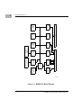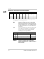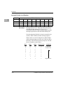
1
MVME1X7P Single-Board Computer
Programmer’s Reference
Guide
V1X7PA/PG1
Edition of October 2000
© Copyright 2000 Motorola, Inc.
All rights reserved.
Printed in the United States of America.
Motorola® and the Motorola logo are registered trademarks of Motorola, Inc.
MC68040™ and MC68060™ are trademarks of Motorola, Inc.
All other products mentioned in this document are trademarks or registered trademarks of
their respective holders.
Safety Summary
The following general safety precautions must be observed during all phases of operation, service, and repair of this
equipment. Failure to comply with these precautions or with specific warnings elsewhere in this manual could result
in personal injury or damage to the equipment.
The safety precautions listed below represent warnings of certain dangers of which Motorola is aware. You, as the user
of the product, should follow these warnings and all other safety precautions necessary for the safe operation of the
equipment in your operating environment.
Ground the Instrument.
To minimize shock hazard, the equipment chassis and enclosure must be connected to an electrical ground. If the
equipment is supplied with a three-conductor AC power cable, the power cable must be plugged into an approved
three-contact electrical outlet, with the grounding wire (green/yellow) reliably connected to an electrical ground
(safety ground) at the power outlet. The power jack and mating plug of the power cable meet International
Electrotechnical Commission (IEC) safety standards and local electrical regulatory codes.
Do Not Operate in an Explosive Atmosphere.
Do not operate the equipment in any explosive atmosphere such as in the presence of flammable gases or fumes.
Operation of any electrical equipment in such an environment could result in an explosion and cause injury or damage.
Keep Away From Live Circuits Inside the Equipment.
Operating personnel must not remove equipment covers. Only Factory Authorized Service Personnel or other
qualified service personnel may remove equipment covers for internal subassembly or component replacement or any
internal adjustment. Service personnel should not replace components with power cable connected. Under certain
conditions, dangerous voltages may exist even with the power cable removed. To avoid injuries, such personnel should
always disconnect power and discharge circuits before touching components.
Use Caution When Exposing or Handling a CRT.
Breakage of a Cathode-Ray Tube (CRT) causes a high-velocity scattering of glass fragments (implosion). To prevent
CRT implosion, do not handle the CRT and avoid rough handling or jarring of the equipment. Handling of a CRT
should be done only by qualified service personnel using approved safety mask and gloves.
Do Not Substitute Parts or Modify Equipment.
Do not install substitute parts or perform any unauthorized modification of the equipment. Contact your local
Motorola representative for service and repair to ensure that all safety features are maintained.
Observe Warnings in Manual.
Warnings, such as the example below, precede potentially dangerous procedures throughout this manual. Instructions
contained in the warnings must be followed. You should also employ all other safety precautions which you deem
necessary for the operation of the equipment in your operating environment.
Warning
To prevent serious injury or death from dangerous voltages, use extreme
caution when handling, testing, and adjusting this equipment and its
components.
Flammability
All Motorola PWBs (printed wiring boards) are manufactured with a flammability rating
of 94V-0 by UL-recognized manufacturers.
EMI Caution
!
Caution
This equipment generates, uses and can radiate electromagnetic energy. It
may cause or be susceptible to electromagnetic interference (EMI) if not
installed and used with adequate EMI protection.
Lithium Battery Caution
This product contains a lithium battery to power the clock and calendar circuitry.
!
Caution
!
Attention
!
Vorsicht
Danger of explosion if battery is replaced incorrectly. Replace battery only
with the same or equivalent type recommended by the equipment
manufacturer. Dispose of used batteries according to the manufacturer’s
instructions.
Il y a danger d’explosion s’il y a remplacement incorrect de la batterie.
Remplacer uniquement avec une batterie du même type ou d’un type
équivalent recommandé par le constructeur. Mettre au rebut les batteries
usagées conformément aux instructions du fabricant.
Explosionsgefahr bei unsachgemäßem Austausch der Batterie. Ersatz nur
durch denselben oder einen vom Hersteller empfohlenen Typ. Entsorgung
gebrauchter Batterien nach Angaben des Herstellers.
CE Notice (European Community)
Motorola Computer Group products with the CE marking comply with the EMC Directive
(89/336/EEC). Compliance with this directive implies conformity to the following
European Norms:
EN55022 “Limits and Methods of Measurement of Radio Interference Characteristics
of Information Technology Equipment”; this product tested to Equipment Class B
EN50082-1:1997 “Electromagnetic Compatibility—Generic Immunity Standard, Part
1. Residential, Commercial and Light Industry”
System products also fulfill EN60950 (product safety) which is essentially the requirement
for the Low Voltage Directive (73/23/EEC).
Board products are tested in a representative system to show compliance with the above
mentioned requirements. A proper installation in a CE-marked system will maintain the
required EMC/safety performance.
In accordance with European Community directives, a “Declaration of Conformity” has
been made and is on file within the European Union. The “Declaration of Conformity” is
available on request. Please contact your sales representative.
Notice
While reasonable efforts have been made to assure the accuracy of this document,
Motorola, Inc. assumes no liability resulting from any omissions in this document, or from
the use of the information obtained therein. Motorola reserves the right to revise this
document and to make changes from time to time in the content hereof without obligation
of Motorola to notify any person of such revision or changes.
Electronic versions of this material may be read online, downloaded for personal use, or
referenced in another document as a URL to the Motorola Computer Group website. The
text itself may not be published commercially in print or electronic form, edited, translated,
or otherwise altered without the permission of Motorola, Inc.
It is possible that this publication may contain reference to or information about Motorola
products (machines and programs), programming, or services that are not available in your
country. Such references or information must not be construed to mean that Motorola
intends to announce such Motorola products, programming, or services in your country.
Limited and Restricted Rights Legend
If the documentation contained herein is supplied, directly or indirectly, to the U.S.
Government, the following notice shall apply unless otherwise agreed to in writing by
Motorola, Inc.
Use, duplication, or disclosure by the Government is subject to restrictions as set forth in
subparagraph (b)(3) of the Rights in Technical Data clause at DFARS 252.227-7013 (Nov.
1995) and of the Rights in Noncommercial Computer Software and Documentation clause
at DFARS 252.227-7014 (Jun. 1995).
Motorola, Inc.
Computer Group
2900 South Diablo Way
Tempe, Arizona 85282
Contents
About This Manual
Overview of Contents ...............................................................................................xxii
Comments and Suggestions ......................................................................................xxii
Conventions Used in This Manual...........................................................................xxiii
CHAPTER 1
Programming Issues
Introduction................................................................................................................1-1
The Petra ASIC and Second-Generation MVME1X7 Boards............................1-1
Features...............................................................................................................1-3
Applicable Industry Standards............................................................................1-4
Block Diagram ....................................................................................................1-4
Programming Interfaces.............................................................................................1-7
MC680X0 MPU..................................................................................................1-7
Data Bus Structure ..............................................................................................1-7
EEPROMs on the MVME1X7P .........................................................................1-8
MVME167...................................................................................................1-8
MVME177...................................................................................................1-9
Flash Memory on the MVME177.......................................................................1-9
SRAM ...............................................................................................................1-10
Onboard SDRAM .............................................................................................1-11
Battery-Backed-Up RAM and Clock................................................................1-12
VMEbus Interface.............................................................................................1-12
I/O Interfaces ....................................................................................................1-12
Serial Port Interface ...................................................................................1-13
Parallel (Printer) Interface .........................................................................1-14
Ethernet Interface ......................................................................................1-15
SCSI Interface............................................................................................1-16
Local Resources................................................................................................1-16
Programmable Tick Timers .......................................................................1-16
Watchdog Timer ........................................................................................1-17
Software-Programmable Hardware Interrupts...........................................1-17
Local Bus Timeout ....................................................................................1-17
vii
Functional Description ............................................................................................ 1-17
VMEbus Interface and VMEchip2................................................................... 1-18
VMEchip2 General-Purpose I/O............................................................... 1-18
Petra/VMEchip2 Redundant Logic ........................................................... 1-18
Memory Maps.......................................................................................................... 1-20
Local Bus Memory Map................................................................................... 1-20
Normal Address Range ............................................................................. 1-20
Detailed I/O Memory Maps ...................................................................... 1-25
BBRAM/TOD Clock Memory Map ......................................................... 1-41
Interrupt Acknowledge Map ..................................................................... 1-46
VMEbus Memory Map .................................................................................... 1-46
VMEbus Accesses to the Local Bus ......................................................... 1-46
VMEbus Short I/O Memory Map ............................................................. 1-46
Interrupt Handling ................................................................................................... 1-47
Example: VMEchip2 Tick Timer 1 Periodic Interrupt..................................... 1-47
Cache Coherency (MVME167P)............................................................................. 1-49
Cache Coherency (MVME177P)............................................................................. 1-50
Using Bus Timers .................................................................................................... 1-51
Indivisible Cycles .................................................................................................... 1-52
Supervisor Stack Pointer (MC68060)...................................................................... 1-53
Sources of Local Bus Errors .................................................................................... 1-54
Local Bus Timeout ........................................................................................... 1-54
VMEbus Access Timeout................................................................................. 1-54
VMEbus BERR* .............................................................................................. 1-54
VMEchip2 ........................................................................................................ 1-55
Bus Error Processing ........................................................................................ 1-55
Error Conditions ...................................................................................................... 1-55
MPU Parity Error ............................................................................................. 1-56
MPU Offboard Error ........................................................................................ 1-56
MPU TEA - Cause Unidentified ...................................................................... 1-56
MPU Local Bus Time-out ................................................................................ 1-57
DMAC VMEbus Error ..................................................................................... 1-57
DMAC Parity Error .......................................................................................... 1-57
DMAC Offboard Error ..................................................................................... 1-58
DMAC LTO Error ............................................................................................ 1-58
DMAC TEA - Cause Unidentified ................................................................... 1-59
SCC Retry Error ............................................................................................... 1-59
SCC Parity Error .............................................................................................. 1-60
SCC Offboard Error ......................................................................................... 1-60
SCC LTO Error................................................................................................. 1-61
LAN Parity Error.............................................................................................. 1-61
viii
LAN Offboard Error .........................................................................................1-61
LAN LTO Error ................................................................................................1-62
SCSI Parity Error ..............................................................................................1-62
SCSI Offboard Error .........................................................................................1-62
SCSI LTO Error ................................................................................................1-63
CHAPTER 2
VMEchip2
Introduction................................................................................................................2-1
Functional Blocks ......................................................................................................2-4
Local-Bus-to-VMEbus Interface ........................................................................2-4
Local-Bus-to-VMEbus Requester ...............................................................2-7
VMEbus-to-Local-Bus Interface ........................................................................2-9
Local-Bus-to-VMEbus DMA Controller..........................................................2-10
No-Address-Increment DMA Transfers ....................................................2-12
DMAC VMEbus Requester.......................................................................2-13
Tick and Watchdog Timers ...............................................................................2-14
Prescaler.....................................................................................................2-14
Tick Timers................................................................................................2-15
Watchdog Timer ........................................................................................2-15
VMEbus Interrupter..........................................................................................2-16
VMEbus System Controller..............................................................................2-17
Arbiter........................................................................................................2-17
IACK Daisy-Chain Driver.........................................................................2-17
Bus Timer ..................................................................................................2-17
Reset Driver ...............................................................................................2-18
Local Bus Interrupter and Interrupt Handler ....................................................2-18
Global Control and Status Registers.................................................................2-20
LCSR Programming Model .....................................................................................2-20
Programming the VMEbus Slave Map Decoders.............................................2-26
VMEbus Slave Ending Address Register 1 ..............................................2-28
VMEbus Slave Starting Address Register 1 .............................................2-28
VMEbus Slave Ending Address Register 2 ..............................................2-29
VMEbus Slave Starting Address Register 2 .............................................2-29
VMEbus Slave Address Translation Address Offset Register 1 ..............2-29
VMEbus Slave Address Translation Select Register 1 ............................2-30
VMEbus Slave Address Translation Address Offset Register 2 ...............2-31
VMEbus Slave Address Translation Select Register 2 ............................2-31
VMEbus Slave Write Post and Snoop Control Register 2 ........................2-32
VMEbus Slave Address Modifier Select Register 2 .................................2-33
VMEbus Slave Write Post and Snoop Control Register 1 ........................2-35
ix
VMEbus Slave Address Modifier Select Register 1 ................................. 2-36
Programming the Local-Bus-to-VMEbus Map Decoders................................ 2-37
Local Bus Slave (VMEbus Master) Ending Address Register 1 .............. 2-39
Local Bus Slave (VMEbus Master) Starting Address Register 1 ............. 2-40
Local Bus Slave (VMEbus Master) Ending Address Register 2 .............. 2-40
Local Bus Slave (VMEbus Master) Starting Address Register 2 ............. 2-40
Local Bus Slave (VMEbus Master) Ending Address Register 3 ............. 2-41
Local Bus Slave (VMEbus Master) Starting Address Register 3 ............ 2-41
Local Bus Slave (VMEbus Master) Ending Address Register 4 ............. 2-41
Local Bus Slave (VMEbus Master) Starting Address Register 4 ............ 2-42
Local Bus Slave (VMEbus Master)
Address Translation Address Register 4 .......................................... 2-42
Local Bus Slave (VMEbus Master)
Address Translation Select Register 4 ............................................. 2-42
Local Bus Slave (VMEbus Master) Attribute Register 4 ......................... 2-43
Local Bus Slave (VMEbus Master) Attribute Register 3 ......................... 2-44
Local Bus Slave (VMEbus Master) Attribute Register 2 ......................... 2-45
Local Bus Slave (VMEbus Master) Attribute Register 1 ......................... 2-46
VMEbus Slave GCSR Group Address Register ...................................... 2-47
VMEbus Slave GCSR Board Address Register ....................................... 2-48
Local-Bus-to-VMEbus Enable Control Register ..................................... 2-49
Local-Bus-to-VMEbus I/O Control Register ........................................... 2-50
ROM Control Register ............................................................................. 2-51
Programming the VMEchip2 DMA Controller................................................ 2-51
DMAC Registers .............................................................................................. 2-53
EPROM Decoder, SRAM and DMA Control Register ........................... 2-53
Local-Bus-to-VMEbus Requester Control Register ................................ 2-54
DMAC Control Register 1 (bits 0-7) ....................................................... 2-55
DMAC Control Register 2 (bits 8-15) ..................................................... 2-57
DMAC Control Register 2 (bits 0-7) ....................................................... 2-58
DMAC Local Bus Address Counter ......................................................... 2-59
DMAC VMEbus Address Counter .......................................................... 2-60
DMAC Byte Counter ............................................................................... 2-60
Table Address Counter ............................................................................. 2-60
VMEbus Interrupter Control Register ...................................................... 2-61
VMEbus Interrupter Vector Register ....................................................... 2-62
MPU Status and DMA Interrupt Count Register ..................................... 2-62
DMAC Status Register ............................................................................. 2-63
Programming the Tick and Watchdog Timers.................................................. 2-64
VMEbus Arbiter Time-Out Control Register .......................................... 2-64
DMAC Ton/Toff Timers and VMEbus
Global Time-out Control Register..................................................... 2-65
x
VME Access, Local Bus, and Watchdog Time-out Control Register ......2-66
Prescaler Control Register ........................................................................2-67
Tick Timer 1 Compare Register ...............................................................2-68
Tick Timer 1 Counter ...............................................................................2-68
Tick Timer 2 Compare Register ...............................................................2-69
Tick Timer 2 Counter ...............................................................................2-69
Board Control Register .............................................................................2-70
Watchdog Timer Control Register ...........................................................2-71
Tick Timer 2 Control Register ..................................................................2-72
Tick Timer 1 Control Register ..................................................................2-73
Prescaler Counter ......................................................................................2-73
Programming the Local Bus Interrupter ...........................................................2-74
Local Bus Interrupter Status Register (bits 24-31) ...................................2-77
Local Bus Interrupter Status Register (bits 16-23) ...................................2-78
Local Bus Interrupter Status Register (bits 8-15) .....................................2-79
Local Bus Interrupter Status Register (bits 0-7) .......................................2-80
Local Bus Interrupter Enable Register (bits 24-31) ..................................2-81
Local Bus Interrupter Enable Register (bits 16-23) ..................................2-82
Local Bus Interrupter Enable Register (bits 8-15) ....................................2-83
Local Bus Interrupter Enable Register (bits 0-7) ......................................2-84
Software Interrupt Set Register (bits 8-15) ...............................................2-85
Interrupt Clear Register (bits 24-31) ........................................................2-85
Interrupt Clear Register (bits 16-23) ........................................................2-86
Interrupt Clear Register (bits 8-15) ..........................................................2-87
Interrupt Level Register 1 (bits 24-31) .....................................................2-87
Interrupt Level Register 1 (bits 16-23) .....................................................2-88
Interrupt Level Register 1 (bits 8-15) .......................................................2-88
Interrupt Level Register 1 (bits 0-7) .........................................................2-89
Interrupt Level Register 2 (bits 24-31) .....................................................2-89
Interrupt Level Register 2 (bits 16-23) .....................................................2-90
Interrupt Level Register 2 (bits 8-15) .......................................................2-90
Interrupt Level Register 2 (bits 0-7) .........................................................2-91
Interrupt Level Register 3 (bits 24-31) .....................................................2-91
Interrupt Level Register 3 (bits 16-23) .....................................................2-92
Interrupt Level Register 3 (bits 8-15) .......................................................2-92
Interrupt Level Register 3 (bits 0-7) .........................................................2-93
Interrupt Level Register 4 (bits 24-31) .....................................................2-93
Interrupt Level Register 4 (bits 16-23) .....................................................2-94
Interrupt Level Register 4 (bits 8-15) .......................................................2-94
Interrupt Level Register 4 (bits 0-7) .........................................................2-95
Vector Base Register ................................................................................2-95
I/O Control Register 1 ..............................................................................2-96
xi
I/O Control Register 2 .............................................................................. 2-97
I/O Control Register 3 .............................................................................. 2-97
Miscellaneous Control Register ............................................................... 2-98
GCSR Programming Model .................................................................................. 2-100
Programming the GCSR................................................................................. 2-102
VMEchip2 Revision Register ................................................................ 2-103
VMEchip2 ID Register ........................................................................... 2-104
VMEchip2 LM/SIG Register ................................................................. 2-104
VMEchip2 Board Status/Control Register ............................................. 2-106
General Purpose Register 0 .................................................................... 2-107
General Purpose Register 1 .................................................................... 2-107
General Purpose Register 2 .................................................................... 2-107
General Purpose Register 3 .................................................................... 2-108
General Purpose Register 4 .................................................................... 2-108
General Purpose Register 5 .................................................................... 2-108
CHAPTER 3
PCCchip2
Introduction ............................................................................................................... 3-1
Summary of Major Features............................................................................... 3-1
Functional Description .............................................................................................. 3-2
General Description............................................................................................ 3-2
BBRAM Interface .............................................................................................. 3-3
82596CA LAN Controller Interface................................................................... 3-3
MPU Port and MPU Channel Attention...................................................... 3-3
MC68040-Bus Master Support for 82596CA ............................................. 3-4
LANC Bus Error ......................................................................................... 3-4
LANC Interrupt ........................................................................................... 3-5
53C710 SCSI Controller Interface ..................................................................... 3-6
Parallel Port Interface ......................................................................................... 3-6
General Purpose I/O Pin..................................................................................... 3-7
CD2401 SCC Interface....................................................................................... 3-7
Tick Timer .......................................................................................................... 3-9
Overall Memory Map .............................................................................................. 3-10
Programming Model................................................................................................ 3-11
Chip ID Register............................................................................................... 3-14
Chip Revision Register..................................................................................... 3-14
General Control Register.................................................................................. 3-15
Vector Base Register ........................................................................................ 3-16
xii
Programming the Tick Timers ..........................................................................3-18
Tick Timer 1 Compare Register ................................................................3-18
Tick Timer 1 Counter ................................................................................3-19
Tick Timer 2 Compare Register ................................................................3-19
Tick Timer 2 Counter ................................................................................3-20
Prescaler Count Register ...........................................................................3-20
Prescaler Clock Adjust Register ................................................................3-20
Tick Timer 2 Control Register...................................................................3-22
Tick Timer 1 Control Register...................................................................3-23
General Purpose Input Interrupt Control Register.....................................3-24
General Purpose Input/Output Pin Control Register .................................3-25
Tick Timer 2 Interrupt Control Register....................................................3-25
Tick Timer 1 Interrupt Control Register....................................................3-26
SCC Error Status and Interrupt Control Registers............................................3-27
SCC Error Status Register .........................................................................3-27
SCC Modem Interrupt Control Register....................................................3-28
SCC Transmit Interrupt Control Register..................................................3-29
SCC Receive Interrupt Control Register ...................................................3-30
Modem PIACK Register ...........................................................................3-31
Transmit PIACK Register .........................................................................3-32
Receive PIACK Register ...........................................................................3-33
LANC Error Status and Interrupt Control Registers ........................................3-34
LANC Error Status Register......................................................................3-34
82596CA LANC Interrupt Control Register .............................................3-35
LANC Bus Error Interrupt Control Register .............................................3-36
Programming the SCSI Error Status and Interrupt Registers ...........................3-37
SCSI Error Status Register ........................................................................3-37
SCSI Interrupt Control Register ................................................................3-38
Programming the Printer Port ...........................................................................3-39
Printer ACK Interrupt Control Register ....................................................3-39
Printer FAULT Interrupt Control Register................................................3-40
Printer SEL Interrupt Control Register......................................................3-41
Printer PE Interrupt Control Register ........................................................3-42
Printer BUSY Interrupt Control Register ..................................................3-43
Printer Input Status Register......................................................................3-44
Printer Port Control Register .....................................................................3-45
Chip Speed Register ..................................................................................3-46
Printer Data Register .................................................................................3-47
Interrupt Priority Level Register................................................................3-48
Interrupt Mask Level Register...................................................................3-49
xiii
CHAPTER 4
MCECC Functions
Introduction ............................................................................................................... 4-1
Features...................................................................................................................... 4 -2
Functional Description .............................................................................................. 4-3
General Description............................................................................................ 4-3
Performance........................................................................................................ 4-3
Cache Coherency................................................................................................ 4-4
ECC .................................................................................................................... 4-5
Cycle Types................................................................................................. 4-5
Error Reporting ........................................................................................... 4-5
Single Bit Error (Cycle Type = Burst Read or Non-Burst Read) ............... 4-5
Double Bit Error (Cycle Type = Burst Read or Non-Burst Read) .............. 4-6
Triple (or Greater) Bit Error
(Cycle Type = Burst Read or Non-Burst Read) .................................. 4-6
Cycle Type = Burst Write ........................................................................... 4-6
Single Bit Error (Cycle Type = Non-Burst Write)...................................... 4-6
Double Bit Error (Cycle Type = Non-Burst Write) .................................... 4-6
Triple (or Greater) Bit Error (Cycle Type = Non-Burst Write) .................. 4-7
Single Bit Error (Cycle Type = Scrub) ....................................................... 4-7
Double Bit Error (Cycle Type = Scrub) ...................................................... 4-7
Triple (or Greater) Bit Error (Cycle Type = Scrub) .................................... 4-7
Error Logging ..................................................................................................... 4-8
Scrub................................................................................................................... 4-8
Refresh................................................................................................................ 4-8
Arbitration .......................................................................................................... 4-9
Chip Defaults...................................................................................................... 4-9
Programming Model................................................................................................ 4-10
Chip ID Register............................................................................................... 4-13
Chip Revision Register..................................................................................... 4-13
Memory Configuration Register ...................................................................... 4-14
Base Address Register...................................................................................... 4-15
DRAM Control Register .................................................................................. 4-15
BCLK Frequency Register ............................................................................... 4-16
Data Control Register ....................................................................................... 4-17
Scrub Control Register ..................................................................................... 4-19
Scrub Period Register Bits 15-8 ....................................................................... 4-20
Scrub Period Register Bits 7-0 ......................................................................... 4-20
Chip Prescaler Counter..................................................................................... 4-21
Scrub Time On/Time Off Register ................................................................... 4-21
Scrub Prescaler Counter (Bits 21-16)............................................................... 4-23
Scrub Prescaler Counter (Bits 15-8)................................................................. 4-23
xiv
Scrub Prescaler Counter (Bits 7-0) ...................................................................4-24
Scrub Timer Counter (Bits 15-8) ......................................................................4-24
Scrub Timer Counter (Bits 7-0) ........................................................................4-25
Scrub Address Counter (Bits 26-24).................................................................4-25
Scrub Address Counter (Bits 23-16).................................................................4-26
Scrub Address Counter (Bits 15-8)...................................................................4-26
Scrub Address Counter (Bits 7-4).....................................................................4-26
Error Logger Register .......................................................................................4-27
Error Address (Bits 31-24) ...............................................................................4-28
Error Address (Bits 23-16) ...............................................................................4-28
Error Address (Bits 15-8) .................................................................................4-29
Error Address (Bits 7-4) ...................................................................................4-29
Error Syndrome Register ..................................................................................4-30
Defaults Register 1............................................................................................4-30
Defaults Register 2............................................................................................4-32
SDRAM Configuration Register .....................................................................4-33
Initialization ......................................................................................................4-34
Syndrome Decoding.................................................................................................4-36
APPENDIX A
Summary of Changes
Introduction...............................................................................................................A-1
APPENDIX B
Printer and Serial Port Connections
Introduction............................................................................................................... B-1
Connection Diagrams................................................................................................ B-1
APPENDIX C
Related Documentation
MCG Documents ...................................................................................................... C-1
Manufacturers’ Documents....................................................................................... C-2
Related Specifications............................................................................................... C-3
xv
xvi
List of Figures
Figure 1-1. MVME167P Block Diagram...................................................................1-5
Figure 1-2. MVME177P Block Diagram...................................................................1-6
Figure 1-3. MVME177 Flash and EPROM Memory Mapping Schemes................1-10
Figure 2-1. VMEchip2 Block Diagram .....................................................................2-5
Figure 3-1. PCCchip2 Block Diagram.......................................................................3-2
Figure B-1. MVME1X7P Printer Port with MVME712M ...................................... B-2
Figure B-2. MVME1X7P Serial Port 1 Configured as DCE ................................... B-3
Figure B-3. MVME1X7P Serial Port 2 Configured as DCE ................................... B-4
Figure B-4. MVME1X7P Serial Port 3 Configured as DCE ................................... B-5
Figure B-5. MVME1X7P Serial Port 4 Configured as DCE ................................... B-6
Figure B-6. MVME1X7P Serial Port 1 Configured as DTE ................................... B-7
Figure B-7. MVME1X7P Serial Port 2 Configured as DTE ................................... B-8
Figure B-8. MVME1X7P Serial Port 3 Configured as DTE ................................... B-9
Figure B-9. MVME1X7P Serial Port 4 Configured as DTE ................................. B-10
xvii
xviii
List of Tables
Table 1-1. MVME1X7P Features Summary ..............................................................1-3
Table 1-2. Functions Duplicated in VMEchip2 and Petra ASICs............................1-19
Table 1-3. Local Bus Memory Map .........................................................................1-21
Table 1-4. Local I/O Devices Memory Map ............................................................1-22
Table 1-5. VMEchip2 Memory Map (Sheet 1 of 3).................................................1-26
Table 1-6. Printer Memory Map ..............................................................................1-31
Table 1-7. PCCchip2 Memory Map.........................................................................1-32
Table 1-8. MCECC Internal Register Memory Map................................................1-34
Table 1-9. Cirrus Logic CD2401 Serial Port Memory Map ....................................1-36
Table 1-10. 82596CA Ethernet LAN Memory Map ................................................1-40
Table 1-11. 53C710 SCSI Memory Map..................................................................1-41
Table 1-12. M48T58 BBRAM,TOD Clock Memory Map ......................................1-42
Table 1-13. BBRAM Configuration Area Memory Map.........................................1-42
Table 1-14. TOD Clock Memory Map.....................................................................1-43
Table 1-15. Single-Cycle Instructions......................................................................1-52
Table 2-1. Features of the VMEchip2 ASIC..............................................................2-1
Table 2-2. VMEchip2 Memory Map—LCSR Summary (Sheet 1 of 2) ..................2-22
Table 2-3. DMAC Command Packet Format...........................................................2-53
Table 2-4. Local Bus Interrupter Summary .............................................................2-75
Table 2-5. VMEchip2 Memory Map (GCSR Summary) .......................................2-103
Table 3-1. PCCchip2 Devices Memory Map ...........................................................3-10
Table 3-2. PCCchip2 Memory Map - Control and Status Registers........................3-12
Table 4-1. MCECC Functions on the Petra ASIC .....................................................4-2
Table 4-2. Memory System Cycle Timing .................................................................4-4
Table 4-3. MCECC Sector Internal Register Memory Map ....................................4-11
Table 4-4. Syndrome Bit Encoding..........................................................................4-36
Table 4-5. Identifying SDRAM Bank in Error ........................................................4-37
Table A-1. List of Changes ......................................................................................A-1
Table C-1. Motorola Computer Group Documents ................................................. C-1
Table C-2. Manufacturers’ Documents .................................................................... C-2
Table C-3. Related Specifications ............................................................................ C-3
xix
xx
About This Manual
This manual provides board-level information and detailed ASIC
information, including register bit descriptions, for the MVME167PAxxSE and MVME177PA-xxSE series of VME single-board computers,
known collectively as the ‘‘MVME1X7P’’.
The “Petra” chip that distinguishes MVME167P and MVME177P singleboard computers is an application-specific integrated circuit (ASIC) used
on various Motorola VME boards which combines a variety of functions
previously implemented in other ASICs (among them the MC2 chip, the
IP2 chip, and the MCECC chip) in a single ASIC. On the MVME1X7P,
the “Petra” chip replaces the MCECC ASIC. As of the publication date, the
information presented in this manual applies to the following
MVME1X7P models:
Model Number
Characteristics
MVME167PA-24SE
25MHz MC68040, 16MB SDRAM, SCSI and Ethernet
MVME167PA-25SE
25MHz MC68040, 32MB SDRAM, SCSI and Ethernet
MVME167PA-34SE
33MHz MC68040, 16MB SDRAM, SCSI and Ethernet
MVME167PA-35SE
33MHz MC68040, 32MB SDRAM, SCSI and Ethernet
MVME167PA-36SE
33MHz MC68040, 64MB SDRAM, SCSI and Ethernet
MVME177PA-54SE
50MHz MC68060, 16MB SDRAM, SCSI and Ethernet
MVME177PA-55SE
50MHz MC68060, 32MB SDRAM, SCSI and Ethernet
MVME177PA-56SE
50MHz MC68060, 64MB SDRAM, SCSI and Ethernet
MVME177PA-64SE
60MHz MC68060, 16MB SDRAM, SCSI and Ethernet
MVME177PA-65SE
60MHz MC68060, 32MB SDRAM, SCSI and Ethernet
MVME177PA-66SE
60MHz MC68060, 64MB SDRAM, SCSI and Ethernet
MVME177PA-67SE
60MHz MC68060, 128MB SDRAM, SCSI and Ethernet
This manual is intended for anyone who designs OEM systems, adds
capability to an existing compatible system, or works in a lab environment
for experimental purposes. A basic knowledge of computers and digital
logic is assumed. To use this manual, you may also wish to become
familiar with the publications listed in Appendix C, Related
Documentation.
xxi
Overview of Contents
Chapter 1, Programming Issues, describes the board-level hardware
features of MVME1X7P single-board computers. It includes memory
maps and a discussion of some general software considerations such as
cache coherency, interrupts, and bus errors.
Chapter 2, VMEchip2, describes the VMEchip2 ASIC, the local
bus/VMEbus interface chip on MVME1X7P boards.
Chapter 3, PCCchip2, describes the PCCchip2 ASIC. The PCChip2 is a
peripheral channel controller designed to interface an MC680x0compatible local bus to various on-board peripheral devices such as SCSI
and LAN controllers.
Chapter 4, MCECC Functions, describes the ECC DRAM controller ASIC
(MCECC). On the MVME1X7P boards, it supplies the interface to a 144bit wide DRAM memory system.
Appendix A, Summary of Changes, lists the modifications that
accompanied the introduction of the Petra ASIC on the MVME167P and
MVME177P.
Appendix B, Printer and Serial Port Connections, contains drawings of
the printer and serial port interface connections available with the
MVME167P/MVME177P and MVME712 series transition board.
Appendix C, Related Documentation, lists all documentation related to the
MVME167P and MVME177P.
Comments and Suggestions
Motorola welcomes and appreciates your comments on its documentation.
We want to know what you think about our manuals and how we can make
them better. Mail comments to:
Motorola Computer Group
Reader Comments DW164
2900 S. Diablo Way
Tempe, Arizona 85282
xxii
You can also submit comments to the following e-mail address:
[email protected]
In all your correspondence, please list your name, position, and company.
Be sure to include the title and part number of the manual and tell how you
used it. Then tell us your feelings about its strengths and weaknesses and
any recommendations for improvements.
Conventions Used in This Manual
The following typographical conventions are used in this document:
$
dollar
specifies a hexadecimal number
%
percent
specifies a binary number
&
ampersand
specifies a decimal number
Unless otherwise specified, all address references are in hexadecimal.
An asterisk (*) following the signal name for signals which are level
significant denotes that the signal is true or valid when the signal is low.
An asterisk (*) following the signal name for signals which are edge
significant denotes that the actions initiated by that signal occur on high to
low transition.
xxiii
bold
is used for user input that you type just as it appears; it is also used for
commands, options and arguments to commands, and names of
programs, directories and files.
italic
is used for names of variables to which you assign values. Italic is also
used for comments in screen displays and examples, and to introduce
new terms.
courier
is used for system output (for example, screen displays, reports),
examples, and system prompts.
<Enter>, <Return> or <CR>
<CR> represents the carriage return or Enter key.
CTRL
represents the Control key. Execute control characters by pressing the
Ctrl key and the letter simultaneously, for example, Ctrl-d.
In this manual, assertion and negation are used to specify forcing a signal
to a particular state. In particular, assertion and assert refer to a signal that
is active or true; negation and negate indicate a signal that is inactive or
false. These terms are used independently of the voltage level (high or low)
that they represent.
Data and address sizes are defined as follows:
xxiv
❏
A byte is eight bits, numbered 0 through 7, with bit 0 being the least
significant.
❏
A word is 16 bits, numbered 0 through 15, with bit 0 being the least
significant.
❏
A longword is 32 bits, numbered 0 through 31, with bit 0 being the
least significant.
The terms control bit, status bit, true, and false are used extensively in this
document. The term control bit is used to describe a bit in a register that
can be set and cleared under software control. The term true is used to
indicate that a bit is in the state that enables the function it controls. The
term false is used to indicate that the bit is in the state that disables the
function it controls. In all tables, the terms 0 and 1 are used to describe the
actual value that should be written to the bit, or the value that it yields when
read. The term status bit is used to describe a bit in a register that reflects
a specific condition. The status bit can be read by software to determine
operational or exception conditions.
xxv
xxvi
1Programming Issues
1
Introduction
The MVME167P and MVME177P single-board computers are complex
boards that interface both to the VMEbus and the SCSI bus. From a
programming standpoint, their multiple-bus interfaces raise issues of
cache coherency and support of indivisible cycles. There are also various
potential sources of bus error.
This chapter discusses those topics in addition to interrupt handling, the
use of bus timers, and the programming interface to each device on the
board. Programmable registers that reside in ASICs (Application-Specific
Integrated Circuits) on the MVME1X7P boards are covered in the chapters
devoted to those devices.
Note
The MVME1X7P’s new ’‘Petra’’ ASIC performs the functions
previously implemented in the MCECC chip. For ease of use in
conjunction with programming models and documentation
developed for earlier boards, however, the structure of this
manual preserves the functional distinctions that formerly
characterized the MCECC ASIC.
The Petra ASIC and Second-Generation MVME1X7 Boards
Due to rapid changes in technology, the production of certain ASICs used
on various Motorola first- and second-generation VME embedded
controllers and single-board computers has ended. The Petra chip was
developed to replace these discontinued ASICs. In the case of
MVME167/177 series boards, the discontinued ASIC is the MCECC chip.
The Petra chip now supplies the functions formerly implemented in the
MCECC chip.
1-1
1
Programming Issues
The Petra ASIC is functionally compatible with each of the components
that it replaces. In cases where functionality between ASICs is exclusive,
configuration switches or jumpers are provided to let you select the
desired functionality.
In several areas of functionality, the configuration switches provide
backward compatibility with earlier MVME167/177 implementations, but
you can override their settings in software if you wish. A “R/W” by the
corresponding register table entry in this manual denotes instances where
this override capability is present.
Where the older technology supported “fast page” or “EDO” DRAM
chips, the Petra memory controllers support SDRAM devices. The two
memory controllers modeled in Petra duplicate the functionality of the
“parity” memory controller found in the MC ASICs used on certain other
boards as well as that of the “single-bit error correcting/double-bit error
detecting” memory controller found in the MCECC ASICs used on the
MVME167/177.
This Programmer’s Reference Guide describes the MCECC model (in
Chapter 4). In the MVME167/177 application, there is logic on the Petra
chip to prevent you from inadvertently enabling the MC memory controller
model.
The same SDRAM memory array serves both controller models. The
SDRAM array is 32 data bits wide with 7 checkbits. The array architecture
is a non-interleaved single bank for sizes below 32MB. For array sizes
above 32MB, additional physical memory banks are added but the
architecture remains non-interleaved.
A final note on the SDRAM implementation: The bandwidth between the
SDRAM and local bus is greater than it was with the earlier DRAM array.
As a result, software takes less time to execute. Applications that
incorporate elapsed-time functions which are dependent on code
execution may have problems.
For readers who need to know the ASIC-specific differences between the
previous MCECC and Petra/MCECC programming models in detail,
certain areas of the text in this manual are printed in italics and marked
with change bars (as is done here). Readers should compare those sections
to the corresponding sections of the first- and second-generation manuals.
1-2
Computer Group Literature Center Web Site
Introduction
Features
The “Petra” ASIC supplants the MCECC memory controller ASIC on
MVME1X7P boards, performing the memory control functions previously
carried out by the MCECC chip: It supplies the programmable interface for
the ECC-protected 16/32/64/128MB DRAM emulation.
The following table summarizes the features of the MVME167P and
MVME177P single-board computers.
Table 1-1. MVME1X7P Features Summary
Feature
MVME167P
MVME177P
Processor
25/33MHz 32-bit MC68040
microprocessor
50/60MHz 32-bit MC68060
microprocessor
DRAM
16/32/64/128MB synchronous DRAM (SDRAM). Configurable to emulate
4/8/16/32/64/128MB ECC-protected DRAM
MVME1X7P boards use SDRAM (Synchronous DRAM) in place of DRAM.
Up to 64MB SDRAM is available on MVME167P boards; up to 128MB is
available on MVME177P boards.
SRAM
128KB SRAM with battery backup
EPROM
Four 44-pin JEDEC standard PLCC
EPROM sockets
Two 44-pin JEDEC standard PLCC
EPROM sockets
Flash
Not available
Four Intel 28F008SA Flash memory
devices with optional write protection
NVRAM and
RTC
8K by 8 Non-Volatile RAM (NVRAM) and Real-Time Clock (RTC) with
battery backup and watchdog function (SGS-Thomson M48T58)
Timers
Four 32-bit tick timers and watchdog timer in Petra ASIC
Two 32-bit tick timers and watchdog timer in VMEchip2 ASIC
Software
Interrupts
Eight software interrupts (including those in the VMEchip2 ASIC)
I/O
Four EIA-232-D configurable serial ports via P2 and transition module
Parallel (printer) interface via P2 and transition module
SCSI interface with DMA via P2 or LCP2 adapter board
Ethernet transceiver interface via DB15 connector on transition module
http://www.motorola.com/computer/literature
1-3
1
1
Programming Issues
Table 1-1. MVME1X7P Features Summary (Continued)
Feature
MVME167P
VMEbus
interface
MVME177P
VMEbus system controller functions
VMEbus-to-local-bus interface (A32/A24, D32/D16/D8)
Local-bus-to-VMEbus interface (A16/A24/A32, D8/D16/D32)
Programmable interrupter and interrupt handler
Global Control/Status register for interprocessor communications
DMA capability for fast local-memory/VMEbus transfers (A16/A24/A32,
D16/D32 (D16/D32/D64 BLT)
Switches
Two pushbutton switches (ABORT and RESET)
Status Indicators
Eight LEDs: Board Fail (FAIL), CPU Status (STAT), CPU Activity (RUN),
System Controller (SCON), LAN Activity (LAN), LAN Power (+12V), SCSI
Activity (SCSI), VME Activity (VME)
Applicable Industry Standards
These boards conform to the requirements of the following documents:
❏
VMEbus Specification (IEEE 1014-87)
❏
EIA-232-D Serial Interface Specification, EIA
❏
SCSI Specification, ANSI
Block Diagram
Figure 1-1 and Figure 1-2 are general block diagrams of the MVME167P
and MVME177P single-board computers.
1-4
Computer Group Literature Center Web Site
P1
EPROM
4 44-pin
PLCC
i82696CA
Ethernet
Controller
25/33MHZ
MC68040
MPU
53C710
SCSI
Compressor
PETRA
P2
CD2401
Quad Serial
I/O Controller
Centronics
Compatible
Parallel I/O
Port
M48T58
Battery Backed
8KB RAM/Clock
PCCCHIP 2
Mezzanine
Connectors
Up to 128MB ECC DRAM
1-5
http://www.motorola.com/computer/literature
VMEchip 2
VMEbus
Interface
128KB
SRAM
Battery Option
16-64MB
ECC SDRAM
Memory Array
2816 0800
Figure 1-1. MVME167P Block Diagram
1
Introduction
Programming Issues
1
P1
EPROM
2 44-pin
PLCC
4MB FLASH
i82696CA
Ethernet
Controller
50/60MHZ
MC68040
MPU
53C710
SCSI
Compressor
PETRA
P2
CD2401
Quad Serial
I/O Controller
Centronics
Compatible
Parallel I/O
Port
M48T58
Battery Backed
8KB RAM/Clock
PCCCHIP 2
Mezzanine
Connectors
Up to 128MB ECC DRAM
Computer Group Literature Center Web Site
1-6
VMEchip 2
VMEbus
Interface
128KB
SRAM
Battery Option
16-128MB
ECC SDRAM
Memory Array
2816 0800
Figure 1-2. MVME177P Block Diagram
Programming Interfaces
Programming Interfaces
The following sections describe the programming interface to devices on
the MVME167P and MVME177P single-board computers. Unless the
section specifies a particular board type, the discussion applies to both
models.
MC680X0 MPU
The MVME167P is based on the MC68040 microprocessor. The
MVME177P is based on the MC68060 microprocessor. Both processors
have on-chip instruction and data caches and a floating-point processor
(refer to the MC68040 and MC68060 user’s manuals for more
information).
Both models are available in various versions with the features listed in
Table 1-1 on page 1-3.
Data Bus Structure
The local bus for all single-board computers described in this manual is a
32-bit synchronous bus, which is based on an MC68040-compatible bus
and which supports burst transfers. Throughout this manual this bus is
referred to as the Local Bus. The various Local Bus master and slave
devices use the Local Bus to communicate. The Local Bus is arbitrated by
priority type arbiter. The priority of the Local Bus masters from highest to
lowest is:
Highest priority
Lowest priority
82596CA LAN
CD2401 serial (through the PCCchip2)
53C710 SCSI
VMEbus
MPU
http://www.motorola.com/computer/literature
1-7
1
1
Programming Issues
As a general rule, any master can access any slave; not all combinations
pass the common sense test, however. Refer to the device-specific sections
of this manual and to the user’s guide for each device to determine its port
size, data bus connection, and any restrictions that apply when accessing
the device.
EEPROMs on the MVME1X7P
Both boards include 44-pin PLCC/CLCC sockets for EEPROMs,
organized as follows:
Model
Sockets
Banks
MVME167
4
2
MVME177
2
1
The MVME167P boards use 27C102JK or 27C202JK type EEPROMs.
The MVME177 boards use SGS-Thompson M27C4002 (256K x 16) or
AMD 27C4096 type EEPROMs.
The EEPROMs are organized as 32-bit wide banks that support 8-, 16-,
and 32-bit read accesses. (The MVME177 has Flash memory in addition
to EEPROM.)
MVME167
The EEPROMs are mapped to Local Bus address 0 following a Local Bus
reset. This allows the MC68040 to access the stack pointer and execution
address following a reset. The EEPROMs are controlled by the VMEchip2
ASIC. The map decoder, the access time, and the time they appear at
address 0 are programmable parameters. Refer to Chapter 2, VMEchip2 for
more detail.
1-8
Computer Group Literature Center Web Site
Programming Interfaces
MVME177
The EEPROMs on the MVME177 share 2MB of memory with the first
2MB of Flash memory. The EEPROM can co-exist with 2MB of Flash, or
you may wish to program all 4MB as Flash memory. The Flash and
EEPROM configuration is jointly controlled by a configuration switch
(S4) as described in Chapters 1 and 4 of MVME177P Single Board
Computer Installation and Use, and by control bit GPIO2 in the
VMEchip2 ASIC, as described in Chapter 2, VMEchip2.
The EPROMs are mapped to Local Bus address 0 following a Local Bus
reset.This allows the MC68060 processor to access the reset vector and
execution address following a reset.
Flash Memory on the MVME177
The MVME177 includes four 28F008SA Flash memory devices. The 32bit wide Flash can support 8-, 16-, and 32-bit accesses. The Flash can be
used for the onboard debugger firmware, which can be downloaded from
I/O resources such as Ethernet, SCSI, serial port, or VMEbus. Flash writeprotection is programmable by setting a control bit (GPIO bit 1) in the
VMEchip2 GPIO register after downloading.
When the Flash memory is used with EEPROM, only the top or bottom
2MB of Flash memory is visible at any one time. For access to the
shadowed area of Flash, the 177Bug firmware provides the SFLASH
command.
The MVME177 is shipped with the top 2MB of Flash memory and
EEPROM mapped as illustrated by Map 2 in Figure 1-3.
The 177Bug is shipped in EEPROM. To map all 4MB of Flash and retain
access to the 177Bug, perform the following steps:
1. Map Flash and EEPROM as shown in Map 3 in Figure 1-3.
2. Copy the 177Bug into the bottom 2MB of Flash memory.
3. Remap Flash memory as shown in Map 1 in Figure 1-3.
http://www.motorola.com/computer/literature
1-9
1
1
Programming Issues
MAP 1
MAP 2
(as shipped)
MAP 3
FFBFFFFF
FFBFFFFF
FLASH
MEMORY
4MB
FLASH
TOP 2MB
FLASH
BOTTOM
2MB
1MB EPROM
DUPLICATED:
READABLE
NOT WRITABLE
1MB EPROM
DUPLICATED:
READABLE
NOT WRITABLE
FFA00000
FF900000
1MB EPROM
(BUG)
1MB EPROM
FF800000
FF800000
NO EPROM
IN MAP
1534 9408
Figure 1-3. MVME177 Flash and EPROM Memory Mapping Schemes
SRAM
The MVME167P and MVME177P single-board computers include
128KB of 32-bit wide 100ns static RAM (SRAM) that supports 8-, 16-,
and 32-bit wide accesses. The SRAM allows the debugger to operate and
limited diagnostics to execute without using the on-board SDRAM or
mezzanines. The SRAM is under the control of the VMEchip2 ASIC, and
the access time is programmable. Refer to Chapter 2, VMEchip2 for more
detail.
The MVME177P provides for SRAM battery backup. The battery backup
function is supplied by a Dallas DS1210S nonvolatile controller chip and
Panasonic 2032 (or equivalent) battery.
1-10
Computer Group Literature Center Web Site
Programming Interfaces
The MVME177P implements primary and secondary backup sources. You
can select from +5V standby power, the onboard battery, or both.
The jumpers and configuration switches for the MVME167P and
MVME177P are described in Chapter 1 of the Installation and Use manual
for the respective boards.
Onboard SDRAM
MVME167P boards are built with 16MB-64MB synchronous DRAM
(SDRAM). MVME177P boards are built with 16MB-128MB SDRAM.
The MVME1X7P may have the SDRAM configured to model 4MB, 8MB,
16MB, 32MB, 64MB, or 128MB of ECC-protected DRAM.
In addition to the onboard SDRAM, an additional mezzanine (of the type
used on previous MVME1X7 boards) can be plugged in to provide up to
128MB of additional DRAM. All DRAM has ECC protection.
The SDRAM map decoder can be programmed to accommodate different
base address(es) and sizes of mezzanine boards. The onboard SDRAM is
disabled by a Local Bus reset; it must be programmed in order for you to
access it.
Most DRAM devices require some number of access cycles before the
DRAMs are fully operational. Normally this requirement is met by the
onboard refresh circuitry and normal DRAM initialization. However,
software should insure a minimum of 10 initialization cycles are
performed to each bank of RAM.
Detailed programming information is available in the chapters on the
memory options.
http://www.motorola.com/computer/literature
1-11
1
1
Programming Issues
Battery-Backed-Up RAM and Clock
Although the M48T58-70 RAM and clock chip is an 8-bit device, the
interface provided by the PCCchip2 supports 8-, 16-, and 32-bit accesses
to the M48T58. No interrupts are generated by the clock. Refer to Chapter
3, PCCchip2 and to the M48T58 data sheet for detailed programming
guidance and battery life information.
VMEbus Interface
The VMEbus interface is implemented with an ASIC called the
VMEchip2. The VMEchip2 includes:
❏
Two tick timers
❏
A watchdog timer
❏
Programmable map decoders for the master and slave interfaces
❏
A VMEbus to/from local bus DMA controller
❏
A VMEbus to/from local bus non-DMA programmed access
interface
❏
A VMEbus interrupter, a VMEbus system controller, a VMEbus
interrupt handler, and a VMEbus requester
Processor-to-VMEbus transfers can be D8, D16, or D32. VMEchip2 DMA
transfers to the VMEbus, however, can be D16, D32, D16/BLT, D32/BLT,
or D64/MBLT.
Refer to Chapter 2, VMEchip2 for detailed programming information.
I/O Interfaces
The MVME167P and MVME177P single-board computers provide
onboard I/O for many system applications. The I/O functions include serial
ports, parallel (printer) port, Ethernet transceiver interface, and SCSI mass
storage interface.
1-12
Computer Group Literature Center Web Site
Programming Interfaces
Serial Port Interface
The CD2401 serial controller chip (SCC) is used to implement the four
serial ports. The serial ports support the standard baud rates (110 to 38.4K
baud). The four serial ports differ in function because of the limited
number of pins on the P2 I/O connector:
❏
Serial port 1 is a minimum-function asynchronous port. It uses
RXD, CTS, TXD, and RTS.
❏
Serial ports 2 and 3 are full-function asynchronous ports. They use
RXD, CTS, DCD, TXD, RTS, and DTR.
❏
Serial port 4 is a full-function asynchronous or synchronous port. It
can operate at synchronous bit rates up to 64 k bits per second. It
uses RXD, CTS, DCD, TXD, RTS, and DTR. It also interfaces to
the synchronous clock signal lines. Refer to Appendix C, Related
Documentation for drawings of the serial port interface
connections.
All four serial ports use EIA-232-D drivers and receivers located on the
main board, and all the signal lines are routed to the I/O connector. The
configuration headers are located on the main board and may be on some
transition boards. An external I/O transition board is necessary to convert
the I/O connector pinout to industry-standard connectors.
Note
The MVME1X7P board hardware ties the DTR signal from the
CD2401 to the pin labeled RTS at connector P2. Likewise, RTS
from the CD2401 is tied to DTR on P2. Therefore, when
programming the CD2401, assert DTR when you want RTS, and
RTS when you want DTR.
On both MVME167P and MVME177P boards, the interface provided by
the PCCchip2 allows the 16-bit CD2401 serial controller chip to appear at
contiguous addresses. Accesses to the CD2401, however, must be 8 or 16
bits. 32-bit accesses are not permitted. Refer to the CD2401 data sheet and
to Chapter 3, PCCchip2 for detailed programming information.
http://www.motorola.com/computer/literature
1-13
1
1
Programming Issues
The CD2401 supports DMA operations to local memory. Because the
CD2401 does not support a retry operation necessary to break VMEbus
lockup conditions, the CD2401 DMA controllers should not be
programmed to access the VMEbus. The hardware does not restrict the
CD2401 to onboard DRAM.
Parallel (Printer) Interface
The PCCchip2 ASIC provides an 8-bit bidirectional parallel port. All eight
bits of the port must be either inputs or outputs (no individual selection).
In addition to the 8 bits of data, there are two control pins and five status
pins. Each of the status pins can generate an interrupt to the MPU in any
of the following programmable conditions: high level, low level,
high-to-low transition, or low-to-high transition. This port may be used as
a Centronics-compatible parallel printer port or as a general parallel I/O
port.
When used as a parallel printer port, the five status pins function as: Printer
Acknowledge (ACK), Printer Fault (FAULT∗), Printer Busy (BSY),
Printer Select (SELECT), and Printer Paper Error (PE), while the control
pins act as Printer Strobe (STROBE∗), and Input Prime (INP∗).
The PCCchip2 provides an auto-strobe feature similar to that of the
MVME147 PCC. In auto-strobe mode, after a write to the Printer Data
Register, the PCCchip2 automatically asserts the STROBE∗ pin for a
selected time specified by the Printer Fast Strobe control bit. In manual
mode, the Printer Strobe control bit directly controls the state of the
STROBE∗ pin.
Refer to Chapter 3, PCCchip2 for detailed programming information.
Refer to Appendix C, Related Documentation for drawings of the printer
port interface connections.
1-14
Computer Group Literature Center Web Site
Programming Interfaces
Ethernet Interface
The MVME1X7P uses the Intel 82596CA LAN coprocessor to implement
the Ethernet transceiver interface. The 82596CA accesses local RAM
using DMA operations to perform its normal functions. Because the
82596CA has small internal buffers and the VMEbus has an undefined
latency period, buffer overrun may occur if the DMA is programmed to
access the VMEbus. Therefore, the 82596CA should not be programmed
to access the VMEbus.
Every MVME1X7P that is built with an Ethernet interface is assigned an
Ethernet Station Address. The address is $0001AFxxxxxx where xxxxxx is
the unique 6-nibble number assigned to the board (i.e., every MVME1X7P
has a different value for xxxxxx).
Each board has an Ethernet Station Address displayed on a label attached
to the VMEbus P2 connector. In addition, the six bytes including the
Ethernet address are stored in the configuration area of the BBRAM. That
is, 0001AFxxxxxx is stored in the BBRAM. At an address of $FFFC1F2C,
the upper four bytes (0001AFxx) can be read. At an address of
$FFFC1F30, the lower two bytes (xxxx) can be read. (Refer to the
BBRAM/TOD Clock memory map description in this chapter under
Battery-Backed-Up RAM and Clock for specifics.)
The MVME1X7P debugger firmware has the capability to retrieve or set
the Ethernet address. If the data in the BBRAM is lost, use the number on
the VMEbus P2 connector label to restore it.
The Ethernet transceiver interface is located on the MVME1X7P main
board, and the industry-standard DB15 connector is located on the
MVME712B transition board.
Support functions for the 82596CA LAN coprocessor are provided by the
PCCchip2 ASIC. Refer to the 82596CA user’s guide and to Chapter 3,
PCCchip2 for detailed programming information.
http://www.motorola.com/computer/literature
1-15
1
1
Programming Issues
SCSI Interface
The MVME167P and MVME177P single-board computers provide for
mass storage subsystems through the industry-standard SCSI bus. These
subsystems may include hard and floppy disk drives, streaming tape
drives, and other mass storage devices. The SCSI interface is implemented
using the NCR 53C710 SCSI I/O controller.
Support functions for the 53C710 are provided by the PCCchip2 ASIC.
Refer to the 53C710 user’s guide and to Chapter 3, PCCchip2 for detailed
programming information.
SCSI Termination
It is important that the SCSI bus be properly terminated at both ends.
Sockets for terminators are provided on the P2 or LCP2 adapter board. If
the SCSI bus ends at the adapter board, termination resistors must be
installed on the adapter board. +5V power to the SCSI bus TERM power
line and termination resistors is supplied through a fuse located on the
adapter board (in the case of the MVME167P) or through a fuse on the
MVME712 series transition module and a diode on the adapter board (in
the case of the MVME177P).
Local Resources
The MVME167P and MVME177P single-board computers include many
resources for the local processor. These include tick timers, softwareprogrammable hardware interrupts, a watchdog timer, and a local bus
timeout.
Programmable Tick Timers
Four 32-bit programmable tick timers with 1µs resolution are available:
two in the VMEchip2 ASIC and two in the PCCchip2 ASIC. The tick
timers may be programmed to generate periodic interrupts to the
processor. Refer to Chapter 2, VMEchip2 and Chapter 3, PCCchip2
respectively for detailed programming information.
1-16
Computer Group Literature Center Web Site
Functional Description
Watchdog Timer
The VMEchip2 ASIC supplies a watchdog timer function. When enabled,
the watchdog timer must be reset by software within the programmed
interval or it times out. The watchdog timer can be programmed to
generate a SYSRESET∗ signal, a local reset signal, or a board fail signal if
it times out. Refer to Chapter 2, VMEchip2 for detailed programming
information.
Software-Programmable Hardware Interrupts
The VMEchip2 ASIC supplies eight software-programmable hardware
interrupts. These interrupts allow software to create a hardware interrupt.
Refer to Chapter 2, VMEchip2 for detailed programming information.
Local Bus Timeout
The MVME167P and MVME177P single-board computers provide a
timeout function in the VMEchip2 ASIC for the Local Bus. When the
timer is enabled and a Local Bus access times out, a Transfer Error
Acknowledge (TEA) signal is sent to the Local Bus master. The time-out
value is selectable by software for 8 µsec, 64 µsec, 256 µsec, or infinite.
The Local Bus timer does not operate during VMEbus bound cycles.
VMEbus bound cycles are timed by the VMEbus access timer and the
VMEbus global timer. Refer to Chapter 2, VMEchip2 for detailed
programming information.
Functional Description
This section highlights a few specific features of the MVME1X7P singleboard computers. For a complete functional description of the major
blocks of the MVME1X7P, refer to the Installation and Use manual.
http://www.motorola.com/computer/literature
1-17
1
1
Programming Issues
VMEbus Interface and VMEchip2
The local-bus-to-VMEbus interface and the VMEbus-to-local-bus
interface are provided by the VMEchip2 ASIC. The VMEchip2 can also
provide the VMEbus system controller functions. Refer to the VMEchip2
description in Chapter 2 for detailed programming information.
VMEchip2 General-Purpose I/O
The MVME1X7P single-board computers, both MVME167P and
MVME177P, follow the previous MVME177 in their routing of GPIO
signals:
❏
GPIO1 controls Flash memory write protection.
❏
GPIO3 selects between shared EPROM/Flash mode or Flash-only
mode.
❏
GPIO2 controls whether the upper or lower Flash addresses are used
in shared EPROM/Flash mode.
❏
GPIO0’s function as +12V power status signal is unchanged.
Petra/VMEchip2 Redundant Logic
In support of possible future configurations in which the MVME1X7P
might be offered as a single-board computer without the VMEbus
interface, certain logic in the VMEchip2 has been duplicated in the Petra
chip. Table 1-2 shows the location of the overlapping logic. As long as the
VMEchip2 ASIC is present, the redundant logic is inhibited in the Petra
chip.
Note that the ABORT switch logic in the VMEchip2 is not used. Likewise
unused are the GPI inputs to the VMEchip2, which are located at
$FFF40088 bits 7-0. Instead, the ABORT switch interrupt is integrated into
the Petra ASIC at location $FFF42043. The GPI inputs are integrated into
the Petra ASIC at location $FFF4202C bits 23-16.
1-18
Computer Group Literature Center Web Site
Functional Description
Table 1-2. Functions Duplicated in VMEchip2 and Petra ASICs
VMEchip2
Petra Chip
Notes
Address
Bit #
Address
Bit #
$FFF40060
28-24
$FFF42044
28-24
1,5
$FFF40060
22-19,
17,16
$FFF42044
22-19,
17,16
2,5
$FFF4004C
13-8
$FFF42044
13-8
3,5
$FFF40048
7
$FFF42048
8
4
$FFF40048
9
$FFF42048
9
4,5
$FFF40048
10
$FFF42048
10
4,5
$FFF40048
11
$FFF42048
11
4,5
$FFF40064
31-0
$FFF4204C
3-0
8
$FFF42040
6- 0
6
$FF800000-$FFBFFFFF
31-0
$FF800000-$FFBFFFFF
31-0
7
$FFE00000-$FFEFFFFF
31-0
Programmable
31-0
7
Notes
1. RESET switch control.
2. Watchdog timer control.
3. Access and watchdog timer parameters.
4. MPU TEA (bus error) status
5. Bit numbering for the VMEchip2 and Petra ASICs has a one-to-one
correspondence.
6. ABORT switch interrupt control. Implemented also in the
VMEchip2, but with a different bit organization (refer to the
VMEchip2 description in Chapter 2). In the MVME1X7P, the
ABORT switch is wired to the Petra chip, not the VMEchip2.
7. The SRAM and EPROM decoder in the VMEchip2 (version 2) must
be disabled by software before any accesses are made to these
address spaces.
http://www.motorola.com/computer/literature
1-19
1
1
Programming Issues
8. 32-bit prescaler. The prescaler can also be accessed at $FFF40064
when the optional VMEbus is not enabled.
Memory Maps
There are two points of view for memory maps:
1. The mapping of all resources as viewed by local bus masters (local
bus memory map)
2. The mapping of onboard resources as viewed by VMEbus masters
(VMEbus memory map)
The memory maps and I/O maps described in the following tables are
correct for all local bus masters. Some address translation capability exists
in the VMEchip2. This capability makes it possible to have multiple
MVME1X7P modules on the same VMEbus with different virtual local
bus maps as viewed by different VMEbus masters.
Local Bus Memory Map
The local bus memory map is split into different address spaces by the
transfer type (TT) signals. The local resources respond to the normal
access and interrupt acknowledge codes.
Normal Address Range
The following tables show the memory maps of devices that respond to the
normal address range. The normal address range is defined by the Transfer
Type (TT) signals on the local bus. On the MVME1X7P, Transfer Types
0, 1, and 2 define the normal address range.
Table 1-3 is the entire map from $00000000 to $FFFFFFFF. Many areas
of the map are user-programmable, and suggested uses are shown in the
table. The cache inhibit function is programmable in the MC680x0 MMU.
1-20
Computer Group Literature Center Web Site
Memory Maps
The onboard I/O space must be marked cache-inhibit and serialized in its
page table. Table 1-4 on page 1-22 further defines the map for the local I/O
devices on the MVME1X7P.
Table 1-3. Local Bus Memory Map
Address
Range
Devices Accessed
Port Size
Size
Software
Cache
Inhibit
DRAMSIZE
N
1, 2
Notes
$00000000 DRAMSIZE
User Programmable
(Onboard SDRAM)
D32
DRAMSIZE $FF7FFFFF
User Programmable
(VMEbus)
D32/D16
3GB
?
3, 4
$FF800000 $FFBFFFFF
ROM (167P)
D32
4MB
N
1
EPROM/Flash (177P)
D32
2MB
EPROM,
4MB Flash
N
1,6
$FFC00000 $FFDFFFFF
Reserved
2MB
--
5
$FFE00000 $FFE1FFFF
SRAM
D32
128KB
N
--
$FFE20000 $FFEFFFFF
SRAM (repeated)
D32
896KB
N
--
$FFF00000 $FFFEFFFF
Local I/O Devices
(Refer to next table)
D32-D8
1MB
Y
3
$FFFF0000 $FFFFFFFF
User Programmable
(VMEbus A16)
D32/D16
64KB
?
2, 4
--
Notes
1. ROM on MVME167P, ROM/Flash on MVME177P. Flash/EPROM
devices appear at $FF800000 - $FFBFFFFF, and also appear at
$00000000 - $003FFFFF if the ROM0 bit in the VMEchip2
EPROM control register is high (ROM0 = 1).
The ROM0 bit is located at address $FFF40030 bit 20. ROM0 is set
to 1 after each reset. The ROM0 bit must be cleared before other
resources (DRAM or SRAM) can be mapped in this range
http://www.motorola.com/computer/literature
1-21
1
1
Programming Issues
($00000000 - $003FFFFF). The VMEchip2 and DRAM map
decoders are disabled by a local bus reset.
On the MVME177P, the Flash/EPROM memory is mapped at
$00000000 - $003FFFFF by hardware default through the
VMEchip2.
2. This area is user-programmable. The suggested use is shown in the
table. The DRAM decoder is programmed in the MCECC chip, and
the local-to-VMEbus decoders are programmed in the VMEchip2.
3. Size is approximate.
4. Cache inhibit depends on devices in area mapped.
5. This area is not decoded. If these locations are accessed and the
local bus timer is enabled, the cycle times out and is terminated by
a TEA signal.
6. The Flash and EEPROM configuration is jointly controlled by a
configuration switch (S4) as described in Chapters 1 and 4 of
MVME177P Single Board Computer Installation and Use, and by
control bit GPIO2 in the VMEchip2 ASIC, as described in Chapter
2, VMEchip2. Depending on the setting of S4, this address space
may reference 2MB EPROM, 1MB EPROM and 2MB Flash, or
4MB Flash.
Table 1-4 focuses on the Local I/O Devices portion of the local bus Main
Memory Map..
Table 1-4. Local I/O Devices Memory Map
Address Range
Devices Accessed
Port Size
Size
Notes
$FFF00000 - $FFF3FFFF
Reserved
--
256KB
5
$FFF40000 - $FFF400FF
VMEchip2 (LCSR)
D32
256B
1,4
$FFF40100 - $FFF401FF
VMEchip2 (GCSR)
D32-D8
256B
1,4
$FFF40200 - $FFF40FFF
Reserved
--
3.5KB
5,7
$FFF41000 - $FFF41FFF
Reserved
--
4KB
5
$FFF42000 - $FFF42FFF
PCCchip2
D32-D8
4KB
1
$FFF43000 - $FFF430FF
Petra/MCECC #1
D8
256B
1
1-22
Computer Group Literature Center Web Site
Memory Maps
Table 1-4. Local I/O Devices Memory Map (Continued)
Address Range
Devices Accessed
Port Size
Size
Notes
$FFF43100 - $FFF431FF
Petra/MCECC #2
D8
256B
1
$FFF43200 - $FFF43FFF
Petra/MCECCs (repeated)
--
3.5KB
1,7
$FFF44000 - $FFF44FFF
Reserved
--
4KB
5
$FFF45000 - $FFF451FF
CD2401 (Serial Comm. Cont.)
D16-D8
512B
1,9
$FFF45200 - $FFF45DFF
Reserved
--
3KB
7,9
$FFF45E00 - $FFF45FFF
Reserved
--
512B
1,9
$FFF46000 - $FFF46FFF
82596CA (LAN)
D32
4KB
1,8
$FFF47000 - $FFF47FFF
53C710 (SCSI)
D32/D8
4KB
1
$FFF48000 - $FFF4FFFF
Reserved
--
32KB
5
$FFF50000 - $FFF6FFFF
Reserved
--
128KB
5
$FFF70000 - $FFF76FFF
Reserved
--
28KB
6
$FFF77000 - $FFF77FFF
Reserved
--
4KB
2
$FFF78000 - $FFF7EFFF
Reserved
--
28KB
6
$FFF7F000 - $FFF7FFFF
Reserved
--
4KB
2
$FFF80000 - $FFF9FFFF
Reserved
--
128KB
6
$FFFA0000 - $FFFBFFFF
Reserved
--
128KB
5
$FFFC0000 - $FFFCFFFF
M48T58 (BBRAM, TOD
Clock)
D32-D8
64KB
1
$FFFD0000 - $FFFDFFFF
Reserved
--
64KB
5
$FFFE0000 - $FFFEFFFF
Reserved
--
64KB
2
http://www.motorola.com/computer/literature
1-23
1
1
Programming Issues
Notes
1. For a complete description of the register bits, refer to the data sheet
for the specific chip. For a more detailed memory map refer to the
following detailed peripheral device memory maps.
2. On the MVME1X7P, this area does not return an acknowledge
signal. If the local bus timer is enabled, the access times out and is
terminated by a TEA signal.
3. Byte reads should be used to read the interrupt vector. These
locations do not respond when an interrupt is not pending. If the
local bus timer is enabled, the access times out and is terminated by
a TEA signal.
4. Writes to the LCSR in the VMEchip2 must be 32 bits. LCSR writes
of 8 or 16 bits terminate with a TEA signal. Writes to the GCSR may
be 8, 16 or 32 bits. Reads to the LCSR and GCSR may be 8, 16 or
32 bits.
5. This area does not return an acknowledge signal. If the local bus
timer is enabled, the access times out and is terminated by a TEA
signal.
6. This area does return an acknowledge signal.
7. Size is approximate.
8. Port commands to the 82596CA must be written as two 16-bit
writes: upper word first and lower word second.
9. The CD2401 appears repeatedly from $FFF45200 to $FFF45FFF
on the MVME1X7P. If the local bus timer is enabled, the access
times out and is terminated by a TEA signal.
1-24
Computer Group Literature Center Web Site
Memory Maps
Detailed I/O Memory Maps
Tables 1-5 through 1-14 give the detailed memory maps for: 7
VMEchip2
Table 1-5
PCCchip 2
Table 1-7
Printer
Table 1-6
MCECC Internal Register
Table 1-8
Cirrus Logic CD2401 Serial Port
Table 1-9
82596CA Ethernet LAN chip
Table 1-10
53C710 SCSI chip
Table 1-11
M48T58 BBRAM, TOD Clock
Table 1-12
BBRAM Configuration Area
Table 1-13
TOD Clock
Table 1-14
You can obtain manufacturers’ errata sheets for the various chips listed
above by contacting your local Motorola sales representative. A nondisclosure agreement may be necessary.
http://www.motorola.com/computer/literature
1-25
1
1
Programming Issues
Table 1-5. VMEchip2 Memory Map (Sheet 1 of 3)
VMEchip2 LCSR Base Address = $FFF40000
OFFSET:
31
30
29
28
27
26
25
24
23
22
21
0
SLAVE ENDING ADDRESS 1
4
SLAVE ENDING ADDRESS 2
8
SLAVE ADDRESS TRANSLATION ADDRESS 1
C
SLAVE ADDRESS TRANSLATION ADDRESS 2
ADDER
2
10
31
30
29
28
27
SNP
2
26
25
19
18
17
16
WP
2
SUP
2
USR
2
A32
2
A24
2
BLK
D64
2
BLK
2
PRGM
2
DATA
2
24
23
22
21
20
19
18
17
16
14
MASTER ENDING ADDRESS 1
18
MASTER ENDING ADDRESS 2
1C
MASTER ENDING ADDRESS 3
20
MASTER ENDING ADDRESS 4
MASTER ADDRESS TRANSLATION ADDRESS 4
24
28
20
MAST
D16
EN
MAST
WP
EN
MAST
D16
EN
MASTER AM 4
31
30
29
28
27
26
MASTER AM 3
GCSR
BOARD SELECT
GCSR GROUP SELECT
2C
MAST
WP
EN
25
30
24
23
22
21
20
WAIT
RMW
ROM
ZERO
MAST
4
EN
MAST
3
EN
MAST
2
EN
MAST
1
EN
19
18
17
16
DMA TB
SNP MODE
SRAM
SPEED
34
38
DMA CONTROLLER
3C
DMA CONTROLLER
40
DMA CONTROLLER
44
DMA CONTROLLER
48
TICK
2/1
TICK
IRQ 1
EN
CLR
IRQ
IRQ
STAT
VMEBUS
INTERRUPT
LEVEL
VMEBUS INTERRUPT VECTOR
This sheet continues on facing page.
1-26
Computer Group Literature Center Web Site
Memory Maps
15
14
13
12
11
10
9
8
7
6
5
4
3
2
1
0
A24
1
BLK
D64
1
BLK
1
PRGM
1
DATA
1
4
3
2
1
0
SLAVE STARTING ADDRESS 1
SLAVE STARTING ADDRESS 2
SLAVE ADDRESS TRANSLATION SELECT 1
SLAVE ADDRESS TRANSLATION SELECT 2
ADDER
1
15
14
13
12
SNP
1
11
10
9
WP
1
SUP
1
USR
1
8
7
6
A32
1
5
MASTER STARTING ADDRESS 1
MASTER STARTING ADDRESS 2
MASTER STARTING ADDRESS 3
MASTER STARTING ADDRESS 4
MASTER ADDRESS TRANSLATION SELECT 4
MAST
D16
EN
MAST
WP
EN
IO2
EN
IO2
WP
EN
15
14
ARB
ROBN
MAST
DHB
DMA
TBL
INT
MAST
D16
EN
MASTER AM 2
IO2
S/U
13
MAST
DWB
DMA LB
SNP MODE
IO2
P/D
12
IO1
EN
IO1
D16
EN
IO1
WP
EN
IO1
S/U
9
8
11
10
MST
FAIR
MST
RWD
DMA
INC
VME
DMA
INC
LB
DMA
WRT
MPU
LBE
ERR
MPU
LPE
ERR
MAST
WP
EN
MASTER AM 1
ROM
SIZE
ROM BANK B
SPEED
ROM BANK A
SPEED
7
6
5
4
DMA
HALT
DMA
EN
DMA
TBL
DMA
FAIR
DMA
D16
DMA
D64
BLK
DMA
BLK
DMA
AM
5
DMA
AM
4
DMA
AM
3
DMA
AM
2
DMA
AM
1
DMA
AM
0
MPU
LOB
ERR
MPU
LTO
ERR
DMA
LBE
ERR
DMA
LPE
ERR
DMA
LOB
ERR
DMA
LTO
ERR
DMA
TBL
ERR
DMA
VME
ERR
DMA
DONE
MASTER
VMEBUS
3
2
DM
RELM
1
0
DMA
VMEBUS
LOCAL BUS ADDRESS COUNTER
VMEBUS ADDRESS COUNTER
BYTE COUNTER
TABLE ADDRESS COUNTER
DMA TABLE
INTERRUPT COUNT
MPU
CLR
STAT
1360 9403
This sheet begins on facing page.
http://www.motorola.com/computer/literature
1-27
1
1
Programming Issues
Table 1-5. VMEchip2 Memory Map (Sheet 2 of 3)
VMEchip2 LCSR Base Address = $FFF40000
OFFSET:
31
30
29
28
27
26
25
24
23
22
ARB
BGTO
EN
4C
21
20
DMA
TIME OFF
19
18
17
16
VME
GLOBAL
TIMER
DMA
TIME ON
50
TICK TIMER 1
54
TICK TIMER 1
58
TICK TIMER 2
TICK TIMER 2
5C
SCON
60
SYS
FAIL
BRD
FAIL
STAT
PURS
STAT
CLR
PURS
STAT
BRD
FAIL
OUT
RST
SW
EN
SYS
RST
WD
CLR
TO
WD
CLR
CNT
WD
TO
STAT
TO
BF
EN
WD
SRST
LRST
WD
RST
EN
64
WD
EN
PRE
31
30
29
28
27
26
25
24
23
22
21
20
19
18
17
16
68
AC
FAIL
IRQ
AB
IRQ
SYS
FAIL
IRQ
MWP
BERR
IRQ
PE
IRQ
IRQ1E
IRQ
TIC2
IRQ
TIC1
IRQ
VME
IACK
IRQ
DMA
IRQ
SIG3
IRQ
SIG2
IRQ
SIG1
IRQ
SIG0
IRQ
LM1
IRQ
LM0
IRQ
6C
EN
IRQ
31
EN
IRQ
30
EN
IRQ
29
EN
IRQ
28
EN
IRQ
27
EN
IRQ
26
EN
IRQ
25
EN
IRQ
24
EN
IRQ
23
EN
IRQ
22
EN
IRQ
21
EN
IRQ
20
EN
IRQ
19
EN
IRQ
18
EN
IRQ
17
EN
IRQ
16
CLR
IRQ
31
CLR
IRQ
30
CLR
IRQ
29
CLR
IRQ
28
CLR
IRQ
27
CLR
IRQ
26
CLR
IRQ
25
CLR
IRQ
24
CLR
IRQ
23
CLR
IRQ
22
CLR
IRQ
21
CLR
IRQ
20
CLR
IRQ
19
CLR
IRQ
18
CLR
IRQ
17
CLR
IRQ
16
70
74
78
AC FAIL
IRQ LEVEL
ABORT
IRQ LEVEL
SYS FAIL
IRQ LEVEL
MST WP ERROR
IRQ LEVEL
7C
VME IACK
IRQ LEVEL
DMA
IRQ LEVEL
SIG 3
IRQ LEVEL
SIG 2
IRQ LEVEL
80
SW7
IRQ LEVEL
SW6
IRQ LEVEL
SW5
IRQ LEVEL
SW4
IRQ LEVEL
84
SPARE
IRQ LEVEL
VME IRQ 7
IRQ LEVEL
VME IRQ 6
IRQ LEVEL
VME IRQ 5
IRQ LEVEL
88
VECTOR BASE
REGISTER 0
VECTOR BASE
REGISTER 1
MST
IRQ
EN
SYS
FAIL
LEVEL
AC
FAIL
LEVEL
ABORT
GPIOEN
LEVEL
8C
This sheet continues on facing page.
1-28
Computer Group Literature Center Web Site
Memory Maps
15
14
13
VME
ACCESS
TIMER
12
11
LOCAL
BUS
TIMER
10
9
8
7
6
5
WD
TIME OUT
SELECT
4
3
2
1
0
CLR
OVF
1
COC
EN
1
TIC
EN
1
PRESCALER
CLOCK ADJUST
COMPARE REGISTER
COUNTER
COMPARE REGISTER
COUNTER
CLR
OVF
2
OVERFLOW
COUNTER 2
COC
EN
2
TIC
EN
2
OVERFLOW
COUNTER 1
SCALER
15
14
13
12
11
10
9
8
7
6
5
4
3
2
1
0
SW7
IRQ
SW6
IRQ
SW5
IRQ
SW4
IRQ
SW3
IRQ
SW2
IRQ
SW1
IRQ
SW0
IRQ
SPARE
VME
IRQ7
VME
IRQ6
VME
IRQ5
VME
IRQ4
VME
IRQ3
VME
IRQ2
VME
IRQ1
EN
IRQ
15
EN
IRQ
14
EN
IRQ
13
EN
IRQ
12
EN
IRQ
11
EN
IRQ
10
EN
IRQ
9
EN
IRQ
8
EN
IRQ
7
EN
IRQ
6
EN
IRQ
5
EN
IRQ
4
EN
IRQ
3
EN
IRQ
2
EN
IRQ
1
EN
IRQ
0
SET
IRQ
15
SET
IRQ
14
SET
IRQ
13
SET
IRQ
12
SET
IRQ
11
SET
IRQ
10
SET
IRQ
9
SET
IRQ
8
CLR
IRQ
15
CLR
IRQ
14
CLR
IRQ
13
CLR
IRQ
12
CLR
IRQ
11
CLR
IRQ
10
CLR
IRQ
9
CLR
IRQ
8
P ERROR
IRQ LEVEL
IRQ1E
IRQ LEVEL
TIC TIMER 2
IRQ LEVEL
TIC TIMER 1
IRQ LEVEL
SIG 1
IRQ LEVEL
SIG 0
IRQ LEVEL
LM 1
IRQ LEVEL
LM 0
IRQ LEVEL
SW3
IRQ LEVEL
SW2
IRQ LEVEL
SW1
IRQ LEVEL
SW0
IRQ LEVEL
VME IRQ 4
IRQ LEVEL
VMEB IRQ 3
IRQ LEVEL
VME IRQ 2
IRQ LEVEL
VME IRQ 1
IRQ LEVEL
GPIOO
GPIOI
GPI
MP
IRQ
EN
REV
EROM
DIS
SRAM
DIS
MST
NO
EL
BBSY
DIS
BSYT
EN
INT
DIS
BGN
1361 9403
This sheet begins on facing page.
http://www.motorola.com/computer/literature
1-29
1
1
Programming Issues
Table 1-5. VMEchip2 Memory Map (Sheet 3 of 3)
VMEchip2 GCSR Base Address = $FFF40100
Offsets
Bit Numbers
VME
-bus
Local
Bus
0
0
2
4
4
8
General Purpose Control and Status register 0
6
C
General Purpose Control and Status register 1
8
10
General Purpose Control and Status register 2
A
14
General Purpose Control and Status register 3
C
18
General Purpose Control and Status register 4
E
1C
General Purpose Control and Status register 5
1-30
15
14
13
L
M
3
L
M
2
L
M
1
12
11
10
9
8
7
6
5
S
I
G
1
S
I
G
0
R
S
T
I
S
F
BF
Chip Revision
L
M
0
S
I
G
3
4
3
2
1
0
X
X
X
Chip ID
S
I
G
2
S
C
O
N
SYS
FL
Computer Group Literature Center Web Site
Memory Maps
Table 1-6. Printer Memory Map
Printer ACK Interrupt Control Register
$FFF42030
BIT
31
30
29
28
27
26
25
24
NAME
PLTY
E/L*
INT
IEN
ICLR
IL2
IL1
IL0
Printer FAULT Interrupt Control Register
$FFF42031
BIT
23
22
21
20
19
18
17
16
NAME
PLTY
E/L*
INT
IEN
ICLR
IL2
IL1
IL0
Printer SEL Interrupt Control Register
$FFF42032
BIT
15
14
13
12
11
10
9
8
NAME
PLTY
E/L*
INT
IEN
ICLR
IL2
IL1
IL0
Printer PE Interrupt Control Register
$FFF42033
BIT
7
6
5
4
3
2
1
0
NAME
PLTY
E/L*
INT
IEN
ICLR
IL2
IL1
IL0
Printer BUSY Interrupt Control Register
$FFF42034
BIT
31
30
29
28
27
26
25
24
NAME
PLTY
E/L*
INT
IEN
ICLR
IL2
IL1
IL0
Printer Input Status Register
BIT
15
NAME
PLTY
14
13
$FFF42036
12
11
10
9
8
ACK
FLT
SEL
PE
BSY
Printer Port Control Register
BIT
7
6
5
NAME
Printer Data Register
$FFF42037
4
3
2
1
0
DOEN
INP
STB
FAST
MAN
16 bits
$FFF4203A
BIT
15-0
NAME
PD15 - PD0
http://www.motorola.com/computer/literature
1-31
1
1
Programming Issues
Table 1-7. PCCchip2 Memory Map
PCCchip2 Base Address = $FFF42000
OFFSET:
D31
D24
D23
D16
CHIP ID
00
CHIP REVISION
04
TIC TIMER 1
08
TIC TIMER 1
0C
TIC TIMER 2
10
TIC TIMER 2
14
PRESCALER COUNT REGISTER
GPI
IEN
GPI
ICLR
SCC
RTRY
ERR
SCC
PAR
ERR
SCC
EXT
ERR
SCC
LTO
ERR
SCC
SCLR
28
LAN
PAR
ERR
LAN
EXT
ERR
LAN
LTO
ERR
LAN
SCLR
2C
SCSI
PAR
ERR
SCSI
EXT
ERR
SCSI
LTO
ERR
SCSI
SCLR
18
GPI
PLTY
GPI
E/L*
GPI
INT
PRESCALER CLOCK ADJUST
1C
GPI
IRQ LEVEL
GPI
SCC
MDM
ERR
SCC
MDM
IEN
SCC
MDM
AVEC
GPOE
GPO
SCC MODEM
IRQ LEVEL
20
24
30
34
SCC TRANSMIT PIACK
PRTR
ACK
PLTY
PRTR
BSY
PLTY
PRTR
ACK
E/L*
PRTR
BSY
E/L*
PRTR
ACK
INT
PRTR
BSY
INT
PRTR
ACK
IEN
PRTR
BSY
IEN
PRTR
ACK
ICLR
PRTR
BSY
ICLR
38
PRTR ACK
IRQ LEVEL
PRTR
FLT
PLTY
PRTR
FLT
E/L*
PRTR
FLT
INT
PRTR
FLT
IEN
PRTR
FLT
ICLR
PRTR FAULT
IRQ LEVEL
PRTR BSY
IRQ LEVEL
CHIP SPEED
3C
SCC PROVIDES ITS OWN VECTORS
This sheet continues on facing page.
1-32
Computer Group Literature Center Web Site
Memory Maps
D15
D8
DRO
CPU
040
MSTR
INT
EN
FAST
BRAM
CLR
OVF
2
COC
EN
2
TIC
EN
2
D7
D0
VECTOR BASE REGISTER
COMPARE REGISTER
COUNTER REGISTER
COMPARE REGISTER
COUNTER REGISTER
OVERFLOW
COUNTER 2
TIC2
INT
TIC2
IEN
TIC2
ICLR
TIC TIMER 2
IRQ LEVEL
SCC
TX
IRQ
SCC
TX
IEN
SCC
TX
AVEC
SCC TRANSMIT
IRQ LEVEL
CLR
OVF
1
OVERFLOW
COUNTER 1
SCC
SC1
SCC
SC0
COC
EN
1
TIC
EN
1
TIC1
INT
TIC1
IEN
TIC1
ICLR
TIC TIMER 1
IRQ LEVEL
SCC
RX
IRQ
SCC
RX
IEN
SCC
RX
AVEC
SCC RECEIVE
IRQ LEVEL
SCC MODEM PIACK
SCC RECEIVE PIACK
LAN
INT
PLTY
PRTR
SEL
PLTY
PRTR
ANY
INT
LAN
INT
E/L*
PRTR
SEL
E/L*
LAN
INT
PRTR
SEL
INT
LAN
IEN
LAN
ICLR
PRTR
SEL
IEN
PRTR
SEL
ICLR
PRTR
ACK
PRTR
FLT
LAN INT
IRQ LEVEL
LAN
SC1
PRTR
PE
PLTY
PRTR SEL
IRQ LEVEL
PRTR
SEL
PRTR
PE
PRTR
BSY
LAN
SC0
PRTR
PE
E/L*
LAN
ERR
INT
LAN
ERR
IEN
LAN
ERR
ICLR
SCSI
IRQ
SCSI
IEN
PRTR
PE
INT
PRTR
PE
IEN
PRTR
PE
ICLR
PRTR
DAT
ENBL
PRTR
INP
LAN ERR
IRQ LEVEL
SCSI INT
IRQ LEVEL
PRTR PE
IRQ LEVEL
PRTR
STB
PRTR
FAST
ASTB
PRTR
MAN
STB
PRINTER DATA
INTERRUPT
IPL LEVEL
INTERRUPT
MASK LEVEL
1362 9403
This sheet begins on facing page.
http://www.motorola.com/computer/literature
1-33
1
1
Programming Issues
Table 1-8. MCECC Internal Register Memory Map
MCECC Base Address = $FFF43000 (1st); $FFF43100 (2nd)
Register Bit Names
Register
Offset
Register
Name
D31
D30
D29
D28
D27
D26
D25
D24
$00
CHIP ID
CID7
CID5
CID5
CID4
CID3
CID2
CID1
CID0
$04
CHIP
REVISION
REV7
REV6
REV5
REV4
REV3
REV2
REV1
REV0
$08
MEMORY
CONFIG
0
0
FSTR
D
1
0
MSIZ2
MSIZ1
MSIZ0
$0C
DUMMY 0
0
0
0
0
0
0
0
0
$10
DUMMY 1
0
0
0
0
0
0
0
0
$14
BASE
ADDRESS
BAD31
BAD30
BAD2
9
BAD2
8
BAD27
BAD26
BAD25
BAD24
$18
DRAM
CONTROL
BAD23
BAD22
RWB5
SWAI
T
RWB3
NCEIE
N
NCEB
EN
RAMEN
$1C
BCLK
FREQUENCY
BCK7
BCK6
BCK5
BCK4
BCK3
BCK2
BCK1
BCK0
$20
DATA
CONTROL
0
0
DERC
ZFILL
RWCKB
0
0
0
$24
SCRUB
CONTROL
RACO
DE
RADA
TA
HITDI
S
SCRB
SCRBEN
0
SBEIE
N
IDIS
$28
SCRUB
PERIOD
SBPD1
5
SBPD1
4
SBPD1
3
SBPD
12
SBPD11
SBPD1
0
SBPD9
SBPD8
$2C
SCRUB
PERIOD
SBPD7
SBPD6
SBPD5
SBPD
4
SBPD3
SBPD2
SBPD1
SBPD0
$30
CHIP
PRESCALE
CPS7
CPS6
CPS5
CPS4
CPS3
CPS2
CPS1
CPS0
$34
SCRUB TIME
ON/OFF
SRDIS
0
STON
2
STON
1
STON0
STOFF
2
STOFF
1
STOFF0
$38
SCRUB
PRESCALE
0
0
SPS21
SPS20
SPS19
SPS18
SPS17
SPS16
$3C
SCRUB
PRESCALE
SPS15
SPS14
SPS13
SPS12
SPS11
SPS10
SPS9
SPS8
$40
SCRUB
PRESCALE
SPS7
SPS6
SPS5
SPS4
SPS3
SPS2
SPS1
SPS0
$44
SCRUB
TIMER
ST15
ST14
ST3
ST12
ST11
ST10
ST9
ST8
1-34
Computer Group Literature Center Web Site
Memory Maps
Table 1-8. MCECC Internal Register Memory Map (Continued)
MCECC Base Address = $FFF43000 (1st); $FFF43100 (2nd)
Register
Offset
Register
Name
$48
Register Bit Names
D31
D30
D29
D28
D27
D26
D25
D24
SCRUB
TIMER
ST7
ST6
ST5
ST4
ST3
ST2
ST1
ST0
$4C
SCRUB
ADDR CNTR
0
0
0
0
0
SAC26
SAC25
SAC24
$50
SCRUB
ADDR CNTR
SAC23
SAC22
SAC21
SAC20
SAC19
SAC18
SAC17
SAC16
$54
SCRUB
ADDR CNTR
SAC15
SAC14
SAC13
SAC12
SAC11
SAC10
SAC9
SAC8
$58
SCRUB
ADDR CNTR
SAC7
SAC6
SAC5
SAC4
0
0
0
0
$5C
ERROR
LOGGER
ERRLO
G
ERD
ESCR
B
ERA
EALT
0
MBE
SBE
$60
ERROR
ADDRESS
EA31
EA30E
EA29
EA28
EA27
EA26
EA25
EA24
$64
ERROR
ADDRESS
EA23
EA22
EA21
EA20
EA19
EA18
EA17
EA16
$68
ERROR
ADDRESS
EA15
EA14
EA13
EA12
EA11
EA10
EA9
EA8
$6C
ERROR
ADDRESS
EA7
EA6
EA5
EA4
0
0
0
0
$70
ERROR
SYNDROME
S7
S6
S5
S4
S3
S2
S1
S0
$74
DEFAULTS1
WRHDI
S
STATC
OL
FSTR
D
SELI1
SELI0
RSIZ2
RSIZ1
RSIZ0
$78
DEFAULTS2
FRC_O
PN
XY_FL
IP
REFDI
S
TVEC
T
NOCAC
HE
RESST
2
RESST
1
RESST0
http://www.motorola.com/computer/literature
1-35
1
1
Programming Issues
Table 1-9. Cirrus Logic CD2401 Serial Port Memory Map
Base Address = $FFF45000
Register Description
Register
Name
Offsets
Size
Access
Global Registers
Global Firmware Revision Code Register
GFRCR
81
B
R
Channel Access Register
CAR
EE
B
R/W
Option Registers
Channel Mode Register
CMR
1B
B
R/W
Channel Option Register 1
COR1
10
B
R/W
Channel Option Register 2
COR2
17
B
R/W
Channel Option Register 3
COR3
16
B
R/W
Channel Option Register 4
COR4
15
B
R/W
Channel Option Register 5
COR5
14
B
R/W
Channel Option Register 6
COR6
18
B
R/W
Channel Option Register 7
COR7
07
B
R/W
Special Character Register 1
SCHR1
1F
B
R/W
Async
Special Character Register 2
SCHR2
1E
B
R/W
Async
Special Character Register 3
SCHR3
1D
B
R/W
Async
Special Character Register 4
SCHR4
1C
B
R/W
Async
Special Character Range low
SCRl
23
B
R/W
Async
Special Character Range high
SCRh
22
B
R/W
Async
LNext Character
LNXT
2E
B
R/W
Async
1-36
Computer Group Literature Center Web Site
Memory Maps
Table 1-9. Cirrus Logic CD2401 Serial Port Memory Map (Continued)
Base Address = $FFF45000
Register Description
Register
Name
Offsets
Size
Access
Bit Rate and Clock Option Registers
Receive Frame Address Register1
RFAR1
1F
B
R/W Sync
Receive Frame Address Register2
RFAR2
1E
B
R/W Sync
Receive Frame Address Register3
RFAR3
1D
B
R/W Sync
Receive Frame Address Register4
RFAR4
1C
B
R/W Sync
CRC Polynomial Select Register
CPSR
D6
B
R/W Sync
Receive Baud Rate Period Register
RBPR
CB
B
R/W
Receive Clock Option Register
RCOR
C8
B
R/W
Transmit Baud Rate Period Register
TBPR
C3
B
R/W
Transmit Clock Option Register
TCOR
C0
B
R/W
Channel Command and Status Registers
Channel Command Register
CCR
13
B
R/W
Special Transmit Command Register
STCR
12
B
R/W
Channel Status Register
CSR
1A
B
R
Modem Signal Value Registers
MSVRRTS
DE
B
R/W
MSVRDTR
DF
B
R/W
Interrupt Registers
Local Interrupt Vector Register
LIVR
09
B
R/W
Interrupt Enable Register
IER
11
B
R/W
Local Interrupting Channel Register
LICR
26
B
R/W
Stack Register
STK
E2
B
R
Receive Interrupt Registers
Receive Priority Interrupt Level Register
RPILR
E1
B
R/W
Receive Interrupt Register
RIR
ED
B
R
Receive Interrupt Status Register
RISR
88
W
R/W
(NOTE)
http://www.motorola.com/computer/literature
1-37
1
1
Programming Issues
Table 1-9. Cirrus Logic CD2401 Serial Port Memory Map (Continued)
Base Address = $FFF45000
Register Description
Register
Name
Offsets
Size
Access
Receive Interrupt Status Register low
RISRl
89
B
R
Receive Interrupt Status Register high
RISRh
88
B
R
Receive FIFO Output Count
RFOC
30
B
R
Receive Data Register
RDR
F8
B
R
Receive End Of Interrupt Register
REOIR
84
B
W
Transmit Interrupt Registers
Transmit Priority Interrupt Level Register
TPILR
E0
B
R/W
Transmit Interrupt Register
TIR
EC
B
R
Transmit Interrupt Status Register
TISR
8A
B
R
Transmit FIFO Transfer Count
TFTC
80
B
R
Transmit Data Register
TDR
F8
B
W
Transmit End Of Interrupt Register
TEOIR
85
B
W
Modem Interrupt Registers
Modem Priority Interrupt Level Register
MPILR
E3
B
R/W
Modem Interrupt Register
MIR
EF
B
R
Modem (/Timer) Interrupt Status Register
MISR
8B
B
R
Modem End Of Interrupt Register
MEOIR
86
B
W
DMA Registers
DMA Mode Register (write only)
DMR
F6
B
W
Bus Error Retry Count
BERCNT
8E
B
R/W
DMA Buffer Status
DMABSTS
19
B
R
DMA Receive Registers
A Receive Buffer Address Lower
ARBADRL
42
W
R/W
A Receive Buffer Address Upper
ARBADRU
40
W
R/W
B Receive Buffer Address Lower
BRBADRL
46
W
R/W
B Receive Buffer Address Upper
BRBADRU
44
W
R/W
A Receive Buffer Byte Count
ARBCNT
4A
W
R/W
1-38
Computer Group Literature Center Web Site
Memory Maps
Table 1-9. Cirrus Logic CD2401 Serial Port Memory Map (Continued)
Base Address = $FFF45000
Register Description
Register
Name
Offsets
Size
Access
B Receive Buffer Byte Count
BRBCNT
48
W
R/W
A Receive Buffer Status
ARBSTS
4F
B
R/W
B Receive Buffer Status
BRBSTS
4E
B
R/W
Receive Current Buffer Address Lower
RCBADRL
3E
W
R
Receive Current Buffer Address Upper
RCBADRU
3C
W
R
DMA Transmit Registers
A Transmit Buffer Address Lower
ATBADRL
52
W
R/W
A Transmit Buffer Address Upper
ATBADRU
50
W
R/W
B Transmit Buffer Address Lower
BTBADRL
56
W
R/W
B Transmit Buffer Address Upper
BTBADRU
54
W
R/W
A Transmit Buffer Byte Count
ATBCNT
5A
W
R/W
B Transmit Buffer Byte Count
BTBCNT
58
W
R/W
A Transmit Buffer Status
ATBSTS
5F
B
R/W
B Transmit Buffer Status
BTBSTS
5E
B
R/W
Transmit Current Buffer Address Lower
TCBADRL
3A
W
R
Transmit Current Buffer Address Upper
TCBADRU
38
W
R
Timer Registers
Timer Period Register
TPR
DA
B
R/W
Receive Time-out Period Register
RTPR
24
W
R/W
Async
Receive Time-out Period Regis low
RTPRl
25
B
R/W
Async
Receive Time-out Period Register high
RTPRh
24
B
R/W
Async
General Timer 1
GT1
2A
W
R Sync
http://www.motorola.com/computer/literature
1-39
1
1
Programming Issues
Table 1-9. Cirrus Logic CD2401 Serial Port Memory Map (Continued)
Base Address = $FFF45000
Register Description
Register
Name
Offsets
Size
Access
General Timer 1 low
GT1l
2B
B
R Sync
General Timer 1 high
GT1h
2A
B
R Sync
General Timer 2
GT2
29
B
R Sync
Transmit Timer Register
TTR
29
B
R Async
Note
This is a 16-bit register
Table 1-10. 82596CA Ethernet LAN Memory Map
82596CA Ethernet LAN Directly Accessible Registers
Data Bits
Address
D31
$FFF46000
D16
Upper Command Word
$FFF46004
D15
D0
Lower Command Word
MPU Channel Attention (CA)
Notes
1. Refer to the MPU Port and MPU Channel Attention register entries.
2. After resetting, you must write the System Configuration Pointer to
the command registers before writing to the MPU Channel
Attention register. Writes to the System Configuration Pointer must
be upper word first, lower word second.
1-40
Computer Group Literature Center Web Site
Memory Maps
Table 1-11. 53C710 SCSI Memory Map
Base Address is $FFF47000
Big Endian
Mode
53C710 Register Address Map
SCRIPTs Mode and
Little Endian Mode
00
SIEN
SDID
SCNTL1
SCNTL0
00
04
SOCL
SODL
SXFER
SCID
04
08
SBCL
SBDL
SIDL
SFBR
08
0C
SSTAT2
SSTAT1
SSTAT0
DSTAT
0C
10
DSA
10
14
CTEST3
CTEST2
CTEST1
CTEST0
14
18
CTEST7
CTEST6
CTEST5
CTEST4
18
1C
TEMP
20
LCRC
24
DCMD
CTEST8
ISTAT
1C
DFIFO
DBC
20
24
28
DNAD
28
2C
DSP
2C
30
DSPS
30
34
SCRATCH
34
38
DCNTL
3C
DWT
DIEN
DMODE
ADDER
Note
38
3C
Accesses may be 8-bit or 32-bit, but not 16-bit.
BBRAM/TOD Clock Memory Map
The M48T58 BBRAM (also called Non-Volatile RAM or NVRAM) is divided into
six areas as shown in Table 1-12. The first five areas are defined by software, while
the sixth area, the time-of-day (TOD) clock, is defined by the chip hardware. The
first area is reserved for user data. The second area is used by Motorola networking
software. The third area may be used by an operating system. The fourth area is
http://www.motorola.com/computer/literature
1-41
1
1
Programming Issues
used by the MVME1X7P board debugger (MVME1X7Bug). The fifth area,
detailed in Table 1-13, is the configuration area. The sixth area, the TOD clock,
detailed in Table 1-14, is defined by the chip hardware.
Table 1-12. M48T58 BBRAM,TOD Clock Memory Map
Address Range
Description
Size
(Bytes)
$FFFC0000 - $FFFC0FFF
User Area
4096
$FFFC1000 - $FFFC10FF
Networking Area
256
$FFFC1100 - $FFFC16F7
Operating System Area
1528
$FFFC16F8 - $FFFC1EF7
Debugger Area
2048
$FFFC1EF8 - $FFFC1FF7
Configuration Area
256
$FFFC1FF8 - $FFFC1FFF
TOD Clock
8
Table 1-13. BBRAM Configuration Area Memory Map
Address Range
1-42
Description
Size
(Bytes)
$FFFC1EF8 - $FFFC1EFB
Version
4
$FFFC1EFC - $FFFC1F07
Serial Number
12
$FFFC1F08 - $FFFC1F17
Board ID
16
$FFFC1F18 - $FFFC1F27
PWA
16
$FFFC1F28 - $FFFC1F2B
Speed
4
$FFFC1F2C - $FFFC1F31
Ethernet Address
6
$FFFC1F32 - $FFFC1F33
Reserved
2
$FFFC1F34 - $FFFC1F35
SCSI ID
2
$FFFC1F36 - $FFFC1F3D
System ID
8
$FFFC1F3E - $FFFC1F45
Mezz. Board 1 PWB
8
$FFFC1F46 - $FFFC1F4D
Mezz. Board 1 Serial Number
8
Computer Group Literature Center Web Site
Memory Maps
Table 1-13. BBRAM Configuration Area Memory Map
Address Range
Description
Size
(Bytes)
$FFFC1F4E - $FFFC1F55
Mezz. Board 2 PWB
8
$FFFC1F56 - $FFFC1F5D
Mezz. Board 2 Serial Number
8
$FFFC1F5E - $FFFC1FF6
Reserved
153
$FFFC1FF7
Checksum
1
Table 1-14. TOD Clock Memory Map
Address
Data Bits
D
3
Function
D
7
D
6
D
5
D
4
D
2
D
1
D
0
$FFFC1FF8
W
R
S
Calibration
$FFFC1FF9
ST
--
--
--
--
--
--
--
Seconds
00
$FFFC1FFA
x
--
--
--
--
--
--
--
Minutes
00
$FFFC1FFB
x
x
--
--
--
--
--
--
Hour
00
$FFFC1FFC
x
FT
x
x
x
--
--
--
Day
01
Control
$FFFC1FFD
x
x
--
--
--
--
--
--
Date
01
$FFFC1FFE
x
x
x
--
--
--
--
--
Month
01
$FFFC1FFF
--
--
--
--
--
--
--
--
Year
00
Notes W = Write Bit
R = Read Bit
S = Sign Bit
ST = Stop Bit
FT = Frequency Test
x = Must be set to 0
The data structure of the configuration bytes starts at $FFFC1EF8 and is
as follows.
http://www.motorola.com/computer/literature
1-43
1
1
Programming Issues
struct brdi_cnfg {
char
char
char
char
char
char
char
char
char
char
char
char
char
char
char
}
version[4];
serial[12];
id[16];
pwa[16];
speed[4];
ethernet_adr[6];
fill[2];
lscsiid[2];
sysid[8];
brd1_pwb[8];
brd1_serial[8];
brd2_pwb[8];
brd2_serial[8];
reserved[153];
cksum[1];
The fields are defined as follows:
1. Four bytes are reserved for the revision or version of this structure.
This revision is stored in ASCII format, with the first two bytes
being the major version numbers and the last two bytes being the
minor version numbers. For example, if the version of this structure
is 1.0, this field contains:
0100
2. Twelve bytes are reserved for the serial number of the board in
ASCII format. For example, this field could contain:
000000470476
3. Sixteen bytes are reserved for the board ID in ASCII format. For
example, for a 16 MB, 25 MHz MVME167 board, this field
contains:
MVME167P-24SE
(The 13 characters are followed by three blanks.)
4. Sixteen bytes are reserved for the printed wiring assembly (PWA)
number assigned to this board in ASCII format. This includes the
01-W prefix. This is for the main logic board if more than one board
is required for a set. Additional boards in a set are defined by a
1-44
Computer Group Literature Center Web Site
Memory Maps
structure for that set. For example, for a 64MB, 33MHz
MVME167P board at revision C, the PWA field contains:
01-W3620F35C
(The 13 characters are followed by three blanks.)
5. Four bytes contain the speed of the board in MHz. The first two
bytes are the whole number of MHz and the second two bytes are
fractions of MHz. For example, for a 25.00 MHz board, this field
contains:
2500
6. Six bytes are reserved for the Ethernet address. The address is stored
in hexadecimal format. (Refer to the detailed description earlier in
this chapter.)
7. These two bytes are reserved.
8. Two bytes are reserved for the local SCSI ID. The SCSI ID is stored
in ASCII format.
9. Eight bytes are reserved for the systems serial ID, for boards used in
a system.
10. Eight bytes are reserved for the printed wiring board (PWB) number
assigned to the first mezzanine board in ASCII format. This does not
include the 01-W prefix. For example, for a 16MB parity mezzanine
at revision E, the PWB field contains:
3690B03E
11. Eight bytes are reserved for the serial number assigned to the first
mezzanine board in ASCII format.
12. Eight bytes are reserved for the printed wiring board (PWB) number
assigned to the optional second mezzanine board in ASCII format.
13. Eight bytes are reserved for the serial number assigned to the
optional second mezzanine board in ASCII format.
14. Growth space (153 bytes) is reserved. This pads the structure to an
even 256 bytes. System-specific items, such as size of system side,
and systems side version, may go here.
http://www.motorola.com/computer/literature
1-45
1
1
Programming Issues
15. The final byte of the area is reserved for a checksum (as defined in
the Debugging Package User’s Manual for MVME167Bug and
MVME177Bug, and the Debugging Package for Motorola 68K
CISC CPUs User’s Manual) for security and data integrity of the
configuration area of the NVRAM. This data is stored in
hexadecimal format.
Interrupt Acknowledge Map
The local bus distinguishes interrupt acknowledge cycles from other
cycles by placing the binary value %11 on TT1-TT0. It also specifies the
level that is being acknowledged using TM2-TM0. The interrupt handler
selects which device within that level is being acknowledged.
VMEbus Memory Map
This section describes the mapping of local resources as viewed by
VMEbus masters. Default addresses for the slave, master, and GCSR
address decoders are provided by the ENV command.
VMEbus Accesses to the Local Bus
The VMEchip2 includes a user-programmable map decoder for the
VMEbus-to-local-bus interface. The map decoder allows you to program
the starting and ending address and the modifiers to which the
MVME1X7P responds.
VMEbus Short I/O Memory Map
The VMEchip2 includes a user-programmable map decoder for the GCSR.
The GCSR map decoder allows you to program the starting address of the
GCSR in the VMEbus short I/O space.
1-46
Computer Group Literature Center Web Site
Interrupt Handling
Interrupt Handling
M68000-based systems use hardware-vectored interrupts. Board MPUs
from the M68000 family require that the C040 bit in the PCCchip2 General
Control register (address $FFF42002) be set. For more information, refer
to the General Control Register section in Chapter 3, PCCchip2.
Most interrupt sources are level and base vector programmable. Interrupt
vectors from the PCCchip2 and VMEchip2 ASICs have two sections:
Base value
Can be set by the processor, usually the upper four
bits
Lower bits
Set according to the particular interrupt source
There is a hierarchy of interrupt sources, prioritized as follows:
Highest priority
Interrupts from the PCCchip2
Lowest priority
Interrupt sources from the VMEchip2
The MC68040 and MC68060 processors employ a seven-level prioritized,
hardware-vectored interrupt scheme that is standard in the M68000 family.
The Local Bus distinguishes interrupt acknowledge cycles from other
cycles by placing the binary value %11 on TT1-TT0. It also specifies the
level that is being acknowledged using TM2-TM0. The interrupt handler
selects which device within that level is being acknowledged.
Example: VMEchip2 Tick Timer 1 Periodic Interrupt
This section describes the use of interrupts on MVME167P and
MVME177P single-board computers. The following example illustrates
how to generate and handle a VMEchip2 Tick Timer 1 interrupt on
M68000-based single-board computers such as the MVME1X7P. Specific
values are given for the register writes. It is advisable to read this entire
section before you perform any of these procedures.
http://www.motorola.com/computer/literature
1-47
1
1
Programming Issues
1. Set up Tick Timer:
Step
Register and Address
Action and Reference
1
Prescaler Control register
$FFF4004C
If not already initialized by the debugger, initialize as
follows: Prescaler register = 256–Bclock (MHz). This
gives a 1 MHz clock to the tick timers. Bclock is the bus
clock rate, such as 25MHz.
256–25 = $E7.
2
Tick Timer 1
Compare register
$FFF40050
For periodic interrupts, set the Compare Register value =
Period (s). For example, if you want an interrupt every
millisecond, set the register value to 1000 ($3E8). Refer
to the Tick Timer 1 Compare Register description in
Chapter 2.
3
Tick Timer 1
Counter register
$FFF40054
Write a zero to clear the register.
4
Tick Timer 1
Control register
$FFF40060 (8 bits)
Write $07 to this register (set bits 0, 1, and 2). This
enables the Tick Timer 1 counter to increment, resets the
count to zero on compare, and clears the overflow
counter.
2. Set up local bus interrupter:
Step
Register and Address
Action and Reference
5
Vector Base register
$FFF40088 (8 of 32 bits)
If not already initialized by the debugger, set Interrupt
Base register 0 by writing to bits 28-31. Refer to the
Vector Base Register description and to Table 2-4, Local
Bus Interrupter Summary, in Chapter 2.
6
Interrupt Level register 1
(bits 0-7)
$FFF40078 (8 of 32 bits)
Write desired level of Tick Timer 1 interrupt to bits 0-2.
7
Local Bus Interrupter
Enable register
$FFF4006C (8 of 32 bits)
Set bit 24 (ETIC1) to 1 to enable Tick Timer 1 interrupts.
8
I/O Control Register 1
$FFF40088 (8 of 32 bits)
Write a 1 to bit 23 to enable interrupts from the
VMEchip2. A 0 masks all interrupts from the VMEchip2.
1-48
Computer Group Literature Center Web Site
Cache Coherency (MVME167P)
Periodic Tick Timer 1 interrupts now occur, so you need an interrupt
handler. Section 3 gives the details, as follows.
3. Set up an interrupt handler routine:
Step
Action and Reference
Your interrupt handler should include the following features.
1
Be sure the MC680x0 Vector Base register is set up. Set the proper MC680x0
exception vector location so the processor vectors to your interrupt handler location.
You can determine the proper exception vector location to set from the MC680x0
Vector Base register, the VMEchip2 Base register, and Table 2-4, Local Bus
Interrupter Summary in Chapter 2, from which you can determine the actual interrupt
vector given on a Tick Timer 1 interrupt. Lower the MC680x0 mask so the interrupt
level you programmed is accepted. The interrupt handler itself should include the
following (steps 2 through 5).
2
Confirm that the Tick Timer 1 interrupt occurred, by reading the status of bit 24 in the
Interrupter Status register at $FFF40068. A high indicates an interrupt present.
3
Clear the Tick Timer 1 interrupt by writing a 1 to bit 24 of the Interrupt Clear register at
$FFF40074.
4
Increment a software counter to keep track of the number of interrupts, if desired.
Output a character or some other action (such as toggling the FAIL LED) on an
appropriate count, such as 1000.
5
Return from exception.
Cache Coherency (MVME167P)
The MVME167P’s MC68040 processor has the ability to watch Local Bus
cycles executed by other Local Bus masters such as the SCSI DMA
controller, the LAN controller, the VMEchip2 DMA controller, and the
VMEbus-to-Local-Bus controller. This bus snooping capability is
described in the M68040 Microprocessors User’s Manual sections on
Cache Coherency and Bus Snooping Operation.
When snooping is enabled, the MC68040 MPU can source data and
invalidate cache entries as required by the current cycle. The MPU cannot
watch VMEbus cycles that do not access the Local Bus. Software must
http://www.motorola.com/computer/literature
1-49
1
1
Programming Issues
ensure that data shared by multiple processors is kept in un-cached
memory. The software must also mark all onboard I/O areas as cache
inhibited and serialized.
Cache Coherency (MVME177P)
The MVME177P’s MC68060 processor has the ability to watch the
external bus during accesses by other bus masters, maintaining coherency
between the MC68060’s caches and external memory systems.To
maintain cache coherency, the MC68060 provides automatic snoopinvalidation when it is not the bus master. When an external cycle is
marked as snoopable, the bus snooper checks the caches and invalidates
the matching data.
Unlike the MC68040, the MC68060 cannot source or sink cache data
during alternate bus master accesses. Therefore, the MVME177 uses a
single snoop control line – SC1. Snoop control bits for SC0 must be set to
0.
MC68060 cache coherency and bus snooping capabilities are described in
the M68060 Microprocessors User’s Manual, in the sections on Cache
Coherency and Bus Snooping Operation.
1-50
Computer Group Literature Center Web Site
Using Bus Timers
Using Bus Timers
This section illustrates the use of bus timers by describing the sequence of
events when the MPU on one single-board computer accesses the Local
Bus memory on another single-board computer using the VMEbus. This
scenario involves three bus timers, which normally should be set to quite
different values:
Local bus timer
Measures the time an access to an onboard resource
takes
VMEbus access
timer
Measures the time from when the VMEbus request has
been initiated to when a VMEbus grant has been
obtained
Global VMEbus
timer
Measures the time from when a VMEbus cycle begins to
when it completes
The sequence begins when the MPU asserts a request for the Local Bus.
The MPU must wait until the Local Bus is released by the current bus
master before its cycle can begin. When the MPU is granted the Local Bus,
it begins its cycle and the Local Bus timer starts counting. It continues to
count until an address decode of the VMEbus address space is detected and
then the timer stops. This is normally a very short period of time. In fact,
all Local Bus non-error bus accesses are normally very short, such as the
time to access onboard memory. Therefore, it is recommended this timer
be set to a small value, such as 8 µsec.
The next timer to take over when one single-board computer accesses
another is the VMEbus access timer. This measures the time from when
the VMEbus has been address-decoded (and hence a VMEbus request has
been made) to when VMEbus mastership has been granted. Because
experience has shown that some VME systems can become very busy, we
recommend this time-out be set to a large value, such as 32 msec. For
debug purposes this value can also be set to infinity.
Once the VMEbus has been granted, a third timer takes over. This is the
global VMEbus timer. This timer starts when a transfer actually begins
(DS0 or DS1 goes active) and ends when that transfer completes (DS0 or
http://www.motorola.com/computer/literature
1-51
1
1
Programming Issues
DS1 goes inactive). This time should be longer than any expected
legitimate transfer time on the bus. We normally set it to 256 µsec. This
timer can also be disabled for debug purposes.
Before a single-board computer access to another single-board computer
can complete, however, the VMEchip2 on the accessed board must decode
a slave access and request the Local Bus of the second board. When the
Local Bus is granted (any in-process onboard transfers have completed),
then the Local Bus timer of the accessed board starts. Normally, this is also
set to 8 µsec. When the memory has the data available, a transfer
acknowledge signal (TA) is given. This translates into a DTACK signal on
the VMEbus which is then translated into a TA signal to the first requesting
processor, and the transfer is complete.
If the VMEbus global timer expires on a legitimate transfer, the VMEbus
to Local Bus controller in the VMEchip2 may become confused and the
VMEchip2 may misbehave. Therefore the bus timer values must be set
correctly. The correct settings may depend on the system configuration.
Indivisible Cycles
The MVME167P and MVME177P single-board computers perform
operations that require indivisible read-modify-write (RMW) memory
accesses. These RMW sequences occur when the MMU modifies table
entries or when the MPU executes one of the single-cycle instructions
listed in Table 1-15.
Table 1-15. Single-Cycle Instructions
MPU
1-52
Instructions
MC68040
CAS, CAS2, TAS
MC68060
CAS
CAS2 and misaligned CAS instructions are emulated
by software (see NOTE)
Computer Group Literature Center Web Site
Supervisor Stack Pointer (MC68060)
Note
Software emulation of CAS2 and misaligned CAS instructions is
performed by the MC68060 Software Package, which is included
in all Motorola-supplied operating systems for the MVME177P.
Contact your sales office for information about obtaining the
MC68060 Software Package for use with other operating
systems.
The single-board computers do not fully support all RMW operations in all
possible cases. The modules make the following assumptions and support
a limited subset of RMW instructions:
❏
The single-board computers support single-address RMW cycles.
❏
Multiple-address RMW cycles are not guaranteed indivisible and
may cause illegal VMEbus cycles.
❏
Lock cycles caused by MMU table walks on the VMEbus do not
cause illegal VMEbus cycles but they are not guaranteed do be
indivisible.
On M68000-based systems, aligned CAS and all TAS cycles are always
single-address RMW operations, while misaligned CAS and CAS2
operations and operations in the MMU can be multiple-address RMW
cycles. The VMEbus does not support multiple-address RMW cycles and
there is no defined protocol for supporting multiple-address RMW cycles
that start onboard and then access offboard resources. Because it is not
possible to tell if the processor is executing a single- or multiple-address
read-modify-write cycle, software should only execute single-address
RMW instructions. For efficiency, all CAS instructions should be aligned.
Supervisor Stack Pointer (MC68060)
On the MC68060, use of the supervisor stack pointer is reserved for system
programming functions. All application software must be written to run in
user mode. Such software will migrate to any M68000 platform without
modification.
Programs written for platforms like the MC68040, which do use the
supervisor stack pointer, must be recompiled before you can run them on
a MC68060-based single-board computer such as the MVME177.
http://www.motorola.com/computer/literature
1-53
1
1
Programming Issues
Sources of Local Bus Errors
A TEA* signal (indicating a bus error) is returned to the Local Bus master
when a Local Bus time-out occurs, a DRAM parity error occurs and parity
checking is enabled, or a VME bus error occurs during a VMEbus access.
The sources of Local Bus errors on the Single Board Computers are
described in the next subsections.
Local Bus Timeout
A Local Bus Timeout occurs whenever a Local Bus cycle does not
complete within the programmed time (VMEbus bound cycles are not
timed by the Local Bus timer). If the system is configured properly, this
should only happen if software accesses a non-existent location within the
onboard address range.
VMEbus Access Timeout
A VMEbus Access Timeout occurs whenever a VMEbus bound transfer
does not receive a VMEbus bus grant within the programmed time. This is
usually caused by another bus master holding the bus for an excessive
period of time.
VMEbus BERR*
A VMEbus BERR∗ occurs when the BERR∗ signal line is asserted on the
VMEbus while a Local Bus master is accessing the VMEbus. VMEbus
BERR∗ should occur only if one of the following events is detected:
1-54
❏
An initialization routine samples to see if a device is present on the
VMEbus and it is not.
❏
Software accesses a nonexistent device within the VMEbus range.
❏
Erroneous configuration data causes the VMEchip2 to incorrectly
access a device on the VMEbus (such as driving LWORD∗ low to
a 16-bit board).
Computer Group Literature Center Web Site
Error Conditions
❏
A hardware error occurs on the VMEbus.
❏
A VMEbus slave reports an access error (such as parity error).
VMEchip2
An 8- or 16-bit write to the LCSR in the VMEchip2 ASIC causes a local
BERR∗.
Bus Error Processing
Because different conditions can cause bus error exceptions, the software
must be able to distinguish the source. To aid in this, status registers are
provided for every Local Bus master. The next section describes the
various causes of bus error and the associated status registers.
Generally, the bus error handler can interrogate the status bits and proceed
with the result. However, an interrupt may occur during the execution of
the bus error handler (before an instruction can write to the status register
to raise the interrupt mask). If the interrupt service routine causes a second
bus error, the status that indicates the source of the first bus error may be
lost. Application software must take this possibility into account.
Error Conditions
This section lists the various error conditions that are reported by the
single-board computer hardware. A subheading identifies each error
condition; a standard format provides the following information:
❏
Description of the error
❏
How notification of the error is made
❏
Status register(s) containing information about the error
❏
Comments pertaining to the error
http://www.motorola.com/computer/literature
1-55
1
1
Programming Issues
MPU Parity Error
Description:
A DRAM parity error.
MPU Notification:
TEA is asserted during an MPU DRAM access.
Status:
Bit 9 of the MPU Status and DMA Interrupt Count register
in the VMEchip2 at address $FFF40048.
Comments:
After memory has been initialized, this error normally
indicates a hardware problem.
MPU Offboard Error
Description:
An error occurred while the MPU was attempting to access
an offboard resource.
MPU Notification:
TEA is asserted during offboard access.
Status:
Bit 8 of the MPU Status and DMA Interrupt Count
register.
Address $FFF40048
Comments:
This can be caused by a VMEbus timeout, a VMEbus
BERR∗, or a single-board computer VMEbus access
timeout. The latter is the time from when the VMEbus has
been requested to when it is granted.
MPU TEA - Cause Unidentified
1-56
Description:
An error occurred while the MPU was attempting an
access.
MPU Notification:
TEA is asserted during an MPU access.
Status:
Bit 10 of the MPU Status and DMA Interrupt Count
register.
Address $FFF40048
Comments:
No status was given as to the cause of the TEA assertion.
Computer Group Literature Center Web Site
Error Conditions
MPU Local Bus Time-out
Description:
An error occurred while the MPU was attempting to access
a local resource.
MPU Notification:
TEA is asserted during the MPU access.
Status:
Bit 7 of the MPU Status and DMA Interrupt Count register
(actually in the DMAC Status register).
Address
$FFF40048
Comments:
The Local Bus timer timed out. This usually indicates the
MPU tried to read or write an address at which there was
no resource. Otherwise, it indicates a hardware problem.
DMAC VMEbus Error
Description:
The DMAC experienced a VMEbus error during an
attempted transfer.
MPU Notification:
DMAC interrupt (when enabled)
Status:
The VME bit is set in the DMAC Status register (address
$FFF40048 bit 1).
Comments:
This indicates the DMAC attempted to access a VMEbus
address at which there was no resource or the VMEbus
slave returned a BERR∗ signal.
DMAC Parity Error
Description:
Parity error while the DMAC was reading DRAM.
MPU Notification:
DMAC interrupt (when enabled)
Status:
The DLPE bit is set in the DMAC Status register (address
$FFF40048 bit 5).
Comments:
If the TBL bit is set (address $FFF40048 bit 2), the error
occurred during a command table access; otherwise the
error occurred during a data access.
http://www.motorola.com/computer/literature
1-57
1
1
Programming Issues
DMAC Offboard Error
Description:
Error encountered while the Local Bus side of the DMAC
was attempting to go to the VMEbus.
MPU Notification:
DMAC interrupt (when enabled)
Status:
The DLOB bit is set in the DMAC Status register (address
$FFF40048 bit 4).
Comments:
This is normally caused by a programming error. The
Local Bus address of the DMAC should not be
programmed with a Local Bus address that maps to the
VMEbus. If the TBL bit is set (address $FFF40048 bit 2),
the error occurred during a command table access;
otherwise the error occurred during a data access.
DMAC LTO Error
1-58
Description:
A Local Bus time-out (LTO) occurred while the DMAC
was Local Bus master.
MPU Notification:
DMAC interrupt (when enabled)
Status:
The DLTO bit is set in the DMAC Status register (address
$FFF40048 bit 3).
Comments:
This indicates the DMAC attempted to access a Local Bus
address at which there was no resource. If the TBL bit is
set (address $FFF40048 bit 2), the error occurred during a
command table access; otherwise the error occurred during
a data access.
Computer Group Literature Center Web Site
Error Conditions
DMAC TEA - Cause Unidentified
Description:
An error occurred while the DMAC was Local Bus master
and additional status was not provided.
MPU Notification:
DMAC interrupt (when enabled)
Status:
The DLBE bit is set in the DMAC Status register (address
$FFF40048 bit 6).
Comments:
An 8- or 16-bit write to the LCSR in the VMEchip2 causes
this error. If the TBL bit is set (address $FFF40048 bit 2),
the error occurred during a command table access;
otherwise the error occurred during a data access.
SCC Retry Error
Description:
Local Bus Retry occurred due to VMEbus Dual Port Lock
or LAN-wanted-Bus while the SCC was Local Bus master.
MPU Notification:
SCC Transmit Interrupt or SCC Receive Interrupt
Status:
SCC Transmit Interrupt Status register
SCC Transmit Current Buffer Address register
SCC Receive Interrupt Status register High
SCC Receive Current Buffer Address register PCCchip2
SCC Error Status register ($FFF4201C)
Comments:
The DMA controllers in the SCC should not be
programmed to access the VMEbus. Refer to the Serial
Port Interface section in this chapter. SCC Transmit and
Receive interrupt enables are controlled in the SCC and in
the PCCchip2.
http://www.motorola.com/computer/literature
1-59
1
1
Programming Issues
SCC Parity Error
Description:
Parity Error detected while the SCC was reading DRAM.
MPU Notification:
SCC Transmit Interrupt or SCC Receive Interrupt
Status:
SCC Transmit Interrupt Status register
SCC Transmit Current Buffer Address register
SCC Receive Interrupt Status register High
SCC Receive Current Buffer Address register PCCchip2
SCC Error Status register ($FFF4201C)
Comments:
SCC Transmit and Receive interrupt enables are controlled
in the SCC and in the PCCchip2.
SCC Offboard Error
1-60
Description:
Error encountered while the SCC was attempting to go to
the VMEbus.
MPU Notification:
SCC Transmit Interrupt or SCC Receive Interrupt
Status:
SCC Transmit Interrupt Status register
SCC Transmit Current Buffer Address register
SCC Receive Interrupt Status register High
SCC Receive Current Buffer Address register PCCchip2
SCC Error Status register ($FFF4201C)
Comments:
SCC Transmit and Receive interrupt enables are controlled
in the SCC and in the PCCchip2.
Computer Group Literature Center Web Site
Error Conditions
SCC LTO Error
Description:
Local Bus Time-out occurred while the SCC was Local
Bus master.
MPU Notification:
SCC Transmit Interrupt or SCC Receive Interrupt
Status:
SCC Transmit Interrupt Status register
SCC Transmit Current Buffer Address register
SCC Receive Interrupt Status register High
SCC Receive Current Buffer Address register PCCchip2
SCC Error Status register ($FFF4201C)
Comments:
SCC Transmit and Receive interrupt enables are controlled
in the SCC and in the PCCchip2.
LAN Parity Error
Description:
Parity error while the LANCE was reading DRAM
MPU Notification:
PCCchip2 Interrupt (LAN ERROR IRQ)
Status:
PCCchip2 LAN Error Status register ($FFF42028)
Comments:
The LANCE has no ability to respond to TEA so the error
interrupt and status are provided in the PCCchip2. Control
for the interrupt is in the PCCchip2 LAN Error Interrupt
Control register ($FFF4202B).
LAN Offboard Error
Description:
Error encountered while the LANCE was attempting to go
to the VMEbus.
MPU Notification:
PCCchip2 Interrupt (LAN ERROR IRQ)
Status:
PCCchip2 LAN Error Status register ($FFF42028)
Comments:
The LANCE has no ability to respond to TEA so the error
interrupt and status are provided in the PCCchip2. Control
for the interrupt is in the PCCchip2 LAN Error Interrupt
Control register ($FFF4202B).
http://www.motorola.com/computer/literature
1-61
1
1
Programming Issues
LAN LTO Error
Description:
Local Bus Time-out occurred while the LANCE was Local
Bus master.
MPU Notification:
PCCchip2 Interrupt (LAN ERROR IRQ)
Status:
PCCchip2 LAN Error Status register ($FFF42028)
Comments:
The LANCE has no ability to respond to TEA so the error
interrupt and status are provided in the PCCchip2. Control
for the interrupt is in the PCCchip2 LAN Error Interrupt
Control register ($FFF4202B).
SCSI Parity Error
Description:
Parity error detected while the 53C710 was reading
DRAM.
MPU Notification:
53C710 Interrupt
Status:
53C710 DMA Status register
53C710 DMA Interrupt Status register
PCCchip2 SCSI Error Status register ($FFF4202C)
Comments:
53C710 interrupt enables are controlled in the 53C710 and
in the PCCchip2.
SCSI Offboard Error
1-62
Description:
Error encountered while the 53C710 was attempting to go
to the VMEbus.
MPU Notification:
53C710 Interrupt
Status:
53C710 DMA Status register
53C710 DMA Interrupt Status register
PCCchip2 SCSI Error Status register ($FFF4202C)
Comments:
53C710 interrupt enables are controlled in the 53C710 and
in the PCCchip2.
Computer Group Literature Center Web Site
Error Conditions
SCSI LTO Error
Description:
Local Bus Time-out occurred while the 53C710 was Local
Bus master.
MPU Notification:
53C710 Interrupt
Status:
53C710 DMA Status register
53C710 DMA Interrupt Status register
PCCchip2 SCSI Error Status register ($FFF4202C)
Comments:
53C710 interrupt enables are controlled in the 53C710 and
in the PCCchip2.
http://www.motorola.com/computer/literature
1-63
1
1
Programming Issues
1-64
Computer Group Literature Center Web Site
2VMEchip2
2
Introduction
This chapter describes the VMEchip2 ASIC, the local-bus/VMEbus
interface chip.
The VMEchip2 interfaces the local bus to the VMEbus. In addition to its
VMEbus-defined functions, the VMEchip2 includes a local-bus-toVMEbus DMA controller, VME board support features, and Global
Control and Status Registers (GCSRs) for interprocessor communications.
The following table summarizes the characteristics of the VMEchip2
ASIC.
Table 2-1. Features of the VMEchip2 ASIC
Function
Local-Bus-toVMEbus Interface
Features
Programmable local bus map decoder
Programmable short, standard, and extended VMEbus addressing
Programmable AM codes
Programmable 16-bit and 32-bit VMEbus data width
Software-enabled write posting mode
Write post buffer (one cache line or one four-byte)
Automatically performs dynamic bus sizing for VMEbus cycles
Software-configured VMEbus access timers
Local-bus-to-VMEbus Requester with:
– Software-enabled fair request mode
– Software-configured release modes:
Release-When-Done (RWD) and
Release-On-Request (ROR)
– Software-configured BR0∗-BR3∗ request levels
2-1
VMEchip2
Table 2-1. Features of the VMEchip2 ASIC (Continued)
2
Function
VMEbus-to-LocalBus Interface
Features
Programmable VMEbus map decoder
Programmable AM decoder
Programmable local bus snoop enable
Simple VMEbus-to-local-bus address translation
8-bit, 16-bit and 32-bit VMEbus data width
8-bit, 16-bit and 32-bit block transfer
Standard and extended VMEbus addressing
Software-enabled write posting mode
Write post buffer (17 four-bytes in BLT mode, two four-bytes in nonBLT mode)
An eight four-byte read ahead buffer (BLT mode only)
32-bit Local-Bus-toVMEbus DMA
Controller
Programmable 16-bit, 32-bit, and 64-bit VMEbus data width
Programmable short, standard, and extended VMEbus addressing
Programmable AM code
Programmable local bus snoop enable
16 four-byte FIFO data buffer
Up to 4 GB of data per DMA request
Automatically adjustment of transfer size to optimize bus utilization
DMA complete interrupt
DMAC command chaining supported by a singly-linked list of DMA
commands
VMEbus DMA controller requester with:
– Software-enabled fair request modes;
– Software-configured release modes:
Release-On-Request (ROR), and
Release-On-End-Of-Data (ROEOD);
– Software-configured BR0-BR3 request levels; and
– Software enabled bus-tenure timer
VMEbus Interrupter
Software-configured IRQ1-IRQ7 interrupt request level
8-bit software-programmed status/ID register
2-2
Computer Group Literature Center Web Site
Introduction
Table 2-1. Features of the VMEchip2 ASIC (Continued)
Function
VMEbus System
Controller
2
Features
Arbiter with software-configured arbitration modes:
– Priority (PRI),
– Round-Robin-Select (RRS)
– Single-level (SGL)
Programmable arbitration timer
IACK daisy-chain driver
Programmable bus timer
SYSRESET logic
Global Control Status
Register Set
Four location monitors
Global control of locally detected failures
Global control of local reset
Four global attention interrupt bits
A chip ID and revision register
Four 16-bit dual-ported general purpose registers
Interrupt Handler
All interrupts level-programmable
All interrupts maskable
All interrupts providing a unique vector
Software and external interrupts
Watchdog timer
Control and status bits, 4-bit counter
Two tick timers
Control and status bits, 32-bit counter
http://www.motorola.com/computer/literature
2-3
VMEchip2
2
Functional Blocks
The following sections provide an overview of the functions implemented
by the VMEchip2 ASIC. See Figure 2-1 for a block diagram of the
VMEchip2. Detailed programming models for the local control and status
registers (LCSRs) and the global control and status registers (GCSRs)
appear in subsequent sections.
Local-Bus-to-VMEbus Interface
The local-bus-to-VMEbus interface allows local bus masters access to
global resources on the VMEbus. This interface includes a local bus slave,
a write post buffer, and a VMEbus master.
Using programmable map decoders with programmable attribute bits, the
local-bus-to-VMEbus interface can be configured to provide the following
VMEbus capabilities:
Addressing capabilities:
Data transfer capabilities:
A16, A24, A32
D08, D16, D32
The local bus slave includes six local bus map decoders for accessing the
VMEbus. The first four map decoders are general purpose programmable
decoders, while the other two are fixed and are dedicated for I/O decoding.
The first four map decoders compare local bus address lines A31 through
A16 with a 16-bit start address and a 16-bit end address. When an address
in the selected range is detected, a VMEbus select is generated to the
VMEbus master. Each map decoder also has eight attribute bits and an
enable bit. The attribute bits are for VMEbus AM (address modifier)
codes, D16 enable, and write post (WP) enable.
The fourth map decoder also includes a 16-bit alternate address register
and a 16-bit alternate address select register. This allows any or all of the
upper 16 address bits from the local bus to be replaced by bits from the
alternate address register. The feature allows the local bus master to access
any VMEbus address.
2-4
Computer Group Literature Center Web Site
ADDRESS
CONTROL
ADDRESS
CONTROL
DATA
ADDRESS
ADDRESS
http://www.motorola.com/computer/literature
DATA
DATA
CONTROL
CONTROL
ADDRESS
CONTROL
ADDRESS
CONTROL
DATA
LOCAL BUS MASTER
CONTROL
CONTROL
DATA
CONTROL
DATA
LOCAL BUS MASTER
CONTROL
ADDRESS
DATA
LOCAL BUS SLAVE
CONTROL
DATA
LOCAL BUS
ADDRESS
CONTROL
DATA
GCSR
ADDRESS
CONTROL
DATA
DMA CONTROLLER
DMA CONTROL
16 ENTRY BY 4 BYTES
FIFO
CONTROL
CONTROL
DATA
CONTROL
DATA
GLOBAL CONTROL / STATUS REGISTER
CONTROL
CONTROL
DATA
CONTROL
ADDRESS
16 ENTRY BY 4 BYTES
FIFO
DATA
CONTROL
VMEBUS TO LOCAL BUS INTERFACE
CONTROL
DATA
CONTROL
ADDRESS
4 ENTRY BY 4 BYTES
LOCAL BUS TO VMEBUS INTERFACE
CONTROL
DATA
FIFO
ADDRESS
CONTROL
DATA
ADDRESS
DATA
DATA
ADDRESS
CONTROL
ADDRESS
CONTROL
CONTROL
CONTROL
DATA
VMEBUS MASTER
CONTROL
ADDRESS
DATA
CONTROL
VMEBUS SLAVE
CONTROL
DATA
CONTROL
ADDRESS
CONTROL
DATA
VMEBUS MASTER
1344 9403
ADDRESS
CONTROL
DATA
VMEBUS
Functional Blocks
2
Figure 2-1. VMEchip2 Block Diagram
2-5
VMEchip2
Using the four programmable map decoders, separate VMEbus maps can
be created, each with its own attributes. For example, one map can be
configured as A32, D32 with write posting enabled while a second map
can be A24, D16 with write posting disabled.
2
The first I/O map decoder decodes local bus addresses $FFFF0000 through
$FFFFFFFF as the short I/O A16/D16 or A16/D32 area. The other
provides an A24/D16 space at $F0000000 to $F0FFFFFF and an A32/D16
space at $F1000000 to $FF7FFFFF.
Supervisor/non-privileged and program/data space is determined by
attribute bits. Write posting may be enabled or disabled for each decoder
I/O space and this map decoder may be enabled or disabled.
When write posting is enabled, the VMEchip2 stores the local bus address
and data and then acknowledges the local bus master. The local bus is then
free to perform other operations while the VMEbus master requests the
VMEbus and performs the requested operation.
The write post buffer stores data in single-byte, double-byte, quad-byte, or
one-cache-line (four quad-bytes) form. Write posting should only be
enabled when bus errors are not expected. If a bus error is returned on a
write posted cycle and the interrupt is enabled, the local processor is
interrupted. The address of the error is not saved. Normal memory never
returns a bus error on a write cycle. However, some VMEbus ECC
memory cards perform a read-modify-write operation and therefore may
return a bus error if there is an error on the read portion of a read-modifywrite. Write posting should not be enabled when this type of memory card
is used. Also, memory should not be sized using write operations if write
posting is enabled. I/O areas that have holes should not be write posted if
software may access non-existent memory. Using the programmable map
decoders, write posting can be enabled for “safe” areas and disabled for
areas which are not “safe”.
Block transfer is not supported because the MC680x0 block transfer
capability is not compatible with the VMEbus.
The VMEbus master supports dynamic bus sizing. When a local device
initiates a quad-byte access to a VMEbus slave that only has the D16 data
transfer capability, the chip executes two double-byte cycles on the
VMEbus, acknowledging the local device after all requested four-bytes
2-6
Computer Group Literature Center Web Site
Functional Blocks
have been accessed. This enhances the portability of software because it
allows software to run on the system regardless of the physical
organization of global memory.
Using the local bus map decoder attribute register, the AM code that the
master places on the VMEbus can be programmed under software control.
The VMEchip2 includes a software-controlled VMEbus access timer. It
starts ticking when the chip is requested to do a VMEbus data transfer or
an interrupt acknowledge cycle. The timer stops ticking once the chip has
started the data transfer on the VMEbus. If the data transfer does not begin
before the timer times out, the timer drives the local bus error signal, and
sets the appropriate status bit in the Local Control and Status Register
(LCSR). Using control bits in the LCSR, the timer can be disabled, or it
can be enabled to drive the local bus error signal after 64 µs, 1 ms, or 32
ms.
The VMEchip2 includes a software-controlled VMEbus write post timer.
It starts ticking when a data transfer to the VMEbus is write posted. The
timer stops ticking once the chip has started the data transfer on the
VMEbus. If this does not happen before the timer times out, the chip aborts
the write posted cycle and sends an interrupt to the local bus interrupter. If
the write post bus error interrupt is enabled in the local bus interrupter, the
local processor is interrupted to indicate a write post time-out has occurred.
The write post timer has the same timing as the VMEbus access timer.
Local-Bus-to-VMEbus Requester
The requester provides all the signals necessary to allow the local-bus-toVMEbus master to request and be granted use of the VMEbus. The chip
connects to all signals that a VMEbus requester is required to drive and
monitor.
Requiring no external jumpers, the chip provides the means for software to
program the requester to request the bus on any one of the four bus request
levels, automatically establishing the bus grant daisy-chains for the three
inactive levels.
http://www.motorola.com/computer/literature
2-7
2
VMEchip2
The requester requests the bus if any of the following conditions occur:
2
1. The local bus master initiates either a data transfer cycle or an
interrupt acknowledge cycle to the VMEbus.
2. The chip is requested to acquire control of the VMEbus as signaled
by the DWB input signal pin.
3. The chip is requested to acquire control of the VMEbus as signaled
by the DWB control bit in the LCSR.
The local-bus-to-VMEbus requester in the VMEchip2 implements a fair
mode. By setting the LVFAIR bit, the requester refrains from requesting
the VMEbus until it detects its assigned request line in its negated state.
The local-bus-to-VMEbus requester attempts to release the VMEbus when
the requested data transfer operation is complete, the DWB pin is negated,
the DWB bit in the LCSR is negated and the bus is not being held by a lock
cycle. The requester releases the bus as follows:
1. When the chip is configured in release-when-done (RWD) mode,
the requester releases the bus when the above conditions are
satisfied.
2. When the chip is configured in release-on-request (ROR) mode, the
requester releases the bus when the above conditions are satisfied
and there is a bus request pending on one of the VMEbus request
lines.
To minimize the timing overhead of the arbitration process, the local-busto-VMEbus requester in the VMEchip2 executes an early release of the
VMEbus. If it is about to release the bus and it is executing a VMEbus
cycle, the requester releases BBSY before its associated master completes
the cycle. This allows the arbiter to arbitrate any pending requests, and
grant the bus to the next requester, at the same time that the active master
completes its cycle.
2-8
Computer Group Literature Center Web Site
Functional Blocks
VMEbus-to-Local-Bus Interface
2
The VMEbus-to-local-bus interface allows an off-board VMEbus master
access to onboard resources. The VMEbus-to-local-bus interface includes
the VMEbus slave, write post buffer, and local bus master.
Adhering to the IEEE 1014-87 VMEbus standard, the slave can withstand
address-only cycles, as well as address pipelining, and respond to
unaligned transfers. Using programmable map decoders, it can be
configured to provide the following VMEbus capabilities:
Addressing capabilities:
A24, A32
Data transfer capabilities:
D08(EO), D16, D32, D8/BLT,
D16/BLT, D32/BLT, D64/BLT
(BLT = block transfer)
The slave can be programmed to perform write posting operations. When
in this mode, the chip latches incoming data and addressing information
into a staging FIFO and then acknowledges the VMEbus write transfer by
asserting DTACK∗. The chip then requests control of the local bus and
independently accesses the local resource after it has been granted the local
bus. The write-posting pipeline is two deep in non-block transfer mode and
16 deep in block transfer mode.
To significantly improve the access time of the slave when it responds to
a VMEbus block read cycle, the VMEchip2 contains a 16 four-byte deep
read-ahead pipeline. When responding to a block read cycle, the chip
performs block read cycles on the local bus to keep the FIFO buffer full.
Data for subsequent transfers is then retrieved from the on-chip buffer,
significantly improving the response time of the slave in block transfer
mode.
The VMEchip2 includes an on-chip map decoder that allows software to
configure the global addressing range of onboard resources. The decoder
allows the local address range to be partitioned into two separate banks,
each with its own start and end address (in increments of 64KB), as well
as setting each bank’s address modifier codes, write post enable, and snoop
enable.
http://www.motorola.com/computer/literature
2-9
VMEchip2
Each map decoder includes an alternate address register and an alternate
address select register. These registers allow any or all of the upper 16
VMEbus address lines to be replaced by signals from the alternate address
register. This allows the address of local resources to differ from their
VMEbus address.
2
The alternate address register also provides the upper eight bits of the local
address when the VMEbus slave cycle is A24.
The local bus master requests the local bus and executes cycles as
required. To reduce local bus loading and improve performance it always
attempts to transfer data using a burst transfer as defined by the MC680x0.
When snooping is enabled, the local bus master requests the cache
controller in the MC680x0 to monitor the local bus addresses.
Local-Bus-to-VMEbus DMA Controller
The DMA Controller (DMAC) operates in conjunction with the local bus
master, the VMEbus master, and a 16 four-byte FIFO buffer. The DMA
controller has a 32-bit local address counter, 32-bit table address counter,
a 32-bit VMEbus address counter, a 32-bit byte counter, and control and
status registers. The Local Control and Status register (LCSR) provides
software with the ability to control the operational modes of the DMAC.
Software can program the DMAC to transfer up to 4GB of data in the
course of a single DMA operation. The DMAC supports transfers from any
local bus address to any VMEbus address. The transfers may be from 1
byte to 4GB in length.
To optimize local bus use, the DMAC automatically adjusts the size of
individual data transfers until 32-bit transfers can be executed. Based on
the address of the first byte, the DMAC transfers a single-byte, a
double-byte, or a mixture of both, and then continues to execute quad-byte
block transfer cycles. When the DMAC is set for 64-bit transfers, the
octal-byte transfers takes place. Based on the address of the last byte, the
DMAC transfers a single byte, a double byte, or a mixture of both to end
the transfer.
2-10
Computer Group Literature Center Web Site
Functional Blocks
Using control register bits in the LCSR, the DMAC can be configured to
provide the following VMEbus capabilities:
Addressing capabilities:
A16, A24, A32
Data transfer capabilities:
D16, D32, D16/BLT, D32/BLT,
D64/BLT (BLT = block transfer)
Using the DMA AM (Address Modifier) control register, the address
modifier code that the VMEbus DMA controller places on the VMEbus
can be programmed under software control. In addition, the DMAC can be
programmed to execute block-transfer cycles over the VMEbus.
Complying with the VMEbus specification, the DMAC automatically
terminates block-transfer cycles whenever a 256-byte (D32/BLT) or 2-KB
(D64/BLT) boundary is crossed. It does so by momentarily releasing AS∗
(Address Strobe) and then, in accordance with its bus release/bus request
configuration, initiating a new block-transfer cycle.
To optimize VMEbus use, the DMAC automatically adjusts the size of
individual data transfers until 64-bit transfers (D64/BLT mode), 32-bit
transfers (D32 mode), or 16-bit transfers (D16 mode) can be executed.
Based on the address of the first byte, the DMAC transfers single bytes,
double bytes, or a mixture of both, and then continues to execute transfer
cycles based on the programmed data width. Based on the address of the
last byte, the DMAC transfers single bytes, double bytes, or a mixture of
both to end the transfer.
To optimize local bus use when the VMEbus is operating in D16 mode, the
data FIFO converts D16 VMEbus transfers to D32 local bus transfers. The
FIFO also aligns data if the source and destination addresses are not
aligned so the local bus and VMEbus can operate at their maximum data
transfer sizes.
To allow other boards access to the VMEbus, the DMAC has bus tenure
timers to limit the time the DMAC spends on the VMEbus and to ensure a
minimum time off the VMEbus. Since the local bus is generally faster than
the VMEbus, other local bus masters may use the local bus while the
DMAC is waiting for the VMEbus.
http://www.motorola.com/computer/literature
2-11
2
VMEchip2
The DMAC also supports command chaining through the use of a singlylinked list built in local memory. Each entry in the list includes a VMEbus
address, a local bus address, a byte count, a control word, and a pointer to
the next entry. When the command chaining mode is enabled, the DMAC
reads and executes commands from the list in local memory until all
commands are executed.
2
The DMAC can be programmed to send an interrupt request to the local
bus interrupter when any specific table entry has completed. In addition the
DMAC always sends an interrupt request at the normal completion of a
request or when an error is detected. If the DMAC interrupt is enabled in
the DMAC, the local bus is interrupted.
For increased flexibility in managing the bus tenure to optimize bus usage
as required by the system configuration, the chip contains control bits that
allow the DMAC time on and off the bus to be programmed. Using these
control bits, software can instruct the DMA controller to acquire the bus,
maintain mastership for a specific amount of time, and then, after
relinquishing it, refrain from requesting it for another specific amount of
time.
No-Address-Increment DMA Transfers
During normal memory-to-memory DMA transfers, the DMA controller is
programmed to increment the local bus and VMEbus address. This allows
a block of data to be transferred between VMEbus memory and local bus
memory. In some applications, it may be desirable to transfer a block of
data from local bus memory to a single VMEbus address. This single
VMEbus address may be a FIFO or similar type device which can accept
a large amount of data but only appears at single VMEbus address. The
DMA controller provides support for these devices by allowing transfers
without incrementing the VMEbus address. The DMA controller also
allows DMA transfers without incrementing the local bus address,
although the MVME1x7P has no onboard devices that benefit from not
incrementing the local bus address.
The transfer mode on the VMEbus may be D16, D16/BLT, D32, D32/BLT
or D64/BLT. When the no-increment address mode is selected, some of
the VMEbus address lines and local bus address lines continue to
increment in some modes. This is required to support the various port sizes
2-12
Computer Group Literature Center Web Site
Functional Blocks
and to allow transfers which are not an even byte count or which start at an
odd address, with respect to the port size. A 16-bit device should respond
with VA<1> high or low. Devices on the local bus should respond to any
combination of LA<3..2>. This is required to support the burst mode on
the MC680x0 bus.
Normally when the non-increment mode is used, the starting address and
byte count would be aligned to the port size. For example, a DMA transfer
to a 16-bit FIFO would start on a 16-bit boundary and would have an even
number of 16-bit transfers. If the starting address is not aligned or the byte
count is odd, the DMA controller will increment the lower address lines.
This is required because the lower order address lines are used to define
the size of the transfer and the byte lanes.
The VMEbus uses VA<2..1>, LWORD∗, and DS<1..0>∗ to define the
transfer size and byte lanes. If the VMEbus port size is D32, then VA<1>,
LWORD∗ and DS<1..0>∗ are used to define the transfer size and byte
lanes. During D16 transfers, the VMEbus address line VA<1> toggles. If
the VMEbus port size is D64, then VA<2..1>, LWORD∗ and DS<1..0>∗
are used to define the transfer size and byte lanes. Local bus address
LA<3..0> and SIZ<1..0> are used to define the transfer size and byte lanes
on local bus. During local bus transfers, LA<3..2> count.
The DMA controller internally increments the VMEbus address counter
and if the transfer mode is BLT, the DMA controller generates a new
address strobe (AS∗) when a block boundary is crossed.
DMAC VMEbus Requester
The chip contains an independent VMEbus requester associated with the
DMA Controller. This allows flexibility in instituting different bus tenure
policies for the single-transfer-oriented master and the block-transferoriented DMA controller. The DMAC requester provides all the signals
necessary to allow the on-chip DMA Controller to request and be granted
use of the VMEbus.
Requiring no external jumpers, the chip provides the means for software to
program the DMAC requester to request the bus on any one of the four bus
request levels, automatically establishing the bus grant daisy-chains for the
three inactive levels.
http://www.motorola.com/computer/literature
2-13
2
VMEchip2
The DMAC requester requests the bus as required to transfer data to or
from the FIFO buffer.
2
The requester implements a fair mode. By setting the DFAIR bit, the
requester refrains from requesting the bus until it detects its assigned
request line in its negated state.
The requester releases the bus when requested to by the DMA controller.
The DMAC always releases the VMEbus when the FIFO is full (VMEbus
to local bus) or empty (local bus to VMEbus). The DMAC can also be
programmed to release the VMEbus when another VMEbus master
requests the bus, when the time on timer has expired, or when the time on
timer has expired and another VMEbus master is requesting the bus. To
minimize the timing overhead of the arbitration process, the DMAC
requester executes an early release of the bus. If it is about to release the
bus and it is executing a VMEbus cycle, the requester releases BBSY
before its associated VMEbus master completes the cycle. This allows the
arbiter to arbitrate any pending requests, and grant the bus to the next
requester, at the same time that the DMAC completes its cycle.
Tick and Watchdog Timers
The VMEchip2 has two 32-bit tick timers and a watchdog timer. The tick
timers run on a 1MHz clock which is derived from the local bus clock by
the prescaler.
Prescaler
The prescaler is used to derive the various clocks required by the tick
timers, VME access timers, reset timer, bus arbitration timer, local bus
timer, and VMEbus timer. The prescaler divides the local bus clock to
produce the constant-frequency clocks required. Software is required to
load the appropriate constant, depending upon the local bus clock,
following reset to ensure proper operation of the prescaler.
2-14
Computer Group Literature Center Web Site
Functional Blocks
Tick Timers
2
The VMEchip2 includes two general-purpose tick timers. These timers can
be used to generate interrupts at various rates or the counters can be read
at various times for interval timing. The timers have a resolution of 1 µs.
When free running, they roll over every 71.6 minutes.
Each tick timer has a 32-bit counter, a 32-bit compare register, a 4-bit
overflow register, an enable bit, an overflow clear bit, and a
clear-on-compare enable bit. The counter is readable and writable at any
time. When enabled in free-run mode, it increments every 1µs. When the
counter is enabled in clear-on-compare mode, it increments every 1µs until
the counter value matches the value in the compare register. When a match
occurs, the counter is cleared. When a match occurs, in either mode, an
interrupt is sent to the local bus interrupter and the overflow counter is
incremented. An interrupt to the local bus is only generated if the tick timer
interrupt is enabled by the local bus interrupter. The overflow counter can
be cleared by writing a 1 to the overflow clear bit.
Tick timer 1 or 2 can be programmed to generate a pulse on the VMEbus
IRQ1 interrupt line at the tick timer period. This provides a broadcast
interrupt function which allows several VME boards to receive an interrupt
at the same time. In certain applications, this interrupt can be used to
synchronize multiple processors. This interrupt is not acknowledged on the
VMEbus. This mode is intended for specific applications and is not
defined in the VMEbus specification.
Watchdog Timer
The watchdog timer has a 4-bit counter, four clock select bits, an enable
bit, a local reset enable bit, a SYSRESET enable bit, a board fail enable bit,
counter reset bit, WDTO status bit, and WDTO status reset bit.
When enabled, the counter increments at a rate determined by the clock
select bits. If the counter is not reset by software, the counter reaches its
terminal count. When this occurs, the WDTO status bit is set; and if the
local or SYSRESET function is enabled, the selected reset is generated; if
the board fail function is enabled, the board fail signal is generated.
http://www.motorola.com/computer/literature
2-15
VMEchip2
2
VMEbus Interrupter
The interrupter provides all the signals necessary to allow software to
request interrupt service from a VMEbus interrupt handler. The chip
connects to all signals that a VMEbus interrupter is required to drive and
monitor.
Requiring no external jumpers, the chip provides the means for software to
program the interrupter to request an interrupt on any one of the seven
interrupt request lines. In addition, the chip controls the propagation of the
acknowledge on the IACK daisy-chain.
The interrupter operates in release-on-acknowledge (ROAK) mode. An
8-bit control register provides software with the means to dynamically
program the status/ID information. Upon reset, this register is initialized to
a status/ID of $0F (the uninitialized vector in the 68K-based environment).
The VMEbus interrupter has an additional feature not defined in the
VMEbus specification. The VMEchip2 supports a broadcast mode on the
IRQ1 signal line. When this feature is used, the normal IRQ1 interrupt to
the local bus interrupter should be disabled and the edge-sensitive IRQ1
interrupt to the local bus interrupter should be enabled. All boards in the
system which are not participating in the broadcast interrupt function
should not drive or respond to any signals on the IRQ1 signal line.
There are two ways to broadcast an IRQ1 interrupt. The VMEbus
interrupter in the VMEchip2 may be programmed to generate a level 1
interrupt. This interrupt must be cleared using the interrupt clear bit in the
control register because the interrupt is never acknowledged on the
VMEbus. The VMEchip2 allows the output of one of the tick timers to be
connected to the IRQ1 interrupt signal line on the VMEbus. When this
function is enabled, a pulse appears on the IRQ1 signal line at the
programmed interrupt rate of the tick timer.
2-16
Computer Group Literature Center Web Site
Functional Blocks
VMEbus System Controller
2
With the exception of the optional SERCLK driver and the Power Monitor,
the chip includes all the functions that a VMEbus system controller must
provide. The system controller is enabled/disabled with the aid of an
external jumper (J1), the only jumper required in a VMEchip2-based
VMEbus interface.
Arbiter
The arbitration algorithm used by the chip arbiter is selected by software.
All three arbitration modes defined in the VMEbus Specification are
supported: Priority (PRI), Round-Robin-Select (RRS), as well as Single
(SGL). When operating in the PRI mode, the arbiter asserts the BCLR line
whenever it detects a request for the bus whose level is higher that the one
being serviced.
The chip includes an arbitration timer, preventing a bus lockup when no
requester assumes control of the bus after the arbiter has issued a grant.
Using a control bit, this timer can be enabled or disabled. When enabled,
it assumes control of the bus by driving the BBSY signal after 256 µsecs,
releasing it after satisfying the requirements of the VMEbus specification,
and then re-arbitrating any pending bus requests.
IACK Daisy-Chain Driver
Complying with the latest revision of the VMEbus specification, the
System Controller includes an IACK Daisy-Chain Driver, ensuring that
the timing requirements of the IACK daisy-chain are satisfied.
Bus Timer
The Bus Timer is enabled/disabled by software to terminate a VMEbus
cycle by asserting BERR∗ if any of the VMEbus data strobes is maintained
in its asserted state for longer than the programmed time-out period. The
timeout period can be set to 8, 64, or 256 secs. The bus timer terminates an
unresponded VMEbus cycle only if both it and the system controller are
enabled.
http://www.motorola.com/computer/literature
2-17
VMEchip2
In addition to the VMEbus timer, the chip contains a local bus timer. This
timer asserts the local TEA when the local bus cycle maintained in its
asserted state for longer that the programmed time-out period. This timer
can be enabled or disabled under software control. The time-out period can
be programmed for 8, 64, or 256 seconds.
2
Reset Driver
The chip includes both a global and a local reset driver. When the chip
operates as the VMEbus system controller, the reset driver provides a
global system reset by asserting the VMEbus signal SYSRESET∗. A
SYSRESET∗ may be generated by the RESET switch, a power-up reset, a
watch dog timeout, or by a control bit in the LCSR. SYSRESET∗ remains
asserted for at least 200 msec, as required by the VMEbus specification.
Similarly, the chip provides an input signal and a control bit to initiate a
local reset operation.
The local reset driver is enabled even when the chip is not the system
controller. A local reset may be generated by the RESET switch, a power
up reset, a watch dog time-out, a VMEbus SYSRESET∗ signal, or a
control bit in the GCSR.
Local Bus Interrupter and Interrupt Handler
There are 31 interrupt sources in the VMEchip2 ASIC:
VMEbus ACFAIL interrupter
ABORT
Tick timer 2-1
switch
DMAC done
VMEbus SYSFAIL interrupter
GCSR SIG3-0
Write post bus error
GCSR location monitor 1-0
External input
Software interrupts 7-0
VMEbus IRQ1 edge-sensitive interrupter
VMEbus IRQ7-1 interrupts
VMEchip2 VMEbus interrupter acknowledge
2-18
Computer Group Literature Center Web Site
Functional Blocks
Each of the 31 interrupts can be enabled to generate a local bus interrupt at
any level. For example, VMEbus IRQ5 can be programmed to generate a
level 2 local bus interrupt.
The VMEbus AC fail interrupter is an edge-sensitive interrupter connected
to the VMEbus ACFAIL∗ signal line. This interrupter is filtered to remove
the ACFAIL∗ glitch which is related to the BBSY∗ glitch.
The SYS fail interrupter is an edge-sensitive interrupter connected to the
VMEbus SYSFAIL∗ signal line.
The write post bus error interrupter is an edge-sensitive interrupter
connected to the local-bus-to-VMEbus write post bus error signal line.
The VMEbus IRQ1 edge-sensitive interrupter is an edge-sensitive
interrupter connected to the VMEbus IRQ1∗ signal line. This interrupter is
used when one of the tick timers is connected to the IRQ1∗ signal line.
When this interrupt is acknowledged, the vector is provided by the
VMEchip2 and a VMEbus interrupt acknowledge is not generated. When
this interrupt is enabled, the VMEbus IRQ1 level-sensitive interrupter
should be disabled.
The VMEchip2 VMEbus interrupter acknowledge interrupter is an edgesensitive interrupter connected to the acknowledge output of the VMEbus
interrupter. An interrupt is generated when an interrupt on the VMEbus
from VMEchip2 is acknowledged by a VMEbus interrupt handler.
The tick timer interrupters are edge-sensitive interrupters connected to the
output of the tick timers.
The DMAC interrupter is an edge-sensitive interrupter connected to the
DMAC.
The GCSR SIG3-0 interrupters are edge-sensitive interrupters connected
to the output of the signal bits in the GCSR.
The location monitor interrupters are edge-sensitive interrupters connected
to the location monitor bits in the GCSR.
The software 7-0 interrupters can be set by software to generate interrupts.
The VMEbus IRQ7-1 interrupters are level-sensitive interrupters
connected to the VMEbus IRQ7∗-IRQ1∗ signal lines.
http://www.motorola.com/computer/literature
2-19
2
VMEchip2
The interrupt handler provides all logic necessary to identify and handle all
local interrupts as well as VMEbus interrupts. When a local interrupt is
acknowledged, a unique vector is provided by the chip. Edge-sensitive
interrupters are not cleared during the interrupt acknowledge cycle and
must by reset by software as required. If the interrupt source is the
VMEbus, the interrupt handler instructs the VMEbus master to execute a
VMEbus IACK cycle to obtain the vector from the VMEbus interrupter.
The chip connects to all signals that a VMEbus handler is required to drive
and monitor. On the local bus, the interrupt handler is designed to comply
with the interrupt handling signaling protocol of the MC680x0
microprocessor.
2
Global Control and Status Registers
The VMEchip2 ASIC includes a set of registers that are accessible from
both the VMEbus and the local bus. These registers are provided to aid in
interprocessor communications over the VMEbus. These registers are
fully described in a later section.
LCSR Programming Model
This section defines the programming model for the Local Control and
Status registers (LCSR) in the VMEchip2 ASIC. The local bus map
decoder for the LCSR is included in the VMEchip2. The base address of
the LCSR is $FFF40000 and the registers are 32 bits wide. Single-byte,
double-byte, and quad-byte read operations are permitted, but single-byte
and double-byte write operations are not. Single- and double-byte write
operations return a TEA signal to the local bus. Read-modify-write
operations should be used to modify a byte or a two-byte of a register.
Each register definition includes a table with five lines:
1. The base address of the register and the number of bits defined in
the table.
2. The bits defined by this table.
3. The name of the register or the name of the bits in the register.
2-20
Computer Group Literature Center Web Site
LCSR Programming Model
4. The operations possible on the register bits, defined as follows:
R
This bit is a read-only status bit.
R/W
This bit is readable and writable.
W/AC This bit can be set and it is automatically cleared. This bit can
also be read.
C
Writing a 1 to this bit clears this bit or another bit. This bit reads
0.
S
Writing a 1 to this bit sets this bit or another bit. This bit reads 0.
5. The state of the bit following a reset, defined as follows:
P
The bit is affected by powerup reset.
S
The bit is affected by SYSRESET.
L
The bit is affected by local reset.
X
The bit is not affected by reset.
Table 2-2 shows a summary of the LCSRs.
http://www.motorola.com/computer/literature
2-21
2
VMEchip2
Table 2-2. VMEchip2 Memory Map—LCSR Summary (Sheet 1 of 2)
2
VMEchip2 LCSR Base Address = $FFF40000
OFFSET:
31
30
29
28
27
26
25
24
23
22
21
0
SLAVE ENDING ADDRESS 1
4
SLAVE ENDING ADDRESS 2
8
SLAVE ADDRESS TRANSLATION ADDRESS 1
C
19
18
17
16
SLAVE ADDRESS TRANSLATION ADDRESS 2
ADDER
2
10
31
30
29
28
27
SNP
2
26
25
WP
2
SUP
2
USR
2
A32
2
A24
2
BLK
D64
2
BLK
2
PRGM
2
DATA
2
24
23
22
21
20
19
18
17
16
14
MASTER ENDING ADDRESS 1
18
MASTER ENDING ADDRESS 2
1C
MASTER ENDING ADDRESS 3
20
MASTER ENDING ADDRESS 4
MASTER ADDRESS TRANSLATION ADDRESS 4
24
28
20
MAST
D16
EN
MAST
WP
EN
MAST
D16
EN
MASTER AM 4
31
30
29
28
27
26
MASTER AM 3
GCSR
BOARD SELECT
GCSR GROUP SELECT
2C
MAST
WP
EN
25
30
24
23
22
21
20
WAIT
RMW
ROM
ZERO
MAST
4
EN
MAST
3
EN
MAST
2
EN
MAST
1
EN
19
18
17
16
DMA TB
SNP MODE
SRAM
SPEED
34
38
DMA CONTROLLER
3C
DMA CONTROLLER
40
DMA CONTROLLER
44
48
DMA CONTROLLER
TICK
2/1
TICK
IRQ 1
EN
CLR
IRQ
IRQ
STAT
VMEBUS
INTERRUPT
LEVEL
VMEBUS INTERRUPT VECTOR
This sheet continues on facing page.
2-22
Computer Group Literature Center Web Site
LCSR Programming Model
2
15
14
13
12
11
10
9
8
7
6
5
4
3
2
1
0
A24
1
BLK
D64
1
BLK
1
PRGM
1
DATA
1
4
3
2
1
0
SLAVE STARTING ADDRESS 1
SLAVE STARTING ADDRESS 2
SLAVE ADDRESS TRANSLATION SELECT 1
SLAVE ADDRESS TRANSLATION SELECT 2
ADDER
1
15
14
13
12
SNP
1
11
10
9
WP
1
SUP
1
USR
1
8
7
6
A32
1
5
MASTER STARTING ADDRESS 1
MASTER STARTING ADDRESS 2
MASTER STARTING ADDRESS 3
MASTER STARTING ADDRESS 4
MASTER ADDRESS TRANSLATION SELECT 4
MAST
D16
EN
MAST
WP
EN
IO2
EN
IO2
WP
EN
15
14
ARB
ROBN
MAST
DHB
DMA
TBL
INT
MAST
D16
EN
MASTER AM 2
IO2
S/U
13
MAST
DWB
DMA LB
SNP MODE
IO2
P/D
12
IO1
EN
IO1
D16
EN
IO1
WP
EN
IO1
S/U
9
8
11
10
MST
FAIR
MST
RWD
DMA
INC
VME
DMA
INC
LB
DMA
WRT
MPU
LBE
ERR
MPU
LPE
ERR
MAST
WP
EN
MASTER AM 1
ROM
SIZE
ROM BANK B
SPEED
7
6
DMA
HALT
DMA
EN
DMA
TBL
DMA
FAIR
DMA
D16
DMA
D64
BLK
DMA
BLK
DMA
AM
5
DMA
AM
4
DMA
AM
3
DMA
AM
2
DMA
AM
1
DMA
AM
0
MPU
LOB
ERR
MPU
LTO
ERR
DMA
LBE
ERR
DMA
LPE
ERR
DMA
LOB
ERR
DMA
LTO
ERR
DMA
TBL
ERR
DMA
VME
ERR
DMA
DONE
MASTER
VMEBUS
5
4
ROM BANK A
SPEED
3
2
DM
RELM
1
0
DMA
VMEBUS
LOCAL BUS ADDRESS COUNTER
VMEBUS ADDRESS COUNTER
BYTE COUNTER
TABLE ADDRESS COUNTER
DMA TABLE
INTERRUPT COUNT
MPU
CLR
STAT
1360 9403
This sheet begins on facing page.
http://www.motorola.com/computer/literature
2-23
VMEchip2
Table 2-2. VMEchip2 Memory Map—LCSR Summary (Sheet 2 of 2)
2
VMEchip2 LCSR Base Address = $FFF40000
OFFSET:
31
30
29
28
27
26
25
24
23
22
ARB
BGTO
EN
4C
21
20
DMA
TIME OFF
19
18
17
16
VME
GLOBAL
TIMER
DMA
TIME ON
50
TICK TIMER 1
54
TICK TIMER 1
58
TICK TIMER 2
TICK TIMER 2
5C
SCON
60
SYS
FAIL
BRD
FAIL
STAT
PURS
STAT
CLR
PURS
STAT
BRD
FAIL
OUT
RST
SW
EN
SYS
RST
WD
CLR
TO
WD
CLR
CNT
WD
TO
STAT
TO
BF
EN
WD
SRST
LRST
WD
RST
EN
64
WD
EN
PRE
31
30
29
28
27
26
25
24
23
22
21
20
19
18
17
16
68
AC
FAIL
IRQ
AB
IRQ
SYS
FAIL
IRQ
MWP
BERR
IRQ
PE
IRQ
IRQ1E
IRQ
TIC2
IRQ
TIC1
IRQ
VME
IACK
IRQ
DMA
IRQ
SIG3
IRQ
SIG2
IRQ
SIG1
IRQ
SIG0
IRQ
LM1
IRQ
LM0
IRQ
6C
EN
IRQ
31
EN
IRQ
30
EN
IRQ
29
EN
IRQ
28
EN
IRQ
27
EN
IRQ
26
EN
IRQ
25
EN
IRQ
24
EN
IRQ
23
EN
IRQ
22
EN
IRQ
21
EN
IRQ
20
EN
IRQ
19
EN
IRQ
18
EN
IRQ
17
EN
IRQ
16
CLR
IRQ
31
CLR
IRQ
30
CLR
IRQ
29
CLR
IRQ
28
CLR
IRQ
27
CLR
IRQ
26
CLR
IRQ
25
CLR
IRQ
24
CLR
IRQ
23
CLR
IRQ
22
CLR
IRQ
21
CLR
IRQ
20
CLR
IRQ
19
CLR
IRQ
18
CLR
IRQ
17
CLR
IRQ
16
70
74
78
AC FAIL
IRQ LEVEL
ABORT
IRQ LEVEL
SYS FAIL
IRQ LEVEL
MST WP ERROR
IRQ LEVEL
7C
VME IACK
IRQ LEVEL
DMA
IRQ LEVEL
SIG 3
IRQ LEVEL
SIG 2
IRQ LEVEL
80
SW7
IRQ LEVEL
SW6
IRQ LEVEL
SW5
IRQ LEVEL
SW4
IRQ LEVEL
84
SPARE
IRQ LEVEL
VME IRQ 7
IRQ LEVEL
VME IRQ 6
IRQ LEVEL
VME IRQ 5
IRQ LEVEL
88
VECTOR BASE
REGISTER 0
VECTOR BASE
REGISTER 1
MST
IRQ
EN
SYS
FAIL
LEVEL
AC
FAIL
LEVEL
ABORT
GPIOEN
LEVEL
8C
This sheet continues on facing page.
2-24
Computer Group Literature Center Web Site
LCSR Programming Model
2
15
14
13
VME
ACCESS
TIMER
12
11
LOCAL
BUS
TIMER
10
9
8
7
6
5
WD
TIME OUT
SELECT
4
3
2
1
0
CLR
OVF
1
COC
EN
1
TIC
EN
1
PRESCALER
CLOCK ADJUST
COMPARE REGISTER
COUNTER
COMPARE REGISTER
COUNTER
CLR
OVF
2
OVERFLOW
COUNTER 2
COC
EN
2
TIC
EN
2
OVERFLOW
COUNTER 1
SCALER
15
14
13
12
11
10
9
8
7
6
5
4
3
2
1
0
SW7
IRQ
SW6
IRQ
SW5
IRQ
SW4
IRQ
SW3
IRQ
SW2
IRQ
SW1
IRQ
SW0
IRQ
SPARE
VME
IRQ7
VME
IRQ6
VME
IRQ5
VME
IRQ4
VME
IRQ3
VME
IRQ2
VME
IRQ1
EN
IRQ
15
EN
IRQ
14
EN
IRQ
13
EN
IRQ
12
EN
IRQ
11
EN
IRQ
10
EN
IRQ
9
EN
IRQ
8
EN
IRQ
7
EN
IRQ
6
EN
IRQ
5
EN
IRQ
4
EN
IRQ
3
EN
IRQ
2
EN
IRQ
1
EN
IRQ
0
SET
IRQ
15
SET
IRQ
14
SET
IRQ
13
SET
IRQ
12
SET
IRQ
11
SET
IRQ
10
SET
IRQ
9
SET
IRQ
8
CLR
IRQ
15
CLR
IRQ
14
CLR
IRQ
13
CLR
IRQ
12
CLR
IRQ
11
CLR
IRQ
10
CLR
IRQ
9
CLR
IRQ
8
P ERROR
IRQ LEVEL
IRQ1E
IRQ LEVEL
TIC TIMER 2
IRQ LEVEL
TIC TIMER 1
IRQ LEVEL
SIG 1
IRQ LEVEL
SIG 0
IRQ LEVEL
LM 1
IRQ LEVEL
LM 0
IRQ LEVEL
SW3
IRQ LEVEL
SW2
IRQ LEVEL
SW1
IRQ LEVEL
SW0
IRQ LEVEL
VME IRQ 4
IRQ LEVEL
VMEB IRQ 3
IRQ LEVEL
VME IRQ 2
IRQ LEVEL
VME IRQ 1
IRQ LEVEL
GPIOO
GPIOI
GPI
MP
IRQ
EN
REV
EROM
DIS
SRAM
DIS
MST
NO
EL
BBSY
DIS
BSYT
EN
INT
DIS
BGN
1361 9403
This sheet begins on facing page.
http://www.motorola.com/computer/literature
2-25
VMEchip2
2
Programming the VMEbus Slave Map Decoders
This section includes programming information for the VMEbus-to-localbus map decoders.
The VMEbus-to-local-bus interface allows off-board VMEbus masters
access to local on-board resources. The address of the local resources as
viewed from the VMEbus is controlled by the VMEbus slave map
decoders, which are part of the VMEbus-to-local-bus interface. Two
VMEbus slave map decoders in the VMEchip2 allow two segments of the
VMEbus to be mapped to the local bus. A segment may vary in size from
64KB to 4GB in increments of 64KB. Address translation is provided by
the address translation registers. The upper 16 bits of the local bus address
come from the address translation address register rather than from the
upper 16 bits of the VMEbus address.
Each VMEbus slave map decoder has the following registers: address
translation address register, address translation select register, starting
address register, ending address register, address modifier select register,
and attribute register. The tables on the following pages list the addresses
and bit definitions of these registers.
The VMEbus slave map decoders described in this section are disabled by
local reset, SYSRESET∗, or power-up reset. Use caution when enabling
the map decoders or when modifying their registers after they are enabled.
The safest time to enable or modify the map decoder registers is when the
VMEchip2 is VMEbus master.
To modify the map decoder registers, follow this procedure: Set the DWB
bit in the LCSR and then wait for the DHB bit in the LCSR to be set,
indicating that VMEbus mastership has been acquired. The map decoder
registers can then be modified and the VMEbus released by clearing the
DWB bit in the LCSR. Because the VMEbus is held during this
programming operation, the registers should be programmed quickly with
interrupts disabled.
The VMEbus slave map decoders can be programmed, without obtaining
VMEbus mastership, if they are disabled and the following procedure is
followed: The address translation registers and starting and ending address
registers should be programmed first, and then the map decoders should be
enabled by programming the address modifier select registers.
2-26
Computer Group Literature Center Web Site
LCSR Programming Model
You program a VMEbus slave map decoder by loading the starting address
of the segment into the starting address register and the ending address of
the segment into the ending address register. If the VMEbus address
modifier codes indicate an A24 VMEbus address cycle, then the upper
eight bits of the VMEbus address are forced to 0 before the compare. The
address modifier select register should be programmed for the required
address modifier codes. A VMEbus slave map decoder is disabled when
the address modifier select register is cleared.
The address translation registers allow local resources to have different
VMEbus and local bus addresses. Only address bits A31 through A16 may
be modified.
The address translation registers also provide the upper eight local bus
address lines when an A24 VMEbus cycle is used to access a local
resource. The address translation register should be programmed with the
translated address and the address translation select register should be
programmed to enable the translated address. If address translation is not
desired, then the address translation registers should be programmed to 0.
The address translation address register and the address translation select
register operate in the following way: If you set a bit in the address
translation select register, then the corresponding bit in the address
translation address register drives the appropriate local bus address line. If
you clear the bit in the address translation select register, then the
corresponding VMEbus address line drives the appropriate local bus
address line. The most significant bit of the address translation select
register corresponds to the most significant bit of address translation
register and to A32 of the local bus and A32 of the VMEbus.
In addition to the address translation method previously described, the
VMEchip2 as used on the MVME1X7P includes an adder which can be
used for address translation. When the adder is enabled, the local bus
address is generated by adding the offset value to the VMEbus address
lines VA<31..16>. The offset is the value in the address translation/offset
register. If the VMEbus transfer is A24, then the VMEbus address lines
VA<31..24> are forced to 0 before the addition. The adders are enabled by
setting bit 11 for map decoder 1 and bit 27 for map decoder 2 in register
http://www.motorola.com/computer/literature
2-27
2
VMEchip2
$FFF40010. The adders allow any size board to be mapped on any 64KB
boundary. The adders are disabled and the address replacement method is
used following reset.
2
Write posting is enabled for the segment by setting the write post enable
bit in the attribute register. Local bus snooping for the segment is enabled
by setting the snoop bits in the attribute register. The snoop bits in the
attribute register are driven on to the local bus when the VMEbus-to-localbus interface is local bus master.
VMEbus Slave Ending Address Register 1
ADR/SIZ
BIT
$FFF40000 (16 bits of 32)
31
...
NAME
Ending Address Register 1
OPER
R/W
RESET
0 PS
16
This register is the ending address register for the first VMEbus-to-localbus map decoder.
VMEbus Slave Starting Address Register 1
ADR/SIZ
BIT
$FFF40000 (16 bits of 32)
15
...
NAME
Starting Address Register 1
OPER
R/W
RESET
0 PS
0
This register is the starting address register for the first VMEbus-to-localbus map decoder.
2-28
Computer Group Literature Center Web Site
LCSR Programming Model
VMEbus Slave Ending Address Register 2
ADR/SIZ
BIT
2
$FFF40004 (16 bits of 32)
31
...
NAME
Ending Address Register 2
OPER
R/W
RESET
0 PS
16
This register is the ending address register for the second VMEbus-tolocal-bus map decoder.
VMEbus Slave Starting Address Register 2
ADR/SIZ
BIT
$FFF40004 (16 bits of 32)
15
...
NAME
Starting Address Register 2
OPER
R/W
RESET
0 PS
0
This register is the starting address register for the second VMEbus-tolocal-bus map decoder.
VMEbus Slave Address Translation Address Offset Register 1
ADR/SIZ
BIT
$FFF40008 (16 bits of 32)
31
...
NAME
Address Translation Address Offset Register 1
OPER
R/W
RESET
0 PS
16
This register is the address translation address register for the first
VMEbus-to-local-bus map decoder. It should be programmed to the local
bus starting address. When the adder is engaged, this register is the offset
value.
http://www.motorola.com/computer/literature
2-29
VMEchip2
2
VMEbus Slave Address Translation Select Register 1
ADR/SIZ
BIT
$FFF40008 (16 bits of 32)
15
...
0
NAME
Address Translation Select Register 1
OPER
R/W
RESET
0 PS
This register is the address translation select register for the first VMEbusto-local-bus map decoder. The address translation select register value is
based on the segment size (the difference between the VMEbus starting
and ending addresses).
If the segment size is between the sizes shown in the table below, assume
the larger size.
Segment
Size
2-30
Address
Translation
Select Value
Segment
Size
Address
Translation
Select Value
64KB
FFFF
32MB
FE00
128KB
FFFE
64MB
FC00
256KB
FFFC
128MB
F800
512KB
FFF8
256MB
F000
1MB
FFF0
512MB
E000
2MB
FFE0
1GB
C000
4MB
FFC0
2GB
8000
8MB
FF80
4GB
0000
16MB
FF00
Computer Group Literature Center Web Site
LCSR Programming Model
VMEbus Slave Address Translation Address Offset Register 2
ADR/SIZ
BIT
2
$FFF4000C (16 bits of 32)
31
...
16
NAME
Address Translation Address Offset Register 2
OPER
R/W
RESET
0 PS
This register is the address translation address register for the second
VMEbus-to-local-bus map decoder. It should be programmed to the local
bus starting address. When the adder is enabled, this register is the offset
value.
VMEbus Slave Address Translation Select Register 2
ADR/SIZ
BIT
$FFF4000C (16 bits of 32)
15
...
0
NAME
Address Translation Select Register 2
OPER
R/W
RESET
0 PS
This register is the address translation select register for the second
VMEbus-to-local-bus map decoder. The address translation select register
value is based on the segment size (the difference between the VMEbus
starting and ending addresses). If the segment size is between the sizes
shown in the table below, assume the larger size.
Segment
Size
Address
Translation
Select Value
Segment
Size
Address
Translation
Select Value
64KB
FFFF
32MB
FE00
128KB
FFFE
64MB
FC00
256KB
FFFC
128MB
F800
512KB
FFF8
256MB
F000
1MB
FFF0
512MB
E000
2MB
FFE0
1GB
C000
4MB
FFC0
2GB
8000
8MB
FF80
4GB
0000
16MB
FF00
http://www.motorola.com/computer/literature
2-31
VMEchip2
2
VMEbus Slave Write Post and Snoop Control Register 2
ADR/SIZ
BIT
$FFF40010 (8 bits [4 used] of 32)
31
30
29
28
27
26
25
24
NAME
ADDER
2
SNP2
WP2
OPER
R/W
R/W
R/W
RESET
0 PS
0 PS
0 PS
This register is the slave write post and snoop control register for the
second VMEbus-to-local-bus map decoder.
WP2
When this bit is high, write posting is enabled for the
address range defined by the second VMEbus slave map
decoder. When this bit is low, write posting is disabled for
the address range defined by the second VMEbus slave
map decoder.
SNP2
These bits control the snoop enable lines to the local bus
for the address range defined by the second VMEbus
slave map decoder. The snooping functions differ
according to processor type, as shown:
SNP2
26
25
0
0
Snoop disabled
Snoop enabled
0
1
Source dirty, sink byte/word/longword
Snoop disabled
1
0
Source dirty, invalidate line
Snoop enabled
1
1
Snoop disabled (Reserved)
Snoop disabled
ADDER2
2-32
Requested Snoop Operation
MC68040
MC68060
When this bit is high, the adder is used for address
translation. When this bit is low, the adder is not used for
address translation.
Computer Group Literature Center Web Site
LCSR Programming Model
VMEbus Slave Address Modifier Select Register 2
ADR/SIZ
2
$FFF40010 (8 bits of 32)
BIT
23
22
21
20
19
18
17
16
NAME
SUP
USR
A32
A24
D64
BLK
PGM
DAT
OPER
R/W
R/W
R/W
R/W
R/W
R/W
R/W
R/W
RESET
0 PSL
0 PSL
0 PSL
0 PSL
0 PSL
0 PSL
0 PSL
0 PSL
This register is the address modifier select register for the second
VMEbus-to-local-bus map decoder. There are three groups of address
modifier select bits: DAT, PGM, BLK and D64; A24 and A32; and USR
and SUP. At least one bit must be set from each group to enable the map
decoder.
DAT
When this bit is high, the second map decoder responds to
VMEbus data access cycles. When this bit is low, the
second map decoder does not respond to VMEbus data
access cycles.
PGM
When this bit is high, the second map decoder responds to
VMEbus program access cycles. When this bit is low, the
second map decoder does not respond to VMEbus
program access cycles.
BLK
When this bit is high, the second map decoder responds to
VMEbus block access cycles. When this bit is low, the
second map decoder does not respond to VMEbus block
access cycles.
D64
When this bit is high, the second map decoder responds to
VMEbus D64 block access cycles. When this bit is low,
the second map decoder does not respond to VMEbus
D64 block access cycles.
A24
When this bit is high, the second map decoder responds to
VMEbus A24 (standard) access cycles. When this bit is
low, the second map decoder does not respond to
VMEbus A24 access cycles.
http://www.motorola.com/computer/literature
2-33
VMEchip2
2
2-34
A32
When this bit is high, the second map decoder responds to
VMEbus A32 (extended) access cycles. When this bit is
low, the second map decoder does not respond to
VMEbus A32 access cycles.
USR
When this bit is high, the second map decoder responds to
VMEbus user (non-privileged) access cycles. When this
bit is low, the second map decoder does not responded to
VMEbus user access cycles.
SUP
When this bit is high, the second map decoder responds to
VMEbus supervisory access cycles. When this bit is low,
the second map decoder does not respond to VMEbus
supervisory access cycles.
Computer Group Literature Center Web Site
LCSR Programming Model
VMEbus Slave Write Post and Snoop Control Register 1
ADR/SIZ
BIT
2
$FFF40010 (8 bits [4 used] of 32)
15
14
13
12
11
10
9
8
NAME
ADDER
1
SNP1
WP1
OPER
R/W
R/W
R/W
RESET
0 PS
0 PS
0 PS
This register is the slave write post and snoop control register for the first
VMEbus-to-local-bus map decoder.
WP1
When this bit is high, write posting is enabled for the
address range defined by the first VMEbus slave map
decoder. When this bit is low, write posting is disabled for
the address range defined by the first VMEbus slave map
decoder.
SNP1
These bits control the snoop enable lines to the local bus
for the address range defined by the first VMEbus slave
map decoder. The snooping functions differ according to
processor type, as shown:
SNP1
Requested Snoop Operation
10
9
0
0
Snoop disabled
Snoop enabled
0
1
Source dirty, sink byte/word/longword
Snoop disabled
1
0
Source dirty, invalidate line
Snoop enabled
1
1
Snoop disabled (Reserved)
Snoop disabled
ADDER1
MC68040
MC68060
When this bit is high, the adder is used for address
translation. When this bit is low, the adder is not used for
address translation.
http://www.motorola.com/computer/literature
2-35
VMEchip2
2
VMEbus Slave Address Modifier Select Register 1
ADR/SIZ
$FFF40010 (8 bits of 32)
BIT
7
6
5
4
3
2
1
0
NAME
SUP
USR
A32
A24
D64
BLK
PGM
DAT
OPER
R/W
R/W
R/W
R/W
R/W
R/W
R/W
R/W
RESET
0 PSL
0 PSL
0 PSL
0 PSL
0 PSL
0 PSL
0 PSL
0 PSL
This register is the address modifier select register for the first VMEbusto-local-bus map decoder. There are three groups of address modifier
select bits: DAT, PGM, BLK and D64; A24 and A32; and USR and SUP.
At least one bit must be set from each group to enable the first map
decoder.
2-36
DAT
When this bit is high, the first map decoder responds to
VMEbus data access cycles. When this bit is low, the first
map decoder does not responded to VMEbus data access
cycles.
PGM
When this bit is high, the first map decoder responds to
VMEbus program access cycles. When this bit is low, the
first map decoder does not respond to VMEbus program
access cycles.
BLK
When this bit is high, the first map decoder responds to
VMEbus block access cycles. When this bit is low, the
first map decoder does not respond to VMEbus block
access cycles.
D64
When this bit is high, the first map decoder responds to
VMEbus D64 block access cycles. When this bit is low,
the first map decoder does not respond to VMEbus D64
block access cycles.
A24
When this bit is high, the first map decoder responds to
VMEbus A24 (standard) access cycles. When this bit is
low, the first map decoder does not respond to VMEbus
A24 access cycles.
Computer Group Literature Center Web Site
LCSR Programming Model
A32
When this bit is high, the first map decoder responds to
VMEbus A32 (extended) access cycles. When this bit is
low, the first map decoder does not respond to VMEbus
A32 access cycles.
USR
When this bit is high, the first map decoder responds to
VMEbus user (non-privileged) access cycles. When this
bit is low, the first map decoder does not respond to
VMEbus user access cycles.
SUP
When this bit is high, the first map decoder responds to
VMEbus supervisory access cycles. When this bit is low,
the first map decoder does not respond to VMEbus
supervisory access cycles.
Programming the Local-Bus-to-VMEbus Map Decoders
This section includes programming information on the local-bus-toVMEbus map decoders and the GCSR base address registers.
The local-bus-to-VMEbus interface allows onboard local bus masters
access to off-board VMEbus resources. The address of the VMEbus
resources as viewed from the local bus is controlled by the local bus slave
map decoders, which are part of the local-bus-to-VMEbus interface. Four
of the six local-bus-to-VMEbus map decoders are programmable, while
the two I/O map decoders are fixed. The first I/O map decoder provides an
A16/D16 or A16/D32 space at $FFFF0000 to $FFFFFFFF which is the
VMEbus short I/O space. The second I/O map decoder provides an
A24/D16 space at $F000000 to $F0FFFFFF and an A32/D16 space at
$F1000000 to $FF7FFFFF.
A programmable segment may vary in size from 64KB to 4GB in
increments of 64KB. Address translation for the fourth segment is
provided by the address translation registers which allow the upper 16 bits
of the VMEbus address to be provided by the address translation address
register rather than the upper 16 bits of the local bus.
http://www.motorola.com/computer/literature
2-37
2
VMEchip2
Each of the four programmable local bus map decoders has a starting
address, an ending address, an address modifier register with attribute
bits, and an enable bit. The fourth decoder also has address translation
registers. The addresses and bit definitions for these registers are in the
tables below.
2
A local bus slave map decoder is programmed by loading the starting
address of the segment into the starting address register and the ending
address of the segment into the ending address register. The address
modifier code is programmed into the address modifier register. Because
the local-bus-to-VMEbus interface does not support VMEbus block
transfers, block transfer address modifier codes should not be
programmed.
The address translation register allows a local bus master to view a
portion of the VMEbus that may be hidden by onboard resources or an area
of the VMEbus may be mapped to two local address. For example, some
devices in the I/O map may support write posting while others do not. The
VMEbus area in question may be mapped to two local bus addresses, one
with write posting enabled and one with write posting disabled. The
address translation registers allow local bus address bits A31 through A16
to be modified. The address translation register should be programmed
with the translated address, and the address translation select register
should be programmed to enable the translated address. If address
translation is not desired, then the address translation registers should be
programmed to 0.
The address translation address register and the address translation select
register operate in the following way: If you set a bit in the address
translation select register, then the corresponding bit in the address
translation address register drives the appropriate VMEbus address line. If
you clear the bit in the address translation select register, then the
corresponding local bus address line drives the appropriate VMEbus
address line. The most significant bit of the address translation select
register corresponds to the most significant bit of the address translation
address register and to A32 of the local bus and A32 of the VMEbus.
2-38
Computer Group Literature Center Web Site
LCSR Programming Model
Write posting is enabled for the segment by setting the write post enable
bit in the address modifier register. D16 transfers are forced by setting the
D16 bit in the address modifier register. A segment is enabled by setting
the enable bit. Segments should not be programmed to overlap.
The first I/O map decoder maps the local bus address range $FFFF0000 to
$FFFFFFFF to the A16 (short I/O) map of the VMEbus. This segment may
be enabled using the enable bit. Write posting may be enabled for this
segment using the write post enable bit. The transfer size may be D16 or
D32 as defined by the D16 bit in the control register.
The second I/O map decoder provides support for the other I/O map of the
VMEbus. This decoder maps the local bus address range $F0000000 to
$F0FFFFFF to the A24 map of the VMEbus and the address range
$F1000000 to $FF7FFFFF to the A32 map of the VMEbus. The transfer
size is always D16. This segment may be enabled using the enable bit.
Write posting may be enabled using the write post enable bit.
The local bus map decoders should not be programmed such that more
than one map decoder responds to the same local bus address or a map
decoder conflicts with on-board resources. You may, however, program
the map decoders to allow a VMEbus address to be accessed from more
than one local bus address.
Local Bus Slave (VMEbus Master) Ending Address Register 1
ADR/SIZ
BIT
$FFF40014 (16 bits of 32)
31
...
NAME
Ending Address Register 1
OPER
R/W
RESET
0 PS
16
This register is the ending address register for the first local-bus-toVMEbus map decoder.
http://www.motorola.com/computer/literature
2-39
2
VMEchip2
2
Local Bus Slave (VMEbus Master) Starting Address Register 1
ADR/SIZ
BIT
$FFF40014 (16 bits of 32)
15
...
NAME
Starting Address Register 1
OPER
R/W
RESET
0 PS
0
This register is the starting address register for the first local-bus-toVMEbus map decoder.
Local Bus Slave (VMEbus Master) Ending Address Register 2
ADR/SIZ
BIT
$FFF40018 (16 bits of 32)
31
...
NAME
Ending Address Register 2
OPER
R/W
RESET
0 PS
16
This register is the ending address register for the second local-bus-toVMEbus map decoder.
Local Bus Slave (VMEbus Master) Starting Address Register 2
ADR/SIZ
BIT
$FFF40018 (16 bits of 32)
15
...
NAME
Starting Address Register 2
OPER
R/W
RESET
0 PS
0
This register is the starting address register for the second local-bus-toVMEbus map decoder.
2-40
Computer Group Literature Center Web Site
LCSR Programming Model
Local Bus Slave (VMEbus Master) Ending Address Register 3
ADR/SIZ
BIT
2
$FFF4001C (16 bits of 32)
31
...
NAME
Ending Address Register 3
OPER
R/W
RESET
0 PS
16
This register is the ending address register for the third local-bus-toVMEbus map decoder.
Local Bus Slave (VMEbus Master) Starting Address Register 3
ADR/SIZ
BIT
$FFF4001C (16 bits of 32)
15
...
NAME
Starting Address Register 3
OPER
R/W
RESET
0 PS
0
This register is the starting address register for the third local-bus-toVMEbus map decoder.
Local Bus Slave (VMEbus Master) Ending Address Register 4
ADR/SIZ
BIT
$FFF40020 (16 bits of 32)
31
...
NAME
Ending Address Register 4
OPER
R/W
RESET
0 PS
16
This register is the ending address register for the fourth local-bus-toVMEbus map decoder.
http://www.motorola.com/computer/literature
2-41
VMEchip2
2
Local Bus Slave (VMEbus Master) Starting Address Register 4
ADR/SIZ
BIT
$FFF40020 (16 bits of 32)
15
...
NAME
Starting Address Register 4
OPER
R/W
RESET
0 PS
0
This register is the starting address register for the fourth local-bus-toVMEbus map decoder.
Local Bus Slave (VMEbus Master) Address Translation Address Register 4
ADR/SIZ
BIT
$FFF40024 (16 bits of 32)
31
...
NAME
Address Translation Address Register 4
OPER
R/W
RESET
0 PS
16
This register is the address translation address register for the fourth localbus-to-VMEbus bus map decoder.
Local Bus Slave (VMEbus Master) Address Translation Select Register 4
ADR/SIZ
BIT
$FFF40024 (16 bits of 32)
15
...
NAME
Address Translation Select Register 4
OPER
R/W
RESET
0 PS
0
This register is the address translation select register for the fourth localbus-to-VMEbus bus map decoder.
2-42
Computer Group Literature Center Web Site
LCSR Programming Model
Local Bus Slave (VMEbus Master) Attribute Register 4
ADR/SIZ
2
$FFF40028 (8 bits of 32)
BIT
31
30
NAME
D16
WP
AM
OPER
R/W
R/W
R/W
RESET
0 PS
0 PS
0 PS
29
28
27
26
25
24
This register is the attribute register for the fourth local-bus-to-VMEbus
bus map decoder.
AM
These bits define the VMEbus address modifier codes that
the VMEbus master uses for the segment defined by map
decoder 4. Because the local-bus-to-VMEbus interface
does not support block transfers, the block transfer
address modifier codes should not be used.
WP
When this bit is high, write posting is enabled to the
segment defined by map decoder 4. When this bit is low,
write posting is disabled to the segment defined by map
decoder 4.
D16
When this bit is high, D16 data transfers are performed to
the segment defined by map decoder 4. When this bit is
low, D32 data transfers are performed to the segment
defined by map decoder 4.
http://www.motorola.com/computer/literature
2-43
VMEchip2
2
Local Bus Slave (VMEbus Master) Attribute Register 3
ADR/SIZ
$FFF40028 (8 bits of 32)
BIT
23
22
NAME
D16
WP
AM
OPER
R/W
R/W
R/W
RESET
0 PS
0 PS
O PS
21
20
19
18
17
16
This register is the attribute register for the third local-bus-to-VMEbus bus
map decoder.
2-44
AM
These bits define the VMEbus address modifier codes that
the VMEbus master uses for the segment defined by map
decoder 3. Because the local-bus-to-VMEbus interface
does not support block transfers, the block transfer
address modifier codes should not be used.
WP
When this bit is high, write posting is enabled to the
segment defined by map decoder 3. When this bit is low,
write posting is disabled to the segment defined by map
decoder 3.
D16
When this bit is high, D16 data transfers are performed to
the segment defined by map decoder 3. When this bit is
low, D32 data transfers are performed to the segment
defined by map decoder 3.
Computer Group Literature Center Web Site
LCSR Programming Model
Local Bus Slave (VMEbus Master) Attribute Register 2
ADR/SIZ
2
$FFF40028 (8 bits of 32)
BIT
15
14
NAME
D16
WP
AM
OPER
R/W
R/W
R/W
RESET
0 PS
0 PS
O PS
13
12
11
10
9
8
This register is the attribute register for the second local-bus-to-VMEbus
bus map decoder.
AM
These bits define the VMEbus address modifier codes that
the VMEbus master uses for the segment defined by map
decoder 2. Since the local-bus-to-VMEbus interface does
not support block transfers, the block transfer address
modifier codes should not be used.
WP
When this bit is high, write posting is enabled to the
segment defined by map decoder 2. When this bit is low,
write posting is disabled to the segment defined by map
decoder 2.
D16
When this bit is high, D16 data transfers are performed to
the segment defined by map decoder 2. When this bit is
low, D32 data transfers are performed to the segment
defined by map decoder 2.
http://www.motorola.com/computer/literature
2-45
VMEchip2
2
Local Bus Slave (VMEbus Master) Attribute Register 1
ADR/SIZ
$FFF40028 (8 bits of 32)
BIT
7
6
NAME
D16
WP
AM
OPER
R/W
R/W
R/W
RESET
0 PS
0 PS
O PS
5
4
3
2
1
0
This register is the attribute register for the first local-bus-to-VMEbus bus
map decoder.
2-46
AM
These bits define the VMEbus address modifier codes that
the VMEbus master uses for the segment defined by map
decoder 1. Because the local-bus-to-VMEbus interface
does not support block transfers, the block transfer
address modifier codes should not be used.
WP
When this bit is high, write posting is enabled to the
segment defined by map decoder 1. When this bit is low,
write posting is disabled to the segment defined by map
decoder 1.
D16
When this bit is high, D16 data transfers are performed to
the segment defined by map decoder 1. When this bit is
low, D32 data transfers are performed to the segment
defined by map decoder 1.
Computer Group Literature Center Web Site
LCSR Programming Model
VMEbus Slave GCSR Group Address Register
ADR/SIZ
BIT
2
$FFF4002C (8 bits of 32)
31
...
NAME
GCSR Group Address Register 4
OPER
R/W
RESET
$00 PS
24
This register defines the group address of the GCSR as viewed from the
VMEbus. The GCSR address is defined by the group address and the board
address. Once enabled, the GCSR register should not be reprogrammed
unless the VMEchip2 ASIC is VMEbus master.
GCSR Group These bits define the group portion of the GCSR address.
These bits are compared with VMEbus address lines A8
through A15. The recommended group address for the
MVME1x7P is $D2.
http://www.motorola.com/computer/literature
2-47
VMEchip2
2
VMEbus Slave GCSR Board Address Register
ADR/SIZ
BIT
$FFF4002C (4 bits of 32)
23
...
NAME
GCSR Board Address
OPER
R/W
RESET
$F PS
20
This register defines the board address of the GCSR as viewed from the
VMEbus. The GCSR address is defined by the group address and the board
address. Once enabled, the GCSR register should not be reprogrammed
unless the VMEchip2 is VMEbus master. The value $F in the GCSR board
address register disables the map decoder. The map decoder is enabled
when the board address is not $F.
GCSR Board
These bits define the board number portion of the GCSR
address. These bits are compared with VMEbus address
lines A4 through A7. The GCSR is enabled by values $0
through $E. The address $XXFY in the VMEbus A16
space is reserved for the location monitors LM0 through
LM3.
Note that XX is the group address and Y is the location
monitor (1,LM0; 3,LM1; 5,LM2; 7,LM3).
2-48
Computer Group Literature Center Web Site
LCSR Programming Model
Local-Bus-to-VMEbus Enable Control Register
ADR/SIZ
2
$FFF4002C (4 bits of 32)
BIT
19
18
17
16
NAME
EN4
EN3
EN2
EN1
OPER
R/W
R/W
R/W
R/W
RESET
0 PSL
0 PSL
0 PSL
0 PSL
This register is the map decoder enable register for the four programmable
local-bus-to-VMEbus map decoders.
EN1
When this bit is high, the first local-bus-to-VMEbus map
decoder is enabled. When this bit is low, the first localbus-to-VMEbus map decoder is disabled.
EN2
When this bit is high, the second local-bus-to-VMEbus
map decoder is enabled. When this bit is low, the second
local-bus-to-VMEbus map decoder is disabled.
EN3
When this bit is high, the third local-bus-to-VMEbus map
decoder is enabled. When this bit is low, the third localbus-to-VMEbus map decoder is disabled.
EN4
When this bit is high, the fourth local-bus-to-VMEbus
map decoder is enabled. When this bit is low, the fourth
local-bus-to-VMEbus map decoder is disabled.
http://www.motorola.com/computer/literature
2-49
VMEchip2
2
Local-Bus-to-VMEbus I/O Control Register
ADR/SIZ
$FFF4002C (8 bits of 32)
BIT
15
14
13
12
11
10
9
8
NAME
I2EN
I2WP
I2SU
I2PD
I1EN
I1D16
I1WP
I1SU
OPER
R/W
R/W
R/W
R/W
R/W
R/W
R/W
R/W
RESET
0 PSL
0 PS
O PS
0 PS
0 PS
O PS
0 PS
O PS
This register controls the VMEbus short I/O map and the F page
($F0000000 through $FF7FFFFF) I/O map.
2-50
I1SU
When this bit is high, the VMEchip2 drives a supervisor
address modifier code when the short I/O space is
accessed. When this bit is low, the VMEchip2 drives a
user address modifier code when the short I/O space is
accessed.
I1WP
When this bit is high, write posting is enabled to the
VMEbus short I/O segment. When this bit is low, write
posting is disabled to the VMEbus short I/O segment.
I1D16
When this bit is high, D16 data transfers are performed to
the VMEbus short I/O segment. When this bit is low, D32
data transfers are performed to the VMEbus short I/O
segment.
I1EN
When this bit is high, the VMEbus short I/O map decoder
is enabled. When this bit is low, the VMEbus short I/O
map decoder is disabled.
I2PD
When this bit is high, the VMEchip2 drives a program
address modifier code when the F page is accessed. When
this bit is low, the VMEchip2 drives a data address
modifier code when the F page is accessed.
I2SU
When this bit is high, the VMEchip2 drives a supervisor
address modifier code when the F page is accessed. When
this bit is low, the VMEchip2 drives a user address
modifier code when the F page is accessed.
Computer Group Literature Center Web Site
LCSR Programming Model
I2WP
When this bit is high, write posting is enabled to the local
bus F page. When this bit is low, write posting is disabled
to the local bus F page.
I2EN
When this bit is high, the F page ($F0000000 through
$FF7FFFFF) map decoder is enabled. The F0 page is
defined as A24/D16 on the VMEbus while the F1-FE
pages are defined as A32/D16. When this bit is low, the F
page is disabled.
ROM Control Register
ADR/SIZ
BIT
$FFF4002C
7
6
5
4
3
2
1
NAME
SIZE
BSSPD
ASPD
OPER
R/W
R/W
R/W
RESET
0 PS
0 PS
0 PS
0
This function is not used on the MVME1x7P.
Programming the VMEchip2 DMA Controller
This section includes programming information on the DMA controller,
VMEbus interrupter, MPU status register, and local-bus-to-VMEbus
requester register.
The VMEchip2 features a local-bus -to-VMEbus DMA controller
(DMAC). The DMAC has two modes of operation: command chaining,
and direct. In direct mode, the local bus address, the VMEbus address, the
byte count, and the control register of the DMAC are programmed and the
DMAC is enabled. The DMAC transfers data, as programmed, until the
byte count is zero or an error is detected. When the DMAC stops, the status
bits in the DMAC status register are set and an interrupt is sent to the local
bus interrupter. If the DMAC interrupt is enabled in the local bus
interrupter, the local bus is interrupted. The time on and time off timers
should be programmed to control the VMEbus bandwidth used by the
DMAC.
http://www.motorola.com/computer/literature
2-51
2
VMEchip2
A maximum of 4GB of data may be transferred with one DMAC
command. Larger transfers can be accomplished using the command
chaining mode. In command chaining mode, a singly-linked list of
commands is built in local memory and the table address register in the
DMAC is programmed with the starting address of the list of commands.
The DMAC control register is programmed and the DMAC is enabled. The
DMAC executes commands from the list until all commands are executed
or an error is detected. When the DMAC stops, the status bits are set in the
DMAC status register and an interrupt is sent to the local bus interrupter.
If the DMAC interrupt is enabled in the local bus interrupter, the local bus
is interrupted. When the DMAC finishes processing a command in the list,
and interrupts are enabled for that command, the DMAC sends an interrupt
to the local bus interrupter. If the DMAC interrupt is enabled in the local
bus interrupter, the local bus is interrupted.
2
The DMAC control is divided into two registers. The first register is only
accessible by the processor. The second register can be loaded by the
processor in direct mode and by the DMAC in command chaining mode.
Once the DMAC is enabled, the counter and control registers should not
be modified by software. When you use the command chaining mode, the
list of commands must be in local 32-bit memory and the entries must be
quad-byte aligned.
A DMAC command list includes one or more DMAC command packets.
A DMAC command packet includes a control word that defines the
VMEbus AM code, the VMEbus transfer size, the VMEbus transfer
method, the DMA transfer direction, the VMEbus and local bus address
counter operation, and the local bus snoop operation. The format of the
control word is the same as the lower 16 bits of the control register. The
command packet also includes a local bus address, a VMEbus address, a
byte count, and a pointer to the next command packet in the list. The end
of a command is indicated by setting bit 0 or 1 of the next command
address. Table 2-3 shows the command packet format.
2-52
Computer Group Literature Center Web Site
LCSR Programming Model
.
2
Table 2-3. DMAC Command Packet Format
Entry
Function
0 (bits 0-15)
--
Control Word
1 (bits 0-31)
Local Bus Address
2 (bits 0-31)
VMEbus Address
3 (bits 0-31)
Byte Count
4 (bits 0-31)
Address of Next Command Packet
DMAC Registers
This section provides addresses and bit level descriptions of the DMAC
counters, control registers, and status registers. Other control functions are
also included in this section.
EPROM Decoder, SRAM and DMA Control Register
ADR/SIZ
BIT
$FFF40030 (8 bits [6 used] of 32)
23
NAME
22
21
20
WAIT RMW
19
18
17
16
ROM0
TBLSC
SRAMS
OPER
R/W
R/W
R/W
R/W
RESET
0 PSL
1 PSL
0 PS
0 PS
This register controls the snoop control bits used by the DMAC when it is
accessing table entries.
SRAMS
These VMEchip2 bits are not used on the MVME1x7P.
http://www.motorola.com/computer/literature
2-53
VMEchip2
TBLSC
2
These bits control the snoop signal lines on the local bus
when the DMAC is table walking. The snooping functions
differ according to processor type, as shown:
TBLSC
Requested Snoop Operation
19
18
MC68040
0
0
Snoop disabled
Snoop enabled
0
1
Source dirty, sink byte/word/longword
Snoop disabled
1
0
Source dirty, invalidate line
Snoop enabled
1
1
Snoop disabled (Reserved)
Snoop disabled
ROM0
MC68060
This bit is not used on the MVME1x7P. Its function is
performed by the ROM0 bit in the Petra/MC2 PROM
Access Time Control register. Refer to Chapter 3.
WAIT RMW This function is not used on the MVME1x7P.
Local-Bus-to-VMEbus Requester Control Register
ADR/SIZ
$FFF40030 (8 bits [7 used] OF 32)
BIT
15
14
13
NAME
ROBN
DHB
DWB
OPER
R/W
R
R/W
R/W
R/W
R/W
RESET
0 PS
0 PS
0 PSL
0 PS
0 PS
0 PS
12
11
10
LVFAIR LVRWD
9
8
LVREQL
This register controls the VMEbus request level, the request mode, and
release mode for the local-bus-to-VMEbus interface.
LVREQL
2-54
These bits define the VMEbus request level. The request
level can only change while the VMEchip2 is bus master.
The VMEchip2 always requests at the old level until it
becomes bus master and the new level takes effect. If the
VMEchip2 is bus master when the level is changed, the
new level does not take effect until the bus has been
released and re-requested at the old level. The requester
always requests the VMEbus at level 3 the first time
following a SYSRESET.
Computer Group Literature Center Web Site
LCSR Programming Model
0
1
2
3
The request level is 0.
The request level is 1.
The request level is 2.
The request level is 3.
2
LVRWD
When this bit is high, the requester operates in
release-when-done mode. When this bit is low, the
requester operates in release-on-request mode.
LVFAIR
When this bit is high, the requester operates in fair mode.
When this bit is low, the requester does not operate in fair
mode. In fair mode, the requester waits until the request
signal line for the selected level is inactive before
requesting the VMEbus.
DWB
When this bit is high, the VMEchip2 requests the
VMEbus and does not release it. When this bit is low, the
VMEchip2 releases the VMEbus according to the release
mode programmed in the LVRWD bit. When the
VMEbus has been acquired, the DHB bit is set.
DHB
When this bit is high, the VMEbus has been acquired in
response to the DWB bit being set. When the DWB bit is
cleared, this bit is cleared.
ROBN
When this bit is high, the VMEbus arbiter operates in
round-robin mode. When this bit is low, the arbiter
operates in priority mode.
DMAC Control Register 1 (bits 0-7)
ADR/SIZ
BIT
NAME
OPER
RESET
7
DHALT
S
0 PS
6
DEN
S
0 PS
$FFF40030 (8 bits of 32)
5
4
3
2
DTBL DFAIR
DRELM
R/W
R/W
R/W
0 PS
0 PS
0 PS
1
0
DREQL
R/W
0 PS
This control register is loaded by the processor; it is not modified when the
DMAC loads new values from the command packet.
DREQL
These bits define the VMEbus request level for the
DMAC requester. The request level can only change
while the VMEchip2 is bus master. The VMEchip2
http://www.motorola.com/computer/literature
2-55
VMEchip2
always requests at the old level until it becomes bus
master and the new level takes effect. If the VMEchip2 is
bus master when the level is changed, the new level does
not take effect until the bus has been released and rerequested at the old level. The requester always requests
the VMEbus at level 3 the first time following a
SYSRESET.
2
0
1
2
3
DRELM
These bits define the VMEbus release mode for the
DMAC requester. The DMAC always releases the bus
when the FIFO is full (VMEbus to local bus) or empty
(local bus to VMEbus).
0
1
2
3
2-56
VMEbus request level 0
VMEbus request level 1
VMEbus request level 2
VMEbus request level 3
Release when the time on timer has expired
and a BRx∗ signal is active on the VMEbus.
Release when the time on timer has expired.
Release when a BRx∗ signal is active on the
VMEbus.
Release when a BRx∗ signal is active on the
VMEbus or the time on timer has expired.
DFAIR
When this bit is high, the DMAC requester operates in fair
mode. It waits until its request level is inactive before
requesting the VMEbus. When this bit is low, the DMAC
requester does not operate in fair mode.
DTBL
The DMAC operates in direct mode when this bit is low,
and it operates in command chaining mode when this bit
is high.
DEN
The DMAC is enabled when this bit is set high. This bit
always reads 0.
DHALT
When this bit is high, the DMAC halts at the end of a
command when the DMAC is operating in command
chaining mode. When this bit is low, the DMAC executes
the next command in the list.
Computer Group Literature Center Web Site
LCSR Programming Model
DMAC Control Register 2 (bits 8-15)
ADR/SIZ
2
$FFF40034 (8 bits [7 USED] of 32)
BIT
15
NAME
INTE
OPER
RESET
14
13
12
11
10
9
8
SNP
VINC
LINC
TVME
D16
R/W
R/W
R/W
R/W
R/W
R/W
0 PS
0 PS
0 PS
0 PS
0 PS
0 PS
This portion of the control register is loaded by the processor or by the
DMAC when it loads the command word from the command packet.
Because this register is loaded from the command packet in command
chaining mode, the descriptions here also apply to the control word in the
command packet.
D16
When this bit is high, the DMAC executes D16 cycles on
the VMEbus. When this bit is low, the DMAC executes
D32/D64 cycles on the VMEbus.
TVME
This bit defines the direction in which the DMAC
transfers data. When this bit is high, data is transferred to
the VMEbus. When it is low, data is transferred to the
local bus.
LINC
When this bit is high, the local bus address counter is
incremented during DMA transfers. When this bit is low,
the counter is not incremented. This bit should normally
be set high. In special situations such as transferring data
to or from a FIFO, it may be desirable to not increment the
counter.
VINC
When this bit is high, the VMEbus address counter is
incremented during DMA transfers. When this bit is low,
the counter is not incremented. This bit should normally
be set high. In special situations such as transferring data
to or from a FIFO, it may be desirable to not increment the
counter.
http://www.motorola.com/computer/literature
2-57
VMEchip2
SNP
2
These bits control the snoop signal lines on the local bus
when the DMAC is local bus master and it is not accessing
the command table. The snooping functions differ
according to processor type, as shown:
SNP
Requested Snoop Operation
14
13
MC68040
0
0
Snoop disabled
Snoop enabled
0
1
Source dirty, sink byte/word/longword
Snoop disabled
1
0
Source dirty, invalidate line
Snoop enabled
1
1
Snoop disabled (Reserved)
Snoop disabled
INTE
MC68060
This bit is used only in command chaining mode. It is only
modified when the DMAC loads the control register from
the control word in the command packet. When this bit in
the command packet is set, an interrupt is sent to the local
bus interrupter when the command in the packet has been
executed. The local bus is interrupted if the DMAC
interrupt is enabled.
DMAC Control Register 2 (bits 0-7)
ADR/SIZ
BIT
$FFF40034 (8 bits of 32)
7
6
5
4
3
2
NAME
BLK
VME AM
OPER
R/W
R/W
RESET
0 PS
0 PS
1
0
This portion of the control register is loaded by the processor or the DMAC
when it loads the command word from the command packet. Because this
byte is loaded from the command packet in command chaining mode, the
descriptions here also apply to the control word in the command packet.
VME AM
2-58
These bits define the address modifier codes the DMAC
drives on the VMEbus when it is bus master. During
non-block transfer cycles, bits 0-5 define the VMEbus
address modifiers. During block transfers, bits 2-5 define
Computer Group Literature Center Web Site
LCSR Programming Model
VMEbus address modifier bits 2-5, and address modifier
bits 0 and 1 are provided by the DMAC to indicate a block
transfer. Block transfer mode should not be set in the
address modifier codes. The special block transfer bits
should be set to enable block transfers. If non-block cycles
are required to reach a 32- or 64-bit boundary, bits 0 and
1 are used during these cycles.
BLK
These bits control the block transfer modes of the DMAC:
0
Block transfers disabled
1
The DMAC executes D32 block transfer cycles
on the VMEbus. In block transfer mode, the
DMAC may execute byte and two-byte cycles
at the beginning and ending of a transfer in
non-block transfer mode. If the D16 bit is set,
the DMAC executes D16 block transfers.
2
Block transfers disabled
3
The DMAC executes D64 block transfer cycles
on the VMEbus. In block transfer mode, the
DMAC may execute byte, two-byte and four-byte
cycles at the beginning and ending of a transfer
in non-block transfer mode. If the D16 bit is set,
the DMAC executes D16 block transfers.
DMAC Local Bus Address Counter
ADR/SIZ
BIT
$FFF40038 (32 bits)
31
...
NAME
DMAC Local Bus Address Counter
OPER
R/W
RESET
0 PS
0
In direct mode, this counter is programmed with the starting address of the
data in local bus memory.
http://www.motorola.com/computer/literature
2-59
2
VMEchip2
2
DMAC VMEbus Address Counter
ADR/SIZ
BIT
$FFF4003C (32 bits)
31
...
NAME
DMAC VMEbus Address Counter
OPER
R/W
RESET
0 PS
0
In direct mode, this counter is programmed with the starting address of the
data in VMEbus memory.
DMAC Byte Counter
ADR/SIZ
BIT
$FFF40040 (32 bits)
31
...
NAME
DMAC Byte Counter
OPER
R/W
RESET
0 PS
0
In direct mode, this counter is programmed with the number of bytes of
data to be transferred.
Table Address Counter
ADR/SIZ
BIT
$FFF40044 (32 bits)
31
...
NAME
Table Address Counter
OPER
R/W
RESET
0 PS
0
In command chaining mode, this counter should be loaded by the
processor with the starting address of the list of commands. This register
gets reloaded by the DMAC with the starting address of the current
command. The last command in a list should have bits 0 and 1 set in the
next command pointer.
2-60
Computer Group Literature Center Web Site
LCSR Programming Model
VMEbus Interrupter Control Register
ADR/SIZ
BIT
2
$FFF40048 (8 bits [7 used] of 32)
31
30
29
28
27
26
25
NAME
IRQ1S
IRQC
IRQS
IRQL
OPER
R/W
S
R
S
RESET
0 PS
0 PS
0 PS
0 PS
24
This register controls the VMEbus interrupter.
IRQL
These bits define the level of the VMEbus interrupt
generated by the VMEchip2. A VMEbus interrupt is
generated by writing the desired level to these bits. These
bits always read 0 and writing 0 to these bits has no effect.
IRQS
This bit is the IRQ status bit. When this bit is high, the
VMEbus interrupt has not been acknowledged. When this
bit is low, the VMEbus interrupt has been acknowledged.
This is a read-only status bit.
IRQC
This bit is the VMEbus interrupt clear bit. When this bit is
set high, the VMEbus interrupt is removed. This feature is
only used when the IRQ1 broadcast mode is used. Normal
VMEbus interrupts should never be cleared. This bit
always reads 0; writing a 0 to it has no effect.
IRQ1S
These bits control the function of the IRQ1 signal line on
the VMEbus:
0
The IRQ1 signal from the interrupter is
connected to the VMEbus IRQ1 signal line.
1
The output from tick timer 1 is connected to
the VMEbus IRQ1 signal line.
2
The IRQ1 signal from the interrupter is
connected to the VMEbus IRQ1 signal line.
3
The output from tick timer 2 is connected to
the VMEbus IRQ1 signal line.
http://www.motorola.com/computer/literature
2-61
VMEchip2
2
VMEbus Interrupter Vector Register
ADR/SIZ
BIT
$FFF40048 (8 bits of 32)
23
...
16
NAME
Interrupter Vector
OPER
R/W
RESET
$0F PS
This register controls the VMEbus interrupter vector.
MPU Status and DMA Interrupt Count Register
ADR/SIZ
BIT
$FFF40048 (8 bits of 32)
15
14
13
12
11
10
9
8
NAME
DMAIC
MCLR
MLBE
MLPE
MLOB
OPER
R
C
R
R
R
RESET
0 PS
0 PS
0 PS
0 PS
0 PS
This is the MPU status register and DMAC interrupt counter.
2-62
MLOB
When this bit is set, the MPU received a TEA and the
status indicated off-board. This bit is cleared by writing a
1 to the MCLR bit in this register.
MLPE
When this bit is set, the MPU received a TEA and the
status indicated a parity error during a DRAM data
transfer. This bit is cleared by writing a 1 to the MCLR bit
in this register.
MLBE
When this bit is set, the MPU received a TEA and no
additional status was provided. This bit is cleared by
writing a 1 to the MCLR bit in this register.
MCLR
Writing a 1 to this bit clears the MPU status bits 7, 8, 9,
and 10 (MLTO, MLOB, MLPE, and MLBE) in this
register.
Computer Group Literature Center Web Site
LCSR Programming Model
DMAIC
The DMAC interrupt counter is incremented when an
interrupt is sent to the local bus interrupter. The value in
this counter indicates the number of commands processed
when the DMAC is operated in command chaining mode.
If the interrupt count exceeds 15, the counter rolls over.
This counter operates regardless of whether the DMAC
interrupts are enabled. This counter is cleared when the
DMAC is enabled.
DMAC Status Register
ADR/SIZ
$FFF40048 (8 bits of 32)
BIT
7
6
5
4
3
2
1
0
NAME
MLTO
DLBE
DLPE
DLOB
DLTO
TBL
VME
DONE
OPER
R
R
R
R
R
R
R
R
RESET
0 PS
0 PS
0 PS
0 PS
0 PS
0 PS
0 PS
0 PS
This is the DMAC status register.
DONE
This bit is set when the DMAC has finished executing
commands, either without errors or because the halt bit
was set. This bit is cleared when the DMAC is enabled.
VME
If this bit is set, the DMAC has received a VMEbus BERR
during a data transfer. This bit is cleared when the DMAC
is enabled.
TBL
If this bit is set, the DMAC has received an error on the
local bus while it was reading commands from the
command packet. Additional information is provided in
bits 3 - 6 (DLTO, DLOB, DLPE, and DLBE). This bit is
cleared when the DMAC is enabled.
DLTO
If this bit is set, the DMAC has received a TEA and the
status indicated a local bus time-out. This bit is cleared
when the DMAC is enabled.
DLOB
If this bit is set, the DMAC has received a TEA and the
status indicated off-board. This bit is cleared when the
DMAC is enabled.
http://www.motorola.com/computer/literature
2-63
2
VMEchip2
2
DLPE
If this bit is set, the DMAC has received a TEA and the
status indicated a parity error during a DRAM data
transfer. This bit is cleared when the DMAC is enabled.
DLBE
If this bit is set, the DMAC has received a TEA and no
additional status was provided. This bit is cleared when
the DMAC is enabled.
MLTO
If this bit is set, the MPU has received a TEA and the
status indicated a local bus time-out. This bit is cleared by
writing a 1 to the MCLR bit in this register.
Programming the Tick and Watchdog Timers
The VMEchip2 has two 32-bit tick timers and one watchdog timer. This
section provides addresses and bit level descriptions of the prescaler, tick
timer, watchdog timer registers, and various other timer registers.
VMEbus Arbiter Time-Out Control Register
ADR/SIZ
BIT
$FFF4004C (8 bits [1 used] of 32)
31
30
29
28
27
26
25
24
NAME
ARBTO
OPER
R/W
RESET
0 PS
This register controls the VMEbus arbiter time-out timer.
ARBTO
2-64
When this bit is high, the VMEbus grant time-out timer is
enabled. When this bit is low, the VMEbus grant timer is
disabled. When the timer is enabled and the arbiter does
not receive a BBSY signal within 256 µs after a grant is
issued, the arbiter asserts BBSY and removes the grant.
The arbiter then rearbitrates any pending requests.
Computer Group Literature Center Web Site
LCSR Programming Model
DMAC Ton/Toff Timers and VMEbus Global Time-out Control Register
ADR/SIZ
BIT
2
$FFF4004C (8 bits of 32)
23
22
21
20
19
18
17
16
NAME
TIME OFF
TIME ON
VGTO
OPER
R/W
R/W
R/W
RESET
0 PS
0 PS
0 PS
This register controls the DMAC time off timer, the DMAC time on timer,
and the VMEbus global time-out timer.
VGTO
These bits define the VMEbus global time-out value.
When DS0 or DS1 is asserted on the VMEbus, the timer
begins timing. If the timer times out before the data
strobes are removed, a BERR signal is sent to the
VMEbus. The global time-out timer is disabled when the
VMEchip2 is not system controller.
0
1
2
3
TIME ON
These bits define the maximum time the DMAC spends
on the VMEbus:
0
1
2
3
TIME OFF
8 µs
64 µs
256 µs
The timer is disabled
16 µs
32 µs
64 µs
128 µs
4
5
6
7
256 µs
512 µs
1024 µs
When done (or no data)
These bits define the minimum time the DMAC spends
off the VMEbus:
0
1
2
3
0 µs
16 µs
32 µs
64 µs
http://www.motorola.com/computer/literature
4
5
6
7
128 µs
256 µs
512 µs
1024 µs
2-65
VMEchip2
2
VME Access, Local Bus, and Watchdog Time-out Control Register
ADR/SIZ
BIT
$FFF4004C (8 bits of 32)
15
14
13
12
10
9
NAME
VATO
LBTO
WDTO
OPER
R/W
R/W
R/W
RESET
0 PS
0 PS
0 PS
WDTO
LBTO
VATO
8
These bits define the watchdog time-out period:
Bit Encoding
0
1
2
3
4
5
6
7
2-66
11
Time-out
512 µs
1 ms
2 ms
4 ms
8 ms
16 ms
32 ms
64 ms
Bit Encoding
8
9
10
11
12
13
14
15
Time-out
128 ms
256 ms
512 ms
1 s
4 s
16 s
32 s
64 s
These bits define the local bus time-out value. The timer
begins timing when TS is asserted on the local bus. If TA
or TAE is not asserted before the timer times out, a TEA
signal is sent to the local bus. The timer is disabled if the
transfer is bound for the VMEbus.
0
8 µs
2
256 µs
1
64 µs
3
The timer is disabled
These bits define the VMEbus access time-out value.
When a transaction is headed to the VMEbus and the
VMEchip2 is not the current VMEbus master, the access
timer begins timing. If the VMEchip2 has not received
bus mastership before the timer times out and the
transaction is not write posted, a TEA signal is sent to the
local bus. If the transaction is write posted, a write post
error interrupt is sent to the local bus interrupter.
0
64 µs
2
32 ms
1
1 ms
3
The timer is disabled
Computer Group Literature Center Web Site
LCSR Programming Model
Prescaler Control Register
ADR/SIZ
BIT
2
$FFF4004C (8 bits of 32)
7
...
NAME
Prescaler Adjust
OPER
R/W
RESET
$DF P
0
The prescaler provides the various clocks required by the counters and
timers in the VMEchip2. In order to specify absolute times from these
counters and timers, the prescaler must be adjusted for different local bus
clocks. The prescaler register should be programmed based on the
following equation. This provides a 1MHz clock to the Tick timers.
prescaler register = 256–Bclock (MHz)
For example, for operation at 25MHz the prescaler value is $E7, and at
32MHz it is $E0.
Non-integer local bus clocks introduce an error into the specified times for
the various counters and timers. This is most notable in the tick timers. The
tick timer clock can be derived by the following equation.
tick timer clock = Bclock / (256–prescaler value)
If the prescaler is not correctly programmed, the bus timers do not generate
their specified values and the VMEbus reset time may be violated. The
maximum clock frequency for the tick timers is the B clock divided by
two. The prescaler register control logic does not allow the value 255
($FF) to be programmed.
http://www.motorola.com/computer/literature
2-67
VMEchip2
2
Tick Timer 1 Compare Register
ADR/SIZ
BIT
$FFF40050 (32 bits)
31
...
NAME
Tick timer 1 Compare Register
OPER
R/W
RESET
0P
0
The tick timer 1 counter is compared to this register. When they are equal,
an interrupt is sent to the local bus interrupter and the overflow counter is
incremented. If the clear-on-compare mode is enabled, the counter is also
cleared. For periodic interrupts, the following equation should be used to
calculate the compare register value for a specific period (T).
compare register value = T (µs)
When programming the tick timer for periodic interrupts, the counter
should be cleared to zero by software and then enabled. If the counter does
not initially start at 0, the time to the first interrupt may be longer or shorter
than expected. Remember the rollover time for the counter is 71.6 minutes.
Tick Timer 1 Counter
ADR/SIZ
BIT
$FFF40054 (32 bits)
31
...
NAME
Tick timer 1 Counter
OPER
R/W
RESET
0P
0
This is the tick timer 1 counter. When enabled, it increments every
microsecond. Software may read or write the counter at any time.
2-68
Computer Group Literature Center Web Site
LCSR Programming Model
Tick Timer 2 Compare Register
2
ADR/SIZ
BIT
$FFF40058 (32 bits)
31
...
NAME
Tick timer 2 Compare Register
OPER
R/W
RESET
0P
0
The tick timer 2 counter is compared to this register. When they are equal,
an interrupt is sent to the local bus interrupter and the overflow counter is
incremented. If the clear-on-compare mode is enabled, the counter is also
cleared. For periodic interrupts, the following equation should be used to
determine the compare register value for a specific period.
compare register value = T (µs)
When programming the tick timer for periodic interrupts, the counter
should be cleared to zero by software and then enabled. If the counter does
not initially start at 0, the time to the first interrupt may be longer or shorter
than expected. Remember the rollover time for the counter is 71.6 minutes.
Tick Timer 2 Counter
ADR/SIZ
BIT
$FFF4005C (32 bits)
31
...
NAME
Tick timer 2 Counter
OPER
R/W
RESET
0P
0
This is the tick timer 2 counter. When enabled, it increments every
microsecond. Software may read or write the counter at any time.
http://www.motorola.com/computer/literature
2-69
VMEchip2
2
Board Control Register
ADR/SIZ
BIT
2-70
$FFF40060 (8 bits [7 used] of 32)
31
30
29
28
27
26
25
NAME
SCON
SFFL
BRFLI
PURS
OPER
R
R
R
R
C
R/W
R/W
RESET
X
X
1 PSL
1P
0 PS
1 PSL
1P
CPURS BDFLO
24
RSWE
RSWE
The RESET switch enable bit is used with the “no
VMEbus interface” option. This bit is duplicated at the
same bit position in the MC2 chip at location $FFF42044.
When this bit or the duplicate bit in the MC2 chip is high,
the RESET switch is enabled. When both bits are low, the
RESET switch is disabled.
BDFLO
When this bit is high, the VMEchip2 asserts the
BRDFAIL signal pin. When this bit is low, this bit does
not contribute to the BRDFAIL signal on the VMEchip2.
CPURS
When this bit is set high, the powerup reset status bit is
cleared. This bit is always read 0.
PURS
This bit is set by a powerup reset. It is cleared by a write
to the CPURS bit.
BRFLI
When this status bit is high, the BRDFAIL signal pin on
the VMEchip2 is asserted. When this status bit is low, the
BRDFAIL signal pin on the VMEchip2 is not asserted.
The BRDFAIL pin may be asserted by an external device,
the BDFLO bit in this register, or a watchdog time-out.
SFFL
When this status bit is high, the SYSFAIL signal line on
the VMEbus is asserted. When this status bit is low, the
SYSFAIL signal line on the VMEbus is not asserted.
SCON
When this status bit is high, the VMEchip2 is configured
as system controller. When this status bit is low, the
VMEchip2 is not configured as system controller.
Computer Group Literature Center Web Site
LCSR Programming Model
Watchdog Timer Control Register
ADR/SIZ
2
$FFF40060 (8 bits of 32)
BIT
23
22
21
NAME
SRST
WDCS
WDCC
OPER
S
C
C
R
R/W
R/W
R/W
R/W
RESET
0 PS
0
0
0P
0 PSL
0 PSL
1 PSL
0 PSL
20
19
18
17
16
WDTO WDBFE WDS/L WDRSE WDEN
WDEN
When this bit is high, the watchdog timer is enabled.
When this bit is low, the watchdog timer is not enabled.
WDRSE
When this bit is high, and a watchdog time-out occurs, a
SYSRESET or LRESET is generated. The WDS/L bit in
this register selects the reset. When this bit is low, a
watchdog time-out does not cause a reset.
WDS/L
When this bit is high and the watchdog timer has timed
out and the watchdog reset enable (WDRSE bit in this
register) is high, a SYSRESET signal is generated on the
VMEbus which in turn causes LRESET to be asserted.
When this bit is low and the watchdog timer has timed out
and the watchdog reset enable (WDRSE bit in this
register) is high, an LRESET signal is generated on the
local bus.
WDBFE
When this bit is high and the watchdog timer has timed
out, the VMEchip2 asserts the BRDFAIL signal pin.
When this bit is low, the watchdog timer does not
contribute to the BRDFAIL signal on the VMEchip2.
WDTO
When this status bit is high, a watchdog time-out has
occurred. When this status bit is low, a watchdog time-out
has not occurred. This bit is cleared by writing a 1 to the
WDCS bit in this register.
WDCC
When this bit is set high, the watchdog counter is reset.
The counter must be reset within the time-out period or a
watchdog time-out occurs.
http://www.motorola.com/computer/literature
2-71
VMEchip2
2
WDCS
When this bit is set high, the watchdog time-out status bit
(WDTO bit in this register) is cleared.
SRST
When this bit is set high, a SYSRESET signal is generated
on the VMEbus. SYSRESET resets the VMEchip2 and
clears this bit.
Tick Timer 2 Control Register
ADR/SIZ
BIT
$FFF40060 (8 bits [7 used] of 32)
15
NAME
2-72
14
13
OVF
12
11
10
9
8
COVF
COC
EN
OPER
R
C
R/W
R/W
RESET
0 PS
0 PS
0 PS
0 PS
EN
When this bit is high, the counter increments. When this
bit is low, the counter does not increment.
COC
When this bit is high, the counter is reset to 0 when it
compares with the compare register. When this bit is low,
the counter is not reset.
COVF
The overflow counter is cleared when a 1 is written to this
bit.
OVF
These bits are the output of the overflow counter. The
overflow counter is incremented each time the tick timer
sends an interrupt to the local bus interrupter. The
overflow counter can be cleared by writing a 1 to the
COVF bit.
Computer Group Literature Center Web Site
LCSR Programming Model
Tick Timer 1 Control Register
2
ADR/SIZ
$FFF40060 (8 bits of 32)
BIT
7
6
5
4
3
2
1
0
NAME
OVF
COVF
COC
EN
OPER
R
C
R/W
R/W
RESET
0 PS
0 PS
0 PS
0 PS
EN
When this bit is high, the counter increments. When this
bit is low, the counter does not increment.
COC
When this bit is high, the counter is reset to 0 when it
compares with the compare register. When this bit is low,
the counter is not reset.
COVF
The overflow counter is cleared when a 1 is written to this
bit.
OVF
These bits are the output of the overflow counter. The
overflow counter is incremented each time the tick timer
sends an interrupt to the local bus interrupter. The
overflow counter can be cleared by writing a 1 to the
COVF bit.
Prescaler Counter
ADR/SIZ
BIT
$FFF40064 (32 bits)
31
...
NAME
Prescaler Counter
OPER
R/W
RESET
0P
0
The VMEchip2 has a 32-bit prescaler that provides the clocks required by
the various timers in the chip. Access to the prescaler is provided for test
purposes. The counter is described here because it may be useful in other
applications. The lower 8 bits of the prescaler counter increment to $FF at
the local bus clock rate and then they are loaded from the prescaler adjust
register. When the load occurs, the upper 24 bits are incremented. When
the prescaler adjust register is correctly programmed, the lower 8 bits
increment at the local bus clock rate and the upper 24 bits increment every
microsecond. The counter may be read at any time.
http://www.motorola.com/computer/literature
2-73
VMEchip2
2
Programming the Local Bus Interrupter
The local bus interrupter is used by devices that need to interrupt the local
bus. There are 31 devices that can interrupt the local bus through the
VMEchip2. In the general case, each interrupter has a level select register,
an enable bit, a status bit, a clear bit, and a set bit for the software
interrupts. Each interrupter also provides a unique interrupt vector to the
processor. The upper four bits of the vector are programmable in the vector
base registers. The lower four bits are unique for each interrupter. There
are two base registers, one for the first 16 interrupters, and one for the next
8 interrupters. The VMEbus interrupters provide their own vectors. A
summary of the interrupts appears in Table 2-4.
The status bit of an interrupter is affected by the enable bit. If the enable
bit is low, the status bit is also low. Interrupts may be polled by setting the
enable bit and programming the level to 0. This enables the status bit and
prevents the local bus from being interrupted. The enable bit does not clear
edge-sensitive interrupts. If necessary, edge-sensitive interrupts should be
cleared, in order to remove any old interrupts, and then re-enabled. The
master interrupt enable (MIEN) bit must be set before the VMEchip2 can
generate any interrupts. The MIEN bit is in I/O Control Register 1.
2-74
Computer Group Literature Center Web Site
LCSR Programming Model
2
Table 2-4. Local Bus Interrupter Summary
Vector
Priority for
Simultaneous Interrupts
VMEbus IRQ1
External
Lowest
VMEbus IRQ2
External
VMEbus IRQ3
External
VMEbus IRQ4
External
VMEbus IRQ5
External
VMEbus IRQ6
External
VMEbus IRQ7
External
Spare
$Y7
Software 0
$Y8
Software 1
$Y9
Software 2
$YA
Software 3
$YB
Software 4
$YC
Software 5
$YD
Software 6
$YE
Software 7
$YF
GCSR LM0
$X0
GCSR LM1
$X1
GCSR SIG0
$X2
GCSR SIG1
$X3
GCSR SIG2
$X4
GCSR SIG3
$X5
Interrupt
http://www.motorola.com/computer/literature
:
:
2-75
VMEchip2
Table 2-4. Local Bus Interrupter Summary (Continued)
2
Interrupt
Vector
DMAC
$X6
VMEbus Interrupter Acknowledge
$X7
Tick Timer 1
$X8
Tick Timer 2
$X9
VMEbus IRQ1 Edge-Sensitive
$XA
(Not used on MVME1x7P)
$XB
VMEbus Master Write Post Error
$XC
VMEbus SYSFAIL
$XD
(Not used on MVME1x7P)
$XE
VMEbus ACFAIL
$XF
Priority for
Simultaneous Interrupts
:
:
Highest
Notes
1. X = The contents of vector base register 0.
2. Y = The contents of vector base register 1.
3. Refer to the Vector Base register description later in this chapter for
recommended Vector Base register values.
2-76
Computer Group Literature Center Web Site
LCSR Programming Model
Local Bus Interrupter Status Register (bits 24-31)
ADR/SIZ
2
$FFF40068 (8 bits of 32)
BIT
31
30
29
28
27
26
25
24
NAME
ACF
AB
SYSF
MWP
PE
VI1E
TIC2
TIC1
OPER
R
R
R
R
R
R
R
R
RESET
0 PSL
0 PSL
0 PSL
0 PSL
0 PSL
0 PSL
0 PSL
0 PSL
This register is the local bus interrupter status register. When an interrupt
status bit is high, a local bus interrupt is being generated. When an interrupt
status bit is low, a local interrupt is not being generated. The interrupt
status bits are:
TIC1
Tick timer 1 interrupt.
TIC2
Tick timer 2 interrupt
VI1E
VMEbus IRQ1 edge-sensitive interrupt.
PE
Not used on MVME1x7P.
MWP
VMEbus master write post error interrupt.
SYSF
VMEbus SYSFAIL interrupt.
AB
Not used on MVME1x7P.
ACF
VMEbus ACFAIL interrupt.
http://www.motorola.com/computer/literature
2-77
VMEchip2
2
Local Bus Interrupter Status Register (bits 16-23)
ADR/SIZ
$FFF40068 (8 bits of 32)
BIT
23
22
21
20
19
18
17
16
NAME
VIA
DMA
SIG3
SIG2
SIG1
SIG0
LM1
LM0
OPER
R
R
R
R
R
R
R
R
RESET
0 PSL
0 PSL
0 PSL
0 PSL
0 PSL
0 PSL
0 PSL
0 PSL
This register is the local bus interrupter status register. When an interrupt
status bit is high, a local bus interrupt is being generated. When an interrupt
status bit is low, a local interrupt is not being generated. The interrupt
status bits are:
2-78
LM0
GCSR LM0 interrupt.
LM1
GCSR LM1 interrupt.
SIG0
GCSR SIG0 interrupt.
SIG1
GCSR SIG1 interrupt.
SIG2
GCSR SIG2 interrupt.
SIG3
GCSR SIG3 interrupt.
DMA
DMAC interrupt.
VIA
VMEbus interrupter acknowledge interrupt.
Computer Group Literature Center Web Site
LCSR Programming Model
Local Bus Interrupter Status Register (bits 8-15)
ADR/SIZ
2
$FFF40068 (8 bits of 32)
BIT
15
14
13
12
11
10
9
8
NAME
SW7
SW6
SW5
SW4
SW3
SW2
SW1
SW0
OPER
R
R
R
R
R
R
R
R
RESET
0 PSL
0 PSL
0 PSL
0 PSL
0 PSL
0 PSL
0 PSL
0 PSL
This register is the local bus interrupter status register. When an interrupt
status bit is high, a local bus interrupt is being generated. When an interrupt
status bit is low, a local interrupt is not being generated. The interrupt
status bits are:
SW0
Software 0 interrupt.
SW1
Software 1 interrupt.
SW2
Software 2 interrupt.
SW3
Software 3 interrupt.
SW4
Software 4 interrupt.
SW5
Software 5 interrupt.
SW6
Software 6 interrupt.
SW7
Software 7 interrupt.
http://www.motorola.com/computer/literature
2-79
VMEchip2
2
Local Bus Interrupter Status Register (bits 0-7)
ADR/SIZ
$FFF40068 (8 bits of 32)
BIT
7
6
5
4
3
2
1
0
NAME
SPARE
VME7
VME6
VME5
VME4
VME3
VME2
VME1
OPER
R
R
R
R
R
R
R
R
RESET
0 PSL
0 PSL
0 PSL
0 PSL
0 PSL
0 PSL
0 PSL
0 PSL
This register is the local bus interrupter status register. When an interrupt
status bit is high, a local bus interrupt is being generated. When an interrupt
status bit is low, a local interrupt is not being generated. The interrupt
status bits are:
2-80
VME1
VMEbus IRQ1 Interrupt.
VME2
VMEbus IRQ2 Interrupt.
VME3
VMEbus IRQ3 Interrupt.
VME4
VMEbus IRQ4 Interrupt.
VME5
VMEbus IRQ5 Interrupt.
VME6
VMEbus IRQ6 Interrupt.
VME7
VMEbus IRQ7 Interrupt.
SPARE
Not used.
Computer Group Literature Center Web Site
LCSR Programming Model
Local Bus Interrupter Enable Register (bits 24-31)
ADR/SIZ
2
$FFF4006C (8 bits of 32)
BIT
31
30
29
28
27
26
25
24
NAME
EACF
EAB
ESYSF
EMWP
EPE
EVI1E
ETIC2
ETIC1
OPER
R/W
R/W
R/W
R/W
R/W
R/W
R/W
R/W
RESET
0 PSL
0 PSL
0 PSL
0 PSL
0 PSL
0 PSL
0 PSL
0 PSL
This register is the local bus interrupter enable register. When an enable bit
is high, the corresponding interrupt is enabled. When an enable bit is low,
the corresponding interrupt is disabled. The enable bit does not clear
edge-sensitive interrupts or prevent the flip-flop from being set. If
necessary, edge-sensitive interrupters should be cleared to remove any old
interrupts and then re-enabled.
ETIC1
Enable tick timer 1 interrupt.
ETIC2
Enable tick timer 2 interrupt.
EVI1E
Enable VMEbus IRQ1 edge-sensitive interrupt.
EPE
Not used on MVME1x7P.
EMWP
Enable VMEbus master write post error interrupt.
ESYSF
Enable VMEbus SYSFAIL interrupt.
EAB
Not used on MVME1x7P.
EACF
Enable VMEbus ACFAIL interrupt.
http://www.motorola.com/computer/literature
2-81
VMEchip2
2
Local Bus Interrupter Enable Register (bits 16-23)
ADR/SIZ
$FFF4006C (8 bits of 32)
BIT
23
22
21
20
19
18
17
16
NAME
EVIA
EDMA
ESIG3
ESIG2
ESIG1
ESIG0
ELM1
ELM0
OPER
R/W
R/W
R/W
R/W
R/W
R/W
R/W
R/W
RESET
0 PSL
0 PSL
0 PSL
0 PSL
0 PSL
0 PSL
0 PSL
0 PSL
This register is the local bus interrupter enable register. When an enable bit
is high, the corresponding interrupt is enabled. When an enable bit is low,
the corresponding interrupt is disabled. The enable bit does not clear
edge-sensitive interrupts or prevent the flip-flop from being set. If
necessary, edge-sensitive interrupters should be cleared to remove any old
interrupts and then re-enabled.
2-82
ELM0
Enable GCSR LM0 interrupt.
ELM1
Enable GCSR LM1 interrupt.
ESIG0
Enable GCSR SIG0 interrupt.
ESIG1
Enable GCSR SIG1 interrupt.
ESIG2
Enable GCSR SIG2 interrupt.
ESIG3
Enable GCSR SIG3 interrupt.
EDMA
Enable DMAC interrupt.
EVIA
VMEbus interrupter acknowledge interrupt.
Computer Group Literature Center Web Site
LCSR Programming Model
Local Bus Interrupter Enable Register (bits 8-15)
ADR/SIZ
2
$FFF4006C (8 bits of 32)
BIT
15
14
13
12
11
10
9
8
NAME
ESW7
ESW6
ESW5
ESW4
ESW3
ESW2
ESW1
ESW0
OPER
R/W
R/W
R/W
R/W
R/W
R/W
R/W
R/W
RESET
0 PSL
0 PSL
0 PSL
0 PSL
0 PSL
0 PSL
0 PSL
0 PSL
This is the local bus interrupter enable register. When an enable bit is high,
the corresponding interrupt is enabled. When an enable bit is low, the
corresponding interrupt is disabled. The enable bit does not clear
edge-sensitive interrupts or prevent the flip-flop from being set. If
necessary, edge-sensitive interrupters should be cleared to remove any old
interrupts and then re-enabled.
ESW0
Enable software 0 interrupt.
ESW1
Enable software 1 interrupt.
ESW2
Enable software 2 interrupt.
ESW3
Enable software 3 interrupt.
ESW4
Enable software 4 interrupt.
ESW5
Enable software 5 interrupt.
ESW6
Enable software 6 interrupt.
ESW7
Enable software 7 interrupt.
http://www.motorola.com/computer/literature
2-83
VMEchip2
2
Local Bus Interrupter Enable Register (bits 0-7)
ADR/SIZ
$FFF4006C (8 bits of 32)
BIT
7
6
5
4
3
2
1
0
NAME
SPARE
EIRQ7
EIRQ6
EIRQ5
EIRIQ4
EIRQ3
EIRQ2
EIRQ1
OPER
R/W
R/W
R/W
R/W
R/W
R/W
R/W
R/W
RESET
0 PSL
0 PSL
0 PSL
0 PSL
0 PSL
0 PSL
0 PSL
0 PSL
This is the local bus interrupter enable register. When an enable bit is high,
the corresponding interrupt is enabled. When an enable bit is low, the
corresponding interrupt is disabled. The enable bit does not clear
edge-sensitive interrupts or prevent the flip-flop from being set. If
necessary, edge-sensitive interrupters should be cleared to remove any old
interrupts and then re-enabled.
2-84
EIRQ1
Enable VMEbus IRQ1 interrupt.
EIRQ2
Enable VMEbus IRQ2 interrupt.
EIRQ3
Enable VMEbus IRQ3 interrupt.
EIRQ4
Enable VMEbus IRQ4 interrupt.
EIRQ5
Enable VMEbus IRQ5 interrupt.
EIRQ6
Enable VMEbus IRQ6 interrupt.
EIRQ7
Enable VMEbus IRQ7 interrupt.
SPARE
SPARE.
Computer Group Literature Center Web Site
LCSR Programming Model
Software Interrupt Set Register (bits 8-15)
ADR/SIZ
2
$FFF40070 (8 bits of 32)
BIT
15
14
13
12
11
10
9
8
NAME
SSW7
SSW6
SSW5
SSW4
SSW3
SSW2
SSW1
SSW0
OPER
S
S
S
S
S
S
S
S
RESET
0 PSL
0 PSL
0 PSL
0 PSL
0 PSL
0 PSL
0 PSL
0 PSL
This register is used to set the software interrupts. An interrupt is set by
writing a 1 to it. The software interrupt set bits are:
SSW0
Set software 0 interrupt.
SSW1
Set software 1 interrupt.
SSW2
Set software 2 interrupt.
SSW3
Set software 3 interrupt.
SSW4
Set software 4 interrupt.
SSW5
Set software 5 interrupt.
SSW6
Set software 6 interrupt.
SSW7
Set software 7 interrupt.
Interrupt Clear Register (bits 24-31)
ADR/SIZ
$FFF40074 (8 bits of 32)
BIT
31
30
29
28
27
26
25
24
NAME
CACF
CAB
CSYSF
CMWP
CPE
CVI1E
CTIC2
CTIC1
OPER
C
C
C
C
C
C
C
C
RESET
0 PSL
0 PSL
0 PSL
0 PSL
0 PSL
0 PSL
0 PSL
0 PSL
This register is used to clear the edge-sensitive interrupts. An interrupt is
cleared by writing a 1 to its clear bit. The clear bits are defined below.
CTIC1
Clear tick timer 1 interrupt.
CTIC2
Clear tick timer 2 interrupt.
http://www.motorola.com/computer/literature
2-85
VMEchip2
2
CVI1E
Clear VMEbus IRQ1 edge-sensitive interrupt.
CPE
Not used on MVME1x7P.
CMWP
Clear VMEbus master write post error interrupt.
CSYSF
Clear VMEbus SYSFAIL interrupt.
CAB
Not used on MVME1x7P.
CACF
Clear VMEbus ACFAIL interrupt.
Interrupt Clear Register (bits 16-23)
ADR/SIZ
$FFF40074 (8 bits of 32)
BIT
23
22
21
20
19
18
17
16
NAME
CVIA
CDMA
CSIG3
CSIG2
CSIG1
CSIG0
CLM1
CLM0
OPER
C
C
C
C
C
C
C
C
RESET
X
X
X
X
X
X
X
X
This register is used to clear the edge-sensitive interrupts. An interrupt is
cleared by writing a 1 to its clear bit. The clear bits are defined below.
2-86
CLM0
Clear GCSR LM0 interrupt.
CLM1
Clear GCSR LM1 interrupt.
CSIG0
Clear GCSR SIG0 interrupt.
CSIG1
Clear GCSR SIG1 interrupt.
CSIG2
Clear GCSR SIG2 interrupt.
CSIG3
Clear GCSR SIG3 interrupt.
CDMA
Clear DMA controller interrupt.
CVIA
Clear VMEbus interrupter acknowledge interrupt.
Computer Group Literature Center Web Site
LCSR Programming Model
Interrupt Clear Register (bits 8-15)
ADR/SIZ
2
$FFF40074 (8 bits of 32)
BIT
15
14
13
12
11
10
9
8
NAME
CSW7
CSW6
CSW5
CSW4
CSW3
CSW2
CSW1
CSW0
OPER
C
C
C
C
C
C
C
C
RESET
X
X
X
X
X
X
X
X
This register is used to clear the edge software interrupts. An interrupt is
cleared by writing a 1 to its clear bit. The clear bits are:
CSW0
Clear software 0 interrupt.
CSW1
Clear software 1 interrupt.
CSW2
Clear software 2 interrupt.
CSW3
Clear software 3 interrupt.
CSW4
Clear software 4 interrupt.
CSW5
Clear software 5 interrupt.
CSW6
Clear software 6 interrupt.
CSW7
Clear software 7 interrupt.
Interrupt Level Register 1 (bits 24-31)
ADR/SIZ
BIT
$FFF40078 (8 bits [6 used] of 32)
31
30
29
28
27
26
25
NAME
ACF LEVEL
AB LEVEL
OPER
R/W
R/W
RESET
0 PSL
0 PSL
24
This register is used to define the level of the abort interrupt and the
ACFAIL interrupt.
AB LEVEL
Not used on MVME1x7P.
ACF LEVEL These bits define the level of the ACFAIL interrupt.
http://www.motorola.com/computer/literature
2-87
VMEchip2
2
Interrupt Level Register 1 (bits 16-23)
ADR/SIZ
BIT
$FFF40078 (8 bits [6 used] of 32)
23
22
21
20
19
18
17
NAME
SYSF LEVEL
WPE LEVEL
OPER
R/W
R/W
RESET
0 PSL
0 PSL
16
This register is used to define the level of the SYSFAIL interrupt and the
master write post bus error interrupt.
WPE LEVEL These bits define the level of the master write post bus
error interrupt.
SYSF LEVEL These bits define the level of the SYSFAIL interrupt.
Interrupt Level Register 1 (bits 8-15)
ADR/SIZ
BIT
$FFF40078 (8 bits [6 used] of 32)
15
14
13
12
11
10
9
NAME
PE LEVEL
IRQ1E LEVEL
OPER
R/W
R/W
RESET
0 PSL
0 PSL
8
This register is used to define the level of the VMEbus IRQ1
edge-sensitive interrupt and the level of the external interrupt.
IRQ1E LEVEL
These bits define the level of the VMEbus IRQ1
edge-sensitive interrupt.
PE LEVEL
2-88
Not used on MVME1x7P.
Computer Group Literature Center Web Site
LCSR Programming Model
Interrupt Level Register 1 (bits 0-7)
ADR/SIZ
BIT
2
$FFF40078 (8 bits [6 used] of 32)
7
6
5
4
3
2
1
NAME
TICK2 LEVEL
TICK1 LEVEL
OPER
R/W
R/W
RESET
0 PSL
0 PSL
0
This register is used to define the level of the tick timer 1 interrupt and the
tick timer 2 interrupt.
TICK1 LEVEL
These bits define the level of the tick timer 1 interrupt.
TICK2 LEVEL
These bits define the level of the tick timer 2 interrupt.
Interrupt Level Register 2 (bits 24-31)
ADR/SIZ
BIT
$FFF4007C (8 bits [6 used] of 32)
31
30
29
28
27
26
25
NAME
VIA LEVEL
DMA LEVEL
OPER
R/W
R/W
RESET
0 PSL
0 PSL
24
This register is used to define the level of the DMA controller interrupt and
the VMEbus acknowledge interrupt.
DMA LEVEL These bits define the level of the DMA controller
interrupt.
VIA LEVEL
These bits define the level of the VMEbus interrupter
acknowledge interrupt.
http://www.motorola.com/computer/literature
2-89
VMEchip2
2
Interrupt Level Register 2 (bits 16-23)
ADR/SIZ
BIT
$FFF4007C (8 bits [6 used] of 32)
23
22
21
20
19
18
17
NAME
SIG3 LEVEL
SIG2 LEVEL
OPER
R/W
R/W
RESET
0 PSL
0 PSL
16
This register is used to define the level of the GCSR SIG2 interrupt and the
GCSR SIG3 interrupt.
SIG2 LEVEL These bits define the level of the GCSR SIG2 interrupt.
SIG3 LEVEL These bits define the level of the GCSR SIG3 interrupt.
Interrupt Level Register 2 (bits 8-15)
ADR/SIZ
BIT
NAME
$FFF4007C (8 bits [6 used] of 32)
15
14
13
SIG1 LEVEL
12
11
10
9
8
SIG0 LEVEL
OPER
R/W
R/W
RESET
0 PSL
0 PSL
This register is used to define the level of the GCSR SIG0 interrupt and the
GCSR SIG1 interrupt.
SIG0 LEVEL These bits define the level of the GCSR SIG0 interrupt.
SIG1 LEVEL These bits define the level of the GCSR SIG1 interrupt.
2-90
Computer Group Literature Center Web Site
LCSR Programming Model
Interrupt Level Register 2 (bits 0-7)
ADR/SIZ
BIT
2
$FFF4007C (8 bits [6 used] of 32)
7
6
5
4
3
2
1
NAME
LM1 LEVEL
LM0 LEVEL
OPER
R/W
R/W
RESET
0 PSL
0 PSL
0
This register is used to define the level of the GCSR LM0 interrupt and the
GCSR LM1 interrupt.
LM0 LEVEL These bits define the level of the GCSR LM0 interrupt.
LM1 LEVEL These bits define the level of the GCSR LM1 interrupt.
Interrupt Level Register 3 (bits 24-31)
ADR/SIZ
BIT
NAME
$FFF40080 (8 bits [6 used] of 32)
31
30
29
SW7 LEVEL
28
27
26
25
24
SW6 LEVEL
OPER
R/W
R/W
RESET
0 PSL
0 PSL
This register is used to define the level of the software 6 interrupt and the
software 7 interrupt.
SW6 LEVEL These bits define the level of the software 6 interrupt.
SW7 LEVEL These bits define the level of the software 7 interrupt.
http://www.motorola.com/computer/literature
2-91
VMEchip2
2
Interrupt Level Register 3 (bits 16-23)
ADR/SIZ
BIT
$FFF40080 (8 bits [6 used] of 32)
23
22
21
20
19
18
17
NAME
SW5 LEVEL
SW4 LEVEL
OPER
R/W
R/W
RESET
0 PSL
0 PSL
16
This register is used to define the level of the software 4 interrupt and the
software 5 interrupt.
SW4 LEVEL These bits define the level of the software 4 interrupt.
SW5 LEVEL These bits define the level of the software 5 interrupt.
Interrupt Level Register 3 (bits 8-15)
ADR/SIZ
BIT
NAME
$FFF40080 (8 bits [6 used] of 32)
15
14
13
SW3 LEVEL
12
11
10
9
8
SW2 LEVEL
OPER
R/W
R/W
RESET
0 PSL
0 PSL
This register is used to define the level of the software 2 interrupt and the
software 3 interrupt.
SW2 LEVEL These bits define the level of the software 2 interrupt.
SW3 LEVEL These bits define the level of the software 3 interrupt.
2-92
Computer Group Literature Center Web Site
LCSR Programming Model
Interrupt Level Register 3 (bits 0-7)
ADR/SIZ
BIT
2
$FFF40080 (8 bits [6 used] of 32)
7
6
5
4
3
2
1
NAME
SW1 LEVEL
SW0 LEVEL
OPER
R/W
R/W
RESET
0 PSL
0 PSL
0
This register is used to define the level of the software 0 interrupt and the
software 1 interrupt.
SW0 LEVEL These bits define the level of the software 0 interrupt.
SW1 LEVEL These bits define the level of the software 1 interrupt.
Interrupt Level Register 4 (bits 24-31)
ADR/SIZ
BIT
NAME
$FFF40084 (8 bits [6 used] of 32)
31
30
29
28
27
SPARE LEVEL
26
25
24
VIRQ7 LEVEL
OPER
R/W
R/W
RESET
0 PSL
0 PSL
This register is used to define the level of the VMEbus IRQ7 interrupt and
the spare interrupt. The VMEbus level 7 (IRQ7) interrupt may be mapped
to any local bus interrupt level.
VIRQ7 LEVEL
These bits define the level of the VMEbus IRQ7 interrupt.
SPARE LEVEL
Not used on the MVME1x7P.
http://www.motorola.com/computer/literature
2-93
VMEchip2
2
Interrupt Level Register 4 (bits 16-23)
ADR/SIZ
BIT
$FFF40084 (8 bits [6 used] of 32)
23
22
21
20
19
18
17
NAME
VIRQ6
VIRQ5 LEVEL
OPER
R/W
R/W
RESET
0 PSL
0 PSL
16
This register is used to define the level of the VMEbus level 5 (IRQ5)
interrupt and the VMEbus level 6 (IRQ6) interrupt. The IRQ5 and IRQ6
interrupts may be mapped to any local bus interrupt level.
VIRQ5 LEVEL
These bits define the level of the VMEbus IRQ5 interrupt.
VIRQ6 LEVEL
These bits define the level of the VMEbus IRQ6 interrupt.
Interrupt Level Register 4 (bits 8-15)
ADR/SIZ
BIT
$FFF40084 (8 bits [6 used] of 32)
15
14
13
12
11
10
9
NAME
VIRQ4
VIRQ3 LEVEL
OPER
R/W
R/W
RESET
0 PSL
0 PSL
8
This register is used to define the level of the VMEbus level 3 (IRQ3)
interrupt and the VMEbus level 4 (IRQ4) interrupt. The IRQ3 and IRQ4
interrupts may be mapped to any local bus interrupt level.
VIRQ3 LEVEL
These bits define the level of the VMEbus IRQ3 interrupt.
VIRQ4 LEVEL
These bits define the level of the VMEbus IRQ4 interrupt.
2-94
Computer Group Literature Center Web Site
LCSR Programming Model
Interrupt Level Register 4 (bits 0-7)
ADR/SIZ
BIT
NAME
OPER
RESET
7
2
$FFF40084 (8 bits [6 used] of 32)
5
4
3
2
1
0
VIRQ2
VIRQ1 LEVEL
R/W
R/W
0 PSL
0 PSL
6
This register is used to define the level of the VMEbus level 1 (IRQ1)
interrupt and the VMEbus level 2 (IRQ2) interrupt. The IRQ1 and IRQ2
interrupts may be mapped to any local bus interrupt level.
VIRQ1 LEVEL
These bits define the level of the VMEbus IRQ1 interrupt.
VIRQ2 LEVEL
These bits define the level of the VMEbus IRQ2 interrupt.
Vector Base Register
ADR/SIZ
BIT
NAME
OPER
RESET
31
$FFF40088 (8 bits of 32)
29
28
27
26
30
VBR 0
R/W
0 PSL
25
24
VBR 1
R/W
0 PSL
This register is used to define the interrupt base vectors.
VBR 1
VBR 0
Note
These bits define the interrupt base vector 1.
These bits define the interrupt base vector 0.
Refer to Table 2-4, Local Bus Interrupter Summary, for
further information.
A suggested setting for the VMEchip2 Vector Base register
is: VBR0 = 6, VBR1 = 7 (i.e., setting the Vector Base register
at address $FFF40088 to $67xxxxxx). This produces a
Vector Base0 of $60 corresponding to the “X” in Table 2-4,
and a Vector Base1 of $70 corresponding to the “Y” in Table
2-4.
http://www.motorola.com/computer/literature
2-95
VMEchip2
2
I/O Control Register 1
ADR/SIZ
$FFF40088 (8 bits of 32)
BIT
23
22
21
NAME
MIEN
SYSFL
ACFL
OPER
R/W
R
R
R
R/W
R/W
R/W
R/W
RESET
0 PSL
X
X
X
0 PS
0 PS
0 PS
0 PS
20
19
18
17
16
ABRTL GPOEN3 GPOEN2 GPOEN1 GPOEN0
This register is a general purpose I/O control register. Bits 16-19 control
the direction of the four General Purpose I/O pins (GPIO0-3).
2-96
GPOEN0
When this bit is low, the GPIO0 pin is an input.
When this bit is high, the GPIO0 pin is an output.
GPOEN1
When this bit is low, the GPIO1 pin is an input.
When this bit is high, the GPIO1 pin is an output.
GPOEN2
When this bit is low, the GPIO2 pin is an input.
When this bit is high, the GPIO2 pin is an output.
GPOEN3
When this bit is low, the GPIO3 pin is an input.
When this bit is high, the GPIO3 pin is an output.
ABRTL
This bit indicates the status of the ABORT switch.
When this bit is high, the ABORT switch is depressed.
When this bit is low, the ABORT switch is not depressed.
ACFL
This bit indicates the status of the ACFAIL signal line on
the VMEbus. When this bit is high, the ACFAIL signal
line is active. When this bit is low, the ACFAIL signal line
is not active.
SYSFL
This bit indicates the status of the SYSFAIL signal line on
the VMEbus. When this bit is high, the SYSFAIL signal
line is active. When this bit is low, the SYSFAIL signal
line is not active.
MIEN
When this bit is low, all interrupts controlled by the
VMEchip2 are masked. When this bit is high, all
interrupts controlled by the VMEchip2 are not masked.
Computer Group Literature Center Web Site
LCSR Programming Model
I/O Control Register 2
2
ADR/SIZ
BIT
NAME
$FFF40088 (8 bits of 32)
15
14
13
12
GPIOO3 GPIOO2 GPIOO1 GPIOO0
11
10
9
8
GPIOI3 GPIOI2 GPIOI1 GPIOI0
OPER
R/W
R/W
R/W
R/W
R
R
R
R
RESET
0 PSL
0 PS
0 PS
0 PS
X
X
X
X
GPIOO1
Connects to pin 16 of the Remote Status and Control
register.
GPIOO2
Connects to pin 17 of the Remote Status and Control
register.
GPIOO3
Connects to pin 18 of the Remote Status and Control
register.
GPIOI1
Not used.
GPIOI2
Not used.
GPIOI3
Not used.
I/O Control Register 3
ADR/SIZ
$FFF40088 (8 bits of 32)
BIT
7
6
5
4
3
2
1
0
NAME
GPI7
GPI6
GPI5
GPI4
GPI3
GPI2
GPI1
GPI0
OPER
R
R
R
R
R
R
R
R
RESET
X
X
X
X
X
X
X
X
This function is not used on the MVME1x7P.
http://www.motorola.com/computer/literature
2-97
VMEchip2
2
Miscellaneous Control Register
ADR/SIZ
$FFF4008C (8 bits of 32)
BIT
7
6
5
4
3
2
1
0
NAME
MPIRQEN
REVEROM
DISSRAM
DISMST
NOELBBSY
DISBSYT
ENINT
DISBGN
OPER
R/W
R/W
R/W
R/W
R/W
R/W
R/W
R/W
RESET
0 PSL
0 PSL
0 PSL
0 PS
0 PS
0 PS
0 PS
0 PS
DISBGN
When this bit is high, the VMEbus BGIN filters are
disabled. When this bit is low, the VMEbus BGIN filters
are enabled. This bit should not be set.
ENINT
When this bit is high, the local bus interrupt filters are
enabled. When this bit is low, the local bus in- terrupt
filters are disabled. This bit should not be set.
DISBSYT
When this bit is low, the minimum VMEbus BBSY∗ time
when the local bus master has been retried off the local
bus is 32 local bus clocks. When this bit is high, the
minimum VMEbus BBSY∗ time when the local bus
master has been retried off the local bus is 3 local bus
clocks.
When a local bus master attempts to access the VMEbus
and a VMEbus master attempts to access the local bus, a
deadlock is created. The VMEchip2 detects this condition
and requests the local bus master to give up the local bus
and retry the cycle. This allows the VMEbus master to
complete the cycle to the local bus. If the VMEchip2
receives VMEbus mastership, the local master has not
returned from the retry, and this bit is high, VMEchip2
drives VMEbus BBSY∗ for the minimum time (about 90
ns) and then releases the VMEbus. If the local master does
not return from the retry within this 90 ns window, the
board loses its turn on the VMEbus. If the VMEchip2
receives VMEbus mastership, the local master has not
returned from the retry, and this bit is low, VMEchip2
drives VMEbus BBSY∗ for a minimum of 32 local bus
clocks, which allows the local bus master time to return
2-98
Computer Group Literature Center Web Site
LCSR Programming Model
from the retry and the board does not lose its turn on the
VMEbus. For this reason, it is recommended that this bit
remain low.
NOELBBSY
When this bit is high, the early release feature of bus busy
feature on the VMEbus is disabled. The VMEchip2 drives
BBSY∗ low whenever VMEbus AS∗ is low. When this bit
is low, the early release feature of bus busy feature on the
VMEbus is not disabled.
DISMST
When this bit is high, the VME LED on the MVME1x7P
illuminates on assertion of Local Bus Reset or when the
VMEchip2 ASIC is driving Local Bus Busy. When this
bit is low, the VME LED on the MVME1x7P illuminates
on assertion of Local Bus Reset, when the VMEchip2 is
driving Local Bus Busy, or when the VMEchip2 is driving
the VMEbus address strobe.
(The signal is also available at J2, the Remote Reset
connector behind the front panel. This connector allows
the Reset, Abort, and LED functions to be extended to the
exterior of the enclosure containing the board.)
DISSRAM
When this bit is high, the SRAM decoder in the
VMEchip2 is disabled. When this bit is low, the SRAM
decoder in the VMEchip2 is enabled. Because the SRAM
decoder in the VMEchip2 is not used on the MVME1x7P,
this bit must be set.
REVEROM
This function is not used on the MVME1x7P. This bit
must not be set.
MPIRQEN
This function is not used on the MVME1x7P. This bit
must not be set.
http://www.motorola.com/computer/literature
2-99
2
VMEchip2
2
GCSR Programming Model
This section describes the programming model for the Global Control and
Status Registers (GCSR) in the VMEchip2. The local bus map decoder for
the GCSR registers is included in the VMEchip2. The local bus base
address for the GCSR is $FFF40100. The registers in the GCSR are 16 bits
wide and they are byte accessible from both the VMEbus and the local bus.
The GCSR is located in the 16-bit VMEbus short I/O space and it responds
to address modifier codes $29 or $2D. The address of the GCSR as viewed
from the VMEbus depends upon the GCSR group select value XX and
GCSR board select value Y programmed in the LCSR. The board value Y
may be $0 through $E, allowing 15 boards in one group. The value $F is
reserved for the location monitors.
The VMEchip2 includes four location monitors (LM0-LM3). The location
monitors provide a broadcast signaling capability on the VMEbus. When
a location monitor address is generated on the VMEbus, all location
monitors in the group are cleared. The signal interrupts SIG0-SIG3 should
be used to signal individual boards. The location monitors are located in
the VMEbus short I/O space and the specific address is determined by the
VMEchip2 group address. The location monitors LM0-LM3 are located at
addresses $XXF1, $XXF3, $XXF5, and $XXF7 respectively. A location
monitor cycle on the VMEbus is generated by a read or write to VMEbus
short I/O address $XXFN, where XX is the group address and N is the
specific location monitor address. When the VMEchip2 generates a
location monitor cycle to the VMEbus, within its own group, the
VMEchip2 DTACKs itself. A VMEchip2 cannot DTACK location
monitor cycles to other groups.
The GCSR section of the VMEchip2 contains the following registers: a
Chip ID register, a Chip Revision register, a Location Monitor Status
register, an Interrupt Control register, a Board Control register, and six
General Purpose registers.
The Chip ID and Revision registers are provided to allow software to
determine the ID of the chip and its revision level. The VMEchip2 has a
chip ID of ten. ID codes 0 and 1 are used by the old VMEchip. The initial
revision of the VMEchip2 is 0. If mask changes are required, the revision
level is incremented.
2-100
Computer Group Literature Center Web Site
GCSR Programming Model
The Location Monitor Status register provides the status of the location
monitors. A location monitor bit is cleared when the VMEchip2 detects a
VMEbus cycle to the corresponding location monitor address. When the
LM0 or LM1 bits are cleared, an interrupt is set to the local bus interrupter.
If the LM0 or LM1 interrupt is enabled in the local bus interrupter, then a
local bus interrupt is generated. The location monitor bits are set by writing
a 1 to the corresponding bit in the location monitor register. LM0 and LM1
can also be set by writing a 1 to the corresponding clear bits in the local
interrupt clear register.
The Interrupt Control register provides four bits that allow the VMEbus
to interrupt the local bus. An interrupt is sent to the local bus interrupter
when one of the bits is set. If the interrupt is enabled in the local bus
interrupter, then a local bus interrupt is generated. The interrupt bits are
cleared by writing a 1 to the corresponding bit in the interrupt clear
register.
The Board Control register allows a VMEbus master to reset the local bus,
prevent the VMEchip2 from driving the SYSFAIL signal line, and detect
if the VMEchip2 wants to drive the SYSFAIL signal line.
The six General Purpose registers can be read and written from both the
local bus and the VMEbus. These registers are provided to allow local bus
masters to communicate with VMEbus masters. The function of these
registers is not defined by this specification. The GCSR supports
read-modify-write cycles such as TAS.
!
Caution
The GCSR allows a VMEbus master to reset the local bus. This feature is
very dangerous and should be used with caution.
The local reset feature is a partial system reset, not a complete system reset
such as powerup reset or SYSRESET. When the local bus reset signal is
asserted, a local bus cycle may be aborted. The VMEchip2 is connected to
both the local bus and the VMEbus and if the aborted cycle is bound for
the VMEbus, erratic operation may result.
Communications between the local processor and a VMEbus master
should use interrupts or mailbox locations; reset should not be used in
normal communications. Reset should be used only when the local
processor is halted or the local bus is hung and reset is the last resort.
http://www.motorola.com/computer/literature
2-101
2
VMEchip2
2
Programming the GCSR
A complete description of the GCSR appears in the following tables. Each
register definition includes a table with five lines.
1. The base address of the register and the number of bits defined in
the table.
2. The bits defined by this table.
3. The name of the register or the name of the bits in the register.
4. The operations possible on the register bits, defined as follows:
R
This bit is a read-only status bit.
R/W
This bit is readable and writable.
S/R
Writing a 1 to this bit sets it. Reading it returns its current status.
5. The state of the bit following a reset, defined as follows:
2-102
P
This bit is affected by power-up reset.
S
The bit is affected by SYSRESET.
L
The bit is affected by local bus reset.
X
The bit is not affected by reset.
Computer Group Literature Center Web Site
GCSR Programming Model
Table 2-5 shows a summary of the GCSR.
2
Table 2-5. VMEchip2 Memory Map (GCSR Summary)
VMEchip2 GCSR Base Address = $FFF40100
Offsets
Bit Numbers
VM
E
bus
Loca
l Bus
0
0
2
4
4
8
General Purpose Control and Status Register 0
6
C
General Purpose Control and Status Register 1
8
10
General Purpose Control and Status Register 2
A
14
General Purpose Control and Status Register 3
C
18
General Purpose Control and Status Register 4
E
1C
General Purpose Control and Status Register 5
15
14
13
12
11
10
9
8
7
6
5
Chip Revision
LM
3
LM
2
LM
1
LM
0
SI
G3
SI
G2
4
3
2 1 0
Chip ID
SI
G1
SI
G0
RS
T
IS
F
B
F
SCO
N
SYSF
L
X X X
VMEchip2 Revision Register
ADR/SIZ
BIT
Local Bus: $FFF40100/VMEbus: $XXY0 (8 bits)
15
...
NAME
VMEchip2 Revision Register
OPER
R
RESET
01 PS
8
This register is the VMEchip2 revision register. The revision level for the
VMEchip2 starts at 0 and is incremented if mask changes are required. The
VMEchip2 used on the MVME1x7P is revision $01 or greater.
http://www.motorola.com/computer/literature
2-103
VMEchip2
2
VMEchip2 ID Register
ADR/SIZ
BIT
Local Bus: $FFF40100/VMEbus: $XXY0 (8 bits)
7
...
0
NAME
VMEchip2 ID Register
OPER
R
RESET
10 PS
This register is the VMEchip2 ID register. The ID for the VMEchip2 is 10.
VMEchip2 LM/SIG Register
ADR/SIZ
Local Bus: $FFF40104/VMEbus: $XXY2 (8 bits)
BIT
15
14
13
12
11
10
9
8
NAME
LM3
LM2
LM1
LM0
SIG3
SIG2
SIG1
SIG0
OPER
R
R
R
R
S/R
S/R
S/R
S/R
RESET
1 PS
1 PS
1 PS
1 PS
0 PS
0 PS
0 PS
0 PS
This register is the VMEchip2 location monitor register and the interrupt
register.
2-104
SIG0
The SIG0 bit is set when a VMEbus master writes a 1 to
it. When the SIG0 bit is set, an interrupt is sent to the local
bus interrupter. The SIG0 bit is cleared when the local
processor writes a 1 to the SIG0 bit in this register or the
CSIG0 bit in the local interrupt clear register.
SIG1
The SIG1 bit is set when a VMEbus master writes a 1 to
it. When the SIG1 bit is set, an interrupt is sent to the local
bus interrupter. The SIG1 bit is cleared when the local
processor writes a 1 to the SIG1 bit in this register or the
CSIG1 bit in the local interrupt clear register.
SIG2
The SIG2 bit is set when a VMEbus master writes a 1 to
it. When the SIG2 bit is set, an interrupt is sent to the local
bus interrupter. The SIG2 bit is cleared when the local
processor writes a 1 to the SIG2 bit in this register or the
CSIG2 bit in the local interrupt clear register.
Computer Group Literature Center Web Site
GCSR Programming Model
SIG3
The SIG3 bit is set when a VMEbus master writes a 1 to
it. When the SIG3 bit is set, an interrupt is sent to the local
bus interrupter. The SIG3 bit is cleared when the local
processor writes a 1 to the SIG3 bit in this register or the
CSIG3 bit in the local interrupt clear register.
LM0
This bit is cleared by an LM0 cycle on the VMEbus.
When this bit is cleared, an interrupt is set to the local bus
interrupter. This bit is set when the local processor or a
VMEbus master writes a 1 to the LM0 bit in this register
or the CLM0 bit in local interrupt clear register.
LM1
This bit is cleared by an LM1 cycle on the VMEbus.
When this bit is cleared, an interrupt is set to the local bus
interrupter. This bit is set when the local processor or a
VMEbus master writes a 1 to the LM1 bit in this register
or the CLM1 bit in local interrupt clear register.
LM2
This bit is cleared by an LM2 cycle on the VMEbus. This
bit is set when the local processor or a VMEbus master
writes a 1 to the LM0 bit in this register.
LM3
This bit is cleared by an LM3 cycle on the VMEbus. This
bit is set when the local processor or a VMEbus master
writes a 1 to the LM3 bit in this register.
http://www.motorola.com/computer/literature
2-105
2
VMEchip2
2
VMEchip2 Board Status/Control Register
ADR/SIZ
Local Bus: $FFF40104/VMEbus: $XXY2 (8 bits [5 used])
BIT
7
6
5
4
3
NAME
RST
ISF
BF
SCON
SYSFL
OPER
S/R
R/W
R
R
R
RESET
0 PSL
0 PSL
1 PS
X
1 PSL
2
1
0
This register is the VMEchip2 board status/control register.
2-106
SYSFL
This bit is set when the VMEchip2 is driving the
SYSFAIL signal.
SCON
This bit is set if the VMEchip2 is system controller.
BF
When this bit is high, the Board Fail signal is active.
When this bit is low, the Board Fail signal is inactive.
When this bit is set, the VMEchip2 drives SYSFAIL if the
inhibit SYSFAIL bit is not set.
ISF
When this bit is set, the VMEchip2 is prevented from
driving the VMEbus SYSFAIL signal line. When this bit
is cleared, the VMEchip2 is allowed to drive the VMEbus
SYSFAIL signal line.
RST
This bit allows a VMEbus master to reset the local bus.
Refer to the note on local reset in the GCSR Programming
Model section, earlier in this chapter. When this bit is set,
a local bus reset is generated. This bit is cleared by the
local bus reset.
Computer Group Literature Center Web Site
GCSR Programming Model
General Purpose Register 0
ADR/SIZ
BIT
2
Local Bus: $FFF40108/VMEbus: $XXY4 (16 bits)
15
...
NAME
General Purpose Register 0
OPER
R/W
RESET
0 PS
0
This register is a general purpose register that allows a local bus master to
communicate with a VMEbus master. The function of this register is not
defined by the hardware specification.
General Purpose Register 1
ADR/SIZ
BIT
Local Bus: $FFF4010C/VMEbus: $XXY6 (16 bits)
15
...
NAME
General Purpose Register 1
OPER
R/W
RESET
0 PS
0
This register is a general purpose register that allows a local bus master to
communicate with a VMEbus master. The function of this register is not
defined by the hardware specification.
General Purpose Register 2
ADR/SIZ
BIT
Local Bus: $FFF40110/VMEbus: $XXY8 (16 bits)
15
...
NAME
General Purpose Register 2
OPER
R/W
RESET
0 PS
0
This register is a general purpose register that allows a local bus master to
communicate with a VMEbus master. The function of this register is not
defined by the hardware specification.
http://www.motorola.com/computer/literature
2-107
VMEchip2
2
General Purpose Register 3
ADR/SIZ
BIT
Local Bus: $FFF40114/VMEbus: $XXYA (16 bits)
15
...
NAME
General Purpose Register 3
OPER
R/W
RESET
0 PS
0
This register is a general purpose register that allows a local bus master to
communicate with a VMEbus master. The function of this register is not
defined by the hardware specification.
General Purpose Register 4
ADR/SIZ
BIT
Local Bus: $FFF40118/VMEbus: $XXYC (16 bits)
15
...
NAME
General Purpose Register 4
OPER
R/W
RESET
0 PS
0
This register is a general purpose register that allows a local bus master to
communicate with a VMEbus master. The function of this register is not
defined by the hardware specification.
General Purpose Register 5
ADR/SIZ
BIT
Local Bus: $FFF4011C/VMEbus: $XXYE (16 bits)
15
...
NAME
General Purpose Register 5
OPER
R/W
RESET
0 PS
0
This register is a general purpose register that allows a local bus master to
communicate with a VMEbus master. The function of this register is not
defined by the hardware specification.
2-108
Computer Group Literature Center Web Site
3PCCchip2
3
Introduction
This chapter defines the peripheral channel controller ASIC, referred to
hereafter as the PCCchip2. The PCCchip2 is designed to interface an
MC68040-compatible local bus (Local Bus) to various peripheral devices.
Summary of Major Features
This section lists the major features of the PCCchip2.
❏
BBRAM interface with dynamic sizing support.
❏
8-bit parallel I/O port.
❏
Master and slave interface for CD2401 Intelligent Multi-Protocol
Peripheral.
❏
Host interface to Intel 82596CA LAN Coprocessor.
❏
Host interface to NCR SCSI I/O Processor.
❏
Two 32-bit tick timers.
❏
Interrupt handler for tick timers and all peripherals:
– All interrupts are level-programmable.
– All interrupts are maskable.
– All interrupts provide a unique vector.
3-1
PCCchip2
Functional Description
The following sections provide an overview of the functions provided by
the PCCchip2. A detailed programming model for the PCCchip2 control
and status registers is provided in a later section.
3
General Description
The PCCchip2 interfaces the MC68040 microprocessor bus to the local
peripherals on the Single-Board Computers including: battery-backed
RAM, Serial Communications Controller (CL-CD2401), LAN controller
(82596CA), and SCSI controller (NCR53C710). The PCCchip2 also
provides two 32-bit timers and a parallel I/O port. The block diagram of
the PCCchip2 is shown as Figure 3-1.
MC68040 BUS
TICK
TIMER 1
MC68040
BUS
I/F
BBRAM
I/F
BBRAM
PRINTER
PORT
I/F
PARALLEL
I/O PORT
CD2401
SERIAL
I/F
CD2401
SCC
MISC.
MAP
DECODER
TICK
TIMER 2
SCSI
LANC
MEMC040
INTERRUPT
HANDLER
bd065 9209
Figure 3-1. PCCchip2 Block Diagram
3-2
Computer Group Literature Center Web Site
Functional Description
BBRAM Interface
The PCCchip2 provides a read/write interface to the BBRAM by any bus
master on the MC68040 bus. The PCCchip2 performs dynamic sizing for
accesses to the 8-bit BBRAM to make it appear contiguous. This feature
allows code to be executable from the BBRAM. The BBRAM device
access time must be no greater than 5 BCLK periods in fast mode or 9
BCLK periods in slow mode. The BBRAM speed option is controlled by
a control bit in the General Control Register.
82596CA LAN Controller Interface
The LAN controller interface is described in the following sections.
MPU Port and MPU Channel Attention
The PCCchip2 allows the (MC68040-compatible) Local Bus master to
communicate directly with the Intel 82596CA LAN Coprocessor by
providing a map decoder and required control and timing logic. Two types
of direct access are feasible with the 82596CA: MPU Port and MPU
Attention.
MPU Port access enables the MPU to write to an internal, 32-bit 82596CA
command register. This allows the MPU to do four things:
1. Write an alternate System Configuration Pointer address.
2. Write an alternative dump area pointer and perform a dump.
3. Execute a software reset.
4. Execute a self-test.
Each Port access must consist of two 16-bit writes: Upper Command Word
(two bytes) and Lower Command Word (two bytes). The Upper Command
Word (two bytes) is mapped at $FFF46000 and the Lower Command
Word (two bytes) is mapped at $FFF46002.
The PCCchip2 only supports (decodes) MPU Port writes. It does not
decode MPU Port reads. (Nor does the 82596CA support MPU Port reads.)
http://www.motorola.com/computer/literature
3-3
3
PCCchip2
MPU Channel Attention access is used to cause the 82596CA to begin
executing memory resident Command blocks. To execute an MPU
Channel Attention, the Local Bus bus master performs a simple read or
write to address $FFF46004.
3
MC68040-Bus Master Support for 82596CA
The 82596CA has DMA capability with an Intel i486-bus interface. When
it is the local bus master, external hardware is needed to convert its bus
cycles into MC68040-bus cycles. When the 82596CA has local bus
mastership, the PCCchip2 drives the following Local Bus (MC68040-bus)
signal lines:
❏
Snoop Control SC1-SC0. (With the value programmed into the
LAN Interrupt Control Register.) (Only SC1 is used on the
MVME177.)
❏
Transfer Types TT1-TT0. (With the value of %00.)
❏
Transfer Modifiers TM2-TM0. (With the value of %101.)
❏
Transfer Acknowledge (TA*) if Transfer Error Acknowledge
(TEA*) is detected.
LANC Bus Error
The 82596CA does not provide a way to terminate a bus cycle with an
error indication. The interface to the 82596CA on the Single-Board
Computers provides several ways of processing bus errors that occur while
the 82596CA is local bus master. These options are controlled by registers
in the VMEchip2 and the PCCchip2.
The GPIO2 signal on the VMEchip2 LCSR (address $FFF40088) controls
how the 82596CA interface logic responds to bus errors. If the GPIO2
signal is programmed as an input (reset state) or programmed as an output
and set high, bus errors are processed in the following way.
The 82596CA interface logic monitors all bus cycles initiated by the
82596CA, and if a bus error is indicated (TEA* = 0 and TA* = 1), the Back
Off signal (BOFF*) to the 82596CA is asserted to keep the 82596CA off
the local bus and prevent it from transmitting bad data or corrupting local
3-4
Computer Group Literature Center Web Site
Functional Description
memory. The LANC Error Status Register in the PCCchip2 is updated and
a LANC bus error interrupt is generated if it is enabled in the PCCchip2.
The Back Off signal remains asserted until the 82596CA is reset via a port
reset command. After the 82596CA is reset, pending operations must be
restarted.
If the GPIO2 signal is programmed as an output and set low, bus errors are
processed in the following way. The 82596CA interface logic monitors all
bus cycles initiated by the 82596CA, and if a bus error is indicated (TEA*
= 0 and TA* = 1), the interface logic asserts the TA* signal to terminate
the bus cycle. The LANC Error Status Register in the PCCchip2 is updated
and a LANC bus error interrupt is generated if it is enabled in the
PCCchip2. In this case the 82596CA continues to operate and because the
cycle was terminated with an error, the 82596CA may transmit bad data or
corrupt memory.
LANC Interrupt
When the PCCchip2 detects a high level on the INT signal from the
82596CA, if such interrupts are enabled, it generates an interrupt to the
MPU.
If the C040 bit is set, the interrupt request goes to the MPU via the EIPL*
pins at the level that is programmed for LANC interrupts in the LANC
Interrupt Control Register.
If the C040 bit is cleared, the interrupt goes to the MPU via the INT pin (if
the level that is programmed for LANC interrupts in the LANC Interrupt
Control Register is higher than the level set in the Interrupt Mask Level
Register).
When the MPU acknowledges the LANC interrupt, the PCCchip2
responds with the vector that corresponds to LANC interrupts.
http://www.motorola.com/computer/literature
3-5
3
PCCchip2
53C710 SCSI Controller Interface
The PCCchip2 provides a map decoder and an interrupt handler for the
NCR-53C710 SCSI I/O Processor. The base address for the 53C710 is
$FFF47000.
3
When the PCCchip2 detects low a level on the IRQ* line from the 53C710,
if such interrupts are enabled, it generates an interrupt to the MPU.
If the C040 bit is set, the interrupt request goes to the MPU via the EIPL*
pins at the level that is programmed for SCSI interrupts in the SCSI
Interrupt Control Register.
If the C040 bit is cleared, the interrupt goes to the MPU via the INT pin (if
the level that is programmed for SCSI interrupts in the SCSI Interrupt
Control Register is higher than the level set in the Interrupt Mask Level
Register).
Parallel Port Interface
The PCCchip2 provides an 8/16-bit bidirectional parallel port. All eight or
sixteen bits of the port must be either inputs or outputs (no individual
selection). In addition to the 8/16 bits of data, there are two control pins
and five status pins. Each of the status pins can generate an interrupt to the
MPU in any of the following programmable conditions: high level, low
level, high-to-low transition, or low-to-high transition. This port may be
used as a parallel printer port or as a general parallel I/O port.
When used as a parallel printer port, the five status pins function as: Printer
Acknowledge (ACK), Printer Fault (FAULT*), Printer Busy (BSY),
Printer Select (SELECT), and Printer Paper Error (PE); while the control
pins act as Printer Strobe (STROBE*), and Input Prime (INP*).
The PCCchip2 provides an auto-strobe feature similar to that of the
MVME147 PCC. In auto-strobe mode, after a write to the Printer Data
Register, the PCCchip2 automatically asserts the STROBE* pin for a
selected time specified by the Printer Fast Strobe control bit. In manual
mode, the Printer Strobe control bit directly controls the state of the
STROBE* pin.
3-6
Computer Group Literature Center Web Site
Functional Description
General Purpose I/O Pin
The General Purpose I/O pin can be used as an input pin, as an output pin,
or as both. The PCCchip2 has a status bit that reflects the state of the pin.
The PCCchip2 also has a control bit that allows it to drive the pin, and
another control bit that controls the level that is driven.
The input can be configured to generate an interrupt to the MPU in any of
the following programmable conditions: high level, low level, high-to-low
transition, or low-to-high transition.
CD2401 SCC Interface
The PCCchip2 provides the required logic to interface the CL-CD2401
(SCC) Intelligent MultiProtocol Peripheral to the MC68040-compatible
Local Bus. The interface logic consists of a local master interface, a local
slave interface, a CD2401 Host interface, a CD2401 DMA interface, a
CD2401 interrupt handler, and a Local Bus requester.
The base address for the CL-CD2401 is $FFF45000. It has 8- and 16-bit
registers only. Consequently it does not respond when accessed with a size
of 4 bytes (SIZ1,0 = %00) or with a size of 16 bytes (SIZ1,0 = %11).
There are three interrupts sources from the SCC: receive interrupt, transmit
interrupt, and modem interrupt. The PCCchip2 provides the ability to
individually program the priority level of each of these interrupt sources.
When the C040 bit is set, these interrupts are sent to the MPU via the
EIPL* pins (at the programmed level).
When the C040 bit is cleared, they are sent to the MPU via the INT pin.
(The INT pin is only asserted if the programmed level of the interrupt
source is higher than the level programmed into the Interrupt Mask Level
Register.)
There are two interrupt acknowledge modes supported by the PCCchip2
for the SCC: auto vector and direct. In auto vector mode, the PCCchip2
supplies the interrupt vector to the MPU. (No interrupt acknowledge cycle
is seen by the CD2401.) In direct mode, the SCC supplies the vector to the
MPU. (The PCCchip2 passes the interrupt acknowledge cycle on through
http://www.motorola.com/computer/literature
3-7
3
PCCchip2
to the CD2401. Note that the PCCchip2 drives the CD2401 A7-A0 pins
with $01 for modem interrupt acknowledges, $02 for transmit interrupt
acknowledges and $03 for receive interrupt acknowledges.) The use of the
auto vector mode is not recommended because the CD2401 can supply the
vector and the CD2401 requires an interrupt acknowledge cycle.
3
In order to support polling with the CD2401, the PCCchip2 supports
pseudo interrupt acknowledge (PIACK) cycles to the CD2401. (This is
required since the CD2401 has no other way of clearing its interrupt
requests.) PIACK cycles happen as follows:
1. The MPU waits for an IRQ bit to be set in one of the three SCC
interrupt control registers.
2. The Local Bus master starts a normal read cycle to one of the three
PIACK registers in the PCCchip2. (The three PIACK registers
correspond to modem, transmit, and receive interrupts
respectively.)
3. The PCCchip2 upon detecting the start of the read, performs an
interrupt acknowledge cycle to the CD2401. (The PCCchip2 drives
the CD2401 A7 through A0 pins with a value that corresponds to the
PIACK register that is being read. If the Modem PIACK Register is
being read, then A7 through A0 = $01. If the Transmit PIACK
Register is being read, then A7 through A0 = $02. If the Receive
PIACK Register is being read, then A7 through A0 = $03.)
4. As the interrupt acknowledge cycle completes, the PCCchip2 places
the vector being driven by the CD2401 onto the Local Bus D0
through D8 and D16 through D23 signals. (From the MPU point of
view, the status read from the selected PCCchip2 PIACK register is
the vector from the CD2401.)
5. The PCCchip2 signals to the local MPU (via TA*) that the read
cycle is complete.
3-8
Computer Group Literature Center Web Site
Functional Description
Tick Timer
The PCCchip2 includes two 32-bit general purpose tick timers. The tick
timers run on a 1MHz clock which is derived from the processor clock by
a prescaler.
Each tick timer has a 32-bit counter, a 32-bit compare register, and a clearon-compare enable bit. The counter is readable and writable at any time.
These timers can be used to generate interrupts at various rates or the
counters can be read at various times for interval timing. There are two
modes of operation for these timers: free-running and clear-on-compare.
In free-running mode, the timers have a resolution of 1 µs and roll over
after the count reaches the maximum value $FFFFFFFF. The rollover
period for the timers is 71.6 minutes.
When the counter is enabled in the clear-on-compare mode, it increments
every 1 µs until the counter value matches the value in the compare
register. When a match occurs, the counter is cleared.
When a match occurs, in either mode, an interrupt is sent to the Local Bus
interrupter and the overflow counter is incremented. An interrupt to the
Local Bus is only generated if the tick timer interrupt is enabled by the
Local Bus interrupter. The overflow counter can be cleared by writing a
one to the overflow clear bit.
http://www.motorola.com/computer/literature
3-9
3
PCCchip2
Overall Memory Map
The following memory map includes all devices selected by the PCCchip2
map decoders, including those internal to the chip and those external.
These devices respond only when the Transfer Type signals carry the
values of %00 or %01 which correspond to Normal and MOVE16 accesses
on the Local Bus.
3
Table 3-1. PCCchip2 Devices Memory Map
Address Range
3-10
Selected Device
Comments
$FFF42000-$FFF4203F
PCCchip2 Registers
See Programming Model
$FFF42040-$FFF42FFF
PCCchip2 Registers
Repeated
$FFF43000-$FFF43FFF
MCECC (Memory Controller)
External Device
$FFF45000-$FFF450FF
CD2401 (SCC)
External Device
$FFF45100-$FFF45FFF
CD2401 (SCC)
Repeated
$FFF46000-$FFF46FFF
82596CA (LANC)
External Device
$FFF47000-$FFF47FFF
53C710 (SCSI)
External Device
$FFF80000-$FFFBFFFF
Reserved
External Device
$FFFC0000-$FFFCFFFF
DS1643/M48T58 (BBRAM,
TOD Clock)
External Device
Computer Group Literature Center Web Site
Programming Model
Programming Model
This section defines the programming model for the control and status
registers (CSR) in the PCCchip2. The base address of the CSR is
$FFF42000. The PCCchip2 control and status registers can be accessed as
bytes (8 bits), two-bytes (16 bits), or four-bytes(32 bits). The possible
operations for each bit in the CSR are as follows:
R
This bit is a read only status bit.
R/W
This bit is readable and writable.
W/AC This bit can be set and it is automatically cleared.
This bit can also be read.
C
Writing a one to this bit clears this bit or another bit.
This bit reads zero.
S
Writing a one to this bit sets this bit or another bit.
This bit reads zero.
0
This bit is read only. It always reads as 0.
The possible states of the bits after local and power-up reset are as defined
below.
P
The bit is affected by power-up reset.
L
The bit is affected by local reset.
X
The bit is not affected by reset.
V
The effect of reset on this bit is variable.
0
The bit is always 0.
1
The bit is always 1.
A summary of the PCCchip2 CSR is shown in Table 6-2.
http://www.motorola.com/computer/literature
3-11
3
PCCchip2
Table 3-2. PCCchip2 Memory Map - Control and Status Registers
3
PCCchip2 Base Address = $FFF42000
OFFSET:
D31
D24
D23
D16
CHIP ID
00
CHIP REVISION
04
TIC TIMER 1
08
TIC TIMER 1
0C
TIC TIMER 2
10
TIC TIMER 2
14
PRESCALER COUNT REGISTER
GPI
IEN
GPI
ICLR
SCC
RTRY
ERR
SCC
PAR
ERR
SCC
EXT
ERR
SCC
LTO
ERR
SCC
SCLR
28
LAN
PAR
ERR
LAN
EXT
ERR
LAN
LTO
ERR
LAN
SCLR
2C
SCSI
PAR
ERR
SCSI
EXT
ERR
SCSI
LTO
ERR
SCSI
SCLR
18
GPI
PLTY
GPI
E/L*
GPI
INT
PRESCALER CLOCK ADJUST
1C
GPI
IRQ LEVEL
GPI
SCC
MDM
ERR
SCC
MDM
IEN
SCC
MDM
AVEC
GPOE
GPO
SCC MODEM
IRQ LEVEL
20
24
30
34
SCC TRANSMIT PIACK
PRTR
ACK
PLTY
PRTR
BSY
PLTY
PRTR
ACK
E/L*
PRTR
BSY
E/L*
PRTR
ACK
INT
PRTR
BSY
INT
PRTR
ACK
IEN
PRTR
BSY
IEN
PRTR
ACK
ICLR
PRTR
BSY
ICLR
38
PRTR ACK
IRQ LEVEL
PRTR
FLT
PLTY
PRTR
FLT
E/L*
PRTR
FLT
INT
PRTR
FLT
IEN
PRTR
FLT
ICLR
PRTR FAULT
IRQ LEVEL
PRTR BSY
IRQ LEVEL
CHIP SPEED
3C
SCC PROVIDES ITS OWN VECTORS
This sheet continues on facing page.
3-12
Computer Group Literature Center Web Site
Programming Model
3
D15
D8
DRO
CPU
040
MSTR
INT
EN
FAST
BRAM
CLR
OVF
2
COC
EN
2
TIC
EN
2
D7
D0
VECTOR BASE REGISTER
COMPARE REGISTER
COUNTER REGISTER
COMPARE REGISTER
COUNTER REGISTER
OVERFLOW
COUNTER 2
TIC2
INT
TIC2
IEN
TIC2
ICLR
TIC TIMER 2
IRQ LEVEL
SCC
TX
IRQ
SCC
TX
IEN
SCC
TX
AVEC
SCC TRANSMIT
IRQ LEVEL
CLR
OVF
1
OVERFLOW
COUNTER 1
SCC
SC1
SCC
SC0
COC
EN
1
TIC
EN
1
TIC1
INT
TIC1
IEN
TIC1
ICLR
TIC TIMER 1
IRQ LEVEL
SCC
RX
IRQ
SCC
RX
IEN
SCC
RX
AVEC
SCC RECEIVE
IRQ LEVEL
SCC MODEM PIACK
SCC RECEIVE PIACK
LAN
INT
PLTY
PRTR
SEL
PLTY
PRTR
ANY
INT
LAN
INT
E/L*
PRTR
SEL
E/L*
LAN
INT
PRTR
SEL
INT
LAN
IEN
LAN
ICLR
PRTR
SEL
IEN
PRTR
SEL
ICLR
PRTR
ACK
PRTR
FLT
LAN INT
IRQ LEVEL
LAN
SC1
PRTR
PE
PLTY
PRTR SEL
IRQ LEVEL
PRTR
SEL
PRTR
PE
PRTR
BSY
LAN
SC0
PRTR
PE
E/L*
LAN
ERR
INT
LAN
ERR
IEN
LAN
ERR
ICLR
SCSI
IRQ
SCSI
IEN
PRTR
PE
INT
PRTR
PE
IEN
PRTR
PE
ICLR
PRTR
DAT
ENBL
PRTR
INP
LAN ERR
IRQ LEVEL
SCSI INT
IRQ LEVEL
PRTR PE
IRQ LEVEL
PRTR
STB
PRTR
FAST
ASTB
PRTR
MAN
STB
PRINTER DATA
INTERRUPT
IPL LEVEL
INTERRUPT
MASK LEVEL
1362 9403
This sheet begins on facing page.
http://www.motorola.com/computer/literature
3-13
PCCchip2
Chip ID Register
The Chip ID Register is located at $FFF42000. It is an 8-bit read-only
register that is hard-wired to a hexadecimal value of $20. Writes to this
register are ignored; however, the PCCchip2 always terminates the cycles
properly with TA*.
3
ADR/SIZ
$FFF42000 (8 bits)
BIT
31
30
29
28
27
26
25
24
NAME
CID7
CID6
CID5
CID4
CID3
CID2
CID1
CID0
OPER
R
R
R
R
R
R
R
R
RESET
0
0
1
0
0
0
0
0
Chip Revision Register
The Chip Revision Register is located at $FFF42001. It is an 8-bit readonly register that is hard-wired to reflect the revision level of the PCCchip2
ASIC. The current value of this register is $00. Writes to this register are
ignored; however, the PCCchip2 always terminates the cycles properly
with TA*.
ADR/SIZ
3-14
$FFF42001 (8 bits)
BIT
23
22
21
20
19
18
17
16
NAME
REV7
REV6
REV5
REV4
REV3
REV2
REV1
REV0
OPER
R
R
R
R
R
R
R
R
RESET
0
0
0
0
0
0
0
0
Computer Group Literature Center Web Site
Programming Model
General Control Register
The General Control Register is located at $FFF42002. It is an 8-bit
register that controls chip general functions. The Master Interrupt Enable
bit (MIEN) must be set high for any interrupts from the PCCchip2 to be
asserted to the processor.
ADR/SIZ
$FFF42002 (8 bits)
DIR
15
NAME
DR0
OPER
R/W
R
R
R
RESET
V PL
0
0
0
FAST
Note
14
13
12
11
10
9
8
C040
MIEN
FAST
R
R/W
R/W
R/W
0
0P
0 PL
0P
This control bit tailors the control circuit for BBRAM to
the speed of BBRAM.
The PCCchip2 runs at half the MPU speed on the MVME177P.
For example, an MVME177P with a 50 MHz MPU will run the
PCCchip2 at 25 MHz.
When operating at 25 MHz, the FAST bit should be
cleared for devices with access times longer than 200 ns
(5 CLK cycles). The bit can be set for devices that have
access times of 200 ns or faster. It is not allowed to use
devices slower than 360 ns (9 CLK cycles), at 25 MHz.
When operating at 33 MHz, the FAST bit should be
cleared for devices with access times longer than 150 ns
(5 CLK cycles). The bit can be set for devices that have
access times 150 ns or faster. It is not allowed to use
devices slower than 270 ns (9 CLK cycles), at 33 MHz.
MIEN
Master Interrupt Enable. When this bit is high, interrupts
from and via the PCCchip2 are allowed to reach the MPU.
When it is low, all interrupts from the PCCchip2 are
disabled (this includes both the EIPL* pins and the INT
pin). Also, when the bit is low, all interrupt acknowledge
cycles to the PCCchip2 are passed on, via the IACKOUT*
pin. This bit is cleared by a reset.
http://www.motorola.com/computer/literature
3-15
3
PCCchip2
C040
CPU040. This bit should remain set to indicate that the
MPU is from the M68000 family. When the bit is set,
EIPL<2..0>∗ are driven as outputs which carry the
priority encoded interrupt request from the PCCchip2
interrupt sources. When the bit is cleared, EIPL<2..0>∗
are not driven as outputs, but are inputs only.
DR0
Download ROM at 0 (not applicable to MVME1X7P).
This bit should remain cleared, so that DROM appears
only in its normal address range. (When DR0 is set,
DROM also appears at $00000000 through $0001FFFF.)
DR0 is cleared by power-up or local reset, but if no other
device responds (within a certain amount of time) to the
first memory access after the reset, then the PCCchip2 sets
DR0. This causes the DROM to respond to the memory
access (and all memory accesses thereafter until software
clears DR0).
3
Note
V=1 if no other device responds to the first memory access
after Power-up or Local Reset. Otherwise V=0.
Vector Base Register
The Interrupt Vector Base Register is located at $FFF42003. It is an 8-bit
read/write register that is used to supply the vector to the MPU during an
interrupt acknowledge cycle for: the two internal tick timers, LAN
interrupt, LAN BERR interrupt, SCSI interrupt, GPIO interrupt, and
parallel port interrupts. Only the most significant four bits are used. The
least significant four bits encode the interrupt source during the
acknowledge cycle. The exception to this is that after reset occurs, the
interrupt vector passed is $0F, which remains in effect until a write is
generated to the Vector Base Register.
3-16
Computer Group Literature Center Web Site
Programming Model
A normal read access to the Vector Base Register yields the value $0F if
the read happens before it has been initialized. A normal read access yields
all 0s on bits 0-3 and the value that was last written on bits 4-7 if the read
happens after the Vector Base Register has been initialized. A suggested
setting of the Vector Base Register is $50.
ADR/SIZ
$FFF42003 (8 bits)
BIT
7
6
5
4
3
2
1
0
NAME
IV7
IV6
IV5
IV4
IV3
IV2
IV1
IV0
OPER
R/W
R/W
R/W
R/W
R
R
R
R
RESET
0 PL
0 PL
0 PL
0 PL
1 PL
1 PL
1 PL
1 PL
The encoding for the interrupt sources is shown below, where IV3-IV0
refer to bits 3-0 of the vector passed during the IACK cycle:
Interrupt Source
Printer Port-BSY
Printer Port-PE
Printer Port-SELECT
Printer Port-FAULT
Printer Port-ACK
SCSI IRQ
LANC ERR
LANC IRQ
Tick Timer 2 IRQ
Tick Timer 1 IRQ
GPIO IRQ
Serial Modem IRQ (auto vector mode only)
Serial RX IRQ (auto vector mode only)
Serial TX IRQ (auto vector mode only)
IV3-IV0
$0
$1
$2
$3
$4
$5
$6
$7
$8
$9
$A
$B
$C
$D
Priority
Lowest
Highest
The PCCchip2 supports an auto vector mode for the Cirrus Logic CD2401
SCC serial port. (Refer to the AVEC bit in the following registers: SCC
Modem Interrupt Control Register, SCC Transmit Interrupt Control
Register, and SCC Receive Interrupt Control Register.) If this mode is
disabled by setting the AVEC bits to 0, then the PCCchip2 obtains the
vector from the SCC and passes it to the MPU. Using the auto vector mode
is NOT recommended.
http://www.motorola.com/computer/literature
3-17
3
PCCchip2
A suggested setting of the Local Interrupt Vector Register in the SCC chip
is $5C. This produces the following vectors:
3
$5C
Serial RX Exception IRQ
$5D
Serial Modem IRQ
$5E
Serial TX IRQ
$5F
Serial RX IRQ
Programming the Tick Timers
This section provides addresses and bit level descriptions of the prescaler,
tick timers, and various other timer registers.
Tick Timer 1 Compare Register
The Tick Timer 1 Compare Register is a 32-bit register located at
$FFF42004. The count value of Tick Timer 1 is compared to this register.
When they are equal, an interrupt is sent to the Local Bus interrupter and
the overflow counter is incremented. If the clear-on-compare mode is
enabled, the counter is also cleared. For periodic interrupts, the following
equation should be used to determine the compare register value for a
specific period.
compare register value = T (µs)
When programming the tick timer for periodic interrupts, the counter
should be cleared to zero by software and then enabled. If the counter does
not initially start at zero, the time to the first interrupt may be longer or
shorter than expected. The rollover time for the counter is 71.6 minutes.
ADR/SIZ
BIT
3-18
$FFF42004 (32 bits)
31
...
NAME
Tick Timer 1 Compare Register
OPER
R/W
RESET
0P
0
Computer Group Literature Center Web Site
Programming Model
Tick Timer 1 Counter
The Tick Timer 1 Counter is a 32-bit read/write register located at address
$FFF42008. When enabled, it increments every microsecond. Software
may read or write the counter at any time.
ADR/SIZ
BIT
$FFF42008 (32 bits)
31
...
NAME
Tick Timer 1 Counter
OPER
R/W
RESET
X
0
Tick Timer 2 Compare Register
The Tick Timer 2 Compare Register is a 32-bit register located at
$FFF4200C. The count value of Tick Timer 2 is compared to this register.
When they are equal, an interrupt is sent to the Local Bus interrupter and
the overflow counter is incremented. If the clear-on-compare mode is
enabled, the counter is also cleared. For periodic interrupts, the following
equation should be used to determine the compare register value for a
specific period.
compare register value = T (µs)
When programming the tick timer for periodic interrupts, the counter
should be cleared to zero by software and then enabled. If the counter does
not initially start at zero, the time to the first interrupt may be longer or
shorter than expected. The rollover time for the counter is 71.6 minutes.
ADR/SIZ
BIT
$FFF4200C (32 bits)
31
...
NAME
Tick Timer 2 Compare Register
OPER
R/W
RESET
0P
http://www.motorola.com/computer/literature
0
3-19
3
PCCchip2
Tick Timer 2 Counter
The Tick Timer 2 Counter is a 32-bit read/write register located at address
$FFF42010. When enabled, it increments every microsecond. Software
may read or write the counter at any time.
3
ADR/SIZ
BIT
$FFF42010 (32 bits)
31
...
NAME
Tick Timer 2 Counter
OPER
R/W
RESET
X
0
Prescaler Count Register
The Prescaler Count Register is an 8-bit counter used to generate the 1
MHz clock for the two tick timers. This register is a read-only register
located at address $FFF42014. It increments to $FF at the BCLK
frequency, then it is loaded from the Prescaler Clock Adjust Register.
ADR/SIZ
BIT
$FFF42014 (8 bits)
31
...
NAME
Prescaler Count
OPER
R/W
RESET
X
24
Prescaler Clock Adjust Register
Note
The PCCchip2 runs at half the MPU speed on the MVME177P.
For example, an MVME177P with a 50 MHz MPU will run the
PCCchip2 at 25 MHz.
The Prescaler Clock Adjust Register is an 8-bit read/write register located
at address $FFF42015. It is required to adjust the prescaler so that it
maintains a 1 MHz clock source for the tick timers, regardless of what
3-20
Computer Group Literature Center Web Site
Programming Model
frequency is used for BCLK. To provide a 1 MHz clock to the tick timers,
the prescaler adjust register should be programmed based on the following
equation:
3
prescaler clock adjust register = 256 - BCLK (MHz)
For example, for operation at 20 MHz the prescaler value is $EC, at 25
MHz it is $E7, and at 33 MHz it is $DF.
Non-integer Local Bus clocks introduce an error into the specified times
for the tick timers. The tick timer clock can be derived by the following
equation.
tick timer clock = BCLK / (256 - prescaler value)
The maximum clock frequency for the tick timers is the BCLK frequency
divided by two. The value 255 ($FF) is not allowed to be programmed into
this register. If a write with the value of $FF occurs to this register, the
PCCchip2 terminates the cycle properly with TA*, but the register remains
unchanged.
ADR/SIZ
BIT
$FFF42015 (8 bits)
23
...
NAME
Prescaler Clock Adjust
OPER
R/W
RESET
$DF P
http://www.motorola.com/computer/literature
16
3-21
PCCchip2
Tick Timer 2 Control Register
This is an 8-bit read/write register that controls Tick Timer 2. It is located
at address $FFF42016.
3
ADR/SIZ
3-22
$FFF42016 (8 bits)
BIT
15
14
13
12
NAME
OVF3
OVF2
OVF1
OVF0
OPER
R
R
R
R
RESET
0 PL
0 PL
0 PL
0 PL
11
10
9
8
COVF
COC
CEN
R
C
R/W
R/W
0
0 PL
0 PL
0 PL
CEN
Counter Enable. When this bit is high, the counter
increments. When this bit is low, the counter does not
increment.
COC
Clear On Compare. When this bit is high, the counter is
reset to zero when it compares with the compare register.
When this bit is low, the counter is not reset.
COVF
Clear Overflow Counter. The overflow counter is cleared
when a one is written to this bit.
OVF3-OVF0
These four bits are the outputs of the overflow counter.
The overflow counter is incremented each time the tick
timer sends an interrupt to the Local Bus interrupter. The
overflow counter can be cleared by writing a one to the
COVF control bit.
Computer Group Literature Center Web Site
Programming Model
Tick Timer 1 Control Register
This is an 8-bit read/write register that controls Tick Timer 1. It is located
at address $FFF42017.
ADR/SIZ
$FFF42017 (8 bits)
BIT
7
6
5
4
NAME
OVF3
OVF2
OVF1
OVF0
OPER
R
R
R
R
RESET
0 PL
0 PL
0 PL
0 PL
3
2
1
0
COVF
COC
CEN
R
C
R/W
R/W
0
0 PL
0 PL
0 PL
CEN
Counter Enable. When this bit is high, the counter
increments. When this bit is low, the counter does not
increment.
COC
Clear On Compare. When this bit is high, the counter is
reset to zero when it compares with the compare register.
When this bit is low, the counter is not reset.
COVF
Clear Overflow Counter. The overflow counter is cleared
when a one is written to this bit.
OVF3-OVF0
These four bits are the outputs of the overflow counter.
The overflow counter is incremented each time the tick
timer sends an interrupt to the Local Bus interrupter. The
overflow counter can be cleared by writing a one to the
COVF control bit.
http://www.motorola.com/computer/literature
3-23
3
PCCchip2
General Purpose Input Interrupt Control Register
ADR/SIZ
3
$FFF42018 (8 bits)
BIT
31
30
29
28
27
26
25
24
NAME
PLTY
E/L*
INT
IEN
ICLR
IL2
IL1
IL0
OPER
R/W
R/W
R
R/W
C
R/W
R/W
R/W
RESET
0 PL
0 PL
0 PL
0 PL
0 PL
0 PL
0 PL
0 PL
IL2-IL0
These three bits select the interrupt level for the general
purpose input/output (GPIO) pin. Level 0 does not
generate an interrupt.
ICLR
In edge-sensitive mode, writing a logic 1 to this bit clears
the INT status bit. This bit has no function in levelsensitive mode. This bit is always read as zero.
IEN
When this bit is high, the interrupt is enabled. The
interrupt is disabled when this bit is low.
INT
When this bit is high, a general purpose input interrupt is
being generated at the level programmed in IL2-IL0 (if
nonzero).
E/L*
When this bit is high, the interrupt is edge-sensitive. The
interrupt is level-sensitive when this bit is low.
PLTY
When this bit is low, the interrupt is activated by either a
rising edge on the GPIO pin or a high level on the GPIO
pin (depending on the E/L* bit).
When this bit is high, the interrupt is activated by either a
falling edge on the GPIO pin or a low level of the GPIO
pin (depending on the E/L* bit).
Note that if this bit is changed while the E/L* bit is set (or
is being set), a GPIO interrupt may be generated. This can
be avoided by setting the ICLR bit during write cycles that
change the E/L* bit.
3-24
Computer Group Literature Center Web Site
Programming Model
General Purpose Input/Output Pin Control Register
ADR/SIZ
BIT
$FFF42019 (8 bits)
23
22
21
20
19
NAME
18
17
16
GPI
GPOE
GPO
OPER
R
R
R
R
R
R
R/W
R/W
RESET
0
0
0
0
0
X
0 PL
0 PL
GPO
When GPO is set, and GPOE is set, the GPIO pin is at a
logic high level. When GPO is cleared, and GPOE is set,
the GPIO pin is at a logic low level.
GPOE
This bit controls whether or not the PCCchip2 drives the
GPIO pin. When GPOE is set, the PCCchip2 drives the
GPIO pin. When GPOE is cleared, the PCCchip2 does not
drive the GPIO pin.
GPI
This bit reflects the state of the GPIO pin. It is set when
GPIO is high and cleared when GPIO is low. On the
Single-Board Computers, the PCCGPIO1 pin is
connected to the remote reset connector pin 19.
Tick Timer 2 Interrupt Control Register
ADR/SIZ
BIT
$FFF4201A (8 bits)
15
14
NAME
13
12
11
10
9
8
INT
IEN
ICLR
IL2
IL1
IL0
OPER
R
R
R
R/W
C
R/W
R/W
R/W
RESET
0
0
0 PL
0 PL
0 PL
0 PL
0 PL
0 PL
IL2-IL0
Interrupt Request Level. These three bits select the
interrupt level for Tick Timer 2. Level 0 does not generate
an interrupt.
ICLR
Writing a logic 1 into this bit clears the INT status bit.
This bit is always read as zero.
IEN
Interrupt Enable. When this bit is high, the interrupt is
enabled. The interrupt is disabled when this bit is low.
http://www.motorola.com/computer/literature
3-25
3
PCCchip2
INT
Interrupt Status. When this bit is high a Tick Timer 2
interrupt is being generated at the level programmed in
IL2-IL0 (if nonzero). This bit is edge-sensitive and can be
cleared by writing a logic 1 into the ICLR control bit.
3
Tick Timer 1 Interrupt Control Register
ADR/SIZ
BIT
$FFF4201B (8 bits)
7
6
NAME
3-26
5
4
3
2
1
0
INT
IEN
ICLR
IL2
IL1
IL0
OPER
R
R
R
R/W
C
R/W
R/W
R/W
RESET
0
0
0 PL
0 PL
0 PL
0 PL
0 PL
0 PL
IL2-IL0
Interrupt Request Level. These three bits select the
interrupt level for Tick Timer 1. Level 0 does not generate
an interrupt.
ICLR
Writing a logic 1 into this bit clears the INT status bit.
This bit is always read as zero.
IEN
Interrupt Enable. When this bit is high, the interrupt is
enabled. The interrupt is disabled when this bit is low.
INT
Interrupt Status. When this bit is high a Tick Timer 1
interrupt is being generated at the level programmed in
IL2-IL0 (if nonzero). This bit is edge-sensitive and can be
cleared by writing a logic 1 into the ICLR control bit.
Computer Group Literature Center Web Site
Programming Model
SCC Error Status and Interrupt Control Registers
This section provides addresses and bit level descriptions of the SCC
interrupt control registers and status registers.
3
SCC Error Status Register
ADR/SIZ
BIT
$FFF4201C (8 bits)
28
27
26
25
24
NAME
RTRY
PRTY
EXT
LTO
SCLR
OPER
R
R
R
R
W/R-0
0 PL
0 PL
0 PL
0 PL
0
RESET
31
0
SCLR
30
0
29
0
Writing a 1 to this bit clears bits 25 through 28 (LTO,
EXT, PRTY, and RTRY). Reading this bit always yields
0.
LTO,EXT,
These bits indicate the status of the last Local Bus
PRTY,RTRY error condition encountered by the SCC while performing
DMA accesses to the Local Bus. A Local Bus error
condition is flagged by the assertion of TEA*. When the
SCC receives TEA* if the source of the error is localtime-out, then LTO is set and EXT, PRTY, and RTRY are
cleared. If the source of the TEA* is due to an error in
going to the VMEbus, then EXT is set and the other three
status bits are cleared. If the source of the error is DRAM
parity check error, then PRTY is set and the other three
status bits are cleared. If the source of the TEA* is
because a retry was needed, then RTRY is set and the
other three status bits are cleared. If the source of the error
is none of the above conditions, then all four bits are
cleared. Writing a 1 to bit 24 (SCLR) also clears all four
bits.
http://www.motorola.com/computer/literature
3-27
PCCchip2
SCC Modem Interrupt Control Register
ADR/SIZ
BIT
3
$FFF4201D (8 bits)
23
22
NAME
3-28
21
20
19
18
17
16
IRQ
IEN
AVEC
IL2
IL1
IL0
OPER
R
R
R
R/W
R/W
R/W
R/W
R/W
RESET
0
0
X
0 PL
0 PL
0 PL
0 PL
0 PL
IL2-IL0
Interrupt Request Level. These three bits select the
interrupt level for SCC modem Interrupt. Level 0 does not
generate an interrupt.
AVEC
When this bit is high, the PCCchip2 supplies the interrupt
vector to the MPU during an IACK for SCC modem
interrupt. When this bit is low, the PCCchip2 obtains the
vector from the SCC and passes it to the MPU. The use of
the AVEC mode is not recommended.
IEN
Interrupt Enable. When this bit is high, the interrupt is
enabled. The interrupt is disabled when this bit is low.
IRQ
Interrupt Status. This status bit reflects the state of the
SCC-IRQ1 pin of the CD2401 (qualified by the IEN bit).
When this bit is high, an SCC modem interrupt is being
generated at the level programmed in IL2-IL0 (if
nonzero). This status bit does not need to be cleared,
because it is not edge-sensitive.
Computer Group Literature Center Web Site
Programming Model
SCC Transmit Interrupt Control Register
ADR/SIZ
BIT
$FFF4201E (8 bits)
15
14
NAME
13
12
11
10
9
8
IRQ
IEN
AVEC
IL2
IL1
IL0
OPER
R
R
R
R/W
R/W
R/W
R/W
R/W
RESET
0
0
X
0 PL
0 PL
0 PL
0 PL
0 PL
IL2-IL0
Interrupt Request Level. These three bits select the
interrupt level for SCC Transmit Interrupt. Level 0 does
not generate an interrupt.
AVEC
When this bit is high, the PCCchip2 supplies the interrupt
vector to the MPU during an IACK for SCC transmit
interrupt. When this bit is low, the PCCchip2 obtains the
vector from the SCC and passes it to the MPU. The use of
the AVEC mode is not recommended.
IEN
Interrupt Enable. When this bit is high, the interrupt is
enabled. The interrupt is disabled when this bit is low.
IRQ
Interrupt Status. This status bit reflects the state of the
SCC-IRQ2 pin of the CD2401 (qualified by the IEN bit).
When this bit is high, an SCC Transmit interrupt is being
generated at the level programmed in IL2-IL0 (if
nonzero). This status bit does not need to be cleared,
because it is not edge-sensitive.
http://www.motorola.com/computer/literature
3-29
3
PCCchip2
SCC Receive Interrupt Control Register
ADR/SIZ
3
$FFF4201F (8 bits)
BIT
7
6
5
4
3
2
1
0
NAME
SC1
SC0
IRQ
IEN
AVEC
IL2
IL1
IL0
OPER
R/W
R/W
R
R/W
R/W
R/W
R/W
R/W
RESET
0 PL
0 PL
X
0 PL
0 PL
0 PL
0 PL
0 PL
IL2-IL0
Interrupt Request Level. These three bits select the
interrupt level for SCC Receive Interrupt. Level 0 does
not generate an interrupt.
AVEC
When this bit is high, the PCCchip2 supplies the interrupt
vector to the MPU during an IACK for SCC receive
interrupt. When this bit is low, the PCCchip2 obtains the
vector from the SCC and passes it to the MPU. The use of
the AVEC mode is not recommended.
IEN
Interrupt Enable. When this bit is high, the interrupt is
enabled. The interrupt is disabled when this bit is low.
IRQ
Interrupt Status. This status bit reflects the state of the
SCC-IRQ3 pin of the CD2401 (qualified by the IEN bit).
When this bit is high, an SCC receive interrupt is being
generated at the level programmed in IL2-IL0 (if
nonzero). This status bit does not need to be cleared,
because it is not edge-sensitive.
SC1-SC0
Snoop Control. These control bits determine the value that
the PCCchip2 drives onto the local MC68040 bus SC1
and SC0 pins, when the CL-CD2401(SCC) performs
DMA accesses. During SCC DMA, when bit SC0 is 0,
Local Bus pin SC0 is low, and when bit SC0 is 1, pin SC0
is high. The same relationship holds true for bit and pin
SC1. See the M68040 and MC68060 user’s manuals for
details on how it uses the Snoop Control signals.
Note
3-30
On the MVME177P, which uses only SC1, the SC0 bit must
be 0.
Computer Group Literature Center Web Site
Programming Model
Modem PIACK Register
ADR/SIZ
$FFF42023 (8 bits)
BIT
7
6
5
4
3
2
1
0
NAME
MIV7
MIV6
MIV5
MIV4
MIV3
MIV2
MIV1
MIV0
OPER
R
R
R
R
R
R
R
R
RESET
X
X
X
X
X
X
X
X
The Modem PIACK Register is used to execute modem pseudo interrupt
acknowledge cycles to the CD2401.
When the Local Bus master initiates a read cycle to this register, the
PCCchip2 executes an interrupt acknowledge cycle to the CD2401 with
A7-A0 = $01. (Note that the PILR1 register in the CD2401 should be set
to the same value ($01) for the interrupt acknowledge cycle to operate
properly.)
To finish the local read cycle, the PCCchip2 drives the vector received
from the CD2401 onto the local data bus, and asserts TA*. Reads to this
register are termed pseudo interrupt acknowledge cycles because they are
normal read cycles on the Local Bus side but they are interrupt
acknowledge cycles on the CD2401 side of the PCCchip2. They are
necessary to support polled mode operation with the CD2401.
Note
If this register is read when an interrupt is not present, the
interrupt acknowledge cycle times out with a TEA if the Local
Bus timer is enabled.
MIV7-MIV0
Modem interrupt vector bits 7-0 reflect the modem
interrupt vector driven by the CD2401 to the PCCchip2
during a pseudo interrupt acknowledge cycle.
http://www.motorola.com/computer/literature
3-31
3
PCCchip2
Transmit PIACK Register
ADR/SIZ
3
$FFF42025 (8 bits)
BIT
23
22
21
20
19
18
17
16
NAME
TIV7
TIV6
TIV5
TIV4
TIV3
TIV2
TIV1
TIV0
OPER
R
R
R
R
R
R
R
R
RESET
X
X
X
X
X
X
X
X
The Transmit PIACK Register is used to execute transmit pseudo interrupt
acknowledge cycles to the CD2401.
When the Local Bus master initiates a read cycle to this register, the
PCCchip2 executes an interrupt acknowledge cycle to the CD2401 with
A7-A0 = $02. (Note that the PILR1 register in the CD2401 should be set
to the same value ($02) for the interrupt acknowledge cycle to operate
properly.)
To finish the local read cycle, the PCCchip2 drives the vector received
from the CD2401 onto the local data bus, and asserts TA*. Reads to this
register are termed pseudo interrupt acknowledge cycles because they are
normal read cycles on the Local Bus side but they are interrupt
acknowledge cycles on the CD2401 side of the PCCchip2. They are
necessary to support polled mode operation with the CD2401.
Note
If this register is read when an interrupt is not present, the
interrupt acknowledge cycle times out with a TEA if the Local
Bus timer is enabled.
TIV7-TIV0
3-32
Transmit Interrupt vector bits 7-0 reflect the transmit
interrupt vector driven by the CD2401 to the PCCchip2
during a pseudo interrupt acknowledge cycle.
Computer Group Literature Center Web Site
Programming Model
Receive PIACK Register
ADR/SIZ
$FFF42027 (8 bits)
BIT
7
6
5
4
3
2
1
0
NAME
RIV7
RIV6
RIV5
RIV4
RIV3
RIV2
RIV1
RIV0
OPER
R
R
R
R
R
R
R
R
RESET
X
X
X
X
X
X
X
X
The Receive PIACK Register is used to execute receive pseudo interrupt
acknowledge cycles to the CD2401.
When the Local Bus master initiates a read cycle to this register, the
PCCchip2 executes an interrupt acknowledge cycle to the CD2401 with
A7-A0 = $03. (Note that the PILR1 register in the CD2401 should be set
to the same value ($03) for the interrupt acknowledge cycle to operate
properly.)
To finish the local read cycle, the PCCchip2 drives the vector received
from the CD2401 onto the local data bus, and asserts TA*. Reads to this
register are termed pseudo interrupt acknowledge cycles because they are
normal read cycles on the Local Bus side but they are interrupt
acknowledge cycles on the CD2401 side of the PCCchip2. They are
necessary to support polled mode operation with the CD2401.
Note
If this register is read when an interrupt is not present, the
interrupt acknowledge cycle times out with a TEA if the Local
Bus timer is enabled.
RIV7-RIV0
Receive Interrupt vector bits 7-0 reflect the transmit
interrupt vector driven by the CD2401 to the PCCchip2
during a pseudo interrupt acknowledge cycle.
http://www.motorola.com/computer/literature
3-33
3
PCCchip2
LANC Error Status and Interrupt Control Registers
This section provides addresses and bit level descriptions of the LANC
interrupt control registers and status register.
3
LANC Error Status Register
ADR/SIZ
BIT
$FFF42028 (8 bits)
31
30
29
28
NAME
27
26
25
24
PRTY
EXT
LTO
SCLR
OPER
R
R
R
R
R
R
R
W/R-0
RESET
0
0
0
0
0 PL
0 PL
0 PL
0
SCLR
Writing a 1 to this bit clears bits 25 through 27 (LTO,
EXT, and PRTY). Reading this bit always yields 0.
LTO,EXT,PRTY These bits indicate the status of the last Local Bus error
condition encountered by the LANC while performing
DMA accesses to the Local Bus.
A Local Bus error condition is flagged by the assertion of
TEA*.
When the LANC receives TEA*:
If the source of the error is local time-out,
then LTO is set and EXT and PRTY are
cleared.
If the source of the TEA* is due to an error in
going to the VMEbus, then EXT is set and the
other two status bits are cleared.
If the source of the error is DRAM parity
check error, then PRTY is set and the other
two status bits are cleared.
If the source of the error is none of the above
conditions, then all three bits are cleared.
Writing a 1 to bit 24 (SCLR) also clears all three bits.
3-34
Computer Group Literature Center Web Site
Programming Model
82596CA LANC Interrupt Control Register
ADR/SIZ
$FFF4202A (8 bits)
BIT
15
14
13
12
11
10
9
8
NAME
PLTY
E/L*
INT
IEN
ICLR
IL2
IL1
IL0
OPER
R/W
R/W
R
R/W
C
R/W
R/W
R/W
RESET
0 PL
0 PL
0 PL
0 PL
0 PL
0 PL
0 PL
0 PL
IL2-IL0
Interrupt Request Level. These three bits select the
interrupt level for the 82596CA LANC. Level 0 does not
generate an interrupt.
ICLR
In edge-sensitive mode, writing a logic 1 to this bit clears
the INT status bit. This bit has no function in levelsensitive mode. This bit is always read as zero.
IEN
Interrupt Enable. When this bit is high, the interrupt is
enabled. The interrupt is disabled when this bit is low.
INT
This status bit reflects the state of the INT pin from the
LANC (qualified by the IEN bit). When this bit is high, a
LANC INT interrupt is being generated at the level
programmed in IL2-IL0 (if nonzero).
E/L*
Edge or Level. When this bit is high, the interrupt is edgesensitive. The interrupt is level-sensitive when this bit is
low.
PLTY
Polarity.
When this bit is low, interrupt is activated by a rising
edge/high level of the LANC INT pin.
When this bit is high, interrupt is activated by a falling
edge/low level of the LANC INT pin.
Note that if this bit is changed while the E/L* bit is set (or
is being set), a LANC interrupt may be generated. This
can be avoided by setting the ICLR bit during write cycles
that change the E/L* bit.
http://www.motorola.com/computer/literature
3-35
3
PCCchip2
LANC Bus Error Interrupt Control Register
ADR/SIZ
3
$FFF4202B (8 bits)
BIT
7
6
5
4
3
2
1
0
NAME
SC1
SC0
INT
IEN
ICLR
IL2
IL1
IL0
OPER
R/W
R/W
R
R/W
C
R/W
R/W
R/W
RESET
0 PL
0 PL
0 PL
0 PL
0 PL
0 PL
0 PL
0 PL
IL2-IL0
Interrupt Request Level. These three bits select the
interrupt level. Level 0 does not generate an interrupt.
ICLR
Writing a logic 1 into this bit clears the INT status bit.
This bit is always read as zero.
IEN
Interrupt Enable. When this bit is high, the interrupt is
enabled. The interrupt is disabled when this bit is low.
IRQ
Interrupt Status. When this bit is high, a LANC Bus Error
interrupt is being generated at the level programmed in
IL2-IL0 (if nonzero).
SC1-SC0
Snoop Control. These control bits determine the value that
the PCCchip2 drives onto the local MC68040 bus SC1
and SC0 pins, when the 82596CA (LANC) performs
DMA accesses.
During LANC DMA, if bit SC0 is 0 Local Bus pin SC0 is
low, and when bit SC0 is 1, pin SC0 is high. The same
relationship holds true for bit and pin SC1. See the
M68040 user’s manual for details on how it uses the
Snoop Control signals.
Note
3-36
On the MVME177P, which uses only SC1, the SC0 bit must be 0.
Computer Group Literature Center Web Site
Programming Model
Programming the SCSI Error Status and Interrupt Registers
This section provides address and bit level description of the SCSI
interrupt control register and status register.
3
SCSI Error Status Register
ADR/SIZ
BIT
$FFF4202C (8 bits)
31
30
29
28
NAME
27
26
25
24
PRTY
EXT
LTO
SCLR
OPER
R
R
R
R
R
R
R
W/R-0
RESET
0
0
0
0
0 PL
0 PL
0 PL
0
SCLR
Writing a 1 to this bit clears bits 25 through 27 (LTO,
EXT, and PRTY). Reading this bit always yields 0.
LTO,EXT,PRTY These bits indicate the status of the last Local Bus error
condition encountered by the SCSI processor while
performing DMA accesses to the Local Bus.
A Local Bus error condition is flagged by the assertion of
TEA*.
When the SCSI processor receives TEA*:
If the source of the error is local time-out,
then LTO is set and EXT and PRTY are
cleared.
If the source of the TEA* is due to an error in
going to the VMEbus, then EXT is set and the
other two status bits are cleared.
If the source of the error is DRAM parity
check error, then PRTY is set and the other
two status bits are cleared.
If the source of the error is none of the above
conditions, then all three bits are cleared.
Writing a 1 to bit 24 (SCLR) also clears all three bits.
http://www.motorola.com/computer/literature
3-37
PCCchip2
SCSI Interrupt Control Register
ADR/SIZ
BIT
3
$FFF4202F (8 bits)
7
6
NAME
5
4
3
IRQ
IEN
2
1
0
IL2
IL1
IL0
OPER
R/W
R/W
R
R/W
R/W
R/W
R/W
R/W
RESET
0 PL
0 PL
0 PL
0 PL
0 PL
0 PL
0 PL
0 PL
IL2-IL0
Interrupt Request Level. These three bits select the
interrupt level for the SCSI Processor. Level 0 does not
generate an interrupt.
IEN
Interrupt Enable. When this bit is high, the interrupt is
enabled. The interrupt is disabled when this bit is low.
IRQ
Interrupt Status. This status bit reflects the state of the
IRQ* pin of the SCSI Processor (qualified by the IEN bit).
When this bit is high, a SCSI processor interrupt is being
generated at the level programmed in IL2-IL0 (if
nonzero). This status bit does not need to be cleared,
because it is not edge-sensitive.
3-38
Computer Group Literature Center Web Site
Programming Model
Programming the Printer Port
This section provides addresses and bit level descriptions of the printer
port control, status, and data registers.
Printer ACK Interrupt Control Register
ADR/SIZ
$FFF42030 (8 bits)
BIT
31
30
29
28
27
26
25
24
NAME
PLTY
E/L*
INT
IEN
ICLR
IL2
IL1
IL0
OPER
R/W
R/W
R
R/W
C
R/W
R/W
R/W
RESET
0 PL
0 PL
0 PL
0 PL
0 PL
0 PL
0 PL
0 PL
IL2-IL0
These three bits select the interrupt level for the printer
ACK. Level 0 does not generate an interrupt.
ICLR
In edge-sensitive mode, writing a logic 1 to this bit clears
the INT status bit. This bit has no function in levelsensitive mode. This bit is always read as zero.
IEN
When this bit is high, the interrupt is enabled. The
interrupt is disabled when this bit is low.
INT
When this bit is high, a printer ACK interrupt is being
generated at the level programmed in IL2-IL0 (if
nonzero).
E/L*
When this bit is high, the interrupt is edge-sensitive. The
interrupt is level-sensitive when this bit is low.
PLTY
When this bit is low, interrupt is activated by a falling
edge/low level on the PRACKI* pin.
When this bit is high, interrupt is activated by a rising
edge/high level on the PRACKI* pin.
Note that if this bit is changed while the E/L* bit is set (or
is being set), an ACK interrupt may be generated. This can
be avoided by setting the ICLR bit during write cycles that
change the E/L* bit.
http://www.motorola.com/computer/literature
3-39
3
PCCchip2
Printer FAULT Interrupt Control Register
ADR/SIZ
3
$FFF42031 (8 bits)
BIT
23
22
21
20
19
18
17
16
NAME
PLTY
E/L*
INT
IEN
ICLR
IL2
IL1
IL0
OPER
R/W
R/W
R
R/W
C
R/W
R/W
R/W
RESET
0 PL
0 PL
0 PL
0 PL
0 PL
0 PL
0 PL
0 PL
IL2-IL0
These three bits select the interrupt level for the printer
FAULT. Level 0 does not generate an interrupt.
ICLR
In edge-sensitive mode, writing a logic 1 to this bit clears
the INT status bit. This bit has no function in levelsensitive mode. This bit is always read as zero.
IEN
When this bit is high, the interrupt is enabled. The
interrupt is disabled when this bit is low.
INT
When this bit is high, a printer FAULT interrupt is being
generated at the level programmed in IL2-IL0 (if
nonzero).
E/L*
When this bit is high, the interrupt is edge-sensitive. The
interrupt is level-sensitive when this bit is low.
PLTY
When this bit is low, interrupt is activated by a falling
edge/low level of the PRFAULTI* pin.
When this bit is high, interrupt is activated by a rising
edge /high level of the PRFAULTI* pin.
Note that if this bit is changed while the E/L* bit is set (or
is being set), a FAULT interrupt may be generated. This
can be avoided by setting the ICLR bit during write cycles
that change the E/L* bit.
3-40
Computer Group Literature Center Web Site
Programming Model
Printer SEL Interrupt Control Register
ADR/SIZ
$FFF42032 (8 bits)
BIT
15
14
13
12
11
10
9
8
NAME
PLTY
E/L*
INT
IEN
ICLR
IL2
IL1
IL0
OPER
R/W
R/W
R
R/W
C
R/W
R/W
R/W
RESET
0 PL
0 PL
0 PL
0 PL
0 PL
0 PL
0 PL
0 PL
IL2-IL0
These three bits select the interrupt level for the printer
SEL. Level 0 does not generate an interrupt.
ICLR
In edge-sensitive mode, writing a logic 1 to this bit clears
the INT status bit. This bit has no function in levelsensitive mode. This bit is always read as zero.
IEN
When this bit is high, the interrupt is enabled. The
interrupt is disabled when this bit is low.
INT
When this bit is high, a printer SEL interrupt is being
generated at the level programmed in IL2-IL0 (if
nonzero).
E/L*
When this bit is high, the interrupt is edge-sensitive. The
interrupt is level-sensitive when this bit is low.
PLTY
When this bit is low, interrupt is activated by a rising
edge/high level of the SEL pin.
When this bit is high, interrupt is activated by a falling
edge/low level of the SEL pin.
Note that if this bit is changed while the E/L* bit is set (or
is being set), a SEL interrupt may be generated. This can
be avoided by setting the ICLR bit during write cycles that
change the E/L* bit.
http://www.motorola.com/computer/literature
3-41
3
PCCchip2
Printer PE Interrupt Control Register
ADR/SIZ
3
$FFF42033 (8 bits)
BIT
7
6
5
4
3
2
1
0
NAME
PLTY
E/L*
INT
IEN
ICLR
IL2
IL1
IL0
OPER
R/W
R/W
R
R/W
C
R/W
R/W
R/W
RESET
0 PL
0 PL
0 PL
0 PL
0 PL
0 PL
0 PL
0 PL
IL2-IL0
These three bits select the interrupt level for the printer
PE. Level 0 does not generate an interrupt.
ICLR
In edge-sensitive mode, writing a logic 1 to this bit clears
the INT status bit. This bit has no function in levelsensitive mode. This bit is always read as zero.
IEN
When this bit is high, the interrupt is enabled. The
interrupt is disabled when this bit is low.
INT
When this bit is high, a printer PE interrupt is being
generated at the level programmed in IL2-IL0 (if
nonzero).
E/L*
When this bit is high, the interrupt is edge-sensitive. The
interrupt is level-sensitive when this bit is low.
PLTY
When this bit is low, interrupt is activated by a rising
edge/high level of the PE pin.
When this bit is high, interrupt is activated by a falling
edge/low level of the PE pin.
Note that if this bit is changed while the E/L* bit is set (or
is being set), a PE interrupt may be generated. This can be
avoided by setting the ICLR bit during write cycles that
change the E/L* bit.
3-42
Computer Group Literature Center Web Site
Programming Model
Printer BUSY Interrupt Control Register
ADR/SIZ
$FFF42034 (8 bits)
BIT
31
30
29
28
27
26
25
24
NAME
PLTY
E/L*
INT
IEN
ICLR
IL2
IL1
IL0
OPER
R/W
R/W
R
R/W
C
R/W
R/W
R/W
RESET
0 PL
0 PL
0 PL
0 PL
0 PL
0 PL
0 PL
0 PL
IL2-IL0
These three bits select the interrupt level for the printer
BUSY. Level 0 does not generate an interrupt.
ICLR
In edge-sensitive mode, writing a logic 1 to this bit clears
the INT status bit. This bit has no function in levelsensitive mode. This bit is always read as zero.
IEN
When this bit is high, the interrupt is enabled. The
interrupt is disabled when this bit is low.
INT
When this bit is high, a printer BUSY interrupt is being
generated at the level programmed in IL2-IL0 (if
nonzero).
E/L*
When this bit is high, the interrupt is edge-sensitive. The
interrupt is level-sensitive when this bit is low.
PLTY
When this bit is low, interrupt is activated by a rising
edge/high level of the BUSY pin.
When this bit is high, interrupt is activated by a falling
edge/low level of the BUSY pin.
Note that if this bit is changed while the E/L* bit is set (or
is being set), a BUSY interrupt may be generated. This
can be avoided by setting the ICLR bit during write cycles
that change the E/L* bit.
http://www.motorola.com/computer/literature
3-43
3
PCCchip2
Printer Input Status Register
ADR/SIZ
3
3-44
$FFF42036 (8 bits)
BIT
15
NAME
PINT
OPER
R
R
RESET
X
0
14
13
12
11
10
9
8
ACK
FLT
SEL
PE
BSY
R
R
R
R
R
R
0
X
X
X
X
X
BSY
This bit reflects the state of the Printer Busy input pin. It
is 1 when BSY is high and 0 when BSY is low.
PE
This bit reflects the state of the Printer Paper Error input
pin. It is 1 when PE is high and 0 when PE is low.
SEL
This bit reflects the state of the Printer Select input pin. It
is 1 when SELECT is high and 0 when SELECT is low.
FLT
This bit reflects the state of the Printer Fault input pin. It
is 1 when FAULT* is low and 0 when FAULT* is high.
ACK
This bit reflects the state of the Printer Acknowledge input
pin. It is 1 when ACK* is low and 0 when ACK* is high.
PINT
Printer Interrupt Status. When this bit is high, an interrupt
is being generated at the level programmed in one or more
of the Printer Interrupt Control Registers. The interrupt
may come from one or more printer status pins.
Computer Group Literature Center Web Site
Programming Model
Printer Port Control Register
ADR/SIZ
BIT
$FFF42037 (8 bits)
7
6
5
NAME
4
3
2
1
0
DOEN
INP
STB
FAST
MAN
OPER
R
R
R
R/W
R/W
R/W
R/W
R/W
RESET
0
0
0
0 PL
0 PL
0 PL
0 PL
0 PL
MAN
Manual Strobe Control - This bit selects the auto or
manual mode for the printer strobe. When this bit is low,
the printer strobe is generated automatically by a write to
the Printer Data Register (auto mode). When this bit is
high, the strobe pin is directly controlled by the STB
control bit (manual mode).
FAST
Strobe Timing - In auto mode, this bit controls the printer
strobe timing. When this bit is low, the strobe time is 212
BCLK periods (10.6 µs at 20MHz, 8.5 µs at 25MHz and
6.4 µs at 33MHz). When this bit is high, the strobe time is
50 BCLK periods (2.5 µs at 20MHz, 2 µs at 25MHz and
1.5 µs at 33MHz). Note that the strobe time is the width of
the low-going pulse generated on the STB* pin. Also note
that after a write to the Printer Data Register, the
PCCchip2 delays about one strobe time before issuing the
STB* pulse. This bit is not used in manual mode.
Note
STB
The PCCchip2 runs at half the MPU speed on the
MVME177P. For example, an MVME177P with a 50 MHz
MPU will run the PCCchip2 at 25 MHz.
Manual Strobe Control - In the manual mode, the software
controls the strobe timing. When this bit is high, the
printer strobe is activated. When this bit is low, the printer
strobe is not activated. This bit has no function in auto
mode.
http://www.motorola.com/computer/literature
3-45
3
PCCchip2
INP
Printer Input Prime - This bit controls the input prime
signal. When this bit is high, the input prime signal is
activated. When this bit is low, the input prime signal is
not activated. Software must control the timing of the
printer input prime signal.
DOEN
Printer Data Output Enable - This bit controls the external
data buffer for the printer port. When this bit is high, the
external printer data buffer is enabled. When this bit is
low, the external printer data buffer is disabled. For
normal connection to a printer, DOEN should be set to 1.
3
Chip Speed Register
ADR/SIZ
$FFF42038 (16-bits)
BIT
31-16
NAME
CS31 - CS16
OPER
R
RESET
X
CS31-CS16
3-46
This read-only register is for factory test purposes only.
Computer Group Literature Center Web Site
Programming Model
Printer Data Register
ADR/SIZ
$FFF4203A (16-bits)
BIT
15-0
NAME
PD15 - PD0
OPER
R/W
RESET
X
PD15-PD0
3
Writing to these bits causes the PCCchip2 to latch data
into the external printer data buffer. Generally the printer
data buffer only connects to PD7-PD0, because most
printer data paths are 8 bits wide.
PD7-PD0 can be accessed as an 8-bit register at location
$FFF4203B, or PD15-PD0 can be accessed as a 16-bit
register at location $FFF4203A.
In auto mode, writing these bits also generates the strobe
for the printer. Reading these bits causes the PCCchip2 to
read the data from the printer data signal lines (no strobe
is generated).
When the DOEN bit is set, the printer data signal lines are
driven by the external printer data buffer. When the
DOEN bit is cleared, they must be terminated to high or to
low and/or an external device must drive them.
http://www.motorola.com/computer/literature
3-47
PCCchip2
Interrupt Priority Level Register
ADR/SIZ
BIT
3
$FFF4203E (8 bits)
15
14
13
12
11
NAME
10
9
8
IPL2
IPL1
IPL0
OPER
R
R
R
R
R
R
R
R
RESET
0
0
0
0
0
X
X
X
IPL2-IPL0
Interrupt Priority Level - These bits reflect the priorityencoded interrupt request level. This level is a
combination of the PCCchip2 interrupt requests and the
interrupt requests driven onto the EIPL2-EIPL0 pins.
Note that when the C040 bit is cleared, external devices
can drive EIPL2-EIPL0 with their interrupt requests.
When C040 is set, the PCCchip2 drives EIPL2-EIPL0
with its interrupt requests. In this case (C040 set), IPL2IPL0 only reflect PCCchip2 interrupt requests. The IPL
bits are encoded as shown below:
3-48
IPL2
IPL1
IPL0
Priority Level
Comments
0
0
0
0
No Interrupt
0
0
1
1
Lowest Level
0
1
0
2
0
1
1
3
1
0
0
4
1
0
1
5
1
1
0
6
1
1
1
7
Highest Level
Computer Group Literature Center Web Site
Programming Model
Interrupt Mask Level Register
ADR/SIZ
BIT
$FFF4203F (8 bits)
7
6
5
4
3
NAME
2
1
0
MSK2
MSK1
MSK0
OPER
R
R
R
R
R
R/W
R/W
R/W
RESET
0
0
0
0
0
1 PL
1 PL
1 PL
MSK2-MSK0 Interrupt Mask Level - The interrupt mask level bits
determine the level which must be exceeded by IPL2IPL0 in order for the PCCchip2 to assert its INT pin. The
MSK bits are encoded as follows:
MSK2
MSK1
MSK0
Priority Level
0
0
0
0
0
0
1
1
0
1
0
2
0
1
1
3
1
0
0
4
1
0
1
5
1
1
0
6
1
1
1
7
http://www.motorola.com/computer/literature
Comments
Lowest Level
Highest Level
3-49
3
PCCchip2
3
3-50
Computer Group Literature Center Web Site
4MCECC Functions
4
Introduction
The ECC DRAM Controller ASIC (MCECC) is a device used on earlier
MVME167/177 models whose functions are now incorporated into the
Petra chip on the MVME1x7. The two memory controllers modeled in
Petra duplicate the functionality of the “parity memory controller” found
in MC ASICs as well as that of the “single-bit error correcting/double-bit
error detecting” memory controller found in MCECC ASICs.
For ease of use in conjunction with processes, programming models and
documentation developed for earlier boards, the structure of this manual
preserves the functional distinctions that formerly characterized the
MCECC ASIC. This chapter describes the Petra chip as used in the
MVME1x7 MCECC implementation.
The MCECC ASICs, used in a set of two, provided the interface to a 144bit wide DRAM memory array. The Petra implementation provides an
interface to a 40-bit SDRAM memory array. There are 32 bits for data, 7
for check bits, and one bit that is not used. SDRAM configurations that
allow array sizes of 16MB to 128MB are supported. For a complete
description of the memory configurations that are supported, refer to the
definition of the SDCFG2-SDCFG0 bits in the SDRAM Configuration
register.
4-1
MCECC Functions
Features
MCECC functions now implemented on the Petra chip include:
Table 4-1. MCECC Functions on the Petra ASIC
4
Function
Memory Control
Features
2-1-1-1 memory accesses (sustained) for burst writes
4-1-1-1 memory accesses (sustained) for burst reads (5-1-1-1 with BERR
on or when FSTRD is cleared)
Support for byte, two-byte, four-byte, and cache line read or write transfers
Programmable base address for DRAM
Built-in refresh timer and refresh controller
Programmable-period automatic scrub operation
Error Handling
ECC Single-Bit Error Detect and Correct
Software-enabled Interrupt on Single-Bit Error
Double-Bit Error Detect
Software-programmable Bus Error and/or Interrupt on double-bit error
4-2
Computer Group Literature Center Web Site
Functional Description
Functional Description
The following sections provide an overview of the functions provided by
the Petra MCECC sector. For a detailed programming model for the
Petra/MCECC control and status registers, refer to the Programming
Model section.
4
General Description
The Petra MCECC sector is a single-chip solution for memory control
functions. The memory architecture is a single bank of SDRAM, 32 bits
wide plus seven check bits. The MCECC sector provides all the functions
required to implement a memory system. These include programmable
map decoding, memory control, refresh, and a memory scrubber. The
scrubber, when enabled, periodically scans memory for errors. If the
scrubber finds a single-bit error in the memory array, it corrects the error.
This prevents soft single-bit errors from becoming double-bit errors.
Performance
The Petra MCECC sector maintains tags for each internal bank of
SDRAM. Each bank may be in an active or idle state. SDRAM access time
is a function of the state of the bank of memory being addressed. If the
bank addressed is active, performance is additionally a function of the page
of memory being referenced. If the page referenced is open, access time is
the shortest possible. Maximum access time will occur when the page
referenced is not open, since the open page must be first closed and the
desired page then opened.
Page sizes are determined by the configuration of the SDRAM device.
Sizes range from 256 to 1024 memory locations per page.
The Petra MCECC sector design is targeted for SDRAM devices of the
PC100 type. Memory access time are not influenced by the settings of
mode bits or SDRAM speed selections.
The basic performance specifications for the MCECC sector are listed in
Table 4-2.
http://www.motorola.com/computer/literature
4-3
MCECC Functions
Note
4
The table is not complete because it cannot account for the effects
of a write posting operation. If the Petra MCECC sector is idle
and a write cycle is initiated on the local bus, the cycle is writeposted and the local bus is acknowleged in two clock ticks. If
another bus cycle is initiated while the write post operation is in
progress, the new cycle is stalled until the write posting is
complete. The Read cycles are extended by one clock cycle if the
the NCEBEN bit is set in the SDRAM Control register.
Since the bandwidth between the SDRAM and the processor local
bus is generally higher than that of the logic it replaces (the
MCECC pair and EDO DRAMs), software will take less time to
execute. This could change the behavior of certain applications.
Table 4-2. Memory System Cycle Timing
Access
Description
Memory States
Idle
Active Hit
Active Miss
Read Single
4 clock cycles
3 clock cycles
5 clock cycles
Read Burst
4-1-1-1 clock cycles
3-1-1-1 clock cycles
5-1-1-1 clock cycles
Write Burst
2-1-1-1 clock cycles
2-1-1-1 clock cycles
2-1-1-1 clock cycles
Write Longword
2 clock cycles
2 clock cycles
2 clock cycles
Write 1 or 2 Bytes 9 clock cycles
8 clock cycles
10 clock cycles
Cache Coherency
The MCECC sector supports the MC680x0 caching scheme on the local
bus by always providing 32 bits of valid data during DRAM read cycles
regardless of the number of bytes requested by the local bus master for the
cycle. It also supports cache coherency by monitoring the memory inhibit
(MI∗) signal.
For a write or read cycle, the MCECC sector always waits for MI∗ to be
negated before it begins a read or write cycle to the DRAM. If another
local bus slave asserts TA∗ or TEA∗ before MI∗ is negated, then the
MCECC sector never begins the DRAM write cycle.
4-4
Computer Group Literature Center Web Site
Functional Description
ECC
The Petra MCECC sector pair performs single-bit error correction and
double-bit error detection (SECDED). Since the SDRAM device can
deliver data from incremental addresses with each clock tick (subject to
boundary limitations), the Petra MCECC sector does not implement an
interleaved memory architecture. The SDRAM array is 32 data bits plus
seven checkbits wide. The depth is dependent on the number and type of
SDRAM devices.
Cycle Types
The Petra MCECC sector always initiates burst read/write accesses to the
SDRAM device. If the bus access is not a burst, the cycle is terminated
early. Single- and double-byte write cycles are read-modify-write
accesses, but longword write accesses require no read cycle.
Error Reporting
The Petra MCECC sector generates ECC check bits for write cycles. It also
checks read data from the DRAM and corrects the data if it contains a
single-bit error. If a non-correctable error occurs within the read data, the
Petra MCECC sector so indicates by asserting its non-correctable error
(NCE∗) pin.
The following paragraphs describe the actions that the MCECC sector will
take in different error situations.
Single Bit Error (Cycle Type = Burst Read or Non-Burst Read)
1. Correct the data that is driven to the local MC680x0 bus.
2. Do not correct the data in DRAM. The DRAM is not corrected until
the next scrub of that address, which happens only if scrubbing is
enabled.
3. Terminate the cycle normally. (Assert TA∗ to the local bus.)
4. Log the error if not already logged.
5. Notify the local MPU via interrupt, if so enabled.
http://www.motorola.com/computer/literature
4-5
4
MCECC Functions
Double Bit Error (Cycle Type = Burst Read or Non-Burst Read)
You cannot correct the data that is driven to the local MC680x0 bus.
1. Leave the error in DRAM. (Note that the error is not corrected in
DRAM during the next scrub of that address.)
2. Terminate the cycle with Bus Error (assert TEA∗ to the local bus) if
so enabled.
4
3. Log the error if not already logged.
4. Notify the local MPU via interrupt, if so enabled.
Triple (or Greater) Bit Error (Cycle Type = Burst Read or Non-Burst Read)
Some of these errors are detected correctly and are handled the same as a
double-bit error. The rest may show up as "no error" or "single-bit error",
both of which are incorrect.
Cycle Type = Burst Write
Because all of the bits are written during a burst write, no checking is done.
Single Bit Error (Cycle Type = Non-Burst Write)
1. Correct the data read from the DRAM, merge with the write data,
and write the correct, merged data to the DRAM.
2. Terminate the cycle normally. (Assert TA∗ to the local bus.)
3. Log the error if not already logged.
4. Notify the local MPU via interrupt if so enabled.
Double Bit Error (Cycle Type = Non-Burst Write)
1. Do not perform the write portion of the cycle. (This causes the
location to continue to indicate a non-correctable error when
accessed.)
2. Terminate the cycle normally. (Assert TA∗ to the local bus.)
3. Log the error if not already logged.
4-6
Computer Group Literature Center Web Site
Functional Description
4. Notify the local MPU via interrupt if so enabled.
Triple (or Greater) Bit Error (Cycle Type = Non-Burst Write)
Some of these errors are detected correctly and are handled the same as a
double-bit error. The rest may show up as "no error" or "single-bit error",
both of which are incorrect.
Single Bit Error (Cycle Type = Scrub)
1. Write corrected data to the DRAM.
2. Log the error if not already logged.
3. Notify the local MPU via interrupt if so enabled.
Double Bit Error (Cycle Type = Scrub)
1. Do not perform the write portion of the cycle. (This causes the
location to continue to indicate a non-correctable error when
accessed.)
2. Log the error if not already logged.
3. Notify the local MPU via interrupt if so enabled.
Triple (or Greater) Bit Error (Cycle Type = Scrub)
Some of these errors are detected correctly and are treated the same as a
double-bit error. The rest may show up as "no error" or "single-bit error",
both of which are incorrect.
http://www.motorola.com/computer/literature
4-7
4
MCECC Functions
Error Logging
ECC error logging is facilitated by the Petra MCECC sector because of its
internal latches. When an error (single- or double-bit) occurs in the
DRAMs to which the MCECC sector is connected, it freezes the address
of the error and the syndrome bits associated with the data that is in error.
Each MCECC sector segment performs this logging function
independently of the other. Once the MCECC sector has logged an error,
it does not log any new errors that occur until the ERRLOG control/status
bit has been cleared by software.
4
Scrub
The MCECC sector contains programmable registers and circuitry to
implement the memory scrubbing function. Programmable registers
determine how often the entire DRAM is scrubbed. During a scrub, the
scrubber holds the memory for a programmable amount of time and then
releases it for the local bus, or for a refresher if one of them is requesting
local bus mastership. The scrubber then refrains from using the DRAM
again for a programmable amount of time. Each scrub cycle is made up of
a full 39-bit read of DRAM, a correction of any single-bit errors, and a
write of the full 39 corrected bits back to the same location. If a single- or
double-bit error occurs and if such interrupts are enabled in the control
register, the local bus master is notified. A software bit is available to
disable the read portion of the scrub cycle.
Refresh
The MCECC sector provides refresh control for the DRAM. It performs a
single CAS-before-RAS refresh cycle to the two DRAM blocks
approximately once every 15.6 µs.
4-8
Computer Group Literature Center Web Site
Functional Description
Arbitration
The MCECC sector has three different entities that can request use of the
DRAM cycle controller: (1) the local bus master, (2) the refresher, and (3)
the scrubber.
The MCECC pair arbiter accepts requests and provides grants to the
requesting entities as follows:
4
❏
Priority is (highest to lowest) refresher, local bus, and scrubber.
❏
When no requests are pending, the arbiter defaults to providing a
local bus grant for fast response to local bus cycles.
❏
Although the arbiter operates on a priority basis, it also performs a
pseudo round robin algorithm in order to prevent starving any of the
requesting entities.
Chip Defaults
Certain parameters in the Petra MCECC sector have to be configured.
These include DRAM size, DRAM speed, Control and Status register
selection, etc. The configuration parameters are loaded into the Defaults
1, Defaults 2, and SDRAM Configuration registers on the first clock edge
after reset negation. Software can override this initial setting by writing to
the Defaults registers. However, it is not recommended that non-test
software alter the contents of the Defaults registers. The actual values
loaded into the Defaults registers are determined by board-level jumpers
and configuration resistors.
http://www.motorola.com/computer/literature
4-9
MCECC Functions
Programming Model
This section defines the programming model for the control and status
registers (CSRs) in the MCECC sector. The base address of the CSRs is
hard-coded to the address $FFF43000 for the MCECC sector on the first
mezzanine board and to $FFF43100 for the MCECC sector on the second
mezzanine board.
4
Note that several bits in the register map have changed in functionality
from the MCECC ASIC pair. In most cases these bits were defined to be
nonoperational in the MCECC model, but were also defined as to their
original intent. This specification entirely omits those bit definitions.
The possible operations for each bit in the CSR are as follows:
R
The bit is a read-only status bit.
R/W
The bit is readable and writable.
R/C
This status bit is cleared by writing a 1 to it.
C
Writing a 0 to the bit clears it or another bit. This bit reads zero.
S
Writing a 1 to the bit sets it or another bit. This bit reads 0.
The possible states of the bits after local, software, and power-up reset are
as defined below.
4-10
P
The bit is affected by power-up reset.
L
The bit is affected by local reset.
S
The bit is affected by software reset. (Writing $0F to the Chip
ID register)
X
The bit is not affected by reset.
V
The effect of reset on this bit is variable.
Computer Group Literature Center Web Site
Programming Model
Table 4-3. MCECC Sector Internal Register Memory Map
MCECC Sector Base Address = $FFF43000 (1st board); $FFF43100 (2nd board)
Register
Offset
Register Bit Names
Name
D31
D30
D29
D28
D27
D26
D25
D24
$00
CHIP ID
CID7
CID6
CID5
CID4
CID3
CID2
CID1
CID0
$04
CHIP
REVISION
REV7
REV6
REV5
REV47
REV3
REV2
REV1
REV0
$08
MEMORY
CONFIG
0
0
FSTRD
1
0
MSIZ2
MSIZ1
MSIZ0
$0C
0
0
0
0
0
0
0
0
$10
0
0
0
0
0
0
0
0
BAD25
BAD24
$14
BASE
ADDRESS
BAD31
BAD30
BAD29
BAD28
BAD27
BAD26
$18
DRAM
CONTROL
BAD23
BAD22
RWB5
RWB4
RWB3
NCEIEN NCEBEN
RAMEN
$1C
BCLK
BCK7
FREQUENCY
BCK6
BCK5
BCK47
BCK3
BCK2
BCK1
BCK0
$20
DATA
CONTROL
0
0
DERC
ZFILL
RWCKB
0
0
0
$24
SCRUB
CONTROL
0
0
0
SCRB
SCRBEN
0
SBEIEN
RWB0
$28
SCRUB
PERIOD
SBPD15
SBPD14
SBPD13
SBPD12
SBPD11
SBPD10
SBPD9
SBPD8
$2C
SCRUB
PERIOD
SBPD7
SBPD6
SBPD5
SBPD4
SBPD3
SBPD2
SBPD1
SBPD07
$30
CHIP
PRESCALE
CPS7
CPS6
CPS5
CPS4
CPS3
CPS2
CPS1
CPS0
$34
SCRUB TIME SRDIS
ON/OFF
0
STON2
STON1
STON0
STOFF2
STOFF1
SRDIS
$38
SCRUB
PRESCALE
0
0
SPS21
SPS20
SPS19
SPS18
SPS17
SPS16
$3C
SCRUB
PRESCALE
SPS15
SPS14
SPS13
SPS12
SPS11
SPS10
SPS9
SPS85
http://www.motorola.com/computer/literature
4-11
4
MCECC Functions
Table 4-3. MCECC Sector Internal Register Memory Map (Continued)
MCECC Sector Base Address = $FFF43000 (1st board); $FFF43100 (2nd board)
Register
Offset
4
Register Bit Names
Name
D31
D30
D29
D28
D27
D26
D25
D24
$40
SCRUB
PRESCALE
SPS7
SPS6
SPS5
SPS4
SPS3
SPS2
SPS1
SPS0
$44
SCRUB
TIMER
ST15
ST14
ST13
ST12
ST11
ST10
ST9
ST8
$48
SCRUB
TIMER
ST7
ST6
ST5
ST4
ST3
ST2
ST1
ST0
$4C
SCRUB
ADDR CNTR
0
0
0
0
0
SAC26
SAC25
SAC24
$50
SCRUB
ADDR CNTR
SAC23
SAC22
SAC21
SAC20
SAC19
SAC18
SAC17
SAC16
$54
SCRUB
ADDR CNTR
SAC15
SAC14
SAC13
SAC12
SAC11
SAC10
SAC9
SAC8
$58
SCRUB
ADDR CNTR
SAC7
SAC6
SAC5
SAC4
07
0
0
0
$5C
ERROR
LOGGER
ERRLOG
ERD
ESCRB
ERA
EALT
0
MBE
SBE
$60
ERROR
ADDRESS
EA31
EA30
EA29
EA28
EA27
EA26
EA25
EA24
$64
ERROR
ADDRESS
EA23
EA22
EA21
EA20
EA19
EA18
EA17
EA16
$68
ERROR
ADDRESS
EA15
EA14
EA13
EA12
EA11
EA10
EA9
EA8
$6C
ERROR
ADDRESS
EA7
EA6
EA5
EA4
07
0
0
0
$70
ERROR
SYNDROME
S7
S6
S5
S4
S3
S2
S1
S0
$74
DEFAULTS1
RWB7
RWB6
FSTRD
SELI1
SELI0
RSIZ2
RSIZ1
RSIZ0
$78
DEFAULTS2
RWB7
RWB6
REFDIS
TVECT
NOCACHE
RESST2
RESST1
RESST0
$7C
SDRAM
CONFIG
SDCFG2
SDCFG1
SDCFG0
4-12
Computer Group Literature Center Web Site
Programming Model
Chip ID Register
The Chip ID register is hard-wired to a hexadecimal value of $81. The
Petra MCECC sector can be given a software reset by writing a value of
$0F to this register. This write is terminated properly with TA∗ and sets
most internal registers to their default (power-up) state. Although writes of
any value other than $0F to this register are ignored, the MCECC sector
always terminates the cycles properly with TA∗.
ADR/SIZ
BIT
1st $FFF43000/2nd $FFF43100 (8-bits)
31
30
29
28
27
26
25
24
NAME
CID7
CID6
CID5
CID4
CID3
CID2
CID1
CID0
OPER
R
R
R
R
R
R
R
R
RESET
X
X
X
X
X
X
X
X
Chip Revision Register
The Chip Revision register is hard-wired to reflect the revision level of the
Petra/MCECC ASIC. The current value of the register is $01. Although
writes to this register are ignored, the MCECC sector pair always
terminates the cycles properly with TA∗.
ADR/SIZ
BIT
1st $FFF43004/2nd $FFF43104 (8-bits)
31
30
29
28
27
26
25
24
NAME
REV7
REV6
REV5
REV4
REV3
REV2
REV1
REV0
OPER
R
R
R
R
R
R
R
R
RESET
X
X
X
X
X
X
X
X
http://www.motorola.com/computer/literature
4-13
4
MCECC Functions
Memory Configuration Register
ADR/SIZ
1st $FFF43008/2nd $FFF43108 (8-bits)
BIT
31
30
29
28
27
26
25
24
NAME
0
0
FSTRD
0
0
MSIZ2
MSIZ1
MSIZ0
OPER
R
R
R
R
R
R
R
R
RESET
X
X
X
X
X
X
X
X
4
MSIZ2-MSIZ0
MSIZ2-MSIZ0 together define the size of the total
memory to be controlled by the MCECC sector. These
bits reflect the RSIZ2-RSIZ0 bits in Defaults Register 1.
MSIZ2
MSIZ1
MSIZ0
0
0
0
0
0
0
0
MSIZ2
MSIZ1
MSIZ0
4MB
1
0
0
64MB
1
8MB
1
0
1
128MB
1
0
16MB
1
1
0
Reserved
1
1
32MB
1
1
1
Reserved
Note
FSTRD
4-14
Memory Size
Memory Size
Remember that the DRAM organization presented in the
table above is relevant to the extent that it aids in emulating
DRAM configurations from earlier programming models.
For the actual SDRAM device and size options now
applicable to the MVME1x7P boards, refer to Table 1-1.
FSTRD reflects the state of the FSTRD bit in Defaults
Register 1. When 1, this bit indicates that DRAM reads
are operating at full speed. When 0, it indicates that
DRAM read accesses are slowed by one clock cycle.
Computer Group Literature Center Web Site
Programming Model
Base Address Register
These eight bits are combined with the two most significant bits in Register
7 (the next register) to form BAD31-BAD22, which defines the base
address of the memory. For larger memory sizes, the lower significant bits
are ignored.
4
The bit assignments for the Base Address register are:
ADR/SIZ
BIT
1st $FFF43014/2nd $FFF43114 (8-bits)
31
30
29
28
27
26
25
24
NAME
BAD31
BAD30
BAD29
BAD28
BAD27
BAD26
BAD25
BAD24
OPER
R/W
R/W
R/W
R/W
R/W
R/W
R/W
R/W
RESET
0 PLS
0 PLS
0 PLS
0 PLS
0 PLS
0 PLS
0 PLS
0 PLS
DRAM Control Register
The bit assignments for the DRAM Control register are:
ADR/SIZ
BIT
1st $FFF43018/2nd $FFF43118 (8-bits)
31
30
29
28
27
26
25
24
NAME
BAD23 BAD22 RWB5 RWB4
RWB3 NCEIEN
NCEBEN
RAMEN
OPER
R/W
RESET 0 PLS
R/W
R/W
R/W
R/W
R/W
R
R/W
0 PLS
0 PLS
0 PLS
0 PLS
0 PLS
0 PLS
0 PLS
RAMEN
RAM Enable. This control bit is used to enable the local
bus to perform read/write accesses to the memory.
Accesses are enabled when this bit is set and are disabled
when this bit is cleared. This bit should only be set after
BAD31-BAD22 have been initialized.
http://www.motorola.com/computer/literature
4-15
MCECC Functions
NCEBEN Setting the NCEBEN control bit enables the MCECC pair
to assert TEA∗ when a non-correctable error occurs
during a local bus access to memory. In some cases setting
NCEBEN causes DRAM accesses to be delayed by one
clock. This delay is incurred when the access is a local bus
(or scrub) read and the FSTRD bit is set.
4
NCEIEN
When NCEIEN is set, the logging of a non-correctable
error causes the INT signal pin to pulse true. Note that
NCEIEN has no effect on DRAM access time.
RWB3
Read/Write Bit 3 is a general purpose read/write bit.
RWB4
Read/Write Bit 4 is a general purpose read/write bit.
RWB5
Read/Write Bit 5 is a general purpose read/write bit.
BAD22, BAD23
These are the lower two bits of the DRAM base address
described in the previous register.
BCLK Frequency Register
The Bus Clock (BCLK) Frequency register should be programmed with
the hexadecimal value of the operating clock frequency in MHz (i.e., $19
for 25MHz and $21 for 33MHz). The MCECC sector pair uses the value
programmed in this register to control the Prescaler counter. The Prescaler
counter increments to $FF and then it is loaded with the two’s complement
of the value in the BCLK Frequency register. This produces a 1MHz clock
that is used by the refresh timer and the scrubber. When the BCLK
Frequency register is correctly programmed with the BCLK frequency, the
DRAMs are refreshed approximately once every 15.6 microseconds. After
power-up, this register is initialized to $19 (for 25MHz).
4-16
Computer Group Literature Center Web Site
Programming Model
Note
This register is configured only during power-up-reset and is
unchanged by software or local reset.
ADR/SIZ
BIT
1st $FFF4301C/2nd $FFF4311C (8-bits)
31
30
29
28
27
26
25
24
NAME
BCK7
BCK6
BCK5
BCK4
BCK3
BCK2
BCK1
BCK0
OPER
R/W
R/W
R/W
R/W
R/W
R/W
R/W
R/W
RESET
0P
0P
0P
1P
1P
0P
0P
1P
4
Data Control Register
ADR/SIZ
1st $FFF43020/2nd $FFF43120 (16-bits)
BIT
31
30
29
28
27
26
25
24
NAME
0
0
DERC
ZFILL
RWCKB
0
0
0
OPER
R
R
R/W
R/W
R/W
R
R
R
RESET
X
X
1 PLS
0 PLS
0 PLS
X
X
X
RWCKB
READ/WRITE CHECKBITS, when set, enables the data
from the seven checkbits in the Petra MCECC sector (bits
30-24) to be written and read on the local MC680x0 data
bus. This bit should be cleared for normal system
operation.
Note that if test software forces a single-bit error to a
location (line) using this function, the scrubber may
correct the location before the test software gets a chance
to check for the single-bit error at that location. This can
be avoided by disabling scrubbing and making sure that
all previous scrubs have completed before performing the
test. Also note that writing bad checkbits can set the
ERRLOG bit in the Error Logger register.
http://www.motorola.com/computer/literature
4-17
MCECC Functions
The writing of checkbits causes the MCECC sector to
perform a read-modify-write to DRAM. If the location to
which check bits are being written has a single- or doublebit error, data in the location may be altered by the write
checkbits operation. To avoid this, it is recommended that
the DERC bit also be set while the RWCKB bit is set. A
suggested sequence for performing read-write checkbits
is as follows:
4
1. Stop all scrub operations by clearing all of the STON bits and setting
all of the STOFF bits in the Scrub Time On/Time Off register.
2. Set the DERC and RWCKB bits in the Data Control register.
3. Perform the desired read and/or write checkbit operations.
4. Clear the DERC and RWCKB bits in the Data Control register.
5. Perform the desired testing related to the location/locations that
have had their checkbits altered.
6. Allow the scrubber to proceed by restoring the STON and STOFF
bits to their original state.
ZFILL
ZERO FILL memory, when set, forces all zeros to be
written to the DRAM during any kind of write cycle or
scrub cycle. It is intended for use with the zero-fill
function (refer to the section on Initialization at the end of
this chapter). This bit should be cleared for normal system
operation.
When ZFILL is set, the read portion of a scrub cycle is
suppressed and writes of all zeros are executed.
DERC
4-18
DISABLE ERROR CORRECTION, when set to 1,
disables single-bit error correction by the Petra MCECC
sector. Specifically, data read from the DRAM array is
presented to the local MC680x0 data bus unaltered. Lessthan-line write data performs a read-modify-write without
correcting single-bit errors that may occur on the read
portion of the read-modify-write. Note that DERC does
not affect the generation of check bits. DERC should be
Computer Group Literature Center Web Site
Programming Model
cleared during normal system operation. DERC also
allows the write portion of a read-modify-write to
complete regardless of whether or not there was a multiple
bit error during the read portion of the read-modify-write.
DERC also affects scrub cycles.
4
Scrub Control Register
ADR/SIZ
1st $FFF43024/2nd $FFF43124 (8-bits)
BIT
31
30
29
28
NAME
0
0
0
OPER
R
R
RESET
0 PLS
0 PLS
27
25
24
SCRB SCRBEN 0
SBEIEN
RWB0
R
R
R
R/W
R/W
0 PLS
0 PLS 0 PLS
X
0 PLS
0 PLS
R/W
26
RWB0
RWB0 is a general-purpose read/write bit.
SBEIEN
Setting SBEIEN causes the logging of a single-bit error to
create a true pulse on the INT signal pin.
SCRBEN This control bit enables the scrubber to operate. When
SCRBEN is set, the MCECC sector immediately
performs a scrub of the entire DRAM array. When the
scrub is complete, if software has cleared SCRBEN, then
scrubbing is not done again, until software sets the
SCRBEN bit. If software has not cleared the SCRBEN bit,
then when the amount of time indicated in the Scrub
Period (SBPD) register expires, the MCECC sector scrubs
the DRAM array again. It continues to perform scrubs of
the entire DRAM array at the frequency indicated in the
SBPD register. The scrubber does not start a new scrub
once the SCRBEN bit is cleared. The time between scrubs
is approximately two seconds times the value stored in the
SBPD register. Note that a power-up, local, or software
reset stops the scrubber.
http://www.motorola.com/computer/literature
4-19
MCECC Functions
SCRB
This status bit reflects the state of the scrubber. When the
scrubber is in the process of doing a scrub, this bit is set.
When the scrubber is between scrubs, this bit is cleared.
Scrub Period Register Bits 15-8
4
The Scrub Period Control register controls how often a scrub of the entire
memory is performed if the SCRBEN bit is set in the Scrub Control
register. The time between scrubs is approximately two seconds times the
value programmed into the Scrub Period register. The scrub period can be
programmed from once every four seconds to once every 36 hours. This
register contains bits 15-8 of the Scrub Period register.
ADR/SIZ
BIT
1st $FFF43028/2nd $FFF43128 (8-bits)
31
30
29
28
27
26
25
24
NAME
SBPD15 SBPD14 SBPD13 SBPD12 SBPD11 SBPD10 SBPD9 SBPD8
OPER
R/W
R/W
R/W
R/W
R/W
R/W
R/W
R/W
RESET
1 PLS
1 PLS
1 PLS
1 PLS
1 PLS
1 PLS
1 PLS
1 PLS
Scrub Period Register Bits 7-0
This register contains bits 7-0 of the Scrub Period register.
ADR/SIZ
BIT
1st $FFF4302C/2nd $FFF4312C (8-bits)
31
30
29
28
27
26
25
24
NAME
SBPD7
SBPD67
SBPD5
SBPD4
SBPD3
SBPD2
SBPD1
SBPD0
OPER
R/W
R/W
R/W
R/W
R/W
R/W
R/W
R/W
RESET
1 PLS
1 PLS
1 PLS
1 PLS
1 PLS
1 PLS
1 PLS
1 PLS
4-20
Computer Group Literature Center Web Site
Programming Model
Chip Prescaler Counter
This register reflects the current value in the prescaler counter. The
Prescaler counter is used with the BCLK Frequency register to produce a
1MHz clock signal for use by the refresher and by the scrubber. The
register is readable and writable for test purposes. Programming of this
register is not recommended.
ADR/SIZ
BIT
1st $FFF43030/2nd $FFF43130 (8-bits)
31
30
29
28
27
26
25
24
NAME
CPS7
CPS6
CPS57
CPS4
CPS3
CPS2
CPS1
CPS0
OPER
R/W
R/W
R/W
R/W
R/W
R/W
R/W
R/W
RESET
0P
0P
0P
0P
0P
0P
0P
0P
Scrub Time On/Time Off Register
ADR/SIZ
BIT
1st $FFF43034/2nd $FFF43134 (8-bits)
31
30
29
28
27
26
25
24
NAME
RWB7
0
STON2
STON1
STON0
STOFF2
STOFF1
STOFF0
OPER
R/W
R
R/W
R/W
R/W
R/W
R/W
R/W
RESET
0 PLS
0
0 PLS
0 PLS
0 PLS
0 PLS
0 PLS
0 PLS
STOFF2-STOFF0
STOFF2-STOFF0 control the amount of time that the
scrubber refrains from requesting use of the DRAM each
time it gives it up during a scrub. They control the off time
as follows:
http://www.motorola.com/computer/literature
4-21
4
MCECC Functions
4
STOFF2
STOFF1
STOFF0
Scrubber Time Off
0
0
0
Request DRAM immediately
0
0
1
Request DRAM after 16 BCLK cycles
0
1
0
Request DRAM after 32 BCLK cycles
0
1
1
Request DRAM after 64 BCLK cycles
1
0
0
Request DRAM after 128 BCLK cycles
1
0
1
Request DRAM after 256 BCLK cycles
1
1
0
Request DRAM after 512 BCLK cycles
1
1
1
Request DRAM never
STON2-STON0
STON2-STON0 control the amount of time that the
scrubber occupies the DRAM before providing a window
during which the local bus and refresher might use it.
They control the on time as follows:
4-22
STON2
STON1
STON0
Scrubber Time On
0
0
0
Keep DRAM for 1 memory cycle
0
0
1
Keep DRAM for 16 BCLK cycles
0
1
0
Keep DRAM for 32 BCLK cycles
0
1
1
Keep DRAM for 64 BCLK cycles
1
0
0
Keep DRAM for 128 BCLK cycles
1
0
1
Keep DRAM for 256 BCLK cycles
1
1
0
Keep DRAM for 512 BCLK cycles
1
1
1
Keep DRAM for TOTAL SCRUB TIME
Computer Group Literature Center Web Site
Programming Model
Note that if STON2-0 is zero, the scrubber always releases
the DRAM after one memory cycle, even if neither the
local bus nor refresher need it.
RWB7
Read/Write Bit 7 is a general-purpose read/write bit.
4
Scrub Prescaler Counter (Bits 21-16)
The Scrub Prescaler counter uses the 1MHz clock as an input to create the
0.5 Hz clock that is used for the scrub period. Writes to this address update
the scrub prescaler. Reads to this address yield the value in the scrub
prescaler. The ability to read and write to the scrub prescaler is provided
for test purposes. Programming this counter is not recommended. This
register reflects the current value in the scrub prescaler bits 21-16.
ADR/SIZ
1st $FFF43038/2nd $FFF43138 (8-bits)
BIT
31
30
29
28
27
26
25
24
NAME
0
0
SPS21
SPS20
SPS19
SPS18
SPS17
SPS16
OPER
R/W
R/W
R/W
R/W
R/W
R/W
R/W
R/W
RESET
0 PLS
0 PLS
0 PLS
0 PLS
0 PLS
0 PLS
0 PLS
0 PLS
Scrub Prescaler Counter (Bits 15-8)
This register reflects the current value in the scrub prescaler bits 15-8.
ADR/SIZ
BIT
1st $FFF4303C/2nd $FFF4313C (8-bits)
31
30
29
28
27
26
25
24
NAME
SPS15
SPS14
SPS13
SPS12
SPS11
SPS10
SPS9
SPS8
OPER
R/W
R/W
R/W
R/W
R/W
R/W
R/W
R/W
RESET
0 PLS
0 PLS
0 PLS
0 PLS
0 PLS
0 PLS
0 PLS
0 PLS
http://www.motorola.com/computer/literature
4-23
MCECC Functions
Scrub Prescaler Counter (Bits 7-0)
This register reflects the current value in the scrub prescaler bits 7-0.
ADR/SIZ
4
1st $FFF43040/2nd $FFF43140 (8-bits)
BIT
31
30
29
28
27
26
25
24
NAME
SPS7
SPS6
SPS5
SPS4
SPS3
SPS2
SPS1
SPS0
OPER
R/W
R/W
R/W
R/W
R/W
R/W
R/W
R/W
RESET
0 PLS
0 PLS
0 PLS
0 PLS
0 PLS
0 PLS
0 PLS
0 PLS
Scrub Timer Counter (Bits 15-8)
This read/write register is the Scrub Timer counter. If scrubbing is enabled
and the Scrub Period register is non-zero, the Scrub Timer counter
increments approximately once every two seconds until it matches the
value programmed into the Scrub Period register, at which time it clears
and resumes incrementing. Writes to this address update the Scrub Timer
counter and reads to this address yield the counter’s value. The ability to
read and write this register is provided for test purposes. Programming this
counter is not recommended. This register reflects the current value in the
Scrub Timer counter bits 15-8.
ADR/SIZ
BIT
4-24
1st $FFF43044/2nd $FFF43144 (8-bits)
31
30
29
28
27
26
25
24
NAME
ST15
ST14
ST13
ST12
ST11
ST10
ST9
ST8
OPER
R/W
R/W
R/W
R/W
R/W
R/W
R/W
R/W
RESET
0 PLS
0 PLS
0 PLS
0 PLS
0 PLS
0 PLS
0 PLS
0 PLS
Computer Group Literature Center Web Site
Programming Model
Scrub Timer Counter (Bits 7-0)
This register reflects the current value in the Scrub Timer counter bits 7-0.
ADR/SIZ
BIT
1st $FFF43048/2nd $FFF43148 (8-bits)
31
30
29
28
27
26
25
24
NAME
ST7
ST6
ST5
ST4
ST3
ST2
ST1
ST0
OPER
R/W
R/W
R/W
R/W
R/W
R/W
R/W
R/W
RESET
0 PLS
0 PLS
0 PLS
0 PLS
0 PLS
0 PLS
0 PLS
0 PLS
4
Scrub Address Counter (Bits 26-24)
This read/write register is the Scrub Address counter. Each time the
scrubber performs a scrub memory cycle, the Scrub Address counter
increments. For an entire scrub, the Scrub Address counter starts at 0 and
increments until it reaches the DRAM size that is indicated by the
MEMSIZ pins. Writes to this address update the Scrub Address counter;
reads to this address yield the value in the counter. The ability to read and
write this counter is provided for test purposes. Note that if scrubbing is in
process, the Scrub Time On/Time Off register should be set for the
minimum time on and the maximum time off during any writes to this
register. This register reflects the current value in the Scrub Address
counter bits 26-24.
ADR/SIZ
1st $FFF4304C/2nd $FFF4314C (8-bits)
BIT
31
30
29
28
27
26
25
24
NAME
0
0
0
0
0
SAC26
SAC25
SAC24
OPER
R/W
R/W
R/W
R/W
R/W
R/W
R/W
R/W
RESET
X
X
X
X
X
0 PLS
0 PLS
0 PLS
http://www.motorola.com/computer/literature
4-25
MCECC Functions
Scrub Address Counter (Bits 23-16)
This register reflects the current value in the Scrub Address counter bits
23-16.
ADR/SIZ
4
BIT
1st $FFF43050/2nd $FFF43150 (8-bits)
31
30
29
28
27
26
25
24
NAME
SAC23
SAC22
SAC21
SAC20
SAC19
SAC18
SAC17
SAC16
OPER
R/W
R/W
R/W
R/W
R/W
R/W
R/W
R/W
RESET
0 PLS
0 PLS
0 PLS
0 PLS
0 PLS
0 PLS
0 PLS
0 PLS
Scrub Address Counter (Bits 15-8)
This register reflects the current value in the Scrub Address counter bits
15-8.
ADR/SIZ
BIT
1st $FFF43054/2nd $FFF43154 (8-bits)
31
30
29
28
27
26
25
24
NAME
SAC15
SAC14
SAC13
SAC12
SAC11
SAC10
SAC9
SAC8
OPER
R/W
R/W
R/W
R/W
R/W
R/W
R/W
R/W
RESET
0 PLS
0 PLS
0 PLS
0 PLS
0 PLS
0 PLS
0 PLS
0 PLS
Scrub Address Counter (Bits 7-4)
This register reflects the current value in the Scrub Address counter bits 74.
ADR/SIZ
BIT
4-26
1st $FFF43058/2nd $FFF43158 (8-bits)
31
30
29
28
27
26
25
24
NAME
SAC7
SAC6
SAC5
SAC4
0
0
0
0
OPER
R/W
R/W
R/W
R/W
R
R
R
R
RESET
0 PLS
0 PLS
0 PLS
0 PLS
X
X
X
X
Computer Group Literature Center Web Site
Programming Model
Error Logger Register
ADR/SIZ
BIT
1st $FFF4305C/2nd $FFF4315C (8-bits)
31
30
29
28
27
26
25
24
NAME
ERRLOG
ERD
ESCRB
ERA
EALT
0
MBE
SBE
OPER
R/C
R
R
R
R
R
R
R
RESET
0 PLS
0 PLS
0 PLS
0 PLS
0 PLS
X
0 PLS
0 PLS
4
SBE
SINGLE BIT ERROR is set when the last error logged
was due to a single-bit error. It is cleared when a 1 is
written to the ERRLOG bit. The syndrome code reflects
the bit in error. (Refer to the Syndrome Decoding section.)
MBE
MULTIPLE BIT ERROR is set when the last error logged
was due to a multiple bit error. It is cleared when a 1 is
written to the ERRLOG bit. The syndrome code is
meaningless if MBE is set.
ERA
This bit provides status for a function that is not currently
used in the MCECC sector.
EALT
EALT indicates that the last logging of an error occurred
on a DRAM access by an alternate (MI∗ not asserted)
local bus master.
ESCRB
ESCRB indicates the entity that was accessing DRAM at
the last logging of a single- or double-bit error. If ESCRB
is 1, it indicates that the scrubber was accessing DRAM.
If ESCRB is 0, it indicates that the local MC680x0 bus
master was accessing DRAM.
ERD
ERD reflects the state of the local bus READ signal pin at
the last logging of a single- or double-bit error. ERD = 1
corresponds to READ = high and ERD = 0 to READ =
low. ERD is meaningless if ESCRB is set.
http://www.motorola.com/computer/literature
4-27
MCECC Functions
ERRLOG When set, ERRLOG indicates that a single- or a doublebit error has been logged by this MCECC and that no
more will be logged until the error is cleared. The bit can
only be set by logging an error and cleared by writing a 1
to it. When ERRLOG is cleared, the MCECC is ready to
log a new error. Note that because hardware duplicates
control register writes to both MCECCs, clearing
ERRLOG in one MCECC sector clears it in the other. Any
available error information in either MCECC should be
recovered before clearing ERRLOG.
4
Error Address (Bits 31-24)
This register reflects the value that was on bits 31-24 of the local MC680x0
address bus at the last logging of an error.
ADR/SIZ
BIT
1st $FFF43060/2nd $FFF43160 (8-bits)
31
30
29
28
27
26
25
24
NAME
EA31
EA30
EA29
EA28
EA27
EA26
EA25
EA24
OPER
R
R
R
R
R
R
R
R
RESET
0 PLS
0 PLS
0 PLS
0 PLS
0 PLS
0 PLS
0 PLS
0 PLS
Error Address (Bits 23-16)
This register reflects the value that was on bits 23-16 of the local MC680x0
address bus at the last logging of an error.
ADR/SIZ
BIT
4-28
1st $FFF43064/2nd $FFF43164 (8-bits)
31
30
29
28
27
26
25
24
NAME
EA23
EA22
EA21
EA20
EA19
EA18
EA17
EA16
OPER
R
R
R
R
R
R
R
R
RESET
0 PLS
0 PLS
0 PLS
0 PLS
0 PLS
0 PLS
0 PLS
0 PLS
Computer Group Literature Center Web Site
Programming Model
Error Address (Bits 15-8)
This register reflects the value that was on bits 15-8 of the local MC680x0
address bus at the last logging of an error.
ADR/SIZ
BIT
1st $FFF43068/2nd $FFF43168 (8-bits)
31
30
29
28
27
26
25
24
NAME
EA15
EA14
EA13
EA12
EA11
EA10
EA9
EA8
OPER
R
R
R
R
R
R
R
R
RESET
0 PLS
0 PLS
0 PLS
0 PLS
0 PLS
0 PLS
0 PLS
0 PLS
4
Error Address (Bits 7-4)
This register reflects the value that was on bits 7-4 of the local MC680x0
bus at the last logging of an error.
ADR/SIZ
BIT
1st $FFF4306C/2nd $FFF4316C (8-bits)
31
30
29
28
27
26
25
24
NAME
EA7
EA6
EA5
EA4
0
0
0
0
OPER
R
R
R
R
R
R
R
R
RESET
0 PLS
0 PLS
0 PLS
0 PLS
X
X
X
X
http://www.motorola.com/computer/literature
4-29
MCECC Functions
Error Syndrome Register
ADR/SIZ
4
1st $FFF43070/2nd $FFF43170 (16-bits)
BIT
31
30
29
28
27
26
25
24
NAME
0
S6
S5
S4
S3
S2
S1
S0
OPER
R
R
R
R
R
R
R
R
RESET
0 PLS
0 PLS
0 PLS
0 PLS
0 PLS
0 PLS
0 PLS
0 PLS
S6-S0
Bits SYNDROME6-0 reflect the syndrome value at the last
logging of an error. The seven-bit code indicates the
position of the data error. When all the bits are 0, there is
no error. Note that if the logged error was noncorrectable, then these bits are meaningless (refer to the
Syndrome Decoding section).
Defaults Register 1
ADR/SIZ
BIT
1st $FFF43074/2nd $FFF43174 (8-bits)
31
30
29
28
27
NAME
RWB7
RWB6
FSTRD SELI1 SELI0 RSIZ2 RSIZ1 RSIZ0
OPER
R/W
R/W
R/W
R/W
RESET
0 PL
V PLS
V PLS
V PLS V PLS V PLS V PLS V PLS
R/W
26
R/W
25
R/W
24
R/W
It is not recommended that non-test software write to this register.
RSIZ2-RSIZ0
Bits RSIZ2-RSIZ0 determine the size of the DRAM array
that is assumed by the MCECC. They control the size as
follows:
4-30
Computer Group Literature Center Web Site
Programming Model
RSIZ2
RSIZ1
RSIZ0
DRAM Array Size
0
0
0
4MB
0
0
1
8MB
0
1
0
16MB
0
1
1
32MB
1
0
0
64MB
1
0
1
128MB
1
1
0
Reserved
1
1
1
Reserved
4
The states of RSIZ2-0 after reset (power-up, soft, or local)
match those of the RSIZ2-0 bits from the reset serial bit
stream.
SELI1, SELI0
The SELI1, SELI0 control bits determine the base address
at which the control and status registers respond, as shown
below:
SELI1
SELI0
Register Base Address
0
1
$FFF43000
1
0
$FFF43100
SELI1 and SELI0 are initialized by hardware after a
power-up, soft, or local reset. Their initialized state is
determined by board-level configuration resistors.
FSTRD
The FSTRD control bit determines the speed at which
SDRAM reads occur. When it is 1, SDRAM reads happen
at full speed. When it is 0, SDRAM reads are slowed by
one clock, unless they are already slowed by NCEBEN
http://www.motorola.com/computer/literature
4-31
MCECC Functions
being set. The state of FSTRD after a reset (power-up,
soft, or local) is determined by board-level configuration
resistors.
4
RWB6
Read/Write Bit 6 is a general-purpose read/write bit.
RWB7
Read/Write Bit 7 is a general-purpose read/write bit.
Defaults Register 2
ADR/SIZ
BIT
1st $FFF43078/2nd $FFF43178 (8-bits)
31
30
29
28
27
26
NAME 0
0
0
0
0
RESST2 RESST1 RESST0
OPER
R/W
R/W
R/W
R/W
R/W
R/W
R/W
0 PLS
0 PLS
V PLS
V PLS
V PLS
V PLS
V PLS
R/W
RESET 0 PLS
25
24
It is not recommended that non-test software write to this register.
RESST2-RESST0
These general-purpose read/write bits are initialized by a
power-up, soft, or local reset to match the RESST2RESST0 bits from the reset serial bit stream.
4-32
Computer Group Literature Center Web Site
Programming Model
SDRAM Configuration Register
ADR/SIZ
1st $FFF4307c/2nd $FFF4317c (8-bits)
BIT
31
30
29
28
27
NAME
0
0
0
0
0
OPER
R
R
R
R
R
R
R
R
RESET
0 PLS
0 PLS
0 PLS
V PLS
V PLS
V PLS
V PLS
V PLS
26
25
24
SDCFG2 SDCFG1 SDCGF0
SDCFG2-SDCFG0
Define the physical SDRAM memory population on the
printed circuit board:
SDCFG2
SDCFG1
SDCFG0
DRAM Array Size
0
0
0
SDRAM device is 64MBit x 16 data with
one bank composed of 3 devices
0
0
1
SDRAM device is 64MBit x 8 data with
one bank composed of 5 devices
0
1
0
SDRAM device is 64MBit x 8 data with
two banks composed of 5 devices each
0
1
1
SDRAM device is 64MBit x 8 data with
four banks composed of 5 devices each
1
0
0
SDRAM device is 128MBit x 8 data with
one bank composed of 5 devices
1
0
1
SDRAM device is 128MBit x 8 data with
two banks composed of 5 devices each
1
1
0
reserved
1
1
1
reserved
http://www.motorola.com/computer/literature
4-33
4
MCECC Functions
Initialization
Most DRAM vendors require that the DRAMs be subjected to some
number of access cycles before the DRAMs are fully operational. The
MCECC does not perform this initialization automatically, but depends on
software to perform enough dummy accesses to DRAM to meet the
requirement. The number of cycles required is fewer than 10. If there are
multiple blocks of DRAM, software has to perform at least 10 accesses to
each block.
4
The MCECC pair provides a fast zero-fill capability. The sequence shown
below performs such a zero fill. It zeroes all of the DRAM controlled by
this MCECC pair at the rate of 100MB/second when the BCLK pin is
operating at 25MHz. This sequence may have to be altered to perform the
scrub more slowly if the scrub causes the DRAM to consume too much
power at full speed.
1. Make sure that the scrubber is disabled by clearing the SCRBEN bit
in the Scrub Control register. (Clear bit 27 of offset $24.)
2. Make sure that the scrubber is done with any old scrub cycles by
waiting for the SCRB bit in the Scrub Control register to be cleared.
(Wait for bit 28 of offset $24 = 0.)
3. Discontinue all accesses from the MC680x0 bus to the DRAM.
4. Ensure that all accesses have stopped by clearing the RAMEN bit in
the DRAM Control register. (Clear bit 0 of offset $18)
5. Set the ZFILL bit in the MCECC pair. (Set Bit 28 of offset $20)
6. Set the Scrub Time On/Time Off register for the maximum rate and
to do write cycles, by setting the SRDIS bit, setting all of the STON
bits, and clearing all of the STOFF bits. (Write $B8 to offset $34)
7. Enable scrubbing by setting the SCRBEN bit in the Scrub Control
register. (Set bit 27 of offset $24.)
8. Ensure that the zero-fill has started by waiting for the SCRB bit in
the Scrub Control register to be set. (Wait for bit 28 of offset $24 =
1.)
4-34
Computer Group Literature Center Web Site
Programming Model
9. Ensure that the zero-fill stops after one pass by clearing the
SCRBEN bit in the Scrub Control register. (Clear bit 27 of offset
$24.)
10. Wait for the zero-fill to complete by waiting for the SCRB bit in the
Scrub Control register to be cleared. (Wait for bit 28 of offset $24 =
0.)
11. Clear the ZFILL bit in the MCECC pair. (Clear Bit 28 of offset $20.)
12. The entire DRAM that is controlled by this MCECC is now zerofilled. The software can now program the appropriate scrubbing
mode and other desired initialization, and enable DRAM for
operation.
http://www.motorola.com/computer/literature
4-35
4
MCECC Functions
Syndrome Decoding
The following table defines the syndrome bit encoding for the
Petra/MCECC ASIC. A syndrome code value of $00 indicates no error
found. All other syndrome code values denote an error. The bit in error is
decoded as shown in the table.
4
Table 4-4. Syndrome Bit Encoding
4-36
Bit in Error
Syndrome Code
Bit in Error
Syndrome Code
Bit 0
$4F
Bit 16
$0E
Bit 1
$4A
Bit 17
$0B
Bit 2
$52
Bit 18
$13
Bit 3
$54
Bit 19
$15
Bit 4
$57
Bit 20
$16
Bit 5
$58
Bit 21
$19
Bit 6
$5B
Bit 22
$1A
Bit 7
$5D
Bit 23
$1C
Bit 8
$23
Bit 24
$62
Bit 9
$25
Bit 25
$64
Bit 10
$26
Bit 26
$67
Bit 11
$29
Bit 27
$68
Bit 12
$2A
Bit 28
$6B
Bit 13
$2C
Bit 29
$6D
Bit 14
$31
Bit 30
$70
Bit 15
$34
Bit 31
$77
Check Bit 0
$01
Check Bit 4
$10
Check Bit 1
$02
Check Bit 5
$20
Check Bit 2
$04
Check Bit 6
$40
Check Bit 3
$08
Computer Group Literature Center Web Site
Syndrome Decoding
Since the memory architecture is 32 data bits plus seven syndrome bits
with a non-interleaved architecture, there is no corresponding entry for
Bank in Error. The selection of the physical SDRAM bank is decoded from
the address bus. Consequently, the Error Address register must be
examined to determine which bank contains the error. Given a specific
SDRAM configuration, the following table relates bits in the Error
Address register to the physical bank where the error originated.
.
Table 4-5. Identifying SDRAM Bank in Error
DRAM Array Size and Bank with
the Error
SDCFG2
SDCFG1
SDCFG0
0
0
0
Device is 64Mbit x 16 data with one
bank composed of 3 devices.
0
0
1
Device is 64Mbit x 8 data with one
bank composed of 5 devices.
0
1
0
Device is 64Mbit x 8 data with two
banks composed of 5 devices each.
If EA24 = 0, Bank 0
If EA24 = 1, Bank 1
0
1
1
Device is 64Mbit x 8 data with four
banks composed of 5 devices each.
If EA[25:24] = 00, Bank 0
If EA[25:24] = 01, Bank 1
If EA[25:24] = 10, Bank 2
If EA[25:24] = 11,Bank 3
1
0
0
Device is 128Mbit x 8 data with one
bank composed of 5 devices.
1
0
1
Device is 128Mbit x 8 data with two
banks composed of 5 devices each.
If EA25 = 0, Bank 0
If EA25 = 1, Bank 1
http://www.motorola.com/computer/literature
4-37
4
MCECC Functions
4
4-38
Computer Group Literature Center Web Site
ASummary of Changes
A
Introduction
This appendix summarizes the modifications that accompanied the
introduction of the Petra ASIC on the MVME167P and MVME177P
single-board computers. Differences in function and implementation
between previous MVME167 and MVME177 models and the new
MVME1x7P boards are listed in the following table..
Table A-1. List of Changes
Function
Previous Implementation
MVME1x2P2 Implementation
MCECC memory control
MCECC ASIC, revision 00.
Petra ASIC, revision 02 (page 3-12).
DRAM
DRAM with parity or ECC protection
(MVME167).
DRAM with ECC protection
(MVME177).
SDRAM with ECC protection (page
1-2).
Ethernet interface
N82C501AD device.
LXT901 device (softwaretransparent)
EEPROM sockets
Through-hole 44-pin PLCC.
Surface-mount 44-pin PLCC.
Serial interface
MC14506 device.
MAX211E device.
Real-time clock
M48T08 device.
M48T58 device.
LEDs
Through-hole, wave soldered.
Surface mount, with light pipes.
SRAM battery
Through-hole, dual battery.
Surface mount holder.
A-1
A
Summary of Changes
A-2
Computer Group Literature Center Web Site
BPrinter and Serial Port
Connections
B
Introduction
This appendix has connection diagrams for the printer port and the four
serial ports on the MVME1X7P. These ports are connected to external
devices through an MVME712M transition module.
The configuration of the serial ports as Data Terminal Equipment (DTE)
or Data Circuit-terminating Equipment (DCE) is accomplished by jumpers
on the transition module. For more information, refer to the user’s manual
for the MVME712M.
Connection Diagrams
The following figures illustrate the connection diagrams for the
MVME712M transition module:
Figure
Number
Figure B-1
Figure B-2
Figure B-3
Figure B-4
Figure B-5
Figure B-6
Figure B-7
Figure B-8
Figure B-9
Name
MVME167P/177P Printer Port with MVME712M
MVME167P/177P Serial Port 1 Configured as DCE
MVME167P/177P Serial Port 2 Configured as DCE
MVME167P/177P Serial Port 3 Configured as DCE
MVME167P/177P Serial Port 4 Configured as DCE
MVME167P/177P Serial Port 1 Configured as DTE
MVME167P/177P Serial Port 2 Configured as DTE
MVME167P/177P Serial Port 3 Configured as DTE
MVME167P/177P Serial Port 4 Configured as DTE
B-1
B-2
PDEN*
PRFLT*
PRPE
PRBSY
PRACK*
PRSEL
PRINP*
PRSTB*
PRWE*
9P
F543
LS244
LS244
LS244
LS244
LS244
LS244
LS244
A
A
A
A
A
A
A
A
OEBA
ENBA
ENBA
LEBA
OEAB
ENAB
LEAB
B
B
B
B
B
B
B
B
P2
ADAPTER
BOARD
64
COND
CABLE
MVME712M
1347 9403
32
12
11
10
13
31
1
2
3
4
5
6
7
8
9
36 PIN
RIBBON
B
SAD < 0 >
SAD < 1 >
SAD < 2 >
SAD < 3 >
SAD < 4 >
SAD < 5 >
SAD < 6 >
SAD < 7 >
PRRE*
PCCCHIP2
MVME167P / MVME177P
Printer and Serial Port Connections
Figure B-1. MVME1X7P Printer Port with MVME712M
Computer Group Literature Center Web Site
http://www.motorola.com/computer/literature
CTS0*
CD0*
RXD0
DTR0*
TXD0
CD2401
54
85 1.5K
34
55
39
R
MC145406
R
MC145406
D
MC145406
D
MC145406
MVME167P / MVME177P
C26
C24
C25
C23
P2
ADAPTER
BOARD
64
COND
CABLE
+12V
+12V
1.5K
1.5K
MVME712
TRANSITION
BOARD
4
2
7
6
5
8
3
DB25
1348 9403
RTS
TXD
GND
DSR
CTS
DCD
RXD
Connection Diagrams
B
Figure B-2. MVME1X7P Serial Port 1 Configured as DCE
B-3
B-4
CTS1*
CD1*
RXD1
DTR1*
RTS1*
TXD1
CD2401
58
11
35
59
60
40
R
MC145406
R
MC145406
R
MC145406
D
MC145406
D
MC145406
D
MC145406
MVME167P / MVME177P
C30
C32
C28
C29
C31
C27
P2
ADAPTER
BOARD
64
COND
CABLE
+12V
1.5K
MVME712
TRANSITION
BOARD
4
20
2
7
6
5
8
3
DB25
1349 9403
RTS
DTR
TXD
GND
DSR
CTS
DCD
RXD
Printer and Serial Port Connections
B
Figure B-3. MVME1X7P Serial Port 2 Configured as DCE
Computer Group Literature Center Web Site
http://www.motorola.com/computer/literature
CTS2*
CD2*
RXD2
DTR2*
RTS2*
TXD2
CD2401
63
18
36
64
65
41
R
MC145406
R
MC145406
R
MC145406
D
MC145406
D
MC145406
D
MC145406
MVME167P / MVME177P
A22
A24
A20
A21
A23
A19
P2
ADAPTER
BOARD
64
COND
CABLE
+12V
1.5K
MVME712
TRANSITION
BOARD
4
20
2
7
6
5
8
3
DB25
1350 9403
RTS
DTR
TXD
GND
DSR
CTS
DCD
RXD
Connection Diagrams
B
Figure B-4. MVME1X7P Serial Port 3 Configured as DCE
B-5
B-6
CTS3*
CD3*
RXD3
TXCI3
RXCI3
TXCO3
DTR3*
RTS3*
TXD3
CD2401
67
22
38
52
51
47
68
69
42
R
MC145406
R
MC145406
R
MC145406
R
MC145406
D
MC145406
R
MC145406
D
MC145406
D
MC145406
D
MC145406
D
MC145406
MVME167P / MVME177P
1
J7
1
J6
A29
A31
A26
A28
A32
A27
A30
A25
P2
ADAPTER
BOARD
64
COND
CABLE
RTXC4
TRXC4
1
J15
+12V
1.5K
MVME712
TRANSITION
BOARD
4
20
2
7
24
17
15
6
5
8
3
DB25
1351 9403
RTS
DTR
TXD
GND
TTXC
RRXC
RTXC
DSR
CTS
DCD
RXD
Printer and Serial Port Connections
B
Figure B-5. MVME1X7P Serial Port 4 Configured as DCE
Computer Group Literature Center Web Site
http://www.motorola.com/computer/literature
CTS0*
CD0*
RXD0
DTR0*
TXD0
CD2401
54
85 1.5K
34
55
39
R
MC145406
9P
R
MC145406
D
MC145406
D
MC145406
MVME167P / MVME177P
C26
C24
C25
C23
P2
ADAPTER
BOARD
64
COND
CABLE
+12V
1.5K
MVME712
TRANSITION
BOARD
5
3
7
4
20
2
DB25
1352 9403
CTS
RXD
GND
RTS
DTR
TXD
Connection Diagrams
B
Figure B-6. MVME1X7P Serial Port 1 Configured as DTE
B-7
B-8
CTS1*
CD1*
RXD1
DTR1*
RTS1*
TXD1
CD2401
58
11
35
59
60
40
R
MC145406
R
11P
MC145406
R
MC145406
D
MC145406
D
MC145406
D
MC145406
MVME167P / MVME177P
C30
C32
C28
C29
C31
C27
P2
ADAPTER
BOARD
64
COND
CABLE
MVME712
TRANSITION
BOARD
5
8
3
7
4
20
2
DB25
1353 9403
CTS
DCD
RXD
GND
RTS
DTR
TXD
Printer and Serial Port Connections
B
Figure B-7. MVME1X7P Serial Port 2 Configured as DTE
Computer Group Literature Center Web Site
http://www.motorola.com/computer/literature
CTS2*
CD2*
RXD2
DTR2*
RTS2*
TXD2
CD2401
63
18
36
64
65
41
R
MC145406
R
9P
MC145406
R
MC145406
D
MC145406
D
MC145406
D
MC145406
MVME167P / MVME177P
A22
A24
A20
A21
A23
A19
P2
ADAPTER
BOARD
64
COND
CABLE
MVME712
TRANSITION
BOARD
5
8
3
7
4
20
2
DB25
1354 9403
CTS
DCD
RXD
GND
RTS
DTR
TXD
Connection Diagrams
B
Figure B-8. MVME1X7P Serial Port 3 Configured as DTE
B-9
B-10
CTS3*
CD3*
RXD3
TXCI3
RXCI3
TXCO3
DTR3*
RTS3*
TXD3
CD2401
67
22
38
52
51
47
68
69
42
R
MC145406
R
MC145406
R
MC145406
R
MC145406
D
MC145406
R
MC145406
D
MC145406
D
MC145406
D
MC145406
D
MC145406
MVME167P / MVME177P
1
J7
1
J6
A29
A31
A26
A28
A32
A27
A30
A25
P2
ADAPTER
BOARD
64
COND
CABLE
RTXC4
TRXC4
1
J15
MVME712
TRANSITION
BOARD
5
8
3
7
24
17
15
4
20
2
DB25
1355 9403
CTS
DCD
RXD
GND
TTXC
RRXC
RTXC
RTS
DTR
TXD
Printer and Serial Port Connections
B
Figure B-9. MVME1X7P Serial Port 4 Configured as DTE
Computer Group Literature Center Web Site
CRelated Documentation
C
MCG Documents
The Motorola Computer Group publications listed below are referenced in
this manual. You can obtain paper or electronic copies of MCG
publications by:
❏
Contacting your local Motorola sales office
❏
Visiting MCG’s World Wide Web literature site,
http://www.motorola.com/computer/literature
..
Table C-1. Motorola Computer Group Documents
Document Title
Motorola
Publication Number
MVME167P Single Board Computer Installation and Use
V167PA/IH
MVME177P Single Board Computer Installation and Use
V177PA/IH
MVME167Bug Debugging Package User’s Manual
MVME167BUG
MVME177Bug Debugging Package User’s Manual
MVME177BUG
Debugging Package for Motorola 68K CISC CPUs User’s
Manual (Parts 1 and 2)
68KBUG1/D
68KBUG2/D
Single Board Computers SCSI Software User’s Manual
SBCSCSI/D
MVME712M Transition Module and P2 Adapter Board
Installation and Use
VME712MA/IH
MVME712-12, MVME712-13, MVME712A,
MVME712AM, and MVME712B Transition Modules and
LCP2 Adapter Board User’s Manual
MVME712A/D
To locate and view the most up-to-date product information in PDF or
HTML format, visit http://www.motorola.com/computer/literature.
C-1
Related Documentation
Manufacturers’ Documents
For additional information, refer to the following table for manufacturers’
data sheets or user’s manuals. As a further help, sources for the listed
documents are also provided. Please note that in many cases, the
information is preliminary and the revision levels of the documents are
subject to change without notice.
C
Table C-2. Manufacturers’ Documents
Document Title and Source
C-2
Publication
Number
M68000 Family Reference Manual
MC68060 Microprocessor User’s Manual
Literature Distribution Center for Motorola
Telephone: 1-800- 441-2447
FAX: (602) 994-6430 or (303) 675-2150
E-mail: [email protected]
Web: http://www.mot.com/SPS
M68000FR
M68060UM
82596CA Local Area Network Coprocessor Data Sheet
82596CA Local Area Network Coprocessor User’s Manual
28F016SA Flash Memory Data Sheet
Intel Corporation
Web: http://developer.intel.com/design
290218
296853
209435
SYM 53C710 (was NCR 53C710) SCSI I/O Processor Data Manual
SYM 53C710 (was NCR 53C710) SCSI I/O Processor Programmer’s Guide
Symbios Logic Inc.
1731 Technology Drive, Suite 600
San Jose, CA 95110
NCR Managed Services Center — Telephone: 1-800-262-7782
Web: http://www.lsilogic.com/products/symbios
NCR53C710DM
NCR53C710PG
M48T58(B) TIMEKEEPER™ and 8K x 8 Zeropower™ RAM Data Sheet
SGS-Thomson Microelectronics Group
Marketing Headquarters (or nearest Sales Office)
1000 East Bell Road
Phoenix, Arizona 85022
Telephone: (602) 867-6100
Web: http://www.st.com/stonline/books
M48T58
Computer Group Literature Center Web Site
Related Specifications
Table C-2. Manufacturers’ Documents (Continued)
Document Title and Source
Z85230 Serial Communications Controller Product Brief
Zilog Inc.
210 Hacienda Avenue
Campbell, CA 95008-6609
Web: http://www.zilog.com/products
Publication
Number
C
Z85230pb.pdf
Related Specifications
For additional information, refer to the following table for manufacturers’
data sheets or user’s manuals. As a further help, sources for the listed
documents are also provided. Please note that in many cases, the
information is preliminary and the revision levels of the documents are
subject to change without notice.
Table C-3. Related Specifications
Document Title and Source
VME64 Specification
VITA (VMEbus International Trade Association )
7825 E. Gelding Drive, Suite 104
Scottsdale, AZ 85260
Telephone: (602) 951-8866
Web: http://www.vita.com
Publication
Number
ANSI/VITA 1-1994
NOTE: An earlier version of the VME specification is available as:
Versatile Backplane Bus: VMEbus
Institute of Electrical and Electronics Engineers, Inc.
Publication and Sales Department
345 East 47th Street
New York, New York 10017-21633
Telephone: 1-800-678-4333
http://www.motorola.com/computer/literature
ANSI/IEEE
Standard 1014-1987
C-3
Related Documentation
Table C-3. Related Specifications (Continued)
Publication
Number
Document Title and Source
C
OR
Microprocessor system bus for 1 to 4 byte data
Bureau Central de la Commission Electrotechnique Internationale
3, rue de Varembé
Geneva, Switzerland
IEC 821 BUS
ANSI Small Computer System Interface-2 (SCSI-2), Draft Document X3.131198X, Revision 10c
Global Engineering Documents
15 Inverness Way East
Englewood, CO 80112-5704
X3.131-198X Rev.
10c
Interface Between Data Terminal Equipment and Data Circuit-Terminating
Equipment Employing Serial Binary Data Interchange (EIA-232-D)
Global Engineering Documents
Suite 400
1991 M Street, NW
Washington, DC 20036
Telephone: 1-800-854-7179
Telephone: (303) 397-7956
Web: http://global.ihs.com
ANSI/EIA-232-D
Standard
C-4
Computer Group Literature Center Web Site
Index
Numerics
53C710 SCSI controller 1-15, 3-6
82596CA
LAN coprocessor 1-14, 3-3
LAN coprocessor memory map 1-40
LANC Interrupt Control Register 3-35
A
A16/D16 space, VMEbus 2-37
A16/D16 space, VMEchip2 ASIC 2-6
A16/D32 space, VMEbus 2-37
A16/D32 space, VMEchip2 ASIC 2-6
A24/D16 space, VMEbus 2-37, 2-51
A24/D16 space, VMEchip2 ASIC 2-6
A32/D16 space, VMEbus 2-37, 2-51
A32/D16 space, VMEchip2 ASIC 2-6
ABORT switch interrupt, address 1-18
AC Fail interrupter, VMEbus 2-19
access cycles, VMEbus 2-33
access timer, VMEbus 2-7
ACFAIL* signal line 2-19, 2-96
adder, in address translation 2-31, 2-32, 2-35
adders, VMEchip2 2-27
address
GCSR, VMEchip2 1-46, 2-100
LCSR, VMEchip2 2-20
VMEbus resources 2-37
address counter, VMEbus 2-13
address modifier
codes 2-43, 2-44
codes (DMAC) 2-58
register (VMEbus slave) 2-38
select bits 2-33, 2-36
address range
devices 1-20
local bus 2-39
address translation
address register 2-38
address register, slave map decoder 2-27
registers 2-38
registers, slave map decoder 2-27
select register 2-38
select register, slave map decoder 2-27
address translation registers, slave map
decoder 2-27
addresses
PCCchip2 ASIC 3-11
SCC status and control registers
(PCCchip2 ASIC) 3-27
addressing capabilities
local-bus-to-VMEbus interface 2-4
VMEbus-to-local-bus interface 2-9
VMEchip2 DMAC 2-11
alternate address register, VMEchip2 ASIC
2-10
arbiter
time-out timer, VMEbus 2-64
VMEbus 2-17
arbitration modes, VMEbus 2-17
ASIC replaced by Petra 1-2
attribute register, VMEchip2 2-28
snoop bits 2-28
auto vector mode (PCCchip2 ASIC) 3-7
IN-1
Index
B
I
N
D
E
X
Back Off signal (PCCchip2 ASIC) 3-5
backward compatibility 1-2
base address, VMEchip2 LCSR 2-20
battery backup 1-10
BBRAM
configuration area memory map 1-42
interface, PCCchip2 3-3
memory map 1-41
speed control 3-15
BBRAM (battery-backed-up RAM) 1-12
restoring lost Ethernet address 1-15
BBSY* signal, VMEbus 2-98
BERR* signal, VMEbus 2-17
BGIN filters, VMEbus 2-98
binary number, symbol for xxiii
block (D64) access cycles, VMEbus 2-33,
2-36
block access cycles, VMEbus 2-33, 2-36
block diagrams
MVME1X7P board 1-4
PCCchip2 ASIC 3-2
VMEchip2 ASIC 2-5
block transfer
cycles, VMEchip2 DMAC 2-11
mode 2-9
modes, DMAC 2-59
board
address, GCSR 2-48
failure signal, VMEchip2 ASIC 2-70
ID 1-44
serial number 1-44
speed 1-46
status/control register, VMEchip2 2-106
Board Control register, VMEchip2 2-101
BRDFAIL* signal pin, VMEchip2 ASIC
2-70, 2-71
broadcast interrupt function (VMEchip2
timers) 2-15
broadcast mode, VMEbus 2-16
BSY signal and arbitration timer 2-17
burst read cycle type 4-5
IN-2
burst write cycle type 4-6
bus error 3-4
processing 1-55
sources 1-54
status, SCSI 3-37
bus map decoder, LCSR 2-20
bus sizing, VMEchip2 ASIC 2-6
bus timer (local) 1-17
bus timer enable/disable, VMEbus 2-17
bus timers, example of use 1-51
byte counter, DMAC 2-60
C
cache coherency
MCECC sector 4-4
MVME1x7P 1-49
cache inhibit function 1-20
cautions for use of reset (VMEchip2) 2-101
CD2401 serial controller chip 1-12, 3-7
memory map 1-36
changes from previous boards A-1
checksum byte 1-46
chip arbiter, VMEbus 2-17
chip ID and revision registers (VMEchip2
ASIC) 2-100
Chip ID register
MCECC sector 4-13
PCCchip2 ASIC 3-14
Chip Revision register
MCECC sector 4-13
PCCchip2 ASIC 3-14
Chip Speed register (PCCchip2 ASIC) 3-46
clear bits
LANC error 3-34
SCSI error 3-37
clear overflow counter
tick timer 1 3-23
tick timer 2 3-22
clear-on-compare
tick timer 1 3-23
tick timer 2 3-22
Computer Group Literature Center Web Site
clear-on-compare mode, VMEchip2 counters
2-15
clocks for VMEchip2 counters and timers
2-67
command chaining mode, VMEchip2
DMAC 2-12, 2-52
command packets, DMAC 2-52
compatibility, backward 1-2
connection diagrams
printer and serial port B-1
transition module B-1
Control and Status registers (CSRs),
PCCchip2 ASIC 3-11
memory map 3-12
counter enable
tick timer 1 3-23
tick timer 2 3-22
cycle types, MCECC sector 4-5
D
data access cycles, VMEbus 2-33, 2-36
data bus structure 1-7
data sheets, sources of C-2
data transfer capabilities
local-bus-to-VMEbus interface 2-4
VMEbus-to-local-bus interface 2-9
VMEchip2 DMAC 2-11
data transfer size, VMEchip2 DMAC 2-11
data transfers, DMA (VMEchip2 ASIC) 2-52
data transfers, VMEbus 2-43, 2-44
DCE connections (serial ports) B-1
debugging packages C-1
decimal number, symbol for xxiii
decoders
programmable 2-4
VMEchip2 2-26
devices, normal address range 1-20
DFAIR bit 2-14
differences from previous boards A-1
direct mode
DMAC 2-51
PCCchip2 ASIC 3-7
http://www.motorola.com/computer/literature
DMA
and serial interface 1-14
transfers, no-address-increment 2-12
DMA Controller (DMAC), VMEchip2 ASIC
2-10, 2-51
DMAC
command packets 2-52
interrupter, VMEbus 2-19
LTO error 1-58
offboard error 1-58
parity error 1-57
TEA, cause unidentified 1-59
VMEbus error 1-57
VMEbus requester 2-13
DMAC registers (VMEchip2 ASIC)
DMAC byte counter 2-60
DMAC Control register 1 (bits 0-7) 2-55
DMAC Control register 2 (bits 0-7) 2-58
DMAC Control register 2 (bits 8-15)
2-57
DMAC local bus address counter 2-59
DMAC Status register 2-63
DMAC VMEbus address counter 2-60
Local-Bus-to-VMEbus Requester
Control register 2-54
MPU Status and DMA Interrupt Count
register 2-62
PROM Decoder, SRAM and DMA
Control register 2-53
table address counter 2-60
VMEbus Interrupter Control register
2-61
VMEbus Interrupter Vector register 2-62
double bit error 4-6
DRAM
map decoder 1-11
specifications 1-3
DS1210S device 1-10
DTACK* signal (VMEchip2 ASIC) 2-9
DTE connections (serial ports) B-1
dump, performing 3-3
DWB bit (VMEchip2 LCSR) 2-8
IN-3
I
N
D
E
X
Index
E
I
N
D
E
X
ECC (error-correcting code) 4-5
edge/level-sensitive
interrupt, GPIO 3-24
LANC 3-35
printer acknowledge 3-39
printer busy 3-43
printer fault 3-40
printer paper error 3-42
printer select 3-41
edge-sensitive interrupters, VMEbus 2-19
edge-sensitive interrupts, VMEchip2 ASIC
2-74
EIA-232-D drivers/receivers 1-13
ending address register (VMEbus slave) 2-38
ending address register, slave map decoder
2-27
EPROM 1-8
addresses 1-21
socket 1-3
errata sheets, obtaining 1-25
error conditions, description of 1-55
error logging, MCECC sector 4-5, 4-8
error status
LANC error 3-34
SCC error (PCCchip2 ASIC) 3-27
error status register, SCSI 3-37
errors
LANC bus 3-4
Ethernet station address 1-15, 1-45
restoring to BBRAM 1-15
examples
setting up interrupt handler routine 1-49
setting up local bus interrupter 1-48
extended access cycles, VMEbus 2-34, 2-37
F
fair mode, VMEchip2 2-8, 2-14
fast read bit status 4-14
IN-4
features
MCECC sector 4-1
MVME1X7P 1-3
PCCchip2 ASIC 3-1
VMEchip2 ASIC 2-1
Flash memory devices 1-8, 1-9
functional description 1-17
VMEchip2 ASIC 2-4
G
GCSR
base address registers, programming
2-37
board address 2-48
group address 2-47
map decoder 1-46
programming model 2-100
SIG3-0 interrupters, VMEbus 2-19
GCSR (global control/status registers)
programming 2-102
VMEchip2 2-20, 2-100
General Control register (PCCchip2 ASIC)
3-3, 3-15
General Purpose Input Interrupt Control
register (PCCchip2 ASIC) 3-24
General Purpose Input/Output Pin Control
register (PCCchip2 ASIC) 3-25
General Purpose Register 1 2-107
general-purpose I/O (GPIO) pins (PCCchip2
ASIC) 3-7
general-purpose I/O pins 2-96
general-purpose registers, VMEchip2 2-101
global
control/status registers (GCSRs) 2-100
reset driver, VMEbus 2-18
reset, VMEbus 2-18
global control/status registers
General Purpose Register 0 2-107
General Purpose Register 2 2-107
General Purpose Register 3 2-108
General Purpose Register 4 2-108
General Purpose Register 5 2-108
Computer Group Literature Center Web Site
ID register, VMEchip2 2-104
VMEchip2 Board Status/Control
register 2-106
VMEchip2 ID register 2-104
VMEchip2 LM/SIG register 2-104
VMEchip2 Revision register 2-103
GPI inputs, addresses 1-18
GPIO pin (PCCchip2 ASIC) 3-25
GPIO pin drive (PCCchip2 ASIC) 3-25
GPIO pin logic (PCCchip2 ASIC) 3-25
group address, GCSR 2-47
H
hexadecimal number, symbol for xxiii
I
I/O interfaces 1-3
I/O map decoders 2-6, 2-37, 2-39
I/O memory maps 1-25
i486-bus interface 3-4
IACK cycle, VMEbus 2-20
IACK daisy-chain driver, VMEbus and 2-17
IACK daisy-chain, VMEbus 2-16
indivisible cycles (MC68040 and MC68060)
1-52
indivisible memory accesses 1-52
initialization, MCECC sector 4-34
INT clear
GPIO 3-24
LANC bus error 3-36
LANC interrupt 3-35
printer acknowledge 3-39
printer busy 3-43
printer fault 3-40
printer paper error 3-42
printer select 3-41
tick timer 1 3-26
tick timer 2 3-25
interrupt
acknowledge map 1-46
base vectors, VMEbus 2-95
control register, VMEchip2 2-101
http://www.motorola.com/computer/literature
counter, DMAC 2-62
handler routine, how to set up 1-49
mask level 3-49
interrupt enable
GPIO 3-24
LANC bus error 3-36
LANC interrupt 3-35
printer acknowledge 3-39
printer busy 3-43
printer fault 3-40
printer paper error 3-42
printer select 3-41
SCC modem 3-28
SCC receive 3-30
SCC transmit 3-29
SCSI processor 3-38
tick timer 1 3-26
tick timer 2 3-25
interrupt handler
SCSI I/O 3-6
VMEbus 2-16
VMEchip2 2-18
interrupt handling 1-47
interrupt level
GPIO 3-24
LANC bus error 3-36
LANC interrupt 3-35
printer acknowledge 3-39
printer busy 3-43
printer fault 3-40
printer paper error 3-42
printer select 3-41
SCC modem 3-28
SCC receive 3-30
SCC receive interrupt 3-30
SCC transmit (PCCchip2 ASIC) 3-29
SCSI processor 3-38
tick timer 1 3-26
tick timer 2 (PCCchip2 ASIC) 3-25
Interrupt Mask Level register (PCCchip2
ASIC) 3-49
interrupt priority level 3-48
IN-5
I
N
D
E
X
Index
I
N
D
E
X
Interrupt Priority Level register (PCCchip2
ASIC) 3-48
interrupt sources
PCCchip2 VBR 3-17
VMEchip2 ASIC 2-18
interrupt status
GPIO 3-24
LANC bus error 3-36
LANC interrupt 3-35
printer acknowledge 3-39
printer busy 3-43
printer fault 3-40
printer input 3-44
printer paper error 3-42
printer select 3-41
SCC modem 3-28
SCC receive 3-30
SCC transmit 3-29
SCSI processor 3-38
tick timer 1 3-26
tick timer 2 3-26
interrupt status bit 2-77
Interrupt Vector Base register (PCCchip2
ASIC) 3-16
interrupt vectors 1-47
SCC modem 3-28
SCC transmit 3-29
interrupter acknowledge interrupter,
VMEbus 2-19
interrupter control, VMEbus 2-61
interrupts
broadcast 2-15, 2-16
edge-sensitive (VMEchip2 ASIC) 2-74
hardware 1-17
how to use 1-47
LANC 3-5
masked 2-96
tick timer example 1-47
IRQ1 interrupter, VMEbus 2-19
IRQ7-1 interrupters, VMEbus 2-19
IN-6
L
LAN
controller interface 3-3
interface 1-14
LTO error 1-62
offboard error 1-61
parity error 1-61
LANC
bus error 3-4
Bus Error Interrupt Control register
(PCCchip2 ASIC) 3-36
Error Status register (PCCchip2 ASIC)
3-34
interrupts 3-5
LCSR
base address 2-20
memory map 2-22
programming model 2-20
LCSR (Local Control and Status Registers),
VMEchip2 2-20
LEDs 2-99
LM/SIG register, VMEchip2 2-104
local bus
accesses from VMEbus 1-46
address counter, DMAC 2-59
address range 2-39
base address, GCSR 2-100
error sources 1-54
interrupt filters, VMEchip2 ASIC 2-98
interrupter summary 2-75
interrupter, how to set up 1-48
map decoder registers 2-38
memory map 1-20, 1-21
reset 2-106
timeout function 1-17, 1-54
timeout value 2-66
Transfer Type (TT) signals 1-20
local bus interrupter
DMAC and 2-12
programming 2-74
VMEchip2 2-18
Computer Group Literature Center Web Site
local bus interrupter registers
I/O Control register 1 2-96
I/O Control register 2 2-97
I/O Control register 3 2-97
Interrupt Level register 4 (bits 0-7) 2-95
Miscellaneous Control register 2-98
Status register (bits 16-23) 2-78
Status register (bits 24-31) 2-77
Vector Base register 2-95
local bus master 2-9
VMEbus and 2-10
local bus slave (VMEbus master) registers
Address Translation Address Register 4
2-42
Address Translation Select Register 4
2-42
Attribute Register 1 2-46
Attribute Register 2 2-45
Attribute Register 3 2-44
Attribute Register 4 2-43
Ending Address Register 1 2-39
Ending Address Register 2 2-40
Ending Address Register 3 2-41
Ending Address Register 4 2-41
Starting Address Register 1 2-40
Starting Address Register 2 2-40
Starting Address Register 3 2-41
Starting Address Register 4 2-42
local bus slave, composition of 2-4
local bus timer
VMEchip2 ASIC 2-18
local control and status segisters (LCSRs),
VMEbus 2-7
local I/O devices memory map 1-22
local reset driver, VMEbus 2-18
local reset, VMEbus 2-18
local SCSI ID 1-45
local-bus-to-VMEbus
Enable Control register 2-49
I/O Control register 2-50
interface 1-18
interface, VMEchip2 2-4
http://www.motorola.com/computer/literature
map decoders, programming 2-37
requester 2-7
requester register, programming 2-51
location monitor
interrupters, VMEbus 2-19
status register (VMEchip2 ASIC) 2-101
location monitors LM0-LM3 (VMEchip2
ASIC) 2-100
LVFAIR bit (VMEchip2 ASIC) 2-8
M
M48T58 BBRAM, TOD Clock memory map
1-42
manual strobe control 3-45
map decoders 2-37
GCSR 1-46
SDRAM 1-11
VMEbus interface 1-46
VMEchip2 ASIC 2-4, 2-6, 2-9
master interrupt enable (MIEN) bit 2-74,
2-96
master interrupt enable (PCCchip2 ASIC)
3-15
MC68040
bus master support for 82596C 3-4
MPU 1-7
MC68060
MPU 1-7
MC680x0
indivisible RMW memory accesses 1-52
MOVE16 access 3-10
normal access 3-10
MCECC chip Memory Controller ASIC 1-3
MCECC internal register memory map 1-34
MCECC sector
arbitration process 4-9
Base Address register 4-15
BCLK Frequency register 4-16
chip defaults 4-9
Chip Prescaler counter 4-21
Data Control register 4-17
Defaults register 1 4-30
IN-7
I
N
D
E
X
Index
I
N
D
E
X
Defaults register 2 4-32
DRAM Control register 4-15
Error Address (bits 23-16) 4-28
Error Address (bits 31-24) 4-28
Error Address (bits 7-4) 4-29
Error Address Bits (15-8) 4-29
Error Logger register 4-27
Error Syndrome register 4-30
features 4-1
initialization 4-34
internal register memory map 4-11
Memory Configuration register 4-14
refresh control 4-8
Scrub Address counter (bits 15-8) 4-26
Scrub Address counter (bits 23-16) 4-26
Scrub Address counter (bits 26-24) 4-25
Scrub Address counter (bits 7-4) 4-26
Scrub Control register 4-19
Scrub Period register bits 15-8 4-20
Scrub Period Register bits 7-0 4-20
Scrub Prescaler counter (Bits 15-8) 4-23
Scrub Prescaler counter (bits 21-16)
4-23
Scrub Prescaler counter (Bits 7-0) 4-24
Scrub Time On/Time Off register 4-21
Scrub Timer counter (Bits 15-8) 4-24
Scrub Timer counter (bits 7-0) 4-25
scrubbing function 4-8
SDRAM Configuration register 4-33
specifications 4-4
memory accesses, indivisible 1-52
memory devices used on board 1-3
memory maps
82596CA Ethernet LAN coprocessor
1-40
BBRAM configuration area 1-42
BBRAM, TOD clock 1-41
Cirrus Logic CD2401 serial controller
chip 1-36
interrupt acknowledge 1-46
local bus 1-20
local I/O devices 1-22
IN-8
M48T58 BBRAM, TOD Clock 1-42
MCECC internal register 1-34
MCECC sector internal registers 4-11
PCCchip2 1-32
PCCchip2 ASIC 3-10
printer 1-31
SCSI 1-41
time-of-day clock 1-43
VMEbus 1-46
VMEchip2 GCSR 1-30, 2-103
VMEchip2 LCSR 1-26
VMEchip2 LCSR summary 2-22
microprocessors used on board 1-3
MIEN (master interrupt enable) bit 2-74,
2-96
modem interrupt control register, SCC 3-28
Modem PIACK register (PCCchip2 ASIC)
3-31
MPU
channel attention 3-3
channel attention access 3-4
local bus timeout 1-57
offboard error 1-56
parity error 1-56
port 3-3
port access 3-3
TEA, cause unidentified 1-56
MPU Status register, programming 2-51
MVME167Bug/177Bug debugging packages
C-1
MVME1X7P
example of VMEchip2 Tick Timer 1
periodic interrupt 1-47
features 1-3
functional description 1-17
microprocessors 1-3
MVME712M, MVME1X7P printer port B-2
N
no-address-increment DMA transfers 2-12
non-burst read cycle type 4-5
non-burst write cycle type 4-6
Computer Group Literature Center Web Site
non-privileged access cycles, VMEbus 2-34,
2-37
Non-Volatile RAM (NVRAM) 1-3
memory map 1-41
see BBRAM 1-41
O
overflow counter output
tick timer 1 3-23
tick timer 2 3-22
overflow counter, VMEchip2 ASIC 2-72,
2-73
P
P2 connector
and Ethernet station address 1-15
parallel port interface (PCCchip2 ASIC) 3-6
parallel printer port 1-14
PCCchip2 ASIC
82596CA LAN controller interface 3-3
BBRAM interface 3-3
block diagram 3-2
CD2401 SCC interface 3-7
Chip ID register 3-15
Chip Revision register 3-14
features 3-1
functional description 3-2
General Control register 3-15
general-purpose I/O pin 3-7
LANC Error Status and Interrupt
Control registers 3-34
memory map 1-32, 3-10
parallel port interface 3-6
programming model 3-11
programming printer port 3-39
programming SCSI Error Status and
Interrupt registers 3-37
programming tick timers 3-18
SCC Error Status register and Interrupt
Control registers 3-27
SCSI controller interface 3-6
tick timer support 1-16, 3-9
http://www.motorola.com/computer/literature
Vector Base register 3-16
periodic interrupt example 1-47
periodic interrupts (PCCchip2 ASIC) 3-18
Petra ASIC
functionality of 1-2
redundancies with VMEchip2 1-18
PIACK register, modem 3-31
polarity
GPIO 3-24
LANC interrupt 3-35
printer acknowledge 3-39
printer busy 3-43
printer fault 3-40
printer paper error 3-42
printer select 3-41
power monitor function, VMEbus 2-17
powerup reset, VMEchip2 ASIC 2-70
prescaler
clock (PCCchip2 ASIC) 3-21
Clock Adjust register (PCCchip2 ASIC)
3-20
Count register (PCCchip2 ASIC) 3-20
VMEchip2 ASIC 2-14
printer
acknowledge status (ACK) 3-44
busy status 3-44
data 3-47
data output enable 3-46
fault status 3-44
input prime 3-46
interface 1-14
memory map 1-31
paper error status 3-44
port 1-14
select status 3-44
Printer ACK Interrupt Control register
(PCCchip2 ASIC) 3-39
Printer BUSY Interrupt Control register
(PCCchip2 ASIC) 3-43
Printer Data register (PCCchip2 ASIC) 3-47
Printer Fault Interrupt Control register
(PCCchip2 ASIC) 3-40
IN-9
I
N
D
E
X
Index
I
N
D
E
X
Printer Input Status register (PCCchip2
ASIC) 3-44
Printer PE Interrupt Control register
(PCCchip2 ASIC) 3-42
printer port connection
MVME1X7P, MVME712M B-2, B-3,
B-4, B-5, B-6, B-7, B-8, B-9,
B-10
printer port connection diagrams B-1
Printer Port Control register (PCCchip2
ASIC) 3-45
Printer SEL Interrupt Control register 3-41
Priority (PRI) arbitration mode, VMEbus
2-17
processor-to-VMEbus transfers 1-12
program access cycles, VMEbus 2-33, 2-36
program address modifier code (VMEbus)
2-50
programmable map decoders 2-37
programming
DMA controller, VMEchip2 ASIC 2-51
GCSR (global control/status registers),
VMEchip2 2-102
GCSR base address registers 2-37
LCSR, VMEchip2 2-20
local bus interrupter 2-74
local-bus-to-VMEbus map decoders,
VMEchip2 2-37
local-bus-to-VMEbus requester register
2-51
MPU Status register 2-51
tick and watchdog timers, VMEchip2
2-64
tick timers, PCCchip2 ASIC 3-18
VMEbus interrupter 2-51
VMEbus slave map decoders 2-26
programming issues 1-2
programming model
MCECC sector 4-10
PCCchip2 ASIC 3-11
VMEchip2 GCSR 2-100
VMEchip2 LCSR 2-20
IN-10
PROM/ EPROM sockets 1-3
pseudo interrupt acknowledge (PIACK)
cycles 3-8, 3-32, 3-33
R
receive interrupt
SCC 3-30
vector bits 3-33
Receive PIACK register (PCCchip2 ASIC)
3-33
register definitions, LCSR 2-20
registers
local bus map decoders 2-38
PCCchip2 ASIC 3-11
VMEbus slave map decoder 2-26
related specifications C-3
release-on-acknowledge (ROAK) mode,
VMEbus 2-16
release-on-request (ROR) mode, VMEchip2
ASIC 2-8
reset drivers, VMEbus 2-18
RESET switch, enabling/disabling 2-70
revision level, PCCchip2 ASIC 3-14
revision register
VMEchip2 2-103
ROM Control register, VMEchip2 ASIC
2-51
Round Robin Select (RRS) arbitration mode,
VMEbus 2-17
S
SCC
interface 3-7
LTO error 1-61
offboard error 1-60
parity error 1-60
retry error 1-59
SCC Error Status register (PCCchip2 ASIC)
3-27
SCC Modem Interrupt Control register
(PCCchip2 ASIC) 3-28
Computer Group Literature Center Web Site
SCC Receive Interrupt Control register
(PCCchip2 ASIC) 3-30
SCC Transmit Interrupt Control register
(PCCchip2 ASIC) 3-29
scrub cycle type 4-7
SCSI
controller interface (PCCchip2 ASIC)
3-6
Error Status register (PCCchip2 ASIC)
3-37
ID (see local SCSI ID) 1-45
interface 1-16
Interrupt Control register (PCCchip2
ASIC) 3-38
LTO error 1-63
memory map 1-41
offboard error 1-62
parity error 1-62
terminator configuration 1-16
SDRAM
implementation 1-2, 4-1, 4-5
map decoder 1-11
segment size, address translation 2-31
segment size, translating 2-30
SERCLK driver 2-17
serial
interface description 1-13
port connection diagrams B-1
short I/O area, VMEchip2 ASIC 2-6
short I/O map decoder (VMEbus) 2-50
short I/O memory map 1-46
short I/O segment, VMEbus 2-50
short I/O space, VMEbus 2-37, 2-100
signal interrupts SIG0-SIG3 (VMEchip2
ASIC) 2-100
Single (SGL) arbitration mode, VMEbus
2-17
single bit error 4-5
size, VMEbus segment 2-30, 2-31
slave map decoders, VMEbus 2-26
snoop control 3-4
SCC receive 3-30
http://www.motorola.com/computer/literature
snoop control bits 2-53
snoop control register 2-32
snoop control, LANC bus error 3-36
snoop function enabling 2-28, 2-32, 2-35
snoop signal lines (DMAC) 2-58
snooping, definition of 1-49, 2-10
software 7-0 interrupters, VMEbus 2-19
software interrupts 1-3
specifications
applicable industry standards 1-4
MCECC sector 4-4
related C-3
SRAM (static RAM) 1-10
specifications 1-3
standard access cycles, VMEbus 2-33, 2-36
starting address register (VMEbus slave)
2-38
starting address register, slave map decoder
2-27
static RAM (SRAM) 1-10
status LEDs 1-4
status register, DMAC 2-63
status register, MPU (DMAC) 2-62
strobe timing 3-45
strobe, printer 3-45
supervisor address modifier code (VMEbus)
2-50
Supervisor Stack pointer (on MVME177)
1-53
supervisory access cycles, VMEbus 2-34,
2-37
switches (ABORT and RESET) 1-4
syndrome decoding 4-36
SYSFAIL* interrupter 2-19
SYSFAIL* signal line 2-19, 2-70, 2-96
SYSRESET function, VMEchip2 ASIC 2-15
SYSRESET* signal 1-17, 2-18, 2-71
system controller function, VMEchip2 ASIC
2-70
enable/disable 2-17
systems serial ID 1-45
IN-11
I
N
D
E
X
Index
T
I
N
D
E
X
TEA source 3-34
Tick Timer 1 Compare register 3-18
Tick Timer 1 Control register (PCCchip2
ASIC) 3-23
Tick Timer 1 counter (PCCchip2 ASIC) 3-19
Tick Timer 1 Interrupt Control register
(PCCchip2 ASIC) 3-26
Tick Timer 2 Compare register (PCCchip2
ASIC) 3-19
Tick Timer 2 Control register (PCCchip2
ASIC) 3-22
Tick Timer 2 counter (PCCchip2 ASIC) 3-20
Tick Timer 2 Interrupt Control register
(PCCchip2 ASIC) 3-25
tick timer interrupters 2-19
tick timers 1-3, 1-16
PCCchip2 ASIC 3-9, 3-18
VMEchip2 2-14
time-of-day clock 1-3
memory map 1-43
timeout
local bus 1-17, 1-54
VMEbus 1-54
timeout period
VMEbus 2-17
watchdog 2-66
timer registers (VMEchip2 ASIC)
Board Control register 2-70
DMAC time on/off timers 2-65
Prescaler Control register 2-67
Prescaler counter 2-73
Tick Timer 1 Compare register 2-68
Tick Timer 1 Control register 2-73
Tick Timer 1 counter 2-68
Tick Timer 2 Compare register 2-69
Tick Timer 2 Control register 2-72
Tick Timer 2 counter 2-69
VME Access, Local Bus, and Watchdog
Time-Out Control register 2-66
VMEbus Arbiter Time-Out Control
register 2-64
IN-12
VMEbus global time-out timer 2-65
Watchdog Timer Control register 2-71
timers 1-3
local bus 1-51
VMEbus 2-7
transfer mode, VMEbus 2-12
Transfer Type (TT) signals 1-20
transfer types (PCCchip2 ASIC) 3-4
transition modules 1-13
connection diagrams B-1
transmit interrupt
SCC 3-29
Transmit PIACK register (PCCchip2 ASIC)
3-32
triple bit error 4-6
U
updates from previous boards A-1
user access cycles, VMEbus 2-34, 2-37
V
Vector Base register (VBR) 3-17
vector base registers, VMEchip2 ASIC 2-74
VME LED 2-99
VMEbus
access timeout 1-54
access time-out value (DMAC) 2-66
address counter, DMAC 2-60
BBSY* signal 2-98
BERR* signal 1-54
capabilities 2-4, 2-9, 2-11
interface 1-4, 1-12
interrupter function, VMEchip2 ASIC
2-16
interrupter, programming 2-51
IRQ1, IRQ2 interrupts 2-95
mapping 1-46
maps, creating 2-6
master, bus sizing and 2-6
request level (DMAC) 2-54, 2-55
requester, DMAC 2-13
segment size, translating 2-30
Computer Group Literature Center Web Site
slave 2-9
slave map decoders 2-26
slave map decoders, programming 2-26
system controller function 2-17
timer 2-18
VMEbus Slave registers
Address Modifier Select Register 1 2-36
Address Modifier Select Register 2 2-33
Address Translation Address Offset
Register 1 2-29
Address Translation Address Offset
Register 2 2-31
Address Translation Select Register 1
2-30
Address Translation Select Register 2
2-31
Ending Address Register 1 2-28
Ending Address Register 2 2-29
GCSR Board Address Register 2-48
GCSR Group Address Register 2-47
Starting Address Register 1 2-28
Starting Address Register 2 2-29
Write Post and Snoop Control Register 1
2-35
Write Post and Snoop Control Register 2
2-32
VMEbus-to-local-bus interface 1-18, 2-9
VMEchip2 ASIC 1-12
BERR* signal 1-55
block diagram 2-5
features 2-1
functional blocks 2-4
functional description 2-4
GCSR programming model 2-100
programming model 2-20
watchdog timer function 1-17
VMEchip2/Petra chip redundancies 1-18
http://www.motorola.com/computer/literature
W
watchdog timer
VMEchip2 1-17, 2-14, 2-15
write post
buffer 2-9
buffer, VMEchip2 ASIC 2-6
bus error interrupter, VMEbus 2-19
enable bits 2-39
enabling 2-32, 2-35, 2-43, 2-44, 2-50,
2-51
register 2-32
timer, VMEchip2 ASIC 2-7
write posting, VMEchip2 ASIC 2-6, 2-9
I
N
D
E
X
IN-13
Index
I
N
D
E
X
IN-14
Computer Group Literature Center Web Site