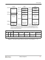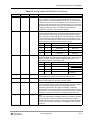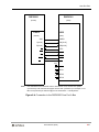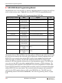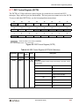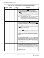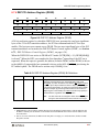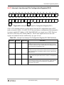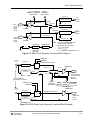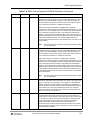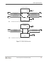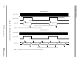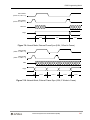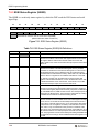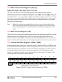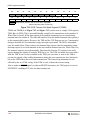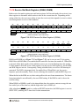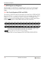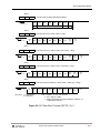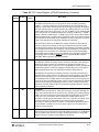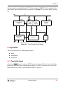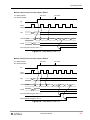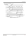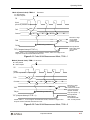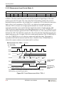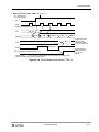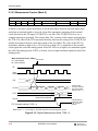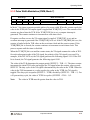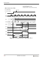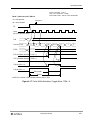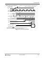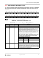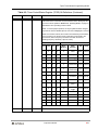
1
DSP56301 User’s Manual 24-Bit Digital Signal Processor DSP56301UM/AD Revision 3, March 2001 OnCE, DigitalDNA, and the DigitalDNA logo are trademarks of Motorola, Inc. Motorola reserves the right to make changes without further notice to any products herein. Motorola makes no warranty, representation or guarantee regarding the suitability of its products for any particular purpose, nor does Motorola assume any liability arising out of the application or use of any product or circuit, and specifically disclaims any and all liability, including without limitation consequential or incidental damages. “Typical” parameters which may be provided in Motorola data sheets and/or specifications can and do vary in different applications and actual performance may vary over time. All operating parameters, including “Typicals” must be validated for each customer application by customer’s technical experts. Motorola does not convey any license under its patent rights nor the rights of others. Motorola products are not designed, intended, or authorized for use as components in systems intended for surgical implant into the body, or other applications intended to support life, or for any other application in which the failure of the Motorola product could create a situation where personal injury or death may occur. Should Buyer purchase or use Motorola products for any such unintended or unauthorized application, Buyer shall indemnify and hold Motorola and its officers, employees, subsidiaries, affiliates, and distributors harmless against all claims, costs, damages, and expenses, and reasonable attorney fees arising out of, directly or indirectly, any claim of personal injury or death associated with such unintended or unauthorized use, even if such claim alleges that Motorola was negligent regarding the design or manufacture of the part. Motorola and are registered trademarks of Motorola, Inc. Motorola, Inc. is an Equal Opportunity/Affirmative Action Employer. How to reach us: USA/EUROPE Motorola Literature Distribution P.O. Box 5405 Denver, Colorado 80217 1-303-675-2140 1-800-441-2447 Technical Information Center 1-800-521-6274 JAPAN Motorola Japan Ltd. SPS, Technical Information Center 3-20-1, Minami-Azabu, Minato-ku Tokyo 106-8573 Japan 81-3-3440-3569 Home Page http://www.mot.com/SPS/DSP DSP Helpline http://www.motorola-dsp.com/contact email: [email protected] ASIA/PACIFIC Motorola Semiconductors H.K. Ltd. Silicon Harbour Centre 2 Dai King Street Tai Po Industrial Estate Tai Po, N.T., Hong Kong 852-26668334 MOTOROLA INC., 1996, 2001 Overview 1 Signals/Connections 2 Memory Configuration 3 Core Configuration 4 Programming the Peripherals 5 Host Interface (HI32) 6 Enhanced Synchronous Serial Interface (ESSI) 7 Serial Communications Interface (SCI) 8 Triple Timer Module 9 Bootstrap Program A Programming Reference B 1 Overview 2 Signals/Connections 3 Memory Configuration 4 Core Configuration 5 Programming the Peripherals 6 Host Interface (HI32) 7 Enhanced Synchronous Serial Interface (ESSI) 8 Serial Communications Interface (SCI) 9 Triple Timer Module A Bootstrap Program B Programming Reference Contents Chapter 1 Overview 1.1 Manual Organization ............................................................................................................. 1-1 1.2 Manual Conventions .............................................................................................................. 1-2 1.3 DSP56300 Core Features....................................................................................................... 1-4 1.4 DSP56300 Core Functional Blocks ....................................................................................... 1-6 1.4.1 Data ALU............................................................................................................................... 1-6 1.4.1.1 Data ALU Registers......................................................................................................... 1-7 1.4.1.2 Multiplier-Accumulator (MAC) ...................................................................................... 1-7 1.4.2 Address Generation Unit (AGU) ........................................................................................... 1-7 1.4.3 Program Control Unit (PCU) ................................................................................................. 1-8 1.4.4 PLL and Clock Oscillator ...................................................................................................... 1-9 1.4.5 JTAG TAP and OnCE Module .............................................................................................. 1-9 1.4.6 On-Chip Memory................................................................................................................. 1-10 1.5 Internal Buses ...................................................................................................................... 1-10 1.6 DMA .................................................................................................................................... 1-11 1.7 Peripherals ........................................................................................................................... 1-12 1.7.1 General-Purpose Input/Output (GPIO) signals.................................................................... 1-12 1.7.2 Host Interface (HI32)........................................................................................................... 1-12 1.7.3 Enhance Synchronous Serial Interface (ESSI) .................................................................... 1-12 1.7.4 Serial Communications Interface (SCI)............................................................................... 1-13 1.7.5 Triple Timer Module ........................................................................................................... 1-13 1.8 Related Documents and Web Sites ...................................................................................... 1-14 Chapter 2 Signals/Connections 2.1 2.2 2.3 2.4 2.5 2.5.1 2.5.2 2.5.3 2.6 2.7 Power ..................................................................................................................................... 2-4 Ground ................................................................................................................................... 2-4 Clock...................................................................................................................................... 2-5 PLL ........................................................................................................................................ 2-5 External Memory Expansion Port (Port A) ........................................................................... 2-6 External Address Bus............................................................................................................. 2-6 External Data Bus .................................................................................................................. 2-6 External Bus Control ............................................................................................................. 2-6 Interrupt and Mode Control ................................................................................................... 2-9 Host Interface (HI32)........................................................................................................... 2-10 Contents v 2.8 2.9 2.10 2.11 2.12 Enhanced Synchronous Serial Interface 0 ........................................................................... 2-22 Enhanced Synchronous Serial Interface 1 ........................................................................... 2-25 Serial Communications Interface (SCI)............................................................................... 2-27 Timers .................................................................................................................................. 2-27 JTAG and OnCE Interface................................................................................................... 2-29 Chapter 3 Memory Configuration 3.1 3.1.1 3.1.2 3.1.3 3.1.4 3.2 3.2.1 3.2.2 3.2.3 3.3 3.3.1 3.3.2 3.3.3 3.4 3.5 3.6 3.7 Program Memory Space ........................................................................................................ 3-1 Internal Program Memory .................................................................................................... 3-2 Memory Switch Modes—Program Memory ......................................................................... 3-2 Instruction Cache ................................................................................................................... 3-2 Program Bootstrap ROM ....................................................................................................... 3-3 X Data Memory Space........................................................................................................... 3-3 Internal X Data Memory........................................................................................................ 3-3 Memory Switch Modes—X Data Memory ........................................................................... 3-3 Internal I/O Space—X Data Memory .................................................................................... 3-4 Y Data Memory Space........................................................................................................... 3-4 Internal Y Data Memory........................................................................................................ 3-4 Memory Switch Modes—Y Data Memory ........................................................................... 3-4 External I/O Space—Y Data Memory................................................................................... 3-5 Dynamic Memory Configuration Switching ......................................................................... 3-5 Sixteen-Bit Compatibility Mode Configuration .................................................................... 3-6 Internal Memory Configuration Summary ............................................................................ 3-6 Memory Maps........................................................................................................................ 3-7 Chapter 4 Core Configuration 4.1 4.2 4.3 4.3.1 4.3.2 4.4 4.4.1 4.4.2 4.4.3 4.5 4.6 4.6.1 4.6.2 4.6.3 4.7 4.8 vi Operating Modes.................................................................................................................... 4-2 Bootstrap Program ................................................................................................................. 4-5 Central Processor Unit (CPU) Registers................................................................................ 4-6 Status Register (SR)............................................................................................................... 4-6 Operating Mode Register (OMR) ........................................................................................ 4-12 Configuring Interrupts ......................................................................................................... 4-15 Interrupt Priority Registers (IPRC and IPRP)...................................................................... 4-16 Interrupt Table Memory Map .............................................................................................. 4-17 Processing Interrupt Source Priorities Within an IPL ......................................................... 4-19 PLL Control Register (PCTL) ............................................................................................. 4-21 Bus Interface Unit (BIU) Registers ..................................................................................... 4-22 Bus Control Register............................................................................................................ 4-22 DRAM Control Register (DCR) .......................................................................................... 4-24 Address Attribute Registers (AAR[0–3]) ............................................................................ 4-27 DMA Control Registers 5–0 (DCR[5–0]) ........................................................................... 4-29 Device Identification Register (IDR)................................................................................... 4-34 DSP56303 DSP56301 User’s Manual 4.9 4.10 JTAG Identification (ID) Register ....................................................................................... 4-35 JTAG Boundary Scan Register (BSR)................................................................................. 4-35 Chapter 5 Programming the Peripherals 5.1 5.2 5.3 5.3.1 5.3.2 5.3.3 5.3.4 5.4 5.4.1 5.4.2 5.4.3 5.4.4 5.4.5 Peripheral Initialization Steps ................................................................................................ 5-1 Mapping the Control Registers .............................................................................................. 5-2 Data Transfer Methods .......................................................................................................... 5-2 Polling.................................................................................................................................... 5-2 Interrupts ................................................................................................................................ 5-3 DMA ...................................................................................................................................... 5-4 Advantages and Disadvantages ............................................................................................. 5-4 General-Purpose Input/Output (GPIO) .................................................................................. 5-4 Port B Signals and Registers.................................................................................................. 5-5 Port C Signals and Registers.................................................................................................. 5-6 Port D Signals and Registers ................................................................................................. 5-6 Port E Signals and Registers .................................................................................................. 5-6 Triple Timer Signals and Registers ....................................................................................... 5-7 Chapter 6 Host Interface (HI32) 6.1 Features .................................................................................................................................. 6-1 6.2 Overview................................................................................................................................ 6-4 6.3 Data Transfer Paths................................................................................................................ 6-6 6.3.1 Host-to-DSP Data Path .......................................................................................................... 6-6 6.3.2 DSP-To-Host Data Path......................................................................................................... 6-7 6.4 Reset States .......................................................................................................................... 6-12 6.5 DSP-Side Operating Modes................................................................................................. 6-12 6.5.1 Terminate and Reset (DCTR[HM] = $0)........................................................................... 6-13 6.5.2 PCI Mode (DCTR[HM] = $1) ........................................................................................... 6-13 6.5.3 Universal (DCTR[HM] = $2) and Enhanced Universal (DCTR[HM] = $3) Bus Modes 6-15 6.5.4 GPIO Mode (DCTR[HM] = $4) ........................................................................................ 6-16 6.5.5 Self-Configuration Mode (DCTR[HM] = $5) ................................................................... 6-16 6.6 Host Port Pins ...................................................................................................................... 6-18 6.7 HI32 DSP-Side Programming Model .................................................................................. 6-22 6.7.1 DSP Control Register (DCTR) ............................................................................................ 6-23 6.7.2 DSP PCI Control Register (DPCR) ..................................................................................... 6-26 6.7.3 DSP PCI Master Control Register (DPMC) ........................................................................ 6-30 6.7.4 DSP PCI Address Register (DPAR) .................................................................................... 6-33 6.7.5 DSP Status Register (DSR).................................................................................................. 6-35 6.7.6 DSP PCI Status Register (DPSR) ........................................................................................ 6-38 6.7.7 DSP Receive Data FIFO (DRXR) ....................................................................................... 6-41 6.7.8 DSP Master Transmit Data Register (DTXM) .................................................................... 6-42 6.7.9 DSP Slave Transmit Data Register (DTXS)........................................................................ 6-42 Contents vii 6.7.10 DSP Host Port GPIO Direction Register (DIRH)................................................................ 6-43 6.7.11 DSP Host Port GPIO Data Register (DATH) ...................................................................... 6-43 6.8 Host-Side Programming Model ........................................................................................... 6-44 6.8.1 HI32 Control Register (HCTR) ........................................................................................... 6-48 6.8.2 Host Interface Status Register (HSTR)................................................................................ 6-56 6.8.3 Host Command Vector Register (HCVR) ........................................................................... 6-59 6.8.4 Host Master Receive Data Register (HRXM) ..................................................................... 6-61 6.8.5 Host Slave Receive Data Register (HRXS) ......................................................................... 6-61 6.8.6 Host Transmit Data Register (HTXR) ................................................................................. 6-62 6.8.6.1 PCI Mode (DCTR[HM] = $1) ....................................................................................... 6-63 6.8.6.2 Universal Bus mode (DCTR[HM] = $2 or $3).............................................................. 6-63 6.8.7 Device ID/Vendor ID Configuration Register (CDID/CVID)............................................. 6-64 6.8.8 Status/Command Configuration Register (CSTR/CCMR).................................................. 6-64 6.8.9 Class Code/Revision ID Configuration Register (CCCR/CRID) ........................................ 6-67 6.8.10 Header Type/Latency Timer Configuration Register (CHTY/CLAT/CCLS) ..................... 6-68 6.8.11 Memory Space Base Address Configuration Register (CBMA) ......................................... 6-70 6.8.12 Subsystem ID and Subsystem Vendor ID Configuration Register (CSID) ......................... 6-71 6.8.13 Interrupt Line-Interrupt Pin Configuration Register(CILP) ................................................ 6-73 6.9 HI32 Programming Model/Quick Reference....................................................................... 6-74 Chapter 7 Enhanced Synchronous Serial Interface (ESSI) 7.1 7.2 7.2.1 7.2.2 7.2.3 7.2.4 7.2.5 7.2.6 7.3 7.3.1 7.3.2 7.3.3 7.4 7.4.1 7.4.2 7.4.3 7.4.4 7.4.5 7.4.6 7.4.7 7.4.8 7.4.9 7.5 viii ESSI Enhancements ............................................................................................................... 7-2 ESSI Data and Control Signals .............................................................................................. 7-3 Serial Transmit Data Signal (STD)........................................................................................ 7-3 Serial Receive Data Signal (SRD) ......................................................................................... 7-3 Serial Clock (SCK) ................................................................................................................ 7-3 Serial Control Signal (SC0) ................................................................................................... 7-4 Serial Control Signal (SC1) ................................................................................................... 7-4 Serial Control Signal (SC2) ................................................................................................... 7-6 Operation ............................................................................................................................... 7-6 ESSI After Reset .................................................................................................................... 7-6 Initialization ........................................................................................................................... 7-6 Exceptions.............................................................................................................................. 7-7 Operating Modes: Normal, Network, and On-Demand....................................................... 7-10 Normal/Network/On-Demand Mode Selection ................................................................... 7-10 Synchronous/Asynchronous Operating Modes ................................................................... 7-11 Frame Sync Selection .......................................................................................................... 7-11 Frame Sync Signal Format .................................................................................................. 7-11 Frame Sync Length for Multiple Devices............................................................................ 7-12 Word Length Frame Sync and Data Word Timing.............................................................. 7-12 Frame Sync Polarity............................................................................................................. 7-12 Byte Format (LSB/MSB) for the Transmitter...................................................................... 7-13 Flags..................................................................................................................................... 7-13 ESSI Programming Model................................................................................................... 7-14 DSP56303 DSP56301 User’s Manual 7.5.1 7.5.2 7.5.3 7.5.4 7.5.5 7.5.6 7.5.7 7.5.8 7.5.9 7.5.10 7.6 7.6.1 7.6.2 7.6.3 ESSI Control Register A (CRA) .......................................................................................... 7-14 ESSI Control Register B (CRB) .......................................................................................... 7-18 ESSI Status Register (SSISR).............................................................................................. 7-28 ESSI Receive Shift Register ................................................................................................ 7-29 ESSI Receive Data Register (RX) ....................................................................................... 7-30 ESSI Transmit Shift Registers ............................................................................................. 7-30 ESSI Transmit Data Registers (TX[2–0])............................................................................ 7-33 ESSI Time Slot Register (TSR) ........................................................................................... 7-33 Transmit Slot Mask Registers (TSMA, TSMB) .................................................................. 7-33 Receive Slot Mask Registers (RSMA, RSMB) ................................................................... 7-35 GPIO Signals and Registers................................................................................................. 7-36 Port Control Registers (PCRC and PCRD).......................................................................... 7-36 Port Direction Registers (PRRC and PRRD)....................................................................... 7-37 Port Data Registers (PDRC and PDRD).............................................................................. 7-38 Chapter 8 Serial Communication Interface (SCI) 8.1 Operating Modes.................................................................................................................... 8-1 8.1.1 Synchronous Mode ................................................................................................................ 8-2 8.1.2 Asynchronous Mode .............................................................................................................. 8-2 8.1.3 Multidrop Mode ..................................................................................................................... 8-2 8.1.3.1 Transmitting Data and Address Characters ..................................................................... 8-3 8.1.3.2 Wired-OR Mode .............................................................................................................. 8-3 8.1.3.3 Idle Line Wakeup............................................................................................................. 8-3 8.1.3.4 Address Mode Wakeup.................................................................................................... 8-3 8.2 I/O Signals ............................................................................................................................. 8-3 8.2.1 Receive Data (RXD) .............................................................................................................. 8-4 8.2.2 Transmit Data (TXD)............................................................................................................. 8-4 8.2.3 SCI Serial Clock (SCLK) ...................................................................................................... 8-4 8.3 SCI After Reset ...................................................................................................................... 8-5 8.4 SCI Initialization.................................................................................................................... 8-6 8.4.1 Preamble, Break, and Data Transmission Priority................................................................. 8-7 8.4.2 Bootstrap Loading Through the SCI (Boot Mode 2 or A)..................................................... 8-8 8.5 Exceptions.............................................................................................................................. 8-8 8.6 SCI Programming Model....................................................................................................... 8-9 8.6.1 SCI Control Register (SCR) ................................................................................................ 8-12 8.6.2 SCI Status Register (SSR) ................................................................................................... 8-17 8.6.3 SCI Clock Control Register (SCCR) ................................................................................... 8-19 8.6.4 SCI Data Registers............................................................................................................... 8-22 8.6.4.1 SCI Receive Register (SRX).......................................................................................... 8-22 8.6.4.2 SCI Transmit Register (STX) ........................................................................................ 8-23 8.7 GPIO Signals and Registers................................................................................................. 8-24 8.7.1 Port E Control Register (PCRE) .......................................................................................... 8-24 8.7.2 Port E Direction Register (PRRE) ....................................................................................... 8-25 8.7.3 Port E Data Register (PDRE)............................................................................................... 8-25 Contents ix Chapter 9 Triple Timer Module 9.1 Overview................................................................................................................................ 9-1 9.1.1 Triple Timer Module Block Diagram .................................................................................... 9-2 9.1.2 Individual Timer Block Diagram........................................................................................... 9-2 9.2 Operation ............................................................................................................................... 9-3 9.2.1 Timer After Reset .................................................................................................................. 9-3 9.2.2 Timer Initialization ................................................................................................................ 9-4 9.2.3 Timer Exceptions ................................................................................................................... 9-4 9.3 Operating Modes.................................................................................................................... 9-5 9.3.1 Triple Timer Modes ............................................................................................................... 9-6 9.3.1.1 Timer GPIO (Mode 0) ..................................................................................................... 9-6 9.3.1.2 Timer Pulse (Mode 1) ...................................................................................................... 9-8 9.3.1.3 Timer Toggle (Mode 2) ................................................................................................. 9-10 9.3.1.4 Timer Event Counter (Mode 3) ..................................................................................... 9-12 9.3.2 Signal Measurement Modes................................................................................................. 9-14 9.3.2.1 Measurement Input Width (Mode 4) ............................................................................. 9-14 9.3.2.2 Measurement Input Period (Mode 5)............................................................................. 9-16 9.3.2.3 Measurement Capture (Mode 6) .................................................................................... 9-18 9.3.3 Pulse Width Modulation (PWM, Mode 7)........................................................................... 9-19 9.3.4 Watchdog Modes ................................................................................................................. 9-22 9.3.4.1 Watchdog Pulse (Mode 9) ............................................................................................. 9-22 9.3.4.2 Watchdog Toggle (Mode 10)......................................................................................... 9-24 9.3.4.3 Reserved Modes............................................................................................................. 9-25 9.3.5 Special Cases ....................................................................................................................... 9-25 9.3.6 DMA Trigger ....................................................................................................................... 9-25 9.4 Triple Timer Module Programming Model ......................................................................... 9-25 9.4.1 Prescaler Counter ................................................................................................................. 9-25 9.4.2 Timer Prescaler Load Register (TPLR) ............................................................................... 9-27 9.4.3 Timer Prescaler Count Register (TPCR) ............................................................................. 9-28 9.4.4 Timer Control/Status Register (TCSR)................................................................................ 9-28 9.4.5 Timer Load Register (TLR) ................................................................................................. 9-33 9.4.6 Timer Compare Register (TCPR) ........................................................................................ 9-34 9.4.7 Timer Count Register (TCR) ............................................................................................... 9-34 Chapter A Bootstrap Program Chapter B Programming Reference B.1 B.2 B.3 Internal I/O Memory Map......................................................................................................B-3 Interrupt Sources and Priorities .............................................................................................B-9 Programming Sheets ............................................................................................................B-13 Index x DSP56303 DSP56301 User’s Manual Figures 1-1 2-1 2-2 3-1 3-2 3-3 3-4 3-5 3-6 3-7 3-8 4-1 4-2 4-4 4-3 4-5 4-6 4-7 4-8 4-9 4-10 4-11 5-1 5-2 5-3 5-4 5-5 5-6 6-1 6-2 6-3 6-4 6-5 6-6 6-7 DSP56301 Block Diagram ................................................................................... 1-11 Signals Identified by Functional Group ................................................................. 2-2 Host Interface/Port B Detail Signal Diagram......................................................... 2-3 Default Settings (0, 0, 0)......................................................................................... 3-7 16-Bit Space With Default RAM (0, 0, 1).............................................................. 3-8 Switched Program RAM (0, 1, 0)........................................................................... 3-9 16-Bit Space With Switched Program RAM (0, 1, 1).......................................... 3-10 Instruction Cache Enabled (1, 0, 0) ...................................................................... 3-11 16-Bit Space With Instruction Cache Enabled (1, 0, 1) ....................................... 3-12 Switched Program RAM and Instruction Cache Enabled (1, 1, 0) ...................... 3-13 16-Bit Space, Switched Program RAM, Instruction Cache Enabled (1, 1, 1) ..... 3-14 Status Register (SR) ............................................................................................... 4-7 Operating Mode Register (OMR)......................................................................... 4-12 Interrupt Priority Register-Peripherals (IPRP) (X:$FFFFFE).............................. 4-16 Interrupt Priority Register-Core (IPRC) (X:$FFFFFF)........................................ 4-16 PLL Control Register (PCTL) .............................................................................. 4-21 Bus Control Register (BCR)................................................................................. 4-22 DRAM Control Register (DCR)........................................................................... 4-24 Address Attribute Registers (AAR[0–3]) (X:$FFFFF9–$FFFFF6) ..................... 4-27 DMA Control Register (DCR) ............................................................................. 4-29 Identification Register Configuration (Revision E) ............................................. 4-34 JTAG Identification (ID) Register Configuration ................................................ 4-35 Memory Mapping of Peripherals Control Registers .............................................. 5-2 Host Interface/Port B Detail Signal Diagram......................................................... 5-5 Port C Signals ......................................................................................................... 5-6 Port D Signals......................................................................................................... 5-6 Port E Signals ......................................................................................................... 5-6 Triple Timer Signals............................................................................................... 5-7 HI32 Block Diagram .............................................................................................. 6-5 Connection to a PCI Bus ...................................................................................... 6-19 Connection to 16-Bit ISA/EISA Data Bus ........................................................... 6-20 Connection to the DSP56300 Core Port A Bus.................................................... 6-21 DSP Control Register (DCTR)............................................................................. 6-23 DSP PCI Control Register (DPCR)...................................................................... 6-26 DSP PCI Master Control Register (DPMC)......................................................... 6-30 DSP56301 User’s Manual xi 6-8 6-9 6-10 6-11 6-12 6-13 6-14 6-15 6-16 6-17 6-18 6-19 6-20 6-21 6-22 7-1 7-2 7-3 7-4 7-5 7-6 7-7 7-8 7-9 7-10 7-11 7-12 7-13 7-14 7-15 7-16 7-17 7-18 7-19 7-20 8-1 8-2 8-3 xii DSP PCI Address Register (DPAR)..................................................................... 6-33 DSP Status Register (DSR) .................................................................................. 6-35 DSP PCI Status Register (DPSR)......................................................................... 6-38 DSP Host Port Direction Register (DIRH)........................................................... 6-43 DSP Host Port GPIO Data Register (DATH)....................................................... 6-43 Host Interface Control Register (HCTR) ............................................................. 6-48 Host Interface Status Register (HSTR) ................................................................ 6-56 Host Command Vector Register (HCVR)............................................................ 6-59 Device/Vendor ID Configuration Register (CDID/CVID) .................................. 6-64 Status/Command Configuration Register (CSTR/CCMR) .................................. 6-64 Class Code/Revision ID Configuration Register CCCR/CRID) .......................... 6-67 Header Type/Latency Timer Configuration Register (CHTY/CLAT/CCLS)...... 6-68 Memory Space Base Address Configuration Register (CBMA).......................... 6-70 Subsystem ID and Subsystem Vendor ID Configuration Register (CSID).......... 6-71 Interrupt Line-Interrupt Pin Configuration Register(CILP) ................................. 6-73 ESSI Block Diagram .............................................................................................. 7-1 ESSI Control Register A(CRA)............................................................................ 7-14 ESSI Clock Generator Functional Block Diagram............................................... 7-17 ESSI Frame Sync Generator Functional Block Diagram ..................................... 7-17 ESSI Control Register B (CRB) ........................................................................... 7-18 CRB FSL0 and FSL1 Bit Operation (FSR = 0).................................................... 7-24 CRB SYN Bit Operation ...................................................................................... 7-25 CRB MOD Bit Operation..................................................................................... 7-26 Normal Mode, External Frame Sync (8 Bit, 1 Word in Frame)........................... 7-27 Network Mode, External Frame Sync (8 Bit, 2 Words in Frame) ....................... 7-27 ESSI Status Register (SSISR) .............................................................................. 7-28 ESSI Data Path Programming Model (SHFD = 0)............................................... 7-31 ESSI Data Path Programming Model (SHFD = 1)............................................... 7-32 ESSI Transmit Slot Mask Register A (TSMA) .................................................... 7-33 ESSI Transmit Slot Mask Register B (TSMB)..................................................... 7-34 ESSI Receive Slot Mask Register A (RSMA) ..................................................... 7-35 ESSI Receive Slot Mask Register B (RSMB)...................................................... 7-35 Port Control Registers (PCRC X:$FFFFBF) (PCRD X:$FFFAF)....................... 7-36 Port Direction Registers (PRRC X:$FFFFBE) (PRRD X: $FFFFAE) ................ 7-37 Port Data Registers (PDRC X:$FFFFBD) (PDRD X: $FFFFAD) ...................... 7-38 SCI Data Word Formats (SSFTD = 1), 1 ............................................................. 8-10 SCI Data Word Formats (SSFTD = 0), 2 ............................................................. 8-11 SCI Control Register (SCR) ................................................................................. 8-12 DSP56301 User’s Manual 8-4 8-5 8-6 8-7 8-8 8-9 8-10 9-1 9-2 9-3 9-4 9-5 9-6 9-7 9-8 9-9 9-10 9-11 9-12 9-13 9-14 9-15 9-16 9-17 9-18 9-19 9-20 9-21 9-22 9-23 B-1 B-2 B-3 B-4 B-5 B-6 B-7 B-8 SCI Clock Control Register (SCCR).................................................................... 8-19 SCI Baud Rate Generator ..................................................................................... 8-20 16 x Serial Clock .................................................................................................. 8-21 SCI Programming Model—Data Registers .......................................................... 8-22 Port E Control Register (PCRE X:$FFFF9F)....................................................... 8-24 Port E Direction Register (PRRE X:$FFFF9E).................................................... 8-25 Port Data Registers (PDRE X:$FFFF9D) ............................................................ 8-25 Triple Timer Module Block Diagram..................................................................... 9-2 Timer Module Block Diagram ............................................................................... 9-3 Timer Mode (TRM = 1) ......................................................................................... 9-7 Timer Mode (TRM = 0) ......................................................................................... 9-7 Pulse Mode (TRM = 1) .......................................................................................... 9-8 Pulse Mode (TRM = 0) .......................................................................................... 9-9 Toggle Mode, TRM = 1 ....................................................................................... 9-10 Toggle Mode, TRM = 0 ....................................................................................... 9-11 Event Counter Mode, TRM = 1............................................................................ 9-12 Event Counter Mode, TRM = 0............................................................................ 9-13 Pulse Width Measurement Mode, TRM = 1 ........................................................ 9-15 Pulse Width Measurement Mode, TRM = 0 ........................................................ 9-15 Period Measurement Mode, TRM = 1.................................................................. 9-16 Period Measurement Mode, TRM = 0.................................................................. 9-17 Capture Measurement Mode, TRM = 0 ............................................................... 9-18 Pulse Width Modulation Toggle Mode, TRM = 1 ............................................... 9-20 Pulse Width Modulation Toggle Mode, TRM = 0 ............................................... 9-21 Watchdog Pulse Mode.......................................................................................... 9-23 Watchdog Toggle Mode ....................................................................................... 9-24 Timer Module Programmer’s Model.................................................................... 9-26 Timer Prescaler Load Register (TPLR)................................................................ 9-27 Timer Prescaler Count Register (TPCR).............................................................. 9-28 Timer Control/Status Register (TCSR) ................................................................ 9-28 Status Register (SR) .............................................................................................B-13 Operating Mode Register (OMR).........................................................................B-14 Interrupt Priority Register Core (IPRC) ...............................................................B-15 Interrupt Priority Register Peripherals (IPRP) .....................................................B-16 Phase-Locked Loop Control Register (PCTL) .....................................................B-17 Bus Control Register (BCR).................................................................................B-18 DRAM Control Register (DCR)...........................................................................B-19 Address Attribute Registers (AAR[3–0]).............................................................B-20 DSP56301 User’s Manual xiii B-9 B-10 B-11 B-12 B-13 B-14 B-15 B-16 B-17 B-18 B-19 B-20 B-21 B-22 B-23 B-24 B-25 B-26 B-27 B-28 B-29 B-30 B-31 xiv DMA Control Registers 5–0 (DCR[5–0]) ............................................................B-21 DSP Control Register (DCTR).............................................................................B-22 DSP PCI Control Register (DPCR)......................................................................B-23 DSP PCI Master Control Register (DPMC).........................................................B-24 DSP PCI Address Register (DPAR).....................................................................B-25 HI32 Control Register (HCTR) ............................................................................B-26 Host Command Vector Register (HCVR)............................................................B-27 Status/Command Configuration Register (CSTR/CCMR) ..................................B-28 Header Type/Latency Timer Configuration Register (CHTY/CLAT/CCLS)......B-29 Memory Space Base Address Configuration Register (CBMA)..........................B-30 Subsystem ID and Subsystem Vendor ID Configuration Register (CSID)..........B-31 ESSI Control Register A (CRA)...........................................................................B-32 ESSI Control Register B (CRB) ...........................................................................B-33 ESSI Transmit and Receive Slot Mask Registers (TSM, RSM) ..........................B-34 SCI Control Register (SCR) .................................................................................B-35 SCI Clock Control Registers (SCCR) ..................................................................B-36 Timer Prescaler Load Register (TPLR)................................................................B-37 Timer Control/Status Register (TCSR) ................................................................B-38 Timer Load Registers (TLR) ................................................................................B-39 Host Data Direction and Host Data Registers (HDDR, HDR).............................B-40 Port C Registers (PCRC, PRRC, PDRC) .............................................................B-41 Port D Registers (PCRD, PRRD, PDRD) ............................................................B-42 Port E Registers (PCRE, PRRE, PDRE) ..............................................................B-43 DSP56301 User’s Manual Tables 1-1 1-2 1-3 2-1 2-2 2-3 2-4 2-5 2-6 2-7 2-8 2-9 2-10 2-11 2-12 2-13 2-14 2-15 2-16 2-17 3-1 3-2 4-1 4-2 4-3 4-4 4-5 4-6 4-7 4-8 4-9 4-10 4-11 4-12 6-1 6-2 6-3 6-4 6-5 6-6 6-7 6-8 6-9 High True/Low True Signal Conventions ................................................................. 1-2 DSP56301 Switch Memory Configuration.............................................................. 1-10 DSP56301 Documentation ...................................................................................... 1-14 DSP56301 Functional Signal Groupings ................................................................... 2-1 Power Inputs .............................................................................................................. 2-4 Ground Signals .......................................................................................................... 2-4 Clock Signals ............................................................................................................. 2-5 Phase-Lock Loop Signals .......................................................................................... 2-5 External Address Bus Signals.................................................................................... 2-6 External Data Bus Signals ......................................................................................... 2-6 External Bus Control Signals..................................................................................... 2-6 Interrupt and Mode Control ....................................................................................... 2-9 Host Interface........................................................................................................... 2-10 Summary of HI32 Signals and Modes ..................................................................... 2-14 Host Port Pins (HI32) .............................................................................................. 2-16 Enhanced Synchronous Serial Interface 0 ............................................................... 2-23 Enhanced Serial Synchronous Interface 1 ............................................................... 2-25 Serial Communication Interface .............................................................................. 2-27 Triple Timer Signals ................................................................................................ 2-28 JTAG/OnCE Interface ............................................................................................. 2-29 DSP56301 RAM Configurations ............................................................................... 3-6 DSP56301 RAM Address Ranges by Configuration................................................. 3-6 DSP56301 Operating Modes ..................................................................................... 4-2 Operating Mode Definitions ...................................................................................... 4-3 Status Register Bit Definitions ................................................................................. 4-7 Operating Mode Register (OMR) Bit Definitions ................................................... 4-12 Interrupt Priority Level Bits..................................................................................... 4-17 Interrupt Sources...................................................................................................... 4-17 Interrupt Source Priorities Within an IPL................................................................ 4-19 PLL Control Register (PCTL) Bit Definitions ........................................................ 4-21 Bus Control Register (BCR) Bit Definitions ........................................................... 4-22 DRAM Control Register (DCR) Bit Definitions ..................................................... 4-25 Address Attribute Registers (AAR[0–3]) Bit Definitions ....................................... 4-27 DMA Control Register (DCR) Bit Definitions........................................................ 4-29 HI32 Features, Core-Side and Host-Side................................................................... 6-2 HI32 Features in PCI Mode and Universal Bus Mode .............................................. 6-3 HI32 (PCI Master Data Transfer Formats ................................................................. 6-8 Transmit Data Transfer Format ................................................................................. 6-9 Receive Transfer Data Formats ............................................................................... 6-10 HI32 Reset ............................................................................................................... 6-12 HI32 Modes ............................................................................................................. 6-13 Host Port Pin Functionality...................................................................................... 6-18 HI32 Programming Model, DSP Side ..................................................................... 6-22 Tables xv 6-10 6-11 6-12 6-13 6-14 6-15 6-16 6-17 6-18 6-19 6-20 6-21 6-22 6-23 6-24 6-25 6-26 6-27 6-28 6-29 6-30 7-1 7-2 7-3 7-4 7-5 7-6 8-1 8-2 8-3 8-4 8-5 9-1 9-2 9-3 9-4 B-1 B-2 B-3 B-4 xvi DSP Control Register (DCTR) Bit Definitions ....................................................... 6-23 DSP PCI Control Register (DPCR) Bit Definitions ................................................ 6-27 DSP PCI Master Control Register (DMPC) Bit Definitions ................................... 6-31 DSP PCI Address Register (DPAR) Bit Definitions ............................................... 6-33 DSP Status Register (DSR) Bit Definitions............................................................. 6-35 DSP PCI Status Register (DPSR) Bit Definitions ................................................... 6-38 DATH and DIRH Functionality .............................................................................. 6-43 HI32 Programming Model, Host-Side Registers ..................................................... 6-44 PCI Bus Commands................................................................................................. 6-46 Host-Side Registers (PCI Memory Address Space1)............................................... 6-47 Host-Side Registers (PCI Configuration Address Space1) ...................................... 6-47 Host-Side Registers (Universal Bus Mode Address Space1)................................... 6-47 Host Interface Control Register (HCTR) Bit Definitions ........................................ 6-49 Host Interface Status Register (HSTR) Bit Definitions........................................... 6-57 Host Command Vector Register (HCVR) Bit Definitions ...................................... 6-60 Device ID/Vendor ID Configuration Register (CDID/CVID) Bit Definitions........ 6-64 Status/Command Configuration Register (CSTR/CCMR) Bit Definitions ............. 6-65 Class Code/Revision ID Configuration Register (CCCR/CRID) Bit Definitions ... 6-67 Header Type/Latency Timer Configuration Register (CHTY/CLAT/CCLS) Bit Definitions.......................................................................................................... 6-68 Memory Space Base Address Configuration Register (CBMA) Bit Definitions .... 6-70 Interrupt Line-Interrupt Pin Configuration Register(CILP) Bit Definitions .......... 6-73 ESSI Clock Sources ................................................................................................... 7-3 Mode and Signal Definitions ..................................................................................... 7-5 ESSI Control Register A (CRA) Bit Definitions ..................................................... 7-15 ESSI Control Register B (CRB) Bit Definitions ..................................................... 7-19 ESSI Status Register (SSISR) Bit Definitions ......................................................... 7-28 ESSI Port Signal Configurations ............................................................................. 7-37 SCI Registers After Reset .......................................................................................... 8-5 SCI Control Register (SCR) Bit Definitions............................................................ 8-12 SCI Status Register .................................................................................................. 8-17 SCI Status Register (SSR) Bit Definitions .............................................................. 8-17 SCI Clock Control Register (SCCR) Bit Definitions .............................................. 8-19 Timer Prescaler Load Register (TPLR) Bit Definitions .......................................... 9-27 Timer Prescaler Count Register (TPCR) Bit Definitions ........................................ 9-28 Timer Control/Status Register (TCSR) Bit Definitions........................................... 9-28 Inverter (INV) Bit Operation ................................................................................... 9-32 Guide to Programming Sheets ...................................................................................B-2 Internal I/O Memory Map (X Data Memory)............................................................B-3 Interrupt Sources........................................................................................................B-9 Interrupt Source Priorities Within an IPL................................................................B-11 DSP56301 User’s Manual Chapter 1 Overview This manual describes the DSP56301 24-bit digital signal processor (DSP), its memory, operating modes, and peripheral modules. The DSP56301 is an implementation of the DSP56300 core with a unique configuration of on-chip memory, cache, and peripherals. Use this manual in conjunction with the DSP56300 Family Manual (DSP56300FM/AD), which describes the CPU, core programming models, and instruction set details. DSP56301 Technical Data (DSP56301/D)—referred to as the data sheet—provides electrical specifications, timing, pinout, and packaging descriptions of the DSP56301. You can obtain these documents, as well as Motorola’s DSP development tools, through a local Motorola Semiconductor Sales Office or authorized distributor. To receive the latest information on this DSP, access the Motorola DSP home page at the address given on the back cover of this document. 1.1 Manual Organization This manual contains the following chapters and appendices: n Chapter 1, Overview Features list and block diagram, related documentation, organization of this manual, and the notational conventions used. n Chapter 2, Signals/Connections DSP56301 signals and their functional groupings. n Chapter 3, Memory Maps DSP56301 memory spaces, RAM configuration, memory configuration bit settings, memory sizes, and memory locations. n Chapter 4, Core Configuration Registers for configuring the DSP56300 core when programming the DSP56301—in particular, the interrupt vector locations and the operation of the interrupt priority registers; operating modes and how they affect the processor’s program and data memories. n Chapter 5, Programming the Peripherals Guidelines on initializing the DSP56301 peripherals, including mapping control registers, specifying a method of transferring data, and configuring for General-Purpose Input/Output (GPIO). Overview 1-1 Manual Conventions n Chapter 6, Host Interface (HI32) HI32 features, signals, architecture, programming model, reset, interrupts, external host programming model, initialization, and a quick reference to the HI32 programming model. n Chapter 7, Enhanced Synchronous Serial Interface (ESSI) Enhancements, data and control signals, programming model, operating modes, initialization, exceptions, and GPIO. n Chapter 8, Serial Communication Interface (SCI) Signals, programming model, operating modes, reset, initialization, and GPIO. n Chapter 9, Triple Timer Module Architecture, programming model, and operating modes of three identical timer devices available for use as internals or event counters. n Appendix A, Bootstrap Program Bootstrap code for the DSP56301. n Appendix B, Programming Reference Peripheral addresses, interrupt addresses, and interrupt priorities for the DSP56301; programming sheets list the contents of the major DSP56301 registers for programmer’s reference. 1.2 Manual Conventions This manual uses the following conventions: n Bits within registers are always listed from most significant bit (MSB) to least significant bit (LSB). n Bits within a register are indicated AA[n–m], n > m, when more than one bit is involved in a description. For purposes of description, the bits are presented as if they are contiguous within a register. However, this is not always the case. Refer to the programming model diagrams or to the programming sheets to see the exact location of bits within a register. n When a bit is described as “set,” its value is 1. When a bit is described as “cleared,” its value is 0. n The word “assert” means that a high true (active high) signal is pulled high to VCC or that a low true (active low) signal is pulled low to ground. The word “deassert” means that a high true signal is pulled low to ground or that a low true signal is pulled high to VCC. See Table 1-1. Table 1-1. High True/Low True Signal Conventions 1-2 Signal/Symbol Logic State Signal State Voltage PIN1 True Asserted Ground2 PIN False Deasserted VCC3 DSP56301 User’s Manual Manual Conventions Table 1-1. High True/Low True Signal Conventions Signal/Symbol Logic State Signal State Voltage PIN True Asserted VCC3 PIN False Deasserted Ground2 1. PIN is a generic term for any pin on the chip. 2. Ground is an acceptable low voltage level. See the appropriate data sheet for the range of acceptable low voltage levels (typically a TTL logic low). VCC is an acceptable high voltage level. See the appropriate data sheet for the range of acceptable high voltage levels (typically a TTL logic high). 3. n n Pins or signals that are asserted low (made active when pulled to ground) are indicated like this: — In text, they have an overbar: for example, RESET is asserted low. — In code examples, they have a tilde in front of their names. In Example 1-1, line 3 refers to the SS0 signal (shown as ~SS0). Sets of signals are indicated by the first and last signals in the set, for instance HA[0–2]. n “Input/Output” indicates a bidirectional signal. “Input or Output” indicates a signal that is exclusively one or the other. n Code examples are displayed in a monospaced font, as shown in Example 1-1. Example 1-1. Sample Code Listing BFSET #$0007,X:PCC; Configure: line 1 ; line 2 MISO0, MOSI0, SCK0 for SPI master ; ~SS0 as PC3 for GPIO line 3 n Hexadecimal values are indicated with a dollar sign ($) preceding the value. For example, $FFFFFF is the X memory address for the core interrupt priority register. n The word “reset” appears in four different contexts in this manual: — — — — the reset signal, written as RESET the reset instruction, written as RESET the reset operating state, written as Reset the reset function, written as reset Overview 1-3 DSP56300 Core Features 1.3 DSP56300 Core Features All DSP56300 core family members contain the DSP56300 core and additional modules. The modules are chosen from a library of standard predesigned elements, such as memories and peripherals. New modules can be added to the library to meet customer specifications. A standard interface between the DSP56300 core and the on-chip memory and peripherals supports a wide variety of memory and peripheral configurations. In particular, the DSP56301 includes Motorola’s JTAG port and OnCE module. Core features are fully described in the DSP56300 Family Manual. This manual, in contrast, documents pinout, memory, and peripheral features. Core features are as follows: n 80/100 Million Instructions per Second (MIPS) using an internal 80/100 MHz clock at 3.0–3.6 V, depending on the revision of the DSP56301 n Object code compatible with the DSP56000 core n Highly parallel instruction set n Data Arithmetic Logic Unit (Data ALU) n — Fully pipelined 24 x 24-bit parallel multiplier-accumulator (MAC) — 56-bit parallel barrel shifter (fast shift and normalization; bit stream generation and parsing) — Conditional ALU instructions — 24-bit or 16-bit arithmetic support under software control Program Control Unit (PCU) n — Position Independent Code (PIC) support — Addressing modes optimized for DSP applications (including immediate offsets) — On-chip instruction cache controller — On-chip memory-expandable hardware stack — Nested hardware DO loops — Fast auto-return interrupts Direct Memory Access (DMA) Controller — — — — 1-4 Six DMA channels supporting internal and external accesses One-, two-, and three- dimensional transfers (including circular buffering) End-of-block-transfer interrupts Triggering from interrupt lines and all peripherals DSP56301 User’s Manual DSP56300 Core Features n Phase Lock Loop (PLL)—Allows change of low power Divide Factor (DF) without loss of lock n Output clock with skew elimination n Hardware debugging support n — On-Chip Emulation (OnCE) module — Joint Action Test Group (JTAG) Test Access Port (TAP) port — Address Trace mode reflects internal Program RAM accesses at the external port On-chip memories: — Program RAM, instruction cache, X data RAM, and Y data RAM sizes are programmable: Program RAM Size Instruction Cache Size X Data RAM Size Y Data RAM Size Instruction Cache1 Switch Mode2 4096 × 24-bit 0 2048 × 24-bit 2048 × 24-bit disabled (CE = 0) disabled (MS = 0) 3072 × 24-bit 1024 × 24-bit 2048 × 24-bit 2048 × 24-bit enabled (CE = 1) disabled (MS = 0) 2048 × 24-bit 0 3072 × 24-bit 3072 × 24-bit disabled (CE = 0) enabled (MS = 1) 1024 × 24-bit 1024 × 24-bit 3072 × 24-bit 3072 × 24-bit enabled (CE = 1) enabled (MS = 1) 1. Controlled by the Cache Enable (CE) bit in the Status Register (SR) 2. Controlled by the Memory Select (MS) bit in the Operating Mode Register (OMR) n — 192 or 3 K × 24-bit bootstrap ROM, depending on the DSP56301 revision Off-chip memory expansion: n — Data memory expansion to two 16 M × 24-bit word memory spaces in 24-Bit mode or two 64 K × 16-bit memory spaces in Sixteen-Bit Compatibility mode — Program memory expansion to one 16 M × 24-bit words memory space in 24-Bit mode or 64 K × 16-bit in Sixteen-Bit Compatibility mode — External memory expansion port — Chip Select Logic for glueless interface to SRAMs — On-chip DRAM Controller for glueless interface to DRAMs On-chip peripheral support: — 32-bit parallel PCI/Universal Host Interface (HI32), PCI Rev. 2.1 compliant with glueless interface to other DSP563xx buses — ISA interface requires only 74LS45-style buffer — Two Enhanced Synchronous Serial Interfaces (ESSI0 and ESSI1) Overview 1-5 DSP56300 Core Functional Blocks n — Serial Communications Interface (SCI) with baud rate generator — Triple timer module — Up to forty-two programmable General Purpose Input/Output (GPIO) pins, depending on which peripherals are enabled Reduced power dissipation — — — — Very low power CMOS design Wait and Stop low-power standby modes Fully-static logic Optimized power management circuitry (instruction-dependent, peripheral-dependent, and mode-dependent) 1.4 DSP56300 Core Functional Blocks The functional blocks of the DSP56300 core are as follows: n Data arithmetic logic unit (ALU) n Address generation unit n Program control unit n PLL and clock oscillator n JTAG TAP and OnCE module In addition, the DSP56301 provides a set of on-chip peripherals, discussed in Section 1.7, Peripherals, on page 1-12. 1.4.1 Data ALU The data ALU performs all the arithmetic and logical operations on data operands in the DSP56300 core. These are the components of the data ALU: 1-6 n Fully pipelined 24 × 24-bit parallel multiplier-accumulator n Bit field unit, comprising a 56-bit parallel barrel shifter (fast shift and normalization; bit stream generation and parsing) n Conditional ALU instructions n Software-controllable 24-bit or 16-bit arithmetic support n Four 24-bit input general-purpose registers: X1, X0, Y1, and Y0 n Six data ALU registers (A2, A1, A0, B2, B1, and B0) that are concatenated into two general-purpose, 56-bit accumulators, A and B, accumulator shifters n Two data bus shifter/limiter circuits DSP56301 User’s Manual DSP56300 Core Functional Blocks 1.4.1.1 Data ALU Registers The data ALU registers are read or written over the X data bus and the Y data bus as 16- or 24-bit operands. The source operands for the data ALU can be 24, 48, or 56 bits in 24-bit mode or 16, 32, or 40 bits in 16-bit mode. They always originate from data ALU registers. The results of all data ALU operations are stored in an accumulator. Data ALU operations are performed in two clock cycles in a pipeline so that a new instruction can be initiated in every clock cycle, yielding an effective execution rate of one instruction per clock cycle. 1.4.1.2 Multiplier-Accumulator (MAC) The MAC unit comprises the main arithmetic processing unit of the DSP56300 core and performs all of the calculations on data operands. For arithmetic instructions, the unit accepts as many as three input operands and outputs one 56-bit result of the following form: extension:most significant product:least significant product (EXT:MSP:LSP). The multiplier executes 24-bit × 24-bit parallel, fractional multiplies between twos-complement signed, unsigned, or mixed operands. The 48-bit product is right-justified and added to the 56-bit contents of either the A or B accumulator. A 56-bit result can be stored as a 24-bit operand. The LSP is either truncated or rounded into the MSP. Rounding is performed if specified. 1.4.2 Address Generation Unit (AGU) The AGU performs the effective address calculations using integer arithmetic necessary to address data operands in memory and contains the registers that generate the addresses. It implements four types of arithmetic: linear, modulo, multiple wrap-around modulo, and reverse-carry. The AGU operates in parallel with other chip resources to minimize address-generation overhead. The AGU is divided into halves, each with its own identical address ALU. Each address ALU has four sets of register triplets, and each register triplet includes an address register, offset register, and modifier register. Each contains a 24-bit full adder (called an offset adder). A second full adder (called a modulo adder) adds the summed result of the first full adder to a modulo value that is stored in its respective modifier register. A third full adder (called a reverse-carry adder) is also provided. The offset adder and the reverse-carry adder work in parallel and share common inputs. The only difference between them is that the carry operation propagates in opposite directions. Test logic determines which of the three summed results of the full adders is output. Each address ALU can update one address register from its own address register file during one instruction cycle. The contents of the associated modifier register specify the type of Overview 1-7 DSP56300 Core Functional Blocks arithmetic used in the address register update calculation. The modifier value is decoded in the address ALU. 1.4.3 Program Control Unit (PCU) The PCU prefetches and decodes instructions, controls hardware DO loops, and processes exceptions. Its seven-stage pipeline controls the different processing states of the DSP56300 core. The PCU consists of three hardware blocks: n Program decode controller — decodes the 24-bit instruction loaded into the instruction latch and generates all signals necessary for pipeline control. n Program address generator — contains all the hardware needed for program address generation, system stack, and loop control. n Program interrupt controller — arbitrates among all interrupt requests (internal interrupts, as well as the five external requests IRQA, IRQB, IRQC, IRQD, and NMI), and generates the appropriate interrupt vector address. PCU features include the following: n Position-independent code support n Addressing modes optimized for DSP applications (including immediate offsets) n On-chip instruction cache controller n On-chip memory-expandable hardware stack n Nested hardware DO loops n Fast auto-return interrupts n Hardware system stack The PCU uses the following registers: 1-8 n Program counter register n Status register n Loop address register n Loop counter register n Vector base address register n Size register n Stack pointer n Operating mode register n Stack counter register DSP56301 User’s Manual DSP56300 Core Functional Blocks 1.4.4 PLL and Clock Oscillator The clock generator in the DSP56300 core comprises two main blocks: the PLL, which performs clock input division, frequency multiplication, and skew elimination; and the clock generator, which performs low-power division and clock pulse generation. These features allow you to: n Change the low-power divide factor without losing the lock n Output a clock with skew elimination The PLL allows the processor to operate at a high internal clock frequency using a low-frequency clock input, a feature that offers two immediate benefits: n A lower-frequency clock input reduces the overall electromagnetic interference generated by a system. n The ability to oscillate at different frequencies reduces costs by eliminating the need to add additional oscillators to a system. 1.4.5 JTAG TAP and OnCE Module In the DSP56300 core is a dedicated user-accessible TAP that is fully compatible with the IEEE 1149.1 Standard Test Access Port and Boundary Scan Architecture. Problems with testing high-density circuit boards led to the development of this standard under the sponsorship of the Test Technology Committee of IEEE and the JTAG. The DSP56300 core implementation supports circuit-board test strategies based on this standard. The test logic includes a TAP with four dedicated signals, a 16-state controller, and three test data registers. A boundary scan register links all device signals into a single shift register. The test logic, implemented utilizing static logic design, is independent of the device system logic. For details on the JTAG port, consult the DSP56300 Family Manual. The OnCE module interacts with the DSP56300 core and its peripherals nonintrusively so that you can examine registers, memory, or on-chip peripherals. This facilitates hardware and software development on the DSP56300 core processor. OnCE module functions are provided through the JTAG TAP signals. For details on the OnCE module, consult the DSP56300 Family Manual. Overview 1-9 Internal Buses 1.4.6 On-Chip Memory The memory space of the DSP56300 core is partitioned into program, X data, and Y data memory space. The data memory space is divided into X and Y data memory in order to work with the two address ALUs and to feed two operands simultaneously to the data ALU. Memory space includes internal RAM and ROM and can be expanded off-chip under software control. There is an on-chip 192/3K x 24-bit bootstrap ROM. For details on internal memory, see Chapter 3, Memory Configuration. Program RAM, instruction cache, X data RAM, and Y data RAM size are programmable, as Table 1-2 shows. Table 1-2. DSP56301 Switch Memory Configuration Program RAM Size Instruction Cache Size X Data RAM Size Y Data RAM Size Instruction Cache1 Switch Mode2 4096 × 24-bit 0 2048 × 24-bit 2048 × 24-bit disabled (CE = 0) disabled (MS = 0) 3072 × 24-bit 1024 × 24-bit 2048 × 24-bit 2048 × 24-bit enabled (CE = 1) disabled (MS = 0) 2048 × 24-bit 0 3072 × 24-bit 3072 × 24-bit disabled (CE = 0) enabled (MS = 1) 1024 × 24-bit 1024 × 24-bit 3072 × 24-bit 3072 × 24-bit enabled (CE = 1) enabled (MS = 1) 1. Controlled by the Cache Enable (CE) bit in the Status Register (SR) 2. Controlled by the Memory Select (MS) bit in the Operating Mode Register (OMR) 1.5 Internal Buses All internal buses on the DSP56300 devices are 24-bit buses. To provide data exchange between the blocks, the DSP56301 implements the following buses: n Peripheral I/O expansion bus to peripherals n X memory expansion bus to X memory n Y memory expansion bus to Y memory n Program data bus for carrying program data throughout the core n X memory data bus for carrying X data throughout the core n Y memory data bus for carrying Y data throughout the core n Program address bus for carrying program memory addresses throughout the core n X memory address bus for carrying X memory addresses throughout the core n Y memory address bus for carrying Y memory addresses throughout the core. 1-10 DSP56301 User’s Manual DMA The block diagram in Figure 1-1 illustrates these buses among other components. 52 6 6 3 Memory Expansion Area Address Generation Unit Six Channel DMA Unit 24-Bit DSP56300 Core Bootstrap ROM DDB YDB XDB PDB GDB Internal Data Bus Switch EXTAL Clock Generator XTAL PLL 2 RESET PINIT/NMI YAB XAB PAB DAB (Default) Program Interrupt Controller Program Decode Controller Program Address Generator Y Data RAM 2048 × 24 (Default) YM_EB Peripheral Expansion Area X Data RAM 2048 × 24 XM_EB Program RAM 4096 × 24 (Default) SCI ESSI PM_EB Host Interface (HI32) PIO_EB Triple Timer External 24 Address Bus Switch ADDRESS External Bus Interface and I - Cache Control External Data Bus Switch 14 CONTROL 24 DATA Power Management 5 Data ALU 24 × 24 + 56 → 56-bit JTAG MAC Two 56-bit Accumulators OnCE™ DE 56-bit Barrel Shifter MODD/IRQA MODC/IRQB MODB/IRQC MODA/IRQD Figure 1-1. DSP56301 Block Diagram 1.6 DMA The DMA block has the following features: n Six DMA channels supporting internal and external accesses n One-, two-, and three-dimensional transfers (including circular buffering) n End-of-block-transfer interrupts n Triggering from interrupt lines and all peripherals Overview 1-11 Peripherals 1.7 Peripherals In addition to the core features, the DSP56301 provides the following peripherals: n n n n n As many as 42 user-configurable General-Purpose Input/Output (GPIO) signals Host Interface (HI32) Dual Enhanced Synchronous Serial Interfaces (ESSI0 and ESSI1) Serial Communications Interface (SCI) Triple timer module 1.7.1 General-Purpose Input/Output (GPIO) signals The GPIO port consists of as many as 42 programmable signals, all of which are also used by the peripherals (HI32, ESSI, SCI, and timer). There are no dedicated GPIO signals. After a reset, the signals are automatically configured as GPIO. Three memory-mapped registers per peripheral control GPIO functionality. Programming techniques for these registers to control GPIO functionality are detailed in Chapter 5, Programming the Peripherals. 1.7.2 Host Interface (HI32) The Host Interface (HI32) is a fast parallel host port up to 32 bits wide that can directly connect to the host bus. The HI32 supports a variety of standard buses and provides glueless connection with a number of industry-standard microcomputers, microprocessors, DSPs, and DMA controllers. In one of its modes of operation, PCI mode, the HI32 is a dedicated bidirectional target (slave) / initiator (master) parallel port with a 32-bit wide data path up to eight words deep. The HI32 can connect directly to the PCI bus. 1.7.3 Enhance Synchronous Serial Interface (ESSI) The DSP56301 provides two independent and identical ESSIs. Each ESSI has a full-duplex serial port for communication with a variety of serial devices, including one or more industry-standard CODECs, other DSPs, microprocessors, and peripherals that implement the Motorola Serial Peripheral Interface (SPI). The ESSI consists of independent transmitter and receiver sections and a common ESSI clock generator. ESSI capabilities include: n n n n n n 1-12 Independent (asynchronous) or shared (synchronous) transmit and receive sections with separate or shared internal/external clocks and frame syncs Normal mode operation using frame sync Network mode operation with as many as 32 time slots Programmable word length (8, 12, 16, 24, or 32 bits) Program options for frame synchronization and clock generation One receiver and three transmitters per ESSI DSP56301 User’s Manual Peripherals 1.7.4 Serial Communications Interface (SCI) The SCI provides a full-duplex port for serial communications with other DSPs, microprocessors, or peripherals such as modems. The SCI interfaces without additional logic to peripherals that use TTL-level signals. With a small amount of additional logic, the SCI can connect to peripheral interfaces that have non-TTL level signals, such as the RS-232C, RS-422, and so forth. This interface uses three dedicated signals: transmit data, receive data, and SCI serial clock. It supports industry-standard asynchronous bit rates and protocols, as well as high-speed synchronous data transmission (up to 12.5 Mbps for a 100 MHz clock). SCI asynchronous protocols include a multidrop mode for master/slave operation with wakeup on idle line and wakeup on address bit capability. This mode allows the DSP56301 to share a single serial line efficiently with other peripherals. Separate SCI transmit and receive sections can operate asynchronously with respect to each other. A programmable baud-rate generator provides the transmit and receive clocks. An enable vector and an interrupt vector allow the baud-rate generator to function as a general-purpose timer when the SCI is not using it or when the interrupt timing is the same as that used by the SCI. 1.7.5 Triple Timer Module The triple timer module is composed of a common 21-bit prescaler and three independent and identical general-purpose 24-bit timer/event counters, each with its own memory-mapped register set. Each timer has the following properties: n A single signal that can function as a GPIO signal or as a timer signal n Uses internal or external clocking and can interrupt the DSP after a specified number of events (clocks) or signal an external device after counting internal events n Connects to the external world through one bidirectional signal. When this signal is configured as an input, the timer functions as an external event counter or measures the external pulse width/signal period. When the signal is used as an output, the timer functions as either a timer, a watchdog, or a pulse width modulator. Overview 1-13 Related Documents and Web Sites 1.8 Related Documents and Web Sites The documents listed in Table 1-3 are required for a complete description of the DSP56301 and are necessary to design properly with the part. Documentation is available from the following sources (see back cover for detailed information): n A local Motorola distributor n A Motorola semiconductor sales office n A Motorola Literature Distribution Center n The World Wide Web (WWW) Table 1-3. DSP56301 Documentation Name Description Order Number DSP56300 Family Manual Detailed description of the DSP56300 family processor core and instruction set DSP56300FM/AD DSP56301 User’s Manual (this manual) Detailed functional description of the DSP56301 memory configuration, operation, and register programming DSP56301UM/AD DSP56301 Technical Data DSP56301 features list and physical, electrical, timing, and package specifications DSP56301/D You can download these documents and other related documentation (all in pdf format) referenced by the product page at: http://www.mot.com/SPS/DSP/ For printed copies, contact the Literature Distribution Center at the number(s) provided on the back cover of this manual. 1-14 DSP56301 User’s Manual Chapter 2 Signals/Connections The DSP56301 input and output signals are organized into functional groups, as shown in Table 2-1. Two different configurations are illustrated in Figure 2-1 and Figure 2-2. The difference between these two configurations is the host port functionality. Although the DSP56301 operates from a 3.3 volt supply, some of the input pins can tolerate 5 volts. A special notice for this feature is added to the description of these pins. Table 2-1. DSP56301 Functional Signal Groupings Number of Signals Detailed Description Power (VCC) 25 Table 2-2 Ground (GND) 26 Table 2-3 Clock 2 Table 2-4 Phase-Lock Loop (PLL) 3 Table 2-5 24 Table 2-6 24 Table 2-7 Bus control 15 Table 2-8 Interrupt and mode control 5 Table 2-9 Port B2 52 Table 2-11 Table 2-12 Ports C and D3 12 Table 2-13 and Table 2-14 Port E4 Functional Group Address bus Port A1 Data bus Host Interface (HI32) Enhanced Synchronous Serial Interfaces (ESSI0 and ESSI1) Serial Communications Interface (SCI) 3 Table 2-15 Timers5 3 Table 2-16 JTAG/OnCE Port 6 Table 2-17 Notes: 1. 2. 3. 4. 5. Port A signals define the external memory interface port, including the external address bus, data bus, and control signals. The data bus lines have internal keepers. Port B signals are the HI32 port signals multiplexed with the GPIO signals. Port C and D signals are the two ESSI port signals multiplexed with the GPIO signals. All Port C and D signals have keepers. Port E signals are the SCI port signals multiplexed with the GPIO signals. All Port E signals have keepers. All timer signals have keepers. Signals/Connections 2-1 DSP56301 VCCP VCCQ VCCA VCCD VCCC VCCH VCCS GNDP GND1P GNDQ GNDA GNDD GNDN GNDH GNDS 4 6 4 2 6 2 4 6 4 2 6 2 EXTAL XTAL Power Inputs: PLL Internal Logic Address Bus Data Bus Bus Control HI32 ESSI/SCI/Timer Grounds: PLL PLL Internal Logic Address Bus Data Bus Bus Control HI32 ESSI/SCI/Timer Clock CLKOUT PCAP PINIT D[0–23] AA[0–3]/ RAS[0–3] RD WR BS TA BR BG BB BL CAS BCLK BCLK Notes: 1. 2. 3. PCI Bus Host Interface (HI32) Port1 Extended Synchronous Serial Interface Port 0 (ESSI0)2 52 24 External Address Bus 24 External Data Bus 4 Extended Synchronous Serial Interface Port 1 (ESSI1)2 3 3 Serial Communications Interface (SCI) Port2 External Bus Control Timers3 Universal Bus SC0[0–2] SCK0 SRD0 STD0 Port C GPIO PC[0–2] PC3 PC4 PC5 SC1[0–2] SCK1 SRD1 STD1 Port D GPIO PD[0–2] PD3 PD4 PD5 RXD TXD SCLK Port E GPIO PE0 PE1 PE2 TIO0 TIO1 TIO2 JTAG/OnCE Port Timer GPIO TIO0 TIO1 TIO2 TCK TDI TDO TMS TRST DE The HI32 port supports PCI and non-PCI bus configurations. Twenty-four of these HI32 signals can also be configured alternately as GPIO signals (PB[0–23]). The ESSI0, ESSI1, and SCI signals are multiplexed with the Port C GPIO signals (PC[0–5]), Port D GPIO signals (PD[0–5]), and Port E GPIO signals (PE[0–2]), respectively. TIO[0–2] can be configured as GPIO signals. Figure 2-1. Signals Identified by Functional Group 2-2 Port B GPIO See Figure 2-2 for a listing of the Host Interface/Port B Signals PLL Port A A[0–23] MODA/IRQA MODB/IRQB MODC/IRQC MODD/IRQD RESET NMI Interrupt/ Mode Control DSP56301 User’s Manual PCI Bus Universal Bus Port B GPIO HAD0 HAD1 HAD2 HAD3 HAD4 HAD5 HAD6 HAD7 HAD8 HAD9 HAD10 HAD11 HAD12 HAD13 HAD14 HAD15 HC0/HBE0 HC1/HBE1 HC2/HBE2 HC3/HBE3 HTRDY HIRDY HDEVSEL HLOCK HPAR HPERR HGNT HREQ HSERR HSTOP HIDSEL HFRAME HCLK HAD16 HAD17 HAD18 HAD19 HAD20 HAD21 HAD22 HAD23 HAD24 HAD25 HAD26 HAD27 HAD28 HAD29 HAD30 HAD31 HRST HINTA PVCL HA3 HA4 HA5 HA6 HA7 HA8 HA9 HA10 HD0 HD1 HD2 HD3 HD4 HD5 HD6 HD7 HA0 HA1 HA2 Tie to pull-up or VCC HDBEN HDBDR HSAK HBS HDAK HDRQ HAEN HTA HIRQ HWR/HRW HRD/HDS Tie to pull-up or VCC Tie to pull-up or VCC HD8 HD9 HD10 HD11 HD12 HD13 HD14 HD15 HD16 HD17 HD18 HD19 HD20 HD21 HD22 HD23 HRST HINTA Leave unconnected PB0 PB1 PB2 PB3 PB4 PB5 PB6 PB7 PB8 PB9 PB10 PB11 PB12 PB13 PB14 PB15 PB16 PB17 PB18 PB19 PB20 PB21 PB22 PB23 Internal disconnect Internal disconnect Internal disconnect Internal disconnect Internal disconnect Internal disconnect Internal disconnect DSP56301 Host Interface (HI32) Port B Signals Note: Host Port (HP) Reference Internal disconnect Internal disconnect Internal disconnect Internal disconnect Internal disconnect Internal disconnect Internal disconnect Internal disconnect Internal disconnect Internal disconnect Internal disconnect Internal disconnect Internal disconnect Internal disconnect Internal disconnect Internal disconnect Internal disconnect Internal disconnect Leave unconnected HP0 HP1 HP2 HP3 HP4 HP5 HP6 HP7 HP8 HP9 HP10 HP11 HP12 HP13 HP14 HP15 HP16 HP17 HP18 HP19 HP20 HP21 HP22 HP23 HP24 HP25 HP26 HP27 HP28 HP29 HP30 HP31 HP32 HP33 HP34 HP35 HP36 HP37 HP38 HP39 HP40 HP41 HP42 HP43 HP44 HP45 HP46 HP47 HP48 HP49 HP50 PVCL HPxx is a reference only and is not a signal name. GPIO references formerly designated as HIOxx have been renamed PBxx for consistency with other Motorola DSPs. Figure 2-2. Host Interface/Port B Detail Signal Diagram Signals/Connections 2-3 Power 2.1 Power Table 2-2. Power Inputs Power Name Description VCCP PLL Power—VCC dedicated for PLL use. The voltage should be well-regulated and the input should be provided with an extremely low impedance path to the VCC power rail. VCCQL Quiet Core (Low) Power—An isolated power for the core processing logic. This input must be isolated externally from all other chip power inputs. The user must provide adequate external decoupling capacitors. VCCQH Quiet External (High) Power—A quiet power source for I/O lines. This input must be tied externally to all other chip power inputs. The user must provide adequate decoupling capacitors. VCCA Address Bus Power—An isolated power for sections of the address bus I/O drivers. This input must be tied externally to all other chip power inputs. The user must provide adequate external decoupling capacitors. VCCD Data Bus Power—An isolated power for sections of the data bus I/O drivers. This input must be tied externally to all other chip power inputs. The user must provide adequate external decoupling capacitors. VCCC Bus Control Power—An isolated power for the bus control I/O drivers. This input must be tied externally to all other chip power inputs. The user must provide adequate external decoupling capacitors. VCCH Host Power—An isolated power for the HI32 I/O drivers. This input must be tied externally to all other chip power inputs. The user must provide adequate external decoupling capacitors. VCCS ESSI, SCI, and Timer Power—An isolated power for the ESSI, SCI, and timer I/O drivers. This input must be tied externally to all other chip power inputs. The user must provide adequate external decoupling capacitors. 2.2 Ground Table 2-3. Ground Signals Ground Name Description GNDP PLL Ground— GND dedicated for PLL use. The connection should be provided with an extremely low-impedance path to ground. VCCP should be bypassed to GNDP by a 0.47 µF capacitor located as close as possible to the chip package. GNDP1 PLL Ground 1—GND dedicated for PLL use. The connection should be provided with an extremely low-impedance path to ground. GNDQ Quiet Ground—An isolated ground for the internal processing logic. This connection must be tied externally to all other chip ground connections. The user must provide adequate external decoupling capacitors. GNDA Address Bus Ground—An isolated ground for sections of the address bus I/O drivers. This connection must be tied externally to all other chip ground connections. The user must provide adequate external decoupling capacitors. GNDD Data Bus Ground—An isolated ground for sections of the data bus I/O drivers. This connection must be tied externally to all other chip ground connections. The user must provide adequate external decoupling capacitors. GNDN Bus Control Ground—An isolated ground for the bus control I/O drivers. This connection must be tied externally to all other chip ground connections. The user must provide adequate external decoupling capacitors. GNDH Host Ground—An isolated ground for the HI32 I/O drivers. This connection must be tied externally to all other chip ground connections. The user must provide adequate external decoupling capacitors. GNDS ESSI, SCI, and Timer Ground—An isolated ground for the ESSI, SCI, and timer I/O drivers. This connection must be tied externally to all other chip ground connections. The user must provide adequate external decoupling capacitors. 2-4 DSP56301 User’s Manual Clock 2.3 Clock Table 2-4. Clock Signals Signal Name Type State During Reset Signal Description EXTAL Input Input External Clock/Crystal Input—Interfaces the internal crystal oscillator input to an external crystal or an external clock. XTAL Output Chip-driven Crystal Output—Connects the internal crystal oscillator output to an external crystal. If an external clock is used, leave XTAL unconnected. 2.4 PLL Table 2-5. Phase-Lock Loop Signals Signal Name PCAP Type Input State During Reset Input Signal Description PLL Capacitor—Connects an off-chip capacitor to the PLL filter. Connect one capacitor terminal to PCAP and the other terminal to VCCP. If the PLL is not used, PCAP may be tied to VCC, GND, or left floating. CLKOUT Output Chip-driven Clock Output—An output clock synchronized to the internal core clock phase. Note: If the PLL is enabled and both the multiplication and division factors equal one, then CLKOUT is also synchronized to EXTAL. If the PLL is disabled, the CLKOUT frequency is half the frequency of EXTAL. PINIT Input Input PLL Initial—During assertion of RESET, the value of PINIT is written into the PLL enable (PEN) bit of the PLL control (PCTL) register, determining whether the PLL is enabled or disabled. Signals/Connections 2-5 External Memory Expansion Port (Port A) 2.5 External Memory Expansion Port (Port A) When the DSP56301 enters a low-power standby mode (stop or wait), it releases bus mastership and tri-states the relevant Port A signals: A[0–23], D[0–23], AA0/RAS0–AA3/RAS3, RD, WR, BB, CAS, BCLK, BCLK. 2.5.1 External Address Bus Table 2-6. External Address Bus Signals Signal Name A[0–23] State During Reset Type Output Tri-stated Signal Description Address Bus—When the DSP is the bus master, A[0–23] are active-high outputs that specify the address for external program and data memory accesses. Otherwise, the signals are tri-stated. To minimize power dissipation, A[0–23] do not change state when external memory spaces are not being accessed. 2.5.2 External Data Bus . Table 2-7. External Data Bus Signals Signal Name D[0–23] Notes: 1. State During Reset Type Input/ Output Tri-stated Signal Description Data Bus—When the DSP is the bus master, D0–D23 are active-high, bidirectional input/outputs that provide the bidirectional data bus for external program and data memory accesses. Otherwise, D[0–23] are tri-stated. These lines have weak keepers to maintain the last state even if all drivers are tri-stated. One pin is reserved for use in the expansion port interface and the peripherals interface. Leave this pin unconnected. 2.5.3 External Bus Control Table 2-8. External Bus Control Signals Signal Name Type State During Reset Signal Description AA[0–3] Output Tri-stated Address Attribute—When defined as AA, these signals can be used as chip selects or additional address lines. The default use defines a priority scheme under which only one AA signal can be asserted at a time. Setting the AA priority disable (APD) bit (Bit 14) of the OMR, the priority mechanism is disabled and the lines can be used together as four external lines that can be decoded externally into 16 chip select signals. RAS[0–3] Output Tri-stated Row Address Strobe—When defined as RAS, these signals can be used as RAS for DRAM interface. These signals are tri-statable outputs with programmable polarity. 2-6 DSP56301 User’s Manual External Memory Expansion Port (Port A) Table 2-8. External Bus Control Signals (Continued) Signal Name Type State During Reset Signal Description RD Output Tri-stated Read—When the DSP is the bus master, RD is an active-low output that is asserted to read external memory on the data bus (D0–D23). Otherwise, RD is tri-stated. WR Output Tri-stated Write—When the DSP is the bus master, WR is an active-low output that is asserted to write external memory on the data bus (D0–D23). Otherwise, the signals are tri-stated. BS Output Tri-stated Bus Strobe — When the DSP is the bus master, BS is asserted for half a clock cycle at the start of a bus cycle to provide an “early bus start” signal for a bus controller. If the external bus is not used during an instruction cycle, BS remains deasserted until the next external bus cycle. TA Input Ignored Input Transfer Acknowledge—If the DSP56301 is the bus master and there is no external bus activity, or the DSP56301 is not the bus master, the TA input is ignored. The TA input is a data transfer acknowledge (DTACK) function that can extend an external bus cycle indefinitely. Any number of wait states (1, 2. . .infinity) may be added to the wait states inserted by the bus control register (BCR) by keeping TA deasserted. In typical operation, TA is deasserted at the start of a bus cycle, is asserted to enable completion of the bus cycle, and is deasserted before the next bus cycle. The current bus cycle completes one clock period after TA is asserted synchronous to CLKOUT. The number of wait states is determined by the TA input or by the BCR, whichever is longer. The BCR can be used to set the minimum number of wait states in external bus cycles. To use the TA functionality, the BCR must be programmed to at least one wait state. A zero wait state access cannot be extended by TA deassertion; otherwise, improper operation may result. TA can operate synchronously or asynchronously depending on the setting of the OMR[TAS] bit. TA functionality must not be used while DRAM accesses are performed; otherwise, improper operation may result. Note: For operations that do not use the TA bus control function, pull this pin low. BR Output Output (deasserted) Bus Request—Asserted when the DSP requests bus mastership and deasserted when the DSP no longer needs the bus. BR is asserted or deasserted independently of whether the DSP56301 is a bus master or a bus slave. Bus “parking” allows BR to be deasserted even though the DSP56301 is the bus master. (See the description of bus “parking” in the BB signal description.) The bus request hold (BRH) bit in the BCR allows BR to be asserted under software control even though the DSP does not need the bus. BR is typically sent to an external bus arbitrator that controls the priority, parking, and tenure of each master on the same external bus. BR is affected only by DSP requests for the external bus, never for the internal bus. During hardware reset, BR is deasserted and the arbitration is reset to the bus slave state. Signals/Connections 2-7 External Memory Expansion Port (Port A) Table 2-8. External Bus Control Signals (Continued) Signal Name BG Type Input State During Reset Ignored Input Signal Description Bus Grant—Asserted/deasserted synchronous to CLKOUT for proper operation, BG is asserted by an external bus arbitration circuit when the DSP56301 becomes the next bus master. When BG is asserted, the DSP56301 must wait until BB is deasserted before taking bus mastership. When BG is deasserted, bus mastership is typically given up at the end of the current bus cycle. This may occur in the middle of an instruction that requires more than one external bus cycle for execution. The default operation of this bit requires a setup and hold time as specified in DSP56301 Technical Data (the data sheet). An alternate mode can be invoked: set the asynchronous bus arbitration enable (ABE) bit (Bit 13) in the OMR. When this bit is set, BG and BB are synchronized internally. This eliminates the respective setup and hold time requirements but adds a required delay between the deassertion of an initial BG input and the assertion of a subsequent BG input. Note: For operations that do not use the BG bus control function, pull this pin low. BB Input/ Output Input Bus Busy—Asserted and deasserted synchronous to CLKOUT, BB indicates that the bus is active. Only after BB is deasserted can the pending bus master become the bus master (and then assert the signal again). The bus master can keep BB asserted after ceasing bus activity regardless of whether BR is asserted or deasserted. Such “bus parking” allows the current bus master to reuse the bus without rearbitration until another device requires the bus. BB is deasserted by an “active pull-up” method (that is, BB is driven high and then released and held high by an external pull-up resistor). The default operation of this bit requires a setup and hold time as specified in the DSP56301 Technical Data sheet. An alternate mode can be invoked: set the ABE bit (Bit 13) in the OMR. When this bit is set, BG and BB are synchronized internally. See BG for additional information. Note: BB requires an external pull-up resistor. BL Output Never tri-stated; deasserted Bus Lock— Asserted at the start of an external indivisible Read-Modify-Write (RMW) bus cycle and deasserted at the end of the write bus cycle. BL remains asserted between the read and write bus cycles of the RMW bus sequence. BL can be used to “resource lock” an external multi-port memory for secure semaphore updates. The only instructions that automatically assert BL are BSET, BCLR, or BCHG, which accesses external memory. BL can also be asserted by setting the BLH bit in the BCR register. CAS Output Tri-stated Column Address Strobe—When the DSP is the bus master, DRAM uses CAS to strobe the column address. Otherwise, if the bus mastership enable (BME) bit in the DRAM control register is cleared, the signal is tri-stated. BCLK Output Tri-stated Bus Clock—When the DSP is the bus master, BCLK is active as a sampling signal when the program address tracing mode is enabled (that is, the ATE bit in the OMR is set). When BCLK is active and synchronized to CLKOUT by the internal PLL, BCLK precedes CLKOUT by one-fourth of a clock cycle. The BCLK rising edge can be used to sample the internal program memory access on the A[0–23] address lines. BCLK Output Tri-stated Bus Clock Not—When the DSP is the bus master, BCLK is the inverse of the BCLK signal. Otherwise, the signal is tri-stated. 2-8 DSP56301 User’s Manual Interrupt and Mode Control 2.6 Interrupt and Mode Control The interrupt and mode control signals select the chip’s operating mode as it comes out of hardware reset. After RESET is deasserted, these inputs are hardware interrupt request lines. Table 2-9. Interrupt and Mode Control Signal Name Type State During Reset Signal Description RESET Input, Input Schmitttrigger Reset—Must be asserted at power up. Deassertion of RESET is internally synchronized to CLKOUT. When asserted, the chip goes into the Reset state and the internal phase generator is reset. The Schmitt-trigger allows a slowly rising input (such as aa charging capacitor) to reset the chip reliably. If RESET is deasserted synchronous to CLKOUT, exact start-up timing is guaranteed, allowing multiple processors to start synchronously and operate together in lock-step. Deasserting the RESET signal latches the initial chip operating mode from the MODA–MODD inputs. This input is 5 V tolerant. MODA Input, Input Schmitttrigger Mode Select A—Internally synchronized to CLKOUT. MODA, MODB, MODC, and MODD select one of 16 initial chip operating modes, latched into the OMR when the RESET signal is deasserted. IRQA Input External Interrupt Request A—After reset, this input becomes a level-sensitive or negative-edge-triggered, maskable interrupt request input during normal instruction processing. If IRQA is asserted synchronous to CLKOUT, multiple processors can be resynchronized using the WAIT instruction and asserting IRQA to exit the wait state. If the processor is in the stop standby state and IRQA is asserted, the processor exits the stop state. MODB Input, Input Schmitttrigger Mode Select B—Internally synchronized to CLKOUT. MODA, MODB, MODC, and MODD select one of 16 initial chip operating modes, latched into the OMR when the RESET signal is deasserted. IRQB Input External Interrupt Request B—After reset, this input becomes a level-sensitive or negative-edge-triggered, maskable interrupt request input during normal instruction processing. If IRQB is asserted synchronous to CLKOUT, multiple processors can be resynchronized using the WAIT instruction and asserting IRQB to exit the wait state. MODC Input, Input Schmitttrigger Mode Select C—Internally synchronized to CLKOUT. MODA, MODB, MODC, and MODD select one of 16 initial chip operating modes, latched into the OMR when the RESET signal is deasserted. IRQC Input External Interrupt Request C—After reset, this input becomes a level-sensitive or negative-edge-triggered, maskable interrupt request input during normal instruction processing. If IRQC is asserted synchronous to CLKOUT, multiple processors can be resynchronized using the WAIT instruction and asserting IRQC to exit the wait state. MODD Input, Input Schmitttrigger Mode Select D—Internally synchronized to CLKOUT. MODA, MODB, MODC, and MODD select one of 16 initial chip operating modes, latched into the OMR when the RESET signal is deasserted. IRQD Input External Interrupt Request D—After reset, this input becomes a level-sensitive or negative-edge-triggered, maskable interrupt request input during normal instruction processing. If IRQD is asserted synchronous to CLKOUT, multiple processors can be resynchronized using the WAIT instruction and asserting IRQD to exit the wait state. NMI Input, Input Schmitttrigger Nonmaskable Interrupt—After RESET deassertion and during normal instruction processing, the negative-edge-triggered NMI request is internally synchronized to CLKOUT. Signals/Connections 2-9 Host Interface (HI32) 2.7 Host Interface (HI32) The Host Interface (HI32) provides a fast parallel data port up to 32 bits wide that can connect directly to the host bus. The HI32 supports a variety of standard buses and provides glueless connection with the PCI bus standard and with a number of industry-standard microcomputers, microprocessors, DSPs and DMA hardware. The functions of the signals associated with the HI32 vary according to the programmed configuration of the interface as determined by the 24-bit DSP Control Register (DCTR). Refer to Chapter 6, Host Interface (HI32) for detailed descriptions of this and other HI32 configuration registers. Note: All HI32 inputs are 5 V tolerant. Table 2-10. Host Interface Type State During Reset HAD[0–7] Input/Output Tri-stated HA[3–10] Input Signal Name PB[0–7] Input/Output HD[7–0] Input/Output PB[15–8] Input or Output 2-10 Host Address/Data 0–7—When the HI32 is programmed to interface with a PCI bus and the HI function is selected, these signals are lines 0–7 of the bidirectional, multiplexed Address/Data bus. Host Address 3–10—When HI32 is programmed to interface with a universal non-PCI bus and the HI function is selected, these signals are lines 3–10 of the input Address bus. Input or Output HAD[15–8] Signal Description Port B 0–7—When the HI32 is configured as GPIO through the DCTR, these signals are individually programmed as inputs or outputs through the HI32 Data Direction Register (DIRH). Tri-stated Host Address/Data 8–15—When the HI32 is programmed to interface with a PCI bus and the HI function is selected, these signals are lines15–8 of the bidirectional, multiplexed Address/Data bus. Host Data 0–7—When the HI32 is programmed to interface with a universal non-PCI bus and the HI function is selected, these signals are lines 7–0 of the bidirectional Data bus. Port B 8–15—When the HI32 is configured as GPIO through the DCTR, these signals are individually programmed as inputs or outputs through the HI32 DIRH. DSP56301 User’s Manual Host Interface (HI32) Table 2-10. Host Interface (Continued) Signal Name HC0–HC3/ HBE[3–0] HA[2–0] Type State During Reset Input/Output Tri-stated Input Signal Description Command 0–3/Byte Enable 0–3—When the HI32 is programmed to interface with a PCI bus and the HI function is selected, these signals are lines7–0 of the bidirectional, multiplexed Address/Data bus. Host Address 0–2—When the HI32 is programmed to interface with a universal non-PCI bus and the HI function is selected, these signals are lines 2–0 of the input Address bus. The fourth signal in this set should be connected to a pull-up resistor or directly to VCC when a non-PCI bus is used. Port B 16–19—When the HI32 is configured as GPIO through the DCTR, these signals are individually programmed as inputs or outputs through the HI32 DIRH. PB[19–16] Input or Output HTRDY Input/ Output HDBEN Output Host Data Bus Enable—When HI32 is programmed to interface with a universal non-PCI bus and the HI function is selected, this signal is Host Data Bus Enable output. PB20 Input or Output Port B 20—When the HI32 is configured as GPIO through the DCTR, this signal is individually programmed as an input or output through the HI32 DIRH. HIRDY Input/ Output HDBDR Output Host Data Bus Direction—When HI32 is programmed to interface with a universal non-PCI bus and the HI function is selected, this signal is Host Data Bus Direction output. PB21 Input or Output Port B 21—When the HI32 is configured as GPIO through the DCTR, this signal is individually programmed as an input or output through the HI32 DIRH. HDEVSEL Input/ Output HSAK Output Host Select Acknowledge—When HI32 is programmed to interface with a universal non-PCI bus and the HI function is selected, this signal is Host Select Acknowledge output. PB22 Input or Output Port B 22—When the HI32 is configured as GPIO through the DCTR, this signal is individually programmed as an input or output through the HI32 DIRH. Tri-stated Tri-stated Tri-stated Host Target Ready—When the HI32 is programmed to interface with a PCI bus and the HI function is selected, this is the Host Target Ready signal. Host Initiator Ready—When the HI32 is programmed to interface with a PCI bus and the HI function is selected, this is the Host Initiator Ready signal. Host Device Select—When the HI32 is programmed to interface with a PCI bus and the HI function is selected, this is the Host Device Select signal. Signals/Connections 2-11 Host Interface (HI32) Table 2-10. Host Interface (Continued) Signal Name HLOCK Type Input/ Output State During Reset Tri-stated Signal Description Host Lock—When the HI32 is programmed to interface with a PCI bus and the HI function is selected, this is the Host Lock signal. HBS Input Host Bus Strobe—When HI32 is programmed to interface with a universal non-PCI bus and the HI function is selected, this signal is Host Bus Strobe Schmitt-trigger input. PB23 Input or Output Port B 23—When the HI32 is configured as GPIO through the DCTR, this signal is individually programmed as an input or output through the HI32 DIRH. HPAR Input/ Output HDAK Input Tri-stated Host Parity—When the HI32 is programmed to interface with a PCI bus and the HI function is selected, this is the Host Parity signal. Host DMA Acknowledge—When HI32 is programmed to interface with a universal non-PCI bus and the HI function is selected, this signal is Host DMA Acknowledge Schmitt-trigger input. Port B —When the HI32 is configured as GPIO through the DCTR, this signal is internally disconnected. HPERR Input/ Output HDRQ Output Tri-stated Host Parity Error—When the HI32 is programmed to interface with a PCI bus and the HI function is selected, this is the Host Parity Error signal. Host DMA Request—When HI32 is programmed to interface a with universal non-PCI bus and the HI function is selected, this signal is Host DMA Request output. Port B —When the HI32 is configured as GPIO through the DCTR, this signal is internally disconnected. HGNT Input HAEN Input Input Host Bus Grant—When the HI32 is programmed to interface with a PCI bus and the HI function is selected, this is the Host Bus Grant signal. Host Address Enable—When HI32 is programmed to interface with a universal non-PCI bus and the HI function is selected, this signal is Host Address Enable output. Port B —When the HI32 is configured as GPIO through the DCTR, this signal is internally disconnected. HREQ Output HTA Output Tri-stated Host Bus Request—When the HI32 is programmed to interface a PCI bus and the HI function is selected, this is the Host Bus Request signal. Host Transfer Acknowledge—When HI32 is programmed to interface with a universal non-PCI bus and the HI function is selected, this signal is Host Data Bus Enable output. Port B —When the HI32 is configured as GPIO through the DCTR, this signal is internally disconnected. 2-12 DSP56301 User’s Manual Host Interface (HI32) Table 2-10. Host Interface (Continued) Signal Name Type HSERR Output, open drain HIRQ Output, open drain State During Reset Tri-stated Signal Description Host System Error—When the HI32 is programmed to interface with a PCI bus and the HI function is selected, this is the Host System Error signal. Host Interrupt Request—When HI32 is programmed to interface with a universal non-PCI bus and the HI function is selected, this signal is Host Interrupt Request output. Port B —When the HI32 is configured as GPIO through the DCTR, this signal is internally disconnected. HSTOP HWR/HRW Input/ Output Tri-stated Input Host Stop—When the HI32 is programmed to interface with a PCI bus and the HI function is selected, this is the Host Stop signal. Host Write/Host Read-Write—When HI32 is programmed to interface with a universal non-PCI bus and the HI function is selected, this signal is Host Write/Host Read-Write Schmitt-trigger input. Port B —When the HI32 is configured as GPIO through the DCTR, this signal is internally disconnected. HIDSEL Input HRD/HDS Input Input Host Initialization Device Select—When the HI32 is programmed to interface with a PCI bus and the HI function is selected, this is the Host Initialization Device Select signal. Host Read/Host Data Strobe—When HI32 is programmed to interface with a universal non-PCI bus and the HI function is selected, this signal is Host Data Read/Host Data Strobe Schmitt-trigger input. Port B —When the HI32 is configured as GPIO through the DCTR, this signal is internally disconnected. HFRAME Input/ Output Tri-stated Host Frame—When the HI32 is programmed to interface with a PCI bus and the HI function is selected, this is the Host cycle Frame signal. Non-PCI bus—When HI32 is programmed to interface with a universal non-PCI bus and the HI function is selected, this signal must be connected to a pull-up resistor or directly to VCC. Port B —When the HI32 is configured as GPIO through the DCTR, this signal is internally disconnected. HCLK Input Input Host Clock—When the HI32 is programmed to interface with a PCI bus and the HI function is selected, this is the Host Bus Clock input. Non-PCI bus—When the HI32 is programmed to interface with a universal non-PCI bus and the HI function is selected, this signal must be connected to a pull-up resistor or directly to VCC. Port B —When the HI32 is configured as GPIO through the DCTR, this signal is internally disconnected. Signals/Connections 2-13 Host Interface (HI32) Table 2-10. Host Interface (Continued) Type State During Reset HAD[31–16] Input/Output Tri-stated HD[23–8] Input/Output Signal Name Signal Description Host Address/Data 16–31—When the HI32 is programmed to interface with a PCI bus and the HI function is selected, these signals are lines 16–31 of the bidirectional, multiplexed Address/Data bus. Host Data 8–23—When the HI32 is programmed to interface with a universal non-PCI bus and the HI function is selected, these signals are lines 8–23 of the bidirectional Data bus. Port B —When the HI32 is configured as GPIO through the DCTR, these signals are internally disconnected. HRST Input HRST Input Tri-stated Hardware Reset—When the HI32 is programmed to interface with a PCI bus and the HI function is selected, this is the Hardware Reset input. Hardware Reset—When the HI32 is programmed to interface with a universal non-PCI bus and the HI function is selected, this signal is the Hardware Reset Schmitt-trigger input. Port B —When the HI32 is configured as GPIO through the DCTR, this signal is internally disconnected. HINTA Output, open drain Tri-stated Host Interrupt A—When the HI function is selected, this signal is the Interrupt A open-drain output. Port B —When the HI32 is configured as GPIO through the DCTR, this signal is internally disconnected. PVCL Input Input PCI Voltage Clamp—When the HI32 is programmed to interface with a PCI bus and the HI function is selected and the PCI bus uses a 3 V signal environment, connect this pin to VCC (3.3 V) to enable the high voltage clamping required by the PCI specifications. In all other cases, including a 5 V PCI signal environment, leave the input unconnected. Table 2-11. Summary of HI32 Signals and Modes Signal Name PCI Mode Enhanced Universal Bus Mode Universal Bus Mode GPIO Mode HP0 HAD0 HA3 HIO0 HP1 HAD1 HA4 HIO1 HP2 HAD2 HA5 HIO2 HP3 HAD3 HA6 HIO3 HP4 HAD4 HA7 HIO4 HP5 HAD5 HA8 HIO5 HP6 HAD6 HA9 HIO6 HP7 HAD7 HA10 HIO7 2-14 DSP56301 User’s Manual Host Interface (HI32) Table 2-11. Summary of HI32 Signals and Modes (Continued) Signal Name PCI Mode Enhanced Universal Bus Mode Universal Bus Mode GPIO Mode HP8 HAD8 HD0 HIO8 HP9 HAD9 HD1 HIO9 HP10 HAD10 HD2 HIO10 HP11 HAD11 HD3 HIO11 HP12 HAD12 HD4 HIO12 HP13 HAD13 HD5 HIO13 HP14 HAD14 HD6 HIO14 HP15 HAD15 HD7 HIO15 HP16 HC0/HBE0 HA0 HIO16 HP17 HC1/HBE1 HA1 HIO17 HP18 HC2/HBE2 HA2 HIO18 HP19 HC3/HBE3 Unused (must be pulled up or down) HIO19 HP20 HTRDY HDBEN HIO20 HP21 HIRDY HDBDR HIO21 HP22 HDEVSEL HSAK HIO22 HP23 HLOCK HBS (Schmitt trigger buffer on input— pull up if not used) HIO23 HP24 HPAR HDAK (Schmitt trigger buffer on input— pull up if not used) disconnected HP25 HPERR HDRQ disconnected HP26 HGNT HAEN disconnected HP27 HREQ HTA disconnected HP28 HSERR HIRQ disconnected HP29 HSTOP HWR/HRW (Schmitt trigger buffer on input) disconnected HP30 HIDSEL HRD/HDS (Schmitt trigger buffer on input) disconnected HP31 HFRAME Unused (must be pulled up) disconnected HP32 HCLK Unused (must be pulled up) HP33 HAD16 (pull up or down if not used) HD8 disconnected HP34 HAD17 (pull up or down if not used) HD9 disconnected HP35 HAD18 (pull up or down if not used) HD10 disconnected HP36 HAD19 (pull up or down if not used) HD11 disconnected HP37 HAD20 (pull up or down if not used) HD12 disconnected HP38 HAD21 (pull up or down if not used) HD13 disconnected HP39 HAD22 (pull up or down if not used) HD14 disconnected Signals/Connections 2-15 Host Interface (HI32) Table 2-11. Summary of HI32 Signals and Modes (Continued) Signal Name HP40 HP41 HP42 PCI Mode Enhanced Universal Bus Mode Universal Bus Mode GPIO Mode HAD23 (pull up or down if not used)1 HD15 disconnected HAD24 used)1 HD16 disconnected 1 HD17 disconnected used)1 HD18 disconnected HAD25 (pull up or down if not (pull up or down if not used) HP43 HAD26 (pull up or down if not HP44 HAD27 (pull up or down if not used)1 HD19 disconnected HAD28 1 HD20 disconnected (pull up or down if not used)1 HD21 disconnected used)1 HD22 disconnected HD23 disconnected HP45 HP46 HAD29 (pull up or down if not used) HP47 HAD30 (pull up or down if not HP48 HAD31 (pull up or down if not used)1 HP49 HRST HRST (Schmitt trigger buffer on input) HP50 HINTA PVCL Leave unconnected 1. HD23-HD16 Output is high impedance if HRF≠$0. Input is disconnected if HTF≠$0. Table 2-12. Host Port Pins (HI32) Signal Name HP[7–0] HP[15–8] 2-16 Universal Bus Mode PCI Enhanced Universal Bus Mode HAD[15–0] Address/Data Multiplexed Bus Tri-state bidirectional bus. During the first clock cycle of a transaction HAD31-HAD0 contain the physical byte address (32 bits). During subsequent clock cycles, HAD31-HAD0 contain data. HA[10–3] Host Address Bus Input pin. Selects HI32 register to access. HA[10–3] select the HI32 and HA[2–0] select the particular register of the HI32 to be accessed. HD[7–0] Host Data Bus Tri-state, bidirectional bus. Transfers data between the host processor and the HI32. This bus is released (disconnected) when the HI32 is not selected by HA[10-0]. The HD[23–0] pins are driven by the HI32 during a read access and are inputs to the HI32 during a write access. HD[23–16] outputs are high impedance if HRF≠$0. HD[23–16] inputs are disconnected if HTF≠$0. DSP56301 User’s Manual GPIO HIO[15–8] GPIO2 Host Interface (HI32) Table 2-12. Host Port Pins (HI32) (Continued) Signal Name HP[18–16] HP19 HC3/HBE3 HP20 HP21 Universal Bus Mode PCI Enhanced Universal Bus Mode HC3/HBE3–HC0/HBE0 Bus Command/Byte Enable Tri-state bidirectional bus. During the address phase of a transaction, HC3/HBE3–HC0/HBE0 define the bus command. During the data phase HC3/HBE3–HC0/HBE0 are used as byte enables. The byte enables determine which byte lanes carry meaningful data. GPIO HA[2–0] Host Address Bus Input pin. Selects HI32 register to access. HA[10–3] select the HI32 and HA[2–0] select the particular register of the HI32 to be accessed. HIO[18–16] GPIO2 Reserved Must be forced or pulled to VCC or GND. HIO19 GPIO2 HTRDY Host Target Ready Sustained tri-state bidirectional pin. 2 Indicates the target agent’s ability to complete the current data phase of the transaction. HTRDY is used in conjunction with HIRDY. When a data phase is completed on any clock both HIRDY and HTRDY are sampled asserted. HTRDY is asserted if: n during a data read valid data is present on HAD31-HAD0 (HRRQ=1 in the HSTR). n during a data write it indicates the HI32 is ready to accept data (HTRQ=1 in the HSTR). n during a vector write it indicates the HI32 is ready to accept a new host command (HC=0 in the HCVR). Wait cycles are inserted until HIRDY and HTRDY are asserted together. HDBEN Host Data Bus Enable Output pin. Asserted during HI32 accesses. When asserted the external (optional) data transceiver outputs are enabled. When deasserted the external transceiver outputs are high impedance. HIRDY Host Initiator Ready Sustained tri-state bidirectional pin.2 Indicates the initiating agent’s ability to complete the current data phase of the transaction. Used with HTRDY. When a data phase is completed on any clock both HIRDY and HTRDY are sampled asserted. Wait cycles are inserted until both HIRDY and HTRDY are asserted together. The HI32 deasserts HIRDY if it cannot complete the next data phase. HDBDR Host Data Bus Direction Output pin. Driven high on write data transfers and driven low on read data transfers. This pin is normally high. Signals/Connections HIO20 GPIO2 HIO21 GPIO2 2-17 Host Interface (HI32) Table 2-12. Host Port Pins (HI32) (Continued) Signal Name HP22 Universal Bus Mode PCI Enhanced Universal Bus Mode GPIO HDEVSEL Host Device Select Sustained tri-state bidirectional pin.2 When actively driven, indicates the driving device has decoded its address as a target of the current access. As an input it indicates whether any device on the bus is selected. HSAK Host Select Acknowledge Active low output pin. Acknowledges to the host processor that the HI32 has identified its address as a slave. HSAK is asserted when the HI32 is the selected slave; otherwise HSAK is released. HP23 HLOCK Host Lock Sustained tri-state bidirectional pin.2 Indicates an atomic operation that may require multiple transactions to complete. When HLOCK is asserted, non-exclusive transactions to the HI32 are ‘retried’ (that is, this is an entire resource lock). HBS Bus Strobe Schmitt trigger input pin. Asserted at the start of a bus cycle (for half of a clock cycle) providing an “early bus start” signal. This enables the HI32 to respond (HTA valid) earlier. HBS should be forced or pulled up to VCC if not used (for example, ISA bus). HIO23 GPIO2 HP24 HPAR Host Parity Tri-state bidirectional pin. Even parity across HAD[31–0] and HC3/HBE3–HC0/HBE0. The master drives HPAR during address and write data phases; the target drives HPAR during read data phases. HDAK Host DMA Acknowledge Schmitt trigger input pin. Indicates that the external DMA channel is accessing the HI32. The HI32 is selected as a DMA device if HDAK and HWR or HRD (in the double-strobe mode) or HDAK and HDS (in the single-strobe mode) are asserted. HDAK should be forced or pulled up to VCC if not used. disconnected HP25 HPERR Parity Error Sustained tri-state bidirectional pin.2 Used for reporting of data parity errors. HPERR must be driven active (by the agent receiving data) two clocks following the data (that is one clock following the HPAR signal) when a data parity error is detected. HDRQ DMA Request Output Pin. Supports ISA/EISA-type DMA data transfers. The HI32 asserts HDRQ when a DMA request (receive and/or transmit) is generated in the HI32. HDRQ is deasserted when the DMA request source is cleared (HDAK is asserted), masked (by RREQ=0 or TREQ=0) or disabled (DMAE=0). The polarity of HDRQ pin is controlled by HDRP bit in the DCTR. disconnected HP26 HGNT Bus Grant Input pin. Indicates to the HI32 that it has mastership of the bus. If not used, this pin should be forced or pulled up to Vcc. HAEN Host Address Enable Input pin. Enables ISA/EISA DMA / I/O type accesses. When high, the HI32 responds to DMA cycles only (if DMAE=1 in the DCTR; if DMAE=0, the HI32 ignores the access). When low, the HI32 responds when it identifies its address (that is ISA/EISA DMA / I/O type-space accesses). disconnected 2-18 DSP56301 User’s Manual HI022 GPIO2 Host Interface (HI32) Table 2-12. Host Port Pins (HI32) (Continued) Signal Name Universal Bus Mode PCI Enhanced Universal Bus Mode GPIO HP27 HREQ Bus Request Tri-state, Output pin. Indicates to the arbiter that the HI32 requires use of the bus. HREQ is deasserted in the same PCI clock that the HI32 asserts HFRAME. As during the STOP reset HREQ is high impedance; an external pull-up should be connected if it is connected to the PCI bus arbiter. HTA Host Transfer Acknowledge Tri-state, Output pin. For high speed data transfer between the HI32 and an external host when the host uses a non-interrupt driven handshake mechanism. If the HI32 deasserts HTA at the beginning of the host access, the host should extend the access as long as HTA is deasserted. The polarity of the HTA pin is controlled by HTAP in the DCTR. The HTA pin is asserted if: n during a data read valid data is present on HD23-HD0 (HRRQ=1 in the HSTR). n during a data write it indicates the HI32 is ready to accept data (HTRQ=1 in the HSTR). n during a vector write it indicates the HI32 is ready to accept a new host command (HC=0 in the HCVR). disconnected HP28 HSERR Host System Error Open drain output pin1. Reports address parity errors and other errors where the result will be catastrophic. Asserted for a single PCI clock by the HI32. HIRQ Host Interrupt Request Output pin1. Used by the HI32 to request service from the host processor. HIRQ may be connected to an interrupt request pin of a host processor, a transfer request of a DMA controller or a control input of external circuitry. disconnected HIRQ is initially asserted by the HI32 when an interrupt request is enabled (TREQ=1 or RREQ=1) and the corresponding data path is ready for a data transfer. If the HIRH bit in the DCTR is cleared: HIRQ assertion is a pulse with a width controlled by the CLAT register. If HIRH is set: HIRQ is deasserted at the beginning of a corresponding host data access (read or write), or masked (by TREQ=0 or RREQ=0) or disabled (DMAE=1). HIRQ is asserted again after the host access (regardless of the HIRH value), if enabled and the corresponding data path is ready for a data transfer. The HIRQ drive (driven or open drain) is controlled by the HIRD bit in the DCTR. Signals/Connections 2-19 Host Interface (HI32) Table 2-12. Host Port Pins (HI32) (Continued) Signal Name HP29 Universal Bus Mode PCI Enhanced Universal Bus Mode HSTOP Host Stop Sustained tri-state bidirectional pin.2 Indicates that the current target is requesting the master to stop the current transaction. HWR/HRW Host Write/Read-Write Schmitt trigger input pin. When in the double-strobe mode of the HI32 (HDSM=0), this pin functions as host write input strobe (HWR). The host processor initiates a write access by asserting HWR. Data input is latched with the rising edge of HWR. GPIO disconnected In the single-strobe mode of the HI32 (HDSM=1), this pin functions as host read-write (HRW) input. It selects the direction of data transfer for each host processor access: from the HI32 to the host processor when HRW is asserted and from the host processor to the HI32 when HRW is deasserted. The polarity of the HRW pin is controlled by HRWP bit in the DCTR. NOTE: Simultaneous assertion of HRD and HWR is illegal. HP30 HIDSEL Initialization Device Select Input pin. Used as a chip select in lieu of the upper 21 address lines during configuration read and write transactions. HRD/HDS Host Read/Data Strobe Schmitt-trigger input pin. In the double-strobe mode of the HI32 (HDSM=0), this pin functions as the host read strobe (HRD). The host processor initiates a read access by asserting HRD. Data output may be latched with the rising edge of HRD. disconnected In the single-strobe mode of the HI32 (HDSM=1), this pin functions as the host data strobe (HDS). The host processor initiates a read access by asserting HDS with HRW asserted. Data output may be latched with the rising edge of HDS. The host processor initiates a write access by asserting HDS with HRW deasserted. Data input is latched by the HI32 with the rising edge of HDS. NOTE: Simultaneous assertion of HRD and HWR is illegal. HP31 2-20 HFRAME Host Cycle Frame Sustained tri-state bidirectional pin.2 Driven by the current master to indicate the beginning and duration of an access. HFRAME is deasserted in the final data phase of the transaction. Reserved. Must be forced or pulled up to VCC. DSP56301 User’s Manual disconnected Host Interface (HI32) Table 2-12. Host Port Pins (HI32) (Continued) Signal Name Universal Bus Mode PCI Enhanced Universal Bus Mode GPIO HP32 HCLK Host Bus Clock Input pin. Provides timing for all transactions on PCI. All other PCI signals are sampled on the HCLK rising edge. Reserved. Must be forced or pulled up to VCC. disconnected HP[40–33] HAD[31–16] Address/Data Multiplexed Bus Tri-state bidirectional bus. During the first clock of a transaction HAD[31–16] contain the physical byte address (32 bits). During subsequent clock HAD[31–16] contain data. HD[23–8] Data Bus Tri-state bidirectional bus. Transfers data between the host processor and the HI32. This bus is released (disconnected) when the HI32 is not selected by HA[10–0]. The HD[23–0] pins are driven by the HI32 during a read access, and are inputs to the HI32 during a write access. During operation with a host bus less than 16 bits wide, the HD[23–8] pins not used to transfer data must be pulled to Vcc or GND. For example: during operation with an 8-bit bus, HP[40–33] must be pulled up to Vcc or pulled down to GND. disconnected Note: Motorola recommends that you pull these unused data lines down. Pulling these lines up sets the corresponding bits when the external host writes to the HCTR. HP[48–41] HD[23–16] Data Bus Tri-state bidirectional bus. Transfers data between the host processor and the HI32. This bus is released (disconnected) when the HI32 is not selected by HA[10–0]. The HD[23–16] pins are driven by the HI32 during a read access and are inputs to the HI32 during a write access. HD[23–16] outputs are high impedance if HRF≠$0. HD[23–16] inputs are disconnected if HTF≠$0. During operation with a host bus less than 24 bits wide, the data pins not used to transfer data must be forced or pulled to Vcc or to GND. For example: during operations with a 16-bit bus (for example, ISA bus), HP[48–41] must be forced or pulled up to V CC or pulled down to GND. disconnected Note: Motorola recommends that you pull these unused data lines down. Pulling the lines up sets the corresponding bits when the external host writes to the HCTR. Signals/Connections 2-21 Enhanced Synchronous Serial Interface 0 Table 2-12. Host Port Pins (HI32) (Continued) Signal Name Universal Bus Mode PCI Enhanced Universal Bus Mode GPIO HP49 HRST Hardware Reset Input pin. Forces the HI32 PCI sequencer to the initial state. All pins are forced to the disconnected state. HRST is asynchronous to HCLK. HP50 HINTA Host Interrupt A Active low, open drain output pin(3). Used by the HI32 to request service from the host processor. HINTA can connect to an interrupt request pin of a host processor, a control input of external circuitry, or be used as a general-purpose open-drain output. HINTA is asserted by the HI32 when the DSP56300 core sets DCTR[HINT]. HINTA is released (high impedance) when the DSP56300 core clears DCTR[HINT]. HINTA is asynchronous to HCLK. Notes: 1. 2. 3. 4. 5. HRST Hardware Reset Schmitt-trigger input pin. Forces the HI32 to its initial state. All pins are forced to the disconnected state. The polarity of the HRST pin is controlled by HRSP bit in the DCTR. This list does not include VCC and Ground supply pins. The GPIO pin is controlled by the corresponding bits in the GPIO data (DATH) and GPIO direction (DIRH) registers. Open-drain output pin is driven, when asserted, by the HI32. When deasserted the pin is released (high impedance). This enables using a multi-slave configuration. An external pull-up must connect externally for proper operation. Sustained Tri-State is an active low tri-state signal owned and driven by one and only one agent at a time. The agent that drives this pin low must drive it high for at least one clock before letting it float. A new agent cannot start driving a sustained tri-state signal any sooner that one clock after the previous owner tri-states it. A pull-up resistor is required to sustain the inactive state until another agent drives it. All pins except PCVL are 5 V tolerant. 2.8 Enhanced Synchronous Serial Interface 0 Two synchronous serial interfaces (ESSI0 and ESSI1) provide a full-duplex serial port for serial communication with a variety of serial devices, including one or more industry-standard CODECs, other DSPs, microprocessors, and peripherals that implement the Motorola serial peripheral interface (SPI). All ESSI pins are 5V tolerant. 2-22 DSP56301 User’s Manual Enhanced Synchronous Serial Interface 0 Table 2-13. Enhanced Synchronous Serial Interface 0 Signal Name SC00 Type Input or Output State During Reset Input Signal Description Serial Control 0—For asynchronous mode, this signal is used for the receive clock I/O (Schmitt-trigger input). For synchronous mode, this signal is used either for transmitter 1 output or for serial I/O flag 0. Port C 0—The default configuration following reset is GPIO input PC0. When configured as PC0, signal direction is controlled through the port directions register (PRR0). The signal can be configured as ESSI signal SC00 through the port control register (PCR0). PC0 This signal has a weak keeper to maintain the last state even if all drivers are tri-stated. SC01 PC1 Input/ Output Input Serial Control 1—For asynchronous mode, this signal is the receiver frame sync I/O. For synchronous mode, this signal is used either for transmitter 2 output or for serial I/O flag 1. Port C 1—The default configuration following reset is GPIO input PC1. When configured as PC1, signal direction is controlled through PRR0. The signal can be configured as an ESSI signal SC01 through PCR0. Input or Output This signal has a weak keeper to maintain the last state even if all drivers are tri-stated. SC02 Input/ Output PC2 Input or Output Input Serial Control Signal 2—Used for frame sync I/O. SC02 is the frame sync for both the transmitter and receiver in synchronous mode, and for the transmitter only in asynchronous mode. When configured as an output, this signal is the internally generated frame sync signal. When configured as an input, this signal receives an external frame sync signal for the transmitter (and the receiver in synchronous operation). Port C 2—The default configuration following reset is GPIO input PC2. When configured as PC2, signal direction is controlled through PRR0. The signal can be configured as an ESSI signal SC02 through PCR0. This signal has a weak keeper to maintain the last state even if all drivers are tri-stated. Signals/Connections 2-23 Enhanced Synchronous Serial Interface 0 Table 2-13. Enhanced Synchronous Serial Interface 0 (Continued) Signal Name SCK0 Type Input/ Output State During Reset Input Signal Description Serial Clock—Provides the serial bit rate clock for the ESSI. The SCK0 is a clock input or output, used by both the transmitter and receiver in synchronous modes or by the transmitter in asynchronous modes. Although an external serial clock can be independent of and asynchronous to the DSP system clock, it must exceed the minimum clock cycle time of 6T (that is, the system clock frequency must be at least three times the external ESSI clock frequency). The ESSI needs at least three DSP phases inside each half of the serial clock. PC3 Port C 3—The default configuration following reset is GPIO input PC3. When configured as PC3, signal direction is controlled through PRR0. The signal can be configured as an ESSI signal SCK0 through PCR0. Input or Output This signal has a weak keeper to maintain the last state even if all drivers are tri-stated. SRD0 Input/ Output PC4 Input or Output Input Serial Receive Data—Receives serial data and transfers the data to the ESSI receive shift register. SRD0 is an input when data is being received. Port C 4—The default configuration following reset is GPIO input PC4. When configured as PC4, signal direction is controlled through PRR0. The signal can be configured as an ESSI signal SRD0 through PCR0. This signal has a weak keeper to maintain the last state even if all drivers are tri-stated. STD0 Input/ Output PC5 Input or Output Input Serial Transmit Data—Transmits data from the serial transmit shift register. STD0 is an output when data is transmitted. Port C 5—The default configuration following reset is GPIO input PC5. When configured as PC5, signal direction is controlled through PRR0. The signal can be configured as an ESSI signal STD0 through PCR0. This signal has a weak keeper to maintain the last state even if all drivers are tri-stated. 2-24 DSP56301 User’s Manual Enhanced Synchronous Serial Interface 1 2.9 Enhanced Synchronous Serial Interface 1 Table 2-14. Enhanced Serial Synchronous Interface 1 Signal Name SC10 Type Input or Output State During Reset Input Signal Description Serial Control 0—For asynchronous mode, this signal is used for the receive clock I/O (Schmitt-trigger input). For synchronous mode, this signal is used either for transmitter 1 output or for serial I/O flag 0. Port D 0—The default configuration following reset is GPIO input PD0. When configured as PD0, signal direction is controlled through the port directions register (PRR1). The signal can be configured as an ESSI signal SC10 through the port control register (PCR1). Input or Output PD0 This signal has a weak keeper to maintain the last state even if all drivers are tri-stated. SC11 Input/ Output Input Serial Control 1—For asynchronous mode, this signal is the receiver frame sync I/O. For synchronous mode, this signal is used either for Transmitter 2 output or for Serial I/O Flag 1. Port D 1—The default configuration following reset is GPIO input PD1. When configured as PD1, signal direction is controlled through PRR1. The signal can be configured as an ESSI signal SC11 through PCR1. PD1 Input or Output This signal has a weak keeper to maintain the last state even if all drivers are tri-stated. SC12 Input/ Output PD2 Input or Output Input Serial Control Signal 2—For frame sync I/O. SC12 is the frame sync for both the transmitter and receiver in synchronous mode, and for the transmitter only in asynchronous mode. When configured as an output, this signal is the internally generated frame sync signal. When configured as an input, this signal receives an external frame sync signal for the transmitter (and the receiver in synchronous operation). Port D 2—The default configuration following reset is GPIO input PD2. When configured as PD2, signal direction is controlled through PRR1. The signal can be configured as an ESSI signal SC12 through PCR1. This signal has a weak keeper to maintain the last state even if all drivers are tri-stated. Signals/Connections 2-25 Enhanced Synchronous Serial Interface 1 Table 2-14. Enhanced Serial Synchronous Interface 1 (Continued) Signal Name SCK1 Type Input/ Output State During Reset Input Signal Description Serial Clock—Provides the serial bit rate clock for the ESSI. The SCK1 is a clock input or output used by both the transmitter and receiver in synchronous modes, or by the transmitter in asynchronous modes. Although an external serial clock can be independent of and asynchronous to the DSP system clock, it must exceed the minimum clock cycle time of 6T (that is, the system clock frequency must be at least three times the external ESSI clock frequency). The ESSI needs at least three DSP phases inside each half of the serial clock. PD3 Port D 3—The default configuration following reset is GPIO input PD3. When configured as PD3, signal direction is controlled through PRR1. The signal can be configured as an ESSI signal SCK1 through PCR1. Input or Output This signal has a weak keeper to maintain the last state even if all drivers are tri-stated. SRD1 Input/ Output PD4 Input or Output Input Serial Receive Data—Receives serial data and transfers the data to the ESSI receive shift register. SRD1 is an input when data is being received. Port D 4—The default configuration following reset is GPIO input PD4. When configured as PD4, signal direction is controlled through PRR1. The signal can be configured as an ESSI signal SRD1 through PCR1. This signal has a weak keeper to maintain the last state even if all drivers are tri-stated. STD1 Input/ Output PD5 Input or Output Input Serial Transmit Data—Transmits data from the serial transmit shift register. STD1 is an output when data is being transmitted. Port D 5—The default configuration following reset is GPIO input PD5. When configured as PD5, signal direction is controlled through PRR1. The signal can be configured as an ESSI signal STD1 through PCR1. This signal has a weak keeper to maintain the last state even if all drivers are tri-stated. 2-26 DSP56301 User’s Manual Serial Communications Interface (SCI) 2.10 Serial Communications Interface (SCI) The SCI provides a full duplex port for serial communication with other DSPs, microprocessors, or peripherals such as modems. All SCI pins are 5 V tolerant. Table 2-15. Serial Communication Interface Signal Name Type RXD Input PE0 Input or Output State During Reset Input Signal Description Serial Receive Data—Receives byte-oriented serial data and transfers it to the SCI receive shift register. Port E 0—The default configuration following reset is GPIO input PE0. When configured as PE0, signal direction is controlled through the SCI port directions register (PRR). The signal can be configured as an SCI signal RXD through the SCI port control register (PCR). This signal has a weak keeper to maintain the last state even if all drivers are tri-stated. TXD Output PE1 Input or Output Input Serial Transmit Data—Transmits data from the SCI transmit data register. Port E 1—The default configuration following reset is GPIO input PE1. When configured as PE1, signal direction is controlled through the SCI PRR. The signal can be configured as an SCI signal TXD through the SCI PCR. This signal has a weak keeper to maintain the last state even if all drivers are tri-stated. SCLK PE2 Input/ Output Input or Output Input Serial Clock—Provides the input or output clock used by the transmitter and/or the receiver. Port E 2—The default configuration following reset is GPIO input PE2. When configured as PE2, signal direction is controlled through the SCI PRR. The signal can be configured as an SCI signal SCLK through the SCI PCR. This signal has a weak keeper to maintain the last state even if all drivers are tri-stated. 2.11 Timers The DSP56301 has three identical and independent timers. Each timer can use internal or external clocking and either interrupt the DSP56301 after a specified number of events (clocks) or signal an external device after counting a specific number of internal events. All timer pins are 5 V tolerant. Signals/Connections 2-27 Timers Table 2-16. Triple Timer Signals Signal Name TIO0 Type Input or Output State During Reset Input Signal Description Timer 0 Schmitt-Trigger Input/Output— When Timer 0 functions as an external event counter or in measurement mode, TIO0 is used as input. When Timer 0 functions in watchdog, timer, or pulse modulation mode, TIO0 is used as output. The default mode after reset is GPIO input. This can be changed to output or configured as a timer I/O through the timer 0 control/status register (TCSR0). This signal has a weak keeper to maintain the last state even if all drivers are tri-stated. TIO1 Input or Output Input Timer 1 Schmitt-Trigger Input/Output— When Timer 1 functions as an external event counter or in measurement mode, TIO1 is used as input. When Timer 1 functions in watchdog, timer, or pulse modulation mode, TIO1 is used as output. The default mode after reset is GPIO input. This can be changed to output or configured as a timer I/O through the timer 1 control/status register (TCSR1). This signal has a weak keeper to maintain the last state even if all drivers are tri-stated. TIO2 Input or Output Input Timer 2 Schmitt-Trigger Input/Output— When timer 2 functions as an external event counter or in measurement mode, TIO2 is used as input. When timer 2 functions in watchdog, timer, or pulse modulation mode, TIO2 is used as output. The default mode after reset is GPIO input. This can be changed to output or configured as a timer I/O through the timer 2 control/status register (TCSR2). This signal has a weak keeper to maintain the last state even if all drivers are tri-stated. 2-28 DSP56301 User’s Manual JTAG and OnCE Interface 2.12 JTAG and OnCE Interface The DSP56300 family and in particular the DSP56301 support circuit-board test strategies based on the IEEE 1149.1 Standard Test Access Port and Boundary Scan Architecture, the industry standard developed under the sponsorship of the Test Technology Committee of IEEE and the JTAG. The OnCE module interfaces nonintrusively with the DSP56300 core and its peripherals so that you can examine registers, memory, or on-chip peripherals. Functions of the OnCE module are provided through the JTAG Test Access Port (TAP) signals. All JTAG and OncE pins are 5 V tolerant. Table 2-17. JTAG/OnCE Interface Signal Name Type State During Reset Signal Description TCK Input Input Test Clock—A test clock input signal to synchronize the JTAG test logic. TDI Input Input Test Data Input—A test data serial input signal for test instructions and data. TDI is sampled on the rising edge of TCK and has an internal pull-up resistor. TDO Output Tri-stated Test Data Output—A test data serial output signal for test instructions and data. TDO is tri-statable and is actively driven in the shift-IR and shift-DR controller states. TDO changes on the falling edge of TCK. TMS Input Input Test Mode Select—An input signal to sequence the test controller’s state machine. TMS is sampled on the rising edge of TCK and has an internal pull-up resistor. TRST Input Input Test Reset—A Schmitt-trigger input signal to asynchronously initialize the test controller. TRST has an internal pull-up resistor. TRST must be asserted after power up. DE Input/ Output Input Debug Event—An open-drain signal. As an input, enters the Debug mode of operation from an external command controller. As an output, acknowledges that the chip has entered Debug mode. When asserted as an input, DE causes the DSP56300 core to finish the executing instruction, save the instruction pipeline information, enter the Debug mode, and wait for commands to be entered from the debug serial input line. This signal is asserted as an output for three clock cycles when the chip enters Debug mode as a result of a debug request or as a result of meeting a breakpoint condition. The DE has an internal pull-up resistor. This is not a standard part of the JTAG TAP controller. The signal connects directly to the OnCE module to initiate Debug mode directly or to provide a direct external indication that the chip has entered the debug mode. All other interface with the OnCE module must occur through the JTAG port. Signals/Connections 2-29 JTAG and OnCE Interface 2-30 DSP56301 User’s Manual Chapter 3 Memory Configuration Like all members of the DSP56300 core family, the DSP56301 addresses three sets of 16 M × 24-bit memory: program, X data, and Y data. Each of these memory spaces includes both on-chip and external memory (accessed through the external memory interface). The DSP56301 is extremely flexible because it has several modes to allocate on-chip memory between the program memory and the two data memory spaces. You can also configure it to operate in a special sixteen-bit compatibility mode that allows the chip to use DSP56000 object code without any change; this can result in higher performance of existing code for applications that do not require a larger address space. This section provides detailed information on each of these memory spaces. 3.1 Program Memory Space Program memory space consists of the following: n Internal program RAM (4 K by default) n Instruction cache (optional, 1 K) formed from program RAM. When enabled, the memory addresses used by the internal cache memory are switched to external memory. The internal memory in this address range switches to cache-only mode and is not available via direct addressing when cache is enabled. In systems using Instruction Cache, always enable the cache (CE = 1) before loading code into internal program memory; this prevents the condition in which code loaded into program memory before cache is enabled “disappears” after cache is enabled. n Off-chip memory expansion (optional, as much as 64 K in 16-bit mode or 16 M in 24-bit mode). Refer to the DSP56300 Family Manual, especially Chapter 9, External Memory Interface (Port A), for details on using the external memory interface to access external program memory. n Bootstrap program ROM (3 K × 24-bit) Note: Early versions of the DSP56301 used a 192 × 24-bit bootstrap ROM space. Note: Program memory space at locations $FF00C0–$FFFFFF is reserved and should not be accessed. Memory Configuration 3-1 Program Memory Space 3.1.1 Internal Program Memory The default on-chip program memory consists of a 24-bit-wide, high-speed, SRAM occupying the lowest 4 K (default), 3 K, 2 K, or 1 K locations in program memory space, depending on the settings of the OMR[MS] and SR[CE] bits. Section 4.3.2, Operating Mode Register (OMR), on page 4-12 provides details on the MS bit. Section 4.3.1, Status Register (SR), on page 4-6 provides details on the CE bit. The default on-chip program RAM is organized in 16 banks with 256 locations each (4 K). Setting the MS bit switches four banks of program memory to the X data memory and an additional four banks of program memory to the Y data memory. Setting the CE bit switches four banks of internal program memory to the Instruction Cache and reassigns its address to external program memory. The internal memory addresses for the Instruction Cache vary depending on the setting of the MS and CE bits. Refer to the memory maps in Section 3.7 for detailed information about the program memory configurations. 3.1.2 Memory Switch Modes—Program Memory Memory switch mode allows reallocation of portions of program RAM to X and Y data RAM. OMR[7] is the memory switch (MS) bit that controls this function, as follows: n When the MS bit is cleared, program memory consists of the default 4 K × 24-bit memory space described in the previous section. In this default mode, the lowest external program memory location is $1000. If the CE bit is set, the program memory consists of the lowest 3 K × 24-bits of memory space and the lowest external program memory location is $0C00. n When the MS bit is set, the highest 2 K × 24-bit portion of the internal program memory is switched to internal X and Y data memory. In this mode, the lowest external program memory location is $800. If the CE bit is set and the MS bit is set, the program memory consists of the lowest 1 K × 24-bits of memory space and the lowest external program memory location is $400. 3.1.3 Instruction Cache In program memory space, the location of the internal Instruction Cache (when enabled by the CE bit) varies depending on the setting of the MS bit, as noted above. Refer to the memory maps in Section 3.7 for detailed address information. When the instruction cache is enabled (that is, the SR[CE] bit is set), 1 K program words switch to instruction cache and are not accessible via addressing; the address range switches to external program memory. 3-2 DSP56301 User’s Manual X Data Memory Space 3.1.4 Program Bootstrap ROM In the current version of the DSP56301, the program memory space occupying locations $FF0000–$FF0C00 contains the 3 K-word DSP56301 bootstrap program space. Note: In older versions of the DSP56301, the program memory space occupying locations $FF0000–$FF00BF contains the 192-word DSP56301 bootstrap program. 3.2 X Data Memory Space The X data memory space consists of the following: n Internal X data memory (2 K by default up to 3 K) n Internal I/O space (upper 128 locations) n Optional off-chip memory expansion (up to 64 K in 16-bit mode or 16 M in 24-bit mode). Refer to the DSP56300 Family Manual, especially Chapter 9, External Memory Interface (Port A), for details on using the external memory interface to access external X data memory. Note: The X memory space at $FF0000–$FFEFFF is reserved and should not be accessed. 3.2.1 Internal X Data Memory The default on-chip X data RAM is a 24-bit-wide, internal, static memory in the lowest 2 K locations ($000–$7FF) in X memory space. The on-chip X data RAM is organized into 8 banks with 256 locations each. Available X data memory space is increased by 1 K through reallocation of program memory using the memory switch mode described in the next section. 3.2.2 Memory Switch Modes—X Data Memory Memory switch mode reallocates portions of program RAM to X and Y data memory. Bit 7 in the OMR is the MS bit that controls this function, as follows: n When the MS bit is cleared, the X data memory consists of the default 2 K × 24-bit memory space described in the previous section. In this default mode, the lowest external X data memory location is $800. n When the MS bit is set, a portion of the higher locations of the internal program memory is switched to X and Y data memory. The X data memory in this mode consists of a 3 K × 24-bit memory space. In this mode, the lowest external X data memory location is $C00. Memory Configuration 3-3 Y Data Memory Space 3.2.3 Internal I/O Space—X Data Memory One part of the on-chip peripheral registers and some of the DSP56301 core registers occupy the top 128 locations of the X data memory ($FFFF80–$FFFFFF). This area is referred to as the internal X I/O space and it can be accessed by MOVE, MOVEP instructions and by bit-oriented instructions (BCHG, BCLR, BSET, BTST, BRCLR, BRSET, BSCLR, BSSET, JCLR, JSET, JSCLR and JSSET). The contents of the internal X I/O memory space are listed in Section B.1 in Appendix B. 3.3 Y Data Memory Space The Y data memory space consists of the following: n Internal Y data memory (2 K by default up to 3 K) n External I/O space (upper 128 locations) n Optional off-chip memory expansion (up to 64 K in 16-bit mode or 16 M in 24-bit mode). Refer to the DSP56300 Family Manual, especially Chapter 9, External Memory Interface (Port A), for details on using the external memory interface to access external Y data memory. Note: The Y memory space at $FF0000–$FFEFFF is reserved and should not be accessed. 3.3.1 Internal Y Data Memory The default on-chip Y data RAM is a 24-bit-wide, internal, static memory occupying the lowest 2 K ($000–$7FF) of Y memory space. The on-chip Y data RAM is organized into 8 banks with 256 locations each. Available Y data memory space is increased by 1 K through reallocation of program memory using the memory switch mode described in the next section. 3.3.2 Memory Switch Modes—Y Data Memory Memory switch mode reallocates of portions of program RAM to X and Y data memory. Bit 7 in the OMR is the MS bit that controls this function, as follows: 3-4 n When the MS bit is cleared, the Y data memory consists of the default 2 K × 24-bit memory space described in the previous section. In this default mode, the lowest external Y data memory location is $800. n When the MS bit is set, a portion of the higher locations of the internal program memory is switched to X and Y data memory. The Y data memory in this mode consists of a 3 K × 24-bit memory space. In this mode, the lowest external Y data memory location is $C00. DSP56301 User’s Manual Dynamic Memory Configuration Switching 3.3.3 External I/O Space—Y Data Memory The off-chip peripheral registers should be mapped into the top 128 locations of Y data memory ($FFFF80–$FFFFFF in the 24-bit Address mode or $FF80–$FFFF in the 16-bit Address mode) to take advantage of the Move Peripheral Data (MOVEP) instruction and the bit-oriented instructions (BCHG, BCLR, BSET, BTST, BRCLR, BRSET, BSCLR, BSSET, JCLR, JSET, JSCLR, and JSSET). 3.4 Dynamic Memory Configuration Switching Do not change the OMR[MS] bit when the SR[CE] bit is set. The Instruction Cache occupies the top 1 K of what is otherwise Program RAM, and to switch memory into or out of Program RAM when the cache is enabled can cause conflicts. To change the MS bit when CE is set: 1. Clear CE. 2. Change MS. 3. Set CE. CAUTION To ensure that dynamic switching is trouble-free, do not allow any accesses (including instruction fetches) to or from the affected address ranges in program and data memories during the switch cycle. Because an interrupt could cause the DSP to fetch instructions out of sequence and might violate the switch condition, special care should be taken in relation to the interrupt vector routines. CAUTION Pay special attention when executing a memory switch routine using the OnCE port. Running the switch routine in trace mode, for example, can cause the switch to complete after the MS bit changes while the DSP is in Debug mode. As a result, subsequent instructions may be fetched according to the new memory configuration (after the switch) and thus may not execute properly. Memory Configuration 3-5 Sixteen-Bit Compatibility Mode Configuration 3.5 Sixteen-Bit Compatibility Mode Configuration The sixteen-bit compatibility (SC) mode allows the DSP56301 to use DSP56000 object code without change. The SC bit (Bit 13 in the SR) is used to switch from the default 24-bit mode to this special 16-bit mode. SC is cleared by reset. You must set this bit to select the SC mode. The address ranges described in the previous sections apply in the SC mode with regard to the reallocation of X and Y data memory to program memory in MS mode, but the maximum addressing ranges are limited to $FFFF, and all data and program code are 16 bits wide. 3.6 Internal Memory Configuration Summary The RAM configurations for the DSP56301 are listed in Table 3-1. Table 3-1. DSP56301 RAM Configurations Bit Settings Memory Sizes (in K) MS CE Program RAM X data RAM Y data RAM Cache 0 0 1 1 0 1 0 1 4 3 2 1 2 2 3 3 2 2 3 3 0 1 0 1 The actual memory locations for Program RAM and the Instruction Cache in the Program memory space are determined by the MS and CE bits, and their addresses are given in Table 3-2. Table 3-2. DSP56301 RAM Address Ranges by Configuration MS CE 0 0 1 1 Note: 3-6 1. Program RAM Location Cache Location 0 $000–$FFF N/A 1 $000–$BFF $C00–$FFF1 0 $000–$7FF N/A 1 $000–$3FF $400–$7FF1 When enabled, the internal memory location is not accessible and the address range is assigned to external program memory. DSP56301 User’s Manual Memory Maps 3.7 Memory Maps The figures in this section show the memory space and RAM configurations defined by the settings of the SR[CE], SR[SC], and OMR[MS] bits. The figures show the configuration, and the accompanying tables describe the bit settings, memory sizes, and memory locations. Note that when the Sixteen-Bit Compatibility mode bit SR[SC] is set, the DSP56301 memory map is changed to enable 16-bit wide address access to the memory mapped X-I/O. Default Program X Data $FFFFFF $FFFFFF $FFFF80 Internal— Reserved $FFF000 $FF00C0 Bootstrap ROM1 $FF0000 $FF0000 Y Data Internal I/O (128 words) External $FFFFFF $FFFF80 External I/O (128 words) External $FFF000 Internal— Reserved Internal— Reserved $FF0000 External Internal Program RAM (4K) $000000 $000800 $000800 $000000 $000000 Memory Configuration CE MS SC 0 0 0 1. Internal Y Data RAM (2K) Internal X Data RAM (2K) Bit Settings Note: External External $001000 Program RAM X Data RAM Y Data RAM Cache Addressable Memory Size 4K $000–$FFF 2K $000–$7FF 2K $000–$7FF None 16 M Address range is for 3 K bootstrap space. Figure 3-1. Default Settings (0, 0, 0) Memory Configuration 3-7 Memory Maps Program X Data $FFFF $FFFF $FF80 External Y Data Internal I/O (128 words) $FFFF $FF80 External I/O (128 words) External External $1000 $0800 $0800 Internal Program RAM (4K) Internal X Data RAM (2K) $0000 $0000 Bit Settings Internal Y Data RAM (2K) $0000 Memory Configuration CE MS SC 0 0 1 Program RAM X Data RAM Y Data RAM Cache Addressable Memory Size 4K $000–$FFF 2K $000–$7FF 2K $000–$7FF None 64K Figure 3-2. 16-Bit Space With Default RAM (0, 0, 1) 3-8 DSP56301 User’s Manual Memory Maps Program X Data $FFFFFF $FFFFFF $FFFF80 Internal— Reserved Y Data Internal I/O (128 words) External I/O (128 words) $FFFF80 External External $FFF000 $FF00C0 1 Bootstrap ROM $FF0000 $FFFFFF $FF0000 $FFF000 Internal— Reserved Internal— Reserved $FF0000 External External External $000C00 $000C00 $000800 Internal Program RAM (2K) $000000 $000000 $000000 Bit Settings Memory Configuration CE MS SC 0 1 0 Note: 1. Internal Y Data RAM (3K) Internal X Data RAM (3K) Program RAM X Data RAM Y Data RAM Cache Addressable Memory Size 2K $000–$800 3K $000–$BFF 3K $000–$BFF None 16M Address range is for 3 K bootstrap space. Figure 3-3. Switched Program RAM (0, 1, 0) Memory Configuration 3-9 Memory Maps Program X Data $FFFF $FFFF $FF80 External Y Data Internal I/O (128 words) $FFFF $FF80 External I/O (128 words) External External $0C00 $0C00 $0800 Internal Program RAM (2K) $0000 Internal X Data RAM (3K) $0000 Bit Settings Internal Y Data RAM (3K) $0000 Memory Configuration CE MS SC 0 1 1 Program RAM X Data RAM Y Data RAM Cache Addressable Memory Size 2K $000–$7FF 3K $000–$BFF 3K $000–$BFF None 64K Figure 3-4. 16-Bit Space With Switched Program RAM (0, 1, 1) 3-10 DSP56301 User’s Manual Memory Maps Program $FFFFFF X Data $FFFFFF Internal— Reserved $FFFF80 Internal I/O (128 words) $FF00C0 $FF0000 Bootstrap $FFFFFF $FFFF80 External I/O (128 words) External $FFF000 ROM1 Y Data $FF0000 External $FFF000 Internal— Reserved Internal— Reserved $FF0000 External External External $000C00 $000800 $000800 Internal Program RAM (3K) $000000 Internal Y Data RAM (2K) Internal X Data RAM (2K) $000000 $000000 NOTE: External program memory begins immediately after the internal program memory. The internal memory modules that are mapped to the addresses $00C00–$001000 are used as I-Cache space when the I-Cache is enabled, and these addresses become part of the external P memory space. Bit Settings Memory Configuration CE MS SC Program RAM X Data RAM Y Data RAM Cache 1 0 0 3K $000–$BFF 2K $000–$7FF 2K $000–$7FF 1K not addressable Note: 1. Addressable Memory Size 16M Address range is for 3 K bootstrap space. Figure 3-5. Instruction Cache Enabled (1, 0, 0) Memory Configuration 3-11 Memory Maps Program $FFFF X Data $FFFF $FF80 Internal I/O (128 words) External Y Data $FFFF $FF80 External I/O (128 words) External External $0C00 $0800 $0800 Internal Program RAM (2K) $0000 Internal X Data RAM (2K) $0000 Internal Y Data RAM (2K) $0000 NOTE: External program memory begins immediately after the internal program memory. The internal memory modules that are mapped to the addresses $0C00–$1000 are used as Instruction Cache space when the Instruction Cache is enabled, and these addresses become part of the external P memory space. Bit Settings Memory Configuration CE MS SC Program RAM X Data RAM Y Data RAM Cache 1 0 1 3K $000–$BFF 2K $000–$7FF 2K $000–$7FF 1K not addressable Figure 3-6. 16-Bit Space With Instruction Cache Enabled (1, 0, 1) 3-12 DSP56301 User’s Manual Addressable Memory Size 64K Memory Maps Program $FFFFFF Internal— Reserved X Data $FFFFFF $FFFF80 Internal I/O (128 words) Y Data $FFFFFF $FFFF80 External I/O (128 words) External $FFF000 $FF00C0 Bootstrap ROM1 $FF0000 $FF0000 External $FFF000 Internal— Reserved External Internal— Reserved $FF0000 External External $000C00 $000C00 $000400 Internal Program RAM (1K) $000000 Internal Y Data RAM (3K) Internal X Data RAM (3K) $000000 $000000 NOTE: External program memory begins immediately after the internal program memory. The internal memory modules that are mapped to the addresses $000400–$000800 are used as Instruction Cache space when the Instruction Cache is enabled, and these addresses become part of the external P memory space. Bit Settings Memory Configuration CE MS SC Program RAM X Data RAM Y Data RAM Cache 1 1 0 1K $000–$3FF 3K $000–$BFF 3K $000–$BFF 1K not addressable Note: 1. Addressable Memory Size 16 M Address range is for 3 K bootstrap space. Figure 3-7. Switched Program RAM and Instruction Cache Enabled (1, 1, 0) Memory Configuration 3-13 Memory Maps Program X Data $FFFF $FFFF $FF80 Y Data Internal I/O (128 words) $FFFF $FF80 External External I/O (128 words) External External $0C00 $0C00 Internal X Data RAM (3K) $0400 $0000 Internal Program RAM (1K) $0000 Internal Y Data RAM (3K) $0000 NOTE: External program memory begins immediately after the internal program memory. The internal memory modules that are mapped to the addresses $0400–$0800 are used as Instruction Cache space when the Instruction Cache is enabled, and these addresses become part of the external P memory space. Bit Settings Memory Configuration CE MS SC Program RAM X Data RAM Y Data RAM Cache 1 1 1 1K $000–$3FF 3K $000–$BFF 3K $000–$BFF 1K not addressable Addressable Memory Size 64 K Figure 3-8. 16-Bit Space, Switched Program RAM, Instruction Cache Enabled (1, 1, 1) 3-14 DSP56301 User’s Manual Chapter 4 Core Configuration This chapter presents DSP56300 core configuration details specific to the DSP56301. These configuration details include the following: n Operating modes n Bootstrap program n Central Processor registers n — Status Register (SR) — Operating Mode Register (OMR) Interrupt Priority Registers (IPRC and IPRP) n PLL Control (PCTL) register n Bus Interface Unit registers n — Bus Control Register (BCR) — DRAM Control Register (DCR) — Address Attribute Registers (AAR[3–0]) DMA Control Registers 5–0 (DCR[5–0]) n Device Identification Register (IDR) n JTAG Identification (ID) Register n JTAG Boundary Scan Register (BSR) For information about specific registers or modules in the DSP56300 core, refer to the DSP56300 Family Manual. Core Configuration 4-1 Operating Modes 4.1 Operating Modes The operating modes govern not only how the DSP56301 operates but also the start-up procedure location when the DSP56301 leaves the reset state. The MODA–MODD pins are sampled as the DSP56301 exits the reset state. Table 4-1 depicts the mode assignments and Table 4-2 defines the modes. Table 4-1. DSP56301 Operating Modes 4-2 Mode MOD D MOD C MOD B MOD A Reset Vector Description 0 0 0 0 0 $C00000 Expanded mode 1 0 0 0 1 $FF0000 Bootstrap from byte-wide memory 2 0 0 1 0 $FF0000 Bootstrap through SCI 3 0 0 1 1 $FF0000 Host bootstrap in DSP-to-DSP mode 4 0 1 0 0 $FF0000 Bootstrap from serial EEPROM through SCI 5 0 1 0 1 $FF0000 Host bootstrap 16-bit wide UB mode supporting ISA (slave) glueless connection 6 0 1 1 0 $FF0000 Host bootstrap 8-bit wide UB mode in double-strobe pin configuration 7 0 1 1 1 $FF0000 Host bootstrap 8-bit wide UB mode in single-strobe pin configuration 8 1 0 0 0 $008000 Expanded mode 9 1 0 0 1 $FF0000 Bootstrap from byte-wide memory A 1 0 1 0 $FF0000 Bootstrap through SCI B 1 0 1 1 $FF0000 Host bootstrap in DSP-to-DSP mode C 1 1 0 0 $FF0000 Host bootstrap PCI target (slave) mode D 1 1 0 1 $FF0000 Host bootstrap 16-bit wide UB mode supporting ISA (slave) glueless connection E 1 1 1 0 $FF0000 Host bootstrap 8-bit wide UB mode in double-strobe pin configuration F 1 1 1 1 $FF0000 Host bootstrap 8-bit wide UB mode in single-strobe pin configuration DSP56301 User’s Manual Operating Modes Table 4-2. Operating Mode Definitions Mode Description 0 Expanded mode—Bypasses the bootstrap ROM. The DSP56301 begins fetching instructions, starting at $C00000. Memory accesses are performed using SRAM memory access type with 31 wait states and no address attributes selected (default). 1 Bootstrap from byte-wide memory—Loads a program memory segment from consecutive byte-wide P memory locations, starting at P:$D00000 (bits 7-0). The memory is selected by the Address Attribute AA1 and is accessed with 31 wait states. The EPROM bootstrap code expects first to read 3 bytes specifying the number of program words, then 3 bytes specifying the address to start loading the program words, and then 3 bytes for each program word to be loaded. The number of words, the starting address, and the program words are read least significant byte first followed by the middle and then the most significant byte. The program concatenates consecutive three byte sequences into 24-bit words and stores them in contiguous PRAM memory locations starting at the specified address. After the program words are read, program execution starts from the same address where loading started. 2 Bootstrap through SCI—The hardware reset vector is located at address $FF0000 in the bootstrap ROM. The program bootstraps through the SCI. The bootstrap program sets the SCI to operate in 10-bit asynchronous mode, with 1 start bit, 8 data bits, 1 stop bit, and no parity. Data is received in this order: start bit, 8 data bits (LSB first), and one stop bit. Data is aligned in the SCI receive data register with the LSB of the least significant byte of the received data appearing at Bit 0.The user must provide an external clock source with a frequency at least 16 times the transmission data rate. Each byte received by the SCI is echoed back through the SCI transmitter to the external transmitter. The boot program concatenates every three bytes read from the SCI into a 24-bit wide DSP56301 word. Note: 3 Host bootstrap in DSP-to-DSP mode—The hardware reset vector is located at address $FF0000 in the bootstrap ROM. The program bootstraps through the HI32 in UB mode, double strobe, HTA pin active low. The DSP56301 is written with 24-bit-wide words. Note: 4 DSP CLKOUT rate must be at least three times the data transfer rate. Bootstrap from SPI-compatible Serial EEPROM through the SCI—The hardware reset vector is at address $FF0000 in the bootstrap ROM. The program bootstraps through the HI32 in standard PCI slave configuration. The DSP56301 is written with 24-bit-wide words encapsulated in 32-bit wide PCI transfers. Note: 5 DSP CLKOUT rate must be at least 64 times the data transmission rate. DSP CLKOUT rate must be 5/3 of the PCI clock. Host bootstrap 16-bit wide ISA slave glueless interface in UB mode—Loads the program memory from the Host Interface programmed to operate in the Universal Bus mode supporting ISA (slave) glueless connection. Using Self-Configuration mode, the base address in the CBMA is initially written with $2F, corresponding to an ISA HTXR address of $2FE (Serial Port 2 Modem Status read-only register). The HI32 bootstrap code expects to read 32 consecutive times the magic number $0037. Subsequently, the bootstrap code expects to read a 16-bit word that is the designated ISA Port Address; this address is written into the CBMA. The HOST Processor must poll for the Host Interface to be reconfigured. This must be done by reading the HSTR and verifying that the value $0013 is read. Then the host processor starts writing data to the Host Interface. The HI32 bootstrap code expects to read a 24-bit word first that specifies the number of program words, followed by a 24-bit word specifying the address from which to start loading the program words, followed by a 24-bit word for each program word to be loaded. The program words are stored in contiguous PRAM memory beginning at the specified starting address. After reading the program words, program execution starts from the address where loading started. Note: DSP CLKOUT rate must be at least three times the data transfer rate. Core Configuration 4-3 Operating Modes Table 4-2. Operating Mode Definitions (Continued) Mode Description 6 Host bootstrap 8-bit wide UB mode in double-strobe pin configuration—The hardware reset vector is located at address $FF0000 in the bootstrap ROM. The program bootstraps through HI32 in UB slave double-strobe (HWR, HRD) configuration. The DSP56301 is written with 24-bit wide words broken into 8-bit wide host bus transfers. You can use this mode for booting from various microprocessors or microcontrollers—for example, booting a slave DSP56301 from port A of a master DSP563xx. Note: 7 Host bootstrap 8-bit wide UB mode in single-strobe pin configuration—The hardware reset vector is at address $FF0000 in the bootstrap ROM. The program bootstraps through HI32 in UB slave single-strobe (HRW, HDS) configuration. The DSP56301 is written with 24-bit wide words using 8-bit wide host bus transfers. You can use this mode for booting from various microprocessors or microcontrollers. Note: DSP CLKOUT rate must be at least three times the data transfer rate. 8 Expanded mode—Bypasses the bootstrap ROM. The DSP56301 begins fetching instructions, starting at $008000. Memory accesses are performed using SRAM memory access type with 31 wait states and no address attributes selected (default). 9 Bootstrap from byte-wide memory—Loads a program memory segment from consecutive byte-wide P memory locations, starting at P:$D00000 (bits 7-0). The memory is selected by the Address Attribute AA1 and is accessed with 31 wait states. The EPROM bootstrap code expects first to read 3 bytes specifying the number of program words, then 3 bytes specifying the address to start loading the program words, and then 3 bytes for each program word to be loaded. The number of words, the starting address, and the program words are read least significant byte first followed by the middle and then the most significant byte. The program concatenates consecutive three byte sequences into 24-bit words and stores them in contiguous PRAM memory locations starting at the specified address. After the program words are read, program execution starts from the same address where loading started. A Bootstrap through SCI—The hardware reset vector is located at address $FF0000 in the bootstrap ROM. The program bootstraps through the SCI. The bootstrap program sets the SCI to operate in 10-bit asynchronous mode, with 1 start bit, 8 data bits, 1 stop bit, and no parity. Data is received in this order: start bit, 8 data bits (LSB first), and one stop bit. Data is aligned in the SCI receive data register with the LSB of the least significant byte of the received data appearing at Bit 0.The user must provide an external clock source with a frequency at least 16 times the transmission data rate. Each byte received by the SCI is echoed back through the SCI transmitter to the external transmitter. The boot program concatenates every three bytes read from the SCI into a 24-bit wide DSP56301 word. Note: B C DSP CLKOUT rate must be at least 64 times the data transmission rate. Host bootstrap in DSP-to-DSP mode—The hardware reset vector is located at address $FF0000 in the bootstrap ROM. The program bootstraps through the HI32 in UB mode, double strobe, HTA pin active low. The DSP56301 is written with 24-bit-wide words. Note: DSP CLKOUT rate must be at least three times the data transfer rate. Host bootstrap PCI mode (32-bit wide)—The hardware reset vector is located at address $FF0000 in the bootstrap ROM. The program bootstraps through the HI32 in standard PCI slave configuration. The DSP56301 is written with 24-bit-wide words encapsulated in 32-bit wide PCI transfers. Note: 4-4 DSP CLKOUT rate must be at least three times the data transfer rate. DSP CLKOUT rate must be 5/3 of the PCI clock. DSP56301 User’s Manual Bootstrap Program Table 4-2. Operating Mode Definitions (Continued) Mode Description D Host bootstrap 16-bit wide ISA slave glueless interface in UB mode—Loads the program memory from the Host Interface programmed to operate in the Universal Bus mode supporting ISA (slave) glueless connection. Using Self-Configuration mode, the base address in the CBMA is initially written with $2F, which corresponds to an ISA HTXR address of $2FE (Serial Port 2 Modem Status read-only register). The HI32 bootstrap code expects to read 32 consecutive times the magic number $0037. Subsequently, the bootstrap code expects to read a 16-bit word that is the designated ISA Port Address this address is written into the CBMA. The HOST Processor must poll for the Host Interface to be reconfigured. This must be done by reading the HSTR and verifying that the value $0013 is read. Then the host processor starts writing data to the Host Interface. The HI32 bootstrap code expects to read a 24-bit word first that specifies the number of program words, followed by a 24-bit word specifying the address from which to start loading the program words, followed by a 24-bit word for each program word to be loaded. The program words are stored in contiguous PRAM memory beginning at the specified starting address. After reading the program words, program execution starts from the address where loading started. Note: E Host bootstrap 8-bit wide UB mode in double-strobe pin configuration—The hardware reset vector is located at address $FF0000 in the bootstrap ROM. The program bootstraps through HI32 in UB slave double-strobe (HWR, HRD) configuration. The DSP56301 is written with 24-bit wide words broken into 8-bit wide host bus transfers. You can use this mode for booting from various microprocessors or microcontrollers—for example, booting a slave DSP56301 from port A of a master DSP563xx. Note: F DSP CLKOUT rate must be at least three times the data transfer rate. DSP CLKOUT rate must be at least three times the data transfer rate. Host bootstrap 8-bit wide UB mode in single-strobe pin configuration—The hardware reset vector is located at address $FF0000 in the bootstrap ROM. The program bootstraps through HI32 in UB slave single-strobe (HRW, HDS) configuration. The DSP56301 is written with 24-bit wide words broken into 8-bit wide host bus transfers. You can use this mode for booting from various microprocessors or microcontrollers. Note: DSP CLKOUT rate must be at least three times the data transfer rate. 4.2 Bootstrap Program In recent revisions of the DSP56301, the bootstrap program is factory-programmed in an internal 3 K × 24-bit bootstrap ROM located in program memory space at locations $FF0000–$FF0BFF.1 The bootstrap program can load any program RAM segment from an external byte-wide EPROM, the SCI, Serial EEPROM, other DSP56301, or the host port. The bootstrap program code for a recent revision of the DSP56301 is listed in Appendix A, Bootstrap Program. Upon exiting the reset state, the DSP56301 samples the MODA–MODD signal lines and loads their values into OMR[MA–MD]. The mode input signals (MODA–MODD) and the resulting MA–MD bits determine which bootstrap mode the DSP56301 enters (see Table 4-1). 1. In early revisions of the DSP56301, the size of the bootstrap program is 192 bytes × 24 bits. Core Configuration 4-5 Central Processor Unit (CPU) Registers You can invoke the bootstrap program options (except modes 0 and 8) at any time by setting the MA, MB, MC, and MD bits in the OMR and jumping to the bootstrap program entry point, $FF0000. Software can set the mode selection bits directly in the OMR. Bootstrap modes 1–7 and 9–F select different specific bootstrap loading source devices. For the bootstrap program to execute correctly in these modes, you must use the following data sequence when downloading the user program through an external port: 1. Three bytes that specify the number of (24-bit) program words to be loaded 2. Three bytes that specify the (24-bit) start address where the user program loads in the DSP56301 program memory 3. The user program (three bytes for each 24-bit program word) Note: The three bytes for each data sequence are loaded least significant byte first. When the bootstrap program finishes loading the specified number of words, it jumps to the specified starting address and executes the loaded program. 4.3 Central Processor Unit (CPU) Registers There are two CPU registers that must be configured to initialize operation. The Status Register (SR) selects various arithmetic processing protocols and contains several status reporting flag bits. The Operating Mode Register (OMR) configures several system operating modes and characteristics. 4.3.1 Status Register (SR) The Status Register (SR) (Figure 4-1) is a 24-bit register that indicates the current system state of the processor and the results of previous arithmetic computations. The SR is pushed onto the system stack when program looping is initialized or a JSR is performed, including long interrupts. The SR consists of the following three special-purpose 8-bit control registers: n 4-6 Extended Mode Register (EMR) (SR[23–16]) and Mode Register (MR) (SR[15–8]) —These special-purpose registers define the current system state of the processor. The bits in both registers are affected by hardware reset, exception processing, ENDDO (end current DO loop) instructions, RTI (return from interrupt) instructions, and TRAP instructions. In addition, the EMR bits are affected by instructions that specify SR as their destination (for example, DO FOREVER instructions, BRKcc instructions, and MOVEC). During hardware reset, all EMR bits are cleared. The MR register bits are affected by DO instructions, and instructions that directly reference the MR (for example, ANDI, ORI, or instructions, such as MOVEC, that specify SR as the destination). During processor reset, the interrupt mask bits are set and all other bits are cleared. DSP56301 User’s Manual Central Processor Unit (CPU) Registers n Condition Code Register (CCR) (SR[7–0])—Defines the results of previous arithmetic computations. The CCR bits are affected by Data Arithmetic Logic Unit (Data ALU) operations, parallel move operations, instructions that directly reference the CCR (for example, ORI and ANDI), and instructions that specify SR as a destination (for example, MOVEC). Parallel move operations affect only the S and L bits of the CCR. During processor reset, all CCR bits are cleared. The definition of the three 8-bit registers within the SR is primarily for the purpose of compatibility with other Motorola DSPs. Bit definitions in the following paragraphs identify the bits within the SR and not within the subregister. Extended Mode Register (EMR) 23 22 21 20 19 18 0 0 0 16 15 14 13 12 SA FV LF DM SC CP[1–0] RM SM CE Reset: 1 1 17 Mode Register (MR) 0 0 0 0 0 0 0 11 10 Condition Code Register (CCR) 8 7 6 5 4 3 2 1 0 S[1–0] I[1–0] S L E U N Z V C 0 1 0 0 0 0 0 0 0 0 0 9 1 Reserved bit. Read as zero; write to zero for future compatibility Figure 4-1. Status Register (SR) Table 4-3. Status Register Bit Definitions Bit Number Bit Name Reset Value Description 23–22 CP[1–0] 11 Core Priority Under control of the CDP[1–0] bits in the OMR, the CP bits specify the priority of core accesses to external memory. These bits are compared against the priority bits of the active DMA channel. If the core priority is greater than the DMA priority, the DMA waits for a free time slot on the external bus. If the core priority is less than the DMA priority, the core waits for a free time slot on the external bus. If the core priority equals the DMA priority, the core and DMA access the external bus in a round robin pattern (for example, ... P, X, Y, DMA, P, X, Y, ...). Priority Mode Dynamic Static 21 RM 0 Core DMA Priority Priority 0 Determined (Lowest) by DCRn 1 (DPR[1–0]) 2 for active DMA 3 (Highest) channel core < DMA core = DMA core > DMA OMR (CDP[1-0]) 00 SR (CP[1–0]) 00 00 00 00 01 10 11 01 10 11 xx xx xx Rounding Mode Selects the type of rounding performed by the Data ALU during arithmetic operations. If RM is cleared, convergent rounding is selected. If RM is set, two’s-complement rounding is selected. Core Configuration 4-7 Central Processor Unit (CPU) Registers Table 4-3. Status Register Bit Definitions (Continued) Bit Number Bit Name Reset Value Description 20 SM 0 Arithmetic Saturation Mode Selects automatic saturation on 48 bits for the results going to the accumulator. This saturation is performed by a special circuit inside the MAC unit. The purpose of this bit is to provide an Arithmetic Saturation mode for algorithms that do not recognize or cannot take advantage of the extension accumulator. 19 CE 0 Cache Enable Enables/disables the instruction cache controller. If CE is set, the cache is enabled, and instructions are cached into and fetched from the internal Program RAM. If CE is cleared, the cache is disabled and the DSP56300 core fetches instructions from external or internal program memory, according to the memory space table of the specific DSP56300 core-based device. Note: 18 4-8 To ensure proper operation, do not clear Cache Enable mode while Burst mode is enabled (OMR[BE] is set). 0 Reserved. Write to zero for future compatibility. 17 SA 0 Sixteen-Bit Arithmetic Mode Affects data width functionality, enabling the Sixteen-bit Arithmetic mode of operation. When SA is set, the core uses 16-bit operations instead of 24-bit operations. In this mode, 16-bit data is right-aligned in the 24-bit memory locations, registers, and 24-bit register portions. Shifting, limiting, rounding, arithmetic instructions, and moves are performed accordingly. For details on Sixteen-Bit Arithmetic mode, consult the DSP56300 Family Manual. 16 FV 0 DO FOREVER Flag Set when a DO FOREVER loop executes. The FV flag, like the LF flag, is restored from the stack when a DO FOREVER loop terminates. Stacking and restoring the FV flag when initiating and exiting a DO FOREVER loop, respectively, allow program loops to be nested. When returning from the long interrupt with an RTI instruction, the system stack is pulled and the value of the FV bit is restored. 15 LF 0 Do Loop Flag When a program loop is in progress, enables the detection of the end of the loop. The LF is restored from stack when a program loop terminates. Stacking and restoring the LF when initiating and exiting a program loop, respectively, allow program loops to be nested. When returning from the long interrupt with an RTI instruction, the System Stack is pulled and the LF bit value is restored. DSP56301 User’s Manual Central Processor Unit (CPU) Registers Table 4-3. Status Register Bit Definitions (Continued) Bit Number Bit Name Reset Value 14 DM 0 Description Double-Precision Multiply Mode Enables four multiply/MAC operations to implement a double-precision algorithm that multiplies two 48-bit operands with a 96-bit result. Clearing the DM bit disables the mode. Note: The Double-Precision Multiply mode is supported to maintain object code compatibility with devices in the DSP56000 family. For a more efficient way of executing double precision multiply, refer to the chapter on the Data Arithmetic Logic Unit in the DSP56300 Family Manual. In Double-Precision Multiply mode, the behavior of the four specific operations listed in the double-precision algorithm is modified. Therefore, do not use these operations (with those specific register combinations) in Double-Precision Multiply mode for any purpose other than the double precision multiply algorithm. All other Data ALU operations (or the four listed operations, but with other register combinations) can be used. The double-precision multiply algorithm uses the Y0 Register at all stages. Therefore, do not change Y0 when running the double-precision multiply algorithm. If the Data ALU must be used in an interrupt service routine, Y0 should be saved with other Data ALU registers to be used and restored before the interrupt routine terminates. 13 SC 0 Sixteen-Bit Compatibility Mode Affects addressing functionality, enabling full compatibility with object code written for the DSP56000 family. When SC is set, MOVE operations to/from any of the following PCU registers clear the eight MSBs of the destination: LA, LC, SP, SSL, SSH, EP, SZ, VBA and SC. If the source is either the SR or OMR, then the eight MSBs of the destination are also cleared. If the destination is either the SR or OMR, then the eight MSBs of the destination are left unchanged. To change the value of one of the eight MSBs of the SR or OMR, clear SC. SC also affects the contents of the Loop Counter Register. If SC is cleared (normal operation), then a loop count value of zero causes the loop body to be skipped, and a loop count value of $FFFFFF causes the loop to execute the maximum number of 224 – 1 times. If the SC bit is set, a loop count value of zero causes the loop to execute 216 times, and a loop count value of $FFFFFF causes the loop to execute 216 – 1 times. Note: 12 0 Due to pipelining, a change in the SC bit takes effect only after three instruction cycles. Insert three NOP instructions after the instruction that changes the value of this bit to ensure proper operation. Reserved. Write to 0 for future compatibility. Core Configuration 4-9 Central Processor Unit (CPU) Registers Table 4-3. Status Register Bit Definitions (Continued) Bit Number Bit Name Reset Value Description 11–10 S[1–0] 0 Scaling Mode Specify the scaling to be performed in the Data ALU shifter/limiter and the rounding position in the Data ALU MAC unit. The Shifter/limiter Scaling mode affects data read from the A or B accumulator registers out to the X-data bus (XDB) and Y-data bus (YDB). Different scaling modes can be used with the same program code to allow dynamic scaling. One application of dynamic scaling is to facilitate block floating-point arithmetic. The scaling mode also affects the MAC rounding position to maintain proper rounding when different portions of the accumulator registers are read out to the XDB and YDB. Scaling mode bits are cleared at the start of a long Interrupt Service Routine and during a hardware reset. 9–8 I[1–0] 11 S1 S0 Scaling Mode Rounding Bit SEquation 0 0 No scaling 23 S = (A46 XOR A45) OR (B46 XOR B45) OR S (previous) 0 1 Scale down 24 S = (A47 XOR A46) OR (B47 XOR B46) OR S (previous) 1 0 Scale up 22 S = (A45 XOR A44) OR (B45 XOR B44) OR S (previous) 1 1 Reserved — S undefined Interrupt Mask Reflect the current Interrupt Priority Level (IPL) of the processor and indicate the IPL needed for an interrupt source to interrupt the processor. The current IPL of the processor can be changed under software control. The interrupt mask bits are set during hardware reset, but not during software reset. Priority Lowest Highest 7 4-10 S 0 Exceptions Permitted Exceptions Masked I1 I0 0 0 IPL 0, 1, 2, 3 None 0 1 IPL 1, 2, 3 IPL 0 1 0 IPL 2, 3 IPL 0, 1 1 1 IPL 3 IPL 0, 1, 2 Scaling Set when a result moves from accumulator A or B to the XDB or YDB buses (during an accumulator to memory or accumulator to register move) and remains set until explicitly cleared; that is, the S bit is a sticky bit. The logical equations of this bit are dependent on the Scaling mode. The scaling bit is set if the absolute value in the accumulator, before scaling, is > 0.25 or < 0.75. DSP56301 User’s Manual Central Processor Unit (CPU) Registers Table 4-3. Status Register Bit Definitions (Continued) Bit Number Bit Name Reset Value Description 6 L 0 Limit Set if the overflow bit is set or if the data shifter/limiter circuits perform a limiting operation. In Arithmetic Saturation mode, the L bit is also set when an arithmetic saturation occurs in the Data ALU result; otherwise, it is not affected. The L bit is cleared only by a processor reset or by an instruction that specifically clears it (that is, a sticky bit); this allows the L bit to be used as a latching overflow bit. The L bit is affected by data movement operations that read the A or B accumulator registers. 5 E 1 Extension Cleared if all the bits of the integer portion of the 56-bit result are all ones or all zeros; otherwise, this bit is set. The Scaling mode defines the integer portion. If the E bit is cleared, then the low-order fraction portion contains all the significant bits; the high-order integer portion is sign extension. In this case, the accumulator extension register can be ignored. If the E bit is set, it indicates that the accumulator extension register is in use. 4 U 0 S1 S0 Scaling Mode Integer Portion 0 0 No scaling Bits 55–47 0 1 Scale down Bits 55–48 1 0 Scale up Bits 5–46 1 1 Reserved Undefined Unnormalized Set if the two MSBs of the Most Significant Portion (MSP) of the result are identical; otherwise, this bit is cleared. The MSP portion of the A or B accumulators is defined by the Scaling mode. S1 0 S0 0 Scaling Mode No scaling U = (Bit 47 XOR Bit 46) Integer Portion 0 1 Scale down U = (Bit 48 XOR Bit 47) 1 0 Scale up U = (Bit 46 XOR Bit 45) 1 1 Reserved U undefined 3 N 0 Negative Set if the MSB of the result is set; otherwise, this bit is cleared. 2 Z 0 Zero Set if the result equals zero; otherwise, this bit is cleared. 1 V 0 Overflow Set if an arithmetic overflow occurs in the 56-bit result; otherwise, this bit is cleared. V indicates that the result cannot be represented in the accumulator register (that is, the register overflowed). In Arithmetic Saturation mode, an arithmetic overflow occurs if the Data ALU result is not representable in the accumulator without the extension part (that is, 48-bit accumulator or the 32-bit accumulator in Arithmetic Sixteen-bit mode). 0 C 0 Carry Set if a carry is generated by the MSB resulting from an addition operation. This bit is also set if a borrow is generated in a subtraction operation; otherwise, this bit is cleared. The carry or borrow is generated from Bit 55 of the result. The C bit is also affected by bit manipulation, rotate, and shift instructions. Core Configuration 4-11 Central Processor Unit (CPU) Registers 4.3.2 Operating Mode Register (OMR) The OMR is a read/write register divided into three byte-sized units. The lowest two bytes (EOM and COM) control the chip’s operating mode. The high byte (SCS) controls and monitors the stack extension. The OMR control bits are shown in Figure 4-2. Stack Control/Status (SCS) 23 22 21 20 19 18 17 Extended Operating Mode (EOM) 16 15 14 13 12 11 10 9 8 Chip Operating Mode (COM) 7 SEN WRP EOV EUN XYS ATE APD ABE BRT TAS BE CDP[1–0] MS 6 SD 5 4 3 2 EBD MD MC 1 0 MB MA Reset: 0 0 0 0 0 0 0 0 0 0 0 0 0 0 1 1 0 0 0 0 * * * * * After reset, these bits reflect the corresponding value of the mode input (that is, MODD, MODC, MODB, or MODA, respectively). Reserved bit. Read as zero; write to zero for future compatibility Figure 4-2. Operating Mode Register (OMR) The Enhanced Operating Mode (EOM) and Chip Operating Mode (COM) bytes are affected only by processor reset and by instructions directly referencing the OMR (that is, ANDI, ORI, and other instructions, such as MOVEC, that specify OMR as a destination). The Stack Control/Status (SCS) byte is referenced implicitly by some instructions, such as DO, JSR, and RTI, or directly by the MOVEC instruction. During processor reset, the chip operating mode bits (MD, MC, MB, and MA) are loaded from the external mode select pins MODD–MODA, respectively. Table 4-4 defines the DSP56301 OMR bits. Table 4-4. Operating Mode Register (OMR) Bit Definitions Bit Number Bit Name 23–21 4-12 Reset Value Description 0 Reserved. Write to 0 for future compatibility. 20 SEN 0 Stack Extension Enable Enables/disables the stack extension in data memory. If the SEN bit is set, the extension is enabled. Hardware reset clears this bit, so the default out of reset is a disabled stack extension. 19 WRP 0 Stack Extension Wrap Flag Set when copying from the on-chip hardware stack (System Stack Register file) to the stack extension memory begins. You can use this flag during the debugging phase of the software development to evaluate and increase the speed of software-implemented algorithms. The WRP flag is a sticky bit (that is, cleared only by hardware reset or by an explicit MOVEC operation to the OMR). DSP56301 User’s Manual Central Processor Unit (CPU) Registers Table 4-4. Operating Mode Register (OMR) Bit Definitions (Continued) Bit Number Bit Name Reset Value Description 18 EOV 0 Stack Extension Overflow Flag Set when a stack overflow occurs in Stack Extended mode. Extended stack overflow is recognized when a push operation is requested while SP = SZ (Stack Size register), and the Extended mode is enabled by the SEN bit. The EOV flag is a sticky bit (that is, cleared only by hardware reset or by an explicit MOVEC operation to the OMR). The transition of the EOV flag from zero to one causes a Priority Level 3 (Non-maskable) stack error exception. 17 EUN 0 Stack Extension Underflow Flag Set when a stack underflow occurs in Extended Stack mode. Extended stack underflow is recognized when a pull operation is requested, SP = 0, and the SEN bit enables Extended mode. The EUN flag is a sticky bit (that is, cleared only by hardware reset or by an explicit MOVEC operation to the OMR). Transition of the EUN flag from zero to one causes a Priority Level 3 (Non-maskable) stack error exception. Note: While the chip is in Extended Stack mode, the UF bit in the SP acts like a normal counter bit. 16 XYS 0 Stack Extension XY Select Determines whether the stack extension is mapped onto X or Y memory space. If the bit is clear, then the stack extension is mapped onto the X memory space. If the XYS bit is set, the stack extension is mapped to the Y memory space. 15 ATE 0 Address Trace Enable When set, the Address Trace Enable (ATE) bit enables Address Trace mode. The Address Trace mode is a debugging tool that reflects internal memory accesses at the external bus address. 14 APD 0 Address Attribute Priority Disable Disables the priority assigned to the Address Attribute signals (AA[0–3]). When APD = 0 (default setting), the four Address Attribute signals each have a certain priority: AA3 has the highest priority, AA0 has the lowest priority. Therefore, only one AA signal can be active at one time. This allows continuous partitioning of external memory; however, certain functions, such as using the AA signals as additional address lines, require the use of additional interface hardware. When APD is set, the priority mechanism is disabled, allowing more than one AA signal to be active simultaneously. Therefore, the AA signals can be used as additional address lines without the need for additional interface hardware. For details on the Address Attribute Registers, see Section 4.6.3, Address Attribute Registers (AAR[0–3]), on page 4-27. 13 ABE 0 Asynchronous Bus Arbitration Enable Eliminates the setup and hold time requirements for BB and BG, and substitutes a required non-overlap interval between the deassertion of one BG input to a DSP56300 family device and the assertion of a second BG input to a second DSP56300 family device on the same bus. When the ABE bit is set, the BG and BB inputs are synchronized. This synchronization causes a delay between a change in BG or BB until this change is actually accepted by the receiving device. Core Configuration 4-13 Central Processor Unit (CPU) Registers Table 4-4. Operating Mode Register (OMR) Bit Definitions (Continued) Bit Number Bit Name Reset Value Description 12 BRT 0 Bus Release Timing Selects between fast or slow bus release. If BRT is cleared, a Fast Bus Release mode is selected (that is, no additional cycles are added to the access and BB is not guaranteed to be the last Port A pin that is tri-stated at the end of the access). If BRT is set, a Slow Bus Release mode is selected (that is, an additional cycle is added to the access, and BB is the last Port A pin that is tri-stated at the end of the access). 11 TAS 0 TA Synchronize Select Selects the synchronization method for the input Port A pin—TA (Transfer Acknowledge). If TAS is cleared, you are responsible for asserting the TA pin in synchrony with the chip clock, as described in the technical data sheet. If TAS is set, the TA input pin is synchronized inside the chip, thus eliminating the need for an off-chip synchronizer. Note: The TAS bit has no effect when the TA pin is deasserted: you are responsible for deasserting the TA pin in synchrony with the chip clock, regardless of the value of TAS. 10 BE 0 Cache Burst Mode Enable Enables/disables Burst mode in the memory expansion port during an instruction cache miss. If the bit is cleared, Burst mode is disabled and only one program word is fetched from the external memory when an instruction cache miss condition is detected. If the bit is set, Burst mode is enabled, and up to four program words are fetched from the external memory when an instruction cache miss is detected. 9–8 CDP[1–0] 11 Core-DMA Priority Specify the priority of core and DMA accesses to the external bus. n 00 = Determined by comparing status register CP[1–0] to the active DMA channel priority n 01 = DMA accesses have higher priority than core accesses n 10 = DMA accesses have the same priority as the core accesses n 11 = DMA accesses have lower priority than the core accesses 7 MS 0 Memory Switch Mode Allows some internal data memory (X, Y, or both) to become part of the chip internal Program RAM. Notes: 1. 2. 3. 4-14 Program data placed in the Program RAM/Instruction Cache area changes its placement after the OMR[MS] bit is set (that is, the Instruction Cache always uses the lowest internal Program RAM addresses). To ensure proper operation, place six NOP instructions after the instruction that changes the MS bit. To ensure proper operation, do not set the MS bit while the Instruction Cache is enabled (SR[CE] bit is set). DSP56301 User’s Manual Configuring Interrupts Table 4-4. Operating Mode Register (OMR) Bit Definitions (Continued) Bit Number Bit Name Reset Value Description 6 SD 0 Stop Delay Mode Determines the length of the delay invoked when the core exits the Stop state. The STOP instruction suspends core processing indefinitely until a defined event occurs to restart it. If SD is cleared, a 128K clock cycle delay is invoked before a STOP instruction cycle continues. However, if SD is set, the delay before the instruction cycle continues is 16 clock cycles. The long delay allows a clock stabilization period for the internal clock to begin oscillating and to stabilize. When a stable external clock is used, the shorter delay allows faster start-up of the DSP56300 core. 0 Reserved. Write to zero for future compatibility. 5 4 EBD 0 External Bus Disable Disables the external bus controller to reduce power consumption when external memories are not used. When EBD is set, the external bus controller is disabled and external memory cannot be accessed. When EBD is cleared, the external bus controller is enabled and external access can be performed. Hardware reset clears the EBD bit. 3–0 MD–MA See Note Chip Operating Mode Indicate the operating mode of the DSP56300 core. On hardware reset, these bits are loaded from the external mode select pins, MODD, MODC, MODB, and MODA, respectively. After the DSP56300 core leaves the Reset state, MD–MA can be changed under program control. Note: The MD–MA bits reflect the corresponding value of the mode input (that is, MODD–MODA), respectively. 4.4 Configuring Interrupts DSP56301 interrupt handling, like that for all DSP56300 family members, is optimized for DSP applications. Refer to the sections describing interrupts in Chapter 2, Core Architecture Overview, in the DSP56300 Family Manual. Two registers are used to configure the interrupt characteristics: n Interrupt Priority Register Core (IPRC)—Programmed to configure the priority levels for the core DMA interrupts and the external interrupt lines as well as the interrupt line trigger modes n Interrupt Priority Register Peripherals (IPRP)—Programmed to configure the priority levels for the interrupts used with the on-chip peripheral devices The interrupt table resides in the 256 locations of program memory to which the PCU vector base address (VBA) register points. These locations store the starting instructions of the interrupt handler for each specified interrupt. The memory is programmed by the bootstrap program at startup. Core Configuration 4-15 Configuring Interrupts 4.4.1 Interrupt Priority Registers (IPRC and IPRP) There are two interrupt priority registers in the DSP56301. The IPRC (Figure 4-3) is dedicated to DSP56300 core interrupt sources, and IPRP (Figure 4-4) is dedicated to DSP56301 peripheral interrupt sources. 22 23 21 20 19 18 17 16 15 14 13 12 D5L1 D5L0 D4L1 D4L0 D3L1 D3L0 D2L1 D2L0 D1L1 D1L0 D0L1 D0L0 DMA0 IPL DMA1 IPL DMA2 IPL DMA3 IPL DMA4 IPL DMA5 IPL 11 IDL2 10 9 8 IDL1 IDL0 ICL2 7 6 5 4 3 2 1 0 ICL1 ICL0 IBL2 IBL1 IBL0 IAL2 IAL1 IAL0 IRQA IPL IRQA mode IRQB IPL IRQB mode IRQC IPL IRQC mode IRQD IPL IRQD mode Figure 4-3. Interrupt Priority Register-Core (IPRC) (X:$FFFFFF) 23 22 21 20 19 18 17 16 15 14 13 12 reserved 11 10 9 7 6 5 4 3 2 1 0 8 T0L1 T0L0 SCL1 SCL0 S1L1 S1L0 S0L1 S0L0 HPL1 HPL0 HI08 IPL ESSI0 IPL ESSI1 IPL SCI IPL TRIPLE TIMER IPL reserved Reserved bit; read as zero; should be written with zero for future compatibility Figure 4-4. Interrupt Priority Register-Peripherals (IPRP) (X:$FFFFFE) 4-16 DSP56301 User’s Manual Configuring Interrupts The DSP56301 has a four-level interrupt priority structure. Each interrupt has two interrupt priority level bits (IPL[1–0]) that determine its interrupt priority level. Level 0 is the lowest priority; Level 3 is the highest-level priority and is non-maskable. Table 4-5 defines the IPL bits. Table 4-5. Interrupt Priority Level Bits IPL bits Interrupts Enabled Interrupts Masked Interrupt Priority Level 0 No — 0 0 1 Yes 0 1 1 0 Yes 0, 1 2 1 1 Yes 0, 1, 2 3 xxL1 xxL0 0 The IPRC also selects the trigger mode of the external interrupts (IRQA–IRQD). If the value of the IxL2 bit is 0, the interrupt mode is level-triggered. If the value is 1, the interrupt mode is negative-edge-triggered. 4.4.2 Interrupt Table Memory Map Each interrupt is allocated two instructions in the interrupt table, resulting in 128 table entries for interrupt handling. Table 4-6 shows the table entry address for each interrupt source. The DSP56301 initialization program loads the table entry for each interrupt serviced with two interrupt servicing instructions. In the DSP56301, only some of the 128 vector addresses are used for specific interrupt sources. The remaining interrupt vectors are reserved and can be used for host NMI (IPL = 3) or for host command interrupt (IPL = 2). Unused interrupt vector locations can be used for program or data storage. Table 4-6. Interrupt Sources Interrupt Starting Address Interrupt Priority Level Range VBA:$00 3 Hardware RESET VBA:$02 3 Stack error VBA:$04 3 Illegal instruction VBA:$06 3 Debug request interrupt VBA:$08 3 Trap VBA:$0A 3 Nonmaskable interrupt (NMI) VBA:$0C 3 Reserved VBA:$0E 3 Reserved Interrupt Source Core Configuration 4-17 Configuring Interrupts Table 4-6. Interrupt Sources (Continued) Interrupt Starting Address Interrupt Priority Level Range VBA:$10 0–2 IRQA VBA:$12 0–2 IRQB VBA:$14 0–2 IRQC VBA:$16 0–2 IRQD VBA:$18 0–2 DMA channel 0 VBA:$1A 0–2 DMA channel 1 VBA:$1C 0–2 DMA channel 2 VBA:$1E 0–2 DMA channel 3 VBA:$20 0–2 DMA channel 4 VBA:$22 0–2 DMA channel 5 VBA:$24 0–2 TIMER 0 compare VBA:$26 0–2 TIMER 0 overflow VBA:$28 0–2 TIMER 1 compare VBA:$2A 0–2 TIMER 1 overflow VBA:$2C 0–2 TIMER 2 compare VBA:$2E 0–2 TIMER 2 overflow VBA:$30 0–2 ESSI0 receive data VBA:$32 0–2 ESSI0 receive data with exception status VBA:$34 0–2 ESSI0 receive last slot VBA:$36 0–2 ESSI0 transmit data VBA:$38 0–2 ESSI0 transmit data with exception status VBA:$3A 0–2 ESSI0 transmit last slot VBA:$3C 0–2 Reserved VBA:$3E 0–2 Reserved VBA:$40 0–2 ESSI1 receive data VBA:$42 0–2 ESSI1 receive data with exception status VBA:$44 0–2 ESSI1 receive last slot VBA:$46 0–2 ESSI1 transmit data VBA:$48 0–2 ESSI1 transmit data with exception status VBA:$4A 0–2 ESSI1 transmit last slot VBA:$4C 0–2 Reserved VBA:$4E 0–2 Reserved VBA:$50 0–2 SCI receive data 4-18 Interrupt Source DSP56301 User’s Manual Configuring Interrupts Table 4-6. Interrupt Sources (Continued) Interrupt Starting Address Interrupt Priority Level Range VBA:$52 0–2 SCI receive data with exception status VBA:$54 0–2 SCI transmit data VBA:$56 0–2 SCI idle line VBA:$58 0–2 SCI timer VBA:$5A 0–2 Reserved VBA:$5C 0–2 Reserved VBA:$5E 0–2 Reserved VBA:$60 0–2 Host receive data full VBA:$62 0–2 Host transmit data empty VBA:$64 0–2 Host command (default) VBA:$66 0–2 Reserved : : VBA:$FE 0–2 Interrupt Source : Reserved 4.4.3 Processing Interrupt Source Priorities Within an IPL If more than one interrupt request is pending when an instruction executes, the interrupt source with the highest IPL is serviced first. When several interrupt requests with the same IPL are pending, another fixed-priority structure within that IPL determines which interrupt source is serviced first. Table 4-7 shows this fixed-priority list of interrupt sources within an IPL, from highest to lowest at each level The interrupt mask bits in the Status Register (I[1–0]) can be programmed to ignore low priority-level interrupt requests. Table 4-7. Interrupt Source Priorities Within an IPL Priority Interrupt Source Level 3 (nonmaskable) Highest Hardware RESET Stack error Illegal instruction Debug request interrupt Trap Lowest Nonmaskable interrupt Levels 0, 1, 2 (maskable) Highest IRQA (external interrupt) IRQB (external interrupt) Core Configuration 4-19 Configuring Interrupts Table 4-7. Interrupt Source Priorities Within an IPL (Continued) Priority Interrupt Source IRQC (external interrupt) IRQD (external interrupt) DMA channel 0 interrupt DMA channel 1 interrupt DMA channel 2 interrupt DMA channel 3 interrupt DMA channel 4 interrupt DMA channel 5 interrupt Host command interrupt Host transmit data empty Host receive data full ESSI0 RX data with exception interrupt ESSI0 RX data interrupt ESSI0 receive last slot interrupt ESSI0 TX data with exception interrupt ESSI0 transmit last slot interrupt ESSI0 TX data interrupt ESSI1 RX data with exception interrupt ESSI1 RX data interrupt ESSI1 receive last slot interrupt ESSI1 TX data with exception interrupt ESSI1 transmit last slot interrupt ESSI1 TX data interrupt SCI receive data with exception interrupt SCI receive data SCI transmit data SCI idle line SCI timer TIMER0 overflow interrupt TIMER0 compare interrupt TIMER1 overflow interrupt TIMER1 compare interrupt TIMER2 overflow interrupt Lowest 4-20 TIMER2 compare interrupt DSP56301 User’s Manual PLL Control Register (PCTL) 4.5 PLL Control Register (PCTL) The bootstrap program must initialize the system Phase-Lock Loop (PLL) circuit by configuring the PLL Control Register (PCTL). The PCTL is an X-I/O mapped, read/write register that directs the on-chip PLL operation. (See Figure 4-5.) 23 22 21 20 19 18 17 16 15 14 13 12 PD3 PD2 PD1 PD0 COD PEN PSTP XTLD XTLR DF2 DF1 DF0 11 10 9 8 7 6 5 4 3 2 1 0 MF11 MF10 MF9 MF8 MF7 MF6 MF5 MF4 MF3 MF2 MF1 MF0 Figure 4-5. PLL Control Register (PCTL) Table 4-8 defines the DSP56301 PCTL bits. Changing the following bits may cause the PLL to lose lock and re-lock according to the new value: PD[3–0], PEN, XTLR, and MF. Table 4-8. PLL Control Register (PCTL) Bit Definitions Bit Number Bit Name Reset Value Description 23–20 PD[3–0] 0 Predivider Factor Define the predivision factor (PDF) to be applied to the PLL input frequency. The PD[3–0] bits are cleared during DSP56301 hardware reset, which corresponds to a PDF of one. 19 COD 0 Clock Output Disable Controls the output buffer of the clock at the CLKOUT pin. When COD is set, the CLKOUT output is pulled high. When COD is cleared, the CLKOUT pin provides a 50 percent duty cycle clock. 18 PEN Set to PINIT input value 17 PSTP 0 PLL Stop State Controls PLL and on-chip crystal oscillator behavior during the stop processing state. 16 XTLD 0 XTAL Disable Controls the on-chip crystal oscillator XTAL output. The XTLD bit is cleared during DSP56301 hardware reset, so the XTAL output signal is active, permitting normal operation of the crystal oscillator. 15 XTLR 0 Crystal Range Controls the on-chip crystal oscillator transconductance. The XTLR bit is cleared (0) during hardware reset in the DSP56303. 14–12 DF[2–0] 0 Division Factor Define the DF of the low-power divider. These bits specify the DF as a power of two in the range from 20 to 27. 11–0 MF[11–0] 0 PLL Multiplication Factor Define the multiplication factor that is applied to the PLL input frequency. The MF bits are cleared during DSP56301 hardware reset and thus correspond to an MF of one. PLL Enable Enables PLL operation. Core Configuration 4-21 Bus Interface Unit (BIU) Registers 4.6 Bus Interface Unit (BIU) Registers The three Bus Interface Unit (BIU) registers configure the external memory expansion port (Port A). They include the following: n Bus Control Register (BCR) n DRAM Control Register (DCR) n Address Attribute Registers (AAR[3–0]) To use Port A correctly, configure these registers as part of the bootstrap process. The following subsections describe these registers. 4.6.1 Bus Control Register The Bus Control Register (BCR), depicted in Figure 4-6, is a read/write register that controls the external bus activity and Bus Interface Unit (BIU) operation. All BCR bits except bit 21, BBS, are read/write bits. The BCR bits are defined in Table 4-9. 23 22 21 BRH BLH BBS 11 10 9 20 19 18 17 16 15 14 13 12 BDFW4 BDFW3 BDFW2 BDFW1 BDFW0 BA3W2 BA3W1 BA3W0 BA2W2 8 7 6 5 4 3 2 1 0 BA2W1 BA2W0 BA1W4 BA1W3 BA1W2 BA1W1 BA1W0 BA0W4 BA0W3 BA0W2 BA0W1 BA0W0 Figure 4-6. Bus Control Register (BCR) Table 4-9. Bus Control Register (BCR) Bit Definitions Bit Number Bit Name Reset Value Description 23 BRH 0 Bus Request Hold Asserts the BR signal, even if no external access is needed. When BRH is set, the BR signal is always asserted. If BRH is cleared, the BR is asserted only if an external access is attempted or pending. 22 BLH 0 Bus Lock Hold Asserts the BL signal, even if no read-modify-write access is occurring. When BLH is set, the BL signal is always asserted. If BLH is cleared, the BL signal is asserted only if a read-modify-write external access is attempted. 21 BBS 0 Bus State This read-only bit is set when the DSP is the bus master and is cleared otherwise. 4-22 DSP56301 User’s Manual Bus Interface Unit (BIU) Registers Table 4-9. Bus Control Register (BCR) Bit Definitions (Continued) Bit Number Bit Name Reset Value Description 20–16 BDFW[4–0] 11111 (31 wait states) Bus Default Area Wait State Control Defines the number of wait states (one through 31) inserted into each external access to an area that is not defined by any of the AAR registers. The access type for this area is SRAM only. These bits should not be programmed as zero since SRAM memory access requires at least one wait state. When four through seven wait states are selected, one additional wait state is inserted at the end of the access. When selecting eight or more wait states, two additional wait states are inserted at the end of the access. These trailing wait states increase the data hold time and the memory release time and do not increase the memory access time. 15–13 BA3W[2–0] 111 Bus Area 3 Wait State Control (7 wait states) Defines the number of wait states (one through seven) inserted in each external SRAM access to Area 3 (DRAM accesses are not affected by these bits). Area 3 is the area defined by AAR3. Note: Do not program the value of these bits as zero since SRAM memory access requires at least one wait state. When four through seven wait states are selected, one additional wait state is inserted at the end of the access. This trailing wait state increases the data hold time and the memory release time and does not increase the memory access time. 12–10 BA2W[2–0] 111 Bus Area 2 Wait State Control (7 wait states) Defines the number of wait states (one through seven) inserted into each external SRAM access to Area 2 (DRAM accesses are not affected by these bits). Area 2 is the area defined by AAR2. Note: Do not program the value of these bits as zero, since SRAM memory access requires at least one wait state. When four through seven wait states are selected, one additional wait state is inserted at the end of the access. This trailing wait state increases the data hold time and the memory release time and does not increase the memory access time. 9–5 BA1W[4–0] 11111 (31 wait states) Bus Area 1 Wait State Control Defines the number of wait states (one through 31) inserted into each external SRAM access to Area 1 (DRAM accesses are not affected by these bits). Area 1 is the area defined by AAR1. Note: Do not program the value of these bits as zero, since SRAM memory access requires at least one wait state. When four through seven wait states are selected, one additional wait state is inserted at the end of the access. When selecting eight or more wait states, two additional wait states are inserted at the end of the access. These trailing wait states increase the data hold time and the memory release time and do not increase the memory access time. Core Configuration 4-23 Bus Interface Unit (BIU) Registers Table 4-9. Bus Control Register (BCR) Bit Definitions (Continued) Bit Number Bit Name Reset Value Description 4–0 BA0W[4–0] 11111 (31 wait states) Bus Area 0 Wait State Control Defines the number of wait states (one through 31) inserted in each external SRAM access to Area 0 (DRAM accesses are not affected by these bits). Area 0 is the area defined by AAR0. Note: Do not program the value of these bits as zero, since SRAM memory access requires at least one wait state. When selecting four through seven wait states, one additional wait state is inserted at the end of the access. When selecting eight or more wait states, two additional wait states are inserted at the end of the access. These trailing wait states increase the data hold time and the memory release time and do not increase the memory access time. 4.6.2 DRAM Control Register (DCR) The DRAM controller is an efficient interface to dynamic RAM devices in both random read/write cycles and Fast Access mode (Page mode). An on-chip DRAM controller controls the page hit circuit, the address multiplexing (row address and column address), the control signal generation (CAS and RAS) and the refresh access generation (CAS before RAS) for a variety of DRAM module sizes and access times. The on-chip DRAM controller configuration is determined by the DRAM Control Register (DCR). The DRAM Control Register (DCR) is a 24-bit read/write register that controls and configures the external DRAM accesses. The DCR bits are shown in Figure 4-7. Note: To prevent improper device operation, you must guarantee that all the DCR bits except BSTR are not changed during a DRAM access. 23 22 21 20 19 18 17 16 15 14 13 12 BRP BRF7 BRF6 BRF5 BRF4 BRF3 BRF2 BRF1 BRF0 BSTR BREN BME 11 10 9 8 7 6 5 4 3 2 1 0 BPS1 BPS0 BRW1 BRW0 BCW1 BCW0 BPLE Reserved bit. Read as zero; write to zero for future compatibility Figure 4-7. DRAM Control Register (DCR) 4-24 DSP56301 User’s Manual Bus Interface Unit (BIU) Registers Table 4-10. DRAM Control Register (DCR) Bit Definitions Bit Number Bit Name Reset Value 23 BRP 0 Description Bus Refresh Prescaler Controls a prescaler in series with the refresh clock divider. If BPR is set, a divide-by-64 prescaler is connected in series with the refresh clock divider. If BPR is cleared, the prescaler is bypassed. The refresh request rate (in clock cycles) is the value written to BRF[7–0] bits + 1, multiplied by 64 (if BRP is set) or by one (if BRP is cleared). When programming the periodic refresh rate, you must consider the RAS time-out period. Hardware support for the RAS time-out restriction does not exist . Note: Refresh requests are not accumulated and, therefore, in a fast refresh request rate not all the refresh requests are served (for example, the combination BRF[7–0] = $00 and BRP = 0 generates a refresh request every clock cycle, but a refresh access takes at least five clock cycles). 22–15 BRF[7–0] 0 Bus Refresh Rate Controls the refresh request rate. The BRF[7–0] bits specify a divide rate of 1–256 (BRF[7–0] = $00–$FF). A refresh request is generated each time the refresh counter reaches zero if the refresh counter is enabled (BRE = 1). 14 BSTR 0 Bus Software Triggered Reset Generates a software-triggered refresh request. When BSTR is set, a refresh request is generated and a refresh access is executed to all DRAM banks (the exact timing of the refresh access depends on the pending external accesses and the status of the BME bit). After the refresh access (CAS before RAS) is executed, the DRAM controller hardware clears the BSTR bit. The refresh cycle length depends on the BRW[1–0] bits (a refresh access is as long as the out-of-page access). 13 BREN 0 Bus Refresh Enable Enables/disables the internal refresh counter. When BREN is set, the refresh counter is enabled and a refresh request (CAS before RAS) is generated each time the refresh counter reaches zero. A refresh cycle occurs for all DRAM banks together (that is, all pins that are defined as RAS are asserted together). When this bit is cleared, the refresh counter is disabled and a refresh request may be software triggered by using the BSTR bit. In a system in which DSPs share the same DRAM, the DRAM controller of more than one DSP may be active, but it is recommended that only one DSP have its BREN bit set and that bus mastership is requested for a refresh access. If BREN is set and a WAIT instruction is executed, periodic refresh is still generated each time the refresh counter reaches zero. If BREN is set and a STOP instruction is executed, periodic refresh is not generated and the refresh counter is disabled. The contents of the DRAM are lost. 12 BME 0 Bus Mastership Enable Enables/disables interface to a local DRAM for the DSP. When BME is cleared, the RAS and CAS pins are tri-stated when mastership is lost. Therefore, you must connect an external pull-up resistor to these pins. In this case (BME = 0), the DSP DRAM controller assumes a page fault each time the mastership is lost. A DRAM refresh requires a bus mastership. If the BME bit is set, the RAS and CAS pins are always driven from the DSP. Therefore, DRAM refresh can be performed, even if the DSP is not the bus master. Core Configuration 4-25 Bus Interface Unit (BIU) Registers Table 4-10. DRAM Control Register (DCR) Bit Definitions (Continued) Bit Number Bit Name Reset Value 11 BPLE 0 Bus Page Logic Enable Enables/disables the in-page identifying logic. When BPLE is set, it enables the page logic (the page size is defined by BPS[1–0] bits). Each in-page identification causes the DRAM controller to drive only the column address (and the associated CAS signal). When BPLE is cleared, the page logic is disabled, and the DRAM controller always accesses the external DRAM in out-of-page accesses (for example, row address with RAS assertion and then column address with CAS assertion). This mode is useful for low power dissipation. Only one in-page identifying logic exists. Therefore, during switches from one DRAM external bank to another DRAM bank (the DRAM external banks are defined by the access type bits in the AARs, different external banks are accessed through different AA/RAS pins), a page fault occurs. 0 Reserved. Write to zero for future compatibility. 0 Bus DRAM Page Size Defines the size of the external DRAM page and thus the number of the column address bits. The internal page mechanism works according to these bits only if the page logic is enabled (by the BPLE bit). The four combinations of BPS[1–0] enable the use of many DRAM sizes (1 M bit, 4 M bit, 16 M bit, and 64 M bit). The encoding of BPS[1–0] is: n 00 = 9-bit column width, 512 words n 01 = 10-bit column width, 1 K words n 10 = 11-bit column width, 2 K words n 11 = 12-bit column width, 4 K words When the row address is driven, all 24 bits of the external address bus are driven [for example, if BPS[1–0] = 01, when driving the row address, the 14 MSBs of the internal address (XAB, YAB, PAB, or DAB) are driven on address lines A[0–13], and the address lines A[14–23] are driven with the 10 MSBs of the internal address. This method enables the use of different DRAMs with the same page size. 0 Reserved. Write to zero for future compatibility. 10 9–8 BPS[1–0] 7–4 Description 3–2 BRW[1–0] 0 Bus Row Out-of-page Wait States Defines the number of wait states that should be inserted into each DRAM out-of-page access. The encoding of BRW[1–0] is: n 00 = 4 wait states for each out-of-page access n 01 = 8 wait states for each out-of-page access n 10 = 11 wait states for each out-of-page access n 11 = 15 wait states for each out-of-page access 1–0 BCW[1–0] 0 Bus Column In-Page Wait State Defines the number of wait states to insert for each DRAM in-page access. The encoding of BCW[1–0] is: n 00 = 1 wait state for each in-page access n 01 = 2 wait states for each in-page access n 10 = 3 wait states for each in-page access n 11 = 4 wait states for each in-page access 4-26 DSP56301 User’s Manual Bus Interface Unit (BIU) Registers 4.6.3 Address Attribute Registers (AAR[0–3]) The Address Attribute Registers (AAR[0–3]) are read/write registers that control the activity of the AA0/RAS0–AA3/RAS3 pins. The associated AAn/RASn pin is asserted if the address defined by the BAC bits in the associated AAR matches the exact number of external address bits defined by the BNC bits, and the external address space (X data, Y data, or program) is enabled by the AAR. Figure 4-8 shows an AAR register; Table 4-11 lists the bit definitions. Note: The DSP56301 does not support address multiplexing. 23 22 21 20 19 18 17 16 15 14 13 12 BAC11BAC10 BAC9 BAC8 BAC7 BAC6 BAC5 BAC4 BAC3 BAC2 BAC1 BAC0 Address to Compare 11 10 9 8 7 BNC3 BNC2 BNC1 BNC0 BPAC 6 5 1 4 3 2 0 BYEN BXEN BPEN BAAP BAT1 BAT0 External Access Type AA pin polarity Program space Enable X data space Enable Y data space Enable Reserved Packing Enable Number of Address bit to compare Reserved Bit. Write to zero for future compatibility. Figure 4-8. Address Attribute Registers (AAR[0–3]) (X:$FFFFF9–$FFFFF6) Table 4-11. Address Attribute Registers (AAR[0–3]) Bit Definitions Bit Number Bit Name Reset Value 23–12 BAC[11–0] 0 Bus Address to Compare Read/write control bits that define the upper 12 bits of the 24-bit address with which to compare the external address to determine whether to assert the corresponding AA/RAS signal. This is also true of 16-bit compatibility mode. The BNC[3–0] bits define the number of address bits to compare. 11–8 BNC[3–0] 0 Bus Number of Address Bits to Compare Specify the number of bits (from the BAC bits) that are compared to the external address. The BAC bits are always compared with the Most Significant Portion of the external address (for example, if BNC[3–0] = 0011, then the BAC[11–9] bits are compared to the 3 MSBs of the external address). If no bits are specified (that is, BNC[3–0] = 0000), the AA signal is activated for the entire 16 M-word space identified by the space enable bits (BPEN, BXEN, BYEN), but only when the address is external to the internal memory map. The combinations BNC[3–0] = 1111, 1110, 1101 are reserved. Description Core Configuration 4-27 Bus Interface Unit (BIU) Registers Table 4-11. Address Attribute Registers (AAR[0–3]) Bit Definitions (Continued) Bit Number Bit Name Reset Value 7 BPAC 0 Description Bus Packing Enable Enables/disables the internal packing/unpacking logic. When BPAC is set, packing is enabled. In this mode each DMA external access initiates three external accesses to an 8-bit wide external memory (the addresses for these accesses are DAB, then DAB + 1 and then DAB + 2). Packing to a 24-bit word (or unpacking from a 24-bit word to three 8-bit words) is done automatically by the expansion port control hardware. The external memory should reside in the eight Least Significant Bits (LSBs) of the external data bus, and the packing (or unpacking for external write accesses) occurs in “Little Endian” order (that is, the low byte is stored in the lowest of the three memory locations and is transferred first; the middle byte is stored/transferred next; and the high byte is stored/transferred last). When this bit is cleared, the expansion port control logic assumes a 24-bit wide external memory. Notes: 1. 2. 3. 4. 6 BPAC is used only for DMA accesses and not core accesses. To ensure sequential external accesses, the DMA address should advance three steps at a time in two-dimensional mode with a row length of one and an offset size of three. For details, refer to Motorola application note, APR23/D, Using the DSP56300 Direct Memory Access Controller . To prevent improper operation, DMA address + 1 and DMA address + 2 should not cross the AAR bank borders. Arbitration is not allowed during the packing access (that is, the three accesses are treated as one access with respect to arbitration, and the bus mastership is not released during these accesses). 0 Reserved. Write to 0 for future compatibility. 5 BYEN 0 Bus Y Data Memory Enable A read/write control bit that enables/disables the AA pin and logic during external Y data space accesses. When set, BYEN enables the comparison of the external address to the BAC bits during external Y data space accesses. If BYEN is cleared, no address comparison is performed. 4 BXEN 0 Bus X Data Memory Enable A read/write control bit that enables/disables the AA pin and logic during external X data space accesses. When set, BXEN enables the comparison of the external address to the BAC bits during external X data space accesses. If BXEN is cleared, no address comparison is performed. 3 BPEN 0 Bus Program Memory Enable A read/write control bit that enables/disables the AA/RAS pin and logic during external program space accesses. When set, BPEN enables the comparison of the external address to the BAC bits during external program space accesses. If BPEN is cleared, no address comparison is performed. 2 4-28 BAAP 0 Bus Address Attribute Polarity A read/write Bus Address Attribute Polarity (BAAP) control bit that defines whether the AA/RAS signal is active low or active high. When BAAP is cleared, the AA/RAS signal is active low (useful for enabling memory modules or for DRAM Row Address Strobe). If BAAP is set, the appropriate AA/RAS signal is active high (useful as an additional address bit). DSP56301 User’s Manual DMA Control Registers 5–0 (DCR[5–0]) Table 4-11. Address Attribute Registers (AAR[0–3]) Bit Definitions (Continued) Bit Number Bit Name Reset Value 1–0 BAT[1–0] 0 Description Bus Access Type Read/write bits that define the type of external memory (DRAM or SRAM) to access for the area defined by the BAC[11–0],BYEN, BXEN, and BPEN bits. The encoding of BAT[1–0] is: n 00 = Reserved n 01 = SRAM access n 10 = DRAM access n 11 = Reserved When the external access type is defined as a DRAM access (BAT[1–0] = 10), AA/RAS acts as a Row Address Strobe (RAS) signal. Otherwise, it acts as an Address Attribute signal. External accesses to the default area always execute as if BAT[1–0] = 01 (that is, SRAM access). If Port A is used for external accesses, the BAT bits in the AAR3–0 registers must be initialized to the SRAM access type (that is, BAT = 01) or to the DRAM access type (that is BAT = 10). To ensure proper operation of Port A, this initialization must occur even for an AAR register that is not used during any Port A access. Note: At reset, the BAT bits are initialized to 00. 4.7 DMA Control Registers 5–0 (DCR[5–0]) The DMA Control Registers (DCR[5–0]) are read/write registers that control the DMA operation for each of their respective channels. All DCR bits are cleared during processor reset. 23 22 21 20 19 18 17 16 15 14 13 12 DE DIE DTM2 DTM1 DTM0 DPR1 DPR0 DCON DRS4 DRS3 DRS2 DRS1 11 10 9 8 7 6 5 4 3 2 1 0 DRS0 D3D DAM5 DAM4 DAM3 DAM2 DAM1 DAM0 DDS1 DDS0 DSS1 DSS0 Figure 4-9. DMA Control Register (DCR) Table 4-12. DMA Control Register (DCR) Bit Definitions Bit Reset Bit Name Number Value 23 DE 0 Description DMA Channel Enable Enables the channel operation. Setting DE either triggers a single block DMA transfer in the DMA transfer mode that uses DE as a trigger or enables a single-block, single-line, or single-word DMA transfer in the transfer modes that use a requesting device as a trigger. DE is cleared by the end of DMA transfer in some of the transfer modes defined by the DTM bits. If software explicitly clears DE during a DMA operation, the channel operation stops only after the current DMA transfer completes (that is, the current word is stored into the destination). Core Configuration 4-29 DMA Control Registers 5–0 (DCR[5–0]) Table 4-12. DMA Control Register (DCR) Bit Definitions (Continued) Bit Reset Bit Name Number Value Description 22 DIE 0 DMA Interrupt Enable Generates a DMA interrupt at the end of a DMA block transfer after the counter is loaded with its preloaded value. A DMA interrupt is also generated when software explicitly clears DE during a DMA operation. Once asserted, a DMA interrupt request can be cleared only by the service of a DMA interrupt routine. To ensure that a new interrupt request is not generated, clear DIE while the DMA interrupt is serviced and before a new DMA request is generated at the end of a DMA block transfer—that is, at the beginning of the DMA channel interrupt service routine. When DIE is cleared, the DMA interrupt is disabled. 21–19 DTM[2–0] 0 DMA Transfer Mode Specify the operating modes of the DMA channel, as follows: DTM[2–0] Trigger DE Cleared After 000 request Yes Block Transfer—DE enabled and DMA request initiated. The transfer is complete when the counter decrements to zero and the DMA controller reloads the counter with the original value. 001 request Yes Word Transfer—A word-by-word block transfer (length set by the counter) that is DE enabled. The transfer is complete when the counter decrements to zero and the DMA controller reloads the counter with the original value. 010 request Yes Line Transfer—A line by line block transfer (length set by the counter) that is DE enabled. The transfer is complete when the counter decrements to zero and the DMA controller reloads the counter with the original value. 011 DE Yes Block Transfer—The DE-initiated transfer is complete when the counter decrements to zero and the DMA controller reloads the counter with the original value. 100 request No Block Transfer—The transfer is enabled by DE and initiated by the first DMA request. The transfer is completed when the counter decrements to zero and reloads itself with the original value. The DE bit is not cleared at the end of the block, so the DMA channel waits for a new request. Transfer Mode Note: 101 request No The DMA End-of-Block-Transfer Interrupt cannot be used in this mode. Word Transfer—The transfer is enabled by DE and initiated by every DMA request. When the counter decrements to zero, it is reloaded with its original value. The DE bit is not automatically cleared, so the DMA channel waits for a new request. Note: The DMA End-of-Block-Transfer Interrupt cannot be used in this mode. 110–111 Note: 4-30 Reserved When DTM[2–0] = 001 or 101, some peripherals can generate a second DMA request while the DMA controller is still processing the first request (see the description of the DRS bits). DSP56301 User’s Manual DMA Control Registers 5–0 (DCR[5–0]) Table 4-12. DMA Control Register (DCR) Bit Definitions (Continued) Bit Reset Bit Name Number Value 18–17 DPR[1–0] 0 Description DMA Channel Priority Define the DMA channel priority relative to the other DMA channels and to the core priority if an external bus access is required. For pending DMA transfers, the DMA controller compares channel priority levels to determine which channel can activate the next word transfer. This decision is required because all channels use common resources, such as the DMA address generation logic, buses, and so forth. DPR[1–0] Channel Priority 00 Priority level 0 (lowest) 01 Priority level 1 10 Priority level 2 11 Priority level 3 (highest) n If all or some channels have the same priority, then channels are activated in a n n n n round-robin fashion—that is, channel 0 is activated to transfer one word, followed by channel 1, then channel 2, and so on. If channels have different priorities, the highest priority channel executes DMA transfers and continues for its pending DMA transfers. If a lower-priority channel is executing DMA transfers when a higher priority channel receives a transfer request, the lower-priority channel finishes the current word transfer and arbitration starts again. If some channels with the same priority are active in a round-robin fashion and a new higher-priority channel receives a transfer request, the higher-priority channel is granted transfer access after the current word transfer is complete. After the higher-priority channel transfers are complete, the round-robin transfers continue. The order of transfers in the round-robin mode may change, but the algorithm remains the same. The DPR bits also determine the DMA priority relative to the core priority for external bus access. Arbitration uses the current active DMA priority, the core priority defined by the SR bits CP[1–0], and the core-DMA priority defined by the OMR bits CDP[1–0]. Priority of core accesses to external memory is as follows: Core Configuration 4-31 DMA Control Registers 5–0 (DCR[5–0]) Table 4-12. DMA Control Register (DCR) Bit Definitions (Continued) Bit Reset Bit Name Number Value 18–17 cont. DPR[1–0] Description OMR - CDP[1–0] CP[1–0] Core Priority 00 00 0 (lowest) 00 01 1 00 10 2 00 11 3 (highest) 01 xx DMA accesses have higher priority than core accesses 10 xx DMA accesses have the same priority as core accesses 11 xx DMA accesses have lower priority than core accesses n If DMA priority > core priority (for example, if CDP = 01, or CDP = 00 and 16 4-32 DCON 0 DPR > CP), the DMA performs the external bus access first and the core waits for the DMA channel to complete the current transfer. n If DMA priority = core priority (for example, if CDP = 10, or CDP = 00 and DPR = CP), the core performs all its external accesses first and then the DMA channel performs its access. n If DMA priority < core priority (for example, if CDP=11, or CDP = 00 and DPR < CP), the core performs its external accesses and the DMA waits for a free slot in which the core does not require the external bus. n In Dynamic Priority mode (CDP = 00), the DMA channel can be halted before executing both the source and destination accesses if the core has higher priority. If another higher-priority DMA channel requests access, the halted channel finishes its previous access with a new higher priority before the new requesting DMA channel is serviced. DMA Continuous Mode Enable Enables/disables DMA Continuous mode. When DCON is set, the channel enters the Continuous Transfer mode and cannot be interrupted during a transfer by any other DMA channel of equal priority. DMA transfers in the continuous mode of operation can be interrupted if a DMA channel of higher priority is enabled after the continuous mode transfer starts. If the priority of the DMA transfer in continuous mode (that is, DCON = 1) is higher than the core priority (CDP = 01, or CDP = 00 and DPR > CP), and if the DMA requires an external access, the DMA gets the external bus and the core is not able to use the external bus in the next cycle after the DMA access even if the DMA does not need the bus in this cycle. However, if a refresh cycle from the DRAM controller is requested, the refresh cycle interrupts the DMA transfer. When DCON is cleared, the priority algorithm operates as for the DPR bits. DSP56301 User’s Manual DMA Control Registers 5–0 (DCR[5–0]) Table 4-12. DMA Control Register (DCR) Bit Definitions (Continued) Bit Reset Bit Name Number Value 15–11 DRS[4–0] 0 Description DMA Request Source Encodes the source of DMA requests that trigger the DMA transfers. The DMA request sources may be external devices requesting service through the IRQA, IRQB, IRQC and IRQD pins, triggering by transfers done from a DMA channel, or transfers from the internal peripherals. All the request sources behave as edge-triggered synchronous inputs. DRS[4–0] Requesting Device 00000 External (IRQA pin) 00001 External (IRQB pin) 00010 External (IRQC pin) 00011 External (IRQD pin) 00100 Transfer done from channel 0 00101 Transfer done from channel 1 00110 Transfer done from channel 2 00111 Transfer done from channel 3 01000 Transfer done from channel 4 01001 Transfer done from channel 5 01010 ESSI0 receive data (RDF0 = 1) 01011 ESSI0 transmit data (TDE0 = 1) 01100 ESSI1 receive data (RDF1 = 1) 01101 ESSI1 transmit data (TDE1 = 1) 01110 SCI receive data (RDRF = 1) 01111 SCI transmit data (TDRE = 1) 10000 Timer0 (TCF0 = 1) 10001 Timer1 (TCF1 = 1) 10010 Timer2 (TCF2 = 1) 10011 Host receive data full (HRDF = 1) 10100 Host transmit data empty (HTDE = 1) 10101–11111 Reserved Peripheral requests 18–21 (DRS[4–0] = 111xx) can serve as fast request sources. Unlike a regular peripheral request in which the peripheral can not generate a second request until the first one is served, a fast peripheral has a full duplex handshake to the DMA, enabling a maximum throughput of a trigger every two clock cycles. This mode is functional only in the Word Transfer mode (that is, DTM = 001 or 101). In the Fast Request mode, the DMA sets an enable line to the peripheral. If required, the peripheral can send the DMA a one cycle triggering pulse. This pulse resets the enable line. If the DMA decides by the priority algorithm that this trigger will be served in the next cycle, the enable line is set again, even before the corresponding register in the peripheral is accessed. 10 D3D 0 Three-Dimensional Mode Indicates whether a DMA channel is currently using three-dimensional (D3D = 1) or non-three-dimensional (D3D = 0) addressing modes. The addressing modes are specified by the DAM bits. Core Configuration 4-33 Device Identification Register (IDR) Table 4-12. DMA Control Register (DCR) Bit Definitions (Continued) Bit Reset Bit Name Number Value Description 9–4 DAM[5–0] 0 DMA Address Mode Defines the address generation mode for the DMA transfer. These bits are encoded in two different ways according to the D3D bit. 3–2 DDS[1–0] 0 DMA Destination Space Specify the memory space referenced as a destination by the DMA. Note: 1–0 DSS[1–0] 0 In Cache mode, a DMA to Program memory space has some limitations (as described in Chapter 8, Instruction Cache, and Chapter 11, Operating Modes and Memory Spaces in the DSP56300 Family Manual). DDS1 DDS0 DMA Destination Memory Space 0 0 X Memory Space 0 1 Y Memory Space 1 0 P Memory Space 1 1 Reserved DMA Source Space Specify the memory space referenced as a source by the DMA. Note: In Cache mode, a DMA to Program memory space has some limitations (as described in Chapter 8, Instruction Cache, and Chapter 11, Operating Modes and Memory Spaces in the DSP56300 Family Manual). DSS1 DSS0 DMA Source Memory Space 0 0 X Memory Space 0 1 Y Memory Space 1 0 P Memory Space 1 1 Reserved 4.8 Device Identification Register (IDR) The IDR is a read-only factory-programmed register that identifies DSP56300 family members. It specifies the derivative number and revision number of the device. This information is used in testing or by software. Figure 4-10 shows the contents of the IDR. Revision numbers are assigned as follows: $0 is revision 0, $1 is revision A, and so on. . 23 Note: 16 15 12 11 0 Reserved Revision Number Derivative Number $00 See Note $301 No specific revision number is shown because this manual is current for several revisions of the DSP56301. Figure 4-10. Identification Register Configuration (Revision E) 4-34 DSP56301 User’s Manual JTAG Identification (ID) Register 4.9 JTAG Identification (ID) Register The JTAG ID register is a 32-bit read-only factory-programmed register that distinguishes the component on a board according to the IEEE 1149.1 standard. Figure 4-11 shows the JTAG ID register configuration. Version information corresponds to the revision number ($0 for revision 0, $1 for revision A, and so forth). I) 31 28 27 22 21 12 11 1 0 Version Information Design Center Number Sequence Number Manufacturer Identity 1 See Note 000110 0000000011 00000001110 1 Note: No specific revision number is shown because this manual is current for several versions of the DSP56301. Figure 4-11. JTAG Identification (ID) Register Configuration 4.10 JTAG Boundary Scan Register (BSR) The BSR in the DSP56301 JTAG implementation contains bits for all device signals, clock pins, and their associated control signals. All DSP56301 bidirectional pins have a corresponding register bit in the BSR for pin data and are controlled by an associated control bit in the BSR. For details on the BSR, consult the DSP56300 Family Manual. For the latest description of the BSR contents by available package type in boundary scan description language (BSDL), call your local Motorola Semiconductor Sales Office or authorized distributor, or refer to the following Motorola website: http://www.mot.com/SPS/DSP/tools/other.html#56303 Core Configuration 4-35 JTAG Boundary Scan Register (BSR) 4-36 DSP56301 User’s Manual Chapter 5 Programming the Peripherals When the DSP56301 peripherals (HI32, ESSI, SCI, and Timers) are programmed in a given application, a number of possible modes and options are available for use. Chapters 6–9 describe in detail the possible modes and configurations for peripheral registers and ports. This chapter presents general guidelines for initializing the peripherals. These guidelines include a description of how the control registers are mapped in the DSP56301, data transfer methods that are available when the various peripherals are used, and information on General-Purpose Input/Output (GPIO) configuration. 5.1 Peripheral Initialization Steps Each peripheral has its own initialization process. However, all four peripherals share some common steps, which follow: 1. Determine the Register values to be programmed. — Find the peripheral register descriptions in the manual. — Choose the appropriate modes to configure for a given application. — Determine the bit settings for programming those modes. 2. Make sure the peripheral is in individual reset state or disabled. — Peripheral control registers should not be modified while the peripheral is active. 3. Configure the registers by writing the predetermined values to them. — Write the register values determined in step 1 into the appropriate register locations. 4. Enable the peripheral. — Once the peripheral is enabled, it operates according the programmed modes determined in step 1. For detailed initialization procedures unique to each peripheral, consult the initialization section within each peripheral’s chapter. Programming the Peripherals 5-1 Mapping the Control Registers 5.2 Mapping the Control Registers The I/O peripherals are controlled through registers mapped to the top 128 words of X-data memory ($FFFF80–$FFFFFF). Referred to as the internal I/O space, the control registers are accessed by move (MOVE, MOVEP) instructions and bit-oriented instructions (BCHG, BCLR, BSET, BTST, BRCLR, BRSET, BSCLR, BSSET, JCLR, JSET, JSCLR, AND JSSET). The contents of the internal X I/O memory space are listed in Appendix B, Programming Reference, Table B-2. X Data Memory $FFFFFF Internal I/O $FFFF80 $FFF000 Peripheral Control Registers Memory Space External Internal Reserved $FF0000 External $0007FF Internal X Data RAM 2K (default) $000000 Figure 5-1. Memory Mapping of Peripherals Control Registers 5.3 Data Transfer Methods Peripheral I/O on the DSP56301 can be accomplished in three ways: n Polling n Interrupts n DMA 5.3.1 Polling Polling is the easiest method for data transfers. When polling is chosen, the DSP56300 core continuously checks a specified register flag waiting for an event to happen. One example would be setting an overflow flag in one of the Timers. Once the event occurs, the DSP56301 is free to continue with its next task. However, while it is waiting for the event to occur, the 5-2 DSP56301 User’s Manual Data Transfer Methods DSP56300 core does not execute any other code. Polling is the easiest transfer method since it does not require register initializations, but it is also the least efficient use of the DSP core. Each peripheral has its own set of flags that can be polled to determine when data is ready to be transferred. For example, the ESSI control registers provide bits that tell the core when data is ready to be transferred to or from the peripheral. The core polls these bits to determine when to interact with the peripheral. Similar flags exist for each peripheral. 5.3.2 Interrupts Interrupts are more efficient than polling but require additional register initializations. Polling requires the core to remain busy checking a flag in a specified control register and therefore does not allow the core to execute other code at the same time. With interrupts, the programmer can initialize the interrupt so it is triggered off one of the same flags that can be polled so the core does not have to continuously check a flag. Once the interrupt is initialized and the flag is set, the core is notified to execute a data transfer. Until the flag is set, the core can remain busy executing other sections of code. When an interrupt occurs, the core execution flow jumps to the interrupt start address defined in Table B-3 in Appendix B, Programming Reference. It executes code starting at the interrupt address. If it is a short interrupt (that is, the service routine is two opcodes long), the code automatically returns to the original program flow after executing two opcodes with no impact to the pipeline. Otherwise, if a longer service routine is required the programmer can place a jump-to-subroutine (JSR) instruction at the interrupt service address. In this case, the program executes that service routine and continues until a return-from-interrupt (RTI) instruction executes. The execution flow then resumes at the position of the program counter before the interrupt was triggered. Configuring interrupts requires two steps: 1. Setting up the interrupt routine: — The interrupt handler is located at the interrupt starting address. — The interrupt routines can be short (only two opcodes long) or long (more than two opcodes and requiring a JSR instruction). 2. Enabling the interrupts: b. Set the corresponding bits in the applicable peripheral control register. c. Enable peripheral interrupts in the Interrupt Priority Register (IPRP). d. Enable global interrupts in the Mode Register (MR) portion of the Status Register (SR). Events that change bits in the peripheral control registers can then trigger the interrupt. Depending on the peripheral, two to six peripheral interrupt sources are available to the programmer. Programming the Peripherals 5-3 General-Purpose Input/Output (GPIO) 5.3.3 DMA The Direct Memory Access (DMA) controller permits data transfers between internal/ external memory and/or internal/external I/O in any combination without the intervention of the core. Dedicated DMA address and data buses and internal memory partitioning ensure achievement of high-level isolation so the DMA operation does not interfere with or slow down core operation. The DMA moves data to/from the peripheral transmit/receive registers. You can use the DMA control registers to configure sources and destinations of data transfers. Depending on the peripheral, one to four peripheral request sources are available. This is the most efficient method of data transfer available. Core intervention is not required after the DMA channel is initialized. DMA requires more initialization code and consideration of DMA modes. However, it is the most efficient use of core resources. Once these registers are programmed, you must enable the DMA by triggering a DMA request off one of the peripheral control flags or enabling it in normal program flow or an interrupt service routine. 5.3.4 Advantages and Disadvantages Polling is the easiest method to implement, but it requires a large amount of DSP56300 core processing power. The core cannot be involved in other processing activities while it is polling receive and transmit ready bits. Interrupts require more code, but the core can process other routines while waiting for data I/O. An interrupt is generated when data is ready to be transferred to or from the peripheral device. DMA requires even less core intervention, and the setup code is minimal, but the DMA channels must be available. 5.4 General-Purpose Input/Output (GPIO) The DSP56301 provides 42 bidirectional pins that can be configured as GPIO signals or as peripheral-dedicated signals or some combination of both depending on the peripheral. No dedicated GPIO pins are provided. All peripheral pins, except those of the HI32, are GPIO inputs by default after reset. The control register settings of the DSP56301 peripherals determine whether these pins function as GPIO or as peripheral-dedicated signals or some combination of both. This section tells how signals are used as GPIO. Chapter 2, Signals/Connections details the special uses of the 42 bidirectional pins. These signals fall into five groups and are controlled separately or as a group: n n n n n 5-4 Port B—24 GPIO signals (shared with part of the host interface signals) Port C—6 GPIO signals (shared with the ESSI0 signals) Port D—6 GPIO signals (shared with the ESSI1 signals) Port E—3 GPIO signals (shared with the SCI signals) Timers—3 GPIO signals (shared with the triple timer signals) DSP56301 User’s Manual General-Purpose Input/Output (GPIO) 5.4.1 Port B Signals and Registers As shown in Figure 5-2, you can configure twenty-four Port B signals as GPIO signals. DSP56301 Host Interface (HI32)/ Port B Signals Note: HPxx is a reference only and is not a signal name. GPIO references formerly designated as HIOxx have been renamed PBxx for consistency with other Motorola DSPs. PCI Bus Universal Bus Port B GPIO HAD0 HAD1 HAD2 HAD3 HAD4 HAD5 HAD6 HAD7 HAD8 HAD9 HAD10 HAD11 HAD12 HAD13 HAD14 HAD15 HC0/HBE0 HC1/HBE1 HC2/HBE2 HC3/HBE3 HTRDY HIRDY HDEVSEL HLOCK HPAR HPERR HGNT HREQ HSERR HSTOP HIDSEL HFRAME HCLK HAD16 HAD17 HAD18 HAD19 HAD20 HAD21 HAD22 HAD23 HAD24 HAD25 HAD26 HAD27 HAD28 HAD29 HAD30 HAD31 HRST HINTA PVCL HA3 HA4 HA5 HA6 HA7 HA8 HA9 HA10 HD0 HD1 HD2 HD3 HD4 HD5 HD6 HD7 HA0 HA1 HA2 Tie to pull-up or VCC HDBEN HDBDR HSAK HBS HDAK HDRQ HAEN HTA HIRQ HWR/HRW HRD/HDS Tie to pull-up or VCC Tie to pull-up or VCC HD8 HD9 HD10 HD11 HD12 HD13 HD14 HD15 HD16 HD17 HD18 HD19 HD20 HD21 HD22 HD23 HRST HINTA Leave unconnected PB0 PB1 PB2 PB3 PB4 PB5 PB6 PB7 PB8 PB9 PB10 PB11 PB12 PB13 PB14 PB15 PB16 PB17 PB18 PB19 PB20 PB21 PB22 PB23 Internal disconnect Internal disconnect Internal disconnect Internal disconnect Internal disconnect Internal disconnect Internal disconnect Internal disconnect Internal disconnect Internal disconnect Internal disconnect Internal disconnect Internal disconnect Internal disconnect Internal disconnect Internal disconnect Internal disconnect Internal disconnect Internal disconnect Internal disconnect Internal disconnect Internal disconnect Internal disconnect Internal disconnect Internal disconnect Internal disconnect Internal disconnect Leave unconnected Host Port (HP) Reference HP0 HP1 HP2 HP3 HP4 HP5 HP6 HP7 HP8 HP9 HP10 HP11 HP12 HP13 HP14 HP15 HP16 HP17 HP18 HP19 HP20 HP21 HP22 HP23 HP24 HP25 HP26 HP27 HP28 HP29 HP30 HP31 HP32 HP33 HP34 HP35 HP36 HP37 HP38 HP39 HP40 HP41 HP42 HP43 HP44 HP45 HP46 HP47 HP48 HP49 HP50 PVCL Figure 5-2. Host Interface/Port B Detail Signal Diagram The DSP GPIO Data Register (DATH) registers controls the GPIO functionality of Port B. Chapter 6, Host Interface (HI32) discusses this register. Programming the Peripherals 5-5 General-Purpose Input/Output (GPIO) 5.4.2 Port C Signals and Registers Each of the six Port C signals not used as an ESSI0 signal can be configured as a GPIO signal. Three registers control the GPIO functionality of Port C: Port C control register (PCRC), Port C direction register (PRRC), and Port C data register (PDRC). Chapter 7, Enhanced Synchronous Serial Interface (ESSI) discusses these registers. Port C GPIO DSP56301 SC0[0–2] Enhanced Synchronous Serial Interface Port 0 (ESSI0) SCK0 PC[0–2] PC3 SRD0 PC4 STD0 PC5 Figure 5-3. Port C Signals 5.4.3 Port D Signals and Registers Each of the six Port D signals not used as an ESSI1 signal can be configured as a GPIO signal. Three registers control the GPIO functionality of Port D: Port D control register (PCRD), Port D direction register (PRRD), and Port D data register (PDRD). Chapter 7, Enhanced Synchronous Serial Interface (ESSI) discusses these registers. DSP56301 SCK1 Port D GPIO PD[0–2] PD3 SRD1 PD4 STD1 PD5 SC1[0–2] Enhanced Synchronous Serial Interface Port 1 (ESSI1) Figure 5-4. Port D Signals 5.4.4 Port E Signals and Registers Each of the three Port E signals not used as an SCI signal can be configured as a GPIO signal. Three registers control the GPIO functionality of Port E: Port E control register (PCRE), Port E direction register (PRRE), and Port E data register (PDRE). Chapter 8, Serial Communication Interface (SCI) discusses these registers. DSP56301 Serial Communications Interface (SCI) Port TXD Port E GPIO PE0 PE1 SCLK PE2 RXD Figure 5-5. Port E Signals 5-6 DSP56301 User’s Manual General-Purpose Input/Output (GPIO) 5.4.5 Triple Timer Signals and Registers Each of the three triple timer interface signals (TIO0–TIO2) not used as a timer signal can be configured as a GPIO signal. Each signal is controlled by the appropriate timer control status register (TCSR[0–2]). Chapter 9, Triple Timer Module discusses these registers. Timer GPIO DSP56301 TIO0 Timers TIO1 TIO0 TIO1 TIO2 TIO2 Figure 5-6. Triple Timer Signals Programming the Peripherals 5-7 General-Purpose Input/Output (GPIO) 5-8 DSP56301 User’s Manual Chapter 6 Host Interface (HI32) The Host Interface (HI32) is a fast parallel host port up to 32 bits wide that can directly connect to the host bus. The HI32 supports a variety of standard buses and provides glueless connection with a number of industry-standard microcomputers, microprocessors, DSPs, and DMA controllers. The DSP56300 core controls host port pin functionality and polarity. The host bus can operate asynchronously to the DSP clock, so the HI32 registers are divided into two banks: the host-side bank, which is accessible to the external host, and the DSP-side bank, which is accessible to the DSP56300 core. Figure 6-1 on page 6-5 is a block diagram showing the HI32 registers. The HI32 supports three classes of interfaces: n Peripheral Component Interconnect (PCI) bus, PCI Specification Revision 2.1. In PCI mode, the HI32 is a dedicated bidirectional initiator/target (master/slave) parallel port with a 32-bit wide data path up to eight words deep. The HI32 can directly connect to the PCI bus.1 n Universal bus interface. In Universal Bus (UB) modes, the HI32 is a dedicated bidirectional slave-only parallel port with a six word deep data path up to 24 bits wide. In this mode, the HI32 can directly connect to 8-bit data buses, 16-bit data buses (for example, ISA/EISA, Micro Channel), and 24-bit data buses (for example, DSP56300 core-based DSP Port A bus). n General-purpose I/O (GPIO) port. The DSP56300 core can program unused host port pins as GPIO pins. The HI32 provides up to 24 GPIO pins. 6.1 Features This section discusses the DSP56301 host interface features as they apply to the DSP56300 core interface, the host interface, PCI mode, and Universal Bus mode. 1. Two Motorola application notes cover HI32 operation in PCI mode: AN1780/D, DSP563xx HI32 As A PCI Agent, and AN1788/D, DSP563xx HI32 PCI Functions. These application notes, and accompanying code files, are available at: http://www.mot.com/SPS/DSP/Documentation/appnotes.html. Host Interface (HI32) 6-1 Features Table 6-1. HI32 Features, Core-Side and Host-Side Feature Core-Side Interface Host-Side Interface Mapping 11 internal I/O space locations PCI mode: Memory space:16 K Dword (32-bit wide) locations composed of: n Three 32-bit read/write registers (control, status, and host command) n 16377 32-bit read/write locations corresponding to one 32-bit input data FIFO and one 32-bit output data FIFO n Four 32-bit reserved locations (read only) n Configuration space:Sixty-four 32-bit locations (57 of which are reserved) Universal Bus mode: n Three 24-bit read/write registers (control, status and host command) n One 24-bit read/write register for input and output data FIFO (four of which are reserved) n Eight locations up to 24-bits wide (four are reserved) Word Size 24 bits 8, 16, 24, or 32 bits PCI Mode: Data Format Conversion Output data alignment of 16 bit words to 16-bit double words (Dwords) Output data alignment of 24-bit words to 32-bit Dwords n Left aligned and zero filled n Right aligned and zero extended n Right aligned and sign extended Input data alignment of 32-bit Dwords to 24-bit words (three MSBs, three LSBs) True 32-bit input and output data transfers 32-bit PCI bus data to two DSP56300 core 16-bit words, and vice versa Universal Bus Mode: Data Format Conversion Output data alignment of 24-bit words to 16-bit words (two MSBs, two LSBs) Data Buffers FIFOs up to eight words deep on both transmit and receive data paths 6-2 Input data alignment of 16-bit words to 24-bit words n left aligned and zero filled n right aligned and zero extended n right aligned and sign extended FIFOs six or eight words deep on transmit and receive data paths, five deep in Universal Bus mode DSP56301 User’s Manual Features Table 6-1. HI32 Features, Core-Side and Host-Side (Continued) Feature Handshaking Protocols Core-Side Interface Host-Side Interface n Software polled n Interrupt driven (fast or long) n Direct Memory Access (up to six Universal Bus mode: n Software Polled n Interrupt Driven—Data Request (HIRQ pin) and Interrupt A (HINTA pin) n Data Acknowledge (HTA pin) n Direct Memory Access (External DMA—HDRQ and HDAK pins) PCI mode: n Software polled (PCI Interrupt (HINTA pin)) n Data Acknowledge (HTRDY and HIRDY pins) n Bus Arbitration (HREQ and HGNT) DSP56300 core DMA channels) GPIO 24 I/O pins (data and pin direction are programmable) Self Configuration Indirect write-only access of DSP56300 core to the HI32 configuration registers Instructions Memory-mapped registers allow standard MOVE instruction for data transfers between the DSP56301 and external hosts; special MOVEP instruction provides I/O service capability using fast interrupts and faster execution with fewer instruction words n PCI Mode: 32-bit internal address Address Decoding decoding n Universal Bus mode: 11-bit (12 with HAEN) internal address decoding Data Fetch Types In HI32 (slave) to host data transfers: fetch and pre-fetch Semaphores Flags for HI32 allocation in a multi-host system Table 6-2. HI32 Features in PCI Mode and Universal Bus Mode Feature PCI Mode Universal Bus Mode Operation Initiator (master) or target (slave) Slave in many standard bus environments (for example, ISA bus or DSP56300 core-based DSP Port A bus) Word Size 8,16, 24, and 32 bits (as defined by the HBE[3–0] lines) 8,16, and 24 bits wide. Input Data Alignment 32-bit words to 24 bit words: n Three MSBs n Three LSBs 16-bit words to 24-bit words n Left aligned and zero filled n Right aligned and zero extended n Right aligned and sign extended Host Interface (HI32) 6-3 Overview Table 6-2. HI32 Features in PCI Mode and Universal Bus Mode (Continued) Feature Output Data Alignment Data Tramsfer Speed PCI Mode 24-bit words to 32-bit words: n Left aligned and zero filled n Right aligned and zero extended n Right aligned and sign extended n Up to 33 Mword/sec zero wait-state data n n n n Interrupts transfers (with a 33 MHz PCI clock and a DSP clock (CLKOUT) frequency of 66 MHz or more) True 32-bit input and output data transfers (32-bit PCI bus data to two DSP56300 core 16-bit words, and vice versa) Bursts of up to 16384 32-bit words when accessed as a memory-mapped target Bursts of up to sixty-four 32-bit words or unlimited length (as master) High speed (fast peripheral) DSP56300 core DMA transfers (two core clock cycles per DMA transfer) n Software-driven PCI Interrupt Requests (Interrupt A) n Vectored DSP56300 core interrupts; separately for receive, transmit, transaction termination, error events, and host commands Voltage System Both 3.3 V and 5 V PCI signalling environments n Memory-space and configuration n n n n n Universal Bus Mode 24-bit words to 16-bit words (two most significant bytes, two least significant bytes) n Data transfers at three clock cycles per transfer (that is, 22 Mword/sec for a 66 MHz DSP clock (CLKOUT)), when operating synchronously with an DSP56300 core-based DSP host (two wait states per access) n High speed (fast peripheral) DSP56300 core DMA transfers (two core clock cycles per DMA transfer) n Interrupt requests: hardware driven (HIRQ) and software driven (HINTA) n Vectored DSP56300 core interrupts; separately for receive and transmit events and host commands An external data buffer may be needed for drive and voltage level compatibility with the external bus (for example, the ISA bus requires buffering) n Self-Configuration mode for initializing the transactions as a target; memory-space, I/O-space, and configuration transactions as an initiator Exclusive (locked) accesses Self-Configuration mode for initializing the configuration registers in a system without an external system configurator Address insertion in the data written to the HI32 Parity generation, detection, and reporting System error generation and reporting configuration registers in a system without an external system configurator 6.2 Overview Figure 6-1 shows the two banks of registers in the HI32, DSP-side and host-side. The DSP56300 core can access the DSP-side registers, which are listed in Table 6-9, HI32 Programming Model, DSP Side, on page 6-22. The host-side registers, which are accessed by the host bus, are listed in Table 6-17, HI32 Programming Model, Host-Side Registers, on page 6-44. 6-4 DSP56301 User’s Manual Overview DSP-Side Registers DCTR DSP Control Register DPSR DSP PCI Status Register DPCR DSP PCI Control Register DRXR DSP Receive Data Register DSP PCI Master Control Register DTXM DSP Master Transmit Data Register DPAR DSP PCI Address Register DTXS DSP Slave Transmit Data Register DSR DSP Status Register DIRH DSP Host Port GPIO Direction Register DATH DSP Host Port GPIO Data Register DPMC DSP DMA Data Bus DSP Global Data Bus DPCR DPMC 24 24 24 24 24 DPAR DCTR DSR HSTR HCTR DRXR PCI Configuration Space CDID CVID CSTR CCMR CCCR CRID HCVR 24 24 DTXM 24 24 DTXS 6 words deep DPSR 24 8 words deep 24 6 words deep 24 HTXR HRXM HRXS 24 24 24 24 24 DIRH DATH CHTY CLAT CCLS CBMA 24 CSID data transfer format converter CILP 32 32 32 32 32 32 HOST Bus Host-Side Registers CDID/CVID Device ID/Vendor ID Configuration Register CSTR/CCMR Status/Command Configuration Register CCCR/CRID Class Code/Revision ID Configuration Register HCTR Host Interface Control Register HSTR Host Interface Status Register HCVR Host Command Vector Register CHTY/CLAT/ CCLS Header Type/Latency Timer Configuration Register Cache Line Size Configuration Register HRXM Host Master Receive Data Register CBMA Memory Space Base Address Configuration Register HRXS Host Slave Receive Data Register CSID Subsystem Vendor ID Configuration Register HTXR Host Transmit Data Register CILP Note: Interrupt Line-Interrupt Pin Configuration Register As the PCI master, the HI32 uses the HRXM to output data. The host bus cannot access this register. Figure 6-1. HI32 Block Diagram In Self-Configuration mode (DCTR[HM] = $5), the DSP56300 core can indirectly write all registers in the PCI Configuration Space but the CDID/DVID register. The HI32 cannot read any of the registers in its configuration space. Host processors can use standard host processor instructions and addressing modes to communicate with the HI32 registers. The host processor can be any of a number of industry-standard microcomputers or microprocessors, Host Interface (HI32) 6-5 Data Transfer Paths DMA controllers, or standard peripheral buses (for example, ISA/EISA) because the interface appears to the host as static RAM. A host command feature enables the host processor to issue vectored interrupt requests to the DSP56300 core. Writing to a vector address register in the HI32, the host can select any one of 128 DSP56300 core interrupt routines to execute. This flexibility allows the host programmer to execute up to 128 pre-programmed functions inside the DSP. For example, host exceptions can allow the host processor to read or write DSP registers, X, Y, or program memory locations, force exception handlers (for example, SSI, Timer, IRQA, IRQB exception routines), and perform control and debugging operations if exception routines are implemented in the DSP to perform these tasks. The host processor can also generate non-maskable interrupt requests to the DSP56300 core using the host commands. 6.3 Data Transfer Paths The master data transfer format control bits (FC[1–0] in the DPMC) affect the HTXR-DRXR and DTXM-HRXM data paths only (see Table 6-3, HI32 (PCI Master Data Transfer Formats, on page 6-8). The target data transfer format control bits (HTF[1–0] and HRF[1–0] in the HCTR) affect the HTXR–DRXR and DTXS–HRXS data paths only (see Table 6-4, Transmit Data Transfer Format, on page 6-9 and Table 6-5, Receive Transfer Data Formats, on page 6-10). The data paths to the other host registers are not affected by the data transfer format control bits. 6.3.1 Host-to-DSP Data Path In PCI mode data transfers in which the HI32 is the master (DCTR[HM] = $1) with DPMC[FC]≠$0, the host-to-DSP data path is a 24-bit wide FIFO that is six words deep. The host data is written into the host side of the FIFO (HTXR) as 24-bit words, and the DSP56300 core reads 24-bit words from the DSP side (DRXR). In PCI mode data transfers in which the HI32 is the master (DCTR[HM] = $1) with DPMC[FC] = $0, and In PCI mode data transfers in which the HI32 is the target (DCTR[HM] = $1) with HTF = $0, the host-to-DSP data path operates 32-bit wide FIFO that is three words deep. The host data is written into the HTXR as 32-bit words, and the DSP56300 core reads 24-bit words from the DRXR. Each word read by the DSP56300 core contains 16 bits of data, right aligned and zero extended. The first word read by the DSP56300 core contains the two least significant bytes of the 32-bit word read into the HTXR. The second word contains the two most significant bytes of the 32-bit word read into the HTXR. As the active target, in a memory space write transaction, the HTXR is accessed if the PCI address is between HI32_base_address: $01C and HI32_base_address: $FFFC (that is, the host process or views HTXR as a 16377 Dword write-only memory). As the active master, all data read from the target is written to the HTXR. 6-6 DSP56301 User’s Manual Data Transfer Paths In PCI mode data transfers in which the HI32 is the target (DCTR[HM] = $1) with HCTR[HTF]≠$0, the host-to-DSP data path is a six word deep, 24-bit wide FIFO. The host writes 24-bit words to the HTXR, and the DSP56300 core reads 24-bit words from the DRXR. In Universal Bus mode data transfers, the host-to-DSP data path is a five word deep, 24-bit wide FIFO. The host writes 24-bit words to the HTXR, and the DSP56300 core reads 24-bit words from the DRXR. Note: To guarantee proper HI32 operation, the DMA should service the HI32 under the following restrictions: — Two DMA channels should not service the DRXR FIFO if master and slave data is mixed there. — The DMA data transfers should not be concurrent with the DSP56300 core data transfers to/from the same HI32 data FIFO. 6.3.2 DSP-To-Host Data Path In PCI mode data transfers in which the HI32 is the master (DCTR[HM] = $1) with DPMC[FC]≠$0, the master DSP-to-host data path (DTXM-HRXM) is an eight word deep FIFO. The DSP56300 core writes to the DSP side of the FIFO (DTXM). The data is output to the bus from the host side (HRXM). In PCI mode data transfers in which the HI32 is the master (DCTR[HM] = $1) with DPMC[FC] = $0, the master DSP-to-host data path is a FIFO four words deep and 32 bits wide. The DSP56300 core writes 24-bit words to the DTXM. Each word written by the DSP56300 core contains 16-bits of significant data, right aligned, the most significant byte is not transmitted. The first word written by the DSP56300 core contains the two least significant bytes of the 32-bit word to be output from the HRXM. The second word written by the DSP56300 core contains the two most significant bytes of the 32-bit word output from the HRXM. Each time a 32-bit word is output from the HRXM, the 32-bits of significant data located in two words written to the DTXM are output. In PCI mode data transfers in which the HI32 is the target (DCTR[HM] = $1) with HCTR[HRF]≠$0 and in Universal Bus mode data transfers, the slave DSP-to-host data path (DTXS-HRXS) is a six word deep FIFO. The DSP56300 core writes 24-bit words to the DTXS. The data is output, a word at a time, to the bus from the HRXS. In PCI mode data transfers in which the HI32 is the target (DCTR[HM] = $1) with HCTR[HRF] = $0, the slave DSP-to-host data path is a three word deep, 32-bit wide FIFO. The DSP56300 core writes 24-bit words to the DTXS. Each word written by the DSP56300 core contains 16-bits of significant data, right aligned, the most significant byte is not transmitted. The first word written by the DSP56300 core contains the two least significant bytes of the 32-bit word to be output from the HRXS. The second word written by the DSP56300 core contains the two most significant bytes of the 32-bit word output from the Host Interface (HI32) 6-7 Data Transfer Paths HRXS. Each time the host reads a 32-bit word from the HRXS, the 32-bits of significant data located in two locations of the slave DSP-to-host data path (DTXS and HRXS) are output. The DSP side of the DSP-to-host data FIFOs is described in the following pages. For a detailed description of the host side, see Section 6.8.4, Host Master Receive Data Register (HRXM), on page 6-61 and Section 6.8.5, Host Slave Receive Data Register (HRXS), on page 6-61. Table 6-3. HI32 (PCI Master Data Transfer Formats DPMC Register FC1 FC0 0 0 DSP-to-PCI Host Data Transfer Format The two least significant bytes of two HRXM locations are output. HI32 0 1 1 0 GDB/MDDB GDB/MDDB X DTXM $0 DRXR X HRXM $0 HTXR HI32 HDTFC HDTFC PCI bus PCI bus The three least significant PCI data bytes are written to the HTXR. GDB/MDDB HI32 GDB/MDDB DTXM DRXR HRXM HTXR $0 HDTFC HDTFC $0 PCI bus The three least significant HRXM bytes are output right aligned and sign extended. HI32 6-8 All 32 PCI data bits are written to the HTXR as two zero extended 16-bit words. X The three least significant HRXM bytes are output right aligned and zero extended. HI32 PCI Host-to-DSP Data Transfer Format X PCI bus The three least significant PCI data bytes are written to the HTXR. GDB/MDDB HI32 GDB/MDDB DTXM DRXR HRXM HTXR S HDTFC HDTFC S PCI bus DSP56301 User’s Manual X PCI bus Data Transfer Paths Table 6-3. HI32 (PCI Master Data Transfer Formats (Continued) DPMC Register FC1 FC0 1 1 DSP-to-PCI Host Data Transfer Format The three least significant HRXM bytes are output left aligned and zero filled. PCI Host-to-DSP Data Transfer Format The three most significant PCI data bytes are written to the HTXR. GDB/MDDB HI32 GDB/MDDB HI32 DTXM DRXR HRXM HTXR $0 HDTFC HDTFC $0 PCI bus X PCI bus Table 6-4. Transmit Data Transfer Format HCTR Host-to-DSP Data Transfer Format HTF1 HTF0 0 0 PCI mode All 32 PCI data bits are written to the HTXR as two zero extended 16-bit words. GDB/MDDB HI32 0 1 Universal Bus mode All HD[23–0] data are written to the HTXR. GDB/MDDB HI32 $0 DRXR DRXR $0 HTXR HTXR HDTFC HDTFC PCI bus Host bus The three least significant PCI data bytes are written HD[15–0] are written to the HTXR, right aligned to the HTXR. and zero extended. HI32 X GDB/MDDB $0 GDB/MDDB DRXR $0 DRXR HTXR $0 HTXR HDTFC $0 HDTFC PCI bus Host Interface (HI32) HI32 Host bus 6-9 Data Transfer Paths Table 6-4. Transmit Data Transfer Format (Continued) HCTR Host-to-DSP Data Transfer Format HTF1 HTF0 1 0 PCI mode The three least significant PCI data bytes are written HD[15–0] are written to the HTXR, right aligned to the HTXR. and sign extended. GDB/MDDB HI32 1 S GDB/MDDB DRXR S DRXR HTXR S HTXR HDTFC S HDTFC HI32 PCI bus X 1 Universal Bus mode Host bus The three most significant PCI data bytes are written HD[15–0] are written to the HTXR, left aligned, to the HTXR. and zero filled. GDB/MDDB HI32 X $0 GDB/MDDB DRXR $0 DRXR HTXR $0 HTXR HDTFC $0 HDTFC HI32 PCI bus Host bus Table 6-5. Receive Transfer Data Formats HCTR HRF 1 HRF 0 0 0 DSP to Host Data Transfer Format PCI mode The two least significant bytes of two HRXS locations are output. HI32 6-10 Universal Bus mode The three least significant HRXS bytes are output to HD[23–0]. X GDB/MDDB X DTXS DTXS X HRXS HRXS HDTFC HDTFC PCI bus Host bus DSP56301 User’s Manual HI32 GDB/MDDB Data Transfer Paths Table 6-5. Receive Transfer Data Formats HCTR HRF 1 HRF 0 0 1 DSP to Host Data Transfer Format PCI mode The three least significant HRXS bytes are output right aligned and zero extended. GDB/MDDB HI32 1 0 1 The two least significant HRXS bytes are output to HD[15–0]. X GDB/MDDB DTXS X DTXS HRXS X HRXS HI32 $0 HDTFC HDTFC $0 PCI bus Host bus The three least significant HRXS bytes are output right aligned and sign extended. GDB/MDDB HI32 1 Universal Bus mode The two least significant HRXS bytes are output to HD[15–0]. X GDB/MDDB DTXS X DTXS HRXS X HRXS HI32 S HDTFC HDTFC S PCI bus Host bus The three least significant HRXS bytes are output left aligned and zero filled. GDB/MDDB HI32 The two middle HRXS bytes are output to HD[15–0]. X GDB/MDDB DTXS X DTXS HRXS X HRXS HI32 $0 HDTFC HDTFC $0 PCI bus Host bus Host Interface (HI32) 6-11 Reset States 6.4 Reset States Table 6-6 describes the various HI32 reset states. Table 6-6. HI32 Reset Type Hardware Reset HS Initiated by the Host Initiated by the DSP56300 Core Software Reset Entered when Description The DSP56300 core RESET pin is asserted. These resets force the HI32 DSP side state machines, control registers, and status registers to their initial states. These resets also activate the Personal Software (PS) reset. The RESET instruction is executed. Personal Software Reset PS The DSP56300 core writes zeros to the HI32 mode bits HM[2–0] in the DSP control register or the HS reset has executed. The HI32 terminates the current PCI transaction (if it is an active PCI agent), clears the HACT bit in the DSP Status Register (DSR) and enters the personal software (PS) reset state. All data paths are cleared. In the personal software reset state, the HI32 is a PCI agent and responds to all memory and configuration space transactions with a retry event. If connected to other buses (for example, ISA bus, DSP56300 core-based DSP Port A bus, and so on) all outputs are high impedance. STOP mode ST The STOP instruction executes. This reset forces all host port pins to the disconnected state: all outputs are high impedance, all inputs are electrically disconnected. The host port pins are affected immediately. Note: Personal Hardware Reset PH The HI32 HRST/HRST pin is asserted. This mode can execute only when the HACT bit in the DSP Status Register (DSR) is zero. This reset forces the HI32 host-side state machines, control registers, and configuration registers to their initial states. All host port pins, except HRST/HRST, are forced to the disconnected state: all outputs are high impedance, all inputs are electrically disconnected. The DSP-side state machines are not affected. The HRST/HRST pin is ignored in Self-Configuration mode. 6.5 DSP-Side Operating Modes The HI32 Mode (DCTR[HM]) bits in the DSP Control Register (DCTR) control the HI32 operating modes (see Table 6-10, DSP Control Register (DCTR) Bit Definitions, on page 6-23). The DSP56300 core can change the value of the DCTR[HM] bits only when the HI32 is in the personal software reset state (DCTR[HM] = $0, DSR[HACT] = 0). These bits must not be changed together (that is, in the same core write) with any of the following bits: HDSM, HRWP, HTAP, HDRP, HRSP, HIRH, or HIRD. The combinations DCTR[HM] = $6, DCTR[HM] = $7 are reserved for future expansion and should not be used. 6-12 DSP56301 User’s Manual DSP-Side Operating Modes Table 6-7. HI32 Modes HM[2–0] HI32 Mode 000 Terminate and Reset 001 PCI 010 Universal Bus 011 Enhanced Universal Bus 100 GPIO 101 Self-Configuration 110 Reserved 111 Reserved 6.5.1 Terminate and Reset (DCTR[HM] = $0) When DCTR[HM2–0] is written with a value of $0 and the HI32 is in PCI mode (DCTR[HM] = $1), the HI32 is an active PCI master. The HI32 generates a master-initiated termination. If it is a selected target in a memory space transaction, the HI32 generates a target-disconnect-C/retry event, thus completing the PCI transaction. When the PCI idle state is subsequently detected, the HI32 clears DSR[HACT] and enters the personal software reset state. In personal software reset state, all data paths are cleared, and the HI32 responds to all memory and configuration space transactions with a retry event. If the HI32 is not in an active target in PCI mode (DCTR[HM]≠$1) memory space transaction, the HI32 immediately clears DSR[HACT] in the DSR and enters the personal software (PS) reset state. Clearing the DCTR[HM] bits does not affect configuration space transactions. In the personal software reset the HI32 consumes very little current. This is a low-power state. For even greater power savings, the HI32 can be programmed to the GPIO mode. 6.5.2 PCI Mode (DCTR[HM] = $1) The HI32 supports: n Glueless connection to the standard PCI bus. n Operation as an initiator (master) or target (slave). n 24- to 32-bit, 32- to 24-bit data formatting and true 32-bit (Dword) data transfers. n Memory-space and configuration transactions as a target. n Memory-space, I/O-space and configuration transactions as an initiator. Note: For proper operation , CLKOUT should be 5/3 of the PCI clock. Using DMA channels optimizes PCI data throughput, as Example 6-1 and Example 6-2 illustrate. Host Interface (HI32) 6-13 DSP-Side Operating Modes Example 6-1. PCI /DMA Throughput (32-Bit) PCI clock = 33 MHz 56301 core clock = 66 MHz 33-bit PCI mode 1 wait state SRAM DMA transfers: SRAM -> host transmit FIFO (master or slave) Best throughput rate is 14.14 Mwords/sec. Here’s why... 1: HI32 max transfer rate (32-bit) (pci_cyc + pci_w.s) x multfactor 1 + 1.33 x 2 multfactor = 2 because f_core = = = tot_cyc 4.67 66 MHz and f_pci = 33 MHz. Since 4 2/3 (HI32) > 2 (core), this dominates, so the answer is 66/4.67 = 14.14 Mwords/s. 2: (DMA transfer internal memory) DRXR --> (DMA) --> internal X: 2( 1 (src) + 1 (dest) + 0 (w.s.) ) = > 66 / 4.67 = 14.14 Mwords/sec = 2 * 2 = 4 (DMA faster than HI32) (HI32-constrained) 3: (dma transfer external memory) core cycles (DMA) ----------------1 DMA source access 1 external wait state 1 DMA destination access -3 total DRXR --> (DMA) --> external X: 2( 1 (src) + 1 (dest) + 1 (w.s.) ) = > 66 / 6 = 11 Mwords/sec = 2 * 3 = 6 (DMA slower than HI32) (DMA-constrained) Example 6-2. PCI /DMA Throughput (24-Bit) PCI clock = 33 MHz 56301 core clock = 66 MHz 24-bit PCI mode 1 wait state SRAM DMA transfers: SRAM -> host transmit FIFO (master or slave) Best throughput rate is 33 Mwords/sec. Here’s why... 1: HI32 max transfer rate (24 bit) 6-14 DSP56301 User’s Manual DSP-Side Operating Modes (pci_cyc + pci_w.s) x multfactor 1 + 0 x 2 multfactor = 2 because f_core = = = tot_cyc 2 66 MHz and f_pci = 33 MHz. Since 4 2/3 (HI32) > 2 (core), this dominates, so the answer is 66/2 = 33 Mwords. 2: (DMA transfer internal memory) DRXR --> (DMA) --> internal X: ( 1 (src) + 1 (dest) + 0 (w.s.) ) = > 66 / 2 = 33 Mwords/sec = 2 (DMA As fast as HI32) (Max HI32 Rate) 3: (dma transfer external memory) core cycles (DMA) ----------------1 DMA source access 1 external wait state 1 DMA destination access -3 total DRXR --> (DMA) --> external X: ( 1 (src) + 1 (dest) + 1 (w.s.) ) = > 66 / 3 = 22 Mwords/sec = 3 (DMA slower than HI32) (DMA-constrained) 6.5.3 Universal (DCTR[HM] = $2) and Enhanced Universal (DCTR[HM] = $3) Bus Modes In both Universal bus mode and Enhanced Universal Bus mode, the following are true: n Glueless connection to various external buses (for example, ISA/EISA, DSP56300 core-based DSP Port A bus). n 24-bit, 16-bit (with data alignment) and 8-bit buses. n ISA/EISA bus DMA-type accesses. n HP19, HP31, and HP32 are unused and must be forced or pulled up to VCC. n When the host bus is less than 24 bits wide, the data pins that are not used for transferring data must be forced or pulled up or down to VCC or to GND, respectively. For example, for a 16-bit bus (ISA bus and so on), HP[48–41] must be forced or pulled up to VCC or pulled down to GND. Host Interface (HI32) 6-15 DSP-Side Operating Modes In addition, for Universal Bus mode, pins HP[22–20] are GPI/O. For Enhanced Universal Bus mode, two control signals (data direction and data output enable) are output to an optional external data buffer. Also, there is host select acknowledge output. 6.5.4 GPIO Mode (DCTR[HM] = $4) n General-purpose I/O (GPIO) port, pins HP[23–0]. n Pins HP[48–33], HP[30–24] are disconnected. n HP31 and HP32 are unused and must be forced or pulled up to VCC. n Minimum current consumption. 6.5.5 Self-Configuration Mode (DCTR[HM] = $5) n Indirect write-only DSP56300 core access to to all registers in the PCI configuration space except CDID/CVID. n All host port pins are in the disconnected state. In Self-Configuration mode, the HI32 base address and HIRQ pulse width are programmed for operation in the Universal Bus mode, and the configuration registers are prorammed for operation in a PCI environment without an external system configurator. In Self-Configuration mode (DCTR[HM] = $5), the DSP56300 core can indirectly write to all the writeable HI32 configuration registers. The DSP56300 core writes the 32-bit data to the AR bits of the DPMC and DPAR registers (the remaining bits in these registers are ignored). The two most significant bytes of the 32 bits are written to the DPMC, the two least significant, to the DPAR. Therefore, the 16 most significant bits of the 32 bit PCI data word reside in the DPMC AR bits (16 least significant bits of DPMC). The 16 least significant bits of the 32-bit PCI data word reside in the DPAR AR bits (16 least significant bits of DPAR). The HI32 hardware transfers the data to the configuration register. The registers must be written sequentially beginning with the CSTR/CCMR register (location $04). After each write to the DPAR, a 32-bit data word (Dword) is transferred to the accessed register, and an internal pointer advances to point to the next Dword location in the configuration space. Note: At least one DSP instruction must appear between writing the Self-Configuration mode (HM[2–0] = $5) and the first write to the DPAR if the first write requires one DSP clock cycle (for example, move immediate and move from external memory require more than one clock cycle). If the SIDR/SVID register is to be written in Self-Configuration mode and the host has already written the CBMA address, this address is over written by this prodcedure. You must be careful to ensure that this does not happen. In the example code that follows, the DPMC AR bits are loaded with the Base Address upper 16 bits of the 32 bit PCI word (Dword) and 6-16 DSP56301 User’s Manual DSP-Side Operating Modes never changed. Therefore the upper 16 bits of the base address are written to every register location, in this example. Example 6-3. Self-Configuration Procedure for PCI Mode M_DCTR equ DCTR_ADDR M_DPMC equ DPMC_ADDR M_DPAR equ DPAR_ADDR ; HI32 via programmed address :$5 ; HI32 via programmed address :$6 ; HI32 via programmed address :$8 movep #$500000,x:M_DCTR movep #BASE_ADDRESS,x:M_DPMC movep #CCMR_DATA,x:M_DPAR ; enter self configuration mode ; CBMA Data (location $10) ; write CSTR & CCMR (location $04) movep movep movep movep movep ; ; ; ; ; #$0,x:M_DPAR #CLAT_DATA,x:M_DPAR #$0,x:M_DPAR #>$012345,x:M_DPMC #>$6789ab,x:M_DPAR dummy write to location $08 write CLAT (location $0C) write CBMA (location $10) set SIDR value to $2345 set SVID value to $89ab and write ; Example 6-4. Self-Configuration Procedure for Universal Bus Mode M_DCTR equ DCTR_ADDR M_DPMC equ DPMC_ADDR M_DPAR equ DPAR_ADDR movep movep movep movep movep movep ; HI32 via programmed address :$5 ; HI32 via programmed address :$6 ; HI32 via programmed address :$8 #$500000,x:M_DCTR #BASE_ADDRESS,x:M_DPMC #$0,x:M_DPAR #$0,x:M_DPAR #HIRQ__DURATION,x:M_DPAR #$0,x:M_DPAR ; ; ; ; ; ; enter self configuration mode CBMA Data (location $10) dummy write to location $04 dummy write to location $08 write CLAT (location $0C) write CBMA (location $10) Host Interface (HI32) 6-17 Host Port Pins 6.6 Host Port Pins The HI32 signals are discussed in Chapter 2. In this section, Table 6-8 summarizes the pin functionality in the different HI32 operating modes. Examples of host-to-HI32 connections are given in Figure 6-2, Figure 6-3, and Figure 6-4. Table 6-8. Host Port Pin Functionality Universal Bus Mode 1 PCI Bus Mode HI32 Port Pin DCTR[HM] = $1 HP[7–0] Enhanced Universal Bus Mode Universal Bus Mode DCTR[HM] = $3 DCTR[HM] = $2 HAD[15–0] HP[15–8] HP[19–16] HC[3–0]/HBE[3–0] GPIO Mode DCTR[HM] = $4 HA[10–3] HIO[7–0] HD[7–0] HIO[15–8] HA[2–0] HIO[18–16] UNUSED1 HIO19 HP20 HTRDY HDBEN HIO20 HP21 HIRDY HDBDR HIO21 HP22 HDEVSEL HSAK HIO22 HP23 HLOCK HBS 1 HIO23 HP24 HPAR HDAK 3 disconnected HP25 HPERR HDRQ HP26 HGNT HAEN HP27 HREQ HTA HP28 HSERR HIRQ HP29 HSTOP HWR/HRW HP30 HIDSEL HRD/HDS HP31 HFRAME UNUSED2 HP32 HCLK UNUSED4 HP[40–33] HAD[23–16] HD[15–8] disconnected HP[48–41] HAD[31–24] HD[23–16] Output is high impedance if HCTR[HRF]≠$0. Input is disconnected if HCTR[HTF]≠$0. HP49 HRST HP50 HINTA NOTES: 1. 2. 3. 4. 6-18 HRST When the host bus is less than 24 bits wide, the data pins that are not used for transferring data must be forced or pulled to Vcc or to GND. Must be forced or pulled to Vcc or GND. HBS/HDAK should be forced or pulled up to Vcc if not used. Must be forced or pulled up to Vcc. DSP56301 User’s Manual Host Port Pins PCI Bus DSP56301 (initiator/target) (target/initiator) HI32 AD[31–0] HAD[31–0] C3/BE3–C0/BE0 HC3/HBE3–HC0/HBE0 PAR HPAR FRAME HFRAME IRDY HIRDY TRDY HTRDY DEVSEL HDEVSEL STOP HSTOP PERR HPERR SERR HSERR REQ HREQ GNT HGNT IDSEL HIDSEL RST HRST CLK HCLK LOCK HLOCK INTA HINTA Figure 6-2. Connection to a PCI Bus Host Interface (HI32) 6-19 Host Port Pins Host DSP56301 (master) (slave) ISA HI32 AEN HAEN SBHE HA10 SA[0] HA9 SA[9–4] HA[8–3] SA[3–1] HA[2–0] HDBEN HDBDR D[15–0] BUF CHRDY * HD[15–0] HTA IOWC HWR IORC HRD * IO16 HSAK * IRQ HIRQ DRQ HDRQ DAK HDAK RESDRV Vcc HRST Vcc HBS Vcc HP31 Vcc HP32 HP19 HD[23–16] * Open Collector Note: The HI32 can be externally buffered to drive the current required by the ISA/EISA standard. HI32 inputs should be externally buffered if the other ISA/EISA agents are not “3 Volt friendly” as defined in the PCI specifications. Figure 6-3. Connection to 16-Bit ISA/EISA Data Bus 6-20 DSP56301 User’s Manual Host Port Pins DSP56301 DSP56301 (master) (slave) Port A HI32 (master) (slave) HAEN AA0 A[10–0] HA[10–0] D[23–0] HD[23–0] TA HTA WR HWR RD HRD IRQA HIRQ BS HBS Vcc HDAK Vcc Vcc HP31 HP32 Vcc HP19 Note: If the HI32 DSP and the host DSP use the same EXTAL clock, the HI32 can operate synchronously at its maximum throughput of three clock cycles/word. (For example, for a 6 MHz clock (CLKOUT )the HI32 throughput is 22 Mwords/sec = 66 Mbytes/sec. Figure 6-4. Connection to the DSP56300 Core Port A Bus Host Interface (HI32) 6-21 HI32 DSP-Side Programming Model 6.7 HI32 DSP-Side Programming Model The DSP56300 core views the HI32 as a memory-mapped peripheral occupying eleven 24-bit words in data memory space. Table 6-9 shows the HI32 DSP-side programming model. Table 6-9. HI32 Programming Model, DSP Side X Memory Register Address Mode X:FFFFC5 PCI Universal Bus X:FFFFC6 PCI only X:FFFFC7 Register Page DSP Control Register (DCTR) page 23 DSP PCI Control Register (DPCR) page 26 PCI Self-Configuration DSP PCI Master Control Register (DPMC) page 30 X:FFFFC8 PCI Self-Configuration DSP PCI Address Register (DPAR) page 33 X:FFFFC9 PCI Universal Bus DSP Status Register (DSR) page 35 X:FFFFCA PCI only DSP PCI Status Register (DPSR) page 38 X:FFFFCB PCI Universal Bus DSP Receive Data FIFO (DRXR) page 41 X:FFFFCC PCI Universal Bus DSP Master Transmit Data FIFO (DTXM) page 42 X:FFFFCD PCI Universal Bus DSP Slave Transmit Data FIFO (DTXS) page 42 X:FFFFCE Universal Bus (DCTR[HM] = $2) GPIO DSP Host Port GPIO Direction Register (DIRH) page 43 X:FFFFCF Universal Bus (DCTR[HM] = $2) GPIO DSP Host Port GPIO Data Register (DATH) page 43 The separate host-to-DSP and DSP-to-host data paths are FIFOs through which the HI32 and the host processor transfer data efficiently and at high speeds. Memory mapping allows the DSP56300 core to transfer data with the HI32 registers using standard instructions and addressing modes. In addition, the MOVEP instruction allows HI32-to-memory and memory-to-HI32 data transfers without the use of an intermediate register. The DSP56300 core can access the HI32 using either standard polling, interrupt, or DMA techniques. The general-purpose DMA channels in the DSP56300 core can be programmed to transfer data between the HI32 data FIFOs and other DMA accessible resources at maximum throughput without DSP56300 core intervention. This section describes the purpose and operation of each bit in the HI32 registers that are visible to the DSP56300 core. The HI32 host-side programming model is described in Section 6.8, Host-Side Programming Model, on page 6-44. 6-22 DSP56301 User’s Manual HI32 DSP-Side Programming Model 6.7.1 DSP Control Register (DCTR) The DCTR is a 24-bit read/write control register by which the core controls the HI32 interrupts, flags, and host port pin functionality. The host processor cannot access the DCTR. To access individual DCTR bits, use the bit manipulation instructions. . 23 22 21 20 19 18 17 16 HM2 HM1 HM0 HIRD HIRH HRSP HDRP All modes All modes All modes UB UB UB UB 15 14 13 12 11 10 9 8 HTAP UB HRWP UB HDSM UB 7 6 5 4 3 2 1 0 HINT UB/PCI HF5 UB/PCI HF4 UB/PCI HF3 UB/PCI SRIE UB/PCI STIE UB/PCI HCIE UB/PCI Reserved. Write to 0 for future compatibility UB = Universal Bus mode PCI = PCI mode Figure 6-5. DSP Control Register (DCTR) Table 6-10. DSP Control Register (DCTR) Bit Definitions Bit Number Bit Name 23 22–20 Reset Value Mode 0 HM[2–0] 0 Description Reserved. Write to 0 for future compatibility. All modes HI32 Mode Control the operation modes and pin functionality of the HI32. Values are as follows: 000 Terminate and Reset 001 PCI 010 Universal Bus 011 Enhanced Universal Bus 100 GPIO 101 Self Configuration 110 Reserved 111 Reserved Host Interface (HI32) 6-23 HI32 DSP-Side Programming Model Table 6-10. DSP Control Register (DCTR) Bit Definitions (Continued) Bit Number Bit Name 19 HIRD Reset Value Mode Description 0 UB Host Interrupt Request Drive Control Controls the output drive of the HIRQ pin when the HI32 is in a Universal Bus mode (DCTR[HM] = $2 or $3). When HIRD is cleared, the HIRQ pin is an open-drain output—that is, driven low when asserted, released (high impedance) when deasserted. When HIRD is set, the HIRQ pin is always driven. The value of HIRD can be changed only when DSR[HACT] = 0. HIRD is ignored when the HI32 is not in a Universal Bus mode (DCTR[HM] ≠ $2 or $3). Note: 18 HIRH 0 UB The HDSM, HRWP, HTAP, HDRP, HRSP, HIRH, and HIRD bits affect the host port pins directly. To assure proper operation, these pins can be changed only when DSR[HACT] = 0. The HM[2–0] bits must not be changed together with these bits (that is, in the same core write). Host Interrupt Request Handshake Mode Controls the handshake mode of the HIRQ pin when the HI32 is in a Universal Bus mode (DCTR[HM] = $2 or $3). The HI32 asserts HIRQ when a host interrupt request (receive and/or transmit) is generated in the HI32. When HIRH is cleared and a host interrupt request is generated, HIRQ is asserted for the number of DSP56300 core clock cycles specified CLAT[LT[7–0]] and then deasserted. The duration of the HIRQ pulse is expressed as follows: HIRQ_PULSE_WIDTH = (LT[7–0]_Value + 1) • DSP56300_Core_clock_cycle If HIRH is set, HIRQ is deasserted when the interrupt request source is cleared (by the corresponding host data access), masked (by TREQ = 0 or RREQ = 0), or disabled by the DMA enable bit HCTR[DMAE]. The value of HIRH can be changed only when DSR[HACT] = 0. HIRH is ignored when the HI32 is not in a Universal Bus mode (DCTR[HM] ≠ $2 or $3). 6-24 17 HRSP 0 UB Host Reset Polarity Controls the polarity of the HRST pin when the HI32 is in a Universal Bus or the GPIO mode (DCTR[HM] = $2, $3, or $4). If HRSP is cleared, the HRST pin is active high and the HI32 is reset if the HRST pin is high (that is, asserted). If HRSP is set, the HRST pin is active low and the HI32 is reset if the HRST pin is low (that is, asserted). The value of HRSP can change only when DSR[HACT] = 0. HRSP is ignored in PCI mode (DCTR[HM] = $1). 16 HDRP 0 UB Host DMA Request Polarity Controls the polarity of HDRQ pin when the HI32 is in a Universal Bus mode (DCTR[HM] = $2 or $3). If HDRP is cleared, the HDRQ pin is active high and the HI32 requests DMA service by driving the HDRQ pin high (that is, asserted). If HDRP is set, the HDRQ pin is active low and the HI32 requests DMA service by driving the HDRQ pin low (that is, asserted). The value of HDRP can change only when DSR[HACT] = 0. HDRP is ignored when the HI32 is not in a Universal Bus mode (DCTR[HM] ≠ $2 or $3). DSP56301 User’s Manual HI32 DSP-Side Programming Model Table 6-10. DSP Control Register (DCTR) Bit Definitions (Continued) Bit Number Bit Name 15 HTAP Reset Value Mode Description 0 UB Host Transfer Acknowledge Polarity Controls the polarity of the HTA pin when the HI32 is in a Universal Bus mode (DCTR[HM] = $2 or $3). If HTAP is cleared, the HTA pin is active high and the HI32 requests to extend the access by driving the HTA pin low (that is, deasserted). If HTAP is set, the HTA pin is active low and the HI32 requests to extend the access by driving the HTA pin high (that is, deasserted). Note: HTA is driven in the Universal Bus modes (DCTR[HM] = $2 or $3) while an external host is accessing the HI32. If the HI32 is not accessed, the HTA pin is high impedance. The value of HTAP can change only when DSR[HACT] = 0. HTAP is ignored when the HI32 is not in a Universal Bus mode (DCTR[HM] ≠ $2 or $3). 14 HRWP 0 UB Host Read/Write Polarity Controls the polarity of HWR/HRW signal in single-strobe Universal Bus modes (DCTR[HM] = $2 or $3 and HDSM = 1); that is, when the HWR/HRW signal (HP29) functions as the host read/write (HRW) signal. When HRWP is cleared, the host-to-DSP data transfer direction corresponds to the low level of the HRW signal, and DSP-to-host data transfer direction corresponds to high level of the HRW signal. When HRWP is set, the host-to-DSP data transfer direction corresponds to the high level of the HRW signal, and DSP-to-host data transfer direction corresponds to the low level of the HRW signal. The value of HRWP can change only when DSR[HACT] = 0. HRWP is ignored when the HI32 is not in a Universal Bus mode or double-strobe host port mode is selected (DCTR[HM] ≠ $2 or $3, or HDSM = 0). 13 HDSM 0 UB Host Data Strobe Mode Controls the data strobe mode of the host port pins in a Universal Bus mode (DCTR[HM] = $2 or $3). When HDSM is cleared, the double-strobe pin mode is selected: the HWR/HRW pin (HP29) functions as host write strobe HWR, and HRD/HDS (HP30) functions as a host read strobe HRD. When HDSM is set, the single-strobe pin mode is selected: the HWR/HRW pin functions as host read/write HRW and HRD/HDS functions as host data strobe HDS. The value of HDSM can change only when DSR[HACT] = 0 in the DSR. HDSM is ignored when the HI32 is not in a Universal Bus mode (DCTR[HM] ≠ $2 or $3). 12–7 6 0 HINT 0 Reserved. Write to 0 for future compatibility. UB/PCI Host Interrupt A Controls the HINTA pin. When the core sets HINT, the HINTA pin is driven low. When the core clears HINT, the HINTA pin is released. Host Interface (HI32) 6-25 HI32 DSP-Side Programming Model Table 6-10. DSP Control Register (DCTR) Bit Definitions (Continued) Bit Number Bit Name Reset Value Mode Description 5–3 HF[5–3] 0 UB/PCI Host Flags General-purpose flags for DSP-to-host communication. The DSP56300 core can set or clear these bits. HF[5–3] are visible to the external host in the HSTR. There are six host flags: three by which the host signals the DSP56300 core (HF[2–0]) and three by which the DSP56300 core signals the host processor (HF[5–3]). The host flags do not cause interrupts; they must be polled to determine whether they have changed. These flags can be used individually or as encoded triads. 2 SRIE 0 UB/PCI Slave Receive Interrupt Enable Enables a DSP56300 core interrupt request when the slave receive data request (SRRQ) status bit in the DSR is set. When SRIE is cleared, SRRQ interrupt requests are disabled. When SRIE is set, a slave receive data interrupt request is generated if SRRQ is set. 1 STIE 0 UB/PCI Slave Transmit Interrupt Enable Enables a DSP56300 core interrupt request when the slave transmit data request (STRQ) status bit in the DSR is set. When STIE is cleared, STRQ interrupt requests are disabled. When STIE is set, a slave transmit data interrupt request is generated if STRQ is set. 0 HCIE 0 UB/PCI Host Command Interrupt Enable Enables a vectored core interrupt request when the DSR[HCP] is set. When HCIE is cleared, HCP interrupt requests are disabled. When HCIE and DSR[HCP] are both set, a host command interrupt request is generated. The starting address of this interrupt is determined by the host vector HV[6–0] in the Host Command Vector Register (HCVR). When the host non-maskable interrupt (HNMI) bit is set in the Host Command Vector Register (HCVR), HCIE is ignored, and an interrupt is generated if HCP is set, regardless of HCIE. 6.7.2 DSP PCI Control Register (DPCR) The DPCR is a 24-bit read/write control register by which the DSP56300 core controls the HI32 PCI interrupts and interface logic. The host processor cannot access the DPCR. The bit manipulation instructions are useful for accessing individual bits in the DPCR. . 23 22 15 14 MTT CLRT 7 6 TAIE 21 20 19 18 IAE RBLE MWSD MACE 13 12 11 10 TCIE 5 4 PEIE MAIE 16 SERF 9 8 TTIE 3 2 1 MRIE MTIE Reserved. Write to 0 for future compatibility Figure 6-6. DSP PCI Control Register (DPCR) 6-26 17 DSP56301 User’s Manual 0 HI32 DSP-Side Programming Model Table 6-11. DSP PCI Control Register (DPCR) Bit Definitions Bit Number Bit Name 23–22 21 IAE Reset Value Description 0 Reserved. Write to 0 for future compatibility. 0 Insert Address Enable In PCI mode (DCTR[HM] = $1), inserts the PCI transaction address at the head of the incoming data stream in accordance with the value of the host data transfer format (HTF) bits in the HCTR. When IAE is set, the HI32 writes the PCI transaction address to the HTXR before the data written by the host, if the HI32 is accessed in a write transaction. In 32-bit mode, the two least significant bytes of the PCI transaction address are written to the two least significant bytes of the HTXR. Then the two most significant bytes of the PCI transaction address are inserted as 00HHHH, $00LLLL, where HHHH = HAD[31:16] and LLLL = HAD[15–0]). If HCTR[HTF] ≠ $0, only the two least significant bytes of the PCI transaction address are written to the two least significant bytes of the HTXR (the address is inserted as $00LLLL, where LLLL = HAD[15–0]). The incoming data is written to the HTXR after the address. IAE is ignored when the HI32 is not in the PCI mode (DCTR[HM]≠$1). The value of IAE can change only when DSR[HACT] = 0 or HDTC = 1. Note: 20 RBLE 0 When the HI32 is in PCI mode, the Insert Address Enable control bit (IAE = 1) can be set only when the Receive Buffer Lock Enable control bit is set (RBLE = 1 in the DPCR). Receive Buffer Lock Enable In PCI mode (DCTR[HM] = $1), assures that the host-to-DSP data path contains data from only one external master. RBLE inhibits the HI32 from responding to new PCI write transactions to the HTXR until the DSP56300 core reads all the data written to the HTXR. When RBLE is set and one of the following conditions occurs: n a non-exclusive write transaction to the HTXR n an HLOCK deassertion completes after an exclusive write access to the HTXR n a read transaction initiated by the HI32 completes then the following situations occur: n Forthcoming PCI write accesses to the HTXR are disconnected (retry or disconnect-C) until the DSP56300 core writes a value of one to the host data transfer complete (HDTC) bit in the DPSR. n If the host-to-DSP data path is empty (SRRQ = 0 and MRRQ = 0) because of DSP56300 core reads from the DRXR, the HDTC bit is set. The HI32 disconnects (retry or disconnect-C) all PCI write accesses to the HTXR until the DSP56300 core writes a value of one to the HDTC bit to clear it. When RBLE is cleared, the HI32 does not set the HDTC bit. If the HDTC bit is cleared, the HI32 responds to write PCI transactions according to the status of the host-to-DSP data path. RBLE is ignored when the HI32 is not in the PCI mode (DCTR[HM]≠$1). The value of RBLE may be changed only when DSR[HACT] = 0 or HDTC = 1. Host Interface (HI32) 6-27 HI32 DSP-Side Programming Model Table 6-11. DSP PCI Control Register (DPCR) Bit Definitions (Continued) Bit Number Bit Name Reset Value Description 19 MWSD 0 Master Wait State Disable Disables PCI wait states (inserted by deasserting HIRDY) during a data phase. When MWSD is cleared, the HI32 as the active PCI master (DCTR[HM] = $1) inserts wait states to extend the current data phase if it cannot guarantee the completion of the next data phase. The HI32 asserts HIRDY and completes the current data phase when one of the following is true: n it can complete the next data phase n it determines to terminate the transaction due to time-out or completion If MWSD is set, the HI32, as the active PCI master (DCTR[HM] = $1), does not insert wait states. If it cannot guarantee the completion of the next data phase, the HI32 completes the current data phase and terminates the transaction. MWSD is ignored when the HI32 is not in the PCI mode (DCTR[HM]≠$1). The value of MWSD can change only when DSR[HACT] = 0. 18 MACE 0 Master Access Counter Enable Enables/disables the master access counter. When the master access counter is enabled, the HI32, as the active PCI master (DCTR[HM] = $1), terminates the current PCI transaction when the counter reaches the terminal count. When MACE is cleared, the counter is disabled and the burst length of HI32-initiated transactions is unlimited. To terminate an HI32-initiated transaction, the DSP56300 core writes a value of one to the DPCR[MTT] bit. MACE is ignored when the HI32 is not in PCI mode (DCTR[HM]≠$1). The value of MACE can change only if MARQ = 1 or DSR[HACT] = 0. 0 Reserved. Write to 0 for future compatibility. 17 6-28 16 SERF 0 HSERR Force Controls the HSERR pin state in PCI mode (DCTR[HM] = $1). When the core sets SERF and the HI32 is the current PCI bus master or a selected target, the HSERR pin is pulsed one PCI clock cycle. If the system error enable (SERE) bit is set in the Status/Command Configuration Register (CSTR/CCMR), the signalled system error (SSE) bit is set in the CSTR/CCMR. HI32 hardware clears SERF after HSERR is asserted. When SERF is cleared, HI32 hardware controls the HSERR pin. The DSP56300 core cannot write a value of zero to SERF. SERF is ignored when the SERE bit is cleared or when the HI32 is not an active PCI agent (that is, DCTR[HM]≠$1 or the HI32 is not the current PCI bus master or a selected target). 15 MTT 0 Master Transfer Terminate Generates a transaction termination initiated by the PCI master. In PCI mode (DCTR[HM] = $1), when the HI32 is the active PCI master and the DSP56300 core sets the MT bit, a master- initiated transaction termination (not master-abort) is generated. HI32 hardware clears MTT when the PCI bus is in the idle state. The DSP56300 core cannot write a value of zero to MTT. MTT is ignored when the HI32 is not in the PCI mode (DCTR[HM]≠$1). DSP56301 User’s Manual HI32 DSP-Side Programming Model Table 6-11. DSP PCI Control Register (DPCR) Bit Definitions (Continued) Bit Number Bit Name Reset Value Description 14 CLRT 0 Clear Transmitter Clears the HI32 master-to-host bus data path in PCI mode (DCTR[HM] = $1). When the DSP56300 core sets CLRT, the HI32 hardware clears the master DSP-to-host bus data path (that is, the DTXM-HRXM FIFO is forced empty), thus setting the PCI Master Transmit Data Request bit (MTRQ) in the DPSR. Then it clears CLRT. The DSP56300 core cannot write a value of zero to CLRT. To assure operation, the DSP56300 core can set CLRT only under the following conditions: 1. MARQ is set in the DPSR (that is, the DSP56300 core has not initiated a PCI transaction). 2. No DSP56300 core DMA channel is enabled to service HI32 master transmit data DMA requests. CLRT is ignored when the HI32 is not in PCI mode (DCTR[HM]≠$1). 13 12 TCIE 11–10 9 TTIE 8 7 TAIE 6 5 PEIE 0 Reserved. Write to 0 for future compatibility. 0 Transfer Complete Interrupt Enable Enables/disables a DSP56300 core interrupt request in PCI mode (DCTR[HM] = $1). The request is generated if the host data transfer complete (HDTC) status bit in the DSP PCI Status Register (DPSR) is set. When TCIE is cleared, transfer complete interrupt requests are disabled. 0 Reserved. Write to 0 for future compatibility. 0 Transaction Termination Interrupt Enable Enables/disables a DSP56300 core interrupt request in PCI mode (DCTR[HM] = $1) when the HI32, as a PCI master, executes a time-out termination (TO is set), a target-initiated disconnect (DPSR[TDIS] is set), or a retry termination (TRTY is set). When TTIE is cleared, transaction termination interrupt requests are disabled. 0 Reserved. Write to 0 for future compatibility. 0 Transaction Abort Interrupt Enable Enables/disables a DSP56300 core interrupt request in PCI mode (DCTR[HM] = $1) when the HI32, as a PCI master, executes a master-abort termination (DPSR[MAB] is set) or a target initiated target-abort termination (TAB is set). If TAIE is cleared, transaction abort interrupt requests are disabled. 0 Reserved. Write to 0 for future compatibility. 0 Parity Error Interrupt Enable Enables/disables a DSP56300 core interrupt request when a parity error is detected in PCI mode (DCTR[HM] = $1). When PEIE is cleared, parity error interrupt requests are disabled. When PEIE is set, a parity error interrupt request is generated if a parity error (address or data) is detected and the address parity error (APER) status bit or the data parity error (DPER) status bit in the DPSR is set. Host Interface (HI32) 6-29 HI32 DSP-Side Programming Model Table 6-11. DSP PCI Control Register (DPCR) Bit Definitions (Continued) Bit Number Bit Name Reset Value Description 4 MAIE 0 Master Address Interrupt Enable Enables/disables a DSP56300 core interrupt request when the HI32 is not the PCI transaction initiator in the PCI mode (DCTR[HM] = $1). If MAIE is cleared, master address interrupt requests are disabled. If MAIE is set, a master address interrupt request is generated if the master address request (MARQ) status bit in the DPSR is set. 0 Reserved. Write to 0 for future compatibility. 3 2 MRIE 0 Master Receive Interrupt Enable Enables/disables a DSP56300 core interrupt request when the master receive data request (MRRQ) status bit in the DSP Status Register (DPSR) is set. If MRIE is cleared, master receive data interrupt requests are disabled. 1 MTIE o Master Transmit Interrupt Enable Enables/disables a DSP56300 core interrupt request when the master transmit data request (MTRQ) status bit in the DPSR is set. If MTIE is cleared, MTRQ interrupt requests are disabled. 0 Reserved. Write to 0 for future compatibility. 0 6.7.3 DSP PCI Master Control Register (DPMC) The DPMC is a 24-bit read/write register by which the DSP56300 core generates the two most significant bytes of the 32-bit PCI transaction address and controls the burst length and data transfer format. The host processor cannot access the DPMC. The DPMC bits are ignored when the HI32 is not in PCI mode (DCTR[HM]≠$1). The DPMC can be written only if MARQ is set or in Self-Configuration mode. 23 22 21 20 19 18 17 16 FC1 FC0 BL5 BL4 BL3 BL2 BL1 BL0 15 14 13 12 11 10 9 8 AR31 AR30 AR29 AR28 AR27 AR26 AR25 AR24 7 6 5 4 3 2 1 0 AR23 AR22 AR21 AR20 AR19 AR18 AR17 AR16 Figure 6-7. DSP PCI Master Control Register (DPMC) 6-30 DSP56301 User’s Manual HI32 DSP-Side Programming Model Table 6-12. DSP PCI Master Control Register (DMPC) Bit Definitions Bit Number Bit Name Reset Value Description 23–22 FC[1–0] 0 Data Transfer Format Control In PCI mode (DCTR[HM] = $1), define data transfer formats between the HI32 and a PCI agent when the HI32 is a bus master. The data transfer format converter) operates according to the specified FC[1–0]. To assure proper operation: FC[1–0] can be changed only if both the host-to-DSP and the DSP-to-host master data paths are empty. In addition, switching between 32-bit data modes and non-32-bit data modes may be done only in the personal software reset state (DCTR[HM] = $0 and DSR[HACT] = 0). See Table 6-3 on page 6-8 for a description of data transfer formats. FC[1–0] are ignored when the HI32 is not in PCI mode (DCTR[HM] ≠ $1). In a PCI DSP-to-Host transaction: IFC = $0 (32-bit data mode The two least significant bytes of the first word written to the DTXM and the two least significant bytes of the second word written to the DTXM are output to the HAD[31–0] pins. HAD[31–0] = $HHHHLLLL, where LLLL are the two least significant bytes of the first word written to the DTXM and HHHH are the two least significant bytes of the second word written to the DTXM. DPMC[FC] = $1 The data written to the DTXM is output to the HAD[31–0] pins as right aligned and zero extended in the most significant byte. IFC = $2 The data written to the DTXM is output to the HAD[31–0] pins as right aligned and sign extended in the most significant byte. DPMC[FC] = $3 The data written to the DTXM is output to the HAD[31–0] pins as left aligned and zero filled in the least significant byte. In a PCI Host-to-DSP transaction: DPMC[FC] = $0 (32-bit data mode) Host Interface (HI32) The two least significant bytes PCI data bytes from the HAD[15–0] pins are transferred to the two least significant bytes of the DRXR after which the two most significant bytes, from the HAD[31–16] pins, are transferred to the two least significant bytes of the DRXR. Thus, when the DSP56300 core reads two words from the DRXR, the two least significant bytes of the first word read contain the two least significant bytes of the 32-bit word written to the HTXR, the two least significant bytes of the second word read contain the two most significant bytes of the 32-bit word. 6-31 HI32 DSP-Side Programming Model Table 6-12. DSP PCI Master Control Register (DMPC) Bit Definitions (Continued) Bit Number Bit Name Reset Value Description 23–22 Cont. FC[1–0] Cont. 0 DPMC[FC] = $1 or $2 The three least significant PCI data bytes from the HAD[23–0] pins are transferred to the DRXR to be read by the DSP56300 core. DPMC[FC] = $3 6-32 The three most significant PCI data bytes from the HAD[31–8] pins are transferred to the DRXR to be read by the DSP56300 core. 21–16 BL[5–0] 0 PCI Data Burst Length Control the PCI data burst length. The value of the BL[5–0] bits is the desired number of accesses in the burst, minus one. In PCI mode (DCTR[HM] = $1), when the DSP56300 core writes to the DPAR, the master access counter is initialized with the value of BL[5–0]. The burst length can be programmed from 1 (BL = $00) to 64 (BL = $3F) accesses. If the master access counter is enabled (MACE = 1 in the DPCR) and the HI32 is the active PCI master, the value of the counter decrements after each data cycle in which data is transferred (that is, a data phase) until the counter value reaches $00. Then the HI32 PCI master executes one more data phases and terminates the transaction. A transaction can be terminated before the counter reaches $00—for example, via a target-initiated transaction termination, the bus grant is taken, or the DSP56300 core writes a value of one to MTT. The value of the counter at the end of a transaction is indicated by the RDC[5–0] bits in the DSP PCI Status Register (DPSR). 15–0 AR[31–16] 0 DSP PCI Transaction Address (High) The two most significant bytes of the 32-bit PCI transaction address. The two least significant bytes reside in the DPAR (see Section 6.7.4, DSP PCI Address Register (DPAR), on page 6-33). In PCI mode (DCTR[HM] = $1),when the DSP56300 core writes to the DPAR, the PCI ownership is requested. When the request is granted, the HI32 initiates a PCI transaction. The full 32-bit address (AR[31–16] from the DPMC and AR[15–0] from the DPAR) is driven to the HAD[31–0] pins during the PCI address phase. DSP56301 User’s Manual HI32 DSP-Side Programming Model 6.7.4 DSP PCI Address Register (DPAR) 23 22 21 20 19 18 17 16 BE3 BE2 BE1 BE0 C3 C2 C1 C0 15 14 13 12 11 10 9 8 AR15 AR14 AR13 AR12 AR11 AR10 AR9 AR8 7 6 5 4 3 2 1 0 AR7 AR6 AR5 AR4 AR3 AR2 AR1 AR0 Figure 6-8. DSP PCI Address Register (DPAR) A 24-bit read/write register by which the DSP56300 core generates the two least significant bytes of the 32-bit PCI transaction address, the PCI bus command and the PCI bus byte enables. The host processor cannot access DPAR. The two most significant bytes of the PCI transaction address are located in the DSP PCI Master Control register (DPMC, see Section 6.7.3, DSP PCI Master Control Register (DPMC), on page 6-30). When the DSP56300 core writes to DPAR in PCI mode (DCTR[HM] = $1), DPSR[MARQ] is cleared.1 When the HI32 can complete the first data phase,2ownership of the PCI bus is requested. When the request is granted, the address (from the DPMC and the DPAR) is driven to the HAD[31–0] pins and the bus command is driven to the HC[3–0]/HBE[3–0] pins during the PCI address phase. The DPAR can be written only if MARQ is set. Table 6-13. DSP PCI Address Register (DPAR) Bit Definitions Bit Number Bit Name Reset Value Description 23–20 BE[3–0] 0 PCI Byte Enables Determine which byte lanes carry meaningful data in PCI mode (DCTR[HM] = $1) when the HI32 is a PCI master. BE3 applies to byte 3, and BE0 to byte 0. Byte enables are driven to HC[3–0]/HBE[3–0] pins during the PCI data phases. As master, the HI32 drives all the HRXM data to the HAD[31–0] pins during write transactions and writes the HAD[31–0] pins to the HTXR (in accordance with the FC[1–0] bits) in read transactions, regardless of the BE[3–0] value. Note: The PCI host must not change the values of the BE[3–0] bits during PCI read transactions from the HI32 as a PCI target. 1. DPSR[MARQ] is the PCI Master Address Request bit in the DSP PCI Status Register. This bit indicates that the HI32 is currently not the initiator of a PCI transaction and the DPAR can be written with the address of the next transaction. 2. That is, in a write transaction, the DSP-to-host data path is not empty; in a read transaction, the host-to-DSP data path is not full. Host Interface (HI32) 6-33 HI32 DSP-Side Programming Model Table 6-13. DSP PCI Address Register (DPAR) Bit Definitions (Continued) Bit Number Bit Name Reset Value Description 19–16 C[3–0] 0 PCI Bus Command Defines the PCI bus command. When the DSP56300 core writes to the DPAR and the HI32 is in PCI mode (DCTR[HM] = $1), ownership of the PCI bus is requested. When the request is granted, the address is driven to the HAD[31–0] pins and the bus command is driven to the HC[3–0]/HBE[3–0] pins during the PCI address phase. PCI bus commands that the HI32 supports as a PCI master are listed here. The HI32 does not support illegal values, and they should not be used. Note: 15–0 6-34 AR[15–0] 0 C[3–0] 0000 Illegal Command Type 0001 Illegal 0010 I/O Read 0011 I/O Write 0100 Illegal 0101 Illegal 0110 Memory Read 0111 Memory Write 1000 Illegal 1001 Illegal 1010 Configuration Read 1011 Configuration Write 1100 Memory Read Multiple 1101 Illegal 1110 Memory Read Line 1111 Memory Write and Invalidate When the Memory Write and Invalidate command is used, a minimum transfer of one complete cache line should be guaranteed, reflected by the Burst Length value used (BL[5– 0] in the DMPC). The cache line size is set by the PCI configurator in the Cache Line Size Configuration Register (CCLS). The DSP56300 core cannot access this value, so the system must provide the CCLS value to the DSP56300 core in another user-defined way. DSP PCI Transaction Address (Low) In memory accesses, the AR[1–0] bits have the following meaning: AR1 0 AR0 0 0 1 PCI Cache line toggle mode (the data must be arranged by the DSP software) 1 X Reserved DSP56301 User’s Manual Burst Order Linear incrementing HI32 DSP-Side Programming Model 6.7.5 DSP Status Register (DSR) . 23 22 21 20 19 18 17 16 15 14 13 12 11 10 9 8 7 6 5 4 3 2 1 0 HF2 UBM PCI HF1 UBM PCI HF0 UBM PCI SRRQ UBM PCI STRQ UBM PCI HCP UBM PCI HACT UBM PCI SC Reserved. Write to 0 for future compatibility UBM = Universal Bus mode PCI = PCI mode SC = Self-Configuration mode Figure 6-9. DSP Status Register (DSR) A 24-bit read-only status register by which the DSP56300 core examines the HI32 status and flags. The host processor cannot access DSR. Note: When data is written to the HI32, there is a two-cycle pipeline delay while any status bits affected by this operation are updated. If any of the status bits are read during the two-cycle delay, the status bit may not reflect the current status. Table 6-14. DSP Status Register (DSR) Bit Definitions Bit Bit Name Number 23 22–6 HACT Reset Value 0 0 Mode Description UBM PCI SC HI32 Active Indicates the activity of the HI32. HACT is set when DCTR[HM] = $1, $2, $3, or $5. HACT is cleared in response to Terminate and Reset (DCTR[HM] = $0): n While the HI32 is an active PCI bus master or selected target in a memory space transaction, a master-initiated termination or target disconnect, respectively, is generated. When the PCI idle state is detected, HACT is cleared. n While the HI32 is in a Universal Bus or Self-Configuration mode (DCTR[HM] = $2, $3 or $5), the HACT status bit in the DSR is cleared immediately. When HACT is set, the HI32 is active, and the DCTR mode and polarity bits must not be changed. Reserved. Write to 0 for future compatibility. Host Interface (HI32) 6-35 HI32 DSP-Side Programming Model Table 6-14. DSP Status Register (DSR) Bit Definitions (Continued) Bit Bit Name Number 5–3 HF[2–0] Reset Value 0 Mode Description UBM PCI Host Flags Indicate the state of host flags HF[2–0], respectively, in the Host Control Register (HCTR) on the host side. Only the host processor can change HF[2–0]. In PCI mode (DCTR[HM] = $1), the HF[2–0] bits are updated at the end of a transaction. Personal hardware reset clears HF[2–0]. Note: 2 SRRQ 0 UBM PCI Slave Receive Data Request Indicates that the receive data FIFO (DRXR) contains data written by the host processor to the HI32 slave. When an external host writes data to the host-to-DSP FIFO (HTXR-DRXR), SRRQ is set. SRRQ is cleared when the DRXR is emptied by DSP56300 core reads or the data to be read from the DRXR is master data. When SRRQ is set: n If SRIE is set, a slave receive data interrupt request is generated. n If enabled by an DSP56300 core DMA channel, a slave receive data DMA request is generated. Note: 6-36 A potential problem exists when the status bits HF[2–0] are read as an encoded triad. During personal hardware reset, these bits are cleared asynchronously. For example: If HF[2–0] change from 111 to 000, there is a small probability the DSP56300 core could read the bits during transition and receive 001 or 110 or other combinations instead of 000. To avoid this problem, the DSP56300 core must read these bits twice and check for consensus. Side-effects of reading the empty DRXR: If the DSP56300 core reads the DRXR when the FIFO is empty, the SRRQ bit is set. SRRQ can also be set when the OncE interface reads it (or when debugging tools are used). When the DRXR is read while empty, either a reset or approximately 12 more reads of DRXR are required to clear SRRQ. DSP56301 User’s Manual HI32 DSP-Side Programming Model Table 6-14. DSP Status Register (DSR) Bit Definitions (Continued) Bit Bit Name Number 1 STRQ Reset Value 1 Mode Description UBM PCI Slave Transmit Data Request Indicates that the slave transmit data FIFO (DTXS) is not full and the DSP56300 core can write to it. STRQ functions in accordance with the value of the slave fetch type (SFT) bit in the Host Control Register (HCTR). In Fetch mode, the HI32 requests data from the DSP56300 core (by enabling the STRQ status bit and generating core interrupt requests or DMA requests, if enabled), only after the host begins a read transaction from the HI32. In Pre-Fetch mode when the DTXS is not full, the HI32 requests data from the DSP56300 core (by enabling the STRQ status bit and generating core interrupt requests or DMA requests if enabled). Hardware, software, and personal software resets set STRQ. In the personal software reset state, STRQ = 0. PCI mode (DCTR[HM] = Fetch (SFT = 1): The DSP-to-host data path $1) is a six word deep FIFO buffer (three word deep in the 32-bit data format mode, HCTR[HRF] = $0). During a read transaction from the DTXS-HRXS FIFO, STRQ reflects the status of the DTXS. STRQ is set if the DTXS is not full. STRQ is cleared when the DSP56300 core fills the DTXS. When the host is not executing a read transaction from the HRXS, the DSP-to-host data path is forced to the reset state and STRQ is cleared. Universal Bus mode (DCTR[HM] = $2 or $3) Fetch (SFT = 1): There is no FIFO buffering of the DSP-to-host data path. At the beginning of a read data transfer from the HRXS, STRQ is set. STRQ is cleared when the DSP56300 core writes to the DTXS. If the host is not reading from the HRXS, the DSP-to-host data path is forced to the reset and STRQ is cleared. PCI and Universal Bus Pre-Fetch (SFT = 0): The DSP-to-host data modes (DCTR[HM] = $1, path is a six word deep FIFO buffer (three $2 or $3) word deep in the 32-bit data format mode, DCTR[HM] = $1 and HCTR[HRF] = $0). STRQ is set if the DTXS is not full. STRQ is cleared when the DSP56300 core fills the DTXS. STRQ is set n When STIE is set, a slave transmit data interrupt request is generated. n When enabled by a DSP56300 core DMA channel, a slave transmit data DMA request is generated. 0 HCP 0 UBM PCI Host Command Pending Indicates that the host has set the HC bit and that a host command interrupt is pending. The HCP bit reflects the status of the HC bit in the HCVR. If HCP is set and HCIE is set, a host command interrupt request is generated. The HI32 interrupt logic hardware clears HC and HCP when the HC interrupt request is serviced. The host cannot clear HC. Host Interface (HI32) 6-37 HI32 DSP-Side Programming Model 6.7.6 DSP PCI Status Register (DPSR) . 23 22 21 20 19 18 17 16 RDC5 RDC4 RDC3 RDC2 RDC1 RDC0 13 12 11 10 9 8 HDTC TO TRTY TDIS TAB 3 2 1 0 MRRQ MTRQ MWS 15 14 RDCQ MDT 7 6 5 4 MAB DPER APER MARQ Reserved. Write to 0 for future compatibility Figure 6-10. DSP PCI Status Register (DPSR) A 24-bit read-only status register by which the DSP56300 core examines the status and flags of the HI32 in PCI mode (DCTR[HM] = $1). The host processor cannot access the DPSR. Table 6-15. DSP PCI Status Register (DPSR) Bit Definitions Bit Number Bit Name 23–22 21–16 Reset Value 0 RDC[5–0] Description Reserved. Write to 0 for future compatibility. Remaining Data Count Read-only bits that indicate the PCI data phases remaining to complete a PCI burst after the HI32 completes a transaction as a PCI master. RDC[5–0] are updated each time a transaction terminates and the HI32 is a PCI master (MARQ = 1). If the transaction terminates normally, the value of RDC[5–0] is $00 and TO = 0, TRTY = 0, TDIS = 0, TAB = 0, MAB = 0. If the master access counter is enabled and the burst does not complete for any reason, the value of RDC[5–0] is the remaining number of data phases remaining to complete the burst minus one (that is, RDC = $2 signifies that three more words must be transferred to complete the burst). The length of the burst is limited by BL[5–0] in the DPMC. If the master counter is disabled (DPCR[MACE] is cleared), the RDC[5–0] and RDCQ bits are not valid. Note: 15 RDCQ Typical reasons why a burst does not complete are a target-initiated transaction termination or a requirement that the HI32 generate a master-initiated time-out transaction termination. Remaining Data Count Qualifier Qualifies the value of the DPSR[RDC] bits. If the MDT bit is cleared (MARQ = 1) at the end of a transaction initiated by the HI32 (that is, not all the master data transferred), the burst length for the next transaction to the same target to complete the data transfer is calculated as follows: BL[5–0] = RDC[5–0] + RDCQ Note: 6-38 If any of the DPSR[TAB/TRTY/MAB] status bits are set, the transaction can be initiated again with the same address and burst length by writing the DPAR with its previous value. If the master counter is disabled (DPCR[MACE] is cleared), the RDC[5–0] and RDCQ bits are not valid. DSP56301 User’s Manual HI32 DSP-Side Programming Model Table 6-15. DSP PCI Status Register (DPSR) Bit Definitions (Continued) Bit Number Bit Name Reset Value Description 14 MDT 0 Master Data Transferred Indicates the status of the latest completed PCI transaction to which the HI32 was a PCI master. MDT is set at the end of a transaction (MARQ = 1) if the HI32 successfully transferred the master data, as defined by the DPMC[BL] bits. Otherwise, MDT is cleared. If MARQ is set, it is sufficient to check MDT to determine whether the HI32 transferred all master data to the designated target. If MARQ is set and MDT is cleared, you can find out why the transaction terminated before all the data transferred by checking the TO, TRTY, TDIS, TAB, and MAB status bits in the DSPR. Note: 13 12 HDTC If the Master Access Counter is disabled (DPCR[MACE] = 0), MDT is not valid. 0 Reserved. Write to 0 for future compatibility. 0 PCI Host Data Transfer Complete When the receive buffer lock enable (RBLE) bit in the DSP PCI Control Register (DPCR) is set, it indicates that the host-to-DSP data path is empty. HDTC is set if SRRQ and MRRQ are cleared (that is, the host-to-DSP data path is emptied by DSP56300 core reads) under one of the following conditions: n A non-exclusive PCI write transaction to the HTXR terminates or completes. n HLOCK is deasserted after the completion of an exclusive write access to the HTXR. The HI32 disconnects (retry or disconnect-C) forthcoming write accesses to the HTXR as long as HDTC is set. Note: The HDTC bit is not set after a read transaction initiated by the HI32 as a PCI master.HDTC is cleared when the DSP56300 core writes a value of one to it. The DSP56300 core can write a value of one to HDTC only if this bit is set. When HDTC is cleared, the HI32 responds to write PCI transactions according to the status of the host-to-DSP data path. Hardware, software and personal software resets clear HDTC. Note: Each of the bits APER, DPER, MAB, TAB, TDIS, TRTY, TO, and HDTC are cleared by writing one to the specific bit. To assure that only the desired bit is cleared, do not use the BSET command. The proper way to clear these bits is to write (MOVE(P) instruction) ones to the bits to be cleared and zeros to all the others. 11 TO 0 PCI Time Out Termination Indicates that an HI32-initiated PCI transaction has terminated due to the deassertion of the bus grant after the latency timer expired. When TO is set and DPCR[TTIE] is set, a transaction termination interrupt request is generated. TO is cleared when the DSP56300 core writes a value of one to it. 10 TRTY 0 PCI Target Retry Indicates that an HI32-initiated PCI transaction has terminated with a target-initiated retry. When TRTY is set and DPCR[TTIE] is set, a transaction termination interrupt request is generated. TRTY is cleared when the DSP56300 core writes a value of one to it. Host Interface (HI32) 6-39 HI32 DSP-Side Programming Model Table 6-15. DSP PCI Status Register (DPSR) Bit Definitions (Continued) Bit Number Bit Name Reset Value Description 9 TDIS 0 PCI Target Disconnect Indicates that an HI32-initiated PCI transaction has terminated with a target-initiated disconnect. When TDIS is set and, if DPCR[TTIE] is set, a transaction termination interrupt request is generated. TDIS is cleared when the DSP56300 core writes a value of one to it. 8 TAB 0 PCI Target Abort Indicates that an HI32-initiated PCI transaction has terminated with target abort. When TAB is set and DPCR[TAIE] is set, a transaction abort interrupt request is generated. TAB is cleared when the DSP56300 core writes a value of one to it. If an HI32-initiated PCI transaction terminates with target abort, the received target abort bit (RTA) in the CSTR is also set. 7 MAB 0 PCI Master Abort Indicates that an HI32-initiated PCI transaction has terminated with master abort. MAB is set and, if DPCR[TAIE] is set, generates a transaction abort interrupt request. MAB is cleared when the DSP56300 core writes a value of one to it. If an HI32-initiated PCI transaction terminates with a master abort, the received master abort bit (RMA) in the CSTR is also set. 6 DPER 0 PCI Data Parity Error In PCI mode (DCTR[HM] = $1) when the HI32 is a PCI master or selected target, indicates that a data parity error has been detected by the HI32 hardware or reported by the external host (HPERR asserted). At the end of a transaction, if a data parity error is detected, DPER is set and, if DPCR[PEIE] is set, a parity error interrupt request is generated. DPER is cleared when the DSP56300 core writes a value of one to it. In personal software reset DPER does not reflect new data parity errors. 5 APER 0 PCI Address Parity Error In PCI mode (DCTR[HM] = $1) when the HI32 is a PCI target, indicates that the HI32 hardware has detected an address parity error. At the end of a transaction, if an address parity error is detected, APER is set and, if DPCR[PEIE] is set, a parity error interrupt request is generated. If an address parity error is detected: n The HI32 target claims the cycles and terminates as though the address was correct. n If the system error enable (SERE) bit in the Status/Command Configuration Register (CSTR/CCMR) is set, the HSERR pin is pulsed one PCI clock cycle, and the signalled system error (SSE) bit is set in the CSTR/CCMR. n The detected parity error bit (DPE) in the CSTR is set. APER is cleared when the DSP56300 core writes a value of one to it. In personal software reset, APER does not reflect new address parity errors. 4 MARQ 0 PCI Master Address Request Indicates that the HI32 is not the initiator of a PCI transaction and that the DPAR can be written with the address of the next transaction. When the PCI bus master enable bit (BM) is set in the CCMR and the HI32 is first programmed to the PCI mode (DCTR[HM] = $1) or completes a PCI transaction as a master, MARQ is set. If DPCR[MAIE] is set, a master address interrupt request is generated. MARQ is cleared when the DSP56300 core writes the DPAR or the PCI bus master enable bit (BM) is cleared in the CCMR. Hardware, software, personal hardware, and personal software resets clear MARQ. 6-40 DSP56301 User’s Manual HI32 DSP-Side Programming Model Table 6-15. DSP PCI Status Register (DPSR) Bit Definitions (Continued) Bit Number Bit Name 3 Reset Value Description 0 Reserved. Write to 0 for future compatibility. 2 MRRQ 0 PCI Master Receive Data Request Indicates that the DSP receive data FIFO (DRXR) contains data read from the host bus by the HI32 master. When the HI32, as master, reads data from the host bus to the host-to-DSP FIFO (HTXR-DRXR), MRRQ is set. MRRQ is cleared if the DRXR is emptied by DSP56300 core reads or the data to be read from the DRXR is slave data. When MRRQ is set and DPCR[MRIE] is set, a master receive data interrupt request is generated. When MRRQ is set and when enabled by an DSP56300 core DMA channel, a master receive data DMA request is generated. Hardware, software and personal software resets clear MRRQ. 1 MTRQ 1 PCI Master Transmit Data Request Indicates that the DSP master transmit data FIFO (DTXM) is not full and can be written by the DSP56300 core. MTRQ is cleared when the DTXM is filled by core writes. MTRQ is set when data is output from the DTXM-HRXM FIFO to the host bus. When MTRQ is set and DPCR[MTIE] is set, a master transmit data interrupt request is generated. When enabled by a DSP56300 core DMA channel, a master transmit data DMA request is generated. Hardware, software, and personal software resets set MTRQ. In the personal software reset state MTRQ = 0. 0 MWS 0 PCI Master Wait States Indicates that the HI32, as master in a PCI transaction, inserts wait states to extend the current data phase (or the first data phase if the transaction is not yet initiated) by deasserting HIRDY because it cannot guarantee completion of the next data phase. MWS is enabled when the DPCR[MWSD] bit is cleared. MWS is set in a PCI write transaction when there is only one word in the HI32-to-host data path. MWS is set in a PCI read transaction, if there is only one empty location in the host-to-DSP data path. This has many applications. For example, the Master Transfer Terminate (MTT) bit in the DSP PCI Control Register (DPCR) generates a transaction termination initiated by the PCI master. The DSP56300 core can set MTT when MWS is set to terminate a transaction after the transfer of a specific number of words. After MTT is set the HI32 completes the data phase and terminates the transaction. Hardware, software, and personal software resets clear MWS. 6.7.7 DSP Receive Data FIFO (DRXR) The 24-bit wide DSP Receive Data Register (DRXR) is the output stage of the host-to-DSP data path FIFO for host-to-DSP data transfers (refer to Section 6.3, Data Transfer Paths, on page 6-6). The DRXR contains master data, that is, data read by the HI32 as PCI master from an external target to be read if DPSR[MRRQ] is set. MRRQ is cleared if the data in the DRXR is slave data or when the host-to-DSP data path FIFO is emptied by DSP56300 core reads. The DSP56300 core can set the DPCR[MRIE] bit to cause a host receive data interrupt when MRRQ is set. The DRXR contains slave data—that is, data written to the HI32 from the host bus—to be read if DSR[SRRQ] is set. DSR[SRRQ] is cleared if the data in the DRXR is master data or Host Interface (HI32) 6-41 HI32 DSP-Side Programming Model when the host-to-DSP data path FIFO is emptied by DSP56300 core reads. The DSP56300 core can set the SRIE bit to cause a host receive data interrupt when SRRQ is set. In 32-bit mode (DCTR[HM] = $1 with DPMC[FC] = $0 or HCTR[HTF] = $0), only the two least significant bytes contain data. The most significant byte is read as zeroes. (See Table 6-3). Hardware, software, and personal software resets empty the host-to-DSP data path FIFO (SRRQ and MRRQ are cleared). 6.7.8 DSP Master Transmit Data Register (DTXM) The 24-bit wide DSP Master Transmit Data Register (DTXM) is the input stage of the master DSP-to-host data path FIFO for DSP-to-host master data transfers in PCI mode (DCTR[HM] = $1). The DTXM can be written if the DPSR[MTRQ] bit is set. To prevent overwriting of previous data, data should not be written to the DTXM until DPSR[MTRQ] is set. Filling the DTXM by DSP56300 core writes (MOVE(P) instructions or DMA transfers) clears DPSR[MTRQ]. The DSP56300 core can set the DPCR[MTIE] bit to cause a host receive data interrupt when DPSR[MTRQ] is set. In PCI mode (DCTR[HM] = $1), the DSP56300 core can clear the HI32 master-to-host bus data path and empty DTXM by setting DPCR[CLRT]. In 32-bit mode (DCTR[HM] = $1 with DPMC[FC] = $0), only the two least significant bytes of the DTXM are transferred. (See Table 6-3). Hardware, software and personal software resets empty the DTXM. 6.7.9 DSP Slave Transmit Data Register (DTXS) The 24-bit wide DSP Slave Transmit Data Register (DTXS) is the input stage of the slave DSP-to-host data path FIFO for DSP-to-host slave data transfers in PCI mode (DCTR[HM] = $1). The DTXS can be written if the DSR[STRQ] bit is set. To prevent overwriting of previous data, data should not be written to the DTXS until DSR[STRQ] is set. Filling the DTXS by DSP56300 core writes (MOVE(P) instructions or DMA transfers) clears DSR[STRQ]. The DSP56300 core can set the STIE bit to cause a host receive data interrupt when DSR[STRQ] is set. In 32-bit mode (DCTR[HM] = $1 with HCTR[HRF] = $0), only the two least significant bytes of the DTXS are transferred. (See Section 6.3.2, DSP-To-Host Data Path, on page 6-7, and Table 6-3, HI32 (PCI Master Data Transfer Formats, on page 6-8). Hardware, software and personal software resets empty the DTXS. 6-42 DSP56301 User’s Manual HI32 DSP-Side Programming Model 6.7.10 DSP Host Port GPIO Direction Register (DIRH) 23 22 21 20 19 18 17 16 DIR23 DIR22 DIR21 DIR20 DIR19 DIR18 DIR17 DIR16 15 14 13 12 11 10 9 8 DIR15 DIR14 DIR13 DIR12 DIR11 DIR10 DIR9 DIR8 7 6 5 4 3 2 1 0 DIR7 DIR6 DIR5 DIR4 DIR3 DIR2 DIR1 DIR0 Figure 6-11. DSP Host Port Direction Register (DIRH) A 24-bit read/write register by which the DSP56300 core controls the direction of the host port pins in GPIO mode. The host processor cannot access DIRH. The DIR[23–0] bits define the corresponding GPIO pins as input or output. The functionality of DIR[23–0] is defined in Table 6-16. Hardware and software resets clear all DIRH bits. Table 6-16. DATH and DIRH Functionality DATx DIRx GPIO Pin1 Non-GPIO Pin1 0 Read-only bit. The value read is the binary value of the pin. The corresponding pin is configured as an input. Read-only bit. Does not contain significant data. 1 Read/write bit. The value written is the value read. The corresponding pin is configured as an output, and is driven with the data written to DATx. Read/write bit. The value written is the value read. Note: 1. Defined by the selected mode 6.7.11 DSP Host Port GPIO Data Register (DATH) 23 22 21 20 19 18 17 16 DAT23 DAT22 DAT21 DAT20 DAT19 DAT18 DAT17 DAT16 15 14 13 12 11 10 9 8 DAT15 DAT14 DAT13 DAT12 DAT11 DAT10 DAT9 DAT8 7 6 5 4 3 2 1 0 DAT7 DAT6 DAT5 DAT4 DAT3 DAT2 DAT1 DAT0 Figure 6-12. DSP Host Port GPIO Data Register (DATH) A 24-bit read/write data register by which the DSP56300 core reads or writes data to/from host port pins configured as GPIO. The host processor cannot access DATH. DAT[23– 0] read or write data from/to the corresponding GPIO pin. The functionality of the DAT[23–0] bits is defined in Table 6-16. Hardware and software resets clear all DATH bits. Host Interface (HI32) 6-43 Host-Side Programming Model 6.8 Host-Side Programming Model The HI32 appears to the host processor as a bank of registers, listed in Table 6-17. Table 6-17. HI32 Programming Model, Host-Side Registers X Memory Register Address Mode Page Host Interface Control Register (HCTR) UBM PCI page 48 Host Interface Status Register (HSTR) UBM PCI page 57 Host Command Vector Register (HCVR) UBM PCI page 59 PCI page 61 Host Slave Receive Data Register (HRXS) UBM PCI page 61 Host Transmit Data Register (HTXR) UBM PCI page 62 Device ID/Vendor ID Configuration Register (CDID/CVID) PCI page 67 Status/Command Configuration Register (CSTR/CCMR) PCI page 64 Class Code/Revision ID Configuration Register (CCCR/CRID) PCI page 67 Header Type/Latency Timer Configuration Register Cache Line Size Configuration Register (CHTY/CLAT/CCLS) UBM PCI page 68 Memory Space Base Address Configuration Register (CBMA) UBM PCI page 70 Subsystem ID and Subsystem Vendor ID Configuration Register (CSID) PCI page 71 Interrupt Line-Interrupt Signal Configuration Register (CILP) PCI page 73 Register Host Master Receive Data Register (HRXM) Note: As the PCI master, the HI32 uses the HRXM to output data, and the host bus cannot access this register. In the Universal Bus modes: n The HI32 occupies eight words in the host processor address space. The host processor cannot access the PCI configuration registers (CDID/CVID, CSTR/CCMR, CCCR/CRID, CHTY/CLAT, CBMA, CSID, and CILP) in the Universal Bus modes. However, it can configure these registers in Self-Configuration mode. n Because of the fast DSP56300 core interrupt response, most host microprocessors can read or write data at their maximum programmed non-DMA instruction rate without testing the handshake flags for each transfer. If the full interrupt driven handshake is not needed, the high-speed data transfer between the host and the HI32 can be supported with only the host data strobe/acknowledge handshake mechanism. DMA 6-44 DSP56301 User’s Manual Host-Side Programming Model hardware can be used with the handshake flags to transfer data without host processor intervention. n When a host bus is less than 24 bits wide, the unused data pins must be forced or pulled up or down to VCC or to GND, respectively. For example, for a 16-bit bus (such as an ISA bus), HP[48–41] must be forced or pulled up to VCC or pulled down to GND. In PCI mode: n In memory space read/write transactions, the HI32 occupies 16384 Dwords. The host can access the HTXR FIFO and HRXS FIFO at 16377 Dword locations. These FIFOs appear to the external host as 16377 Dwords of read/write memory. Registers are accessed as 32-bit data words. n The HAD[1–0] pins should be zero during the address phase of a transaction. The HI32 responds with a target-disconnect transaction termination with the first data phase if HAD[1–0] ≠ $0 during the address phase. n Configuration space accesses: n — In read/write transactions, the HI32 occupies 64 Dwords. The configuration registers are accessed as 32-bit Dwords, so the HAD[1–0] pins must be zero during the address phase. The HI32 ignores the transaction if HAD[1–0] ≠ $0 during the address phase of a configuration transaction. — In HCTR, HSTR, HCVR, and configuration space register accesses, if all four byte lanes are disabled, the HI32 completes the data phase without affecting any flags or data. PCI host-to-DSP data transfers: n n — In transfers to the HI32 registers (HCTR, HSTR, HCVR, and all configuration space registers), disabled byte lanes (that is, the corresponding byte enable line is deasserted) are not written and the corresponding bytes do not contain significant data. — Data is written to the HTXR FIFO in accordance with FC[1– 0] or HTF[1–0] bits, regardless of the value of the byte enable pins (HC3/HBE3–HC0/HBE0). In PCI DSP-to-host data transfers via the HRXS or HRXM, all four byte lanes are driven with data, in accordance with FC[1–0] or HRF[1–0] bits, regardless of the value of the byte enable pins (HC3/HBE3-HC0/HBE0). In HI32-to-PCI agent data transfers, all four byte lanes are driven with data, regardless of the value of the byte enables. As a PCI target, the HI32 executes the PCI bus command as shown in Table 6-18. Host Interface (HI32) 6-45 Host-Side Programming Model Table 6-18. PCI Bus Commands HC3/HBE3-HC0/HBE0 Note: n 6-46 Executed as Command Type 0000 ignored1 0001 ignored1 0010 ignored1 0011 ignored1 0100 ignored1 0101 ignored1 0110 Memory Read 0111 Memory Write 1000 ignored1 1001 ignored1 1010 Configuration Read 1011 Configuration Write 1100 Memory Read 1101 ignored1 1110 Memory Read 1111 Memory Write All internal address decoding is ignored and DEVSEL is not asserted. The HI32 does not reach deadlock due to illegal PCI events. Illegal PCI events bring the HI32 master and target state machines to the idle state. DSP56301 User’s Manual Host-Side Programming Model Table 6-19. Host-Side Registers (PCI Memory Address Space1) Base Address: $0000 Reserved (4 Dwords) Base Address:$000C Base Address: $0010 HI32 Control Register (HCTR) Base Address: $0014 HI32 Status Register (HSTR) Base Address: $0018 Host Command Vector Register (HCVR) Base Address:$001C Host Transmit/Slave Receive Data Register (HTXR/HRXS) (16377 Dwords) Base Address:$FFFC Note: Addresses are shown in bytes. Table 6-20. Host-Side Registers (PCI Configuration Address Space 1) $00 CDID/CVID Device ID (CDID) Vendor ID (CVID) $04 CSTR/CCMR Status (CSTR) Command (CCMR) $08 CCCR/CRID Class Code (CCCR) Revision ID (CRID) $0C CHTY/CLAT Header Type (CHTY) $10 CBMA Memory Space Base Address (CBMA) $14 Reserved(6 Dwords) Latency Timer (CLAT) Cache Line (CCLS) $28 $2C CSID $30 Subsystem ID and Subsystem Vendor ID (CSID) Reserved (3 Dwords) $38 $3C (CILP) MAX_LAT MIN_GNT Interrupt Line $40 Interrupt Pin (48 Dwords) $FC Note: Addresses are shown in bytes. Table 6-21. Host-Side Registers (Universal Bus Mode Address Space1) Base Address: $0 Reserved (4 Locations) Base Address: $3 Base Address: $4 HI32 Control Register (HCTR) Base Address: $5 HI32 Status Register (HSTR) Base Address: $6 Host Command Vector Register (HCVR) Base Address: $7 Host Transmit/Slave Receive Data FIFO (HTXR/HRXS) Note: Addresses shown are in words (locations). The base address is defined by eight bits of the CBMA register. Host Interface (HI32) 6-47 Host-Side Programming Model 6.8.1 HI32 Control Register (HCTR) 31 30 29 13 28 12 27 11 26 9 24 8 23 21 6 5 20 18 17 HS2 PCI UBM PCI HS0 HRF1 HRF0 HTF1 HTF0 SFT DMAE HF2 HF1 HF0 RREQ TREQ UBM PCI UBM PCI UBM PCI UBM PCI UBM PCI UBM PCI UBM PCI UBM PCI Reserved. Read as zero. Write to zero for future compatibility. 16 TWSD HS1 UBM 4 19 14 UBM PCI 7 22 15 UBM PCI 10 25 3 2 UBM PCI 1 0 UBM PCI UB = Universal Bus mode PCI = PCI mode Figure 6-13. Host Interface Control Register (HCTR) The HCTR is a 32-bit read/write control register by which the host processor controls the HI32 interrupts, flags, semaphores, data transfer formats, and operation modes. The HCTR bits affect the HI32 logic upon the completion of the transaction in which they were written. n In PCI mode (DCTR[HM] = $1), the HAD[31– 0] pins are driven with HCTR data during a read access; and the pins are written to the HCTR in a write access. In PCI mode memory space transactions, the HCTR is accessed if the PCI address is HI32_base_address: $010. n In a 24-bit data Universal Bus mode (DCTR[HM] = $2 or $3 and HCTR[HTF] = $0 or HCTR[HRF] = $0), the HD[23–0] pins are driven with the three least significant HCTR bytes during a read access; HD[23–0] are written to the three least significant HCTR bytes in a write access. n In a 16-bit data Universal Bus mode (DCTR[HM] = $2 or $3 and HCTR[HTF]≠$0 or HCTR[HRF]≠$0), the HD[15–0] pins are driven with the two least significant bytes of the HCTR in a read access; HD[15–0] are written to the two least significant bytes of the HCTR, the most significant portion is zero filled during the HCTR write. n In a Universal Bus mode (DCTR[HM] = $2 or $3), the HCTR is accessed if the HA[10–3] value matches the HI32 base address (see Section 6.8.11, Memory Space Base Address Configuration Register (CBMA), on page 6-70) and the HA[2–0] value is $4. The HCTR is written in accordance with the byte enables (HC[3–0]/HBE[3–0] pins). Byte lanes that are not enabled are not written, and the corresponding bits remain unchanged. 6-48 DSP56301 User’s Manual Host-Side Programming Model Table 6-22. Host Interface Control Register (HCTR) Bit Definitions Bit Number Bit Name 31–20 19 Reset Value Mode 0 TWSD 0 Description Reserved. Write to zero for future compatibility. PCI Target Wait State Disable Note: Do not set the TWSD bit. This bit is reserved. The HI32 may operate improperly in PCI mode when the Target Wait State Disable (TWSD) bit is set. Disables PCI wait states (which are inserted by deasserting HTRDY) during a data phase. If TWSD is cleared and the HI32 is in PCI mode (DCTR[HM] = $1): n as the selected target in a read data phase from the HRXS, the HI32 inserts PCI wait states if the HRXS is empty (HRRQ = 0). Wait states are inserted until the data is transferred from the DSP side to the HRXS. Up to eight wait states can be inserted before a target initiated transaction termination (disconnect-C/Retry) is generated. n as the selected target in a write data phase to the HTXR, the HI32 inserts PCI wait states if the HTXR is full (HTRQ = 0). Wait states are inserted until the data is transferred from the HTXR to the DSP side. Up to eight wait states can be inserted before a target initiated transaction termination (disconnect-C/Retry) is generated. n as the selected target in a write data phase to the HCVR, the HI32 inserts PCI wait states if a host command is pending (HC = 1). Wait states are inserted until the pending host command is serviced. Up to eight wait states can be inserted before a target initiated transaction termination (disconnect-C/Retry) is generated. If TWSD is set and the HI32 is in the PCI mode (DCTR[HM] = $1): n as the selected target in a read transaction from the HRXS, the HI32 generates a target initiated transaction termination (disconnect-C) if the HRXS is empty (HRRQ = 0). n as the selected target in a write transaction to the HTXR, the HI32 generates a target initiated transaction termination (disconnect-C) if the HTXR is full (HTXR = 0). n as the selected target in a write transaction to the HCVR, the HI32 generates a target initiated transaction termination (disconnect-C) if a host command is pending (HC = 1). TWSD is ignored when the HI32 is not in PCI mode (DCTR[HM]≠$1). The personal hardware reset clears TWSD. 18–17 16–14 0 HS[2–0] 0 Reserved. Write to zero for future compatibility. UBM PCI Host Semaphores Used by the host processors for software arbitration of mastership over the HI32. These bits do not affect the HI32 operation and serve only as a read/write semaphore repository. These bits can be used as a mailbox between the external hosts. For example, the semaphores can assist HI32 bus arbitration among several external hosts. All external host processors that compete for mastership over the HI32 should work according to the same software protocol for handling over the HI32 from one host processor to another. Host Interface (HI32) 6-49 Host-Side Programming Model Table 6-22. Host Interface Control Register (HCTR) Bit Definitions (Continued) Bit Number Bit Name 13 12–11 Reset Value Mode 0 HRF[1–0] 0 Description Reserved. Write to zero for future compatibility. UBM PCI Host Receive Data Transfer Format Define data transfer formats for DSP-to-host communication. The data transfer format converter (HDTFC) operates according to the specified HRF[1–0] (See Table 6-5, Receive Transfer Data Formats, on page 6-10). The personal hardware reset clears HRF[1–0]. DSP-to-PCI host data transfer formats (DCTR[HM] = $1): n If HCTR[HRF] = $0 (32-bit data mode): The two least significant bytes of two words written to the DTXS are transferred to the HRXS. The two least significant bytes of the first word written to the DTXS are transferred to the two least significant bytes of the HRXS. The two least significant bytes of the second word written to the DTXS are transferred to the two most significant bytes of the HRXS. All four HRXS bytes are output to the HAD[31–0] pins. n If HCTR[HRF] = $1: The data written to the DTXS is transferred to the three least significant HRXS bytes and output to the HAD[31–0] pins as right aligned and zero extended in the most significant byte. n If HCTR[HRF] = $2: The data written to the DTXS is transferred to the three least significant HRXS bytes and output to the HAD[31–0] pins as left aligned and zero filled in the least significant byte. n If HCTR[HRF] = $3: The data written to the DTXS is transferred to the three least significant HRXS bytes and output to the HAD[31–0] pins as right aligned and sign extended in the most significant byte. Universal Bus mode DSP-to-host data transfer formats (DCTR[HM] = $2 or $3): n If HCTR[HRF] = $0: The data written to the DTXS is transferred to the HRXS and output to the HI32 data pins HD[23–0]. n If HCTR[HRF] = $1 or $2: The two least significant bytes of the data written to the DTXS is transferred to the HRXS and output to HI32 data pins HD[15–0]. n If HCTR[HRF] = $3: The two most significant bytes of the data written to the DTXS is transferred to the HRXS and output to HI32 data pins HD[15–0]. To assure proper operation, HRF[1–0] can be changed only if the DSP-to-host slave data path is empty. In addition, switching between 32-bit data modes and non-32-bit data modes can occur only in the personal software reset state (DCTR[HM] = $0 and DSR[HACT] = 0). 10 6-50 0 Reserved. Write to zero for future compatibility. DSP56301 User’s Manual Host-Side Programming Model Table 6-22. Host Interface Control Register (HCTR) Bit Definitions (Continued) Bit Number Bit Name Reset Value Mode Description 9–8 HTF[1–0] 0 UBM PCI Host Transmit Data Transfer Format Define data transfer formats for host-to-DSP communication. The data transfer format converter (HDTFC) operates according to the specified HTF[1–0] (see Table Table 6-4, Transmit Data Transfer Format, on page 6-9). The personal hardware reset clears HTF[1–0]. PCI host-t- DSP data transfer formats (DCTR[HM] = $1): n If HCTR[HTF] = $0 (32-bit data mode): All four PCI data bytes from HAD[31–0] pins are written to the 32-bit HTXR. The two least significant bytes are transferred to the two least significant bytes of the DRXR FIFO. Then the two most significant bytes are transferred to the two least significant bytes of the DRXR FIFO. Thus, when the DSP56300 core reads two words from the DRXR, the two least significant bytes of the first word read contain the two least significant bytes of the 32-bit word written to the HTXR, the two least significant bytes of the second word read contain the two most significant bytes of the 32-bit word. n If HCTR[HTF] = $1 or $2: The three least significant PCI data bytes from the HAD[23–0] pins transfer to the three least significant HTXR bytes and are sent to DRXR to be read by the DSP56300 core. n If HCTR[HTF] = $3: The three most significant PCI data bytes from the HAD[31–8] pins transfer to the three least significant HTXR bytes and are sent to the DRXR to be read by the DSP56300 core. Universal Bus mode host-to-DSP data transfer formats (DCTR[HM] = $2 or $3): n If HCTR[HTF] = $0: The 24-bit data from HD[23–0] data pins transfers to the three least significant HTXR bytes and is sent to DRXR to be read by the DSP56300 core. n If HCTR[HTF] = $1: The 16-bit data from HD[15–0] data pins transfers to the three least significant HTXR bytes as right aligned and zero extended and sent to DRXR to be read by the DSP56300 core. n If HCTR[HTF] = $2: The 16-bit data from HD[15–0] data pins transfers to the three least significant HTXR bytes as right aligned and sign extended and sent to DRXR to be read by the DSP56300 core. n If HCTR[HTF] = $3: The 16-bit data from HD[15–0] data pins transfers to the three least significant bytes of the HTXR as left aligned. The least significant byte is zero filled and sent to DRXR to be read by the DSP56300 core. To assure proper operation: n HTF[1–0] can be changed if the host-to-DSP data path is empty. n Switching between 32-bit data modes and non-32-bit data modes can occur only in the personal software reset state (DCTR[HM] = $0 and HACT = 0). n If the HTF[1–0] value is not equal to the value of the FC[1–0] bits in the DPMC, PCI transactions that start in the non-data address space (the PCI address is less than HI32_base_address:$007) should not extend into the data address space. Host Interface (HI32) 6-51 Host-Side Programming Model Table 6-22. Host Interface Control Register (HCTR) Bit Definitions (Continued) Bit Number 9–8 cont. Bit Name Reset Value Mode HTF[1–0] 0 UBM PCI Description Host Transmit Data Transfer Format (cont.) Note: When the HI32 is in PCI mode, the HTF control bits affect the address insertion (the IAE bit is set in the DPCR) in the same way they affect the transferred data. Address as appears on the PCI bus: $12345678 HTF[1–0] 7 SFT 0 UBM PCI Inserted Address 0 0 $005678, 0 1 $345678 1 0 $345678 1 1 $123456 Slave Fetch Type Defines Fetch mode (data fetch or pre-fetch), as follows: n SFT = 1, Fetch n SFT = 0, Pre-Fetch In Fetch mode, the HI32 requests data from the DSP56300 core only after the host has begun a read transaction from the HI32. The HI32 issues this request by enabling the STRQ status bit and generating core interrupt requests or DMA requests, if enabled. In Pre-Fetch mode: the HI32 requests data from the DSP56300 core whenever the DTXS is not full. The HI32 issues this request by enabling the STRQ status bit and generating core interrupt requests or DMA requests, if enabled. The value of SFT can be changed only if the DTXS-HRXS data path is empty. The personal hardware reset clears SFT. PCI mode (DCTR[HM] = $1) 6-52 $001234 Fetch (SFT = 1): The DSP-to-host data path (DTXS-HRXS) is a six word deep (three word deep if HCTR[HRF] = $0) FIFO buffer. Writing SFT = 1 resets the DSP-to-host data path and clears STRQ and HSTR[HRRQ]. During a read transaction from the HRXS, STRQ is set if the DTXS-HRXS FIFO is not full, and cleared when the DSP56300 core fills the DTXS. HSTR[HRRQ] is cleared if the HRXS is empty, and set if it contains data to be read by an external host. If the host is not executing a read transaction from the HRXS, the DSP-to-host data path is forced to the reset state and STRQ and HSTR[HRRQ] are cleared. DSP56301 User’s Manual Host-Side Programming Model Table 6-22. Host Interface Control Register (HCTR) Bit Definitions (Continued) Bit Number Bit Name Reset Value Mode 7 Cont. SFT Cont. 0 UBM PCI Description Universal Bus mode (DCTR[HM] = $2 or $3) Fetch (SFT = 1): There is no FIFO buffering of the DSP-to-host data path. Writing SFT = 1 resets the DSP-to-host data path and clears the STRQ and the HSTR[HRRQ]. At the beginning of a read data transfer from the HRXS, STRQ is set. STRQ is cleared when the DSP56300 core writes to the DTXS; HSTR[HRRQ] is cleared if the HRXS is empty and set if it contains data to be read by an external host. If the host is not reading from the HRXS, the DSP-to-host data path is forced to the reset, and STRQ and HSTR[HRRQ] are cleared. Note: Any data remaining in the DSP-to-host data path is lost when the reset state is entered. PCI and Universal Bus Pre-fetch (SFT = 0): modes (DCTR[HM] = The DSP-to-host data path is a six word deep $1, $2 or $3) FIFO buffer (three words deep in the 32-bit data format mode, DCTR[HM] = $1 and HCTR[HRF] = $0). STRQ reflects the status of the DTXS, and HSTR[HRRQ] reflects the status of the HRXS. STRQ is set if the DTXS is not full and cleared when the DSP56300 core fills the DTXS. HSTR[HRRQ] is cleared if the HRXS is empty, and set when it contains data to be read by an external host. Host Interface (HI32) 6-53 Host-Side Programming Model Table 6-22. Host Interface Control Register (HCTR) Bit Definitions (Continued) Bit Number Bit Name Reset Value Mode Description 6 DMAE 0 UBM DMA Enable (ISA/EISA) Used by the host processor to enable the HI32 ISA/EISA DMA-type accesses in a Universal Bus mode (DCTR[HM] = $2 or $3). If the host drives the HAEN pin low, the HI32 responds when it identifies its address (such as ISA/EISA I/O-type accesses). The HI32 does not respond to ISA/EISA DMA-type accesses. When the HAEN pin is high: n If DMAE is cleared, the HI32 cannot be accessed. n If DMAE is set, the HI32 responds to ISA/EISA DMA-type accesses. When DMAE is cleared, the HDRQ pin is deasserted, HIRQ is active. If DMAE is set, the HIRQ pin is deasserted, HDRQ is active. This allows the HI32 to generate host DMA requests during ISA/EISA I/O-type accesses. A typical application is an external host write to the HI32 using a polling procedure and external DMA reads from the HI32. An external bus controller arbitrates between the two and sets or clears HAEN accordingly. If both DMAE and HAEN are set, HTA is released (high impedance) because DMA devices cannot extend DMA cycles (ISA/EISA). The personal hardware reset clears DMAE. DMAE HAEN bit pin 5 –3 6-54 HF[2–0] 0 UBM PCI ISA/EISA Access Type HIRQ and HDRQ Functionality 0 0 The HI32 responds when it identifies its address (that is, ISA/EISA I/O-type access) HIRQ is active, HDRQ is deasserted 0 1 The HI32 does not respond to any access HIRQ is active, HDRQ is deasserted 1 0 The HI32 responds when it identifies its address (that is, ISA/EISA I/O-type access) HDRQ is active, HIRQ is deasserted1 1 1 The HI32 responds when HDAK is asserted (that is, ISA/EISA DMA-type access) HDRQ is active, HIRQ is deasserted Host Flags General-purpose flags for host-to-DSP communication. The host processor sets and clears HF[2–0]. The personal hardware reset clears HF[2–0]. DSP56301 User’s Manual Host-Side Programming Model Table 6-22. Host Interface Control Register (HCTR) Bit Definitions (Continued) Bit Number Bit Name Reset Value Mode 2 RREQ 0 UBM Description Receive Request Enable Controls the HIRQ and HDRQ pins for DSP-to-host data transfers in a Universal Bus mode (DCTR[HM] = $2 or $3). When DMAE is cleared, RREQ enables the host interrupt request (HIRQ) pin if the host receive data request (HRRQ) status bit in the HSTR is set. If RREQ is cleared, HRRQ host interrupt requests are disabled. The host interrupt request HIRQ pin is asserted if HRRQ is set. HDRQ is deasserted. If DMAE is set, RREQ enables the host DMA request (HDRQ) pin when the host receive data request (HRRQ) status bit in the HSTR is set. If RREQ is cleared, HRRQ host DMA requests are disabled. If RREQ is set, the host DMA request HDRQ pin is asserted if HRRQ is set. HIRQ is deasserted (high impedance) if HIRD = 0 in the DCTR. Note: In a Universal Bus mode (DCTR[HM] = $2 or $3), when both the TREQ and RREQ control bits (in the HCTR) are cleared, host interrupt request / strobe / acknowledge hardware handshake (using the HIRQ / Data Strobe / HTA pins) is disabled. The host can poll the HTRQ, and HSTR[HRRQ] status bits or use the host data strobe/acknowledge hardware handshake (using the Data Strobe / HTA pins). DMAE TREQ RREQ HIRQ Pin HDRQ pin 0 0 0 deasserted 2 (HRRQ, HTRQ polling) high impedance 0 1 0 HTRQ Host Interrupt Request Enabled high impedance 0 1 1 HRRQ, HTRQ Interrupt high impedance Requests Enabled 1 0 0 deasserted1 high impedance 1 0 1 deasserted1 HRRQ DMA Request Enabled 1 1 0 deasserted1 HTRQ DMA Request Enabled 1 1 1 deasserted1 HRRQ, HTRQ Host DMA Requests Enabled Host Interface (HI32) 6-55 Host-Side Programming Model Table 6-22. Host Interface Control Register (HCTR) Bit Definitions (Continued) Bit Number Bit Name Reset Value Mode Description 1 TREQ 0 UBM Transmit Request Enable Controls the HIRQ and HDRQ pins for host transmit data transfers in a Universal Bus mode (DCTR[HM] = $2 or $3). When the DMA enable bit (DMAE) is cleared, TREQ (when set) enables the Host Interrupt Request HIRQ pin if the host transmit data request (HTRQ) status bit in the HI32 Status Register (HSTR) is set. If TREQ is cleared, HTRQ host interrupt requests are disabled. If TREQ is set and HTRQ is set, the host interrupt request HIRQ pin is asserted. HDRQ is deasserted. When DMAE and the HSTR[HTRQ] status bit are set, TREQ enables the host DMA request (HDRQ) pin. When TREQ is cleared, HTRQ external DMA requests are disabled. If TREQ and HTRQ are set, the host DMA request HDRQ pin is asserted. HIRQ is deasserted (high impedance if HIRD = 0 in the DCTR). The personal hardware reset clears TREQ. 0 Note: 0 1. 2. Reserved. Write to zero for future compatibility. High impedance if HIRD = 0 in the DCTR. High impedance if HIRD = 0 in the DCTR. 6.8.2 Host Interface Status Register (HSTR) 31 30 29 28 27 26 25 24 23 22 21 20 19 18 17 16 15 14 13 12 11 10 9 8 7 6 5 4 3 2 1 0 HF5 HF4 HF3 HRRQ HTRQ TRDY UBM PCI UBM PCI UBM PCI HREQ HINT UBM PCI Reserved, read as zero and should be written zero UBM PCI UBM = Universal Bus mode UBM PCI UBM PCI UBM PCI PCI = PCI mode Figure 6-14. Host Interface Status Register (HSTR) The HSTR is a 32-bit read-only status register by which the host processor examines the status and flags of the HI32. n When the HSTR is read to the PCI bus (DCTR[HM] = $1), the HAD[31– 0] pins are driven with the HSTR data during a read access. n In a 24-bit data Universal Bus mode (DCTR[HM] = $2 or $3 and HCTR[HRF] = $0), the HD[23–0] pins are driven with the three least significant HSTR bytes during a read access. 6-56 DSP56301 User’s Manual Host-Side Programming Model n In a 16-bit data Universal Bus mode (DCTR[HM] = $2 or $3 and HCTR[HRF]≠$0), the HD[15–0] pins are driven with the two least significant bytes of the HSTR in a read access. n In PCI mode (DCTR[HM] = $1) memory space transactions, the HSTR is accessed if the PCI address is HI32_base_address: $014. n In a Universal Bus mode (DCTR[HM] = $2 or $3), the HSTR is accessed if the HA[10–3] value matches the HI32 base address (see Section 6.8.11, Memory Space Base Address Configuration Register (CBMA), on page 6-70) and the HA[2–0] value is $5. Table 6-23. Host Interface Status Register (HSTR) Bit Definitions Bit Number Bit Name 6 5–3 Mode 0 31–8 7 Reset Value HREQ HINT HF[5–3] 0 0 0 Description Reserved. Write to 0 for future compatibility. UBM PCI Host Request Set and cleared as follows. The personal software reset clears HREQ. TREQ RREQ HREQ 0 0 cleared 0 1 set if HRRQ = 1 otherwise cleared 1 0 set if HTRQ = 1 otherwise cleared 1 1 set if HTRQ = 1 or HRRQ = 1 otherwise cleared UBM PCI Host interrupt A UBM PCI Host Flags Indicate the state of host flags HF[5–3], respectively, in the DSP Control Register (DCTR) on the DSP side. Only the DSP56300 core can change HF[5–3]. Reflects the status of the HINT bit in the DSP Control Register (DCTR) and the HINTA pin. HINT is set if the host interrupt A bit is set in the DCTR and the HINTA pin is driven low. HINT is cleared if the host interrupt A is cleared in the DCTR, and the HINTA pin is driven low. Host Interface (HI32) 6-57 Host-Side Programming Model Table 6-23. Host Interface Status Register (HSTR) Bit Definitions (Continued) Bit Number Bit Name Reset Value 2 HRRQ 0 Mode Description UBM PCI Host Receive Data Request Indicates that the host slave receive data FIFO (HRXS) contains data from the DSP56300 core and can be read by the host processor. In PCI mode, as a target in a read data phase from the HRXS, the HI32 deasserts HTRDY and inserts up to eight PCI wait cycles, if HRRQ is cleared. In a Universal Bus mode read from the HRXS, the HI32 slave deasserts HTA as long as HRRQ is cleared. HRRQ can assert the HIRQ pin if the RREQ bit is set. Regardless of whether the HRRQ host interrupt request is enabled, HRRQ provides valid status so that the host processor can use polling techniques. HRRQ functions in accordance with the value of the slave fetch type (SFT) bit in the HCTR. In Fetch mode, (SFT = 1), the HRRQ is always read as zero. In Pre-Fetch mode (SFT = 0), the DSP-to-host data path is FIFO buffered. HRRQ reflects the status of the HRXS. HRRQ is cleared if the HRXS is empty and is set when data is transferred from the DTXS. 1 HTRQ 0 UBM PCI Host Transmit Data Request Indicates that the host transmit data FIFO (HTXR) is not full and can be written by the host processor. HTRQ is set when the HTXR data is transferred to the DRXR. HTRQ is cleared when the HTXR is filled by host processor writes. In PCI mode, as target in a write data phase to the HTXR, the HI32 deasserts HTRDY, and inserts up to eight PCI wait cycles, if HTRQ is cleared. In a Universal Bus mode write to the HTXR, the HI32 slave deasserts HTA as long as HTRQ is cleared. HTRQ can assert the external HIRQ pin if the TREQ bit is set. Regardless of whether the HTRQ host interrupt request is enabled, HTRQ provides valid status so that the host processor can use polling techniques. 0 TRDY 1 UBM PCI Transmitter Ready Indicates that both HTXR and DRXR are empty. When TRDY is set to one, both HTXR and DRXR are empty. TRDY is cleared when the host processor writes to HTXR. The data the host processor writes to the HTXR is immediately transferred to the DSP side of the HI32. This has many applications. For example, if the host processor issues a host command that causes the DSP56300 core to read the DRXR, the host processor can be guaranteed that the data it transferred to the HI32 is what the DSP56300 core is receiving. To support high-speed data transfers, the HI32 host-to-DSP data path is a six word deep FIFO (five words deep in the Universal Bus modes, three word deep in 32-bit mode, DCTR[HM] = $1 and HCTR[HTF] = $0). In PCI data transfers with DCTR[HM] = $1 and HCTR[HTF]≠$0, if TRDY is set, the HI32 does not insert wait states into the next six data transfers written by the host to the HTXR. In PCI data transfers with DCTR[HM] = $1 and HCTR[HTF] = $0 (that is, 32-bit mode), if TRDY is set, the HI32 does not insert wait states in the next three data phases written by the host to the HTXR. In Universal bus mode data transfers, if TRDY is set, the HI32 does not insert wait states into the next five data transfers written by the host to the HTXR. 6-58 DSP56301 User’s Manual Host-Side Programming Model 6.8.3 Host Command Vector Register (HCVR) ) 31 30 29 28 27 26 25 24 23 22 21 20 19 18 17 16 15 14 13 12 11 10 9 8 7 6 5 4 3 2 1 0 HV6 HV5 HV4 HV3 HV2 HV1 HV0 HC UBM PCI UBM PCI UBM PCI UBM PCI UBM PCI UBM PCI UBM PCI UBM PCI HNMI Reserved. Read as zero. Write to zero for future compatibility. PCI = PCI mode UBM = Universal Bus mode Figure 6-15. Host Command Vector Register (HCVR) The HCVR is a 32-bit read/write register by which the host processor causes the DSP56300 core to execute a vectored interrupt. The host command feature is independent of any of the data transfer mechanisms in the HI32. It can cause any of the 128 possible interrupt routines in the DSP to be executed. The HCVR is written in accordance with the byte enables (HC3/HBE3-HC0/HBE0 pins). Byte lanes that are not enabled are not written and the corresponding bits remain unchanged. n When the HCVR is read to the PCI bus (DCTR[HM] = $1), the HAD[31–0] pins are driven with the HCVR data during a read access; and these pins are written to the HCVR in a write access. n In a 24-bit data Universal Bus mode (DCTR[HM] = $2 or $3 and HCTR[HTF] = $0 or HCTR[HRF] = $0), the HD[23–0] pins are driven with the three least significant bytes of the HCVR in a read access; HD[23–0] are written to the three least significant bytes of the HCVR, the most significant portion is zero filled during the HCVR write. n In a 16-bit data Universal Bus mode (DCTR[HM] = $2 or $3 and HCTR[HTF]≠$0 or HCTR[HRF]≠$0), the HD[15–0] pins are driven with the two least significant bytes of the HCVR in a read access; HD[15–0] are written to the two least significant bytes of the HCVR, the most significant portion is zero filled during the HCVR write. n In PCI mode (DCTR[HM] = $1) memory space transactions, the HCVR is accessed if the PCI address is HI32_base_address: $018. n In a Universal Bus mode (DCTR[HM] = $2 or $3), the HCVR is accessed if the HA[10–3] value matches the HI32 base address (see Section 6.8.11, Memory Space Base Address Configuration Register (CBMA), on page 6-70) and the HA[2–0] value is $6. Host Interface (HI32) 6-59 Host-Side Programming Model If TWSD is cleared, the HI32 is the selected PCI target (DCTR[HM] = $1) in a write data phase to the HCVR. It inserts PCI wait states if a host command is pending (HC = 1). Wait states are inserted until the pending host command is serviced. Up to eight wait states can be inserted before a target-initiated transaction termination (disconnect-C/Retry) is generated. In a Universal Bus mode write to the HCVR, the HI32 inserts wait states if a host command is pending (HC = 1). Wait states are inserted until the pending host command is serviced. Table 6-24. Host Command Vector Register (HCVR) Bit Definitions Bit Number Bit Name HNMI 0 HV[6–0] Programmable Description Reserved. Write to zero for future compatibility. UBM PCI 0 14–8 7–1 Mode 0 31–16 15 Reset Value Host Non-Maskable Interrupt Used by the host processor to force the generation of the host command as a non-maskable interrupt request. If HNMI and HC are set, the host command interrupt is processed with the highest priority, regardless of the current HI32 interrupt priority (as written in the DSP56300 Peripheral Priority Register (IPRP)). If HNMI is cleared and HC is set, the host command interrupt is processed in accordance with the priority programmed in the IPRPand can be disabled by clearing DCTR[HCIE]. The personal hardware reset clears HNMI. Reserved. Write to zero for future compatibility. UBM PCI Host Command Vector Select the host command interrupt address. When the DSP56300 core interrupt control logic recognizes the host command interrupt, the starting address of the executed interrupt is 2 × (HV[6–0]). The host processor can select any of the 128 possible interrupt routine starting addresses in the DSP by writing the interrupt routine starting address divided by two into HV. This means that the host processor can force any of the existing interrupt routines (SSI, Timer, IRQA, IRQB, and so on) and can use any of the reserved or otherwise unused starting addresses if they have been pre-programmed in the DSP. The host processor can force non-maskable interrupts of the DSP56300 core by setting the host non-maskable interrupt (HNMI) bit in the HCVR. When the HI32 command interrupt logic recognizes that HNMI is set, the host command interrupt is processed with the highest priority, regardless of the current HI32 interrupt priority (as written in the DSP56300 Peripheral Priority Register (IPRP)). CAUTION: HV[6–0] should not be used with a value of zero, the reset location, because this location is normally programmed with a JMP instruction. Doing so causes an improper short interrupt. The personal hardware reset sets HV to the default host command vector, which is programmable). 6-60 DSP56301 User’s Manual Host-Side Programming Model Table 6-24. Host Command Vector Register (HCVR) Bit Definitions (Continued) Bit Number Bit Name Reset Value Mode Description 0 HC 0 UBM PCI Host Command Used by the host processor to handshake the execution of host command interrupt requests. Normally, the host processor sets HC to request a host command interrupt from the DSP56300 core. When the DSP56300 core acknowledges the host command interrupt request, HI32 hardware clears the HC bit. The host processor can read the state of HC to determine when the host command request is serviced. The host processor cannot clear HC. Setting HC causes host command pending (HCP) to be set in the DSR. The host can write HC and HV in the same write cycle if desired. If HC is set: n In the PCI mode: The HI32 is a target in a write data phase to the HCVR. It deasserts HTRDY and inserts up to eight PCI wait cycles until HC is cleared. n In a Universal Bus mode: In a write transaction to the HCVR, the HI32 slave deasserts HTA until HC is cleared. 6.8.4 Host Master Receive Data Register (HRXM) The HRXM is the output stage of the master DSP-to-host data path FIFO for DSP-to-host data transfers. Neither the DSP56300 core nor the host can access the HRXM. The HRXM transfers the data to the HI32 data pins via the data transfer format converter (HDTFC). The value of the DPMC[FC] bits define which bytes of the HRXM are output to the pins and their alignment. (See Section 6.3.2, DSP-To-Host Data Path, on page 6-7 and Table 6-3, HI32 (PCI Master Data Transfer Formats, on page 6-8). In PCI mode (DCTR[HM] = $1), the DSP56300 core can clear the HI32 master-to-host bus data path and empty HRXM by setting the DPCR[CLRT] bit. In PCI DSP-to-host data transfers via the HRXM, all four byte lanes are driven with data, in accordance with the FC[1–0] bits, regardless of the value of the byte enable pins (HC3/HBE3-HC0/HBE0). Hardware, software and personal software resets empty the HRXM. 6.8.5 Host Slave Receive Data Register (HRXS) The HRXS is the output stage of the slave DSP-to-host data path FIFO for DSP-to-host data transfers. The DSP56300 core cannot access HRXS. The HRXS contains valid data when the HSTR[HRRQ] bit is set. Emptying the HRXS by host processor reads clears HSTR[HRRQ]. The HRXS transfers the data to the HI32 data pins via the data transfer format converter (HDTFC). The value of the HCTR[HRF] bits define which bytes of the HRXS are output to Host Interface (HI32) 6-61 Host-Side Programming Model the pins and their alignment. (See Section 6.3.2, DSP-To-Host Data Path, on page 6-7 and Section 6.3.1, Host-to-DSP Data Path, on page 6-6). In a PCI mode (DCTR[HM] = $1) memory space read transaction, the HRXS is accessed if the PCI address is between HI32_base_address: $01C and HI32_base_address: $FFFC. The host processor views HRXS as a 16377 Dword read-only memory. In PCI DSP-to-host data transfers via the HRXS, all four byte lanes are driven with data, in accordance with HRF[1–0] bits, regardless of the value of the byte enable pins (HC3/HBE3-HC0/HBE0). In a Universal Bus mode (DCTR[HM] = $2 or $3), the HRXS is accessed if the HA[10–3] value matches the HI32 base address (CBMA, see Section 6.8.11, Memory Space Base Address Configuration Register (CBMA), on page 6-70) and the HA[2–0] value is $7. In a 24-bit data Universal Bus mode (DCTR[HM] = $2 or $3 and HCTR[HRF] = $0), the HRXS is viewed by the host processor as a 24-bit read-only register. HD[23–0] pins are driven with all three bytes of the HRXS in a read access. In a 16-bit data Universal Bus mode (DCTR[HM] = $2 or $3 and HCTR[HRF]≠$0), the HRXS is viewed by the host processor as a 16-bit read-only register. In a read access, the HD[15–0] pins are driven with data from the two most significant bytes or two least significant bytes of the HRXS, as defined by the HCTR[HRF] bits. When HSTR[HRRQ] is set and HCTR[RREQ] is set: n The HREQ status bit is set in the HSTR. n The HIRQ pin is asserted, if DMAE is cleared (in the Universal Bus modes). n The HDRQ pin is asserted, if DMAE is set (in the Universal Bus modes). If TWSD is cleared, the HI32, as the selected PCI target (DCTR[HM] = $1) in a read data phase from the HRXS inserts PCI wait states if the HRXS is empty (HRRQ = 0). Wait states are inserted until the data is transferred from the DSP side to the HRXS. Up to eight wait states can be inserted before a target-initiated transaction termination (disconnect-C/Retry) is generated. In a Universal Bus mode read from the HRXS, the HI32 inserts wait states if the HRXS is empty (HRRQ = 0). Wait states are inserted until the data transfers from the DSP side to the HRXS. Hardware, software and personal software resets empty the HRXS (HSTR[HRRQ] is cleared). 6.8.6 Host Transmit Data Register (HTXR) The HTXR is the input stage of the host-to-DSP data path FIFO for host-to-DSP data transfers. The DSP56300 core cannot access HTXR. The host processor can write to the HTXR if the HSTR[HTRQ] bit is set. Data should not be written to the HTXR until HSTR[HTRQ] is set to prevent previous data from being overwritten. Filling the HTXR by host processor writes clears HSTR[HTRQ]. 6-62 DSP56301 User’s Manual Host-Side Programming Model The HTXR receives data from the HI32 data pins via the data transfer format converter (HDTFC). The value of the HCTR[FC] bits or the HCTR[HTF] bits define which bytes of the PCI bus are written to the HTXR and their alignment. (See Table 6-3, HI32 (PCI Master Data Transfer Formats, on page 6-8, Section 6.3.1, Host-to-DSP Data Path, on page 6-6 and Table 6-4, Transmit Data Transfer Format, on page 6-9). When HSTR[HTRQ] is set and TREQ in the HCTR is set: n The HSTR[HREQ] status bit is set. n The HIRQ pin is asserted, if DMAE is cleared (in the Universal Bus modes). n The HDRQ pin is asserted, if DMAE is set (in the Universal Bus modes). Hardware, software, and personal software resets empty the HTXR (HSTR[HTRQ] is set). 6.8.6.1 PCI Mode (DCTR[HM] = $1) As the active target in a memory space write transaction, the HTXR is accessed if the PCI address is between HI32_base_address: $01C and HI32_base_address: $FFFC (that is, the host processor views HTXR as a 16377 Dword write-only memory). As the active master, the HTXR is written with all data read from the accessed target. In PCI host-to-DSP data transfers, data is written to the HTXR FIFO in accordance with FC[1–0] or HTF[1–0] bits, regardless of the value of the byte enable pins (HC3/HBE3-HC0/HBE0). If TWSD is cleared, the HI32 as the selected PCI target (DCTR[HM] = $1) in a write data phase to the HTXR, inserts PCI wait states if the HTXR is full (HTRQ = 0). Wait states are inserted until the data transfers from the HTXR to the DSP side. Up to eight wait states can be inserted before a target-initiated transaction termination (disconnect-C/Retry) is generated. 6.8.6.2 Universal Bus mode (DCTR[HM] = $2 or $3) The HTXR is accessed if the HA10-HA3 value matches the HI32 base address (see Section 6.8.11, Memory Space Base Address Configuration Register (CBMA), on page 6-70) and the HA[2–0] value is $7. In 24-bit data Universal Bus mode (DCTR[HM] = $2 or $3 and HTF = $0), the host processor views the HTXR as a 24-bit write-only register. HD[23–0] pins are written to all three bytes of the HTXR in a write access. In a 16-bit data Universal Bus mode (DCTR[HM] = $2 or $3 and HTF≠$0), the host processor views the HTXR as a 16-bit write-only register. In a write access, the HD[15–0] pins are written to the two most significant bytes or least significant bytes of the HTXR, as defined by the HCTR[HTF]. In a Universal Bus mode write to the HTXR the HI32 inserts wait states if the HTXR is full (HTRQ = 0). Wait states are inserted until the data is transferred from the HTXR to the DSP side. Host Interface (HI32) 6-63 Host-Side Programming Model 6.8.7 Device ID/Vendor ID Configuration Register (CDID/CVID) r 31 30 29 28 27 26 25 24 23 22 21 20 19 18 17 16 DID15 DID14 DID13 DID12 DID11 DID10 DID9 DID8 DID7 DID6 DID5 DID4 DID3 DID2 DID1 DID0 15 14 13 12 11 10 9 VID15 VID14 VID13 VID12 VID11 VID10 VID9 8 7 6 5 4 3 2 1 0 VID8 VID7 VID6 VID5 VID4 VID3 VID2 VID1 VID0 Figure 6-16. Device/Vendor ID Configuration Register (CDID/CVID) A PCI-standard 32-bit read-only register mapped into the PCI configuration space in PCI mode or in mode 0 (DCTR[HM] = $1 or $0). CDID/CVID is accessed if a configuration read command is in progress and the PCI address is $00. The DID[15–0] bits identify the DSP. The VID[15–0] bits identify the manufacturer of the DSP. The contents of CDID/CVID are hardwired and are unaffected by any type of reset. The host processor can access CDID/CVID only when the HI32 is in PCI mode (DCTR[HM]≠$1). Table 6-25. Device ID/Vendor ID Configuration Register (CDID/CVID) Bit Definitions Bit Number Bit Name Reset Value Description 31–16 DID[15–0] Hardwired Device ID $1801 = DSP56301 15–0 VIV[15–0] Hardwired Vendor ID $1057 6.8.8 Status/Command Configuration Register (CSTR/CCMR) r 31 30 29 28 27 DPE SSE RMA RTA STA 15 14 13 12 11 26 25 24 23 22 21 20 19 18 17 16 6 5 4 3 2 1 0 BM MSE DST1 DST0 DPR FBBC 10 9 8 7 SERE WCC PERR Not implemented, read as zero, should be written as zero Reserved, read as zero and should be written as zero Figure 6-17. Status/Command Configuration Register (CSTR/CCMR) A PCI-standard 32-bit read/write register mapped into the PCI configuration space in PCI mode or in mode 0 (DCTR[HM] = $1 or $0). CSTR/CCMR is accessed if a configuration 6-64 DSP56301 User’s Manual Host-Side Programming Model read/write command is in progress and the PCI address is $04. In Self-Configuration mode (DCTR[DCTR[HM]] = $5), the DSP56300 core can indirectly access the CCMR (see Section 6.5.5, Self-Configuration Mode (DCTR[HM] = $5), on page 6-16). The host writes to CSTR/CCMR in accordance with the byte enables. Byte lanes that are not enabled are not written, and the corresponding bits remain unchanged. The host can access CSTR/CCMR only in PCI mode (DCTR[HM]≠$1). Table 6-26. Status/Command Configuration Register (CSTR/CCMR) Bit Definitions Bit Number Bit Name Reset Value Description 31 DPE 0 Detected Parity Error Indicates that the HI32 hardware has detected a parity error. In PCI mode (DCTR[HM] = $1), DPE is set when the HI32 detects either an address or data parity error. DPE is cleared when the host processor writes a value of one to it. The personal hardware reset clears DPE. 30 SSE 0 Signaled System Error Indicates a system error. In PCI mode (DCTR[HM] = $1), SSE is set when the HI32 asserts the HSERR pin. SSE is cleared when the host processor writes a value of one to it. The personal hardware reset clears SSE. 29 RMA 0 Received Master Abort Indicates a master-abort PCI bus state. In PCI mode (HM = $1), RMA is set when the HI32, as a master device, terminates its transaction with master-abort. RMA is cleared when the host processor writes a value of one to it. The personal hardware reset clears RMA. 28 RTA 0 Received Target Abort Indicates a target-abort PCI bus event. In PCI mode (DCTR[HM] = $1), RTA is set when the HI32, as a master device, detects that its transaction is terminated with target-abort. RTA is cleared when the host processor writes a value of one to it. The personal hardware reset clears RTA. 27 STA 0 Signalled Target Abort Indicates a target-abort PCI bus event. In PCI mode (DCTR[HM] = $1), STA is set when the HI32, as a target device, terminates a transaction with target-abort. STA is cleared when the host processor writes a value of one to it. The personal hardware reset clears STA. 26–25 DST[1–0] 0 DEVSEL Timing (hardwired to $1) Encode the timing of the HDEVSEL pin in PCI mode (DCTR[HM] = $1). DST[1–0] are hardwired to DST = $1, indicating that the HI32 belongs to the medium DEVSEL timing class of the PCI devices. 24 DPR 0 Data Parity Reported Indicates the detection of a data parity error in PCI mode (DCTR[HM] = $1). The DPR is set when the HI32 acts as a bus master and detects a data parity error or samples HPERR asserted while CCMR[PERR] is set. DPR is cleared when the host processor writes a value of one to it. The personal hardware reset clears DPR. Host Interface (HI32) 6-65 Host-Side Programming Model Table 6-26. Status/Command Configuration Register (CSTR/CCMR) Bit Definitions Bit Number Bit Name Reset Value Description 23 FBBC 0 Fast Back-to-Back Capable (hardwired to one) Indicates that the HI32 supports fast back-to-back transactions as a target in PCI mode (DCTR[HM] = $1). This bit is hardwired to one. 22–10 0 Reserved. Write to zero for future compatibility. 9 0 Not implemented. Write to zero for future compatibility. System Error Enable 8 SERE 0 7 WCC 0 Wait Cycle Control (hardwired to zero) 6 PERR 0 Parity Error Response Enable/disables HI32 HSERR pin driving in PCI mode (DCTR[HM] = $1). When SERE is cleared, the HSERR pin is disabled (that is, high impedance). When SERE is set, the force system error bit DPCR[SERF] is set and the HI32 is an active PCI agent, or an address parity error is detected, which causes the HI32 to pulse the HSERR pin and set the signalled system error bit CSTR[SSE]. The personal hardware reset clears SERE. Controls HI32 response to parity errors in PCI mode (DCTR[HM] = $1). When PERR is cleared, the HI32 does not drive HPERR. If PERR is set and a parity error is detected, the HI32 pulses the HPERR pin. If a parity error or HPERR low is detected, the HI32 sets the DPR bit in the CSTR/CCMR. In both cases, the HI32 sets bit 15 (DPE) in the CSTR/CCMR, sets DPER in the DPSR, and generates a parity error interrupt request if DPCR[PEIE] is set. The personal hardware reset clears PERE. 5–3 2 BM 0 Not implemented. Write to zero for future compatibility. 0 Bus Master Enable Controls HI32 ability to act as a master on the PCI bus in PCI mode (DCTR[HM] = $1). When BM is cleared, the HI32 is disabled from acting as a bus master; when BM is set, the HI32 can function as a bus master. This bit affects the MARQ bit in the DSP-side Status Register (DPSR). When BM is cleared, MARQ is also cleared. The personal hardware reset clears BM. 1 0 6-66 MSE 0 Memory Space Enable Controls the HI32 response to the PCI memory space accesses in PCI mode (DCTR[HM] = $1). The HI32 memory space response is disabled if MSE is cleared and enabled if MSE is set. The personal hardware reset clears MSE. 0 Not implemented. Write to zero for future compatibility. DSP56301 User’s Manual Host-Side Programming Model 6.8.9 Class Code/Revision ID Configuration Register (CCCR/CRID) r( 31 30 29 28 27 26 25 24 23 22 21 20 19 18 17 16 BC7 BC6 BC5 BC4 BC3 BC2 BC1 BC0 SC7 SC6 SC5 SC4 SC3 SC2 SC1 SC0 15 14 13 12 11 10 9 8 7 6 5 4 3 2 1 0 PI7 PI6 PI5 PI4 PI3 PI2 PI1 PI0 RID7 RID6 RID5 RID4 RID3 RID2 RID1 RID0 Figure 6-18. Class Code/Revision ID Configuration Register CCCR/CRID) A PCI-standard 32-bit read-only register mapped into the PCI configuration space in PCI mode or in mode 0 (DCTR[HM] = $1 or $0). CCCR/CRID is accessed when a configuration read command is in progress and the PCI address is $08. The host can access CCCR/CRID only when the HI32 is in PCI mode (DCTR[HM]≠$1). The contents of CCCR/CRID are hardwired and are unaffected by any type of reset. Table 6-27. Class Code/Revision ID Configuration Register (CCCR/CRID) Bit Definitions Register Bit Number Bit Name CCCR 31–24 BC[7 –0] PCI Device Base Class $04:(Multimedia device) 23–16 SC[7–0] PCI Device Sub-Class $80:(Other multimedia device) 15–8 P[17–10] PCI Device Program Interface $00:(Default program interface) 7–0 RID[7–0] Revision ID Specify the DSP-specific identifier (as an extension of Device ID). A = $01 B = $02 C = $03 D = $04 CRID Description Host Interface (HI32) 6-67 Host-Side Programming Model 6.8.10 Header Type/Latency Timer Configuration Register (CHTY/CLAT/CCLS) r( 31 30 29 28 27 26 25 24 15 14 13 12 11 10 9 8 LT7 LT6 LT5 LT4 LT3 LT2 LT1 LT0 23 22 21 20 19 18 17 16 HT7 HT6 HT5 HT4 HT3 HT2 HT1 HT0 7 6 5 4 3 2 1 0 CLS7 CLS6 CLS5 CLS4 CLS3 CLS2 CLS2 CLS0 Not implemented. Read and write as zero for future compatibility. Figure 6-19. Header Type/Latency Timer Configuration Register (CHTY/CLAT/CCLS) A PCI-standard read/write register mapped into the PCI configuration space in PCI mode or in mode 0 (DCTR[HM] = $1 or $0). The CHTY/CLAT/CCLS is accessed when a configuration read/write command is in progress and the PCI address is $0C. In Self-Configuration mode (DCTR[HM]] = $5), the DSP56300 core can indirectly access the CLAT (see Section 6.5.5, Self-Configuration Mode (DCTR[HM] = $5), on page 6-16). The CHTY/CLAT/CCLS is written in accordance with the byte enables. Byte lanes that are not enabled are not written and the corresponding bits remain unchanged. The host can access CHTY/CLAT/CCLS only when the HI32 is in PCI mode (HM≠$1). Table 6-28. Header Type/Latency Timer Configuration Register (CHTY/CLAT/CCLS) Bit Definitions Bit Number Bit Name 31–24 23–16 6-68 HT[7–0] Reset Value Description 0 Not implemented. Write to zero for future compatibility. 0 Header Type (hardwired to $00) Read-only bits that identify the layout of bytes $10-$3F in the configuration space and also whether the device contains multiple functions. DSP56301 User’s Manual Host-Side Programming Model Table 6-28. Header Type/Latency Timer Configuration Register (CHTY/CLAT/CCLS) Bit Definitions (Continued) Bit Number Bit Name Reset Value Description 15–8 LT[7–0] 0 Latency Timer (High) In PCI mode (HM = $1), specify the value of the latency timer for this PCI bus master in units of PCI bus clock cycles. In the Universal Bus modes (HM = $2,$3) with HIRH cleared, LT[7–0] specify the duration of the HIRQ pulse in units of DSP56300 core clock cycles. The following equation gives the duration of the HIRQ pulse: HIRQ_PULSE_WIDTH = (LT[7–0]_Value + 1) • DSP56300_Core_clock_cycle The DSP56300 core can write to these bits in Self-Configuration mode (see Example 6-4 on page 6-17). The personal hardware reset clears LT[7–0]. Note: 7–0 CLS[7–0] 0 When the HIRQ pin is used in pulse mode (HIRH = 0 in DCTR), the LT[7–0] value (in CLAT) should not be zero. Cache Line Size Read/write bits that specify the system cache line size in units of 32-bit words. These bits compose the Cache Line Size Configuration Register (CCLS). Note: When some PCI commands are used (for example, the Memory Write and Invalidate commands), a minimum transfer of one complete cache line should be guaranteed. This should be reflected by the Burst Length value used (BL[5–0]) in the DMPC. The cache line size is set by the PCI configurator in the Cache Line Size Configuration Register (CCLS), but the DSP56300 core cannot read this value. The system should provide the CCLS value to the DSP56300 core in another user-defined way. Host Interface (HI32) 6-69 Host-Side Programming Model 6.8.11 Memory Space Base Address Configuration Register (CBMA) r 31 30 29 28 27 26 25 24 23 22 21 20 19 18 17 16 PM31 PM30 PM29 PM28 PM27 PM26 PM25 PM24 PM23/ PM22/ PM21/ PM20/ PM19/ PM18/ PM17/ PM16/ GB10 GB9 GB98 GB7 GB6 GB5 GB4 GB3 15 14 13 12 11 10 9 PM15 PM14 PM13 PM12 PM11 PM10 PM9 8 7 6 5 4 3 2 1 0 PM8 PM7 PM6 PM5 PM4 PF MS1 MS0 MSI Hardwired to zero Figure 6-20. Memory Space Base Address Configuration Register (CBMA) A PCI-standard read/write register mapped into the PCI configuration space in PCI mode or in mode 0 (HM = $1 or $0). The CBMA is accessed if a configuration read/write command is in progress and the PCI address is $10. The CBMA controls the HI32 mapping into the PCI memory space and the Universal Bus mode space. In Self-Configuration mode (DCTR[HM] = $5), the DSP56300 core can indirectly access the CBMA (see Section 6.5.5, Self-Configuration Mode (DCTR[HM] = $5), on page 6-16). The CBMA is written in accordance with the byte enables. Byte lanes that are not enabled are not written and the corresponding bits remain unchanged. The host can access CBMA only when the HI32 is in PCI mode (HM≠$1). Table 6-29. Memory Space Base Address Configuration Register (CBMA) Bit Definitions Bit Number Bit Name Reset Value Description 31–16 PM[31–16] 0 Memory Base Address High/Low Defines the HI32 base address when it is mapped into the PCI memory space. PM[15–4] are hardwired to zero, and the PCI master can write to PM[31–16] during system configuration. The HI32 target occupies 16384 32-bit words of the PCI memory space. The HI32 is selected by the 20 most significant PCI address pins HAD[31–12]. The twelve least significant address pins HAD[11–0] select the HI32 registers on the host side (see Figure 6-2 on page 6-19). The personal hardware reset clears PM[31–16]. 23–16 GB[10–3] 6-70 Universal Bus Mode Base Address Defines the HI32 base address when it is mapped into the Universal Bus mode space. The remaining CBMA bits are ignored in the Universal Bus modes. The HI32 slave occupies eight locations in the Universal Bus mode space. The HI32 is selected by the eight most significant address pins HA[10–3]. The three least significant address pins HA[2–0] select the HI32 registers on the host side. The personal hardware reset clears GB[10–3]. DSP56301 User’s Manual Host-Side Programming Model Table 6-29. Memory Space Base Address Configuration Register (CBMA) Bit Definitions (Continued) Bit Number Bit Name Reset Value 15–4 PM[15–4] 0 3 PF 2–1 MS[1 –0] 0 MSI Description Memory Base Address Low (Hardwired to zeros) 0 (Hardwired) Pre-Fetch (Hardwired to zero) Indicates whether the data is pre-fetchable. PF is hardwired to zero and is unaffected by any type of reset. 0 (Hardwired) Memory Space (Hardwired to zeros) Specifies that the CBMA register is 32 bits wide and mapping can be done anywhere in the 32-bit memory space. MS1 and MS0 are hardwired to zero and are unaffected by any type of reset. 0 (Hardwired) Memory Space Indicator (Hardwired to zero) Specifies that the CBMA register maps the HI32 into the PCI memory space. MSI is hardwired to zero and is unaffected by any type of reset. 6.8.12 Subsystem ID and Subsystem Vendor ID Configuration Register (CSID) r 31 30 29 28 27 26 25 SID15 SID14 SID13 SID12 SID11 SID10 SID9 15 14 13 12 11 10 9 24 23 22 21 20 19 18 17 16 SID8 SID7 SID6 SID5 SID4 SID3 SID2 SID1 SID0 8 7 6 5 4 3 2 1 0 SVID SVID SVID SVID SVID SVID SVID SVID SVID SVID SVID SVID SVID SVID SVID SVID 15 14 13 12 11 10 9 8 7 6 5 4 3 2 1 0 Figure 6-21. Subsystem ID and Subsystem Vendor ID Configuration Register (CSID) A PCI-standard read/write register mapped into the PCI configuration space in PCI mode (HM = $1). The CSID register is read if a configuration read command is in progress and the PCI address is $2C. In Self-Configuration mode (HM = $5), the DSP56300 core can indirectly write the CSID (see Section 6.5.5, Self-Configuration Mode (DCTR[HM] = $5), on page 6-16). The host cannot access the CSID register when the system is not in PCI mode (HM≠$1). This register uniquely identifies the add-in board or subsystem in which the DSP56301 resides. Add-in card vendors can use this mechanism to distinguish their cards from one another even though the cards may have the same DSP56301 on them (and therefore the same Vendor ID and Device ID). Implementation of this register is optional, and an all-zero value indicates that the device (for example, add-in board) does not support subsystem identification. The CSID bits are cleared after power-up. Any reset does not affect the value written to the CSID. Host Interface (HI32) 6-71 Host-Side Programming Model Use the following procedure for writing to the CSID: 1. Power up the DSP56301. The default CSID value is $00000000. The HI32 is in the Personal Software Reset state (HM = $0) and responds to memory and configuration space PCI transactions with a retry event. 2. Boot the DSP56301through the EPROM or SCI. a. The program downloaded to the DSP56301 should do the following: — Enter the Self-Configuration mode (HM = $5) and write the CSID. The HI32 still responds to memory and configuration space PCI transactions with a retry event. — Optional: set the PCTL value. This enables the DSP56301 to run from the low-frequency internal clock. — Enter the Personal Software Reset state (HM = $0). — Enter PCI mode (HM = $1). Now a PCI master can access the DSP56301 PCI configuration space. — Optional: Set the mode bits in the OMR to MC:MB:MA = 100 and jump to the DSP56301 bootstrap ROM start address $FF0000 for further program download from the HI32 in the PCI mode. Example 6-5. Code for Setting the CSID movep rep movep movep movep movep movep Note: 6-72 move#0, x0 #>$500000, x:M_DCTR #4 X0, x:M_DPAR #>$012345, x:M_DPMC #>$6789ab, x:M_DPAR x0, x:M_DCTR #$100000, x:M_DCTR ; set constant ; Set Self-Configuration mode ; ; ; ; ; set register pointer to SIDR/DVID set SIDR value to $2345 set SVID value to $89ab and write SIDR/SVID personal software reset set PCI mode Also see Example 6-3 on page 6-17. DSP56301 User’s Manual Host-Side Programming Model 6.8.13 Interrupt Line-Interrupt Pin Configuration Register(CILP) 31 30 29 28 27 26 25 24 23 22 21 20 19 18 17 16 ML7 ML6 ML5 ML4 ML3 ML2 ML1 ML0 MG7 MG6 MG5 MG4 MG3 MG2 MG1 MG0 15 14 13 12 11 10 9 8 7 6 5 4 3 2 1 0 IP7 IP6 IP5 IP4 IP3 IP2 IP1 IP0 IL7 IL6 IL5 IL4 IL3 IL2 IL1 IL0 Hardwired to zero Hardwired to one Figure 6-22. Interrupt Line-Interrupt Pin Configuration Register(CILP) CILP is PCI-standard read-only register mapped into the PCI configuration space in PCI mode or in mode 0 (HM = $1 or $0). CILP is accessed when a configuration read command is in progress and the PCI address is $FC. The DSP56300 core cannot access CILP. The host can access CILP only in PCI mode (HM≠$1). The 24 most significant bits of the CILP register are hardwired and are unaffected by any type of reset. Table 6-30. Interrupt Line-Interrupt Pin Configuration Register(CILP) Bit Definitions Bit Number Bit Name Reset Value 31–24 ML[7–0] 0 (Hardwired) MAX_LAT Specifies how often the device needs to gain access to the PCI bus. Because the HI32 has no major requirements for the settings of Latency Timers, these bits are hardwired to zero. 23–16 MG[7–0] 0 (Hardwired) MIN_GNT Specifies how long a burst the device needs. Because the HI32 has no major requirements for the settings of Latency Timers, these bits are hardwired to zero. 15–8 IP[7–0] 1 (Hardwired) Interrupt Pin Specifies which interrupt the device uses. A value of 1 corresponds to PCI INTA. 7–0 IL[7–0] 0 Description Interrupt Line Communicates PCI interrupt line routing information. POST software writes the routing information into these bits as it initializes and configures the PCI system. Host Interface (HI32) 6-73 HI32 Programming Model/Quick Reference 6.9 HI32 Programming Model/Quick Reference HI32 Registers—Quick Reference Bit Reset Type Reg Comments Num Mnemonic Name Val Function HS PH PS DSP SIDE DCTR 0 1 2 5-3 6 HCIE Host Command Interrupt Enable 0 1 HCP interrupt disabled HCP interrupt enabled 0 - - STIE Slave Transmit Interrupt Enable 0 1 STRQ interrupt disabled STRQ interrupt enabled 0 - - SRIE Slave Receive Interrupt Enable 0 1 SRRQ interrupt disabled SRRQ interrupt enabled 0 - - $0 - - HF[5–3] HINT HDSM 13 HRWP Host Flags general-purpose flags Host Interrupt A 0 1 HINTA pin is high impedance HINTA pin is driven low Host Data Strobe Mode 0 1 HWR + HRD (double data strobe) HRW + HDS (single data strobe) changed only in PS reset; ignored when not in UBM 0 - - Host RD/WR Polarity 0 1 HRW (0 = WRITE, 1 = READ) changed only in HRW(0 = READ, 1 = WRITE) PS reset; ignored when not in UBM 0 - - Host Transfer Acknowledge Polarity 0 1 HTA HTA changed only in PS reset;ignored when not in UBM 0 - - Host DMA Request Polarity 0 1 HDRQ HDRQ changed only in PS reset;ignored when not in UBM 0 - - Host Reset Polarity 0 1 HRST HRST changed only in PS reset;ignored when not in UBM 0 - - 0 1 HIRQ pulsed HIRQ = full handshake changed only in PS reset HIRQ pulse width is defined by CLAT; ignored when not in UBM 0 - - changed only in PS reset; ignored when not in UBM 0 - - 14 HTAP 15 HDRP 16 HRSP 17 HIRH Host Interrupt Request Handshake Mode 18 HIRD 19 6-74 Host Interrupt Request Drive Control 0 1 HIRQ = open drain HIRQ = driven DSP56301 User’s Manual 0 HI32 Programming Model/Quick Reference HI32 Registers—Quick Reference Bit Reset Type Reg Comments Num Mnemonic DCTR cont. HM[2–0] Name HI32 Mode 22-20 DPCR 1 2 4 5 7 PH PS $0 - - 0 1 MTRQ interrupt disabled MTRQ interrupt enabled 0 - - MRIE Master Receive Interrupt Enable 0 1 MRRQ interrupt disabled MRRQ interrupt enabled 0 - - MAIE Master Address Interrupt Enable 0 1 A/DPER interrupt disabled A/DPER interrupt enabled 0 - - PEIE Parity Error Interrupt Enable 0 1 MARQ interrupt disabled MARQ interrupt enabled 0 - - TAIE Transaction Abort Interrupt Enable 0 1 M/TAB interrupt disabled M/TAB interrupt enabled 0 - - TTIE Transaction Termination Interrupt Enable 0 0 - - 1 TO/DIS/RTY interrupt disabled TO/DIS/RTY interrupt enabled TCIE Transfer Complete Interrupt Enable 0 1 HDTC interrupt disabled HDTC interrupt enabled 0 - - CLRT Clear Transmitter 0 1 inactive set only if empty master transmitter path hardware clears MARQ = 1 0 - - Master Transfer Terminate 0 1 inactive terminate current PCI transaction set only if hardware clears MWS = 1 0 - - SERF HSERR Force 0 1 inactive generate a PCI system error cleared by hardware 0 - - MACE Master Access Counter Enable 0 1 unlimited burst length burst length is limited by the BL value 0 - - Master Wait State Disable 0 HI32 master inserts wait states HI32 master releases bus set only if MARQ =1 0 - - HI32 responds to new accesses HI32 retries accesses after write accesses changed only in PS reset 0 - - 0 - - MTT 15 18 MWSD 19 1 RBLE 20 Receive Buffer Lock Enable 0 1 IAE 21 HS changed to non-zero value only in PS reset Master Transmit Interrupt Enable 14 16 Function Terminate and Reset PCI UBM Enhanced UBM GPIO Self-Configuration Reserved MTIE 9 12 Val 000 001 010 011 100 101 11x Insert Address Enable 0 1 HI32 does not insert address changed only in HI32 inserts address in PS reset incoming data Host Interface (HI32) 6-75 HI32 Programming Model/Quick Reference HI32 Registers—Quick Reference Bit Reset Type Reg Comments Num Mnemonic DPMC 15-0 21-16 Name Val HS PH PS written only if MARQ = 1 $0000 - - written only if MARQ = 1 $0 - - Transmit Receive written only if 32 bit mode 32 bit mode MARQ = 1 3 Right, zero ext .3 LSBs 3 Right, sign ext .3 LSBs 3 Left, zero filled 3 MSBs $0 - - written only if MARQ = 1 $0000 - - PCI Bus Command written only if MARQ = 1 $0 - - PCI Byte Enables written only if MARQ = 1 $0 - - - - 0 BL[5–0] PCI Data Burst Length FC[1–0] Data Transfer Format Control 23-22 DPAR 15-0 19-16 23-20 DSR Function AR[31–16] DSP PCI Transaction Address (High) 00 01 10 11 AR[15–0] DSP PCI Transaction Address (Low) C[3–0] BE[3–0] HCP Host Command Pending 0 1 no host command pending host command pending STRQ Slave Transmit Data Request 1 0 slave transmit FIFO is not full cleared if the slave transmit FIFO is full DTXS is filled by core writes 11 - 1(1) SRRQ Slave Receive Data Request 0 1 slave receive FIFO is empty slave receive FIFO is not empty 0 - 0 0 1 2 5-3 23 DPSR 0 Host Flags - $0 - HACT HI32 Active 0 1 HI32 is in personal reset (PS) HI32 is active 0 - 0 MWS PCI Master Wait States 0 1 HI32 is asserting HIRDY HI32 is deasserting HIRDY 0 - 0 MTRQ PCI Master Transmit Data Request 1 master transmit FIFO is not full master transmit FIFO is full 1(1) - 1(1) 0 cleared if the DTXM is filled by core writes MRRQ PCI Master Receive Data Request 0 1 master receive FIFO is empty cleared if the master receive FIFO is not DRXR is empty emptied by core reads or the data to be read from the DRXR is slave data. 0 - 0 MARQ PCI Master Address Request 1 Core can initiate new transaction Core cannot initiate new transaction 0 0 0 2 6-76 cleared if the DRXR is emptied by core reads or the data to be read from the DRXR is master data HF[2–0] 1 4 cleared when the HC interrupt request is serviced 0 DSP56301 User’s Manual HI32 Programming Model/Quick Reference HI32 Registers—Quick Reference Bit Reset Type Reg Comments Num Mnemonic DPSR cont. APER 5 Name PCI Address Parity Error Val 0 1 DPER PCI Data Parity Error 6 0 1 PS - - a data parity error has not occurred a data parity error has occurred cleared by writing 1 0 - - a master abort has not occurred a master abort has occurred cleared by writing 1 0 - - cleared by writing 1 0 - - 0 TAB PCI Target Abort 0 1 a target abort has not occurred a target abort has occurred TDIS PCI Target Disconnect 0 1 no target disconnect a target disconnect cleared by writing 1 0 - - TRTY PCI Target Retry 0 1 no target retry a target retry cleared by writing 1 0 - - PCI Time Out Termination 0 1 no time-out termination a time-out termination cleared by writing 1 0 - - PCI Host Data Transfer Complete 0 HI32 is transferring data to the core HI32 has completed transfer of data to the core and will disconnect write accesses to the HTXR cleared by writing 1; written 1 only if HDTC = 1 0 - 0 8 11 PH 0 PCI Master Abort 1 10 Function MAB 7 9 HS HI32 target has not detected cleared by an address parity error writing 1 HI32 target has detected an address parity error TO HDTC 1 12 13 MDT 14 Master Data Transferred 0 Remaining Data Count Qualifier 0 1 1 RDCQ 15 21–16 DRXR DTXM DTXS DATH DIRH RDC[5–0] Remaining Data Count No data transfer; all data did not transfer successfully Data transferred successfully 0 0 No data transfer; data transferred successfully Qualify RDC[5–0] value - - - BL[5–0] = RDC[5–0] + RDCQ - - - 23–0 DSP Receive Data FIFO empty 23–0 DSP Master Transmit Data FIFO empty 23–0 DSP Slave Transmit Data FIFO 23–0 23–0 empty DAT[23–0] GPIO Pin Data DIR[23–0] GPIO Pin Direction $0000 00 0 1 Input Output Host Interface (HI32) $0000 00 - - - - 6-77 HI32 Programming Model/Quick Reference HI32 Registers—Quick Reference Bit Reset Type Reg Comments Num Mnemonic Name Val Function HS PH PS Host Side HCTR 1 2 5-3 TREQ Transmit Request Enable 0 1 HTRQ interrupt disabled HTRQ interrupt enabled - 0 - RREQ Receive Request Enable 0 1 HRRQ interrupt disabled HRRQ interrupt enabled - 0 - - 0 - DMA Enable (ISA/EISA) 0 1 HI32 does not support DMA transfers HI32 supports ISA-DMA type transfers - 0 - Slave Fetch Type 0 1 Pre-fetch Fetch - 0 - PCI UBM 32-bit mode 24-bit mode 3 LSBs 2 Right, zero ext. 3 LSBs 2 Right, sign ext. 3 MSbs 2 Left, zero filled - $0 - 00 01 10 11 PCI UBM 32-bit mode 24-bit mode 3 Right, zero ext. 2 LSBs 3 Right, sign ext. 2 LSBs 3 Left, zero filled 2 middle bytes - $0 - HF[2–0] DMAE 6 7 SFT Host Flags HTF[1–0] Host Transmit Data Transfer Format 9-8 HRF[1–0] Host Receive Data Transfer Format 00 01 10 11 12-11 16-14 HS[2–0] Host Semaphores TWSD Target Wait State Disable 19 0 - - 0 - 1 - 1 0 transmit FIF O (6 deep) is empty transmit FIFO is not empty 1 TRDY HSTR HI32 target inserts up to 8 wait states HI32 target does not insert wait states 0 Transmitter Ready 1 0 1 HTRQ Host Transmit Data Request 1 0 host transmit FIFO is not full host transmit FIFO is full 1 - 1 HRRQ Host Receive Data Request 0 1 host receive FIFO is empty host receive FIFO is not empty 0 - 0 0 - - 2 5-3 6 7 6-78 HF[5–3] Host Flags HINT Host Interrupt A 0 1 HINTA pin is high impedance HINTA pin is driven low 0 - - HREQ Host Request 0 1 HIRQ pin is deasserted HIRQ pin is asserted (if enabled) - 0 - DSP56301 User’s Manual HI32 Programming Model/Quick Reference HI32 Registers—Quick Reference Bit Reset Type Reg Comments Num Mnemonic HCVR HC Name Host Command 0 7-1 HV[6–0] HNMI 15 HRXM HRXS HTXR CVID CDID 0 1 Function no host command pending host command pending Host Command Vector Host Non Maskable Interrupt Request 0 1 HS PH PS cleared when the HC interrupt request is serviced - - 0 default vector - a maskable interrupt request a non-maskable interrupt request - default vector 0 31-0 Host Master Receive Data FIFO empty 31-0 Host Slave Receive Data FIFO empty 31-0 Host Transmit Data FIFO empty 15-0 31-16 CCMR CSTR Val VID[15–0] Vendor ID $ 1057 hardwired $1057 - - - DID[15–0] Device ID $ 1801 hardwired $1801 - - - MSE Memory Space Enable 0 1 memory space response disabled memory space response enabled - 0 - Bus Master Enable 0 1 HI32 PCI bus master disabled HI32 PCI bus master enabled - 0 - PERR Parity Error Response 0 1 HI32 does not drive HPERR HI32 drives HPERR if a parity error is detected - 0 - WCC Wait Cycle Control 0 HI32 never executes address hardwired 0 stepping - - - SERE System Error Enable 0 1 HI32 does not drive HSERR HI32 can drive HSERR - 0 - FBBC Fast Back-to-Back Capable 1 HI32 supports fast hardwired 1 back-to-back transactions as a target - - - DPR Data Parity Reported 0 1 no parity error detected cleared by HI32 master parity error writing 1 detected or HPERR asserted - 0 - 1 2 BM 6 7 8 23 24 26-25 DST[1–0] DEVSEL Timing 01 medium DEVSEL timing hardwired 01 - - - STA Signaled Target Abort 0 1 HI32 has not generated a target-abort event HI32 target, generated a target-abort event cleared by writing 1 - 0 - RTA Received Target Abort 0 1 HI32 has not received a target-abort event HI32 master, received a target-abort event cleared by writing 1 - 0 - 27 28 - Host Interface (HI32) 6-79 HI32 Programming Model/Quick Reference HI32 Registers—Quick Reference Bit Reset Type Reg Comments Num Mnemonic CCMR CSTR cont. RMA 7-0 15-8 23-16 31-24 CLAT 15-8 CHTY 23-16 CCLS 7–0 0 2-1 3 15-4 31-16 Function PH PS - 0 - Signaled System Error 0 1 HI32 not asserted HSERR HI32 asserted HSERR cleared by writing 1 - 0 - DPE Detected Parity Error 0 1 no parity error detected parity error detected cleared by writing 1 - 0 - See Table6-26 RID[7–0] - - - PCI Device Program Interface - - - SC[7–0] PCI Device Sub-Class - - - BC[7–0] PCI Device Base Class - - - LT[7–0] Latency Timer - $00 - HT[7–0] Header Type - - PI[7–0] Revision ID $0 CLS[7–0] Cache Line hardwired $0 Memory Space Indicator 0 HI32 is a memory-mapped agent MS[1–0] Memory Space PF Prefetch PM[15–4] Memory Base Address $00 64 Kbytes occupancy of PCI Low memory space hardwired 0 - - - $0 32 bits wide and mapping can hardwired $0 be done anywhere - - - 0 - - - - - - - $0000 - UBM Base Address - $00 - Subsystem ID - - - - - - HI32 data is not pre-fetchable hardwired 0 (in the PCI sense) hardwired $00 PM[31–16] Memory Base Address High SVID[15–0] Subsystem Vendor ID Interrupt Line PCI interrupt line routing information 15-8 IL[7–0] Interrupt Line $01 INTA is supported hardwired $01 23-16 MG[7–0] MAX_GNT $00 Min Grant hardwired $00 31-24 ML[7–0] MAX_LAT $00 Max Latency hardwired $00 1. STRQ. MTRQ are zero in the personal software reset state. 6-80 0 IP[7–0] 7-0 - Specify system cache line size in units of 32-bit words MSI 31–16 SID[15–0] 15–8 CILP HS HI32 has not received a cleared by master-abort event writing 1 HI32 master, terminates a transaction with master-abort SSE 23-15 GB[10–3] CSID 0 1 31 CBMA Val 29 30 CRID CCCR Name Received Master Abort DSP56301 User’s Manual Chapter 7 Enhanced Synchronous Serial Interface (ESSI) The ESSI provides a full-duplex serial port for serial communication with a variety of serial devices, including one or more industry-standard codecs, other DSPs, microprocessors, and peripherals. The ESSI consists of independent transmitter and receiver sections and a common ESSI clock generator. There are two independent and identical ESSIs in the DSP56301: ESSI0 and ESSI1. For simplicity, a single generic ESSI is described here. The ESSI block diagram is shown in Figure 7-1. This interface is synchronous because all serial transfers are synchronized to one clock. GDB DDB RCLK RSMA RSMB TSMA TSMB RX SHIFT REG SRD RX TCLK TX0 SHIFT REG STD TX0 CRA TX1 SHIFT REG CRB SC0 TX1 TSR TX2 SHIFT SSISR SC1 TX2 Interrupts Clock/Frame Sync Generators and Control Logic SC2 SCK Figure 7-1. ESSI Block Diagram Enhanced Synchronous Serial Interface (ESSI) 7-1 ESSI Enhancements Note: This synchronous interface should not be confused with the asynchronous channels mode of the ESSI, in which separate clocks are used for the receiver and transmitter. In that mode, the ESSI is still a synchronous device because all transfers are synchronized to these clocks. Pin notations for the generic ESSI refer to the analogous pin of ESSI0 (PCx) and ESSI1 (PDx). Additional synchronization signals delineate the word frames. The Normal mode of operation transfers data at a periodic rate, one word per period. The Network mode is similar in that it is also for periodic transfers; however, it supports up to 32 words (time slots) per period. The Network mode can be used to build time division multiplexed (TDM) networks. In contrast, the On-Demand mode is for nonperiodic transfers of data. This mode, which offers a subset of the Motorola Serial Peripheral Interface (SPI) protocol, can transfer data serially at high speed when the data become available. Since each ESSI unit can be configured with one receiver and three transmitters, the two units can be used together for surround sound applications (which need two digital input channels and six digital output channels). 7.1 ESSI Enhancements The DSP56000 SSI is enhanced in the following ways to make the ESSI: n Network enhancements — Time slot mask registers (receive and transmit) — End-of-frame interrupt — Drive enable signal (used with transmitter 0) n Audio enhancements n — Three transmitters per ESSI (for six-channel surround-sound) General enhancements n — Can trigger DMA interrupts (receive or transmit) — Separate exception enable bits Other changes — One divide-by-2 step is removed from the internal clock source chain — The CRA[PSR] bit definition is reversed — Gated-Clock mode is not available 7-2 DSP56301 User’s Manual ESSI Data and Control Signals 7.2 ESSI Data and Control Signals Three to six signals are required for ESSI operation, depending on the operating mode selected. The serial transmit data (STD) signal and serial control (SC0 and SC1) signals are fully synchronized to the clock if they are programmed as transmit-data signals. 7.2.1 Serial Transmit Data Signal (STD) The STD signal transmits data from the serial transmit shift register. STD is an output when data is transmitted from the TX0 shift register. With an internally-generated bit clock, the STD signal becomes a high impedance output signal for a full clock period after the last data bit is transmitted if another data word does not follow immediately. If sequential data words are transmitted, the STD signal does not assume a high-impedance state. The STD signal can be programmed as a GPIO signal (P5) when the ESSI STD function is not in use. 7.2.2 Serial Receive Data Signal (SRD) SRD receives serial data and transfers the data to the receive shift register. SRD can be programmed as a GPIO signal (P4) when the SRD function is not in use. 7.2.3 Serial Clock (SCK) SCK is a bidirectional signal providing the serial bit rate clock for the ESSI interface. The signal is a clock input or output used by all the enabled transmitters and receivers in Synchronous modes or by all the enabled transmitters in Asynchronous modes. See Table 7-1 for details. SCK can be programmed as a GPIO signal (P3) when not used as the ESSI clock. Table 7-1. ESSI Clock Sources SYN SCKD SCD0 RX Clock Source RX Clock Out TX Clock Source TX Clock Out EXT, SCK EXT, SCK INT INT — — SCK SCK EXT, SCK INT — SCK Asynchronous 0 0 0 0 0 0 1 1 0 1 0 1 EXT, SC0 INT EXT, SC0 INT — SC0 — SC0 Synchronous 1 1 Note: 0 1 0/1 0/1 EXT, SCK INT — SCK Although an external serial clock can be independent of and asynchronous to the DSP system clock, the external ESSI clock frequency must not exceed Fcore/3, and each ESSI phase must exceed the minimum of 1.5 CLKOUT cycles. The internally sourced ESSI clock frequency must not exceed Fcore/4. Enhanced Synchronous Serial Interface (ESSI) 7-3 ESSI Data and Control Signals 7.2.4 Serial Control Signal (SC0) ESSI0: SC00; ESSI1: SC10 To determine the function of the SC0 signal, select either Synchronous or Asynchronous mode, according to Table 7-2. In Asynchronous mode, this signal is used for the receive clock I/O. In Synchronous mode, this signal is the transmitter data out signal for transmit shift register TX1 or for serial flag I/O. A typical application of serial flag I/O would be multiple device selection for addressing in codec systems. If SC0 is configured as a serial flag signal or receive clock signal, its direction is determined by the Serial Control Direction 0 (SCD0) bit in ESSI Control Register B (CRB). When configured as an output, SC0 functions as the serial Output Flag 0 (OF0) or as a receive shift register clock output. If SC0 is used as the serial Output Flag 0, its value is determined by the value of the serial Output Flag 0 (OF0) bit in the CRB. If SC0 is an input, it functions as either serial Input Flag 0 or a receive shift register clock input. As serial Input Flag 0, SC0 controls the state of the serial Input Flag 0 (IF0) bit in the ESSI Status Register (SSISR). When SC0 is configured as a transmit data signal, it is always an output signal, regardless of the SCD0 bit value. SC0 is fully synchronized with the other transmit data signals (STD and SC1). SC0 can be programmed as a GPIO signal (P0) when the ESSI SC0 function is not in use. Note: The ESSI can operate with more than one active transmitter only in Synchronous mode. 7.2.5 Serial Control Signal (SC1) ESSI0:SC01; ESSI1: SCI11 To determine the function of SC1, select either Synchronous or Asynchronous mode, according to Table 7-2. In Asynchronous mode (as for a single codec with asynchronous transmit and receive), SC1 is the receiver frame sync I/O. In Synchronous mode, SC1 is the transmitter data out signal of transmit shift register TX2, for the transmitter 0 drive-enabled signal, or for serial flag I/O. As serial flag I/O, SC1 operates like SC0. SC0 and SC1are independent flags but can be used together for multiple serial device selection; they can be unencoded to select up to two CODECs or decoded externally to select up to four CODECs. If SC1 is configured as a serial flag or receive frame sync signal, the Serial Control Direction 1 CRB[SCD1] bit determines its direction. 7-4 DSP56301 User’s Manual ESSI Data and Control Signals Table 7-2. Mode and Signal Definitions Control Bits ESSI Signals SYN TE0 TE1 TE2 RE SC0 SC1 SC2 SCK STD SRD 0 0 0 0 1 1 1 1 1 1 1 1 1 1 1 1 1 1 1 1 0 0 1 1 0 0 0 0 0 0 0 0 1 1 1 1 1 1 1 1 X X X X 0 0 0 0 1 1 1 1 0 0 0 0 1 1 1 1 X X X X 0 0 1 1 0 0 1 1 0 0 1 1 0 0 1 1 0 1 0 1 0 1 0 1 0 1 0 1 0 1 0 1 0 1 0 1 U RXC U RXC U F0/U F0/U F0/U TD1 TD1 TD1 TD1 F0/U F0/U F0/U F0/U TD1 TD1 TD1 TD1 U FSR U FSR U F1/T0D/U TD2 TD2 F1/T0D/U F1/T0D/U TD2 TD2 F1/T0D/U F1/T0D/U TD2 TD2 F1/T0D/U F1/T0D/U TD2 TD2 U U FST FST U FS FS FS FS FS FS FS FS FS FS FS FS FS FS FS U U TXC TXC U XC XC XC XC XC XC XC XC XC XC XC XC XC XC XC U U TD0 TD0 U U U U U U U U TD0 TD0 TD0 TD0 TD0 TD0 TD0 TD0 U RD U RD U RD U RD U RD U RD U RD U RD U RD U RD TXC RXC XC FST FSR FS TD0 TD1 TD2 T0D RD F0 F1 U X = = = = = = = = = = = = = = = Transmitter clock Receiver clock Transmitter/receiver clock (synchronous operation) Transmitter frame sync Receiver frame sync Transmitter/receiver frame sync (synchronous operation) Transmit data signal 0 Transmit data signal 1 Transmit data signal 2 Transmitter 0 drive enable if SSC1 = 1 & SCD1 = 1 Receive data Flag 0 Flag 1 if SSC1 = 0 Unused (can be used as GPIO signal) Indeterminate When configured as an output, SC1 functions as a serial Output Flag, as the transmitter 0 drive-enabled signal, or as the receive frame sync signal output. If SC1 is used as serial Output Flag 1, its value is determined by the value of the serial Output Flag 1 (OF1) bit in the CRB. When configured as an input, this signal can receive frame sync signals from an external source, or it acts as a serial input flag. As a serial input flag, SC1controls status bit IF1 in the SSISR. When SC1 is configured as a transmit data signal, it is always an output signal, regardless of the SCD1 bit value. As an output, it is fully synchronized with the other ESSI transmit data signals (STD and SC0). SC1 can be programmed as a GPIO signal (P1) when the ESSI SC1 function is not in use. Enhanced Synchronous Serial Interface (ESSI) 7-5 Operation 7.2.6 Serial Control Signal (SC2) ESSI0:SC02; ESSI1:SC12 SC2 is a frame sync I/O signal for both the transmitter and receiver in Synchronous mode and for the transmitter only in Asynchronous mode. The direction of this signal is determined by the SCD2 bit in the CRB. When configured as an output, this signal outputs the internally generated frame sync signal. When configured as an input, this signal receives an external frame sync signal for the transmitter in Asynchronous mode and for both the transmitter and receiver when in Synchronous mode. SC2 can be programmed as a GPIO signal (P2) when the ESSI SC2 function is not in use. 7.3 Operation This section discusses ESSI basics: reset state, initialization, and exceptions. 7.3.1 ESSI After Reset A hardware RESET signal or software RESET instruction clears the port control register and the port direction control register, thus configuring all the ESSI signals as GPIO. The ESSI is in the reset state while all ESSI signals are programmed as GPIO; it is active only if at least one of the ESSI I/O signals is programmed as an ESSI signal. 7.3.2 Initialization To initialize the ESSI, do the following: 1. Send a reset: hardware RESET signal, software RESET instruction, ESSI individual reset, or STOP instruction reset. 2. Program the ESSI control and time slot registers. 3. Write data to all the enabled transmitters. 4. Configure at least one signal as ESSI signal. 5. If an external frame sync is used, from the moment the ESSI is activated, at least five (5) serial clocks are needed before the first external frame sync is supplied. Otherwise, improper operation may result. When the PC[5–0] bits in the GPIO Port Control Register (PCR) are cleared during program execution, the ESSI stops serial activity and enters the individual reset state. All status bits of the interface are set to their reset state. The contents of CRA and CRB are not affected. The ESSI individual reset allows a program to reset each interface separately from the other internal peripherals. During ESSI individual reset, internal DMA accesses to the data registers of the ESSI are not valid, and data read there are undefined. To ensure proper operation of the 7-6 DSP56301 User’s Manual Operation ESSI, use an ESSI individual reset when you change the ESSI control registers (except for bits TEIE, REIE, TLIE, RLIE, TIE, RIE, TE2, TE1, TE0, and RE). Here is an example of how to initialize the ESSI. 1. Put the ESSI in its individual reset state by clearing the PCR bits. 2. Configure the control registers (CRA, CRB) to set the operating mode. Disable the transmitters and receiver by clearing the TE[2–0] and RE bits. Set the interrupt enable bits for the operating mode chosen. 3. Enable the ESSI by setting the PCR bits to activate the input/output signals to be used. 4. Write initial data to the transmitters that are in use during operation. This step is needed even if DMA services the transmitters. 5. Enable the transmitters and receiver to be used. Now the ESSI can be serviced by polling, interrupts, or DMA. Once the ESSI is enabled (Step 3), operation starts as follows: 1. For internally generated clock and frame sync, these signals start activity immediately after the ESSI is enabled. 2. The ESSI receives data after a frame sync signal (either internally or externally generated) only when the receive enable (RE) bit is set. 3. Data is transmitted after a frame sync signal (either internally or externally generated) only when the transmitter enable (TE[2–0]) bit is set. 7.3.3 Exceptions The ESSI can generate six different exceptions. They are discussed in the following paragraphs (ordered from the highest to the lowest exception priority): n ESSI receive data with exception status: Occurs when the receive exception interrupt is enabled, the receive data register is full, and a receiver overrun error has occurred. This exception sets the ROE bit. The ROE bit is cleared when you first read the SSISR and then read the Receive Data Register (RX). n ESSI receive data: Occurs when the receive interrupt is enabled, the receive data register is full, and no receive error conditions exist. A read of RX clears the pending interrupt. This error-free interrupt can use a fast interrupt service routine for minimum overhead. Enhanced Synchronous Serial Interface (ESSI) 7-7 Operation n Note: The maximum time it takes to service a receive last slot interrupt should not exceed N – 1 ESSI bits service time (where N is the number of bits the ESSI can transmit per time slot). n ESSI transmit data with exception status: Occurs when the transmit exception interrupt is enabled, at least one transmit data register of the enabled transmitters is empty, and a transmitter underrun error has occurred. This exception sets the SSISR[TUE] bit. The TUE bit is cleared when you first read the SSISR and then write to all the transmit data registers of the enabled transmitters, or when you write to TSR to clear the pending interrupt. n ESSI transmit last slot interrupt: Occurs when the ESSI is in Network mode at the start of the last slot of the frame. This exception occurs regardless of the transmit mask register setting. The transmit last slot interrupt can signal that the transmit mask slot register can be reset, the DMA channels can be reconfigured, and data memory pointers can be reassigned. Using the Transmit Last Slot interrupt guarantees that the previous frame is serviced with the previous frame settings and the new frame is serviced with the new frame settings without synchronization problems. Note: n 7-8 ESSI receive last slot interrupt: Occurs when the ESSI is in Network mode and the last slot of the frame has ended. This interrupt is generated regardless of the receive mask register setting. The receive last slot interrupt can signal that the receive mask slot register can be reset, the DMA channels can be reconfigured, and data memory pointers can be reassigned. Using the receive last slot interrupt guarantees that the previous frame is serviced with the previous setting and the new frame is serviced with the new setting without synchronization problems. The maximum transmit last slot interrupt service time should not exceed N – 1 ESSI bits service time (where N is the number of bits in a slot). ESSI transmit data: Occurs when the transmit interrupt is enabled, at least one of the enabled transmit data registers is empty, and no transmitter error conditions exist. Write to all the enabled TX registers or to the TSR to clear this interrupt. This error-free interrupt uses a fast interrupt service routine for minimum overhead (if no more than two transmitters are used). DSP56301 User’s Manual Operation To configure an ESSI exception, perform the following steps: 1. Configure the interrupt service routine (ISR): a. Load vector base address register VBA (b23:8) b. Define I_VEC to be equal to the VBA value (if that is nonzero). If it is defined, I_VEC must be defined for the assembler before the interrupt equate file is included. c. Load the exception vector table entry: two-word fast interrupt, or jump/branch to p:I_SI0TD subroutine (long interrupt). 2. Configure interrupt trigger; preload transmit data a. Enable and prioritize overall peripheral interrupt functionality. IPRP (S0L1:0) b. Write data to all enabled transmit registers. TX00 c. Enable a peripheral interrupt-generating function. CRB (TE0) Note: d. Enable a specific peripheral interrupt. CRB0 (TIE) e. Enable peripheral and associated signals. PCRC (PC[5–0]) f. Unmask interrupts at the global level. SR (I1–0) The example material to the right of the steps shows register settings for configuring an ESSI0 transmit interrupt using transmitter 0. The order of the steps is optional except that the interrupt trigger configuration must not be completed until the ISR configuration is complete. Since step 2c may cause an immediate transmit without generating an interrupt, perform the transmit data preload in step 2b before step 2c to ensure that valid data is sent in the first transmission. After the first transmit, subsequent transmit values are typically loaded into TXnn by the ISR (one value per register per interrupt). Therefore, if N items are to be sent from a particular TXnn, the ISR needs to load the transmit register (N – 1) times. Steps 2c and 2d can be performed in step 2a as a single instruction. If an interrupt trigger event occurs before all interrupt trigger configuration steps are performed, the event is ignored and not queued. If interrupts derived from the core or other peripherals need to be enabled at the same time as ESSI interrupts, step 2f should be performed last. Enhanced Synchronous Serial Interface (ESSI) 7-9 Operating Modes: Normal, Network, and On-Demand 7.4 Operating Modes: Normal, Network, and On-Demand The ESSI has three basic operating modes and several data and operation formats. These modes are programmed via the ESSI control registers. The data and operation formats available to the ESSI are selected when you set or clear control bits in the CRA and CRB. These control bits are WL[2–1], MOD, SYN, FSL[1–0], FSR, FSP, CKP, and SHFD. 7.4.1 Normal/Network/On-Demand Mode Selection To select either Normal mode or Network mode, clear or set CRB[MOD]. In Normal mode, the ESSI sends or receives one data word per frame (per enabled receiver or transmitter). In Network mode, 2 to 32 time slots per frame can be selected. During each frame, 0 to 32 data words are received or transmitted (from each enabled receiver or transmitter). In either case, the transfers are periodic. The Normal mode typically transfers data to or from a single device. Network mode is typically used in time division multiplexed networks of CODECs or DSPs with multiple words per frame. Network mode has a submode called On-Demand mode. Set the CRB[MOD] for Network mode, and set the frame rate divider to 0 (DC = $00000) to select On-Demand mode. This submode does not generate a periodic frame sync. A frame sync pulse is generated only when data is available to transmit. The frame sync signal indicates the first time slot in the frame. On-Demand mode requires that the transmit frame sync be internal (output) and the receive frame sync be external (input). For simplex operation, Synchronous mode could be used; however, for full-duplex operation, Asynchronous mode must be used. You can enable data transmission that is data-driven by writing data into each TX. Although the ESSI is double-buffered, only one word can be written to each TX, even if the transmit shift register is empty. The receive and transmit interrupts function normally, using TDE and RDF; however, transmit underruns are impossible for On-Demand transmission and are disabled. This mode is useful for interfacing with codecs requiring a continuous clock. Note: 7-10 When the ESSI transmits data in On-Demand mode (that is, MOD = 1 in the CRB and DC[4–0]=$00000 in the CRA) with WL[2–0] = 100, the transmission does not work properly. To ensure correct operation, do not use On-Demand mode with the WL[2–0] = 100 32-bit word length mode. DSP56301 User’s Manual Operating Modes: Normal, Network, and On-Demand 7.4.2 Synchronous/Asynchronous Operating Modes The transmit and receive sections of the ESSI interface are synchronous or asynchronous. The transmitter and receiver use common clock and synchronization signals in Synchronous mode; they use separate clock and sync signals in Asynchronous mode. The CRB[SYN] bit selects synchronous or asynchronous operation. When the SYN bit is cleared, the ESSI TX and RX clocks and frame sync sources are independent. If the SYN bit is set, the ESSI TX and RX clocks and frame sync are driven by the same source (either external or internal). Since the ESSI operates either synchronously or asynchronously, separate receive and transmit interrupts are provided. Transmitter 1 and transmitter 2 operate only in Synchronous mode. Data clock and frame sync signals are generated internally by the DSP or obtained from external sources. If clocks are internally generated, the ESSI clock generator derives bit clock and frame sync signals from the DSP internal system clock. The ESSI clock generator consists of a selectable fixed prescaler with a programmable prescaler for bit rate clock generation and a programmable frame-rate divider with a word-length divider for frame-rate sync-signal generation. 7.4.3 Frame Sync Selection The transmitter and receiver can operate independently. The transmitter can have either a bit-long or word-long frame-sync signal format, and the receiver can have the same or another format. The selection is made by programming the CRB FSL[1–0], FSR, and FSP bits. 7.4.4 Frame Sync Signal Format CRB[FSL1] controls the frame sync signal format. n If CRB[FSL1] is cleared, the receive frame sync is asserted during the entire data transfer period. This frame sync length is compatible with Motorola codecs, serial peripherals that conform to the Motorola SPI, serial A/D and D/A converters, shift registers, and telecommunication pulse code modulation serial I/O. n If CRB[FSL1] is set, the receive frame sync pulses active for one bit clock immediately before the data transfer period. This frame sync length is compatible with Intel and National Semiconductor Corporation components, codecs, and telecommunication pulse code modulation serial I/O. Enhanced Synchronous Serial Interface (ESSI) 7-11 Operating Modes: Normal, Network, and On-Demand 7.4.5 Frame Sync Length for Multiple Devices The ability to mix frame sync lengths is useful to configure systems in which data is received from one type of device (for example, codec) and transmitted to a different type of device. CRB[FSL0] controls whether RX and TX have the same frame sync length. n If CRB[FSL0] is cleared, both RX and TX have the same frame sync length. n If CRB[FSL0] is set, RX and TX have different frame sync lengths. CRB[FSL0] is ignored when CRB[SYN] is set. 7.4.6 Word Length Frame Sync and Data Word Timing The CRB[FSR] bit controls the relative timing of the word length frame sync relative to the data word timing. n When CRB[FSR] is cleared, the word length frame sync is generated (or expected) with the first bit of the data word. n When CRB[FSR] is set, the word length frame sync is generated (or expected) with the last bit of the previous word. CRB[FSR] is ignored when a bit length frame sync is selected. 7.4.7 Frame Sync Polarity The CRB[FSP] bit controls the polarity of the frame sync. n When CRB[FSP] is cleared, the polarity of the frame sync is positive; that is, the frame sync signal is asserted high. The ESSI synchronizes on the leading edge of the frame sync signal. n When CRB[FSP] is set, the polarity of the frame sync is negative; that is, the frame sync is asserted low. The ESSI synchronizes on the trailing edge of the frame sync signal. The ESSI receiver looks for a receive frame sync edge (leading edge if CRB[FSP] is cleared, trailing edge if FSP is set) only when the previous frame is completed. If the frame sync is asserted before the frame is completed (or before the last bit of the frame is received in the case of a bit frame sync or a word-length frame sync with CRB[FSR] set), the current frame sync is not recognized, and the receiver is internally disabled until the next frame sync. Frames do not have to be adjacent; that is, a new frame sync does not have to follow the previous frame immediately. Gaps of arbitrary periods can occur between frames. All the enabled transmitters are tri-stated during these gaps. 7-12 DSP56301 User’s Manual Operating Modes: Normal, Network, and On-Demand 7.4.8 Byte Format (LSB/MSB) for the Transmitter Some devices, such as CODECs, require a MSB-first data format. Other devices, such as those that use the AES–EBU digital audio format, require the LSB first. To be compatible with all formats, the shift registers in the ESSI are bidirectional. You select either MSB or LSB by programming CRB[SHFD]. n If CRB[SHFD] is cleared, data is shifted into the receive shift register MSB first and shifted out of the transmit shift register MSB first. n If CRB[SHFD] is set, data is shifted into the receive shift register LSB first and shifted out of the transmit shift register LSB first. 7.4.9 Flags Two ESSI signals (SC[1–0]) are available for use as serial I/O flags. Their operation is controlled by the SYN, SCD[1–0], SSC1, and TE[2–1] bits in the CRB/CRA.The control bits OF[1–0] and status bits IF[1–0] are double-buffered to and from SC[1–0]. Double-buffering the flags keeps the flags in sync with TX and RX. The SC[1–0] flags are available in Synchronous mode only. Each flag can be separately programmed. The SC0 flag is enabled when transmitter 1 is disabled (TE1 = 0). The flag’s direction is selected by the SCD0 bit. When SCD0 is set, SC0 is configured as output. When SCD0 is cleared, SC0 is configured as input. Similarly, the SC1 flag is enabled when transmitter 2 is disabled (TE2 = 0), and the SC1 signal is not configured as the transmitter 0 drive-enabled signal (Bit SSC1 = 0). The direction of SC1 is determined by the SCD1 bit. When SCD1 is set, SC1 is an output flag. When SCD1 is cleared, SC1 is an input flag. When programmed as input flags, the value of the SC[1–0] bits is latched at the same time as the first bit of the received data word is sampled. Once the input is latched, the signal on the input flag signal (SC0 and SC1) can change without affecting the input flag. The value of SC[1–0] does not change until the first bit of the next data word is received. When the received data word is latched by RX, the latched values of SC[1–0] are latched by the SSISR IF[1–0] bits, respectively, and can be read by software. When they are programmed as output flags, the value of the SC[1–0] bits is taken from the value of the OF[1–0] bits. The value of OF[1–0] is latched when the contents of TX transfer to the transmit shift register. The value on SC[1–0] is stable from the time the first bit of the transmit data word transmits until the first bit of the next transmit data word transmits. Software can directly set the OF[1–0] values, allowing the DSP56301 to control data transmission by indirectly controlling the value of the SC[1–0] flags. Enhanced Synchronous Serial Interface (ESSI) 7-13 ESSI Programming Model 7.5 ESSI Programming Model The ESSI is composed of the following registers: n Two control registers (CRA, CRB), page 14 and page 18 n One status register (SSISR), page 28 n One Receive Shift Register, page 29 n One Receive Data Register (RX), page 30 n Three Transmit Shift Registers, page 30 n Three Transmit Data Registers (TX0, TX1, TX2), page 30 n One special-purpose Time Slot Register (TSR), page 33 n Two Transmit Slot Mask Registers (TSMA, TSMB), page 33 n Two Receive Slot Mask Registers (RSMA, RSMB), page 35 This section discusses the ESSI registers and describes their bits. Section 7.6, GPIO Signals and Registers, on page 7-36 covers ESSI GPIO. 7.5.1 ESSI Control Register A (CRA) The ESSI Control Register A (CRA) is one of two 24-bit read/write control registers that direct the operation of the ESSI. CRA controls the ESSI clock generator bit and frame sync rates, word length, and number of words per frame for serial data. 23 11 PSR 22 21 20 19 18 17 SSC1 WL2 WL1 WL0 ALC 10 9 8 7 6 5 PM7 PM6 PM5 16 15 14 13 12 DC4 DC3 DC2 DC1 DC0 4 3 2 1 0 PM4 PM3 PM2 PM1 PM0 —Reserved bit; read as 0; write to 0 for future compatibility. (ESSI0 X:$FFFFB5, ESSI1 X:$FFFFA5) Figure 7-2. ESSI Control Register A(CRA) 7-14 DSP56301 User’s Manual ESSI Programming Model Table 7-3. ESSI Control Register A (CRA) Bit Definitions Bit Number Bit Name 23 Reset Value Description 0 Reserved. Write to 0 for future compatibility. 22 SSC1 0 Select SC1 Controls the functionality of the SC1 signal. If SSC1 is set, the ESSI is configured in Synchronous mode (the CRB synchronous/asynchronous bit (SYN) is set), and transmitter 2 is disabled (transmit enable (TE2) = 0), then the SC1 signal acts as the transmitter 0 driver-enabled signal while the SC1 signal is configured as output (SCD1 = 1). This configuration enables an external buffer for the transmitter 0 output. If SSC1 is cleared, the ESSI is configured in Synchronous mode (SYN = 1), and transmitter 2 is disabled (TE2 = 0), then the SC1 acts as the serial I/O flag while the SC1 signal is configured as output (SCD1 = 1). 21–19 WL[2–0] 0 Word Length Control Select the length of the data words transferred via the ESSI. Word lengths of 8-, 12-, 16-, 24-, or 32-bits can be selected. The ESSI data path programming model in Figure 7-12 and Figure 7-13 shows additional information on how to select different lengths for data words. The ESSI data registers are 24 bits long. The ESSI transmits 32-bit words in one of two ways: n by duplicating the last bit 8 times when WL[2–0] = 100 n by duplicating the first bit 8 times when WL[2–0] = 101. Note: When WL[2–0] = 100, the ESSI is designed to duplicate the last bit of the 24-bit transmission eight times to fill the 32-bit shifter. Instead, after the 24-bit word is shifted correctly, eight zeros (0s) are shifted. ESSI Word Length Selection WL2 WL1 WL0 Number of Bits/Word 0 0 0 8 0 0 1 12 0 1 0 16 0 1 1 24 1 0 0 32 (valid data in the first 24 bits) 1 0 1 32 (valid data in the last 24 bits) 1 1 0 Reserved 1 1 1 Reserved Note: When the ESSI transmits data in On-Demand mode (that is, MOD = 1 in the CRB and DC[4–0]=00000 in the CRA) with WL[2–0] = 100, the transmission does not work properly. To ensure correct operation, do not use On-Demand mode with the WL[2–0] = 100 32-bit word length mode. Enhanced Synchronous Serial Interface (ESSI) 7-15 ESSI Programming Model Table 7-3. ESSI Control Register A (CRA) Bit Definitions (Continued) Bit Number Bit Name Reset Value Description 18 ALC 0 Alignment Control The ESSI handles 24-bit fractional data. Shorter data words are left-aligned to the MSB, bit 23. For applications that use 16-bit fractional data, shorter data words are left-aligned to bit 15. The ALC bit supports shorter data words. If ALC is set, received words are left-aligned to bit 15 in the receive shift register. Transmitted words must be left-aligned to bit 15 in the transmit shift register. If the ALC bit is cleared, received words are left-aligned to bit 23 in the receive shift register. Transmitted words must be left-aligned to bit 23 in the transmit shift register. Note: If the ALC bit is set, only 8-, 12-, or 16-bit words are used. The use of 24- or 32-bit words leads to unpredictable results. Reserved. Write to 0 for future compatibility. 17 16–12 DC[4–0] 0 Frame Rate Divider Control Control the divide ratio for the programmable frame rate dividers that generate the frame clocks. In Network mode, this ratio is the number of words per frame minus one. In Normal mode, this ratio determines the word transfer rate. The divide ratio ranges from 1 to 32 (DC = 00000 to 11111) for Normal mode and 2 to 32 (DC = 00001 to 11111) for Network mode. A divide ratio of one (DC = 00000) in Network mode is a special case known as On-Demand mode. In Normal mode, a divide ratio of one (DC = 00000) provides continuous periodic data word transfers. A bit-length frame sync must be used in this case; you select it by setting the FSL[1–0] bits in the CRA to (01). Figure 7-4 shows the ESSI frame sync generator functional block diagram. 11 PSR 0 Prescaler Range Controls a fixed divide-by-eight prescaler in series with the variable prescaler. This bit extends the range of the prescaler when a slower bit clock is needed. When PSR is set, the fixed prescaler is bypassed. When PSR is cleared, the fixed divide-by-eight prescaler is operational, as in Figure 7-3. This definition is reversed from that of the SSI in other DSP56000 family members. The maximum allowed internally generated bit clock frequency is the internal DSP56301 clock frequency divided by 4; the minimum possible internally generated bit clock frequency is the DSP56301 internal clock frequency divided by 4096. Note: 10–8 7–0 7-16 PM[7–0] The combination PSR = 1 and PM[7–0] = $00 (dividing Fcore by 2) can cause synchronization problems and thus should not be used. 0 Reserved. Write to 0 for future compatibility. 0 Prescale Modulus Select Specify the divide ratio of the prescale divider in the ESSI clock generator. A divide ratio from 1 to 256 (PM = $0 to $FF) can be selected. The bit clock output is available at the transmit clock signal (SCK) and/or the receive clock (SC0) signal of the DSP. The bit clock output is also available internally for use as the bit clock to shift the transmit and receive shift registers. Figure 7-3 shows the ESSI clock generator functional block diagram. Fcore is the DSP56301 core clock frequency (the same frequency as the enabled CLKOUT signal). Careful choice of the crystal oscillator frequency and the prescaler modulus can generate the industry-standard CODEC master clock frequencies of 2.048 MHz, 1.544 MHz, and 1.536 MHz. DSP56301 User’s Manual ESSI Programming Model TX 1 or Flag0 Out Flag0 In CRB(TE1) CRB(OF0) SSISR(IF0) (Sync Mode) (Sync Mode) CRA(WL2–0) RX Word Clock /8, /12, /16, /24, /32 Sync: TX 1, or Flag0 Async: RX clk 0 SCD0 = 0 SYN = 0 CRB(SYN) = SCn0 1 2 3 4,5 RX Shift Register SYN = 0 SCD0 = 1 RCLOCK SYN = 1 CRB(SCD0) CRA(WL2–0) TCLOCK 0 1 Internal Bit Clock TX Word Clock /8, /12, /16, /24, /32 2 3 4,5 SCKn Sync: TX/RX clk Async: TX clk TX Shift Register CRB(SCKD) /2 CRA(PSR) CRA(PM7:0) /1 or /8 /1 to /256 1 0 (Opposite from SSI) FCORE 0 255 Note:1. FCORE is the DSP56300 core internal clock frequency. 2. ESSI internal clock range: min = FOSC/4096 max = FOSC/4 3. ‘n’ in signal name is ESSI # (0 or 1) Figure 7-3. ESSI Clock Generator Functional Block Diagram RX Word Clock CRB(FSL1) CRB(FSR) CRA(DC4:0) SyncTyp e /1 to /32 0 Internal Rx Frame Sync CRB(SCD1) 31 CRB(SCD1) = 1 SYN = 0 CRB(SYN) = 0 Receive Control Logic SCn1 Receive Frame Sync SCD1 = 0 SYN = 1 SYN = 1 These signals are identical in sync mode. Flag1 In TX 2, Flag1 Out, or drive enb. SSISR(IF1) CRB(TE2) CRB(OF1) CRA(SSC1) (Sync Mode) (Sync Mode) CRB(FSL[1–0]) CRB(FSR) TX Word Clock Sync: TX 2 Flag1, or drive enb. Async: RX F.S. CRB(SCD2) CRA(DC4–0) Sync Type /1 to /32 0 Internal TX Frame Sync 31 Transmit Control Logic Transmit Frame Sync SCn2 Sync: TX/RX F.S. Async: TX F.S. Figure 7-4. ESSI Frame Sync Generator Functional Block Diagram Enhanced Synchronous Serial Interface (ESSI) 7-17 ESSI Programming Model 7.5.2 ESSI Control Register B (CRB) CRB is one of two read/write control registers that direct the operation of the ESSI (see Figure 7-5). The CRB bit definitions are presented in Table 7-4. CRB controls the ESSI multifunction signals, SC[2–0], which can be used as clock inputs or outputs, frame synchronization signals, transmit data signals, or serial I/O flag signals. 23 22 21 20 19 18 17 16 15 14 13 12 REIE TEIE RLIE TLIE RIE TIE RE TE0 TE1 TE2 MOD SYN 11 10 9 8 7 6 5 4 3 2 1 0 CKP FSP FSR FSL1 FSL0 SHFD SCKD SCD2 SCD1 SCD0 OF1 OF0 (ESSI0 X:$FFFFB6, ESSI1 X:$FFFFA6) Figure 7-5. ESSI Control Register B (CRB) The CRB contains the serial output flag control bits and the direction control bits for the serial control signals. Also in the CRB are interrupt enable bits for the receiver and the transmitter. Bit settings of the CRB determines how many transmitters are enabled: 0, 1, 2, or 3. The CRB settings also determine the ESSI operating mode. Either a hardware RESET signal or a software RESET instruction clears all the bits in the CRB. Table 7-2, Mode and Signal Definitions, on page 7-5 summarizes the relationship between the ESSI signals SC[2–0], SCK, and the CRB bits. The ESSI has two serial output flag bits, OF1 and OF0. The normal sequence follows for setting output flags when transmitting data (by transmitter 0 through the STD signal only). 1. Wait for TDE (TX0 empty) to be set. 2. Write the flags. 3. Write the transmit data to the TX register Bits OF0 and OF1 are double-buffered so that the flag states appear on the signals when the TX data is transferred to the transmit shift register. The flag bit values are synchronized with the data transfer. The timing of the optional serial output signals SC[2–0] is controlled by the frame timing and is not affected by the settings of TE2, TE1, TE0, or the receive enable (RE) bit of the CRB. The ESSI has three transmit enable bits (TE[2–0]), one for each data transmitter. The process of transmitting data from TX1 and TX2 is the same. TX0 differs from these two bits in that it can also operate in Asynchronous mode. The normal transmit enable sequence is to write data to one or more transmit data registers (or the Time Slot Register (TSR)) before you set the TE bit. The normal transmit disable sequence is to set the Transmit Data Empty (TDE) bit and then to clear the TE, Transmit Interrupt Enable (TIE), and Transmit Exception Interrupt 7-18 DSP56301 User’s Manual ESSI Programming Model Enable (TEIE) bits. In Network mode, if you clear the appropriate TE bit and set it again, then you disable the corresponding transmitter (0, 1, or 2) after transmission of the current data word. The transmitter remains disabled until the beginning of the next frame. During that time period, the corresponding SC (or STD in the case of TX0) signal remains in a high-impedance state. The CRB bits are cleared by either a hardware RESET signal or a software RESET instruction. Table 7-4. ESSI Control Register B (CRB) Bit Definitions Bit Number Bit Name Reset Value Description 23 REIE 0 Receive Exception Interrupt Enable When the REIE bit is set, the DSP is interrupted when both RDF and ROE in the ESSI status register are set. When REIE is cleared, this interrupt is disabled. The receive interrupt is documented in Section 7.3.3, Exceptions, on page 7-7. A read of the status register followed by a read of the receive data register clears both ROE and the pending interrupt. 22 TEIE 0 Transmit Exception Interrupt Enable When the TEIE bit is set, the DSP is interrupted when both TDE and TUE in the ESSI status register are set. When TEIE is cleared, this interrupt is disabled. The use of the transmit interrupt is documented in Section 7.3.3, Exceptions, on page 7-7. A read of the status register, followed by a write to all the data registers of the enabled transmitters, clears both TUE and the pending interrupt. 21 RLIE 0 Receive Last Slot Interrupt Enable Enables/disables an interrupt after the last slot of a frame ends when the ESSI is in Network mode. When RLIE is set, the DSP is interrupted after the last slot in a frame ends regardless of the receive mask register setting. When RLIE is cleared, the receive last slot interrupt is disabled. The use of the receive last slot interrupt is documented in Section 7.3.3, Exceptions, on page 7-7. RLIE is disabled when the ESSI is in On-Demand mode (DC = $0). 20 TLIE 0 Transmit Last Slot Interrupt Enable Enables/disables an interrupt at the beginning of the last slot of a frame when the ESSI is in Network mode. When TLIE is set, the DSP is interrupted at the start of the last slot in a frame regardless of the transmit mask register setting. When TLIE is cleared, the transmit last slot interrupt is disabled. The transmit last slot interrupt is documented in Section 7.3.3, Exceptions, on page 7-7. TLIE is disabled when the ESSI is in On-Demand mode (DC = $0). 19 RIE 0 Receive Interrupt Enable Enables/disables a DSP receive data interrupt; the interrupt is generated when both the RIE and receive data register full (RDF) bit (in the SSISR) are set. When RIE is cleared, this interrupt is disabled. The receive interrupt is documented in Section 7.3.3, Exceptions, on page 7-7. When the receive data register is read, it clears RDF and the pending interrupt. Receive interrupts with exception have higher priority than normal receive data interrupts. If the receiver overrun error (ROE) bit is set (signaling that an exception has occurred) and the REIE bit is set, the ESSI requests an SSI receive data with exception interrupt from the interrupt controller. Enhanced Synchronous Serial Interface (ESSI) 7-19 ESSI Programming Model Table 7-4. ESSI Control Register B (CRB) Bit Definitions (Continued) Bit Number Bit Name Reset Value Description 18 TIE 0 Transmit Interrupt Enable Enables/disables a DSP transmit interrupt; the interrupt is generated when both the TIE and the TDE bits in the ESSI status register are set. When TIE is cleared, the transmit interrupt is disabled. The transmit interrupt is documented in Section 7.3.3. When data is written to the data registers of the enabled transmitters or to the TSR, it clears TDE and also clears the interrupt. Transmit interrupts with exception conditions have higher priority than normal transmit data interrupts. If the transmitter underrun error (TUE) bit is set (signaling that an exception has occurred) and the TEIE bit is set, the ESSI requests an SSI transmit data with exception interrupt from the interrupt controller. 17 RE 0 Receive Enable Enables/disables the receive portion of the ESSI. When RE is cleared, the receiver is disabled: data transfer into RX is inhibited. If data is being received while this bit is cleared, the remainder of the word is shifted in and transferred to the ESSI receive data register. RE must be set in both Normal and On-Demand modes for the ESSI to receive data. In Network mode, clearing RE and setting it again disables the receiver after reception of the current data word. The receiver remains disabled until the beginning of the next data frame. Note: 16 TE0 0 The setting of the RE bit does not affect the generation of a frame sync. Transmit 0 Enable Enables the transfer of data from TX0 to Transmit Shift Register 0. TE0 is functional when the ESSI is in either synchronous or Asynchronous mode. When TE0 is set and a frame sync is detected, the transmitter 0 is enabled for that frame. When TE0 is cleared, transmitter 0 is disabled after the transmission of data currently in the ESSI transmit shift register. The STD output is tri-stated, and any data present in TX0 is not transmitted. In other words, data can be written to TX0 with TE0 cleared; the TDE bit is cleared, but data is not transferred to the transmit shift register 0. The transmit enable sequence in On-Demand mode can be the same as in Normal mode, or TE0 can be left enabled. Note: 7-20 Transmitter 0 is the only transmitter that can operate in Asynchronous mode (SYN = 0). The setting of the TE0 bit does not affect the generation of frame sync or output flags. DSP56301 User’s Manual ESSI Programming Model Table 7-4. ESSI Control Register B (CRB) Bit Definitions (Continued) Bit Number Bit Name Reset Value Description 15 TE1 0 Transmit 1 Enable Enables the transfer of data from TX1 to Transmit Shift Register 1. TE1 is functional only when the ESSI is in Synchronous mode and is ignored when the ESSI is in Asynchronous mode. When TE1 is set and a frame sync is detected, transmitter 1 is enabled for that frame. When TE1 is cleared, transmitter 1 is disabled after completing transmission of data currently in the ESSI transmit shift register. Any data present in TX1 is not transmitted. If TE1 is cleared, data can be written to TX1; the TDE bit is cleared, but data is not transferred to transmit shift register 1. If the TE1 bit is kept cleared until the start of the next frame, it causes the SC0 signal to act as serial I/O flag from the start of the frame in both Normal and Network mode. The transmit enable sequence in On-Demand mode can be the same as in Normal mode, or the TE1 bit can be left enabled. Note: 14 TE2 0 The setting of the TE1 bit does not affect the generation of frame sync or output flags. Transmit 2 Enable Enables the transfer of data from TX2 to Transmit Shift Register 2. TE2 is functional only when the ESSI is in Synchronous mode and is ignored when the ESSI is in Asynchronous mode. When TE2 is set and a frame sync is detected, transmitter 2 is enabled for that frame. When TE2 is cleared, transmitter 2 is disabled after completing transmission of data currently in the ESSI transmit shift register. Any data present in TX2 is not transmitted. If TE2 is cleared, data can be written to TX2; the TDE bit is cleared, but data is not transferred to transmit shift register 2. If the TE2 bit is kept cleared until the start of the next frame, it causes the SC1 signal to act as a serial I/O flag from the start of the frame in both Normal mode and Network mode. The transmit enable sequence in On-Demand mode can be the same as in Normal mode, or the TE2 bit can be left enabled. Note: The setting of the TE2 bit does not affect the generation of frame sync or output flags. 13 MOD 0 Mode Select Selects the operational mode of the ESSI, as in Figure 7-8 on page 7-26, Figure 7-9 on page 7-27, and Figure 7-10 on page 7-27. When MOD is cleared, the Normal mode is selected; when MOD is set, the Network mode is selected. In Normal mode, the frame rate divider determines the word transfer rate: one word is transferred per frame sync during the frame sync time slot. In Network mode, a word can be transferred every time slot. For details, see Section 7.3. 12 SYN 0 Synchronous/Asynchronous Controls whether the receive and transmit functions of the ESSI occur synchronously or asynchronously with respect to each other. (See Figure 7-7 on page 7-25.) When SYN is cleared, the ESSI is in Asynchronous mode, and separate clock and frame sync signals are used for the transmit and receive sections. When SYN is set, the ESSI is in Synchronous mode, and the transmit and receive sections use common clock and frame sync signals. Only in Synchronous mode can more than one transmitter be enabled. Enhanced Synchronous Serial Interface (ESSI) 7-21 ESSI Programming Model Table 7-4. ESSI Control Register B (CRB) Bit Definitions (Continued) Bit Number Bit Name Reset Value Description 11 CKP 0 Clock Polarity Controls which bit clock edge data and frame sync are clocked out and latched in. If CKP is cleared, the data and the frame sync are clocked out on the rising edge of the transmit bit clock and latched in on the falling edge of the receive bit clock. If CKP is set, the data and the frame sync are clocked out on the falling edge of the transmit bit clock and latched in on the rising edge of the receive bit clock. 10 FSP 0 Frame Sync Polarity Determines the polarity of the receive and transmit frame sync signals. When FSP is cleared, the frame sync signal polarity is positive; that is, the frame start is indicated by the frame sync signal going high. When FSP is set, the frame sync signal polarity is negative; that is, the frame start is indicated by the frame sync signal going low. 9 FSR 0 Frame Sync Relative Timing Determines the relative timing of the receive and transmit frame sync signal in reference to the serial data lines for word length frame sync only. When FSR is cleared, the word length frame sync occurs together with the first bit of the data word of the first slot. When FSR is set, the word length frame sync occurs one serial clock cycle earlier (that is, simultaneously with the last bit of the previous data word). 8–7 FSL[1–0] 0 Frame Sync Length Selects the length of frame sync to be generated or recognized, as in Figure 7-6 on page 7-24, Figure 7-9 on page 7-27, and Figure 7-10 on page 7-27. 7-22 FSL1 FSL0 0 0 1 1 0 1 0 1 RX word word bit bit Frame Sync Length TX word bit bit word 6 SHFD 0 Shift Direction Determines the shift direction of the transmit or receive shift register. If SHFD is set, data is shifted in and out with the LSB first. If SHFD is cleared, data is shifted in and out with the MSB first, as in Figure 7-12 on page 7-31 and Figure 7-13 on page 7-32. 5 SCKD 0 Clock Source Direction Selects the source of the clock signal that clocks the transmit shift register in Asynchronous mode and both the transmit and receive shift registers in Synchronous mode. If SCKD is set and the ESSI is in Synchronous mode, the internal clock is the source of the clock signal used for all the transmit shift registers and the receive shift register. If SCKD is set and the ESSI is in Asynchronous mode, the internal clock source becomes the bit clock for the transmit shift register and word length divider. The internal clock is output on the SCK signal. When SCKD is cleared, the external clock source is selected. The internal clock generator is disconnected from the SCK signal, and an external clock source may drive this signal. DSP56301 User’s Manual ESSI Programming Model Table 7-4. ESSI Control Register B (CRB) Bit Definitions (Continued) Bit Number Bit Name Reset Value Description 4 SCD2 0 Serial Control Direction 2 Controls the direction of the SC2 I/O signal. When SCD2 is set, SC2 is an output; when SCD2 is cleared, SC2 is an input. Note: Programming the ESSI to use an internal frame sync (that is, SCD2 = 1 in CRB) causes the SC2 and SC1 signals to be programmed as outputs. However, if the corresponding multiplexed pins are programmed by the Port Control Register (PCR) to be GPIOs, the GPIO Port Direction Register (PRR) chooses their direction. The ESSI uses an external frame sync if GPIO is selected. To assure correct operation, either program the GPIO pins as outputs or configure the pins in the PCR as ESSI signals. The default selection for these signals after reset is GPIO. This note applies to both ESSI0 and ESSI1. 3 SCD1 0 Serial Control Direction 1 In Synchronous mode (SYN = 1) when transmitter 2 is disabled (TE2 = 0), or in Asynchronous mode (SYN = 0), SCD1 controls the direction of the SC1 I/O signal. When SCD1 is set, SC1 is an output; when SCD1 is cleared, SC1 is an input. When TE2 is set, the value of SCD1 is ignored and the SC1 signal is always an output. 2 SCD0 0 Serial Control Direction 0 In Synchronous mode (SYN = 1) when transmitter 1 is disabled (TE1 = 0), or in Asynchronous mode (SYN = 0), SCD0 controls the direction of the SC0 I/O signal. When SCD0 is set, SC0 is an output; when SCD0 is cleared, SC0 is an input. When TE1 is set, the value of SCD0 is ignored and the SC0 signal is always an output. 1 OF1 0 Serial Output Flag 1 In Synchronous mode (SYN = 1), when transmitter 2 is disabled (TE2 = 0), the SC1 signal is configured as ESSI flag 1. When SCD1 is set, SC1 is an output. Data present in bit OF1 is written to SC1 at the beginning of the frame in Normal mode or at the beginning of the next time slot in Network mode. 0 OF0 0 Serial Output Flag 0 In Synchronous mode (SYN = 1), when transmitter 1 is disabled (TE1 = 0), the SC0 signal is configured as ESSI flag 0. When SCD0 is set, the SC0 signal is an output. Data present in Bit OF0 is written to SC0 at the beginning of the frame in Normal mode or at the beginning of the next time slot in Network mode. Enhanced Synchronous Serial Interface (ESSI) 7-23 ESSI Programming Model Word Length: FSL1 = 0, FSL0 = 0 Serial Clock RX, TX Frame SYNC RX, TX Serial Data Note: Data Data Frame sync occurs while data is valid. One Bit Length: FSL1 = 1, FSL0 = 0 Serial Clock RX, TX Frame SYNC RX, TX Serial Data Note: Data Data Frame sync occurs for one bit time preceding the data. Mixed Frame Length: FSL1 = 0, FSL0 = 1 Serial Clock RX Frame Sync RXSerial Data Data Data Data Data TX Frame SYNC TX Serial Data Mixed Frame Length: FSL1 = 1, FSL0 = 1 Serial Clock RX Frame SYNC RX Serial Data Data Data TX Frame SYNC TX Serial Data Data Data Figure 7-6. CRB FSL0 and FSL1 Bit Operation (FSR = 0) 7-24 DSP56301 User’s Manual ESSI Programming Model Asynchronous (SYN = 0) Transmitter Clock SCK ESSI Bit Clock STD Frame SYNC External Transmit Clock External Transmit Frame SYNC SC2 Internal Clock Internal Frame SYNC External Receive Clock External Receive Frame SYNC SC0 SC1 Clock Frame SYNC SRD Receiver Note: Transmitter and receiver may have different clocks and frame syncs. SYNCHRONOUS (SYN = 1) Transmitter Frame SYNC Clock External Clock External Frame SYNC SCK ESSI Bit Clock STD SC2 Internal Clock Internal Frame SYNC Clock Frame SYNC SRD Receiver Note: Transmitter and receiver may have the same clock frame syncs. Figure 7-7. CRB SYN Bit Operation Enhanced Synchronous Serial Interface (ESSI) 7-25 Serial Clock SSI Control Register B (CRB) (READ/WRITE) Frame SYNC DSP56301 User’s Manual Figure 7-8. CRB MOD Bit Operation Transmitter Interrupt (or DMA Request) and Serial Data Data Data Receiver Interrupt (or DMA Request) and Flags Note: Interrupts occur and data is transferred once per frame sync. Network Mode (MOD = 1) Serial Clock Frame SYNC Transmitter Interrupts (or DMA Request) and Serial Data Slot 1 Slot 2 Slot 3 Slot 1 Receiver Interrupt (or DMA Request) and Flags Set Note: Interrupts occur every time slot and a word may be transferred. Slot 2 ESSI Programming Model 7-26 Normal Mode (MOD = 0) ESSI Programming Model Frame SYNC (FSL0 = 0, FSL1 = 0) Frame SYNC (FSL0 = 0, FSL1 = 1) Data Out Flags Slot 0 Wait Slot 0 Figure 7-9. Normal Mode, External Frame Sync (8 Bit, 1 Word in Frame) Frame SYNC (FSL0 = 0, FSL1 = 0) Frame SYNC (FSL0 = 0, FSL1 = 1) Data Flags SLOT 0 SLOT 1 SLOT 0 SLOT 1 Figure 7-10. Network Mode, External Frame Sync (8 Bit, 2 Words in Frame) Enhanced Synchronous Serial Interface (ESSI) 7-27 ESSI Programming Model 7.5.3 ESSI Status Register (SSISR) The SSISR is a read-only status register by which the DSP reads the ESSI status and serial input flags. 23 22 21 20 19 18 17 16 15 14 13 12 11 10 9 8 7 6 5 4 3 2 1 0 RDF TDE ROE TUE RFS TFS IF1 IF0 —Reserved bit; read as 0; write to 0 0 for future compatibility. (ESSI0 X:$FFFFB7, ESSI1 X:$FFFFA7) Figure 7-11. ESSI Status Register (SSISR) Table 7-5. ESSI Status Register (SSISR) Bit Definitions Bit Number Bit Name 23–8 7-28 Reset Value Description 0 Reserved. Write to 0 for future compatibility. 7 RDF 0 Receive Data Register Full Set when the contents of the receive shift register transfer to the receive data register. RDF is cleared when the DSP reads the receive data register. If RIE is set, a DSP receive data interrupt request is issued when RDF is set. 6 TDE 0 Transmit Data Register Empty Set when the contents of the transmit data register of every enabled transmitter are transferred to the transmit shift register. It is also set for a TSR disabled time slot period in Network mode (as if data were being transmitted after the TSR has been written). When TDE is set, TDE data is written to all the TX registers of the enabled transmitters or to the TSR. The TDE bit is cleared when the DSP writes to all the transmit data registers of the enabled transmitters, or when the DSP writes to the TSR to disable transmission of the next time slot. If the TIE bit is set, a DSP transmit data interrupt request is issued when TDE is set. 5 ROE 0 Receiver Overrun Error Flag Set when the serial receive shift register is filled and ready to transfer to the receive data register (RX) but RX is already full (that is, the RDF bit is set). If the REIE bit is set, a DSP receiver overrun error interrupt request is issued when the ROE bit is set. The programmer clears ROE by reading the SSISR with the ROE bit set and then reading the RX. 4 TUE 0 Transmitter Underrun Error Flag Set when at least one of the enabled serial transmit shift registers is empty (that is, there is no new data to be transmitted) and a transmit time slot occurs. When a transmit underrun error occurs, the previous data (which is still present in the TX registers not written) is retransmitted. In Normal mode, there is only one transmit time slot per frame. In Network mode, there can be up to 32 transmit time slots per frame. If the TEIE bit is set, a DSP transmit underrun error interrupt request is issued when the TUE bit is set. The programmer can also clear TUE by first reading the SSISR with the TUE bit set, then writing to all the enabled transmit data registers or to the TSR. DSP56301 User’s Manual ESSI Programming Model Table 7-5. ESSI Status Register (SSISR) Bit Definitions (Continued) Bit Number Bit Name Reset Value Description 3 RFS 0 Receive Frame Sync Flag When set, the RFS bit indicates that a receive frame sync occurred during the reception of a word in the serial receive data register. In other words, the data word is from the first time slot in the frame. When the RFS bit is cleared and a word is received, it indicates (only in Network mode) that the frame sync did not occur during reception of that word. RFS is valid only if the receiver is enabled (that is, if the RE bit is set). Note: 2 TFS 0 In Normal mode, RFS is always read as 1 when data is read because there is only one time slot per frame, the frame sync time slot. Transmit Frame Sync Flag When set, TFS indicates that a transmit frame sync occurred in the current time slot. TFS is set at the start of the first time slot in the frame and cleared during all other time slots. If the transmitter is enabled, data written to a transmit data register during the time slot when TFS is set is transmitted (in Network mode) during the second time slot in the frame. TFS is useful in Network mode to identify the start of a frame. TFS is valid only if at least one transmitter is enabled that is, when TE0, TE1, or TE2 is set). Note: In Normal mode, TFS is always read as 1 when data is being transmitted because there is only one time slot per frame, the frame sync time slot. 1 IF1 0 Serial Input Flag 1 The ESSI latches any data on the SC1 signal during reception of the first received bit after the frame sync is detected. IF1 is updated with this data when the data in the receive shift register transfers into the receive data register. IF1 is enabled only when SC1 is an input flag and Synchronous mode is selected; that is, when SC1 is programmed as ESSI in the port control register (PCR), the SYN bit is set, and the TE2 and SCD1 bits are cleared. If it is not enabled, IF1 is cleared. 0 IF0 0 Serial Input Flag 0 The ESSI latches any data on the SC0 signal during reception of the first received bit after the frame sync is detected. The IF0 bit is updated with this data when the data in the receive shift register transfers into the receive data register. IF0 is enabled only when SC0 is an input flag and the Synchronous mode is selected; that is, when SC0 is programmed as ESSI in the port control register (PCR), the SYN bit is set, and the TE1 and SCD0 bits are cleared. If it is not enabled, the IF0 bit is cleared. 7.5.4 ESSI Receive Shift Register The 24-bit Receive Shift Register (see Figure 7-12 and Figure 7-13) receives incoming data from the serial receive data signal. The selected (internal/external) bit clock shifts data in when the associated frame sync I/O is asserted. Data is received MSB first if SHFD is cleared and LSB first if SHFD is set. Data transfers to the ESSI Receive Data Register (RX) after 8, 12, 16, 24, or 32 serial clock cycles are counted, depending on the word length control bits in the CRA. Enhanced Synchronous Serial Interface (ESSI) 7-29 ESSI Programming Model 7.5.5 ESSI Receive Data Register (RX) The Receive Data Register (RX) is a 24-bit read-only register that accepts data from the receive shift register as it becomes full, according to Figure 7-12 and Figure 7-13. The data read is aligned according to the value of the ALC bit. When the ALC bit is cleared, the MSB is bit 23, and the least significant byte is unused. When the ALC bit is set, the MSB is bit 15, and the most significant byte is unused. Unused bits are read as 0. If the associated interrupt is enabled, the DSP is interrupted whenever the RX register becomes full. 7.5.6 ESSI Transmit Shift Registers The three 24-bit transmit shift registers contain the data being transmitted, as in Figure 7-12 and Figure 7-13. Data is shifted out to the serial transmit data signals by the selected (whether internal or external) bit clock when the associated frame sync I/O is asserted. The word-length control bits in CRA determine the number of bits that must be shifted out before the shift registers are considered empty and can be written again. Depending on the setting of the CRA, the number of bits to be shifted out can be 8, 12, 16, 24, or 32. Transmitted data is aligned according to the value of the ALC bit. When ALC is cleared, the MSB is Bit 23 and the least significant byte is unused. When ALC is set, the MSB is Bit 15 and the most significant byte is unused. Unused bits are read as 0. Data shifts out of these registers MSB first if the SHFD bit is cleared and LSB first if SHFD is set. 7-30 DSP56301 User’s Manual ESSI Programming Model 23 87 16 15 Receive High Byte 7 Receive Middle Byte 0 ESSI Receive Data Register Receive Low Byte 07 0 7 0 87 16 15 Serial 23 Receive Receive High Byte Receive Middle Byte Receive Low Byte Shift 0 7 07 Register 7 0 0 24 Bit 16 Bit SRD 12 Bit 8 Bit WL1, WL0 MSB LSB 8-bit Data 0 MSB 0 Least Significant Zero Fill 0 LSB 12-bit Data LSB MSB 16-bit Data MSB LSB 24-bit Data Note: (a) Receive Registers 23 16 15 Transmit High Byte Data is received MSB first if SHFD = 0. 24-bit fractional format (ALC = 0). 32-bit mode is not shown. 8 7 Transmit Middle Byte 0 ESSI Transmit Data Register Transmit Low Byte 7 0 7 0 7 0 23 16 15 0 7 0 Transmit High Byte STD 7 Transmit Middle Byte 0 7 MSB MSB MSB 07 0 LSB 8-bit Data 0 ESSI Transmit Shift Register Transmit Low Byte 0 Least Significant Zero Fill 0 LSB 12-bit Data LSB 16-bit Data LSB MSB 24-bit Data (b) Transmit Registers Note: Data is transmitted MSB first if SHFD = 0. 4-bit fractional format (ALC = 0). 32-bit mode is not shown. Figure 7-12. ESSI Data Path Programming Model (SHFD = 0) Enhanced Synchronous Serial Interface (ESSI) 7-31 ESSI Programming Model 23 87 16 15 Receive High Byte Receive Middle Byte 0 ESSI Receive Data Register (Read Only) Receive Low Byte 7 0 7 07 0 23 16 15 07 0 Receive High Byte SRD Receive Middle Byte 7 0 7 MSB ESSI Receive Shift Register Receive Low Byte 07 0 LSB 8-bit Data 0 MSB 0 Least Significant Zero Fill 0 LSB 12-bit Data LSB MSB 16-bit Data MSB LSB 24-bit Data (a) Receive Registers Data is received MSB first if SHFD = 0. 24-bit fractional format (ALC = 0). 32-bit mode is not shown. 23 16 15 87 0 ESSI Transmit Data Register Transmit High Byte Transmit Middle Byte Transmit Low Byte (Write Only) 07 7 0 7 0 23 Note: 07 16 15 Transmit High Byte 7 Transmit Middle Byte 0 7 0 Transmit Low Byte 07 0 ESSI Transmit Shift Register 24 Bit 16 Bit STD 12 Bit 8 Bit MSB LSB 8-bit Data 0 MSB 0 0 WL1, WL0 Least Significant Zero Fill LSB 12-bit Data LSB MSB 16-bit Data MSB LSB 24-bit Data (b) Transmit Registers Note: Data is received MSB first if SHFD = 0. 4-bit fractional format (ALC = 0). 32-bit mode is not shown. Figure 7-13. ESSI Data Path Programming Model (SHFD = 1) 7-32 DSP56301 User’s Manual ESSI Programming Model 7.5.7 ESSI Transmit Data Registers (TX[2–0]) ESSI0:TX20, TX10, TX00; ESSI1:TX21, TX11, TX01 TX2, TX1, and TX0 are 24-bit write-only registers. Data written into these registers automatically transfers to the transmit shift registers. (See Figure 7-12 and Figure 7-13.) The data transmitted (8, 12, 16, or 24 bits) is aligned according to the value of the ALC bit. When the ALC bit is cleared, the MSB is Bit 23. When ALC is set, the MSB is Bit 15. If the transmit data register empty interrupt has been enabled, the DSP is interrupted whenever a transmit data register becomes empty. Note: When data is written to a peripheral device, there is a two-cycle pipeline delay while any status bits affected by this operation are updated. If any of those status bits are read during the two-cycle delay, the status bit may not reflect the current status. 7.5.8 ESSI Time Slot Register (TSR) TSR is effectively a write-only null data register that prevents data transmission in the current transmit time slot. For timing purposes, TSR is a write-only register that behaves as an alternative transmit data register, except that, rather than transmitting data, the transmit data signals of all the enabled transmitters are in the high-impedance state for the current time slot. 7.5.9 Transmit Slot Mask Registers (TSMA, TSMB) Both transmit slot mask registers are read/write registers. When the TSMA or TSMB is read to the internal data bus, the register contents occupy the two low-order bytes of the data bus, and the high-order byte is filled by 0. In Network mode the transmitter(s) use these registers to determine which action to take in the current transmission slot. Depending on the bit settings, the transmitter(s) either tri-state the transmitter(s) data signal(s) or transmit a data word and generate a transmitter empty condition. 23 22 21 20 19 18 17 16 15 14 13 12 TS15 TS14 TS13 TS12 11 10 9 8 7 6 5 4 3 2 1 0 TS11 TS10 TS9 TS8 TS7 TS6 TS5 TS4 TS3 TS2 TS1 TS0 —Reserved bit; read as 0; write to 0 0 for future compatibility. (ESSI0 X:$FFFFB4, ESSI1 X:$FFFFA4) Figure 7-14. ESSI Transmit Slot Mask Register A (TSMA) Enhanced Synchronous Serial Interface (ESSI) 7-33 ESSI Programming Model 23 22 21 20 19 18 17 16 15 14 13 12 TS31 TS30 TS29 TS28 11 10 9 8 7 6 5 4 3 2 1 0 TS27 TS26 TS25 TS24 TS23 TS22 TS21 TS20 TS19 TS18 TS17 TS16 —Reserved bit; read as 0; write to 0 0 for future compatibility. (ESSI0 X:$FFFFB3, ESSI1 X:$FFFFA3) Figure 7-15. ESSI Transmit Slot Mask Register B (TSMB) TSMA and TSMB (as in Figure 7-12 and Figure 7-13) can be seen as a single 32-bit register, TSM. Bit n in TSM (TSn) is an enable/disable control bit for transmission in slot number N. When TSn is cleared, all the data signals of the enabled transmitters are tri-stated during transmit time slot number N. The data still transfers from the enabled transmit data register(s) to the transmit shift register. However, the TDE and the TUE flags are not set. Consequently, during a disabled slot, no transmitter empty interrupt is generated. The DSP is interrupted only for enabled slots. Data written to the transmit data register when the transmitter empty interrupt request is serviced transmits in the next enabled transmit time slot. When TSn is set, the transmit sequence proceeds normally. Data transfers from the TX register to the shift register during slot number N, and the TDE flag is set. The TSM slot mask does not conflict with the TSR. Even if a slot is enabled in the TSM, you can chose to write to the TSR to tri-state the signals of the enabled transmitters during the next transmission slot. Setting the bits in the TSM affects the next frame transmission. The frame being transmitted is not affected by the new TSM setting. If the TSM is read, it shows the current setting. After a hardware RESET signal or software RESET instruction, the TSM register is reset to $FFFFFFFF, enabling all 32 slots for data transmission. 7-34 DSP56301 User’s Manual ESSI Programming Model 7.5.10 Receive Slot Mask Registers (RSMA, RSMB) Both receive slot mask registers are read/write registers. In Network mode, the receiver(s) use these registers to determine which action to take in the current time slot. Depending on the setting of the bits, the receiver(s) either tri-state the receiver(s) data signal(s) or receive a data word and generate a receiver full condition. 23 22 21 20 19 18 17 16 15 14 13 12 RS15 RS14 RS13 RS12 11 10 9 8 7 6 5 4 3 2 1 0 RS11 RS10 RS9 RS8 RS7 RS6 RS5 RS4 RS3 RS2 RS1 RS0 —Reserved bit; read as 0; write to 0 0 for future compatibility. (ESSI0 X:$FFFFB2, ESSI1 X:$FFFFA2) Figure 7-16. ESSI Receive Slot Mask Register A (RSMA) 23 22 21 20 19 18 17 16 15 14 13 12 RS31 RS30 RS29 RS28 11 10 9 8 7 6 5 4 3 2 1 0 RS27 RS26 RS25 RS24 RS23 RS22 RS21 RS20 RS19 RS18 RS17 RS16 –Reserved. Read as zero. Write with zero for future compatibility. (ESSI0 X:$FFFFB1, ESSI1 X:$FFFFA1) Figure 7-17. ESSI Receive Slot Mask Register B (RSMB) RSMA and RSMB (as in Figure 7-12 and Figure 7-13) can be seen as one 32-bit register, RSM. Bit n in RSM (RSn) is an enable/disable control bit for time slot number N. When RSn is cleared, all the data signals of the enabled receivers are tri-stated during time slot number N. Data transfers from the receive data register(s) to the receive shift register(s), but the RDF and ROE flags are not set. Consequently, during a disabled slot, no receiver full interrupt is generated. The DSP is interrupted only for enabled slots. When RSn is set, the receive sequence proceeds normally. Data is received during slot number N, and the RDF flag is set. When the bits in the RSM are set, their setting affects the next frame transmission. The frame being transmitted is not affected by the new RSM setting. If the RSM is read, it shows the current setting. When RSMA or RSMB is read by the internal data bus, the register contents occupy the two low-order bytes of the data bus, and the high-order byte is filled by 0. After a hardware RESET signal or a software RESET instruction, the RSM register is reset to $FFFFFFFF, enabling all 32 time slots for data transmission. Enhanced Synchronous Serial Interface (ESSI) 7-35 GPIO Signals and Registers 7.6 GPIO Signals and Registers The functionality of each ESSI port is controlled by three registers: port control register (PCRC, PCRD), port direction register (PRRC, PRRD), and port data register (PDRC, PDRD). 7.6.1 Port Control Registers (PCRC and PCRD) The read/write 24-bit PCRs control the functionality of the signal lines for ESSI0 and ESSI1. Each of the PCR bits 5–0 controls the functionality of the corresponding signal line. When a PCR[i] bit is set, the corresponding port signal is configured as an ESSI signal. When a PCR[i] bit is cleared, the corresponding port signal is configured as a GPIO signal. Either a hardware RESET signal or a software RESET instruction clears all PCR bits. 23 22 21 20 19 18 11 10 9 8 7 6 Note: 17 16 15 14 13 5 4 3 2 1 0 PCx5 PCx4 PCx3 PCx2 PCx1 PCx0 For Px[5–0], a 0 selects Pxn as the signal and a 1 selects the specified ESSI signal. For ESSI0, the GPIO signals are PC[5–0] and the ESSI signals are STD0, SRD0, SCK0, and SC0[2–0]. For ESSI1, the GPIO signals are PD[5–0] and the ESSI signals are STD1, SRD1, SCK1, and SC1[2–0]. = Reserved. Read as zero. Write with zero for future compatibility. Figure 7-18. Port Control Registers (PCRC X:$FFFFBF) (PCRD X:$FFFAF) 7-36 12 DSP56301 User’s Manual GPIO Signals and Registers 7.6.2 Port Direction Registers (PRRC and PRRD) The read/write PRRC and PRRD control the data direction of the ESSI0 and ESSI1 GPIO signals when they are enabled by the associated Port Control Register (PCRC or PCRD, respectively). When PRRC[i] or PRRD[i] is set, the corresponding signal is an output (GPO) signal. When PRRC[i] or PRRD[i] is cleared, the corresponding signal is an input (GPI) signal. Either a hardware RESET signal or a software RESET instruction clears all PRRC and PRRD bits. 23 22 21 20 19 18 11 10 9 8 7 6 Note: 17 16 15 14 13 12 5 4 3 2 1 0 PRx5 PRx4 PRx3 PRx2 PRx1 PRx0 For bits 5–0, a 0 configures PRxn as a GPI and a 1 configures PRxn as a GPO. For ESSI0, the GPIO signals are PC[5–0]. For ESSI1, the GPIO signals are PD[5–0]. The corresponding direction bits for Port C GPIOs are PRC[5–0]. The corresponding direction bits for Port D GPIOs are PRD[5–0]. = Reserved. Read as zero. Write with zero for future compatibility. Figure 7-19. Port Direction Registers (PRRC X:$FFFFBE) (PRRD X: $FFFFAE) The following table summarizes the ESSI port signal configurations. Table 7-6. ESSI Port Signal Configurations PCRC/PCRD[i] PRRC/PRRD[i] Port Signal[i] Function 1 X ESSI0/ESSI1 0 0 Port C/Port D GPI 0 1 Port C/Port D GPO X: The signal setting is irrelevant to the Port Signal[i] function. Enhanced Synchronous Serial Interface (ESSI) 7-37 GPIO Signals and Registers 7.6.3 Port Data Registers (PDRC and PDRD) Bits 5–0 of the read/write PDRs write data to or read data from the associated ESSI GPIO signal lines if they are configured as GPIO signals. If a port signal PC[i] or PD[i] is configured as an input (GPI), the corresponding PDRC[i] pr PDRD[i] bit reflects the value present on the input signal line. If a port signal PC[i] or PD[i] is configured as an output (GPO), a value written to the corresponding PDRC[i] pr PDRD[i] bit is reflected as a value on the output signal line. Either a hardware RESET signal or a software RESET instruction clears all PDRC and PDRD bits. 23 22 21 20 19 18 17 16 15 14 13 12 11 10 9 8 7 6 5 4 3 2 1 0 PDRx5 PDRx4 PDRx3 PDRx2 PDRx1 PDRx0 Note: For bits 5–0, the value represents the level that is written to or read from the associated signal line if it is enabled as a GPIO signal by the respective port control register (PCRC or PCRD) bits. For ESSI0, the GPIO signals are PC[5–0]. For ESSI1, the GPIO signals are PD[5–0]. The corresponding data bits for Port C GPIOs are PDRC[5–0]. The corresponding data bits for Port D GPIOs are PDRD[5–0]. = Reserved. Read as zero. Write with zero for future compatibility. Figure 7-20. Port Data Registers (PDRC X:$FFFFBD) (PDRD X: $FFFFAD) 7-38 DSP56301 User’s Manual Chapter 8 Serial Communication Interface (SCI) The DSP56301 Serial Communication Interface (SCI) provides a full-duplex port for serial communication with other DSPs, microprocessors, or peripherals such as modems. The SCI interfaces without additional logic to peripherals that use TTL-level signals. With a small amount of additional logic, the SCI can connect to peripheral interfaces that have non-TTL level signals, such as RS-232, RS-422, and so on. This interface uses three dedicated signals: transmit data, receive data, and SCI serial clock. It supports industry-standard asynchronous bit rates and protocols, as well as high-speed synchronous data transmission. SCI asynchronous protocols include a multidrop mode for master/slave operation with wake-up on idle line and wake-up on address bit capability. This mode allows the DSP56301 to share a single serial line efficiently with other peripherals. The SCI consists of separate transmit and receive sections that can operate asynchronously with respect to each other. A programmable baud rate generator supplies the transmit and receive clocks. An enable vector and an interrupt vector are included so that the baud-rate generator can function as a general-purpose timer when the SCI is not using it, or when the interrupt timing is the same as that used by the SCI. 8.1 Operating Modes The operating modes for the DSP56301 SCI are as follows: n 8-bit synchronous (shift register mode) n 10-bit asynchronous (1 start, 8 data, 1 stop) n 11-bit asynchronous (1 start, 8 data, 1 even parity, 1 stop) n 11-bit asynchronous (1 start, 8 data, 1 odd parity, 1 stop) n 11-bit multidrop asynchronous (1 start, 8 data, 1 data type, 1 stop) This mode is used for master/slave operation with wake-up on idle line and wakeup on address bit capability. It allows the DSP56301 to share a single serial line efficiently with other peripherals. These modes are selected by the SCR WD[2–0] bits. Synchronous data mode is essentially a high-speed shift register for I/O expansion and stream-mode channel interfaces. A gated Serial Communication Interface (SCI) 8-1 Operating Modes transmit and receive clock compatible with the Intel 8051 serial interface mode 0 synchronizes data. Asynchronous modes are compatible with most UART-type serial devices. Standard RS-232 communication links are supported by these modes. Multidrop Asynchronous mode is compatible with the MC68681 DUART, the M68HC11 SCI interface, and the Intel 8051 serial interface. 8.1.1 Synchronous Mode Synchronous mode (SCR[WD2–0]=000, Shift Register mode) handles serial-to-parallel and parallel-to-serial conversions. In Synchronous mode, the clock is always common to the transmit and receive shift registers. As a controller (synchronous master), the DSP puts out a clock on the SCLK pin. To select master mode, choose the internal transmit and receive clocks (set TCM and RCM=0). As a peripheral (synchronous slave), the DSP accepts an input clock from the SCLK pin. To select the slave mode, choose the external transmit and receive clocks (TCM and RCM=1). Since there is no frame signal, if a clock is missed because of noise or any other reason, the receiver loses synchronization with the data without any error signal being generated. You can detect an error of this type with an error detecting protocol or with external circuitry such as a watchdog timer. The simplest way to recover synchronization is to reset the SCI. 8.1.2 Asynchronous Mode Asynchronous data uses a data format with embedded word sync, which allows an unsynchronized data clock to be synchronized with the word if the clock rate and number of bits per word is known. Thus, the clock can be generated by the receiver rather than requiring a separate clock signal. The transmitter and receiver both use an internal clock that is 16 times the data rate to allow the SCI to synchronize the data. The data format requires that each data byte have an additional start bit and stop bit. Also, two of the word formats have a parity bit. The Multidrop mode used when SCIs are on a common bus has an additional data type bit. The SCI can operate in full-duplex or half-duplex modes since the transmitter and receiver are independent. 8.1.3 Multidrop Mode Multidrop is a special case of asynchronous data transfer. The key difference is that a protocol allows networking transmitters and receivers on a single data-transmission line. Inter-processor messages in a multidrop network typically begin with a destination address. All receivers check for an address match at the start of each message. Receivers with no address match can ignore the remainder of the message and use a wakeup mode to enable the receiver at the start of the next message. Receivers with an address match can receive the 8-2 DSP56301 User’s Manual I/O Signals message and optionally transmit an acknowledgment to the sender. The particular message format and protocol used are determined by the user’s software. 8.1.3.1 Transmitting Data and Address Characters To send data, the 8-bit data character must be written to the STX register. Writing the data character to the STX register sets the ninth bit in the frame to zero, which indicates that this frame contains data. To send an 8-bit address, the address data is written to the STXA register, and the ninth bit in the frame is set to one, indicating that this frame contains an address. 8.1.3.2 Wired-OR Mode Building a multidrop bus network requires connecting multiple transmitters to a common wire. The Wired-OR mode allows this to be done without damaging the transmitters when the transmitters are not in use. A protocol is still needed to prevent two transmitters from simultaneously driving the bus. The SCI multidrop word format provides an address field to support this protocol. 8.1.3.3 Idle Line Wakeup A wakeup mode frees a DSP from reading messages intended for other processors. The usual operational procedure is for each DSP to suspend SCI reception (the DSP can continue processing) until the beginning of a message. Each DSP compares the address in the message header with the DSP’s address. If the addresses do not match, the SCI again suspends reception until the next address. If the address matches, the DSP reads and processes the message and then suspends reception until the next address. The Idle Line Wakeup mode wakes up the SCI to read a message before the first character arrives. 8.1.3.4 Address Mode Wakeup The purpose and basic operational procedure for Address Mode Wakeup is the same as for Idle Line Wakeup. The difference is that Address Mode Wakeup re-enables the SCI when the ninth bit in a character is set to one (if cleared, this bit marks a character as data; if set, an address). As a result, an idle line is not needed, which eliminates the dead time between messages. 8.2 I/O Signals Each of the three SCI signals (RXD, TXD, and SCLK) can be configured as either a GPIO signal or as a specific SCI signal. Each signal is independent of the others. For example, if only the TXD signal is needed, the RXD and SCLK signals can be programmed for GPIO. Serial Communication Interface (SCI) 8-3 I/O Signals However, at least one of the three signals must be selected as an SCI signal to release the SCI from reset. To enable SCI interrupts, program the SCI control registers before any of the SCI signals are programmed as SCI functions. In this case, only one transmit interrupt can be generated because the Transmit Data Register is empty. The timer and timer interrupt operate regardless of how the SCI pins are configured, either as SCI or GPIO. 8.2.1 Receive Data (RXD) This input signal receives byte-oriented serial data and transfers the data to the SCI receive shift register. Asynchronous input data is sampled on the positive edge of the receive clock (1 × SCLK) if the SCI Clock Polarity (SCKP) bit is cleared. RXD can be configured as a GPIO signal (PE0) when the SCI RXD function is not in use. 8.2.2 Transmit Data (TXD) This output signal transmits serial data from the SCI transmit shift register. Data changes on the negative edge of the asynchronous transmit clock (SCLK) if SCKP is cleared. This output is stable on the positive edge of the transmit clock. TXD can be programmed as a GPIO signal (PE1) when the SCI TXD function is not in use. 8.2.3 SCI Serial Clock (SCLK) This bidirectional signal provides an input or output clock from which the transmit and/or receive baud rate is derived in Asynchronous mode and from which data is transferred in Synchronous mode. SCLK can be programmed as a GPIO signal (PE2) when the SCI SCLK function is not in use. This signal can be programmed as PE2 when data is being transmitted on TXD, since the clock does not need to be transmitted in Asynchronous mode. Because SCLK is independent of SCI data I/O, there is no connection between programming the PE2 signal as SCLK and data coming out the TXD signal. 8-4 DSP56301 User’s Manual SCI After Reset 8.3 SCI After Reset There are several different ways to reset the SCI: n n n n Hardware RESET signal Software RESET instruction: Both hardware and software resets clear the port control register bits, which configure all I/O as GPIO input. The SCI remains in the Reset state as long as all SCI signals are programmed as GPIO (PC2, PC1, and PC0 all are cleared); the SCI becomes active only when at least one of the SCI I/O signals is not programmed as GPIO. Individual reset: During program execution, the PC2, PC1, and PC0 bits can all be cleared (that is, individually reset), causing the SCI to stop serial activity and enter the Reset state. All SCI status bits are set to their reset state. However, the contents of the SCR remain unaffected so the DSP program can reset the SCI separately from the other internal peripherals. During individual reset, internal DMA accesses to the data registers of the SCI are not valid, and the data is unknown. Stop processing state reset (that is, the STOP instruction) Executing the STOP instruction halts operation of the SCI until the DSP is restarted, causing the SCI Status Register (SSR) to be reset. No other SCI registers are affected by the STOP instruction. Table 8-1 illustrates how each type of reset affects each register in the SCI. Table 8-1. SCI Registers After Reset Reset Type Register SCR Bit Mnemonic REIE SCKP STIR TMIE TIE RIE ILIE TE RE WOMS RWU WAKE SBK SSFTD WDS[2–0] Bit Number 16 15 14 13 12 11 10 9 8 7 6 5 4 3 2–0 HW Reset SW Reset IR Reset ST Reset 0 0 0 0 0 0 0 0 0 0 0 0 0 0 0 0 0 0 0 0 0 0 0 0 0 0 0 0 0 0 — — — — — — — — — — — — — — — — — — — — — — — — — — — — — — Serial Communication Interface (SCI) 8-5 SCI Initialization Table 8-1. SCI Registers After Reset (Continued) Reset Type Register Bit Mnemonic Bit Number HW Reset SSR SW Reset R8 7 0 0 FE 6 0 0 PE 5 0 0 OR 4 0 0 IDLE 3 0 0 RDRF 2 0 0 TDRE 1 1 1 TRNE 0 1 1 TCM 15 0 0 RCM 14 0 0 SCCR SCP 13 0 0 COD 12 0 0 CD[11–0] 11–0 0 0 SRX SRX[23–0] 23–16, 15–8, 7–0 — — STX STX[23–0] 23–0 — — SRSH SRS[8–0] 8–0 — — STSH STS[8–0] 8–0 — — SRSH SCI receive shift register, STSH—SCI transmit shift register HW Hardware reset is caused by asserting the external RESET signal. SW Software reset is caused by executing the RESET instruction. IR Individual reset is caused by clearing PCRE (bits 0–2) (configured for GPIO). ST Stop reset is caused by executing the STOP instruction. 1 The bit is set during this reset. 0 The bit is cleared during this reset. — The bit is not changed during this reset. IR Reset ST Reset 0 0 0 0 0 0 1 1 — — — — — — — — — 0 0 0 0 0 0 1 1 — — — — — — — — – 8.4 SCI Initialization The SCI is initialized as follows: 1. Ensure that the SCI is in its individual reset state (PCRE = $0). Use a hardware RESET signal or software RESET instruction. 2. Program the SCI control registers. 3. Configure at least one SCI signal as an SCI signal. If interrupts are to be used, the signals must be selected, and global interrupts must be enabled and unmasked before the SCI can operate. The order does not matter; any one of these three requirements for interrupts can enable the SCI, but the interrupts should be unmasked last (that is, I[1–0] bits in the Status Register (SR) should be changed last). Synchronous applications usually require exact frequencies, so the crystal frequency must be chosen carefully. An alternative to selecting the system clock to accommodate the SCI requirements is to provide an external clock to the SCI. When the SCI is configured in Synchronous mode, internal clock, and all the SCI pins are simultaneously enabled, an extra pulse of one DSP clock length is provided on the SCLK pin. 8-6 DSP56301 User’s Manual SCI Initialization There are two workarounds for this issue: n Enable an SCI pin other than SCLK. n In the next instruction, enable the remaining SCI pins, including the SCLK pin. Following is an example of one way to initialize the SCI: 1. Ensure that the SCI is in its individual reset state (PCRE = $0). 2. Configure the control registers (SCR, SCCR) according to the operating mode, but do not enable transmitter (TE = 0) or receiver (RE = 0). Note: It is now possible to set the interrupts enable bits that are used during the operation. No interrupt occurs yet. 3. Enable the SCI by setting the PCRE bits according to which signals are used during operation. 4. If transmit interrupt is not used, write data to the transmitter. Note: If transmitter interrupt enable is set, an interrupt is issued and the interrupt handler should write data into the transmitter. The DMA channel services the SCI transmit request if it is programmed to service the SCI transmitter. 5. Enable transmitters (TE = 1) and receiver (RE = 1) according to use. Operation starts as follows: n For an internally-generated clock, the SCLK signal starts operation immediately after the SCI is enabled (Step 3 above) for Asynchronous modes. In Synchronous mode, the SCLK signal is active only while transmitting (that is, a gated clock). n Data is received only when the receiver is enabled (RE = 1) and after the occurrence of the SCI receive sequence on the RXD signal, as defined by the operating mode (that is, idle line sequence). n Data is transmitted only after the transmitter is enabled (TE = 1), and after the initialization sequence has been transmitted (depending on the operating mode). 8.4.1 Preamble, Break, and Data Transmission Priority Two or three transmission commands can be set simultaneously: n A preamble (TE is set.) n A break (SBK is set or is cleared.) n An indication that there is data for transmission (TDRE is cleared.) Serial Communication Interface (SCI) 8-7 Exceptions After the current character transmission, if two or more of these commands are set, the transmitter executes them in the following order: preamble, break, data. 8.4.2 Bootstrap Loading Through the SCI (Boot Mode 2 or A) When the DSP comes out of reset, it checks the MODD, MODC, MODB, and MODA pins and sets the corresponding mode bits in the Operating Mode Register (OMR). If the mode bits are write to 0010 or 1010, respectively, the DSP loads the program RAM from the SCI. Appendix shows the complete bootstrap code. This program (1) configures the SCI, (2) loads the program size, (3) loads the location where the program begins loading in program memory, and (4) loads the program. First, the SCI Control Register is set to $000302, which enables the transmitter and receiver and configures the SCI for 10 bits asynchronous with one start bit, 8 data bits, one stop bit, and no parity. Next, the SCI Clock Control Register is set to $00C000, which configures the SCI to use external receive and transmit clocks from the SCLK pin input. This external clock must be 16 times the desired serial data rate. The next step is to receive the program size and then the starting address to load the program. These two numbers are three bytes each loaded least significant byte first. Each byte is echoed back as it is received. After both numbers are loaded, the program size is in A0 and the starting address is in A1. The program is then loaded one byte at a time, least significant byte first. After the program is loaded, the operating mode is set to zero, the CCR is cleared, and the DSP begins execution with the first instruction loaded 8.5 Exceptions The SCI can cause five different exceptions in the DSP, discussed here from the highest to the lowest priority: 1. SCI receive data with exception status occurs when the receive data register is full with a receiver error (parity, framing, or overrun error). To clear the pending interrupt, read the SCI status register; then read SRX. Use a long interrupt service routine to handle the error condition. This interrupt is enabled by SCR[16] (REIE). 2. SCI receive data occurs when the receive data register is full. Read SRX to clear the pending interrupt. This error-free interrupt can use a fast interrupt service routine for minimum overhead. This interrupt is enabled by SCR[11] (RIE). 3. SCI transmit data occurs when the transmit data register is empty. Write STX to clear the pending interrupt. This error-free interrupt can use a fast interrupt service routine for minimum overhead. This interrupt is enabled by SCR[12] (TIE). 8-8 DSP56301 User’s Manual SCI Programming Model 4. SCI idle line occurs when the receive line enters the idle state (10 or 11 bits of ones). This interrupt is latched and then automatically reset when the interrupt is accepted. This interrupt is enabled by SCR[10] (ILIE). 5. SCI timer occurs when the baud rate counter reaches zero. This interrupt is automatically reset when the interrupt is accepted. This interrupt is enabled by SCR[13] (TMIE). 8.6 SCI Programming Model The SCI programming model can be viewed as three types of registers: n Control n — SCI Control Register (SCR) in Figure 8-3 — SCI Clock Control Register (SCCR) in Figure 8-4 Status n — SCI Status Register (SSR) in Figure 8-3 Data transfer — SCI Receive Data Registers (SRX) in Figure 8-7 — SCI Transmit Data Registers (STX) in Figure 8-7 — SCI Transmit Data Address Register (STXA) in Figure 8-7 The SCI includes the GPIO functions described in Section 8.7, GPIO Signals and Registers, on page 8-24. The next subsections describe the registers and their bits. Serial Communication Interface (SCI) 8-9 SCI Programming Model Mode 0 0 0 0 8-bit Synchronous Data (Shift Register Mode) WDS2 WDS1 WDS0 TX (SSFTD = 1) D7 D6 D5 D4 D3 D2 D1 D0 One Byte From Shift Register Mode 2 0 1 0 10-bit Asynchronous (1 Start, 8 Data, 1 Stop) WDS2 WDS1 WDS0 TX (SSFTD = 1) Start Bit D7 D6 D5 D4 D3 D2 D1 D0 or Data Type Stop Bit Mode 4 1 0 0 11-bit Asynchronous (1 Start, 8 Data, 1 Even Parity, 1 Stop) WDS2 WDS1 WDS0 TX (SSFTD = 1) Start Bit D7 D6 D5 D4 D3 D2 D1 D0 or Data Type Even Parity Stop Bit Mode 5 1 0 1 11-bit Asynchronous (1 Start, 8 Data, 1 Odd Parity, 1 Stop) WDS2 WDS1 WDS0 TX (SSFTD = 1) Start Bit D7 D6 D5 D4 D3 D2 D1 D0 or Data Type Odd Parity Stop Bit Mode 6 1 1 0 11-bit Asynchronous Multidrop (1 Start, 8 Data, 1 Data Type, 1 Stop) WDS2 WDS1 WDS0 TX (SSFTD = 1) Start Bit Data Type: 1 = Address Byte 0 = Data Byte D7 D6 D5 D4 D3 D2 D1 D0 Stop Bit Note: 1.Modes 1, 3, and 7 are reserved. 2. D0 = LSB; D7 = MSB 3. Data is transmitted and received LSB first if SSFTD = 0, or MSB first if SSFTD = 1 Figure 8-1. SCI Data Word Formats (SSFTD = 1), 1 8-10 Data Type DSP56301 User’s Manual SCI Programming Model Mode 0 0 0 0 8-bit Synchronous Data (Shift Register Mode) WDS2 WDS1 WDS0 TX (SSFTD = 0) D0 D1 D2 D3 D4 D5 D6 D7 One Byte From Shift Register Mode 2 0 1 0 10-bit Asynchronous (1 Start, 8 Data, 1 Stop) WDS2 WDS1 WDS0 TX (SSFTD = 0) Start Bit D0 D1 D2 D3 D4 D5 D6 D7 or Data Type Stop Bit Mode 4 1 0 0 11-bit Asynchronous (1 Start, 8 Data, 1 Even Parity, 1 Stop) WDS2 WDS1 WDS0 TX (SSFTD = 0) Start Bit D0 D1 D2 D3 D4 D5 D6 D7 or Data Type Even Parity Stop Bit Mode 5 1 0 1 11-bit Asynchronous (1 Start, 8 Data, 1 Odd Parity, 1 Stop) WDS2 WDS1 WDS0 TX (SSFTD = 0) Start Bit D0 D1 D2 D3 D4 D5 D6 D7 or Data Type Odd Parity Stop Bit Mode 6 1 1 0 11-bit Asynchronous Multidrop (1 Start, 8 Data, 1 Data Type, 1 Stop) WDS2 WDS1 WDS0 TX (SSFTD = 0) Start Bit D0 Data Type: 1 = Address Byte 0 = Data Byte D1 D2 D3 D4 D5 D6 D7 Data Type Stop Bit Note: 1.Modes 1, 3, and 7 are reserved. 2. D0 = LSB; D7 = MSB. 3. Data is transmitted and received LSB first if SSFTD = 0, or MSB first if SSFTD = 1. Figure 8-2. SCI Data Word Formats (SSFTD = 0), 2 Serial Communication Interface (SCI) 8-11 SCI Programming Model 8.6.1 SCI Control Register (SCR) The SCR is a read/write register that controls the serial interface operation. Seventeen of its 24 bits are defined. . 23 22 21 20 19 18 17 16 REIE 15 14 13 12 11 10 9 8 SCKP STIR TMIE TIE RIE ILIE TE RE 7 6 5 4 3 2 1 0 WOMS RWU WAKE SBK SSFTD WDS2 WDS1 WDS0 —Reserved bit; read as 0; write to 0 for future compatibility. Figure 8-3. SCI Control Register (SCR) Table 8-2. SCI Control Register (SCR) Bit Definitions Bit Number Bit Name 23–17 Reset Value Description 0 Reserved. Write to 0 for future compatibility. 16 REIE 0 Receive with Exception Interrupt Enable Enables/disables the SCI receive data with exception interrupt. If REIE is cleared, the receive data with exception interrupt is disabled. If both REIE and RDRF are set, and PE, FE, and OR are not all cleared, the SCI requests an SCI receive data with exception interrupt from the interrupt controller. Either a hardware RESET signal or a software RESET instruction clears REIE. 15 SCKP 0 SCI Clock Polarity Controls the clock polarity sourced or received on the clock signal (SCLK), eliminating the need for an external inverter. When SCKP is cleared, the clock polarity is positive; when SCKP is set, the clock polarity is negative. In Synchronous mode, positive polarity means that the clock is normally positive and transitions negative during valid data. Negative polarity means that the clock is normally negative and transitions positive during valid data. In Asynchronous mode, positive polarity means that the rising edge of the clock occurs in the center of the period that data is valid. Negative polarity means that the falling edge of the clock occurs during the center of the period that data is valid. Either a hardware RESET signal or a software RESET instruction clears SCKP. 14 STIR 0 Timer Interrupt Rate Controls a divide-by-32 in the SCI Timer interrupt generator. When STIR is cleared, the divide-by-32 is inserted in the chain. When STIR is set, the divide-by-32 is bypassed, thereby increasing timer resolution by a factor of 32. Either a hardware RESET signal or a software RESET instruction clears this bit. To ensure proper operation of the timer, STIR must not be changed during timer operation (that is, if TMIE = 1). 8-12 DSP56301 User’s Manual SCI Programming Model Table 8-2. SCI Control Register (SCR) Bit Definitions (Continued) Bit Number Bit Name Reset Value 13 TMIE 0 Timer Interrupt Enable Enables/disables the SCI timer interrupt. If TMIE is set, timer interrupt requests are sent to the interrupt controller at the rate set by the SCI clock register. The timer interrupt is automatically cleared by the timer interrupt acknowledge from the interrupt controller. This feature allows DSP programmers to use the SCI baud rate generator as a simple periodic interrupt generator if the SCI is not in use, if external clocks are used for the SCI, or if periodic interrupts are needed at the SCI baud rate. The SCI internal clock is divided by 16 (to match the 1 × SCI baud rate) for timer interrupt generation. This timer does not require that any SCI signals be configured for SCI use to operate. Either a hardware RESET signal or a software RESET instruction clears TMIE. 12 TIE 0 SCI Transmit Interrupt Enable Enables/disables the SCI transmit data interrupt. If TIE is cleared, transmit data interrupts are disabled, and the transmit data register empty (TDRE) bit in the SCI status register must be polled to determine whether the transmit data register is empty. If both TIE and TDRE are set, the SCI requests an SCI transmit data interrupt from the interrupt controller. Either a hardware RESET signal or a software RESET instruction clears TIE. 11 RIE 0 SCI Receive Interrupt Enable Enables/disables the SCI receive data interrupt. If RIE is cleared, the receive data interrupt is disabled, and the RDRF bit in the SCI status register must be polled to determine whether the receive data register is full. If both RIE and RDRF are set, the SCI requests an SCI receive data interrupt from the interrupt controller. Receive interrupts with exception have higher priority than normal receive data interrupts. Therefore, if an exception occurs (that is, if PE, FE, or OR are set) and REIE is set, the SCI requests an SCI receive data with exception interrupt from the interrupt controller. Either a hardware RESET signal or a software RESET instruction clears RIE. 10 ILIE 0 Idle Line Interrupt Enable When ILIE is set, the SCI interrupt occurs when IDLE (SCI status register bit 3) is set. When ILIE is cleared, the IDLE interrupt is disabled. Either a hardware RESET signal or a software RESET instruction clears ILIE. An internal flag, the shift register idle interrupt (SRIINT) flag, is the interrupt request to the interrupt controller. SRIINT is not directly accessible to the user. When a valid start bit is received, an idle interrupt is generated if both IDLE and ILIE are set. The idle interrupt acknowledge from the interrupt controller clears this interrupt request. The idle interrupt is not asserted again until at least one character has been received. The results are as follows: n The IDLE bit shows the real status of the receive line at all times. n An idle interrupt is generated once for each idle state, no matter how long the idle state lasts. Description Serial Communication Interface (SCI) 8-13 SCI Programming Model Table 8-2. SCI Control Register (SCR) Bit Definitions (Continued) Bit Number Bit Name Reset Value 9 TE 0 Description Transmitter Enable When TE is set, the transmitter is enabled. When TE is cleared, the transmitter completes transmission of data in the SCI transmit data shift register, and then the serial output is forced high (that is, idle). Data present in the SCI transmit data register (STX) is not transmitted. STX can be written and TDRE cleared, but the data is not transferred into the shift register. TE does not inhibit TDRE or transmit interrupts. Either a hardware RESET signal or a software RESET instruction clears TE. Setting TE causes the transmitter to send a preamble of 10 or 11 consecutive ones (depending on WDS), giving you a convenient way to ensure that the line goes idle before a new message starts. To force this separation of messages by the minimum idle line time, we recommend the following sequence: 1. Write the last byte of the first message to STX. 2. Wait for TDRE to go high, indicating the last byte has been transferred to the transmit shift register. 3. Clear TE and set TE to queue an idle line preamble to follow immediately the transmission of the last character of the message (including the stop bit). 4. Write the first byte of the second message to STX. In this sequence, if the first byte of the second message is not transferred to STX prior to the finish of the preamble transmission, the transmit data line remains idle until STX is finally written. 8-14 8 RE 0 Receiver Enable When RE is set, the receiver is enabled. When RE is cleared, the receiver is disabled, and data transfer from the receive shift register to the receive data register (SRX) is inhibited. If RE is cleared while a character is being received, the reception of the character completes before the receiver is disabled. RE does not inhibit RDRF or receive interrupts. Either a hardware RESET signal or a software RESET instruction clears RE. 7 WOMS 0 Wired-OR Mode Select When WOMS is set, the SCI TXD driver is programmed to function as an open-drain output and can be wired together with other TXD signals in an appropriate bus configuration, such as a master-slave multidrop configuration. An external pullup resistor is required on the bus. When WOMS is cleared, the TXD signal uses an active internal pullup. Either a hardware RESET signal or a software RESET instruction clears WOMS. DSP56301 User’s Manual SCI Programming Model Table 8-2. SCI Control Register (SCR) Bit Definitions (Continued) Bit Number Bit Name Reset Value 6 RWU 0 Description Receiver Wakeup Enable When RWU is set and the SCI is in Asynchronous mode, the wakeup function is enabled; i. e., the SCI is asleep and can be awakened by the event defined by the WAKE bit. In Sleep state, all interrupts and all receive flags except IDLE are disabled. When the receiver wakes up, RWU is cleared by the wakeup hardware. You can also clear the RWU bit to wake up the receiver. You can use RWU to ignore messages that are for other devices on a multidrop serial network. Wakeup on idle line (i. e., WAKE is cleared) or wakeup on address bit (i. e., WAKE is set) must be chosen. When WAKE is cleared and RWU is set, the receiver does not respond to data on the data line until an idle line is detected. When WAKE is set and RWU is set, the receiver does not respond to data on the data line until a data frame with Bit 9 set is detected. When the receiver wakes up, the RWU bit is cleared, and the first frame of data is received. If interrupts are enabled, the CPU is interrupted and the interrupt routine reads the message header to determine whether the message is intended for this DSP. If the message is for this DSP, the message is received, and RWU is set to wait for the next message. If the message is not for this DSP, the DSP immediately sets RWU. Setting RWU causes the DSP to ignore the remainder of the message and wait for the next message. Either a hardware RESET signal or a software RESET instruction clears RWU. RWU is ignored in Synchronous mode. 5 WAKE 0 Wakeup Mode Select When WAKE is cleared, the wakeup on Idle Line mode is selected. In the wakeup on idle line mode, the SCI receiver is re-enabled by an idle string of at least 10 or 11 (depending on WDS mode) consecutive ones. The transmitter’s software must provide this idle string between consecutive messages. The idle string cannot occur within a valid message because each word frame there contains a start bit that is 0. When WAKE is set, the wakeup on address bit mode is selected. In the wakeup on address bit mode, the SCI receiver is re-enabled when the last (eighth or ninth) data bit received in a character (frame) is 1. The ninth data bit is the address bit (R8) in the 11-bit multidrop mode; the eighth data bit is the address bit in the 10-bit asynchronous and 11-bit asynchronous with parity modes. Thus, the received character is an address that has to be processed by all sleeping processors—that is, each processor has to compare the received character with its own address and decide whether to receive or ignore all following characters. 4 SBK 0 Send Break A break is an all-zero word frame—a start bit 0, characters of all zeros (including any parity), and a stop bit 0 (that is, ten or eleven zeros, depending on the mode selected). If SBK is set and then cleared, the transmitter finishes transmitting the current frame, sends 10 or 11 0s, and reverts to idle or sending data. If SBK remains set, the transmitter continually sends whole frames of 0s (10 or 11 bits with no stop bit). At the end of the break code, the transmitter sends at least one high (set) bit before transmitting any data to guarantee recognition of a valid start bit. Break can signal an unusual condition, message, and so on, by forcing a frame error; the frame error is caused by a missing stop bit. 3 SSFTD 0 SCI Shift Direction Determines the order in which the SCI data shift registers shift data in or out: MSB first when set, LSB first when cleared. The parity and data type bits do not change their position in the frame, and they remain adjacent to the stop bit. Serial Communication Interface (SCI) 8-15 SCI Programming Model Table 8-2. SCI Control Register (SCR) Bit Definitions (Continued) Bit Number Bit Name Reset Value 2–0 WDS[2–0] 0 8-16 Description Word Select Select the format of transmitted and received data. Asynchronous modes are compatible with most UART-type serial devices, and they support standard RS-232 communication links. Multidrop Asynchronous mode is compatible with the MC68681 DUART, the M68HC11 SCI interface, and the Intel 8051 serial interface. Synchronous data mode is essentially a high-speed shift register for I/O expansion and stream-mode channel interfaces. You can synchronize data by using a gated transmit and receive clock compatible with the Intel 8051 serial interface mode 0. When odd parity is selected, the transmitter counts the number of ones in the data word. If the total is not an odd number, the parity bit is set, thus producing an odd number. If the receiver counts an even number of ones, an error in transmission has occurred. When even parity is selected, an even number must result from the calculation performed at both ends of the line, or an error in transmission has occurred. WDS2 WDS1 WDS0 Mode Word Formats 0 0 0 0 8-Bit Synchronous Data (shift register mode) 0 0 1 1 Reserved 0 1 0 2 10-Bit Asynchronous (1 start, 8 data, 1 stop) 1 1 1 3 Reserved 1 0 0 4 11-Bit Asynchronous (1 start, 8 data, 1 even parity, 1 stop) 1 0 1 5 11-Bit Asynchronous (1 start, 8 data, 1 odd parity, 1 stop) 1 1 0 6 11-Bit Multidrop Asynchronous (1 start, 8 data, 1 data type, 1 stop) 0 1 1 7 Reserved DSP56301 User’s Manual SCI Programming Model 8.6.2 SCI Status Register (SSR) The SSR is a read-only register that indicates the status of the SCI. 23 22 21 20 19 18 17 16 15 14 13 12 11 10 9 8 7 6 5 4 3 2 1 0 R8 FE PE OR IDLE RDRF TDRE TRNE —Reserved bit; read as 0; write to 0 for future compatibility. Table 8-3. SCI Status Register Table 8-4. SCI Status Register (SSR) Bit Definitions Bit Number Bit Name 23–8 Reset Value Description 0 Reserved. Write to 0 for future compatibility. 7 R8 0 Received Bit 8 In 11-bit Asynchronous Multidrop mode, the R8 bit indicates whether the received byte is an address or data. R8 is set for addresses and is cleared for data. R8 is not affected by reads of the SRX or SCI status register. A hardware RESET signal, a software RESET instruction, an SCI individual reset, or a STOP instruction clears R8. 6 FE 0 Framing Error Flag In Asynchronous mode, FE is set when no stop bit is detected in the data string received. FE and RDRE are set simultaneously when the received word is transferred to the SRX. However, the FE flag inhibits further transfer of data into the SRX until it is cleared. FE is cleared when the SCI status register is read followed by a read of the SRX. A hardware RESET signal, a software RESET instruction, an SCI individual reset, or a STOP instruction clears FE. In 8-bit Synchronous mode, FE is always cleared. If the byte received causes both framing and overrun errors, the SCI receiver recognizes only the overrun error. 5 PE 0 Parity Error In 11-bit Asynchronous modes, PE is set when an incorrect parity bit is detected in the received character. PE and RDRF are set simultaneously when the received word is transferred to the SRX. If PE is set, further data transfer into the SRX is not inhibited. PE is cleared when the SCI status register is read, followed by a read of SRX. A hardware RESET signal, a software RESET instruction, an SCI individual reset, or a STOP instruction also clears PE. In 10-bit Asynchronous mode, 11-bit multidrop mode, and 8-bit Synchronous mode, the PE bit is always cleared since there is no parity bit in these modes. If the byte received causes both parity and overrun errors, the SCI receiver recognizes only the overrun error. Serial Communication Interface (SCI) 8-17 SCI Programming Model Table 8-4. SCI Status Register (SSR) Bit Definitions (Continued) Bit Number Bit Name Reset Value 4 OR 0 Overrun Error Flag Set when a byte is ready to be transferred from the receive shift register to the receive data register (SRX) that is already full (RDRF = 1). The receive shift register data is not transferred to the SRX. The OR flag indicates that character(s) in the received data stream may have been lost. The only valid data is located in the SRX. OR is cleared when the SCI status register is read, followed by a read of SRX. The OR bit clears the FE and PE bits; that is, overrun error has higher priority than FE or PE. A hardware RESET signal, a software RESET instruction, an SCI individual reset, or a STOP instruction clears OR. 3 IDLE 0 Idle Line Flag Set when 10 (or 11) consecutive ones are received. IDLE is cleared by a start-bit detection. The IDLE status bit represents the status of the receive line. The transition of IDLE from 0 to 1 can cause an IDLE interrupt (ILIE). 2 RDRF 0 Receive Data Register Full Set when a valid character is transferred to the SCI receive data register from the SCI receive shift register (regardless of the error bits condition). RDRF is cleared when the SCI receive data register is read. 1 TDRE 1 Transmit Data Register Empty Set when the SCI transmit data register is empty. When TDRE is set, new data can be written to one of the SCI transmit data registers (STX) or the transmit data address register (STXA). TDRE is cleared when the SCI transmit data register is written. Either a hardware RESET signal, a software RESET instruction, an SCI individual reset, or a STOP instruction sets TDRE. Description In Synchronous mode, when the internal SCI clock is in use, there is a delay of up to 5.5 serial clock cycles between the time that STX is written until TDRE is set, indicating the data has been transferred from the STX to the transmit shift register. There is a delay of 2 to 4 serial clock cycles between writing STX and loading the transmit shift register; in addition, TDRE is set in the middle of transmitting the second bit. When using an external serial transmit clock, if the clock stops, the SCI transmitter stops. TDRE is not set until the middle of the second bit transmitted after the external clock starts. Gating the external clock off after the first bit has been transmitted delays TDRE indefinitely. In Asynchronous mode, the TDRE flag is not set immediately after a word is transferred from the STX or STXA to the transmit shift register nor when the word first begins to be shifted out. TDRE is set 2 cycles (of the 16 × clock) after the start bit; that is, 2 (16 × clock) cycles into the transmission time of the first data bit. 0 8-18 TRNE 1 Transmitter Empty This flag bit is set when both the transmit shift register and transmit data register (STX) are empty, indicating that there is no data in the transmitter. When TRNE is set, data written to one of the three STX locations or to the transmit data address register (STXA) is transferred to the transmit shift register and is the first data transmitted. TRNE is cleared when a write into STX or STXA clears TDRE or when an idle, preamble, or break is transmitted. When set, TRNE indicates that the transmitter is empty; therefore, the data written to STX or STXA is transmitted next. That is, there is no word in the transmit shift register being transmitted. This procedure is useful when initiating the transfer of a message (that is, a string of characters). DSP56301 User’s Manual SCI Programming Model 8.6.3 SCI Clock Control Register (SCCR) The SCCR is a read/write register that controls the selection of clock modes and baud rates for the transmit and receive sections of the SCI interface. The SCCR is cleared by a hardware RESET signal. 23 22 21 20 19 18 17 16 15 14 13 12 11 10 9 8 TCM RCM SCP COD CD11 CD10 CD9 CD8 7 6 5 4 3 2 1 0 CD7 CD6 CD5 CD4 CD3 CD2 CD1 CD0 Reserved. Read as 0. Write to 0 for future compatibility. Figure 8-4. SCI Clock Control Register (SCCR) Table 8-5. SCI Clock Control Register (SCCR) Bit Definitions Bit Bit Name Number 23–16 Reset Value Description 0 Reserved. Write to 0 for future compatibility. 15 TCM 0 Transmit Clock Source Selects whether an internal or external clock is used for the transmitter. If TCM is cleared, the internal clock is used. If TCM is set, the external clock (from the SCLK signal) is used. 14 RCM 0 Receive Clock Mode Source Selects whether an internal or external clock is used for the receiver. If RCM is cleared, the internal clock is used. If RCM is set, the external clock (from the SCLK signal) is used. TCM RCM SCLK Mode 0 0 TX Clock RX Clock Internal Internal Output Synchronous/asynchronous 0 1 Internal External Input Asynchronous only 1 0 External Internal Input Asynchronous only 1 1 External External Input Synchronous/asynchronous 13 SCP 0 Clock Prescaler Selects a divide by 1 (SCP is cleared) or divide by 8 (SCP is set) prescaler for the clock divider. The output of the prescaler is further divided by 2 to form the SCI clock. 12 COD 0 Clock Out Divider The clock output divider is controlled by COD and the SCI mode. If the SCI mode is synchronous, the output divider is fixed at divide by 2. If the SCI mode is asynchronous, either: n If COD is cleared and SCLK is an output (that is, TCM and RCM are both cleared), then the SCI clock is divided by 16 before being output to the SCLK signal. Thus, the SCLK output is a 1 × clock. n If COD is set and SCLK is an output, the SCI clock is fed directly out to the SCLK signal. Thus, the SCLK output is a 16 × baud clock. Serial Communication Interface (SCI) 8-19 SCI Programming Model Table 8-5. SCI Clock Control Register (SCCR) Bit Definitions (Continued) Bit Bit Name Number 11–0 Reset Value CD[11–0] 0 Description Clock Divider Specifies the divide ratio of the prescale divider in the SCI clock generator. A divide ratio from 1 to 4096 (CD[11–0] = $000 to $FFF) can be selected. The SCI clock determines the data transmission (baud) rate and can also establish a periodic interrupt that can act as an event timer or be used in any other timing function. Bits CD11– CD0, SCP, and SCR[STIR] work together to determine the time base. If SCR[TMIE] = 1 when the periodic time-out occurs, the SCI timer interrupt is recognized and pending. The SCI timer interrupt is automatically cleared when the interrupt is serviced. This interrupt occurs every time the periodic timer times out. Figure 8-5 shows the block diagram of the internal clock generation circuitry with the formula to compute the bit rate when the internal clock is used. Fcore Divide By 2 12-bit Counter Prescaler: Divide by 1 or 8 Divide By 2 SCP CD[11–0] Internal Clock Divide by 16 SCI Core Logic Uses Divide by 16 for Asynchronous Uses Divide by 2 for Synchronous STIR COD If Asynchronous Divide by 1 or 16 If Synchronous Divide By 2 SCKP SCKP = 0 + SCKP = 1 - Timer Interrupt (STMINT) Fcore bps = 64 × (7(SCP) + 1) × CD + 1) where: SCP = 0 or 1 CD = $000 to $FFF SCLK Figure 8-5. SCI Baud Rate Generator 8-20 DSP56301 User’s Manual SCI Programming Model As noted in Section 8.6.1, the SCI can be configured to operate in a single Synchronous mode or one of five Asynchronous modes. Synchronous mode requires that the TX and RX clocks use the same source, but that source may be the internal SCI clock if the SCI is configured as a master device or an external clock if the SCI is configured as a slave device. Asynchronous modes may use clocks from the same source (internal or external) or different sources for the TX clock and the RX clock. For synchronous operation, the SCI uses a clock that is equal to the two times the desired bit rate (designated as the 2 × clock) for both internal and external clock sources. It must use the same source for both the TX and RX clock. The internal clock is used if the SCI is the master device and the external clock is used if the SCI is the slave device, as noted above. The clock is gated and limited to a maximum frequency equal to one eighth of the DSP core operating frequency (that is, 12.5 MHz for a DSP core frequency of 100 MHz). For asynchronous operation, the SCI can use the internal and external clocks in any combination as the source clocks for the TX clock and RX clock. If an external clock is used for the SCLK input, it must be sixteen times the desired bit rate (designated as the 16 × clock), as indicated in Figure 8-6. When the internal clock is used to supply a clock to an external device, the clock can use the actual bit rate (designated as the 1 × clock) or the 16 × clock rate, as determined by the COD bit. The output clock is continuous. Select 8-or 9-bit Words 0 Idle Line 1 2 3 4 5 6 7 8 RX, TX Data (SSFTD = 0) Start Stop Start x1 Clock x16 Clock (SCKP = 0) Figure 8-6. 16 x Serial Clock When SCKP is cleared, the transmitted data on the TXD signal changes on the negative edge of the serial clock and is stable on the positive edge. When SCKP is set, the data changes on the positive edge and is stable on the negative edge. The received data on the RXD signal is sampled on the positive edge (if SCKP = 0) or on the negative edge (if SCKP = 1) of the serial clock. Serial Communication Interface (SCI) 8-21 SCI Programming Model 8.6.4 SCI Data Registers The SCI data registers are divided into two groups: receive and transmit, as shown in Figure 8-7. There are two receive registers: a Receive Data Register (SRX) and a serial-to-parallel Receive Shift Register. There are also two transmit registers: a Transmit Data Register (called either STX or STXA) and a parallel-to-serial Transmit Shift Register. 23 16 15 8 7 0 SCI Receive Data Register High (Read Only) SRX SRX SCI Receive Data Register Middle (Read Only) SRX SCI Receive Data Register Low (Read Only) SCI Receive Data Shift Register RXD Note: SRX is the same register decoded at three different addresses. (a) Receive Data Register 23 16 15 8 7 0 STX SCI Transmit Data Register High (Write Only) STX SCI Transmit Data Register Middle (Write Only) SCI Transmit Data Register Low (Write Only) STX SCI Transmit Data Shift Register 23 16 15 TXD 8 7 0 STXA SCI Transmit Data Address Register (Write Only) Note: Bytes are masked on the fly. 1. STX is the same register decoded at four different addresses. (b) Transmit Data Register Figure 8-7. SCI Programming Model—Data Registers 8.6.4.1 SCI Receive Register (SRX) Data bits received on the RXD signal are shifted into the SCI receive shift register. When a complete word is received, the data portion of the word is transferred to the byte-wide SRX. This process converts serial data to parallel data and provides double buffering. Double buffering promotes flexibility and increased throughput since the programmer can save (and process) the previous word while the current word is being received. The SRX can be read at three locations as SRXL, SRXM, and SRXH. When SRXL is read, the contents of the SRX are placed in the lower byte of the data bus and the remaining bits on 8-22 DSP56301 User’s Manual SCI Programming Model the data bus are read as zeros. Similarly, when SRXM is read, the contents of SRX are placed into the middle byte of the bus, and when SRXH is read, the contents of SRX are placed into the high byte with the remaining bits are read as 0s. This way of mapping SRX efficiently packs three bytes into one 24-bit word by ORing three data bytes read from the three addresses. The SCR WDS0, WDS1, and WDS2 control bits define the length and format of the serial word. The SCR receive clock mode (RCM) defines the clock source. In Synchronous mode, the start bit, the eight data bits, the address/data indicator bit or the parity bit, and the stop bit are received, respectively. Data bits are sent LSB first if SSFTD is cleared, and MSB first if SSFTD is set. In Synchronous mode, a gated clock provides synchronization. In either Synchronous or Asynchronous mode, when a complete word is clocked in, the contents of the shift register can be transferred to the SRX and the flags; RDRF, FE, PE, and OR are changed appropriately. Because the operation of the receive shift register is transparent to the DSP, the contents of this register are not directly accessible to the programmer. 8.6.4.2 SCI Transmit Register (STX) The transmit data register is a one-byte-wide register mapped into four addresses as STXL, STXM, STXH, and STXA. In Asynchronous mode, when data is to be transmitted, STXL, STXM, and STXH are used. When STXL is written, the low byte on the data bus is transferred to the STX. When STXM is written, the middle byte is transferred to the STX. When STXH is written, the high byte is transferred to the STX. This structure makes it easy for the programmer to unpack the bytes in a 24-bit word for transmission. TDXA should be written in 11-bit asynchronous multidrop mode when the data is an address and the programmer wants to set the ninth bit (the address bit). When STXA is written, the data from the low byte on the data bus is stored in it. The address data bit is cleared in 11-bit asynchronous multidrop mode when any of STXL, STXM, or STXH is written. When either STX (STXL, STXM, or STXH) or STXA is written, TDRE is cleared. The transfer from either STX or STXA to the transmit shift register occurs automatically, but not immediately, after the last bit from the previous word is shifted out; that is, the transmit shift register is empty. Like the receiver, the transmitter is double-buffered. However, a delay of two to four serial clock cycles occurs between when the data is transferred from either STX or STXA to the transmit shift register and when the first bit appears on the TXD signal. (A serial clock cycle is the time required to transmit one data bit.) The transmit shift register is not directly addressable, and there is no dedicated flag for this register. Because of this fact and the two- to four-cycle delay, two bytes cannot be written consecutively to STX or STXA without polling, because the second byte might overwrite the first byte. Thus, you should always poll the TDRE flag prior to writing STX or STXA to Serial Communication Interface (SCI) 8-23 GPIO Signals and Registers prevent overruns unless transmit interrupts are enabled. Either STX or STXA is usually written as part of the interrupt service routine. An interrupt is generated only if TDRE is set. The transmit shift register is indirectly visible via the SSR[TRNE] bit. In Synchronous mode, data is synchronized with the transmit clock. That clock can have either an internal or external source, as defined by the TCM bit in the SCCR. The length and format of the serial word is defined by the WDS0, WDS1, and WDS2 control bits in the SCR. In Asynchronous mode, the start bit, the eight data bits (with the LSB first if SSFTD = 0 and the MSB first if SSFTD = 1), the address/data indicator bit or parity bit, and the stop bit are transmitted in that order. The data to be transmitted can be written to any one of the three STX addresses. If SCKP is set and SSHTD is set, SCI Synchronous mode is equivalent to the SSI operation in 8-bit data on-demand mode. Note: When data is written to a peripheral device, there is a two-cycle pipeline delay until any status bits affected by this operation are updated. If you read any of those status bits within the next two cycles, the bit does not reflect its current status. For details see the DSP56300 Family Manual. 8.7 GPIO Signals and Registers Three registers control the GPIO functionality of the SCI pins: Port E control register (PCRE), Port E direction register (PRRE) and Port E data register (PDRE). 8.7.1 Port E Control Register (PCRE) The read/write PCRE controls the functionality of SCI GPIO signals. Each of the PCRE[2–0] bits controls the functionality of the corresponding port signal. When a PCRE[i] bit is set, the corresponding port signal is configured as an SCI signal. When a PC[i] bit is cleared, the corresponding port signal is configured as a GPIO signal. A hardware RESET signal or a software RESET instruction clears all PCRE bits. 23 22 21 20 19 18 17 16 15 14 13 12 11 10 9 8 7 6 5 4 3 2 1 0 PE2/ SCLK PE1/ TXD PE0/ RXD Note: For bits 2–0, a 0 selects PEn as the signal and a 1 selects the specified SCI signal. = Reserved. Read as zero. Write to zero for future compatibility. Figure 8-8. Port E Control Register (PCRE X:$FFFF9F) 8-24 DSP56301 User’s Manual GPIO Signals and Registers 8.7.2 Port E Direction Register (PRRE) The read/write PRRE controls the direction of SCI GPIO signals. When port signal[i] is configured as GPIO, PRRE[i] controls the port signal direction. When PRRE[i] is set, the GPIO port signal[i] is configured as output. When PRRE[i] is cleared, the GPIO port signal[i] is configured as input. A hardware RESET signal or a software RESET instruction clears all PRRE bits. 23 22 21 20 19 18 17 16 15 14 13 12 11 10 9 8 7 6 5 4 3 2 1 0 PRRE2 PRRE1 PRRE0 Note: For bits 2–0, a 0 configures PEn as a GPI and a 1 configures PEn as a GPO. For the SCI, the GPIO signals are PE[2–0]. The corresponding direction bits for Port E GPIOs are PRRE[2–0]. = Reserved. Read as zero. Write with zero for future compatibility. Figure 8-9. Port E Direction Register (PRRE X:$FFFF9E) 8.7.3 Port E Data Register (PDRE) Bits 2–0 of the read/write 24-bit PDRE writes data to or reads data from the associated SCI signal lines when configured as GPIO signals. If a port signal PE[i] is configured as an input (GPI), the corresponding PDRE[i] bit reflects the value present on the input signal line. If a port signal PE[i] is configured as an output (GPO), a value written to the corresponding PDRE[i] bit is reflected as a value on the output signal line. Either a hardware RESET signal or a software RESET instruction clears all PDR bits. 23 22 21 20 19 18 17 16 15 11 10 9 8 7 6 5 4 3 Note: 14 13 12 2 1 0 PDRE2 PDRE1 PDRE0 For bits 2–0, the value represents the level that is written to or read from the associated signal line if enabled as a GPIO signal by the PCRE bits. For SCI, the GPIO signals are PE[2–0]. The corresponding data bits are PDRE[2–0]. = Reserved. Read as zero. Write with zero for future compatibility. Figure 8-10. Port Data Registers (PDRE X:$FFFF9D) Serial Communication Interface (SCI) 8-25 GPIO Signals and Registers 8-26 DSP56301 User’s Manual Chapter 9 Triple Timer Module The timers in the DSP56301 internal triple timer module act as timed pulse generators or as pulse-width modulators. Each timer has a single signal that can function as a GPIO signal or as a timer signal. Each timer can also function as an event counter to capture an event or to measure the width or period of a signal. 9.1 Overview The timer module contains a common 21-bit prescaler and three independent and identical general-purpose 24-bit timer/event counters, each with its own register set. Each timer has the following capabilities: n Uses internal or external clocking n Interrupts the DSP56301 after a specified number of events (clocks) or signals an external device after counting internal events n Triggers DMA transfers after a specified number of events (clocks) occurs n Connects to the external world through one bidirectional signal, designated TIO[0– 2] for timers 0–2. When TIO is configured as an input, the timer functions as an external event counter or measures external pulse width/signal period. When TIO is configured as an output, the timer functions as a timer, a watchdog timer, or a pulse-width modulator. When the timer does not use TIO, it can be used as a GPIO signal (also called TIO[0–2]). Triple Timer Module 9-1 Overview 9.1.1 Triple Timer Module Block Diagram Figure 9-1 shows a block diagram of the triple timer module. This module includes a 24-bit Timer Prescaler Load Register (TPLR), a 24-bit Timer Prescaler Count Register (TPCR), and three timers. Each timer can use the prescaler clock as its clock source. GDB 24 24 24 TPLR TPCR 24 Timer Prescaler Load Register Timer Prescaler Count Register Timer 0 Timer 1 24-bit Counter Timer 2 CLK/2 TIO0 TIO1 TIO2 Figure 9-1. Triple Timer Module Block Diagram 9.1.2 Individual Timer Block Diagram Figure 9-2 shows the structure of an individual timer block. The DSP56301 treats each timer as a memory-mapped peripheral with four registers occupying four 24-bit words in the X data memory space. The three timers are identical in structure and function. Either standard polled or interrupt programming techniques can be used to service the timers. A single, generic timer is discussed in this chapter. Each timer includes the following: 9-2 n 24-bit counter n 24-bit read/write Timer Control and Status Register (TCSR) n 24-bit read-only Timer Count Register (TCR) n 24-bit write-only Timer Load Register (TLR) n 24-bit read/write Timer Compare Register (TCPR) n Logic for clock selection and interrupt/DMA trigger generation. DSP56301 User’s Manual Operation The timer mode is controlled by the TC[3–0] bits which are TCSR[7–4]. For a listing of the timer modes and descriptions of their operations, see Section 9.3, Operating Modes, on page 9-5. . GDB 24 24 24 TCSR Control/Status Register 24 Count Register Compare Register 24 24 24 2 Timer Control Logic TIO CLK/2 Prescaler CLK TCPR TCR TLR Load Register 9 24 24 Counter = Timer interrupt/DMA request Figure 9-2. Timer Module Block Diagram 9.2 Operation This section discusses the following timer basics: n Reset n Initialization n Exceptions 9.2.1 Timer After Reset A hardware RESET signal or software RESET instruction clears the Timer Control and Status Register for each timer, thus configuring each timer as a GPIO. A timer is active only if the timer enable bit 0 (TCSR[TE]) in the specific timer TCSR is set. Triple Timer Module 9-3 Operation 9.2.2 Timer Initialization To initialize a timer, do the following: 1. Ensure that the timer is not active either by sending a reset or clearing the TCSR[TE] bit. 2. Configure the control register (TCSR) to set the timer operating mode. Set the interrupt enable bits as needed for the application. 3. Configure other registers: Timer Prescaler Load Register (TPLR), Timer Load Register (TLR), and Timer Compare Register (TCPR) as needed for the application. 4. Enable the timer by setting the TCSR[TE] bit. 9.2.3 Timer Exceptions Each timer can generate two different exceptions: n Timer Overflow (highest priority) — Occurs when the timer counter reaches the overflow value. This exception sets the TOF bit. TOF is cleared when a value of one is written to it or when the timer overflow exception is serviced. n Timer Compare (lowest priority) — Occurs when the timer counter reaches the value given in the Timer Compare Register (TCPR) for all modes except measurement modes. In measurement modes 4–6, a compare exception occurs when the appropriate transition occurs on the TIO signal. The Compare exception sets the TCF bit. TCF is cleared when a value of one is written to it or when the timer compare interrupt is serviced. To configure a timer exception, perform the following steps. The example at the right of each step shows the register settings for configuring a Timer 0 compare interrupt. The order of the steps is optional except that the timer should not be enabled (step 2e) until all other exception configuration is complete: 1. Configure the interrupt service routine (ISR): a. Load vector base address register VBA (b23–8) b. Define I_VEC to be equal to the VBA value (if that is nonzero). If it is defined, I_VEC must be defined for the assembler before the interrupt equate file is included. c. Load the exception vector table entry: two-word fast interrupt, or jump/branch to p:TIM0C subroutine (long interrupt). 9-4 DSP56301 User’s Manual Operating Modes 2. Configure the interrupt trigger: a. Enable and prioritize overall peripheral interrupt functionality. IPRP (TOL[1–0]) b. Enable a specific peripheral interrupt. TCSR0 (TCIE) c. Unmask interrupts at the global level. SR (I[1–0]) d. Configure a peripheral interrupt-generating function. TCSR0 (TC[7–4]) e. Enable peripheral and associated signals. TCSR0 (TE) 9.3 Operating Modes Each timer has operating modes that meet a variety of system requirements, as follows: n Timer n — GPIO, mode 0: Internal timer interrupt generated by the internal clock — Pulse, mode 1: External timer pulse generated by the internal clock — Toggle, mode 2: Output timing signal toggled by the internal clock — Event counter, mode 3: Internal timer interrupt generated by an external clock Measurement n — Input width, mode 4: Input pulse width measurement — Input period, mode 5: Input signal period measurement — Capture, mode 6: Capture external signal PWM, mode 7: Pulse width modulation n Watchdog — Pulse, mode 9: Output pulse, internal clock — Toggle, mode 10: Output toggle, internal clock Note: To ensure proper operation, the TCSR TC[3–0] bits should be changed only when the timer is disabled (that is, when TCSR[TE] is cleared). Triple Timer Module 9-5 Operating Modes 9.3.1 Triple Timer Modes For all triple timer modes, the following points are true: n The TCSR[TE] bit is set to clear the counter and enable the timer. Clearing TCSR[TE] disables the timer. n The value to which the timer is to count is loaded into the TCPR. (This is true for all modes except the measurement modes (modes 4 through 6). n The counter is loaded with the TLR value on the first clock. n If the counter overflows, TCSR[TOF] is set, and if TCSR[TOIE] is set, an overflow interrupt is generated. n You can read the counter contents at any time from the Timer Count Register (TCR). 9.3.1.1 Timer GPIO (Mode 0) Bit Settings Mode Characteristics TC3 TC2 TC1 TC0 Mode Name Function TIO Clock 0 0 0 0 0 GPIO Timer GPIO Internal In Mode 0, the timer generates an internal interrupt when a counter value is reached, if the timer compare interrupt is enabled (see Figure 9-3 and Figure 9-4). When the counter equals the TCPR value, TCSR[TCF] is set and a compare interrupt is generated if the TCSR[TCIE] bit is set. If the TCSR[TRM] bit is set, the counter is reloaded with the TLR value at the next timer clock and the count is resumed. If TCSR[TRM] is cleared, the counter continues to increment on each timer clock signal. This process repeats until the timer is disabled. 9-6 DSP56301 User’s Manual Operating Modes Mode 0 (internal clock, no timer output): TRM = 1 N = write preload M = write compare first event last event TE Clock (CLK/2 or prescale CLK) TLR N 0 Counter (TCR) TCPR N N+1 M N N+1 M TCF (Compare Interrupt if TCIE = 1) Figure 9-3. Timer Mode (TRM = 1) Mode 0 (internal clock, no timer output): TRM = 0 N = write preload M = write compare first event last event TE Clock (CLK/2 or prescale CLK) TLR N 0 Counter (TCR) TCPR N N+1 M M+1 0 1 M TCF (Compare Interrupt if TCIE = 1) TOF (Overflow Interrupt if TCIE = 1) Figure 9-4. Timer Mode (TRM = 0) Triple Timer Module 9-7 Operating Modes 9.3.1.2 Timer Pulse (Mode 1) Bit Settings Mode Characteristics TC3 TC2 TC1 TC0 Mode Name Function TIO Clock 0 0 0 1 1 Timer Pulse Timer Output Internal In Mode 1, the timer generates an external pulse on its TIO signal when the timer count reaches a pre-set value. The TIO signal is loaded with the value of the TCSR[INV] bit. When the counter matches the TCPR value, TCSR[TCF] is set and a compare interrupt is generated if the TCSR[TCIE] bit is set. The polarity of the TIO signal is inverted for one timer clock period. If TCSR[TRM] is set, the counter is loaded with the TLR value on the next timer clock and the count is resumed. If TCSR[TRM] is cleared, the counter continues to increment on each timer clock. This process repeats until TCSR[TE] is cleared (disabling the timer). The TLR value in the TCPR sets the delay between starting the timer and generating the output pulse. To generate successive output pulses with a delay of X clock cycles between signals, set the TLR value to X/2 and set the TCSR[TRM] bit. This process repeats until the timer is disabled. Mode 1 (internal clock): TRM = 1 first event N = write preload M = write compare TE Clock (CLK/2 or prescale CLK) TLR N 0 Counter (TCR) TCPR N N+1 M N N+1 M TCF (Compare Interrupt if TCIE = 1) TIO pin (INV = 0) pulse width = timer clock period TIO pin (INV = 1) Figure 9-5. Pulse Mode (TRM = 1) 9-8 DSP56301 User’s Manual Operating Modes Mode 1 (internal clock): TRM = 0 first event N = write preload M = write compare TE Clock (CLK/2 or prescale CLK) TLR N 0 Counter (TCR) TCPR N N+1 M M+1 0 1 M TCF (Compare Interrupt if TCIE = 1) TIO pin (INV = 0) pulse width = timer clock period TIO pin (INV = 1) TOF (Overflow Interrupt if TCIE = 1) Figure 9-6. Pulse Mode (TRM = 0) Triple Timer Module 9-9 Operating Modes 9.3.1.3 Timer Toggle (Mode 2) Bit Settings Mode Characteristics TC3 TC2 TC1 TC0 Mode Name Function TIO Clock 0 0 1 0 2 Toggle Timer Output Internal In Mode 2, the timer periodically toggles the polarity of the TIO signal. When the timer is enabled, the TIO signal is loaded with the value of the TCSR[INV] bit. When the counter value matches the value in the TCPR, the polarity of the TIO output signal is inverted. TCSR[TCF] is set, and a compare interrupt is generated if the TCSR[TCIE] bit is set. If the TCSR[TRM] bit is set, the counter is loaded with the value of the TLR when the next timer clock is received, and the count resumes. If the TRM bit is cleared, the counter continues to increment on each timer clock. This process repeats until the timer is cleared (disabling the timer). The TCPR[TLR] value sets the delay between starting the timer and toggling the TIO signal. To generate output signals with a delay of X clock cycles between toggles, set the TLR value to X/2, and set the TCSR[TRM] bit. This process repeats until the timer is disabled (that is, TCSR[TE] is cleared). Mode 2 (internal clock): TRM = 1 first event N = write preload M = write compare TE Clock (CLK/2 or prescale CLK) TLR N 0 Counter (TCR) TCPR N N+1 M N N+1 M TCF (Compare Interrupt if TCIE = 1) TIO pin (INV = 0) pulse width = M - N clock periods TIO pin (INV = 1) Figure 9-7. Toggle Mode, TRM = 1 9-10 DSP56301 User’s Manual Operating Modes Mode 2 (internal clock): TRM = 0 first event N = write preload M = write compare TE Clock (CLK/2 or prescale CLK) TLR N 0 Counter (TCR) TCPR N N+1 M M+1 0 1 M TCF (Compare Interrupt if TCIE = 1) TIO pin (INV = 0) First toggle = M - N clock periods Second and later toggles = 2 24 clock periods TIO pin (INV = 1) TOF (Overflow Interrupt if TCIE = 1) Figure 9-8. Toggle Mode, TRM = 0 Triple Timer Module 9-11 Operating Modes 9.3.1.4 Timer Event Counter (Mode 3) Bit Settings Mode Characteristics TC3 TC2 TC1 TC0 Mode Name Function TIO Clock 0 0 1 1 3 Event Counter Timer Input External In Mode 3, the timer counts external events and issues an interrupt (if interrupt enable bits are set) when the timer counts a preset number of events. The timer clock signal can be taken from either the TIO input signal or the prescaler clock output. If an external clock is used, it must be internally synchronized to the internal clock, and its frequency must be less than the DSP56301 internal operating frequency divided by 4. The value of the TCSR[INV] bit determines whether low-to-high (0 to 1) transitions or high-to-low (1 to 0) transitions increment the counter. If the INV bit is set, high-to-low transitions increment the counter. If the INV bit is cleared, low-to-high transitions increment the counter. When the counter matches the value contained in the TCPR, TCSR[TCF] is set and a compare interrupt is generated if the TCSR[TCIE] bit is set. If the TCSR[TRM] bit is set, the counter is loaded with the value of the TLR when the next timer clock is received, and the count is resumed. If the TCSR[TRM] bit is cleared, the counter continues to increment on each timer clock. This process repeats until the timer is disabled. Mode 3 (internal clock): TRM = 1 first event N = write preload M = write compare TE if clock source is from TIO pin, TIO < CPUCLK + 4 Clock (TIO pin or prescale CLK) TLR N 0 Counter (TCR) TCPR N N+1 M N M interrupts every M - N clock periods TCF (Compare Interrupt if TCIE = 1) NOTE: If INV = 1, counter is clocked on 1-to-0 clock transitions, instead of 0-to-1 transitions. Figure 9-9. Event Counter Mode, TRM = 1 9-12 N+1 DSP56301 User’s Manual Operating Modes Mode 3 (internal clock): TRM = 0 N = write preload M = write compare if clock source is from TIO pin, TIO < CPUCLK + 4 first event TE Clock (TIO pin or prescale CLK) TLR N 0 Counter (TCR) TCPR N N+1 M M+1 0 1 M TCF (Compare Interrupt if TCIE = 1) TOF (Overflow Interrupt if TCIE = 1) NOTE: If INV = 1, counter is clocked on 1-to-0 clock transitions, instead of 0-to-1 transitions. Figure 9-10. Event Counter Mode, TRM = 0 Triple Timer Module 9-13 Operating Modes 9.3.2 Signal Measurement Modes The following signal measurement and pulse width modulation modes are provided: n Measurement input width (Mode 4) n Measurement input period (Mode 5) n Measurement capture (Mode 6) n Pulse width modulation (PWM) mode (Mode 7) The external signal synchronizes with the internal clock that increments the counter. This synchronization process can cause the number of clocks measured for the selected signal value to vary from the actual signal value by plus or minus one counter clock cycle. 9.3.2.1 Measurement Input Width (Mode 4) Bit Settings Mode Characteristics TC3 TC2 TC1 TC0 Mode Name Function TIO Clock 0 1 0 0 4 Input width Measurement Input Internal In Mode 4, the timer counts the number of clocks that occur between opposite edges of an input signal. After the first appropriate transition (as determined by the TCSR[INV] bit) occurs on the TIO input signal, the counter is loaded with the TLR value. If TCSR[INV] is set, the timer starts on the first high-to-low (1 to 0) signal transition on the TIO signal. If the INV bit is cleared, the timer starts on the first low-to-high (that is, 0 to 1) transition on the TIO signal. When the first transition opposite in polarity to the INV bit setting occurs on the TIO signal, the counter stops. TCSR[TCF] is set and a compare interrupt is generated if the TCSR[TCIE] bit is set. The value of the counter (which measures the width of the TIO pulse) is loaded into the TCR, which can be read to determine the external signal pulse width. If the TCSR[TRM] bit is set, the counter is loaded with the TLR value on the first timer clock received following the next valid transition on the TIO input signal, and the count resumes. If TCSR[TRM] is cleared, the counter continues to increment on each timer clock. This process repeats until the timer is disabled. 9-14 DSP56301 User’s Manual Operating Modes Mode 4 (internal clock): TRM = 1 first event N = write preload M = write compare TE Clock (CLK/2 or prescale CLK) N TLR 0 Counter N N+1 M N+1 Next 0-to-1 edge on TIO loads counter and process repeats M TCR width being measured TIO pin Interrupt Service reads TCR; width = M - N clock periods TCF (Compare Interrupt if TCIE = 1) NOTE: If INV = 1, a 1-to-0 edge on TIO loads the counter, and a 0-to-1 edge on TIO stops the counter and loads TCR with the count. Figure 9-11. Pulse Width Measurement Mode, TRM = 1 Mode 4 (internal clock): TRM = 1 first event N = write preload M = write compare TE Clock (CLK/2 or prescale CLK) TLR Counter N 0 N N+1 M M TCR width being measured TIO pin TCF (Compare Interrupt if TCIE = 1) NOTE: If INV = 1, a 1-to-0 edge on TIO loads the counter, and a 0-to-1 edge on TIO stops the counter and loads TCR with the count. Next 0-to-1 N + 1edge on TIO starts counter from current count and process repeats. Overflow may occur (TOF = 1). Interrupt Service reads TCR for accumulated width of M - N clock periods. Figure 9-12. Pulse Width Measurement Mode, TRM = 0 Triple Timer Module 9-15 Operating Modes 9.3.2.2 Measurement Input Period (Mode 5) Bit Settings Mode Characteristics TC3 TC2 TC1 TC0 Mode Name Function TIO Clock 0 1 0 1 5 Input period Measurement Input Internal In Mode 5, the timer counts the period between the reception of signal edges of the same polarity across the TIO signal. The value of the INV bit determines whether the period is measured between consecutive low-to-high (0 to 1) transitions of TIO or between consecutive high-to-low (1 to 0) transitions of TIO. If INV is set, high-to-low signal transitions are selected. If INV is cleared, low-to-high signal transitions are selected. After the first appropriate transition occurs on the TIO input signal, the counter is loaded with the TLR value. On the next signal transition of the same polarity that occurs on TIO, TCSR[TCF] is set, and a compare interrupt is generated if the TCSR[TCIE] bit is set. The contents of the counter load into the TCR. The TCR then contains the value of the time that elapsed between the two signal transitions on the TIO signal. After the second signal transition, if the TCSR[TRM] bit is set, the TCSR[TE] bit is set to clear the counter and enable the timer. The counter is repeatedly loaded and incremented until the timer is disabled. If the TCSR[TRM] bit is cleared, the counter continues to increment until it overflows. Mode 5 (internal clock): TRM = 1 first event N = write preload M = write compare TE Clock (CLK/2 or prescale CLK) TLR Counter N 0 N N+1 N M TCR TIO pin M period being measured Interrupt Service reads TCR; period = M - N clock periods TCF (Compare Interrupt if TCIE = 1) NOTE: If INV = 1, a 1-to-0 edge on TIO loads the counter, and a 0-to-1 edge on TIO loads TCR with count and the counter with N. Figure 9-13. Period Measurement Mode, TRM = 1 9-16 Counter continues counting, N +does 1 not stop DSP56301 User’s Manual Operating Modes Mode 5 (internal clock): TRM = 0 first event N = write preload M = write compare TE Clock (CLK/2 or prescale CLK) TLR Counter N 0 N N+1 M+1 M TCR TIO pin M Counter continues counting, N +does 1 not stop. Overflow may occur (TOF=1). period being measured Interrupt Service reads TCR; period = M - N clock periods TCF (Compare Interrupt if TCIE = 1) NOTE: If INV = 1, a 1-to-0 edge on TIO loads the counter, and a 0-to-1 edge on TIO loads TCR with count and the counter with N. Figure 9-14. Period Measurement Mode, TRM = 0 Triple Timer Module 9-17 Operating Modes 9.3.2.3 Measurement Capture (Mode 6) Bit Settings Mode Characteristics TC3 TC2 TC1 TC0 Mode Name Function TIO Clock 0 1 1 0 6 Capture Measurement Input Internal In Mode 6, the timer counts the number of clocks that elapse between when the timer starts and when an external signal is received. At the first appropriate transition of the external clock detected on the TIO signal, TCSR[TCF] is set and, if the TCSR[TCIE] bit is set, a compare interrupt is generated. The counter halts. The contents of the counter are loaded into the TCR. The value of the TCR represents the delay between the setting of the TCSR[TE] bit and the detection of the first clock edge signal on the TIO signal. The value of the INV bit determines whether a high-to-low (1 to 0) or low-to-high (0 to 1) transition of the external clock signals the end of the timing period. If the INV bit is set, a high-to-low transition signals the end of the timing period. If INV is cleared, a low-to-high transition signals the end of the timing period. Mode 6 (internal clock): TRM = 1 first event N = write preload M = write compare TE Clock (CLK/2 or prescale CLK) TLR Counter N 0 N N+1 N delay being measured Interrupt Service reads TCR; delay = M - N clock periods TCF (Compare Interrupt if TCIE = 1) NOTE: If INV = 1, a 1-to-0 edge on TIO loads TCR with count and stops the counter. Figure 9-15. Capture Measurement Mode, TRM = 0 9-18 Counter stops counting; N +overflow 1 may occur before capture (TOF = 1) M TCR TIO pin M DSP56301 User’s Manual Operating Modes 9.3.3 Pulse Width Modulation (PWM, Mode 7) Bit Settings Mode Characteristics TC3 TC2 TC1 TC0 Mode Name Function TIO Clock 0 1 1 1 7 Pulse width modulation PWM Output Internal In Mode 7, the timer generates periodic pulses of a preset width. When the counter equals the value in the TCPR, the TIO output signal is toggled and TCSR[TCF] is set. The contents of the counter are placed into the TCR. If the TCSR[TCIE] bit is set, a compare interrupt is generated. The counter continues to increment on each timer clock. If counter overflow occurs, the TIO output signal is toggled, TCSR[TOF] is set, and an overflow interrupt is generated if the TCSR[TOIE] bit is set. If the TCSR[TRM] bit is set, the counter is loaded with the TLR value on the next timer clock and the count resumes. If the TCSR[TRM] bit is cleared, the counter continues to increment on each timer clock. This process repeats until the timer is disabled. When the TCSR[TE] bit is set and the counter starts, the TIO signal assumes the value of INV. On each subsequent toggle of the TIO signal, the polarity of the TIO signal is reversed. For example, if the INV bit is set, the TIO signal generates the following signal: 1010. If the INV bit is cleared, the TIO signal generates the following signal: 0101. The value of the TLR determines the output period ($FFFFFF − TLR + 1). The timer counter increments the initial TLR value and toggles the TIO signal when the counter value exceeds $FFFFFF. The duty cycle of the TIO signal is determined by the value in the TCPR. When the value in the TLR increments to a value equal to the value in the TCPR, the TIO signal is toggled. The duty cycle is equal to ($FFFFFF – TCPR) divided by ($FFFFFF − TLR + 1). For a 50 percent duty cycle, the value of TCPR is equal to ($FFFFFF + TLR + 1)/2. Note: The value in TCPR must be greater than the value in TLR. Triple Timer Module 9-19 Operating Modes Period = $FFFFFF - TLR + 1 Duty cycle = ($FFFFFF - TCPR) Ensure that TCPR > TLR for correct functionality Mode 7 (internal clock): TRM = 1 N = write preload M = write compare first event TE Clock (CLK/2 or prescale CLK) N TLR 0 Counter (TCR) M N M+1 0 N M TCPR TCF (Compare Interrupt if TCIE = 1) TCF (Overflow Interrupt if TDIE = 1) TIO pin (INV = 0) TIO pin (INV = 1) Pulse width Period Figure 9-16. Pulse Width Modulation Toggle Mode, TRM = 1 9-20 DSP56301 User’s Manual N+1 Operating Modes Period = $FFFFFF - TLR + 1 Duty cycle = ($FFFFFF - TCPR) Ensure that TCPR > TLR for correct functionality Mode 7 (internal clock): TRM = 0 N = write preload M = write compare first event TE Clock (CLK/2 or prescale CLK) N TLR 0 Counter (TCR) M N M+1 0 1 2 M TCPR TCF (Compare Interrupt if TCIE = 1) TCF (Overflow Interrupt if TDIE = 1) TIO pin (INV = 0) TIO pin (INV = 1) Pulse width Period NOTE: On overflow, TCR is loaded with the value of TLR. Figure 9-17. Pulse Width Modulation Toggle Mode, TRM = 0 Triple Timer Module 9-21 Operating Modes 9.3.4 Watchdog Modes The following watchdog timer modes are provided: n Watchdog Pulse n Watchdog Toggle 9.3.4.1 Watchdog Pulse (Mode 9) Bit Settings Mode Characteristics TC3 TC2 TC1 TC0 Mode Name Function TIO Clock 1 0 0 1 9 Pulse Watchdog Output Internal In Mode 9, the timer generates an external signal at a preset rate. The signal period is equal to the period of one timer clock. After the counter reaches the value in the TCPR, if the TCSR[TRM] bit is set, the counter is loaded with the TLR value on the next timer clock and the count resumes. Therefore TRM = 1 is not useful for watchdog functions. If the TCSR[TRM] bit is cleared, the counter continues to increment on each subsequent timer clock. This process repeats until the timer is disabled (that is, TCSR[TE] is cleared). If the counter overflows, a pulse is output on the TIO signal with a pulse width equal to the timer clock period. If the INV bit is set, the pulse polarity is high (logical 1). If INV is cleared, the pulse polarity is low (logical 0). The counter reloads when the TLR is written with a new value while the TCSR[TE] bit is set. In Mode 9, internal logic preserves the TIO value and direction for an additional 2.5 internal clock cycles after the hardware RESET signal is asserted. This convention ensures that a valid RESET signal is generated when the TIO signal resets the DSP56301. 9-22 DSP56301 User’s Manual Operating Modes Mode 9 (internal clock): TRM = 0 N = write preload M = write compare (Software does not reset watchdog timer; watchdog times out) first event TRM = 1 is not useful for watchdog function TE Clock (CLK/2 or prescale CLK) N TLR 0 Counter (TCR) N N+1 M M+1 0 1 M TCPR TCF (Compare Interrupt if TCIE = 1) TOF (Overflow Interrupt if TOIE = 1) float TIO pin (INV = 0) float TIO pin (INV = 1) pulse width = timer clock period low high TIO can connect to the RESET pin, internal hardware preserves the TIO value and direction for an additional 2.5 clocks to ensure a reset of valid length. Figure 9-18. Watchdog Pulse Mode Triple Timer Module 9-23 Operating Modes 9.3.4.2 Watchdog Toggle (Mode 10) Bit Settings Mode Characteristics TC3 TC2 TC1 TC0 Mode Name Function TIO Clock 1 0 1 0 10 Toggle Watchdog Output Internal In Mode 10, the timer toggles an external signal after a preset period. The TIO signal is set to the value of the INV bit.When the counter equals the value in the TCPR, TCSR[TCF] is set, and a compare interrupt is generated if the TCSR[TCIE] bit is also set. If the TCSR[TRM] bit is set, the counter loads with the TLR value on the next timer clock and the count resumes. Therefore, TRM = 1 is not useful for watchdog functions. If the TCSR[TRM] bit is cleared, the counter continues to increment on each subsequent timer clock. When a counter overflow occurs, the polarity of the TIO output signal is inverted. The counter is reloaded whenever the TLR is written with a new value while the TCSR[TE] bit is set. This process repeats until the timer is disabled. In Mode 10, internal logic preserves the TIO value and direction for an additional 2.5 internal clock cycles after the hardware RESET signal is asserted. This convention ensures that a valid reset signal is generated when the TIO signal resets the DSP56301. Mode 10 (internal clock): TRM = 0 first event TRM = 1 is not useful for watchdog function N = write preload M = write compare TE Clock (CLK/2 or prescale CLK) N TLR 0 Counter (TCR) N N+1 M M TCPR TCF (Compare Interrupt if TCIE = 1) TOF (Overflow Interrupt if TOIE = 1) float low TIO pin (INV = 0) float high TIO pin (INV = 1) TIO can connect to the RESET pin, internal hardware preserves the TIO value and direction for an additional 2.5 clocks to ensure a reset of valid length. Figure 9-19. Watchdog Toggle Mode 9-24 DSP56301 User’s Manual M+1 0 1 Triple Timer Module Programming Model 9.3.4.3 Reserved Modes Modes 8, 11, 12, 13, 14, and 15 are reserved. 9.3.5 Special Cases The following special cases apply during wait and stop state. n Timer behavior during wait — Timer clocks are active during the execution of the WAIT instruction and timer activity is undisturbed. If a timer interrupt is generated, the DSP56301 leaves the wait state and services the interrupt. n Timer behavior during stop — During execution of the STOP instruction, the timer clocks are disabled, timer activity stops, and the TIO signals are disconnected. Any external changes that happen to the TIO signals are ignored when the DSP56301 is in stop state. To ensure correct operation, disable the timers before the DSP56301 is placed in stop state. 9.3.6 DMA Trigger Each timer can also trigger DMA transfers if a DMA channel is programmed to be triggered by a timer event. The timer issues a DMA trigger on every event in all modes of operation. To ensure that all DMA triggers are serviced, provide for the preceding DMA trigger to be serviced before the DMA channel receives the next trigger. 9.4 Triple Timer Module Programming Model The timer programmer’s model in Figure 9-20 shows the structure of the timer registers. 9.4.1 Prescaler Counter The prescaler counter is a 21-bit counter that decrements on the rising edge of the prescaler input clock. The counter is enabled when at least one of the three timers is enabled (that is, one or more of the timer enable bits are set) and is using the prescaler output as its source (that is, one or more of the PCE bits are set). Triple Timer Module 9-25 Triple Timer Module Programming Model 23 0 Timer Prescaler Load Register (TPLR) TPLR = $FFFF83 23 0 Timer Prescaler Count Register (TPCR) TPLR = $FFFF82 23 22 21 20 19 18 17 16 Timer Control/Status Register (TCSR) TCF TOF 15 14 PCE 7 6 TC3 23 13 12 11 DO DI DIR 5 4 3 TC2 TC1 TC0 10 9 8 TRM INV 2 1 TCIE TOIE TCSR0 = $FFFF8F TCSR1 = $FFFF8B TCSR2 = $FFFF87 0 TE 0 Timer Load Register (TLR) TLR0 = $FFFF8E TLR1 = $FFFF8A TLR2 = $FFFF86 23 0 Timer Compare Register (TCPR) TCPR0 = $FFFF8D TCPR1 = $FFFF89 TCPR2 = $FFFF85 23 0 Timer Count Register (TCR) TCR0 = $FFFF8C TCR1 = $FFFF88 TCR2 = $FFFF84 Reserved bit. Read as 0. Write with 0 for future compatibility Figure 9-20. Timer Module Programmer’s Model 9-26 DSP56301 User’s Manual Triple Timer Module Programming Model 9.4.2 Timer Prescaler Load Register (TPLR) The TPLR is a read/write register that controls the prescaler divide factor (that is, the number that the prescaler counter loads and begins counting from) and the source for the prescaler input clock. 23 22 21 20 19 18 17 16 15 14 13 12 PS1 PS0 PL20 PL19 PL18 PL17 PL16 PL15 PL14 PL13 PL12 11 10 9 8 7 6 5 4 3 2 1 0 PL11 PL10 PL9 PL8 PL7 PL6 PL5 PL4 PL3 PL2 PL1 PL0 — Reserved bit. Read as 0. Write to 0 for future compatibility Figure 9-21. Timer Prescaler Load Register (TPLR) Table 9-1. Timer Prescaler Load Register (TPLR) Bit Definitions Bit Number Bit Name 23 22–21 PS[1–0] Reset Value Description 0 Reserved. Write to zero for future compatibility. 0 Prescaler Source Control the source of the prescaler clock. The prescaler’s use of a TIO signal is not affected by the TCSR settings of the timer of the corresponding TIO signal. If the prescaler source clock is external, the prescaler counter is incremented by signal transitions on the TIO signal. The external clock is internally synchronized to the internal clock. The external clock frequency must be lower than the DSP56301 internal operating frequency divided by 4 (that is, CLK/4). NOTE: To ensure proper operation, change the PS[1–0] bits only when the prescaler counter is disabled. Disable the prescaler counter by clearing TCSR[TE] of each of three timers. 20–0 PL[20–0] 0 PS1 0 PS0 0 Prescaler Clock Source 0 1 TIO0 1 0 TIO1 1 1 TIO2 Internal CLK/2 Prescaler Preload Value Contains the prescaler preload value, which is loaded into the prescaler counter when the counter value reaches 0 or the counter switches state from disabled to enabled. If PL[20–0] = N, then the prescaler counts N+1 source clock cycles before generating a prescaler clock pulse. Therefore, the prescaler divide factor = (preload value) + 1. Triple Timer Module 9-27 Triple Timer Module Programming Model 9.4.3 Timer Prescaler Count Register (TPCR) The TPCR is a read-only register that reflects the current value in the prescaler counter. 23 22 21 20 19 18 17 16 15 14 13 12 PC20 PC19 PC18 PC17 PC16 PC15 PC14 PC13 PC12 11 10 9 8 7 6 5 4 3 2 1 0 PC11 PC10 PC9 PC8 PC7 PC6 PC5 PC4 PC3 PC2 PC1 PC0 Reserved bit; read as 0; write to 0 for future compatibility Figure 9-22. Timer Prescaler Count Register (TPCR) Table 9-2. Timer Prescaler Count Register (TPCR) Bit Definitions Bit Number Bit Name Reset Value 23–21 20–0 PC[20–0] Description 0 Reserved. Write to zero for future compatibility. 0 Prescaler Counter Value Contain the current value of the prescaler counter. 9.4.4 Timer Control/Status Register (TCSR) The TCSR is a read/write register controlling the timer and reflecting its status. 23 11 22 10 DIR 21 20 19 18 17 16 TCF TOF 9 8 7 6 5 4 TRM INV TC3 TC2 TC1 TC0 15 14 13 12 DO DI 2 1 0 TCIE TOIE TE PCE 3 Reserved. Read as 0. Write to 0 for future compatibility Figure 9-23. Timer Control/Status Register (TCSR) Table 9-3. Timer Control/Status Register (TCSR) Bit Definitions Bit Number 23–22 9-28 Bit Name Reset Value 0 Description Reserved. Write to zero for future compatibility. DSP56301 User’s Manual Triple Timer Module Programming Model Table 9-3. Timer Control/Status Register (TCSR) Bit Definitions (Continued) Bit Number Bit Name Reset Value Description 21 TCF 0 Timer Compare Flag Indicate that the event count is complete. In timer, PWM, and watchdog modes, the TCF bit is set after (M – N + 1) events are counted. (M is the value in the compare register and N is the TLR value.) In measurement modes, the TCF bit is set when the measurement completes. Writing a one to the TCF bit clears it. A zero written to the TCF bit has no effect. The bit is also cleared when the timer compare interrupt is serviced. The TCF bit is cleared by a hardware RESET signal, a software RESET instruction, the STOP instruction, or by clearing the TCSR[TE] bit to disable the timer. NOTE: The TOF and TCF bits are cleared by a 1 written to the specific bit. To ensure that only the target bit is cleared, do not use the BSET command. The proper way to clear these bits is to write 1, using a MOVEP instruction, to the flag to be cleared and 0 to the other flag. 20 TOF 0 Timer Overflow Flag Indicates that a counter overflow has occurred. This bit is cleared by writing a one to the TOF bit. Writing a zero to TOF has no effect. The bit is also cleared when the timer overflow interrupt is serviced. The TOF bit is cleared by a hardware RESET signal, a software RESET instruction, the STOP instruction, or by clearing the TCSR[TE] bit to disable the timer. 19–16 15 PCE 14 0 Reserved. Write to zero for future compatibility. 0 Prescaler Clock Enable Selects the prescaler clock as the timer source clock. When PCE is cleared, the timer uses either an internal (CLK/2) signal or an external (TIO) signal as its source clock. When PCE is set, the prescaler output is the timer source clock for the counter, regardless of the timer operating mode. To ensure proper operation, the PCE bit is changed only when the timer is disabled. The PS[1–0] bits of the TPLR determine which source clock is used for the prescaler. A timer can be clocked by a prescaler clock that is derived from the TIO of another timer. 0 Reserved. Write to zero for future compatibility. 13 DO 0 Data Output The source of the TIO value when it is a data output signal. The TIO signal is a data output when the GPIO mode is enabled and DIR is set. A value written to the DO bit is written to the TIO signal. If the INV bit is set, the value of the DO bit is inverted when written to the TIO signal. When the INV bit is cleared, the value of the DO bit is written directly to the TIO signal. When GPIO mode is disabled, writing to the DO bit has no effect. 12 DI 0 Data Input Reflects the value of the TIO signal. If the INV bit is set, the value of the TIO signal is inverted before it is written to the DI bit. If the INV bit is cleared, the value of the TIO signal is written directly to the DI bit. Triple Timer Module 9-29 Triple Timer Module Programming Model Table 9-3. Timer Control/Status Register (TCSR) Bit Definitions (Continued) Bit Number Bit Name Reset Value Description 11 DIR 0 Direction Determines the behavior of the TIO signal when it functions as a GPIO signal. When DIR is set, the TIO signal is an output; when DIR is cleared, the TIO signal is an input. The TIO signal functions as a GPIO signal only when the TC[3–0] bits are cleared. If any of the TC[3–0] bits are set, then the GPIO function is disabled, and the DIR bit has no effect. 0 Reserved. Write to zero for future compatibility. 10 9 TRM 0 Timer Reload Mode Controls the counter preload operation. In timer (0–3) and watchdog (9–10) modes, the counter is preloaded with the TLR value after the TCSR[TE] bit is set and the first internal or external clock signal is received. If the TRM bit is set, the counter is reloaded each time after it reaches the value contained by the TCR. In PWM mode (7), the counter is reloaded each time counter overflow occurs. In measurement (4–5) modes, if the TRM and the TCSR[TE] bits are set, the counter is preloaded with the TLR value on each appropriate edge of the input signal. If the TRM bit is cleared, the counter operates as a free running counter and is incremented on each incoming event. 8 INV 0 Inverter Affects the polarity definition of the incoming signal on the TIO signal when TIO is programmed as input. It also affects the polarity of the output pulse generated on the TIO signal when TIO is programmed as output. See Table 9-4, “Inverter (INV) Bit Operation,” on page 32. The INV bit does not affect the polarity of the prescaler source when the TIO is input to the prescaler. NOTE: The INV bit affects both the timer and GPIO modes of operation. To ensure correct operation, change this bit only when one or both of the following conditions is true: the timer is disabled (the TCSR[TE] bit is cleared). The timer is in GPIO mode. 9-30 DSP56301 User’s Manual Triple Timer Module Programming Model Table 9-3. Timer Control/Status Register (TCSR) Bit Definitions (Continued) Bit Number Bit Name Reset Value Description 7–4 TC[3–0] 0 Timer Control Control the source of the timer clock, the behavior of the TIO signal, and the Timer mode of operation. Section 9.3, Operating Modes, on page 9-5 describes the timer operating modes in detail. NOTE: To ensure proper operation, the TC[3–0] bits should be changed only when the timer is disabled (that is, when the TCSR[TE] bit is cleared) NOTE: If the clock is external, the counter is incremented by the transitions on the TIO signal. The external clock is internally synchronized to the internal clock, and its frequency should be lower than the internal operating frequency divided by 4 (that is, CLK/4). Bit Settings Mode Characteristics TC3 TC2 TC1 TC0 Mode Number Mode Function 0 0 0 0 0 Timer and GPIO GPIO 1 Internal 0 0 0 1 1 Timer pulse Output Internal 0 0 1 0 2 Timer toggle Output Internal 0 0 1 1 3 Event counter Input External 0 1 0 0 4 Input width measurement Input Internal 0 1 0 1 5 Input period measurement Input Internal 0 1 1 0 6 Capture event Input Internal 0 1 1 1 7 Pulse width modulation 1 0 0 0 8 Reserved — 1 0 0 1 9 Watchdog pulse Output Internal 1 0 1 0 10 Watchdog Toggle Output Internal 1 0 1 1 11 Reserved — — 1 1 0 0 12 Reserved — — 1 1 0 1 13 Reserved — — 1 1 1 0 14 Reserved — — 1 1 1 1 15 Reserved — — TIO Clock Output Internal — Note 1: The GPIO function is enabled only if all of the TC[3–0] bits are 0. 3 0 Reserved. Write to zero for future compatibility. Triple Timer Module 9-31 Triple Timer Module Programming Model Table 9-3. Timer Control/Status Register (TCSR) Bit Definitions (Continued) Bit Number Bit Name Reset Value Description 2 TCIE 0 Timer Compare Interrupt Enable Enables/disables the timer compare interrupts. When set, TCIE enables the compare interrupts. In the timer, pulse width modulation (PWM), or watchdog modes, a compare interrupt is generated after the counter value matches the value of the TCPR. The counter starts counting up from the number loaded from the TLR and if the TCPR value is M, an interrupt occurs after (M – N + 1) events, where N is the value of TLR. When cleared, the TCSR[TCIE] bit disables the compare interrupts. 1 TOIE 0 Timer Overflow Interrupt Enable Enables timer overflow interrupts. When set, TOIE enables overflow interrupt generation. The timer counter can hold a maximum value of $FFFFFF. When the counter value is at the maximum value and a new event causes the counter to be incremented to $000000, the timer generates an overflow interrupt. When cleared, the TOIE bit disables overflow interrupt generation. 0 TE 0 Timer Enable Enables/disables the timer. When set, TE enables the timer and clears the timer counter. The counter starts counting according to the mode selected by the timer control (TC[3–0]) bit values. When clear, TE bit disables the timer. NOTE: When all three timers are disabled and the signals are not in GPIO mode, all three TIO signals are tri-stated. To prevent undesired spikes on the TIO signals when you switch from tri-state into active state, these signals should be tied to the high or low signal state by pull-up or pull-down resistors. Table 9-4. Inverter (INV) Bit Operation TIO Programmed as Input TIO Programmed as Output Mode INV = 0 INV = 1 0 GPIO signal on the TIO signal read directly. GPIO signal on the TIO signal inverted. 1 Counter is incremented on the rising edge of the signal from the TIO signal. Counter is incremented on the falling edge of the signal from the TIO signal. 2 Counter is incremented on the rising edge of the signal from the TIO signal. Counter is incremented on the falling edge of the signal from the TIO signal. 3 Counter is incremented on the rising edge of the signal from the TIO signal. Counter is incremented on the falling edge of the signal from the TIO signal. 9-32 INV = 0 Bit written to GPIO put on TIO signal directly. — Initial output put on TIO signal directly. DSP56301 User’s Manual — INV = 1 Bit written to GPIO inverted and put on TIO signal. — Initial output inverted and put on TIO signal. — Triple Timer Module Programming Model Table 9-4. Inverter (INV) Bit Operation (Continued) TIO Programmed as Input TIO Programmed as Output Mode INV = 0 4 5 6 INV = 1 Width of the high input pulse is measured. Width of the low input pulse is measured. Period is measured between the rising edges of the input signal. Period is measured between the falling edges of the input signal. Event is captured on the rising edge of the signal from the TIO signal. Event is captured on the falling edge of the signal from the TIO signal. 7 INV = 0 INV = 1 — — — — — — — — Pulse generated by the timer has positive polarity. — — Pulse generated by the timer has positive polarity. Pulse generated by the timer has negative polarity. — — Pulse generated by the timer has positive polarity. Pulse generated by the timer has negative polarity. 9 10 Pulse generated by the timer has negative polarity. 9.4.5 Timer Load Register (TLR) The TLR is a 24-bit write-only register. In all modes, the counter is preloaded with the TLR value after the TCSR[TE] bit is set and a first event occurs. n In timer modes, if the TCSR[TRM] bit is set, the counter is reloaded each time after it reaches the value contained by the timer compare register and the new event occurs. n In measurement modes, if TCSR[TRM] and TCSR[TE] are set, the counter is reloaded with the value in the TLR on each appropriate edge of the input signal. n In PWM modes, if TCSR[TRM] is set, the counter is reloaded each time after it overflows and the new event occurs. n In watchdog modes, if TCSR[TRM] is set, the counter is reloaded each time after it reaches the value contained by the timer compare register and the new event occurs. In this mode, the counter is also reloaded whenever the TLR is written with a new value while TCSR[TE] is set. n In all modes, if TCSR[TRM] is cleared (TRM = 0), the counter operates as a free-running counter. Triple Timer Module 9-33 Triple Timer Module Programming Model 9.4.6 Timer Compare Register (TCPR) The TCPR is a 24-bit read/write register that contains the value to be compared to the counter value. These two values are compared every timer clock after TCSR[TE] is set. When the values match, the timer compare flag bit is set and an interrupt is generated if interrupts are enabled (that is, the timer compare interrupt enable bit in the TCSR is set). The TCPR is ignored in measurement modes. 9.4.7 Timer Count Register (TCR) The TCR is a 24-bit read-only register. In timer and watchdog modes, the contents of the counter can be read at any time from the TCR register. In measurement modes, the TCR is loaded with the current value of the counter on the appropriate edge of the input signal, and its value can be read to determine the width, period, or delay of the leading edge of the input signal. When the timer is in measurement mode, the TIO signal is used for the input signal. 9-34 DSP56301 User’s Manual Appendix A Bootstrap Program This appendix lists the bootstrap program for the DSP56301. ; BOOTSTRAP CODE FOR DSP56301 - (C) Copyright 1996,1999 Motorola Inc. ; Original June 18, 1996. ; Revised Februaury 1999 to add burnin and serial eprom. ; ; Bootstrap through the Host Interface, External EPROM or SCI. ; ; This is the Bootstrap program contained in the DSP56301 ; ; 3K Boot ROM (K30A only). ; ; This program can load any program RAM segment from an external ; ; EPROM, from the Host Interface or from the SCI serial interface. ; ; ;;;;;;;;;;;;;;;;;;;; MEMORY EQUATES ;;;;;;;;;;;;;;;;;;;;;;;; EQUALDATA equ 1 ;; 1 if xram and yram are of equal ;; size and addresses, 0 otherwise. if start_dram length_dram else start_xram length_xram start_yram length_yram endif (EQUALDATA) equ 0 equ $0800 equ equ equ equ 0 $0800 0 $0800 ;; 2k XRAM start_pram length_pram equ equ 0 $1000 ;; 4k PRAM ;; 2k X and Y RAM ;; same addresses ;; 2k YRAM ;;;;;;;;;;;;;;;;;;;;;;;;;;;;;;;;;;;;;;;;;;;;;;;;;;;;;;;;;;;;;;;;;;;;;;;;;;; ; If MD:MC:MB:MA=x000, then the Boot ROM is bypassed and the DSP56301 ; will start fetching instructions beginning with address $C00000 (MD=0) ; or $008000 (MD=1) assuming that an external memory of SRAM type is ; used. The accesses will be performed using 31 wait states with no ; address attributes selected (default area). ; ; ;;;;;;;;;;;;;;;;;;;;;;;;;;;;;;;;;;;;;;;;;;;;;;;;;;;;;;;;;;;;;;;;;;;;;;;;;;; ; If MD:MC:MB:MA=x001, then it loads a program RAM segment from ; consecutive byte-wide P memory locations, starting at P:$D00000 (bits DSP56301 User’s Manual A-1 ; 7-0). The memory is selected by the Address Attribute AA1 and is ; accessed with 31 wait states. ; ; The EPROM bootstrap code expects first to read 3 bytes specifying the ; number of program words, then 3 bytes specifying the address to ; start loading the program words, and then 3 bytes for each program word ; to be loaded. The number of words, the starting address, and the program ; words are read least significant byte first followed by the mid and ; then by the most significant byte. ; ; The program words will be condensed into 24-bit words and stored in ; contiguous PRAM memory locations starting at the specified starting ; address. After the program words are read, program execution starts ; from the same address where loading started. ; ; ;;;;;;;;;;;;;;;;;;;;;;;;;;;;;;;;;;;;;;;;;;;;;;;;;;;;;;;;;;;;;;;;;;;;;;;;;;; ; If MD:MC:MB:MA=x010, then it loads the program RAM from the SCI interface. ; ; The SCI bootstrap code expects first to receive 3 bytes specifying the ; number of program words, then 3 bytes specifying the address to ; start loading the program words, and then 3 bytes for each program word ; to be loaded. The number of words, the starting address, and the program ; words are received least significant byte first followed by the mid and ; then by the most significant byte. ; ; The program words will be condensed into 24-bit words and stored in ; contiguous PRAM memory locations starting at the specified starting ; address. After reading the program words, program execution starts ; from the same address where loading started. ; ; The SCI is programmed to work in asynchronous mode with 8 data bits, 1 ; stop bit and no parity. The clock source is external and the clock ; frequency must be 16x the baud rate. After each byte is received, it ; is echoed back through the SCI transmitter. ; ; ;;;;;;;;;;;;;;;;;;;;;;;;;;;;;;;;;;;;;;;;;;;;;;;;;;;;;;;;;;;;;;;;;;;;;;;;;;; ; If MD:MC:MB:MA=x011, then it loads the program RAM from the Host Interface ; programmed to operate in the Universal Bus mode supporting DSP-to-DSP ; glueless connection. ; ; The HI32 bootstrap code expects first to read a 24-bit word specifying ; the number of program words, then a 24-bit word specifying the ; address to start loading the program words, and then 24-bit word for ; each program word to be loaded. ; ; The program words will be stored in contiguous PRAM memory ; locations starting at the specified starting address. After ; the program words are read, program execution starts from the same ; address where loading started. ; ; The Host Interface bootstrap load program may be stopped by setting the ; Host Flag 0 (HF0) in HCTR register. This will start execution of the ; loaded program from the specified starting address. ; ; During the access, the HAEN and HA[10 – 3] pins must be driven low; pins ; HA[2 – 0] select the HI32 registers. ; Before booting through the Host Interface it is recommended that the A-2 DSP56301 User’s Manual ; Host boot program verify that the HI32 is operational by reading ; the status register (HSTR) and confirming that its value is $3. ; ; Suggested DSP-to-DSP connection: ; ; slave master ; 56301/HI32 563xx/PortA ; ; HA[10:3] <- A[10:3] ; selects HI32 (base address 00000000) ; HA[2:0] <- A[2:0] ; selects HTXR registers ; HD[24:0] <-> D[24:0] ; Data bus ; HBS_ <- BS_ ; Bus Strobe (optional, see Note1) ; HAEN <- AAx ; DMA cycle disable (AAx is active low) ; HTA -> TA_ ; Transfer Acknowledge (optional, see Note2) ; HIRQ_ -> IRQx_ ; Interrupt Request (active low, open drain) ; HWR_ <- WR_ ; Write strobe ; HRD_ <- RD_ ; Read strobe ; HRST <- system reset ; Reset (active low) ; ; Pins HP31, HP32 and HDAK_ must be tied to Vcc. Pins HP[22:20] can be ; used as GPIO pins. Pin HINTA_ can be used as software driven interrupt ; request pin. ; ; Note1: If HBS_ to BS_ connection is used, the synchronous connection of ; the HI32 is used and therefore the 563xx/master should access the ; 56301/slave as SRAM with 2 wait states. In addition the CLKOUT of ; 563xx/master should connect to EXTAL of 56301/slave, and both ; master and slave should enable the PLL. For the slave ; multiplication, division and predivision fuctors should be one to ; guarantee syncronization between master and slave. ; For asynchronous connection, HBS_ must be tied to Vcc. ; ; Note2: If HTA to HTA_ connection is not used, it is recommended that ; the HOST Processor’s boot program verify that the Host Interface ; is ready by reading the status register (HSTR) and confirming that TRDY=1 ; or HTRQ=1. ; ; ;;;;;;;;;;;;;;;;;;;;;;;;;;;;;;;;;;;;;;;;;;;;;;;;;;;;;;;;;;;;;;;;;;;;;;;;;;; ; If MD:MC:MB:MA=x100, then it loads the program RAM from the Host ; Interface programmed to operate in the PCI target (slave) mode. ; ; The HI32 bootstrap code expects first to read a 24-bit word specifying ; the number of program words, then a 24-bit word specifying the ; address to start loading the program words, and then 24-bit word for ; each program word to be loaded. ; ; The program words will be stored in contiguous PRAM memory ; locations starting at the specified starting address. After ; the program words are read, program execution starts from the same ; address where loading started. ; ; The Host Interface bootstrap load program can be stopped by setting the ; Host Flag 0 (HF0) in the HCTR register. This starts execution of the ; loaded program from the specified starting address. ; ; The HOST Processor must first configure the Host Interface as a PCI slave ; and then start writing data to the Host Interface. The HOST Processor ; must program the HCTR HTF1-HTF0 bits as 01, 10 or 11 and then DSP56301 User’s Manual A-3 ; correspondingly drive the 24-bit data mapped into the 32-bit PCI bus word. ; ; Note that for the synchronization purposes, the DSP-to-PCI clock ratio ; should be more than 5/3. ; ; ;;;;;;;;;;;;;;;;;;;;;;;;;;;;;;;;;;;;;;;;;;;;;;;;;;;;;;;;;;;;;;;;;;;;;;;;;;; ; If MD:MC:MB:MA=x101, then it loads the program RAM from the Host ; Interface programmed to operate in the Universal Bus mode supporting ; ISA (slave) glue less connection. ; ; Using Self-Configuration mode, the base address in the CBMA is initially ; written with $2f, which corresponds to an ISA HTXR address of $2fe ; (Serial Port 2 Modem Status read only register). ; ; The HI32 bootstrap code expects to read 32 consecutive times the "magic ; number" $0037. Subsequently the bootstrap code expects to read a 16-bit word ; that is the designated ISA Port Address; this address is written into the ; CBMA. The HOST Processor must poll for the Host Interface to be reconfigured. ; This must be done by reading the HSTR and verifying that the value $0013 is ; read. From this moment the HOST Processor can start writing data to the ; Host Interface. ; ; The HI32 bootstrap code expects first to read a 24-bit word (see ; Note below) specifying the number of program words, then a ; 24-bit word specifying the address to start loading the program ; words, and then 24-bit word for each program word to be loaded. ; ; The program words will be stored in contiguous PRAM memory ; locations beginning at the specified starting address. After ; the program words are read, program execution starts from the same ; address where loading started. ; ; The Host Interface bootstrap load program can be stopped by setting the ; Host Flag 0 (HF0) in the HCTR register. This will start execution of the ; loaded program from the specified starting address. ; ; Note: This ISA connection implies 16-bit data width access only and ; that the number of transferred 16-bit wide words must be ; even. ; ; The 24-bit words must be packed into 16-bit ISA words and then sent ; by the HOST Processor in the following sequence: ; ; | M0 | L0 | ; | L1 | H0 | ; | H1 | M1 | ; ; The boot program will convert every three 16-bit wide host words to two ; 24-bit wide 56301 opcodes in the following format: ; ; | H0 | M0 | L0 | ; | H1 | M1 | L1 | ; ; The Host Processor must program the Host Interface to operate in the ; zero fill mode (HTF1-HTF0 = 01 in HCTR). ; ; Sugested 56301 to ISA connection: ; A-4 DSP56301 User’s Manual ; HA[10] <- SBHE_ ; selects HI32 (base address 10011111) ; HA[9] <- SA[0] ; selects HI32 (base address 10011111) ; HA[8:3] <- SA[9:4] ; selects HI32 (base address 10011111) ; HA[2:0] <- SA[3:1] ; selects HTXR registers ; HD[15:0] - SD[15:0] ; Data bus ; HD[23:16] - Not connected ; High Data Bus - Should be pulled up or down ; HDBEN_ -> OE_ ; Output enable of transcievers ; HDBDR -> DIR ; Direction of transcievers ; HSAK_ -> IO16_ ; 16 bit data word ; HBS_ <- Vcc ; Bus Strobe disabled ; HAEN <- AEN ; DMA cycle enable ; HTA -> CHRDY ; Channel ready ; HWR_ <- IOWC_ ; IO/DMA write strobe ; HRD_ <- IORC_ ; IO/DMA read strobe ; HRST <- inverted RSTDRV ; invert ISA reset ; ; ;;;;;;;;;;;;;;;;;;;;;;;;;;;;;;;;;;;;;;;;;;;;;;;;;;;;;;;;;;;;;;;;;;;;;;;;;;; ; If MD:MC:MB:MA=x110, then it loads the program RAM from the Host ; Interface programmed to operate in the Universal Bus (UB) mode, in ; double-strobe pin configuration. ; ; The HI32 bootstrap code expects first to receive 3 bytes specifying the ; number of program words, then 3 bytes specifying the address to ; start loading the program words and then 3 bytes for each program word ; to be loaded. The number of words, the starting address and the program ; words are received least significant byte first followed by the mid and ; then by the most significant byte. ; ; The program words will be condensed into 24-bit words and stored in ; contiguous PRAM memory locations starting at the specified starting ; address. After reading the program words, program execution starts ; from the same address where loading started. ; ; The Host Interface bootstrap load program may be stopped by setting the ; Host Flag 0 (HF0) in HCTR register. This will start execution of the ; loaded program from the specified starting address. ; ; The user must externally decode the port address with active low logic and ; connect the select line to HAEN; all the address lines shall be pulled down ; except for HA3, HA2 and HA1 that select the HOST Interface registers. ; ; When booting through the Host Interface it is recommended that the Host ; boot program verify that the Host Interface is operational by ; reading the status register (HSTR) and confirm that TRDY=1. ; ; When booting through the Host Interface, it is recommended that the ; HOST Processor’s boot program verify that the Host Interface is ; ready by reading the status register (HSTR) and confirm that TRDY=1 ; or HTRQ=1. ; ; ;;;;;;;;;;;;;;;;;;;;;;;;;;;;;;;;;;;;;;;;;;;;;;;;;;;;;;;;;;;;;;;;;;;;;;;;;;; ; If MD:MC:MB:MA=x111, then it loads the program RAM from the Host ; Interface programmed to operate in the Universal Bus (UB) mode, in ; single-strobe pin configuration. ; ; Other than the single-strobe pin configuration, this mode is identical to ; the double-strobe pin configuration UB mode (MD:MC:MB:MA=x110). DSP56301 User’s Manual A-5 ; ; ;;;;;;;;;;;;;;;;;;;;;;;;;;;;;;;;;;;;;;;;;;;;;;;;;;;;;;;;;;;;;;;;;;;;;;;;;;; ; If MD:MC:MB:MA=0100, then it loads the program RAM from a SPI ; compatible Serial EPROM connected to the SCI interface as in the scheme ; below: ; ; ; ___________ __________ ; DSP56301 | | SEEPROM ; | | ; SCI(SCLK)|-----------------------|SCK ; | | ; SCI(TXD)|-----------------------|SIN ; | | ; SCI(RXD)|-----------------------|SOUT ; | | ; | | ; | |__ ; AA1 |-----------------------|CS ; | | ; ___________| |__________ ; ; The SEEPROM is selected by the Address Attribute Pin AA1. ; ; The SCI-SEEPROM bootstrap code expects first to receive 3 bytes ; specifying the number of program words, afterwards 3 bytes ; specifying the address to start loading the program words and ; then 3 bytes for each program word to be loaded. The number of ; words, the starting address and the program words are received ; least significant byte first followed by the mid and then by the most ; significant byte. ; ; ; The program words will be condensed into 24-bit words and ; stored in contiguous PRAM memory locations starting at the ; specified starting address. After the program words are read, ; program execution starts from the same address where loading ; started. ; ; The SCI is configured to work in Mode 0 (8-bit Synchronous), Negative ; Clock Polarity, MSB First Shift Direction. The clock source is ; internal and the SCI frequency is programmed to 1/400 of the chip ; operating frequency ;;;;;;;;;;;;;;;;;;;;;;;;;;;;;;;;;;;;;;;;;;;;;;;;;;;;;;;;;;;;;;;;;;;;;;;;;;; BOOT equ $D00000 ; this is the location in P memory ; on the external memory bus ; where the external byte-wide ; EPROM would be located AARV equ $D00409 ; AAR1 selects the EPROM as CE~ ; mapped as P from $D00000 to ; $DFFFFF, active low M_BAAP EQU 2 ; Address Attribute Pin Polarity M_SSR EQU $FFFF93 ; SCI Status Register M_STXL EQU $FFFF95 ; SCI Transmit Data Register (low) M_SRXL EQU $FFFF98 ; SCI Receive Data Register (low) M_SCCR EQU $FFFF9B ; SCI Clock Control Register M_SCR EQU $FFFF9C ; SCI Control Register A-6 DSP56301 User’s Manual M_SCTE EQU M_TDRE EQU M_RDRF EQU M_PCRE M_DCTR M_DPMC M_DPAR M_DSR M_DRXR M_AAR1 M_PDRC M_PRRC SCK0 EQU EQU EQU EQU EQU EQU EQU EQU EQU EQU 9 1 2 ; SCI Transmitter Enable ; Transmit Data Register Empty ; Receive Data Register Full $FFFF9F $FFFFC5 $FFFFC7 $FFFFC8 $FFFFC9 $FFFFCB $FFFFF8 $FFFFBD $FFFFBE $3 ; Port E Control register ; DSP CONTROL REGISTER (DCTR) ; DSP PCI MASTER CONTROL REGISTER (DPMC) ; DSP PCI ADDRESS REGISTER (DPAR) ; DSP STATUS REGISTER (DSR) ; DSP RECEIVE DATA FIFO (DRXR) ; Address Attribute Register 1 ;; Port C GPIO Data Register ;; Port C Direction Register ;; SCK0 is bit #3 as GPIO ORG PL:$ff0000,PL:$ff0000 ; bootstrap code starts at $ff0000 START clr a #$0a,X0 move #$3e,x1 TABLE one ; ; ; ; ; ; ; ; clear a and load X0 with constant $0a0000 X1=$3E0000 prepare for UB mode host programming HM=$3 (UB) HIRD=1 (HIRQ_ pin - drive high enabled) HIRH=1 (HIRQ_ pin - handshake enabled) HRSP=1 (HRST pin - active low) HTAP=0 (HTA pin - active high) HDSM=0 (Double-strobe pin mode enabled) movec omr,a1 and #$f,a ; modd is not don’t care move a1,n0 move #TABLE,r0 ;; Table is here because it should actuallly start from 1 jmp (r0)+n0 ; Reserved, currently aliased to ’b1001 bra <EPROMLD ; MD:MC:MB:MA=0001 , load from eprom two bra <SCILD bra <BURN bra <SEREPROM bra <ISAHOSTLD bra <UB2HOSTLD bra nop <UB1HOSTLD three ; MD:MC:MB:MA=0010 , load from SCI ; Reserved, used for burn-in ; MD:MC:MB:MA=0011 ,burn four five ; MD:MC:MB:MA=0100, Serial EPROM ; Reserved, currently aliased to ’b1101 ; MD:MC:MB:MA=0101, 16 bit UB ISA mode six seven eight nine ; MD:MC:MB:MA=0110, UB double strobe ; Reserved, currently aliased to ’b1111 ; MD:MC:MB:MA=0111, UB single strobe ; external boot bra <EPROMLD ; MD:MC:MB:MA=1001 , load from eprom bra <SCILD ; MD:MC:MB:MA=1010 , load from SCI bra <UB3HOSTLD ; MD:MC:MB:MA=1011 ,301 to 301 boot bra thirteen bra fourteen bra fifteen <PCIHOSTLD ; MD:MC:MB:MA=1100, PCI 32 bit <ISAHOSTLD ; MD:MC:MB:MA=1101, 16 bit UB ISA mode <UB2HOSTLD ; MD:MC:MB:MA=1110, UB double strobe ten eleven twelve DSP56301 User’s Manual A-7 bra <UB1HOSTLD ; MD:MC:MB:MA=1111, UB single strobe ;======================================================================== ; This is the routine that loads from the Host Interface in UB (UNIVERSAL) mode, ; with single-strob pin configuration (RD/WR,DS). ; MD:MC:MB:MA=x111 - Host UB UB1HOSTLD bset #13,x1 ; HDSM=1 (Double-strob pin mode disabled) ;======================================================================== ; This is the routine that loads from the Host Interface in UB (UNIVERSAL) mode, ; with double-strobe pin configuration (RD,WR). ; MD:MC:MB:MA=x110 - Host UB UB2HOSTLD movep x1,X:M_DCTR do #6,_LOOP0 jclr #2,X:M_DSR,* movep X:M_DRXR,a2 asr #8,a,a _LOOP0 move a1,r0 move a1,r1 ; ; ; ; ; ; ; ; ; Configure HI32 in UB mode Single or Double strobe read # of words and start address Wait for SRRQ to go high (i.e. data ready) Shift 8 bit data into A1 starting address for load save it in r1 a0 holds the number of words ; Download P memory through UB do a0,_LOOP1 do #3,_LOOP2 ; Load instruction words ; for each byte jset #2,X:M_DSR,_LBLB jclr #3,X:M_DSR,_LBLA enddo bra <TERMINATE ; ; ; ; Wait for SRRQ to go high (i.e. data ready) If HF0=1, stop loading new data. Must terminate the do loop Terminate loop (enddo) and finish movep X:M_DRXR,a2 asr #8,a,a ; ; ; ; ; ; ; Store 16-bit data in accumulator Shift 8 bit data into A1 and go get another 24-bit word. Store 24-bit data in P mem movem cannot be at LA. and go get another 24-bit word. finish bootstrap _LBLA _LBLB _LOOP2 movem a1,p:(r0)+ nop _LOOP1 bra <FINISH ;======================================================================== ; This routine loads from the Host Interface in ISA (UNIVERSAL) mode. ; MD:MC:MB:MA=x101 - Host ISA ; 16-bit wide dual-strobe Universal Bus mode (e.g to support ; ISA (slave) glue less connection). ; Using self configuration mode, the base address in CBMA is written with ; $2f which corresponds to an ISA HTXR address of $2fe (Serial Port 2 Modem ; Status read only register). ISAHOSTLD move #$5a,b ; b1=$5a0000 movep b1,X:M_DCTR ; Configure HI32 as Self-Config movep #$00002f,X:M_DPMC ; write to DPMC rep #4 movep X0,X:M_DPAR ; write to DPAR (CSTR+CCMR,CCCR+CRID,CLAT,CBMA) ; completing 32 bit write A-8 DSP56301 User’s Manual ; Switch to ISA mode movep X0,X:M_DCTR move #$010020,y1 ; Software personal reset ; width 16, offset 32 ; (also used as replacment to needed NOP after sw reset!) movep #$3a0000,X:M_DCTR ; ; ; ; ; ; ; HM=$3 (UB) HIRD=1 (HIRQ_ pin - drive high enabled) HIRH=0 (HIRQ_ pin - handshake disabled) HRSP=1 (HRST pin - active low) HDRP=0 (HDRQ pin - active high) HTAP=0 (HTA pin - active high) HDSM=0 (Data-strob pin mode enabled) ; read the "magic sequence" 32 consecutive words with value $37 _LBLC do #32,_LOOP3 ; jclr #2,X:M_DSR,* ; Wait for SRRQ to go high (i.e. data ready) movep X:M_DRXR,A1 ; Store 24-bit data into A1 and #$00ffff,A ; Mask upper byte cmp #$37,A ; Compare the 24-bit dat to $000037 beq <_LBLD ; If dat = $37 then go back to loop enddo ; else break the loop and retry bra <_LBLC _LBLD nop _LOOP3 ; read new CBMA value ("ISA base address") jclr #2,X:M_DSR,* ; Wait for SRRQ to go high (i.e. data ready) movep X:M_DRXR,A1 ; Store 24-bit data into A1 ; Switch to Self Configuration mode movep X0,X:M_DCTR ; Software personal reset movep A1,X:M_DPMC ; write to DPMC ; (also used as replacment to needed NOP after sw reset!) movep b1,X:M_DCTR ; Configure HI32 as Self-Config rep #4 movep X0,X:M_DPAR ; write to DPAR (CSTR+CCMR,CCCR+CRID,CLAT,CBMA) ; Switch to ISA mode movep X0,X:M_DCTR move #$010010,x1 ; Software personal reset ; width 16, offset 16 ; (also used as replacment to needed NOP after sw reset!) movep #$3a0010,x:M_DCTR ; ; ; ; ; ; ; ; HM=$3 (UB) HIRD=1 (HIRQ_ pin - drive high enabled) HIRH=0 (HIRQ_ pin - handshake disabled) HRSP=1 (HRST pin - active low) HDRP=0 (HDRQ pin - active high) HTAP=0 (HTA pin - active high) HDSM=0 (Double-strob pin mode enabled) HF4 =1 (turn on flag 4 for handshake) jclr #2,X:M_DSR,* movep X:M_DRXR,a0 jclr #2,X:M_DSR,* movep X:M_DRXR,x0 jclr #2,X:M_DSR,* Wait for SRRQ to go high (i.e. data ready) Store number of words Wait for SRRQ to go high (i.e. data ready) Store starting address Wait for SRRQ to go high (i.e. data ready) ; ; ; ; ; DSP56301 User’s Manual A-9 movep X:M_DRXR,y0 insert x1,x0,a insert y1,y0,a move a1,r0 move a0,a1 ; Download P memory through UB lsr a r0,r1 ; ; ; ; ; Store starting address concatenate next 16-bit word concatenate next 16-bit word start to p-mem number of words to transfer ; divide loop count by 2 and save r0 do a1,_LOOP4 ; Load instruction words jset #2,X:M_DSR,_LBLF jclr #3,X:M_DSR,_LBLE bra <TERMINATE ; Wait for SRRQ to go high (i.e. data ready) ; If HF0=1, stop loading new data. ; Terminate loop (enddo) and finish movep X:M_DRXR,a0 ; Store 16-bit data in accumulator jset #2,X:M_DSR,_LBLH jclr #3,X:M_DSR,_LBLG bra <TERMINATE ; Wait for SRRQ to go high (i.e. data ready) ; If HF0=1, stop loading new data. ; Terminate loop (enddo) and finish movep X:M_DRXR,x0 ; Store 16-bit data in register jset #2,X:M_DSR,_LBLJ jclr #3,X:M_DSR,_LBLI bra <TERMINATE ; Wait for SRRQ to go high (i.e. data ready) ; If HF0=1, stop loading new data. ; Terminate loop (enddo) and finish movep X:M_DRXR,y0 insert x1,x0,a insert y1,y0,a movem a0,p:(r0)+ movem a1,p:(r0)+ nop ; ; ; ; ; ; ; ; _LBLE _LBLF _LBLG _LBLH _LBLI _LBLJ _LOOP4 bra <FINISH Store 16-bit data in register concatenate next 16-bit word concatenate next 16-bit word Store 24-bit data in P mem. Store 24-bit data in P mem. movem cannot be at LA. and go get another 24-bit word. finish bootstrap ;======================================================================== ; This is the routine that loads from the Host Interface in PCI mode. ; MD:MC:MB:MA=x100 - Host PCI PCIHOSTLD bset #20,X:M_DCTR UB3_CONT jclr #2,X:M_DSR,* movep X:M_DRXR,a0 jclr #2,X:M_DSR,* movep X:M_DRXR,r0 move r0,r1 ; Configure HI32 as PCI ; ; ; ; ; Wait for SRRQ to go high (i.e. data ready) Store number of words Wait for SRRQ to go high (i.e. data ready) Store starting address save r0 do a0,_LOOP5 ; Load instruction words jset #2,X:M_DSR,_LBLL jclr #3,X:M_DSR,_LBLK bra <TERMINATE ; Wait for SRRQ to go high (i.e. data ready) ; If HF0=1, stop loading data. Else check SRRQ. ; Terminate loop (enddo) and finish movep X:M_DRXR,P:(R0)+ nop ; ; ; ; _LBLK _LBLL _LOOP5 A-10 Store 24-bit data in P mem. movem cannot be at LA. and go get another 24-bit word. finish bootstrap DSP56301 User’s Manual bra <FINISH ; ;======================================================================== ; This is the routine for 56301-to-56301 boot. ; MD:MC:MB:MA=x011 - HI32 in UB mode, double strobe, HTA pin active low UB3HOSTLD movep #$268000,x:M_DCTR ; ; ; ; ; ; ; bra <UB3_CONT HM=$2 (UB) HIRD=0 (HIRQ_ pin - drive high disabled, open drain) HIRH=1 (HIRQ_ pin - handshake enabled) HRSP=1 (HRST pin - active low) HDRP=0 (HDRQ pin - active high) HTAP=1 (HTA pin - active low) HDSM=0 (Double-strobe pin mode enabled) ; continue ;======================================================================== ; This is the routine that loads from the SCI. ; MD:MC:MB:MA=x010 - external SCI clock SCILD movep #$0302,X:M_SCR movep #$C000,X:M_SCCR movep #7,X:M_PCRE ; Configure SCI Control Reg ; Configure SCI Clock Control Reg ; Configure SCLK, TXD and RXD do #6,_LOOP6 ; ; ; ; ; ; ; jclr #2,X:M_SSR,* movep X:M_SRXL,A2 jclr #1,X:M_SSR,* movep A2,X:M_STXL asr #8,a,a get 3 bytes for number of program words and 3 bytes for the starting address Wait for RDRF to go high Put 8 bits in A2 Wait for TDRE to go high echo the received byte _LOOP6 move a1,r0 move a1,r1 ; starting address for load ; save starting address do a0,_LOOP7 do #3,_LOOP8 jclr #2,X:M_SSR,* movep X:M_SRXL,A2 jclr #1,X:M_SSR,* movep a2,X:M_STXL asr #8,a,a ; Receive program words movem a1,p:(r0)+ nop ; Store 24-bit result in P mem. ; movem cannot be at LA. bra <FINISH ; Boot from SCI done ; ; ; ; Wait for RDRF to go high Put 8 bits in A2 Wait for TDRE to go high echo the received byte _LOOP8 _LOOP7 ;======================================================================== ; This is the routine that loads from external EPROM. ; MD:MC:MB:MA=x001 EPROMLD move #BOOT,r2 movep #AARV,X:M_AAR1 ; r2 = address of external EPROM ; aar1 configured for SRAM types of access DSP56301 User’s Manual A-11 do #6,_LOOP9 movem p:(r2)+,a2 asr #8,a,a _LOOP9 move a1,r0 move a1,r1 do a0,_LOOP10 do #3,_LOOP11 movem p:(r2)+,a2 asr #8,a,a _LOOP11 movem a1,p:(r0)+ nop _LOOP10 bra <FINISH ; ; ; ; ; ; ; read number of words and starting address Get the 8 LSB from ext. P mem. Shift 8 bit data into A1 ; ; ; ; ; ; ; ; ; read program words Each instruction has 3 bytes Get the 8 LSB from ext. P mem. Shift 8 bit data into A1 Go get another byte. Store 24-bit result in P mem. movem cannot be at LA. and go get another 24-bit word. Boot from EPROM done starting address for load save it in r1 a0 holds the number of words ;======================================================================== TERMINATE enddo ; End the loop before exit. FINISH ; This is the exit handler that returns execution to normal ; expanded mode and jumps to the RESET vector. andi #$0,ccr jmp (r1) ; Clear CCR as if RESET to 0. ; Then go to starting Prog addr. ; End of bootstrap code. Number of program words: 191. BURN ;; get PATTERN pointer clr b #PATTERNS,r6 move #<(NUM_PATTERNS-1),m6 ;; b is the error accumulator ;; program runs forever in ;; cyclic form ;; configure SCK0 as gpio output. PRRC register is cleared at reset. movep b,x:M_PDRC ;; clear GPIO data register bset #SCK0,x:M_PRRC ;; Define SCK0 as output GPIO pin ;; SCK0 toggles means test pass do #9,burn1 ;;---------------------------;; test RAM ;; each pass checks 1 pattern ;;---------------------------move p:(r6)+,x1 move p:(r6)+,x0 move p:(r6)+,y0 ;; pattern for x memory ;; pattern for y memory ;; pattern for p memory ;; write pattern to all memory locations if A-12 (EQUALDATA) ;; write x and y memory clr a #start_dram,r0 move #>length_dram,n0 ;; x/y ram symmetrical ;; start of x/y ram ;; length of x/y ram DSP56301 User’s Manual rep n0 mac x0,x1,a x,l:(r0)+ else ;; exercise mac, write x/y ram ;; x/y ram not symmetrical ;; write x memory clr a #start_xram,r0 move #>length_xram,n0 rep n0 mac x0,y0,a x1,x:(r0)+ ;; write y memory clr a #start_yram,r1 move #>length_yram,n1 rep n1 mac x1,y0,a x0,y:(r1)+ ;; start of xram ;; length of xram ;; exercise mac, write xram ;; start of yram ;; length of yram ;; exercise mac, write yram endif ;; write p memory clr a #start_pram,r2 move #>length_pram,n2 rep n2 move y0,p:(r2)+ if ;; check memory contents (EQUALDATA) ;; check dram clr a #start_dram,r0 do n0,_loopd move x:(r0),a1 eor x1,a add a,b move y:(r0)+,a1 eor x0,a add a,b ;; start of pram ;; length of pram ;; write pram ;; x/y ram symmetrical ;; restore pointer, clear a ;; a0=a2=0 ;; accumulate error in b ;; a0=a2=0 ;; accumulate error in b _loopd else ;; x/y ram not symmetrical ;; check xram clr a #start_xram,r0 do n0,_loopx move x:(r0)+,a1 eor x1,a add a,b ;; restore pointer, clear a ;; a0=a2=0 ;; accumulate error in b _loopx ;; check yram clr a #start_yram,r1 do n1,_loopy move y:(r1)+,a1 eor x0,a add a,b ;; restore pointer, clear a ;; a0=a2=0 ;; accumulate error in b _loopy endif DSP56301 User’s Manual A-13 ;; check pram clr a #start_pram,r2 do n2,_loopp move p:(r2)+,a1 eor y0,a add a,b ;; restore pointer, clear a ;; a0=a2=0 ;; accumulate error in b _loopp label1 ;;--------------------------------------------------;; toggle pin if no errors, stop execution otherwise. ;;--------------------------------------------------beq label1 bclr #SCK0,x:M_PDRC ;; clear sck0 if error, enddo ;; terminate the loop normally bra <burn1 ;; and stop execution ;; if no error bchg #SCK0,x:M_PDRC ;; toggle pin and keep on looping burn1 wait PATTERNS NUM_PATTERNS ;; enter wait after test completion ORG PL:,PL: dsm 4 ;; align for correct modulo addressing ORG PL:PATTERNS,PL:PATTERNS ;; Each value is written to all memories dc dc dc dc $555555 $AAAAAA $333333 $F0F0F0 equ *-PATTERNS SEREPROM ;-----------------------------------------------------------------------; DSP563xx ; ; DESCRIPTION Bootstrap from Serial EEPROM through SCI ; ; UPDATE 11 June 1998 ;-----------------------------------------------------------------------READ_BLOCK ; (2) RESET SERIAL INTERFACE movep #$008108,x:M_SCR ; Mode 0 (8-bit Synchronous) ; MSB first ; Negative Clock Polarity ; TX disabled ; RX enabled ;; movep #$000031,x:M_SCCR ; work freq = 1/400 * DSP freq ;; The following line is for testing only movep #$000001,x:M_SCCR ; work freq = 1/2 * DSP freq ; internal tx clock, internal rx clock, ; prescaler divides by 1, clock ; divider: $32 movep #$000007,x:M_PCRE ; Configure SCLK, TXD and RXD ; as SCI pins ; (4) ASSERT CHIP SELECT A-14 DSP56301 User’s Manual bset #M_BAAP,x:M_AAR1 ; change AA1 polarity, in order to set ; it high ; (5) ACTIVATE SERIAL INTERFACE and SYNCHRONIZE movep #3,x:M_STXL ; load TX byte (READ opcode, B0) bset #M_SCTE,x:M_SCR ; activate SCI’s TX ; (6) TRANSMIT OPCODE and ADDRESS jclr #M_TDRE,x:M_SSR,* ; wait until byte is TXed (opcode, B0) movep #0,x:M_STXL ; load TX byte (address, B1) jclr #M_RDRF,x:M_SSR,* ; wait until byte is RXed (garbage, B2-) movep x:M_SRXL,a2 ; read garbage jclr #M_TDRE,x:M_SSR,* ; wait until byte is TXed (address, B1) movep a2,x:M_STXL ; keep transmitting to maitain clock (ECHO) jclr #M_RDRF,x:M_SSR,* ; wait until byte is RXed (garbage, B1-) movep x:M_SRXL,a2 ; read garbage ; first read two words: program_length and target_address do #6,_rd_2_ws jclr #M_TDRE,x:M_SSR,* ; wait until byte is TXed (ECHO) movep a2,x:M_STXL ; keep transmitting to maitain clock (ECHO) jclr #M_RDRF,x:M_SSR,* ; wait until byte is RXed (valid, B0.) movep x:M_SRXL,a2 ; read ONE byte (valid, B0...) asr #8,a,a ; pack it _rd_2_ws move a1,r0 ; starting address for load move a1,r1 ; save starting address ; Now read program words do a0,_rd_n_ws ; read N words do #3,_rd_bytes ; read 3 bytes jclr #M_TDRE,x:M_SSR,* ; wait until byte is TXed (ECHO) movep a2,x:M_STXL ; keep transmitting to maintain clock (ECHO) ; (7) READ ONE BYTE jclr #M_RDRF,x:M_SSR,* ; wait until byte is RXed (valid, B6...) movep x:M_SRXL,a2 ; read ONE byte (valid, B6...) ; (8) PACK IT asr #8,a,a ; pack it _rd_bytes ; (10) WRITE TO DESTINATION move a1,p:(r0)+ ; Store 24-bit result in P mem nop ; pipeline delay nop ; pipeline delay _rd_n_ws ; (13) DEASSERT CHIP SELECT bclr #M_BAAP,x:M_AAR1 ; change AA1 polarity, in order to set ; it high bra <FINISH ; Boot from EPROM done DSP56301 User’s Manual A-15 A-16 DSP56301 User’s Manual Chapter B Programming Reference This reference for programmers includes a table showing the addresses of all DSP memory-mapped peripherals, an exception priority table, and programming sheets for the major programmable DSP registers. The programming sheets are grouped in the following order: central processor, Phase Lock Loop, (PLL), Enhanced Synchronous Serial Interface (ESSI), Serial Communication Interface (SCI), Timer, and GPIO. Each sheet provides room to write in the value of each bit and the hexadecimal value for each register. You can photocopy these sheets and reuse them for each application development project. For details on the instruction set of the DSP56300 family of DSPs, see the DSP56300 Family Manual. There is a programmer’s reference for each of the peripherals in the respective peripheral chapters. n Table B-2, Internal I/O Memory Map (X Data Memory), on page B-3 lists the memory addresses of all on-chip peripherals. n Table B-3, Interrupt Sources, on page B-9 lists the interrupt starting addresses and sources. n Table B-4, Interrupt Source Priorities Within an IPL, on page B-11 lists the priorities of specific interrupts within interrupt priority levels. n The programming sheets appear in this manual as figures (listed in Table B-1); they show the major programmable registers on the DSP56301. Programming Reference B-1 Table B-1. Guide to Programming Sheets Module Page Figure B-1, Status Register (SR) page B-13 Figure B-2, Operating Mode Register (OMR) page B-14 Figure B-3, Interrupt Priority Register Core (IPRC) page B-15 Figure B-4, Interrupt Priority Register Peripherals (IPRP) page B-16 PLL Figure B-5, Phase-Locked Loop Control Register (PCTL) page B-17 BIU Figure B-6, Bus Control Register (BCR) page B-18 Figure B-7, DRAM Control Register (DCR) page B-19 Figure B-8, Address Attribute Registers (AAR[3–0]) page B-20 DMA Figure B-9, DMA Control Registers 5–0 (DCR[5–0]) page B-21 HI32 Figure B-10, DSP Control Register (DCTR) page B-22 Figure B-11, DSP PCI Control Register (DPCR) page B-23 Figure B-12, DSP PCI Master Control Register (DPMC) page B-24 Figure B-13, DSP PCI Address Register (DPAR) page B-25 Figure B-14, HI32 Control Register (HCTR) page B-26 Figure B-15, Host Command Vector Register (HCVR) page B-27 Figure B-16, Status/Command Configuration Register (CSTR/CCMR) page B-28 Figure B-17, Header Type/Latency Timer Configuration Register (CHTY/CLAT/CCLS) page B-29 Figure B-18, Memory Space Base Address Configuration Register (CBMA) page B-30 Figure B-19, Subsystem ID and Subsystem Vendor ID Configuration Register (CSID) page B-31 Figure B-20, ESSI Control Register A (CRA) page B-32 Figure B-21, ESSI Control Register B (CRB) page B-33 Figure B-22, ESSI Transmit and Receive Slot Mask Registers (TSM, RSM) page B-34 Figure B-23, SCI Control Register (SCR) page B-35 Figure B-24, SCI Clock Control Registers (SCCR) page B-36 Figure B-25, Timer Prescaler Load Register (TPLR) page B-37 Figure B-26, Timer Control/Status Register (TCSR) page B-38 Figure B-27, Timer Load Registers (TLR) page B-39 Figure B-28, Host Data Direction and Host Data Registers (HDDR, HDR) page B-40 Figure B-29, Port C Registers (PCRC, PRRC, PDRC) page B-41 Figure B-30, Port D Registers (PCRD, PRRD, PDRD) page B-42 Figure B-31, Port E Registers (PCRE, PRRE, PDRE) page B-43 Central Processor IPR ESSI SCI Timers GPIO B-2 Programming Sheet DSP56301 User’s Manual Internal I/O Memory Map B.1 Internal I/O Memory Map Table B-2. Internal I/O Memory Map (X Data Memory) Peripheral 16-Bit Address 24-Bit Address IPR $FFFF $FFFFFF Interrupt Priority Register Core (IPR-C) $FFFE $FFFFFE Interrupt Priority Register Peripheral (IPR-P) PLL $FFFD $FFFFFD PLL Control Register (PCTL) OnCE $FFFC $FFFFFC OnCE GDB Register (OGDB) BIU $FFFB $FFFFFB Bus Control Register (BCR) $FFFA $FFFFFA DRAM Control Register (DCR) $FFF9 $FFFFF9 Address Attribute Register 0 (AAR0) $FFF8 $FFFFF8 Address Attribute Register 1 (AAR1) $FFF7 $FFFFF7 Address Attribute Register 2 (AAR2) $FFF6 $FFFFF6 Address Attribute Register 3 (AAR3) $FFF5 $FFFFF5 ID Register (IDR) $FFF4 $FFFFF4 DMA Status Register (DSTR) $FFF3 $FFFFF3 DMA Offset Register 0 (DOR0) $FFF2 $FFFFF2 DMA Offset Register 1 (DOR1) $FFF1 $FFFFF1 DMA Offset Register 2 (DOR2) $FFF0 $FFFFF0 DMA Offset Register 3 (DOR3) $FFEF $FFFFEF DMA Source Address Register (DSR0) $FFEE $FFFFEE DMA Destination Address Register (DDR0) $FFED $FFFFED DMA Counter (DCO0) $FFEC $FFFFEC DMA Control Register (DCR0) $FFEB $FFFFEB DMA Source Address Register (DSR1) $FFEA $FFFFEA DMA Destination Address Register (DDR1) $FFE9 $FFFFE9 DMA Counter (DCO1) $FFE8 $FFFFE8 DMA Control Register (DCR1) DMA DMA0 DMA1 Programming Reference Register Name B-3 Internal I/O Memory Map Table B-2. Internal I/O Memory Map (X Data Memory) (Continued) Peripheral 16-Bit Address 24-Bit Address DMA2 $FFE7 $FFFFE7 DMA Source Address Register (DSR2) $FFE6 $FFFFE6 DMA Destination Address Register (DDR2) $FFE5 $FFFFE5 DMA Counter (DCO2) $FFE4 $FFFFE4 DMA Control Register (DCR2) $FFE3 $FFFFE3 DMA Source Address Register (DSR3) $FFE2 $FFFFE2 DMA Destination Address Register (DDR3) $FFE1 $FFFFE1 DMA Counter (DCO3) $FFE0 $FFFFE0 DMA Control Register (DCR3) $FFDF $FFFFDF DMA Source Address Register (DSR4) $FFDE $FFFFDE DMA Destination Address Register (DDR4) $FFDD $FFFFDD DMA Counter (DCO4) $FFDC $FFFFDC DMA Control Register (DCR4) $FFDB $FFFFDB DMA Source Address Register (DSR5) $FFDA $FFFFDA DMA Destination Address Register (DDR5) $FFD9 $FFFFD9 DMA Counter (DCO5) $FFD8 $FFFFD8 DMA Control Register (DCR5) $FFD7 $FFFFD7 Reserved $FFD6 $FFFFD6 Reserved $FFD5 $FFFFD5 Reserved $FFD4 $FFFFD4 Reserved $FFD3 $FFFFD3 Reserved $FFD2 $FFFFD2 Reserved $FFD1 $FFFFD1 Reserved $FFD0 $FFFFD0 Reserved $FFCF $FFFFCF Host Port GPIO Data Register (DATH) $FFCE $FFFFCE Host Port GPIO Direction Register (DIRH) DMA3 DMA4 DMA5 PORT B B-4 Register Name DSP56301 User’s Manual Internal I/O Memory Map Table B-2. Internal I/O Memory Map (X Data Memory) (Continued) Peripheral 16-Bit Address 24-Bit Address HI32 $FFCD $FFFFCD DSP Slave Transmit Data FIFO (DTXS) $FFCC $FFFFCC DSP Master Transmit DATA FIFO (DTXM) $FFCB $FFFFCB DSP Receive Data FIFO (DRXR) $FFCA $FFFFCA DSP PCI Status Register (DPSR) $FFC9 $FFFFC9 DSP Status Register (DSR) $FFC8 $FFFFC8 DSP PCI Address Register (DPAR) $FFC7 $FFFFC7 DSP PCI Master Control Register (DPMC) $FFC6 $FFFFC6 DSP PCI Control Register (DPCR) $FFC6 $FFFFC5 DSP Control Register (DCTR) $FFC4 $FFFFC4 Reserved $FFC3 $FFFFC3 Reserved $FFC2 $FFFFC2 Reserved $FFC1 $FFFFC1 Reserved $FFC0 $FFFFC0 Reserved $FFBF $FFFFBF Port C Control Register (PCRC) $FFBE $FFFFBE Port C Direction Register (PRRC) $FFBD $FFFFBD Port C GPIO Data Register (PDRC) PORT C Programming Reference Register Name B-5 Internal I/O Memory Map Table B-2. Internal I/O Memory Map (X Data Memory) (Continued) Peripheral 16-Bit Address 24-Bit Address ESSI 0 $FFBC $FFFFBC ESSI 0 Transmit Data Register 0 (TX00) $FFBB $FFFFBB ESSI 0 Transmit Data Register 1 (TX01) $FFBA $FFFFBA ESSI 0 Transmit Data Register 2 (TX02) $FFB9 $FFFFB9 ESSI 0 Time Slot Register (TSR0) $FFB8 $FFFFB8 ESSI 0 Receive Data Register (RX0) $FFB7 $FFFFB7 ESSI 0 Status Register (SSISR0) $FFB6 $FFFFB6 ESSI 0 Control Register B (CRB0) $FFB5 $FFFFB5 ESSI 0 Control Register A (CRA0) $FFB4 $FFFFB4 ESSI 0 Transmit Slot Mask Register A (TSMA0) $FFB3 $FFFFB3 ESSI 0 Transmit Slot Mask Register B (TSMB0) $FFB2 $FFFFB2 ESSI 0 Receive Slot Mask Register A (RSMA0) $FFB1 $FFFFB1 ESSI 0 Receive Slot Mask Register B (RSMB0) $FFB0 $FFFFB0 Reserved $FFAF $FFFFAF Port D Control Register (PCRD) $FFAE $FFFFAE Port D Direction Register (PRRD) $FFAD $FFFFAD Port D GPIO Data Register (PDRD) PORT D B-6 Register Name DSP56301 User’s Manual Internal I/O Memory Map Table B-2. Internal I/O Memory Map (X Data Memory) (Continued) Peripheral 16-Bit Address 24-Bit Address ESSI 1 $FFAC $FFFFAC ESSI 1 Transmit Data Register 0 (TX10) $FFAB $FFFFAB ESSI 1 Transmit Data Register 1 (TX11) $FFAA $FFFFAA ESSI 1 Transmit Data Register 2 (TX12) $FFA9 $FFFFA9 ESSI 1 Time Slot Register (TSR1) $FFA8 $FFFFA8 ESSI 1 Receive Data Register (RX1) $FFA7 $FFFFA7 ESSI 1 Status Register (SSISR1) $FFA6 $FFFFA6 ESSI 1 Control Register B (CRB1) $FFA5 $FFFFA5 ESSI 1 Control Register A (CRA1) $FFA4 $FFFFA4 ESSI 1 Transmit Slot Mask Register A (TSMA1) $FFA3 $FFFFA3 ESSI 1 Transmit Slot Mask Register B (TSMB1) $FFA2 $FFFFA2 ESSI 1 Receive Slot Mask Register A (RSMA1) $FFA1 $FFFFA1 ESSI 1 Receive Slot Mask Register B (RSMB1) $FFA0 $FFFFA0 Reserved $FF9F $FFFF9F Port E Control Register (PCRE) $FF9E $FFFF9E Port E Direction Register (PRRE) $FF9D $FFFF9D Port E GPIO Data Register (PDRE) $FF9C $FFFF9C SCI Control Register (SCR) $FF9B $FFFF9B SCI Clock Control Register (SCCR) $FF9A $FFFF9A SCI Receive Data Register - High (SRXH) $FF99 $FFFF99 SCI Receive Data Register - Middle (SRXM) $FF98 $FFFF98 SCI Recieve Data Register - Low (SRXL) $FF97 $FFFF97 SCI Transmit Data Register - High (STXH) $FF96 $FFFF96 SCI Transmit Data Register - Middle (STXM) $FF95 $FFFF95 SCI Transmit Data Register - Low (STXL) $FF94 $FFFF94 SCI Transmit Address Register (STXA) $FF93 $FFFF93 SCI Status Register (SSR) PORT E SCI Programming Reference Register Name B-7 Internal I/O Memory Map Table B-2. Internal I/O Memory Map (X Data Memory) (Continued) Peripheral Triple Timer B-8 16-Bit Address 24-Bit Address Register Name $FF92 $FFFF92 Reserved $FF91 $FFFF91 Reserved $FF90 $FFFF90 Reserved $FF8F $FFFF8F Timer 0 Control/Status Register (TCSR0) $FF8E $FFFF8E Timer 0 Load Register (TLR0) $FF8D $FFFF8D Timer 0 Compare Register (TCPR0) $FF8C $FFFF8C Timer 0 Count Register (TCR0) $FF8B $FFFF8B Timer 1 Control/Status Register (TCSR1) $FF8A $FFFF8A Timer 1 Load Register (TLR1) $FF89 $FFFF89 Timer 1 Compare Register (TCPR1) $FF88 $FFFF88 Timer 1 Count Register (TCR1) $FF87 $FFFF87 Timer 2 Control/Status Register (TCSR2) $FF86 $FFFF86 Timer 2 Load Register (TLR2) $FF85 $FFFF85 Timer 2 Compare Register (TCPR2) $FF84 $FFFF84 Timer 2 Count Register (TCR2) $FF83 $FFFF83 Timer Prescaler Load Register (TPLR) $FF82 $FFFF82 Timer Prescaler Count Register (TPCR) $FF81 $FFFF81 Reserved $FF80 $FFFF80 Reserved DSP56301 User’s Manual Interrupt Sources and Priorities B.2 Interrupt Sources and Priorities Table B-3. Interrupt Sources Interrupt Starting Address Interrupt Priority Level Range VBA:$00 3 Hardware RESET VBA:$02 3 Stack error VBA:$04 3 Illegal instruction VBA:$06 3 Debug request interrupt VBA:$08 3 Trap VBA:$0A 3 Nonmaskable interrupt (NMI) VBA:$0C 3 Reserved VBA:$0E 3 Reserved VBA:$10 0–2 IRQA VBA:$12 0–2 IRQB VBA:$14 0–2 IRQC VBA:$16 0–2 IRQD VBA:$18 0–2 DMA channel 0 VBA:$1A 0–2 DMA channel 1 VBA:$1C 0–2 DMA channel 2 VBA:$1E 0–2 DMA channel 3 VBA:$20 0–2 DMA channel 4 VBA:$22 0–2 DMA channel 5 VBA:$24 0–2 TIMER 0 compare VBA:$26 0–2 TIMER 0 overflow VBA:$28 0–2 TIMER 1 compare VBA:$2A 0–2 TIMER 1 overflow VBA:$2C 0–2 TIMER 2 compare VBA:$2E 0–2 TIMER 2 overflow VBA:$30 0–2 ESSI0 receive data VBA:$32 0–2 ESSI0 receive data with exception status VBA:$34 0–2 ESSI0 receive last slot VBA:$36 0–2 ESSI0 transmit data VBA:$38 0–2 ESSI0 transmit data with exception status VBA:$3A 0–2 ESSI0 transmit last slot VBA:$3C 0–2 Reserved Interrupt Source Programming Reference B-9 Interrupt Sources and Priorities Table B-3. Interrupt Sources (Continued) Interrupt Starting Address Interrupt Priority Level Range VBA:$3E 0–2 Reserved VBA:$40 0–2 ESSI1 receive data VBA:$42 0–2 ESSI1 receive data with exception status VBA:$44 0–2 ESSI1 receive last slot VBA:$46 0–2 ESSI1 transmit data VBA:$48 0–2 ESSI1 transmit data with exception status VBA:$4A 0–2 ESSI1 transmit last slot VBA:$4C 0–2 Reserved VBA:$4E 0–2 Reserved VBA:$50 0–2 SCI receive data VBA:$52 0–2 SCI receive data with exception status VBA:$54 0–2 SCI transmit data VBA:$56 0–2 SCI idle line VBA:$58 0–2 SCI timer VBA:$5A 0–2 Not assigned VBA:$5C 0–2 Not assigned VBA:$5E 0–2 Not assigned VBA:$60 0–2 Host PCI transaction termination VBA:$62 0–2 Host PCI transaction abort VBA:$64 0–2 Host PCI parity error VBA:$66 0–2 Host PCI transfer complete VBA:$68 0–2 Host PCI master receive request VBA:$6A 0–2 Host slave receive request VBA:$6C 0–2 Host PCI master transmit request VBA:$6E 0–2 Host slave transmit request VBA:$70 0–2 Host PCI master address request VBA:$72 0–2 / 3 VBA:$74 0–2 : : VBA:$FE 0–2 B-10 Interrupt Source Host command / Host NMI (default) Not assigned : Not assigned DSP56301 User’s Manual Interrupt Sources and Priorities Table B-4. Interrupt Source Priorities Within an IPL Priority Interrupt Source Level 3 (nonmaskable) Highest Hardware RESET Stack error Illegal instruction Debug request interrupt Trap Nonmaskable interrupt Lowest Nonmaskable Host Command Interrupt Levels 0, 1, 2 (maskable) Highest IRQA (external interrupt) IRQB (external interrupt) IRQC (external interrupt) IRQD (external interrupt) DMA channel 0 interrupt DMA channel 1 interrupt DMA channel 2 interrupt DMA channel 3 interrupt DMA channel 4 interrupt DMA channel 5 interrupt Host command interrupt Host PCI Transaction Termination Host PCI Transaction Abort Host PCI Parity Error Host PCI Transfer Complete Host PCI Master Receive Request Host Slave Receive Request Host PCI Master Transmit Request Host Slave Transmit Request Host PCI Master Address Request ESSI0 RX data with exception interrupt ESSI0 RX data interrupt Programming Reference B-11 Interrupt Sources and Priorities Table B-4. Interrupt Source Priorities Within an IPL (Continued) Priority Interrupt Source ESSI0 receive last slot interrupt ESSI0 TX data with exception interrupt ESSI0 transmit last slot interrupt ESSI0 TX data interrupt ESSI1 RX data with exception interrupt ESSI1 RX data interrupt ESSI1 receive last slot interrupt ESSI1 TX data with exception interrupt ESSI1 transmit last slot interrupt ESSI1 TX data interrupt SCI receive data with exception interrupt SCI receive data SCI transmit data SCI idle line SCI timer TIMER0 overflow interrupt TIMER0 compare interrupt TIMER1 overflow interrupt TIMER1 compare interrupt TIMER2 overflow interrupt Lowest B-12 TIMER2 compare interrupt DSP56301 User’s Manual Programming Sheets B.3 Programming Sheets Date: Application: Programmer: Sheet 1 of 2 Central Processor Carry Overflow Zero Negative Unnormalized ( U = Acc(47) xnor Acc(46) ) Extension Limit FFT Scaling ( S = Acc(46) xor Acc(45) ) S(1:0) 00 01 10 11 I(1:0) 00 01 10 11 Scaling Mode Scaling Mode No scaling Scale down Scale up Reserved Interrupt Mask Exceptions Masked None IPL 0 IPL 0, 1 IPL 0, 1, 2 Sixteen-Bit Compatibilitity Double Precision Multiply Mode Loop Flag DO-Forever Flag Sixteen-Bit Arithmetic Instruction Cache Enable Arithmetic Saturation Rounding Mode CP(1:0) 00 01 10 11 Core Priority Core Priority 0 (lowest) 1 2 3 (highest) 23 22 21 20 19 18 17 16 15 14 13 12 11 10 9 CP1 CP0 RM SM CE *0 SA FV LF DM Extended Mode Register (EMR) Status Register (SR) Reset = $C00300 SC *0 S1 S0 I1 Mode Register (MR) 8 7 6 5 4 3 2 1 0 I0 S L E U N Z V C Condition Code Register (CCR) Read/Write *= Reserved, Program as 0 Figure B-1. Status Register (SR) Programming Reference B-13 Programming Sheets Date: Application: Programmer: Sheet 2 of 2 Central Processor Chip Operating Modes MOD(D:A) Mode Reset Vector 0000 0 $C00000 0001 1 $FF0000 0010 2 $FF0000 0011 3 — 0100 4 $FF0000 0101 5 $FF0000 0110 6 $FF0000 0111 7 $FF0000 1000 8 $008000 1001 9 $FF0000 1010 A $FF0000 1011 B $FF0000 1100 C $FF0000 1101 D $FF0000 1110 E $FF0000 1111 F $FF0000 External Bus Disable 0 = enable 1 = disable Stop Delay 0 = 128 K clocks 1 = 16 clocks Memory Switch Mode 0 = disable 1 = enable Core-DMA Priority CDP(1:0) 00 01 10 11 Core-DMA Priority Core vs DMA Priority DMA accesses > Core DMA accesses = Core DMA accesses < Core Description Expanded mode Bootstrap from byte-wide memory Bootstrap through SCI Reserved Bootstrap from ISA host Bootstrap from HC11 host Bootstrap from 8051 host Bootstrap from MC68302 host Expanded mode Bootstrap from byte-wide memory Bootstrap through SCI Bootstrap through SCI Bootstrap from ISA host Bootstrap from HC11 host Bootstrap from 8051 host Bootstrap from MC68302 host Burst Mode Enable 0 = disable 1 = enable TA Synchronize Select 0 = not selected 1 = selected Bus Release Timing 0 = fast 1 = slow Asynchronous Bus Arbitration Enable 0 = disable 1 = enable Address Attribute Priority Disable 0 = enable 1 = disable Address Trace Enable 0 = disable 1 = enable Stack Extension XY Select 0 = X memory 1 = Y memory Extended Stack Underflow Flag 0 = no 1 = underflow Extended Stack Overflow Flag 0 = no 1 = overflow Extended Stack Wrap Flag 0 = no wrap 1 = wrap (sticky bit) Stack Extension Enable 0 = disable 1 = enable 23 22 21 20 19 18 17 16 15 14 13 12 11 10 9 *0 *0 *0 SEN WRP EOV EUN XYS ATE APD System Stack Control Status Register (SCS) ABE BRT TAS 8 7 BE CDP1 CDP0 MS Extended Chip Operating Mode Register (EOM) Operating Mode Register (OMR) Read/Write Reset = $00030X; X = latched from levels on Mode pins 6 5 SD *0 3 2 1 0 EBD MD 4 MC MB MA Chip Operating Mode Register (COM) * = Reserved, Program as 0 Figure B-2. Operating Mode Register (OMR) B-14 DSP56301 User’s Manual Programming Sheets Date: Application: Programmer: Sheet 1 of 2 Interrupt Priority DMA5 IPL D5L1 0 0 1 1 D5L0 0 1 0 1 Enabled No Yes Yes Yes IRQD Mode IPL — 0 1 2 IDL2 0 1 Trigger Level Neg. Edge ICL2 0 1 Trigger Level Neg. Edge IBL2 0 1 Trigger Level Neg. Edge IAL2 0 1 Trigger Level Neg. Edge IDL1 0 0 1 1 IDL0 0 1 0 1 Enabled No Yes Yes Yes IPL — 0 1 2 Enabled No Yes Yes Yes IPL — 0 1 2 Enabled No Yes Yes Yes IPL — 0 1 2 Enabled No Yes Yes Yes IPL — 0 1 2 DMA4 IPL D4L1 0 0 1 1 D4L0 0 1 0 1 Enabled No Yes Yes Yes IPL — 0 1 2 IRQC Mode ICL1 0 0 1 1 DMA3 IPL D3L1 0 0 1 1 D3L0 0 1 0 1 Enabled No Yes Yes Yes IPL — 0 1 2 IRQB Mode DMA2 IPL D2L1 0 0 1 1 D2L0 0 1 0 1 Enabled No Yes Yes Yes IPL — 0 1 2 D1L0 0 1 0 1 Enabled No Yes Yes Yes IBL1 0 0 1 1 IBL0 0 1 0 1 IRQA Mode DMA1 IPL D1L1 0 0 1 1 ICL0 0 1 0 1 IPL — 0 1 2 IAL1 0 0 1 1 IAL0 0 1 0 1 DMA0 IPL D0L1 0 0 1 1 D0L0 0 1 0 1 Enabled No Yes Yes Yes IPL — 0 1 2 23 22 21 20 19 18 17 16 15 14 13 12 11 10 9 8 7 6 5 4 3 2 1 0 D5L1 D5L0 D4L1 D4L0 D3L1 D3L0 D2L1 D2L0 D1L1 D1L0 D0L1 D0L0 IDL2 IDL1 IDL0 ICL2 ICL1 ICL0 IBL2 IBL1 IBL0 IAL2 IAL1 IAL0 Interrupt Priority Register (IPRC) Reset = $000000 X:$FFFFFF Read/Write Figure B-3. Interrupt Priority Register Core (IPRC) Programming Reference B-15 Programming Sheets Date: Application: Programmer: Sheet 2 of 2 Interrupt Priority Triple Timer IPL TOL1 0 0 1 1 TOL0 0 1 0 1 Enabled No Yes Yes Yes IPL — 0 1 2 ESSI1 IPL S1L1 0 0 1 1 SCI IPL SCL1 0 0 1 1 SCL0 0 1 0 1 Enabled No Yes Yes Yes IPL — 0 1 2 S1L0 0 1 0 1 Enabled No Yes Yes Yes IPL — 0 1 2 ESSI0 IPL S0L1 0 0 1 1 S0L0 0 1 0 1 Enabled No Yes Yes Yes HPL1 0 0 1 1 HPL0 0 1 0 1 IPL — 0 1 2 Host IPL 23 22 21 20 19 18 17 16 15 14 13 12 11 10 *0 *0 *0 *0 *0 *0 *0 *0 *0 *0 *0 *0 *0 *0 $0 $0 Interrupt Priority Register (IPRP) Reset = $000000 9 8 7 6 5 4 Enabled No Yes Yes Yes 3 2 IPL — 0 1 2 1 0 TOL1 TOL0 SCL1 SCL0 S1L1 S1L0 S0L1 S0L0 HPL1 HPL0 $0 X:$FFFFFE Read/Write * = Reserved, Program as 0 Figure B-4. Interrupt Priority Register Peripherals (IPRP) B-16 DSP56301 User’s Manual Programming Sheets Date: Application: Programmer: Sheet 1 of 1 PLL XTAL Disable Bit (XTLD) Predivision Factor Bits (PD0–PD3) PD3–PD0 Predivision Factor PDF $0 1 $1 2 $2 3 • • • • • • $F 16 0 = Enable Xtal Oscillator 1 = EXTAL Driven From An External Source Crystal Range Bit (XTLR) 0 = External Xtal Freq > 200KHz 1 = External Xtal Freq < 200KHz Clock Output Disable (COD) 0 = 50% Duty Cycle Clock 1 = Pin Held In High State PSTP 0 1 1 Division Factor Bits (DF0–DF2) DF2–DF0 Division Factor DF $0 20 21 $1 22 $2 • • • • • • $7 27 PSTP and PEN Relationship PEN Operation During STOP PLL Oscillator 1 Disabled Disabled 0 Disabled Enabled 1 Enabled Enabled Multiplication Factor Bits MF0–MF11 MF11–MF0 Multiplication Factor MF $000 1 $001 2 $002 3 • • • • • • $FFF 4095 $FFF 4096 23 22 21 20 19 18 17 16 15 14 13 12 11 10 9 PD3 PD2 PD1 PD0 COD PEN PSTP XTLD XTLR DF2 PLL Control Register (PCTL) DF1 8 DF0 MF11 MF10 MF9 MF8 7 6 5 4 3 2 MF7 MF6 MF5 MF4 MF3 MF2 1 0 MF1 MF0 X:$FFFFFD Read/Write Reset = $000000 Figure B-5. Phase-Locked Loop Control Register (PCTL) Programming Reference B-17 Programming Sheets Date: Application: Programmer: Sheet 1 of 3 Bus Interface Unit NOTE: All BCR bits are read/write control bits. Default Area Wait Control, Bits 20–16 Bus Request Hold, Bit 23 Area 3 Wait Control, Bits 15–13 0 = BR pin is asserted only for attempted or pending access Area 2 Wait Control, Bits 12–10 1 = BR pin is always asserted Area 1 Wait Control, Bits 9–5 Area 0 Wait Control, Bits 4– 0 These read/write control bits define the number of wait states inserted into each external SRAM access to the designated area. The value of these bits should not be programmed as zero. Bus Lock Hold, Bit 22 0 = BL pin is asserted only for attempted readwrite modify external access 1 = BL pin is always asserted Bits Bit Name # of Wait States Bus State, Bit 21 20–16 BDFW[4–0] 0–31 0 = DSP is not bus master 15–13 BA3W[2–0] 0–7 1 = DSP is bus master 12–10 BA2W[2–0] 0–7 9–5 BA1W[4–0] 0–31 4–0 BA0W[4–0] 0–31 23 22 21 20 19 18 17 16 15 14 13 12 11 10 9 BRH BLH BBS BDFW[4–0] Bus Control Register (BCR) Reset = $1FFFFF BA3W[2–0] BA2W[2–0] 8 7 6 BA1W[4–0] X:$FFFFFB Read/Write Figure B-6. Bus Control Register (BCR) B-18 DSP56301 User’s Manual 5 4 3 2 BA0W[4–0] 1 0 Programming Sheets Date: Application: Programmer: Sheet 2 of 3 Bus Interface Unit NOTE: All DCR bits are read/write control bits. Refresh Prescaler, Bit 23 0 = Prescaler bypassed 1 = Divide-by-64 prescaler used Bus Software Triggered Refresh, Bit 14 0 = Refresh complete/reset 1 = Software triggered refresh request Refresh Request Rate, Bits 22–15 These read/write control bits define the refresh request rate. The bits specify a divide from 1–256 (BRF[7–0] = $00–$FF). A refresh request is generated every time the refresh counter reaches zero, if the refresh counter is enabled (i.e., BREN = 1). Bus Row Out-of-Page Wait States, Bits 3–2 Bus Refresh Enable, Bit 13 0 = Disable 1 = Enable 00 = 4 wait states 01 = 8 wait states 10 = 11 wait states 11 = 15 wait states Bus Mastership Enable, Bit 12 0 = Disable 1 = Enable Bus In-Page Wait States, Bits 1–0 00 = 1 wait state 01 = 2 wait states 10 = 3 wait states 11 = 4 wait states Bus Page Logic Enable, Bit 11 0 = Disable 1 = Enable Bus DRAM Page Size, Bits 9–8 00 = 9-bit column width, 512 01 = 10-bit column width, 1 K 10 = 11-bit column width, 2 K 11 = 12-bit column width, 4 K 23 22 21 20 19 18 17 16 15 14 13 12 11 10 9 BRP BRF[7–0] BSTR BREN BME BPLE DRAM Control Register (DCR) Reset = $000000 *0 8 BPS[1–0] 7 6 5 4 *0 *0 *0 *0 3 2 BRW[1–0] 1 0 BCW[1–0] X:$FFFFFA Read/Write * = Reserved, Program as 0 Figure B-7. DRAM Control Register (DCR) Programming Reference B-19 Programming Sheets Date: Application: Programmer: Sheet 3 of 3 Bus Interface Unit Bus Packing Enable, Bit 7 0 = Disable internal packing/unpacking logic 1 = Enable internal packing/unpacking logic Bus Y Data Memory Enable, Bit 5 0 = Disable AA pin and logic during external Y data space accesses 1 = Enable AA pin and logic during external Y data space accesses Bus Address to Compare, Bits 23–12 Bus X Data Memory Enable, Bit 4 0 = Disable AA pin and logic during external X data space accesses 1 = Enable AA pin and logic during external X data space accesses BAC[11–0] = address to compare to the external address in order to decide whether to assert the AA pin Bus Program Memory Enable, Bit 3 0 = Disable AA pin and logic during external program space accesses 1 = Enable AA pin and logic during external program space accesses Bus Number of Address Bits to Compare, Bits 11–8 BNC[3–0] = number of bits (from BAC bits) that are compared to the external address Bus Address Attribute Polarity, Bit 2 0 = AA/RAS signal is active low 1 = AA/RAS signal is active high (Combinations BNC[3–0] = 1111, 1110, 1101 are reserved.) Bus Access Type, Bits 1–0 BAT[1–0] 00 01 10 11 23 22 21 20 19 18 17 16 15 14 13 12 11 10 9 8 7 BAC11 BAC10 BAC9 BAC8 BAC7 BAC6 BAC5 BAC4 BAC3 BAC2 BAC1 BAC0 BNC3 BNC2 BNC1 BNC0 BAC7 Address Attribute Registers 3 (AAR3) Address Attribute Registers 2 (AAR2) Address Attribute Registers 1 (AAR1) Address Attribute Registers 0 (AAR0) Reset = $000000 Encoding Reserved SRAM access DRAM access Reserved 6 *0 5 4 3 2 1 0 BYEN BXEN BPEN BAAP BAT1 BAT0 X:$FFFFF6 Read/Write X:$FFFFF7 Read/Write X:$FFFFF8 Read/Write X:$FFFFF9 Read/Write = Reserved, Program as 0 * Figure B-8. Address Attribute Registers (AAR[3–0]) B-20 DSP56301 User’s Manual Programming Sheets Date: Programmer: Application: Sheet 1 of 1 DMA Address Mode, Bits 9–4 Non-Three-Dimensional Addressing Modes (D3D=0) DAM[2–0] = source DAM[5–3] = Destination DMA Interrupt Enable, Bit 22 0 = Disables DMA Interrupt 1 = Enables DMA interrupt DMA Transfer Mode, Bits 21–19 DTM[2:0] 000 001 010 011 100 101 110 111 Triggered By request request request DE request request reserved reserved DE Cleared yes yes yes yes no no Transfer Mode block transfer word transfer line transfer block transfer block transfer word transfer DMA Channel Priority, Bits 18–17 DPR[1:0] 00 01 10 11 Channel Priority Priority level 0 (lowest) Priority level 1 Priority level 2 Priority level 3 (highest) DAM[5–3] DAM[2–0] 000 001 010 011 100 101 110–111 DAM[5–3] 000 001 010 011 100 101 110 111 DRS[4:0] DAM [1–0] 00 01 10 11 DIE Offset Register Selection DOR0 DOR1 DOR2 DOR3 None None Offset Selection DOR0 DOR1 DOR2 DOR3 None None DOR[0–1] DOR[2–3] DCO Layout Mode C DCOH[23–12] DCOM[11–6] DCOL[5–0] Mode D DCOH[23–18] DCOM[17–6] DCOL[5–0] Mode E DCOH[23–18] DCOM[17–12] DCOL[11–0] — Reserved Requesting Device 00000–00011 External (IRQA, IRQB, IRQC, IRQD) 00100–01001 Transfer done from channel 0,1,2,3,4,5 01010–01011 ESSI0 Receive, Transmit Data 01100–01101 ESSI1 Receive, Transmit Data 01110–01111 SCI Receive, Transmit Data 10000–10010 Timer0, Timer1, Timer2 10011 Host Receive Data Full 10100 Host Transmit Data Empty DTM[2–0] Addressing Mode 2D 2D 2D 2D No update Postincrement-by-1 3D 3D Counter DMA Destination Space, Bits 3–2 DSS[1:0] 00 01 10 11 DSS[1:0] 00 01 10 11 Reserved DPR[1–0] DCON DMA Control Registers (DCR5–DCR0) Reset = $000000 DMA Destination Memory X Memory Space Y Memory Space P Memory Space Reserved DMA Source Space, Bits 1–0 23 22 21 20 19 18 17 16 15 14 13 12 11 10 9 DE Counter Mode B B B B A A Addressing Mode Offset Selection Source: 3D Source: DOR[0–1] Destination: Defined by DAM[5–3] Source: Defined by DAM[5–3] Destination: 3D Destination: DOR[2–3] 1 DMA Request Source, Bits 15–11 Addressing Mode 2D 2D 2D 2D No update Postincrement-by-1 reserved Three-Dimensional Addressing Modes (D3D=1) DAM2 0 DMA Continuous Mode Enable, Bit 16 0 = Disables continuous mode 1 = Enables continuous mode 10101 - 11111 DMA Three-Dimensional Mode, Bit 10 0 = Three-Dimensional mode disabled 1 = Three-Dimensional mode enabled DMA Channel Enable, Bit 23 0 = Disables channel operation 1 = Enables channel operation DRS[4–0] D3D 8 7 6 DMA Source Memory X Memory Space Y Memory Space P Memory Space Reserved 5 4 DAM[5–0] 3 2 DDS[1–0] 1 0 DSS[1–0] X:$FFFFD8, X:$FFFFDC, X:$FFFFE0, X:$FFFFE4, X:$FFFFE8, X:$FFFFEC Read/Write Figure B-9. DMA Control Registers 5–0 (DCR[5–0]) Programming Reference B-21 Programming Sheets Date: Application: Programmer: Sheet 1 of 10 Host Processor (HI32) Host Transfer Acknowledge Polarity, Bit 15 0 = HTA is active high 1 = HTA is active low HI32 Mode, Bits 22–20 Control HI32 operating modes, as follows: 000 Terminate and Reset 001 PCI 010 Universal Bus 011 Enhanced Universal Bus 100 GPIO 101 Self-Configuration 110 Reserved 111 Reserved Host Read/Write Polarity, Bit 14 0 = Host-to-DSP direction is low HRW 1 = Host-to-DSP direction is high HRW Host Data Strobe Mode, Bit 13 0 = Double-Strobe pin mode is selected 1 = Single-strobe pin mode is selected Host Interrupt A, Bit 6 0 = HINTA pin released 1 = HINTA pin driven low Host Interrupt Request Drive Control, Bit 19 0 = HIRQ pin is an open-drain output 1 = HIRQ pin is always driven Host Flags, Bits 5–3 Used for DSP-to-host communication Set or cleared by DSP, visible to host Host Interrupt Request Handshake Mode, Bit 18 0 = HIRQ is asserted for specified number of core clock cycles, which is set in the CLAT[LT] 1 = HIRQ is deasserted when interrupt request source is cleared Slave Receive Interrupt Enable, Bit 2 0 = SRRQ interrupt requests are disabled 1 = Core interrupt when DSR[SRRQ] is set Host Reset Polarity, Bit 17 0 = HRST pin is active high and the HI32 is reset if the HRST pin is high 1 = HRST pin is active low and the HI32 is reset if the HRST pin is low Slave Transmit Interrupt Enable, Bit 1 0 = STRQ interrupt requests are disabled 1 = Core interrupt when DSR[STRQ] is set Host DMA Request Polarity, Bit 16 0 = HDRQ pin is active high 1 = HDRQ pin is active low 23 22 21 20 19 18 *0 17 16 15 14 Host Command Interrupt Enable, Bit 0 0 = HCP interrupt requests are disabled 1 = Core interrupt when DSR[HCP] is set 13 12 11 10 9 HM2 HM1 HM0 HIRD HIRH HRSP HDRPHRWP HRWP HDSM 8 7 *0 *0 *0 *0 *0 *0 DSP Control Register (DCTR) Read/Write Address: X: FFFFC5 Reset = $000000 6 5 4 3 HINT HF5 HF4 HF3 2 SRIE 1 * = Reserved, Program as 0 Note: All bits but the mode setting bits (Bits 22–20) work only in a Universal Bus Mode (DCTR[HM] = $2 or $3) Figure B-10. DSP Control Register (DCTR) B-22 DSP56301 User’s Manual 0 STIE HCIE Programming Sheets Date: Application: Programmer: Sheet 2 of 10 Host Processor (HI32) Clear Transmitter, Bit 14 0 = No data transaction pending. 1 = Clears HI32 master-to-host bus data path. Insert Address Enable, Bit 21 0 = Does not write PCI transaction address. 1 = Writes PCI transaction address to HTXR. (Ignored when HI32 is not in PCI mode. Can be set only when DPCR[RBLE]] = 1.) Transfer Complete Interrupt Enable, Bit 12 0 = Disables transfer complete interrupt requests. 1 = Enables transfer complete interrupt requests. Receive Buffer Lock Enable, Bit 20 0 = HDTC bit not set. PCI write access to HTXR can occur. 1 = HDTC bit is set. PCI write access to HTXR cannot occur. Transaction Termination Interrupt Enable, Bit 9 0 = Disables transaction interrupt requests. 1 = Enables transaction interrupt requests. Transaction Abort Interrupt Enable, Bit 7 0 = Disables transaction abort interrupts. 1 = Enables transaction abort interrupts. Master Wait State Disable, Bit 19 0 = Enables insertion of PCI wait states. 1 = Disables insertion of PCI wait states. Parity Error Interrupt Enable, Bit 5 0 = Disables parity error interrupts. 1 = Enables parity error interrupts. Master Access Counter Enable, Bit 18 0 = Disables master access counter. 1 = Enables master access counter. Master Address Interrupt Enable, Bit 4 0 = Disables master address interrupts. 1 = Enables master address interrupts. System Error Force, Bit 16 0 = HI32 hardware controls the HSERR pin. 1 = Pulse HSERR pin one PCI clock cycle. Master Receive Interrupt Enable, Bit 2 0 = Disables master receive interrupts. 1 = Enables master receive interrupts. Master Transfer Terminate, Bit 15 0 = PCI bus is in idle state. 1 = Generates master-initiated transaction termination 23 22 21 20 *0 *0 19 18 IAE RBLE MWSD MACE Master Transmit Interrupt Enable, Bit 1 0 = Disables master transmit interrupts. 1 = Enables master transmit interrupts. 17 16 15 14 13 12 11 10 9 *0 *0 SERF MTT CLRT TCIE 8 7 6 *0 *0 *0 *0 TTIE TAIE DSP PCI Control Register (DPCR) Address: X:FFFFC6 Read/Write Reset = $000000 Note: All bits work only in PCI mode (DCTR[HM] = $1). 5 PEIE 4 3 MAIE *0 2 MRIE 1 0 MTIE *0 * = Reserved, Program as 0 Figure B-11. DSP PCI Control Register (DPCR) Programming Reference B-23 Programming Sheets Date: Application: Programmer: Sheet 3 of 10 Host Processor (HI32) Data Transfer Format Control, Bits 23–22 HI32-PCI data transfer formats, as follows: PCI DSP-to-Host (data in DTXM) 00 32-bit data mode 01 Data to HAD[31–0] right-aligned and zero extended in MSB 10 Data to HAD[31–0] right-aligned and sign extended in MSB 11 Data to HAD[31–0] left-aligned and zero filled in LSB PCI Data Burst Length, Bits 21–16 The value is the desired number of burst accesses – 1. PCI Host-to-DSP 00 32-bit data mode 01 3 LSB PCI data to DRXR from HAD[23–0] 10 3 LSB PCI data to DRXR from HAD[23–0] 11 3 MSB PCI data to DRXR from HAD[31–8] DSP PCI Transaction Address (High), Bits 15–0 The two most significant bytes of the 32-bit PCI transaction address. Note: LSB = least significant byte; MSB = most significant byte 23 22 21 20 19 18 17 16 15 14 13 12 11 10 FC1 FC0 BL5 BL4 BL3 BL2 BL1 BL0 AR31 AR30 AR29 AR28 AR27 9 AR26 AR25 8 7 AR24 AR23 6 5 AR22 AR21 4 AR20 3 2 AR19 AR18 1 0 AR17 AR16 DSP PCI Master Control Register (DPMC) Address: X:FFFFC7 Read/Write Reset = $000000 Note: All bits work only in PCI mode (DCTR[HM] = $1). You can write to the DPMC only if MARQ is set or the system is in Self-Configuration mode. Figure B-12. DSP PCI Master Control Register (DPMC) B-24 DSP56301 User’s Manual Programming Sheets Date: Application: Programmer: Sheet 4 of 10 Host Processor (HI32) PCI Byte Enables, Bits 23–20 BE[3–0] enable byte lanes 3–0, respectively. PCI Bus Command, Bits 19–16 Defines PCI bus commands, as follows: C[3–0] Command Type 0000 Illegal 0001 Illegal 0010 I/O Read 0011 I/O Write 0100 Illegal 0101 Illegal 0110 Memory Read 0111 Memory Write 1000 Illegal 1001 Illegal 1010 Configuration Read 1011 Configuration Write 1100 Memory Read Multiple 1101 Illegal 1110 Memory Read Line 1111 Memory Write and Invalidate DSP PCI Transaction Address (Low) The two least significant bytes of the 32-bit PCI transaction address. In addition, the lowest two bits have the following meaning: AR[1–0] 23 22 21 20 19 18 17 16 15 14 13 12 11 10 BE3 BE2 BE1 BE0 C3 C2 C1 C0 AR15 AR14 AR13 AR12 AR11 AR10 Burst Order 00 Linear incrementing 01 PCI Cache line toggle mode (DSP software arranges data. 1x Reserved 9 8 7 6 5 4 3 2 1 0 AR9 AR8 AR7 AR6 AR5 AR4 AR3 AR2 AR1 AR0 Address: X:FFFFC7 Read/Write DSP PCI Address Register (DPAR) Reset = $000000 Note: All bits work only in PCI mode (DCTR[HM] = $1). You can write to the DPAR only if MARQ is set. Figure B-13. DSP PCI Address Register (DPAR) Programming Reference B-25 Programming Sheets Date: Application: Programmer: Sheet 5 of 10 Host Processor (HI32) Host Transmit Data Transfer Format, Bits 9–8 HI32 bus data transfer formats, as follows: PCI Host-to-DSP (DCTR[HM] = $1) Target Wait State Disable, Bit 19 0 = PCI wait states enabled 1 = PCI wait states disabled Modes: PCI only 00 32-bit data mode 01 3 LSBs from HAD[23–0] to HTXR/DRXR LSBs 10 3 LSBs from HAD[23–0] to HTXR/DRXR LSBs 11 3 MSBs from HAD[31–8] to HTXR/DRXR LSBs Note: Address insertion is affected the same way as the data in PCI mode. UB Host-to-DSP (DCTR[HM] = $2 or $3) Host Semaphores, Bits 16–14 Serve only as read/write repository for semaphores when multiple master hosts are used. Modes: UBM and PCI 00 24-bit data mode: HD[23–0] to 3 LSBs HTXR/DRXR 01 HD[15–0] to 3 LSBs HRXS (right-aligned/zero extended) to DRXR 10 HD[15–0] to 3 LSBs HRXS (right-aligned/sign extended) to DRXR 11 HD[15–0] to 3 LSBs HRXS (left aligned/zero filled) to DRXR Note: LSB = least significant byte; MSB = most significant byte Modes: UBM and PCI Slave Fetch Type, Bit 7 0 = Fetch mode 1 = Pre-fetch mode Modes: UBM and PCI Host Receive Data Transfer Format, Bits 12–11 HI32 bus data transfer formats, as follows: DSP-to-PCI Host (DCTR[HM] = $1) 00 32-bit data mode 01 3 LSBs in DTXS/HRXS right-aligned/zero extended to HAD[31–0] MSB 10 3 LSBs in DTXS/HRXS left-aligned /zero filled to HAD[31–0] LSB 11 3 LSBs in DTXS/HRXS right-aligned/sign extended in HAD[31–0] MSB DMA Enable, Bit 6 0 = DMA accesses disabled 1 = DMA accesses enabled Modes: UBM only Host Flags, Bits 5–3 Used for host-to-DSP communication Set or cleared by host, visible to DSP DSP-to-UB Host (DCTR[HM] = $2 or $3) 00 24-bit data mode: DTXS to HRXS and HD[23–0] 01 2 LSB data in DTXS to HRXS and HD[15–0] 10 2 LSB data in DTXS to HRXS and HD[15–0] 11 2 MSB data in DTXS to HRXS and HD[15–0] Receive Request Enable, Bit 2 0 = Receive requests disabled 1 = Receive requests enabled Modes: UBM only Note: LSB = least significant byte; MSB = most significant byte Modes: UBM and PCI Transmit Request Enable, Bit 1 0 = Transmit requests disabled 1 = Transmit requests enabled Modes: UBM only 31 30 29 28 27 26 25 24 23 22 21 20 19 18 17 16 15 14 13 12 11 10 9 8 7 6 5 4 3 2 1 0 *0 *0 *0 *0 *0 *0 *0 *0 *0 *0 *0 *0 *0 *0 TWSD HS2 HS1 HS0 *0 HRF1 HRF0 HI32 Control Register (HCTR) Read/Write Reset = $00000000 *0 HTF1 HTF0 SFT DMAE HF2 HF1 HF0 RREQ TREQ *0 = Reserved, Program as 0 * Figure B-14. HI32 Control Register (HCTR) B-26 DSP56301 User’s Manual Programming Sheets Date: Application: Programmer: Sheet 6 of 10 Host Processor (HI32) Host Non-Maskable Interrupt, Bit 15 0 = Host Command Interrupt normal priority 1 = Host Command Interrupt highest priority Modes: UBM and PCI Host Command Vector, Bits 7–1 Selects host command interrupt address. Caution: Never use the reset location $0. Modes: UBM and PCI Transmit Request Enable, Bit 0 0 = Transmit requests disabled 1 = Transmit requests enabled Modes: UBM and PCI 31 30 29 28 27 26 25 24 23 22 21 20 19 18 17 16 15 14 13 12 11 10 9 8 7 6 5 4 3 2 1 0 *0 *0 *0 *0 *0 *0 *0 *0 *0 *0 *0 *0 *0 *0 *0 *0 *0 *0 *0 *0 *0 *0 *0 HNMI HI32 Command Vector Register (HCVR) Reset = $00000000 Read/Write HV6 HV5 HV4 HV3 HV2 HV1 HV0 HC * = Reserved, Program as 0 Figure B-15. Host Command Vector Register (HCVR) Programming Reference B-27 Programming Sheets Date: Application: Programmer: Sheet 7 of 10 Host Processor (HI32) Data Parity Reported, Bit 24 0 = No parity error reported 1 = HI32 (as master) reported data parity error Modes: PCI only Detected Parity Error, Bit 31 0 = No parity error detected 1 = Parity error detected Modes: PCI only Signaled System Error, Bit 30 0 = No signaled system error detected 1 = Signaled system error detected Modes: PCI only Fast Back-to-Back Capable, Bit 23 Always 1 (hardwired) Modes: PCI only System Error Enable, Bit 8 0 = HSERR pin disabled 1 = HSERR pin enabled Modes: PCI only Received Master Abort, Bit 29 0 = No master abort received 1 = Master abort bus state Modes: PCI only Write Cycle Control, Bit 7 Always 0 (hardwired) Modes: PCI only Received Target Abort, Bit 28 0 = No target abort received 1 = Target abort received Modes: PCI only Signalled Target Abort, Bit 27 0 = No target abort issued (HI32 as target) 1 = HI32 issued target abort to terminate transaction Modes: PCI only DEVSEL Timing, Bits 26–25 Always $1 (hardwired) HI32 is medium DEVSEL timing class Modes: PCI only Parity Error Response, Bit 6 0 = HI32 does not drive HPERR 1 = HPERR enabled for driving or detection Modes: PCI only Bus Master Enable, Bit 2 0 = HI32 bus mastership disabled 1 = HI32 bus mastership enabled Modes: PCI only Memory Space Enable, Bit 1 0 = Memory space response disabled 1 = Memory space response enabled Modes: PCI only 31 30 29 28 27 26 25 24 23 22 21 20 19 18 17 16 15 14 13 12 11 10 9 8 7 6 5 4 3 2 1 0 DPE SSE RMA RTA STA DST1 DST0 DPR 0 1 FBBC ****** * *** **** 1 0 0 0 0 0 0 0 0 0 0 0 0 0 0 HI32 Status/Command Configuration Register (CSTR/CCMR) Reset = $02400000 SERE WCC PERR 0 *0 *0 *0 DSP56301 User’s Manual MSE *0 Read/Write * = Reserved, Program as 0 Figure B-16. Status/Command Configuration Register (CSTR/CCMR) B-28 BM Programming Sheets Date: Application: Programmer: Sheet 8 of 10 Host Processor (HI32) Header Type, Bits 23–16 Read-only; hardwired to $00 Modes: PCI only Latency Timer (High), Bits 15–8 PCI: Specifies the latency timer in PCI bus cycles UBM: Specifies duration of HIRQ pulse Modes: UBM and PCI Cache Line Size, Bits 7–0 CCLS Register Specifies cache line size (32-bit words) Modes: UBM and PCI 31 30 29 28 27 26 25 24 23 22 21 20 19 18 17 16 15 14 13 12 11 10 9 8 7 6 5 4 3 2 1 0 *0 *0 *0 *0 *0 *0 *0 *0 0 0 0 0 0 0 0 0 HT7 HT6 HT5 HT4 HT3 HT2 HT1 HT0 LT7 LT6 LT5 LT4 LT3 LT2 LT1 LT0 CLS7 CLS6 CLS5 CLS4 CLS3 CLS2 CLS1 CLS0 HI32 Header Type/Latency Timer Configuration Register (CHTY/CLAT/CCLS) Read/Write Reset = $00000000 = Reserved, Program as 0 * Figure B-17. Header Type/Latency Timer Configuration Register (CHTY/CLAT/CCLS) Programming Reference B-29 Programming Sheets Date: Application: Programmer: Sheet 9 of 10 Host Processor (HI32) Memory Base Address Low, Bits 15–4 Hardwired to $000 Modes: PCI PCI Mode Base Address High, Bits 31–16 Specifies the HI32 base address in PCI mode Modes: PCI only Pre-fetch, Bit 3 Hardwired to 0 Data is not pre-fetchable Modes: PCI Memory Space, Bits 2–1 Hardwired to 00 CBMA register is 32 bits wide Modes: PCI Universal Bus Mode Base Address, Bits 23–16 Specifies the HI32 base address in UBM Modes: UBM only Memory Space Indicator, Bit 0 Hardwired to 0 CBMA register maps HI32 into PCI memory Modes: PCI 31 30 29 28 27 26 25 24 23 22 21 20 19 18 17 16 15 14 13 12 11 10 9 8 7 6 5 4 3 2 1 0 PM31 PM30 PM29 PM28 PM27 PM26 PM25 PM24 PM23/ PM22/ PM21/ PM20/ PM19/ PM18/ PM17/ PM16/ PM15 PM14 PM13 PM12 PM11 PM10 PM9 GB10 GB9 GB8 GB7 GB6 GB5 GB4 GB3 PM8 PM7 PM6 PM5 PM4 PF MS1 MS0 MSI 0 0 0 0 0 0 0 00 0 0 0 0 0 0 0 HI32 Memory Space Base Address Configuration Register (CBMA) Reset = $00000000 Read/Write Figure B-18. Memory Space Base Address Configuration Register (CBMA) B-30 DSP56301 User’s Manual Programming Sheets Date: Application: Programmer: Sheet 10 of 10 Host Processor (HI32) Subsystem ID Register, Bits 31–16 Specifies the subsystem ID Modes: PCI mode only Subsystem Vendor ID Register, Bits 31–16 Specifies the subsystem vendor ID Modes: PCI mode only 31 30 29 28 27 26 25 24 23 22 21 20 19 18 17 16 15 14 13 12 11 10 9 8 7 6 5 4 3 2 1 0 SVID[15–0] SID[15–0] HI32 Subsystem ID and Subsystem Vendor ID Configuration Register (CSID) Reset = $00000000 Read/Write Figure B-19. Subsystem ID and Subsystem Vendor ID Configuration Register (CSID) Programming Reference B-31 Programming Sheets Date: Application: Programmer: Sheet 1 of 3 ESSI Select SC1 as Tx#0 drive enable 0 = SC1 functions as serial I/O flag 1 = functions as driver enable of Tx#0 external buffer WL2 0 0 0 0 1 1 1 1 WL1 0 0 1 1 0 0 1 1 Word Length Control WL0 Number of bits/word 0 8 1 12 0 16 1 24 0 32 (data in first 24 bits) 1 32 (data in last 24 bits) 0 Reserved 1 Reserved Alignment Control 0 = 16-bit data left aligned to bit 23 1 = 16-bit data left aligned to bit 15 Frame Rate Divider Control DC4:0 = $00-$1F (1 to 32) Divide ratio for Normal mode # of time slots for Network The combination of PSR = 1 and PM[7:0] = $00 is forbidden Prescaler Range 0 = divide by 8 1 = divide by 1 23 22 21 20 19 18 17 16 15 14 13 12 11 10 9 *0 SSC1 WL2 WL1 WL0 ALC *0 DC4 DC3 DC2 DC1 DC0 PSR 8 *0 *0 *0 Prescale Modulus Select PM[7–0] = $00-$FF (divide by 1 to 256) 7 6 PM7 PM6 5 4 3 2 1 PM5 PM4 PM3 PM2 PM1 0 PM0 ESSI Control Register A (CRAx) ESSI0—X:$FFFFB5 Read/Write Reset = $000000 ESSI1—X:$FFFFA5 Read/Write * = Reserved, Program as 0 Figure B-20. ESSI Control Register A (CRA) B-32 DSP56301 User’s Manual Programming Sheets Date: Application: Programmer: Sheet 2 of 3 ESSI Clock Polarity (clk edge data & Frame Sync clocked out/in) 0 = out on rising/in on falling 1 = in on rising/out on falling Receive Exception Interrupt Enable 0 = Disable 1 = Enable Transmit Exception Interrupt Enable 0 = Disable 1 = Enable Frame Sync Polarity 0 = high level (positive) 1 = low level (negative) Receive Last Slot Interrupt Enable 0 = Disable 1 = Enable Frame Sync Relative Timing (WL Frame Sync only) 0 = with first data bit 1 = 1 clock cycle earlier than first data bit Transmit Last Slot Interrupt Enable 0 = Disable 1 = Enable Receive Interrupt Enable 0 = Disable 1 = Enable Transmit Interrupt Enable 0 = Disable 1 = Enable FSL1 FSL0 0 0 1 1 0 1 0 1 Receiver Enable 0 = Disable 1 = Enable Transmit 0 Enable 0 = Disable 1 = Enable Transmit 1 Enable (SYN=1 only) 0 = Disable 1 = Enable Transmit 2 Enable (SYN=1 only) 0 = Disable 1 = Enable Mode Select 0 = Normal Shift Direction 0 = MSB First Serial Control Direction Bits (see Table 7-2) Pin SCDx = 0 (Input) SCDx = 1 (Output) SC0 Rx Clk Flag 0 SC1 Rx Frame Sync Flag 1 SC2 Tx Frame Sync Tx, Rx Frame Sync Sync/Async Control (Tx & Rx transfer together or not) 0 = Asynchronous 1 = Synchronous REIE TEIE RLIE TLIE RIE TIE RE TE0 TE1 ESSI Control Register B (CRBx) Reset = $000000 1 = LSB First Clock Source Direction 0 = External Clock 1 = Internal Clock 1 = Network 23 22 21 20 19 18 17 16 15 14 13 12 11 10 9 Frame Sync Length TX RX Word Word Bit Word Bit Bit Word Bit Output Flag x If SYN = 1 and SCD1 = 1 OFx → SCx Pin 8 7 6 5 4 3 2 1 0 TE2 MOD SYN CKP FSP FSR FSL1 FSL0 SHFD SCKD SCD2 SCD1 SCD0 OF1 OF0 ESSI0—X:$FFFFB6 Read/Write ESSI1—X:$FFFFA6 Read/Write Figure B-21. ESSI Control Register B (CRB) Programming Reference B-33 Programming Sheets Date: Application: Programmer: Sheet 3 of 3 ESSI 23 SSI Transmit Slot Mask 0 = IgnoreTime Slot 1 = Active Time Slot 16 15 14 13 12 11 10 9 *0 *0 TS15 TS14 TS13 TS12 TS11 TS10 TS9 ESSI Transmit Slot Mask A (TSMA[0–1]) Reset = $FFFF 23 SSI Transmit Slot Mask 0 = IgnoreTime Slot 1 = Active Time Slot SSI Receive Slot Mask 0 = IgnoreTime Slot 1 = Active Time Slot RS15 RS14 RS13 RS12 RS11 RS10 RS9 ESSI Receive Slot Mask A (RSMA[0–1] Reset = $FFFF 23 SSI Receive Slot Mask 0 = Ignore Time Slot 1 = Active Time Slot 4 3 2 1 0 TS4 TS3 TS2 TS1 TS0 4 3 2 1 0 8 7 6 5 8 7 6 5 4 3 2 1 0 RS8 RS7 RS6 RS5 RS4 RS3 RS2 RS1 RS0 4 3 2 1 0 ESSI0—X:$FFFFB2 Read/Write ESSI1—X:$FFFFA2 Read/Write 16 15 14 13 12 11 10 9 *0 *0 5 TS5 ESSI0—X:$FFFFB3 Read/Write ESSI1—X:$FFFFA3 Read/Write 16 15 14 13 12 11 10 9 *0 *0 6 TS6 TS31 TS30 TS29 TS28 TS27 TS26 TS25 TS24 TS23 TS22 TS21 TS20 TS19 TS18 TS17 TS16 ESSI Transmit Slot Mask B (TSMB[0–1]) Reset = $FFFF 23 7 TS7 ESSI0—X:$FFFFB4 Read/Write ESSI1—X:$FFFFA4 Read/Write 16 15 14 13 12 11 10 9 *0 *0 8 TS8 8 7 6 5 RS31 RS30 RS29 RS28 RS27 RS26 RS25 RS24 RS23 RS22 RS21 RS20 RS19 RS18 RS17 RS16 ESSI Receive Slot Mask B (RSMB[0–1]) Reset = $FFFF ESSI0—X:$FFFFB1 Read/Write ESSI1—X:$FFFFA1 Read/Write * = Reserved, Program as 0 Figure B-22. ESSI Transmit and Receive Slot Mask Registers (TSM, RSM) B-34 DSP56301 User’s Manual Programming Sheets Date: Application: Programmer: Sheet 1 of 2 SCI Word Select Bits 0 0 0 = 8-bit Synchronous Data (Shift Register Mode) 0 0 1 = Reserved 0 1 0 = 10-bit Asynchronous (1 Start, 8 Data, 1 Stop) 0 1 1 = Reserved 1 0 0 = 11-bit Asynchronous (1 Start, 8 Data, Even Parity, 1 Stop) 1 0 1 = 11-bit Asynchronous (1 Start, 8 Data, Odd Parity, 1 Stop) 1 1 0 = 11-bit Multidrop (1 Start, 8 Data, Data Type, 1 Stop) 1 1 1 = Reserved Transmitter Enable 0 = Transmitter Disable 1 = Transmitter Enable Idle Line Interrupt Enable 0 = Idle Line Interrupt Disabled 1 = Idle Line Interrupt Enabled Receive Interrupt Enable 0 = Receive Interrupt Disabled 1 = Idle Line Interrupt Enabled Receiver Wakeup Enable 0 = receiver has awakened 1 = Wakeup function enabled Transmit Interrupt Enable 0 = Transmit Interrupts Disabled 1 = Transmit Interrupts Enabled Wired-Or Mode Select 1 = Multidrop 0 = Point to Point Timer Interrupt Enable 0 = Timer Interrupts Disabled 1 = Timer Interrupts Enabled Send Break 0 = Send break, then revert 1 = Continually send breaks Receiver Enable 0 = Receiver Disabled 1 = Receiver Enabled SCI Timer Interrupt Rate 0 = ÷ 32, 1 = ÷ 1 SCI Shift Direction 0 = LSB First 1 = MSB First Wakeup Mode Select 0 = Idle Line Wakeup 1 = Address Bit Wakeup SCI Clock Polarity 0 = Clock Polarity is Positive 1 = Clock Polarity is Negative SCI Receive Exception Inerrupt 0 = Receive Interrupt Disable 1 = Receive Interrupt Enable 23 *0 16 15 14 13 12 11 10 9 REIE SCKP STIR TMIE TIE RIE SCI Control Register (SCR) Reset $000000 ILIE TE 8 RE 7 6 5 4 3 2 1 0 WOMS RWU WAKE SBK SSFTD WDS2 WDS1 WDS0 X:$FFFF9C Read/Write * = Reserved, Program as 0 Figure B-23. SCI Control Register (SCR) Programming Reference B-35 Programming Sheets Date: Application: Programmer: Sheet 2 of 2 SCI TCM 0 0 1 1 RCM 0 1 0 1 TX Clock Internal Internal External External RX Clock Internal External Internal External Transmitter Clock Mode/Source 0 = Internal clock for Transmitter 1 = External clock from SCLK SCLK Pin Output Input Input Input Clock Divider Bits (CD11–CD0) CD11–CD0 Icyc Rate $000 Icyc/1 $001 Icyc/2 $002 Icyc/3 • • • • • • $FFE Icyc/4095 $FFF Icyc/4096 Mode Synchronous/Asynchronous Asynchronous only Asynchronous only Synchronous/Asynchronous Receiver Clock Mode/Source 0 = Internal clock for Receiver 1 = External clock from SCLK Clock Out Divider 0 = Divide clock by 16 before feed to SCLK 1 = Feed clock to directly to SCLK SCI Clock Prescaler 0 = ÷1 1 = ÷ 8 23 15 14 13 12 11 10 *0 TCM RCM SCP 9 COD CD11 CD10 CD9 8 7 6 5 4 3 2 1 0 CD8 CD7 CD6 CD5 CD4 CD3 CD2 CD1 CD0 SCI Clock Control Register (SCCR) Reset = $000000 Address X:$FFFF9B Read/Write *= Reserved, Program as 0 Figure B-24. SCI Clock Control Registers (SCCR) B-36 DSP56301 User’s Manual Programming Sheets Date: Application: Programmer: Sheet 1 of 3 Timers PS (1–0) 00 01 10 11 Prescaler Clock Source Internal CLK/2 TIO0 TIO1 TIO2 23 22 21 20 19 18 17 16 15 14 13 12 11 10 9 *0 PS1 8 7 6 5 4 3 2 1 0 PS0 Prescaler Preload Value (PL [20–0]) Timer Prescaler Load Register (TPLR) Reset = $000000 X:$FFFF83 Read/Write *= Reserved, Program as 0 Figure B-25. Timer Prescaler Load Register (TPLR) Programming Reference B-37 Programming Sheets Date: Application: Programmer: Sheet 2 of 3 Inverter Bit 8 0 = 0- to-1 transitions on TIO input increment the counter, or high pulse width measured, or high pulse output on TIO Timers 1 = 1-to-0 transitions on TIO input increment the counter, or low pulse width measured, or low pulse output on TIO Timer Reload Mode Bit 9 0 = Timer operates as a free running counter 1 = Timer is reloaded when selected condition occurs Timer Control Bits 4–7 (TC[3–0]) TIO Clock Mode GPIO Internal Timer Output Internal Timer Pulse Output Internal Timer Toggle Input External Event Counter Input Internal Input Width Input Internal Input Period Input Internal Capture Output Internal Pulse Width Modulation – – Reserved Output Internal Watchdog Pulse Output Internal Watchdog Toggle – – Reserved – – Reserved – – Reserved – – Reserved – – Reserved TC (3:0) 0000 0001 0010 0011 0100 0101 0110 0111 1000 1001 1010 1011 1100 1101 1110 1111 Direction Bit 11 0 = TIO pin is input 1 = TIO pin is output Data Input Bit 12 0 = Zero read on TIO pin 1 = One read on TIO pin Data Output Bit 13 0 = Zero written to TIO pin 1 = One written to TIO pin Timer Enable Bit 0 0 = Timer Disabled 1 = Timer Enabled Prescaled Clock Enable Bit 15 0 = Clock source is CLK/2 or TIO 1 = Clock source is prescaler output Timer Overflow Interrupt Enable Bit 1 0 = Overflow Interrupts Disabled 1 = Overflow Interrupts Enabled Timer Compare Flag Bit 21 0 = “1” has been written to TCSR(TCF), or timer compare interrupt serviced Timer Compare Interrupt Enable Bit 2 0 = Compare Interrupts Disabled 1 = Compare Interrupts Enabled 1 = Timer Compare has occurred Timer Overflow Flag Bit 20 0 = “1” has been written to TCSR(TOF), or timer Overflow interrupt serviced 1 = Counter wraparound has occurred 23 22 21 20 19 18 17 16 15 14 13 12 11 10 9 *0 *0 TCF TOF *0 *0 *0 *0 PCE *0 DO DI DIR *0 8 TRM INV 7 6 5 4 3 TC3 TC2 TC1 TC0 *0 2 1 TCIE TQIE 0 TE Timer Control/Status Register TCSR0:$FFFF8F Read/Write Reset = $000000 TCSR1:$FFFF8B Read/Write TCSR2:$FFFF87 Read/Write *= Reserved, Program as 0 Figure B-26. Timer Control/Status Register (TCSR) B-38 DSP56301 User’s Manual Programming Sheets Date: Application: Programmer: Sheet 3 of 3 Timers 23 22 21 20 19 18 17 16 15 14 13 12 11 10 9 8 7 6 5 4 3 2 1 0 Timer Reload Value Timer Load Register (TLR[0–2]) Reset = $000000 TLR0—X:$FFFF8E Write Only TLR1—X:$FFFF8A Write Only TLR2—X:$FFFF86 Write Only Figure B-27. Timer Load Registers (TLR) Programming Reference B-39 Programming Sheets Date: Application: Programmer: Sheet 1 of 4 GPIO Port B (HI08) DRx = 1 → HIx is Output DRx = 0 → HIx is Input 15 DR15 14 13 12 11 10 9 8 7 6 5 4 3 2 1 0 DR14 DR13 DR12 DR11 DR10 DR9 DR8 DR7 DR6 DR5 DR4 DR3 DR2 DR1 DR0 Host Data Direction Register (HDDR) Reset = $00 X:$FFFFC8 Write DRx holds value of corresponding HI08 GPIO pin. Function depends on HDDR. 15 14 13 12 11 10 9 8 7 6 5 4 3 2 1 0 D15 D14 D13 D12 D11 D10 D9 D8 D7 D6 D5 D4 D3 D2 D1 D0 Host Data Register (HDR) Reset = Undefined X:$FFFFC9 Write Figure B-28. Host Data Direction and Host Data Registers (HDDR, HDR) B-40 DSP56301 User’s Manual Programming Sheets Date: Application: Programmer: Sheet 2 of 4 GPIO Port C (ESSI0) PCn = 1 → Port Pin configured as ESSI PCn = 0 → Port Pin configured as GPIO 23 6 5 4 3 2 1 0 *0 *0 PCC5 PCC4 PCC3 PCC2 PCC1 Port C Control Register (PCRC) Reset = $000000 PDCn = 1 → Port Pin is Output PDCn = 0 → Port Pin is Input 23 6 5 4 3 2 1 *0 *0 PRC5 PRC4 PRC3 PRC2 PRC1 Port C Direction Register (PRRC) Reset = $000000 PCC0 X:$FFFFBF Read/Write 0 PRC0 X:$FFFFBE Read/Write if port pin n is GPIO input, then PDn reflects the value on port pin n if port pin n is GPIO output, then value written to PDn is reflected on port pin n 23 6 *0 *0 5 PDC5 4 3 PDC4 PDC3 2 PDC2 1 PDC1 0 PDC0 Port C GPIO Data Register (PDRC) X:$FFFFBD Read/Write Reset = $000000 *= Reserved, Program as 0 Figure B-29. Port C Registers (PCRC, PRRC, PDRC) Programming Reference B-41 Programming Sheets Date: Application: Programmer: Sheet 3 of 4 GPIO Port D (ESSI1) PCn = 1 → Port Pin configured as ESSI PCn = 0 → Port Pin configured as GPIO 23 6 5 4 3 2 1 0 *0 *0 PCD5 PCD4 PCD3 PCD2 PCD1 Port D Control Register (PCRD) Reset = $000000 PDCn = 1 → Port Pin is Output PDCn = 0 → Port Pin is Input 23 6 5 4 3 2 1 *0 *0 PRD5 PRD4 PRD3 PRD2 PRD1 Port D Direction Register (PRRD) Reset = $000000 PCD0 X:$FFFFAF Read/Write 0 PRD0 X:$FFFFAE Read/Write if port pin n is GPIO input, then PDn reflects the value on port pin n if port pin n is GPIO output, then value written to PDn is reflected on port pin n 23 6 *0 *0 5 PDD5 4 PDD4 3 PDD3 2 PDD2 1 PDD1 0 PDD0 Port D GPIO Data Register (PDRD) X:$FFFFAD Read/Write Reset = $000000 *= Reserved, Program as 0 Figure B-30. Port D Registers (PCRD, PRRD, PDRD) B-42 DSP56301 User’s Manual Programming Sheets Date: Application: Programmer: Sheet 4 of 4 GPIO Port E (SCI) PCn = 1 → Port Pin configured as ESSI PCn = 0 → Port Pin configured as GPIO 23 6 5 4 3 2 1 0 *0 *0 *0 *0 *0 PCE2 PCE1 Port E Control Register (PCRE) Reset = $000000 PDCn = 1 → Port Pin is Output PDCn = 0 → Port Pin is Input 23 6 5 4 3 2 1 *0 *0 *0 *0 *0 PRE2 PRE1 Port E Direction Register (PRRE) Reset = $000000 PCE0 X:$FFFF9F Read/Write 0 PRE0 X:$FFFF9E Read/Write if port pin n is GPIO input, then PDn reflects the value on port pin n if port pin n is GPIO output, then value written to PDn is reflected on port pin n 23 6 5 4 3 *0 *0 *0 *0 *0 2 PDE2 1 PDE1 Port E GPIO Data Register (PDRE) Reset = $000000 0 PDE0 X:$FFFF9D Read/Write *= Reserved, Program as 0 Figure B-31. Port E Registers (PCRE, PRRE, PDRE) Programming Reference B-43 Programming Sheets B-44 DSP56301 User’s Manual Index A adder modulo 1-7 offset 1-7 reverse-carry 1-7 Address Arithmetic Logic Unit (Address ALU) 1-7 Address Attribute 0–3 (AA[0–3]) 2-6 Address Attribute Priority Disable (APD) bit 4-13 Address Attribute Registers (AAR) 4-22, 4-27 Bus Access Type (BAT) 4-29 Bus Address Attribute Polarity (BAAP) 4-28 Bus Address to Compare (BAC) 4-27 Bus Number of Address Bits to Compare (BNC) 4-27 Bus Packing Enable (BPAC) 4-28 Bus Program Memory Enable (BPEN) 4-28 Bus X Data Memory Enable (BXEN) 4-28 Bus Y Data Memory Enable (BYEN) 4-28 programming sheet B-20 address bus external 2-6 signals 2-1, 2-6 Address Generation Unit (AGU) 1-7 Address Mode Wakeup 8-3 Address Trace Enable (ATE) bit 4-13 Address Trace mode 1-5 addressing modes 1-4, 1-8 Alignment Control (ALC) bit 7-16 Arithmetic Saturation Mode (SM) bit 4-7 Asynchronous Bus Arbitration Enable (ABE) bit 4-13 asynchronous data transfer 8-2 Asynchronous mode 7-10, 8-2, 8-15, 8-17, 8-18 Asynchronous Multidrop mode 8-17 B barrel shifter 1-4, 1-6 baud rate generator 1-6 bit-oriented instructions 5-2 bootstrap 3-1, 3-3 code 8-8 program 4-5 program options, invoking 4-6 ROM 1-5 Boundary Scan Register (BSR) 4-35 Burst Mode Enable (BE) bit 4-14 bursts 6-4 bus address signals 2-1 data signals 2-1, 2-6 external address 2-6 external data 2-6 internal 1-10 Bus Access Type (BAT) bits 4-29 Bus Address Attribute Polarity (BAAP) bit 4-28 Bus Address to Compare (BAC) bits 4-27 Bus Area 0 Wait State Control (BA0W) bits 4-24 Bus Area 1 Wait State Control (BA1W) bits 4-23 Bus Area 2 Wait State Control (BA2W) bits 4-23 Bus Area 3 Wait State Control (BA3W) bits 4-23 Bus Busy (BB) 2-8 Bus Clock (BCLK) 2-8 Bus Clock Not (BCLK) 2-8 Bus Column In-Page Wait State (BCW) bit 4-26 Bus Control Register (BCR) 4-22 Bit Definitions 4-22 Bus Area 0 Wait State Control (BA0W) 4-24 Bus Area 1 Wait State Control (BA1W) 4-23 Bus Area 2 Wait State Control (BA2W) 4-23 Bus Area 3 Wait State Control (BA3W) 4-23 Bus Default Area Wait State Control (BDFW) 4-23 Bus Lock Hold (BLH) bit 4-22 Bus Request Hold (BRH) 4-22 Bus Request Hold (BRH) bit 4-22 Bus State (BBS) bit 4-22 programming sheet B-18 bus control signals 2-1 Bus Default Area Wait State Control (BDFW) bits 4-23 Bus DRAM Page Size (BPS) bit 4-26 Bus Grant (BG) 2-8 Bus Interface Unit (BIU) Address Attribute Registers (AAR) 4-22 Bus Control Register (BCR) 4-22 DRAM Control Register (DCR) 4-22 Bus Lock (BL) 2-8 Bus Mastership Enable (BME) bit 4-25 Bus Number of Address Bits to Compare (BNC) bits 4-27 Bus Packing Enable (BPAC) bit 4-28 Bus Page Logic Enable (BPLE) bit 4-26 Bus Program Memory Enable (BPEN) bit 4-28 Bus Refresh Enable (BREN) bit 4-25 Bus Refresh Prescaler (BRP) bit 4-25 Bus Refresh Rate (BRF) bit 4-25 Bus Release Timing (BRT) bit 4-14 Bus Request (BR) 2-7 Bus Request Hold (BRH) bit 4-22 DSP56301 User’s Manual Index-1 Bus Row Out-of-Page Wait States (BRW) bit 4-26 Bus Software Triggered Reset (BSTR) bit 4-25 Bus Strobe (BS) 2-7 Bus X Data Memory Enable (BXEN) bit 4-28 Bus Y Data Memory Enable (BYEN) bit 4-28 C Cache Burst Mode Enable (BE) bit 4-14 Cache Enable (CE) bit 3-7, 4-7, 4-8 Cache Line Size (CLS[7–0]) bits 6-69 Cache Line Size Configuraiton Register (CCLS) 6-34 Carry (C) bit 4-11 Central Processing Unit (CPU) 1-1 Chip Operating Mode (MD–MA) bits 4-15 Class Code/Revision ID Configuration Register (CCCR/CRID) 6-67 PCI Device Base Class (BC[7–0]) 6-67 PCI Device Program Interface (P[17–10]) 6-67 PCI Device Sub-Class (SC[7–0]) 6-67 Revision ID (RID[7–0]) 6-67 Clear Transmitter (CLRT) bit 6-29 clock 2-1, 2-5 signals 2-5 Clock Divider (CD) bits 8-20 clock generator 7-11, 7-17 Clock Generator (CLKGEN) 1-9 Clock Out Divider (COD) 8-19 Clock Output (CLKOUT) 2-5 Clock Output Disable (COD) bit 4-21 Clock Polarity (CKP) bit 7-22 Clock Prescaler (SCP) 8-19 Clock Source Direction (SCKD) bit 7-22 CMOS design 1-6 code compatibility 1-4 codec 7-4, 7-10, 7-13 Column Address Strobe (CAS) 2-8 COM byte 4-12 Condition Code Register (CCR) 4-7 Carry (C) 4-11 Extension (E) 4-11 Limit (L) 4-11 Negative (N) 4-11 Overflow (V) 4-11 Scaling (S) 4-10 Unnormalized (U) 4-11 Zero (Z) 4-11 Control Register A (CRA) Alignment Control (ALC) 7-16 Frame Rate Divider Control (DC) 7-16 Prescale Modulus Select (PM) 7-16 Prescaler Range (PSR) 7-16 programming sheet B-32 Select SCK (SSC1) 7-15 Index-2 Word Length Control (WL) 7-15 Control Register B (CRB) Clock Polarity (CKP) 7-22 Clock Source Direction (SCKD) 7-22 Frame Sync Length (FSL) 7-22 Frame Sync Polarity (FSP) 7-22 Frame Sync Relative Timing (FSR) 7-22 Mode Select (MOD) 7-21 programming sheet B-33 Receive Enable (RE) 7-20 Receive Exception Interrupt Enable (REIE) 7-19 Receive Interrupt Enable (RIE) 7-19 Receive Last Slot Interrupt Enable (RLIE) 7-19 Serial Control Direction 0 (SCD0) 7-23 Serial Control Direction 1 (SCD1) 7-23 Serial Control Direction 2 (SCD2) 7-23 Serial Output Flag 0 (OF0) 7-23 Serial Output Flag 1 (OF1) 7-23 Shift Directions (SHFD) 7-22 Synchronous/Asynchronous (SYN) 7-21 Transmit 0 Enable (TE0) 7-20 Transmit 1 Enable (TE1) 7-21 Transmit 2 Enable (TE2) 7-21 Transmit Exception Interrupt Enable (TEIE) 7-19 Transmit Interrupt Enable (TIE) 7-20 Transmit Last Slot Interrupt Enable (TLIE) 7-19 control register mapping 5-2 conventions,document 1-2 core Data ALU 1-4 Program Control Unit (PCU) 1-4 Core Priority (CP) bits 4-7 Core-DMA Priority (CDP) bits 4-14 Crystal (XTAL) output 2-5 crystal frequency 8-6 Crystal Range (XTLR) bit 4-21 D data alignment, input 6-3 Data Arithmetic Logic Unit (Data ALU) 1-4, 1-6, 1-7 registers 1-7 data bus external 2-6 signals 2-1, 2-6 Data Input (DI) bit 9-29 data memory expansion 1-5 Data Output (DO) bit 9-29 Data Parity Reported (DPR) bit 6-65 Data Transfer Format Control (FC[1–0]) bits 6-31 data transfer format converter 6-63 data transfer methods 5-2 deadlock, HI32 6-46 Debug Event (DE 2-29 DSP56301 User’s Manual Debug mode entering 2-29 external indication 2-29 Debug support 1-5 Detected Parity Error (DPE) bit 6-65 Device/Vendor ID Configuration Register (CDID/CVID) 6-64 DEVSEL Timing (DST[1–0]) bits 6-65 Direct Memory Access (DMA) ISA/EISA bus 6-15 ISA/EISA bus enable 6-54 Request Source bits 4-29 techniques 6-22 transfers 5-2, 5-4 triggered by timer 9-25 Direction (DIR) bit 9-30 Division Factor (DF) bits 4-21 DMA Address Mode (DAM) bit 4-34 DMA Channel Enable (DE) bit 4-29 DMA Channel Priority (DPR) bit 4-31 DMA Continuous Mode Enable (DCON) bit 4-32 DMA Control Registers (DCRs) 4-29 bit definitions 4-29 DMA Address Mode (DAM) 4-34 DMA Channel Enable (DE) 4-29 DMA Channel Priority (DPR) 4-31 DMA Continuous Mode Enable (DCON) 4-32 DMA Destination Space (DDS) 4-34 DMA Interrupt Enable (DIE) 4-30 DMA Request Source (DRS) 4-33 DMA Source Space (DSS) 4-34 DMA Three-Dimensional Mode (D3D) 4-33 DMA Transfer Mode (DTM) 4-30 programming sheet B-21 DMA Destination Space (DDS) bit 4-34 DMA Enable (DMAE) bit 6-54 DMA Enable (ISA/EISA) bit 6-54 DMA Interrupt Enable (DIE) bit 4-30 DMA Request Source (DRS) bit 4-33 DMA see Direct Memory Access DMA Source Space (DSS) bit 4-34 DMA Three-Dimensional Mode (D3D) bit 4-33 DMA Transfer Mode (DTM) bit 4-30 DO FOREVER (FV) Flag bit 4-8 DO loop 1-4, 1-8 Do Loop Flag (LF) bit 4-8 document conventions 1-2 Double-Precision Multiply Mode (DM) bit 4-9 DRAM controller 1-5 DRAM Control Register (DCR) 4-22, 4-24 Bit Definitions 4-25 Bus Column In-Page Wait State (BCW) 4-26 Bus DRAM Page Size (BPS) 4-26 Bus Mastership Enable (BME) 4-25 Bus Page Logic Enable (BPLE) 4-26 Bus Refresh Enable (BREN) 4-25 Bus Refresh Prescaler (BRP) 4-25 Bus Refresh Rate (BRF) 4-25 Bus Row Out-of-Page Wait States (BRW) 4-26 Bus Software Triggered Reset (BSTR) 4-25 programming sheet B-19 DSP Control Register (DCTR) 6-12 Host Command Interrupt Enable (HCIE) 6-26 Host Data Strobe Mode (HDSM) 6-25 Host DMA Request Polarity (HDRP) 6-24 Host Flags 5–3 (HF[5–3]) 6-26 Host Interrupt A (HINT) 6-25 Host Interrupt Request Drive Control (HIRD) 6-24 Host Interrupt Request Handshake Mode (HIRH) 6-24 Host Read/Write Polarity (HRWP) 6-25 Host Reset Polarity (HRSP) 6-24 Host Transfer Acknowledge Polarity (HTAP) 6-25 Slave Receive Interrupt Enable (SRIE) 6-26 Slave Transmit Interrupt Enable (STIE) 6-26 DSP Host Port GPIO Data Register (DATH) 6-43 DSP Master Transmit Data Register (DTXM) 6-42 DSP PCI Address Register (DPAR) DSP PCI Transaction Address (Low) (AR[15–0]) 6-34 PCI Bus Command (C[3–0]) 6-34 PCI Byte Enables (BE[3–0]) 6-33 DSP PCI Master Control Register (DPMC) Data Transfer Format Control (FC[1–0]) 6-31 DSP PCI Transaction Address (High) (AR[31–16]) 6-32 PCI Data Burst Length (BL[5–0]) 6-32 DSP PCI Port Control Register (DPCR) Clear Transmiter (CLRT) 6-29 HSERR Force (SERF) 6-28 Insert Address Enable (IAE) 6-27 Master Access Counter Enable (MACE) 6-28 Master Address Interrupt Enable (MAIE) 6-30 Master Receive Interrupt Enable (MRIE) 6-30 Master Transfer Terminate (MTT) 6-28 Master Transmit Interrupt Enable (MTIE) 6-30 Master Wait State Disable (MWSD) 6-28 Parity Error Interrupt Enable (PEIE) 6-29 Receive Buffer Lock Enable (RBLE) 6-27 Transaction Abort Interrupt Enable (TAIE) 6-29 Transaction Termination Interrupt Enable (TTIE) 6-29 Transfer Complete Interrupt Enable (TCIE) 6-29 DSP PCI Status Register (DPSR) Master Data Transferred (MDT) 6-39 PCI Address Parity Error (APER) 6-40 PCI Data Parity Error (DPER) 6-40 Index-3 PCI Host Data Transfer Complete (HDTC) 6-39 PCI Master Abort (MAB) 6-40 PCI Master Address Request (MARQ) 6-40 PCI Master Receive Data Request (MRRQ) 6-41 PCI Master Transmit Data Request (MTRQ) 6-41 PCI Master Wait States (MWS) 6-41 PCI Target Abort (TAB) 6-40 PCI Target Disconnect (TDIS) 6-40 PCI Target Retry (TRTY) 6-39 PCI Time Out Termination (TO) 6-39 Remaining Data Count (RDC[5–0]) 6-38 Remaining Data Count Qualifier (RDCQ) 6-38 DSP PCI Transaction Address (High) (AR[31–16]) bits 6-32 DSP PCI Transaction Address (Low) (AR[15–0]) bits 6-34 DSP Receive Data FIFO (DRXR) 6-41 DSP Slave Transmit Data Register (DTXS) 6-7, 6-42 DSP Status Register (DSR) HI32 Active (HACT) 6-35 Host Command Pending (HCP) 6-37 Host Flags 2–0 (HF[2–0]) 6-36 Slave Receive Data Request (SRRQ) 6-36 Slave Transmit Data Request (STRQ) 6-37 DSP56000 code compatibility 1-4 DSP56300 code compatibility 1-4 core 1-1 Family Manual 1-1, 1-4 DSP56301 Technical Data 1-1 DSP56301 Operating Modes 4-2 dynamic memory configuration switching 3-5 E Enhanced Synchronous Serial Interface (ESSI) 1-5, 2-2, 2-23, 2-25, 7-1 24-bit fractional data 7-16 after reset 7-6 Asynchronous mode 7-4, 7-11, 7-20 audio enhancements 7-2 byte format 7-13 clock generator 7-11, 7-17 Clock Sources 7-3 codec 7-13 control and time slot registers 7-6 control direction of SC2 I/O signal 7-23 Control Register A (CRA) Alignment Control (ALC) 7-16 Frame Rate Divider Control (DC) 7-16 Prescale Modulus Select (PM) 7-16 Prescaler Range (PSR) 7-16 Index-4 programming sheet B-32 Select SCK (SSC1) 7-15 Word Length Control (WL) 7-15 Control Register B (CRB) Clock Polarity (CKP) 7-22 Clock Source Directions (SCKD) 7-22 Frame Sync Length (FSL) 7-22 Frame Sync Polarity (FSP) 7-22 Frame Sync Relative Timing (FSR) 7-22 Mode Select (MOD) 7-21 programming sheet B-33 Receive Enable (RE) 7-20 Receive Exception Interrupt Enable (REIE) 7-19 Receive Interrupt Enable (RIE) 7-19 Receive Last Slot Interrupt Enable 7-19 Serial Control Direction 0 (SCD0) 7-23 Serial Control Direction 1 (SCD1) 7-23 Serial Control Direction 2 (SCD2) 7-23 Serial Output Flag 0 (OF0) 7-23 Serial Output Flag 1 (OF1) 7-23 Shift Direction (SHFD) 7-22 Synchronous/Asynchronous (SYN) 7-21 Transmit 0 Enable (TE0) 7-20 Transmit 1 Enable (TE1) 7-21 Transmit 2 Enable (TE2) 7-21 Transmit Exception Interrupt Enable (TEIE) 7-19 Transmit Interrupt Enable (TIE) 7-20 Transmit Last Slot Interrupt Enable (TLIE) 7-19 control registers 7-14 data and control signals 7-3 DMA 7-7 exception configuration 7-9 exceptions 7-7 receive last slot interrupt 7-8 transmit data 7-8 transmit data with exception status 7-8 transmit last slot interrupt 7-8 flags 7-13 frame rate divider 7-10 frame sync generator 7-17 length 7-12 polarity 7-12 selection 7-11 signal 7-7, 7-10, 7-18 word length 7-12 initialization 7-6 initialization example 7-7 internally generated clock and frame sync 7-7 interrupt 7-7 Interrupt Service Routine (ISR) 7-9 interrupt trigger event 7-9 multiple serial device selection 7-4 DSP56301 User’s Manual network enhancements 7-2 Network mode 7-2, 7-8, 7-10, 7-21 Normal mode 7-2, 7-10, 7-20, 7-21 On-Demand mode 7-10, 7-15, 7-20, 7-21 operating mode 7-6, 7-10, 7-21 polling 7-7 Port Control Register (PCR) 7-6, 7-36 Port Control Register C (PCRC) 7-36 Port Control Register D (PCRD) 7-36 Port Data Register (PDR) 7-38 Port Data Register C (PDRC) 7-38 Port Data Register D (PDRD) 7-38 Port Direction Register (PRR) 7-37 Port Direction Register C (PRRC) 7-37 Port Direction Register D (PRRD) 7-37 prescale divider 7-16 programming model 7-14 receive data interrupt request 7-28 Receive Data Register (RX) 7-14, 7-30 Receive Shift Register 7-29 receive shift register clock output 7-4 Receive Slot Mask Register (RSM) programming sheet B-34 Receive Slot Mask Registers (RSMA and RSMB) 7-14, 7-35 reset 7-6 RX clock 7-11 RX frame sync 7-11 RX frame sync pulses active 7-11 select source of clock signal 7-22 Serial Clock (SCK), ESSI 7-3 Serial Control 0 (SC00 and SC10) 7-4 Serial Control 1 (SC01 and SC11) 7-4 Serial Control 2 (SC02 and SC12) 7-6 Serial Input Flag (IF0) 7-4 Serial Output Flag 0 (OF0) bit 7-4 Serial Output Flags (OF0–OF1) 7-18 Serial Receive Data (SRD) 7-3 Serial Transmit Data (STD) 7-3 signals 2-1 SPI protocol 7-2 Synchronous mode 7-4, 7-11, 7-13 Synchronous Serial Interface Status Register (SSISR) 7-14, 7-28 bit definitions 7-28 Receive Data Register Full (RDF) 7-28 Receiver Frame Sync Flag (RFS) 7-29 Receiver Overrun Error Flag (ROE) 7-28 Serial Input Flag 0 (IF0) 7-29 Serial Input Flag 1 (IF1) 7-29 Transmit Data Register Empty (TDE) 7-28 Transmit Frame Sync Flag (TFS) 7-29 Transmitter Underrun Error Flag (TUE) 7-28 Synchronous/Asynchronous (SYN) bit 7-11 Time Slot Register (TSR) 7-8, 7-33 Transmit Data Registers (TX0–TX2) 7-14, 7-33 Transmit Enable (TE) 7-18 Transmit Shift Registers 7-30 Transmit Slot Mask Register (TSM) programming sheet B-34 Transmit Slot Mask Registers (TSMA and TSMB) 7-14, 7-33 TX clock 7-11 variable prescaler 7-16 word length frame sync 7-12 word length frame sync timing 7-12 Enhanced Synchronous Serial Interface 0 (ESSI0) GPIO 5-6 signals 2-23 Enhanced Synchronous Serial Interface 1 (ESSI1) GPIO 5-6 signals 2-25 Enhanced Universal Bus mode 6-15 EOM byte 4-12 ESSI 1-12 ESSI0 Interrupt Priority Level (S0L) bits 4-16 ESSI1 Interrupt Priority Level (S1L) bits 4-16 expansion memory 3-1 Extended Mode Register (EMR) 4-7 Arithmetic Saturation Mode (SM) 4-7 Cache Enable (CE) 4-8 Core Priority (CP) 4-7 DO FOREVER (FV) Flag 4-8 Rounding Mode (RM) 4-7 Sixteen-bit Arithmetic Mode (SA) 4-8 Extension (E) bit 4-11 External (EXTAL) clock input 2-5 external address bus 2-6 external bus control 2-6 External Bus Disable (EBD) bit 4-15 external data bus 2-6 external memory expansion port 2-6 F Fast Back-to-Back Capable (FBBC) bit 6-66 frame rate divider 7-10 Frame Rate Divider Control (DC) bits 7-16 frame sync generator 7-17 length 7-12 selection 7-11 signal 7-7, 7-10, 7-18 Frame Sync Length (FSL) bits 7-22 Frame Sync Polarity (FSP) bit 7-22 Frame Sync Relative Timing (FSR) bit 7-22 Framing Error Flag (FE) bit 8-17 functional signal groups 2-2 Index-5 G General-Purpose Input/Output (GPIO) 1-5, 1-6, 2-2, 5-4 data register 6-43 direction register 6-43 ESSI0 5-6 ESSI1 5-6 HI08 5-5 Port B 2-3, 5-5 Port C 5-6 Port D 5-6 Port E 5-6 SCI 5-6 timer 5-7 GPIO mode 6-13 ground (GND) 2-1, 2-4 H handshake flags 6-44 hardware stack 1-8 Header Type (HT[7–0]) bits 6-68 Header Type/Latency Timer Configuration Register (CHTY/CLAT/CCLS) Cache Line Size (CLS[7–0]) 6-69 Latency Timer (High) (LT[7–0]) 6-69 HI32 Active (HACT) bit 6-35 HI32 Control Register (HCTR) DMA Enable (DMAE) 6-54 Host Flags 2–0 (HF[2–0]) 6-54 Host Receive Data Transfer Format (HRF[1–0]) 6-50 Host Semaphores (HS[2–0]) 6-49 Host Transmit Data Transfer Format (HTF[1–0]) 6-51 Receive Request Enable (RREQ) 6-55 Slave Fetch Type (SFT) 6-52 Target Wait State Disable (TWSD) 6-49 Transmit Request Enable (TREQ) 6-56 HI32 Interrupt Priority Level (HPL) bits 4-16 HIRQ pin 6-69 Host Command (HC) bit 6-61 Host Command Interrupt Enable (HCIE) bit 6-26 Host Command Pending (HCP) bit 6-37 Host Command Vector (HV[6–0]) bits 6-60 Host Command Vector Register (HCVR) 6-59 Host Command (HC) 6-61 Host Command Vector (HV[6–0]) 6-60 Host Non-Maskable Interrupt (HNMI) 6-60 Host Data Direction Register (HDDR) programming sheet B-40 Host Data Register (HDR) programming sheet B-40 Host Data Strobe Mode (HDSM) bit 6-25 Host DMA Request Polarity (HDRP) bit 6-24 Index-6 Host Flags 2–0 (HF[2–0]) bits 6-36, 6-54 Host Flags 5–3 (HF[5–3]) bits 6-26, 6-57 Host Interface (HI32) 1-5, 2-2 16-bit data Universal Bus mode 6-48 active PCI master 6-13 address insertion 6-4 bit manipulation instructions 6-26 block diagram 6-5 byte enable pins 6-45 Cache Line Size Configuration Register (CCLS) 6-34 Class Code/Revision ID Configuration Register (CCCR/CRID) 6-67 PCI Device Base Class (BC[7–0]) 6-67 PCI Device Program Interface (P[17–10]) 6-67 PCI Device Sub-Class (SC[7–0]) 6-67 Revision ID (RID[7–0]) 6-67 clearing the HM bits 6-13 Configuration space accesses 6-45 core interrupts 6-4 data transfer 6-6 data transfer format converter 6-63 deadlock 6-46 Device/Vendor ID Configuration Register (CDID/CVID) 6-64 disable PCI wait states 6-28 DMA 6-22 DMA transfers 6-42 DSP Control Register (DCTR) 6-23 Host Command Interrupt Enable (HCIE) 6-26 Host Data Strobe Mode (HDSM) 6-25 Host DMA Request Polarity (HDRP) 6-24 Host Flags 5–3 ‹HF[5–3]) 6-26 Host Interrupt A (HINT) 6-25 Host Interrupt Request Drive Control (HIRD) 6-24 Host Interrupt Request Handshake Mode (HIRH) 6-24 Host Read/Write Polarity (HRWP) 6-25 Host Reset Polarity (HRSP) 6-24 Host Transfer Acknowledge Polarity (HTAP) 6-25 Slave Receive Interrupt Enable (SRIE) 6-26 Slave Transmit Interrupt Enable (STIE) 6-26 DSP Host Port GPIO Data Register (DATH) 6-43 DSP Host Port GPIO Direction Register (DIRH) 6-43 DSP Master Transmit Data Register (DTXM) 6-42 DSP PCI Address Register (DPAR) 6-33 DSP PCI Transaction Address (Low) (AR[15–0] 6-34 PCI Bus Command (C[3–0]) 6-34 PCI Byte Enables (BE[3–0]) 6-33 DSP PCI Master Control Register (DPMC) 6-30 Data Transfer Format Control (FC[1–0]) 6-31 DSP56301 User’s Manual DSP PCI Transaction Address (High) (AR[31–16]) 6-32 PCI Data Burst Length (BL[5–0]) 6-32 DSP PCI Port Control Register (DPCR) 6-26 Clear Transmitter (CLRT) 6-29 HSERR Force (SERF) 6-28 Insert Address Enable (IAE) 6-27 Master Access Counter Enable (MACE) 6-28 Master Address Interrupt Enable (MAIE) 6-30 Master Receive Interrupt Enable (MRIE) 6-30 Master Transfer Terminate (MTT) 6-28 Master Transmit Interrupt Enable (MTIE) 6-30 Master Wait State Disable (MWSD) 6-28 Parity Error Interrupt Enable (PEIE) 6-29 Receive Buffer Lock Enable (RBLE) 6-27 Transaction Abort Interrupt Enable (TAIE) 6-29 Transaction Termination Interrupt Enable (TTIE) 6-29 Transfer Complete Interrupt Enable (TCIE) 6-29 DSP PCI Status Register (DPSR) 6-38 Master Data Transferred (MDT) 6-39 PCI Address Parity Error (APER) 6-40 PCI Data Parity Error (DPER) 6-40 PCI Host Data Transfer Complete (HDTC) 6-39 PCI Master Abort (MAB) 6-40 PCI Master Address Request (MARQ) 6-40 PCI Master Receive Data Request (MRRQ) 6-41 PCI Master Transmit Data Request (MTRQ) 6-41 PCI Master Wait States (MWS) 6-41 PCI Target Abort (TAB) 6-40 PCI Target Disconnect (TDIS) 6-40 PCI Target Retry (TRTY) 6-39 PCI Time Out Termination (TO) 6-39 Remaining Data Count (RDC[5–0]) 6-38 Remaining Data Count Qualifier (RDCQ) 6-38 DSP Receive Data FIFO (DRXR) 6-41 DSP Slave Transmit Data Register (DTXS) 6-7, 6-42 DSP Status Register (DSR) 6-35 HI32 Active (HACT) 6-35 Host Command Pending (HCP) 6-37 Host Flags 2–0 (HF[2–0]) 6-36 Slave Receive Data Request (SRRQ) 6-36 Slave Transmit Data Request (STRQ) 6-37 DSP56300 core access 6-22 DSP-side operating modes 6-12 programming model 6-22 DSP-to-host data path 6-7 general-purpose flags 6-26 enable/disable master access counter 6-28 Enhanced Universal Bus mode 6-15 examples of host-to-HI32 connections 6-18 exception handlers 6-6 external data buffer 6-4 GPIO 5-5, 6-16 GPIO mode 6-13, 6-16 HAD[31–0) pins 6-33 handshake flags 6-44 Header Type/Latency Timer Configuration Register (CHTY/CLAT/CCLS) 6-68 Cache Line Size (CLS[7–0]) 6-69 Header Type (HT[7–0]) 6-68 Header Type (HT[7–0])) 6-68 Latency Timer (High) (LT[7–0]) 6-69 HI32 Control Register (HCTR) 6-48 DMA Enable (DMAE) 6-54 Host Flags 2–0 (HF[2–0]) 6-54 Host Receive Data Transfer Format (HRF[1–0]) 6-50 Host Semaphores (HS[2–0]) 6-49 Host Transmit Data Transfer Format (HTF[1–0]) 6-51 Receive Request Enable (RREQ) 6-55 Slave Fetch Type (SFT) 6-52 Target Wait State Disable (TWSD) 6-49 Transmit Request Enable (TREQ) 6-56 HI32 Mode (HM) bits 6-12 HI32-to-memory data transfers 6-22 HI32-to-PCI agent data transfers 6-45 host command 6-6 Host Command Vector Register (HCVR) 6-59 Host Command (HC) 6-61 Host Command Vector (HV[6–0]) 6-60 Host Non-Maskable Interrupt (HNMI) 6-60 Host Data Direction Register (HDDR) programming sheet B-40 Host Data Register (HDR) programming sheet B-40 Host Interface Control Register (HCTR) 6-6 Host Interface Status Register (HSTR) 6-57 Host Flags 5–3 (HF[5–3]) 6-57 Host Interrupt A (HINT) 6-57 Host Receive Data Request (HRRQ) 6-58 Host Request (HREQ) 6-57 Host Transmit Data Request (HTRQ) 6-58 Transmitter Ready (TRDY) 6-58 Host Master Receive Data Register (HRXM) 6-7, 6-61 Host Port Pins 2-16 host request 6-57 Host Slave Receive Data Register (HRXS) 6-61, 6-62 Host Transmit Data Register (HTXR) 6-62 host-side programming model 6-44 HTXR-DRXR and DTXM-HRXM data paths 6-6 incomplete burst 6-38 Index-7 initializing configuration registers 6-4 input and output data transfers 6-4 interrupt 6-22 Interrupt Line-Interrupt Pin Configuration Register (CILP) 6-73 Interrupt Line (IL[7–0]) 6-73 Interrupt Pin (IP[7–0]) 6-73 MAX_LAT (ML[7–0] 6-73 MIN_GNT (MG[7–0]) 6-73 interrupt requests 6-4 low power state 6-13 Memory Space Base Address Configuration Register (CBMA) 6-70 Memory Base Address High/Low (PM[31–16]) 6-70 Memory Base Address Low (PM[15–4]) 6-71 Memory Space (MS[1–0]) 6-71 Memory Space Indicator (MSI) 6-71 Pre-Fetch (PF) 6-71 Universal Bus Mode Base Address (GB[10–3]) 6-70 memory space read/write transactions 6-45 Memory Write and Invalidate command 6-34 memory-to-HI32 data transfers 6-22 modes 6-13 MOVE instruction 6-42 MOVEP instruction 6-22 NMIs 6-6 operating modes 6-12, 6-18 parity 6-4 PCI configuration registers 6-44 PCI DSP-to-host transaction 6-31 PCI host-to-DSP data transfers 6-45 PCI host-to-DSP transaction 6-31 PCI idle state 6-13 PCI master data transfer formats 6-8 PCI master transaction termination 6-28 PCI mode 2-2, 6-13, 6-45, 6-63 PCI target data transfers 6-6, 6-7 personal software reset state 6-12, 6-13 pin functionality 6-18 pins 6-16 preventing data overwriting 6-42 reset 6-12 reset states 6-12 Self-Configuration mode 6-44, 6-72 signalling environments 6-4 signals 2-1, 2-10 signals and modes 2-14 software mastership arbitration 6-49 software-driven PCI Interrupt Requests 6-4 standard polling 6-22 Status/Command Configuration Register (CSTR/CCMR) 6-64 Index-8 Data Parity Reported (DPR) 6-65 Detected Parity Error (DPE) 6-65 DEVSEL Timing (DST[1–0]) 6-65 Fast Back-to-Back Capable (FBBC) 6-66 Memory Space Enable (MSE) 6-66 Parity Error Response (PERR) 6-66 PCI Bus Master Enable (BM) 6-66 Received Master Abort (RMA) 6-65 Received Target Abort (RTA) 6-65 Signaled System Error (SSE) 6-65 Signalled Target Abort (STA) 6-65 System Error Enable (SERE) 6-66 Wait Cycle Control (WCC) 6-66 STOP reset 6-12 Subsystem ID and Subsystem Vendor ID Configuration Register (CSID) 6-71 system errors 6-4 target-disconnect-C/retry event 6-13 terminate and reset 6-13 Universal Bus mode 6-15 Universal Bus Mode Address Space 6-47 Universal Bus modes 6-44, 6-63 vectored DSP56300 core interrupts 6-4 Host Interface Status Register (HSTR) 6-56 Host Flags 5–3 (HF[5–3]) 6-57 Host Interrupt A (HINT) 6-57 Host Receive Data Request (HRRQ) 6-58 Host Request (HREQ) 6-57 Host Transmit Data Request (HTRQ) 6-58 Transmitter Ready (TRDY) 6-58 Host Interrupt A (HINT) bit 6-25, 6-57 Host Interrupt Request Drive Control (HIRD) bit 6-24 Host Interrupt Request Handshake Mode (HIRH) bit 6-24 Host Master Receive Data Register (HRXM) 6-7, 6-61 Host Non-Maskable Interrupt (HNMI) bit 6-60 Host Read/Write Polarity (HRWP) bit 6-25 Host Receive Data Request (HRRQ) bit 6-58 Host Receive Data Transfer Format (HRF[1–0]) bits 6-50 Host Request 6-57 Host Request (HREQ) bit 6-57 Host Reset Polarity (HRSP) bit 6-24 Host Semaphores (HS[2–0]) bits 6-49 Host Slave Receive Data Register (HRXS) 6-61, 6-62 Host Transfer Acknowledge Polarity (HTAP) bit 6-25 Host Transmit Data Register (HTXR) 6-62 Host Transmit Data Request (HTRQ) bit 6-58 Host Transmit Data Transfer Format (HTF[1–0]) bits 6-51 HPERR pin 6-66 HRST/HRST pin 6-12 HSERR Force (SERF) bit 6-28 HSERR pin 6-66 DSP56301 User’s Manual I I/O space X data memory 3-4 Y data memory 3-5 Idle Line Flag (IDLE) bit 8-18 Idle Line Interrupt Enable (ILIE) bit 8-13 Idle Line Wakeup mode 8-3 illegal PCI events 6-46 initialization system 5-1 initializing the timer 9-3 input data alignment 6-3 Insert Address Enable (IAE) bit 6-27 instruction cache 1-5, 3-2 location 3-6 instruction cache controller 1-4 internal buses 1-10 internal memory configuration summary 3-6 internal program memory 3-1, 3-2 interrupt 1-8 configuring 4-15 source priorities 4-19 sources 4-16, 4-17 table 4-15 table, memory map 4-17 trigger mode 4-17 vector 4-17 interrupt and mode control 2-1, 2-9 interrupt control 2-9 Interrupt Line (IL[7–0]) bits 6-73 Interrupt Line-Interrupt Pin Configuration Register (CILP) Interrupt Line (IL[7–0]) 6-73 Interrupt Pin (IP[7–0]) 6-73 MAX_LAT (ML[7–0]) 6-73 MIN_GNT (MG[7–0]) 6-73 Interrupt Mask (I) bits 4-10 Interrupt Pin (IP[7–0]) bits 6-73 Interrupt Priority Register Core (IPRC) 4-16 IRQD–IRQA Priority and Mode (IDL–IAL) 4-16 programming sheet B-15 Interrupt Priority Register Peripherals (IPRP) 4-16 ESSI0 Interrupt Priority Level (S0L) 4-16 ESSI1 Interrupt Priority Level (S1L) 4-16 HI32 Interrupt Priority Level (HPL) 4-16 programming sheet B-16 SCI Interrupt Priority Level (SCL) 4-16 Timer Interrupt Priority Level (TOL) 4-16 Interrupt Request A (IRQA) 2-9 Interrupt Request B (IRQB) 2-9 Interrupt Request C(IRQC) 2-9 Interrupt Request D (IRQD) 2-9 Interrupt Service Routine (ISR) 7-9, 9-4 interrupt trigger event 7-9 interrupts 1-4, 5-2, 5-3 core HI32 6-4 Inverter (INV) bit 9-30, 9-32 IRQD–IRQA Priority and Mode (IDL–IAL) bits 4-16 ISA/EISA bus DMA-type accesses 6-15 J Joint Test Action Group (JTAG) 1-5, 1-9, 4-35 interface 2-29 JTAG/OnCE Port 2-2 L Latency Timer (High) (LT[7–0]) 6-69 Limit (L) bit 4-11 Literature Distribution Center 1-14 Loop Address (LA) register 1-8 Loop Counter (LC) register 1-8 low-power state 6-13 M M68HC11 SCI interface 8-16 MA–MD bits 4-5 mapping control registers 5-2 Master Access Counter Enable (MACE) 6-28 Master Address Interrupt Enable (MAIE) bit 6-30 Master Data Transferred (MDT) bit 6-39 Master Receive Interrupt Enable (MRIE) bit 6-30 Master Transfer Terminate (MTT) bit 6-28 Master Transmit Interrupt Enable (MTIE) bit 6-30 Master Wait State Disable (MWSD) bit 6-28 MAX_LAT (ML[7–0]) bits 6-73 MC68681 DUART 8-16 memory allocation switching 3-2 configuration 3-5 configuration summary 3-6 dynamic switching 3-5 expansion 3-1 maps 3-7 on-chip 1-10 Memory Base Address High/Low (PM[31–16]) bits 6-70 Memory Base Address Low (PM[15–4]) 6-71 memory expansion port 1-5 memory space X I/O 5-2 Memory Space (MS[1–0]) bits 6-71 Memory Space Base Address Configuration Register (CBMA) Memory Base Address High/Low (PM[31–16] 6-70 Index-9 Memory Base Address Low (PM[15–4]) 6-71 Memory Space (MS[1–0]) 6-71 Memory Space Indicator (MSI) 6-71 Pre-Fetch (PF) 6-71 Universal Bus Mode Base Address (GB[10–3]) 6-70 Memory Space Indicator (MSI) 6-71 Memory Switch (MS) bit 3-7 Memory Switch mode 3-2 X data Memory 3-3 Y data memory 3-4 Memory Switch Mode (MS) bit 4-14 MIN_GNT (MG[7–0]) bits 6-73 MODA–MODD pins 4-2, 8-8 mode control 2-9 Mode Register (MR) 4-7 Do Loop Flag (LF) 4-8 Double-Precision Multiply Mode (DM) 4-9 Interrupt Mask (I) 4-10 Scaling (S) Mode 4-10 Sixteen-bit Compatibility (SC) mode 4-9 Mode Select (MOD) bit 7-21 Mode Select A (MODA) 2-9 Mode Select B (MODB) 2-9 Mode Select C (MODC) 2-9 Mode Select D (MODD) 2-9 modulo adder 1-7 MOVE instruction 6-42 MOVEP instruction 6-22 Multidrop mode 8-2 Multiplication Factor (MF) bits 4-21 Multiplier-Accumulator (MAC) 1-6, 1-7 N Negative (N) bit 4-11 Network mode 7-8 Non-Maskable Interrupt (NMI) 2-9 O off-chip memory 1-5, 3-1 offset adder 1-7 on-chip DRAM controller 1-5 On-Chip Emulation (OnCE) module 1-5, 1-9 interface 2-29 on-chip memory 1-5, 1-10 On-Demand mode 7-10, 7-15 operating mode definitions 4-3 Operating Mode Register (OMR) 1-8, 4-6, 4-12, 6-72 Address Attribute Priority Disable (APD) 4-13 Address Trace Enable (ATE) 4-13 Asynchronous Bus Arbitration Enable (ABE) 4-13 Bus Release Timing (BRT) 4-14 Cache Burst Mode Enable (BE) 4-14 Index-10 Chip Operating Mode (MD–MA) 4-15 COM byte 4-12 Core-DMA Priority (CDP) 4-14 EOM byte 4-12 External Bus Disable (EBD) 4-15 Memory Switch Mode (MS) 4-14 programming sheet B-14 SCS byte 4-12 Stack Extension Enable (SEN) 4-12 Stack Extension Overflow Flag (EOV) 4-13 Stack Extension Underflow Flag (EUN) 4-13 Stack Extension Wrap Flag (WRP) 4-12 Stack Extension XY Select (XYS) 4-13 Stop Delay Mode (SD) 4-15 TA Synchronize Select (TAS) 4-14 operating modes 4-2 HI32 6-12 Overflow (V) bit 4-11 Overrun Error Flag (OR) bit 8-18 P Parity Error (PE) bit 8-17 Parity Error Interrupt Enable (PEIE) 6-29 Parity Error Response (PERR) bit 6-66 PCI Address Parity Error (APER) bit 6-40 PCI bus command 6-45 PCI Bus Command (C[3–0]) bits 6-34 PCI Bus Master Enable (BM) bit 6-66 PCI Byte Enables (BE[3–0]) bits 6-33 PCI Data Burst Length (BL[5–0]) bits 6-32 PCI Data Parity Error (DPER) 6-40 PCI Device Base Class (BC[7–0]) 6-67 PCI Device Program Interface (P[17–10]) 6-67 PCI Device Sub-Class (SC[7–0]) bits 6-67 PCI Host Data Transfer Complete (HDTC) bit 6-39 PCI host-to-DSP data transfers 6-45 PCI idle state 6-13 PCI master active 6-13 PCI Master Abort (MAB) 6-40 PCI Master Address Request (MARQ) bit 6-40 PCI Master Receive Data Request (MRRQ) bit 6-41 PCI Master Transmit Data Request (MTRQ) 6-41 PCI Master Wait States (MWS) bit 6-41 PCI Memory Address Space 6-47 PCI Memory Space Enable (MSE) 6-66 PCI Mode 6-63 PCI mode 6-13, 6-45, 6-63, 6-64 memory space transactions 6-57 PCI Target Abort (TAB) 6-40 PCI Target Disconnect (TDIS) bit 6-40 PCI Target Retry (TRTY) bit 6-39 PCI Time Out Termination (TO) bit 6-39 DSP56301 User’s Manual PCI-only registers DSP PCI Address Register (DPAR) 6-33 DSP PCI Master Control Register (DPMC) 6-30 DSP PCI Port Control Register (DPCR) 6-26 DSP PCI Status Register (DPSR) 6-38 Peripheral Component Interconnect (PCI) 1-5 configuration registers 6-44 illegal events 6-46 PCI Specification Revision 2.0 6-1 Peripheral I/O Expansion Bus 1-10 peripheral programming 5-1 personal software reset state 6-12 HI32 6-12 Phase-Lock Loop (PLL) 2-5 signals 2-1, 2-5 Phase-Lock Loop (PLL) Initial (PINIT) state 2-5 PINIT 4-21 PLL 1-9 PLL Capacitor (PCAP) 2-5 PLL Control (PCTL) register 4-21 Clock Output Disable (COD) 4-21 Crystal Range (XTLR) 4-21 Division Factor (DF) 4-21 PLL Enable (PEN) 4-21 PLL Multiplication Factor (MF) 4-21 PLL Stop State (PSTP) 4-21 Predivider Factor (PD) 4-21 programming sheet B-17 XTAL Disable (XTLD) 4-21 PLL Enable (PEN) bit 4-21 PLL Stop State (PSTP) bit 4-21 polling 5-2 Port A 2-6, 4-22 Port B 5-5 GPIO 2-3, 5-5 programming sheet B-40 Port C 2-2, 2-23, 5-6 control registers 7-36 Port C Control Register (PCRC) 7-36 programming sheet B-41 Port C Data Register (PDRC) 7-38 programming sheet B-41 Port C Direction Register (PRRC) 7-37 programming sheet B-41 Port D 2-2, 2-25, 5-6 control registers 7-36 Port D Control Register (PCRD) 7-36 programming sheet B-42 Port D Data Register (PDRD) 7-38 programming sheet B-42 Port D Direction Register (PRRD) 7-37 programming sheet B-42 Port E 2-27, 5-6 Port E Control Register (PCRE) 8-24 programming sheet B-43 Port E Data Register (PDRE) 8-25 programming sheet B-43 Port E Direction Register (PRRE) 8-25 programming sheet B-43 Position Independent Code (PIC) support 1-4 power 2-1, 2-4 Predivider Factor (PD) bits 4-21 Pre-Fetch (PF) bit 6-71 prescale divider for ESSI 7-16 Prescale Modulus Select (PM) bits 7-16 Prescaler Clock Enable (PCE) bit 9-29 prescaler counter 9-25 Prescaler Counter Value (PC) bits 9-28 Prescaler Preload Value (PL) bits 9-27 Prescaler Range (PSR) bit 7-16 Prescaler Source (PS) bits 9-27 Program Address Bus (PAB) 1-10 Program Address Generator (PAG) 1-8 Program Control Unit (PCU) 1-4, 1-8 Program Counter (PC) register 1-8 Program Data Bus (PDB) 1-10 Program Decode Controller (PDC) 1-8 Program Interrupt Controller (PIC) 1-8 program memory 1-5, 3-2 internal 3-1 program memory expansion 1-5 Program ROM, bootstrap 3-1 programming model ESSI 7-14 HI32 DSP side 6-22 host side 6-44 SCI 8-9 timer 9-25 programming peripherals 5-1 R Read (RD) 2-7 Read Address Strobe 0–3 (RAS[0–3]) 2-6 Receive Buffer Lock Enable (RBLE) bit 6-27 Receive Clock Mode Source (RCM) 8-19 Receive Data (RXD) signal 8-4 Receive Data Register (RX) 7-30 Receive Data Register Full (RDF) bit 7-28 Receive Data Register Full (RDRF) bit 8-18 Receive Enable (RE) bit 7-20 Receive Exception Interrupt Enable (REIE) bit 7-19 Receive Frame Sync Flag (RFS) 7-29 Receive Interrupt Enable (RIE) bit 7-19 Receive Last Slot Interrupt Enable (RLIE) bit 7-19 Receive Request Enable (RREQ) bit 6-55 Receive Shift Register 7-29 Index-11 Receive Slot Mask Registers (RSMA and RSMB) 7-14, 7-35 Receive with Exception Interrupt Enable (REIE) bit 8-12 Received Bit 8 (R8) bit 8-17 Received Master Abort (RMA) bit 6-65 Received Target Abort (RTA) 6-65 Receiver Enable (RE) bit 8-14 Receiver Overrun Error Flag (ROE) 7-28 Receiver Wakeup Enable (RWU) bit 8-15 Related Documents and Web Sites 1-14 Remaining Data Count (RDC[5–0]) bits 6-38 Remaining Data Count Qualifier (RDCQ) bit 6-38 RESET 2-9 reset STOP 6-12 reset state 4-2, 4-5 HI32 6-12 reverse-carry adder 1-7 Revision ID (RID[7–0]) bits 6-67 ROM, bootstrap 3-1, 3-3 Rounding Mode (RM) bit 4-7 RX clock 7-11 S SC register 1-8 Scaling (S) bit 4-10 Scaling (S) Mode bits 4-10 SCI Clock Control Register (SCCR) 8-9, 8-19 bit definitions 8-19 Clock Divider (CD) 8-20 Clock Out Divider (COD) 8-19 Clock Prescaler (SCP) 8-19 programming sheet B-36 Receive Clock Mode Source (RCM) 8-19 Transmit Clock Source (TCM) 8-19 SCI Clock Polarity (SCKP) bit 8-12 SCI Control Register (SCR) 8-9, 8-12 bit definitions 8-12 Idle Line Interrupt Enable (ILIE) 8-13 programming sheet B-35 Receive with Exception Interrupt Enable (REIE) 8-12 Receiver Enable (RE) 8-14 Receiver Wakeup Enable (RWU) 8-15 SCI Clock Polarity (SCKP) 8-12 SCI Receive Interrupt Enable (RIE) 8-13 SCI Shift Direction (SSFTD) 8-15 SCI Transmit Interrupt Enable (TIE) 8-13 Send Break (SBK) 8-15 Timer Interrupt Enable (TMIE) 8-13 Timer Interrupt Rate (STIR) 8-12 Transmitter Enable (TE) 8-14 Wakeup Mode Select (WAKE) 8-15 Wired-OR Mode Select (WOMS) 8-14 Index-12 Word Select (WDS) 8-16 SCI Interrupt Priority Level (SCL) bits 4-16 SCI Receive Data Register (SRX) 8-9, 8-22 SCI Receive Interrupt Enable (RIE) bit 8-13 SCI Serial Clock signal (SCLK) 8-4 SCI Shift Direction (SSFTD) 8-15 SCI Status Register (SSR) 8-9, 8-17 bit definitions 8-17 Framing Error Flag (FE) 8-17 Idle Line Flag (IDLE) 8-18 Overrun Error Flag (OR) 8-18 Parity Error (PE) 8-17 Receive Data Register Full (RDRF) 8-18 Received Bit 8 (R8) 8-17 Transmit Data Register Empty (TDRE) 8-18 Transmitter Empty (TRNE) 8-18 SCI Transmit Data Address Register (STXA) 8-9 SCI Transmit Data Register (STX or STXA) 8-22 SCI Transmit Data Register (STX) 8-9, 8-23 SCI Transmit Interrupt Enable (TIE) bit 8-13 SCLK 8-2, 8-6 SCS byte 4-12 Select SCK (SSC1) bit 7-15 Self-Configuration mode 6-12, 6-44, 6-72 Send Break (SBK) bit 8-15 Serial Clock (SCK) 7-3 Serial Clock (SCLK), SCI 8-2 Serial Communications Interface (SCI) 1-5, 1-6, 1-13, 2-2, 8-1 Address Mode Wakeup 8-3 Asynchronous mode 8-2 bootstrap loading 8-8 crystal frequency 8-6 data registers 8-22 Data Word Formats 8-10 enable wakeup function 8-15 enable/disable SCI receive data with exception interrupt 8-12 exceptions 8-8 Idle Line 8-9 Receive Data 8-8 Receive Data with Exception Status 8-8 Timer 8-9 Transmit Data 8-8 GPIO 5-6 GPIO functionality 8-24 I/O signals 8-3 Idle Line Wakeup mode 8-3 individual reset state (PCR = $0) 8-6 initialization 8-6 Inter-processor messages 8-2 interrupts 8-6 Multidrop mode 8-2 operating mode 8-1 DSP56301 User’s Manual Asynchronous 8-1 Synchronous 8-1 programming model 8-9 data registers 8-22 Receive Data (RXD) 8-4 recover synchronization 8-2 reset 8-5 RXD, TXD, SCLK 8-3 SCI Clock Control Register (SCCR) 8-7, 8-8, 8-9, 8-19 bit definitions 8-19 Clock Divider (CD) 8-20 Clock Out Divider (COD) 8-19 Clock Prescaler (SCP) 8-19 programming sheet B-36 Receive Clock Mode Source (RCM) 8-19 Transmit Clock Source (TCM) 8-19 SCI Control Register (SCR) 8-7, 8-8, 8-9, 8-12 bit defintions 8-12 Idle Line Interrupt Enable (ILIE) 8-13 programming sheet B-35 Receive with Exception Interrupt Enable (REIE) 8-12 Receiver Enable (RE) 8-14 Receiver Wakeup Enable (RWU) 8-15 SCI Clock Polarity (SCKP) 8-12 SCI Receive Interrupt Enable (RIE) 8-13 SCI Shift Direction (SSFTD) 8-15 SCI Transmit Interrupt Enable (TIE) 8-13 Send Break (SBK) 8-15 Timer Interrupt Enable (TMIE) 8-13 Timer Interrupt Rate (STIR) 8-12 Transmitter Enable (TE) 8-14 Wakeup Mode Select (WAKE) 8-15 Wired-OR Mode Select (WOMS) 8-14 Word Select (WDS) 8-16 SCI Receive Data Register (SRX) 8-9, 8-22 SCI Status Register (SSR) 8-9, 8-17 bit definitions 8-17 Framing Error Flag (FE) 8-17 Idle Line Flag (IDLE) 8-18 Overrun Error Flag (OR) 8-18 Parity Error (PE) 8-17 Receive Data Register Full (RDRF) 8-18 Received Bit 8 (R8) 8-17 Transmit Data Register Empty (TDRE) 8-18 Transmitter Empty (TRNE) 8-18 SCI Transmit Data Address Register (STXA) 8-9 SCI Transmit Data Register (STX) 8-9 select wakeup on idle line mode 8-15 Serial Clock (SCLK) 8-4, 8-21 state after reset 8-5 Synchronous mode 8-2 transmission priority preamble, break, and data 8-7 transmit and receive shift registers 8-2 Transmit Data (TXD) 8-4 Transmit Data Register (STX or STXA) 8-22 Transmit Data Register (STX) 8-23 Wired-OR mode 8-3 Serial Control 0 (SC00 and SC10) signals 7-4 Serial Control 1 (SC01 and SC11) signals 7-4 Serial Control 2 (SC02 and SC12) signals 7-6 Serial Control Direction 0 (SCD0) bit 7-23 Serial Control Direction 1 (SCD1) bit 7-23 Serial Control Direction 2 (SCD2) bit 7-23 Serial Input Flag 0 (IF0) bit 7-4, 7-29 Serial Input Flag 1 (IF1) bit 7-29 Serial Output Flag (OF0–OF1) bits 7-18 Serial Output Flag 0 (OF0) bit 7-4, 7-23 Serial Output Flag 1 (OF1) bit 7-23 Serial Receive Data (SRD) signal 7-3 Serial Transmit Data (STD) signal 7-3 setting timer operating mode 9-4 Shift Direction (SHFD) bit 7-22 Signaled System Error (SSE) bit 6-65 Signalled Target Abort (STA) bit 6-65 signals by function 2-1 functional grouping 2-2 Sixteen-bit Arithmetic Mode (SA) bit 4-8 Sixteen-bit Compatibility (SC) mode 3-6 Sixteen-bit Compatibility (SC) mode bit 3-7, 4-9 Size register (SZ) 1-8 Slave Fetch Type (SFT) 6-52 Slave Receive Data Request (SRRQ) bit 6-36 Slave Receive Interrupt Enable (SRIE) bit 6-26 Slave Transmit Data Request (STRQ) bit 6-37 Slave Transmit Interrupt Enable (STIE) bit 6-26 SRAM support 1-5 Stack Counter register (SC) 1-8 Stack Extension Enable (SEN) bit 4-12 Stack Extension Overflow Flag (EOV) bit 4-13 Stack Extension Underflow Flag (EUN) bit 4-13 Stack Extension Wrap Flag (WRP) bit 4-12 Stack Extension XY Select (XYS) bit 4-13 Stack Pointer (SP) 1-8 start-up procedure location 4-2 Status Register (SR) 1-8, 4-7 bit definitions 4-7 Condition Code Register (CCR) 4-7 Carry (C) 4-11 Extension (E) 4-11 Limit (L) 4-11 Negative (N) 4-11 Overflow (V) 4-11 Scaling (S) 4-10 Unnormalized (U) 4-11 Index-13 Zero (Z) 4-11 Extended Mode Register (EMR) 4-7 Arithmetic Saturation Mode (SM) 4-7 Cache Enable (CE) 4-8 Core Priority (CP) 4-7 DO FOREVER (FV) Flag 4-8 Instruction Cache Enable (CE) 4-7 Rounding Mode (RM) 4-7 Sixteen-bit Arithmetic Mode (SA) 4-8 Mode Register (MR) 4-7 Do Loop Flag (LF) 4-8 Double-Precision Multiply Mode (DM) 4-9 Interrupt Mask (I) 4-10 Scaling (S) Mode 4-10 Sixteen-bit Compatibility (SC) Mode 4-9 programming sheet B-13 Status/Command Configuration Register (CSTR/CCMR) 6-64 Data Parity Reported (DPR) 6-65 Detected Parity Error (DPE) 6-65 DEVSEL Timing (DST[1–0]) 6-65 Fast Back-to-Back Capable (FBBC) 6-66 Parity Error Response (PERR) 6-66 PCI Bus Master Enable (BM) 6-66 PCI Memory Space Enable (MSE) 6-66 Received Master Abort (RMA) 6-65 Received Target Abort (RTA) 6-65 Signaled System Error (SSE) 6-65 Signalled Target Abort (STA) 6-65 System Error Enable (SERE) 6-66 Wait Cycle Control (WCC) 6-66 Stop Delay Mode (SD) bit 4-15 STOP instruction 6-12, 8-6 STOP reset 6-12 Switch mode 1-5 switching memory configuration dynamically 3-5 switching memory sizes 3-2 Synchronous mode 7-10, 7-11, 7-13, 8-2, 8-18 Synchronous Serial Interface Status Register (SSISR) 7-14, 7-28 Receive Data Register Full (RDF) 7-28 Receiver Frame Sync Flag (RFS) 7-29 Receiver Overrun Error Flag (ROE) 7-28 Serial Input Flag 0 (IF0) 7-29 Serial Input Flag 1 (IF1) 7-29 Transmit Data Register Empty (TDE) 7-28 Transmit Frame Sync Flag (TFS) 7-29 Transmitter Underrun Error Flag (TUE) 7-28 Synchronous/Asynchronous (SYN) bit 7-21 System Error Enable (SERE) bit 6-66 system initialization 5-1 SZ register 1-8 Index-14 T TA Synchronize Select (TAS) bit 4-14 Target Wait State Disable (TWSD) bit 6-49 Test Access Port (TAP) 1-5, 1-9 signals 2-29 Test Clock (TCK) 2-29 Test Data Input (TDI) 2-29 Test Data Output (TDO) 2-29 Test Mode Select (TMS) 2-29 Test Reset (TRST 2-29 Time Slot Register (TSR) 7-33 timer 2-2, 2-27 after Reset 9-3 enabling 9-4 exception 9-4 Compare 9-4 Overflow 9-4 GPIO 5-7 initialization 9-3 operating modes 9-5 Capture (mode 6) 9-5, 9-14, 9-18 Event Counter (mode 3) 9-5, 9-12 GPIO (mode 0) 9-5, 9-6 Input Period (mode 5) 9-5, 9-14, 9-16 Input Width (mode 4) 9-5, 9-14 overview 9-6 Pulse (mode 1) 9-5, 9-8 Pulse Width Modulation (PWM) (mode 7) 9-5, 9-14, 9-19 reserved 9-25 setting 9-4 signal measurement modes 9-14 Toggle (mode 2) 9-5, 9-10 watchdog modes 9-21 Watchdog Pulse (mode 9) 9-5, 9-22 Watchdog Toggle (mode 10) 9-5, 9-22 prescaler counter 9-25 programming model 9-25 signals 2-1 special cases 9-25 timer compare interrupts 9-32 Timer Compare Register (TCPR) 9-34 Timer Control/Status Register (TCSR) 9-28 Data Input (DI) 9-29 Data Output (DO) 9-29 Direction (DIR) 9-30 Inverter (INV) 9-30, 9-32 Prescaler Clock Enable (PCE) 9-29 Timer Compare Flag (TCF) 9-29 Timer Compare Interrupt Enable (TCIE) 9-32 Timer Control (TC) 9-31 Timer Enable (TE) 9-32 Timer Overflow Flag (TOF) 9-29 DSP56301 User’s Manual Timer Overflow Interrupt Enable (TOIE) 9-32 Timer Reload Mode (TRM) 9-30 Timer Count Register (TCR) 9-34 Timer Load Registers (TLR) 9-33 Timer Prescaler Count Register (TPCR) 9-28 Prescaler Counter Value (PC) 9-28 Timer Prescaler Load Register (TPLR) 9-27 bit definitions 9-27 Prescaler Preload Value (PL) 9-27 Prescaler Source (PS) 9-27 Timer Compare Flag (TCF) bit 9-29 Timer Compare Interrupt Enable (TCIE) bit 9-32 Timer Compare Register (TCPR) 9-4, 9-34 Timer Control (TC) bits 9-31 Timer Control/Status Register (TCSR) 9-3, 9-28 bit definitions 9-28 Data Input (DI) 9-29 Data Output (DO) 9-29 Direction (DIR) 9-30 Inverter (INV) 9-30, 9-32 Prescaler Clock Enable (PCE) 9-29 programming sheet B-38 Timer Compare Flag (TCF) 9-29 Timer Compare Interrupt Enable (TCIE) 9-32 Timer Control (TC) 9-31 Timer Enable (TE) 9-32 Timer Overflow Flag (TOF) 9-29 Timer Overflow Interrupt Enable (TOIE) 9-32 Timer Reload Mode (TRM) 9-30 Timer Count Register (TCR) 9-34 Timer Enable (TE) bit 9-32 Timer Interrupt Enable (TMIE) bit 8-13 Timer Interrupt Priority Level (TOL) bits 4-16 Timer Interrupt Rate (STIR) bit 8-12 Timer Load Registers (TLR) 9-4, 9-33 programming sheet B-39 Timer module 1-13 architecture 9-1 timer block diagram 9-2 Timer Overflow Flag (TOF) bit 9-29 Timer Overflow Interrupt Enable (TOIE) bit 9-32 Timer Prescaler Count Register (TPCR) 9-28 bit definitions 9-28 Prescaler Counter Value (PC) 9-28 Timer Prescaler Load Register (TPLR) 9-4, 9-27 bit definitions 9-27 Prescaler Preload Value (PL) 9-27 Prescaler Source (PS) 9-27 programming sheet B-37 Timer Reload Mode (TRM) bit 9-30 Timers 2-2 Transaction Abort Interrupt Enable (TAIE) bit 6-29 Transaction Termination Interrupt Enable (TTIE) bit 6-29 Transfer Acknowledge (TA) 2-7 Transfer Complete Interrupt Enable (TCIE) bit 6-29 Transmit 0 Enable (TE0) bit 7-20 Transmit 1 Enable (TE1) bit 7-21 Transmit 2 Enable (TE2) bit 7-21 Transmit Clock Source (TDM) bit 8-19 Transmit Data Register Empty (TDE) bit 7-28 Transmit Data Register Empty (TDRE) bit 8-18 Transmit Data Registers (TX0–TX2) 7-14, 7-33 Transmit Data signal (TXD) 8-4 Transmit Enable (TE) bits 7-18 Transmit Exception Interrupt Enable (TEIE) bit 7-19 Transmit Frame Sync Flag (TFS) 7-29 Transmit Interrupt Enable (TIE) bit 7-20 Transmit Last Slot Interrupt Enable (TLIE) bit 7-19 Transmit Request Enable (TREQ) bit 6-56 Transmit Shift Registers 7-30 Transmit Slot Mask Registers (TSMA and TSMB) 7-14, 7-33 Transmitter Empty (TRNE) bit 8-18 Transmitter Enable (TE) bit 8-14 Transmitter Ready (TRDY) bit 6-58 Transmitter Underrun Error Flag (TUE) 7-28 triple timer module 1-13 TX clock 7-11 TXD signal 8-4 U Universal Bus modes 6-44, 6-63 Universal Bus mode 6-15, 6-63 16-bit 6-48, 6-57, 6-63 24-bit 6-56 Universal Bus Mode Address Space 6-47 Universal Bus Mode Base Address (GB[10–3]) bits 6-70 Universal Host Interface 1-5 Unnormalized (U) bit 4-11 V VBA register 1-8 Vector Base Address register (VBA) 1-8 W Wait Cycle Control (WCC) bit 6-66 Wakeup Mode Select (WAKE) bit 8-15 Wired-OR Mode Select (WOMS) bit 8-14 Word Length Control (WL) bits 7-15 Word Select (WDS) bits 8-16 Write (WR) 2-7 X X data memory 3-3 Index-15 X I/O memory space 3-4, 5-2 X Memory Address Bus (XAB) 1-10 X Memory Data Bus (XDB) 1-10 X Memory Expansion Bus 1-10 X-data memory 1-5 XTAL Disable (XTLD) bit 4-21 Y Y data memory 3-4 Y I/O space 3-5 Y Memory Address Bus (YAB) 1-10 Y Memory Data Bus (YDB) 1-10 Y Memory Expansion Bus 1-10 Y-data memory 1-5 Z Zero (Z) bit 4-11 Index-16 DSP56301 User’s Manual