1
LCDTelevision
Service Manual
Chassis:
Product
MT5380
Type:
(1) --ELCHW261
LHDN26W57US
Ver 1.0
Hisense Electric Co.,
August,
2009
Ltd.
Contents
Contents .......................................................................................................................................................................
-2-
Service Manual
-3-
...........................................................................................................................................................
1. Precautions and notices .....................................................................................................................................
-3-
1.1 Warning ...................................................................................................................................................
-4-
1.2 Notes .......................................................................................................................................................
-7-
2. Product Function Specifications
.......................................................................................................................
2.1 Product Function .....................................................................................................................................
-9-9-
2.2 Specifications ........................................................................................................................................
- 10 -
3. LCD Panel Spec ..............................................................................................................................................
- 11 -
3.1 General Description
..............................................................................................................................
- 11 -
3.2 General Features ...................................................................................................................................
- 12 -
4. Chassis Layout and Overall Wiring Diagrams ...............................................................................................
Boards and Chassis Layout .........................................................................................................................
5. Factory/Service
OSD Menu and Adjustment ..................................................................................................
- 13 - 13 - 14 -
5.1 To enter the Factory OSD Menu ...........................................................................................................
- 14 -
5.2 Factory OSD Menu ...............................................................................................................................
- 14 -
5.3 Designer Menu ......................................................................................................................................
- 15 -
5.4 To Exit the Aging Mode ........................................................................................................................
- 17 -
6. Software Upgrading ........................................................................................................................................
- 18 -
6.1 Get ready for upgrading ........................................................................................................................
- 18 -
6.2 Upgrading
- 20 -
7. Troubleshooting
with the MtkTool ................................................................................................................
..............................................................................................................................................
- 24 -
7.1 Troubleshooting
for Remote Control ....................................................................................................
- 24 -
7.2 Troubleshooting
for Function Key ........................................................................................................
- 25 -
7.3 TV won't Power On ..............................................................................................................................
- 26 -
7.4 Troubleshooting
for Audio ....................................................................................................................
- 27 -
7.5 Troubleshooting
for TV/VGA/HDMI
- 28 -
7.6 Troubleshooting
for YPbPr input ..........................................................................................................
- 29 -
7.7 Troubleshooting
for Video/S-Video
- 30 -
input ..........................................................................................
input .............................................................................................
8. Explode View and Explode Born List .............................................................................................................
- 31 -
9. Schematic circuit diagram ..............................................................................................................................
- 31 -
-2-
Service Manual
1. Precautions and notices
BEFORE SERVICING THE LCD TV, READ THE SAFETY PRECAUTIONS IN
THIS MANUAL•
USE ONLY MANUFACTURER SPECIFIED REPLACEMENT PARTS WHEN
SERVICING.
USE OF NON-AUTHORIZED PARTS WILL VOID THE MANUFACTURE'S
WARRANTY
Proper service and repair is important to the safe, reliable operation of all Hisense
Electric Co., Ltd Equipment.
The service procedures
recommended
described in this Service Guide are effective methods of performing
by Hisense and
service operations.
Some of these service operations require the use of tools specially designed for the
purpose. The special tools should be used when and as recommended.
It is important to note that this manual contains various CAUTIONS
and NOTICES
which should be carefully read in order to minimize the risk of personal injury to service
personnel.
The possibility exists that improper service methods may damage the
equipment and pose risk of personal injury
• It is also important to understand
EXHAUSTIVE.
that these CAUTIONS
Service should only be performed
-3-
and NOTICES
by an experienced
ARE NOT
electronics
techician trained in the proper Television
Hereafter throughout
safety and service methods and procedures
this manual, Hisense Electric Co., Ltd will be referred to as
Hisense.
1.1 Warning
1.1.1
Critical components
having special safety characteristics
Ref. No. in the parts list. Use of non-manufacturer's
shock, fire, or other hazards.Under
no circumstances
modified or altered without written permission
are identified with a a_ by the
recommended
should the original design be
from Hisense. Hisense assumes no
liability, express or implied, arising out of any unauthorized
Servicetech
parts may create
modification
of design.
assumes all liability.
DANGER
CAUTION
TO ENSURE THE CONTINUED
RELIABILITY OF THIS PRODUCT, USE ONLY
ORIGINAL MANUFACTURER'S
REPLACEMENT
PARTS, WHICH ARE LISTED WITH
THEIR PART NUMBERS IN THE PARTS LIST SECTION OF THIS SERVICE GUIDE,
1.1.2.
All ICs and many other semiconductors
are susceptible to electrostatic
Careless handling during repair can reduce life drastically.
discharges (ESD).
When repairing, be sure to
use anti-static table mats and properly use a grounding wrist stra. Keep components
tools also at this same potential.
-4-
and
IMPORTANT:
Always disconnect the power cord from AC outlet before replacing parts or modules.
1.1.3
To prevent electrical shock, use only a properly grounded 3 prong outlet or extension
cord.
1.1.4
When replacement
manufacturer
substitutions
manufacturer's
parts are required, be sure to use replacement
or have the same characteristics
parts specified by the
as the original part. Unauthorized
may result in fire, electric shock, or other hazards and will void the
warranty.
1.1.5
Safety regulations
require that after a repair the set must be returned in its original
condition. In addition, prior to closing set, check that:
-Note:
>All wire harnesses
and flex cables are properly routed and secured with factory tape
and/or mounted cable clamps.
> All cables and connectors
are properly insulated and do not have any bare wires/lead
exposed.
-5-
1.1.6
(1) Do not supply a voltage higher than that specified to this product. This may
damage the product and may cause a fire.
(2) Do not use this product:
> High humidity areas
> In an area where any water could enter or splash into the unit.
High humidity and water could damage the product and cause fire.
(3) If a foreign substance (such as water, metal, or liquid) gets inside the panel
module, immediately
turn off the power. Continuing to use the product may cause fire
or electric shock.
(4) If the product emits smoke, and abnormal smell, or makes an abnormal sound,
immediately
turn off the power. Continuing to use the product, it may cause fire or
electric shock.
(5) Do not pull out or insert the power cable from/to an outlet with wet hands. It may
cause electric shock.
(6) Do not damage or modify the power cable. It may cause fire or electric shock.
(7) If the power cable is damaged, or if the connector is loose, do not use the product:
otherwise, this can lead to fire or electric shock.
(8) If the power connector or the connector of the power cable becomes dirty or dusty,
wipe it with a dry cloth. Otherwise, this can lead to fire.
(9) Use only with the cart, stand, tripod, bracket, or table specified by the manufacturer,
-6-
or sold with the apparatus. When a cart is used, use caution when moving the
cart/apparatus
combination
to avoid injury from tip-over.
1.2 Notes
Notes on Safe Handling of the LCD panel and during service
The work procedures
shown with the Note indication are important for ensuring the
safety of the product and the servicing work. Be sure to follow these instructions.
• Before starting the work, secure a sufficient working space.
• At all times other than when adjusting and checking the product, be sure to turn OFF
the POWER Button and disconnect the power cable from the power source of the TV
during servicing.
• To prevent electric shock and breakage of PC board, start the servicing work at least 30
seconds after the main power has been turned off. Especially when installing and
removing
the power board, start servicing at least 2 minutes after the main power has
been turned off.
• While the main power is on, do not touch any parts or circuits other than the ones
specified. If any connection
other than the one specified is made between the measuring
equipment and the high voltage power supply block, it can result in electric shock or
may trip the main circuit breaker When installing the LCD module in, and removing it
from the packing carton, be sure to have at least two persons perform the work.
• When the surface of the panel comes into contact with the cushioning materials, be
-7-
sure to confirm that there is no foreign matter on top of the cushioning
the surface of the panel comes into contact with the cushioning
observe this precaution
materials before
materials. Failure to
may result in, the surface of the panel being scratched by foreign
matter.
• Be sure to handle the circuit board by holding the large parts as the heat sink or
transformer.
Failure to observe this precaution
abnormality
in the soldered areas.
may result in the occurrence
• Do not stack the circuit boards. Failure to observe this precaution
problems resulting from scratches on the parts, the deformation
short-circuits
of an
may result in
of parts, and
due to residual electric charge.
• Perform a safety check when servicing is completed.
serviced points have not undergone
any deterioration
Verify that the peripherals
of the
during servicing. Also verify that
the screws, parts and cables removed for servicing purposes have all been returned to
their proper locations in accordance
with the original setup.
The lightning flash with arrowhead
symbol, within an equilateral
triangle is intended to alert the user to the presence of uninsulated
dangerous voltage within the products enclosure that may be of sufficient magnitude
to
constitute a risk of electric shock.
The exclamation
point within an equilateral triangle is intended to alert
the user to the presence of important operating and maintenance
instructions
in the literature accompanying
-8-
the set.
(servicing)
2. Product Function
Specifications
2.1 Product Function
Front Cabinet
Input
_l_tion
Volume
Up
Volume
Down
Channel
Up
Channel
Down
Power(On/Stand
_Remote
reviver
-9-
by)
Back Cabinet
AC INPUT
2.2 Specifications
-10-
Appendix
Model
ELCHW261
Diagonal
display
Television
system
Audio
size
American
multiplex
Channem
TV standard
system
VRF: 2_,13
UHF: 14_,59
CATV:lN125
Digital Terrestrial
Broadcast (8VSB): 2_-_59
Digital cable (64/256 QAM): 1-,135
coverage
640 x 480/50Hz,800
YPbPr/YCbCr
ATSC/NTSC
BTSC system
PC mode
HDMI
26 Inches
mode
mode
lO80Z/50Hz
4BOI/50Hz,480P/50HzJ20Pi50H%
l O801/50Hz
1366 x 768
Power
AC 120 V, 60 Hz
Power consumption
75W
Audio power
5W+5W
RF input
1024 x 768/50Hz
4801/50Hz,480P/50Hz,720Pi50Hz,
Resolution
source
x 500/50Hz,
Cable/Antenna
xl
VideoX1
S-VideoX1
Video input
ComponentX2
HDMIX2
Connection
Interface
Graphic
iHput
Analog
RGB 15pin
AVAudio
Audio
input
x 1
X 1
ComponentAudio
VGAAudio
X2
Input X 1
Audio X 1
Coaxial Audio out x 1
Audio output
Headphone
Length:
Width:
Height:
Dimensions
audio out x i
26.5inches
8.2 inches
20.3 inches
23.1 Ibs
Environmenta_
Supplied
conditions
accessories
Temperature 5_C,_3d_C(41F_@5F} Humidity:20%_80%RH, Atmospheric pressure:86kPa.-106kPa
Remote control, AC cord, Batteries, User Hanua[, Warranty
Remote Control Guide, Warranty Registration
card
Desgn and specifications
an subject to change without
notice.
CUSTONERNOTICE:
Use carefu ly when operating
to prevent damage
to the screen.
Card, QSG,
3. LCD Panel Spec
Panel:
M260TWRl\ROH
3.1 General
SN
1061384
Description
The M260TWR1 is a color active matrix thin film transistor (TFT)liquid crystal display
(LCD) that uses amorphous silicon TFT as a switching device. It is composed of a TFT
LCD panel, a timing controller, voltage reference, common voltage, DC-DC converter,
column driver; and row driver circuit. This TFT LCD has a 26-inch diagonally measured
active display area with WXGA resolution (1366 vertical by 768 horizontal pixel array).
_-,26" WXGA TFT LCD Panel
'!,_'
'ill
[] 4U CCFLs Backlight System
mSupported WXGA (V:1.,366lines, H:768 pixels)resolution
mCompatible with RollS Standard
-11-
3.2 General Features
Product
Summary
Screen Diagonal
26
Active Area
575J69
Pixels H x V
1,366. (x3) x 768
Pixel Pitch
0.4215 (per one triiad)x:
Pixel Arrangement
RG,B.
Disp_a_ Mode
NormaililyWhite_
(H) x 323.712: (V)"
Medical Stripe
mm
......
ii!!!i
_I:!i!!ii:?
White Luminance
Contrast
Response
cd, m _ (CCFL@7mA)
s00 _
Ratio
....
Time
ms@c
v
Logic Power Consumption
36 typ]ca (Black pa_ern_ 60Hz)
Boc Powe,
ght
typical (C,FL
current 7mA)
wa_
watt
3_900 tS@ica/
9
Outline DimensQB
626 (W) x 373 (H) x 32 (T)*
mm
Electrica_ Inte_ace (_ic)
8 bit LVDS
Suppo_ Co_or
16.7 M
i_:i:ii2iih, iii{i;{"
.......
80% typica[
_i_1
Viewing Direction
:Su_ace Treatment
...... *The gib_sities
6 o:'dock
Anti Glare + 3H
were not calculated
in the thickness
-12-
of the outline dimension.
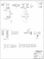
4. Chassis Layout and Overall Wiring Diagrams
Boards and Chassis Layout
No
Description
Part No.
Type/Model
PCB/Model
(1)
Main Board
121477
RSAG2.908.1553-2\ROH
RSAG7.820.1730\VER.D\ROH
(2)
Power Board
122630
RSAG2.908.1498-2\ROH
RSAG7.820.1646\VER.C\ROH
(3)
Keypad Board
113354
RSAG2.908.1088\ROH
RSAG7.820.1101
(4)
IR Board
116295
RSAG2.908.1260-2\ROH
RSAG7.820.1337\VER.B\ROH
-13-
\VER.B\ROH
5. Factory/Service
5.1 To enter
OSD Menu and Adjustment
the Factory
OSD Menu
a. With factory RC (remote control)
1. Press "M" button and enter factory mode.
2. Press "Menu" button and enter factory OSD menu.
3. Press "CH+"/"CH-" button select the function menu, press "VOL+"/"VOL-" enter the selected
function menu. Press "VOL+"/"VOL-" button adjust values in the menu.
b. With user's RC
1.
PowerTVOn
2.
3.
Press Menu button and call up User OSD Menu
Select Audio-> Balance
4.
Enter 0->5->3
5.
Note: If necessary, re-do number keys.
Factory OSD appears.
6.
Press Menu again and leave factory OSD.
5.2 Factory
5.2.1 White
Note:
OSD Menu
Balance
Different
1. Auto
->2 in sequence.
source
has different
WB values.
Before
adjusting,
please
change
to desired
source.
Color
For VGA and Component
Before adjusting,
Video sources, WB values must be adjusted.
prepare the signal instruments
such as DVD or K-8256 first, and find the video picture
with gray and color bars. Then please change to desired source.
source
Timing
1
ADC V{3A
2
ADC HDTV
Pattern
1024"768
gray-3color
720P
gray-3color
Notes:
a,
Press
"M"
b,
Press
"Menu"
c,
Select
the
d,
Press
e, Close
button
item
and
button
the
and
"Auto
VOL+ button
OSD menu
enter
to
factory
enter
mode.
factory
Color"
auto
after
color.
5 seconds.
-14-
OSD menu.
Notes
For V{3A source
For Component
Video
5.2.2
Factory
Option
Item
Default
Options
Notes
M-Can enter factory
1
with factory
M
MODE
RC or user RC.
M, U
U-Can enter factory
only with user'
Note:
MODE
"M" is only used for factory
5.2.3 Version
5.2.4
Default
Options
Note
Version
Software
2
Date
The date of current
Software
info of the TV, readable
version
version
only.
Meaning
Clean
Note
Clean
Clear partly
Protected
Clean All
_
Clear completely
Note: The factory
by error, you can choose to "Clean
to different
Protected",
except
data and Auto Color data
Clean
menu date varies according
data
all
data
sources. Incase
changing
a.
Select
the item
b.
Press
VOL+ button
c.
Close
the
d.
Restart
All".
"Cleall
to clear
OSD lllenu after
the
the EEPROMdata.
5 seconds.
TV.
5.3 Designer
Menu
Mode
Standard:
TV
AV
S-Video
Component
VGA
HDMI
R Gain
119
119
119
141
127
120
G Gain
125
125
125
145
120
122
B Gain
130
130
130
145
130
132
-15-
the factory
by which you can resume the default
To clear the EEPROM:
5.3.1 Video
version
the EEPROM
Item
data
s RC.
Info
1
Clear
mode
production.
Item
Note:
mode
value,
Offset:
TV
AV
S-Video
Component
VGA
HDMI
R Offset
116
116
116
121
124
120
G Offset
124
124
124
125
126
128
B Offset
124
124
124
125
127
128
Cool:
TV
AV
S-Video
Component
VGA
HDMI
R Gain
119
119
119
141
127
120
G Gain
125
125
125
145
120
122
B Gain
145
145
145
160
145
147
TV
AV
S-Video
Component
VGA
HDMI
R Gain
134
134
134
156
142
135
G Gain
125
125
125
145
120
122
B Gain
130
130
130
145
130
132
Warm:
5.3.2 Video
Curve:
TV
AV
S-Video
Component
VGA
HDMI
Bright
Max
600
650
650
700
700
650
Bright
Min
0
0
0
0
0
0
Bright Mid
520
550
550
550
590
530
Contrast
650
600
600
550
600
600
Max
Contrast
Min
0
0
0
0
0
0
Contrast
Mid
500
480
480
460
440
470
800
800
800
800
800
800
0
0
0
0
0
0
570
550
550
500
630
500
Hue Max
1000
1000
1000
1000
1000
1000
Hue Min
0
0
0
0
0
0
Hue Mid
471
471
471
471
471
471
Saturation
Max
Saturation
Min
Saturation
Mid
-16-
5.3.3
Picture
Mode
TV
AV
S-Video
Component
VGA
HDMI
Vivid Bright
55
55
55
55
55
55
Vivid Contrast
55
55
55
55
55
55
Vivid
55
55
55
55
55
55
Std Bright
50
50
50
50
50
50
Std Contrast
50
50
50
50
50
50
Std
50
50
50
50
50
50
45
45
45
45
45
45
45
45
45
45
45
45
45
45
45
45
45
45
Min
20
Mid
80
Max
TV
0
24
34
49
80
AV/S-Video
0
23
30
47
67
component
0
23
30
47
67
HDMI
0
19
24
35
52
VGA
0
23
30
47
67
Saturation
Saturation
Hovie
Bright
Hovie
Contrast
Hovie
Saturation
5.3.4 Volume
Note:
Curve:
Set Downmix
to "Lt/Rt".
5.4 To Exit the Aging Mode
If There
Aging
mode,
is a red
use your
"M"
moving
on the
user RC, and enter
screen,
8->0->8
it means
the
TV is in Aging
mode.
To exit the
->7 in sequence.
Note:
The above
to determine
"Factory/Service
OSD
Menu"
the appearances.
-17-
are reference
only,
please
refer
to the actual
units
6. Software
Upgrading
The software is upgraded
main board of the unit.
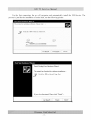
6.1 Get ready
6.1.1
Install
by a burning toll-MtkTool,
file *.bin to the
for upgrading
the driver
_L-2303
Double
which can burn the program
Briver
click the icon
, install the driver.
PL-2303Driver
Installer
Setupis:
preparing
theInstallShield?
Wizard°_,,,hieh
,,,_ill
guideyouthroughtherest
ofthesetup
process.
Pleasewait.
.........
_';'n_'_i'"'""_
Select the default value, the driver will be installed
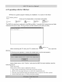
6.1.2
Hardware
Connect
step by step.
connecting
the unit to your
serial port to the TV's
RS232
pc with a USB-to-serial
port
cable.
USB
port
connects
to your
port.
USB connector: to PC.
Serial connector:
port.
-18-
to TV's RS232
J
]
pc, and
For the first connecting,
process
the pc will recognize
is just like the installation
The
-.vizard
is installing
_rzpi.
software,
and automatically
of a mini disk, see the following
Please
install the USB device.
picture.
wait....
_y_
Last
$1,_)(1_)
N e xt Nt_o['l',I)
Finish Finding New Hardware
Ca.ncel_
_/_¢Szard+
_
The wizard has finished the sofN,'are mstallatlo
"
" n :_-'
Prolific IfSB-to-Serial Comm Port
If you close thev,Jzard, Please click rtmsn . '
-19-
_
The
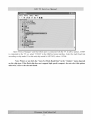
6.2 Upgrading with the MtkTool
MTKtool
is a green program
needing
no installation•
It is saved in the folder
MTR_00L_20061027
• There are five folders/files
........ A
!_{_.__
The MtkTool
whenever
_:
fl_shin£
!=_+_
[ i_!7!):_'_
i'
[i
in this folder altergether.
ini
using log is restored
MtkTool.
i_
ird
Shortcut
MtkTool,
L2:?'_
to
exe
:h_tkTool. exe
in the MtkLog folder• It records the running time and date
the tool is used. The log will be a txt file named by the date and time.
!!q
: 11:51:££,
start
2116-1£-2
MtkTool. exe
_
After connecting
the TV with your PC, double click
......................................
icon, open the
MtkTool.
If following
Ignore
following
error appears,
these
errors,
click
it means the related
"Confirm"
and enter
port is not be set properly•
the MtkTool
main
interface,
see the
picture•
Flash
chip model
Please
refer
1--Select
to follow
mode
steps to update
of Flash
2--Refer
to the next page
3--Press
the icon beside
4--Set
the software:
chip to MT538X
instruction
the baud
as the below
to select
the communicate
rate and make
the flash baud rate to 115200
as the below
- 20 -
picture.
sure it is green
picture.
port.
as the below
picture.
5--Click
the browse button to select the *.bin file that will be updated.
6--Click
the "start" button to update software.
Check Sun
LoadBinfile:
Backupfile:
_
Verify
_ BlankCheck
I_ HighSpeed
USB toUAFIT BridgeControllerI_ ShakeHand
Custom BurningAddress
Custom BurningEnd:
DirectControl
-21 -
[HEX)
Open
"Device
is connected
to the
according
Where
on the chip type.
reserve
and find which
TV; so, select
to chip model.
Note:
otherwise,
Manager"
"COM4"
For this unit(
the selected
in the MtkTool
chip model
or not click the "Auto
If the flash
port is connected
chip does not support
- 22 -
main
is MT538X),
Set Flash
mood.
with the TV. In above
Baud
interface.
select
Rate"
high speed
Select
picture,
the right
COM4
baud
rate
115200.
in the "window"
transport,
menu
do not select
depends
this option;
Fort
Baud
Rate
i
Browse i
_
Upgrade
CheckSum
>7 USB to UART Bridge Conl:rol!e[
Bumi"g AdS(eis! _
£hakeHand
_[HEX]
Cu=OmBU'oiOg
End:
.......
Click
"Browse"
button,
find the upgrading
!HE×
ClearMSG
program
file, and select
it. Press
"Upgrade"
and start upgrading.
The following
interface
LoadBin file: _
Backup file:
appears
on the screen,
indicating
uild(hkense",PH_-,
upgrading
successfully.
Check Sum
Browse
5ackLip:bin
Browse
_
Backup
P i
.I
,::A_,
SorlL
W
_ I:JL;L,J.
,
,_)=ci
--1)
"
ILq IIYI
I
_" II_:P..-')ll_<;h
I
Verify
]8I_;
{¢41
[rla;I}]}881
li:]Ib
b,<I.IZ<>MI
BlankCheck
High Speed
#_ USB to UART Bridge Controller
ShakeHand
Custom Burning Address :
[HEX]
Custom Burning End:
_"-Direct
Control
Clear MSG
- 23 -
IJ_:_b-<
0
button
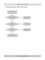
7. Troubleshooting
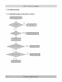
7.1 Troubleshooting
for Remote Control
YES
NO
YES
YES
NO
YES
NO
- 24 -
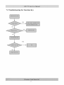
7.2 Troubleshooting
for Function
Key
YES
l
YES
- 25 -
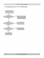
7.3 TV won't Power On
NO
NoI
NO
NO
NO
l
Neither I
Both
works
Work
YES
NO
- 26 -
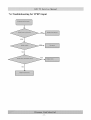
7.4 Troubleshooting
for Audio
YES
NO
YES
NO
YES
NO
YES
NO
l
- 27 -
7.5 Troubleshooting
for TV/VGA/HDMI
NO
NoI
YES
r-
- 28 -
input
7.6 Troubleshooting
for YPbPr input
YES
YES
NO
- 29 -
7.7 Troubleshooting
for Video/S-Video
NO
y
YES
YES
YES
NO
-30-
input
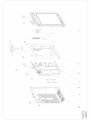
8. Explode
9. Schematic
View and Explode
Bom List
circuit diagram
-31 -
tm_
_
_z_
LT_
ELEMENT
No.
Part No.
1
ELCHW261
PARTS
LIST
Code Number
122619
Description
front cover
Qty.
1
2
1048975
lens led
1
RSAG8.640.065\ROH
3
116295
IR Board Unit
1
RSAG2.908.1260-2\ROH
4
1058744
bracket
2
RSAG8.038.1878\ROH
5
1061384
LCD Panel
1
M260TWR1\ROH
6
122630
Power Board unit
1
RSAG2.908.1498-2\ROH
7
1061396
1
RSAG4.114.126\ROH
8
1060591
1
RSAG8.081.577\ROH
9
1048779
bracket
1
RSAG6.150.452\ROH
10
1052031
back
1
RSAG8.074.526\Z1\ROH
11
121477
Unit
1
RSAG2.908.1553-2\ROH
12
1050067
bracket
1
RSAG8.038.1304\ROH
13
1059722
power cord
1
YS-05-E-I\ROH
14
1050054
cover board
1
RSAG8.632.022\ROH
15
113354
Key board unit
1
RSAG2.908.1088\ROH
16
1052188
Key bracket
1
RSAG8.078.481\Z3\ROH
17
1055277
1036391
2
1
YDT4211E-5W8R-H\ROH
18
speaker
cover board
19
1049574
base unit
1
RSAG6.121.053\ROH
20
1059711
back label
1
RSAG8.804.3509\ROH
21
1060565
side label
1
RSAG8.804.3534\ROH
bracket
unit
bracket
unit
cover
RSAG8.074.453\Z
17\ROH
RSAG8.634.047\ROH
Remark
]
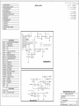
I
2,3,4,5,6,7,8,9,10,I1,12,13,1@ND
01 :INDEX/POWER
2,7,8,9,13
IN
02:DIGITAL/ANALOG
_MT5380_2LAYERS
POWER
2,6,7,8,9,11,t2,13
2,3,5,14
03:MT5380PERIPHERAL
04:DDR1
2,9,11,14
<<
_>_>
+12V
<<
_>_>
+12V
/
+5V
<<
_>_>
+5V
+3V3SB
<<
_>_>
+3V3SB
+5VSB
<<
}>}>
+5VSB
MEMORY
05: FLAS H/JTAG/UART
9
BRI_OUT<< }}
06:ANALOG
9
BRI_EXT << }}
PLL/USB2.0/TUNER
3
07:LINE OUT/HP
08:AMP/MUTE
3
3
OPWRSB_<
}}
OPWMt << _>_>
OPCTRL2<<
BRI OUT
BRI EXT
OPWRSB
OPWMt
_>_> OPCTRL2
09:LVDS/HEADPHONE
10:YPBPR
INPUT
11 :VGA IN/LR
12:HDMI
13:AV/SV
INPUT
IN FROM AV BOARD
14:1R/KEY
+5V
+5V
+12V
xP1
L1
+5VSB
121mH
$C#1uF/16V
GPIO
BI ON/OFF
DIMMING
Definition
+12V
7
GPIO
GPIO
0
1
SYSTEM
EEPROM
iCl
___100nF10402
20K/0402
HDMIEDIDWP
GPIO
3
USB POWER
EN
GPIO
4
NC
GPIO
5
NC
GPIO
6
VGA DDC WP PROTECT
GPIO
7
HDMI HDP
GPIO
8
HDMI POWER
ON/OFF
HIGH
= > OPEN
FRAME
POWER
OFF
LOW = > OPEN
FRAME
POWER
ON
R3
9
TCOM
10
USB POWER
GPIO
11
NC
GPIO
12
TMDS351S2
GPIO
13
TMDS351S1
10
POWER CONTROL
-tc3
0402/I'
0K/0402
R5
OR0!O4O2
v2 _
PROTECT
3904/N_
CEC FUNCTION
OPCTRL1
POWER
OPCTRL2
BLK ON/OFF
OPCTRL3
SOFT MUTE CONTROL
OPCTRL4
TRAP MODE
OPCTRL5
TRAP MODE
OPWRSB
POWER
i
4K7/O4021NC
POWER INPUT
LED
R7
BRI EXT
IN ON/OFF
+5V O
ADIN1,2
ADIN3
KEY BOAD
TUNER AFT
ADIN4
NC
OIRI
IR
C4
10K!0402/NC
R9
'X/X/"
1K/0402
PWRDET
___
R8 _
R1O
100nF/0402T
OPWMt
R ll
4K7%0402
Definition
RF AGC
NC
IF AGC
IF AGC FOR TUNER
..,_L_
+5V O
I
V3
I
1
_
-Lc5
-Lc6
DII_IMING
|
--_0
nF/O4O_170u F/10IN C
-----
1
R14
10K!0402
R12
10K!O402/NCwR13
ORO/0402/NC
_904
BRI OUT
P
_/X/"
"_
GPIO
OPWRSB
4K7/0402
T100nF/0402
SWITCH
OPCTRL0
ADIN0
/_+2%%3F/16V
--
GPIO
1%2nF10402
0PWRSB
m
TJC10-14A
GPIO
i
R1
WP PROTECT
11
iCE2
fT_470uF/16V
+5VS
R15.
Hisense Electric Co.,LTD
BL ON/OFF
HISENSE SHENZHEN
+3V3SB
10K/0402
'.--v'V.1oK!O402
RI_6 _
4K_/0_0
4
V4
904
l
R17
OK/O402/NC
R&D
Suite 406,1angfeng Bldg,#2 Kefa Road Nanshan District,Shenzhen,China
Te1:86-755-26532018
Fax:86-755-26532013
Title
Back Li,qht Control
•
A
INDEX/POWER IN
--
B
Size3
<Dec>
Document Number
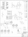
Date:
Monday. June 01, 2009
C
Ie(.
_Sheet
1
of
1
14
"
1,3,4,5,6,7,8,9,10,11,12,13,14
+5V
VTT
L
DV33
t
GI
3
IN
_
OUT
OUT
2
czi
C8
<
IR19
iCE
5
it9
I
4.7uF/10V
iiio4o?ou
2oo ,o4o
,16
CE4
R18
100nF/040 1
AZ1117/ADJ
N2
___
GND
SD
VSENSE
VREF
i
100uF/16V
_
_-_o-
300R/0402
MEM VREF_
logoc_I_L
75R/0402/NC 1 YoJ
---_
R22 o _
DDRV
VTT
PVIN
AVIN _ 6
5
VDDQ i
4K,,040
I
DDRV
C12
CE6
I
100uF/16v
I
luF T
0nF/0402
/
VTT
FOR
HEH
VREF
DDR
TERHINATOR
FOR
DDR
AND
HT5381
VREF
N3
+5V
AV33
O
C_
N4
+5V
?
DV10
4
Vcc
O/P
O/P
9oo o4o
T
"
OCSET z
uJ
_ #
>>
1
FB
'
R25
_ ]00nF/0402'
CE10
.--_.
C19
CE9
470uF/16V
--
100uF/16 1
I100nF/0402
Low
_m
1.25
ESR
<125
'R29
,
,180R/0402 _
+
CEll
t
b
,N
©
OUT
OUT
<
CE14
i
C25
<
:R30
i021
I.
0E15
i
0E16
_
OUT
_
1R03;R/040IC22
i
i
23
i
CE12
CE17 i
100uF/16V
R32
100uF/16VI
I
470uF/16V
_6nF/0402
1AZll17/ADJ
--_-_'--
I00nF/042nF/040I
100R/0402 ---"
LTC27
084
100uF/16V
--
---"
R34
100uF/16V
300R/0402
1.25 x
t
OUT
100uF/16V _
R33
3.3V
AV25
63
P_ IN
110R/0402--_0nF/0402___
100nF/0402
I
=
(1+180/110)
N6
t
DDRV
Z
iC24
100uF/16V
l
x
mOHM
N7
+5V
9
OUT
1_ AZ1117/ADJ
--___-
0.8 x (1+0.75K/2K) = 1.1V
+3V3SB
IN
100uF/16V
300R/0402
I10nF/0402
N5
3
CE 1 3
CE7
100nF/0402
+5V
i
_
;0nF/0402_
___P1534
C20
OUT
--
AZ1117/ADJ
m
-
z
R24
R28
100nF/040 t
+5VSB
: | :
_
T
i
1C18
R27
2K/0402
B340A
L
+
820R/0402
VD1
__ i0n_'0402!
2
4
,180R/0402__c_C14
iC16
f
OUT
OUT
33uH
ic13
T00nF/0402/NC
?
4,C 6vT
5
z
_
<
IN
L3
iC17
I
LP2996
_._100nF/0402
75R/0402/NC 1 Nf
L
GND
*5V
DV10
MEM VREF
VTT
DDRV
DV33
AV33
+12V
AV25
AVt2
+5V TUNER
+3V3SB
+5VSB
GND
+5V
DV10
MEM_VREF
VTT
DDRV
DV33
AV33
+12V
AV25
AV12
+5V TUNER
+3V3SB
+5VSB
1,6,7,8,9,11,12,13
5
4
4
4,5
3,5
3,6,7,9,12
1,7,8,9,13
6,13
6,10,12
6
1,3,5,14
1,9,11,14
100nF/0402
(1+180/110)
i
= 3.3v
__
120R/0402
22uF/16V/NC
_
1.25
x
(l+lO0/lOO)
N8
DIGITAL
=
2.5V
1.25 x (1+120/110) = 2.6V
AV25
POWER
AV12
C3
[)
OUT
<
i
CE18 __
100uF/16_
R35
iC28
_ ,N_AZ1117/ADJ
OUT___T
._T. C29
ICE19
C30
-- --100nF/0402
100R/0402 ___10nF/0402-_0nF/04100uF/16V
R36
__
__
0R0/0402
+12V
R37
1.25 x (i+0/i00) = 1.25V
10% tolerance
-__N10
+12V
N9
_71N
+5V TUNER
IN
OUT
C31
ADJ/GND
00nF/0402
8D08
I
CE20
i
CE21
220uF/16 1
i
470uF/16V I
£4
©
_.L_C32
I
63
Z
OUT
100nF10402
78D0_
I
10nF/0402
ANALOG
POWER
_100nF/0402
Hisense Electric Co.,LTD
POWER
SUPPLY
+5V
FOR
TUNER
HISENSE SHENZHEN
R&D
Suite 406,1angfeng Bldg,#2 Kefa Road Nanshan District,Shenzhen,China
Te1:86-755-26532018
Fax:86-755-26532013
ritle
DIGITAL/ANALOG
•
A
B
C
D
_iz;3
<Doc>
Document Number
)ate:
Monday, June 01, 2009
POWER
Ie_/.
ISheet
E
2
of
14
1
OSDA0
OSCL0
OSDA1
OSCL1
?f16
?f)7
63
6?
OPWMt
OPWM2
?f14
?f15
OXTALO
OXTALI
146
AVCC
SRV
149
AVDD33
XTAL147
ADIN3
_C 37
I
i
15,t
ADIN2
ADIN1
0 0nF/040 2.__ F/0402
C38
_
_._C61
152
151
PWRDET
150
AVDD33 REG88
C XREG
87
ORESET#
OPWRSB
71
7?
+3V3SB
OSDA0
OSCL0
OSDA1
OSCL1
OPWM0
OPWM1
OPWM2
VCXO
XTALO
XTALI
AVDD33SRV
AVDD33_XTAL
GPIO_6
GPIO_7
GPIO8
GPIO 9
GPIO _0
GPIO
GPIO
GPIO
59
6Q
717
GPIO
GPIO
GPIO
6
7
8
71,1
714
GPIO
GPIO
9
10
9?
fll
76
75
90
89
2,5
/
CE22
" R38
i
f
f
150R/0402
OPCTRL0
OPCTRLI
OPCTRL2
OPCTRL3
OPCTRL4
OPCTRL5
"_ 220uF/16V
0_
R42
100R/0402
C35
I
CEC
I>
ORESET#
,
R40
C XREG
R39
? 1K/0402
l
,- 004
VD2
12
OSDA1
<< >>
OSDA1
12
OSCL1
<< >>
OSCL1
1
OPWRSB
((
100nF/0402
14
OPCTRLI
<< >>
divider
only
for
A version
<< >>
OPCTRL2
8
OPCTRL3
<< >>
OPCTRL3
5
GPIO_O
<< >>
12
GPIO_I
<< >>
GPIO 1
GP_O_3
<<>>
GP_O
3
IC
the
power
on
6
timing
_
4K7/0402
R45
4K7/0402/NC OPCTRL5
4K7/0402/NC
GPIO_6
12
GPIO_7
(())
GPIO 7
12
GPIO_8
(()_
GPIO 8
R47_02
\
4K7/0402/NC OPWM2
-
R50
AOBCK
iC39
R52 _/0402
R56
For
I
1M/0402
3.3V
AOLRCK
R54
G1
OXTALI
Trap
Mode
OPWM2
AOBCK
AOLRCK
O
O
O
0
0
i
,
mode
q
mode
Core
Mode
OPCTRL5
Reset
1
us
O
I100nF/0402
OXTALO
GP_o9
6
GPIO_10
<< >>
GPIO 10
14
ADIN1
<<
}>)
ADIN1
14
ADIN2
<< >>
ADIN2
6
ADIN3
<< >>
ADIN3
12
CEC
(())
CEC
10PWM1
(())
OPWMt
7
_
AOBCK
AOLRCK
OSDA0
_
OSCL0
+3V3SB
AVDD33
C42
-- Z20pF/0402
AOBCK
AOLRCK
REG
820nH
--20pF/0402
12
12
120R
Trap
luF
L5
C41
ICE
<<>>
C40
TXC
I_1
60MHz
Normal
GP_o_9
_02/NC
Tarp
2K7/0402/NC
I
R55
"PWRDET
R53[__x/N_4K7/0402
9
120R
4K7/0402
\
_%/%_4K7/0402/NC
GPIO 6
AVCC SRV
DV33
\
+3V3SB
(())
GPIO 0
11
OPCTRL4
DV33
OPCTRLI
OPCTRL2
4.7uF/1OV
Adjust
OPWRSB
1
1N4148
The
_
C36
+3V3SB
R48
1K/040,I
DV33
+3V3SB
DV10
DV10
MT5380 SMD LQFP
/
AV33
DV33
+3V3SB
+3V3SB
/
OPCTRL4
OPCTRL5
ORESET
OPWRSB
0
1
3
11
12
13
OPCTRL0
OPCTRL1
OPCTRL2
OPCTRL3
AVDD33
REG
C XREG-
GPIO
GPIO
GPIO
I
GPIO-5
ADIN4
ADIN3
ADIN2
ADIN1
ADIN0
--_nF
245
?46
?f19
GPIO_0
GPIO_I
GPIO 3
GPIO-4
GND
1,2,4,5,6,7,8,9,10,11,12,13,14GND
2,6,7,9,12
2,5
1,2,5,14
N11B
i
C44
1
_
luF
1
OSDA0
OSCL0
C45
OPCTRL4
C43
1
Third-Tone
Crystal
----
lnF/0402
100nF/0402
AV33
AV33
HOLE/GND
+3V3SB
R57
10K!040:
AVDD33 XTAL
R58
I£1
N12
__vcc
R59
GPIO 0
11_
OSCL_
v
OSDA0
6 _WPI
5 I SDA
SCL
R60 10 ,0402
3904
AV33
I
4K7/0402
61
OSDA0
oo ,4o64i
No
NC
GND
NC
I-t2
i
V6
10K/0402/N_.._
L7
EEPROM 24C16
IIC
ADDRESS
120RI
C47
C48
luF
100nF/0402
HOLE/GND
H3
HOLE/GND
Lo 2
"AO"
AV33
R62
M2
M3
M4
4K7/0402
MARK
MARK
MARK
OSCL0
SH1
H4
HOLE/GND
H5
HOLE/GND
H6
HOLE/GND
Mll
M12
M13
M14
ARROW
ARROW
Label
Label
).o 2
M20
@
._4xl
W/HOUSING/._
M-RSAG7.070.201-H×
Hisense Electric Co.,LTD
HISENSE
machine
SHENZHEN
R&D
Suite 406,1angfeng Bldg,#2 Kefa Road Nanshan District,Shenzhen,China
Te1:86-755-26532018
Fax:86-755-26532013
Title
PERIPHERAL
_L
N11A
RDQS0
RDQM0
RDQ0
RDQI
11
13
9
,5
RDQ2
RDQ3
RDQ4
RDQ5
RDQ6
7
6
,5
4
3
RDQ7
RDQS1
RDQM1
RDQ8
RDQ9
?
17
1,5
1,9
?f)
RDQI0
RDQ11
RDQ12
RDQ13
RDQ14
21
22
23
24
?5
RDQI5
?6
MEM VREF 53
RCS#
46
RDQS0
RDQM0
RA0
RA7
RDQ0
RDQ1
RWE
RBAO
RDQ2
RDQ3
RDQ4
RA6
RBA1
RA5
RDQ5
RDQ6
RRAS
RA8
RDQ7
RDQS1
RDQM1
RDQ8
RA10
RA4
RCAS
RA12
RDQ9
RDQ10
RDQ11
RDQ12
RDQ13
RCKE
RA11
RA9
RA3
RA1
RDQ14
RDQ15
RA2
RCLK0
RCLKO
RVREF0
47
36
40
43
37
44
3,5
42
35
4,5
39
41
32
31
33
34
fil
4,9
50
RA0
RA7
RWE#
RBA0
RA6
RBA1
RA5
RRAS#
RA8
RA 10
RA4
RCAS#
RA 12
RCKE
RA11
RA9
RA3
RA1
RA2
?,5
?9
RCLK0#
RCLK0
MEM
MEM
MEM
MEM
ADDR12
ADDR11
ADDR9
ADDR8
ADDR7
ADDR6
ADDR5
ADDR4
MEM WE#
MEM CAS#
1
?
3
4
47x4
iN/N/N.
iN/N/N.
_
tN/_/N.
,5
7
6
5
RA12
RA11
RA9
RA8
1R_.,_x4
? iN/N/N.
3 _
4 tN/_/N.
RN12 47x4
1 iN/N/N.
? iN/N/N.
,5
7
6
5
RA7
RA6
RA5
RA4
,5
7
RWE#
RCAS#
=6
RRAS#
,5
7
6
fi
RCS#
RBA0
RBA1
RA1O
7
6
5
RA0
RA1
RA2
RA3
Add
2
2,5
2
MEM
DQ0
--
VDD
DQ0
MEM
MEM
DQI
DQ2
--
VDDQ
DO1
DQ2
VSSQ
DQ14
DQ13
MEM
MEM
DQ3
DQ4
VSSQ
DO3
DQ4
VDDQ
DQ12
DQ 11
MEM
DQ5
VDDQ
VSSQ
MEM
DQ6
DO5
DQ6
DQ10
DQ9
MEM
DQ7
VSSQ
DQ7
NC
VDDQ
DQ8
NC
MEM
MEM
DQS0
ADDR13
VDDQ
LDQS
NC
VDD
VSSQ
UDQS
NC
VREF
--
--
--
MT5380 SMD LQFP
serial
resistors
for
DRAH
VSS
DQ15
MEM
MEM
DQM0
WE#
NC
LDM
VSS
UDM
MEM
MEM
MEM
CAS#
RAS#
CS#
WE
CAS
RAS
CS
CLK
CLK
CKE
NC
MEM
BA0
NC
A12
MEM
MEM
MEM
MEM
MEM
BA1
ADDRt0
ADDR0
ADDRt
ADDR2
BS0
BS1
A10/AP
A0
A1
A11
A9
A8
A7
A6
MEM
ADDR3
A2
A3
VDD
A5
A4
VSS
.L
6,5
64
63
6?
61
6O
,5,9
MEM
MEM
MEM
MEM
CS#
BA0
BA1
ADDRt0
_'3 _,%/%.
RN14 47x4
1 'N/N/N.
2 _N/N/N.
3 *N/N/N.
4 *N/N/_.
MEM
MEM
MEM
MEM
ADDR0
ADDRt
ADDR2
ADDR3
1R_v_X4,5
2 _N/N/N.
3 *_/N/N.
4 *N/_/_.
GND
_L
Add
serial
resistors
RDQ0
MEM DQ12
MEM DQ11
MEM DQI0
MEM DQ9
51
MEM DQS1
RDQI
RDQ2
RDQ3
RDQ4
RDQ5
R71
RDQ6
RDQ7
RDQS0
RDQM0
RDQM1
MEM DQ8
RDQS1
RDQ8
RDQ9
RDQI0
RDQ11
MEM VREF
48
47
46
45
44
41
40
39
3,5
37
36
35
34
MEM
MEM
MEM
MEM
DQM1
CLK0#
CLK0
CLKEN
MEM
MEM
MEM
MEM
MEM
MEM
MEM
MEM
ADDR12
ADDR11
ADDR9
ADDR8
ADDR7
ADDR6
ADDR5
ADDR4
RDQ12
RDQ13
RDQ14
RDQ15
4RN_x4R
3 ./N/N/"
2 ./W
6
7
_R_;_4.1
6 _
7 'N/N/N.
3
2
MEMMEM
DQ3DQ
4 1R_4_
MEM DQ5 3 ./N/N/"
MEM DQ6 2 ./W
6
7
7
6
?
3
MEM DQ9
MEM DQI0
6
7
78
MEMMEMDQI5
DQI4 1? _
./N/N_
./N/N/_
?1 _
3
?
./N/N/"
./N/_/"
R-RESCA3216-8N-HX
---
R-RESC1608N-HX
MEM WE#
MEM CAS#
MEM RAS#
4 R_,/_x45
3 _
? _
6
7
MEMME
M BA0cs#
MEM BA1
MEM ADDRt0
1R_4
3 _
? ./N/_/'
5,5
6
7
+IV3DMEM
ADDR4
MEM ADDR5
MEM ADDR6
MEM ADDR7
_N_4_
3 ./N/_/_
2 ./N/N/'
1 ./N/N/"
6
7
,5
MEM CLKEN
_ _ _ -" R73
MEMvTTDD
RvVREF
+IV3D
DRAH
MEM DQ0
MEM DQI
MEM DQ2
MEM CLKEN
,./N/N.
22R
for
fiRNl_/N/N47x4 4
6 _
3
7 'N/N/N.
?
16M x 16 DDR TSOP-66
RCKE
Ill
MEM DQ14
MEM DQ13
,57
,56
RR
,54
R-TSOP66N-0.650-11.76-HX
MEM VREF
DDR_7
VTT
MEM DQ15
DDR#1
MEM RAS#
_
DDRV
N13
RCS
RN7
MEM
MEM
MEM
MEM
((
1,2,3,5,6,7,8,9,10,11,12,13,1GND
DDRV
" "_\
MEM ADDR12
MEM ADDR11
R72
_/N/N.
+IV3D
75R/NC
1R17I)l,_sv7_X4,5
2 _N/N/N.
7
MEMMEMMEM
ADDRoADDR8
ADDR9
iRN_4_
RCLKORcLK0#
j,,'_
DDRV
DDRV
'..
"/N/N'R75"/N/N'22R
ME'iMEM
CLK0#/CLK0
R74100R
-
22R _
_
MEM
MEM
MEM
MEM
_
MEM VREF
i_
CE23
1
100uFl16V
:
1C49150
--_0nF,0402
i51
i52
_00nF10402--_0nF,0402
i53
i54
_00nF10402--_0nF,0402
i55
iC561C57
_00nF/0402--_0nF/0402T100nF/0402T
iC 8
/
47uF/10v
ADDRt
ADDR2
ADDR3
ADDR13
3
2
1
R76
./N/N/_
./N/N/_
./N/N/"
_N/N/_
6
7
,5
75R/NC
C60
4.7uFIIOVINC
II
1
100nF/04_l-_
00nF/0402
I
DDRV
T
Tc65- ooF,o4o
2
T100nFI0402T100nF/0402Ic67
IC68
TI
100uF/16vCE24--h4.ct910
v
+IV3D
VTT
+ 1V3D
C79
1C74
ic75
i076
ic70
ic71
ic77
i078
1
T100nF/040T100nF/040T100nF/040T100nF/040T100nF/040T
4.7uF/10V
IC81
IC82
CE26
100uF/16V
I100nF/0402
IC80
100nF/040T100nF/040T100nF/040T100nF/040T100nF/0402
IC83
__L
T
_L_+OE
C73 FI10V"_0uF'
A-E6.3-R-HX
16v
T
Hisense Electric Co.,LTD
HISENSE SHENZHEN
R&D
Suite 406,1angfeng Bldg,#2 Kefa Road Nanshan District,Shenzhen,China
Te1:86-755-26532018
Fax:86-755-26532013
Title
DDR MEMORY
s,_3 I Document<Doc
> Number
Date:
Monday TJune 0% 2009
Ie(.o
ISheet
4
of
14
1
1
I
[
1,2,3,4,6,7,8,9,10,11,12,13,14
1,2,3,14
2,3
N15
POCE0#
POOE#
PDD0
PDD1
?fi?
?ill
?fi0
249
POCE0
POOE
PDD0
PDD1
UORX
UOTX
95
94
UORX
UOTX
93
OIRI
N14
POCE0#
1
R0/0402
OIRI
2
'
3
4
GND
253
JTMS
JTRST
JTCI<
JTDO
JTDI
7
6
fi
POCE0#
M25P16/NS
JTMS
JTRST#
JTCK
JTDO
JTDI
256
265
264
i. vo l
Q
HOLD
W /VPP
C
VSS
D
. RZ8.
PDD0
DUAL
1 I
_ I HOLD#
DV33
DV33
DV33
DV33
POOE#
PDD1
LAYOUT
_
_P02
_
_
0R0/0402
DV33
SCLK I 11
_
Ivoo
2
2,4
POOE#
PDD1
NC
C84
PO5
P01
PO4
PO0
PO3 _
GND
I '"
_ I cs#
SO/PO7
WP#/ACC I 9
I
MX25L1605/S25FL016A
GND
<<>>
GND
N11J
_L
+3V3SB
+3V3SB
DV33
DV33
DV10
DDRV
DV10
DDRV
_C85
OIRI
GND
11
14
11
3
100nF/O402_-']OnF/0402
FRESET#
UORX
UOTX
OIRI
GPIO_0
//
UOTX
UORX 0
GPIO
l/
4HB
DV33
DV33
MT5380 SMD LQFP
RN19
10K/NC
R-RESCA3216-8N-HX
JTRST#
JTMS
JTDI
JTCK
R82
JTDO
33R/0402
' R83
> 10K!0402
+3V3SB
Nlll
DVl0
O
DDRV
4R
57
5R
61
7n
164
?15
?nR
VCCK
VCCK
VCCK
VCCK
VCCK
DVDD10
DVDD10
VCCK
VCCK
VCCK
VCC210
VCC210
VCC210
VCC210
VCC210
VCC210
VCC210
VCC210
VCC210
VCC210
VCC310
VCC310
VCC310
DV33
---------
XS13
XP2
1C87
ic88
ic89
ic90
1C91
UORX
UOTX
20nF,0402ToonF,0402ToonF,04
4-7uF'lov
T luF
I
/
O
R86
R87
0R0/0402
/x
0R0/0402
L
1
R319
./N/%
0R0/0402
UORX
R
?
R320
JN/N#-0R0/0402
UOTX
TJC10-4A
BYPASS
DV33
D58
10P
10P
3
3
3
o_7
t_
E-PAD
m
MT5380 SMD LQFP
_
DVlO
DDRV
)
_
F
I
,
I
'
I_I_o 4
--4TuF'l°vTlu
I'-I
ic96
T100
ic97
n F//D0_(
21(O
ic98
1C101
1c99
I,:F/ac40T100 nF/04( T100
ic102
i
ic103
ic104
ic105
ic106
ic107
ic108
ic109
iCl10
IClll
I
nF/0402
I4.7uF11
ovT1
uF
IT
i
IOOnF/O402T
100nF/0402
T
100nF/0402
T
100nF/0402
TIOOnF/O402_I_o_IOOnF/O402TOT
100nF/040
100nF/040
100nF/0,02
I
I
CORE
BYPASS
Near
I
IC
Hisense Electric Co.,LTD
HISENSE SHENZHEN
R&D
Suite 406,1angfeng Bldg,#2 Kefa Road Nanshan District,Shenzhen,China
Te1:86-755-26532018
Fax:86-755-26532013
Title
FLASH/JTAG/UART
•
5
4
3
2
Size3
<Dec>
Document Number
Date:
Monday, June 01, 2009
Ie(.
ISheet
1
5
of
14
1
1
1
I
[
N11D
GND
USB VRT
65 I
USB DP
AVDD33 USB
AVDD12 USB
2
66 I USB-DM
67 I USB-DP
6,9 I AVDb33 USB
AVDD12-USB
USB #P
DM
]
AVDD12-TVDPLL
AVDD12 FiDMPLL
AVDD12 APLL
AVDD12 SYSPLL
65 I USB
TN0 VRT
TP0
-
_
AVDD12 PLL
157
155
16,3
161
AVDD12
AVDD12
AVDD12
AVDD12
R88
USB VRT
PLL
PLL
PLL
PLL
C112
5K1/0402 1%
AV12
--
100pF/0402/NC
AVDD12
AVDD12SKDPLL
AVUU12-ADCPLL
DMPLL I 162
156
155
AVDD12 PLL
AV12
,8
L9
MT5380 SMD LQFP
120R
AV12
+5V
AV33
AV25
+5V TUNER
AfDU12
__C118
Cl
USB
10121
131 /
_L
4-7uF/10 T
T
AVDD12 PLL
FAT
120R
iC115
c114
_L
lc116
13
313
3
1C117
luF
T4.7uF/10V
T10nF/0402
FAT IN1GPIO_3
FAT_IN1+
GPIO_10
iN1+
FAT iN1GPIO 3
GPIO 10
l/I/
I100nF/0402
N11H
AV33
MPX0P
MPX0N
166
165
TP4
AVDD25
AVSS25
SIFP
SIFN
SADC
SADC
165
167
4.7uF/10V
197
196
3
TP3
RF AGC
IF-AGC
TUNERDATA
TUNER
ADIN3
ADIN3
<< }}
AVDD25 SADC
AVSS25 SADC
AF
TUNER DATA
TUNER CLK
00nF/0402
195
RF
CLK
1 K/0402
R89
AGC
120R
_)
=
IF
ICll
AGC
AfDD33
10122
1
_L012o
+5V
9
ear
USB DP
USB DM
LIO
4.7uF/10VI100nF/0402
47nF/0402
MT5380 SMD LQFP
-%
USB
|
i
chip
i
120R/NC
xs1
i
AV25
Near
Near
Tuner
AVDD25 SADC
i
T
I
luF
D2 _r]_D1
o.15P3
_ h,o.15P
lC
R9O
70uF/16V/NC
IIC123
10nF/0402 MPX0P
0R0/0402
C125
126
AV33
AV33
C127
lcl
N16
R306
4-7uF/10v
T10nF/0402T100nF/0402
AVSS25 SADC_
/
GNU
[_ll
110128
10nF/0402 MPXON
GPIO
3
R 138
_/NA
0R0/0402/NC
I
+5V
L 14
=
_
T
T
10uH
/
10_24016V_
=
R-'NDC2012N-HX
/
VD3
ILl
_
10mA
f-'-I V,N svv
I.I
SHDN
--
FB _
,
AP1522 /
Vout = 1.25 x (1 + Rb/Ra)
I
iCE28
1N4148
"_47uF/50V
t -_, R99
_4K7/0402
_ Ra
IFA OUT
IF AGC
IFD OUT1
GND
$_tz_ GND
IFD OUT2
GND
GND
GND
GND
5
0132
R 1 O0
1 10K/0402
-lOOoRb
::
1Q
11
TPS2065/2061/NC
i0130
T
100nF/50V
ull-1
c317
GND
GND
NC
NC
NC
NC
NC
NC
RG AGC TP
NC
VT(+30V)
IF+
IFIF AGC
TUNER /-F TP
SCL
SDA
GND
BP(+5V)
NC
AFT
S_F
CVBS
TUNER CLKt
TUNER DATA1
7
_
GPIO 10
0R0/0402/NC
OC#15
+30V TUNER
_L
u2 N
NC
NC
NC
SCL
SDA
NC
VCC
-------
,) 100K/0402/NC
9-
::
N17 ,4 I
C014tF/0402
OUT _'_
OUT
41EN#
_L
"_-
R308
GNDOUT
IN
IN
100K/0402/N(
R91
_N/N/'
0R0/0402
R307
100K/0402/NC
9
CE27
C246
+30V TUNER
FAT INO+
I
9
1Q
11
12
II
FAT IN1+
10nF/0402
47pF/0402/Nc
lc129
C253
120R
FAT INO-
I
II
FAT IN1-
220K10402
47pFlO4021NC
10nF/0402
R98
GND
GND
GND
GND
GND
GND
IF AGC 1
FAT iN0FAT INO+
AV33
IF AGC 1
TUNER
TUNER
14
15
16
17
CLKt
DATA1
+5V TUNER
120R
CE29
4K7/0402
_.__C10nF/0402
131
'N/N/_
I
Close to
100nF/0402
i
470uF/16V
I100nF/0402
R102
C302
R97
/4K7/0402,
TUNER CLK/
TUNER DATA
560R/0402
560R/0402
C318
33pF/040_--
_
R96_,
Tuner
R101
_/X/"
I
__C134
_4
IF AGC
4K7/0402
i
O+5V_TUNER_I
ADIN3
53
NEAR TUNER
33pF/0402
DTVS203CH201A
GND
GNU
_
Hisense Electric Co.,LTD
DVT-8ADC1-T41FOHS
HISENSE SHENZHEN
R&D
Suite 406,1angfeng Bldg,#2 Kefa Road Nanshan District,Shenzhen,China
Te1:86-755-26532018
Fax:86-755-26532013
]]tle
ANALOG
•
5
4
3
2
PLL/USB2.0/TUNER
Size3
<Doc>
Document Number
Date:
Monday TJune 0% 2009
Ie_/.
_Sheet
1
6
of
14
0
AV33
N11G
179
176
177
176
175
174
17,3
177
171
1f!,3
1f!l
lf!?
lf!0
R103
AINOL
AINOR
AINI_L
AIN1R
AIN2_L
AIN2R
AIN3L
AIN3 R
AVDD33 AADC
AVSS33 AADC
VMID AT, DC
REFP_AADC
REFN AADC
ASPDIF
AOMCLK
AOLRCK
AOBCK
AOSDATA0
ALl
AR1
AL2
AR2
AVDD33 ADAC0
AVDD33 ADAC1
AVSS33_ADAC0
AVSS33 ADAC1
AD/_C VCM
AVDD33_DIG
AOMCLK
_)
AOLRCK
AOBCK
AOSDATA0 _)
ALIO
AR10
AL20
A R20
AVDD33 ADACO
AVDD33 ADAC1
AVSS33 ADACO
AVSS33 ADAC1
ADAC VCM
AVDD33 DIG
OUT
0E301
TP5
120R
AVSS33
100uF/16_"
TP6
_L0137
Z11uf
120R
Av33
AADCT
C145
i
T
|
l
C146
AVSS33 DIG
luF
L18f_
120R
C147
AV33
AVDD33
ADAC%
O141
AVSS33
IuF
T
?
R104
_X/N/'
20K!0402
)÷
iN0
10uF/10V
ADAC
I
XS2
R105
IN0
,'j:y_/_'_i _
I}
SPDIFOUT
100nF/0402
AIN0 R
+12V
+5V
AV33
3
AOBCK
\......
AOBCK
0I
1
143
O144
.7uFIIOVZIOOnF/0402
100nF/0402
13 AIN3 L
_
13
8 AIN3_-R
ALl_AMP
//'_'_
88 ARI_AMP
MUTE
<< >>
i
C149
l
m
AVSS33 ADAC
luF
--11100nF/0402
R
A
R286
)÷
3
AINt
AR20
+
HPOUTR
MUTE
o_
9
_
,,
wL?
yL
1
aND 5
_
HPOUTL
/
o
8
]
Rl13
L
20K!0402
10uF/10V
_
C150
',
o _____
C315
MUTE
AL20
t_
YPBPRL iN1
AIN3 L
ALI AMP
AIN3
R
AR1 AMP
XS12B
D56
10P
33K/0402
C154
C314
YPBPRR
__
XS12A
D3
10uF/10V
XS15
<(<(>>
<(<(>>
<<>>
-L
ADAO VCM
IO
O142
+5VSB
AV33
AIN0 L
20_'4402
AV2-L-A-P
1'2'8'9'13
+12V
1,2,6,8,9,1t,12,13+5V
_L
<< >>
AVDD33 ADAC1
C307
O151
?
C140
+5VSB
L20
i100nF/0402
120R
YPBPRR
l
C139
GND
<< >>
13 AL20
13
AR20
C301
AV2-L-A-P
l
SMD LQFP
XS3
YPBPRL
I0136
REFNA_OO
1 1°°nF'°4°2 _L
• ' i
Avo033
oiG
120R
10J#8
100nF/0402
AV33
'_
Z
1,2,9,11,14
T4.7uF/10vT100nFIO4022,3,6,9,12
?
4.7uF/10V
MT5380
VIMD AADC
AVDD33 AADC
_o2
2f)0
?f)l
2f)?
1,gf!
1tiff
1f!7
1,91
1f!9
1,92
1f!4
1,90
1f!6
1f!5
170
1,2,3,4,5,6,8,9,10,11,12,13,14GND
L17
REFP AADC
SPDIF
AIN0 L
AIN0 R
AINt L
AINt R
AIN2 L
AIN2 R
AIN3 L
AIN3 R
AVDD33 AADC
AVSS33 AADC
VIMD AADC
REFP AADC
REFN AADC
AV33
R262
_/N/'
20K!0402
IN1
,'j:y_/_'_i _
AINt
R
0E31
R108
ALIO
Tooo ,oh
R109
Rlll
_N/N/"
10K!0402
1oo ,o4
i of
•
0E32
Rl10
0R0/0402
HPOUTL
F,
20R/0402
__
C156
lnF/0402
Rl12
10K!0402/NC
+12V_B
470_16140_2116402
7uF/10V
--__=.-Rl14
33K'°4---"_°2
_[_0159
0E35
Rl15
AR10
33K/04"--'v_02
_L158
Rl17
0E33
._ _
ALtO
100R10402
Rl18
,_
_
_ +
22u/FlI16V
1_R122
470;1F/60040T_22
K/0402
....
_"_0pF/0402
.....
,I,
10K10402
O162----
0R010402
lnF/040;
4 7uF/C_;_N C._
/
_
I
100R/0402
CE34
N19A
I'_'-.. N19'_
/
I .>
?,
" _O4558
bEF_A
R123
R127
:,
_
?
f
R120
1
÷(
1
22uF/16V
q._2V/+5V
O169
R120
20R/04'VV_02I
ALl
._h
470pF/0402-_
I
_
R 124
HPOUTR
7
L-y oo422ou_/'16v
8 / m262°R/°4°2
___ -]-g7uF,lOV,NZ3
-
22K!0402
0K!0402/NC
--___=.-
OK!0402/NC
A
0E36
/
.....
--1oF,040
0164/VREF
Zo2V_
AMP
R121
,.,.__
6I_
I
10K!0402
R125
<
_
0R0/0402
22uF/16V
]
-r _0pF/0402
"vv,
+12V B
+12V
L21
t"mt"',
120R
?
_Z
0E38
Z
VREF_B
R128
0167
K!0"x'/X/'402
100
R129
R135
O165
100K!0402
O166
--100nF/0402
0uF/16V
0E37
R132
R133
0E39
100nF/0402
R137
100R/0402
22uF/16V
10K!0402
AR1 AMP
0R0/0402
C170
C168
R139
22uF/16V
C171
10K/0402/NC
+12V/+5V_A
470pF/0402
XS4
+12V/+5V_A
VREF_A
1
VGAL IN
R
?
VGAR IN
GND
.3
L
O152
(__
R141
L22
0R0/0402
+5V
0N0/0402/NC
I
/
f
120R
_
?
47
K/04"%/%_02
_0E41
__._c 172
100uF/16V
100nF/0402
Vll
T T
R143 ,_
4714/040
2_'
__._ 0173
/N
I
]+ 0E42
10uF/10V
+
+12V
_L
•
O153
)÷
10uF/10V
R106
_/N/'
20K!0402
R107
20K!0402
AIN2 L
Hisense Electric Co.,LTD
AIN2 R
HISENSE SHENZHEN
title
_100nF/0402_00uF/16V
D6
___
R&D
Suite 4O6,1angfeng Bldg,#2 Kefa Road Nanshan District,Shenzhen,China
Te1:86-755-26532018
Fax:86-755-26532013
LINE OUT/HP
10P
Size3
<Doc>
Document Number
Date:
Monday, June 01, 2009
Ie_/.
]Sheet
7
of
14
1
CE43
VD4
_-]_
1_ 4148
1,2,3,4,5,6,7,9,10,11,12,13,14
- 22_
GND
<<
>>
+5V
<(
>_
+5V
+12V
((
_
+12V
14
ALI_AMP
(<)>
ALI
AMP
14
ARI_AMP
(())
AR1
AMP
9
MUTE
<<
}}
MUTE
3
OPCTRL3
<<
>>
OPCTRL3
1,2,6,7,9,11,12,13
R145 I
+5V
+12V
R146
1%10410402
0R0/0402/NC l
0R0/0402
R149
R148
220R/0402
1K/0402/NC
L
R150 1 VD7
LJ 12
1K/04021N41V/8
]
R156
)
_
VD9
R155
1N414856K/0402<__
0R0/0402/NC/
]c
.J_
+5V +12V
1,2,7,9,13
lVD_4 __
GND
' 4K7/0402
R147
l
.1. VD_
_
V8
R151
-1N_I48/NC
1
VD8
bJ
nOFF MUTE1
? 39[
/_
0R0/0402
Ti
1N4148
+ CE44
R153
"_
V9
_
_
M1%T4E
IR,52 3904/NO R'54-T-10uF/'Ov/NOI47K/0402 c
220uF/16V
47K/0402
i
R157
47K!0402
VD10
R158
MTUE
1N4148
CIRCUIT
OPCTRL3
0R0/040£
I
AR1 AMP
ALt AMP
TPA7266
R
II
17
4.7uF/10V
C177
R 1 62
TPA7266 L
470R/0402
C179
100pF/0402
R160
>
10K/0402/NC
2OUT+
15
AMP-Rout+
NC1
XP3
NC3
+5V
R161
10K!0402/NC
2IN+
1IN+
II
4.7uF/10V
._LC. 178
IOOnF/O402/NC
N20
C176
R159
'N/N_
470R/0402
C175F"1
+12V
MUTE
T
L23
--_OpF/0402
121mH
CE45 il
470uF/16V"T"
/
C180
-
6
7
2OUTSGND
AMUTE1OUT+
Standby
NC2
VCC1
VCC2
1OUT-
14
AMP-RoutAMP-Lout+
3
2
1
I_D
4o
2
AMP-Lout-
--luF
PWGND
TI A7266SA
Q1
M-TO_220-15-TDA7266SA-NO-HX
4xl W/HOUSING
M-RSAG5.861.145-HX
Hisense Electric Co.,LTD
HISENSE SHENZHEN
R&D
Suite 406,1angfeng Bldg,#2 Kefa Road Nanshan District,Shenzhen,China
Te1:86-755-26532018
Fax:86-755-26532013
Title
AMP/MUTE
Size3
<Dec>
Document Number
Date:
Monday, June 01, 2009
1
Ie_z.
ISheet
8
of
14
AV33
1,2,3,4,5,6,7,8,10,11,12,13,14
AV33
NllC
A0N
A0P
A1N
AlP
A2N
A2P
CK1N
CK1P
A3N
A3P
A4N
A4P
A5N
A5P
A6N
A6P
CK2N
CK2P
A7N
A7P
244
243
242
241
239
236
?37
236
236
234
233
232
230
229
226
227
??6
??5
??4
?P3
AVDD33 VPLL
A0N
AVDD33
LVDSA
AVDD33-LVDSB
A0P
A1N
AlP
A2N
A2P
AVDD33]LVDSC
AVDD33
VPLL
CK1N
CK1P
A3N
A3P
A4N
227
231
240
AVDD33
AVDD33
AVDD33
219
AVDD33 VPLL
TP2
TN2
LVDS
LVDS
LVDS
1
C181
120R
L24
1
luF
!:N']}:ELLJ-J+gVlII,
P8
AVDD33 LVDS
I
C182
T4.7uF/10V
__L
'_i£:,L<R167/R1711@[:L{i[,
100nF/0402
/
_
L26
_
C185
luF
2,3,6,7,12
2
100nF/0402
DV33
R163
L27
LVDS OUT
+12v0
_
L28
12OR
_
fk29
l
SEL
R165
120_NC_
'4K7/0402/NC
_._ 120_.01 i
LUT]
20K!0402
L-_--_- -uz J
Iy04
luF
0335 A0P
0336
100nF/0402
C338
AtP
0337 A2P
CK1P
100nF/0402
0329 A3P
1
3
fi
7
,9
11
13
10
17
14
16
18
?0
??
24
LVDSVDD
LVDSVDD
GND
GND
AI
BRI EXT
GND
15
17
19
?1
?3
30
3?
34
36
38
A0N
031 c
AtN
A2N
CK1N
A3N
_
100nF/0402 0333 A4P
100nF/0402 3332
A5P
00nF/0402 C330A6P
lO0nF/040"; 3334
CK2P
00nF/0402 C331A7P
l
L
1
I I
C32_
032"
ITCON
SCL
VCC
SDA
100nF/0402
1-20x2
M-2P,_
II
B2P
B2N
BtP
BtN
Contro!]
VDD25
TST PGM
q
I
<<>>
+5V
<<>>
AVS3
DV33
<<>>
DV33
GPlO_9<<>)
GPlO9
BRI_EXT << >>
BRI EXT
BRI_OUT << >>
BRI OUT
_1_
100nF/0402
I
A6N 0327 100nF/0402
CK2N
c326 100nF/0402
A7N c32_ 100nF/0402
100nF/0402
0323
m
]-2.00X2.00-180-HX
m
100nF/0402
B2P
B2N
B1P
B1N
B0P
_
_
_
_
>>
G2P
G2N
>>
>>
B0N >>
(<B2P
_B2N
(,<B 1P
_<BtN
GIP >>
GIN >>
G0P
G0N
CLKP
CLKN
R2P
R2N
R1P
R1N
R0P
R0N
R175
i
R174
VDT RC
C324
100nF/0402
33
35
37
0322
VDD33
100K!040:
+5V
AVS3
I
A5N
TCON SDA
2
100nF/0402
31
[T-CON]
SCL
GND
+12V
tC46
45
44
43
42
41
40
39
38
37
36
35
34
33
32
31
3O
29
28
27
26
25
24
23
22
21
_- 2O
_- 19
18
17
16
15
_- 14
13
12
11
10
9
8
7
6
:_- 5
:_- 4
3
:_- 2
1
O190
VDD33
WP
>)
AGND AFE
GND
A4N
R172
[AS!C
>>
<_
100nF/0402
29
----100nF/0402
1K/0402
R173
1
<<
I
--I--
220uF/16vi
1
GND
+12V
03201 100nF/0402
CE48
C187
1_0402
N22
AT24C08-10TU-1.8
N21
_ I
I R
SI_D1
_
'_ I G1"I]I_'_ ''D1 _
_2]_TD2
_._'_LVDSVDD
___•__0189
IRF7314-I 100nF/0402
iC188
I
100nF/0402
100nF/0402
"--I:
GND
T I
R1671 I
56K!_0_
I I
,[ _
1 _02
GPIO 9
R169
I
- I
R168
VDD33
100nF/0402
I1°°2Fl16v
---_C186._[,_
R17_2uF T
for
R166
' 4K7/0402/NC
0E47
"T"
?
4
6
GND
GND
SEL
BRI OUT
GND
A__I
l
3
XP4
R164
4K7/0402/NC
4K7/0402/NC
LO = > LVD8 POWER OFF
A2
A0
GND
I
I
LVDSVDD
LVDSVDD
12OR
HI = > LVD8 POWER ON
A1
1,2,6,7,8,t1,t2,13
iC184
L£ i,I _i<LV )S V ) )ll<J_ 1,_',
+5Vc
A7N
A7P
EEPROH
120R
100uF/16V
DV33
fIt]It:HOS@;It{]Ii_Y._<t:3.3V
_,]'i'fR167/R171/c18611<jii£24
A4P
A5N
A5P
A6N
A6P
CK2N
CK2P
C183
|
--I_
I+ CE46
MT5380 SMD LQFP
[I20
1,2,7,8,13
N24
>>
))
_
_
>>
>)
>)
>)
>)
]>_
B2P
B2N
BtP
BtN
BOP
B0N
G2P
G2N
GtP
GiN
G0P
G0N
CLKP
CLKN
R2P
R2N
RtP
RtN
R0P
R0N
C191
K/0402
LVDSVDD
V5V
L30
luF
N23
R176
120R
):
-
ii
CE49
-
_ i VIN
©_ VOUT__
VOUT
C192
T00nF/0402
--
--
00nF/0402
3
T
100nF/0402
VIN
VOUT
LVDS
SEL
OV25V
1
DE
1'
!
,[
G1N
RSDSGND
Rxo
- CM1671A-KQ
RXCLK+
A3P
V33V
STH)_
STH
TP1 _
POL
POL ,,2,2"
BOP
B0N
G2P
G2N
G1P
LVDSVDD(2.5V)
RX2RX2+
A2N
A2P
CK1N
CK1P
A3N
N25
AIC1117-25
100uF/16 T
LVDSGND
RX0RX0+
RX1RX 1 +
A0N
A0P
AtN
AtP
_AIC1117-33
R177
V5V
15K!0402
IC193
CE50
100uF/16V
100uF/16 T
OV33V
O
PI
RX3RX3+
LVDSGND
PLLVDD(2.5)
LVDS DE(TST AGE)
SELLVDS
CKV
STV
OE
RSDSVDD(2.5V)
G0P
G0N
CLKP
CLKN
R2P
/i
CKV
STV
OE
GVOFF
GVOFF
>>
R2N
R1P
R1N
ic195
lO:U
T :6
100nF/0402
XP5
45PIN
_B
R178 _,
10K!0402 <
Debug
port
V5V
_B
V5V
[Filter
V33V
near
VDD33
T-CON]
R0P
R0N
V25V VDD25
tt
[Terminator
12°Rc196icl c19G19
luFTlu_
i
luF--lu_
1
02
1
--100nF_100n_2
100_02
100_
R181
A0N
02
_
R184
AtN
_
R186
A2N
_
R187
CK1N
_
R189
A3N
•
A
B
_
I
(<ROP
(<RON
0
5
TJCl0-5A
R179
R180 _
22R/0402
22R/0402
TP1
POE
R182-
22R/0402
STV
STV
CKV _,.-
R183 _
22R/04
OE
100R/0402
A0P
100R/0402
AtP
GVOFF
<<GVOFF
_
22R/0402
100R/0402
A2P
SCL
""T"
[
CE53
2200uF/16V
I TCON SDA _---1
TST PGM
_TH
(<POE
Hisense Electric Co.,LTD
I-IISENSE SI-IENZI-IEN
OE
C204
100nF/0402/NC
R&D
Suite 406,1angfeng Bldg,#2 Kefa Road Nanshan District,Shenzhen,China
Te1:86-755-26532018
Fax:86-755-26532013
Title
R188
100R/0402
I TCON
I 14
STH
near
I3
i
LVDS OUT / HEADPHONE
1K/0402
CK1P
100R/0402
A3P
C
D
Size3
<Doc>
Document Number
Date:
Monday, June 01, 2009
re(.1
_heet
E
9
of
14
1,2,3,4,5,6,7,8,9,1t,12,13,14
2,6,12
AV12
N11E
soYo
YOP
YON
PBOP
PBRON
PROP
SOY1
Y1P
Y1N
PBtP
PBR1N
PR1P
107
1Oh
1Q£
114
115
116
11_
11£
170
171
177
123
SOY0
Y0P
YON
PBOP
PBRON
PROP
SOY1
Y1P
Y1N
PB1P
AVDD12
DVDD12
VGA
AVSS12_RGBADC
AVDD12
RGBADC
AVSS__RGBFE
AVDD12_RGBFE
GP
GN
VSYNC
HSYNC
SOG
TN1
TP1
TP20
TP19
113
110
105
1@
DVDD12
AVSS12
AVDD12
AVSS12
AVDD12
VGA
104
106
96
99
1Q?
103
96
97
1Q0
RGBADC
11
11
11
11
11
11
11
11
11
AV12
120R
RGBADC
RGBADC
RGBFE
RGBFE
0205
10206
DVDD12
VGA
120R
T
RP
RN
BP
BN
PBR1N
PR1P
117
RP
RN
BP
BN
GP
GN
VSYNC
HSYNC
SOG
luF
AVSS12
i
RGBADil00nF/0402
I
0207
10208
luF
<<>>
<<>>--
GND
AV12
GND
_L
AV12
HSYNC
HSYNC
VSYNC
BP
BN
SOG
GP
/
GN
RP
RN
BP
BN
SOG
GP
GN
VSYNC
RP
RN
I100nF/0402
AV12
?
L34
AVDD12
RGBFE
120R
MT5380 SMD LQFP
0209
T
10210
lUFAvss12
RGBFEI100nF/0402
1' EAP,LY
]'EAP,LY
YPBPP,
HT5380
R190
CO1NECTOP,
XS5
L35
mY',
120R
YO IN
' R192
i'
,75R/0402
"--_pF/0402
PB0 IN
I
I
I
O213
1 _/N/'0R0/0402 O211
"X/N/'
R191
O212
68R/0402
II 4.7nF/0402 SOY0
II
10nF/0402 y0p
I
PRO IN
R193
AV3-L-Y-P
R194
0R0/0402
m
C214
II10nF/0402
y0 N
II 10nF/0402
PBOP
C217
II10nF/0402
PBRON
R2OO_N/N/_ 0219
68R/0402
ii10nF/0402
PR0 P
100R/0402
II
_
_B
q
L36
fm¢_
120R
R195
_N/N/_
68R/0402
R196
_ _Dll
h, 10P
i
I
II
O216
I
t_
._L
O215
q
t_
75R/0402
_ VD12
h,10P
R199
-
L37
t15pF/0401,
.--[--O218
75R/0402
R197
R198
0R0/0402
100R/0402
II
I
i 15pF/0402
120R
R235
XS7
,
L67
Y1 iN
120R
PBt
iN
D21
k,10P
R229
i
_02
028°
I
68R/0402
0309
II 47nF/°4°2
SoY1
0312II1°nF'°4°2 1p
I
PR1 IN
75R/0402 -_pF/0402
--
D
AV3-L-Y-P
I
R236 R2310243
II10nF,0402 1N
0R0/0402
100R/0402
I
_B
T
L65
_
120R
D22
k,10P
R230
._[
O311
i
R233_
i
68R/0402
O313
i i 10nF/0402
PB1P
O310
I I 10nF/0402
PBR1N
I
I
I
I
75R/0402
15pF/04021
i
._L
R237
R232
0R0/0402
100R/0402
II
Hisense Electric Co.,LTD
I
I
r D23
HISENSE SHENZHEN
I
R228
k,10P
75R/0402
L66
120R
-- Z c242
R&D
i
15pF/04021
_
,
P
R234
_
68R/0402
O241
in 10nF/0402
II
Suite 406,1angfeng Bldg,#2 Kefa Road Nanshan District,Shenzhen,China
Te1:86-755-26532018
Fax:86-755-26532013
PR1P
]-itle
YPBPR INPUT
•
5
4
3
2
Size3
<Doc>
Document Number
Date:
Monday, June 01, 2009
Ie_/.
_Sheet
1
10
of
14
1
1,2,3,4,5,6,7,8,9,10,12,13,14
1,2,6,7,8,9,12,13
GND
<_<__>_>
+5V
<_<__>_>
HSYNC
+5V
XS6
D-SUB15
UOTX
o
1?
o
13
o
o
)
o
)
HSYNC#
o
)
VSYNC#
UORX
6
1
7
?
8
3
9
4
)
VGASDA IN
VGASCL
R205
NEARLY
NEARLY VGA CON.
IC
IN
14
o
15
o
o
BN
RP
RN
UoRxUOTX
_
R202
RED GND
RED
GRN GND
GRN
BLU GND
BLU
L38
VD11
GRN
l _/_/'0R0/0402
--
1N4148
t
VD12
A
UORX
GP_O_6<<>>
Ir
11
GP
GN
BP
GP
GN
BP
BN
RP
RN
UOTX
_L
R201
100R/0402
SOG
SOG <<:
10
10
10
10
10
10
10
_L
+5V
VSYNC
HSYNC
lO w .c
10
GND
_1
68R/0402
0R0/0402
100R/0402
6
1147nF/0402SOG
0220
_
GPIO
10nF/0402
GP
10nF/0402
GN
120R
R204
_J[_D13
L0222
VGA PLUGPWR
1N4148
)
GRN GND _10P
o-
100R/0402
1 75R/040_'_pF/0402
VGA_PLUGPWR
VGA PLUGPWR
L39
k.
_
10P
BLU
10nF/0402
jr D14
t
__----
__
BP
lC225
I
R210
120R
R209
_---
/
10226
10K!0402 f
R211
HSYNC#
=
L40
f.ym
BLU
GND
_D15
75R/040T5pF/0402
HSYNC
0R0/0402
L41
t
_
680R/0402
D016
J | 10nF/0402
II
L42
I
WP
SOL
vcc
NC
NC
NCI-i---I,
SDA G.oJ-----I i
E'-E'P"R
O M _2"
10nF/0402
t
RP
N : WP ENABLE
L : WP DBABLE
L0230
120R
75R/040T5pF/0402
R217 R2180231111onF,o4o2R.
0R0/0402
VSYNC
VGAROMWP
100R/0402
GPIO
680R/0402
7
--_¢_
BN
0228
REO
VSYNC#
100R/0402
5pF/0402
R216
R219
0227
_0229
RED
0K!0402
I
120R
</214
R213
100nF/0402
VGAROMWP
VGASCL
VGASDA
R212
!
N26
6
R220
J
1
120R
v12
0232
DI#
<_ R22110402
5pF/0402
10K!04'%/X_02
R222
_i
VGA_PLUGPWR
VGA_PLUGPWR
R225
'N/N/"
100R/0402
IN
D19
10P
VGASCL
0233
10K!0402/NC _
10K!0402
R226
'N/N/"
100R/0402
VGASDA IN
D20
10P
-- --100nF/0402
3904
R224
R223
10K!0402
VGASCL
i"__
VGASDA
C234
100nF/0402
Hisense Electric Co.,LTD
HISENSE SHENZHEN
R&D
Suite 408,1angfeng Bldg,#2 Kefa Road Nanshan District,Shenzhen,China
Te1:86-755-26532018
Fax:88-755-28532013
Title
VGA IN
Size3
<Doc>
Document Number
Date:
Monday, June 01, 2009
Ie_/.
_Sheet
11
of
14
1
1
[
AV33
N11K
RXOB
RXO
RXOB
RX0
RX1B
RX1
RX2B
79
_fl
R1
R2
R3
R4
R5
RX2
R6
L43
AVDD33
12°
RX0 CB
RX0-C
RX0-0B
RX0-0
RX0-1B
RX0-1
RX0-2B
RX0[2
OPWR-0_5V
73
AVDD33 HDMI
AVDD12_-CVCC
7R
74
OPWR
T
I_ 'uF
1
H
_Ls266I
5V
AVDD33 H
AVDD12 CVCC
T
L61
_[_C237
__L4ZuF"°v
I'°°n_'°4°2
AV12
1
120R
.----
AV33
EXT
RES
I_-Z_-_Tp21
CE56
lo
_y
AV33_HDMI
?
306
1.2.3A.5.6J.&9,10,11,13,14
GND
<(_ _>_>
GND
+SV
L_
120R
i
MT5390 SMD LQFP
AVDD12
C239
CVCCI
0240
AV33
I
luF
I
4"7uF/10V
1
_0
OnF/0402
100nF/0402
I i 00_J-0402/N C
1
R327
10KJ0402/NC
R329
10K/0402/NC
R325
"VV'
4K7/0402/NC
2.3.6,7,9
2,6.10
2,6.10
AV33
AV12
+3V3SB
33
GPIO 1
GPIO-7 _
GPlO
GPlO 71--
s
sp_o_6<< >>
_p_o6
3
OSDA1
OSCL1
33
OSDAO
OSOLO
_L
AV12
_
)_
+3V3SB
CEC
1
V14
OSCL1
OSDA0
_
_
OSCL0
AV33
?
R324
C305
_ R321
L
$K7/0402
N27
R323
I
_C304
10K/0402
AV33_HDMI
2.2uF/10V
EEPROM 24C02
R-SOICO8N-1.270-6.00-HX
100nF/04_
OSCL1
V16
OSDA1
3904
AV33_HDMI
R322
02
N28
33P-J0402
47K/0402
4K7/0402
AV33_HDMI
R331
0R0/0402/NC
HDMI EDID EEPROM
----POW1
R261
HDM_SDA
<
_ HPD SINK
4_
I_ SDA_SINK
39
R270
_/X/
38
R272
_/X/
1
SCL SINK
HDMISCL
12C CTRL
1
EN
R274
_/X/
100R/0402
GPIO
7
100R/0402
R264
OSDA1
R278
_
100R/0402
OSCL1
,17
GND
BRGEN
Z1
35
RXCB
34
RXC
RXICB
Y1
RX1O
VCC
3?
RXOB
3I
RX0
D24
_t4
_ o1_p
RXO 2
RXO 2B
D27 Yk_l
PS321
RXO 1
D26 Yk_l
RXO 1B
RX1
D29 Yk_l
RXO 0
RX1
D28 Yk_l
OB
O
RXO 0B
RXOC
D31 rk"l
RX1
OEO
RXOCB
RX1
rk"l
RX1
HDMISOL
HDMISDA
0
R305
0
47K/0402
Rg]4
W
47K/0402
RX1
HDMISCL
_5
0
POW6
HPD6
R281
R280
1B
_V_
R259
39K/0402
1
2B
2
R279
1 K/0402
100R/0402
100R/0402
29
RXIB
Y3
?8
RX1
R263
Z4
26
RX2B
Y4
?5
RX2
GND
2,1
ADDR
23
CTL
??
SI/S_DA CTL
?I
S2/SCL
POW0
HDMI VCC0
Z3
VCC .-2.7--
$3/120
-
GND
3n
AV33_HDMI
- R271_
R269_N/N/
100PJ0402
OSDAO
100R/0402
©I
_
i-
R276
__R266_/N/10OR/0402
IOK/0402
R315
OSOL0
0K/0402
AV33_HDMI
D44
_
..?n47Dl__
o
1
0.15P
RX12
9
D45
9
D46
9
D48
9
D49
9
D50
9
D51
9
1
0.15P
RX1 2B
1
0.15P
RX1
1
1
0.15P
RX1
1B
1
0.15P
RX1 0
1
0.15P
RX1 0B
1
0.15P
RX1C
112,_1
_'m."l
112,_1
_'m."l
112,_1
_'m."l
112,_1
_'m."l
112,_1
_"k"l
112,_1
_"k"l
112,_1
AV33_HDMI
TC= 1c 911c=
4.7uF/10V
1
0.15P
RX1CB
RX1
RX1 0B
RX1C
HDMISCL
1
1c 901c 961c=
/c=
T00oF,0402_.jTOOnF,040=TOOnF,040
_j.YOOnF,040=T00oF/0402_j.TOOnF/040=T00oF/040
_tq00oF/0402
__&
1_
o
R304
47_0402
R287
W
47K/0402
HDM_SDA 1
OEO
HDMISOL
HDMISDA
POW1
HPD1
R285
R284
11
R282
_^_
R283
39_0402
_
100P-J0402
100P-J0402
HDMI VCC1
1_0402
R326
_0402
Hisense
Electric
Co.,LTD
HISENSE SHENZHEN R&D
I Suite 406,1angfeng BId9,#2 Kefa Road Nanshan District,Shenzhen,China
I
Fax:86-755-26532013
le
HDMI
A2
<Doc>
pate:
•
A
B
C
D
INPUT
1.1
Monday_ June 01_2009
_Sheet
E
12
of
14
|
"
AV25
GND
1,2,3,4,5,6,7,8,9,10,11,12,14
2,6
N11F
CVBS0
CVBS1
SY0
SC0
131
129
l?f!
177
CVBS0
CVBS1
SY0
SC0
SY1
SC1
Near chip
135
133
VlNDC
134
D2SA_I
13f!
VIP ATV
VIN-ATV
VlNDC
DVDD25
DVSS25
GND
141
14?
13?
130
124
DVDD25
VADC
DVSS25
VADC
GND TUNER
GD CVBS
GNDSV
AVDD25
AVSS25
VIP ATV
VIN ATV
DVDD25
VADC
VADC
TUNER
GND
GND
_._E._.
FAT iN1+
CVBS
SV
AVDD25
AVSS25
L46
7 47pF/0402
I
VADC
VADC
AVDD25REF
AVSS25REF
AVDD25VFE
AVSS25VFE
VADC
VADC
AVDD25
AVSS25
AVDD25
AVSS25
025"
._1._ C293
390nH
L49
33pF,040_--I--
33pF/0402
m
luFDVSS25
VADC
For
digital
Tuner
Av25
<<>>
Av25
+5V+12V
_
+5V
._L
-
+12V
t,12
6
FAT_IN1+
_
6
FAT_IN1-
<< >> FAT IN1-
AV25
VADC
120R
AL20
C258
i
1
C259
1
100nF/0402
filter
100nF/040Z00nF/0402
>> FAT IN1+
A_N3J_ <<>> A_N3
[_
A_H3_R <<>> A_.3R
C257
MT5380 SMD LQFP
I100nF,0402
II'
T
100pF/0402/NC
c,_L c250
-m.--100pF/0402/NC
JI
VlN ATV
AVDD25
D2SA
1,2,6,7,8,9,1
C252
C255 _ _ 27pF/0402
47pF10402
C292_C256
4.7uF/10V
AVSS25
luF
T
Near
1
C251
GND
VIP ATV
1(3248
-r_7p F/0402/N
|
_.
,11
_
0R0/0402
i 220nH/NC
L50
L47
220nH
390nil
R95
,N/N/_
I 0_0,0402_k
0249
i
C247
220nH
FAT iN1-
-
220nH
_ L52
REF
REF
VFE
VFE
0402
L45
33pF/0402
14,3
144
13,9
140
137
136
i
>>
1,2,7,8,9
120R
Ic308
C244
VADC
_
VADC
AR20AL20 _
7
7
AR20
chip
Near
Tuner
Near
IC
AV25
C260
+12V C
+12V
47nF/0402
I
C261
AVDD25 REF
CVBS0
1_t
I
'
C262
7pF/0402
GND
_I_
-
t
I
120R
f
120R
TUNER
i
luF
CE61
i
VREF_C
?
R30O
47 04"f 0 I
._L C300
R301
2..
C263
1C264
AVSS25 REF
luF
m
i100nF/0402
._LC299
AV25
I00uFI16T00nF/0402
47K/0402 l
T
100nF/0402
AVDD25 VFE
120R
iC266
I
C267
R299
33_°4"_"_°2
_ 0296 I
AL20
)+C291
__',,/N,f'
R293
R295
_--2-
_Tl°°pF/°4_l
*I_
10uF,_ov10_0402
0_0,0402
w-F c
CE60
N29A
,3J+l_
AVL
logo7
XS9
AV0 IN
NEARLY
AV
NEARLY
CONNECTOR
HT538@
R241
+ (
_
22uF/16V_
C265
120R
100N/0402
R242
75R/0402
D34
h, 10P
i
i
i
_B
0270
II
AVLIN
II
II
GNDCVBS
l!u O
R292
10uFll0V
R296
--_
R244
C271
AVRIN
AR20
C269
C294
+
luF
10uFll0V
R303
"X/N/'
470R/0402
AV AUR OUT
R297
47nF/0402
33K/0402
R243
'N/N/'
0R0/0402
AV AUL OUT
0K/0402/NC
iC268
47pF/0402
R302
_N/N/_
470R/0402
I100nF'0402
R294
CVBS1
AVRIN
SIDE_
AVSS25 VFE
luF
- 1o ,040
-[-4.TuF,lOV
l v_o
AVLIN
L58
m
20"*'_402
AIN3 L
R245
,N/N/_
20K!0402
AIN3 R
j_
C295
TI°°pF'_4_9:
0R0/0402VRF_ C
C290
.--[-- C298
lnF/0402
-_=.-
IAVR
÷( _
5 I+/
111"
I4-TuF/1OV
CO4558
J
L_V-
c
_ 10K/0402/NC
D36
D35
L 10P
XSll
10P
c,
-
I
L59
SC0 IN
I
12o
II
100R/0402
1R247
D37
C272
R246
I
LI
sco
1
AV AUL OUT
47nF/0402
F
i0273
AV AUR OUT
10P
XSlO
5R/040217pF/040_
9
_D53
R248
GND
SYO IN
_
D54
10P
i
100R/0402
R249
C275
Hisense Electric Co.,LTD
47nF10402
HISENSE SHENZHEN
I
R250
175R/0402T47pF/0402
__
C274
C276
GND
I
0N0/0402
I
SV
]-itle
luF
AV/SV IN FROM AV BOARD
I
•
5
4
R&D
Suite 406,1anofeng Bldg,#2 Kefa Road Nanshan District,Shenzhen,China
Te1:86-755-26532018
Fax:86-755-26532013
3
2
Size3
<Doc>
Document Number
Date:
Monday, June 01, 2009
Ie_/.
ISheet
1
13
of
14
1
I
I
[
I
+3V3SB
TO KEY BOARD
1,2,3,4,5,6,7,8,9,10,11,12,13
GND
<<
_>_>
GND
R251 _-
/
+3V3SB
1,2,3,5
1,2,9,1t
R253
10R/0402
ADIN1ADIN2
2K2/0402 t
f
C278
r D39',D40
i, 10PA
10R/0402
I
ADIN2ADIN1
_
5
OiRI
<<
_>>
OiRI
3
OPCTRLI
<<
_>)
OPCTRLI
ADIN1
TJCl0-4A
I
10P
C62
+5_
)
+5VSB
3 _,,,_
lnF,o4o_.____TnF,o4o2; +3_
m
_
XP7
'gv"
R254
C277 -J--
+3V3SB
+5VSB
ADIN2
I10uF/NC
10R/0402/NC
+5VSB
+5VSB
R256
R255
l
10R/0402
4K7/0402 _
XP8
PW LED
PWR iR
PWR
C279
I
PW
_--_ 00nF/0402 "t
iR
OPCTRLI
CE54
"
,,1t
22uF/16v
._L
OIRI
LED
R258
IR
_R2_51
1
1fio o2- mv15
3904
TJC10-5A
10R/0402
TO IR/LED
BOARD
Hisense Electric Co.,LTD
HISENSE
SHENZHEN
R&D
Suite 406,1angfeng Bldg,#2 Kefa Road Nanshan District,Shenzhen,China
Te1:86-755-26532018
Fax:86-755-26532013
title
IR/KEY/BLKON/DIMMING
A
Size
Document Number
_
<Doe>
3ate:
Monda
L__
June 01 2009
heet
E
14
of
14