1
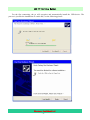
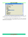
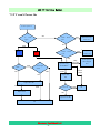
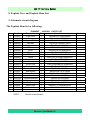
LCD Television
Service Manual
Chassis: MT5380
Product Type:40LE45S、40LC45S
Ver 1.0
Hisense Electric Co.,Ltd.
March,2009
LCD TV Service Manual
Contents
Contents.......................................................................................................................................................................- 2 Service Manual ...........................................................................................................................................................- 3 1. Precautions and notices.....................................................................................................................................- 3 1.1 Warning...................................................................................................................................................- 4 1.2 Notes.......................................................................................................................................................- 7 2. Product Function Specifications .....................................................................................................................- 10 2.1 Product Function...................................................................................................................................- 10 2.2 Specifications........................................................................................................................................- 11 3. LCD Panel Spec..............................................................................................................................................- 12 3.1General Description ...............................................................................................................................- 12 3.2 General Features ...................................................................................................................................- 13 4. Chassis Layout and Overall Wiring Diagrams ...............................................................................................- 14 4.1 Boards and Chassis Layout...................................................................................................................- 14 4.2 Wires and Cables Overall Wiring Diagram(s)......................................................................................- 15 5. Factory/Service OSD Menu and Adjustment..................................................................................................- 16 5.1 To enter the Factory OSD Menu ...........................................................................................................- 16 5.2 Factory OSD Menu...............................................................................................................................- 16 5.3 Designer Menu......................................................................................................................................- 17 5.4 To Exit the Aging Mode........................................................................................................................- 19 6. Software Upgrading........................................................................................................................................- 20 6.1 Get ready for upgrading........................................................................................................................- 20 6.2 Upgrading with the MtkTool ................................................................................................................- 22 7. Troubleshooting ..............................................................................................................................................- 26 7.1 Troubleshooting for Remote Control ....................................................................................................- 26 7.2 Troubleshooting for Function Key........................................................................................................- 27 7.3 TV won’t Power On..............................................................................................................................- 28 7.4 Troubleshooting for Audio....................................................................................................................- 29 7.5 Troubleshooting for TV/VGA/HDMI input..........................................................................................- 30 7.6 Troubleshooting for YPbPr input..........................................................................................................- 31 7.7 Troubleshooting for Video/S-Video input.............................................................................................- 32 8. Explode View and Explode Bom List.............................................................................................................- 33 9. Schematic circuit diagram ..............................................................................................................................- 33 -
Hisense Confidential
-2-
LCD TV Service Manual
Service Manual
1. Precautions and notices
BEFORE SERVICING THE LCD TV, READ THE SAFETY PRECAUTIONS IN
THIS MANUAL.
WHEN REPLACEMENT PARTS ARE REQUIRED, BE SURE TO USE
REPLACEMENT PARTS SPECIFIED BY THE MANUFACTURER.
Proper service and repair is important to the safe, reliable operation of all Hisense
Electric Co., Ltd Equipment. The service procedures recommended by Hisense and
described in this Service Guide are effective methods of performing service operations.
Some of these service operations require the use of tools specially designed for the
purpose. The special tools should be used when and as recommended.
It is important to note that this manual contains various CAUTIONS and NOTICES
which should be carefully read in order to minimize the risk of personal injury to service
personnel. The possibility exists that improper service methods may damage the
equipment. It is also important to understand that these CAUTIONS and NOTICES ARE
NOT EXHAUSTIVE. Hisense could not possibly know, evaluate and advise the service
trade of all conceivable ways in which service might be done or of the possible
hazardous consequences of each way. Consequently, Hisense has not undertaken any
Hisense Confidential
-3-
LCD TV Service Manual
such broad evaluation. Accordingly, a serviceman that uses a service procedure or tools,
which are not recommended by Hisense, must first satisfy himself thoroughly that
neither his safety nor the safe of the equipment will be jeopardized by the service
method selected.
Hereafter throughout this manual, Hisense Electric Co., Ltd will be referred to as
Hisense.
1.1 Warning
1.1.1
Critical components having special safety characteristics are identified with a
by the
Ref. No. in the parts list. Use of substitute replacement parts, which do not have the
same specified safety characteristics, may create shock, fire, or other hazards.
Under no circumstances should the original design be modified or altered without
written permission from Hisense. Hisense assumes no liability, express or implied,
arising out of any unauthorized modification of design. Serviceman assumes all liability.
DANGERCAUTION CAUTION
TO ENSURE THE CONTINUED RELIABILITY OF THIS PRODUCT, USE ONLY
ORIGINAL MANUFACTURER'S REPLACEMENT PARTS, WHICH ARE LISTED WITH
THEIR PART NUMBERS IN THE PARTS LIST SECTION OF THIS SERVICE GUIDE.
1.1.2.
All ICs and many other semiconductors are susceptible to electrostatic discharges (ESD).
Hisense Confidential
-4-
LCD TV Service Manual
Careless handling during repair can reduce life drastically. When repairing, make sure
that you are connected with the same potential as the mass of the set by a wristband with
resistance. Keep components and tools also at this same potential.
1. Never replace modules or other components while the unit is switched on.
2. When making settings, use plastic rather than metal tools. This will prevent any
short circuits and the danger of a circuit becoming unstable.
1.1.3
To prevent electrical shock, do not use this polarized ac plug with an extension cord,
receptacle, or the outlet unless the blades can be fully inserted to prevent blade exposure.
To prevent electrical shock, match wide blade or plug to wide slot, fully insert.
1.1.4
When replacement parts are required, be sure to use replacement parts specified by the
manufacturer or have the same characteristics as the original part. Unauthorized
substitutions may result in fire, electric shock, or other hazards.
1.1.5
Safety regulations require that after a repair the set must be returned in its original
condition. In particular attention should be paid to the following points.
-Note: The wire trees should be routed correctly and fixed with the mounted cable
clamps.
-The insulation of the mains lead should be checked for external damage.
1.1.6
Hisense Confidential
-5-
LCD TV Service Manual
(1) Do not touch Signal and Power Connector while this product operates. Do not
touch EMI ground part and Heat Sink of Film Filter.
(2) Do not supply a voltage higher than that specified to this product. This may damage
the product and may cause a fire.
(3) Do not use this product in locations where the humidity is extremely high, where it
may be splashed with water, or where flammable materials surround it. Do not install
or use the product in a location that does no satisfy the specified environmental
conditions. This may damage the product and may cause a fire.
(4) If a foreign substance (such as water, metal, or liquid) gets inside the panel module,
immediately turn off the power. Continuing to use the product may cause fire or
electric shock.
(5) If the product emits smoke, and abnormal smell, or makes an abnormal sound,
immediately turn off the power. Continuing to use the product, it may cause fire or
electric shock.
(6) Do not disconnect or connect the connector while power to the product is on. It
takes some time for the voltage to drop to a sufficiently low level after the power has
been turned off. Confirm that the voltage has dropped to a safe level before
disconnecting or connecting the connector.
(7) Do not pull out or insert the power cable from/to an outlet with wet hands. It may
cause electric shock.
(8) Do not damage or modify the power cable. It may cause fire or electric shock.
Hisense Confidential
-6-
LCD TV Service Manual
(9) If the power cable is damaged, or if the connector is loose, do not use the product:
otherwise, this can lead to fire or electric shock.
(10) If the power connector or the connector of the power cable becomes dirty or dusty,
wipe it with a dry cloth. Otherwise, this can lead to fire.
(11) Use only with the cart, stand, tripod, bracket, or table specified by the
manufacturer, or sold with the apparatus. When a cart is used, use caution when
moving the cart/apparatus combination to avoid injury from tip-over.
1.2 Notes
Notes on Safe Handling of the LCD panel and during service
The work procedures shown with the Note indication are important for ensuring the
safety of the product and the servicing work. Be sure to follow these instructions.
• Before starting the work, secure a sufficient working space.
• At all times other than when adjusting and checking the product, be sure to turn OFF
the POWER Button and disconnect the power cable from the power source of the TV
during servicing.
• To prevent electric shock and breakage of PC board, start the servicing work at least 30
seconds after the main power has been turned off. Especially when installing and
removing the power board, start servicing at least 2 minutes after the main power has
been turned off.
• While the main power is on, do not touch any parts or circuits other than the ones
Hisense Confidential
-7-
LCD TV Service Manual
specified. If any connection other than the one specified is made between the measuring
equipment and the high voltage power supply block, it can result in electric shock or
activation of the leakage-detection circuit breaker.
• When installing the LCD module in, and removing it from the packing carton, be sure
to have at least two persons perform the work.
• When the surface of the panel comes into contact with the cushioning materials, be
sure to confirm that there is no foreign matter on top of the cushioning materials before
the surface of the panel comes into contact with the cushioning materials. Failure to
observe this precaution may result in, the surface of the panel being scratched by foreign
matter.
• When handling the circuit board, be sure to remove static electricity from your body
before handling the circuit board.
• Be sure to handle the circuit board by holding the large parts as the heat sink or
transformer. Failure to observe this precaution may result in the occurrence of an
abnormality in the soldered areas.
• Do not stack the circuit boards. Failure to observe this precaution may result in
problems resulting from scratches on the parts, the deformation of parts, and
short-circuits due to residual electric charge.
• Routing of the wires and fixing them in position must be done in accordance with the
original routing and fixing configuration when servicing is completed. All the wires are
routed far away from the areas that become hot (such as the heat sink). These wires are
Hisense Confidential
-8-
LCD TV Service Manual
fixed in position with the wire clamps so that the wires do not move, thereby ensuring
that they are not damaged and their materials do not deteriorate over long periods of time.
Therefore, route the cables and fix the cables to the original position and states using the
wire clamps.
• Perform a safety check when servicing is completed. Verify that the peripherals of the
serviced points have not undergone any deterioration during servicing. Also verify that
the screws, parts and cables removed for servicing purposes have all been returned to
their proper locations in accordance with the original setup.
The lightning flash with arrowhead symbol, within an equilateral
triangle is intended to alert the user to the presence of uninsulated
dangerous voltage within the products enclosure that may be of sufficient magnitude to
constitute a risk of electric shock.
The exclamation point within an equilateral triangle is intended to alert
the user to the presence of important operating and maintenance (servicing)
instructions in the literature accompanying the set.
Hisense Confidential
-9-
LCD TV Service Manual
2. Product Function Specifications
2.1 Product Function
Front Cabinet
Hisense Confidential
- 10 -
LCD TV Service Manual
Back Cabinet
2.2 Specifications
Hisense Confidential
- 11 -
40LE45S
1920
40LC45S
1080
230W
VideoX2
S- VideoX1
ComponentX2
HDMIX3
AV Audio X 2
Component Audio X 2
VGA Audio Input X 1
AV Audio X 1
Optical Audio out x 1
Length: 39.1 inches
Width: 12.2 inches
Height: 28.3 inches
55.1 lbs
LCD TV Service Manual
3. LCD Panel Spec
LTD42W29NUS:
Panel: LTA400HA07\JK\ROH
SN:1051263
3.1General Description
Hisense Confidential
- 12 -
LCD TV Service Manual
3.2 General Features
Hisense Confidential
- 13 -
LCD TV Service Manual
4. Chassis Layout and Overall Wiring Diagrams
4.1 Boards and Chassis Layout
No
Description
Part No.
Type/Model
PCB/ Model
(1)
Main board
120639
RSAG2.908.1375-7\ROH
RSAG7.820.1525\VER.A\ROH
(2)
Power board
117734
RSAG2.908.1192-11\ROH
RSAG7.820.1185\VER.E\ROH
(3)
AV board
113354
RSAG2.908.1232\ROH
RSAG7.820.1342\VER.B\ROH
(4)
keypad board
112829
RSAG2.908.1088\ROH
RSAG7.820.1101\VER.B\ROH
(5)
IR board
115138
RSAG2.908.1048\ROH
RSAG7.820.1013\VER.A\ROH
Hisense Confidential
- 14 -
LCD TV Service Manual
4.2 Wires and Cables Overall Wiring Diagram(s)
No
DESCRIPTION
SPECIPICATION
NOTE
1
LVDS signal
HX2-2X20KLB350P-LG\ROH
Main BDXP9<-->Panel
2
Audio out put (R/L)
TJC3H-4Y-650-900\ROH
Main BD XP8<-->Speakers
3
Buttons
TJC10T-3Y-900\ROH
Main BDXP12<--> Key BD XPK1
4
Led & IR
TJC10T-5Y-900\ROH
Main BD XP13<-->IR &LED BD XPR01
5
AV and S-video signal
HX-2026C550\ROH
Main BD XP11<-->AV BD XP01
6
Headphone signal
TJC3T-4Y-400\ROH
Main BD XP10<-->AV BD XP02
7
Series upgrade
TJC10T-4Y-350\ROH
Main BD XP7<-->AV BD XP03
8
Audio Amplifily
TJC10T-4Y-250\ROH
Power BD XP808<--> Main BD XP5
9
+5V, +12V supply to Main BD
TJC10T-14Y-250\ROH
Main BD XP3<-->Power BD XP812
10-1
Backlight Power
HX-3005B450\ROH
Power BD XP809<--> Panel left backlight port
10-2
Backlight Power
HX-3004B550\ROH
Power BD XP815<--> Panel right backlight port
Hisense Confidential
- 15 -
LCD TV Service Manual
5. Factory/Service OSD Menu and Adjustment
5.1 To enter the Factory OSD Menu
a. With factory RC (remote control)
1. Press “M” button and enter factory mode.
2. Press “Menu” button and enter factory OSD menu.
3. Press “CH+”/“CH-” button select the function menu, press “VOL+”/“VOL-” enter the selected
function menu. Press “VOL+”/“VOL-” button adjust values in the menu.
b. With user’s RC
1. Power TV On
2. Press Menu button and call up User OSD Menu
3. Select Audio-> Balance
4. Enter 0->5->3 ->2 in sequence.
Note: If necessary, re-do number keys.
5. Factory OSD appears.
6. Press Menu again and leave factory OSD.
5.2 Factory OSD Menu
5.2.1 White Balance
Note: Different source has different WB values. Before adjusting, please change to desired source.
1. Auto Color
For VGA and Component Video sources, WB values must be adjusted.
Before adjusting, prepare the signal instruments such as DVD or K-8256 first, and find the video picture
with gray and color bars. Then please change to desired source.
source
Timing
Pattern
Notes
1
ADC VGA
1024*768
gray-3color
For VGA source
2
ADC HDTV
720P
gray-3color
For Component Video
Notes:
a、Press “M” button and enter factory mode.
b、Press “Menu” button and enter factory OSD menu.
c、Select the item “Auto Color”.
d、Press VOL+ button to auto color.
e、Close the OSD menu after 5 seconds.
Hisense Confidential
- 16 -
LCD TV Service Manual
5.2.2 Factory Option
Item
Default
Options
Notes
M-Can enter factory mode
1
MODE
M
with factory RC or user RC.
M, U
U-Can enter factory mode
only with user’s RC.
Note: MODE “M” is only used for factory production.
5.2.3 Version Info
Item
Default
Options
Note
1
Version
Software version
2
Date
The date of current version
Note: Software version info of the TV, readable only.
5.2.4 Clear the EEPROM
Item
Meaning
Clean
Note
Clean data except
Clear partly
Protected
Clean All
WB data and Auto Color data
Clear completely
Clean all data
Note: The factory menu date varies according to different sources. Incase changing the factory
data by error, you can choose to “Clean Protected”, by which you can resume the default value.
To clear the EEPROM:
a. Select the item “Clean All”.
b. Press VOL+ button to clear the EEPROM data.
c. Close the OSD menu after 5 seconds.
d. Restart the TV.
5.3 Designer Menu
5.3.1 Video Mode
Standard:
TV
AV
S-Video
Component
VGA
HDMI
R Gain
119
119
119
141
127
120
G Gain
125
125
125
145
120
122
B Gain
130
130
130
145
130
132
Hisense Confidential
- 17 -
LCD TV Service Manual
Offset:
TV
AV
S-Video
Component
VGA
HDMI
R Offset
116
116
116
121
124
120
G Offset
124
124
124
125
126
128
B Offset
124
124
124
125
127
128
TV
AV
S-Video
Component
VGA
HDMI
R Gain
119
119
119
141
127
120
G Gain
125
125
125
145
120
122
B Gain
145
145
145
160
145
147
TV
AV
S-Video
Component
VGA
HDMI
R Gain
134
134
134
156
142
135
G Gain
125
125
125
145
120
122
B Gain
130
130
130
145
130
132
Cool:
Warm:
5.3.2 Video Curve:
TV
AV
S-Video
Component
VGA
HDMI
Bright Max
600
650
650
700
700
650
Bright Min
0
0
0
0
0
0
Bright Mid
520
550
550
550
590
530
Contrast
650
600
600
550
600
600
Contrast Min
0
0
0
0
0
0
Contrast Mid
500
480
480
460
440
470
Saturation
800
800
800
800
800
800
0
0
0
0
0
0
570
550
550
500
630
500
Hue Max
1000
1000
1000
1000
1000
1000
Hue Min
0
0
0
0
0
0
Hue Mid
471
471
471
471
471
471
Max
Max
Saturation
Min
Saturation
Mid
Hisense Confidential
- 18 -
LCD TV Service Manual
5.3.3
Picture Mode
TV
AV
S-Video
Component
VGA
HDMI
Vivid Bright
55
55
55
55
55
55
Vivid Contrast
55
55
55
55
55
55
Vivid
55
55
55
55
55
55
Std Bright
50
50
50
50
50
50
Std Contrast
50
50
50
50
50
50
Std
50
50
50
50
50
50
Movie Bright
45
45
45
45
45
45
Movie
45
45
45
45
45
45
45
45
45
45
45
45
Min
20
Mid
80
Max
TV
0
24
34
49
80
AV/ S-Video
0
23
30
47
67
component
0
23
30
47
67
HDMI
0
19
24
35
52
VGA
0
23
30
47
67
Saturation
Saturation
Contrast
Movie
Saturation
5.3.4 Volume Curve:
Note:Set Downmix to “Lt/Rt”.
5.4 To Exit the Aging Mode
If There is a red “M” moving on the screen, it means the TV is in Aging mode. To exit the
Aging mode, use your user RC, and enter 8->0->8 ->7 in sequence.
The above “Factory/Service OSD Menu” are reference only, please refer to the actual units
to determine the appearances.
Hisense Confidential
- 19 -
LCD TV Service Manual
6. Software Upgrading
The software is upgraded by a burning toll-MtkTool, which can burn the program file *.bin to the
main board of the unit.
6.1 Get ready for upgrading
6.1.1 Install the driver
Double click the icon
, install the driver.
Select the default value, the driver will be installed step by step.
6.1.2 Hardware connecting
Connect the unit to your pc with a USB-to-serial port cable. USB port connects to your pc, and
serial port to the TV’s RS232 port.
USB connector: to PC.
Serial connector: to TV’s RS232
port.
Hisense Confidential
- 20 -
LCD TV Service Manual
For the first connecting, the pc will recognize and automatically install the USB device. The
process is just like the installation of a mini disk, see the following picture.
Hisense Confidential
- 21 -
LCD TV Service Manual
6.2 Upgrading with the MtkTool
MTKtool is a green program needing no installation. It is saved in the folder
. There are five folders/files in this folder altergether.
The MtkTool using log is restored in the MtkLog folder. It records the running time and date
whenever the tool is used. The log will be a txt file named by the date and time.
After connecting the TV with your PC, double click
icon, open the
MtkTool.
If following error appears, it means the related port is not be set properly.
Ignore these errors, click “Confirm” and enter the MtkTool main interface, see the
following picture.
Flash chip model
Please refer to follow steps to update the software:
1—Select mode of Flash chip to MT538X as the below picture.
2—Refer to the next page instruction to select the communicate port.
3—Press the icon beside the baud rate and make sure it is green as the below picture.
4—Set the flash baud rate to 115200 as the below picture.
Hisense Confidential
- 22 -
LCD TV Service Manual
5—Click the browse button to select the *.bin file that will be updated.
6—Click the “start” button to update software.
Select mode
Communicate
of Flash chip
port
Set
Flash
Select *.bin
Baud Rate
file
Start upgrade
Information
of
upgrade
process
Hisense Confidential
- 23 -
LCD TV Service Manual
Open “Device Manager” and find which port is connected with the TV. In above picture, COM4
is connected to the TV; so, select “COM4” in the MtkTool main interface. Select the right baud rate
according to chip model. For this unit( chip model is MT538X), select 115200.
Note: Where or not click the “Auto Set Flash Baud Rate” in the “window” menu depends
on the chip type. If the flash chip does not support high speed transport, do not select this option;
otherwise, reserve the selected mood.
Hisense Confidential
- 24 -
LCD TV Service Manual
Click “Browse” button, find the upgrading program file, and select it. Press “Upgrade” button
and start upgrading.
The following interface appears on the screen, indicating upgrading successfully.
Hisense Confidential
- 25 -
LCD TV Service Manual
7. Troubleshooting
7.1 Troubleshooting for Remote Control
Remote control does not work
YES
Try new batteries
Replace battery
NO
Replace RC
YES
Replace remote control
Check IR receiver
Change Led & IR board
YES
Replace Led & IR BD
NO
YES
Change Led & IR cable
Replace Led & IR cable
NO
Replace main board
Hisense Confidential
- 26 -
LCD TV Service Manual
7.2 Troubleshooting for Function Key
Buttons does not work
YES
Replace tact switch
Check switches
NO
YES
Check key board
Replace Key BD
NO
Check Key BD cable
YES
Change Key BD
OK
NO
Replace main board
Hisense Confidential
- 27 -
LCD TV Service Manual
7.3 TV won’t Power On
TV won’t power on
Is
NO
LED
Check
light?
Power
Make Sure Power
YES
source is live
Inlet
NO
YES
BLUE
Check
RED
YES
Power
Replace
Power Cord
Cord
NO
Check/replace IR
Only
Try Power on by
YES
OSD?
Check signal
RC and Button
Source
Neither
YES
NO
PCA
Both
works
NO
BD or Keypad
one works
Work
Replace Main
BD
Replace Main BD
NO
Power on
YES
Replace Panel
NO
Replace Power BD
OK
Hisense Confidential
- 28 -
YES
OK
LCD TV Service Manual
7.4 Troubleshooting for Audio
No sound
YES
Check connecter
Reconnect
NO
YES
Replace speaker wire
Check speaker wire
NO
YES
Check speaker set
Replace speaker set
NO
Replace main board
YES
OK
NO
Replace PSU
Hisense Confidential
- 29 -
LCD TV Service Manual
7.5 Troubleshooting for TV/VGA/HDMI input
No picture on the screen
NO
Check Signal Source
Make sure signal
source is available
YES
Reconnect
Check connect
NO
YES
Check cable
Replace cable
NO
Replace main board
Hisense Confidential
- 30 -
LCD TV Service Manual
7.6 Troubleshooting for YPbPr input
No picture on the screen
Check Source work or not
NO
Check Source Device
YES
Check connect
YES
Reconnect
NO
Check Wires (Green Blue, Red)
YES
Replace wires
NO
Replace main board
Hisense Confidential
- 31 -
LCD TV Service Manual
7.7 Troubleshooting for Video/S-Video input
No picture on the screen
Check Source work or not
NO
Check Signal Source
YES
YES
Check connect
Reconnect
NO
YES
Check Cable/ Wires
Replace Cable/Wires
NO
Replace main board
Hisense Confidential
- 32 -
LCD TV Service Manual
8. Explode View and Explode Bom List
9. Schematic circuit diagram
The Explode Bom list as following:
No.
1
2
3
4
5
6
7
8
9
10
11
12
13
14
15
16
17
18
19
20
21
22
23
ELEMENT
Description
Front Cover
Button
Keypad PCA
Speaker
Decoration
IR Board
Block
Bracket
LCD Panel
Stand
Bracket Unit
Cover
LVDS Cord
Bracket Unit
Terminal Bracket
Main Board
Power Board
AV Board
Terminal Bracket
Rating Label
Side Label
Rear Cover
Bottom Label
Part No.
120635
1047019
113354
1045081
1044957
112829
1036391
1044979
1053082
1049465
1044954
1044607
1049070
1046686
1052588
120639
117734
120813
1052589
1058676
1052577
114634
1052576
NOTE:
*
40LE45S PARTS LIST
Qty.
Code Number
1
RSAG8.074.410\Z14\ROH
1
RSAG8.335.067\Z1\ROH
1
RSAG2.908.1088\ROH
2
YDT415E-10W8R-F\ROH
1
RSAG6.434.012\ROH
1
RSAG2.908.1048\ROH
1
RSAG8.634.047\black\ROH
13
RSAG8.048.078\ROH
1
LTA400HA07\JK\ROH
1
WG6.121.041\High Gloss\ROH
2
RSAG6.150.230\ROH
1
RSAG8.632.011\Z1\ROH
1
HX2-2X20KLB450P-SAM\ROH
1
RSAG6.150.381\ROH
1
RSAG8.081.450\ROH
1
RSAG2.908.1375-7\ROH
1
RSAG2.908.1192-11\ROH
1
RSAG2.908.1605\ROH
1
RSAG8.081.451\ROH
1
RSAG8.807.4195\ROH
1
RSAG8.804.3322\ROH
1
RSAG6.170.190\black\ROH
1
RSAG8.804.3321\ROH
Needn't to be stocked
Hisense Confidential
- 33 -
Remark
*
*
*
*
*
*
*
*
*
*
*
LCD TV Service Manual
8. Explode View and Explode Bom List
9. Schematic circuit diagram
The Explode Bom list as following:
No.
1
2
3
4
5
6
7
8
9
10
11
12
13
14
15
16
17
18
19
20
21
22
23
ELEMENT
Description
Front Cover
Button
Keypad PCA
Speaker
Decoration
IR Board
Block
Bracket
LCD Panel
Stand
Bracket Unit
Cover
LVDS Cord
Bracket Unit
Terminal Bracket
Main Board
Power Board
AV Board
Terminal Bracket
Rating Label
Side Label
Rear Cover
Bottom Label
Part No.
120635
1047019
113354
1045081
1044957
112829
1036391
1044979
1053082
1049465
1044954
1044607
1049070
1046686
1052588
120639
117734
120813
1052589
1058676
1052577
114634
1052576
NOTE:
*
40LE45S PARTS LIST
Qty.
Code Number
1
RSAG8.074.410\Z14\ROH
1
RSAG8.335.067\Z1\ROH
1
RSAG2.908.1088\ROH
2
YDT415E-10W8R-F\ROH
1
RSAG6.434.012\ROH
1
RSAG2.908.1048\ROH
1
RSAG8.634.047\black\ROH
13
RSAG8.048.078\ROH
1
LTA400HA07\JK\ROH
1
WG6.121.041\High Gloss\ROH
2
RSAG6.150.230\ROH
1
RSAG8.632.011\Z1\ROH
1
HX2-2X20KLB450P-SAM\ROH
1
RSAG6.150.381\ROH
1
RSAG8.081.450\ROH
1
RSAG2.908.1375-7\ROH
1
RSAG2.908.1192-11\ROH
1
RSAG2.908.1605\ROH
1
RSAG8.081.451\ROH
1
RSAG8.807.4195\ROH
1
RSAG8.804.3322\ROH
1
RSAG6.170.190\black\ROH
1
RSAG8.804.3321\ROH
Needn't to be stocked
Hisense Confidential
- 34 -
Remark
*
*
*
*
*
*
*
*
*
*
*
A
B
+5VSB
R2
2
2
+5V
+5V
+12V
+5VSB
121mH
BL_ON/OFF
DIMMING
+12V
CE2
+18V
+12V
+5V
+5V
220uF/16V
OPWRSB
HIGH = > OPEN FRAME POWER OFF
LOW = > OPEN FRAME POWER ON
R10
ON/OFF
1
2
+5VSB
3
4
5
6
7
8
9
10
+18V
OPWRSB
1
C5
100nF
2
R8
2
+18V
11
12
+5V
13
14
+5V
+5V
15
16
+5V
4K7
R9
10K
0R0
R11
3
C4
100nF
XP4
V3
3904
TJC10-14A
1
+ CE3
470uF/16V
3
+ CE4
4K7/NC
TJC10-4A
1
2
3
4
17
18
+12V
19
20
+12V
21
22
23
24
XP5
POWER INPUT
+18V
CE5
+
XP6
+18V
R12
BRI_EXT
2
3
4
5
6
7
8
+5VSB
9
10
+5VSB
+5VSB
11
12
+5VSB
13
14
15
16
17
18
19
20
21
22
10K/NC
R14
R13
BRI_OUT
10K/NC
R15
3
R16
1
DIMMING
0R0
V5
3904/NC
4K7/NC
R17
2K2
C8
2
10uF/10V/NC
C9
100nF
ON/OFF
2X11-22/NC
R18
0R0/NC
+5V
+3V3SB
R19
10K
+12V
1K
C7
100nF
OPWM1
+18V
1
+12V
+5V
+12V
2X12-2/NC
C6
100nF/25V
220uF/25V
OPCTRL2
R20
10K
R21
BL_ON/OFF
V6
3904
1
4K7
R22
10K/NC
Back Light Control
A
+5VSB
ON/OFF
TJC3-11A/NC
+5VSB
ON/OFF
R7
3K3/NC
C3
100nF
470uF/16V
R6
20K
V4
3904/NC
1
2
3
4
5
6
7
8
9
10
11
TJC3-10A/NC
+
L1
XP2
1
2
3
4
5
6
7
8
9
10
121mH
POWER IN ON/OFF
PWRDET
key pad
Tuner AFT
NC
IR
GPIO Definition
NC
IF AGC FOR TUNER
XP1
3
RF_AGC
IF_AGC
C2
100nF/NC
10K/NC
CE1
220uF/16V/NC
2
1
GPIO_0
GPIO_1
GPIO_3
GPIO_4
GPIO_5
GPIO_6
GPIO_7
GPIO_8
GPIO_9
GPIO_10
GPIO_11
GPIO_12
GPIO_13
OPCTRL0
OPCTRL1
OPCTRL2
OPCTRL3
OPCTRL4
OPCTRL5
OPWRSB
ADIN0
ADIN1,2
ADIN3
ADIN4
OIRI
GPIO Definition
SYSTEM EEPROM WP PROTECT
HDMI EDID WP
USB POWER EN
LG PDPDISPEN
4052 AV1/AV2 SW
VGA DDC WP PROTECT
HDMI HDP
HDMI CHIP_POWER
TCOM POWER CONTROL
USB POWER EN
4052 AV1/AV2 SW
U2RX /NC
U2TX /NC
CEC FUNCTION
power LED
BLK ON/OFF
soft mute control
trap mode
trap mode
+
C1
100nF/NC
V2
3904/NC
V1
1
3904/NC
1
1K/NC
R4
1
2
3
4
5
6
7
8
9
10
11
12
13
14
8
7
6
5
OPWM1
+12V
+18V
OPWRSB
+5V
+3V3SB
+5VSB
ON/OFF
OPCTRL2
BRI_OUT
BRI_EXT
2
2
P-CH
D1
D1
D2
D2
3
3
R5
OPWRSB
L2
S1
G1
S2
G2
IRF7314/NC
06:ANALOG PLL/USB2.0/TUNER
07:LINE OUT/HP
08:AMP/MUTE
09:LVDS/HEADPHONE
10:YPBPR INPUT
11:VGA IN/LR
XP3
1
2
3
4
R3
15K/NC
15K/NC
R1
15K/NC
12:HDMI INPUT
13:AV/SV IN FROM AV BOARD
14:IR/KEY/BLKON/DIMMING
E1:REVISION HISTORY
E2:BLOCK DIAGRAM
+5V
N1
03:MT5380PERIPHERAL
04:DDR1 MEMORY
05:FLASH/JTAG/UART
2,3,4,5,6,7,8,9,10,11,12,13,14 GND
3
OPWM1
2,7,8,9,14 +12V
8
+18V
3
OPWRSB
2,6,7,8,9,11,13 +5V
2,3,5,14 +3V3SB
2,9,14
+5VSB
9
ON/OFF
3
OPCTRL2
9
BRI_OUT
9
BRI_EXT
+5VSB
OPWRSB
HIGH = OFF
LOW = ON
01:INDEX/POWER IN
02:DIGITAL/ANALOG POWER
C
B
C
BL_ON/OFF
1
R374
0R0/NC
A
+5V
B
ADJ/GND
+ CE6
2
4
OUT
OUT
C11
10uF/10V
R24
AZ1117/ADJ 180R
+ CE7
C12
4K7
100nF
100uF/16V
N3
1
2
3
4
DDRV
R25
R26
300R
MEM_VREF
75R/NC 1%
DDRV
8
7
6
5
+
C15
LP2996
C14
1uF
C13
100nF
R27
75R/NC 1%
GND
VTT
SD
PVIN
VSENSE AVIN
VREF
VDDQ
GND
+5V
DV10
MEM_VREF
VTT
DDRV
DV33
AV33
+12V
AV25
AV12
+5V_TUNER
+3V3SB
+5VSB
1,3,4,5,6,7,8,9,10,11,12,13,14 GND
1,6,7,8,9,11,13 +5V
5
DV10
4
MEM_VREF
4
VTT
4,5 DDRV
3,5 DV33
3,6,7,9,12 AV33
1,7,8,9,14 +12V
6,13 AV25
6,10,12 AV12
6
+5V_TUNER
1,3,5,14 +3V3SB
1,9,14 +5VSB
R23
C10
100nF
100uF/16V
4
E
DV33
1
IN
D
VTT
N2
3
C
4
CE8
100uF/16V
100nF
VTT FOR DDR TERMINATOR
MEM_VREF FOR DDR AND MT5381 VREF
N4
N5
+5V
3
DV10
IN
L3
470uF/16V
C19
R31
100nF
100K
3
OCSET
33uH
R29
C18
750R
100nF/NC
1
FB
Vss
Vss
+
EN
CE10
C17
100nF/NC
2
3K
6
5
O/P
O/P
7
8
R28
Vcc
1
4
+
CE11
C20
470uF/16V
CE12
C21
100nF
R30
180R
AZ1117/ADJ
+
CE9
+
C16
100uF/16V
100nF
C22
100nF
100uF/16V
10nF
OUT
OUT
2
4
R33
300R
R32
2K
VD1
B340A
AP1513
AV33
ADJ/GND
+5V
1.25 x (1+180/110) = 3.3V
3
3
C23
100nF
Low ESR <125 mOHM
0.8 x (1+0.75K/2K) = 1.1V
N7
1
+
AZ1117/ADJ
2
+
CE13
100uF/16V
IN
OUT
R35
C27
CE16
100nF
CE15
100uF/16V
+
C28
IN
3
AV25
1
2
4
R34
180R
3
N8
+5V
+3V3SB
OUT
OUT
ADJ/GND
IN
1
ADJ/GND
3
DDRV
ADJ/GND
+5V
N6
+5VSB
LT1084
110R
C24
+
+
100nF
CE17
100uF/16V
CE19
CE18
470uF/16V
OUT
OUT
2
4
AZ1117/ADJ
R-TO3N-2.28-9.91-HX
10uF/10V/NC
R39
120R
1.25 x (1+180/110) = 3.3V
C26
10nF
+
CE14
100uF/16V
R37
100R
C30
R38
300R
C25
100nF
100nF
100uF/16V
100nF
100uF/16V
R36
100R
C29
+
1.25 x (1+100/100) = 2.5V
1.25 x (1+120/110) = 2.6V
N9
3
AV12
1
2
IN
ADJ/GND
AV25
DIGITAL POWER
CE20
100uF/16V
+
OUT
OUT
2
4
AZ1117/ADJ
2
R40
100R
C33
C31
C32
10nF
100nF
+ CE21
100uF/16V
100nF
R41
0R0
+12V
1.25 x (1+0/100) = 1.25V
10% tolerance
R42
22R/2W
3
ADJ/GND
OUT
78D08/NC
100nF/NC
1
+5V_TUNER
1
CE22
CE23
470uF/16V
220uF/16V/NC
+
IN
C35
100nF
78D05
GND
IN
2
+
C34
N11
+8V
N10
1
OUT
2
ANALOG POWER
3
+12V
C36
C37
10nF
100nF
1
POWER SUPPLY +5V FOR TUNER
A
B
C
D
E
5
4
3
2
1
154
153
152
151
150
ADIN3
ADIN2
ADIN1
PWRDET
C40
100nF
AVDD33_REG 88
C_XREG
87
ORESET#
71
OPWRSB
72
OSDA0
OSCL0
OSDA1
OSCL1
OPWM0
OPWM1
OPWM2
VCXO
XTALO
XTALI
AVDD33_SRV
AVDD33_XTAL
ADIN4
ADIN3
ADIN2
ADIN1
ADIN0
AVDD33_REG
C_XREG
ORESET_
OPWRSB
GPIO_0
GPIO_1
GPIO_3
GPIO_4
GPIO_5
GPIO_6
GPIO_7
GPIO_8
GPIO_9
GPIO_10
GPIO_11
GPIO_12
GPIO_13
245
246
209
210
211
59
60
212
213
214
216
217
218
OPCTRL0
OPCTRL1
OPCTRL2
OPCTRL3
OPCTRL4
OPCTRL5
92
91
76
75
90
89
GPIO_0
GPIO_1
GPIO_3
GPIO_4
GPIO_5
GPIO_6
GPIO_7
GPIO_8
GPIO_9
GPIO_10
GPIO_11
U2RX
U2TX
+3V3SB
+3V3SB
R43
150R
TP2
TP3
OPCTRL0
OPCTRL1
OPCTRL2
OPCTRL3
OPCTRL4
OPCTRL5
R45
+
R44
C_XREG
0R0
C38
4.7uF/10V
R47
V7
R48
C39
1uF
3904
47K
The divider only for A version IC
MT5380 SMD LQFP
Adjust the power on timing
+3V3SB
DV33
4K7/NC
4K7
R49
4K7
OPCTRL4
R50
R51
4K7/NC
OPCTRL5
R52
4K7
+3V3SB
L4
AVCC_SRV
DV33
120R
R54
4K7/NC
OPWM2
R55
R56
4K7/NC
AOBCK
R57
4K7
AOLRCK
R59
4K7/NC
R53
1K
C
R58
4K7
PWRDET
R61
C41
1uF
R60
C42
100nF
U10
1
1M
G1
For 3.3V Tarp
2K7/NC
D
OPCTRL2
OPCTRL1
OPCTRL3
AOBCK
AOLRCK
OPWM1
GPIO_0
GPIO_1
GPIO_3
GPIO_4
GPIO_5
GPIO_6
GPIO_7
GPIO_8
GPIO_9
GPIO_10
GPIO_11
U2TX
U2RX
1 OPCTRL2
14 OPCTRL1
8 OPCTRL3
7 AOBCK
7 AOLRCK
1 OPWM1
5 GPIO_0
12 GPIO_1
6 GPIO_3
GPIO_4
13 GPIO_5
11 GPIO_6
12 GPIO_7
12 GPIO_8
9
GPIO_9
6 GPIO_10
13 GPIO_11
U2TX
9
U2RX
ORESET#
1
220R
VD2
1N4148
TP4
TP5
1K
220uF/16V
R46
100R
CEC
CE24
3
D
206
207
63
62
193
204
205
148
OXTALO
145
OXTALI
146
AVCC_SRV
149
AVDD33_XTAL 147
2
TP1
OSDA0
OSCL0
OSDA1
OSCL1
OPWM0
OPWM1
OPWM2
GND
AV33
DV33
+3V3SB
OSDA1
OSCL1
OSDA0
OSCL0
OPWRSB
ADIN3
ADIN2
ADIN1
CEC
DV10
1,2,4,5,6,7,8,9,10,11,12,13,14 GND
2,6,7,9,12 AV33
2,5 DV33
1,2,5,14 +3V3SB
12 OSDA1
12 OSCL1
9,12 OSDA0
9,12 OSCL0
1 OPWRSB
6 ADIN3
14 ADIN2
14 ADIN1
12 CEC
2,5 DV10
N12B
Trap Mode
OPWM2
Normal mode
AOBCK
0
0
ICE mode
Trap Mode
0
0
OPCTRL5
Core Reset 1 us
24CXX
U8
TXC
OXTALI
AOLRCK
OXTALO
1
60MHz
0
1
A0
+3V3SB
L6
C43
C44
20pF
20pF
L5
820nH
1
U9
AVDD33_REG
1
120R
OPCTRL4
0
C
A0
C45
C46
1uF
100nF
1
C47
1nF
Third-Tone Crystal
A0
24CXX
U7
24CXX
A0
24CXX
AV33
+3V3SB
AV33
L7
AVDD33_XTAL
120R
R62
10K
R64
1
10K
NC
NC
NC
GND
1
2
3
4
24C16
9
8
7
6
IIC ADDRESS "A0"
AV33
9
8
7
6
9
8
7
6
2
3
4
5
2
3
4
5
HOLE/GND
H6
9
8
7
6
2
3
4
5
2
3
4
5
9
8
7
6
9
8
7
6
2
3
4
5
2
3
4
5
1
2
3
4
5
1
9
8
7
6
2
3
4
5
1
1
2
3
4
5
HOLE/GND
H5
9
8
7
6
9
8
7
6
2
3
4
5
2
3
4
5
EMC1
1
2
3
4
1
2
3
4
5
HOLE/GND
H3
9
8
7
6
1
9
8
7
6
2
3
4
5
A
1
HOLE/GND
H2
9
8
7
6
1
1
2
3
4
5
1
A
9
8
7
6
2
3
4
5
2
3
4
5
OSCL0
HOLE/GND
H1
9
8
7
6
4K7
OSDA0
9
8
7
6
HOLE/GND
H8
R67
4K7
100nF
9
8
7
6
1
1
R66
C50
1uF
HOLE/GND
H7
1
1
AV33
C49
B
HOLE/GND
H4
2
V8
3904
R65
10K/NC
VCC
WP
SCL
SDA
1
GPIO_0
8
7
6
5
C48
100nF
1
3
B
N13
R63
33R
OSCL0
OSDA0
M-RSAG7.070.201-HX
4x1 W/HOUSING
屏蔽盖
5
4
3
2
1
5
4
3
2
1
N12A
1,2,3,5,6,7,8,9,10,11,12,13,14
DDRV
D
RDQS0
RDQM0
RDQ0
RDQ1
RDQ2
RDQ3
RDQ4
RDQ5
RDQ6
RDQ7
RDQS1
RDQM1
RDQ8
RDQ9
RDQ10
RDQ11
RDQ12
RDQ13
RDQ14
RDQ15
11
13
9
8
7
6
5
4
3
2
17
15
19
20
21
22
23
24
25
26
RDQS0
RDQM0
RDQ0
RDQ1
RDQ2
RDQ3
RDQ4
RDQ5
RDQ6
RDQ7
RDQS1
RDQM1
RDQ8
RDQ9
RDQ10
RDQ11
RDQ12
RDQ13
RDQ14
RDQ15
MEM_VREF
RCS#
53
46
RVREF0
RCS_
RA0
RA7
RWE_
RBA0
RA6
RBA1
RA5
RRAS_
RA8
RA10
RA4
RCAS_
RA12
RCKE
RA11
RA9
RA3
RA1
RA2
47
36
40
43
37
44
38
42
35
45
39
41
32
31
33
34
51
49
50
RA0
RA7
RWE#
RBA0
RA6
RBA1
RA5
RRAS#
RA8
RA10
RA4
RCAS#
RA12
RCKE
RA11
RA9
RA3
RA1
RA2
RCLK0_
RCLK0
28
29
RCLK0#
RCLK0
MEM_DQ1
MEM_DQ2
MEM_DQ3
MEM_DQ4
MEM_DQ5
MEM_DQ6
MEM_DQ7
MEM_DQS0
MEM_ADDR13
MEM_DQM0
MEM_WE#
MEM_CAS#
MEM_RAS#
MEM_CS#
MT5380 SMD LQFP
RN7
C
MEM_ADDR12
MEM_ADDR11
MEM_ADDR9
MEM_ADDR8
1
2
3
4
MEM_ADDR7
MEM_ADDR6
MEM_ADDR5
MEM_ADDR4
1
2
3
4
MEM_WE#
MEM_CAS#
MEM_RAS#
1
2
3
4
MEM_CS#
MEM_BA0
MEM_BA1
MEM_ADDR10
1
2
3
4
MEM_ADDR0
MEM_ADDR1
MEM_ADDR2
MEM_ADDR3
1
2
3
4
RN10
RN12
RN14
RN16
8 47x4
7
6
5
RA12
RA11
RA9
RA8
8 47x4
7
6
5
RA7
RA6
RA5
RA4
8 47x4
7
6
5
RWE#
RCAS#
RRAS#
8 47x4
7
6
5
RCS#
RBA0
RBA1
RA10
8 47x4
7
6
5
RA0
RA1
RA2
RA3
MEM_BA0
MEM_BA1
MEM_ADDR10
MEM_ADDR0
MEM_ADDR1
MEM_ADDR2
MEM_ADDR3
Add serial resistors for DRAM
1
2
3
4
5
6
7
8
9
10
11
12
13
14
15
16
17
18
19
20
21
22
23
24
25
26
27
28
29
30
31
32
33
VDD
DQ0
VDDQ
DQ1
DQ2
VSSQ
DQ3
DQ4
VDDQ
DQ5
DQ6
VSSQ
DQ7
NC
VDDQ
LDQS
NC
VDD
NC
LDM
WE
CAS
RAS
CS
NC
BS0
BS1
A10/AP
A0
A1
A2
A3
VDD
66
65
64
63
62
61
60
59
58
57
56
55
54
53
52
51
50
49
48
47
46
45
44
43
42
41
40
39
38
37
36
35
34
VSS
DQ15
VSSQ
DQ14
DQ13
VDDQ
DQ12
DQ11
VSSQ
DQ10
DQ9
VDDQ
DQ8
NC
VSSQ
UDQS
NC
VREF
VSS
UDM
CLK
CLK
CKE
NC
A12
A11
A9
A8
A7
A6
A5
A4
VSS
R76
RDQ0 RN1 5
RDQ1
6
RDQ2
7
RDQ3
8
RDQ4 RN3 5
RDQ5
6
RDQ6
7
RDQ7
8
RDQS0 R68
RDQM0 R69
RDQM1 R73
RDQS1 R72
RDQ8 RN5
RDQ9
RDQ10
RDQ11
RDQ12 RN8
RDQ13
RDQ14
RDQ15
MEM_DQ12
MEM_DQ11
MEM_DQ10
MEM_DQ9
MEM_DQ8
MEM_DQS1
MEM_VREF
MEM_DQM1
MEM_CLK0#
MEM_CLK0
MEM_CLKEN
MEM_ADDR12
MEM_ADDR11
MEM_ADDR9
MEM_ADDR8
MEM_ADDR7
MEM_ADDR6
MEM_ADDR5
MEM_ADDR4
4 47x4
3
2
1
4 47x4
3
2
1
47R
47R
47R
47R
1 47x4
2
3
4
5 47x4
6
7
8
8
7
6
5
4
3
2
1
MEM_DQ0 RN2
4
MEM_DQ1
3
MEM_DQ2
2
MEM_DQ3
1
MEM_DQ4 RN4
4
MEM_DQ5
3
MEM_DQ6
2
MEM_DQ7
1
MEM_DQS0 R70
MEM_DQM0 R71
MEM_DQM1 R75
MEM_DQS1 R74
MEM_DQ8 RN6 4
MEM_DQ9
3
MEM_DQ10
2
MEM_DQ11
1
MEM_DQ12RN9 4
MEM_DQ13
3
MEM_DQ14
2
MEM_DQ15
1
MEM_WE#
MEM_CAS#
MEM_RAS#
MEM_CS#
RN13
MEM_BA0
MEM_BA1
MEM_ADDR10
+1V3D
MEM_ADDR4 RN15
MEM_ADDR5
MEM_ADDR6
MEM_ADDR7
MEM_CLKEN
MEM_CLKEN
RCLK0
R79
100R
R80
MEM_CLK0#
22R
DDRV
4
3
2
1
4
3
2
1
4
3
2
1
R77
MEM_ADDR12 RN17
MEM_ADDR11
MEM_ADDR9
MEM_ADDR8
MEM_ADDR0 RN18
MEM_ADDR1
MEM_ADDR2
MEM_ADDR3
MEM_ADDR13 R81
MEM_CLK0
22R
5 75x4
6
7
8
5 75x4
6
7
8
75R
75R
75R
75R
5 75x4
6
7
8
5 75x4
6
7
8
D
+1V3D
RN11
22R
R78
+1V3D
Add serial resistors for DRAM
MEM_DQ14
MEM_DQ13
DDR#1
RCKE
MEM_VREF
DDRV
VTT
MEM_DQ15
16M x 16 DDR
RCLK0#
DDRV
2
MEM_VREF
2,5 DDRV
2
VTT
N14
MEM_DQ0
GND
GND
DDRV
1
2
3
4
4
3
2
1
5 75x4
6
7
8
5 75x4
6
7
8
5 75x4
6
7
8
C
75R/NC
8 75x4
7
6
5
5 75x4
6
7
8
75R/NC
MEM_VREF
CE25
100uF/16V
+
B
C51
C52
C53
C54
C55
C56
C57
100nF
100nF
100nF
100nF
100nF
100nF
100nF
C58
100nF
C59
4.7uF/10V
C60
C61
C62
100nF
100nF
4.7uF/10V/NC
B
DDRV
C63
C64
C65
C66
C67
C68
100nF
100nF
100nF
100nF
100nF
100nF
C69
100nF
C70
100nF
+
C71
4.7uF/10V
CE26
100uF/16V
+1V3D
VTT
+1V3D
C81
100nF
C74
100nF
C75
100nF
C76
100nF
C77
100nF
C78
100nF
C79
100nF
+
C80
4.7uF/10V
C82
100nF
C83
100nF
C84
100nF
CE28
100uF/16V
C85
100nF
C72
100nF
+ CE27
C73
4.7uF/10V
100uF/16v
A
A
5
4
3
2
1
5
4
3
2
1
1,2,3,4,6,7,8,9,10,11,12,13,14
1,2,9,14
1,2,3,14
2,3
2
2,4
1,2,3,14
14
11
11
3
N12J
N16
POCE0#
POOE#
PDD0
PDD1
252
251
250
249
POCE0_
POOE_
PDD0
PDD1
U0RX
U0TX
95
94
U0RX
U0TX
OIRI
93
OIRI
253
1
256
255
254
JTMS
JTRST#
JTCK
JTDO
JTDI
JTMS
JTRST_
JTCK
JTDO
JTDI
D
N15
POCE0#
PDD0 R82
0R0
FRESET#
GND
1
2
3
4
S_
VCC
Q
HOLD_
W_/VPP
C
VSS
D
DV33
DV33
DV33
DV33
POOE#
PDD1
8
7
6
5
M25P32
POCE0#
PDD0 R83
0R0
DUAL LAYOUT
4MB
1
2
3
4
5
6
7
8
HOLD#
VCC
NC
PO2
PO1
PO0
CS#
SO/PO7
SCLK
SI
PO6
PO5
PO4
PO3
GND
WP#/ACC
POOE#
PDD1
16
15
14
13
12
11
10
9
GND
FRESET#
DV33
C87
C86
100nF
10nF
GND
+5VSB
+3V3SB
DV33
DV10
DDRV
+3V3SB
OIRI
U0RX
U0TX
GPIO_0
GND
+5VSB
+3V3SB
DV33
DV10
DDRV
+3V3SB
OIRI
U0RX
U0TX
GPIO_0
D
MX25L1605/NC
DV33
DV33
MT5380 SMD LQFP
+3V3SB
4
3
2
1
R85
10K
R84
RN19
10K/NC
FRESET#
5
6
7
8
3
10K/NC
JTRST#
JTDI
JTMS
GPIO_0
R86
C88
100nF
1
V9
3904/NC
JTCK
2
470R/NC
+3V3SB
R87
JTDO
33R
R88
R89
R90
4K7
4K7
10K
1
C
XP7
1
2
3
4
0R0
0R0
1
U0RX R91
U0TX R92
C
TJC10-4A
D2
15P
2
2
D1
15P
DDRV
N12I
DV10
14
48
57
58
61
70
164
215
208
247
VCCK
VCCK
VCCK
VCCK
VCCK
DVDD10
DVDD10
VCCK
VCCK
VCCK
VCC2IO
VCC2IO
VCC2IO
VCC2IO
VCC2IO
VCC2IO
VCC2IO
VCC2IO
VCC2IO
VCC2IO
B
DV33
10
12
16
18
27
30
52
54
55
56
VCC3IO_3
VCC3IO_3
VCC3IO_3
64
199
248
E-PAD
257
C89
C90
100nF
100nF
C91
100nF
C92
C93
4.7uF/10V
1uF
I / O BYPASS
DV33
B
MT5380 SMD LQFP
DV10
DDRV
C94
4.7uF/10V
C95
1uF
C96
100nF
C97
100nF
C98
C99
100nF
100nF
C100
100nF
C101
C102
100nF
100nF
C103
C104
C105
C106
C107
C108
C109
C110
C111
C112
C113
4.7uF/10V
1uF
100nF
100nF
100nF
100nF
100nF
100nF
100nF
100nF
100nF
R-CAPC1005L-HX
DDR BYPASS Near IC
CORE BYPASS Near IC
A
A
5
4
3
2
1
5
4
3
USB_VRT
USB_DM
USB_DP
AVDD33_USB
AVDD12_USB
TP6
TP7
68
65
66
67
69
159
160
USB_VRT
USB_DM
USB_DP
AVDD33_USB
AVDD12_USB
TP0
TN0
AVDD12_PLL
AVDD12_PLL
AVDD12_PLL
AVDD12_PLL
AVDD12_PLL
AVDD12_PLL
AVDD12_PLL
162
157
155
163
161
158
156
AVDD12_ADCPLL
AVDD12_TVDPLL
AVDD12_HDMIPLL
AVDD12_APLL
AVDD12_SYSPLL
AVDD12_DMPLL
AVDD12_DTDPLL
2
1
R93
USB_VRT
N12D
C114
1,2,3,4,5,7,8,9,10,11,12,13,14
2,10,12
1,2,7,8,9,11,13
2,3,7,9,12
2,13
3
13
13
5K1 1%
100pF/NC
AV12
L9
AV12
L8
120R
MT5380 SMD LQFP
N12H
AVDD12_PLL
120R
AVDD12_USB
C115
C116
4.7uF/10V
100nF
C117
10uF/10V
C119
1uF
C120
4.7uF/10V
C118
C121
10nF
100nF
2
13
13
3
3
AV33
D
RF_AGC
IF_AGC
195
194
L10
TP9
TUNER_DATA
TUNER_CLK
120R
RF_AGC
IF_AGC
R94
1K
AVDD33_USB
C122
4.7uF/10V
C124
47nF
Near chip
MT5380 SMD LQFP
C123
100nF
+
C127
C128
4.7uF/10V
1uF
C129
C130
10nF
100nF
MPX0
MPX1
R95
R96
0R0
0R0/NC
C126
10nF
MPX0P
GND
R98
0R0
C131
MPX0N
100nF/NC
AV33
1
2
3
4
100K/NC
GPIO_3
R100
0R0/NC
C
R97
100K/NC
N17
R99
10nF
AVSS25_SADC
GND
IN
IN
EN#
3:D4:VCC
2
8
7
6
5
OUT
OUT
OUT
OC#
R101
USB TYPEA
D4
D3
15P/NC
15P/NC
2
AVDD25_SADC
120R
3
1
220uF/16V/NC
AV33
1:GND
2:D+
4
C125
CE29
Near IC
Near Tuner
1
2
3
4
USB_DP
USB_DM
120R/NC
AV25
XS1
+5V
L11
L12
D
AVDD25_SADC
AVSS25_SADC
5
165
167
6
197
196
AVDD25_SADC
AVSS25_SADC
1
TUNER_DATA
TUNER_CLK
SIFP
SIFN
AF
1
166
168
169
+5V_TUNER
FAT_IN2+
FAT_IN2GPIO_3
GPIO_10
+5V_TUNER
FAT_IN2+
FAT_IN2GPIO_3
GPIO_10
2
MPX0P
MPX0N
TP8
GND
AV12
+5V
AV33
AV25
ADIN3
CVBS0T
CVBS1T
GND
AV12
+5V
AV33
AV25
ADIN3
CVBS0T
CVBS1T
GPIO_10
0R0/NC
TPS2065/2061/NC
C
R102
100K/NC
Vout = 1.25 x ( 1 + Rb / Ra )
L13
VD3
10mA
+30V_TUNER
1
+5V
1N4148
100nF
+ CE31
47uF/50V
N18
100uF/16V
5
4
C133
100nF/50V
2
CE30
10uH
C132
+
SW
1
GND
2
FB
3
V_IN
SHDN
C134
R103
110K
100nF
Rb
R104
4K7
AP1522
Ra
+5V_TUNER_1
L15
U2
B
120R/NC
GND
GND
22
23
NC OR OOB
B1_+5V
SIF
CVBS
RF_AGC
AFT
NC
+5V
NC
NC
T/P(TU)
GND
GND
SCL
SDA
AS
T/P(A-IF)
IF_ AGC
NC
AFTAFT+
1
2
3
4
5
6
7
8
9
10
11
12
13
14
15
16
17
18
19
20
21
GND
GND
24
25
C136
100nF/NC
MPX1
CVBS1T
AFT
U2
GND
GND
22
23
NC
NC
NC
NC
NC
NC
RG_AGC_TP
NC
VT(+30V)
IF+
IFIF_AGC
TUNER_IF_TP
SCL
SDA
GND
BP(+5V)
NC
AFT
SIF
CVBS
1
2
3
4
5
6
7
8
9
10
11
12
13
14
15
16
17
18
19
20
21
+30V_TUNER
R116
R115
R117
100R/NC TUNER_CLK
100R/NC TUNER_DATA
AFT
120R
R108
FAT_IN0-
ADIN3
100K
R107
220K
FAT_IN2-
0R0
100nF/50V
R109
IF_AGC_1
0R0
R111
L16
+5V_TUNER_1
120R
C138
CE32
C139
470uF/16V
100nF
AV33
IF_AGC
C137 4K7
10nF
B
Close to Tuner
+5V_TUNER
AFT
MPX0
CVBS0T
R106
ROUTE SYMMETRICALLY
L14
C135
+
24
25
26
27
28
29
FAT_IN2+
0R0
10nF
GND
GND
GND
GND
GND
GND
R105
FAT_IN0+
R113
100R
TUNER_CLK
R114
100R
TUNER_DATA
R110
4K7
R112
4K7
4K7/NC
R118
0R0/NC
SAMSUNG TUNER DTVS203CH201A
IF_AGC_1
FAT_IN1FAT_IN1+
R120
R119
0R0/NC FAT_IN20R0/NC FAT_IN2+
A
A
ALPS TUNER TDQU4-524A
5
4
3
2
1
A
R121
N12G
179
178
177
176
175
174
173
172
171
183
181
182
180
AIN0_L
AIN0_R
AIN1_L
AIN1_R
AIN2_L
AIN2_R
AIN3_L
AIN3_R
AVDD33_AADC
AVSS33_AADC
VMID_AADC
REFP_AADC
REFN_AADC
SPDIF_OUT
ADAC_VCM
470R
203
200
201
202
198
188
187
191
189
192
184
190
186
185
170
ASPDIF
AOMCLK
AOLRCK
AOBCK
AOSDATA0
AL1
AR1
AL2
AR2
AVDD33_ADAC0
AVDD33_ADAC1
AVSS33_ADAC0
AVSS33_ADAC1
ADAC_VCM
AVDD33_DIG
AOMCLK
AOLRCK
AOBCK
A0SDATA0
AL1O
AR1O
AL2O
AR2O
AVDD33_ADAC0
AVDD33_ADAC1
AVSS33_ADAC0
AVSS33_ADAC1
ADAC_VCM
AVDD33_DIG
TP10
C140
10uF/10V
C141
AV33
100nF
TP11
L17
REFP_AADC
C142
1uF
L18
100uF/16V
C146
C147
1uF
100nF
AVDD33_ADAC0
C149
C148
1uF
AVSS33_AADC
100nF
AVSS33_ADAC0
AV33
L20
AVDD33_ADAC1
120R
C150
1uF
AIN0_L
YPBPR0R_IN
C153
10uF/10V
R123
20K
AIN0_R
YPBPR1L_IN
C154
10uF/10V
R124
20K
AIN1_L
YPBPR1R_IN
C155
10uF/10V
R125
20K
AIN1_R
C152
100nF
AVSS33_ADAC1
AV33
R126
L21
AVDD33_DIG
33K
120R
C157
10uF/10V
R127
20K
AIN2_L
VGAR_IN
C159
10uF/10V
R129
20K
AIN2_R
C162
AVLIN_SW
C166
AVRIN_SW
10uF/10V
10uF/10V
R135
20K
R136
20K
C158
10uF/10V
C160
C161
100nF
1uF
AL2O
R131
100R
AVSS33_DIG
C163
470pF
AIN3_L
CE34
+
VGAL_IN
AOLRCK
AOBCK
+5VSB
+12V
AV33
+5V
HPOUTL
HPOUTR
AVO_LOUT
AVO_ROUT
22uF/16V
R128
R130
10K
0R0
C164
1nF
R133
22K
C156
100pF
4
20K
N19A
2
CE35
1
3
LM4558
8
R122
X
10uF/10V
OFF_MUTE
-
C151
OFF_MUTE
100nF
120R
MT5380 SMD LQFP
YPBPR0L_IN
8
3
AOLRCK
3
AOBCK
1,2,9,14 +5VSB
1,2,8,9,14 +12V
2,3,6,9,12 AV33
1,2,6,8,9,11,13 +5V
9 HPOUTL
9 HPOUTR
13 AVO_LOUT
13 AVO_ROUT
C145
C144
10uF/10V
100nF
AV33
L19
+
C143
REFN_AADC
AVDD33_AADC
120R
CE33
SPDIF_OUT
YPBPR0L_IN
YPBPR0R_IN
YPBPR1L_IN
YPBPR1R_IN
VGAL_IN
VGAR_IN
AVLIN_SW
AVRIN_SW
120R
AV33
SPDIF_OUT
YPBPR0L_IN
YPBPR0R_IN
YPBPR1L_IN
YPBPR1R_IN
VGAL_IN
VGAR_IN
AVLIN_SW
AVRIN_SW
10
10
10
10
10
11
11
13
13
VIMD_AADC
C165
R132
+
AIN0_L
AIN0_R
AIN1_L
AIN1_R
AIN2_L
AIN2_R
AIN3_L
AIN3_R
AVDD33_AADC
AVSS33_AADC
VIMD_AADC
REFP_AADC
REFN_AADC
GND
OFF_MUTE
AL1O
AR1O
1,2,3,4,5,6,8,9,10,11,12,13,14 GND
8 OFF_MUTE
14
AL1O
14
AR1O
20R
22uF/16V
AVO_LOUT
R134
10K/NC
+12V_B
4.7uF/10V/NC
VREF_B
AIN3_R
R137
22uF/16V
R140
10K
0R0
6
R144
1nF
22K
LM4558
8
C168
470pF
C170
4.7uF/10V/NC
R147
10K
0R0
22K
CE37
R141
3
C174
R148
LM4558
20R
22uF/16V
HPOUTL
+12V
R150
R151
120R
10K/NC
+12V_A
C175
100nF
4.7uF/10V/NC
VREF_A
VREF_B
+12V_B
L22
+
CE40
100uF/16V
C176
100nF
47K
R152
47K
C177
100nF
R153
4
C178
100pF
0R0
6
7
5
C179
R157
LM4558
1nF
22K
8
C180
470pF
CE43
N20B
C181
R158
+
R156
10K
X
22uF/16V
R155
-
100R
CE42
+
AR1O
R154
20R
22uF/16V
HPOUTR
R159
10K/NC
+12V_A
4.7uF/10V/NC VREF_A
+12V
VREF_A
+12V_A
L23
R160
120R
C182
100nF
+
CE44
100uF/16V
C183
100nF
47K
R161
47K
C184
100nF
+
CE45
100uF/16V
A
AVO_ROUT
R142
10K/NC
+12V_B
VREF_B
CE39
N20A
1
33K
20R
22uF/16V
4
2
8
C173
1nF
R149
C171
100pF
X
C172
470pF
22uF/16V
R146
-
100R
CE38
+
AL1O
R145
+
33K
N19B
7
5
C169
R143
A
4
C167
100pF
+
R139
X
100R
CE36
+
AR2O
R138
-
33K
A
+
CE41
100uF/16V
A
+5V +12V
1
1N4148
VD5
R163
R162
100K
0R0
R165
0R0/NC
0R0
1
1N4148
P_MUTE: LOW FOR MUTE
1,2,6,7,9,11,13
1
1,2,7,9,14
14
14
9
R164
+
2
2
CPU_MUTE: HIGH FOR MUTE
1,2,3,4,5,6,7,9,10,11,12,13,14
GND
GND
VREG
CE46 220uF/16V
VD4
R166
MUTE_3100: HIGH FOR MUTE
3
7
0R0/NC
R168
+5V
+18V
+12V
AL1_3100
AR1_3100
SHUTDOWN
MUTE_3100
OPCTRL3
OFF_MUTE
+5V
+18V
+12V
AL1_3100
AR1_3100
HPDET#
MUTE_3100
OPCTRL3
OFF_MUTE
+5V +12V
SHUTDOWN: LOW FOR MUTE
15K
R167
4K7
VD7
1
2
1
2
VD8
3OFF_MUTE1
R179
10K
C185
R174
3904
MUTE_3100
V10
1
V12
1
10K
1N4148
+
3904
10uF/10V/NC
47K/NC
R176
47K/NC
C186
100nF/NC
47K
CE47
220uF/16V
2
56K
R172
R173
2
1
R178
VD9
1N4148
SHUTDOWN
V11
3906
0R0
1N4148
1K
R177
0R0/NC
2
1N4148/NC
R175
3
R171
2
1
1K/NC
3
VD6
2
R170
220R
R169
R180
47K
R181
MTUE CIRCUIT
VD10
OPCTRL3
1
2
0R0
1N4148
C187
100nF/NC
+12V
L24
121mH
VPA
R182
R183
100K
0R0/NC
VPA
L27
37
GND
39
40
41
38
BSRN
ROUTN
ROUTN
42
1uF
GAIN0
VCLAMPL
30
C203
1uF
8
GAIN0
PGNDL
29
9
GAIN1
PGNDL
28
MSTR/SLV#
PVCCL
27
R195
100K
C205
220nF
PVCCL
GND
L30
C204
1uF/25V
+
CE51 121mH
220uF/25V
25
C206
220nF
L31A
L31
33uH
C209
220nF
C207
1uF
C208
100pF
C211
C210
220nF
L32A
L32
33uH
A
121mH
220uF/25V
XP8
26
GND
GND
GND
SYNC
12
+ CE50
R+
RLL+
49
11
TPA3100D2
VREG
ROUTP
ROUTP
44
43
BSRP
SHUTDOWN#
46
45
C202
7
24
4K7
MUTE
32
31
BSLN
0R0
PGNDR
1uF/25V
PGNDR
LOUTN
R194
C200
33
VCLAMPR
23
4K7/NC 4K7/NC
R193
34
LINN
LOUTN
R192
PVCCR
VPA
L29
6
22
0R0
R191
36
35
LINP
10
R190
GND
PVCCR
AGND
TPA310X
A
C194
220nF
33uH
5
21
1uF
220nF
LOUTP
C201
220nF
LOUTP
C197
10uF/10V
C193
20
TPA310X_L
BSLP
10K/NC 10K/NC
AVCC
RINP
C192
4
AGND
100pF
3
R189
18
100pF
R187
RINN
17
C199
GND
2
VBYP
TPA310X_R
C196
1
16
1uF
VREG
C198
ROSC
C195
10uF/10V
15
R188
FAULT
N21
470R
47
1uF/25V
220uF/25V
R186
470R
33uH
0R0
C191
19
+
CE49
C190
470nF
R185
121mH
C189
220nF
33uH
L28A
L28
100K
48
VPA
AL1_3100
L26A
L26
MUTE_3100
A
AR1_3100
SHUTDOWN
33uH
R184
AVCC
CE48
470uF/25V
GND
+
C188
100nF
14
L25
121mH/NC
13
+18V
470nF
VPA
4
3
2
1
TJC3-4A
A
B
C
D
E
1,2,3,4,5,6,7,8,10,11,12,13,14
N12C
4
A0N
A0P
A1N
A1P
A2N
A2P
CK1N
CK1P
A3N
A3P
A4N
A4P
A5N
A5P
A6N
A6P
CK2N
CK2P
A7N
A7P
244
243
242
241
239
238
237
236
235
234
233
232
230
229
228
227
226
225
224
223
1,2,6,7,8,11,13
A0N
A0P
A1N
A1P
A2N
A2P
CK1N
CK1P
A3N
A3P
A4N
A4P
A5N
A5P
A6N
A6P
CK2N
CK2P
A7N
A7P
AVDD33_LVDSA
AVDD33_LVDSB
AVDD33_LVDSC
222
231
240
AVDD33_LVDS
AVDD33_LVDS
AVDD33_LVDS
AVDD33_VPLL
219
AVDD33_VPLL
TP2
TN2
220
221
TP13
TP12
XP9
L33
+5V
LVDS OUT
120R/NC
L34
2
1
LVDSVDD
LVDSVDD
4
3
LVDSVDD
GND
6
5
GND
GND
8
7
GND
SEL
10
9
12
11
GND
14
13
GND
A0P
16
15
A0N
A1P
18
17
A1N
A2P
20
19
A2N
CK1P
22
21
CK1N
A3P
24
23
A3N
26
25
GND
28
27
GND
A4P
30
29
A4N
A5P
32
31
A5N
BRI_OUT
120R/NC
L35
+12V
MT5380 SMD LQFP
120R
L36
AV33
120R
1uF
LO = > LVDS POWER OFF
C214
C215
10uF/10V
100nF
GPIO_9
AV33
AVDD33_VPLL
47K
C217
100nF
1
C216
100nF
V13
3904
N22
1
2
3
4
S1
G1
S2
G2
P-CH
D1
D1
D2
D2
8
7
6
5
+5VSB
AI
BRI_EXT
7
HPOUTL
7
HPOUTR
8
SHUTDOWN
8
MUTE_3100
3,12
OSDA0
3,12
OSCL0
1
BRI_EXT
1
BRI_OUT
1,2,14
+5VSB
1
ON/OFF
+12V
+5V
GPIO_4
GPIO_9
U2TX
U2RX
DV33
AV33
HPOUTL
HPOUTR
HPDET#
MUTE_3100
OSDA0
OSCL0
BRI_EXT
BRI_OUT
+5VSB
ON/OFF
4
AGND_AFE
LVDSVDD
IRF7314
+
C218
100nF
CE53
220uF/16V
3
R-SOT3N-0.95-2.80-HX
120R
+ CE54
100uF/16V
R198
R197
4K7
L38
R196
47K
3
C213
C212
1uF
HI = > LVDS POWER ON
AVDD33_LVDS
2
L37
3
+ CE52
100uF/16V
120R/NC
+5VSB
1,2,7,8,14 +12V
1,2,6,7,8,11,13 +5V
3
GPIO_4
3
GPIO_9
3
U2TX
3
U2RX
2
DV33
2,3,6,7,12 AV33
LVDSVDD
GND
GND
C219
C220
1uF
100nF
A6P
34
33
A6N
CK2P
36
35
CK2N
A7P
38
37
A7N
40
39
2X20-40
XP10
SHUTDOWN
1
2
3
4
1
HPOUTR
HPOUTL
1
TJC3-4A
D5
D6
15P
R202
OSCL0
R201
2
R200
2K0/NC
SEL
AI
100R/NC
2
2
15P
R199
OSDA0
DV33
DV33
SEL
+5VSB
100R/NC
2
4K7/NC
DV33
R203
AI
10K/NC
R205
0R0
0R0
R206
10K/NC
GPIO_4
DISPEN
3
R204
R208
R207
BRI_EXT
10K/NC
V14
3904/NC
1
2
10K/NC
PDP SELECT
LCD SELECT
1
1
A
B
C
D
E
5
4
3
2
1
1,2,3,4,5,6,7,8,9,11,12,13,14
AV12
L39
N12E
D
SOY0
Y0P
Y0N
PB0P
PBR0N
PR0P
SOY1
Y1P
Y1N
PB1P
PBR1N
PR1P
TP14
TP15
107
108
109
114
115
116
118
119
120
121
122
123
SOY0
Y0P
Y0N
PB0P
PBR0N
PR0P
SOY1
Y1P
Y1N
PB1P
PBR1N
PR1P
112
111
TN1
TP1
DVDD12_VGA
AVSS12_RGBADC
AVDD12_RGBADC
AVSS12_RGBFE
AVDD12_RGBFE
117
113
110
105
101
RP
RN
BP
BN
GP
GN
VSYNC
HSYNC
SOG
104
106
98
99
102
103
96
97
100
DVDD12_VGA
AVSS12_RGBADC
AVDD12_RGBADC
AVSS12_RGBFE
AVDD12_RGBFE
AVDD12_RGBADC
AV12
120R
C221
1uF
L40
C222
AVSS12_RGBADC
RP
RN
BP
BN
GP
GN
VSYNC
HSYNC
SOG
DVDD12_VGA
120R
100nF
C223
C224
1uF
100nF
7
7
7
7
GND
GND
11
11
11
11
11
11
11
11
11
2,6,12
HSYNC
VSYNC
BP
BN
SOG
GP
GN
RP
RN
AV12
YPBPR1L_IN
YPBPR1R_IN
YPBPR0L_IN
YPBPR0R_IN
HSYNC
VSYNC
BP
BN
SOG
GP
GN
RP
RN
AV12
YPBPR1L_IN
YPBPR1R_IN
YPBPR0L_IN
YPBPR0R_IN
D
AV12
L41
AVDD12_RGBFE
120R
MT5380 SMD LQFP
C225
C226
1uF
100nF
AVSS12_RGBFE
NEARLY MT5380
R209
XS2A
左
绿 SIGNAL
1
GND
2
中
0R0
R210
120R
1
Y0_IN
NEARLY YPBPR CONNECTOR
L42
上
蓝 SIGNAL
3
GND
4
红 SIGNAL
5
GND
6
PB0_IN
D7
15P
右
R211
C229
75R
15pF
C228
10nF
Y0P
C230
R214
120R
1
SOY0
10nF
Y0N
C231
10nF
PB0P
C233
10nF
PBR0N
C235
10nF
PR0P
100R
L43
68R
左
C232
GND
8
蓝 SIGNAL
9
Y1_IN
D8
15P
R215
15pF
75R
下
PB1_IN
GND
10
红 SIGNAL
11
GND
12
2
7
R216
2
绿 SIGNAL
中
0R0
D9
15P
右
PR1_IN
100R
C234
15pF
75R
L44
1
PR0_IN
R218
R217
R219
120R
68R
XS3A
B
NEARLY MT5380
上
白 SIGNAL
1
GND
2
红 SIGNAL
3
5
4
YPBPR0L_IN
R220
NEARLY YPBPR CONNECTOR
Y1_IN
D10
1
1
D13
15P
右
2
2
Y1P
C239
10nF
Y1N
10nF
PB1P
C240
R226
75R
C241
15pF
R227
0R0
R228
C242
10nF
PBR1N
100R
A
D14
15P
D15
D16
15P
15P
1
SIGNAL
GND
10nF
68R
YPBPR1R_IN
1
红 SIGNAL
R225
120R
YPBPR1L_IN
8
10
9
C237
100R
L46
2
6
7
R224
0R0
下
GND
SOY1
C238
15pF
R223
PB1_IN
白 SIGNAL
4.7nF
75R
XS3B
左
R222
2
15P
1
D12
15P
D11
15P
C236
68R
2
YPBPR0R_IN
2
SIGNAL
GND
120R
1
右
0R0
R221
L45
2
左
PR1_IN
1
B
A
R213
0R0
PB0_IN
4.7nF
C
R212
PR0_IN
XS2B
C227
68R
2
C
Y0_IN
R229
75R
C243
15pF
L47
R230
120R
5
4
C244
10nF
PR1P
68R
3
2
1
A
1,2,3,4,5,6,7,8,9,10,12,13,14
GND
1,2,9,14 +5VSB
10
SOG
10
VSYNC
10
HSYNC
7
VGAR_IN
7
VGAL_IN
5
U0RX
5
U0TX
3
GPIO_6
12
HSYNC#
13
VSYNC#
14
VGASCL_IN
15
VD11
1N4148/NC
L48
GRN
120R
1
11
VGASDA_IN
RED_GND
RED
GRN_GND
GRN
BLU_GND
BLU
6
1
7
2
8
3
9
4
10
5
D17
15P
VGA_PLUGPWR
VD12
1N4148/NC
1
U0TX
R232
100R/NC
NEARLY IC
NEARLY VGA CON.
XS4
GRN_GND
R234
75R
U0RX
D18
15P
D-SUB15
BLU
C245
4.7nF
SOG
0R0
R233
C246
10nF
GP
C248
10nF
GN
C249
10nF
BP
R235
R236
0R0
100R
R238
120R
VGA_PLUGPWR
VGA_PLUGPWR
C250
68R
2
C253
5pF
RED
2
R244
10K
100R
C252
10nF
BN
8
7
6
5
VSYNC
VCC
WP
SCL
SDA
NC
NC
NC
GND
1
2
3
4
24C02/NC
C254
10nF
RP
H : WP ENABLE
L : WP DISABLE
68R
R246
75R
100nF/NC
N23
VGAROMWP
VGASCL
VGASDA
C255
5pF
R247
R248
0R0
100R
C256
10nF
RN
VGAROMWP
A
GPIO_6
120R
680R
1
R243
0R0
R245
2
RED_GND
L52
R249
VSYNC#
R242
120R
D21
15P
A
75R
L51
1
1
BLU_GND
5pF
120R
680R
D20
15P
HSYNC
C251
R240
10K/NC
3
L50
R241
HSYNC#
R239
2
D19
15P
R251
V15
1
3904/NC
C257
5pF
R252
10K/NC
2
R250
10K
2
10K/NC
D22
15P
VGA_PLUGPWR
VGA_PLUGPWR
R254
10K
R253
10K
VGAR_IN
R255
VGASCL_IN
D23
15P
2
2
D26
15P
A
VGASDA
100R
D24
15P
100nF
2
D25
15P
R256
VGASDA_IN
C258
1
1
VGAL_IN
VGASCL
100R
1
3
4
2
1
5
2
R
WR
WL
L
GND
1
XS5
GP
GN
BP
BN
RP
RN
U0TX
U0RX
+5V
C247
5pF
L49
1
17
R237
100R/NC
R231
+5VSB
SOG
VSYNC
HSYNC
VGAR_IN
VGAL_IN
U0RX
U0TX
GPIO_6
68R
2
16
+5V
10
GP
10
GN
10
BP
10
BN
10
RP
10
RN
5
U0TX
5
U0RX
1,2,6,7,8,9,13 +5V
GND
C259
100nF
A
B
AV33
L53
N12K
C
D
E
1,2,3,4,5,6,7,8,9,10,11,13,14
AVDD33_H
120R
100nF
23
22
1uF
RX1_2
AVDD33_H
AVDD12_CVCC
AV12
L54
R257
CEC
AVDD12_CVCC
C264
C263
1uF
CEC0
CEC1
C265
100nF
4.7uF/10V
4
RX0_2
D36
2
1 0.15P
RX0_2B
D39
2
1 0.15P
RX0_1
D40
2
1 0.15P
RX0_1B
D42
2
1 0.15P
RX0_0
D38
2
1 0.15P
RX0_0B
D45
2
1 0.15P
RX0C
D46
2
1 0.15P
RX0CB
RX1_2
1 0.15P
RX1_2B
D29
2
1 0.15P
RX1_1
D30
2
1 0.15P
RX1_1B
D31
2
1 0.15P
RX1_0
D32
2
1 0.15P
RX1_0B
D33
2
1 0.15P
RX1C
D34
2
1 0.15P
RX1CB
1
2
3
4
5
6
7
8
9
10
11
12
13
14
15
16
17
18
19
RX1_2B
RX1_1
RX1_1B
RX1_0
RX1_0B
RX1C
RX1CB
CEC1
HDMISCL_1
HDMISDA_1
R258
R261
R260
R259
POW1
HPD1_0
100R
100R
37K
1K
HDMI_VCC1
XS7
RX0_2
1
2
3
4
5
6
7
8
9
10
11
12
13
14
15
16
17
18
19
RX0_2B
RX0_1
RX0_1B
RX0_0
RX0_0B
RX0C
RX0CB
CEC0
HDMISCL_0
HDMISDA_0
100R
100R
R266
R265
R267
R268
POW0
HPD0_0
37K
1K
HDMI_VCC0
R262
GND
+5V
AV33
AV12
AV25
GPIO_8
GPIO_1
GPIO_7
CEC
OSDA1
OSCL1
OSDA0
OSCL0
GND
+5V
AV33
AV12
AV25
GPIO_8
GPIO_1
GPIO_7
CEC
OSDA1
OSCL1
OSDA0
OSCL0
4
XS6
HDMI TYPE-A
R-DC1R019JD1-HX
10K/NC
1
1 0.15P
1 0.15P
2
HDMISCL_1 R263
47K
HDMISDA_1 R264
47K
HDMI_VCC1
D43
15P
D41
15P
2
2
2
D28
23
22
D35
D27
CEC2
0R0/NC
120R
MT5380 SMD LQFP
1,2,6,7,8,9,11,13
2,3,6,7,9
2,6,10
2,6,13
3
3
3
3
3
3
3,9
3,9
C262
20
21
78
74
C261
4.7uF/10V
C260
1
AVDD33_HDMI
AVDD12_CVCC
TP16
OPWR0_5V
1
77
73
D44
15P
D37
15P
2
EXT_RES
OPWR0_5V
1
RX0_CB
RX0_C
RX0_0B
RX0_0
RX0_1B
RX0_1
RX0_2B
RX0_2
2
79
80
81
82
83
84
85
86
2
RXCB
RXC
RX0B
RX0
RX1B
RX1
RX2B
RX2
23
22
20
21
HDMI TYPE-A
R269
1
D50
2
1 0.15P
RX2_2
D54
2
1 0.15P
RX2_2B
D48
2
1 0.15P
RX2_1
D55
2
1 0.15P
RX2_1B
D56
2
1 0.15P
RX2_0
RX2_2B
RX2_1
RX2_1B
RX2_0
2
1
HPD2_0
3
R273
100R
1
2
3
4
5
6
7
8
9
10
11
12
13
14
15
16
17
18
19
1
D47
15P
15P
2
47K
D53
D52
15P
2
HDMISDA_0 R270
D51
15P
HDMI_VCC0
2
47K
1
RX2_2
10K/NC
HDMISCL_0 R271
D49
2
1 0.15P
RX2_0B
D57
2
1 0.15P
RX2C
D58
2
1 0.15P
RX2CB
RX2_0B
RX2C
RX2CB
CEC2
HDMISCL_2
HDMISDA_2
POW2
HPD2_0
R274
R272
R276
R275
R277
100R
100R
37K
1K
HDMI_VCC2
3
XS8
HDMI TYPE-A
R286
100R
39
R288
100R
OSDA1
38
R289
100R
OSCL1
IIC_CTRL_EN
GND
36
Z1
35
RXCB
Y1
34
RXC
VCC
33
Z2
32
RX1_2
RX1_2B
RX1_1
RX1_1B
RX1_0
RX1_0B
RX1C
RX1CB
HDMISCL_1
HDMISDA_1
4K7/NC
1
R301
500R %1
1
1
15P
2
2
2
RX0
Y2
31
30
Z3
29
RX1B
Y3
28
RX1
VCC
27
R291
10K
R290
C267
4K7
100nF
R292
N25
1
2
3
4
NC
NC
NC
GND
VCC
WP
SCL
SDA
33R
8
7
6
5
OSCL1
OSDA1
V16
3904
R293
1
GPIO_1
10K
24C02
R294
Z4
26
RX2B
Y4
25
RX2
GND
24
S3/I2C_ADDR
23
R295
4K7/NC
S2/SCL_CTL
22
R296
100R
OSCL0
S1/SDA_CTL
21
R298
100R
OSDA0
0R0/NC
HDMI EDID EEPROM
I/powdn
AV33_HDMI
L55
120R
R299
10K
AV33
AV33_HDMI
V17
3904/NC
20
NC
D60
15P
AV33
GND
R302
D61
15P
RX0B
C268
10uF/10V
R300
47K
D59
AV33
R303
AV33_HDMI
HDMISDA_2 R285
D62
15P
HDMI_VCC2
GPIO_7
37
SDA_SINK
47K
2
4K7
HDMISCL_2 R283
1
1
4K7
SCL_SINK
19
VCC
REXT
18
GND
A14
40
R284 R282
2
42
43
46
41
PSINK
OE/STANDBY
HPD3
POW3
SDA3
45
47
GND
SCL3
50
49
51
52
54
53
48
B31
A31
VCC
B32
A32
B33
GND
56
57
58
55
A33
VCC
B34
A34
44
17
1
100R
B14
HPD1
16
POW1
80
15
GND
79
14
78
VCC
POW1
R297
A13
A24
13
77
B13
B24
RX0_2
HPD_SINK
R-TSQFP080N-0.500-14.00X14.00-HX
12
VCC
76
11
A23
75
GND
74
RX0_2B
4K7
PS321
10
B23
A12
GND
73
B12
72
VCC
A22
9
B22
71
8
70
RX0_0
7
RX0_0B
A11
VCC
6
A21
R281
3
B21
AV33_HDMI
2
67
69
RX0_1
59
GND
68
RX0_1B
GND
EDID_BRG_EN
66
B11
RX0C
SCL2
65
5
RX0CB
2
64
GND
R280
4K7
60
SDA2
SCL1
R279
0R0/NC
CEXT
HPD2
63
4
HDMISCL_0
HPD1_0
62
SDA1
R287
100R
I/I2C_RST
HDMISDA_0
POW2
2
HPD0_0
61
3
AV33_HDMI
POW0
10K/NC
AV33_HDMI
OPWR0_5V
4.7uF/10V
N24
R-DC1R019JD1-HX
R278
POW2
HDMISCL_2
HDMISDA_2
RX2C
RX2CB
RX2_0B
RX2_0
RX2_1B
RX2_1
RX2_2
RX2_2B
C266
20
21
4K7/NC
C269
100nF
R304
100K/NC
AV33
4K7/NC
4K7/NC
R306
10K/NC
R305
AV33_HDMI
1
10K/NC
R307
GPIO_8
4K7/NC
V18
3904/NC
AV33_HDMI
C270
4.7uF/10V
C271
100nF
C272
100nF
C273
100nF
C274
100nF
C275
100nF
C276
100nF
C277
100nF
C278
100nF
R-CAPC1608N-HX
A
B
C
D
E
5
4
3
2
1
1,2,3,4,5,6,7,8,9,10,11,12,14
N12F
AV25
CVBS0
CVBS1
SY0
SC0
SY1
SC1
131
129
128
127
126
125
CVBS0
CVBS1
SY0
SC0
SY1
SC1
D
VIP_ATV
VIN_ATV
VINDC
D2SA
135
133
134
138
VIP_ATV
VIN_ATV
VINDC
D2SA
DVDD25_VADC
DVSS25_VADC
GND_TUNER
GD_CVBS
GND_SV
141
142
132
130
124
DVDD25_VADC
DVSS25_VADC
GND_TUNER
GND_CVBS
GND_SV
AVDD25_VADC
AVSS25_VADC
AVDD25_REF
AVSS25_REF
AVDD25_VFE
AVSS25_VFE
143
144
139
140
137
136
AVDD25_VADC
AVSS25_VADC
AVDD25_REF
AVSS25_REF
AVDD25_VFE
AVSS25_VFE
AV25
Near chip
C279
L56
FAT_IN2+
0R0
10nF
L59
C283
1uF
AV25
10nF
L61
L60
R309
R308
CVBS1T
CVBS0
100R
47nF
Near IC
C296
C295
47pF
R310
75R/NC
0R0/NC
R312
100nF
AVSS25_VFE
AVSS25_VADC
C294
SPDIF_OUT
SPDIF_OUT
C293
1uF
100nF
Near Tuner
0R0
R311
C292
D
+5V_TUNER
+5V_TUNER
7
C291
FAT_IN2+
FAT_IN2GPIO_5
GPIO_11
AVO_LOUT
AVO_ROUT
FAT_IN2+
FAT_IN2GPIO_5
GPIO_11
AVO_LOUT
AVO_ROUT
2
120R
C290
1uF
C289
10uF/10V
MT5380 SMD LQFP
AVDD25_VFE
AVDD25_VADC
120R
AV25
AVLIN_SW
AVRIN_SW
CVBS0T
+5V
SPDIF_OUT
CVBS0T
CVBS1T
AV25
AVLIN_SW
AVRIN_SW
CVBS0T
+5V
SPDIF_OUT
CVBS0T
CVBS1T
6
6
3
3
7
7
C286
100nF
DVSS25_VADC
AVSS25_REF
For digital Tuner filter
CVBS0T
C285
1uF
C284
100nF
AV25
C288
100nF
Near chip
120R
C282
100pF/NC
VIN_ATV
C287
0R0
DVDD25_VADC
AVDD25_REF
120R
C281
100pF/NC
C280
43pF/NC
FAT_IN2-
L58
L57
VIP_ATV
GND
GND
2,6
7
7
6
1,2,6,7,8,9,11
7
6
6
GND_TUNER
0R0
AV OUT
+5V
1uF
C297
100nF
R313
4K7
CE55
D2SA
L62
0R0
+5V_AV
R319
75R
D63
15P
2
GPIO_5
GPIO_11
0R0
R336
AVRIN_SW
B
C305
47nF
+
2
SY1
100R
C306
47pF
R335
75R
D64
15P
13
R327
R331
AV1_IN
+5V
R339
0R0
C307
GND_SV
1uF
0R0
R340
R338
22K
C308
47nF
SC1
C309
C310
10uF/10V
100nF
100R/NC
B
C311
AVIN_R1
10uF/10V
AVO_ROUT
C314
AV_OUT
AVIN_R1
10uF/10V
AV_OUT
0R0
C313
47nF
SY0
AVIN_L1
100R
1
R341
15K
1
R342
15K
R344
R343
SY0_IN
SC0_IN
1
AVIN_R2
XP11
C312
47pF/NC
AVO_LOUT
D72
15P
2
C316
1uF
GND_SV
R347
SC0_IN
R348
0R0
D74
15P
AV0_IN
AVIN_R2
AVIN_L2
D67
15P
5
4
D68
15P
D70
15P
AV1_IN
C317
47nF
SC0
100R
R349
75R
C318
47pF
A
2
A
SY0_IN
AVO_LOUT
SPDIF_OUT
13X2-26
0R0
D73
15P
D66
15P
26
24
22
20
18
16
14
12
10
8
6
4
2
2
D69
15P
2
2
2
C315
47pF
R346
1
D71
15P
1
1
1
AVO_ROUT
R345
75R
2
D65
15P
25
23
21
19
17
15
13
11
9
7
5
3
1
1
0R0
0R0
0R0
2
R326
R330
R329
1
16
10
9
6
8
7
CVBSO_GND
GND_CVBS
1uF
0R0
74LV4052
R337
22K
C303
R322
75R
1
R334
27R
12
14
15
11
AVLIN_SW
AV_OUT
68R
2
+5V_AV
R333
27R
0R0
220uF/16V
R315
2
R328
15K
15K
2Y0 2-COM
2Y1
2Y2
VCC
2Y3
A
B
INH
1Y0 GND
1Y1 GND
1Y2
1Y3 1-COM
R325
1
27R
R332
30K
C302
47pF
2
R324
10uF/10V
3
CE56
CVBS1
R320
R323
1
5
2
4
47nF
1
C299
10uF/10V
N26
27R
AVIN_L2 C304
C298
100R
R318
10uF/10V
AVIN_L1 C300
C301
100nF
R321
22K
3904
100uF/16V
R316
R314
AV0_IN
120R
R317
22K
NEARLY MT5380
+5V_AV
V19
1
+
NEARLY AV CONNECTOR
+5V_TUNER
+5V_AV
C
3
C
3
2
1
A
B
C
D
E
1,2,3,4,5,6,7,8,9,10,11,12,13
1,2,3,5
1,2,9
1,2,7,8,9
1,2,6,7,8,9,11,13
2,3,5
3
5
7
7
3
3
1,2,9
8
8
4
GND
GND
+3V3SB
+5VSB
+12V
+5V
DV33
OPCTRL1
OIRI
AR1O
AL1O
ADIN1
ADIN2
+5VSB
AR1_3100
AL1_3100
+3V3SB
+5VSB
+12V
+5V
DV33
OPCTRL1
OIRI
AR1O
AL1O
ADIN1
ADIN2
+5VSB
AR1_3100
AL1_3100
4
R350
3
C320
10K/NC
+12V_C
3
33K
100R
CE59
+
R362
22uF/16V
R363
R364
10K
0R0
C325
100pF
6
7
5
R365
1nF
22K
LM4558
8
C326
470pF
N27B
C328
CE60
10R
XP13
3
PWR_IR
V20
C329
100nF
2
1K
C330
10uF/10V
AR1_3100
R367
10K/NC
+12V_C
R369
3904
20R
22uF/16V
4.7uF/10V/NC VREF_C
+5VSB
1
R366
+
D76
15P
2
D75
15P
+5VSB
R370
AL1_3100
R357
R361
C327
PW_LED
20R
22uF/16V
4.7uF/10V/NC
TJC10-3A
AR1O
OPCTRL1
LM4558
R356
VREF_C
TO KEY BOARD
R368
4K7
4
1
4
1
R360
10R
2
C324
1nF
22K
CE58
N27A
X
C323
1nF
C322
1nF
R359
2
1
ADIN2
3
C321
470pF
1
2
3
0R0
8
XP12
R358
10R
ADIN1
10K
C319
100pF
-
2K2
R355
X
R352
2K2
22uF/16V
R354
-
100R
+
AL1O
R351
R353
CE57
+
33K
+3V3SB
PW_LED
OIRI
IR
R372
10R
2
5
4
3
2
1
VREF_C
+12V_C
+12V
L63
+5V
L64
120R
R371
C331
100nF
+
C332
CE61
100uF/16V 100nF
120R/NC
47K
R373
47K
C333
100nF
+
CE62
100uF/16V
TJC10-5A
2
TO IR/LED BOARD
1
1
1
1
FM3
MARK
1
FM2
MARK
1
FM1
MARK
U3
U4
U5
U6
LABEL
LABEL
LABEL
LABEL
1
1
1
1
1
1
1
1
1
1
MARK/LABEL
A
B
C
D
E