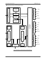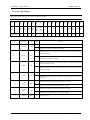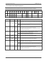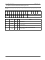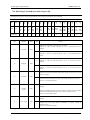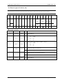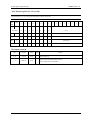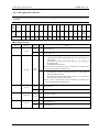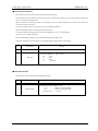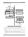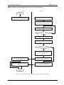
1
LSI Specification
MB86617A
IEEE1394 Serial Bus Controller
for DTV
MB86617A
LSI Specification
Rev. 1.0
Rev.1.0
August 16, 2001
i
Fujitsu VLSI
LSI Specification
MB86617A
Contents
CHAPTER 1 OVERVIEW ............................................................................................................................................................................1
CHAPTER 2 FEATURES ..............................................................................................................................................................................2
CHAPTER 3 CHIP BLOCK .........................................................................................................................................................................3
3.1. BLOCK D IAGRAM..................................................................................................................................................................................4
<NORMAL OPERATION M ODE ......................................................................................................................................................................4
<ASYNCHRONOUS TRANSMIT FIFO EXTENDED MODE ......................................................................................................................5
<ASYNCHRONOUS RECEIVE FIFO EXTENDED MODE .......................................................................................................................... 6
3.2. FUNCTION OF EACH B LOCK ...................................................................................................................................................................7
<PHY LAYER C ONTROL C IRCUIT.............................................................................................................................................................7
<LINK LAYER C ONTROL C IRCUIT ........................................................................................................................................................... 7
<TSP IC I NTERFACE .................................................................................................................................................................................... 7
<CP IC INTERFACE ......................................................................................................................................................................................7
<DATA BRIDGE .............................................................................................................................................................................................7
CHAPTER 4 PIN ASSIGN MENT............................................................................................................................................................... 8
4.1. PIN ASSIGNMENT ..................................................................................................................................................................................... 9
4.2.C ORRESPONDING TABLE OF MB86617A P IN ..................................................................................................................................... 10
4.3. O UTLINE DRAWING OF PACKAGE ........................................................................................................................................................ 11
CHAPTER 5 PIN FUNCTION ................................................................................................................................................................... 12
5.1. IEEE1394 INTERFACE ........................................................................................................................................................................... 13
5.2. ISOCHRONOUS I NTERFACE .................................................................................................................................................................... 14
5.4. MPU I NTERFACE .................................................................................................................................................................................... 16
5.5. OTHER PINS ............................................................................................................................................................................................ 17
5.6. POWER/GND PIN................................................................................................................................................................................... 18
CHAPTER 6 INTERNAL REGISTER .................................................................................................................................................... 19
CHAPTER 7 INTERNAL REGISTER FUNCT ION DESCRIPTION ........................................................................................... 25
7.1. M ODE -CONTROL REGISTER .................................................................................................................................................................. 27
7.2. FLAG & STATUS REGISTER .................................................................................................................................................................... 29
Rev.1.0
ii
Fujitsu VLSI
LSI Specification
MB86617A
7.3. INSTRUCTION FETCH R EGISTER ........................................................................................................................................................... 31
7.4. INTERRUPT-FACTOR INDICATE REGISTER/ INTERRUPT-MASK SETTING REGISTER........................................................................ 32
7.5. R ECEIVE A CKNOWLEDGE INDICATE R EGISTER ................................................................................................................................. 33
7.6. A-BUFFER DATA PORT RECEIVE /TRANSMIT ...................................................................................................................................... 34
7.7. TSP T RANSMIT I NFORMATION SETTING REGISTER [A] ................................................................................................................... 35
7.8. TSP T RANSMIT I NFORMATION SETTING REGISTER [B] ................................................................................................................... 37
7.9. T RANSMIT OFFSET SETTING REGISTER [A] ....................................................................................................................................... 39
7.10. TRANSMIT OFFSET SETTING REGISTER [B] ..................................................................................................................................... 40
7.11. TSP RECEIVE INFORMATION SETTING REGISTER ........................................................................................................................... 41
7.12. RECEIVE DSS PACKET HEADER I NDICATE REGISTER [A]/T RANSMIT DSS P ACKET HEADER SETTING REGISTER [A] ....... 44
7.13. RECE IVE DSS PACKET HEADER I NDICATE REGISTER [B]/T RANSMIT DSS P ACKET HEADER SETTING REGISTER [B] ........ 45
7.14. TSP STATUS REGISTER....................................................................................................................................................................... 46
7.15. DATA BRIDGE T RANSMIT INFORMATION SETTING REGISTER 1 [A]............................................................................................. 48
7.16. DATA BRIDGE T RANSMIT INFORMATION SETTING REGISTER 2 [A]............................................................................................. 49
7.17. DATA BRIDGE T RANSMIT INFORMATION SETTING REGISTER 3 [B] ............................................................................................. 50
7.18. DATA BRIDGE T RANSMIT INFORMATION SETTING REGISTER 4 [B] ............................................................................................. 51
7.19. DATA BRIDGE RECEIVE I NFORMATION SETTING R EGISTER .......................................................................................................... 52
7.20. TRANSMIT PACKET L INK /SPLIT SETTING R EGISTER ...................................................................................................................... 53
7.21. LATE PACKET DECISION RANGE SETTING REGISTER [A] .............................................................................................................. 55
7.22. LATE PACKET DECISION RANGE SETTING REGISTER [B] .............................................................................................................. 56
7.23. RECEIVE ISOCHRONOUS PACKET HEADER INDICATE REGISTER 1 [A] ........................................................................................ 57
7.24. RECEIVE ISOC HRONOUS PACKET HEADER INDICATE REGISTER 2 [A] ........................................................................................ 58
7.25. RECEIVE ISOCHRONOUS PACKET HEADER INDICATE REGISTER 3 [B]......................................................................................... 59
7.26. RECEIVE ISOCHRONOUS PACKET HEADER INDICATE REGISTER 4 [B]......................................................................................... 60
7.27. FIFO RESET SETTING REGISTER....................................................................................................................................................... 61
7.28. DATA BRIDGE T RANSMIT /RECEIVE STATUS REGISTER [A] ........................................................................................................... 62
7.29. DATA BRIDGE T RANSMIT /RECEIVE STATUS REGISTER [B] ........................................................................................................... 65
7.30. ISOCHRONOUS CHANNEL M ONITOR REGISTER ............................................................................................................................... 68
7.31. CYCLE-TIMER -MONITOR INDICATE REGISTER................................................................................................................................. 69
Rev.1.0
iii
Fujitsu VLSI
LSI Specification
MB86617A
7.32. PING T IME M ONITOR REGISTER ........................................................................................................................................................ 70
7.33. PHY/LINK REGISTER/A DDRESS SETTING REGISTER ................................................................................................................... 71
7.34. PHY/LINK REGISTER ACCESS P ORT ............................................................................................................................................... 72
7.35. REVISION INDICATE REGISTER .......................................................................................................................................................... 73
7.36. TRANSMIT CGMS/TSCH I NDICATE REGISTER [A] ....................................................................................................................... 74
7.37. TRANSMIT CGMS/TSCH I NDICATE REGISTER [B] ........................................................................................................................ 75
7.38. TRANSMIT CGMS/TSCH I NDICATE STATUS REGISTER ................................................................................................................ 76
7.39. TRANSMIT EMI/OE SETTING REGISTER.......................................................................................................................................... 78
CHAPTER 8 PHY/INK REGISTER FUNCTION DESCRIPTION ................................................................................................ 80
8.1. PHY/LINK REGISTER TABLE .............................................................................................................................................................. 81
8.2. PHYSICAL REGISTER #00 (READ)......................................................................................................................................................... 83
8.3. PHYSICAL REGISTER #01 (READ/WRITE) ............................................................................................................................................ 84
8.4. PHYSICAL REGISTER #02 (READ)......................................................................................................................................................... 85
8.5. PHYSICAL REGISTER #03 (READ)......................................................................................................................................................... 86
8.6. PHYSICAL REGISTER #04 (READ/WRITE) ............................................................................................................................................ 87
8.7. PHYSICAL REGISTER #05 (READ/WRITE) ............................................................................................................................................ 88
8.8. PHYSICAL REGISTER #07, 08, 09 (READ) ........................................................................................................................................... 90
8.9. PHYSICAL REGISTER #0A, 0B, 0C (READ/WRITE) ............................................................................................................................ 91
8.10. PHYSICAL REGISTER #0D, 0E, 0F (READ /WRITE) ........................................................................................................................... 92
8.11. PHYSICAL REGISTER #10 (READ)....................................................................................................................................................... 93
8.12. PHYSICAL REGISTER #11, 12, 13 (READ) ......................................................................................................................................... 94
8.13. PHYSICAL REGISTER #14, 15, 16 (READ) ......................................................................................................................................... 95
8.14. PHYSICAL REGISTER #17, 18, 19, 1A, 1B, 1C, 1D, 1E (READ/ WRITE ) ....................................................................................... 96
8.15. LINK REGISTER #00 (READ/WRITE)................................................................................................................................................... 97
8.16. LINK REGISTER #01 (READ/WRITE)................................................................................................................................................... 98
8.17. LINK REGISTER #02 (READ/WRITE)................................................................................................................................................... 99
8.18. LINK REGISTER #03 (READ/WRITE)................................................................................................................................................. 100
CHAPTER 9 INSTRUCTIO N ................................................................................................................................................................ 101
9.1. I NSTRUCTION C ODE T ABLE ..............................................................................................................................................................102
Rev.1.0
iv
Fujitsu VLSI
LSI Specification
MB86617A
9.2. DESCRIPTION OF EACH INSTRUCTION............................................................................................................................................... 103
CHAPTER 10 INTERRUPT ..................................................................................................................................................................... 106
10.1. I NTERRUPT-FACTOR I NDICATOR REGISTER & INTERRUPT- MASK SETTING REGISTER .............................................................107
10.2. I NTERRUPT.......................................................................................................................................................................................... 108
10.3. DESCRIPTION OF INTERRUPT............................................................................................................................................................ 109
CHAPTER 11 OPERATION ...................................................................................................................................................................112
11.1. INITIALIZATION ................................................................................................................................................................................ 113
11.2. SELF -ID PACKET RECEIVING .........................................................................................................................................................114
11.2.1
11.2.2
Self -ID Packet Receive at Bus Reset Process .............................................................................................................115
Self-ID Packet Receive after Transmitting Ping Packet Ping................................................................................ 118
11.3. ASYNCHRONOUS PACKET TRANSMITTING................................................................................................................................. 120
11.4. ASYNCHRONOUS PACKET RECEIVING .........................................................................................................................................122
11.5. ISOCHRONOUS PACKET TRANSMITTING ..................................................................................................................................... 125
11.6. ISOCHRONOUS PACKET RECEIVING .............................................................................................................................................128
CHAPTER 12 SYSTEM CONFIGURATION ...................................................................................................................................130
12.1. RECOMMENDED C ONNECTION FOR 1934 PORT (FOR ONE PORT) .......................................................................................... 131
12.2. RECOMMENDED C ONNECTION FOR CABLE POWER SUPPLY ..................................................................................................132
12.3. RECOMMENDED C ONNECTION FOR BUILD-IN PLL LOOP F ILTER .........................................................................................133
12.4. C ONFIGURATION OF FEEDBACK C IRCUIT AT CRYSTAL O SCILLATOR ...................................................................................134
Rev.1.0
v
Fujitsu VLSI
LSI S pecification
MB86617A
Chapter 1 Overview
This chapter explains the overview of MB86617A.
MB86617A is Fujitsu’s IEEE1394 serial bus controller based on both IEEE1394 Standard (IEEE Std. 1394-1995) and P1394.a
Standard Draft (rev.2.0).
This MB86617A has three ports for network under the 1394 cable environment, differential transceiver, and comparator, and the
transfer data rate supports S400.
MB86617A integrates PHY and LINK layers into single-chip, and plans for degression of component side product and saving power
consumption.
MB86617A has two exclusive ports (one is the combined use for receiving a message of interface for DV) for MPEG2 and DSS data
transfer, and performs isolating and packeting of Header and Data department with these two ports automatically. This function is
suited for maintaining continuum of transfer.
Rev.1.0
1
Fujitsu VLSI
LSI S pecification
MB86617A
Chapter 2 Features
This chapter explains the features of MB86617A.
> Compliant with IEEE1394 high performance serial bus standard and P1394.a standard draft
> Integrates PHY and LINK layers into single-chip
> 1394 port number : 3 ports
> Transfer Data Rate : S100, S200, S400
> On-chip PLL (corresponding to Crystal Osci llator) : generate internal clock
> 4K Byte X 2 channels Isochronous transmit and receive data buffer
> 256Byte Asynchronous exclusive buffer for transmit/receive
> Auto isolating and packeting for received header and data of packet
> Two exclusive ports for Isochronous transfer (8 bit bus)
> Loading interface with copy protection LSI (8 bits I/O)
> Generating and Checking Function for 32bit CRC
> 6-pin cable supported
> Power supply system : 3.3V size-D battery
> Package : LQFP -176 (FPT-176P-M03)
Rev.1.0
2
Fujitsu VLSI
LSI S pecification
MB86617A
Chapte r 3 Chip Block
This chapter explains the MB86617A block diagram and the function of each block.
3.1. Block Diagram
3.2. Function of Each Block
Rev.1.0
3
Fujitsu VLSI
LSI S pecification
MB86617A
3.1. Block Diagram
MB86617A block diagram is shown below.
< Normal Operation Mode
Asynch Transmit
Exclusive FIFO
(256 byte)
TPA0
1394 Interface (Port 0)
Host Interface
Asynch Transmit
Packet Process
Asynch Transmit
Packet Process
XTPA0
TPB0
XTPB0
TPBIAS0
Asynch Transmit
Exclusive FIFO
(256 byte)
TPA1
FIFO
(2KByte)
(2KByte)
CP IC
Interface
FIFO
(2KByte)
XTPA1
TPB1
XTPB1
TPBIAS1
TPA2
1394 Interface (Port 2)
Data Bridge
TSP IC Interface
FIFO
(2KByte)
1394 Interface (Port 1)
FIFO
PHY/
LINK
Layer
Control
Circuit
XTPA2
TPB2
XTPB2
TPBIAS2
Fig.3.1.1 Block Diagram - Normal Operation Mode -
Rev.1.0
4
Fujitsu VLSI
LSI S pecification
MB86617A
< Asynchronous Transmit FIFO Extended Mode
Asynch Transmit
Exclusive FIFO
(256 byte)
TPA0
1394 Interface (Port 0)
Host Interface
Asynch Transmit
PacketProcess
Asynch Transmit
PacketProcess
XTPA0
TPB0
XTPB0
TPBIAS0
Asynch Transmit
Exclusive FIFO
(256 byte)
TPA1
FIFO
(2KByte)
CP IC
Interface
FIFO
(2KByte)
XTPA1
TPB1
XTPB1
TPBIAS1
TPA2
1394 Interface (Port 2)
(2KByte)
Data Bridge
TSP IC Interface
FIFO
1394 Interface (Port 1)
FIFO
(2KByte)
PHY/
LINK
Layer
Control
Circuit
XTPA2
TPB2
XTPB2
TPBIAS2
Fig.3.1.2 Block Diagram - Asynchronous Transmit FIFO Extended Mode -
Rev.1.0
5
Fujitsu VLSI
LSI S pecification
MB86617A
< Asynchronous Receive FIFO Extended Mode
Asynch Transmit
Exclusive FIFO
(256 byte)
TPA0
1394 Interface (Port 0)
Host Interface
Asynch Transmit
Packet Process
Asynch Transmit
Packet Process
XTPA0
TPB0
XTPB0
TPBIAS0
Asynch Transmit
Exclusive FIFO
(256 byte)
TPA1
FIFO
(2KByte)
CP IC
Interface
FIFO
(2KByte)
XTPA1
TPB1
XTPB1
TPBIAS1
TPA2
1394 Interface (Port 2)
(2KByte)
Data Bridge
TSP IC Interface
FIFO
1394 Interface (Port 1)
FIFO
(2KByte)
PHY/
LINK
Layer
Control
Circuit
XTPA2
TPB2
XTPB2
TPBIAS2
Fig.3.1.3 Block Diagram - Asynchronous Receive FIFO Extended Mode -
Rev.1.0
6
Fujitsu VLSI
LSI S pecification
MB86617A
3.2. Function of Each Block
This section explains the function of each block for MB86617A.
< PHY Layer Control Circuit
This circuit is for the Physical layer of IEEE 1394 with the following functions.
> Asynchronous transfer is supported under cable environment.
> Maximum transfer data rate : 393.216Mbit/sec.
> with three ports for transceiver/receiver : transfer IEEE1394 packet
> with bus monitor, initial performance for occurring bus reset, speed signaling, arbitration, encode/decode : transfer/receive data
< LINK Layer Control Circuit
This circuit generates standard packet for IEEE1394, controls transfer, and performs the following functions.
> Generates and checks 32 bit CRC for header and data of packet.
> Activates cycle master function with integrated 32 bit cycle timer register
< TSP IC Interface
This TSP IC Interface has two exclusive ports with the following functions for transmitting/receiving TSP IC, MPEG2-TS and DSS
data, and receiving DV data.
> Adds time stamp to both MPEG2 -TS and DSS data.
> Outputs received data just when the value of time stamp (SPH) and cycle timer is matched with each other.
> Integrated transmit/receive (dual purpose) FIFO for transferring Isochronous by 2K byte X 2 channels.
< CP IC Interface
This interface adds the copy information to CP IC so as to correspond to copy protect.
< Data Bridge
This Data Bridge packets MPEG2-TS, DSS, and DVC, and re-builds the receiving data.
At data transmission, this section adds Isochronous packet header and CIP header, and connects/separates source packet
When transmitting 2ch, it connects Isochronous packet.
At data receipt, it deletes Isochronous packet header and CIP header, restores by unit of source packet.
When receiving 2ch, it separates Isochronous packet and divide them to each FIFO.
> Integrated transmit/receive (dual purpose) FIFO for transferring Isochronous by 2K byte X 2 channels.
Rev.1.0
7
Fujitsu VLSI
LSI S pecification
MB86617A
Chapter 4 Pin Assignment
This chapter explains the pin assignment and table of pin function of MB86617A.
4.1. Pin Assignment
4.2. Corresponding Table of MB86617A Pin
4.3. Outline Drawing of Package
Rev.1.0
8
Fujitsu VLSI
LSI S pecification
MB86617A
4.1. Pin Assignment
The following diagram shows the MB86617A pin assignment.
SELTSPA
DSSCLKA
VDD
VSS
TSCLKB
TSSYNCB
TSCGMSB
TSVALB
TSDB7
TSDB6
TSDB5
TSDB4
VDD
VSS
TSDB3
TSDB2
TSDB1
TSDB0
IERRB
SELIOB
SELTSPB
DSSCLKB
VDD
VSS
TEST3
TEST4
XFP
XILWRE
XIV
ICLK
VDD
VSS
TEST5
TEST6
A7
A6
A5
A4
A3
A2
A1
TEST7
VDD
VSS
133
135
140
145
150
155
160
165
170
175
176
XRESET
MODE1
MODE0
XCS
XWR(XDS)
XRD(R/XW)
ALE
XINT
DREQ
XDACK
VDD
VSS
D15
D14
D13
D12
D11
D10
D9
D8
VDD
VSS
AD7
AD6
AD5
AD4
AD3
AD2
AD1
D0
TEST1
TEST2
VSS
XI
VDD
XO
AVSS
AVDD
FIL
RF
AVSS
AVDD
RO
CPS
1
132
130
5
125
10
120
15
115
20
SELIOA
IERRA
TSDA0
TSDA1
TSDA2
TSDA3
VSS
VDD
TSDA4
TSDA5
TSDA6
TSDA7
TSVALA
TSCGMSA
TSSYNCA
TSCLKA
VSS
VDD
MB86617
110
FPT-176P-M03
25
105
VSS
VDD
30
100
35
VSS
VDD
95
40
90
89
44
88
85
VSS
VDD
PMODE
LINKON
PWR3
PWR2
PWR1
VDD
VSS
AVSS
AVDD
TPBIAS0
TPA0
XTPA0
TPB0
XTPB0
AVDD
AVSS
AVSS
AVDD
TPBIAS1
TPA1
XTPA1
TPB1
XTPB1
AVDD
AVSS
AVSS
AVDD
TPBIAS2
TPA2
XTPA2
TPB2
XTPB2
AVDD
AVSS
9
80
75
70
65
60
55
50
45
Rev.1.0
Fujitsu VLSI
LSI S pecification
MB86617A
4.2. Corresponding Table of MB86617A Pin
The following table shows the corresponding items of MB86617A pin.
Pin
No.
I/O
Pin Name
Pin
No.
1
2
3
4
5
6
7
8
9
10
11
12
13
14
15
16
17
18
19
20
21
22
23
24
25
26
27
28
29
30
31
32
33
34
35
36
37
38
39
40
41
I
I
I
I
I
I
I
O
O
I
I/O
I/O
I/O
I/O
I/O
I/O
I/O
I/O
I/O
I/O
I/O
I/O
I/O
I/O
I/O
I/O
I/O
I/O
I
I/O
O
O
-
XRESET
MODE1
MODE0
XCS
XWR(XDS)
XRD(R/XW)
ALE
XINT
DREQ
XDACK
VDD
VSS
D15
D14
D13
D12
D11
D10
D9
D8
VDD
VSS
AD7
AD6
AD5
AD4
AD3
AD2
AD1
D0
TEST1
TEST2
VSS
XI
VDD
XO
AVSS
AVDD
FIL
RF
AVSS
42
-
43
44
O
I
Rev.1.0
I/O
Pin Name
45
46
47
48
49
50
51
52
53
54
55
56
57
58
59
60
61
62
63
64
65
66
67
68
69
70
71
72
73
74
75
76
77
78
79
80
81
82
83
84
85
I/O
I/O
I/O
I/O
O
I/O
I/O
I/O
I/O
O
I/O
I/O
I/O
I/O
O
I
I
I
O
I
AVSS
AVDD
XTPB2
TPB2
XTPA2
TPA2
TPBIAS2
AVDD
AVSS
AVSS
AVDD
XTPB1
T PB1
XTPA1
TPA1
TPBIAS1
AVDD
AVSS
AVSS
AVDD
XTPB0
TPB0
XTPA0
TPA0
TPBIAS0
AVDD
AVSS
VSS
VDD
PWR1
PWR2
PWR3
LINKON
PMODE
-
AVDD
86
-
RO
CPS
87
88
Pin
No.
VDD
89
90
91
92
93
94
95
96
97
98
99
100
101
102
103
104
105
106
107
108
109
110
111
112
113
114
115
116
117
118
119
120
121
122
123
124
125
126
127
128
129
VSS
10
I/O
Pin Name
Pin
No.
I/O
Pin Name
O
I
I/O
I
I
I/O
I/O
I/O
I/O
I/O
I/O
I/O
I/O
I/O
O
O
O
I
I/O
I/O
O
O
I
I
I/O
I/O
I
I
I
I
I
I
I
SELTSPA
DSSCLKA
VDD
VSS
TSCLKB
TSSYNCB
TSCGMSB
TSVALB
TSDB7
TSDB6
TSDB5
TSDB4
VDD
VSS
TSDB3
TSDB2
TSDB1
TSDB0
IERRB
SELIOB
SELTSPB
DSSCLKB
VDD
VSS
TEST3
TEST4
XFP
XILWRE
XIV
ICLK
VDD
VSS
TEST5
TEST6
A7
A6
A5
A4
A3
A2
A1
-
VDD
VSS
-
VDD
VSS
I/O
I/O
I/O
I/O
I/O
I/O
I/O
I/O
I/O
I/O
I/O
VDD
VSS
TSCLKA
TSSYNCA
TSCGMSA
TSVALA
TSDA7
TSDA6
TSDA5
TSDA4
VDD
VSS
TSDA3
TSDA2
TSDA1
133
134
135
136
137
138
139
140
141
142
143
144
145
146
147
148
149
150
151
152
153
154
155
156
157
158
159
160
161
162
163
164
165
166
167
168
169
170
171
172
173
130
I/O
TSDA0
174
I/O
TEST7
131
132
O
O
IERRA
SELIOA
175
176
-
VDD
VSS
Fujitsu VLSI
LSI S pecification
MB86617A
4.3. Outline Drawing of Package
This section shows the outline drawing of MB86617A package (LQFP -176).
Rev.1.0
11
Fujitsu VLSI
LSI S pecification
MB86617A
Chapter 5 Pin Function
This chapter explains the MB86617A pin function.
5.1. IEEE1394 Interface
5.2. Isochronous (TSP-IC,DV-IC) Interface
5.4. MPU Interface
5.5. Other Pins
5.6. Power/GND Pin
Rev.1.0
12
Fujitsu VLSI
LSI S pecification
MB86617A
5.1. IEEE1394 Interface
This section explains the pin function of IEEE1394 interface.
Signal Name
I/O
TPA0
I/O
I/O pin of TPA + (plus) signal on cable port 0
XTPA0
I/O
I/O pin of TPA - (minus) signal on cable port 0
TPB0
I/O
I/O pin of TPB + (plus) signal on cable port 0
XTPB0
I/O
I/O pin of TPB - (minus) signal on cable port 0
TPA1
I/O
I/O pin of TPA + (plus) signal on cable port 1
XTPA1
I/O
I/O pin of TPA - (minus) signal on cable port 1
TPB1
I/O
I/O pin of TPB + (plus) signal on cable port 1
XTPB1
I/O
I/O pin of TPB - (minus) signal on cable port 1
TPA2
I/O
I/O pin of TPA + (plus) signal on cable port 2
XTPA2
I/O
I/O pin of TPA - (minus) signal on cable port 2
TPB2
I/O
I/O pin of TPB + (plus) signal on cable port 2
XTPB2
I/O
I/O pin of TPB - (minus) signal on cable port 2
TPBIAS0
O
Output pin of reference voltage for common voltage on cable port 0
TPBIAS1
O
Output pin of reference voltage for common voltage on cable port 1
TPBIAS2
O
Output pin of reference voltage for common voltage on cable port 2
Rev.1.0
Function
13
Fujitsu VLSI
LSI S pecification
MB86617A
5.2. Isochronous Interface
This section explains the pin function of Isochronous interface.
Signal Name
I/O
TSVALIDA
I/O
I.O pin for indicating effective data period of TS packet (on port A)
‘H’ active signal
TSSYNCA
I/O
Input/Output pin for indicating leading data of TS packet (on port A)
‘H’ active signal
TSCLKA
I/O
On transmitting: sync clock input pin for input data of TS packet
On receiving : sync clock output pin for output data of TS packet
(switchable either 6.144MHz or 3.072MHz)
TSDA7 - 0
I/O
I/O pin for TS packet data (on Port A)
TSCGMSA
I
Serial input pin for CGMS and TSCH information (on port A)
Effective for 8 clocks since TSSYNCA input signal rising
SELIOA
O
Output pin for switching I/O on port A
Outputs ‘L’ at transmitting and ‘H’at receiving
SELTSPA
O
Output pin for switching output device from port A
TSVALIDB
I/O
I.O pin for indicating effective data period of TS packet (on port B)
‘H’ active signal
TSSYNCB
I/O
Input/Output pin for indicating leading data of TS packet (on port B)
‘H’ active signal
TSCLKB
I/O
On transmitting: sync clock input pin for input data of TS packet
On receiving : sync clock output pin for output data of TS packet
(switchable either 6.144MHz or 3.072MHz)
TSDB7 - 0
I/O
I/O pin for TS packet data (on port B)
TSCGMSB
I
Serial input pin for CGMS and TSCH information (on port B)
Effective for 8 clocks since TSSYNCA input signal rising
SELIOB
O
Output pin for switching I/O on port B
Outputs ‘L’ at transmitting and ‘H’at receiving
SELTSPB
O
Output pin for switching output device from port B
ICLK
I
Clock input pin from DV-IC
XILWRE
O
Output pin for signal to be allowed accessing to Isochronous-FIFO
Asserted by completing reception of data for one source packet
‘L’ active signal
XIV
I
Input signal for enable signal of Isochronous data
Output Isochronous- FIFO data to data output pin while this signal in active.
Switch data synchronizing with rise edge of ICLK
XFP
O
Output pin of time stamp trigger signal
‘L’ active signal
Rev.1.0
Function
14
Fujitsu VLSI
LSI S pecification
MB86617A
IERRA
O
IERRB
O
Output pin for noticing error of receive data (on port A)
‘H’ active signal
Output pin for noticing error of receive data (on port B)
‘H’ active signal
DSSCLKA
I
Clock input pin for DSS data (27MHz)
DSSCLKB
I
Clock input pin for DSS data (27MHz)
Rev.1.0
15
Fujitsu VLSI
LSI S pecification
MB86617A
5.4. MPU Interface
This section explains the pin function of MPU interface.
Signal Name
I/O
A7 – 1
I
D15 - 8,0
AD7 – 1
I/O
XCS
I
Chip enable input pin for this device
XRD(R/W)
I
80 system mode: read out strobe input pin for this device
68 system mode: input pin for controlling read out/write for this device
XWR(XDS)
I
80 system mode: strobe input pin for writing into this device
68 system mode: input pin of XDS signal to be output with data bus in available
ALE
I
Input pin of ALE signal to be output with its address in available when selecting
multiplex mode
When selecting non-multiplex mode, set this signal in fixed ‘L’
DREQ
O
Output pin of DMA transfer requiring signal for DMAC
XDACK
I
Input pin of DMA allowance signal from DMAC
XINT
O
Output pin for interruption request
Rev.1.0
Function
Address input pin for selecting internal register
Available only when selecting non-multi mode
When selecting multiplex mode, set this signal in fixed ‘L’
Data I/O pin
Corresponding to address input signal when selecting multiplex mode
16
Fujitsu VLSI
LSI S pecification
MB86617A
5.5. Other Pins
This section explains the pin function like internal PLL.
Signal Name
I/O
XRESET
I
Input signal for resetting signal
When operating with cable supply power, set this pin to ‘L’.
I
This pin is used for setting operating mode of MPU.
This device is operated as follows depending on the setting of MODE1 and MODE0
pins;
‘00’ input: TX1940 mode
‘01’ input: MB90F574 mode
‘10’ input: 80 system non-multiplex mode
‘11’ input: 68 system non-multiplex mode
MODE1
MODE0
Function
XO
I/O
XI
I
RF
O
Connect t o GND through 5.1kΩ register.
FIL
O
Exterior type filter circuit connecting pin for internal PLL
RO
O
Connect to GND through 5.1kΩ register.
CPS
I
Power supply input pin from IEEE1394 cable
Detect cable supply power 0 to 33V (requiring of lowering/dividing voltage)
PMODE
I
Criterion pin for inputting power
‘L’ input : operate with power supplying through IEEE1394 cable
‘H’ input: operate with system power
I
Setting pin got POWER_CLASS of Self-ID packet to be transmitted when operating
with supply power through cable.
Note) The POWER_CLASS of the Self_ID packet to be sent when operating
under the system power does not use this pin, but follows the setting of
Pwr bit (Bit2 to 0) of Physical Register#4.
LINKON
O
Output pin for detecting Link-on packet receive
Output ‘H’ when receiving Link-on packet under operating with supply power
through IEEE1394 cable. When PMODE becomes ‘H’, ‘L’ is output. With the
PMODE in ‘H’, the output of this pin is not changed.
If not using this pin, set this pin as open one.
TEST1 - 7
I/O
This pin is for test. Use this pin as open one.
Exterior type crystal connecting pin for oscillator circuit (24.576MHz)
PWR3 - 1
Rev.1.0
17
Fujitsu VLSI
LSI S pecification
MB86617A
5.6. Power/GND Pin
This section explains the power/GND pin.
Signal Name
I/O
VDD
-
3.3V digital power pin
VSS
-
Digital ground pin
AVDD
-
3.3V analog power pin
AVSS
-
Analog ground pin
Rev.1.0
Function
18
Fujitsu VLSI
LSI S pecification
MB86617A
Chapter 6 Internal Register
This chapter explains the MB86617A internal register.
Note that the access of internal register is applied only 16 bits access.
WRITE
READ
Register Name
Register Name
00
mode-control
mode-control
02
(reserved)
flag & status
04
Instruction-fetch
Instruction-fetch
06
Interrupt-mask setting [A]
Interrupt indicate [A]
08
Interrupt-mask setting [B]
Interrupt indicate [B]
0A
(reserved)
Receive Acknowledge
0C
A-buffer data port transmit
A-buffer data port receive
0E
(reserved)
(reserved)
10
TSP transmit information setting [A]
TSP transmit information setting [A]
12
TSP transmit information setting [B]
TSP transmit information setting [B]
14
transmit offset setting [A] (upper)
transmit offset setting [A] (upper)
16
transmit offset setting [A] (lower)
transmit offset setting [A] (lower)
18
transmit offset setting [B] (upper)
transmit offset setting [B] (upper)
1A
transmit offset setting [B] (lower)
transmit offset setting [B] (lower)
1C
TSP receive information setting
TSP receive information setting
1E
transmit DSS packet header setting [A]
(most significant)
receive DSS packet header setting [A]
(most significant)
Address
(HEX)
Rev.1.0
19
Fujitsu VLSI
LSI S pecification
MB86617A
WRITE
READ
Register Name
Register Name
20
transmit DSS packet header setting [A] (upper)
receive DSS packet header setting [A] (upper)
22
transmit DSS packet header setting [A] (medium)
receive DSS packet header setting [A] (medium)
24
transmit DSS packet header setting [A] (lower)
receive DSS packet header setting [A] (lower)
26
transmit DSS packet header setting [A]
(least significant)
receive DSS packet header setting [A]
(least significant)
28
transmit DSS packet header setting [B]
(most significant)
receive DSS packet header setting [B]
(most significant)
2A
transmit DSS packet header setting [B] (upper)
receive DSS packet header setting [B] (upper)
2C
transmit DSS packet header setting [B] (medium)
receive DSS packet header setting [B] (medium)
2E
transmit DSS packet header setting [B] (lower)
receive DSS packet header setting [B] (lower)
30
transmit DSS packet header setting [B]
(least significant)
receive DSS packet header setting [B]
(least significant)
32
(reserved)
TSP status
34
data bridge transmit information setting 1 [A]
data bridge transmit information setting 1 [A]
36
data bridge transmit information setting 2 [A]
data bridge transmit information setting 2 [A]
38
data bridge transmit information setting 3 [B]
data bridge transmit information setting 3 [B]
3A
data bridge transmit information setting 4 [B]
data bridge transmit information setting 4 [B]
3C
data bridge receive information setting
data bridge receive information setting
3E
transmit packet concatenate/split setting
transmit packet concatenate/split setting
40
Late packet criterion range setting [A]
Late packet criterion range setting [A]
42
Late packet criterion range setting [B]
Late packet criterion range setting [B]
44
(reserved)
receive Isochronous packet header indicate 1 [A]
46
(reserved)
receive Isochronous packet header indicate 2 [A]
48
(reserved)
receive Isochronous packet header indicate 3 [B]
4A
(reserved)
receive Isochronous packet header indicate 4 [B]
4C
FIFO reset
FIFO reset
4E
(reserved)
data bridge transmit/receive status [A]
Address
(HEX)
Rev.1.0
20
Fujitsu VLSI
LSI S pecification
MB86617A
WRITE
READ
Register Name
Register Name
50
(reserved)
data bridge transmit/receive status [B]
52
(reserved)
Isochronous channel monitor 1
54
(reserved)
Isochronous channel monitor 2
56
(reserved)
Isochronous channel monitor 3
58
(reserved)
Isochronous channel monitor 4
5A
(reserved)
cycle-time-monitor (upper)
5C
(reserved)
cycle-time-monitor (lower)
5E
(reserved)
Ping time monitor
60
PHY/LINK register address setting
PHY/LINK register address setting
62
PHY/LINK register access port
PHY/LINK register access port
64
(reserved)
Revision indicate register (upper)
66
(reserved)
Revision indicate register (lower)
68
(reserved)
(reserved)
6A
(reserved)
(reserved)
6C
(reserved)
(reserved)
6E
(reserved)
(reserved)
70
(reserved)
(reserved)
72
(reserved)
(reserved)
74
(reserved)
(reserved)
76
(reserved)
(reserved)
78
(reserved)
(reserved)
7A
(reserved)
(reserved)
7C
(reserved)
(reserved)
7E
(reserved)
(reserved)
Address
(HEX)
Rev.1.0
21
Fujitsu VLSI
LSI S pecification
MB86617A
WRITE
READ
Register Name
Register Name
80
(reserved)
transmit CGMS/TSCH indicate [A]
82
(reserved)
transmit CGMS/TSCH indicate [B]
84
transmit CGMS/TSCH indicate status
transmit CGMS/TSCH indicate status
86
transmit EMI/OE setting
transmit EMI/OE setting
88
(reserved)
(reserved)
8A
(reserved)
(reserved)
8C
(reserved)
(reserved)
8E
(reserved)
(reserved)
90
(reserved)
(reserved)
92
(reserved)
(reserved)
94
(reserved)
(reserved)
96
(reserved)
(reserved)
98
(reserved)
(reserved)
9A
(reserved)
(reserved)
9C
(reserved)
(reserved)
9E
(reserved)
(reserved)
A0
(reserved)
(reserved)
A2
(reserved)
(reserved)
A4
(reserved)
(reserved)
A6
(reserved)
(reserved)
A8
(reserved)
(reserved)
AA
(reserved)
(reserved)
AC
(reserved)
(reserved)
AE
(reserved)
(reserved)
Address
(HEX)
Rev.1.0
22
Fujitsu VLSI
LSI S pecification
MB86617A
WRITE
READ
Register Name
Register Name
B0
(reserved)
(reserved)
B2
(reserved)
(reserved)
B4
(reserved)
(reserved)
B6
(reserved)
(reserved)
B8
(reserved)
(reserved)
BA
(reserved)
(reserved)
BC
(reserved)
(reserved)
BE
(reserved)
(reserved)
C0
(reserved)
(reserved)
C2
(reserved)
(reserved)
C4
(reserved)
(reserved)
C6
(reserved)
(reserved)
C8
(reserved)
(reserved)
CA
(reserved)
(reserved)
CC
(reserved)
(reserved)
CE
(reserved)
(reserved)
D0
(reserved)
(reserved)
D2
(reserved)
(reserved)
D4
(reserved)
(reserved)
D6
(reserved)
(reserved)
D8
(reserved)
(reserved)
DA
(reserved)
(reserved)
DC
(reserved)
(reserved)
DE
(reserved)
(reserved)
Address
(HEX)
Rev.1.0
23
Fujitsu VLSI
LSI S pecification
MB86617A
WRITE
READ
Register Name
Register Name
E0
(reserved)
(reserved)
E2
(reserved)
(reserved)
E4
(reserved)
(reserved)
E6
(reserved)
(reserved)
E8
(reserved)
(reserved)
EA
(reserved)
(reserved)
EC
(reserved)
(reserved)
EE
(reserved)
(reserved)
F0
(reserved)
(reserved)
F2
(reserved)
(reserved)
F4
(reserved)
(reserved)
F6
(reserved)
(reserved)
F8
(reserved)
(reserved)
FA
(reserved)
(reserved)
FC
(reserved)
(reserved)
FE
(reserved)
(reserved)
Address
(HEX)
Rev.1.0
24
Fujitsu VLSI
LSI S pecification
MB86617A
Chapter 7 Internal Register Function Description
This chapter explains the details of the internal register of MB86617A.
7.1. mode-control Register
7.2. flag & status Register
7.3. instruction fetch Register
7.4. interrupt-factor Indicate Register/interrupt-mask Setting Register
7.5. Receive Acknowledge Indicate Register
7.6. A-buffer Data Port Receive/Transmit
7.7. TSP Transmit Information Setting Register [A]
7.8. TSP Transmit Information Setting Register [B]
7.9. Transmit Offset Setting Register [A]
7.10. Transmit Offset Setting Register [B]
7.11. TSP Receive Information Setting Register
7.12. Transmit DSS Packet Header Setting Register [A]
7.13. Transmit DSS Packet Header Setting Register [B]
7.14. TSP Status Register
7.15. Data Bridge Transmit Information Setting Register 1 [A]
7.16. Data Bridge Transmit Information Setting Register 2 [A]
7.17. Data Bridge Transmit Information Setting Register 3 [B]
7.18. Data Bridge Transmit Information Setting Register 4 [B]
7.19. Data Bridge Receive Information Setting Register
7.20. Transmit Packet Link/Split Setting Register
7.21. Late Packet Decision Range Setting Register [A]
7.22. Late Packet Decision Range Setting Register [B]
7.23. Receive Isochronous Packet Header Indicate Register 1 [A]
7.24. Receive Isochronous Packet Header Indicate Register 2 [A]
Rev.1.0
25
Fujitsu VLSI
LSI S pecification
7.25.
7.26.
7.27.
7.28.
7.29.
7.30.
7.31.
7.32.
7.33.
7.34.
7.35.
7.36.
7.37.
7.38.
7.39.
Rev.1.0
MB86617A
Receive Isochronous Packet Header Indicate Register 3 [B]
Receive Isochronous Packet Header Indicate Register 4 [B]
FIFO Reset Setting Register
Data Bridge Transmit/Receive Status Register [A]
Data Bridge Transmit/Receive Status Register [B]
Isochronous channel monitor Register
cycle-timer-monitor Indicate Register
Ping time monitor Register
PHY/LINK Register/Address Setting Register
PHY/LINK Register/Access Port
Revision Indicate Register
Transmit CGMS/TSCH Indicate Register [A]
Transmit CGMS/TSCH Indicate Register [B]
Transmit CGMS/TSCH Indicate Status Register
Transmit EMI/OE Setting Register
26
Fujitsu VLSI
LSI S pecification
MB86617A
7.1. M ode-control Register
Mode-control register is the register that performs the relative setting of various operation mode of this LSI.
AD
R/W
Bit
15
Bit
14
Bit
13
Bit
12
Bit
11
Bit
10
Bit
9
Bit
8
Bit
7
Bit
6
Bit
5
Bit
4
Bit
3
00h
R/W
-
-
-
-
CPS
soft
reset
clk
off
s-ID
store
Cp_
trhrou
gh
-
-
-
Iso-FI
FO no
clr
AsynFIFOs
el
‘0’
‘0’
‘0’
‘0’
‘0’
‘0’
‘1’
‘0’
‘0’
‘0’
‘0’
‘1’
‘0’
Initial Value
BIT
Bit Name
15 - 12
reserved
Write
-
Always write in ‘0’.
-
PHY/LINK is reset by writing ‘0’ after writing ‘1’ (not automatic clear)
Note:
1) Perform read modify write so as not to re-write other bit.
2) Write ‘0’ after 500 ns minimum passed after writing ‘1’.
0
Not stop clock for providing to TSP I/F, CP I/F and data bridge.
1
Stop clock for providing to TSP I/F, CP I/F and data bridge when PMODE input
terminal is in ‘H’.
0
Deletes Self-ID packet in spite of receiving it during bus reset.
1
In case of receiving Self-ID packet during bus reset process, this bit stores 512 byte
at maximum accompanying with both Asynchronous receive FIFO and
Asynchronous transmit FIFO.
0
Enable CP -IC interface.(Needs external CP IC)
1
Disable CP -IC interface. CP-IC interface i s internally by passed.
0
TSSYNCA and TSSYNCB signals are neccesary to detect the first byte of the input
data to TSP interface.
1
TSSYNCA and TSSYNCB signals are not neccesary to detect the first byte of the
input data to TSP interface.
0
TSSYNCA and TSSYNCB signals are not asserted when the data is outputted from
TSP interface.
1
TSSYNCA and TSSYNCB signals are asserted when the data is outputted from TSP
interface.
Read
0
Always indicate ‘0’.
Write
0
Always write in ‘0’.
0
Clears receive Isochronous-FIFO when bus reset occurred.
1
Does not clear Isochronous-FIFO when bus reset occurred.
Read/
Write
5
4
Rev.1.0
s-ID store
Note 1)
Read/
Write
Cp_through
Read/
Write
Sync_out
‘1’
Always indicate ‘0’.
clk off
6
‘1’
-
10
Sync_in
‘1’
CP
standby
Read
CPS soft reset
7
send/re TSP
standc
by
Bit
0
Value
11
8
Bit
1
Action
Read/
Write
9
Bit
2
Read/
Write
Read/
Write
Function
reserved
Iso-FIFO
no clr
Read/
Write
27
Fujitsu VLSI
LSI S pecification
MB86617A
BIT
Bit Name
Action
3
Asyn-FIFO
sel
Read/
Write
2
1
0
send/rec
TSP stand-by
CP stand-by
value
Function
0
Uses 2K byte FIFO on LINK I/F side of bridge for Isochronous transmit/receive.
1
Uses 2K byte FIFO on LINK I/F side of bridge for Asynchronous transmit/receive.
0
Uses 2K byte FIFO for Asynchronous transmit with Asyn-FIFO sel (bit3) ‘1’.
1
Uses 2K byte FIFO for Asynchronous receive with Asyn-FIFO sel (bit3) ‘1’.
0
Activates TSP -IC I/F terminal output.
1
Disables TSP-IC I/F terminal output, and brings it in high impedance status.
0
Activates CP I/F terminal output.
0
Disables CP I/F terminal output, and brings it in high impedance status.
Read/
Write
Read/
Write
Read/
Write
Note 1) Refer to “Self-ID Packet Receive Operation” for the internal operation flow and read-out flow of with this bit set at ‘1’.
Rev.1.0
28
Fujitsu VLSI
LSI S pecification
MB86617A
7.2. flag & status Register
flag & status register indicates the status of this LSI and data access inquiries.
AD
R/W
Bit
15
Bit
14
Bit
13
Bit
12
Bit
11
Bit
10
Bit
9
Bit
8
Bit
7
Bit
6
Bit
5
Bit
4
Bit
3
Bit
2
Bit
1
Bit
0
02h
R
IPC
busy
tran
ready
tran
busy
ISO
cycle
A-Txbuff
empty
A-Rxbuff
empty
-
-
-
-
-
sleep
data
req
recv
busy
cmstr
INT
‘0’
‘0’
‘0’
‘0’
‘1’
‘1’
‘0’
‘0’
‘0’
‘0’
‘0’
‘0’
‘0’
‘0’
‘0’
‘0’
Initial Value
BIT
Bit Name
Action
15
IPC busy
Read
14
13
12
11
10
9– 5
Rev.1.0
tran ready
tran busy
ISO cycle
Function
0
Indicates that receipt of instruction is available.
1
Indicates that receipt of instruction is not available.
0
Indicates that bus reset or forced sleep is being executed, and transmit/receive of
packet is unavailable.
1
Indicates that bus reset is completed and forced sleep is not being executed, and
transmit/receive of packet is available.
0
Indicates that packet transmit is not being executed or in the process of packet
receive addressed to this node.
1
Indicates that packet transmit is being executed or in the process of packet receive
addressed to this node.
0
Indicates that Isochronous cycle is not being executed.
1
Indicates that Isochronous cycle is being executed by transmit or receive of cycle
start packet.
0
Indicates that Asynchronous transmit specific buffer is not empty.
1
Indicates that Asynchronous transmit specific buffer is empty.
0
Indicates that Asynchronous receive specific buffer is not empty.
1
Indicates that Asynchronous receive specific buffer is empty.
0
Always indicate ‘0’.
Read
Read
Read
A-T x-buff
Empty
Read
A-Rx-buff
Empty
Read
reserved
Value
Read
29
Fujitsu VLSI
LSI S pecification
BIT
4
3
2
1
0
Bit Name
sleep
data req
recv busy
Note 2)
cmstr
INT
MB86617A
Action
Value
Function
0
Indicates that the device is not in forced sleep.
1
Indicates that the device is in forced sleep by accepting “Start sleep” (01h)
instruction.
0
Indicates that no data is stored in ASYNC receive specific buffer.
1
Indicates that data is stored in ASYNC receive specific buffer.
0
Indicates that packet receive is not in busy mode.
1
Indicates that packet receive is in busy mode due to receipt of Asynchronous
packet and self-ID packet.
0
Indicates that node is not the cycle master now.
1
Node is the cycle master now.
0
Interrupt indicate register does not have interrupt.
1
Interrupt indicate register has interrupt.
Read
Read
Read
Read
Read
Note 1) IEEE1394 block is in internal reset status until integrated PLL is locked after turning the power ON. PHY layer and Link
layer do not operate during this period.
Note 2) In case that Asynchronous packet addressed to this node is received with this Bit indicate ‘1’, it transmits “ack busy X”.
Rev.1.0
30
Fujitsu VLSI
LSI S pecification
MB86617A
7.3. instruction-fetch Register
instruction-fetch register is the register that writes in instructions for this LSI, and consists of the instruction code and operand.
Refer to “Chapter 9 Instruction” for each instruction code and operand code.
AD
R/W
04h
R/W
Bit
15
Bit
14
Bit
13
Bit
12
Bit
11
Bit
10
Bit
9
Bit
8
Bit
7
Bit
6
Bit
5
Bit
4
Bit
3
Instruction code
operand
“00 h”
“00 h”
Initial Value
BIT
Bit Name
Action
Value
15 - 8
instruction
code
Read/
Write
-
Specify each instruction code.
7- 0
operand
Read/
Write
-
Specify required operand for each instruction code.
Write ‘0’ into all bits for instructions without operand.
Bit
2
Bit
1
Bit
0
Function
Note) Before writing in instruction for this register, read out IPC busy Bit (bit15) of “7.2. flag & status Register”, and confirm that the
IPC busy value is ‘0’.
Rev.1.0
31
Fujitsu VLSI
LSI S pecification
MB86617A
7.4. interrupt-factor Indicate Register/interrupt-mask Setting Register
interrupt-factor indicate register is the register that indicates interrupt reported by this LSI.
Refer to “Chapter 10 Interrupt” for measure against and details of each Bit and interrupt factor.
interrupt-mask setting register is the register that controls mask of each interrupt factor generated by this LSI.
AD
R/
Bit
15
Bit
14
Bit
13
Bit
12
Bit
11
Bit
10
Bit
9
Bit
8
Bit
7
R
Interrupt-factor
W
interrupt-mask
R
Interrupt-factor
W
interrupt-mask
Bit
6
Bit
5
Bit
4
Bit
3
Bit
2
Bit
1
Bit
0
‘0’
‘0’
‘0’
‘0’
‘0’
‘0’
‘0’
06h
08h
Initial Value
BIT
‘0’
‘0’
Bit Name
interrupt-facto
r
‘0’
‘0’
Action
Rev.1.0
‘0’
‘0’
‘0’
‘0’
Value
Function
0
Indicate that interrupt factors are not generated.
1
Indicate that interrupt factors are generated.
After reading out this register, clear to ‘0’ automatically.
0
Do not mask interrupt factors.
1
Mask interrupt factors.
Interrupt factors masked by setting of this register are neither stored in interrupt
indicate register nor assert INT signal.
Read
15 - 0
interrupt-mask
‘0’
Write
32
Fujitsu VLSI
LSI S pecification
MB86617A
7.5. Receive Acknowledge Indicate Register
Receive Acknowledge indicate register is the register that indicates received Acknowledge packet addressed to itself.
Read out this register after interrupt report of “Asynchronous packet send”.
AD
R/W
Bit
15
Bit
14
Bit
13
Bit
12
Bit
11
Bit
10
Bit
9
Bit
8
0Ah
R
-
-
-
-
-
-
-
-
Receive ack-code
Receive ack-parity
‘0’
‘0’
‘0’
‘0’
‘0’
‘0’
‘0’
‘0’
“0 h”
“0 h”
Initial Value
Bit
7
Bit
6
Bit
5
Bit
4
Bit
3
Bit
2
BIT
Bit Name
Action
Value
15 - 8
reserved
Read
-
Always indicate ‘0’.
7- 4
Receive
Acknowledge-co
de
Read
-
Indicate code of received Acknowledge packet addressed to it.
(MSB: bit7, LSB: bit5)
3- 0
Receive
Acknowledge-par
ity
Read
-
Indicate parity of received Acknowledge packet addressed to it.
(MSB: bit3, LSB: bit0)
Bit
1
Bit
0
Function
Note) In case of not receiving Acknowledge within specified time, this register indicates “00h ” and reports interrupt of “Acknowledge
missing”.
Rev.1.0
33
Fujitsu VLSI
LSI S pecification
MB86617A
7.6. A-buffer Data Port Receive/Transmit
This integrated register is the buffer access port for both ASYNC receive specific buffer and ASYNC transmit specific one.
Read data is able to be read out IEEE1394 packet data in the order received. (MSB: 1 ST read)
Write data is transmitted as IEEE1394 packet data in the order written in. (MSB: 1ST write)
AD
R/W
Bit
15
Bit
14
Bit
13
Bit
12
Bit
11
Bit
10
Bit
9
Bit
8
Bit
7
Bit
6
Bit
5
R
ASYNC Receive Specific Buffer Data
W
ASYNC Transmit Specific Buffer Data
Bit
4
Bit
3
Bit
2
Bit
1
Bit
0
0Ch
Initial Value
BIT
15 - 0
Rev.1.0
Undefined
Bit Name
Action
Value
Function
ASYNC Receive
Specific Buffer
Data
Read
-
Read out port of Asynchronous receive specific buffer.
(MSB: bit15, LSB: bit0)
ASYNC Transmit
Specific Buffer
Data
Write
-
Write in port of Asynchronous transmit specific buffer.
(MSB: bit15, LSB: bit0)
34
Fujitsu VLSI
LSI S pecification
MB86617A
7.7. TSP Transmit Information Setting Register [A]
TSP transmit information setting register [A] is the register that makes settings for transmit packet processed by bridge-Ach.
AD
R/W
Bit
15
Bit
14
Bit
13
10h
R/W
Tx
start
-A
Tx
end
-A
Tx
select
-A
Initial Value
‘0’
‘0’
‘0’
BIT
15
14
13
Bit
12
Bit Name
Action
Tx start -A
Read/
Write
Tx end-A
Tx select-A
Read/
Write
Read/
Write
12 - 7
set TS-ID-A
Read/
Write
6
Tx form-A
Read/
Write
5
Rev.1.0
input DSS
size-A
Read/
Write
Bit
11
Bit
10
Bit
9
Bit
8
Bit
7
Bit
6
Bit
5
Bit
4
Bit
3
set TS-ID-A
Tx
form
-A
input
DSS
size-A
EMI
select
-A
“00 h”
‘0’
‘0’
‘0’
Bit
2
Bit
1
Bit
0
set EMI-A
27M
count
-A
port
maskA
“00 b”
‘0’
‘0’
Value
Function
0
Automatically clears when transmit process is started with bridge-Ach after setting
at ‘1’.
1
Starts transmit processing with bridge-Ach.
0
Automatically clears when transmit process is stopped by bridge-Ach after setting
at ‘1’.
1
Stops transmit process by bridge-Ach.
0
Outputs ‘L’ to SELTSPA output terminal.
1
Outputs ‘H’ to SELTSPA output terminal.
-
Set TSCH classification ID to be stored at FIFO of bridge-Ach.
(MSB: bit12, LSB: bit7)
0
Processes transmit data as MPEG2-TS.
1
Processes transmit data as DSS packet.
0
Processes transmit DSS packet as 140 byte.
1
Processes transmit DSS packet as 130 byte.
35
Fujitsu VLSI
LSI S pecification
BIT
4
3- 2
1
0
Rev.1.0
Bit Name
EMI select-A
set EMI-A
27M count-A
port mask -A
MB86617A
Action
Value
Function
0
Selects CGMS information input from TSP -IC as EMI information to be output to
CP-IC.
1
Selects setting value of set EMI-A (bit3 to 2) as EMI information to be output to
CP-IC.
-
Set EMI information to be output to CP-IC.
Valid only when EMI select -A (bit4) is ‘1’.
(MSB: bit3, LSB: bit2)
0
Does not insert internal 27 MHz counter value to System clock count ran ge of DSS
packet header.
1
Inserts internal 27 MHz counter value to System clock count range of DSS packet
header.
0
Does not mask port A input of TSP-IC interface.
Read in input data from port A at transmit.
1
Masks port A input of TSP -IC interface.
Does not read in input data from port A at transmit.
Read/
Write
Read/
Write
Read/
Write
Read/
Write
36
Fujitsu VLSI
LSI S pecification
MB86617A
7.8. TSP Transmit Information Setting Register [B]
TSP transmit information setting register [B] is the register that makes settings for transmit packet processed by bridge-Bch.
AD
R/W
Bit
15
Bit
14
Bit
13
12h
R/W
Tx
start
-B
Tx
end
-B
Tx
select
-B
Initial Value
‘0’
‘0’
‘0’
BIT
15
14
13
Bit
12
Bit Name
Action
Tx start -B
Read/
Write
Tx end-B
Tx select-B
Read/
Write
Read/
Write
12 - 7
set TS-ID-B
Read/
Write
6
Tx form-B
Read/
Write
5
Rev.1.0
input DSS
size-B
Read/
Write
Bit
11
Bit
10
Bit
9
Bit
8
Bit
7
Bit
6
Bit
5
Bit
4
Bit
3
set TS-ID-B
Tx
form
-B
input
DSS
size-B
EMI
select
-B
“00 h”
‘0’
‘0’
‘0’
Bit
2
Bit
1
Bit
0
set EMI-B
27M
count
-B
port
maskB
“00 b”
‘0’
‘0’
Value
Function
0
Automatically clears when transmit process is started with bridge - Bch after setting
at ‘1’.
1
Starts transmit process with bridge-Bch.
0
Automatically clears when transmit process is stopped by bridge- Bch after setting
at ‘1’.
1
Stops transmit process by bridge-Bch.
0
Outputs ‘L’ to SELTSPB output terminal.
1
Outputs ‘H’ to SELTSPB output terminal.
-
Set TSCH classification ID to be stored at FIFO of bridge-Bch.
(MSB: bit12, LSB: bit7)
0
Processes transmit data as MPEG2 -TS packet.
1
Processes transmit data as DSS packet.
0
Processes transmit DSS packet as 140 byte.
1
Processes transmit DSS packet as 130 byte.
37
Fujitsu VLSI
LSI S pecification
BIT
4
3- 2
1
0
Rev.1.0
Bit Name
EMI select-B
set EMI-B
27M count-B
port mask -B
MB86617A
Action
Value
Function
0
Selects CGMS information input from TSP -IC as EMI information to be output to
CP-IC.
1
Selects setting value of set EMI-A (bit3 to 2) as EMI information to be output to
CP-IC.
-
Set EMI information to be output to CP-IC.
Valid only when EMI select -A (bit4) is ‘1’.
(MSB: bit3, LSB: bit2)
0
Does not insert internal 27 MHz counter to System clock count range of DSS
packet header.
1
Inserts internal 27 MHz counter to System clock count range of DSS packet header.
0
Does not mask port B input of TSP-IC interface.
Reads in input data from port A at transmit.
1
Masks port B input of TSP-IC interface.
Does not read in input data from port A at transmit.
Read/
Write
Read/
Write
Read/
Write
Read/
Write
38
Fujitsu VLSI
LSI S pecification
MB86617A
7.9. Transmit Offset Setting Register [A]
Transmit offset setting register [A] is the register that sets offset value added to cycle-time-monitor value. Its aim is to generate source
packet header (Time-stamp) added to transmit packet processed by bridge -Ach. (Max. 32 ms)
Time-stamp value is generated on the basis of cycle-time-monitor value at input of first byte of source packet from TSP -IC.
AD
R/W
14h
R/W
16h
R/W
Bit
15
Bit
14
Bit
13
Bit
12
Bit
11
Bit
10
Bit
9
Bit
6
Bit
5
Bit
4
Bit
3
Bit
2
Bit
1
Bit
0
transmit-offset-A (high)
transmit-offset-A (low)
“0000 h”
BIT
Bit Name
15 - 4 (high)
reserved
Action
Value
Function
Read
-
Always indicate ‘0’.
Write
-
Always write in ‘0’.
3 - 0 (high)
15 - 12 (low)
Set value to be added to cycle-count range of cycle-time-monitor.
Setting range is 0h to FFh. (unit=125µS).
transmit-offset
-A
Rev.1.0
Bit
7
reserved
Initial Value
11 - 0
Bit
8
Read/
Write
Set value to be added to cycle-offset range of cycle-time-monitor.
Setting range is 0h to C00h. (unit=1/24.576 MHz).
39
Fujitsu VLSI
LSI S pecification
MB86617A
7.10. Transmit Offset Setting Register [B]
Transmit off set setting register [B] is the register that sets offset value added to cycle-time-monitor value Its aim is to generate source
packet header (Time-stamp) added to transmit packet processed by bridge -Bch. (Max. 32 ms)
Time-stamp value is generated on the basis of cycle-time-monitor value at input of first byte of source packet from TSP -IC.
AD
R/W
18h
R/W
1Ah
R/W
Bit
15
Bit
14
Bit
13
Bit
12
Bit
11
Bit
10
Bit
9
Bit
6
Bit
5
Bit
4
Bit
3
Bit
2
Bit
1
Bit
0
transmit-offset-B (high)
transmit-offset-B (low)
“0000 h”
BIT
Bit Name
15 - 4 (high)
reserved
Action
Value
Read
-
Always indicate ‘0’.
Write
-
Always write in ‘0’.
3 - 0 (high)
15 - 12 (low)
Function
Set value to be added to cycle-count range of cycle-time-monitor.
Setting range is 0h to FFh. (unit=125µS).
transmit-offset
-B
Rev.1.0
Bit
7
reserved
Initial Value
11 - 0
Bit
8
Read/
Write
Set value to be added to cycle-offset range of cycle-time-monitor.
Setting range is 0h to C00h. (unit=1/24.576MHz).
40
Fujitsu VLSI
LSI S pecification
MB86617A
7.11. TSP Receive Information Setting Register
TSP receive information setting register performs the setting for outputting received packet to TSP -IC
AD
R/W
Bit
15
Bit
14
Bit
13
Bit
12
Bit
11
Bit
10
Bit
9
Bit
8
1Ch
R/W
TV2B
TV1B
-
-
output
DSS
size-B
DVEN
DSSEN
TS-E
N
‘0’
‘0’
‘0’
‘0’
‘0’
‘0’
‘0’
‘1’
Initial Value
BIT
15
14
13 - 12
11
10
9
Rev.1.0
Bit Name
Action
TV2B
Read/
Write
TV1B
Bit
7
Bit
6
TV2A TV1A
‘0’
Value
‘0’
Bit
5
Bit
4
Bit
3
Bit
2
Bit
1
Bit
0
-
-
output
DSS
size-A
TCL
KSL
CMP
SEL
TSC
MP
‘0’
‘0’
‘0’
‘0’
‘0’
‘0’
Function
0
Does not output packet received by bridge -Bch to port B of TSP -IC I/F.
1
Outputs packet received by bridge-Bch to port B of TSP -IC I/F.
0
Does not output packet received by bridge -Bch to port A of TSP -IC I/F.
1
Outputs packet received by bridge-Bch to port A of TSP-IC I/F.
Read
-
Always indicates ‘0’.
Write
-
Always write in ‘0’.
0
Outputs DSS packet received by bridge -Bch, with DSS packet header attached, to
TSP-IC in unit of 140 byte.
1
Outputs DSS packet received by bridge- Bch, without attachment of DSS packet
header, to TSP-IC in unit of 130 byte.
Removed DSS packet header is stored at receive DSS packet header indicate
register [B].
0
Deletes received data and reports FMT error when DV data is received.
ISO packet header and CIP header are indicated in register.
1
Allows receiving DV data.
0
Deletes received data and reports FMT error when DSS data is received.
ISO packet header and CIP header are indicated in register.
1
Allows receiving DSS data.
Read/
Write
reserved
output DSS
size-B
Read/
Write
DV-EN
Read/
Write
DSS-EN
Read/
Write
41
Fujitsu VLSI
LSI S pecification
BIT
8
7
6
5- 4
3
2
1
0
Bit Name
TS-EN
TV2A
TV1A
MB86617A
Action
Value
Function
0
Deletes received data and reports FMT error when MPEG2 -TS data is received.
ISO packet header and CIP header are indicated in register.
1
Allows receiving MPEG2 -TS data.
0
Does not output the packet received by bridge-Ach to port B of TSP-IC I/F.
1
Outputs the packet received by bridge-Ach to port B of TSP -IC I/F.
0
Does not output the packet received by bridge-Ach to port A of TSP-IC I/F.
1
Outputs the packet received by bridge-Ach to port A of TSP -IC I/F.
Read
-
Always indicates ‘0’.
Write
-
Always write in ‘0’.
0
Outputs DSS packet with DSS packet header received by bridge- Bch to TSP-IC in
unit of 140 byte.
1
Outputs DSS packet without DSS packet header received by bridge-Ach to TSP -IC
in unit of 130 byte.
Removed DSS packet header is stored at receive DSS packet header indicate register
[A].
0
Outputs received data to TSP -IC in synchronization with 6.144 MHz TSCLK.
1
Outputs received data to TSP -IC in synchronization with 3.072 MHz TSCLK.
0
Outputs to port A when TSCMP (bit0) is ‘1’.
1
Outputs to port B when TSCMP (bit0) is ‘1’.
0
Does not merge packet received by Ach and Bch.
1
Outputs to one TSP-IC after merging packets received by Ach and Bch.
Read/
Write
Read/
Write
Read/
Write
reserved
output DSS
size-
TCLKSL
CMPSEL
TSCMP
Read/
Write
Read/
Write
Read/
Write
Read/
Write
Note 1) Do not set TV2B (bit15), TV1B (bit14), and DV1B (bit12) to ‘1’ simultaneously.
Note 2) Do not set TV2A (bit7), TV1A (bit6), and DV1A (bit4) to ‘1’ simultaneously.
Note 3) Do not set TV2B (bit15) and TV2A (bit7) to ‘1’ simultaneously.
Note 4) Do not set TV1B (bit14) and TV1A (bit6) to ‘1’ simultaneously.
Note 5) Do not set ‘1’ to TV2B (bit15), TV1B (bit14), TV2A (bit7) and TV1A(bit6) when TSCMP (bit0) is set to ‘1’.
Note 6) FMT error is reported when receiving data format other than DV-EN (bit10), DSS-EN (bit9) and TS-EN (bit8) regardless of
their settings.
Rev.1.0
42
Fujitsu VLSI
LSI S pecification
MB86617A
Register setting value and selection of output port are shown in the table below.
Bit 15
Receive
Status
Bit 14
Bit 7
Bit 6
Bit 1
Bit 0
TS
CMP
TSP -IC I/F
Port B
TV2B
TV1B
TV2A
TV1A
0
0
0
1
0
0
Processing-Ach
Receive data
-
0
0
1
0
0
0
-
Processing-Ach
Receive data
0
1
0
0
0
0
Processing-Bch
Receive data
-
1
0
0
0
0
0
-
Processing-Bch
Receive data
1
0
0
1
0
0
Processing-Ach
Receive data
Processing-Bch
Receive data
0
1
1
0
0
0
Processing-Bch
Receive data
Processing-Ach
Receive data
0
0
0
0
0
1
Processing-Ach+Bc
h
Receive data
-
0
0
0
0
1
1
-
Processing-Ach+Bc
h
Receive data
1ch receive
2ch receive
Rev.1.0
TSP -IC I/F
Port A
CMP
SEL
43
Fujitsu VLSI
LSI S pecification
MB86617A
7.12. Receive DSS Packet Header Indicate Register [A]/Transmit DSS Packet Header
Setting Register [A]
Receive DSS packet header indicate register [A] indicates DSS packet header range of DSS packet received by bridge-Ach.
Transmit DSS packet header setting register [A] sets DSS packet header range of DSS packet received by bridge -Ach.
AD
R/W
Bit
15
R
Rx-SI
F-A
Rx-System clock count-A(high)
W
Tx-SIF
-A
T x-System clock count-A(high)
1Eh
Bit
14
Bit
13
Bit
12
Bit
11
Bit
10
Bit
9
Bit
8
Bit
7
Bit
6
Bit
5
Bit
4
Bit
3
R
Rx-System clock count-A(low)
Rx-E
F-A
Reserved
W
T x-System clock count-A(low)
Tx-E
F-A
reserved
20h
R
reserved
W
reserved
R
reserved
W
reserved
R
reserved
W
reserved
Initial Value
“0000 h ”
Bit
2
Bit
1
Bit
0
22h
24h
26h
BIT
Bit Name
Active
Value
Function
Rx-SIF-A
Read
-
Indicates SIF range of received DSS packet header.
T x-SIF-A
Write
-
Write in SIF range of transmits DSS packet header.
Rx-System
clock count-A
Read
-
Indicate System clock count range of received DSS packet header.
(MSB: 1Eh-bit14 , LSB: 20h-bit8)
T x-System
clock count-A
Write
-
Write in System clock count range of transmit DSS packet header.
(MSB: 1Eh-bit14 , LSB: 20h-bit8)
Rx-EF-A
Read
-
Indicates EF range of received DSS packet header.
Tx-EF-A
Write
-
Write in EF range of transmits DSS packet header.
Read
-
Indicates reserved range of received DSS packet header.
Write
-
Write in reserved range of transmit DSS packet header.
15 (1Eh)
14 - 0 (1Eh)
15 - 8(20h)
7(20h)
6 - 0(20h)
15 - 0(22h)
15 - 0(24h)
15 - 0(26h)
Rev.1.0
reserved
44
Fujitsu VLSI
LSI S pecification
MB86617A
7.13. Receive DSS Packet Header Indicate Register [B]/Transmit DSS Packet Header
Setting Register [B]
Receiv e DSS packet header indicate register [B] indicates DSS packet header range of DSS packet received by bridge-Bch.
Transmit DSS packet header setting register [B] sets DSS packet header range of DSS packet received by bridge-Bch.
AD
R/W
Bit
15
R
Rx-SI
F-B
Rx-System clock count-B (high)
W
Tx-SIF
-B
T x-System clock count-B (high)
28h
Bit
14
Bit
13
Bit
12
Bit
11
Bit
10
Bit
9
Bit
8
Bit
7
Bit
6
Bit
5
Bit
4
Bit
3
R
Rx-maximum bit rate-B (low)
Rx-E
F-B
reserved
W
T x-maximum bit rate-B (low)
Tx-E
F-B
reserved
2Ah
R
reserved
W
reserved
R
reserved
W
reserved
R
reserved
W
reserved
Initial Value
“0000 h ”
Bit
2
Bit
1
Bit
0
2Ch
2Eh
30h
BIT
Bit Name
Action
Value
Function
Rx-SIF-B
Read
-
Indicates SIF range of receive DSS packet header.
T x-SIF-B
Write
-
Write in SIF range of transmit DSS packet header.
Rx-System
clock count-B
Read
-
Indicate System clock count range of receive DSS packet header.
(MSB: 28h-bit14, LSB: 2Ah-bit8)
T x-System
clock count-B
Write
-
Write in System clock count range of transmit DSS packet header.
(MSB: 28h-bit14, LSB: 2Ah-bit8)
Rx-EF-B
Read
-
Indicates EF range of received DSS packet header.
Tx-EF-B
Write
-
Write in EF range of transmit DSS packet header.
Read
-
Indicates reserved range of receive DSS packet header.
Write
-
Write in reserved range of transmit DSS packet header.
15 (28h)
14 - 0 (28h)
15 - 8(2Ah)
7(2Ah)
6 - 0 (2Ah)
7 - 0 (2Ch)
15 - 0 (2Eh)
15 - 0 (30h)
Rev.1.0
reserved
45
Fujitsu VLSI
LSI S pecification
MB86617A
7.14. TSP Status Register
TSP status register indicates status of TSP -IC I/F.
AD
R/W
Bit
15
Bit
14
Bit
13
Bit
12
Bit
11
Bit
10
Bit
9
Bit
8
Bit
7
Bit
6
Bit
5
Bit
4
Bit
3
Bit
2
Bit
1
Bit
0
32h
R
CG
chg-B
TS
chg-B
no
47h-B
TSP
FIFOf
ull-B
TSP
FIFO
emp-B
Tx-len
gth-errB
-
-
CG
chg-A
TS
chg-A
no
47h-A
TSP
FIFO
full-A
TSP
FIFO
emp-A
Tx-len
gth-errA
-
-
‘0’
‘0’
‘0’
‘0’
‘1’
‘0’
‘0’
‘0’
‘0’
‘0’
‘0’
‘0’
‘1’
‘0’
‘0’
‘0’
Initial Value
BIT
15
14
13
12
11
10
Rev.1.0
Bit Name
CG chg-B
TS chg-B
no 47h-B
Action
Function
0
Indicates that CGMS information input from port B of TSP IC I/F is not changed.
1
Indicates that CGMS information corresponding to TSCH classification ID of same
type input from port B of TSP IC I/F is changed.
Clears to ‘0’ by lead of this register.
0
Indicates that TS classification ID input from port B of TSP IC I/F is not changed.
1
Indicates that TSCH classification ID input from port B of TSP IC I/F is not
consistent with TSCH classification ID (10h- bit12 to 7 set TS-ID- A or 12h- bit12 to
7 set TS-ID-B) to be stored to FIFO.
Clears to ‘0’ by lead of this register.
0
Indicates that synchronization byte of received MPEG2-TS input from CP-IC by
bridge-Bch is 47h
1
Indicates that synchronization byte of received MPEG2-TS input from CP-IC by
bridge-Bch is not 47h
Clears to ‘0’ by lead of this register.
0
Indicates that FIFO on TSP IC I/F side of bridge-Bch is not full.
1
Indicates that FIFO on TSP IC I/F side of bridge-Bch is full.
0
Indicates that FIFO on TSP IC I/F side of bridge-Bch is not empty.
1
Indicates that FIFO on TSP IC I/F side of bridge -Bch is empty.
0
Indicates that transmit data length input from TSP IC I/F is normal.
1
Indicates that transmit data length input from TSP IC I/F is not consistent with
specified format data length.
Deletes transmit data without writing into FIFO.
Clears to ‘0’ by lead of this register.
Read
Read
Read
TSP FIFO
full-B
Read
TSP FIFO
emp-B
Read
T x-length-err B
Value
Read
46
Fujitsu VLSI
LSI S pecification
MB86617A
BIT
Bit Name
Active
Value
9~8
reserved
Read
-
Always indicate ‘0’.
0
Indicates that CGMS information input from port A of TSP IC I/F is not changed.
1
Indicates that CGMS information input from port A of TSP IC I/F is changed.
Clears to ‘0’ by lead of this register.
0
Indicates that TS classification ID input from port A of TSP IC I/F is not changed.
1
Indicates that TSCH classification ID input from port B of TSP IC I/F is not
consistent with TSCH classification ID (10h- bit12 to 7 set TS-ID- A or 12h- bit12 to
7 set TS-ID-B) to be stored to FIFO.
Clears to ‘0’ by lead of this register.
0
Indicates that synchronization byte of received MPEG2-TS input from CP-IC by
bridge-Bch is 47h
1
Indicates that synchronization byte of received MPEG2-TS input from CP-IC by
bridge-Bch is not 47h
Clears to ‘0’ by lead of this register.
0
Indicates that FIFO on TSP IC I/F side of bridge-Ach is not full.
1
Indicates that FIFO on TSP IC I/F side of bridge-Ach is full.
0
Indicates that FIFO on TSP IC I/F side of bridge-Ach is not empty.
1
Indicates that FIFO on TSP IC I/F side of bridge-Ach is empty.
0
Indicates transmit data length input from TSP IC I/F is normal.
1
Indicates transmit data length input from TSP IC I/F is not consistent with
specified format data length.
Deletes transmit data without writing into FIFO.
Clears to ‘0’ by lead of this register.
-
Always indicate ‘0’.
7
6
5
4
3
2
1- 0
Rev.1.0
CG chg-A
TS chg-A
no 47h-A
Read
Read
Read
TSP FIFO
full-A
Read
TSP FIFO
emp-A
Read
T x-length-err A
reserved
Function
Read
Read
47
Fujitsu VLSI
LSI S pecification
MB86617A
7.15. Data Bridge Transmit Information Setting Register 1 [A]
Data bridge transmit information setting register 1 [A] is the register that sets CIP header range added to transmit packet processed by
bridge-Ach.
AD
R/W
34h
R/W
Bit
15
Bit
14
Initial Value
Bit
13
Bit
12
Bit
11
Bit
10
Bit
9
Bit
8
Bit
7
Bit
6
Bit
5
Bit
3
Bit
2
Bit
1
Bit
0
Tx SID-A
Tx DBS-A
Tx FN-A
“00 h”
“00 h”
“00 b”
BIT
Bit Name
Action
Value
15 - 10
Tx SID-A
Read/
Write
-
Write in SID range of transmit CIP header.
(MSB: bit15, LSB: bit10)
9- 2
Tx DBS-A
Read/
Write
-
Write in DBS range of transmit CIP header.
(MSB: bit9, LSB: bit2)
MPEG2-TS at transmit: “00000110” b
DSS at transmit: “00001001” b
1- 0
Tx FN-A
Read/
Write
-
Write in FN range of transmit CIP header.
(MSB: bit1, LSB: bit0)
MPEG2-TS at transmit: “11” b
DSS at transmit: “10” b
Rev.1.0
Bit
4
Function
48
Fujitsu VLSI
LSI S pecification
MB86617A
7.16. Data Bridge Transmit Information Setting Register 2 [A]
Data bridge transmit information setting register 2 [A] is the register that sets CIP header range, transmit channel, and speed added to
transmit packet processed by bridge-Ach.
AD
R/W
36h
R/W
Bit
15
Bit
14
Initial Value
Bit
13
Bit
12
Bit
11
Bit
10
Bit
9
Bit
8
Bit
7
Bit
6
Bit
5
Bit
4
Bit
3
Tx channel-A
Tx speed-A
-
“00” h
‘0’
“00” h
“00” b
‘0’
Action
Value
15 - 10
Tx FMT -A
Read/
Write
-
Write in FMT range of transmit CIP header.
(MSB: bit15, LSB: bit10)
MPEG2-TS at transmit: “100000” b
DSS at transmit: “100001” b
9
Tx TSF-A
Read/
Write
-
Write in TSF range of transmits CIP header.
8- 3
Tx channel-A
Read/
Write
-
Write in channel range of transmit Isochronous packet header.
(MSB: bit8, LSB: bit 3)
Read/
Write
-
Write in transmit packet speed.
(MSB: bit2, LSB: bit1)
s100 at transmit: “00” b
s200 at transmit: “01” b
s400 at transmit: “10” b
Read
-
Always indicates ‘0’.
Write
-
Always writes in ‘0’.
0
reserved
Rev.1.0
Bit
0
Tx
TSFA
Bit Name
Tx speed-A
Bit
1
Tx FMT-A
BIT
2- 1
Bit
2
Function
49
Fujitsu VLSI
LSI S pecification
MB86617A
7.17. Data Bridge Transmit Information Setting Register 3 [B]
Data bridge transmit information setting register 3 [B] is the register that sets CIP header range added to transmit packet processed by
bridge-Bch.
AD
R/W
38h
R/W
Bit
15
Bit
14
Initial Value
Bit
13
Bit
12
Bit
11
Bit
10
Bit
9
Bit
8
Bit
7
Bit
6
Bit
5
Bit
3
Bit
2
Bit
1
Bit
0
Tx SID-B
Tx DBS-B
Tx FN-B
“00 h”
“00 h”
“00 b”
BIT
Bit Name
Action
Value
15 - 10
Tx SID-B
Read/
Write
-
Write in SID range of transmit CIP header.
(MSB: bit15, LSB: bit10)
9- 2
Tx DBS-B
Read/
Write
-
Write in DBS range of transmit CIP header.
(MSB: bit9, LSB: bit2)
MPEG2-TS at transmit: “00000110” b
DSS at transmit: “00001001” b
1- 0
Tx FN-B
Read/
Write
-
Write in FN range of transmit CIP header.
(MSB: bit1, LSB: bit0)
MPEG2-TS at transmit: “11” b
DSS at transmit: “10” b
Rev.1.0
Bit
4
Function
50
Fujitsu VLSI
LSI S pecification
MB86617A
7.18. Data Bridge Transmit Information Setting Register 4 [B]
Data bridge transmit information setting register 4 [B] is the register that sets CIP header range, transmit channel and speed added to transmit
packet processed by bridge-Bch.
AD
R/W
3Ah
R/W
Bit
15
Bit
14
Initial Value
Bit
13
Bit
12
Bit
11
Bit
10
Bit
9
Bit
8
Bit
7
Bit
6
Bit
5
Bit
4
Bit
3
Tx channel-B
Tx speed-B
-
“00” h
‘0’
“00” h
“00” b
‘0’
Action
Value
15 - 10
Tx FMT -B
Read/
Write
-
Write in FMT range of transmit CIP header.
(MSB: bit15, LSB: bit10)
MPEG2-TS at transmit: “100000” b
DSS at transmit: “100001” b
9
Tx TSF-B
Read/
Write
-
Write in TSF range of transmit CIP header.
8- 3
Tx channel-B
Read/
Write
-
Write in channel range of transmit Isochronous packet header.
(MSB: bit8, LSB: bit3)
Read/
Write
-
Write in transmit packet speed.
(MSB: bit2, LSB: bit1)
s100 at transmit: “00” b
s200 at transmit: “01” b
s400 at transmit: “10” b
Read
-
Always indicates ‘0’.
Write
-
Always writes in ‘0’.
0
reserved
Rev.1.0
Bit
0
Tx
TSFB
Bit Name
Tx speed-B
Bit
1
Tx FMT-B
BIT
2- 1
Bit
2
Function
51
Fujitsu VLSI
LSI S pecification
MB86617A
7.19. Data Bridge Receive Information Setting Register
Data bridge receive information register performs the setting of receive packet.
AD
R/W
Bit
15
Bit
14
3Ch
R/
Rx
start
-B
Rx
end
-B
‘0’
‘0’
Initial Value
BIT
15
14
13~8
7
6
5- 0
Rev.1.0
Bit
13
Bit
12
Bit Name
Action
Rx start-B
Read/
Write
Rx end-B
Read/
Write
Rx channel-B
Read/
Write
Rx start-A
Read/
Write
Rx end-A
Rx-channel-A
Read/
Write
Read/
Write
Bit
11
Bit
10
Bit
9
Bit
8
Bit
7
Bit
6
Bit
5
Bit
4
Bit
3
Bit
2
Rx channel-B
Rx
start
-A
Rx
end
-A
Rx channel-A
“00 h”
‘0’
‘0’
“00 h”
Bit
1
Bit
0
Value
Function
0
Automatically clears when receive process is executed by bridge- Bch after setting
at ‘1’.
1
Executes receive process by bridge -Bch.
0
Automatically clears when receive process is stopped by bridge -Bch after setting at
‘1’.
1
Stops receive process by bridge -Bch.
-
Write in Isochronous packet channel to be received by bridge-Bch.
(MSB: bit8, LSB: bit3)
0
Automatically clears when receive process is executed by bridge- Ach after setting
at ‘1’.
1
Starts receive process by bridge -Ach.
0
Automatically clears when receive process is stopped by bridge -Ach after setting at
‘1’.
1
Stops receive process by bridge -Ach.
-
Write in Isochronous packet channel to be received by bridge-Ach
(MSB: bit5, LSB: bit0)
52
Fujitsu VLSI
LSI S pecification
MB86617A
7.20. Transmit Packet Link/Split Setting Register
Transmit packet link/split setting register is the register that sets number of link and split of source packets to be transmitted.
AD
R/W
Bit
15
Bit
14
Bit
13
3Eh
R/W
o/e
selectB
Tx
o/e-B
NF5
SPB
SPQB
‘0’
‘0’
‘0’
“000 b”
Initial Value
BIT
15
14
13
Bit Name
o/e select-B
Tx o/e-B
NF5SPB
Bit
12
Action
Bit
11
Bit
9
Bit
8
Bit
7
Bit
6
Bit
5
Bit
4
Bit
3
Bit
2
Bit
1
Bit
0
DBQB
o/e
selectA
Tx
o/e-A
NF5
SPA
SPQA
DBQA
“00 b”
‘0’
‘0’
‘0’
“000 b”
“00 b”
Value
Function
0
Selects odd/even value to be input from CP-IC as odd/even range of Isochronous
packet header to be transmitted by bridge -Bch.
1
Selects Tx o/e- B (bit14) setting value as odd/even range of Isochronous packet
header to be transmitted by bridge -Bch
-
Write in odd/even range of transmit Isochronous packet header.
Valid with o/e select- B (bit15) setting value ‘1’, and reads in this setting value to
transmit Isochronous packet header.
0
Executes 2SP combined transmission as FIFO NFULL operation when setting of
2SP separated transmission or combined transmission for less than 2SP.
With more than 3 SP, executes according to setting.
1
Executes 5 SP combined transmission at FIFO FULL.
Read/
Write
Read/
Write
Bit
10
Read/
Write
12 - 10
SPQB
Read/
Write
-
Write in number of link of source packet processed by bridge-Bch.
9- 8
DBQB
Read/
Write
-
Write in number of split of source packet processed by bridge-Bch.
0
Selects odd/even value to be input from CP-IC as odd/even range of Isochronous
packet header to be transmitted by bridge -Bch.
1
Selects Tx o/e-B b (bit6) setting value as odd/even range of Isochronous packet
header to be transmitted by bridge-Bch
-
Write in odd/even range of transmit Isochronous packet header.
Valid with o/e select-B (bit7) setting value ‘1’, and reads in this setting value to
transmit Isochronous packet header.
7
6
Rev.1.0
o/e select-A
Tx o/e-A
Read/
Write
Read/
Write
53
Fujitsu VLSI
LSI S pecification
BIT
5
Bit Name
NF5SPA
MB86617A
Action
Read/
Write
Value
Function
0
Executes 2SP combined transmission as FIFO NFULL operation when setting of
2SP separated transmission or combined transmission for less than 2SP.
With more than 3 SP, executes according to setting.
1
Executes 5 SP combined transmission at FIFO FULL.
4- 2
SPQA
Read/
Write
-
Write in number of links for source packet processed by bridge-Ach.
1- 0
DBQA
Read/
Write
-
Write in number of links for source packet processed by bridge-Ach.
Note)
>SPQ[2:0] ----- Please specify link number of source packet.
Valid setting values are 0 - 5.
Processes assuming there are no settings from microcomputer during ‘0’ setting.
When 6 - 7 are set, it is regarded to be 5 source packet link.
>DBQ[1:0] ---- Please specify split number of source packet.
‘00’ ---No setting from microcomputer.
‘01’ ---2 splits
‘10’ ---4 splits
‘11’ ---8 splits, 4 splits at DSS
> When the setting values of both SPQ [2:0] and DBQ [1:0] are not ‘0’, follow the setting of SPQ [2:0].
When the setting values of both SPQ [2:0] and DBQ [1:0] are ‘0’ (no setting from microcomputer), LSI automatically executes link
process in 1 source packet unit.
Rev.1.0
54
Fujitsu VLSI
LSI S pecification
MB86617A
7.21. Late Packet Decision Range Setting Register [A]
Late packet decision range setting register [A] is the register that sets Late decision range of source packet to be transmitted by bridge -Ach.
AD
R/W
40h
R/W
Bit
15
Bit
14
Bit
13
Bit
12
Bit
11
Bit
10
Bit
9
Bit
8
Bit
5
Bit
4
Bit
3
Bit
2
Bit
1
Bit
0
“0000 h ”
Bit Name
Action
Value
Function
Write in Late packet decision range.
Setting range is 0h to FFh (unit: 125µS).
15 - 8
late range-A
7- 0
Bit
6
late range-A
Initial Value
BIT
Bit
7
Read/
Write
Write in Late packet decision range.
Setting range is 0h to C0h (unit: 16/24.576MHz).
Note)
Late packet decision is performed by comparing the time difference between SPH (Source Packet Header) and CTR (Cycle Time Monitor).
-Transmit:
Packet is transmitted normally when calculation result of “SPH” minus “CTR” for source packet transmitted from Bridhe-Ach is within the
“late range-A + ‘0000’h”.
If it is out of range, Late packet process is performed. The packet concerned is deleted and transmit late is reported.
Set the upper 16 bit of the setting value for transmit offset setting register[A] (14h to 16h).
-Receive:
Received packet is output at the point of “SPH = CTR” when calculation result of “ SPH” minus “ CTR” for source packet received at
Bridhe -Ach is within the “late range-A + ‘0000’h” (the value this register is shifted 4 bits to the left).
If it is out of range, Late packet process is performed. The packet concerned is deleted and receive late is reported.
Rev.1.0
55
Fujitsu VLSI
LSI S pecification
MB86617A
7.22. Late Packet Decision Range Setting Register [B]
Late packet decision range setting register [B] is the register that sets Late decision range of source packet to be transmitted by bridge -Bch.
AD
R/W
42h
R/W
Bit
15
Bit
14
Bit
13
Bit
12
Bit
11
Bit
10
Bit
9
Bit
8
Bit
5
Bit
4
Bit
3
Bit
2
Bit
1
Bit
0
“0000 h ”
Bit Name
Action
Value
Function
Write in Late packet decision range.
Setting range is 0h to FFh (unit: 125µS).
15 - 8
late range-B
7- 0
Bit
6
late range-B
Initial Value
BIT
Bit
7
Read/
Write
Write in Late packet decision range.
Setting range is 0h to C0h (unit: 16/24.576MHz).
Note)
Late packet decision is performed by comparing the time difference between SPH (Source Packet Header) and CTR (Cycle Time Monitor).
-T ransmit:
Packet is transmitted normally when calculation result of “SPH” minus “CTR” for source packet transmitted from Bridhe- Bch is within the
“late range-B + ‘0000’h”.
If it is out of range, Late packet process is performed. The packet concerned is deleted and transmit late is reported.
Set the upper 16 bit of the setting value for transmit offset setting register[B] (14h to 16h).
-Receive:
Received packet is output at the point of “SPH = CTR” when calculation result of “ SPH” minus “ CTR” for source packet received at
Bridhe -Bch is within the “late range-B + ‘0000’h” (the value this register is shifted 4 bits to the left).
If it is out of range, Late packet process is performed. The packet concerned is deleted and receive late is reported.
Rev.1.0
56
Fujitsu VLSI
LSI S pecification
MB86617A
7.23. Receiv e Isochronous Packet Header Indicate Register 1 [A]
Receive Isochronous packet header indicate register 1 [A] is the register that indicates Isochronous packet header information received by
bridge-Ach.
AD
R/W
Bit
15
Bit
14
Bit
13
Bit
12
Bit
11
Bit
10
Bit
9
44h
R
-
-
-
-
-
-
-
Rx EMI-A
Rx
o/e-A
Rx SID-A
‘0’
‘0’
‘0’
‘0’
‘0’
‘0’
‘0’
“00 b”
‘0’
“00 h”
Initial Value
Bit
8
Bit
7
Bit
6
Bit
5
Bit
4
Bit
3
BIT
Bit Name
Action
Value
15 - 9
reserved
Read
-
Always indicate ‘0’.
8- 7
Rx EMI-A
Read
-
Indicate EMI range of receive Isochronous packet header.
(MSB: bit8, LSB: bit7)
6
Rx o/e-A
Read
-
Indicates odd/even range of receive Isochronous packet header.
5- 0
Rx SID-A
Read
-
Indicate SI range of CIP header of receive Isochronous packet.
(MSB: bit8, LSB: bit3)
Rev.1.0
Bit
2
Bit
1
Bit
0
Function
57
Fujitsu VLSI
LSI S pecification
MB86617A
7.24. Receive Isochronous Packet Header Indicate Register 2 [A]
Receive Isochronous packet header indicate register 2 [A] is the register that indicates Isochronous packet CIP header information received
by bridge-Ach.
AD
R/W
Bit
15
Bit
14
Bit
13
Bit
12
46h
R
-
-
-
-
Rx FMT -A
Rx
56-A
Rx STYPE-A
‘0’
‘0’
‘0’
‘0’
“3F”
‘0’
“00 h”
Initial Value
Bit
11
Bit
10
Bit
9
Bit
8
Bit
7
Bit
6
Bit
5
Bit
4
Bit
3
Bit
2
BIT
Bit Name
Action
Value
15 - 12
reserved
Read
-
Always indicate ‘0’.
11 - 6
Rx FMT -A
Read
-
Indicate FMT range of receive Isochronous packet CIP header.
(MSB: bit11, LSB: bit6)
Bit
1
Bit
0
Function
5
Rx 56-A
Read
-
Indicates 50/60 range of receive Isochronous packet CIP header when receiving
DV.
Indicates TSF range of receive Isochronous packet CIP header when receiving
MPEG2-TS or DSS.
4- 0
Rx STYPE-A
Read
-
Indicate STYPE range of CIP header of receive Isochronous packet.
(MSB: bit4, LSB: bit0)
Rev.1.0
58
Fujitsu VLSI
LSI S pecification
MB86617A
7.25. Receive Isochronous Packet Header Indicate Register 3 [B]
Receive Isochronous packet header indicate register 3 [B] is the register that indicates Isochronous packet header information received by
bridge-Bch.
AD
R/W
Bit
15
Bit
14
Bit
13
48h
R
-
-
-
‘0’
‘0’
‘0’
Initial Value
Bit
12
‘0’
Bit
11
Bit
10
Bit
9
Bit
8
Bit
7
Bit
6
Bit
5
Bit
4
Bit
3
-
-
-
Rx EMI-B
Rx
o/e-B
Rx SID-B
‘0’
‘0’
‘0’
“00 b”
‘0’
“00 h”
BIT
Bit Name
Action
Value
15 - 9
reserved
Read
-
Always indicate ‘0’.
8- 7
Rx EMI-B
Read
-
Indicate EMI range of receive Isochronous packet header.
(MSB: bit8, LSB: bit7)
6
Rx o/e-B
Read
-
Indicates odd/even range of receive Isochronous packet header.
5- 0
Rx SID-B
Read
-
Indicate SI range of CIP header of receive Isochronous packet.
(MSB: bit5, LSB: bit0)
Rev.1.0
Bit
2
Bit
1
Bit
0
Function
59
Fujitsu VLSI
LSI S pecification
MB86617A
7.26. Receive Isochronous Packet Header Indicate Register 4 [B]
Receive Isochronous packet header indicate register 4 [B] is the register that indicates Isochronous packet CIP header information received
by bridge-Bch.
AD
R/W
Bit
15
Bit
14
Bit
13
Bit
12
4Ah
R
-
-
-
-
Rx FMT -B
Rx
56-B
Rx STYPE-B
‘0’
‘0’
‘0’
‘0’
“3F”
‘0’
“00 h”
Initial value
Bit
11
Bit
10
Bit
9
Bit
8
Bit
7
Bit
6
Bit
5
Bit
4
Bit
3
Bit
2
BIT
Bit Name
Action
Value
15 - 12
reserved
Read
-
Always indicate ‘0’.
11 - 6
Rx FMT -B
Read
-
Indicate FMT range of receive Isochronous packet CIP header.
(MSB: bit11, LSB: bit6)
Bit
1
Bit
0
Function
5
Rx 56-B
Read
-
Indicates 50/60 range of receive Isochronous packet CIP header when receiving
DV.
Indicates TSF range of receive Isochronous packet CIP header when receiving
MPEG2-TS or DSS.
4- 0
Rx STYPE-B
Read
-
Indicate STYPE range of CIP header of receive Isochronous packet.
(MSB: bit4, LSB: bit0)
Rev.1.0
60
Fujitsu VLSI
LSI S pecification
MB86617A
7.27. FIFO Reset Setting Register
FIFO reset setting register sets force reset of bridge and each FIFO.
AD
R/W
4Ch
R/W
Initial Value
Bit
15
Bit
14
resetT
SP
reset-B
FIFOB
‘0’
‘0’
Bit
13
Bit
12
6
5
4- 0
Bit
5
Bit
4
Bit
3
Bit
2
Bit
1
Bit
0
reset
TSP
FIFOA
reset
BRG
FIFOA
-
-
-
-
-
‘0’
‘0’
‘0’
‘0’
‘0’
‘0’
‘0’
-
-
‘0’
‘0’
‘0’
‘0’
‘0’
‘0’
‘0’
Read/
Write
7
Bit
6
-
reset-B
12 - 8
Bit
7
-
15
reset BRG
FIFO-B
Bit
8
-
Action
13
Bit
9
resetA
Bit Name
reset TSP
FIFO-B
Bit
10
reset
BRG
FIFOB
BIT
14
Bit
11
Value
Function
0
Releases forced reset of bridge-Bch.
1
Executes forced reset of bridge-Bch.
0
Releases FIFO reset on TSP -IC I/F side of bridge-Bch.
1
Resets FIFO on TSP-IC I/F side of bridge-Bch.
0
Releases FIFO reset on LINK-I/F side of bridge-Bch.
1
Resets FIFO on LINK I/F side of bridge-Bch.
Read
-
Always indicate ‘0’.
Write
-
Always write in ‘0’.
0
Releases forced reset of bridge-Ach.
1
Execute forced reset of bridge-Ach.
0
Releases FIFO reset on TSP -IC I/F side of bridge-Ach.
1
Resets FIFO on TSP-IC I/F of bridge-Ach.
0
Releases FIFO reset on LINK-I/F side of bridge-Ach.
1
Resets FIFO on LINK I/F side of bridge-Ach.
Read
-
Always indicate ‘0’.
Write
-
Always write in ‘0’.
Read/
Write
Read/
Write
reserved
reset-A
reset TSP
FIFO-A
reset BRG
FIFO-A
Read/
Write
Read/
Write
Read/
Write
Reserved
Note 1) This register is not cleared automatically.
After writing ‘1’, check the state and then write ‘0’.
Note 2) Do not set ‘1’ to this register during transmit/receive execution.
Rev.1.0
61
Fujitsu VLSI
LSI S pecification
MB86617A
7.28. Data Bridge Transmit/Receive Status Register [A]
Data bridge transmit/receive status register indicates status of packet to be transmitted/received by bridge-Ach.
AD
R/W
Bit
15
Bit
14
Bit
13
Bit
12
Bit
11
Bit
10
R
Tx
busyA
Rx
busyA
Rx
1STPA
Rx
EMI
chg-A
Rx o/e
chg-A
‘0’
‘0’
‘0’
‘0’
‘0’
4Eh
Initial Value
BIT
15
14
13
12
11
Rev.1.0
Bit Name
Tx busy-A
Rx busy-A
Rx 1STP-A
Rx EMI
chg-A
Rx o/e chg-A
Action
Bit
9
Bit
8
Bit
7
Bit
6
Bit
5
Bit
4
Bit
3
Bit
2
Bit
1
Bit
0
Rx
dlen
err-A
-
Tx
late-A
Rx
late-A
Rx 56
err-A
Rx
stype
err-A
BRG
FIFO
full-A
BRG
FIFO
empA
Rx
DBC
err-A
Rx
CIP
err-A
Rx
FMT
err-A
‘0’
‘0’
‘0’
‘0’
‘0’
‘0’
‘0’
‘1’
‘0’
‘0’
‘0’
Value
Function
0
Indicates that bridge-Ach is not in the process of transmit.
Indicates ‘0’ when Tx end- A (10h-bit14) is set at ‘1’ and transmit process is
stopped.
1
Indicates that bridge-Ach is in the process of transmit.
Indicates ‘1’ when Tx start -A (10h-bit15) is set at ‘1’ and transmit process is
started.
0
Indicates that bridge-Ach is not in the process of receive.
Indicates ‘0’ when Rx end-A (3Ch -bit6) is set at ‘1’ and receive process is stopped.
1
Indicates that bridge-Ach is in the process of receive.
Indicates ‘1’ when Rx start-A (3Ch -bit7) is set at ‘1’ and receive process is started.
0
Indicates that Isochronous packet received after starting receive process is not the
first packet received.
1
Indicates that the first Isochronous packet is received after receive process is
started.
Clears to ‘0’ by lead of this register.
0
Indicates that EMI information of received Isochronous packet header is not
changed.
1
Indicates that EMI informatio n of received Isochronous packet header has changed
from just former EMI information of packet received by Isochronous-cycle.
Clears to ‘0’ by lead of this register.
0
Indicates that odd/even information of received Isochronous packet header is not
changed.
1
Indicates that odd/even information of received Isochronous packet header has
changed from just former odd/even information of packet received by
Isochronous-cycle.
Clears to ‘0’ by lead of this register.
Read
Read
Read
Read
Read
62
Fujitsu VLSI
LSI S pecification
BIT
10
9
8
7
6
5
4
3
2
Rev.1.0
Bit Name
Rx dlen-err-A
reserved
Tx late-A
Rx late-A
Rx 56 err-A
Rx stype
err-A
BRG FIFO
full-A
BRG FIFO
emp-A
Rx DBC err-A
MB86617A
Action
Value
Function
0
Indicates that the data length of received packet is same as specified data length in
format.
1
Indicates that the data length of received packet differs to the specified data length
in the format.
Clears to ‘0’ by lead of this register.
-
Always indicates ‘0’.
0
Indicates that transmit packet is transmitted normally.
1
Indicates that transmit packet became Late packet.
transmit.
Clears to ‘0’ by lead of this register.
0
Indicates that the received packet is normal.
1
Indicates that received packet was Late packet.
Delete packet, and not output to TSP-IC.
Clears to ‘0’ by lead of this register.
0
Indicates that 50/60 range of CIP header for received Isochronous packet is ‘0’.
1
Indicates that 50/60 range of CIP header of received Isochronous packet is ‘1’
Clears to ‘0’ by lead of this register.
0
Indicates that STYPE range of CIP hea der of received Isochronous packet is
‘00000’ or ‘00001’.
1
Indicates that STYPE range of CIP header of received Isochronous packet is other
than ‘00000’ or ‘00001’.
Clears to ‘0’ by lead of this register.
0
Indicates that FIFO on LINK I/F side of bridge-Ach is not full.
1
Indicates that FIFO on LINK I/F side of bridge-Ach is full.
0
Indicates that FIFO on LINK I/F side of bridge-Ach is not empty.
1
Indicates that FIFO on LINK I/F side of bridge-Ach is empty.
0
Indicates that DBC range of CIP header of received Isochronous packet is normal.
1
Indicates that DBC range of CIP header of received Isochronous packet received is
not consecutive.
Clears to ‘0’ by lead of this register.
Read
Read
Read
Read
Delete packet, and not
Read
Read
Read
Read
Read
63
Fujitsu VLSI
LSI S pecification
BIT
1
0
Rev.1.0
Bit Name
Rx CIP err-A
Rx FMT err-A
MB86617A
Action
Value
Function
0
Indicates that CIP header of received Isochronous packet is normal.
1
Indicates that CIP header of received Isochronous packet has an error.
Clears to ‘0’ by lead of this register.
0
Indicates that FMT range of CIP header of received Isochronous packet is the value
allowed to be received at DV-EN, DSS- EN or TS-EN (1Ch –bit10 to 8)
(DV=‘00000’, MPEG2=‘10000’ or DSS=‘100001’).
1
Indicates that FMT range of CIP header of received Isochronous packet is other
than the value allowed to be received at DV-EN, DSS-EN or TS- EN (1Ch – bit10 to
8) (DV=‘00000’, MPEG2=‘10000’ or DSS=‘100001’).
Clears to ‘0’ by reading of this register.
Read
Read
64
Fujitsu VLSI
LSI S pecification
MB86617A
7.29. Data Bridge Transmit/Receive Status Register [B]
Data bridge transmit/receive status register [B] indicates status of packet transmitted/received by bridge-Bch.
AD
R/W
Bit
15
Bit
14
Bit
13
Bit
12
Bit
11
Bit
10
R
Tx
busyB
Rx
busyB
Rx
1STPB
Rx
EMI
chg-B
Rx o/e
chg-B
‘0’
‘0’
‘0’
‘0’
‘0’
50h
Initial Value
BIT
15
14
13
12
11
Rev.1.0
Bit Name
Tx busy-B
Rx busy-B
Rx 1STP-B
Rx EMI
chg-B
Rx o/e chg-B
Action
Bit
9
Bit
8
Bit
7
Bit
6
Bit
5
Bit
4
Bit
3
Bit
2
Bit
1
Bit
0
Rx
dlen
err-B
-
Tx
late-B
Rx
late-B
Rx 56
err-B
Rx
stype
err-B
BRG
FIFO
full-B
BRG
FIFO
empB
Rx
DBC
err-B
Rx
CIP
err-B
Rx
FMT
err-B
‘0’
‘0’
‘0’
‘0’
‘0’
‘0’
‘0’
‘1’
‘0’
‘0’
‘0’
Value
Function
0
Indicates that bridge-Bch is not in the process of transmit.
Indicates ‘0’ when Tx end- B (12h-bit14) is set at ‘1’ and transmit process is
stopped.
1
Indicates that bridge-Bch is in the process of transmit.
Indicates ‘1’ when Tx start -B (12h-bit15) is set at ‘1’ and transmit process is
started.
0
Indicates that bridge-Bch is not in the process of receive.
Indicates ‘0’ when Rx end- B (3Ch- bit14) is set at ‘1’ and receive process is
stopped.
1
Indicates that bridge-Bch is in the process of receive.
Indicates ‘1’ when Rx start -B (3Ch- bit15) is set at ‘1’ and receive process is
started.
0
Indicates that received Isochronous packet after starting receive process is not the
first receive packet.
1
Indicates that the first Isochronous packet is received after starting receive process.
Clears to ‘0’ by lead of this register.
0
Indicates that EMI information of receive Isochronous packet header is not
changed.
1
Indicates that EMI information of receive Isochronous packet header has changed
from just former EMI information of packet received by Isochronous-cycle.
Clears to ‘0’ by lead of this register.
0
Indicat es that odd/even information of receive Isochronous packet header is not
changed.
1
Indicates that odd/even information of receive Isochronous packet header has
changed from just former odd/even information of packet received by
Isochronous-cycle.
Clears to ‘0’ by lead of this register.
Read
Read
Read
Read
Read
65
Fujitsu VLSI
LSI S pecification
BIT
10
9
8
7
6
5
4
3
2
Rev.1.0
Bit Name
Rx dlen-err-B
Reserved
Tx late-B
Rx late-B
Rx 56 err-B
Rx stype err-B
BRG FIFO
full-B
BRG FIFO
emp-B
Rx DBC err-B
MB86617A
Action
Value
Function
0
Indicates that data length of receive packet is same as specified data length in
format.
1
Indicates that data length of receive packet differs to the specified data length in the
format.
Clears to ‘0’ by lead of this register.
-
Always indicates ‘0’.
0
Indicates that transmit packet is transmitted normally.
1
Indicates that transmit packet became Late packet.
transmit.
Clears to ‘0’ by lead of this register.
0
Indicates that received packet is normal.
1
Indicates that received packet was Late packet.
Deletes packet, and does not output to TSP-IC.
Clears to ‘0’ by lead of this register.
0
Indicates that 50/60 range of CIP header of received Isochronous packet is ‘0’.
1
Indicates that 50/60 range of CIP header of received Isochronous packet is ‘1’
Clears to ‘0’ by lead of this register.
0
Indicates that STYPE range of CIP header of received Isochronous packet is
‘00000’ or ‘00001’.
1
Indicates that STYPE range of CIP header of received Isochronous packet is other
than ‘00000’ or ‘00001’.
Clears to ‘0’ by lead of this regist er.
0
Indicates that FIFO on LINK I/F side of bridge-Ach is not full.
1
Indicates that FIFO on LINK I/F side of bridge-Ach is full.
0
Indicates that FIFO on LINK I/F side of bridge-Ach is not empty.
1
Indicates that FIFO on LINK I/F side of bridge-Ach is empty.
0
Indicates that DBC range of CIP header of received Isochronous packet is normal.
1
Indicates that DBC range of CIP header of received Isochronous packet is not
consecutive.
Clears to ‘0’ by lead of this register.
Read
Read
Read
Read
Read
Delete packet, and not
Read
Read
Read
Read
66
Fujitsu VLSI
LSI S pecification
BIT
1
0
Rev.1.0
Bit Name
Rx CIP err-B
Rx FMT err-B
MB86617A
Action
Value
Function
0
Indicates that CIP header of received Isochronous packet is normal.
1
Indicates that CIP header of received Isochronous packet has an error.
Cleared to ‘0’ by lead of this register.
0
Indicates that FMT range of CIP header of received Isochronous packet is the value
allowed to be received at DV-EN, DSS- EN or TS-EN (1Ch –bit10 to 8)
(DV=‘00000’, MPEG2=‘10000’ or DSS=‘100001’).
1
Indicates that FMT range of CIP header of received Isochronous packet is other
than the value allowed to be received at DV-EN, DSS-EN or TS- EN (1Ch – bit10 to
8) (DV=‘00000’, MPEG2=‘10000’ or DSS=‘100001’).
Clears to ‘0’ by reading of this register.
Read
Read
67
Fujitsu VLSI
LSI S pecification
MB86617A
7.30. Isochronous Channel Monitor Register
Isochronous channel monitor register is the register that indicates Isochronous packet channel flowing through 1394 bus.
Bit
15
Bit
14
Bit
13
Bit
12
Bit
11
Bit
10
Bit
9
Bit
8
Bit
7
Bit
6
AD
R/W
52h
R
Isochronous channel monitor1
54h
R
Isochronous channel monitor2
56h
R
Isochronous channel monitor3
58h
R
Isochronous channel monitor4
Initial Value
BIT
15 - 0
Rev.1.0
Bit
5
Bit
4
Bit
3
Bit
2
Bit
1
Bit
0
“0000 h”
Bit Name
Isochronous
channel
monitor
Action
Read
Value
Function
-
Indicate that ‘1’ at Bit corresponding to channel number of Isochronous packet
flowing through 1394 bus.
52h-bit15 - 0: channel0 - channel15
54h-bit15 - 0: channel16 - channel31
56h-bit15 - 0: channel32 - channel47
58h-bit15 - 0: channel48 - channel63
68
Fujitsu VLSI
LSI S pecification
MB86617A
7.31. Cycle-timer-monitor Indicate Register
Cycle-timer-monitor indicate register indicates value of integrated cycle-timer register.
Bit
15
Bit
14
Bit
13
Bit
12
Bit
11
Bit
10
Bit
9
Bit
8
Bit
7
Bit
6
AD
R/W
5Ah
R
cycle-timer-monitor (hi)
5Ch
R
cycle-timer-monitor (lo)
Initial Value
Bit
5
Bit
4
Bit
3
Bit
2
Bit
1
Bit
0
“0000 h”
BIT
Bit Name
Action
Value
15 - 0
cycle-timer-m
onitor
Read
-
Function
Indicate value of built-in cycle-timer register.
(MSB: bit15, LSB: bit0)
Note) This register latches the lower word (5 A h) by reading out lower word (5Ch), and releases latch by reading out upper word.
To read out this register, make sure to read out in the order of 5C h → 5A h, two as a set.
Rev.1.0
69
Fujitsu VLSI
LSI S pecification
MB86617A
7.32. Ping Time Monitor Register
Ping time monitor register is the register that indicates time period of transmitting request packet to receiving response packet to the request.
AD
R/W
5Eh
R
Bit
15
Bit
14
Bit
13
Bit
12
Bit
11
Bit
10
Bit
9
Bit
8
Bit
7
Bit
6
Bit
5
Bit
4
Bit
3
Bit
2
Bit
1
Bit
0
Ping time monitor
Initial Value
“0000 h ”
BIT
Bit Name
Action
Value
Function
15 - 0
Ping time
monitor
Read
-
Indicate time period from transmitting request packet to receiving response packet
to the request. Counts by 20ns unit.
(MSB: bit15, LSB: bit0)
Rev.1.0
70
Fujitsu VLSI
LSI S pecification
MB86617A
7.33. PHY/LINK Register/Address Setting Register
PHY/LINK register/address setting register is the register that sets address in order to access PHY/LINK register indirectly. PHY/LINK
register indicated with address set by this register can be accessed from PHY/LINK register/access port.
AD
R/W
Bit
15
Bit
14
Bit
13
Bit
12
Bit
11
Bit
10
Bit
9
Bit
8
Bit
7
60h
R/W
-
-
-
-
-
-
-
-
-
phy/link-addr
‘0’
‘0’
‘0’
‘0’
‘0’
‘0’
‘0’
‘0’
‘0’
“00 h”
Initial Value
BIT
Bit Name
15 - 7
reserved
6- 0
Rev.1.0
phy/link-addr
Bit
6
Bit
5
Action
Value
Read
-
Always indicate ‘0’.
Write
-
Always write in ‘0’.
Read/
Write
-
Set address of PHY/LINK register to be accessed.
(MSB: 6, LSB: 0)
Bit
4
Bit
3
Bit
2
Bit
1
Bit
0
Function
71
Fujitsu VLSI
LSI S pecification
MB86617A
7.34. PHY/LINK Register Access Port
PHY/LINK register access port is the port to access PHY/LINK register indirectly. PHY/LINK register indicated with address set by
PHY/LINK register/address setting register can be accessed from this port.
AD
R/W
62h
R/W
Bit
15
Bit
14
Bit
13
Bit
12
Bit
11
Bit
10
Bit
9
Bit
8
15 - 0
Rev.1.0
Bit
6
Bit
5
Bit
4
Bit
3
Bit
2
Bit
1
Bit
0
phy/link-data
Initial Value
BIT
Bit
7
“0000 h”
Bit Name
Action
Value
Function
Read
-
Indicates PHY/LINK register contents defined by address set by PHY/LINK
register/address setting register. (MSB: 15, LSB: 0)
Write
-
Executes write in the process of register defined by this address set by PHY/LINK
register/address setting register. (MSB: 15, LSB: 0)
phy/link-data
72
Fujitsu VLSI
LSI S pecification
MB86617A
7.35. Revision Indicate Register
Revision indicate register is the register that indicates chip revision of this LSI.
AD
R/W
Bit
15
Bit
14
Bit
13
Bit
12
Bit
11
64h
Bit
10
Bit
9
Bit
8
Bit
7
Bit
6
Bit
5
Bit
4
Bit
3
Bit
2
Bit
1
Bit
0
Revision code (hi)
66h
R
Revision code (lo)
Initial Value
Fixed
BIT
Bit Name
Action
Value
15 - 0
Revision code
Read
-
Rev.1.0
Function
Indicate Revision code.
(MSB: bit15, LSB: bit0)
73
Fujitsu VLSI
LSI S pecification
MB86617A
7.36. Transmit CGMS/TSCH Indicate Register [A]
Transmit CGMS/TSCH indicate register [A] indicates CGMS information and identification of TS type for source packet input from port A
at TSP IC I/F.
AD
R/W
80h
R
Initial Value
Bit
15
Bit
14
Bit
13
Bit
12
Bit
11
Bit
10
Bit
9
Bit
8
Bit
7
Bit
6
Bit
5
Bit
4
Bit
3
Bit
2
CGMSA-2
TSCHA-2
CGMSA-1
TSCHA-1
“00 b”
“00 h”
“00 b”
“00 h”
Bit
1
Bit
0
BIT
Bit Name
Action
Value
15 - 14
CGMSA-2
Read
-
Indicates CGMS information for source packet indicated in TSCHA-2 (bit13 to 8).
(MSB: bit15, LSB: bit14)
13 - 8
TSCHA-2
Read
-
Indicates if ID of TS type for source packet input from port A at TSP IC I/F is
different from that in low bit (TSCHA-1).
(MSB: bit13, LSB: bit8)
7- 6
CGMSA-1
Read
-
Indicates CGMS information for source packet indicated in TSCHA-1 (bit5 to 0).
(MSB: bit7, LSB: bit6)
5- 0
TSCHA-1
Read
-
Indicates ID of TS type for source packet input first from port A at TSP IC I/F
(MSB: bit5, LSB: bit0)
Rev.1.0
Function
74
Fujitsu VLSI
LSI S pecification
MB86617A
7.37. Transmit CGMS/TSCH Indicate Register [B]
Transmit CGMS/TSCH indicate register [B] indicates CGMS information and identification of TS type for source packet input from port B
at TSP IC I/F.
AD
R/W
82h
R
Initial Value
Bit
15
Bit
14
Bit
13
Bit
12
Bit
11
Bit
10
Bit
9
Bit
8
Bit
7
Bit
6
Bit
5
Bit
4
Bit
3
Bit
2
CGMSB-2
TSCHB-2
CGMSB-1
TSCHB-1
“00 b”
“00 h”
“00 b”
“00 h”
Bit
1
Bit
0
BIT
Bit Name
Action
Value
15 - 14
CGMSB-2
Read
-
Indicates CGMS information for source packet indicated in TSCHB-2 (bit13 to 8).
(MSB: bit15, LSB: bit14)
13 - 8
TSCHB-2
Read
-
Indicates if ID of TS type for source packet input from port B at TSP IC I/F is
different from that in low bit (TSCHB-1).
(MSB: bit13, LSB: bit8)
7- 6
CGMSB-1
Read
-
Indicates CGMS information for source packet indicated in TSCHB-1 (bit5 to 0).
(MSB: bit7, LSB: bit6)
5- 0
TSCHB-1
Read
-
Indicates ID of TS type for source packet input first from port B at TSP IC I/F
(MSB: bit5, LSB: bit0)
Rev.1.0
Function
75
Fujitsu VLSI
LSI S pecification
MB86617A
7.38. Transmit CGMS/TSCH Indicate Status Register
Transmit CGMS/TSCH indicate status register indicates validity of source packet input from TSP IC I/F.
AD
R/W
Bit
15
Bit
14
Bit
13
Bit
12
Bit
11
Bit
10
Bit
9
Bit
8
Bit
7
Bit
6
Bit
5
Bit
4
Bit
3
Bit
2
Bit
1
Bit
0
84h
R/W
-
-
-
-
-
act TSC
HB
vld-T
SC
HB-2
vld-T
SC
HB-1
-
-
-
-
-
act TSC
HA
vld-T
SC
HA-2
vld-T
SC
HA-1
‘0’
‘0’
‘0’
‘0’
‘0’
‘0’
‘0’
‘0’
‘0’
‘0’
‘0’
‘0’
‘0’
‘0’
‘0’
‘0’
Initial Value
BIT
Bit Name
15 - 11
reserved
Action
Value
Function
Read
-
Always indicate ‘0’.
Write
-
Always write in ‘0’.
0
Indicates that the packet indicated in CGMSB-1 and TSCHB-1 (82h- bit7 to 0) was
finally input from port B at TSP IC I/F.
1
Indicates that the packet indicated in CGMSB-2 and TSCHB-2 (82h- bit15 to 8)
was finally input from port B at TSP IC I/F.
-
Clears to ‘0’ by writing “1”.
0
Indicates that the value indicated in CGMSB-2 and TSCHB-2 (82h - bit15 to 8) is
invalid.
1
Indicates that the value indicated in CGMSB-2 and TSCHB-2 (82h - bit15 to 8) is
valid.
-
Clears to ‘0’ by writing “1”.
0
Indicates that the value indicated in CGMSB -1 and TSCHB-1 (82h-bit7 to 0) is
invalid.
1
Indicates that the value indicated in CGMSB -1 and TSCHB-1 (82h-bit7 to 0) is
valid.
Write
-
Clears to ‘0’ by writing “1”.
Read
-
Always indicate ‘0’.
Write
-
Always write in ‘0’.
Read
10
Act -TSCHB
Write
Read
9
Vld-TSCHB-2
Write
Read
8
7- 3
Rev.1.0
Vld-TSCHB-1
reserved
76
Fujitsu VLSI
LSI S pecification
BIT
Bit Name
MB86617A
Action
Value
Function
0
Indicates that the packet indicated in CGMSA-1 and TSCHA-1 (80h - bit7 to 0) was
finally input from port A at TSP IC I/F.
1
Indicates that the packet indicated in CGMSA-2 and TSCHA-2 (80h- bit15 to 8)
was finally input from port A at TSP IC I/F.
-
Clears to ‘0’ by writing “1”.
0
Indicates that the value indicated in CGMSA-2 and TSCHA-2 (80h- bit15 to 8) is
invalid.
1
Indicates that the value indicated in CGMSA-2 and TSCHA-2 (80h- bit15 to 8) is
valid.
-
Clears to ‘0’ by writing “1”.
0
Indicates that the value indicated in CGMSA-1 and TSCHA-1 (80h-bit7 to 0) is
invalid.
1
Indicates that the value indicated in CGMSA-1 and TSCHA-1 (80h-bit7 to 0) is
valid.
-
Clears to ‘0’ by writing “1”.
Read
2
act -TSCHA
Write
Read
1
vld-TSCHA-2
Write
Read
0
vld-TSCHA-1
Write
Rev.1.0
77
Fujitsu VLSI
LSI S pecification
MB86617A
7.39. Transmit EMI/OE Setting Register
Transmit EMI/OE setting register sets EMI information and Odd/Even value added to empty packet until valid data is transmitted.
AD
R/W
Bit
15
86h
R/W
IPH
select
-B
‘0’
Initial Value
BIT
15
14 - 13
12
11 - 8
7
Rev.1.0
Bit
14
Bit
12
Bit
11
Bit
10
Bit
9
Bit
8
Bit
7
Bit
6
IPH EMI-B
IPH
OEB
-
-
-
-
IPH
select
-A
“00 b”
‘0’
‘0’
‘0’
‘0’
‘0’
‘0’
Bit Name
IPH select -B
Bit
13
Action
Bit
5
Bit
4
Bit
3
Bit
2
Bit
1
Bit
0
IPH EMI-A
IPH
OEA
-
-
-
-
“00 b”
‘0’
‘0’
‘0’
‘0’
‘0’
Value
Function
0
Sets the default value (EMI=‘00’, OE = ‘0’) as EMI information and Odd/Even
value added to IPH of empty packet until valid data is transmitted after starting
transmission.
1
Selects the setting value of IPH EMI-B (bit14 to 13) and IPH OE- B (bit 12) as EMI
information and Odd/Even value added to IPH of empty packet until valid data is
transmitted after starting transmission.
-
Set EMI information which are set in IPH of empty packet transmitted from
bridge-Bch.
Valid only when IPH select-B (bit15) is set to ‘1’.
(MSB: bit14, LSB: bit13)
EMI information after transmitting valid data depends on the setting of EMI
select-B (12h-bit4).
Read/
Write
IPH EMI-B
Read/
Write
IPH OE-B
Read/
Write
-
Set Odd/Even value which is set in IPH of empty packet transmitted from
bridge-Bch.
Valid only when IPH select-B (bit15) is set to ‘1’.
EMI information after transmitting valid data depends on the setting of o/e select-B
(3Eh-bit15).
Read
-
Always indicate ‘0’.
Write
-
Always write in ‘0’.
0
Sets the default value (EMI=‘00’, OE = ‘0’) as EMI information and Odd/Even
value added to IPH of empty packet until valid data is transmitted after starting
transmission.
1
Selects the setting value of IPH EMI-A (bit6 to 5) and IPH OE-A (bit 4) as EMI
information and Odd/Even value added to IPH of empty packet until valid data is
transmitted after starting transmission.
reserved
IPH select -A
Read/
Write
78
Fujitsu VLSI
LSI S pecification
BIT
Bit Name
MB86617A
Action
Value
Function
-
Set EMI information which are set in IPH of empty packet transmitted from
bridge-Ach.
Valid only when IPH select-A (bit7) is set to ‘1’.
(MSB: bit6, LSB: bit5)
EMI information after transmitting valid data depends on the setting of EMI
select-A (10h-bit4).
IPH EMI-A
Read/
Write
4
IPH OE-A
Read/
Write
-
Set Odd/Even value which is set in IPH of empty packet transmitted from
bridge-Ach.
Valid only when IPH select-A (bit7) is set to ‘1’.
EMI information after transmitting valid data depends on the setting of o/e select-A
(3Eh-bit8).
Read
-
Always indicate ‘0’.
3- 0
reserved
Write
-
Always write in ‘0’.
6- 5
Rev.1.0
79
Fujitsu VLSI
LSI S pecification
MB86617A
Chapter 8 PHY/INK Register Function Description
This chapter explains the Physical Register and Link register that enables to access from PHY/LINK register access port (address 62h) by
setting PHYT/LINK register address setting register (address 60h) in detail.
8.1.
8.2.
8.3.
8.4.
8.5.
8.6.
8.7.
8.8.
8.9.
8.10.
8.11.
8.12.
8.13.
8.14.
8.15.
8.16.
8.17.
8.18.
Rev.1.0
PHY/LINK Register Table
Physical Register#00
Physical Register#01
Physical Register#02
Physical Register#03
Physical Register#04
Physical Register#05
Physical Register#07, 08, 09
Physical Register#0A, 0B, 0C
Physical Register#0D, 0E, 0F
Physical Register#10
Physical Register#11, 12, 13
Physical Register#14, 15, 16
Physical Register#17, 18, 19, 1A, 1B, 1C, 1D, 1E
Link Register#00
Link Register#01
Link Register#02
Link Register#03
80
Fujitsu VLSI
LSI S pecification
MB86617A
8.1. PHY/LINK Register Table
Table of Physical Register and Link Register is shown below.
PHY/LINK
addr
Write
Read
00h
(reserved)
Physical register #00
02h
Physical register #01
←
04h
(reserved)
Physical register #02
06h
(reserved)
Physical register #03
08h
Physical register #04
←
0Ah
Physical register #05
←
0Ch
(reserved)
Physical r egister #07
0Eh
(reserved)
Physical register #08
10h
(reserved)
Physical register #09
12h
Physical register #0A
←
14h
Physical register #0B
←
16h
Physical register #0C
←
18h
Physical register #0D
←
1Ah
Physical register #0E
←
1Ch
Physical register #0F
←
1Dh
(reserved)
Physical register #10
1Eh
(reserved)
Physical register #11
20h
(reserved)
Physical register #12
24h
(reserved)
Physical register #13
26h
(reserved)
Physical register #14
28h
(reserved)
Physical register #15
2Ah
(reserved)
Physic al register #16
Rev.1.0
81
Fujitsu VLSI
LSI S pecification
MB86617A
PHY/LINK
addr
Write
Read
2Ch
Physical register #17
←
2Eh
Physical register #18
←
30h
Physical register #19
←
32h
Physical register #1A
←
34h
Physical register #1B
←
36h
Physical register #1C
←
38h
Physical register #1D
←
3Ah
Physical register #1E
←
3Ch
Link register #00
←
3Eh
Link register #01
←
40h
Link register #02
←
42h
Link register #03
←
Rev.1.0
82
Fujitsu VLSI
LSI S pecification
MB86617A
8.2. Physical register #00 (read)
Physical Register#00 is the register that indicates Physical ID, root status, and cable power st atus of this node.
phy/
linkaddr
R/W
Bit
15
Bit
14
Bit
13
Bit
12
Bit
11
Bit
10
Bit
9
Bit
8
00 h
R
-
-
-
-
-
-
-
-
‘0’
‘0’
‘0’
‘0’
‘0’
‘0’
‘0’
‘0’
Initial value
Bit
7
Bit
6
Bit
5
Bit
4
Bit
3
Bit
2
Bit
1
Bit
0
Physical_ID
R
PS
“00 h”
‘0’
‘0’
Description of Each Bit
BIT
Bit name
Action
Value
15 – 8
Reserved
Read
0
Always indicate ‘0’.
7– 2
Physical_ID
Read
-
Indicate node No. of this node determined by Self- identify during processing bus
reset. (MSB : 7 , LSB : 2)
Effective after completion of bus reset.
0
Indicates that this node is not root.
1
R
Read
1
Indicates that this node is root.
0
Indicates that the supplied cable power is below specification.
1
Indicates that the supplied cable power is over specification.
0
Rev.1.0
PS
Function
Read
83
Fujitsu VLSI
LSI S pecification
MB86617A
8.3. Physical register #01 (read/write)
Physical Register#01 is the register that set s/indicates force-root and gap-count.
Do not write into this register except for the case that the node is Bus manager or Isochronous resource manager in the environment with
no Bus manager.
phy/
linkaddr
R/W
Bit
15
Bit
14
Bit
13
Bit
12
Bit
11
Bit
10
Bit
9
Bit
8
Bit
7
Bit
6
02 h
R/W
-
-
-
-
-
-
-
-
RHB
IRB
Gap_count
‘0’
‘0’
‘0’
‘0’
‘0’
‘0’
‘0’
‘0’
‘0’’
‘0’
“3F h”
Initial Value
Bit
5
Bit
4
Bit
3
Bit
2
Bit
1
Bit
0
Description of Each Bit
BIT
Bit Name
15 - 8
reserved
7
6
5- 0
RHB
Note 1)
IRB
Gap_count
Note 2)
Action
Value
Read
-
Always indicate ‘0’.
Write
-
Always write ‘0’.
0
This node does not try to be root during next bus reset.
1
This node tries to be root during next bus reset.
0
Does not perform bus reset.
1
Performs bus reset. Automatically clears to “0” at the completion of bus reset.
Read
-
Indicate current gap-count value (MSB: 5 , LSB: 0).
Write
-
Set gap-count value (MSB: 5 , LSB: 0).
Read/
Write
Read/
Write
Function
Note 1) This bit is automatically set by receiving the PHY configuration packet, too.
Note 2) This bit is automatically set by receiving the PHY configuration packet, too.
Also, this bit value returns to initial value at the second next bus reset.
Rev.1.0
84
Fujitsu VLSI
LSI S pecification
MB86617A
8.4. Physical register #02 (read)
Physical Register#02 is the register that indicates if the extended PHY register map is in existence or not, and the number of ports (3
port).
phy/
linkaddr
R/W
Bit
15
Bit
14
Bit
13
Bit
12
Bit
11
Bit
10
Bit
9
Bit
8
04 h
R
-
-
-
-
-
-
-
-
Extended
-
Total_ports
‘0’
‘0’
‘0’
‘0’
‘0’
‘0’
‘0’
‘0’
“7 h”
‘0’
“3h”
Fixed value
Bit
7
Bit
6
Bit
5
Bit
4
Bit
3
Bit
2
Bit
1
Bit
0
< Description of each Bit
BIT
Bit Name
Action
Value
15 - 8
reserved
Read
-
Always indicate ‘0’.
7- 5
Extended
Read
-
Indicate that this node has the extended PHY register map. (MSB: 7 , LSB: 5)
Always indicate fixed value “7 h”.
4
reserved
Read
-
Always indicates ‘0’.
3- 0
Total_ports
Read
-
Indicate the number of ports held by this node (MSB: 4 , LSB: 0).
Always indicate fixed value “3 h”.
Rev.1.0
Function
85
Fujitsu VLSI
LSI S pecification
MB86617A
8.5. Physical register #03 (read)
Physical Register#03 is the register that indicates max. transfer speed (S400) of this node.
phy/
linkaddr
R/W
Bit
15
Bit
14
Bit
13
Bit
12
Bit
11
Bit
10
Bit
9
Bit
8
06 h
R
-
-
-
-
-
-
-
-
‘0’
‘0’
‘0’
‘0’
‘0’
‘0’
‘0’
‘0’
Fixed value
Bit
7
Bit
6
Bit
5
Max _speed
‘0’
‘1’
Bit
4
Bit
3
Bit
2
‘0’
‘0’
Bit
1
Bit
0
Delay
‘0’
‘0’
‘0’
‘0’
< Description of Each Bit
BIT
Bit Name
Action
Value
15 - 8
reserved
Read
-
Always indicate ‘0’.
7- 5
Max_speed
Read
-
Indicate max. transfer speed supporting PHY of this node (MSB: 7 , LSB: 5).
Always indicates fixed value “010 b” (= S400).
4
reserved
Read
-
Always indicates ‘0’.
3- 0
Delay
Read
-
Indicate Delay value at the receive signal repeat (MSB: 3 , LSB: 0).
Always indicate fixed value “0000 b”.
Rev.1.0
Function
86
Fujitsu VLSI
LSI S pecification
MB86617A
8.6. Physical register #04 (read/write)
Physical Register#04 is the register that sets the parameter of Self-ID packet to be transmitted by this node.
phy/
linkaddr
R/W
Bit
15
Bit
14
Bit
13
Bit
12
Bit
11
Bit
10
Bit
9
Bit
8
-
-
-
-
-
-
-
-
R
08 h
Bit
7
Bit
6
‘0’
‘0’
‘0’
‘0’
‘0’
‘0’
‘0’
‘0’
‘1’
‘1’
Bit
4
Bit
3
Bit
2
Bit
1
Bit
0
Jitter
Link_a Conte
ctive
nder
W
Initial Value
Bit
5
Pwr_class
-
-
-
‘0’
‘0’
‘0’
‘0’
‘0’
‘0’
< Description of Each Bit
BIT
Bit Name
15 - 8
reserved
Action
Value
Function
Read
-
Always indicate ‘0’.
Write
-
Always write in ‘0’.
7
Link_active
Note 1)
Read/
Write
-
Set L bit (Link_active) value of Self-ID packet automatically transmitted by this
node with the system power ON.
6
Contender
Note 2)
Read/
Write
-
Set c bit (CONTENDER) value of Self-ID packet automatically transmitted by this
node with the system power ON.
Read
-
Indicate Jitter value at receive signal repeat.
(MSB : 5 , LSB : 3)
Always indicates fixed value “000 b”.
Write
-
Always write in ‘0’.
Read/
Write
-
Set pwr field (POWER_CLASS) value of Self-ID packet automatically transmitted
by this node with the system power ON.
5- 3
2- 0
Jitter
Pwr_class
Note 3)
Note 1) L bit value of Self-ID packet that is automatically transmitted by this node with the cable supply power ON is always set at ‘0’
regardless of the setting of this bit.
Note 2) c bit value of Self-ID packet that is automatically transmitted by this node with the cable supply power ON is always set at ‘0’
regardless of the setting of this bit.
Note 3) pwr field value of Self-ID packet which is automatically transmitted by this node with the cable supply power ON is always set
at the value of PWR3 - 1 terminal regardless of the setting of this bit.
Rev.1.0
87
Fujitsu VLSI
LSI S pecification
MB86617A
8.7. Physical register #05 (read/write)
Physical Register#05 is the register indicating availability of cable supply power standard and timeout detect of arbitration state machine.
phy/
linkaddr
R/W
Bit
15
Bit
14
Bit
13
Bit
12
Bit
11
Bit
10
Bit
9
Bit
8
Bit
7
Bit
6
Bit
5
Bit
4
Bit
3
Bit
2
Bit
1
Bit
0
0A h
R/W
-
-
-
-
-
-
-
-
Resume
_Int
ISBR
Loop
Pwr
_fail
Time
out
Port_
event
Enab
_accel
Enab_
multi
‘0’
‘0’
‘0’
‘0’
‘0’
‘0’
‘0’
‘0’
‘0’’
‘0’
‘0’
‘0’
‘0’
‘0’
‘0’
‘0’
Initial Value
< Description of Each Bit
BIT
Bit Name
15 - 8
reserved
7
6
Resume_Int
ISBR
Action
Value
Read
-
Always indicate ‘0’.
Write
-
Always write in ‘0’.
0
Does not indicate ‘1’ at Port_event bit during resume processing.
1
Indicates ‘1’ at Port_event bit during resume processing.
0
Does not perform short bus reset.
1
Performs short bus reset. Automatically clears to ‘0’ at the completion of bus
reset.
0
Indicates that port connection is in a loop.
1
Indicates that port connection is in a loop.
-
Clears the bit value to ‘0’ by writing in ‘1’.
0
Indicates that the cable supply power satisfies the standard.
1
Indicates that the cable supply power does not satisfy the standard.
-
Clears the bit value to ‘0’ by writing in ‘1’.
0
Indicates that timeout is not detected by arbitration state machine.
1
Indicates that timeout is det ected by arbitration state machine.
-
Clears the bit value to ‘0’ by writing in ‘1’.
Read/
Write
Read/
Write
Function
Read
5
Loop
Write
Read
4
Pwr_fail
Write
Read
3
Timeout
Write
Rev.1.0
88
Fujitsu VLSI
LSI S pecification
BIT
Bit Name
MB86617A
Action
Value
0
Indicates that port event and resume processing have not occurred.
1
Indicates that Connected, Bias, Disabled, Fault bit has changed when Int_enable bit
is set at ‘1’.
Indicates that resume processing was performed when Resume_Int bit is set at ‘1’.
-
Clears the bit value to ‘0’ by writing in ‘1’.
0
Disables arbitration acceleration function.
1
Enables arbitration acceleration function.
0
Disables multi-speed packet concatenation function.
1
Enables multi-speed packet concatenation function.
Read
2
Port_event
Write
1
0
Rev.1.0
Enab_accel
Enab_multi
Read/
Write
Read/
Write
Function
89
Fujitsu VLSI
LSI S pecification
MB86617A
8.8. Physical register #07, 08, 09 (read)
Physical Register#07, 08, 09 are the registers that indicate signal condition of IEEE1394 port and cable connection condition.
phy/
linkaddr
R/W
Bit
15
Bit
14
Bit
13
Bit
12
Bit
11
Bit
10
Bit
9
Bit
8
0C h
R
-
-
-
-
-
-
-
-
Astat-0
0E h
R
-
-
-
-
-
-
-
-
10 h
R
-
-
-
-
-
-
-
-
‘0’
‘0’
‘0’
‘0’
‘0’
‘0’
‘0’
‘0’
Initial Value
Bit
7
Bit
3
Bit
2
Bit
1
Bit
0
Bstate-0
Child0
Connec
ted-0
-
-
Astat-1
Bstate-1
Child1
Connec
ted-1
-
-
Astat-2
Bstate-2
Child2
Connec
ted-2
-
-
‘0’
‘0’
‘0’
‘0’
‘0’
Bit
6
Bit
5
‘0’
‘0’
Bit
4
‘0’
< Description of Each Bit
BIT
Bit Name
Action
Value
15 - 8
reserved
Read
-
Always indicate ‘0’.
-
Indicate TPA line state of 1394 port n (MSB : 7 , LSB : 6).
00 = invalid
01 = ‘1’
10 = ‘0’
11 = ‘Z’
-
Indicate TPB line state of 1394 port n (MSB : 5 , LSB : 4).
00 = invalid
01 = ‘1’
10 = ‘0’
11 = ‘Z’
0
Indicates that 1394 port n is parent port.
1
Indicates that 1394 port n is children port.
0
Indicates that cable is not connected to 1394 port n.
1
Indicates that cable is connected to 1394 port n.
-
Always indicate ‘0’
7- 6
Astat-n
Read
5- 4
Bstat-n
Read
3
Child-n
Read
2
1- 0
Rev.1.0
Connected-n
reserved
Function
Read
Read
90
Fujitsu VLSI
LSI S pecification
MB86617A
8.9. Physical register #0A, 0B, 0C (read/write)
Physical Register#0A, 0B, 0C are the registers that indicate bias detect condition of IEEE1394 installed in this node and performs setting
of enable/disable of IEEE1394 port.
phy/
linkaddr
R/W
Bit
15
Bit
14
Bit
13
Bit
12
Bit
11
Bit
10
Bit
9
Bit
8
Bit
7
Bit
6
Bit
5
Bit
4
Bit
3
Bit
2
-
-
-
-
-
-
-
-
-
-
-
-
-
-
R
12 h
Bias-0
W
-
R
14h
Bias-1
-
-
-
-
-
-
-
-
-
-
-
-
-
-
W
-
R
16h
Bias-2
-
-
-
-
-
-
-
-
-
-
-
-
-
-
W
Initial Value
Bit
1
‘0’
‘0’
‘0’
‘0’
‘0’
‘0’
‘0’
‘0’
‘0’
‘0’
‘0’
‘0’
‘0’
‘0’
‘0’
Bit
0
Disabl
ed-0
Disabl
ed-1
Disabl
ed-2
‘0’
< Description of Each Bit
BIT
Bit Name
15 - 2
reserved
Action
Value
Function
Read
-
Always indicates’0’.
Write
-
Always write in ‘0’.
0
Indicates that bias voltage is not detected at 1394 port n.
1
Indicates that bias voltage is detected at 1394 port n.
-
Always indicates ‘0’.
0
Enables 1394 port n.
1
Disable 1394 port n.
Read
1
Bias-n
Write
0
Rev.1.0
Disabled-n
Read/
Write
91
Fujitsu VLSI
LSI S pecification
MB86617A
8.10. Physical register #0D, 0E, 0F (read/write)
Physical Register#0D, 0E, 0F are the registers that indicate maximum transfer speed of the node connected to IEEE1394 port installed in
this node.
phy/
linkaddr
R/W
Bit
15
Bit
14
Bit
13
Bit
12
Bit
11
Bit
10
Bit
9
Bit
8
-
-
-
-
-
-
-
-
R
18 h
-
R
-
-
-
-
-
-
-
-
-
W
-
R
-
-
Negotiated_speed-2
-
-
-
-
-
-
-
-
W
Initial value
Bit
5
Negotiated_speed-1
-
1C h
Bit
6
Negotiated_speed-0
W
1A h
Bit
7
‘0’
‘0’
‘0’
‘0’
‘0’
‘0’
‘0’
‘0’
-
-
-
‘0’’
‘0’’
‘0’
Bit
4
Bit
3
Bit
2
Bit
1
Bit
0
Int_en
Fault-0
able-0
-
-
-
Int_en
Fault-1
able-1
-
-
-
Int_en
Fault-2
able-2
-
-
-
‘0’
‘0’
‘0’
‘0’
‘0’
< Description of Each Bit
BIT
Bit Name
15 - 8
reserved
7- 5
4
Negotiated_
speed-n
Int_enable-n
Action
Value
Read
-
Always indicates’0’.
Write
-
Always write in ‘0’.
Read
-
Indicate max. transfer speed between nodes connected to 1394 port n.
(MSB: 7, LSB: 5)
000 = S100
001 = S200
010 = S400
011 - 111 = invalid
Write
-
Always write in ‘0’.
0
Does not indicate ‘1’ at Port_event bit when Connected, Bias, Disabled, Fault bit
changed.
1
Indicates ‘1’ at Port_event bit when Connected, Bias, Disabled, Fault bit changed.
0
Indicates that suspend or resume processing is normal.
1
Indicates that suspend or resume processing occurred error.
-
Clears the bit value to ‘0’ by writing in ‘1’.
-
Always indicates’0’.
-
Always write in ‘0’.
Read/
Write
Function
Read
3
Fault
Write
2- 0
Rev.1.0
reserved
Read/
Write
92
Fujitsu VLSI
LSI S pecification
MB86617A
8.11. Physical register #10 (read)
Physical Register#10 is the register that indicates Compliance_level of this node.
phy/
linkaddr
R/W
Bit
15
Bit
14
Bit
13
Bit
12
Bit
11
Bit
10
Bit
9
Bit
8
1E h
R
-
-
-
-
-
-
-
-
Compliance_level
‘0’
‘0’
‘0’
‘0’
‘0’
‘0’
‘0’
‘0’
“01 h”
Fixed value
Bit
7
Bit
6
Bit
5
Bit
4
Bit
3
Bit
2
Bit
1
Bit
0
Description of Each Bit
BIT
Bit Name
Action
Value
15 - 8
reserved
Read
-
Always indicate ‘0’.
7- 0
Compliance_l
evel
Read
-
Indicate that this node supports P1394a standard.
(MSB: 7 , LSB: 0)
Always indicate fixe value “01 h”.
Rev.1.0
Function
93
Fujitsu VLSI
LSI S pecification
MB86617A
8.12. Physical register #11, 12, 13 (read)
Physical Register#11, 12, 13 are the registers that indicate Vendor_ID of this node.
phy/
linkaddr
R/W
Bit
15
Bit
14
Bit
13
Bit
12
Bit
11
Bit
10
Bit
9
Bit
8
20 h
R
-
-
-
-
-
-
-
-
Vendor_ID-hi
‘0’
‘0’
‘0’
‘0’
‘0’
‘0’
‘0’
‘0’
“00 h”
-
-
-
-
-
-
-
-
Vendor_ID-mid
‘0’
‘0’
‘0’
‘0’
‘0’
‘0’
‘0’
‘0’
“00 h”
-
-
-
-
-
-
-
-
Vendor_ID-lo
‘0’
‘0’
‘0’
‘0’
‘0’
‘0’
‘0’
‘0’
“0E h”
Fixed Value
22 h
R
Fixed Value
24 h
R
Fixed Value
Bit
7
Bit
6
Bit
5
Bit
4
Bit
3
Bit
2
Bit
1
Bit
0
Description of Each Bit
BIT
Bit Name
Action
Value
15 - 8
reserved
Read
-
Always indicate ‘0’.
7- 0
Vendor_ID
Read
-
Indicate Vendor ID of Fujitsu (MSB: 7, LSB: 0).
Always indicate fixed value “00000E h”.
Rev.1.0
Function
94
Fujitsu VLSI
LSI S pecification
MB86617A
8.13. Physical register #14, 15, 16 (read)
Physical Register#14, 15, 16 are the registers that indicate Product_ID of this node.
phy/
linkaddr
R/W
Bit
15
Bit
14
Bit
13
Bit
12
Bit
11
Bit
10
Bit
9
Bit
8
26 h
R
-
-
-
-
-
-
-
-
Product_ID-hi
‘0’
‘0’
‘0’
‘0’
‘0’
‘0’
‘0’
‘0’
“08 h”
-
-
-
-
-
-
-
-
Product_ID-mid
‘0’
‘0’
‘0’
‘0’
‘0’
‘0’
‘0’
‘0’
“66 h”
-
-
-
-
-
-
-
-
Product_ID-lo
‘0’
‘0’
‘0’
‘0’
‘0’
‘0’
‘0’
‘0’
“17 h”
Fixed Value
28 h
R
Fixed Value
2A h
R
Fixed Value
Bit
7
Bit
6
Bit
5
Bit
4
Bit
3
Bit
2
Bit
1
Bit
0
< Description of Each Bit
BIT
Bit Name
Action
Value
15 - 8
reserved
Read
-
Always indicate ‘0’.
7- 0
Vendor_ID
Read
-
Indicate Product ID of this chip (MSB: 7, LSB: 0).
Always indicate fixed value “086617 h”.
Rev.1.0
Function
95
Fujitsu VLSI
LSI S pecification
MB86617A
8.14. Physical register #17, 18, 19, 1A, 1B, 1C, 1D, 1E (read/write)
Physical Register#17, 18, 19, 1A, 1B, 1C, 1D, 1E are in the range of 8 bit X 8 Free_RAM.
phy/
linkaddr
R/W
2C h
Bit
15
Bit
14
Bit
13
Bit
12
Bit
11
Bit
10
Bit
9
Bit
8
R/
-
-
-
-
-
-
-
-
Free_RAM-0
2E h
R/W
-
-
-
-
-
-
-
-
Free_RAM-1
30 h
R/
-
-
-
-
-
-
-
-
Free_RAM-2
32 h
R/
-
-
-
-
-
-
-
-
Free_RAM-3
34 h
R/
-
-
-
-
-
-
-
-
Free_RAM-4
36 h
R/
-
-
-
-
-
-
-
-
Free_RAM-5
38 h
R/
-
-
-
-
-
-
-
-
Free_RAM-6
3A h
R/
-
-
-
-
-
-
-
-
Free_RAM-7
‘0’
‘0’
‘0’
‘0’
‘0’
‘0’
‘0’
‘0’
“00 h”
Initial value
Bit
7
Bit
6
Bit
5
Bit
4
Bit
3
Bit
2
Bit
1
Bit
0
< Description of Each Bit
BIT
Bit Name
15 - 8
reserved
7- 0
Rev.1.0
Free_RAM
Action
Value
Function
Read
-
Always indicates’0’.
Write
-
Always write in ‘0’.
Read/
Write
-
Range of 8 bit X 8 Free RAM.
96
Fujitsu VLSI
LSI S pecification
MB86617A
8.15. Link register #00 (read/write)
Link Register#00 is the register that sets this node to operate as cycle master.
phy/
linkaddr
R/W
Bit
15
Bit
14
Bit
13
Bit
12
Bit
11
Bit
10
Bit
9
Bit
8
Bit
7
Bit
6
Bit
5
Bit
4
Bit
3
Bit
2
Bit
1
Bit
0
3C h
R/W
-
-
-
-
-
-
-
-
-
-
cycle
master
-
-
-
-
-
‘0’
‘0’
‘0’
‘0’
‘0’
‘0’
‘0’
‘0’
‘0’’
‘0’
‘1’
‘0’
‘0’
‘0’
‘0’
‘0’
Initial Value
< Description of Each Bit
BIT
Bit Name
15 - 6
reserved
Action
Value
Function
Read
-
Always indicate ‘0’.
Write
-
Always write in ‘0’.
0
Does not cycle master.
1
Operates as cycle master if it is root.
Write
-
Sets the value of this bit at ‘1’ by writing in ‘1’.
Read
-
Always indicate ‘0’.
Write
-
Always write in ‘0’.
Read
5
4- 0
Rev.1.0
cycle master
reserved
97
Fujitsu VLSI
LSI S pecification
MB86617A
8.16. Link register #01 (read/write)
Link Register#00 is the register that sets this node to perform as cycle master.
phy/
linkaddr
R/W
Bit
15
Bit
14
Bit
13
Bit
12
Bit
11
Bit
10
Bit
9
Bit
8
Bit
7
Bit
6
Bit
5
Bit
4
Bit
3
Bit
2
Bit
1
Bit
0
3E h
R/W
-
-
-
-
-
-
-
-
-
-
cycle
master
-
-
-
-
-
‘0’
‘0’
‘0’
‘0’
‘0’
‘0’
‘0’
‘0’
‘0’’
‘0’
‘1’
‘0’
‘0’
‘0’
‘0’
‘0’
Initial Value
< Description of Each Bit
BIT
Bit Name
15 - 6
reserved
Action
Value
Function
Read
-
Always indicate ‘0’.
Write
-
Always write in ‘0’.
0
Does not cycle master.
1
Performs as cycle master if it is root.
Write
-
Sets the value of this bit at ‘0’ by writing in ‘1’.
Read
-
Always indicate ‘0’.
Write
-
Always write in ‘0’.
Read
5
4- 0
Rev.1.0
cycle master
reserved
98
Fujitsu VLSI
LSI S pecification
MB86617A
8.17. Link register #02 (read/write)
Link Register#02 is the register that sets transfer mode of acknowledge packet transmitted by this node and disable setting
of Link layer.
phy/
linkaddr
R/W
Bit
15
Bit
14
Bit
13
Bit
12
Bit
11
Bit
10
Bit
9
Bit
8
Bit
7
Bit
6
Bit
5
Bit
4
Bit
3
Bit
2
Bit
1
Bit
0
40 h
R/W
-
-
-
-
-
-
-
-
-
-
-
-
ack
mode
-
Link
Enable
-
‘0’
‘0’
‘0’
‘0’
‘0’
‘0’
‘0’
‘0’
‘0’’
‘0’
‘0’
‘0’
‘1’
‘0’
‘1’
‘0’
Initial Value
< Description of Each Bit
BIT
Bit Name
15 - 4
reserved
Action
Value
Read
-
Always indicate ‘0’.
Write
-
Always write in ‘0’.
0
3
ack mode
Read/
Write
1
2
1
0
Rev.1.0
Function
At receipt of normal packet.
Automatically transmits Acknowledge packet of “ack_pending” to all
request packet.
Automatically transmits Acknowledge packet of “ack _complete” to
all response packet.
Automatically transmits packet.
Code value of Acknowledge packet, automatically transmitted when
error is detected, depends on the kind of error.
At receipt of normal packet.
Automatically transmits Acknowledge packet of “ack_pending” to
Read request and Lock request.
Automatically transmits Acknowledge packet of “ack_complete” to
Write request packet and all response packet.
Code value of Acknowledge packet automatically transmitted when
error is detected depends on the kind of error.
Read
-
Always indicates ‘0’.
Write
-
Always write in ‘0’.
0
LINK layer is disabled.
1
LINK layer is enabled.
Read
-
Always indicates ‘0’.
Write
-
Always write in ‘0’.
reserved
Link Enable
Read/
Write
reserved
99
Fujitsu VLSI
LSI S pecification
MB86617A
8.18. Link register #03 (read/write)
Link Register#03 is the register that performs Link layer reset and initializes setting of the node.
phy/
linkaddr
R/W
Bit
15
Bit
14
Bit
13
Bit
12
42 h
R/W
-
-
-
-
‘0’
‘0’
‘0’
‘0’
Initial Value
Bit
11
‘0’
Bit
10
Bit
9
Bit
8
Bit
7
Bit
6
Bit
5
Bit
4
Bit
3
Bit
2
Bit
1
Bit
0
-
-
-
-
-
-
-
-
-
Link
init
Link
reset
‘0’
‘0’
‘0’
‘0’’
‘0’
‘0’
‘0’
‘0’
‘0’
‘0’
‘0’
< Description of Each Bit
BIT
Bit Name
15 - 2
reserved
1
0
Rev.1.0
Link init
Link reset
Action
Value
Read
-
Always indicate ‘0’.
Write
-
Always write in ‘0’.
0
Releases initialize of LINK layer.
1
Initializes LINK layer.
0
Releases reset of LINK layer.
1
Resets LINK layer.
Read/
Write
Read/
Write
Function
100
Fujitsu VLSI
LSI S pecification
MB86617A
Chapter 9 Instruction
This chapter explains the instruction codes and details for respective instructions.
9.1.
9.2.
Rev.1.0
Instruction Code Table
Description of Each Instruction
101
Fujitsu VLSI
LSI S pecification
MB86617A
9.1. Instruction Code Table
Instruction name
code
Operand
Start sleep
01
Remove sleep
02
Asynchronous receive
03
Remove busy mode
04
Send PHY packet
21
Asynchronous Send
31
Speed code
Data-FIFO init
63
FIFO select code
DMA Transmit (Asynchronous)
71
DMA Transmit (PHY packet)
72
DMA Receive
73
Rev.1.0
102
Fujitsu VLSI
LSI S pecification
MB86617A
9.2. Description of Each Instruction
< Start sleep (01 h)
This instruction changes this device into forced sleep, stops the driver/receiver function of 1394 port, and then changed into the status
with this device’s cable cut.
Also, it stops the clock to be input from integrated PLL to IEEE1394 block.
Access to each register is available.
No interrupt this instruction is reported.
Confirm the sleep condition using sleep Bit (Bit4) of flag & status register (address 02h).
< Remove sleep (02 h)
This instruction releases this device from forced sleep condition.
No interrupt to this instruction is reported.
Confirm the sleep condition release using sleep Bit (Bit4) of flag & status register (address 02h)
< Asynchronous Receive (03 h)
This instruction reads the out data stored at ASYNC receive specific buffer.
Even though the receive data length does not satisfy with the quadlet unit, this instruction stores up to quadlet unit.
The receive data does not have CRC code and Logical inverse part.
< Remove busy mode (04 h)
This instruction releases the busy mode set due to receiving normal Asynchronous packet or Self-ID packet addressed to this node.
< Send PHY packet (21 h)
This instruction transmits the data stored at ASYNC receive specific buffer.
Do not issue this instruction in case that this instruction is not Bus manager node, or not Isochronous resource manager no de without
existence of Bus manager.
When packet transmit operation is completed normally, this instruction report s the interrupt of “Physical packet send” (INT25).
Store the transmit data at ASYNC transmit specific buffer beforehand.
Logical inverse part is added automatically by this device.
Rev.1.0
103
Fujitsu VLSI
LSI S pecification
MB86617A
< Asynchronous Send (31 h)
This instruction transmits the data stored at the ASYNC transmit specific buffer.
This instruction performs the following serial actions, from access to arbitration by detecting arb-reset-gap, generation and transfer of
packet, to receipt of Acknowledge packet.
When the performances from packet transmit to Acknowledge receive are normally completed, this instruction reports interrupt of
“Asynchronous packet send” (INT17).
In case of occurring an error, it reports interrupt of error, and completes performance.
Store the transmit data at ASYNC transmit specific buffer beforehand.
In case that the transmit data length does not satisfy with the quadlet unit, write in ‘0’ until quadlet unit.
The CRC code is to be added automatically.
Received Acknowledge is indicated at receive Acknowledge indicate register (address 08h).
Note) When destination-ID is set at Broadcast, it is completed without waiting for receipt of Acknowledge.
BIT
Operand Name
7- 2
Reserved
1- 0
Speed code
Meaning
Always specify ‘0’.
Specify transmit Speed code . (MSB: 1, LSB: 0)
00
= S100
01
= S200
10
= S400
11
= (reserved)
< Data-FIFO init (63h)
This instruction clears the contents of buffer specified by Operand.
BIT
7- 0
Rev.1.0
Operand Name
FIFO select code
Meaning
Specify buffer to be cleared.
“11 h”
“12 h”
Other than above
104
(MSB: 7, LSB: 0)
= ASYNC receive specific buffer
= ASYNC transmit specific buffer
= (reserved)
Fujitsu VLSI
LSI S pecification
MB86617A
< DMA Transmit (Asynchronous) (71h)
This instruction writes in the transmit Asynchronous packet to ASYNC transmit specific buffer using DMA transmit.
Assert DREQ signal after issuing this instruction.
Determine the transmit bite value by transmit data length within packet header, write in up to quadlet unit, then negate DREQ signal.
After completion of writing in, issue the Asynchronous send instruction (31h).
< DMA Transmit (PHY packet) (72h)
This instruction writes in the transmit PHY packet to ASYNC transmit specific buffer using DMA transfer.
Assert the DREQ signal after issuing this instruction.
Negate the DREQ signal after writing in 2 bites.
After completion of writing in, issue the Send PHY packet instruction (21h).
< DMA Receive (73h)
This instruction reads out the data stored in ASYNC receive specific FIFO using DMA transfer.
Issue Asynchronous receive instruction (03h) before issuing this instruction.
Assert DREQ signal after issuing this instruction.
Negate DREQ signal when ASYNC receive specific FIFO is empty.
Rev.1.0
105
Fujitsu VLSI
LSI S pecification
MB86617A
Chapter 10 Interrupt
This chapter explains the inturrput-factors and method for interrupt-mask.
10.1.
10.2.
10.3.
Rev.1.0
Interrupt-factor Indicator Register & interrupt-mask Setting Register
Interrupt
Description of Interrupt
106
Fujitsu VLSI
LSI S pecification
MB86617A
10.1. Interrupt-factor Indicator Register & interrupt-mask Setting Register
AD
R/
R
06h
Bit
15
Bit
14
Bit
13
Bit
12
Bit
11
Bit
10
Bit
9
Bit
8
Bit
7
Bit
6
Bit
5
Bit
4
Bit
3
Bit
2
Bit
1
Bit
0
INT
1
INT
2
INT
3
INT
4
INT
5
INT
6
INT
7
INT
8
INT
9
INT
10
INT
11
INT
12
INT
13
INT
14
INT
15
INT
16
INT
26
INT
27
INT
28
INT
29
INT
30
INT
31
INT
32
‘0’
‘0’
‘0’
‘0’
‘0’
‘0’
‘0’
W
R
08h
interrupt-mask
INT
17
INT
18
INT
19
INT
20
INT
21
INT
22
INT
23
W
Intial Value
INT
24
INT
25
Interrupt-mask
‘0’
‘0’
‘0’
‘0’
‘0’
‘0’
‘0’
‘0’
‘0’
>
interrupt-factor Indicate Register
This register indicate the interrupt content reported by this device. Do not indicate the interrupt code specified MASK. Do not reflect
its code to XINT terminal either.
>
interrupt-mask setting register
This register masks the interrupt reported by this device. Do not report the interrupt if ‘1’ is set for Bit corresponding to interrupt factor.
Rev.1.0
107
Fujitsu VLSI
LSI S pecification
MB86617A
10.2. Interrupt
Interrupt
INT1
INT2
INT3
INT4
INT5
INT6
INT7
INT8
INT9
INT10
INT11
INT12
INT13
INT14
INT15
INT16
INT17
INT18
INT19
INT20
INT21
INT22
INT23
INT24
INT25
INT26
INT27
INT28
INT29
INT30
INT31
INT32
Rev.1.0
Interrupt Item
Loop detected
Self-ID packet error
Bus reset complete
Bus reset detected
Isochronous packet receive error (A-ch)
Isochronous packet receive error (B-ch)
Isochronous cycle too long
Bus occupancy violation
Asynchronous packet received
CPIF output header is no 47h (Transmit)
Data length short error
Data length long error
Packet format error
Header CRC error
Data CRC error
Asynchronous receive FIFO full
Asynchronous packet send
Input CGMS or TSCH changed
Acknowledge missing
Acknowledge send
Receive EMI or ODD/EVEN changed
First packet received
Cycle start packet received
Cycle start packet send
Physical packet send
Extended PHY packet received
Physical configuration packet received
Link-on packet received
Self-ID packet received
Receive late occurred
Instruction abort
Transmit late occurred
108
Fujitsu VLSI
LSI S pecification
MB86617A
10.3. Description of Interrupt
Each interrupt items are described below.
Interrupt
INT1
Interrupt Item
Loop detected
Description
Topology is in Loop.
> Need to issue “Bus reset”.
Occurred convention failure like Physical-ID did not count up each
Self-ID packet received during Self Identify process.
> Continues to receive Self-ID packet after reporting interrupt, but
reports “Bus reset complete” (05h) interrupt.
INT2
Self-ID packet error
Detected logical inverse error while receiving Self-ID packet after
sending Ping packet in normal transfer mode.
>Delete receive packet.
INT3
Bus reset complete
This device has completed Bus reset process and able to perform packet
transfer.
> All the follows, Bus reset, Tree Identify, and Self Identify, are
completed by this interrupt information.
INT4
Bus reset detected
Reset Bus reset in any of the following conditions.
>Detected BUSRESET signal from other node.
>Received “Bus reset”
Isochronous packet receive error (A-ch)
The following errors occurred at bridge-Ach during packet receiving.
>Data length value differs from that specified in the format.
>The value of 50/60 range at CIP header is ‘1’ at DV receiving.
>The value of STYPE range at CIP header is other than ‘00000’
or ‘00001’ at DV receiving.
>The value of DBC range at CIP header is discontinuous.
>Header error in CIP header.
>The value of FMT range at CIP header is other than that all owed to
be received at DV-EN, DSS-EN or TS-EN (1Ch-bit10 to 8)
(DV= ‘000000’, MPEG2-TS=‘100000’, DSS=‘100001’).
Isochronous packet receive error (B-ch)
The following errors occurred at bridge-Bch during packet receiving.
>Data length value differs f rom that specified in the format.
>The value of 50/60 range at CIP header is ‘1’ at DV receiving.
>The value of STYPE range at CIP header is other than ‘00000’
or ‘00001’ at DV receiving.
>The value of DBC range at CIP header is discontinuous.
>Header error in CIP header.
>The value of FMT range at CIP header is other than that allowed to
be received at DV-EN, DSS-EN or TS-EN (1Ch-bit10 to 8)
(DV= ‘000000’, MPEG2-TS=‘100000’, DSS=‘100001’).
INT5
INT6
Rev.1.0
109
Fujitsu VLSI
LSI S pecification
Interrupt
MB86617A
Interrupt Item
Description
INT7
Isochronous cycle too long
Isochronous cycle exceeded specified time.
>Informs only if this node is Cycle master.
INT8
Bus occupancy violation
Node occupied longer time than MAX_DATA_TIME.
>Need to issue “Bus reset”.
INT9
Asynchronous packet received
Received Asynchronous packet addressed to self-node normally, and
stored data at ASYNC receive specific buffer.
INT10
CPIF output header is no 47h (Transmit)
Header byte of source packet output from CPIF at transmitting
MPSG2 -TS is not ‘47h’.
>Valid only when transmitting MPSG2-TS.
INT11
Data length short error
Receive packet data length is shorter than data-length of packet header.
INT12
Data length long error
Receive packet data length is longer than data-length of packet header.
>Store only data indicated by data-length value to buffer.
INT13
Packet format error
Detected format error in packet received.
Occurred convention failure of packet format like Reserved range is not
‘0’.
>Delete packet received.
INT14
Header CRC error
Detected CRC error in the header of packet received.
>Delete packet received.
INT15
Data CRC error
Detected CRC error in the data range of packet received.
>Do not delete packet received.
INT16
Asynchronous receive FIFO full
ASYNC receive specific buffer is full.
>Delete following packet received.
INT17
Asynchronous packet send
Completed sending Asynchronous packet by issueing instruction.
INT18
Input CGMS or TSCH changed
CGMS or TSCH information input from TSP IC I/F was not consistent
with the souce packet input just before.
INT19
Acknowledge missing
Not returned Acknowledge packet in correspondance with Asynchronous
packet of non-broadcast sent from self-node within specified limit.
INT20
Acknowledge send
Completed sending Acknowledge packet.
INT21
Receive EMI or ODD/EVEN changed
Changede EMI data or ODD/EVEN value of received Isochronous
packet.
INT22
First packet received
Received the first packet after setting receive ISO channel.
Rev.1.0
110
Fujitsu VLSI
LSI S pecification
Interrupt
MB86617A
Interrupt Item
Description
INT23
Cycle start packet received
Received cycle start packet normally when self node is not root
> Isochronous cycle starts.
Set ISO cycle Bit (Bit12) of flag & status register (address 02h) at ‘1’
simaltaneously with this interrupt report.
INT24
Cycle start packet send
Completed to send Cycle start packet when self node is root.
INT25
Physical packet send
Completed to send Physical packet.
INT26
Extended PHY packet received
Received Extended PHY packet normally.
INT27
Physical configuration packet
received
Received Physical configuration packet normally.
> Reflect to Physical register#01(address Phy/Link-reg 02h) and switch
to specified performance automatically.
INT28
Link on packet received
Received Link-on packet addressed to self-node normally.
> Assert LINKON terminal output simultaneously.
INT29
Self-ID packet received
Received Self -ID packet normally.
Store data at ASYNC receive specific buffer.
INT30
Receive late occurred
Receive-late was occured.
Delete packet received.
INT31
Instruction abort (State)
Though Instruction was issued, it was not accepted bec ause the content
was not appropriate for this device.
e.g.) >Issued “ Remove sleep” (02h) instruction in spite of not in sleep
condition.
>Issued “Instruction suspend”(62h) instruction without instruction
to be stopped.
>Used undefine operand against issued instruction.
>Issued instruction was undefined.
etc.
INT32
Transmit late occurred
Transmit-late was occured.
>Delete packet transmitted.
Rev.1.0
111
Fujitsu VLSI
LSI S pecification
MB86617A
Chapter 11 Operation
This chapter explains the operation of this device and displays the examples of control flow.
11.1. Initialization
11.2. Self-ID Packet Receiving
11.3. Asynchronous Packet Transmitting
11.4. Asynchronous Packet Receiving
11.5. Isochronous Packet Transmitting
11.6. Isochronous Packet Receiving
Rev.1.0
112
Fujitsu VLSI
LSI S pecification
MB86617A
11.1. Initialization
The example of control flow from the system power on to the packet transmitting/receiving possible state is shown below.
In this examle, the device is not operated with cable power supply before turning on the power of system.
<Host>
<Device>
START
System power ON
Power CPS terminal to ‘L’, up to 500ns.
Power XRESET terminal to ‘L’, up to
400ns.
Inner reset and release reset.
Start internal PLL.
Receive BUS_RESET
No
Yes
Start bus reset process.
Read Bus reset detected (INT4)
interrupt.
Report Bus reset detected(INT4) interrupt (assert
XINT).
Complete bus reset process.
Read Bus reset complete (INT3)
interrupt.
Report Bus reset complete (INT3)
interrupt (assert XINT).
END
Packet
transmitting/receiving
possible
Figure 11.1 Example of flow for Initialization
Rev.1.0
113
Fujitsu VLSI
LSI S pecification
MB86617A
11.2. Self-ID Packet Receiving
The example of control flow for receiving Self -ID packet is shown below.
11.2.1
11.2.2
Rev.1.0
Self-ID Packet Receive during Bus Reset Process
Self-ID Packet Receive after Ping Packet Transmitting
114
Fujitsu VLSI
LSI S pecification
11.2.1
MB86617A
Self-ID Packet Receive at Bus Reset Process
This section explains the receiving process of Self-ID packet.
The MB86617A device is capable of receiving self-ID packets that each mode transmit in the self-identity stage of bus reset
process. When ‘1’ is written to the s-ID store bit of mode- control register (refer to 7.1), the self-ID packet in the bus reset
process can be received and the data removing the logical inverse section is stored in the Asynchronous receive- FIFO and
Asynchronous transmit -FIFO (512 bytes maxixum). When the number of total data exceeds 512 bytes, the overflown data
are discarded.
Bus reset force-clears FIFO for Asynchronous receiving and FIFO for Asynchronous transmitting to store Self-ID packet.
Rev.1.0
115
Fujitsu VLSI
LSI S pecification
MB86617A
< Flow chart before bus reset completion
<Host>
<Device>
Start bus reset.
Read Bus reset detected (INT4) interrupt.
Report Bus reset detected (INT4)
interrupt. (assert XINT)
(Assert XINT).
‘1’
-ID store
‘0’
Bus reset completed .
No
Yes
Read Bus reset completed (INT3)
interrupt.
Report Bus reset completed (INT3)
interrupt.
END
Set FIFO according to FIFO mode.
Clear Asynchronous receive buffer.
(Note 1)
recv busy bit=0
Store received Self-ID packet to
Asynchronous receive buffer.
Bus reset completed.
No
Yes
Read Bus reset completed (INT3)
interrupt.
.
Report Bus reset completed (INT3)
(assert XINT) interrupt.
recv busy bit=1
END
Figure 11.2.1.1 Flow example for Self-ID packet receiving before bus reset completion
Rev.1.0
116
Fujitsu VLSI
LSI S pecification
MB86617A
< Flow chart after bus reset completion
<Host>
<Device>
START
Read Self -ID?
No
Yes
Issue Asynchronous receive (03h)
instruction.
Prepare for reading received data.
Read one word from receive
Asynchronous data port.
‘1’
Read one word of the received data
and increment the read pointer of
buffer.
data req bit
‘0’
Issue Remove busy (04h) instruction.
Receive Remove busy(04h) instruction.
recv busy bit=0
Clear the receive Asynchronous buffer
and set FIFO according to FIFO mode.
(Note 2)
END
Figure 11.2.1.2 Flow example for Self-ID packet receiving after bus reset completed
Note1: When Asyn- FIFO sel (mode-control register[3]) is 1 and send/rec (mode-control register [2]) is 1, Asynchronous receive
FIFO (256 byte) and Bridge FIFO (2048 byte) are used with combined as Asynchronous receive buffer.
In other case, Asynchronous receive FIFO (256 byte) and Asynchronous transmit FIFO (256 byte) are used with
combined.
Note2: When Asyn- FIFO sel is 1 and transmit/rec is 1, Asynchronous transmitting FIFO (256 byte) and Bridge FIFO (2048 byt)
are cleared,
When Asyn-FIFO SEL is 1 and transmit/rec is 0, Asynchronous receiving FIFO (256 byte) and Asynchronous
transmitting FIFO (256 byte) are cleared. Asynchronous transmit FIFO and Bridge FIFO are combined to be set in
Asynchronous transmit buffer. Set Asynchronous receive FIFO to Asynchronous receive buffer.
When Asyn- FIFO sel is 0, Asynchronous receive FIFO (256 byte) and Asynchronous transmit FIFO (256 byte) are cleared
and re-set Asynchronous receive FIFO to Asynchronous receive buffer, Asynchronous transmit FIFO to Asynchronous
transmit buffer.
Rev.1.0
117
Fujitsu VLSI
LSI S pecification
11.2.2
MB86617A
Self-ID Packet Receive after Transmitting Ping Packet Ping
Regardless of s-ID store bit setting in the mode- control register (refer to 7.1), the device receives self-ID packet after a ping
packet transmitted and stores the data removing logical inverse section in the Asynchronous receive-FIFO.
< Flow chart from transmitting of Pig packet to receiving Self-ID packet Ping
<Host>
<Device>
START
Store ping packet to be transmitted in
Asynchronous receive buffer.
Store pin packet (two word) to be
transmitted in Asynchronous transmit
buffer.
Issue Send PHY packet(21h)
Issue instruction.
Receive Transmit PHY packet (21h)instruction.
Read Asynchronous transmit buffer.
Arbitration procedure
Arbitration result
Lost
Won
Transmit Ping packet.
Read Physical packet send interrupt
(INT25)
.
Report Physical packet send interrupt (INT25)
(assert XINT).
Store received Self-ID packet in
Asynchronous receive buffer.
recv busy=1
Read Self -ID packet received interrupt
(INT29)
.
Report Self-ID packet received
interrupt(INT29) (assert XINT)
(XINT
)
END
Figure 11.2.2.1 Flow example of operation from Pin packet transmitting to Self -ID packet receiving
Rev.1.0
118
Fujitsu VLSI
LSI S pecification
MB86617A
< Flow chart after receiving Self-ID packet
<Host>
<Device>
START
Issue Asynchronous receive (03h)
instruction.
Prepare for reading received data
Read the data of one word from
receive Asynchronous data port.
Read one word of received data and
increment the read pointer
Of receive buffer.
Read flag & status register.
1
data req bit
0
Issue Remove busy (04h) instruction.
Receive Remove busy (04h) instruction.
FIFO remote mode for receiving
completed.
recv busy bit=0
END
Figure 11.2.2.2 Flow example after receiving Self-ID packet.
Rev.1.0
119
Fujitsu VLSI
LSI S pecification
MB86617A
11.3. Asynchronous Packet Transmitting
The example of control flow for transmitting of Asynchronous packet is shown below.
< Flow chart before storing transmitting data into Asynchronous transmit FIFO
<Host>
<Device>
START
Write data for 1 word for
Asynchronous transmit buffer and
increment the write pointer.
Write one word the data to be
transmitted in Asynchronous transmit
data port.
Number of residual transfer byte =
Number of residual transfer byte
–(minus) 2.
Number of residual transfer
byte > 0
END
Figure 11.3.1 Flow chart before storing transmitting data in Asynchronous transmit FIFO
Note1: Store the data to be transmit previously in Asynchronous transmit FIFO.
Note2: If the transmitting length is below the digit of quadret, write “0” there up to quadret unit.
Note3: The device can automatically attaches CRC code.
Rev.1.0
120
Fujitsu VLSI
LSI S pecification
MB86617A
< Flow chart after storing transmitting data into Asynchronous transmit FIFO
<Host>
<Device>
START
Receive Asynchronous transmit (31h) instruction.
Issue Asynchronous transmit (31h) instruction.
Read Asynchronous transmit buffer.
Arbitration procedure
Arbitration result
Lost
Won
Transmit Asynchronous packet.
After the transfer of DATA_END,
release bus and wait Asynchronous
packet receiving.
Acknowledge received?
No
Yes
Store receive Acknowledge packet in
receive Acknowledge indication
register.
Read Asynchronous packet transmit
(INT17) interrupt.
Report Asynchronous packet send
(INT17) interrupt (assert XINT).
Read Acknowledge missing (INT20)
interrupt.
Report Acknowledge missing (INT20)
interrupt (assert XINT).
END
Figure 11.3.2 Flow chart after storing transmitting data in Asynchronous transmit FIFO
Rev.1.0
121
Fujitsu VLSI
LSI S pecification
MB86617A
11.4. Asynchronous Packet Receiving
The example of control flow for receiving Asynchronous packet is shown below.
Rev.1.0
122
Fujitsu VLSI
LSI S pecification
MB86617A
< Flow chart for received data before storing in Asynchronous receive FIFO
<Host>
<Device>
Receive packet to self-node.
Check Header CRC.
OK
NG
Report Header CRC Error(INT14)
interrupt and duscard received packet.
Read Header CRC Error (INT14)
interrupt.
Packet receiving process
completed
recv busy bit
‘0’
‘1’
Transmit “Ack_busy_X” and
discard received packet.
Packet receiving process
completed
Store Asynchronous packet into
Async hronous receive buffer.
Transmit Acknowledge packet
Receive buffer=full
No
Yes
Read Asynchronous Receive FIFO
full(INT16)
interrupt.
Report Asynchronous Receive FIFO full
(INT16) interrupt(assert XINT).
Read Asynchronous packet
received(INT9)
interrupt.
Report Asynchronous packet receive
(INT9) interrupt(assert XINT).
recv busy bit=1
Packet receiving process
completed
Figure 11.4.1 Flow example for received data before storing in Asynchronous receive FIFO
Rev.1.0
123
Fujitsu VLSI
LSI S pecification
MB86617A
< Flow chart for received data after storing in Asynchronous receive FIFO
<Host>
<Device>
START
Issue Asynchronous receive(03h)
instruction.
Prepare for reading received data.
Read 1 word of the data from receive
Asynchronous data port
Read 1 word of received data and
increment read pointer of receive
buffer.
Read flag & status register.
1
data req bit
0
Issue Remove busy(04h)
instruction
Receive Remove busy(04h) instruction.
Receive FIFO read mode completed.
recv busybit=0
END
Figure 11.4.2 Flow chart for received data after storing in Asynchronous receive FIFO
Note1: If the length of received data is below quadret digid, it is stored by quadret unit????.
Note2: CRC code is not included in the data.
Rev.1.0
124
Fujitsu VLSI
LSI S pecification
MB86617A
11.5. Isochronous Packet Transmitting
The example of control flow for transmitting Isochronous packet is shown below.
Rev.1.0
125
Fujitsu VLSI
LSI S pecification
MB86617A
<Host>
<Device>
START
Set necessary data to registers such as
Bridg and TSPIF(Note).
Set value to registers such as Bridge and
TSPIF.
Input the source packet data and clock
into TSPIF port.
Store source packet in FIFO at TSPIF.
Transmit source packet to CP LSI.
Receive processed source packet from
CP LSI and store it in FIFO at Bridge.
Isocycle
No
Yes
Arbitration procedure
Arbitration result
Lost
Won
Transmit Late evaluation
Transmit Late
Yes
Read Transmit late occurred (INT32)
interrupt.
Report Transmit late occurred (INT32)
interrupt(assert XINT).
Discard source packet and transmit
empty packet.
Connect source packet according to
register setting and transmit.
END
Figure 11.5 Flow example for transmitting Isochronous packet
Rev.1.0
126
Fujitsu VLSI
LSI S pecification
MB86617A
(Note)Register and bit necessary for transmitting are as follows.
Data
Address
00h
14h,16h
18h,1Ah
34h
36h
38h
3Ah
40h
42h
MPEG-TS
DSS
TSPSB=0, CPSB=0
Set value of transmit Offset(Ach).
Set value of transmit Offset (Bch)
DBSA=06h, FNA=3h
TXFMTA=20h, TXCHA(Iso channel No.)
DBSB=06h, FNB=3h
TXFMTB=20h, TXCHB(Iso channel No.)
Set criteria for Late packet (Ach).
Set criteria for Late packet (Bch).
DBSA=09h, FNA=2h
TXFMTA=21h, TXCHA(Iso channel No.)
DBSB=09h, FNB=2h
TXFMTB=21h, TXCHB(Iso channel No.)
10h
Set at Ach transmitting.
TXSTA=1, TFA
Set at Ach transmitting.
TXSTA=1, TFA, TXFMTA=1,
IDSIZEA=1(DSS130)
12h
Set at Bch transmitting.
TXSTB=1, TFB
Set at Bch transmitting.
TXSTB=1, TFB, TXFMTB=1,
IDSIZEB=1(DSS130)
Rev.1.0
127
Fujitsu VLSI
LSI S pecification
MB86617A
11.6. Isochronous Packet Receiving
The example of control flow for receiving Isochronous packet is shown below.
<Host>
<Device>
START
Set necessary data to registers such as
Bridg and TSPIF.
Set value to registers such as Bridge and
TSPIF(Note).
Receive Iso packet.
Store source packet in FIFO at Bridge.
Transmit source packet to CP LSI.
Receive processed source packet from
CP LSI and store it in FIFO at TSPIF.
Receive Late evaluation
Receive Late
No
Yes
Read Receive late occurred (INT30)
interrupt.
Report Receive late occurred(INT30)
interrupt(assert XINT).
Discard source packet.
Output source packet from the TSPIF port
when the value of source packet header
equals to the value of cycle timer.
END
Figure 11.6 Flow example for transmitting Isochronous packet
Rev.1.0
128
Fujitsu VLSI
LSI S pecification
MB86617A
(Note)Register and bit necessary for receiving are as follows.
Address
00h
1Ch
40h
42h
3Ch
Rev.1.0
Data
DSS
MPEG-TS
DV
TSPSB=0, CPSB=0
TSEN=1,
Set
TV1A,TV1B,TV2A,TV2B
according to Ch received and
port.
Set criteria for Late packet (Ach).
Set criteria for Late packet (Bch).
DSSEN=1,
Set
TV1A,TV1B,TV2A,TV2B
according to Ch received and
port.
DVEN=1,
Set
TV1A,TV1B,TV2A,TV2B
according to Ch received and
port.
-
Ach received : RXSTA=1h, RXCHA(Iso channel No.)
Bch received : RXSTB=1h, RXCHB(Iso channel No.)
129
Fujitsu VLSI
LSI S pecification
MB86617A
Chapter 12 System Configuration
This chapter explains the system configuration of this chip.
12.1. Recommended Connection for 1934 Port (for one port)
12.2. Recommended Connection for Cable Power Supply
12.3. Recommended Connection for Build-in PLL Loop Filter
12.4. Configuration of Feedback Circuit at Crystal Oscillator
Rev.1.0
130
Fujitsu VLSI
LSI S pecification
MB86617A
12.1. Recommended Connection for 1934 Port (for one port)
The example of recommended connection of 1934 port terminal for one port is shown below.
1 F
56
56
56
56
5.1k
250pF
5.1k ア1%
Figure 12.1 Recommended connection for 1934 port (for one port)
For unused 1394 port, TPBIAS should be open and TPA, XTPA, TPB and XTPB should be be connected to GND.
Rev.1.0
131
Fujitsu VLSI
LSI S pecification
MB86617A
12.2 Recommended Connection for Cable Power Supply
The example of recommended connection of cable power supply for 1394 cable is shown below.
Cable
Power
(max 33V)
510KΩ ±5%
CPS
2.2uF
91KΩ ±5%
Figure 12.2 Recommended connection for cable power supply
Rev.1.0
132
Fujitsu VLSI
LSI S pecification
MB86617A
12.3. Recommended Connection for Build-in PLL Loop Filter
The example of recommended connection for build-in PLL loop filter is shown below.
RF
FIL
390Ω ±5%
5.1KΩ ±5%
3300pF ±5%
Figure 12.3 Recommended connection for build-in PLL loop filter
Rev.1.0
133
Fujitsu VLSI
LSI S pecification
MB86617A
12.4. Configuration of Feedback Circuit at Crystal Oscillator
The example of configuration of feedback circuit at crystal oscillator is shown below.
No outside resistance is needed because the feedback resistance is built -in.???
XO
XI
20pF
20pF
Figure 12.4 Configuration of feedback circuit at crystal oscillator
Rev.1.0
134
Fujitsu VLSI