1
RM0403-3-E01
Application
Manual
Real Time Clock Module
RX-8564LC
Model
Product Number
RX-8564LC
Q418564C0xxxx00
NOTICE
• The material is subject to change without notice.
• Any part of this material may not be reproduced or duplicated in any form or any means without the
written permission of EPSON TOYOCOM.
• The information, applied circuit, program, usage etc., written in this material is just for reference.
EPSON TOYOCOM does not assume any liability for the occurrence of infringing any patent or copyright
of a third party. This material does not authorize the licensing for any patent or intellectual copyrights.
• Any product described in this material may contain technology or the subject relating to strategic
products under the control of the Foreign Exchange and Foreign Trade Law of Japan and may require an
export licence from the Ministry of International Trade and industry or other approval from another
government agency.
• These products are intended for general use in electronic equipment. When using them in specific
applications that require extremely high reliability such as applications stated below, it is required to
obtain the permission from EPSON TOYOCOM in advance.
/ Space equipment (artificial satellites, rockets, etc) / Transportation vehicles and related (automobiles,
aircraft, trains, vessels, etc) / Medical instruments to sustain life / Submarine transmitters
/ Power stations and related / Fire work equipment and security equipment / traffic control equipment
/ and others requiring equivalent reliability.
• In this manual for EPSON TOYOCOM, product code and marking will still remain as previously
identified prior to the merger.Due to the on going strategy of gradual unification of part numbers, please
review product code and marking as they will change during the course of the coming months.
We apologize for the inconvenience, but we will eventually have a unified part numbering system
for Epson Toyocom which will be user friendly.
RX − 8564 LC
CONTENTS
1. Overview...................................................................................................................1
2. Block diagram.........................................................................................................1
3. Terminal description.............................................................................................2
3.1. Terminal connections ..............................................................................................................2
3.2. Pin Functions .............................................................................................................................2
4. External Dimensions / Marking Layout ..........................................................3
4.1. External Dimensions ................................................................................................................3
4.2. Marking Layout ..........................................................................................................................3
5. Absolute Maximum Ratings ..............................................................................4
6. Recommended operating conditions .............................................................4
7. Frequency Characteristics .................................................................................4
8. Electrical Characteristics ....................................................................................5
8.1. DC characteristics ....................................................................................................................5
8.2. AC electrical characteristics ..................................................................................................6
9. Reference data ......................................................................................................7
10. External connection example .........................................................................8
11. Application notes ................................................................................................9
12. Overview of Functions and Description of Registers ..........................10
12.1. Overview of Functions ........................................................................................................10
12.2. Register table ........................................................................................................................11
13. Description of Functions ................................................................................12
13.1. Description of registers.......................................................................................................12
13.2.
13.3.
13.4.
13.5.
13.6.
13.1.1. Control register 1 ( Reg − 00 [h] ) ...................................................................................12
13.1.2. Control register 2 ( Reg − 01 [h] ) ...................................................................................13
13.1.3. Clock counter ( Reg − 02 [h] to 04 [h] ) ...........................................................................14
13.1.4. Calendar counter ( Reg − 05 [h] , 07 [h] , 08 [h] ) ............................................................15
13.1.5. Day counter ( Reg − 6[h] ) .............................................................................................15
13.1.6. Alarm registers ( Reg − 09 [h] to 0C [h] ) ........................................................................16
13.1.7. Timer setting register ( Reg − 0E [h] )............................................................................16
13.1.8. Down counter for fixed-cycle timer ( Reg − 0F [h] ).........................................................16
13.1.9. CLKOUT output register (Reg - 0D [h]) ..........................................................................17
Fixed-cycle Timer Interrupt Function .............................................................................18
Alarm Interrupt Function ....................................................................................................25
/INT "L" Interrupt Output When Interrupt Function Operates.................................28
Flow Charts ............................................................................................................................29
Reading/Writing Data via the I2C Bus Interface .........................................................32
RX − 8564 LC
Low power consumption / Small size thin model package
I2C-Bus Interface Real Time Clock Module
RX − 8564 LC
• Built in frequency adjusted 32.768 kHz crystal unit.
• Interface type
: 400 kHz two-wire I2C-bus interface
• Wide operating voltage range
: 1.8 V to 5.5 V
• Wide timekeeper voltage range
: 1.0 V to 5.5 V ( at Ta = +25 °C )
• Low backup current
: 275 nA ( Typ. ) / 3 V
: C-MOS output with output control
• 32.768-kHz clock frequency output
• Real-time clock function
Clock/calendar function, auto leap year correction function, alarm interrupt function, etc.
2
The I C-BUS is a trademark of PHILIPS ELECTRONICS N.V.
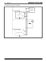
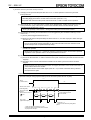
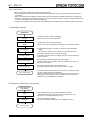
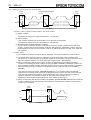
1. Overview
2
This module is an I C bus interface real-time clock that has bult-in 32.768-kHz crystal oscillator.
In addition to a calendar (year, month, day, weekday, hour, minute, second) function and a clock counter
function, this module's real-time clock functions include an alarm function and a fixed-cycle timer interrupt
function.
The devices in this module are fabricated via a C-MOS process for low current consumption, which enables
long-term battery back-up.
All of these many functions are implemented in a compact package, which makes it suitable for various
kinds of mobile telephones, handy terminals and other small electronic devices.
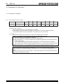
2. Block diagram
32.768 kHz
CRYSTAL
Control 1
OSC
Voltage Detector
00
Control 2
Seconds
Minutes
CLKOUT
CLKOE
Hours
OUTPUT
DIVIDER
CONTROL
Days
Weekdays
Month / Century
Years
/ INT
CONTROL
LOGIC
SCL
SDA
I2C-BUS
Minutes Alarm
Hour Alarm
Day Alarm
Weekday Alarm
INTERFACE
CLKOUT frequency
ADDRESS
POR
REGISTER
Page − 1
Timer Control
Timer
0F
ETM12E-01
RX − 8564 LC
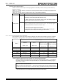
3. Terminal description
3.1. Terminal connections
RX − 8564 LC
1.
N.C.
2.
N.C.
3.
N.C.
4.
N.C.
12.
11. CLKOE
# 12
#1
N.C.
10. VDD
9. CLKOUT
#7
#6
5. /INT
8. SCL
7. SDA
6. GND
VSOJ − 12pin
3.2. Pin Functions
Signal
I/O
name
SCL
SDA
Input
Bi-Directional
Function
2
This is the serial clock input pin for I C Bus communications.
This pin's signal is used for input and output of address, data, and ACK bits,
2
synchronized with the serial clock used for I C communications.
Since the SDA pin is an N-ch open drain pin during output, be sure to connect a suitable
pull-up resistance relative to the signal line capacity.
The CLKOUT pin is a clock output pin (C-MOS output) with the output control function.
The CLKOE pin can be used in combination with the FE bit, FD1 bit, and FD0 bit to
control the output mode of the CLKOUT output pin.
CLKOUT
Output
The CLKOE input pin can be used in combination with the FE bit, FD1 bit, and FD0 bit to
select the frequency output from the CLKOUT output pin (32.768 kHz, 1024 Hz, 32 Hz, or
1 Hz) or to stop output.
When output is stopped, the CLKOUT output pin is at low level ( = " L " ).
CLKOE pin
input
"H"
CLKOE
Input
"L"
FE
bit
1
0
1
0
CLKOUT pin
output
Output
( C-MOS )
OFF
("L")
OFF
("L")
OFF
("L")
During the initial power-on (when power is applied from 0 V), if the CLKOE input pin is at
high level ( = " H " ), the power-on reset function selects 32.768 kHz as the frequency.
This pin outputs alarm signals, fixed timer interrupt signals, and other interrupt signals at
low level ( = " L " ). This pin is an open drain pin.
/INT
Output
VDD
−
This pin connects to the plus side of the power.
GND
−
This pin connects to the minus side (ground) of the power.
N.C.
−
This pin is not connected internally. Be sure to connect using OPEN, or GND or VDD.
Note : Be sure to connect a bypass capacitor rated at least 0.1 µF between VDD and GND.
Page − 2
ETM12E-01
RX − 8564 LC
4. External Dimensions / Marking Layout
4.1. External Dimensions
RX − 8564 LC ( VSOJ − 12pin )
• External dimensions
• Recommended soldering pattern
3.6 ± 0.2
2.5
#7
0.27
2.4
1.6
0.5
0.8
3.2
( 0.4 )
2.8 ± 0.2
2.4
0.8
# 12
#6
2.77
0.08 M
0.22
Min. 0
0.5
1.1 ± 0.1
#1
Unit : mm
0.08
4.2. Marking Layout
RX − 8564 LC ( VSOJ − 12pin )
Type
Logo
E 8564
A123B
#1 Pin Mark
Production lot
∗ Contents displayed indicate the general markings and display, but are not the standards for the fonts, sizes and positioning.
Page − 3
ETM12E-01
RX − 8564 LC
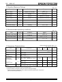
5. Absolute Maximum Ratings
Parameter
GND = 0 V
Symbol
Condition
Rating
Unit
Supply Voltage
VDD
Between VDD and GND
−0.5 to +6.5
V
Supply Voltage
IDD
VDD pin
−50 to 50
mA
Input Voltage
VI
Input pin
GND−0.5 to VDD+0.5
V
Output Voltage
VO
/INT pin
GND−0.5 to VDD+0.5
V
DC Input Current
II
−10 to 10
mA
DC Output Current
IO
−10 to 10
mA
−55 to +125
°C
Storage
Temperature Range
Stored bare product after
unpacking
TSTG
6. Recommended operating conditions
Item
Symbol
Operating supply voltage
VDD
Clock supply voltage
VDD
Operating temperature
TOPR
∗1)
Condition
Unit
1.8 to 5.5
V
VLOW (∗1) to 5.5
V
access
at 400 kHz
−40 to +85
No condensation
°C
See " 8.1. DC Electrical Characteristics ".
Item
Output frequency
Frequency precision
Frequency
voltage
characteristics
Frequency
temperature
characteristics
Oscillation
startup-up time
Aging
∗2 )
Rating
I2C-BUS
* Unless otherwise specified, GND = 0 V
, Ta = +25 °C , VDD = 3.0 V
7. Frequency Characteristics
∗1 )
GND = 0 V
Symbol
Comments
Min.
fo
32.768
∆f/f
Ta = +25 °C
VDD = 3.0 V
f/V
Ta = +25 °C
VDD = 1.8 V to 5.5 V
Top
Ta = −20 °C to +70 °C,
VDD = 3.0 V ; Reference at +25 °C
tSTA
Ta = +25 °C
VDD = 1.8 V
Ta = −40 °C to +85 °C,
VDD = 3.0 V
fa
Typ.
Ta = +25 °C , VDD = 3.0 V ; first year
Max.
( Typ. )
Unit
kHz
5 ± 23
(∗1) (∗2)
× 10−6
±2
( Max. )
× 10−6 / V
−120
−5
+10
× 10−6
3.0
s
3.0
s
+5
× 10−6
/ year
This difference is 1 minute by 1 month. ( excluding offset )
Includes variation in frequency during two rounds of reflow processing.
∗ Reflow processing is performed under conditions specified by Seiko Epson Corporation.
(See the relevant specifications.)
Page − 4
ETM12E-01
RX − 8564 LC
8. Electrical Characteristics
8.1. DC characteristics
Item
* Unless otherwise specified, GND = 0 V , VDD = 1.8 V to 5.5 V
, Ta = −40 °C to +85 °C
Symbol
Current consumption
∗ interface active
Condition
Min.
Typ.
Max.
Unit
fSCL = 400 kHz
800
µA
fSCL = 100 kHz
200
µA
IDD
Current consumption
fSCL = 0 Hz, VDD = 5.0 V
330
800
nA
fSCL = 0 Hz, VDD = 3.0 V
275
700
nA
∗ CLKOUT = disabled
( CLKOE = GND )
fSCL = 0 Hz, VDD = 2.0 V
250
650
nA
Current consumption
fSCL = 0 Hz, VDD = 5.0 V
2.5
3.4
µA
fSCL = 0 Hz, VDD = 3.0 V
1.5
2.2
µA
fSCL = 0 Hz, VDD = 2.0 V
1.1
1.6
µA
∗ interface inactive
( fSCL = 0 Hz )
∗ interface inactive
( fSCL = 0 Hz )
IDD
IDD32K
∗ CLKOUT = 32 kHz output
( LOAD is 0 pF )
"L" input voltage
VIL
GND − 0.5
0.3 × VDD
V
"H" input voltage
VIH
0.7 × VDD
VDD + 0.5
V
"L" output current
IOL
( SDA )
VOL = 0.4 V, VDD = 5 V
−3
mA
"L" output current
IOL
( /INT )
VOL = 0.4 V, VDD = 5 V
−1
mA
"L" output current
IOL
( CLKOUT )
VOL = 0.4 V, VDD = 5 V
−1
mA
"H" output current
IOH
( CLKOUT )
VOH = 4.6 V, VDD = 5 V
Leakage current
Low voltage detection
ILO
VLOW
VO = VDD or GND
−1
1
mA
1
µA
Ta = +25 °C
0.9
1.0
V
Ta = −20 °C to +70 °C
0.9
1.2
V
Ta = −40 °C to +85 °C
0.9
1.3
V
Page − 5
ETM12E-01
RX − 8564 LC
8.2. AC electrical characteristics
Item
* Unless otherwise specified, GND = 0 V , VDD = 1.8 V to 5.5 V
, Ta = −40 °C to +85 °C
Symbol
SCL clock frequency
Condition
Min.
Typ.
fSCL
Max.
Unit
400
kHz
Start condition set-up time
tSU; STA
0.6
µs
Start condition hold time
tHD; STA
0.6
µs
Data set-up time
tSU; DAT
100
ns
Data hold time
tHD; DAT
0
ns
Stop condition set-up time
tSU; STO
0.6
µs
Bus free time between a STOP
and START condition
tBUF
1.3
µs
SCL "L" time
tLOW
1.3
µs
SCL "H" time
tHIGH
0.6
µs
SCL and SDA rise time
tr
0.3
µs
SCL and SDA fall time
tf
0.3
µs
tSP
50
ns
Tolerance spike time on bus
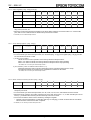
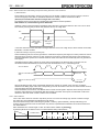
Timing chart
Protocol
START
CONDITION
(S)
tSU ; STA
BIT 7
MSB
(A7)
tLOW
BIT 6
BIT 0
LSB
(R/W)
(A6)
tHIGH
ACK
(A)
STOP
CONDITION
(P)
1 / fSCL
START
CONDITION
(S)
tSU ; STA
SCL
(S)
(P)
(S)
tBUF
tr
tf
SDA
(A)
tHD ; STA
Note :
tSU ; DAT
tHD ; DAT
tSP
tSU ; STO
tHD ; STA
I2C access time between a START and a START condition or between a START and a STOP condition to this
device must be less than one second.
Page − 6
ETM12E-01
RX − 8564 LC
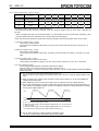
9. Reference data
(1) Example of frequency and temperature characteristics
× 10-6
θT = +25 °C Typ.
α = -0.035 × 10⁻⁶ Typ.
1. Frequency and temperature characteristics can be
approximated using the following equations.
0
Frequency ∆fT
[ Finding the frequency stability ]
∆fT = α ( θT − θX ) 2
! ∆fT
! α [ 1 / °C2 ]
-50
! θT [ °C ]
! θX [ °C ]
-100
-150
-50
0
50
100
: Frequency deviation in any temperature
: Coefficient of secondary temperature
( −0.035 ± 0.005 ) × 10−6 / °C2
: Ultimate temperature ( +25 ± 5 °C )
: Any temperature
2. To determine overall clock accuracy, add the
frequency precision and voltage characteristics.
∆f/f = ∆f/fo + ∆fT + ∆fV
Temperature [°C]
! ∆f/f
: Clock accuracy (stable frequency)
in any temperature and voltage.
: Frequency precision
: Frequency deviation in any temperature.
: Frequency deviation in any voltage.
! ∆f/fo
! ∆fT
! ∆fV
3. How to find the date difference
Date Difference = ∆f/f × 86400(Sec)
∗ For example: ∆f/f = 11.574 × 10 is an error of
approximately 1 second/day.
-6
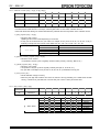
(2) Current and voltage consumption characteristics
(2-1) Current consumption when non-accessed (i)
when CLKOUT=OFF
(2-2) Current consumption when non-accessed (ii)
when CLKOUT=32.768kHz
Condition :
Condition :
fSCL=0 Hz, Ta=+25 °C, CLKOUT=OFF
fSCL=0 Hz, Ta=+25 °C, CLKOUT=32.768 kHz
10
0.5
Current consumption [µA]
Current consumption [µA]
1.0
IDD[µA]
2
3
4
CL=30 pF
5
IDD32K[µA]
CL=0 pF
2
5
3
4
5
Supply Voltage VDD[V]
Supply Voltage VDD[V]
Page − 7
ETM12E-01
RX − 8564 LC
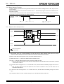
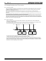
10. External connection example
VDD
SCL
2
I C-BUS
Master
SDA
VDD
SCL
8564
SLAVE ADRS = 1010001
SDA
GND
Pull up Registor
R=
tr
C BUS
VDD
SCL
2
I C-BUS device
SDA
GND
Page − 8
ETM12E-01
RX − 8564 LC
11. Application notes
1) Notes on handling
This module uses a C-MOS IC to realize low power consumption.
Carefully note the following cautions when handling.
(1) Static electricity
While this module has built-in circuitry designed to protect it against electrostatic discharge, the chip could still be damaged by a large
discharge of static electricity. Containers used for packing and transport should be constructed of conductive materials. In addition,
only soldering irons, measurement circuits, and other such devices which do not leak high voltage should be used with this module,
which should also be grounded when such devices are being used.
(2) Noise
If a signal with excessive external noise is applied to the power supply or input pins, the device may malfunction or "latch up." In order
to ensure stable operation, connect a filter capacitor (preferably ceramic) of greater that 0.1 µF as close as possible to the power
supply pins (between VDD and GNDs). Also, avoid placing any device that generates high level of electronic noise near this module.
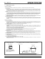
* Do not connect signal lines to the shaded area in the figure shown in Fig. 1 and, if possible, embed this area in a GND land.
(3) Voltage levels of input pins
When the input pins are at the mid-level, this will cause increased current consumption and a reduced noise margin, and can impair
the functioning of the device. Therefore, try as much as possible to apply the voltage level close to VDD or GND.
(4) Handling of unused pins
Since the input impedance of the input pins is extremely high, operating the device with these pins in the open circuit state can lead
to unstable voltage level and malfunctions due to noise. Therefore, pull-up or pull-down resistors should be provided for all unused
input pins.
2) Notes on packaging
(1) Soldering heat resistance.
If the temperature within the package exceeds +260 °C, the characteristics of the crystal oscillator will be degraded and it may be
damaged. The reflow conditions within our reflow profile is recommended. Therefore, always check the mounting temperature and
time before mounting this device. Also, check again if the mounting conditions are later changed.
* See Fig. 2 profile for our evaluation of Soldering heat resistance for reference.
(2) Packaging equipment
This product uses a molded package whose back contains glass.
Therefore, it is possible for shocks during packaging to cause product breakage, depending on the packaging machinery and
conditions.
Please be sure to check that the load placed on products during packaging is as low as possible (low speeds during loading onto the
substrate, low chuck forces, etc.) before using packaging equipment.
Carry out the same checks when changing packaging conditions.
The presence of foreign objects between this product and the packaging substrate may result in product breakage.
Guard against introduction of foreign objects during packaging.
Also, carry out measures to eliminate static electricity during packaging of and operations with this product.
(3) Ultrasonic cleaning
Depending on the usage conditions, there is a possibility that the crystal oscillator will be damaged by resonance during ultrasonic
cleaning. Since the conditions under which ultrasonic cleaning is carried out (the type of cleaner, power level, time, state of the inside
of the cleaning vessel, etc.) vary widely, this device is not warranted against damage during ultrasonic cleaning.
(4) Mounting orientation
This device can be damaged if it is mounted in the wrong orientation. Always confirm the orientation of the device before mounting.
(5) Leakage between pins
Leakage between pins may occur if the power is turned on while the device has condensation or dirt on it. Make sure the device is dry
and clean before supplying power to it.
(6) Use of adhesive after packaging product
This product uses a molded package whose back contains glass.
Please check that use of the adhesive does not cause problems before adopting any adhesive as a measure to reinforce the
packaging for your product.
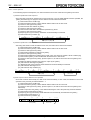
Fig. 1 : Example GND Pattern
RX − 8564 LC
Fig. 2 : Reference profile for our evaluation of Soldering heat resistance.
Temperature [ °C ]
( VSOJ − 12 pin )
+260 °C Max.
−1 ∼ −5 °C / s
+1 ∼ +5 °C / s
∗ The shaded part (
)
indicates where a GND pattern
should be set without getting too
close to a signal line
+1 ∼ +5 °C / s
+170 °C
100 s
+220 °C
35 s
Pre-heating area
Stable Melting area
time [ s ]
Page − 9
ETM12E-01
RX − 8564 LC
12. Overview of Functions and Description of Registers
12.1. Overview of Functions
1) Clock functions
This function is used to set and read out month, day, hour, date, minute, second, and year (last two digits) data.
Any (two-digit) year that is a multiple of 4 is treated as a leap year and calculated automatically as such until the
year 2099.
∗ For details, see "13.1. Description of Registers".
2) Fixed-cycle interrupt generation function
The fixed-cycle timer interrupt generation function generates an interrupt event periodically at any fixed cycle set
between 244.14 µs and 255 minutes.
When an interrupt event is generated, the /INT pin goes to low level ("L") and "1" is set to the TF bit to report that
an event has occurred.
Two types of operations can be selected for this function (level interrupt mode and repeated interrupt mode).
∗ For details, see "13.2. Fixed-cycle Interrupt Function".
3) Alarm interrupt function
The alarm interrupt generation function generates interrupt events for alarm settings such as date, day, hour, and
minute settings.
When an interrupt event occurs, the AF bit value is set to "1" and the /INT pin goes to low level to indicate that an
event has occurred.
∗ For details, see "13.3. Alarm Interrupt Function".
4) 32.768 kHz output function
The 32.768 kHz clock signal (with precision equal to that of the on-chip crystal osillator) can be output (as C-MOS
output) via the CLKOUT pin.
If a different frequency is required, 32.768 kHz, 1024 Hz, 32 Hz, or 1 Hz can be selected.
∗ For details, see "13.1.9. CLKOUT output register".
Page − 10
ETM12E-01
RX − 8564 LC
12.2. Register table
Address [h]
Function
bit 7
bit 6 bit 5
bit 4
bit 3 bit 2
bit 1
bit 0
00
Control 1
TEST
0
STOP
0
TEST
01
Control 2
0
×
0
TI / TP
02
Seconds
VL
40
20
03
Minutes
×
40
04
Hours
×
05
Days
06
note
0
0
0
∗3 , ∗4
AF
TF
AIE
TIE
∗4 , ∗5
10
8
4
2
1
∗1
20
10
8
4
2
1
∗5
×
20
10
8
4
2
1
∗5
×
×
20
10
8
4
2
1
∗5
Weekdays
×
×
×
×
×
4
2
1
∗5
07
Months / Century
C
×
×
10
8
4
2
1
∗5
08
Years
80
40
20
10
8
4
2
1
09
Minute Alarm
AE
40
20
10
8
4
2
1
0A
Hour Alarm
AE
×
20
10
8
4
2
1
∗5
0B
Day Alarm
AE
×
20
10
8
4
2
1
∗5
0C
Weekday Alarm
AE
×
×
×
×
4
2
1
∗5
0D
CLKOUT frequency
FE
×
×
×
×
×
FD1
FD0
∗2 , ∗5
0E
Timer control
TE
×
×
×
×
×
TD1
TD0
∗5
0F
Timer
128
64
32
16
8
4
2
1
Note)
During the initial power-on (from 0 V) and if the value of the VL bit is "1" when the VL bit is read, be sure to
initialize all registers before using them.
When doing this, be careful to avoid setting incorrect data as the date or time, as timed operations cannot be
guaranteed if incorrect date or time data has been set.
∗1.
During the initial power-on (from 0 V), the power-on reset function sets "1" to the VL bit.
∗ Since the value of other registers is undefined at this time, be sure to reset all registers before using them.
∗2.
During the initial power-on (from 0 V), the power-on reset function sets "1" to the FE bit and the FD1 and FD0 bits
are reset to "0".
∗ If the CLKOE input pin is at high level ("H"), output from the CLKOUT output pin is at 32.768 kHz.
∗3.
The two TEST bits for address 00 (Control 1) are for use by Seiko Epson Corporation.
When initializing, be sure to write "0". Afterward, be sure to write "0" whenever writing to these bits.
∗ This device's operations are not guaranteed if "1" has been set to any of these bits.
∗4.
All bits marked with "0" should have a value of "0" after initialization.
∗5.
All bits marked with “x” are read-only bits whose value when read is undefined. Be sure to mask these bits after
they are read.
Page − 11
ETM12E-01
RX − 8564 LC
13. Description of Functions
13.1. Description of registers
13.1.1. Control register 1 ( Reg − 00 [h] )
Address [h]
Function
bit 7
bit 6
bit 5
bit 4
bit 3
bit 2
bit 1
bit 0
00
Control 1
TEST
0
STOP
0
TEST
0
0
0
• This register is used to control stopping and starting of the clock function, calendar function, and other functions.
1) TEST bits (bit 7 and bit 3)
These two TEST bits are for use by Seiko Epson Corporation.
When initializing, be sure to write "0". Afterward, be sure to write "0" whenever writing to these bits.
∗ This device's operations are not guaranteed if "1" has been set to any of these bits.
2) STOP bit
The STOP bit is used to stop functions such as the clock, calendar, alarm, and timer.
Writing "1" to the STOP bit stops operation of the clock, calendar, alarm, timer, etc.
∗1) When the STOP bit = "1", operations are restricted.
Do not use any settings other than the clock and calendar settings.
∗2) When the STOP bit = "1", output via CLKOUT may be stopped, depending on the selected frequency.
Note this with caution.
(1) If 32.768 kHz has been selected as the output frequency, output will continue at 32.768 kHz.
(2) If any other output frequency was selected (1024 Hz, 32 Hz, or 1 Hz), CLKOUT output is stopped.
∗3) When the STOP bit = "1", the I2C-BUS bus timeout function is disabled. Note this with caution.
When the STOP bit = "0", these operations are resumed (stop mode is canceled).
∗ 0.5 seconds after the STOP bit value is changed from "1" to "0", the "second" value is updated
(without waiting for a full second to elapse). This operation occurs once only after changing the STOP bit
value.
(This is done to keep the error margin to within ±0.5 seconds in relation to the actual time whenever the
clock value is changed via any timing.)
Page − 12
ETM12E-01
RX − 8564 LC
13.1.2. Control register 2 ( Reg − 01 [h] )
Address [h]
Function
bit 7
bit 6
bit 5
bit 4
bit 3
bit 2
bit 1
bit 0
01
Control 2
0
×
0
TI / TP
AF
TF
AIE
TIE
• This register is used to monitor various interrupt event settings and the conditions under which various interruptrelated events occur.
1) TI / TP bit ( Interrupt Signal Output Mode Select. Interrupt / Periodic )
When a fixed-cycle timer interrupt event occurs (when the TF bit goes from "0" to 1") , this bit specifies
whether the interrupt operation occurs just once or repeatedly.
Writing "1" to this bit sets repeated operation.
Writing "0" to this bit sets single-shot operation.
∗ For details, see "9.2. Fixed-cycle Timer Interrupt Function ".
2) AF bit ( Alarm Flag )
This is a flag bit that retains the result when an alarm interrupt event has been detected.
When an alarm interrupt event occurs, this bit's value changes from "0" to "1".
∗ For details, see "9.3. Alarm Interrupt Function".
3) TF bit ( Timer Flag )
This is a flag bit that retains the result when a fixed-cycle timer interrupt event has been detected.
When a fixed-cycle timer interrupt event occurs, this bit's value changes from "0" to "1".
∗ For details, see "9.2. Fixed-cycle Timer Interrupt Function ".
4) AIE bit ( Alarm Interrupt Enable )
This bit sets the operation of the /INT interrupt signal when an alarm interrupt event has occurred (the AF bit
value changes from "0" to "1").
When a "1" is written to this bit, occurrence of an interrupt event causes a low-level interrupt signal to be
output from /INT pin.
Writing "0" to this bit prohibits low-level output from the /INT pin.
∗ For details, see "9.3. Alarm Interrupt Function".
5) TIE bit ( Timer Interrupt Enable )
This bit sets the operation of the /INT interrupt signal when a fixed-cycle interrupt event has occurred (the
TF bit value changes from "0" to "1").
When a "1" is written to this bit, occurrence of an interrupt event causes a low-level interrupt signal to be
output from /INT pin.
Writing "0" to this bit prohibits low-level output from the /INT pin.
∗ For details, see "9.2. Fixed-cycle Timer Interrupt Function ".
Page − 13
ETM12E-01
RX − 8564 LC
13.1.3. Clock counter ( Reg − 02 [h] to 04 [h] )
Address [h]
Function
bit 7
bit 6
bit 5
bit 4
bit 3
bit 2
bit 1
bit 0
02
Seconds
VL
40
20
10
8
4
2
1
03
Minutes
×
40
20
10
8
4
2
1
04
Hours
×
×
20
10
8
4
2
1
• The clock counter counts seconds, minutes, and hours.
• The data format is BCD format. For example, when the "seconds" register value is "0101 1001" it indicates 59
seconds.
∗ When overwriting time data, we recommend setting "1" to the STOP bit to stop the clock before overwriting. (This
prevents unintentional carry operations from occurring while overwriting data.)
∗ Note with caution that writing non-existent time data may interfere with normal operation of the clock counter.
1) [ Seconds ] register ( Reg − 02 [h] )
This counter counts seconds.
Count values are updated as: 00 seconds, 01 second, 02 to 59 seconds, 00 seconds, 01 second, etc. in
that order.
2) [ Minutes ] register ( Reg − 03 [h] )
This counter counts minutes.
Count values are updated as: 00 minutes, 01 minute, 02 to 59 minutes, 00 minutes, 01 minute, etc. in that
order.
3) [ Hours ] register ( Reg − 04 [h] )
The [Hours] counter uses a 24-hour clock.
Count values are updated as: 00 hours, 01 hour, 02 to 23 hours, 00 hours, 01 hour, etc. in that order.
4) VL bit ( Voltage Low Flag )
This is a flag bit that retains the result when detecting low voltage.
When the power source's voltage drops below VLOW[V]*, this flag is set to 1.
If this bit's value is "1" when read, this RTC's data is ignored, in which case all registers should be initialized
before being used.
(1) A "1" is set to this VL flag during initial power-on (from 0 V).
Since the value of other registers is undefined at this time, be sure to reset all registers before using
them.
(2) When recovering from backup mode, read this VL flag, and if its value is "1" be sure to initialize the
registers before using them.
(3) When initializing, be sure to clear this VL flag to zero to prepare for the next voltage detection.
(4) This VL flag was designed to provide a voltage drop warning after the voltage of the backup battery or
other devices has gradually dropped, and it is not designed to respond to sharp fluctuations in voltage
due to power supply chatter, etc.
VDD
(1) VL=”1”
(2) VL=”0”
(3) VL=”1”
VLOW
GND
GND=0 V
(1) VL="1" as result of initial supply of power
(2) When the power supply is low but voltage not dropping to VLOW , VL remains at "0"
with no change
(3) When the power supply is low and voltage dropping below VLOW , VL becomes "1".
∗ The value of the VL bit in (2) and (3) need to be zero cleared in (1).
(5) This VL flag is cleared via a write operation regardless of data.
Be sure to read this flag's value before writing to this register.
Page − 14
ETM12E-01
RX − 8564 LC
13.1.4. Calendar counter ( Reg − 05 [h] , 07 [h] , 08 [h] )
Address [h]
Function
bit 7
bit 6
bit 5
bit 4
bit 3
bit 2
bit 1
bit 0
05
Days
×
×
20
10
8
4
2
1
07
Months / Century
C
×
×
10
8
4
2
1
08
Years
80
40
20
10
8
4
2
1
• The auto calendar function updates all dates, months, and years from January 1, 2001 to December 31, 2099.
• The data format is BCD format. For example, a date register value of "0011 0001" indicates the 31st.
∗ Note with caution that writing non-existent date data may interfere with normal operation of the calendar counter.
1) [ Day ] register ( Reg − 05 [h] )
• This is the date counter.
Updating of this counter varies depending on the month.
∗ A leap year is set whenever the year value is a multiple of four (such as 04, 08, 12, 88, 92, or 96). In
February of a leap year, the counter counts dates from "01," "02," "03," to "28," "29," "01," etc.
Month
[ Days ]
Write / Read
Date update pattern
01, 02, 03 ∼ 30, 31, 01 ∼
01, 02, 03 ∼ 30, 01, 02 ∼
01, 02, 03 ∼ 28, 01, 02 ∼
01, 02, 03 ∼ 28, 29, 01 ∼
1, 3, 5, 7, 8, 10, or 12
4, 6, 9, or 11
February in normal year
February in leap year
2) [ Months / Century ] register ( Reg − 07 [h] )
• This is the month counter.
It is updated in annual cycles of regularly ordered months (January, February, March, etc.).
3) [ YEAR ] register ( Reg − 08 [h] )
• This is the year counter.
It is updated in 100-year cycles of regularly ordered years (00, 01, 02 to 99, etc.).
∗ Any year that is a multiple of four (04, 08, 12, 88, 92, 96, etc.) is handled as a leap year.
4) C bit ( Century bit )
• This bit indicates change of century.
∗ When the year digit data overflows from 99 to 00, this bit is set. By presetting it to 0 while still in the 20th
century, it will be set in year 2000, but in fact the first year in the 21 century should be 2001.
13.1.5. Day counter ( Reg − 6[h] )
Address [h]
Function
bit 7
bit 6
bit 5
bit 4
bit 3
bit 2
bit 1
bit 0
06
Weekdays
×
×
×
×
×
4
2
1
• The day (of the week) is indicated by 3 bits, bit 0 to bit 2.
[ Weekdays ]
bit 7
bit 6
bit 5
bit 4
bit 3
bit 2
bit 1
bit 0
Day
0
0
0
Sunday
×
×
×
×
×
0
0
1
Monday
×
×
×
×
×
0
1
0
Tuesday
×
×
×
×
×
Write / Read
0
1
1
Wednesday
×
×
×
×
×
1
0
0
Thursday
×
×
×
×
×
1
0
1
Friday
×
×
×
×
×
1
1
0
Saturday
×
×
×
×
×
∗ Note with caution that any settings other than the seven listed above may prevent normal operation.
Page − 15
ETM12E-01
RX − 8564 LC
13.1.6. Alarm registers ( Reg − 09 [h] to 0C [h] )
Address [h]
Function
bit 7
bit 6
bit 5
bit 4
bit 3
bit 2
bit 1
bit 0
09
Minute Alarm
AE
40
20
10
8
4
2
1
0A
Hour Alarm
AE
×
20
10
8
4
2
1
0B
Day Alarm
AE
×
20
10
8
4
2
1
0C
Weekday Alarm
AE
×
×
×
×
4
2
1
• The AIE bit and AF bit can both be set or used when using alarm interrupt function to set interrupt events for dates,
days, hours, minutes, etc.
• When the current time matches the settings in the above alarm registers, the AF bit's value is "1" and the /INT
pin's status is low to indicate that an alarm interrupt event has occurred.
∗ For details, see "9.3. Alarm Interrupt Function".
13.1.7. Timer setting register ( Reg − 0E [h] )
Address [h]
Function
bit 7
bit 6
bit 5
bit 4
bit 3
bit 2
bit 1
bit 0
0E
Timer control
TE
×
×
×
×
×
TD1
TD0
• This register is used to control the fixed-cycle timer interrupt function.
• To use the fixed-cycle timer interrupt function, the TI/TP bits (Reg − 01 [h]), timer register (Reg − 0F [h]), and the
TF and TIE bits are all set or used.
1) TE bit ( Timer Enable )
This bit is used to control operation of the fixed-cycle timer interrupt function.
When "1" is written to this bit, the fixed-cycle timer interrupt function starts operating.
When "0" is written to this bit, the fixed-cycle timer interrupt function stops operating.
∗ For details, see "9.2. Fixed-cycle Timer Interrupt Function ".
2) TD1,TD0 bits ( Timer countDown interval select 1, 0 )
These bits specify the fixed-cycle timer interrupt function's countdown period (source clock).
Four different periods can be selected via combinations of these two bit values.
∗ For details, see "9.2. Fixed-cycle Timer Interrupt Function ".
13.1.8. Down counter for fixed-cycle timer ( Reg − 0F [h] )
Address [h]
Function
bit 7
bit 6
bit 5
bit 4
bit 3
bit 2
bit 1
bit 0
0F
Timer
128
64
32
16
8
4
2
1
• This register is used to set the default (preset) value for the counter. Any count value from 1 (01 h) to
255 (FFh) can be set
• To use the fixed-cycle timer interrupt function, the TE, TI/TP, TF, TIE, TD1, and TD0 bits are set and used.
• When this down counter's count value changes from 01h to 00h, when TF bit = "1", or when the /INT pin is at low
level ("L"), it indicates that a fixed-cycle timer interrupt event has occurred.
• The current countdown status can be checked by reading this register.
∗ However, since the read data is not held (the data may be changing), to obtain accurate data the countdown
status should be read twice and then compared.
∗ For details, see "9.2. Fixed-cycle Timer Interrupt Function ".
Page − 16
ETM12E-01
RX − 8564 LC
13.1.9. CLKOUT output register (Reg - 0D [h])
Address [h]
Function
bit 7
bit 6
bit 5
bit 4
bit 3
bit 2
bit 1
bit 0
0D
CLKOUT frequency
FE
×
×
×
×
×
FD1
FD0
• This register is used to control clock output via the CLKOUT output pin.
• This register is valid only when the CLKOE input pin is at high level, at which time clock output is enabled or
disabled (stopped) depending on the settings in this register.
∗ When the CLKOE input pin is at low level, CLKOUT is at low level regardless of the settings in this register.
1) FE bit ( Frequency output Enable )
When this register is valid (when CLKOE is at high level), it is used to control the CLKOUT pin's output
status.
When the FE bit value is "1", the CLKOUT pin is in output mode. The content being output at that time is
the frequency specified via the FD1 and FD0 bit.
When the FE bit value is "0", the CLKOUT pin is output STOP mode (= low level).
2) FD1, FD0 bits
A combination of the FD1 and FD0 bits is used to select the frequency to be output.
3) CLKOUT output based on various settings
CLKOE pin
input
"H"
"L"
Χ : don't care
FE
bit
1
0
1
0
FD1
bit
0
0
1
1
Χ
Χ
Χ
FD0
bit
0
1
0
1
Χ
Χ
Χ
CLKOUT pin
output
32768 Hz Output
( C-MOS )
1024 Hz Output
( C-MOS )
32 Hz Output
( C-MOS )
1 Hz Output
( C-MOS )
OFF
("L")
OFF
("L")
OFF
("L")
∗ During initial power-on (from 0 V), "1" is set to the FE bit by the power-on reset function, and the FD1
and FD0 bits are reset to zero.
Consequently, 32.768 kHz output can be obtained from the CLKOUT output pin by setting the CLKOE
input pin to high level.
Note) Re: CLKOUT output operation when STOP bit value is "1"
Note with caution that when the STOP bit value is "1", output via CLKOUT may be stopped, depending on
the selected frequency.
(1) When 32.768 kHz output has been selected, output continues at 32.768 kHz.
(2) When any other frequency has been set (1024Hz, 32Hz, or 1Hz), CLKOUT output is stopped.
Page − 17
ETM12E-01
RX − 8564 LC
13.2. Fixed-cycle Timer Interrupt Function
The fixed-cycle timer interrupt function generates an interrupt event periodically at any fixed cycle set between
244.14 µs and 255 minutes.
There are two operation modes: "level interrupt mode" whereby the operation ends after one time, and "repeated
interrupt mode" whereby the operation is automatically repeated.
When either of these interrupt events occurs, the event's occurrence is indicated by the "1" value set to the TF
bit and by the low-level ("L") status of the /INT pin.
13.2.1. Overview of fixed-cycle timer interrupt function
• The fixed-cycle timer interrupt function is used with several combinations of settings.
(1) Operation mode setting (level interrupt mode or repeated interrupt mode)
(2) Fixed-cycle timer operation period setting (period = countdown reference cycle × count value)
(3) Setting as to whether to output (at low level) an interrupt signal from the /INT output pin after a specified
amount of operation time has elapsed.
• When operation of the fixed-cycle timer starts (TE, "0" → "1"), various events occur after the specified time has
elapsed.
(1) The TF (Timer Flag) bit value, which indicates when a fixed-cycle timer interrupt event has occurred, changes
from "0" to "1".
(2) When the TIE (Timer Interrupt Enable) bit value is "1", the /INT output pin status changes from Hi-Z to "L".
1) Overview of level interrupt mode
(TI/TP bit = "0")
Once an interrupt event has occurred, the operation ends after one iteration.
∗ However, if only the TF bit is cleared to zero without stopping operation of the fixed-cycle timer (TE bit
value remains "1"), note with caution that an interrupt event will occur during the next timer cycle (period).
If an interrupt event occurs during level interrupt mode, the /INT output goes to low level.
The low level output is maintained as it is until the TF bit is cleared to zero. (When TIE = "1" )
∗Example of /INT
operation
period
TIE = " 1 "
TF = " 0 "
TE = " 0 " → " 1 "
TF = " 0 " → " 1 "
TF = " 1 " → " 0 "
2) Overview of repeated interrupt mode (TI/TP bit = "1")
After an interrupt event occurs, the operation is automatically repeated.
When an interrupt event occurs during repeated interrupt mode, /INT output goes to low level only during
the tRTN period, and then it is automatically canceled and returns to Hi-Z status.
However, even after returning to Hi-Z status, similar /INT output is obtained after the next interrupt event
occurs.
Afterward, this is repeated until fixed-cycle timer operation is stopped.
∗Example of /INT
operation
Auto reset time
tRTN
period
TIE = " 1 "
TF = " 0 "
TE = " 0 " → " 1 "
TF = " 0 " → " 1 "
Page − 18
TIE = " 1 " → " 0 "
ETM12E-01
RX − 8564 LC
3) Overview of fixed-cycle timer interrupt function
(1) Changing the TE (Timer Enable) bit value from "0" to "1" starts operation of the fixed-cycle timer
interrupt function.
∗ Before starting the fixed-cycle timer interrupt function each time, be sure to write a value (preset
value/Reg-0F[h]) as the down counter value for the timer (when TE = "0").
(Note) Note with caution that the preset value must be set or reset to enable correct operation.
(2) When the TE bit = "1", the timer's down counter (Timer Register/Reg − 0F[h]) counts down once per
cycle (countdown cycle) of the source clock that was selected via the TD1 and TD0 bits (Timer
countdown interval select bits 1 and 0).
∗ Timer cycle (Period) = Source clock × value (preset value) set to timer's down counter
(3) The following processing is executed after an event is triggered by the countdown reaching a count
value of "0".
∗1) The TF (Timer Flag) bit value becomes "1".
∗2) When the TIE (Timer Interrupt Enable) bit value becomes "1", the /INT output pin's status changes
from Hi-z to "L".
∗ After the /INT output pin's status changes from Hi-z to "L", the /INT status is either held at low
level or automatically cleared, depending on the TI/TP bit's setting from the operation mode
(level interrupt mode or repeated interrupt mode).
∗3) The timer's down counter automatically returns to the preset value and then the countdown
operation is repeated.
∗ When the TE bit value is "1", countdown operation of the timer's down counter will be repeated
regardless of the operation mode or of any event that has occurred.
(4) When the TE bit is cleared from "1" to 0", the fixed-cycle timer interrupt function stops.
∗1) The TF bit value remains "1" until it is cleared to zero (even if the fixed-cycle timer function has been
stopped).
∗2) The timer's down counter value becomes invalid once the fixed-cycle timer function has been
stopped.
∗ When the fixed-cycle timer interrupt function is stopped, the timer's down counter value and the
preset value both become invalid.
∗ The preset value must be written again (when TE = "0") in order to start the fixed-cycle timer
interrupt function again.
∗ Operation example
∗ Operation example during repeated interrupt mode and when preset value is "5" (05h).
"1"
TE-bit
( Timer Enable )
(Timer function is ON )
"0"
(Timer function is OFF )
Timer's down counter
(Timer Register)
Fixed-cycle timer
interrupt
Internal event occurs at
( ) part
0
0
0
5 4 3 2 1 5 4 3 2 1 5 4 3 2 1 5 4 3
∗ Countdown is stopped
Source
clock
Period
Period
Period
∗ Count value and preset
value are invalid.
/INT output
(Open drain output)
∗ When TIE = "1"
output is at low level only during tRTN
period.
∗ When the TE-bit is changed to "1", the
countdown starts from the preset value, which is
"5" (05h) in this example.
Page − 19
ETM12E-01
RX − 8564 LC
13.2.2. Related registers for function of timer interrupts.
Address [h]
Function
bit 7
bit 6
bit 5
bit 4
bit 3
bit 2
bit 1
bit 0
01
Control 2
0
×
0
TI / TP
AF
TF
AIE
TIE
0E
Timer control
TE
×
×
×
×
×
TD1
TD0
0F
Timer
128
64
32
16
8
4
2
1
∗ Before starting the fixed-cycle timer interrupt function each time, be sure to write a value (preset value/Reg-0F[h])
as the timer's down counter value (when TE = "0").
(Note) Note with caution that the preset value must be set or reset to enable correct operation.
∗ Before entering operation settings, we recommend first clearing the TE bit to "0" and then clearing the TF and TIE
bits to "0" in that order, so that all control-related bits are zero-cleared (= set to operation stop mode) to prevent
hardware interrupts from occurring inadvertently while entering settings.
1) TI / TP bit ( Interrupt Signal Output Mode Select. Interrupt / Periodic )
When a fixed-cycle timer interrupt event occurs, this bit selects whether to end the operation after one
iteration or to repeat the operation.
Data
TI / TP
Description
[Level interrupt mode]
0
Fixed-cycle timer interrupt function operates one time only (∗)
∗) Another operation can be set via various bit settings.
Write / Read
[Repeated interrupt mode]
1
Fixed-cycle timer interrupt function operates repeatedly
2) TD1, TD0 bits ( Timer countDown interval select 1, 0 )
These bits specify the fixed-cycle timer interrupt function's countdown period (source clock).
Four different periods can be selected via combinations of these two bit values.
TD1, TD0
TD1
( bit 1 )
TD0
( bit 0 )
W/R
0
0
1
1
0
1
0
1
Source clock
4096 Hz
64 Hz
1 Hz
1/60 Hz
/ 244.14 µs cycle
/ 15.625 ms cycle
/ Updated per second
/ Updated per minute
/INT auto recovery time tRTN
during repeated interrupt mode
Preset value
Preset value
n=1
1<n
122 µs
244 µs
7.813 ms
15.625 ms
15.625 ms
15.625 ms
15.625 ms
15.625 ms
∗1) During repeated interrupt mode (TI/TP bit = "1"), the auto recovery time tRTN (when the /INT pin is
switched from low level to Hi-Z) varies according to the source clock and preset value, as shown above.
∗2) The countdown when a 1-Hz source clock has been selected is linked to updating of the internal clock's
seconds setting.
∗ Since the internal clock is linked to updating of the seconds setting, if the timer is started at a clock
time of 0.9 seconds, the first countdown will occur only 0.1 second later. (The second and subsequent
countdowns will occur at the correct time interval.)
∗2) The countdown when a 1/60-Hz source clock has been selected is linked to updating of the internal
clock's minutes setting.
∗ Since the internal clock is linked to updating of the minutes setting, if the timer is started at a clock
time of 50 seconds, the first countdown will occur only 10 seconds later. (The second and subsequent
countdowns will occur at the correct time interval.)
Page − 20
ETM12E-01
RX − 8564 LC
3) Down counter for fixed-cycle timer ( Timer Register )
This register is used to set the default (preset) value for the counter. Any count value from 1 (01 h) to
255 (FFh) can be set
When the fixed-cycle timer interrupt function is operating, the down counter counts down one step per
source clock cycle, and when the count value goes from 01h to 00h, an event such as changing the TF bit
value to "1" occurs.
∗ When the fixed-cycle timer function has been stopped (when the TE bit value has been changed from "1"
to "0"), the timer's down counter value and preset value both become invalid.
∗ The preset value must be written again (when TE = "0") in order to start the fixed-cycle timer interrupt
function again.
∗ The status during a countdown can be checked by reading this register.
( However, since the read data is not held (the data may be changing), to obtain accurate data the
countdown status should be read twice and then compared. )
4) TE bit ( Timer Enable )
This bit enables operation of the of the fixed-cycle timer interrupt function to start.
TE
Data
Description
0
Stops fixed-cycle timer interrupt function
1
Starts fixed-cycle timer interrupt function
Write / Read
5) TF bit ( Timer Flag )
This is a flag bit that retains the result when a fixed-cycle timer interrupt event is detected.
If it was already cleared to zero, this value changes from "0" to "1" when an event occurs, and the new
value is retained.
TF
Data
Description
The TF bit is cleared to zero (to cancel the interrupt event), to prepare for the
next event detection.
Note) Even after the interrupt event has been canceled, the fixed-cycle timer
function operates continuously as long as the TE bit (Timer Enable) value
is "1".
0
Write
∗ Level interrupt mode (single-shot operation)
1) Clearing the TF bit to zero cancels the low-level status of the /INT pin
(the /INT pin goes to Hi-Z status) .
2) When the TE bit value remains "1", the timer's down counter continues
to count down, and when the counter value goes form 01h to 00h, the
TF bit value is again changed to "1", the /INT pin goes to low level, and
an event occurs.
1
This bit is invalid after a "1" has been written to it.
0
Fixed-cycle timer interrupt events are not detected.
Read
1
Fixed-cycle timer interrupt events are detected.
∗ Result is retained until this bit is cleared to zero
Page − 21
ETM12E-01
RX − 8564 LC
6) TIE bit ( Timer Interrupt Enable )
This bit is used to control output of interrupt signals from the /INT pin when a fixed-cycle timer interrupt
event has occurred.
When a "1" is written to this bit, occurrence of an interrupt event causes a low-level interrupt signal to be
output from /INT pin.
When a "0" is written to this bit, output from the /INT pin is prohibited (disabled).
TIE
Data
Description
1) When a fixed-cycle timer interrupt event occurs, an interrupt signal is not
generated or is canceled (/INT status remains Hi-Z).
0
2) When a fixed-cycle timer interrupt event occurs, the interrupt signal is
canceled (/INT status changes from low to Hi-Z).
Write / Read
When a fixed-cycle timer interrupt event occurs, an interrupt signal is
generated (/INT status changes from Hi-Z to low).
1
∗ Level interrupt mode (single-shot operation)
If the TIE bit value is changed from "0" to "1" without first canceling the
interrupt event, the /INT pin immediately goes to low level.
13.2.3. Fixed-cycle timer interrupt interval (example)
The combination of the source clock settings (settings in TD1 and TD0) and fixed-cycle timer countdown
setting (Reg−C setting) sets the fixed-cycle timer interrupt interval, as shown in the following examples.
Source clock
Timer Counter
setting
4096 Hz
64 Hz
TD1,0 = 0,0
TD1,0 = 0,1
−
−
1 Hz
(When seconds
setting is updated)
1/60 Hz
(When minutes
setting is updated)
TD1,0 = 1,0
TD1,0 = 1,1
−
−
0
(00h)
1
(01h)
244.14 µs
15.625 ms
1s
1 min
2
(02h)
488.28 µs
31.250 ms
2s
2 min
(03h)
732.42 µs
46.875 ms
3s
3 min
3
•
•
•
255
(FFh)
•
•
•
•
•
•
62.26 ms
3.984 s
•
•
•
•
•
•
255 s
255 min
• Fixed-cycle timer interrupt time error and fixed-cycle timer interrupt interval time
+0
A fixed-cycle timer interrupt time error is an error in the selected source clock's / −1 interval time.
Accordingly, the fixed-cycle timer interrupt's interval (one cycle) falls within the following range in
relation to the set time.
Fixed-cycle timer interrupt's interval
(Fixed-cycle timer interrupt's set time(∗) − source clock interval) to (fixed-cycle timer interrupt set time)
∗) Fixed-cycle timer interrupt's set time = Source clock setting × Countdown timer setting for fixed-cycle timer
∗ The time actually set to the timer is adjusted by adding the time described above to the
communication time for the serial data transfer clock used for the setting.
Page − 22
ETM12E-01
RX − 8564 LC
13.2.4. Diagram of fixed-cycle timer interrupt function
13.2.4.1. Operation example of level interrupt mode ( TI / TP = " 0 " )
• After an interrupt event has occurred, this function operates only once.
Start of fixed-cycle timer operation
(6)
(1)
TE bit
∗ Even if the TE bit is cleared to zero, the TF bit value
is held as "1". Also, the /INT pin is not canceled.
The TF bit value is held until it is directly cleared to
zero.
"1"
"0"
"1"
"1"
(4)
TIE bit
"0"
(5)
∗ After the TF bit is cleared to zero, the
/INT pin is set to Hi-Z mode regardless
of the TE bit's value.
/INT output
Hi - z
"L"
(7)
∗ When the TF bit is cleared to
zero, /INT is canceled.
"1"
(3)
TF bit
"0"
1st period
Internal interrupt
processing
(1)
• • • 01
2nd period
h → 00 h
(2)
• • • 01
h → 00 h
∗ When TE = "0" the countdown is stopped
(6)
∗ The fixed-cycle timer function starts (the countdown starts) when the TE bit value changes
from "0" to "1".
∗ Before starting the fixed-cycle timer interrupt function each time, be sure to write a value
(preset value/Reg-0F[h]) as the timer's down counter value (when TE = "0").
RTC's internal operation
Write operation
∗ Before starting the fixed-cycle timer interrupt function each time, be sure to write a value (preset value/Reg-0F[h])
as the timer's down counter value (when TE = "0").
(Note) Note with caution that the preset value must be set or reset to enable correct operation.
∗ Before entering operation settings, we recommend first clearing the TE bit to "0" and then clearing the TF and TIE
bits to "0" in that order, so that all control-related bits are zero-cleared (= set to operation stop mode) to prevent
hardware interrupts from occurring inadvertently while entering settings.
(1) When the TE bit value is changed from "0" to 1", the fixed-cycle timer's countdown begins.
(2) A fixed-cycle timer interrupt event occurs when the down counter value goes from 01h to 00h during a
countdown in which the down counter's count value is decremented at each source clock cycle.
(3) When a fixed-cycle timer interrupt event occurs, the TF bit value is changed to "1".
(4) If the TIE bit = "1" when a fixed-cycle timer interrupt occurs, /TIRQ pin output goes low.
∗ If the TIE bit = "0" when a fixed-cycle timer interrupt occurs, /TIRQ pin output remains Hi-Z.
(5) During the period when the TF bit value is "1" following the occurrence of an interrupt event, the TIE bit can be
set to switch the /INT pin to any status.
(6) As long as the TE bit value remains “1", the operation sequence "countdown by timer's down counter → internal
event processing → loading of preset value → countdown…" is repeated regardless of the operation mode, etc.
However, this operation sequence has no effect unless the TF bit has been cleared to zero.
∗ If the TE bit value remains "1" and only the TF bit is cleared to zero, (the fixed-cycle timer continues to
operate), note with caution that an interrupt event will occur the next time the counter value changes from
01h to 00h (the TF bit will become "1" again and the /INT pin status will be "L").
(6) When the TF bit = "1" its value is retained until it is cleared to zero.
Even when the TE bit is cleared to zero, the TF bit value is retained as "1" and the /INT pin status is not reset.
(7) After the TF bit is cleared to zero, the /TIRQ pin is set to Hi-Z status regardless of the TIE bit's value.
Page − 23
ETM12E-01
RX − 8564 LC
13.2.4.2. Operation example of repeated interrupt mode ( TI / TP = " 1 " )
• After an interrupt event has occurred, execution of the operation is automatically repeated continuously.
Fixed-cycle timer operation
starts
Fixed-cycle timer operation
stops
"1"
(1)
TE bit
(10)
Fixed-cycle timer operation in progress
"0"
"1"
"1"
(5)
TIE bit
"0"
(9)
Hi - z
/INT output
(6)
"L"
tRTN
tRTN
tRTN
(8)
(4)
(3)
TF bit
1st period
Event
occurs
(1)
• • • 01
h → 00 h
∗ Low level is held during
tRTN, even if the TF bit is
cleared to zero.
2nd period
(2)
3rd period
(7)
∗ The fixed-cycle timer function (countdown) starts when the TE bit value is changed from "0" to "1".
∗ Before starting the fixed-cycle timer interrupt function each time, be sure to write a value (preset
value/Reg-0F[h]) as the timer's down counter value (when TE = "0").
"1"
(11)
∗ TF bit value is held as "1"
even if the TE bit is cleared to
zero.
"0"
(10)
∗ As long as the TE bit value
is "0", the countdown is
stopped and no events occur.
RTC's internal operation
Write operation
∗ Before starting the fixed-cycle timer interrupt function each time, be sure to write a value (preset value/Reg-0F[h])
as the timer's down counter value (when TE = "0").
(Note) Note with caution that the preset value must be set or reset to enable correct operation.
∗ Before entering operation settings, we recommend first clearing the TE bit to "0" and then clearing the TF and TIE
bits to "0" in that order, so that all control-related bits are zero-cleared (= set to operation stop mode) to prevent
hardware interrupts from occurring inadvertently while entering settings.
(1) When the TE bit value is changed from "0" to 1", the fixed-cycle timer's countdown begins.
(2) A fixed-cycle timer interrupt event starts a countdown based on the countdown period (source clock). When the
count value changes from 01h to 00h, an interrupt event occurs.
∗ After the interrupt event that occurs when the count value changes from 01h to 00h, the counter
automatically reloads the preset value and again starts to count down. (Repeated operation)
(3) When a fixed-cycle timer interrupt event occurs, "1" is written to the TF bit.
(4) When the TF bit = "1" its value is retained until it is cleared to zero.
∗ ( 11 ) Even when the TE bit is cleared to zero, the TF bit value is retained as "1" and the /TIRQ pin status is
not reset.
(5) If the TIE bit = "1" when a fixed-cycle timer interrupt occurs, /INT pin output goes low.
∗ ( 9 ) If the TIE bit = "0" when a fixed-cycle timer interrupt occurs, /INT pin output remains Hi-Z.
(6) Output from the /INT pin remains low during the tRTN period following each event, after which it is automatically
cleared to Hi-Z status.
(7) When the next interrupt event occurs, the /INT is again set to low level ("L").
∗ (4) In this operation example, the TF bit is not cleared to zero, so the "1" value is held.
(8) When /INT is at low level ("L"), it remains at low level during the tRTN period, even if the TF bit value is changed
from "1" to "0".
(10) Changing the TE bit value from "1" to 0" stops the fixed-cycle timer's function (stops the countdown).
Page − 24
ETM12E-01
RX − 8564 LC
13.3. Alarm Interrupt Function
The alarm interrupt generation function generates interrupt events for alarm settings such as date, day, hour, and
minute settings.
When an interrupt event occurs, the AF bit value is set to "1" and the /INT pin goes to low level to indicate that an
event has occurred.
∗ When an alarm interrupt event occurs, low-level output from /AIRQ is not automatically reset (it can be reset only
intentionally) and the low-level status of /AIRQ is retained.
∗Example of /INT
operation
AIE = " 1 "
( AF = " 0 " → " 1 " )
AF = " 1 " → " 0 " or
AIE = " 1 " → " 0 "
13.3.1. Diagram of alarm interrupt function
"1"
"1"
(4)
AIE bit
"0"
(5)
(7)
/INT output
Hi - z
"L"
(6)
"1"
(3)
(2)
AF bit
"0"
(1)
Event
occurs
RTC internal operation
Write operation
(1) The minute, hour, day of week (weekday), and date at which an alarm interrupt event will occur is set in
advance, and the interrupt event occurs when the current time matches this pre-set time.
(2) When a time alarm interrupt event occurs, the AF bit values becomes "1".
(3) When the AF bit = "1", its value is retained until it is cleared to zero.
(4) If AIE = "1" when an alarm interrupt occurs, the /INT pin output goes low.
∗ When an alarm interrupt event occurs, /INT pin output goes low, and this status is then held until it is cleared
via the AF bit or AIE bit.
(5) If the AIE value is changed from "1" to "0" while /INT is low, the /INT status immediately changes from low to Hiz.
∗ After the alarm interrupt occurs and before the AF bit value is cleared to zero, the /INT status can be
controlled via the AIE bit.
(6) If the AF bit value is changed from "1" to "0" while /INT is low, the /INT status immediately changes from low to
Hi-z.
(7) If the AIE bit value is "0" when an alarm interrupt occurs, the /INT pin status remains Hi-z.
Page − 25
ETM12E-01
RX − 8564 LC
13.3.2. Alarm interrupt function registers
Address [h]
Function
bit 7
bit 6
bit 5
bit 4
bit 3
bit 2
bit 1
bit 0
01
Control 2
0
×
0
TI / TP
AF
TF
AIE
TIE
03
Minutes
×
40
20
10
8
4
2
1
04
Hours
×
×
20
10
8
4
2
1
05
Days
×
×
20
10
8
4
2
1
06
Weekdays
×
×
×
×
×
4
2
1
09
Minute Alarm
AE
40
20
10
8
4
2
1
0A
Hour Alarm
AE
×
20
10
8
4
2
1
0B
Day Alarm
AE
×
20
10
8
4
2
1
0C
Weekday Alarm
AE
×
×
×
×
4
2
1
∗ Before entering settings for operations, we recommend writing a "0" to the AIE bit to prevent hardware interrupts
from occurring inadvertently while entering settings.
1) Alarm registers ( Reg − 09 [h] to 0C [h] )
The hour, minute, date or day when an alarm interrupt event will occur is set using this register and the AE
bit.
When the settings made in the alarm registers match the current time, the AF bit value is changed to "1". At
that time, if the AIE bit value has already been set to "1", the /INT pin goes low.
• AE bit
∗1) When the AE bit value is "1", the data concerning the setting in question is ignored and is not
subject to any comparison that would trigger an alarm interrupt.
To exclude a setting from possibly triggering an alarm interrupt, write "1" to the AE bit in the register
corresponding to the setting in question.
(Example) To leave [hour], [minute], and [day of week (weekday)] settings as possible alarm interrupt
triggers while excluding only the [day] setting from being a possible alarm interrupt trigger: → Write
80h (AE = "1") to the register used for the [day] setting register (the DAY Alarm
register, (Reg − 0B[h])).
∗2) If all four AE bits have a value of "1", no alarm interrupt events will occur.
2) AF bit ( Alarm Flag )
This is a flag bit that retains the result when an alarm interrupt event has been detected.
When this flag bit value is already set to "0", occurrence of an alarm interrupt event changes it to "1".
AF
Data
Description
The AF bit is cleared to zero to prepare for the next status detection
0
∗ Clearing this bit to zero enables /AIRQ low output to be canceled (/AIRQ
remains Hi-Z) when an alarm interrupt event has occurred.
1
This bit is invalid after a "1" has been written to it.
0
Alarm interrupt events are not detected.
Write
Read
1
Alarm interrupt events are detected.
∗ Result is retained until this bit is cleared to zero.
Page − 26
ETM12E-01
RX − 8564 LC
3) AIE bit ( Alarm Interrupt Enable )
This bit is used to control interrupt signal output from the /INT pin when an alarm interrupt event has
occurred.
Writing "1" to this bit causes a low-level interrupt signal to be output from the /INT pin when an interrupt
event occurs.
When a "0" is written to this bit, output from the /INT pin is prohibited (disabled).
AIE
Data
0
Write / Read
Description
1 ) When an alarm interrupt event occurs, an interrupt signal is not generated
or is canceled (/INT status remains Hi-z).
2 ) When an alarm interrupt event occurs, the interrupt signal is canceled
(/INT status changes from low to Hi-z).
When an alarm interrupt event occurs, an interrupt signal is generated (/INT
status changes from Hi-z to low).
1
∗ If the AIE bit value is changed from "0" to "1" without first canceling an
interrupt event (i.e., if the AF bit value remains "1"), the /INT pin is
immediately set to low level ("L").
∗ To detect when an alarm interrupt event has occurred without having to set the /INT pin to low level,
monitor the AF bit value (to see if it changes from "0" to "1") while keeping the AIE bit value as "0".
13.3.3. Examples of alarm settings
1) Basic information about alarm settings
• Four parameters can be set as alarm objects: minute, hour, day, and date.
• Hour settings are based on a 24-hour clock.
• To exclude a setting from possibly triggering an alarm interrupt, write "1" to the AE bit in the register
corresponding to the setting in question.
∗ If all four AE bits have a value of "1", no alarm interrupt events will occur.
• Alarm interrupt events occur when conditions change to become conditions which trigger an alarm.
2) Examples of alarm settings are listed below.
At 7:30 AM every
Monday
Reg − 0C[h]
Reg − 0B[h]
Reg − 0A[h]
Reg − 09[h]
Weekday
Alarm
Day
Alarm
Hour
Alarm
Minute
Alarm
[Weekday] set
[Day] set
[Hour] set
[Minute] set
01 h
(Monday
[Weekday])
AE bit "1"
([Day] ignored)
07h
(7:00 AM)
30h
(30 [Minute])
At 7:30 PM on the 15th
of each month
AE bit "1"
([Weekday]
ignored)
15 h
([15] days)
19 h
(7:00 PM)
30 h
(30 minutes)
At the top of each
=hour (one-hour cycle)
AE bit "1"
([Weekday]
ignored)
AE bit "1"
([Day] ignored)
AE bit "1"
([Hour] ignored)
00 h
(00 minutes)
Page − 27
ETM12E-01
RX − 8564 LC
13.4. /INT "L" Interrupt Output When Interrupt Function Operates
1) Setting interrupt events to occur in response to /INT "L" interrupt output
The /INT interrupt output pin is shared as the output pin for two kinds of interrupt events: events related to
the fixed-cycle timer interrupt function and events related to the alarm interrupt function.
When an interrupt occurs (when /INT is at low level ("L")), read the TF and AF flags to determine which type
of interrupt event occurred (which flag value changed to "1").
2) How to prevent /INT pin from going to low level ("L")
To prevent the /INT pin from going to low level ("L"), clear all TIE and AIE bits to zero.
To detect when an interrupt event has occurred without having to set the /INT pin to low level, monitor the
TF and AF flag bit values to see if the target interrupt event has occurred (i.e., to see if either flag bit value
changes from "0" to "1").
Page − 28
ETM12E-01
RX − 8564 LC
13.5. Flow Charts
• The flow charts shown below are intended as examples only.
∗ These examples are written to be easily understood, and therefore they may not be as efficient as the actual
processing.
∗ Ways to boost processing efficiency include setting several processes as parallel processes and changing the
sequence of operations in areas where it does not create any problems. (Some of the processing described here
may not be necessary under certain use conditions.)
∗ To ensure that operations are as expected, make adjustments according to the use conditions (use environment).
1) Initialization example
Initialization
Initialize Control 1
register
• Initialize the Control 1 register. (Reg-00[h])
• Be sure to write "0" to the two TEST bits.
Initialize Control 2
register
• Initialize the Control 2 register. (Reg-01[h])
• Write "0" to the AIE and TIE bits to prevent output of unintended interrupts.
Set current time
Set alarm interrupt
Set CLKOUT output
Set timer interrupt
Go to next process
• Set "[Year/Month/Day [day of week] hour:minute:second]. (Reg-02[h] to
08[h])
∗ For current time setting, refer to "Write to clock and calendar" below.
• Set the alarm interrupt function. (Reg-09[h] to 0C[h])
(If the alarm interrupt function is not being used, we recommend writing "1"
to all four AE bits.)
• Set the CLKOUT output pin's output status. (Reg-0D[h])
(Since the initial power-on setting is "output 32.768 kHz clock", write "0" to
the FE bit to stop output.)
• Set the timer interrupt function. (Reg-0E[h] to 0F[h])
(If the timer interrupt function is not used, write "0" to the TE bit.)
∗ The address auto increment function can be used to set continuous writing
from Reg - 00[h] to 0F[h] during initialization.
In such cases, be sure to write "1" to the STOP bit (to stop the clock) before
starting the continuous write operation, and write "0" to the STOP bit (to
start the clock) once initialization is completed.
2) Example of initial power-on processing
Initial power-on
processing
Wait
Initialization
• Wait until the internal crystal oscillator has begun to oscillate.
(This wait time should be about one second. For details, refer to the
regulation for the oscillation start time tSTA [s].)
• Be sure to initialize all registers.
(For further description of initialization, see "Initialization" below.)
To next process
Page − 29
ETM12E-01
RX − 8564 LC
3) Example of processing to recover from backup mode
Backup recovery
processing
∗1
No ( VL = " 1 " ) ∗2
∗1) Check the VL bit (Voltage Low Flag).
VL = " 0 " ?
Yes
( VL = " 0 " )
∗3
Initialization
∗2) When the VL bit = "1", it may be due to
an error during backup (clock data or
register settings may have been lost,
due to a voltage drop, etc.), so be sure
to initialize.
∗3) Be sure to initialize all registers. (For
further description of initialization, see
"Initialization" below.)
To next process
4) Example of clock and calendar write processing
Set current time
STOP ← " 1 "
Write current time
STOP ← " 0 "
• Write "1" to the STOP bit to prevent clock updates while setting the current
time.
• Write the data (among the [Year/Month/Day [day of
week]:hour:minute:second] data) that needs to be set (or reset).
∗ When initializing be sure to initialize all of the data.
• Zero-clear the STOP bit to start (restart) the clock's operation.
∗ The clock starts from the set [second] + 500 ms (500 ms after the set
second). (The first [second] update occurs 500 ms later.)
To next process
5) Example of clock and calendar read processing
Read current time
Read current time
• The required information (among the [Year/Month/Day [day of
week]:hour:minute:second] data) is read within one second.
∗ There is no need to manipulate the STOP bit.
To next process
Page − 30
ETM12E-01
RX − 8564 LC
6) Example of timer interrupt function setting
i. Cancel timer interrupt
function
Set timer interrupt
function
• Zero-clear the TE bit to stop the timer interrupt function.
TE ← " 0 "
• Zero-clear the TF bit and TIE bit to cancel the previous timer interrupt output
(/IRQ output).
TF ← " 0 "
TIE ← " 0 "
∗1
∗1
• Select the operation mode (one-shot interrupt or repeated continuous
interrupts).
Set TI / TP bit
1) When repeated continuous interrupts are selected
Write "1" to the TI / TP bits.
2) When one-shot interrupt is selected
Write "0" to the TI / TP bits.
ii. Set timer interrupt
function
∗2
• Select event-triggered /INT output (output/do not output interrupt when at
low level).
Set TIE bit
1) Output interrupt when at low level
Write "1" to the TIE bit.
2) Do not output interrupt when at low level
Write "0" to the TIE bit.
• Set the timer's countdown period (= source clock).
• Select using a combination of TD1 and TD0 bit values.
Set TD1, TD0 bit
∗3
Initialize counter
iii. Start timer interrupt function
∗2
TE ← " 1 "
∗3
• Set down counter's initial value. (Reg − 0F[h])
(Note) Be sure to set or reset the down counter's initial value each time.
• Write "1" to the TE bit to start the timer interrupt function.
(Note) Before starting the timer interrupt function, be sure to set or reset the
down counter's initial value (see ∗3 above).
To next process
Page − 31
ETM12E-01
RX − 8564 LC
13.6. Reading/Writing Data via the I2C Bus Interface
13.6.1. Overview of I2C-BUS
2
The I C bus supports bi-directional communications via two signal lines: the SDA (data) line and SCL (clock) line. A
combination of these two signals is used to transmit and receive communication start/stop signals, data transfer
signals, acknowledge signals, and so on.
Both the SCL and SDA signals are held at high level whenever communications are not being performed.
The starting and stopping of communications is controlled at the rising edge or falling edge of SDA while SCL is at
high level.
During data transfers, data changes that occur on the SDA line are performed while the SCL line is at low level, and
on the receiving side the data is output while the SCL line is at high level.
2
The I C bus device does not include a chip select pin such as is found in ordinary logic devices. Instead of using a
chip select pin, slave addresses are allocated to each device and the receiving device responds to communications
only when its slave address matches the slave address in the received data. In either case, the data is transferred via
the SCL line at a rate of one bit per clock pulse.
13.6.2. System configuration
2
All ports connected to the I C bus must be either open drain or open collector ports in order to enable AND
connections to multiple devices.
SCL and SDA are both connected to the VDD line via a pull-up resistance. Consequently, SCL and SDA are both
held at high level when the bus is released (when communication is not being performed).
VDD
SDA
SCL
Master
Slave
Master
Slave
Transmitter/
Receiver
Transmitter/
Receiver
Transmitter/
Receiver
Transmitter/
Receiver
CPU, etc.
[ 8564 ]
2
Other I C bus device
Any device that controls the data transmission and data reception is defined as a "Master".
and any device that is controlled by a master device is defined as a “Slave”.
The device transmitting data is defined as a “Transmitter” and the device receiving data is defined as a receiver”
In the case of this RTC module, controllers such as a CPU are defined as master devices and the RTC module is
defined as a slave device. When a device is used for both transmitting and receiving data, it is defined as either a
transmitter or receiver depending on these conditions.
Page − 32
ETM12E-01
RX − 8564 LC
13.6.3. Starting and stopping I2C bus communications
START
Repeated START(RESTART)
condition
condition
STOP
condition
SCL
[S]
[ Sr ]
[P]
SDA
1 s ( Max. )
1) START condition, repeated START condition, and STOP condition
(1) START condition
•
The SDA level changes from high to low while SCL is at high level.
(2) STOP condition
• This condition regulates how communications on the I2C-BUS are terminated.
The SDA level changes from low to high while SCL is at high level.
(3) Repeated START condition (RESTART condition)
• In some cases, the START condition occurs between a previous START condition and the next STOP
condition, in which case the second START condition is distinguished as a RESTART condition. Since the
required status is the same as for the START condition, the SDA level changes from high to low while SCL
is at high level.
2) Caution points
∗1) The master device always controls the START, RESTART, and STOP conditions for communications.
∗2) The master device does not impose any restrictions on the timing by which STOP conditions affect
transmissions, so communications can be forcibly stopped at any time while in progress. (However, this is
only when this RTC module is in receiver mode (data reception mode = SDA released).
∗3) When communicating with this RTC module, the series of operations from transmitting the START
condition to transmitting the STOP condition should occur within 1 seconds. (A RESTART condition may
be sent between a START condition and STOP condition, but even in such cases the series of operations
from transmitting the START condition to transmitting the STOP condition should still occur within 1
seconds.)
2
If this series of operations requires 1 seconds or longer, the I C bus interface will be automatically
cleared and set to standby mode by this RTC module's bus timeout function. Note with caution that both
write and read operations are invalid for communications that occur during or after this auto clearing
operation. (When the read operation is invalid, all data that is read has a value of "1").
Restarting of communications begins with transfer of the START condition again
∗4) When communicating with this RTC module, wait at least 1.3 µs (see the tBUF rule) between transferring
a STOP condition (to stop communications) and transferring the next START condition (to start the next
round of communications).
STOP
START
condition
condition
SCL
[P]
[S]
SDA
1.3 µs (Min.)
Page − 33
ETM12E-01
RX − 8564 LC
13.6.4. Data transfers and acknowledge responses during I2C-BUS communications
1) Data transfers
Data transfers are performed in 8-bit (1 byte) units once the START condition has occurred. There is no limit on
the amount (bytes) of data that are transferred between the START condition and STOP condition.
(However, the transfer time must be no longer than 1 seconds.)
The address auto increment function operates during both write and read operations.
After address Fh, incrementation goes to address 0h.
Updating of data on the transmitter (transmitting side)'s SDA line is performed while the SCL line is at low level.
The receiver (receiving side) receives data while the SCL line is at high level.
SCL
SDA
Data is valid
when data line is
stable
Data can be
changed
∗ Note with caution that if the SDA data is changed while the SCL line is at high level, it will be treated as a START,
RESTART, or STOP condition.
2) Data acknowledge response (ACK signal)
When transferring data, the receiver generates a confirmation response (ACK signal, low active) each time an 8-bit
data segment is received. If there is no ACK signal from the receiver, it indicates that normal communication has
not been established. (This does not include instances where the master device intentionally does not generate an
ACK signal.)
Immediately after the falling edge of the clock pulse corresponding to the 8th bit of data on the SCL line, the
transmitter releases the SDA line and the receiver sets the SDA line to low (= acknowledge) level.
SCL from Master
1
2
8
SDA from transmitter (sending
side)
9
Release SDA
SDA from receiver (receiving
side)
Low active
ACK signal
After transmitting the ACK signal, if the Master remains the receiver for transfer of the next byte, the SDA is
released at the falling edge of the clock corresponding to the 9th bit of data on the SCL line. Data transfer resumes
when the Master becomes the transmitter.
When the Master is the receiver, if the Master does not send an ACK signal in response to the last byte sent from
the slave, that indicates to the transmitter that data transfer has ended. At that point, the transmitter continues to
release the SDA and awaits a STOP condition from the Master.
13.6.5. Slave address
2
The I C bus device does not include a chip select pin such as is found in ordinary logic devices. Instead of using a
chip select pin, slave addresses are allocated to each device.
All communications begin with transmitting the [START condition] + [slave address (+ R/W specification)]. The
receiving device responds to this communication only when the specified slave address it has received matches its
own slave address.
Slave addresses have a fixed length of 7 bits. This RTC's slave address is [1010 001∗].
An R/W bit ("∗
∗" above) is added to each 7-bit slave address during 8-bit transfers.
Slave address
Transfer data
bit 7
bit 6
bit 5
bit 4
bit 3
bit 2
Read
A3 h
1
0
1
0
0
0
Write
A2 h
Page − 34
R/W bit
bit 1
1
bit 0
1 ( = Read)
0 ( = Write)
ETM12E-01
RX − 8564 LC
13.6.6. I2C bus protocol
In the following sequence descriptions, it is assumed that the CPU is the master and the [ 8564 ] is the slave.
1) Address specification write sequence
Since the [ 8564 ] includes an address auto increment function, once the initial address has been specified, the
[ 8564 ] increments (by one byte) the receive address each time data is transferred.
(1) CPU transfers start condition [S].
(2) CPU transmits the [ 8564 ] 's slave address with the R/W bit set to write mode.
(3) Check for ACK signal from [ 8564 ] .
(4) CPU transmits write address to [ 8564 ] .
(5) Check for ACK signal from [ 8564 ] .
(6) CPU transfers write data to the address specified at (4) above.
(7) Check for ACK signal from [ 8564 ] .
(8) Repeat (6) and (7) if necessary. Addresses are automatically incremented.
(9) CPU transfers stop condition [P].
(1)
(2)
S
Slave address
0
(3)
(4)
(5)
(6)
(7)
(8)
0
Address
0
Data
0
Data
(9)
0
P
R/W
ACK signal from [ 8564 ]
2) Address specification read sequence
After using write mode to write the address to be read, set read mode to read the actual data.
(1) CPU transfers start condition [S].
(2) CPU transmits the [ 8564 ] 's slave address with the R/W bit set to write mode.
(3) Check for ACK signal from [ 8564 ] .
(4) CPU transfers address for reading from [ 8564 ] .
(5) Check for ACK signal from [ 8564 ] .
(6) CPU transfers RESTART condition [Sr] (in which case, CPU does not transfer a STOP condition [P]).
(7) CPU transfers [ 8564 ] 's slave address with the R/W bit set to read mode.
(8) Check for ACK signal from [ 8564 ] (from this point on, the CPU is the receiver and the [ 8564 ] is the
transmitter).
(9) Data from address specified at (4) above is output by the [ 8564 ] .
(10) CPU transfers ACK signal to [ 8564 ] .
(11) Repeat (9) and (10) if necessary. Read addresses are automatically incremented.
(12) CPU transfers ACK signal for "1".
(13) CPU transfers stop condition [P].
(1)
(2)
S
Slave address
0
(3)
(4)
(5)
(6)
(7)
0
Address
0
Sr
Slave address
1
R/W
(8)
(9)
(10)
(11)
0
Data
0
Data
(12) (13)
1
P
R/W
ACK from CPU
ACK from [ 8564 ]
3) Read sequence when address is not specified
Once read mode has been initially set, data can be read immediately. In such cases, the address for each read
operation is the previously accessed address + 1.
(1) CPU transfers start condition [S].
(2) CPU transmits the [ 8564 ] 's slave address with the R/W bit set to read mode.
(3) Check for ACK signal from [ 8564 ] (from this point on, the CPU is the receiver and the [ 8564 ] is the
transmitter).
(4) Data is output from the [ 8564 ] to the address following the end of the previously accessed address.
(5) CPU transfers ACK signal to [ 8564 ] .
(6) Repeat (4) and (5) if necessary. Read addresses are automatically incremented in the [ 8564 ] .
(7) CPU transfers ACK signal for "1".
(8) CPU transfers stop condition [P].
(1)
(2)
S
Slave address
1
(3)
(4)
(5)
(6)
(7)
(8)
0
Data
0
Data
1
P
R/W
ACK from [ 8564 ]
ACK from CPU
Page − 35
ETM12E-01
Application Manual
AMERICA
EPSON ELECTRONICS AMERICA, INC.
TOYOCOM U.S.A. ,INC.
HEADQUARTER
150 River Oaks Parkway, San Jose, CA 95134, U.S.A.
Phone: (1)800-228-3964 (Toll free) : (1)408-922-0200 (Main)
Fax: (1)408-922-0238
http://www.eea.epson.com
Atlanta Office
One Crown Center 1895 Phoenix Blvd. Suite 348 Atlanta,
GA 30349
Phone: (1)800-228-3964 (Toll free) : (1)770-907-7667 (Main)
301Edgewater Place, Ste. 120, Wakefield, MA 01880, U.S.A.
Phone: (1)800-922-7667 (Toll free) : (1)781-246-3600 (Main)
Fax: (1)781-246-5443
101 Virginia St., Ste. 290, Crystal Lake, IL 60014, U.S.A.
Phone: (1)800-853-3588 (Toll free) : (1)815-455-7630 (Main)
Fax: (1)815-455-7633
1960 E. Grand Ave., 2nd Floor, El Segundo, CA 90245, U.S.A.
Phone: (1)800-249-7730 (Toll free) : (1)310-955-5300 (Main)
Fax: (1)310-955-5400
Boston Office
Chicago Office
El Segundo Office
617 East Golf Road,Suite 112,Arlington Heights,IL60005,U.S.A.
Phone: (1)847-593-8780
Fax: (1)847-593-5678
EUROPE
TOYOCOM EUROPE GmbH
EPSON EUROPE ELECTRONICS GmbH
HEADQUARTER
Riesstrasse 15, 80992 Munich, Germany
Phone: (49)-(0)89-14005-0 Fax: (49)-(0)89-14005-110
http://www.epson-electronics.de
HEADQUARTER
UK Office
Düsseldorf Branch Office
UK & Ireland Branch Office
French Branch Office
Altstadtstrasse 176, 51379 Leverkusen, Germany
Phone: (49)-(0)2171-5045-0 Fax: (49)-(0)2171-5045-10
Unit 2.4, Doncastle House, Doncastle Road, Bracknell,
Berkshire RG12 8PE, England
Phone: (44)-(0)1344-381700 Fax: (44)-(0)1344-381701
LP 915 Les Conquérants, 1 Avenue de l' Atlantique,
Z.A. de Courtaboeuf 2
91976 Les Ulis Cedex, France
Phone: (33)-(0)1-64862350 Fax: (33)-(0)1-64862355
Bollenhoehe 5,40822 Mettmann,Germany
Phone: (49)2104-91890
Fax: (49)2104-918930
Unit 4, e-space south 26 St Thomas’Place Ely,
Cambridgeshir CB7 4EX , England
Phone: (44)-(0)1353-644060 Fax: (44)-(0)8704-583822
ASIA
EPSON (CHINA) CO., LTD.
23F, Beijing Silver Tower 2# North RD DongSangHuan
ChaoYang District, Beijing, China
Phone: (86) 10-6410-6655 Fax: (86) 10-6410-7319
http://www.epson.com.cn
Shinghai Branch
High-Tech Building,900 Yishan Road Shanghai 200233,China
Phone: (86) 21-5423-5577 Fax: (86) 21-5423-4677
TOYOCOM ASIA PTE.LTD.
No.1 Tannery Road,#05-03,Cencon I,Singapore 347719
Phone: (65)6841-6311
Fax: (65)6841-2886
TOYOCOM HONG KONG LTD.
Unit 11&12,8/F,Millennium City,378 Kwun Tong Road,Kwun Tong,
Kowloon,Hong Kong
Phone: (852)2409-9033
Fax: (852)2409-9130
EPSON HONG KONG LTD.
20/F., Harbour Centre, 25 Harbour Road, Wanchai,
Hong kong
Phone: (852) 2585-4600 Fax: (852) 2827-2152
http://www.epson.com.hk
EPSON ELECTRONIC TECHNOLOGY DEVELOPMENT (SHENZHEN )CO., LTD.
12/F, Dawning Mansion,#12 Keji South Road, Hi-Tech Park,
Shenzhen, China
Phone: (86) 755-26993828 Fax: (86) 755-26993838
EPSON TAIWAN TECHNOLOGY & TRADING LTD.
14F, No.7, Song Ren Road, Taipei 110
Phone: (886) 2-8786-6688 Fax: (886)2-8786-6660
http://www.epson.com.tw
EPSON SINGAPORE PTE. LTD.
No 1 HarbourFront Place, #03-02 HarbourFront Tower One,
Singapore 098633.
Tel: (65)- 6-586-5500 Fax: (65) 6-271-3182
http://www.epson.com.sg
SEIKO EPSON CORPORATION KOREA Office
50F, KLI 63 Building,60 Yoido-dong, Youngdeungpo-Ku,
Seoul, 150-763, Korea
Phone: (82) 2-784-6027 Fax: (82) 2-767-3677
http://www.epson-device.co.kr
Gumi Branch Office
2F, Grand Bldg,457-4, Songjeong-dong Gumi-City,
Gyongsangbuk-Do,
730-090, Korea
Phone: (82) 54-454-6027 Fax: (82) 54-454-6093
TOYOCOM SHANGHAI CO.,LTD.
High-Tech Building,900 Yishan Road Shanghai 200233,China
Phone: (86) 21-5423-4000
Distributor
QD SALES ENGINEERING GROUP
Electronic devices information on WWW server
http://www.epsontoyocom.co.jp