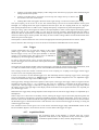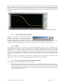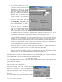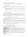
1
XZ001 AGILENT ACQIRIS USER MANUAL FAMILY OF 8-BIT DIGITIZERS For Use with DP and DC Series Digitizers Models covered: DP105 / DP106 / DP110 DP111 / DP210 / DP211 / DP212 DP214 / DP235 / DP240 DP1400 DC110 / DC135 / DC140 DC211 / DC211A / DC240 / DC241 / DC241A DC265 / DC270 / DC271 / DC271A / DC271AR User Manual: Family of 8-bit Digitizers ZM020010I Rev.A June 2007 The information in this document is subject to change without notice and may not be construed in any way as a commitment by Agilent Technologies Inc. While Agilent Technologies makes every effort to ensure the accuracy and contents of the document it assumes no responsibility for any errors that may appear. All software described in the document is furnished under license. The software may only be used and copied in accordance with the terms of license. Instrumentation firmware is thoroughly tested and thought to be functional but it is supplied “as is” with no warranty for specified performance. No responsibility is assumed for the use or the reliability of software, firmware or any equipment that is not supplied by Agilent Technologies Inc. or its affiliated companies. Any versions of this manual which are supplied with a purchased product will be replaced at your request with the latest revision in electronic format. At Agilent Technologies we appreciate and encourage customer input. If you have a suggestion related to the content of this manual or the presentation of information, please contact your local Acqiris representative or Acqiris Technical Support ([email protected]) or come visit our web site at http://www.acqiris.com. Trademarks: product and company names listed are trademarks or trade names of their respective companies Acqiris Headquarters: Acqiris USA: Acqiris Asia-Pacific: Agilent Technologies SA 12, chemin des Aulx CH-1228 Plan-les-Ouates Geneva Switzerland Agilent Technologies Inc. P.O. Box 2203 Monroe, NY 10949 USA Agilent Technologies Australia Pty Ltd 347 Burwood Highway, Forest Hill VIC 3131 Australia Tel: +41 22 884 32 90 Tel: 845 782 6544 Tel: +61 3 9210 2890 Fax: +41 22 884 32 99 Fax: 845 782 4745 Fax: +61 3 9210 5929 © Copyright Agilent Technologies Inc. June 2007 User Manual: Family of 8-bit Digitizers Page 2 of 66 CONTENTS 1. OUT OF THE BOX........................................................................................................................... 5 1.1. Message to the User ..................................................................................................................... 5 1.2. Using this Manual ........................................................................................................................ 5 1.3. Conventions Used in This Manual ............................................................................................... 5 1.4. Disclaimer and Safety .................................................................................................................. 6 1.5. Warning Regarding Medical Use ................................................................................................. 6 1.6. Packaging and Handling............................................................................................................... 6 1.7. Warranty....................................................................................................................................... 7 1.8. Warranty and Repair Return Procedure, Assistance and Support ................................................ 7 1.9. System Requirements ................................................................................................................... 7 1.10. Transport & Shipping................................................................................................................... 8 1.11. Maintenance ................................................................................................................................. 8 1.12. Cleaning ....................................................................................................................................... 9 1.13. Disposal and Recycling ................................................................................................................ 9 2. INSTALLATION ............................................................................................................................ 10 2.1. IC414 Installation....................................................................................................................... 10 2.1.1. IC414 Hardware installation hints.................................................................................. 10 2.1.2. IC414 Windows software installation ............................................................................ 10 2.2. Installing the Software under Windows ..................................................................................... 11 2.2.1. Warnings ........................................................................................................................ 11 2.2.2. Multiple Versions........................................................................................................... 11 2.2.3. Installation...................................................................................................................... 11 2.3. Installing the Software for Linux ............................................................................................... 21 2.3.1. Kernel Mode Driver Compilation .................................................................................. 22 2.3.2. Special cases................................................................................................................... 23 2.3.3. Environment variables for the Firmware........................................................................ 23 2.4. Installing the Hardware .............................................................................................................. 23 2.5. After Restarting .......................................................................................................................... 24 2.5.1. Windows 2000 ............................................................................................................... 24 2.5.2. Windows XP .................................................................................................................. 24 2.6. LabVIEW RT ............................................................................................................................. 26 2.7. Installing the IVI-COM/C Driver............................................................................................... 27 2.8. Distribution for Windows 2000/XP and Linux .......................................................................... 27 3. PRODUCT DESCRIPTION........................................................................................................... 28 3.1. Overview .................................................................................................................................... 28 3.2. Channel Input ............................................................................................................................. 29 3.2.1. Coupling......................................................................................................................... 29 3.2.2. Impedance ...................................................................................................................... 29 3.2.3. Input Protection.............................................................................................................. 29 3.2.4. Mezzanine Front-end...................................................................................................... 29 3.2.5. Bandwidth and Rise Time .............................................................................................. 29 3.2.6. Input Voltage and Offset ................................................................................................ 31 3.2.7. Vertical Resolution......................................................................................................... 31 3.2.8. DC Accuracy and Linearity............................................................................................ 31 3.2.9. Using Probes .................................................................................................................. 32 3.3. Data Acquisition......................................................................................................................... 32 3.3.1. Sampling Rate ................................................................................................................ 33 3.3.2. Acquisition Memory ...................................................................................................... 33 3.3.3. Single and Sequence Acquisition Modes ....................................................................... 33 3.3.4. DP1400 Simultaneous Multibuffer Acquisition and Readout (SMAR) ......................... 34 3.3.5. Timing............................................................................................................................ 34 3.3.6. Timebase Range ............................................................................................................. 34 3.3.7. Combining channels....................................................................................................... 34 3.4. Trigger........................................................................................................................................ 34 3.4.1. Trigger Source................................................................................................................ 34 3.4.2. Trigger Coupling............................................................................................................ 35 User Manual: Family of 8-bit Digitizers Page 3 of 66 3.4.3. Trigger Level.................................................................................................................. 35 3.4.4. Edge Trigger Slope......................................................................................................... 35 3.4.5. Window Trigger ............................................................................................................. 35 3.4.6. HF Trigger...................................................................................................................... 35 3.4.7. Spike Stretcher ............................................................................................................... 35 3.4.8. DP1400 Multi-source Trigger ........................................................................................ 35 3.4.9. Pre- and Post-Trigger Delay........................................................................................... 36 3.4.10. Trigger Status ................................................................................................................. 36 3.5. External Clock and Reference .................................................................................................... 36 3.6. Internal Calibration .................................................................................................................... 37 3.7. ASBus ........................................................................................................................................ 37 3.8. Special Front Panel Input and Output(DP1400 & DC271-FAMILY)........................................ 37 3.9. External Trigger Output (DP1400 & DC271-FAMILY)............................................................ 38 3.10. Frequency Counter mode ........................................................................................................... 38 3.11. Electrical, Environmental and Physical Specifications .............................................................. 39 3.11.1. Electrical ........................................................................................................................ 39 3.11.2. Environmental and Physical........................................................................................... 40 4. RUNNING THE ACQIRISLIVE APPLICATION ...................................................................... 41 4.1. Getting Started with AcqirisLive................................................................................................ 41 4.2. Control Panel and Functions ...................................................................................................... 42 4.2.1. Control Panel Mode ....................................................................................................... 42 4.2.2. Displaying Multiple Traces ............................................................................................ 43 4.2.3. Numeric Editor............................................................................................................... 44 4.2.4. Keyboard shortcuts......................................................................................................... 44 4.2.5. Input Voltage Scale, Offset and Coupling...................................................................... 44 4.2.6. Trigger............................................................................................................................ 45 4.2.7. Acquisition Mode........................................................................................................... 45 4.2.8. Timebase and Memory................................................................................................... 46 4.2.9. Using digitizers of different models simultaneously...................................................... 46 4.2.10. Segmented Memory ....................................................................................................... 47 4.2.11. Display Features, Zoom and Persistence........................................................................ 47 4.3. Top Line Menu of AcqirisLive................................................................................................... 48 4.4. Setup........................................................................................................................................... 48 4.5. Store, Autostore and Conversion of Waveforms........................................................................ 48 4.6. Calibrate ..................................................................................................................................... 50 4.7. Combine channels ...................................................................................................................... 50 4.8. External 10 MHz Reference and External Clock ....................................................................... 50 4.9. Additional Waveform Information............................................................................................. 50 4.10. Display Features......................................................................................................................... 51 4.11. Command Line Switches............................................................................................................ 51 5. RUNNING THE GEOMAPPER APPLICATION ....................................................................... 54 5.1. Who needs a Geographical Map of Modules ............................................................................. 54 5.2. When should the GeoMapper Application be used .................................................................... 54 5.3. How to run GeoMapper.............................................................................................................. 54 6. APPENDIX A: ASBUS FOR COMPACTPCI/PXI DIGITIZERS ............................................. 57 7. APPENDIX B: ASBUS2 FOR PCI DIGITIZERS......................................................................... 58 8. APPENDIX C: XA001 BATTERY BACKUP FOR COMPACTPCI DIGITIZERS ................ 59 9. APPENDIX D: XA100 BNC INPUT OVERVOLTAGE PROTECTION.................................. 60 10. APPENDIX E: XP100 FAN UNIT FOR DP214/DP235/DP240 UNITS...................................... 61 11. APPENDIX F: XP101 FAN UNIT FOR DP DIGITIZERS (OBSOLETE)................................ 62 12. APPENDIX G: XP103 FAN UNIT FOR THE DP FAMILY OF MODULES ........................... 63 13. APPENDIX H: XP104 FAN UNIT FOR DP1400 ......................................................................... 64 14. APPENDIX I: XP105 FAN UNIT FOR DP1400........................................................................... 66 User Manual: Family of 8-bit Digitizers Page 4 of 66 1. Out of the Box 1.1. Message to the User Congratulations on having purchased an Agilent Technologies Acqiris data conversion product. Acqiris Digitizers are high-speed data acquisition modules designed for capturing high frequency electronic signals. To get the most out of the products we recommend that you read this manual carefully. We trust the product you have purchased will meet with your expectations and provide you with a high quality solution to your data conversion applications. 1.2. Using this Manual This guide assumes you are familiar with the operation of a personal computer (PC) running a Windows 2000/XP or other supported operating system. It also assumes you have a basic understanding of the principles of data acquisition using either a waveform digitizer or a digital oscilloscope. The manual is divided into 5 separate sections. To understand the elements of operation for the module it is essential that you read them all. Chapter 1 OUT OF THE BOX, describes what to do when you first receive your new Acqiris product. Special attention should be paid to sections on safety, packaging and product handling. Before installing your product please ensure that your system configuration matches or exceeds the requirements specified. Chapter 2 INSTALLATION, covers all elements of installation and performance verification. Before attempting to use your Acqiris product for actual measurements we strongly recommend that you read all sections of this chapter. Chapter 3 PRODUCT DESCRIPTION, provides a full description of all the functional elements of the digitizer. Chapter 4 RUNNING THE ACQIRISLIVE APPLICATION, describes the operation of AcqirisLive 3.1, an application that enables basic operation of Acqiris digitizers in a Windows 2000/XP environment. Note: AcqirisMAQS is an alternate software application offering many interesting possibilities for the control of acquisition systems in a single or multi-machine environment. Ask your salesman or Acqiris for more information. Chapter 5 RUNNING THE GEOMAPPER APPLICATION, describes the purpose and operation of the GeoMapper application which is needed for some ASBus Multi-instrument systems. For information necessary for writing you own software to control Acqiris products you should refer to the Programmer’s Guide and the Programmer’s Reference Manual. 1.3. Conventions Used in This Manual The following conventions are used in this manual: This icon to the left of text warns that an important point must be observed. WARNING Denotes a warning, which advises you of precautions to take to avoid being electrically shocked. CAUTION Denotes a caution, which advises you of precautions to take to avoid electrical, mechanical, or operational damages. NOTE Denotes a note, which alerts you to important information. Italic text denotes a warning, caution, or note. Bold Italic text is used to emphasize an important point in the text or a note mono text is used for sections of code, programming examples and operating system commands. B,KB,MB,GB is for Byte, KiloByte = 1024 bytes, MegaByte = 1024*1024 bytes, GigaByte = 1024*1024*1024 bytes Certain features are common to several different modules. For increased readability we have defined the following families: User Manual: Family of 8-bit Digitizers Page 5 of 66 DC271-FAMILY 1.4. DC135/DC140/DC211/DC211A/DC241/DC241A/ DC271/DC271A/ DC271AR/DP214/DP235/DP240 Disclaimer and Safety The DP Series PCI Digitizer cards have been designed to operate in a standard PCI slot found inside most personal computers. The model DC Series CompactPCI/PXI Digitizers have been designed to operate inside a CompactPCI/PXI crate. The crate provides the modules with all needed power. Agilent Technologies does not recommend operation of the DC Series modules outside of a CompactPCI/PXI crate. Do not exceed the maximum input voltage rating! The maximum input voltage for 50 Ω input impedance is ±5 V. The maximum input for 1 MΩ input impedance is ±100 V (dc + ac) except for the DC2x1A/AR models where it is ±300 V (dc + ac) . CAUTION: 1.5. Warning Regarding Medical Use The Digitizer cards are not designed with components and testing procedures that would ensure a level of reliability suitable for use in treatment and diagnosis of humans. Applications of these cards involving medical or clinical treatment can create a potential for accidental injury caused by product failure, or by errors on the part of the user. These cards are not intended to be a substitute for any form of established process or equipment used to monitor or safeguard human health and safety in medical treatment. WARNING: The modules discussed in this manual have not been designed for making direct measurements on the human body. Users who connect an Acqiris module to a human body do so at their own risk. 1.6. Packaging and Handling Your Digitizer is shipped with the following components: • A small 3.5” compact disc in an Acqiris paper CD envelope that includes o 10 product user manuals in electronic form (Signal Analyzers, Streamer Analyzers, Family of 8-bit Digitizers, Family of 10-bit Digitizers, Family of 12-bit Digitizers, Family of Averagers, Family of Analyzers, Family of Time Counters, CC10X Family of CompactPCI Crates and CC121 CompactPCI Crate), o 1 Programmer’s Guide and 1 Programmer’s Reference Manual, o device drivers with sample software for different operating systems, environments and languages, o the AcqirisAnalyzers application, a demonstration program for the AC/SC Analyzer products, o the AcqirisLive application, a demonstration program for our digitizer and averager products, o the DemoSSR application, a demonstration program for the Acqiris AP235/AP240 Analyzers, o the DemoAPX01 application, a demonstration program for the Acqiris AP101/AP201 Analyzers, o the DemoTC application, a demonstration program for the Acqiris TC840/TC890 Time Counters, o product data sheets, o full installation procedures for use with Microsoft Windows, National Instruments LabVIEW RT, Wind River VxWorks, IVI-COM/C, and Linux software. • A declaration of conformity • Optional documentation such as a model-dependent document giving Specifications & Characteristics, a Calibration Certificate, or a Performance Verification After carefully unpacking all items, inspect each to ensure there are no signs of visible damage. Also check that all the components received match those listed on the enclosed packing list. Agilent Technologies cannot accept responsibility for missing items unless we are notified promptly of any discrepancies. If any items are found to be missing or are received in a damaged condition please contact the Agilent service center or your local supplier immediately. Retain the box and packing materials for possible inspection and/or reshipment. User Manual: Family of 8-bit Digitizers Page 6 of 66 1.7. Warranty All Agilent Technologies Acqiris Digitizer products are warranted to operate within specification, assuming normal operation, for a period of three years from the date of shipment. It is recommended that yearly calibration be made in order to verify product performance. All repairs, replacement and spare parts are warranted for a period of 3 months. A 5-year repair warranty is available as an option. Agilent Technologies endeavors to provide leading edge technology that includes the latest concepts in hardware and software design. As such software and firmware used with the products is under continual refinement and improvement. All software and instrument firmware is supplied “as is” with no warranty of any kind. Software and firmware is thoroughly tested and thought to be functional at the time of shipment. At Agilent Technologies’ discretion software and firmware may be revised if a significant operational malfunction is detected. Products supplied but not manufactured by Agilent Technologies are covered solely by the warranty of the original equipment manufacturer. In exercising this warranty, Agilent Technologies will repair or replace any product returned to the Agilent service center, within the warranty period. The warranty covers all defects that are a result of workmanship or materials. This excludes defects that are caused by accident, misuse, neglect, or abnormal operation. The purchaser is responsible for returning the goods to the nearest Agilent service center. This includes transportation costs and insurance. Agilent Technologies will return all warranty repairs with transportation prepaid. 1.8. Warranty and Repair Return Procedure, Assistance and Support Agilent Technologies Inc. acquired Acqiris SA and its product lines in December 2006. Before returning any Agilent Technologies Acqiris product for repair please contact your nearest Agilent Technologies Service Center. You can find information about technical and professional services, product support, and equipment repair and service on the Web, see http://www.agilent.com/find/service (or http://www.agilent.com/ and after selecting your country click on Contact Us). The service center will ask for your name, company, phone number and address, the model and serial numbers of the unit to be repaired, and a brief description of the problem. Before issuing a Service Order they will ask you to communicate with us by phone or eMail so that we can learn as much as needed about the problems observed. If a unit returned under guarantee is found to be working normally and this procedure was not followed we reserve the right to charge you for the work done. For your nearest customer support center contact Acqiris at 1-877-ACQIRIS in the USA, +41 22 884 32 90 in Europe or +61 3 9210 2890 in the Asia-Pacific region. Alternatively, please contact Acqiris Technical Support ([email protected]) or come visit our web site at http://www.acqiris.com. The Agilent Technologies Support Centers can also help redirect you for any questions concerning the installation and operation of your equipment. 1.9. System Requirements In order to obtain reasonable performance from your digitizer, Acqiris products need the following minimum PC System Requirements: Processor: 150 MHz Pentium (higher recommended) Memory: 64 MB RAM. The previous number is a very rough estimate. Assuming that you are using AcqirisLive or an application of your own that operates on the acquired data it seems reasonable to ask for 10 times the total acquisition memory that you will be using at the same time in the application. Performance is likely to be degraded if less memory is available. Display resolution: At least 800 x 600 pixels and 256 colors for use of AcqirisLive or AcqirisDemo Operating System: Microsoft Windows 2000/XP including 2003 Server, Wind River VxWorks 5.5.1, and Linux. The following Linux versions have compiled loadable kernel modules: RedHat Enterprise Linux Version 3 - Kernel Version 2.4.21-4.EL RedHat Enterprise Linux Version 3 - Kernel Version 2.4.21-4.ELsmp, Suse Linux 9.2 - Kernel version 2.6.8-24-smp, Debian Sarge 3.1 2.6.8-3-686, Debian 4.0 etch Kernel version 2.6.18-4-686, Scientific Linux 4.4 Kernel version 2.6.9-11.EL). User Manual: Family of 8-bit Digitizers Page 7 of 66 Linux kernel driver source code is available for compilation. Support for Windows 95/98/NT4 is included “as is” since these operating systems are no longer supported by Microsoft. Hard Drive Space: 20 MB Minimum CD Drive (or any method to copy Acqiris Software installation files from CD to the hard drive such as LAN, floppy drive, etc.) LabVIEW: The Acqiris LabVIEW driver is available for National Instruments LabVIEW versions 7.1or 8.0 LabVIEW RT: The Acqiris LabVIEW RT driver is available for National Instruments LabVIEW RT version 7.1 or higher. The VISA driver must be version 3.0 or higher. MATLAB: The Acqiris MEX interface can be used with MathWorks MATLAB 6.5 or a newer vesion. Visual BASIC: The interface files and examples are available for Microsoft Visual Basic versions 5 or 6 and the interface files only for .NET. Tornado: The example files are useable with Wind River Tornado 2.2.1 1.10. Transport & Shipping CAUTION: Cards can be safely transported in their original shipping packages. DC cards can be transported when properly mounted in a CompactPCI crate. The transport of DP cards mounted in a PC is a more delicate issue. Because of their mass the cards can vibrate loose unless they are properly secured and braced. DP cards held only in the front and on the bottom should not be shipped in their PC. However, properly mounted DP cards with XP103 or XP105 fans can be sufficiently well held; the Adjustable retainer must be used so as to hold the card in place. To package the instrument for shipping: Step Notes 1. Place the instrument in its original packaging materials. • If the original packaging materials are not available, use a professional packaging service. Contact your Agilent Service Center for more information. 2. Surround the instrument with at least 3 to 4 inches (8 to 10 cm) of its original packing material or bubble-pack to prevent the instrument from moving in its shipping container. 3. After wrapping it with packing material, place the instrument in its original shipping container or a strong shipping container that is made of double-walled corrugated cardboard with 159 kg (350 lb) bursting strength. • The shipping container must be large and strong enough to accommodate your instrument and allow at least 3 to 4 inches (8 to 10 cm) on all sides for packing material. 4. Seal the shipping container securely with strong nylon adhesive tape. 5. Mark the shipping container “FRAGILE, HANDLE WITH CARE” to help ensure careful handling. 6. Use the address obtained from your Agilent Technologies Service Center. 7. Retain copies of all shipping papers. CAUTION: Damage can result if the original packaging materials are not used. Packaging materials should be anti-static and cushion the instrument on all sides. NEVER USE STYRENE PELLETS IN ANY SHAPE AS PACKAGING MATERIALS. They do not adequately cushion the instrument or prevent it from moving in the shipping container. Styrene pellets can also cause equipment damage by generating static electricity or by lodging in fan motors. 1.11. Maintenance The cards do not require any maintenance. There are no user serviceable parts inside. A periodic calibration can be obtained on request. User Manual: Family of 8-bit Digitizers Page 8 of 66 1.12. Cleaning Cleaning procedures consist only of exterior cleaning. Clean the exterior surfaces of the module with a dry lint-free cloth or a soft-bristle brush. If any dirt remains, wipe with a cloth moistened in a mild soap solution. Remove any soap residue by wiping with a cloth moistened with clear water. Do not use abrasive compounds on any parts. 1.13. Disposal and Recycling Electronic equipment should be properly disposed of. Acqiris Digitizers and their accessories must not be thrown out as normal waste. Separate collection is appropriate and may be required by law. User Manual: Family of 8-bit Digitizers Page 9 of 66 2. Installation This chapter describes how to install the Acqiris hardware and software for Windows 2000/XP, National Instruments LabVIEW RT, Linux, or Wind River VxWorks. NOTE: For a first time installation we strongly recommend installing the software before inserting the hardware into the PC. 2.1. IC414 Installation NOTE: If you are going to install an IC414 interface for the first time and are running Windows 2000/XP you should follow the procedure below before installing the Acqiris hardware. 2.1.1. IC414 Hardware installation hints The PCI-8570/PXI-8570 User's Manual (Rev. 1.00) section 2.5 gives Hardware Installation instructions. CAUTION: Turn off the power of the PC; the PC may have to be unplugged to ensure that the PCI bus has no power available. CAUTION: Touch the antistatic package to a grounded object before removing the card from the package. Electrostatic discharge can damage the card. The standard cable pair provided each have a red connector on one end and a black connector on the other. Therefore the correct connection can be made by plugging the Red connector into the L0Rx socket and the Black connector into the L0Tx socket on the PXI module and the other Red connector into the PCI module socket furthest from the PCI card internal base connector and the Black connector into the next socket. If you intend to use 64-bit 66 MHz transfer to maximize data transfer speed you should cable a “bundled link” using two standard cable pairs and both the L0 and L1 pairs of connectors. You should also make sure that you configure the PXI-8570 M66EN Jumper correctly. 2.1.2. IC414 Windows software installation Linux users do not need to read any further since there is no special software installation. Windows users should have the hardware installed as noted above. This software installation should be done before any Acqiris modules are placed in the CompactPCI crates. This may mean that you have to remove the module from the crate as delivered. The crate should be turned on first followed by the PC. If the cabling and start-up sequence is done correctly there will be no LED illuminated on the PCI unit connected pair and the LED's of the PXI connected pair will be lit. For Windows XP installation, Select the Control Panel under Settings in the Start menu. Then, if you are using the Category View select Printers and Other Hardware. After this, for both Category and Classic views, go to System and then display the Hardware tab to get access to the Driver Signing menu. Since neither the AdLink nor the Acqiris driver has been submitted for Windows Logo testing you must select either the Ignore or Warn action. The resulting menu looks as shown: User Manual: Family of 8-bit Digitizers Page 10 of 66 The PCI-8570/PXI-8570 User's Manual (Rev. 1.00) section 2.4 contains the software installation instructions. These should be executed before allowing the hardware installation process to look for the driver. If you have an AdLink CD Version 2004A4 or later you can use it; if not you should download the latest driver from the WEB site (http://www.adlinktech.com/). You can then continue with the Hardware Installation. A reboot will then be necessary. At this point the Stargen Fabric PCI Adapter and the Stargen Aruba Fabric-to-PCI Bridge should appear correctly installed under System Devices in the Device Manager. NOTE: If you have an AdLink CD Version 2005A3 or later you can find 8570install.exe in the folder X:\Driver Installation\PXI Platform\PXI Extension\PCI_PXI-8570\Wnt2kxp and the starfab1.inf file in the folder X:\Driver Installation\PXI Platform\PXI Extension\PCI_PXI-8570\Win98. 2.2. Installing the Software under Windows 2.2.1. Warnings If Setup detects a previous installation of Acqiris software on your system, a warning screen will be displayed. It is recommended to exit Setup and uninstall older versions. The installer from software releases prior to Acqiris Software 2.0 installed the Digitizer Driver DLL files into the System directory. These will be removed by Setup. If you wish to keep the old installation on your system, you should exit Setup, and move all Acqiris driver files (acqiris*, acqrs* and acqir*) to some archive directory. The DLL files will be installed into the bin subdirectory of the Acqiris software root, and the corresponding path will be added to the PATH environment variable. 2.2.2. Multiple Versions With the software installation from Acqiris Software 2.0 (or above), it is possible to keep multiple versions on the same system, but you must specify a different root directory (i.e. Install Folder). If you keep the same directory, Setup will overwrite your previous installation. To go back to a previous version, you must change the PATH environment variable and reinstall the Kernel driver. Under Windows 2000/XP: 1. Copy the SYS file from <old_AcqirisSoftware_root>\bin\kernel to the Windows\System32\drivers directory. 2. Change the AcqirisDxRoot, AcqirisDxDir and PATH environment variables to the old root. 3. Reboot the computer. 2.2.3. Installation Before installing the Acqiris hardware, you should complete the following steps to install the software for Windows 2000/XP. NOTE: You will need administrator privileges to complete the software installation under Windows 2000/XP. 1. Insert the Acqiris Software CD into the CD-ROM drive of your computer. If the Autorun program does not start automatically (Autoplay disabled), you can start it manually, or navigate to the AcqirisSoftware\Windows folder in order to display the files included. 2. Choose Install AcqirisSoftware for Windows 2000/XP (or run Setup.exe from AcqirisSoftware\Windows folder). After several seconds for initialization the following screen will appear. User Manual: Family of 8-bit Digitizers Page 11 of 66 the 3. To proceed with the installation click “Next”. The following screen will be shown. 4. Please enter your user information and click “Next” to continue. If the program finds that there is still Acqiris software installed on your machine a warning panel (not shown) will appear. Otherwise, the next screen shows: User Manual: Family of 8-bit Digitizers Page 12 of 66 5. Pick the desired combination of module families and click "Next" to continue. 6. The screen above will normally allow the documentation to be installed. Remove the check from the box if you do not want online access to the manuals. 7. The next screen allows you to enable LabVIEW RT and/or Wind River VxWorks support. By default there will be none but if desired you can install any of them together with Windows support or without Windows support. Click “Next” to continue. User Manual: Family of 8-bit Digitizers Page 13 of 66 8. The screen below asks for the desired installation type. After having made your choice Click “Next” to continue. 9. If you chose the Custom installation, the following screen will let you select each package individually. Note that the space indicated for LabVIEW, Firmware and UserManual packages is incorrect. The correct values are 4.1 MB, 21 MB, and 27 MB respectively. User Manual: Family of 8-bit Digitizers Page 14 of 66 10. If MATLAB is installed on your machine, you will be asked to point the installer to the MATLAB root directory. You should do this if you want the installer to modify the standard startup.m file to incorporate the Acqiris adaptor. 11. Now that the elements of the installation have all been decided you will be prompted for the installation folder. This will be the root directory of the Acqiris software installation. If User Manuals (27 MB) and Firmware (21 MB) are loaded more space than indicated here will be required on the drive. For the case of a Tornado 2.2 installation the folder name should not contain any spaces. 12. Furthermore, you should give a name to the shortcut folder. This is the menu entry under Start → Programs where you will find the shortcuts for AcqirisLive, manual(s), etc. User Manual: Family of 8-bit Digitizers Page 15 of 66 13. If you have enabled the installation of 12-bit Digitizers, Averagers, or Analyzers, the next screen lets you change the name of the directory where the FPGA firmware will be installed. 14. AcqirisLive needs the LabWindows/CVI 7.0 Run-Time Engine to run. If Setup has detected that a LabWindows/CVI Run-Time Engine is already installed on your system, it will ask you if you would like to install it locally for AcqirisLive anyway. If you are not sure about the version of the CVI Run-Time Engine on your system, it is recommended to install it locally. Click “Next” to continue. User Manual: Family of 8-bit Digitizers Page 16 of 66 15. Depending on the install type, you may be asked which LabVIEW version format you want for the LabVIEW files. Select the appropriate format and click “Next” to continue. 16. A summary will be shown to allow you to check what you have asked for User Manual: Family of 8-bit Digitizers Page 17 of 66 17. You are now ready to install. You may still go back to any previous screen to modify your selection. Click “Install” when ready. 18. Setup will now copy the files and make the necessary changes to your system. When done, an information screen will be displayed. Please read this carefully. User Manual: Family of 8-bit Digitizers Page 18 of 66 19. Registration of your installation will help us provide you with better support. You will also be notified of updates and upgrades. All information submitted to us will be treated confidentially and never be disclosed outside the company. User Manual: Family of 8-bit Digitizers Page 19 of 66 20. Setup will prepare a registration e-mail in your e-mail client application upon termination of the setup procedure. You can then decide whether or not you wish to send it. You may also add comments. Uncheck the box if you do not want to register your installation. 21. Click “Finish”. The software installation is now complete. 22. You can now either accept the suggestion to restart the computer or you should shutdown your computer and proceed with the hardware installation. User Manual: Family of 8-bit Digitizers Page 20 of 66 2.3. Installing the Software for Linux The Acqiris Software is ready to install and run on Linux systems with any of the following: RedHat Enterprise Linux Version 3 - Kernel Version 2.4.21-4.EL RedHat Enterprise Linux Version 3 - Kernel Version 2.4.21-4.ELsmp, Suse Linux 9.2 - Kernel version 2.6.8-24-smp, Debian Sarge 3.1 2.6.8-3-686, Debian 4.0 etch Kernel version 2.6.18-4-686, Scientific Linux 4.4 Kernel version 2.6.9-11.EL) The following tar files exist with the driver and library compiled with the GNU gcc version shown: AcqirisLinux-3.1a-gcc-3.3.tar.gz - compiled under Suse 9.2 with GNU gcc 3.3. AcqirisLinux-3.1a-gcc-3.4.tar.gz - compiled under SL 4.4 with GNU gcc 3.4. AcqirisLinux-3.1a-gcc-4.1.tar.gz - compiled under Debian etch with GNU gcc 4.1. The Kernel Driver source code is available for recompilation for users with other Linux systems. The appropriate tar file should be copied to a local directory (e.g. your home directory) and then unpacked by using the following command tar xzf AcqirisLinux-3.1a-gcc-X.x.tar.gz The resulting directory AcqirisLinux contains an install script drv-install and a graphical Demo program demo/AcqirisDemo. Before installing the driver you have to put the correct version of the Kernel mode driver into acqirisPCI.o. Type cd AcqirisLinux/lib/modules and either cp acqrsPCI.o[.n] acqrsPCI.o (Linux kernel 2.4) or cp acqrsPCI.ko[.n] acqrsPCI.ko (Linux kernel 2.6) where [.n] is the running version of the Linux kernel. This can be obtained by running the command uname -r The following versions exist: User Manual: Family of 8-bit Digitizers Page 21 of 66 acqrsPCI.o.2.4.21-4.EL acqrsPCI.ko.2.6.8-3-686 acqrsPCI.ko.2.6.8-24-smp acqrsPCI.ko.2.6.9-11.EL acqrsPCI.ko.2.6.18-4-686 for Red Hat Enterprise Linux version 3 for Debian 3.1 'sarge' for Suse 9.2 for Scientific Linux 4.4 for Debian 4.0 'etch' To install the driver and the load script to the system, you have to get super user privileges and execute the driver install script by typing, cd AcqirisLinux ./drv-install add You can check that the driver is loaded properly with lsmod or dmesg. The drv-install script has the following additional functionality: drv-install rem to remove the driver and load script drv-install res to restart the driver If you intend to use an Averager, an Analyzer, or a 12-Bit Digitizer you must install the Firmware .bit files. You can either copy them from the Firmware directory of the CD-ROM or download them from our WEB site. They should be placed in the Firmware subdirectory of AcqirisLinux. In the case of the CD-ROM, this can be done by continuing the above command sequence with the following: cp /mnt/CDRom/Firmware/*.bit Firmware/ 2.3.1. Kernel Mode Driver Compilation For some special kernels, for example SMP, the kernel mode driver will have to be recompiled on the target system. All files needed to compile a new kernel mode driver are in AcqirisLinux/linuxdriverpci for Kernel 2.4 or in AcqirisLinux/linux2.6driverpci for Kernel 2.6 The makefile can be used for compilation under a standard compatible distribution. To compile the driver, the kernel header files need to be installed. Furthermore, depending on the Linux distribution, the kernel source files may need to be installed. The makefile will try to guess where they are located. If it fails, see instructions inside the makefile itself to specify manually where these kernel header files are located. To compile a new kernel under linux-2.4, issue the following commands: cd linuxdriverpci make clean to remove all *.o files in AcqirisLinux/linuxdriverpci. make to generate a new kernel mode driver acqrsPCI.o and also copy it to the directory AcqirisLinux/lib/modules where the install script (drv_install) can access it. drv_install rem to remove the previous installed kernel mode driver. drv_install add to install the new driver. To compile a new kernel under linux-2.6, issue the following commands: cd linux2.6driverpci make clean all to generate a new kernel mode driver acqrsPCI.ko from scratch. make install to copy the kernel module where it should reside. Note that this version of the loadable kernel module had been tested on Linux kernel versions up to 2.6.18. However, starting with kernel 2.6.17, a few kernel functions relating to the device classes are no longer available to proprietary modules. Thus automatic creation of the /dev/acqrsPCI node has to be done manually in the /etc/rc.local file. For Debian users, in order to compile the kernel module on a system, a few packages that match the current kernelimage must be installed. For instance, on a Debian 3.1 sarge system 686 the required packages are: kernel-image-2.6-686 kernel-image-2.6.8-3-686 kernel-headers-2.6-686 kernel-headers-2.6.8-3 kernel-headers-2.6.8-3-686 kernel-kbuild-2.6-3 User Manual: Family of 8-bit Digitizers Page 22 of 66 2.3.2. Special cases If you are running a Linux distribution that doesn’t use the standard paths for the load scripts, you can load the driver with the command cd AcqirisLinux ./drv-install load Copy the driver to the module directory as follows: cp lib/modules/acqrsPCI.o[.n] /lib/modules/{kv}/ACQIRIS/acqrsPCI.o where [.n] is the optional designation of the desired version of the acqrsPCI driver as given above and {kv} is the appropriate system kernel version (obtained with uname -r, i.e. 2.4.20). Then add the following command to /etc/rc.local. /sbin/insmod –f /lib/modules//{kv}/ACQIRIS/acqrsPCI.o For systems using udev (the dynamic /dev/ hierarchy) it may be convenient to automatically create the /dev/acqrsPCI node at boot. To do this, add the following command to the /etc/rc.local file: /sbin/mknod -m 666 /dev/acqrsPCI c 124 0 2.3.3. Environment variables for the Firmware Automatic loading of the firmware needed by 12-bit, analyzer, and averager modules relies on the environment variable AcqirisDxDir pointing to the directory containing the file AqDrv4.ini which in turn points to the directory containing the Firmware .bit files. Therefore, assuming that your Firmware is in /usr/local/AcqirisLinux/Firmware and that AqDrv4.ini is in /usr/local/AcqirisLinux/demo then you must edit AqDrv4.ini so that it contains the line fpgaPath=/usr/local/AcqirisLinux/Firmware Then, if your shell is csh or tcsh modify the /etc/csh.login file to contain the line setenv AcqirisDxDir /usr/local/AcqirisLinux/demo or, if your shell is bash, ksh, zsh or sh, modify the /etc/profile file to contain the lines AcqirisDxDir=/usr/local/AcqirisLinux/demo export AcqirisDxDir 2.4. 1. Installing the Hardware Turn off the power of the PC and the crate in the case of a CompactPCI module. CAUTION: For PCI modules the PC may have to be unplugged to ensure that the PCI bus has no power available. However, CompactPCI crates can be left plugged in since this ensures proper grounding. CAUTION: Touch the antistatic package to a grounded object before removing the card from the package. Electrostatic discharge can damage the card. 2. Module in a PC: open the PC, identify a free PCI slot and carefully insert the DP Series card into it. Be sure to ground yourself by touching the grounded PC frame and avoid touching any components on the DP Series card. Make sure that the grounding of the card’s mounting bracket to the back panel rail of the computer is done correctly. If present make sure that the fan's adjustable retainer is correctly positioned and tightened for mechanical support. Close the PC. Module in a CompactPCI crate: Follow the instructions of the crate manufacturer to insert the DC Series card into a free 6U CompactPCI peripheral slot. Be sure to ground yourself by touching the grounded crate and avoid touching any components on the DC Series card. Be sure to tighten both front panel mounting screws to lock the module into place and insure proper grounding of the frame. NOTE: To ensure the best possible performance, users of Acqiris CC121 Crates with ASBus systems should respect the module placement rules to be found in the Acqiris CC121 CompactPCI Crate User Manual. PCI Bus extension module in a PC: Consult the manufacturer's documentation for any special instructions. Open the PC, identify a free PCI slot and carefully insert the card into it. Be sure to ground yourself by touching the grounded PC frame and avoid touching any components on the card. Make sure that the grounding of the card’s mounting bracket to the back panel rail of the computer is done correctly. Close the PC. Connect the module to the CompactPCI crate controller. User Manual: Family of 8-bit Digitizers Page 23 of 66 3. Turn on the power of the crate(s), if present, and then the PC and start the operating system. NOTE: Acqiris Digitizers are equipped with a LED. If this LED is not glowing orange or red when the power is applied there is a severe problem. Either the module is broken or the necessary voltages for its use are not available. NOTE: For proper system operation when using the IC200, IC414, or other PCI extension interface to connect a CC10X crate to a remote PC, the crate must be powered on before the PC in order for the PC BIOS to recognize the presence of the CompactPCI crate. 4. Devices that were installed using a previous version of Acqiris Software the instruments in these logical positions will still appear as Unknown Devices. This can be changed to the new Acqiris type category with the Grey Diamond icon by Uninstalling the device and then Installing again. Instructions on this procedure can be found in the ReadMe.txt file in the manuals folder of your Acqiris Software installation. 2.5. After Restarting 2.5.1. Windows 2000 Under Windows 2000, you must login with administrator privileges after the first boot following the hardware installation; the Plug&Play system must have the appropriate privileges to be able to complete your hardware installation successfully. After a successful hardware installation, you will be able to use your Acqiris Digitizer(s) with normal privileges. At the first boot following the hardware installation, Windows will detect the new hardware and will install the devices automatically. The following image will appear. NOTE: In some systems an application program (such as AcqirisLive) will not yet work correctly at this point. One additional boot cycle may be needed if this is the first time that a hardware board is being installed. 2.5.2. Windows XP Under Windows XP, you must login with administrator privileges after the first boot following the hardware installation; the Plug&Play system must have the appropriate privileges to be able to complete your hardware installation successfully. After a successful hardware installation, you will be able to use your Acqiris Digitizer(s) with normal privileges. If you login with administrator privileges after the first boot following the hardware installation, Windows will detect the new hardware and start the “Found New Hardware Wizard” after a few seconds. User Manual: Family of 8-bit Digitizers Page 24 of 66 To proceed with the installation click "No, not this time" and then “Next”. The following window will appear: To proceed with the installation click “Next”. You should then see User Manual: Family of 8-bit Digitizers Page 25 of 66 and then NOTE: In some systems an application program (such as AcqirisLive) will not yet work correctly at this point. One additional boot cycle may be needed if this is the first time that a hardware board is being installed. 2.6. LabVIEW RT During program development you can choose whether you use LabVIEW or LabVIEW RT compatible libraries by switching the version present in National Instruments\LabVIEW m.n\instr.lib\. This swap can be facilitated by User Manual: Family of 8-bit Digitizers Page 26 of 66 using the Install VI library for LabVIEW or LabVIEW Real-Time shortcut available in the Shortcut folder under Start → Programs. There is only one Acqiris Driver. It supports all Acqiris Instruments. The instructions below concern LabVIEW RT as used in NI PXI processors. The Aq_RT.inf and AqRT_4.ini files must be uploaded to the target. To do this, • start the MAX application, • right click on the target • select file transfer • select the Aq_RT.inf file on your host machine and upload ('To Remote') to the LabVIEW RT working directory (/NI-RT/system) on the target • select the Aq_RT.ini file on your host machine and upload ('To Remote') to the LabVIEW RT working directory (/NI-RT/system) giving it the name AqDrv4.ini For Acqiris modules which need FPGA files you should, • create the folder \firmware in the /NI-RT/system directory using the file transfer application • select the FPGA files (from <AcqirisDxRoot>\Firmware) you want to copy to the target and upload them into the firmware directory Restart the target after finishing the file transfers. Restart the MAX Explorer and you should have Acqiris digitizers detected in your PXI system. 2.7. Installing the IVI-COM/C Driver Please install Acqiris Software for Windows first. Then the Acqiris Software CD Autorun program gives access to two installers: IVI Shared Components 1.4 IVI-COM/C IviAqD1 driver These must be installed in the order shown above. For more information you can then consult the Readme.txt file in the IVI\Drivers\IviAqD1 folder or the documentation through the program shortcut present under Ivi/IviAqD1. 2.8. Distribution for Windows 2000/XP and Linux The manuals/ReadMe.txt file contains a list of files to be found after a complete installation of Acqiris Software on Windows systems. Similarly the ReadMeLinux file gives the list of files corresponding to that installation. User Manual: Family of 8-bit Digitizers Page 27 of 66 3. Product Description 3.1. Overview DP110 Block Diagram Signal Input 8bit 8 bit Input Signal Amplifier 50 Ohms SH + ADC Ext memories DEMUX Acq Mem 1M Ohms TIMEBASE trigger Input Trigger Signal Amplifier 50 Ohms TRIGGER circuit Thr DAC 1M Ohms CAL DAC Card Controller Controller PLX PCI Interface PCI Bus Acqiris Digitizers are available in two popular industry standards. The DP series digitizers are PCI modules that plug directly into a vacant PCI slot in a PC. The PCI Bus is a well-defined industry standard. The DC series products are CompactPCI/PXI compliant and require an appropriate CompactPCI crate. The digitizers are all fully programmable over the PCI bus and deliver oscilloscope-like performance. Data captured by the digitizers can be transferred to a host processor, either in the PC, in the crate, or interfaced to the crate, over the PCI bus using a 32-bit bus operating at 33 MHz, at speeds up to 100 MB/s. The DP1400 can use the PCI bus at 66 MHz thus allowing transfer rates up to 200 MB/s. DC1XX series digitizers occupy a single slot of a 3U CompactPCI crate and they comply with the 3U Compact PCI standard (PXI compliant). DC2XX series digitizers occupy a single slot of a 6U CompactPCI crate and they comply with the 6U CompactPCI standard (PXI compliant). Acqiris digitizers are designed to provide superior measurement precision and accuracy. Key acquisition specifications (such as DC accuracy, integral and differential non-linearity) have been optimized to deliver maximum measurement fidelity. Careful circuit layout, custom IC’s and special packaging techniques have all been employed to reduce overall system noise. The use of custom IC’s also dramatically reduces the total number of discrete components required. This has tremendous benefits on reliability and also allows the modules to use a minimal amount of power (15 W typical for a single channel 1 GS/s card). The block diagram above is a simplified representation of a single channel unit. For complete technical specifications concerning your particular digitizer please refer to the product’s Specifications & Characteristics. In addition, we maintain up-to-date versions of all product data sheets on our web site (www.acqiris.com). The data sheets are available in pdf format and are best viewed using Adobe Acrobat software. If you have trouble accessing our web site, or viewing the data sheets, please contact your nearest sales office. User Manual: Family of 8-bit Digitizers Page 28 of 66 3.2. Channel Input 3.2.1. Coupling Both AC and DC coupling modes are available. The AC mode couples signals capacitively thus removing the input signal’s DC component and filtering out any signal component below 16 Hz for the DC2x1A digitizers, 32 Hz for the DC271-Family and 10 Hz for all other models. DC mode allows all signal components to be passed through to the digitizer. 3.2.2. Impedance The input channels of the DP and DC Series digitizers offer termination into 50 Ω and, sometimes 1 MΩ. The 50 Ω coupling mode offers high quality termination with better than ± 1% precision. It is ideally suited to use with 50 Ω transmission lines (coax), high bandwidth low impedance (typically 500 Ω) probes or active probes. The 1 MΩ coupling mode provides a high impedance (low load) capability that is suited for use with most standard high impedance probes. The high impedance mode also features low (typically ~10 pF, see table) capacitance that helps to minimize loading effects that can occur when probing high frequency circuits. 3.2.3. Input Protection The input amplifiers are fully protected against over-voltage signals. Input signals up to ±300 V for the DC271A, DC271AR, DC241A, and DC211A and ±100 V otherwise (DC + peak AC < 10 KHz) at 1 MΩ and up to ±5 V DC at 50 Ω, can be input without damaging the front-end electronics. The front-end also provides an overload protection that will automatically switch the coupling from 50 Ω to 1 MΩ if the signal is greater than ±5 V DC. This is implemented for most modules (not the DC2x1A) that have the 1MΩ impedance possibility. 3.2.4. Mezzanine Front-end The front-end electronics are all mounted on a removable mezzanine card. In the event of accidental damage, or as components fatigue over time (e.g. relays in high duty cycle automated testing applications), the mezzanine card allows for fast and efficient replacement. 3.2.5. Bandwidth and Rise Time The bandwidth specification indicates the frequency at which an input signal will be attenuated by 3 dB (approximately 30% loss of amplitude). The bandwidth also affects the minimum rise and fall times that can be passed through the front-end electronics. A pulse with a very sharp edge will be observed to have a minimum rise time (τmin) determined by the front-end electronics. In general a pulse with a given 10-90% rise time (τ10-90real) will be observed with a slower value given by: τ10-902 = τ10-90real2 + τmin2 where τmin (ns) ≈ 0.35 (GHz-ns) / BW (GHz) The following table indicates the bandwidth and rise time performance of the DP and DC Series digitizers. For many digitizers, the bandwidth can be limited with hardware bandwidth limiters as shown in the tables below. For many of the older models the bandwidth at 50 mV FS, BW50, is not as high as that of the other sensitivities. User Manual: Family of 8-bit Digitizers Page 29 of 66 Model Agilent # DP105 Bandwidth into 50 Ω Bandwidth/ Capacitance into 1 MΩ Minimum Rise Time BW Limiter selections Maximum Offset Other particularities 150 MHz 150 MHz 2.3 ns NA 20 V BW50 = 90 MHz 8 pF U1067A DP106 250 MHz NA 1.4 ns NA NA BW50 = 200 MHz Max FS =0.5 V DP110 250 MHz 250 MHz 1.4 ns NA 20 V BW50 = 200 MHz 8 pF U1067A DP111 500 MHz NA 0.7 ns 25 MHz NA BW50 = 200 MHz Max FS =0.5 V DP210 500 MHz 400 MHz 0.7 ns NA 20 V BW50 = 200 MHz 8 pF U1068A 500 MHz NA 0.7 ns 25 MHz NA BW50 = 200 MHz Max FS =0.5 V DP212 500 MHz NA 0.7 ns 25 MHz NA BW50 = 200 MHz Max FS =0.5 V DP214 1 GHz NA 0.35 ns 20, 200, 700 MHz 5V DC271 FAMILY 500 MHz NA 0.7 ns 20, 200 MHz 5V DC271 FAMILY 1 GHz NA 0.35 ns 20, 200, 700 MHz 5V DC271 FAMILY 1 GHz NA 0.35 ns 20, 200, 700 MHz 5V 250 MHz 250 MHz 1.4 ns NA 20 V BW50 = 200 MHz DP211 U1068A U1069A DP235 U1069A DP240 U1069A DP1400 U1071A DC110 8 pF DC135 500 MHz NA 0.7 ns 20, 200 MHz 5V DC271 FAMILY FC Option 1 GHz NA 0.7 ns 20, 200, 700 MHz 5V DC271 FAMILY FC Option 1 GHz NA 0.35 ns 20, 200, 700 MHz 5V DC271 FAMILY 950 MHz ( 1 GHz typical) 300 MHz typical 14 pF 0.35 ns (50Ω) (1.2 ns typical 1 MΩ) 20, 200, 700 MHz (see remark below) 5 V (50Ω) DC271 FAMILY Max FS = 50 V (1 MΩ) 500 MHz 400 MHz 0.7 ns NA 20 V BW50 = 200 MHz 0.35 ns 20, 200, 700 MHz 5V DC271 FAMILY U1061A DC140 U1061A DC211 U1064A DC211A U1064A DC240 20 V (> 0.5 V FS & 1MΩ) 200 V (> 5V FS & 1MΩ) 11 pF DC241 1 GHz NA U1064A User Manual: Family of 8-bit Digitizers Page 30 of 66 Model Agilent # DC241A U1064A DC265 Bandwidth into 50 Ω Minimum Rise Time BW Limiter selections Maximum Offset Other particularities 950 MHz ( 1 GHz typical) Bandwidth/ Capacitance into 1 MΩ 300 MHz typical 14 pF 0.35 ns (50Ω) (1.2 ns typical 1 MΩ) 20, 200, 700 MHz (see remark below) 5 V (50Ω) DC271 FAMILY Max FS = 50 V (1 MΩ) 150 MHz 150 MHz 2.3 ns NA 20 V BW50 = 90 MHz 1.4 ns NA 20 V BW50 = 90 MHz 11 pF U1063A DC270 250 MHz 250 MHz 11 pF U1063A DC271 20 V (> 0.5 V FS & 1MΩ) 200 V (> 5V FS & 1MΩ) 1 GHz NA 0.35 ns 20, 200, 700 MHz 5V DC271 FAMILY 950 MHz ( 1 GHz typical) 300 MHz typical 14 pF 0.35 ns (50Ω) (1.2 ns typical 1 MΩ) 20, 200, 700 MHz (see remark below) 5 V (50Ω) DC271 FAMILY Max FS = 50 V (1 MΩ) The AR has only 2 channels U1064A DC271A U1064A DC271AR 20 V (> 0.5 V FS & 1MΩ) 200 V (> 5V FS & 1MΩ) For 1 MΩ coupling in the DC2x1A/AR the 700 MHz Bandwidth Limiter cannot be used. Furthermore, for FS gain > 5V the 200 MHz Bandwidth Limiter is always active. 3.2.6. Input Voltage and Offset The input channel provides a fully programmable amplifier with variable input voltage and offset. Full Scale (FS) input voltages are selectable from 50 mV to 5 V (except as shown above) in a 1, 2, 5 sequence. Care should be taken to select an input voltage range that will allow the signal to be recorded using as much dynamic range of the digitizer as possible. The Variable Offset is programmable in the range of ±2 V when using an FS Input Voltage setting of 500 mV or below, increasing to ± Maximum Offset for FS settings above 500 mV. The raw 8-bit ADC data values are in the range [-128,+127] with the first and last values reserved for underflow and overflow respectively. The midpoint value, 0, of the range corresponds to the negative of the offset voltage. Thus the Full Scale Range (FSR) goes from –Offset Voltage – (FS/2) to –Offset Voltage + (FS/2) Signals going outside of the FSR will be clipped and data values for the clipped portion of a signal should be regarded as erroneous. The maximum input voltage for 50 Ω input impedance is ±5 V. The maximum input for 1 MΩ input impedance is ±100 V (dc + ac) except for the DC2x1A/AR models where it is ±300 V (dc + ac). 3.2.7. Vertical Resolution The digitizers described in this manual use an ADC system with 8 bits of vertical resolution (256 levels). The dynamic range of the ADC covers the Full Scale Range (FSR) of the Input Voltage setting. For example, if the Input Voltage is set to 1 V then the ADC resolution is equivalent to 3.91 mV. To obtain the best dynamic range from the ADC care should be taken to ensure that the input signal varies over more than 50% of the Input Voltage FSR setting. 3.2.8. DC Accuracy and Linearity The DP and DC Series digitizers use low noise front-end electronics in order to ensure voltage measurement is made with accuracy and precision. DC voltage accuracy, at 0 V offset, is better than ±2% (±1% typical) of the input voltage full scale. The differential linearity is better than ±0.7 LSB ( ±0.8 LSB for DC135/DC140 digitizers and ±0.9 LSB for other DC271-FAMILY digitizers). User Manual: Family of 8-bit Digitizers Page 31 of 66 3.2.9. Using Probes The 50 Ω and 1 MΩ input impedance settings make it possible to use Acqiris digitizers with a wide variety of probes. The 50 Ω setting is most commonly used for active probes and low impedance (500 Ω) passive probes. The 1 MΩ setting is normally used for high impedance probes. While it is possible to use a variety of different manufacturers high impedance probes we recommend the use of our model P001 Passive Probe. The model P001 is matched to the Acqiris digitizers to ensure that effects that can reduce measurement quality, such as bandwidth loss and capacitive loading, are minimized. The P001 features 300 MHz bandwidth, 10 MΩ input impedance and 10:1 attenuation. These specifications make it an excellent choice for most general purpose probing applications. Before using any Passive Probe with a digitizer care should be taken to check that the probe has been correctly adjusted (refer to the Probe’s Calibration procedure). NOTE: Passive high impedance probes are not suitable for high fidelity measurements above 100 MHz. The nonnegligible (5-10 pF) tip capacitance loads the signal causing distortion and/or ringing when combined with the ground lead inductance. 3.3. Data Acquisition The table below summarizes the characteristics discussed in the sections that follow: Model Max. Sampling Rate Max. CONVER TERS PER CHANNEL/ CHANNELS DP105 500 MS/s 1/1 DP106 500 MS/s DP110 Maximum Optional Memory/ channel Maximum TTI Timebase Segments Resolution Accuracy 128K 2M 4000 80 ps 50 ppm ±2V 1/1 128K 2M 4000 80 ps 50 ppm ±2V 1 GS/s 1/1 128K 8M 8000 80 ps 50 ppm ±2V DP111 1 GS/s 1/1 128K 2M 4000 5 ps 2 ppm ±3V DP210 2 GS/s 1/1 256K 16M 8000 5 ps 2 ppm ±3V DP211 2 GS/s 1 / 1* 256K 16M 8000 5 ps 2 ppm ±3V DP212 2 GS/s 1/1 256K 16M 8000 5 ps 2 ppm ±3V DP214 2 GS/s 1/1 256K 16M 8000 5 ps 2 ppm ±2V DP235 1 GS/s 2/2 128K 2M 4000 5 ps 2 ppm ±2V DP240 2 GS/s 2/2 128K 8M 8000 5 ps 2 ppm ±2V DP1400 2 GS/s 2/2 128K NA 1000 ~13ps 2 ppm AC 0 V DC110 1 GS/s 1 /1 128K 8M 8000 5 ps 50 ppm ±2V DC135 1 GS/s 2 /2 128K 2M 4000 5 ps 2 ppm ±2V DC140 2 GS/s 2/2 128K 8M 8000 5 ps 2 ppm ±2V DC211 4 GS/s 1/1 512K 32M 8000 5 ps 2 ppm ±2V DC211A 4 GS/s 1/1 128K 8M 8000 5 ps 2 ppm ±2V DC240 2 GS/s 1/2 256K 16M 8000 5 ps 2 ppm ±3V DC241 4 GS/s 2/2 256K 16M 8000 5 ps 2 ppm ±2V DC241A 4 GS/s 2/2 128K 8M 8000 5 ps 2 ppm ±2V DC265 500 MS/s 1/4 128K 2M 4000 5 ps 2 ppm ±2V DC270 1 GS/s 1/4 128K 8M 8000 5 ps 2 ppm ±2V DC271 4 GS/s 4/4 128K 8M 8000 5 ps 2 ppm ±2V DC271A 4 GS/s 4/4 128K 8M 8000 5 ps 2 ppm ±2V DC271AR 2 GS/s 2/2 128K 8M 8000 5 ps 2 ppm ±2V User Manual: Family of 8-bit Digitizers Default Memory points/ channel External Clock Max./ Min. Thresh. Page 32 of 66 The * indicates a Dual Input module where there is one channel which can digitize the signal on one of the two BNC inputs 3.3.1. Sampling Rate All Acqiris digitizers contain an analog-to-digital conversion (ADC) system that can sample waveforms, in a real time sampling mode, at rates from the maximum allowed rate down to 100 S/s (10 ms per point). The sampling rate can be programmed and is selectable in a 1, 2, 2.5, 4, 5 sequence (i.e. 1 MS/s, 2 MS/s, 2.5 MS/s, 4 MS/s, 5 MS/s, 10 MS/s, … 1 GS/s, 2GS/s, 4 GS/s). The maximum sampling rate shown above sometimes exploits the possibility of combining channels. 3.3.2. Acquisition Memory Data from the ADC is stored in on-board acquisition memory. The amount of memory in use for acquisition can be programmed and is selectable from 1 point to the full amount of acquisition memory available. For technical reasons, a certain memory “overhead” is required for each waveform, reducing the available memory by a small amount. In order to simplify programming, an interface function recommends the best sampling rate and the maximum possible number of data points, taking into account the available memory, the requested time window, the number of segments (in Sequence mode), as well as the required memory overhead. To ensure maximum sampling rate and high timing resolution, we strongly recommend the use of long acquisition memories whenever possible. For example, the model DC110 or DP110 with 2 Mpoints of memory can record a signal over a 2 ms period with a sampling rate of 1 GS/s (1 ns per point). The fast sampling rate ensures that all high frequency signal components, up to the full 250 MHz bandwidth of the digitizer, are accurately recorded. If the memory were reduced to just 20 Kpoints then the sampling rate would need to be reduced to just 10 MS/s (20,000/2 ms) to record the same 2 ms period. All frequencies above 5 MHz would then be incorrectly digitized and important signal characteristics may be distorted or even completely missed. 3.3.3. Single and Sequence Acquisition Modes Digitizers acquire waveforms in association with triggers. Each waveform is made of a series of measured voltage values (sample points) that are made by the ADC at a uniform clock rate. To maximize sampling rates and utilize memory as efficiently as possible, the digitizers include both Single and Sequential storage modes. For both of these modes the data of all of the active channels is acquired synchronously; all of the ADC’s are acquiring data at the same time, to within a small fraction of the maximum sampling rate. The Single Acquisition mode is the normal operation of most digitizer products. In this mode an acquisition consists of a waveform recorded with a single trigger. The user selects the sampling rate and acquisition memory size and sets the number of segments to 1 (default value). The Sequence Acquisition mode allows the capture and storage of consecutive “single” waveforms. Sequence Acquisition mode is useful as it can optimize the digitizer’s sampling rate and memory requirements for applications where only portions of the signal being analyzed are important. The mode is extremely useful in almost all impulseresponse type applications (RADAR, SONAR, LIDAR, Time-of-Flight, Ultrasonics, Medical and Biomedical Research, etc.). In Sequence Acquisition mode the acquisition memory is divided into a pre-selected number of segments. Waveforms are stored in successive memory segments as they arrive. Each waveform requires its own individual trigger. The memory can be divided into any number of segments between 2 and 200 (up to 8000 segments with options M32M, M16M, M8M and M4M, 4000 segments with option M2M, 2000 with option M1M). In Sequence Acquisition mode the user needs to specify the sampling rate, the total acquisition memory, and the number of segments. Note that the Single Acquisition mode is just a special case of the Sequence Acquisition mode with the number of segments set to 1. Sequence acquisition enables successive events, which can occur within a very short time, to be captured and stored without loss. A crucial feature of Sequence Acquisition mode is that it has a very fast trigger rearm time. A fast trigger rearm helps produce very low “dead time” (less than 800 ns for the highest available sampling rates) between the segments of a sequence acquisition. The “dead time” is the period after the end of an event when the card cannot digitize data for a new trigger event. To complement this mode of operation the digitizer can also measure and store the arrival time of each trigger using the information from the on board Trigger Time Interpolator (TTI). Readout of the individual trigger time stamps makes it possible to determine the time from one trigger to any other trigger in the sequential acquisition. The TTI resolution sets the resolution of the trigger time stamps (see section 3.3.5 Timing and the table above). User Manual: Family of 8-bit Digitizers Page 33 of 66 3.3.4. DP1400 Simultaneous Multibuffer Acquisition and Readout (SMAR) For this module the internal memory has a dual-port structure which can be exploited to permit simultaneous data acquisition and read out. When the special SMAR option is present the memory can be turned into a circular buffer of a chosen number of banks, between 2 and 1000. Data can be read out of one bank while data is acquired into any available free banks. This mechanism, together with sequence acquisition, helps achieve a high maximum continuous event rate in spite of interrupts due to the computer operating system. The maximum continuous event rate is the maximum value of the trigger frequency that can be accepted without the loss of any event. It will work for both 1 and 2 converter/channel modes. 3.3.5. Timing A crystal-controlled timebase is used to clock the ADC system of the digitizers. The timebase accuracy is guaranteed as shown in the table at the beginning of this section. The digitizers also include a built-in Trigger Time Interpolator (TTI) that measures the time from the trigger point to the first sample point. This information is essential for determining the precise relation between the trigger or other event of interest and the digitized samples of the signal. The approximate TTI resolution is also given in the table at the beginning of this section. 3.3.6. Timebase Range The timebase range defines the time period over which data is being acquired. For example, the DC110 has a standard acquisition memory of 128 Kpoints and maximum sampling rate of 1 GS/s. Therefore, at the maximum sampling rate, the digitizer can record a signal over a timebase range of up to 130 μs (approx. 130,000 points * 1 ns/point). The timebase range can be adjusted by varying the amount of acquisition memory or the sampling rate of the digitizer. 3.3.7. Combining channels The DC135/DC140/DC241/DC241A/DC271/DC271A/DC271AR/DP235/DP240/DP1400 digitizers offer the possibility of combining the converters (and their memories) from two or four channels to analyze a single input channel. With this feature the maximum sampling rate and the maximum amount of acquisition memory can be doubled or quadrupled if all of the input channels are not of immediate interest. 3.4. Trigger Normally the trigger settings applied to the digitizer are used to determine the time at which the device will stop acquiring data. Some models are also capable of a ‘Start on Trigger’ mode of acquisition (see the Programmer’s Guide for further details). The various trigger settings are outlined below. 3.4.1. Trigger Source The trigger source can be a signal applied to either an Input Channel (internal triggering) or the External Trigger Input. For the DC135/DC140/DC211/DC211A/DC241/DC241A/DC271/DC271A/DC271AR modules, a standardized trigger in signal can also be routed via the PXI Bus Star Trigger line. Most digitizers provide a separate front panel input BNC connector that can be used as an External Trigger Input. The External Input provides a fully functional trigger circuit with selectable level and slope as for the Internal Triggering source; however it does not include coupling choices nor HF, Window, and Spike Stretcher triggers. The external trigger termination (1 MΩ or 50 Ω) is also selectable on many modules. In modules with this feature, the circuit also provides an overload protection that will automatically switch the coupling from 50 Ω to 1 MΩ if the signal is greater than ±5 V DC. The DC271-FAMILY digitizers have a fixed 50 Ω termination impedance. They also allow the same BW limiter selections as can be found for the channels. The DC271-Family digitizers' external trigger circuit has diode protection against overload. The DP1400 also gives the choice of 50 Ω or 1 MΩ termination impedance for the MCX external input and has diode protection against overload. However, there are no BW limiters and only DC trigger coupling is available. In all 50 Ω cases a ±5 V limit on trigger signals should be respected, although somewhat higher voltages for short time periods will not damage the unit. For 1 MΩ input signals up to ±100 V (DC + peak AC < 10 KHz) are allowed. User Manual: Family of 8-bit Digitizers Page 34 of 66 3.4.2. Trigger Coupling Trigger coupling is used to select the coupling mode applied to the input of the trigger circuitry. Modes available include AC LF Reject and DC. The AC LF Reject mode couples signals capacitively and removes the input signal's DC component and signals below 50 KHz (50 Hz for DC271-FAMILY digitizers). DC mode allows all signal components to be passed through to the trigger circuit. The DC271-FAMILY digitizers have an HF Reject mode that removes signal components above 50 KHz. 3.4.3. Trigger Level The trigger level specifies the voltage at which the selected trigger source will produce a valid trigger. The trigger level is defined as a set voltage. Using the internal trigger, the level is set with respect to the midpoint voltage (Vm= – Offset voltage) of the digitizer’s vertical scale. Internal trigger level settings (expressed in %) must be within Vm ± 0.6 FS (0.5 FS for DC271-FAMILY digitizers), where FS is the channel Full Scale. All trigger circuits have sensitivity levels that must be exceeded in order for reliable triggering to occur. For most digitizers, the AC coupled mode is implemented with an auto-level trigger. Only the DC271-FAMILY digitizers allow trigger levels to be selected in connection with the AC coupling choices. The DC271-FAMILY digitizers allow the user to choose the external trigger Full Scale from the set of values 0.5, 1.0, 2.0 or 5.0 V. The external trigger level can then be set to values in the range ± 0.5 FS. The DP1400 has a single external Trigger Full Scale of 10 V. All other digitizers have an external trigger range of ± 3 V. The DC271-FAMILY digitizers will trigger on signals with a peak-peak amplitude > 15% FS from DC to their bandwidth limit. 3.4.4. Edge Trigger Slope The trigger slope defines which one of the two possible transitions will be used to initiate the trigger when it passes through the specified trigger level. Positive slope indicates that the signal is transitioning from a lower voltage to a higher voltage. Negative slope indicates the signal is transitioning from a higher voltage to a lower voltage. 3.4.5. Window Trigger The DC271-FAMILY digitizers and the 2 channels of the DP1400 implement a Window trigger. Two trigger level thresholds are used to define the desired range. The trigger can then be chosen to occur either when the signal exits or enters the window range. This mode can be thought of as the appropriate OR of two edge triggers of opposite slope. 3.4.6. HF Trigger The DC271-FAMILY digitizers and the 2 channels of the DP1400 implement an HF trigger that allows triggers to be reliably accepted at rates above ∼ 1 GHz. In this mode, triggers occur on every fourth positive edge. The window trigger mode is not available. 3.4.7. Spike Stretcher The trigger circuit of the 2 channels of the DP1400 also has a Spike Stretcher mode which ensures that even very short pulses are capable of generating triggers. This mode is useful if the time interval during which the trigger signal satisfies the threshold condition is less than 0.5 ns and the trigger frequency is less than 10 MHz. The trigger slope is positive in this mode. 3.4.8. DP1400 Multi-source Trigger This digitizer permits triggers that require a pattern condition including one of the trigger channels and the external trigger. The trigger condition defined above, on each of the inputs, defines the TRUE/FALSE state of each input. These states can be logically combined with AND, OR, NAND, or NOR to define the overall trigger condition. Potential triggers can then occur on the FALSE to TRUE transitions of the combined signal. There is a small (~ns) delay between the times at which two simultaneous inputs arrive at the logical element that defines the overall trigger condition. If necessary, this must be corrected for by cable delay on the external input; the delay will depend on the overall configuration and therefore must be determined by the user. User Manual: Family of 8-bit Digitizers Page 35 of 66 3.4.9. Pre- and Post-Trigger Delay To increase trigger flexibility a pre- or post-trigger delay can be applied to the trigger position. The amount of pre-trigger delay can be adjusted between 0 and 100% of the acquisition time window (i.e. sampling interval x number of samples), whereas the post-trigger delay can be adjusted between 0 and 200 million samples. Pre- or post-trigger delays are just different aspects of the same trigger positioning parameter: • The condition of 100% pre-trigger indicates that all data points are acquired prior to the trigger, i.e. the trigger point is at the end of the acquired waveform. • The condition of 0% pre-trigger (which is identical to a post-trigger of 0) indicates that all data points are acquired immediately after the trigger, i.e. the trigger point is at the beginning of the acquired waveform. • The condition of a non-zero post-trigger delay indicates that the data points are acquired after the trigger occurs, at a time that corresponds to the post-trigger delay, i.e. the trigger point is before the acquired waveform. The digitizer hardware accepts pre- and post-trigger adjustments in increments of 16 samples. By definition posttrigger settings are a positive number and pre-trigger settings are a negative number. Thus it is only natural that the software drivers treat pre- and post-trigger delays as a single parameter in seconds that can vary between –nbrSamples * samplingInterval (100% pre-trigger) and +maxPostTrigSamples * samplingInterval (max post-trigger). Since the Acqiris software drivers provide very accurate trigger position information upon waveform readout, the accepted resolution of the user-requested pre-/post-trigger delay is much better than 16 samples. For more details, refer to the Programmer’s Guide. 3.4.10. Trigger Status The front panel includes a tri-color LED indicator to show the status of the trigger. When the LED is green it indicates the trigger is armed and waiting for a valid trigger to occur. Red indicates that the trigger has occurred, the acquisition is complete and the data is waiting to be readout. The user can override the default functions and program the LED color in an application-specific manner. 3.5. External Clock and Reference For applications where the user wants to replace the internal clock of the digitizer and drive the ADC with an external source, either an External Clock or an External Reference signal can be used. The Clock or Reference signals can be entered into the digitizer either by the dedicated MMCX (DC271-FAMILY), MCX (DP1400), or BNC (DC240) connector or via the shared External Input connector on the front panel (all other models). In addition, for the DC135/DC140/DC211/DC211A/DC241/DC241A/ DC271/DC271A/DC271AR models the PXI Bus 10 MHz system clock signal (PXI_CLK10) can be used as the reference. With External Clock two operating modes are possible; Continuous for the case in which the clock signals are always present and Start/Stop for the situation where the user needs complete control of the sampling process. The Start/Stop mode is not available for the DP1400. When using a Continuous External Clock, the user must ensure that the input signal has a frequency between 10 MHz and 2 GHz (DP1400 and DC271-FAMILY) or between 10 MHz and 500 MHz (all other models). For the Start/Stop mode the input signal frequency must be less than 1 GHz (DC271Family) or 500 MHz (all other models). In all cases it must have a minimum peak to peak amplitude into 50 Ω at the front of the digitizer of at least 0.5 V for DC135/DC140/DC211A/DC241A/DC271A/DC271AR/DP1400, 1 V all other DC271-Family and 2 V for other models. The DP1400 has a fixed threshold and uses AC coupling. Otherwise, the transitions of the clock are defined with the aid of a threshold that is user selectable in the range [-2.0 V, 2.0 V] ([-3.0 V, 3.0 V] for the DC240).. The signals should not exceed ±5 V amplitude. For a detailed discussion on the programmed use of the external clock, refer to the Programmer’s Guide. For applications that require greater timing precision and long-term stability than is obtainable from the internal clock, a 10 MHz Reference signal can be used. The External Reference is nominally at 10 MHz. However, frequencies in the range [9.0 MHz, 10.2 MHz] will be accepted for all models other than the DP1400. If you do this you may need to correct for the difference in your application since the digitizer and the driver have no way to know about such deviations. The amplitude and threshold conditions, for an External Reference, are the same as for the External Clock. If synchronization between several digitizers is required, the reference signal should be applied to all of them. User Manual: Family of 8-bit Digitizers Page 36 of 66 3.6. Internal Calibration The software drivers supplied include calibration functions for the timing, gain and offset settings, which can be executed upon user request. The digitizers are never calibrated in an “automatic” way, i.e. as a side effect of another operation. This ensures programmers have full control of all calibrations performed through software in order to maintain proper event synchronization within automated test applications. The model DC and DP series digitizers include a high precision voltage source and a 16-bit DAC, used to determine the input voltage and offset calibration. For accurate time and voltage measurements it is recommended to perform a calibration once the module has attained a stable operating temperature (usually reached with a few minutes of digitizer operation after power on). Further calibration should not be necessary unless temperature variations occur. A full internal calibration of a digitizer can be very time consuming (> 100 s/digitizer), in particular for the DC2x1A models. Therefore, several other options are available. They are documented in the Programmer's Reference Manual. A program can always be started with the digitizer in an uncalibrated state and data taken can be used for many kinds of testing. However, as soon as good data respecting the specifications of the instrument is required a calibration of at least the current acquisition state is needed. The full internal calibration has the advantage that it generates the calibration constants needed for any possible configuration of the instrument; its disadvantage is the time taken. If a more selective calibration is done it will allow the generation of good data in the current acquisition state. This calibration will remain useable whenever that acquisition state is used again for as long as the temperature of the instrument does not change significantly. A fast calibration of a channel in a configuration can be done in around a second. Many applications can save time by only performing calibration for the configurations that will actually be used. 3.7. ASBus The DC Series digitizers may be used in applications that require many data acquisition channels. In such cases it is possible to use more than one digitizer in a standard CompactPCI/PXI crate. Each DC Series digitizer, except the DC135 and DC140 models, includes ASBus, a proprietary high bandwidth auto-synchronous bus system that allows multiple digitizers to work together synchronously. The ASBus distributes both the clock and trigger signals along a plug-in front panel bus, between all the digitizers that participate in the system. It allows any digitizer to act as the trigger source and any other digitizer to act as the clock source (acquisition master), enabling all the digitizers to be clocked at the same time. Synchronizing the clock signals between the devices improves the accuracy of cross-channel measurements and is essential for accurate time correlation between signals on different channels. The ASBus is intended to connect modules of the same type, i.e. of the same model number, although some exceptions to this rule might be possible. If modules with the same model number, but different memory length options, are connected only the shortest memory length can be used. The ASBus connector is located on the front panel of each cPCI module. Bridges are used to connect adjacent modules for synchronization, which is then activated through software by defining a master module and the trigger source. Up to 7 modules may be synchronized with the ASBus. More detailed information and the commands required to setup the ASBus clock and trigger distribution are included in the Programmer's Guide and Reference manual. 2 The DP1400 uses the ASBus system with a connector on the top of each card to achieve the same functionality. It works for up to 3 modules. 3.8. Connector CLK IN I/O A TR OUT I/O B Special Front Panel Input and Output(DP1400 & DC271-FAMILY) Function 50 Ω External Reference or External Clock Input User configurable (see below) Signal occurs after an accepted TRIGGER. User configurable (see below) The DC271-Family uses MMCX connectors for these functions; the DP1400 uses the MCX type. The I/O A and I/O B signals are 3.3 V compatible CMOS. This means that, on input, low is < 0.7 V and high must be in the range [1.7 V, 5.0 V]. An unconnected signal will be high. This definition ensures TTL compatibility. On output, the low level User Manual: Family of 8-bit Digitizers Page 37 of 66 will be in the range [0 V, 0.7 V] and the high level in the range [1.7 V, 3.3 V] for HiZ. The high level output will typically give 0.8 V into 50 Ω. The I/O A or B connectors can be used for an Enable trigger input or the following output signals: 10 MHz reference clock, Acquisition skipping to next segment, Acquisition is active, Trigger is armed. 3.9. External Trigger Output (DP1400 & DC271-FAMILY) When the digitizer is ready to be triggered and a valid trigger signal occurs, a trigger output is generated for external use. It is always available on the Front Panel Trigger Out MCX or MMCX connector. The pulse ends when the data acquisition for the trigger in question is complete. NOTE: The External Trigger Output functionality is implemented in the hardware. No Trigger Out signal occurs for software-generated triggers such as those of the AUTO mode of AcqirisLive or through the use of the function AcqrsD1_forceTrigger. However, AcqrsD1_forceTriggerEx does generate the signal. Trigger Output Block diagram: Signal: 1.6V swing 0v centered 50 Ohm Trigger Out G=1 0.8 V) The output swing is 1.6 V (± Offset: +/-2.5 V when unloaded and 0.8 V when and fall terminated on 50 Ω. The rise times are 2.5 ns typical. The offset can be adjusted, by software control in the range [–2.5 V, +2.5 V] unloaded, or [+5V GND 1.25 V, +1.25 V] into 50 Ω. The maximum output current capability is ± 15 mA. As the output is retro-terminated, it is ECL R TTL R Signal possible to drive a 50 Ω line unterminated (HiZ) without loss of 220 signal 68 performance. Trigger For a TTL compatible signal, set the offset to 1.0 V and the Out swing at destination will be +0.2 to +1.8 V. With Offset R 220 For an ECL compatible signal, terminated on 50 Ω to –1.2 V, -1.18V -5V set the offset to –1.2 V and the output will be in the range [–0.8 V, –1.6 V]). Trigger Out R 68 With Offset +1.18V GND Alternatively, to reduce the current drawn from the digitizer, the terminations shown here can be used: For the DC135/DC140/DC211/DC211A/DC241/DC241A/DC271/DC271A/DC271AR modules, a standardized trigger out signal can also be routed to the PXI Bus Star Trigger line. 3.10. Frequency Counter mode The new DC140 and DC135 digitizers offer an optional Frequency Counter (FC) mode. This option allows the measurement of the average frequency or period of a signal for frequencies up to 400 MHz over a user-selectable aperture between 1 ms and 1000 s. The accuracy is limited by that of the timebase, < 2 ppm; the short term stability is of ~ 0.1 ppm. The accuracy can be improved if an appropriate external reference clock is used. Frequencies in excess of 100 MHz will be measured using the HF divide by four feature of the trigger circuit. A digitizer with the FC option can also totalize the number of triggers during a chosen time interval or a userprovided gate signal. This can be done for trigger frequencies under 125 MHz and for total counts up to 248. The time interval is measured using the same clock as is being used to drive the digitizer. The user gate signal has to be made available on one of the Control I/O inputs. User Manual: Family of 8-bit Digitizers Page 38 of 66 3.11. Electrical, Environmental and Physical Specifications 3.11.1. Electrical Model PCI Rev DMA Transfer Rate (MB/s) Max. Power Consumption (W) WITH Standard MEMORY OPTION Current Requirements (A) (with Memory option) +12 V +5 V +3.3 V -12 V DP105 2.1 ~100 13.5 15 0.55 1.3(1.6) NA NA DP106 2.1 ~100 13.5 15 0.55 1.3(1.6) NA NA DP110 2.1 ~100 13.5 15 0.55 1.3(1.6) NA NA DP111 2.1 ~100 20 20 0.75 1.4 (2.0) NA 0.03 DP210 2.1 ~100 22 25 0.9 2 (2.6) NA 0.03 DP211 2.1 ~100 17 20 0.75 1.4 (2.0) NA 0.03 DP212 2.1 ~100 17 20 0.75 1.4 (2.0) NA 0.03 DP214 2.2 ~100 22 25 0.85 1.5 1.1 (1.9) 0.03 DP235 2.2 ~100 24 27 0.93 1.7 1.1 (1.9) 0.03 DP240 2.2 ~100 24 27 0.93 1.7 1.1 (1.9) 0.03 DP1400 2.3 ~100 14 27 0.09 1.3 1.8 () 0.04 DC110 2.1 ~100 15 17 0.7 1.1 0.4 (0.9) NA DC135 2.2 ~20 12 13.3 0.46 0.46 1.1 (1.5) 0.04 DC140 2.2 ~20 13 16 0.46 0.46 1.4 (2.2) 0.04 DC211 2.2 ~100 42 50 1.7 2.7 3.0 (4.5) 0.05 DC211A 2.2 ~100 42 50 1.7 2.7 3.0 (4.5) 0.05 DC240 2.1 ~100 40 45 1.3 3 2 (3.5) NA DC241 2.2 ~100 42 50 1.7 2.7 3.0 (4.5) 0.05 DC241A 2.2 ~100 42 50 1.7 2.7 3.0 (4.5) 0.05 DC265 2.1 ~100 40 45 1.2 2.9 1.9 (3.5) NA DC270 2.1 ~100 40 45 1.2 2.9 1.9 (3.5) NA DC271 2.2 ~100 42 50 1.7 2.7 3.0 (4.5) 0.05 DC271A 2.2 ~100 42 50 1.7 2.7 3.0 (4.5) 0.05 DC271AR 2.2 ~100 42 50 1.7 2.7 3.0 (4.5) 0.05 Almost all Acqiris Digitizers use the PCI Bus at 33 MHz. The DP1400 can also use the PCI Bus at frequencies up to 66 MHz. All modules are compatible for either V I/O = 3.3 V or 5 V. User Manual: Family of 8-bit Digitizers Page 39 of 66 3.11.2. Environmental and Physical The modules have a Declaration of Conformity according to ISO/IEC Guide 22 and EN45014 and CE Marks of Compliance. The American Standard MIL-PRF-28800F has been used as the source for many of the characteristics specified below. Those indicated with a ‘*’ are compatible with Class 3 as defined in that standard. The front panels of the CompactPCI modules are in compliance with the IEEE 1101.10 standard. Operating Temperature 0° to 40°C – for the DP1400 and DC271-FAMILY modules 0° to 50°C – all other modules The above values are for the ambient temperature of the room (or equivalent) where the PC or CompactPCI crate is located. The temperature as measured on the board may well be significantly higher. On-board temperatures above 60°C should be avoided. Relative Humidity* 5 to 95% (non-condensing) Dimensions All DP modules conform to the PCI standard. The DP214/DP235/DP240 and DP211/DP212/DP111 modules are 107 mm × 210 mm and require a long card slot. If used with the XP103 fan they can be adjusted to conform to the full 342 mm length. The DP1400 measures 107 mm × 170 mm without its fan. If used with the XP104 fan it can be adjusted to conform to the full long card length of 342 mm; when the XP105 fan is used the overall length is 235 mm. All other cards require a short card slot (107 mm × 175 mm). An XP100 fan will add 45 mm to the length of any card. The DC110, DC140, and DC135 conform to the 3U CompactPCI standard (100 mm × 160 mm × 20 mm). All other DC modules conform to the 6U CompactPCI standard (233 mm × 160 mm × 20 mm). Shock* 30 G, half-sine pulse Vibration* 5-500 Hz, random Safety Complies with EN61010-1 EMC Immunity Complies with EN61326-1: Industrial Environment EMC Emissions Complies with EN61326-1: Class A for radiated emissions Required Airflow > 2 m/s in situ User Manual: Family of 8-bit Digitizers Page 40 of 66 4. Running the AcqirisLive Application AcqirisLive is an application to control and demonstrate the capabilities of Acqiris Digitizers on a single machine. AcqirisMAQS is more advanced application offering many interesting possibilities for the control of acquisition systems in a single or multi-machine environment. Ask your salesman or Acqiris for more information. 4.1. Getting Started with AcqirisLive Once the software and hardware installation described in Section 2 of this manual is complete, you will find AcqirisLive in the start menu of your computer. Start AcqirisLive from the menu. An initial AcqirisLive load screen will appear followed by a panel of controls and a waveform display window. During startup, AcqirisLive searches for all Acqiris Digitizers on the PCI bus. If no digitizers are found on the PCI bus, AcqirisLive will display an error message indicating that no digitizers were found, and the program will continue in simulation mode. If this is not wanted, turn off the computer, install and turn ON the hardware on the PCI bus and, then, restart the computer. AcqirisLive is intended to verify the functionality of the card and to serve as an easy to use and convenient program for capturing, displaying, and archiving captured data into the format of your choice, binary or ASCII. AcqirisLive is provided free with the purchase of any Acqiris Digitizer. We supply drivers on the CDROM for National Instruments LabWindows/CVI, LabVIEW, Microsoft Visual C++, and Visual Basic. We also provide some examples (GetStarted applications) as a guide or starting point for programmers developing their own applications to interface with the DC or DP series digitizer cards. When you start AcqirisLive a display like that shown below appears. AcqirisLive displays two independent windows, a control window and a display window. The control window contains functions that allow you to manipulate the acquisition parameters of the card. In order to display an acquired waveform, connect a signal to the input, and then select the Auto acquisition mode at the bottom of the control panel. A waveform should appear in the display. User Manual: Family of 8-bit Digitizers Page 41 of 66 Other controls in the control panel allow you to select the optimal acquisition settings for your particular signal. Each of the other control panel functions will be discussed in detail in the following Control Panel Functions section. Here is a sample result. DSO 4.2. Control Panel and Functions TR 4.2.1. Control Panel Mode In AcqirisLive there are two control panel modes available, Oscilloscope Mode and Transient Recorder Mode. The choice of mode is entirely determined by the preference of the user. Both modes provide the same set of functional capabilities but display the settings slightly differently. For example in Transient Recorder Mode, the user selects the Full Scale Range of the amplifier whereas in Oscilloscope Mode the user selects the input voltage scale set in Volts/Div. The desired mode is selected using one of the two buttons shown at the top of the control panel. The distinction between the control panels for the two operating modes can be seen in the images below. In both modes it is possible to set the memory depth and the sample speed independently within the limits of the maximum available memory. However the two modes differ in the following way. In Oscilloscope Mode, the user selects the time window (time per div) and the sampling rate will be adjusted to the fastest possible within the limits of the available memory. The maximum available memory is programmable. In Transient Recorder Mode, the user selects the capture time window, the sampling rate, or the number of samples. When selecting the capture time window, the number of samples is adapted, keeping the current sampling rate and number of segments, up to the maximum available memory on the card. When selecting the sampling rate, the number of samples is adapted, keeping the current capture time window and number of segments, up to the maximum available memory on the card. When selecting the number of samples, the capture time window is adapted, keeping the current sampling rate and number of segments. User Manual: Family of 8-bit Digitizers Page 42 of 66 Oscilloscope Mode Transient Recorder Mode 4.2.2. Displaying Multiple Traces If multi-channel modules, or several single channel modules, are installed on the PCI bus, multiple waveform displays, one from each installed channel, are overlaid on the display. The current channel is selected by clicking on the channel name within the upper portion of the control panel. The vertical settings of the current channel and the timebase and trigger of the correspondent digitizer are then indicated. A unique name is given to each channel installed on the PCI bus. The current channel is indicated by a dark highlight over the name. Settings changed on the main control panel will only affect the active channel. Always verify proper acquisition setting for each channel prior to collecting data. There is a small rectangular indicator button to the left of each channel name in the channel list. If this indicator is filled in, the channel waveform is active; the channel is turned on and displayed in the display window. Clicking on this indicator once turns it transparent. This deactivates the reading of the data from the channel and clears the waveform display. Clicking once again on the indicator turns the channel back on and the indicator is filled in. After making such changes the channel data will not be displayed until after the next acquisition. The image at the left shows a channel list with four active channels in the system. All are turned on and displayed in the display window as indicated by the black indicators at the left. The DC271 Ch1 is the currently selected channel. The channel list image at the right shows the same system with the DC271 Ch2 selected as the current channel. The other indicators are transparent and therefore their channels are turned off and not displayed. User Manual: Family of 8-bit Digitizers Page 43 of 66 As an alternative to controlling the channels to be displayed from the control panel you can also control them by selecting the desired channels from the list of channel gains shown at the right hand side of the display window. Pressing the Finder button at the top of the control panel will identify the module associated with the current channel. When the finder button is depressed, the LED on the front panel lights up yellow on the digitizer module with the current channel. 4.2.3. Numeric Editor The numeric editor is shown in the control window at locations where numeric values are set. The Acqiris Numeric Editor enables easy input of numeric values, particularly those ranging over many decades. The numeric value can be changed in multiple ways. A number can be typed directly into the white number display area or alternatively, the Acqiris Numeric Editor may be used. In order to use the Acqiris Numeric Editor, click on the green numeric editor icon at the left of the number display. A numeric editor control will appear as shown. The methods to change the values are: 1. Increment or decrement any digit with the arrow buttons by pressing the increment or decrement button. When the button is held down, the digit will continue to increment or decrement automatically. 2. Click on a digit and drag the mouse up or down to increase or decrease the value. 3. Type a new value with the keyboard for any highlighted digit. The value is constrained to fall within its allowed range whenever the user attempts to enter a larger or smaller value. Digits that are below the resolution or granularity cannot be modified. A message is displayed in the numeric setting control window when the pointer is positioned over a digit that is below the allowed granularity and cannot be changed. 4.2.4. Keyboard shortcuts Two shortcuts have been defined to simplify applying changes of a parameter to a group of channels. When the mouse is over the control of a channel parameter 's' can be used to set the current value to all channels of all available instruments 'c' can be used to set the current value to all channels of the current instrument. Other shortcuts are: 'Ctrl-S' as a synonym for 'Save Setup' 'Ctrl-R' as a synonym for 'Recall Setup' 'Ctrl-C' as a synonym for Calibrate all (active) instruments' 'Ctrl-E' functions as a toggle between 'Internal Clock' and 'External Clock' operation. 4.2.5. Input Voltage Scale, Offset and Coupling Settings for input voltage scale, offset, coupling and impedance are available in the portion of the control panel shown to the right. The selected channel is shown on the upper section of the display. Only this channel will be affected by changes in any settings on the control panel. The input voltage scale is set by one of three possible methods: User Manual: Family of 8-bit Digitizers Page 44 of 66 1. Clicking on the white numeric display of the voltage scale will show a pop-up list. Select the desired gain setting with the mouse pointer. 2. Clicking on the Decrement / Increment icons will step the voltage scale up or down to the next level for each click of the mouse. 3. Clicking Max / Min will toggle to the least sensitive gain setting or to the most sensitive gain setting. The input Coupling can be set for AC or DC. The selected setting is shown as an actuated indicator with a green backlight. AC coupling blocks DC signal components from the input. The AC coupling mode acts as a high pass filter passing frequencies above 10 Hz. In DC coupling all frequency components are passed through the input. The input voltage offset control applies an offset to the input amplifier in order to better digitize and display signals offset away from 0 volts. Signals riding on a DC level can be most accurately characterized when the offset is adjusted so that the acquisitions are made about the midpoint of the digitizer’s Full Scale Range, and when as much of the 8-bit ADC range is used as possible. The ability to select an offset voltage enables accurate measurement when offsets are present in the signal. The Impedance selection allows the user to choose the appropriate internal input termination of 50 Ω or 1 MΩ. The Adv button in this section gives access to the choice of hardware bandwidth limits for the channel. 4.2.6. Trigger Trigger characteristics are set using the settings in the control panel Trigger section. The trigger source setting can be either Internal (trigger on any one of the input channels) or External (trigger on an external input). The trigger source is indicated in the display by the name appearing under Source. In order to select the trigger source, click the drop-down source menu in the trigger Source section of the control panel and choose the desired one. Notice that, for most digitizer models, when external trigger is selected, the controls for the trigger termination, 50 Ω or 1 MΩ, are enabled in the Coupling section. Select the desired termination for the external trigger. The Coupling section also contains a selection for AC or DC coupling. AC coupling on the trigger sets the trigger circuit to an AC Low Frequency Reject mode. Use the Level section to set the desired trigger level. The relationship between coupling, trigger source, and trigger level was discussed in section 3.4.3 Trigger Level. The DC271-FAMILY digitizers have two adjustable trigger levels associated with the range of the window trigger. The trigger Delay setting positions the acquisition with respect to the trigger. Pre-trigger values are negative and are selectable in the range of [0 to – (10 * timebase)]. The value (10 * timebase) is equivalent to the time window or capture-time. 100% pre-trigger is achieved by setting the Delay to -capture-time. A 100% pre-trigger delay means the trigger point is at the right edge of the display and all of the data in the acquired waveform were captured just prior to the trigger event. Maximum Post trigger delay settings depend on the sample interval used. Post trigger delays are adjustable up to 200 Mpoints. When a Slope box is shown next to the delay section, selecting the trigger slope is achieved by depressing either the positive or negative slope buttons. The DC271-FAMILY digitizers extend the functionality of the slope section to allow the choice of the window and HF divide trigger modes when the multiple mode slope button is selected. When the Window trigger is chosen buttons below it will allow the user to choose between trigger on entering or exiting the window trigger level range. The Adv button in this section gives access to the choice of External Trigger range and Bandwidth Limiter for the DC271-FAMILY digitizers. It also allows the user to set the offset of the trigger out signal. 4.2.7. Acquisition Mode The acquisition mode of the digitizers is selected using one of four acquisition mode buttons in the Acquisition section of the control panel. Available acquisition modes are Auto, Normal, Single and Stop. User Manual: Family of 8-bit Digitizers Page 45 of 66 This Acquisition section of the control panel also indicates the number of waveforms acquired per second by the digitizer. The use of each of the acquisition modes is described below. In the discussion, a valid trigger indicates a trigger signal meeting the trigger conditions at a time when the digitizer is armed and ready to acquire data. In Single and Normal modes the display will only be updated after each active digitizer has received a trigger. Stop will stop the acquisition and hold the latest complete acquisition on the display. Single mode is used in order to capture one event at the first valid trigger. It freezes the acquisition in the digitizer’s memory, and on the display, until the user requests another acquisition. After an acquisition is taken in Single mode, the digitizer will ignore subsequent trigger events until the Single button is pressed again or another acquisition mode is selected. Pressing the single button re-arms the trigger and captures one acquisition at the next valid trigger. Normal mode is used to continuously acquire waveforms into memory for valid trigger events. The display is updated with the new acquisitions in accordance with the Display Refresh Rate setting under the Options menu on the top line of the AcqirisLive Control window. Acquisitions will happen for each valid trigger until either single or Stop is pressed. If the trigger indicator at the lower left of the waveform display does not blink green, the digitizer is not receiving valid triggers. Check the trigger settings or select Auto mode in order to obtain a display of the waveform. Auto mode will acquire and display waveforms according to the trigger settings if a valid trigger is present within a timeout interval. If a valid trigger is not available within this interval, the digitizer generates its own trigger in order to digitize and display whatever signal is at the input at that time. If valid triggers are received at a high enough rate, Auto mode behavior differs little from normal mode behavior on the display. However if the trigger rate is too low or trigger settings are not appropriate for the characteristics of the signal, the input signal will not be stable on the display. This occurs because the internal auto-trigger generated by the digitizer is asynchronous to the input signal. Auto mode is often used to aid in setup when the input signal must be quickly characterized in order to determine proper trigger settings for Normal or Single mode acquisitions. 4.2.8. Timebase and Memory The timebase and memory settings should be chosen together in order to optimize the desired sample rate for the acquisition. In oscilloscope mode the timebase settings range from 10 ns/div to 5 S/div. In Transient Recorder mode time windows of 100 ns to 20 Ks are available when using a card with the 2 Mpoint memory option. In order to change the timebase click on the white area in the timebase display window and select the desired timebase from the list. Alternatively, the Decrement / Increment timebase selection buttons may be used in order to change the timebase in steps with each click of the mouse. The sample rate and sample interval resulting from the combination of memory and timebase are indicated under the Sampling section of the control panel. The Memory setting shows the maximum number of points to be acquired. The actual number of points acquired could be less than the maximum number set if the acquisition time window selected fills less than the selected amount of memory at the full sample rate. Alternatively, in oscilloscope mode, if a slower timebase is selected, in order to ensure that the selected amount of memory will be filled before the acquisition is complete, the digitizer will reduce its sample rate as necessary. This action differs from the same case in Transient Recorder mode where preference is given to the selected sample interval. In Transient Recorder mode, the digitizer will continue to allocate more memory with increasing capture times. This is done in order to maintain the selected sample interval for as long a time window as is possible given the available memory. When the card memory is fully utilized, the sample rate will decrease with increasing capture times. 4.2.9. Using digitizers of different models simultaneously AcqirisLive features a single timebase (i.e. the set of acquisition parameters pertaining to the time axis of the waveform, such as the sampling rate and the number of samples). It is therefore not possible to specify different timebase settings for different digitizers. However, it is possible to run each digitizer at its maximum available sampling rate performance in the following way: • Select the Scope mode. User Manual: Family of 8-bit Digitizers Page 46 of 66 • In the channels list, select a channel from the fastest digitizer (that will make that digitizer the current digitizer). • Make sure the maximum number of samples (MAX samples in Memory panel) is large enough. • Select the desired time per division setting (timebase panel): the fastest sampling rate for the current digitizer, compatible with the maximum number of samples, will be selected and applied to all digitizers in the system. Any digitizer not capable to satisfy that sampling rate will run at its closest setting. Finally, note that the sampling rate menu (visible in Transient Recorder mode) contains the sampling rate capability of all digitizers currently in use. You must turn off the channels of 'slower' digitizers in order to view the highest sampling rates of the 'faster' digitizers. 4.2.10. Segmented Memory Segmented memory enables the sequential acquisition mode . This feature is particularly useful when capturing impulse-response type waveforms in a variety of applications. Segmented memory is available in all acquisition modes. However, it is generally used in either Normal or Single mode. Waveform display occurs only after all segments are filled. Segments can be displayed sequentially on the display or they can be overlaid on top of each other. To select an overlaid display, select the item Overlay Segments under the Options menu. Segmented data can be archived to any storage device on the computer in a similar way to non-segmented acquisitions. If the acquisition needs to be stopped before all segments are filled, press the Stop button. In order to set up the sequential acquisition mode, simply select more than 1 segment on the segment selection control under the Memory section of the control window and start the acquisition. 4.2.11. Display Features, Zoom and Persistence A waveform zoom feature is available under the View menu of the display window. The screen image below shows the normal display and the zoom window that appears when zoom is selected. The zoom scale and center position are modified using the horizontal and vertical controls shown on the zoom display window. To the right side of the zoom window click on the “Horizontal” button, then modify the zoom expansion factor by clicking the “In” or “Out” buttons. The vertical blue cursor, or box, (depending on the zoom factor), shown on the main display window indicates the center point and range of the zoom. The vertical box or line can be dragged right or left with the mouse in order to re-position the center point of the waveform displayed in the zoom display window. Alternatively, the right and left arrows at the bottom of the zoom display window will reposition the horizontal center of the zoom. In order to expand the zoom region vertically, select the “Vertical” button on the zoom display and click the “In” / “Out” buttons. Alternatively, the up / down arrows on the scale indicator just below the vertical button can be used. When the vertical scale is expanded, the top and bottom lines forming the blue box in the main display window show the extent of the vertical zoom region. The vertical position of the box, and thus the data region shown on the zoom display, may be changed by moving the box vertically with the mouse or by clicking on the up and down arrows at the left of the zoom display window. When expanding a waveform to the point where individual data points are seen, it may be desirable to use the “Connect data points” option under the Options menu in AcqirisLive. When this option is selected, larger data points are drawn on the display and a line connects each point. User Manual: Family of 8-bit Digitizers Page 47 of 66 The main display window contains a drop down selector that controls the display type for both the main display and the zoom window. There are two modes available, the Live Display, or the Persistence Display. When persistence display is selected, all points drawn to the display windows remain on while new points are added from subsequent acquisitions. This mode is particularly suited for examining the jitter on an edge of a periodic signal as shown in the image below. To clear the display in persistence display mode, press the “Clear” button that appears on the main display window. 4.3. Top Line Menu of AcqirisLive The top line menu contains functions offering additional utility to the AcqirisLive application. Provisions are included for storing instrument setups, waveforms, converting the format of stored data files, identifying models and versions and in the Options Menu, calibrating the digitizer, extended control of event acquisition and controlling the display properties. These possibilities are discussed in the next few sections. 4.4. Setup The Setup menu allows you to store and recover instrument configurations. When you store a configuration the parameters used to configure each of the channels of each module together with the timebase and trigger configurations will be saved in a file. You will be asked to choose the destination directory for the file and be allowed to give it an appropriate name. When you choose to recover a file you will be asked to give the name or navigate to it using the browser functionality. If you are using many modules the settings in the configuration file will be associated preferentially with the digitizer that has that serial number or then with the digitizer in the same location. Only the parameters of the modules are stored in the configuration file. This means that parameters of the AcqirisLive program, such as channel activation and display mode choices are not included. 4.5. Store, Autostore and Conversion of Waveforms The store menu gives you two mechanisms to store waveforms. 1. The Store Waveform option allows you to store the last acquired waveform for the current channel. To store the last acquired waveform for each of the active channels, you must sequentially select each one to make it the current channel and use the Store Waveform menu command. The title of the Store Waveform dialog indicates the name of the channel that will be stored. The data is stored in ASCII format, as Raw ADC values or Amplitudes (in Volts). User Manual: Family of 8-bit Digitizers Page 48 of 66 2. The Autostore option allows you to store consecutively acquired waveforms from all of the active channels into files. Configuration of Autostore is achieved by selecting the Autostore item under the Store menu. Autostore brings up the dialog box shown here. Three formats are available for stored waveforms, Binary, Raw ADC values, and Amplitude values (in Volts). The destination folder can be selected or created on any system drive using the Browse button. Waveforms will be stored in a new folder under the destination folder. The new folder will be named AcqirisRun_{date}_{time}. Each waveform will be stored in a file with a name {channel identifier}_{i}.{suffix}, where i goes from 1 to N and the suffix indicates the data type. If the data is stored in Binary form, the suffix will be .data and an additional ASCII format .awh file is written which contains necessary details about each of the other files. Otherwise, the suffix will be .awd. The number of generations of waveforms to be stored with this function is selectable from 1 to N. N is a maximum number dependent on the number of samples taken in each waveform. There is also a user selectable limit on the total amount of data allowed in any single Autostore acquisition series. When using segmented memory with Autostore, a waveform is considered to be a complete set of acquired segments. When storing Amplitudes, it is possible to write each segment as a separate column of data in the waveform file. This is achieved by clicking the check box option Segments as columns in the Autostore settings window. Formatting with segments in columns, in Amplitude format, is limited to 200 segments. The Binary file format selection provides the fastest storage performance and generates the smallest files on the hard drive. Binary files can be subsequently converted to either Raw ADC values or to Amplitude values using the Data Format Conversion utility provided with AcqirisLive. Selecting the “Write files at end option” acquires all waveforms into memory first, before converting to the selected format and writing the data to disk. This option allows for faster data capture times. Selecting the “Show waveforms” allows the user to see the waveforms before writing them to disk. When all parameters are selected, click OK, and then select Normal, Auto or Single acquisition mode. When the waveforms are recorded a progress bar will appear to show the status of the acquisition and of writing the data to disk. The Autostore function can be aborted from the progress bar. Raw ADC values are the raw 8-bit ADC levels in ASCII format. The channel’s gain and offset are needed in order to obtain the signal level in Volts. The required information to convert the Raw ADC values to voltage is included in the header information of each Raw ADC ASCII file or in the .awh file accompanying the binary files. In order to convert the Raw ADC values into Volts the following formula should be used. V = vGain * data – vOffset The Amplitudes [V] selection stores the waveforms as voltage samples in ASCII format. This data has already been adjusted for gain and offset and can be directly read out as a voltage. However, it requires roughly twice as much space as Raw ADC value data. For the sequential acquisition mode, the segment time stamps are also stored when waveforms are saved using the Autostore and Save Waveform functions. Data stored in binary format with Autostore must be converted before it can be imported into a data processing package or a spreadsheet (e.g. Excel). The Data Format Conversion option is found under the Store menu. Select Data Format Conversion in order to bring up the following window. The acquisition must be stopped in order to access this menu. To convert the binary data, simply select the source folder User Manual: Family of 8-bit Digitizers Page 49 of 66 where the data is located, select the output format and click OK. All binary data files found in the source directory will be converted to the desired format. If you are writing amplitudes with multiple segments, formatting with segments in columns is limited to 200 segments. 4.6. Calibrate The Calibrate item in the Options menu leads to a sub-menu where a particular type of calibration can be invoked. In order to use this item the acquisition must be stopped; otherwise the Calibrate option is not selectable. The possibilities are Calibrate instruments - to perform a self-calibration on the digitizers, calibrating the gain, offset, trigger level and the timing. Performing a calibration compensates for any drift in these properties, typically due to component temperature variations. Calibrate current combine configuration – to perform a calibration only at the current configuration in each instrument. Calibrate External Clock Timing – to do a calibration of the internal TDC in the Continuous External Clock mode. 4.7. Combine channels The Combine Channels function in the Options menu gives the DC135/DC140/DC241/DC241A/DC271/DC271A/DC271AR/DP235/DP240 user the control of how many converters will be used for each channel. This allows the memory size and the sampling rate to be increased in situations where not all of the input channels need to be acquired. Normally digitizer modules work with one converter/channel. If two or more converters/channel are desired, the identities of the channels to be used have to be chosen with the Active Channel control. 4.8. External 10 MHz Reference and External Clock Either one of the External 10 MHz Reference or External Clock options can be selected in the Options Menu. The external input threshold option, available in the options menu, must also be set appropriately. The 10 MHz Reference can be activated at the I/O B output. The External Clock function is available in AcqirisLive only when using the control panel in Transient Recorder mode. The input frequency should be keyed into the clock frequency selector (outlined in red) on the control panel. Then the appropriate sampling frequency must be selected in order for the proper timebase to be displayed on the waveform display window. The time window displayed can be manipulated by allocating more or less memory to the acquisition. The External 10 MHz Reference in AcqirisLive is designed to work either in Oscilloscope mode or in Transient Recorder mode. The timebase and sample rate for waveform capture is fully selectable when using the external reference, just as it is when using the digitizer’s own internal reference clock. 4.9. Additional Waveform Information The Options menu also includes possibilities to obtain additional information about the waveform. In both cases described below the display will be updated after each acquisition. The “Show Segment Timestamps” option shows a display like the one below: It gives you the information needed to better understand the trigger times of the individual segments of an acquisition. By definition the first trigger of an acquisition occurs at t1=0.0. There are two columns for each digitizer. For the n’th row, the first column contains the difference tn – tn-1 and the second column contains tn. The top line contains the average value of the tn in the left column and the standard deviation of the tn in the right one. The times are in ps. The “Show Parameters” option activates a display of pulse parameters for each active channel. Inactive channels will have parameter values of 0.0. The parameters will be calculated in a model in which the distribution of measured voltages has two distinct peaks. If this condition is not satisfied the results will be unreliable. User Manual: Family of 8-bit Digitizers Page 50 of 66 4.10. Display Features Display features in the Options menu include items for • turning the waveform display off (by de-selecting “Display Waveforms”), • overlaying segments of a sequence, • connecting displayed data points, • modifying the display refresh rate, • displaying the internal temperature of the currently selected module 4.11. Command Line Switches When starting the AcqirisLive application, the executable's name in the command line can be followed by one or more switches to change the running conditions. Syntax The syntax of the command line is the following: path\AcqirisLive.exe options where options are chosen from the following list [-a][-b][-B][-c][-d][-h][-i][-l][-m][-n][-p][-s][t][-v][-x] Available Switches List of available switches: -a start in Averager mode -b Buffer size for large waveforms -B Number of banks for SMAR mode -c no initial calibration -d use DMA for data transfers (default) -h high priority process (default) -i use acquisition interrupts -l low priority process -m medium priority process -n no DMA for data transfers -p Use acquisition polling -r start in Transient Recorder (digitizer) mode -s simulation mode -t temperature update off -v show acquisition state -x disable automatic multi-instruments Operation Mode Acqiris averagers can be operated in Averager Mode or in standard Digitizer Mode. AcqirisLive operates in either mode, but since these are mutually exclusive, only instruments that support the chosen mode are accessible in any given mode. E.g. only averagers are accessible in Averager Mode, while both digitizers and averagers are accessible in Digitizer Mode. The operation mode can be switched within the application. By default, AcqirisLive starts in Digitizer Mode. User Manual: Family of 8-bit Digitizers Page 51 of 66 Buffer size Upon startup of the application, the available physical memory on the computer is checked. The total data buffer size is then limited to the available memory minus 10% of the total memory. It is also possible to limit the total data buffer size to a fixed value with the -bn option (where n is the limit in MB, e.g. -b200 will limit the buffer to 200 MB). The data buffer is then shared among the active channels. When the total acquisition memory (sum over all active channels) exceeds the data buffer size limit, readout of the data will be partial. The special operation modes such as Segments Average, Average, Digital Filter and FFT are not supported with partial data readout. Partial readout is controlled with the Very Long Memory panel (menu Options ->Very Long Memory...). The first segment and the first sample to read out can be specified. Note that if the buffer is large enough for at least 1 full segment, only full segments will be read (i.e. first sample control is ignored). When saving data to file, you will be prompted for a maximum number of segments per file. Banks for SMAR Some of the 10-bit Family modules are capable of acquiring data and being read out simultaneously. The -Bn option allows the internal memory of the digitizer to be divided into n banks. To observe the improved acquisition trigger rate achievable in this mode it is suggested to set up the desired conditions and then turn the event display off. The trigger out signal can be used to monitor the trigger rate; an interval width trigger can be used to check if triggers are missing. Calibration Before operation, the instruments must undergo an internal calibration. As this calibration can only proceed sequentially for each channel, the initialization time of AcqirisLive can become significant for systems with many channels. Therefore, it can sometimes be desirable to be able to start the application quickly by skipping the calibration (which must then be done "manually" before collecting correct data). DMA Data Transfers By default, data transfers on the PCI bus between the digitizer memory and the PC are done in DMA (Direct Memory Access) mode, which allows the fastest transfer speeds (up to about 130 MB/s peak, 100 MB/s sustained acquisition data rate). These very high data rates are not well supported by all hardware configurations (PC motherboard), and system hangs due to endless retries on the PCI bus have been observed on some machines. Such problems disappear when switching DMA mode off (data transfer rate is then about 2.8 MB/s). Please note that switching DMA data transfer mode off precludes the use of acquisition interrupts. The –i switch will therefore be ignored when –n is used. Process Priority When the program checks for an event from the operating system (e.g. to react to user input), it can put itself to sleep for a specified period of time. This gives other applications more processor time, but limits the performance of AcqirisLive in terms of maximum acquisition rate. The default is not to go to sleep, but this can be overridden to allow better performance for other applications. Note that this sleep policy is only in effect while the acquisition is running. When the acquisition stops, the sleep policy is always reset to the longest sleep period. Acquisition Interrupts When performing acquisitions, there are 2 possible ways to wait for the acquisition to complete: polling or using a hardware interrupt. • -p Polling: AcqirisLive runs as a single thread process. After an acquisition is started, the instruments are regularly polled to check when the acquisition is complete. The user interface is still alive, but the latency for reading the data after the acquisition may vary. • -i Hardware interrupt: In this mode, AcqirisLive is run as a multi-thread process. After starting an acquisition, a new thread is created to wait for the hardware interrupt indicating that the acquisition completed. This thread is put to sleep, and wakes up upon reception of the interrupt from the instrument, or after a 2 seconds timeout. Please note that switching the DMA data transfer mode off precludes the use of acquisition interrupts. The –i switch will therefore be ignored when –n is used. Transient Recorder mode The application will start in the Transient Recorder mode as opposed to the oscilloscope mode User Manual: Family of 8-bit Digitizers Page 52 of 66 Simulation Mode Simulation mode allows you to run AcqirisLive without having any digitizer installed in the PC. Temperature Update The internally measured temperature of the currently selected module is normally displayed. Using this switch turns this feature off. Acquisition State This switch turns on the display of the current acquisition state (Stopped, Ready, Started, Reading, Data ready). This is helpful when running with time-consuming settings (e.g. many segments overlaid, many channels, large records, etc.), but will slow down the overall performance. Multi-instruments By default, AcqirisLive tries to detect instruments connected through ASBus, and will initialize any connected digitizers as a multi-instrument. This behavior can be inhibited by the -x switch, in which case any ASBus connector will be ignored. User Manual: Family of 8-bit Digitizers Page 53 of 66 5. Running the GeoMapper Application 5.1. Who needs a Geographical Map of Modules The GeoMapper application gives the user the possibility of telling the Acqiris driver crucial details of the physical position of modules when this information cannot be deduced directly. It allows the driver to correctly adjust trigger and clock delays between the different modules of an ASBus multi-Instrument and arrange the modules in an intuitive order. The GeoMapper application has been implemented as a Wizard with the goal of learning the physical position of each module of a multi-bus system. The driver already knows the logical Bus and logical Slot numbers of each Acqiris unit present. However, because of varying conventions for the compactPCI slot arrangement on a bus, this is not sufficient to determine the physical position. Furthermore, with the aid of the map, the software can ensure that the modules of an Auto-defined multi-Instrument will be ordered to correspond to increasing physical slot number. NOTE: The unusual slot numbering convention of the CC121 is documented in the CC121 CompactPCI Crate User Manual. The CC10X crates have a simpler slot numbering convention that the Acqiris driver already takes into account. CompactPCI Crates from other manufacturers represent an unknown element. NOTE: The GeoMapper is of use for some ASBus systems in CC121 crates and, perhaps, crates from other manufacturers. CC121 crate configurations with both an Acqiris acquisition module in one of the last 7 slots and with the PC running under Windows 2000 or XP will not need the GeoMapper. Users who do not need GeoMapper do not need to read this chapter any further. 5.2. When should the GeoMapper Application be used The application needs to be used whenever the bus or slot configuration of the system changes in a fundamental way. The most obvious trouble symptom is that an expected multi-Instrument was not found. Alternatively the driver can issue error messages that the AcqirisLive application and other programs will see. Among them are Modules are not contiguous in ASBus combination ACQIRIS_ERROR_MODULES_NOT_CONTIGUOUS ASBus Candidate Modules not on same bus ACQIRIS_ERROR_MODULES_NOT_ON_SAME_BUS 'AcqGeo.map' file is invalid or corrupted ACQIRIS_ERROR_INVALID_GEOMAP_FILE In all of these cases the GeoMapper application should be run to ensure that the map file is up to date. If desired the GeoMapper application will generate a default configuration in which it allows the driver to make all of the choices. This is done by specifying "None (Disable GeoMap)" as the desired configuration in "Step1: Crate count" of the application. 5.3. How to run GeoMapper After software installation you will find GeoMapper in the AcqirisApp directory of the installation directory. After being started the program will learn about the Acqiris devices present and then show a screen like the one below: The choice of the number of crates ranges from None up to the number of bus segments that the driver has found containing Acqiris modules. If you choose None and save the resulting AqGeo.map file the system will behave in its natural way without any additional user provided information. If you want to give the driver information on the physical position of modules you should select the appropriate number of crates. If the number of crates does not User Manual: Family of 8-bit Digitizers Page 54 of 66 correspond to your expectations you may have hardware problems (unpowered, broken, or badly cabled crates or modules). The next step is to associate each bus segment with a physical crate. The menu to do this is shown below: Selecting a row will cause all of the LED's of modules in that Bus to be turned on RED. This should make it easy to identify which crate the modules are in. The third step is to specify the number of slots in each crate. This is shown below: The 4th step consists of arranging the modules of each crate into the correct order. The menu shown below is one in which all of this work has been done for the modules of a fully populated CC121. Selecting a position will cause a module to have its red LED turned on. Then the Up and Down buttons will allow you to move the module in question to the desired "Position in crate". User Manual: Family of 8-bit Digitizers Page 55 of 66 The final step is to actuate the Save button so that the final configuration will be memorized and made available to the driver. The GeoMapper application will always work with the standard AqGeo.map file. If you need to have several such files corresponding to different configurations it is up to you to either rename the files or transfer them to other directories in an appropriate manner. User Manual: Family of 8-bit Digitizers Page 56 of 66 6. Appendix A: ASBus for CompactPCI/PXI Digitizers Specification and User Instructions User Manual: Family of 8-bit Digitizers Page 57 of 66 7. Appendix B: ASBus2 for PCI Digitizers User Manual: Family of 8-bit Digitizers Page 58 of 66 8. Appendix C: XA001 Battery Backup for CompactPCI Digitizers Specification and Assembly Instructions User Manual: Family of 8-bit Digitizers Page 59 of 66 9. Appendix D: XA100 BNC Input Overvoltage Protection Specifications and User Instructions User Manual: Family of 8-bit Digitizers Page 60 of 66 10. Appendix E: XP100 Fan Unit for DP214/DP235/DP240 units Specification and Assembly Instructions User Manual: Family of 8-bit Digitizers Page 61 of 66 11. Appendix F: XP101 Fan Unit for DP Digitizers (Obsolete) Specification and Assembly Instructions User Manual: Family of 8-bit Digitizers Page 62 of 66 12. Appendix G: XP103 Fan Unit for the DP Family of Modules Specification and Assembly Instructions User Manual: Family of 8-bit Digitizers Page 63 of 66 13. Appendix H: XP104 Fan Unit for DP1400 User Manual: Family of 8-bit Digitizers Page 64 of 66 User Manual: Family of 8-bit Digitizers Page 65 of 66 14. Appendix I: XP105 Fan Unit for DP1400 User Manual: Family of 8-bit Digitizers Page 66 of 66