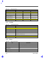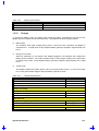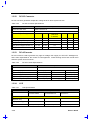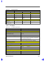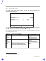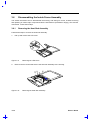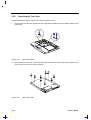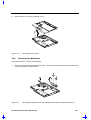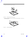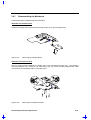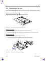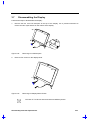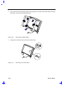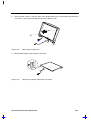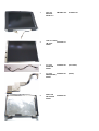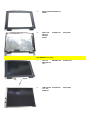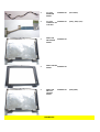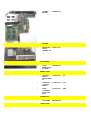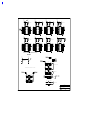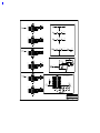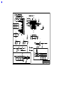
1
365 Notebook Service Guide 6HUYLFHJXLGHILOHVDQGXSGDWHVDUHDYDLODEOHRQ$FHU ,QWUDQHWDQG&6'GDWDEDVHRQ/RWXV1RWHV Copyright Copyright 1998 by Acer Incorporated. All rights reserved. No part of this publication may be reproduced, transmitted, transcribed, stored in a retrieval system, or translated into any language or computer language, in any form or by any means, electronic, mechanical, magnetic, optical, chemical, manual or otherwise, without the prior written permission of Acer Incorporated. Disclaimer Acer Incorporated makes no representations or warranties, either expressed or implied, with respect to the contents hereof and specifically disclaims any warranties of merchantability or fitness for any particular purpose. Any Acer Incorporated software described in this manual is sold or licensed "as is". Should the programs prove defective following their purchase, the buyer (and not Acer Incorporated, its distributor, or its dealer) assumes the entire cost of all necessary servicing, repair, and any incidental or consequential damages resulting from any defect in the software. Further, Acer Incorporated reserves the right to revise this publication and to make changes from time to time in the contents hereof without obligation of Acer Incorporated to notify any person of such revision or changes. Acer is a registered trademark of Acer Incorporated. Intel is a registered trademark of Intel Corporation. Pentium is a trademark of Intel Corporation. Other brand and product names are trademarks and/or registered trademarks of their respective holders. ii About this Manual Purpose This service guide aims to furnish technical information to the service engineers and advanced users when upgrading, configuring, or repairing the Extensa 365 notebook. Manual Structure This service guide consists of four chapters and seven appendices as follows: Chapter 1 System Introduction This chapter gives the technical specifications for the notebook and its peripherals. Chapter 2 BIOS Setup Information This chapter includes the system BIOS information, focusing on the BIOS setup utility. Chapter 3 Disassembly and Unit Replacement This chapter tells how to disassemble the notebook and replace components. Appendix A Model Number Definition This appendix shows the different configuration options for the 365 series notebook computer. Appendix B Compatibility Test Report Excerpt This appendix contains the compatibility test report of the notebook. Appendix C BIOS POST Checkpoint This appendix lists the POST checkpoints of the notebook BIOS. Appendix D Silk Screen This appendix contains the silk screen of the notebook. Appendix E Spare Parts List This appendix lists the spare parts for the 365 series notebook computer with their part numbers and other information. Appendix G Schematics This appendix contains the schematic diagrams for the system board. Appendix H Troubleshooting to Board Repairing If you need help……. iii Conventions The following are the conventions used in this manual: Text entered by user Represents parameter settings and text input by the user. Screen messages Denotes actual messages that appear onscreen. , , , etc. Represent the actual keys that you have to press on the keyboard. NOTE Gives bits and pieces of additional information related to the current topic. WARNING Alerts you to any damage that might result from doing or not doing specific actions. CAUTION Gives precautionary measures to avoid possible hardware or software problems. IMPORTANT Reminds you to do specific actions relevant to the accomplishment of procedures. TIP Tells how to accomplish a procedure with minimum steps through little shortcuts. iv Table of Contents Chapter 1 System Introduction 1.1 Overview......................................................................................................... 1-1 1.2 Jumpers and Connectors ............................................................................... 1-2 1.3 Hardware Configuration and Specification ..................................................... 1-4 1.3.1 Memory Address Map..................................................................... 1-4 1.3.2 Interrupt Channel Map .................................................................... 1-4 1.3.3 DMA Channel Map.......................................................................... 1-5 1.3.4 I/O Address Map ............................................................................. 1-5 1.3.5 Processor........................................................................................ 1-6 1.3.6 BIOS ............................................................................................... 1-6 1.3.7 System Memory .............................................................................. 1-6 1.3.8 Second-Level Cache....................................................................... 1-7 1.3.9 Video Memory ................................................................................. 1-7 1.3.10 Video ............................................................................................... 1-7 1.3.11 Parallel Port..................................................................................... 1-8 1.3.12 Serial Port ....................................................................................... 1-9 1.3.13 Audio ............................................................................................... 1-9 1.3.14 PCMCIA .......................................................................................... 1-9 1.3.15 Touchpad ...................................................................................... 1-10 1.3.16 Keyboard....................................................................................... 1-10 1.3.17 FDD............................................................................................... 1-11 1.3.18 HDD .............................................................................................. 1-11 1.3.19 CD-ROM ....................................................................................... 1-12 1.3.20 Battery........................................................................................... 1-12 1.3.21 Charger ......................................................................................... 1-13 1.3.22 DC-DC Converter.......................................................................... 1-14 v 1.4 1.5 DC-AC Inverter.............................................................................. 1-14 1.3.24 LCD ............................................................................................... 1-14 1.3.25 AC Adapter.................................................................................... 1-15 Software Configuration and Specification..................................................... 1-17 1.4.1 BIOS.............................................................................................. 1-17 1.4.2 Drivers, Applications and Utilities.................................................. 1-23 Block Diagrams ............................................................................................ 1-25 1.5.1 System .......................................................................................... 1-25 1.5.2 Clock ............................................................................................. 1-26 1.6 Environmental Requirements ...................................................................... 1-27 1.7 Mechanical Specifications ............................................................................ 1-28 Chapter 2 BIOS Setup 2.1 Basic System Settings.................................................................................... 2-3 2.2 Startup Configuration...................................................................................... 2-4 2.3 Onboard Devices Configuration ..................................................................... 2-6 2.4 System Security.............................................................................................. 2-8 2.5 Power Management Settings ....................................................................... 2-10 2.6 Load Default Settings ................................................................................... 2-12 Chapter 3 3.1 vi 1.3.23 Disassembly and Unit Replacement General Information........................................................................................ 3-2 3.1.1 Before You Begin ............................................................................ 3-2 3.1.2 Connector Types............................................................................. 3-3 3.1.3 Disassembly Sequence................................................................... 3-4 3.2 Installing Memory ........................................................................................... 3-6 3.3 Removing the Modem Board.......................................................................... 3-8 3.4 Removing the Hard Disk Drive ....................................................................... 3-9 3.5 Removing the Keyboard ............................................................................... 3-10 3.6 3.7 Disassembling the Inside Frame Assembly ................................................. 3-12 3.6.1 Removing the Heat Sink Assembly............................................... 3-12 3.6.2 Removing the Display ................................................................... 3-13 3.6.3 Removing the Internal Drive ......................................................... 3-14 3.6.4 Replacing the CPU ....................................................................... 3-15 3.6.5 Detaching the Top Cover .............................................................. 3-16 3.6.6 Removing the Mainboard.............................................................. 3-17 3.6.7 Disassembling the Mainboard....................................................... 3-19 3.6.8 Disassembling the Top Cover....................................................... 3-20 Disassembling the Display ........................................................................... 3-21 Appendices Appendix A Model Number Definition Appendix B Compatibility Test Report Excerpt Appendix C BIOS POST Checkpoint Appendix D Silk Screen Appendix E Spare Parts List Appendix F Explored View Diagram Appendix G Schematics Appendix H Ttroubleshooting to Board Repairing List of Figures 1-1 Jumpers and Connectors (Top View)............................................................. 1-2 1-2 Jumpers and Connectors (Bottom View) ....................................................... 1-3 1-3 Power Management Block Diagram............................................................. 1-18 1-4 System Block Diagram ................................................................................. 1-25 1-5 Clock Block Diagram.................................................................................... 1-26 3-1 Removing the Battery Pack............................................................................ 3-2 3-2 Using Connectors With Locks........................................................................ 3-3 vii viii 3-3 Disassembly Sequence Flowchart ................................................................. 3-5 3-4 Removing the Memory Door........................................................................... 3-6 3-5 Installing and Removing Memory ................................................................... 3-7 3-6 Removing the Modem Board.......................................................................... 3-8 3-7 Removing the Hard Disk Drive ....................................................................... 3-9 3-8 Removing the Display Hinge Covers............................................................ 3-10 3-9 Removing the Keyboard ............................................................................... 3-10 3-10 Unplugging the Keyboard Connectors.......................................................... 3-11 3-11 Removing the LED Cover............................................................................. 3-12 3-12 Removing the Heat Sink Assembly .............................................................. 3-12 3-13 Unplugging the Display Cable ...................................................................... 3-13 3-14 Removing the Display Hinge Screws ........................................................... 3-13 3-15 Removing the Display Hinge Screws ........................................................... 3-14 3-16 Removing the Internal Drive ......................................................................... 3-15 3-17 Replacing the CPU ....................................................................................... 3-15 3-18 Removing Cables ......................................................................................... 3-16 3-19 Removing Cables ......................................................................................... 3-16 3-20 Detaching the Top Cover.............................................................................. 3-17 3-21 Removing the Keyboard/Touchpad Board and DC-DC Converter Board Cover .................................................................... 3-17 3-22 Removing the DC-DC Converter Board ....................................................... 3-18 3-23 Removing the Mainboard ............................................................................. 3-18 3-24 Removing the Charger Board....................................................................... 3-19 3-25 Removing the PCMCIA Sockets .................................................................. 3-19 3-26 Removing the Hard Disk Drive Heat Sink .................................................... 3-20 3-27 Removing the Touchpad and Speakers ....................................................... 3-20 3-28 Removing the LCD Bumpers........................................................................ 3-21 3-29 Removing the Display Bezel Screws ............................................................ 3-21 3-30 Removing the Display Bezel......................................................................... 3-22 3-31 Removing the Inverter Board ....................................................................... 3-22 3-32 Removing the LCD Panel............................................................................. 3-23 3-33 Removing the display cable from LCD Panel............................................... 3-23 List of Tables 1-1 SW1 Switch Settings ...................................................................................... 1-3 1-2 Memory Address Map .................................................................................... 1-4 1-3 Interrupt Channel Map.................................................................................... 1-4 1-4 DMA Channel Map ......................................................................................... 1-5 1-5 I/O Address Map ............................................................................................ 1-5 1-6 Processor Specifications ................................................................................ 1-6 1-7 BIOS Specifications....................................................................................... 1-6 1-8 Memory Configurations .................................................................................. 1-7 1-9 Video RAM Configuration............................................................................... 1-7 1-10 Video Hardware Specification ....................................................................... 1-7 1-11 Supported External CRT Resolutions ............................................................ 1-8 1-12 Supported LCD Resolutions........................................................................... 1-8 1-13 Parallel Port Configurations........................................................................... 1-8 1-14 Serial Port Configurations .............................................................................. 1-9 1-15 Audio Specifications ....................................................................................... 1-9 1-16 PCMCIA Specifications ................................................................................ 1-10 1-17 Touchpad Specifications .............................................................................. 1-10 1-18 Keyboard Specifications ............................................................................... 1-10 1-19 Windows 95 Key Descriptions..................................................................... 1-11 1-20 FDD Specifications....................................................................................... 1-11 1-21 HDD Specifications ...................................................................................... 1-11 1-22 CD-ROM Specifications ............................................................................... 1-12 ix x 1-23 Battery Specifications ................................................................................... 1-12 1-24 Charger Specifications ................................................................................. 1-13 1-25 DC-DC Converter Specifications.................................................................. 1-14 1-26 DC-AC Inverter Specifications...................................................................... 1-14 1-27 LCD Specifications ....................................................................................... 1-14 1-28 AC Adapter Specifications............................................................................ 1-15 1-29 Hotkey Descriptions...................................................................................... 1-17 1-30 Standby Mode Conditions and Descriptions................................................. 1-19 1-31 Light Green Mode Conditions and Descriptions ........................................... 1-20 1-32 Hibernation Mode Conditions and Descriptions ........................................... 1-21 1-33 Display Standby Mode Conditions and Descriptions .................................... 1-21 1-34 Hard Disk Standby Mode Conditions and Descriptions................................ 1-22 1-35 Location of Drivers in the System Utility CD................................................. 1-23 1-36 Location of Applications in the System Utility CD ......................................... 1-24 2-1 Basic System Settings Parameters ................................................................ 2-3 2-2 Startup Configuration Parameters.................................................................. 2-4 2-3 Onboard Devices Configuration Parameters.................................................. 2-6 2-4 System Security Parameters .......................................................................... 2-8 2-5 Power Management Settings ....................................................................... 2-10 3-1 Guide to Disassembly Sequence ................................................................... 3-4 C-1 POST Checkpoint List ....................................................................................E-1 &KDSWHU System Introduction 1.1 Overview This computer combines high-performance, versatility, power management features and multimedia capabilities with unique style and ergonomic design. This computer was designed with the user in mind. Here are just a few of its many features: • Performance • Intel Pentium® processor with MMX™ technology • 64-bit main memory and external (L2) cache memory • Large LCD display and PCI local bus video with graphics acceleration • Internal CD-ROM drive and external 3.5-inch floppy drive (CD-ROM drive model) • Internal 3.5-inch floppy drive (FDD model) • High-capacity, Enhanced-IDE hard disk • Nickel Metal-Hydride battery pack • Power management system with light green, standby and hibernation power saving modes • Multimedia • 16-bit high-fidelity stereo audio with 3-D sound • Built-in dual speakers • Ultra-slim, high-speed CD-ROM drive • Connectivity • High-speed fax/data modem port • USB (Universal Serial Bus) port • Human-centric Design and Ergonomics • Lightweight and slim • Sleek, smooth and stylish design • Full-sized keyboard and wide palmrest • Ergonomically-centered touchpad pointing device • Expansion • CardBus PC card (formerly PCMCIA) slots (two type II/I or one type III) with ZV (Zoomed Video) port support • User-upgradeable memory and hard disk System Introduction 1-1 1.2 Jumpers and Connectors TOP VIEW CN1 CN2 PH1 PH2 PH3 CN9 CN10 CN3 CN4 CN5 CN7 CN6 CN8 CN11 CN12 SW1 CN13 CN14 CN15 CN16 CN17 CN18 GF1 PCB No. 97160-1 CN1 CN2 CN3 CN4 CN5 CN6 CN7 CN8 USB port VGA port Parallel port Serial port RJ-11 phone jack LCD connector DC-DC connector Charger connector Figure 1-1 1-2 CN9 CN10 CN11 CN12 CN13 CN14 CN15 CN16 Internal speaker connector (left) Internal speaker connector (right) PCMCIA socket connector Inverter connector FDD/CD-ROM connector Internal keyboard/touchpad connector HDD connector CD-ROM connector CN17 CN18 SW1 GF1 PH1 PH2 PH3 CPU board connector Battery connector KB/password/logo setting switch Golden finger for debug card Microphone connector Line-In connector Line-out connector Jumpers and Connectors (Top View) Service Guide BOTTOM VIEW CN20 CN19 CN21 PCB No. 97160-1 CN19 CN20 CN21 Modem connector Modem connector DIMM socket Figure 1-2 Jumpers and Connectors (Bottom View) The following tables list the switch settings for SW1. Table 1-1 SW1 Switch Settings ON Switch 1 (Logo Screen) Switch 2 (Password) OFF OEM Acer Bypass Check English European Japanese Korean Switch 3 (KB Language) Off On Off On Switch 4 (KB Language) Off Off On On System Introduction 1-3 1.3 Hardware Configuration and Specification 1.3.1 Memory Address Map Table 1-2 Memory Address Map Address Range 000000 - 09FFFF Definition 640 KB memory Function Base memory 0A0000 - 0BFFFF 128 KB video RAM Reserved for graphics display buffer 0C0000 - 0CBFFF Video BIOS Video BIOS 0F0000 - 0FFFFF 64 KB system BIOS System BIOS 100000 - top limited Extended memory SIMM memory FE0000 - FFFFFF 256 KB system ROM Duplicate of code assignment at 0E0000-0FFFFF 1.3.2 Table 1-3 Priority 1 2 3 4 5 6 7 8 9 10 11 12 13 14 15 16 17 18 19 1-4 Interrupt Channel Map Interrupt Channel Map Interrupt Number SMI NMI IRQ 0 IRQ 1 IRQ 2 IRQ 8 IRQ 9 IRQ 10 IRQ 11 IRQ 12 IRQ 13 IRQ 14 IRQ 15 IRQ 3 IRQ 4 IRQ 5 IRQ 6 IRQ 7 Interrupt Source Power management unit Parity error detected, I/O channel error Interval timer, counter 0 output Keyboard Interrupt from controller 2 (cascade) Real-time clock / Cascaded to INT 0AH (IRQ 2) / Audio / PCMCIA/Internal Modem Audio (option) / PCMCIA / Internal modem / Serial communication port 2 / PCMCIA / USB Audio (option) / PCMCIA / Internal modem / Serial communication port 1 / PCMCIA PS/2 mouse INT from coprocessor Hard disk controller / PCMCIA controller CD-ROM controller / PCMCIA controller Serial communication port 2 / Internal modem / Audio / PCMCIA Serial communication port 1 / Internal modem / Audio / PCMCIA Parallel port (option) / Audio / PCMCIA Diskette controller Parallel port (option) / Audio / Internal Modem Service Guide 1.3.3 DMA Channel Map Table 1-4 DMA Channel Map Controller Channel Address Function 1 1 1 1 2 2 2 2 0 1 2 3 4 5 6 7 0087 0083 0081 0082 Cascade 008B 0089 008A Audio (option) / Audio Audio (option) / ECP / Audio Diskette Audio (option) / ECP Cascade Not support Not support Audio (option) 1.3.4 I/O Address Map Table 1-5 I/O Address Map Address Range 000 - 00F 020 - 021 040 - 043 048 - 04B 060 - 06E 070 - 071 080 - 08F 0A0 - 0A1 0C0 - 0DF 1F0 - 1F7 220 - 22F 230 - 23F 240 - 24F 250 - 25F 278 - 27F 2E8 - 2EF 2F8 - 2FF 378, 37A 3BC - 3BE 3B4, 3B5, 3BA 3C0 - 3C5 3C6 - 3C9 3C0 - 3CF 3D0 - 3DF 3E0 - 3E1 3E8 - 3EF 3F0 - 3F7 3F8 - 3FF CF8 - CFF System Introduction Device DMA controller-1 Interrupt controller-1 Timer 1 Timer 2 Keyboard controller 8742 chip select Real-time clock and NMI mask DMA page register Interrupt controller-2 DMA controller-2 Hard disk select Audio (option) - default Audio (option) Audio (option) Audio (option) Parallel port 3 COM 4 COM 2 Parallel port 2 Parallel port 1 Video subsystem Video subsystem Video DAC Enhanced graphics display Color graphics adapter PCMCIA controller COM3 Floppy disk controller COM 1 PCI configuration register 1-5 1.3.5 Processor Table 1-6 Processor Specifications Item Specification CPU type P55C-166, Tillamook-200/233 CPU package TCP Switchable processor speed (Y/N) Yes Minimum working speed 0MHz CPU core voltage 2.45V/1.8V/1.8V CPU I/O voltage 3.3V/2.5V/2.5V 1.3.6 BIOS Table 1-7 BIOS Specifications Item Specification BIOS vendor Acer BIOS version V3.0 BIOS in flash EPROM (Y/N) Yes BIOS ROM size 256KB BIOS package type 32-pin PLCC Same BIOS for STN color/TFT color (Y/N) Yes The BIOS can be overwritten/upgradeable using the "AFLASH" utility (AFLASH.EXE). Please refer to software specification section for details. 1.3.7 System Memory Memory is upgradeable from 16 to 80 MB, employing 16-/32-/64-MB 64-bit soDIMMs (Small Outline Dual Inline Memory Modules). After installing the memory modules, the system automatically detects and reconfigures the total memory size during the POST routines. The following lists important memory specifications. • • 1-6 Memory bus width: 64-bit Expansion RAM module type:144-pin, 64-bit, small outline Dual Inline Memory Module (soDIMM) Service Guide • Expansion RAM module size/configuration: • 8MB (1M*16x4) • 16MB (2M*8x8) • 32MB (4M*16x4) • 64MB (8M*8x8) • Expansion RAM module speed/voltage/package: 60ns/3.3v/TSOP EDO • EDO and fast-page mode DIMMs may be used together in a memory configuration. The following table lists all possible memory configurations. Table 1-8 1.3.8 Memory Configurations On Board Slot 1 Total Memory 16 MB 0 MB 16 MB 16 MB 16 MB 32 MB 16 MB 32 MB 48 MB 16 MB 64MB 80 MB Second-Level Cache This notebook has 256KB second-level (L2) cache onboard. 1.3.9 Video Memory Table 1-9 Video RAM Configuration Item Specification Fixed or upgradeable Fixed, build in chip Memory size/configuration 1.1MB Memory speed 50ns Memory voltage 3.3V 1.3.10 Video Table 1-10 Video Hardware Specification Item Specification Video chip NeoMagic 2097 Working voltage 3.3V System Introduction 1-7 External CRT Resolution Support Table 1-11 Supported External CRT Resolutions Resolution x Color on External CRT CRT Refresh Rate Simultaneous on TFT LCD Simultaneous on STN LCD CRT only Simultaneous SVGA SVGA 640x480x16 60 60 Y Y 640x480x256 60,75,85 60 Y Y 640x480x65,536 60,75,85 60 Y Y 640x480x16,777,216 60,75,85 60 Y Y 800x600x256 60,75,85 60 Y Y 800x600x65,536 60,75,85 60 Y Y 1024x768x256 60,75,85 60 Y Y LCD Resolution Support Table 1-12 Supported LCD Resolutions Resolution x Color on LCD Only* TFT LCD (SVGA) DSTN LCD (SVGA) 640x480x16 Y Y 640x480x256 Y Y 640x480x65,536 Y Y 640x480x16,777,216 Y Y 800x600x256 Y Y 800x600x65,536 Y Y 1024x768x256 Y Y * Maximum resolution (External CRT): 1024x768 Using software, you can set the LCD to a higher resolution than its physical resolution, but the image shown on the LCD will pan. 1.3.11 Parallel Port Table 1-13 Parallel Port Configurations Item Specification Number of parallel ports 1 ECP support Yes (set by BIOS setup) Connector type 25-pin D-type Location Rear side Selectable parallel port (by BIOS Setup) • Parallel port : Enabled / Disabled • Base Address: 378h/278h/3BCH • IRQ: 7/ 5 1-8 Service Guide 1.3.12 Serial Port Table 1-14 Serial Port Configurations Item Specification Number of serial ports 1 16550 UART support Yes Connector type 9-pin D-type Location Rear side Selectable serial port (by BIOS Setup) • • • 1.3.13 Serial Port : Enabled / Disabled Base Address : 3F8h / 2F8h / 3E8h / 2E8h IRQ: 4 /11 Audio Table 1-15 Audio Specifications Item Specification Chipset YMF715 Audio onboard or optional Built-in Mono or stereo Stereo Resolution 16-bit Compatibility SB-16 , Windows Sound System Mixed sound sources Voice, Synthesizer, Line-in, Microphone, CD Voice channel 8-/16-bit, mono/stereo Sampling rate 44.1 kHz Internal microphone No Internal speaker / quantity Yes / 2 pcs. Microphone jack Yes Headphone jack Yes 1.3.14 PCMCIA PCMCIA is an acronym for Personal Computer Memory Card International Association. The PCMCIA committee set out to standardize a way to add credit-card size peripheral devices to a wide range of personal computers with as little effort as possible. There are two type II/I or one type III PC Card slots found on the left panel of the notebook. These slots accept credit-card-sized cards that enhances the usability and expandability of the notebook. ZV (Zoomed Video) port support allows your system to support hardware MPEG in the form of a ZV PC card. System Introduction 1-9 Table 1-16 PCMCIA Specifications Item Specification Chipset O2 Micro OZ6833 Supported card type Type-II / Type-III Number of slots Two Type-II or one Type-III Access location Left side ZV (Zoomed Video) port support Yes 1.3.15 Table 1-17 Touchpad Touchpad Specifications Item Specification Vendor & model name Synaptics TM3202TPD-226 Power supply voltage (V) 5 ± 10% Location Palm-rest center Internal & external pointing device work simultaneously Yes Support external pointing device hot plug Yes X/Y position resolution (points/mm) 20 Interface PS/2 (compatible with Microsoft mouse driver) 1.3.16 Table 1-18 Keyboard Keyboard Specifications Item Specification Vendor & model name SMK KAS1901-0161R (English) Total number of keypads 84/85 keys Windows 95 keys Yes, (Logo key / Application key): Internal & external keyboard work simultaneously Yes Windows 95 Keys The keyboard has two keys that perform Windows 95-specific functions. See Table 1-26. 1-10 Service Guide Table 1-19 Windows 95 Key Descriptions Key Description Windows logo key Application key 1.3.17 Start button. Combinations with this key performs special functions, e.g.: Windows + Tab Activate next Taskbar button • Windows + E Explore My Computer • Windows + F Find Document • Windows + M Minimize All • Shift + Windows + M Undo Minimize All • Windows + R Display Run dialog box • Opens the application’s context menu (same as right-click). FDD Table 1-20 FDD Specifications Item Specification Vendor & model name Mitsumi D353F2 Floppy Disk Specifications Media recognition 2DD (720K) 2HD (1.2M, 3-mode) 2HD (1.44M) Sectors / track 9 15 18 Tracks 80 80 80 Data transfer rate (Kbits/s) 250 300 500 500 Rotational speed (RPM) 300 360 360 300 Read/write heads 2 Encoding method MFM Power Requirement Input Voltage (V) 1.3.18 +5 ± 10% HDD Table 1-21 HDD Specifications Item Vendor & Model Name Specification Hitachi DK225A-21 IBM DTNA22160 IBM DDLA21620 Capacity (MB) 2160 2160 1620 Bytes per sector 512 512 512 Logical heads 16 16 16 Logical sectors 63 63 63 Logical cylinders 4889 4200 3152 Physical read/write heads 6 6 3 Disks 3 3 2 Drive Format Drive Format System Introduction 1-11 Table 1-21 HDD Specifications Item Specification Spindle speed (RPM) 4464 4000 4000 Buffer size (KB) 128 96 96 Interface ATA-3(IDE) ATA-3 ATA-3 Data transfer rate (disk-buffer, Mbytes/s) 5.7 ~ 9.0 5 ~ 7.7 5 ~ 8.3 Data transfer rate (host-buffer, Mbytes/s) 16.6 /33.3 (max., PIO mode 4) 16.6 (max., PIO mode 4) 16.6 (max., PIO mode 4) 5 ± 5% 5 + 5% 5 ± 5% Performance Specifications DC Power Requirements Voltage tolerance (V) 1.3.19 CD-ROM Table 1-22 CD-ROM Specifications Item Specification Vendor & Model Name Teac-20X Performance Specification Speed (KB/sec) 2100 (ave. speed), 3000 (max.) Access time (ms) 150 (Typ.) Buffer memory (KB) 128 Interface Enhanced IDE (ATAPI) compatible Applicable disc format CD-DA, CD-ROM, CD-ROM XA (except ADPCM), CD-I, Photo CD (Multisession), Video CD, CD+ Loading mechanism Soft eject (with emergency eject hole) Power Requirement Input Voltage (V) 1.3.20 5 Battery Table 1-23 Battery Specifications Item Battery gauge on screen Specification Yes, by hotkey Vendor & model name Solomonbtp-1631(pack)/Toshiba(cell) Battery type NiMH Cell capacity (mAH) 3500 Cell voltage (V) 1.2 Number of battery cell 7-cell Package configuration 7 serial Package voltage (V) 8.4 1-12 Service Guide Table 1-23 Battery Specifications Item Specification Package capacity (WAH) 3500 Second battery No 1.3.21 Charger To charge the battery, place the battery pack inside the battery compartment and plug the AC adapter into the notebook and an electrical outlet. The adapter has three charging modes: • Rapid mode The notebook uses rapid charging when power is turned off and a powered AC adapter is connected to it. In rapid mode, a fully depleted battery gets fully charged in approximately two hours. • Charge-in-use mode When the notebook is in use with the AC adapter plugged in, the notebook also charges the battery pack if installed. This mode will take longer to fully charge a battery than rapid mode. In charge-in-use mode, a fully depleted battery gets fully charged in approximately six to eight hours. • Trickle mode The adapter charges the battery pack for two hours using trickle current 17 ± 3mA, then shifts to 1/10 duty pulse trickle charge to keep the battery capacity at 100%. Table 1-24 Charger Specifications Item Specification Vendor & model name Ambit T62.096.C.00 Input voltage (from adapter, V) 0-24 Output current (to DC/DC converter, A) 4.3 Battery Low Voltage Battery Low 1 level (V) 8.2 ± 0.15 Battery Low 2 level (V) 7.8 ± 0.15 Battery Low 3 level (V) 6.8 ± 0.15 Charge Current Background charge (charge even system is still operative, A) 0.9 ± 0.1 (typ.) Normal charge (charge while system is not operative, A) 2.0 ± 0.1(typ.) Charging Protection Maximum temperature protection ( System Introduction ) 60 1-13 1.3.22 DC-DC Converter DC-DC converter generates multiple DC voltage level for whole system unit use. Table 1-25 DC-DC Converter Specifications Item Specification Vendor & model name Ambit T62.095.C.00 Input voltage (Vdc) 8~21 Output Rating Current (w/ load, A) 5V 3.3V Vcpu (2.47 /2.15 /1.8V/2.0V) +12V +6V 5VSB 0~3.2 0~3.3 0~6 0~0.15 0~0.1 0.005 Voltage ripple (max., mV) 50 50 50 100 300 75 Voltage noise (max., mV) 100 100 100 200 500 250 OVP (Over Voltage Protection, V) 6.1~8.0 4.2~6.2 3-4 - - - OCP (Over Current Protection, A) 4-6 4-6 6.5-9 0.3-0.4 - - 1.3.23 DC-AC Inverter DC-AC inverter is used to generate very high AC voltage, then supply to LCD CCFT backlight use, and is also responsible for the control of LCD brightness. Avoid touching the DC-AC inverter area while the system unit is turned on. Table 1-26 DC-AC Inverter Specifications Item Specification Vendor & model name Ambit T62.104.C.00 Input voltage (V) 6.8(in.) - 22(max.) - - 750 (max.) Output voltage (Vrms, no load) 1000 (min.) - 1600 (max.) Output voltage frequency (kHz) 40 (min.) - 65 (max.) 1.0~5.5 (min.) 1.5~6.1 (typ.) 2.0~6.7 (max.) Input current (mA) Output current (mArms) 1.3.24 LCD Table 1-27 LCD Specifications Item Vendor & model name Specification TORiSAN LM-JK53-22NFQ TORiSAN LM-JK53-22NFR-A HITACHI TX31D21VC Mechanical Specifications LCD display area (diagonal, inch) 12.1 12.1 12.1 Display technology STN STN TFT Resolution SVGA (800x600) VGA (800x600) SVGA (800x600) 1-14 Service Guide Table 1-27 LCD Specifications Item Specification Supported colors -- -- 262,144 colors 40 (typ.) 40 (typ.) 80 (typ.) Brightness (cd/m ) 70 (typ.) 70 (typ.) 70 (typ.) Brightness control keyboard hotkey keyboard hotkey keyboard hotkey Contrast control using keyboard hotkey using keyboard hotkey none Supply voltage for LCD display (V) 3.3 or 5 (typ.) 3.3 or 5 (typ.) 3.0 ~ 3.6 (typ.) Supply voltage for LCD backlight (Vrms) 630 (typ.) 630 (typ.) 595(typ.), 660(max) Optical Specification Contrast ratio 2 Electrical Specification 1.3.25 AC Adapter Table 1-28 AC Adapter Specifications Item Vendor & model name Specification Delta ADP-45GB Rev. E3, E5 Input Requirements Nominal voltages (Vrms) 90 - 270 Nominal frequency (Hz) 47 - 63 Frequency variation range (Hz) 47 - 63 Maximum input current (A, @90Vac, full load) 1.5 A Inrush current The maximum inrush current will be less than 50A and 100A when the adapter is connected to 115Vac(60Hz) and 230Vac(50Hz) respectively. Efficiency It should provide an efficiency of 83% minimum, when measured at maximum load under 115V(60Hz). Output Ratings (CV mode) DC output voltage (V) +19.0V~20.5V Noise + Ripple (mV) 300mvp-pmax (20Mhz bandwidth) Output Ratings (CV mode) Load (A) 0 (min.) DC output voltage (V) +12 ~+19 Constant output (A) 2.75 ± 0.2 2.4 (max.) Dynamic Output Characteristics Turn-on delay time (s, @115Vac) 2 Hold up time (ms; @115 Vac input, full load) 5 (min.) Over Voltage Protection (OVP, V) 26 System Introduction 1-15 Table 1-28 AC Adapter Specifications Item Specification Short circuit protection Output can be shorted without damage Electrostatic discharge (ESD, kV) ±15 (at air discharge) Dielectric Withstand Voltage Primary to secondary 3000 Vac (or 4242 Vdc), 10 mA for 1 second Leakage current 0.25 mA maximum @ 254 Vac, 60Hz. Regulatory Requirements Internal filter meets: 1. FCC class B requirements. (USA) 2. VDE 243/1991 class B requirements. (German) 3. CISPR 22 Class B requirements. (Scandinavia) 4. VCCI class II requirements. (Japan) 1-16 Service Guide 1.4 Software Configuration and Specification 1.4.1 BIOS The BIOS is compliant to PCI v2.1, APM v1.2, E-IDE and PnP specification. It also defines the hotkey functions and controls the system power-saving flow. Keyboard Hotkey Definition The notebook supports the following hotkeys. Table 1-29 Hotkey Hotkey Descriptions Icon Function Description Fn-Esc Hotkey Escape Exits the hotkey control. Fn-F1 Hotkey Help Displays the hotkey list and help. Press | to exit the screen. Brightness Control Toggles between brightness control and contrast control. Fn-F2 ? Press the scale hotkeys (Fn- →and Fn -←) to increase and decrease the brightness or contrast level. Contrast Control Notebooks with TFT displays do not show the brightness control icon. Fn-F3 Display Toggle Switches display from LCD to CRT to both LCD and CRT. Fn-F4 Battery Gauge Displays the battery gauge. Fn-F5 Volume Control Press the scale hotkeys (Fn-→ and Fn-←) to increase and decrease the output level. Fn-F6 Setup Gains access to BIOS Setup’s Advanced System Configuration parameters. Fn-F7 Hibernation/Standby Enters hibernation mode if the 0-volt suspend function is installed and enabled; otherwise, the notebook enters standby mode. Fn-→ Scale Increase Increases the setting of the current icon. Fn-← Scale Decrease Decreases the setting of the current icon. Fn-T Toggle Touchpad Turns the internal touchpad on and off. When the available hotkey is toggled, the system will issue a beep to enter the assigned process. System Introduction 1-17 MultiBoot The system can boot from the FDD, External FDD, HDD, or CD-ROM. The user can select the desired booting process to boot the system. If the CD-ROM is bootable, the BIOS will override the other process to boot the system directly. Power Management This computer has a built-in power management unit that monitors system activity. System activity refers to any activity involving one or more of the following devices: keyboard, mouse, floppy drive, hard disk, peripherals connected to the serial and parallel ports, and video memory. If no activity is detected for a period of time (called an inactivity time-out), the computer stops some or all of these devices in order to conserve energy. This computer employs an innovative power management technique called Heuristic Power Management or HPM. HPM allows the computer to provide maximum power conservation and maximum performance at the same time. Power management methods used by most computers are timer-based. You set inactivity time-out values for the display, hard disk, and other devices. The computer then "sleeps" when these timeouts elapse. The problem with this is that no two users are alike. Each of us has his or her own habits when using the computer, which makes timer-based power management ineffective. With HPM, your computer manages its power according to the way you use your computer. This means the computer delivers maximum power when you need it, and saves power when you don’t need the maximum — all without your intervention. There are no timers to set, because the HPM system figures out everything for you. Cover Door Close Power Switch Off More than 3 Seconds Power Off Power Switch On Display Screen Off Check password if needed K/B, PS/2 Mouse Pressed System Active Display Standby Timer Time Out Power Switch (Beep) Standby Event Normal Mode Hibernation Event Standby Mode Light Green Mode Power Switch (Beep) Power Switch Cover Door Close Standby Mode Hibernation Mode HDD Standby Timer Time Out Idle of HDD Figure 1-3 1-18 Standby Wakeup Event Cover Door Open Light Green Mode HDD Standby Mode (HDD Motor Off) HDD Acess Power Management Block Diagram Service Guide ON MODE Normal full-on operation STANDBY MODE The computer consumes very low power in standby mode. memory until battery is drained. Data remain intact in the system Warning: Unstored data is lost when you turn off the computer power in standby mode or when the battery is drained. Table 1-30 Standby Mode Conditions and Descriptions Condition Description The condition to There are two necessary conditions for the computer to enter standby mode: enter Standby Heuristic Power Management Mode must be set to [ENABLED]. • Mode In this situation, the following are ways to enter standby mode: • • • • Pressing the sleep hot key Fn-F7 If the waiting time determined by the computer’s HPM unit elapses without any system activity. Closing the display cover. With the System Sleep State is set to [HIBERNATION], the computer also enters standby mode if the hibernation file (Sleep Manager) is invalid or not present. “Hard Disk Drive” is [Disabled] in System Security of BIOS SETUP. • “Hard Disk 0” is [None] in Basic System Configuration of BIOS SETUP. • Note: If the computer detects a PC I/O card installed in the PC card slots, the computer "sleeps" (light green mode) to maintain your communications connection. It will not enter standby mode. The condition of • Standby Mode • • • • • The condition back to On Mode Issue a beep. The standby indicator flashes. Disable the mouse, serial and the parallel port. The keyboard controller, HDD and VGA enter the standby mode. Stop the CPU internal clock. All the functions are disabled except the keyboard, battery low warning and modem ring wake up from standby (if enabled). Any one of following activities will let system back to Normal Mode: Any keystroke (Internal KB or External KB) • Any active pointing device (internal or external, PS/2 or serial or USB) • Resume Timer matched • Opening the display cover if you closed the display cover to enter Standby mode. • Modem ring • System Introduction 1-19 LIGHT GREEN MODE The notebook consumes very low power in light green mode. Data and I/O connections remain intact in the system memory until battery is drained. Table 1-31 Light Green Mode Conditions and Descriptions Condition Description The condition to enter Light Green Mode • • PCMCIA I/O Card detected and occupy resources (Non Cardbus mode). HPM timer times out or cover close or APM standby / suspend function calls. The condition of Light Green Mode • • Issue a beep. Only HDD, VGA enter standby The condition back to On Mode Any one of following activities will let system back to Normal Mode: Any keystroke (Internal KB or External KB) • Any active pointing device (internal or external, PS/2 or serial or USB) • Resume Timer matched • Modem ring • HIBERNATION MODE In hibernation mode, all power shuts off (the computer does not consume any power). The computer saves all system information onto the hard disk before it enters hibernation mode. Once you turn on the power, the computer restores this information and resumes where you left off upon leaving hibernation mode. If the computer beeps but does not enter hibernation mode after pressing the sleep hot key, it means the operating system will not allow the computer to enter the power saving mode. Do not change any devices (such as add memory or swap hard disks when the computer is in hibernation mode. If the computer detects a PC I/O card installed in the PC card slots, the computer enters light green mode to maintain your communications connection. It will not enter standby nor hibernation mode. 1-20 Service Guide Table 1-32 Hibernation Mode Conditions and Descriptions Condition Description The condition to enter Hibernation Mode There are two necessary conditions for the computer to enter standby mode: • Heuristic Power Management Mode must be set to [ENABLED]. • The hibernation file created by Sleep Manager must be present and valid. In this situation, the following are ways to enter hibernation mode: • Pressing the sleep hot key Fn-F7 • “Hard Disk Drive” is not [Disabled] in System Security of BIOS SETUP. • “Hard Disk 0” is not [None] in Basic System Configuration of BIOS SETUP. • If the waiting time determined by the computer’s HPM unit elapses without any system activity. • If a battery low condition takes place, the computer enters hibernation mode in about three minutes. The Sleep Upon Battery-low parameter in Setup must be set to [ENABLED]. • Invoked by the operating system power saving modes The condition of Hibernation Mode • Except the RTC, KB controller and power switch, all the system components are off. The condition back to On Mode • Pressing the power switch. • Resume Timer matched DISPLAY STANDBY MODE Screen activity is determined by the keyboard, the built-in touchpad, and an external PS/2 pointing device. If these devices are idle for the period determined by the computer’s HPM unit, the display shuts off until you press a key or move the touchpad or external mouse. Table 1-33 Display Standby Mode Conditions and Descriptions Condition Description The condition to enter Display Standby Mode • Pointing device is idle until Display Standby Timer times-out or LCD cover is closed. The condition of Display Standby Mode • All the system components are on except LCD backlight and CRT horizontal frequency output (if CRT is connected) The condition back to On Mode • Any keystroke (Internal KB or External KB) • Pointing device activity The VGA BIOS should support DPMS (Desktop Power Management System) for the standby and hibernation mode function call. When the Display Standby Timer expires, the system BIOS will execute the DPMS service routines. HARD DISK STANDBY MODE The hard disk enters standby mode when there are no disk read/write operations within the period of time determined by the computer’s HPM unit. In this state, the power supplied to the hard disk is reduced to a minimum. The hard disk returns to normal once the computer accesses it. System Introduction 1-21 Table 1-34 Hard Disk Standby Mode Conditions and Descriptions Condition Description The condition to enter HDD Standby Mode Display Standby HPM timer times-out or LCD cover is closed. The condition of HDD Standby Mode All the system components are on except HDD spindle motor The condition back to On Mode Any access to HDD BATTERY LOW When the battery capacity is low and no adapter is plugged in, the system will generate the following battery low warning: • Flash power LED with 1 Hz. • Issue 4 short beeps per minute (if enabled in setup). • If the AC adapter does not plug in within 3 minutes and the “Standby/Hibernation upon Batterylow” in BIOS SETUP is enabled, the system will enter Standby/0-Volt Hibernation Mode. The battery low warning will stop as soon as the AC adapter is plugged into the system. THE AUTODIM PROCESS OF THE LCD BRIGHTNESS The notebook has a unique “automatic dim” power saving feature. When the notebook is using AC power and you disconnect the AC adapter from the notebook, the system “decides” whether or not to automatically dim the LCD backlight to save power. If the LCD backlight is too bright, the system automatically adjusts it to a manageable level; otherwise, the level stays the same. If you want a brighter picture, you can then adjust the brightness and contrast level using hotkeys (Fn-F2). If you reconnect AC power to the system, the system automatically adjusts the LCD backlight to its original level — the brightness and contrast level before disconnecting the AC adapter. If you adjusted the brightness and contrast level after disconnecting AC power, the level stays the same after you reconnect the AC adapter. There are two reasons for the notebook to have the LCD AutoDim feature. The first is to save the power during the notebook is operating under the DC mode. The second is to save the “favorite” brightness parameter set by the user. 1-22 Service Guide The following processes are the basic methods used to implement the LCD brightness AutoDim. 1. If the original brightness is over 75% and the AC power is on-line, the BIOS will change the brightness to 75% after the AC power is off-line. 2. If the original brightness is below 75%, the brightness maintains the same level even if the AC power is off-line. 3. If the brightness is already changed by the hotkey under DC power, it will not be changed after the AC power is plugged in. 4. If the brightness is not changed by the hotkey under DC power, the brightness will be changed back to the old setting — the previous brightness parameter under AC power. 5. If the previous brightness parameter does not exist, the brightness will not be changed in process 4. 1.4.2 Drivers, Applications and Utilities The notebook comes preloaded with the following software: • Windows 95 • System utilities and application software 1 2 • Sleep Manager utility • Display drivers • Audio drivers • PC Card slot drivers and applications • Other third-party application software Table 1-35 Location of Drivers in the System Utility CD Device Category Function Location Sound, video and game controllers Audio ENGLISH\WIN95\AUDIO\ Mouse Mouse ENGLISH\WIN95\MOUSE\ Display adapters Video ENGLISH\WIN95\VGA\ PCMCIA Zoomed Video Port English\Win95\PCMCIA\ 1 In some areas, a different operating system may be pre-loaded instead of Windows 95. 2 The system utilities and application software list may vary. System Introduction 1-23 To re-install applications under Windows 95, click on Start, then Run…. Based on the location of the application, run the setup program to install the application. The following table lists the applications and their locations: Table 1-36 Location of Applications in the System Utility CD Name Function Location Sleep Manager 0V Suspend utility ENGLISH\WIN95\SLEEPMGR\ Y-Station Audio application ENGLISH\WIN95\Ystation SafeOFF Protect if user accidentally press the power switch ENGLISH\WIN95\SAFEOFF Drivers for Windows 3.x and Windows NT are also found in the System Utility CD if you should need them. 1-24 Service Guide 1.5 Block Diagrams 1.5.1 System CPU P55C/ Tillamook CPU Bus DRAM on board ALI M1531 DIMM Socket PCI Bus PCMCIA O2Micro OZ6833 USB Conn. ALI M1533 CD-ROM & HDD Conn. VGA NeoMagic NM2097 ISA Bus AUDIO YMF715 OpAmp TPA0102. Figure 1-4 Super I/O NS97338 Serial Port Parallel Port KBC M38813 BIOS ROM Internal FDD Conn. Battery Conn. Charger Conn. System Block Diagram System Introduction 1-25 1.5.2 Clock M1533 DIMM SMB BUS CLK GEN CY2272 CPU CLK PCI CLK CPU 1531 CACHE 1533 M1531 NM2097 O2M 6833 14.318M 48MHZ 1533 USB DIMM SDRAM CLK NM2097 YMF715 MODEM ID CLK 24MHz NS 97338 8 MHz Figure 1-5 1-26 38813 Clock Block Diagram Service Guide 1.6 Environmental Requirements Table 1- 37 Environmental Requirements Item Specification Temperature Operating ( ) Non-operating( +5~ +35 ) -20 ~ +60 Humidity Operating (non-condensing) 20% ~ 85% Non-operating (non-condensing) 20% ~ 90% Operating Vibration (unpacked) Operating 5 - 25.6Hz, 0.38mm; 25.6 - 250Hz, 0.5G Sweep rate 0.5 octave / minute Number of test cycles 2 / axis (X,Y,Z) Non-operating Vibration (unpacked) Non-operating 5 - 27.1Hz, 0.6G; 27.1 - 50Hz, 0.41mm; 50-500Hz, 2G Sweep rate 0.5 octave / minute Number of text cycles 4 / axis (X,Y,Z) Non-operating Vibration (packed) Non-operating 5 - 62.6Hz, 0.51mm; 62.6-500Hz, 4G Sweep rate 0.5 octave / minute Number of text cycles 4 / axis (X,Y,Z) Shock Non-operating (unpacked) 40G peak, 11±2ms, half-sine Non-operating (packed) 50G peak, 11±2ms, half-sine Altitude Operating 10,000 feet (5°C ~ 40°C) Non-operating 40,000 feet (-20°C ~ 60°C) ESD Air discharge 8kV (no error) 12.5kV (no restart error) 15kV (no damage) Contact discharge 4kV (no error) 6kV (no restart error) 8kV (no damage) System Introduction 1-27 1.7 Mechanical Specifications Table 1-38 Mechanical Specifications Item Specification Weight FDD model CD-ROM model (includes battery) 2.77 kg. (6.11 lb.) 2.89 kg. (6.37 lb.) Dimensions (main footprint) WxDxH 310mm x 245mm x 46mm (12.2” x 9.65” x 1.81”) 1-28 Service Guide &KDSWHU BIOS Setup The Setup Utility is a hardware configuration program built into your computer’s BIOS (Basic Input/Ouput System). Your computer is already properly configured and optimized, and you do not need to run this utility. However, if you encounter configuration problems, you may need to run Setup. Please also refer to Chapter 6, Troubleshooting when a problem arises. To activate the Setup Utility, press F2 after you hear a beep while the Extensa logo is being displayed. When Silent Boot (described later in this chapter) is disabled, a message displays telling you when you can press F2 to run the Setup Utility. BIOS V3.0 -----------------------------------------------------------------------------------------------------016384 KB Memory Good Enter Setup, Press F2 Key -----------------------------------------------------------------------------------------------------ACR58000-M12-970324-R01-A0-EN Copyright Acer Incorporated 1990-1997. All Rights Reserved BIOS Setup 2-1 Pressing F2 brings up the main screen of the Setup Utility. SETUP Utility Basic System Settings Startup Configuration Onboard Devices Configuration System Security Power Management Load Default Settings ↑↓→←=Move Highlight Bar, ↵=Select, Esc=Exit Press the cursor keys (↑↓→←) to move the highlight bar, then press Enter to make a menu selection. 2-2 Service Guide 2.1 Basic System Settings The Basic System Settings screen contains parameter items involving basic computer settings. Basic System Settings Date ------------------------------------ [Thu Jun. 11, 1998] Time ----------------------------------- [10:00:00] Floppy Disk A ---------------------- [1.44 MB 3.5-inch] Floppy Disk B ---------------------- [ None ] Cylinders Heads Sectors Size(MB) Hard Disk ---------------------------- [Auto] xxxx xx xx xxxx ↑↓=Move Highlight Bar, →←=Change Setting, Esc=Exit Press ↑ and ↓ to move the highlight bar; press → and ← to change the setting of the highlighted parameter. To exit this screen and return to the main screen, press Esc. The following table describes the parameters in this screen. Settings in boldface are the default and suggested parameter settings. Table 2-1 Parameter Basic System Settings Parameters Description Setting or Format Date Sets the computer’s system date Day of the Week-Month-DayYear Time Sets the computer’s system time Hour:Min:Sec Floppy Disk A Selects the floppy disk drive type. 1.44 MB 3.5-inch None Floppy Disk B Selects the floppy disk drive type. None 1.44 MB 3.5-inch Hard Disk Selects the hard disk drive type. In most cases, you only have need for one floppy disk drive (A), so this is normally set to None. When set to User, you need to specify the Cylinder, Head and Sector information. For hassle-free and correct drive detection, this should be set to Auto. BIOS Setup Auto User None 2-3 2.2 Startup Configuration The Startup Configuration screen contains parameter items that are set up when the computer starts up. Startup Configuration Boot Display --------------------------Memory Test --------------------------Silent Boot ----------------------------System Boot Drive ------------------Boot from CD-ROM -----------------CardBus Support -------------------USB Function Support ------------- [Auto] [Enabled] [Enabled] [Drive A Then C] [Enabled] [Enabled ] [Disabled] ↑↓=Move Highlight Bar, →←=Change Setting, Esc=Exit Press ↑ and ↓ to move the highlight bar; press → and ← to change the setting of the highlighted parameter. To exit this screen and return to the main screen, press Esc. The following table describes the parameters in this screen. Settings in boldface are the default and suggested parameter settings. Table 2-2 Parameter Boot Display Startup Configuration Parameters Description Sets the display device (computer LCD and/or external monitor) to use when the computer starts (boots) up. Setting or Format Auto Both When set to Auto, the computer outputs to the external monitor if one is connected; otherwise, the computer outputs to the LCD. Memory Test Runs or skips the memory test. Enabled Disabled Silent Boot Hides or displays the POST (Power-on SelfTest) screen messages. Enabled Disabled System Boot Drive Sets the startup (boot) sequence of the drives in your computer. Drive A Then C Drive C Then A Drive C Drive A For example, when set to Drive A Then C, the computer searches for a system (bootable) diskette in drive A first before proceeding with drive C. 2-4 Service Guide Table 2-2 Parameter Boot from CD-ROM Startup Configuration Parameters Description Tells the computer to search for a bootable disc in the CD-ROM drive and boot from that disc. Setting or Format Disabled Enabled If the computer cannot find a bootable disc, it proceeds according to the System Boot Drive parameter setting. CardBus Support Enables or disables CardBus support. USB Function Support Selects support for USB (Universal Serial Bus). Enable this parameter if you are connecting USB device(s) to the computer. BIOS Setup For more information concerning CardBus, see section 3.7. Enabled Disabled Disabled Enabled 2-5 2.3 Onboard Devices Configuration The Onboard Devices Configuration screen contains parameter items that are related to port devices on your computer. Onboard Devices Configuration Serial Port ---------------------------Base Address --------------------IRQ ----------------------------------Parallel Port ------------------------Base Address --------------------IRQ ----------------------------------Operation Mode -----------------ECP DMA Channel --------------- [Enabled] [3F8h] [4] [Enabled] [378h] [7] [Bi-directional] [-] ↑↓=Move Highlight Bar, →←=Change Setting, Esc=Exit Press ↑ and ↓ to move the highlight bar; press → and ← to change the setting of the highlighted parameter. To exit this screen and return to the main screen, press Esc. The following table describes the parameters in this screen. Settings in boldface are the default and suggested parameter settings. Table 2-3 Parameter Onboard Devices Configuration Parameters Description Setting or Format Serial Port Enables or disables the serial port Enabled Disabled Base Address Sets the I/O base address of the serial port 3F8h 2F8h 3E8h 2E8h Sets the IRQ (interrupt request) channel of the serial port 4 11 Parallel Port Enables or disables the parallel port Enabled Disabled Base Address Sets the I/O base address of the parallel port 378h 278h 3BCh IRQ Sets the interrupt request (IRQ) channel of the parallel port 7 5 Operation Mode Selects the operation mode of the parallel port. Bi-directional ECP Standard IRQ 2-6 ECP (Extended Capabilities Port) supports a 16byte FIFO (first in, first out) which can be accessed by host DMA cycles and PIO cycles, boosting I/O bandwidth to meet the demands of high-performance peripherals. Service Guide Table 2-3 Parameter ECP DMA Channel BIOS Setup Onboard Devices Configuration Parameters Description Sets the DMA channel of the parallel port when the parallel operation mode is set to ECP. Setting or Format 1 3 2-7 2.4 System Security The System Security screen contains parameter items that help safeguard and protect your computer from unauthorized use. System Security Disk Diskette Drive --------------------Hard Disk Drive ------------------ Drive Setup Password -------------------POST Password -------------------- Control [Normal] [Normal] [ [ None None ] ] ↑↓=Move Highlight Bar, →←=Change Setting, Esc=Exit Press ↑ and ↓ to move the highlight bar; press → and ← to change the setting of the highlighted parameter. To exit this screen and return to the main screen, press Esc. The following table describes the parameters in this screen. Settings in boldface are the default and suggested parameter settings. Table 2-4 Parameter 1 System Security Parameters Description Setting or Format Diskette Drive (Control) Sets the control level of the diskette drive. Normal Disabled Write Protect All Sectors Write Protect Boot Sector Hard Disk Drive (Control) Sets the control level of the diskette drive. Normal Disabled Write Protect All Sectors Write Protect Boot Sector Setup 1 Password Sets (and enables) the setup password. None Enabled When set, this password protects this Setup Utility from unauthorized entry. Before the computer allows access to the Setup Utility, you need to enter the setup password. To set passwords, see section 1.9.2. 2-8 Service Guide Table 2-4 Parameter Power On 1 Password BIOS Setup System Security Parameters Description Sets (and enables) the power- on password. When set, this password protects the computer from unauthorized entry. At startup, you need to enter the power on password to continue computer operation. Setting or Format None Enabled 2-9 2.5 Power Management Settings The Power Management Settings screen contains parameter items related to power-saving and power management. Power Management Settings Heuristic Power Management Mode -------Display Always On --------------------------------- [Enabled] [Disabled] Hotkey Beep ----------------------------------------- [Enabled] Modem Ring Resume On Indicator ---------Battery-low Warning Beep ---------------------Sleep Upon Battery-low ------------------------- [Enabled] [Enabled] [Enabled] ↑↓=Move Highlight Bar, →←=Change Setting, Esc=Exit Press ↑ and ↓ to move the highlight bar; press → and ← to change the setting of the highlighted parameter. To exit this screen and return to the main screen, press Esc. The following table describes the parameters in this screen. Settings in boldface are the default and suggested parameter settings. Table 2-5 Parameter Power Management Settings Description Heuristic Power Managemen t Mode Enables or disables heuristic power management mode. Display Always On When enabled the computer does not enter display standby mode. Setting or Format Enabled Disabled For more information on power management modes, see section 2.2.1. Disabled Enabled Note: Always enable this parameter when playing VCDs (Video Compact Disc). If not, the system will enter standby mode after 30 minutes and the screen will go blank. Hotkey Beep When enabled the computer gives out a “beep” sound every time you use a hotkey. Enabled Disabled For more information on Hotkeys, see section 1.4.1. Modem Ring Resume On Indicator 2-10 When enabled, and an incoming modem ring is detected, the computer wakes up from standby mode. When the computer is off or in hibernation mode, the computer will not resume on a modem ring. Enabled Disabled Service Guide Table 2-5 Parameter Power Management Settings Description Setting or Format Battery-low Warning Beep Enables or disables warning beeps during a battery-low condition. Enabled Disabled Sleep Upon Battery-low Enables or disables the sleep function (hibernation or standby) during a battery-low condition. Enabled Disabled When the computer is running very low on battery power, the computer will disregard the system sleep state setting and enter hibernation mode if Sleep Manager is installed and the hibernation file is valid (see section 5.1). BIOS Setup 2-11 2.6 Load Default Settings When you select the Load Default Settings item from the main screen, a dialog box appears asking you to confirm that you want to reset all settings to their factory defaults. Load Setup Default Settings Are you sure? [Yes] [No] Choose Yes to confirm or No to close the dialog box and return to the main screen. 2-12 Service Guide &KDSWHU Disassembly and Unit Replacement This chapter contains step-by-step procedures on how to disassemble the notebook computer for maintenance and troubleshooting. To disassemble the computer, you need the following tools: • Wrist grounding strap and conductive mat for preventing electrostatic discharge • Flat-bladed screwdriver • Phillips screwdriver • Hexagonal screwdriver • Tweezers • Plastic stick The screws for the different components vary in size. During the disassembly process, group the screws with the corresponding components to avoid mismatch when putting back the components. Disassembly and Unit Replacement 3-1 3.1 General Information 3.1.1 Before You Begin Before proceeding with the disassembly procedure, make sure that you do the following: 1. Turn off the power to the system and all peripherals. 2. Unplug the AC adapter and all power and signal cables from the system. 3. Press the battery compartment cover release button 4. Pull out the battery pack using the pull loop at the end. Figure 3-1 and slide out the cover. Removing the Battery Pack Removing all power sources from the system prevents accidental short circuit during the disassembly process. 3-2 Service Guide 3.1.2 Connector Types There are two kinds of connectors on the main board: • Connectors with no locks Unplug the cable by simply pulling out the cable from the connector. • Connectors with locks You can use a plastic stick to lock and unlock connectors with locks. The cables used here are special FPC (flexible printed-circuit) cables, which are more delicate than normal plastic-enclosed cables. Therefore, to prevent damage, make sure that you unlock the connectors before pulling out the cables. Do not force cables out of the connectors. CONNECTORS WITH LOCKS • Unplugging the Cable To unplug the cable, first unlock the connector by pulling up the two clasps on both sides of the connector with a plastic stick. Then carefully pull out the cable from the connector. • Plugging the Cable To plug the cable back, first make sure that the connector is unlocked, then plug the cable into the connector. With a plastic stick, press the two clasps on both sides of the connector to secure the cables in place. Unplugging the Cable Plugging the Cable Unplugging the Cable Plugging the Cable Figure 3-2 Using Connectors With Locks Connectors mentioned in the following procedures are assumed to be no-lock connectors unless specified otherwise. Disassembly and Unit Replacement 3-3 3.1.3 Disassembly Sequence The disassembly procedure described in this manual is divided into four major sections: • Section 4.2: Installing memory • Section 4.3: Removing the modem board • Section 4.4: Removing the hard disk drive • Section 4.5: Removing the keyboard • Section 4.6: Disassembling the inside frame assembly • Section 4.7: Disassembling the display The following table lists the components that need to be removed during servicing. For example, if you want to remove the motherboard, you must first remove the keyboard, then disassemble the inside assembly frame in that order. Table 3-1 Guide to Disassembly Sequence Service Item Prerequisite Remove or replace the hard disk drive Remove or replace the internal module Remove the keyboard (and heat sink assembly). Remove the motherboard for service or replacement 1. 2. Remove the keyboard. Disassemble the housing. Remove the touchpad 1. 2. Remove the keyboard. Disassemble the housing. Replace the LCD Remove the display. Install CPU Remove the keyboard (and heat sink assembly). Install additional memory The flowchart on the succeeding page gives a clearer and more graphic representation on the entire disassembly sequence. Please refer to it from time to time, together with the screw list below. SCREW LIST • A screw M2x4L Black (p/n: 86.1A322.4R0) • B screw M2x6L NI (p/n: 86.1A522.6R0) • C screw M2x20L NI (p/n: 86.1A522.200) • D screw M2.5x8L NYLOK B-ZN (p/n: 86.1A353.8R0) • E screw M2.5x6L NYLOK NI (p/n:86.1A553.6R0) • F screw M3x6L BIND NI (p/n:86.4A524.6R0) • G screw M2.5x4L BLACK.NY (p/n: 86.1A553.4R0) • H screw M2x14L NI (p/n: 86.1A522.140) • I screw M2x4L NI (p/n: 86.1A522.4R0) • J screw cap M2*L5 NI (p/n: 86.7A522.5R0) 3-4 Service Guide Remove HDD Cover Open Dimm Door Open Battery Door Modem Module DIMM Battery Remove Display Hinge Unplug K/B conector HDD Remove K/B Remove LED Cover Bx1 Cx4 Remove LED Cover Bx2 (for TFT LCD only) Unplug LCD Cable /Inverter Cable Remove Heat Sink Display Module Dx8 Gx2 Unplug Cables CPU EMI Bracket Unplug Cables (FDD/CD-ROM) Lower Case Ix2 CPU Board Upper Case DC-DC Covert Bd Keyboard Board Ix2 Jx2, Gx2 Touch Audio Board Pad Speaker Dx4 Ex4 Display Bazel Remove FDD/CD-ROM Fx3 Inverter Board LCD Pannel M/B Bx2 Hx2 PCMCIA Socket Figure 3-3 Charger Board Disassembly Sequence Flowchart Disassembly and Unit Replacement 3-5 3.2 Installing Memory Follow these steps to insert memory modules: 1. Turn off the computer. Then turn the computer over to access its base. 2. Remove three screws from the memory door; then lift up and remove the memory door. Figure 3-4 Removing the Memory Door 3. Remove the memory modules from its shipping container. 4. Align the connector edge of the memory module with the key in the connector. Insert the edge of the memory module board into the connector. Use a rocking motion to fully insert the module. Push downward on each side of the memory module until it snaps in place. To remove the memory module, release the slot locks found on both ends of the memory slot to release the DIMM. Then pull out the memory module. 3-6 Service Guide Figure 3-5 5. Installing and Removing Memory Replace the memory door and secure it with the screws. Sleep Manager must be run after installing additional memory for the computer to hibernate properly. If Sleep Manager is active, it will automatically adjust the hibernation file on your notebook. If you are using an operating system other than Windows 95 or DOS, you may need to re-partition your hard disk drive to allow for the additional memory. Check with your system administrator. Disassembly and Unit Replacement 3-7 3.3 Removing the Modem Board When you open the memory door, you can also access and replace the modem board. See figure below. Figure 3-6 3-8 Removing the Modem Board Service Guide 3.4 Removing the Hard Disk Drive Follow these steps to remove the hard disk drive: 1. Turn the computer over and locate the hard disk drive bay cover. 2. Press the hard disk drive bay cover release and slide the cover out to remove it. Set aside the cover. 3. Pull the hard disk drive tab to remove the hard disk drive from the hard disk drive bay. Figure 3-7 4. Removing the Hard Disk Drive Store the hard disk drive in an antistatic bag. If you want to install a new hard disk drive, reverse the steps described above. Disassembly and Unit Replacement 3-9 3.5 Removing the Keyboard Follow these steps to remove the keyboard: 1. Slide out the two display hinge covers on both sides of the notebook. Figure 3-8 2. Using a pointed instrument, unlock the keyboard locks. keyboard to expose the keyboard connectors. Figure 3-9 3-10 Removing the Display Hinge Covers Then pull out and flip down the Removing the Keyboard Service Guide 3. Unplug the keyboard connectors (CN3 and CN5) from the keyboard/touchpad board. Set aside the keyboard. Figure 3-10 Unplugging the Keyboard Connectors Disassembly and Unit Replacement 3-11 3.6 Disassembling the Inside Frame Assembly This section discusses how to disassemble the housing, and during its course, includes removing and replacing of certain major components like the internal drive (CD-ROM or floppy), CPU and the main board. Follow these steps: 3.6.1 Removing the Heat Sink Assembly Follow these steps to remove the heat sink assembly: 1. Pull up and remove the LED cover. Figure 3-11 2. Remove the five screws that secure the heat sink assembly to the housing. Figure 3-12 3-12 Removing the LED Cover Removing the Heat Sink Assembly Service Guide 3.6.2 Removing the Display Follow these steps to remove the display: 1. Remove two screws on the bottom and two screws on the rear of the unit. Figure 3-13 Unplugging the Display Cable 2. Open the display then pull up the display cable (CN6) and unplug the inverter cable (CN12). For DSTN type LCD display: For TFT type LCD display: Unscrew the display cable first before pulling out. Figure 3-14 Removing the Display Hinge Screws Disassembly and Unit Replacement 3-13 3. Detach the display from the main unit and set aside. Figure 3-15 3.6.3 Removing the Display Hinge Screws Removing the Internal Drive Follow these steps to remove the internal drive: 1. Pull up the FDD/CD module latches. 2. Unplug the two internal drive cables (CN16 for FDD; CN13 and CN16 for CD-ROM). 3. Pull out the internal drive and set it aside. Ensure the drive cables do not become hooked on the inside frame assembly when removing and reinstalling the drive. 3-14 Service Guide Figure 3-16 3.6.4 Removing the Internal Drive Replacing the CPU Gently pull out the CPU heat sink and the CPU board (CN17) from the mainboard. Figure 3-17 Replacing the CPU Reverse the steps above to insert a replacement CPU. Disassembly and Unit Replacement 3-15 3.6.5 Detaching the Top Cover Follow these steps to detach the top cover from the bottom cover: 1. Unplug the touchpad cable (CN6) from the keyboard/touchpad board and speaker cables (CN9 and CN10). Figure 3-18 2. Remove the screws found on the lower case (ten total screws, two screws shorter than the rest found on the front corners of the computer). Figure 3-19 3-16 Removing Cables Removing Cables Service Guide 3. Detach the top cover from the bottom cover. Figure 3-20 3.6.6 Detaching the Top Cover Removing the Mainboard Follow these steps to remove the mainboard: 1. Remove the keyboard/touchpad board (CN14). Remove two screws and remove the plate that covers the DC-DC converter board. Figure 3-21 Removing the Keyboard/Touchpad Board and DC-DC Converter Board Cover Disassembly and Unit Replacement 3-17 2. Gently remove the DC-DC converter board (CN7). Figure 3-22 Removing the DC-DC Converter Board 3. Remove six (6) screws that secure the motherboard to the base assembly. Then pull up to remove the mainboard. Figure 3-23 3-18 Removing the Mainboard Service Guide 3.6.7 Disassembling the Mainboard Follow these steps to disassemble the mainboard: REMOVING THE CHARGER BOARD Unplug the charger board (containing the power switch, DC-in jack and PS/2 port). Figure 3-24 Removing the Charger Board REMOVING THE PCMCIA SOCKETS The PC Card Connector Module is normally part of the motherboard spare part. The following removal procedure is for reference only. Remove the four (4) screws and then detached the cable connected to the mainbaord (CN11) as shown below. Figure 3-25 Removing the PCMCIA Sockets Disassembly and Unit Replacement 3-19 3.6.8 Disassembling the Top Cover The touchpad, speakers, audio board are connected to the top cover. The sections below describe the removal process of these components. REMOVING THE HARD DISK DRIVE HEAT SINK Pull up to remove the hard disk drive heat sink from the top cover. Figure 3-26 Removing the Hard Disk Drive Heat Sink REMOVING THE TOUCHPAD 1. Remove four screws and lift up the metal plate and touchpad buttons. 2. Unplug the touchpad cable (JP1) and remove the touchpad main sensor and connector unit. REMOVING THE SPEAKERS 1. Unlock the speaker by pushing outward on its locks. 2. The flip up the wire that holds the speaker in place and remove the speaker. Figure 3-27 3-20 Removing the Touchpad and Speakers Service Guide 3.7 Disassembling the Display Follow these steps to disassemble the display: 1. Remove the two oval LCD bumpers at the top of the display; use a pointed instrument to remove the two mylar stickers on the bottom of the display. Figure 3-28 2. Removing the LCD Bumpers Remove four screws on the display bezel. Figure 3-29 Removing the Display Bezel Screws STN and TFT LCDs use the same bezel but different panels. Disassembly and Unit Replacement 3-21 3. Pull out and remove the display bezel by first pulling on the inside of the bezel sides and lower bezel area. Then pull up the top bezel area. Figure 3-30 4. Unplug two connectors and remove the inverter board. Figure 3-31 3-22 Removing the Display Bezel Removing the Inverter Board Service Guide 5. Remove three screws on the four sides of the display panel (one screw holds and grounds the LCD cable). Then tilt the LCD Panel away for the display cover. Figure 3-32 Removing the LCD Panel 6. Detached the Display cable from the LCD Panel. Figure 3-33 Removing the display cable from LCD Panel Disassembly and Unit Replacement 3-23 $SSHQG $S SHQGL[$ L[$ Model Number Definition This appendix shows the model number definition of the notebook. 36 X X LCD: D: 12.1” DSTN T: 12.1” TFT CPU, Memory, HDD, FDD/CD-ROM, Battery: 5: 6: 7: 8: 9: P55C-166, 16MB, 2.1G, Internal FDD, NiMH Battery P55C-166, 16MB, 2.1G, External FDD, 20x CD-ROM, NiMH Battery Tillamook-200, 32MB, 2.1G, External FDD, 20x CD-ROM, NiMH Battery Tillamook-200, 32MB, 2.1G, Internal FDD, NiMH Battery Tillamook-233, 32MB, 3.2G, External FDD, 20x CD-ROM, NiMH Battery Model Number Definition A-1 $SSHQG $S SHQGL[% L[% Compatibility Test Report Excerpt This paragraph will usually be inserted into the Service Guide in the following weeks. Please check the http://ipg.intranet.acer.com.tw (Customer Services on the website) to find out when this information is available. $SSHQGL[& BIOS POST Checkpoints This appendix lists the POST checkpoints of the notebook BIOS. Table C-1 POST Checkpoint List Checkpoint Description 04h • Dispatch Shutdown Path Note: At the beginning of POST, port 64 bit 2 (8042 system flag) is read to determine whether this POST is caused by a cold or warm boot. If it is a cold boot, a complete POST is performed. If it is a warm boot, the chip initialization and memory test is eliminated from the POST routine. 08h • Reset PIE, AIE, UIE Note: These interrupts are disabled in order to avoid any incorrect actions from happening during the POST routine. 09h • Initialize m1531 0Ah • Initialize m1533 • Initialize m7101 10h • DMA(8237) testing & initialization 14h • System Timer(8254) testing & initialization 18h • DRAM refresh cycle testing • Set default SS:SP= 0:400 1Ch • CMOS shutdown byte test, battery, and check sum Note: Several parts of the POST routine require the system to be in protected mode. When returning to real mode from protected mode, the processor is reset, therefore POST is re-entered. In order to prevent re-initialization of the system, POST reads the shutdown code stored in location 0Fh in CMOS RAM. Then it jumps around the initialization procedure to the appropriate entry point. The CMOS shutdown byte verification assures that CMOS 0Fh area is fine to execute POST properly. • • Initialize default CMOS setting if CMOS bad Initialize RTC time base Note: The RTC has an embedded oscillator that generates a 32.768 KHz frequency. To initialize the RTC time base, turn on this oscillator and set a divisor to 32768 so that the RTC can count time correctly 1Dh, 1Eh • DRAM type determination 2Ch • 128K base memory testing • 20h Set default SS:SP= 0:400 Note: The 128K base memory area is tested for POST execution. memory area is tested later. • KB controller(8041/8042) testing • KB type determination • Write default command byte upon KB type BIOS POST Checkpoints The remaining C-1 Table C-1 POST Checkpoint List Checkpoint Description 24h • PIC(8259) testing & initialization 30h • System Shadow RAM 34h • DRAM sizing 3Ch • Initialize interrupt vectors 4Bh • Identify CPU brand and type 35h • PCI pass 0 40h • Assign I/O if device request 41h • Assign Memory if device requested 44h • Assign IRQ if device request 45h • Enable command byte if device is OK 50h • Initialize Video display 52h • Download keyboard matrix 4Ch • ChipUp initialization for CPU clock checking 54h • Process VGA shadow region 58h • Set POST screen mode(Graphic or Text) • Display Acer(or OEM) logo if necessary • Display Acer copyright message if necessary • Display BIOS serial number 59h • Hook int vector 1ch for POST quiet boot 5Ch • Memory testing 5Ah • SMRAM test and SMI handler initialization 4Eh • Audio initialization 60h • External Cache sizing • External Cache testing(SRAM & Controller) • Enable internal cache if necessary • Enable external cache if necessary • Reset KB device 64h • Check KB status Note: The keyboard LEDs should flash once. • Reset pointing device • Check pointing device 70h • Parallel port testing 74h • Serial port testing 78h • Math Coprocessor testing 80h • Set security status 84h • KB device initialization • Enable KB device 7Ch C-2 Service Guide Table C-1 POST Checkpoint List Checkpoint Description 6Ch • 88h • 89h • 90h • Display POST status if necessary 93h • Rehook int1c for quiet boot 94h • Initialize I/O ROM A4h • Initialize security feature A8h • Setup SMI parameters A0h • Initialize Timer counter for DOS use ACh • Enable NMI • Enable parity checking • Set video mode • Power-on password checking • Display configuration table • Clear memory buffer used for POST • Select boot device B0h FDD testing & parameter table setup Note: The FDD LED should flash once and its head should be positioned HDD testing & parameter table setup Get CPU MUX Note: This routine is to identify the user-set CPU frequency, not CPU-required frequency BIOS POST Checkpoints C-3 $SSHQG $S SHQGL[' L[' Silk Screen 1.1 CPU Board Layout For the mainboard layout, please refer to the next page. The following table is a reference when 1 mounting the CPU. CPU Mounting Reference Table Volt. CPU Volt Ext Freq Ratio Freq R4 R6 R8 R11 R20 R22 R24 R26 RX14 RY1 RX6 RX9 RX11 RX12 UX2 UX3 P55C-133MHz 2.5V 133=66x2 V X V X V X X V V X V X X X X X P55C-150MHz 2.5V 150=60x2.5 V X V V X X V V V X V X X X X X P55C-166MHz 2.5V 166=66x2.5 V X V X X X V V V X V X X X X X TLMK-200MHz 1.8V 200=66x3 X X V X X V V X V X X V V V V V TLMK-233MHz 1.8V 233=66x3.5 X X V X V V X X V X X V V V V V TLMK-266MHz 2.0V 266=66x4 X V V X X X V V X V X V V V V V PCB No. 96532-SA CPU Board Layout (Top) 1 V: mount on; X: not mount on Silk Screen D-1 PCB No. 96532-SA CPU Board Layout (Bottom) Silk Screen D-2 1.2 Keyboard/Touchpad Board PCB No. 97349-1 Keyboard/Touchpad Board (Top View) PCB No. 97349-1 Keyboard/Touchpad Board (Bottom View) Silk Screen D-3 Mainboard Layout Bottom) Acer 365/366D/366T Spare Parts List (P/N 91.40B01.XXX) Picture LEVEL Description Acer Part No ADAPTER 1 ADT 100-240V 25.10068.001 PA-1480-19AC 355 BATTERY PACK 1 ASSY BTY PACK BTP1631 AN365 60.40B10.001 CD-ROM 1 365 CD-ROM 6M.40B08.001 COMMENT/LOCATION 2 C.A 70P FPC 60MM CDROM 390 2 ASSY CD-ROM 60.43A16.002 HOLDER 390 50.43A06.002 CHARGER 1 CHARGER T62.096.C.00 365 19.21030.241 CONVERTER 1 CONVER DC/DC T62.095.C.00 365 19.21030.231 DC-DC COVER 1 ASSY DC-DC BRACKET AN365 60.40B04.001 MIDEL COVER 1 ASSY MIDLE COVER 050 390 HDD COVER 60.43A08.001 (S02,S05) ( 366D,366T) (Int.) (S02,S05) (366D,366T) 1 ASSY HDD COVER 60.43A17.002 DIMM COVER 1 ASSY DIMM 60.43A20.002 COVER AN390 BATTERY COVER 1 ASSY BATTERY COVER 60.43A21.003 CPU BOARD 1 365 CPU 55.40B02.031 BOARD P55C166 DIMM 1 DIMM EDO 32MB 3.3V 60NS 4K 55.46804.021 FDD 1 365 FDD 6M.40B03.001 MODULE (Int.) 1 365 FDD 6M.40B07.001 MODULE (Ext). 2 C.A 25/26P 320MM FDD C440329-1 2 C.A 30P FPC 50.43A05.001 60MM FDD 390 2 ASSY FDD 60.40B11.001 2MB MF355H 322MR 3M0D 50.40B05.001 (S02,S05) (366D,366T) (Ext.) (S02,S05) (366D,366T) FOOT PACK 1 ASSY FOOT 6M.40B01.001 47.45001.001+47.46902.001+47.43A 01.001 HDD MODULE 1 365 HDD 6M.40B02.001 MODULE HITACHI 2GB 56.02759.011 1 6M.40B02.011 365 HDD MODULE IBM 2GB 56.02756.051 1 6M.40B02.021 365 HDD MODULE HITACHI 3GB 56.02973.011 2 C.A 44P FPC HDD 390 50.43A08.001 HEAT SINK 1 ASSY U HEAT 60.40B05.001 SINK AN365 HINGE PACK 1 ASSY HINGE 6M.40B11.001 HINGE COVER 1 365 COVER HINGE 6M.40B05.001 2 COVER (L) 42.43A03.001 HINGE (TOOLING) 390 34.43B07.001+34.43A04.001 2 COVER (R) 42.43A04.001 HINGE (TOOLING) 390 INVERTER 1 INVERTER T62.104.C.00 390/355 19.21030.301 KEYBOARD BOARD 1 390 KEYBOARD BOARD 55.43A04.001 KEYBOARD 1 US KB-84 KEY 90.46907.001 KAS19010161R LOWER CASE 1 ASSY L CASE 60.40B07.001 AN365 LCD MODULE 12.1" (DSTN) 6M.40B01.001 1 365 LCD MODULE DSTN 12.1" 2 LCD 12.1 DSTN56.0743A.011 LM-JK5322NFR 2 C.A LCD INVERTER AN365 2 C.A LCD 50.40B03.001 WIRE(SAYNO) AN365 2 ASSY LCD PNL SANYO AN365 50.40B02.001 60.40B02.021 56.40B01.031 (TFT.DSTN) (DSTN) 2 ASSY LCD BZL60.40B03.021 AN365 2 ASSY LCD PNL HITTX31D21 AN365 60.40B02.031 (S05) (366T) LCD MODULE 12.1" (TFT) 1 365 LCD 6M.40B01.021 MODULE TFT 12.1" 56.40B01.021 2 LCM TX31D21 56.07468.021 12.1" TFT SVGA HIT (S05) (366D) 2 C.A LCD INVERTER AN365 2 C.A LCD 50.40B04.031 COAXICAL HIT -TX31D21 2 ASSY LCD PNL SANYO AN365 2 ASSY LCD BZL60.40B03.021 AN365 2 ASSY LCD PNL HITTX31D21 AN365 MAINBOARD 50.40B02.001 (TFT.DSTN) (S05) ( 366T) (TFT) 60.40B02.021 60.40B02.031 (S05) (366T) 1 365 MAIN BOARD 55.40B01.001 MODEM 1 MODEM 56K 54.09011.091 CSI AC5614BMC 700 PLATE NAME 1 PLATE 40.43A02.001 NAME(LOGO) PC AN390 POWER CORD 1 CORD SPT27.01618.001 2#18*2C 7A125V1830M M US 1 CORD VCTF 3C 7A125V JAPAN 27.03518.021 JPN 1 CORD 1203VVH2-F #18*2C 2.5A 250A 27.01218.021 ERU SCREW PACK 1 365 SCREW UPPER CASE 6M.40B04.001 1 365 U CASE MODULE 6M.40B06.001 2 SPK 0.5W 78DB ZK2808C 140M 23.40031.011 2 KNOB TOUCH 42.43A10.001 PAD (TOOLING) 390 2 TOUCH PAD 56.1740B.001 LOGITEC/TP3 ULTRA-THIN LEVEL 1-1 : Stands for Field Replaceable Units(FRU) and Customer Replaceable Units (CRU) for system level1 service repair use. LEVEL 1-2 : Stands for subassemblies of FRUs and CRUs which are component level of service repair use. LEVEL 2 : Stands for consuming parts which are easily demaged with replacement action taken. $SSHQG $S SHQGL[) L[) Explored View Diagram A p p e n d i x Schematics This appendix shows the schematic diagrams of the notebook. G-1 CPU Board Connector G-2 M1531 Bypass Capacitors G-3 M1531 G-4 M1533 G-5 M1533 Configuration G-6 Cache RAM & Tag RAM G-7 16M EDO DRAM on board G-8 DIMM Socket G-9 Clock Generator CY2272 G-10 VGA Chip NM2097 G-11 LCD Interface G-12 LCD Inverter G-13 CRT Interface G-14 HDD, media LED G-15 CD-ROM, Internal FDD G-16 USB G-17 RTC, ROM G-18 Keyboard Controller M38813 G-19 Fax/.Modem, Golden Finger G-20 Super I/O 97338 G-21 Serial Port G-22 Parallel Port, External FDD G-23 Audio Chip YMF715 OPL3-SA3 G-24 OP-AMP G-25 PCMCIA Controller OZ6833 G-26 TPS2206 & Socket G-27 DC/DC, Charger, Battery Board G-28 Skew Holes G CPU BD TO BD CONNECTOR VCORE CLOSE PIN 3~6,54~57 200 1 TC16 2 ST100U10VDM BC200 BC201 BC202 SCD1U SCD1U SC1KP 150 100 50 +3.3V CLOSE PIN 104,105,154,155 200mil VCORE 151 101 51 1 BC309 \ SC10U16V CN17A 51 2 52 3 53 4 54 5 6 55 56 7 57 8 9 58 59 10 60 11 12 61 62 13 63 14 15 64 65 16 66 17 18 67 68 19 69 20 21 70 71 $CPUD21 22 72 23 24 73 74 $CPUD20 $CPUD19 25 75 26 27 76 77 28 78 29 79 30 31 80 81 32 82 33 34 83 84 35 85 36 37 86 87 38 88 39 40 89 90 $CPUD4 $CPUA29 $CPUD37 41 91 $CPUD3 $CPUA28 $CPUA27 $CPUD36 42 43 92 93 $CPUD2 44 94 45 46 95 96 47 97 48 49 98 99 50 100 (VCORE SELECT) 27 VSEL1 27 VSEL2 VSEL3 27 $CPUD63 $CPUD62 $CPUD61 $CPUD60 $CPUD59 $CPUD58 $CPUD57 $CPUD56 $CPUD55 $CPUD54 $CPUD53 $CPUD52 $CPUD51 $CPUD50 $CPUD49 $CPUD48 $CPUD47 $CPUD46 $CPUD45 $CPUD44 $CPUD43 $CPUD42 $CPUD41 $CPUD40 $CPUD39 $CPUD38 $CPUD35 $CPUD34 BC197 BC198 SCD1U SC1KP 22U 10V 1 CN17B 101 151 102 152 103 104 153 154 105 155 106 107 156 157 108 158 109 110 159 160 111 161 112 113 162 163 114 164 115 116 165 166 117 167 118 119 168 169 $BE#5 120 170 $BE#7 121 122 171 172 123 173 $WB/WT# 124 125 174 175 $HOLD 126 176 127 177 $CPUA20 128 129 178 179 $CPUA19 130 180 131 132 181 182 133 183 134 135 184 185 136 186 137 138 187 188 139 189 140 141 190 191 142 192 193 194 $CPUA6 $CPUA23 143 144 $CPUA22 145 195 $CPUA4 146 147 196 197 148 198 149 150 199 200 $CPUD33 4,5,8,26 4,5,8,9,26 $SMBCLK $SMBDATA $CPUD32 $CPUD31 $CPUD30 1 +3.3V R254 2 5156EN 0R3 $CPUD29 $CPUD28 16mil $CPUD27 4 $CPUD26 $CPUD25 9 9 $CPUD24 4 $CPUD23 $CPUD22 3 3 $CPUD15 1 R136 4K7R3 $CPUD12 $CPUD11 $CPUD9 $CPUD8 $CPUD7 $CPUD6 $CPUD5 $CPUD1 CLKSEL2 $FERR# $M/IO# $CACHE# ($INV) 3 $BRDY# 3 $BOFF# 3 $NA# $CPUD17 $CPUD16 $CPUD10 CPU_TH# CLKSEL1 3 $AHOLD 3 $KEN# $CPUD18 $CPUD14 $CPUD13 +12V 3 $SMIACT# 3 $CPULOCK# $HLDA 2 4 $CPUINIT 4 $IGNNE# 4 $SMI# 4 $INTR $CPUA31 $CPUA30 $CPUA26 $CPUA25 $CPUA24 $CPUD0 $CPUA21 AMP-CONN200 $D/C# 3 $EADS#3 $CPUADS# 3,6 $HITM# 3 $W/R# 3 $A20M# 4 $CPURST 4 $BE#0 $BE#1 VIO $BE#2 $BE#3 $BE#4 1 $BE#6 $CPURST 1KR3 $CPUCLK 9 $STPCLK# R257 2 1 $STPCLK# 4 R256 2 $CPUADS# 10KR3 $NMI 4 1 $CPUA18 R147 2 $WB/WT# 10KR3 $CPUA17 $CPUA16 $CPUA15 $CPUA14 1 $CPUA13 $CPUA12 $CPUA11 R146 2 $CACHE# 10KR3 $CPUA10 $CPUA9 1 $CPUA8 $CPUA7 R133 2 $BRDY# 10KR3 $CPUA5 $CPUA3 AMP-CONN200 VIO VIO 3,6 25mil $CPUD[0..63] RP21 $SMI# $INTR 1 10 2 9 $NMI 3 4 8 7 5 6 $A20M# $IGNNE# $CPUINIT $STPCLK# SRP10K VIO VCORE V CORE =2.5V (P55C) 1,3,6 $CPUA[3..18] 1,3,6 $CPUA[19..31] 3,6 $BE#[0..7] 2 TC19 BC175 BC176 BC177 ST100U10VDM SCD1U SCD1U SC1KP VIO =3.3V (P55C) BC207 $STPCLK# SC100P 1 V IO (1533) CLOSE PIN 44~47,94~97 =1.8V (TLMK) |LINK 1 CPU Board conn. |M1531-C.SCH 2 M1531 , M1533 bypass cap. |M1531.SCH |M1533.SCH 3 4 M1531 M1533 |M1533-C.SCH 5 M1533 configurations |CACHE.SCH |DRAM.SCH 6 7 CACHE RAM , TAG RAM DRAM 8 DIMM socket |DIMM.SCH CLOSE PIN 146,147,196,197 =2.5V (TLMK) BC300 SC10U16V \ 22U 10V BC298 SCD1U BC299 SC1KP |CLOCK.SCH |VGA.SCH 9 10 Clock generator VGA chip |LCD.SCH 11 LCD |INVERTER.SCH |CRT.SCH 12 Inverter 13 CRT |HDD.SCH 14 HDD |CD-FDD.SCH |USB.SCH 15 16 CD-ROM , Internal FDD USB |RTC-ROM.SCH 17 RTC , BIOS ROM |KBC.SCH |MODEM.SCH 18 19 KBC Golden finger , FAX/MODEM |SUPER-IO.SCH 20 Super I/O chip |SERIAL.SCH 21 RS-232 , serial port COM1 |PARALLEL.SCH |AUDIO.SCH 22 23 Parallel port LPT1 Audio chip |OP-AMP.SCH 24 Audio OP amp. |PCMCIA.SCH |SOCKET.SCH 25 26 PCMCIA/CARDBUS controller PCMCIA power IC , CARD socket |POWER.SCH 27 Charger , DC/DC , BAT Conn. |HOLE.SCH 28 Skew holes 1998/03/01 Sun. 22:00 Acer Incorporated 365 Title CPU Board conn. Size Document Number B Date: REV 97160-1, 365 March 1, 1998 Sheet V15 1 of 28 M1531 BYPASS CAPACITORS VIO VIO 16mil BC174 BC193 BC184 BC185 BC186 SC4D7U10V5ZY SCD1U SCD1U SC1KP SC4D7U10V5ZY +3.3V +3.3V 20mil BC296 BC183 BC180 BC181 BC173 BC191 SC4D7U10V5ZY SCD1U SC1KP SCD1U SC1KP SC4D7U10V5ZY +5V 1531+5V D3 6 1 5 2 BC206 SC2D2U16V5ZY 4 10mil BC194 BC182 BC192 SC1KP SCD1U SC2D2U16V5ZY 3 RB731U +5V U10B 25 $PCMREQ#3 4 1 4 6 $REQ#3 5 3 +5V 7 SOHCT32 U25E 1 4 4 $STPCLK# 11 10 7 $STPCLK SOHCT14 +5V M1533 BYPASS CAPACITORS U10D 12 +5V 1 4 RX1 11 +5V 1 PHOLDXX# 2 13 DUMMY-R3 7 20mil BC67 BC93 BC116 BC94 BC114 SC4D7U10V5ZY SCD1U SCD1U SC1KP SC4D7U10V5ZY 4,5 $33PHOLD# SOHCT32 1 RX2 2 $PHOLD#3 0R3 +3.3V +3.3V 30mil BC137 BC117 BC96 BC95 BC113 SC4D7U10V5ZY SCD1U SCD1U SC1KP SC4D7U10V5ZY VIO 1533VIO 1 G17 2 10mil GAP-CLOSE BC115 SCD1U BC118 SC4D7U10V5ZY ACER INCORPORATED 365 Title M1531 Bypass Capacitors Size Document Number B Date: REV 97160-SB, M1531-C February 3, 1998 Sheet V14 2 of 28 RP13 20,23 DRQ1 20 DRQ3 20 DRQ2 +5V 1 10 2 9 3 8 4 7 5 6 +3.3V DRQ020,23 DRQ5 4 DRQ6 4 DRQ7 4 BC288 1 SCD1U R91 SRP4K7 10KR3 U25A 2 1 4 1 RSTDRV 4 RSTDRV 2 7 RSTDRV# RSTDRV# 14,15,18 4 $RSM# $RSM# SOHCT14 +5V RP11 4 IOCHK# 4 DACK#5 4 DACK#6 1 IOCHK# 2 3 9 8 4 4 DACK#7 BC97 BC119 SCD1U SC4D7U16V6ZY 10 DACK#34 DACK#04 7 5 DACK#24 DACK#14 6 SRP4K7 +3.3V +5V +5V 1 R188 2 $SMBCLK (GPO0,PCS#) SD[0..7] 4,5,17,18,19,20,23 4 ENAUDIO# +5V INTEL PC mode 10KR3 1 RP22 SD0 1 10 SD1 2 3 9 8 SD2 SD3 4 5 +5V SD4 7 SD5 SD6 6 SD7 4 PWR_LED# 1 PWR_LED# $SMBCLK 1,4,8,9,26 15KR3 R64 2 1 ENAUDIO# R184 2 R189 2 $SMBDATA $SMBDATA 1,4,8,9,26 15KR3 10KR3 Ext. I/O APIC disabled SRP10K 4 XDIR 1 XDIR Pentium CPU is used R46 2 10KR3 SD[8..15] 4,5,17,18,19,20,23 +5V 4 TC RP23 1 SD8 10 2 SD10 3 SD11 4 5 +5V 9 8 SD9 1 TC GPIO0~7 R43 2 10KR3 SD13 SD14 6 SD15 4 SPKR 1 SPKR Internal KBC disabled SRP10K R45 2 1 10KR3 R44 1 2 ROMKBCS# 4 ROMKBCS# 4 +3.3V SD12 7 R89 2 $STANDBY# 10KR3 $STANDBY# 4 (GPO8) +3.3V LA[17..23] Chip test mode disabled 10KR3 1 +5V R185 2 $GPIO13 $GPIO13 4 10KR3 RP12 LA17 1 LA18 2 10 9 LA19 3 LA20 4 5 8 LA22 LA23 7 6 +5V LA21 SBHE# 1 SBHE#4 +3.3V SRP10K R187 2 $GPIO17 $GPIO17 4 10KR3 USB in normal mode RN7 2 4 4 1 $33PHOLD# $SERR# 2 $SERR# 3 ($OVCR#1) $GPI1 4 8 7 1 6 5 R88 2 GPIO3 GPIO3 4 10KR3 SRN10K +5V 1 R47 2 GPIO9 4 RP10 1 10 2 9 IO16# 3 MEMW# MEMW# 4 MEMR# MEMR# 5 +5V 8 7 M16# 4,18,19,20,23 IOW# 4,18,19,20,23 IOR# 4,17,19 4,17,19 IOW# IOR# 10KR3 REFSH# 0WS# 6 IO16# 4 Support 256KB ROM M16# REFSH# 4 4 0WS# 20 4 SPLED SRP10K 4 4 SPLED 1 RN31 8 2 7 6 3 $USBP1+$USBP1+ $USBP1- 4 $USBP1- 1 R186 2 $GPIO14 $GPIO14 4 10KR3 5 SRN10K +5V RP3 4,19,20,23 IRQ3 4,19,20 IRQ4 4,19,20,23 IRQ5 4,20 IRQ6 IRQ3 IRQ4 1 10 2 9 IRQ7 IRQ5 3 4 8 7 IRQ9 5 6 IRQ6 +5V IRQ10 IRQ11 IRQ7 4,20,23 +5V IRQ9 4,20,23 IRQ10 4,19,20,23 IRQ11 4,19,20,23 1 SRP10K R59 10KR3 2 4 FIR_EN# +5V +3.3V RN3 18 IRQ1 18 IRQ12 IRQ14 4 4 IRQ15 RN4 IRQ1 1 8 1 8 $INTA# IRQ12 2 3 7 6 2 7 $INTB# 3 6 4 5 4 5 $INTC# $INTD# IRQ14 IRQ15 SRN10K $INTA# $INTB# $INTC# $INTD# 10,25 4,25 4,25 4 SRN4K7 Acer Inc. 365 4,19,20 IOCHRDY 1 R249 2 Title M1533 Configurations 1KR3 Size Document Number B Date: REV 97160-1, M1533-C March 1, 1998 Sheet V15 5 of 28 $CPUD[0..63] 1,3 $ $$ $ $$ $ $$ $ $ $$ $ $$ $ $$ $ $$ $ $$ $ CCCCCCCCCCCCCCCCCCCCCCCCCC 3 $TAG[0..7] PPPPPPPPPPPPPPPPPPPPPPPPPP UUUUUUUUUUUUUUUUUUUUUUUUUU 1 R138 DDDDDDDDDDDDDDDDDDDDDDDDDD 10KR3 0 12 3 45 6 78 9 1 11 1 11 1 11 1 22 2 22 2 +3.3V 0 12 3 45 6 78 9 01 2 34 5 2 30mil U29 30mil +3.3V 66 6 6 77 7 77 7 7 78 8 88 8 88 8 89 9 99 9 6 78 9 01 2 34 5 6 90 1 23 4 56 7 81 2 34 5 45 30mil 58 VIO 109 122 13 25 38 1 64 R247 2 77 89 102 DUMMY-R3 128 1 $CPUA18 R248 2 L2_MODE L2_PIN42 41 42 114 DUMMY-R3 $BE#0 $BE#1 $BE#2 3 $BWE# $BWE# $BE#3 $BE#4 $BE#5 $BE#6 1 $BE#[0..7] $BE#7 $CPUA10 $CPUA9 $CPUA8 $CPUA7 $CPUA6 1,3 $CPUA[3..18] $CPUA5 $CPUA4 $CPUA3 $CPUA11 $CPUA12 $CPUA13 107 108 111 112 117 118 119 120 53 54 55 56 57 60 61 62 52 51 50 49 $CPUA14 $CPUA15 48 $CPUA16 44 47 VCC I I I I I I I I I I I I I I I I I I I I I I I I I OI OOOOOOOOOOOOOOOOOOOOOOOO O 1 2 3 45 6 78 9 11 1 1 11 1 11 12 2 2 22 2 2 0 1 2 3 4 5 6 7 8 9 0 1 2 3 4 5 6 IO27 VCC IO28 VCC VCC IO29 IO30 VCCQ IO31 VCCQ IO32 VCCQ IO33 VCCQ IO34 VCCQ VCCQ IO35 IO36 VCCQ IO37 VCCQ IO38 MODE IO39 NC IO40 BWE# IO41 BW1# BW2# IO42 IO43 BW3# IO44 BW4# BW5# IO45 IO46 BW6# IO47 BW7# BW8# IO48 IO49 A7 IO50 A6 A5 IO51 IO52 A4 IO53 A3 A2 IO54 IO55 A1 IO56 A0 NC IO57 IO58 A8 IO59 A9 A10 IO60 IO61 A11 IO62 A12 A13 IO63 AA GGGG GGG IO64 ADD CC A GGNNNNG NNNN D O VS PS CG W EC EE 2E 3C EC EC L Z 1 NG NG NNNDDDDDDDD # # # # # # # # 2 3 KZ 4 CDDDDQQQQQQQQ 1 11 1 11 1 11 1 1 64 4 11 5 41 9 76 3 21 1 12 1 33 0 21 9 60 0 3 0 85 9 64 1 40 50 6 3 61 2 42 52 62 75 30 U27 $CPUA18 1 R139 2 1 26 TAG_PIN26 96 $CPUD26 $CPUA6 10 9 97 $CPUD27 $CPUA7 8 98 $CPUD28 $CPUA8 7 99 $CPUD29 $CPUA9 6 100 $CPUD30 $CPUD31 $CPUA10 $CPUA11 5 101 2 $CPUD32 $CPUA12 3 3 $CPUA17 2 4 $CPUD33 $CPUD34 $CPUA13 25 5 $CPUD35 $CPUA14 24 6 $CPUD36 $CPUD37 $CPUA16 23 7 $CPUA15 21 8 $CPUD38 9 $CPUD39 $CPUD40 $CPUA5 10 11 12 DUMMY-R3 4 A14 VCC A13 D7 A0 D6 A1 D5 A2 D4 A3 D3 A4 D2 A5 D1 A6 A7 D0 A12 A8 A9 CS1* OE* A11 WE* A10 GND 28 19 $TAG7 18 $TAG6 17 $TAG5 $TAG4 16 15 13 $TAG3 12 $TAG1 $TAG0 11 20 22 27 3 $TWE# $CPUD42 $CPUD43 16 17 $TWE# 14 S32K8-12 $CPUD41 15 $TAG2 $CPUD44 $CPUD45 $CPUD46 18 19 20 $CPUD47 $CPUD48 $CPUD49 21 22 23 +3.3V +3.3V $CPUD50 $CPUD51 $CPUD52 24 30mil 27 28 $CPUD53 29 $CPUD55 $CPUD56 BC203 BC205 BC204 $CPUD57 SC4D7U10V5ZY SCD1U SC4D7U10V5ZY $CPUD54 30 31 32 $CPUD58 $CPUD59 33 34 $CPUD60 35 36 $CPUD61 $CPUD62 37 $CPUD63 S32K64-7 $ C 3 $CADV# 1 $CPUADS# 3 $CADS# 3 $GWE# 3 $COE# 3 $CCS# L 2 P U _ A C E 1 7 VIO 2 L2_CE2 L2_MODE 4 $PCIRST# 9 $L2CLK 4 $ZZ 1 2 RN42 8 7 3 $ZZ 6 4 5 SRN10K +3.3V +3.3V $CADV# 1 R143 2 BC322 $CADV#XX 100R3 R144 1 2 $CPUADS# BC189 BC188 BC195 BC303 BC179 BC304 SC4D7U10V5ZY SCD1U SCD1U SCD1U SC1KP SC4D7U10V5ZY SC47P BC323 $CPUADS#XX 100R3 $CADS# 1 R141 2 SC47P BC320 $CADS#XX 100R3 VIO $GWE# 1 VIO R142 2 SC47P BC321 $GWE#XX 100R3 $COE# BC312 BC199 BC311 BC310 BC187 BC178 BC190 BC196 SC4D7U10V5ZY SCD1U SCD1U SC1KP SCD1U SCD1U SC1KP SC4D7U10V5ZY 1 R145 2 100R3 SC47P BC324 $COE#XX SC47P Acer Inc. 365 Title CACHE RAM & TAG RAM Size Document Number B Date: REV 97160-SB, CACHE January 21, 1998 Sheet V14 6 of 28 +3.3V 16mil +3.3V +3.3V BC339 BC316 BC337 BC315 CX8 BC335 BC314 CX7 BC333 BC313 SCD1U SC4D7U10V5ZY SCD1U SC4D7U10V5ZY SC1KP SCD1U SC4D7U10V5ZY SC1KP SCD1U SC4D7U10V5ZY DM4 DM3 S2M8-6 1 3 $MWE# 3 $MRAS#0 $MD0 2 $MD1 3 $MD2 4 $MD3 5 $MWE# $MRAS#0 6 7 $TMA11 8 $TMA10 9 $TMA0 10 $TMA1 11 $MA2 12 $MA3 13 14 VSS DQ0 DQ7 28 1 27 $MD7 $MD8 2 26 DQ1 DQ6 25 DQ2 DQ5 24 DQ4 DQ3 23 W# CAS# 22 RAS# OE# 21 A11/NC A9 20 A10 A8 19 A0 A7 18 A1 A6 17 A2 A5 16 A3 A4 $MD6 $MD9 3 $MD5 $MD10 4 $MD4 $MD11 5 $MCAS#0 $MWE# $MRAS#0 6 7 $MA9 $TMA11 8 $MA8 $TMA10 9 $MA7 $TMA0 10 $MA6 $TMA1 11 $MA5 $MA2 12 $MA4 $MA3 13 VCC VSS 15 14 VCC VSS DQ0 DQ7 $MD15 $MD16 2 26 DQ1 DQ6 25 DQ2 DQ5 24 DQ4 DQ3 23 W# CAS# 22 RAS# OE# 21 A11/NC A9 20 A10 A8 19 A0 A7 18 A1 A6 17 A2 A5 16 A3 A4 $MD14 $MD17 3 $MD13 $MD18 4 $MD12 $MD19 5 $MCAS#1 $MWE# $MRAS#0 6 7 $MA9 $TMA11 8 $MA8 $TMA10 9 $MA7 $TMA0 10 $MA6 $TMA1 11 $MA5 $MA2 12 $MA4 $MA3 13 $TMA11 $TMA10 $TMA0 $TMA1 $MA2 $MA3 15 14 2 3 4 6 7 8 9 10 11 12 13 14 DQ7 28 1 27 $MD23 $MD24 2 26 DQ1 DQ6 25 DQ2 DQ5 24 DQ4 DQ3 23 W# CAS# 22 RAS# OE# 21 A11/NC A9 20 A10 A8 19 A0 A7 18 A1 A6 17 A2 A5 16 A3 A4 $MD22 $MD25 3 $MD21 $MD26 4 $MD20 $MD27 5 $MCAS#2 $MWE# $MRAS#0 6 7 $MA9 $TMA11 8 $MA8 $TMA10 9 $MA7 $TMA0 10 $MA6 $TMA1 11 $MA5 $MA2 12 $MA4 $MA3 13 VCC VSS 15 14 VCC VSS DQ0 DQ7 DQ1 DQ6 DQ2 DQ5 DQ3 DQ4 28 27 $MD31 26 25 $MD30 24 $MD28 $MD29 23 W# CAS# 22 RAS# OE# 21 A11/NC A9 20 A10 A8 19 A0 A7 18 A1 A6 17 A2 A5 16 A3 A4 VCC VSS $MCAS#3 $MA9 $MA8 $MA7 $MA6 $MA5 $MA4 15 +3.3V BC332 BC347 BC334 CX10 BC350 BC336 BC318 BC338 CX9 SCD1U SC4D7U10V5ZY SCD1U SC4D7U10V5ZY SC1KP SCD1U SC4D7U10V5ZY SCD1U SC4D7U10V5ZY SC1KP DM7 DM6 S2M8-6 VCC VSS DQ0 DQ7 28 1 27 26 DQ6 25 DQ5 24 DQ3 DQ4 23 W# CAS# 22 RAS# OE# 21 A11/NC A9 20 A10 A8 19 A0 A7 18 A1 A6 17 A2 A5 16 A3 A4 15 VCC VSS DQ1 DQ2 5 VSS DQ0 BC345 DM8 $MRAS#0 VSS S2M8-6 VCC +3.3V S2M8-6 $MD35 $MWE# 1 27 VCC DM1 S2M8-6 28 +3.3V 1 $MD34 DM2 S2M8-6 VCC +3.3V $MD32 $MD33 +3.3V $MD39 $MD38 $MD40 $MD41 $MD37 $MD42 $MD36 $MCAS#4 $MD43 $MWE# $MRAS#0 $MA9 $MA8 $TMA11 $TMA10 $MA7 $TMA0 $MA6 $MA5 $TMA1 $MA2 $MA4 $MA3 2 3 4 5 6 7 8 9 10 11 12 13 14 VCC VSS DQ0 DQ7 27 26 DQ6 25 DQ5 24 DQ3 DQ4 23 W# CAS# 22 RAS# OE# 21 A11/NC A9 20 A10 A8 19 A0 A7 18 A1 A6 17 A2 A5 16 A3 A4 15 VCC VSS DQ1 DQ2 DM5 S2M8-6 28 1 $MD47 $MD46 $MD48 $MD49 $MD45 $MD50 $MD44 $MCAS#5 2 3 4 $TMA11 $TMA10 $MA7 $TMA0 $MA6 $MA5 $TMA1 $MA2 $MA4 $MA3 DQ7 28 1 27 26 DQ6 25 DQ5 24 DQ3 DQ4 23 W# CAS# 22 RAS# OE# 21 A11/NC A9 20 A10 A8 19 A0 A7 18 A1 A6 17 A2 A5 16 A3 A4 15 VCC VSS 6 7 $MRAS#0 $MA9 $MA8 VSS DQ0 DQ1 DQ2 5 $MD51 $MWE# S2M8-6 VCC 8 9 10 11 12 13 14 $MD55 $MD54 $MD56 $MD57 $MD53 $MD58 $MD52 $MCAS#6 2 3 4 $MD59 $MWE# $MRAS#0 $MA9 $MA8 $TMA11 $TMA10 $MA7 $TMA0 $MA6 $MA5 $TMA1 $MA2 $MA4 $MA3 5 6 7 8 9 10 11 12 13 14 VCC VSS DQ0 DQ7 28 27 26 DQ6 25 DQ5 24 DQ3 DQ4 23 W# CAS# 22 RAS# OE# 21 A11/NC A9 20 A10 A8 19 A0 A7 18 A1 A6 17 A2 A5 16 A3 A4 15 VCC VSS DQ1 DQ2 $MD63 $MD62 $MD61 $MD60 $MCAS#7 $MA9 $MA8 $MA7 $MA6 $MA5 $MA4 72.48214.209 400mil 2MX8-6 EDO3.3V B09 X 300mil X +3.3V +3.3V 3,8 $MD[0..63] 60mil $MA12 8 $MA13 8 1 BC308 TC18 2 SC4D7U16V6ZY 3 $A[2..13] ST22U $MA[2..11] $A3 $A4 $A5 $A2 1 2 RN44 8 7 3 6 $MA4 $MA5 4 5 $MA2 $MA3 SRN22 ALL DAMPING RESISTORS MUST CLOSE M1531 $A8 1 RN17 8 $A7 2 3 7 6 4 5 $A6 $A9 8 Both DRAM and DIMM $MA8 $MA7 $MA6 $MA9 SRN22 3 $CAS#[0..7] $MCAS#[0..7] 8 $A10 1 RN43 8 $A11 $A12 2 7 3 4 6 5 $A13 $MA10 $MA11 $MA12 To DIMM socket $MA13 SRN22 1 $CAS#0 2 $CAS#1 3 $CAS#2 4 $CAS#3 RN14 8 7 6 5 $MCAS#0 $MCAS#1 $MCAS#2 $MCAS#3 3 $AA0 3 $AA1 $AA0 1 RN16 8 $AA1 2 3 7 6 4 5 $MAA0 $MAA0 8 $MAA1 8 $TMA0 $MAA1 $TMA1 $MAA0 TO DIMM $TMA0 TO DRAM $MAA1 TO DIMM $TMA1 TO DRAM SRN22 SRN22 1 $CAS#7 2 $CAS#6 3 $CAS#5 4 $CAS#4 RN41 8 7 $MCAS#7 6 $MCAS#5 5 $MCAS#4 $MCAS#6 $A10 1 R252 2 $TMA10 22R3 SRN22 To DRAM on board $A11 1 R253 2 $TMA11 DUMMY-R3 Acer Inc. $TMA11 FOR 4K REFRESH 365 Title 16M EDO DRAM on board Size Document Number B Date: REV 97160-SB, DRAM January 21, 1998 Sheet V14 7 of 28 +3.3V +3.3V 3,7 $MD[0..63] $MD[0..63] BC341 BC342 BC348 BC317 BC349 SCD1U SCD1U SCD1U SCD1U SC4D7U10V5ZY BC344 BC346 BC319 BC351 BC343 SCD1U SCD1U SCD1U SCD1U SC4D7U10V5ZY CX12 SC1KP CX13 SC1KP CX14 SC1KP CN21 145 1 7 $MCAS#[0..7] 7 $MAA0 7 $MAA1 $MD33 8 $MD34 $MD35 7 $MD3 9 11 12 $MD4 13 14 $MD36 $MD5 15 16 $MD6 17 18 $MD37 $MD38 $MD7 19 21 20 22 $MD39 $MCAS#0 23 24 $MCAS#4 $MCAS#1 25 27 26 28 $MCAS#5 $MAA0 29 30 $MA3 $MAA1 31 33 32 34 $MA4 35 36 37 39 38 40 41 42 $MD11 43 45 44 46 $MD43 $MD12 $MD13 47 48 50 52 $MD44 $MD45 $MD14 49 51 $MD15 53 54 55 57 56 58 59 60 61 62 63 65 64 66 67 68 69 71 70 72 73 74 75 77 76 78 79 80 81 83 82 84 85 86 87 89 88 90 91 92 93 95 94 96 $MD52 97 98 $MD54 $MD55 $MA2 9 $SDRAM_CLK0 3 $MSRAS#0 3 $MWE# 3 $MRAS#2 3 $MRAS#3 $MD16 $MD17 $MD18 $MD19 $MD20 $MD21 $MD22 $MD23 $MA6 $MA8 $MA9 $MA10 $MCAS#2 $MCAS#3 $MD24 $MD25 $MD26 $MD27 $MD28 $MD29 $MD30 $MD31 $SMBDATA $MD32 6 5 $MD2 $MD9 $MD10 1,4,5,9,26 4 10 3 $MD1 $MD8 7 $MA[2..11] 2 $MD0 99 101 100 102 103 104 105 106 107 109 108 110 111 112 113 115 114 116 117 118 119 121 120 122 123 124 125 127 126 128 129 130 131 133 132 134 135 136 137 139 138 140 141 142 143 144 +3.3V $MA5 $MD40 $MD41 $MD42 +3.3V $MD46 $MD47 CX11 SC1KP $CLKEN0 3 $MA12 $MA13 $MSCAS#0 3 $CLKEN1 3 $MA127 $MA137 $SDRAM_CLK1 9 $MD48 $MD49 $MD50 $MD51 $MD53 $MA7 $MA11 $MA12 $MA13 $MCAS#6 $MCAS#7 $MD56 $MD57 $MD58 $MD59 $MD60 $MD61 $MD62 $MD63 $SMBCLK 1,4,5,9,26 146 SDIMM144 Acer Inc. 365 Title DIMM SOCKET Size Document Number B Date: REV 97160-SB, DIMM January 19, 1998 Sheet V14 8 of 28 +3.3V CLKAVDD 1 +3.3V +3.3V VIO VIO R118 2 22R3 1 2 TC14 BC285 BC168 ST22U SCD1U SC4D7U16V6ZYSC1KP CX16 BC150 BC165 BC162 BC151 BC152 BC166 BC167 BC161 CX15 BC164 BC163 SCD1U SC1KP SCD1U SC1KP SCD1U SCD1U SC4D7U16V6ZY SC4D7U10V5ZY SC1KP SCD1U SC4D7U10V5ZY Width-Space 6mil-10mil (SMT) 10 R207 2 1 $VGA14M $VGA14M X2 4 47R3 23 2272X1 R206 2 1 AUDIO14M AUDIO14M 3 1 2 2272X2 XTAL4P-14.318MHZ 47R3 BC149 BC148 SC10P SC10P 1 R227 2 $USBCLK $USBCLK4 +3.3V 47R3 19 R208 1 2 MODEM14M MODEM14M 16mil 47R3 4 33_14M 33_14M CLKAVDD R216 2 1 $PCISTP# 16mil 1 VIO +3.3V $P33CLK +3.3V 1 R209 2 $P33CLK 1 25 R210 2 1 $VGACLK $VGACLK 2 3 2272X1 4 2272X2 5 6 REF1 7 1 $CARDCLK $CARDCLK 47R3 PCICLK_F R211 2 PCICLK0 PCICLK1 PCICLK2 8 9 10 11 12 13 47R3 14 3 $P31CLK 15 16 R212 2 $P31CLK 1 17 18 19 47R3 +3.3V 1 R213 2 PWR_DWN# SEL1 20KR3 4,5,8,26 20 21 22 23 $SMBDATA 1,4,5,8,26 24 $SMBCLK 10KR3 $SIO24M 20 AVDD REF0 VSS XTALIN XTALOUT REF1 R235 2 $CPUSTP# 1 R229 2 $CPUCLK $CPUCLK1 10KR3 56R3 U23 1 REF0 47R3 10 $SIO24M 47R3 40mil 47R3 4 R228 2 R234 2 1 48 VDDQS 47 USBCLK 46 IOCLK 45 VSS 44 CPUCLK0 43 CPUCLK1 42 VDDCPU 41 PCICLK_F CPUCLK2 40 VSS CPUCLK3 39 VSS PCICLK0 38 PCICLK1 SDRAM0 37 PCICLK2 SDRAM1 36 PCICLK3 VDDQS 35 VDDQS SDRAM2 34 PCICLK4 SDRAM3 33 VSS VSS 32 EPCICLK SDRAM4 31 VSS SDRAM5 30 VDDQS VDDQS 29 PWR_DWN# CPU_STOP# 28 SEL1 PCI_STOP# 27 VSS VSS 26 SDATA SEL0 25 SCLK SEL2 USBCLK 1 SIO24M CPUCLK R230 2 $L2CLK $L2CLK 6 8mil-12mil 56R3 L2CLK VDDQS 1 31CLK R231 2 $31CLK $31CLK 3 56R3 SDRAM0 SDRAM1 1 R232 2 $SDRAM_CLK0 $SDRAM_CLK0 8 56R3 1 R233 2 $SDRAM_CLK1 $SDRAM_CLK1 8 56R3 $PCISTP# $PCISTP# 4 $CPUSTP# SEL2 $CPUSTP# 4 CY2272 BC274 MODEM14M BC289 SC33P +3.3V $USBCLK SC10P BC273 $VGA14M BC290 SC33P $SLOWDWN $SLOWDWN 4 +5V $SIO24M BC286 SCD1U +3.3V SC22P BC272 1 R239 100KR3 AUDIO14M 1 R238 SC33P 47KR3 U24A 2 BC275 1 CLKSEL1 33_14M 1 4 1 2 CLKSEL1 2 3 SEL1 BC291 SC33P V : Install 7 $CPUCLK X : Not install SOLCX125M SC10P SEL1 SEL2 CPUCLK SEL1 SEL2 R107 R99 BC292 $L2CLK 0 0 60.0MHz V V 0 1 66.6MHz V X SC10P +5V BC276 $P33CLK $SLOWDWN +3.3V BC293 $31CLK CPUSTOP#=SEL0=0 => freq/4 +3.3V 1 SC33P SC15P BC277 $VGACLK 2 BC294 $SDRAM_CLK0 SC33P 1 CLKSEL2 R236 47KR3 U24B 1 4 CLKSEL25 4 CLKDWN=1 => SEL1=1, SEL2=1, freq=55MHz 2 6 SEL2 SC10P 7 BC278 $CARDCLK 1 R237 100KR3 SOLCX125M BC295 $SDRAM_CLK1 SC22P SC10P BC279 $P31CLK SC33P Acer Inc. 365 Title Clock Generator CY2272 Size Document Number B Date: REV 97160-SB, CLOCK February 3, 1998 Sheet V14 9 of 28 U17 148 25,26 ACAD14 25,26 ACAD16 149 150 25,26 ACCBE#1 25,26 ARSVD/A18 151 152 25,26 ACPAR 25,26 ACBLOCK# 155 158 25,26 ACPERR# 25,26 ACSTOP# ZV 159 160 25,26 ACDEVSEL# 25,26 ACTRDY# 25 ACCLK 161 162 163 25,26 ACFRAME# 25,26 ACIRDY# 164 165 166 25,26 ACAD17 25,26 ACCBE#2 167 25,26 ACAD19 $AD[0..31] 3,4,25 +3.3V R123 2 1 $PERR#1 $REQ#1 $AD2 21 $AD3 22 $AD4 24 $AD5 26 $AD6 28 $AD7 30 $AD8 32 33 $AD10 34 $AD11 35 36 10KR3 $AD15 $AD16 G14 2 $AD17 $VGAPERR# $AD18 $AD19 $AD20 $AD21 $AD22 $AD23 $AD24 GAP-OPEN (For NM2160) $AD25 $AD26 $AD27 $AD28 $AD29 $AD30 3,4,25 $PAR 3,4,25 $TRDY# R81 2 3,4,25 $STOP# 33R3 RN1 8 7 3 6 4 5 VGADIS 4 $VGASUS XCKEN 47 48 49 50 52 53 54 55 56 58 60 51 63 66 $VGAPERR# 67 68 4 $PCIRST# 1 2 46 65 $CLKRUN# 3,4,25 43 45 61 69 70 $DEVSEL# $INTA# 4,5 9 $VGACLK 3,4,25 $FRAME# 3,4,25 $IRDY# VGAIDSEL 41 31 40 3,4,25 $AD22 1 38 39 $CBE#0 $CBE#3 3,4,25 37 $AD31 $CBE#1 $CBE#2 $CBE#[0..3] 20 $AD9 $AD14 G13 2 1 19 $AD12 $AD13 $PERR#25 GAP-CLOSE 3 $AD0 $AD1 71 72 73 145 81 VGAIDSEL 84 110 VGADIS $VGASUS 77 83 XCKEN 75 168 VCLK/PCLK 144 EVIDEO#/HREF 146 BLANK#/VS 147 DCLK/FSC/NC P0/Y0 P1/Y1 P2/Y2 P3/Y3 76 82 4 $32KO +3.3V 1 R180 2 85 86 MTEST# 10KR3 9 $VGA14M 87 92 93 ACAD1225,26 104 105 99 100 XTALVDD VCLKVDD MCLKVDD DACVDD 94 103 106 95 102 VGA_VCCA XTALVDD G2 (ZV_HREF) (ZV_VREF) 1 1 R36 2 GAP-CLOSE 140 PDATA0 139 PDATA1 137 PDATA2 P6/Y6 P7/Y7 P8/UV0 P9/UV1 P10/UV2 P11/UV3 P12/UV4 P13/UV5 P14/UV6 P15/UV7 AD0 AD1 AD2 AD3 AD4 AD5 G0 R2 R1 135 PDATA3 131 PDATA4 130 PDATA5 129 PDATA6 128 PDATA7 127 PDATA8 126 PDATA9 124 PDATA10 123 PDATA11 122 PDATA12 121 PDATA13 120 PDATA14/LCD_ID3 119 PDATA15/LCD_ID2 118 PDATA16/LCD_ID1 117 PDATA17/LCD_ID0 R0 AD7 AD8 AD9 AD10 AD11 AD12 AD13 AD14 AD15 AD16 AD17 AD18 AD19 AD20 AD21 AD22 AD23 AD24 AD25 AD28 AD29 AD30 AD31 C/BE0# G[0..7] 11 B[0..7] 11 RGBGND BC65 BC231 BC61 SC4D7U16V6ZY SCD1U SC4D7U16V6ZY RGBGND G2 G1 B3 G3 R3 VGA_VCCA MCLKVDDVGA_VCCA VCLKVDD B2 R5 1 B4 R39 2 20mil 1 R38 2 20mil G4 0R3 R4 B5 0R3 G5 BC235 BC64 BC234 BC63 R6 SCD1U SC4D7U16V6ZY SCD1U SC4D7U16V6ZY G6 B6 R7 RGBGND G7 RGBGND B7 VGA_VCCA DACVDD 1 R37 2 20mil 0R3 BC233 SCD1U BC232 SCD1U BC62 SC4D7U16V6ZY RGBGND 142 FPVCC 143 FPVEE 108 FPBACK 112 FLM 113 LP 141 SCLK 111 FPHDE/MD0 115 SCLKI AD26 AD27 11 B0 13 PDATA18 14 PDATA19 15 PDATA20 16 PDATA21 17 PDATA22 18 PDATA23 169 PDATA24 170 PDATA25 171 PDATA26 172 PDATA27 174 PDATA28 176 PDATA29 2 PDATA30 3 PDATA31 4 PDATA32 5 PDATA33 6 PDATA34 7 PDATA35 AD6 R[0..7] B1 $ENAVDD 11 $NDISPLAY $FPBACK4,12 FLM 11 LP 11 +5V +5V SHFCLK 11 MOD 11 20mil C/BE1# C/BE2# C/BE3# 9 NC/ROM_CS#/NC BC107 CX18 SC2D2U16V5ZYSC1KP PAR BC109 SCD1U BC108 SC4D7U10V5ZY 136 DVSS 154 DVSS 173 DVSS PERR# TRDY# STOP# DEVSEL# INTA# GND BCLK GND 23 64 109 GND 88 GND 10 VSSP 29 VSSP 44 VSSP 59 VSSP 80 VSSP 114 VSSP 125 VSSP 138 VSSP 153 VSSP FRAME# IRDY# CLKRUN# IDSEL RESET# VGADIS SUSPEND XCKEN +3.3V BUSSEL +3.3V 40mil FOR HVDD BC136 CX17 SC4D7U16V6ZYSC1KP BC87 SCD1U BC106 SCD1U BC90 SC4D7U10V5ZY ACTIVITY/A25 74 NTSC_PAL/NC 79 CSYNC/NC 98 R 97 G 96 B STANDBY/STATUS1 R 13 RTC32K/STATUS2 PVCLKI/STATUS3 G B 13 PMCLKI/STATUS4 MTEST# 89 HSYNC 90 VSYNC 11 DDC2BD 12 DDC2BC XTAL2 XTAL1 REXT AVSSX1 AVSSV AVSSM AVSSR1 101 AVDDX1 AVDDV AVDDM 1 +5V R61 2 BC88 BC105 BC89 SCD1U SCD1U SC4D7U10V5ZY 11K 1% 11KR3F RGBGND LCD VGA_VCCA TRACE TO PIN 100 BC236 2951CM_FB VGA_PIN133 134 DVDD 156 +3.3V BC352 SCD1U SCD1U +3.3V U5 1 2 FOR DVDD VDD Logic 27 RGBGND OUT INPUT SENSE FB 3 +3.3V 62 SD 4 VDD 107 VDD 5V/TAP GND ERROR 8 7 6 5 BC237 25 HVDD 42 HVDD 57 HVDD 78 HVDD +3.3V Host R63 2 +5V +3.3V DVDD 175 DRAM DVDD AVDDR1 AVDDR2 +3.3V FOR VDD REXT 157 MMVDD 1 HMVDD/LVDD 8 LVDD 116 LVDD 132 LVDD 133 VBB AVSSR2 13 HSYNC 13 VSYNC 13 DDC_DATA 13 DDC_CLK 13 SCD1U 1 $NDISPLAY 2 20mil 0R3 P5/Y5 ZV 91 (ZV_PCLK) P4/Y4 $VGASUS SRN10K ACLKRUN# 25,26 ACAD925,26 BC91 BC92 BC112 SCD1U SC1KP SC4D7U10V5ZY LP2951CM RGBGND RGBGND NM2097-1 33R3 +3.3V +3.3V BUSSEL1 R35 2 FOR LVDD U24C 1 4 1 0 0R3 R62 4 33DISPLAY 9 8 1 $33DISP 2 $DISPLAY 11 G3 1 2 DUMMY-R3 7 SOLCX125M $GNT#1 3 BC66 BC111 BC110 SCD1U SC1KP SC4D7U10V5ZY Acer Inc. GAP-OPEN 365 (For NM2160) Title VGA Chip NM2097 Size Document Number B Date: REV 97160-SB, VGA February 3, 1998 Sheet V14 10 of 28 RC2 6 10 R[0..7] P3 R0 7 5 RR0 P2 R1 8 4 RR1 P10 R3 9 P18 R6 10 3 RR3 2 RR6 1 RN23 8 $R0 2 7 $R1 3 6 $R3 4 5 $R6 1 10 FLM R41 2 LCDFLM 10R3 BC239 SRN22 1 R166 2 1 FLMXX 22R3 SC47P EZAST11AAAJ 1 10 LP R42 2 R165 2 1 LPXX 10R3 LCDLP 10R3 BC240 SC22P RC1 6 P1 P15 P12 R2 7 5 RR2 1 2 RN22 8 7 R4 8 4 RR4 3 6 $R4 $R5 4 5 $R7 R5 9 3 $R2 1 10 MOD R40 2 R7 10 2 1 BC238 SC22P RR7 EZAST11AAAJ L9 RC4 10 G[0..7] P7 G0 G1 7 5 8 4 1 10 SHFCLK 6 P0 LCDMOD 10R3 RR5 SRN22 P21 R164 2 MODXX 1 22R3 GG0 GG1 P9 G3 9 3 GG3 P19 G6 10 2 GG6 1 2 RN25 8 7 3 6 4 5 2 R181 2 1 SHFCLKXX 56R3 L2 LCDXCLKXX 1 2 0R3 LCDXCLK BK1608LL241 $G0 8-12mil $G1 BC241 $G3 $G6 SC22P SRN22 1 EZAST11AAAJ BC213 +3.3V SCD1U +3.3V 1 RC3 R158 6 P6 G2 7 5 GG2 1 2 3 7 6 P14 G4 8 4 GG4 P17 G5 9 3 GG5 4 5 2 $G2 $G4 G7 10 2 GNDOUT OUT IN IN OUT EN# OUT 8 7 LCDVDD 6 5 $G5 $G7 TPS2013D 10 $ENAVDD GG7 1 R157 2 LCDFET_G 1 40mil 3 Q1 2N7002 2 100KR3 1 3 4 LCDVDDEN# SRN22 P22 U2 1 2 47KR3 RN24 8 BC212 SC2D2U16V5ZY EZAST11AAAJ RC6 6 10 B[0..7] P5 B0 7 5 BB0 P4 B1 8 4 BB1 P8 B3 9 P20 B6 10 3 BB3 2 BB6 1 RN27 8 2 7 3 4 6 5 CN6 $B0 $B1 $R0 $R1 $B3 $R3 $B6 $R6 1 39 2 38 37 3 4 36 5 $G1 35 34 6 7 $G3 $G6 33 8 32 31 9 10 $B0 $B1 30 11 29 28 12 13 27 14 26 25 15 16 24 17 23 22 18 19 21 20 LCDVDD SRN22 $G0 2 1 40 R163 EZAST11AAAJ DUMMY-R3 $B3 1 10 $DISPLAY $B6 LCDMOD LCDLP RC5 6 P11 P13 LCDXCLK B2 7 5 B4 8 4 $R7 $G2 $G4 $G5 $G7 $B2 $B4 $B5 40mil LCDFLM RN26 8 7 $B2 BB4 3 6 $B5 BC221 4 5 $B7 SCD1U B5 9 3 BB5 B7 10 2 BB7 SRN22 LCDVDD $B7 1 2 P23 LCD Connecter $R5 BB2 P16 1 $R2 $R4 BC218 BC219 BC220 SC1KP SCD1U SC2D2U16V5ZY SCNN40C $B4 LCDVEE12 EZAST11AAAJ Acer Inc. 365 Title LCD Interface Size Document Number B Date: REV 97160-SB, LCD January 21, 1998 Sheet V14 11 of 28 +5V 1 +5V INV+5VA 2 4 ID_DATA 1 BC125 SCD1U 4 33CCFT +5V 1 R110 1 4 2 2 CCFTRES 3 10KR3 7 CCFT_ONXX# SOHCT125 2 BC101 SC1KP +5V CCFT_ON 3 Q2 RN1424 1 2 R191 1 100R3 R112 510R3 2 U11A 1 R190 15KR3 BC131 SC1KP Inverter 1 2 4 ID_CLK R193 15KR3 R194 1 Up 2 100R3 +5V INV+5VA 10 $FPBACK 1 4 CONTRAST 1 4 4 U11B 5 6 CNTRSTON R113 ID_DATAXX ID_CLKXX CONTRAST_ON CCFT_ON $FPBACKXX 2 100R3 R116 5K1R3D 13 BC130 SC1KP DCBATOUT 80mil INV+5VA 2 2 CONTRAST_ON CN12 12 11 10 9 8 7 6 5 4 3 2 1 Orange Blue Green White Red Gray Black Brown Yellow Purple 14 11 100R3 SOHCT125 7 1 R195 1 BC269 SC1KP LCDVEE BC132 SC1KP HRS-CON12 BC143 SCD1U Down DCBATOUT INV+5VA CX1 INV+5VA INV2951FB +6V SCD1U 1 2 3 4 UX1 OUT INPUT SENSE FB SD 5V/TAP GND ERROR LP2951ACM 8 7 6 5 BC133 SC1KP BC129 SC1U50V5ZY BC145 SCD1U CX2 SCD1U Acer Inc. 365 Title LCD Inverter Size A Date: Document Number 97160-SB, INVERTER January 8, 1998 Sheet 12 of REV V11 28 10 DDC_CLK DDC_CLK 1 R156 2 100R3 10 HSYNC 1 HSYNC R18 2 HSYNCXX 1 10R3 10 VSYNC 1 VSYNC +3.3V R17 2 R3 2 CRT Connecter CRT_HS 0R3 VSYNCXX 10R3 1 R4 2 CRT_VS CRT_VS 16 0R3 68.00031.001 CRT_B 2 1 2 D6 BAV99LT1 3 1 D7 BAV99LT1 3 BC3 SC47P BC5 SC47P CRT_HS DDC_DATAXX CRT_G 10 DDC_DATA VSW1XX 1 DDC_DATA R2 CN2 5 15 10 4 14 9 3 13 8 2 12 7 1 11 6 DDC_CLKXX 17 2 VIDEO-15-4-D 100R3 CRT_R (RGBGND trace to VGA) width-space 6-10mil 4 CRT# CRT# 1 R21 2 1KR3 10 R L6 1 2 NL322522T-2R2 L7 1 2 NL322522T-2R2 L8 1 2 NL322522T-2R2 R 10 G G 10 B B CRT_R BC35 SC1KP CRT_G CRT_B +3.3V 1 D5 D1 2 D4 2 3 3 2 R16 75R3 2 R1 75R3 1 2 R155 75R3 BC1 SC47P BC2 SC47P BC4 SC47P 3 1 1 BAV99LT1 2 1 1 BAV99LT1 BAV99LT1 TRACE TO VGA AVSS & CRT RGBGND (6,7,8) AVSS (91,99,100,104,105) REXT (101) (RGBGND trace to VGA) 1 6 2 7 11 6 +5V DDC_CLK 1 R5 2 CRT+5V 2 4K7R3 1 DDC_DATA DY1 1 Left 1 11 3 8 12 12 7 4 9 13 8 2 3 13 5 10 14 15 14 9 10 4 5 15 Right S1N4148 (Top View) R19 2 4K7R3 +5V CRT# 1 R20 2 100KR3 Acer Inc. 365 Title CRT Interface Size Document Number B 97160-1, CRT Date: February 26, 1998 Sheet 13 of REV V15 28 4 PIDE_D[0..15] CN15 4 3 42 4 1 PIDE_DRQ 1 R222 2 2 21 HD_D9 3 22 HD_D7 HD_D10 4 23 HD_D6 PIDE_D4 1 10 HD_D11 5 24 HD_D5 PIDE_D5 2 9 PIDE_D0 R221 HD_D12 6 25 HD_D4 PIDE_D6 3 8 PIDE_D1 5K6R3HDD+5V HD_D13 7 26 HD_D3 PIDE_D7 4 7 PIDE_D2 HD_D14 8 27 HD_D2 5 6 PIDE_D3 HD_D15 9 28 HD_D1 HD_DRQ 10 29 HD_D0 R128 HD_IOR# 11 30 4K7R3 HD_RDY 12 31 HD_DACK# 13 32 14 33 15 34 100R3 2 1 1 2 4 PIDE_AK# HDD+5V HD_D8 2 R101 1 HD_A2 HD_CS3# 33R3 16 35 17 36 18 19 37 38 20 39 RSTDRV# 5 RP18 SRP10K HDD+5V HD_IOW# HDCN_PIN34 1 HD_A1 HD_A0 R224 2 100R3 SIRQI RP17 1 HD_CS1# HDD_LED# R223 PIDE_D12 4K7R3 PIDE_D13 PIDE_D14 2 40 41 HDD+5V 4 PIDE_D15 1 1 2 10 9 3 8 4 5 7 6 PIDE_D8 PIDE_D9 PIDE_D10 PIDE_D11 R129 SRP10K 4K7R3 4 4 HRS-CON40 2 HDD+5V HDD+5V HDD conn. PIDE_D0 PIDE_D1 PIDE_D2 PIDE_D3 1 2 RN35 8 7 3 6 4 5 HD_D0 HD_D1 HD_D2 HD_D3 SRN220 PIDE_D4 PIDE_D5 1 RN36 8 2 7 PIDE_D6 3 4 6 5 PIDE_D7 HD_D4 HD_D5 HD_D6 HD_D7 SRN220 4 PIDE_CS3# 60mil 1 R215 2 RN37 8 7 3 6 HD_D10 HD_D9 PIDE_D8 4 5 HD_D8 1 RN34 8 PIDE_D10 PIDE_D9 47R3 +5V 1 2 PIDE_D11 HD_CS3# HD_D11 L5 1 2 HDD+5V 4 PIDE_CS1# 0R6 1 SRN220 HD_CS1# 47R3 TC13 BC160 CX19 PIDE_D15 PIDE_D14 ST22U SCD1U SC1KP PIDE_D13 2 3 7 6 PIDE_D12 4 5 1 2 R120 2 4 PIDE_IOR# 1 R103 2 HD_D15 HD_D14 HD_D13 HD_D12 HD_IOR# SRN220 47R3 4 PIDE_IOW# 1 R198 2 47R3 HD_IOW# 4 PIDE_A0 4 PIDE_A1 4 PIDE_A2 1 2 RN32 8 7 3 6 4 5 HD_A0 HD_A1 HD_A2 SRN47 HDD+5V 1 +5V R117 2 4K7R3 +5V BC158 SCD1U 1 4 PIDE_RDY 1 R225 2 HD_RDY 100R3 R126 47KR3 U13B 2 4 20 DR0# 1 4 6 5 7 +5V MEDIA_LED# 27 SOHCT08 U13A HDD_LED# 1 1 4 3 15 CDROM_LED# HDCD_LED# 2 7 SOHCT08 Acer Inc. 365 Title HDD, media LED Size Document Number B Date: REV 97160-1, HDD February 26, 1998 Sheet V15 14 of 28 4 SIDE_D[0..15] +5V CDROM+5V CDROM+5V L4 1 RP8 SIDE_D7 1 10 SIDE_D6 2 9 SIDE_D0 SIDE_D5 3 8 SIDE_D1 SIDE_D4 4 5 7 6 SIDE_D2 2 FBM3225 1 SIDE_D3 2 TC17 BC301 BC302 ST22U SCD1U SC1KP CDROM+5V 60mil SRP10K CDROM+5V Up CDROM+5V BC144 RP9 RN6 SIDE_D15 1 10 SIDE_D14 SIDE_D13 2 9 3 8 SIDE_D8 SIDE_D9 SIDE_D12 4 7 SIDE_D10 5 6 SIDE_D11 4 SIDE_A0 4 SIDE_A1 4 SIDE_A2 1 8 CD_A0 2 7 3 6 CD_A1 CD_A2 4 5 X SRN100 SRP10K BC281 4 3MODE CDROM+5V 1 1 R119 2 CD_CS3# 4 100R3 SIDE_D3 SIDE_D1 SIDE_D2 SIDE_D0 1 2 RN12 8 7 3 6 CD_D1 CD_D2 5 CD_D0 4 CD_D3 4 SIDE_CS1# 1 R214 2 CD_CS1# 1 SIDE_D6 2 3 7 6 SIDE_D7 4 5 SIDE_D4 SIDE_D5 43 40 39 38 37 36 35 34 33 32 31 30 29 28 27 26 25 24 22 23 21 100KR3 20 19 18 16 17 15 14 13 CD/FDD# 23 8-12mil 42 R217 2 100R3 CD_D6 CD_D7 4 SIDE_IOR# 1 20 DR0#20 DSKCHG# 20 MTR0#20 FDIR# 20 STEP# 20 WDATA# 20 WGATE# 20 TRK0# 20 WRTPRT# 20 RDATA# 20 HDSEL#20 8-12mil CD_AUDR 23 12 10 11 9 8 7 CD_D6 CD_D5 6 4 5 3 CD_D4 2 1 44 41 CD_D3 CD_D1 CD_D4 CD_D5 INDEX# CD_D7 CD_AUDL SRN150 RN39 8 CN13 SCD1U 75 ohm 66.75036.080 CDROM+5V 4 SIDE_CS3# BC280 SC4D7U16V6ZY SC1KP RSTDRV# 5 CD_D2 CD_D0 MOLEX-CONN40A R102 2 CD_IOR# Down 100R3 SRN150 SIDE_D8 SIDE_D9 SIDE_D10 SIDE_D11 1 2 RN40 8 7 3 6 CD_D9 CD_D10 4 5 CD_D11 CD_D8 SRN150 SIDE_D12 1 SIDE_D13 2 3 SIDE_D14 SIDE_D15 4 RN13 8 4 SIDE_IOW# 1 R197 2 CD_IOW# CD-ROM 1st conn. FDD conn. 100R3 4 SIDE_RDY 1 R244 2 CD_RDY 100R3 CD_D12 7 6 CD_D13 60mil CD_D14 CD_D15 5 CDROM+5V SRN150 Up 1 R246 1KR3 CN16 32 31 2 CDROM+5V CD_IOW# CD_INTR CDROM+5V INDEX# 1 CD_A0 2 R245 4K7R3 R201 2 14 CDROM_LED# 1 CDROM+5V 1KR3 R202 1 2 DSKCHG# CD_A2 CDROM_LED# 4 1KR3 TRK0# 1 R135 2 1 SIDE_DRQ CD_DRQ 30 29 28 26 27 25 24 23 22 21 20 18 19 17 16 15 14 12 13 11 10 9 8 6 7 5 4 3 2 1 CD_D14 100R3 R220 2 CD_D12 CD_D10 1 R134 1KR3 CD_D8 CDROM+5V CD_RDY CD_A1 CD_CS1# 1 CDROM+5V CD2CN_PIN13 CD_IOR# CD_D15 CD_D13 CD_D11 CD_D9 4 SIDE_AK# 4K7R3 2 R196 1 100R3 34 R219 1 2 WRTPRT# R242 4K7R3 2 CD_CS3# 33 2 MOLEX-CONN30A 1KR3 RDATA# 1 R218 2 Down 1KR3 CD-ROM 2nd conn. THESE RESISTORS MUST BE CLOSED FDD CONN. +5V U25F 1 4 13 CD_INTR 1 R243 2 SIRQII 4 12 7 SIRQII# 4 SOHCT14 100R3 1 R241 4K7R3 2 Acer Inc. 365 Title CDROM, Internal FDD Size Document Number B Date: REV 97160-SB, CD-FDD February 3, 1998 Sheet V14 15 of 28 +5V U1 GND OUT IN OUT IN OUT EN# OC# TPS2014 1 2 3 4 BC34 SCD1U USB_ON#XX +5V 2 USBPWR1 BC210 1 2 TC5 2 ST47U16VDK R152 10KR3 2 R15 100KR3 R14 1 BC209 SCD1U +5V SCD1U 1 4 USB_ON# 80mil 8 7 6 5 $OVCR#0 1 4 CX20 SCD1U 10KR3 USBP00 USB conn. +5V 1 4 USB_IN# 1 R151 2 2 1 R150 100KR3 6-10mil 4 4 USBP00 USBP01 USBPWR1 USBP00 USBP01 USB_PIN5 10KR3 6 1 2 3 4 5 7 R153 2 15KR3 CN1 USBP01 1 R154 2 15KR3 BERG-USB BC211 SCD1U DIRECTLY CONNECTING TO CHASSIS ( PIN 6 , 7 ) Acer Inc. 365 Title USB Size A Date: Document Number 97160-SB, USB January 19, 1998 Sheet 16 of REV V14 28 20mil +5V +5V SD[0..7] 4,5,18,19,20,23 1 R97 BC135 1KR3 SCD1U 2 CH+5VSB U9 24 13 27 PWRGOOD# 4 RTCAS 4 RTCRW 14 15 17 4 RTCDS 18 RTCRST# 21 RTCRCL# 22 4 RTC256 RTCBC 1 20 2 G20 GAP-OPEN 2 3 2 G7 R 1 GAP-OPEN R T X 1 SD7 10 SD6 9 AS AD5 8 R/W# AD4 7 AD3 DS 6 RST# AD2 5 RCL# AD1 4 EXTRAM AD0 19 BC INT# 23 X1 32K 1 MOT 12 X2 VSS 16 VSS SD5 AD7 CS# AD6 1 SD4 R98 SD3 10KR3 SD2 2 SD1 SD0 RTC_IRQ8# RTC_IRQ8# 22 R T 1 BQ3285LD T C Easy to touch 11 VCC R72 2 ENABLE# ENABLE#27 C 1 X1 2 1KR3 X 2 BC104 C XTAL-32.768KHZ B T + 1 1 BC270 DUMMY-R3 DUMMY-R3 near Charger BT1 BC134 BH-12 SC22P 2 SC1KP $OSC32KI 4 1 BC271 +3.3V 2 2 U24D 1 4 1 3 near M1533 $OSC32KI 12 11 7 4,18 SA[0..15] $PCM32K25,26 SOLCX125M 20mil +5V BC327 SCD1U U28 SA0 SA1 SA2 SA3 SA4 SA5 SA6 SA7 SA8 SA9 SA10 4 ROMKBCS# 4,5 MEMR# 10 9 8 7 6 5 27 26 23 SA11 SA12 25 SA13 28 29 SA14 SA15 4 BIOSA16 12 11 4 3 2 A0 A1 A2 A3 A4 A5 A6 A7 A8 A9 A10 VCC SD0 14 DQ1 15 DQ2 17 DQ3 18 DQ4 19 DQ5 20 DQ6 21 DQ7 SD1 DQ0 PGM A14 A15 A16 +5V 13 A11 A12 A13 32 VSS SD2 SD3 SD4 4 5 6 3 2 1 SD5 D9 SD6 SD7 31 RB731U MEMW# 4,5 SKT1 16 20mil 22 24 1 CE VPP 30 OEA17/N.C ROM_VPP S128K8-150 BC326 BC325 SCD1U SC2D2U16V5ZY SSKT32 4 BIOSA17 FLSH2 2 3 Q6 S2N3906 1 PLCC ROM SOCKET 1 R259 +12V 10KR3 2 20mil F L S H 1 4 FLASH_ON 2 3 Q5 RN1424 1 Acer Inc. 365 Title RTC, ROM Size Document Number B Date: REV 97160-SA, RTC-ROM December 2, 1997 Sheet 17 V10 of 28 40mil 4,5,17,18,20,23 SD[0..7] SA[0..15] 4,18 +5V GF1 SD6 35 36 SD7 37 SD5 38 39 40 41 42 43 44 45 46 47 48 49 27 PWRGOOD 50 MEMW# 4,5 MEMW# MEMR# 4,5 MEMR# 51 52 53 54 55 56 57 58 59 60 61 4,5 IOR# 4,5 IOW# 4 AEN IOCHRDY 4,5 62 63 64 65 4 RSTDRV 66 67 +5V 68 A1 A2 B1 B2 A3 B3 A4 B4 A5 B5 A6 B6 A7 A8 B7 B8 A9 B9 A10 B10 A11 B11 A12 B12 A13 B13 A14 B14 A15 B15 A16 B16 A17 B17 A18 B18 A19 B19 A20 B20 A21 B21 A22 B22 A23 B23 A24 B24 A25 B25 A26 B26 A27 B27 A28 B28 A29 B29 A30 B30 A31 B31 A32 B32 A33 B33 A34 B34 1 2 +5V 3 4 SA0 5 SA1 6 SA2 7 8 SA3 9 10 SA5 SA6 11 SA7 12 SA8 SA9 BC331 SA4 13 14 15 SCD1U U30 SA10 +5V SA11 SA12 16 17 18 1 R258 2 SA13 SA14 SA15 19 10KR3 SA12 1 SA13 2 SA14 3 AEN_G1 6 AEN 4 5 SA15 20 21 A VCC B Y0 C Y1 Y2 G1 Y3 G2A G2B Y4 Y5 16 15 12 11 10 Y6 8 GND Y7 22 16BIT_AEN 14 13 9 7 SOHCT138 23 24 25 26 27 28 29 30 SD0 31 SD1 SD2 32 33 SD3 34 SD4 MS-DBG-GF68 Golden Finger 30mil +5V BC305 BC306 BC307 SC2D2U16V5ZY SC1KP SCD1U YMF+5VA 1 CN20 2 1 SA0 4 3 SD0 SA1 6 8 5 7 SD1 SA2 SA3 SA4 SA5 SA6 SA7 SA8 SA9 SA10 SA11 4,5,20,23 IRQ3 4,5,20 IRQ4 IRQ5 4,5,20,23 4,5,20,23 4,5 4 MODEM_OFF 10 9 12 14 11 13 16 15 18 20 17 19 22 21 24 26 23 25 28 27 30 32 29 31 34 33 IRQ11 36 38 35 37 IOW# IOR# 40 39 42 44 41 43 MODEM_RI 46 45 48 50 47 49 52 51 IRQ10 IRQ11 R250 220KR3 U14C 2 SD2 SD3 1 4 9 MODEM_RI 8 SD4 21 COM1_RI SD5 SD6 RIXX 10 7 1 SD7 TSAHCT86 R183 U14D 100KR3 1 4 12 2 11 $RI 13 7 $RI 4 TSAHCT86 1 25 $CARD_RI 16BIT_AEN GAP-CLOSE 1 RJ11_GND R124 100KR3 MODEM14M 9 IOCHRDY +5V 2 20mil RSTDRV MODEM_SPKR 24 RJ11 CONN 30mil SAM-CONN52D L3 MD2CN_PIN1 1 CN19 FAX/MODEM 1st conn. 1 2 RJ11_PIN2 BLM31A601S 2 1 4 3 6 8 5 7 10 2 CN5 X BC60 2KV SC1KP1KV 10 1 2 9 SAM-CONN10D MD2CN_PIN10 (Top View) RV1 P3100SB BC86 9 G24 2 1 2 3 4 X GND 5 1 2 3 4 GND 6 SC1KP1KV 1 2 RJ11_PIN3 RJ11-11395 L10 BLM31A601S RJ11_GND 2 52 1 51 RJ11_GND 30mil FAX/MODEM 2nd conn. Acer Inc. 365 Title FAX/MODEM, Golden Finger Size Document Number B Date: REV 97160-SB, MODEM February 4, 1998 Sheet 19 V11 of 28 +5V BC82 SCD047U25V3KX RS232_28 RS232_24 RS232_1 RS232_2 BC49 SCD33U16V3ZY 28 24 1 2 14 13 12 20 19 18 17 16 15 23 22 21 20 SOUT1# 20 RTS1# 20 DTR1# 19 COM1_RI 20 DSR1# 20 RI1# 20,22 CTS1# 20 SIN1 20 DCD1# 4321 5678 RN29 SRN10K 1 R54 10KR3 2 F O R C E O N 1 +5V U16 C1+ VCC C1V+ C2+ VC2T1IN T1OUT T2IN T2OUT T3IN T3OUT R2OUTB R1OUT R1IN R2OUT R2IN R3OUT R3IN R4OUT R4IN R5OUT R5IN FORCEON FORCEOFF# INVALID# GND MAX3243 BC81 SCD33U16V3ZY BC256 SCD1U 26 27 3 RS232_27 RS232_3 9 10 11 PSOUT1# PRTS1# PDTR1# 4 5 6 7 8 PDSR1# PRI1# PCTS1# PSIN1 PDCD1# BC50 SCD33U16V3ZY 25 R53 100KR3 2 +5V Serial port 10 5 9 4 8 3 7 2 6 1 11 PRI1# PDTR1# PCTS1# PSOUT1# PRTS1# PSIN1 PDSR1# PDCD1# BC26 SC680P BC28 SC680P BC27 SC680P BC25 SC680P BC24 SC680P BC29 SC680P BC31 SC680P BC32 SC680P CN4 (Top View) RS232-9-4-D Wide GND line Acer Inc. 365 Title Serial port Size A Date: Document Number 97160-1, SERIAL March 1, 1998 Sheet 21 of REV V15 28 Parallel port RP1 1 PAUTOFD# 2 PERROR# 10 9 PBUSY 3 8 PACK# PSLCTIN#4 5 PRT+5V 7 PPE 6 PSLCT PINIT# PRT+5V PRT+5V CN3 26 1 R173 2 PSTROB# (FDD+5V) 1KR3 1 PSTROB# 40mil SRP1K PAUTOFD# 14 PPD0 2 15 PERROR# +5V +5V 3 PPD1 16 PINIT# 1 D8 17 PSLCTIN# S1N4148 5 PPD3 18 PNF RP2 PPD4 1 PPD5 2 10 9 PPD3 PPD6 3 PPD7 4 8 PPD2 7 5 6 PPD1 PPD0 PRT+5V 4 PPD2 PRT+5V 2 U11C 1 4 9 4 3MODE 19 R192 1 2 3MODEXX 8 7 7 PPD5 P3MODE +5V SOHCT125 R161 2 21 PRT_PIN21 9 PPD7 R32 1: 720K/1.44M 22 150R6 20mil PRT pin20=GND 8 PPD6 1 0: 1.2M 20 P3MODE 1 33R3 SRP1K 6 PPD4 1 0 10KR3 10 PACK# 23 2 1 R11 2 PBUSY 11 FDD_IN 24 12 PPE FDD pin21=24 short 25 100KR3 13 PSLCT 27 PRNT25-4-D CX3 SC2D2U16V5ZY +12V +5V 1 1 RY5 10KR3 2 +5V RY4 100KR3 20 STROB# 2 via 2 CY2 CY3 SCD1U SC4D7U16V6ZY STROB#1 R51 2 Q3PIN4 1 RY6 2 PSTROB# (DR0#) 33R3 BC12 U7 (FDD+5V) SC100P 1 \ FDD5V_ON# 2 100KR3 1 7 8 R52 4 47KR3 2 Q3A CY4 FDC6301N SC1KP 5 6 3 Q3PIN3 20 PD[0..7] PD0 U7DRAIN PD1 PD2 40mil PD3 1 2 RN19 8 7 3 6 4 5 PPD0 PPD1 PPD2 PPD3 4 3 1 R131 2 Q3B FDC6301N SI9956DY 1 FDD_INXX SRN33 2 6 BC13 BC14 BC15 BC17 SC68P SC68P SC68P SC68P U7OUT 10KR3 40mil F1 1 BC169 SCD1U 2 5 PSTROB# MINISMDC110(FDD+5V) 40mil 1.1A/6V 1 RN20 8 PD6 2 3 7 6 PD7 4 5 PD4 PD5 PPD4 PPD5 PPD6 PPD7 SRN33 +5V BC18 SC68P BC19 SC68P BC20 SC68P BC21 SC68P U25B 1 4 FDD_IN 1 R122 2 3 PNF# 4 PNF PNF 4,20 100KR3 7 SOHCT14 20 20 ACK# BUSY 20 PE 20 SLCT ACK# BUSY PE SLCT 1 2 RN21 8 7 3 6 4 5 +5V PACK# PBUSY PPE PSLCT SRN33 BC297 BC47 BC48 BC22 BC23 SC68P SC68P SC68P SC68P SCD1U 1 RY2 100KR3 2 21 CTS1# +5V R111 2 1 CTS1# 1 SLCTIN#1 20 SLCTIN# 2 INIT# 20 INIT# 3 ERROR# ERROR# 20 4 AUTOFD# 20 AUTOFD# RY3 2 0R3 $IRQ8# 4 RN18 8 PSLCTIN# PINIT# 7 6 5 PERROR# PAUTOFD# SRN33 10KR3 +5V +5V BC16 SC68P +5V BC217 SC68P BC216 SC68P BC215 SC68P +5V D2 3 4 2 RTC_IRQ8# 5 1 BC122 1 R107 R125 SCD1U +5V BC30 47KR3 10KR3 17 RTC_IRQ8# SCD1U 2 2 PBUSY 1 6 PBUSYXX U13D U10A 1 1 4 20 MTR0# 3 12 1 4 11 1 UY1B 2 PBUSYORPNF 13 2 RB731U UY1 UY1A 3 7 7 SOHCT32 A VCC 5 B GND Y 4 SOHCT08 FDD_BUSY# FDD_BUSY#4 Acer Inc. NC7SZ08 365 PNF Title Parallel port, External FDD Size Document Number B Date: REV 97160-1, PARALLEL March 4, 1998 Sheet 22 V15 of 28 +5V OP+5V L1 BC40 1 2 20mil CN9 L_BYPASS SPKR_L+ Left 1 2 SPKR_LFBM3225 SC1U10V3ZY CON2-10 CX22 BC225 12mil trace SC1KP SC4D7U10V5ZY BC43 R_BYPASS CN10 SPKR_R+ SC1U10V3ZY Right 1 SPKR_R- 2 CON2-10 BC39 SC100P PH1 1 R23 2 1 HP_L 33KR3 5 R22 2 4 20KR3 23 MIC_IN MIC_IN 1 3 R167 2 Left 2 MIC_PIN2 1 BK1608HM121 PH-JK24 BC38 BC36 SC1KP SC100P 23 SOUND_L 1 SOUND_L R168 2 LINE_L 1 33KR3 R169 2 33KR3 U4 HP_L 4 5 L_BYPASS 6 R24 2 1 ENAUDIO# L BYPASS L VDD OP_PIN8 8 2 SHOUTDOWN NC NC 17 23 0R3 NC 18 R_BYPASS 19 20 HP_R 21 OP+5V BC11 SCD1U 3 L OUT+ 10 L OUT- L LINE IN L HP IN 7 OP+5V R VDD SPKR_L+ SPKR_L- 14 SE/BTL# 16 HP/LINE# 11 MUTE IN 9 MUTE OUT 1 GND/HS 12 GND/HS 13 GND/HS 24 GND/HS HP_IN ENAUDIO# 23 LINE_IN_R LINE_IN_R 1 R160 2 BK1608HM121 ENAUDIO# 4 PH2 5 1 4 3 R26 100KR3 LI_PIN3 LI_PIN2 R7 23 2 LINE_IN_L LINE_IN_L 1 2 Middle 2 1 BK1608HM121 R BYPASS R HP IN R OUT- R LINE IN R OUT+ 15 SPKR_R- 22 SPKR_R+ PH-JK24 BC37 SCD1U BC9 BC8 SC1KP SC1KP TPA0102 23 SOUND_R SOUND_R 1 R171 2 LINE_R 1 33KR3 R10 2 33KR3 OP+5V BC44 SC100P SPKR_R+1 TC6 2 R6 SPRXX 1 ST100U10VDM 1 R172 2 HP_R 1 1 2 R50 4K7R3 BK1608HM121 2 R27 2 PH3 5 4 HP_IN 33KR3 20KR3 SPKR_L+ 1 BC227 TC4 2 SPLXX ST100U10VDM 1 SP_PIN4 SP_PIN3 R159 2 3 Right 2 1 SP_PIN2 BK1608HM121 SC100P PH-JK24 BC6 SC100P 80.10711.141 100uF,10V BC7 SC100P 7343 (3mm) +5V 1 R251 100KR3 BK1608HM102 2 YMF+5VA 1 19 MODEM_SPKR U14A 1 1 4 BC353 SCD1U 3 4 SPKR 4 SPKRXX 2 1 7 TSAHCT86 R49 2 5 3 2 LINE_L 750KR3 (Top View) U14B 4 1 4 BC354 6 BUZZERXX BUZZER 1 R48 2 HP_L 5 SCD1U 7 750KR3 TSAHCT86 25 $CARD_SPKR ACER INCORPORATED 365 Title OP-AMP Size Document Number B Date: REV 97160-1, OP-AMP March 1, 1998 Sheet V15 24 of 28 Lower=Slot1=B, Upper=Slot0=A Near Conn. U21 15 16 +3.3V 17 1 +5V 2 30 7 +12V 24 8 AVPP 9 AVCC 10 AVCC 11 AVCC 3.3V 3.3V 3.3V 5V 5V 5V BVCC 12V BVCC 12V BVCC BVPP 6 14 4 $PCIRST# 3 25 SDATA $PCM32K 17,25 4 5 25 SLATCH RESET LATCH NC GND A3 A4 A5 ACAD0 BCAD1 A6 ACAD1 BCAD2 B7 A7 ACAD2 BCAD3 BCAD4 B8 A8 B9 A9 ACAD3 ACAD4 26 27 BCAD5 B10 A10 ACAD5 BCAD6 B11 A11 ACAD6 28 BCAD7 B12 A12 ACAD7 B13 A13 B14 A14 BCCBE#0 B15 A15 ACCBE#0 BCAD8 B16 A16 ACAD8 BCAD9 B17 A17 ACAD9 BCAD10 B18 A18 ACAD10 BCAD11 B19 A19 ACAD11 B20 A20 BCAD12 B21 A21 ACAD12 BCAD13 B22 A22 ACAD13 B23 B24 A23 A24 B25 A25 B26 B27 A26 A27 B28 A28 B29 B30 A29 A30 B31 A31 B32 B33 A32 A33 B34 A34 B35 B36 A35 A36 B37 A37 B38 B39 A38 A39 B40 A40 B41 B42 A41 A42 B43 A43 B44 A44 B45 B46 A45 A46 B47 A47 B48 B49 A48 A49 B50 A50 B51 B52 A51 A52 B53 A53 B54 B55 A54 A55 B56 A56 BCAD23 B57 B58 A57 A58 ACAD23 BCAD24 B59 A59 ACAD24 BCCBE#3 B60 B61 A60 A61 ACCBE#3 B62 A62 B63 B64 A63 A64 B65 A65 B66 B67 A66 A67 ACAD27 B68 A68 B69 A69 ACAD29 ACAD30 B70 B71 A70 A71 ACAD31 B72 A72 B73 B74 A73 A74 B75 A75 29 12 25 BRSVD/D14 NC NC OC# 25 B_VS1 BCAD14 BCAD15 BCCBE#1 BCAD16 1 2 10 9 3 8 ACPERR# ACIRDY# 7 6 ACBLOCK# 4 5 25 BCPAR 25 BRSVD/A18 BCPERR# 25 25 SRP10K BCBLOCK# 25 BCGNT# 25 BCSTOP# 25 BCINT# BCDEVSEL# 25 A_SLOT_VCC 25 BCCLK BCTRDY# 25 RP14 ACSTOP# ACDEVSEL# 1 10 2 9 ACTRDY# 3 4 8 7 ACRST# 5 ACSTSCHG 25 25 BCIRDY# BCFRAME# BCCBE#2 BCAD17 6 BCAD18 BCAD19 BCAD20 SRP10K 25 B_SLOT_VCC B_VS2 BCAD21 25 BCRST# RP16 BCINT# BCSERR# BCREQ# BCAUDIO 1 2 10 9 3 8 BCPERR# BCIRDY# 4 5 7 6 BCBLOCK# DUMMY 25 BCSERR# 25 BCREQ# BCAD22 BCAD25 SRP10K 25 BCAUDIO 25 BCSTSCHG BCAD26 B_SLOT_VCC BCAD27 BCAD28 BCAD29 BCAD30 RP15 BCSTOP# BCDEVSEL# 1 2 9 BCTRDY# 3 4 8 7 5 6 BCRST# A2 B6 RP6 ACAUDIO B2 B4 B5 BCCD1# A_SLOT_VCC ACSERR# ACREQ# A1 B3 TPS2206 ACINT# CN11 B1 BCAD0 B_VPP DATA NC 18 22 23 10 BCSTSCHG X 1st Field = 66.10336.100 25 BRSVD/D2 25 BCLKRUN# 25 BCCD2# A_VPP A_VPP H 1 RESET# CLOCK A_SLOT_VCC B_VPP B_SLOT_VCC 25 NC 13 21 25 NC NC 19 20 B_SLOT_VCC A_VPP A_SLOT_VCC BCAD31 B76 1 R200 ACCD1# 25 BC265 BC121 SCD1U SC1U50V5ZY 100KR3 2 A_SLOT_VCC ARSVD/D14 25 1 A_VS1 25 BC263 BC264 SCD1U SC1KP TC11 2 ST22U ACAD14 ACAD15 ACCBE#1 ACAD16 ACPAR 10,25 ARSVD/A18 10,25 ACPERR# 10,25 B_SLOT_VCC ACBLOCK# 10,25 ACGNT# 25 ACSTOP#10,25 ACINT# 25 ACDEVSEL# 10,25 ACCLK25 ACTRDY#10,25 ACCBE#2 ACAD17 1 BC262 BC261 SCD1U SC1KP TC10 2 ST22U B_VPP ACIRDY# 10,25 ACFRAME# 10,25 ACAD18 1 ACAD19 ACAD20 A_VS2 ACAD21 ACAD22 25 R104 100KR3 BC260 BC120 SCD1U SC1U50V5ZY 2 ACRST#25 ACSERR# 25 ACREQ# 25 Near 2206 ACAD25 ACAUDIO25 +3.3V ACAD26 ACSTSCHG 25 ACAD28 1 BC287 ARSVD/D2 25 TC15 SCD1U 2 ST22U ACLKRUN# 10,25 ACCD2# 25 A76 SRP10K ZZ A_SLOT_VCC RN9 1 8 2 7 3 6 4 5 H 2 ACAD10 ACLKRUN# B_SLOT_VCC RN33 1 8 7 3 6 4 5 1 25,26 ACAD[0..8] 25 ACCBE#0 10,25 ACAD9 10,25 ACCBE#1 25,26 ACAD[10..11] 10,25 ACCBE#2 10,25 ACAD12 25 ACCBE#3 25 ACAD13 10,25 ACAD14 SKT2 BCCBE#0 BCAD10 BCLKRUN# SRN10K 25 25 SSKT152 BCCBE#[0..3] BCAD[0..31] +3.3V +5V 1 R240 20KR3 +3.3V U13C 2 U12 $SMBDATA $SMBCLK 1,4,5,8,9 1,4,5,8,9 4 SYS_TH# +5V ACCBE#0 SRN10K 2 AMP-CONN152 1 2 3 4 SDA SCL O.S. GND 8 +VS 7 A0 6 A1 5 A2 LM75CIMX-3 ACCD2# 9 BCCD2# 10 1 4 8 7 1 BC153 R121 SCD1U 470R3 Pull-down 470 2 BC138 TC12 SCD1U 25 ACAD15 10,25 ACAD16 10,25 ACAD17 23,25 ACAD18 10,25 ACAD19 25,26 ACAD[20..31] 2 ST22U +12V BC139 BC140 SCD1U SC1U50V5ZY CARD_IN# 4 SOHCT08 Acer Inc. 365 Title TPS2206 & SOCKET Size Document Number B Date: REV 97160-SB, SOCKET February 3, 1998 Sheet 26 V14 of 28 R174 2 1 4 PWR_LED# 4 $SUSLED# DC_PWRLED# 510R3 1 R175 2 R176 2 510R3 DC_SUSLED# 1 CH_BAT_USE# 1 14 MEDIA_LED# BAT_USE#4 47KR3 10mil 510R3 1 Q_CHG# R177 2 CH+5VSB 510R3 CN7 DC_MEDIA# R179 2 1 DC_QCHG# 5 DC_CAPS# 6 DC_NUM# 7 16 MIL 8 +6V 1 BL1# 4 17 ENABLE# 11 13 14 CPU core 15 voltage 16 ON/OFF# 1 R77 2 470R3 CH_KBDATA 2 1 CH_KBCLK 4 18 19 X X X TLMK 1.8V 20 21 X 0 X P55C 2.47V 22 K6 23 24 X X 0 0 X X 2.15V +5V 4 (BT+SENSE) R78 1 2 $PWRBTN# (KB+5V) 7 CH_BL2# 10 9 CH_BL1# 12 11 SIU Q_CHG# CH_DISABLE 14 13 16 15 CH_BAT_USE# 1 CH_GG3 CH_ON/OFF# 18 17 CH_GG2 2 7 CH_PWRBTN# 20 22 TH 19 CH_GG1 CH_GG0 3 6 4 5 24 23 26 25 28 27 30 32 29 31 34 33 36 38 35 37 40 39 42 41 DCBATOUT 28 16mil CH+5VSB 21 BT- RN2 8 GUAGE3 4 GUAGE2 4 GUAGE1 4 GUAGE0 4 (BT-SENSE) SRN47K +5V 200mil BT- 1 R80 DUMMY-R3 DCBATOUT 2 SAMTEC-CONN42D 200 MIL 29 30 +12V ON/OFF# CH_GG1 31 DC+5VSB Charger 32 33 PWRGIN 1 VSEL3 1 VSEL1 1 VSEL2 DCBATOUT 200mil BT+ 26 27 SCD1U CH_MSCLK 5 8 25 2.25V BC85 3 6 BT+ 1KR3 CH_MSDATA ENABLE# 17 VCORE CH+5VSB CN8 12 VCORE 50mil +5V R74 2 47KR3 10 +3.3V (KB_GND) 47KR3 9 510R3 R73 2 3 4 510R3 18 NUM_LED# 1 BL2# 4 1 2 R178 2 1 18 CAPS_LED# VSEL3VSEL1VSEL2 R58 2 34 35 36 37 DCBATOUT 38 39 200mil 40 SMS14001GS BC56 BC59 BC58 SC10U35V0ZY SC10U35V0ZY SC10U35V0ZY +6V +3.3V +5V BC51 BC53 SC2D2U16V5ZY SCD1U VCORE 1 1 TC7 2 ST47U16VDK TC8 2 ST47U16VDK pdb: 80.1071D.341 CX23 SC1KP 100uF/16V M7343 Low ESR, Sprague +5V 1 BC229 SCD1U 2 1 1 TC1 ST100U10VDM 2 TC9 BC52 ST100U10VDM SCD1U 1 TC3 2 TC2 ST100U10VDM 2 U10C ST100U10VDM 1 4 9 4 $OFFPWR2 8 DISABLEXX 1 R75 2 CH_DISABLE 10 4 DISABLE 100R3 7 SOHCT32 1 R76 1 1 R109 10KR3 R108 10KR3 10KR3 2 +5V +5V U25C U25D 1 4 PWRGIN1 R33 2 5 PWRGINXX 1 1 4 6 9 8 2 2 +3.3V R79 2 $PWRBTN# 10KR3 PWRGOOD 4,19 +5V 100KR3 +5V 7 7 SOHCT14 SOHCT14 BC54 1 SC100P R57 2 SIU 8 76 5 RN5 PWRGOOD# 17 0R3 SRN10K 1 23 4 +5V 18 KBCLK 1 R71 2 CH_KBCLK 47R3 1 R148 18 KBDATA 18 MSDATA 1 100KR3 2 200 MIL L11 BT+ 1 200 MIL 1 BAT_IN# R55 2 R149 2 1 BTINXX 10KR3 R260 2 10KR3 BTY+ 1 2 CN18 6 7 BTY_IN# 3 8 TH 4 5 9 10 BT- BTY+ 18 MSCLK CH_KBDATA 47R3 CH_MSDATA 47R3 2 FBM4532 4 1 R70 2 1 R56 2 CH_MSCLK 47R3 BTY_IN# TH BC103 BC102 BC83 BC84 BT- SC47P SC47P SC47P SC47P BC340 BC328 BC329 SCD1U SCD1U SCD1U BC208 BC330 200 MIL SC1KP SC1KP AMP-CONN10B Acer Inc. CX6 SC1KP 365 Title DC/DC, Charger, Battery board Size Document Number B Date: REV 97160-1, POWER February 26, 1998 Sheet V15 27 of 28 H1 5 1 2 4 3 6 BEETLE4 H7 H20 H5 H10 H3 H6 H21 HOLEA HOLEB HOLEC HOLED HOLER HOLES HOLEB 1 1 1 1 1 1 1 H8 H15 H16 H19 HOLEE HOLEG HOLEF HOLEH 1 H2 HOLEI 1 1 H4 HOLEJ H18 H13 H17 HOLEO HOLEP HOLEQ 1 1 H11 H9 HOLEK HOLEL 1 1 1 1 1 1 H12 H14 HOLEM HOLEN Near LCD conn. : H4, H5 Near CPU Board : H13, H14, H17, H18 Near Battery conn. : H20, H21 1 1 Acer Inc. 365 Title SKEW HOLEs Size Document Number B Date: REV 97160-SB, HOLE January 22, 1998 Sheet V14 28 of 28 $SSHQG $S SHQGL[+ L[+ Troubleshooting to Board Repairing This paragraph will usually be inserted into the Service Guide in the following weeks. Please check the http://ipg.intranet.acer.com.tw (Customer Services on the website) to find out when this information is available.