1
Maintenance Manual
ExtensaTM 900 Series
Notebook Computers
9813715-0001
December 1996
Copyright © 1996 Texas Instruments
All Rights Reserved
ExtensaTM 900 Series Notebook Computers
Maintenance Manual
TI Part No. 9813715-0001
Original Issue: December 1996
Changes may be made periodically to the information in this publication. Such
changes will be incorporated in new editions of this manual.
No part of this publication may be reproduced, stored in a retrieval system, or
transmitted, in any form or by any means, electronic, mechanical,
photocopy, recording, or otherwise, without the prior written permission of
Texas Instruments.
The equipment, as well as the programs that TI has created to use with them,
are tools that can help people better manage the information used in their
business; but tools — including TI products — cannot replace sound judgement nor make the manager's business decisions.
Consequently, TI cannot warrant that its products are suitable for any specific
customer application. The manager must rely on judgement of what is best for
his or her business.
Address all correspondence regarding orders to:
Texas Instruments
P.O. Box 6102, M/S 3255
Temple, Texas 76503
Extensa is a trademark of Texas Instruments. The icons in the Windows Notebook and
Startup groups are copyrighted by Texas Instruments.
IBM and PS/2 are registered trademarks, and OS/2 is a trademark of International
Business Machines Corporation.
Microsoft, Windows and MS-DOS are registered trademarks of Microsoft Corporation..
Intel and Pentium are registered trademarks of Intel Corporation.
Cirrus is a registered trademark of Cirrus Logic, Inc.
Ethernet is a registered trademark of Xerox Corporation.
IRDA is a trademark of Infra Red Data Association.
Sound Blaster is a trademark of Creative Technology, Ltd.
SimulSCAN is a trademark of Cirrus Logic, Inc.
SCSI is a registered trademark of Security Control Systems, Inc.
Synaptics is a registered trademark of Synaptics, Inc.
Phillips is a tegistered trademark of Phillips screw Company.
TranXit is a trademark of Puma Technology, Inc.
Cyrix is a registered trademark of Dakota Systems, Incorporated.
CHIPS is a registered trademark of Chips Technologies, Inc.
AudioRack is a trademark of ESS Technology, Inc.
Preface
Introduction
This manual provides installation, operation and servicing data for the ExtensaTM 900
Series Notebook Computers.
Intended Audience
This manual is primarily intended for use by qualified service technicians but contains
information useful to non-technical users.
Contents
This manual contains six sections and one appendix that are common to all Extensa
900 Series Notebook Computers (differences described as they are covered):
♦ Section 1: General Description - Introduces the main features of the Extensa
900 Series Notebook Computers; identifies all options, provides physical and
electrical specifications.
♦ Section 2: Installation - Describes how to unpack, install options and begin
using the notebook.
♦ Section 3: Operating Instructions - Describes the notebook computer
operating controls and indicators and basic operating procedures required to
support maintenance operations.
♦ Section 4: Theory of Operation - Provides a block diagram level theory of
operation for the Extensa Series Notebooks.
♦ Section 5: Troubleshooting Procedures - Provides troubleshooting
procedures for the notebook computer series.
♦ Section 6: Field Service - Provides preventive and corrective maintenance
procedures for the notebook computer series including FRU removal/
replacement procedures.
♦ Appendix A: Notebook Schematic Diagrams - Provides schematic diagrams
for the Extensa 900 Series Notebook Computer.
♦ Appendix B: MPB Schematic Diagrams - Provides schematic diagrams for the
Extensa 900 Series Mobile Productivity Base.
Preface ix
Other Manuals About the System
The following documents provide additional information related to the Extensa
Notebook Computer Series:
♦ Extensa Series Notebook Computers Users Guide - Contains user reference
information for the Extensa 900 Series Notebook Computers.
♦ PC-Doctor Help and Technical Reference (online)
Ordering Parts and Supplies
To order a copy of any TI publication or to order option kits, spare parts or supplies for
your system, contact your TI reseller:
Telephone Toll-free: 1-800-TI TEXAS.
x Preface
Contents
Paragraph
Page
Preface
Introduction - - - - - - - - - - - - - - Intended Audience- - - - - - - - - - Contents - - - - - - - - - - - - - - - - Other Manuals About the SystemOrdering Parts and Supplies - - - -
-
-
-
-
-
-
-
-
-
-
-
-
-
-
-
-
-
-
-
-
-
-
-
-
-
-
-
-
-
-
-
-
- vii
- vii
- vii
-viii
-viii
Section 1 General Description
Introduction - - - - - - - - - - - - - - - - - - - - - - - - - - - - - - - - - - - - - - - - - - - - - - 1-1
Product Overview - - - - - - - - - - - - - - - - - - - - - - - - - - - - - - - - - - - - - - - - - - - 1-1
Video Display Features - - - - - - - - - - - - - - - - - - - - - - - - - - - - - - - - - - - 1-3
Internal LCD - - - - - - - - - - - - - - - - - - - - - - - - - - - - - - - - - - - - - - 1-3
External CRTs - - - - - - - - - - - - - - - - - - - - - - - - - - - - - - - - - - - - - 1-3
Display Hot Key Sequences - - - - - - - - - - - - - - - - - - - - - - - - - - - - 1-3
Keyboard Features - - - - - - - - - - - - - - - - - - - - - - - - - - - - - - - - - - - - - - 1-4
Software Features - - - - - - - - - - - - - - - - - - - - - - - - - - - - - - - - - - - - - - - 1-4
Standard Peripheral Devices - - - - - - - - - - - - - - - - - - - - - - - - - - - - - - - - 1-5
900 Series Connectivity Features - - - - - - - - - - - - - - - - - - - - - - - - - - - - - 1-5
Notebook Expansion Capabilities - - - - - - - - - - - - - - - - - - - - - - - - - - - - - 1-7
Memory Expanson - - - - - - - - - - - - - - - - - - - - - - - - - - - - - - - - - - - - - - 1-7
PCMCIA Card Options - - - - - - - - - - - - - - - - - - - - - - - - - - - - - - - - - - - - 1-7
Mobile Productivity Base Option - - - - - - - - - - - - - - - - - - - - - - - - - - - - - 1-7
Docking and Undocking- - - - - - - - - - - - - - - - - - - - - - - - - - - - - - 1-10
Mobile Productivity Base Ports - - - - - - - - - - - - - - - - - - - - - - - - - 1-11
Advanced PCI Card Options - - - - - - - - - - - - - - - - - - - - - - - - - - - 1-12
Notebook Battery - - - - - - - - - - - - - - - - - - - - - - - - - - - - - - - - - - - - - - - - - - 1-12
Standard Test Features - - - - - - - - - - - - - - - - - - - - - - - - - - - - - - - - - - - - - - 1-12
Power On Self Test - - - - - - - - - - - - - - - - - - - - - - - - - - - - - - - - - - - - - 1-12
PC-Doctor Diagnostics Program- - - - - - - - - - - - - - - - - - - - - - - - - - - - - 1-13
Extensa 900 Series Specifications - - - - - - - - - - - - - - - - - - - - - - - - - - - - - - - 1-14
Regulatory Agency Approvals- - - - - - - - - - - - - - - - - - - - - - - - - - - - - - - - - - - 1-17
Section 2 Installation
Introduction - - - - - - - - - - - - - - - - - - - - - - - - - - - - - - - - - - - - - - - - - - - - - - Unpacking Instructions - - - - - - - - - - - - - - - - - - - - - - - - - - - - - - - - - - - - - - Installing Internal Notebook Options - - - - - - - - - - - - - - - - - - - - - - - - - - - - - Installing Main Memory Expansion (Optional) - - - - - - - - - - - - - - - - - - - Setting Up the Software - - - - - - - - - - - - - - - - - - - - - - - - - - - - - - - - - - Installing PCMCIA Options - - - - - - - - - - - - - - - - - - - - - - - - - - - - - - - - -
2-1
2-1
2-2
2-2
2-3
2-4
Contents iii
Contents
(continued)
Paragraph
Section 2 Installation (continued)
Installing External Notebook Options - - - - - - - - - - - - Installing the Mobile Productivity Base (Option) - Docking the Notebook to the MPB - - - - - - Cabling to the MPB - - - - - - - - - - - - - - - - Installing Ext. Keyboard/Mouse/Numeric Keypad
Installing an External Parallel Printer - - - - - - - - Installing an External Serial Port Device - - - - - - Installing an External VGA Monitor - - - - - - - - - Primary Battery Pack Installation - - - - - - - - - - - - - - - Installing the AC Power Adapter - - - - - - - - - - - - - - - Initial Software Load - - - - - - - - - - - - - - - - - - - - - - - -
Page
-
-
-
-
-
-
-
-
-
-
-
-
-
-
-
-
- 2-5
- 2-5
- 2-5
- 2-6
- 2-8
- 2-9
2-10
2-11
2-13
2-13
2-14
Section 3 Operating Instructions
Introduction - - - - - - - - - - - - - - - - - - - - - - - - - - - - - - - - - - - - - - - - - - - - - - 3-1
Controls/Indicators - - - - - - - - - - - - - - - - - - - - - - - - - - - - - - - - - - - - - - - - - - 3-1
Power On/Off Switch - - - - - - - - - - - - - - - - - - - - - - - - - - - - - - - - - - - - - 3-2
Notebook LEDs - - - - - - - - - - - - - - - - - - - - - - - - - - - - - - - - - - - - - - - - - 3-2
LED Icons - - - - - - - - - - - - - - - - - - - - - - - - - - - - - - - - - - - - - - - - - - - - 3-2
Keyboard Hot Key Sequences - - - - - - - - - - - - - - - - - - - - - - - - - - - - - - - 3-3
Windows 95 Special Keys - - - - - - - - - - - - - - - - - - - - - - - - - - - - - - 3-5
DOS Special Keys - - - - - - - - - - - - - - - - - - - - - - - - - - - - - - - - - - - 3-5
Configuring the Touchpad- - - - - - - - - - - - - - - - - - - - - - - - - - - - - - - - - - - - - - 3-6
Using a CD-ROM Drive (MPB Option Only - - - - - - - - - - - - - - - - - - - - - - - - - - - 3-6
Inserting a CD (MPB Option Only) - - - - - - - - - - - - - - - - - - - - - - - - - - - - 3-6
Handling CDs (MPB Option Only - - - - - - - - - - - - - - - - - - - - - - - - - - - - - 3-6
Built-In Sound System - - - - - - - - - - - - - - - - - - - - - - - - - - - - - - - - - - - - - - - - 3-7
Turning Sound On/Off- - - - - - - - - - - - - - - - - - - - - - - - - - - - - - - - - - - - 3-7
Sound Software - - - - - - - - - - - - - - - - - - - - - - - - - - - - - - - - - - - - - - - - 3-7
External Sound Equipment- - - - - - - - - - - - - - - - - - - - - - - - - - - - - - - - - 3-8
Using Remote Connections - - - - - - - - - - - - - - - - - - - - - - - - - - - - - - - - - - - - - 3-8
Using the Fast Infrared (FIR) Port- - - - - - - - - - - - - - - - - - - - - - - - - - - - - 3-8
Using Zoomed Video Features - - - - - - - - - - - - - - - - - - - - - - - - - - - - - - - - - - - 3-9
MPEG PC Card - - - - - - - - - - - - - - - - - - - - - - - - - - - - - - - - - - - - - - - - - 3-9
Battery Saving Tips - - - - - - - - - - - - - - - - - - - - - - - - - - - - - - - - - - - - - - - - - - 3-9
Lowering Inactivity Timeouts- - - - - - - - - - - - - - - - - - - - - - - - - - - - - - - - 3-9
Suspending Operation While Idle - - - - - - - - - - - - - - - - - - - - - - - - - - - - 3-10
Responding to a Low Battery Condition- - - - - - - - - - - - - - - - - - - - - - - - 3-10
Replacing the Battery- - - - - - - - - - - - - - - - - - - - - - - - - - - - - - - - - - - - 3-11
Saving to Disk - - - - - - - - - - - - - - - - - - - - - - - - - - - - - - - - - - - - - - - - 3-11
iv Contents
Contents
(continued)
Paragraph
Section 4 Theory of Operation
Page
Introduction - - - - - - - - - - - - - - - - - - - - - - - - - - - - - - - - - - - - - - - - - - - - - - - 4-1
Notebook Functional Overview - - - - - - - - - - - - - - - - - - - - - - - - - - - - - - - - - - 4-1
System Processor - - - - - - - - - - - - - - - - - - - - - - - - - - - - - - - - - - - - - - - 4-3
Memory Subsystem- - - - - - - - - - - - - - - - - - - - - - - - - - - - - - - - - - - - - - 4-5
Main Memory- - - - - - - - - - - - - - - - - - - - - - - - - - - - - - - - - - - - - - 4-5
Flash ROM - - - - - - - - - - - - - - - - - - - - - - - - - - - - - - - - - - - - - - - 4-6
System Controller Function - - - - - - - - - - - - - - - - - - - - - - - - - - - - 4-6
ALI M1521 (Memory, Cache and DRAM Controller)- - - - - - - - - - - - - 4-8
ALI M1523 (PCA-ISA Bridge)- - - - - - - - - - - - - - - - - - - - - - - - - - - - 4-9
Video Subsystem - - - - - - - - - - - - - - - - - - - - - - - - - - - - - - - - - - - - - - -4-12
C&T 65550 Features - - - - - - - - - - - - - - - - - - - - - - - - - - - - - - - - -4-12
Versatile Panel Support - - - - - - - - - - - - - - - - - - - - - - - - - - - - - - -4-13
Low Power Consumption - - - - - - - - - - - - - - - - - - - - - - - - - - - - - -4-13
Software Compatibility/Flexibility - - - - - - - - - - - - - - - - - - - - - - - -4-13
Sound Subsystem - - - - - - - - - - - - - - - - - - - - - - - - - - - - - - - - - - - - - - -4-13
ESS1878 Audio Controller with Interface to Expansion Audio Mixer -4-13
ES1878 Features - - - - - - - - - - - - - - - - - - - - - - - - - - - - - - - - - - -4-14
Keyboard Subsystem - - - - - - - - - - - - - - - - - - - - - - - - - - - - - - - - - - - - -4-14
I/O Subsystem - - - - - - - - - - - - - - - - - - - - - - - - - - - - - - - - - - - - - - - - -4-14
NS87338VJG Super I/O Controller - - - - - - - - - - - - - - - - - - - - - - -4-14
Hard Disk Drive Subsystem - - - - - - - - - - - - - - - - - - - - - - - - - - - - - - - -4-17
PCI0643 Features- - - - - - - - - - - - - - - - - - - - - - - - - - - - - - - - - - -4-17
Floppy Disk Drive Subsystem - - - - - - - - - - - - - - - - - - - - - - - - - - - - - - -4-18
PCI 1130 Features - - - - - - - - - - - - - - - - - - - - - - - - - - - - - - - - - -4-19
PCMCIA Subsystem - - - - - - - - - - - - - - - - - - - - - - - - - - - - - - - - - - - - -4-18
Power Subsystem - - - - - - - - - - - - - - - - - - - - - - - - - - - - - - - - - - - - - - -4-20
ALI M6377 Power Management Unit - - - - - - - - - - - - - - - - - - - - - -4-22
AC Power Adapter- - - - - - - - - - - - - - - - - - - - - - - - - - - - - - - - - - -4-25
Mobile Productivity Base Interface - - - - - - - - - - - - - - - - - - - - - - - - - - - -4-25
Section 5 Troubleshooting Procedures
Introduction - - - - - - - - - - - - - - - - - - - - - - - Overview of Fault Isolation Process - - - - - - - Troubleshooting Procedures - - - - - - - - - - - - Troubleshooting a Power Supply Problem
Troubleshooting a Display Problem - - - Fault Isolation Using Power On Self TestPOST Error Messages - - - - - - - - POST Beep Error Messages - - - - Run-Time Error Messages - - - - - - - - - PCMCIA Modem Problems - - - - - - - - - -
-
-
-
-
-
-
-
-
-
-
-
-
-
-
-
-
-
-
-
-
-
-
- 5-1
- 5-1
- 5-3
- 5-3
- 5-3
- 5-4
- 5-5
- 5-8
- 5-9
-5-10
Contents v
Contents
(continued)
Paragraph
Section 6 Troubleshootig Procedures (continued)
General Fault Isolation Procedures - - - - - - - - - - Fault Isolation Using Diagnostics - - - - - - - - - - - PC-Doctor (In DOS Mode or DOS Windows) Supporting Online Documentation - - - - - - User Interface to PC-Doctor - - - - - - - - - - Quitting PC-Doctor - - - - - - - - - - - - - - - - -
-
-
-
-
-
-
-
Page
-
-
-
-
-
-
-
-
-
-
-
-
-
5-12
5-13
5-13
5-15
5-15
5-15
Section 6 Field Service
Introduction - - - - - - - - - - - - - - - - - - - - - - - - - - - - - - - - - - - - - - - - - - - - - - - 6-1
Preventive Maintenance - - - - - - - - - - - - - - - - - - - - - - - - - - - - - - - - - - - - - - - 6-1
Cleaning the Computer - - - - - - - - - - - - - - - - - - - - - - - - - - - - - - - - - - - 6-1
Handling the Computer - - - - - - - - - - - - - - - - - - - - - - - - - - - - - - - - - - - 6-2
Handling the Computer Battery Pack - - - - - - - - - - - - - - - - - - - - - - - - - - 6-2
Password Caution - - - - - - - - - - - - - - - - - - - - - - - - - - - - - - - - - - - - - - - 6-3
Required Tools and Equipment - - - - - - - - - - - - - - - - - - - - - - - - - - - - - - - - - - 6-3
Notebook FRUs - - - - - - - - - - - - - - - - - - - - - - - - - - - - - - - - - - - - - - - - - - - - - 6-3
Cover-Display Assembly - - - - - - - - - - - - - - - - - - - - - - - - - - - - - - - - - - - 6-4
System Base Assembly- - - - - - - - - - - - - - - - - - - - - - - - - - - - - - - - - - - - 6-6
Mobile Productivity Base Assembly - - - - - - - - - - - - - - - - - - - - - - - - - - - 6-9
Notebook FRU Replacement Procedures - - - - - - - - - - - - - - - - - - - - - - - - - - - 6-10
Removing/Replacing the Notebook Battery Pack- - - - - - - - - - - - - - - - - - 6-11
Removing/Replacing PCMCIA Options - - - - - - - - - - - - - - - - - - - - - - - - 6-12
Installing/Removing the Mobile Productivity Base- - - - - - - - - - - - - - - - - 6-13
Removing/Replacing the Hard Disk Drive Assembly - - - - - - - - - - - - - - - 6-15
Removing/Replacing the Keyboard Assembly - - - - - - - - - - - - - - - - - - - - 6-16
Heat Sink Assembly Removal/Replacement - - - - - - - - - - - - - - - - - - - - - 6-17
Display Assembly Removal/Replacement - - - - - - - - - - - - - - - - - - - - - - 6-18
Removing/Replacing the LED/Microphone Board Assembly - - - - - - - - - - 6-19
Removing/Replacing the CPU Board- - - - - - - - - - - - - - - - - - - - - - - - - - 6-20
Removing/Replacing the Top Cover - - - - - - - - - - - - - - - - - - - - - - - - - - 6-21
Removing/Replacing the VGA Video Board - - - - - - - - - - - - - - - - - - - - - 6-23
Removing/Replacing the Power Supply Board - - - - - - - - - - - - - - - - - - - 6-24
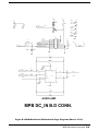
Removing/Replacing the DC-In Board Assembly- - - - - - - - - - - - - - - - - - 6-25
Removng/Replacing the PC Card Module - - - - - - - - - - - - - - - - - - - - - - 6-26
Removing/Replacing the Main Board Assembly - - - - - - - - - - - - - - - - - - 6-27
Removing Touchpad and Speakers - - - - - - - - - - - - - - - - - - - - - - - - - - - 6-28
Removing/Replacing the Display Bezel - - - - - - - - - - - - - - - - - - - - - - - - 6-29
Removing/Replacing the LCD - - - - - - - - - - - - - - - - - - - - - - - - - - - - - - 6-30
Removing/Replacing the Display Inverter Boards - - - - - - - - - - - - - - - - - 6-31
Removing/Repalcing MPB FRUs- - - - - - - - - - - - - - - - - - - - - - - - - - - - - - - - - 6-32
Removing/Replacing the Media Bay Device - - - - - - - - - - - - - - - - - - - - - 6-32
vi Contents
Contents
(continued)
Paragraph
Section 6 Field Service (continued)
Removing/Replacing
Removing/Replacing
Removing/Replacing
Removing/Replacing
Removing/Replacing
Removing/Replacing
the
the
the
the
the
the
MPB Battery - - - - - - - - - MPB Housing- - - - - - - - - Docking Cable - - - - - - - - Docking Mechanism - - - - MPB DC-DC Converter - - MPB Main Board Assembly
Page
-
-
-
-
-
-
-
-
-
-
-
-
-
-
-6-33
-6-34
-6-35
-6-36
-6-37
-6-38
Appendix A Notebook Schematic Diagrams
Introduction - - - - - - - - - - - - - - - - - - - - - - - - - - - - - - - - - - - - - - - - - - - - - - - A-1
Appendix B Notebook Schematic Diagrams
Introduction - - - - - - - - - - - - - - - - - - - - - - - - - - - - - - - - - - - - - - - - - - - - - - - B-1
Appendix A POST BIOS
Introduction - - - - - - - - - - - - - - - - - - - - - - - - - - - - - - - - - - - - - - - - - - - - - - - C-1
Contents vii
1
General Description
1.1 Introduction
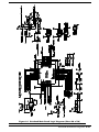
This manual contains field and factory level servicing information for the ExtensaTM 900
Series Notebook Computers (Figure 1-1) marketed by Texas Instruments. This section
provides a general overview of the Extensa 900 Series, describes the standard and
optional features, and identifies the major assemblies and subassemblies. This section
also contains detailed functional and environmental specifications for the Extensa 900
Series Notebook Computers.
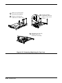
Figure 1-1 Extensa 900 Series Notebook Computers
Basic Extensa 900 Series
Notebook
Extensa 900 Series
with Mobile Productivity Base
1.2 Product Overview
The Extensa 900 Series Notebook Computers are ultra-slim, large screen, highperformance, multimedia notebooks powered by the Intel® P54CSLM Pentium®
Processor Chip (133-MHz). The Extensa 900 can be equipped with an optional Mobile
Productivity Base that allows for quick connect/disconnect to/from the desktop
environment and expanded functionality (modular bay and Advanced PCI card
features).
Other major features of the 900 Series include:
♦ 133 MHz Pentium processor with internal 256 KB cache memory and math
coprocessor
General Description 1-1
♦ Powerful PCI Bus architecture
♦ 16 MB
main memory (expandable to 80 MB using 8 MB, 8 MB, 16 MB, 32 MB
or 64 MB EDO 64-bit type small outline dual inline memory module (soDIMM)
upgrades)
♦ 256 KB Level-2 cache memory
♦ Built-in 2.5-inch IDE high capacity (1.35 GB or greater) Hard Disk Drive
♦ External Floppy Drive Module (attaches to the Parallel Port)
♦ Advanced video features
- DSTN or TFT internal color display
- Simultaneous display with external CRT
- 2.0 MB video memory
- Fast video graphics accelerator
♦ Built-In 86/87-key keyboard
♦ Internal touchpad pointing device with two Select buttons
♦ Fast Infrared communications
♦ Built-in audio features
- 16-bit stereo audio
- Line In, Line Out and Microphone In stereo jacks
♦ Small, lightweight AC adapter, auto-switching (90 VAC to 264 VAC, 50-60 Hz)
♦ Portable power system with advanced power savings features for extra long
battery life
- Zero-Volt Suspend, 5-Volt Suspend and Standby power saving modes
- Rechargeable Li-Ion battery pack
♦ Powerful expansion capabilities including:
- Flexible set of desktop ports including external CRT (and simultaneous
LCD and external CRT display), 9-pin serial port, parallel port for
external printer/floppy drive, PS/2® port for external keyboard or mouse
- PC Card slots for two Type I or II options or one Type III option
- Mobile Productivity Base ready
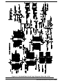
Figure 1-2 identifies the major external notebook features.
1-2 General Description
LCD
Power
Switch
Status
Indicators
Right
Speaker
Right
Battery
Lock
FIR
Port
Audio and
Mic Jacks
Left
Speaker
Touchpad
Battery
Pack
Bottom of Unit
HDD
Access
Cover
Left
Battery
Lock
VGA
Port
Serial
Port
PC
Card
Slots
Parallel
Port
PS/2
Port
Expansion
Memory
Acess
Cover
AC Adapter
Connection
Figure 1-2 900 Series Notebook External Features
1.2.1 Video Display Features
The Extensa 900 Series Notebooks contain large screen internal LCD displays and can
simultaneously drive the internal LCD and an external CRT (SimulSCANTM mode). On
all Extensa models, the LCD screen brightness, contrast, video mode of operation, etc.
are adjustable from the keyboard as described in Section 3.
General Description 1-3
1.2.1.1 Internal LCD
The Extensa 900 Series Notebooks contain one of the following LCDs (model dependent):
♦ 12.1-inch DSTN display (900CD Only)
♦ 11.3-inch TFT
1.2.1.2 External CRTs
The Extensa 900 Series Notebooks are equipped with a 15-pin SVGA connector that
can drive an external CRT (either alone or simultaneously with the internal LCD).
When the notebook is set to the SimulSCAN mode, a minimum resolution of 800 x 600
x 256 colors is supported. When operating in the External CRT Mode, resolutions up
to 1280 x 1024 x 256 colors are supported.
1.2.1.3 Display Hot Key Sequences
The display mode of operation (LCD only, Simultaneous LCD and external CRT and
external CRT only modes) is keyboard-selectable using the following hot key sequences.
♦ Fn-Up Arrow and Fn-Down Arrow - Control LCD screen brightness (higher
brightness setting uses more battery energy)
♦ Fn-Right Arrow
♦ Fn-Left Arrow
- Lightens the LCD screen contrast
- Darkens the LCD screen contrast
♦ Fn-F12 - Alternates between display modes (LCD, External CRT or both)
♦ Fn-F11 - Turns off the LCD backlight; pressing any key turns the LCD backlight
on.
Note: In addition to the hot keys that control the notebook display functions,
there are several other hot key functions that control other notebook functions
such as turning the Touchpad on/off, etc. For these sequences, refer to
Section 3.
1-4 General Description
1.2.2 Keyboard Features
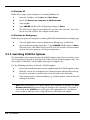
The Extensa 900 Series Notebooks contain a built-in 86/87-key keyboard (Figure 1-3)
compatible with the IBM® enhanced 101/102-key keyboard. The keyboard contains 12
programmable function keys, an embedded numeric keypad (Figure 1-4) and dedicated
control keys (hot keys).
Figure 1-3 Embedded Numeric Keypad
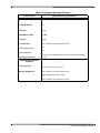
1.2.3 Software Features
As a standard feature, the Extensa 900 notebooks are factory loaded with dual load
(Windows® 95 or Windows for Workgroups) software to allow the user to configure the
notebook’s operating system environment as summarized in Table 1-1.
Table 1-1 User-Selectable Operating System Environments
Operating System
Description
Windows 95
Supports both desktop and mobile operation with Plug N Play capabilities and Advanced Power
Management; customized to include TI startup screen, CSL Support information, Internet
browser, multimedia options, and choice of wallpaper to customize different computer resources,
TI utilities such as wBattery, wSetpower, TISetup, variety of device drivers including Cirrus®
CL-GD7548, ESS 1888 Sound Device Drivers, WinModem Device Drivers, PC-Card Bus Socket
Services and Card Services Device Drivers, and Windows 95 MPEG-1 Software Audio/Video
Compression Device Drivers.
Windows/DOS 6.22
This environment has some limitations in the Plug N Play area; includes TI utilities and various
device drivers including Cirrus CL-GD7548, ESS 1888 Sound Device Drivers, WinModem Device
Drivers, PC-Card Bus Socket Services and Card Services Device Drivers, etc.
General Description 1-5
1.2.4 Standard Peripheral Devices
As standard features, the Extensa notebooks include an internal IDE hard drive, an
external 3.5-inch floppy disk drive and built-in touchpad (mouse device).
1.2.5 900 Series Connectivity Features
As standard features, the Extensa 900 Series notebooks includes most standard
desktop ports including a serial port, parallel port, PS/2 port, and external VGA port.
The 900 Series also includes a fast infrared (FIR) port and an expansion bus connector
for attaching to the optional Mobile Productivity Base. The external ports for the 900
Series are shown in Figure 1-4 and described in Table 1-2.
VGA
Port
Serial
Port
Parallel
Port
PS/2
Port
AC Adapter
Connection
FIR
Port
Line
Out Line
In
Mic
In
Figure 1-4 900 Series External Ports
1-6 General Description
Table 1-2 900 Series External Ports
Port Assignment
Description
External VGA Port
15-pin Female connector used to attach an external SVGA monitor to the
notebook.
Serial Port
9-pin Male connector used to attach an RS-232 serial device to the notebook.
Parallel Port
25-pin Female connector used to attach a bidirectional printer or an external
floppy disk drive (requires special cable for use with floppy disk drive).
PS/2 Port
6-pin Circular connectors used to attach external keyboard/mouse devices to
the notebook.
AC Adapter Connector
Power in connector used to attach the output of the AC adapter to the
notebook.
Fast Infrared Port
Fast Infrared Port (4 M/b) used for wireless communications between the
notebook and an FIR-equipped device such as keyboard, another notebook,
printer, etc.
Audio In/Out, Mic In Jacks
Stereo audio line inputs, stereo line outputs and external microphone input
MPB Bus
PCI Bus plus sidebands that support an optional Mobile Productivity Base.
1.2.6 Notebook Expansion Capabilities
In addition to the external ports, the Extensa 900 Series Notebooks are designed with
a variety of expansion features that permit substantial functionality and performance
upgrades over the life of the product. The expansion capabilities built into the notebook
are summarized in Table 1-3 and described in greater detail in the following paragraphs.
Table 1-3 Extensa 900 Expansion Features Summary
Expansion Feature
Description
External 3.5-inch Diskette Drive Module
Provides convenient storage on a removable diskette format
Memory Expansion Features
Main memory can be expanded from 16 MB to a maximum of 80 MB using
one soDIMM module (8 MB, 16 MB, 32 MB, or 64 MB configurations).
Flash ROM (hardware feature)
Permits new versions of BIOS to be downloaded into Flash ROM without
physically having to replace the ROMs
PCMCIA Slots
Allows installation of any optional PCMCIA device such as speakerphone
modems, Ethernet® cards, and full motion video cards.
Mobile Productivity Base Ready
Connectors and latch mechanisms to accept a Mobile Productivity Base
(provides desktop connectivity with quick removal/installation feature required
for combination desktop and portable environments and increased functionality
including media bay and Advanced PCI Card support).
General Description 1-7
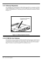
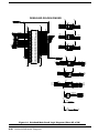
1.2.7 Memory Expansion
The notebook comes standard with 16 MB of RAM expandable to a maximum of 80 MB
using soDIMM modules (available in 8, 16, 32 or 64 MB sizes). Access to the expansion
socket is accommodated via a removable panel on the bottom of the notebook as shown
in Figure 1-5.
Expansion Memory
Access Cover
Figure 1-5 Memory Expansion Features
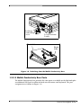
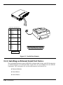
1.2.8 PCMCIA Card Options
The Notebook contains an onboard PCMCIA Controller and two 64-pin sockets that can
accept up to two credit-card size (14.5 mm) Type I or Type II PCMCIA option cards or
one Type III card. The PCMCIA Card options install on the left side of the notebook
(Figure 1-6) and are removed using the PC Card Release levers.
1-8 General Description
Figure 1-6 Installing PCMCIA Card Options
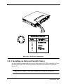
1.2.9 Mobile Productivity Base Option
The Mobile Productivity Base (Figure 1-7) provides a port replicator function with
separate External Keyboard and Mouse ports, plus powerful desktop expansion
features including a Modular Bay for CD-ROM or Floppy Disk Drive and provisions for
an Advanced PCI Card option. These features are summarized in Table 1-4.
Table 1-4 Mobile Productivity Base Expansion Features
Expansion Feature
Description
Media Bay CD-ROM Drive
Reads from Audio CD, Photo CD or CD-ROM
Media Bay 3.5-inch Diskette Drive Module
Provides convenient storage on a removable disk format
Advanced PCI Slot
Provisions for installing one Advanced PCI Card
Secondary Battery Option
Provides for extended portable operation time
General Description 1-9
Notebook
Connector
Secondary Battery
Audio Jacks
Advanced
PCI Option Slot
Media Bay
(Floppy or
CD-ROM Drive)
Two PS/2 Ports
for both External
Keyboard and Mouse
Standard
Notebook
Ports
Figure 1-7 Mobile Productivity Base (MPB) Features
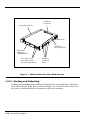
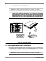
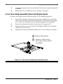
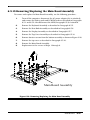
1.2.9.1 Docking and Undocking
Docking and undocking of the Mobile Productivity Base is controlled by a latch and
lever on the left side of the base as shown in Figure 1-8. The latch releases the lever;
the lever is extended 90 degrees outward to release the notebook.
1-10 General Description
Docking/
Undocking
Lever
Lever Release
Latch
Left Side
Right
Side
Figure 1-8 Undocking from the Mobile Productivity Base
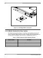
1.2.9.2 Mobile Productivity Base Ports
The Mobile Productivity Base provides the same ports as available on the Notebook plus
an additional PS/2 port to allow for both external mouse and keyboard. The port
assignments are shown in Figure 1-9.
General Description 1-11
Mic
In
Line
In
Line
Out
PS/2
Keyboard
Port
PS/2
Mouse
Port
Serial
Port
VGA
Port
Advanced
PCI
Parallel
Port
Figure 1-9 Mobile Productivity Base Ports
1.2.9.3 Advanced PCI Card Options
The Extensa 900 Series Notebooks contain provisions for an advanced PCI Card as
shown in Figure 1-7.
1.3 Notebook Battery
The notebook computer uses a Lithium-Ion battery pack. A second identical battery
can be installed in the optional Mobile Connectivity Base as shown in Figure 1-7.
1.4 Standard Test Features
The Extensa 900 Series Notebook Computers use modular design and built-in test
features to reduce the mean time to repair. A power on self test program automatically
verifies the operational state of the primary circuits and a powerful suite of diagnostic
tests (known as PC-Doctor) are available to further test selected parts of the system.
1.4.1 Power On Self Test
The Extensa line of notebook computers contain a BIOS-resident, Power On Self Test
(POST) that automatically performs a test of memory and all major circuits each time
1-12 General Description
the computer is powered up. In the event of a failure, the computer displays a descriptive
error message and issues a series of coded beeps (in case the display subsystem is not
functioning). If self test completes normally, the computer displays the amount of
memory tested, loads the Operating System and Windows environment.
1.4.2 PC-Doctor Diagnostics Program
The Extensa 900 Series Notebooks are shipped with PC-Doctor for Windows, a powerful
diagnostics tool that can help you scan a system for viruses, determine the hardware
configuration of a local or remote system, benchmark its performance, analyze the
performance of all subsystems, and perform a suite of interactive and non-interactive
tests on attached devices (such as printers, VGA monitors, SCSI® devices, CD-ROM
drives). The test results are stored in a log which can be printed out (by pressing F2)
or saved in a disk file (by pressing F3).
Features of the diagnostic program are accessed through a series of pull-down menus
and basic keyboard keys (cursor keys to move highlighted pointer, Enter key to select
a highlighted feature, Esc key to cancel a function and move back one level.
PC-Doctor is typically user-friendly but if you don't understand a feature, contextsensitive help information is available at any time by pressing the F1 function key;
pressing the F1 function key twice accesses the online Technical Reference Manual for
PC-Doctor.
A powerful set of utilities within PC-Doctor (that can be run locally or remotely) simplify
the task of determining system configuration data, allocating and using system memory,
IRQ and DMA use, what device drivers are installed, what COM and LPT ports are
assigned and what ports are available, identifying partitioning data for fixed disk
drive(s), determining the VGA setup information, reading the software interrupts/
interrupt vectors, etc.
Note: Refer to Troubleshooting Procedures (Section 5) for additional information
regarding the Diagnostics Program.
General Description 1-13
1.5 Extensa 900 Series Specifications
General specifications for the Extensa 900 Series Notebooks are provided in Table 1-5.
Table 1-5 Extensa 900 Specifications
Characteristic
CPU
Model 900 Series Specifications
Pentium P54CSLM, 133 MHz; 3.1 Volt,
Internal Hard Disk Drive
Disk Storage Capacity:
1.35 GB or greater
Average access time:
12 ms or less
Throughput
11+ Million I/O's per second
DRAM Memory
Size
16 MB DRAM, 60-ns, page-interleaved
80 MB
Maximum Expansion Size
Flash ROM:
256 KB
FDD
External
Disk Storage Capacity:
1.44 MB
Disk Size
3.5-inch disk
Drive Height
12.5 mm
Mode
Choice of 720 KB/1.2 MB or 1.44 MB
CD-ROM Drive
LCD Display
Software
Internal Keyboard
Available with Mobile Productivity Base option
12.1-inch DSTN, SVGA or 11.3-inch TFT, SVGA
Dual Load
86/87-key, PS/2 and AT-compatible
Embedded Numeric Keypad
Key Travel
Built-in Mouse Device
1-14 General Description
3 mm
Touchpad built-in to the base of the keyboard (select buttons on sides
of Touchpad)
Table 1-5 Extensa 900 Specifications
Characteristic
Model 900 Series Specifications
Video Subsystem
LCD Aspect Ratio
1-1
Emulations:
SVGA
Video Memory Size
1.5 MB
Video Bus:
32-bits
LCD Resolution:
640 x 480 pixels bit-mapped at 256 colors
80
LCD Characters/Line
25
LCD Lines/Screen:
LCD Brightness Control:
Function hot key brightness and contrast control and SimulSCAN
control
External CRT Monitor
Interface
Connector Type:
15-Pin, female, D-type connector
Monitors Supported:
640 x 480 with 16.7 million colors on CRT
800 x 600 with 65K colors on CRT
1024 x 768 with up to 256 colors on CRT
General Description 1-15
Table 1-5 Extensa 900 Specifications
Characteristic
RS-232-D Serial Port:
Model 900 Series Specifications
9-Pin, male, sub-D-type connector
Method:
EIA RS-232-D
Type:
Asynchronous transmission
Bits per
second:
110, 200, 300, 600, 1200, 2400, 4800, 9600, 19200
Parity: Transmit:
Odd, even, mark, space
Receive:
Data check: odd, even
Line control:
READY/BUSY, DC1/DC3
Data word:
7- or 8-bit
16550 UART Support
Yes
Selectable Serial Port
(BIOS Setup)
COM1(IRQ4, 3F8h)
COM2(IRQ3, 2F8h)
COM3(IRQ4, 3E8h)
COM4(IRQ4, 2E8h)
Disable
Parallel Port
Connector Type
Fast I/R Port
Transfer Data Rate
Mobile Productivity
Base Ready
1-16 General Description
EPP/ECP Bidirectional
25-Pin, DB-25 Connector
Yes
4 Mb/s
Yes
1.6 Regulatory Agency Approvals
All Extensa 900 Series products meet the following regulatory agency standards:
♦ Underwriter’s Lab (UL) Standard 1950 (safety)
♦ Canadian Standards Association (CSA) Standard 950 or CUL (safety)
♦ FCC CFR 47, Part 15, Subpart B, FCC Level B (Emissions)
♦ Canadian Department of Communications (DOC) ICES, Class B (Emissions)
♦ VDE- EN60950 (Safety)
♦ EN 50082-1 (Immunity: ESD, RFI, EFT, and Surge)
♦ EN 50081-1 (Emissions: RFI, EMI, Harmonics, and Flicker)
♦ Approval Marks: UL, CUL, VDE, FCC, and CE
General Description 1-17
2
Installation
2.1 Introduction
This section contains unpacking and preparation for use instructions for the Extensa
900 Series Notebook Computers. This includes:
♦ Removing the computer and all manuals, options and accessories from the
shipping container(s)
♦ Installing Internal Notebook Options
♦ Installing External Notebook Options
♦ Installing Battery Packs
♦ Installing Desktop Devices
♦ Installing the AC Adapter
♦ Checking Out the System
♦ Installing the System Software
♦ Making Backups of System Software
♦ Loading Application Software
2.2 Unpacking Instructions
Unpack the computer using the following instructions:
1.
Carefully cut the tape that seals the top flap of the shipping carton.
2.
Remove the computer and the accessories carton from the main shipping
carton.
3.
Remove all protective coverings from the computer.
4.
Open the accessory box; remove the contents.
Note: Save the two shipping containers and packaging for later reuse.
Installation 2-1
2.3 Installing Internal Notebook Options
If you have no internal options to install at this time, skip to Paragraph 2.4. Otherwise,
continue with Paragraph 2.3.1.
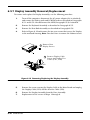
2.3.1 Installing Main Memory Expansion (Optional)
Main memory on the 900 Series Notebooks can be expanded using an EDO Small
Outline Dual Inline Memory Module (EDO soDIMM). These modules are available in
8 MB, 16 MB, 32 MB, and 64 MB sizes and install in the expansion memory slot on
the System Board accessed through the Memory Expansion Door on the bottom of the
notebook. The installation process consists of the following steps:
Caution: The EDO soDIMM module option contains components that are
sensitive to static electricity. When handling the module and the internal
parts of the computer, protect against static electricity by using wrist or
ankle grounding straps and grounded working mats. When moving or
storing items, use the anti-static bags supplied with the items.
1.
Ensure that the notebook is powered off and the AC adapter disconnected
from the AC outlet. Also, ensure that all batteries are out of the unit.
2.
Disconnect any peripheral device interface cables from the external interface
connectors and remove any installed PCMCIA options.
3.
Turn the notebook over and locate the Expansion Memory Access Cover on
the bottom of the notebook.
4.
Remove the screw holding the Expansion Memory Access Cover and remove
the cover.
5.
Remove the EDO soDIMM module from its shipping container.
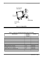
6.
Refer to Figure 2-1. To install an soDIMM module, first align the connector
edge of the memory module with the key in the connector. Insert the edge of
the memory module board into the connector using a rocking motion to fully
insert the module. Push downward on each side of the memory module until
it snaps in place.
7.
Reinstall the Expansion Memory Access Cover using the screw removed in
Step 4.
8.
Replace the batteries and AC adapter.
9.
Power up the notebook. If all of the installed memory is not recognized, try
reseating the soDIMM module and rebooting.
2-2 Installation
Expansion
Memory
Access
Cover
Inserting
soDIMM
Memory
Module
Figure 2-1 Memory Expansion Removal/Replacement
Note: After installing expansion memory in your notebook, you must run the
PHDISK utility in order for the Save-To-Disk or 0V Suspend functions to operate
correctly.
2.3.2 Setting up the Software
Note: If you are using an operating system other than Windows 95, Windows for
Workgroups, or DOS, you may need to re-partition your hard disk drive to allow
for the additional memory. Check with your system administrator.
Installation 2-3
In Windows 95
Follow these steps if your computer is running Windows 95.
1.
From the Taskbar, select Start then Shut Down.
2.
Select the Restart the Computer in MS-DOS mode.
3.
Click on Yes.
4.
Type PHDISK /C /F at the DOS prompt and press Enter.
5.
The DOS screen appears and shows the save file name and size. Press any
key to reset the system. The computer will reboot.
In Windows for Workgroups
Follow these steps if your computer is running MS-DOS® and Windows for Workgroups.
1.
Close all applications and exit Windows for Workgroups to MS-DOS.
2.
At the command prompt (typically C:\) type PHDISK /C /F and press Enter.
This will create a file which can be used to save the contents of your memory
system when you perform a 0V Suspend operation.
2.3.3 Installing PCMCIA Options
The Notebook has two connector slots for PCMCIA option cards. These two slots can be
used to install one Type III or two Type I/II credit card size PCMCIA option cards. You
can install a PCMCIA (PC card) without turning the computer off.
Use the following procedure to install a PCMCIA option:
1.
Review the installation instructions supplied with the PCMCIA option card(s).
2.
Hold the card at the end opposite the connector pins with the label side up.
Insert the card into an unused slot on the left side of the Notebook.
3.
If the option requires external cabling (e.g., modem option), connect external
cabling at this time.
Note: After installation of a PCMCIA option card, Windows 95 displays the New
Hardware Found dialog box to help you configure the new device. To remove a
card, click on the PCMCIA icon; then, press the appropriate PC Card Release
lever (or press both levers for a Type III device) and remove the option.
2-4 Installation
Figure 2-2 Installing PCMCIA Option Cards
Note: When installing a Zoomed Video option card, the card must be installed in
the lower card slot (slot 0 or A). Other option cards can be installed in either card
slot.
2.4 Installing External Notebook Options
2.4.1 Installing the Mobile Productivity Base (Option)
If using the Mobile Productivity Base option, install this accessory now. If not using
the MPB at this time, proceed directly to Paragraph 2.4.2.
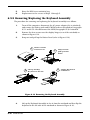
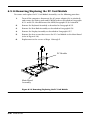
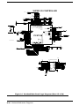
2.4.1.1 Docking the Notebook to the MPB
To dock the Notebook Computer into the MPB, use the following procedure:
1.
Turn the notebook over and open the expansion door (slide the door toward
the center of the notebook) to expose the docking connector.
2.
Slide the lever release latch to the front of the MPB to release the docking
lever (refer to Figure 2-3).
Installation 2-5
3.
Swing the Docking Lever outward a full 90 degrees from the side of the MPB.
4.
Slide the notebook into the MPB, right side first, as shown in Figure 2-3.
Ensure that the docking guides on both the notebook and the MPB are
securely hooked.
5.
Rest the notebook on the MPB. Then press and hold the notebook against
the MPB and swing the Docking Latch inward until the Lever Release Latch
locks.
1
3
Open the expansion door
on bottom of notebook
2
Slide notebook into MPB,
right side first; ensure
docking guides are hooked
4
Slide release latch on MPB
forward; swing the docking
level outward 90 degrees
Press and hold down
notebook and swing the dock
lever in until the release latch
locks
Figure 2-3 Docking the Notebook into the MPB
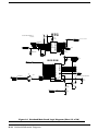
2.4.1.2 Cabling to the MPB
Refer to Figure 2-4 (MPB Port Assignments) and then connect all desktop devices to the
MPB instead of directly to the notebook as described in Paragraphs 2.4.2 through 2.4.5.
2-6 Installation
Mic
In
Line
In
Line
Out
PS/2
Keyboard
Port
PS/2
Mouse
Port
Serial
Port
VGA
Port
Advanced
PCI
Parallel
Port
Figure 2-4 MPB Port Assignments
Installation 2-7
Battery Pack
Figure 2-5 MPB Battery Pack Removal/Installation Installation
2.4.2 Installing Ext. Keyboard/Mouse/Numeric Keypad
A PS/2 compatible Keyboard, mouse or an optional PS/2-compatible numeric keypad
may be installed on the notebook via the mouse connector on the left rear port as shown
in Figure 2-6.
Note: Refer to Figure 2-4 for port assignments if using the MPB option.
2-8 Installation
Figure 2-6 PS/2 Port Connections
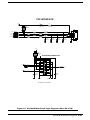
2.4.3 Installing an External Parallel Printer
The Notebook is equipped with an external, bidirectional, ECC/EPP compatible, 25-pin
parallel printer port. The connector pinouts and connector location are shown in
Figure 2-7.
Note: Refer to Figure 2-4 for port assignments if using the MPB option.
Installation 2-9
PARALLEL PORT PINOUTS
SIGNAL
1
2
3
4
5
6
7
8
9
10
11
12
13
14
15
16
17
18
19
20
21
22
23
24
25
26
Strobe*
Data Bit 0
Data Bit 1
Data Bit 2
Data Bit 3
Data Bit 4
Data Bit 5
Data Bit 6
Data Bit 7
Acknowledge*
Busy
Paper Out
Select
Auto Line Feed*
Error*
Initialize Printer*
Select In*
LPT 18
VCC
PLP120
PLP121
PLP122
FDD 5V
FDD 5V
LP125
Ground
SPP Mode
STB*
PD0
PD1
PD2
PD3
PD4
PD5
PD6
PD7
ACK*
BUSY
PE
SLCT
AFD*
ERR*
INIT*
SLIN*
LPT18
VCC
PLP120
PLP121
PLP122
FDD 5V
FDD 5V
LP125
Ground
Note: * Denotes
Active Low
Figure 2-7 Parallel Port Pinouts
2.4.4 Installing an External Serial Port Device
The notebook contains an external RS-232 serial port with a 9-pin, male DB-9 connector
as shown in Figure 2-10 (25-pin cables require the use of an adapter for use with the
9-pin port). The serial ports are used to interconnect such devices as:
♦ External Modem
♦ Serial Mouse
♦ Serial Printer
2-10 Installation
♦ Any device that uses an RS-232 interface
Note: Refer to Figure 2-4 for port assignments if using the MPB option.
Caution: Never connect a parallel device to a serial port or a serial device
to a parallel port or video port; this may cause damage to the notebook
and/or external device. If you are uncertain of what type connector the
external device has, refer to the technical manual for the external device.
Figure 2-8 Serial Port Pinouts
2.4.5 Installing an External VGA Monitor
The notebook (and optional MPB) contain an external CRT port that can drive one of
a variety of monitor resolutions and colors as summarized in Section 1. The associated
connector location and pinouts for the notebook are shown in Figure 2-9.
Note: Refer to Figure 2-4 for port assignments if using the MPB option.
Installation 2-11
Figure 2-9 External VGA Pinouts
Use the following procedure to install an external monitor:
1.
Turn off power to both the notebook and monitor.
2.
Connect the 15-pin external VGA cable from the monitor to the VGA connector
on the notebook computer (Figure 2-9) or MPB (Figure 2-4).
3.
Power up the notebook computer first; then, turn on power to the monitor.
4.
Setup the notebook display mode for LCD only, simultaneous LCD and CRT
or CRT only (under Windows 95, select the Change Display Utility; under
2-12 Installation
Windows for Workgroups, use the WinMode Utility).
5.
Install the correct driver, if required (refer to the Monitor Installation
Instructions supplied by the CRT vendor).
2.5 Primary Battery Pack Installation
1.
Turn off the computer and disconnect the AC adapter if attached to the
computer.
2.
Unlatch the end locks by pushing the endcaps outward with your thumbs.
3.
Align battery connector to connector on notebook and insert the battery pack
into the battery compartment; then push the battery in completely until you
feel the contacts engage.
4.
Relatch the battery locks on both ends of the battery.
Unlock Battery Pack
Remove Battery
from Front of Notebook
Flush
If Battery Lock comes off,
reinstall as shown
Slide
Figure 2-10 Notebook Battery Removal/Replacement
2.6 Installing the AC Power Adapter
Use the following procedures to connect the AC adapter to the system:
Caution: Use only the AC adapter supplied with the computer; other
adapters can damage the unit.
Installation 2-13
1.
Remove the AC adapter from the packaging. Connect the round coaxial
connector supplied with the notebook to the DC IN power receptacle on the
left rear of the notebook as shown in Figure 2-9.
2.
Connect the female side of the AC power cord to the AC adapter and connect
the male end to a grounded AC outlet.
DC-IN Connector
AC Adapter
Figure 2-11 Installing the AC Adapter
2.7 Initial Software Load
After unpacking and setting up the notebook for the first time, you must perform an
initial software load that takes approximately 30 minutes.
Because of the way Windows 95 structures its files, stopping in the middle of the setup
process can cause irreversible file damage.
2-14 Installation
Before starting the initial software load process, ensure that you have the following:
♦ Extensa 900 User’s Guide - Contains latest software installation instructions.
♦ AC Adapter/Access to AC power - Although the battery pack may have some
charge, it may be insufficient for the entire set up. Loss of power during setup
can cause irreversible file damage.
♦ Certificate of Authenticity - You will need to enter the number from your
Windows 95 Certificate of Authenticity during Windows 95 Setup. This
certificate is part of the Windows 95 documentation kit. You need this number
even if you are installing Windows for Workgroups.
♦ Language - During initial setup you choose the following:
- Language for Windows displays
- Language for keyboard installed
♦ Printer type - As part of the Windows setup, you are prompted to choose a
printer. Microsoft® includes the files for many different printers. If you cannot
find your printer in the list, you will need the floppy disk with the printer driver
provided by the printer manufacturer. If you do not want to install a printer at
this time, you can skip this part of the setup. Which operating system to load
♦ Operating System Type - During initial setup you must choose which
operating system to load, either Windows 95 or MS-DOS and Windows for
Workgroups (DOS+WFW). This choice is final. You will not be able to change the
operating system after installation is complete. For most users Windows 95 is
the better choice. You might want to load DOS+WFW under the following
circumstances.
- Your corporation or workgroup may have guidelines that require use of
DOS+WFW. Check with your manager to determine the policy at your
company.
- The software that controls your local area network may not be compatible
with Windows 95. Check with your network administrator to determine
whether Windows 95 is compatible.
- Although most software that is compatible with DOS+WFW is also
compatible with Windows 95, it is possible that the existing software you
are using will not run in Windows 95. If you have a critical software
application that you intend to copy to your new computer, check with
the manufacturer of the software to determine whether your application
is compatible with Windows 95.
2-15 Installation
3
Operating Instructions
3.1 Introduction
This section contains a summary of notebook operating procedures useful for
maintenance operations. For additional detail, refer to the Extensa 900 Series Notebook
Computer User’s Guide supplied with the notebook.
3.2 Controls/Indicators
The operating controls and indicators for the 900 Series Notebooks are shown in Figure
3-1 and briefly described in the following paragraphs.
Disk Media
Battery Charging
Standby Mode
Pwr/Batt Low
Caps Lock
Num Lock
Power
Switch
Figure 3-1 Operating Controls and Indicators
Operating Instructions 3-1
3.2.1 Power On/Off Switch
The notebook contains an alternate action power switch located center of the notebook
near the status indicators as shown in Figure 3-1. The first time you press the power
switch, power is turned on to the notebook. The next time you press the power switch,
power is turned off.
3.2.2 Notebook LEDs
The notebook contains the following LED Indicators:
♦ Disk Media Indicator
♦ Battery Charging Indicator
♦ Standby Mode Indicator
♦ Power On/ Battery Low (Blinking) Indicator
♦ Caps Lock Indicator
♦ Num Lock Indicator
3.2.3 LED Icons
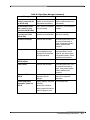
Table 3-1 contains a listing and description of Extensa LED Icons:
Table 3-1 LED Icon Descriptions
Icon
Description
Disk Media Indicator
Lights when the computer writes to or reads from the floppy disk drive,
or reads from the CD-ROM drive.
Battery Charging Indicator
Lights when a powered AC adapter connected to the computer is
charging the battery.
Flashes when there is a problem with the battery or the battery is not
recognized by the smart charger.
Turns off when there is no battery or the battery is fully charged.
3-2 Operating Instructions
Table 3-1 LED Icon Descriptions
Icon
Description
Standby Mode Indicator
Lights when the computer is in Standby mode. Flashes when the
computer is in the 5V Suspend mode.
The computer enters Standby Mode if the Standby hot key (Fn+F4) is
pressed or the Standby Timeout parameter in Setup is enabled and
expires.
The computer enters 5V Suspend Mode if the Suspend hot key
(Fn+F3) is pressed or the 5V Suspend Timeout parameter in Setup
is enabled and expires or the display is closed.
Power/Battery-low Indicator
Lights when the computer is on and there is power to the computer.
Flashes when the battery power is low. Connect a powered AC
adapter to the computer as soon as possible.
Caps Lock Indicator
Lights when the caps lock function is toggled ON using the Caps Lock
Key.
Num Lock Indicator
A
Lights when the embedded numeric keypad is toggled ON using the
Num Lock hot key (Fn+F7). Refer to Using the Internal Numeric
Keypad section in the Extensa 900 Series User’s Guide for further
details.
3.2.4 Keyboard Hot Key Sequences
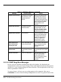
Table 3-2 contains a summary of keyboard hot key sequences useful when performing
maintenance operations.
Table 3-2 Summary of Notebook Hot Key Sequences
Function
Key Sequence
CMOS Setup
Fn+F1
Enter 0V Suspend Mode
Fn+F2
5 Volt Suspend
Fn+F3
Enter Standby Mode
Fn+F4
Resume from Standby Mode
Press any key
Scroll Lock
Fn+F6
Numeric Lock
Fn+F7
Turn off the LCD backlight
Fn+F11
Turn on the LCD backlight
Press any key
Operating Instructions 3-3
Table 3-2 Summary of Notebook Hot Key Sequences
Function
Key Sequence
Alternate between display modes (LCD, Ext.l CRT or both)
Fn+F12
Decrease LCD screen brightness
Fn+Down Arrow
Increase LCD screen brightness
Fn+Up Arrow
Lighten LCD screen contrast
Fn+Right Arrow
Darken the LCD screen contrast
Fn+Left Arrow
Exit 0V Suspend Mode
Press Power switch
Toggle speaker output on/off
Fn+End
Stop a command or application
Ctrl+Pause
Resume a command or application
Press any key
Send the contents of the screen to the printer
Shift+PrtSc
Sets the notebook to echo keystrokes to the printer; prints a line when
you press Enter; continues until you press Ctrl+P
Ctrl+P
Enable/disable the internal keypad
Fn+T
Warm boot
Ctrl+Alt+Del
Start
Windows logo key
Display the application’s context menu
Application key
Table 3-3 Hot Keys Available on Attached External keyboard
Function
Key Sequence
System Setup
Ctrl+Alt+F1
0V Suspend
Ctrl+Alt+F2
5V Suspend
Ctrl+Alt+F3
LCD/CRT Toggle
Ctrl+Alt+F12
Speaker Toggle
Ctrl+Alt+S
3-4 Operating Instructions
3.2.4.1 Windows 95 Special Keys
Pressing the Windows Logo Key acts as the Start button. Pressing this key in
combination with other keys performs special functions. Table 3-4 contains several
examples of using the Windows 95 special keys.
Table 3-4 Windows 95 Special Keys
Hot Key
Function
Windows Logo Key+Tab
Activates next Taskbar button
Windows Logo Key+E
Explore my Computer
Windows Logo Key+F
Find Document
Windows Logo Key+M
Minimize All
Windows Logo Key+R
Display Run dialog box
Pressing the Application Key displays the context menu for an application. This is the
same as clicking the secondary (right) mouse button.
Please refer to your Windows 95 manual for more information on these Windows 95specific keys and their functions.
3.2.4.2 DOS Special Keys
Table 3-5 contains a list of the DOS special keys.
Table 3-5 DOS Special Keys
Hot Key
Function
Ctrl+Pause
Stops a command or application; primarily used
to stop the screen from scrolling; pressing any
other key resumes the execution of the command
or application.
Shift+Prt Sc
Sends the contents of the screen to the printer
port; prints only text characters unless you have
run the Graphics.com utility to enable printing
graphics.
Ctrl+Break
Terminates the current command or application.
Ctrl+P
Sets the computer to echo keystrokes to the
printer; prints a line when you press Enter;
continues until you press Ctrl-P again.
Ctrl+Alt+Del
Terminates all programs, reloads MS-DOS and
executes the Autoexec file; also called the “warm
start” or “warm boot”.
Operating Instructions 3-5
3.3 Configuring the Touchpad
You can personalize the control of the touchpad by configuring various settings using
the Synaptics® Touchpad utility. Configure the touchpad using the Mouse utility located
in the Control Panel Window. Follow these steps to configure the Touchpad:
In Windows 95
1.
Select the Start button, then select Settings.
2.
Select Control Panel to display the Control Panel window.
3.
Double-click on the Synaptics Touchpad icon.
4.
Select the touchpad tab to customize the touchpad to your preference.
5.
Click on Enhancements to bring up additional features and to get to the
online help for the Synaptics Touchpad drivers.
In Windows for Workgroups
1.
From the Program Manager double-click on the Main program group.
2.
Double-click on the Control Panel icon.
3.
Double-click on the Synaptics Touchpad icon.
4.
Select the touchpad tab to customize the touchpad to your preference.
5.
Click on Help for the Synaptics Touchpad drivers online documentation.
3.4 Using a CD-ROM Drive (MPB Option Only)
An optional CD-ROM drive installed in the modular bay of a docked Mobile Productivity
Base option provides fast access to text, programs, graphics, sound, animation and
video on a standard CD. (With an optional MPEG PC Card installed, you can play back
approximately 75 minutes of MPEG1-compressed, full-motion video from a CD.)
3.4.1 Inserting a CD (MPB Option Only)
1.
With the system powered up, press the eject button on the front of the
CD-ROM drive to eject the disc tray.
2.
Slide out the disc tray.
3.
Place the CD, label side up, in the depression on the disc tray.
4.
Slide the disc tray into the drive.
3.4.2 Handling CDs (MPB Option Only)
Follow these guidelines to avoid damaging your CDs:
♦ When removing a CD from its protective case or loading a CD into a drive, hold
the CD by its central hole and outer edge. Never touch the data surface (nonlabel side).
3-6 Operating Instructions
♦ To protect the CD against scratches and dirt when not in use, keep the CD in
its protective case.
♦ Clean a CD with a clean, dry, lint-free cloth.
Always wipe from the center to
the edge. Don’t wipe the CD in a clockwise or counterclockwise direction.
♦ Keep CDs away from high temperatures and direct sunlight.
3.5 Built-In Sound System
The Extensa 900 Series Notebook comes with an internal microphone and stereo
speakers. These features give direct sound generation and recording capability in the
system.
3.5.1 Turning Sound On/Off
To mute or restore sound, press the following keys:
♦
Fn+PgUp:
Turns mute On/Off
3.5.2 Sound Software
The computer has pre-installed sound support utilities in the AudioRack32 group.
These include:
♦ AudioRack™32
♦ Audio Recorder
Operating Instructions 3-7
3.5.3 External Sound Equipment
You can improve the quality of sound production and increase convenience by
connecting external sound equipment.
The computer has the following jacks for connecting to external sound equipment:
♦ Microphone Input
♦ Stereo Headphone/Speaker Line Output
♦ Stereo Line Input
3.6 Using Remote Connections
The computer can send and receive e-mail, surf the Internet, connect to one of the
online services or share files with other office employees.
The Extensa communicates with the outside world in one of the following ways:
♦ Over a telephone line using a PC Card modem installed in the computer
♦ Over a network using a network adapter
Note: You can purchase compatible modems and network adapters from your
dealer or directly from Texas Instruments.
3.6.1 Using the Fast Infrared (FIR) Port
The FIR port, located on the rear of the computer, offers wireless communication with
other Texas Instruments notebook computers or a variety of IRDA™-compliant devices.
Without a physical connection, you can print remotely, transfer files between
computers, use a remote mouse during a presentation or receive information from a
PDA or pocket organizer. To transfer a file follow these steps:
Align the FIR ports of the two devices making sure that the distance separating them
is between six inches and three feet (one meter).
After the devices are aligned, use the TranXit™ software, located in the TranXit group,
to complete the communication process. (For further information, refer to the online
TranXit Quick Reference Guide.)
3-8 Operating Instructions
3.7 Using Zoomed Video Features
Your computer supports Zoomed Video (ZV) PC Cards through the PC Card slots. ZV
PC Cards connect to the internal ZV port, allowing advanced multimedia capabilities
such as video conferencing and on-screen television at full, smooth motion. The Zoomed
Video port adds a dedicated video bus that provides a direct link between a PC Card
and the VGA accelerator or audio DAC. This “detour” lets video and audio data bypass
the PCI bus, reducing bandwidth impositions and improving system performance for
more fluid audio and video.
3.7.1 MPEG PC Card
The optional MPEG PC Card uses the Zoomed Video port built into the computer to
display MPEG video and audio on the computer. The MPEG card features MPEG-1
video playback with 16.7 million colors, MPEG-1 audio layers I and II, is MPC3
compliant and Windows 95 Plug and Play. With this option you can run full-motion
video, combined with digital audio, graphics, text and data, enabling you to create far
more effective presentations or play the most advanced video games.
3.8 Battery Saving Tips
There are a number of actions you can take to reduce the rate at which your computer
depletes the battery. By taking some or all of these actions, you can substantially
increase the time you can operate on battery power before recharging the battery:
♦ Reducing screen brightness — Although the screen controller uses new
technology to increase brightness without increasing energy consumption, the
screen is still the largest single consumer of the battery charge. Reducing the
brightness to the lowest acceptable level increases battery life. To reduce the
brightness, press Fn+↓.
♦ Caching the hard disk drive -— By caching the hard disk drive, you can reduce
the length of time the hard disk drive is rotating and using energy. Both
Windows 95 and Windows for Workgroups use a disk-caching program by
default. As long as you have not disabled these programs, you can take
advantage of the battery savings.
3.8.1 Lowering Inactivity Timeouts
Inactivity timeouts turn off devices in the computer when you are not using them.
Lowering the inactivity timeouts shortens the period of time the computer waits before
turning off the device.
Operating Instructions 3-9
3.8.2 Suspending Operation While Idle
Although the computer goes into Suspend mode automatically after a defined period of
inactivity, you can reduce energy consumption even further by pressing either Fn+F3
(Suspend) or Fn+F4 (Standby) as soon as you no longer need the computer to be active.
♦ Pressing Fn+F4 (Standby) turns off the screen.
♦ Pressing Fn+F3 (Suspend) turns off the screen, stops the hard disk drive, and
reduces energy usage to the lowest level possible without turning off the
computer.
♦ Pressing the Shift key resumes activity after the notebook has been in either
the Suspend or Standby modes.
3.8.3 Responding to a Low Battery Condition
When you are operating the computer on battery power and the charge remaining is
down to between 10% and 20%, the battery-low indicator blinks and an audible alarm
sounds. When this happens you should take the following actions to conserve battery
power and reduce the possibility of data loss.
♦
♦
♦
♦
♦
Saving files — Save all open files frequently while the computer is in a
low-battery condition.
Turning off the alarm — Turn off the audible alarm by pressing Fn+End
(Mute).
Reducing screen brightness — Reduce screen brightness by pressing Fn+↓.
Connecting the AC adapter — If you have access to AC power, connect the
computer to the AC adapter. You can do this without turning off the computer.
Suspending operations — Press Fn+F3 or Fn+F4 to put the computer into
Suspend or Standby mode whenever you are not actively using the computer.
Press the Shift key to bring the computer out of Suspend or Standby mode.
3-10 Operating Instructions
3.8.4 Replacing the battery
If you have a spare, charged battery, you can do one of the following.
♦ Insert a secondary battery into the MPB option (if installed).
♦ If you already have a battery in a docked MPB, you can replace the primary
battery without turning off the computer.
♦ If you cannot insert the spare battery, suspend operations to disk by pressing
Fn+F2 and replace the battery. When you turn on the computer, the computer
returns to the saved state.
3.8.5 Saving to Disk
When the battery power becomes critically low (less than 5% charge remaining), the
computer saves the current state of the computer to disk and turns off. When you turn
the computer on again, the computer restores the state that was saved to disk.
Operating Instructions 3-11
4
Theory of Operation
4.1 Introduction
This section contains a general block diagram theory of operation description of the
Extensa 900 Series Notebook Computers.
Note: Various internal components may change on future models and
busses/bus speeds are subject to change.
4.2 Notebook Functional Overview
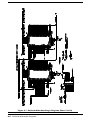
The Extensa 900 Series Notebooks consist of eight major functions or sections
including:
♦ System Processor — implemented on the Main Board Assembly
♦ Memory Subsystem — implemented on the Main Board Assembly
♦ I/O Subsystem — implemented on the Main Board Board
♦ Keyboard Subsystem — implemented on the Main Board Assembly and the
Keyboard Assembly
♦ Video Subsystem — implemented on the Main Board and LCD Display Panel
assemblies
♦ Sound Subsystem — implemented on the Main Board Assembly
♦ Touchpad Mouse Subsystem — implemented on the Touchpad assembly and
on the Main Board Assembly
♦ Hard Disk Drive Subsystem — implemented on the Main
Board Assembly and
the Hard Disk Drive Assembly
♦ Floppy Disk Drive Subsystem — implemented on the Main Board Board and
Floppy Disk Drive Assembly
♦ PCMCIA Controller and Sockets — implemented on the PCMCIA Module and
on the Main Board
♦ Power Subsystem — implemented on the Main Board, the battery pack, and
the AC adapter
Theory of Operation 4-1
586
CPU
CPU Bus
SRAM
M1521
DRAM
BGA
PCI Bus
IDE Master
CD
M1523
HDD
ISA Bus
Figure 4-1 Extensa Functional Block Diagram
4-2 Theory of Operation
MPB
Graphic
controller
4.2.1 System Processor
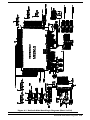
The System Processor function for the notebook is implemented on the Main Board in
the form of an Intel Pentium P54-C Superscalar 586 Processor Chip. The processor
operates in conjunction with RAM and ROM Memory and other control logic to process
software instructions (BIOS, DOS, Windows, and applications). The processor
communicates with the hard disk drive and the memory components using high speed
busses.
The Processor also interacts with other hardware logic to provide the power savings
features for the notebook. These features include controlling CPU clock speeds,
reducing clock speeds whenever possible, e.g., when performing floppy disk drive
accesses, powering down unused devices, etc. A detailed block diagram of the Extensa
900 Series Notebook is shown in Figure 4-2.
The IRQ assignments for the 900 Series Notebooks is provided in Table 4-1.
Table 4-1 Interrupt Channel map
Priority
1
2
3
4
5
6
7
8
9
10
11
12
13
14
15
16
17
Interrupt Number
SMI
NMI
IRQ 0
IRQ 1
IRQ 2
IRQ 8
IRQ 9
IRQ 10
IRQ 11
IRQ 12
IRQ 13
IRQ 14
IRQ 15
IRQ 3
IRQ 4
IRQ 5
IRQ 6
IRQ 7
Interrupt Source
Power management unit
Parity error detected, I/O channel error
Interval timer, counter 0 output
Keyboard
Interrupt from controller 2 (cascade)
Real-time clock
Cascaded to INT 0AH (IRQ 2)
Audio (option) / PCMCIA
Audio (option) / PCMCIA
PS/2 mouse
INT from coprocessor
Hard disk controller
CD-ROM controller
Serial port 2, 4
Serial port 1, 3
Parallel port 1 / audio (option)
Diskette controller
Parallel port 2 / audio (option)
NOTE: A PCMCIA card can use IRQ 3, 4, 5, 7, 9 and 11 as long as
it does not conflict with the interrupt address of any other device.
Theory of Operation 4-3
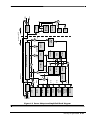
Figure 4-2 Detailed System Block Diagram
4-4 Theory of Operation
M1523
SD(15:0)
INTERNAL
KB
PS2
M38813
SA2
PCMCIA
SA(11:0)
SD(15:0)
ESS1878S
SD(15:0)
ISA BUS
BIOS
AD(31:0)
TOUCH
PAD
CRT
16MB
RAM
DIMM*1
PARALLEL
PORT
SERIAL
PORT
SA(9:0)
LCD
87338
65550/S3
AD(31:0)
$MA(11:0)
$MD(63:0)
SA(9:0) SD(15:0)
M6377
SD(15:0)
UV(7:0)
Y(7:0)
VIDEO
RAM
HOST BUS
$CPU_A(17:3)
L2 CACHE
$CPU_D(63:0)
PCI1130
$CPU_A(31:3)
AD(31:0)
SA(16:0),LA(23:17)
PCI BUS
CPU
$CPU_D(63:0)
$CPU_A(31:3)
$CPU_D(63:0)
FIR
RDATA#,WDATA#
HDD
PCI0643
AD(31:0)
AD(31:0)
M1521
Notebook
FDD
CD-ROM
PCI0643
AD(31:0)
SERIAL
PORT
AD(31:0)
Advanced
PCI Card
PARALLEL
PORT
MEDIA BAY
Y(7:0)
UV(7:0)
MPB
4.2.2 Memory Subsystem
The memory subsystem comprises the following components:
♦ Main memory
♦ L2 Secondary Memory (cache)
♦ Flash ROM
The Extensa Series uses fast Extended Data Out (EDO) DRAM for main and video
memory and high-speed synchronous, pipelined burst SRAM for L2 cache memory.
Main BIOS and Video BIOS are stored in Flash ROM.
The Extensa 900 Series Memory Address Map is shown in Table 4-2.
Table 4-2 Memory Address Map
Address Range
Definition
Function
000000 - 09FFFF
640 KB memory
Base memory
0A0000 - 0BFFFF
128 KB video RAM
Reserved for graphics display buffer
0C0000 - 0CBFFF
Video BIOS
Video BIOS
0E0000 - 0EFFFF
0F0000 - 0FFFFF
128 KB system BIOS
System BIOS
System BIOS
100000 - FFFFFF
Extended memory
Onboard memory
FE0000 - FFFFFF
256 KB system ROM
Duplicate of code assignment at 0E0000-0FFFFF
The DMA Channel Map is listed in Table 4-3.
Table 4-3 DMA Channel Map
Controller
Channel
Address
Function
1
1
1
1
2
2
2
2
0
1
2
3
4
5
6
7
0087
0083
0081
0082
Cascade
008B
0089
008A
Audio (option)
ECP/FIR/Audio
Diskette
ECP/FIR/Audio
Cascade
Spare
Spare
Spare
4.2.2.1 Main Memory
The standard 900 Series notebook comes with 16 MB of Main memory installed on the
Main Board. Memory expansion accommodations are provided via a standard soDIMM
connector on the bottom of the Main Board Assembly. By installing a 64 MB soDIMM
module, the basic memory size can be expanded to a maximum of 80 MB.
Theory of Operation 4-5
4.2.2.2 Flash ROM
All versions of the Extensa notebook family use a "Flash" ROM that contains both the
main system BIOS and the VGA BIOS. The Flash ROM contains "Boot Block" logic that
allows downloading new versions of BIOS without destroying the Boot Load area.
The Flash ROM execution is 8 bits wide. However, better performance can be attained
by enabling the Shadow ROM in the CMOS setup routine or by selecting the Windows
Control Panel Applet. When the Shadow ROM is enabled, BIOS is copied into a 32-bit,
high-speed system.
4.2.3 System Controller Function
The Extensa 900 Series notebook design uses two chips, the ALI M1521 (memory, Cache
and DRAM Controller for the Pentium System and the M1523 (PCI to ISA Bridge chip)
combine to provide the 586 system controller function for the new multimedia/
multithreading operating system, Windows 95.
The notebook utilizes the BGA package to improve the AC characterization, resolves
system bottleneck and make the system manufacturing easier. The system architecture
includes the UMA, ECC, PBSRAM, SDRAM/BEDO, and multi-bus with highly efficient,
deep FIFO between the buses, such as the HOST/PCI/ISA dedicated IDE bus.
The I/O Address Map for the 900 Series Notebook is provided in Table 4-4.
4-6 Theory of Operation
Table 4-4 I/O Address Map
Address Range
000 - 00F
020 - 021
022 - 023
040 - 043
048 - 04B
060 - 06E
070 - 071
080 - 08F
0A0 - 0A1
0C0 - 0DF
178 - 17A
1F0 - 1F7
170 - 177
3F6, 3F7
220 - 22F
240 - 24F
260 - 26F
280 - 28F
278 - 27F
2E8 - 2EF
2F8 - 2FF
378 - 37A
3B4, 3B5, 3BA
3C0 - 3C5
3C6 - 3C9
3C0 - 3CF
3D0 - 3DF
3E0 - 3E1
3E8 - 3EF
3F0 - 3F7
3F8 - 3FF
CF8 - CFF
Device
DMA controller-1
Interrupt controller-1
M1523 registers
Timer 1
Timer 2
Keyboard controller
Real-time clock and NMI mask
DMA page register
Interrupt controller-2
DMA controller-2
6377 registers
Hard disk select
CD-ROM
Audio (option)
Audio (option) - default
Audio (option)
Audio (option)
Parallel port 1
COM 4
COM 2
Parallel port 2
Video subsystem
Video DAC
Enhanced graphics display
Color graphics adapter
PCMCIA controller
COM3
Floppy disk controller
COM 1
PCI configuration register
Theory of Operation 4-7
4.2.3.1 ALI M1521 (Memory, Cache and DRAM Controller)
The M1521 provides the system controller and data path components for the Extensa
900 Pentium-based system. It provides 64-bit CPU bus interface, 32-bit PCI bus
interface, 64/72 DRAM data bus with ECC or parity, secondary cache interface
including pipeline burst SRAM or asynchronous SRAM, PCI master to DRAM interface,
four PCI master arbiters, and a UMA arbiter. The M1521 bus interfaces are designed
to interface with 3V and 5V buses. It directly connects to 3V CPU bus, 3V or 5V tag,
3V or 5V DRAM bus, and 5V PCI bus.
4.2.3.1.1 Features of the ALI M1521
♦ Supports all Intel/Cyrix®/AMD 586-class processors (with host bus of 66 MHz,
60 MHz and 50 MHz at 3V)
♦ Supports M1/K5/Dakota™ CPUs
♦ Supports linear wrap mode for M1
♦ Supports asynchronous/pipeline-burst SRAM
♦ Write-back/dynamic write-back cache policy
♦ Built-in 8K* 2-bit SRAM for MESI protocol to cost and enhance performance
♦ Cacheable memory up to 512 MB with 11-bit tag SRAM
♦ Supports 3V/5V SRAMs for tag address
♦ Supports FPM/EDO/BEDO/SDRAM DRAMs
♦ RAS lines
♦ 64-bit data path to memory
♦ Symmetrical/asymmetrical DRAMs
♦ 3V or 5V DRAMs
♦ Duplicated MA[1:0] driving pins for burst access
♦ No buffer needed for RASJ and CASJ and MA[1:0]
♦ CBR and RAS-only refresh
♦ Supports 64M-bit (16M* 4, 8M* 8, 4M*16) technology DRAMs
♦ Supports programmable-strength MA buffer
♦ Supports error checking and correction (ECC) and parity for DRAM
4-8 Theory of Operation
♦ Supports the most flexible six 32-bit populated banks of DRAM (to spare
12 MB for Windows 95)
♦ Supports SIMM and DIMM
♦ UMA (unified memory architecture)
♦ Dedicated UMA arbiter pins
♦ Supports several protocols from major graphics vendors
♦ SFB size : 512 KB/1 MB/2 MB/3 MB/4 MB
♦ CPU could access frame buffer memory through system memory controller
♦ Alias address for frame buffer memory
♦ Fully synchronous 25/30/33 MHz 5V PCI interface
♦ PCI bus arbiter: five PCI masters and M1523 supported
♦ DWORDs for CPU-to-PCI Memory write posted buffers
♦ Convert back-to-back CPU to PCI memory write to PCI burst cycle
♦ DWORDS for PCI-to-DRAM write-posted/Read-prefetching buffers
♦ PCI-to-DRAM up to 133 MB/sec bandwidth (even when L1/L2 write-back)
♦ L1/L2 pipelined snoop ahead for PCI-to-DRAM cycle
♦ Supports PCI mechanism #1 only
♦ PCI spec. 2.1 support (N(16/8)+8 rule, passive release, fair arbitration)
♦ Enhanced performance for memory-read-line, memory-read-multiple, and
memory-write-multiple
♦ Invalidates PCI commands
♦ DRAM refresh during 5V system suspend
♦ I/O leakage stopper for power saving during system suspend
4.2.3.2 ALI M1523 (PCI-ISA Bridge)
The M1523 provides a bridge between the PCI bus and the ISA bus and ensures full
compatibility between the PCI and ISA functions. The M1523 has an Integrated System
Peripherals (ISP) chip that provides advanced DMA controller features. This chip
contains the keyboard controller, real time clock and IDE master controller. This chip
also supports the Advanced Programmable Interrupt controller (APIC) interface.
Theory of Operation 4-9
One eight-byte bidirectional line buffer is provided for ISA/DMA master memory read/
writes. One 32-bit wide posted-write buffer is provided for PCI memory write cycles to
the ISA bus. It also supports a PCI to ISA IRQ routing table and level-to-edge trigger
transfer.
The chip has two extra IRQ lines and one programmable chip select for motherboard
Plug-and-Play functions. The interrupt lines can be routed to any of the available ISA
interrupts.
The on-chip IDE controller supports two IDE connectors for up to four IDE devices
providing an interface for IDE hard disks and CD-ROMs. The ATA bus pins are dedicated
to improve the performance of IDE master.
The M1523 supports the Super Green feature for Intel and Intel compatible CPUs. It
implements programmable hardware events, software event and external switches (for
suspend/turbo/ring-in). The M1523 provides CPU clock control (STPCLKJ). The
STPCLKJ can be active (low) or inactive (high) in turn by throttling control.
4.2.3.2.1 M1523 Features Summary
♦ Provides a bridge between the PCI bus and ISA bus
♦ PCI interface
♦ Supports PCI master and slave interface
♦ Supports PCI master and slave initiated termination
♦ PCI spec. 2.1 compliant (delay transaction support)
♦ Buffers
♦ 8-byte bidirectional line buffers for DMA/ISA memory read/write cycles to PCI
bus
♦ 32-bit posted-write buffer for PCI memory write and I/O data write (for sound
card) to ISA bus
♦ Provides steerable PCI interrupts for PnP PCI devices
♦ Up to eight PCI interrupts routing
♦ Level-to-edge trigger transfer
♦ Enhanced DMA controller
♦ Provides seven programmable channels (four for 8-bit data size, three for
16-bit data size)
♦ 32-bit addressability
♦ Provides compatible DMA transfers
4-10 Theory of Operation
♦ Provides type F transfers
♦ Interrupt controller
♦ Provides 14 interrupt channels
♦ Independently programmable level/edge triggered channels
♦ Counter/Timers
♦ Provides 8254 compatible timers for system timer, refresh request, speaker
output use
♦ Keyboard controller
♦ Built-in PS2/AT keyboard controller
♦ The specific I/O is used to save the external TTL buffer
♦ Real time clock
♦ Built-in real time clock
♦ 128-byte CMOS RAM with 2
♦ Plug-and-Play port support
♦ Programmable chip select
♦ Steerable interrupt request lines
♦ PMU interface
♦ Supports CPU SMM mode, SMI feature
♦ Supports programmable stop clock throttle
♦ Supports the APM control
♦ Provides external suspend mode switch/turbo switch/ring-in switch
♦ Provides four system states for power saving (on, doze, standby, suspend)
♦ Provides three timers from 1 second to 300 minutes to individually monitor
VGA, MODE, IN status
♦ Supports RTC alarm wake up control
♦ IDE interface
♦ Built-in PCI IDE master controller
Theory of Operation 4-11
♦ Supports PIO modes up to mode 5 timings, and multiword DMA mode 0, 1, 2
♦ 8 x 32-bit pre-read and posted-write buffers
♦ Dedicated pins for ATA interface
♦ Supports up to 256 KB ROM size decode
♦ Reserved USB interface
♦ 208-pin PQFP package
4.2.4 Video Subsystem
The video subsystem is implemented on the VGA Video Board and on the Main Board
Assemblies.
The notebook contains a built-in LCD and features simultaneous LCD and external
VGA display.
The video subsystem includes a 1.5 MB DRAM memory, 32-bit DRAM bus, and separate
display and memory clocks. An additional frame buffer/accelerator DRAM increases
the available memory band width for CPU accesses. The video section also uses
additional levels of write FIFOs, a read cache, page mode DRAM.
Control of the video subsystem is provided by the C&T 65550 High Performance Flat
Panel/CRT VGA Controller chip. The C&T65550 multimedia flat panel/CRT GUI
accelerators provide 64-bit high performance and new hardware multimedia support
features as described in the following paragraphs.
4.2.4.1 C&T 65550 Features
The C&T65550 integrates a powerful 64-bit graphics accelerator engine for Bit Block
Transfer (BitBLT), hardware cursor, and other functions intensively used in graphical
User Interfaces (GUls) such as Microsoft Windows. Superior performance is also
achieved through a direct 32-bit interface to the PCI Local Bus.
4.2.4.1.1 Hardware MultiMedia Support
The C&T65550 implements independent multimedia capture (and display systems) onchip. The capture system places data in display memory (usually off screen) and the
display system places it in a window on the screen.
The capture system can receive data from either the system bus or from the ZV enabled
video port in either RGB or YUV format. The input data can also scaled down before
storage in display memory (e.g., from any size larger than 320 x 240 down to
352 x 248). Capture of input data may also be double-buffered for smoothing and to
prevent image tearing.
The display system can independently place either RGB or YUV data from anywhere in
display memory into an on-screen window which can be any size and located at any
4-12 Theory of Operation
pixel boundary (YUV data is converted to RGB "on-the-fly" on output). Non-rectangular
windows are supported via color keying. The data can be functionally zoomed on output
up to 8x to fit the onscreen window and can be horizontally and vertically interpolated
to scale or zoom artifacts. Interlaced and non-interlaced data are supported in both
capture and display systems.
4.2.4.2 Versatile Panel Support
The C&T65550 supports a wide variety of monochrome and color Single-Panel,
Single-Drive (SS) and Dual-Panel, Dual Drive (DD) standard and high-resolution passive
STN and active matrix TFT/MIM LCD, and EL panels. For monochrome panels, up to
64 gray scales are supported. Up to 4096 different colors can be displayed on passive
STN LCDs and up to 16M colors on 24-bit active matrix LCDs. The C&T65550 offers a
variety of programmable features to optimize display quality. Vertical centering and
stretching are provided for handling modes with less than 480 lines on 480-line panels.
Horizontal and vertical stretching capabilities are also available for both text and
graphics modes for optimal display of VGA text and graphics modes on 800 x 600 and
1024 x 768 panels. Three selectable color-to-gray scale reduction techniques and
SMARTMAP© are available for improving the ability to view color applications on
monochrome panels. CHIPS®' polynomial FRC algorithm reduces panel flicker on a
wider range of panel types with a single setting for a particular panel type.
4.2.4.3 Low Power Consumption
The C&T65550 employs a variety of advanced power management features to reduce
power consumption of the display sub-system and extend battery life. Although
optimized for 3.3V operation, the C&T65550 controller's internal logic, memory
interface, bus interface, and panel interfaces can he independently configured to
operate at either 3.3V or 5V.
4.2.4.4 Software Compatibility/Flexibility
The C&T65550 are fully compatible with VGA at the register and BIOS levels. CHIPS
and third-party vendors supply fully VGA-compatible BIOS, end-user utilities and
drivers for common application programs.
4.2.5
Sound Subsystem
The Extensa Series Notebook is equipped with an ESS1878 sound chip that is Sound
BlasterTM and Sound Blaster Pro compatible. Internal stereo speakers provide the
Notebook with sound generation capabilities. A set of 3.5 mm connectors allow for
external microphone and line inputs and headphone/speaker outputs.
The sound subsystem also includes a variety of sound utilities that combine to provide
additional multi-media functions.
4.2.5.1 ESS1878 Audio Controller with Interface to Expansion
Audio Mixer
The ES1878 is a member of the ESS family of audio controllers that includes the
ES1868. It shares most of the features of the ES1868 and includes new features, such
Theory of Operation 4-13
as support for the expansion audio mixer chip, the ES978, and a new IIS serial port
and stereo D/A converter. A 4-wire expansion analog bus and 2-wire serial control bus
connect the ES1878 and the ES978.
4.2.5.2 ES1878 Features
♦ Hot-dock interface to expansion audio mixer (ES978)
♦ Plug-and-Play support using internal resource ROM
♦ Monophonic full-duplex using two DMA channels
♦ Self-timed joystick port ("digital joystick")
♦ Support for up to 7 general purpose outputs and 7 general purpose inputs that
can be slaved with corresponding pins of ES978 in expansion unit
♦ IIS interface to intemal stereo D/A for external ZV port or MPEG audio
♦ Completely general interrupt mapping, including sharing all interrupts
4.2.6 Keyboard Subsystem
The keyboard subsystem, implemented on the Keyboard Assembly and the Main Board
Assemblies Board, consists of the following major sections:
♦ Keyboard Assembly
♦ Keyboard Scanner
♦ Status LED Interface
4.2.7 I/O Subsystem
The I/O subsystem is implemented with an NS87338VJG Super I/O Controller and the
associated peripherals.
4.2.7.1 NS87338VJG Super I/O Controller
The PC87338VJG is a single chip solution for most commonly used I/O peripherals in
ISA, and EISA based computers. It incorporates a Floppy Disk Controller (FDC), two
full featured UARTs, and an IEEE 1284-compatible parallel port Standard PC-AT
address decoding for all the peripherals and a set of configuration registers are also
implemented in this highly integrated member of the Super I/O family. Advanced power
management features, mixed voltage operation and integrated Serial-lnfrared (both
IrDA and Sharp) support makes the PC87338 an ideal choice for low-power and/or
portable personal computer applications.
The PC87338 FDC uses a high performance digital data separator eliminating the need
for any external filter components. It is fully compatible with the PC8477 and
incorporates a superset of DP8473, NEC PD765 and N82077 floppy disk controller
4-14 Theory of Operation
functions. All popular 5.25-inch and 3.5-inch floppy disk drives, including the 2.88 MB,
3.5-inch floppy disk drive, are supported. In addition, automatic media sense and
2 Mbps tape drive support are provided by the FDC.
The two UARTs are fully NS16450 and NS16550 compatible. Both ports support MIDI
baud rates and one port also supports IrDA 1.0 SIR (with data rate of 115.2 Kbps), IrDA
1.1 MIR and FIR (with data rate of 1.152 Mbps and 4.0 Mbps respectively), and Sharp
SIR (with data rate of 38.4 Kbps respectively) compliant signaling protocol.
The parallel port is fully IEEE 1284 level 2 compatible. The SPP (Standard Parallel Port)
is fully compatible with ISA and EISA parallel ports. In addition to the SPP, EPP
(Enhanced Parallel Port) and ECP (Extended Capabilities Port) modes are supported by
the parallel port.
A set of configuration registers are provided to control the Plug and Play and other
various functions of the PC87338. These registers are accessed using two 8-bit wide
index and data registers. The ISA I/O address of the register pair can be relocated using
a power-up strapping option and the software configuration after power-up.
When idle, advanced power management features allows the PC87338 to enter
extremely low power modes under software control. The PC87338 operates at a 3.3/5V
power supply.
4.2.7.1.1 PC87338 Features
♦ 100% compatible with ISA, and EISA architectures
♦ Floppy Disk Controller
♦ Software compatible with the DP8473, the 765A and the N82077
♦ 16-byte FlFO (disabled by default)
♦ Burst and Non-Burst modes
♦ Perpendicular Recording drive support
♦ New high-performance internal digital data separator (no external filter
components required)
♦ Low-power CMOS with enhanced power-down mode
♦ Automatic media-sense support, with full IBM TDR (Tape Drive Register)
implementation
♦ Supports fast 2 Mbps and standard 1 Mbps/500 kbps/250 kbps tape drives
♦ Bidirectional Parallel Port
♦ Enhanced Parallel Port (EPP) compatible
Theory of Operation 4-15
♦ Extended Capabilities Port (ECP) compatible, including level 2 support
♦ Bidirectional under either software or hardware control
♦ Compatible with ISA, and EISA, architectures
♦ Ability to multiplex FDC signals on parallel port pins allows use of an external
Floppy Disk Drive (FDD)
♦ Includes protection circuit to prevent damage to the parallel port when a
connected printer is powered up or is operated at a higher voltage
♦ UARTs
♦ Software compatible with the PC16550A and PC16450
♦ MIDI baud rate support
♦ Infrared support on UART2 (IrDA 1.0 SIR, IrDA 1.1 MIR and FIR, and Sharp SIR)
♦ Address Decoder
♦ 6 bit or 10 bit decoding
♦ External Chip Select capability when 10 bit decoding
♦ Full relocation capability (no limitation)
♦ Enhanced Power Management
♦ Special configuration registers for power-down
♦ Enhanced programmable power-down FDC command
♦ Auto power-down and wake-up modes
♦ 2 special pins for power management
♦ Typical current consumption during power-down is less than 10 µA
♦ Reduced pin leakage current
♦ Voltage support
♦ 3.3/5V operation
♦ General Purpose Pins
♦ 1 pin, for 2 separate programmable chip select decoders, can be programmed
for game port control
♦ Plug and Play Compatible
4-16 Theory of Operation
♦ 16 bit addressing (full programmable)
♦ 10 selectable IRQs
♦ 4 selectable DMA Channels
♦ 3 SIRQ Inputs allows external devices to mapping IRQs
♦ 100-pin TQFP package - PC87338VJG
4.2.8 Hard Disk Drive Subsystem
The Hard Disk Drive Subsystem, implemented on the Main Board Board and on the
associated hard disk drive module(s), provides disk storage for all system software and
user files.
The notebook is equipped with a high-capacity hard disk drive. The hard disk drive also
features built-in power conservation features configured from the standard CMOS
Setup Routine. An Automatic Power Down mode can be selected which powers down
the drive motor during periods of inactivity. An additional level of power conservation
may also be selected which powers down the motor plus all control circuits.
The hard disk drives are factory formatted as a single drive (Drive C:) and are preloaded
with installation versions of Windows 95 or Windows for Workgroups (in dual load
versions, the user selects operating system during software installation).
The Hard Disk Controller is implemented with the PCIO643 Controller Chip described
in greater detail in the following paragraph.
4.2.8.1 PCI0643 Features
♦ Capable of 16 MB/second transfer rates in DMA mode - up to 20 MB/second
in PIO mode
♦ Supports bus master DMA at 133 MB/second PCI burst rate
♦ Support PCI DMA transfers for both DMA-capable and PIO-only drives
♦ Fully supports ATAPI DMA/PIO transfers
♦ 2 channels - supports up to 4 IDE drives
♦ Surpasses and supports Enhanced IDE Mode 3, Mode 4 and propose Mode 5
timing from the widest range of disk drive manufacturers
♦ Supports multi-word and single-word DMA modes 0, 1 and 2
♦ Fully supports the latest PCI-IDE specification and all the Plug-and-Play (PnP)
specifications.
♦ Supports Windows 95, Windows NT 3.1 and 3.5 (Daytona), and OS/2™
Theory of Operation 4-17
♦ CMD's complete set of 32-bit drivers handle both DMA and PIO
♦ Fully compatible with the latest PCI, PCI IDE, ATA-2, Enhanced IDE, Fast IDE,
ATAPI, plug and play, and ATA-2 Power Management Feature Set
♦ Fully supports all ATAPI-compatible devices, including CD-ROM, tape, MO, and
other devices
♦ Fully supports legacy (IRQ 14 and 15)
♦ Hardware and software mode switching and chip enable/disable capabilities
♦ Programmable read-ahead and write-back buffers enhance transfer rates
♦ Fully compatible with all major operating systems
♦ 100-pin PQFP
4.2.9 Floppy Disk Drive Subsystem
The Extensa 900 is equipped with a 3.5-inch floppy disk drive that can read/write
standard 3.5-inch disks (either1.44 MB or 2 MB capacity). The drive can also read a
720 KB disk (for interchange of data with other computers).
The data transfer rate for the floppy disk drive is 500 Kbits per second for high-density
disks and 250 Kbits per second for double-density disks.
The floppy drive controller is implemented on the PC87338 Super I/O Controller chip
described in the previous paragraphs.
4.2.10 PCMCIA Subsystem
The notebook is equipped with a PCMCIA subsystem that accomodates either two
Type I or Type II PCMCIA cards or one Type III card. The heart of the PCMCIA Subsystem
is the TI PCI 1130 high-performance PCI-to-PC Card controller that supports two
independent PC Card sockets compliant with the 1995 PC card standard. The PCI 1130
provides a set of features that make it ideal for bridging between PCI and PC Cards in
both notebook and desktop computers. The 1995 PC Card standard retains the 16-bit
PC Card specification defined in PCMCIA release 2.1 and defines the new 32-bit PC
Card, called CardBus, capable of full 32-bit data transfers at 33 MHz. The PCI 1130
supports any combination of 16-bit and CardBus PC Cards in its two sockets, powered
at 3.3V or 5V as required.
The PCI 1130 is compliant with the PCI local bus specification revision 2.1, and its PCI
interface can act as either a PCI master device or a PCI slave device. The PCI bus
mastering is initiated during 16-bit PC Card DMA transfers or CardBus PC Card bus
mastering cycles.
All card signals are internally buffered to allow hot insertion and removal without
external buffering. The PCI 1130 internal data path logic allows the host to access
4-18 Theory of Operation
8-, 16-, and 32-bit cards using full 32-bit PCI cycles for maximum performance.
Independent 32-bit write buffers allow fast-posted writes to improve system-bus
utilization.
An advanced CMOS process is used to achieve low system-power consumption while
operating at PCI clock rates up to 33 MHz. Several low-power modes allow the host
power-management system to further reduce power consumption.
4.2.10.1 PCI 1130 Features
♦ 3.3V core logic with universal PCI interface compatible with 3.3V or 5V PCI
signaling environments
♦ Supports PCI Local Bus specification 2.1
♦ Mix and match 3.3V/5V PC card 16 cards and 3.3V CardBus cards
♦ Supports two PC card or CardBus slots with hot insertion and removal
♦ 1995 PC Card standard compliant
♦ Low-Power advanced submicron CMOS technology
♦ Uses serial interface to Texas Instruments (TI) tps2202a dual power switch
♦ System interrupts can be programmed as PCI-Style or ISA IRQ-Style interrupts
♦ ISA IRQ interrupts can be serialized onto a single IRQSER pin
♦ Independent read and write buffers for each direction
♦ Supports burst transfers to maximize data throughput on the PCI and CardBus
bus
♦ Multifunction PCI device with separate five PCI Memory Windows and two I/O
Windows available to each PC Card 16 socket
♦ Two l/O Windows and two memory windows available to each CardBus socket
♦ CardBus Memory Windows can be individually selected prefetchable or nonPREFETCHABLE
♦ ExchangeableCard (ExCAT)-compatible registers are mapped in memory and
I/O space
♦ TI extension registers are mapped in the PCI configuration space
♦ Intel 82365SL DF register compatible
♦ Supports 16-bit distributed Direct Memory Access (DMA) on both PC Card
sockets
Theory of Operation 4-19
♦ Supports PC/PCI DMA on both PC Card sockets
♦ Supports Zoom Video Mode
♦ Supports Ring Indicate
♦ Packaged in 208-pin Thin Plastic Quad Flatpack (PDV)
4.2.11
Power Subsystem
The notebook is equipped with a software/hardware monitored/controlled Power
Subsystem that minimizes battery usage for prolonged battery operation and
automatically recharges the batteries when the notebook is used with an AC adapter.
The control for the power subsystem is implemented with the ALI M6377 Power
Management Unit chip as described below.
A simplified block diagram of the power subsystem is shown in Figure 4-3.
4-20 Theory of Operation
BAT+
AD+
M AX213
RESUME
GLUE
LOGIC
8MB
DRAM /
DIMM *1
VRAM
65550/S3
M 38813
M 6375
LCD
CHARGER
SW
M+3.3V
M+5V
M+5V
M+5V
M+5V
PCI0643
M 1523
M 1521
+3.3V
SW
SW
+5V
+5V
+5V
+3.3V
87338
HDD
SW
M+7V
+5V
+12V
SW
M+12V
CD/DC2
FDD
HDD/
CD
CD_5V
PCI0643
SW
+5V
+3.3V
CHARGER
ADVANCED
PCI CARD
+12V
Notebook MPB
FLASH
ROM
ES1878S
AUDIO_VDD
L2 CACHE
CPU
+2.9V
SW
M+2.9V
DC/DC CONVERTER
9088MAL
M+3.3V
SW
+3.3V
PCI1130
VGA_VDD
M+5V
SW
M+5V
DCBATOUT
UMA
Figure 4-3 Power Subsystem Simplified Block Diagram
Theory of Operation 4-21
BAT+
AD+
4.2.11.1 ALI M6377 Power Management Unit
The major features of the ALI M6377 Power Management Unit include:
♦ Three operation states
— ON state
— DOZE state
— SLEEP state
♦ Programmable DOZE and SLEEP timers
♦ Programmable EL timer for backlight control
♦ Three output pins depending on operation state, each pin is programmable and
power configurable.
♦ Provide system activity monitoring, including:
♦ Video
♦ Hard disk drive
♦ Floppy disk drive
♦ Serial port
♦ Keyboard
♦ Parallel port
♦ Two programmable I/O groups activity monitor, each group contains 16/8
I/O addresses.
♦ One predefined I/O group activity monitor
♦ Multiple external wake up events from DOZE and SLEEP states
♦ External push button
♦ RTC alarm
♦ Two levels battery warning monitor
Port definitions for the M6377 Chip are provided in Table 4-5.
4-22 Theory of Operation
Table 4-5 M6377 GPIO Port Definitions
Item
Description
GPIO17
(W/R)
1: Connect serial BUS with charger ROM.
0: Disconnect serial BUS with charger ROM.
GPIO20 is the CLK and GPIO21 is the DATA for the serial BUS.
GPIO16
Reserved
GPIO15
(W/R)
1: CPU high temperature SMI is allowed.
0: CPU low temperature SMI is allowed.
GPIO14
(W/R)
1: Connect the ZV BUS with PCMCIA card.
0: Connect the ZV BUS with Feature board.
GPIO13
(W)
1: Force the system to enter 0V suspend or power down mode, and then could press power
button to turn on system again.
0: Normal
GPIO12
(W/R)
1: Force FAN on
0: Normally
GPIO11
(W/R)
1: Enable+12V power foor FLASH ROM.
0: Disable+12V power.
GPIO10
(W/R)
1: Disable FIR VCC.
0: Enable FIR VCC.
GPIO27
(R)
1: CPU high temperature.
0: CPU low temperature.
GPIO26
(W/R)
1: notebook’s SMBUS is accessible.
0: MPB’s SMBUS is accessible.
GPIO25
(W/R)
1: Brightness level is fixed
0: Brightness is trimable via GPIO22 & GPIO20.
The current brightness level is stored when PIO25 low to high transations.
GPIO24
(W/R)
For DSTN LCD only.
1: Contrast level is fixed.
0: Contrast is trimable via GPIO22 & GPIO20.
The current brightness level is stored when PIO25 low to high transations.
GPIO23
1: Normally
0: Ready to transations.
GPIO22
(W/R)
The Brightness & Contrast for LCD system is devided into 32 scale by programing GPIO22 &
GPIO20.
1: Brightness is incremented with GPIO23 “L” and GPIO20 high to low transations.
Contrast is incremented with GPIO24 :L” and GPIO20 high to low transations.
0: Brightness is decremented with GPIO24 “L” and GPIO20 high to low transations.
Contrast is decremented with GPIO23 “L” and GPIO20 high to low transations.
GPIO21
(W/R)
The system provide a serial BUS while wired to Inverter ROM, notebook’s Charger ROM, MPB’s
Charger ROM and Uma’s dock ROM.
GPIO21 is the serial DAT and GPIO20 is the serial CLK.
Theory of Operation 4-23
Table 4-5 M6377 GPIO Port Definitions (Continued)
Item
Description
GPIO20
(W/R)
GPIO20 is the common CLK for below serial BUS:
A. For Charger ROM, Inverter ROM, MPB ROM serial BUS.
B. For Brightness & Contrast control.
C. For Feature board.
GPIO37
(W/R)
GPIO37 is serial DATA for Feature board serial BUS, and GPIO20 is the serial CLK.
GPIO36
(W/R)
1: Normally
0: Disable MPB power.
GPIO35
GPIO34
GPIO33
(W/R)
The system use 3-wire BUS to communicate with thermal sensor (DS1620). These functions are
shown as below:
GPIO35 1: Enable DS1620.
0: Disable DS1620.
GPIO34 is CLK for 3-wire BUS .
GPIO33 is DATA, must be valid during the rising edge of CLK(GPIO34).
GPIO32
(W/R)
1: Normally
0: System into STANDBY mode.
GPIO31
(W/R)
1: Enable 1394 power.
0: Disable 1394 power.
GPIO30
(W/R)
1: Go to 5V suspend.
0: Normally
SE12
(W)
1: Normally
0: Disable notebook’s OP amplify.
SE11(W)
SE10(W)
Reserved
GPIO7
1: Media bay switch is unlocked.
0: Media bay switch is locked.
GPIO6
1: MPB is connected.
0: MPB is disconnected.
GPIO5
received
GPIO2
1: No FDD connected.
0: FDD connected.
GPIO1
0: No 2nd channel IDE device connected
1: 2nd channel IDE device connected.
GPI00
1: Parallel port connected with FDD while the parallel port SMI occured.
0: Parallel port connect with printer.
4-24 Theory of Operation
4.2.11.2 AC Power Adapter
The computer is equipped with a universal AC power adapter that converts AC voltage
into DC voltage (approx. 46 Watts of power) used to operate the notebook and charge
the batteries. The specifications for the AC adapter include:
♦
Input Voltage: 100 to 250 VAC
♦
Input Current: Approximately 1.5 Amps
♦
Input Frequency: 50 to 60 Hz
4.2.12 Mobile Productivity Base Interface
Notebook
MPB
ZV
65550/S3
SW
ZV
M1521
M1523
PCI1130
PCI0643
PCI
SW
PCI
Advanced
PCI Card
DPCIRST#
PCICLK1
M6377
PCI0643
CLOCK
PCICLK2
GEN.
HDD/
CD/MO
IDE
RDATA#,
WDATA#
SW
SW
87338
FDD
Figure 4-5 MPB Interface Diagram
Theory of Operation 4-25
5
Troubleshooting Procedures
5.1 Introduction
This section provides an overview of the fault isolation process, provides guidelines for
isolating 900 Series computer malfunctions to replaceable subassemblies and provides
instructions for executing diagnostics and interpreting error messages.
5.2 Overview of Fault Isolation Process
The fault isolation process (summarized in Figure 5-1) consists of the following steps:
♦ Checking the Notebook power system (including battery packs and AC adapter
connections) - refer to Paragraph 5.4.
♦ Checking Switch settings (ensuring Power is On and notebook correctly
configured)
- Pressing the Shift key to ensure that Notebook is not in Suspend mode
- Verifying if computer is configured to boot from the A: Drive or C: Drive
- Checking LCD brightness adjustment (press Fn-Up Arrow keys to
increase brightness)
- Ensuring that computer is not set for external monitor (press Fn-F12 to
select internal screen)
♦ Undocking from the Mobile Productivity Base (if installed) and running
diagnostics to isolate problem to either the base or the notebook.
♦ Recording and attempting to resolve any displayed error messages or error
beeps (refer to Paragraph 5.3.3.1 and Tables 5-1 and 5-2)
♦ Rebooting the system (Ctrl-Alt-Del)
♦ If the computer is capable of running the Setup program; checking the serial
and parallel port configurations, Sound System enable/disable, and other
features that may affect system operation.
♦ Running PC-Doctor Diagnostics to further isolate problem area (refer to
Paragraph 5.5). For indicated hardware failures, cycling power and repeating
self test to verify that a hard failure has occurred.
♦ Removing and replacing suspect hardware (as described in Section 6 of this
manual) and retest the system using the diagnostic tests as described in
Paragraph 5.4.5.
Troubleshooting Procedures 5-1
®
START
When Power button
is pressed, no indication
of power is present (dark
LCD, no Status icons lit,
no disk drive activity, etc.)
COMPUTER
TROUBLE
INDICATION
?
NO
DEAD
COMPUTER
SYMPTOMS
?
YES
NO
Press Power button;
Selftest automatically
runs when power turned on.
MPB
NO
TROUBLE
INDICATION
?
See Paragraphs
5.3.1 & 5.3.2
See Paragraph
5.4
RUN
SELF TEST
ERROR
MESSAGE
?
YES
See Paragraphs
5.3.3.1 and 5.3.3.2
NO
MODEM
PROBLEM
?
YES
See Paragraph
5.3.5
NO
RUN
DIAGNOSTICS
YES
DIAGNOSTICS
ERROR MSG
?
See Paragraph
5.5
NO
Figure 5-1 Notebook Computer Troubleshooting Flow Chart
5-2 Troubleshooting Procedures
5.3
Troubleshooting Procedures
The built-in self test program and the disk resident diagnostics program (PC-Doctor)
are useful tools in computer troubleshooting. However, if the computer has a power,
keyboard or display problem, you must first solve this problem before running
diagnostics. If the computer powers up and displays messages on the LCD or emits a
series of beeps, skip to Paragraph 5.3.3.1 for further instructions.
5.3.1 Troubleshooting a Power Supply Problem
If the computer does not power up when the Power Switch is pressed, you most likely
have a malfunction in the power subsystem (loss of power at the AC outlet, faulty AC
adapter, discharged Battery Packs, or faulty Power Supply on the Main Board). With a
power problem, all LEDs are extinguished, the LCD screen is blank, the system does
not respond when the suspend switch is pressed several times consecutively and no
drive activity can be heard. The computer is unable to load software and displays no
visible signs of activity. To fault isolate a power problem, check the following:
♦ AC adapter and Battery - Plug in the AC adapter and double-check all
connections on the adapter and computer. Ensure that the Notebook Power
switch is set to the On position and that the system is not in Suspend or Sleep
mode.
♦ Measure the voltage at the AC outlet or plug in a known good appliance (e.g.,
a lamp) to verify that voltage is present. If the voltage is okay, try replacing the
AC adapter.
♦ Check to see that a charged battery pack is installed correctly; also attach the
AC adapter and connect to live wall outlet. If the AC outlet voltage, AC adapter,
and battery packs test normal but the computer will not power up, try the DCIn PWB, Power Supply PWB, Main Board PWB or LED PWB.
5.3.2 Troubleshooting a Display Problem
If the LCD remains blank when you turn on the computer, and the status indicators
light, check the following controls on the display:
♦ LCD suspend mode - Press Shift to terminate Suspend mode.
♦ Brightness set too low - Press Fn-Up Arrow keys to increase screen brightness
♦ Notebook Set for External Monitor - Press Fn-F12 to switch to the internal
screen.
♦ Faulty LCD - Replace the cover-display assembly as described in Section 6 of
this manual.
♦ Low battery - Use a fully charged battery and/or plug in the AC adapter.
Troubleshooting Procedures
5-3
Table 5-1 contains fault isolation information for Display Problems on the notebook.
Symptoms are listed along the left side of the chart and the various Display FRUs are
listed along the top of the chart. Within the body of the table are the probabilities of
each of the FRUs causing that particular problem. For example, a single display line
on the screen is most likely caused by the LCD Panel or Display Cable; other components
have a low probability of causing the problem.
Table 5-1 Display Troubleshooting Guide
Problem Description
Inverter
LCD
Display
Mother
Board
Panel
Cable
Board
BIOS
Single line on LCD display (horizontal
or vertical)
Low
High
Medium
Low
Low
Multiple lines on display (horizontal or
vertical)
Low
Medium
Medium
Low
Low
Sections of the display are missing
characters
Low
Medium
Medium
Low
Low
Scrambled Display
Low
Medium
Low
Medium
Medium
Intermittent characters on display
Low
Medium
Medium
Medium
Low
Bright display, no visible characters
Low
Medium
Medium
Medium
Low
Brightness level fluctuating or display
blinking on/off
High
Low
Medium
Low
Low
Display goes dim over time
High
Medium
Low
Low
Low
Dim display but characters very
visible
Medium
Medium
Low
Low
Low
Very dark display and characters are
slightly visible when a light is directed
at surface of the display
High
Low
Low
Low
Low
Very dark display and no characters
are visible
Low
High
High
Medium
Low
5.3.3 Fault Isolation Using Power On Self Test
When the computer is first powered up, it automatically performs a Power On Self Test
(POST) that checks the notebook’s central hardware and memory functions. During
POST (which lasts for a few seconds), the display shows copyright and version number
information.
Note: Some procedures in this paragraph require you to use keystroke
sequences, such as Ctrl-Alt-Del. To execute a keystroke sequence such as this,
you must press all three keys simultaneously.
5-4 Troubleshooting Procedures
5.3.3.1 POST Error Messages
Upon successful completion of Power On Self Test, the computer automatically loads
its operating system and other built-in utilities. If POST fails to complete successfully,
the display shows one of the error messages described in Table 5-2.
Note: In the event of a hardware problem that affects the display, the Notebook
also communicates errors via a series of beeps. The interpretation of the beep
codes is provided in Table 5-3.
Note: Refer to Appendix C for POST BIOS listing.
Troubleshooting Procedures
5-5
Table 5-2 Power On Self Test Error Messages
Message
Possible Cause
Action
Diskette drive A failure
The drive failed or is missing.
Check the drive to determine the
problem.
Diskette read failure - press
F1 to retry boot, F2 for
SETUP utility
The disk is either not
formatted or is defective.
Replace the disk with a bootable
disk and retry.
Display adapter failed,
using alternate
The primary video adapter
failed.
Check the primary video
adapter.
Gate A20 failure
The keyboard controller is
not accepting command,
specifically, the enable and
disable A20 command.
Check the keyboard controller
and system board. Turn the
power off, then back on again. If
the problem persists contact
qualified service personnel .
Fixed disk configuration
error
The specified configuration is
not supported or doesn't
match the actual hardware
installed.
Correct the fixed diskette
configuration.
Fixed disk controller failure
The fixed diskette may be
defective.
Try rebooting. If that doesn't
work, replace the fixed diskette.
Fixed disk read failurepress F1 to retry boot, F2
for SETUP utility
The fixed diskette may be
configured incorrectly or is
defective.
Check the drive type selected in
Setup. Try rebooting. If that
does not work, replace the fixed
diskette.
Pointer device failure
The PS/2-style mouse failed.
Try rebooting. If problem
persists, check the mouse, cable
and connector.
5-6 Troubleshooting Procedures
Table 5-2 Post Error Messages (continued)
Message
Possible Cause
Action
No boot device available press F1 to retry boot, F2
for SETUP utility
Either disk drive A:, the fixed
diskette, or both the disk and
fixed diskette are defective.
Try rebooting. If the problem
persists, replace the disk or the
fixed diskette.
No boot sector on fixed
disk - press F1 to retry
boot, F2 for SETUP utility
The C: drive is not formatted
or is not bootable.
Format the C: drive and make it
bootable.
Not a boot diskette - press
F1 to retry boot, F2 for
SETUP utility
The disk in drive A: is not
formatted as a bootable disk.
Replace the disk with a bootable
disk and try rebooting.
No timer tick interrupt
The timer chip has failed.
Check the system board. Turn
the power off, then back on
again. If the problem persists,
contact qualified service
personnel.
Shutdown failure
Either the keyboard controller
is not accepting the reset
command or the associated
reset logic has failed.
Check the keyboard controller
and system board. Turn the
power off, then back on again.
If the problem persists, contact
qualified service personnel.
Time of day not set - run
SETUP program
Real time clock not set.
Run the Setup utility.
Timer 2 failure
The timer chip has failed.
Check the system board. Turn
the power off, then back on
again. If the problem persists,
contact qualified service
personnel.
F2 to enter ROM-based
SETUP
Invalid configuration
information must be
changed.
You must run the Setup utility
and correct configuration
information.
Invalid configuration
information - please run
SETUP
Display adapter is configured
incorrectly.
Run the Setup utility.
Memory size is incorrect.
Wrong number of disk drives.
Other configuration errors.
Troubleshooting Procedures
5-7
Table 5-2 POST Error Messages (continued)
Message
Possible Cause
Action
Keyboard clock line failure
The keyboard, the keyboard
cable connection, or the
keyboard controller is
defective.
Make sure the keyboard cable
and keyboard are connected
properly. Check the keyboard
controller and the system board.
Turn the power off, then back on
again. If the problem persists,
contact qualified service
personnel.
Keyboard data line failure
The keyboard controller
firmware has failed.
Check the keyboard controller
and system board. Turn the
power off, then back on again.
If the problem persists, contact
qualified service personnel.
Keyboard stuck key failure
A key is jammed.
Locate the jammed key and fix it.
Make sure the keyboard cable
and keyboard are connected
properly. Turn the power off,
then back on again. If the
problem persists, contact
qualified service personnel.
Memory failure at hexvalue, read hex-value,
expecting hex-value
Circuitry associated with the
memory chips has failed.
Turn the power off, then back on
again. If the problem persists,
contact qualified service
personnel.
Unexpected interrupt in
protected mode
Hardware interrupt or NMI
occurred while in protected
mode.
Check the timer chip or the
interrupt controller on the system
board.
Real time clock failure
The RTC or battery failed.
Run Setup and turn the power
off and on. If the problem
persists, replace the RTC
battery. If the problem remains,
contact qualified service
personnel.
5.3.3.2 POST Beep Error Messages
In the event of a hardware problem that affects the display, the Notebook also
communicates errors via a series of beeps. These codes may be heard over the system's
speaker as a series of beeps (long and short duration). The interpretation of the beep
codes is provided in Table 5-3.
To recover from a self test error, try cycling power to the computer. Also, press
Ctrl-Alt-Esc to ensure that the Setup configuration is correct. In general, most of the
5-8 Troubleshooting Procedures
failures are associated with the Upper and Lower Electronics Boards and may require
board removal/replacement.
Try running PC-Doctor (Paragraph 5.5) if possible to verify the source of problem.
Table 5-3 Self Test Beep Messages
Beep Code
Description
VGA Failures
1 Long, 2 Short
Horizontal Retrace Failed
1 Long, 3 Short
DAC Test Failed
1 Long, 4 Short
Monitor Sense Failed
1 Long, Five Short
Vertical Retrace Failed
1 Long, 6 Short
DVideo Memory Test Failed
System Failures
2 Short
Battery Low 1
3 Short
Battery Low 2
5.3.4 Run-Time Error Messages
In the event of a hardware/software error that occurs after completion of POST, the
error messages listed and described in Table 5-4 may occur.
Troubleshooting Procedures
5-9
Table 5-4 Run-Time Error Message Troubleshooting
Message
Cause
Action
I/O card parity interrupt at
address. Type (S)hut off NMI,
(R)eboot, other keys to
continue
Memory on a peripheral card
has failed.
Check the memory cards
installed in the system.
Memory parity interrupt at
address. Type (S)hut off NMI,
(R)eboot, other keys to
continue
A memory chip(s) has failed.
Check the memory on the
system board.
Unexpected HW interrupt,
interrupt at address. Type
(R)eboot, other keys to
continue
Hardware problem. Not
displayed if the expected
interrupt handler is not enabled.
Check all hardware in the
system.
Unexpected SW interrupt,
interrupt at address. Type
(R)eboot, other keys to
continue
Error(s) in the software
program. Not displayed if the
extended interrupt handler is
not enabled.
Turn the machine off and then
on again. If doesn’t work, check
the program.
Unexpected type 02 interrupt at
xxxxh. Type (S)hut off NMI,
(R)eboot, other keys to
continue
A parity error occurred, but the
source can not be determine.
Turn the power off and then on
again.
5.3.5 PCMCIA Modem Problems
If an optional PCMCIA modem does not work properly, check the following items:
♦ Dialing problem or wrong number - Try dialing a number that you have
previously dialed successfully.
♦ Faulty phone line - Connect a telephone to the line and listen for a dial tone.
♦ Software program - Check to ensure that you have installed the software
correctly.
5.4 General Fault Isolation Procedures
If troubleshooting a sytem containing a docked MPB, try undocking the Notebbok and
tracing the malfunction to either the notebook or the MPB.
Table 5-5 contains a summary of general problems that may occur during operation of
the notebook and the appropriate corrective actions that should be taken for each. For
other symptoms, go on to Paragraph 5.5 and troubleshoot the notebook using PC Doctor
Diagnostics.
5-10 Troubleshooting Procedures
Table 5-5 General Troubleshooting Procedures
Problem
No power
Corrective Actions
1. Check that the AC adapter is plugged into
the power connector of the system. Also,
check that the AC adapter is plugged into a
properly grounded AC power outlet.
2. If using the battery as main power source,
check if the battery pack is of the right type,
charged, and is inserted correctly.
3. Check the powerboard of the system. Is it
inserted into the motherboard connector
properly? Otherwise, replace the powerboard.
Data on the LCD is unreadable
1. Adjust the brightness and contrast display
controls.
2. Check if the LCD cables are inserted
properly. Check connections inside the LCD
panel.
3. Verify if installed VGA driver is correct.
4. Check VGA controller chip on the
motherboard to see if there is any cold or
loose soldering.
5. Replace the motherboard.
Troubleshooting Procedures
5-11
Table 5-5 General Troubleshooting Procedures (continued)
LCD screen does not show data
Battery Power does not last
System halts during boot sequence
I/O processing malfunctions
Diskette drive does not work
Hard disk drive malfunction
5-12 Troubleshooting Procedures
1.
Check the LCD Status Bar if Suspend mode is
activated. Press any key or press the power
button to resume operation and display.
2.
Check if LCD cables are disconnected or loose.
3.
Check if the display output is switched to the
external monitor.
4.
Verify that the Contrast level is set to minimum.
5.
Check if there is power.
6.
Replace the LCD Inverter board found inside the
LCD Panel.
1.
Make sure that the power management features
are enabled.
2.
Recharge the battery pack for 1.5 hours before
using again.
3.
Replace the battery pack.
1.
Check condition of selected bootload device (disk
or hard disk) for bad boot track or incorrect OS
files.
2.
Try booting from a new bootable disk and recopy
or repartition hard disk drive.
3.
Check for any BIOS error messages on the
display screen.
4.
Replace motherboard.
1.
Check the connections of all internal devices.
2.
Replace motherboard.
1.
Check if floppy disk drive cable is connected
properly.
2.
Check disk type if correct and not faulty.
3.
Replace disk drive.
4.
Replace motherboard.
1.
Check if hard disk drive is set properly on CMOS
Setup.
2.
Check drive cables and connections.
3.
Check if hard disk drive is good.
4.
Replace the motherboard.
Table 5-5 General Troubleshooting Procedures (continued)
Memory malfunction
1. Check if the memory module is inserted properly.
2. Replace the memory module.
3. Replace the motherboard.
External keyboard or PS/2 mouse doesn’t
work
1. Check if the keyboard or the mouse are
connected properly. Check if the Y-cable is being
used. Power off system first before plugging in
the device.
2. Replace the keyboard or mouse.
3. Replace the motherboard.
PCMCIA card does not work
1. Check the PCMCIA driver installation for any IRQ
or I/O address conflicts.
2. Check if the PCMCIA card is inserted properly
and all connections are set.
3. Replace the PCMCIA card.
4. Replace the motherboard.
Mouse doesn’t work
1. Check if PS/2 mouse driver is properly installed.
2. Check the keyboard controller chip for any cold or
loosed soldering.
3. Replace the motherboard.
Serial device does not work
1. Check if serial driver is correctly configured.
2. Check if serial device is connected properly.
3. Replace serial device.
4. Check the I/O controller chip on the motherboard
for any cold or loosed soldering.
5. Replace the motherboard.
Parallel device does not work
1. Check if all connections are properly set.
2. Check if external device is turned on.
3. Check I/O controller chip on the motherboard for
any cold or loose soldering.
4. Replace the motherboard.
Troubleshooting Procedures
5-13
5.5 Fault Isolation Using Diagnostics
PC-Doctor, supplied with the Extensa Series Notebooks, is a powerful diagnostics tool
that can help you determine the hardware configuration of a local or remote system,
benchmark its performance, analyze the performance of all subsystems, and perform
a suite of interactive and non-interactive tests on attached devices (such as printers,
joystick devices, VGA monitors, SCSI® devices, CD-ROM drives). The test results are
stored in a log which can be printed out or saved in a disk file.
5.5.1 PC-Doctor (In DOS Mode or DOS Window)
Features of the diagnostic program are accessed through a series of pull-down menus
and basic keyboard keys (cursor keys to move highlighted pointer, Enter key to select
a highlighted feature, Esc key to cancel a function and move back one level.
PC-Doctor is typically user friendly but if you don't understand a feature, contextsensitive "help" information is available at any time by pressing the F1 function key;
pressing the F1 function key twice accesses the online Technical Reference Manual for
PC-Doctor.
A powerful set of utilities within PC-Doctor (that can be run locally or remotely) simplify
the task of determining system configuration data, allocating and using system memory,
IRQ and DMA use, what device drivers are installed, what COM and LPT ports are
assigned and what ports are available, identifying partitioning data for fixed disk
drive(s), determining the VGA setup information, reading the software interrupts/
interrupt vectors, etc.
Functionally, PC-Doctor includes the following:
♦ Group of non-Interactive diagnostic tests that perform a non-destructive test
of the major hardware functions in the notebook (Processor, Memory, System
board, video section, serial and parallel ports (when loopback adapters are
installed), hard disk drive and floppy disk drive).
♦ Group of Interactive tests (require operator input) for testing the keyboard, video
sections, sound subsystem, mouse, joystick, disk drive, printer subsystem and
the SCSI/CD-ROM Drive subsystems supported by the docking station options.
♦ Utility that provides detailed system information such as configuration data,
allocation and use of system memory, IRQ and DMA use, what device drivers
are installed, what COM and LPT ports are assigned and what ports are
available, partitioning data for fixed disk drive(s), VGA setup information,
software interrupts and interrupt vectors, and installed SCSI options.
♦ Group of special purpose utilities to run other tests from PC-Doctor, perform a
virus scan of the system, edit configuration files, surface scan hard drives,
measure system performance, open a DOS prompt, provides terminal access
to devices connected to serial ports, supports memory debug operations,
enables remote operations, permits deep discharge of notebook batteries and
provides an extensive test reporting function.
5-14 Troubleshooting Procedures
5.5.2 Supporting Online Documentation
The PC-Doctor Diagnostic contains the following online information sources:
♦ Online Technical Manual - Selected at any time by pressing F1 key twice or
by clicking on the Question Mark in the upper left hand corner of any
PC-Doctor Menu
♦ On-line Help system - Provides context sensitive information from every
PC-Doctor screen- accessed by pressing F1 key once (pressing F1 twice gets
you into the online manual)
5.5.3 User Interface to PC-Doctor
PC-Doctor is structured as a text-mode, windowed user interface with pull-down
menus. Program operation requires the use of the following keys:
♦ Cursor Keys - Moves the highlighted pointer
♦ Enter Key - Selects the highlighted option
♦ Esc Key - Cancels current function and goes back one step
♦ F1 Key - Activates the context-sensitive help feature (pressing F1 twice in a row
calls up the online Technical Reference Manual for PC-Doctor)
Scrolling windows, which show the results of various operations, use the following keys:
♦ Page Up/Page Down - Moves the screen one page at a time
♦ F2 - Prints the log to PRN
♦ F3 - Saves the log to a file
You can also use the mouse or Point to interact with PC-Doctor. The leftmost Select
key is used to choose objects (menu entries and action codes typically enclosed in
brackets). The rightmost Select key is equivalent to the Esc key which takes you back
to your previous step.
5.5.4 Quitting PC-Doctor
To exit PC-Doctor, select the Quit pull down menu and then select the Quit option.
Note: For additional information, access the Online Reference Manual for
PC-Doctor.
Troubleshooting Procedures
5-15
6
Field Service
6.1 Introduction
This section contains general preventive and corrective maintenance procedures that
apply to all members of the Extensa 900 Notebook family. The first part of the section
describes the computer cleaning procedures and preferred handling procedures for
sensitive components (e.g., disk drives, batteries).
The second part of the section identifies all field-replaceable parts; the remainder of the
section contains removal and replacement procedures for the field-replaceable parts.
6.2 Preventive Maintenance
Preventive maintenance is limited to cleaning the plastic case, keyboard and the display
screen.
6.2.1 Cleaning the Computer
When it is necessary to clean the plastic case and keyboard use a soft, lint-free cloth,
slightly dampened with a mild detergent solution or use the contents of any
commercially available computer cleaning kit.
Caution: Never spray any liquids directly on the computer case, keyboard,
or screen. If the liquid-crystal display (LCD) screen has become smeared
or dusty, clean the screen first with a soft, clean, lint-free cloth and gently
wipe the glass. If the glass is still smeared, use distilled water or a 25%
solution of alcohol and distilled water.
Caution: Do not use paper towels to clean the display screen. Paper can
scratch the display screen matte.
Field Service 6-1
6.2.2
Handling the Computer
The notebook computer requires reasonable care and handling for extended life. Some
of the precautions to follow to protect your computer against accidental damage include:
♦ Never pick up or carry the unit by the cover
♦ Do not force the cover beyond its fully opened position (about 180 degrees)
♦ Never subject the computer to harsh environments (dusty areas or areas of
rapidly changing temperatures)
♦ Never place anything on top of the computer, particularly when it is operating
or charging (could result in overheating and damage to the computer).
♦ Never move the computer while the hard drive is rotating (press the Suspend
button to put the computer in a Sleep mode before closing cover).
♦ Never expose the computer hard disk drive(s) or disks to strong magnetic fields
such as those generated by transformers, speakers, or telephone handsets.
6.2.3 Handling the Computer Battery Pack
The battery pack furnished with the computer requires reasonable care and handling
to ensure efficient operation and maximum life. Periodically inspect the battery
terminals and the batteries for evidence of corrosion and oxide build-up; clean if
necessary.
To ensure that the battery packs endure normal life cycle, always observe the following
precautions when handling the battery packs:
♦ Do not drop the battery pack or subject it to excessive shock and vibration.
♦ Do not expose the battery pack to direct sunlight, moisture, or chemical
compounds.
♦ Do not disassemble the battery pack.
♦ Do not use the battery pack to power other devices.
♦ Do not short the battery leads or connect the battery with reversed polarity.
♦ Never attempt to charge the battery pack in any way other than as described
in this manual.
♦ Always charge the battery pack as soon as possible after a low battery
indication.
6-2 Field Service
6.2.4 Password Caution
The notebook computer can be password protected to prevent unauthorized use.
However, if the password is lost, the notebook must be returned to the Texas
Instruments manufacturing facility in Temple, Texas U.S.A. to restore access. This
service is not covered by warranty.
6.3 Required Tools and Equipment
All Extensa Notebook corrective maintenance procedures can be performed using the
following tools:
♦ Tweezers
♦ Plastic Stick
♦ Small flat-blade screwdriver
♦ Small Phillips® screwdriver
♦ 5 mm Nut Driver
Caution: All boards, options and peripherals contain components that are
sensitive to static electricity. When handling any of these items, protect
against static electricity by using wrist grounding straps and grounded
working mats. When moving or storing items, use the anti-static bags
supplied with the items.
6.4 Notebook FRUs
Table 6-1 lists and describes the various FRUs for the Extensa 990 Series. As shown
in Figure 6-1, all members of the Extensa 900 Series Notebook Computers contain two
major assemblies:
♦
Notebook Assembly
- Cover-Display Assembly
- Base Assembly
♦
Mobile Productivity Base Assembly
Field Service
6-3
Notebook Assemblies
Cover-Display Assembly
Base Assembly
Mobile Productivity
Base Assembly
Figure 6-1 Extensa 900 Series Assemblies
6.4.1 Cover-Display Assembly
The Cover-Display Assembly shown in Figure 6-2, contains the LCD screen, DC-AC
Inverter Board, DC-DC Inverter Board, bezel LCD cover and various other components
as listed in Table 6-1.
6-4 Field Service
.
DC-AC Inverter
Board Assembly
(large PWB)
CN2
LCD
Assembly
Latch Securing
Inverter Boards
LCD Inverter
Board (smaller
PWB)
Figure 6-2 Display FRUs
Table 6-1 Top Cover Assembly Field-Replaceable Units (FRUs)
FRU Description
Assembly/
Disassembly
Paragraph
TI Part No.
PWB INVERTER, DSTN, EXT. 90X
6.5.19
9813635-0001
BEZEL, DISPLAY DSTN 12.1", EXT. 90X
6.5.17
9813636-0001
LCD PANEL, DSTN, 12.1",SHARP, EXT. 90X
6.5.18
9813637-0001
DISPLAY ASSY. DSTN, 12.1", SHARP, EXT. 90X
6.5.7
9813638-0001
CABLE, DISPLAY, DSTN, FJ, EXT. 90X
6.5.7
9813678-0001
PWB INVERTER, TFT, EXT. 90X
6.5.19
9813639-0001
BEZEL, DISPLAY TFT, FJ, EXT. 90X
6.5.17
9813640-0001
LCD PANEL, TFT, 11.3", FJ, EXT. 90X
6.5.18
9813641-0001
DISPLAY ASSY, TFT, 11.3", SHARP, EXT. 90X
6.5.7
9813642-0001
CABLE, INVERTER WIRE 12P, EXT. 900
6.5.19
9813680-0001
Field Service
6-5
6.4.2 System Base Assembly
As shown in Figure 6-3, the System Base Assembly houses a variety of field-replaceable
subassemblies and components. The various assemblies and reference paragraph
numbers containing removal/replacement procedures are listed in Table 6-2.
LCD
Microphone
Keyboard
Assembly
Speaker
Battery
Heatsink
Assembly
Speaker
PC Card
Module
Power Supply
Board
Main Board
Notebook with Keyboard
and Battery Removed
Battery Connector
Cable Assembly
LED Board
CPU
Board
VGA Video
Board
TOP Cover
Touchpad
Assembly
Figure 6-3 Notebook Base Assembly Major FRUs
6-6 Field Service
Table 6-2 Base Assembly Field-Replaceable Units (FRUs)
Base Assembly FRU Description
Assembly/
Disassembly
Paragraph
TI Part No.
PWB Assemblies
PWB ASSY, MAIN BOARD W/O CPU, EXT. 90X
6.5.15
9813651-0001
PWB ASSY, VGA BOARD, EXT.90 X
6.5.11
9813652-0001
PWB ASSY, LED BOARD, EXT. 90X
6.5.8
9813653-0001
PWB ASSY, CPU BOARD, EXT. 90X
6.5.9
9813654-0001
PWB ASSY, DC-IN BOARD, EXT. 90X
6.5.13
9813655-0001
PWB ASSY, BATTERY BOARD, EXT. 90X
6.5.12
9813656-0001
PWB, POWER SUPPLY, EXT. 90X
6.5.12
9813643-0001
KEYBOARD, US, EXT. 90X
6.5.5
9813648-0001
KEYBOARD, UK, EXT. 900
6.5.5
9813648-0002
KEYBOARD, GER, EXT .900
6.5.5
9813648-0003
KEYBOARD, FRA, EXT. 900
6.5.5
9813648-0004
KEYBOARD, SPA, EXT. 900
6.5.5
9813648-0005
KEYBOARD, SWI/GER/FRA, EXT. 900
6.5.5
9813648-0006
KEYBOARD, ITA, EXT. 900
6.5.5
9813648-0007
KEYBOARD, POR, EXT. 900
6.5.5
9813648-0008
KEYBOARDS, SWE, EXT. 900
6.5.5
9813648-0010
KEYBOARD, DEN, EXT. 900
6.5.5
9813648-0012
KEYBOARD, NOR, EXT. 900
6.5.5
9813648-0013
KEYBOARD, FIN, EXT. 900
6.5.5
9813648-0014
KEYBOARD, BEL, EXT. 900
6.5.5
9813648-0015
KEYBOARD, CHI, EXT. 900
6.5.5
9813648-0019
KEYBOARD, KOR, EXT. 900
6.5.5
9813648-0020
HDD, 1.4GB, IBM, EXT.90X
6.5.4
9813645-0001
CABLE, FLEX, HDD, EXT.90X
6.5.4
9813644-0001
TOUCHPAD
6.5.16
9813516-0001
CABLE ASSY., TOUCHPAD, EXT. 90X
6.5.16
9813679-0001
Keyboards
Peripherals/Cables
Field Service
6-7
Table 6-2 Base Assembly Field-Replaceable Units (FRUs)
Base Assembly FRU Description
Assembly/
Disassembly
Paragraph
TI Part No.
FDD, EXT. 90X
Ref
9813649-0001
HDD BRACKET ASSY, EXT. 900
6.5.4
9813683-0001
CASE, UPPER, EXT. 90X
6.5.10
9813646-0001
CASE, LOWER, EXT. 90X
6.5.10
9813647-0001
BATTERY, LI-ION, EXT. 90X
6.5.1
9813633-0001
HEAT SINK, MAIN, EXT. 900
6.5.6
9813685-0001
AC ADAPTER, 45W, ADP-45HP, EXT. 6XX
Ref
9813497-0004
PCMCIA MODULE, EXT. 900
6.5.14
9813716-0001
Service Manual
Ref
9813715-0001
Dummy Battery (case only) EXT. 90X
6.5.1
9813717-0001
Other Major Assemblies
Doors, Access Covers, misc
COVER MEMORY, EXT. 900
2.3.1
9813663-0001
BRACKET HINGE, EXT. 900
Ref
9813664-0001
SPRING, EXT. SWP, EXT 900' SPG EXT SWP 0.2*2.0*17
Ref
9813665-0001
HINGE, RIGHT, EXT. 900
Ref
9813666-0001
HINGE, LEFT, EXT. 900
Ref
9813667-0001
KNOB BATTERY, EXT. 900
Ref
9813668-0001
COVER, HDD, EXT. 900
Ref
9813669-0001
TUBE FOR LCD ABS 072 EXT. 900
Ref
9813674-0001
BATTERY LOCK, RIGHT, EXT. 900
Ref
9813675-0001
BATTERY LOCK LEFT, EXT. 900
Ref
9813676-0001
DOOR SLIDE PC+FB 082 EXT. 900
Ref
9813677-0001
ASSY CORE UPPER CASE, EXT. 900
Ref
9813681-0001
HEAT PLATE ASSY., EXT. 900
6.5.6
9813682-0001
COVER, KEYBOARD, EXT. 900
6.5.5
9813684-0001
HOLDER ,TOUCHPAD, EXT.900
6.5.16
9813686-0001
SPRING LCD LOCK WPS EXT.900
Ref
9813687-0001
HOLDER DOCK CONNECTOR , EXT. 900
Ref
9813688-0001
RUBBER FOOT CR EXT.900
Ref
9813689-0001
6-8 Field Service
Table 6-2 Base Assembly Field-Replaceable Units (FRUs)
Base Assembly FRU Description
Assembly/
Disassembly
Paragraph
TI Part No.
TOUCHPAD, GND PLATE, EXT. 900
6.5.16
9813690-0001
CABLE, FLEX, LED BOARD, EXT. 90X
6.5.8
9813691-0001
6.4.3 Mobile Productivity Base Assembly
The FRU list for the MPB is provided in Table 6-3. The major MPB FRUs are identified
in Figure 6-4.
Table 6-3 Mobile Productivity Base FRUs
FRU Description
Assembly/
Disassembly
Paragraph
TI Part No.
PWB ASSY, CHARGER BOARD, MPB, EXT. 90X
Ref
9813657-0001
CASE, BOTTOM, MPB, EXT. 90X
Ref
9813658-0001
PWB ASSY, MAIN BOARD, MPB, EXT. 90X
6.6.7
9813661-0001
PWB ASSY, DC-IN BOARD, MPB, EXT. 90X
6.6.6
9813662-0001
PWB ASSY, BATTERY BOARD, EXT. 900
(same as used in Notebook)
Ref
9813656-0001
CASE, UPPER, MPB, EXT. 90X
Ref
9813659-0001
CABLE ASSY, DOC, MPB, EXT. 90X
Ref
9813660-0001
KNOB HAND LEVER LOCK, MPB, EXT. 900
Ref
9813670-0001
KNOB, MODULE LATCH, MPB, EXT. 900
Ref
9813671-0001
LOCK HAND LEVER, MPB, EXT. 900
Ref
9813672-0001
LATCH MODULE, MPB, EXT. 900
Ref
9813673-0001
CD-ROM DRIVE, EXT. 90X
6.6.1
9813650-0001
Field Service
6-9
Upper Cover of
Mobile Productivity Base
Dock Release
Lever
Lever Release
Latch
DC-DC Converter
Main Board
Assembly
Dock
Mechanism
MPB with Upper Cover
Removed
Figure 6-4 Mobile Productivity Base Major FRUs
6.5 Notebook FRU Replacement Procedures
The following paragraphs contain field service-level removal/replacement procedures
for the 900 Series Notebook Computers.
Most FRU removal/replacement procedures involve connecting and disconnecting cable
connectors. The Extensa series uses two types of connectors including:
♦ Locking-type connectors - Use a plastic stick to unlock and lock these type of
connectors as shown in Figure 6-5.
♦ Non-locking connectors
6-10 Field Service
Unplugging the
Cable
Connecting the
Cable
Figure 6-5 Removing/Installing Cables with Locking-Type Connectors
6.5.1
Removing/Replacing the Notebook Battery Pack
Before performing any of the assembly/disassembly procedures, always disconnect the
AC adapter from the notebook and remove all battery packs. The procedure for removing
and replacing the notebook battery pack is as follows:
1.
Turn off the computer and disconnect the AC adapter from the computer.
2.
Unlock the battery on each side of the notebook and pull the battery out of
the front of the notebook as shown in Figure 6-6.
3.
Replacement is essentially the reverse of Steps 1 and 2 (connector side of
battery goes up).
Field Service
6-11
Unlock Battery Pack
Remove Battery
from Front of Notebook
Unlock the Battery
Pull Battery Out of Unit
Flush
If Battery Lock comes off,
reinstall as shown
Slide
Figure 6-6 Notebook Battery Removal/Replacement
6.5.2 Removing/Replacing PCMCIA Options
The procedure for removing and replacing the PCMCIA options is as follows:
1.
Turn off the computer and remove the battery pack(s) as described in
Paragraph 6.5.1.
2.
Press the upper card eject button to eject the upper card, lower button
controls the lower card and use both buttons for Type III devices.
3.
To replace the PCMCIA device, remove any filler cards present and insert the
device. Reinstall any external cabling required for the device.
6-12 Field Service
Figure 6-7 Installing/Removing PCMCIA Options
6.5.3 Installing/Removing the Mobile Productivity Base
The procedure for removing and replacing the Mobile Productivity Base assembly is as
follows:
1.
Power down the notebook and disconnect the AC adapter if installed.
2.
Slide the lever release latch to the front of the MPB to release the docking
lever (refer to Figure 6-8).
3.
Swing the Docking Lever outward a full 90 degrees from the side of the MPB.
Field Service
6-13
Docking/
Undocking
Lever
Lever Release
Latch
Left Side
Right
Side
Figure 6-8 Removing/Replacing the MPB
4.
The swing lever also pushes the computer up slightly off the MPB allowing
you to grasp the computer on the left hand side.
5.
Lift the computer up slightly on the left hand side. Hold the computer securely
on both ends and pull the computer out of the MPB, left side first as shown
in Figure 6-8
6.
Close the lever and close the expansion door on the bottom of the computer.
7.
To replace the notebook in the MPB, turn the notebook over and open the
expansion door (slide the door toward the center of the notebook).
8.
Slide the Release latch toward the front of the MPB to release the lever; then
swing the lever completely away from the MPB until the lever is 90 degrees
open from the side of the MPB.
6-14 Field Service
9.
Slide the computer into the MPB, right side first, ernsuring that the guides
on both the computer and the docking base are securely hooked; then rest
the computer on the base.
10.
Press and hold down the computer; then swing the lever toward the MPB
until the latch release locks the computer in place.
6.5.4 Removing/Replacing the Hard Disk Drive Assembly
The procedure for removing and replacing the Hard Disk Drive assembly is as follows:
1.
Power down the notebook, disconnect the AC adapter, if installed, and remove
the battery pack as described in Paragraphs 6.5.1 and 6.5.2.
2.
Disconnect the Mobile Productivity Base and any installed PCMCIA options.
3.
Turn the computer over and remove the hard disk drive bay cover (refer to
Figure 6-9).
4.
Grasp the drive loop and remove the drive from the notebook.
HDD
Access
Cover
Drive
Removal
Loop
Figure 6-9 Removing/Replacing the Hard Disk Drive Module
Field Service
6-15
5.
Store the HDD in an antistatic bag.
6.
Replacement is the reverse of Steps 1 through 5.
6.5.5 Removing/Replacing the Keyboard Assembly
The procedure for removing and replacing the keyboard assembly is as follows:
1.
Turn off the computer; disconnect the AC power adapter (if it is attached),
and remove the battery pack and PCMCIA cards as described in Paragraphs
6.5.1 and 6.5.2. Also disconnect the MPB (Paragraph 6.5.3) if attached.
2.
Remove the four screws near the display hinges (rear of the notebook) as
shown in Figure 6-10.
3.
Snap out and pull up the Status Panel (refer to Figure 6-10).
1
3
Remove Status
Panel Screws
Lift up and flip
Keyboard to the left
2
Snap out and
pull up Status
Panel
4
Unplug Keyboard
Connectors
Figure 6-10 Removing the Keyboard Assembly
4.
Lift up the Keyboard Assembly to free it from the notebook and then flip the
keyboard to the left side of the notebook as shown in Figure 6-10.
6-16 Field Service
5.
Unplug the keyboard connectors (CN5 and CN14) and set aside the Keyboard
Assembly.
6.
Replacement is essentially the reverse of Steps 1 through 5.
6.5.6 Heat Sink Assembly Removal/Replacement
To remove and replace the Heat Sink Assembly, use the following procedure:
1.
Turn off the computer; disconnect the AC power adapter (if it is attached),
and remove the battery pack and PCMCIA cards as described in Paragraphs
6.5.1 and 6.5.2. Also disconnect the MPB (Paragraph 6.5.3) if attached.
2.
Remove the Keyboard Assembly as described in Paragraph 6.5.5.
3.
Remove the four screws securing the Heat Sink Assembly to the notebook
and remove the heat sink.
4.
Replacement of the Heat Sink Assembly is the reverse of Steps 1 through 3.
1
Remove Keyboard
2
Remove four screws
and remove Heat Sink
Assembly
Figure 6-11 Heat Sink Assembly Removal/Replacement
Field Service
6-17
6.5.7 Display Assembly Removal/Replacement
To remove and replace the Display Assembly, use the following procedure:
1.
Turn off the computer; disconnect the AC power adapter (if it is attached),
and remove the battery pack and PCMCIA cards as described in Paragraphs
6.5.1 and 6.5.2. Also disconnect the MPB (Paragraph 6.5.3) if attached.
2.
Remove the Keyboard Assembly as described in Paragraph 6.5.5.
3.
Remove the Heat Sink Assembly as described in Paragraph 6.5.6.
4.
Refer to Figure 6-12 and remove the two rear screws that secure the Display
to the notebook housing. Note: You don’t have to remove the leftmost screw.
1
Remove Rear
Display Screws
2
Remove Display Cable
Screw And Unplug Two
Cables (CN1, CN8)
CN8
CN1
Figure 6-12 Removing/Replacing the Display Assembly
5.
Remove the screw securing the Display Cable to the Main Board and unplug
the Display Cable (CN1) and the Inverter Cable (CN8).
6.
Remove the Display Assembly from the Base Assembly.
7.
Replacement is the reverse of Steps 1 through 6.
6-18 Field Service
6.5.8 Removing/Replacing the LED/Microphone Board
Assembly
To remove and replace the LED Board Assembly, use the following procedure:
1.
Turn off the computer; disconnect the AC power adapter (if it is attached),
and remove the battery pack and PCMCIA cards as described in Paragraphs
6.5.1 and 6.5.2. Also disconnect the MPB (Paragraph 6.5.3) if attached.
2.
Remove the Keyboard Assembly as described in Paragraph 6.5.5.
3.
Remove the Heat Sink Assembly as described in Paragraph 6.5.6.
4.
Remove the Display Assembly as described in Paragraph 6.5.7.
5.
Remove the two screws that secure the LED Board Assembly and unplug
cable connector CN7; remove the LED Board Assembly.
6.
Replacement is the reverse of Steps 1 through 5.
1
Remove Keyboard
2
Remove Heat Sink
3
Remove two screws
and Connector CN7
CN7
Figure 6-13 Removing/Replacing the LED/Microphone Board Assembly
Field Service
6-19
6.5.9 Removing/Replacing the CPU Board
To remove and replace the CPU Board Assembly, use the following procedure:
1.
Turn off the computer; disconnect the AC power adapter (if it is attached),
and remove the battery pack and PCMCIA cards as described in Paragraphs
6.5.1 and 6.5.2. Also disconnect the MPB (Paragraph 6.5.3) if attached.
2.
Remove the Keyboard Assembly as described in Paragraph 6.5.5.
3.
Remove the Heat Sink Assembly as described in Paragraph 6.5.6.
4.
Remove the screw securing the CPU Board to the Main Board and pull up to
remove the board from connector J1.
5.
Replacement is the reverse of Steps 1 through 4.
1
Remove Keyboard and
Heat Sink Assemblies
2
Remove screw and
Cable Connector at J1
J1
Figure 6-14 CPU Board Assembly Removal/Replacement
6-20 Field Service
6.5.10 Removing/Replacing the Top Cover
To remove and replace the Top Cover Assembly, use the following procedure:
1.
Turn off the computer; disconnect the AC power adapter (if it is attached),
and remove the battery pack and PCMCIA cards as described in Paragraphs
6.5.1 and 6.5.2. Also disconnect the MPB (Paragraph 6.5.3) if attached.
2.
Remove the Keyboard Assembly as described in Paragraph 6.5.5.
3.
Remove the Heat Sink Assembly as described in Paragraph 6.5.6.
4.
Remove the Display Assembly as described in Paragraph 6.5.7.
5.
Remove four screws from the bottom of the base assembly.
6.
Turn the base assembly over and remove Touchpad/Speaker connector
CN19.
7.
Remove four screws from the four corners of the top cover (Figure 6-14).
8.
Beginning from the left side of the unit, unsnap the top cover from the base
assembly.
9.
Replacement is the reverse of Steps 1 through 8.
Field Service
6-21
1
2
Remove keyboard and
Heat Sink Assemblies
3
Remove four Screws
at Bottom of Main Unit
4
Unplug Speaker
Connector CN19 an
remove screws at fo
corners
Beginning at left side,
unsnap top cover
from base assembly
Figure 6-15 Removing/Replacing the Top Cover
6-22 Field Service
6.5.11 Removing/Replacing the VGA Video Board
To remove and replace the VGA Video Board Assembly, use the following procedure:
1.
Turn off the computer; disconnect the AC power adapter (if it is attached),
and remove the battery pack and PCMCIA cards as described in Paragraphs
6.5.1 and 6.5.2. Also disconnect the MPB (Paragraph 6.5.3) if attached.
2.
Remove the Keyboard Assembly as described in Paragraph 6.5.5.
3.
Remove the Heat Sink Assembly as described in Paragraph 6.5.6.
4.
Remove the Display Assembly as described in Paragraph 6.5.7.
5.
Remove two screws and unplug the VGA Video Board from the Main Board
as shown in Figure 6-16.
6.
Replacement is the reverse of Steps 1 through 5.
1
2
Remove Keyboard,
Heat Sink and Top
Cover Assemblies
Remove Two Screws
and Unplug VGA Board
from Main Board
Figure 6-16 Removing/Replacing the VGA Video Board Assembly
Field Service
6-23
6.5.12 Removing/Replacing the Power Supply Board
To remove and replace the Power Supply Board Assembly, use the following procedure:
1.
Turn off the computer; disconnect the AC power adapter (if it is attached),
and remove the battery pack and PCMCIA cards as described in Paragraphs
6.5.1 and 6.5.2. Also disconnect the MPB (Paragraph 6.5.3) if attached.
2.
Remove the Keyboard Assembly as described in Paragraph 6.5.5.
3.
Remove the Heat Sink Assembly as described in Paragraph 6.5.6.
4.
Remove the screw that secures the Power Supply Board Assembly to the Main
Board and remove the board from the base assembly.
5.
Replacement is the reverse of Steps 1 through 4.
Power Supply
Board
CN22 and CN20
CN1
Battery Connector
Cable Assembly
Figure 6-17 Removing/Replacing the VGA Video Board Assembly
6-24 Field Service
6.5.13 Removing/Replacing the DC-In Board Assembly
To remove and replace the DC-In Board Assembly, use the following procedure:
1.
Turn off the computer; disconnect the AC power adapter (if it is attached),
and remove the battery pack and PCMCIA cards as described in Paragraphs
6.5.1 and 6.5.2. Also disconnect the MPB (Paragraph 6.5.3) if attached.
2.
Remove the Keyboard Assembly as described in Paragraph 6.5.5.
3.
Remove the Heat Sink Assembly as described in Paragraph 6.5.6.
4.
Unplug cable connectors CN9 and CN10 and remove the board.
5.
Replacement is the reverse of Steps 1 through 4.
CN10
DC-In
Board
CN9
Figure 6-18 Removing/Replacing the DC-In Board Assembly
Field Service
6-25
6.5.14 Removing/Replacing the PC Card Module
To remove and replace the PC Card Module Assembly, use the following procedure:
1.
Turn off the computer; disconnect the AC power adapter (if it is attached),
and remove the battery pack and PCMCIA cards as described in Paragraphs
6.5.1 and 6.5.2. Also disconnect the MPB (Paragraph 6.5.3) if attached.
2.
Remove the Keyboard Assembly as described in Paragraph 6.5.5.
3.
Remove the Heat Sink Assembly as described in Paragraph 6.5.6.
4.
Remove the Display Assembly as described in Paragraph 6.5.7.
5.
Remove the four screws that secure the PC Card Module to the Main Board
(refer to Figure 6-19).
6.
Replacement is the reverse of Steps 1 through 5.
PC Module
Main Board
Assembly
Figure 6-19 Removing/Replacing the PC Card Module
6-26 Field Service
6.5.15 Removing/Replacing the Main Board Assembly
To remove and replace the Main Board Assembly, use the following procedure:
1.
Turn off the computer; disconnect the AC power adapter (if it is attached),
and remove the battery pack and PCMCIA cards as described in Paragraphs
6.5.1 and 6.5.2. Also disconnect the MPB (Paragraph 6.5.3) if attached.
2.
Remove the Keyboard Assembly as described in Paragraph 6.5.5.
3.
Remove the Heat Sink Assembly as described in Paragraph 6.5.6.
4.
Remove the Display Assembly as described in Paragraph 6.5.7.
5.
Remove the Top Cover Assembly as described in Paragraph 6.5.10.
6.
Remove fourteen screws from the bottom assembly as shown in Figure 6-20.
7.
Remove the top cover as described in Paragraph 6.5.10.
8.
Remove the Main Board Assembly.
9.
Replacement is the reverse of Steps 1 through 8.
Main Board Assembly
Figure 6-20 Removing/Replacing the Main Board Assembly
Field Service
6-27
6.5.16 Removing Touchpad and Speakers
To remove and replace the Touchpad and Speakers, use the following procedure:
1.
Turn off the computer; disconnect the AC power adapter (if it is attached),
and remove the battery pack and PCMCIA cards as described in Paragraphs
6.5.1 and 6.5.2. Also disconnect the MPB (Paragraph 6.5.3) if attached.
2.
Remove the Keyboard Assembly as described in Paragraph 6.5.5.
3.
Remove the Heat Sink Assembly as described in Paragraph 6.5.6.
4.
Remove the Display Assembly as described in Paragraph 6.5.7.
5.
Remove the Top Cover Assembly as described in Paragraph 6.5.10.
6.
Remove the connectors on both sides of the Touchpad Assembly and detach
speakers from the top cover.
7.
Remove the two screws that secure the Touchpad Assembly to the Top Cover
and remove the Button Assembly, Metal Plate, and Touchpad Main Sensor
as shown in Figure 6-21.
8.
Replacement is the reverse of Steps 1-7.
Connector
Button Assembly
Metal Plate
Touchpad
Figure 6-21 Removing Touchpad Assembly
6-28 Field Service
6.5.17 Removing/Replacing the Display Bezel
To remove and replace the Display Bezel Assembly, use the following procedure:
1.
Turn off the computer; disconnect the AC power adapter (if it is attached),
and remove the battery pack and PCMCIA cards as described in Paragraphs
6.5.1 and 6.5.2. Also disconnect the MPB (Paragraph 6.5.3) if attached.
2.
Use a sharp object to remove the six bezel screw covers and remove the six
screws.
3.
Pull out and remove the Display Bezel.
4.
Replacement is the reverse of Steps 1 through 3.
Figure 6-22 Removing/Replacing the Display Bezel
Field Service
6-29
6.5.18 Removing/Replacing the LCD
To remove and replace the LCD, use the following procedure:
1.
Turn off the computer; disconnect the AC power adapter (if it is attached),
and remove the battery pack and PCMCIA cards as described in Paragraphs
6.5.1 and 6.5.2. Also disconnect the MPB (Paragraph 6.5.3) if attached.
2.
Remove the Display Bezel as described in Paragraph 6.5.17.
3.
Remove three screws securing the LCD Assembly and pull up on the LCD
Panel (Figure 6-23).
4.
Tilt the LCD Panel away from the display cover; unplug the LCD Panel from
the Display Cable Assembly (Figure 6-23) and remove the LCD Assembly.
5.
Replacement is the reverse of Steps 1 through 4.
Figure 6-23 Removing/Replacing the LCD Assembly
6-30 Field Service
6.5.19 Removing/Replacing the Display Inverter Boards
To remove and replace the Display Inverter Boards, use the following procedure:
1.
Turn off the computer; disconnect the AC power adapter (if it is attached),
and remove the battery pack and PCMCIA cards as described in Paragraphs
6.5.1 and 6.5.2. Also disconnect the MPB (Paragraph 6.5.3) if attached.
2.
Remove the Display Bezel as described in Paragraph 6.5.17.
3.
Gently fold back the foil around the display and unplug the inverter cable,
CN2.
4.
Next, remove the screw securing the DC-AC Inverter Board (larger of the two
PWBs) and the LCD ID Board (smaller of the PWBs) to the display back cover.
5.
Press down on the latch (refer to Figure 6-24) and remove the Inverter Boards.
6.
Replacement is the reverse of Steps 1 through 5.
CN2
Figure 6-24 Removing/Replacing the Display Inverter Boards
Field Service
6-31
6.6 Removing/Replacing MPB FRUs
6.6.1 Removing/Replacing the Media Bay Device
To remove and replace a MPB Modular Bay Device (e.g., CD-ROM Drive or Floppy Disk
Drive), use the following procedure:
1.
Turn off the computer; disconnect the AC power adapter (if it is attached),
and remove the battery pack and PCMCIA cards as described in Paragraphs
6.5.1 and 6.5.2. Also disconnect the MPB (Paragraph 6.5.3) if attached.
2.
Unlatch the module by pressing the latch at the base of the MPB toward the
unlock icon (rear of MPB) (refer to Figure 6-25).
3.
Simultaneously, grasp the recessed grip area on the module and pull module
out of the MPB.
4.
Installation is the reverse of Steps 1 through 3.
Mobile Productivity
Base
Modular Bay
Release
Latch
CD-ROM
Drive
Figure 6-25 Installing/Removing Media Bay Devices
6-32 Field Service
6.6.2 Removing/Replacing the MPB Battery
To remove and replace an MPB battery pack or dummy battery pack, use the following
procedure:
1.
Turn off the computer; disconnect the AC power adapter (if it is attached),
and remove the battery pack and PCMCIA cards as described in Paragraphs
6.5.1 and 6.5.2. Also disconnect the MPB (Paragraph 6.5.3) if attached.
2.
Using your thumbs, unlock the two battery locks at each side of the MPB
(refer to Figure 6-26).
3.
Pull the module out of the MPB.
4.
Installation is the reverse of Steps 1 through 3.
Unlocking the Battery
Battery Groove
Removing the Battery
Figure 6-26 Installing/Removing Battery Pack in MPB
Field Service
6-33
6.6.3 Removing/Replacing the MPB Housing
To remove and replace the MPB housing, use the following procedure:
1.
Turn off the computer; disconnect the AC power adapter (if it is attached),
and remove the battery pack and PCMCIA cards as described in Paragraphs
6.5.1 and 6.5.2. Also disconnect the MPB (Paragraph 6.5.3) if attached.
2.
Using your thumbs, unlock the two battery locks at each side of the MPB
(refer to Figure 6-26).
3.
Pull the module out of the MPB.
4.
Slide the Lever Release Latch forward to release the Docking Lever; extend
Docking Lever 90 degrees from the side of the MPB.
5.
Remove fourteen screws from the top of the MPB as shown in Figure 6-27.
6.
Lift up on the top section of the MPB Housing (from the left side as shown in
Figure 6-27) then pull to remove the top section of the MPB.
7.
Replacement is the reverse of Steps 1 through 6.
1 Extend Dock
Release lever
B
A
Dock Release
Lever
Lever Release
Latch
Upper Cover of
Mobile Productivity Base
14 Screws
2 Remove Screws
3
Lift and Pull Out
Upper Cover
Figure 6-27 Removing/Replacing the MPB Housing
6-34 Field Service
6.6.4 Removing/Replacing the Docking Cable
To remove and replace the MPB Docking Cable, use the following procedure:
1.
Turn off the computer; disconnect the AC power adapter (if it is attached),
and remove the battery pack and PCMCIA cards as described in Paragraphs
6.5.1 and 6.5.2. Also disconnect the MPB (Paragraph 6.5.3) if attached.
2.
Using your thumbs, unlock the two battery locks at each side of the MPB
(refer to Figure 6-26); pull the battery pack out of the MPB.
3.
Remove the MPB Housing as described in Paragraph 6.6.3.
4.
Remove two screws securing the Docking Cable to release the assembly (refer
to Figure 6-28).
5.
Remove the four screws securing the Docking Cable assembly to the Docking
Mechanism and remove the Docking Cable.
6.
Replacement is essentially the reverse of Steps 1 through 5.
Release Docking Cable
Remove Docking Cable Screws
Figure 6-28 Removing/Replacing the MPB Docking Cable
Field Service
6-35
6.6.5 Removing/Replacing the Docking Mechanism
To remove and replace the MPB Docking Mechanism, use the following procedure:
1.
Turn off the computer; disconnect the AC power adapter (if it is attached),
and remove the battery pack and PCMCIA cards as described in Paragraphs
6.5.1 and 6.5.2. Also disconnect the MPB (Paragraph 6.5.3) if attached.
2.
Using your thumbs, unlock the two battery locks at each side of the MPB
(refer to Figure 6-26); pull the battery pack out of the MPB.
3.
Remove the MPB Housing as described in Paragraph 6.6.3.
4.
Remove the Docking Cable as described in Paragraph 6.6.4.
5.
Remove the two screws that secure the Docking Mechanism to the bottom
section of the housing and remove the Docking Mechanism.
6.
Replacement is the reverse of Steps 1 through 5.
Docking Mechanism
Figure 6-29 Removing/Replacing the Docking Mechanism
6-36 Field Service
6.6.6 Removing/Replacing the MPB DC-DC Converter
To remove and replace the MPB DC-DC Converter Assembly, use the following
procedure:
1.
Turn off the computer; disconnect the AC power adapter (if it is attached),
and remove the battery pack and PCMCIA cards as described in Paragraphs
6.5.1 and 6.5.2. Also disconnect the MPB (Paragraph 6.5.3) if attached.
2.
Using your thumbs, unlock the two battery locks at each side of the MPB
(refer to Figure 6-26); pull the battery pack out of the MPB.
3.
Remove the MPB Housing as described in Paragraph 6.6.3.
4.
Remove the screw that secures the DC-DC Converter to the bottom section
of the MPB housing and remove the DC-DC-Converter.
5.
Replacement is the reverse of Steps 1 through 4.
DC-DC Converter
CN8, CN9
Figure 6-30 Removing/Replacing the MPB DC-DC Converter Board
Field Service
6-37
6.6.7 Removing/Replacing the MPB Main Board Assembly
To remove and replace the MPB Main Board Assembly, use the following procedure:
1.
Turn off the computer; disconnect the AC power adapter (if it is attached),
and remove the battery pack and PCMCIA cards as described in Paragraphs
6.5.1 and 6.5.2. Also disconnect the MPB (Paragraph 6.5.3) if attached.
2.
Using your thumbs, unlock the two battery locks at each side of the MPB
(refer to Figure 6-26); pull the battery pack out of the MPB.
3.
Remove the MPB Housing as described in Paragraph 6.6.3.
4.
Remove the MPB Docking Cable and Docking Mechanism as described in
Paragraphs 6.6.4 and 6.6.5.
5.
Remove the screw that secures the DC-DC Converter to the bottom section
of the MPB housing and remove the DC-DC-Converter.
6.
Remove the DC-In and Battery Charger Cable Connectors (CN 13 and CN10).
7.
Remove the 12 screws that secure the Main Board to the bottom section of
the housing. Then pull up on the main board and remove it from the unit.
8.
Replacement is the reverse of Steps 1 through 7.
CN10
CN13
12 Screws
Main Board
Assembly
Figure 6-31 Removing/Replacing the MPB Main Board Assembly
6-38 Field Service
A
Notebook Schematic Diagrams
A.1 Introduction
This section contains schematic diagrams for the Extensa 900 Series Notebook
Computer. Logic schematics for the Mobile Productivity Base are provided in Appendix
B of this manual.
Notebook Schematic Diagrams A-1
Figure A-1 Notebook Main Board Logic Diagrams (Sheet 1 of 30)
A-2 Notebook Schematic Diagrams
Figure A-1 Notebook Main Board Logic Diagrams (Sheet 2 of 30)
Notebook Schematic Diagrams A-3
Figure A-1 Notebook Main Board Logic Diagrams (Sheet 3 of 30)
A-4 Notebook Schematic Diagrams
Figure A-1 Notebook Main Board Logic Diagrams (Sheet 4 of 30)
Notebook Schematic Diagrams A-5
Figure A-1 Notebook Main Board Logic Diagrams (Sheet 5 of 30)
A-6 Notebook Schematic Diagrams
Figure A-1 Notebook Main Board Logic Diagrams (Sheet 6 of 30)
Notebook Schematic Diagrams A-7
DIMM SOCKET
DRAM_VCC
2 $MA[0..11]
2,6
$MD[0..63]
$MD[0..63]
CN12
145
$MD0
$MD1
$MD2
$MD3
$MD4
$MD5
$MD6
$MD7
$CAS#0
$CAS#1
$MA0
$MA1
$MA2
$MD8
$MD9
$MD10
$MD11
$MD12
$MD13
$MD14
$MD15
2 $MWE#
2 $RAS#2
2 $RAS#3
$MD16
$MD17
$MD18
$MD19
$MD20
$MD21
$MD22
$MD23
$MA6
$MA8
$MA9
$MA10
$CAS#2
$CAS#3
$MD24
$MD25
$MD26
$MD27
$MD28
$MD29
$MD30
$MD31
R81
19
DIMM_DATA
1
2
2KR3
2
4
6
8
10
12
14
16
18
20
22
24
26
28
30
32
34
36
38
40
42
44
46
48
50
52
54
56
58
60
1
3
5
7
9
11
13
15
17
19
21
23
25
27
29
31
33
35
37
39
41
43
45
47
49
51
53
55
57
59
$MD32
$MD33
$MD34
$MD35
$MD36
$MD37
$MD38
$MD39
$CAS#4
$CAS#5
$MA3
$MA4
$MA5
$MD40
$MD41
$MD42
$MD43
1
R202
100KR3
2
DIMM_IN#
62
64
66
68
70
72
74
76
78
80
82
84
86
88
90
92
94
96
98
100
102
104
106
108
110
112
114
116
118
120
122
124
126
128
130
132
134
136
138
140
142
144
61
63
65
67
69
71
73
75
77
79
81
83
85
87
89
91
93
95
97
99
101
103
105
107
109
111
113
115
117
119
121
123
125
127
129
131
133
135
137
139
141
143
M+5V
$MD44
$MD45
$MD46
$MD47
9
$MD48
$MD49
$MD50
$MD51
$MD52
$MD53
$MD54
$MD55
$MA7
$MA11
$CAS#6
$CAS#7
$MD56
$MD57
$MD58
$MD59
$MD60
$MD61
$MD62
$MD63
R154
100KR3
8
9
7SOLCX125M
146
SDIMM144
$CAS#[0..7]
DRAM_VCC
C171
SC10U16V
C166
SCD1U
C167
SCD1U
C168
SCD1U
C169
SCD1U
C172
SCD1U
DRAM_VCC
C179
SCD1U
C180
SCD1U
C176
SCD1U
C177
SCD1U
C178
SCD1U
Figure A-1 Notebook Main Board Logic Diagrams (Sheet 7 of 30)
A-8 Notebook Schematic Diagrams
ID_CLK
19
M+3.3V
1
1U51C
0
4
2
2
2 $CAS#[0..7]
23
1
1
R82
3K3R3
MOS_ON#
M+3.3V
Figure A-1 Notebook Main Board Logic Diagrams (Sheet 8 of 30)
Notebook Schematic Diagrams A-9
Figure A-1 Notebook Main Board Logic Diagrams (Sheet 9 of 30)
A-10 Notebook Schematic Diagrams
Figure A-1 Notebook Main Board Logic Diagrams (Sheet 10 of 30)
Notebook Schematic Diagrams A-11
Figure A-1 Motherboard PWB Logic Diagrams (Sheet 11 of 23 )
A-12 Notebook Schematic Diagrams
Figure A-1 Notebook Main Board Logic Diagrams (Sheet 12 of 30)
Notebook Schematic Diagrams A-13
+5V
SB: ADD DUMMY RESISTER TO
U40 PIN 22
RTC
+5V
1
R105
10KR3
CX21
SCD1U
2
SD[0..7]
SD[0..7]
4,14,15,17,19,20,25
U40
PWRGOOD#
RTCAS
RTCRW
RTCDS
23 PWRGOOD#
4 RTCAS
19 RTCRW
19 RTCDS
G1
1
RX13
1
14 ENEXTCMOS
2
2
GAP-OPEN
DUMMY-R3
24
13
14
15
17
18
21
22
20
2
3
1
BT1
BR1225-H1A
VCC
AD7
CS$
AD6
AS
AD5
R/W$
AD4
DS
AD3
RST$
AD2
RCL$
AD1
EXTRAM AD0
INT$
BC
SQW
X1
MOT
VSS
X2
VSS
SD7
SD6
SD5
SD4
SD3
SD2
SD1
SD0
IRQ#8
11
10
9
8
7
6
5
4
19
23
1
12
16
20,23
@IRQ8#
1
R101
DUMMY-R3
BQ3285E
2
X4
1
2
2
+5V
4
3
CAN32768
4
5
6
D16
RB731U
C213
SCD1U
BIOS ROM
3
2
1
4 SA[0..15]
U45
SA0
SA1
SA2
SA3
SA4
SA5
SA6
SA7
SA8
SA9
SA10
SA11
SA12
SA13
SA14
SA15
+5V
1
4
4 RTCROMCS#
25 DISROM
RTCROMCS#
U44A
1
3
DISROM
2
19 XSA16
19 XSA17
4 MEMR#
7
MEMR#
12
11
10
9
8
7
6
5
27
26
23
25
4
28
29
3
2
22
24
A0
A1
A2
A3
A4
A5
A6
A7
A8
A9
A10
A11
A12
A13
A14
A15
A16
VCC
DQ0
DQ1
DQ2
DQ3
DQ4
DQ5
DQ6
DQ7
PGM
VSS
CE
VPP
OE A17/N.C
32
13
14
15
17
18
19
20
21
SD0
SD1
SD2
SD3
SD4
SD5
SD6
SD7
31
MEMW#
1
RX21
100KR3
2
2
3
Q6
S2N3906
1
M+12V
1
R147
10KR3
19 FLASH_ON
FLASH_ON
2
2
3
Q7
RN1424
1
Figure A-1 Notebook Main Board Logic Diagrams (Sheet 13 of 30)
A-14 Notebook Schematic Diagrams
4
SB:ADD 100KR3 FOR QUICK DISCHARGE
1
30
S128K8-150
SSHC32
MEMW#
16
C226
SCD1U
KBC_5V
KEYBOARD CONTROLLER
KBC_5V
+5V
C154
SC1KP
4,13,15,17,19,20,25
C153
SCD1U
M+5V
1
KKKKKKKKKKKK
CCCCCCCCCCCC
O O O OO OO O O O OO
L L L LL LL L L L LL
1 2 3 4 5 6 7 8 9 1 1 1
0 1 2
SD[0..7]
SD[0..7]
1
R87
10KR3
KKKK
CCCC
OO O O
LL L L
1 1 1 1
3 4 5 6
R84
100KR3
1
2
RY1
47KR3
2
2
KBC_5V
1
2
26
TDATA
TCLK
26
49
50
51
52
53
54
55
56
57
58
59
60
61
62
63
64
KROW8
KROW7
KROW6
KROW5
KROW4
KROW3
KROW2
KROW1
SCHOKE-D
TDATA
TCLK
SD7
SD6
SD5
SD4
SD3
P37
P36
P35
P34
P33
P32
P31
P30
VCC
P61/CNTR0
P60/INT5/OBF2
DQ7
DQ6
DQ5
DQ4
DQ3
P
5
2
/
S
C
L
K
PP
5 5
1 0
/ /
TR
XX
DD
P
4
7
/
I
N
T
4
P
4
6
/
I
N
T
3
4
3
LSM702
P20
P21
P22
P23
P24
P25
P26
P27
VSS
XOUT
P
4
XIN
5
P40
/
I
P41/INT0
B
RESET#
FPP
0 4 4
CNVSS
# 4 3 P42/INT1
/ / /
OO I
BBN
FF T
1 0 2
M38813
P
5
3
/
S
R
D D D WR C D
QQQRD SAY
2 1 0 # # # 0 #
1
2
U28
PPPPP PPPPPPPPPPP
0 0 0 0 0 0 0 0 1 1 1 1 1 1 1 1
0 1 2 3 4 5 6 7 0 1 2 3 4 5 6 7
L12
SW1
SC:ADD RY1 PULLED-UP
4 4 4 4 4 4 4 4 4 3 3 3 3 3 3 3
8 7 6 5 4 3 2 1 0 9 8 7 6 5 4 3
M+5V
32
31
30
29
28
27
26
25
24
23
22
21
20
19
18
17
HOTKEY#
19
10
SUSPEND#
CLLED#
NLLED#
CLLED#
NLLED#
X2
1
10,11,15
28
28
1
R83
DUMMY-R3
M+5V
2
1
RESON-8MHZ
KBC_5V
3
2
B_SMB_DATA
B_SMB_CLK
1
2
2 SB: ADD 20K PULL-UP TO @SUSRST#
R76
1
2
DUMMY-R3
@SUSRST#
DUMMY-R3
KBDATA
+5V
KBDATA
1
RX09
20KR3
SB: ADD IRQ1 PULL-UP
KBCLK
KBCLK
IRQ1
IRQ1
IRQ12
IRQ12
SD2
SD1
SD0
ENEXTCMOS
23
ANYKEY
EN_213RI
21,26
PS2DATA
PS2CLK
21,26
13
20
21,26
2
4 IOW#
4 IOR#
20 @KBCS#
4 SA2
RX08
20KR3
R79
M38813
1 1 1 1 1 1 1
1 2 3 4 5 6 7 8 9 0 1 2 3 4 5 6
HOTKEY#
3.3V/5V#
IOW#
IOR#
@KBCS#
SA2
21,26
PIN1,4
4
4
MATRIX1
ANYKEY
EN_213RI
PS2DATA
PS2CLK
ON
PASSWORD ENABLE
OFF
PASSWORD DISABLE
KB TYPE
0
TYPE 0
1
TYPE 1
SB: M+5V CHANGED TO +5VSB
+5VSB
CN14
KCOL1
1
KCOL3
3
KCOL5
5
KCOL7
KCOL9
KCOL11
KCOL2
4
KCOL4
6
KCOL6
8
KCOL8
U25A
1
4
RX26
1
B_SMB_DATA
2
1
9
10
KCOL10
12
KCOL12
13
KCOL14
15
14
KCOL13
16
KCOL15
7
19
SMB_SEL
11
1
3
27
SMB1_DATA
U25B
1
4
RX27
11
B_SMB_CLK
SOHC4066
10
1
2
SMB1_CLK
27
SMB2_DATA
SMB2_CLK
21
21
470R3
17
18
7
ELCO-CONN18
KBC_5V
2
470R3
7
KCOL5
KCOL16
2
KBC_5V
1
2
SOHC4066
U25C
1
4
4
3
+5V
RP21
KROW4
KROW3
KROW2
KROW1
1
2
3
4
5
1
4
10
9
8
7
6
KROW8
KROW7
KROW6
KROW5
13
U61F
7
5
SOHC4066
12
7
U25D
1
4
SSHC14
SRP10K
8
9
1
SMB_SEL=1 : SELECT SHIVA BATTERY
R68
100KR3
SMB_SEL=0 : SELECT UMA BATTERY
7
6
SOHC4066
2
CN5
KROW1
1
KROW3
3
KROW5
5
KROW7
7
2
KROW2
4
KROW4
6
KROW6
8
KROW8
ELCO-CONN8
Figure A-1 Notebook Main Board Logic Diagrams (Sheet 14 of 30)
Notebook Schematic Diagrams A-15
SUPER I/O CONTROLLER
PD[0..7]
16,21,22
PP PP
DD DD
0 1 2 3
PPPP
DDDD
4 5 6 7
8 7 6 5
8 7 6 5
RP12
SRN33
RP11
SRN33
RP10
1 2 3 4
R42
16,22
4
STROB#
1
IRQ[3..7]
I I
RR
QQ
3 4
+5V
4 RSTDRV
C112
SCD1U
$SIO_24M
R57
47R3
2
R52
NOT INSTALLED
4 TC
2
0WS#
4
4,19
DRQ2
4 DACK#2
8 $SIO_24M
100R3
IRSL1
C118
SC47P
4 IOW#
4 IOR#
4 AEN
4,13,14,17,19,20,25
SD[0..7]
1
2
3
4
$SIO_24M
SD7
SD6
SD5
SD4
SD3
SD2
SD1
SD0
SA9
SA8
SA7
SA6
SA5
SA4
SA3
1
2
3
4
5
6
7
8
9
10
11
12
13
14
15
16
17
18
19
20
21
22
23
24
25
CS1/ZWS
DRQ2
DACK2
TC
X1
IRSL1
VSS
D7
D6
D5
D4
D3
D2
D1
D0
WR
RD
AEN
A9
A8
A7
A6
A5
A4
A3
D
S
K
AC
AAA1 H
2 1 0 0 G
ACK#
16,22
BUSY
16,22
PE
16,22
SLCT
16,22
8
7
6
5
1
0 9 9 9 9 9 9 9 9 9 9 8 8 8 8 8 8 8 8 8 8 7 7 7 7
0 9 8 7 6 5 4 3 2 1 0 9 8 7 6 5 4 3 2 1 0 9 8 7 6
1
1
8
7
6
5
SRN33
RP9
I I I
RRR
QQ Q
5 6 7
MI I V I I I
RRRDRRR
Q Q D Q QQ
5 6 7
3 4
/
A
D
R
A
T
E
0
C125
SC39P
1
2
3
4
1 2 3 4
2
33R3
SPP
T DD
B0 1
/ / /
WI T
RNR
I DK
T E0
EX
PPVPPPPA
DDS DDDDC
2 3 S4 5 6 7 K
/ /
/ / / / /
WR D M D M D
PD SSRSR
A KE AE 1
T
CNT N
A H0 E 1
G 0
BP S SI
UE L L N
S/ CI I
Y WT N T
/ D/ / /
WA W S D
AT GT I
I AAER
T
T P
/
E/
M
A
T
S
R
T
1
R
B
EA
RF
RD
/ /
HD
DS
ST
ER
LB
/
D
E
N
S
E
L
SRN33
DCD1
DSR1
SIN1
RTS1/BADDR0
SOUT1/BOUT1/BADDR1
CTS1
DTR1
RI1
DCD2/A15
DSR2/IRQ12/IRRX2/IRSL0
SIN2/IRRX1
RTS2/A14
SOUT2/BOUT2/CFG0/IRTX
CTS2/A13
DTR2/A12
RI2/A11
VSS
IRQ15/SIRQI1/DRQ3
IRQ11
IRQ10
IRQ9
DRQ0
DACK0
DACK1
IOCHRDY
75
74
73
72
71
70
69
68
67
66
65
64
63
62
61
60
59
58
57
56
55
54
53
52
51
DCD1#
DSR1#
SIN1
RTS1#
SOUT1
CTS1#
DTR1#
RI1#
SA15
SA14
IRTX
SA13
SA12
SA11
20
RI1#
IRRX2
IRRX1
16
16
IRTX
16
DRQ3
4,19
IRQ11
4
IRQ10
4
IRQ9
4
DRQ0
4,19
4
DACK#0
4
DACK#1
4
IOCHRDY#
PNF 16
RPM
22
INDEX#
22
MTR0#
MTR0#
22 DSKCHG#
4,19
DRQ1
22
HDSEL
22 RDATA#
22 WRTPRT#
22 TRK0#
22
WGATE#
22
WDATA#
22
STEP#
22
FDIR
+5V
4
DACK#3
C151
SCD1U
C155
SC10U16V
C159
SC1KP
22
DR0#
IRSL2
M+5V
SB: CHANGE MAX213 TO MAX3243
C62
U7
C61
28
24
1
2
14
13
12
20
19
18
17
16
15
23
22
21
SCD1U
SCD1U
SOUT1
RTS1#
DTR1#
SIN1
DSR1#
CTS1#
20,23
20
@RI1#
@DCD1#
14 SUSPEND#
C1+
VCC
C1V+
C2+
VC2T1IN
T1OUT
T2IN
T2OUT
T3IN
T3OUT
R2OUTB
R1OUT
R1IN
R2OUT
R2IN
R3OUT
R3IN
R4OUT
R4IN
R5OUT
R5IN
FORCEON
FORCEOFF#
INVALID#
GND
26
27
3
C81
C82
SCD1U
9
10
11
SCD1U
PSOUT1
PRTS1#
PDTR1#
16,21
16,21
16,21
4
5
6
7
8
PSIN1
PDSR1#
PCTS1#
PRI1#
PDCD1#
16,21
16,21
16
16,21
16,21
25
MAX3243
CX13
SCD1U
1
RX35
1MR3
2
Figure A-1 Notebook Main Board Logic Diagrams (Sheet 15 of 30)
A-16 Notebook Schematic Diagrams
20
SA[11..15]
PC87338VJG
2 2 2 2 3 3 3 3 3 3 3 3 3 3 4 4 4 4 4 4 4 4 4 4 5
6 7 8 9 0 1 2 3 4 5 6 7 8 9 0 1 2 3 4 5 6 7 8 9 0
SA2
SA1
SA0
SA10
4 SA[0..10]
16,22
16,22
16,21
16
U23
D
R
A
D T
R E
V 1
2
/
/
M
P S
N E
F
N
/
1
D /
R C
2
S
3
0
/
/
S SD
I
I R
R RA
Q QT
1
I E
3
2 0
/
/ /
I
DM
R AS
SVCE
LDKN
2 D3 0
PC87338
M
T
D
R
E
1
N
/
S
I
E
D
L
L
/
E
A
D
/
D
R I R
HR
WW
I
DDD T GDS
R 1 MNA
RSA RAAT DV S D/ T DT
Q E T WK T T E I S L R P R E E
1 L AP 0 E AP RS 2 0 D0 X1
SLCTIN#
INIT#
ERROR#
AUTOFD#
4
Figure A-1 Notebook Main Board Logic Diagrams (Sheet 16 of 30)
Notebook Schematic Diagrams A-17
)
Figure A-1 Notebook Main Board Logic Diagrams (Sheet 17 of 30)
A-18 Notebook Schematic Diagrams
Figure A-1 Notebook Main Board Logic Diagrams (Sheet 18 of 30)
Notebook Schematic Diagrams A-19
)
Figure A-1 Notebook Main Board Logic Diagrams (Sheet 19 of 30)
A-20 Notebook Schematic Diagrams
Figure A-1 Notebook Main Board Logic Diagrams (Sheet 20 of 30)
Notebook Schematic Diagrams A-21
Figure A-1 Notebook Main Board Logic Diagrams (Sheet 21 of 30)
A-22 Notebook Schematic Diagrams
Figure A-1 Notebook Main Board Logic Diagrams (Sheet 22 of 30)
Notebook Schematic Diagrams A-23
Figure A-1 Notebook Main Board Logic Diagrams (Sheet 23 of 30)
A-24 Notebook Schematic Diagrams
Figure A-1 Notebook Main Board Logic Diagrams (Sheet 24 of 30)
Notebook Schematic Diagrams A-25
DEBUG-BD GOLDEN FINGER
+5V
+5V
SD[0..15]
RP49
SD0
SD1
SD2
SD3
+5V
+5V
1
2
3
4
5
4
4 RSTDRV
IOCHRDY#
4 AEN
4 IOW#
4 IOR#
4 BALE
4
IRQ11
4 LA23
4 LA22
4 LA21
4 LA20
4 MEMR#
4 MEMW#
13
DISROM
19 FLASH_ON
23 PWRGIN
RSTDRV
IOCHRDY#
AEN
IOW#
IOR#
BALE
IRQ11
LA23
LA22
LA21
LA20
MEMR*
MEMW*
DISROM
FLASH_ON
PWRGIN
SD15
SD14
SD13
SD12
SD11
SD10
SD9
SD8
SD7
SD6
SD5
A1
A2
A3
A4
A5
A6
A7
A8
A9
A10
A11
A12
A13
A14
A15
A16
A17
A18
A19
A20
A21
A22
A23
A24
A25
A26
A27
A28
A29
A30
A31
A32
A33
A34
A35
A36
A37
A38
A39
A40
SD4
SD5
SD6
SD7
SRP10K
GF1
41
42
43
44
45
46
47
48
49
50
51
52
53
54
55
56
57
58
59
60
61
62
63
64
65
66
67
68
69
70
71
72
73
74
75
76
77
78
79
80
10
9
8
7
6
B1
B2
B3
B4
B5
B6
B7
B8
B9
B10
B11
B12
B13
B14
B15
B16
B17
B18
B19
B20
B21
B22
B23
B24
B25
B26
B27
B28
B29
B30
B31
B32
B33
B34
B35
B36
B37
B38
B39
B40
1
2
3
4
5
6
7
8
9
10
11
12
13
14
15
16
17
18
19
20
21
22
23
24
25
26
27
28
29
30
31
32
33
34
35
36
37
38
39
40
SD4
SD3
SD2
SD1
SD0
MEMW#
MEMR#
RTCROMCS#
XSA17
XSA16
SBHE#
LA19
LA18
LA17
SA16
SA15
SA14
SA13
SA12
SA11
SA10
SA9
SA8
SA7
SA6
SA5
SA4
SA3
SA2
SA1
SA0
+5V
+5V
RP46
RTCROMCS#
XSA17
19
19
XSA16
4
SBHE#
4
LA19
4
LA18
4
LA17
1
2
3
4
5
SD8
SD9
SD10
SD11
4
10
9
8
7
6
SD15
SD14
SD13
SD12
SRP100K
+5V
+5V
RP47
1
2
3
4
5
SBHE#
LA19
LA18
LA17
10
9
8
7
6
LA23
LA22
LA21
LA20
SRP100K
+5V
SA[0..16]
SA[0..16]
+5V
4
RP45
4
MS-DBG-GF80
IRQ10
IRQ9
4
4
IRQ7
IRQ11
IRQ10
IRQ9
IRQ7
1
2
3
4
5
10
9
8
7
6
IRQ3
IRQ4
IRQ5
IRQ6
IRQ3
IRQ4
IRQ5
IRQ6
4
4
4
4
SRP10K
+5V
+5V
RP48
MEMR#
MEMW#
IOR#
IOW#
1
2
3
4
5
10
9
8
7
6
IRQ15
IRQ14
RSTDRV IRQ12
10
9
8
7
6
DRQ0
DRQ5
DRQ6
DRQ7
4
4
4
SRP10K
RP36
4,19
DRQ1
4,19
4,19
DRQ3
DRQ2
DRQ1
DISROM
DRQ3
DRQ2
1
2
3
4
5
DRQ0
DRQ5
DRQ6
DRQ7
4,19
4,19
4,19
4,19
SRP4K7
+5V
RP41
1
2
3
4
8
7
6
5
MEMCS16#
IOCS16#
REFRESH#
MEMCS16#
IOCS16#
REFRESH#
SRN100K
+5V
R258
1
2 IOCHRDY#
1KR3
+5V
R263
1
2
IOCHK#
4
10KR3
Figure A-1 Notebook Main Board Logic Diagrams (Sheet 25 of 30)
A-26 Notebook Schematic Diagrams
4
4
4
PS2 INTERFACE
+5V
F1
L9
1
1
2
8 7 6 5
2
SPOLY100
MLB321611
RP3
SRN10K
CN9
1 2 3 4
7
R1
14,21
14,21
1
KBCLK
KBDATA
14,21
PS2DATA
2
1
R2
1
PS2CLK
14,21
L4
47R3
R4
1
2
L5
2
47R3
R3
1
2
1
2
1
47R3
47R3
2
MLB321611
1
L7
2
6
5
4
3
2
1
MLB321611
L6
2
MLB321611
MLB321611
8
C79
SC47P
C78
SC47P
C77
SC47P
C76
SC47P
SD5339810-6
+5V
8 7 6 5
RP31
SRN10K
TOUCHPAD CONNECTOR
+5V
1 2 3 4
CN19
17
18
1
2
3
18 SPK_R1
4
5
14 TCLK
6
TDATA
7
14
8
9
10
11
18 SPK_L1
12
13
14
C234
SC47P
15
C224
SC47P
16
SD5255917-14
AUD_GND
SB: CHANGE CN19 PIN DEFINITION
Figure A-1 Notebook Main Board Logic Diagrams (Sheet 26 of 30)
Notebook Schematic Diagrams A-27
CHARGER INTERFACE CIRCUIT
BAT+
CN21
+5VSB
+5VSB
1
2
3
4
5
6
7
8
BAT_VS
SMB1_CLK
14
14
SMB1_DATA
BAT_TH
+5VSB
1
+5VSB
R253
47KR3
C351
SCD1U
U86F
1
4
AD+
2
C352
SC1KP
AD_IN#
R252
MOLEX-CON8
12
3
Q9
RN1424
1
22
1
13
150KR3
7
AD5V
AD5V
23
SSHC14
BATTERY CONNECTOR
ADAPTOR PLUG-IN DETECTION CIRCUIT
BAT+
BAT+
SMB1_CLK, SMB1_DATA: CHARGER SMB I2C
+5VSB
1
1
3
5
7
9
11
13
15
17
19
SMB1_CLK
21
BAT_VS
CSO
19 CHGR_CLK
CHARGE_LED
28
CN22
2
4
6
8
10
12
14
16
18
20
R251
10KR3
CSI, CSO:CHARGER HANDSHAKING
SIGNALS
2
SMB1_DATA
CSI
BAT_TH
ADAPTOR/BATTERY INTERFACE
21
CHGR_DATA
19
DCBATOUT
AD+
D28
CHGR_CLK,CHGR_DATA:
CHARGER SEEPROM'S CLOCK & DATA
1
2
1
NSQ03A04-1
D27
2
MOLEX-CONN20A
CHARGER CONNECTOR
NSQ03A04-1
BAT+
U94
1
1
R270
240KR3
330KR3
3
DY6
MBR0540T1
DY1
BZX84C4V3L
1
2
3
4
8
7
6
5
DCBATOUT
SI4435DY
2
2
CY14
SCD1U50V3ZY
1
D22
2
1
3
1
QY1
2N7002
BAV99
2.2KR3
RY16
RY23
2
1
2
2
1
3
R269
100KR3
82KR3
1
2
Q13
220KR3
4K7R3
R242
3
1
CY13
SCD1U50V3ZY
2
BL3#
2N7002
1
2
560R3
+5V
DCBATOUT
1
3
5
7
9
11
13
15
17
19
AD+
19
BL2#
29 ON/OFF#
+5VSB
DCBATOUT
CN20
2
4
6
8
10
12
14
16
18
20
BL1#
19
BL3#
AD5V
6/18 MOVE BL3# FROM PIN 10 TO PIN 16
MOLEX-CONN20A
1
R272
0R3
CHARGER CONNECTOR
2
CHARGER SEEPROM
ADDRESS SELECT
SHIVA:PULL LOW(ADDRESS 0)
UMA:OPEN(ADDRESS 1)
INTERNAL PULLED HIGH AT CHARGER BOARD
Figure A-1 Notebook Main Board Logic Diagrams (Sheet 27 of 30)
A-28 Notebook Schematic Diagrams
DK_ADBATON
LED INTERFACE
CHARGE_LED#
3
Q1
RN1424
1
2
27 CHARGE_LED
+5VSB
M+5V
C74
SCD1U
3
Q2
RN1424
1
2
21 DK_CHG_LED
+5V
C72
SCD1U
M+5V
C73
SCD1U
+5V
+5VSB
CN7
20
19
1
2
3
SB: ADD LOWBAT_LED
4
20
@COVER_SW
COVER_SW
LOWBAT_LED
5
POWER_SW2
6
7
POWER_SW2
19
29
8
CHARGE_LED#
14 NLLED#
NLOCK_LED#
14 CLLED#
CLOCK_LED#
9
10
HDD/FDD_LED#
12
STANDBY_LED#
14
MIC_R
11
13
15
18
16
INTMIC
18
17
AUD_GND
SD5255917-16
+5V
CLOSE TO CONNECTOR
1
R141
10KR3
2
24 HDD_LED#
21 DK_DISKLED#
HDD/FDD_LED#
19
19 STNDBY#
+5V
1
4
11
+5V
U8E
1
4
9
10
+5V
U8D
8
1
4
12
1
3
CLOSE TO AUDIO CHIP
U56D
11
STANDBY_LED#
1
7
D7
S1N4148
SSHC14
7
SSHC14
7
SSHC125
1
R14
2MR5
2
1
2
R26
220KR3
2
C59
SC1U10V5JY
Figure A-1 Notebook Main Board Logic Diagrams (Sheet 28 of 30)
Notebook Schematic Diagrams A-29
Figure A-1 Notebook Main Board Logic Diagrams (Sheet 29 of 30)
A-30 Notebook Schematic Diagrams
M+5V
+5V
U34A
1
4
1
2
11
SSHC14
7
+5V
U53E
1
4
13
10
M+5V
M+5V
U1E
1
4
11
SSHC14
7
13
SSHC14
7
9
SSHC14
7
2
SSHC14
7
1
4
U11B
7
SSHC14
3
4
+5V
U12D
1
4
12
1
SSHC14
7
M+5V
U11A
1
4
12
+5V
U8F
1
4
12
13
13
SSHC14
7
M+5V
U34F
1
4
10
+5V
U1F
1
4
10
11
SSHC14
7
M+5V
U34E
1
4
12
SSHC14
7
M+5V
U53F
1
4
12
13
SSHC14
7
U19F
1
4
8
SSHCT04
7
+5V
M+5V
M+5V
U67B
1
4
4
M+5V
U67C
1
4
5
8
13
7
SSHC32
VCC
D
11
10
7
14
2
12
6
3
7
SSHC32
U64A
4
U67D
1
4
9
Q
C
GND L
Q
5
CLK
7
SSHC32
P
R
6
SSHCT74
1
+5V
1
4
+5VSB
U54A
1
+5VSB
U91C
1
4
+5V
U91D
1
4
9
12
3
2
+5V
8
10
1
4
U14A
7
TSHCT00
1
11
3
13
2
7
SSHC08
SSHC08
7
SSHC08
7
+5V
1
4
U48D
12
11
+5V
13
7
AUDIO_+5VA
SSHC08
1
0
14
12
VCC P
R
D
11
U43B
Q
CLK
C
GND L
7
Q
1
3
U75D
1
4
9
8
9
8
7
6
SOHC4066
SSHC74
+5V
AUD_GND
M+3.3V
1
4
9
M+3.3V
1
0
U62C
8
7
SOLCX125M
1
4
12
M+3.3V
1
3
U62D
11
7
SOLCX125M
1
4
2
M+3.3V
U51A
1
3
7
1
4
5
SOLCX125M
M+3.3V
U51B
6
7
1
4
4
12
SOLCX125M
1
3
U51D
11
7
SOLCX125M
Figure A-1 Notebook Main Board Logic Diagrams (Sheet 30 of 30)
Notebook Schematic Diagrams A-31
B
MPB Schematic Diagrams
B.1 Introduction
This section contains schematic diagrams for the Extensa 900 Mobile Productivity Base.
Logic schematics for the MPB are provided in Appendix A of this manual.
MPB Schematic Diagrams B-1
B-2 MPB Schematic Diagrams
2
Figure B-1 MPB CPU Board Logic Diagrams (Sheet 1 of 3)
$CPU_A[3..31]
$BE#[0..7]
2
2 $SMI#
$CPUINIT
2,3
2,3 $CPURST
2 $CPUCLK
2 $STPCLK#
2 $NMI
CPU_VCC
$BE#5
$BE#4
$BE#3
$BE#2
$BE#1
$BE#0
3
NF3
STC222B
2
3
NF2
STC222B
2
$BE#7
$BE#6
$CPU_A10
$CPU_A11
$CPU_A12
$CPU_A13
$CPU_A14
$CPU_A15
$CPU_A16
$CPU_A17
$CPU_A18
$CPU_A19
$CPU_A20
$CPU_A31
$CPU_A25
$CPU_A26
$CPU_A27
$CPU_A28
$CPU_A3
$CPU_A4
$CPU_A5
$CPU_A6
$CPU_A7
$CPU_A8
$CPU_A9
C33
SC1KP
1
C15
SC1KP
1
J1A
51
52
53
54
55
56
57
58
59
60
61
62
63
64
65
66
67
68
69
70
71
72
73
74
75
76
77
78
79
80
81
82
83
84
85
86
87
88
89
90
91
92
93
94
95
96
97
98
99
100
WR200PVFWA1
1
2
3
4
5
6
7
8
9
10
11
12
13
14
15
16
17
18
19
20
21
22
23
24
25
26
27
28
29
30
31
32
33
34
35
36
37
38
39
40
41
42
43
44
45
46
47
48
49
50
C53
SC1KP
C18
SC1KP
2
$CPU_A30
$CPU_A29
$CPU_A21
$CPU_A22
$CPU_A23
$CPU_A24
3
3
3
3
3
2
2
2
2
2
$CPU_D[0..63]
2
$HOLD
2
$HLOCK#
$HLDA
2
$SMIACT#
2
$AHOLD
2
$A20M#
2
$INTR
2
$NA#
2
$KEN#
2
$WB/WT#
$EADS#
$HITM#
$CACHE#
$BOFF#
2
$INV
$IGNNE#
2
2
$FERR#
$CPUADS#
2
$MIO#
2
$DC#
2
$WR#
2
2
$BRDY#
CPU_VEND
CPU_ID3
CPU_ID2
CPU_ID1
CPU_ID0
CPU_VOLT1
3
CPU_VOLT0
3
CPU_THMG
3
CPU_THM
3
VCC_3V
SC22U10V0JY
C27
SC22U10V0JY
C20
VCC_3V
C34
SC22U10V0JY
C49
SC22U10V0JY
$CPU_D7
$CPU_D6
$CPU_D5
$CPU_D4
$CPU_D3
$CPU_D2
$CPU_D1
$CPU_D0
$CPU_D15
$CPU_D14
$CPU_D13
$CPU_D12
$CPU_D11
$CPU_D10
$CPU_D9
$CPU_D8
$CPU_D23
$CPU_D22
$CPU_D21
$CPU_D20
$CPU_D19
$CPU_D18
$CPU_D17
$CPU_D16
$CPU_D31
$CPU_D30
$CPU_D29
$CPU_D28
$CPU_D27
$CPU_D26
$CPU_D25
$CPU_D24
$CPU_D33
$CPU_D32
C32
SC1KP
1
3
2
NF1
STC222B
J1B
C46
151
152
153
154
155
156
157
158
159
160
161
162
163
164
165
166
167
168
169
170
171
172
173
174
175
176
177
178
179
180
181
182
183
184
185
186
187
188
189
190
191
192
193
194
195
196
197
198
199
200
C38
SC22U10V0JY
SC22U10V0JY
C50
C37
SC22U10V0JY
$CPU_D38
$CPU_D37
$CPU_D36
$CPU_D35
$CPU_D34
$CPU_D39
$CPU_D47
$CPU_D46
$CPU_D45
$CPU_D44
$CPU_D43
$CPU_D42
$CPU_D41
$CPU_D40
$CPU_D55
$CPU_D54
$CPU_D53
$CPU_D52
$CPU_D51
$CPU_D50
$CPU_D49
$CPU_D48
R28
0R3
|LINK
|CPU1.SCH
|CPU2.SCH
2
1
R29
0R3
SB
FOR SHIVA
2
1
2
1
SC22U10V0JY
C3
VCC_I/O
SC22U10V0JY
C48
SC22U10V0JY
C44
R30
0R3
2
1
R31
0R3
CPU BOARD CONNECTOR
CPU_VOLTAGE1
CPU_VOLTAGE2
CPU_VOLTAGE3
CPU_VOLTAGE4
$CPU_D63
$CPU_D62
$CPU_D61
$CPU_D60
$CPU_D59
$CPU_D58
$CPU_D57
$CPU_D56
CPU_VCC
C14
SC1KP
C54
SC22U10V0JY
SC22U10V0JY
WR200PVFWA1
101
102
103
104
105
106
107
108
109
110
111
112
113
114
115
116
117
118
119
120
121
122
123
124
125
126
127
128
129
130
131
132
133
134
135
136
137
138
139
140
141
142
143
144
145
146
147
148
149
150
C45
SC22U10V0JY
C51
SC22U10V0JY
VCC_CPU
P
Figure B-1 MPB CPU Board Logic Diagrams (Sheet 2 of 3)
MPB Schematic Diagrams B-3
VCC_CPU
C19
C43
C4
C2
C9
C21
C16
C12
SCD1U
SCD1U
SCD1U
SCD1U
SCD1U
SCD1U
SCD1U
SCD1U
C6
SCD1U
VCC_CPU
C30
SCD1U
C22
SCD1U
C13
SCD1U
C29
SCD1U
C40
SCD1U
C25
SCD1U
C36
SCD1U
1 CPU_VOLT0
1
R25
36KR3D
1 CPU_VEND
2
1 CPU_ID3
1 CPU_VOLT1
1 CPU_ID2
1 CPU_ID1
1 CPU_ID0
1 CPU_THM
1
1
R11
0R3
1
R12
0R3
2
1
1
R3
0R3
2
2
R2
0R3
1
R14
0R3
TH1
TH301
2
2
2
1 CPU_THMG
FOR SHIGA
Not Installed
SHIVA NOT INS.
CPU_THM
SHIVA
1
SHIGA
SHIGA
CPU
CLOCK
R26
10KR3
RATIO
R11
R12
R11
50MHz
X
O
X
O
60MHz
O
X
X
66MHz
X
X
O
R3
R2
X1.5
O
O
X
X2.0
X
O
X
X2.5
O
X
R12
2
CPU_VOLT0
CPU_VOLT1
CPU_THMG
C47
SCD1U
1
U2
2
3
DQ
CLK/CONV#
RST#
GND
VDD
THIGH
TLOW
TCOM
8
7
6
5
CPU_VEND
CPU_ID3
CPU_ID2
4
O : Install
DS1620
FOR SHIVA
SHIGA NOT INS.
X : Not install
VCC_I/O
J2
20
VCC_I/O
R8
1 $CPUINIT
1 $CPURST
2 $RS#
2 $PRDY
$TDI
2 $TDO
2 $TMS
R9
1
1
2
2
33R3
R27
33R3
1
2
R22
1
2 $TCK
2 $TRST#
2
33R3
33R3
1
2
3
4
5
6
7
8
9
10
11
12
13
14
15
16
17
18
19
C31
C42
C52
C10
C11
SCD1U
SCD1U
SCD1U
SCD1U
SCD1U
C35
SCD1U
C39
SCD1U
C24
HRS-CON18
SCD1U
C28
SCD1U
C41
SCD1U
C5
SCD1U
C23
SCD1U
SHIVA & SHIGA NOT INS.
THERMAL SENSOR
Figure B-1 MPB CPU Board Logic Diagrams (Sheet 3 of 3)
B-4 MPB Schematic Diagrams
C8
SCD1U
C17
SCD1U
CLOSE BATTRY CONN. PIN1
CN1
1
2
3
4
5
6
7
8
AMP-CON8
CN2
C2
SC1000P50V3MX
C3
SC1000P50V3MX
C4
SC1000P50V3MX
C5
SC1000P50V3MX
1
2
3
4
5
6
7
8
MOLEX-CON8
C1
SC1000P50V3MX
C6
SC1000P50V3MX
Figure B-2 MPB Battery Board Logic Diagrams (Sheet 1 of 1)
MPB Schematic Diagrams B-5
Figure B-3 MPB Main Board (Motherboard) Logic Diagrams (Sheet 1 of 10)
B-6 MPB Schematic Diagrams
TP153
TP154
TP162
TP24
TP144
TP160
TP163
TP-1
TP-1
T146
TP-1
T145
TP-1
T141
TP-1
T148
TP-1
T147
T151
SB
5 FDD/PRT#
PD0
1,5
PD1
1,5
PD2
1,5
PD3
1,5
PD4
1,5
PD5
1,5
PD6
1,5
PD7
1,5
9,10
KBCLK
9,10
KBDATA
7,10
CHARGER_ON
3 DSKCHG#
3,10
HDSEL
3 RDATA#
3 WRTPRT#
3 TRK0#
3,10
WGATE#
WDATA#
3,10
STEP#
3,10
FDIR
3,10
MTR0#
3,10
DR0#
3,10
3 INDEX#
PAGE 1
PAGE 2
PAGE 3
PAGE 4
PAGE 5
PAGE 6
PAGE 7
PAGE 8
PAGE 9
PAGE 10
PCIRST#
NOT INSTALL
2
2
1
3K3R3
R153
TP66
TP65
TP171
3 AUDIO_CD_R
6 CD/FDD_RDY#
6 CD_LOCK#
AUD_GND
8,10
EN_FBZV#
7 DK_MOSON
6,10
EN_1394PWR
7 CSO
7,10
CSI
7
SMB_CLK
7
SMB_DATA
8,10
FBACT#
7,8,10
I2C_CLK
7,10
I2C_DATA
4 DK_MIC
3 AUDIO_CD_L
LOOPBACK 1
TP146
TP145
TP141
TP148
TP147
TP151
LOOPBACK
TP-1
TP-1
T153
TP-1
T154
TP-1
T162
TP-1
T24
TP-1
T144
TP-1
T160
T163
1
1
1
0R3
R3
0R3
R1
TP-1
TP-1
T53
TP-1
T28
T60
|LINK
|DOCKIDE.SCH
|CD_FDD.SCH
|AUDIO.SCH
|DOCKPORT.SCH
|POWER.SCH
|CHARGER.SCH
|FEATURE.SCH
|PS2_CONN.SCH
|TP.SCH
2
1
+5V
2
2
2
CN1
TP-1
TP-1
T376
TP-1
T69
T54
1
2
3
4
5
6
7
8
9
10
11
12
13
14
15
16
17
18
19
20
21
22
23
24
25
26
27
28
29
30
31
32
33
34
35
36
37
38
39
40
41
42
43
44
45
46
47
48
49
50
51
52
53
54
55
56
57
58
59
60
TRDY#
R144
47KR3
TP182
TP138
TP181
TP137
TP88
TP376
2
1
1
R124
2 10R3
1
IRDY#
2
1
2
3
4
2
1
4
AUD_GND
R146
47KR3
SRN10
RP11
8
7
6
5
DK_HDLED#
FBDATA
PRI1#
PDTR1#
PCTS1#
PSOUT1
PRTS1#
PSIN1
PDSR1#
PDCD1#
AUTOFD#
ERROR#
INIT#
SLCTIN#
SLCT
PE
BUSY
ACK#
STROB#
PS2CLK
PS2DATA
IRQ15
USBP1
USBP0
PCIRST#
REQ#0
GNT#0
GNT#1
3
8,10
5
5
5
5
5
5
5
5
5
5
5
5
5
5
5
5
5
9,10
9,10
2
8
8
1
2
3
4
8
7
6
5
8
7
6
5
Y0
Y1
Y2
Y3
Y4
Y5
Y6
Y7
SRN10
RP10
ZV_PCLK
SRN10
RP9
4
3
2
1
1
2
3
4
CRT_G
CRT_R
5,10
CRT_SW3
CRT_B
8
7
6
5
SRN10
RP3
5,10
5,10
ZV_PCLK
5
C/BE#0
C/BE#1
C/BE#2
C/BE#3
5
6
7
8
5
6
7
8
SRN10
$PCICLK1
RP1
8
7
6
5
ZV_LRCLK
ZV_MCLK
8
Y[0..7]
8
AD16
AD17
AD18
AD19
AD20
AD21
AD22
AD23
AD0
AD1
AD2
AD3
AD4
AD5
AD6
AD7
REQ#1
PAR
INTC#
INTB#
1
2
3
4
10R3
R119
1
2
3
4
SRN10
TP72
TP71
TP70
RP4
SRN10
TP62
RP2
4
3
2
1
1
2
RGB_GND
TP103
TP152
TP63
TP64
TP77
TP76
TP75
TP74
TP175
TP73
TP141
TP60
TP53
TP54
TP55
TP61
TP56
TP57
TP58
TP177
TP59
TP67
TP68
TP69
TP66
TP28
CN2
1
2
3
4
5
6
7
8
9
10
11
12
13
14
15
16
17
18
19
20
21
22
23
24
25
26
27
28
29
30
31
32
33
34
35
36
37
38
39
40
41
42
43
44
45
46
47
48
49
50
51
52
53
54
55
56
57
58
59
60
JAE-CONN120B
61
62
63
64
65
66
67
68
69
70
71
72
73
74
75
76
77
78
79
80
81
82
83
84
85
86
87
88
89
90
91
92
93
94
95
96
97
98
99
100
101
102
103
104
105
106
107
108
109
110
111
112
113
114
115
116
117
118
119
120
RGB_GND
TP171
TP146
TP145
TP148
TP147
TP151
TP150
TP149
TP161
TP173
TP166
TP167
TP168
TP165
TP164
TP170
TP162
TP172
TP160
TP163
TP153
TP24
TP154
TP144
TP176
TP65
DOCKING CONNECTOR
8
8,10
2,10
9,10
9,10
2,8,10
2
REQ#1
PAR
2,8,10
INTC#
8
INTB#
2,8 PERR#
8,10
$PCICLK1
TP-1
TP-1
T61
T262
6
DOCKPWOK
C/BE#[0..3]
6
ON/OFF#
2,8,10
3
CD_EXIST#
3
FDD_EXIST#
7
DK_BL1#
7
DK_BL2#
8,10
FLASH_ON
7
DK_CHG_LED
5
77NOCON
7,10
EN_CHGR_ROM
4
4
4
4,10
4,10
TP61
LOOPBACK
DK_LINEIN_L
DK_LINEIN_R
AD[0..31]
TP-1
TP-1
T150
TP-1
T149
T161
DK_SOUND_R
DK_SOUND_L
DK_PJIN#
DK_MIC_PJIN
TP150
TP149
TP161
AD[0..31]
0R3
R145
47KR3
AD+
R5
TP-1
TP-1
T68
TP-1
T67
T375
2,8,10
TP191
TP68
TP67
TP375
Docking conn.
UMA IDE I/F ( PCI0643Q )
CD ,HDD & FDD I/F & QW
AUDIO AMP. & DC_IN BD. CONN.
CRT ,PRINTER ,RS-232 CONN.
DC/DC ,FDD/IDE'S PWOER MOSFET & 1493'S POWER MOSFET
CHRGER ,E2PROM & BATTRY CONN.
Feature board conn.
PS2'S MOUSE , PS2'S KEYBOARD & USB CONN.
2
1
TP114
DEVSEL#
JAE-CONN120B
DEVSEL#
R18
47KR3
2,8,10
TP15
TP193
TP46
TP375
61
62
63
64
65
66
67
68
69
70
71
72
73
74
75
76
77
78
79
80
81
82
83
84
85
86
87
88
89
90
91
92
93
94
95
96
97
98
99
100
101
102
103
104
105
106
107
108
109
110
111
112
113
114
115
116
117
118
119
120
TP376
TP69
TP54
TP248
DCBATOUT
0R3
R2
TP53
TP28
TP60
FRAME#
R143
10KR3
TP-1
TP-1
T66
TP-1
T65
T171
1
1
4
3
2
1
4
3
2
1
2
2
TP138
TP88
TP137
TP182
TP181
TP114
TP15
TP193
TP46
TP248
1
5
6
7
8
SRN10
1
2
RP8
5,10
CRT_HS
TP-1
TP-1
T138
TP-1
T88
TP-1
T137
TP-1
T182
TP-1
T181
TP-1
T114
TP-1
T15
TP-1
T193
TP-1
T46
T248
TP62
TP71
TP72
TP73
TP59
TP58
TP57
TP56
TP55
TP191
5,10
ZV_HREF
ZV_VREF
5
5
5
DDC_CLK
CRT_SW1
CRT_SW2
CRT_VS
2
10R3 1
R122
AD24
AD25
AD26
AD27
AD28
AD29
AD30
AD31
8
0R3
TP-1
TP-1
T62
TP-1
T71
TP-1
T72
TP-1
T73
TP-1
T59
TP-1
T58
TP-1
T57
TP-1
T56
TP-1
T55
T191
TP103
TP77
TP76
TP75
TP74
TP152
TP175
TP64
TP63
TP70
8
8
R123
2,10
LOOPBACK
8
8
ZV_SCLK
ZV_DATA
UV[0..7]
5
6
7
8
5
6
7
8
AD8
AD9
AD10
AD11
AD12
AD13
AD14
AD15
$PCICLK0
SRN10
RP6
ZV_SCLK
ZV_DATA
10R3
R121
4
3
2
1
4
3
2
1
ZV_HREF
ZV_VREF
UV0
UV1
UV2
UV3
UV4
UV5
UV6
UV7
10R3
0R3
R118
R120
SRN10
RP7
5
6
7
8
$PCICLK0
SRN10
RP5
2
TP-1
TP-1
T103
TP-1
T77
TP-1
T76
TP-1
T75
TP-1
T74
TP-1
T152
TP-1
T175
TP-1
T64
TP-1
T63
T70
TP172
TP170
TP164
TP165
TP168
TP167
TP166
TP173
TP176
TP177
FRAME#
SERR#
STOP#
TRDY#
IRDY#
TP-1
TP-1
T172
TP-1
T170
TP-1
T164
TP-1
T165
TP-1
T168
TP-1
T167
TP-1
T166
TP-1
T173
TP-1
T176
T177
2,8,10
8,10
2,8,10
2,8,10
2,8,10
Figure B-3 MPB Main Board (Motherboard) Logic Diagrams (Sheet 2 of 10)
MPB Schematic Diagrams B-7
[0..15]
FRAME#
CD_PASS#
Q
Q
1,8,10
IDE_D0
IDE_D1
IDE_D2
IDE_D3
IDE_D4
IDE_D5
IDE_D6
IDE_D7
IDE_D8
IDE_D9
IDE_D10
IDE_D11
IDE_D12
IDE_D13
IDE_D14
IDE_D15
NC
VCC
C/BE#[0..3]
FRAME#
1
3
1
0
+5V
C
L
P
R
/4OE
4A
4Y
/3OE
3A
3Y
GND
CLK
VCC
D
QS3125
/1OE
1A
1Y
/2OE
2A
2Y
GND
NC
U24
7
11
14
12
9
16
15
14
13
12
11
10
U5B
1
C7
SC39P
C/BE#3
C/BE#2
C/BE#1
C/BE#0
PCIRST#
2
1
AD24
2K2R3
R32
2
20KR3
R19
C4
SC1KP
TP319
1
1,8,10
IRDY#
2
TP304
TP29
C3
SCD1U
+3.3V
AD19
AD18
AD17
AD23
AD22
AD21
AD20
1
IRDY#
10
11
12
13
14
15
16
17
18
19
20
21
22
23
24
25
1
2
3
4
5
6
7
8
9
22R3
R20
$PCICLK0
TRDY#
DEVSEL#
IDE_DRQ0
PERR#
PAR
STOP#
2
TP377
DEVSEL#
DUMMY-R3
R158
AD31
AD30
AD29
AD28
AD27
AD26
AD25
AD24
TRDY#
DEVSEL#
3 IDE_DRQ0
1,8,10
PERR#
PAR
1,8,10
1,8,10
STOP#
2
R43
47R3
1 $PCICLK0
IRQ15
1,8,10
1,8,10
R163
47KR3
AD[0..31]
+3.3V
2
1
+5V
1 PCIRST#
C/BE#[0..3]
AD[0..31]
+5V
TP380
TP378
SOHCT74
8
9
TP361
1
IDE CONTROLLER
IDE_D[0..15]
1,8,10
1
2
3
4
5
6
7
8
+5V
FRAME#
4
RESET#
PCIMODE
C/BE3#
C/BE2#
C/BE1#
C/BE0#
AD31
AD30
AD29
AD28
AD27
AD26
AD25
AD24
VSS
VDD
AD23
AD22
AD21
AD20
ENIDE
IRQ14
AD19
AD18
AD17
7 SSHC14
3
1 U11B
4
+5V
Not install
TP323
2
1
T
P
3
3
4
1
C9
SC39P
R42
47R3
2
TP110
22R3
R21
TP357
IRDY#
2
A
DAA
1 DD
0 9 8
1
6
A
D
AA
DD
1 1
5 4
A
D
1
3
1
2
A
D
T
P
3
4
7
T T
P P
3 3
4 4
8 9
I
D
E
_
D
1
5
I I
DD
EE
_ _
DD
1 1
4 3
I
D
E
_
D
1
2
1 2 3 4
8 7 6 5
T
AA
P
DD AA 3
1 1 DD 4
1 0 9 8 6
RP17
DSD4
DSD5
DSD6
DSD7
D
S
D
1
1
75
74
73
72
71
70
69
68
67
66
65
64
63
62
61
60
59
58
57
56
55
54
53
52
51
U4
PCI0643Q
DSD10
DSD8
DSD9
TEST1#
DMARQ1
DRST#
DIOW#
DIOR#
DCS1#
DCS0#
VSS
A AA AA A AA
D DD DD D DD
7 6 5 4 3 2 1 0
SRN22
VDD
VSS
TP293
TP344
TRDY#
C11
SC39P
R40
47R3
2
2
1
1
2
3
4
2
1
+3.3V
R36
10KR3
TP314
TP313
TP312
TP311
TP300
TP297
TP298
TP299
1
2
3
4
8
7
6
5
SRN22
RP20
SRN22
RP19
1
1KR3
R35
SRN22
RP18
SCD1U
C1
SC
TP351
TP344
TP357
TP304
3,10
1,10
1
8
1KR3
R24
TP338
1
2
3
4
+5V
REQ#1
GNT#1
INTC#
C5
SC47P
2
1
2
1
IDE_DACK0#
+3.3V
22R3
R23
TP339
TP326
TP340
TP325
TP20
TP310
TP354
TP353
TP320
TP321
TP343
TP322
1
REQ#1
GNT#1
IDE_DACK0#
2
DUMMY-R3
R39
C10
SC39P
R41
47R3
C
N
D H
DN
I I R
OO D
WR Y
##
DIRQ1
DSD0
DSD1
DSD2
DSD3
DSA2
DSA1
DSA0
22 D
D D
S D
SD
S
D D DS
D V V A A A A A A AA
1 1 1 1 S D D D D D D D DD
5 4 3 2 SD 7 6 5 4 3 2 10
D
C
S
3
#
2 2 2 2 3 3 3 3 3 3 3 3 3 3 4 4 4 4 4 4 4 4 4 4 5
6 7 8 9 0 1 2 3 4 5 6 7 8 9 0 1 2 3 4 5 6 7 8 9 0
A
D
1
1
PD
C
I C
S
R 2
E #
T Q
# #
DT I I P
IR E
N R
S T
Q IC
QT A 1 G
2 0 # 5 N
PCI0643
0
#
D
M
A
C
K
/
#
DT V V P D2
E
VR
DD
AN
D
D S
S IC M
SY
C CI
E#
L KD
K 1 E
0 L
#
# E
N
S PP D
T
E M
A
RR
O A
P
R R
#
# Q
A A
A
DA
D D
D
D VA
1 S1 1 1 1
6 S5 4 3 2
#
I F
D R
DR
S
A
E YM
L # E
2
1
RX6
10KR3
1
1
1
0 9 9 9 9 9 9 9 9 9 9 8 8 8 8 8 8 8 8 8 8 7 7 7 7
0 9 8 7 6 5 4 3 2 1 0 9 8 7 6 5 4 3 2 1 0 9 8 7 6
2
6
7
P
10KR3
2
T
R33
1
I
C8
SC39P
R44
47R3
TP112
2
1
$PCICLK0
TP361
33R3
R34
8
7
6
5
8
7
6
5
2
IDE_D8
IDE_D9
IDE_D10
IDE_D11
SRN22
RP22
2
1
SRN22
RP21
8
7
6
5
8
7
6
5
4K7R3
IDE_IOCS16#
TP314
TP299
TP298
TP297
TP300
TP338
TP325
TP340
TP326
TP339
3
0R3
R38
IDE_RST#
3,10
3,10
3,10
3,10
IDE_A2
IDE_A1
IDE_A0
2
2
SB
22R3
R22
TP-1
TP-1
T269
TP-1
T351
TP-1
T322
TP-1
T343
TP-1
T321
TP-1
T320
TP-1
T353
TP-1
T354
T310
IDE_RST#
IDE_A2
IDE_A1
IDE_A0
SC470P
C6
1
TP269
IDE_IOW#
IDE_IOR#
IDE_CS1#
IDE_CS0#
2
1
R37
TP269
TP351
TP322
TP343
TP321
TP320
TP353
TP354
TP310
+3.3V
2K2R3
NOT INSTALL
R31
1
2
3
4
TP-1
TP-1
T293
TP-1
T110
TP-1
T334
TP-1
T112
TP-1
T267
TP-1
T29
T319
IDE_IOCS16#
3
TP293
TP110
TP334
TP112
TP267
TP29
TP319
1
2
3
4
IDE_D4
IDE_D5
IDE_D6
IDE_D7
IDE_D0
IDE_D1
IDE_D2
IDE_D3
SC1KP
C2
IDE_RDY
TP-1
T344
TP-1
T357
TP-1
T304
TP-1
T361
3,10
3,10
3,10
1
TP-1
TP-1
T314
TP-1
T299
TP-1
T298
TP-1
T297
TP-1
T300
TP-1
T338
TP-1
T325
TP-1
T340
TP-1
T326
T339
3,10
IDE_IRQ
IRQ15
TP377
TP380
TP378
TP323
TP20
TP346
TP347
TP348
TP349
TP311
TP312
TP313
3
1,10
TP-1
TP-1
T377
TP-1
T380
TP-1
T378
TP-1
T323
T20
TP-1
TP-1
T346
TP-1
T347
TP-1
T348
TP-1
T349
TP-1
T311
TP-1
T312
T313
Figure B-3 MPB Main Board (Motherboard) Logic Diagrams (Sheet 3 of 10)
B-8 MPB Schematic Diagrams
+5V
+5V
AD+
T329
1
TP329
R102
DUMMY-R3
1
T332
R101
TP332
100KR3
C88
C89
SCD1U
SC1KP
TP-1
TP-1
2
T330
DK_PJIN#
DK_PJIN#
1,10
2
Q7
3
2
TP-1
TP330
1
2N7002
TP-1
TP328
TP333
AD+
TP-1
T333
CN13
2
4
5
8
1
2
7
10
DK_LINEIN_L
1
9
12
1
1KR6
DK_LINEIN_R
+5V
13
1
DK_MIC
AMP_5V
11
14
R159
1
T328
3
6
LINE_OUT_R
R162
+5V
1
LINE_OUT_L
16
2
15
18
1
DK_MIC_PJIN
L7
C87
17
1
2
SCD1U
20
19
1KR6
SCHOKE-D
3
D14
SB
HRS-CONN20D
BZX84C4V3L
1
AUD_GND
C85
SC100P
R100
1
2
56KR3
AMP_5V
C84
SCD1U
U19
8
R97
1
DK_SOUND_L
1
AUD_GND
2
TP329
V
2
D
IN_A
C82
D
20KR3
1
TP328
1
2
LINE_OUT_L
OUT_A
TP332
R98
DK_SOUND_R
1
6
ST47U10VDM
IN_B
2
1
C83
TP330
3
20KR3
7
BYPASS
5
TP333
1
2
LINE_OUT_R
OUT_B
DK_PJIN#
ST47U10VDM
SHUTDOWN
G
N
D
C81
SC1U
LM4880M
4
AUD_GND
AUD_GND
R99
1
2
56KR3
C86
SC100P
AUDIO AMP.
MPB DC_IN B.D CONN.
Figure B-3 MPB Main Board (Motherboard) Logic Diagrams (Sheet 4 of 10)
MPB Schematic Diagrams B-9
Figure B-3 MPB Main Board (Motherboard) Logic Diagrams (Sheet 5 of 10)
B-10 MPB Schematic Diagrams
Figure B-3 MPB Main Board (Motherboard) Logic Diagrams (Sheet 6 of 10)
MPB Schematic Diagrams B-11
TP296
TP359
TP318
TP257
TP249
1,10
2
1
TP341
TP360
TP305
DOCKPWOK
ST22U35VDM
C66
TP-1
TP-1
T282
TP-1
T341
TP-1
T360
T305
1
2
1
3K3R3
2
TP360
1
3
2
BZX84C4V3L
D13
ON/OFF#
1
2
+12V
+8V
+5V
TP341
U11A
2
C67
100KR3
R140
8
7
6
5
8
R111
SC1KP
C61
1
7
1
4
+5V
9
1
SSHC14
U11D
10KR3
2
2
1,3,10
R112
1
3
C70
SCD1U
TP249
10KR3
2 ST100U16VDM
1
R150
470KR3
1
7 SSHC14
1
4
+5V
100KR3
R141
1
SCD1U
C64
1
2
SC1KP
ST100U16VDM
1
TP305
2N7002
Q3
SI4435DY
SCD1U
1
R149
82KR3
T
P
3
1
8
C68
2
3
T
P
3
5
9
2
1
2
1
1
2
3
4
U15
C69
C58
+3.3V
TP-1
TP-1
T345
TP-1
T308
TP-1
T83
T241
R79
470KR3
ST22U35VDM
R157
2
1
C65
TP345
TP308
TP83
TP241
C59
2 ST100U16VDM
1
+5V
TP282
DCBATOUT
TP-1
TP-1
T296
TP-1
T359
TP-1
T318
TP-1
T257
T249
CX1
SCD47U
SC
DCBATOUT
C71
EN_1394PWR
1
2
3
4
5
6
2 7
8
9
10
11
12
13
14
15
16
CN14
1
2
1,10
SCD1U
C106
SCD1U
7
1
4
+5V
SSHC32
SCD1U
C107
2
1
U12A
CD_LOCK#
RN1424
Q1
8
SCD1U
TP345
10
R148
220KR3
C108
2
1
7
1
4
U3F
SCD1U
C109
12
U3E
1
+5V
DC/DC & POWER SWITCH
C112
SCD1U
2
R58
1KR3
1394POWER
CD_LOCK#
1
3
T
P
2
4
1
2
1
CD_5V
DCBATOUT
3
MBRS340
D6
C111
DC/DC
T62-030-C
+12V
1
CD/FDD_RDY#
TP257
3V
3V
5V
5V
GND
GND
3V_ID
DCBATT_IN
DCBATT_IN
3.3V ON/OFF
PGVCC
PG
ON/OFF
5VSB
12V
8V
CD/FDD_RDY#
DCBATOUT
D12
BAV99
2
SMD075
F1
30V/0.75A
2 ST10U35VDM
1
1
13
2
SCD1U
C22
1
2
3
4
C101
SCD1U
SCD1U
C96
C23
SC1U
S1N4148
2
2
U16
C102
SCD1U
C103
SCD1U
SCD1U
1
SSHC14
1
C98
7
1
4
C97
U3A
+5V
8
7
6
5
+5V
SCD1U
2
SI4410DY
CD_5V
TP308
2MR5
R59
D2
BAT+
+5V
1
1
100KR3
TP296
SCD1U
C110
D1
CD_5V
S1N4148
R56
1
2
1
2N7002
Q2
TP282
R81
100KR3
7SSHC14
1
4
+5V
SSHC14
11
TP83
2
3
2
1
+12V
2
1
2
2
C104
SCD1U
SCD1U
C99
1
R115
100KR3
SW1 3
10KR3
R127
+5V
C105
SCD1U
SCD1U
C100
DS-1200-02
Figure B-3 MPB Main Board (Motherboard) Logic Diagrams (Sheet 7 of 10)
B-12 MPB Schematic Diagrams
AD+
CHARGER_ON
DK_BL2#
2
1
BAT_VS
ID_CLK
DK_CHG_LED
1,10
SMB_CLK
10
9
8
7
6
5
4
3
2
1
DCBATOUT
10
9
8
7
6
5
4
3
2
1
C74
SC1KP
BAT+
DK_BL3#
AD5V
DK_BL1#
DCBATOUT
ID_DATA
BAT_TH
CSI
SMB_DATA
MOLEX-CON8
MOLEX-CONN20
20
19
18
17
16
15
14
13
12
11
CN8
MOLEX-CONN20
20
19
18
17
16
15
14
13
12
11
CN9
BAT_TH
R83
100KR3
BAT+
SMB_CLK
SMB_DATA
CSO
1
1
2
3
4
5
6
7
8
CN10
SC1KP
SCD1U
C73
SCD1U
C76
C75
BAT_VS
BAT+
C72
ST22U35VDM
1,10
1
2
1
BAT+
+5VSB
1
220KR3
RX4
1
+5V
+5VSB
1,10
2
1
2
1
2
3
1
2
2
+5V
2
1
2
1
QX1
2N7002
R109
DUMMY-R3
R106
0R3
SC
QX3
2N7002
DX1
MMBZ5230B
1
3
2
1
2
1
2
1
2
1
3
R105
0R3
TP336
TP335
TP337
560R3
R104
2K2R3
RX2
2
1
2
3
4
BAT+
1
2
3
4
24C02
S256K8
8
7
6
5
SI4435DY
U18
A0
VCC
A1 TEST
A2
SCL
GND SDA
U20
2
DCBATOUT
D7
BAV99
1
CX6
SCD1U50V3ZY
1
2
R108
DUMMY-R3
R85
82KR3
TP121
R86
330KR3
1
TP350
CHARGER I/F
R110
DUMMY-R3
R107
0R3
MASTER/SLAVE SELECT
IN MASTER MODE PULL LOW
1
2
DX2
MBR0540T1
CX4
SCD1U50V3ZY
2
1
DK_BL3#
SC
T
P
2
8
5
2
1
+5V
2
3
1
R113
0R3
2
2
2N7002
Q5
TP244
1,10
I2C_CLK
I2C_DATA
TP327
8
7
6
5
AD+
DK_MOSON
1
1
ID_DATA
ID_CLK
NSQ03A04-1
D9
11
1
2
1
7
1
4
+5VSB
7
1
4
+5VSB
R91
1MR3
DK_BL3#
1
2
1
3
2
3
+5VSB
C113
SCD1U
1
DCBATOUT
R88
150KR3
TP292
R87
47KR3
NSQ03A04-1
D8
2
1
2
1
AD+
AD5V
SOHC4066
10
U22B
SOHC4066
2
U22A
Q4
2N7002
2
1
R142
100KR3
I2C_DATA
7
1
4
1,10
EN_CHGR_ROM
I2C_CLK
1,8,10
4
+5VSB
1
5
U22C
1
TP327
TP350
TP121
TP244
TP285
TP337
TP335
TP336
TP292
1KR3
AD5V
ID_DATA
ID_CLK
DK_BL3#
SC
CX3
SCD1U
RX3
2
DK_BL3#
SOHC4066
3
TP-1
TP-1
T372
TP-1
T364
TP-1
T363
TP-1
T367
TP-1
T327
TP-1
T350
TP-1
T121
TP-1
T244
TP-1
T285
TP-1
T337
TP-1
T335
TP-1
T336
T292
1
3
2
1
+5VSB
2
+5VSB
DX3
BAV99
LOOPBACK
RX1
100KR3
Figure B-3 MPB Main Board (Motherboard) Logic Diagrams (Sheet 8 of 10)
MPB Schematic Diagrams B-13
TP355
TP-1
T200
TP-1
T201
1394-3
1394-1
TP-1
T213
TP-1
T214
1394-5
1394-7
TP-1
TP-1
T195
TP-1
T203
1394-10
1394-9
1394-4
TP-1
T199
1394-6
TP-1
T202
TP-1
T198
C15
SC39P
R46
47R3
TP356
1394-2
2
1
C12
SC39P
R48
47R3
DEVSEL#
T197
2
1
1394-8
TP358
IRDY#
FRAME#
TP302
TP358
TP309
TP356
1394POWER
TP342
TP306
TP309
$PCICLK1
TP-1
TP-1
T124
TP-1
T342
T306
TP-1
T104
TP-1
TP-1
T302
TP-1
T358
TP-1
T309
TP-1
T356
T355
C16
SC39P
R45
47R3
TP355
2
1
C13
SC39P
R49
47R3
FLASH_VPP
TP302
TRDY#
2
1
1,2,10
2
1
AD[0..31]
1,2,8,10
1,2,10
1,2,8,10
Y0
Y2
Y4
Y6
UV0
1,10
UV2
1,10
UV4
1,10
1,10
UV6
ZV_PCLK
+3.3V
FBDATA
1,10
1,10
1,10
1,10
C/BE#0
C/BE#1
TRDY#
STOP#
PERR#
FRAME#
+3.3V
C/BE#3
1 GNT#0
1 FBACT#
ZV_LRCLK
1,10
ZV_DATA
1,10
1,2,10
INTC#
1 PCIRST#
1,10
1,10
1,2,10
1,2,10
1,2,10
1,2,8,10
C14
SC39P
R47
47R3
AD7
AD5
AD3
AD1
AD13
AD11
AD9
C/BE#0
TRDY#
STOP#
PERR#
C/BE#1
AD15
C/BE#3
AD22
AD20
AD18
AD16
FRAME#
3.3V
GNT#0
AD30
AD28
AD26
AD24
FBACT#
IILR
IIDATA
INTC#
PCIRST#
UV0
UV2
UV4
UV6
ZV_PCLK
3.3V
Y0
Y2
Y4
Y6
FBDATA
1394POWER
1394-6
1394-8
1394-10
1394-4
1394-2
+5V
61
62
63
64
65
66
67
68
69
70
71
72
73
74
75
76
77
78
79
80
81
82
83
84
85
86
87
88
89
90
91
92
93
94
95
96
97
98
99
100
101
102
103
104
105
106
107
108
109
110
111
112
113
114
115
116
117
118
119
120
1
2
3
4
5
6
7
8
9
10
11
12
13
14
15
16
17
18
19
20
21
22
23
24
25
26
27
28
29
30
31
32
33
34
35
36
37
38
39
40
41
42
43
44
45
46
47
48
49
50
51
52
53
54
55
56
57
58
59
60
HRS-CONN120B
CN3
AD6
AD4
AD2
AD0
AD14
AD12
AD10
AD8
IRDY#
DEVSEL#
EN_FBZV#
SERR#
PAR
PCI ID
AD23
AD21
AD19
AD17
C/BE#2
3.3V
REQ#0
AD31
AD29
AD27
AD25
IIMCLK
ZV_VREF
IISCLK
INTB#
$FB_CLK
UV1
UV3
UV5
UV7
ZV_HREF
3.3V
FLASH_VPP
FBCLK
Y1
Y3
Y5
Y7
1394POWER
1394-5
1394-7
1394-9
1394-1
1394-3
1,10
1,10
1,10
1,10
1,10
6
3
4
1,2,8,10
2
6
2
1
1
Not install
5
+5V
C92
ST10U
D10
RB731U
3
1
TP306
S2N3906
C91
SCD1U
2N3906
2
Q8
Advanced PCI I/F
IRDY#
1,2
1,2
DEVSEL#
EN_FBZV#
1
SERR#
1,10
PAR
1,2,10
1
1,10
1,10
1,10
1,10
1,7
C/BE#2
+3.3V
AD19
REQ#0
ZV_SCLK
INTB#
$PCICLK1
ZV_MCLK
ZV_VREF
UV1
UV3
UV5
UV7
ZV_HREF
+3.3V
I2C_CLK
Y1
1,10
Y3
1,10
Y5
1,10
Y7
1,10
1394POWER
1394-1,2,3,4 ADD GUARD TRACE.
+12V
1
3
2
1
2
1
+12V
2
RN1424
Q9
TP342
R116
10KR3
R147
10KR3
FLASH_ON
1
15V/1.1A
+5V
F2
1
2
L1
TP117
2
+5V
1
SPOLY100
MLB321611
1
4
4
U2B
SMD100
MLB321611
1
1 KBCLK
1
R94
2
8
2
6
5
CN11
5
7
3
1
2
4
2
1
47R3
1,10
L2
1
TP42
L3
47R3
TP41
KBDATA
2
R93
MLB321611
9
+5V
6
C77
C78
7 KBMS-CONN
U2C
1
4
9
SC47P
SC47P
SSHC00
8
10
KEYBOARD CONN
+5V
SSHC00
7
SMD100
F3
L4
2
1
TP38
2
1
SPOLY100
15V/1.1A
1
R95
PS2DATA
R96
TP39
1
47R3
1,10
L6
47R3
L5
8
2
CN12
11
13
9
2
4
6
2
1
4
12
3
1
U2D
+5V
5
MLB321611
1
2
1
TP40
2
1 PS2CLK
MLB321611
7
SSHC00
MLB321611
C79
SC47P
C80
SC47P
7
KBMS-CONN
+5V
U12C
MOUSE CONN
+5V
T117
TP117
2
15V/1.1A
1
4
9
F4
SPOLY100
SSHC32
7
TP-1
T42
TP42
SMD100
8
10
+5V
1
U1D
TP-1
T41
TP41
1
4
12
11
1
L8
MLB321611
TP38
6
13
TP-1
T38
SSHC32
7
1
2
R151
1
2
3
4
2
1 USBP0
1 USBP1
33R3
2
1
JP1
5
TP40
TP-1
T40
TP39
TP-1
T39
TP125
TP-1
T125
TP303
TP-1
T303
AMP-USB-CONN
C116
+5V
U12D
R152
C114
C115
SC47P
SC47P
SCD1U
8
33R3
7
1
4
12
11
13
7
+5V
1
4
12
11
7
+5VSB
+5V
U11F
1
4
13
TP-1
T352
TP352
U11E
10
8
1
4
+5V
U22D
TP-1
TP352
9
SSHC14
7
R25
1
2
SSHC14
7
6
SOHC4066
10KR3
4
U5A
5
14
Q
2
3
6
PS/2 , USB CONN.& NO USE GATE
P VCC
R
D
Q
CLK
C
L GND
7
SOHCT74
1
R26
TP303
2
1
10KR3
Figure B-3 MPB Main Board (Motherboard) Logic Diagrams (Sheet 9 of 10)
B-14 MPB Schematic Diagrams
SSHC32
Figure B-3 MPB Main Board (Motherboard) Logic Diagrams (Sheet 10 of 10)
MPB Schematic Diagrams B-15
PERR#
2,8
AD10
AD11
1,2,8
1,2,8
3 CD_PASS#
3 DSKCHG#
C/BE#3
1 FDIR
8 Y2
3 WRTPRT#
3 FDD_EXIST#
IDE_IOCS16#
1,2,8
AD26
1,2,8
C/BE#0
AD24
1,2,8
STOP#
AD13
1,2,8
1,2,8
1,2,8
Y0
INTC#
8
8 Y1
8 Y3
AD15
8
Y5
Y7
8 Y4
8
8
1 CRT_B
CRT_VS
1,2,8
1
AD14
TP-1
TP-1
T45
TP-1
T44
TP-1
T43
T37
TP-1
TP-1
T35
TP-1
T33
TP-1
T32
TP-1
T27
TP-1
T26
TP-1
T25
T23
TP-1
TP-1
T22
TP-1
T21
TP-1
T19
TP-1
T18
TP-1
T17
TP-1
T16
1,9
AD3
AD2
AD0
AD4
AD5
AD6
AD7
AD1
DEVSEL#
SERR#
1 CRT_G
C/BE#1
1,2,8
8 ZV_PCLK
1,8
1,2
1,2,8
1,2,8
1,2,8
1,2,8
1,2,8
1,2,8
1,2,8
1,2,8
1 FBACT#
KBDATA
5 FDD/PRT#
1,9
1 KBCLK
PS2DATA
1 PS2CLK
TP-1
TP-1
T106
TP-1
T105
TP-1
T102
TP-1
T101
TP-1
T100
TP-1
T99
TP-1
T98
TP-1
T97
TP-1
T96
TP-1
T95
TP-1
T94
T93
TP-1
TP-1
T92
TP-1
T91
TP-1
T90
TP-1
T87
TP-1
T86
TP-1
T85
T84
TP-1
T81
TP-1
T14
TP-1
1 GNT#1
TP-1
T80
TP-1
T52
TP-1
T51
TP-1
T50
TP-1
T49
TP-1
T48
T47
T12
1 GNT#0
8 ZV_LRCLK
8 ZV_HREF
8 ZV_VREF
8 Y6
8 ZV_MCLK
1,2,8
TP-1
TP-1
T11
TP-1
T10
T9
TP-1
T8
TP-1
T7
TP-1
T6
TP-1
T5
AD30
AD28
8 UV0
8 UV6
8 UV4
1 $PCICLK1
8 UV2
2 IDE_A0
1 HDSEL
3 TRK0#
1 WDATA#
1 STEP#
3 INDEX#
1 DR0#
3 RDATA#
3 AUDIO_CD_R
1 EN_1394PWR
1 PCIRST#
1 CRT_R
1 CRT_HS
1,2,8
1,2,8
6 CD_LOCK#
7 DK_MOSON
5 77NOCON
8 REQ#0
1 WGATE#
6 CD/FDD_RDY#
2 IDE_RST#
TP-1
TP-1
T155
TP-1
T143
TP-1
T142
TP-1
T140
TP-1
T139
TP-1
T136
TP-1
T135
TP-1
T134
TP-1
T133
TP-1
T132
TP-1
T131
T130
TP-1
TP-1
T129
TP-1
T128
TP-1
T127
TP-1
T126
TP-1
T123
TP-1
T122
TP-1
T119
T118
TP-1
TP-1
T116
TP-1
T115
TP-1
T113
TP-1
T111
TP-1
T109
TP-1
T108
T107
I2C_CLK
1 USBP0
1 USBP1
I2C_DATA
1,2,8
1,2,8
1,2,8
1,2,8
1,2,8
1,2,8
1,2,8
1,2,8
1,2,8
AD29
AD31
AD27
AD20
AD22
AD21
AD23
AD19
AD9
4 DK_PJIN#
1,7
1,7
1 EN_FBZV#
1 EN_CHGR_ROM
1 FLASH_ON
3 DK_HDLED#
1 DK_SOUND_R
1 DK_SOUND_L
8 UV3
8 UV5
1 $PCICLK0
8 UV1
8 UV7
8 ZV_DATA
8 ZV_SCLK
TP-1
TP-1
T210
TP-1
T209
TP-1
T208
TP-1
T207
TP-1
T206
TP-1
T205
TP-1
T204
TP-1
T196
TP-1
T194
TP-1
T192
TP-1
T190
T189
TP-1
TP-1
T188
TP-1
T187
TP-1
T186
TP-1
T185
TP-1
T184
TP-1
T183
TP-1
T180
T179
TP-1
TP-1
T178
TP-1
T174
TP-1
T169
TP-1
T159
TP-1
T158
TP-1
T157
T156
2
AD17
INTB#
2 IRQ15
6 DOCKPWOK
3 AUDIO_CD_L
1,2,8
TRDY#
C/BE#2
IDE_CS0#
2 IDE_CS1#
2 IDE_IOW#
2 IDE_A1
2 IDE_IOR#
1,2,8
1,2,8
FBDATA
IRDY#
FRAME#
AD16
3 IDE_IRQ
1,2
1,8
1,2,8
1,2,8
3 IDE_RDY
+5V
1 MTR0#
CD_5V
AD12
AD18
AD8
PAR
AD25
3 CD_EXIST#
1,2,8
1,2,8
1,2,8
1,2,8
1,2,8
TP-1
TP-1
T266
TP-1
T265
TP-1
T264
TP-1
T263
TP-1
T260
TP-1
T259
TP-1
T258
TP-1
T256
TP-1
T255
TP-1
T254
TP-1
T253
T252
TP-1
TP-1
T251
TP-1
T250
TP-1
T247
TP-1
T246
T245
TP-1
TP-1
T243
TP-1
T242
TP-1
T240
TP-1
T238
T218
TP-1
TP-1
T217
TP-1
T216
TP-1
T215
TP-1
T212
T211
2 REQ#1
IDE_D10
IDE_D9
IDE_D4
IDE_D5
IDE_D6
IDE_D7
IDE_D0
IDE_D1
IDE_D2
IDE_D3
IDE_D8
IDE_D11
IDE_D15
IDE_D14
IDE_D12
IDE_D13
2
1 CSI
AMP_5V
IDE_A2
2 IDE_DACK0#
2,3
2,3
2,3
2,3
3 IDE_DRQ0
2,3
2,3
2,3
2,3
2,3
2,3
2,3
2,3
2,3
2,3
2,3
2,3
TP-1
TP-1
T362
T331
TP-1
TP-1
T295
TP-1
T291
TP-1
T290
TP-1
T289
TP-1
T288
TP-1
T287
TP-1
T284
T283
TP-1
TP-1
T281
TP-1
T280
TP-1
T279
TP-1
T278
TP-1
T277
TP-1
T276
TP-1
T275
T274
TP-1
TP-1
T273
TP-1
T272
TP-1
T271
TP-1
T270
T268
1
7
7 CSO
DK_BL2#
CHARGER_ON
+5VSB
DK_CHG_LED
7
7 DK_BL1#
TP-1
TP-1
T371
T370
TP-1
TP-1
T369
T368
TP-1
TP-1
T366
T365
RGBGND
RGBGND
CN2
1
2
ENAVEE
C52
2
SCD1U
Y[0..7]
Y[0..7]
76
77
78
79
80
81
82
83
84
85
86
87
88
89
90
91
92
93
27 94
95
96
AD11 29
30
AD12 31
AD13 32
98
99
AD8
AD9
28
AD10
UV[0..7]
C/BE#[0..3]
2
AD[0..31]
AD[0..31]
2
C/BE#[0..3]
AD14 33
AD15 34
2
2
35
2
SERR# 36
SERR#
STOP#
TRDY#
2
C/BE#1
FRAME#
AD16
TRDY# AD17
STOP#
AD18
FRAME#
2
2
AD19
AD20
AD21
AD22
AD23
AD24
AD25
$VGACLK
DEVSEL#
R11
AD28
1
52
55
56
47R3
AD29 57
47R3
2
2
AD30 58
AD31 59
C40
SC39P
C25
SC39P
60
61
+3.3V
C44
1
R10
TRDY#
1
R9
47R3
37
38
39
40
41
42
43
44
45
46
47
48
49
50
51
53
C/BE#3AD26
AD27 54
1
R22
75
DDC_DATA
DDC_CLK
UV[0..7]
2
SCD1U
CRT_R
73
74
5
6
7
8
9 10
+5V
C10 11
12
ENAVEE
SCD1U
13
14
DISPLAY
15
4
DISPLAY
16
2
17
18
AD0
ZV_VREF
ZV_VREF
AD1
19
AD2
20
AD3
21
22
AD4
23
AD5
AD6
24
25
AD7
26
2
2
72
3
4
CRT_HS
CRT_HS
2
71
2
CRT_VS
CRT_VS
62
63
64
65
66
67
68
69
70
CRT_B
CRT_R
2
CRT_G
CRT_G
2
CRT_B
2
+5V
C29
SCD1U
LCDVEE
ZV_PCLK
C53
ZV_PCLK
4
ZV_HREF
ZV_HREF
SCD1U
2
Y0
Y1
Y2
Y3
FRAME#
2
Y4
Y5
Y6
Y7
97
C/BE#0
100
UV0
101
UV1
UV2
102
103
104
UV3
UV4
105
106
UV5
107
UV6
108
109
UV7
PAR
110
111
112
PERR#
113
DEVSEL#
114
115
IRDY#
116
C/BE#2
117
118
119
120
121
122
123
124
125
126
127
3.3V/5V#
128
PCIRST#
129
130
131
@32K2
132
133
134
$VGA_14M
135
136HRS-CONN140
137
138
139
140
PAR
PERR#
DEVSEL#
2
IRDY#
2
2
2
CLOSE VGA C
3.3V/5V#
PCIRST#
STNDBY#
STNDBY#
2
$VGA_14M
$VGACLK
5
2
$VGACLK
2
+3.3V
@32K2
C43
SCD1U
2
2
2
C1747R3
SC39P
C15
SC39P
IRDY#
1
R23
2
VGA BOARD CONNECTOR
47R3
C41
SC39P
Figure B-4 MPB VGA Board Logic Diagrams (Sheet 1 of 5)
B-16 MPB Schematic Diagrams
Figure B-4 MPB VGA Board Logic Diagrams (Sheet 2 of 5)
MPB Schematic Diagrams B-17
4
SHFCLK
MOD
4
LP
4
LFS
4
1
SRN4K7
RP9
C34
SC47P
1
10R3
R17
1
8
7
6
5
2
C35
SC33P
1
10R3
2 R18
1
1
1
1
1
1
1 PCIRST#
SB
VAA0
VAA5
C/BE#0
C/BE#1
C/BE#2
C/BE#3
C36
SC33P
1
10R3
2 R19
4
R[0..7]
203
204
154
178
201
28
29
30
199
179
180
182
183
185
187
189
191
192
190
186
188
193
194
196
195
197
198
200
53
54
70
69
68
67
62
61
2
ACTI
ENABKL
SHFCLK
M
LP
FLM
ENAVDD
ENAVEE
V
M
A
D
2
VV
MM
AA
DD
34
V
M
A
D
5
V
M
A
D
6
VV
MM
AA
DD
78
V
M
A
D
9
M MM M M MM M M MM
A AA A A AA A A AA
D DD D D DD D D DD
0 12 3 4 56 7 8 91
0
VV
MM
AA
DD
11
01
V
M
A
D
1
2
V
M
A
D
1
3
VV
MM
AA
DD
11
45
M
A
D
1
5
VV
MM
BB
DD
56
V
M
B
D
7
V
M
B
D
8
VV
MM
BB
DD
91
0
V
M
B
D
1
1
VV
MM
BB
DD
11
23
V
M
B
D
1
4
V
M
B
D
1
5
M
B
D
1
2
M
B
D
1
3
MM
BB
DD
11
45
65550-B
M M MM M M MM M M MM
B B BB B B BB B B BB
D D DD D D DD D D DD
0 1 23 4 5 67 8 9 11
01
V
A
A
1
VV
AA
AA
23
V
A
A
4
V
A
A
5
VV
AA
AA
67
5
6
7
8
5
6
7
8
R0
R1
R2
R3
R4
R5
R6
R7
SRN22
SRN22
RP1
RP2
4
3
2
1
4
3
2
1
A A A AA A A AA A AA
D D D DD D D DD D DD
0 1 2 34 5 6 78 9 11
01
A
D
1
2
A
D
1
3
AA
DD
11
45
11
12
13
14
15
16
17
18
19
20
A
D
1
6
A
D
1
7
A
D
2
0
A
D
2
1
AA
DD
22
23
A
D
2
4
AA
DD
22
67
10
9
8
7
6
5
4
3
2
1
A
D
2
5
QPRN-R27C15
U1
AA
DD
11
89
A
D
2
8
AA
DD
23
90
A
D
3
1
V
A
A
8
Z
V
_
V
R
E
F
5
6
A
G
N
D
A
V
C
C
5
9
AVCC
MD
VV
CC
CC
C
1
0 6
8 6
DVCC
I I
V V
C C
C C
1
8 8
0 1
1
1
RGBGND
2 2
0 0
2 8
HSYNC
VSYNC
RSET
R
G
B
RASC#
CASCH#
CASCL#
WEC#
OEC#
MCD0
MCD1
MCD2
MCD3
MCD4
MCD5
MCD6
MCD7
MCD8
MCD9
MCD10
MCD11
MCD12
MCD13
MCD14
MCD15
P0
P1
P2
P3
P4
P5
P6
P7
P8
P9
P10
P11
P12
P13
P14
P15
RASA#
RASB#
CASAH#
CASAL#
CASBH#
CASBL#
WEA#
WEB#
OEAB#
CC
GG
NN
DD
01
C
V
C
C
1
2
1
RGBGND
UV7
UV6
UV3
UV4
UV5
Y0
Y1
Y2
Y3
Y4
Y5
Y6
Y7
UV0
UV1
UV2
CT65550
60
58
57
65
64
55
101
103
104
102
100
106
107
109
110
111
112
113
114
115
116
117
118
119
120
121
122
71
72
73
74
75
76
78
79
81
82
83
84
85
86
87
88
156
123
159
160
125
126
157
124
155
U4
2
1
2
1
2
3
4
5
6
7
8
9
10
1
2
3
4
5
6
7
8
9
10
2
1
R6
75R3
1
C12
SCD1U
UV[0..7]
ZV_PCLK
Y[0..7]
RGBGND
R5
75R3
ZV_PCLK
33R3
R12
C2
SC10U16V
R8
560R3
1
+5V
VGA CONTROLLER
ZV_HREF
ZV_VREF
1 2 35 1 1 18 6 71
2 6 92 6 3 09 3 78
1 9 5
4
C
V
C
C
0
2 2
0 0
5 6
CVCC1
CVCC0
VGAPWR
M MM
B B BB G GG D D I I
G G GG N N N G G GG
N N NN D DD N N NN
D D DD A BC D D DD
B B MM
V V VV
C C CC
C C CC
AB
11
4 54
9 2 82
+5V
VRAMVCC
RGBGND
Z
V
_
H
R
E
F
9 9
8 9
H
CR
AE
8F
A AA A A AA A A
A AA A A AA A A
0 12 3 4 56 7 8
1 1 11 1 11 1 1
4 4 44 4 55 5 5
5 6 78 9 01 2 3
V
A
A
0
9 9 9 99 9 99
0 1 2 34 5 67
M
A
D
1
4
V
M
B
D
4
C C CC C C CC
A A AA A A AA
0 1 23 4 5 67
MM
AA
DD
11
23
V
M
B
D
3
5 5 44 4 4 44 4 4 33 3 33 3 2 11 1 11 1 1
1 0 98 7 6 54 1 0 87 6 54 3 0 98 7 65 4 3 87 6 5 43 2 1
M
A
D
1
1
VV
MM
BB
DD
12
11 1 11 1 1 11 1 1 11 1 1 1
22 2 33 3 3 33 3 3 34 4 4 4
78 9 01 2 3 45 6 7 80 1 3 4
V
M
B
D
0
VAA[0..8]
A AA A A AA A A AA A AA A A AA A AA A A AA A A AA A A A
D DD D D DD D D DD D DD D D DD D DD D D DD D D DD D D D
0 00 0 0 00 0 0 01 1 11 1 1 11 1 12 2 2 22 2 2 22 2 3 3
0 12 3 4 56 7 8 90 1 23 4 5 67 8 90 1 2 34 5 6 78 9 0 1
REFCLK
(RESERVED)
32KHZ
STNDBY#
CLK
A23
PERR#
SERR#
A20
ROMA0
ROMA1
ROMA2
ROMA3
ROMA4
ROMA5
ROMA6
ROMA7
ROMA8
ROMA9
ROMA10
ROMA11
ROMA12
ROMA13
ROMA14
ROMA15
ROMA16
ROMA17
ROMOE#
RESET#
C/BE0#
C/BE1#
C/BE2#
C/BE3#
V
M
A
D
1
1 1 11 1 1 11 1 1 11 1 11 1
6 6 66 6 6 66 7 7 77 7 77 7
2 3 45 6 7 89 0 1 23 4 56 7
V
M
A
D
0
VMBD[0..15]
FRAME#
IRDY#
TRDY#
DEVSEL#
STOP#
PAR
IDSEL
4K7R3
R21
207
43
32
21
10
22
23
24
25
27
31
2 11
1
C33
SC47P
AD[0..31]
ENAVEE
1
1
ENAVDD
5
C37
SC33P
10R3
2
DDC_DATA
DDC_CLK
2 R20
1
1
1 @32K2
1 STNDBY#
1 $VGA_14M
33R3
FRAME#
IRDY#
TRDY#
DEVSEL#
STOP#
PAR
AD22 1
R24
VMAD[0..15]
1 PERR#
1
SERR#
1 $VGACLK
RGBGND
GAP-CLOSE
G1
SB
1 C/BE#[0..3]
1
2
3
4
3
3
3
2
1
1
R7
75R3
R
G
B
HSYNC
VSYNC
1
QPRN-R27C15
8
7
6
5
1
2
3
4
1
1
1
1
2
3
4
1
2
3
4
1
2
3
4
1
2
3
4
SRN33
1
1
1
2
3
4
8
7
6
5
SRN22
SRN22
RP4
RP3
SRN22
RP6
8
7
6
5
8
7
6
5
8
7
6
5
8
7
6
5
SUD7
SUD6
SUD4
SUD5
SUD3
SUD2
SUD1
SUD0
LD3
LD2
LD1
LD0
UD3
UD2
UD1
UD0
RASB#
WEB#
CASBH#
CASBL#
CASAL#
CASAH#
WEA#
RASA#
SRN22
RP5
C18
SCD1U
SRN33
RP7
RP8
CRT_R
CRT_G
CRT_B
CRT_HS
CRT_VS
20
19
18
17
16
15
14
13
12
11
20
19
18
17
16
15
14
13
12
11
3
QPRN-R27C15
U2
U3
VRAMOE#
PRASB#
PWEB#
PCASBH#
PCASBL#
PCASAL#
PCASAH#
PWEA#
PRASA#
C28
SCD1U
3
3
3
3
3
3
3
3
SUD[0..7]
LD[0..3]
UD[0..3]
Figure B-4 MPB VGA Board Logic Diagrams (Sheet 3 of 5)
B-18 MPB Schematic Diagrams
VAA[0..8]
2
VMBD[0..15]
2
VAA0
VAA1
VAA2
VAA3
WEA#
RASA#
VAA0
VAA1
VAA2
VAA3
WEA#
RASA#
VMBD4
VMBD5
VMBD6
VMBD7
VMBD0
VMBD1
VMBD2
VMBD3
C39
SCD1U
VRAMVCC
2 WEA#
2 RASA#
VMAD4
VMAD5
VMAD6
VMAD7
VMAD0
VMAD1
VMAD2
VMAD3
C42
SCD1U
VRAMVCC
VSS
DQ15
DQ14
DQ13
DQ12
VSS
DQ11
DQ10
DQ9
DQ8
N.C
N.C
N.C
LCAS
UCAS
OE
A8
A7
A6
A5
A4
VSS
VCC
DQ0
DQ1
DQ2
DQ3
VCC
DQ4
DQ5
DQ6
DQ7
N.C
N.C
N.C
N.C
WE
RAS
N.C
A0
A1
A2
A3
VCC
VSS
DQ15
DQ14
DQ13
DQ12
VSS
DQ11
DQ10
DQ9
DQ8
N.C
N.C
N.C
LCAS
UCAS
OE
A8
A7
A6
A5
A4
VSS
U10
M5M44256
M5M44256
S256K16-60
C38
SCD1U
1
2
3
4
5
6
7
8
9
10
11
12
13
14
15
16
17
18
19
20
21
22
U12
S256K16-60
VCC
DQ0
DQ1
DQ2
DQ3
VCC
DQ4
DQ5
DQ6
DQ7
N.C
N.C
N.C
N.C
WE
RAS
N.C
A0
A1
A2
A3
VCC
C16
SCD1U
1
2
3
4
5
6
7
8
9
10
11
12
13
14
15
16
17
18
19
20
21
22
CASBL#
CASBH#
OE#
VAA8
VAA7
VAA6
VAA5
VAA4
VMBD11
VMBD10
VMBD9
VMBD8
VMBD15
VMBD14
VMBD13
VMBD12
CASAL#
CASAH#
OE#
VAA8
VAA7
VAA6
VAA5
VAA4
VMAD11
VMAD10
VMAD9
VMAD8
VMAD15
VMAD14
VMAD13
VMAD12
2
2
2
VAA0
VAA1
VAA2
VAA3
WEB#
RASB#
VMAD4
VMAD5
VMAD6
VMAD7
VAA0
VAA1
VAA2
VAA3
WEB#
RASB#
VMBD4
VMBD5
VMBD6
VMBD7
VMBD0
VMBD1
VMBD2
VMBD3
C31
SCD1U
VRAMVCC
2 WEB#
2 RASB#
CASAL#
CASAH#
VRAMOE#
SCD1U
C30
VMAD0
VMAD1
VMAD2
VMAD3
2M VRAM
44
43
42
41
40
39
38
37
36
35
34
33
32
31
30
29
28
27
26
25
24
23
44
43
42
41
40
39
38
37
36
35
34
33
32
31
30
29
28
27
26
25
24
23
VRAMVCC
U5
VSS
DQ15
DQ14
DQ13
DQ12
VSS
DQ11
DQ10
DQ9
DQ8
N.C
N.C
N.C
LCAS
UCAS
OE
A8
A7
A6
A5
A4
VSS
M5M44256
S256K16-60
VCC
DQ0
DQ1
DQ2
DQ3
VCC
DQ4
DQ5
DQ6
DQ7
N.C
N.C
N.C
N.C
WE
RAS
N.C
A0
A1
A2
A3
VCC
M5M44256
C19
SCD1U
1
2
3
4
5
6
7
8
9
10
11
12
13
14
15
16
17
18
19
20
21
22
VSS
DQ15
DQ14
DQ13
DQ12
VSS
DQ11
DQ10
DQ9
DQ8
N.C
N.C
N.C
LCAS
UCAS
OE
A8
A7
A6
A5
A4
VSS
U11
S256K16-60
VCC
DQ0
DQ1
DQ2
DQ3
VCC
DQ4
DQ5
DQ6
DQ7
N.C
N.C
N.C
N.C
WE
RAS
N.C
A0
A1
A2
A3
VCC
C13
SCD1U
1
2
3
4
5
6
7
8
9
10
11
12
13
14
15
16
17
18
19
20
21
22
44
43
42
41
40
39
38
37
36
35
34
33
32
31
30
29
28
27
26
25
24
23
44
43
42
41
40
39
38
37
36
35
34
33
32
31
30
29
28
27
26
25
24
23
CASBL#
CASBH#
OE#
VAA8
VAA7
VAA6
VAA5
VAA4
VMBD11
VMBD10
VMBD9
VMBD8
VMBD15
VMBD14
VMBD13
VMBD12
CASAL#
CASAH#
OE#
VAA8
VAA7
VAA6
VAA5
VAA4
VMAD11
VMAD10
VMAD9
VMAD8
VMAD15
VMAD14
VMAD13
VMAD12
CASBL#
CASBH#
2
2
VMAD[0..15]
2
)
2
R[0..7]
SUD[0..7]
2
1
CN1
2
R2
80
79
78
77
76
75
74
73
CLK
R15
10R3
1
NF1
STC222B
1
2
R1
22R3
2
3
C3
R2
R5
SC47P
72
71
70
69
68
67
66
65
64
63
SB
R6
SUD2
SUD1
2 LP
SUD6
SUD5
62
61
60
59
58
57
56
55
2 UD2
2 UD1
2 LD2
54
53
52
51
50
49
48
47
46
1
R16
0R3
45
44
43
42
41
2
1
2
3
4
5
6
7
8
9
10
11
12
13
14
15
16
17
18
19
20
21
22
23
24
25
26
27
28
29
30
31
32
33
34
R13
1
2
R0
LFS
2
22R3
R3
R4
R7
SUD3
SUD0
SUD7
SUD4
UD3
2
UD0
2
LD3
2
LD1
2
+5V
LD0
2
LCDVEE
R14
1
2
1
MOD
22R3
2
1
LCDPWR
100KR3
2
35
36
37
38
39
R1
LCD_3/5V#
LCD_3/5V#
C1
SC10U16V
40
5
C26
SCD1U
JAE-CONN80C
+3.3V
+3.3V
R0
R1
R2
R3
10
9
8
7
6
CP1
1
2
3
4
5
R4
R5
R6
R7
SRP1K-2
SUD0
SUD1
SUD2
SUD3
10
9
8
7
6
CP2
C51
SCD1U
1U13A
4
2
3
7SSHC04
1
2
3
4
5
SUD4
SUD5
SUD6
SUD7
1
2
3
4
5
LD0
LD1
LD2
LD3
1 U13B
4
4
1
DISPLAY
1
7 SSHC04
LVC ,VHC OR LCX
SRP1K-2
UD0
UD1
UD2
UD3
10
9
8
7
6
CP3
SRP1K-2
LCD I/F
CHIP CAPACITOR
Figure B-4 MPB VGA Board Logic Diagrams (Sheet 4 of 5)
MPB Schematic Diagrams B-19
Figure B-4 MPB VGA Board Logic Diagrams (Sheet 5 of 5)
B-20 MPB Schematic Diagrams
VGAPWR
1
R26
R25
2
2
2
HF70ACB
L4
C45 33R3
SCD1U
1
C32 33R3
SCD1U
1
VRAMVCC
C7
SC10U16V
C23
SC10U16V
C24
SC10U16V
C14
SCD1U
RGBGND
RGBGND
RGBGND
C8
SCD01U
AVCC
C22
SCD01U
CVCC0
C46
SCD01U
CVCC1
1
C20
SC10U16V
2
2
+3.3V
+5V
NOT INS.
DUMMY-R3
R32
0R3
R31
4 LCD_3/5V#
1
C6
SCD1U
11
+3.3V
2 ENAVDD
7
1
4
5
+3.3V
7
1
4
SSHC04
10
U13E
9
7
1
4
SSHC04
8
U13D
SSHC04
6
U13C
C27
SCD1U
1 3.3V/5V#
+3.3V
LVC , VHC OR LCX
SC1000P50V3MX
C4
VGAPWR
C50
SCD1U
Close 105(MGNDC),108(MVCCC) PIN
7
1
4
VOLTAGE SWITCH
C9
SCD1U
C21
SCD1U
C47
SCD1U
C11
SC10U16V
C5
SC10U16V
C49
SC10U16V
Close 66(DVCC)PIN & 63,89(GND)PIN
C48
SC1U16V5ZY
DVCC
12
11
+3.3V
9
8
6
5
2
1
7
7
1
4
+3.3V
7
1
4
+3.3V
R27
100KR3
13
1
4
+3.3V
SSHC02
13
U9D
LCD_3/5V#
0
0
1
1
SSHC02
10
U9C
SSHC02
4
U9B
SSHC04
12
U13F
3
2
7
1
4
+3.3V
U9A
ENAVDD
0
1
0
1
5
4
2
3
DVCC
5
4
2
3
LCDPWR
5
4
2
3
VGAPWR
SSHC02
1
SR
1
G
N
D
SR
5VIN
3.3VIN
1
G
N
D
LCDPWR
S1
S2
0
0
1
0
0
0
0
1
S1
S2
VCC
VCC
SR
5VIN
3.3VIN
U8
SI9706DY
S1
S2
VCC
VCC
1
G
N
D
5VIN
3.3VIN
U6
SI9706DY
S1
S2
VCC
VCC
U7
SI9706DY
8
7
6
8
7
6
8
7
6
+3.3V
+5V
2
1
4
3
AUD_GND
DK_MIC
DK_MIC_PJIN
DK_LINEIN_R
DK_LINEIN_L
LINE_OUT_R
LINE_OUT_L
MOJ-D21
JK1
7
9
11
13
15
17
19
8
10
12
14
16
18
20
AUD_GND
HRS-CONN20D
1
3
5
CN4
SCD1U
C17
2
4
6
C2
AD+
SC1000P50V3JN
TR6
+5V
3
DK_PJIN#
SBT-0308W
1
2
4
SCD1U
C1
DK_MIC_PJIN
DK_MIC
DK_LINEIN_R
DK_LINEIN_L
AD+
LINE_OUT_R
LINE_OUT_L
SC100P25V3KN
C13
2
1
SC100P25V3KN
C10
C9
SC100P25V3KN
1
1
10KR3
R1
1
1
2
2
L3
HF70ACB
1
2
HF70ACB
L5
L2
HF70ACB
SC100P25V3KN
C4
C3
SC100P25V3KN
2
SC1000P50V3JN
HF70ACB
L1
2
C6
C5
SC100P25V3KN
C8
SC100P25V3KN
C14
SCD1U
C16
SC100P25V3KN
C12
SC100P25V3KN
C11
SC100P25V3KN
HF70ACB
L4
2
1
2
1
+5V
R2
C15
100KR3
R3
10KR3
DK_PJIN#
1
2
3
4
5
AUD_GND
C7
AUD_GND
2
3
4
5
1
AUD_GND
PH-JK11
CN1
2
3
4
5
1
SC1000P50V3JN
PH-JK11
CN2
CN3
PH
)
Figure B-5 MPB DC In Board Logic Diagrams (Sheet 1 of 1)
MPB Schematic Diagrams B-21
+5VSB
M+5V
+5V
+5V
MICROPHONE
CN2
LED2
CN1
R3
18
1
2
1
2
3
4
5
6
7
8
1
CLOCK_LED
STANDBY_LED
NLOCK_LED
HDD/FDD_LED
CHARGE_LED
1
NLOCK_LED
2
LED-G
NUMBER LOCK
1KR3
+5V
LED3
R4
CLOCK_LED
1
2
1
1KR3
9
10
POWER_SW2
COVER_SW
POWER_LED
2
11
12
13
14
15
16
2
LED-G
CAPS LOCK
+5V
LED1
R1
POWER_LED
1
1
2
2
1KR3
17
MOLEX-CON16
LED-G
POWER LED
+5V
LED6
STANDBY_LED
R5
1
2
1
1KR3
SW1
1
2
LED-G
STANDBY LED
+5VSB
COVER_SW
LED4
3
R6
CHARGE_LED
1
2
SW-SPVE1
2
1
2
LED-G
CHARGING LED
1KR3
+5V
LED5
R2
1
POWER_SW2
1KR3
SW2
1
3
4
SKQGAB
HDD/FDD_LED
2
1
2
LED-G
HD/FD/CD LED
2
Figure B-6 MPB LED Board Logic Diagrams (Sheet 1 of 1)
B-22 MPB Schematic Diagrams
C
POST BIOS
C.1 Introduction
This section contains a listing of the POST BIOS calls for the Extensa 900 Series
Notebook.
;---------------------------------------------------------------------------; Make sure we entered POST in real mode
; Determine the CPU type
; Convert all segment limits to 4GB
;---------------------------------------------------------------------------002H post Verify Real Mode
004H cpu Get Type J
006H post Hardware Initialize
024H postSetHugeESJ
;---------------------------------------------------------------------------; Initialize the chipset
; Set the in-POST flag
; Autosize the RAM
; Clear the base RAM
; Test the base RAM
; Autosize the cache
; Shadow the BIOS
;---------------------------------------------------------------------------008H cs Initialize
011H post Reg Initialize J
00EH io Initialize OPTIONAL
00CH cache Initialize
016H post Checksum Test
018H post Timer Init
017H cache Pre Ram Auto size, OPTIONAL
028H cs Ram Auto size
03AH cache Auto size
02AH post Zero Base Ram
02CH post Real Address Test
030H post Base Ram Test
02FH cache Pre Sys Shadow OPTIONAL
038H cs System Shadow Config
020H post Refresh Test, FAR
009H post Set In Post Flag, FAR
;---------------------------------------------------------------------------; Initialize all the hardware to a known state
;---------------------------------------------------------------------------00AH cpu Initialize
00BH cpu Cache On
00FH fdiskInitializeJ
010H pmInitializeJ, OPTIONAL
;---------------------------------------------------------------------------; Perform hardware tests, and further initialization
;---------------------------------------------------------------------------014H post I8742 Init, FAR
POST BIOS C-1
01AH post Dma InitJ, FAR
01CH post Reset PIC
;---------------------------------------------------------------------------; Test the keyboard controller
; Compute the CPU clock speed
; Test the CMOS RAM
;---------------------------------------------------------------------------022H post I8742 Test, FAR
032H post Compute Speed, FAR
034H post Cmos Test, FAR
;---------------------------------------------------------------------------; Optimize chipset timing
; Optimize other hardware
;---------------------------------------------------------------------------03CH cs Adv Config
03DH post Adv Reg Config, OPTIONAL
;---------------------------------------------------------------------------; Initialize interrupt vectors
; Make sure ROM copyright notice is intact
; Check for configuration errors
; Initialize the video
; Shadow the video
; Display the copyright notice
; Display the CPU type
; Initialize EISA bus
; Set segment limits back to 4GB (PCI code may have changed them)
;---------------------------------------------------------------------------042H post Vector Init, FAR
046H post Copyright Check, FAR
047H pci Op Rom Init
049H pci Init
048H post Config Check, FAR
04AH pci Video Init
04CH cs Video Shadow Config
024H postSetHugeESJ
;---------------------------------------------------------------------------; Test and initialize the keyboard
; Check for unexpected interrupts
; Display prompt "Press F2 to enter SETUP"
;---------------------------------------------------------------------------052H post KB Test, FAR
054H feat Setup Keyclick, OPTIONAL, FAR
076H post Keyboard Test, FAR
058H post Hot Interrupt Test, FAR
;---------------------------------------------------------------------------; Initialize QuietBoot if it's installed
; Note: Both the keyboard and timer interrupts (IRQ0 and IRQ1) are enabled
;
here. Also, interrupts are enabled here and run through the end
;
of POST. If your POST task requires interrupts to be off, please
;
preserve them by doing a PUSHF, CLI at the beginning and a POPF at
;
the end. If you change the PIC, please preserve existing bits.
; Display the copyright notice
; Display the CPU type
; Initialize EISA bus
C-2 POST BIOS
; Display prompt "Press F2 to enter SETUP"
;---------------------------------------------------------------------------04BH quiet Boot Start, OPTIONAL, FAR
04EH post Copyright Display, FAR
050H cpu Display, FAR
051H eisa Init, OPTIONAL
05AH post Display F2 Message, FAR
;---------------------------------------------------------------------------; Disable the CPU cache
; Size and test the system memory
; Size and test the extended memory
; Test extended memory address lines
; User hook # 1
;---------------------------------------------------------------------------05BH cpu Cache Off
05CH post Memory Test, FAR
060H post Extended Memory Test, FAR
062H post Extended Address Test, FAR
064H user Patch1
;---------------------------------------------------------------------------; Enable and configure the cache
; Display the cache size if a cache was detected and enabled.
; Display size of shadow RAM, size of non-disposable BIOS
;---------------------------------------------------------------------------066H cache Adv Config
068H cache Configure
06AH post Display Cache Size, FAR
06CH post Display Shadows, FAR
06EH post Display Non Disposable, FAR
;---------------------------------------------------------------------------; Display any POST errors
; Check for configuration errors
; Test Real Time Clock
; Check for keyboard errors
;---------------------------------------------------------------------------070H post Display Error Messages, FAR
072H post Test Config, FAR
074H post RTC Test, FAR
;---------------------------------------------------------------------------; Set up hardware interrupt vectors
; Test coprocessor if present
; Return to standard real mode
;---------------------------------------------------------------------------07CH post Setup Hardware Vectors, FAR
07EH cpu Coprocessor Test, FAR
096H post Clear Huge ES
;---------------------------------------------------------------------------; Disable programmable I/O devices
; Detect and install fixed RS232 ports
; Detect and install fixed parallel ports
; Init PC-compatible PNP & PCI devices (COM, LPT, floppy, etc.)
; Re-enable programmable I/O and check for conflicts with fixed I/O
;---------------------------------------------------------------------------post Shutdown Eight Table LABEL post Proc
POST BIOS C-3
094H
080H
085H
082H
084H
086H
post Disable A20, FAR
io Before Init, OPTIONAL
pci Init Pcc, OPTIONAL
io RS232 Test Code
io Parallel Test Code
io After Init
;---------------------------------------------------------------------------; Initialize Bios Data Area and Extended Bios Data Area
; Initialize hard and floppy disk controllers
; Initialize MP Environment
;---------------------------------------------------------------------------088H
08CH
090H
08AH
08BH
095H
093H
092H
post Bios Init, FAR
post Floppy Test, FAR
fdisk Post Test, FAR
post Init Ext BDAJ, FAR
feat Mouse Test, OPTIONAL, FAR
hdd CD Test, OPTIONAL, FAR
mp Init, OPTIONAL
user Patch2
;---------------------------------------------------------------------------; Scan for BIOS ROM extensions
;---------------------------------------------------------------------------098H pci Rom Area Check
;---------------------------------------------------------------------------; Set up Power Management
; Enable hardware interrupts
; Set time
; Check for key lock
; Init typematic rate
;---------------------------------------------------------------------------09CH pm Setup, OPTIONAL
09EH post Enable IRQs, FAR
0A0H post Set Time Of Day, FAR
0A2H post Key Lock Test, FAR
0A4H feat Init Keyboard Rate, OPTIONAL, FAR
;---------------------------------------------------------------------------; Erase F2 prompt
; Check to see if F2 key was pressed
; Optionally print "Press F1 or F2" prompt, and/or enter SETUP
;---------------------------------------------------------------------------0A8H post Erase F2 Msg, FAR
0AAH post Scan For F2, FAR
0ACH post Setup Check, FAR
;---------------------------------------------------------------------------; Clear the In Post flag
; Check for errors
; Prepare to boot
; Beep once
; Optionally check password
;---------------------------------------------------------------------------0AEH post Clear Boot Flag, FAR
C-4 POST BIOS
0B0H post Error Check, FAR
0B2H post Done, FAR
0B4H post One Beep, FAR
0B5H quiet Boot End, OPTIONAL, FAR
0B6H feat Check Password, OPTIONAL, FAR
;---------------------------------------------------------------------------; Shutdown 4 is a boot retry
;---------------------------------------------------------------------------post Shutdown Four TableLABELpost Proc
;---------------------------------------------------------------------------;Clear parity checkers
;Optionally clear the screen
;Optionally display any reminder messages
;Try to boot via INT 19
;---------------------------------------------------------------------------0BCH post Clear Parity, FAR
0BAH post DMI Config, OPTIONAL, FAR
0BDH feat Boot Menu, OPTIONAL, FAR
0BBH pnp Oprom InitBCVs, OPTIONAL, FAR
0BEH post Clear Screen, FAR
0BFH post Check Reminders, OPTIONAL, FAR
08FH fdisk Pre Fast Init, OPTIONAL
091H fdisk Fast Init, OPTIONAL
09FH fdisk Rest Fast Init, OPTIONAL
097H post Mp Fix Up Table, OPTIONAL
0C0H postInt19
postSegment ENDS
POST BIOS C-5