1
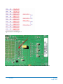
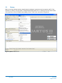
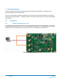
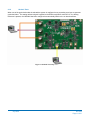
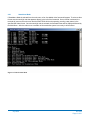
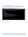
User Guide: SDALTEVK HSMC SDI ADAPTER BOARD 9-Jul-09 Version 0.06 SDI Development Kit using National Semiconductor’s LMH0340 serializer and LMH0341 deserializer July 2009 Rev 0.06 Page 1 of 31 1 ....Overview 3 2 ....Evaluation Kit (SDALTEVK) Contents 3 ....Hardware Setup 3 5 3.1 CYCLONE III DEVELOPMENT BOARD (MAIN BOARD) DESCRIPTION.................................................................... 6 3.2 SDALTEVK BOARD DESCRIPTION ................................................................................................................. 8 4 ....Software Setup 9 4.1 INSTALLATION ................................................................................................................................................ 9 4.2 STARTUP .................................................................................................................................................... 10 5 ....Evaluating Hardware 13 5.1 TEST SETUPS .............................................................................................................................................. 13 5.1.1 Standalone Video Generator Tests ................................................................................................... 13 5.1.2 Genlock Tests .................................................................................................................................... 14 5.1.3 Video Pass-through Tests ................................................................................................................. 15 5.2 TERMINAL BASED SD/HD/3G SDI EVALUATION ............................................................................................ 15 5.2.1 Standalone Mode............................................................................................................................... 16 5.2.2 Pass-through Mode ........................................................................................................................... 17 5.2.3 Genlocked Mode.................................................................................. Error! Bookmark not defined. 5.3 PUSH BUTTON BASED SD/HD/3G SDI EVALUATION ..................................................................................... 19 5.3.1 Push Button Main Menu .................................................................................................................... 19 5.3.2 System Mode ..................................................................................................................................... 20 5.3.3 Datapath Menu .................................................................................................................................. 20 5.3.4 Video Format Menu ........................................................................................................................... 20 5.3.5 Frequency Menu ................................................................................................................................ 21 5.4 FPGA REGISTER MAP ................................................................................................................................. 21 5.4.1 Miscellaneous Registers:................................................................................................................... 22 5.4.2 Reset Registers ................................................................................................................................. 22 5.4.3 Rx Video Registers ............................................................................................................................ 22 5.4.4 Datapath Registers ............................................................................................................................ 24 5.4.5 Clocking ............................................................................................................................................. 26 5.4.6 Video Timing ...................................................................................................................................... 26 5.5 SUPPORTED TEST PATTERNS....................................................................................................................... 29 6 ....Documentation 30 7 ....Schematics, BOMs, and Data Sheets 30 8 ....Reference FPGA IP 30 9 ....Up to Date Information 30 10 ..Part Numbers 30 July 2009 Rev 0.06 Page 2 of 31 1 Overview The SDALTEVK enables rapid evaluation of the LMH0340/0341 serializer and deserializer in Serial Digital Interface (SDI) applications. Other National devices also highlighted on this board are shown in Table 1. Device Table 1) National Semiconductor Devices on the SDALTEVK Quantity Description Function LMH0340 2 LMH0341 LMH0344 LMH1981 1 1 1 LMH1982 1 DS90CP22 DS90LV028 A DS90LV031 A LP3878-ADJ 1 1 1 LM20242 1 1 SD, HD and 3G SDI serializer + cable driver SD, HD and 3G SDI deserializer SD, HD and 3G cable equalizer Multi-Format Video Sync Separator Multi-Rate Video Clock Generator with Genlock 2x2 LVDS Cross Point Switch Dual LVDS to 3V CMOS Receiver Quad 3V CMOS to LVDS Line Driver Micropower 800mA Low Noise Adjustable Voltage Regulator 2A PowerWise™ Adjustable Frequency Synchronous Buck Regulator SDI Serializer Reference Designator U1, U6 SDI Deserializer SDI Equalizer Optional Clock Source Optional Clock Source Clock Multiplexer Optional Clock Output Optional Clock Source 2.5V Regulator U11 U13 U3 3.3V Regulator U12 U9 U7 U5 U2 U10 Examples of firmware are provided for the Standard Definition SMPTE 259M (SD-SDI) interface, the High Definition SMPTE 292M (HD-SDI) interface, and the 3G SMPTE 424M (3G-SDI) interface. The video standards supported by the example firmware are shown in Table 2. Table 2) Video Standards Supported by Firmware Video Standard NTSC, PAL 720p50, 720p59, 720p60, 1080s23.98, 1080s24, 1080i50, 1080i59, 1080i60, 1080p29.97, 1080p30 1080p50, 1080p59.9, 1080p60 Rate SD HD 3G A user interface allows for managing the FPGA firmware functions and the LMH0340/0341/1982 device registers. 2 Evaluation Kit (SDALTEVK) Contents The SDALTEVK contains the following parts: SDALTEVK HSMC SDI ADAPTER Board Screws, standoffs and spacers for mounting the EVK to the Cyclone III Development Board July 2009 Rev 0.06 Page 3 of 31 The following is required to complete the evaluation kit: Altera Cyclone III Development Kit Altera Part Number: DK-DEV-3C120N National Semiconductor SDI compiled .sof file from: http://www.national.com/sdaltevk o Triple Rate Standalone mode with multiple format selection o Triple Rate pass-thru mode with format detection o Pattern selection o Gen-Lock function supported o Register programming supported Altera compiled .sof file from: ftp://ftp.altera.com/outgoing/National_SerDes/an535_1_0.zip o Triple Rate pass-thru mode Quartus II 8.0 or newer http://www.altera.com/products/ Nios II EDS 8.0 http://www.altera.com/products/ Cygwin from http://www.cygwin.com/ SDI cables PC July 2009 Rev 0.06 Page 4 of 31 Hardware Setup The SDALTEVK printed circuit board is designed to interface with the HSMC connector on the Cyclone III Development Boards. Power, control bus, and LVDS bus signals are supplied to the daughter board through the HSMC connector. The Cyclone III FPGA provides the SD/HD/3G SDI and general purpose stacks as well as the control interface to a PC through a USB cable. This evaluation system allows inexpensive FPGAs to deliver up to 3 Gbps on a coax cable. Figure 1 Evaluation Kit Block Diagram Figure 2 Evaluation Kit Connections July 2009 Rev 0.06 Page 5 of 31 2.1 Cyclone III Development Board (Main Board) Description The main board has a Cyclone III FPGA. The FPGA provides the SD/HD/3G SDI and general purpose stacks as well as the control interfaces through the supplied example firmware. The daughter board is connected to the main board through the high speed mezzanine connector (HSMC), J8. This connector provides power, control bus, and data bus. The main board communicates to a PC through a USB cable. Figure 3 Cyclone III Development Board 2.2 Cyclone III Development Board Termination Resistors The Altera Cyclone III device does not have any internal termination on the receive LVDS I/O’s. Termination resistors must be added to the Cyclone III board. The terminations resistors must be placed as close to the FPGA’s pin as possible. The 3C120 host board has the layout footprints for the termination resistors. Eleven 100 Ohm resistors in 0402 package size are required to install onto the host board. The resistors are located on the bottom side of the board. They are between the FPGA and the HSMC port A connector. Figures 4 and 5 show the schematic and board location of the LVDS termination resistors. July 2009 Rev 0.06 Page 6 of 31 Figure 4 Resistors on HSCM port A Figure 5 Photograph of the back of the Cyclone III board showing location of the 100 Ohm Resistors July 2009 Rev 0.06 Page 7 of 31 2.3 SDALTEVK Board Description The HSMC SDI ADAPTER board features the 5:1 LMH0340 serializer IC with integrated cable driver, the 1:5 LMH0341 deserializer IC and the LMH0344 adaptive cable equalizer IC, all highlighted in orange. These devices support SD, HD, or 3G SDI interfaces across 75 ohm coaxial cable, which can interface with the board via BNC connectors J3, J8, J10, or J13. For added testing flexibility, the additional components shown in blue allow for several different clocking schemes. All of the clocking schemes are controlled by the DS90CP22 which is used to multiplex the various clock sources to the FPGA. The LMH1981 receives analog video via BNC connector J2 and provides the HSYNC and VSYNC to the LMH1982 for clock generation. The LMH1982 can also generate a clock based on a local 27 MHz oscillator. By using the DS90LV031A, an external clock can be applied to the card at SMA connector J4. In order to observe the quality of the clock provided to the FPGA, the clock can be routed to the DS90LV028A which will drive a CMOS clock out of SMA connector J5. Power is provided to the board via two separate power rails that travel across the HSMC connector from the Cyclone III host board. The Powerwise® LM20242 adjustable frequency synchronous buck regulator supplies the 3.3V power for the evaluation card by using the 12V rail from the host board. The LP3878ADJ low noise regulator uses the 3V power of the host board to supply the 2.5V power to the evaluation card. Figure 6 SDALTEVK July 2009 Rev 0.06 Page 8 of 31 3 Software Setup 3.1 Installation Make sure the Altera hardware is not connected to the PC. The following installation instructions are for the Windows XP Operating System. Quartus II 8.0 or newer is required to properly operate the SDALTEVK. If the terminal interface is desired then Nios II EDS 8.0 or newer must also be installed on the PC. If an older version of either Quartus II or Nios II EDS is already installed, make sure that it is updated before attempting to use the SDALTEVK. If necessary, please see http://www.altera.com/products/ to download the latest software. In order to use the Nios II terminal interface, Cygwin must be installed on the PC. Visit http://www.cygwin.com/ to download the latest version of Cygwin for free. Make sure that the file “cygwin1.dll” is installed to the path: C:\altera\80\nios2eds\bin Install the Quartus II 8.0 Software Execute the Quartus II 8.0 software installation program. The program is called “80_quartus_windows.exe”. This will load the driver files onto the PC. Follow the install instructions prompted by the Quartus install daemon Install the Nios II EDS 8.0 Software Execute the Nios II EDS installation program. The program is called “80_nios2eds_windows.exe”. Follow the install instructions prompted by the Nios II install daemon The software installation is complete. July 2009 Rev 0.06 Page 9 of 31 3.2 Startup Make sure all the software has been installed and the hardware is powered on and connected to the PC. Run Quartus II by either by using the path “C:\altera\80\quartus\bin\quartus.exe” or selecting it from the “altera” folder in the start menu. Once the software has loaded go to the “Tools” menu, and select “Programmer.” Figure 7 Quartus Main Screen July 2009 Rev 0.06 Page 10 of 31 This will bring up the programming window shown below. Click on the “Hardware Setup…” button, select the USB-Blaster and click Close. Use the “Add File…” button to select the appropriate bit image to program the FPGA. Make sure that the “Program/Configure” box is checked and that the “Mode” menu has JTAG selected. Press the “Start” button to program the FPGA. Once the progress bar reaches 100%, the SDALTEVK is ready to use. Figure 8 Quartus Programming Screen July 2009 Rev 0.06 Page 11 of 31 Once the FPGA has been programmed, the SDALTEVK can be evaluated using the push button interface on the Cyclone III main board. However, if the terminal interface is desired for evaluation, run the Nios II terminal program called “nios2-terminal.exe”. This program can be found in the bin folder of the Nios II root directory, for example “C:\altera\80\nios2eds\bin\nios2-terminal.exe”. If the software loads correctly, a terminal window will appear with a greeting message as shown below. Figure 9 Nios II Terminal Main Menu July 2009 Rev 0.06 Page 12 of 31 4 Evaluating Hardware The EVK is designed for flexible and accurate evaluation of LMH0340 and LMH0341. Evaluation can be performed using internal or external stimuli. There is an internal pattern generator implemented in the FPGA that will generate test patterns to verify signal transmission and signal integrity. The pattern generator can generate various types of SD, HD and 3G SDI static video patterns. 4.1 4.1.1 Test Setups Standalone Video Generator Tests In Standalone mode the system performance can be determined by the internal pattern generator. This is done by connecting the serializer output TX1 on J8 to the deserializer input RX on J13. The loop through output of the deserializer can be connected to external test equipment such as a WFM700 or an oscilloscope. Figure 10 Loop-back Test Setup July 2009 Rev 0.06 Page 13 of 31 4.1.2 Genlock Tests When one of the genlocked modes is selected the system is configured to use an analog sync input to generate genlocked video. The analog reference signal is applied to the EVK through BNC connector J2. If no analog reference is present, the LMH1982 has been configured to automatically switch to the on board oscillator. Figure 11 Genlock Test Setup July 2009 Rev 0.06 Page 14 of 31 4.1.3 Video Pass-through Tests In Pass-through Mode the EVK uses the clock recovered by the LMH0341 from the SDI input as the reference clock. The video data is then routed through the FPGA to the LMH0340 for transmission. To configure the EVK for Pass-through Mode connect the source generator to J13 of the deserializer and connect the terminating device to the serializer BNC connector J8. Refer to the diagram below. The loop through driver can also be connected to the terminating device via BNC connector J10. Figure 12 Pass-through Test Setup 4.2 Terminal Based SD/HD/3G SDI Evaluation Below the terminal greeting message is the main menu. The table below gives a brief description of the main menu options. Table 3 Terminal Menu Options Menu Option Name 1 I2C Read 2 I2C Write 3 Register Read 4 Register Write 5 I2C Bus Scan 6 Put System in Standalone Mode 7 Put System in Analog Sync TPG mode 8 Put System in Analog Sync Reclock Mode 9 Put System in Analog Sync Alternate TPG mode SDI Passthrough Mode A July 2009 Function Read from a device register. Write to a device register. Read from an FPGA register. Write to an FPGA register. Returns 7-bit address of all devices on the serial control bus. Configures system for Standalone Mode. Accesses format select menu. Generates clock from Analog sync input and uses this to drive Test Pattern Generator When supplied with an Analog Sync and a synchronous SDI input, the system uses the gunlock feature of the LMH1982 to reclock the SDI video with a clock derived from the analog input. Generates Test patterns synchronized to the SDI input. SDI video is received by the LMH0341, analysed and retransmitted, using the clock recovered from the LMH0341. Rev 0.06 Page 15 of 31 4.2.1 Standalone Mode If Standalone Mode is selected from the main menu, a list of available video formats will appear. To select a video format enter the two digit code that appears directly to the left of the format title. Once a format is selected, the terminal will return to the main menu and the SDALTEVK will then be operating, sending a test pattern in the specified SDI video format. Once the two digit code is selected, the Selected format will be displayed followed by the Main Menu. After the main menu a reminder of what mode the system is currently in will be shown. Figure 13 Video Format Menu July 2009 Rev 0.06 Page 16 of 31 4.2.2 Analog Sync TPG mode In Analog Sync TPG mode, the user provides an analog sync signal to the analog sync input on the evaluation board (the BNC connector labeled ‘Analog IN’). The LMH1981 extracts the sync information from this signal and passes it to the LMH1982 which generates video clocks for the FPGA, which are then used to clock the LMH0340 serializer and provide an SDI test signal output which is genlocked to the Analog input. Figure 14 Analog Sync TPG Mode 4.2.3 Analog Sync Reclock Mode In Analog Sync Reclock Mode, you provide both an analog Sync input as in the Analog Sync TPG mode, and an SDI input which is genlocked to the Analog Sync input. The timing information is extracted from the analog signal, and a new serial clock is generated using the LMH1982, and this clock is used to reclock the data received through the SDI input port. 4.2.4 Analog Sync alternate TPG Mode In Analog Sync Alternate TPG Mode, the system operates in a similar manner to the Analog Sync TPG mode, except that the output video format need not be the same as the analog sync input. For example you could use an analog sync from an NTSC 525 line 59.94 frame rate signal, and generate an SDI output which is an HD, 720P50 output. July 2009 Rev 0.06 Page 17 of 31 4.2.5 Pass Through Mode Before selecting Pass-through Mode from the main menu, apply an SD, HD or 3G SDI video signal from an external source to the SDALTEVK. When Pass-through Mode is selected from the main menu, a message will appear notifying if an input signal of a supported format is detected and return to the main menu. Figure 15 Pass-through Mode Screen July 2009 Rev 0.06 Page 18 of 31 4.3 Push Button Based SD/HD/3G SDI Evaluation The EVK can be configured for evaluation by using the push buttons on the Cyclone III main board only. The push button interface allows the EVK to be configured in the same modes as the terminal interface option. However, only the Nios II terminal interface allows for device and FPGA register access. Figure 16 LED and Push Button Locations 4.3.1 Push Button Main Menu After the FPGA has been programmed, the push buttons default to the main menu options. While in the main menu, LED 1 will blink. LED 6, 7, or 8 will illuminate to indicate the current configuration of the EVK. PB 0 PB 1 System Mode LED 1 Blink LED 2 Off PB 2 DP Settings LED 3 Off LED 4 Off Video Format LED 5 Off LED 6 Genlock PB 3 Video Frequency LED 7 Passthroug h LED 8 Standalone Figure 19) Main Menu Push Button Functions and Board Status LED Indications July 2009 Rev 0.06 Page 19 of 31 4.3.2 System Mode The System Mode menu contains the various configuration options for the EVK. Use this menu to configure the EVK into one of the 3 previously discussed modes of operations. PB 0 PB 1 Cancel LED 1 Off PB 2 Genlock LED 2 Blink LED 3 Off LED 4 Off PB 3 Passthrough LED 5 Off LED 6 Standalone LED 7 LED 8 Indicates Current Mode Once a mode has been selected, all of the LEDs will flash and the system will return to the main menu. A successful configuration is indicated by a single flash, while two flashes indicate a failure. If a failure occurs, refer to the table below for the most common causes. Configuration Standalone Genlock Passthrough 4.3.3 Typical Cause of Failure Incorrect format specified or mismatch between frequency and video format. No reference or invalid reference. Input video not present or unrecognized. Datapath Menu This menu will be available in a future release. If this menu is selected the LEDs will flash twice and the system will return to the main menu. 4.3.4 Video Format Menu The Video Format Menu configures the push buttons to navigate through the supported video formats. Users must select a video format with a compatible frequency in order for the system to be configured. If the system is in Standalone Mode and a valid combination is selected, the LEDs will flash once to indicate successful configuration. In other modes the video format and frequency settings are ignored. See the table below for the supported video formats and clock frequencies. PB 0 PB 1 Cancel LED 1 Off LED 2 Off July 2009 PB 2 OK LED 3 Blink PB 3 Up LED 4 Off LED 5 Off LED 6 Down LED 7 LED 8 Indicates Current Mode Rev 0.06 Page 20 of 31 5 Frequency Menu This menu configures the push buttons to cycle through supported clock frequencies. Users must select a video format with a compatible frequency in order for the system to be configured. If the system is in Standalone Mode and a valid combination is selected, the LEDs will flash once to indicate successful configuration. In other mode the video format and frequency settings are ignored. PB 0 PB 1 PB 2 Cancel LED 1 Off OK LED 2 Off LED 3 Off PB 3 Up LED 4 Blink LED 5 Off Down LED 6 LED 7 LED 8 Indicates Current Mode Figure 22) Frequency Menu Push Button Functions and Board Status LED Indications Format Number Active Lines Type 13.5 MHz SD 000 0:0000 1:0001 2:0010 3:0011 4:0100 525 486 720 720 1080 I I P P S 5:0101 6:0110 7:0111 1080 1080 1080 I I P 8:1000 9:1001 1080 1080 P P A:1010 B:1011 1080 1080 Clock Frequency 74.17 MHz 74.25 MHz HD 001 HD 010 148.35 MHz 3G 011 148.5 MHz 3G 100 PAL NTSC 720P59.94 1080S23.9 8 1080I59.94 1080P23.9 8 1080P29.9 7 720P50 720P60 1080S24 1080I50 1080I60 1080P24 1080P25 1080P30 P P Figure 23) Video Format and Clock Frequency Table 1080P59.94 1080P50 1080P60 Depending on the format the frequency specified in Figure 22 can refer to either the field or frame rate. For interlaced images it is the field rate and for progressive and segmented frame it is the frame rate. 5.1 FPGA Register Map This section describes the registers associated with the SDI Video Firmware. Registers can be either status or control, and are read or write respectively. The registers are grouped into several main sections: 1. Miscellaneous 2. Reset 3. Rx Video 4. Datapath 5. Clocking 6. Timing July 2009 Rev 0.06 Page 21 of 31 5.1.1 Miscellaneous Registers: Hex Address: 00 5.1.2 Name IPT ID Description ID Code (1234 Hex) Bits 15:0 Bit Description ID Code Description Status bits of various system resets Bits 15:4 Bit Description Reserved Reset Registers Hex Address: 01 Name RESET STATUS 02 5.1.3 RESET CONTROL Control Reset Signals 3 2 1 0 15:0 Description Status bits of Rx video Bits 15:4 Deserializer Lock Serializer Lock CPU_RST_N CPU_RST Reserved Rx Video Registers Hex Address: 03 04 Name RX VID STATUS RX VID STD Detected Video Standard Bit Description Reserved 3 Vid Reset Flag: Indicates that video reset has been asserted 2 Deser Flag: Indicates that the deserializer lock has toggled. 1 Descram Flag: Indicates that the descrambler lock has toggled. 0 Descram Locked: Indicates that the descrambler is locked onto incoming video Reserved 15:13 12 SMPTE 352 Packet Detected 11 Reserved 10:8 Frequency detected: 000 0 SD 270Mbps 001 1 HD 1.485/1.001 Gbps 010 2 HD 1.485 Gbps 011 3 HD 2.97/1.001 Gbps 100 4 HD 2.97 Gbps July 2009 Rev 0.06 Page 22 of 31 Hex Address: Name Description Bits Bit Description 7:4 Reserved 3:0 05 CRC STATUS CRC Error Check 15 Format Detected: 0000 0 PAL I50 0001 1 NTSC I59 0010 2 P720 50 0011 3 P720 60 0100 4 S1080 24 0101 5 I1080 50 0110 6 I1080 60 0111 7 P1080 24 1000 8 P1080 25 1001 9 P1080 30 1010 A P1080 50 1011 B P1080 60 Reserved 06 CRC CONTROL CRC Check Control 14:0 15:3 CRC Error Count Reserved 07 EDH STATUS 1 EDH Error Check Status Reg 2 Select Holdover Mode 1 Reset Status flags 0 15 Reset CRC Error Count Reserved 14:10 08 EDH STATUS 2 EDH Error Check Status Reg 2 9:5 Active Picture error flags 4:0 15 ANC flags EDH Present 14:12 July 2009 Full Field error flags 11:8 EDH Detection Count (indicates intermittent EDH) Full Frame CRC error count 7:4 Active Picture CRC error count 3 Full Field CRC Error detected 2 Active Picture CRC Error detected 1 Full Field CRC valid 0 Active Picture CRC valid Rev 0.06 Page 23 of 31 Hex Address: 09 Name EDHAP COUNT 0A EDH FF COUNT 0B AUDIO IN STATUS 0C SMPTE35234 0D SMPTE35212 0E AUDIO IN CONTROL Description Extended Count of EDH Errors Extended Count of EDH Errors Input Audio (Over SDI) Status Extracted SMPTE352 Bytes 3, 4 Extracted SMPTE352 Bytes 1, 2 I2S Output Control Bits 15:0 15:0 15:4 3 Group 4 detected 2 Group 3 detected 1 Group 2 detected 0 15:0 Group 1 detected SMPTE352 Bytes 4 and 3 15:0 SMPTE352 Bytes 2 and 1 15:1 Reserved 0 5.1.4 Bit Description 16 bit Active Picture EDH error count 16 bit Full Frame EDH error count Reserved Enable I2S Output Datapath Registers Hex Address: 10 11 Name DP STATUS DP CONTROL Description Datapath Status Register Bits 15:0 15 14:7 6 5 4 12 13 July 2009 DP FORMAT CONTROL DP FREQ Datapath Format Control Datapath Frequency Control Bit Description Reserved Data Pat Bypass Reserved Insert CRC/EDH Errors on output Insert EDH Packets on output 3 Insert SMPTE352 Packets on output Insert audio on output 2 Reserved 1 Disable TPG/Output Received video Reserved Force Format 0 15 14:4 Reserved 3:0 Select Video Format, see RX VID STD for values Reserved 15:3 Rev 0.06 Page 24 of 31 Hex Address: Name CONTROL Description Bits 2:0 14 15 DP AUDIO OUT CONTROL Control Audio Insertion Module 15:8 Selected Frequency, see RX VID FREQ for values AFN ( Audio Frame Count) Max 7:4 Audio control packet rate 3 Reserved 2 1:0 15:0 Select internal tone generator (0) or I2S input (1) Select output audio group Reserved 15:8 Channel 1 Frequency 7:0 15:8 Channel 2 Frequency Channel 3 Frequency AUDIO OUT STATUS AUDIO OUT INCR 1 Controls Increment Rate for Internal Tone Generator 17 AUDIO OUT INCR 2 Controls Increment Rate for Internal Tone Generator 18 AUDIO OUT CSB 1 Controls Audio CSB 7:0 15:8 Channel 4 Frequency Channel Status Block CRC Controls Audio CSB 7:0 15:8 Channel Status Block Byte 2 Channel Status Block Byte 1 Select Output test Pattern 7:0 15 Channel Status Block Byte 0 Reserved 14 RP219 Pattern Select 3A (0) 3B(1) RP219 Part 2 Pattern Select: 00 0 2A 01 1 2B 10 2 Y Valid Range Ramp 11 3 YUV Full Range Ramp 16 19 1A AUDIO OUT CSB 2 TEST PATTERN CONTROL Audio Output Status Bit Description 13:12 11:6 Reserved 5:4 Select Calculate Patterns: 00 0 Black 01 1 Pathological 10 2 Y Valid Range Ramp 11 3 YUV Full Range Ramp 3 2:0 Reserved Pattern Select: 000 0 100% Color Bars July 2009 Rev 0.06 Page 25 of 31 Hex Address: Name 1B SMPTE 352 INSERT CONTROL LINE PATTERN UPDATE 1 LINE PATTERN UPDATE 2 LINE PATTERN UPDATE ADDR 1C 1D 1E 5.1.5 Description Allows bytes 3 and 4 of the SMPTE352 packet to be set 16 MSB for line pattern update 16 LSB for line pattern update Adress and write enable for pattern update Bits 15:8 Bit Description 001 1 Sweep (not implemented) 010 2 Calculated Patterns 011 3 Pulse/Bar 100 4 RP219 Pattern 101 5 SMPTE Bars Others 100% Color Bars Byte 4 7:0 15:0 Byte 3 Update Value 15:0 Update Value 15 Write Enable 14:11 Reserved 10:0 Update adress Clocking Hex Address: 20 Name CLOCK STATUS: ALTERA Description Status of ALtera PLLs Bits 15:3 2 21 5.1.6 CLOCK CONTROL: ALTERA Control Altera Clock selection Bit Description Reserved 1 Active clock: specified whether the receive (0) or PLL (1) clock is for transmission Tx PLL Locked 0 15 Rx PLL Locked Select PLL (1) or Rx (0) Clock 14:0 Reserved Video Timing Hex Address: 23 Name CONTROL GENLOCK Description Control Genlock Mode Bits 15:2 1:0 24 GENLOCK STATUS Status of Gunlock Interface 15 14:12 July 2009 Bit Description Reserved Select System Mode: 00 0 Use Received Video Timing 01 1 Use Genlock timing 10 2 Freerun/User specified timing 11 3 Use Genlock timing with user specified format Progressive video on reference SD HD 3G Format Rev 0.06 Page 26 of 31 Hex Address: Name Description Bits 11 10 Genlock reference present 9 Genlock No Lock 8 Genlock No Ref 7 Reserved 6:4 3:0 25 VFORMAT STATUS Looks for Matching VFORMAT Sequences from the LMH1981 and Decodes Them 15 14:12 11 10:0 26 LINE TIME COUNT 27 STATUS GENFORMAT Used to Determine Format. See Genlock_if module for details Format Used to Drive Timing Generator Status of Timing Generator Reserved 15:11 Reserved 10:8 Frequency selected, as per RX VID FREQ Reserved 15 14:12 11 10:8 July 2009 Decoded format type: 000 0 Unknown 001 1 PAL 010 2 NTSC 011 3 576P 100 4 480P 101 5 720P 110 6 1080I 111 7 1080P 15:0 3:0 STATUS TIMING Genlock frequency, as per RX VID FREQ Genlock format, as per RX VID STD Reserved Vformat received from LMH1981 Line time count 16 MSB 7:4 28 Bit Description Reserved Format selected, as per RX VID STD Input present Reserved Sync to input timing Reserved Rev 0.06 Page 27 of 31 Hex Address: July 2009 Name Description Bits 7:0 Bit Description Counts when timing is resynchronized Rev 0.06 Page 28 of 31 5.2 Supported Test Patterns The following test patterns are available from the SDI firmware in all SD, HD and 3G formats: 100% Color Bars Frequency Sweep Matrix Pathological Black Luma Ramp SMPTE 75% Color Bars Y/C Full Range Ramp SMPTE RP219 Color Bars Luma Pulse & Bar July 2009 Rev 0.06 Page 29 of 31 6 Documentation Additional SDALTEVK documentation can be found on the EVK website. 7 Schematics, BOMs, and Data Sheets All of the schematics, BOMs, and data sheets for the SDALTEVK can be found on the EVK website. 8 Reference FPGA IP The reference FPGA IP source code and documentation can be found on EVK website. 9 Up to Date Information For up to date information check this URL http://www.national.com/sdaltevk 10 Part Numbers Cyclone III Development Board: DK-DEV-3C120N http://www.altera.com/products/devkits/altera/kit-cyc3.html LMH0340/LMH0341 Evaluation Kit: July 2009 SDALTEVK Rev 0.06 Page 30 of 31 Revision History Release 0.00 0.01 0.02 Date 8-19-2008 8-19-2008 8-25-2008 0.03 8-28-2008 N. Unger 0.04 0.05 9-02-2008 N. Unger 9-03-2008 N. Unger 0.06 07-09-2009 M. Sauerwald July 2009 Who M. Wolfe M. Wolfe N. Unger Revisions Creation 1st draft Updated TOC Table headings Column widths Put revision history at the end Change font of the TOC to Ariel Inserted termination resistor instructions Minor wording changes on Table 1 Updated Altera Part Number to DK-DEV-3C120N Recovered File Changed date format in the revision history Updated for December 2008 IP release Rev 0.06 Page 31 of 31 IMPORTANT NOTICE Texas Instruments Incorporated and its subsidiaries (TI) reserve the right to make corrections, modifications, enhancements, improvements, and other changes to its products and services at any time and to discontinue any product or service without notice. Customers should obtain the latest relevant information before placing orders and should verify that such information is current and complete. All products are sold subject to TI’s terms and conditions of sale supplied at the time of order acknowledgment. TI warrants performance of its hardware products to the specifications applicable at the time of sale in accordance with TI’s standard warranty. Testing and other quality control techniques are used to the extent TI deems necessary to support this warranty. Except where mandated by government requirements, testing of all parameters of each product is not necessarily performed. TI assumes no liability for applications assistance or customer product design. Customers are responsible for their products and applications using TI components. To minimize the risks associated with customer products and applications, customers should provide adequate design and operating safeguards. TI does not warrant or represent that any license, either express or implied, is granted under any TI patent right, copyright, mask work right, or other TI intellectual property right relating to any combination, machine, or process in which TI products or services are used. Information published by TI regarding third-party products or services does not constitute a license from TI to use such products or services or a warranty or endorsement thereof. Use of such information may require a license from a third party under the patents or other intellectual property of the third party, or a license from TI under the patents or other intellectual property of TI. Reproduction of TI information in TI data books or data sheets is permissible only if reproduction is without alteration and is accompanied by all associated warranties, conditions, limitations, and notices. Reproduction of this information with alteration is an unfair and deceptive business practice. TI is not responsible or liable for such altered documentation. Information of third parties may be subject to additional restrictions. Resale of TI products or services with statements different from or beyond the parameters stated by TI for that product or service voids all express and any implied warranties for the associated TI product or service and is an unfair and deceptive business practice. TI is not responsible or liable for any such statements. TI products are not authorized for use in safety-critical applications (such as life support) where a failure of the TI product would reasonably be expected to cause severe personal injury or death, unless officers of the parties have executed an agreement specifically governing such use. Buyers represent that they have all necessary expertise in the safety and regulatory ramifications of their applications, and acknowledge and agree that they are solely responsible for all legal, regulatory and safety-related requirements concerning their products and any use of TI products in such safety-critical applications, notwithstanding any applications-related information or support that may be provided by TI. Further, Buyers must fully indemnify TI and its representatives against any damages arising out of the use of TI products in such safety-critical applications. TI products are neither designed nor intended for use in military/aerospace applications or environments unless the TI products are specifically designated by TI as military-grade or "enhanced plastic." Only products designated by TI as military-grade meet military specifications. Buyers acknowledge and agree that any such use of TI products which TI has not designated as military-grade is solely at the Buyer's risk, and that they are solely responsible for compliance with all legal and regulatory requirements in connection with such use. TI products are neither designed nor intended for use in automotive applications or environments unless the specific TI products are designated by TI as compliant with ISO/TS 16949 requirements. Buyers acknowledge and agree that, if they use any non-designated products in automotive applications, TI will not be responsible for any failure to meet such requirements. Following are URLs where you can obtain information on other Texas Instruments products and application solutions: Products Applications Audio www.ti.com/audio Automotive and Transportation www.ti.com/automotive Amplifiers amplifier.ti.com Communications and Telecom www.ti.com/communications Data Converters dataconverter.ti.com Computers and Peripherals www.ti.com/computers DLP® Products www.dlp.com Consumer Electronics www.ti.com/consumer-apps DSP dsp.ti.com Energy and Lighting www.ti.com/energy Clocks and Timers www.ti.com/clocks Industrial www.ti.com/industrial Interface interface.ti.com Medical www.ti.com/medical Logic logic.ti.com Security www.ti.com/security Power Mgmt power.ti.com Space, Avionics and Defense www.ti.com/space-avionics-defense Microcontrollers microcontroller.ti.com Video and Imaging www.ti.com/video RFID www.ti-rfid.com OMAP Mobile Processors www.ti.com/omap Wireless Connectivity www.ti.com/wirelessconnectivity TI E2E Community Home Page e2e.ti.com Mailing Address: Texas Instruments, Post Office Box 655303, Dallas, Texas 75265 Copyright © 2012, Texas Instruments Incorporated