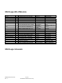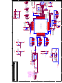
1
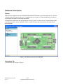
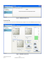
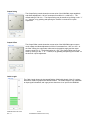
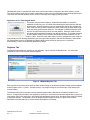
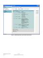
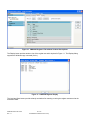
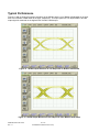
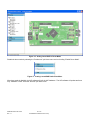
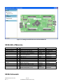
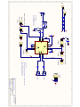
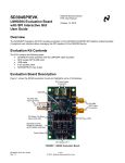
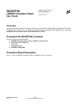
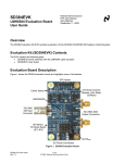
SD384SPIEVK
LMH0384 Evaluation Board
with SPI Interactive GUI
User Guide
National Semiconductor
EVK User Manual
Gary Melchior
September 11, 2009
Overview
The SD384SPI Evaluation Kit (EVK) enables evaluation of the LMH0384 3G/HD/SD SDI Adaptive Cable Equalizer.
A graphical user interface allows managing the SPI registers of the LMH0384 device.
Evaluation Kit (SD384SPIEVK) Contents
The EVK contains the following parts:
• SD384EVK board assembly with the LMH0384 cable equalizer
• SPA dongle (SPIÆUSB card)
• USB cable
• 6-pin parallel cable
• SD384SPIEVK User Guide
Evaluation Board Description
Figure 1 shows the SD384 evaluation board and highlights some of its features.
SD384SPI EVK User Guide
Rev 1.1
1 of 19
© 2009 National Semiconductor Corp.
Figure 1. SD384 Evaluation Board
SDI Input and SDO Output
The SDI input connector (J1) is a 75Ω BNC connector. The SDI input should conform to the SMPTE 424M,
SMPTE 292M, or SMPTE 259M standards.
The SDO output connectors (J2 and J3) are 50Ω SMA connectors. When using only one side of the output pair,
the other side should be terminated with a 50Ω SMA termination. For example, when only using the SDO output,
¯¯¯¯
SDO should be terminated with a 50Ω SMA termination.
DC Power Connectors
The VCC and GND power connectors should be powered with a DC input voltage of 3.3V ± 5% (3.6V maximum).
SD384SPI EVK User Guide
Rev 1.1
2 of 19
© 2009 National Semiconductor Corp.
SPI Mode / Pin Mode Select (JP1 – JP4)
JP1, JP2, JP3, and JP4 are used to select between SPI Mode or Pin mode. To select Pin Mode, set four jumpers
as shown in Figure 2, and to select SPI Mode, set four jumpers as shown in Figure 3. Either Pin Mode or SPI
mode must be selected for proper operation; do not leave JP1-JP4 open.
Figure 2. Pin Mode Select
Figure 3. SPI Mode Select
MUTEREF (JP5)
JP5 allows control of the MUTEREF function and may be used in either Pin Mode or SPI Mode. MUTEREF is an input
voltage used to set the threshold for ¯¯¯
CD . The MUTEREF DC input voltage should be between 0V and 3.3V. Refer
to the LMH0384 datasheet for details. Leave JP5 unconnected for normal operation.
Pin Mode Controls (JP6 – JP8)
JP6, JP7, and JP8 are used to control LMH0384 features while the device is configured for Pin Mode. Jumpers
should not be placed on JP6, JP7, or JP8 while the device is configured for SPI Mode.
¯¯¯
CD and MUTE (JP6)
¯¯¯ ) monitoring and MUTE control. ¯¯¯
JP6 allows Carrier Detect (CD
CD is high when no input signal is present. MUTE
may be used to force the outputs on or off, or tied to ¯¯¯
CD to allow automatic mute operation based on the input
signal. To activate mute and force the outputs into a muted condition, set the jumper to pull MUTE to VCC. To turn
off mute so that the outputs will never mute, set the jumper to tie MUTE to GND. For normal operation, set the
jumper to tie ¯¯¯
CD to MUTE for automatic mute control. The LMH0384 MUTE pin has an internal pulldown (to
disable mute), so JP6 may be left unconnected and the LMH0384 will never mute.
BYPASS (JP7)
JP7 allows control of the equalization BYPASS function. To put the device into bypass mode, set the jumper to pull
BYPASS to VCC. To turn off bypass (for normal operation) set the jumper to pull BYPASS to GND. The LMH0384
BYPASS pin has an internal pulldown (to disable bypass), so JP7 may be left unconnected for normal operation.
AUTO SLEEP (JP8)
JP8 allows control of the AUTO SLEEP function. To put the device into auto sleep mode in which it will power
down when no input is detected, set the jumper to pull AUTO SLEEP to VCC. To turn off auto sleep and prevent
the LMH0384 from automatically powering down, set the jumper to pull AUTO SLEEP to GND. The LMH0384
AUTO SLEEP pin has an internal pullup (to enable auto sleep), so JP8 may be left unconnected to enable auto
sleep mode.
SD384SPI EVK User Guide
Rev 1.1
3 of 19
© 2009 National Semiconductor Corp.
SPI Header (JP9)
JP9 is the SPI (Serial Peripheral Interface) header. It allows access to the SPI pins (¯¯¯
SS , MISO, MOSI, and SCK)
while the LMH0384 is in SPI mode. To use the SPI interactive GUI, plug the 6-pin parallel cable between this
header and JP7 on the SPA dongle to connect the pins one-for-one as shown in Table 1. The SPA dongle requires
special software and must be connected to the PC via the USB – see the Software Setup section.
Table 1. SPI Connections between SD384 and SPA Dongle
SD384 JP9
Pin #
Name
1
GND
2
SCK
3
MOSI
4
MISO
5
SS
6
GND
Æ
Æ
Æ
Æ
Æ
Æ
SPA dongle JP7
Pin #
Name
1
GND
2
MCK
3
MOSI
4
MOSI
5
SS
6
GND
Carrier Detect LED (D1)
D1 shows the status of Carrier Detect. This LED is GREEN when an input signal has been detected, and OFF
when no input is detected. D1 shows the status of Carrier Detect while in Pin Mode or SPI Mode.
SPA Dongle Description
The SPA dongle is required to use the SPI interactive GUI. The SPA dongle connects between the LMH0384 SPI
pins and the USB input of a PC. The SPA dongle is shown in Figure 4. JP7 is the SPI Header. The SPA dongle is
powered through the USB, and the D1 LED is RED when the SPA dongle is connected to a PC via the USB to
indicate the board is powered.
Figure 4. SPA Dongle
SD384SPI EVK User Guide
Rev 1.1
4 of 19
© 2009 National Semiconductor Corp.
Software Setup
System Requirements
Operating System:
USB:
Windows XP or Vista
2.0
Installation
Download the latest software from the LMH0384 Evaluation Board page, which can be found here:
http://www.national.com/analog/interface/sdi_sdv_evaluation_boards. Extract the ALPF_monthdayyear_major
version_minor version.exe” (ex. ALPF_07082009_127_0005.exe) file to a temporary location that can be deleted
later.
Make sure the SPA dongle is not connected to the PC. The following installation instructions are for the Windows
XP Operating System.
Install the ALP software
Execute the ALP Setup Wizard program called “ALPF_monthdayyear_major version_minor version.exe” (ex.
ALPF_07082009_127_0005.exe) that was extracted to a temporary location.
There are 7 steps to the installation once the setup wizard is started:
1. Select the “Next” button.
2. Select “I accept the agreement” and then select the “Next” button.
3. Select the location to install the ALP software and then select the “Next” button.
4. Select the location for the start menu shortcut and then select the “Next” button.
5. There will then be a screen that allows the creation of a desktop and Quick Launch icon. After selecting
the desired choices select the “Next” button.
6. Select the “Install” button, and the software will then be installed to the selected location.
7. Uncheck “Launch Analog LaunchPAD” and select the “Finish” button. The ALP software will start if
“Launch Analog LaunchPAD” is checked, but it will not be useful until the USB driver is installed.
Connect JP9 of the SD384 evaluation board to JP7 of the SPA dongle via the 6-pin parallel cable as shown in
Table 1. Power on the SD384 evaluation board with a 3.3 VDC power supply. Connect the SPA dongle to the PC
with the USB cable. The “Found New Hardware Wizard” will open on the PC. Proceed to the next section to install
the USB driver.
Install the USB driver
There are 6 steps to install the USB driver:
1. Select “No, not at this time” then select the “Next” button.
2. Select “Install from a list or specific location” then select the “Next” button.
3. Select “Search for the best driver in these locations”. Uncheck “Search removable media” and check
“Include this location in the search”.
4. Browse to the Install Directory which is typically located at “C:\Program Files\National Semiconductor
Corp\Analog LaunchPAD\vx.x.x\Drivers” and select the “Next” button. Windows should find the driver.
5. Select “Continue Anyway”.
6. Select the “Finish” button.
The software installation is complete. The ALP software may now be launched, as described in the next section.
SD384SPI EVK User Guide
Rev 1.1
5 of 19
© 2009 National Semiconductor Corp.
Software Description
Startup
Make sure all the software has been installed and the hardware is powered on and connected to the PC. Execute
“Analog LaunchPAD” from the start menu. The default start menu location is “Programs\National Semiconductor
Corp\Analog LaunchPAD vx.x.x\Analog LaunchPAD”.
The application should come up in the state shown in Figure 5 below. If it does not, see “Trouble Shooting” at the
end of this document. Click on “LMH0384 – Nano” to select the device and open up the device profile and its
associated tabs.
Figure 5. ALP Startup Screen for the LMH0384
Information Tab
The Information tab is shown in Figure 6.
SD384SPI EVK User Guide
Rev 1.1
6 of 19
© 2009 National Semiconductor Corp.
Figure 6. LMH0384 Information Tab
Functional Tab
The Functional tab is the main tab of the GUI and presents a high level view of the LMH0384, as shown in Figure 7.
Figure 7. LMH0384 Functional Tab
SD384SPI EVK User Guide
Rev 1.1
7 of 19
© 2009 National Semiconductor Corp.
Output Swing
The Output Swing control shows the current value of the LMH0384 output amplitude
and allows adjustment in 100 mV increments from 400 mVP-P to 800 mVP-P. The
default setting is 700 mVP-P. The Output Swing may be set either by clicking on the “+”
or “-” buttons, or by grabbing and spinning the “handle” on the knob for a quick
adjustment.
Output Offset
The Output Offset control shows the current value of the LMH0384 output common
mode voltage and allows adjustment in 200 mV increments from 1.05V to 1.85V. At
the “Max” setting, the outputs are referenced to the positive supply and the output
common mode is 2.1V. The default setting is 1.25V. The Output Offset may be set
either by clicking on the “+” or “-” buttons, or by grabbing and spinning the “handle” on
the knob for a quick adjustment.
Cable Length
The Cable Length shows the interpreted Belden 1694A cable length of the CLI register,
both with a visual bar graph and a decimal readout. The Cable Length is only valid when
an input signal is detected, and is greyed out when there is no input to the LMH0384.
SD384SPI EVK User Guide
Rev 1.1
8 of 19
© 2009 National Semiconductor Corp.
Input Launch Level Control
The Input Launch Level Control is useful to compensate for attenuation
of the input signal prior to the equalizer due to a passive splitter or nonideal input termination network.
The Coarse Amplitude control shows the current setting of the Coarse
Control register and may be used to set the input for either 0 dB (default)
or 6 dB of input attenuation. At the default setting of 0 dB, the LMH0384
operates normally and expects a launch amplitude of 800 mVP-P. With
the Coarse Amplitude set to -6 dB, the LMH0384 is optimized for input
signals with 6 dB of input attenuation (400 mVP-P).
The Launch Amplitude Fine Tuning may be used to further fine tune the
LMH0384 input compensation, from -2.2 dB to 2.9 dB. The Launch
Amplitude Fine Tuning may be set either by clicking on the “+” or “-”
buttons, or by grabbing and spinning the “handle” on the knob for a quick
adjustment.
Sleep State and Signal Detect
The Sleep State control shows the status of the Sleep Mode register bits and
allows control over the sleep mode. The Sleep State settings are as follows:
On: Force the LMH0384 into sleep mode (powered down) regardless of whether
there is an input signal or not.
Off: Disable sleep mode (force LMH0384 to stay enabled).
Auto: Sleep mode active when no input signal detected (default mode).
The LMH0384 Sleep State indicator shows the current status of the LMH0384 sleep state. It is GREEN to indicate
sleeping or OFF to indicate not sleeping.
The Signal Detect shows the status of the input carrier detect. It is GREEN to indicate the input signal is present or
OFF to indicate the input signal is absent.
Output Mute and Equalizer Bypass
The Output Mute indicator shows the mute status, and the button may be used to toggle the mute
function. The indicator is GREEN to indicate mute (LMH0384 outputs are muted) and OFF to
indicate normal mode (outputs are not muted).
The Equalizer Bypass indicator shows the bypass status, and the button may be used to toggle
the bypass function. The indicator is GREEN to indicate bypass is active (equalization is
bypassed) and OFF to indicate normal mode.
Extended 3G Reach Mode
The Extended 3G Reach Mode indicator shows the status of the Extended 3G Reach
Mode register bit, and the button may be used to toggle this register bit. The indicator is
GREEN when the bit is set for extended 3G reach mode, and OFF when the LMH0384 is
set for normal mode. Note that the indicator shows the status of the register bit – not
whether the device is actually in extended 3G reach mode or not. If extended 3G reach
mode is set, the LMH0384 will remain in this mode until the input cable is physically changed or power is cycled.
For example, extended 3G reach mode is forced, and then it is turned off. The indicator will show it is off, but the
SD384SPI EVK User Guide
Rev 1.1
9 of 19
© 2009 National Semiconductor Corp.
LMH0384 will still be in extended 3G reach mode until the input cable is changed or the device power is cycled.
The GUI provides a simple way to reset the extended 3G reach mode: the Extended 3G Reach Mode Reset button.
This button will reset the equalizer, and is similar to removing and re-applying the input cable.
Application of CLI: Extending 3G Reach
This control may be used to enable a “Smart 3G Reach Mode” to extend the
LMH0384 3G reach by up to 15m while still maintaining the performance at HD and
SD data rates. When this mode is active, it automatically controls the extended 3G
reach mode and only enables extended 3G reach mode when the input cable length
to the equalizer is less than the threshold. The indicator is GREEN when this mode
is active, and OFF when this mode is not used (default). When this mode is active,
the “Smart 3G Reach Mode Threshold” may also be changed. The default threshold
is 180m (Belden 1694A), which means that extended 3G reach mode will only be
active when the input cable length is <180m. When the input cable length is ≥180m, extended 3G reach mode will
automatically turn off, allowing equalization of much longer cable lengths for HD and SD data rates. When Smart
3G Reach Mode is active, the Extended 3G Reach Mode control cannot be used (since it is controlled
automatically). Refer to the LMH0384 datasheet for details.
Registers Tab
The Registers tab displays all registers for the LMH0384. Figure 8 shows the Registers tab. The Value field
indicates the value of the currently selected register.
Figure 8. LMH0384 Registers Tab
Each register can be examined in detail by either double clicking on the desired registers fold bar (with the address
and the register name, e.g. 0x00 – General Control) or by single clicking the icon at the right of the fold bar (two
inverted carats).
The Refresh button will re-read the currently selected register and the Refresh All will read all registers in the
device. Changes may be made to the registers by checking or un-checking the individual register bits or typing in a
new register value in the Value field. After setting the appropriate register value, the Apply button must be pressed
to apply the changes. The detailed view of the General Control register is shown in Figure 9 with Verbose
Descriptions checked and Figure 10 with Verbose Descriptions un-checked.
SD384SPI EVK User Guide
Rev 1.1
10 of 19
© 2009 National Semiconductor Corp.
Figure 9. LMH0384 Registers Tab with Verbose Descriptions
SD384SPI EVK User Guide
Rev 1.1
11 of 19
© 2009 National Semiconductor Corp.
Figure 10. LMH0384 Registers Tab without Verbose Descriptions
The Display button provides another view of the register set and is depicted in Figure 11. The Display dialog
supports the Windows copy command (Ctrl+c).
Figure 11. LMH0384 Register Display
The Load and Save buttons provide a handy mechanism for restoring or saving the register set external to the
evaluation board.
SD384SPI EVK User Guide
Rev 1.1
12 of 19
© 2009 National Semiconductor Corp.
Typical Performance
Figures 12 and 13 show typical output waveforms of the SD384, with the 1m of Belden 1694A cable on the input
and 110m of Belden 1694A cable on the input, respectively. The input signal is a 2.97 Gbps PRBS10, and the
output signal is measured on the Agilent DCA-J 86100C Oscilloscope.
Figure 12. SD384 Output Waveform at 2.97 Gbps with 1m Belden 1694A Cable
Figure 13. SD384 Output Waveform at 2.97 Gbps with 110m Belden 1694A Cable
SD384SPI EVK User Guide
Rev 1.1
13 of 19
© 2009 National Semiconductor Corp.
Trouble Shooting
If the following window (Figure 14) opens after starting the ALP software, double check the hardware setup.
Figure 14. Analog LaunchPAD No Devices Error
It may also be that the USB driver is not installed. Check the device manager. There should be an ”NSC ALP
Nano Atmel” device under the “Universal Serial Bus Controllers” as shown in Figure 15.
Figure 15. Windows XP, Analog LaunchPAD USB Driver
The software should start with only “LMH0384 - Nano” in the “Devices” pull down menu. If there are more devices
then the software is most likely in demo mode. When the ALP is operating in demo mode there is a “(Demo Mode)”
indication in the lower left of the application status bar as shown in Figure 16.
SD384SPI EVK User Guide
Rev 1.1
14 of 19
© 2009 National Semiconductor Corp.
Figure 16. Analog LaunchPAD in Demo Mode
Disable the demo mode by selecting the “Preferences” pull down menu and un-checking “Enable Demo Mode”.
Figure 17. Analog LaunchPAD Preferences Menu
After demo mode is disabled, the ALP software will poll the ALP hardware. The ALP software will update and have
only “LMH0384 - Nano” under the “Devices” pull down menu.
SD384SPI EVK User Guide
Rev 1.1
15 of 19
© 2009 National Semiconductor Corp.
Figure 18. Analog LaunchPAD Screen with Demo Mode Off
SD384 Bill of Materials
Reference Designator
C1, C7, C8
C2, C3, C4
C5, C6, C14, C16, C17
D1
J1
Qty
3
3
5
1
1
Description
Capacitor, 4.7uF, 6.3V, X5R, 0603
Capacitor, 1uF, 6.3V, X5R, 0402
Capacitor, 0.1uF, 16V, X5R, 0402
LED, Green, 0603
BNC, Amphenol, 75-ohm, edge launch
J2, J3
JP1, JP2, JP3, JP4, JP7, JP8
JP5
JP6
JP9
L1
2
6
1
1
1
1
PS1, PS2
R1, R2
R5
R4
2
2
1
1
SMA, 50-ohm, edge launch
Header, 3x1, 0.1"
Header, 2x1, 0.1"
Header, 3x2, 0.1"
Header, 6x1, 0.1"
Inductor, 5.6nH, 0402
PCB Quick-Fit Male Terminal, .052"
diameter, .250" tab size
Resistor, 75-ohm, 1/16W, 1%, 0402
Resistor, 37.4-ohm, 1/16W, 1%, 0402
Resistor, 300-ohm, 1/10W, 5%, 0402
U1
1
LMH0384 Cable Equalizer, LLP-16
SD384 Schematic
SD384SPI EVK User Guide
Rev 1.1
16 of 19
© 2009 National Semiconductor Corp.
Manufacturer
Panasonic - ECG
Panasonic - ECG
Panasonic - ECG
Lite-On
Amphenol
Johnson
Components
3M/ESD
3M/ESD
3M/ESD
3M/ESD
Murata
Keystone
Electronics
Yageo
Vishay/Dale
Panasonic - ECG
National
Semiconductor
Manufacturer Part No.
ECJ-1VB0J475M
ECJ-0EB0J105M
ECJ-0EB1C104K
LTST-C190GKT
31-6009
142-0701-851
929834-02-36
929834-02-36
929836-02-36
929834-02-36
LQP15MN5N6B02D
1287-ST
RC0402FR-0775RL
CRCW040237R4FKED
ERJ-2GEJ301X
LMH0384SQ
GND
PS2
2
1
PS1
2
1
SDI
J1
C1
4.7uF
Z75_1
BNC_EDGE
C14
0.1uF
L1
5.6nH
2
C16
0.1uF
C15
open
R1
75
JP2
1
2
3
VCC
C17
0.1uF
GND
C2
1uF
C3
1uF
BYPASS
CD
GND
R5
37.4
Z75_2
R2
75
HDR_3
VCC
GND
Z75_3
Z75_4
JP3
1
2
3
HDR_3
R4
300
C5
0.1uF
CD
GND
CD
D1
JP6
1
3
5
VEE
SDI
SDI
SPI_EN
3
VCC
C4
1uF
JP4
1
2
3
HDR_3
GND
VCC
GND
GND
JP7
1
2
3
HDR_3
BYPASS
C6
0.1uF
U1
LMH0384
12
11
10
9
MUTEREF
HDR_2
1
2
JP5
VEE/SS
SDO
SDO
AUTOSLP/MISO
GND
VCC
GND
BYPASS
VCC
4
JP8
1
2
3
HDR_3
4
C7
4.7uF
C8
4.7uF
JP9
SPI Header
5
SDO+
GND
J2
SMA_R_EDGE
SDO-
GND
SCK
MOSI
MISO
SS
GND
1
2
3
4
5
6
Z50_1
J3
SMA_R_EDGE
HDR_6
Z50_2
GND
Z50_1, Z50_2: W=40MIL, ZO=50+-5%
SMA: 3/4 inch spacing, center to center
5
MUTE/SCK
MOSI
AUTOSLP/MISO
VEE/SS
Doc No.
File: C:\SD384\LMH0344.SchDoc
Print Date: 3/4/2009
Size: B
Sheet 1
of 1
Rev: A
SD384 Evaluation Board for LMH0384
Title
ZDIFF100_P, ZDIFF100_N: DIFFERENTIAL 100OHM IMPEDANCE
LAYOUT NOTE:
ZDIFF100_N
ZDIFF100_P
AUTO SLEEP
GND
VCC
Pin Mode Controls (do not place Jumpers JP6-8 for SPI Mode)
2
4
6
HDR_3X2
CD/MUTE
LED
1
2
3
4
MOSI
CD/MOSI
CD
3
AUTOSLP/MISO
1
VCC
GND
VCC
GND
MUTE/SCK
8
LAYOUT NOTE:
Z75_1: W=20MIL, ZO=75+-5%
Z75_2: W=20MIL, ZO=75+-5%
JP1
1
2
3
SPI Mode / Pin Mode Select (JP1-JP4)
SPI Mode
Pin Mode
SPI_EN
HDR_3
2
VEE/SS
13
VCC
CD/MOSI
MUTEREF
MUTEREF
15
14
MUTE/SCK
7
BYPASS/CD
BYPASS/CD
CD/MOSI
16
VCC
AEC6
AEC+
5
17
DAP
A
B
C
D
1
SPI_EN
6
Company Confidential
National Semiconductor
6
A
B
C
D
SPA Dongle Bill of Materials
Reference Designator
CR2,CR1
C1,C2,C3,C4,C5,C6,C100
C7
C8,C9
C10,C11
C14
C15
Qty
2
7
1
2
2
1
1
Description
SUPPRESSOR ESD 24VDC 0603 SMD
CAP CER .1UF 50V 10% X7R 0603
CAPACITOR TANT 1.0UF 16V 10% SMD
CAP CER .22UF 50V Y5V 0603
CAP CERAMIC 15PF 50V NP0 0603
CAPACITOR TANT 4.7UF 16V 10% SMD
CAP CERM 33000PF 5% 50V X7R 0603
D1
1
LED TOPLED 628NM SUP RED CLR SMD
D5,D2
2
LED TOPLED 628/570 RED/GRN 4PLCC
D3
JP1,JP2,JP3
JP6,JP7
JP8
J3
R1,R4,R5,R16,R20,R100
R2,R3
R6,R7,R101,R102,R103
R13,R14,R17,R22,R23
R18,R15
R19
SW1,SW2
U1
U4
Y1
1
3
2
1
1
6
2
5
5
2
1
2
1
1
1
DIODE HI CONDUCTANCE 100V LL-34
CONN HEADER VERT .100 3POS 15AU
CONN HEADER VERT .100 6POS 15AU
CONN HEADER VERT .100 4POS 15AU
CONN RECEPT MINI USB2.0 5POS.
RES ZERO OHM 1/10W 5% 0603 SMD
RES 22 OHM 1/16W 3300PPM 5% 0603
RES 47K OHM 1/16W .1% 0603 SMD
RES 1.0K OHM 1/16W .1% 0603 SMD
RES 100K OHM 1/16W .1% 0603 SMD
RES 120K OHM 1/16W .1% 0603 SMD
SWITCH TACT
IC AVR MCU 128K 64QFN
IC REG LDO 300MA ADJ 8MSOP
CRYSTAL 16.000MHZ 18PF FUND SMD
SPA Dongle Schematic
SD384SPI EVK User Guide
Rev 1.1
18 of 19
© 2009 National Semiconductor Corp.
Manufacturer
Littelfuse Inc
Murata
Kemet
TDK Corporation
Kemet
Kemet
AVX Corporation
Osram Opto
Semiconductors
Osram Opto
Semiconductors
Fairchild
Semiconductor
AMP/Tyco
AMP/Tyco
AMP/Tyco
Hirose
Panasonic
Panasonic
Panasonic
Panasonic
Panasonic
Panasonic
APEM Components
Atmel
National Semiconductor
Abracon Corporation
Manufacturer Part No.
PGB1010603MR
GRM188R71H104KA93D
T491A105K016AT
C1608Y5V1H224Z
C0603C150J5GACTU
T491A475K016AT
06035C333JAT2A
LS M670-H2L1-1-0-10R18-Z
LSG T670-JL-1-0+JL-1-010-R18-Z
FDLL4148
87224-3
87224-6
87224-4
UX60-MB-5ST
ERJ-3GEY0R00V
ERA-V33J220V
ERA-3AEB473V
ERA-3AEB102V
ERA-3AEB104V
ERA-3AEB124V
ADTSM31NV
AT90USB1287-16MU
LP3982IMM-ADJ/NOPB
ABM3-16.000MHZ-B2-T
VCC
C3
AVCC
R1
0603
0ohm
C2
A
VCC J2
1
3
5
7
9
2
4
6
8
10
PE6
PE4
PE2
PE0
PF[7..0]
2x5 pin Jumper_open
PE[7..0]
C4
0.1uF
1
2
3
4
5
6
7
8
9
10
11
12
13
14
15
16
LAYOUT NOTE:
D+ D- resistors
close to the MCU
LAYOUT NOTE:
C5 next to pin 3
of U1
PE7
PE5
PE3
PE1
VCC
AVCC
C5
0.1uF
CR2
PE6
UVCON PE7
UVCC
R2 22_ohm 0603 DR3 22_ohm 0603 D+
GND
UCAP
VBUS
PE3
PB0
PB1
PB2
+ C7
PB3
PB4
1uF
PB5
PB6
PB7
VCC
U1
PE6
PE7
UVcc
DD+
UGnd
UCap
VBus
PE3
PB0
PB1
PB2
PB3
PB4
PB5
PB6
47Kohm
0603
R103
GND
TDI - JTAG
TDO - JTAG
TMS - JTAG
TCK - JTAG
Vref
R102
PD7
PD6
PD5
PD4
Vref
47Kohm
0603
JP6
1
2
3
4
5
6
PB[7..0]
GND
MCK - SPI
MOSI - SPI
MISO - SPI
#SS - SPI
GND
R4
0603
0ohm
PB[7..0]
PB1
PB2
PB3
PB0
R101
VCC
47Kohm
0603
PB3
JP3
PB2
1
2
3
JP2
JP1
1
2
3
1
3
5
7
9
J1
R100
0ohm
0603
VCC
PF4
PF5
PF6
PF7
B
2
4
6
8
10
VCC
C100
VCC
0.1uF
RESETB
2x5 pin Jumper_open
PF[7..0]
PF[7..0]
AREF
AGND
AVCC
C6
0.1uF
AT90 AVR® 8-Bit
Y1
C1
0.1uF
48
47
46
45
44
43
42
41
40
39
38
37
36
35
34
33
PD[7..0]
PA3
PA4
PA5
PA6
PA7
PE2
PC7
PC6
PC5
PC4
PC3
PC2
PC1
PC0
PE1
PE0
C
VCC J7
1
3
5
7
9
2
4
6
8
10
2
4
6
8
10
PA6
PA4
PA2
PA0
PC6
PC4
PC2
PC0
2x5 pin Jumper_open
PA[7..0]
J4
PC[7..0]
PC[7..0]
VCC
1
3
5
7
9
PD[7..0]
PD6
PD4
PD2
PD0
VBUS
PA5
D3
PA7
2
1
D2
D5
U4
OUT
IN
GND
OUT
D
2 R14 0603
1Kohm
PA4
8
7
6
5
PA6
LAYOUT NOTE:
Group LEDs
in-line
REG_LDO
/FAULT
/SHDN
CC
SET
2 R22 0603
1Kohm
R17 0603 4
3
1Kohm
LED-Green, Red
1
1
2
3
4
R13
1Kohm
0603
LED-super-red
D1
R23 0603 4
3
1Kohm
LED-Green, Red
1
5V
4.7uF
+ C14
VCC
SS DIODE
C9
PE2
0.22uF
D
U4 OUT = 1.25*(1+(R15+R18)/R19)
Bootloader
Activation
SPST
SW2
47Kohm
0603
R7
RESETB
HWB
VCC
C8
R6
47Kohm
0603
SW1
SPST
0.22uF
VCC
2x5 pin Jumper_open
2
4
6
8
10
2x5 pin Jumper_open
1
3
5
7
9
VCC J5
PA7
PA5
PA3
PA1
PC7
PC5
PC3
PC1
PD7
PD5
PD3
PD1
PC[7..0]
PA[7..0]
LAYOUT NOTE:
C1 next to pin 52
of U1
PA[7..0]
PA3
PA4
PA5
PA6
PA7
PE2
PC7
PC6
PC5
PC4
PC3
PC2
PC1
PC0
PE1
PE0
PD[7..0]
15pF
C11
16MHz CRYSTAL
LAYOUT NOTE: C10
C6 next to pin 21
15pF
of U1
RST
Reset Circuit
C
2
1
0.1uF
JP7
1
2
3
4
5
6
CR1
VBUS
GND
CS - I2S
SCL - I2S
SDA - I2S
PB1
1
2
3
B
1
2
0.1uF
ID
LAYOUT NOTE:
Ferrite & capacitors
close to the MCU
PB4
PD0
PD1
LAYOUT NOTE:
Resistor close
to the device
0603
0ohm
AGND R5
1
2
3
4
5
8
SHIELD
7
PA0
PA1
PA2
XTAL2
XTAL1
PD0
PD1
PD2
PD3
PD4
PD5
PD6
PD7
9
PF0
PF1
PF2
PF3
PF4
PF5
PF6
PF7
VCC
J3
JP8
1
2
3
4
TVS - Zener Diode
A
PE4
PE5
TVS - Zener Diode
4
3
2
1
mini USB 5pin
64
63
62
61
60
59
58
57
56
55
54
53
52
51
50
49
AVCC
GND
AREF
PF0
PF1
PF2
PF3
PF4
PF5
PF6
PF7
GND
VCC
PA0
PA1
PA2
PB7
PE4
PE5
RESETB
VCC
GND
XTAL2
XTAL1
PD0
PD1
PD2
PD3
PD4
PD5
PD6
PD7
17
18
19
20
21
22
23
24
25
26
27
28
29
30
31
32
RESETB
LAYOUT NOTES:
UCAP CAPACITOR
close to the MCU
2
1
GND
6
PA[7..0]
PA[7..0]
R15 0603
100Kohm
R18
100Kohm
0603
5V
Thursday, November 06, 2008
Document Number
Atmel Dongle Card Rev 1
Atmel Dongle Card
C15
R19
120Kohm
0.033uF 0603
Title
Size
B
Date:
E
VCC3
R16 0603
0ohm
R20 0603
0ohm
R21 0603
0ohm_open
UCAP
!!! DO NOT LOAD R21 !!!
1
of
If R21 is loaded
DO NOT MOUNT R20
DO NOT MOUNT U4
This will allow use of
3.3V from U1 internal
reguator
E
Sheet
Rev
0f
VCC
1
4
3
2
1
IMPORTANT NOTICE
Texas Instruments Incorporated and its subsidiaries (TI) reserve the right to make corrections, modifications, enhancements, improvements,
and other changes to its products and services at any time and to discontinue any product or service without notice. Customers should
obtain the latest relevant information before placing orders and should verify that such information is current and complete. All products are
sold subject to TI’s terms and conditions of sale supplied at the time of order acknowledgment.
TI warrants performance of its hardware products to the specifications applicable at the time of sale in accordance with TI’s standard
warranty. Testing and other quality control techniques are used to the extent TI deems necessary to support this warranty. Except where
mandated by government requirements, testing of all parameters of each product is not necessarily performed.
TI assumes no liability for applications assistance or customer product design. Customers are responsible for their products and
applications using TI components. To minimize the risks associated with customer products and applications, customers should provide
adequate design and operating safeguards.
TI does not warrant or represent that any license, either express or implied, is granted under any TI patent right, copyright, mask work right,
or other TI intellectual property right relating to any combination, machine, or process in which TI products or services are used. Information
published by TI regarding third-party products or services does not constitute a license from TI to use such products or services or a
warranty or endorsement thereof. Use of such information may require a license from a third party under the patents or other intellectual
property of the third party, or a license from TI under the patents or other intellectual property of TI.
Reproduction of TI information in TI data books or data sheets is permissible only if reproduction is without alteration and is accompanied
by all associated warranties, conditions, limitations, and notices. Reproduction of this information with alteration is an unfair and deceptive
business practice. TI is not responsible or liable for such altered documentation. Information of third parties may be subject to additional
restrictions.
Resale of TI products or services with statements different from or beyond the parameters stated by TI for that product or service voids all
express and any implied warranties for the associated TI product or service and is an unfair and deceptive business practice. TI is not
responsible or liable for any such statements.
TI products are not authorized for use in safety-critical applications (such as life support) where a failure of the TI product would reasonably
be expected to cause severe personal injury or death, unless officers of the parties have executed an agreement specifically governing
such use. Buyers represent that they have all necessary expertise in the safety and regulatory ramifications of their applications, and
acknowledge and agree that they are solely responsible for all legal, regulatory and safety-related requirements concerning their products
and any use of TI products in such safety-critical applications, notwithstanding any applications-related information or support that may be
provided by TI. Further, Buyers must fully indemnify TI and its representatives against any damages arising out of the use of TI products in
such safety-critical applications.
TI products are neither designed nor intended for use in military/aerospace applications or environments unless the TI products are
specifically designated by TI as military-grade or "enhanced plastic." Only products designated by TI as military-grade meet military
specifications. Buyers acknowledge and agree that any such use of TI products which TI has not designated as military-grade is solely at
the Buyer's risk, and that they are solely responsible for compliance with all legal and regulatory requirements in connection with such use.
TI products are neither designed nor intended for use in automotive applications or environments unless the specific TI products are
designated by TI as compliant with ISO/TS 16949 requirements. Buyers acknowledge and agree that, if they use any non-designated
products in automotive applications, TI will not be responsible for any failure to meet such requirements.
Following are URLs where you can obtain information on other Texas Instruments products and application solutions:
Products
Applications
Audio
www.ti.com/audio
Automotive and Transportation www.ti.com/automotive
Amplifiers
amplifier.ti.com
Communications and Telecom www.ti.com/communications
Data Converters
dataconverter.ti.com
Computers and Peripherals
www.ti.com/computers
DLP® Products
www.dlp.com
Consumer Electronics
www.ti.com/consumer-apps
DSP
dsp.ti.com
Energy and Lighting
www.ti.com/energy
Clocks and Timers
www.ti.com/clocks
Industrial
www.ti.com/industrial
Interface
interface.ti.com
Medical
www.ti.com/medical
Logic
logic.ti.com
Security
www.ti.com/security
Power Mgmt
power.ti.com
Space, Avionics and Defense
www.ti.com/space-avionics-defense
Microcontrollers
microcontroller.ti.com
Video and Imaging
www.ti.com/video
RFID
www.ti-rfid.com
OMAP Mobile Processors
www.ti.com/omap
Wireless Connectivity
www.ti.com/wirelessconnectivity
TI E2E Community Home Page
e2e.ti.com
Mailing Address: Texas Instruments, Post Office Box 655303, Dallas, Texas 75265
Copyright © 2012, Texas Instruments Incorporated