1
TMS320x2833x Analog-to-Digital Converter
(ADC) Module
Reference Guide
Literature Number: SPRU812A
September 2007 – Revised October 2007
2
SPRU812A – September 2007 – Revised October 2007
Submit Documentation Feedback
Contents
Preface ............................................................................................................................... 7
1
Analog-to-Digital Converter (ADC)
Features ............................................................................................................ 10
1.2
Autoconversion Sequencer Principle of Operation
1.3
...........................................................
1.2.1 Sequential Sampling Mode .............................................................................
1.2.2 Simultaneous Sampling Mode ..........................................................................
Uninterrupted Autosequenced Mode ...........................................................................
1.4
1.5
1.6
1.7
1.8
1.9
1.10
1.11
12
13
14
19
1.3.1
Sequencer Start/Stop Mode (Sequencer Start/Stop Operation With Multiple
Time-Sequenced Triggers) ............................................................................. 21
1.3.2
Simultaneous Sampling Mode .......................................................................... 23
...............................................................................
1.3.4 Interrupt Operation During Sequenced Conversions ...............................................
ADC Clock Prescaler .............................................................................................
1.4.1 ADC-module Clock and Sample Rate .................................................................
Low-power Modes .................................................................................................
Power-up Sequence ..............................................................................................
Sequencer Override Feature ....................................................................................
ADC Calibration ...................................................................................................
1.8.1 ADC_Cal Assembly Routine Method ..................................................................
1.8.2 Pointer to-Function Method .............................................................................
Internal/External Reference Voltage Selection ................................................................
Offset Error Correction............................................................................................
ADC to DMA Interface ............................................................................................
1.3.3
2
................................................................................ 9
1.1
Input Trigger Description
23
24
26
26
26
27
27
28
29
29
30
31
32
......................................................................................................... 33
........................................................................................... 34
Maximum Conversion Channels Register (ADCMAXCONV) ............................................... 38
Autosequence Status Register (ADCASEQSR) ............................................................... 40
ADC Status and Flag Register (ADCST) ....................................................................... 41
ADC Reference Select Register (ADCREFSEL) .............................................................. 43
ADC Offset Trim Register (ADCOFFTRIM) .................................................................... 43
ADC Input Channel Select Sequencing Control Registers .................................................. 44
ADC Conversion Result Buffer Registers (ADCRESULTn).................................................. 45
ADC Registers
2.1
2.2
2.3
2.4
2.5
2.6
2.7
2.8
ADC Control Registers
SPRU812A – September 2007 – Revised October 2007
Submit Documentation Feedback
Contents
3
List of Figures
1-1
1-2
1-3
1-4
1-5
1-6
1-7
1-8
1-9
1-10
1-11
1-12
1-13
2-1
2-2
2-3
2-4
2-5
2-6
2-7
2-8
2-9
2-10
2-11
2-12
2-13
2-14
4
Block Diagram of the ADC Module ......................................................................................
Sequential Sampling Mode (SMODE = 0) ..............................................................................
Simultaneous Sampling Mode (SMODE=1) ............................................................................
Block Diagram of Autosequenced ADC in Cascaded Mode .........................................................
Block Diagram of Autosequenced ADC With Dual Sequencers ....................................................
Flow Chart for Uninterrupted Autosequenced Mode ..................................................................
Example of ePWM Triggers to Start the Sequencer ..................................................................
Interrupt Operation During Sequenced Conversions .................................................................
ADC Core Clock and Sample-and-Hold (S/H) Clock ..................................................................
Clock Chain to the ADC ...................................................................................................
External Bias for 2.048-V External Reference ..........................................................................
Flow Chart of Offset Error Correction Process .........................................................................
Ideal Code Distribution of Sampled 0-V Reference....................................................................
ADC Control Register 1 (ADCTRL1) (Address Offset 00h) ...........................................................
ADC Control Register 2 (ADCTRL2) (Address Offset 01h) ...........................................................
ADC Control Register 3 (ADCTRL3) (Address Offset 18h) ...........................................................
Maximum Conversion Channels Register (ADCMAXCONV) (Offset Address 02h) ..............................
Autosequence Status Register (ADCASEQSR) (Address Offset 07h) ..............................................
ADC Status and Flag Register (ADCST) (Address Offset 19h) ......................................................
ADC Reference Select Register (ADCREFSEL) (Address Offset 1Ch) .............................................
ADC Offset Trim Register (ADCOFFTRIM) (Address Offset 1Dh) ..................................................
ADC Input Channel Select Sequencing Control Registers (ADCCHSELSEQ1) (Address Offset 03h) .........
ADC Input Channel Select Sequencing Control Registers (ADCCHSELSEQ2) (Address Offset 04h) .........
ADC Input Channel Select Sequencing Control Registers (ADCCHSELSEQ3) (Address Offset 05h) .........
ADC Input Channel Select Sequencing Control Registers (ADCCHSELSEQ4) (Address Offset 06h) .........
ADC Conversion Result Buffer Registers (ADCRESULTn) - (Addresses 0x7108-0x7117) ......................
ADC Conversion Result Buffer Registers (ADCRESULTn) - (Addresses 0x0B00-0x0B0F) .....................
List of Figures
11
13
14
15
16
21
22
25
26
26
30
31
32
34
35
37
38
40
41
43
43
44
44
44
44
45
45
SPRU812A – September 2007 – Revised October 2007
Submit Documentation Feedback
List of Tables
1-1
1-2
1-3
1-4
1-5
1-6
1-7
1-8
2-1
2-2
2-3
2-4
2-5
2-6
2-7
2-8
2-9
2-10
2-11
ADC Registers ..............................................................................................................
Comparison of Single and Cascaded Operating Modes .............................................................
Values for ADCCHSELSEQn Registers (MAX_CONV1 Set to 6) ...................................................
Values for ADCCHSELSEQn (MAX_CONV1 set to 2) ................................................................
Values After Second Autoconversion Session .........................................................................
Input Triggers ...............................................................................................................
Clock Chain to the ADC ...................................................................................................
Power Options ..............................................................................................................
ADC Control Register 1 (ADCTRL1) Field Descriptions ..............................................................
ADC Control Register 2 (ADCTRL2) Field Descriptions ..............................................................
ADC Control Register 3 (ADCTRL3) Field Descriptions .............................................................
Maximum Conversion Channels Register (ADCMAXCONV) Field Descriptions ..................................
Bit Selections for MAX_CONV1 for Various Number of Conversions ..............................................
Autosequence Status Register (ADCASEQSR) Field Descriptions .................................................
State of Active Sequencer ................................................................................................
ADC Status and Flag Register (ADCST) Field Descriptions .........................................................
ADC Reference Select Register (ADCREFSEL) Field Descriptions.................................................
ADC Offset Trim Register (ADCOFFTRIM) Field Descriptions ......................................................
CONVnn Bit Values and the ADC Input Channels Selected ........................................................
SPRU812A – September 2007 – Revised October 2007
Submit Documentation Feedback
List of Tables
11
17
20
23
23
23
26
27
34
35
37
39
39
40
40
41
43
43
44
5
6
List of Tables
SPRU812A – September 2007 – Revised October 2007
Submit Documentation Feedback
Preface
SPRU812A – September 2007 – Revised October 2007
Read This First
Notational Conventions
This document uses the following conventions.
• Hexadecimal numbers are shown with the suffix h or with a leading 0x. For example, the following
number is 40 hexadecimal (decimal 64): 40h or 0x40.
• Registers in this document are shown in figures and described in tables.
– Each register figure shows a rectangle divided into fields that represent the fields of the register.
Each field is labeled with its bit name, its beginning and ending bit numbers above, and its
read/write properties below. A legend explains the notation used for the properties.
– Reserved bits in a register figure designate a bit that is used for future device expansion.
Related Documents From Texas Instruments
The following documents are available for download from the Texas Instruments website, www.ti.com.
Data Manual—
SPRS439— TMS320F28335, F28334, F28332 Digital Signal Controllers (DSCs) Data Manual contains
the pinout, signal descriptions, as well as electrical and timing specifications for the F2833x
devices.
CPU User's Guides—
SPRU430— TMS320C28x DSP CPU and Instruction Set Reference Guide describes the central
processing unit (CPU) and the assembly language instructions of the TMS320C28x fixed-point
digital signal processors (DSPs). It also describes emulation features available on these DSPs.
SPRUEO2— TMS320C28x Floating Point Unit and Instruction Set Reference Guide describes the
floating-point unit and includes the instructions for the FPU.
Peripheral Guides—
SPRU566— TMS320x28xx, 28xxx Peripheral Reference Guide describes the peripheral reference guides
of the 28x digital signal processors (DSPs).
SPRUFB0— TMS320x2833x System Control and Interrupts Reference Guide describes the various
interrupts and system control features of the 2833x digital signal controllers (DSCs).
SPRU812— TMS320x2833x Analog-to-Digital Converter (ADC) Reference Guide describes how to
configure and use the on-chip ADC module, which is a 12-bit pipelined ADC.
SPRU949— TMS320x2833x External Interface (XINTF) User's Guide describes the XINTF, which is a
nonmultiplexed asynchronous bus, as it is used on the 2833x devices.
SPRU963— TMS320x2833x Boot ROM User's Guide describes the purpose and features of the
bootloader (factory-programmed boot-loading software) and provides examples of code. It also
describes other contents of the device on-chip boot ROM and identifies where all of the information
is located within that memory.
SPRUFB7— TMS320x2833x Multichannel Buffered Serial Port (McBSP) User's Guide describes the
McBSP available on the F2833x devices. The McBSPs allow direct interface between a DSP and
other devices in a system.
SPRUFB8— TMS320x2833x Direct Memory Access (DMA) Reference Guide describes the DMA on the
2833x devices.
SPRU812A – September 2007 – Revised October 2007
Submit Documentation Feedback
Read This First
7
www.ti.com
Related Documents From Texas Instruments
SPRU791— TMS320x28xx, 28xxx Enhanced Pulse Width Modulator (ePWM) Module Reference Guide
describes the main areas of the enhanced pulse width modulator that include digital motor control,
switch mode power supply control, UPS (uninterruptible power supplies), and other forms of power
conversion.
SPRU924— TMS320x28xx, 28xxx High-Resolution Pulse Width Modulator (HRPWM) describes the
operation of the high-resolution extension to the pulse width modulator (HRPWM).
SPRU807— TMS320x28xx, 28xxx Enhanced Capture (eCAP) Module Reference Guide describes the
enhanced capture module. It includes the module description and registers.
SPRU790— TMS320x28xx, 28xxx Enhanced Quadrature Encoder Pulse (eQEP) Reference Guide
describes the eQEP module, which is used for interfacing with a linear or rotary incremental
encoder to get position, direction, and speed information from a rotating machine in high
performance motion and position control systems. It includes the module description and registers.
SPRU074— TMS320x28xx, 28xxx Enhanced Controller Area Network (eCAN) Reference Guide describes
the eCAN that uses established protocol to communicate serially with other controllers in electrically
noisy environments.
SPRU051— TMS320x28xx, 28xxx Serial Communication Interface (SCI) Reference Guide describes the
SCI, which is a two-wire asynchronous serial port, commonly known as a UART. The SCI modules
support digital communications between the CPU and other asynchronous peripherals that use the
standard non-return-to-zero (NRZ) format.
SPRU059— TMS320x28xx, 28xxx Serial Peripheral Interface (SPI) Reference Guide describes the SPI a high-speed synchronous serial input/output (I/O) port - that allows a serial bit stream of
programmed length (one to sixteen bits) to be shifted into and out of the device at a programmed
bit-transfer rate.
SPRU721— TMS320x28xx, 28xxx Inter-Integrated Circuit (I2C) Reference Guide describes the features
and operation of the inter-integrated circuit (I2C) module that is available on the TMS320x280x
digital signal processor (DSP).
Tools Guides—
SPRU513— TMS320C28x Assembly Language Tools User's Guide describes the assembly language
tools (assembler and other tools used to develop assembly language code), assembler directives,
macros, common object file format, and symbolic debugging directives for the TMS320C28x device.
SPRU514— TMS320C28x Optimizing C Compiler User's Guide describes the TMS320C28x™ C/C++
compiler. This compiler accepts ANSI standard C/C++ source code and produces TMS320 DSP
assembly language source code for the TMS320C28x device.
SPRU608— The TMS320C28x Instruction Set Simulator Technical Overview describes the simulator,
available within the Code Composer Studio for TMS320C2000 IDE, that simulates the instruction
set of the C28x™ core.
SPRU625— TMS320C28x DSP/BIOS Application Programming Interface (API) Reference Guide
describes development using DSP/BIOS.
8
Read This First
SPRU812A – September 2007 – Revised October 2007
Submit Documentation Feedback
Chapter 1
SPRU812A – September 2007 – Revised October 2007
Analog-to-Digital Converter (ADC)
The TMS320x2833x ADC module is a 12-bit pipelined analog-to-digital converter (ADC). The analog
circuits of this converter, referred to as the core in this document, include the front-end analog multiplexers
(MUXs), sample-and-hold (S/H) circuits, the conversion core, voltage regulators, and other analog
supporting circuits. Digital circuits, referred to as the wrapper in this document, include programmable
conversion sequencer, result registers, interface to analog circuits, interface to device peripheral bus, and
interface to other on-chip modules.
This reference guide is applicable for the ADC found on the TMS320x2833x family of processors. This
includes all Flash-based, ROM-based and RAM-based devices within the 2833x family.
Topic
..................................................................................................
1.1
1.2
1.3
1.4
1.5
1.6
1.7
1.8
1.9
1.10
1.11
Features...................................................................................
Autoconversion Sequencer Principle of Operation ........................
Uninterrupted Autosequenced Mode ...........................................
ADC Clock Prescaler ................................................................
Low-power Modes .....................................................................
Power-up Sequence ..................................................................
Sequencer Override Feature .......................................................
ADC Calibration ........................................................................
Internal/External Reference Voltage Selection ..............................
Offset Error Correction ..............................................................
ADC to DMA Interface ................................................................
SPRU812A – September 2007 – Revised October 2007
Submit Documentation Feedback
Page
10
12
19
26
26
27
27
28
30
31
32
Analog-to-Digital Converter (ADC)
9
www.ti.com
Features
1.1
Features
The ADC module has 16 channels, configurable as two independent 8-channel modules to service the
ePWM modules. The two independent 8-channel modules can be cascaded to form a 16-channel module.
Although there are multiple input channels and two sequencers, there is only one converter in the ADC
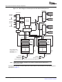
module. Figure 1-1 shows the block diagram of the ADC module.
The two 8-channel modules can autosequence a series of conversions; each module has the choice of
selecting any one of the respective eight channels available through an analog MUX. In the cascaded
mode, the autosequencer functions as a single 16-channel sequencer. On each sequencer, once the
conversion is completed, the selected channel value is stored in its respective ADCRESULT register.
Autosequencing allows the system to convert the same channel multiple times, allowing the user to
perform oversampling algorithms. This oversampling gives increased resolution over traditional
single-sampled conversion results.
Functions of the ADC module include:
• 12-bit ADC core with built-in dual sample-and-hold (S/H)
• Simultaneous sampling or sequential sampling modes
• Analog input: 0 V to 3 V
• Fast conversion time runs at 12.5 MHz, ADC clock, or 6.25 MSPS
• 16-channel, multiplexed inputs
• Autosequencing capability provides up to 16 "autoconversions" in a single session. Each conversion
can be programmed to select any 1 of 16 input channels.
• Sequencer can be operated as two independent 8-state sequencers or as one large 16-state
sequencer (i.e., two cascaded 8-state sequencers).
• Sixteen result registers (individually addressable) to store conversion values
– The digital value of the input analog voltage is derived by:
when input ≤ 0 V
Digital Value + 0,
Digital Value + 4096
Digital Value + 4095,
A
when 0 V < input < 3 V
when input ≥ 3 V
All fractional values are truncated.
•
•
•
•
•
10
Input Analog Voltage * ADCLO
3
Multiple triggers as sources for the start-of-conversion (SOC) sequence
– S/W - software immediate start
– ePWM 1-6
– GPIO XINT2
Flexible interrupt control allows interrupt request on every end-of-sequence (EOS) or every other EOS
Sequencer can operate in "start/stop" mode, allowing multiple "time-sequenced triggers" to
synchronize conversions.
ePWM triggers can operate independently in dual-sequencer mode.
Sample-and-hold (S/H) acquisition time window has separate prescale control.
Analog-to-Digital Converter (ADC)
SPRU812A – September 2007 – Revised October 2007
Submit Documentation Feedback
www.ti.com
Features
Figure 1-1. Block Diagram of the ADC Module
ADCENCLK
SYSCLKOUT
High-speed
prescaler
System
control block
C28x
HSPCLK
HALT
Analog
MUX
Result Registers
Result Reg 0
ADCINA0
70A8h
Result Reg 1
S/H-A
ADCINA7
12-Bit
ADC
module
Result Reg 7
70AFh
Result Reg 8
70B0h
Result Reg 15
70B7h
ADCINB0
S/H-B
ADCINB7
ADC Control Registers
S/W
ePWMx SOCA
SOC
Sequencer 1
S/W
Sequencer 2
SOC
ePWMx SOCB
GPIO/XINT2_
ADCSOC
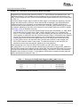
Table 1-1. ADC Registers
Name
Address
(1)
Address (2)
Size (x16)
Description
ADCTRL1
0x7100
1
ADC Control Register 1
ADCTRL2
0x7101
1
ADC Control Register 2
ADCMAXCONV
0x7102
1
ADC Maximum Conversion Channels Register
ADCCHSELSEQ1
0x7103
1
ADC Channel Select Sequencing Control Register 1
ADCCHSELSEQ2
0x7104
1
ADC Channel Select Sequencing Control Register 2
ADCCHSELSEQ3
0x7105
1
ADC Channel Select Sequencing Control Register 3
ADCCHSELSEQ4
0x7106
1
ADC Channel Select Sequencing Control Register 4
ADCASEQSR
0x7107
1
ADC Auto-Sequence Status Register
ADCRESULT0
0x7108
0x0B00
1
ADC Conversion Result Buffer Register 0
ADCRESULT1
0x7109
0x0B01
1
ADC Conversion Result Buffer Register 1
ADCRESULT2
0x710A
0x0B02
1
ADC Conversion Result Buffer Register 2
ADCRESULT3
0x710B
0x0B03
1
ADC Conversion Result Buffer Register 3
ADCRESULT4
0x710C
0x0B04
1
ADC Conversion Result Buffer Register 4
ADCRESULT5
0x710D
0x0B05
1
ADC Conversion Result Buffer Register 5
ADCRESULT6
0x710E
0x0B06
1
ADC Conversion Result Buffer Register 6
ADCRESULT7
0x710F
0x0B07
1
ADC Conversion Result Buffer Register 7
ADCRESULT8
0x7110
0x0B00
1
ADC Conversion Result Buffer Register 8
ADCRESULT9
0x7111
0x0B09
1
ADC Conversion Result Buffer Register 9
(1)
(2)
The registers in this column are Peripheral Frame 2 registers.
The ADC result registers are dual mapped in the device. Locations in Peripheral Frame 2 (0x7108-0x7117) are 2 wait states
and left justified. Locations in Peripheral Frame 0 space (0x0B00-0x0B0F) are 0 wait states and right justified. During high
speed/continuous conversion use of the ADC, use the 0 wait state locations to avoid missing ADC conversions.
SPRU812A – September 2007 – Revised October 2007
Submit Documentation Feedback
Analog-to-Digital Converter (ADC)
11
www.ti.com
Autoconversion Sequencer Principle of Operation
Table 1-1. ADC Registers (continued)
Name
Address
(1)
Address (2)
Size (x16)
0x0B0A
1
ADC Conversion Result Buffer Register 10
Description
ADCRESULT10
0x7112
ADCRESULT11
0x7113
0x0B0B
1
ADC Conversion Result Buffer Register 11
ADCRESULT12
0x7114
0x0B0C
1
ADC Conversion Result Buffer Register 12
ADCRESULT13
0x7115
0x0B0D
1
ADC Conversion Result Buffer Register 13
ADCRESULT14
0x7116
0x0B0E
1
ADC Conversion Result Buffer Register 14
ADCRESULT15
0x7117
0x0B0F
1
ADC Conversion Result Buffer Register 15
ADCTRL3
0x7118
1
ADC Control Register 3
ADCST
0x7119
1
ADC Status Register
Reserved
0x711A
0x711B
2
ADCREFSEL
0x711C
1
ADC Reference Select Register
ADCOFFTRIM
0x711D
1
ADC Offset Trim Register
Reserved
0x711E
0x711F
2
ADC Status Register
To obtain the specified accuracy of the ADC, proper board layout is very critical. To the best extent
possible, traces leading to the ADCINxx pins should not run in close proximity to the digital signal paths.
This is to minimize switching noise on the digital lines from getting coupled to the ADC inputs.
Furthermore, proper isolation techniques must be used to isolate the ADC module power pins from the
digital supply.
1.2
Autoconversion Sequencer Principle of Operation
The ADC sequencer consists of two independent 8-state sequencers (SEQ1 and SEQ2) that can also be
cascaded together to form one 16-state sequencer (SEQ). The word "state" represents the number of
autoconversions that can be performed with the sequencer. Block diagrams of the single (16-state,
cascaded) and dual (two 8-state, separated) sequencer modes are shown in Figure 1-4 and Figure 1-5,
respectively.
In both cases, the ADC has the ability to autosequence a series of conversions. This means that each
time the ADC receives a start-of-conversion request, it can perform multiple conversions automatically.
For every conversion, any one of the available 16 input channels can be selected through the analog
MUX. After conversion, the digital value of the selected channel is stored in the appropriate result register
(ADCRESULTn). (The first result is stored in ADCRESULT0, the second result in ADCRESULT1, and so
on). It is also possible to sample the same channel multiple times, allowing the user to perform
"over-sampling", which gives increased resolution over traditional single-sampled conversion results.
Note:
In the sequential sampling dual-sequencer mode, a pending SOC request from either
sequencer is taken up as soon as the sequence initiated by the currently active sequencer is
finished. For example, assume that the A/D converter is busy catering to SEQ2 when an
SOC request from SEQ1 occurs. The A/D converter will start SEQ1 immediately after
completing the request in progress on SEQ2. If SOC requests are pending from both SEQ1
and SEQ2, the SOC for SEQ1 has priority. For example, assume that the A/D converter is
busy catering to SEQ1. During that process, SOC requests from both SEQ1 and SEQ2 are
made. When SEQ1 completes its active sequence, the SOC request for SEQ1 will be taken
up immediately. The SOC request for SEQ2 will remain pending.
The ADC can also operate in simultaneous sampling mode or sequential sampling mode. For each
conversion (or pair of conversions in simultaneous sampling mode), the current CONVxx bit field defines
the pin (or pair of pins) to be sampled and converted. In sequential sampling mode, all four bits of
CONVxx define the input pin. The MSB defines which sample-and-hold buffer the input pin is associated
with, and the three LSBs define the offset. For example, if CONVxx contains the value 0101b, ADCINA5 is
the selected input pin. If it contains the value 1011b, ADCINB3 is the selected input pin. In simultaneous
12
Analog-to-Digital Converter (ADC)
SPRU812A – September 2007 – Revised October 2007
Submit Documentation Feedback
www.ti.com
Autoconversion Sequencer Principle of Operation
sampling mode, the MSB of the CONVxx register is discarded. Each sample and hold buffer samples the
associated pin given by the offset provided in the three LSBs of the CONVxx register. For instance, if the
CONVxx register contains the value 0110b, ADCINA6 is sampled by S/H-A and ADCINB6 is sampled by
S/H-B. If the value is 1001b, ADCINA1 is sampled by S/H-A and ADCINB1 is sampled by S/H-B. The
voltage in S/H-A is converted first, followed by the S/H-B voltage. The result of the S/H-A conversion is
placed in the current ADCRESULTn register (ADCRESULT0 for SEQ1, assuming the sequencer has been
reset). The result of the S/H-B conversion is placed in the next ADCRESULTn register (ADCRESULT1 for
SEQ1, assuming the sequencer has been reset). The result register pointer is then increased by two (to
point to ADCRESULT2 for SEQ1, assuming the sequencer had originally been reset).
1.2.1 Sequential Sampling Mode
Figure 1-2 shows the timing of sequential sampling mode. In this example, the ACQ_PS bits are set to
0001b.
Figure 1-2. Sequential Sampling Mode (SMODE = 0)
Variable-width
acquisition window
ADC
Clock
Channel
Select
[C0NV00]†
[C0NV00]†
[C0NV01](A)
SH Clock
S
ADC SOC
trigger
C1
S
C1
Legend: C1 − Duration of time for result register update
S − Acquisition window
A
ADC channel address contained in [CONV00] 4-bit register; CONV00 for SEQ1 and CONV08 for SEQ2.
SPRU812A – September 2007 – Revised October 2007
Submit Documentation Feedback
Analog-to-Digital Converter (ADC)
13
www.ti.com
Autoconversion Sequencer Principle of Operation
1.2.2 Simultaneous Sampling Mode
Figure 1-3 describes the timing of simultaneous sampling mode. In this example, the ACQ_PS bits are set
to 0001b.
Figure 1-3. Simultaneous Sampling Mode (SMODE=1)
Variable-width
acquisition window
Clock
ADC Clock
Channel
Select
[CONV00]†
[CONV00](A)
[CONV01](A)
C2
SOC
SH Clock
S
ADC SOC
Trigger
C1
C2
C1
S
Legend: C1 − Duration of time for Ax channel result in result register
C2 − Duration of time for Bx channel result in result register
S − Acquisition window
A
14
ADC channel address contained in [CONV00] 4-bit register; [CONV00] means A0/B0 channels; [CONV01] means
A1/B1 channels.
Analog-to-Digital Converter (ADC)
SPRU812A – September 2007 – Revised October 2007
Submit Documentation Feedback
www.ti.com
Autoconversion Sequencer Principle of Operation
Figure 1-4. Block Diagram of Autosequenced ADC in Cascaded Mode
Analog MUX
ADCINA0
ADCINA1
Result MUX
ADCRESULT0
MUX
select
ADCRESULT1
S/H-A
12-bit
analog-to-digital
converter
(ADC)
ADCINA7
ADCINB0
ADCINB1
S/H-B
MUX
select
12
ADCRESULT2
12
SOC
ADCINB7
Result
select
EOC
ADCRESULT15
MAX_CONV1
Ch Sel (CONV00)
Ch Sel (CONV01)
4
Ch Sel (CONV02)
Ch Sel (CONV03)
Autosequencer
state machine
Ch Sel (CONV15)
State
pointer
MUX
select
4
Note: Possible values are:
Channel select = 0 to 15
ADCMAXCONV = 0 to 15
Software
ePWMx SOCA
Start-of-sequence trigger
ePWMx SOCB
External pin
(GPIO/XINT2_ADCSOC)
SPRU812A – September 2007 – Revised October 2007
Submit Documentation Feedback
Analog-to-Digital Converter (ADC)
15
www.ti.com
Autoconversion Sequencer Principle of Operation
Figure 1-5. Block Diagram of Autosequenced ADC With Dual Sequencers
Result MUX
ADCRESULT0
Analog MUX
ADCINA0
ADCINA1
ADCRESULT1
12
MUX
select
S/H-A
12
ADCINA7
ADCINB0
12-bit A/D
converter
S/H-B
ADCINB1
ADCRESULT7
Result
select
12
MUX
Result MUX
MUX
select
ADCRESULT8
EOC
SOC
ADCINB7
ADCRESULT9
12
4
Sequencer arbiter
12
4
Result
select
4
SOC1
EOC1
SOC2
MAX_CONV1
Ch Sel (CONV00)
Ch Sel (CONV01)
Ch Sel (CONV02)
Ch Sel (CONV07)
Software
ePWMx SOCA
External pin
(XINT2_ADCSOC)
Note:
EOC2
MAX_CONV2
State
pointer
Ch Sel (CONV08)
State
pointer
Ch Sel (CONV09)
4
Ch Sel (CONV10)
Ch Sel (CONV11)
Ch Sel (CONV03)
Note: Possible values:
Channel select = 0 − 15
MAX CONV1 = 0 − 7
MAX CONV2 = 0 − 7
ADCRESULT15
SEQ1
Start-of-sequence
trigger
Ch Sel (CONV15)
Software
SEQ2
Start-of-sequence
trigger
ePWMx SOCB
ADC start of conversion (SOC) trigger sources
There is only one ADC in the DSP. This converter is shared by the two sequencers in
dual-sequencer mode.
The sequencer operation for both 8-state and 16-state modes is almost identical; the few differences are
highlighted in Table 1-2.
16
Analog-to-Digital Converter (ADC)
SPRU812A – September 2007 – Revised October 2007
Submit Documentation Feedback
www.ti.com
Autoconversion Sequencer Principle of Operation
Table 1-2. Comparison of Single and Cascaded Operating Modes
Feature
Start-of-conversion (SOC)
triggers
Single 8-state sequencer #1
(SEQ1)
Single 8-state
sequencer #2 (SEQ2)
Cascaded 16-state
sequencer (SEQ)
ePWMx SOCA, software,
external pin
ePWMx SOCB, software
ePWMx SOCA, ePWMx
SOCB, software,
external pin
8
8
16
Yes
Yes
Yes
Maximum number of
autoconversions
(i.e., sequence length)
Autostop at end-ofsequence (EOS)
Arbitration priority
High
Low
Not applicable
ADC conversion result register
locations
0 to 7
8 to 15
0 to 15
CONV00 to CONV07
CONV08 to CONV15
CONV00 to CONV15
ADCCHSELSEQn bit field
assignment
For convenience, the sequencer states will be subsequently referred to as:
• For SEQ1: CONV00 to CONV07
• For SEQ2: CONV08 to CONV15
• For Cascaded SEQ: CONV00 to CONV15
The analog input channel selected for each sequenced conversion is defined by CONVxx bit fields in the
ADC input channel select sequencing control registers (ADCCHSELSEQn). CONVxx is a 4-bit field that
specifies any one of the 16 channels for conversion. Since a maximum of 16 conversions in a sequence is
possible when using the sequencers in cascaded mode, 16 such 4-bit fields (CONV00 - CONV15) are
available and are spread across four 16-bit registers (ADCCHSELSEQ1 - ADCCHSELSEQ4). The
CONVxx bits can have any value from 0 to 15. The analog channels can be chosen in any desired order
and the same channel may be selected multiple times.
SPRU812A – September 2007 – Revised October 2007
Submit Documentation Feedback
Analog-to-Digital Converter (ADC)
17
www.ti.com
Autoconversion Sequencer Principle of Operation
Example 1-1. Simultaneous Sampling Dual Sequencer Mode Example
Example initialization:
AdcRegs.ADCTRL3.bit.SMODE_SEL =
AdcRegs.ADCMAXCONV.all =
0x1;
0x0033;
// Setup simultaneous sampling mode
// 4 double conv's each sequencer (8 total)
AdcRegs.ADCCHSELSEQ1.bit.CONV00 = 0x0;
// Setup conv from ADCINA0 & ADCINB0
AdcRegs.ADCCHSELSEQ1.bit.CONV01 = 0x1;
// Setup conv from ADCINA1 & ADCINB1
AdcRegs.ADCCHSELSEQ1.bit.CONV02 = 0x2;
// Setup conv from ADCINA2 & ADCINB2
AdcRegs.ADCCHSELSEQ1.bit.CONV03 = 0x3;
// Setup conv from ADCINA3 & ADCINB3
AdcRegs.ADCCHSELSEQ3.bit.CONV08 = 0x4;
// Setup conv from ADCINA4 & ADCINB4
AdcRegs.ADCCHSELSEQ3.bit.CONV09 = 0x5;
// Setup conv from ADCINA5 & ADCINB5
AdcRegs.ADCCHSELSEQ3.bit.CONV10 = 0x6;
// Setup conv from ADCINA6 & ADCINB6
AdcRegs.ADCCHSELSEQ3.bit.CONV11 = 0x7;
// Setup conv from ADCINA7 & ADCINB7
If SEQ1 and SEQ2 were both executed, the results would go to the following RESULT registers:
ADCINA0 -> ADCRESULT0
ADCINB0 -> ADCRESULT1
ADCINA1 -> ADCRESULT2
ADCINB1 -> ADCRESULT3
ADCINA2 -> ADCRESULT4
ADCINB2 -> ADCRESULT5
ADCINA3 -> ADCRESULT6
ADCINB3 -> ADCRESULT7
ADCINA4 -> ADCRESULT8
ADCINB4 -> ADCRESULT9
ADCINA5 -> ADCRESULT10
ADCINB5 -> ADCRESULT11
ADCINA6 -> ADCRESULT12
ADCINB6 -> ADCRESULT13
ADCINA7 -> ADCRESULT14
ADCINB7 -> ADCRESULT15
18
Analog-to-Digital Converter (ADC)
SPRU812A – September 2007 – Revised October 2007
Submit Documentation Feedback
www.ti.com
Uninterrupted Autosequenced Mode
Example 1-2. Simultaneous Sampling Cascaded Sequencer Mode Example
AdcRegs.ADCTRL3.bit.SMODE_SEL
=
0x1;
// Setup simultaneous sampling mode
0x1;
// Setup cascaded sequencer mode
AdcRegs.ADCTRL1.bit.SEQ_CASC
=
AdcRegs.ADCMAXCONV.all =
0x0007;
// 8 double conv's (16 total)
AdcRegs.ADCCHSELSEQ1.bit.CONV00
= 0x0;
// Setup conv from ADCINA0 & ADCINB0
AdcRegs.ADCCHSELSEQ1.bit.CONV01
= 0x1;
// Setup conv from ADCINA1 & ADCINB1
AdcRegs.ADCCHSELSEQ1.bit.CONV02
= 0x2;
// Setup conv from ADCINA2 & ADCINB2
AdcRegs.ADCCHSELSEQ1.bit.CONV03
= 0x3;
// Setup conv from ADCINA3 & ADCINB3
AdcRegs.ADCCHSELSEQ2.bit.CONV04
= 0x4;
// Setup conv from ADCINA4 & ADCINB4
AdcRegs.ADCCHSELSEQ2.bit.CONV05
= 0x5;
// Setup conv from ADCINA5 & ADCINB5
AdcRegs.ADCCHSELSEQ2.bit.CONV06
= 0x6;
// Setup conv from ADCINA6 & ADCINB6
AdcRegs.ADCCHSELSEQ2.bit.CONV07
= 0x7;
// Setup conv from ADCINA7 & ADCINB7
If the cascaded SEQ was executed, the results would go to the following ADCRESULT registers:
ADCINA0 -> ADCRESULT0
ADCINB0 -> ADCRESULT1
ADCINA1 -> ADCRESULT2
ADCINB1 -> ADCRESULT3
ADCINA2 -> ADCRESULT4
ADCINB2 -> ADCRESULT5
ADCINA3 -> ADCRESULT6
ADCINB3 -> ADCRESULT7
ADCINA4 -> ADCRESULT8
ADCINB4 -> ADCRESULT9
ADCINA5 -> ADCRESULT10
ADCINB5 -> ADCRESULT11
ADCINA6 -> ADCRESULT12
ADCINB6 -> ADCRESULT13
ADCINA7 -> ADCRESULT14
ADCINB7 -> ADCRESULT15
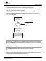
1.3
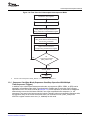
Uninterrupted Autosequenced Mode
The following description applies to the 8-state sequencers (SEQ1 or SEQ2). In this mode, SEQ1/SEQ2
can autosequence up to eight conversions of any channel in a single sequencing session (16 when
sequencers are cascaded together). Figure 1-6 shows the flow diagram. The result of each conversion is
stored in one of the eight result registers (ADCRESULT0 - ADCRESULT7 for SEQ1 and ADCRESULT8 ADCRESULT15 for SEQ2). These registers are filled from the lowest address to the highest address.
The number of conversions in a sequence is controlled by MAX_CONVn (a 3-bit or 4-bit field in the
ADCMAXCONV register), which is automatically loaded into the sequencing counter status bits
(SEQ_CNTR[3:0]) in the autosequence status register (ADCASEQSR) at the start of an autosequenced
conversion session. The MAX_CONVn field can have a value ranging from zero to seven (zero to fifteen
when sequencers are cascaded together). SEQ_CNTR bits count down from their loaded value as the
sequencer starts from state CONV00 and continues sequentially (CONV01, CONV02, and so on) until
SEQ_CNTR has reached zero. The number of conversions completed during an autosequencing session
is equal to (MAX_CONVn + 1).
SPRU812A – September 2007 – Revised October 2007
Submit Documentation Feedback
Analog-to-Digital Converter (ADC)
19
www.ti.com
Uninterrupted Autosequenced Mode
Example 1-3. Conversion in Dual-Sequencer Mode Using SEQ1
Suppose seven conversions are desired from SEQ1 (i.e., inputs ADCINA2 and ADCINA3 twice, then
ADCINA6, ADCINA7, and ADCINB4 must be converted as part of the autosequenced session), then
MAX_CONV1 should be set to 6 and the ADCCHSELSEQn registers should be set to the values shown
in Table 1-3.
Conversion begins once the start-of-conversion (SOC) trigger is received by the sequencer. The SOC
trigger also loads the SEQ_CNTR bits. Those channels that are specified in the ADCCHSELSEQn
registers are taken up for conversion, in the predetermined sequence. The SEQ_CNTR bits are
decremented by one automatically after every conversion. Once SEQ_CNTR reaches zero, two things
can happen, depending on the status of the continuous run bit (CONT_RUN) in the ADCTRL1 register.
See Figure 1-6 for an illustration of the flow.
• If CONT_RUN is set, the conversion sequence starts all over again automatically (i.e., SEQ_CNTR
gets reloaded with the original value in MAX_CONV1 and SEQ1 state is set to CONV00 [See
Section 1.7 for more options]). In this case, to avoid overwriting the data, you must be sure that the
result registers are read before the next conversion sequence begins. The arbitration logic designed
into the ADC ensures that the result registers are not corrupted should a contention arise (ADC
module trying to write into the result registers while you try to read from them at the same time).
• If CONT_RUN is not set, the sequencer stays in the last state (CONV06, in this example) and
SEQ_CNTR continues to hold a value of zero. To repeat the sequence on the next SOC, the
sequencer must be reset using the RST_SEQn bit prior to the next SOC.
If the interrupt flag is set every time SEQ_CNTR reaches zero (INT_ENA_SEQn = 1 and
INT_MOD_SEQn = 0), you can (if needed) manually reset the sequencer (using the RST_SEQn bit in
the ADCTRL2 register) in the interrupt service routine (ISR). This causes the SEQn state to be reset to
its original value (CONV00 for SEQ1 and CONV08 for SEQ2). This feature is useful in the Start/Stop
operation of the sequencer. Example 1-3 also applies to SEQ2 and the cascaded 16-state sequencer
(SEQ) with differences outlined in Table 1-2.
Table 1-3. Values for ADCCHSELSEQn Registers (MAX_CONV1 Set to 6)
(1)
20
Bits 15-12 (1)
Bits 11-8 (1)
Bits 7-4 (1)
Bits 3-0 (1)
70A3h
3
2
3
2
ADCCHSELSEQ1
70A4h
x
12
7
6
ADCCHSELSEQ2
70A5h
x
x
x
x
ADCCHSELSEQ3
70A6h
x
x
x
x
ADCCHSELSEQ4
Values are in decimal, and x = don't care
Analog-to-Digital Converter (ADC)
SPRU812A – September 2007 – Revised October 2007
Submit Documentation Feedback
www.ti.com
Uninterrupted Autosequenced Mode
Figure 1-6. Flow Chart for Uninterrupted Autosequenced Mode
Initialize the ADC registers
SOC trigger arrives
MAX_CONVn value gets loaded into
SEQ_CNTR bits in ADCASEQSR register
Conversion begins.
SEQ_CNTR bits are decremented by
one for every conversion
Current conversion complete.
Digital result is written into
corresponding ADCRESULTn register
No
All
conversions complete?
(SEQ_CNTR = 0?)
Yes
Set INT_SEQn
Stop
A
The flow chart corresponds to CONT_RUN bit = 0 and INT_MOD_SEQn bit = 0.
1.3.1 Sequencer Start/Stop Mode (Sequencer Start/Stop Operation With Multiple
Time-Sequenced Triggers)
In addition to the uninterrupted autosequenced mode, any sequencer (SEQ1, SEQ2, or SEQ) can be
operated in a Stop/Start mode which is synchronized to multiple start-of-conversion (SOC) triggers,
separated in time. This mode is similar to Example 1-3, but the sequencer is allowed to be retriggered
without being reset to the initial state CONV00, once it has completed its first sequence (i.e., the
sequencer is not reset in the interrupt service routine). Therefore, when one conversion sequence ends,
the sequencer stays in the current conversion state. The continuous run bit (CONT_RUN) in the
ADCTRL1 register must be set to zero (i.e., disabled) for this mode.
SPRU812A – September 2007 – Revised October 2007
Submit Documentation Feedback
Analog-to-Digital Converter (ADC)
21
www.ti.com
Uninterrupted Autosequenced Mode
Example 1-4. Sequencer Start/Stop Operation
Requirement: To start three autoconversions (e.g., I1,I2,I3) off trigger 1 (underflow) and three
autoconversions (e.g., V1,V2,V3) off trigger 2 (period). Triggers 1 and 2 are separated in time by 25 µs
and are provided by an ePWM. See Figure 1-7. Only SEQ1 is used in this case.
Note:
Triggers 1 and 2 may be an SOC signal from ePWM, external pin, or software. The same
trigger source may occur twice to satisfy the dual-trigger requirement of this example.
Care must be taken such that multiple ePWM triggers are not lost due sequences already
in progress. See Section 1.3.3.
Here MAX_CONV1 is set to 2 and the ADC Input Channel Select Sequencing Control Registers
(ADCCHSELSEQn) are set as shown in Table 1-4.
Once reset and initialized, SEQ1 waits for a trigger. With the first trigger, three conversions with
channel-select values of: CONV00 (I1), CONV01 (I2), and CONV02 (I3) are performed. SEQ1 then waits
at current state for another trigger. Twenty-five microseconds later when the second trigger arrives,
another three conversions occur, with channel-select values of CONV03 (V1), CONV04 (V2), and
CONV05 (V3).
The value of MAX_CONV1 is automatically loaded into SEQ_CNTR for both trigger cases. If a different
number of conversions are required at the second trigger point, you must (at some appropriate time
before the second trigger) change the value of MAX_CONV1 through software, otherwise, the current
(originally loaded) value will be reused. This can be done by an ISR that changes the value of
MAX_CONV1 at the appropriate time. The interrupt operation modes are described in Section 1.3.4.
At the end of the second autoconversion session, the ADC result registers will have the values shown
in Table 1-5.
At this point, SEQ1 keeps "waiting" at the current state for another trigger. Now, the user can reset
SEQ1 (by software) to state CONV00 and repeat the same trigger1, 2 sessions.
Figure 1-7. Example of ePWM Triggers to Start the Sequencer
50 µs
25 µs
ePWM
counter
PWM A/B
output
I1, I2, I3
22
Analog-to-Digital Converter (ADC)
V1, V2,V3
I1, I2, I3
V1, V2, V3
SPRU812A – September 2007 – Revised October 2007
Submit Documentation Feedback
www.ti.com
Uninterrupted Autosequenced Mode
Table 1-4. Values for ADCCHSELSEQn (MAX_CONV1 set to 2)
Bits 15-12
Bits 11-8
Bits 7-4
Bits 3-0
70A3h
V1
I3
I2
I1
ADCCHSELSEQ1
70A4h
x
x
V3
V2
ADCCHSELSEQ2
70A5h
x
x
x
x
ADCCHSELSEQ3
70A6h
x
x
x
x
ADCCHSELSEQ4
Table 1-5. Values After Second Autoconversion
Session
Buffer Register
ADC Conversion Result Buffer
ADCRESULT0
I1
ADCRESULT1
I2
ADCRESULT2
I3
ADCRESULT3
V1
ADCRESULT4
V2
ADCRESULT5
V3
ADCRESULT6
x
ADCRESULT7
x
ADCRESULT8
x
ADCRESULT9
x
ADCRESULT10
x
ADCRESULT11
x
ADCRESULT12
x
ADCRESULT13
x
ADCRESULT14
x
ADCRESULT15
x
1.3.2 Simultaneous Sampling Mode
The ADC has the ability to sample two ADCINxx inputs simultaneously, provided that one input is from the
range ADCINA0 - ADCINA7 and the other input is from the range ADCINB0 - ADCINB7. Furthermore, the
two inputs must have the same sample-and-hold offset (i.e., ADCINA4 and ADCINB4, but not ADCINA7
and ADCINB6). To put the ADC into simultaneous sampling mode, the SMODE_SEL bit in the ADCTRL3
register must be set. See Section 1.2 for details.
1.3.3 Input Trigger Description
Each sequencer has a set of trigger inputs that can be enabled/disabled. See Table 1-6 for the valid input
triggers for SEQ1, SEQ2, and cascaded SEQ.
Table 1-6. Input Triggers
SEQ1 (sequencer 1)
SEQ2 (sequencer 2)
Cascaded SEQ
Software trigger (software SOC)
Software trigger (software SOC)
Software trigger (software SOC)
ePWMx SOCA
ePWMx SOCB
ePWMx SOCA
XINT2_ADCSOC
ePWMx SOCB
XINT2_ADCSOC
SPRU812A – September 2007 – Revised October 2007
Submit Documentation Feedback
Analog-to-Digital Converter (ADC)
23
www.ti.com
Uninterrupted Autosequenced Mode
Notes:
•
•
•
•
An SOC trigger can initiate an autoconversion sequence whenever a sequencer is in an
idle state. An idle state is either CONV00 prior to receiving a trigger, or any state which
the sequencer lands on at the completion of a conversion sequence, i.e., when
SEQ_CNTR has reached a count of zero.
If an SOC trigger occurs while a current conversion sequence is underway, it sets the
SOC_SEQn bit (which would have been cleared on the commencement of a previous
conversion sequence) in the ADCTRL2 register. If yet another SOC trigger occurs, it is
lost (i.e., when the SOC_SEQn bit is already set (SOC pending), subsequent triggers
will be ignored).
Once triggered, the sequencer cannot be stopped/halted in mid sequence. The program
must either wait until an end-of-sequence (EOS) or initiate a sequencer reset, which
brings the sequencer immediately back to the idle start state (CONV00 for SEQ1 and
cascaded cases; CONV08 for SEQ2).
When SEQ1/2 are used in cascaded mode, triggers going to SEQ2 are ignored, while
SEQ1 triggers are active. Cascaded mode can be viewed as SEQ1 with 16 states
instead of eight.
1.3.4 Interrupt Operation During Sequenced Conversions
The sequencer can generate interrupts under two operating modes. These modes are determined by the
Interrupt-Mode-Enable control bits in ADCTRL2.
A variation of Example 1-4 can be used to show how interrupt mode 1 and mode 2 are useful under
different operating conditions.
Case 1: Number of samples in the first and second sequences are not equal
• Mode 1 Interrupt operation (i.e., Interrupt request occurs at every EOS)
1. Sequencer is initialized with MAX_CONVn = 1 for converting I1 and I2
2. At ISR "a", MAX_CONVn is changed to 2 (by software) for converting V1, V2, and V3
3. At ISR "b", the following events take place :
a. MAX_CONVn is changed to 1 again for converting I1 and I2.
b. Values I1, I2, V1, V2, and V3 are read from ADC result registers.
c. The sequencer is reset.
4. Steps 2 and 3 are repeated. Note that the interrupt flag is set every time SEQ_CNTR reaches zero
and both interrupts are recognized.
Case 2: Number of samples in the first and second sequences are equal
• Mode 2 Interrupt operation (i.e., Interrupt request occurs at every other EOS)
1. Sequencer is initialized with MAX_CONVn = 2 for converting I1, I2, and I3 (or V1, V2, and V3).
2. At ISR "b" and "d", the following events take place :
a. Values I1, I2, I3,V1, V2, and V3 are read from ADC result registers.
b. The sequencer is reset.
3. Step 2 is repeated.
Case 3: Number of samples in the first and second sequences are equal (with dummy read)
• Mode 2 Interrupt operation (i.e., Interrupt request occurs at every other EOS)
1. Sequencer is initialized with MAX_CONVn = 2 for I1, I2, and x(dummy sample).
2. At ISR "b" and "d", the following events take place :
a. Values I1, I2, x,V1, V2, and V3 are read from ADC result registers.
b. The sequencer is reset.
3. Step 2 is repeated. Note that the third I-sample (x) is a dummy sample, and is not really required.
However, to minimize ISR overhead and CPU intervention, advantage is taken of the "every other"
Interrupt request feature of Mode 2.
24
Analog-to-Digital Converter (ADC)
SPRU812A – September 2007 – Revised October 2007
Submit Documentation Feedback
www.ti.com
Uninterrupted Autosequenced Mode
Figure 1-8. Interrupt Operation During Sequenced Conversions
50 µs
25 µs
ePWM
counter
PWM A/B
output
I1,I2
V1,V2,V3
I1,I2
V1,V2,V3
Sampling
request
Case 1
“a”
I1,I2,I3
“b”
V1,V2,V3
“c”
I1,I2,I3
“b”
I1,I2,x
V1,V2,V3
“d”
V1,V2,V3
“d”
I1,I2,x
V1,V2,V3
SEQ
interrupt
Sampling
request
Case 2
SEQ
interrupt
Sampling
request
Case 3
“b”
SPRU812A – September 2007 – Revised October 2007
Submit Documentation Feedback
“d”
SEQ
interrupt
Analog-to-Digital Converter (ADC)
25
www.ti.com
ADC Clock Prescaler
1.4
ADC Clock Prescaler
The peripheral clock HSPCLK is divided down by the ADCCLKPS[3:0] bits of the ADCTRL3 register. An
extra divide-by-two is provided via the CPS bit of the ADCTRL1 register. In addition, the ADC can be
tailored to accommodate variations in source impedances by widening the sampling/acquisition period.
This is controlled by the ACQ_PS[3:0] bits in the ADCTRL1 register. These bits do not affect the
conversion portion of the S/H and conversion process, but do extend the length of time in which the
sampling portion takes by extending the start of the conversion pulse. See Figure 1-9.
Figure 1-9. ADC Core Clock and Sample-and-Hold (S/H) Clock
ADCTRL1[11-8]
(ACQ_PS[3-0])
ADCTRL1[7]=1
(CPS=1)
x1/2
HSPCLK
4-bit clock
divider
(x1, 1/2, ... 1/30)
S/H clock
pulse
SOC pulse
generator
x1
ADCTRL1[7]=0
(CPS=0)
ADCCLK
ADCTRL3[4-1]
(ADCLKPS[3-0])
A
See register bit definition for clock divider ratio and S/H pulse control. S/H pulse width determines the size of
acquisition window (the time period for which sampling switch is closed).
1.4.1 ADC-module Clock and Sample Rate
The ADC module has several prescaler stages to generate any desired ADC operating clock speed.
Figure 1-10 defines the clock selection stages that feed the ADC module. Table 1-7 gives two example
settings and shows both the effective sustained sequential sampling rate and the sample and hold window
time for those settings.
Figure 1-10. Clock Chain to the ADC
XCLKIN
PLL
HSPCLK
HISPCP
No PLL
Fclk
ADCLKPS
CPS
ADCENCLK
PCLKCR[3]
ADCCLK
ACQ_PS
SH clock/
pulse
Table 1-7. Clock Chain to the ADC
XCLKIN
30 MHz
20 MHz
1.5
SYSCLKOUT
150 MHz
100 MHz
HISPCLK
ADCTRL3[4-1]
ADCTRL1[7]
HSPCP = 3
ADCLKPS = 0
CPS=0
150 MHz/
2 X 3 = 25 MHz
25 MHz
25 MHz
HSPCP = 2
ADCLKPS = 2
CPS = 1
100 MHz/
2 X 2 = 25 MHz
25/2 X 2 =
6.25 MHz
6.25 MHz/
2 X 1 = 3.125
MHz
ADCCLK
ADCTRL1[11-8]
SH Width
ACQ_PS = 0
25 MHz
12.5 MHz
12.5 MSPS sustained
conversion rate
ACQ_PS = 15
3.125 MHz
183.824 kHz
183.824 kSPS sustained
conversion rate
1 ADC Clock
40 ns
16 ADC
Clocks
5.12 µs
Low-power Modes
The ADC supports three separate power sources each controlled by independent bits in the ADCTRL3
register. These three bits combine to make up three power levels: ADC power up, ADC power down, and
ADC off.
26
Analog-to-Digital Converter (ADC)
SPRU812A – September 2007 – Revised October 2007
Submit Documentation Feedback
www.ti.com
Power-up Sequence
Table 1-8. Power Options
Power Level
1.6
ADCBGRFDN1
ADCBGRFDN0
ADCPWDN
ADC power-up
1
1
1
ADC power-down
1
1
0
ADC off
0
0
0
Reserved
1
0
X
Reserved
0
1
X
Power-up Sequence
The ADC resets to the ADC off state. When powering up the ADC, use the following sequence:
1. If external reference is desired, enable this mode using bits 15-14 in the ADCREFSEL Register. This
mode must be enabled before band gap is powered.
2. Power up the reference, bandgap, and analog circuits together by setting bits 7-5 (ADCBGRFDN[1:0],
ADCPWDN) in the ADCTRL3 register.
3. Before performing the first conversion, a delay of 5 ms is required.
When powering down the ADC, all three bits can be cleared simultaneously. The ADC power level must
be controlled via software and they are independent of the state of the device power modes.
Sometimes it is desirable to power down the ADC while leaving the band-gap and reference powered by
clearing the ADCPWDN bit only. When the ADC is re-powered, a delay of 20 μs is required after this bit is
set before performing any conversions.
Note:
1.7
The 2833x ADC requires a 5-ms delay after all of the circuits are powered up. This differs
from the 281x ADC.
Sequencer Override Feature
In normal operation, sequencers SEQ1, SEQ2 or cascaded SEQ1 help to convert selected ADC channels
and store them in the respective ADCRESULTn registers, sequentially. The sequence naturally wraps
around at the end of the MAX_CONVn setting. With the sequencer override feature, the natural
wraparound of the sequencers can be controlled in software. The sequencer override feature is controlled
by bit 5 of the ADC Control Register 1 (ADCCTRL1).
For example, assume the SEQ_OVRD bit is 0 and the ADC is in cascaded-sequencer,
continuous-conversion mode with MAX_CONV1 set to 7. Normally, the sequencer would increment
sequentially and update up to ADCRESULT7 register with ADC conversions and wraps around to 0. At the
end of the ADCRESULT7 register update, the relevant interrupt flag would be set.
With the SEQ_OVRD bit set to 1, the sequencer updates seven result registers and does not wrap around
to 0. Instead, the sequencer will increment sequentially and update the ADCRESULT8 register onwards
until the ADCRESULT15 register is reached. After updating ADCRESULT15 register, the natural wrap
around to 0 will occur. This feature treats the result registers (0-15) like a FIFO for sequential data capture
from the ADC. This feature is very helpful to capture ADC data when ADC conversions are done at the
maximum data rate.
SPRU812A – September 2007 – Revised October 2007
Submit Documentation Feedback
Analog-to-Digital Converter (ADC)
27
www.ti.com
ADC Calibration
Recommendations and caution on sequencer override feature:
• After reset, SEQ_OVRD bit will be 0; therefore the sequencer override feature remains disabled.
• When SEQ _OVRD bit is set for all nonzero values of MAX_CONVn, the related interrupt flag bit will
be set for every MAX_CONVn count of result register update.
• For example, if ADCMAXCONV is set to 3, then the interrupt flag for the selected sequencer will be set
every four result register updates. The wraparound always occurs at the end of the sequencer (i.e.,
after ADCRESULT15 register update in cascaded sequencer mode).
• This will be functional in conversions using SEQ1, SEQ2, and cascaded sequencers using SEQ1.
• It is recommended that this feature not be enabled/controlled dynamically within the program. Always
enable this feature during the ADC module initialization.
• In continuous-conversion mode with sequencer changes, the ADC channel address uses the preset
values in CONVxx registers. If continuous conversions of the same channel are needed then all the
CONVxx registers should have the same channel address.
• In continuous-conversion mode, if a sequencer reset is needed: set CONT_RUN bit to 0, wait 2 cycles
in the ADC Clock domain, then reset the sequencer. CONT_RUN can then be set back to 1.
• For example, to get 16 contiguous samples for the ADCINA0 channel using the sequencer override
feature, all 16 CONVxx registers should be set to 0x0000.
1.8
ADC Calibration
The ADC_cal() routine is programmed into TI reserved OTP memory by the factory. The boot ROM
automatically calls the ADC_cal() routine to initialize the ADCREFSEL and ADCOFFTRIM registers with
device specific calibration data. During normal operation, this process occurs automatically and no action
is required by the user.
If the boot ROM is bypassed by Code Composer Studio during the development process, then
ADCREFSEL and ADCOFFTRIM must be initialized by the application. For working examples, see the
ADC initialization in the C2833x C/C++ Header Files and Peripheral Examples (SPRC530).
The next two sections describe different methods for calling the ADC_Cal() routine.
Note:
FAILURE TO INITIALIZE THESE REGISTERS WILL CAUSE THE ADC TO FUNCTION
OUT OF SPECIFICATION.
Because TI reserved OTP memory is secure, the ADC_Cal() routine must be called from
secure memory or called from non-secure memory after the Code Security Module is
unlocked. If the system is reset or the ADC module is reset using Bit 14 (RESET) from the
ADC Control Register 1, the routine must be repeated.
28
Analog-to-Digital Converter (ADC)
SPRU812A – September 2007 – Revised October 2007
Submit Documentation Feedback
www.ti.com
ADC Calibration
1.8.1 ADC_Cal Assembly Routine Method
The following three steps describe how to call the ADC_cal routine from an application:
Step 1. Add the ADC_cal assembly function to your project. The source is included with the C2833x
C/C++ Header Files and Peripheral Examples (SPRC530). The following code shows the
contents of the ADC_cal function. The values 0xAAAA and 0xBBBB are place holders. The
actual values programmed by TI are device specific.
;----------------------------------------------; This is the ADC cal routine. This routine is programmed
; into reserved memory by the factory. 0xAAAA and 0xBBBB
; are place holders. The actual values programmed by TI
; are device specific.
; The ADC clock must be enabled before calling
; this function.
;----------------------------------------------.def _ADC_cal
.asg "0x711C",
ADCREFSEL_LOC
.sect ".adc_cal"
_ADC_cal
MOVW DP,
#ADCREFSEL_LOC >> 6
MOV
@28, #0xAAAA
MOV
@29, #0xBBBB
LRETR
Step 2.
Add the .adc_cal section to your linker command file using the following:
MEMORY
{
PAGE 0 :
...
ADC_CAL
...
}
SECTIONS
{
...
.adc_cal
...
}
Step 3.
: origin = 0x380080, length = 0x000009
: load = ADC_CAL,
PAGE = 0, TYPE = NOLOAD
Call the ADC_cal function before using the ADC. The ADC clocks must be enabled before
making this call.
extern void ADC_cal(void);
…
EALLOW;
SysCtrlRegs.PCLKCR0.bit.ADCENCLK = 1;
ADC_cal();
SysCtrlRegs.PCLKCR0.bit.ADCENCLK = 0;
EDIS;
1.8.2 Pointer to-Function Method
Because the ADC_CAL() routine is already programmed to TI reserved OTP memory by the factory, it can
be called via a pointer to the function by using the following steps:
Step 1. Define ADC_Cal as a pointer to the programmed function in the OTP memory.
#define ADC_Cal (void (*) (void)) 0x380080
Step 2.
Call the ADC_Cal() function.
...
EALLOW;
SysCtrlRegs.PCLKCR0.bit.ADCENCLK=1;
(*ADC_Cal) ();
SysCTRLRegs.PCLKCR0.bit.ADCENCLK=0;
EDIS;
SPRU812A – September 2007 – Revised October 2007
Submit Documentation Feedback
Analog-to-Digital Converter (ADC)
29
www.ti.com
Internal/External Reference Voltage Selection
1.9
Internal/External Reference Voltage Selection
By default, an internally generated bandgap voltage reference is selected to supply the ADC logic.
Based on customer application requirements, the ADC logic may be supplied by an external voltage
reference. The ADC will accept 2.048 V, 1.5 V, or 1.024 V on the ADCREFIN pin. The value of the
ADCREFSEL register determines the reference source selected.
If the internal reference option is chosen, the ADCREFIN pin can be left connected to the selected source,
left floating, or grounded. Regardless of which option is chosen, the external circuit for the ADCRESEXT,
ADCREFP, and ADCREFM pins is the same.
The external reference voltage of 2.048 V was chosen to match industry standard reference components.
These components are available in various temperature ratings. A recommended Texas Instruments part
is REF3020AIDBZ.
Figure 1-11. External Bias for 2.048-V External Reference
F280x DSP
ADCREFIN
ADC reference
ADC REFSEL
2.048-V reference
ADCRESEXT(A)
ADCREFP(A)
ADCREFM(A)
Bandgap
reference
ADC LO
Analog ground
A
30
For component values, see the TMS320F28332, TMS320F28334, TMS320F28335 Digital Signal Controllers (DSCs)
Data Manual (literature number SPRS439).
Analog-to-Digital Converter (ADC)
SPRU812A – September 2007 – Revised October 2007
Submit Documentation Feedback
www.ti.com
Offset Error Correction
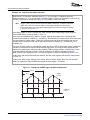
1.10 Offset Error Correction
The 2833x ADC supports offset correction via a 9-bit field in the ADC Offset Trim
Register(ADCOFFTRIM). The value contained in this register will be added/subtracted before the results
are available in the ADC result registers. This operation is contained in the ADC module, so timing for
results will not be affected. Furthermore, since the operation is handled inside the ADC, the full dynamic
range of the ADC will be maintained for any trim value.
The ADCOFFTRIM register is pre-loaded by the ADC_cal routine in the boot ROM. To further reduce the
offset error in the target application, connect the signal ADCLO to one of the ADC channels and convert
that channel, modifying the value in the ADCOFFTRIM, until a centered zero code is observed. See
Figure 1-12 for a flow diagram.
Figure 1-12. Flow Chart of Offset Error Correction Process
Convert ADCLO
reference
~20 conversions
Are
any codes
0?
Yes
Add 40 (decimal)
to the OFFTRIM
register
No
Calculate the average
output code of the
conversions
Subtract the average from
the value in the OFFTRIM
register and write result back
to the OFFTRIM register
Example 1-5. Negative Offset
At startup, most of the reference conversions yield a zero result. After writing the value 0x28 (40
decimal) into the OFFTRIM register, all of the reference conversions give a positive result and average
out to 0x19 (25 decimal). The final value written to the OFFTRIM register should be 0x0F (15 decimal).
Example 1-6. Positive Offset
At startup, all of the reference conversions yield a positive result with an average of 0x14 (20 decimal).
The final value written to the OFFTRIM register should be 0x1EC (-20 decimal).
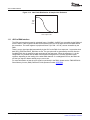
After the offset error correction process is completed, a half bell curved distribution similar to Figure 1-13
should be seen when multiple ADCLO samples are converted. The other half of the bell curve is hidden
due to the fact that the converter bottoms out at a code of zero.
SPRU812A – September 2007 – Revised October 2007
Submit Documentation Feedback
Analog-to-Digital Converter (ADC)
31
www.ti.com
ADC to DMA Interface
Figure 1-13. Ideal Code Distribution of Sampled 0-V Reference
Hits
per
code
0
1
2
3
ADC output code
4095
1.11 ADC to DMA Interface
The ADC result registers located in peripheral frame 0 (0x0B00 – 0x0B0F) are accessible by the DMA unit
on the F2833x. These registers can also be accessed by the CPU at the same time as the DMA without
bus contention. The result registers in peripheral frame 2 (0x7108 – 0x710F) are not accessible by the
DMA.
There is a sync signal provided automatically by the ADC to the DMA for a sequencer 1 conversion when
both SEQ_OVRD and CONT_RUN bits are set. The sync pulse will be generated by the ADC after the
first MAXCONV limit is reached for each pass through the sequencer. When the sequencer 1 is in this
configuration it is possible that the DMA could become misaligned to the currently populated result
registers, depending on the loading of the other DMA channels. If a misalignment occurs, the DMA can
use the sync signal to detect and flag a sync error event.
For more information on how the sync signal is used locally in the DMA, please see the TMS320F2833x
Direct Memory Access (DMA) Reference Guide (literature number SPRUFB8).
32
Analog-to-Digital Converter (ADC)
SPRU812A – September 2007 – Revised October 2007
Submit Documentation Feedback
Chapter 2
SPRU812A – September 2007 – Revised October 2007
ADC Registers
This chapter contains the ADC registers and bit definitions, with the registers grouped by function.
Topic
2.1
2.2
2.3
2.4
2.5
2.6
2.7
2.8
..................................................................................................
ADC Control Registers ..............................................................
Maximum Conversion Channels Register (ADCMAXCONV) ...........
Autosequence Status Register (ADCASEQSR) .............................
ADC Status and Flag Register (ADCST) .......................................
ADC Reference Select Register (ADCREFSEL) .............................
ADC Offset Trim Register (ADCOFFTRIM) ....................................
ADC Input Channel Select Sequencing Control Registers ..............
ADC Conversion Result Buffer Registers (ADCRESULTn) ..............
SPRU812A – September 2007 – Revised October 2007
Submit Documentation Feedback
Page
34
38
40
41
43
43
44
45
ADC Registers
33
www.ti.com
ADC Control Registers
2.1
ADC Control Registers
Figure 2-1. ADC Control Register 1 (ADCTRL1) (Address Offset 00h)
15
14
Reserved
RESET
13
SUSMOD
12
11
ACQ_PS
8
R-0
R/W-0
R/W-0
R/W-0
7
6
5
4
CPS
CONT_RUN
SEQ_OVRD
SEQ_CASC
3
Reserved
0
R/W-0
R/W-0
R/W-0
R/W-0
R-0
LEGEND: R/W = Read/Write; R = Read only; -n = value after reset
Table 2-1. ADC Control Register 1 (ADCTRL1) Field Descriptions
Bit(s)
Name
Value
Description
15
Reserved
Reads return a zero. Writes have no effect.
14
RESET
ADC module software reset. This bit causes a master reset on the entire ADC module.
All register bits and sequencer state machines are reset to the initial state as occurs
when the device reset pin is pulled low (or after a power-on reset). This is a
one-time-effect bit, meaning this bit is self-cleared immediately after it is set to 1. Read
of this bit always returns a 0. Also, the reset of ADC has a latency of two clock cycles
(that is, other ADC control register bits should not be modified until two ADC clock
cycles after the instruction that resets the ADC.
0
No effect
1
Resets entire ADC module (bit is then set back to 0 by ADC logic)
Note: The ADC module is reset during a system reset. If an ADC module reset is
desired at any other time, you can do so by writing a 1 to this bit. After two ADC clock
domain cycles, you can then write the appropriate values to the ADCCTRL1 register bits.
The example below assumes 150-MHz DSP Clock and 25-MHz ADCCLK. Assembly
code:
MOV ADCTRL1, #01xxxxxxxxxxxxxxb; Resets the ADC (RESET = 1)
RPT #10|| NOP; Provides the required delay between writes to ADCTRL1
MOV ADCTRL1, #00xxxxxxxxxxxxxxb ; Configures ADCTRL1 to user-desired value.
Note that the second MOV is not required if the default configuration is sufficient.
13-12
11-8
7
SUSMOD[1:0]
Emulation-suspend mode. These bits determine what occurs when an
emulation-suspend occurs (due to the debugger hitting a breakpoint, for example).
00
Mode 0. Emulation suspend is ignored.
01
Mode 1. Sequencer and other wrapper logic stops after current sequence is complete,
final result is latched, and state machine is updated.
10
Mode 2. Sequencer and other wrapper logic stops after current conversion is complete,
result is latched, and state machine is updated.
11
Mode 3. Sequencer and other wrapper logic stops immediately on emulation suspend.
ACQ_PS[3:0]
Acquisition window size. This bit field controls the width of SOC pulse, which, in turn,
determines for what time duration the sampling switch is closed. The width of SOC pulse
is ADCTRL1[11:8] + 1 times the ADCLK period.
CPS
Core clock prescaler. The prescaler is applied to divided device peripheral clock,
HSPCLK.
0
ADCCLK = Fclk/1
1
ADCCLK = Fclk/2
Note: Fclk = Prescaled HSPCLK (ADCCLKPS[3:0])
6
34
CONT_RUN
ADC Registers
Continuous run. This bit determines whether the sequencer operates in continuous
conversion mode or start-stop mode. This bit can be written while a current conversion
sequence is active. This bit will take effect at the end of the current conversion
sequence; i.e., software can set/clear this bit until EOS has occurred, for valid action to
be taken. In the continuous conversion mode, there is no need to reset the sequencer;
however, the sequencer must be reset in the start-stop mode to put the converter in
state CONV00.
SPRU812A – September 2007 – Revised October 2007
Submit Documentation Feedback
www.ti.com
ADC Control Registers
Table 2-1. ADC Control Register 1 (ADCTRL1) Field Descriptions (continued)
Bit(s)
5
4
3-0
Name
Value
Description
0
Start-stop mode. Sequencer stops after reaching EOS. On the next SOC, the sequencer
starts from the state where it ended unless a sequencer reset is performed.
1
Continuous conversion mode. After reaching EOS, the behavior of the sequencer
depends on the state of the SEQ_OVRD bit. If this bit is cleared, the sequencer starts
over again from its reset state (CONV00 for SEQ1 and cascaded, CONV08 for SEQ2). If
SEQ_OVRD is set, the sequencer starts again from its current position, without
resetting.
SEQ_OVRD
Sequencer override. Provides additional sequencer flexibility in continuous run mode by
overriding the wrapping around at the end of conversions set by MAX_CONVn.
0
Disabled - Allows the sequencer to wrap around at the end of conversions set by
MAX_CONVn.
1
Enabled - Overrides the sequencer from wrapping around at the end of conversions set
by MAX_CONVn. Wraparound occurs only at the end of the sequencer.
SEQ_CASC
Cascaded sequencer operation. This bit determines whether SEQ1 and SEQ2 operate
as two 8-state sequencers or as a single 16-state sequencer (SEQ).
0
Dual-sequencer mode. SEQ1 and SEQ2 operate as two 8-state sequencers.
1
Cascaded mode. SEQ1 and SEQ2 operate as a single 16-state sequencer (SEQ).
Reserved
Reads return zero. Writes have no effect.
Figure 2-2. ADC Control Register 2 (ADCTRL2) (Address Offset 01h)
15
14
13
12
11
10
9
8
ePWM_SOCB_SEQ
RST_SEQ1
SOC_SEQ1
Reserved
INT_ENA_SEQ1
INT_MOD_SEQ1
Reserved
ePWM_SOCA_SEQ1
R/W-0
R/W-0
R/W-0
R-0
R/W-0
R/W-0
R-0
R/W-0
7
6
5
4
3
2
1
0
EXT_SOC_SEQ1
RST_SEQ2
SOC_SEQ2
Reserved
INT_ENA_SEQ2
INT_MOD_SEQ2
Reserved
ePWM_SOCB_SEQ2
R/W-0
R/W-0
R/W-0
R-0
R/W-0
R/W-0
R-0
R/W-0
LEGEND: R/W = Read/Write; R = Read only; W = Write access, S = Set only, C = Clear -n = value after reset
Table 2-2. ADC Control Register 2 (ADCTRL2) Field Descriptions
Bit(s) Name
15
14
Value
ePWM_SOCB_SEQ
Description
ePWM SOCB enable for cascaded sequencer (Note: This bit is active only in cascaded
mode.)
0
No action
1
Setting this bit allows the cascaded sequencer to be started by an ePWM SOCB signal.
The ePWM modules can be programmed to start a conversion on various events. See the
TMS320x28xx , 28xxx Enhanced Pulse Width Modulation Module Reference Guide
(literature number SPRU791) for more information on the ePWM modules.
RST_SEQ1
Reset sequencer1 Writing a 1 to this bit resets SEQ1 or the cascaded sequencer
immediately to an initial "pretriggered" state, i.e., waiting for a trigger at CONV00. A
currently active conversion sequence will be aborted.
0
No action
1
Immediately reset sequencer to state CONV00
SPRU812A – September 2007 – Revised October 2007
Submit Documentation Feedback
ADC Registers
35
www.ti.com
ADC Control Registers
Table 2-2. ADC Control Register 2 (ADCTRL2) Field Descriptions (continued)
Bit(s) Name
13
Value
SOC_SEQ1
Description
Start-of-conversion (SOC) trigger for Sequencer 1 (SEQ1) or the cascaded sequencer.
This bit can be set by the following triggers:
• S/W - Software writing a 1 to this bit
• ePWM SOCA
• ePWM SOCB (only in cascaded mode)
• EXT - External pin (i.e., GPIO Port A pin (GPIO31-0) configured as XINT2 in the
GPIOxINT2SEL register.
See the TMS320x2833x System Control and Interrupts Reference Guide (literature
number SPRUFB0) for details on how to configure a GPIO pin as XINT2. When a trigger
occurs, there are three possibilities:
Case 1: SEQ1 idle and SOC bit clear SEQ1 starts immediately (under arbiter control).
This bit is set and cleared, allowing for any "pending" trigger requests.
Case 2: SEQ1 busy and SOC bit clear Bit is set signifying a trigger request is pending.
When SEQ1 finally starts after completing current conversion, this bit is cleared.
Case 3: SEQ1 busy and SOC bit set Any trigger occurring in this case is ignored (lost).
0
Clears a pending SOC trigger.
Note: If the sequencer has already started, this bit is automatically cleared, and hence,
writing a zero has no effect; i.e., an already started sequencer cannot be stopped by
clearing this bit.
1
Software trigger - Start SEQ1 from currently stopped position (i.e., Idle mode)
Note: The RST_SEQ1 (ADCTRL2.14) and the SOC_SEQ1 (ADCTRL2.13) bits should not
be set in the same instruction. This resets the sequencer, but does not start the
sequence. The correct sequence of operation is to set the RST_SEQ1 bit first, and the
SOC_SEQ1 bit in the following instruction. This makes certain that the sequencer is reset
and a new sequence started. This sequence applies to the RST_SEQ2 (ADCTRL2.6) and
SOC_SEQ2 (ADCTRL2.5) bits also.
12
Reserved
11
INT_ENA_SEQ1
10
SEQ1 interrupt enable. This bit enables the interrupt request to CPU by INT SEQ1.
0
Interrupt request by INT_SEQ1 is disabled.
1
Interrupt request by INT_SEQ1 is enabled.
INT_MOD_SEQ1
SEQ1 interrupt mode. This bit selects SEQ1 interrupt mode. It affects the setting of INT
SEQ1 at the end of the SEQ1 conversion sequence.
0
INT_SEQ1 is set at the end of every SEQ1 sequence.
1
INT_SEQ1 is set at the end of every other SEQ1 sequence.
9
Reserved
Reads return a zero. Writes have no effect.
8
ePWM_SOCA_SEQ1
ePWM SOCA enable bit for SEQ1
7
6
36
Reads return a zero. Writes have no effect.
0
SEQ1 cannot be started by ePWMx SOCA trigger.
1
Allows SEQ1/SEQ to be started by ePWMx SOCA trigger. The ePWMs can be
programmed to start a conversion on various events.
EXT_SOC_SEQ1
External signal start-of-conversion bit for SEQ1
0
No action
1
Setting this bit enables an ADC autoconversion sequence to be started by a signal from a
GPIO Port A pin (GPIO31-0) configured as XINT2 in the GPIOXINT2SEL register. See
the TMS320x2833x System Control and Interrupts Reference Guide (literature number
SPRUFB0)
RST_SEQ2
ADC Registers
Reset SEQ2
0
No action
1
Immediately resets SEQ2 to an initial "pretriggered" state, i.e., waiting for a trigger at
CONV08. A currently active conversion sequence will be aborted.
SPRU812A – September 2007 – Revised October 2007
Submit Documentation Feedback
www.ti.com
ADC Control Registers
Table 2-2. ADC Control Register 2 (ADCTRL2) Field Descriptions (continued)
Bit(s) Name
5
Value
SOC_SEQ2
Description
Start of conversion trigger for sequencer 2 (SEQ2). (Only applicable in dual-sequencer
mode; ignored in cascaded mode.) This bit can be set by the following triggers:
• S/W - Software writing of 1 to this bit
• ePWM SOCB
When a trigger occurs, there are three possibilities:
Case 1: SEQ2 idle and SOC bit clear SEQ2 starts immediately (under arbiter control) and
the bit is cleared, allowing for any pending trigger requests.
Case 2: SEQ2 busy and SOC bit clear Bit is set signifying a trigger request is pending.
When SEQ2 finally starts after completing current conversion, this bit will be cleared.
Case 3: SEQ2 busy and SOC bit set Any trigger occurring in this case will be ignored
(lost).
0
Clears a Pending SOC trigger
Note: If the sequencer has already started, this bit is automatically cleared, and writing a
zero has no effect; i.e., an already started sequencer cannot be stopped by clearing this
bit.
1
Starts SEQ2 from currently stopped position (i.e., Idle mode)
4
Reserved
Reads return a zero. Writes have no effect.
3
INT_ENA_SEQ2
SEQ2 interrupt enable. This bit enables or disables an interrupt request to the CPU by
INT SEQ2.
2
0
Interrupt request by INT_SEQ2 is disabled.
1
Interrupt request by INT_SEQ2 is enabled.
INT_MOD_SEQ2
SEQ2 interrupt mode. This bit selects SEQ2 interrupt mode. It affects the setting of INT
SEQ2 at the end of the SEQ2 conversion sequence.
1
Reserved
0
ePWM_SOCB_SEQ2
0
INT_SEQ2 is set at the end of every SEQ2 sequence.
1
INT_SEQ2 is set at the end of every other SEQ2 sequence.
Reads return a zero. Writes have no effect.
ePWM SOCB enable bit for SEQ2.
0
SEQ2 cannot be started by ePWMx SOCB trigger.
1
Allows SEQ2 to be started by ePWMx SOCB trigger. The ePWMs can be programmed to
start a conversion on various events.
Figure 2-3. ADC Control Register 3 (ADCTRL3) (Address Offset 18h)
15
8
Reserved
R-0
7
6
5
4
1
0
ADCBGRFDN
ADCPWDN
ADCCLKPS
SMODE_SEL
R/W-0
R/W-0
R/W-0
R/W-0
LEGEND: R/W = Read/Write; R = Read only; -n = value after reset
Table 2-3. ADC Control Register 3 (ADCTRL3) Field Descriptions
Bit(s) Name
Value
Description
15-8
Reserved
Reads return a zero. Writes have no effect.
7-6
ADCBGRFDN[1:0]
ADC bandgap and reference power down. These bits control the power up and power
down of the bandgap and reference circuitry inside the analog core. See Section 1.6 for
power-up sequence requirements.
5
ADCPWDN
00
The bandgap and reference circuitry is powered down.
11
The bandgap and reference circuitry is powered up.
ADC power down. This bit controls the power up and power down of all the analog
circuitry inside the analog core except the bandgap and reference circuitry. See
Section 1.6 for power-up sequence requirements.
SPRU812A – September 2007 – Revised October 2007
Submit Documentation Feedback
ADC Registers
37
www.ti.com
Maximum Conversion Channels Register (ADCMAXCONV)
Table 2-3. ADC Control Register 3 (ADCTRL3) Field Descriptions (continued)
Bit(s) Name
4-1
Value
Description
0
All analog circuitry inside the core except the bandgap and reference circuitry is powered
down.
1
The analog circuitry inside the core is powered up.
ADCCLKPS [3:0]
Core clock divider. 28x peripheral clock, HSPCLK, is divided by 2*ADCCLKPS[3-0],
except when ADCCLKPS[3-0] is 0000, in which case HSPCLK is directly passed on. The
divided clock is further divided by ADCTRL1[7]+1 to generate the core clock, ADCLK.
ADCCLKPS [3:0] Core Clock Divider ADCLK
0
2.2
0000
0 HSPCLK/(ADCTRL1[7] + 1)
0001
1 HSPCLK/[2*(ADCTRL1[7] + 1)]
0010
2 HSPCLK/[4*(ADCTRL1[7] + 1)]
0011
3 HSPCLK/[6*(ADCTRL1[7] + 1)]
0100
4 HSPCLK/[8*(ADCTRL1[7] + 1)]
0101
5 HSPCLK/[10*(ADCTRL1[7] + 1)]
0110
6 HSPCLK/[12*(ADCTRL1[7] + 1)]
0111
7 HSPCLK/[14*(ADCTRL1[7] + 1)]
1000
8 HSPCLK/[16*(ADCTRL1[7] + 1)]
1001
9 HSPCLK/[18*(ADCTRL1[7] + 1)]
1010
10 HSPCLK/[20*(ADCTRL1[7] + 1)]
1011
11 HSPCLK/[22*(ADCTRL1[7] + 1)]
1100
12 HSPCLK/[24*(ADCTRL1[7] + 1)]
1101
13 HSPCLK/[26*(ADCTRL1[7] + 1)]
1110
14 HSPCLK/[28*(ADCTRL1[7] + 1)]
1111
15 HSPCLK/[30*(ADCTRL1[7] + 1)]
SMODE_SEL
Sampling mode select. This bit selects either sequential or simultaneous sampling mode.
0
Sequential sampling mode is selected.
1
Simultaneous sampling mode is selected.
Maximum Conversion Channels Register (ADCMAXCONV)
Figure 2-4. Maximum Conversion Channels Register (ADCMAXCONV) (Offset Address 02h)
15
8
Reserved
R-0
7
6
4
3
0
Reserved
MAX_CONV2
MAX_CONV1
R-0
R/W-0
R/W-0
LEGEND: R/W = Read/Write; R = Read only; x = undefined, -n = value after reset
38
ADC Registers
SPRU812A – September 2007 – Revised October 2007
Submit Documentation Feedback
www.ti.com
Maximum Conversion Channels Register (ADCMAXCONV)
Table 2-4. Maximum Conversion Channels Register (ADCMAXCONV) Field Descriptions
Bit(s)
Name
Description
15-7
Reserved
Reads return a zero. Writes have no effect.
6-0
MAX_CONVn
MAX_CONVn bit field defines the maximum number of conversions executed in an autoconversion
session. The bit fields and their operation vary according to the sequencer modes (dual/cascaded).
For SEQ1 operation, bits MAX_CONV1[2:0] are used.
For SEQ2 operation, bits MAX_CONV2[2:0] are used.
For SEQ operation, bits MAX_CONV1[3:0] are used. An autoconversion session always starts with
the initial state and continues sequentially until the end state if allowed. The result buffer is filled in a
sequential order. Any number of conversions between 1 and (MAX_CONVn +1) can be programmed
for a session.
Example 2-1. ADCMAXCONV Register Bit Programming
If only five conversions are required, then MAX_CONVn is set to four.
Case 1: Dual mode SEQ1 and cascaded mode Sequencer goes from CONV00 to CONV04, and the
five conversion results are stored in the registers Result 00 to Result 04 of the Conversion Result
Buffer.
Case 2: Dual mode SEQ2 Sequencer goes from CONV08 to CONV12, and the five conversion results
are stored in the registers Result 08 to Result 12 of the Conversion Result Buffer.
MAX_CONV1 Value >7 for Dual-Sequencer Mode
If a value for MAX_CONV1, which is greater than 7, is chosen for the dual-sequencer mode (i.e., two
separate 8-state sequencers), then SEQ_CNTR will continue counting past seven, causing the
sequencer to wrap around to CONV00 and continue counting.
Table 2-5. Bit Selections for MAX_CONV1 for
Various Number of Conversions
ADCMAXCONV[3-0]
Number of Conversions
0000
1
0001
2
0010
3
0011
4
0100
5
0101
6
0110
7
0111
8
SPRU812A – September 2007 – Revised October 2007
Submit Documentation Feedback
1000
9
1001
10
1010
11
1011
12
1100
13
1101
14
1110
15
1111
16
ADC Registers
39
www.ti.com
Autosequence Status Register (ADCASEQSR)
2.3
Autosequence Status Register (ADCASEQSR)
Figure 2-5. Autosequence Status Register (ADCASEQSR) (Address Offset 07h)
15
12
7
11
8
Reserved
SEQ_CNTR
R-0
R-0
6
4
3
0
Reserved
SEQ2_STATE
SEQ1_STATE
R-0
R-0
R-0
LEGEND: R/W = Read/Write; R =Read only; x = undefined, -n = value after reset
Table 2-6. Autosequence Status Register (ADCASEQSR) Field Descriptions
Bit(s)
Name
Description
15-12
Reserved
Reads return a zero. Writes have no effect.
11-8
SEQ_CNTR[3:0]
Sequencing counter status bits. The SEQ_CNTRn 4-bit status field is used by SEQ1, SEQ2, and
the cascaded sequencer. SEQ2 is irrelevant in cascaded mode. The Sequencer Counter bit field,
SEQ_CNTR[3:0], is initialized to the value in MAX_CONV at the start of a conversion sequence.
After each conversion (or a pair of conversions in simultaneous sampling mode) in an auto
conversion sequence, the Sequencer Counter decreases by 1.The SEQ_CNTR bits can be read at
any time during the countdown process to check status of the sequencer. This value, together with
the SEQ1 and SEQ2 busy bits, uniquely identifies the progress or state of the active sequencer at
any point in time. See Table 2-7.
Reserved
Reads return a zero. Writes have no effect.
SEQ2_STATE[2:0]
and
SEQ1_STATE[3:0]
SEQ2_STATE and SEQ1_STATE bit fields are the pointers of SEQ2 and SEQ1, respectively.
7
6-0
Table 2-7. State of Active Sequencer
40
ADC Registers
SEQ_CNTR (read only)
Number of conversions
remaining
0000
1 or 0, depending on the busy bit
0001
2
0010
3
0011
4
0100
5
0101
6
0110
7
0111
8
1000
9
1001
10
1010
11
1011
12
1100
13
1101
14
1110
15
1111
16
SPRU812A – September 2007 – Revised October 2007
Submit Documentation Feedback
www.ti.com
ADC Status and Flag Register (ADCST)
2.4
ADC Status and Flag Register (ADCST)
Figure 2-6. ADC Status and Flag Register (ADCST) (Address Offset 19h)
15
8
Reserved
R-0
7
6
5
4
3
2
1
0
EOS_BUF2
EOS_BUF1
INT_SEQ2_CLR
INT_SEQ1_CLR
SEQ2_BSY
SEQ1_BSY
INT_SEQ2
INT_SEQ1
R-0
R-0
R/W-0
R/W-0
R-0
R-0
R-0
R-0
LEGEND: R/W = Read/Write; R = Read only; -n = value after reset
This register is a dedicated status and flag register. The bits in this register are either read-only status or
flag bits, or read-return-zero condition clearing bits.
Table 2-8. ADC Status and Flag Register (ADCST) Field Descriptions
Bit(s)
Name
15-8
Value Description
Reserved
Reads return a zero. Writes have no effect.
7
EOS_BUF2
End of sequence buffer bit for SEQ2. This bit is not used and remains as zero in interrupt
mode 0, i.e. when ADCTRL2[2]=0. In interrupt mode 1, i.e. when ADCTRL2[2]=1, it toggles
on every end of sequence of SEQ2. This bit is cleared on device reset and is not affected by
sequencer reset or clearing of the corresponding interrupt flag.
6
EOS_BUF1
End of sequence buffer bit for SEQ1. This bit is not used and remains as zero in interrupt
mode 0, i.e. when ADCTRL2[10]=0. In interrupt mode 1, i.e. when ADCTRL2[10]=1, it
toggles on every end of sequence of SEQ1. This bit is cleared on device reset and is not
affected by sequencer reset or clearing of the corresponding interrupt flag.
5
INT_SEQ2_CLR
Interrupt clear bit. Read of this bit always returns 0. The clear action is a one-shot event
following a write of 1 to this bit.
4
3
2
1
0
0
Writing a zero to this bit has no effect.
1
Writing a 1 to this bit clears the SEQ2 interrupt flag bit, INT_SEQ2. This bit does not affect
the EOS_BUF2 bit.
INT_SEQ1_CLR
Interrupt clear bit. Read of this bit always returns 0. The clear action is a one-shot event
following a write of 1 to this bit.
0
Writing a zero to this bit has no effect.
1
Writing a 1 to this bit clears the SEQ1 interrupt flag bit, INT_SEQ1. This bit does not affect
the EOS_BUF1 bit.
SEQ2_BSY
SEQ2 busy status bit.
0
SEQ2 is in idle, waiting for trigger.
1
SEQ2 is in progress. Write to this bit has no effect.
SEQ1_BSY
SEQ1 busy status bit. Write to this bit has no effect.
0
SEQ1 is in idle, waiting for trigger.
1
SEQ1 is in progress.
INT_SEQ2
SEQ2 interrupt flag bit. Write to this bit has no effect. In interrupt mode 0, i.e. when
ADCTRL2[2]=0, this bit is set on every end of sequence of Seq 2. In interrupt mode 1, i.e.,
when ADCTRL2[2]=1, this bit is set on an end of sequence of Seq 2 if EOS_BUF2 is set.
0
No SEQ2 interrupt event.
1
SEQ2 interrupt event occurred.
INT_SEQ1
SEQ1 interrupt flag bit. Write to this bit has no effect. In interrupt mode 0, i.e. when
ADCTRL2[10]=0, this bit is set on every end of sequence of Seq 1. In interrupt mode 1, i.e.,
when ADCTRL2[10]=1, this bit is set on an end of sequence of Seq 1 if EOS_BUF1 is set.
0
No SEQ1 interrupt event.
1
SEQ1 interrupt event occurred.
SPRU812A – September 2007 – Revised October 2007
Submit Documentation Feedback
ADC Registers
41
www.ti.com
ADC Status and Flag Register (ADCST)
42
ADC Registers
SPRU812A – September 2007 – Revised October 2007
Submit Documentation Feedback
www.ti.com
ADC Reference Select Register (ADCREFSEL)
2.5
ADC Reference Select Register (ADCREFSEL)
Figure 2-7. ADC Reference Select Register (ADCREFSEL) (Address Offset 1Ch)
15
14
13
0
REF_SEL
Reserved
R/W-0
R/W-0
LEGEND: R/W = Read/Write; R = Read only; -n = value after reset
Table 2-9. ADC Reference Select Register (ADCREFSEL) Field Descriptions
Bit(s)
Name
15-14
REF_SEL[1:0]
13-0
2.6
Value
Reserved
Description
Reference select bits for ADC voltage generation circuit options are listed below:
00
Internal reference selected (default)
01
External reference, 2.048 V on ADCREFIN
10
External reference, 1.500 V on ADCREFIN
11
External reference, 1.024 V on ADCREFIN
These bits are reserved for reference calibration data loaded from the Boot ROM. All
writes to the ADCREFSEL register should leave the contents of this bit field as is after
population by the Boot ROM.
ADC Offset Trim Register (ADCOFFTRIM)
Figure 2-8. ADC Offset Trim Register (ADCOFFTRIM) (Address Offset 1Dh)
15
9
8
0
Reserved
OFFSET_TRIM
R-0
R/W-0
LEGEND: R/W = Read/Write; R = Read only; -n = value after reset
Table 2-10. ADC Offset Trim Register (ADCOFFTRIM) Field Descriptions
Bit(s)
Name
Description
15-9
Reserved
Reads return a zero. Writes have no effect.
8-0
OFFSET_TRIM[8:0]
Offset trim value in LSBs, two's complement format; - 256/255 range
SPRU812A – September 2007 – Revised October 2007
Submit Documentation Feedback
ADC Registers
43
www.ti.com
ADC Input Channel Select Sequencing Control Registers
2.7
ADC Input Channel Select Sequencing Control Registers
Figure 2-9. ADC Input Channel Select Sequencing Control Registers (ADCCHSELSEQ1) (Address
Offset 03h)
15
12
11
8
7
4
3
0
CONV03
CONV02
CONV01
CONV00
R/W-0
R/W-0
R/W-0
R/W-0
LEGEND: R/W = Read/Write; -n = value after reset
Figure 2-10. ADC Input Channel Select Sequencing Control Registers (ADCCHSELSEQ2) (Address
Offset 04h)
15
12
11
8
7
4
3
0
CONV07
CONV06
CONV05
CONV04
R/W-0
R/W-0
R/W-0
R/W-0
LEGEND: R/W = Read/Write; -n = value after reset
Figure 2-11. ADC Input Channel Select Sequencing Control Registers (ADCCHSELSEQ3) (Address
Offset 05h)
15
12
11
8
7
4
3
0
CONV11
CONV10
CONV09
CONV08
R/W-0
R/W-0
R/W-0
R/W-0
LEGEND: R/W = Read/Write; -n = value after reset
Figure 2-12. ADC Input Channel Select Sequencing Control Registers (ADCCHSELSEQ4) (Address
Offset 06h)
15
12
11
8
7
4
3
0
CONV15
CONV14
CONV13
CONV12
R/W-0
R/W-0
R/W-0
R/W-0
LEGEND: R/W = Read/Write; -n = value after reset
Each of the 4-bit fields, CONVxx, selects one of the 16 MUXed analog input ADC channels for an
autosequenced conversion.
Table 2-11. CONVnn Bit Values and the ADC Input
Channels Selected
44
ADC Registers
CONVnn Value
ADC Input Channel Selected
0000
ADCINA0
0001
ADCINA1
0010
ADCINA2
0011
ADCINA3
0100
ADCINA4
0101
ADCINA5
0110
ADCINA6
0111
ADCINA7
1000
ADCINB0
1001
ADCINB1
1010
ADCINB2
1011
ADCINB3
1100
ADCINB4
SPRU812A – September 2007 – Revised October 2007
Submit Documentation Feedback
www.ti.com
ADC Conversion Result Buffer Registers (ADCRESULTn)
Table 2-11. CONVnn Bit Values and the ADC Input
Channels Selected (continued)
2.8
CONVnn Value
ADC Input Channel Selected
1101
ADCINB5
1110
ADCINB6
1111
ADCINB7
ADC Conversion Result Buffer Registers (ADCRESULTn)
In the cascaded sequencer mode, registers ADCRESULT8 through ADCRESULT15 holds the results of
the ninth through sixteenth conversions. The ADCRESULTn registers are left justified when read from
Peripheral Frame 2 (0x7108-0x7117) with two wait states and right justified when read from Peripheral
Frame 0 (0x0B00-0x0B0F) with zero wait states.
Figure 2-13. ADC Conversion Result Buffer Registers (ADCRESULTn) - (Addresses 0x7108-0x7117)
15
14
13
12
11
10
9
8
D11
D10
D9
D8
D7
D6
D5
D4
R-0
R-0
R-0
R-0
R-0
R-0
R-0
R-0
3
7
6
5
4
D3
D2
D1
D0
Reserved
0
R-0
R-0
R-0
R-0
R-0
LEGEND: R/W = Read/Write; R = Read only; -n = value after reset
Figure 2-14. ADC Conversion Result Buffer Registers (ADCRESULTn) - (Addresses
0x0B00-0x0B0F)
15
11
10
9
8
Reserved
12
D11
D10
D9
D8
R-0
R-0
R-0
R-0
R-0
7
6
5
4
3
2
1
0
D7
D6
D5
D4
D3
D2
D1
D0
R-0
R-0
R-0
R-0
R-0
R-0
R-0
R-0
LEGEND: R/W = Read/Write; R = Read only; -n = value after reset
SPRU812A – September 2007 – Revised October 2007
Submit Documentation Feedback
ADC Registers
45
IMPORTANT NOTICE
Texas Instruments Incorporated and its subsidiaries (TI) reserve the right to make corrections, modifications, enhancements,
improvements, and other changes to its products and services at any time and to discontinue any product or service without notice.
Customers should obtain the latest relevant information before placing orders and should verify that such information is current and
complete. All products are sold subject to TI’s terms and conditions of sale supplied at the time of order acknowledgment.
TI warrants performance of its hardware products to the specifications applicable at the time of sale in accordance with TI’s
standard warranty. Testing and other quality control techniques are used to the extent TI deems necessary to support this
warranty. Except where mandated by government requirements, testing of all parameters of each product is not necessarily
performed.
TI assumes no liability for applications assistance or customer product design. Customers are responsible for their products and
applications using TI components. To minimize the risks associated with customer products and applications, customers should
provide adequate design and operating safeguards.
TI does not warrant or represent that any license, either express or implied, is granted under any TI patent right, copyright, mask
work right, or other TI intellectual property right relating to any combination, machine, or process in which TI products or services
are used. Information published by TI regarding third-party products or services does not constitute a license from TI to use such
products or services or a warranty or endorsement thereof. Use of such information may require a license from a third party under
the patents or other intellectual property of the third party, or a license from TI under the patents or other intellectual property of TI.
Reproduction of TI information in TI data books or data sheets is permissible only if reproduction is without alteration and is
accompanied by all associated warranties, conditions, limitations, and notices. Reproduction of this information with alteration is an
unfair and deceptive business practice. TI is not responsible or liable for such altered documentation. Information of third parties
may be subject to additional restrictions.
Resale of TI products or services with statements different from or beyond the parameters stated by TI for that product or service
voids all express and any implied warranties for the associated TI product or service and is an unfair and deceptive business
practice. TI is not responsible or liable for any such statements.
TI products are not authorized for use in safety-critical applications (such as life support) where a failure of the TI product would
reasonably be expected to cause severe personal injury or death, unless officers of the parties have executed an agreement
specifically governing such use. Buyers represent that they have all necessary expertise in the safety and regulatory ramifications
of their applications, and acknowledge and agree that they are solely responsible for all legal, regulatory and safety-related
requirements concerning their products and any use of TI products in such safety-critical applications, notwithstanding any
applications-related information or support that may be provided by TI. Further, Buyers must fully indemnify TI and its
representatives against any damages arising out of the use of TI products in such safety-critical applications.
TI products are neither designed nor intended for use in military/aerospace applications or environments unless the TI products are
specifically designated by TI as military-grade or "enhanced plastic." Only products designated by TI as military-grade meet military
specifications. Buyers acknowledge and agree that any such use of TI products which TI has not designated as military-grade is
solely at the Buyer's risk, and that they are solely responsible for compliance with all legal and regulatory requirements in
connection with such use.
TI products are neither designed nor intended for use in automotive applications or environments unless the specific TI products
are designated by TI as compliant with ISO/TS 16949 requirements. Buyers acknowledge and agree that, if they use any
non-designated products in automotive applications, TI will not be responsible for any failure to meet such requirements.
Following are URLs where you can obtain information on other Texas Instruments products and application solutions:
Products
Applications
Amplifiers
amplifier.ti.com
Audio
www.ti.com/audio
Data Converters
dataconverter.ti.com
Automotive
www.ti.com/automotive
DSP
dsp.ti.com
Broadband
www.ti.com/broadband
Interface
interface.ti.com
Digital Control
www.ti.com/digitalcontrol
Logic
logic.ti.com
Military
www.ti.com/military
Power Mgmt
power.ti.com
Optical Networking
www.ti.com/opticalnetwork
Microcontrollers
microcontroller.ti.com
Security
www.ti.com/security
RFID
www.ti-rfid.com
Telephony
www.ti.com/telephony
Low Power
Wireless
www.ti.com/lpw
Video & Imaging
www.ti.com/video
Wireless
www.ti.com/wireless
Mailing Address: Texas Instruments, Post Office Box 655303, Dallas, Texas 75265
Copyright © 2007, Texas Instruments Incorporated