1
Implementation of a control system for a scaled
series hybrid electric vehicle
Master of Science Thesis
MAGNUS RÖNNBERG
Department of Signals and Systems
Division of Automatic Control, Automation and Mechatronics
CHALMERS UNIVERSITY OF TECHNOLOGY
Göteborg, Sweden, 2007
Report No. EX090/2007
Implementation of a Control System for a
Scaled Series Hybrid Electric Vehicle
Magnus Rönnberg
Master Thesis student
Department of Machine and Vehicle Systems
Chalmers University of Technology
Gothenburg, Sweden
September, 2004
Abstract
In the Mechatronics division of the department of Machine and Vehicle Systems at
Chalmers University of Technology, research related to hybrid electric vehicles (HEVs) is
performed. This master thesis is part of a project which is proposed to develop a HEV
prototype, and it is to be done in the form of a 1:5 scale model car (SMC). The specific
task of this thesis is to design and construct a control system for the SMC, including the
necessary means to control the energy management of the powertrain. Several modules
for the SMC were determined and acquired outside the boundaries of this thesis,
namely: digital signal processor (DSP), electric motor, DC-converter, buffer and primary
power unit (PPU). The different modules had to be integrated and put under software
control of the DSP.
The SMC is equipped with a brush-less DC-motor which can regenerate kinetic energy.
The regenerated energy is stored both in the PPU-batteries and in the buffer which
consists of super capacitors. Through the use of a DC-converter connected to the buffer
the energy level of the buffer can be regulated. Two analogue servos control the front
mechanical disc brakes and the steering. The actuators of the SMC are controlled by a
TMS320LF2407A DSP from Texas Instruments which is integrated in the control system.
The control system of the SMC incorporates ideas regarding generic control architecture
developed within the Mechatronics division at Chalmers. An operator controls the
prototype with a 4-channel RC-transmitter, and the requested actions are interpreted
and processed by the DSP according to a downloaded program. The DSP receives and
interprets sensor signals regarding power flow within the powertrain, as well as motor
rotational speed, rotational speed on the right front wheel and lever positions on the RCtransmitter. The modular computerized SMC control system offers a highly functional,
and yet low-budget HEV for educational purposes and future developments.
Abbreviations
ADC – Analogue-to-Digital Converter
BLDC – Brush-Less Direct Current
CPU – Central Processor Unit
DAC – Digital-to-Analogue Converter
DC – Direct Current
DSP – Digital Signal Processor
EMI – Electro Magnetic Interference
EMS – Energy Management Strategy
FM – Frequency Modulated
GP – General Purpose
HEV – Hybrid Electric Vehicle
IO – In/Out
LED – Light Emitting Diode
OP – Operation
PC – Personal Computer
PPU – Primary Power Unit
PWM – Pulse Width Modulated
QEP – Quadrature Encoded Pulse
RC – Radio Control
SMC – Scale Model Car
1. Introduction .....................................................................................................5
1.1 Thesis Objectives ........................................................................................6
1.2 Limitations ...................................................................................................6
1.3 Contributions ...............................................................................................6
1.4 Thesis Outline .............................................................................................7
1.5 Acknowledgments .......................................................................................7
2. The Complete Vehicle Control System .........................................................8
2.1 Overview .....................................................................................................8
3. Control System Hardware ............................................................................11
3.1 Digital Signal Processor (DSP)..................................................................12
3.2 Radio Control (RC) system........................................................................13
3.3 Electric Motor ............................................................................................13
3.4 DC-converter .............................................................................................14
3.5 Mechanical Brake Servo ...........................................................................16
3.6 Steer Servo ...............................................................................................16
3.7 External Circuits ........................................................................................16
3.7.1 Current sensors.............................................................................................. 17
3.7.2 Optic connectors ............................................................................................ 18
3.7.3 OP-amplifier ................................................................................................... 18
3.7.4 Voltage regulator for 5 Volt circuitry ............................................................... 18
3.7.5 QEP and motor voltage sensor circuit............................................................ 18
3.7.6 Buffer voltage sensor ..................................................................................... 19
3.7.7 Optic rotational sensor ................................................................................... 21
3.8 Connecting the System .............................................................................21
3.8.1 Wiring and shielding ....................................................................................... 22
4. Control System Software .............................................................................24
4.1 DSP functionality .......................................................................................24
4.1.1 Quadrature Encoded Pulse Circuit (QEP)...................................................... 24
4.1.2 Analogue to Digital Converter (ADC) ............................................................. 24
4.1.3 Digital to Analogue Converter (DAC) ............................................................. 24
4.1.4 Pulse Width Modulated (PWM) signals .......................................................... 24
4.1.5 Digital IO-ports ............................................................................................... 25
4.2 The Functional structure of the code .........................................................25
4.2.1 Driver Interface............................................................................................... 26
4.2.2 Driver Interpreter ............................................................................................ 27
4.2.3 Vehicle Motion Control ................................................................................... 27
4.2.4 Energy Management ...................................................................................... 27
4.2.5 Operative Decision ......................................................................................... 28
4.2.6 Chassis .......................................................................................................... 28
4.2.7 Power Supply ................................................................................................. 29
4.3 Program execution ....................................................................................30
4.3.1 System Initiation ............................................................................................. 30
5. Control System Summary ............................................................................32
6. Discussion and Conclusions .......................................................................33
7. Suggestions for Future Work.......................................................................34
8. References ....................................................................................................35
1. Introduction
In a world of limited resources and many petroleum users and emission sources, the
policy question is whether the best use of resources is to build hybrid electric vehicles
(HEVs), to improve the fuel economy and environmental emissions of other mobile
sources, or to devote the resources to other environmental projects, see [1].
In the Mechatronics group of the Department of machine and vehicle systems at
Chalmers University of Technology, research related to HEVs is performed. Currently
computer based modeling and simulation of such vehicles has been used for evaluation.
However, it is desirable to get more practical insight and experience by building a real
prototype of a hybrid electric vehicle.
The step from computer based modeling and simulation to a full scale prototype is a
gigantic leap, which is bound to include many unforeseen problems. Since money is an
issue in science research, as well in the rest of society, the costs of a full scale HEV
prototype appears as daunting. Therefore, as a part of the HEV research at Chalmers,
this project is proposed to develop a prototype in a 1:5 scale of a full scale series HEV.
The prior theories that the SMC incorporates mainly comes from three fields of the HEV
research at Chalmers: powertrain design, energy management and control system
architecture. These theories have influenced the design of the SMC on various levels
and of various degrees.
Powertrain design
• The sizing of hardware components such as motor, DC-converter, buffer and
PPU-batteries.
Energy management
• Sensors and actuators to offer the necessary means for the DSP to control the
power flow.
Control system architecture
• Software structure and communication within the control system.
The scaled model car (SMC) should be constructed to represent a real vehicle in as
many aspects as possible. Basically it should feature the same functionality,
controllability, and behavior as a full scale model and this has been considered during all
parts of the project. The reason for this is that the experience derived from designing the
SMC, and the knowledge gained by testing it ought to be transferable to a full scale
model.
The process of designing a SMC has been divided amongst the members in the project
group, and this thesis is focused on the development and construction of the control
system. The control system is incorporating ideas regarding control architecture
developed within the Mechatronics group. It is designed and equipped with sensors and
actuators to monitor and control the powerflow within the powertrain (motor, PPU and
buffer), as well as the physical behavior of the SMC. A digital signal processor (DSP)
controls the SMC according to a downloaded program and the requested actions from
the real-time operator. The control system offers the necessary means to test different
energy management strategies that has been developed within the Mechatronics group.
One guiding principle during the design and construction of the control system has been
advanced simplicity. By avoiding complex solutions to individual problems the integration
of the various solutions and components is facilitated, since there is less risk of conflicts.
The advanced functionality of the prototype is gained by combining the simple solutions.
1.1 Thesis Objectives
The objective of this thesis is to design, develop and implement a computerized control
system for a scaled HEV prototype. The control system should be able to monitor and
control the power flow of the SMC, as well as basic motion control of the vehicle (velocity
and steering). The work includes the design and construction of hardware and software
necessary to perform these actions. In order to do this the status of the prototype should
be available through sensor signals for the DSP to read and interpret, and the DSP will
also generate control signals for the actuators of the prototype.
1.2 Limitations
Following limitations have been made:
•
DSP, electric motor, DC-converter, buffer and primary power unit (PPU) were
determined and acquired outside the boundaries of this thesis.
•
This thesis does not include the design of any regulatory systems for the
prototype, and neither does it include the mechanical aspects of the prototype.
•
The prototype software is not optimized considering factors like DSP memory or
run-time efficiency.
•
Equations and calculations used to size electric components in prototype circuits
are not presented.
1.3 Contributions
The work of project group leader Jonas Hellgren, PhD student at the Department of
Machine and Vehicle Systems, regarding energy management strategies has been a
contributing factor in the design of the powertrain. His work has also influenced the
design of the control system since it is crucial that the power flow within the system can
be monitored and controlled.
The control system is structured and put under software control of the DSP following
ideas regarding control architecture developed by project group member Leo Laine, PhD
student at the Department of Machine and Vehicle Systems.
Project group member and Master thesis student Dennys Gomez is responsible for the
mechanical design of the prototype and the construction of the buffer. It is presented in
his thesis report Design and Development of a Hybrid Electric Scale Model Car, see [3].
The contribution of this thesis is a computerized control system for the SMC. It features
integrated sensors and actuators that the DSP can use to monitor and control the power
flow in the powertrain of the SMC, as well as the physical behavior of the vehicle. The
control system (hardware and software) is designed in a modular fashion, which
facilitates modifications and further developments.
1.4 Thesis Outline
Chapter 1 gives an introduction to the problem, with objectives and limitations of the
thesis. Chapter 2 presents the complete vehicle control system, and briefly describes the
different parts and their functions. In chapter 3 the hardware of the control system is
presented more thoroughly. It is also described how the hardware components are
connected, monitored and controlled. Chapter 4 presents basic functions of the DSP for
interfacing hardware with software. The functional structure of the program and the
various sub-programs are also described. Chapter 5 gives a summary of the sensors
and actuators of the control system. Conclusions and discussions regarding the control
system are presented in chapter 6. In chapter 7 some suggestions are presented about
future work on the SMC. Circuit diagrams, prototype software and additional information
can be found in the Appendix.
1.5 Acknowledgments
The knowledge and experience of Hans Sandholt, Assistant Professor at the
Mechatronics Division, regarding DSP-applications has been a valuable resource in the
design and development of the SMC control system.
When difficult challenges arose in the field of electronics the wisdom of Jan Möller,
Research Engineer at the Department of Machine and Vehicle Systems, seemed
endless. His advice has been inspiring as well as the seed for many good solutions.
The senior members of the project group, Jonas Hellgren and Leo Laine, have
contributed with support during all phases of this thesis, and their ideas have had much
influence on the design and construction of the prototype.
Master thesis student Aizezi Abuding joined the project group in the latter part of the
work of this master thesis. His arrival was much appreciated as he had the patience and
ability to probe the control system, which proved to be valuable during the writing of this
thesis report.
2. The Complete Vehicle Control System
2.1 Overview
The prototype is built on a modified chassis of a 1:5-scaled remote controlled vehicle, or
RC-vehicle. The mechanical design and physical features of the prototype is described
in the master thesis of Dennys Gomes, see [3], while the focus of this report is placed on
the SMC control system. Most of the electronics of the prototype are part of the control
system, but there are a couple of passive components, namely PPU and buffer, that
don’t participate in the dynamic control of the prototype. However, both PPU and buffer
are interfaced to the control system by the use of sensors.
Fig 1. The communication between PC and DSP is done via a parallel
cable and an emulator connected to the DSP.
The prototype PPU consists of two 12 Volt lead-acid batteries connected in series (see
Fig 2) resulting in a 24 Volt power source. The PPU is directly connected to the electric
motor, and also connected to the buffer via a DC-converter. The buffer consists of eight
super capacitors (2.5 V, 50 F) in a 2-in-parallel and 4-in-series configuration. This
particular powertrain configuration, with PPU and buffer (via DC-converter) directly
connected to the motor, makes the prototype a series HEV.
The programming is done with a PC and the operator downloads the code to the DSP
via a parallel cable and an emulator (see Fig 1). When the program runs the operator
controls the actions of the SMC with a 4-channel RC-transmitter (see Appendix XX for
operational procedure). The FM-signal from the transmitter is received and translated
into four PWM-signals by a RC-receiver which the DSP then interprets.
Fig 2. Top view of prototype showing buffer box (with DC-converter),
DSP-box, external circuit box, PPU and 12 Volt batteries.
Control of the system is achieved by the integrated DSP (see Fig 3), which receives
sensor signals, processes data and sends out control signals to the actuators on the car.
The actuators (steer servo, mechanical brake servo, motor and DC-converter) controls
the physical behavior of the SMC, as well as the power flow within the powertrain.
Fig 3. Left side of prototype showing the DSP-box and motor.
In order to achieve the complete control system, additional circuits has been developed
and integrated into the system. The additional circuits are responsible for interfacing
actuators with the DSP, as well as monitoring the status of the system in the form of
sensors. They are mainly placed in the external circuit box (see Fig 4).
Fig 4. Right side of prototype showing the external circuit box with switches on
top of the box. The buffer box is placed in the rear of the car.
3. Control System Hardware
The vehicle control system consists of seven hardware modules (see Fig 5): DSP, RCsystem (transmitter and receiver), mechanical brake servo, steer servo, electric motor,
DC-converter, and the external circuits. The communication within the control system is
done by electrical signals (analogue and digital).
Fig 5. The control system modules and the communication within the control system. The
arrows show the paths of the control signals (out from DSP) and sensor signals (in to DSP).
The DSP is the central unit of the control system hardware, but it also operates
according to the downloaded prototype software. The defining borderline between these
separate sub-systems can be seen in Fig 6, where Functional level 3 is part of the
hardware, and Functional level 2 is where the software begins (Fig 6 will be further
explained in chapter 4.2).
Fig 6. The borderline between control system hardware and software is between functional level 2 and 3.
The DSP (see chapter 3.1) receives reference signals from RC-receiver, and sensor
signals from the external circuits. The sensors give information to the DSP regarding:
•
•
•
Buffer (voltage and current)
Motor (voltage, current and rotational speed)
Front wheel rotational speed
The DSP then processes the sensor information and generates control signals to the
actuators on the car (motor, DC-converter and servos).
The prototype is equipped with a RC-system (see chapter 3.2) through which the
operator can control the actions of the car. The RC-system (transmitter and receiver)
handles the communication from driver to car, and signals from the RC-receiver are
interpreted by the DSP.
A brushless DC-motor (see chapter 3.3) is used to propel the car, and it is also
responsible for regenerating kinetic energy to electric energy. The DSP generates
control signals for the motor, and it receives sensor signals regarding voltage, current,
rotational speed and rotational direction.
The DC-converter (see chapter 3.4) is the actuator for power management on the
prototype, where it shifts power between, on one side, the buffer and on the other side
PPU and motor. The actions of the DC-converter are controlled by the DSP, which also
monitors relevant sensor signals such as buffer current and buffer voltage.
The two servos, mechanical brake (see chapter 3.5) and steer (see chapter 3.6), receive
control signals from the DSP. The brake servo is connected to both front wheel disc
brakes, and offers a non-regenerative braking mode, while the steer servo controls the
steering angle of the front wheels.
The external circuits (see chapter 3.7) are components that have been integrated in the
system in order to handle various tasks, e.g. signal amplification, sensor readings and
voltage regulation.
3.1 Digital Signal Processor (DSP)
The CPU-core of the prototype consists of a TMS320LF2407A processor from Texas
Instruments, and it is mounted on an evaluation module from Spectrum Digital (see
Appendix I). The DSP receives and sends signals through four expansion connectors.
The DSP is interfaced with a PC via the parallel port and a J-tag emulator. The emulator
is a hardware development system that emulates device operation, and it gives access
to internal and external memory when CPU is running, see [4]. This is an efficient way to
monitor variables and registers on the PC in real-time operation of the DSP-program.
Software for the DSP is written in C, which is supported by the development
environment Code Composer from Texas Instruments, see [5]. Code Composer features
compiler, assembler and linker for C-language.
3.2 Radio Control (RC) system
The RC-system consists of a Hitec Laser 4 FM transmitter, and a HFS-04MG receiver,
also from Hitec (see Appendix II). The RC-system has four available channels, where
each channel can be individually adjusted by the levers of the RC-transmitter. The RCreceiver translates the FM-signal from the transmitter into four separate 50 Hz PWMsignals. The pulse peak-width of each PWM-signal holds information about the position
of corresponding lever on the transmitter. The receiver creates pulses for the four
channels and sends them out in subsequent order (channel 1-2-3-4), where each pulse
is between 0.9 and 2.1 milliseconds long, see [6], depending on the lever positions, and
have a peak voltage of 3.6 Volts.
The RC-transmitter is a handheld device with two levers for controlling the four channels.
Both levers can be adjusted in a two-dimensional fashion (X-Y), and each channel has a
calibration dial for tuning. Channel designation is shown in Fig 7.
Fig 7. RC-transmitter and channel designation. The type of braking (mechanical or regenerative) is here
determined by the lever position, but in future versions of the SMC it is intended to be done by the software.
Channel 1, 2 and 4 are equipped with springs which makes the levers to return to neutral
(middle) position when released. To put the prototype in reverse the operator needs to
put the channel 3 lever in the bottom position and then use the calibration dial for the
channel to control the reverse speed.
3.3 Electric Motor
The motor is a brush-less permanent-magnet DC-motor (BLDC) from Östergrens Motor
(see Appendix II), with a nominal operational voltage of 24 Volts. It is equipped with an
internal control circuit which allows motor control to be done through the use of 10
external motor pins (see Appendix III). A key feature of the motor is the regenerative
braking, where it transforms kinetic energy into electric energy.
The operational mode of the motor depends on the configuration of motor pins #6 and
#7, which controls regenerative brake or traction mode, and also rotational direction
(forward/reverse). Both pins can be put in two different states: Open or connected to
ground, which will determine the operational mode (see Fig 8).
Fig 8. The operating mode of the motor is controlled by pin#6 and pin#7. In configuration A pin#6 is
connected to ground and pin#7 is open, resulting in motor propelling vehicle forward. In configuration B both
pins are connected to ground, resulting in motor propelling car backwards. In configuration C both pins are
open, resulting in regenerative braking when car is moving forward. In configuration D pin#6 is open and
pin#7 is connected to ground, resulting in regenerative braking when car is moving backward.
The motor also requires an analogue control signal between 0-5 Volts to motor pin#4 as
a reference value for either speed or regenerative brake current.
3.4 DC-converter
The DC-converter, manufactured by ZAPI (see Appendix II), is arranged in the
powertrain of the SMC according to Fig 9. It is a bi-directional unit responsible for shifting
energy between the buffer on one side (out-port), and the PPU and the motor on the
other side (in-port).
Fig 9. The powertrain configuration of the SMC. The PPU voltage (Uppu) determines the voltage over the
motor and the DC-converter in-port. The relationship between buffer voltage (Ub) and DC-converter out-port
voltage (Udc) affects the power flow between the two modules, as the voltages strive to reach the same
potential.
The DC-converter is originally designed to be used as a driver circuit for a DC motor,
and the full-bridge configuration of the unit results in different ground potentials for the
buffer and the PPU (and motor, see Fig 10), see [8]. An analogue control signal to the
DC-converter controls the switching characteristics of the circuit, which affects the
voltage over the out-port of the unit. The DC-converter is designed to be used with an
inductive load, see [7], and since the buffer is a capacitive load an inductor was placed
between the positive out-port of the DC-converter and the positive pole of the buffer (see
Appendix V).
Fig 10. The DC-converter has a full-bridge configuration, resulting in separate ground potentials for buffer
and PPU/motor. The switching characteristic of S1, S2, S3 and S4 is controlled by an analogue control
signal to the DC-converter.
The out-port voltage of the DC-converter depends on two variables: PPU voltage and
the analogue control signal (see Fig 11). To produce the desired out-port voltage a
proper control signal is calculated with an algorithm (see Fig 12). The Matlab-file used to
derive the algorithm can be found in Appendix IV.
Fig 11. The out-port voltage depends on two variables: PPU-voltage and control
signal voltage. The dotted line shows the relationship when PPU has a voltage
of 28 volts, and the solid line when it is 24 volts. The same control signal will
result in different out-port voltages, depending on the PPU-voltage.
Control Signal = (DCout * 0.0869) * (1 + (28 – PPU_volt) / 28) + 0.95
Fig 12. To get the desired out-port voltage from the DC-converter the control signal is calculated with an
algorithm which uses the measured PPU-voltage and the desired out-port voltage as input variables.
Depending on the relationship between buffer voltage and DC-converter out-port voltage
the energy will be shifted either in or out of the buffer (see Fig 13). The in-port of the DC-
converter is connected to the PPU and motor, which allows the buffer to be charged by
energy from the PPU, but also from the motor when it is in regenerative brake mode.
Fig 13. In case A, when the buffer voltage is higher than the out-port voltage of the DC-converter, the buffer
will discharge. In case B, when the out-port voltage is higher than the buffer voltage, the buffer will be
charged. In case C, when voltages are even, there will be no power flow between the buffer and the DCconverter.
3.5 Mechanical Brake Servo
The prototype is equipped with a small, analogue Hitec HS-322HD servo (see Appendix
II) as an actuator for mechanical braking. The servo is connected to both frontal disc
brakes, and the action of it is controlled by a 50 Hz PWM signal with an amplitude
between 3-5 Volts, see [6].
3.6 Steer Servo
The steering is performed by an analogue Hitec HS-805BB mega quarter scale servo
(see Appendix II), which offers enough torque to turn the front wheels of the prototype
even at low or no speed. This servo is also controlled by a 50 Hz PWM signal with an
amplitude between 3-5 Volts, see [9].
3.7 External Circuits
The integration of the control system modules, and to put them under the software
control of the DSP, requires additional circuits. It was also necessary to add various
sensors in order to make the status of the system available for the DSP to read and
interpret. All external circuits, except the QEP and motor voltage sensor (see chapter
3.7.5) and the buffer voltage sensor (see chapter 3.7.6), are placed in the external circuit
box (see Fig 14).
Fig 14. The external circuit box holds most of the external circuits of the prototype.
More information about the specific components is available in corresponding chapters.
3.7.1 Current sensors
The prototype is equipped with two current sensors. One is measuring the current going
in/out from the buffer, and the other is measuring the current going in/ out from the
motor. Both sensors are configured for a measurable range from -6 Ampere to 6
Ampere. The sensor generates a signal voltage between 0.25 - 4.75 Volts that is
proportional to the current. However, the analogue-to-digital converter (ADC) of the DSP
can only interpret signals between 0-3.3 Volts (see chapter 4.1.2), and the sensor
signals need to be downscaled before the DSP can interpret them. The downscaling is
achieved by connecting a pair of resistors in series from the signal port of the current
sensor to ground potential. The proportion of the resistors was chosen so the voltage at
the probe point between the resistors came within the limits of the ADC, while keeping
the full measurable range of the current sensors. The drawback of this solution is a lower
resolution of the sensor signal, but an advantage of connecting resistors between the
signal port and ground potential is that it increases the sensor signal current, which in
turn makes it more resilient to outside interference, see [10].
Since current ripple is produced by the armature phase current commutation in the
BLDC-motor, see [2], the motor current sensor will give the same ripples in the sensor
signal. It is a high frequency ripple generated by the motor inductance components in
stator windings and back-EMF, see [2], and the noisy sensor signal leads to poor
precision of the signal interpretation in the DSP. By connecting a capacitor in parallel
with a resistor the sensor signal is low-pass filtered (see Appendix VI and VII).
3.7.2 Optic connectors
Two optic connectors are used to switch between the different operational modes of the
motor (see Appendix VI and VII). By connecting a digital out-port of the DSP to the diode
side of the optic connector (through a 1 kohm resistor), and then have ground potential
and motor pin connected to the collector ports, the DSP-signal can either connect or
disconnect the collector ports (see Fig 15). The chosen IO-ports can source a current of
8 mA, see [11], which is sufficient for good switching capabilities.
The same solution is used to perform the software switch of the DC-converter (see
chapter 4.3.1), which also offers the means to shut down the DC-converter in case of
operational failure, e.g. if current through the buffer exceeds a tolerated limit (however,
this is not yet implemented).
Fig 15. If the digital out-port of the DSP writes low it results in a broken connection between the motor pin
and ground potential. When the digital out-port writes high current flows through the diode which emits light
that is received by the photosensitive collector side. This results in the two collector ports being connected.
3.7.3 OP-amplifier
The motor expects an analogue control signal voltage between 0-5 Volts to motor pin#4
as a reference value (see chapter 3.3). However, since the maximum output from the
digital-to-analogue converter (DAC) on the DSP is 3.3 Volts (see chapter 4.1.3) the
signal needs to be amplified in order to get the full range of control. Therefore the DAC
signal is connected to an OP-amplifier which gives a 1.7 amplification of the signal
voltage (see Appendix VI and VII).
3.7.4 Voltage regulator for 5 Volt circuitry
The 5 Volt switch regulator supplies all parts of the control system (except motor, DCconverter and OP-amplifier) with power. The regulator is mounted on the external circuit
board and it uses a 12 Volt lead-acid battery as power source and regulates it down to 5
Volts (see Appendix VI and VII).
3.7.5 QEP and motor voltage sensor circuit
Quadrature encoded pulses (QEP) are two sequences of pulses with a variable
frequency and a fixed phase shift. When generated by an optical encoder on a motor
shaft, the direction of rotation of the motor can be determined by detecting which of the
two sequences is the leading sequence (see Fig 16 and 17). The angular position and
speed can be determined by the pulse count and pulse frequency, see [13].
Fig 16. Transition of the signal level occurs when the optic sensor detects the transitions of dark/transparent
fields of the rotating optical encoder disc. The distance between the optic sensors determines the phase
shift between the pulse sequences. With a counter-clockwise rotation sensor signal 2 is the leading
sequence.
Fig 17. With a clockwise rotation of the optic encoder disc sensor signal 1 is the leading sequence.
The QEP-signals from motor pins #9 and #10 have a peak voltage of approximately 12
Volts. Since the QEP circuit on the DSP tolerates a 5 Volt input maximum, see [12] the
signals need to be downscaled. This is done by connecting a pair of resistors in series
between the QEP-ports on the motor and ground potential (see Appendix VIII).
As the motor is directly connected to the PPU, motor voltage and PPU voltage are the
same. In order to measure the motor voltage a pair of resistors is connected in series
between motor pins #1 and #3. The resistors are dimensioned to produce a sensor
signal, within the range of the ADC, which is proportional to the measured voltage. The
sizes of the resistors are also chosen to minimize the current while keeping the current
large enough for steady readings, see [10]. The motor has the same ground potential as
the DSP (see chapter 3.8) and therefore an ADC channel on the DSP can be directly
connected to measure the voltage at the probe point between the two resistors.
3.7.6 Buffer voltage sensor
The buffer does not share the same ground potential as the DSP (see chapter 3.4 and
3.8), and therefore the buffer voltage sensor calls for a solution where the two different
ground potentials are kept separated. The voltage sensor has to measure the buffer
voltage and send a corresponding sensor signal to the DSP with the DSP ground
potential as a reference value in order for the DSP to be able to interpret it correctly (see
chapter 4.1). This was achieved by using an optic connector where the diode side is
connected to the buffer, and the collector side is connected to the DSP (see Appendix
IX). The communication between the two sides is done through light emitted by the
diode and received by the photo-sensitive collector side. Depending on the diode
current, which is proportional to the buffer voltage, the intensity of the emitted light will
vary accordingly. The light intensity will result in certain conductivity on the photosensitive collector side, and when the current is affected by the conductivity, so is the
voltage over the collector pins. This voltage is then measured by an ADC-channel on the
DSP, but since the measured sensor voltage doesn’t have a linear relationship with the
buffer voltage (see Fig 18) an algorithm was developed in Matlab for calculating the
buffer voltage (see Fig 19). The Matlab-file used for the buffer voltage sensor algorithm
can be found in Appendix X.
Fig 18. The solid line shows the actual relationship between buffer voltage and
sensor voltage. The dotted line shows the DSP-calculated buffer voltage derived
from the algorithm with the measured sensor voltage as an input variable.
Buffer Voltage = a1 + a2*(bsV) + a3*(bsV)² + a4*(bsV)³
Fig 19. The algorithm calculates the buffer voltage with the buffer sensor voltage (bsV) as an input
variable. The constants a1, a2, a3 and a4 are derived from Matlab in order to approximate the
non-linear relationship between buffer voltage and sensor voltage.
The positive collector pin of the optic connector is connected via a resistor to a voltage
regulator which supplies a reference voltage of 3.3 Volts (see Fig 20). The buffer voltage
sensor is placed in the buffer box (see Fig 21), and the DC-converter is used as power
source for the 3.3 Volt regulator.
Fig 20. The 3.3 volt regulator (Vr) gets power from port B6 on the DC-converter. The buffer voltage
is transferred to the ADC sensor signal voltage while the two sides are kept electronically separated.
Fig 21. The buffer box with the buffer voltage sensor circuit circled in the bottom. To
the left is the buffer and above the buffer voltage sensor circuit is the DC-converter.
3.7.7 Optic rotational sensor
The prototype is equipped with an optic rotational sensor circuit (see Appendix XI),
mounted at the right front wheel (see Fig 22). The mechanical brake disc is used as an
encoder disc due to the suitable design with pre-drilled cooling holes. There are 16 holes
at the outer rim of the disc that are used by the rotational sensor to produce a pair of
phase-shifted QEP signals. These signals are received and interpreted by two QEP
channels on the DSP to calculate the speed and direction (forward/backward) of the
vehicle.
Fig 22. The optic rotational sensor circuit mounted at the brake disc
of the right front wheel of the prototype.
3.8 Connecting the System
The DSP-board is connected to the system through a 37-wire flat cable going from the
expansion connectors on the DSP-board to a 37-pin data port on the inside of the DSPbox. The wires are connected to the expansion connectors according to Appendix XVII.
Another 37-wire flat cable is connected to the data port on the outside of the DSP-box
carrying signals between the DSP and peripheral modules (see Appendix XVIII).
Table 1 shows the different modules of the control system with references to
corresponding wiring diagram in the Appendix.
Module
DSP
PPU and 12 Volt battery
External circuit box
Buffer box
Motor
QEP and motor voltage sensor circuit
RC-receiver, brake servo, steer servo
Optic rotational sensor circuit
Buffer voltage sensor circuit
Appendix
I, XVII, XVIII
XII
XIII, XV
V
XIV
VIII
XVI
XI
IX
Table 1. Control system modules and the corresponding wiring diagrams in the Appendix.
When the control system is connected every module except the buffer shares the same
ground potential (see chapter 3.4). This common ground is used as a reference value for
the DSP when it interprets sensor signals and generates control signals (see chapter
4.1).
3.8.1 Wiring and shielding
There are several sources of electro magnetic interference (EMI) on the SMC. EMI can
cause corrupted signals within the control system since every wire serves as an antenna
by picking up interference from the surrounding. The EMI of primal concern comes from
flowing currents in wires and components, such as:
•
•
•
•
•
Motor
RC-receiver
DC-converter
Buffer
Power wires (carrying high currents) between modules
The best method to avoid interference in general is distance to the source, see [10].
Therefore the power wires are mainly situated in the rear half of the prototype (together
with motor, DC-converter and buffer) and the signal wires are kept in the front half.
However, the RC-receiver is placed in the front of the SMC, and since it is functioning as
a power relay station for the servos the power wires to the RC-receiver can carry
currents up to 3 Ampere, see [6] and [9]. In order to minimize the emitted EMI the
positive and negative power wire are coupled and twisted. This results in the electro
magnetic fields of the wires annulling each other, see [10].
Another source of EMI is wires carrying pulse signals (QEP- and PWM-signals to and
from the DSP) where the alternating signal levels causes fluctuating electromagnetic
fields around the wires. By coupling these signal wires with ground wires the emitted
EMI is reduced, see [10].
The wires that are most sensitive to EMI are the sensor signal wires to the ADC-ports on
the DSP. The sensitivity is due to the analogue nature of these signals where
surrounding interference affects the signal voltage, which results in poor precision of the
DSP-readings. To protect analogue wires from EMI they are grouped and placed inside
metallic mesh covers, which are connected to ground potential at both ends (see Fig
23). The metallic mesh covers are then insulated with electric tape to avoid involuntary
connections and short-circuit within the system. This method shields the wires from EMI
between 10 kHz and 20 GHz, see [10], which effectively protects them from the RCtransmitter FM-signal at 35 MHz, see [6].
Fig 23. The metallic mesh cover is connected to ground potential at both ends, and the signal wires are
protected inside the cover from a wide spectrum of EMI.
4. Control System Software
4.1 DSP functionality
For the proper DSP functionality, it is necessary that the DSP and the modules it
communicates with are sharing the same ground potential. This common ground is used
as a reference value by the DSP when it interprets sensor signals and generates control
signals.
There are a number of DSP functions that integrates hardware signals to digital control
by software, and these functions are briefly described in this chapter.
4.1.1 Quadrature Encoded Pulse Circuit (QEP)
The DSP has two QEP-circuits with two channels each, and each circuit is connected to
a separate general purpose (GP) timer which counts every incoming flank (positive and
negative) on the corresponding channels. Depending on which sequence is leading the
counter either counts up or down, see [13].
One QEP-circuit is used to determine the rotational speed of the motor (see chapter
3.7.5), and the other for the rotational speed of the right front wheel (see chapter 3.7.7).
4.1.2 Analogue to Digital Converter (ADC)
The DSP has 16 ADC channels, which convert analogue signal voltages to digital
values. They are used for interpreting sensor signals, such as current and voltage
sensors. The limits of the possible conversions are set to a minimum of 0 Volts and a
maximum of 3.3 Volts. The ADC works with a resolution of 10 bits, which corresponds to
an analogue resolution of approximately 3.2 mV.
4.1.3 Digital to Analogue Converter (DAC)
The DAC-circuit mounted on the DSP-board is a four channel, 12 bit, double buffered
DAC. This means that data is written to holding registers before it is transferred to the
actual converters. In this manner all four channels can be loaded separately and then
converted at the same time. The minimum output voltage is 0 Volts and the maximum
voltage is 3.3 volts.
Two DAC channels are used in the software: One sends an analogue control signal to
the motor, and the other sends it to the DC-converter.
4.1.4 Pulse Width Modulated (PWM) signals
A pulse width modulated (PWM) signal is a sequence of pulses with changing pulse
widths. The pulses are spread over a number of fixed-length periods so that there is one
pulse in each period. The fixed period is called the PWM (carrier) period and its inverse
is called the PWM (carrier) frequency. The widths of the PWM pulses are determined, or
modulated, from pulse to pulse according to another sequence of desired values, the
modulating signal.
To generate a PWM signal, an appropriate timer is needed to repeat a counting period
that is the same as the PWM period. A compare register is used to hold the modulating
values, and the value of the compare register is constantly compared with the value of
the timer counter (see Fig 24). When the values match, a transition from low (0 Volt) to
high (3.3 Volt) happens on the associated output. When the end of a timer period is
reached, another transition (from high to low) happens on the associated output. In this
way, an output pulse is generated where the ON duration is proportional to the value in
the compare register. This process is automatically repeated and generates a PWM
signal at the associated output, see [13].
Fig 24. The figure shows how a PWM-signal is created with a PERIOD-value of 10 and a COMPARE-value
of 5. The signal level remains low until the value of the counter matches the COMPARE-value, and then a
transition occurs to high signal level. The signal level will now stay high until the counter reaches the
PERIOD-value, and the signal goes low again. This is automatically repeated and results in a PWM-signal.
Two PWM-channels are used by the software to control the brake servo (see chapter
3.5) and the steer servo (see chapter 3.6).
4.1.5 Digital IO-ports
The DSP has up to 40 multi-purpose digital IO-ports depending on the setup and
configuration of the system, see [11]. Each IO-port can be used as either an in- or outport, and they are controlled by 5 registers with 8 IO-ports assigned to each register. The
register controls individual data direction for the IO-ports and the current value written to
them.
The software uses two digital out-ports to control the modes of the motor (see chapter
4.2.7) and one out-port for the software switch of the DC-converter (see chapter 4.3.1).
One digital in-port is used to determine the position of the manual buffer switch (see
chapter 4.3.1 and Appendix XV)
4.2 The Functional structure of the code
The SMC software (see Appendix XIX) is developed according to generic control
architecture principles, see [14], with specific functions of the program allocated in three
different functional levels (see Fig 25). The third level, or the lowest, consists of sensors
(e.g. current sensors) and actuators (e.g. motor, steer servo) on the SMC. They can be
seen as the interface between the digital realm of the software and the actions and
status of the SMC.
Fig 25. The program structure has three functional levels, with level 1 being the highest.
Functional level 2 interprets sensor signals through the ADC, QEP and digital in-ports of
the DSP. It translates the incoming signals to generic values representing the status of
the SMC (e.g. buffer current, velocity), and makes them available for processing in level
1. Functional level 2 is also responsible for the generation of control signals to the
actuators according to decisions taken by functional level 1.
The highest functional level (level 1) collects data from the various subprograms, and
orders performed by level 2 and 3 have their origin in level 1. The SMC software
presented in this thesis is simplified in functional level 1, though it is designed to be
equipped and tested with energy management strategies developed at the Chalmers
Mechatronics Department.
4.2.1 Driver Interface
Driver Interface is responsible for reading the PWM-signals from the RC-receiver and
making the extracted information available for other parts of the program. Since it is the
pulse peak-widths that hold the information about lever positions on the RC-transmitter,
it is a matter of measuring the elapsed time between the positive flank and the negative
flank of the PWM-signals. This is done by connecting a digital in-port on the DSP to each
of the four channels of the receiver.
In order to start the detection of the information bearing channels (2, 3 and 4, see
chapter 3.2) in an appropriate sequence, the first channel is used as a trigger signal. The
program will not measure the elapsed time between the positive and negative flanks of
channel 1. Instead the program waits for the signal to go high, and when it occurs a
counter is set to 0 and starts counting while the program waits for the next incoming
pulse (see Fig 26).
trigg = *PBDATDIR & 0x0010;
// mask everything but bit 4 (ch 1 signal info)
while(trigg == 0)
// waits for ch 1 signal from receiver to go high
{ trigg = *PBDATDIR & 0x0010; }
*T3CNT = 0;
// reset GP-timer 3
Fig 26. Excerpt from Driver Interface showing the while-loop for detection of the positive flank of channel 1
PWM-pulse, and the reset of the GP-timer after that occurs. Then the program is ready to enter another
while-loop as it waits for the positive flank of the channel 2 PWM-pulse.
When the PWM-signal from information bearing channel 2 (brake) goes high the
program detects it and stores the value of the counter as the time stamp for the positive
flank (see Fig 27). When the same signal then goes low again the counter value is
stored as the time stamp for the negative flank. The difference between the two time
stamps is then used to calculate the corresponding lever position on the transmitter, and
it is translated into a normalized value [-1, 1]. This procedure is then repeated for
channel 3 (normalized value [-0.2, 1]) and channel 4 (normalized value [-1, 1]).
ch2 = *PBDATDIR & 0x0020;
// mask everything but bit 5 (ch 2 signal info)
while(ch2 == 0)
//waits for ch 2 signal from receiver to go high
{ ch2 = *PBDATDIR & 0x0020; }
pos_flank2 = *T3CNT;
// stores time-stamp for positive flank
while(ch2 == 0x0020)
// waits for ch 2 signal from receiver to go low
{ ch2 = *PBDATDIR & 0x0020; }
neg_flank2 = *T3CNT;
// stores time-stamp for negative flank
Fig 27. Excerpt from Driver Interface showing the detection of the positive and negative flanks of channel 2
PWM-pulse, and the storing of the time-stamps according to the GP-timer.
4.2.2 Driver Interpreter
Driver Interpreter interprets the normalized values from Driver Interface, regarding
requested actions by the operator. In the present version of the software only the
normalized value for channel 3 (longitudinal) is interpreted to a corresponding requested
speed in meters per second.
4.2.3 Vehicle Motion Control
Vehicle Motion Control is intended to control and regulate the physical behavior of the
vehicle after interpreting the status of the system. VMC can then suggest appropriate
measures to be taken, e.g. in case of spinning wheels when accelerating, in order to
avoid loss of control of the vehicle. This is to be implemented in later versions of the
SMC.
4.2.4 Energy Management
Energy Management is intended to control and regulate the power flow within the
powertrain (PPU, motor and buffer) of the prototype. However, this is not implemented in
the present version of the SMC software.
4.2.5 Operative Decision
Operative Decision is responsible for deciding how the motor pins should be configured
depending on the normalized values from DIF. There are two decisions being taken in
Operative Decision and they affect the motor rotational direction and whether the motor
should be put in traction mode or regenerative brake mode (see chapter 3.3).
The decision regarding rotational direction considers two variables: the normalized value
for channel 3 (longitudinal) and the motor rotational speed. The rotational speed is of
importance since changing the rotational direction of the motor while it is still turning
could damage the stator windings (see Appendix III). Therefore the motor rotational
speed is checked to be zero before a decision to change the direction can be made. The
decision regarding motor rotational direction is communicated through the forward_mode
variable (see Fig 28).
if(ps->rot_speed == 0 && od->speed >= 0)
{ od->forward_mode = 1; }
// check motor speed and
requested speed
// put motor in forward mode
else
od->forward_mode = 0;
// put motor in reverse mode
Fig 28. Excerpt from Operative Decision showing how the forward_mode variable is set.
Traction mode or regenerative brake mode is controlled by the normalized brake
variable derived from Driver Interface (see chapter 4.2.1). The program checks the brake
variable, and if it exceeds the threshold value the brake_mode bit is set to 1 (see Fig
29). This will affect the operational mode of the motor, as the motor pin configuration is
set in Power Supply (see chapter 4.2.7) according to the values of forward_mode and
brake_mode.
if(em->brake > 0.02)
{ od->brake_mode = 1; }
// check if requested brake signal exceeds
threshold value
// put motor in regenerative brake mode
else
od->brake_mode = 0;
// put motor in traction mode
Fig 29. Excerpt from Operative Decision showing how the brake_mode variable is set.
4.2.6 Chassis
Chassis generates control signals to the brake servo and the steer servo. This is done
by loading the compare registers (see chapter 4.1.4) of the PWM-channels with the
values derived from the equations shown in Fig 30. However, the compare-register for
the PWM-signal to the brake servo will not be updated if the brake_mode variable (see
chapter 4.2.5) is set to 1. In that case the operator requests regenerative braking, and
the mechanical brake is disengaged.
*CMPR1 = per_50Hz - (od->steer * 548) * steer_scaling - 1882; // set PWM1
if(od->brake_mode == 0)
// set PWM3 if mechanical brake is requested
{ *CMPR2 = per_50Hz - (od->brake_signal * 375) * brake_scaling - 1380; }
Fig 30. Excerpt from Chassis showing how the PWM-compare registers are loaded. The two scaling
constants (both are set to 1.35) are used to increase the movement of the servos.
Chassis also calculates the rotational speed of the right front wheel. It uses two QEPchannels to receive and interpret the QEP-signals from the optic rotational sensors
mounted on the brake disc of the wheel (see chapter 3.7.7).
4.2.7 Power Supply
Power Supply, or PS, is handling sensor readings regarding motor and buffer, and the
generation of control signals to motor and DC-converter. The first part of the program
uses the ADC-unit of the DSP to translate sensor signals and making them available for
processing in the code. Power Supply monitors motor current and voltage, as well as
buffer current and voltage.
The rotational speed of the motor is calculated by using two QEP-channels connected to
the QEP and motor voltage sensor circuit (see chapter 3.7.5), and it is updated with a
frequency of 5 Hz. The reason for using 5 Hz as the update frequency is the low
resolution of the QEP-signals from the motor, which only gives 2 pulses per revolution of
the motor axis.
When all sensor readings have been performed the program generates control signals to
the motor depending on the decisions that were taken in Operative Decisions (see
chapter 4.2.5). The operational mode of the motor is controlled by a pair of digital outports, which in turn are controlled by the forward_mode and brake_mode variables (see
Fig 31). If brake_mode is set to 0 the motor will be put in traction mode, the DAC1
control signal to motor pin#4 (see chapter 3.3) corresponds to RC-channel 3
(longitudinal). When brake_mode is set to 1 the motor will be put in regenerative brake
mode and DAC1 will be set according to channel 2 (brake). In terms of conventional
vehicles this functionality is similar to the gas and brake pedal, where one foot controls
them both.
if(od->brake_mode)
// regenerative brake mode is requested
{
DAC1 = od->brake_signal * 4000;
// perform DAC
DAC_XFER = 1;
// transfer (write) to DAC1
*PADATDIR = *PADATDIR & 0xFFFE;
// write low on IOPA0 (reg. brake mode)
}
else
// traction mode is requested
{
if(od->forward_mode)
// forward mode is requested
{
DAC1 = (od->speed * 4000) / Cspeed_max;
// perform DAC
DAC_XFER = 1;
// transfer (write) to DAC1
*PADATDIR = (*PADATDIR & 0xFFFB)| 0x0001; // high on IOPA0 (traction
mode), low on IOPA2
(forward mode)
}
else
// reverse mode is requested
{
DAC1 = (od->speed * -8000) / Cspeed_max; // perform DAC
DAC_XFER = 1;
// transfer (write) to DAC1
*PADATDIR = *PADATDIR | 0x0005;
// write high on IOPA0 (speed mode)
and high on IOPA2(reverse mode)
} }
Fig 31. Excerpt from Power Supply showing how the motor pin configuration is controlled and altered
according to the variables brake_mode and forward_mode.
The rotational direction of the motor is controlled by the variable forward_mode as long
as the motor is in traction mode.
Power Supply also generates the control signal (DAC2) to the DC-converter in order to
shift energy in or out from the buffer (see chapter 3.4). However, this is not implemented
in the present version of the SMC software.
4.3 Program execution
The core program consists of a main file which calls the different sub-programs in a
never ending loop, and the main file also determines which variable structures each subprogram has access to (see Fig 32). The duration of a single loop is 20 milliseconds, and
this time is determined in Driver Interface (see chapter 4.2.1) as the program holds until
it detects the 50 Hz PWM-pulse train from the RC-receiver.
main()
{
system_init();
/* system initiation called
for(;;)
{
dif_fcn(&bus.dif);
*/
/* dif function called */
dip_fcn(&bus.dip, &bus.dif);
/* dip function called */
vmc_fcn(&bus.vmc, &bus.dip, &bus.ch);
/* vmc function called */
em_fcn(&bus.em, &bus.dip, &bus.ps, &bus.ch);
/* em function called */
od_fcn(&bus.od, &bus.vmc, &bus.em, &bus.ps);
/* od function called */
ch_fcn(&bus.ch, &bus.od);
/* ch function called
*/
ps_fcn(&bus.ps, &bus.od);
/* ps function called
*/
}
}
Fig 32. The main file of the SMC software consists of a never ending loop after system initiation has been
performed. The sub-programs only have access to the variable structures determined in the main file.
4.3.1 System Initiation
The first step in execution of the program is the System Initiation, where DSP functions
are configured and prepared for use. It includes settings for clock frequency, timers,
ADC-units, event managers and other peripherals of the DSP evaluation module.
The last part of the initiation routine handles the start-up of the DC-converter, and the
initial charging of the buffer.
The DC-converter needs to receive certain control signals in a specific order in order to
function. As out-going signals from the DSP retain the values they had at the end of the
prior execution of the program (unless a soft- or hardware reset is performed) the
software switch of the DC-converter is first used to turn off the unit, and then the control
signals are set to their proper initial values (see Fig 33).
*PBDATDIR = *PBDATDIR & 0xFFBF;
DAC2 = 0;
DAC_XFER = 1;
while(in_q)
{in_q--;}
in_q = 10000;
// write low on IOPB6 to turn off DC/DC unit
// write low on DAC2 to enable startup
// transfer (write) to DAC2
// quick loop to make sure DAC2 gets low
// reload queue variable
*PBDATDIR = *PBDATDIR | 0x0040; // write high on IOPB6 to turn on DC-unit
Fig 33. Excerpt from the system initiation program showing how the software switch of the DC-converter is
first used to turn off the DC-unit as the DAC2 control signal is adjusted. After the loop the DC-unit is turned
on again.
The analogue control signal to the DC-converter (DAC2) is set to 0 and then the
program spins in a short loop in order to give the outgoing signal enough time to get low
(the DAC-circuits are equipped with capacitors which limits the speed of transition
between high and low signal voltages). This is done since the DC-converter will not
function unless the DAC2 signal voltage is below a threshold value of 0.95 V. When the
program exits the short loop the DC-unit is ready to be turned on, which is done by
toggling the software switch.
When DC-converter has been turned on the program will read the motor voltage (=PPU
voltage when motor switch is turned on) and buffer voltage in order to calculate a proper
value for the DAC2. It is important that the DAC2, or control signal to the DC-converter,
is adjusted to a level where the DC-unit out-port voltage is close to the buffer voltage
before the buffer switch is turned on. If the voltage difference is too great it may result in
a charge, or discharge, current that exceeds the tolerated limits of wires and circuits of
the buffer. When DAC2 has been adjusted to an appropriate level two LEDs will be
turned off to indicate that the manual buffer switch can be turned on.
When the manual buffer switch is turned on the DSP receives a signal from the switch
(see Appendix XV), and the buffer charging commences. The DAC2 will now increase
gradually until the buffer is charged to a predefined voltage.
5. Control System Summary
The work consisted of developing a control system that could monitor and control the
energy management (power flow) of the SMC, as well as basic motion control of the
vehicle. The use of sensors, actuators and interfacing external circuits offers the DSP
the necessary means to control following aspects of the prototype:
Steering: The DSP interprets corresponding RC-receiver signal (channel 4) and
generates control signal to the steer servo. The responsible sub-programs are
Driver Interface and Chassis.
Mechanical brake: The DSP interprets corresponding RC-receiver signal (channel 2) and
generates control signal to the brake servo. The responsible subprograms are Driver Interface, Operative Decisions and Chassis.
Regenerative brake: The DSP interprets corresponding RC-receiver signal (channel 2)
and generates control signals to the motor which puts it in
regenerative brake mode. The responsible sub-programs are Driver
Interface, Operative Decisions and Power Supply.
Buffer power flow: The DSP generates analogue control signal to the DC-converter
which affects the power flow to/from the buffer. In present version the
only responsible sub-program is System Initiation.
Motor direction: The DSP interprets corresponding RC-receiver signal (channel 3) and
monitors the rotational speed of the motor. If there is no conflict the DSP
generates control signal to the motor which alters the rotational
direction. The responsible sub-programs are Driver Interface, Operative
Decisions and Power Supply.
Motor rotational speed: The DSP interprets corresponding RC-receiver signal (channel
3) and generates an analogue control signal to the motor. The
responsible sub-programs are Driver Interface, Driver Interpreter
and Power Supply.
The DSP updates all sensor readings with a frequency of 50 Hz, except the motor
rotational speed readings which are updated at 5 Hz (see chapter 4.2.7). Following
sensor feedback is available to the DSP:
•
•
•
•
•
•
•
•
•
Motor voltage (performed in System Initiation and Power Supply)
Motor current (performed in Power Supply)
Motor power flow (voltage and current can be used to calculate the power flow
in/out from the motor according to P = U * I)
Buffer voltage (performed in System Initiation and Power Supply)
Buffer current (performed in Power Supply)
Buffer power flow (voltage and current can be used to calculate the power flow
in/out from the buffer according to P = U * I)
Motor rotational speed (performed in Power Supply)
Right front wheel rotational speed (performed in Chassis)
Lever positions on RC-transmitter (performed in Driver Interface)
6. Discussion and Conclusions
There are a number of questions to consider when evaluating the control system of the
SMC, and they have been divided in three groups: the development process, the result
and the possibilities.
The development process
What was most demanding during the design and development of the control system?
• The initial tests of the DSP, and the possibilities it offered, consumed a lot of time
in the beginning. However, this had to be done thoroughly since implementing a
control system without proper knowledge of the DSP functionality would have
been like laying a puzzle blindfolded.
Were there any major modifications of the control system during the process?
• There were several minor changes which resulted in major improvements of the
control system. Particularly the DSP-readings of the motor current sensor signal
was an enduring problem as the readings fluctuated wildly due to the phase
current commutation of the motor (see chapter 3.7.1). When the reason was
identified the solution only called for a capacitor as a low-pass filter for the sensor
signal.
The result
How well does the control system of the SMC work considering the stated objectives?
• The basic motion control of the SMC (velocity and steering) is fully controllable.
With the RC-transmitter the operator can directly control the mechanical brake,
regenerative brake, steering, vehicle speed and direction (forward/reverse).
Considering the energy management of the prototype, the DSP has access to
the necessary sensor information and it can also control the actuators of the
powertrain (motor and DC-converter). In this regard the stated objectives have
been fulfilled. However, since no energy management strategy has been tested
yet it is too soon to determine if the performance of the control system is
adequate in this aspect.
Are there any drawbacks or limits of the control system?
• The maximum program frequency is 50 Hz (see chapter 4.3), which could prove
to be insufficient for the software to properly detect fast transitions and spikes on
sensor signals.
The possibilities
What can the SMC be used for?
• The cost of the SMC and the accessibility of the control system should make it
appealing for educational purposes. The fundamental design of the control
system is simple enough to be understood by master students with basic
knowledge of electronics and programming. Yet, it offers plenty of possibilities for
further development and advanced functionality.
•
The present version of the SMC is the first step towards a low-budget test
platform useable for research in the field of HEV. However, for research
purposes the performance of the SMC would have to be enhanced in some
aspects.
7. Suggestions for Future Work
This chapter presents suggestions for future developments of the SMC. The suggestions
are not ranked in order of importance, but modifications that improve the stability and
reliability of the system could be considered of higher priority since every pyramid relies
on a solid base.
•
When the buffer is being charged (or discharged) in the System Initiation routine
(see chapter 4.3.1) there is no feedback to the DSP regarding the buffer current.
In order to make the procedure safer and more efficient the DSP can monitor the
buffer current sensor and adjust the control signal to the DC-converter so the
current is regulated. This will protect components in the buffer box that otherwise
might be damaged by high currents, and it is a step towards finding an optimal
buffer charging routine.
•
An additional 5 Volt switch regulator could be advisable to install since if the
maximum current supply limit of a single regulator (about 3 Ampere) is exceeded,
and the power drops, there is an imminent risk of DSP system breakdown. The
servos are the prime consumers of power among the 5 Volt components, and
when they are operating at their maximum ability simultaneously they can sink
currents up to 3 Ampere together.
•
During regenerative braking the energy from the motor is divided between the
PPU and the buffer. However, since the PPU is intended to be replaced by a
fuelcell in later versions of the SMC it will not be able to be charged during
regenerative braking. In order to simulate the fuelcell in this aspect the PPUbatteries can be equipped with a diode at the positive pole. By doing this the
batteries will not be charged during regenerative braking and all the regenerated
power will be diverted to the buffer.
•
Since a fuelcell has an upper limit regarding the power it can provide, the PPUbatteries could be fitted with a current limiter in order to make them simulate a
fuelcell more closely. Otherwise, due to the low inner resistance of the batteries,
the present PPU can supply almost infinite power.
•
By adding a voltage sensor for the 12 Volt battery (supplying the 5 Volt circuits)
the DSP can monitor the condition of the battery, and the program can detect
and enter a safe mode if the voltage drops below a certain level.
•
In order to collect data from the SMC after test runs, it is necessary to implement
a log-function that saves information regarding the system (e.g. sensor values
and control signals) during program execution. The data can then be downloaded and analyzed afterwards.
8. References
[1] L.B. Lave and H.L. MacLean. An Environmental-Economic Evaluation of Hybrid
Electric Vehicles: Toyota’s Prius vs. its Conventional Internal Combustion Engine
Corolla. Transportation Research, Part D: Transport and environment, Vol. 7D, no. 2,
Mar 2002. ISSN 1362-9209.
[2] Tae-Sung Kim et. Al. A New Current Control Algorithm for Torque Ripple Reduction
of BLDC-Motors. Department of electric engineering, Hanyang University, Seoul,
South Korea, 2001.
[3] D.E.B Gomes. Design and Development of a Hybrid Electric Scale Model Car.
Department of Machine and Vehicle Systems, Chalmers University of Technology,
Sweden, 2004.
[4] XDS510PP_PLUS. User Manual for Parallel J-Tag Emulator. Spectrum Digital.
[5] SPRU024e user manual for TMS320LF2407A Evaluation Module. Texas
Instruments.
[6] Laser 4&6 Digital Proportional FM Radio Control System User Manual. Hitec.
[7] 4Q DC-controller User Manual. ZAPI.
[8] J.N. Ross. The Essence of Power Electronics. Prentice Hall. Cornwall, Great Britain,
1997. ISBN 0-13-525643-7.
[9] HS-805BB User Manual. Hitec.
[10] Compendium for 1-day course in Environmental Technique and Handling of
Interference. Chalmers University of Technology. Karlskrona, Sweden, May 1990.
[11] SPRS145i. User Manual for TMS320LF2407A Evaluation Module. Texas
Instruments.
[12] EVM2407d. User Manual for TMS320LF2407A Evaluation Module. Texas
Instruments.
[13] SPRU357b. User Manual for TMS320LF2407A Evaluation Module. Texas
Instruments.
[14] L. Laine and J. Andreasson. Generic Control Architecture Applied to a Hybrid
Electric Sports Utility Vehicle. 20th International Electric Vehicle Symposium, Long
Beach, USA, November 2003.
Appendix I
(DSP evaluation module)
Expansion
connector
P1
Expansion
connector
P3
Reset-button
LEDs
J-tag emulator
connector
DSP power in
DSP ground
P2
Expansion
connector
P4
Expansion
connector
Appendix II
Module
Model
Manufacturer
DSP
TMS320LF2407A
Texas Instruments
Evaluation module
TMS320LF2407A EVM
Spectrum Digital
Motor
BLDC3, 57ZWX03
Östergrens Motor
Steer servo
HS-805BB
Hitec
Brake servo
HS-322HD
Hitec
RC-receiver
HFS-04MG
Hitec
RC-transmitter
Laser 4 FM
Hitec
DC-converter
4Q DC-controller
ZAPI
Appendix III
(connector pin functions for BLDC electric motor)
Pin
Pin#1
Type
Power high
Description
+24 Volt DC power input
Pin#2
Power ground
0 Volt power ground
Pin#3
Signal ground
Pin#4
Control signal
Pin#5
Pin#6
Potentiometer
supply
Regenerative brake
Pin#7
Direction
Pin#8
Enable
Pin#9
Pin#10
QEP output pulse
QEP output pulse
Signal ground for all control signals.
Internally connected to power ground.
Analogue control signal 0-5 Volt for speed and
current control during regenerative braking.
+5.7 Volt via 1 kohm if used with 5k potentiometer
0-5 Volt from pot to control pin#4.
When open the motor is braking. Braking current
controlled via pin#4, 0-5 Volt, where 5 Volt gives
shorted motor without current limit. To enable speed
control of motor pull to pin#3 (signal ground).
When pulled to pin#3 (signal ground) this input
changes motor rotation direction. Operate with no
rotation in motor, since if used when motor is
rotating at high speed it will result in high current in
motor winding.
When connected to 5-24 Volt DC this input enables
all control functions.
2 pulses per motor revolution
2 pulses per motor revolution (60 degrees phase
shifted from pin#9 pulse)
Appendix IV
(DC-converter control signal algorithm)
% PPU = 24 Volt
cntl_sgnl_1 = [0.95 0.96 1 1.1 1.2 1.3 1.4 1.5 1.6 1.7 1.8 1.9
1.97 2];
DCout_1 = [0.1 0.42 0.84 1.68 2.74 3.48 4.64 5.38 6.65 7.38 8.54
9.28 10.03 10.03];
% PPU = 28 Volt
cntl_sgnl_2 = [0.95 0.96 1 1.1 1.2 1.3 1.4 1.5 1.6 1.7 1.8 1.81
1.84 1.9 2];
DCout_2 = [0.12 0.49 0.98 1.96 3.19 4.05 5.4 6.26 7.74 8.6 9.95
10.03 10.33 10.82 12.2];
% plot sampled data
plot(cntl_sgnl_2, DCout_2,':', cntl_sgnl_1, DCout_1);
hold on;
grid on;
The relationship between DC-converter control signal and DC out-port voltage is shown
in the Matlab-plot below. The dashed line is with a PPU voltage (=motor voltage) of 28
Volt, and the solid line shows the relationship at 24 Volt.
The algorithm for calculating the DC-converter control signal has two variables: PPU
voltage (measured) and DC out-port voltage (desired).
ControlSignal = (DCout * 0.0869) * (1 + (28 – PPU_volt) / 28) + 0.95
Appendix V
(buffer box connections)
1
F
Buffer switch 1 (External circuit box)
G4 (External circuit board)
DC-converter switch 2
(External circuit box)
Buffer -
buffer
Buffer +
PPU -
1
C
L
R
DC -
Out-port -
DC +
List of components for buffer box
L = 1000 µH
R = 1 kohm
1
9
2
K6 (External circuit board)
Out-port +
A
1
K8 (External circuit board)
D 1
E
DAC2 (pin#26, P2, DSP)
DC-converter
B
1
buffer
voltage
sensor
circuit
ADCIN6 (pin#9, P2, DSP)
C2
C1
R2
Cs
Sd
C3
R1
C1
L
R2
Cs
R1
Sr
R3
Oc
R3
R3
R5
Op
R3
R4
Appendix VI
(external circuit board)
Appendix VII
(external circuit board)
List of components for external circuit board
R1 = 8 kohm
R2 = 4.3 kohm
R3 = 1 kohm
R4 = 15 kohm
R5 = 20 kohm
C1 = 4.7 µF
C2 = 1000 µF
C3 = 100 µF
L = 100 µH
Sd = 1N5822
Cs = LTS6-NP (current sensor)
Oc = PC817 (optic connector)
Sr = LM2576-5.0 (switch regulator)
Op = CA3140 E (operation amplifier)
Etch-mask for external circuit board
Appendix VIII
(QEP and motor voltage sensor circuit)
Motor pin#3
M4
Motor pin#10
M3
R1
R2
Motor pin#9
M2
R1
R2
Motor pin#1
M1
R3
R4
N5
QEP4 (pin#20, P4, DSP)
N4
DSP ground
N3
QEP3 (pin#24, P1, DSP)
N2
DSP ground
N1
ADCIN5 (pin#8, P2, DSP)
List of components for QEP and motor voltage sensor circuit
R1 = 16 kohm
R2 = 8.2 kohm
R3 = 16 kohm
R4 = 2 kohm
Etch-mask for QEP and motor voltage sensor circuit
Appendix IX
C4
Buffer -
C3
B6 (DC-converter)
C2
PPU -
C1
A15 (DC-converter)
A6 (DC-converter)
D2
D3
A1 (DC-converter)
Oc
R1
Buffer +
D1
(buffer voltage sensor circuit)
Vr
R2
C2
E3
E4
Etch-mask for buffer voltage sensor
K6 (External circuit board)
K8 (External circuit board)
DAC2 (pin#26, P2, DSP)
List of components for buffer voltage sensor
R1 = 2.4 kohm
R2 = 200 ohm
C1 = 0.1 µF
C2 = 2.2 µF
Oc = PC817 (optic connector)
Vr = LE33ABZ (voltage regulator)
ADCIN6 (pin#9, P2, DSP)
E1 C1E2
Appendix X
(buffer voltage sensor algorithm)
BuffV = [0:0.5:14]';
SensV = [3.28 3.28 3.28 3.27 3.24 3.19 3.13 3.06 2.98 2.9 2.8
2.71 2.61 2.51 2.4 2.3 2.19 2.08 1.96 1.86 1.75 1.64
1.55 1.48 1.44 1.4 1.36 1.34 1.31]';
% Plot sampled data
plot(BuffV, SensV);
hold on; %break;
Ss = [ones(size(SensV,1),1), SensV, SensV.^2, SensV.^3];
A = inv(Ss'*Ss)*(Ss'*BuffV)
BV = Ss*A;
plot(BV, SensV, 'g.')
grid on
hold off
The Matlab-program gives a matrix A which is used to calculate the buffer voltage in the
prototype software.
A = [a1; a2; a3; a4]
Buffer Voltage = a1 + a2*(bsV) + a3*(bsV)² + a4*(bsV)³
The variable bsV is the measured buffer sensor voltage.
Graph is showing the relationship between buffer voltage and sensor
voltage (which is read by the DSP) as a solid line. The dotted line is
the calculated buffer voltage derived by the DSP.
Appendix XI
(optic rotational sensor circuit)
S
E
R1
The optic sensors is mounted on
the back side of the circuit with
the emitter ports (E) and the
sensor ports (S) placed as shown
on the figure.
O1
QEP1 (pin#21, P1, DSP)
O2
L2 (External circuit board)
O3
QEP2 (pin#22, P1, DSP)
O4
L1 (External circuit board)
R2
R1
E
S
List of components for optic rotational sensor circuit
R1 = 1 kohm
R2 = 68 ohm
Etch-mask for optic rotational circuit
Appendix XII
(PPU and 12 Volt battery connections)
Motor pin#2
F3 (Buffer box)
PPU switch 1
(External circuit box)
+
+
G6 (External circuit board)
+
-
PPU
12 Volt
-
G5 (External circuit board)
G
1
H
K
2
1
R2
J
L
1
2
1 2 3
1 23
List of components for external circuit box
R1 = 2.5 kohm
R2 = 5.1 kohm
1
R1
1
2 4 6
1 3 5
external circuit board
PPU switch
I
1 2 3
Buffer switch
1
5 Volt switch
Motor pin#1
Motor switch
1 2 3
DSP switch
12 Volt +
12 Volt F2 (Buffer box)
1 2 3
RC-receiver switch
F1 (Buffer box)
PPU +
F4 (Buffer box)
DC-converter switch
1 2 3
IOPA1
(pin#28, P1, DSP)
DSP power +
DSP power -
RC-receiver power +
RC-receiver power -
Appendix XIII
(external circuit box connections)
Appendix XIV
(motor connections)
M1 (QEP and motor
voltage sensor)
G1 (External circuit board)
PPU M4 (QEP and motor
voltage sensor)
K11 (External circuit board)
K2 (External circuit board)
K4 (External circuit board)
M2 (QEP and motor
voltage sensor)
M3 (QEP and motor
voltage sensor)
1
Appendix XV
(external circuit board ports and connections)
1
1
1
J
I
H
1
2
L
1
2
K
1
external circuit board
G
G1 - Motor pin#1
G2 - Motor switch 2 (External circuit box)
G3 - Buffer switch 2 (External circuit box)
G4 - F2 (Buffer box)
G5 - 12 Volt battery G6 - 12 Volt battery +
H1 - 5 Volt switch 2 (External circuit box)
H2 - 5 Volt switch 1 ( External circuit box)
H3 - 5 Volt switch 3 (External circuit box)
I1 - DSP switch 1 (External circuit box)
I2 - DSP power - (DSP)
J1 - RC-receiver 1 (External circuit box)
J2 - RC-receiver power - (RC-receiver)
K1 - IOPA0 (pin#27, P1, DSP)
K2 - Motor pin#6
K3 - IOPA2 (pin#16, P4, DSP)
K4 - Motor pin#7
K5 - IOPB6 (pin#15, P1, DSP)
K6 - A15 (Buffer box)
K7 K8 - A6 (Buffer box)
K9 - DAC1 (pin#25, P2, DSP)
K10 K11 - Motor pin#4
K12 K13 - ADCIN1 (pin#24, P2, DSP)
K14 - ADCIN0 (pin#23, P2, DSP)
L1 - O4 (Optic rotational sensor circuit)
L2 - O2 (Optic rotational sensor circuit)
L3 L4 L5 L6 L7 L8 L9 - Buffer switch 5 (External circuit box)
L10 - Buffer switch 6 (External circuit box)
Appendix XVI
RC-receiver power -
IOPB7 (pin#16, P1, DSP)
PWM3 (pin#5, P1, DSP)
IOPB5 (pin#13, P1, DSP)
DSP ground
IOPB1 (pin#7, P1, DSP)
DSP ground
IOPB4 (pin#12, P1, DSP)
ground
+5 V
B/Ch 4
Ch 3
RC-receiver
Ch 2
Ch 1
control
RC-receiver switch 2 (External circuit box)
PWM1 (pin#3, P1, DSP)
RC-receiver power +
J2 (External circuit board)
ground
+5 V
control
ground
+5 V
control
Steer servo
Brake servo
(RC-receiver and servo connections)
Appendix XVII
(DSP I/O-communication)
signal
- Steer servo control signal
- Brake servo control signal
- RC-receiver channel 1
- RC-receiver channel 2
- RC-receiver channel 3
- RC-receiver channel 4
- Optic rotational sensor 1
- Optic rotational sensor 2
- Motor pulse 1
- Motor pulse 2
- Motor voltage sensor signal
- Motor brake mode signal
- Buffer switch signal
- DC-converter soft switch
- Motor direction signal
- Buffer current sensor signal
- Motor current sensor signal
- Motor control signal
- Buffer voltage sensor signal
- DC-converter control signal
type
PWM1
PWM3
IOPB4
IOPB5
IOPB1
IOPB7
QEP1
QEP2
QEP3
QEP4
ADCIN5
IOPA0
IOPA1
IOPB6
IOPA2
ADCIN0
ADCIN1
DAC1
ADCIN6
DAC2
pin
pin#3
pin#5
pin#12
pin#13
pin#7
pin#16
pin#21
pin#22
pin#24
pin#20
pin#8
pin#27
pin#28
pin#15
pin#16
pin#23
pin#24
pin#25
pin#9
pin#26
(*) coupled with ground-wire
SS = Steer Servo
BS = Brake Servo
RC = RC-receiver
OpRoSe = Optic Rotational Sensor circuit
QMoVoSe = QEP and Motor Voltage Sensor circuit
X = External circuit box
BufVoSe = Buffer Voltage Sensor circuit
port
P1
P1
P1
P1
P1
P1
P1
P1
P1
P4
P2
P1
P1
P1
P4
P2
P2
P2
P2
P2
(*)
(*)
(*)
(*)
(*)
(*)
(*)
(*)
(*)
(*)
to/from
SS
BS
RC
RC
RC
RC
OpRoSe
OpRoSe
QMoVoSe
QMoVoSe
QMoVoSe
X
X
X
X
X
X
X
BufVoSe
BufVoSe
Appendix XVIII
(DSP-bus)
wire#
1
2
3
4
5
6
7
8
9
10
11
12
13
14
15
16
17
18
19
20
21
22
23
24
25
26
27
28
29
30
31
32
33
34
35
36
37
from
DSP
wire#12
DSP
wire#8
RC
RC
RC
RC
RC
RC
RC
RC
OpRoSe
OpRoSe
OpRoSe
OpRoSe
QMoVoSe
QMoVoSe
QMoVoSe
QMoVoSe
QMoVoSe
DSP
X
DSP
DSP
X
X
DSP
BufVoSe
DSP
port & pin
P1, pin#3
P1, pin#5
ch 1 control
ch 1 ground
ch 2 control
ch 2 ground
ch 3 control
ch 3 ground
ch 4 control
ch 4 ground
O1
O4
O3
O4
N3
N2
N5
N4
N1
P1, pin#27
buffer switch
P1, pin#15
P4, pin#16
K4
K13
P2, pin#25
E1
P2, pin#26
DSP = Digital Signal Processor board
SS = Steer Servo
BS = Brake Servo
RC = RC-receiver
OpRoSe = Optic Rotational Sensor circuit
QMoVoSe = QEP and Motor Voltage Sensor circuit
X = External circuit box
BufVoSe = Buffer Voltage Sensor circuit
to
SS
SS
BS
BS
DSP
DSP
DSP
wire#4
DSP
DSP
DSP
wire#2
DSP
DSP
DSP
DSP
DSP
DSP
DSP
DSP
DSP
X
DSP
X
X
DSP
DSP
X
DSP
BufVoSe
port & pin
control
ground
control
ground
P1, pin#12
ground
P1, pin#13
P1, pin#7
ground
P1, pin#16
P1, pin#21
ground
P1, pin#22
ground
P1, pin#24
ground
P4, pin#20
ground
P2, pin#8
K1
P1, pin#28
K5
K3
P2, pin#23
P2, pin#24
K9
P2, pin#9
E3
Appendix XIX
(Main header file)
/******************************************************************************
*
*
Main file
*
- Core program for 1:5 SMC
*
* Authors: Leo, Magnus, Jonas
*
*--------------------------------------------------------------------------------------------------------------------*
*
Structures
*
*
BUS
*
Nested structures
*
DIF
*
DIP
*
VMC
*
OD
*
Ch
*
******************************************************************************/
/* Link all header files to main.h */
#include "init.h"
#include "dif.h"
#include "dip.h"
#include "vmc.h"
#include "od.h"
#include "ch.h"
#include "em.h"
#include "ps.h"
typedef struct bus {
DIF dif;
DIP dip;
VMC vmc;
OD od;
CH ch;
EM em;
PS ps;
}BUS;
Appendix XIX
(Main source file)
/******************************************************************************
*
*
Main file
*
- Core program for 1:5 SMC
*
******************************************************************************/
#include "main.h"
main()
{
/******************************************************************************
*
Variable declaration
******************************************************************************/
BUS bus = {0, 0, 0, 0, 0};
/******************************************************************************
*
Core program
******************************************************************************/
system_init();
* system initiazation called */
for(;;)
{
dif_fcn(&bus.dif);
dip_fcn(&bus.dip, &bus.dif);
vmc_fcn(&bus.vmc, &bus.dip, &bus.ch);
}
}
/* dif function called */
/* dip function called */
/* vmc function called */
em_fcn(&bus.em, &bus.dip, &bus.ps, &bus.ch);
/* em function called */
od_fcn(&bus.od, &bus.vmc, &bus.em, &bus.ps);
/* od function called */
ch_fcn(&bus.ch, &bus.od);
/* ch function called */
ps_fcn(&bus.ps, &bus.od);
/* ps function called */
Appendix XIX
(System Initiation header file)
/******************************************************************************
*
*
Initiation (init)
* - System initiation and configuration
*
* Authors: Magnus, Leo
*
*--------------------------------------------------------------------------------------------------------------------*
*
- Steer servo control signal
PWM1
pin#3
P1
*
- Brake servo control signal
PWM3
pin#5
P1
*
- RC-receiver channel 4
IOPB7
pin#16
P1
*
- RC-receiver channel 2
IOPB5
pin#13
P1
*
- RC-receiver channel 3
IOPB1
pin#7
P1
*
- RC-receiver channel 1
IOPB4
pin#12
P4
*
- Optic rotational sensor 1
QEP1
pin#21
P1
*
- Optic rotational sensor 2
QEP2
pin#22
P1
*
- Motor pulse 1
QEP3
pin#24
P1
*
- Motor pulse 2
QEP4
pin#20
P4
*
- Motor brake mode signal
IOPA0
pin#27
P1
*
- Motor direction signal
IOPA2
pin#16
P4
*
- Buffer current sensor signal
ADCIN0
pin#23
P2
*
- Motor current sensor signal
ADCIN1
pin#24
P2
*
- Buffer voltage sensor signal ADCIN6
pin#9
P2
*
- Motor voltage sensor signal
ADCIN5
pin#8
P2
*
- Motor control signal
DAC1
pin#25
P2
*
- DC/DC software switch
IOPB6
pin#15
P1
*
- DC/DC control signal
DAC2
pin#26
P2
*
- Buffer switch status
IOPB2
pin#7
P1
*
*--------------------------------------------------------------------------------------------------------------------*
*
Initiation Routine and Function Configuration
*
- System Control (enable peripheral modules)
*
- Clock frequency (40 MHz)
*
- Wait-state setup for external memory interface
*
- Disable watchdog
*
- Setup shared I/O-pins
*
- GP timer configuration (1, 2, 3, 4)
*
- PWM-configuration (PWM1 & PWM3)
*
- Capture Unit and QEP configuration
*
(QEP1, QEP2, QEP3, QEP4)
*
- ADC configuration (enable software trigger)
*
******************************************************************************/
/******************************************************************************
*
Hardware-defined addresses for TMS320LF2407A
*
******************************************************************************/
/****************** System Control and Status registers
#define SCSR1
(volatile unsigned int *)0x7018
#define SCSR2
(volatile unsigned int *)0x7019
#define WDCR
(volatile unsigned int *)0x7029
****************************/
/* System control & status reg 1 */
/* System control & status reg 2 */
/* WD timer control reg
*/
/************************* Digital I/O registers **********************************/
#define MCRA
(volatile unsigned int *)0x7090
/* I/O mux control reg A */
#define MCRB
(volatile unsigned int *)0x7092
/* I/O mux control reg B */
#define MCRC
(volatile unsigned int *)0x7094
/* I/O mux control reg C */
#define PADATDIR
(volatile unsigned int *)0x7098
/* I/O port A data & dir reg */
#define PBDATDIR
(volatile unsigned int *)0x709A
/* I/O port B data & dir reg */
/********************* Event Manager A (EVA) registers ***************************/
#define GPTCONA
(volatile unsigned int *)0x7400
/* GP timer control reg A */
#define T1CNT
(volatile unsigned int *)0x7401
/* GP timer 1 counter reg */
#define T1PR
(volatile unsigned int *)0x7403
/* GP timer 1 period reg */
#define T1CON
(volatile unsigned int *)0x7404
/* GP timer 1 control reg */
#define T2CNT
(volatile unsigned int *)0x7405
/* GP timer 2 counter reg */
#define T2PR
(volatile unsigned int *)0x7407
/* GP timer 2 period reg */
#define T2CON
(volatile unsigned int *)0x7408
/* GP timer 2 control reg */
#define CAPCONA
(volatile unsigned int *)0x7420
/* Capture control reg A */
#define COMCONA
(volatile unsigned int *)0x7411
/* Compare control reg A */
#define ACTRA
(volatile unsigned int *)0x7413
/* Compare action control reg A */
#define DBTCONA
(volatile unsigned int *)0x7415
/* Dead-band timer control reg A */
/********************* Event Manager B (EVB) registers ***************************/
#define GPTCONB
(volatile unsigned int *)0x7500
/* GP timer control reg B */
#define T3CNT
(volatile unsigned int *)0x7501
/* GP timer 3 counter reg */
#define T3PR
(volatile unsigned int *)0x7503
/* GP timer 3 period reg */
#define T3CON
(volatile unsigned int *)0x7504
/* GP timer 3 control reg */
#define T4CNT
(volatile unsigned int *)0x7505
/* GP timer 4 counter reg */
#define T4PR
(volatile unsigned int *)0x7507
/* GP timer 4 period reg */
#define T4CON
(volatile unsigned int *)0x7508
/* GP timer 4 control reg */
#define CAPCONB
(volatile unsigned int *)0x7520
/* Capture control reg B */
/**************** Analog-to-Digital Converter (ADC) registers ***********************/
#define ADCTRL1
(volatile unsigned int *)0x70A0
/* ADC control reg 1 */
#define ADCTRL2
(volatile unsigned int *)0x70A1
/* ADC control reg 2 */
#define MAX_CONV
(volatile unsigned int *)0x70A2
/* Max conversion channels reg */
#define CHSELSEQ1 (volatile unsigned int *)0x70A3
/* Ch select seq control reg 1 */
#define CHSELSEQ2 (volatile unsigned int *)0x70A4
/* Ch select seq control reg 2 */
#define CHSELSEQ3 (volatile unsigned int *)0x70A5
/* Ch select seq control reg 3 */
#define CHSELSEQ4 (volatile unsigned int *)0x70A6
/* Ch select seq control reg 4 */
#define AUTO_SEQ_SR (volatile unsigned int *)0x70A7
/* Autosequence status reg */
#define RESULT0
(volatile unsigned int *)0x70A8
/* Conv result buffer reg 0 */
#define RESULT1
(volatile unsigned int *)0x70A9
/* Conv result buffer reg 1 */
#define RESULT2
(volatile unsigned int *)0x70AA
/* Conv result buffer reg 2 */
#define RESULT3
(volatile unsigned int *)0x70AB
/* Conv result buffer reg 3 */
#define RESULT4
(volatile unsigned int *)0x70AC
/* Conv result buffer reg 4 */
#define
ioport unsigned
#define
ioport unsigned
#define
ioport unsigned
WSGR
int portFFFF;
DAC2
int port0001;
DAC_XFER
int port0004;
portFFFF
port0001
/* Wait-state generator reg */
/* C2xx compiler specific keyword */
/* DAC2 register */
port0004
/* DAC Transfer register */
#define
#define
#define
STR(x)
#x
_TI_LED
000ch
OUTMAC(address,data) \
asm("
LDPK _"STR(data)); \
asm("
OUT
_"STR(data) "," STR(address))
/****************** Constant Definitions and Configurations *************************/
#define
#define
#define
initial_SoC
per_50Hz
7
25000
/* initial State of Charge Voltage */
/* 20ms GP timer 1 period, with a x/32 timer
prescaler and 40MHz CPUCLK, to produce 50
Hz PWM-signals
*/
SCSR1_set
0x00AD
/* 0000 0000 1010 1101
bit 15
0: reserved
bit 14
0: CLKOUT = CPUCLK
bit 13-12
00: IDLE1 selected for low power mode
bit 11-9
000: PLL x4 mode (gives 30 MHz CPUCLK frequency)
bit 8
0: reserved
bit 7
1: 1 = enable ADC module clock
bit 6
0: 1 = disable SCI module clock
bit 5
1: 1 = enable SPI module clock
bit 4
0: 1 = disable CAN module clock
bit 3
1: 1 = enable EVB module clock
bit 2
1: 1 = enable EVA module clock
bit 1
0: reserved
bit 0
1: clear the ILLADR bit
*/
#define
WDCR_set
0x00E8
/*
0000 0000 1110 1000
bits 15-8
0’s: reserved
bit 7
1: clear WD flag
bit 6
1: disable the dog
bit 5-3
101: must be written as 101
bit 2-0
000: WDCLK divider = 1
*/
#define
WSGR_set
0x0040
/*
0000 0000 0100 0000
bit 15-11
0’s: reserved
bit 10-9
00: bus visibility off
bit 8-6
001: 1 wait state for I/O space
bit 5-3
bit 2-0
000: 0 wait state for data space
000: 0 wait state for program space
*/
#define
#define
PADATDIR_set 0x0500
/*
0000 0101 0000 0000
bit 15-8
0: pin set as an input
1: pin set as an output
bit 7-0
if pin is input, 0: reads as low
1: reads as high
if pin is output, 0: writes low
1: writes high
*/
PBDATDIR_set 0xC000
/*
1100 0000 0000 0000
bit 15-8
0: pin set as an input
1: pin set as an output
bit 7-0
if pin is input, 0: reads as low
1: reads as high
if pin is output, 0: writes low
1: writes high
*/
#define
MCRA_set
0x0158
/* 0000 0001 0101 1000
bit 15
0: 0=IOPB7, 1=TCLKINA
bit 14
0: 0=IOPB6, 1=TDIRA
bit 13
0: 0=IOPB5, 1=T2PWM/T2CMP
bit 12
0: 0=IOPB4, 1=T1PWM/T1CMP
bit 11
0: 0=IOPB3, 1=PWM6
bit 10
0: 0=IOPB2, 1=PWM5
bit 9
0: 0=IOPB1, 1=PWM4
bit 8
1: 0=IOPB0, 1=PWM3
bit 7
0: 0=IOPA7, 1=PWM2
bit 6
1: 0=IOPA6, 1=PWM1
bit 5
0: 0=IOPA5, 1=CAP3
bit 4
1: 0=IOPA4, 1=CAP2/QEP2
bit 3
1: 0=IOPA3, 1=CAP1/QEP1
bit 2
0: 0=IOPA2, 1=XINT1
bit 1
0: 0=IOPA1, 1=SCIRXD
bit 0
0: 0=IOPA0, 1=SCITXD
*/
#define
MCRB_set
0xFE00
/*
1111 1110 0000 0000
bit 15
1: 0=reserved,
bit 14
1: 0=reserved,
bit 13
1: 0=reserved,
bit 12
1: 0=reserved,
bit 11
1: 0=reserved,
bit 10
1: 0=reserved,
bit 9
1: 0=reserved,
1=TMS2 (always write as 1)
1=TMS (always write as 1)
1=TD0 (always write as 1)
1=TDI (always write as 1)
1=TCK (always write as 1)
1=EMU1 (always write as 1)
1=EMU0 (always write as 1)
bit
bit
bit
bit
bit
bit
bit
bit
bit
8
7
6
5
4
3
2
1
0
0:
0:
0:
0:
0:
0:
0:
0:
0:
0=IOPD0, 1=XINT2/ADCSOC
0=IOPC7, 1=CANRX
0=IOPC6, 1=CANTX
0=IOPC5, 1=SPISTE
0=IOPC4, 1=SPICLK
0=IOPC3, 1=SPISOMI
0=IOPC2, 1=SPISIMO
0=IOPC1, 1=BIO*
0=IOPC0, 1=W/R*
*/
#define
#define
#define
#define
GPTCONA_set
/*
bit 15
bit 14
bit 13
bit 12-11
bit 10-9
bit 8-7
bit 6
bit 5-4
bit 3-2
bit 1-0
*/
0x0000
GPTCONB_set
/*
bit 15
bit 14
bit 13
bit 12-11
bit 10-9
bit 8-7
bit 6
bit 5-4
bit 3-2
bit 1-0
*/
0x0000
ACTRA_set
/*
bit
bit
bit
bit
bit
bit
bit
bit
*/
0x0022
15
14-12
11-10
9-8
7-6
5-4
3-2
1-0
COMCONA_set
/*
0: reserved
0: T2STAT, read only
0: T1STAT, read only
00: reserved
00: T2TOADC, 00 = no timer2 event starts ADC
00: T1TOADC, 00 = no timer1 event starts ADC
0: TCOMPOE, 0 = Hi z all timer compare outputs
00: reserved
00: T2PIN, 00 = forced low
00: T1PIN, 00 = forced low
0: reserved
0: T4STAT, read only
0: T3STAT, read only
00: reserved
00: T4TOADC, 00 = no timer2 event starts ADC
00: T3TOADC, 00 = no timer1 event starts ADC
0: TCOMPOE, 0 = Hi z all timer compare outputs
00: reserved
00: T4PIN, 00 = forced low
00: T3PIN, 00 = forced low
0: space vector dir is CCW (don’t care)
000: basic space vector is 000 (dont’ care)
00: PWM6/IOPB3 pin forced low
00: PWM5/IOPB2 pin forced low
00: PWM4/IOPB1 pin forced low
10: PWM3/IOPB0 pin active high
00: PWM2/IOPA7 pin forced low
10: PWM1/IOPA6 pin active high
0x8200
bit
bit
bit
bit
bit
bit
15
14-13
12
11-10
9
8-0
1: 1 = enable compare operation
00: 00 = reload CMPRx regs on timer 1 underflow
0: 0 = space vector disabled
00: 00 = reload ACTR on timer 1 underflow
1: 1 = enable PWM pins
0’s: reserved
*/
#define
T1CON_set
0x9540
/* 1001 0101 0100 0000
bit 15-14
10: no stop on emulator suspend
bit 13
0: reserved
bit 12-11
10: continuous-up count mode
bit 10-8
101: = x/32 prescaler
bit 7
0: reserved in T1CON
bit 6
1: TENABLE, 1 = enable timer
bit 5-4
00: 00 = CPUCLK is clock source
bit 3-2
00: 00 = reload compare reg on underflow
bit 1
0: 0 = disable timer compare
bit 0
0: reserved in T1CON
*/
#define
T2CON_set
0x9870
/* 1001 1000 0111 0000
bit 15-14
10: no stop on emulator suspend
bit 13
0: reserved
bit 12-11
11: directional-up/down count mode
bit 10-8
000: prescaler doesn't work in QEP counting
bit 7
0: reserved in T1CON
bit 6
1: TENABLE, 1 = enable timer
bit 5-4
11: QEP-circuit is clock source
bit 3-2
00: 00 = reload compare reg on underflow
bit 1
0: 0 = disable timer compare
bit 0
0: use own period register
*/
#define
T3CON_set
0x9540
/* 1001 0101 0100 0000
bit 15-14
10: no stop on emulator suspend
bit 13
0: reserved
bit 12-11
10: continuous-up count mode
bit 10-8
101: = x/32 prescaler
bit 7
0: reserved in T1CON
bit 6
1: TENABLE, 1 = enable timer
bit 5-4
00: 00 = CPUCLK is clock source
bit 3-2
00: 00 = reload compare reg on underflow
bit 1
0: 0 = disable timer compare
bit 0
0: reserved in T1CON
*/
#define
T4CON_set
0x9870
/* 1001 1000 0111 0000
bit
bit
bit
bit
bit
bit
bit
bit
bit
bit
15-14
13
12-11
10-8
7
6
5-4
3-2
1
0
10: no stop on emulator suspend
0: reserved
11: directional-up/down count mode
000: prescaler doesn't work in QEP counting
0: reserved in T1CON
1: TENABLE, 1 = enable timer
11: QEP-circuit is clock source
00: 00 = reload compare reg on underflow
0: 0 = disable timer compare
0: use own period register
*/
#define
#define
#define
CAPCONA_set
0x6400
/* 0110 0100 0000 0000
bit 15
bit 14-13
bit 12
bit 11
bit 10
bit 9
bit 8
bit 7-6
bit 5-4
bit 3-2
bit 1-0
*/
CAPCONB_set
0x6400
/* 0110 0100 0000 0000
bit 15
bit 14-13
bit 12
bit 11
bit 10
bit 9
bit 8
bit 7-6
bit 5-4
bit 3-2
bit 1-0
*/
0: clears all registers of CAP1-3
11: enables QEP. Bits 4-7 & 9 are ignored
0: enables CAP3
reserved
1: selects timer 2 for CAP3
ignored
0: no action on CAP3
ignored
ignored
00: no detection on CAP3
reserved
0: clears all registers of CAP4-6
11: enables QEP. Bits 4-7 & 9 are ignored
0: enable CAP6
reserved
1: selects timer 3 for CAP6
ignored
0: no action on CAP6
ignored
ignored
00: no detection on CAP6
reserved
ADCTRL1_set
0x2FA0
/* 0010 1111 1010 0000
bit 15
0: reserved
bit 14
0: don't reset ADC module software
bit 13-12
10: complete current conversion before stopping
bit 11-8
1111: 32xTclk for acquisition portion of conversion
bit 7
1: ADC logic clock prescale 2:1
bit 6
0: sequencer stops after reaching EOS
bit 5
1: ADC interrupt request priority low
bit 4
0: SEQ1 & SEQ2 not cascade connected
bit 3
0: (reserved) calibration mode disabled
bit 2
bit 1
bit 0
0: (reserved) full ref.voltage to ADC input
0: (reserved) Vreflo is used as precharge value
0: (reserved) self-test mode disabled
*/
#define
ADCTRL2_set
0x4202
/*
0100 0010 0000 0010
bit 15
0: reserved
bit 14
1: reset sequencer (SEQ1)
bit 13
0: no effect (SEQ1)
bit 12
0: reserved (status SEQ1)
bit 11-10
00: interrupt disabled (SEQ1)
bit 9
1: clear interrupt flag (SEQ1)
bit 8
0: SEQ cannot be started by EVA trigger
bit 7
0: external trigger disabled
bit 6
0: no action (SEQ2)
bit 5
0: no effect (SEQ2)
bit 4
0: reserved (status SEQ2)
bit 3-2
00: interrupt disabled (SEQ2)
bit 1
1: clear interrupt flag (SEQ2)
bit 0
0: SEQ cannot be started by EVB trigger
*/
Appendix XIX
(System Initiation source file)
/******************************************************************************
*
*
Initiation Routine and Function Configuration (INIT)
*
- System Control (enable peripheral modules)
*
- Clock frequency (40 MHz)
*
- Wait-state setup for external memory interface
*
- Disable watchdog
*
- Setup shared I/O-pins
*
- GP timer configuration (1, 2, 3, 4)
*
- PWM-configuration (PWM1 & PWM3)
*
- QEP configuration (QEP1, QEP2, QEP3, QEP4)
*
- ADC configuration (enable software trigger)
*
******************************************************************************/
#include "main.h"
/***************************** INIT *****************************************/
extern void system_init()
{
/********************** Variable declaration ************************************/
int in_q = 10000;
/* que constant gives 8 ms wait time */
unsigned int WAIT_image;
int bs_OFF, DAC2_var=0, DAC2_target=0;
double dig_val, bs_Volt, buff_Volt, mot_Volt;
/************************** Configurations ************************************/
*SCSR1 = SCSR1_set;
*SCSR2 = (*SCSR2 | 0x000B) & 0x000F;
/*
bit 15-6
0’s: reserved
bit 5
0: do NOT clear the WD OVERRIDE bit
bit 4
0: XMIF_HI Z, 0=normal mode, 1=Hi Z’d
bit 3
1: disable the boot ROM, enable the FLASH
bit 2
no change MP/MC* bit reflects state of MP/MC* pin
bit 1-0
11: 11 = SARAM mapped to prog and data
*/
*WDCR = WDCR_set;
WSGR = WSGR_set;
/* Disable the watchdog timer */
/* Setup external memory interface for LF2407A EVM */
/************************** Setup shared I/O pins ******************************/
*MCRA = MCRA_set;
/* group A pins */
*MCRB = MCRB_set;
/* group B pins */
*PADATDIR = PADATDIR_set;
/* set IOPA0 and IOPA2 as out-ports */
*PBDATDIR = PBDATDIR_set;
/* set IOPB6 and IOPB7 as out-ports, and IOPB2 as in-port */
/****************** Setup GP timers and PWM configuration ************************/
*T1CON = 0x0000;
/* disable timer 1 (EVA) */
*T2CON = 0x0000;
/* disable timer 2 (EVA) */
*T3CON = 0x0000;
/* disable timer 3 (EVB) */
*T4CON = 0x0000;
/* disable timer 4 (EVB) */
*GPTCONA = GPTCONA_set;
*GPTCONB = GPTCONB_set;
*T1CNT = 0;
*T1PR = per_50Hz;
/* configure GPTCONA */
/* configure GPTCONB */
/* GP timer 1 works to produce PWM1 and PWM3 on COMPARE */
/* with x/32 prescaler the counter is full after 20 ms */
*T2CNT = 0;
*T2PR = 0x1000;
/* GP timer 2 is QEP-counter for QEP1 & QEP2*/
/* maximum period register */
*T3CNT = 0;
*T3PR = 0xFFFF;
/* GP timer 3 provides time base to interpret RC-receiver signals */
/* maximum period register */
*T4CNT = 1000;
*T4PR = 0xFFFF;
/* GP timer 4 is QEP-counter for QEP3 & QEP4 */
/* maximum period register */
*DBTCONA = 0x0000;
*ACTRA = ACTRA_set;
*COMCONA = COMCONA_set;
*T1CON = T1CON_set;
*T2CON = T2CON_set;
*T4CON = T4CON_set;
*CAPCONA = CAPCONA_set;
*CAPCONB = CAPCONB_set;
/* set dead-band of PWM-signals to 0 */
/* PWM1 & PWM3 pins set active high */
/* configure COMCON register */
/* configure T1CON register */
/* configure T2CON register */
/* configure T4CON register */
/* configure QEP1, QEP2 in EVA */
/* configure QEP3 and QEP4 in EVB */
/********** Setup up ADC-unit, and prepare for software triggers *********************/
*ADCTRL1 = ADCTRL1_set;
/* configure ADC control register 1 */
*ADCTRL2 = ADCTRL2_set;
/* configure ADC control register 2 */
/******************** Start DC/DC controller ************************************/
WAIT_image = 0x0F;
OUTMAC(_TI_LED, WAIT_image);
/* turn on all 4 LEDs */
*PBDATDIR = *PBDATDIR & 0xFFBF;
/* write low on IOPB6 to turn off DC/DC unit */
DAC2 = 0;
/* write low on DAC2 to enable startup */
DAC_XFER = 1;
/* transfer (write) to DAC2 */
while(in_q)
{in_q--;}
in_q = 10000;
/* quick loop to make sure DAC2 gets low */
/* reload que variable */
*PBDATDIR = *PBDATDIR | 0x0040;
while(in_q)
/* write high on IOPB6 to turn on DC/DC unit */
/* quick loop to make sure electronic switch on DC-converter turns ON */
{in_q--;}
in_q = 10000;
/* reload que variable */
*CHSELSEQ1 = 0x0058;
*MAX_CONV = 0x0001;
*ADCTRL2 = *ADCTRL2 | 0x2000;
/* conversions on channel 5 and 8 */
/* total of 2 conversions */
/* software trigger for ADC (set bit 13) */
while(in_q)
{in_q--;}
in_q = 10000;
/* quick loop while ADC conversion is finishing */
/* reload que variable */
dig_val = *RESULT1;
mot_Volt = dig_val / 2142 ;
/* ADC value from channel 5 (motor voltage) */
/* calculate motor voltage */
/******************************************************************************
* Here, the program calculates the buffer voltage from the buffer voltage sensor reading.
******************************************************************************/
dig_val = *RESULT0;
/* ADC value from channel 6 (buffer sensor voltage) */
bs_Volt = dig_val / 19776;
/* calculate buffer sensor voltage */
buff_Volt = 49.33 - 47.81*bs_Volt + 19.42*bs_Volt*bs_Volt - 2.85*bs_Volt*bs_Volt*bs_Volt;
/******************************************************************************
* DAC2_var is the digital value corresponding to an output control signal voltage, from the DSP
* to the DC-unit, which will give a DC-unit output voltage adjusted to the present voltage of the
* buffer. DAC2_target is the digital value corresponding to an output control signal voltage, from
* the DSP to the DC-unit, which will charge the buffer to the desired initial State of Charge.
******************************************************************************/
DAC2_var = 1241 * ( (buff_Volt * 0.0869) * (1 + (28 - mot_V) / 28) + 0.95);
DAC2_target = 1241 * ( (initial_SoC * 0.0869) * (1 + (28 - mot_V) / 28) + 0.95);
DAC2 = DAC2_var;
DAC_XFER = 1;
/* load DAC2 with the value that, when transferred,
/* gives an output voltage from the DC-unit which is
/* approximately the same as the buffer voltage.
WAIT_image = 0x03;
OUTMAC(_TI_LED, WAIT_image);
/* indicates that buffer switch now can be turned ON */
bs_OFF = *PBDATDIR & 0x0004;
while(bs_OFF)
{
bs_OFF = *PBDATDIR & 0x0004;
}
WAIT_image = 0x01;
OUTMAC(_TI_LED, WAIT_image);
*/
*/
*/
/* mask everything but bit 3 (buffer switch status) */
/* mask everything but bit 3 (buffer switch status) */
/* indicates buffer switch is turned ON */
/******************************************************************************
* In order to charge the buffer to the initial SoC the DAC2 value should increase gradually. When
* DAC2 has reached a value in the vicinity of the DAC2_target value, the program will exit the
* WHILE-loop and the remaining LED will be turned off, and that indicates that the car is ready
* to run.
******************************************************************************/
if(DAC2_var < DAC2_target)
/* charge buffer */
{
while(DAC2_var < 0.98 * DAC2_target)
{
DAC2_var = DAC2_var + 2;
DAC2 = DAC2_var;
DAC_XFER = 1;
while(in_q)
{in_q--;}
in_q = 6000;
/* quick loop while buffer is charging */
/* reload que variable */
}
}
else
{
/* discharge buffer */
while(DAC2_var > 1.02 * DAC2_target)
{
DAC2_var = DAC2_var - 2;
DAC2 = DAC2_var;
DAC_XFER = 1;
while(in_q)
{in_q--;}
in_q = 6000;
/* quick loop while buffer is discharging */
/* reload que variable */
}
}
DAC2 = DAC2_target;
DAC_XFER = 1;
WAIT_image = 0x00;
OUTMAC(_TI_LED, WAIT_image);
*ADCTRL2 = *ADCTRL2 | 0x4000;
}
/* charge buffer to initial SoC */
/* transfer (write) to DAC2 */
/* turn off all 4 LEDs */
/* reset sequencer (SEQ1) */
Appendix XIX
(Driver Interface header file)
/******************************************************************************
*
*
Driver Interface (DIF)
*
- Extracts information from RC-receiver (4 PWM-signals, 50 Hz) regarding
*
requested actions by driver.
*
* Authors: Magnus, Leo
*
*--------------------------------------------------------------------------------------------------------------------*
Structures
*
* DIF
*
* Converted sensor signals:
*
name:
description:
values:
*
longitudinal
desired long. motion
[-0.3, 1]
*
lateral
desired lat. motion
[-1, 1]
*
brake
reg.brake or mech.brake
[-1, 1]
*
*--------------------------------------------------------------------------------------------------------------------*
Routines/Functions
*
- DIF uses (4) digital in-ports connected to the PWM-signals from RC-receiver to read
*
and interpret the signals. When the signal goes high on an in-port the current value
*
of GP timer 3 is stored as time-stamp for the positive flank of the PWM-signal. The
*
time-stamp for the negative flank is stored in the same way when the signal goes low.
*
The difference of the positive and negative flanks gives the pulse width, which
*
corresponds to the lever position on the RC-transmitter.
*
- Captured peak widths are translated to generic values.
*
*
IOPB4 pin#12 P1
RC-receiver channel 1 (trigger signal)
*
IOPB5 pin#13 P1
RC-receiver channel 2 (brake)
*
IOPB6 pin#15 P1
RC-receiver channel 3 (longitudinal)
*
IOPB7 pin#16 P1
RC-receiver channel 4 (steering)
*
******************************************************************************/
/************************** Addresses *****************************************/
#define PBDATDIR
(volatile unsigned int *)0x709A
/* I/O port B data & dir reg */
#define T3CNT
(volatile unsigned int *)0x7501
/* GP timer 3 counter reg */
/****************** Declare variable structure ************************************/
typedef struct dif {
double longitudinal;
double lateral;
double brake;
}DIF;
/*********************** Declare functions **************************************/
extern void dif_fcn(DIF *dif);
Appendix XIX
(Driver Interface source file)
/******************************************************************************
*
*
Driver Interface (DIF)
*
- Extracts information from PWM-signals from RC-receiver (4 channels, 50 Hz) by
*
measuring the individual pulse peak widths.
*
- Each receiver channel is connected to a digital in-port that can detect
*
signal transitions.
*
- DIF uses rising edge of channel 1 pulse as trigger for peak width detection on
*
channel 2, 3 and 4.
*
- By using a GP-timer the timestamps for positive and negative flanks are stored
*
and used to calculate the peak widths.
*
- Measured peak widths are translated to generic values and put on the BUS.
*
******************************************************************************/
#include "main.h"
/********************************** DIF **************************************/
extern void dif_fcn(DIF *dif)
{
/*************************** Variable declaration ********************************/
double pos_flank2, neg_flank2, pos_flank3, neg_flank3, pos_flank4, neg_flank4;
double lat_count, br_count, long_count;
int trigg, ch2, ch3, ch4;
/************************ handling channel 1 trigger signal ************************/
trigg = *PBDATDIR & 0x0010;
/* mask everything but bit 4 */
while(trigg == 0)
{
trigg = *PBDATDIR & 0x0010;
}
/* waits for ch 1 signal from receiver to go high */
/************************ reading information on channel 2 ************************/
*T3CNT = 0;
/* reset GP timer 3 */
ch2 = *PBDATDIR & 0x0020;
while(ch2 == 0)
{
ch2 = *PBDATDIR & 0x0020;
}
pos_flank2 = *T3CNT;
while(ch2 == 0x0020)
{
ch2 = *PBDATDIR & 0x0020;
/* waits for ch 2 signal from receiver to go high */
/* stores time-stamp for positive flank */
/* waits for ch 2 signal from receiver to go low */
}
neg_flank2 = *T3CNT;
/* stores time-stamp for negative flank */
/*****************************************************************************/
/************************ reading information on channel 3 ************************/
ch3 = *PBDATDIR & 0x0040;
while(ch3 == 0)
{
ch3 = *PBDATDIR & 0x0040;
}
pos_flank3 = *T3CNT;
while(ch3 == 0x0040)
{
ch3 = *PBDATDIR & 0x0040;
}
neg_flank3 = *T3CNT;
/* waits for ch 3 signal from receiver to go high */
/* stores time-stamp for positive flank */
/* waits for ch 3 signal from receiver to go low */
/* stores time-stamp for negative flank */
/*****************************************************************************/
/************************ reading information on channel 4 ************************/
ch4 = *PBDATDIR & 0x0080;
while(ch4 == 0)
{
ch4 = *PBDATDIR & 0x0080;
}
pos_flank4 = *T3CNT;
while(ch4 == 0x0080)
{
ch4 = *PBDATDIR & 0x0080;
}
neg_flank4 = *T3CNT;
/* waits for ch 4 signal from receiver to go high */
/* stores time-stamp for positive flank */
/* waits for ch 4 signal from receiver to go low */
/* stores time-stamp for negative flank */
/*****************************************************************************/
/******************************************************************************
* Use time stamps to calculate peak widths of RC-channels (2,3,4). Translate peak widths
* to generic values responding to lever position of corresponding RC-transmitter channel.
******************************************************************************/
br_count = neg_flank2 - pos_flank2;
if(br_count < 2433 && br_count > 1431)
{
dif->brake = (1931 - br_count) / 500;
/* is brake signal valid? */
/* translate to normalized value [-1; 1] */
}
lat_count = neg_flank4 - pos_flank4;
if(lat_count < 2605 && lat_count > 1098)
{
dif->lateral = (lat_count - 1882) / 548;
}
long_count = neg_flank3 - pos_flank3;
if(long_count < 2610 && long_count > 1050)
{
dif->longitudinal = (long_count - 1370) / 960;
}
}
/* is lateral signal valid? */
/* translate to normalized value [-1; 1] */
/* is longitudinal signal valid? */
/* translate to normalized value [-0.3; 1] */
Appendix XIX
(Driver Interpreter header file)
/******************************************************************************
*
*
Driver Interpreter (DIP)
*
- Interpret the signals from Driver Interface to physical motion
*
* Authors: Magnus, Leo
*
*--------------------------------------------------------------------------------------------------------------------*
*
Structures
*
* DIP
*
* Variables used to describe the desired motion:
*
name:
description:
values:
*
speed
desired speed
[m/s]
*
brake
desired brake action
[0,1]
*--------------------------------------------------------------------------------------------------------------------*
*
Routines/Functions
*
- Calculates corresponding physical values from the generic values from DIF
*
(however, at this point it is only done for longitudinal -> speed)
*
******************************************************************************/
/****************** Declare variable structure ************************************/
typedef struct dip {
double speed;
double steer;
double brake;
}DIP;
/*********************** Declare functions *************************************/
extern void dip_fcn(DIP *dip, DIF *dif);
Appendix XIX
(Driver Interpreter source file)
/******************************************************************************
*
*
Driver Interpreter (DIP)
*
- Interpret the signals from Driver Interface to physical motion
*
******************************************************************************/
#include "main.h"
/********************************** DIP *************************************/
extern void dip_fcn(DIP *dip, DIF *dif)
{
/*************************** Variable declaration *******************************/
const Cspeed_max=6;
/******************************** dip_fcn *************************************/
dip->speed = dif->longitudinal * Cspeed_max;
dip->steer = dif->lateral;
dip->brake = dif->brake;
}
Appendix XIX
(Vehicle Motion Control header file)
/******************************************************************************
*
*
Vehicle Motion Control (VMC)
*
- Desired motion from Driver Interpreter is applied
*
on Wheel Unit actuators.
*
* Authors: Magnus, Leo
*
*--------------------------------------------------------------------------------------------------------------------*
*
Structures
*
* VMC
*
* Variables generated by VMC:
*
name:
description:
values:
*
*
*--------------------------------------------------------------------------------------------------------------------*
*
Routines/Functions
*
*
vmc_fcn
*
*
******************************************************************************/
/****************** Declare variable structure ************************************/
typedef struct vmc {
double steer;
}VMC;
/*********************** Declare functions *************************************/
extern void vmc_fcn();
Appendix XIX
(Vehicle Motion Control source file)
/*****************************************************************************
*
*
Vehicle Motion Control (VMC)
*
- Desired motion from Driver Interpreter is applied on Wheel Unit actuators.
*
******************************************************************************/
#include "main.h"
/********************************** VMC *************************************/
extern void vmc_fcn(VMC *vmc, DIP *dip, CH *ch)
{
/******************************** vmc_fcn ************************************/
vmc->steer=dip->steer;
}
Appendix XIX
(Energy Management header file)
/******************************************************************************
*
*
Energy Management (EM)
*
- The desired vehicle motion is performed in a energy efficient way
*
*
* Authors: Magnus, Jonas, Leo
*
*--------------------------------------------------------------------------------------------------------------------*
*
Structures
*
* EM
*
* Generated variables from (EM):
*
name:
description:
values:
*
*--------------------------------------------------------------------------------------------------------------------*
*
Routines/Functions
*
******************************************************************************/
/****************** Declare variable structure ************************************/
typedef struct em{
double speed;
double brake;
}EM;
/*********************** Declare functions **************************************/
extern void em_fcn();
Appendix XIX
(Energy Management source file)
/******************************************************************************
*
*
Energy Management (EM)
*
- The desired vehicle motion is performed in a energy efficient way
*
******************************************************************************/
#include "main.h"
/********************************** EM **************************************/
extern void em_fcn(EM *em, DIP *dip, PS *ps, CH *ch)
{
/******************************** em_fcn *************************************/
em->speed = dip->speed;
em->brake = dip->brake;
}
Appendix XIX
(Operative Decisions header file)
/******************************************************************************
*
*
Operative Decisions (OD)
*
- Finalization of orders from Vehicle Motion Control (VMC) and Energy
*
Management (EM). Handles conflicts between VMC and EM.
*
*
* Authors: Leo, Magnus
*
*--------------------------------------------------------------------------------------------------------------------*
*
Structures
*
* OD
*
* Variables used for orders:
*
name:
description:
values:
*
forward_mode
motor forward or reverse
1 or 0
*
brake_mode
regenerative brake or not
1 or 0
*
*--------------------------------------------------------------------------------------------------------------------*
*
Routines/Functions
*
*
od_fcn
*
- Finalization of orders to Chassis and Power Supply
*
******************************************************************************/
/****************** Declare variable structure ***********************************/
typedef struct od {
double steer;
double speed;
double brake_mode;
double forward_mode;
double brake_signal;
}OD;
/*********************** Declare functions *************************************/
extern void od_fcn();
Appendix XIX
(Operative Decisions source file)
/******************************************************************************
*
*
Operative Decisions (OD)
*
- Finalization of orders from Vehicle Motion Control (VMC) and Energy
*
Management (EM). Handles conflicts between VMC and EM.
*
******************************************************************************/
#include "main.h"
/***************************** OD ******************************************/
extern void od_fcn(OD *od, VMC *vmc, EM *em, PS *ps)
{
od->steer=vmc->steer;
od->speed = em->speed;
od->brake_signal = em->brake;
/******************************************************************************
*
Regenerative brake request from driver enables regenerative braking mode
******************************************************************************/
if(em->brake > 0.02)
{
od->brake_mode = 1;
}
/* regenerative brake request */
else
od->brake_mode = 0;
/******************************************************************************
* If car is standing still, AND reverse motion is requested, motor rotation direction is altered and
* kept until car is standing still again, AND forward motion is requested once more.
******************************************************************************/
if(ps->rot_speed == 0 && od->speed >= 0)
{
od->forward_mode = 1;
}
else
od->forward_mode = 0;
}
/* motor is put in forward direction mode */
/* motor is put in reverse direction mode */
Appendix XIX
(Chassis header file)
/******************************************************************************
*
*
Chassis (Ch)
*
- Generates 50 Hz PWM-signals to control brake and steer servos.
*
- Calculates rotational speed of (right) front wheel.
*
* Authors: Magnus, Leo
*
*--------------------------------------------------------------------------------------------------------------------*
*
Structures
*
* CH
*
* Converted sensor signals:
*
name:
description:
values:
*
fw_rot_speed
Front wheel rotational speed
[rps]
*--------------------------------------------------------------------------------------------------------------------*
*
Routines/Functions
*
- Generates PWM-signals to control brake and steer servos.
*
- Calculates rotational speed of (right) front wheel. DSP interprets QEP-signals from
*
optic rotational sensors.
*
*
PWM1 pin#3 P1
(steer servo, channel 4)
*
PWM3 pin#5 P1
(brake servo, channel 2)
*
QEP1 pin#21 P1
(optic rotational sensor 1)
*
QEP2 pin#22 P2
(optic rotational sensor 2)
*
******************************************************************************/
/***************************** Addresses **************************************/
#define CMPR1
(volatile unsigned int *)0x7417
/* compare reg 1 */
#define CMPR2
(volatile unsigned int *)0x7418
/* compare reg 2 */
#define T2CON
(volatile unsigned int *)0x7408
/* GP timer 2 control reg */
/********************** Constant Definitions ************************************/
#define
per_50Hz
25000
/* 20ms timer1 period with a 1/32 timer
prescaler and 40MHz CPUCLK
*/
/****************** Declare variable structure
typedef struct ch {
double fw_rot_speed;
}CH;
**********************************/
/************************ Declare functions ************************************/
extern void ch_fcn(CH *ch, OD *od);
Appendix XIX
(Chassis source file)
/******************************************************************************
*
*
Chassis (Ch)
*
- Generates PWM-signals to control brake and steer servos.
*
- calculates (right) front wheel rotational speed.
*
- Applies scale factors to increase, or decrease, brake and steer servo movements.
*
******************************************************************************/
#include "main.h"
/************************** CH *********************************************/
extern void ch_fcn(CH *ch, OD *od)
{
/********************** Variable declaration ************************************/
static double steer_scaling = 1.5;
static double brake_scaling = 1.5;
double alfa_pulse = 1000;
/****************** Front wheel rotational sensor readings *************************/
fw_rot_speed = ((*T2CNT - alfa_pulse) * 0.015625) / 0.02;
/* 64 flanks per turn */
*T2CNT = alfa_pulse;
/* re-load QEP-counter */
/******************************************************************************
*
By loading COMPARE-register 1 (PWM-signal to steer servo), and COMPARE-register 2
*
(PWM-signal to brake servo), 2 separate PWM-signals are generated to control the
*
servos.
******************************************************************************/
*CMPR1 = per_50Hz - (od->steer * 548) * steer_scaling - 1882;
/* set PWM1 */
if(od->brake_mode == 0)
/* set PWM3 if mechanical brake is requested */
{
*CMPR2 = per_50Hz - (od->brake_signal * 375) * brake_scaling - 1380;
}
}
Appendix XIX
(Power Supply header file)
/******************************************************************************
*
*
Power Supply (PS)
*
- Handles sensors and actuators for Power Supply. Functional partitioning
*
is made at differential.
*
- Calculates buffer current
*
- Calculates buffer voltage
*
- Calculates motor current
*
- Calculates motor voltage
*
- Calculates motor rotational speed
*
- Generates motor control signals (direction, and brake or speed)
*
- Generates DC-converter control signals
*
* Authors: Magnus, Leo
*
*--------------------------------------------------------------------------------------------------------------------*
*
Structures
*
* PS
*
* Converted sensor signals:
*
name:
description:
values:
*
rot_speed
Motor rotational speed
[rps]
*
buff_I
buffer current
[A]
*
mot_I
motor current
[A]
*
buff_V
buffer voltage
[V]
*
mot_V
motor voltage
[V]
*--------------------------------------------------------------------------------------------------------------------*
*
Routines/Functions
*
- Uses pulses from pin#9 and pin#10 on the motor to calculate the rotational speed.
*
- Interprets signals from buffer current sensor, and motor current sensor,
*
and calculates currents and directions.
*
- Interprets signals from buffer voltage sensor, and motor voltage sensor, and
*
calculates corresponding voltages.
*
- Generates control signals for motor with DAC1, IOPA0 and IOPA2.
*
- Generates control signal to DC-converter with DAC2 (not used in this version).
*
*
DAC1 pin#25 P2
(out-port for motor control signal, motor pin#4)
*
DAC2 pin#26 P2
(out-port for DC-converter control signal)
*
QEP3 pin#24 P1
(in-port for pulse from motor pin#9)
*
QEP4 pin#20 P4
(in-port for 90 degrees phase-shifted pulse from motor pin#10)
*
ADCIN0 pin#23 P2
(in-port for Buffer Current Sensor)
*
ADCIN1 pin#24 P2
(in-port for Motor Current Sensor)
*
IOPA0 pin#27 P1
(control brake/drive mode of motor)
*
IOPA2 pin#16 P4
(control forward/backward direction of motor)
*
******************************************************************************/
/************************** Addresses ****************************************/
#define T4CNT
(volatile unsigned int *)0x7505
/* GP timer 4 counter reg */
#define PADATDIR
(volatile unsigned int *)0x7098
/* I/O port A data & dir reg */
#define MAX_CONV
(volatile unsigned int *)0x70A2
/* Max conversion channels reg */
#define CHSELSEQ1 (volatile unsigned int *)0x70A3
/* Ch select seq control reg 1 */
#define ADCTRL2
(volatile unsigned int *)0x70A1
/* ADC control reg 2 */
#define RESULT0
(volatile unsigned int *)0x70A8
/* Conv result buffer reg 0 */
#define RESULT1
(volatile unsigned int *)0x70A9
/* Conv result buffer reg 1 */
#define RESULT2
(volatile unsigned int *)0x70AA
/* Conv result buffer reg 2 */
#define RESULT3
(volatile unsigned int *)0x70AB
/* Conv result buffer reg 3 */
/***************** I/O space mapped registers ***********************************/
#define DAC1 port0000
/* DAC1 register */
ioport unsigned int port0000;
#define DAC2 port0001
/* DAC2 register */
ioport unsigned int port0001;
#define DAC_XFER port0004
/* DAC Transfer register */
ioport unsigned int port0004;
/****************** Declare variable structure ***********************************/
typedef struct ps {
double rot_speed;
}PS;
/********************** declare functions **************************************/
extern void ps_fcn();
Appendix XIX
(Power Supply source file)
/******************************************************************************
*
*
Power Supply (PS)
*
- Handles sensors and actuators for Power Supply. Functional partitioning
*
is made at differential.
*
- Uses QEP-pulses out from motor pins #9 and #10 to calculate motor rotational speed.
*
- Interprets signals from buffer current sensor, and motor current sensor,
*
and calculates current and direction.
*
- Interprets signals from buffer voltage sensor, and motor voltage sensor, and
*
calculates corresponding voltages.
*
- Generates control signals for motor with DAC1, IOPA0 and IOPA2.
*
- Generates control signal to DC-converter with DAC2 (not used in this version).
*
******************************************************************************/
#include "main.h"
/********************* Speed check variable declaration ***************************/
unsigned int speed_check = 0
/******************************* CH *****************************************/
extern void ps_fcn(PS *ps, OD *od)
{
/********************** Variable declaration *************************************/
double buff_I, mot_I, bs_V, buff_V, mot_V;
double dig_value;
unsigned int ps_q = 500;
float time;
const Cspeed_max = 6;
/****************** Current and Voltage sensor readings ***************************/
*CHSELSEQ1 = 0x5810;
/* conversions on channel 0, 1, 8 and 5 */
*MAX_CONV = 0x0003;
/* total of 4 conversions */
*ADCTRL2 = *ADCTRL2 | 0x2000;
/* software trigger for ADC (set bit 13) */
while(ps_q)
{ps_q--;}
ps_q=500;
dig_value = *RESULT3;
mot_V = dig_value / 2216;
/* quick loop while ADC conversion is finishing */
/* ADC value from channel 5 (motor voltage) */
/* calculate motor voltage */
dig_value = *RESULT2;
/* ADC value from channel 6 (buffer voltage sensor)*/
bs_V = dig_value / 19776;
/* calculate buffer sensor voltage */
buff_V = 49.3318 - 47.8193*bs_V + 19.4343*bs_V*bs_V - 2.8473*bs_V*bs_V*bs_V;
dig_value = *RESULT1;
mot_I = (dig_value / 19556 - 1.87) * 4.2307;
/* ADC value from channel 1 (motor current) */
/* calculate motor current */
dig_value = *RESULT0;
/* ADC value from channel 0 (buffer current) */
buff_I = (dig_value / 19718 - 1.86) * 4.2716;
/* calculate buffer current */
*ADCTRL2 = *ADCTRL2 | 0x4000;
/* reset sequencer (SEQ1) */
/*****************************************************************************/
/****************** Motor rotational speed ***************************************/
if(speed_check == 10)
/* update with a frequency of 5 Hz */
{
time = speed_check * 0.02;
/* elapsed time in seconds */
ps->rot_speed = ((*T4CNT - 1000)*0.125) / time;
/* 8 flanks per turn */
*T4CNT = 1000;
/* set QEP-counter */
speed_check = 0;
/* reset speed_check variable */
}
speed_check++;
/* increase speed_check variable */
/*****************************************************************************/
/*********************** DC-converter control ************************************
* set DAC2 to control DC-converter. The analogue signal voltage should be between
* 0.95 and 2.00 V, which gives DC-converter output voltage between 0.1 and 10 V.
******************************************************************************/
/*********************** Motor control *****************************************/
if(od->brake_mode)
/* set motor brake control signal with DAC 1 */
{
DAC1 = od->brake_signal * 4000;
/* do digital to analogue conversion */
DAC_XFER = 1;
/* transfer (write) to DAC1 */
*PADATDIR = *PADATDIR & 0xFFFE;
/* write low on IOPA0 (brake mode) */
}
else
{
/* set motor speed control signal with DAC 1 */
if(od->forward_mode)
/* motor drives car forward */
{
DAC1 = (od->speed * 4000) / Cspeed_max;
/* do digital to analogue conversion */
DAC_XFER = 1;
/* transfer (write) to DAC1 */
*PADATDIR = (*PADATDIR & 0xFFFB)| 0x0001;
/* write high on IOPA0 (speed
mode) and low on IOPA2
(forward).
*/
}
else
/* motor drives car backward */
{
DAC1 = (od->speed * -8000) / Cspeed_max;
/* do digital to analogue conversion */
DAC_XFER = 1;
/* transfer (write) to DAC1 */
*PADATDIR = *PADATDIR | 0x0005;
/* write high on IOPA0 (speed mode)
and high on IOPA2 (backward).
*/
}
}
}
Appendix XX
(operational procedure)
•
•
1)
2)
3)
4)
Check the condition of PPU (range: 20-28 Volt) and 12 Volt battery (range: 11-14
Volt). Connect the positive wires to PPU and 12 Volt battery if conditions are OK.
Check frequencies of RC-system crystals. Make sure they are the same.
Connect PC to DSP on SMC via parallel cable and J-tag emulator.
Turn ON the RC-transmitter.
Make sure all switches on external circuit box are OFF.
Turn ON following switches in order:
PPU
Motor (a green LED on motor indicates power is ON)
DC-converter (a red LED on DC-converter indicates power is ON)
5 Volt
DSP (a green LED on DSP indicates power is ON)
RC (a green LED on RC-receiver indicates power is ON)
IMPORTANT! Buffer switch is to remain OFF. Otherwise there is a risk of burning
circuits on SMC as the buffer discharges without the DC-converter to
control it.
5) Start Code Composer, open project file, compile, build and download code to
DSP.
6) Run code.
7) Four red LEDs on the DSP will display the status of the System Initiation routine.
4 LEDs ON: DC-converter start-up routine has commenced.
2 LEDs ON: Buffer switch on external circuit box can now be turned ON.
The program has now measured the buffer voltage and
adjusted the control signal to the DC-converter accordingly
(see chapter 4.3.1).
1 LED ON: The buffer switch has been turned ON, and the buffer is
charging (or discharging) in order to reach the predefined
voltage.
All LEDs are OFF: The buffer has reached the desired voltage, and
System Initiation is finished.
8) The SMC can now be controlled by the RC-transmitter.
...................................................................
9) When the J-tag is connected to the DSP the program execution can be stopped
at any time through Code Composer.
10) Before another test-run turn OFF buffer switch on external circuit box.
11) Compile, build and download code to the DSP.
12) Resume procedure at step 6.
When last test-run has been made:
13) Stop program execution and exit Code Composer.
14) Turn OFF RC-transmitter and all switches on external circuit box (no particular
order).
15) Before leaving the SMC for the night: disconnect the positive wires to PPU and
12 Volt battery, since sneak-currents can discharge the batteries.
Charging
• PPU is charged with a maximum current of 0.92 Ampere at 29.8 Volts. When
charge current drops below 0.1 Ampere the battery is ready for use.
• 12 Volt battery is charged with a maximum current of 0.92 Ampere at 14.9 Volts.
When charge current drops below 0.1 Ampere the battery is ready for use.
• RC-transmitter is charged using an adapter. Do not charge for more than 24
hours.


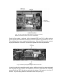

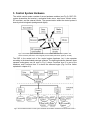
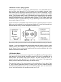

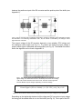

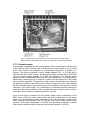
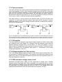
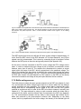


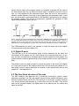
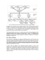

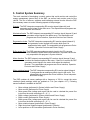

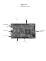
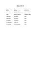

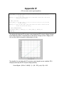
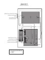


![[SOURce[1|2]]](http://vs1.manualzilla.com/store/data/006001849_1-f604f41c432649719bf8fb1e153f52f2-150x150.png)
![[SOURce[1|2]]](http://vs1.manualzilla.com/store/data/005803287_1-72ff358839cd16ae2e8c94de56269657-150x150.png)