1
IPM L-series
Application Note
Dec. 20
Mitsubishi IPM-series Application Note
Index
Index
1. IPM L-series Features
2. Product Line-up
3. Term Explanation
4. Numbering System
5. Structure
6. Correct and Safety Use of Power Module
7. Reliability
7-1. Introduction
7-2. Basic Concepts of Semiconductor Device Reliability
7-3. Mitsubishi’s Quality-Assurance Program
7-4. Reliability Testing
7-5. Failure Analysis
7-6. Derating and Reliability Projections
7-7. Conclusion
8. Installation of power Module
8-1. Installing Capacitor
8-2. Installation Hints
8-3. Thermal Impedance Considerations & Chip Layout
8-4. Coating Method of Thermal Grease (Example)
9. Using IPM
9-1. Applications of IPM L-series
9-2. Interface of control side of IPM
9-3. Control Power supply of IPM
9-4. Fault Signal of IPM
9-5. Other notice of using IPM
10. Power Loss and Junction Temperature
11. Average Power Loss Simplified Calculation
12. Notice for safe Designs and when Using This Specification
2
Dec. 20
Mitsubishi IPM-series Application Note
IPM L-series Feature, Product Line-up
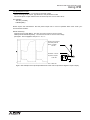
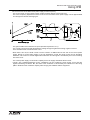
1.IPM L-series Feature
In recent years, motor control devices such as general-purpose inverters and AC servos used in industrial
equipments are being required by ever-increased demands, not only for improved performance and reduced size,
but also for ease of use and benefit to the environment.
To meet these need, Mitsubishi Electric developed the "S-DASH series" IPMs previously. Now, we introduce the
5th generation IPM "L series", the first IPM using the latest CSTBTTM chips. Together with new low package, it
not only contributes greatly to a low loss, but also allows for foot print size reduction and light weight of the end
products.
Features
Integration of 5th generation trench chip (CSTBTTM) achieves lower saturation voltage
Equipped with newly developed control IC
Reduction in EMS, and improvements in EMS
Large reductions in control power consumption
6pack or 7pack New package (Small, Medium, Large-type)
Increased current rating for breaking circuit
Applications
Motor control devices (AC220V / AC440V inverters, servos ,etc.)
DC power supplies such as UPS
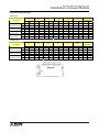
2.Product Line-up
7pack (Inverter+ Brake)
600V (AC220V)
Screw type
PM50RLA060
PM75RLA060
PM100RLA060
PM150RLA060
PM200RLA060
PM300RLA060
6pack (Inverter)
600V (AC220V)
Screw type
PM50CLA060
PM75CLA060
PM100CLA060
PM150CLA060
PM200CLA060
PM300CLA060
PM450CLA060
PM600CLA060
1200V (AC440V)
Screw type
PM25RLA120
PM50RLA120
PM75RLA120
PM100RLA120
PM150RLA120
Pin type
PM50RLB060
PM75RLB060
PM100RLB060
PM150RLB060
1200V (AC440V)
Screw type
PM25CLA120
PM50CLA120
PM75CLA120
PM100CLA120
PM150CLA120
PM200CLA120
PM300CLA120
PM450CLA120
Pin type
PM50CLB060
PM75CLB060
PM100CLB060
PM150CLB060
Pin type
PM25RLB120
PM50RLB120
PM75RLB120
Pin type
PM25CLB120
PM50CLB120
PM75CLB120
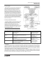
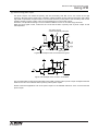
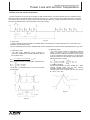
Internal circuit
㪎㫇㪸㪺㫂㩷㩿㪠㫅㫍㪼㫉㫋㪼㫉㪂㩷㪙㫉㪸㫂㪼㪀㩷
㩷
㪍㫇㪸㪺㫂㩷㩿㪠㫅㫍㪼㫉㫋㪼㫉㪀㩷
3
㩷
Dec. 20
Mitsubishi IPM-series Application Note
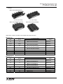
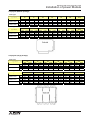
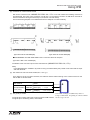
Product Line-up
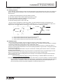
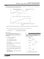
Package
IPM L-series Small-package
㪪㪺㫉㪼㫎㩷㫋㫐㫇㪼㩷㫇㪸㪺㫂㪸㪾㪼㩷
IPM L-series Medium-package
㩷
㩷
㩷
㩷
㩷
㩷
㩷
㩷
㩷
㪧㫀㫅㩷㫋㫐㫇㪼㩷㫇㪸㪺㫂㪸㪾㪼㩷
IPM L-series Large-package
㩷
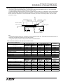
Applications of IPM to AC Motor Controls(General purpose Inverter)
عAC220V Line
Motor Ratings
(kW)
Current Ratings(100%)
(Arms)
3.7
17
5.5/7.5
23/33
11.0
46
15.0/18.5
61/75
22.0
30.0
37.0/45.0
55.0
90
115
145/180
215
عAC440V Line
Motor Ratings
(kW)
Current Ratings(100%)
(Arms)
5.5
12
7.5
17
11.0/15.0
23/31
18.5/22.0
30.0
37.0/45.0
55.0
75.0
37/43
57
71/90
110
144
For Inverter Module
L-series
PM50RLA060,PM50RLB060
PM50CLA060,PM50CLB060
PM75RLA060,PM75RLB060
PM75CLA060,PM75CLB060
PM100RLA060,PM100RLB060
PM100CLA060,PM100CLB060
PM150RLA060,PM150RLB060
PM150CLA060,PM150CLB060
PM200RLA060,PM200CLA060
PM300RLA060,PM300CLA060
PM450CLA060
PM600CLA060
For Inverter Module
L-series
PM25RLA120,PM25RLB120
PM25CLA120,PM25CLB120
PM50RLA120,PM50RLB120
PM50CLA120,PM50CLB120
PM75RLA120,PM75RLB120
PM75CLA120,PM75CLB120
PM100RLA120,PM100CLA120
PM150RLA120,PM150CLA120
PM200CLA120
PM300CLA120
PM450CLA120
4
For Converter
Diode
RM30TA-H
RM30TA-H
RM50TC-H
RM75TC-H
RM75TC-H
RM100DZ-H 3
RM150DZ-H 3
RM150DZ-H 3
For Converter
Diode
RM20TA-2H
RM50TC-2H
RM50TC-2H
RM50TC-2H
RM60DZ-2H 3
RM100DZ-2H 3
RM150DZ-2H 3
RM150DZ-2H 3
Dec. 20
Mitsubishi IPM-series Application Note
Term Explanation
3. Term Explanation
General 1
Symbol
IGBT
FWDi
IPM
tdead
IPM Motor
(PC)
PC
CMR
CMH
CML
CTR
General 2
Symbol
Ta
Tc
Definition
Insulated Gate Bipolar Transistor
Free Wheeling Diode
Intelligent Power Module
Dead Time
Interior Permanent Magnet Motor
Photo-Coupler
Programable Controller
Common Mode Noise Reduction
Current Transfer Ratio
Parameter
Ambient Temperature
Case Temperature
Absolute maximum Ratings
Symbol Parameter
VCES
Collector-Emitter Blocking Voltage
IC
Continuous Collector Current
ICM
Peak Collector Current Repetitive
IE
Continuous Diode Current
IEM
Peak Diode Current Repetitive
PC
Power Dissipation
Tj
Junction Temperature
Tstg
Storage Temperature
Viso
Isolation Voltage
-
Mounting Torque
Anti-parallel to the IGBT
Low side turn-off to high Side turn-on & High Side turn-off to low side turn-on
The maximum rise ratio of common mode voltage
The maximum rise ratio of common mode voltage at the specific high level
The maximum rise ratio of common mode voltage at the specific low level
the ratio of the output current to the input current
Definition
Atmosphere temperature without being subject to thermal source
Case temperature measured at specified point
Definition
Maximum Off-state collector-emitter voltage with gate-emitter shorted
Maximum collector current – DC
Peak collector current, Tj≤150°C
Maximum diode current – DC
Diode peak current, Tj≤150°C
Maximum power dissipation, per device, TC=25°C
Allowable range of IGBT junction temperature during operation
Allowable range of temperature within which the module may be stored or
transported without being subject to electrical load.
Minimum RMS isolation voltage capability applied electric terminal to base
plate, 1 minute duration
Allowable tightening torque for terminal and mounting screws
̪IE and IF are using by the difference of the connection and so on like the following figure.
Electrical Characteristics
Symbol
Parameter
Collector-Emitter Leakage
ICES
Current
Collector-Emitter Saturation
VCE(sat)
Voltage
Turn-on Delay Time
tc(on)
tc(off)
Turn-off Delay Time
Eon
Turn-on Switching loss
Eoff
Turn-off Switching loss
trr
Diode Reverse Recovery Time
VEC
Forward Voltage Drop of Diode
Rth
Thermal Resistance
Rth(j-c)
Rth(c-f)
Thermal Resistance, Junction to
Case
Thermal Resistance, Case to Fin
Definition
IC at VCE = VCES, VGE = 0V
VCE at IC = rated IC and VGE = 15V
Time from IC=10% to VCE=10% of final value
Time from VCE=10% of final value to IC=10% of final value
Energy dissipated inside the IGBT during the turn-on of a single collector
current pulse. Integral time starts from the 10% rise point of the collector
current and ends at the 10% of the collector-emitter voltage point.
Energy dissipated inside the IGBT during the turn-off of a single collector
current pulse. Integral time starts from the 10% rise point of the
collector-emitter voltage and ends at the specified low collector current point,
x% of Ic.
Time from IC=0A to projection of zero IC from Irr and 0.5Irr points with IE =
rated IC.
VEC at -IC = rated Ic
The rise of junction temperature per unit of power applied for a given time
period
IC conducting to establish thermal equilibrium
IC conducting to establish thermal equilibrium lubricated
5
Dec. 20
Mitsubishi IPM-series Application Note
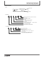
Numbering System
4. Numbering System
Label)
㪫㫐㫇㪼㩷㫅㪸㫄㪼
㪤㪠㪫㪪㪬㪙㪠㪪㪟㪠
㪜㪣㪜㪚㪫㪩㪠㪚
㪡㪘㪧㪘㪥
㪧㪤䋵䋰䌒䌌䌁䋰䋶䋰
㪜㪇㪐㪘㪘㪊
㪣㫆㫋㪅㪥㫆㪅
㩷
Type Name)
䌐䌍㩷 㩷 䋵䋰㩷 㩷 䌒
㩷
㩷
㩷
㩷 䌌䌁㩷 㩷 䋰䋶䋰 䋭 䋳䋰䋰
㩷
㩷
㪪㫇㪼㪺㫀㪽㫀㪺㪸㫋㫀㫆㫅㩷㪥㫌㫄㪹㪼㫉㩷㩿㪥㫆㫋㩷㫇㫉㫀㫅㫋㪼㪻㩷㫆㫅㩷㫋㪿㪼㩷㫃㪸㪹㪼㫃㪀㩷
㪭㫆㫃㫋㪸㪾㪼㩷㪚㫃㪸㫊㫊㩷
㩷 㩷 㪇㪍㪇㪑㩷㪍㪇㪇㪭㩷㪃㪈㪉㪇㪑㩷㪈㪉㪇㪇㪭㩷
㪧㪸㪺㫂㪸㪾㪼㩷
㩷 㩷 㪣㪘㪑㩷㪤㪸㫀㫅㩷㫋㪼㫉㫄㫀㫅㪸㫃㩷㪪㪺㫉㪼㫎㩷㫋㫐㫇㪼㩷
㩷 㩷 㪣㪙㪑㩷㪤㪸㫀㫅㩷㫋㪼㫉㫄㫀㫅㪸㫃㩷㪧㫀㫅㩷㫋㫐㫇㪼㩷
㪚㫆㫅㫅㪼㪺㫋㫀㫆㫅㪈㩷
㩷 㩷 㪩㪑㩷㪎㫇㪸㪺㫂㩷㩿㪠㫅㫍㪼㫉㫋㪼㫉㪂㩷㪙㫉㪸㫂㪼㪀㩷 㩷 㩷 㪚㪑㪍㫇㪸㪺㫂㩷㩿㪠㫅㫍㪼㫉㫋㪼㫉㪀
㪚㫆㫃㫃㪼㪺㫋㫆㫉㩷㪚㫌㫉㫉㪼㫅㫋㩷㫉㪸㫋㫀㫅㪾㩷
㩷 㩷 㪌㪇㪑㩷㪠㪺㪔㪌㪇㪘㩷㪃㪎㪌㪑㩷㪠㪺㪔㪎㪌㪘㩷
㪧㪤㪑㩷㪠㫅㫋㪼㫃㫃㫀㪾㪼㫅㫋㩷㪧㫆㫎㪼㫉㩷㪤㫆㪻㫌㫃㪼㩿㪠㪧㪤㪀㩷
㪣㫆㫋㩷㪥㫌㫄㪹㪼㫉㪀㩷
䌅㩷 㩷
䋰㩷
㩷 䋹
㩷 䌁䌁䋳㩷 㩷 㪞
㩷
㩷
㪩㫆㪟㪪㩷㪚㫆㫄㫇㫃㫀㪸㫅㫋㩷㪪㫐㫄㪹㫆㫃㩷
㪤㪸㫅㫌㪽㪸㪺㫋㫌㫉㫀㫅㪾㩷㫃㫆㫋㩷㫄㪸㫅㪸㪾㪼㫄㪼㫅㫋㩷㫅㫌㫄㪹㪼㫉㩷
㪤㪸㫅㫌㪽㪸㪺㫋㫌㫉㫀㫅㪾㩷㫄㫆㫅㫋㪿㩷
㩷 㩷 㩷 㩷 㩿㪡㪸㫅㪅䌾㪪㪼㫇㪅㪑㩷㪈䌾㪐㪃㩷㪦㪺㫋㪅㪑㩷㪦㪃㩷㪥㫆㫍㪅㪑㩷㪥㪃㩷㪛㪼㪺㪅㪑㩷㪛㪀㩷
㪤㪸㫅㫌㪽㪸㪺㫋㫌㫉㫀㫅㪾㩷㫐㪼㪸㫉㩷 㩷
㩿㫋㪿㪼㩷㫃㪸㫊㫋㩷㪻㫀㪾㫀㫋㩷㫆㪽㩷㫐㪼㪸㫉㪃㩷㪌㪔㪉㪇㪇㪌㩷 㩷 㪍㪔㪉㪇㪇㪍㩷㪅㪅㪀㩷
㪬㪣㩷㪠㪛㩷㪺㫆㪻㪼㩷㩿㪬㪣㩷㪺㪼㫉㫋㫀㪽㫀㪼㪻㩷㫇㫉㫆㪻㫌㪺㫋㫊㩷㫆㫅㫃㫐㪀㩷
6
Dec. 20
Mitsubishi IPM-series Application Note
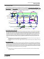
Structure
5. Structure
ex.) Small package Screw type
2.Control input terminal
1.Main electrode
11.Internal
connection
terminal
3.Resin
5.Case
9.Control PCB
6.Wire
1
2
Part
Main electrode
Control input terminal
3
4
5
6
7
8
9
10
11
Resin
Gel
Case
Wire
Chip
Base plate
Control PCB
Insulated substrate
Internal connection terminal
4.Gel
8.Base plate
7.Chip
Quality of the material
Copper plated with nickel
Brass plated with gold
PPS resin
Epoxy
Silicone
PPS resin
Aluminum
Silicon
Copper
Glass epoxy
Ceramic*
Copper plated with nickel
10.Insulated substrate
UL Flame class
UL 94-V0
UL 94-V0
UL 94-V0
UL 94-V0
Note of Insulated substrate
* : All about its structure, material, thickness, and manufacturer is the same as S-series IPM.
S-series IPM has UL(Underwriters Laboratories Inc) Yellow Card #80276 (file. #80271).
7
Dec. 20
Mitsubishi IPM-series Application Note
Correct and Safety Use of Power Module
6. Correct and Safety Use of Power Module
Unsuitable operation (such as electrical, mechanical stress and so on) may lead to damage of power modules.
Please pay attention to the following descriptions and use Mitsubishi Electric's IGBT modules according to the guidance.
Cautions
During Transit
Storage
Prolonged Storage
Operating
Environment
Flame Resistance
Anti-electrostatic
Measures
Anti-electrostatic
Measures
• Keep sipping cartons right side up. If stress is applied by either placing a carton upside down or by
leaning a box against something, terminals can be bent and/or resin packages can be damaged.
• Tossing or dropping of a carton may damage devices inside.
• If a device gets wet with water, malfunctioning and failure may result. Special care should be taken
during rain or snow to prevent the devices from getting wet.
• The temperature and humidity of the storage place should be 5∼35°C and 45∼75% respectively.
The performance and reliability of devices may be jeopardized if devices are stored in an
environment far above or below the range indicated above.
• When storing devices more than one year, dehumidifying measures should be provided for the
storage place. When using devices after a long period of storage, make sure to check the exterior
of the devices is free from scratches, dirt, rust, and so on.
• Devices should not be exposed to water, organic solvents, corrosive gases, explosive gases, fine
particles, or corrosive agents, since any of those can lead to a serious accident.
• Although the epoxy resin and case materials are in conformity with UL 94-V0 standards, it should be
noted that those are not non-flammable.
(1) Precautions against the device rupture caused by static electricity
Static electricity of human bodies and cartons and/or excessive voltage applied across the gate to
emitter may damage and rupture devices. The basis of anti-electro static build-up and quick
dissipation of the charged electricity.
* Containers that are susceptible to static electricity should not be used for transit nor for storage.
* Gate to emitter should be always shorted with a carbon cloth or the like until right before a module is
used. Never touch the gate terminals with bare hands.
* Always ground the equipment and your body during installation (after removing a carbon cloth or the
like. It is advisable to cover the workstation and it's surrounding floor with conductive mats and
ground them.
* It should be noted that devices may get damaged by the static electricity charged to a printed circuit
board if the gate to emitter of the circuit board is open.
* Use soldering irons with grounded tips.
(2) Precautions when the gate to emitter is open
* Voltage should not be applied across the collector to emitter when the gate to emitter is open.
* The gate to emitter should be shorted before removing a device from a unit.
8
Dec. 20
Mitsubishi IPM-series Application Note
Correct and Safety Use of Power Module
Cautions
Mounting
When mounting a module on a heat sink, a device could get damage or degrade if a sudden torque ("one side
tightening ") is applied at only one mounting terminal, since stress is applied on a ceramic plate and silicon
chips inside the module. Shown in Fig.6.1 is the recommended torquing order for mounting screws.
ԙ
Ԛ
Ԙ
ԛ
Ԟ
Ԝ
ԙ
Ԙ
a) Two point mounting type
Ԙ Ԛ
b) four point mounting type
ԝ
ԛ
ԙ
ԟ
c) eight point mounting type
Temporary tightening :Ԙψԙ
ԘψԙψԚψԛ
ԘψԙψԚψԛψԜψԝψԞψԟ
Final tightening :ԙψԘ
ԛψԚψԙψԘ
ԘψԙψԚψԛψԜψԝψԞψԟ
Fig.6.1 The recommended torquing order for mounting screws
*:Temporary tightening torque should be set at 20∼30% of maximum rating.
Also, care must be taken to achieve maximum contact (i.e. minimum contact thermal resistance) for the best
heat dissipation.)
The flatness of a heat sink where a module is mounted (ref.Fig.6.2) should be as follows. Also, the surface
finish should be less than Rz12s.
Copper base plate module:−100μm∼+100μm
Thermal compound with good thermal conductivity should be applied evenly about Aluminum base plate
modules:−100μm∼+200μm on the contact surface of a module and a heat sink.
Heat sink flatness: Less than ± 20 micrometers on a length of 100mm
/Less than 10 micrometers of roughness
Thermal grease thickness: +50∼+100μm
Grease on the contact surface prevents the corrosion of the contact surface. However, use the kind of
grease that has a stable characteristic over the whole operating temperature range and does not change its
properties for several years.
A torque wrench shall be used in tightening mounting screws and tighten screws to the specified torque.
Excessive torquing may result in damage or degradation of a device.
Grease applied area
Power Module
+ Convex
The edge line of base plate
− Concave
Specified range of
heat sink flatness
Fig.6.2 Heat Sink Flatness
9
Dec. 20
Mitsubishi IPM-series Application Note
Reliability
7.Reliability
Wearout Failure
Failure Rate
Radom Failure
Time
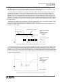
Fig.7.1 Failure Rate Versus Time
O-A-B-C Initial Failure (Factory)
C-D
Early Failure (Field)
D-E
Random Failure (Field)
E-F
Wearout (Field)
(0-A-B-C-D Debugging Period)
Failure Rate
7-1. Introduction
It has only been somewhat over 30 years since
semiconductor devices such as rectifier diodes,
thyristors,
and
transistors
gained
widespread
acceptance for use in industrial machinery and
consumer appliances, but during that period the
reliability standards for these devices have made rapid
advances.
In equipment where high reliability is a must, failure
rate of the semiconductor devices must range from 10 to
100 FIT (1 FIT=10-9/hours). Of course, to achieve such
reliability in the equipment itself, not only must each
individual device be reliable, but also it is also extremely
important to match the specific characteristics of the
device with its application within the piece of equipment.
In fact, information obtained in field studies show that for
semiconductor devices manufactured using identical
procedures, failure rates in the field could vary by a
factor of 10 depending simply on how the device was
used.
The following information covers device reliability with
regards to how a device is used. An introductory
discussion is also presented on quality-control
procedures, and some examples of reliability testing
data are given.
Early Failure
Time
7-2. Basic Concepts of Semiconductor Device
Reliability
Fig.7.2 Semiconductor Device Failure Rate Versus Time
7-2-1. Semiconductor Device Failure Rate Varied with The Lapse of Time
The failure rate of devices used in an average piece of equipment can be expressed by using the bathtub curve shown in Fig.7.1,
line (a). Taken from the standpoint of time, device failures can be classified as an early failure, random failure and wear out failure
period.Three points must be considered regarding the service life of a device; early and random failures rate, and lifetime before
wear out.
But the failure rate of semiconductors is illustrated by line (b) in the graph, where failure rate is shown to gradually diminish as a
factor of time. In other words, a notable feature of semiconductor devices is that the longer a particular device has been used, the
more stable it will be. Viewed from a different perspective, even though random failure rate has been reduced to virtual stability,
the failure distribution pattern shows early failures to still be prevalent. As shown by Fig.7.2 where failure rate versus time is given
for an actual device, the highest failure rate occurs immediately after manufacture, but the process of ageing and debugging
gradually lowers this failure rate.
The next step is with the user, who assembles, adjusts, and takes the device aging. Failure rates continue to decline during this
period also. Generally, the rate for major defect during this period drops to less than 0.1%, and if this rate is exceeded by a
substantial margin, one must look for a fault in the circuit design, assembly procedure, or the device itself. Unless the problem is
found and corrected, frequent field failures will be the likely result. In most cases, the field failure rate can be correlated to major
defect during this period, so this is an important aspect of device reliability.
Upon transferring the equipment to field service, the stress level is reduced further, with a corresponding drop in failure rates.
Failure rates normally range from several FIT to several hundred FIT during this period.
On the other hand, the user must design greater margins. For example, diodes and thyristors should be operated at 50 ~ 60% of
their maximum voltage ratings or lesser, and junction temperatures should not exceed 70 ~ 80% of maximum rating. It is also
important to remember that a device must be in working harmony with other components in the circuit for maximum reliability
standards can be assured.
When designing a piece of equipment for reliable service, device selection must be considered from a standpoint of performance,
reliability, and economy. Since it is not easy to achieve high performance/reliability and economy at the same time, a balance must
be struck on the side of practical value. In other words, device selection should be based on the user’s expectations for the
machine he is designing.
10
Dec. 20
Mitsubishi IPM-series Application Note
Reliability
7-2-2. Power Module Failure Reason
After a piece of equipment has been assembled and adjusted, or has been placed in field service, failed devices that are returned
to the factory are analyzed to determine the cause of failure. This procedure is intended to determine whether the problem lays
with the device itself, or the manner in which it was used. This section will list potential reasons of failure.
Good ֣֣֣֣֣֣֣֣֣֣֣ Device Unmatch for Circuit or Usage Condition
Usage Condition֣֣֣ ֣֣Over voltage
֥ ֿ֣ VCE Over voltage (Collector-Emitter)
֥ ֥ ֿ Switching Surge
֥ ֥ ֿ Bus Bar Voltage Rise
֥ ֥ ֿ Abnormal Control Signal
֥ ֥ ֿ Interfered Noise (Lightning Surge)
֥ ֥ ַ Inappropriate Measurement
֥ ַ֣ VGE Over voltage (Gate-Emitter)
֥ ֿ Static Electricity
֥ ֿ Abnormal Gate Drive Circuit
֥ ֿ Gate Oscillation
֥ ֿ High Voltage Applied
֥ ַ Interfered Surge
ֿ֣֣ Over Temperature (Over Current, Over Load)
֥ ֿ֣ Inappropriate Thermal Design
֥ ֿ֣ Short Arms (Not Enough Dead-Time, False Turn-on )
֥ ֿ֣ Over Current
֥ ֿ֣ Under Gate Drive Voltage
֥ ֿ֣ Gate Circuit Open
֥ ֿ֣ Abnormal Switching Frequency Increase
֥ ֿ֣ Abnormal Switching Frequency Decrease
֥ ֿ֣ Inappropriate Thermal System
֥ ַ֣ Bonding Surface Fatigue
ַ֣֣ Insulation Failure (Ceramic Crack, Internal Solder Melting)
ֿ֣ Heat Sink Mounting Failure (Over Stress)
ַ֣ Over Voltage
Power Device Defect ֣ ֣֣IGBT Chip Manufacture Defect
֥ ֿ֣ Pattern Defect
֥ ַ֣ Surface Fault (Impurity ion)
ַ֣ Module Manufacture Defect
ֿ֣ Wire Bonding Fault
ֿ֣ Connection Fault Between Insulation Base Plate and Module Base Plate (Solder, etc.)
ֿ֣ Internal Electrode Solder Fault
ַ֣ Metalization Fault
Operation life is dependent on the internal wire bonding, thermal fatigue between insulation base-plate and module base-plate.
The thermal fatigue will be described in the next page.
11
Dec. 20
Mitsubishi IPM-series Application Note
Reliability
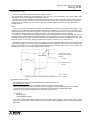
7-2-3. Thermal Fatigue of Power Module
7-2-3-1 Operating Temperature Pattern
The operating temperature pattern of power module is displayed in Fig.7.3. It is important to consider two patterns that are
independent each other in thermal fatigue life of power module.
عOperation Mode 1
Power cycle life is called when change of case temperature is small, but frequent change of junction temperature occurs.
عOperation Mode 2
The other one is thermal cycle life when comparatively slow change of temperature occurs by start and stop of the system.
Temperature
Long Time of System On
Time
Repeat in Short Time
Fig.7.3 Operating Temperature Pattern
12
Dec. 20
Mitsubishi IPM-series Application Note
Reliability
7-2-3-2. Power Cycle Failure Mechanism
Fig.7.4 shows the typical construction of power module. When junction temperature of power module is changed, stress strain
between aluminum wire and silicon chip, and between silicon chip and insulation substrate occurs due to the difference of
coefficient of linear expansion. If this stress is supplied repetitively, thermal fatigue for the junction becomes failure.
For inverter use, power cycle life is a necessary concern, which should be given during designing system. An example is given in
Fig.7.5. The failure mode is that the crack of bonding surface makes progress by stress due to the difference of linear expansion
between aluminum wire and silicone chip and finally lead to the peel failure mode.
A power cycle testing result of Mitsubishi Electric's module is shown in Fig.7.6.
Bonding
Wire
Silicon Chip
Solder
Insulation Baseplate with Copper Foil
Solder
Base Plate
Fig.7.4 Module Structure
Fig.7.5 Bonding Surface Fatigue Caused by Power Cycle Testing
100000k
10000k
Cycle
1000k
100k
10k
1k
1
10
100
1000
ǍTj[°C]
Fig.7.6 Power Cycle Curve
13
Dec. 20
Mitsubishi IPM-series Application Note
Reliability
7-3. Mitsubishi's Quality-Assurance Program
One of the basic goals of Mitsubishi Electric is to offer our customers quality products. As a consequence, product quality, price,
timely delivery, and service are equally important aspects deserving an equal amount of attention. Still, product quality must stand
above all others from a standpoint of customer confidence.
Quality standards in the semiconductor industry are extremely high; production of wafers is a carefully controlled, precision
process, and assembly processes are done under microscopes to assure that there are no sacrifices made in technology, or in
quality.
The following subsections outline the quality-assurance programs Mitsubishi Electric uses in its mass-production.
7.3.1 The Path to a Mass-Production Device
From research prototype, through mass-production, a serial type tests are run at each stage to assure performance and
reliability of the ultimate product. At the same time, the design drawings are also closely checked. The path from the research
stage to mass-production is shown in the flow chart of Fig.7.7 The subsections that follow briefly describe the reliability tests used
to check for device reliability.
7.3.2 Environmental Controls
The semiconductor industry as a whole recognizes the affect environmental factors have on product quality, and rigorous
standards have been established regarding the control of dust, humidity, and temperature in manufacturing facilities. The same
level of standards is also used for the various gases, and the water used in the manufacturing process.
7.3.3 Periodic Inspection and Maintenance of Manufacturing Equipment and Instrumentation
The various equipment and measuring instruments used in semiconductor production are an extremely important element of the
total process. It is therefore imperative that a periodic program be implemented to inspect and adjust these components so that
optimum precision standards are maintained, and to forestall any interruptions in the production process.
7.3.4 Quality-Control of Materials Purchases
Materials are subjected to rigorous acceptance tests using equipment such as spectrometers, helium leak detectors, etc. Before
placing full orders, thorough sample testing is done, and all problem areas are worked out before making an official decision.
Quality-control procedures at the supplier’s plant are also considered in any procurement decision.
7.3.5 Control of the Manufacturing Process
Various measures have been taken to control the elements that have a decisive influence on the quality of the product.
Measuring instruments are used to monitor water purity, atmospheric conditions, furnace temperatures, gas flow, and other
factors. Check-sheet inspections are made, and recorders keep automatic records. These records are carefully correlated with
the records kept on matters such as diffusion depth and surface density to establish proper working conditions.
7.3.6 In-Process and Final Inspections
The goals of the in-process and final inspections are twofold: the first is to assure product quality from the standpoint of outer
appearance, dimensions, structural integrity, and mechanical and electrical characteristics. The second is to feed this information
back upline to improve quality, and to reduce variations in future batches.
In-process inspections are intended to check the wafer and assembly processes, and serve two purposes; one being
self-imposed checks on the production process, the other for use as a quality-control tool. As its name implies, production
personnel to correct deficiencies they clearly recognize use the self-imposed check, and emphasis is placed on points that are
difficult to detect in completed devices. After the device is completed, it is subjected to the final inspection and the
quality-assurance inspection. The final inspection is run on all devices, and consists of testing electrical characteristics and outer
appearance. Quality-assurance personnel assume the role of the end user, and inspect samples for correct electrical
characteristics, outer appearance, and reliability before devices are packed in storage.
The flow chart for the quality-assurance program covered in the above is noted in Fig.7.9.
7.3.7 Quality Information
Mainly the quality assurance division compiles various kinds of quality information such as inspection results and
customer-supplied information. They are quickly fed back to related divisions including the production division for maintenance
and improvement of quality.
In addition, we employ computer-based, streamlined, and effective quality control systems in order to modernize the information
management.
14
Dec. 20
Mitsubishi IPM-series Application Note
Reliability
Fig.7.7 Flow Chart of Quality Assurance Program
15
Dec. 20
Mitsubishi IPM-series Application Note
Reliability
7-4. Reliability Testing
7-4-1 Reliability Testing Procedures
High reliability standards are assured with Mitsubishi semiconductor devices through the rigorous quality-control inspections,
which the devices are subjected to in the design and manufacturing stages, and through the quality-assurance inspections run on
each production lot. Numerous reliability tests have been implemented in order to maintain this standard of reliability.
This section provides an overview of the reliability testing of thyristor devices. Test parameters are shown in Table 7.1, and as
noted, conform to the procedures specified by the Japan Electronics and Information Technology Association (JEITA) handbook.
(Related standards: International Electro technical Commission (IEC))
7-4-2 Results of Reliability Test of IGBT Module
Table 7.2 lists the results of the reliability tests performed on PM75RLA060, a resin sealed type with current rating up to 75A to
date. Failure criterion information is noted in Table 7.3.
Table7.1. Mitsubishi Power Module Reliability Testing
Environmental
Test
Endurance
Test
Test Parameter
Thermal Shock
Temperature Cycling
Vibration
Robustness of Termination
Solder Heat Resistance
Solderability
Mounting Torque
High Temperature Storage
Low Temperature Storage
Wetproof
Intermittent Current Flow
High Temperature Reverse Bias
High Temperature Gate Bias
Test Method
ED-4701
B-141
ޖ
B-131
ޖ
A-121
ޖ
A-111-Σ
ޖ
A-132
ޖ
A-131
ޖ
A-112-Τ
ޖ
B-111
ޖ
B-112
ޖ
B-121
ޖ
㧙
ޖ
㧙
ޖ
㧙
Test Conditions
[Condition A] 100°C : 5 min, 0°C: 5 minutes, 10 cycles
Tstg min 60 min㨪Tstg max 60 min, 10 cycles
2
[Condition B] 10㨪500Hz/15 minute, 98.1m/s , 6h
9.8~40N, 10±1s
[Condition A] 260±5°C, 10±1s, Rosin flux used
[Condition A] 235±5°C, 5±0.5s, Rosin flux used
M5:1.96~3.5N㨯m, 10±1s
Ta=Tstg max, 1000 h
Ta=Tstg min, 1000 h
[Condition B] Ta=60°C, RH=90%, 1000h
ǍTc=50°C(ǍTc=100°C), 5000 cycles
Ta=Tstg max, VCE=85%VCES, VGE=0V, 1000h
Ta=Tstg max, VCE=20V, VGE=0V, 1000h
*:Environmental and resistance testing conforms to standards specified in JEITA ED-4701 for discrete semiconductor devices.
Table7.2. PM75RLA060 Reliability Test Results
Environmental
Test
Test Parameter
Test Method
Test Conditions
Thermal Shock
Temperature Cycling
Vibration
Robustness of Termination
ED-4701
[Condition A] 100°C(5min), 0°C(5min), 10 cycles
-40°C(60 min)~125°C(60 min), 10 cycles
2
[Condition B] 10~500Hz / 15 min, 98.1m/s , 6h
9.8N, 10±1 s
Mounting Screws:M5, 3.5N㨯m, 10±1 s
Main Terminal Screws:M5, 3.5N㨯m, 10±1 s
Ta=125°C, 1000h
Ta=-40°C, 1000h
Ta=60°C, RH=90%, 1000 h
Ta=50~100°C, , 5000h
Ta=125°C, VCES=510V, 1000h
Mounting Torque
Endurance
Test
High Temperature Storage
Low Temperature Storage
Wetproof
Intermittent Current Flow
High Temperature Reverse Bias
B-141
B-131
A-121
A-111-Σ
A-112-Τ
B-111
B-112
B-121
㧙
㧙
No of
No of
Samples Failures
5
0
5
0
5
0
5
0
5
0
5
5
5
5
5
0
0
0
0
0
Talbe7.3. PM75RLA060 Failure Criterion
Test Parameter
Test Conditions
ICES
VCE(sat)
VEC
SC
UV
Electrical Stress
VCE=600V, VD=0V
IC=75A, VD=15V
-IC=75A, VD=0V
VD=15V,VCIN=0V
trip
AC2500V 1 min
Failure Criterion
Lower Limit
Upper Limit
㧙
U.S.L2.0
㧙
U.S.L1.2
㧙
U.S.L1.2
L.S.L0.9
㧙
L.S.L0.9
㧙
Insulation breakdown
Note
Note. U.S.L: Upper Specification Limit / L.S.L: Lower Specification Limit
16
Dec. 20
Mitsubishi IPM-series Application Note
Reliability
7-5. Failure Analysis
Failure analysis is one of the sources of information used
in maintaining, and making improvements in standards of
quality and reliability. Failure analysis procedures are
performed on failed devices at all stages of their life cycle,
ranging from the development state to failure while in use.
Failure analysis procedures are generally divided into area
of external inspections, electrical testing, internal inspections,
and chip analysis. The flow chart for these procedures is
shown in Fig.7.8, while Table 7.4 lists the nature of the tests.
The results of the various reliability and failure analysis tests
reveal the failure mode and mechanism, and this information
is fed back to the process technology and manufacturing
personnel so that they can take the appropriate measures to
improve the final product.
7-6. Derating and Reliability Projections
The degree of reliability for a semiconductor device varies
considerably depending on usage and environmental
conditions. Design standards, the method of manufacture,
and quality-control procedures also play a role in
establishing the intrinsic reliability for semiconductors.
Correlating device derating with reliability is also not an easy
task. Please refer to Mitsubishi device reliability handbook
for more information in detail.
http://www.semicon.melco.co.jp/confidence/index.html
Fig.7.8 Failure Analysis Procedure
Table7.4. Failure analysis inspections and equipment used
Category
Inspection Items
External Inspection
٤ Condition of leads, plating, soldering, and welds
٤ Packaging defect
٤ Solderability
Electrical Characteristics
Testing
٤ Static electrical characteristics, voltage and temperature
margins, checking for broken bond wire, wire
٤ Internal wiring
Internal Inspection
٤ Device removed from package and chip surface observed
for defects
٤ Electrical characteristic check using microprobe
٤ Check for hot spots and other abnormalities
٤ Analysis techniques used to supplement chip surface
observation in internal inspection
٤ Cross-section of chip observed for analyzing oxide film,
diffusion and metallizing
Chip Analysis
Equipment
Stereoscopic microscope
Metallurgy microscope
Oscilloscope
Curve tracer
Characteristics tester
X-ray equipment
Metallurgy microscope
microprobe
Scanning electron microscope
X-ray micro-analyzer
Infrared micro-scanner
Spectrum analyzer
7-7. Conclusion
The above is a simple introduction to general ideas about reliability, reliability tests, and derating and forcasting of reliability of
high power semiconductor, which are semiconductor devices for electric power. As explained above, it is vital for higher
reliability in practical use of semiconductor devices to understand their features and select those, which are suitable for
equipment and sets. It is also important to design semiconductor devices with some allowance to improve reliability, fully taking
their derating into consideration in relation to operating and environmental conditions.
Other essential things to do are to “debug” equipment and sets, and to analyze data obtained in fabrication process and
actual operation to feed them back to design and fabrication stages. To improve the reliability by design of high power
semiconductor requires considerations on many issues as described above. Utilize the semiconductor devices successfully
with the utmost care with comprehensive understanding of their quality, reliability, and economy.
17
Dec. 20
Mitsubishi IPM-series Application Note
Installation of power Module
8. Installation of power Module
8-1 Installing Capacitor
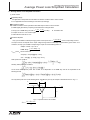
During switching, voltage is induced in power circuit stray inductance by the high di/dt of the main current. This voltage can
appear on the IPM and cause damage. In order to avoid this problem, guidelines that should be followed in designing the
circuit layout are:
1
٤
2
٤
3
٤
4
٤
5
٤
Located the smoothing capacitor as close as possible to the IPM
Use ceramic capacitor near the IPM to bypass high frequency current
Adopt low impedance electrolytic capacitor as smoothing capacitor
Use snubber circuit to absorb surge voltage
Decrease switching speed in order to lower di/dt.
2 and ٤
5 are the most effective to reduce surge voltage. The stray inductance of snubber circuit generally is not
٤
2 , ٤
4 , ٤
5 is needed since there is a limit on the
considered to avoid complicating the circuit. In addition, combination of ٤
2 act as a snubber when oscillation is occurring.
length of wiring. The bypass capacitor of approach ٤
L2 small
Load
Smoothing
L2 large
vce
Snubber
L1 : Stray inductance between the electrolytic capacitor and the IPM.
L2 : Stray inductance between the filter capacitor and the driver.
L3 : Stray inductance between the load and the power circuit's output stage
8-2 Installation Hints
When mounting IPM on a heat-sink, uneven mounting can cause the modules ceramic isolation to crack.
To achieve the best thermal radiation effect, the bigger the contact area is, the smaller the thermal resistance is. Heat-sink
should have a surface finish in range of Rz6 ~ Rz12, curvature within 100μm.
Uniform coating of thermal grease between the module and heat-sink can prevent corrosion of contact parts. Select a
compound, which has stable characteristics over the whole operating temperature range and does not change its properties
over the life of the equipment.
Use a uniform coating of thermal interface compound. The thickness of thermal grease should be ranked in 100~200μm
according to the surface finish.
Mounting screws should be tightened by using a torque wrench to the prescribed torque in progressive stages in a cross
pattern. As mentioned before, over torque terminal or mounting screws may result in damage of IPM.
When an electric driver is used, thermal grease with low viscosity is recommended and extra grease must be extruded
before final tightening screws.
* For the recommended torque order for mounting screws referring to "Installation Method" in the section of
"Correct and Safety Use of Power Module"
Note) Maximum torque specifications are provided in device data sheets. The type and quantity of thermal compounds
having an effect on the thermal resistance are determined by consideration of both thermal grease and heat-sink.
Typical value given in datasheet is measured by using thermal grease produced by Shin-Etsu Chemical Co.,Ltd.
(G-746, which has not issued in Shin-Etsu's publications, is almost the same as G-747.)
18
Dec. 20
Mitsubishi IPM-series Application Note
Installation of power Module
8-3 Thermal Impedance Considerations & Chip Layout
The junction to case thermal resistance Rth(j-c) and the case to heat-sink thermal resistance Rth(c-f) are given in datasheet.
The case temperature has been measured at the just under the chip.
The case temperature measurement point of various products is shown in Table 3. It is measured by uniform 100μm~200μm
coating of thermal grease with thermal conductivity of 0.92W/m㨯°C between the module and heat-sink. A Thermo-couple is
used to measure the temperature of case and heat-sink at the same point shown in the following tables. (0.8φ 3mm depth,
0.3φ thermo-couple)
Chip
㪫㪿㪼㫉㫄㫆㩷㪺㫆㫌㫇㫃㪼㩷㪘㩷
㪫㪺㩿㫁㫌㫊㫋㩷㫌㫅㪻㪼㫉㩷㫋㪿㪼㩷㪺㪿㫀㫇㪀
Base plate
㪫㪿㪼㫉㫄㫆㩷㪺㫆㫌㫇㫃㪼㩷㪙㩷
Heat-sink
㪫㪽
Processes a ditch
㨯Note
*The thermal impedance depends on the material, area and thickness of heat-sink. The smaller the area and the thinner the
heat-sink is, the lower the impedance is for the same material.
*The type and quantity of thermal compounds can affect the thermal resistance.
Table 3:Thermal resistance and chip layout of IPM L-series
㪫㪿㪼㫉㫄㪸㫃㩷㫉㪼㫊㫀㫊㫋㪸㫅㪺㪼㩷㪍㪇㪇㪭㩷㫋㫐㫇㪼㩷
㩷
㪠㫅㫍㪼㫉㫋㪼㫉㩷
㪡㫌㫊㫋㩷㫌㫅㪻㪼㫉㩷㫋㪿㪼㩷㪺㪿㫀㫇㩷
㪫㫐㫇㪼㩷㪥㪸㫄㪼㩷
㪠㪞㪙㪫㪄㪺㪿㫀㫇㩷
㪝㪮㪛㫀㪄㪺㪿㫀㫇㩷
㪩㫋㪿㩿㫁㪄㪺㪀㪨㩷
㪩㫋㪿㩿㫁㪄㪺㪀㩷
㪧㪤㪌㪇㪩㪣㪘㪆㪙㪇㪍㪇㪃㪧㪤㪌㪇㪚㪣㪘㪆㪙㪇㪍㪇㩷
㪇㪅㪐㪌㩷
㪈㪅㪍㪈㩷
㪧㪤㪎㪌㪩㪣㪘㪆㪙㪇㪍㪇㪃㪧㪤㪎㪌㪚㪣㪘㪆㪙㪇㪍㪇㩷
㪇㪅㪊㪉㩷
㪇㪅㪌㪊㩷
㪧㪤㪈㪇㪇㪩㪣㪘㪆㪙㪇㪍㪇㪃㪧㪤㪈㪇㪇㪚㪣㪘㪆㪙㪇㪍㪇㩷
㪇㪅㪉㪎㩷
㪇㪅㪋㪊㩷
㪧㪤㪈㪌㪇㪩㪣㪘㪆㪙㪇㪍㪇㪃㪧㪤㪈㪌㪇㪚㪣㪘㪆㪙㪇㪍㪇㩷
㪇㪅㪉㪇㩷
㪇㪅㪊㪊㩷
㪧㪤㪉㪇㪇㪩㪣㪘㪆㪚㪣㪘㪇㪍㪇㩷
㪇㪅㪈㪍㩷
㪇㪅㪉㪌㩷
㪧㪤㪊㪇㪇㪩㪣㪘㪆㪚㪣㪘㪇㪍㪇㩷
㪇㪅㪈㪉㩷
㪇㪅㪈㪐㩷
㪧㪤㪋㪌㪇㪚㪣㪘㪇㪍㪇㩷
㪇㪅㪈㪉㩷
㪇㪅㪈㪐㩷
㪧㪤㪍㪇㪇㪚㪣㪘㪇㪍㪇㩷
㪇㪅㪇㪎㩷
㪇㪅㪈㪈㩷
㪫㪿㪼㫉㫄㪸㫃㩷㫉㪼㫊㫀㫊㫋㪸㫅㪺㪼㩷㪈㪉㪇㪇㪭㩷㫋㫐㫇㪼㩷
㩷
㪠㫅㫍㪼㫉㫋㪼㫉㩷
㪡㫌㫊㫋㩷㫌㫅㪻㪼㫉㩷㫋㪿㪼㩷㪺㪿㫀㫇㩷
㪫㫐㫇㪼㩷㪥㪸㫄㪼㩷
㪠㪞㪙㪫㪄㪺㪿㫀㫇㩷
㪝㪮㪛㫀㪄㪺㪿㫀㫇㩷
㪩㫋㪿㩿㫁㪄㪺㪀㪨㩷
㪩㫋㪿㩿㫁㪄㪺㪀㩷
㪧㪤㪉㪌㪩㪣㪘㪆㪙㪈㪉㪇㪃㪧㪤㪉㪌㪚㪣㪘㪆㪙㪈㪉㪇㩷
㪇㪅㪏㪊㩷
㪈㪅㪊㪍㩷
㪧㪤㪌㪇㪩㪣㪘㪆㪙㪈㪉㪇㪃㪧㪤㪌㪇㪚㪣㪘㪆㪙㪈㪉㪇㩷
㪇㪅㪉㪍㩷
㪇㪅㪊㪐㩷
㪧㪤㪎㪌㪩㪣㪘㪆㪙㪈㪉㪇㪃㪧㪤㪎㪌㪚㪣㪘㪆㪙㪈㪉㪇㩷
㪇㪅㪉㪈㩷
㪇㪅㪊㪇㩷
㪧㪤㪈㪇㪇㪩㪣㪘㪈㪉㪇㪃㪧㪤㪈㪇㪇㪚㪣㪘㪈㪉㪇㩷
㪇㪅㪈㪍㩷
㪇㪅㪉㪍㩷
㪧㪤㪈㪌㪇㪩㪣㪘㪈㪉㪇㪃㪧㪤㪈㪌㪇㪚㪣㪘㪈㪉㪇㩷
㪇㪅㪈㪉㩷
㪇㪅㪉㪇㩷
㪧㪤㪉㪇㪇㪚㪣㪘㪈㪉㪇㩷
㪇㪅㪈㪉㩷
㪇㪅㪉㪇㩷
㪧㪤㪊㪇㪇㪚㪣㪘㪈㪉㪇㩷
㪇㪅㪇㪏㩷
㪇㪅㪈㪊㩷
㪧㪤㪋㪌㪇㪚㪣㪘㪈㪉㪇㩷
㪇㪅㪇㪌㩷
㪇㪅㪇㪐㩷
㩷
19
㪚㫆㫅㫍㪼㫉㫋㪼㫉㩷
㪡㫌㫊㫋㩷㫌㫅㪻㪼㫉㩷㫋㪿㪼㩷㪺㪿㫀㫇㩷
㪠㪞㪙㪫㪄㪺㪿㫀㫇㩷
㪝㪮㪛㫀㩿㪧㪀㪄㪺㪿㫀㫇㩷
㪩㫋㪿㩿㫁㪄㪺㪀㩷
㪩㫋㪿㩿㫁㪄㪺㪀㪨㩷
㪈㪅㪉㪈㩷
㪉㪅㪈㪐㩷
㪇㪅㪋㪉㩷
㪇㪅㪎㪈㩷
㪇㪅㪋㪉㩷
㪇㪅㪎㪈㩷
㪇㪅㪊㪉㩷
㪇㪅㪌㪊㩷
㪇㪅㪉㪏㩷
㪇㪅㪋㪋㩷
㪇㪅㪉㪈㩷
㪇㪅㪊㪋㩷
㪄㩷
㪄㩷
㪄㩷
㪄㩷
㪺㫆㫅㫋㪸㪺㫋㩷㫋㪿㪼㫉㫄㪸㫃㩷
㫉㪼㫊㫀㫊㫋㪸㫅㪺㪼㩷
㪚㫆㫅㫍㪼㫉㫋㪼㫉㩷
㪡㫌㫊㫋㩷㫌㫅㪻㪼㫉㩷㫋㪿㪼㩷㪺㪿㫀㫇㩷
㪠㪞㪙㪫㪄㪺㪿㫀㫇㩷
㪝㪮㪛㫀㩿㪧㪀㪄㪺㪿㫀㫇㩷
㪩㫋㪿㩿㫁㪄㪺㪀㩷
㪩㫋㪿㩿㫁㪄㪺㪀㪨㩷
㪇㪅㪐㪍㩷
㪈㪅㪏㪉㩷
㪇㪅㪊㪍㩷
㪇㪅㪍㪇㩷
㪇㪅㪉㪏㩷
㪇㪅㪋㪌㩷
㪇㪅㪉㪍㩷
㪇㪅㪋㪇㩷
㪇㪅㪉㪈㩷
㪇㪅㪊㪈㩷
㪄㩷
㪄㩷
㪄㩷
㪄㩷
㪄㩷
㪄㩷
㪺㫆㫅㫋㪸㪺㫋㩷㫋㪿㪼㫉㫄㪸㫃㩷
㫉㪼㫊㫀㫊㫋㪸㫅㪺㪼㩷
㩷
㪩㫋㪿㩿㪺㪄㪽㪀㩷
㪇㪅㪇㪊㪏㩷
㪇㪅㪇㪊㪏㩷
㪇㪅㪇㪊㪏㩷
㪇㪅㪇㪊㪏㩷
㪇㪅㪇㪉㪊㩷
㪇㪅㪇㪉㪊㩷
㪇㪅㪇㪈㪋㩷
㪇㪅㪇㪈㪋㩷
㩷
㪩㫋㪿㩿㪺㪄㪽㪀㩷
㪇㪅㪇㪊㪏㩷
㪇㪅㪇㪊㪏㩷
㪇㪅㪇㪊㪏㩷
㪇㪅㪇㪉㪊㩷
㪇㪅㪇㪉㪊㩷
㪇㪅㪇㪈㪋㩷
㪇㪅㪇㪈㪋㩷
㪇㪅㪇㪈㪋㩷
Dec. 20
Mitsubishi IPM-series Application Note
Installation of power Module
Chip layout (Small package)
600V type
UP
Type Name
VP
WP
UN
VN
Br
WN
㶎RLA/RLB
IGBT
FWDi
IGBT
FWDi
IGBT
FWDi
IGBT
FWDi
IGBT
FWDi
IGBT
FWDi
IGBT
FWDi
PM50RLA/RLB060
X
29.0
29.5
64.6
65.1
85.9
86.4
38.1
37.6
54.8
55.3
76.1
75.6
18.3
22.4
PM50CLA/CLB060
Y
-7.3
1.6
-7.3
2.1
-7.3
2.1
5.3
-4.6
5.3
-4.6
5.3
-4.6
-7.4
7.0
PM75RLA/RLB060
X
28.7
28.7
65.2
65.2
85.3
85.3
38.0
38.0
55.4
55.4
75.5
75.5
19.0
23.0
PM75CLA/CLB060
Y
-6.6
0.8
-6.6
2.5
-6.6
2.5
4.6
-4.5
4.6
-4.5
4.6
-4.5
-7.3
6.6
PM100RLA060
X
28.3
28.0
65.0
65.2
87.0
87.2
39.3
39.5
54.0
53.7
76.0
75.7
17.5
18.7
PM100CLA060
Y
-8.5
1.7
-8.5
1.7
8.5
1.7
6.5
-5.2
6.5
-5.2
6.5
-5.2
-10.4
4.0
PM150RLA060
X
28.3
28.3
65.0
65.0
87.0
87.0
39.3
39.3
54.0
54.0
76.0
76.0
18.1
18.1
PM150CLA060
Y
-7.7
2.4
-7.7
2.4
-7.7
2.4
5.7
-4.4
5.7
-4.4
5.7
-4.4
-10.5
4.0
1200V type
UP
Type Name
VP
WP
UN
VN
Br
WN
㶎RLA/RLB
IGBT
FWDi
IGBT
FWDi
IGBT
FWDi
IGBT
FWDi
IGBT
FWDi
IGBT
FWDi
IGBT
FWDi
PM25RLA/RLB120
X
29.0
29.3
65.0
65.5
85.6
85.9
37.8
37.5
55.2
55.7
75.8
75.3
19.0
22.3
PM25CLA/CLB120
Y
-7.1
1.5
-7.1
2.0
-7.1
2.0
5.1
-4.5
5.1
-4.5
5.1
-4.5
-7.3
6.6
PM50RLA/RLB120
X
28.3
28.4
65.0
64.9
87.0
86.9
39.3
39.2
54.0
54.1
76.0
76.1
17.9
19.3
PM50CLA/CLB120
Y
-7.7
1.5
-7.7
1.5
-7.7
1.5
5.7
-3.5
5.7
-3.5
5.7
-3.5
-10.5
4.3
PM75RLA/RLB120
X
28.3
28.3
65.0
65.0
87.0
87.0
39.3
39.3
54.0
54.0
76.0
76.0
18.1
18.0
PM75CLA/CLB120
Y
-8.2
2.0
-8.2
2.0
-8.2
2.0
6.2
-4.0
6.2
-4.0
6.2
-4.0
-10.1
5.6
㩷
㩷
㩷
㩷
㩷
㩷
㩷
㩷
㩷
㩷
㩷
㩷
㩷
20
Dec. 20
Mitsubishi IPM-series Application Note
Installation of power Module
Chip layout (Medium package)
600V type㩷
UP
Type Name
PM200RLA060
PM200CLA060
PM300RLA060
PM300CLA060
IGBT
23.7
56.7
23.0
56.3
X
Y
X
Y
VP
FWDi
23.0
43.7
23.0
42.7
IGBT
57.2
56.7
57.5
56.3
WP
FWDi
56.5
43.7
56.5
42.7
IGBT
87.7
56.7
87.5
56.3
UN
FWDi
86.5
43.7
86.5
42.7
IGBT
37.7
28.7
37.0
29.1
VN
FWDi
38.0
41.8
38.0
42.7
IGBT
70.2
28.7
70.5
29.1
WN
FWDi
71.5
41.8
71.5
42.7
IGBT
100.7
28.7
100.5
29.1
FWDi
101.5
41.8
101.5
42.7
Br
㶎RLA
IGBT
FWDi
11.0
7.7
26.7
60.9
11.0
8.0
27.1
60.7
1200V type
UP
Type Name
PM100RLA120
PM100CLA120
PM150RLA120
PM150CLA120
IGBT
23.7
56.7
23.0
56.3
X
Y
X
Y
VP
FWDi
23.0
43.4
23.0
43.1
IGBT
57.2
56.7
57.5
56.3
WP
FWDi
56.5
43.4
56.5
43.1
IGBT
87.7
56.7
87.5
56.3
UN
FWDi
86.5
43.4
86.5
43.1
IGBT
37.7
28.7
37.0
29.1
VN
FWDi
38.0
42.0
38.0
42.4
IGBT
70.2
28.7
70.5
29.1
WN
FWDi
71.5
42.0
71.5
42.4
IGBT
100.7
28.7
100.5
29.1
FWDi
101.5
42.0
101.5
42.4
Br
㶎RLA
IGBT
FWDi
10.8
7.2
26.9
60.6
11.0
8.0
26.8
61.0
㩷
㩷
㩷
Chip layout (Large package)
600V type㩷
UP
Type Name
PM450CLA060
PM600CLA060
X
Y
X
Y
IGBT
26.5
85.5
30.5
82.8
X
Y
X
Y
X
Y
IGBT
26.5
85.5
30.1
89.4
30.1
82.7
VP
FWDi
23.9
70.5
20.4
82.8
IGBT
76.5
85.5
80.5
82.8
FWDi
23.6
70.5
19.2
89.4
19.2
82.7
IGBT
76.5
85.5
80.1
89.4
80.1
82.7
WP
FWDi
73.9
70.5
70.4
82.8
IGBT
126.5
85.5
130.5
82.8
FWDi
73.6
70.5
69.2
89.4
69.2
82.7
IGBT
126.5
85.5
130.1
89.4
130.1
82.7
UN
FWDi
123.9
70.5
120.4
82.8
IGBT
23.4
24.5
19.4
27.2
FWDi
123.6
70.5
119.2
89.4
119.2
82.7
IGBT
23.4
24.5
19.8
20.6
19.8
27.2
VN
FWDi
26.0
39.5
29.6
27.2
IGBT
73.4
24.5
69.4
27.2
FWDi
26.4
39.5
30.7
20.6
30.7
27.2
IGBT
73.4
24.5
69.8
20.6
69.8
27.2
WN
FWDi
76.0
39.5
79.6
27.2
IGBT
123.4
24.5
119.4
27.2
FWDi
76.4
39.5
80.7
20.6
80.7
27.2
IGBT
123.4
24.5
119.8
20.6
119.8
27.2
FWDi
126.0
39.5
129.6
27.2
1200V type
UP
Type Name
PM200CLA120
PM300CLA120
PM450CLA120
VP
WP
UN
VN
WN
FWDi
126.4
39.5
130.7
20.6
130.7
27.2
㩷
㩷
㩷
21
Dec. 20
Mitsubishi IPM-series Application Note
Installation of power Module
8-4 Coating Method of Thermal Grease (Example)
The coating method of thermal grease is introduced in this section. The thermal grease is called as grease in the following.
1 Preparations: power module, grease, scraper or roller, electronic mass meter and gloves
٤
2 Relationship between the coating amount and thickness is,
٤
Thickness of grease㧩
amount of grease 䌛g䌝
base area of module 䌛cm 2䌝× density of grease䌛g/cm 3䌝
The recommended thickness of grease is 100μm~200μm.
The amount of grease can be obtained as the following example.
For example : For case with size of 11089(PM100CSD060), the amount of Shin-Etsu Chemical Co.,Ltd. grease
G-746 can be calculated through the equation below.
100㨪200μm㧩
amount of grease䌛g䌝
97.9䌛cm 2 䌝 × 2.66䌛g/cm 3 䌝
ѕThe amount needed isѳ2.6~5.2㨇g㨉
3 Measure the mass of module
٤
4 Measure the grease with the same amount as calculated
٤
5 Coating the module base uniformly by using scraper or roller
٤
6 Mask print of grease.
٤
Finally it is fulfilled to uniformly cover thermal grease on the module base with specified thickness.
Table 4 Thermal Compounds
Manufacturer
Shin-Etsu Chemical Co., Ltd.
GE Toshiba Silicones
Type
KS-609, G-747, else
YG6260
UNIVERSAL
ALCAN
JOINTING-COMPOUND
For more information, please refer to manufacturers.
22
Note
For non-insulation type
Dec. 20
Mitsubishi IPM-series Application Note
Using IPM
9. Using IPM
9-1 Applications of IPML-series to Motor drive
(ex. 6in1 PM**CLA/CLB060, PM**CLA/CLB120)
(ex. 7in1 PM**RLA/RLB060, PM**RLA/RLB120)
Notes for stable and safe operation ;
٨ Design the PCB pattern to minimize wiring length between photo-coupler and IPM's input terminal, and
also to minimize the stray capacity between the input and output wirings of photo -coupler.
٨ Connect low impedance capacitor between the Vcc and GND terminal of each fast switching photo -coupler.
٨ Fast switching photo -couplers : tpLH, tpHL҇0.8 Ǵs, Use High CMR type.
٨ Slow switching photo -coupler : CTR㧪100%
٨ Use 3 isolated control power supplies ( VD ). Also, care should be taken to minimize the instantaneous
voltage charge of the power supply.
٨ Make inductance of DC bus line as small as possible, and minimize surge voltage using snubber capacitor
between P and N terminal.
٨ Use line noise filter capacitor ( ex. 4.7nF ) between each input AC line and ground to reject common
-mode noise from AC line and improve noise immunity of the system.
23
Dec. 20
Mitsubishi IPM-series Application Note
Using IPM
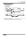
9-2 Interface of control side of IPM
IPM (Intelligent Power Modules) is easy to operate. The integrated drive and protection circuits require only an
isolated power supply and a low level on/off control signal. A fault output is provided for monitoring the operation of
the module internal protection circuits.
(1) Circuit and circuit constant of the IPM interface circuit
The parts of connecting IPM and controller (CPU) are required to use following parts.
Ԙ High speed photo-coupler ,ԙPull-up resistor
Ԛ Condenser (Ceramic condenser for the ripple removal
and electrolytic condenser for the power stabilization)
ԛ Low(high) speed photo-coupler
Input terminal
Fo terminal
Control power supply
Ԝ The mutually insulated stabilized power source of +15 V
(The negative power as it uses in IGBT-MOD is unnecessary.)
Example of constant value of the IPM interface circuit
Symbol
Name
Recommend Value
Rin
Pull-up resistor
20kΩ
C1
Smoothing capacitor
≥ 10uF
Cp
Bypass condenser
PC
Photo-coupler
0.1 ~ 1uF
High CMR, CTR
Note
All input terminal (include Br)
It is necessary that the charge and
discharge electric current and the
dv/dt electric current to IPM(IGBT
gate) can be sufficiently absorbed.
ex.) PS9613
(2) IPM Internal circuit diagram and interface circuit
15V Control
power supply
C1
҈10u
4KP
M
IPM
Vcc
High speed
photo-coupler
Vcin
Cp
0.1u~1uF
100pF
GND
Fo
1.5k
.QYURGGFRJQVQEQWRNGT
(3) IPM Control terminals
The IGBT power switches in the IPM are controlled by a low level input signal. The active low control input will
keep the power devices off when it is held high. Typically the input pin of the IPM is pulled high with a resistor
connected to the positive side of the control power supply. An ON signal is then generated by pulling the control
input low.
The recommended value of the pull-up resistor is 20 kΩ but it can be smaller for the noise countermeasure
and so on. However, if the pull-up resistor is set too small, it will affect the lifetime of the photo-coupler, please
confirm the characteristics with lifetime and so on in the photo-coupler manufacturer.
24
Dec. 20
Mitsubishi IPM-series Application Note
Using IPM
The inside of the control input terminal is connected to the comparator and is with high impedance.
When IPM (IGBT) is turn-off , the output impedance of the photo-coupler becomes high. Total impedance of the
circuit which connect the interface circuit is equal to a resistance of about 20KΩ.
The most important consideration in interface circuit design is layout. Shielding and careful routing of printed
circuit wiring is necessary in order to avoid coupling of dv/dt noise into control circuits. Parasitic capacitance
between high side interface circuits, high and low side interface circuits, or primary and secondary sides of the
isolating devices can cause noise problems. Careful layout of control power supply and isolating circuit wiring is
necessary. In layout, it is important not to make wiring of the photo-coupler primary side and secondly side cross
each other. Also, pattern should be made shortest and not to be crowded around and the magnetic field make the
inside of the current-loop not cross. Place condenser with good frequency response between the power - GND of
the photo coupler.
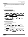
Depending on the pattern layout, sometimes a ringing as shown below occurs. In this case, the output current
of the photo-coupler doesn't change so much than the corrugation at normal.
However, the ringing problem increases the IPM switching loss, results possibly the IPM heat destruction. It is
necessary to check in design.
㩷
㩷
㩷
Control input terminal
Vcin
(secondary-side of
photo-coupler)
5V/div㩷
㩷
㩷
㪦㫌㫋㫇㫌㫋㩷㫍㫆㫃㫋㪸㪾㪼㩷㫆㪽㩷㪠㪧㪤㩷
㪭㪚㪜㩷
㩷 㩷 㩷 㪈㪇㪇㪭㪆㪻㫀㫍㩷
㩷
㫋㫀㫄㪼㩷㪑㩷㪈㫌㫊㪆㪻㫀㫍㩷
㩷
The extraordinary oscillation
Threshold
threshold voltage
Off
On
Off
On
㩷
㪝㫀㪾㪅㪐㪅㪈㩷㪫㪿㪼㩷㪼㫏㪸㫄㫇㫃㪼㩷㫆㪽㩷㫋㪿㪼㩷㫆㫊㪺㫀㫃㫃㪸㫋㫀㫆㫅㩷㫎㪸㫍㪼㪽㫆㫉㫄㩷㪘㩷㫆㪽㩷㫋㪿㪼㩷㫇㪿㫆㫋㫆㪄㪺㫆㫌㫇㫃㪼㫉㩷
㩷
In the following example, the oscillation happens at the timing of both after on and off. When the oscillation after
turn off continues over the dead time, it falls in the period when the opposite arm becomes on then cause an arm
short failure. The protection circuit works and IPM outputs Fo. This phenomenon sometimes happens under the
condition of no-load. It is easily confused with the malfunction on the side of IPM and the cause investigation takes
time. As a countermeasure, reducing the power supply impedance of the photo-coupler and the photo-coupler use
by IPM compatible is effective.
㩷
Control input terminal
Vcin
(secondary-side of
photo-coupler)
5V/div
㩷
time : 10us/div㩷
㩷
㪝㫀㪾㪅㪐㪅㪉㩷㪫㪿㪼㩷㪼㫏㪸㫄㫇㫃㪼㩷㫆㪽㩷㫋㪿㪼㩷㫆㫊㪺㫀㫃㫃㪸㫋㫀㫆㫅㩷㫎㪸㫍㪼㪽㫆㫉㫄㩷㪙㩷㫆㪽㩷㫋㪿㪼㩷㫇㪿㫆㫋㫆㪄㪺㫆㫌㫇㫃㪼㫉㩷
25
Dec. 20
Mitsubishi IPM-series Application Note
Using IPM
(4) Fo terminal of IPM
Fo is the output which shows the abnormal condition of IPM.
The extraordinary modes are overheating(OT), load ( the arm ) short circuit(SC), and control supply under
voltage(UV). Fo does not distinguish these kinds of failures.
The fault output is open collector type with its maximum sink current internally limited. When a fault condition
occurs the open collector device turns on allowing the fault terminal to sink current from the positive side of the
control supply. The inside of the Fo terminal is the open-collector composition which connected resistance
(1.5KΩ) in series.
Note )
If Fo is not used, the malfunction being able to be detected on the side of the system, passing away, it isn't
possible to do a protection-coordination with the system. For example, if Fo on the P-side is not used, then a
earth-short failure will not be able to protect in the system, and the earth-short occurs continuously. Because
IPM sometimes destroys when this condition continues, it is recommended to use all Fo terminals.
Fo terminal is connected with the comparator input circuit inside IPM. When leave this terminal open, there is
possibility that the noise invades from this terminal and cause malfunctions of the circuit inside IPM. In this case,
inserting a high frequency type condenser of about 0.1 μF between the Fo terminal and GND is effective. Also,
when not use Fo, in order not to undergo influence by the noise, connect it to 15 V control source.
Depending on the pattern layout of Fo, surge voltage over 20V is sometimes observed at the Fo terminal. Due
to this surge voltage, the electric strength is exaggerated and the LED part of the photo-coupler destroys. Be
careful of the pattern layout. If the surge voltage is difficult to be reduced, add a diode in the converse and
parallel(It refers to p1). To make low-impedance is important.
㩷
㩷
㩷
㪚㫆㫅㫋㫉㫆㫃㩷㫀㫅㫇㫌㫋㩷㫊㫀㪾㫅㪸㫃㩷
㩿㫇㫉㫀㫄㪸㫉㫐㩷㫊㫀㪻㪼㩷㫆㪽㩷㫇㪿㫆㫋㫆㩷
surge voltage
㪺㫆㫌㫇㫃㪼㫉㪀㩷
㩷 㩷 㩷 㩷 㩷 㪌㪭㪆㪻㫀㫍㩷
㩷
㩷
㪝㫆㩷㫋㪼㫉㫄㫀㫅㪸㫃㩷㫍㫆㫃㫋㪸㪾㪼㩷
㩷 㩷 㩷 㩷 㪌㪭㪆㪻㫀㫍㩷
㩷
㩷
㩷
㩷
㩷
㩷 㫋㫀㫄㪼㩷㪑㩷㪈㫌㫊㪆㪻㫀㫍㩷
㪝㫀㪾㪅㪐㪅㪊㩷㪫㪿㪼㩷㪼㫏㪸㫄㫇㫃㪼㩷㫆㪽㩷㫋㪿㪼㩷㪼㫏㫋㫉㪸㫆㫉㪻㫀㫅㪸㫉㫐㩷㫎㪸㫍㪼㪽㫆㫉㫄㩷㫆㪽㩷㫋㪿㪼㩷㪝㫆㩷㫋㪼㫉㫄㫀㫅㪸㫃㩷
(4) Example of photo coupler
The example of the photo-coupler recommended for IPM is shown below.
High speed photo coupler
High speed photo couplers are connected to the control input terminals of IPM.
When choosing photo coupler, pay attention to the parameters of response time (tpLH,tpHL) and CMR.
Choose the photo coupler that the value of tpLH,tpHL is less than 0.8us, and with high CMR.
Especially, ensure that the phenomena such as the ringing not occur.
For example)
PS9613 (NEC)
TLP559(IGM) (Toshiba)
The photo-coupler manufacturer sometimes has the IPM exclusive-goods ( another form name ) which
sorted out a characteristic. Please inquire the photo-coupler of IPM compatible for the malfunction prevention
when order.
26
Dec. 20
Mitsubishi IPM-series Application Note
Using IPM
Low speed photo coupler
Low speed photo coupler is connected Fo terminal of IPM.
When choosing photo coupler, pay attention to the parameter of CTR.
Choose the photo coupler that the value of CTR is equal to or more than 100 %.
For example)
TLP-521 (Toshiba)
PS2502 (NEC)
Please inquire the manufacturer that the photo-coupler has or has not problem when work under your
environmental condition.
Words and terms)
CTR (Current Transfer Ratio) : The ratio of the output current to the input current
CMR (Common Mode Rejection) : The maximum rise ratio of common mode voltage
tpLH,tpHL : The Propagation delay time LψH ,HψL
㩷
㩷
㩷
㪚㫆㫅㫋㫉㫆㫃㩷㫀㫅㫇㫌㫋㩷㫊㫀㪾㫅㪸㫃
㩿㫊㪼㪺㫆㫅㪻㫃㫐㩷㫊㫀㪻㪼㩷㫆㪽㩷
㫇㪿㫆㫋㫆㩷㪺㫆㫌㫇㫃㪼㫉㪀㩷
㩷 㩷 㩷 㩷 㩷 㪌㪭㪆㪻㫀㫍㩷
㩷
㩷
㩷
㩷
㪚㫆㫃㫃㪼㪺㫋㫆㫉㩷㪺㫌㫉㫉㪼㫅㫋㩷
㫆㪽㩷㫇㪿㫆㫋㫆㩷㪺㫆㫌㫇㫃㪼㫉㩷
㩷 㩷 㩷 㩷 㩷 㪈㫄㪘㪆㪻㫀㫍㩷
8EKP
㩷
㩷
㩷
㫋㫀㫄㪼㩷㪑㪈㪇㫌㫊㪆㪻㫀㫍㩷
Fig.9.4 The example of the input/output waveform of the control input terminal(photo coupler output).
27
Dec. 20
Mitsubishi IPM-series Application Note
Using IPM
(5) Notice of using photo coupler
The photo coupler can isolate the primary side and secondary side. But, this is not correct at the high
frequency. Because, photo coupler have a parasitic capacity between primary side and secondary side. When
high dv/dt is impressed, the pulse electric current flows from the primary side to the secondary side via the
parasitic capacity of photo coupler. This current sometimes turn on the photo coupler.
Therefore, it is important to design a circuit so that the LED will not turn on erroneously by this dv/dt.
When the input signal is OFF, make sure the circuit that the LED of primary side of photo coupler is with
low-impedance.
The LED is ON and
outputs extraordinary ON signal.
IPM
OFF
Parasitic capacity
dv/dt current
Fig.9.5 The example of the circuit which isn't good
㩷
㩷
㩷
IPM
㩷
Fig.9.6. The example of the circuit to recommend
㩷
The recommended circuit doesn't make malfunction (LED of primary side of photo coupler is ON) because the
dv/dt current can not turn ON the LED of primary side of photo coupler.
Please consult the application-note of the photo coupler for the detailed instruction of the circuit around the
photo coupler.
28
Dec. 20
Mitsubishi IPM-series Application Note
Using IPM
(6) Connecter for control terminal of IPM
We use the connector from “HIROSE ELECTRIC CO., LTD” in our test of IPM. The following connector is
recommended. The pace of this connector is 2.00 mm. It is the special connector of IPM which secured an
electrical clearance among the terminals( U-V,V-W,W-U of P-side and N)
The terminal with gold plate is recommended from the viewpoint of contact reliability.
Type name :DF10-31S-2DSA(68)
Type name :DF10-31S-2DSA(62)
٨450~600A/600V and 200~450A/1200V uses a connector with 2.54 mm pitch.
Type
: MDF7-11S-2.54DSA(32)
Typename
name
:DF7-11S-2.54DSA(32)
The details of the connector inquire of the manufacturer (HIROSE ELECTRIC CO., LTD.).
Note)
In the RLB/CLB type, installation by solder is being recommended by the printed circuit board and the input
and main terminal.
(5) The material of control terminal of IPM (RLA / CLA type)
As a reference of the connector selection, the material and the metal finishing of the control terminal on the
side of IPM are shown below.
㩷
㩷
Main material
The specification
of the plating
Brass
substrate
Thickness
Nickel (Ni) thickness=1.5um
= 1∼5μm
Thickness
surface
Gold(Au) thickness=0.3um
= 0.05∼0.2μm
㩷
(6) The guide pin of IPM
The guide pin on both sides of the control terminal of IPM is metal.
The guide pin is molded by plastic, and isolated.
29
In the RLB / CLB type, installation by solder is
being recommended, the plating of control terminal
for these types are Sn
Dec. 20
Mitsubishi IPM-series Application Note
Using IPM
9-3 Control Power supply of IPM
(1) The control power supply
The voltage range including ripples should meet the specification.
Control supply voltage VD(V)
0~4.0
Operation behavior
It is almost the same as no power supply.
External noise may cause IPM malfunction (turns ON).
Supply under-voltage protection will not operate and no
Fo signal will be asserted.
4.0~12.5
Even if control input signals are applied, IGBT does not work
Supply under-voltage protection starts operation and outputs
Fo signals.
12.5~13.5
Switching operation works. However, this value is below the
recommended one, VCE(sat) and switching time will be out of the
specified values, it may increase collector dissipation and
junction temperature.
13.5~16.5
Recommended values.
16.5~20
20.0~
Switching operation works. This range, however, is over the
recommended value, thus, too fast switching speed might
cause the chips to be damaged
The control circuit will be destroyed.
Specifications for Ripple Noise
High frequency noise super imposed on the control IC supply line might cause IC malfunction and cause an
Fo signal output, and results IPM stop (interrupt gates). To avoid such malfunction, the supply circuit should
be designed such that the noise fluctuation is smaller than +/- 5V/us, and the ripple voltage is less than 2V.
Specification :
dv
≤ ±5V / us , Vripple ≤ 2Vp − p
dt
When the noise on the power supply line is a high frequency(pulse-width<about 50ns,
pulse-vibration<about 5V) which does not cause an Fo output from IPM, the noise can be ignored.
The power supply should be a low impedance, be careful of the pattern layout.
Connect a bypass condenser with good frequency response and a smoothing condenser close to the
terminals of IPM. It is effective for the prevention of the malfunction.
Control Supply Starting up and Shutting Down Sequence
Control supply VD should be started up prior to the main supply (P-N supply).
Control supply VD should be shut down after the main supply (P-N supply).
If the main supply had been started up before the control supply, or if the main supply remains after
control supply was shut down, external noise might cause the IPM malfunction.
As for the P-side , use the control power supply which was insulated in each of all of the 2 aspects.
As for the N-side , because the GND in 2 aspects and the converter part is common, a common power can be
used for the three control sources in amount.
30
Dec. 2012
Mitsubishi IPM-series Application Note
Using IPM
(2) The circuit current of control power supply of IPM
The circuit current of control power supply of IPM is shown below.
This current is average of DC and fc=20kHz.
Condition : VD=15V,Tj=25{C, Unit : mA
AC220V
IPM L-series
䌎-side
DC
20kHz
Type. Name
Typ
Max
Typ
Max
PM 50RLA/RLB060
20
30
25
34
PM 50CLA/CLB060
15
25
21
29
PM 75RLA/RLB060
20
30
34
46
PM 75CLA/CLB060
15
25
28
38
PM100RLA060
20
30
38
52
PM100CLA060
15
25
32
44
PM150RLA060
20
30
52
71
PM150CLA060
15
25
35
48
PM200RLA060
24
34
60
81
PM200CLA060
18
28
58
79
PM300RLA060
24
34
83 113
PM300CLA060 *)
18
28
80 108
PM450CLA060 *)
11
18
45
61
PM600CLA060 *)
20
27
55
75
P-side(1 phase)
DC
20kHz
Typ
Max
Typ
Max
5
10
7
10
5
10
7
10
5
10
10
14
5
10
10
14
5
10
11
15
5
10
11
15
5
10
15
21
5
10
15
21
6
12
20
27
6
12
20
27
6
12
25
34
6
12
25
34
11
18
45
61
20
27
55
75
*) The value per device
AC440V
䌎-side
IPM L-series
DC
Type. Name
PM25RLA/RLB120
PM25CLA/CLB120
PM50RLA/RLB120
PM50CLA/CLB120
PM75RLA/RLB120
PM75CLA/CLB120
PM100RLA120
PM100CLA120
PM150RLA120
PM150CLA120
PM200CLA120
PM300CLA120
PM450CLA120
Typ
20
15
20
15
20
15
24
18
24
18
11
20
20
Max
30
25
30
25
30
25
34
28
34
28
18
27
27
20kHz
Typ
Max
24
33
19
26
34
46
30
41
42
57
35
48
53
72
51
69
76 103
67
91
40
54
55
75
55
75
31
P-side(1 phase)
DC
20kHz
Typ
Max
Typ
Max
5
10
7
10
5
10
7
10
5
10
10
14
5
10
10
14
5
10
13
18
5
10
13
18
6
12
17
23
6
12
17
23
6
12
23
32
6
12
23
32
11
18
40
54
20
27
55
75
20
27
55
75
*) The value per device
Dec. 2012
Mitsubishi IPM-series Application Note
Using IPM
The circuit current of the IPM control power supply at other frequency
The circuit current of control power supply of IPM increases with the carrier frequency.
The carrier frequency dependence of the circuit current of the IPM control power supply can be approximated
as a straight line like the following figure.
The gate of IGBT used in IPM has an input-capacitance(Cies=CGE+CCG).
The current to be charged and discharged by flowing through the gate at the timing of gate on and off.
There is IPM that this current becomes 1~2 A.
When IPM is turn-off, the dv/dt current from the collector of IGBT flows into the side of the control power
supply. Design a control power supply in the low impedance so that this dv/dt current can be absorbed.
Otherwise, The control IC of IPM might make malfunction and On signal is activated by this current resulting
arm short circuit.
The control power supply circuit needs a capacity that it can supply and absorb these current.
Usually, such problems(maximum current, impedance) can be avoided by power supply circuit and also
bypass ,smoothing condenser. But, the effect of the condenser is influenced by the inductance of the wiring
pattern. Determine the condenser capacity after verifying the substrate and the equipment.
32
Dec. 2012
Mitsubishi IPM-series Application Note
Using IPM
9-4 Fault Signal of IPM
IPM (Intelligent Power Modules) have sophisticated built-in protection circuits that prevent the power devices
from being damaged should the system malfunction or be over stressed. Control supply under-voltage(UV), over
temperature(OT), and short-circuit(SC) protection are all provided by the IPM's internal gate control circuits. A
fault output signal is provided to alert the system controller if any of the protection circuits are activated. Following
Fig.9.7 is a block diagram showing the IPMs internally integrated functions.
UV protection
OT protection
SC protection
UVr
UVt
VD
Signal input
Fo output
Fo
Fo
Fo
16
Fo
OTr
Tj
VGE
SCt
Ic
Fig.9.7 Timing chart of Control and protection of IPM
Control Supply Under-Voltage (UV)
The IPM’s internal control circuits operate from an isolated 15V DC supply. If, for any reason, the voltage of
this supply drops below the specified under-voltage trip level (UVt), the power devices will be turned off and a
fault signal will be generated. Small glitches less than the specified tdUV(<10us) in length will not affect the
operation of the control circuitry and will be ignored by the under voltage protection circuit. In order for normal
operation to resume, the supply voltage must exceed the under voltage reset level (UVr). Operation of the
under-voltage protection circuit will also occur during power up and power down of the control supply. This
operation is normal and the system controller's program should take the fault output delay (tfo) into account.
Note)
1. Application of the main bus voltage at a rate greater than 20V/ms before the control power supply is on
and stabilized may cause destruction of the power devices.
2. Voltage ripple on the control power supply with dv/dt in excess of 5V/us may cause a false trip of the UV
lock-out.
Over Temperature (OT)
The IPM has a temperature sensor mounted on surface of IGBT chips. If the temperature of the IGBT chips
exceeds the over temperature trip level (OT) the IPMs internal control circuit will protect the power devices by
disabling the gate drive and ignoring the control input signal until the over temperature condition has subsided.
The fault output will remain as long as the over temperature condition exists. When the temperature falls below
the over temperature reset level (OTr), and the control input is high (offstate) the power device will be enabled
and normal operation will resume at the next low (on) input signal.
Note)
1. Tripping of the over-temperature protection is an indication of stressful operation. Repetitive tripping
should be avoided.
33
Dec. 2012
Mitsubishi IPM-series Application Note
Using IPM
Short Circuit (SC)
If a load short circuit occurs or the system controller malfunctions causing a shoot through, the IPMs built in
short circuit protection will prevent the IGBTs from being damaged. When the current, through the IGBT
exceeds the short circuit trip level (SC), an immediate controlled shutdown is initiated and a fault output is
generated.
Note)
1. Tripping of the over current and short circuit protection indicates stressful operation of the IGBT.
Repetitive tripping should be avoided.
2. High surge voltages may occur during emergency shutdown. Low inductance buswork and snubbers are
recommended.
The operating-sequence of the UV protection
a1 : The normal operation=IGBT ON
a2 : The decline of control power supply voltage (UVt)
a3 : IGBT OFF (Even if the input signal is in on state)
a4 : The rise of control power supply (UVr)
a5 : The normal operation=IGBT ON
㩷㩷
㩷
㩷
㩷
The operating-sequence of the OT protection
a1 : The normal operation=IGBT ON
a2 : The overheating detection (OTt)
a3 : IGBT OFF (Even if it makes an input signal to be on)
a4 : The overheating detection reset (OTr)
a5 : The normal operation=IGBT ON
input signal
(Low=ON)
Condition of
protection circuit
Junction
temperature
Tj
RESET
SET
OT
a2
OTr
a4
a1
a3
a5
Output current
I(A)
Fo signal
㩷
34
Dec. 2012
Mitsubishi IPM-series Application Note
Using IPM
The operating-sequence of the SC protection
a1 : The normal operation=IGBT ON
a2 : Short current detection (SCt)
a3 : IGBT gate is blocked softly.
a4 : IGBT turn off gradually.
a5 : Fo timer start (tFo=1.8ms typ.)
a6 : Input signal “H”=OFF
a7 : Input signal “L”=ON
a8 : IGBT maintains off. (When a6~a7 occurs at the time which is shorter than tA)
㩷
input signal
Low=ON
a6
Condition of
protection circuit
a7
SET
RESET
Gate of IGBT
a3
a2
a1
SC
a4
Output current
a8
I(A)
Fo signal
a5
tA
㩷
㩷
㩷
Although IPM has internal protection circuit, it is recommended to ensure the stress which exceeds a
maximum rating does not happen repeatedly.
Therefore, if received Fo signal, please stop the control signal and stop the operation of IPM.
Because IPM doesn't exclude extraordinary cause, it has to be stopped by the system.
35
Dec. 2012
Mitsubishi IPM-series Application Note
Using IPM
9-5 Other notice of using IPM
(1) The treatment of the terminal not to use
Type CLA,CLB have B terminal. These terminal aren’t connected to the circuit. The pattern can be
connected with this terminal. However, pay attention to the wiring. When connecting a pattern with these
terminals, the noise might invades IPM via the terminals. Please just leave these terminals open.
If any phase of the IPM is not used, the corresponded control power supply in the circuit will not use. Please
pull-up the corresponded input terminals and make IGBT off. This is to prevent the erroneous turn on of the
circuit by noise.
(2) The connection of the control side GND(VNC/V*PC) and output emitter GND (N or U/V/W)
Do not connect the control side GND and the output emitter GND on the printed circuit board. Otherwise It
will be easy to undergo influence by the noise. VNC and the N terminal are connected inside IPM. If
connecting VNC and N terminal, the current which should flow through N sometimes flows to VNC. Then,
the electric potential difference occurs between N and VNC by parasitic inductance inside and might cause
IC malfunction.
㧵㧼㧹
㧵㧼㧹
㨂㧰㧰
㨂㧰㧰
㧵㧺
The course
㔚ᵹ⚻〝
of
the current
㨂㧼㧯
㧵㧺
The course
㔚ᵹ⚻〝
of the current
㨂㧼㧯
㨂㧰㧰
㨂㧰㧰
㧵㧺
㧵㧺
㨂㧺㧯
㨂㧺㧯
ㅅ㔚ᵹߦࠃࠆࡁࠗ࠭
The noise
which occurs with stray -current
࿁〝㔚ᵹߩߺࠍᵹߔࠃ߁ߦ
㪣㪸㫐㫆㫌㫋㩷㫋㫆㩷㫇㪸㫊㫊㩷㫆㫅㫃㫐㩷㪸㩷㪺㫀㫉㪺㫌㫀㫋㩷㪺㫌㫉㫉㪼㫅㫋㪅
ࡄ࠲ࡦࠍࠗࠕ࠙࠻ߔࠆ
(3) The circuit structure inside
The IPM is built up with IGBT chip ,FWDi chip, Control IC and the other discreet parts(R,C).
Gate of IGBT chip is MOS structure. However, The gate of IGBT chip doesn’t directly connect to the control
terminal of IPM. VD, Input, Fo and GND terminal are connected to the control IC. It is possible to consider
the terminal of IPM to be a bipolar structure. The countermeasure against static electricity like conventional
IC with MOS structure is unnecessary to IPM.
(The handling of IPM is equal to that of a bipolar IC.)
VCC
IN
Control IC
IGBT
C
FWDi
Driver
Fo
E
GND
(4) The parallel operation
The IPM is not recommended for parallel operation.
Because the balance of the switching time and the current are not identical, the IPM with larger loss might
be thermally damaged because it isn't possible to do the protection-coordination of each IPM.
36
Dec. 2012
Mitsubishi IPM-series Application Note
Power Loss and Junction Temperature
10. Power Loss and Junction Temperature
Junction temperature can be used as an indication of IGBT module situation. This section will discuss how to calculate junction
temperature and give an example based on waveform shown in Fig.10.1. Here, only power loss of IGBT part is given. The power
loss of Diode can be obtained by using the same method as IGBT part. Moreover, junction temperature must never be outside of
the maximum allowable value. It also has impact on the power cycle life.
Fig.10.1
a㧚Power Loss
In order to estimate junction temperature for thermal design, it is necessary to compute total power loss. The first step is the
calculation of power loss per pulse.
Two most important sources of power dissipation that must be considered are conduction losses and switching losses. (Fig.10.2)
(1) Conduction Losses
The total power dissipation during conduction is
computed by multiplying the on-state saturation voltage by
the on-state current.
IC1 × VCE( sat )1 + IC2 × VCE( sat )2
× tw1 (J)
2
Note)The above equation is a simplification of the below one
E( sat ) =
VCE(sat) VS㧚Ic characteristics at Tj=125°C is used in power
loss calculation.
(2) Switching Losses
The most accurate method of determining switching
losses is to plot the Ic and VCE waveforms during the
switching transition. Multiply the waveforms point by point
to get an instantaneous power waveform. The area under
the power waveform is the switching energy expressed in
watt-seconds/pulse or J/pulse.
n: number of partitions
(divide interval between ta and tb equally into n parts,
compute average power loss for each interval.)
Calculation of Eoff has the same method.
The total power loss of one pulse is the sum of (1) and (2).
E1 = E( sat ) + Eon + Eoff
tb
ta
Fig.10.3
Fig.10.2
37
Dec. 2012
Mitsubishi IPM-series Application Note
Power Loss and Junction Temperature
(3) Average Power Loss
The average power loss per pulse is
P1 =
E1
tw 1
(W)
Fig.10.4 is approximation of Fig.10.1 by using rectangle wave.
Fig.10.4
Average power loss during period of tw2 is (See Fig.10.5)
Pav =
E1
×N
tw 2
(W)
N㧦pulse numbers in tw2 period
Fig.10.5
Total average power loss is (See Fig.10.6)
PAV = Pav ×
tw 2
T2
(W)
Fig.10.6
b. Junction Temperature Calculation
Junction temperature can be calculated by using P1, Pav, and PAV that has been obtained so far. Three cases should be
considered according to pulse width.
(1) tw1 is short (tw1<<1ms)
(2) Both of tw1 and tw2 are long(1ms<tw1<tw2<1s)
(3) tw2 is longer than 1s.(tw2>1s)
38
Dec. 2012
Mitsubishi IPM-series Application Note
Power Loss and Junction Temperature
(1) tw1<<1ms
In case of short on interval or low duty as in Fig.10.5, Junction temperatures rise to the highest value at the turn-off moment
of tw2 while the case temperature is stationary. (See Fig.10.7)
Fig.10.7
Fig.10.8
Temperature difference between junction and case can be calculated by using the following formula.
ٌT(j-c)㧩Rth(j-c)PAV㧙Zth(j-c)(tw2)PAV㧗Zth(j-c)(tw2)Pav㧩Rth(j-c)PAV㧗(Pav㧙PAV)Zth(j-c)(tw2)
̖̖thermal resistance between junction and case
Rth(j-c)
Zth(j-c)(tw2) ̖̖thermal impedance between junction and case at tw2 moment
ѕTj㧩Tc㧗ٌT(j-c)
(Tc is measured by thermo-couple.)
Tj(max)=150°C, therefore the allowable case temperature Tc(max) is, Tc(max)=150-ٌT(j-c).
(2) 1ms<tw1<tw2<1s
In this case, ripple should be considered in calculation of average power loss P1.
Using approximation similar to (1) Fig.10.9 is obtained for calculation.
Fig.10.9
ٌT(j-c)㧩Rth(j-c)PAV㧙Zth(tw2)PAV㧗Zth(j-c)(tw2)Pav㧙Zth(j-c)(tw1)Pav㧗Zth(j-c)(tw1)P1
㧩Rth(j-c)PAV㧗(Pav㧙PAV)Zth(j-c)(tW2)㧗(Pl㧙Pav)Zth(j-c)(tw1)
Rth(j-c)
̖̖thermal resistance between junction and case
Zth(j-c)(tw2)
̖̖thermal impedance between junction and case at tw2 moment
Zth(j-c)(tw1)
̖̖thermal impedance between junction and case at tw1 moment
ѕTj㧩Tc㧗ٌT(j-c)
(Tc is measured by thermo-couple.)
Tc(max)㧩150㧙ٌT(j-c)
39
Dec. 2012
Mitsubishi IPM-series Application Note
Power Loss and Junction Temperature
(3) tw2>1s
In a similar way to (2), temperature change of heatsink should be taken into consideration as well. It is necessary to know
the transient heat impedance of the heatsink. (Fig.10.9)
Fig.10.9
Similarly, the temperature difference between junction and ambient can be calculated by using the following formula.
ٌT(j-a)㧩Rth(j-a)PAV㧙Zth(j-a)(tw2)PAV㧗Zth(j-a)(tw2)Pav㧙Zth(j-a)(tw1)Pav㧗Zth(j-a)(tw1)P1
㧩Rth(j-a)PAV㧗(Pav㧙PAV)Zth(j-c)(tw2)㧗(P1㧙Pav)Zth(j-c)(tw1)
ѕTj㧩Ta㧗ٌT(j-a)
(Ta is measured by a thermometer.)
c. Heatsink Selection
Fig.10.10 shows the thermal equivalent circuit when two
or more modules are mounted on one heat sink.
According to this equivalent circuit, the temperature of
the heat sink is
Rth( f
− a)
=
TC(max) − Ta − (PT( AV ) + PD( AV )) × Rth( c − f )
(PT( AV ) + PD( AV )) × N
Moreover, power loss of FWDi should be considered
as well. In thermal design, the allowable case
temperature Tc(max) is up to the smaller one of IGBT
power loss and FWDi part.
Tf㧩Ta㧗(PT(AV)㧗PD(AV))NxRth(f-a)
Ta㧦Ambient temperature
PT(AV):Average power loss of IGBT
PD(AV):Average power loss of FWDi
N:Arm number
Rth(f-a):The heatsink to ambient thermal resistance
The case temperature Tc is,
Tc㧩Tf㧗(PT(AV)㧗PD(AV))Rth(c-f)
Rth(c-f)㧦The case to heatsink thermal resistance
Tc(max) can be calculated by using the below formula.
ѕTc(max)㧩Ta㧗(PT(AV)㧗PD(AV))NxRth(f-a)㧗(PT(AV)㧗
PD(AV))Rth(c-f)
Therefore, the heatsink to ambient thermal resistance
can be computed as
Fig.10.10 Thermal Calculation Model
40
Dec. 2012
Mitsubishi IPM-series Application Note
Average Power Loss Simplified Calculation
11. Average Power Loss Simplified Calculation
(1) VVVF Inverter
عApplicability Range
It is applicable to total power loss calculation for selection of IGBTs used in VVVF inverters.
It is not applicable in the thermal design of the device (limit design).
عAssumption Condition
1 PWM modulation used to synthesize sinusoidal output currents in VVVF inverters
٤
2 PWM signal generated by comparing sinusoidal wave to triangular wave
٤
1− D 1+ D
~
(% / 100 )
2
2
3 Duty cycle of PWM among the rank of
٤
D : modulation rate
4 Output current of ICP㨯sin x without ripple
٤
5 With inductive load rate of cosǰ
٤
عCalculation Equation
Duty cycle of PWM is constantly changing and its value equal to time x
1 + D × sin x
at the corresponding moment.
2
The output current corresponds to the output voltage change and this relationship is represented by power factor cosǰ.
Therefore, the duty cycle of PWM corresponding to output current at arbitrary phase x is
Output current = Icp × sin x
PWM Duty =
1 + D × sin( x + θ)
2
VCE(sat) and VEC at this moment are
Vce(sat ) = Vce(sat )(@ Icp × sin x )
Vec = Vec(@(−1) × Iecp( = Icp) × sin x )
Static power loss of IGBT is
Similarly, static power loss of FWDi is
On the other hand, dynamic power loss of IGBT is not dependent on the PWM duty and can be expressed as the
following formula.
As for dynamic power loss of free-wheeling diode, calculation is given by an example of ideal diode shown in Fig.11.1.
㫋㫉㫉
㪠㪼㪺
㪭㪼㪺
㫋
㪠㫉㫉
㪭㪺㪺
Fig.11.1 Dynamic Power Loss of FWDi
Psw =
Irr × Vcc × trr
4
41
Dec. 2012
Mitsubishi IPM-series Application Note
Average Power Loss Simplified Calculation
Because reverse recovery of free-wheeling diodes occurs in half cycle of the output current, the dynamic power loss of
FWDi is
عInverter Loss Calculation Notes
Divide one cycle of output current into many equal intervals, then calculate actual "PWM duty", "Output current", and
"VCE(sat), VEC, and Psw responding to the current" in each interval. The power loss during one cycle is the sum of each
interval.
The PWM duty depends on the method of generating the signal.
The output current waveform and the relationship between output current and PWM duty cycle are dependent on signal
generator, load and other factors. Therefore, calculation should always be done with actual waveforms.
VCE(sat) uses the value of Tj=125°C.
Psw uses the value under half bridge operating case at Tj=125°C.
عThermal Design Notes
1 It is necessary to examine the worst switching condition.
٤
2 Consideration of temperature variation due to current cycle should be given in thermal design.
٤
(Temperature variation rate is 30% to 35% for 60Hz case. When the output current of several Hz switches for a few
seconds, it almost has equal temperature to a direct current with the same peak value continuously flowing. )
3 Temperature ripple caused by switching operation should be considered especially when switching frequency is much
٤
lower than 10kHz.
42
Dec. 2012
Mitsubishi IPM-series Application Note
Notice for safe Designs and when Using This Specification
12. Notice for safe Designs and when Using This Specification
㩷
Keep safety first in your circuit designs!
Mitsubishi Electric Corporation puts the maximum effort into making semiconductor products better and
more reliable, but these are always the possibility that trouble may occur with them. Trouble with
semiconductors may lead to personal injury, fire or property damage. Remember to give due
consideration to safety when making your circuit designs, with appropriate measures such as (1)
placement of substitutive, auxiliary circuits, (2) use of non-flammable material or (3) prevention against
any malfunction or mishap.㩷
㩷
Notice regarding these materials
These materials are intended as reference to assist our customers in the selection of the Mitsubishi
semiconductor product best suited to the customer’s application; they do not convey any license under
any intellectual property rights, or any other rights, belonging to Mitsubishi Electric Corporation or third
party.
Mitsubishi Electric Corporation assumes no responsibility for any damage, or infringement of any
third-party’s rights, originating in the use of any product data, diagrams, chart, programs, algorithms, or
circuit application examples contained in these materials.
All information contained in these materials, including product data, diagrams, charts, programs and
algorithms represents information on products at the time of publication of these materials, and are
subject to change by Mitsubishi Electric Corporation without notice due to product improvements or other
reasons. It is therefore recommended that customers contact Mitsubishi Electric Corporation or an
authorized Mitsubishi Semiconductor product distributor for the latest product information before
purchasing a product listed herein. The information described here may contain inaccuracies or
typographical errors. Mitsubishi Electric Corporation assumes no responsibility for any damage, liability,
or other loss rising from these inaccuracies or errors. Please also pay attention to information published
by Mitsubishi Electric Corporation by various means, including the Mitsubishi Semiconductor home page
(http://www.mitsubishichips.com)
When using any or all of the information contained in these materials, including product data, diagrams,
charts, programs and algorithms, please be sure to evaluate all information as a total system before
making a final decision on the applicability of the information and products. Mitsubishi Electric Corporation
assumes no responsibility for any damage, liability or other loss resulting from the information contained
herein.
Mitsubishi Electric Corporation semiconductors are not designed or manufactured for use in a device or
system that is used under circumstances in which human life is potentially at stake. Please contact
Mitsubishi Electric Corporation or an authorized Mitsubishi Semiconductor product distributor when
considering the use of a product contained herein for any specific purposes, such as apparatus or
systems for transportation, vehicular, medical, aerospace, nuclear, or undersea repeater use.
The prior written approval of Mitsubishi Electric Corporation is necessary to reprint or reproduce in whole
or in part these materials.
If these products or technologies are subject to the Japanese export control restrictions, they must be
exported under a license from the Japanese government and cannot be imported into a country other
than the approved destination. Any diversion or reexport contrary to the export control laws and
regulations of Japan and/or the country of destination is prohibited.
Please contact Mitsubishi Electric Corporation or an authorized Mitsubishi Semiconductor product
distributor for further details on these materials or the products contained therein.㩷
43
Dec. 2012