1
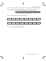
TMS320LF/LC240x
DSP Controllers
Reference Guide
System and Peripherals
Literature Number: SPRU357
January 2000
Printed on Recycled Paper
IMPORTANT NOTICE
Texas Instruments and its subsidiaries (TI) reserve the right to make changes to their products or to discontinue
any product or service without notice, and advise customers to obtain the latest version of relevant information
to verify, before placing orders, that information being relied on is current and complete. All products are sold
subject to the terms and conditions of sale supplied at the time of order acknowledgement, including those
pertaining to warranty, patent infringement, and limitation of liability.
TI warrants performance of its semiconductor products to the specifications applicable at the time of sale in
accordance with TI’s standard warranty. Testing and other quality control techniques are utilized to the extent
TI deems necessary to support this warranty. Specific testing of all parameters of each device is not necessarily
performed, except those mandated by government requirements.
CERTAIN APPLICATIONS USING SEMICONDUCTOR PRODUCTS MAY INVOLVE POTENTIAL RISKS OF
DEATH, PERSONAL INJURY, OR SEVERE PROPERTY OR ENVIRONMENTAL DAMAGE (“CRITICAL
APPLICATIONS”). TI SEMICONDUCTOR PRODUCTS ARE NOT DESIGNED, AUTHORIZED, OR
WARRANTED TO BE SUITABLE FOR USE IN LIFE-SUPPORT DEVICES OR SYSTEMS OR OTHER
CRITICAL APPLICATIONS. INCLUSION OF TI PRODUCTS IN SUCH APPLICATIONS IS UNDERSTOOD TO
BE FULLY AT THE CUSTOMER’S RISK.
In order to minimize risks associated with the customer’s applications, adequate design and operating
safeguards must be provided by the customer to minimize inherent or procedural hazards.
TI assumes no liability for applications assistance or customer product design. TI does not warrant or represent
that any license, either express or implied, is granted under any patent right, copyright, mask work right, or other
intellectual property right of TI covering or relating to any combination, machine, or process in which such
semiconductor products or services might be or are used. TI’s publication of information regarding any third
party’s products or services does not constitute TI’s approval, warranty or endorsement thereof.
Copyright 2000, Texas Instruments Incorporated
Preface
Read This First
About This Manual
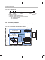
This reference guide describes the architecture, system hardware, peripherals, and general operation of the TMS320x2407/x2406/x2404/x2402 digital
signal processor (DSP) controllers. For a description of the CPU, assembly
language instructions, and XDS510 emulator, refer to TMS320C24x DSP
Controllers CPU and Instruction Set Reference Guide (SPRU160). This book
should be used in conjunction with SPRU160.
Notational Conventions
This document uses the following conventions:
- Program listings, program examples, and interactive displays are shown
in a special typeface similar to a typewriter’s. Examples use a bold
version of the special typeface for emphasis; interactive displays use a
bold version of the special typeface to distinguish commands that you
enter from items that the system displays (such as prompts, command
output, error messages, etc.).
Here is a sample program listing:
0011
0012
0013
0014
0005
0005
0005
0006
0001
0003
0006
.field
.field
.field
.even
1, 2
3, 4
6, 3
Here is an example of a system prompt and a command that you might
enter:
C:
csr –a /user/ti/simuboard/utilities
- In syntax descriptions, the instruction, command, or directive is in a bold
typeface and parameters are in an italic typeface. Portions of a syntax that
are in bold should be entered as shown; portions of a syntax that are in
italics describe the type of information that should be entered. Here is an
example of a directive syntax:
.asect ”section name”, address
.asect is the directive. This directive has two parameters, indicated by section name and address. When you use .asect, the first parameter must be
Contents
iii
Notational Conventions
an actual section name, enclosed in double quotes; the second parameter
must be an address.
- Square brackets [ ] identify an optional parameter. If you use an optional
parameter, you specify the information within the brackets; you don’t enter
the brackets themselves. Here’s an example of an instruction that has an
optional parameter:
LACC 16-bit constant [, shift]
The LACC instruction has two parameters. The first parameter, 16-bit constant, is required. The second parameter, shift, is optional. As this syntax
shows, if you use the optional second parameter, you must precede it with
a comma.
Square brackets are also used as part of the pathname specification for
VMS pathnames; in this case, the brackets are actually part of the pathname (they are not optional).
- Braces { } indicate a list. The symbol | (read as or) separates items with-
in the list. Here’s an example of a list:
{ * | *+ | *– }
This provides three choices: *, *+, or *–.
Unless the list is enclosed in square brackets, you must choose one item
from the list.
- Some directives can have a varying number of parameters. For example,
the .byte directive can have up to 100 parameters. The syntax for this directive is:
.byte value1 [, ... , valuen ]
This syntax shows that .byte must have at least one value parameter, but
you have the option of supplying additional value parameters, separated
by commas.
iv
Information About Cautions and Warnings / Related Documentation From Texas Instruments
Information About Cautions and Warnings
This book may contain cautions.
This is an example of a caution statement.
A caution statement describes a situation that could potentially
damage your software or equipment.
Related Documentation From Texas Instruments
The following books describe the ’C24x and related support tools. To obtain
a copy of any of these TI documents, call the Texas Instruments Literature Response Center at (800) 477-8924. When ordering, please identify the book by
its title and literature number. Many of these documents are located on the Internet at http://www.ti.com.
TMS320C24x DSP Controllers CPU and Instruction Set Reference Guide
(literature number SPRU160) describes the TMS320C24x 16-bit
fixed-point digital signal processor controller. Covered are its
architecture, internal register structure, data and program addressing,
and instruction set. Also includes instruction set comparisons and design
considerations for using the XDS510 emulator.
TMS320LF2407, TMS320LF2406, TMS320LF2402, TMS320LC2406,
TMS320LC2404, TMS320LC2402 DSP Controllers (literature number
SPRS094) data sheet contains the electrical and timing specifications for
these devices, as well as signal descriptions and pinouts for all of the
available packages.
TMS320C1x/C2x/C2xx/C5x Code Generation Tools Getting Started
Guide (literature number SPRU121) describes how to install the
TMS320C1x, TMS320C2x, TMS320C2xx, and TMS320C5x assembly
language tools and the C compiler for the ’C1x, ’C2x, ’C2xx, and ’C5x devices. The installations for MS-DOS, OS/2, SunOS, and Solaris
systems are covered.
Read This First
v
Related Documentation From Texas Instruments
TMS320C1x/C2x/C2xx/C5x Assembly Language Tools User’s Guide (literature number SPRU018) describes the assembly language tools (assembler, linker, and other tools used to develop assembly language
code), assembler directives, macros, common object file format, and
symbolic debugging directives for the ’C1x, ’C2x, ’C2xx, and ’C5x generations of devices.
TMS320C2x/C2xx/C5x Optimizing C Compiler User’s Guide (literature
number SPRU024) describes the ’C2x/C2xx/C5x C compiler. This C
compiler accepts ANSI standard C source code and produces TMS320
assembly language source code for the ’C2x, ’C2xx, and ’C5x generations of devices.
TMS320C2xx C Source Debugger User’s Guide (literature number
SPRU151) tells you how to invoke the ’C2xx emulator and simulator versions of the C source debugger interface. This book discusses various
aspects of the debugger interface, including window management, command entry, code execution, data management, and breakpoints. It also
includes a tutorial that introduces basic debugger functionality.
TMS320C2xx Simulator Getting Started (literature number SPRU137)
describes how to install the TMS320C2xx simulator and the C source
debugger for the ’C2xx. The installation for MS-DOS, PC-DOS,
SunOS, Solaris, and HP-UX systems is covered.
TMS320C2xx Emulator Getting Started Guide (literature number
SPRU209) tells you how to install the Windows 3.1 and Windows 95
versions of the ’C2xx emulator and C source debugger interface.
XDS51x Emulator Installation Guide (literature number SPNU070)
describes the installation of the XDS510, XDS510PP, and
XDS510WS emulator controllers. The installation of the XDS511
emulator is also described.
JTAG/MPSD Emulation Technical Reference (literature number SPDU079)
provides the design requirements of the XDS510 emulator controller,
discusses JTAG designs (based on the IEEE 1149.1 standard), and
modular port scan device (MPSD) designs.
TMS320 DSP Development Support Reference Guide (literature number
SPRU011) describes the TMS320 family of digital signal processors and
the tools that support these devices. Included are code-generation tools
(compilers, assemblers, linkers, etc.) and system integration and debug
tools (simulators, emulators, evaluation modules, etc.). Also covered are
available documentation, seminars, the university program, and factory
repair and exchange.
vi
Trademarks
TMS320 DSP Designer’s Notebook: Volume 1 (literature number
SPRT125) presents solutions to common design problems using ’C2x,
’C3x, ’C4x, ’C5x, and other TI DSPs.
TMS320 Third-Party Support Reference Guide (literature number
SPRU052) alphabetically lists over 100 third parties that provide various
products that serve the family of TMS320 digital signal processors. A
myriad of products and applications are offered—software and hardware
development tools, speech recognition, image processing, noise cancellation, modems, etc.
Trademarks
320 Hotline On-line is a trademark of Texas Instruments Incorporated.
cDSP is a trademark of Texas Instruments Incorporated.
HP-UX is a trademark of Hewlett-Packard Company.
MS-DOS is a registered trademark of Microsoft Corporation.
OS/2 is a trademark of International Business Machines Corporation.
PC is a trademark of International Business Machines Corporation.
PC-DOS is a trademark of International Business Machines Corporation.
Solaris is a trademark of Sun Microsystems, Inc.
SunOS is a trademark of Sun Microsystems, Inc.
TI is a trademark of Texas Instruments Incorporated.
Windows is a registered trademark of Microsoft Corporation.
XDS510 is a trademark of Texas Instruments Incorporated.
XDS510PP is a trademark of Texas Instruments Incorporated.
XDS510WS is a trademark of Texas Instruments Incorporated.
XDS511 is a trademark of Texas Instruments Incorporated.
Read This First
vii
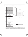
Contents
Contents
1
Introduction . . . . . . . . . . . . . . . . . . . . . . . . . . . . . . . . . . . . . . . . . . . . . . . . . . . . . . . . . . . . . . . . . . . . . 1-1
Summarizes the TMS320 family of products. Introduces the TMS320x240x DSP controllers
and lists their key features.
1.1
1.2
1.3
1.4
2
TMS320 Family Overview . . . . . . . . . . . . . . . . . . . . . . . . . . . . . . . . . . . . . . . . . . . . . . . . . . .
TMS320C240x Series of DSP Controllers . . . . . . . . . . . . . . . . . . . . . . . . . . . . . . . . . . . . . .
Peripheral Overview . . . . . . . . . . . . . . . . . . . . . . . . . . . . . . . . . . . . . . . . . . . . . . . . . . . . . . . .
’240x Highlights . . . . . . . . . . . . . . . . . . . . . . . . . . . . . . . . . . . . . . . . . . . . . . . . . . . . . . . . . . . .
1-2
1-3
1-5
1-6
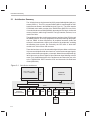
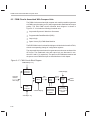
System Configuration and Interrupts . . . . . . . . . . . . . . . . . . . . . . . . . . . . . . . . . . . . . . . . . . . . . . 2-1
Describes the system configuration, interrupts, and how the peripheral interrupt expansion
(PIE) is used to increase interrupt requests capacity.
2.1
2.2
2.3
2.4
2.5
2.6
2.7
2.8
2.9
2.10
2.11
Architecture Summary . . . . . . . . . . . . . . . . . . . . . . . . . . . . . . . . . . . . . . . . . . . . . . . . . . . . . . . 2-2
Configuration Registers . . . . . . . . . . . . . . . . . . . . . . . . . . . . . . . . . . . . . . . . . . . . . . . . . . . . . 2-3
2.2.1 System Control and Status Registers 1 and 2 (SCSR1, SCSR2) . . . . . . . . . . . 2-3
2.2.2 Device Identification Number Register (DINR) . . . . . . . . . . . . . . . . . . . . . . . . . . . 2-7
Interrupt Priority and Vectors . . . . . . . . . . . . . . . . . . . . . . . . . . . . . . . . . . . . . . . . . . . . . . . . . 2-8
Peripheral Interrupt Expansion (PIE) . . . . . . . . . . . . . . . . . . . . . . . . . . . . . . . . . . . . . . . . . 2-12
2.4.1 Interrupt Hierarchy . . . . . . . . . . . . . . . . . . . . . . . . . . . . . . . . . . . . . . . . . . . . . . . . . . 2-14
2.4.2 Interrupt Request Structure . . . . . . . . . . . . . . . . . . . . . . . . . . . . . . . . . . . . . . . . . . 2-14
2.4.3 Interrupt Acknowledge . . . . . . . . . . . . . . . . . . . . . . . . . . . . . . . . . . . . . . . . . . . . . . 2-15
Interrupt Vectors . . . . . . . . . . . . . . . . . . . . . . . . . . . . . . . . . . . . . . . . . . . . . . . . . . . . . . . . . . . 2-16
2.5.1 Phantom Interrupt Vector . . . . . . . . . . . . . . . . . . . . . . . . . . . . . . . . . . . . . . . . . . . . 2-17
2.5.2 Software Hierarchy . . . . . . . . . . . . . . . . . . . . . . . . . . . . . . . . . . . . . . . . . . . . . . . . . 2-18
2.5.3 Nonmaskable Interrupts . . . . . . . . . . . . . . . . . . . . . . . . . . . . . . . . . . . . . . . . . . . . . 2-18
Interrupt Operation Sequence . . . . . . . . . . . . . . . . . . . . . . . . . . . . . . . . . . . . . . . . . . . . . . . 2-19
Interrupt Latency . . . . . . . . . . . . . . . . . . . . . . . . . . . . . . . . . . . . . . . . . . . . . . . . . . . . . . . . . . 2-21
Sample ISR Code . . . . . . . . . . . . . . . . . . . . . . . . . . . . . . . . . . . . . . . . . . . . . . . . . . . . . . . . . 2-22
CPU Interrupt Registers . . . . . . . . . . . . . . . . . . . . . . . . . . . . . . . . . . . . . . . . . . . . . . . . . . . . 2-23
2.9.1 Interrupt Flag Register (IFR) . . . . . . . . . . . . . . . . . . . . . . . . . . . . . . . . . . . . . . . . . 2-23
2.9.2 Interrupt Mask Register (IMR) . . . . . . . . . . . . . . . . . . . . . . . . . . . . . . . . . . . . . . . . 2-25
Peripheral Interrupt Registers . . . . . . . . . . . . . . . . . . . . . . . . . . . . . . . . . . . . . . . . . . . . . . . 2-27
2.10.1 Peripheral Interrupt Vector Register (PIVR) . . . . . . . . . . . . . . . . . . . . . . . . . . . . 2-27
2.10.2 Peripheral Interrupt Request Registers (PIRQR0, 1, 2) . . . . . . . . . . . . . . . . . . 2-28
2.10.3 Peripheral Interrupt Acknowledge Registers (PIACKR0 ,1, 2) . . . . . . . . . . . . . 2-31
Reset . . . . . . . . . . . . . . . . . . . . . . . . . . . . . . . . . . . . . . . . . . . . . . . . . . . . . . . . . . . . . . . . . . . . 2-35
ix
Contents
2.12
2.13
3
3.3
3.4
3.5
3.6
3.7
3.8
3.9
3.10
4.4
Pins . . . . . . . . . . . . . . . . . . . . . . . . . . . . . . . . . . . . . . . . . . . . . . . . . . . . . . . . . . . . . . . . . . . . . . .
Phase-Locked Loop . . . . . . . . . . . . . . . . . . . . . . . . . . . . . . . . . . . . . . . . . . . . . . . . . . . . . . . . .
Watchdog Timer Clock . . . . . . . . . . . . . . . . . . . . . . . . . . . . . . . . . . . . . . . . . . . . . . . . . . . . . .
4.3.1 Watchdog Suspend . . . . . . . . . . . . . . . . . . . . . . . . . . . . . . . . . . . . . . . . . . . . . . . . . .
Low-Power Modes . . . . . . . . . . . . . . . . . . . . . . . . . . . . . . . . . . . . . . . . . . . . . . . . . . . . . . . . . .
4.4.1 Clock Domains . . . . . . . . . . . . . . . . . . . . . . . . . . . . . . . . . . . . . . . . . . . . . . . . . . . . . .
4.4.2 Wake Up from Low-Power Modes . . . . . . . . . . . . . . . . . . . . . . . . . . . . . . . . . . . . .
4-2
4-2
4-2
4-3
4-3
4-3
4-4
Digital Input/Output (I/O) . . . . . . . . . . . . . . . . . . . . . . . . . . . . . . . . . . . . . . . . . . . . . . . . . . . . . . . . . 5-1
Describes the digital I/O ports module.
5.1
5.2
5.3
5.4
x
Factory Masked On-Chip ROM . . . . . . . . . . . . . . . . . . . . . . . . . . . . . . . . . . . . . . . . . . . . . . . 3-2
Flash . . . . . . . . . . . . . . . . . . . . . . . . . . . . . . . . . . . . . . . . . . . . . . . . . . . . . . . . . . . . . . . . . . . . . . 3-2
3.2.1 Flash Control Register Access . . . . . . . . . . . . . . . . . . . . . . . . . . . . . . . . . . . . . . . . 3-2
Overview of Memory and I/O Spaces . . . . . . . . . . . . . . . . . . . . . . . . . . . . . . . . . . . . . . . . . . 3-3
Program Memory . . . . . . . . . . . . . . . . . . . . . . . . . . . . . . . . . . . . . . . . . . . . . . . . . . . . . . . . . . 3-10
3.4.1 Program Memory Configuration . . . . . . . . . . . . . . . . . . . . . . . . . . . . . . . . . . . . . . 3-10
Data Memory . . . . . . . . . . . . . . . . . . . . . . . . . . . . . . . . . . . . . . . . . . . . . . . . . . . . . . . . . . . . . 3-12
3.5.1 Global Data Memory . . . . . . . . . . . . . . . . . . . . . . . . . . . . . . . . . . . . . . . . . . . . . . . . 3-15
I/O Space . . . . . . . . . . . . . . . . . . . . . . . . . . . . . . . . . . . . . . . . . . . . . . . . . . . . . . . . . . . . . . . . . 3-16
XMIF Qualifier Signal Description . . . . . . . . . . . . . . . . . . . . . . . . . . . . . . . . . . . . . . . . . . . . 3-17
Program and Data Spaces . . . . . . . . . . . . . . . . . . . . . . . . . . . . . . . . . . . . . . . . . . . . . . . . . . 3-20
I/O Space . . . . . . . . . . . . . . . . . . . . . . . . . . . . . . . . . . . . . . . . . . . . . . . . . . . . . . . . . . . . . . . . . 3-20
Wait-State Generation . . . . . . . . . . . . . . . . . . . . . . . . . . . . . . . . . . . . . . . . . . . . . . . . . . . . . . 3-21
3.10.1 Generating Wait States With the READY Signal . . . . . . . . . . . . . . . . . . . . . . . . 3-21
3.10.2 Generating Wait States With the ’240x Wait-State Generator . . . . . . . . . . . . . 3-21
Clocks . . . . . . . . . . . . . . . . . . . . . . . . . . . . . . . . . . . . . . . . . . . . . . . . . . . . . . . . . . . . . . . . . . . . . . . . . . 4-1
Describes the PLL, CPU, and watchdog (WD) timer clocks.
4.1
4.2
4.3
5
2-35
2-36
2-36
2-37
Memory . . . . . . . . . . . . . . . . . . . . . . . . . . . . . . . . . . . . . . . . . . . . . . . . . . . . . . . . . . . . . . . . . . . . . . . . . 3-1
Describes the RAM, ROM, and Flash availability on the ’240x devices.
3.1
3.2
4
Illegal Address Detect . . . . . . . . . . . . . . . . . . . . . . . . . . . . . . . . . . . . . . . . . . . . . . . . . . . . . .
External Interrupt Control Registers . . . . . . . . . . . . . . . . . . . . . . . . . . . . . . . . . . . . . . . . . .
2.13.1 External Interrupt 1 Control Register (XINT1CR) . . . . . . . . . . . . . . . . . . . . . . . .
2.13.2 External Interrupt 2 Control Register (XINT2CR) . . . . . . . . . . . . . . . . . . . . . . . .
Digital I/O Ports Register Implementation on ’240x Devices . . . . . . . . . . . . . . . . . . . . . .
Differences in GPIO Implementation in ’240x . . . . . . . . . . . . . . . . . . . . . . . . . . . . . . . . . . .
I/O MUX Control Registers . . . . . . . . . . . . . . . . . . . . . . . . . . . . . . . . . . . . . . . . . . . . . . . . . . .
5.3.1 I/O Mux Control Register A . . . . . . . . . . . . . . . . . . . . . . . . . . . . . . . . . . . . . . . . . . .
5.3.2 I/O Mux Output Control Register B . . . . . . . . . . . . . . . . . . . . . . . . . . . . . . . . . . . . .
5.3.3 I/O Mux Output Control Register C . . . . . . . . . . . . . . . . . . . . . . . . . . . . . . . . . . . . .
Data and Direction Control Registers . . . . . . . . . . . . . . . . . . . . . . . . . . . . . . . . . . . . . . . . . .
5-2
5-4
5-5
5-5
5-6
5-8
5-9
Contents
6
Event Manager (EV) . . . . . . . . . . . . . . . . . . . . . . . . . . . . . . . . . . . . . . . . . . . . . . . . . . . . . . . . . . . . . . 6-1
Describes the event manager (EV) module. Includes descriptions of the general-purpose timer,
compare units, pulse-width modulation waveform circuits, capture units, and quadrature encoder pulse circuits.
6.1
6.2
6.3
6.4
6.5
6.6
6.7
6.8
6.9
Event Manager (EV) Functional Blocks . . . . . . . . . . . . . . . . . . . . . . . . . . . . . . . . . . . . . . . . 6-2
6.1.1 Differences Between ’C240 EV and ’240x EV . . . . . . . . . . . . . . . . . . . . . . . . . . . 6-5
6.1.2 EV Pins . . . . . . . . . . . . . . . . . . . . . . . . . . . . . . . . . . . . . . . . . . . . . . . . . . . . . . . . . . . . 6-6
6.1.3 Power Drive Protection Interrupt (PDPINTx, x = A or B) . . . . . . . . . . . . . . . . . . . 6-8
6.1.4 EV Registers . . . . . . . . . . . . . . . . . . . . . . . . . . . . . . . . . . . . . . . . . . . . . . . . . . . . . . . 6-9
6.1.5 EV Interrupts . . . . . . . . . . . . . . . . . . . . . . . . . . . . . . . . . . . . . . . . . . . . . . . . . . . . . . . 6-9
Event Manager (EV) Register Addresses . . . . . . . . . . . . . . . . . . . . . . . . . . . . . . . . . . . . . 6-11
General-Purpose (GP) Timers . . . . . . . . . . . . . . . . . . . . . . . . . . . . . . . . . . . . . . . . . . . . . . . 6-14
6.3.1 GP Timer Counting Operation . . . . . . . . . . . . . . . . . . . . . . . . . . . . . . . . . . . . . . . . 6-21
6.3.2 GP Timer Compare Operation . . . . . . . . . . . . . . . . . . . . . . . . . . . . . . . . . . . . . . . . 6-26
6.3.3 Timer Control Registers (TxCON and GPTCONA/B) . . . . . . . . . . . . . . . . . . . . 6-31
6.3.4 Generation of PWM Outputs Using the GP Timers . . . . . . . . . . . . . . . . . . . . . . 6-35
6.3.5 GP Timer Reset . . . . . . . . . . . . . . . . . . . . . . . . . . . . . . . . . . . . . . . . . . . . . . . . . . . . 6-36
Compare Units . . . . . . . . . . . . . . . . . . . . . . . . . . . . . . . . . . . . . . . . . . . . . . . . . . . . . . . . . . . . 6-37
6.4.1 Compare Units Registers . . . . . . . . . . . . . . . . . . . . . . . . . . . . . . . . . . . . . . . . . . . . 6-39
6.4.2 Compare Unit Interrupts . . . . . . . . . . . . . . . . . . . . . . . . . . . . . . . . . . . . . . . . . . . . . 6-45
6.4.3 Compare Unit Reset . . . . . . . . . . . . . . . . . . . . . . . . . . . . . . . . . . . . . . . . . . . . . . . . 6-45
PWM Circuits Associated With Compare Units . . . . . . . . . . . . . . . . . . . . . . . . . . . . . . . . 6-46
6.5.1 PWM Generation Capability of Event Manager . . . . . . . . . . . . . . . . . . . . . . . . . 6-47
6.5.2 Programmable Dead-Band (Dead-Time) Unit . . . . . . . . . . . . . . . . . . . . . . . . . . . 6-48
6.5.3 Output Logic . . . . . . . . . . . . . . . . . . . . . . . . . . . . . . . . . . . . . . . . . . . . . . . . . . . . . . . 6-53
PWM Waveform Generation With Compare Units and PWM Circuits . . . . . . . . . . . . . 6-55
6.6.1 Generation of PWM Outputs With Event Manager . . . . . . . . . . . . . . . . . . . . . . 6-56
6.6.2 Register Setup for PWM Generation . . . . . . . . . . . . . . . . . . . . . . . . . . . . . . . . . . 6-56
6.6.3 Asymmetric PWM Waveform Generation . . . . . . . . . . . . . . . . . . . . . . . . . . . . . . 6-57
6.6.4 Symmetric PWM Waveform Generation . . . . . . . . . . . . . . . . . . . . . . . . . . . . . . . 6-58
Space Vector PWM . . . . . . . . . . . . . . . . . . . . . . . . . . . . . . . . . . . . . . . . . . . . . . . . . . . . . . . . 6-60
6.7.1 3-Phase Power Inverter . . . . . . . . . . . . . . . . . . . . . . . . . . . . . . . . . . . . . . . . . . . . . 6-60
6.7.2 Space Vector PWM Waveform Generation with Event Manager . . . . . . . . . . . 6-62
6.7.3 Space Vector PWM Boundary Conditions . . . . . . . . . . . . . . . . . . . . . . . . . . . . . . 6-64
Capture Units . . . . . . . . . . . . . . . . . . . . . . . . . . . . . . . . . . . . . . . . . . . . . . . . . . . . . . . . . . . . . 6-66
6.8.1 Capture Unit Features . . . . . . . . . . . . . . . . . . . . . . . . . . . . . . . . . . . . . . . . . . . . . . . 6-68
6.8.2 Operation of Capture Units . . . . . . . . . . . . . . . . . . . . . . . . . . . . . . . . . . . . . . . . . . 6-69
6.8.3 Capture Unit Registers . . . . . . . . . . . . . . . . . . . . . . . . . . . . . . . . . . . . . . . . . . . . . . 6-70
6.8.4 Capture Unit FIFO Stacks . . . . . . . . . . . . . . . . . . . . . . . . . . . . . . . . . . . . . . . . . . . 6-75
6.8.5 Capture Interrupt . . . . . . . . . . . . . . . . . . . . . . . . . . . . . . . . . . . . . . . . . . . . . . . . . . . 6-77
Quadrature Encoder Pulse (QEP) Circuit . . . . . . . . . . . . . . . . . . . . . . . . . . . . . . . . . . . . . 6-78
6.9.1 QEP Pins . . . . . . . . . . . . . . . . . . . . . . . . . . . . . . . . . . . . . . . . . . . . . . . . . . . . . . . . . . 6-78
6.9.2 QEP Circuit Time Base . . . . . . . . . . . . . . . . . . . . . . . . . . . . . . . . . . . . . . . . . . . . . . 6-78
Contents
xi
Contents
6.10
7
7.3
7.4
7.5
7.6
7.7
Features . . . . . . . . . . . . . . . . . . . . . . . . . . . . . . . . . . . . . . . . . . . . . . . . . . . . . . . . . . . . . . . . . . 7-2
ADC Overview . . . . . . . . . . . . . . . . . . . . . . . . . . . . . . . . . . . . . . . . . . . . . . . . . . . . . . . . . . . . . 7-4
7.2.1 Autoconversion Sequencer: Principle of Operation . . . . . . . . . . . . . . . . . . . . . . . 7-4
7.2.2 Basic Operation . . . . . . . . . . . . . . . . . . . . . . . . . . . . . . . . . . . . . . . . . . . . . . . . . . . . . 7-7
7.2.3 Sequencer “Start/Stop” Operation With Multiple “Time-Sequenced Triggers” 7-9
7.2.4 Input Trigger Description . . . . . . . . . . . . . . . . . . . . . . . . . . . . . . . . . . . . . . . . . . . . 7-12
7.2.5 Interrupt Operation During Sequenced Conversions . . . . . . . . . . . . . . . . . . . . . 7-12
ADC Clock Prescaler . . . . . . . . . . . . . . . . . . . . . . . . . . . . . . . . . . . . . . . . . . . . . . . . . . . . . . . 7-16
Calibration . . . . . . . . . . . . . . . . . . . . . . . . . . . . . . . . . . . . . . . . . . . . . . . . . . . . . . . . . . . . . . . . 7-18
Self-Test . . . . . . . . . . . . . . . . . . . . . . . . . . . . . . . . . . . . . . . . . . . . . . . . . . . . . . . . . . . . . . . . . . 7-19
Register Bit Descriptions . . . . . . . . . . . . . . . . . . . . . . . . . . . . . . . . . . . . . . . . . . . . . . . . . . . 7-20
7.6.1 ADC Control Register 1 . . . . . . . . . . . . . . . . . . . . . . . . . . . . . . . . . . . . . . . . . . . . . 7-20
7.6.2 ADC Control Register 2 . . . . . . . . . . . . . . . . . . . . . . . . . . . . . . . . . . . . . . . . . . . . . 7-23
7.6.3 Maximum Conversion Channels Register . . . . . . . . . . . . . . . . . . . . . . . . . . . . . . 7-27
7.6.4 Autosequence Status Register . . . . . . . . . . . . . . . . . . . . . . . . . . . . . . . . . . . . . . . 7-29
7.6.5 ADC Input Channel Select Sequencing Control Registers . . . . . . . . . . . . . . . . 7-31
7.6.6 ADC Conversion Result Buffer Registers (for Dual-Sequencer Mode) . . . . . 7-33
ADC Conversion Clock Cycles . . . . . . . . . . . . . . . . . . . . . . . . . . . . . . . . . . . . . . . . . . . . . . 7-34
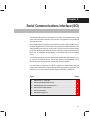
Serial Communications Interface (SCI) . . . . . . . . . . . . . . . . . . . . . . . . . . . . . . . . . . . . . . . . . . . . 8-1
Describes the architecture, functions, and programming of the of the Serial Communications
Interface (SCI) module.
8.1
8.2
8.3
8.4
xii
6-79
6-80
6-80
6-82
6-82
6-85
Analog-to-Digital Converter (ADC) . . . . . . . . . . . . . . . . . . . . . . . . . . . . . . . . . . . . . . . . . . . . . . . . 7-1
Describes the analog-to-digital converter (ADC). Includes a list of features and some register
descriptions.
7.1
7.2
8
6.9.3 Decoding . . . . . . . . . . . . . . . . . . . . . . . . . . . . . . . . . . . . . . . . . . . . . . . . . . . . . . . . . .
6.9.4 QEP Counting . . . . . . . . . . . . . . . . . . . . . . . . . . . . . . . . . . . . . . . . . . . . . . . . . . . . .
6.9.5 Register Setup for the QEP Circuit . . . . . . . . . . . . . . . . . . . . . . . . . . . . . . . . . . . .
Event Manager (EV) Interrupts . . . . . . . . . . . . . . . . . . . . . . . . . . . . . . . . . . . . . . . . . . . . . .
6.10.1 EV Interrupt Request and Service . . . . . . . . . . . . . . . . . . . . . . . . . . . . . . . . . . . .
6.10.2 EV Interrupt Flag Registers . . . . . . . . . . . . . . . . . . . . . . . . . . . . . . . . . . . . . . . . . .
Differences vs. ’C240 SCI . . . . . . . . . . . . . . . . . . . . . . . . . . . . . . . . . . . . . . . . . . . . . . . . . . . . 8-2
8.1.1 SCI Physical Description . . . . . . . . . . . . . . . . . . . . . . . . . . . . . . . . . . . . . . . . . . . . . 8-2
8.1.2 Architecture . . . . . . . . . . . . . . . . . . . . . . . . . . . . . . . . . . . . . . . . . . . . . . . . . . . . . . . . . 8-5
8.1.3 SCI Module Registers . . . . . . . . . . . . . . . . . . . . . . . . . . . . . . . . . . . . . . . . . . . . . . . . 8-6
8.1.4 Multiprocessor and Asynchronous Communication Modes . . . . . . . . . . . . . . . . 8-7
SCI Programmable Data Format . . . . . . . . . . . . . . . . . . . . . . . . . . . . . . . . . . . . . . . . . . . . . . 8-8
SCI Multiprocessor Communication . . . . . . . . . . . . . . . . . . . . . . . . . . . . . . . . . . . . . . . . . . . 8-9
8.3.1 Idle-Line Multiprocessor Mode . . . . . . . . . . . . . . . . . . . . . . . . . . . . . . . . . . . . . . . 8-10
8.3.2 Address-Bit Multiprocessor Mode . . . . . . . . . . . . . . . . . . . . . . . . . . . . . . . . . . . . . 8-12
SCI Communication Format . . . . . . . . . . . . . . . . . . . . . . . . . . . . . . . . . . . . . . . . . . . . . . . . . 8-14
8.4.1 Receiver Signals in Communication Modes . . . . . . . . . . . . . . . . . . . . . . . . . . . . 8-14
8.4.2 Transmitter Signals in Communication Modes . . . . . . . . . . . . . . . . . . . . . . . . . . 8-15
Contents
8.5
8.6
9
SCI Port Interrupts . . . . . . . . . . . . . . . . . . . . . . . . . . . . . . . . . . . . . . . . . . . . . . . . . . . . . . . . .
8.5.1 SCI Baud Rate Calculation . . . . . . . . . . . . . . . . . . . . . . . . . . . . . . . . . . . . . . . . . .
SCI Module Registers . . . . . . . . . . . . . . . . . . . . . . . . . . . . . . . . . . . . . . . . . . . . . . . . . . . . . .
8.6.1 SCI Communication Control Register . . . . . . . . . . . . . . . . . . . . . . . . . . . . . . . . .
8.6.2 SCI Control Register 1 . . . . . . . . . . . . . . . . . . . . . . . . . . . . . . . . . . . . . . . . . . . . . .
8.6.3 Baud-Select Registers . . . . . . . . . . . . . . . . . . . . . . . . . . . . . . . . . . . . . . . . . . . . . .
8.6.4 SCI Control Register 2 . . . . . . . . . . . . . . . . . . . . . . . . . . . . . . . . . . . . . . . . . . . . . .
8.6.5 Receiver Status Register . . . . . . . . . . . . . . . . . . . . . . . . . . . . . . . . . . . . . . . . . . . .
8.6.6 Receiver Data Buffer Registers . . . . . . . . . . . . . . . . . . . . . . . . . . . . . . . . . . . . . . .
8.6.7 Transmit Data Buffer Register . . . . . . . . . . . . . . . . . . . . . . . . . . . . . . . . . . . . . . . .
8.6.8 Priority Control Register . . . . . . . . . . . . . . . . . . . . . . . . . . . . . . . . . . . . . . . . . . . . .
8-17
8-18
8-19
8-20
8-22
8-25
8-26
8-27
8-29
8-30
8-31
Serial Peripheral Interface (SPI) . . . . . . . . . . . . . . . . . . . . . . . . . . . . . . . . . . . . . . . . . . . . . . . . . . . 9-1
Describes the architecture, functions, and programming of the serial peripheral interface (SPI)
module.
9.1
9.2
9.3
9.4
9.5
9.6
Differences vs. ’C240 SPI . . . . . . . . . . . . . . . . . . . . . . . . . . . . . . . . . . . . . . . . . . . . . . . . . . . . 9-2
9.1.1 SPI Physical Description . . . . . . . . . . . . . . . . . . . . . . . . . . . . . . . . . . . . . . . . . . . . . 9-2
SPI Control Registers . . . . . . . . . . . . . . . . . . . . . . . . . . . . . . . . . . . . . . . . . . . . . . . . . . . . . . . 9-4
SPI Operation . . . . . . . . . . . . . . . . . . . . . . . . . . . . . . . . . . . . . . . . . . . . . . . . . . . . . . . . . . . . . . 9-6
9.3.1 Introduction to Operation . . . . . . . . . . . . . . . . . . . . . . . . . . . . . . . . . . . . . . . . . . . . . 9-6
9.3.2 SPI Module Slave and Master Operation Modes . . . . . . . . . . . . . . . . . . . . . . . . . 9-7
SPI Interrupts . . . . . . . . . . . . . . . . . . . . . . . . . . . . . . . . . . . . . . . . . . . . . . . . . . . . . . . . . . . . . . 9-9
9.4.1 SPI_INT_ENA Bit (SPICTL.0) . . . . . . . . . . . . . . . . . . . . . . . . . . . . . . . . . . . . . . . . . 9-9
9.4.2 SPI_INT_FLAG Bit (SPISTS.6) . . . . . . . . . . . . . . . . . . . . . . . . . . . . . . . . . . . . . . . . 9-9
9.4.3 OVERRUN_INT_ENA Bit (SPICTL.4) . . . . . . . . . . . . . . . . . . . . . . . . . . . . . . . . . 9-10
9.4.4 RECEIVER_OVERRUN_FLAG Bit (SPISTS.7) . . . . . . . . . . . . . . . . . . . . . . . . . 9-10
9.4.5 SPI PRIORITY Bit (SPIPRI.6) . . . . . . . . . . . . . . . . . . . . . . . . . . . . . . . . . . . . . . . . 9-10
9.4.6 Data Format . . . . . . . . . . . . . . . . . . . . . . . . . . . . . . . . . . . . . . . . . . . . . . . . . . . . . . . 9-10
9.4.7 Baud Rate and Clocking Schemes . . . . . . . . . . . . . . . . . . . . . . . . . . . . . . . . . . . . 9-11
9.4.8 SPI Clocking Schemes . . . . . . . . . . . . . . . . . . . . . . . . . . . . . . . . . . . . . . . . . . . . . . 9-12
9.4.9 Initialization Upon Reset . . . . . . . . . . . . . . . . . . . . . . . . . . . . . . . . . . . . . . . . . . . . . 9-14
9.4.10 Proper SPI Initialization Using the SPI SW RESET Bit . . . . . . . . . . . . . . . . . . . 9-15
9.4.11 Data Transfer Example . . . . . . . . . . . . . . . . . . . . . . . . . . . . . . . . . . . . . . . . . . . . . . 9-15
SPI Control Registers . . . . . . . . . . . . . . . . . . . . . . . . . . . . . . . . . . . . . . . . . . . . . . . . . . . . . . 9-17
9.5.1 SPI Configuration Control Register (SPICCR) . . . . . . . . . . . . . . . . . . . . . . . . . . 9-18
9.5.2 SPI Operation Control Register (SPICTL) . . . . . . . . . . . . . . . . . . . . . . . . . . . . . . 9-20
9.5.3 SPI Status Register (SPISTS) . . . . . . . . . . . . . . . . . . . . . . . . . . . . . . . . . . . . . . . . 9-21
9.5.4 SPI Baud Rate Register (SPIBRR) . . . . . . . . . . . . . . . . . . . . . . . . . . . . . . . . . . . . 9-23
9.5.5 SPI Emulation Buffer Register (SPIRXEMU) . . . . . . . . . . . . . . . . . . . . . . . . . . . 9-24
9.5.6 SPI Serial Receive Buffer Register (SPIRXBUF) . . . . . . . . . . . . . . . . . . . . . . . . 9-25
9.5.7 SPI Serial Transmit Buffer Register (SPITXBUF) . . . . . . . . . . . . . . . . . . . . . . . 9-26
9.5.8 SPI Serial Data Register (SPIDAT) . . . . . . . . . . . . . . . . . . . . . . . . . . . . . . . . . . . . 9-27
9.5.9 SPI Priority Control Register (SPIPRI) . . . . . . . . . . . . . . . . . . . . . . . . . . . . . . . . . 9-28
SPI Example Waveforms . . . . . . . . . . . . . . . . . . . . . . . . . . . . . . . . . . . . . . . . . . . . . . . . . . . 9-29
Contents
xiii
Contents
10 CAN Controller Module . . . . . . . . . . . . . . . . . . . . . . . . . . . . . . . . . . . . . . . . . . . . . . . . . . . . . . . . . 10-1
Describes the CAN controller module, interface signals, CAN peripheral registers, and mailbox
RAM, layout, and operations.
10.1
10.2
10.3
10.4
10.5
10.6
10.7
10.8
10.9
Introduction . . . . . . . . . . . . . . . . . . . . . . . . . . . . . . . . . . . . . . . . . . . . . . . . . . . . . . . . . . . . . . . 10-2
Overview of the CAN Network . . . . . . . . . . . . . . . . . . . . . . . . . . . . . . . . . . . . . . . . . . . . . . . 10-3
10.2.1 CAN Protocol Overview . . . . . . . . . . . . . . . . . . . . . . . . . . . . . . . . . . . . . . . . . . . . . 10-3
10.2.2 CAN Controller Architecture . . . . . . . . . . . . . . . . . . . . . . . . . . . . . . . . . . . . . . . . . . 10-4
10.2.3 Memory Map . . . . . . . . . . . . . . . . . . . . . . . . . . . . . . . . . . . . . . . . . . . . . . . . . . . . . . . 10-6
Message Objects . . . . . . . . . . . . . . . . . . . . . . . . . . . . . . . . . . . . . . . . . . . . . . . . . . . . . . . . . . 10-9
10.3.1 Mailbox Layout . . . . . . . . . . . . . . . . . . . . . . . . . . . . . . . . . . . . . . . . . . . . . . . . . . . . 10-10
10.3.2 Message Buffers . . . . . . . . . . . . . . . . . . . . . . . . . . . . . . . . . . . . . . . . . . . . . . . . . . 10-12
10.3.3 Write Access to Mailbox RAM . . . . . . . . . . . . . . . . . . . . . . . . . . . . . . . . . . . . . . . 10-12
10.3.4 Transmit Mailbox . . . . . . . . . . . . . . . . . . . . . . . . . . . . . . . . . . . . . . . . . . . . . . . . . . 10-13
10.3.5 Receive Mailbox . . . . . . . . . . . . . . . . . . . . . . . . . . . . . . . . . . . . . . . . . . . . . . . . . . . 10-13
10.3.6 Handling of Remote Frames . . . . . . . . . . . . . . . . . . . . . . . . . . . . . . . . . . . . . . . . 10-14
10.3.7 Acceptance Filter . . . . . . . . . . . . . . . . . . . . . . . . . . . . . . . . . . . . . . . . . . . . . . . . . . 10-16
CAN Control Registers . . . . . . . . . . . . . . . . . . . . . . . . . . . . . . . . . . . . . . . . . . . . . . . . . . . . 10-18
10.4.1 Mailbox Direction/Enable Register (MDER) . . . . . . . . . . . . . . . . . . . . . . . . . . . 10-18
10.4.2 Transmit Control Register (TCR) . . . . . . . . . . . . . . . . . . . . . . . . . . . . . . . . . . . . 10-19
10.4.3 Receive Control Register (RCR) . . . . . . . . . . . . . . . . . . . . . . . . . . . . . . . . . . . . . 10-21
10.4.4 Master Control Register (MCR) . . . . . . . . . . . . . . . . . . . . . . . . . . . . . . . . . . . . . . 10-22
10.4.5 Bit Configuration Registers (BCRn) . . . . . . . . . . . . . . . . . . . . . . . . . . . . . . . . . . 10-24
Status Registers . . . . . . . . . . . . . . . . . . . . . . . . . . . . . . . . . . . . . . . . . . . . . . . . . . . . . . . . . . 10-28
10.5.1 Global Status Register (GSR) . . . . . . . . . . . . . . . . . . . . . . . . . . . . . . . . . . . . . . . 10-28
10.5.2 Error Status Register (ESR) . . . . . . . . . . . . . . . . . . . . . . . . . . . . . . . . . . . . . . . . . 10-29
10.5.3 CAN Error Counter Register (CEC) . . . . . . . . . . . . . . . . . . . . . . . . . . . . . . . . . . 10-31
Interrupt Logic . . . . . . . . . . . . . . . . . . . . . . . . . . . . . . . . . . . . . . . . . . . . . . . . . . . . . . . . . . . . 10-32
10.6.1 CAN Interrupt Flag Register (CAN_IFR) . . . . . . . . . . . . . . . . . . . . . . . . . . . . . . 10-33
10.6.2 CAN Interrupt Mask Register (CAN_IMR) . . . . . . . . . . . . . . . . . . . . . . . . . . . . . 10-35
Configuration Mode . . . . . . . . . . . . . . . . . . . . . . . . . . . . . . . . . . . . . . . . . . . . . . . . . . . . . . . 10-36
Power-Down Mode (PDM) . . . . . . . . . . . . . . . . . . . . . . . . . . . . . . . . . . . . . . . . . . . . . . . . . 10-37
Suspend Mode . . . . . . . . . . . . . . . . . . . . . . . . . . . . . . . . . . . . . . . . . . . . . . . . . . . . . . . . . . . 10-38
11 Watchdog (WD) Timer . . . . . . . . . . . . . . . . . . . . . . . . . . . . . . . . . . . . . . . . . . . . . . . . . . . . . . . . . . 11-1
Describes the features and operation of the watchdog (WD) timer module. Covers the architecture and the registers used to implement WD functions.
11.1
11.2
11.3
xiv
Watchdog Timer Features . . . . . . . . . . . . . . . . . . . . . . . . . . . . . . . . . . . . . . . . . . . . . . . . . .
Control Registers . . . . . . . . . . . . . . . . . . . . . . . . . . . . . . . . . . . . . . . . . . . . . . . . . . . . . . . . . .
11.2.1 Watchdog Suspend . . . . . . . . . . . . . . . . . . . . . . . . . . . . . . . . . . . . . . . . . . . . . . . . .
11.2.2 Operation of WD Timers . . . . . . . . . . . . . . . . . . . . . . . . . . . . . . . . . . . . . . . . . . . . .
11.2.3 WD Prescale Select . . . . . . . . . . . . . . . . . . . . . . . . . . . . . . . . . . . . . . . . . . . . . . . .
11.2.4 Servicing the WD Timer . . . . . . . . . . . . . . . . . . . . . . . . . . . . . . . . . . . . . . . . . . . . .
Watchdog Control Registers . . . . . . . . . . . . . . . . . . . . . . . . . . . . . . . . . . . . . . . . . . . . . . . .
11-2
11-4
11-4
11-5
11-5
11-5
11-8
Contents
11.3.1 WD Counter Register . . . . . . . . . . . . . . . . . . . . . . . . . . . . . . . . . . . . . . . . . . . . . . . 11-8
11.3.2 WD Reset Key Register . . . . . . . . . . . . . . . . . . . . . . . . . . . . . . . . . . . . . . . . . . . . . 11-9
11.3.3 WD Timer Control Register . . . . . . . . . . . . . . . . . . . . . . . . . . . . . . . . . . . . . . . . . . 11-9
12 ’240x–’240 Family Compatibility . . . . . . . . . . . . . . . . . . . . . . . . . . . . . . . . . . . . . . . . . . . . . . . . . 12-1
Describes compatibility issues between the ’240x and ’240 family of processors.
12.1
12.2
12.3
12.4
12.5
12.6
General . . . . . . . . . . . . . . . . . . . . . . . . . . . . . . . . . . . . . . . . . . . . . . . . . . . . . . . . . . . . . . . . . .
Event Manager . . . . . . . . . . . . . . . . . . . . . . . . . . . . . . . . . . . . . . . . . . . . . . . . . . . . . . . . . . . .
Analog-to-Digital Converter . . . . . . . . . . . . . . . . . . . . . . . . . . . . . . . . . . . . . . . . . . . . . . . . .
Serial Communications Interface . . . . . . . . . . . . . . . . . . . . . . . . . . . . . . . . . . . . . . . . . . . .
Serial Peripheral Interface . . . . . . . . . . . . . . . . . . . . . . . . . . . . . . . . . . . . . . . . . . . . . . . . . .
Watchdog Timer . . . . . . . . . . . . . . . . . . . . . . . . . . . . . . . . . . . . . . . . . . . . . . . . . . . . . . . . . . .
12-2
12-3
12-4
12-4
12-4
12-4
13 ’24x–’240x Family Compatibility . . . . . . . . . . . . . . . . . . . . . . . . . . . . . . . . . . . . . . . . . . . . . . . . . 13-1
Describes the major differences between the ’24x and the ’240x family of processors.
13.1
13.2
13.3
13.4
13.5
13.6
13.7
Introduction . . . . . . . . . . . . . . . . . . . . . . . . . . . . . . . . . . . . . . . . . . . . . . . . . . . . . . . . . . . . . . . 13-2
’24x–’240x DSP Overview . . . . . . . . . . . . . . . . . . . . . . . . . . . . . . . . . . . . . . . . . . . . . . . . . . 13-4
Memory Map . . . . . . . . . . . . . . . . . . . . . . . . . . . . . . . . . . . . . . . . . . . . . . . . . . . . . . . . . . . . . . 13-5
13.3.1 Program Space . . . . . . . . . . . . . . . . . . . . . . . . . . . . . . . . . . . . . . . . . . . . . . . . . . . . 13-5
13.3.2 Data Space . . . . . . . . . . . . . . . . . . . . . . . . . . . . . . . . . . . . . . . . . . . . . . . . . . . . . . . . 13-6
13.3.3 I/O Space . . . . . . . . . . . . . . . . . . . . . . . . . . . . . . . . . . . . . . . . . . . . . . . . . . . . . . . . . 13-7
Flash Program Memory . . . . . . . . . . . . . . . . . . . . . . . . . . . . . . . . . . . . . . . . . . . . . . . . . . . . 13-8
13.4.1 Flash Control Mode Register (FCMR) . . . . . . . . . . . . . . . . . . . . . . . . . . . . . . . . . 13-8
13.4.2 Flash Control Registers – Summary Table . . . . . . . . . . . . . . . . . . . . . . . . . . . . . 13-9
System Features . . . . . . . . . . . . . . . . . . . . . . . . . . . . . . . . . . . . . . . . . . . . . . . . . . . . . . . . . 13-16
13.5.1 Oscillator and PLL . . . . . . . . . . . . . . . . . . . . . . . . . . . . . . . . . . . . . . . . . . . . . . . . . 13-16
13.5.2 Watchdog Clock . . . . . . . . . . . . . . . . . . . . . . . . . . . . . . . . . . . . . . . . . . . . . . . . . . . 13-17
13.5.3 System Control Registers . . . . . . . . . . . . . . . . . . . . . . . . . . . . . . . . . . . . . . . . . . . 13-18
Digital I/O (GPIO Pins) . . . . . . . . . . . . . . . . . . . . . . . . . . . . . . . . . . . . . . . . . . . . . . . . . . . . 13-20
13.6.1 Digital I/O and Shared Pin Functions for the ’240x . . . . . . . . . . . . . . . . . . . . . 13-20
Event Manager Module (EVB) . . . . . . . . . . . . . . . . . . . . . . . . . . . . . . . . . . . . . . . . . . . . . . 13-23
A
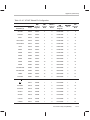
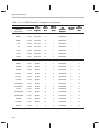
Programmable Register Address Summary . . . . . . . . . . . . . . . . . . . . . . . . . . . . . . . . . . . . . . . . A-1
Provides a summary of all programmable registers on TMS320X240x devices.
B
Program Examples . . . . . . . . . . . . . . . . . . . . . . . . . . . . . . . . . . . . . . . . . . . . . . . . . . . . . . . . . . . . . . B-1
Presents program examples for the ’240x.
B.1
B.2
About These Program Examples . . . . . . . . . . . . . . . . . . . . . . . . . . . . . . . . . . . . . . . . . . . . . B-2
Program Examples . . . . . . . . . . . . . . . . . . . . . . . . . . . . . . . . . . . . . . . . . . . . . . . . . . . . . . . . . B-4
Contents
xv
Contents
C
TMS320F240x Boot ROM Loader: Protocols and Interfacing . . . . . . . . . . . . . . . . . . . . . . . .
C.1 Introduction . . . . . . . . . . . . . . . . . . . . . . . . . . . . . . . . . . . . . . . . . . . . . . . . . . . . . . . . . . . . . . . .
C.1.1 Boot-Load Sequence . . . . . . . . . . . . . . . . . . . . . . . . . . . . . . . . . . . . . . . . . . . . . . . .
C.2 Protocol Definitions . . . . . . . . . . . . . . . . . . . . . . . . . . . . . . . . . . . . . . . . . . . . . . . . . . . . . . . . .
C.2.1 SPI Synchronous Transfer Protocol and Data Formats . . . . . . . . . . . . . . . . . . .
C.2.2 SCI Asynchronous Transfer Protocol and Data Formats . . . . . . . . . . . . . . . . . .
D
Glossary . . . . . . . . . . . . . . . . . . . . . . . . . . . . . . . . . . . . . . . . . . . . . . . . . . . . . . . . . . . . . . . . . . . . . . . . D-1
Explains terms, abbreviations, and acronyms used throughout this book.
xvi
C-1
C-2
C-2
C-6
C-6
C-7
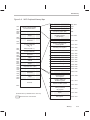
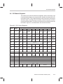
Figures
Figures
1–1
2–1
2–2
2–3
2–4
2–5
2–6
2–7
2–8
2–9
2–10
2–11
2–12
2–13
2–14
2–15
2–16
2–17
2–18
3–1
3–2
3–3
3–4
3–5
3–6
3–7
3–8
3–9
3–10
3–11
3–12
3–13
5–1
5–2
5–3
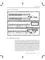
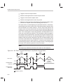
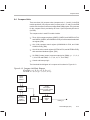
’240x Device Overview . . . . . . . . . . . . . . . . . . . . . . . . . . . . . . . . . . . . . . . . . . . . . . . . . . . . . . . . 1-7
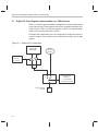
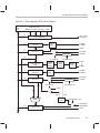
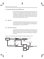
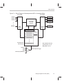
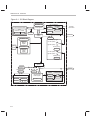
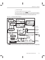
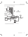
’240x Device Architecture . . . . . . . . . . . . . . . . . . . . . . . . . . . . . . . . . . . . . . . . . . . . . . . . . . . . . . 2-2
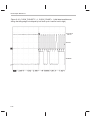
System Control and Status Register 1 (SCSR1) — Address 07018h . . . . . . . . . . . . . . . . . 2-3
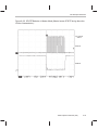
System Control and Status Register 2 (SCSR2) — Address 07019h . . . . . . . . . . . . . . . . . 2-5
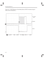
Device Identification Number Register (DINR) — Address 701Ch . . . . . . . . . . . . . . . . . . . 2-7
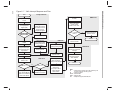
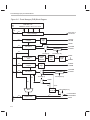
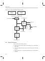
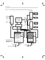
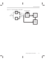
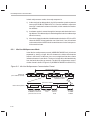
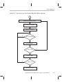
Peripheral Interrupt Expansion Block Diagram . . . . . . . . . . . . . . . . . . . . . . . . . . . . . . . . . . . 2-13
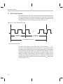
Interrupt Requests . . . . . . . . . . . . . . . . . . . . . . . . . . . . . . . . . . . . . . . . . . . . . . . . . . . . . . . . . . . 2-17
’240x Interrupt Response and Flow . . . . . . . . . . . . . . . . . . . . . . . . . . . . . . . . . . . . . . . . . . . . . 2-20
Interrupt Flag Register (IFR) — Address 0006h . . . . . . . . . . . . . . . . . . . . . . . . . . . . . . . . . . 2-24
Interrupt Mask Register (IMR) — Address 0004h . . . . . . . . . . . . . . . . . . . . . . . . . . . . . . . . . 2-25
Peripheral Interrupt Vector Register (PIVR)— Address 701Eh . . . . . . . . . . . . . . . . . . . . . . 2-27
Peripheral Interrupt Request Register 0 (PIRQR0) — Address 7010h . . . . . . . . . . . . . . . 2-28
Peripheral Interrupt Request Register 1 (PIRQR1) — Address 7011h . . . . . . . . . . . . . . . 2-29
Peripheral Interrupt Request Register 2 (PIRQR2) — Address 7012h . . . . . . . . . . . . . . . 2-30
Peripheral Interrupt Acknowledge Register 0 (PIACKR0) — Address 7014h . . . . . . . . . 2-31
Peripheral Interrupt Acknowledge Register 1 (PIACKR1) — Address 7015h . . . . . . . . . 2-32
Peripheral Interrupt Acknowledge Register 2 (PIACKR2) — Address 7016h . . . . . . . . . 2-33
External Interrupt 1 Control Register (XINT1CR) — Address 7070h . . . . . . . . . . . . . . . . . 2-36
External Interrupt 2 Control Register (XINT2CR) — Address 7071h . . . . . . . . . . . . . . . . . 2-37
Memory Map for ’LF2407 . . . . . . . . . . . . . . . . . . . . . . . . . . . . . . . . . . . . . . . . . . . . . . . . . . . . . . 3-4
Memory Map for ’LF2406 . . . . . . . . . . . . . . . . . . . . . . . . . . . . . . . . . . . . . . . . . . . . . . . . . . . . . . 3-5
Memory Map for ’LF2402 . . . . . . . . . . . . . . . . . . . . . . . . . . . . . . . . . . . . . . . . . . . . . . . . . . . . . . 3-6
Memory Map for ’LC2406 . . . . . . . . . . . . . . . . . . . . . . . . . . . . . . . . . . . . . . . . . . . . . . . . . . . . . . 3-7
Memory Map for ’LC2404 . . . . . . . . . . . . . . . . . . . . . . . . . . . . . . . . . . . . . . . . . . . . . . . . . . . . . . 3-8
Memory Map for ’LC2402 . . . . . . . . . . . . . . . . . . . . . . . . . . . . . . . . . . . . . . . . . . . . . . . . . . . . . . 3-9
Program Memory Map for ’LF2407 . . . . . . . . . . . . . . . . . . . . . . . . . . . . . . . . . . . . . . . . . . . . . 3-10
’2407 Peripheral Memory Map . . . . . . . . . . . . . . . . . . . . . . . . . . . . . . . . . . . . . . . . . . . . . . . . . 3-13
Data Memory Pages . . . . . . . . . . . . . . . . . . . . . . . . . . . . . . . . . . . . . . . . . . . . . . . . . . . . . . . . . . 3-14
I/O Space Address Map for ’240x . . . . . . . . . . . . . . . . . . . . . . . . . . . . . . . . . . . . . . . . . . . . . . 3-16
Program Address/Data — Visibility Functional Timing . . . . . . . . . . . . . . . . . . . . . . . . . . . . . 3-18
Data Address/ Data — Visibility Functional Timing . . . . . . . . . . . . . . . . . . . . . . . . . . . . . . . . 3-19
’240x Wait-State Generator Control Register (WSGR) —
I/O-Space Address FFFFh (’240x) . . . . . . . . . . . . . . . . . . . . . . . . . . . . . . . . . . . . . . . . . . . . . . 3-22
Shared Pin Configuration . . . . . . . . . . . . . . . . . . . . . . . . . . . . . . . . . . . . . . . . . . . . . . . . . . . . . . 5-2
I/O Mux Control Register A (MCRA) — Address 7090h . . . . . . . . . . . . . . . . . . . . . . . . . . . . . 5-5
I/O Mux Control Register B (MCRB) — Address 7092h . . . . . . . . . . . . . . . . . . . . . . . . . . . . . 5-6
Contents
xvii
Figures
5–4
5–5
5–6
5–7
5–8
5–9
5–10
6–1
6–2
6–3
6–4
6–5
6–6
6–7
6–8
6–9
6–10
6–11
6–12
6–13
6–14
6–15
6–16
6–17
6–18
6–19
6–20
6–21
6–22
6–23
6–24
6–25
6–26
6–27
6–28
6–29
6–30
6–31
6–32
6–33
xviii
I/O Mux Control Register C (MCRC) — Address 7094h . . . . . . . . . . . . . . . . . . . . . . . . . . . . 5-8
Port A Data and Direction Control Register (PADATDIR) . . . . . . . . . . . . . . . . . . . . . . . . . . . 5-9
Port B Data and Direction Control Register (PBDATDIR) . . . . . . . . . . . . . . . . . . . . . . . . . . 5-11
Port C Data and Direction Control Register (PCDATDIR) . . . . . . . . . . . . . . . . . . . . . . . . . . 5-12
Port D Data and Direction Control Register (PDDATDIR) . . . . . . . . . . . . . . . . . . . . . . . . . . 5-13
Port E Data and Direction Control Register (PEDATDIR) . . . . . . . . . . . . . . . . . . . . . . . . . . 5-14
Port F Data and Direction Control Register (PFDATDIR) . . . . . . . . . . . . . . . . . . . . . . . . . . 5-15
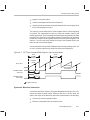
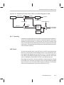
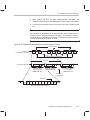
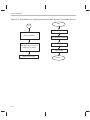
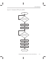
Event Manager (EVA) Block Diagram . . . . . . . . . . . . . . . . . . . . . . . . . . . . . . . . . . . . . . . . . . . . 6-3
Event Manager (EVB) Block Diagram . . . . . . . . . . . . . . . . . . . . . . . . . . . . . . . . . . . . . . . . . . . . 6-4
General-Purpose Timer Block Diagram (x = 2 or 4) [when x = 2: y = 1 and n = 2;
when x = 4: y = 3 and n = 4] . . . . . . . . . . . . . . . . . . . . . . . . . . . . . . . . . . . . . . . . . . . . . . . . . 6-15
GP Timer Continuous Up-Counting Mode (TxPR = 3 or 2) . . . . . . . . . . . . . . . . . . . . . . . . . 6-23
GP Timer Directional Up-/Down-Counting Mode: Prescale Factor 1 and TxPR = 3 . . . . 6-24
GP Timer Continuous Up-/Down-Counting Mode (TxPR = 3 or 2) . . . . . . . . . . . . . . . . . . . 6-25
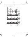
GP Timer Compare/PWM Output in Up-Counting Mode . . . . . . . . . . . . . . . . . . . . . . . . . . . 6-27
GP Timer Compare/PWM Output in Up-/Down-Counting Modes . . . . . . . . . . . . . . . . . . . . 6-28
Timer Control Register (TxCON; x = 1, 2, 3, or 4) — Addresses 7404h (T1),
7408h (T2), 7504h (T3), and 7508h (T4) . . . . . . . . . . . . . . . . . . . . . . . . . . . . . . . . . . . . . . . . 6-31
GP Timer Control Register A (GPTCONA) — Address 7400h . . . . . . . . . . . . . . . . . . . . . . 6-33
GP Timer Control Register B (GPTCONB) — Address 7500h . . . . . . . . . . . . . . . . . . . . . . 6-34
Compare Unit Block Diagram (For EVA: x = 1, 2, 3; y = 1, 3, 5; z = 1.
For EVB: x = 4, 5, 6; y = 7, 9, 11; z = 2) . . . . . . . . . . . . . . . . . . . . . . . . . . . . . . . . . . . . . . . . . 6-37
Compare Control Register A (COMCONA) — Address 7411h . . . . . . . . . . . . . . . . . . . . . . 6-39
Compare Control Register B (COMCONB) — Address 7511h . . . . . . . . . . . . . . . . . . . . . . 6-41
Compare Action Control Register A (ACTRA) — Address 7413h . . . . . . . . . . . . . . . . . . . 6-42
Compare Action Control Register B (ACTRB) — Address 7513h . . . . . . . . . . . . . . . . . . . 6-44
PWM Circuits Block Diagram . . . . . . . . . . . . . . . . . . . . . . . . . . . . . . . . . . . . . . . . . . . . . . . . . . 6-46
Dead-Band Timer Control Register A (DBTCONA) — Address xx15h . . . . . . . . . . . . . . . 6-48
Dead-Band Timer Control Register B (DBTCONB) — Address xx15h . . . . . . . . . . . . . . . 6-49
Dead-Band Unit Block Diagram (x = 1, 2, or 3) . . . . . . . . . . . . . . . . . . . . . . . . . . . . . . . . . . . 6-52
Output Logic Block Diagram (x = 1, 2, or 3; y = 1, 2, 3, 4, 5, or 6) . . . . . . . . . . . . . . . . . . . 6-54
Asymmetric PWM Waveform Generation With Compare Unit and PWM Circuits
(x = 1, 3, or 5) . . . . . . . . . . . . . . . . . . . . . . . . . . . . . . . . . . . . . . . . . . . . . . . . . . . . . . . . . . . . . . . 6-57
Symmetric PWM Waveform Generation With Compare Units and PWM
Circuits (x = 1, 3, or 5) . . . . . . . . . . . . . . . . . . . . . . . . . . . . . . . . . . . . . . . . . . . . . . . . . . . . . . . . 6-58
3-Phase Power Inverter Schematic Diagram . . . . . . . . . . . . . . . . . . . . . . . . . . . . . . . . . . . . . 6-60
Basic Space Vectors and Switching Patterns . . . . . . . . . . . . . . . . . . . . . . . . . . . . . . . . . . . . 6-62
Symmetric Space Vector PWM Waveforms . . . . . . . . . . . . . . . . . . . . . . . . . . . . . . . . . . . . . . 6-65
Capture Units Block Diagram (EVA) . . . . . . . . . . . . . . . . . . . . . . . . . . . . . . . . . . . . . . . . . . . . 6-67
Capture Units Block Diagram (EVB) . . . . . . . . . . . . . . . . . . . . . . . . . . . . . . . . . . . . . . . . . . . . 6-68
Capture Control Register A (CAPCONA) — Address 7420h . . . . . . . . . . . . . . . . . . . . . . . 6-70
Capture Control Register B (CAPCONB) — Address 7520h . . . . . . . . . . . . . . . . . . . . . . . 6-72
Capture FIFO Status Register A (CAPFIFOA) — Address 7422h . . . . . . . . . . . . . . . . . . . 6-74
Capture FIFO Status Register B (CAPFIFOB) — Address 7522h . . . . . . . . . . . . . . . . . . . 6-75
Quadrature Encoder Pulse (QEP) Circuit Block Diagram for EVA . . . . . . . . . . . . . . . . . . . 6-78
Figures
6–34
6–35
6–36
6–37
6–38
6–39
6–40
6–41
6–42
6–43
6–44
6–45
6–46
6–47
7–1
7–2
7–3
7–4
7–5
7–6
7–7
7–8
7–9
7–10
7–11
7–12
8–1
8–2
8–3
8–4
8–5
8–6
8–7
8–8
8–9
8–10
8–11
8–12
8–13
8–14
8–15
8–16
8–17
8–18
Quadrature Encoder Pulse (QEP) Circuit Block Diagram for EVB . . . . . . . . . . . . . . . . . . . 6-79
Quadrature Encoded Pulses and Decoded Timer Clock and Direction . . . . . . . . . . . . . . . 6-80
EVA Interrupt Flag Register A (EVAIFRA) — Address 742Fh . . . . . . . . . . . . . . . . . . . . . . . 6-85
EVA Interrupt Flag Register B (EVAIFRB) — Address 7430h . . . . . . . . . . . . . . . . . . . . . . . 6-87
EVA Interrupt Flag Register C (EVAIFRC) — Address 7431h . . . . . . . . . . . . . . . . . . . . . . 6-88
EVA Interrupt Mask Register A (EVAIMRA) — Address 742Ch . . . . . . . . . . . . . . . . . . . . . 6-89
EVA Interrupt Mask Register B (EVAIMRB) — Address 742Dh . . . . . . . . . . . . . . . . . . . . . 6-90
EVA Interrupt Mask Register C (EVAIMRC) — Address 742Eh . . . . . . . . . . . . . . . . . . . . . 6-90
EVB Interrupt Flag Register A (EVBIFRA) — Address 752Fh . . . . . . . . . . . . . . . . . . . . . . 6-91
EVB Interrupt Flag Register B (EVBIFRB) — Address 7530h . . . . . . . . . . . . . . . . . . . . . . 6-93
EVB Interrupt Flag Register C (EVBIFRC) — Address 7531h . . . . . . . . . . . . . . . . . . . . . . 6-94
EVB Interrupt Mask Register A (EVBIMRA) — Address 752Ch . . . . . . . . . . . . . . . . . . . . . 6-95
EVB Interrupt Mask Register B (EVBIMRB) — Address 752Dh . . . . . . . . . . . . . . . . . . . . . 6-96
EVB Interrupt Mask Register C (EVBIMRC) — Address 752Eh . . . . . . . . . . . . . . . . . . . . . 6-96
Block Diagram of Autosequenced ADC in Cascaded Mode . . . . . . . . . . . . . . . . . . . . . . . . . 7-5
Block Diagram of Autosequenced ADC With Dual Sequencers . . . . . . . . . . . . . . . . . . . . . . 7-6
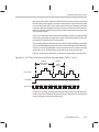
Example of Event Manager Triggers to Start the Sequencer . . . . . . . . . . . . . . . . . . . . . . . 7-10
Interrupt Operation During Sequenced Conversions . . . . . . . . . . . . . . . . . . . . . . . . . . . . . . 7-15
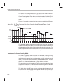
ADC Conversion Time . . . . . . . . . . . . . . . . . . . . . . . . . . . . . . . . . . . . . . . . . . . . . . . . . . . . . . . . 7-16
Clock Prescalers in ’240x ADC . . . . . . . . . . . . . . . . . . . . . . . . . . . . . . . . . . . . . . . . . . . . . . . . . 7-17
ADC Control Register 1 (ADCTRL1) — Address 70A0h . . . . . . . . . . . . . . . . . . . . . . . . . . . 7-20
ADC Control Register 2 (ADCTRL2) — Address 70A1h . . . . . . . . . . . . . . . . . . . . . . . . . . . 7-23
Maximum Conversion Channels Register (MAX_CONV) — Address 70A2h . . . . . . . . . 7-27
Autosequence Status Register (AUTO_SEQ_SR) — Address 70A7h . . . . . . . . . . . . . . . 7-29
ADC Input Channel Select Sequencing Control Registers (CHSELSEQn) . . . . . . . . . . . 7-31
ADC Conversion Result Buffer Registers . . . . . . . . . . . . . . . . . . . . . . . . . . . . . . . . . . . . . . . . 7-33
SCI Block Diagram . . . . . . . . . . . . . . . . . . . . . . . . . . . . . . . . . . . . . . . . . . . . . . . . . . . . . . . . . . . . 8-4
Typical SCI Data Frame Formats . . . . . . . . . . . . . . . . . . . . . . . . . . . . . . . . . . . . . . . . . . . . . . . . 8-8
Idle-Line Multiprocessor Communication Format . . . . . . . . . . . . . . . . . . . . . . . . . . . . . . . . . 8-10
Double-Buffered WUT and TXSHF . . . . . . . . . . . . . . . . . . . . . . . . . . . . . . . . . . . . . . . . . . . . . 8-11
Address-Bit Multiprocessor Communication Format . . . . . . . . . . . . . . . . . . . . . . . . . . . . . . 8-13
SCI Asynchronous Communications Format . . . . . . . . . . . . . . . . . . . . . . . . . . . . . . . . . . . . . 8-14
SCI RX Signals in Communication Modes . . . . . . . . . . . . . . . . . . . . . . . . . . . . . . . . . . . . . . . 8-15
SCI TX Signals in Communications Modes . . . . . . . . . . . . . . . . . . . . . . . . . . . . . . . . . . . . . . 8-16
SCI Control Registers . . . . . . . . . . . . . . . . . . . . . . . . . . . . . . . . . . . . . . . . . . . . . . . . . . . . . . . . 8-19
SCI Communication Control Register (SCICCR) — Address 7050h . . . . . . . . . . . . . . . . . 8-20
SCI Control Register 1 (SCICTL1) — Address 7051h . . . . . . . . . . . . . . . . . . . . . . . . . . . . . 8-22
Baud-Select MSbyte Register (SCIHBAUD) — Address 7052h . . . . . . . . . . . . . . . . . . . . . 8-25
Baud-Select LSbyte Register (SCILBAUD) — Address 7053h . . . . . . . . . . . . . . . . . . . . . . 8-25
SCI Control Register 2 (SCICTL2) — Address 7054h . . . . . . . . . . . . . . . . . . . . . . . . . . . . . 8-26
Receiver Status Register (SCIRXST) — Address 7055h . . . . . . . . . . . . . . . . . . . . . . . . . . . 8-27
Register SCIRXST Bit Associations — Address 7055h . . . . . . . . . . . . . . . . . . . . . . . . . . . . 8-29
Emulation Data Buffer Register (SCIRXEMU) — Address 7056h . . . . . . . . . . . . . . . . . . . 8-30
Receiver Data Buffer (SCIRXBUF) — Address 7057h . . . . . . . . . . . . . . . . . . . . . . . . . . . . . 8-30
Contents
xix
Figures
8–19
8–20
9–1
9–2
9–3
9–4
9–5
9–6
9–7
9–8
9–9
9–10
9–11
9–12
9–13
9–14
9–15
9–16
9–17
9–18
9–19
9–20
9–21
10–1
10–2
10–3
10–4
10–5
10–6
10–7
10–8
10–9
10–10
10–11
10–12
10–13
10–14
10–15
xx
Transmit Data Buffer Register (SCITXBUF) — Address 7059h . . . . . . . . . . . . . . . . . . . . . 8-30
SCI Priority Control Register (SCIPRI) — Address 705Fh . . . . . . . . . . . . . . . . . . . . . . . . . 8-31
SPI Module Block Diagram . . . . . . . . . . . . . . . . . . . . . . . . . . . . . . . . . . . . . . . . . . . . . . . . . . . . . 9-3
SPI Master/Slave Connection . . . . . . . . . . . . . . . . . . . . . . . . . . . . . . . . . . . . . . . . . . . . . . . . . . . 9-7
SPICLK Signal Options . . . . . . . . . . . . . . . . . . . . . . . . . . . . . . . . . . . . . . . . . . . . . . . . . . . . . . . 9-13
SPI: SPICLK-CLKOUT Characteristic when (BRR + 1) is Odd, BRR > 3, and
CLOCK POLARITY = 1 . . . . . . . . . . . . . . . . . . . . . . . . . . . . . . . . . . . . . . . . . . . . . . . . . . . . . . . 9-14
Five Bits per Character . . . . . . . . . . . . . . . . . . . . . . . . . . . . . . . . . . . . . . . . . . . . . . . . . . . . . . . 9-16
SPI Control Registers . . . . . . . . . . . . . . . . . . . . . . . . . . . . . . . . . . . . . . . . . . . . . . . . . . . . . . . . . 9-17
SPI Configuration Control Register (SPICCR) — Address 7040h . . . . . . . . . . . . . . . . . . . 9-18
SPI Operation Control Register (SPICTL) — Address 7041h . . . . . . . . . . . . . . . . . . . . . . . 9-20
SPI Status Register (SPISTS) — Address 7042h . . . . . . . . . . . . . . . . . . . . . . . . . . . . . . . . . 9-21
SPI Baud Rate Register (SPIBRR) — Address 7044h . . . . . . . . . . . . . . . . . . . . . . . . . . . . . 9-23
SPI Emulation Buffer Register (SPIRXEMU) — Address 7046h . . . . . . . . . . . . . . . . . . . . 9-24
SPI Serial Receive Buffer Register (SPIRXBUF) — Address 7047h . . . . . . . . . . . . . . . . . 9-25
SPI Serial Transmit Buffer Register (SPITXBUF) — Address 7048h . . . . . . . . . . . . . . . . 9-26
SPI Serial Data Register (SPIDAT) — Address 7049h . . . . . . . . . . . . . . . . . . . . . . . . . . . . . 9-27
SPI Priority Control Register (SPIPRI) — Address 704Fh . . . . . . . . . . . . . . . . . . . . . . . . . . 9-28
CLOCK_POLARITY = 0, CLOCK_PHASE = 0 (All data transitions are during
the rising edge. Inactive level is low.) . . . . . . . . . . . . . . . . . . . . . . . . . . . . . . . . . . . . . . . . . . . 9-29
CLOCK_POLARITY = 0, CLOCK_PHASE = 1 (Add data transitions are during
the rising edge, but delayed by half clock cycle. Inactive level is low.) . . . . . . . . . . . . . . . 9-30
CLOCK_POLARITY = 1, CLOCK_PHASE = 0 (All data transitions are during
the falling edge. Inactive level is high.) . . . . . . . . . . . . . . . . . . . . . . . . . . . . . . . . . . . . . . . . . . 9-31
CLOCK_POLARITY = 1, CLOCK_PHASE = 1 (Add data transitions are during
the falling edge, but delayed by half clock cycle. Inactive level is high.) . . . . . . . . . . . . . . 9-32
SPISTE Behavior in Master Mode (Master lowers SPISTE during the entire 16 bits
of transmission.) . . . . . . . . . . . . . . . . . . . . . . . . . . . . . . . . . . . . . . . . . . . . . . . . . . . . . . . . . . . . . 9-33
SPISTE Behavior in Slave Mode (Slave’s SPISTE is lowered during the entire 16 bits
of transmission.) . . . . . . . . . . . . . . . . . . . . . . . . . . . . . . . . . . . . . . . . . . . . . . . . . . . . . . . . . . . . . 9-34
CAN Data Frame . . . . . . . . . . . . . . . . . . . . . . . . . . . . . . . . . . . . . . . . . . . . . . . . . . . . . . . . . . . . 10-4
TMS320x240x CAN Module Block Diagram . . . . . . . . . . . . . . . . . . . . . . . . . . . . . . . . . . . . . 10-4
TMS320x240x CAN Module Memory Space . . . . . . . . . . . . . . . . . . . . . . . . . . . . . . . . . . . . . 10-6
CAN Data Frame . . . . . . . . . . . . . . . . . . . . . . . . . . . . . . . . . . . . . . . . . . . . . . . . . . . . . . . . . . . . 10-9
Message Identifier for High Word Mailboxes 0–5 (MSGIDnH) . . . . . . . . . . . . . . . . . . . . . 10-10
Message Identifier for Low Word Mailboxes 0–5 (MSGIDnL) . . . . . . . . . . . . . . . . . . . . . . 10-11
Message Control Field (MSGCTRLn) . . . . . . . . . . . . . . . . . . . . . . . . . . . . . . . . . . . . . . . . . . 10-11
Remote Frame Requests . . . . . . . . . . . . . . . . . . . . . . . . . . . . . . . . . . . . . . . . . . . . . . . . . . . . 10-16
Local Acceptance Mask Register n (0, 1) High Word (LAMn_H) . . . . . . . . . . . . . . . . . . . 10-17
Local Acceptance Mask Register n (0, 1) Low Word (LAMn_L) . . . . . . . . . . . . . . . . . . . . 10-17
Mailbox Direction/Enable Register (MDER) — Address 7100h . . . . . . . . . . . . . . . . . . . . 10-18
Transmission Control Register (TCR) — Address 7101h . . . . . . . . . . . . . . . . . . . . . . . . . 10-19
Receive Control Register (RCR) — Address 7102h . . . . . . . . . . . . . . . . . . . . . . . . . . . . . . 10-21
Master Control Register (MCR) — Address 7103h . . . . . . . . . . . . . . . . . . . . . . . . . . . . . . . 10-22
Bit Configuration Register 2 (BCR2) — Address 7104h . . . . . . . . . . . . . . . . . . . . . . . . . . . 10-25
Figures
10–16
10–17
10–18
10–19
10–20
10–21
10–22
10–23
11–1
11–2
11–3
11–4
13–1
13–2
13–3
13–4
13–5
13–6
13–7
13–8
13–9
B–1
C–1
C–2
C–3
C–4
C–5
C–6
Bit Configuration Register 1 (BCR1) — Address 7105h . . . . . . . . . . . . . . . . . . . . . . . . . . . 10-25
CAN Bit Timing . . . . . . . . . . . . . . . . . . . . . . . . . . . . . . . . . . . . . . . . . . . . . . . . . . . . . . . . . . . . . 10-27
Global Status Register (GSR) — Address 7107h . . . . . . . . . . . . . . . . . . . . . . . . . . . . . . . . 10-28
Error Status Register (ESR) — Address 7106h . . . . . . . . . . . . . . . . . . . . . . . . . . . . . . . . . . 10-29
CAN Error Counter Register (CEC) — Address 7108h . . . . . . . . . . . . . . . . . . . . . . . . . . . 10-31
CAN Interrupt Flag Register (CAN_IFR) — Address 7109h . . . . . . . . . . . . . . . . . . . . . . . 10-33
CAN Interrupt Mask Register (CAN_IMR) — Address 710Ah . . . . . . . . . . . . . . . . . . . . . . 10-35
CAN Initialization . . . . . . . . . . . . . . . . . . . . . . . . . . . . . . . . . . . . . . . . . . . . . . . . . . . . . . . . . . . . 10-36
Block Diagram of the WD Module . . . . . . . . . . . . . . . . . . . . . . . . . . . . . . . . . . . . . . . . . . . . . . 11-3
WD Counter Register (WDCNTR) — Address 7023h . . . . . . . . . . . . . . . . . . . . . . . . . . . . . 11-8
WD Reset Key Register (WDKEY) — Address 7025h . . . . . . . . . . . . . . . . . . . . . . . . . . . . . 11-9
WD Timer Control Register (WDCR) — Address 7029h . . . . . . . . . . . . . . . . . . . . . . . . . . . 11-9
’LF2407 Memory Map for Program Space . . . . . . . . . . . . . . . . . . . . . . . . . . . . . . . . . . . . . . . 13-5
’LF2407 Memory Map for Data Space . . . . . . . . . . . . . . . . . . . . . . . . . . . . . . . . . . . . . . . . . . 13-6
Pump Control Register . . . . . . . . . . . . . . . . . . . . . . . . . . . . . . . . . . . . . . . . . . . . . . . . . . . . . . . 13-10
Flash Control Register . . . . . . . . . . . . . . . . . . . . . . . . . . . . . . . . . . . . . . . . . . . . . . . . . . . . . . . 13-11
Test Control Register . . . . . . . . . . . . . . . . . . . . . . . . . . . . . . . . . . . . . . . . . . . . . . . . . . . . . . . . 13-13
Sector Enable Register . . . . . . . . . . . . . . . . . . . . . . . . . . . . . . . . . . . . . . . . . . . . . . . . . . . . . . 13-14
’240x Watchdog Clock Generation Logic . . . . . . . . . . . . . . . . . . . . . . . . . . . . . . . . . . . . . . . 13-17
Functional Block Diagram for Boot_EN/XF Feature . . . . . . . . . . . . . . . . . . . . . . . . . . . . . . 13-18
Functional Block Diagram of XMIF Signals on ’LF2407 . . . . . . . . . . . . . . . . . . . . . . . . . . . 13-19
Procedure for Generating Executable Files . . . . . . . . . . . . . . . . . . . . . . . . . . . . . . . . . . . . . . . B-2
Example Hardware Configuration for ’LF240x Boot ROM Operation . . . . . . . . . . . . . . . . . C-4
Memory Maps for the ’LF240x Devices in Microcontroller Mode . . . . . . . . . . . . . . . . . . . . . C-5
SPI Data Packet Definition . . . . . . . . . . . . . . . . . . . . . . . . . . . . . . . . . . . . . . . . . . . . . . . . . . . . . C-7
Flowchart for the Serial Loader Baud Rate Match Algorithm . . . . . . . . . . . . . . . . . . . . . . . . C-9
Flowcharts for (a) Serial Asynchronous Loader and the Fetch Header Routine . . . . . . . C-10
Flowchart for FETCH_SCI_WORD . . . . . . . . . . . . . . . . . . . . . . . . . . . . . . . . . . . . . . . . . . . . . C-11
Contents
xxi
Tables
Tables
1–1
2–1
2–2
2–3
2–4
2–5
2–6
2–7
2–8
3–1
3–2
3–3
4–1
5–1
5–2
5–3
5–4
5–5
5–6
5–7
5–8
5–9
5–10
6–1
6–2
6–3
6–4
6–5
6–6
6–7
6–8
6–9
xxii
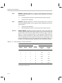
Hardware Features of ’240x Devices . . . . . . . . . . . . . . . . . . . . . . . . . . . . . . . . . . . . . . . . . . . . 1-6
Description of Low-Power Modes . . . . . . . . . . . . . . . . . . . . . . . . . . . . . . . . . . . . . . . . . . . . . . . 2-3
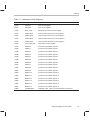
’240x Interrupt Source Priority and Vectors . . . . . . . . . . . . . . . . . . . . . . . . . . . . . . . . . . . . . . 2-8
Peripheral Interrupt Request Descriptions (PIRQR0) . . . . . . . . . . . . . . . . . . . . . . . . . . . . . 2-28
Peripheral Interrupt Request Descriptions (PIRQR1) . . . . . . . . . . . . . . . . . . . . . . . . . . . . . 2-30
Peripheral Interrupt Request Descriptions (PIRQR2) . . . . . . . . . . . . . . . . . . . . . . . . . . . . . 2-31
Peripheral Interrupt Acknowledge Descriptions (PIACKR0) . . . . . . . . . . . . . . . . . . . . . . . 2-32
Peripheral Interrupt Acknowledge Descriptions (PIACKR1) . . . . . . . . . . . . . . . . . . . . . . . 2-33
Peripheral Interrupt Acknowledge Descriptions (PIACKR2) . . . . . . . . . . . . . . . . . . . . . . . 2-34
Data Page 0 Address Map . . . . . . . . . . . . . . . . . . . . . . . . . . . . . . . . . . . . . . . . . . . . . . . . . . . . 3-15
XMIF Signal Descriptions . . . . . . . . . . . . . . . . . . . . . . . . . . . . . . . . . . . . . . . . . . . . . . . . . . . . . 3-17
Setting the Number of Wait States With the ’240x WSGR Bits . . . . . . . . . . . . . . . . . . . . . 3-23
Low-Power Modes Summary . . . . . . . . . . . . . . . . . . . . . . . . . . . . . . . . . . . . . . . . . . . . . . . . . . . 4-4
’240x Digital I/O Port Control Registers Implementation . . . . . . . . . . . . . . . . . . . . . . . . . . . . 5-3
I/O Mux Control Register A (MCRA) Configuration . . . . . . . . . . . . . . . . . . . . . . . . . . . . . . . . . 5-6
I/O Mux Control Register B (MCRB) . . . . . . . . . . . . . . . . . . . . . . . . . . . . . . . . . . . . . . . . . . . . . 5-7
I/O Mux Control Register C (MCRC) . . . . . . . . . . . . . . . . . . . . . . . . . . . . . . . . . . . . . . . . . . . . . 5-8
PADATDIR I/O Pin Designation (Assuming Pins Have Been Selected as I/O; i.e.,
Secondary Function) . . . . . . . . . . . . . . . . . . . . . . . . . . . . . . . . . . . . . . . . . . . . . . . . . . . . . . . . . 5-10
PBDATDIR I/O Pin Designation (Assuming Pins Have Been Selected as I/O; i.e.,
Secondary Function) . . . . . . . . . . . . . . . . . . . . . . . . . . . . . . . . . . . . . . . . . . . . . . . . . . . . . . . . . 5-11
PCDATDIR I/O Pin Designation (Assuming Pins Have Been Selected as I/O; i.e.,
Secondary Function) . . . . . . . . . . . . . . . . . . . . . . . . . . . . . . . . . . . . . . . . . . . . . . . . . . . . . . . . . 5-12
PDDATDIR I/O Pin Designation (Assuming Pins Have Been Selected as I/O; i.e.,
Secondary Function) . . . . . . . . . . . . . . . . . . . . . . . . . . . . . . . . . . . . . . . . . . . . . . . . . . . . . . . . . 5-13
PEDATDIR I/O Pin Designation (Assuming Pins Have Been Selected as I/O; i.e.,
Secondary Function) . . . . . . . . . . . . . . . . . . . . . . . . . . . . . . . . . . . . . . . . . . . . . . . . . . . . . . . . . 5-14
PFDATDIR I/O Pin Designation (Assuming Pins Have Been Selected as I/O; i.e.,
Secondary Function) . . . . . . . . . . . . . . . . . . . . . . . . . . . . . . . . . . . . . . . . . . . . . . . . . . . . . . . . . 5-15
Event Manager A Pins . . . . . . . . . . . . . . . . . . . . . . . . . . . . . . . . . . . . . . . . . . . . . . . . . . . . . . . . . 6-7
Event Manager B Pins . . . . . . . . . . . . . . . . . . . . . . . . . . . . . . . . . . . . . . . . . . . . . . . . . . . . . . . . . 6-8
Addresses of EVA Timer Registers . . . . . . . . . . . . . . . . . . . . . . . . . . . . . . . . . . . . . . . . . . . . . 6-11
Addresses of EVB Timer Registers . . . . . . . . . . . . . . . . . . . . . . . . . . . . . . . . . . . . . . . . . . . . . 6-11
Addresses of EVA Compare Control Registers . . . . . . . . . . . . . . . . . . . . . . . . . . . . . . . . . . . 6-11
Addresses of EVB Compare Control Registers . . . . . . . . . . . . . . . . . . . . . . . . . . . . . . . . . . . 6-12
Addresses of EVA Capture Registers . . . . . . . . . . . . . . . . . . . . . . . . . . . . . . . . . . . . . . . . . . . 6-12
Addresses of EVB Capture Registers . . . . . . . . . . . . . . . . . . . . . . . . . . . . . . . . . . . . . . . . . . . 6-12
Addresses of EVA Interrupt Registers . . . . . . . . . . . . . . . . . . . . . . . . . . . . . . . . . . . . . . . . . . . 6-13
Tables
6–10
6–11
6–12
6–13
6–14
6–15
6–16
6–17
6–18
7–1
7–2
7–3
7–4
7–5
7–6
7–7
7–8
8–1
8–2
8–3
8–4
8–5
9–1
9–2
9–3
10–1
10–2
10–3
10–4
10–5
11–1
11–2
11–3
13–1
13–2
13–3
13–4
13–5
13–6
13–7
13–8
13–9
13–10
13–11
Addresses of EVB Interrupt Registers . . . . . . . . . . . . . . . . . . . . . . . . . . . . . . . . . . . . . . . . . . . 6-13
GP Timer Compare Output in Continuous Up-Counting Modes . . . . . . . . . . . . . . . . . . . . . 6-29
GP Timer Compare Output in Continuous Up-/Down-Counting Modes . . . . . . . . . . . . . . 6-29
Dead-Band Generation Examples . . . . . . . . . . . . . . . . . . . . . . . . . . . . . . . . . . . . . . . . . . . . . . 6-51
Switching Patterns of a 3-Phase Power Inverter . . . . . . . . . . . . . . . . . . . . . . . . . . . . . . . . . . 6-61
Interrupt Flag Register and Corresponding Interrupt Mask Register . . . . . . . . . . . . . . . . . 6-82
Event Manager A (EVA) Interrupts . . . . . . . . . . . . . . . . . . . . . . . . . . . . . . . . . . . . . . . . . . . . . . 6-83
Event Manager B (EVB) Interrupts . . . . . . . . . . . . . . . . . . . . . . . . . . . . . . . . . . . . . . . . . . . . . 6-84
Conditions for Interrupt Generation . . . . . . . . . . . . . . . . . . . . . . . . . . . . . . . . . . . . . . . . . . . . . 6-84
Addresses of ADC Registers . . . . . . . . . . . . . . . . . . . . . . . . . . . . . . . . . . . . . . . . . . . . . . . . . . . 7-3
Comparison of Single and Cascaded Operating Modes . . . . . . . . . . . . . . . . . . . . . . . . . . . . 7-7
Reference Voltage Bit Selection . . . . . . . . . . . . . . . . . . . . . . . . . . . . . . . . . . . . . . . . . . . . . . . . 7-23
Bit Selections for MAX_CONV1 for Various Number of Conversions . . . . . . . . . . . . . . . . 7-29
Status Bit Values for SEQ_CNTR_n . . . . . . . . . . . . . . . . . . . . . . . . . . . . . . . . . . . . . . . . . . . . 7-30
CONVnn Bit Values and the ADC Input Channels Selected . . . . . . . . . . . . . . . . . . . . . . . . 7-32
ADC Conversion Phases vs CLKOUT cycles . . . . . . . . . . . . . . . . . . . . . . . . . . . . . . . . . . . . 7-34
ACQ Values When ACQ_PS = 1, 2, and 3 . . . . . . . . . . . . . . . . . . . . . . . . . . . . . . . . . . . . . . . 7-34
Addresses of SCI Registers . . . . . . . . . . . . . . . . . . . . . . . . . . . . . . . . . . . . . . . . . . . . . . . . . . . 8-6
Programming the Data Format Using SCICCR . . . . . . . . . . . . . . . . . . . . . . . . . . . . . . . . . . . . 8-8
Asynchronous Baud Register Values for Common SCI Bit Rates . . . . . . . . . . . . . . . . . . . 8-18
SCI CHAR2–0 Bit Values and Character Lengths . . . . . . . . . . . . . . . . . . . . . . . . . . . . . . . . . 8-21
SW RESET-Affected Flags . . . . . . . . . . . . . . . . . . . . . . . . . . . . . . . . . . . . . . . . . . . . . . . . . . . . 8-23
Addresses of SPI Control Registers . . . . . . . . . . . . . . . . . . . . . . . . . . . . . . . . . . . . . . . . . . . . . 9-5
SPI Clocking Scheme Selection Guide . . . . . . . . . . . . . . . . . . . . . . . . . . . . . . . . . . . . . . . . . . 9-13
Character Length Control Bit Values . . . . . . . . . . . . . . . . . . . . . . . . . . . . . . . . . . . . . . . . . . . . 9-19
Mailbox Configuration Details . . . . . . . . . . . . . . . . . . . . . . . . . . . . . . . . . . . . . . . . . . . . . . . . . . 10-5
Register Addresses . . . . . . . . . . . . . . . . . . . . . . . . . . . . . . . . . . . . . . . . . . . . . . . . . . . . . . . . . 10-7
Mailbox Addresses . . . . . . . . . . . . . . . . . . . . . . . . . . . . . . . . . . . . . . . . . . . . . . . . . . . . . . . . . . . 10-8
CAN Bit Timing Examples for ICLK = 20 MHz . . . . . . . . . . . . . . . . . . . . . . . . . . . . . . . . . . . 10-27
CAN Notation . . . . . . . . . . . . . . . . . . . . . . . . . . . . . . . . . . . . . . . . . . . . . . . . . . . . . . . . . . . . . . . 10-39
Typical WDKEY Register Power-Up Sequence . . . . . . . . . . . . . . . . . . . . . . . . . . . . . . . . . . . 11-6
WD Module Control Registers . . . . . . . . . . . . . . . . . . . . . . . . . . . . . . . . . . . . . . . . . . . . . . . . . 11-8
WD Overflow (Timeout) Selections . . . . . . . . . . . . . . . . . . . . . . . . . . . . . . . . . . . . . . . . . . . . 11-10
’24x-Compatible Features/Peripherals in ’240x DSPs . . . . . . . . . . . . . . . . . . . . . . . . . . . . . 13-2
New or Modified Features/Peripherals in ’240x DSPs . . . . . . . . . . . . . . . . . . . . . . . . . . . . . 13-3
Features of ’24x and ’240x DSPs . . . . . . . . . . . . . . . . . . . . . . . . . . . . . . . . . . . . . . . . . . . . . . . 13-4
I/O Mapped Registers . . . . . . . . . . . . . . . . . . . . . . . . . . . . . . . . . . . . . . . . . . . . . . . . . . . . . . . . 13-7
Instructions for Entering and Exiting Flash Control Register Mode . . . . . . . . . . . . . . . . . . 13-9
Flash Control Registers in Flash Control Mode . . . . . . . . . . . . . . . . . . . . . . . . . . . . . . . . . . 13-10
’240x PLL Pin Names . . . . . . . . . . . . . . . . . . . . . . . . . . . . . . . . . . . . . . . . . . . . . . . . . . . . . . . . 13-16
Oscillator/PLL Frequency Input Specification . . . . . . . . . . . . . . . . . . . . . . . . . . . . . . . . . . . 13-16
Peripheral Clock Enable Bits . . . . . . . . . . . . . . . . . . . . . . . . . . . . . . . . . . . . . . . . . . . . . . . . . 13-17
’LF2407 Shared Pin Configuration . . . . . . . . . . . . . . . . . . . . . . . . . . . . . . . . . . . . . . . . . . . . 13-21
Event Manager Module and Signal Names for EVA and EVB . . . . . . . . . . . . . . . . . . . . . 13-23
Contents
xxiii
Tables
A–1
B–1
B–2
C–1
xxiv
Summary of Programmable Registers on the ’240x . . . . . . . . . . . . . . . . . . . . . . . . . . . . . . .
Common Files For All Example Programs . . . . . . . . . . . . . . . . . . . . . . . . . . . . . . . . . . . . . . . .
Program Examples . . . . . . . . . . . . . . . . . . . . . . . . . . . . . . . . . . . . . . . . . . . . . . . . . . . . . . . . . . . .
Clock Speeds at Which Baud Rate Locks . . . . . . . . . . . . . . . . . . . . . . . . . . . . . . . . . . . . . . . .
A-2
B-3
B-3
C-8
Examples
Examples
7–1
7–2
7–3
7–4
7–5
9–1
9–2
Conversion in Dual-Sequencer Mode Using SEQ1 . . . . . . . . . . . . . . . . . . . . . . . . . . . . . . . . 7-8
Sequencer “Start/Stop” Operation . . . . . . . . . . . . . . . . . . . . . . . . . . . . . . . . . . . . . . . . . . . . . . . 7-9
MAX_CONV Register Bits Programming . . . . . . . . . . . . . . . . . . . . . . . . . . . . . . . . . . . . . . . . 7-28
Calculating the Conversion Time for a Multiple Conversion Sequence With
CPS = 0 and ACQ = 0: . . . . . . . . . . . . . . . . . . . . . . . . . . . . . . . . . . . . . . . . . . . . . . . . . . . . . . . . 7-35
Calculating the Conversion Time for a Single Conversion Sequence With
CPS = 1 and ACQ = 1: . . . . . . . . . . . . . . . . . . . . . . . . . . . . . . . . . . . . . . . . . . . . . . . . . . . . . . . 7-35
Transmission of Bit from SPIRXBUF . . . . . . . . . . . . . . . . . . . . . . . . . . . . . . . . . . . . . . . . . . . . 9-11
Maximum Baud-Rate Calculation . . . . . . . . . . . . . . . . . . . . . . . . . . . . . . . . . . . . . . . . . . . . . . . 9-12
Contents
xxv
Chapter 1
Introduction
The TMS320x240x series of devices are members of the TMS320 family of
digital signal processors (DSPs) designed to meet a wide range of digital motor
control (DMC) and other embedded control applications. This series is based
on the ’C2xLP 16-bit, fixed-point, low-power DSP CPU, and is complemented
with a wide range of on-chip peripherals and on-chip ROM or flash program
memory, plus on-chip dual-access RAM (DARAM).
This reference guide describes the following four ’240x devices: ’2407, ’2406,
’2404, and ’2402. These low-cost DSPs are intended to enable multiple applications for a nominal price.
This chapter provides an overview of the current TMS320 family, describes the
background and benefits of the ’240x DSP controller products, and introduces
the ’2407, ’2406, ’2404, and ’2402 devices.
Throughout this book, all four devices are collectively referred to as ’240x
devices.
Topic
Page
1.1
TMS320 Family Overview . . . . . . . . . . . . . . . . . . . . . . . . . . . . . . . . . . . . . . 1-2
1.2
TMS320C240x Series of DSP Controllers . . . . . . . . . . . . . . . . . . . . . . . . 1-3
1.3
Peripheral Overview . . . . . . . . . . . . . . . . . . . . . . . . . . . . . . . . . . . . . . . . . . . 1-5
1.4
’240x Highlights . . . . . . . . . . . . . . . . . . . . . . . . . . . . . . . . . . . . . . . . . . . . . . . 1-6
1-1
TMS320 Family Overview
1.1 TMS320 Family Overview
The TMS320 family consists of fixed-point, floating-point, multiprocessor digital signal processors (DSPs), and fixed-point DSP controllers. TMS320 DSPs
have an architecture designed specifically for real-time signal processing. The
’240x series of DSP controllers combines this real-time processing capability
with controller peripherals to create an ideal solution for control system
applications. The following characteristics make the TMS320 family the right
choice for a wide range of processing applications:
-
Very flexible instruction set
Inherent operational flexibility
High-speed performance
Innovative parallel architecture
Cost effectiveness
In 1982, Texas Instruments introduced the TMS32010, the first fixed-point
DSP in the TMS320 family. Before the end of the year, Electronic Products
magazine awarded the TMS32010 the title “Product of the Year”. Today, the
TMS320 family consists of these generations: ’C1x, ’C2x, ’C20x, ’C24x, ’C5x,
’C54x, and ’C6x fixed-point DSPs; ’C3x and ’C4x floating-point DSPs; and
’C8x multiprocessor DSPs. The ’240x devices are considered part of the ’24x
generation of fixed-point DSPs, and members of the ’C2000 platform.
Devices within a generation of a TMS320 platform have the same CPU structure but different on-chip memory and peripheral configurations. Spin-off
devices use new combinations of on-chip memory and peripherals to satisfy
a wide range of needs in the worldwide electronics market. By integrating
memory and peripherals onto a single chip, TMS320 devices reduce system
costs and save circuit board space.
1-2
TMS320C240x Series of DSP Controllers
1.2 TMS320C240x Series of DSP Controllers
Designers have recognized the opportunity to redesign existing digital motor
control (DMC) systems to use advanced algorithms that yield better performance and reduce system component count. DSPs enable:
- Design of robust controllers for a new generation of inexpensive motors,
such as AC induction, DC permanent magnet, and switched-reluctance
motors
- Full variable-speed control of brushless motor types that have lower
manufacturing cost and higher reliability
- Energy savings through variable-speed control, saving up to 25% of the
energy used by fixed-speed controllers
- Increased fuel economy, improved performance, and elimination of
hydraulic fluid in automotive electronic power steering (EPS) systems
- Reduced manufacturing and maintenance costs by eliminating hydraulic
fluid in automotive electronic braking systems
- More efficient and quieter operation due to diminished torque ripple, re-
sulting in less loss of power, lower vibration, and longer life
- Elimination or reduction of memory lookup tables through real-time poly-
nomial calculation, thereby reducing system cost
- Use of advanced algorithms that can reduce the number of sensors
required in a system
- Control of power switching inverters, along with control algorithm
processing
- Single-processor control of multimotor systems
The ’240x DSP controllers are designed to meet the needs of control-based
applications. By integrating the high performance of a DSP core and the
on-chip peripherals of a microcontroller into a single-chip solution, the ’240x
series yields a device that is an affordable alternative to traditional microcontroller units (MCUs) and expensive multichip designs. At 30 million instructions
per second (MIPS), the ’240x DSP controllers offer significant performance
over traditional 16-bit microcontrollers and microprocessors.
The 16-bit, fixed-point DSP core of the ’240x devices provides analog designers a digital solution that does not sacrifice the precision and performance of
their systems. In fact, system performance can be enhanced through the use
Introduction
1-3
TMS320C240x Series of DSP Controllers
of advanced control algorithms for techniques such as adaptive control,
Kalman filtering, and state control. The ’240x DSP controllers offer reliability
and programmability. Analog control systems, on the other hand, are hardwired solutions and can experience performance degradation due to aging,
component tolerance, and drift.
The high-speed central processing unit (CPU) allows the digital designer to
process algorithms in real time rather than approximate results with look-up
tables. The instruction set of these DSP controllers, which incorporates both
signal processing instructions and general-purpose control functions, coupled
with the extensive development support available for the ’240x devices,
reduces development time and provides the same ease of use as traditional
8- and 16-bit microcontrollers. The instruction set also allows you to retain your
software investment when moving from other general-purpose TMS320 fixedpoint DSPs. It is source- and object-code compatible with the other members
of the ’24x generation, source-code compatible with the ’C2x generation, and
upwardly source-code compatible with the ’C5x generation of DSPs from
Texas Instruments.
The ’240x architecture is also well-suited for processing control signals. It uses
a 16-bit word length along with 32-bit registers for storing intermediate results,
and has two hardware shifters available to scale numbers independently of the
CPU. This combination minimizes quantization and truncation errors, and increases processing power for additional functions. Such functions might include a notch filter that could cancel mechanical resonances in a system or an
estimation technique that could eliminate state sensors in a system.
The ’240x DSP controllers take advantage of an existing set of peripheral functions that allow Texas Instruments to quickly configure various series members for different price/performance points or for application optimization. This
library of both digital- and mixed-signal peripherals includes:
-
Timers
Serial communications ports (SCI, SPI)
Analog-to-digital converters (ADC)
Event manager
Safety features such as watchdog timer and power drive protection
The DSP controller peripheral library is continually growing and changing to
suit the needs of tomorrow’s embedded control marketplace.
1-4
Peripheral Overview
1.3 Peripheral Overview
The peripheral set for the ’240x devices includes:
- Event Manager: Timers and PWM generators for digital motor control
- CAN Interface: Controller Area Network (CAN) 2.0b compatible, with six
mailboxes (not available in ’2402 and ’2404)
- A/D: 10-bit ±1, 500 nS conversion, 16/8 channel, analog-to-digital
converter
- SPI: Serial Peripheral Interface – synchronous serial port (not available in
’2402)
- SCI: Serial Communications Interface – asynchronous serial port (univer-
sal asynchronous receiver and transmitter – UART)
- Watchdog timer
- General-purpose bidirectional digital I/O (GPIO) pins
Note:
For device pinouts, electrical characteristics, and timing specifications of
’240x devices, refer to the following data sheet: TMS320LF2407,
TMS320LF2406, TMS320LF2402 TMS320LC2406, TMS320LC2404,
TMS320LC2402 DSP Controllers (literature number SPRS094).
Introduction
1-5
’240x Highlights
1.4 ’240x Highlights
- The ’2407 has an external memory interface and is intended primarily for
emulation tools.
- The ’2406 is similar to the ’240x but lacks external memory interface.
- The ’2402 is a minimum-cost motor control device.
The device configurations available and their features are shown in Table 1–1.
Table 1–1. Hardware Features of ’240x Devices
Feature
’C2xx DSP Core
’LF2407†
’LF2406
’LF2402
’LC2406
’LC2404
’LC2402
Yes
Yes
Yes
Yes
Yes
Yes
Instruction Cycle
33 ns
33 ns
33 ns
33 ns
33 ns
33 ns
MIPS (30 MHz)
30 MIPS
30 MIPS
30 MIPS
30 MIPS
30 MIPS
30 MIPS
DARAM
544
544
544
544
544
544
SARAM
2K
2K
—
2K
1K
—
32K
32K
8K
—
—
—
—
—
—
32K
16K
4K
Boot ROM (16-bit word)
256
256
256
—
—
—
External Memory Interface
Yes
—
—
—
—
—
(16-bit
RAM (16
bit word)
On-chip Flash (16-bit word)
(4 sectors: 4K, 12K, 12K, 4K)
On-chip ROM (16-bit word)
Event Managers A and B
(EVA and EVB)
S General-Purpose (GP) Timers
S Compare (CMP)/PWM
S Capture (CAP)/QEP
EVA, EVB EVA, EVB
EVA
EVA, EVB EVA, EVB
EVA
4
10/16
6/4
4
10/16
6/4
2
5/8
3/2
4
10/16
6/4
4
10/16
6/4
2
5/8
3/2
Watchdog Timer
Yes
Yes
Yes
Yes
Yes
Yes
10-Bit ADC
Yes
Yes
Yes
Yes
Yes
Yes
16
500 ns
16
500 ns
8
500 ns
16
500 ns
16
500 ns
8
500 ns
SPI
Yes
Yes
—
Yes
Yes
—
SCI
Yes
Yes
Yes
Yes
Yes
Yes
CAN
Yes
Yes
—
Yes
—
—
Digital I/O Pins
41
41
21
41
41
21
External Interrupts
5
5
3
5
5
3
3.3 V
3.3 V
3.3 V
3.3 V
3.3 V
3.3 V
S Channels
S Conversion Time (minimum)
Supply Voltage
Packaging
144 TQFP 100 TQFP
64 PQFP
100 TQFP 100 TQFP
64 PQFP
† ’LF2407, the full-featured device of the ’LF240x family of DSP controllers, is useful for emulation and code development.
1-6
’240x Highlights
Figure 1–1 provides a graphical overview of the devices.
Figure 1–1. ’240x Device Overview
PLLF
PLLVCCA
DARAM (B0)
256 Words
XINT1/IOPA2
RS
CLKOUT/IOPE0
TMS2
BIO/IOPC1
PLL Clock
XTAL1/CLKIN
XTAL2
ADCIN00–ADCIN07
’C2xx
DSP
Core
ADCIN08–ADCIN15
VCCA
DARAM (B1)
256 Words
10-Bit ADC
(With Twin
Autosequencer)
MP/MC
BOOT_EN/XF
ÈÈÈÈÈÈÈ
ÈÈÈÈÈÈÈ
ÈÈÈÈÈÈÈ
ÈÈÈÈÈÈÈ
ÈÈÈÈÈÈÈ
ÈÈÈÈÈÈÈ
ÈÈÈÈÈÈÈ
ÈÈÈÈÈÈÈ
ÈÈÈÈÈÈÈ
ÈÈÈÈÈÈÈ
ÈÈÈÈÈÈÈ
ÈÈÈÈÈÈÈ
ÈÈÈÈÈÈÈ
ÈÈÈÈÈÈÈ
ÈÈÈÈÈÈÈ
ÈÈÈÈÈÈÈ
ÈÈÈÈÈÈÈ
ÈÈÈÈÈÈÈ
ÈÈÈÈÈÈÈ
ÈÈÈÈÈÈÈ
ÈÈÈÈÈÈÈ
ÈÈÈÈÈÈÈ
ÈÈÈÈÈÈÈ
ÈÈÈÈÈÈÈ
ÈÈÈÈÈÈÈ
ÈÈÈÈÈÈÈ
ÈÈÈÈÈÈÈ
ÈÈÈÈÈÈÈ
ÈÈÈÈÈÈÈ
SCI
VSS
SARAM (2K Words)
SPI
TP1
TP2
VCCP(5V)
A0–A15
D0–D15
PS, DS, IS
R/W
RD
READY
STRB
WE
ENA_144
VIS_OE
W/R / IOPC0
PDPINTA
CAP1/QEP1/IOPA3
CAP2/QEP2/IOPA4
CAP3/IOPA5
PWM1/IOPA6
PWM2/IOPA7
PWM3/IOPB0
PWM4/IOPB1
PWM5/IOPB2
PWM6/IOPB3
T1PWM/T1CMP/IOPB4
T2PWM/T2CMP/IOPB5
ÈÈÈ
ÈÈÈ
TDIRA/IOPB6
TCLKINA/IOPB7
Flash/ROM
(32K Words:
4K/12K/12K/4K)
CAN
External Memory Interface
JTAG Port
D 3 × Capture Input
D 6 × Compare/PWM
Output
D 2 × GP Timers/PWM
XINT2/ADCSOC/IOPD0
SCITXD/IOPA0
SCIRXD/IOPA1
SPISIMO/IOPC2
SPISOMI/IOPC3
SPICLK/IOPC4
SPISTE/IOPC5
CANTX/IOPC6
CANRX/IOPC7
WD
Digital I/O
(Shared With Other Pins)
Event Manager A
VSSA
VREFHI
VREFLO
DARAM (B2)
32 Words
VDD (3.3 V)
PLLF2
Event Manager B
D 3 × Capture Input
D 6 × Compare/PWM
Output
D 2 × GP Timers/PWM
Port A(0–7) IOPA[0:7]
Port B(0–7) IOPB[0:7]
Port C(0–7) IOPC[0:7]
Port D(0) IOPD[0]
Port E(0–7) IOPE[0:7]
Port F(0–6) IOPF[0:6]
TRST
TDO
TDI
TMS
TCK
EMU0
EMU1
PDPINTB
CAP4/QEP3/IOPE7
CAP5/QEP4/IOPF0
CAP6/IOPF1
PWM7/IOPE1
PWM8/IOPE2
PWM9/IOPE3
PWM10/IOPE4
PWM11/IOPE5
PWM12/IOPE6
T3PWM/T3CMP/IOPF2
T4PWM/T4CMP/IOPF3
TDIRB/IOPF4
TCLKINB/IOPF5
Indicates optional modules. The memory size and peripheral selection of these modules change for different
’240x devices. See Table 1–1 for device-specific details.
Introduction
1-7
Chapter 2
System Configuration and Interrupts
This chapter describes the system configuration registers and interrupts. It
also explains how the peripheral interrupt expansion (PIE) is used to increase
interrupt request capacity.
Topic
Page
2.1
Architecture Summary . . . . . . . . . . . . . . . . . . . . . . . . . . . . . . . . . . . . . . . . 2-2
2.2
Configuration Registers . . . . . . . . . . . . . . . . . . . . . . . . . . . . . . . . . . . . . . . 2-3
2.3
Interrupt Priority and Vectors . . . . . . . . . . . . . . . . . . . . . . . . . . . . . . . . . . 2-8
2.4
Peripheral Interrupt Expansion (PIE) . . . . . . . . . . . . . . . . . . . . . . . . . . . 2-12
2.5
Interrupt Vectors . . . . . . . . . . . . . . . . . . . . . . . . . . . . . . . . . . . . . . . . . . . . . 2-16
2.6
Interrupt Operation Sequence . . . . . . . . . . . . . . . . . . . . . . . . . . . . . . . . . 2-19
2.7
Interrupt Latency . . . . . . . . . . . . . . . . . . . . . . . . . . . . . . . . . . . . . . . . . . . . . 2-21
2.8
Sample ISR Code . . . . . . . . . . . . . . . . . . . . . . . . . . . . . . . . . . . . . . . . . . . . 2-22
2.9
CPU Interrupt Registers . . . . . . . . . . . . . . . . . . . . . . . . . . . . . . . . . . . . . . 2-23
2.10 Peripheral Interrupt Registers . . . . . . . . . . . . . . . . . . . . . . . . . . . . . . . . . 2-27
2.11 Reset . . . . . . . . . . . . . . . . . . . . . . . . . . . . . . . . . . . . . . . . . . . . . . . . . . . . . . . 2-35
2.12 Illegal Address Detect . . . . . . . . . . . . . . . . . . . . . . . . . . . . . . . . . . . . . . . . 2-35
2.13 External Interrupt Control Registers . . . . . . . . . . . . . . . . . . . . . . . . . . . 2-36
2-1
Architecture Summary
2.1 Architecture Summary
The ’240x devices are implemented as ASIC customizable digital signal processors (cDSPs). The CPU, program ROM/FLASH is implemented as ASIC
hard macros as shown in the shaded blocks in Figure 2–1. The CPU uses the
LP256 hard macro which consists of the TMS320C2xx DSP CPU core, 544 x
16 words of dual-access RAM (DARAM), the analysis/JTAG logic, the internal
memory interface, and the logic interface. The logic interface, however, is not
used in the ’240x.
The peripherals interface to the internal memory interface of the CPU through
the PBUS interface. All on-chip peripherals are accessed through the peripheral bus, PBUS. At lower frequencies, all peripheral accesses (reads and
writes) are zero-wait-state, single-cycle accesses. All peripherals, excluding
the watchdog timer counter, are clocked by the CPU clock. A third ASIC
module is the 10-bit 500-ns A/D converter.
These devices have up to 41 bit-selectable digital I/O ports. Most or all of these
I/O ports are multiplexed with other functions, such as event manager signals,
serial communication port signals, or interrupts. Most of these multiplexed digital I/O pins come up in their digital I/O pin mode as an input following a device
reset. For a detailed description of the architecture and instruction set, refer
to the TMS320C24x DSP Controllers CPU and Instruction Set Reference
Guide (SPRU160).
Figure 2–1. ’240x Device Architecture
C2xx CPU + JTAG
+ 544 x 16 DARAM
Logic
I/F
ROM/flash
4K/8K x 16
Mem I/F
Synthesized ASIC gates
P bus I/F
P bus
Event
Managers
(EVA and EVB)
SPI
SCI
CAN
WD
ADC
control
ADC
2-2
Interrupts
reset, etc.
I/O
registers
Configuration Registers
2.2 Configuration Registers
2.2.1
System Control and Status Registers 1 and 2 (SCSR1, SCSR2)
Figure 2–2. System Control and Status Register 1 (SCSR1) — Address 07018h
15
14
13
12
11
10
9
8
OSC FAIL
FLAG
CLKSRC
LPM1
LPM0
CLK_PS2
CLK_PS1
CLK_PS0
OSC FAIL
RESET
RW-0
RW-0
RW-0
RW-0
RW-1
RW-1
RW-1
RW-0
7
6
5
4
3
2
1
0
ADC
CLKEN
SCI
CLKEN
SPI
CLKEN
CAN
CLKEN
EVB
CLKEN
EVA
CLKEN
Reserved
ILLADR
RW-0
RW-0
RW-0
RW-0
RW-0
RW-0
R-0
RW-0
Note:
R = Read access, W = Write access, -0 = value after reset
Bit 15
Oscillator Fail Flag
When set to 1, indicates that the external reference (oscillator or crystal) is operating at a frequency too slow to be functional when compared to an internal
reference oscillator. Power on reset value is 0
Bit 14
Bits 13–12
0
Operating at too slow frequency
1
Operating normally.
CLKSRC. CLKOUT pin source select
0
CLKOUT pin has CPU Clock (30 MHz on a 30-MHz device) as the
output.
1
CLKOUT pin has Watchdog clock as the output
LPM(1:0). Low-power mode select
These bits indicate which low-power mode is entered when the CPU executes
the IDLE instruction. See Table 2–1 for description of the low-power modes.
Table 2–1. Description of Low-Power Modes
LPM(1:0)
Low-Power mode selected
00
IDLE1 (LPM0)
01
IDLE2. (LPM1)
1x
HALT (LPM2)
System Configuration and Interrupts
2-3
Configuration Registers
Bits 11–9
PLL Clock prescale select. These bits select the PLL multiplication factor for
the input clock.
CLK
PS2
CLK
PS1
CLK
PS0
System Clock Frequency
0
0
0
4 x Fin
0
0
1
2 x Fin
0
1
0
1.33 x Fin
0
1
1
1 x Fin
1
0
0
0.8 x Fin
1
0
1
0.66 x Fin
1
1
0
0.57 x Fin
1
1
0.5 x Fin
1
Note:
Bit 8
Bit 7
Bit 6
Bit 5
Bit 4
Bit 3
Bit 2
2-4
Fin is the input clock frequency.
Reset OSC Fail. Reset if Oscillator fails
0
System reset is NOT initiated if the clock monitor detects a bad
oscillator input.
1
System reset is initiated if the clock monitor detects a bad oscillator
input.
ADC CLKEN. ADC module clock enable control bit
0
Clock to module is disabled (i.e. shut down to conserve power)
1
Clock to module is enabled and running normally
SCI CLKEN. SCI module clock enable control bit
0
Clock to module is disabled (i.e. shut down to conserve power)
1
Clock to module is enabled and running normally
SPI CLKEN. SPI module clock enable control bit
0
Clock to module is disabled (i.e. shut down to conserve power)
1
Clock to module is enabled and running normally
CAN CLKEN. CAN module clock enable control bit
0
Clock to module is disabled (i.e. shut down to conserve power)
1
Clock to module is enabled and running normally
EVB CLKEN. EVB module clock enable control bit
0
Clock to module is disabled (i.e. shut down to conserve power)
1
Clock to module is enabled and running normally
EVA CLKEN. EVA module clock enable control bit
0
Clock to module is disabled (i.e. shut down to conserve power)
1
Clock to module is enabled and running normally
Configuration Registers
Bit 1
Reserved
Bit 0
ILLADR. Illegal Address detect bit
If an illegal address has occurred this bit will be set. It is up to software to clear
this bit following an illegal address detect. Note: An illegal address will cause
an NMI.
Figure 2–3. System Control and Status Register 2 (SCSR2) — Address 07019h
15–8
Reserved
RW-0
Note:
7–6
5
4
3
2
1
0
Reserved
WD
OVERRIDE
XMIF_HI-Z
BOOT_EN
MP/MC
DON
PON
RW-0
RW-1
RW-0
RWBOOT_EN
pin
RWMP/MC pin
RW-1
RW-1
R = Read access, W = Write access, -0 = value after reset
Bits 15–6
Reserved. Writes have no effect, read are undefined
Bit 5
Watchdog Override. (WD protect bit)
After RESET, this bit gives the user the ability to disable the WD function
through software (by setting the WDDIS bit = 1 in the WDCR). This bit is a clear
only bit and defaults to a 1 after reset, Note: this bit is cleared by writing a 1
to it.
Bit 4
0
Protects the WD from being disabled by software. This bit cannot
be set to 1 by software. It is a clear-only bit, cleared by writing a 1.
1
This is the default reset value and allows the user to disable the
WD through the WDDIS bit in the WDCR.
Once cleared however, this bit can no longer be set to 1 by software, thereby protecting the integrity of the WD timer.
XMIF_Hi-Z Control
This bit controls the state of the external memory interface (XMIF) signals.
0
XMIF signals in normal driven mode, i.e., not Hi-Z (high impedance)
1
All XMIF signal are forced to Hi-Z state
System Configuration and Interrupts
2-5
Configuration Registers
Bit 3
Boot Enable
This bit reflects the state of the BOOT_EN / XF pin at the time of reset. After
reset and device has “Booted up”, this bit can be changed in software to
re-enable Flash memory visibility, or return to active Boot ROM.
Bit 2
0
Enable Boot ROM — Address space 0000 — 00FF is now occupied by the on-chip Boot ROM Block. Flash memory is totally disabled in this mode.
Note: There is no on-chip boot ROM in ROM (i.e., “LC”240x)
devices.
1
Disable Boot ROM — Program address space 0000 — 7FFF is
mapped to on-chip Flash Memory, in case of ’LF2407 and ’LF2406.
In case of ’LF2402, addresses 0000 – 1FFF are mapped.
Microprocessor / Microcontroller Select
This bit reflects the state of the MP/MC pin at time of reset. After reset this bit
can be changed in software to allow dynamic mapping of memory on and off
chip.
Bits 1–0
0
Set to Microcontroller mode — Program Address range 0000 —
7FFF is mapped internally (i.e. Flash or ROM)
1
Set to Microprocessor mode — Program Address range 0000 —
7FFF is mapped externally (i.e. Customer provides external
memory device.)
Note: MP/MC pin is available only in ’LF2407.
SARAM Program / Data Space Select
DON
PON
0
0
SARAM status
SARAM not mapped (disabled), address space allocated
to external memory.
0
1
SARAM mapped internally to Program space
1
0
SARAM mapped internally to Data space
1
1
SARAM block mapped internally to both Data and Program spaces. This is the default or reset value.
Note: See memory map for location of SARAM addresses
2-6
Configuration Registers
2.2.2
Device Identification Number Register (DINR)
Figure 2–4. Device Identification Number Register (DINR) — Address 701Ch
15
14
13
12
11
10
9
8
DIN15
DIN14
DIN13
DIN12
DIN11
DIN10
DIN9
DIN8
R-x
R-x
R-x
R-x
R-x
R-x
R-x
R-x
7
6
5
4
3
2
1
0
DIN7
DIN6
DIN5
DIN4
DIN3
DIN2
DIN1
DIN0
R-x
R-x
R-x
R-x
R-x
R-x
R-x
R-x
Note:
R = Read access, -x = hardwired device-specific DIN value
Bits 15–4
DIN15–DIN4. These bits contain the hard wired device specific Device Identification Number.
Bits 3–0
DIN3–DIN0. These bits contain the hard wired device revision specific value.
Device
Rev #
DIN #
F2407
1
0510h
F2407
2
0520h
F2407
3
0530h
etc.
System Configuration and Interrupts
2-7
Interrupt Priority and Vectors
2.3 Interrupt Priority and Vectors
A centralized interrupt expansion scheme is implemented in order to accommodate the large number of peripheral interrupts with the six maskable interrupts supported by the CPU. Table 2–2 provides the interrupt source priority
and vectors for the ’240x devices. The details of the ’240x interrupt expansion
scheme are explained in Chapter 2.
Table 2–2. ’240x Interrupt Source Priority and Vectors
Overall
Priority
Interrupt
Name
CPU
Interrupt
Vector
Peripheral
Interrupt
Vector
Source
Maskable? Peripheral
Description
1
Reset
RSN
0000h
N/A
N
RS Pin,
Watchdog
Reset from pin, watchdog time out
2
Reserved
–
0026h
N/A
N
CPU
Emulator trap
3
NMI
NMI
0024h
N/A
N
Nonmaskable
interrupt
Nonmaskable interrupt
CPU
Interrupt
Vector
Peripheral
Interrupt
Vector
(a) INT1 (level 1)
Overall
Priority
Interrupt
Name
4
PDPINTA
INT1
0002h
0020h
Y
EVA
Power drive protection
interrupt pin
5
PDPINTB
INT1
0002h
0019h
Y
EVB
Power drive protection
interrupt pin
6
ADCINT
INT1
0002h
0004h
Y
ADC
ADC interrupt in highpriority mode
7
XINT1
INT1
0002h
0001h
Y
External
interrupt logic
External interrupt pin in
high-priority mode
8
XINT2
INT1
0002h
0011h
Y
External
interrupt logic
External interrupt pin in
high-priority mode
9
SPIINT
INT1
0002h
0005h
Y
SPI
SPI interrupt in highpriority mode
10
RXINT
INT1
0002h
0006h
Y
SCI
SCI receiver interrupt
in high-priority mode
11
TXINT
INT1
0002h
0007h
Y
SCI
SCI transmitter interrupt in high-priority
mode
12
CANMBINT
INT1
0002h
0040h
Y
CAN
CAN mailbox interrupt
(high-priority mode)
13
CANERINT
INT1
0002h
0041h
Y
CAN
CAN error interrupt
(high-priority mode)
2-8
Source
Maskable? Peripheral
Description
Interrupt Priority and Vectors
Table 2–2. ’240x Interrupt Source Priority and Vectors (Continued)
(b) INT2 (level 2)
CPU
Interrupt
Vector
Peripheral
Interrupt
Vector
CMP1INT
INT2
0004h
0021h
Y
EVA
Compare 1 interrupt
15
CMP2INT
INT2
0004h
0022h
Y
EVA
Compare 2 interrupt
16
CMP3INT
INT2
0004h
0023h
Y
EVA
Compare 3 interrupt
17
T1PINT
INT2
0004h
0027h
Y
EVA
Timer 1 period interrupt
18
T1CINT
INT2
0004h
0028h
Y
EVA
Timer 1 compare
interrupt
19
T1UFINT
INT2
0004h
0029h
Y
EVA
Timer 1 underflow
interrupt
20
T1OFINT
INT2
0004h
002Ah
Y
EVA
Timer 1 overflow
interrupt
21
CMP4INT
INT2
0004h
0024h
Y
EVB
Compare 4 interrupt
22
CMP5INT
0025h
Y
EVB
Compare 5 interrupt
23
CMP6INT
INT2
0004h
0026h
Y
EVB
Compare 6 interrupt
24
T3PINT
INT2
0004h
002Fh
Y
EVB
Timer 3 period interrupt
25
T3CINT
INT2
0004h
0030h
Y
EVB
Timer 3 compare
interrupt
26
T3UFINT
INT2
0004h
0031h
Y
EVB
Timer 3 underflow
interrupt
27
T3OFINT
INT2
0004h
0032h
Y
EVB
Timer 3 overflow
interrupt
Overall
Priority
Interrupt
Name
14
INT2
0004h
Source
Maskable? Peripheral
Description
System Configuration and Interrupts
2-9
Interrupt Priority and Vectors
Table 2–2. ’240x Interrupt Source Priority and Vectors (Continued)
(c) INT3 (level 3)
Overall
Priority
Interrupt
Name
CPU
Interrupt
Vector
Peripheral
Interrupt
Vector
Source
Maskable? Peripheral
Description
28
T2PINT
INT3
0006h
002Bh
Y
EVA
Timer 2 period interrupt
29
T2CINT
INT3
0006h
002Ch
Y
EVA
Timer 2 compare
interrupt
30
T2UFINT
INT3
0006h
002Dh
Y
EVA
Timer 2 underflow
interrupt
31
T2OFINT
INT3
0006h
002Eh
Y
EVA
Timer 2 overflow
interrupt
32
T4PINT
INT3
0006h
0039h
Y
EVB
Timer 4 period interrupt
33
T4CINT
INT3
0006h
003Ah
Y
EVB
Timer 4 compare
interrupt
34
T4UFINT
INT3
0006h
003Bh
Y
EVB
Timer 4 undeflow
interrupt
35
T4OFINT
INT3
0006h
003Ch
Y
EVB
Timer 4 overflow
interrupt
CPU
Interrupt
Vector
Peripheral
Interrupt
Vector
(d) INT4 (level 4)
Overall
Priority
Interrupt
Name
36
CAP1INT
INT4
0008h
0033h
Y
EVA
Capture 1 interrupt
37
CAP2INT
INT4
0008h
0034h
Y
EVA
Capture 2 interrupt
38
CAP3INT
INT4
0008h
0035h
Y
EVA
Capture 3 interrupt
39
CAP4INT
INT4
0008h
0036h
Y
EVB
Capture 4 interrupt
40
CAP5INT
INT4
0008h
0037h
Y
EVB
Capture 5 interrupt
41
CAP6INT
INT4
0008h
0038h
Y
EVB
Capture 6 interrupt
2-10
Source
Maskable? Peripheral
Description
Interrupt Priority and Vectors
Table 2–2. ’240x Interrupt Source Priority and Vectors (Continued)
(e) INT5 (level 5)
Overall
Priority
Interrupt
Name
CPU
Interrupt
Vector
Peripheral
Interrupt
Vector
Source
Maskable? Peripheral
Description
27
SPIINT
INT5
000Ah
0005h
Y
SPI
SPI interrupt
(low priority)
28
RXINT
INT5
000Ah
0006h
Y
SCI
SCI receiver interrupt
(low-priority mode)
29
TXINT
INT5
000Ah
0007h
Y
SCI
SCI transmitter interrupt
(low-priority mode)
30
CANMBINT
INT5
000Ah
0040h
Y
CAN
CAN mailbox interrupt
(low-priority mode)
31
CANERINT
INT5
000Ah
0041h
Y
CAN
CAN error interrupt
(low-priority mode)
CPU
Interrupt
Vector
Peripheral
Interrupt
Vector
(f) INT6 (level 6)
Overall
Priority
Interrupt
Name
32
ADCINT
INT6
000Ch
0004h
Y
ADC
ADC interrupt
(low priority)
33
XINT1
INT6
000Ch
0001h
Y
External
interrupt logic
External interrupt pins
(low-priority mode)
34
XINT2
INT6
000Ch
0011h
Y
External
interrupt logic
External interrupt pins
(low-priority mode)
Reserved
000Eh
N/A
Y
CPU
Analysis interrupt
N/A
TRAP
0022h
N/A
N/A
CPU
TRAP instruction
N/A
Phantom
Interrupt
Vector
N/A
0000h
N/A
CPU
Phantom interrupt
vector
Note:
Source
Maskable? Peripheral
Description
Shaded interrupts are new interrupts added to ’240x by virtue of EVB.
System Configuration and Interrupts
2-11
Peripheral Interrupt Expansion (PIE)
2.4 Peripheral Interrupt Expansion (PIE)
The ’240x CPU supports one nonmaskable interrupt (NMI) and six maskable
prioritized interrupt requests INT1–INT6 at the core level. The ’240x devices
have many peripherals, and each peripheral is capable of generating one or
more interrupts in response to many events at the peripheral level.
Because the ’C240x CPU does not have sufficient capacity to handle all peripheral interrupt requests at the core level, a centralized interrupt controller
(PIE) is required to arbitrate the interrupt requests from various sources such
as peripherals and other external pins (see Figure 2–5).
2-12
Peripheral Interrupt Expansion (PIE)
PIRQR1
PIRQR0
Figure 2–5. Peripheral Interrupt Expansion Block Diagram
PDPINTA
PDPINTB
ADCINT
XINT1
XINT2
SPIINT
RXINT
TXINT
CANMBINT
CANERINT
Level 1
IRQ GEN
CMP1INT
CMP2INT
CMP3INT
T1PINT
T1CINT
T1UFINT
T1OFINT
CMP4INT
CMP5INT
CMP6INT
T3PINT
T3CINT
T3UFINT
T3OFINT
Level 2
IRQ GEN
T2PINT
T2CINT
T2UFINT
T2OFINT
T4PINT
T4CINT
T4UFINT
T4OFINT
Level 3
IRQ GEN
CAP1INT
CAP2INT
CAP3INT
CAP4INT
CAP5INT
CAP6INT
Level 4
IRQ GEN
SPIINT
RXINT
TXINT
CANMBINT
CANERINT
Level 5
IRQ GEN
ADCINT
XINT1
XINT2
Level 6
IRQ GEN
PIE
INT1
INT2
CPU
INT3
INT4
INT5
INT6
IACK
PIRQR#
PIACKR#
PIVR#
Data
bus
Addr
bus
System Configuration and Interrupts
2-13
Peripheral Interrupt Expansion (PIE)
2.4.1
Interrupt Hierarchy
The number of interrupt slots available is expanded by having two levels of
hierarchy in the interrupt request system. Both the interrupt request/acknowledge hardware and the interrupt service routine software have two levels of
hierarchy.
2.4.2
Interrupt Request Structure
At the lower level of the hierarchy, the peripheral interrupt requests (PIRQ)
from several peripherals to the interrupt controller are ORed together to generate an interrupt request (INTn) to the CPU. This is the core level interrupt request. There is an interrupt flag bit and an interrupt enable bit located in the
peripheral configuration registers for each event that can cause a PIRQ. There
is also one PIRQ for each event. If an interrupt causing event occurs in a peripheral and the corresponding interrupt enable bit is set, the interrupt request
from the peripheral to the interrupt controller will be asserted. This interrupt request simply reflects the status of the peripheral’s interrupt flag, gated with the
interrupt enable bit. When the interrupt flag is cleared, the interrupt request is
cleared.
Some peripherals may have the capability to make either a high-priority or a
low-priority interrupt request. If a peripheral has this capability, the value of its
interrupt priority bit is also transmitted to the interrupt controller. The interrupt
request (PIRQ) continues to be asserted until it is either automatically cleared
by an interrupt acknowledge or cleared by the software.
At the upper level of the hierarchy, the ORed PIRQs generate interrupt (INTn)
requests to the CPU. The request to the ’C240x CPU is a low-going pulse of
two CPU clock cycles. The PIE controller generates an INTn pulse when any
of the PIRQ’s controlling the INTn become active. If any of the PIRQ’s capable
of asserting the CPU interrupt request are still active in the cycle following an
interrupt acknowledge for the INTn, another INTn pulse is generated. An interrupt acknowledge clears the highest priority pending PIRQ. Note that the interrupts are automatically cleared only at the core level and not at the peripheral
level. The interrupt controller (not the peripherals) defines the following:
- Which CPU interrupt request gets asserted by which peripheral
- Relative priority of each peripheral interrupt requests
This is shown in Table 2–2, ’240x Interrupt Source Priority and Vectors, on
page 2-8.
2-14
Peripheral Interrupt Expansion (PIE)
2.4.3
Interrupt Acknowledge
The hierarchical interrupt expansion scheme requires one interrupt acknowledge signal for each peripheral interrupt request to the interrupt controller.
When the CPU asserts its interrupt acknowledge, it simultaneously puts a value on the program address bus, which corresponds to the CPU interrupt being
acknowledged. (It does this to fetch the interrupt vector from program memory:
each INTn has a vector stored in a dedicated program memory address.) This
value is shown in Table 2–2, ’240x Interrupt Source Priority and Vectors, on
page 2-8. The PIE controller decodes this value to determine which of the
CPU interrupt requests is being acknowledged. It then generates a peripheral
interrupt acknowledge in response to the highest priority, currently asserted
PIRQ associated with that CPU interrupt.
System Configuration and Interrupts
2-15
Interrupt Vectors
2.5 Interrupt Vectors
When the CPU receives an interrupt request, it does not know which peripheral
event caused the request. To enable the CPU to distinguish between all of
these events, a unique peripheral interrupt vector is generated in response to
an active peripheral interrupt request. This vector is loaded into the peripheral
interrupt vector register (PIVR) in the PIE controller. It can then be read by the
CPU and used to generate a vector to branch to the interrupt service routine
(ISR) which corresponds to the event being acknowledged.
In effect there are two vector tables: The CPU’s vector table which is used to
get to the first, general interrupt service routine (GISR) in response to a CPU
interrupt request; and the peripheral vector table which is used to get to the
event specific interrupt service routine (SISR) corresponding to the event
which caused the PIRQ. The code in the GISR should read the PIVR, and after
saving any necessary context, use this value to generate a vector to the SISR.
Figure 2–6 shows an example of how XINT1 (external interrupt in high-priority
mode) generates an interrupt. For XINT1 in high-priority mode, a value of
0001h is loaded in the PIVR register. The CPU ascertains what value was
loaded in the PIVR register and uses this value to determine which peripheral
caused the interrupt and then branches to the appropriate SISR. Such a
branch to the SISR could be a conditional branch (BCND) which is executed
on the condition that the PIVR register holds a particular value. An alternative
scheme would be to left-shift the PIVR register by 1 bit while loading it in the
accumulator and adding a fixed offset value. Program control could then
branch to the address value stored in the accumulator (using BACC instruction). This address would point to the SISR.
2-16
Interrupt Vectors
Figure 2–6. Interrupt Requests
CPU Interrupt Registers and Logic
15
14
13
12
11
10
9
8
7
6
5
INT6
4
3
2
1
0
INT5 INT4 INT3 INT2 INT1
IMR
15
14
13
12
11
10
9
8
7
6
5
INT6
4
3
INTM
1
0
2
Interrupt
acknowledge
INT5 INT4 INT3 INT2 INT1
IFR
Peripheral Interrupt Extension
15
14
13
12
11
10
9
8
7
6
5
4
3
2 1
0
Interrupt controller
PIRQ0 register
Peripheral: External Interrupt
Priority
15
14
13
12
11
10
9
8
7
6
5
4
3
2
Flag
0
Mask
XINT1CR register
2.5.1
1
Priority
Phantom Interrupt Vector
The phantom interrupt vector is an interrupt system integrity feature. If the
CPU’s interrupt acknowledge is asserted, but there is no associated peripheral
interrupt request asserted, the phantom vector is used so that this fault is handled in a controlled manner. The phantom interrupt vector is required when,
for example, the CPU executes a software interrupt instruction with an argument corresponding to a peripheral interrupt (usually INT1–INT6). Another example is when a peripheral makes an interrupt request but its INTn flag was
cleared by software before the CPU acknowledged the request. In this case,
there may be no peripheral interrupt request asserted to the interrupt controller; and therefore, the controller does not know which peripheral interrupt vector to load into the PIVR. In these two situations, the phantom interrupt vector
is loaded into the PIVR in lieu of a peripheral interrupt vector.
System Configuration and Interrupts
2-17
Interrupt Vectors
2.5.2
Software Hierarchy
There are two levels of interrupt service routine hierarchy: the general interrupt
service routine (GISR), and the specific interrupt service routine (SISR). There
is one GISR for each maskable prioritized request (INT1–INT6) to the CPU
which performs all necessary context saves before it fetches the peripheral interrupt vector from the PIVR. This vector is used to generate a branch to the
SISR. There is one SISR for every interrupt request (IRQn) from a peripheral
to the interrupt controller and this SISR performs the required actions in response to the peripheral interrupt request.
2.5.3
Nonmaskable Interrupts
Nonmaskable interrupts such as reset and NMI are not part of PIE. The PIE
controller does not support expansion of nonmaskable interrupts. This is because an ISR must read the peripheral interrupt vector from the PIVR before
interrupts are reenabled. (All interrupts are automatically disabled when an interrupt is taken.) If the PIVR is not read before interrupts are reenabled, another interrupt is acknowledged and a new peripheral interrupt vector is loaded
into the PIVR, causing permanent loss of the original peripheral interrupt
vector.
2-18
Interrupt Operation Sequence
2.6 Interrupt Operation Sequence
An interrupt generating event occurs in a peripheral. Refer to Figure 2–7 for
’240x interrupt response and flow in each module of the ’240x.The interrupt
flag (IF) bit corresponding to that event is set in a register in the peripheral. If
the corresponding interrupt enable (IE) bit is set, the peripheral generates an
interrupt request to the PIE controller by asserting its PIRQ. If the interrupt is
not enabled, the IF remains set until cleared by software. If the interrupt is enabled at a later time, and the interrupt flag is still set, the PIRQ will immediately
be asserted.
If no unacknowledged CPU interrupt request of the same priority level (INTn)
has previously been sent, the PIRQ causes the PIE controller to generate a
CPU interrupt request (INTn). This pulse is active low for two CPU clock
cycles.
The interrupt request to the CPU sets the corresponding flag in the CPU’s interrupt flag register (IFR). If the CPU interrupt has been enabled by setting the
corresponding bit in the CPU’s interrupt mask register (IMR), the CPU stops
what it is doing, masks all other maskable interrupts by setting the INTM bit,
saves some context, and starts executing the general interrupt service routine
(GISR) for that interrupt priority level (INTn). The CPU generates an interrupt
acknowledge automatically which is accompanied by a value on the program
address bus (PAB) corresponding to the interrupt priority level being responded to. For example, if INT3 is asserted, its vector 0006h is loaded in the
PAB. This is the interrupt vector corresponding to INTn (refer to Table 2–2
’240x Interrupt Source Priority and Vectors, on page 2-8).
The PIE controller decodes the PAB value and generates a peripheral interrupt
acknowledge to clear the PIRQ bit associated with the CPU interrupt being acknowledged. The PIE controller then loads the peripheral interrupt vector register (PIVR) with the appropriate peripheral interrupt vector (or the phantom
interrupt vector), from the table stored in the PIE controller.
When the GISR has completed any necessary context saves, it reads the
PIVR and uses that interrupt vector to branch to the specific interrupt service
routine (SISR) for the interrupt event which occurred in the peripheral.
Re-enabling interrupts
Interrupts must not be reenabled until the PIVR has been read;
otherwise, it’s contents can get overwritten by a subsequent interrupt.
System Configuration and Interrupts
2-19
Peripheral Flow
Start
Interrupt flag (IF)
set in peripheral
register (PR)
Interrupt enable
(IE) = 1 in PR?
GISR Flow
Peripheral
CPU branches
interrupt
to
occurs
GISR
Peripheral interrupt
interrupt
Peripheral
occurs
occurs
User code saves
context, reads
PIVR for PIV value
Interrupt generation
awaits IE to be set
or software clear of
the IF bit set in
peripheral register
PIV = phantom
vector?
No
Yes
Interrupt service for
phantom vector
IE set by S/W
No
Yes
PIE Flow
CPU interrupt
acknowledge clears
interrupt request in
PIE (PIRQn)
PIRQ generated
to PIE
PIRQ triggers PIE
flags to be set and
the respective INTx
is generated
PIE logic also
enables pending INTx
Next pending INTx
issued to CPU
CPU receives INTx
CPU Flow
IMR bit = 1?
No
Interrupt generation
logic awaits IMR bit
to be set or software
clear of the IFR bit
Yes
INTM = 0?
No
Interrupt logic awaits
INTM to be cleared
SISR Flow
SISR user code to
service the peripheral
interrupt
PIE logic loads PIV
value into PIVR
Respective
IFR bit is set
Return
Based on PIV
branch to SISR
CPU recognizes the
INTx and issues
interrupt acknowledge
Yes
IFR bit is cleared,
INTM is set,
PC jumps to INTx
vector address
0000–000Ch
Clear IF bit in
peripheral register,
clear INTM bit
Return
Note:
IF
– Interrupt flag. This bit has to be cleared by s/w
or future interrupts will be ignored.
IE
– Interrupt enable
GISR – General ISR
SISR – Specific ISR
PR – Peripheral register, EVIFRA, etc.
Interrupt Operation Sequence
2-20
Figure 2–7. ’240x Interrupt Response and Flow
Interrupt Latency
2.7 Interrupt Latency
There are three components to interrupt latency:
1) Synchronization is the time it takes for the request generated in response
to the occurrence of an interrupt generating event to be recognized by the
PIE controller and converted into a request to the CPU.
2) Core Latency is the time it takes for the CPU to recognize the enabled interrupt request, clear it’s pipeline, and begin fetching the first instruction
from the CPU’s interrupt vector table. There is a minimum core latency of
four CPU cycles. If a higher priority maskable interrupt is requested during
this minimum latency period, it is masked until the ISR for the interrupt being serviced reenables interrupt. The latency can be longer than the minimum if the interrupt request occurs during an uninterruptible operation,
e.g., a repeat loop, a multi-cycle instruction, or during a wait-stated access. If a higher priority interrupt occurs during this additional latency period, it gets serviced before the original lower priority interrupt, assuming
both are enabled.
3) ISR Latency is the time it takes to get to the specific interrupt service
routine (ISR) code for the event that caused the acknowledged interrupt.
ISR latency can vary depending on how much context saving is required.
System Configuration and Interrupts
2-21
Sample ISR Code
2.8 Sample ISR Code
; This sample ISR code illustrates how to branch to a SISR corresponding
; to a peripheral interrupt. No context save is done.
; Timer 1 period interrupt is assumed
main code
.
B
GISR2
; This instruction resides at 0004h of PM
.
.
;========================================================================
; ISRs
;========================================================================
GISR2: LDP
#PIVR >> 7h
; Load the data page containing PIVR
LACL
PIVR
; Load PIVR value in the accumulator
XOR
#0027h
; Timer 1 period interrupt ?
BCND
SISR27,eq
; Branch to T1PINT if Accumulator = 0
; Else reload PIVR in the accumulator and continue
; checking for other peripheral interrupts
SISR27: ...........
...........
LDP
#0E8h
SPLK
#0080h, EVIFRA
;
;
;
;
EXIT_ISR
CLRC
RET
; Before exiting the SISR, clear the interrupt
; mode bit
2-22
INTM
Execute the ISR specific to T1PINT
After executing the SISR, clear the flag bit
that asserted the interrupt, so that future
interrupts may be recognized
CPU Interrupt Registers
2.9 CPU Interrupt Registers
The CPU interrupt registers in the upper level of heirarchy include the following:
- The interrupt flag register (IFR)
- The interrupt mask register (IMR)
2.9.1
Interrupt Flag Register (IFR)
The interrupt flag register (IFR), a 16-bit, memory-mapped register at address
0006h in data-memory space, is used to identify and clear pending interrupts.
The IFR contains flag bits for all the maskable interrupts (INT1–INT6).
When a maskable interrupt is requested, the flag bit in the corresponding peripheral control register is set to 1. If the corresponding mask bit is also 1, the
interrupt request is sent to the CPU, setting the corresponding flag in the IFR.
This indicates that the interrupt is pending or waiting for acknowledgement.
You can read the IFR to identify pending interrupts and write to the IFR to clear
pending interrupts. To clear a single interrupt, write a 1 to the corresponding
IFR bit. All pending interrupts can be cleared by writing the current contents
of the IFR back into the IFR.
The following events also clear an IFR flag:
- The CPU acknowledges the interrupt.
- The ’240x is reset.
Notes:
1) To clear an IFR bit, you must write a 1 to it, not a 0.
2) When a maskable interrupt is acknowledged, only the IFR bit is cleared
automatically. The flag bit in the corresponding peripheral control register is not cleared. If an application requires that the control register flag
be cleared, the bit must be cleared by software.
3) When an interrupt is requested by an INTR instruction and the corresponding IFR bit is set, the CPU does not clear the bit automatically. If
an application requires that the IFR bit be cleared, the bit must be cleared
by software.
4) IMR and IFR registers pertain to core-level interrupts. All peripherals
have their own interrupt mask and flag bits in their respective control/
configuration registers. Note that several peripheral interrupts are
grouped under one core-level interrupt.
System Configuration and Interrupts
2-23
CPU Interrupt Registers
Figure 2–8. Interrupt Flag Register (IFR) — Address 0006h
Note:
15–6
5
4
3
2
1
0
Reserved
INT6 flag
INT5 flag
INT4 flag
INT3 flag
INT2 flag
INT1 flag
0
RW1C-0
RW1C-0
RW1C-0
RW1C-0
RW1C-0
RW1C-0
0 = Always read as zeros, R = Read access, W1C = Write 1 to this bit to clear it, -0 = value after reset
Bits 15–6
Reserved. These bits are always read as 0s.
Bit 5
INT6. Interrupt 6 flag. This bit is the flag for interrupts connected to interrupt
level INT6.
0
1
Bit 4
INT5. Interrupt 5 flag. This bit is the flag for interrupts connected to interrupt
level INT5.
0
1
Bit 3
No INT2 interrupt is pending.
At least one INT2 interrupt is pending. Write a 1 to this bit to clear
it to 0 and clear the interrupt request.
INT1. Interrupt 1 flag. This bit is the flag for interrupts connected to interrupt
level INT1.
0
1
2-24
No INT3 interrupt is pending.
At least one INT3 interrupt is pending. Write a 1 to this bit to clear
it to 0 and clear the interrupt request.
INT2. Interrupt 2 flag. This bit is the flag for interrupts connected to interrupt
level INT2.
0
1
Bit 0
No INT4 interrupt is pending.
At least one INT4 interrupt is pending. Write a 1 to this bit to clear
it to 0 and clear the interrupt request.
INT3. Interrupt 3 flag. This bit is the flag for interrupts connected to interrupt
level INT3.
0
1
Bit 1
No INT5 interrupt is pending.
At least one INT5 interrupt is pending. Write a 1 to this bit to clear
it to 0 and clear the interrupt request.
INT4. Interrupt 4 flag. This bit is the flag for interrupts connected to interrupt
level INT4.
0
1
Bit 2
No INT6 interrupt is pending.
At least one INT6 interrupt is pending. Write a 1 to this bit to clear
it to 0 and clear the interrupt request.
No INT1 interrupt is pending.
At least one INT1 interrupt is pending. Write a 1 to this bit to clear
it to 0 and clear the interrupt request.
CPU Interrupt Registers
2.9.2
Interrupt Mask Register (IMR)
The IMR is a 16-bit, memory-mapped register located at address 0004h in
data memory space. The IMR contains mask bits for all the maskable interrupt
levels (INT1–INT6). Neither NMI nor RS is included in the IMR; thus, IMR has
no effect on these interrupts.
You can read the IMR to identify masked or unmasked interrupt levels, and you
can write to the IMR to mask or unmask interrupt levels. To unmask an interrupt
level, set its corresponding IMR bit to 1. To mask an interrupt level, set its corresponding IMR bit to 0. When an interrupt is masked, it is not acknowledged,
regardless of the value of the INTM bit. When an interrupt is unmasked, it is
acknowledged if the corresponding IFR bit is 1 and the INTM bit is 0.
The IMR is shown in Figure 2–9, and descriptions of the bits follow the figure.
Figure 2–9. Interrupt Mask Register (IMR) — Address 0004h
Note:
15–6
5
4
3
2
1
0
Reserved
INT6 mask
INT5 mask
INT4 mask
INT3 mask
INT2 mask
INT1 mask
0
RW
RW
RW
RW
RW
RW
0 = Always read as zeros, R = Read access, W = Write access, bit values are not affected by a device reset
Bits 15–6
Reserved. These bits are always read as 0s.
Bit 5
INT6. Interrupt 6 mask. This bit masks or unmasks interrupt level INT6.
0
1
Bit 4
INT5. Interrupt 5 mask. This bit masks or unmasks interrupt level INT5.
0
1
Bit 3
Level INT5 is masked.
Level INT5 is unmasked.
INT4. Interrupt 4 mask. This bit masks or unmasks interrupt level INT4.
0
1
Bit 2
Level INT6 is masked.
Level INT6 is unmasked.
Level INT4 is masked.
Level INT4 is unmasked.
INT3. Interrupt 3 mask. This bit masks or unmasks interrupt level INT3.
0
1
Level INT3 is masked.
Level INT3 is unmasked.
System Configuration and Interrupts
2-25
CPU Interrupt Registers
Bit 1
INT2. Interrupt 2 mask. This bit masks or unmasks interrupt level INT2.
0
1
Bit 0
INT1. Interrupt 1 mask. This bit masks or unmasks interrupt level INT1.
0
1
Note:
2-26
Level INT2 is masked.
Level INT2 is unmasked.
Level INT1 is masked.
Level INT1 is unmasked.
The IMR bits are not affected by a device reset.
Peripheral Interrupt Registers
2.10 Peripheral Interrupt Registers
The peripheral interrupt registers include the following:
-
The peripheral interrupt vector register (PIVR)
The peripheral interrupt request register 0 (PIRQR0)
The peripheral interrupt request register 1 (PIRQR1)
The peripheral interrupt request register 2 (PIRQR2)
The peripheral interrupt acknowledge register 0 (PIACKR0)
The peripheral interrupt acknowledge register 1 (PIACKR1)
The peripheral interrupt acknowledge register 2 (PIACKR2)
PIRQR0/1/2 and PIACKR0/1/2 are control registers internal to PIE
module for generating interrupts (INT1 – INT6) to the CPU. While
programming, these registers can be ignored as they monitor the
internal operation of the PIE. These registers are generally used for
test purposes.
2.10.1 Peripheral Interrupt Vector Register (PIVR)
The peripheral interrupt vector register (PIVR) is a 16-bit read-only register. It
is located at address 701Eh (in data space).
During the peripheral interrupt acknowledge cycle, the PIVR is loaded with the
interrupt vector of the highest-priority pending interrupt associated with the
CPU interrupt (INTn) being acknowledged (or the phantom interrupt vector).
The PIVR is shown in Figure 2–10.
Figure 2–10. Peripheral Interrupt Vector Register (PIVR)— Address 701Eh
15
14
13
12
11
10
9
8
V15
V14
V13
V12
V11
V10
V9
V8
R-0
R-0
R-0
R-0
R-0
R-0
R-0
R-0
7
6
5
4
3
2
1
0
V7
V6
V5
V4
V3
V2
V1
V0
R-0
R-0
R-0
R-0
R-0
R-0
R-0
R-0
Note:
R = Read access; -0 = value after reset
Bits 15–0
V15–V0. Interrupt vector. This register contains the peripheral interrupt vector
of the most recently acknowledged peripheral interrupt.
System Configuration and Interrupts
2-27
Peripheral Interrupt Registers
2.10.2 Peripheral Interrupt Request Registers (PIRQR0, 1, 2)
The peripheral interrupt request registers (PIRQRx) enable:
- The state of the peripheral interrupt requests to be read
- A simulated assertion of a particular peripheral interrupt request
PIRQR0 is shown in Figure 2–11, PIRQR1 is shown in Figure 2–12, and
PIRQR2 is shown in Figure 2–13.
Figure 2–11.Peripheral Interrupt Request Register 0 (PIRQR0) — Address 7010h
15
14
13
12
11
10
9
8
IRQ0.15
IRQ0.14
IRQ0.13
IRQ0.12
IRQ0.11
IRQ0.10
IRQ0.9
IRQ0.8
RW-0
RW-0
RW-0
RW-0
RW-0
RW-0
RW-0
RW-0
7
6
5
4
3
2
1
0
IRQ0.7
IRQ0.6
IRQ0.5
IRQ0.4
IRQ0.3
IRQ0.2
IRQ0.1
IRQ0.0
RW-0
RW-0
RW-0
RW-0
RW-0
RW-0
RW-0
RW-0
Note:
R = Read access, W = Write access, -0 = value after reset
Bits 15–0
IRQ0.15–IRQ0.0
0
Corresponding peripheral interrupt is not pending.
1
Peripheral Interrupt is pending.
Note:
Writing a 1 sends IRQ to core; writing a 0 has no effect.
Table 2–3. Peripheral Interrupt Request Descriptions (PIRQR0)
Bit position
Interrupt
Interrupt Description
IRQ 0.0
PDPINTA
Power device protection interrupt pin
INT1
IRQ 0.1
ADCINT
ADC Interrupt. High priority
INT1
IRQ 0.2
XINT1
External Interrupt pin 1. High priority
INT1
IRQ 0.3
XINT2
External Interrupt pin 2. High priority
INT1
IRQ 0.4
SPIINT
SPI interrupt. High priority
INT1
IRQ 0.5
RXINT
SCI receiver interrupt. High priority
INT1
IRQ 0.6
TXINT
SCI transmitter interrupt. High priority
INT1
IRQ 0.7
CANMBINT
CAN mailbox interrupt. High priority
INT1
IRQ 0.8
CANERINT
CAN error interrupt. High priority
INT1
IRQ 0.9
CMP1INT
Compare 1 interrupt
INT2
2-28
Interrupt Level
Peripheral Interrupt Registers
Table 2–3. Peripheral Interrupt Request Descriptions (PIRQR0) (Continued)
Bit position
Interrupt
Interrupt Description
Interrupt Level
IRQ 0.10
CMP2INT
Compare 2 interrupt
INT2
IRQ 0.11
CMP3INT
Compare 3 interrupt
INT2
IRQ 0.12
T1PINT
Timer 1 period interrupt
INT2
IRQ 0.13
T1CINT
Timer 1 compare interrupt
INT2
IRQ 0.14
T1UFINT
Timer 1 underflow interrupt
INT2
IRQ 0.15
T1OFINT
Timer 1 overflow interrupt
INT2
Figure 2–12. Peripheral Interrupt Request Register 1 (PIRQR1) — Address 7011h
15
14
13
12
11
10
9
8
Reserved
IRQ1.14
IRQ1.13
IRQ1.12
IRQ1.11
IRQ1.10
IRQ1.9
IRQ1.8
R-0
RW-0
RW-0
RW-0
RW-0
RW-0
RW-0
RW-0
7
6
5
4
3
2
1
0
IRQ1.7
IRQ1.6
IRQ1.5
IRQ1.4
IRQ1.3
IRQ1.2
IRQ1.1
IRQ1.0
RW-0
RW-0
RW-0
RW-0
RW-0
RW-0
RW-0
RW-0
Note:
R = Read access, W = Write access, -0 = value after reset
Bit 15
Reserved. Reads return zero, writes have no effect.
Bits 14–0
IRQ1.14–IRQ1.0
0
Corresponding peripheral interrupt is not pending.
1
Peripheral Interrupt is pending.
Note:
Writing a 1 sends IRQ to core; writing a 0 has no effect.
System Configuration and Interrupts
2-29
Peripheral Interrupt Registers
Table 2–4. Peripheral Interrupt Request Descriptions (PIRQR1)
Bit position
Interrupt
Interrupt Description
Interrupt Level
IRQ 1.0
T2PINT
Timer 2 period interrupt
INT3
IRQ 1.1
T2CINT
Timer 2 compare interrupt
INT3
IRQ 1.2
T2UFINT
Timer 2 underflow interrupt
INT3
IRQ 1.3
T2OFINT
Timer 2 overflow interrupt
INT3
IRQ 1.4
CAP1INT
Capture 1 interrupt
INT4
IRQ 1.5
CAP2INT
Capture 2 interrupt
INT4
IRQ 1.6
CAP3INT
Capture 3 interrupt
INT4
IRQ 1.7
SPIINT
SPI interrupt. Low priority
INT5
IRQ 1.8
RXINT
SCI receiver interrupt. Low priority
INT5
IRQ 1.9
TXINT
SCI transmitter interrupt. Low priority
INT5
IRQ 1.10
CANMBINT
CAN mailbox interrupt. Low priority
INT5
IRQ 1.11
CANERINT
CAN error interrupt. Low priority
INT5
IRQ 1.12
ADCINT
ADC Interrupt. Low priority
INT6
IRQ 1.13
XINT1
External Interrupt pin 1. Low priority
INT6
IRQ 1.14
XINT2
External Interrupt pin 2. Low priority
INT6
Figure 2–13. Peripheral Interrupt Request Register 2 (PIRQR2) — Address 7012h
15
14
13
12
11
10
9
8
IRQ2.15
IRQ2.14
IRQ2.13
IRQ2.12
IRQ2.11
IRQ2.10
IRQ2.9
IRQ2.8
R-0
RW-0
RW-0
RW-0
RW-0
RW-0
RW-0
RW-0
7
6
5
4
3
2
1
0
IRQ2.7
IRQ2.6
IRQ2.5
IRQ2.4
IRQ2.3
IRQ2.2
IRQ2.1
IRQ2.0
RW-0
RW-0
RW-0
RW-0
RW-0
RW-0
RW-0
RW-0
Note:
R = Read access, -0 = value after reset
Bits 15–0
IRQ2.15–IRQ2.0
0
Corresponding peripheral interrupt is not pending.
1
Peripheral Interrupt is pending.
Note:
2-30
Writing a 1 sends IRQ to core; writing a 0 has no effect.
Peripheral Interrupt Registers
Table 2–5. Peripheral Interrupt Request Descriptions (PIRQR2)
Bit position
Interrupt
Interrupt Description
Interrupt Level
IRQ 2.0
PDPINTB
Power drive protection interrupt pin
INT1
IRQ 2.1
CMP4INT
Compare 4 interrupt
INT2
IRQ 2.2
CMP5INT
Compare 5 interrupt
INT2
IRQ 2.3
CMP6INT
Compare 6 interrupt
INT2
IRQ 2.4
T3PINT
Timer 3 period interrupt
INT2
IRQ 2.5
T3CINT
Timer 3 compare interrupt
INT2
IRQ 2.6
T3UFINT
Timer 3 underflow interrupt
INT2
IRQ 2.7
T3OFINT
Timer 3 overflow interrupt
INT2
IRQ 2.8
T4PINT
Timer 4 period interrupt
INT3
IRQ 2.9
T4CINT
Timer 4 compare interrupt
INT3
IRQ 2.10
T4UFINT
Timer 4 underflow interrupt
INT3
IRQ 2.11
T4OFINT
Timer 4 overflow interrupt
INT3
IRQ 2.12
CAP4INT
Capture 4 interrupt
INT4
IRQ 2.13
CAP5INT
Capture 5 interrupt
INT4
IRQ 2.14
CAP6INT
Capture 6 interrupt
INT4
2.10.3 Peripheral Interrupt Acknowledge Registers (PIACKR0 ,1, 2)
The peripheral interrupt acknowledge registers (PIACKRx) are memory
mapped to enable an easy test of the peripheral interrupt acknowledges.
There are three of these 16-bit registers; and therefore, the PIE controller can
support up to 48 peripheral interrupts. These registers are generally used for
test purposes only and are not for user applications. PIACKR0 is shown in
Figure 2–14, PIACKR1 is shown in Figure 2–15, and PIACKR2 is shown in
Figure 2–16.
Figure 2–14. Peripheral Interrupt Acknowledge Register 0 (PIACKR0) — Address 7014h
15
14
13
12
11
10
9
8
IAK0.15
IAK0.14
IAK0.13
IAK0.12
IAK0.11
IAK0.10
IAK0.9
IAK0.8
RW-0
RW-0
RW-0
RW-0
RW-0
RW-0
RW-0
RW-0
7
6
5
4
3
2
1
0
IAK0.7
IAK0.6
IAK0.5
IAK0.4
IAK0.3
IAK0.2
IAK0.1
IAK0.0
RW-0
RW-0
RW-0
RW-0
RW-0
RW-0
RW-0
RW-0
Note:
R = Read access, W = Write access, -0 = value after reset
System Configuration and Interrupts
2-31
Peripheral Interrupt Registers
Bits 15–0
IACK0.15–IACK0.0. Peripheral interrupt acknowledge bits. Writing a 1
causes the corresponding peripheral interrupt acknowledge to be asserted,
which clears the corresponding peripheral interrupt request. Note that asserting the interrupt acknowledge by writing to this register does not update the
PIVR. Reading the register always returns zeros.
Table 2–6. Peripheral Interrupt Acknowledge Descriptions (PIACKR0)
Bit position
Interrupt
Interrupt Description
Interrupt Level
IAK 0.0
PDPINT
Power Device Protection interrupt pin
INT1
IAK 0.1
ADCINT
ADC Interrupt. High priority
INT1
IAK 0.2
XINT1
External Interrupt pin 1. High priority
INT1
IAK 0.3
XINT2
External Interrupt pin 2. High priority
INT1
IAK 0.4
SPIINT
SPI interrupt. High priority
INT1
IAK 0.5
RXINT
SCI receiver interrupt. High priority
INT1
IAK 0.6
TXINT
SCI transmitter interrupt. High priority
INT1
IAK 0.7
CANMBINT
CAN mailbox interrupt. High priority
INT1
IAK 0.8
CANERINT
CAN error interrupt. High priority
INT1
IAK 0.9
CMP1INT
Compare 1 interrupt
INT2
IAK 0.10
CMP2INT
Compare 2 interrupt
INT2
IAK 0.11
CMP3INT
Compare 3 interrupt
INT2
IAK 0.12
T1PINT
Timer 1 period interrupt
INT2
IAK 0.13
T1CINT
Timer 1 compare interrupt
INT2
IAK 0.14
T1UFINT
Timer 1 underflow interrupt
INT2
IAK 0.15
T1OFINT
Timer 1 overflow interrupt
INT2
Figure 2–15. Peripheral Interrupt Acknowledge Register 1 (PIACKR1) — Address 7015h
15
14
13
12
11
10
9
8
Reserved
IAK1.14
IAK1.13
IAK1.12
IAK1.11
IAK1.10
IAK1.9
IAK1.8
R-0
RW-0
RW-0
RW-0
RW-0
RW-0
RW-0
RW-0
7
6
5
4
3
2
1
0
IAK1.7
IAK1.6
IAK1.5
IAK1.4
IAK1.3
IAK1.2
IAK1.1
IAK1.0
RW-0
RW-0
RW-0
RW-0
RW-0
RW-0
RW-0
RW-0
Note:
2-32
R = Read access, W = Write access, -0 = value after reset
Peripheral Interrupt Registers
Bit 15
Reserved. Reads return zero; writes have no effect.
Bits 14–0
IACK1.14–IACK1.0. Bit behavior is the same as that of PIACKR0.
Table 2–7. Peripheral Interrupt Acknowledge Descriptions (PIACKR1)
Bit position
Interrupt
Interrupt Description
Interrupt Level
IAK 1.0
T2PINT
Timer 2 period interrupt
INT3
IAK 1.1
T2CINT
Timer 2 compare interrupt
INT3
IAK 1.2
T2UFINT
Timer 2 underflow interrupt
INT3
IAK 1.3
T2OFINT
Timer 2 overflow interrupt
INT3
IAK 1.4
CAPINT1
Capture 1 interrupt
INT4
IAK 1.5
CAPINT2
Capture 2 interrupt
INT4
IAK 1.6
CAPINT3
Capture 3 interrupt
INT4
IAK 1.7
SPIINT
SPI interrupt. Low priority
INT5
IAK 1.8
RXINT
SCI receiver interrupt. Low priority
INT5
IAK 1.9
TXINT
SCI transmitter interrupt. Low priority
INT5
IAK 1.10
CANMBINT
CAN mailbox interrupt. Low priority
INT5
IAK 1.11
CANERINT
CAN error interrupt. Low priority
INT5
IAK 1.12
ADCINT
ADC Interrupt. Low priority
INT6
IAK 1.13
XINT1
External Interrupt pin 1. Low priority
INT6
IAK 1.14
XINT2
External Interrupt pin 2. Low priority
INT6
Figure 2–16. Peripheral Interrupt Acknowledge Register 2 (PIACKR2) — Address 7016h
15
14
13
12
11
10
9
8
IAK2.15
IAK2.14
IAK2.13
IAK2.12
IAK2.11
IAK2.10
IAK2.9
IAK2.8
R-0
R/W-0
R/W-0
R/W-0
R/W-0
R/W-0
R/W-0
R/W-0
7
6
5
4
3
2
1
0
IAK2.7
IAK2.6
IAK2.5
IAK2.4
IAK2.3
IAK2.2
IAK2.1
IAK2.0
R/W-0
R/W-0
R/W-0
R/W-0
R/W-0
R/W-0
R/W-0
R/W-0
Note:
R = read access; W = write access; value following dash (–) is value after reset
Bits 15–0
IACK2.15–IACK2.0. Bit behavior is the same as that of PIACKR0.
System Configuration and Interrupts
2-33
Peripheral Interrupt Registers
Table 2–8. Peripheral Interrupt Acknowledge Descriptions (PIACKR2)
Bit position
Interrupt
Interrupt Description
IAK 2.0
PDPINTB
Power drive protection interrupt pin
INT1
IAK 2.1
CMP4INT
Compare 4 interrupt
INT2
IAK 2.2
CMP5INT
Compare 5 interrupt
INT2
IAK 2.3
CMP6INT
Compare 6 interrupt
INT2
IAK 2.4
T3PINT
Timer 3 period interrupt
INT2
IAK 2.5
T3CINT
Timer 3 compare interrupt
INT2
IAK 2.6
T3UFINT
Timer 3 underflow interrupt
INT2
IAK 2.7
T3OFINT
Timer 3 overflow interrupt
INT2
IAK 2.8
T4PINT
Timer 4 period interrupt
INT3
IAK 2.9
T4CINT
Timer 4 compare interrupt
INT3
IAK 2.10
T4UFINT
Timer 4 underflow interrupt
INT3
IAK 2.11
T4OFINT
Timer 4 overflow interrupt
INT3
IAK 2.12
CAP4INT
Capture 4 interrupt
INT4
IAK 2.13
CAP5INT
Capture 5 interrupt
INT4
IAK 2.14
CAP6INT
Capture 6 interrupt
INT4
2-34
Interrupt Level
Reset
Reset / Illegal Address Detect
2.11 Reset
The ’240x devices have two sources of reset:
- An external reset pin
- A watchdog timer timeout
The reset pin is an I/O pin. If there is an internal reset event (watchdog timer),
the reset pin is put into output mode and driven low to indicate to external circuits that the ’240x device is resetting itself.
The external reset pin and watchdog timer reset are ORed together to drive
the reset input to the CPU.
2.12 Illegal Address Detect
The decode logic has the capability to detect accesses to illegal addresses (all
unimplemented addresses including reserved registers in each peripheral’s
memory map). The occurrence of an illegal access sets the illegal address flag
(ILLADR) in the “System Control and Status Register 1” (SCSR1). See section 2.2.1, System Control and Status Registers 1 and 2 (SCSR1, SCSR2), on
page 2-3. The detection of an illegal address generates a nonmaskable interrupt (NMI). The illegal address condition is asserted whenever illegal addresses are accessed. The illegal address flag (ILLADR) remains set following an
illegal address condition until it is cleared by software. A check for illegal address access is made for data memory space only.
System Configuration and Interrupts
2-35
External Interrupt Control Registers
2.13 External Interrupt Control Registers
The two external interrupt control registers that control and monitor XINT1 and
XINT2 pin activities are XINT1CR and XINT2CR.
2.13.1 External Interrupt 1 Control Register (XINT1CR)
Figure 2–17. External Interrupt 1 Control Register (XINT1CR) — Address 7070h
15
14–3
2
1
0
XINT1 flag
Reserved
XINT1 polarity
XINT1 priority
XINT1 enable
RC-0
R-0
RW-0
RW-0
RW-0
Note:
R = Read access, W = Write access, C = Clear by writing a 1, -0 = value after reset
Bit 15
XINT1 Flag
This bit indicates whether the selected transition has been detected on the
XINT1 pin and is set whether or not the interrupt is enabled. This bit is cleared
by the appropriate interrupt acknowledge, by software writing a 1 (writing a 0
has no effect), or by a device reset.
0
No transition detected
1
Transition detected
Bits 14–3
Reserved. Reads return zero; writes have no effect.
Bit 2
XINT1 Polarity
This read/write bit determines whether interrupts are generated on the rising
edge or the falling edge of a signal on the pin.
Bit 1
0
Interrupt generated on a falling edge (high-to-low transition).
1
Interrupt generated on a rising edge (low-to-high transition).
XINT1 Priority
This read/write bit determines which interrupt priority is requested. The CPU
interrupt priority levels corresponding to low and high priority are coded into
the peripheral interrupt expansion controller. These priority levels are shown
in Table 2–2, ’240x Interrupt Source Priority and Vectors, in Chapter 2, on
page 2-8.
Bit 0
0
High priority
1
Low priority
XINT1 Enable
This read/write bit enables or disables external interrupt XINT1.
2-36
0
Disable Interrupt
1
Enable interrupt
External Interrupt Control Registers
2.13.2 External Interrupt 2 Control Register (XINT2CR)
Figure 2–18. External Interrupt 2 Control Register (XINT2CR) — Address 7071h
15
14–3
2
1
0
XINT2 flag
Reserved
XINT2 polarity
XINT2 priority
XINT2 enable
RC-0
R-0
RW-0
RW-0
RW-0
Note:
R = Read access, W = Write access, C = Clear by writing a 1, -0 = value after reset
Bit 15
XINT2 Flag
This bit indicates whether the selected transition has been detected on the
XINT2 pin, and is set whether or not the interrupt is enabled. This bit is cleared
by the appropriate interrupt acknowledge, by software writing a 1 (writing a 0
has no effect), or by a device reset.
0
No transition detected
1
Transition detected
Bits 14–3
Reserved. Reads return zero; writes have no effect.
Bit 2
XINT2 Polarity
This read/write bit determines whether interrupts are generated on the rising
edge or the falling edge of a signal on the pin.
Bit 1
0
Interrupt generated on a falling edge (high-to-low transition).
1
Interrupt generated on a rising edge (low-to-high transition).
XINT2 Priority
This read/write bit determines which interrupt priority is requested. The CPU
interrupt priority levels corresponding to low and high priority are coded into
the peripheral interrupt expansion controller. These priority levels are shown
in Table 2–2, ’240x Interrupt Source Priority and Vectors, in Chapter 2, on
page 2-8.
Bit 0
0
High priority
1
Low priority
XINT2 Enable
This read/write bit enables or disables the external interrupt XINT2.
0
Disable Interrupt
1
Enable interrupt
System Configuration and Interrupts
2-37
Chapter 3
Memory
This chapter describes the RAM, ROM, and Flash availability on the ’240x.
In addition to dual-access RAM (DARAM – B0, B1, B2), which is part of the
CPU core, the ’240x devices include flash EPROM or ROM for additional onchip program memory. Devices with the “LF” prefix are flash devices and devices with the “LC” prefix are ROM devices.
The ’2407 has a 16-bit address bus that can access three individually selectable spaces (192K words total):
- A 64K-word program space
- A 64K-word data space
- A 64K-word I/O space
This chapter shows memory maps for program, data, and I/O spaces. It also
describes available ’240x memory configuration options.
Topic
Page
3.1
Factory Masked On-Chip ROM . . . . . . . . . . . . . . . . . . . . . . . . . . . . . . . . . 3-2
3.2
Flash . . . . . . . . . . . . . . . . . . . . . . . . . . . . . . . . . . . . . . . . . . . . . . . . . . . . . . . . . 3-2
3.3
Overview of Memory and I/O Spaces . . . . . . . . . . . . . . . . . . . . . . . . . . . . 3-3
3.4
Program Memory . . . . . . . . . . . . . . . . . . . . . . . . . . . . . . . . . . . . . . . . . . . . 3-10
3.5
Data Memory . . . . . . . . . . . . . . . . . . . . . . . . . . . . . . . . . . . . . . . . . . . . . . . . 3-12
3.6
I/O Space . . . . . . . . . . . . . . . . . . . . . . . . . . . . . . . . . . . . . . . . . . . . . . . . . . . . 3-16
3.7
XMIF Qualifier Signal Description . . . . . . . . . . . . . . . . . . . . . . . . . . . . . 3-17
3.8
Program and Data Spaces . . . . . . . . . . . . . . . . . . . . . . . . . . . . . . . . . . . . 3-20
3.9
I/O Space . . . . . . . . . . . . . . . . . . . . . . . . . . . . . . . . . . . . . . . . . . . . . . . . . . . . 3-20
3.10 Wait-State Generation . . . . . . . . . . . . . . . . . . . . . . . . . . . . . . . . . . . . . . . . 3-21
3-1
Factory
Factory Masked
Masked On-Chip
On-Chip ROM
ROM / Flash
3.1 Factory Masked On-Chip ROM
The on-chip ROM in ROM devices is mapped in program memory space. This
ROM is always enabled since these devices lack an external memory interface. This ROM is programmed with customer-specific code.
3.2 Flash
The on-chip flash in flash devices is mapped in program memory space. This
flash memory is always enabled in devices that lack an external memory interface. For the ’2407 which has an external memory interface, the MP/MC pin
determines whether the on-chip program memory (flash) or the off-chip program memory (customer design specific) is accessed.
3.2.1
Flash Control Register Access
In addition to the flash memory array, the flash module has four registers that
control operations on the flash array. At any given time, you can access the
memory array in the flash module (array-access mode) or you can access the
control registers (register-access mode) but you cannot access both simultaneously. The flash module has a flash-access control register that selects between the two access modes. This register is the flash control mode register
(FCMR) and is mapped at FF0Fh in I/O space. This is a special type of I/O register that cannot be read. The register functions as follows:
- An OUT instruction, using the register address as an I/O port, places the
flash module in register-access mode. The data operand used is insignificant. For example:
OUT
dummy, 0FF0Fh; Selects register-access mode
- An IN instruction, using the register address as an I/O port, places the flash
module in array-access mode. The data operand used is insignificant. For
example:
IN
dummy, 0FF0Fh; Selects array-access mode
The flash array is not directly accessible as memory in register-access mode,
and the control registers are not directly accessible in array-access mode.
When operating as a program memory to store code, the flash module operates in array-access mode. For details on programming the flash array in
’240x, refer to the TMS320F20x/F24x DSP Embedded Flash Memory Technical Reference (SPRU282).
3-2
Overview of Memory and I/O Spaces
3.3 Overview of Memory and I/O Spaces
The ’240x design is based on an enhanced Harvard architecture. These devices have multiple memory spaces accessible on three parallel buses: a program address bus (PAB), a data-read address bus (DRAB), and a data-write
address bus (DWAB). Each of the three buses access different memory
spaces for different phases of the device’s operation. Because the bus operations are independent, it is possible to access both the program and data
spaces simultaneously. Within a given machine cycle, the CALU can execute
as many as three concurrent memory operations.
The ’240x address map is organized into three individually selectable spaces:
- Program memory (64K words) contains the instructions to be executed,
as well as immediate data used during program execution.
- Data memory (64K words) holds data used by the instructions.
- Input/output (I/O) space (64K words) interfaces to external peripherals
and may contain on-chip registers.
These spaces provide a total address space of 192K words. The ’240x devices
include on-chip memory to aid in system performance and integration.
The advantages of operating from on-chip memory are:
- Higher performance than external memory (because the wait states re-
quired for slower external memories are avoided)
- Lower cost than external memory
- Lower power consumption than external memory
The advantage of operating from external memory is the ability to access a
larger address space. Only the ’2407 has an external memory interface. Other
devices have only on-chip memory. Figure 3–1 through Figure 3–6 depict the
memory map of ’240x devices.
Access to an illegal address will generate an NMI.
Memory
3-3
Overview of Memory and I/O Spaces
Figure 3–1. Memory Map for ’LF2407
Hex
0000
003F
0040
0FFF
1000
Program
Interrupt Vectors
Hex
0000
005F
0060
007F
0080
01FF
0200
Data
Memory-Mapped Registers/
Reserved Addresses
Hex
0000
I/O
ÇÇÇÇÇÇÇÇ
ÇÇÇÇÇÇÇÇ
ÇÇÇÇÇÇÇÇ
ÇÇÇÇÇÇÇÇ
ÇÇÇÇÇÇÇÇ
ÉÉÉÉÉÉÉÉ
ÇÇÇÇÇÇÇÇ
ÉÉÉÉÉÉÉÉ
ÇÇÇÇÇÇÇÇ
ÉÉÉÉÉÉÉÉ
ÇÇÇÇÇÇÇÇ
ÇÇÇÇÇÇÇÇ
ÉÉÉÉÉÉÉÉ
ÉÉÉÉÉÉÉÉ
ÉÉÉÉÉÉÉÉ
ÉÉÉÉÉÉÉÉ
ÇÇÇÇÇÇÇÇ
ÇÇÇÇÇÇÇÇ
ÇÇÇÇÇÇÇÇ
ÇÇÇÇÇÇÇÇ
ÇÇÇÇÇÇÇÇ
ÉÉÉ
ÉÉÉ
Flash sector 0 (4K)
Flash sector 1 (12K)
3FFF
4000
Flash sector 2 (12K)
On-Chip DARAM B2
Illegal/Reserved
On-Chip DARAM (B0)‡
(CNF
= 0) Reserved (CNF = 1)
02FF
0300
On-Chip DARAM (B1)§
03F0
0400
Reserved/Illegal
07FF
0800
SARAM (2K) (DON = 1)
Internal
Reserved (DON = 0)
0FFF
External
1000
Illegal
6FFF
7000
7FFF
8000
87FF
8800
Flash sector 3 (4K)
SARAM (2K) (PON = 1)
Internal
External (PON=0)
6FFF
7000
Peripheral Memory-Mapped
Registers (System, WD, ADC,
7FFF SCI, SPI, CAN, I/O, Interrupts)
8000
External
External
FDFF
FE00
FEFF
FF00
FFFF
Reserved† (CNF = 1)
External (CNF = 0)
FEFF
FF00
FF0E
FF0F
FF10
Reserved
Flash Control Mode Register
(Only for Flash Devices)
Reserved
FFFE
Wait-State Generator Control
Register (On-Chip)
On-Chip DARAM (B0)†
(CNF = 1) External (CNF = 0)
FFFF
On-Chip Flash Memory (Sectored) – if MP/MC = 0
External Program Memory – if MP/MC = 1
FFFF
SARAM (See Table 1–1 for details.)
NOTE A: Boot ROM: If the boot ROM is enabled, then address 0000–00FF in the program space will be occupied by boot ROM.
† When CNF = 1, addresses FE00h–FEFFh and FF00h–FFFFh are mapped to the same physical block (B0) in program-memory
space. For example, a write to FE00h has the same effect as a write to FF00h. For simplicity, addresses FE00h–FEFFh are
referred to as reserved when CNF = 1.
‡ When CNF = 0, addresses 0100h–01FFh and 0200h–02FFh are mapped to the same physical block (B0) in data-memory
space. For example, a write to 0100h has the same effect as a write to 0200h. For simplicity, addresses 0100h–01FFh are
referred to as reserved.
§ Addresses 0300h–03FFh and 0400h–04FFh are mapped to the same physical block (B1) in data-memory space. For example,
a write to 0400h has the same effect as a write to 0300h. For simplicity, addresses 0400h–04FFh are referred to as reserved.
3-4
Overview of Memory and I/O Spaces
Figure 3–2. Memory Map for ’LF2406
Hex
0000
003F
0040
0FFF
1000
Program
Interrupt Vectors
Flash sector 0 (4K)
Flash sector 1 (12K)
3FFF
4000
Flash sector 2 (12K)
ÇÇÇÇÇÇÇÇÇ
ÇÇÇÇÇÇÇÇÇ
ÇÇÇÇÇÇÇÇÇ
ÇÇÇÇÇÇÇÇ ÇÇÇÇÇÇÇÇÇ
ÇÇÇÇÇÇÇÇ ÇÇÇÇÇÇÇÇÇ
ÇÇÇÇÇÇÇÇÇ
ÇÇÇÇÇÇÇÇÇ
ÇÇÇÇÇÇÇÇ
ÇÇÇÇÇÇÇÇÇ
ÉÉÉÉÉÉÉÉ
ÇÇÇÇÇÇÇÇ
ÉÉÉÉÉÉÉÉ ÇÇÇÇÇÇÇÇÇ
ÇÇÇÇÇÇÇÇÇ
ÉÉÉÉÉÉÉÉ
ÇÇÇÇÇÇÇÇÇ
ÇÇÇÇÇÇÇÇ ÇÇÇÇÇÇÇÇÇ
ÉÉÉÉÉÉÉÉ
ÇÇÇÇÇÇÇÇ ÇÇÇÇÇÇÇÇÇ
ÇÇÇÇÇÇÇÇ ÇÇÇÇÇÇÇÇÇ
ÇÇÇÇÇÇÇÇ ÇÇÇÇÇÇÇÇÇ
ÇÇÇÇÇÇÇÇ ÇÇÇÇÇÇÇÇÇ
ÇÇÇÇÇÇÇÇ ÇÇÇÇÇÇÇÇÇ
ÇÇÇÇÇÇÇÇÇ
ÇÇÇÇÇÇÇÇ ÇÇÇÇÇÇÇÇÇ
ÇÇÇÇÇÇÇÇ ÇÇÇÇÇÇÇÇÇ
ÇÇÇÇÇÇÇÇ ÇÇÇÇÇÇÇÇÇ
ÇÇÇÇÇÇÇÇ ÇÇÇÇÇÇÇÇÇ
ÇÇÇÇÇÇÇÇ ÇÇÇÇÇÇÇÇÇ
ÇÇÇÇÇÇÇÇ ÇÇÇÇÇÇÇÇÇ
ÇÇÇÇÇÇÇÇ
ÉÉÇÇÇÇÇÇÇÇÇ
ÇÇÇÇÇÇÇÇ
ÉÉ
Hex
0000
005F
0060
007F
0080
01FF
0200
Data
Memory-Mapped Registers/
Reserved Addresses
Hex
0000
I/O
On-Chip DARAM B2
Illegal/Reserved
On-Chip DARAM (B0)‡
(CNF
= 0) Reserved (CNF = 1)
02FF
0300
On-Chip DARAM (B1)§
03F0
0400
Reserved/Illegal
07FF
0800
SARAM (2K) (DON = 1)
Internal
Reserved (DON=0)
0FFF
Reserved
1000
Illegal
6FFF
7000
6FFF
7000
ÉÉÉÉÉÉÉÉÉ
ÉÉÉÉÉÉÉÉÉ
ÇÇÇÇÇÇÇÇÇ
ÉÉÉÉÉÉÉÉÉ
ÇÇÇÇÇÇÇÇÇ
ÇÇÇÇÇÇÇÇÇ
ÇÇÇÇÇÇÇÇÇ
ÇÇÇÇÇÇÇÇÇ
ÇÇÇÇÇÇÇÇÇ
7FFF
8000
87FF
8800
Flash sector 3 (4K)
SARAM (2K) (PON = 1)
Internal
External (PON=0)
Peripheral Memory-Mapped
Registers (System, WD, ADC,
7FFF SCI, SPI, CAN, I/O, Interrupts)
8000
Reserved
FDFF
FE00
FEFF
FF00
FFFF
Reserved† (CNF = 1)
External (CNF = 0)
On-Chip DARAM (B0)†
(CNF = 1) External (CNF = 0)
Illegal
FEFF
FF00
FF0E
FF0F
FF10
Reserved
Flash Control Mode Register
(Only for Flash Devices)
Reserved
FFFE
Reserved
FFFF
FFFF
SARAM (See Table 1–1 for details.)
On-Chip Flash Memory (Sectored)
NOTE A: Boot ROM: If the boot ROM is enabled, then address 0000–00FF in the program space will be occupied by boot ROM.
† When CNF = 1, addresses FE00h–FEFFh and FF00h–FFFFh are mapped to the same physical block (B0) in program-memory
space. For example, a write to FE00h has the same effect as a write to FF00h. For simplicity, addresses FE00h–FEFFh are
referred to as reserved when CNF = 1.
‡ When CNF = 0, addresses 0100h–01FFh and 0200h–02FFh are mapped to the same physical block (B0) in data-memory
space. For example, a write to 0100h has the same effect as a write to 0200h. For simplicity, addresses 0100h–01FFh are
referred to as reserved.
§ Addresses 0300h–03FFh and 0400h–04FFh are mapped to the same physical block (B1) in data-memory space. For example,
a write to 0400h has the same effect as a write to 0300h. For simplicity, addresses 0400h–04FFh are referred to as reserved.
Memory
3-5
Overview of Memory and I/O Spaces
Figure 3–3. Memory Map for ’LF2402
Hex
0000
003F
0040
0FFF
1000
Program
Interrupt Vectors
Flash sector 0 (4K)
ÇÇÇÇÇÇÇÇ
ÇÇÇÇÇÇÇÇ
ÇÇÇÇÇÇÇÇ
ÇÇÇÇÇÇÇÇ
ÇÇÇÇÇÇÇÇ
ÇÇÇÇÇÇÇÇ
ÇÇÇÇÇÇÇÇ
ÇÇÇÇÇÇÇÇ
ÇÇÇÇÇÇÇÇ
ÇÇÇÇÇÇÇÇ
ÇÇÇÇÇÇÇÇ
ÇÇÇÇÇÇÇÇ
ÇÇÇÇÇÇÇÇ
ÇÇÇÇÇÇÇÇ
ÇÇÇÇÇÇÇÇ
ÇÇÇÇÇÇÇÇ
ÇÇÇÇÇÇÇÇ
ÇÇÇÇÇÇÇÇ
Flash sector 1 (12K)
1FFF
2000
Reserved
7FFF
8000
Reserved
87FF
8800
Hex
0000
005F
0060
007F
0080
01FF
0200
FEFF
FF00
FFFF
Illegal/Reserved
Reserved
0FFF
1000
Illegal
6FFF
7000
Peripheral Memory-Mapped
Registers (System, WD, ADC,
7FFF SCI, SPI, CAN, I/O, Interrupts)
8000
Illegal
Reserved† (CNF = 1)
External (CNF = 0)
ÇÇÇÇÇÇÇÇ
ÇÇÇÇÇÇÇÇ
ÇÇÇÇÇÇÇÇ
ÇÇÇÇÇÇÇÇ
ÇÇÇÇÇÇÇÇ
ÇÇÇÇÇÇÇÇ
ÇÇÇÇÇÇÇÇ
ÇÇÇÇÇÇÇÇ
ÇÇÇÇÇÇÇÇ
ÇÇÇÇÇÇÇÇ
ÇÇÇÇÇÇÇÇ
ÇÇÇÇÇÇÇÇ
ÇÇÇÇÇÇÇÇ
ÇÇÇÇÇÇÇÇ
ÇÇÇÇÇÇÇÇ
ÇÇÇÇÇÇÇÇ
ÇÇÇÇÇÇÇÇ
ÇÇÇÇÇÇÇÇ
ÇÇÇÇÇÇÇÇ
ÇÇÇÇÇÇÇÇ
ÇÇÇÇÇÇÇÇ
ÇÇÇÇÇÇÇÇ
ÇÇÇÇÇÇÇÇ
ÇÇÇÇÇÇÇÇ
ÇÇÇÇÇÇÇÇ
Hex
0000
ÇÇÇÇÇÇÇÇ
ÇÇÇÇÇÇÇÇ
ÇÇÇÇÇÇÇÇ
ÇÇÇÇÇÇÇÇ
ÇÇÇÇÇÇÇÇ
ÇÇÇÇÇÇÇÇ
ÇÇÇÇÇÇÇÇ
ÇÇÇÇÇÇÇÇ
ÇÇÇÇÇÇÇÇ
ÇÇÇÇÇÇÇÇ
ÇÇÇÇÇÇÇÇ
ÇÇÇÇÇÇÇÇ
ÇÇÇÇÇÇÇÇ
ÇÇÇÇÇÇÇÇ
ÇÇÇÇÇÇÇÇ
ÇÇÇÇÇÇÇÇ
ÇÇÇÇÇÇÇÇ
ÇÇÇÇÇÇÇÇ
ÇÇÇÇÇÇÇÇ
ÇÇÇÇÇÇÇÇ
On-Chip DARAM B2
On-Chip DARAM (B0)‡
(CNF
= 0) Reserved (CNF = 1)
02FF
0300
On-Chip DARAM (B1)§
03F0
0400
Reserved/Illegal
07FF
0800
Reserved
FDFF
FE00
Data
Memory-Mapped Registers/
Reserved Addresses
FEFF
FF00
FF0E
FF0F
FF10
I/O
Reserved
Reserved
Flash Control Mode Register
(Only for Flash Devices)
Reserved
FFFE
On-Chip DARAM (B0)†
(CNF = 1) External (CNF = 0)
FFFF
Reserved
FFFF
On-Chip Flash Memory (Sectored)
NOTE A: Boot ROM: If the boot ROM is enabled, then address 0000–00FF in the program space will be occupied by boot ROM.
† When CNF = 1, addresses FE00h–FEFFh and FF00h–FFFFh are mapped to the same physical block (B0) in program-memory
space. For example, a write to FE00h has the same effect as a write to FF00h. For simplicity, addresses FE00h–FEFFh are
referred to as reserved when CNF = 1.
‡ When CNF = 0, addresses 0100h–01FFh and 0200h–02FFh are mapped to the same physical block (B0) in data-memory
space. For example, a write to 0100h has the same effect as a write to 0200h. For simplicity, addresses 0100h–01FFh are
referred to as reserved.
§ Addresses 0300h–03FFh and 0400h–04FFh are mapped to the same physical block (B1) in data-memory space. For example,
a write to 0400h has the same effect as a write to 0300h. For simplicity, addresses 0400h–04FFh are referred to as reserved.
3-6
Overview of Memory and I/O Spaces
Figure 3–4. Memory Map for ’LC2406
Hex
0000
Program
Interrupt Vectors
003F
0040
On-Chip ROM
32K
ÇÇÇÇÇÇÇÇÇ
ÇÇÇÇÇÇÇÇÇ
ÇÇÇÇÇÇÇÇÇ
ÇÇÇÇÇÇÇÇ ÇÇÇÇÇÇÇÇÇ
ÇÇÇÇÇÇÇÇ ÇÇÇÇÇÇÇÇÇ
ÇÇÇÇÇÇÇÇÇ
ÇÇÇÇÇÇÇÇÇ
ÇÇÇÇÇÇÇÇ
ÇÇÇÇÇÇÇÇÇ
ÉÉÉÉÉÉÉÉ
ÇÇÇÇÇÇÇÇ
ÇÇÇÇÇÇÇÇÇ
ÉÉÉÉÉÉÉÉ
ÇÇÇÇÇÇÇÇ
ÇÇÇÇÇÇÇÇÇ
ÉÉÉÉÉÉÉÉ
ÇÇÇÇÇÇÇÇÇ
ÇÇÇÇÇÇÇÇ ÇÇÇÇÇÇÇÇÇ
ÉÉÉÉÉÉÉÉ
ÇÇÇÇÇÇÇÇ ÇÇÇÇÇÇÇÇÇ
ÇÇÇÇÇÇÇÇ ÇÇÇÇÇÇÇÇÇ
ÇÇÇÇÇÇÇÇ ÇÇÇÇÇÇÇÇÇ
ÇÇÇÇÇÇÇÇ ÇÇÇÇÇÇÇÇÇ
ÇÇÇÇÇÇÇÇ ÇÇÇÇÇÇÇÇÇ
ÇÇÇÇÇÇÇÇÇ
ÇÇÇÇÇÇÇÇ ÇÇÇÇÇÇÇÇÇ
ÇÇÇÇÇÇÇÇ ÇÇÇÇÇÇÇÇÇ
ÇÇÇÇÇÇÇÇ ÇÇÇÇÇÇÇÇÇ
ÇÇÇÇÇÇÇÇ ÇÇÇÇÇÇÇÇÇ
ÇÇÇÇÇÇÇÇ ÇÇÇÇÇÇÇÇÇ
ÇÇÇÇÇÇÇÇ ÇÇÇÇÇÇÇÇÇ
ÇÇÇÇÇÇÇÇ ÇÇÇÇÇÇÇÇÇ
ÇÇÇÇÇÇÇÇ
ÇÇÇÇÇÇÇÇÇ
ÉÉÉ
ÉÉÉ
Hex
0000
005F
0060
007F
0080
01FF
0200
Data
Memory-Mapped Registers/
Reserved Addresses
Hex
0000
I/O
On-Chip DARAM B2
Illegal/Reserved
On-Chip DARAM (B0)‡
(CNF
= 0) Reserved (CNF = 1)
02FF
0300
On-Chip DARAM (B1)§
03F0
0400
Reserved/Illegal
07FF
0800
SARAM (2K) (DON = 1)
Internal
Reserved (DON=0)
0FFF
Reserved
1000
Illegal
6FFF
7000
ÉÉÉÉÉÉÉÉÉ
ÉÉÉÉÉÉÉÉÉ
ÇÇÇÇÇÇÇÇÇ
ÉÉÉÉÉÉÉÉÉ
ÇÇÇÇÇÇÇÇÇ
ÇÇÇÇÇÇÇÇÇ
ÇÇÇÇÇÇÇÇÇ
ÇÇÇÇÇÇÇÇÇ
ÇÇÇÇÇÇÇÇÇ
7FFF
8000
87FF
8800
SARAM (2K) (PON = 1)
Internal
Reserved (PON=0)
Reserved
FDFF
FE00
FEFF
FF00
Reserved† (CNF = 1)
External (CNF = 0)
On-Chip DARAM (B0)†
(CNF = 1) External (CNF = 0)
Peripheral Memory-Mapped
Registers (System, WD, ADC,
7FFF SCI, SPI, CAN, I/O, Interrupts)
8000
On-Chip ROM Memory
FF10
Reserved
Reserved
Reserved
FFFE
Reserved
FFFF
FFFF
Illegal
FEFF
FF00
FF0E
FF0F
FFFF
SARAM (See Table 1–1 for details.)
† When CNF = 1, addresses FE00h–FEFFh and FF00h–FFFFh are mapped to the same physical block (B0) in program-memory
space. For example, a write to FE00h has the same effect as a write to FF00h. For simplicity, addresses FE00h–FEFFh are
referred to as reserved when CNF = 1.
‡ When CNF = 0, addresses 0100h–01FFh and 0200h–02FFh are mapped to the same physical block (B0) in data-memory
space. For example, a write to 0100h has the same effect as a write to 0200h. For simplicity, addresses 0100h–01FFh are
referred to as reserved.
§ Addresses 0300h–03FFh and 0400h–04FFh are mapped to the same physical block (B1) in data-memory space. For example,
a write to 0400h has the same effect as a write to 0300h. For simplicity, addresses 0400h–04FFh are referred to as reserved.
Memory
3-7
Overview of Memory and I/O Spaces
Figure 3–5. Memory Map for ’LC2404
Hex
0000
Program
Interrupt Vectors
003F
0040
On-Chip ROM
16K
ÇÇÇÇÇÇÇÇ
ÇÇÇÇÇÇÇÇ
ÇÇÇÇÇÇÇÇ
ÇÇÇÇÇÇÇÇ
ÉÉÉÉÉÉÉÉ
ÇÇÇÇÇÇÇÇ
ÉÉÉÉÉÉÉÉ
ÇÇÇÇÇÇÇÇ
ÉÉÉÉÉÉÉÉ
ÇÇÇÇÇÇÇÇ
ÇÇÇÇÇÇÇÇ
ÇÇÇÇÇÇÇÇ
ÇÇÇÇÇÇÇÇ
ÇÇÇÇÇÇÇÇ
ÇÇÇÇÇÇÇÇ
ÇÇÇÇÇÇÇÇ
ÇÇÇÇÇÇÇÇ
ÇÇÇÇÇÇÇÇ
ÇÇÇÇÇÇÇÇ
Reserved
7FFF
8000
87FF
8800
SARAM (1K) (PON = 1)
Internal
Reserved (PON=0)
Hex
0000
005F
0060
007F
0080
01FF
0200
FEFF
FF00
1000
On-Chip DARAM B2
Illegal/Reserved
Reserved
Peripheral Memory-Mapped
Registers (System, WD, ADC,
7FFF SCI, SPI, CAN, I/O, Interrupts)
8000
Illegal
FEFF
FF00
FF0E
FF0F
FF10
Reserved
Reserved
Reserved
FFFE
On-Chip DARAM (B0)†
(CNF = 1) Reserved (CNF = 0)
Reserved
FFFF
On-Chip ROM Memory
I/O
Illegal
6FFF
7000
Reserved† (CNF = 1)
External (CNF = 0)
FFFF
Hex
0000
On-Chip DARAM (B0)‡
(CNF
= 0) Reserved (CNF = 1)
02FF
0300
On-Chip DARAM (B1)§
03F0
0400
Reserved/Illegal
07FF
0800
SARAM (1K) (DON = 1)
Internal
Reserved (DON=0)
0FFF
Reserved
FDFF
FE00
ÇÇÇÇÇÇÇÇ
ÇÇÇÇÇÇÇÇ
ÇÇÇÇÇÇÇÇ
ÇÇÇÇÇÇÇÇ ÇÇÇÇÇÇÇÇ
ÇÇÇÇÇÇÇÇ ÇÇÇÇÇÇÇÇ
ÇÇÇÇÇÇÇÇ
ÇÇÇÇÇÇÇÇ
ÇÇÇÇÇÇÇÇ
ÇÇÇÇÇÇÇÇ
ÉÉÉÉÉÉÉÉ
ÇÇÇÇÇÇÇÇ
ÇÇÇÇÇÇÇÇ
ÉÉÉÉÉÉÉÉ
ÇÇÇÇÇÇÇÇ
ÇÇÇÇÇÇÇÇ
ÉÉÉÉÉÉÉÉ
ÇÇÇÇÇÇÇÇ
ÇÇÇÇÇÇÇÇ ÇÇÇÇÇÇÇÇ
ÉÉÉÉÉÉÉÉ
ÇÇÇÇÇÇÇÇ ÇÇÇÇÇÇÇÇ
ÇÇÇÇÇÇÇÇ ÇÇÇÇÇÇÇÇ
ÇÇÇÇÇÇÇÇ ÇÇÇÇÇÇÇÇ
ÇÇÇÇÇÇÇÇ ÇÇÇÇÇÇÇÇ
ÇÇÇÇÇÇÇÇ ÇÇÇÇÇÇÇÇ
ÇÇÇÇÇÇÇÇ
ÇÇÇÇÇÇÇÇ ÇÇÇÇÇÇÇÇ
ÇÇÇÇÇÇÇÇ ÇÇÇÇÇÇÇÇ
ÇÇÇÇÇÇÇÇ ÇÇÇÇÇÇÇÇ
ÇÇÇÇÇÇÇÇ ÇÇÇÇÇÇÇÇ
ÇÇÇÇÇÇÇÇ ÇÇÇÇÇÇÇÇ
ÇÇÇÇÇÇÇÇ ÇÇÇÇÇÇÇÇ
ÇÇÇÇÇÇÇÇ ÇÇÇÇÇÇÇÇ
ÇÇÇÇÇÇÇÇ
ÇÇÇÇÇÇÇÇ
ÉÉ
ÉÉ
Data
Memory-Mapped Registers/
Reserved Addresses
FFFF
SARAM (See Table 1–1 for details.)
† When CNF = 1, addresses FE00h–FEFFh and FF00h–FFFFh are mapped to the same physical block (B0) in program-memory
space. For example, a write to FE00h has the same effect as a write to FF00h. For simplicity, addresses FE00h–FEFFh are
referred to as reserved when CNF = 1.
‡ When CNF = 0, addresses 0100h–01FFh and 0200h–02FFh are mapped to the same physical block (B0) in data-memory
space. For example, a write to 0100h has the same effect as a write to 0200h. For simplicity, addresses 0100h–01FFh are
referred to as reserved.
§ Addresses 0300h–03FFh and 0400h–04FFh are mapped to the same physical block (B1) in data-memory space. For example,
a write to 0400h has the same effect as a write to 0300h. For simplicity, addresses 0400h–04FFh are referred to as reserved.
3-8
Overview of Memory and I/O Spaces
Figure 3–6. Memory Map for ’LC2402
Hex
0000
003F
0040
0FFF
1000
Program
Hex
0000
ÇÇÇÇÇÇÇÇ
ÇÇÇÇÇÇÇÇ
ÇÇÇÇÇÇÇÇ
ÇÇÇÇÇÇÇÇ
ÇÇÇÇÇÇÇÇÇ
ÇÇÇÇÇÇÇÇ
ÇÇÇÇÇÇÇÇÇ
ÇÇÇÇÇÇÇÇÇ
ÇÇÇÇÇÇÇÇÇ
ÇÇÇÇÇÇÇÇÇ
ÇÇÇÇÇÇÇÇÇ
ÇÇÇÇÇÇÇÇÇ
ÇÇÇÇÇÇÇÇÇ
ÇÇÇÇÇÇÇÇÇ
ÇÇÇÇÇÇÇÇÇ
ÇÇÇÇÇÇÇÇÇ
ÇÇÇÇÇÇÇÇÇ
ÇÇÇÇÇÇÇÇÇ
ÇÇÇÇÇÇÇÇÇ
ÇÇÇÇÇÇÇÇÇ
ÇÇÇÇÇÇÇÇÇ
Interrupt Vectors
On-Chip ROM (4K)
Reserved
7FFF
8000
87FF
8800
Reserved
005F
0060
007F
0080
01FF
0200
Data
Memory-Mapped Registers/
Reserved Addresses
ÇÇÇÇÇÇÇÇ
ÇÇÇÇÇÇÇÇ
ÇÇÇÇÇÇÇÇ
ÇÇÇÇÇÇÇÇ
ÇÇÇÇÇÇÇÇ
ÇÇÇÇÇÇÇÇ
ÇÇÇÇÇÇÇÇ
ÇÇÇÇÇÇÇÇ
ÇÇÇÇÇÇÇÇ
ÇÇÇÇÇÇÇÇ
ÇÇÇÇÇÇÇÇ
ÇÇÇÇÇÇÇÇ
ÇÇÇÇÇÇÇÇ
ÇÇÇÇÇÇÇÇ
ÇÇÇÇÇÇÇÇ
ÇÇÇÇÇÇÇÇ
ÇÇÇÇÇÇÇÇ
ÇÇÇÇÇÇÇÇ
ÇÇÇÇÇÇÇÇ
ÇÇÇÇÇÇÇÇ
On-Chip DARAM B2
Illegal/Reserved
On-Chip DARAM (B0)‡
(CNF
= 0) Reserved (CNF = 1)
02FF
0300
On-Chip DARAM (B1)§
03F0
0400
Reserved/Illegal
07FF
0800
Reserved
0FFF
1000
Illegal
6FFF
7000
Reserved
FDFF
FE00
FEFF
FF00
Reserved† (CNF = 1)
External (CNF = 0)
On-Chip DARAM (B0)†
(CNF = 1) Reserved (CNF = 0)
Peripheral Memory-Mapped
Registers (System, WD, ADC,
7FFF SCI, SPI, CAN, I/O, Interrupts)
8000
FFFF
FFFF
Illegal
ÇÇÇÇÇÇÇÇÇ
ÇÇÇÇÇÇÇÇÇ
ÇÇÇÇÇÇÇÇÇ
ÇÇÇÇÇÇÇÇÇ
ÇÇÇÇÇÇÇÇÇ
ÇÇÇÇÇÇÇÇÇ
ÇÇÇÇÇÇÇÇÇ
ÇÇÇÇÇÇÇÇÇ
ÇÇÇÇÇÇÇÇÇ
ÇÇÇÇÇÇÇÇÇ
ÇÇÇÇÇÇÇÇÇ
ÇÇÇÇÇÇÇÇÇ
ÇÇÇÇÇÇÇÇÇ
ÇÇÇÇÇÇÇÇÇ
ÇÇÇÇÇÇÇÇÇ
ÇÇÇÇÇÇÇÇÇ
ÇÇÇÇÇÇÇÇÇ
ÇÇÇÇÇÇÇÇÇ
ÇÇÇÇÇÇÇÇÇ
ÇÇÇÇÇÇÇÇÇ
ÇÇÇÇÇÇÇÇÇ
ÇÇÇÇÇÇÇÇÇ
ÇÇÇÇÇÇÇÇÇ
ÇÇÇÇÇÇÇÇÇ
ÇÇÇÇÇÇÇÇÇ
ÇÇÇÇÇÇÇÇÇ
Hex
0000
I/O
Reserved
FEFF
FF00
FF0E
FF0F
Reserved
Reserved
FF10
Reserved
FFFE
Reserved
FFFF
On-Chip ROM Memory
† When CNF = 1, addresses FE00h–FEFFh and FF00h–FFFFh are mapped to the same physical block (B0) in program-memory
space. For example, a write to FE00h has the same effect as a write to FF00h. For simplicity, addresses FE00h–FEFFh are
referred to as reserved when CNF = 1.
‡ When CNF = 0, addresses 0100h–01FFh and 0200h–02FFh are mapped to the same physical block (B0) in data-memory
space. For example, a write to 0100h has the same effect as a write to 0200h. For simplicity, addresses 0100h–01FFh are
referred to as reserved.
§ Addresses 0300h–03FFh and 0400h–04FFh are mapped to the same physical block (B1) in data-memory space. For example,
a write to 0400h has the same effect as a write to 0300h. For simplicity, addresses 0400h–04FFh are referred to as reserved.
Memory
3-9
Program Memory
3.4 Program Memory
In addition to storing the user code, the program memory also stores immediate operands and table information. A maximum of 64K 16-bit words can be
addressed in the program memory for ’240x. This number includes on-chip
DARAM and flash EEPROM/ROM. Whenever an off-chip memory location
needs to be accessed, the appropriate control signals for external access (PS,
DS, STRB, etc.) are automatically generated.
Figure 3–7 shows the ’LF2407 program memory map.
Figure 3–7. Program Memory Map for ’LF2407
0000h
Interrupt
vectors
003Fh
0040h
User code in
flash memory
7FFFh
8000h
External
ÇÇÇÇÇÇÇÇ
ÇÇÇÇÇÇÇÇ
ÇÇÇÇÇÇÇÇ
ÇÇÇÇÇÇÇÇ
FDFFh
FE00h
FEFF
FF00
FFFF
Reset
0000h–0001h
Interrupt level 1
0002h–0003h
Interrupt level 2
0004h–0005h
Interrupt level 3
0006h–0007h
Interrupt level 4
0008h–0009h
Interrupt level 5
000Ah–000Bh
Interrupt level 6
000Ch–000Dh
Reserved
000Eh–000Fh
Reserved
(CNF = 1)
Software interrupts
0010h–0021h
(External if CNF = 0)
TRAP
0022h–0023h
On-chip
DARAM (B0)
(CNF = 1)
NMI
0024h–0025h
Reserved
0026h–0027h
(External if CNF = 0)
Software interrupts
0028h–003Fh
32K on-chip flash (MP/MC = 0)
External (MP/MC = 1)
3.4.1
Program Memory Configuration
Two factors determine the configuration of program memory:
- CNF bit. The CNF bit (bit 12) of status register ST1 determines whether
DARAM B0 is in on-chip program space:
3-10
J
CNF = 0. The 256 words are mapped as external memory.
J
CNF = 1. The 256 words of DARAM B0 are configured for program
use. At reset, B0 is mapped to data space (CNF = 0).
Program Memory
- MP/MC pin. The level on the MP/MC pin determines whether program
instructions are read from on-chip flash/ROM or external memory:
J
MP/MC = 0. The device is configured in microcontroller mode. The onchip ROM/flash EEPROM is accessible. The device fetches the reset
vector from on-chip memory. Accesses to program memory
addresses 0000h–7FFFh will be made to on-chip memory in the case
of ’2407.
J
MP/MC = 1. The device is configured in microprocessor mode. The
device fetches the reset vector from external memory. Accesses to
program memory addresses 0000h–7FFFh will be made to off-chip
memory.
Regardless of the value of MP/MC, the ’240x fetches its reset vector at
location 0000h in program memory. Note that there is no MP/MC pin available on devices that lack an external memory interface.
Memory
3-11
Data Memory
3.5 Data Memory
Data memory space addresses up to 64K of 16-bit words. 32K words are internal memory (0000h to 7FFFh). Internal data memory includes memorymapped registers, DARAM, and peripheral memory-mapped registers. The
remaining 32K words of memory (8000h to FFFFh) form part of the external
data memory. Note that addresses 8000h–FFFFh are not accessible in ’2406,
’2404, and ’2402.
Figure 3–8 shows the data memory map for the ’2407. Each device has three
on-chip DARAM blocks: B0, B1, and B2. B0 is configurable as data memory
or program memory. It is the same memory block accessible either as data
memory or program memory, depending on the CNF bit. Blocks B1 and B2 are
available for data memory only. External data memory is available only on the
’2407.
Data memory can be addressed with either of two addressing modes: directaddressing or indirect-addressing.
When direct addressing is used, data memory is addressed in blocks of
128 words called data pages. Figure 3–9 shows how these blocks are addressed. The entire 64K of data memory consists of 512 data pages labeled
0 through 511. The current data page is determined by the value in the 9-bit
data page pointer (DP) in status register ST0. Each of the 128 words on the
current page is referenced by a 7-bit offset taken from the instruction that is
using direct addressing. Therefore, when an instruction uses direct addressing, you must specify both the data page (with a preceding instruction) and
the offset (in the instruction that accesses data memory).
An access to the following address spaces in the data memory is illegal and
generates a NMI. In addition to these addresses, an access to any of the reserved addresses within the peripheral register maps is also illegal.
0080h–00FFh
710Fh–71FFh (inside CAN)
0500h–07FFh
7230h–73FFh (partly inside CAN)
1000h–700Fh
7440h–74FFh
7030h–703Fh
7540h–75FFh
7060h–706Fh
7600h–7FFFh
7080h–708Fh
8000h–FFFFh (on ’2406, ’2404, and ’2402 only)
70C0h–70FFh
3-12
Data Memory
Figure 3–8. ’2407 Peripheral Memory Map
ÇÇÇÇÇÇÇÇÇ
ÇÇÇÇÇÇÇÇÇ
ÇÇÇÇÇÇÇÇÇ
ÇÇÇÇÇÇÇÇÇ
ÇÇÇÇÇÇÇÇÇ
ÇÇÇÇÇÇÇÇÇ
ÇÇÇÇÇÇÇÇÇ
ÇÇÇÇÇÇÇÇÇÇ
ÇÇÇÇÇÇÇÇÇÇ
ÇÇÇÇÇÇÇÇÇ
ÇÇÇÇÇÇÇÇÇ
ÇÇÇÇÇÇÇÇÇ
ÇÇÇÇÇÇÇÇÇ
ÇÇÇÇÇÇÇÇÇ
ÇÇÇÇÇÇÇÇÇ
ÇÇÇÇÇÇÇÇÇ
ÇÇÇÇÇÇÇÇÇ
Reserved
0000
005F
0060
007F
0080
Memory-mapped registers
and reserved locations
ÇÇÇÇÇÇÇÇÇÇ
ÇÇÇÇÇÇÇÇÇÇ
ÇÇÇÇÇÇÇÇÇÇ
ÇÇÇÇÇÇÇÇÇÇ
ÇÇÇÇÇÇÇÇÇÇ
On-chip DARAM B2
Illegal
00FF
0100
Reserved
01FF
0200
02FF
0300
On-chip DARAM B0
(CNF = 0)
or
Reserved (CNF = 1)
ÇÇÇÇÇÇÇÇÇÇ
ÇÇÇÇÇÇÇÇÇÇ
ÇÇÇÇÇÇÇÇÇÇ
ÇÇÇÇÇÇÇÇÇÇ
ÇÇÇÇÇÇÇÇÇÇ
ÇÇÇÇÇÇÇÇÇÇ
ÇÇÇÇÇÇÇÇÇÇ
ÇÇÇÇÇÇÇÇÇÇ
ÇÇÇÇÇÇÇÇÇÇ
ÇÇÇÇÇÇÇÇÇÇ
03FF
0400
04FF
0500
07FF
0800
0FFF
1000
6FFF
7000
73FF
7400
753F
7540
77FF
7800
On-chip DARAM B1
Reserved
Illegal
SARAM
Illegal
Peripheral frame 1 (PF1)
Peripheral frame 2 (PF2)
Reserved
Illegal
7FFF
8000
0000–0003
Interrupt mask register (IMR)
0004
Reserved
0005
Interrupt flag register (IFR)
0006
Emulation registers
and reserved
0007–005F
Illegal
7000 – 700F
System configuration and
control registers
7010 – 701F
Watchdog timer registers
7020 – 702F
Illegal
7030 – 703F
SPI
7040 – 704F
SCI
7050 – 705F
Illegal
7060 – 706F
External interrupt registers
7070 – 707F
Illegal
7080 – 708F
Digital I/O control registers
7090 – 709F
ADC
70A0 – 70FF
CAN control registers
7100 – 722F
Illegal
7230 – 73FF
General-purpose
timer registers
7400 – 7408
Compare, PWM, and
deadband registers
7411 – 7419
Capture and QEP registers
7420 – 7429
Interrupt mask and
flag registers
742C – 7431
Illegal
7432 – 743F
EVB registers
7500 – 7531
External{
FFFF
ÇÇÇ
ÇÇÇ
{External memory is available on the ’2407 only.
Reserved in the ’2407 devices
ÇÇÇÇÇÇÇÇÇ
ÇÇÇÇÇÇÇÇÇ
Memory
3-13
Data Memory
Figure 3–9. Data Memory Pages
DP Value
Data Memory
Offset
0000 0000 0
.
.
.
0000 0000 0
0000 0000 1
.
.
.
0000 0000 1
0000 0001
0
.
.
.
0000 0001 0
000 0000
.
.
.
111 1111
000 0000
.
.
.
111 1111
000 .0000
.
.
111 1111
Page 1: 0080h–00FFh
.
.
.
.
.
.
.
.
.
.
.
.
.
.
.
.
.
.
1111 1111 1
.
.
.
1111 1111 1
000 0000
.
.
.
111 1111
Page 0: 0000h–007Fh
Page 2: 0100h–017Fh
.
Page 511: FF80h–FFFFh
Data Page 0 Address Map
The data memory also includes the device’s memory-mapped registers
(MMR), which reside at the top of data page 0 (addresses 0000h–007Fh).
Note the following:
- The two registers that can be accessed with zero wait states are:
J
J
Interrupt mask register (IMR)
Interrupt flag register (IFR)
- The test/emulation reserved area is used by the test and emulation sys-
tems for special information transfers.
Do Not Write to Test/Emulation Addresses
Writing to the test/emulation addresses can cause the device to
change its operating mode, and therefore, affect the operation of
an application.
3-14
Data Memory
- The scratch-pad RAM block (B2) includes 32 words of DARAM that pro-
vide for variable storage without fragmenting the larger RAM blocks,
whether internal or external. This RAM block supports dual-access operations and can be addressed via any data-memory addressing mode.
Table 3–1 shows the address map of data page 0.
Table 3–1. Data Page 0 Address Map
Address
Name
Description
0000h–0003h
–
Reserved
0004h
IMR
Interrupt mask register
0005h
–
Reserved
0006h
IFR
Interrupt flag register
0023h–0027h
–
Reserved
002Bh–002Fh
–
Reserved for test/emulation
0060h–007Fh
B2
Scratch-pad RAM (DARAM B2)
Data Memory Configuration
Two factors that contribute to the configuration of data memory are:
- CNF bit. The CNF bit (bit 12) of status register ST1 determines whether
the on-chip DARAM B0 is mapped to data space or program space.
J
CNF = 1. B0 is used for program space.
J
CNF = 0. B0 is used for data space.
At reset, B0 is mapped into data space (CNF = 0).
3.5.1
Global Data Memory
Note:
Global Data Memory is not available in ’240x. Hence, the global memory allocation register (GREG) is a reserved location and should not be accessed.
Memory
3-15
I/O Space
3.6 I/O Space
The I/O-space memory addresses up to 64K 16-bit words. Figure 3–10 shows
the I/O space address map for the ’240x.
Figure 3–10. I/O Space Address Map for ’240x
0000h
External
FEFF
FF00
ÇÇÇÇÇÇÇ
ÇÇÇÇÇÇÇ
ÇÇÇÇÇÇÇ
ÇÇÇÇÇÇÇ
ÇÇÇÇÇÇÇ
Reserved/Illegal
FF0E
FF0F
FF10
Flash control
mode register†
Reserved
FFFE
FFFF
Wait-state generator
control register‡
† Available only on Flash devices.
‡ Available only on devices with external memory interface.
3-16
XMIF Qualifier Signal Description
3.7 XMIF Qualifier Signal Description
The ’240x can address the following memory sizes in each of the external
memory spaces:
Ext. Memory Space
Size (in words)
Qualifier signal (strobe)
Program space
64K
PS
Data space
64K
DS
I/O space
64K
IS
The signals that define the XMIF are given in Table 3–2.
Table 3–2. XMIF Signal Descriptions
Signal/s name
Signal description
A(0:15)
External 16-bit unidirectional address bus.
D(0:15)
External 16-bit bidirectional data bus.
PS
Program space strobe
DS
Data space strobe
IS
I/O space strobe
STRB
External memory access strobe
WE
Write strobe
RD
Read strobe
R/W
Read / Write qualifier
MP/MC
Microprocessor/microcontroller selection pin
VIS_OE
Is active low whenever the external data bus is driving
as an output during visibility mode. Can be used by
external decode logic to prevent data bus contention
while running in visibility mode
ENA_144
If pulled low, the ’2407 device behaves like a
’2402/2404/2406; that is, has no external memory and
generates an Illegal address if any of the 3 external
spaces are accessed.
This pin has an internal pull-down resistor, so when
left disconnected, device behaves appropriately.
Note: These signals allow external memory such as SRAM to be interfaced to
the ’240x in the conventional way.
Figure 3–11 and Figure 3–12 show Visibility mode timing diagrams.
Memory
3-17
XMIF Qualifier Signal Description
Figure 3–11.Program Address/Data — Visibility Functional Timing
FETCH
S DECODE
S OPERAND
S EXECUTE
FETCH
A0–A15
Op-code addr
Op-code addr
D0–D15
Op-code
Op-code
STRB
VIS_OE
3-18
XMIF Qualifier Signal Description
Figure 3–12. Data Address/ Data — Visibility Functional Timing
FETCH
S DECODE
S OPERAND
S EXECUTE
FETCH
A0–A15
Op-code addr
Op-code addr
D0–D15
Op-code
Op-code
STRB
VIS_OE
R/W
Memory
3-19
Program
Program and
and Data
Data Spaces
Spaces / I/O Space
3.8 Program and Data Spaces
PS and STRB are inactive (high) for accesses to on-chip program memory and
data memory. The external data and address busses are active only when accesses are made to external memory locations, except when in bus visibility
(BVIS) mode (see section 3.10, Wait-State Generation).
Two cycles are required on all external writes, including a half-cycle before WE
goes low and a half-cycle after WE goes high. This prevents data contention
on the external buses.
3.9 I/O Space
I/O space accesses are distinguished from program and data memory
accesses by IS going low. All 64K I/O words (external I/O port and on-chip I/O
registers) are accessed via the IN and OUT instructions.
While accesses are made to the on-chip I/O mapped registers, signals IS and
STRB are made inactive, that is, driven to the high state. The external address
and data bus is only active when accesses are made to external I/O memory
locations.
Two cycles are required on all external writes, including a half-cycle before WE
goes low and a half-cycle after WE goes high. This prevents data contention
on the external busses.
3-20
Wait-State Generation
3.10 Wait-State Generation
Wait states are necessary when you want to interface the ’240x with slower
external logic and memory. By adding wait states, you lengthen the time the
CPU waits for external memory or an external I/O port to respond when the
CPU reads from or writes to that memory or port. Specifically, the CPU waits
one extra cycle (one CLKOUT cycle) for every wait state. The wait states operate on CLKOUT cycle boundaries.
To avoid bus conflicts, writes from the ’240x always take at least two
CLKOUT cycles. The ’240x offers two options for generating wait states:
- The READY signal. With the READY signal, you can externally generate
any number of wait states.
- The on-chip wait-state generator. With this generator, you can generate
zero to seven wait states.
3.10.1 Generating Wait States With the READY Signal
When READY is low, the ’240x waits one CLKOUT cycle and checks READY
again. The ’240x will not continue executing until READY is driven high; therefore, if the READY signal is not used, it should be pulled high during external
accesses.
The READY pin can be used to generate any number of wait states. However,
when the ’240x operates at full speed, it cannot respond fast enough to provide
a READY-based wait state for the first cycle. For extended wait states using
external READY logic, the on-chip wait-state generator must be programmed
to generate at least one wait state.
Note: The READY pin has no effect on accesses to internal memory.
3.10.2 Generating Wait States With the ’240x Wait-State Generator
The software wait-state generator can be programmed to generate zero to
seven wait states for a given off-chip memory space (program, data, or I/O),
regardless of the state of the READY signal. This wait-state generator has the
bit fields shown in Figure 3–13 and described after the figure.
Memory
3-21
Wait-State Generation
Figure 3–13. ’240x Wait-State Generator Control Register (WSGR) —
I/O-Space Address FFFFh (’240x)
Note:
15–11
10–9
8–6
5–3
2–0
Reserved
BVIS
ISWS
DSWS
PSWS
0
W-11
W-111
W-111
W-111
0 = Always read as zeros: W = Write access: -n = value after reset
Bits 15–11
Reserved. Bits 15–11 are reserved and always read as 0s.
Bits 10–9
Bus visibility modes. Bits 10–9 allow selection of various bus visibility modes
while running from internal program and/or data memory. These modes provide a method of tracing internal bus activity.
Bit 10 Bit 9 Visibility mode
0
0
Bus visibility OFF (reduces power and noise)
0
1
Bus visibility OFF (reduces power and noise)
1
0
1
1
Data-address bus output to external address bus
Data-data bus output to external data bus
Program-address bus o/p to external address bus
Program-data bus output to external data bus
Bits 8–6
ISWS — I/O-space wait-state bits. Bits 8-6 determine the number of wait
states (0–7) that are applied to reads from and writes to off-chip I/O space. At
reset, the three ISWS bits become 111, setting seven wait states for reads from
and writes to off-chip I/O space.
Bits 5–3
DSWS — Data-space wait-state bits. Bits 5–3 determine the number of wait
states (0–7) that are applied to reads from and writes to off-chip data space.
At reset, the three DSWS bits become 111, setting seven wait states for reads
from and writes to off-chip data space.
Bits 2–0
PSWS — Program-space wait-state bits. Bits 2-0 determine the number of
wait states (0–7) that are applied to reads from and writes to off-chip program
space. At reset, the three PSWS bits become 111, setting seven wait states
for reads from and writes to off-chip program space.
Table 3–3 shows how to set the number of wait states you want for each type
of off-chip memory.
3-22
Wait-State Generation
Table 3–3. Setting the Number of Wait States With the ’240x WSGR Bits
ISWS Bits
DSWS
PSWS
8
7
6
I/O WS
5
4
3
Data WS
2
1
0
Prog WS
0
0
0
0
0
0
0
0
0
0
0
0
0
0
1
1
0
0
1
1
0
0
1
1
0
1
0
2
0
1
0
2
0
1
0
2
0
1
1
3
0
1
1
3
0
1
1
3
1
0
0
4
1
0
0
4
1
0
0
4
1
0
1
5
1
0
1
5
1
0
1
5
1
1
0
6
1
1
0
6
1
1
0
6
1
1
1
7
1
1
1
7
1
1
1
7
In summary, while the READY signal remains high,the wait-state generator inserts from zero to seven wait states to a given memory space, depending on
the values of PSWS, DSWS, and ISWS. The READY signal may then be driven low to generate additional wait states. If m is the number of CLKOUT cycles
required for a particular read or write operation and w is the number of wait
states added, the operation will take (m + w) cycles. At reset, all WSGR bits
are set to 1, making seven wait states the default for every memory space.
Memory
3-23
Chapter 4
Clocks
The ’240x devices use the phase-locked loop (PLL) circuit embedded in the
’240x CPU core to synthesize the on-chip clocks from a lower frequency external clock. There is no means of bypassing the PLL.
Topic
Page
4.1
Pins . . . . . . . . . . . . . . . . . . . . . . . . . . . . . . . . . . . . . . . . . . . . . . . . . . . . . . . . . . 4-2
4.2
Phase-Locked Loop . . . . . . . . . . . . . . . . . . . . . . . . . . . . . . . . . . . . . . . . . . . 4-2
4.3
Watchdog Timer Clock . . . . . . . . . . . . . . . . . . . . . . . . . . . . . . . . . . . . . . . . 4-2
4.4
Low-Power Modes . . . . . . . . . . . . . . . . . . . . . . . . . . . . . . . . . . . . . . . . . . . . 4-3
4-1
Pins
Pins / Phase-Locked Loop / Watchdog Timer Clock
4.1 Pins
There are three device pins associated with clocks:
- XTAL1/CLKIN – This is the clock input from the external crystal to the on-
chip oscillator. If an external oscillator is used, its output must be connected to this pin.
- XTAL2 – This is the clock output from the on-chip oscillator to drive the ex-
ternal crystal.
- CLKOUT/IOPE0 – This is the clock output pin. It is multiplexed with GPIO
pin IOPE0. This pin can be used to output the device (CPU) clock or the
watchdog timer clock. The clock select control bits are in the “System Control and Status Register 1 (SCSR1)”, described in section 2.2.1 on
page 2-3. This pin is configured to output CLKOUT from the CPU following
a device reset.
4.2 Phase-Locked Loop
The PLL used in the ’240x devices is different than the one used in the ’24x
devices. The ’240x PLL supports multiplication factors ranging from 0.5 to
4 times the input clock frequency. The ’240x PLL also needs external R, C
components. (See device data sheet for more details.) A bypass capacitor
(0.1 µF to 0.01 µF, ceramic) should be connected between the PLLVCCA and
VSS pins. All PCB traces pertaining to the PLL circuit must be kept as short as
possible. In addition, the loop area formed by the loop filter components, PCB
traces, and DSP chip should be as small as possible. The lead lengths of the
loop filter components must be kept as short as possible.
4.3 Watchdog Timer Clock
A low frequency clock, WDCLK, is used to clock the watchdog timer. WDCLK
has a nominal frequency of 58593.8 Hz when CPUCLK = 30 MHz. WDCLK is
derived from the CLKOUT of the CPU. This ensures that the watchdog timer
continues to count when the CPU is in IDLE1 or IDLE 2 mode (see section 4.4,
Low-Power Modes, on page 4-3).
The WDCLK is generated in the watchdog timer peripheral.
WDCLK = CLKOUT
512
4-2
Low-Power Modes
4.3.1
Watchdog Suspend
WDCLK is stopped when the CPU’s suspend signal goes active. This is
achieved by stopping the clock input to the clock divider which generates
WDCLK from CLKIN.
4.4 Low-Power Modes
The ’240x has an IDLE instruction. When executed, the IDLE instruction stops
the clocks to all circuits in the CPU; however, the clock output from the CPU
continues to run. With this instruction, the CPU clocks can be shut down to
save power. The CPU exits the IDLE state if reset, or if it receives an interrupt
request.
4.4.1
Clock Domains
All ’240x-based devices have two clock domains:
- The CPU clock domain consists of the clock for most of the CPU logic.
- The System clock domain consists of the peripheral clock (which is de-
rived from CLKOUT of the CPU) and the clock for the interrupt logic in the
CPU.
When the CPU goes into IDLE mode, the CPU clock domain is stopped while
the system clock domain continues to run. This mode is also known as IDLE1
mode. The ’240x CPU also contains support for a second IDLE mode, IDLE2,
implemented in external logic. By asserting the IDLE2 input to the ’240x CPU,
both the CPU clock domain and the system clock domain are stopped, allowing further power savings. A third low-power mode, HALT mode, which is the
deepest mode, is possible if the oscillator and WDCLK are also shut down. In
HALT mode, the input clock to the PLL is shut off.
There are two control bits, LPM (1:0) that specify which of the three possible
low-power modes is entered when the IDLE instruction is executed. This is described in Table 4–1. These bits are located in the “System Control and Status
Register 1 (SCSR1)”, which is described in section 2.2.1, on page 2-3.
Clocks
4-3
Low-Power Modes
Table 4–1. Low-Power Modes Summary
LPMx Bits
SCSR[12:13]
CPU
Clock
Domain
System
Clock
Domain
WDCLK
Status
PLL
Status
OSC
Status
Exit Condition
CPU running
normally
XX
On
On
On
On
On
—
IDLE1 – (LPM0)
00
Off
On
On
On
On
Peripheral interrupts, XINT1/2,
Reset, PDPINTA/B
IDLE2 – (LPM1)
01
Off
Off
On
On
On
Wakeup interrupts,
Watchdog, XINT1/2,
Reset, PDPINTA/B
HALT – (LPM2)
{PLL/OSC
power down}
1X
Off
Off
Off
Off
Off
Watchdog, Reset,
PDPINTA/B
Low-Power
Mode
4.4.2
4.4.2.1
Wake Up from Low-Power Modes
Reset
A reset (from any source) causes the device to exit any of the Idle modes. If
the device is halted, the reset initially starts the oscillator; however, initiation
of the CPU reset sequence may be delayed while the oscillator powers up before clocks are generated.
4.4.2.2
External interrupts
The external interrupts, XINTx, can cause the device to exit any of the lowpower modes, except HALT. If the device is in IDLE2 mode, the synchronous
logic connected to the external interrupt pins is bypassed with combinatorial
logic that recognizes the interrupt on the pin, starts the clocks, and then allows
the clocked logic to generate an interrupt request to the PIE controller.
4.4.2.3
Wake Up Interrupts
Some peripherals have the capability to start the device clocks and then generate an interrupt in response to certain external events, such as activity on a
communication line. As an example, the CAN wake up interrupt can assert the
CAN error interrupt request even when there are no clocks running.
4-4
Low-Power Modes
4.4.2.4
Peripheral interrupts
All peripheral interrupts, if enabled locally and globally, can cause the device
to exit IDLE1 mode. INTM must be enabled for LPM operation. If the IMR bits
are not enabled, the device “wakes up” from LPM mode and executes the next
instruction. Since no ISRs are executed, the peripheral flags must be cleared.
For example, when XINT1 is used to “wake up” the device from LPM0, two
things can happen based on how the XINT1 interrupt is configured. If the
XINT1 interrupt is enabled (by setting the appropriate bit in the XINT1CR register and bit 0 in IMR is set to 1) and INTM bit is zero, a valid XINT1 signal will
first take the device out of LPM0 and will also force the device to the appropriate interrupt vector. However, if the XINT1 interrupt is not enabled (by virtue
of INTM bit or bit 0 of IMR), upon a XINT1 interrupt, the DSP would “wake up”
and continue executing the instruction following the IDLE instruction.
Clocks
4-5
Chapter 5
Digital Input/Output (I/O)
The digital I/O ports module provides a flexible method for controlling both
dedicated I/O and shared pin functions. All I/O and shared pin functions are
controlled using nine 16-bit registers. These registers are divided into two
types:
- I/O MUX Control registers (MCRx) – Used to control the multiplexor selec-
tion that chooses between the primary function of a pin or the generalpurpose I/O function.
- Data and Direction Control registers (PxDATDIR) – Used to control the
data and data direction of bidirectional I/O pins.
The GPIO pins are controlled through “data-memory mapped registers.” Note
that there is no relationship between the GPIO pins and the I/O space of the
device.
Topic
Page
5.1
Digital I/O Ports Register Implementation on ’240x Devices . . . . . . . 5-2
5.2
Differences in GPIO Implementation in ’240x . . . . . . . . . . . . . . . . . . . . 5-4
5.3
I/O MUX Control Registers . . . . . . . . . . . . . . . . . . . . . . . . . . . . . . . . . . . . . 5-5
5.4
Data and Direction Control Registers . . . . . . . . . . . . . . . . . . . . . . . . . . . 5-9
5-1
Digital I/O Ports Register Implementation on ’240x Devices
5.1 Digital I/O Ports Register Implementation on ’240x Devices
Table 5–1 lists the registers available to the digital I/O module as implemented
on the ’240x devices. These registers are memory-mapped to data space from
7090h through 709Fh. All reserved registers and bits are unimplemented:
reads return zero and writes have no effect.
Note that when multiplexed I/O pins are configured for peripheral functions or
as GPIO outputs, the pin status can be monitored by reading the I/O data
register.
Figure 5–1. Shared Pin Configuration
IOP Data Bit
(Read/Write)
In
Primary
Function
Out
IOP DIR Bit
0 = Input
1 = Output
0
Primary Function
or I/O Pin
5-2
1
Pin
MUX Control Bit
(MCRx.n)
0 = I/O Function
1 = Primary Function
Digital I/O Ports Register Implementation on ’240x Devices
Table 5–1. ’240x Digital I/O Port Control Registers Implementation
Address
Register Mnemonic
Description
7090h
MCRA
I/O MUX Control Register A
7092h
MCRB
I/O MUX Control Register B
7094h
MCRC
I/O MUX Control Register C
7098h
PADATDIR
I/O port A Data and Direction Register
709Ah
PBDATDIR
I/O port B Data and Direction Register
709Ch
PCDATDIR
I/O port C Data and Direction Register
709Eh
PDDATDIR
I/O port D Data and Direction Register
7095h
PEDATDIR
I/O port E Data and Direction Register
7096h
PFDATDIR
I/O port F Data and Direction Register
Digital Input/Output (I/O)
5-3
Differences in GPIO Implementation in ’240x
5.2 Differences in GPIO Implementation in ’240x
There are several differences in the GPIO implementation in ’240x when
compared with ’241/’242/’243. When the bit value in an MCRx register (OCRx
register in ’24x) is 1, the primary function is always chosen. By the same token,
when the bit value is 0, the GPIO function is always chosen. There are no exceptions, as in the case of ’24x, where XF, BIO, and CLKOUT pins have a different configuration.
Also, some pins (such as XF and CLKOUT) are paired with different GPIO pins
compared to ’24x (i.e., the “primary function/GPIO pin” mapping/pairing is not
exactly identical to ’24x. Due to the addition of two GPIO ports, “E” and “F”, a
new MUX Control register (MCRC) has been added.
5-4
I/O MUX Control Registers
5.3 I/O MUX Control Registers
There are three I/O mux control registers: I/O mux control register A (MCRA),
I/O mux control register B (MCRB), and I/O mux control register C (MCRC).
I/O Mux Control Register A
5.3.1
Figure 5–2. I/O Mux Control Register A (MCRA) — Address 7090h
15
14
13
12
11
10
9
8
MCRA.15
MCRA.14
MCRA.13
MCRA.12
MCRA.11
MCRA.10
MCRA.9
MCRA.8
RW-0
RW-0
RW-0
RW-0
RW-0
RW-0
RW-0
RW-0
7
6
5
4
3
2
1
0
MCRA.7
MCRA.6
MCRA.5
MCRA.4
MCRA.3
MCRA.2
MCRA.1
MCRA.0
RW-0
RW-0
RW-0
RW-0
RW-0
RW-0
RW-0
RW-0
Note:
R = Read access, W = Write access, -0 = value after reset
Digital Input/Output (I/O)
5-5
I/O MUX Control Registers
Table 5–2. I/O Mux Control Register A (MCRA) Configuration
Pin Function Selected
Note:
5.3.2
Bit #
Name.bit #
(MCA.n = 1)
(Primary)
(MCA.n = 0)
(Secondary)
0
MCRA.0
SCITXD
IOPA0
1
MCRA.1
SCIRXD
IOPA1
2
MCRA.2
XINT1
IOPA2
3
MCRA.3
CAP1/QEP1
IOPA3
4
MCRA.4
CAP2/QEP2
IOPA4
5
MCRA.5
CAP3
IOPA5
6
MCRA.6
CMP1
IOPA6
7
MCRA.7
CMP2
IOPA7
8
MCRA.8
CMP3
IOPB0
9
MCRA.9
CMP4
IOPB1
10
MCRA.10
CMP5
IOPB2
11
MCRA.11
CMP6
IOPB3
12
MCRA.12
T1CMP
IOPB4
13
MCRA.13
T2CMP
IOPB5
14
MCRA.14
TDIRA
IOPB6
15
MCRA.15
TCLKINA
IOPB7
Due to the absence of XINT1/IOPA2 and TDIRA/IOPB6 pins, bits 2 and 14 of MCRA must
be treated as “reserved” for ’2402 devices.
I/O Mux Output Control Register B
Figure 5–3. I/O Mux Control Register B (MCRB) — Address 7092h
15
14
13
12
11
10
9
8
MCRB.15
MCRB.14
MCRB.13
MCRB.12
MCRB.11
MCRB.10
MCRB.9
MCRB.8
RW-1
RW-1
RW-1
RW-1
RW-1
RW-1
RW-1
RW-0
7
6
5
4
3
2
1
0
MCRB.7
MCRB.6
MCRB.5
MCRB.4
MCRB.3
MCRB.2
MCRB.1
MCRB.0
RW-0
RW-0
RW-0
RW-0
RW-0
RW-0
RW-1
RW-1
Note:
5-6
R = Read access, W = Write access, -0 = value after reset
I/O MUX Control Registers
Table 5–3. I/O Mux Control Register B (MCRB)
Pin Function Selected
Notes:
Bit #
Name.bit #
(MCB.n = 1)
(Primary)
(MCB.n = 0)
(Secondary)
0
MCRB.0
W/R
IOPC0
1
MCRB.1
BIO
IOPC1
2
MCRB.2
SPISIMO
IOPC2
3
MCRB.3
SPISOMI
IOPC3
4
MCRB.4
SPICLK
IOPC4
5
MCRB.5
SPISTE
IOPC5
6
MCRB.6
CANTX
IOPC6
7
MCRB.7
CANRX
IOPC7
8
MCRB.8
XINT2/ADCSOC
IOPD0
9
MCRB.9
EMU0
Reserved
10
MCRB.10
EMU1
Reserved
11
MCRB.11
TCK
Reserved
12
MCRB.12
TDI
Reserved
13
MCRB.13
TDO
Reserved
14
MCRB.14
TMS
Reserved
15
MCRB.15
TMS2
Reserved
1) Due to the absence of the W/R/IOPC0, BIO/IOPC1, and SPISTE/IOPC5 pins, bits 0,
1, and 5 of MCRB must be treated as reserved in the ’2402.
2) Due to the absence of SPI and CAN modules (in ’2402), bits 2, 3, 4, 6, and 7 of MCRB
should always be written with 0. The corresponding pins work as GPIO pins only.
3) Due to the absence of the CAN module and W/R function in ’2404, bits 0, 6, and 7
of MCRB should always be written with 0. The corresponding pins work as GPIO
pins only.
4) Due to the absence of the W/R function in ’2406, bit 0 of MCRB should always be
written with 0. The corresponding pin works as a GPIO pin only.
Digital Input/Output (I/O)
5-7
I/O MUX Control Registers
5.3.3
I/O Mux Output Control Register C
Figure 5–4. I/O Mux Control Register C (MCRC) — Address 7094h
15
14
13
12
11
10
9
8
Reserved
Reserved
MCRC.13
MCRC.12
MCRC.11
MCRC.10
MCRC.9
MCRC.8
RW-0
RW-0
RW-0
RW-0
RW-0
RW-0
7
6
5
4
3
2
1
0
MCRC.7
MCRC.6
MCRC.5
MCRC.4
MCRC.3
MCRC.2
MCRC.1
MCRC.0
RW-0
RW-0
RW-0
RW-0
RW-0
RW-0
RW-0
RW-1
Note:
R = Read access, W = Write access, -0 = value after reset
Table 5–4. I/O Mux Control Register C (MCRC)
Pin Function Selected
Note:
5-8
Bit #
Name.bit #
(MCC.n = 1)
(Primary)
(MCC.n = 0)
(Secondary)
0
MCRC.0
CLKOUT
IOPE0
1
MCRC.1
PWM7
IOPE1
2
MCRC.2
PWM8
IOPE2
3
MCRC.3
PWM9
IOPE3
4
MCRC.4
PWM10
IOPE4
5
MCRC.5
PWM11
IOPE5
6
MCRC.6
PWM12
IOPE6
7
MCRC.7
CAP4/QEP3
IOPE7
8
MCRC.8
CAP5/QEP4
IOPF0
9
MCRC.9
CAP6
IOPF1
10
MCRC.10
T3PWM/T3CMP
IOPF2
11
MCRC.11
T4PWM/T4CMP
IOPF3
12
MCRC.12
TDIRB
IOPF4
13
MCRC.13
TCLKINB
IOPF5
14
MCRC.14
Reserved
Reserved
15
MCRC.15
Reserved
Reserved
Due to the absence of the EVB, bits 1 through 13 must be treated as reserved in the
’2402.
Data and Direction Control Registers
5.4 Data and Direction Control Registers
There are six data and direction control registers. Refer to Table 5–1, ’240x
Digital I/O Port Control Registers Implementation, on page 5-3 for the address locations of each register.
Figure 5–5. Port A Data and Direction Control Register (PADATDIR)
15
14
13
12
11
10
9
8
A7DIR
A6DIR
A5DIR
A4DIR
A3DIR
A2DIR
A1DIR
A0DIR
RW-0
RW-0
RW-0
RW-0
RW-0
RW-0
RW-0
RW-0
7
6
5
4
3
2
1
0
IOPA7
IOPA6
IOPA5
IOPA4
IOPA3
IOPA2
IOPA1
IOPA0
RW-0
RW-0
RW-0
RW-0
RW-0
RW-0
RW-0
RW-0
Note:
R = Read access, W = Write access, -0 = value after reset
Bits 15–8
Bits 7–0
AnDIR
0
Configure corresponding pin as an input.
1
Configure corresponding pin as an output.
IOPAn
If AnDIR = 0, then:
0
Corresponding I/O pin is read as a low.
1
Corresponding I/O pin is read as a high.
If AnDIR = 1, then:
0
Set corresponding I/O pin low.
1
Set corresponding I/O pin high.
Digital Input/Output (I/O)
5-9
Data and Direction Control Registers
Table 5–5. PADATDIR I/O Pin Designation (Assuming Pins Have Been Selected as I/O;
i.e., Secondary Function)
I/O Port Data Bit
Pin Name
IOPA0
SCITXD/IOPA0
IOPA1
SCIRXD/IOPA1
IOPA2
XINT1/IOPA2†
IOPA3
CAP1/QEP1/IOPA3
IOPA4
CAP2/QEP2/IOPA4
IOPA5
CAP3/IOPA5
IOPA6
CMP1/IOPA6
IOPA7
CMP2/IOPA7
† There is no IOPA2 pin in ’2402 devices.
5-10
Data and Direction Control Registers
Figure 5–6. Port B Data and Direction Control Register (PBDATDIR)
15
14
13
12
11
10
9
8
B7DIR
B6DIR
B5DIR
B4DIR
B3DIR
B2DIR
B1DIR
B0DIR
RW-0
RW-0
RW-0
RW-0
RW-0
RW-0
RW-0
RW-0
7
6
5
4
3
2
1
0
IOPB7
IOPB6
IOPB5
IOPB4
IOPB3
IOPB2
IOPB1
IOPB0
RW-0
RW-0
RW-0
RW-0
RW-0
RW-0
RW-0
RW-0
Note:
R = Read access, W = Write access, -0 = value after reset
Bits 15–8
Bits 7–0
BnDIR
0
Configure corresponding pin as an input.
1
Configure corresponding pin as an output.
IOPBn
If BnDIR = 0, then:
0
Corresponding I/O pin is read as a low.
1
Corresponding I/O pin is read as a high.
If BnDIR = 1, then:
0
Set corresponding I/O pin low.
1
Set corresponding I/O pin high.
Table 5–6. PBDATDIR I/O Pin Designation (Assuming Pins Have Been Selected as I/O;
i.e., Secondary Function)
I/O Port Data Bit
Pin Name
IOPB0
CMP3/IOPB0
IOPB1
CMP4/IOPB1
IOPB2
CMP5/IOPB2
IOPB3
CMP6/IOPB3
IOPB4
T1CMP/IOPB4
IOPB5
T2CMP/IOPB5
IOPB6
TDIR/IOPB6†
IOPB7
TCLKIN/IOPB7
† There is no IOPB6 pin in ’2402 devices.
Digital Input/Output (I/O)
5-11
Data and Direction Control Registers
Figure 5–7. Port C Data and Direction Control Register (PCDATDIR)
15
14
13
12
11
10
9
8
C7DIR
C6DIR
C5DIR
C4DIR
C3DIR
C2DIR
C1DIR
C0DIR
RW-0
RW-0
RW-0
RW-0
RW-0
RW-0
RW-0
RW-0
7
6
5
4
3
2
1
0
IOPC7
IOPC6
IOPC5
IOPC4
IOPC3
IOPC2
IOPC1
IOPC0
RW-0
RW-0
RW-0
RW-0
RW-0
RW-0
RW-0
RW-0
Note:
R = Read access, W = Write access, -0 = value after reset
Bits 15–8
Bits 7–0
CnDIR
0
Configure corresponding pin as an input.
1
Configure corresponding pin as an output.
IOPCn
If CnDIR = 0, then:
0
Corresponding I/O pin is read as a low.
1
Corresponding I/O pin is read as a high.
If CnDIR = 1, then:
0
Set corresponding I/O pin low.
1
Set corresponding I/O pin high.
Table 5–7. PCDATDIR I/O Pin Designation (Assuming Pins Have Been Selected as I/O;
i.e., Secondary Function)
I/O Port Data Bit
Pin Name
IOPC0
W/R/IOPC0†
IOPC1
BIO/IOPC1†
IOPC2
SPISIMO/IOPC2
IOPC3
SPISOMI/IOPC3
IOPC4
SPICLK/IOPC4
IOPC5
SPISTE/IOPC5†
IOPC6
CANTX/IOPC6
IOPC7
CANRX/IOPC7
† These pins are not available in ’2402 devices.
5-12
Data and Direction Control Registers
Figure 5–8. Port D Data and Direction Control Register (PDDATDIR)
15–9
8
Reserved
D0DIR
RW-0
7–1
0
Reserved
IOPD0
RW-0
Note:
R = Read access, W = Write access, -0 = value after reset
Bits 15–9
Reserved
Bit 8
D0DIR
0
Configure corresponding pin as an input.
1
Configure corresponding pin as an output.
Bits 7–1
Reserved
Bit 0
IOPD0
If D0DIR = 0, then:
0
Corresponding I/O pin is read as a low.
1
Corresponding I/O pin is read as a high.
If D0DIR = 1, then:
0
Set corresponding I/O pin low.
1
Set corresponding I/O pin high.
Table 5–8. PDDATDIR I/O Pin Designation (Assuming Pins Have Been Selected as I/O;
i.e., Secondary Function)
I/O Port Data Bit
Pin Name
IOPD0
XINT2/ADCSOC/IOPD0
IOPD1
Reserved
IOPD2
Reserved
IOPD3
Reserved
IOPD4
Reserved
IOPD5
Reserved
IOPD6
Reserved
IOPD7
Reserved
Digital Input/Output (I/O)
5-13
Data and Direction Control Registers
Figure 5–9. Port E Data and Direction Control Register (PEDATDIR)
15
14
13
12
11
10
9
8
E7DIR
E6DIR
E5DIR
E4DIR
E3DIR
E2DIR
E1DIR
E0DIR
RW-0
RW-0
RW-0
RW-0
RW-0
RW-0
RW-0
RW-0
7
6
5
4
3
2
1
0
IOPE7
IOPE6
IOPE5
IOPE4
IOPE3
IOPE2
IOPE1
IOPE0
RW-0
RW-0
RW-0
RW-0
RW-0
RW-0
RW-0
RW-0
Note:
R = Read access, W = Write access, -0 = value after reset
Bits 15–8
Bits 7–0
EnDIR
0
Configure corresponding pin as an input.
1
Configure corresponding pin as an output.
IOPEn
If EnDIR = 0, then:
0
Corresponding I/O pin is read as a low.
1
Corresponding I/O pin is read as a high.
If EnDIR = 1, then:
0
Set corresponding I/O pin low.
1
Set corresponding I/O pin high.
Table 5–9. PEDATDIR I/O Pin Designation (Assuming Pins Have Been Selected as I/O;
i.e., Secondary Function)
I/O Port Data Bit
Pin Name
IOPE0
CLKOUT/IOPE0
IOPE1
PWM7/IOPE1†
IOPE2
PWM8/IOPE2†
IOPE3
PWM9/IOPE3†
IOPE4
PWM10/IOPE4†
IOPE5
PWM11/IOPE5†
IOPE6
PWM12/IOPE6†
IOPE7
CAP4/QEP3/IOPE7†
† These pins are not available in ’2402 devices.
5-14
Data and Direction Control Registers
Figure 5–10. Port F Data and Direction Control Register (PFDATDIR)
15
14
13
12
11
10
9
8
Reserved
F6DIR
F5DIR
F4DIR
F3DIR
F2DIR
F1DIR
F0DIR
RW-0
RW-0
RW-0
RW-0
RW-0
RW-0
RW-0
7
6
5
4
3
2
1
0
Reserved
IOPF6
IOPF5
IOPF4
IOPF3
IOPF2
IOPF1
IOPF0
RW-0
RW-0
RW-0
RW-0
RW-0
RW-0
RW-0
Note:
R = Read access, W = Write access, -0 = value after reset
Bit 15
Reserved
Bits 14–8
FnDIR
0
Configure corresponding pin as an input.
1
Configure corresponding pin as an output.
Bit 7
Reserved
Bits 6–0
IOPFn
If FnDIR = 0, then:
0
Corresponding I/O pin is read as a low.
1
Corresponding I/O pin is read as a high.
If FnDIR = 1, then:
0
Set corresponding I/O pin low.
1
Set corresponding I/O pin high.
Table 5–10. PFDATDIR I/O Pin Designation (Assuming Pins Have Been Selected as I/O;
i.e., Secondary Function)
I/O Port Data Bit
Pin Name
IOPF0
CAP5/QEP4/IOPF0†
IOPF1
CAP6/IOPF1†
IOPF2
T3PWM/T3CMP/IOPF2†
IOPF3
T4PWM/T4CMP/IOPF3†
IOPF4
TDIR2/IOPF4†
IOPF5
TCLKIN2/IOPF5†
IOPF6
IOPF6†
Reserved
Reserved
† These pins are not available in ’2402 devices.
Digital Input/Output (I/O)
5-15
Chapter 6
Event Manager (EV)
This chapter describes the ’240x Event Manager (EV) module. Most of the EV
pins are shared with general-purpose digital I/O signals. This pin sharing and
how it is controlled is described in Chapter 5, Digital Input/Output (I/O).
The EV module provides a broad range of functions and features that are particularly useful in motion control and motor control applications. There are differences in terms of the functionality between the EV module of ’240x devices
and the EV module of ’240 devices. (However, the EV modules in the ’24x and
’240x families of DSPs are exactly identical in terms of functionality.) Note that
all devices of the ’240x family (with the exception of ’2402) have two EV modules as opposed to one EV module in ’241/’242/’243.
Topic
Page
6.1
Event Manager (EV) Functional Blocks . . . . . . . . . . . . . . . . . . . . . . . . . 6-2
6.2
Event Manager (EV) Register Addresses . . . . . . . . . . . . . . . . . . . . . . . 6-11
6.3
General-Purpose (GP) Timers . . . . . . . . . . . . . . . . . . . . . . . . . . . . . . . . . 6-14
6.4
Compare Units . . . . . . . . . . . . . . . . . . . . . . . . . . . . . . . . . . . . . . . . . . . . . . . 6-37
6.5
PWM Circuits Associated With Compare Units . . . . . . . . . . . . . . . . . 6-46
6.6
PWM Waveform Generation With Compare Units and
PWM Circuits . . . . . . . . . . . . . . . . . . . . . . . . . . . . . . . . . . . . . . . . . . . . . . . . 6-55
6.7
Space Vector PWM . . . . . . . . . . . . . . . . . . . . . . . . . . . . . . . . . . . . . . . . . . . 6-60
6.8
Capture Units . . . . . . . . . . . . . . . . . . . . . . . . . . . . . . . . . . . . . . . . . . . . . . . . 6-66
6.9
Quadrature Encoder Pulse (QEP) Circuit . . . . . . . . . . . . . . . . . . . . . . . 6-78
6.10 Event Manager (EV) Interrupts . . . . . . . . . . . . . . . . . . . . . . . . . . . . . . . . 6-82
6-1
Event Manager (EV) Functional Blocks
6.1 Event Manager (EV) Functional Blocks
All devices of the ’240x family, with the exception of the ’2402, have two event
managers, EVA and EVB. These two event managers are exactly identical to
each other in terms of functionality and register mapping/bit definition. For the
sake of brevity, only the functionality of EVA is explained. Minor differences
(such as naming conventions and register addresses) are highlighted as appropriate.
Each EV module in the ’240x device contains the following functional blocks:
- Two general-purpose (GP) timers (described in section 6.3 on page 6-14).
- Three compare units (described in section 6.4 on page 6-37).
- Pulse-width modulation (PWM) circuits that include space vector PWM
circuits, dead-band generation units, and output logic (described in section 6.5 on page 6-46, section 6.6 on page 6-55, and section 6.7 on
page 6-60).
- Three capture units (described in section 6.8 on page 6-66).
- Quadrature encoder pulse (QEP) circuit (described in section 6.9,
page 6-78).
- Interrupt logic (described in section 6.10 on page 6-82).
Figure 6–1 shows a block diagram of the EVA module and Figure 6–2 shows
a block diagram of the EVB module.
6-2
Event Manager (EV) Functional Blocks
Figure 6–1. Event Manager (EVA) Block Diagram
Data
bus
’240x DSP core
ADDR bus Reset INT1,2,3,4 Clock
16
16
16
16
EV control registers
and control logic
GP timer 1
compare
ADC start of
conversion
Output
logic
T1CMP/
T1PWM
TDIRA
16
TCLKINA
GP timer 1
Prescaler
16
16
16
16
T1CON[4,5]
Full compare
units
GP timer 2
compare
3 SVPWM
state
machine
3
T1CON[8,9,10]
Dead
band
units
3
PWM1
Output
logic
PWM6
Output
logic
T2CMP/
T2PWM
GP timer 2
16
CLKOUT
TCLKINA
CLKOUT
Prescaler
T2CON[8,9,10]
T2CON[4,5]
TDIRA
16
DIR
MUX
Clock
QEP
circuit
CAPCONA[14,13]
2
16
2
2 CAP1/QEP1
CAP2/QEP2
Capture units
CAP3
16
Event Manager (EV)
6-3
Event Manager (EV) Functional Blocks
Figure 6–2. Event Manager (EVB) Block Diagram
Data
bus
’240x DSP core
ADDR bus Reset INT1,2,3,4 Clock
16
16
16
16
EV control registers
and control logic
GP timer 3
compare
ADC start of
conversion
Output
logic
T3CMP/
T3PWM
TDIRB
16
TCLKINB
GP timer 3
Prescaler
16
16
16
16
T3CON[4,5]
Full compare
units
GP timer 4
compare
3 SVPWM
state
machine
3
T3CON[8,9,10]
Dead
band
units
3
Output
logic
PWM7
PWM12
Output
logic
T4CMP/
T4PWM
GP timer 4
16
CLKOUT
Prescaler
TCLKINB
CLKOUT
T4CON[8,9,10]
T4CON[4,5]
TDIRB
16
DIR
MUX
Clock
QEP
circuit
CAPCONB[14,13]
2
16
16
6-4
2
Capture units
2 CAP4/QEP3
CAP5/QEP4
CAP6
Event Manager (EV) Functional Blocks
6.1.1
Differences Between ’C240 EV and ’240x EV
- The single-up count and single-up/down count modes have been re-
moved from the remaining GP timers. Software change: The four timer
modes are now decoded with TMODE1–0. This decoding is different from
the ’C240 EV. TMODE2 is now a reserved bit.
- There is no 32-bit timer mode.
- The GP Timers do not stay at the period register value, FFFFh or 0000h
when operating in directional-up/down count mode (including QEP mode).
They now reverse direction when one of these end points is reached.
- A capture 3 event is now able to start the ADC.
- The capture units of a particular EV can now use any timer associated with
that EV as a time base.
- The capture interrupt flag gets set when a capture event occurs only if
there are one or more capture events stored in the FIFO already.
- The Capture FIFO status bits are now RW. Bits 5–0 of CAPFIFO are now
unnecessary and are reserved.
- Both locations in the capture FIFO can be read individually, not just the top
location.
- The QEP logic can only clock GP timer 2 for EVA and GP timer 4 for EVB.
- The three simple compare units have been removed.
- The compare mode of the (full) compare units has been removed. They
now only operate in PWM mode.
- The dead band counters have been reduced from 8 bits to 4 bits. The dead
band prescaler has been increased from 3 bits to 5 bits, adding two more
prescale values: x/16 and x/32. Software change: There are now three
DBTPSx bits. DBTPS0 moves to bit 2 of DBTCON, DBTPS1 moves to bit 3
and bit 4 becomes DBTPS2.
- Any register bits associated with the removed functions are now reserved
(not implemented).
- Most interrupt control logic has been removed from each peripheral. Each
peripheral now simply has one interrupt request signal and associated enable for each interrupt flag. The peripheral interrupt vector table (containing the peripheral interrupt vectors) is now located in the peripheral interrupt expansion (PIE) controller.
Event Manager (EV)
6-5
Event Manager (EV) Functional Blocks
- Software writing a 1 to the interrupt flag, which has been identified by the
interrupt vector ID, is required to clear the flag. Reading the interrupt vector ID no longer automatically clears the associated flag.
- PDPINTA/B is now enabled following reset.
- Only one write is required to initialize COMCONA/B, not two as on the
’C240.
6.1.2
EV Pins
Each EV module has eight device pins available for compare/PWM outputs:
- Two GP timer compare/PWM output pins:
EVA
EVB
T1CMP/T1PWM
T3CMP/T3PWM
T2CMP/T2PWM
T4CMP/T4PWM
- Six (full) compare/PWM output pins:
EVA
EVB
PWM1
PWM7
PWM2
PWM8
PWM3
PWM9
PWM4
PWM10
PWM5
PWM11
PWM6
PWM12
The EVA module uses three device pins, CAP1/QEP1, CAP2/QEP2, and
CAP3, as capture or quadrature encoder pulse inputs.
The EVB module uses three device pins, CAP4/QEP3, CAP5/QEP4, and
CAP6, as capture or quadrature encoder pulse inputs.
The timers in the EV module can be programmed to operate based on an external clock or the internal device clock. The device pin TCLKINA/B supplies
the external clock input.
The device pin TDIRA/B is used to specify the counting direction when a GP
timer is in directional up-/down-counting mode.
The device pins are summarized in Table 6–1 and Table 6–2.
6-6
Event Manager (EV) Functional Blocks
Table 6–1. Event Manager A Pins
Pin Name
Description
CAP1/QEP1
Capture Unit 1 input, QEP circuit input 1
CAP2/QEP2
Capture Unit 2 input, QEP circuit input 2
CAP3
Capture Unit 3 input
PWM1
Compare Unit 1 output 1
PWM2
Compare Unit 1 output 2
PWM3
Compare Unit 2 output 1
PWM4
Compare Unit 2 output 2
PWM5
Compare Unit 3 output 1
PWM6
Compare Unit 3 output 2
T1CMP
Timer 1 compare/PWM output
T2CMP
Timer 2 compare/PWM output
TCLKINA
External clock input for Timers in EVA
TDIRA
External timer direction input in EVA
Event Manager (EV)
6-7
Event Manager (EV) Functional Blocks
Table 6–2. Event Manager B Pins
6.1.3
Pin Name
Description
CAP4/QEP3
Capture Unit 4 input, QEP circuit input 3
CAP5/QEP4
Capture Unit 5 input, QEP circuit input 4
CAP6
Capture Unit 6 input
PWM7
Compare Unit 4 output 1
PWM8
Compare Unit 4 output 2
PWM9
Compare Unit 5 output 1
PWM10
Compare Unit 5 output 2
PWM11
Compare Unit 6 output 1
PWM12
Compare Unit 6 output 2
T3CMP
Timer 3 compare/PWM output
T4CMP
Timer 4 compare/PWM output
TCLKINB
External clock input for Timers in EVB
TDIRB
External timer direction input in EVB
Power Drive Protection Interrupt (PDPINTx, x = A or B)
An interrupt is generated when the device pin power drive protection interrupt
(PDPINTx) is pulled low. This interrupt is provided for the safe operation of systems such as power converters and motor drives. If PDPINTx is unmasked,
all EV output pins will be put in the high-impedance state by hardware immediately after the PDPINTx pin is pulled low. The interrupt flag associated with
PDPINTx is also set when such an event occurs; however, it must wait until the
transition on PDPINTx has been qualified and synchronized with the internal
clock. The qualification and synchronization causes a delay of 2 clock cycles.
If PDPINTx is unmasked, the flag keeps the EV outputs in the high-impedance
state and generates a peripheral interrupt request. The setting of the flag does
not depend on whether PDPINTx is masked: it happens when a qualified transition occurs on the PDPINTx pin. PDPINTx can be used to inform the monitoring program of motor drive abnormalities such as over-voltage, over-current,
and excessive temperature rise.
This interrupt is enabled following reset.
6-8
Event Manager (EV) Functional Blocks
6.1.4
EV Registers
The Event Manager registers occupy two 64-word (16-bit) frames of address
space. The Event Manager module decodes the lower 6-bits of the address;
while the upper 10 bits of the address are decoded by the peripheral address
decode logic, which provides a module select to the Event Manager when the
peripheral address bus carries an address within the range designated for the
EV on that device.
On the ’240x devices (as with the ’C240 device), EVA registers are located in
the range 7400h to 7431h. EVB registers are located in the range of 7500h to
7531h.
The undefined registers and undefined bits of the EV registers all return zero
when read by user software. Writes have no effect. See Section 6.2, on
page 6-11.
6.1.5
EV Interrupts
The event manager interrupts are arranged into three groups. Each group is
assigned one CPU interrupt (INT2, 3 or 4). Since each group has multiple interrupt sources, the CPU interrupt requests are processed by the Peripheral Interrupt Expansion module. The ’240x interrupt requests have the following
stages of response:
- Interrupt source. If peripheral interrupt conditions occur, the respective
flag bits in registers EVxIFRA, EVxIFRB, or EVxIFRC (x = A or B) are set.
Once set, these flags remain set until explicity cleared by the software. It
is mandatory to clear these flags in the software or future interrupts will not
be recognized.
- Interrupt enable. The event manager interrupts can be individually enable-
d or disabled by interrupt mask registers EVxIMRA, EVxIMRB, and
EVxIMRC (x = A or B). Each bit is set to 1 to enable/unmask the interrupt
or cleared to 0 to disable/mask the interrupt.
- PIE request. If both interrupt flag bits and interrupt mask bits are set, then
the peripheral issues a peripheral interrupt request to the PIE module. The
PIE module can receive more than one interrupt from the peripheral. The
PIE logic records all the interrupt requests and generates the respective
CPU interrupt (INT1, 2, 3, or 4) based on the preassigned priority of the
received interrupts. See Table 2–2, ’240x Interrupt Source Priority and
Vectors, on page 2-8 for priority and vector values.
Event Manager (EV)
6-9
Event Manager (EV) Functional Blocks
- CPU response. On receipt of INT1, 2, 3, or 4 interrupt request, the respec-
tive bit in the CPU interrupt flag register (IFR) will be set. If the corresponding interrupt mask register (IMR) bit is set and INTM bit is cleared, then
the CPU recognizes the interrupt and issues an acknowledgement to the
PIE. Following this, the CPU finishes executing the current instruction and
branches to the interrupt vector corresponding to INT1, 2, 3, or 4. At this
time, the respective IFR bit will be cleared and the INTM bit will be set disabling further interrupt recognition. The interrupt vector contains a branch
instruction for the interrupt service routine. From here, the interrupt response is controlled by the software.
- PIE response. The PIE logic uses the acknowledge signal from the core
to clear the PIRQ bit that issued the CPU interrupt. Along with this, the PIE
updates its PIVR register with the interrupt vector, unique to the peripheral
interrupt, that was just acknowledged. After this, the PIE hardware works
in parallel to the current interrupt software to generate aCPU interrupt and
other pending interrupts, if any.
- Interrupt software. The interrupt software has two levels of response.
6-10
J
Level 1 (GISR). In the first level the software should do any context
save and read the PIVR register from PIE module to decide which interrupt group caused the interrupt.Since the PIVR value is unique, it
can be used to branch to the interrupt service routine specific to this
interrupt condition.
J
Level 2 (SISR). This level is optional and could reside as a part of level 1. However, at this stage the interrupt software has explicit responsibility to avoid improper interrupt response. After executing the interrupt specific code, the routine should clear the interrupt flag in the
EVxIFRA EVxIFRB, or EVxIFRC that caused the serviced interrupt.
Code will return after enabling the CPU’s global interrupt bit INTM
(clear INTM bit).
Event Manager (EV) Register Addresses
6.2 Event Manager (EV) Register Addresses
Table 6–3 through Table 6–10 display the addresses of the Event Manager
registers.
Table 6–3. Addresses of EVA Timer Registers
Address
Register
Name
7400h
GPTCONA
Timer control register
7401h
T1CNT
Timer 1 counter register
7402h
T1CMPR
Timer 1 compare register
7403h
T1PR
Timer 1 period register
7404h
T1CON
Timer 1 control register
7405h
T2CNT
Timer 2 counter register
7406h
T2CMPR
Timer 2 compare register
7407h
T2PR
Timer 2 period register
7408h
T2CON
Timer 2 control register
Timer 1
Timer 2
Table 6–4. Addresses of EVB Timer Registers
Address
Register
Name
7500h
GPTCONB
Timer control register
7501h
T3CNT
Timer 3 counter register
7502h
T3CMPR
Timer 3 compare register
7503h
T3PR
Timer 3 period register
7504h
T3CON
Timer 3 control register
7505h
T4CNT
Timer 4 counter register
7506h
T4CMPR
Timer 4 compare register
7507h
T4PR
Timer 4 period register
7508h
T4CON
Timer 4 control register
Timer 3
Timer 4
Table 6–5. Addresses of EVA Compare Control Registers
Address
Register
Name
7411h
COMCONA
Compare control register
7413h
ACTRA
Compare action control register
7415h
DBTCONA
Dead-band timer control register
7417h
CMPR1
Compare register 1
7418h
CMPR2
Compare register 2
7419h
CMPR3
Compare register 3
Event Manager (EV)
6-11
Event Manager (EV) Register Addresses
Table 6–6. Addresses of EVB Compare Control Registers
Address
Register
Name
7511h
COMCONB
Compare control register
7513h
ACTRB
Compare action control register
7515h
DBTCONB
Dead-band timer control register
7517h
CMPR4
Compare register 4
7518h
CMPR5
Compare register 5
7519h
CMPR6
Compare register 6
Table 6–7. Addresses of EVA Capture Registers
Address
Register
Name
7420h
CAPCONA
Capture control register
7422h
CAPFIFOA
Capture FIFO status register
7423h
CAP1FIFO
Two-level-deep capture FIFO stack 1
7424h
CAP2FIFO
Two-level-deep capture FIFO stack 2
7425h
CAP3FIFO
Two-level-deep capture FIFO stack 3
7427h
CAP1FBOT
7428h
CAP2FBOT
7429h
CAP3FBOT
Bottom registers
of FIFO stacks,
g
ll
l tto
allows
mostt recentt CAPTURE value
be read.
read
Table 6–8. Addresses of EVB Capture Registers
6-12
Address
Register
Name
7520h
CAPCONB
Capture control register
7522h
CAPFIFOB
Capture FIFO status register
7523h
CAP4FIFO
Two-level-deep capture FIFO stack 4
7524h
CAP5FIFO
Two-level-deep capture FIFO stack 5
7525h
CAP6FIFO
Two-level-deep capture FIFO stack 6
7527h
CAP4FBOT
7528h
CAP5FBOT
7529h
CAP6FBOT
g
Bottom registers
of FIFO stacks,
allows
ll
most recent CAPTURE value
l to
be read.
read
Event Manager (EV) Register Addresses
Table 6–9. Addresses of EVA Interrupt Registers
Address
Register
Name
742Ch
EVAIMRA
Interrupt mask register A
742Dh
EVAIMRB
Interrupt mask register B
742Eh
EVAIMRC
Interrupt mask register C
742Fh
EVAIFRA
Interrupt flag register A
7430h
EVAIFRB
Interrupt flag register B
7431h
EVAIFRC
Interrupt flag register C
Table 6–10. Addresses of EVB Interrupt Registers
Address
Register
Name
752Ch
EVBIMRA
Interrupt mask register A
752Dh
EVBIMRB
Interrupt mask register B
752Eh
EVBIMRC
Interrupt mask register C
752Fh
EVBIFRA
Interrupt flag register A
7530h
EVBIFRB
Interrupt flag register B
7531h
EVBIFRC
Interrupt flag register C
Event Manager (EV)
6-13
General-Purpose (GP) Timers
6.3 General-Purpose (GP) Timers
There are two general-purpose (GP) timers in each module. These timers can
be used as independent time bases in applications such as:
- The generation of a sampling period in a control system
- Providing a time base for the operation of the quadrature encoder pulse
(QEP) circuit (GP timer 2/4 only) and the capture units
- Providing a time base for the operation of the compare units and
associated PWM circuits to generate PWM outputs
Timer Functional Blocks
Figure 6–3 shows a block diagram of a GP timer. Each GP timer includes:
- One readable and writeable (RW) 16-bit up and up/down counter register
TxCNT (x = 1, 2, 3, 4). This register stores the current value of the counter
and keeps incrementing or decrementing depending on the direction of
counting.
- One RW 16-bit timer compare register (shadowed), TxCMPR (x = 1, 2,
3, 4)
- One RW 16-bit timer period register (shadowed), TxPR (x = 1, 2, 3, 4)
- RW 16-bit individual timer control register, TxCON (x = 1, 2, 3, 4)
- Programmable prescaler applicable to both internal and external clock
inputs
- Control and interrupt logic
- One GP timer compare output pin, TxCMP (x = 1, 2, 3, 4)
- Output conditioning logic
Another overall control register, GPTCONA/B, specifies the action to be taken
by the timers on different timer events, and indicates the counting directions
of the GP timers. GPTCONA/B is readable and writeable, although writing to
the status bits has no effect.
Note:
Timer 2 can select the period register of timer 1 as its period register. In
Figure 6–3, the mux is applicable only when the figure represents timer 2.
Timer 4 can select the period register of timer 3 as its period register. In
Figure 6–3, the mux is applicable only when the figure represents timer 4.
6-14
General-Purpose (GP) Timers
Figure 6–3. General-Purpose Timer Block Diagram (x = 2 or 4)
[when x = 2: y = 1 and n = 2; when x = 4: y = 3 and n = 4]
TxPR
period register
(shadowed)
TyPR period
register (shadowed)
MUX
TxCMPR
compare
register
(shadowed)
GPTCONA/B
GP timer
control
register
TnCON[0]
Symm/asym
waveform
generator
Compare
logic
Output
logic
TxPWM
Interrupt flags
TxCNT GP
timer counter
ADC start of
conversion
Internal
CPU
clock
Control
logic
TCLKINA/B
TDIRA/B
TxCON
GPTx control
register
GP Timer Inputs
The inputs to the GP timers are:
- The internal device (CPU) clock.
- An external clock, TCLKINA/B, that has a maximum frequency of one-
fourth that of the device clock.
Event Manager (EV)
6-15
General-Purpose (GP) Timers
- Direction input, TDIRA/B, for use by the GP timers in directional up-/down-
counting mode.
- Reset signal, RESET.
When a timer is used with the QEP circuit, the QEP circuit generates both the
timer’s clock and the counting direction.
GP Timer Outputs
The outputs of the timers are:
- GP timer compare outputs TxCMP, x = 1, 2, 3, 4
- ADC start-of-conversion signal to ADC module
- Underflow, overflow, compare match, and period match signals to its own
compare logic and to the compare units
- Counting direction indication bits
Individual GP Timer Control Register (TxCON)
The operational mode of a timer is controlled by its individual control register
TxCON. Bits in the TxCON register determine:
- Which of the four counting modes the timer is in
- Whether an internal or external clock is to be used by the GP Timer
- Which of the eight input clock prescale factors (ranging from 1 to 1/128)
is used
- On which condition the timer compare register is reloaded
- Whether the timer is enabled or disabled
- Whether the timer compare operation is enabled or disabled
- Which period register is used by timer 2, its own, or timer 1’s period register
(EVA)
Which period register is used by timer 4, its own, or timer 3’s period register
(EVB)
Overall GP Timer Control Register (GPTCONA/B)
The control register GPTCONA/B specifies the action to be taken by the timers
on different timer events and indicates their counting directions.
6-16
General-Purpose (GP) Timers
GP Timer Compare Registers
The compare register associated with a GP timer stores the value to be
constantly compared with the counter of the GP timer. When a match happens,
the following events occur:
- A transition occurs on the associated compare output according to the bit
pattern in GPTCONA/B.
- The corresponding interrupt flag is set.
- A peripheral interrupt request is generated if the interrupt is unmasked.
The compare operation of a GP timer can be enabled or disabled by the appropriate bit in TxCON.
The compare operation and outputs can be enabled in any of the timer modes,
including QEP mode.
GP Timer Period Register
The value in the period register of a GP timer determines the period of the timer. A GP timer resets to 0, or starts counting downward when a match occurs
between the period register and the timer counter, depending on which counting mode the timer is in.
Double Buffering of GP Timer Compare and Period Registers
The compare and period registers, TxCMPR and TxPR, of a GP timer are
shadowed. A new value can be written to any of these registers at any time
during a period. However, the new value is written to the associated shadow
register. For the compare register, the content in the shadow register is loaded
into the working (active) register only when a certain timer event specified by
TxCON occurs. For the period register, the working register is reloaded with
the value in its shadow register only when the value of the counter register
TxCNT is 0. The condition on which a compare register is reloaded can be one
of the following:
- Immediately after the shadow register is written
- On underflow; that is, when the GP timer counter value is 0
- On underflow or period match; that is, when the counter value is 0 or when
the counter value equals the value of the period register
The double buffering feature of the period and compare registers allows the
application code to update the period and compare registers at any time during
Event Manager (EV)
6-17
General-Purpose (GP) Timers
a period in order to change the timer period and the width of the PWM pulse
for the period that follows. On-the-fly change of the timer period value, in the
case of PWM generation, means on-the-fly change of PWM carrier frequency.
Caution :
The period register of a GP timer should be initialized before its counter
is initialized to a non-zero value. Otherwise, the value of the period
register will remain unchanged until the next underflow.
Note that a compare register is transparent (the newly loaded value goes directly into the active register) when the associated compare operation is disabled. This applies to all Event Manager compare registers.
GP Timer Compare Output
The compare output of a GP timer can be specified active high, active low,
forced high, or forced low, depending on how the GPTCONA/B bits are configured. It goes from low to high (high to low) on the first compare match when
it is active high (low). It then goes from high to low (low to high) on the second
compare match if the GP timer is in an up-/down-counting mode, or on period
match if the GP timer is in up-counting mode. The timer compare output becomes high (low) right away when it is specified to be forced high (low).
Timer Counting Direction
The counting directions of the GP timers are reflected by their respective bits
in GPTCONA/B during all timer operations as follows:
- 1 represents the up-counting direction.
- 0 represents the down-counting direction.
The input pin TDIRA/B determines the direction of counting when a GP timer
is in directional up-/down-counting mode. When TDIRA/B is high, upward
counting is specified; when TDIRA/B is low, downward counting is specified.
Timer Clock
The source of the GP timer clock can be the internal device clock or the external clock input, TCLKINA/B. The frequency of the external clock must be less
than or equal to one-fourth of that of the device clock. GP timer 2 (EVA) and
6-18
General-Purpose (GP) Timers
GP timer 4 (EVB) can be used with the QEP circuits, in directional up-/downcounting mode. In this case, the QEP circuits provide both the clock and direction inputs to the timer.
A wide range of prescale factors are provided for the clock input to each GP
timer.
QEP-Based Clock Input
The quadrature encoder pulse (QEP) circuit, when selected, can generate the
input clock and counting direction for GP timer 2/4 in the directional up-/downcounting mode. This input clock cannot be scaled by GP timer prescaler circuits (that is, the prescaler of the selected GP timer is always 1 if the QEP circuit is selected as the clock source). Furthermore, the frequency of the clock
generated by the QEP circuits is four times that of the frequency of each QEP
input channel because both the rising and falling edges of both QEP input
channels are counted by the selected timer. The frequency of the QEP input
must be less than or equal to one-fourth of that of the device clock.
GP Timer Synchronization
GP timer 2 can be synchronized with GP timer 1 (for EVA) and GP timer 4 can
be synchronized with GP timer 3 (for EVB) by proper configuration of T2CON
and T4CON, respectively, in the following ways:
- EVA:
Set the T2SWT1 bit in T2CON to start GP timer 2 counting with the TENABLE bit in T1CON (thus, both timer counters start simultaneously).
- EVA:
Initialize the timer counters in GP timers 1 and 2 with different values before starting synchronized operation.
- EVA:
Specify that GP timer 2 uses the period register of GP timer 1 as its period
register (ignoring its own period register) by setting SELT1PR in T2CON.
- EVB:
Set the T4SWT3 bit in T4CON to start GP timer 4 counting with the TENABLE bit in T3CON (thus, both timer counters start simultaneously).
- EVB:
Initialize the timer counters in GP timers 3 and 4 with different values before starting synchronized operation.
- EVB:
Specify that GP timer 4 uses the period register of GP timer 3 as its period
register (ignoring its own period register) by setting SELT3PR in T4CON.
Event Manager (EV)
6-19
General-Purpose (GP) Timers
This allows the desired synchronization between GP timer events. Since each
GP timer starts the counting operation from its current value in the counter register, one GP timer can be programmed to start with a known delay after the
other GP timer.
Starting the A/D Converter with a Timer Event
The bits in GPTCONA/B can specify that an ADC start signal be generated on
a GP timer event such as underflow, compare match, or period match. This
feature provides synchronization between the GP timer event and the ADC
start without any CPU intervention.
GP Timer in Emulation Suspend
The GP timer control register bits also define the operation of the GP timers
during emulation suspend. These bits can be set to allow the operation of GP
timers to continue when an emulation interrupt occurs making in-circuit emulation possible. They can also be set to specify that the operation of GP timers
stops immediately, or after completion of the current counting period, when
emulation interrupt occurs.
Emulation suspend occurs when the device clock is stopped by the emulator,
for example, when the emulator encounters a break point.
GP Timer Interrupts
There are sixteen interrupt flags in EVAIFRA, EVAIFRB, EVBIFRA, and EVBIFRB registers for the GP timers. Each of the four GP timers can generate
four interrupts upon the following events:
- Overflow: TxOFINT (x = 1, 2, 3, or 4)
- Underflow: TxUFINT (x = 1, 2, 3, or 4)
- Compare match: TxCINT (x = 1, 2, 3, or 4)
- Period match: TxPINT (x = 1, 2, 3, or 4)
A timer compare event (match) happens when the content of a GP timer counter is the same as that of the compare register. The corresponding compare
interrupt flag is set one clock cycle after the match if the compare operation
is enabled.
An overflow event occurs when the value of the timer counter reaches FFFFh.
An underflow event occurs when the timer counter reaches 0000h. Similarly,
6-20
General-Purpose (GP) Timers
a period event happens when the value of the timer counter is the same as that
of the period register. The overflow, underflow, and period interrupt flags of the
timer are set one clock cycle after the occurrence of each individual event.
Note that the definition of overflow and underflow is different from their conventional definitions.
6.3.1
GP Timer Counting Operation
Each GP timer has four possible modes of operation:
- Stop/Hold mode
- Continuous Up-Counting mode
- Directional Up-/Down-Counting mode
- Continuous Up-/Down-Counting mode
The bit pattern in the corresponding timer control register TxCON determines
the counting mode of a GP timer. The timer enabling bit, TxCON[6], enables
or disables the counting operation of a timer. When the timer is disabled, the
counting operation of the timer stops and the prescaler of the timer is reset
to x/1. When the timer is enabled, the timer starts counting according to the
counting mode specified by other bits of TxCON.
Stop/Hold Mode
In this mode the GP timer stops and holds at its current state. The timer counter, the compare output, and the prescale counter all remain unchanged in this
mode.
Continuous Up-Counting Mode
The GP timer in this mode counts up according to the scaled input clock until
the value of the timer counter matches that of the period register. On the next
rising edge of the input clock after the match, the GP timer resets to 0 and starts
counting up again.
The period interrupt flag of the timer is set one clock cycle after the match between the timer counter and period register. A peripheral interrupt request is
generated if the flag is not masked. An ADC start is sent to the ADC module
at the same time the flag is set, if the period interrupt of this timer has been
selected by the appropriate bits in GPTCONA/B to start the ADC.
Event Manager (EV)
6-21
General-Purpose (GP) Timers
One clock cycle after the GP timer becomes 0, the underflow interrupt flag of
the timer is set. A peripheral interrupt request is generated by the flag if it is
unmasked. An ADC start is sent to the ADC module at the same time if the underflow interrupt flag of this timer has been selected by appropriate bits in
GPTCONA/B to start ADC.
The overflow interrupt flag is set one clock cycle after the value in TxCNT
matches FFFFh. A peripheral interrupt request is generated by the flag if it is
unmasked.
The duration of the timer period is (TxPR) + 1 cycles of the scaled clock input
except for the first period. The duration of the first period is the same if the timer
counter is 0 when counting starts.
The initial value of the GP timer can be any value between 0h and FFFFh inclusive. When the initial value is greater than the value in the period register, the
timer counts up to FFFFh, resets to 0, and continues the operation as if the
initial value was 0. When the initial value in the timer counter is the same as
that of the period register, the timer sets the period interrupt flag, resets to 0,
sets the underflow interrupt flag, and then continues the operation again as if
the initial value was 0. If the initial value of the timer is between 0 and the contents of the period register, the timer counts up to the period value and continue
to finish the period as if the initial counter value was the same as that of the
period register.
The counting direction indication bit in GPTCONA/B is 1 for the timer in this
mode. Either the external or internal device clock can be selected as the input
clock to the timer. TDIRA/B input is ignored by the GP timer in this counting
mode.
The continuous up-counting mode of the GP timer is particularly useful for the
generation of edge-triggered or asynchronous PWM waveforms and sampling
periods in many motor and motion control systems.
Figure 6–4 shows the continuous up-counting mode of the GP timer.
6-22
General-Purpose (GP) Timers
Figure 6–4. GP Timer Continuous Up-Counting Mode (TxPR = 3 or 2)
TxPR=4–1=3
TxPR=3–1=2
3
3
2
Timer value
2
1
0
2
1
0
1
0
0
TxCON[6]
Timer clock
As shown in Figure 6–4, GP Timer Continuous Up-Counting Mode (TxPR =
3 or 2), no clock cycle is missed from the time the counter reaches the period
register value to the time it starts another counting cycle.
Directional Up-/Down-Counting Mode
The GP timer in directional up-/down-counting mode counts up or down according to the scaled clock and TDIRA/B inputs. The GP timer starts counting
up until its value reaches that of the period register (or FFFFh if the initial count
is greater than the period) when the TDIRA/B pin is held high. When the timer
value equals that of its period register (or FFFFh) the timer resets to zero and
continues counting up to the period again. When TDIRA/B is held low, the GP
timer counts down until its value becomes 0. When the value of the timer has
counted down to 0, the timer reloads its counter with the value in the period
register and starts counting down again.
The initial value of the timer can be any value between 0000h to FFFFh. When
the initial value of the timer counter is greater than that of the period register,
the timer counts up to FFFFh before resetting itself to 0 and counting up to the
period. If TDIRA/B is low when the timer starts with a value greater than the
period register, it counts down to the value of the period register and continues
counting down to 0, at which point the timer counter gets reloaded with the value from the period register as normal.
The period, underflow, and overflow interrupt flags, interrupts, and associated
actions are generated on respective events in the same manner as they are
generated in the continuous up-counting mode.
The latency from a change of TDIRA/B to a change of counting direction is one
clock cycle after the end of the current count (that is, after the end of the current
prescale counter period).
Event Manager (EV)
6-23
General-Purpose (GP) Timers
The direction of counting is indicated for the timer in this mode by the corresponding direction indication bit in GPTCONA/B: 1 means counting up;
0 means counting down. Either the external clock from the TCLKINA/B pin or
the Internal device clock can be used as the input clock for the timer in this
mode.
Figure 6–5 shows the directional up-/down-counting mode of the GP timers.
Figure 6–5. GP Timer Directional Up-/Down-Counting Mode: Prescale Factor 1 and
TxPR = 3
65535
65534
Timer
value
TxPR=3
65533
3
3
2
2
1
0
1
0
3
2
2
1
1
0
0
TDIRA/B
TxCON[6]
Timer
CLK
The directional up-/down-counting mode of GP timer 2/4 can be used with the
quadrature encoder pulse (QEP) circuits in the EV module. The QEP circuits
provide both the counting clock and direction for GP timer 2/4 in this case. This
mode of operation can also be used to time the occurrence of external events
in motion/motor control and power electronics applications.
Continuous Up-/Down-Counting Mode
This mode of operation is the same as the directional up-/down-counting
mode, but the TDIRA/B pin has no effect on the counting direction. The counting direction only changes from up to down when the timer reaches the period
value (or FFFFh if the initial timer value is greater than the period). The timer
direction only changes from down to up when the timer reaches 0.
The period of the timer in this mode is 2*(TxPR) cycles of the scaled clock input
except for the first period. The duration of the first counting period is the same
if the timer counter is 0 when counting starts.
The initial value of the GP timer counter can be any value between 0h and
FFFFh inclusive. When the initial value is greater than that of the period register, the timer counts up to FFFFh, resets to 0, and continues the operation as
6-24
General-Purpose (GP) Timers
if the initial value was 0. When the initial value in the timer counter is the same
as that of the period register, the timer counts down to 0 and continues again
as if the initial value was 0. If the initial value of the timer is between 0 and the
contents of the period register, the timer counts up to the period value and continues to finish the period as if the initial counter value was the same as that
of the period register.
The period, underflow, and overflow interrupt flags, interrupts, and associated
actions are generated on respective events in the same manner as they are
generated in continuous up-counting mode.
The counting direction indication bit for this timer in GPTCONA/B is 1 when the
timer counts upward and 0 when the timer counts downward. Either the external clock from the TCLKINA/B pin or the internal device clock can be selected
as the input clock. TDIRA/B input is ignored by the timer in this mode.
Figure 6–6 shows the continuous up-/down-counting mode of the GP timer.
Figure 6–6. GP Timer Continuous Up-/Down-Counting Mode (TxPR = 3 or 2)
TxPR=3
TxPR=2
Timer period
2x(TxPR)
3
Timer
period
2
Timer value
1
0
2
2
1
1
0
2
1
1
0
1
0
TxCON[6]
Timer clock
Continuous up-/down-counting mode is particularly useful in generating centered or symmetric PWM waveforms found in a broad range of motor/motion
control and power electronics applications.
Event Manager (EV)
6-25
General-Purpose (GP) Timers
6.3.2
GP Timer Compare Operation
Each GP timer has an associated compare register TxCMPR and a PWM output pin TxPWM. The value of a GP timer counter is constantly compared to that
of its associated compare register. A compare match occurs when the value
of the timer counter is the same as that of the compare register. Compare operation is enabled by setting TxCON[1] to 1. If it is enabled, the following happens on a compare match:
- The compare interrupt flag of the timer is set one clock cycle after the
match.
- A transition occurs on the associated PWM output according to the bit con-
figuration in GPTCONA/B, one device clock cycle after the match.
- If the compare interrupt flag has been selected by the appropriate
GPTCONA/B bits to start ADC, an ADC start signal is generated at the
same time the compare interrupt flag is set.
A peripheral interrupt request is generated by the compare interrupt flag if it
is unmasked.
PWM Transition
The transition on the PWM output is controlled by an asymmetric and symmetric waveform generator and the associated output logic, and depends on the
following:
- Bit definition in GPTCONA/B
- Counting mode the timer is in
- Counting direction when the counting mode is continuous-up/-down mode
Asymmetric/Symmetric Waveform Generator
The asymmetric/symmetric waveform generator generates an asymmetric or
symmetric PWM waveform based on the counting mode the GP timer is in.
Asymmetric Waveform Generation
An asymmetric waveform (Figure 6–7) is generated when the GP timer is in
continuous up-counting mode. When the GP timer is in this mode, the output
of the waveform generator changes according to the following sequence:
- 0 before the counting operation starts
- remains unchanged until the compare match happens
6-26
General-Purpose (GP) Timers
- toggles on compare match
- remains unchanged until the end of the period
- resets to 0 at the end of a period on period match, if the new compare value
for the following period is not 0
The output is 1 for the whole period, if the compare value is 0 at the beginning
of a period. The output does not reset to 0 if the new compare value for the
following period is 0. This is important because it allows the generation of PWM
pulses of 0% to 100% duty cycle without glitches. The output is 0 for the whole
period if the compare value is greater than the value in the period register. The
output is 1 for one cycle of the scaled clock input if the compare value is the
same as that of the period register.
One characteristic of asymmetric PWM waveforms is that a change in the value of the compare register only affects one side of the PWM pulse.
Figure 6–7. GP Timer Compare/PWM Output in Up-Counting Mode
Timer
(PWM)
period 1
Timer
(PWM)
period 2
Compare
match
Timer value
New comp
value greater
than period
TxPWM/TxCMP
active low
TxPWM/TxCMP
active high
Active
Inactive
Active
Compare matches
Symmetric Waveform Generation
A symmetric waveform (Figure 6–8) is generated when the GP timer is in continuous up-/down-counting modes. When the GP timer is in this mode, the
state of the output of the waveform generator is determined by the following:
- 0 before the counting operation starts
- Remains unchanged until first compare match
Event Manager (EV)
6-27
General-Purpose (GP) Timers
- Toggles on the first compare match
- Remains unchanged until the second compare match
- Toggles on the second compare match
- Remains unchanged until the end of the period
- Resets to 0 at the end of the period if there is no second compare match,
and the new compare value for the following period is not 0
The output is set to 1 at the beginning of a period and remains 1 until the second compare match if the compare value is 0 at the beginning of a period. After
the first transition, the output remains 1 until the end of the period if the
compare value is 0 for the second half of the period. When this happens, the
output does not reset to 0 if the new compare value for the following period is
still 0. This is done again to assure the generation of PWM pulses of 0% to
100% duty cycle without any glitches. The first transition does not happen if
the compare value is greater than or equal to that of the period register for the
first half of the period. However, the output still toggles when a compare match
happens in the second half of the period. This error in output transition, often
as a result of calculation error in the application routine, is corrected at the end
of the period because the output resets to 0, unless the new compare value
for the following period is 0. In this case, the output remains 1, which again puts
the output of the waveform generator in the correct state.
Note:
The output logic determines what the active state is for all output pins.
Figure 6–8. GP Timer Compare/PWM Output in Up-/Down-Counting Modes
Timer
(PWM)
period 1
Compare
match
Timer value
xPWM/TxCMP
active low Inactive
Active
xPWM/TxCMP
active high
Compare matches
6-28
Timer
(PWM)
period 2
Reloaded
comp value
greater
than period
General-Purpose (GP) Timers
Output Logic
The output logic further conditions the output of the waveform generator to
form the ultimate PWM output that controls different kinds of power devices.
The PWM output can be specified active high, active low, forced low, and
forced high by proper configuration of the appropriate GPTCONA/B bits.
The polarity of the PWM output is the same as that of the output of the associated asymmetric/symmetric waveform generator when the PWM output is specified active high.
The polarity of the PWM output is the opposite of that of the output of the associated asymmetric/symmetric waveform generator when the PWM output is
specified active low.
The PWM output is set to 1 (or 0) immediately after the corresponding bits in
GPTCONA/B are set, and the bit pattern specifies that the state of PWM output
is forced high (or low).
In summary, during a normal counting mode, transitions on the GP timer PWM
outputs happen according to Table 6–11 for the continuous up-counting mode
and according to Table 6–12 for the continuous up-/down-counting mode, assuming compare is enabled.
Setting active means setting high for active high and setting low for active low.
Setting inactive means the opposite.
The asymmetric/symmetric waveform generation, based on the timer counting
mode and the output logic, is also applicable to the compare units.
Table 6–11. GP Timer Compare Output in Continuous Up-Counting Modes
Time in a period
State of Compare Output
Before compare match
Inactive
On compare match
Set active
On period match
Set inactive
Table 6–12. GP Timer Compare Output in Continuous Up-/Down-Counting Modes
Time in a period
State of Compare Output
Before 1st compare match
Inactive
On 1st compare match
Set active
On 2nd compare match
Set inactive
After 2nd compare match
Inactive
Event Manager (EV)
6-29
General-Purpose (GP) Timers
All GP timer PWM outputs are put in the high-impedance state when any of
the following events occurs:
- GPTCONA/B[6] is set to 0 by software
- PDPINTx is pulled low and is not masked
- Any reset event occurs
- TxCON[1] is set to 0 by software
Active/Inactive Time Calculation
For the continuous up-counting mode, the value in the compare register represents the elapsed time between the beginning of a period and the occurrence
of the first compare match, that is, the length of the inactive phase. This
elapsed time is equal to the period of the scaled input clock multiplied by the
value of TxCMPR. Therefore, the length of the active phase (the output pulse
width) is given by (TxPR) – (TxCMPR) + 1 cycle of the scaled input clock.
For the continuous up-/down-counting mode, the compare register can have
a different value while counting down from the value while counting up. The
length of the active phase, that is, the output pulse width, for up-/down-counting modes is given by (TxPR) – (TxCMPR)up + (TxPR) – (TxCMPR)dn cycles
of the scaled input clock, where (TxCMPR)up is the compare value on the way
up and (TxCMPR)dn is the compare value on the way down.
When the value in TxCMPR is 0, the GP timer compare output is active for the
whole period if the timer is in the up-counting mode. For the up-/down-counting
mode, the compare output is active at the beginning of the period if
(TxCMPR)up is 0. The output remains active until the end of the period if
(TxCMPR)dn is also 0.
The length of the active phase (the output pulse width) is 0 when the value of
TxCMPR is greater than that of TxPR for up-counting modes. For the up-/
down-counting mode, the first transition is lost when (TxCMPR)up is greater
than or equal to (TxPR). Similarly, the second transition is lost when
(TxCMPR)dn is greater than or equal to (TxPR). The GP timer compare output
is inactive for the entire period if both (TxCMPR)up and TxCMPR)dn are greater
than or equal to (TxPR) for the up-/down-counting mode.
Figure 6–7, GP Timer Compare/PWM Output in Up-Counting Mode
(page 6-27) shows the compare operation of a GP timer in the up counting
mode. Figure 6–8, GP Timer Compare/PWM Output in Up-/Down-Counting
Modes (page 6-28) shows the compare operation of a GP timer in the up-/
down-counting mode.
6-30
General-Purpose (GP) Timers
6.3.3
Timer Control Registers (TxCON and GPTCONA/B)
The addresses of the GP timer registers are given in Table 6–3 and Table 6–4
on page 6-11. The bit definition of the individual GP timer control registers,
TxCON, is shown in Figure 6–9. The bit definition of the overall GP timer control registers, GPTCONA and GPTCONB, are shown in Figure 6–10 (on
page 6-33) and Figure 6–11 (on page 6-34), respectively.
Individual GP Timer Control Register (TxCON; x = 1, 2, 3, or 4)
Figure 6–9. Timer Control Register (TxCON; x = 1, 2, 3, or 4) — Addresses 7404h (T1),
7408h (T2), 7504h (T3), and 7508h (T4)
15
14
13
12
11
10
9
8
Free
Soft
Reserved
TMODE1
TMODE0
TPS2
TPS1
TPS0
RW-0
RW-0
RW-0
RW-0
RW-0
RW-0
RW-0
RW-0
7
6
5
4
3
2
1
0
T2SWT1/
T4SWT3
TENABLE
TCLKS1
TCLKS0
TCLD1
TCLD0
TECMPR
SELT1PR/
SELT3PR
RW-0
RW-0
RW-0
RW-0
RW-0
RW-0
RW-0
RW-0
Note:
R = Read access, W = Write access, -0 = value after reset
Bits 15–14
Free, Soft. Emulation control bits.
00
Stop immediately on emulation suspend.
01
Stop after current timer period is complete on emulation suspend.
10
Operation is not affected by emulation suspend.
11
Operation is not affected by emulation suspend.
Bit 13
Reserved. Reads return zero, writes have no effect.
Bits 12–11
TMODE1–TMODE0. Count Mode Selection.
00
Stop/Hold
01
Continuous-Up/-Down Count Mode
10
Continuous-Up Count Mode
11
Directional-Up/-Down Count Mode
Event Manager (EV)
6-31
General-Purpose (GP) Timers
Bits 10–8
TPS2–TPS0. Input Clock Prescaler.
000
x/1
100
x/16
001
x/2
101
x/32
010
x/4
110
x/64
011
x/8
111
x/128
x = device (CPU) clock frequency
Bit 7
Bit 6
T2SWT1. In case of EVA, this bit is T2SWT1. (GP timer 2 start with GP timer 1.)
Start GP timer 2 with GP timer 1’s timer enable bit. This bit is reserved in
T1CON.
T4SWT3. In case of EVB, this bit is T4SWT3. (GP timer 4 start with GP timer 3.)
Start GP timer 4 with GP timer 3’s timer enable bit. This bit is reserved in
T3CON.
0
Use own TENABLE bit.
1
Use TENABLE bit of T1CON to enable and disable operation
ignoring own TENABLE bit.
TENABLE. Timer enable.
0
Disable timer operation (the timer is put in hold and the prescaler
counter is reset).
Enable timer operations.
1
Bits 5–4
TCLKS1, TCLKS0. Clock Source Select.
5
4
Timer 1
Timer 2
0
0
Internal
Internal
0
1
External
External
1
0
Reserved
Reserved
1
1
Reserved
QEP Circuit†
† This option is valid only if SELT1PR = 0
Bits 3–2
6-32
TCLD1, TCLD0. Timer Compare Register Reload Condition.
00
When counter is 0.
01
When counter value is 0 or equals period register value.
10
Immediately
11
Reserved
General-Purpose (GP) Timers
Bit 1
TECMPR. Timer compare enable.
Bit 0
0
Disable timer compare operation.
1
Enable timer compare operation.
SELT1PR. In case of EVA, this bit is SELT1PR. (Period register select.) This bit
is a reserved bit in T1CON.
SELT3PR. In case of EVB, this bit is SELT3PR. (Period register select.) This bit
is a reserved bit in T3CON.
0
Use own period register.
1
Use T1PR (in case of EVA) or T3PR (in case of EVB) as period
register ignoring own period register.
Overall GP Timer Control Register (GPTCONA)
Figure 6–10. GP Timer Control Register A (GPTCONA) — Address 7400h
15
14
13
12–11
10–9
8–7
Reserved
T2STAT
T1STAT
Reserved
T2TOADC
T1TOADC
RW-0
R-1
R-1
RW-0
RW-0
RW-0
Note:
6
5–4
3–2
1–0
TCOMPOE
Reserved
T2PIN
T1PIN
RW-0
RW-0
RW-0
RW-0
R = Read access, W = Write access, -n = value after reset
Bit 15
Reserved. Reads return zero; writes have no effect.
Bit 14
T2STAT. GP timer 2 Status. Read only.
Bit 13
0
Counting downward
1
Counting upward
T1STAT. GP timer 1 Status. Read only.
0
Counting downward
1
Counting upward
Bits 12–11
Reserved. Reads return zero; writes have no effect.
Bits 10–9
T2TOADC. Start ADC with timer 2 event.
00
No event starts ADC.
01
Setting of underflow interrupt flag starts ADC.
10
Setting of period interrupt flag starts ADC.
11
Setting of compare interrupt flag starts ADC.
Event Manager (EV)
6-33
General-Purpose (GP) Timers
Bits 8–7
Bit 6
T1TOADC. Start ADC with timer 1 event.
00
No event starts ADC.
01
Setting of underflow interrupt flag starts ADC.
10
Setting of period interrupt flag starts ADC.
11
Setting of compare interrupt flag starts ADC.
TCOMPOE. Compare output enable. If PDPINTx is active this bit is set to zero.
0
Disable all GP timer compare outputs (all compare outputs are put
in the high-impedance state).
Enable all GP timer compare outputs.
1
Bits 5–4
Reserved. Reads return zero; writes have no effect.
Bits 3–2
T2PIN. Polarity of GP timer 2 compare output.
Bits 1–0
00
Forced low
01
Active low
10
Active high
11
Forced high
T1PIN. Polarity of GP timer 1 compare output.
00
Forced low
01
Active low
10
Active high
11
Forced high
Overall GP Timer Control Register (GPTCONB)
Figure 6–11.GP Timer Control Register B (GPTCONB) — Address 7500h
15
14
13
12–11
10–9
8–7
Reserved
T4STAT
T3STAT
Reserved
T4TOADC
T3TOADC
RW-0
R-1
R-1
RW-0
RW-0
RW-0
Note:
6-34
6
5–4
3–2
1–0
TCOMPOE
Reserved
T4PIN
T3PIN
RW-0
RW-0
RW-0
RW-0
R = Read access, W = Write access, -n = value after reset
Bit 15
Reserved. Reads return zero; writes have no effect.
Bit 14
T4STAT. GP timer 4 Status. Read only.
0
Counting downward
1
Counting upward
General-Purpose (GP) Timers
Bit 13
0
Counting downward
1
Counting upward
Bits 12–11
Reserved. Reads return zero; writes have no effect.
Bits 10–9
T4TOADC. Start ADC with timer 4 event.
Bits 8–7
Bit 6
00
No event starts ADC.
01
Setting of underflow interrupt flag starts ADC.
10
Setting of period interrupt flag starts ADC.
11
Setting of compare interrupt flag starts ADC.
T3TOADC. Start ADC with timer 3 event.
00
No event starts ADC.
01
Setting of underflow interrupt flag starts ADC.
10
Setting of period interrupt flag starts ADC.
11
Setting of compare interrupt flag starts ADC.
TCOMPOE. Compare output enable. If PDPINTx is active this bit is set to zero.
0
Disable all GP timer compare outputs (all compare outputs are put
in the high-impedance state).
1
Enable all GP timer compare outputs.
Bits 5–4
Reserved. Reads return zero; writes have no effect.
Bits 3–2
T4PIN. Polarity of GP timer 4 compare output.
Bits 1–0
6.3.4
T3STAT. GP timer 3 Status. Read only.
00
Forced low
01
Active low
10
Active high
11
Forced high
T3PIN. Polarity of GP timer 3 compare output.
00
Forced low
01
Active low
10
Active high
11
Forced high
Generation of PWM Outputs Using the GP Timers
Each GP timer can independently be used to provide a PWM output channel.
Thus, up to two PWM outputs may be generated by the GP timers.
Event Manager (EV)
6-35
General-Purpose (GP) Timers
PWM Operation
To generate a PWM output with a GP timer, a continuous up- or up-/downcounting mode can be selected. Edge-triggered or asymmetric PWM waveforms are generated when a continuous-up count mode is selected. Centered
or symmetric PWM waveforms are generated when a continuous-up/-down
mode is selected. To set up the GP timer for the PWM operation, do the following:
- Set up TxPR according to the desired PWM (carrier) period.
- Set up TxCON to specify the counting mode and clock source, and start
the operation.
- Load TxCMPR with values corresponding to the on-line calculated widths
(duty cycles) of PWM pulses.
The period value is obtained by dividing the desired PWM period by the period
of the GP timer input clock, and subtracting one from the resulting number
when the continuous up-counting mode is selected to generate asymmetric
PWM waveforms. When the continuous up-/down-counting mode is selected
to generate symmetric PWM waveforms, this value is obtained by dividing the
desired PWM period by two times the period of the GP timer input clock.
The GP timer can be initialized the same way as in the previous example. During run time, the GP timer compare register is constantly updated with newly
determined compare values corresponding to the newly determined duty
cycles.
6.3.5
GP Timer Reset
When any RESET event occurs, the following happens:
- All GP timer register bits, except for the counting direction indication bits
in GPTCONA/B, are reset to 0; thus, the operation of all GP timers is disabled. The counting direction indication bits are all set to 1.
- All timer interrupt flags are reset to 0.
- All timer interrupt mask bits are reset to 0, except for PDPINTx; thus, all
GP timer interrupts are masked, except for PDPINTx.
- All GP timer compare outputs are put in the high-impedance state.
6-36
Compare Units
6.4 Compare Units
There are three (full) compare units (compare units 1, 2, and 3) in the EVA
module and three (full) compare units (compare units 4, 5, and 6) in the EVB
module. Each compare unit has two associated PWM outputs. The time base
for the compare units is provided by GP timer 1 (for EVA) and by GP timer 2
(for EVB).
The compare units in each EV module include:
- Three 16-bit compare registers (CMPR1, CMPR2, and CMPR3 for EVA;
and CMPR4, CMPR5, and CMPR6 for EVB), all with an associated shadow register, (RW)
- One 16-bit compare control register (COMCONA for EVA, and COM-
CONB for EVB), (RW)
- One 16-bit action control register (ACTRA for EVA, and ACTRB for EVB),
with associated shadow register, (RW)
- Six PWM (3-state) output (compare output) pins (PWMy, y = 1, 2, 3, 4,
5, 6 for EVA and PWMz, z = 7, 8, 9, 10, 11, 12 for EVB)
- Control and interrupt logic
The functional block diagram of a compare unit is shown in Figure 6–12.
Figure 6–12. Compare Unit Block Diagram
(For EVA: x = 1, 2, 3; y = 1, 3, 5; z = 1.
For EVB: x = 4, 5, 6; y = 7, 9, 11; z = 2)
TzCNT
GPTz
counter
ACTR
full compare
action control register
(shadowed)
Compare
logic
CMPRx
full compare
register
(shadowed)
PWM
circuits
Output
logic
PWMy,y+1
Event Manager (EV)
6-37
Compare Units
The time base for the compare units and the associated PWM circuits is provided by GP timer 1 (for EVA) or GP timer 2 (for EVB), which can be in any of
its counting modes when the compare operation is enabled. Transitions occur
on the compare outputs.
Compare Inputs/Outputs
The inputs to a compare unit include:
- Control signals from control registers
- GP timer 1/3 (T1CNT/T3CNT) and its underflow and period match signals
- RESET
The output of a compare unit is a compare match signal. If the compare operation is enabled, this match signal sets the interrupt flag and causes transitions
on the two output pins associated with the compare unit.
Compare Operation Modes
The operation mode of the compare units is determined by the bits in COMCONx. These bits determine:
- Whether the compare operation is enabled
- Whether the compare outputs are enabled
- The condition on which the compare registers are updated with the values
in their shadow registers
- Whether space vector PWM mode is enabled
Operation
The following paragraph describes the operation of the EVA compare unit. The
operation of the EVB compare unit is identical. For EVB, GP timer 3 and
ACTRB are used.
The value of the GP timer 1 counter is continuously compared with that of the
compare register. When a match is made, a transition appears on the two outputs of the compare unit according to the bits in the action control register (ACTRA). The bits in ACTRA can individually specify each output to be toggle active high or toggle active low (if not forced high or low) on a compare match.
The compare interrupt flag associated with a compare unit is set when a
compare match is made between GP timer 1 and the compare register of this
6-38
Compare Units
compare unit, if compare is enabled. A peripheral interrupt request is generated by the flag if the interrupt is unmasked. The timing of output transitions,
setting of interrupt flags, and generation of interrupt requests are the same as
that of the GP timer compare operation. The outputs of the compare units in
compare mode are subject to modification by the output logic, dead band units,
and the space vector PWM logic.
Register Setup for Compare Unit Operation
The register setup sequence for compare unit operation requires:
6.4.1
For EVA
For EVB
Setting up T1PR
Setting up T3PR
Setting up ACTRA
Setting up ACTRB
Initializing CMPRx
Initializing CMPRx
Setting up COMCONA
Setting up COMCONB
Setting up T1CON
Setting up T3CON
Compare Units Registers
The addresses of registers associated with compare units and associated
PWM circuits are shown in Table 6–5, Addresses of EVA Compare Control
Registers (page 6-11) and Table 6–6, Addresses of EVB Compare Control
Registers (page 6-12), and are further discussed in the following subsections.
Compare Control Registers (COMCONA and COMCONB)
The operation of the compare units is controlled by the compare control registers (COMCONA and COMCONB). The bit definition of COMCONA is summarized in Figure 6–13 and that of COMCONB is summarized in Figure 6–14.
COMCONA and COMCONB are readable and writeable.
Figure 6–13. Compare Control Register A (COMCONA) — Address 7411h
15
14
13
12
11
10
9
8
CENABLE
CLD1
CLD0
SVENABLE
ACTRLD1
ACTRLD0
FCOMPOE
Reserved
RW-0
RW-0
RW-0
RW-0
RW-0
RW-0
RW-0
RW-0
7–0
Reserved
R-0
Note:
R = Read access, W = Write access, -0 = value after reset
Event Manager (EV)
6-39
Compare Units
6-40
Bit 15
CENABLE. Compare enable.
0
Disable compare operation. All shadowed registers (CMPRx,
ACTRA) become transparent.
1
Enable compare operation.
Bits14–13
CLD1, CLD0. Compare register CMPRx reload condition.
00
When T1CNT = 0 (that is, on underflow)
01
When T1CNT = 0 or T1CNT = T1PR (that is, on underflow or
period match)
10
Immediately
11
Reserved; result is unpredictable.
Bit 12
SVENABLE. Space vector PWM mode enable.
0
Disable space vector PWM mode.
1
Enable space vector PWM mode.
Bits 11–10
ACTRLD1, ACTRLD0. Action control register reload condition.
00
When T1CNT = 0 (on underflow)
01
When T1CNT = 0 or T1CNT = T1PR (on underflow or period
match)
10
Immediately
11
Reserved
Bit 9
FCOMPOE. Compare output enable. Active PDPINTx clears this bit to zero.
0
PWM output pins are in high-impedance state; that is, they are
disabled.
1
PWM output pins are not in high-impedance state; that is, they are
enabled.
Bits 8–0
Reserved. Read returns zero; writes have no effect.
Compare Units
Figure 6–14. Compare Control Register B (COMCONB) — Address 7511h
15
14
13
12
11
10
9
8
CENABLE
CLD1
CLD0
SVENABLE
ACTRLD1
ACTRLD0
FCOMPOE
Reserved
RW-0
RW-0
RW-0
RW-0
RW-0
RW-0
RW-0
RW-0
7–0
Reserved
R-0
Note:
R = Read access, W = Write access, -0 = value after reset
Bit 15
CENABLE. Compare enable.
0
Disable compare operation. All shadowed registers (CMPRx,
ACTRB) become transparent.
1
Enable compare operation.
Bits14–13
CLD1, CLD0. Compare register CMPRx reload condition.
00
When T3CNT = 0 (that is, on underflow)
01
When T3CNT = 0 or T3CNT = T3PR (that is, on underflow or
period match)
10
Immediately
11
Reserved; result is unpredictable.
Bit 12
SVENABLE. Space vector PWM mode enable.
0
Disable space vector PWM mode.
1
Enable space vector PWM mode.
Event Manager (EV)
6-41
Compare Units
Bits 11–10
ACTRLD1, ACTRLD0. Action control register reload condition.
00
When T3CNT = 0 (on underflow)
01
When T3CNT = 0 or T3CNT = T3PR (on underflow or period
match)
10
Immediately
11
Reserved
Bit 9
FCOMPOE. Compare output enable. Active PDPINTx clears this bit to zero.
0
PWM output pins are in high-impedance state; that is, they are
disabled.
1
PWM output pins are not in high-impedance state; that is, they are
enabled.
Bits 8–0
Reserved. Read returns zero; writes have no effect.
Compare Action Control Registers (ACTRA and ACTRB)
The compare action control registers (ACTRA and ACTRB) control the action
that takes place on each of the six compare output pins (PWMx, where x = 1–6
for ACTRA, and x = 7–12 for ACTRB) on a compare event, if the compare operation is enabled by COMCONx[15]. ACTRA and ACTRB are doublebuffered. The condition on which ACTRA and ACTRB is reloaded is defined
by bits in COMCONx. ACTRA and ACTRB also contain the SVRDIR, D2, D1,
and D0 bits needed for space vector PWM operation. The bit configuration of
ACTRA is described in Figure 6–15 and that of ACTRB is described in
Figure 6–16.
Figure 6–15. Compare Action Control Register A (ACTRA) — Address 7413h
15
14
13
12
11
10
9
8
SVRDIR
D2
D1
D0
RW-0
RW-0
RW-0
RW-0
RW-0
RW-0
RW-0
RW-0
7
6
5
4
3
2
1
0
CMP6ACT1 CMP6ACT0 CMP5ACT1 CMP5ACT0
CMP4ACT1 CMP4ACT0 CMP3ACT1 CMP3ACT0 CMP2ACT1 CMP2ACT0 CMP1ACT1 CMP1ACT0
RW-0
Note:
RW-0
RW-0
RW-0
RW-0
RW-0
RW-0
R = Read access, W = Write access, -0 = value after reset
Bit 15
6-42
RW-0
SVRDIR. Space vector PWM rotation direction. Used only in space vector
PWM output generation.
0
Positive (CCW)
1
Negative (CW)
Compare Units
Bits 14–12
D2–D0. Basic space vector bits. Used only in space vector PWM output generation.
Bits 11–10
CMP6ACT1–0. Action on compare output pin 6, CMP6.
Bits 9–8
Bits 7–6
Bits 5–4
Bits 3–2
Bits 1–0
00
Forced low
01
Active low
10
Active high
11
Forced high
CMP5ACT1–0. Action on compare output pin 5, CMP5.
00
Forced low
01
Active low
10
Active high
11
Forced high
CMP4ACT1–0. Action on compare output pin 4, CMP4.
00
Forced low
01
Active low
10
Active high
11
Forced high
CMP3ACT1–0. Action on compare output pin 3, CMP3.
00
Forced low
01
Active low
10
Active high
11
Forced high
CMP2ACT1–0. Action on compare output pin 2, CMP2.
00
Forced low
01
Active low
10
Active high
11
Forced high
CMP1ACT1–0. Action on compare output pin 1, CMP1.
00
Forced low
01
Active low
10
Active high
11
Forced high
Event Manager (EV)
6-43
Compare Units
Figure 6–16. Compare Action Control Register B (ACTRB) — Address 7513h
15
14
13
12
11
10
9
8
SVRDIR
D2
D1
D0
CMP12ACT1
CMP12ACT0
CMP11ACT1
CMP11ACT0
RW-0
RW-0
RW-0
RW-0
RW-0
RW-0
RW-0
RW-0
7
6
5
4
3
2
1
0
CMP9ACT1
CMP9ACT0
CMP8ACT1
CMP8ACT0
CMP7ACT1
CMP7ACT0
RW-0
RW-0
RW-0
RW-0
RW-0
RW-0
CMP10ACT1 CMP10ACT0
RW-0
Note:
RW-0
R = Read access, W = Write access, -0 = value after reset
Bit 15
0
Positive (CCW)
1
Negative (CW)
Bits 14–12
D2–D0. Basic space vector bits. Used only in space vector PWM output
generation.
Bits 11–10
CMP12ACT1–0. Action on compare output pin 12, CMP12.
Bits 9–8
Bits 7–6
Bits 5–4
6-44
SVRDIR. Space vector PWM rotation direction. Used only in space vector
PWM output generation.
00
Forced low
01
Active low
10
Active high
11
Forced high
CMP11ACT1–0. Action on compare output pin 11, CMP11.
00
Forced low
01
Active low
10
Active high
11
Forced high
CMP10ACT1–0. Action on compare output pin 10, CMP10.
00
Forced low
01
Active low
10
Active high
11
Forced high
CMP9ACT1–0. Action on compare output pin 9, CMP9.
00
Forced low
01
Active low
10
Active high
11
Forced high
Compare Units
Bits 3–2
Bits 1–0
6.4.2
CMP8ACT1–0. Action on compare output pin 8, CMP8.
00
Forced low
01
Active low
10
Active high
11
Forced high
CMP7ACT1–0. Action on compare output pin 7, CMP7.
00
Forced low
01
Active low
10
Active high
11
Forced high
Compare Unit Interrupts
There is a maskable interrupt flag in EVIFRA and EVIFRC for each compare
unit. The interrupt flag of a compare unit is set one clock cycle after a compare
match, if compare operation is enabled. A peripheral interrupt request is generated by the flag if it is unmasked.
6.4.3
Compare Unit Reset
When any reset event occurs, all register bits associated with the compare
units are reset to 0 and all compare output pins are put in the high-impedance
state.
Event Manager (EV)
6-45
PWM Circuits Associated With Compare Units
6.5 PWM Circuits Associated With Compare Units
The PWM circuits associated with compare units make it possible to generate
six PWM output channels (per EV) with programmable dead-band and output
polarity. The EVA PWM circuits functional block diagram is shown in
Figure 6–17. It includes the following functional units:
- Asymmetric/Symmetric Waveform Generators
- Programmable Dead-Band Unit (DBU)
- Output Logic
- Space Vector (SV) PWM State Machine
The EVB PWM circuits functional block diagram is identical to that of the EVA’s,
with the corresponding change of configuration registers.
The asymmetric/symmetric waveform generators are the same as those of the
GP timers. The dead-band units and output logic are discussed in sections 6.5.2 and 6.5.3, respectively. The space vector PWM state machine and
the space vector PWM technique are described later in this chapter.
Figure 6–17. PWM Circuits Block Diagram
COMCONA[11–13]
Sym/asym
waveform
generator
COMCONA[9]
PHx
x=1,2,3
Compare
matches
MUX
GPT1 flags
SVPWM
state
machine
COMCONA[12]
ACTRA[12–15]
6-46
Dead
band
units
DBTCONA
dead-band
timer control
register
DTPHx
DTPHx_
Output
logic
ACTRA
full compare
action control
register
PWM1
PWM6
PWM Circuits Associated With Compare Units
The PWM circuits are designed to minimize CPU overhead and user intervention when generating pulse width modulated waveforms used in motor control
and motion control applications. PWM generation with compare units and associated PWM circuits are controlled by the following control registers:
T1CON, COMCONA, ACTRA, and DBTCONA (in case of EVA); and T3CON,
COMCONB, ACTRB, and DBTCONB (in case of EVB).
6.5.1
PWM Generation Capability of Event Manager
The PWM waveform generation capability of each event manager module
(A and B) is summarized as follows:
- Five independent PWM outputs, three of which are generated by the
compare units; the other two are generated by the GP timer compares,
plus three additional PWM outputs dependent on the three compare unit
PWM outputs
- Programmable dead-band for the PWM output pairs associated with the
compare units
- Minimum dead-band duration of one device clock cycle
- Minimum PWM pulsewidth and pulsewidth increment/decrement of one
clock cycle
- 16-bit maximum PWM resolution
- On-the-fly change of PWM carrier frequency (double buffered period reg-
isters)
- On-the-fly change of PWM pulsewidths (double buffered compare regis-
ters)
- Power Drive Protection Interrupt
- Programmable generation of asymmetric, symmetric, and space vector
PWM waveforms
- Minimum CPU overhead because of the auto-reloading of the compare
and period registers
Event Manager (EV)
6-47
PWM Circuits Associated With Compare Units
6.5.2
Programmable Dead-Band (Dead-Time) Unit
EVA and EVB have their own programmable dead-band units (DBTCONA and
DBTCONB, respectively)The programmable dead-band unit features:
- One 16-bit dead-band control register, DBTCONx (RW)
- One input clock prescaler: x/1, x/2, x/4, etc., to x/32
- Device (CPU) clock input
- Three 4-bit down counting timers
- Control logic
Dead-Band Timer Control Registers A and B (DBTCONA and DBTCONB)
The operation of the dead-band unit is controlled by the dead-band timer control registers (DBTCONA and DBTCONB). The bit description of DBTCONA
is given in Figure 6–18 and that of DBTCONB is given in Figure 6–19.
Figure 6–18. Dead-Band Timer Control Register A (DBTCONA) — Address xx15h
15–12
11
10
9
8
Reserved
DBT3
DBT2
DBT1
DBT0
R-0
RW-0
RW-0
RW-0
RW-0
7
6
5
4
3
2
1–0
EDBT3
EDBT2
EDBT1
DBTPS2
DBTPS1
DBTPS0
Reserved
RW-0
RW-0
RW-0
RW-0
RW-0
RW-0
R-0
Note:
R = Read access, W = Write access, -0 = value after reset
Bits 15–12
Reserved. Reads return zero; writes have no effect.
Bits 11–8
DBT3 (MSB)–DBT0 (LSB). Dead-band timer period. These bits define the period value of the three 4-bit dead-band timers.
Bit 7
EDBT3. Dead-band timer 3 enable (for pins PWM5 and PWM6 of Compare
Unit 3).
Bit 6
6-48
0
Disable
1
Enable
EDBT2. Dead-band timer 2 enable (for pins PWM3 and PWM4 of Compare
Unit 2).
0
Disable
1
Enable
PWM Circuits Associated With Compare Units
Bit 5
EDBT1. Dead-band timer 1 enable (for pins PWM1 and PWM2 of Compare
Unit 1).
Bits 4–2
0
Disable
1
Enable
DBTPS2 to DBTPS0. Dead-band timer prescaler.
000
x/1
001
x/2
010
x/4
011
x/8
100
x/16
101
x/32
110
x/32
111
x/32
x = Device (CPU) clock frequency
Bits 1–0
Reserved. Reads return zero; writes have no effect.
Figure 6–19. Dead-Band Timer Control Register B (DBTCONB) — Address xx15h
15–12
11
10
9
8
Reserved
DBT3
DBT2
DBT1
DBT0
R-0
RW-0
RW-0
RW-0
RW-0
7
6
5
4
3
2
1–0
EDBT3
EDBT2
EDBT1
DBTPS2
DBTPS1
DBTPS0
Reserved
RW-0
RW-0
RW-0
RW-0
RW-0
RW-0
R-0
Note:
R = Read access, W = Write access, -0 = value after reset
Bits 15–12
Reserved. Reads return zero; writes have no effect.
Bits 11–8
DBT3 (MSB)–DBT0 (LSB). Dead-band timer period. These bits define the period value of the three 4-bit dead-band timers.
Bit 7
EDBT3. Dead-band timer 3 enable (for pins PWM11 and PWM12 of Compare
Unit 6).
Bit 6
0
Disable
1
Enable
EDBT2. Dead-band timer 2 enable (for pins PWM9 and PWM10 of Compare
Unit 5).
0
Disable
1
Enable
Event Manager (EV)
6-49
PWM Circuits Associated With Compare Units
Bit 5
Bits 4–2
EDBT1. Dead-band timer 1 enable (for pins PWM7 and PWM8 of Compare
Unit 4).
0
Disable
1
Enable
DBTPS2 to DBTPS0. Dead-band timer prescaler.
000
x/1
001
x/2
010
x/4
011
x/8
100
x/16
101
x/32
110
x/32
111
x/32
x = Device (CPU) clock frequency
Bits 1–0
Reserved. Reads return zero; writes have no effect.
Inputs and Outputs of Dead-Band Unit
The inputs to the dead-band unit are PH1, PH2, and PH3 from the asymmetric/
symmetric waveform generators of compare units 1, 2, and 3, respectively.
The outputs of the dead-band unit are DTPH1, DTPH1_, DTPH2, DTPH2_,
DTPH3, and DTPH3_, corresponding to PH1, PH2, and PH3, respectively.
Dead Band Generation
For each input signal PHx, two output signals, DTPHx and DTPHx_, are generated. When dead-band is not enabled for the compare unit and its associated
outputs, the two signals are exactly the same. When the dead-band unit is enabled for the compare unit, the transition edges of the two signals are separated by a time interval called dead-band. This time interval is determined by
the DBTCONx bits. If you assume the value in DBTCONx[11–8] is m, and the
value in DBTCONx[4–2] corresponds to prescaler x/p, then the dead-band value is (p*m) device clock cycles.
Table 6–13, on page 6-51, shows the dead-band generated by typical bit combinations in DBTCONx. The values are based on a 50 ns device clock.
Figure 6–20, on page 6-52, shows the block diagram of the dead-band logic
for one compare unit.
6-50
PWM Circuits Associated With Compare Units
Table 6–13. Dead-Band Generation Examples
DBTPS2–DBTPS0 (p)
(DBTCONx[4–2])
DBT3–DBT0 (m)
(DBTCONx[11–8])
Note:
110 and
1x1 (P=32)
100 (P=16)
011 (P=8)
010 (P=4)
001 (P=2)
000 (P=1)
0
0
0
0
0
0
0
1
1.6
0.8
0.4
0.2
0.1
0.05
2
3.2
1.6
0.8
0.4
0.2
0.1
3
4.8
2.4
1.2
0.6
0.3
0.15
4
6.4
3.2
1.6
0.8
0.4
0.2
5
8
4
2
1
0.5
0.25
6
9.6
4.8
2.4
1.2
0.6
0.3
7
11.2
5.6
2.8
1.4
0.7
0.35
8
12.8
6.4
3.2
1.6
0.8
0.4
9
14.4
7.2
3.6
1.8
0.9
0.45
A
16
8
4
2
1
0.5
B
17.6
8.8
4.4
2.2
1.1
0.55
C
19.2
9.6
4.8
2.4
1.2
0.6
D
20.8
10.4
5.2
2.6
1.3
0.65
E
22.4
11.2
5.6
2.8
1.4
0.7
F
24
12
6
3
1.5
0.75
Table values are given in µs.
Event Manager (EV)
6-51
PWM Circuits Associated With Compare Units
Figure 6–20. Dead-Band Unit Block Diagram (x = 1, 2, or 3)
Internal CPU clock
DBTCONx
dead-band
control
register
Prescale
CLK
PHx
from waveform
generators/SV
state machine
Edge
detect
EN
Counter
Compare
logic
DBTCONx
dead-band
control
register
DTPHx
DTPHx_
PHx
DTPHx
Dead band
DTPHx_
6-52
PWM Circuits Associated With Compare Units
Other Important Features of Dead-Band Units
The dead-band unit is designed to prevent an overlap under any operating situation between the turn-on period of the upper and lower devices controlled
by the two PWM outputs associated with each compare unit. This includes situations when the user has loaded a dead-band value greater than that of the
duty cycle, and when the duty cycle is 100% or 0%. As a result, the PWM outputs associated with a compare unit do not reset to an inactive state at the end
of a period when dead band is enabled for the compare unit.
6.5.3
Output Logic
The output logic circuit determines the polarity and/or the action that must be
taken on a compare match for outputs PWMx, for x = 1–12. The outputs associated with each compare unit can be specified active low, active high, forced
low, or forced high. The polarity and/or the action of the PWM outputs can be
programmed by proper configuration of bits in the ACTR register. The PWM
output pins can all be put in the high-impedance state by any of the following:
- Software clearing the COMCONx[9] and COMCONx[8] bits, respectively
- Hardware pulling PDPINTx low when PDPINTx is unmasked
- The occurrence of any reset event
Active PDPINTx (when enabled) and system reset override the bits in COMCONx and ACTRx
Figure 6–21, on page 6-54, shows a block diagram of the output logic circuit
(OLC). The inputs of Output Logic for the compare units are:
- DTPH1, DTPH1_, DTPH2, DTPH2_, DTPH3, and DTPH3_ from the
dead-band unit and compare match signals
- The control bits of ACTRx
- PDPINTx and RESET
The outputs of the Output Logic for the compare units are:
- PWMx, x = 1–6 (for EVA)
- PWMy, y = 7–12 (for EVB)
Event Manager (EV)
6-53
PWM Circuits Associated With Compare Units
Figure 6–21. Output Logic Block Diagram (x = 1, 2, or 3; y = 1, 2, 3, 4, 5, or 6)
ACTR[0–1, 2–3, . . . or 10–11]
10
DTDHx
or
DTDHx_
MUX
10
“1”
11
“0”
00
PWMy
COMCON[9]
Output logic for PWM mode
6-54
PWM Waveform Generation With Compare Units and PWM Circuits
6.6 PWM Waveform Generation With Compare Units and PWM Circuits
A pulse width modulated (PWM) signal is a sequence of pulses with changing
pulse widths. The pulses are spread over a number of fixed-length periods so
that there is one pulse in each period. The fixed period is called the PWM (carrier) period and its inverse is called the PWM (carrier) frequency. The widths of
the PWM pulses are determined, or modulated, from pulse to pulse according
to another sequence of desired values, the modulating signal.
In a motor control system, PWM signals are used to control the on and off time
of switching power devices that deliver the desired current and energy to the
motor windings (see Figure 6–24 on page 6-60). The shape and frequency of
the phase currents and the amount of energy delivered to the motor windings
control the required speed and torque of the motor. In this case, the command
voltage or current to be applied to the motor is the modulating signal. The frequency of the modulating signal is typically much lower than the PWM carrier
frequency.
PWM Signal Generation
To generate a PWM signal, an appropriate timer is needed to repeat a counting
period that is the same as the PWM period. A compare register is used to hold
the modulating values. The value of the compare register is constantly
compared with the value of the timer counter. When the values match, a transition (from low to high, or high to low) happens on the associated output. When
a second match is made between the values, or when the end of a timer period
is reached, another transition (from high to low, or low to high) happens on the
associated output. In this way, an output pulse is generated whose on (or off)
duration is proportional to the value in the compare register. This process is
repeated for each timer period with different (modulating) values in the
compare register. As a result, a PWM signal is generated at the associated output.
Dead Band
In many motion/motor and power electronics applications, two power devices,
an upper and a lower, are placed in series on one power converter leg. The
turn-on periods of the two devices must not overlap with each other in order
to avoid a shoot-through fault. Thus, a pair of non-overlapping PWM outputs
is often required to properly turn on and off the two devices. A dead time (deadband) is often inserted between the turning-off of one transistor and the turning-on of the other transistor. This delay allows complete turning-off of one
transistor before the turning-on of the other transistor. The required time delay
is specified by the turning-on and turning-off characteristics of the power transistors and the load characteristics in a specific application.
Event Manager (EV)
6-55
PWM Waveform Generation With Compare Units and PWM Circuits
6.6.1
Generation of PWM Outputs With Event Manager
Each of the three compare units, together with GP timer 1 (in case of EVA) or
GP timer 3 (in case of EVB), the dead-band unit, and the output logic in the
event manager module, can be used to generate a pair of PWM outputs with
programmable dead-band and output polarity on two dedicated device pins.
There are six such dedicated PWM output pins associated with the three
compare units in each EV module. These six dedicated output pins can be
used to conveniently control 3-phase AC induction or brushless DC motors.
The flexibility of output behavior control by the compare action control register
(ACTRx) also makes it easy to control switched reluctance and synchronous
reluctance motors in a wide range of applications. The PWM circuits can also
be used to conveniently control other types of motors such as DC brush and
stepper motors in single or multi-axis control applications. Each GP timer
compare unit, if desired, can also generate a PWM output based on its own
timer.
Asymmetric and Symmetric PWM Generation
Both asymmetric and symmetric PWM waveforms can be generated by every
compare unit on the EV module. In addition, the three compare units together
can be used to generate 3-phase symmetric space vector PWM outputs. PWM
generation with GP timer compare units has been described in the GP timer
sections. Generation of PWM outputs with the compare units is discussed in
this section.
6.6.2
Register Setup for PWM Generation
All three kinds of PWM waveform generations with compare units and associated circuits require configuration of the same Event Manager registers. The
setup process for PWM generation includes the following steps:
- Setup and load ACTRx.
- Setup and load DBTCONx, if dead-band is to be used.
- Initialize CMPRx.
- Setup and load COMCONx.
- Setup and load T1CON (for EVA) or T3CON (for EVB) to start the opera-
tion.
- Rewrite CMPRx with newly determined values.
6-56
PWM Waveform Generation With Compare Units and PWM Circuits
6.6.3
Asymmetric PWM Waveform Generation
The edge-triggered or asymmetric PWM signal is characterized by modulated
pulses which are not centered with respect to the PWM period, as shown in
Figure 6–22. The width of each pulse can only be changed from one side of
the pulse.
Figure 6–22. Asymmetric PWM Waveform Generation With Compare Unit and PWM Circuits
(x = 1, 3, or 5)
Timer
(PWM)
period 1
Timer
(PWM)
period 1
Compare value
greater than
period
Timer value
PWMx
(active high)
Dead band
PWMx+1
(active low)
Compare matches
To generate an Asymmetric PWM signal, GP timer 1 is put in the continuous
up-counting mode and its period register is loaded with a value corresponding
to the desired PWM carrier period. The COMCONx is configured to enable the
compare operation, set the selected output pins to be PWM outputs, and enable the outputs. If dead-band is enabled, the value corresponding to the required dead-band time should be written by software into the DBT(3:0) bits in
DBTCONx(11:8). This is the period for the 4-bit dead-band timers. One deadband value is used for all PWM output channels.
By proper configuration of ACTRx with software, a normal PWM signal can be
generated on one output associated with a compare unit while the other is held
low (or off) or high (or on), at the beginning, middle, or end of a PWM period.
Such software controlled flexibility of PWM outputs is particularly useful in
switched reluctance motor control applications.
Event Manager (EV)
6-57
PWM Waveform Generation With Compare Units and PWM Circuits
After GP timer 1 (or GP timer 3) is started, the compare registers are rewritten
every PWM period with newly determined compare values to adjust the width
(the duty cycle) of PWM outputs that control the switch-on and off duration of
the power devices. Since the compare registers are shadowed, a new value
can be written to them at any time during a period. For the same reason, new
values can be written to the action and period registers at any time during a
period to change the PWM period or to force changes in PWM output definition.
6.6.4
Symmetric PWM Waveform Generation
A centered or symmetric PWM signal is characterized by modulated pulses
which are centered with respect to each PWM period. The advantage of a symmetric PWM signal over an asymmetric PWM signal is that it has two inactive
zones of the same duration: at the beginning and at the end of each PWM period. This symmetry has been shown to cause less harmonics than an asymmetric PWM signal in the phase currents of an AC motor such as induction and
DC brushless motors when sinusoidal modulation is used. Figure 6–23 shows
two examples of symmetric PWM waveforms.
Figure 6–23. Symmetric PWM Waveform Generation With Compare Units and PWM
Circuits (x = 1, 3, or 5)
Timer (PWM)
period 1
Timer value
PWMx (activelow)
Dead time
PWMx+1 (active high)
Compare matches
The generation of a symmetric PWM waveform with a compare unit is similar
to the generation of an asymmetric PWM waveform. The only exception is that
GP timer 1 (or GP timer 3) now needs to be put in continuous up-/down-counting mode.
6-58
PWM Waveform Generation With Compare Units and PWM Circuits
There are usually two compare matches in a PWM period in symmetric PWM
waveform generation, one during the upward counting before period match,
and another during downward counting after period match. A new compare
value becomes effective after the period match (reload on period) because itmakes it possible to advance or delay the second edge of a PWM pulse. An
application of this feature is when a PWM waveform modification compensates for current errors caused by the dead-band in AC motor control.
Because the compare registers are shadowed, a new value can be written to
them at any time during a period. For the same reason, new values can be written to the action and period registers at any time during a period to change the
PWM period or to force changes in the PWM output definition.
Event Manager (EV)
6-59
Space Vector PWM
6.7 Space Vector PWM
Space vector PWM refers to a special switching scheme of the six power transistors of a 3-phase power converter. It generates minimum harmonic distortion to the currents in the windings of a 3-phase AC motor. It also provides more
efficient use of supply voltage in comparison with the sinusoidal modulation
method.
6.7.1
3-Phase Power Inverter
The structure of a typical 3-phase power inverter is shown in Figure 6–24,
where Va, Vb, and Vc are the voltages applied to the motor windings. The six
power transistors are controlled by DTPHx and DTPHx_ (x = a, b, and c). When
an upper transistor is switched on (DTPHx = 1), the lower transistor is switched
off (DTPHx_ = 0). Thus, the on and off states of the upper transistors (Q1, Q3,
and Q5) or, equivalently, the state of DTPHx (x = a, b, and c) are sufficient to
evaluate the applied motor voltage Uout.
Figure 6–24. 3-Phase Power Inverter Schematic Diagram
Udc
DTPHa
Q1
DTPHb
Q3
Va
DTPHa_
Q2
DTPHb_
DTPHc
Q5
Vb
Q4
DTPHc_
Vc
Q6
GND
Power Inverter Switching Patterns and the Basic Space Vectors
When an upper transistor of a leg is on, the voltage Vx (x = a, b, or c) applied
by the leg to the corresponding motor winding is equal to the voltage supply Udc. When it is off, the voltage applied is zero. The on and off switching of
the upper transistors (DTPHx, x = a, b, or c) have eight possible combinations.
The eight combinations and the derived motor line-to-line and phase voltage
in terms of DC supply voltage Udc are shown in Table 6–14, on page 6-61,
where a, b, and c represent the values of DTPHa, DTPHb, and DTPHc, respectively.
6-60
Space Vector PWM
Table 6–14. Switching Patterns of a 3-Phase Power Inverter
a
b
c
0
0
0
0
0
0
0
0
0
0
0
1
–1/3
–1/3
2/3
0
–1
1
0
1
0
–1/3
2/3
–1/3
–1
1
0
0
1
1
–2/3
1/3
1/3
–1
0
1
1
0
0
2/3
–1/3
–1/3
1
0
–1
1
0
1
1/3
–2/3
1/3
1
–1
0
1
1
0
1/3
1/3
–2/3
0
1
–1
1
1
1
0
0
0
0
0
0
Note:
Va0(Udc) Vb0(Udc) Vc0(Udc) Vab(Udc) Vbc(Udc) Vca(Udc)
0 = off, 1 = on
Mapping the phase voltages corresponding to the eight combinations onto the
d-q plane by performing a d-q transformation (which is equivalent to an orthogonal projection of the 3-vectors (a b c) onto the two dimensional plane perpendicular to the vector (1,1,1), the d-q plane), results in six nonzero vectors
and two zero vectors. The nonzero vectors form the axes of a hexagonal. The
angle between two adjacent vectors is 60 degrees. The two zero vectors are
at the origin. These eight vectors are called the basic space vectors and are
denoted by U0, U60, U120, U180, U240, U300, O000, and O111. The same transformation can be applied to the demanded voltage vector Uout to be applied
to a motor. Figure 6–25 shows the projected vectors and the projected desired
motor voltage vector Uout.
The d axis and q axis of a d-q plane correspond here to the horizontal and vertical geometrical axes of the stator of an AC machine.
The objective of the space vector PWM method is to approximate the motor
voltage vector Uout by a combination of these eight switching patterns of the
six power transistors.
Event Manager (EV)
6-61
Space Vector PWM
Figure 6–25. Basic Space Vectors and Switching Patterns
CCW direction
(SVRDIR=0)
U120 (010)
U60 (011)
Uout
T2
U380 (110)
T1
U140 (100)
U0 (001)
U300 (101)
CW direction
(SVRDIR=1)
The binary representations of two adjacent basic vectors are different in only
one bit. That is, only one of the upper transistors switches when the switching
pattern switches from Ux to Ux+60 or from Ux+60 to Ux. Also, the zero vectors
O000 and O111 apply no voltage to the motor.
Approximation of Motor Voltage with Basic Space Vectors
The projected motor voltage vector Uout, at any given time, falls in one of the
six sectors. Thus, for any PWM period, it can be approximated by the vector
sum of two vector components lying on the two adjacent basic vectors:
Uout = T1 Ux + T2 Ux+60 + T0 (O000 or O111)
where T0 is given by Tp–T1–T2 and Tp is the PWM carrier period. The third term
on the right side of the equation above doesn’t affect the vector sum Uout. The
generation of Uout is beyond the scope of this context. For more details on
space vector PWM and motor control theory, see The Field Orientation Principle in Control of Induction Motors by Andrzej M. Trzynadlowski.
The above approximation means that the upper transistors must have the on
and off pattern corresponding to Ux and Ux+60 for the time duration of T1 and
T2, respectively, in order to apply voltage Uout to the motor. The inclusion of
zero basic vectors helps to balance the turn on and off periods of the transistors, and thus their power dissipation.
6.7.2
Space Vector PWM Waveform Generation with Event Manager
The EV module has built-in hardware to greatly simplify the generation of symmetric space vector PWM waveforms. Software is used to generate space
vector PWM outputs.
6-62
Space Vector PWM
Software
To generate space vector PWM outputs, the user software must:
- Configure ACTRx to define the polarity of the compare output pins
- Configure COMCONx to enable compare operation and space vector
PWM mode, and set the reload condition for CMPRx to be underflow
- Put GP timer 1 (or GP timer 3) in continuous up-/down-counting mode to
start the operation
The user software then needs to determine the voltage Uout to be applied to
the motor phases in the two dimensional d-q plane, decompose Uout, and perform the following for each PWM period:
- Determine the two adjacent vectors, Ux and Ux+60
- Determine the parameters T1, T2, and T0
- Write the switching pattern corresponding to Ux in ACTRx[14–12] and 1
in ACTRx[15], or the switching pattern of Ux+60 in ACTRx[14–12] and 0 in
ACTRx[15]
- Put (1/2 T1) in CMPR1 and (1/2 T1 + 1/2 T2) in CMPR2
Space Vector PWM Hardware
The space vector PWM hardware in the EV module does the following to complete a space vector PWM period:
- At the beginning of each period, sets the PWM outputs to the (new) pattern
Uy defined by ACTRx[14–12]
- On the first compare match during up-counting between CMPR1 and GP
timer 1 at (1/2 T1), switches the PWM outputs to the pattern of Uy+60 if
ACTRx[15] is 1, or to the pattern of Uy if ACTRx[15] is 0 (U0–60 = U300,
U360+60 = U60)
- On the second compare match during up-counting between CMPR2 and
GP timer 1 at (1/2 T1 + 1/2 T2), switches the PWM outputs to the pattern
(000) or (111), whichever differs from the second pattern by one bit
- On the first compare match during down-counting between CMPR2 and
GP timer 1 at (1/2 T1 + 1/2 T2), switches the PWM outputs back to the second output pattern
- On the second compare match during down-counting between CMPR1
and GP timer 1 at (1/2 T1), switches the PWM outputs back to the first pattern
Event Manager (EV)
6-63
Space Vector PWM
Space Vector PWM Waveforms
The space vector PWM waveforms generated are symmetric with respect to
the middle of each PWM period, and for this reason, it is called the symmetric
space vector PWM generation method. Figure 6–26 shows examples of the
symmetric space vector PWM waveforms.
The Unused Compare Register
Only two compare registers are used in space vector PWM output generation.
The third compare register, however, is still constantly compared with GP timer 1. When a compare match happens, the corresponding compare interrupt
flag remains set and a peripheral interrupt request is generated, if the flag is
unmasked. Therefore, the compare register that is not used in the space vector PWM outputs generation can still be used to time events happening in a
specific application. Also, because of the extra delay introduced by the state
machine, the compare output transitions are delayed by one clock cycle in
space vector PWM mode.
6.7.3
Space Vector PWM Boundary Conditions
All three compare outputs become inactive when both compare registers
(CMPR1 and CMPR2) are loaded with a zero value in space vector PWM
mode. In general, it is the user’s responsibility to assure that (CMPR1) ≤
(CMPR2) ≤ (T1PR) in the space vector PWM mode. Otherwise, unpredictable
behavior may result.
6-64
Space Vector PWM
Figure 6–26. Symmetric Space Vector PWM Waveforms
Full compare
match 2
Timer value
Full compare
match 1
DTPH1
DTPH2
DTPH3
U0
(001)
U60
(011)
(111)
(111)
U60
(011)
U0
(001)
SVRDIR=0, (D2 D1 D0)=(001)
Full compare
match 2
Timer value
Full compare
match 1
DTPH1
DTPH2
DTPH3
U300
(101)
U240
(100)
(000)
(000)
U240
(100)
U300
(101)
SVRDIR=1, (D2 D1 D0)=(101)
Event Manager (EV)
6-65
Capture Units
6.8 Capture Units
Capture units enable logging of transitions on capture input pins. There are six
capture units, three is each EV module. Capture Units 1, 2, and 3 are associated with EVA and Capture Units 4, 5, and 6 are associated with EVB. Each capture unit is associated with a capture input pin.
Each EVA capture unit can choose GP timer 2 or 1 as its time base; however,
CAP1 and CAP2 cannot choose a different timer between themselves as their
timebase. Each EVB capture unit can choose GP timer 4 or 3 as its time base;
however, CAP4 and CAP5 cannot choose a different timer between themselves as their timebase.
The value of the GP timer is captured and stored in the corresponding 2-leveldeep FIFO stack when a specified transition is detected on a capture input pin
(CAPx). Figure 6–27 shows a block diagram of an EVA capture unit and
Figure 6–28 shows a block diagram of an EVB capture unit.
6-66
Capture Units
Figure 6–27. Capture Units Block Diagram (EVA)
T2CNT
GP timer 2
counter
CAPCONA[9,10]
2
T1CNT
GP timer 1
counter
MUX
CAPCONA[12–14]
16
16
2-level
FIFO RS
stacks
EN
Edge
detect
RS
3
CAP1,2,3
Capture unit 3
cap. event
Edge
6 select
CAPCONA[8]
CAPCONA[2–7]
ADC start
8
CAPCONA[15]
Cap FIFO
status
clear
6
CAPFIFOA[13–15]
Event Manager (EV)
6-67
Capture Units
Figure 6–28. Capture Units Block Diagram (EVB)
T2CNT
GP timer 4
counter
CAPCONB[9,10]
2
T1CNT
GP timer 3
counter
MUX
CAPCONB[12–14]
16
16
2-level
FIFO RS
stacks
EN
Edge
detect
RS
3
CAP4,5,6
Capture unit 6
cap. event
Edge
6 select
CAPCONB[8]
CAPCONB[2–7]
ADC start
8
CAPCONB[15]
Cap FIFO
status
clear
6
CAPFIFOB[13–15]
6.8.1
Capture Unit Features
Capture units have the following features:
- One 16-bit capture control register (CAPCONA for EVA, CAPCONB for
EVB), (RW)
- One 16-bit capture FIFO status register (CAPFIFOA for EVA, CAPFIFOB
for EVB)
- Selection of GP timer 1 or 2 (for EVA) and GP timer 3 or 4 (for EVB) as the
time base
6-68
Capture Units
- Three 16-bit 2-level-deep FIFO stacks, one for each capture unit.
- Six Schmitt-triggered capture input pins, CAP1 through CAP6, one input
pin for each capture unit. (All inputs are synchronized with the device/CPU
clock: in order for a transition to be captured, the input must hold at its current level to meet the two rising edges of the device clock. Input pins CAP1
and CAP2 (CAP4 and CAP5 in case of EVB) can also be used as QEP
inputs to QEP circuit)
- User-specified transition (rising edge, falling edge, or both edges) detec-
tion
- Six maskable interrupt flags, one for each capture unit
6.8.2
Operation of Capture Units
After a capture unit is enabled, a specified transition on the associated input
pin causes the counter value of the selected GP timer to be loaded into the corresponding FIFO stack. At the same time, if there are already one or more valid
capture values stored in the FIFO stack (CAPxFIFO bits not equal to zero) the
corresponding interrupt flag is set. If the flag is unmasked, a peripheral interrupt request is generated. The corresponding status bits in CAPFIFOx are adjusted to reflect the new status of the FIFO stack each time a new counter value
is captured in a FIFO stack. The latency from the time a transition happens in
a capture input to the time the counter value of selected GP timer is locked is
two clock cycles.
All capture unit registers are cleared to 0 by a RESET condition.
Capture Unit Time Base Selection
For EVA, Capture Unit 3 has a separate time base selection bit from Capture
Units 1 and 2. This allows the two GP timers to be used at the same time, one
for Capture Units 1 and 2, and the other for Capture Unit 3. For EVB, Capture
Unit 6 has a separate time base selection bit.
Capture operation does not affect the operation of any GP timer or the
compare/PWM operations associated with any GP timer.
Event Manager (EV)
6-69
Capture Units
Capture Unit Setup
For a capture unit to function properly, the following register setup must be performed:
1) Initialize the CAPFIFOx and clear the appropriate status bits.
2) Set the selected GP timer in one of its operating modes.
3) Set the associated GP timer compare register or GP timer period register,
if necessary.
4) Set up CAPCONA or CAPCONB as appropriate.
6.8.3
Capture Unit Registers
The operation of the capture units is controlled by four 16-bit control registers,
CAPCONA/B and CAPFIFOA/B. TxCON (x = 1, 2, 3, or 4) registers are also
used to control the operation of the capture units since the time base for capture circuits can be provided by any of these timers. Additionally, CAPCONA/B
is also used to control the operation of the QEP circuit. Table 6–7 and
Table 6–8 on page 6-12 shows the addresses of these registers.
Capture Control Register A (CAPCONA)
Figure 6–29. Capture Control Register A (CAPCONA) — Address 7420h
15
14–13
12
11
CAPRES
CAPQEPN
CAP3EN
Reserved
RW-0
RW-0
RW-0
RW-0
Note:
10
9
8
CAP3TSEL CAP12TSEL CAP3TOADC
RW-0
RW-0
RW-0
7–6
5–4
3–2
1–0
CAP1EDGE
CAP2EDGE
CAP3EDGE
Reserved
RW-0
RW-0
RW-0
RW-0
R = Read access, W = Write access, -0 = value after reset
Bit 15
CAPRES. Capture reset. Always reads zero.
Note: This bit is not implemented as a register bit. Writing a 0 simply clears the
capture registers.
6-70
0
Clear all registers of capture units and QEP circuit to 0.
1
No action
Capture Units
Bits 14–13
CAPQEPN. Capture Units 1 and 2 and QEP circuit control.
00
Bit 12
01
Disable Capture Units 1 and 2 and QEP circuit. FIFO stacks retain
their contents.
Enable Capture Units 1 and 2, disable QEP circuit.
10
Reserved
11
Enable QEP circuit. Disable Capture Units 1 and 2; bits 4–7 and 9
are ignored.
CAP3EN. Capture Unit 3 control.
0
1
Disable Capture Unit 3; FIFO stack of Capture Unit 3 retains its
contents.
Enable Capture Unit 3
Bit 11
Reserved. Reads return zero; writes have no effect.
Bit 10
CAP3TSEL. GP timer selection for Capture Unit 3.
Bit 9
Bit 8
Bits 7–6
Bits 5–4
0
Select GP timer 2
1
Select GP timer 1
CAP12TSEL. GP timer selection for Capture Units 1 and 2.
0
Select GP timer 2
1
Select GP timer 1
CAP3TOADC. Capture Unit 3 event starts ADC.
0
No action
1
Start ADC when the CAP3INT flag is set
CAP1EDGE. Edge detection control for Capture Unit 1.
00
No detection
01
Detect rising edge
10
Detect falling edge
11
Detect both edges
CAP2EDGE. Edge detection control for Capture Unit 2.
00
No detection
01
Detect rising edge
10
Detect falling edge
11
Detect both edges
Event Manager (EV)
6-71
Capture Units
Bits 3–2
CAP3EDGE. Edge detection control for Capture Unit 3.
Bits 1–0
00
No detection
01
Detect rising edge
10
Detect falling edge
11
Detect both edges
Reserved. Reads return zero; writes have no effect.
Capture Control Register B (CAPCONB)
Figure 6–30. Capture Control Register B (CAPCONB) — Address 7520h
15
14–13
12
11
CAPRES
CAPQEPN
CAP6EN
Reserved
RW-0
RW-0
RW-0
RW-0
Note:
10
9
8
CAP6TSEL CAP45TSEL CAP6TOADC
RW-0
RW-0
RW-0
7–6
5–4
3–2
1–0
CAP4EDGE
CAP5EDGE
CAP6EDGE
Reserved
RW-0
RW-0
RW-0
RW-0
R = Read access, W = Write access, -0 = value after reset
Bit 15
CAPRES. Capture reset. Always reads zero.
Note: This bit is not implemented as a register bit. Writing a 0 simply clears the
capture registers.
Bits 14–13
0
Clear all registers of capture units and QEP circuit to 0.
1
No action
CAPQEPN. Capture Units 4 and 5 and QEP circuit control.
00
Bit 12
01
Disable Capture Units 4 and 5 and QEP circuit. FIFO stacks retain
their contents.
Enable Capture Units 4 and 5, disable QEP circuit.
10
Reserved
11
Enable QEP circuit. Disable Capture Units 4 and 5; bits 4–7 and 9
are ignored.
CAP6EN. Capture Unit 6 control.
0
1
6-72
Disable Capture Unit 6; FIFO stack of Capture Unit 6 retains its
contents.
Enable Capture Unit 6
Capture Units
Bit 11
Reserved. Reads return zero; writes have no effect.
Bit 10
CAP6TSEL. GP timer selection for Capture Unit 6.
Bit 9
Bit 8
Bits 7–6
Bits 5–4
Bits 3–2
Bits 1–0
0
Select GP timer 5
1
Select GP timer 4
CAP45TSEL. GP timer selection for Capture Units 4 and 5.
0
Select GP timer 5
1
Select GP timer 4
CAP6TOADC. Capture Unit 6 event starts ADC.
0
No action
1
Start ADC when the CAP6INT flag is set
CAP4EDGE. Edge detection control for Capture Unit 4.
00
No detection
01
Detect rising edge
10
Detect falling edge
11
Detect both edges
CAP5EDGE. Edge detection control for Capture Unit 5.
00
No detection
01
Detect rising edge
10
Detect falling edge
11
Detect both edges
CAP6EDGE. Edge detection control for Capture Unit 6.
00
No detection
01
Detect rising edge
10
Detect falling edge
11
Detect both edges
Reserved. Reads return zero; writes have no effect.
Capture FIFO Status Register A (CAPFIFOA)
CAPFIFOA contains the status bits for each of the three FIFO stacks of the
capture units. The bit description of CAPFIFOA is given in Figure 6–31. If a
write occurs to the CAPnFIFOA status bits at the same time as they are being
updated (because of a capture event), the write data takes precedence.
Event Manager (EV)
6-73
Capture Units
Figure 6–31. Capture FIFO Status Register A (CAPFIFOA) — Address 7422h
15–14
13–12
11–10
9–8
Reserved
CAP3FIFO
CAP2FIFO
CAP1FIFO
R-0
RW-0
RW-0
RW-0
7–0
Reserved
R-0
Note:
R = Read access, W = Write access, -0 = value after reset
Bits 15–14
Reserved. Reads return zero; writes have no effect.
Bits 13–12
CAP3FIFO. CAP3FIFO Status.
Bits 11–10
Bits 9–8
Bits 7–0
00
Empty
01
Has one entry
10
Has two entries
11
Had two entries and captured another one; first entry has been
lost.
CAP2FIFO. CAP2FIFO Status
00
Empty
01
Has one entry
10
Has two entries
11
Had two entries and captured another one; first entry has been
lost.
CAP1FIFO. CAP1FIFO Status.
00
Empty
01
Has one entry
10
Has two entries
11
Had two entries and captured another one; first entry has been
lost.
Reserved. Reads return zero; writes have no effect.
Capture FIFO Status Register B (CAPFIFOB)
CAPFIFOB contains the status bits for each of the three FIFO stacks of the
capture units. The bit description of CAPFIFOB is given in Figure 6–32. If a
write occurs to the CAPnFIFOB status bits at the same time as they are being
updated (because of a capture event), the write data takes precedence.
6-74
Capture Units
Figure 6–32. Capture FIFO Status Register B (CAPFIFOB) — Address 7522h
15–14
13–12
11–10
9–8
Reserved
CAP6FIFO
CAP5FIFO
CAP4FIFO
R-0
RW-0
RW-0
RW-0
7–0
Reserved
R-0
Note:
R = Read access, W = Write access, -0 = value after reset
Bits 15–14
Reserved. Reads return zero; writes have no effect.
Bits 13–12
CAP6FIFO. CAP6FIFO Status.
Bits 11–10
Bits 9–8
Bits 7–0
6.8.4
00
Empty
01
Has one entry
10
Has two entries
11
Had two entries and captured another one; first entry has been
lost.
CAP5FIFO. CAP5FIFO Status
00
Empty
01
Has one entry
10
Has two entries
11
Had two entries and captured another one; first entry has been
lost.
CAP4FIFO. CAP4FIFO Status.
00
Empty
01
Has one entry
10
Has two entries
11
Had two entries and captured another one; first entry has been
lost.
Reserved. Reads return zero; writes have no effect.
Capture Unit FIFO Stacks
Each capture unit has a dedicated 2-level-deep FIFO stack. The top stack consists of CAP1FIFO, CAP2FIFO, and CAP3FIFO (in case of EVA) or
CAP4FIFO, CAP5FIFO, and CAP6FIFO (in case of EVB). The bottom stack
consists of CAP1FBOT, CAP2FBOT, and CAP3FBOT (in case of EVA) or
Event Manager (EV)
6-75
Capture Units
CAP4FBOT, CAP5FBOT, and CAP6FBOT (in case of EVB). The top-level register of any of the FIFO stacks is a read-only register that always contains the
oldest counter value captured by the corresponding capture unit. Therefore,
a read access to the FIFO stack of a capture unit always returns the oldest
counter value stored in the stack. When the oldest counter value in the top register of the FIFO stack is read, the newer counter value in the bottom register
of the stack, if any, is pushed into the top register.
If desired, the bottom register of the FIFO stack can be read. Reading the bottom register of the FIFO stack causes the FIFO status bits to change to 01 (has
one entry), if they were previously 10 or 11. If the FIFO status bits were previously 01 when the bottom FIFO register is read, they will change to 00
(empty).
First Capture
The counter value of the selected GP timer (captured by a capture unit when
a specified transition happens on its input pin) is written into the top register
of the FIFO stack, if the stack is empty. At the same time, the corresponding
status bits are set to 01. The status bits are reset to 00 if a read access is made
to the FIFO stack before another capture is made.
Second Capture
If another capture occurs before the previously captured counter value is read,
the newly captured counter value goes to the bottom register. In the mean time,
the corresponding status bits are set to (10). When the FIFO stack is read before another capture happens, the older counter value in the top register is
read out, the newer counter value in the bottom register is pushed up into the
top register, and the corresponding status bits are set to 01.
The appropriate capture interrupt flag is set by the second capture. A peripheral interrupt request is generated if the interrupt is not masked.
Third Capture
If a capture happens when there are already two counter values captured in
the FIFO stack, the oldest counter value in the top register of the stack is
pushed out and lost, the counter value in the bottom register of the stack is
pushed up into the top register, the newly captured counter value is written into
the bottom register, and the status bits are set to 11 to indicate one or more
older captured counter values have been lost.
The appropriate capture interrupt flag is also set by the third capture. A peripheral interrupt request is generated if the interrupt is not masked.
6-76
Capture Units
6.8.5
Capture Interrupt
When a capture is made by a capture unit and there is already at least one valid
value in the FIFO (indicated by CAPxFIFO bits not equal to zero), the corresponding interrupt flag is set, and if unmasked, a peripheral interrupt request
is generated. Thus, a pair of captured counter values can be read by an interrupt service routine if the interrupt is used. If an interrupt is not desired, either
the interrupt flag or the status bits can be polled to determine if two captures
have occurred allowing the captured counter values to be read.
Event Manager (EV)
6-77
Quadrature Encoder Pulse (QEP) Circuit
6.9 Quadrature Encoder Pulse (QEP) Circuit
Each Event Manager module has a quadrature encoder pulse (QEP) circuit.
The QEP circuit, when enabled, decodes and counts the quadrature encoded
input pulses on pins CAP1/QEP1 and CAP2/QEP2 (in case of EVA) or
CAP4/QEP3 and CAP5/QEP4 (in case of EVB). The QEP circuit can be used
to interface with an optical encoder to get position and speed information from
a rotating machine. When the QEP circuit is enabled, the capture function on
CAP1/CAP2 and CAP4/CAP5 pins is disabled.
6.9.1
QEP Pins
The two QEP input pins are shared between capture units 1 and 2 (or 3 and 4,
for EVB), and the QEP circuit. Proper configuration of CAPCONx bits is required to enable the QEP circuit and disable capture units, thus assigning the
associated input pins for use by the QEP circuit.
6.9.2
QEP Circuit Time Base
The time base for the QEP circuit is provided by GP timer 2 (GP timer 4, in case
of EVB). The GP timer must be put in directional-up/down count mode with the
QEP circuit as the clock source. Figure 6–33 shows the block diagram of the
QEP circuit for EVA and Figure 6–34 shows the block diagram of the QEP circuit for EVB.
Figure 6–33. Quadrature Encoder Pulse (QEP) Circuit Block Diagram for EVA
GP timer 2
GPT2 clock
CLKIN
M
U
X
Prescaler
T2CON[8,9,10]
2
CAPCONA[13,14]
T2CON[4,5]
2
GPT2 dir
M
U
X
CLKOUT
TDIRA
2
CLK
DIR
QEP
decoder
logic
2
2
Capture
unit 1,2
6-78
M
U
X
2 CAP1/QEP1
CAP2/QEP2
Quadrature Encoder Pulse (QEP) Circuit
Figure 6–34. Quadrature Encoder Pulse (QEP) Circuit Block Diagram for EVB
GPT4 clock
GP timer 4
CLKIN
M
U
X
Prescaler
T4CON[8,9,10]
2
CAPCONB[13,14]
T4CON[4,5]
2
GPT4 dir
M
U
X
CLKOUT
TDIRB
2
CLK
DIR
QEP
decoder
logic
2
M
U
X
2 CAP4/QEP3
CAP5/QEP4
2
Capture
unit 4,5
6.9.3
Decoding
Quadrature encoded pulses are two sequences of pulses with a variable frequency and a fixed phase shift of a quarter of a period (90 degrees). When generated by an optical encoder on a motor shaft, the direction of rotation of the
motor can be determined by detecting which of the two sequences is the leading sequence. The angular position and speed can be determined by the pulse
count and pulse frequency.
QEP Circuit
The direction detection logic of the QEP circuit in the EV module determines
which one of the sequences is the leading sequence. It then generates a direction signal as the direction input to GP timer 2 (or 4). The timer counts up if
CAP1/QEP1 (CAP4/QEP3 for EVB) input is the leading sequence, and counts
down if CAP2/QEP2 (CAP5/QEP4 for EVB) is the leading sequence.
Both edges of the pulses of the two quadrature encoded inputs are counted
by the QEP circuit. Therefore, the frequency of the clock generated by the QEP
logic to GP timer 2 (or 4) is four times that of each input sequence. This quadratureclock is connected to the clock input of GP timer 2 (or 4).
Event Manager (EV)
6-79
Quadrature Encoder Pulse (QEP) Circuit
Quadrature Encoded Pulse Decoding Example
Figure 6–35 shows an example of quadrature encoded pulses and the derived
clock and counting direction.
Figure 6–35. Quadrature Encoded Pulses and Decoded Timer Clock and Direction
QEP0
QEP1
Quadrature CLK
DIR
6.9.4
QEP Counting
GP timer 2 (or 4) always starts counting from its current value. A desired value
can be loaded to the GP timer’s counter prior to enabling the QEP mode. When
the QEP circuit is selected as the clock source, the timer ignores the TDIRA/B
and TCLKINA/B input pins.
GP Timer Interrupt and Associated Compare Outputs in QEP Operation
Period, underflow, overflow, and compare interrupt flags for a GP timer with
a QEP circuit clock are generated on respective matches. A peripheral interrupt request can be generated by an interrupt flag, if the interrupt is unmasked.
6.9.5
Register Setup for the QEP Circuit
To start the operation of the QEP circuit in EVA:
1) Load GP timer 2’s counter, period, and compare registers with desired values, if necessary.
2) Configure T2CON to set GP timer 2 in directional-up/down mode with the
QEP circuits as clock source, and enable the selected timer.
3) Configure CAPCONA to enable the QEP circuit.
6-80
Quadrature Encoder Pulse (QEP) Circuit
To start the operation of the QEP circuit in EVB:
1) Load GP timer 4’s counter, period, and compare registers with desired values, if necessary.
2) Configure T4CON to set GP timer 4 in directional-up/down mode with the
QEP circuits as clock source, and enable the selected timer.
3) Configure CAPCONB to enable the QEP circuit.
Event Manager (EV)
6-81
Event Manager (EV) Interrupts
6.10 Event Manager (EV) Interrupts
EV interrupt events are organized into 3 groups: A, B, and C. Each group is
associated with a different interrupt flag and interrupt enable register. There
are several event manager peripheral interrupt requests in each EV interrupt
group. Table 6–16 shows all EVA interrupts, their priority, and grouping; and
Table 6–17 shows all EVB interrupts, their priority, and grouping. There is an
interrupt flag register and a corresponding interrupt mask register for each EV
interrupt group, as shown in Table 6–15. A flag in EVAIFRx (x = A, B, or C) is
masked (will not generate a peripheral interrupt request) if the corresponding
bit in EVAIMRx is 0.
Table 6–15. Interrupt Flag Register and Corresponding Interrupt Mask Register
Flag Register
Mask Register
EVAIFRA
EVAIMRA
EVAIFRB
EVAIMRB
EVAIFRC
EVAIMRC
EVBIFRA
EVBIMRA
EVBIFRB
EVBIMRB
EVBIFRC
EVBIMRC
EV Module
EVA
EVB
6.10.1 EV Interrupt Request and Service
When a peripheral interrupt request is acknowledged, the appropriate peripheral interrupt vector is loaded into the peripheral interrupt vector register
(PIVR) by the PIE controller. The vector loaded into the PIVR is the vector for
the highest priority pending enabled event. The vector register can be read by
the interrupt service routine (ISR).
6-82
Event Manager (EV) Interrupts
Table 6–16. Event Manager A (EVA) Interrupts
Group
A
B
C
Interrupt
Priority
Vector
within group (ID)
Description/Source
INT
PDPINTA
1 (highest)
0020h
Power Drive Protection Interrupt A
CMP1INT
2
0021h
Compare Unit 1 compare interrupt
CMP2INT
3
0022h
Compare Unit 2 compare interrupt
CMP3INT
4
0023h
Compare Unit 3 compare interrupt
T1PINT
5
0027h
GP timer 1 period interrupt
T1CINT
6
0028h
GP timer 1 compare interrupt
T1UFINT
7
0029h
GP timer 1 underflow interrupt
T1OFINT
8 (lowest)
002Ah
GP timer 1 overflow interrupt
T2PINT
1 (highest)
002Bh
GP timer 2 period interrupt
T2CINT
2
002Ch
GP timer 2 compare interrupt
T2UFINT
3
002Dh
GP timer 2 underflow interrupt
T2OFINT
4
002Eh
GP timer 2 overflow interrupt
CAP1INT
1 (highest)
0033h
Capture Unit 1 interrupt
CAP2INT
2
0034h
Capture Unit 2 interrupt
CAP3INT
3
0035h
Capture Unit 3 interrupt
Event Manager (EV)
1
2
3
4
6-83
Event Manager (EV) Interrupts
Table 6–17. Event Manager B (EVB) Interrupts
Group
A
B
C
Interrupt
Priority
Vector
within group (ID)
Description/Source
PDPINTB
1 (highest)
0019h
Power Drive Protection Interrupt B
CMP4INT
2
0024h
Compare Unit 4 compare interrupt
CMP5INT
3
0025h
Compare Unit 5 compare interrupt
CMP6INT
4
0026h
Compare Unit 6 compare interrupt
T3PINT
5
002Fh
GP timer 3 period interrupt
T3CINT
6
0030h
GP timer 3 compare interrupt
T3UFINT
7
0031h
GP timer 3 underflow interrupt
T3OFINT
8 (lowest)
0032h
GP timer 3 overflow interrupt
T4PINT
1 (highest)
0039h
GP timer 4 period interrupt
T4CINT
2
003Ah
GP timer 4 compare interrupt
T4UFINT
3
003Bh
GP timer 4 underflow interrupt
T4OFINT
4
003Ch
GP timer 4 overflow interrupt
CAP4INT
1 (highest)
0036h
Capture Unit 4 interrupt
CAP5INT
2
0037h
Capture Unit 5 interrupt
CAP6INT
3
0038h
Capture Unit 6 interrupt
INT
1
2
3
4
Table 6–18. Conditions for Interrupt Generation
Interrupt
Condition For Generation
Underflow
When the counter reaches 0000h
Overflow
When the counter reaches FFFFh
Compare
When the counter register contents match that of the
compare register
Period
When the counter register contents match that of the period
register
Interrupt Generation
When an interrupt event occurs in the EV module, the corresponding interrupt
flag in one of the EV interrupt flag registers is set to 1. A peripheral interrupt
request is generated to the Peripheral Interrupt Expansion controller, if the flag
is locally unmasked (the corresponding bit in EVAIMRx is set to 1).
6-84
Event Manager (EV) Interrupts
Interrupt Vector
The peripheral interrupt vector corresponding to the interrupt flag that has the
highest priority among the flags that are set and enabled is loaded into the
PIVR when an interrupt request is acknowledged (this is all done in the peripheral interrupt controller, external to the event manager peripheral).
Failure to Clear the Interrupt Flag Bit
The interrupt flag bit in the peripheral register must be cleared by
software writing a 1 to the bit in the ISR. Failure to clear this bit will
prevent future interrupt requests by that source.
6.10.2 EV Interrupt Flag Registers
Addresses of the EVA interrupt registers and the EVB interrupt registers are
shown in Table 6–9 and Table 6–10, respectively, on page 6-13. The registers
are all treated as 16-bit memory mapped registers. The unused bits all return
zero when read by software. Writing to unused bits has no effect. Since
EVxIFRx are readable registers, occurrence of an interrupt event can be monitored by software polling the appropriate bit in EVxIFRx when the interrupt is
masked.
EVA Interrupt Flag Register A (EVAIFRA)
Figure 6–36. EVA Interrupt Flag Register A (EVAIFRA) — Address 742Fh
15–11
Reserved
ÍÍÍÍ
ÍÍÍÍ
ÍÍÍÍ
R-0
7
6–4
T1PINT
FLAG
Reserved
RW-0
R-0
Note:
ÍÍÍÍ
ÍÍÍÍÍ
ÍÍÍÍÍ
ÍÍÍÍ
ÍÍÍÍÍ
ÍÍÍÍÍ
ÍÍÍÍ
ÍÍÍÍÍ
ÍÍÍÍÍ
ÍÍÍÍÍ
ÍÍÍÍ
ÍÍÍÍÍ
ÍÍÍÍÍ
ÍÍÍÍÍ
ÍÍÍÍ
ÍÍÍÍÍ
ÍÍÍÍÍ
ÍÍÍÍÍ
ÍÍÍÍ
ÍÍÍÍÍ
ÍÍÍÍÍ
10
9
8
T1OFINT
FLAG
T1UFINT
FLAG
T1CINT
FLAG
RW-0
RW-0
RW-0
3
2
1
0
CMP3INT
FLAG
CMP2INT
FLAG
CMP1INT
FLAG
PDPINTA
FLAG
RW-0
RW-0
RW-0
RW-0
R = Read access, W = Write access, -0 = value after reset
Event Manager (EV)
6-85
Event Manager (EV) Interrupts
Bits 15–11
Reserved. Reads return zero; writes have no effect.
Bit 10
T1OFINT FLAG. GP timer 1 overflow interrupt.
Read: 0
1
Write: 0
1
Bit 9
1
Write: 0
1
1
Write: 0
1
Flag is reset
Flag is set
No effect
Reset flag
Flag is reset
Flag is set
No effect
Reset flag
T1PINT FLAG. GP timer 1 period interrupt.
Read: 0
1
Write: 0
1
Flag is reset
Flag is set
No effect
Reset flag
Bits 6–4
Reserved. Reads return zero; writes have no effect.
Bit 3
CMP3INT FLAG. Compare 3 interrupt.
Read: 0
1
Write: 0
1
Bit 2
Flag is reset
Flag is set
No effect
Reset flag
CMP2INT FLAG. Compare 2 interrupt.
Read: 0
1
Write: 0
1
6-86
No effect
Reset flag
T1CINT FLAG. GP timer 1 compare interrupt.
Read: 0
Bit 7
Flag is set
T1UFINT FLAG. GP timer 1 underflow interrupt.
Read: 0
Bit 8
Flag is reset
Flag is reset
Flag is set
No effect
Reset flag
Event Manager (EV) Interrupts
Bit 1
CMP1INT FLAG. Compare 1 interrupt.
Read: 0
1
Write: 0
1
Bit 0
Flag is reset
Flag is set
No effect
Reset flag
PDPINTA FLAG. Power drive protection interrupt.
Read: 0
1
Write: 0
1
Flag is reset
Flag is set
No effect
Reset flag
EVA Interrupt Flag Register B (EVAIFRB)
Figure 6–37. EVA Interrupt Flag Register B (EVAIFRB) — Address 7430h
ÍÍÍÍÍ
ÍÍÍÍ
ÍÍÍÍÍ
ÍÍÍÍÍ
ÍÍÍÍÍ
ÍÍÍÍ
ÍÍÍÍÍ
ÍÍÍÍÍ
ÍÍÍÍÍ
ÍÍÍÍ
ÍÍÍÍÍ
ÍÍÍÍÍ
15–4
Reserved
R-0
Note:
3
2
1
0
T2OFINT
FLAG
T2UFINT
FLAG
T2CINT
FLAG
T2PINT
FLAG
RW-0
RW-0
RW-0
RW-0
R = Read access, W = Write access, -0 = value after reset
Bits 15–4
Reserved. Reads return zero; writes have no effect.
Bit 3
T2OFINT FLAG. GP timer 2 overflow interrupt.
Read: 0
1
Write: 0
1
Bit 2
Flag is set
No effect
Reset flag
T2UFINT FLAG. GP timer 2 underflow interrupt.
Read: 0
1
Write: 0
1
Bit 1
Flag is reset
Flag is reset
Flag is set
No effect
Reset flag
T2CINT FLAG. GP timer 2 compare interrupt.
Read: 0
1
Write: 0
1
Flag is reset
Flag is set
No effect
Reset flag
Event Manager (EV)
6-87
Event Manager (EV) Interrupts
Bit 0
T2PINT FLAG. GP timer 2 period interrupt.
Read: 0
1
Write: 0
1
Flag is reset
Flag is set
No effect
Reset flag
EVA Interrupt Flag Register C (EVAIFRC)
Figure 6–38. EVA Interrupt Flag Register C (EVAIFRC) — Address 7431h
ÍÍÍÍÍ
ÍÍÍÍÍ
ÍÍÍÍ
ÍÍÍÍÍ
ÍÍÍÍÍ
ÍÍÍÍ
ÍÍÍÍÍ
ÍÍÍÍÍ
ÍÍÍÍ
15–3
Reserved
R-0
Note:
1
0
CAP3INT
FLAG
CAP2INT
FLAG
CAP1INT
FLAG
RW-0
RW-0
RW-0
R = Read access, W = Write access, -0 = value after reset
Bits 15–3
Reserved. Reads return zero; writes have no effect.
Bit 2
CAP3INT FLAG. Capture 3 interrupt.
Read: 0
1
Write: 0
1
Bit 1
1
Write: 0
1
Bit 0
Flag is reset
Flag is set
No effect
Reset flag
CAP2INT FLAG. Capture 2 interrupt.
Read: 0
Flag is reset
Flag is set
No effect
Reset flag
CAP1INT FLAG. Capture 1 interrupt.
Read: 0
1
Write: 0
1
6-88
2
Flag is reset
Flag is set
No effect
Reset flag
Event Manager (EV) Interrupts
EVA Interrupt Mask Register A (EVAIMRA)
Figure 6–39. EVA Interrupt Mask Register A (EVAIMRA) — Address 742Ch
15–11
Reserved
R-0
ÍÍÍÍ
ÍÍÍÍ
ÍÍÍÍ
ÍÍÍÍ
7
6–4
T1PINT
ENABLE
Reserved
RW-0
R-0
Note:
ÍÍÍÍ
ÍÍÍÍÍ
ÍÍÍÍÍ
ÍÍÍÍ
ÍÍÍÍÍ
ÍÍÍÍÍ
ÍÍÍÍ
ÍÍÍÍÍ
ÍÍÍÍÍ
ÍÍÍÍÍ
ÍÍÍÍ
ÍÍÍÍÍ
ÍÍÍÍÍ
ÍÍÍÍÍ
ÍÍÍÍ
ÍÍÍÍÍ
ÍÍÍÍÍ
ÍÍÍÍÍ
ÍÍÍÍ
ÍÍÍÍÍ
ÍÍÍÍÍ
ÍÍÍÍÍ
ÍÍÍÍ
ÍÍÍÍÍ
ÍÍÍÍÍ
10
9
8
T1OFINT
ENABLE
T1UFINT
ENABLE
T1CINT
ENABLE
RW-0
RW-0
RW-0
3
2
1
0
CMP3INT
ENABLE
CMP2INT
ENABLE
CMP1INT
ENABLE
PDPINTA
ENABLE
RW-0
RW-0
RW-0
RW-1
R = Read access, W = Write access, -n = value after reset
Bits 15–11
Reserved. Reads return zero; writes have no effect.
Bit 10
T1OFINT ENABLE
Bit 9
Bit 8
Bit 7
0
Disable
1
Enable
T1UFINT ENABLE
0
Disable
1
Enable
T1CINT ENABLE
0
Disable
1
Enable
T1PINT ENABLE
0
Disable
1
Enable
Bits 6–4
Reserved. Reads return zero; writes have no effect.
Bit 3
CMP3INT ENABLE
Bit 2
Bit 1
0
Disable
1
Enable
CMP2INT ENABLE
0
Disable
1
Enable
CMP1INT ENABLE
0
Disable
1
Enable
Event Manager (EV)
6-89
Event Manager (EV) Interrupts
Bit 0
PDPINTA ENABLE. This is enabled (set to 1) following reset.
0
Disable
1
Enable
EVA Interrupt Mask Register B (EVAIMRB)
Figure 6–40. EVA Interrupt Mask Register B (EVAIMRB) — Address 742Dh
ÍÍÍÍ
ÍÍÍÍÍ
ÍÍÍÍÍ
ÍÍÍÍ
ÍÍÍÍ
ÍÍÍÍÍ
ÍÍÍÍÍ
ÍÍÍÍ
ÍÍÍÍ
ÍÍÍÍÍ
ÍÍÍÍÍ
ÍÍÍÍ
15–4
Reserved
R-0
Note:
3
2
1
0
T2OFINT
ENABLE
T2UFINT
ENABLE
T2CINT
ENABLE
T2PINT
ENABLE
RW-0
RW-0
RW-0
RW-0
R = Read access, W = Write access, -0 = value after reset
Bits 15–4
Reserved. Reads return zero; writes have no effect.
Bit 3
T2OFINT ENABLE
Bit 2
Bit 1
Bit 0
0
Disable
1
Enable
T2UFINT ENABLE
0
Disable
1
Enable
T2CINT ENABLE
0
Disable
1
Enable
T2PINT ENABLE
0
Disable
1
Enable
EVA Interrupt Mask Register C (EVAIMRC)
Figure 6–41. EVA Interrupt Mask Register C (EVAIMRC) — Address 742Eh
15–3
Reserved
R-0
Note:
6-90
R = Read access, W = Write access, -0 = value after reset
ÍÍÍÍÍ
ÍÍÍÍÍ
ÍÍÍÍ
ÍÍÍÍÍ
ÍÍÍÍÍ
ÍÍÍÍ
ÍÍÍÍÍ
ÍÍÍÍÍ
ÍÍÍÍ
2
1
0
CAP3INT
ENABLE
CAP2INT
ENABLE
CAP1INT
ENABLE
RW-0
RW-0
RW-0
Event Manager (EV) Interrupts
Bits 15–3
Reserved. Reads return zero; writes have no effect.
Bit 2
CAP3INT ENABLE
Bit 1
Bit 0
0
Disable
1
Enable
CAP2INT ENABLE
0
Disable
1
Enable
CAP1INT ENABLE
0
Disable
1
Enable
EVB Interrupt Flag Register A (EVBIFRA)
Figure 6–42. EVB Interrupt Flag Register A (EVBIFRA) — Address 752Fh
ÍÍÍÍ
ÍÍÍÍÍ
ÍÍÍÍÍ
ÍÍÍÍ
ÍÍÍÍÍ
ÍÍÍÍÍ
ÍÍÍÍ
ÍÍÍÍÍ
ÍÍÍÍÍ
ÍÍÍÍÍ
ÍÍÍÍ
ÍÍÍÍÍ
ÍÍÍÍÍ
ÍÍÍÍÍ
ÍÍÍÍ
ÍÍÍÍÍ
ÍÍÍÍÍ
ÍÍÍÍÍ
ÍÍÍÍ
ÍÍÍÍÍ
ÍÍÍÍÍ
15–11
Reserved
R-0
ÍÍÍÍ
ÍÍÍÍ
ÍÍÍÍ
7
6–4
T3PINT
FLAG
Reserved
RW-0
R-0
Note:
10
9
8
T3OFINT
FLAG
T3UFINT
FLAG
T3CINT
FLAG
RW-0
RW-0
RW-0
3
2
1
0
CMP6INT
FLAG
CMP5INT
FLAG
CMP4INT
FLAG
PDPINTB
FLAG
RW-0
RW-0
RW-0
RW-0
R = Read access, W = Write access, -0 = value after reset
Bits 15–11
Reserved. Reads return zero; writes have no effect.
Bit 10
T3OFINT FLAG. GP timer 3 overflow interrupt.
Read: 0
1
Write: 0
1
Bit 9
Flag is reset
Flag is set
No effect
Reset flag
T3UFINT FLAG. GP timer 3 underflow interrupt.
Read: 0
1
Write: 0
1
Flag is reset
Flag is set
No effect
Reset flag
Event Manager (EV)
6-91
Event Manager (EV) Interrupts
Bit 8
T3CINT FLAG. GP timer 3 compare interrupt.
Read: 0
1
Write: 0
1
Bit 7
Flag is set
No effect
Reset flag
T3PINT FLAG. GP timer 3 period interrupt.
Read: 0
1
Write: 0
1
Flag is reset
Flag is set
No effect
Reset flag
Bits 6–4
Reserved. Reads return zero; writes have no effect.
Bit 3
CMP6INT FLAG. Compare 6 interrupt.
Read: 0
1
Write: 0
1
Bit 2
1
Write: 0
1
Bit 1
Flag is set
No effect
Reset flag
Flag is reset
Flag is set
No effect
Reset flag
CMP4INT FLAG. Compare 4 interrupt.
Read: 0
1
Write: 0
1
Bit 0
Flag is reset
CMP5INT FLAG. Compare 5 interrupt.
Read: 0
Flag is reset
Flag is set
No effect
Reset flag
PDPINTB FLAG. Power drive protection interrupt.
Read: 0
1
Write: 0
1
6-92
Flag is reset
Flag is reset
Flag is set
No effect
Reset flag
Event Manager (EV) Interrupts
EVB Interrupt Flag Register B (EVBIFRB)
Figure 6–43. EVB Interrupt Flag Register B (EVBIFRB) — Address 7530h
ÍÍÍÍÍ
ÍÍÍÍ
ÍÍÍÍÍ
ÍÍÍÍÍ
ÍÍÍÍÍ
ÍÍÍÍ
ÍÍÍÍÍ
ÍÍÍÍÍ
ÍÍÍÍÍ
ÍÍÍÍ
ÍÍÍÍÍ
ÍÍÍÍÍ
15–4
Reserved
R-0
Note:
3
2
1
0
T4OFINT
FLAG
T4UFINT
FLAG
T4CINT
FLAG
T4PINT
FLAG
RW-0
RW-0
RW-0
RW-0
R = Read access, W = Write access, -0 = value after reset
Bits 15–4
Reserved. Reads return zero; writes have no effect.
Bit 3
T4OFINT FLAG. GP timer 4 overflow interrupt.
Read: 0
1
Write: 0
1
Bit 2
1
Write: 0
1
No effect
Reset flag
Flag is reset
Flag is set
No effect
Reset flag
T4CINT FLAG. GP timer 4 compare interrupt.
Read: 0
1
Write: 0
1
Bit 0
Flag is set
T4UFINT FLAG. GP timer 4 underflow interrupt.
Read: 0
Bit 1
Flag is reset
Flag is reset
Flag is set
No effect
Reset flag
T4PINT FLAG. GP timer 4 period interrupt.
Read: 0
1
Write: 0
1
Flag is reset
Flag is set
No effect
Reset flag
Event Manager (EV)
6-93
Event Manager (EV) Interrupts
EVB Interrupt Flag Register C (EVBIFRC)
Figure 6–44. EVB Interrupt Flag Register C (EVBIFRC) — Address 7531h
ÍÍÍÍÍ
ÍÍÍÍÍ
ÍÍÍÍ
ÍÍÍÍÍ
ÍÍÍÍÍ
ÍÍÍÍ
ÍÍÍÍÍ
ÍÍÍÍÍ
ÍÍÍÍ
15–3
Reserved
R-0
Note:
1
0
CAP6INT
FLAG
CAP5INT
FLAG
CAP4INT
FLAG
RW-0
RW-0
RW-0
R = Read access, W = Write access, -0 = value after reset
Bits 15–3
Reserved. Reads return zero; writes have no effect.
Bit 2
CAP6INT FLAG. Capture 6 interrupt.
Read: 0
1
Write: 0
1
Bit 1
1
Write: 0
1
Bit 0
Flag is reset
Flag is set
No effect
Reset flag
CAP5INT FLAG. Capture 5 interrupt.
Read: 0
Flag is reset
Flag is set
No effect
Reset flag
CAP4INT FLAG. Capture 4 interrupt.
Read: 0
1
Write: 0
1
6-94
2
Flag is reset
Flag is set
No effect
Reset flag
Event Manager (EV) Interrupts
EVB Interrupt Mask Register A (EVBIMRA)
Figure 6–45. EVB Interrupt Mask Register A (EVBIMRA) — Address 752Ch
15–11
Reserved
R-0
ÍÍÍÍ
ÍÍÍÍ
ÍÍÍÍ
ÍÍÍÍ
7
6–4
T3PINT
ENABLE
Reserved
RW-0
R-0
Note:
ÍÍÍÍ
ÍÍÍÍÍ
ÍÍÍÍÍ
ÍÍÍÍ
ÍÍÍÍÍ
ÍÍÍÍÍ
ÍÍÍÍ
ÍÍÍÍÍ
ÍÍÍÍÍ
ÍÍÍÍÍ
ÍÍÍÍ
ÍÍÍÍÍ
ÍÍÍÍÍ
ÍÍÍÍÍ
ÍÍÍÍ
ÍÍÍÍÍ
ÍÍÍÍÍ
ÍÍÍÍÍ
ÍÍÍÍ
ÍÍÍÍÍ
ÍÍÍÍÍ
ÍÍÍÍÍ
ÍÍÍÍ
ÍÍÍÍÍ
ÍÍÍÍÍ
10
9
8
T3OFINT
ENABLE
T3UFINT
ENABLE
T3CINT
ENABLE
RW-0
RW-0
RW-0
3
2
1
0
CMP6INT
ENABLE
CMP5INT
ENABLE
CMP4INT
ENABLE
PDPINTB
ENABLE
RW-0
RW-0
RW-0
RW-1
R = Read access, W = Write access, -n = value after reset
Bits 15–11
Reserved. Reads return zero; writes have no effect.
Bit 10
T3OFINT ENABLE
Bit 9
Bit 8
Bit 7
0
Disable
1
Enable
T3UFINT ENABLE
0
Disable
1
Enable
T3CINT ENABLE
0
Disable
1
Enable
T3PINT ENABLE
0
Disable
1
Enable
Bits 6–4
Reserved. Reads return zero; writes have no effect.
Bit 3
CMP6INT ENABLE
Bit 2
Bit 1
0
Disable
1
Enable
CMP5INT ENABLE
0
Disable
1
Enable
CMP4INT ENABLE
0
Disable
1
Enable
Event Manager (EV)
6-95
Event Manager (EV) Interrupts
Bit 0
PDPINTB ENABLE. This is enabled (set to 1) following reset.
0
Disable
1
Enable
EVB Interrupt Mask Register B (EVBIMRB)
Figure 6–46. EVB Interrupt Mask Register B (EVBIMRB) — Address 752Dh
ÍÍÍÍ
ÍÍÍÍÍ
ÍÍÍÍÍ
ÍÍÍÍ
ÍÍÍÍ
ÍÍÍÍÍ
ÍÍÍÍÍ
ÍÍÍÍ
ÍÍÍÍ
ÍÍÍÍÍ
ÍÍÍÍÍ
ÍÍÍÍ
15–4
Reserved
R-0
Note:
3
2
1
0
T4OFINT
ENABLE
T4UFINT
ENABLE
T4CINT
ENABLE
T4PINT
ENABLE
RW-0
RW-0
RW-0
RW-0
R = Read access, W = Write access, -0 = value after reset
Bits 15–4
Reserved. Reads return zero; writes have no effect.
Bit 3
T4OFINT ENABLE
Bit 2
Bit 1
Bit 0
0
Disable
1
Enable
T4UFINT ENABLE
0
Disable
1
Enable
T4CINT ENABLE
0
Disable
1
Enable
T4PINT ENABLE
0
Disable
1
Enable
EVB Interrupt Mask Register C (EVBIMRC)
Figure 6–47. EVB Interrupt Mask Register C (EVBIMRC) — Address 752Eh
15–3
Reserved
R-0
Note:
6-96
R = Read access, W = Write access, -0 = value after reset
ÍÍÍÍÍ
ÍÍÍÍÍ
ÍÍÍÍ
ÍÍÍÍÍ
ÍÍÍÍÍ
ÍÍÍÍ
ÍÍÍÍÍ
ÍÍÍÍÍ
ÍÍÍÍ
2
1
0
CAP6INT
ENABLE
CAP5INT
ENABLE
CAP4INT
ENABLE
RW-0
RW-0
RW-0
Event Manager (EV) Interrupts
Bits 15–3
Reserved. Reads return zero; writes have no effect.
Bit 2
CAP6INT ENABLE
Bit 1
Bit 0
0
Disable
1
Enable
CAP5INT ENABLE
0
Disable
1
Enable
CAP4INT ENABLE
0
Disable
1
Enable
Event Manager (EV)
6-97
Chapter 7
Analog-to-Digital Converter (ADC)
Topic
Page
7.1
Features . . . . . . . . . . . . . . . . . . . . . . . . . . . . . . . . . . . . . . . . . . . . . . . . . . . . . 7-2
7.2
ADC Overview . . . . . . . . . . . . . . . . . . . . . . . . . . . . . . . . . . . . . . . . . . . . . . . . 7-4
7.3
ADC Clock Prescaler . . . . . . . . . . . . . . . . . . . . . . . . . . . . . . . . . . . . . . . . . 7-16
7.4
Calibration . . . . . . . . . . . . . . . . . . . . . . . . . . . . . . . . . . . . . . . . . . . . . . . . . . 7-18
7.5
Self-Test . . . . . . . . . . . . . . . . . . . . . . . . . . . . . . . . . . . . . . . . . . . . . . . . . . . . 7-19
7.6
Register Bit Descriptions . . . . . . . . . . . . . . . . . . . . . . . . . . . . . . . . . . . . . 7-20
7.7
ADC Conversion Clock Cycles . . . . . . . . . . . . . . . . . . . . . . . . . . . . . . . . 7-34
7-1
Features
7.1 Features
- 10-bit ADC core with built-in Sample and Hold (S/H)
- Fast conversion time (S/H + Conversion) of 500 ns
- Sixteen multiplexed analog inputs (ADCIN0 – ADCIN15). Eight in ’2402
- Autosequencing capability – up to 16 “autoconversions” in a single ses-
sion. Each conversion session can be programmed to select any one of
the 16 input channels.
- Two independent 8-state sequencers (SEQ1 and SEQ2) that can be oper-
ated individually in “dual-sequencer mode” or cascaded into one large
16-state sequencer (SEQ) in “cascaded mode”
- Four Sequencing Control Registers (CHSELSEQn) that determine the se-
quence of analog channels that are taken up for conversion in a given sequencing mode
- Sixteen (individually addressable) result registers to store the converted
values (RESULT0 – RESULT15)
- Multiple trigger sources for start-of-conversion (SOC) sequence
J
Software:
Software immediate start (using SOC_SEQn bit)
J
EVA:
Event manager A (multiple event sources within EVA)
J
EVB:
Event manager B (multiple event sources within EVB)
J
External:
ADCSOC pin
- Flexible interrupt control allows interrupt request on every End of Se-
quence (EOS) or every other EOS
- Sequencer can operate in “start/stop” mode, allowing multiple “time-
sequenced triggers” to synchronize conversions
- EVA and EVB can independently trigger SEQ1 and SEQ2, respectively.
(This is applicable for dual-sequencer mode only.)
- Sample-and-hold acquisition time window has separate prescale control
- Built-in calibration mode
- Built-in “self-test” mode
7-2
Features
Table 7–1. Addresses of ADC Registers
Address
Register
Name
70A0h
ADCTRL1
ADC control register 1
70A1h
ADCTRL2
ADC control register 2
70A2h
MAX_CONV
Maximum conversion channels register
70A3h
CHSELSEQ1
Channel select sequencing control register 1
70A4h
CHSELSEQ2
Channel select sequencing control register 2
70A5h
CHSELSEQ3
Channel select sequencing control register 3
70A6h
CHSELSEQ4
Channel select sequencing control register 4
70A7h
AUTO_SEQ_SR
Autosequence status register
70A8h
RESULT0
Conversion result buffer register 0
70A9h
RESULT1
Conversion result buffer register 1
70AAh
RESULT2
Conversion result buffer register 2
70ABh
RESULT3
Conversion result buffer register 3
70ACh
RESULT4
Conversion result buffer register 4
70ADh
RESULT5
Conversion result buffer register 5
70AEh
RESULT6
Conversion result buffer register 6
70AFh
RESULT7
Conversion result buffer register 7
70B0h
RESULT8
Conversion result buffer register 8
70B1h
RESULT9
Conversion result buffer register 9
70B2h
RESULT10
Conversion result buffer register 10
70B3h
RESULT11
Conversion result buffer register 11
70B4h
RESULT12
Conversion result buffer register 12
70B5h
RESULT13
Conversion result buffer register 13
70B6h
RESULT14
Conversion result buffer register 14
70B7h
RESULT15
Conversion result buffer register 15
70B8h
CALIBRATION
Calibration result, used to correct subsequent conversions
Analog-to-Digital Converter (ADC)
7-3
ADC Overview
7.2 ADC Overview
7.2.1
Autoconversion Sequencer: Principle of Operation
The ADC sequencer consists of two independent 8-state sequencers (SEQ1
and SEQ2) that can also be cascaded together to form one 16-state sequencer (SEQ). The word “state” represents the number of autoconversions that can
be performed with the sequencer. Block diagrams of the single (16-state, cascaded) and dual (two 8-state, separated) sequencer modes are shown in
Figure 7–1 and Figure 7–2, respectively.
In both cases, the ADC has the ability to autosequence a series of conversions. For every conversion, any one of the available 16 input channels can
be selected through the analog mux. After conversion, the digital value of the
selected channel is stored in the appropriate result register (RESULTn). (The
first result is stored in RESULT0, the second result in RESULT1, and so on).
It is also possible to sample the same channel multiple times, allowing the user
to perform “over-sampling”, which gives increased resolution over traditional
single sampled conversion results.
7-4
ADC Overview
Figure 7–1. Block Diagram of Autosequenced ADC in Cascaded Mode
Analog MUX
Result MUX
ADCIN0
RESULT0
ADCIN1
RESULT1
ADCIN2
10
10-bit, 500-ns
S/H + A/D
converter
RESULT2
10
ADCIN15
MUX
Select
SOC
Result
Select
EOC
RESULT15
MAX_CONV1
Ch Sel (state 0)
State
pointer
Ch Sel (state 1)
4
Ch Sel (state 2)
4
Ch Sel (state 3)
Autosequencer
state machine
Note: Possible values are:
Channel Select = 0 to 15
MAX_CONV = 0 to 15
Ch Sel (state 15)
Software
EVA
Start of sequence trigger
EVB
External pin (ADCSOC)
Analog-to-Digital Converter (ADC)
7-5
ADC Overview
Figure 7–2. Block Diagram of Autosequenced ADC With Dual Sequencers
Result MUX
RESULT0
RESULT1
10
Analog MUX
ADCIN0
10
ADCIN2
10-bit, 500-ns
S/H + A/D
converter
ADCIN15
MUX
Select
SOC
4
10
MUX
Result MUX
RESULT8
EOC
RESULT9
10
4
Sequencer
arbiter
10
RESULT15
Result
Select
4
SOC1
SOC2
EOC1
MAX_CONV1
Ch Sel (state 0)
Note: Possible values:
Channel Select = 0 to 15
MAX_CONV1 = 0 to 7
MAX_CONV2 = 8 to 15
EVA
External pin (ADCSOC)
EOC2
MAX_CONV2
State
pointer
Ch Sel (state 8)
Ch Sel (state 1)
Ch Sel (state 9)
Ch Sel (state 2)
Ch Sel (state 10)
Ch Sel (state 3)
Ch Sel (state 11)
Ch Sel (state 7)
Software
7-6
RESULT7
Result
Select
ADCIN1
Start of
sequence
trigger
SEQ1
State
pointer
Ch Sel (state 15)
Software
EVB
Start of
sequence
trigger
4
SEQ2
ADC Overview
The sequencer operation for both 8-state and 16-state modes is almost identical; the few differences are highlighted in Table 7–2.
Table 7–2. Comparison of Single and Cascaded Operating Modes
Single 8-state
sequencer #1 (SEQ1)
Single 8-state
sequencer #2 (SEQ2)
Cascaded 16-state
sequencer (SEQ)
EVA, software,
external pin
EVB, software
EVA, EVB, software,
external pin
8
8
16
Autostop at end of
sequence (EOS)
Yes
Yes
Yes
Arbitration priority
High
Low
Not applicable
ADC conversion result
register locations
0 to 7
8 to 15
0 to 15
CHSELSEQn bit field
assignment
CONV00 to CONV07
CONV08 to CONV15
CONV00 to CONV15
Feature
Start of conversion
triggers
Maximum number of
autoconversions
(i.e., sequence length)
For convenience, the sequencer states will be subsequently referred to as:
- For SEQ1:
CONV00 to CONV07
- For SEQ2:
CONV08 to CONV15
- For Cascaded SEQ:
CONV00 to CONV15
The analog input channel selected for each sequenced conversion is defined
by CONVnn bit fields in the ADC Input Channel Select Sequencing Control
Registers (CHSELSEQn). (See section 7.6.5.) CONVnn is a 4-bit field that
specifies any one of the 16 channels for conversion. Since a maximum of
16 conversions in a sequence is possible when using the sequencers in cascaded mode, 16 such 4-bit fields (CONV00 – CONV15) are available and are
spread across four 16-bit registers (CHSELSEQ1 – CHSELSEQ4). The
CONVnn bits can have any value from 0 – 15. The analog channels can be
chosen in any desired order and the same channel may be selected multiple
times.
7.2.2
Basic Operation
The following description applies to the 8-state sequencers (SEQ1 or SEQ2).
In this mode, SEQ1/SEQ2 can “autosequence” up to eight conversions of any
channel in a single sequencing session. The result of each conversion is
Analog-to-Digital Converter (ADC)
7-7
ADC Overview
stored in one of the eight result registers (RESULT0 – RESULT7 for SEQ1 and
RESULT8 – RESULT15 for SEQ2). These registers are filled from the lowest
address to the highest address.
The number of conversions in a sequence is controlled by MAX_CONVn (a
3-bit or 4-bit field in the MAX_CONV register), which is automatically loaded
into the Sequencing Counter Status bits (SEQ_CNTR3 – 0) in the Autosequence Status Register (AUTO_SEQ_SR) at the start of an autosequenced
conversion session. The MAX_CONVn field can have a value ranging from
0 to 7. SEQ_CNTRn bits count down from their loaded value as the sequencer
starts from state CONV00 and continues sequentially (CONV01, CONV02,
and so on) until SEQ_CNTRn has reached zero. The number of conversions
completed during an autosequencing session is equal to (MAX_CONVn + 1).
Example 7–1. Conversion in Dual-Sequencer Mode Using SEQ1
Suppose seven conversions are desired from SEQ1 (i.e., Channels 2, 3, 2, 3,
6, 7, and 12 need to be converted as part of the autosequenced session), then
MAX_CONV1 should be set to 6 and the CHSELSEQn registers should be set
to the values shown in the table below:
Bits 15–12
Bits 11–8
Bits 7–4
Bits 3–0
70A3h
3
2
3
2
CHSELSEQ1
70A4h
x
12
7
6
CHSELSEQ2
70A5h
x
x
x
x
CHSELSEQ3
70A6h
x
x
x
x
CHSELSEQ4
Note:
Values are in decimal, and x = don’t care
Conversion begins once the start-of-conversion (SOC) trigger is received by
the sequencer. The SOC trigger also loads the SEQ_CNTR_n bits. Those
channels that are specified in the CHSELSEQn registers are taken up for conversion, in the predetermined sequence. The SEQ_CNTR_n bits are decremented by one automatically after every conversion. Once SEQ_CNTR_n
reaches zero, two things can happen depending on the status of the Continuous Run bit (CONT_RUN) in the ADCTRL1 register.
- If CONT_RUN is set, the conversion sequence starts all over again auto-
matically (i.e., SEQ_CNTR_n gets reloaded with the original value in
MAX_CONV1 and SEQ1 state is set to CONV00). In this case, the user
must ensure that the result registers are read before the next conversion
sequence begins. The arbitration logic designed into the ADC ensures
that the result registers are not corrupted should a contention arise (ADC
module trying to write into the result registers while the user tries to read
from them at the same time).
7-8
ADC Overview
- If CONT_RUN is not set, the sequencer stays in the last state (CONV06,
in this example) and SEQ_CNTR_n continues to hold a value of zero.
Since the interrupt flag is set every time SEQ_CNTR_n reaches zero, the user
can (if needed) manually reset the sequencer (using the RST_SEQn bit in the
ADCTRL2 register) in the Interrupt Service Routine (ISR), so that
SEQ_CNTR_n gets reloaded with the original value in MAX_CONV1 and
SEQ1 state is set to CONV00. This feature is useful in the “Start/Stop” operation of the sequencer. Example 7–1 also applies to SEQ2 and the cascaded
16-state sequencer (SEQ) with differences outlined in Table 7–2.
7.2.3
Sequencer “Start/Stop” Operation With Multiple “Time-Sequenced Triggers”
In addition to the mode described above, any sequencer (SEQ1, SEQ2, or
SEQ) can be operated in a “stop/start” mode which is synchronized to multiple
start-of-conversion (SOC) triggers, separated in time. This mode is identical
to Example 7–1, but the sequencer is allowed to be retriggered without being
reset to the initial state CONV00, once it has finished its first sequence (i.e.,
the sequencer is not reset in the interrupt service routine). Therefore, when
one conversion sequence ends, the sequencer stays in the current conversion
state. The Continuous Run bit (CONT_RUN) in the ADCTRL1 register must
be set to 0 (i.e., disabled) for this mode.
Example 7–2. Sequencer “Start/Stop” Operation
Requirement: To start three autoconversions (e.g., I1,I2,I3) off trigger 1 (underflow) and three autoconversions (e.g., V1,V2,V3) off trigger 2 (period). Triggers 1 and 2 are separated in time by, say, 25 µs and are provided by Event
Manager A (EVA). See Figure 7–3. Only SEQ1 is used in this case.
Note: Triggers 1 and 2 may be a SOC signal from EVA, external pin, or software. The same trigger source may occur twice to satisfy the dual-trigger requirement of this example.
Analog-to-Digital Converter (ADC)
7-9
ADC Overview
Figure 7–3. Example of Event Manager Triggers to Start the Sequencer
50 µs
25 µs
EV1 Timer 1
Counter
EV1
PWM
I1,I2,I3
V1,V2,V3
I1,I2,I3
V1,V2,V3
Here MAX_CONV1 is set to 2 and the ADC Input Channel Select Sequencing
Control Registers (CHSELSEQn) are set to:
Bits 15–12
Bits 11–8
Bits 7–4
Bits 3–0
70A3h
V1
I3
I2
I1
CHSELSEQ1
70A4h
x
x
V3
V2
CHSELSEQ2
70A5h
x
x
x
x
CHSELSEQ3
70A6h
x
x
x
x
CHSELSEQ4
Once reset and initialized, SEQ1 waits for a trigger. With the first trigger, three
conversions with channel-select values of: CONV00 (I1), CONV01 (I2), and
CONV02 (I3) are performed. SEQ1 then waits at current state for another trigger. Twenty-five microseconds later when the second trigger arrives, another
three conversions occur, with channel-select values of CONV03 (V1),
CONV04 (V2), and CONV05 (V3).
The value of MAX_CONV1 is automatically loaded into SEQ_CNTR_n for both
trigger cases. If a different number of conversions are required at the second
trigger point, the user must (at some appropriate time before the second trigger) change the value of MAX_CONV1 through software, otherwise, the current (originally loaded) value will be reused. This can be done by an ISR that
changes the value of MAX_CONV1 at the appropriate time. The interrupt operation modes are described in section 7.2.5, “Interrupt Operation During Sequenced Conversions”.
7-10
ADC Overview
At the end of the second autoconversion session, the ADC result registers will
have following values:
Buffer Register
ADC conversion result buffer
RESULT0
I1
RESULT1
I2
RESULT2
I3
RESULT3
V1
RESULT4
V2
RESULT5
V3
RESULT6
x
RESULT7
x
RESULT8
x
RESULT9
x
RESULT10
x
RESULT11
x
RESULT12
x
RESULT13
x
RESULT14
x
RESULT15
x
At this point, SEQ1 keeps “waiting” at the current state for another trigger. Now,
the user can reset SEQ1 (by software) to state CONV00 and repeat the same
trigger1,2 sessions.
Analog-to-Digital Converter (ADC)
7-11
ADC Overview
7.2.4
Input Trigger Description
Each sequencer has a set of trigger inputs that can be enabled/disabled. The
valid input triggers for SEQ1, SEQ2, and cascaded SEQ is as follows:
SEQ1 (sequencer 1)
SEQ2 (sequencer 2)
Cascaded SEQ
Software trigger (software SOC)
Software trigger (software SOC)
Software trigger (software SOC)
Event manager A (EVA SOC)
Event manager B (EVB SOC)
Event manager A (EVA SOC)
External SOC pin (ADC_SOC)
Event manager B (EVB SOC)
External SOC pin (ADC_SOC)
Note that:
- A SOC trigger can initiate an autoconversion sequence whenever a se-
quencer is in “idle” state. An idle state is either CONV00 prior to receiving
a trigger, or any state which the sequencer lands on at the completion of
a conversion sequence, i.e., when SEQ_CNTR_n has reached a count of
zero.
- If a SOC trigger occurs while a current conversion sequence is underway,
it sets the SOC_SEQn bit (which would have been cleared on the commencement of a previous conversion sequence) in the ADCTRL2 register.
If yet another SOC trigger occurs, it is lost (i.e., when the SOC_SEQn bit
is already set (SOC pending), subsequent triggers will be ignored).
- Once triggered, the sequencer cannot be stopped/halted in mid se-
quence. The program must either wait until an End of Sequence (EOS) or
initiate a sequencer reset, which brings the sequencer immediately back
to the idle start state (CONV00 for SEQ1 and cascaded cases; CONV08
for SEQ2).
- When SEQ1/2 are used in cascaded mode, triggers going to SEQ2 are ig-
nored, while SEQ1 triggers are active. Cascaded mode can be viewed as
SEQ1 with 16 states instead of 8.
7.2.5
Interrupt Operation During Sequenced Conversions
The sequencer can generate interrupts under two operating modes. These
modes are determined by the Interrupt-Mode-Enable Control bits in
ADCTRL2.
A variation of Example 7–2 can be used to show how interrupt mode 1 and
mode 2 are useful under different operating conditions.
7-12
ADC Overview
Case 1:
Number of samples in the first and second sequences are not equal
- Mode 1 Interrupt operation (i.e., Interrupt request occurs at every EOS)
1) Sequencer is initialized with MAX_CONVn = 1 for converting I1 and I2
2) At ISR “a”, MAX_CONVn is changed to 2 (by software) for converting V1,
V2, and V3
3) At ISR “b”, the following events take place :
1) MAX_CONVn is changed to 1 again for converting I1 and I2.
2) Values I1, I2, V1, V2, and V3 are read from ADC result registers.
3) The sequencer is reset.
4) Steps 2 and 3 are repeated. Note that the interrupt flag is set every time
SEQ_CNTR_n reaches zero and both interrupts are recognized.
Case 2:
Number of samples in the first and second sequences are equal
- Mode 2 Interrupt operation (i.e., Interrupt request occurs at every other
EOS)
1) Sequencer is initialized with MAX_CONVn = 2 for converting I1, I2, and I3
(or V1, V2, and V3).
2) At ISR “b” and “d”, the following events take place :
1) Values I1, I2, I3,V1, V2, and V3 are read from ADC result registers.
2) The sequencer is reset.
3) Step 2 is repeated. Note that the interrupt flag is set every time
SEQ_CNTR_n reaches zero. This would happen after the ADC has finished converting I1, I2, and I3 and also after converting V1, V2, and V3. But,
only the EOS generated after the conversion of V1, V2, and V3 triggers the
interrupt.
Analog-to-Digital Converter (ADC)
7-13
ADC Overview
Case 3:
Number of samples in the first and second sequences are equal
(with dummy read)
- Mode 2 Interrupt operation (i.e., Interrupt request occurs at every other
EOS)
1) Sequencer is initialized with MAX_CONVn = 2 for I1, I2, x sampling
2) At ISR “b” and “d”, the following events take place :
1) Values I1, I2, x,V1, V2, and V3 are read from ADC result registers.
2) The sequencer is reset.
3) Step 2 is repeated. Note that the third I-sample (x) is a dummy sample, and
is not really required. However, to minimize ISR overhead and CPU intervention, advantage is taken of the “every other” Interrupt request feature
of Mode 2.
7-14
ADC Overview
Figure 7–4. Interrupt Operation During Sequenced Conversions
50 µs
25 µs
EV1 Timer 1
Counter
EV1
PWM
Sampling
I1,I2
V1,V2,V3
I1,I2
V1,V2,V3
Request
Case 1
SEQ
“a”
“b”
“c”
“d”
Interrupt
Sampling
I1,I2,I3
V1,V2,V3
I1,I2,I3
V1,V2,V3
Request
Case 2
SEQ
“b”
“d”
Interrupt
Sampling
I1,I2,x
V1,V2,V3
I1,I2,x
V1,V2,V3
Request
Case 3
SEQ
“b”
“d”
Interrupt
Analog-to-Digital Converter (ADC)
7-15
ADC Clock Prescaler
7.3 ADC Clock Prescaler
The S/H block in the ’240x ADC can be tailored to accomodate the variation
in source impedances. This is achieved by the ACQ_PS3–ACQ_PS0 bits and
the CPS bit in the ADCTR1 register. The analog-to-digital conversion process
can be divided into two time segments, as shown in Figure 7–5.
Figure 7–5. ADC Conversion Time
••••••
S/H Window
(2 * PS)
Conversion
(11 * ACLK)
1 Complete ADC Conversion
PS = a prescaled CPU clock
PS will be the same as the CPU clock if the prescaler = 1 (i.e.,
ACQ_PS3–ACQ_PS0 bits are all zero) and if CPS = 0. For any other value of
the prescaler, the magnitude of PS will be magnified (effectively increasing the
S/H window time) as described by the “Acquisition Time Window” column in
the bit description for ACQ_PS3–ACQ_PS0. If the CPS bit is made 1, the S/H
window is doubled. This doubling of the S/H window is in addition to the
“stretching” provided by the prescaler. Figure 7–6 shows the role played by the
various prescaler bits in the ADC module. Note that PS and ACLK will be equal
to CPU clock if CPS = 0.
7-16
ADC Clock Prescaler
Figure 7–6. Clock Prescalers in ’240x ADC
ACQ_PS3–ACQ_PS0
Divide
by 2
(CPS = 1)
ACLK
CLK
(CPU clock)
Divide
by
(1 to 16)
PS
S/H
(2 * PS)
(CPS = 0)
×1
A/D
Converter
(11 * ACLK)
Analog-to-Digital Converter (ADC)
7-17
Calibration
7.4 Calibration
In the calibration mode, the sequencers are not operational and the ADCINn
pins are not connected to the A/D converter. The signal that gets connected
to the A/D converter input is determined by BRG_ENA (Bridge Enable) and
HI/LO (VREFHI/VREFLO selection) bits. These two signals connect either
VREFLO or VREFHI or their midpoint to the A/D converter input and a single conversion is then done. The calibration mode can calculate the zero, midpoint or
full-scale offset errors of the ADC. The 2’s complement of the offset error
should then be loaded in the CALIBRATION register. From that point on, the
ADC hardware automatically adds the offset error to the converted value.
To summarize, the CALIBRATION register stores the end result of calibration
in the calibration mode. In the normal mode of the ADC, the value in the CALIBRATION register is automatically added to the output of the ADC before the
result is stored in the RESULTn register.
In order to obtain the best results for midpoint offset calcualtions, both
|(VREFHI – VREFLO)/2| and |(VREFLO – VREFHI)/2| must be used as the reference voltage and the calibration done. The two results should then be averaged.
7-18
Self-Test
7.5 Self-Test
The self-test mode is a way to detect shorts/opens on an ADC pin. The sampling period is doubled in this mode. In the first half of the sampling period, either VREFHI or VREFLO (as determined by the HI/LO bit) is connected to the input of the A/D converter, in addition to the analog input signal provided by the
user. In the second half of the sampling period, only user signal is connected
to the ADC. Assuming there is an open (and VREFHI is used), the result register
would contain the digital representation of VREFHI only.
The self-test mode should be used only to check for shorts and opens. It should
not be used during normal operation. In addition, the calibration mode and the
self-test mode should not be enabled at the same time.
Analog-to-Digital Converter (ADC)
7-19
Register Bit Descriptions
7.6 Register Bit Descriptions
7.6.1
ADC Control Register 1
Figure 7–7. ADC Control Register 1 (ADCTRL1) — Address 70A0h
15
14
13
12
11
10
9
8
Reserved
RESET
SOFT
FREE
ACQ_PS3
ACQ_PS2
ACQ_PS1
ACQ_PS0
RS-0
RW-0
RW-0
RW-0
RW-0
RW-0
RW-0
7
6
5
4
3
2
1
0
CPS
CONT_RUN
INT_PRI
SEQ_CASC
CAL_ENA
BRG_ENA
HI/LO
STEST_
ENA
RW-0
RW-0
RW-0
RW-0
RW-0
RW-0
RW-0
RW-0
Note:
R = Read access, W = Write access, S = Set only, -0 = value after reset
Bit 15
Reserved
Bit 14
RESET. ADC module software reset
This bit causes a master reset on the entire ADC module. All register bits and
sequencer state machines are reset to the initial state as occurs when the device reset pin is pulled low (or after a power-on reset).
Bits 13, 12
0
No effect
1
Resets entire ADC module (bit is then set back to 0 by ADC
logic)
SOFT and FREE. Soft and Free bits
These bits determine what occurs when an emulation-suspend occurs (due
to the debugger hitting a breakpoint, for example). In free-run mode, the peripheral can continue with whatever it is doing. In stop mode, the peripheral can
either stop immediately or stop when the current operation (i.e., the current
conversion) is complete.
7-20
Soft
Free
0
0
Immediate stop on suspend
1
0
Complete current conversion before stopping
X
1
Free run, continue operation regardless of suspend
Register Bit Descriptions
Bits 11–8
ACQ_PS3 – ACQ_PS0. Acquisition time window – prescale bits 3–0
These bits define the ADC clock prescale factor applied to the acquisition portion of the conversion. The prescale values are defined below:
ACQ
ACQ_
# PS3
Notes:
ACQ
ACQ_
PS2
ACQ
ACQ_
PS1
ACQ
ACQ_
PS0
Prel
scaler
(div by)
Acquisition
Ti
Time
Window
Source Z
(CPS 0)
(CPS=0)
(Ω)
Source Z
(CPS 1)
(CPS=1)
(Ω)
0
0
0
0
0
1
2 x Tclk
67
385
1
0
0
0
1
2
4 x Tclk
385
1020
2
0
0
1
0
3
6 x Tclk
702
1655
3
0
0
1
1
4
8 x Tclk
1020
2290
4
0
1
0
0
5
10 x Tclk
1337
2925
5
0
1
0
1
6
12 x Tclk
1655
3560
6
0
1
1
0
7
14 x Tclk
1972
4194
7
0
1
1
1
8
16 x Tclk
2290
4829
8
1
0
0
0
9
18 x Tclk
2607
5464
9
1
0
0
1
10
20 x Tclk
2925
6099
A
1
0
1
0
11
22 x Tclk
3242
6734
B
1
0
1
1
12
24 x Tclk
3560
7369
C
1
1
0
0
13
26 x Tclk
3877
8004
D
1
1
0
1
14
28 x Tclk
4194
8639
E
1
1
1
0
15
30 x Tclk
4512
9274
F
1
1
1
1
16
32 x Tclk
1) Period of Tclk is dependent on the “Conversion Clock Prescale” bit (Bit 7); i.e.,
CPS = 0:
Tclk = 1/CLK (for example, for CLK = 30 MHz, Tclk = 33 ns)
CPS = 1:
Tclk = 2 × (1/CLK) (for example, for CLK = 30 MHz, Tclk = 66 ns)
2) Source impedance Z is a design estimate only.
4829
9909
Bit 7
CPS. Conversion clock prescale
This bit defines the ADC conversion logic clock prescale
0
Fclk = CLK/1
1
Fclk = CLK/2
CLK = CPU clock frequency
Bit 6
CONT_RUN. Continuous run
This bit determines whether the sequencer operates in continuous conversion
mode or start-stop mode. This bit can be written while a current conversion seAnalog-to-Digital Converter (ADC)
7-21
Register Bit Descriptions
quence is active. This bit will take effect at the end of the current conversion
sequence; i.e., software can set/clear this bit until EOS has occurred, for valid
action to be taken. In the continuous conversion mode, there is no need to reset the sequencer; however, the sequencer must be reset in the start-stop
mode to put the converter in state CONV00.
0
1
Bit 5
Bit 4
Start-stop mode. Sequencer stops after reaching EOS. This is
used for multiple time-sequenced triggers.
Continuous conversion mode. After reaching EOS, the sequencer
starts all over again from state CONV00 (for SEQ1 and cascaded)
or CONV08 (for SEQ2).
INT_PRI. ADC interrupt request priority
0
High priority
1
Low priority
SEQ_CASC. Cascaded sequencer operation
This bit determines whether SEQ1 and SEQ2 operate as two 8-state
sequencers or as a single 16-state sequencer (SEQ).
0
1
Bit 3
Dual-sequencer mode. SEQ1 and SEQ2 operate as two 8-state
sequencers.
Cascaded mode. SEQ1 and SEQ2 operate as a single 16-state
sequencer (SEQ).
CAL_ENA. Offset calibration enable
When set to 1, CAL_ENA disables the input channel multiplexer, and connects
the calibration reference selected by the bits HI/LO and BRG_ENA to the ADC
core inputs. The calibration conversion can then be started by setting bit 14
of ADCTRL2 register (STRT_CAL) to 1. Note that CAL_ENA should be set to 1
first before the STRT_CAL bit can be used.
Note: This bit should not be set to 1 if STEST_ENA = 1
Bit 2
0
Calibration mode disabled
1
Calibration mode enabled
BRG_ENA. Bridge enable
Together with the HI/LO bit, BRG_ENA allows a reference voltage to be converted in calibration mode. See the description of the HI/LO bit for reference
voltage selections during calibration.
7-22
0
Full reference voltage is applied to the ADC input
1
A reference midpoint voltage is applied to the ADC input
Register Bit Descriptions
Bit 1
HI/LO. VREFHI / VREFLO selection
When the fail self-test mode is enabled (STEST_ENA = 1), HI/LO defines the
test voltage to be connected. In calibration mode, HI/LO defines the reference
source polarity; see Table 7–3. In normal operating mode, HI/LO has no effect.
0
VREFLO is used as precharge value at ADC input
1
VREFHI is used as precharge value at ADC input
Table 7–3. Reference Voltage Bit Selection
BRG_ENA
HI/LO
CAL_ENA = 1
Reference voltage (V)
STEST_ENA = 1
Reference voltage (V)
0
0
VREFLO
VREFLO
0
1
VREFHI
VREFHI
1
0
|(VREFHI – VREFLO) / 2|
VREFLO
1
1
|(VREFLO – VREFHI) / 2|
VREFHI
Bit 0
7.6.2
STEST_ENA. Self-test function enable
0
Self-test mode disabled
1
Self-test mode enabled
ADC Control Register 2
Figure 7–8. ADC Control Register 2 (ADCTRL2) — Address 70A1h
15
14
13
12
11
10
9
8
EVB_SOC_
SEQ
RST_SEQ1/
STRT_CAL
SOC_SEQ1
SEQ1_BSY
INT_ENA_
SEQ1
(Mode 1)
INT_ENA_
SEQ1
(Mode 0)
INT_FLAG_
SEQ1
EVA_SOC_
SEQ1
RW-0
RS-0
RW-0
RW-0
RW-0
RW-0
RW-0
RW-0
7
6
5
4
3
2
1
0
EXT_SOC_
SEQ1
RST_SEQ2
SOC_SEQ2
SEQ2_BSY
INT_ENA_
SEQ2
(Mode 1)
INT_ENA_
SEQ2
(Mode 0)
INT_FLAG_
SEQ2
EVB_SOC_
SEQ2
RW-0
RS-0
RW-0
RW-0
RW-0
RW-0
RW-0
RW-0
Note:
R = Read access, W = Write access, S = Set only, -0 = value after reset
Bit 15
EVB_SOC_SEQ. EVB SOC enable for cascaded sequencer
(Note: This bit is active only in cascaded mode.)
0
No action
1
Setting this bit allows the cascaded sequencer to be started by an
Event Manager B signal. The Event Manager can be programmed
to start a conversion on various events. See chapter 6, Event Manager (EV), for details.
Analog-to-Digital Converter (ADC)
7-23
Register Bit Descriptions
Bit 14
RST_SEQ1 / STRT_CAL. Reset Sequencer/Start Calibration
Case: Calibration Disabled (Bit 3 of ADCTRL1) = 0
Writing a 1 to this bit will reset the sequencer immediately to an initial “pretriggered” state, i.e., waiting for a trigger at CONV00. A currently active conversion sequence will be aborted.
0
No action
1
Immediately reset sequencer to state CONV00
Case: Calibration Enabled (Bit 3 of ADCTRL1) = 1
Writing a 1 to this bit will begin the converter calibration process.
Bit 13
0
No action
1
Immediately start calibration process
SOC_SEQ1. Start-of-conversion (SOC) trigger for Sequencer 1 (SEQ1). This
bit can be set by the following triggers:
- S/W – Software writing a 1 to this bit
- EVA – Event Manager A
- EVB – Event Manager B (only in cascaded mode)
- EXT – External pin (i.e., the ADCSOC pin)
When a trigger occurs, there are 3 possibilities:
Case 1: SEQ1 idle and SOC bit clear
SEQ1 starts immediately (under arbiter control). This bit is set and cleared, allowing for any “pending” trigger requests.
Case 2: SEQ1 busy and SOC bit clear
Bit is set signifying a trigger request is pending. When SEQ1 finally starts after
completing current conversion, this bit will be cleared.
Case 3: SEQ1 busy and SOC bit set
Any trigger occurring in this case will be ignored (lost).
0
1
7-24
Clears a pending SOC trigger.
Note: If the sequencer has already started, this bit will automatically be cleared, and hence, writing a zero will have no effect; i.e., an
already started sequencer cannot be stopped by clearing this bit.
Software trigger – Start SEQ1 from currently stopped position (i.e.,
Idle mode)
Register Bit Descriptions
Bit 12
SEQ1_BSY. SEQ1 Busy
This bit is set to a 1 while the ADC autoconversion sequence is in progress.
It is cleared when the conversion sequence is complete.
Bits 11–10
Bit 9
0
Sequencer is Idle (i.e., waiting for trigger).
1
Conversion sequence is in progress.
INT_ENA_SEQ1. Interrupt-mode-enable control for SEQ1
Bit 11
Bit 10
Operation Description
0
0
Interrupt is Disabled
0
1
Interrupt Mode 1
Interrupt requested immediately when INT_FLAG_SEQ1
flag is set
1
0
Interrupt Mode 2
Interrupt requested only if INT_FLAG_SEQ1 flag is already set. If clear, INT_FLAG_SEQ1 flag is set and INT
request is suppressed. (This mode allows Interrupt requests to be generated for every other EOS.)
1
1
Reserved
INT_FLAG_SEQ1. ADC interrupt flag bit for SEQ1
This bit indicates whether an interrupt event has occurred or not. This bit must
be cleared by the user writing a 1 to it.
Bit 8
Bit 7
Bit 6
0
No interrupt event
1
An interrupt event has occurred.
EVA_SOC_SEQ1. Event Manager A SOC mask bit for SEQ1
0
SEQ1 cannot be started by EVA trigger.
1
Allows SEQ1 to be started by Event Manager A trigger. The Event
Manager can be programmed to start a conversion on various
events. See chapter 6, Event Manager (EV), for details.
EXT_SOC_SEQ1. External signal start-of-conversion bit for SEQ1
0
No action
1
Setting this bit enables an ADC autoconversion sequence to be
started by a signal from the ADCSOC device pin.
RST_SEQ2. Reset SEQ2
0
No action
1
Immediately resets SEQ2 to an initial “pretriggered” state, i.e.,
waiting for a trigger at CONV08. A currently active conversion sequence will be aborted.
Analog-to-Digital Converter (ADC)
7-25
Register Bit Descriptions
Bit 5
SOC_SEQ2. Start-of-conversion trigger for Sequencer 2 (SEQ2)
(Only applicable in dual-sequencer mode, ignored in cascaded mode.)
This bit can be set by the following triggers:
- S/W – Software writing of 1 to this bit
- EVB – Event Manager B
When a trigger occurs, there are 3 possibilities:
Case 1: SEQ2 idle and SOC bit clear
SEQ2 starts immediately (under arbiter control) and the bit is cleared, allowing
for any “pending” trigger requests.
Case 2: SEQ2 busy and SOC bit clear
Bit is set signifying a trigger request is pending. When SEQ2 finally starts after
completing current conversion, this bit will be cleared.
Case 3: SEQ2 busy and SOC bit set
Any trigger occurring in this case will be ignored (lost).
0
Clears a Pending SOC trigger.
Note: If the sequencer has already started, this bit will automatically be cleared, and hence, writing a zero will have no effect; i.e., an
already started sequencer cannot be stopped by clearing this bit.
Software trigger – Start SEQ2 from currently stopped position (i.e.,
Idle mode)
1
Bit 4
SEQ2_BSY. SEQ2 Busy
This bit is set to a 1 while the ADC autoconversion sequence is in progress.
It is cleared when the conversion sequence is complete.
Bits 3–2
7-26
0
Sequencer is idle (i.e., waiting for trigger).
1
Conversion sequence is in progress.
INT_ENA_SEQ2. Interrupt-mode-enable control for SEQ2
Bit 3
Bit 2
Operation Description
0
0
Interrupt is Disabled
0
1
Interrupt Mode 1
Interrupt requested immediate on INT_FLAG_SEQ2 flag
set
1
0
Interrupt Mode 2
Interrupt requested only if INT_FLAG_SEQ2 flag is already set. If clear, INT_FLAG_SEQ2 flag is set and INT
request is suppressed. (This mode allows Interrupt requests to be generated for every other EOS)
1
1
Reserved
Register Bit Descriptions
Bit 1
INT_FLAG_SEQ2. ADC interrupt flag bit for SEQ2
This bit indicates whether an interrupt event has occurred or not. This bit must
be cleared by the user writing a 1 to it.
Bit 0
7.6.3
0
No interrupt event.
1
An interrupt event has occurred.
EVB_SOC_SEQ2. Event Manager B SOC mask bit for SEQ2
0
SEQ2 cannot be started by EVB trigger.
1
Allows SEQ2 to be started by Event Manager B trigger. The Event
Manager can be programmed to start a conversion on various
events. See chapter 6, Event Manager (EV), for details.
Maximum Conversion Channels Register
Figure 7–9. Maximum Conversion Channels Register (MAX_CONV) — Address 70A2h
15–8
Reserved
R-x
7
6
5
4
3
2
1
0
Reserved
MAX_
CONV2_2
MAX_
CONV2_1
MAX_
CONV2_0
MAX_
CONV1_3
MAX_
CONV1_2
MAX_
CONV1_1
MAX_
CONV1_0
R-x
RW-0
RW-0
RW-0
RW-0
RW-0
RW-0
RW-0
Note:
R = Read access, W = Write access, x = undefined, -0 = value after reset
Bits 15–7
Reserved
Bits 6–0
MAX_CONVn. MAX_CONVn bit field defines the maximum number of autoconversions. The bit fields and their operation vary according to the sequencer
modes (dual/cascaded). The following table summarizes the differences.
Value
SEQ1
SEQ2
Cascaded
Initial state
CONV00
CONV08
CONV00
End state
CONV07
CONV15
CONV15
Max value
7
7
15
Max value + 1
8
8
16
Analog-to-Digital Converter (ADC)
7-27
Register Bit Descriptions
This register contains the number of conversions executed during an autoconversion session. An autoconversion session always starts with the “initial
state” and continues sequentially until the “end state” if allowed. The result
buffer is filled in a sequential order. Any number of conversions between 1 and
(MAX_CONVn +1) can be programmed for a session,
- For SEQ1 operation, bits MAX_CONV1_2 – 0 are used.
- For SEQ2 operation, bits MAX_CONV2_2 – 0 are used.
- For SEQ operation, bits MAX_CONV1_3 – 0 are used.
Example 7–3. MAX_CONV Register Bits Programming
If only five conversions are required, then MAX_CONVn is set to four.
Case 1: Dual mode SEQ1 and cascaded mode
Sequencer goes from CONV00 to CONV04, and the five conversion results
are stored in the registers Result 00 to Result 04 of the Conversion Result
Buffer.
Case 2: Dual mode SEQ2
Sequencer goes from CONV08 to CONV12, and the five conversion results
are stored in the registers Result 08 to Result 12 of the Conversion Result
Buffer.
MAX_CONV1 Value >7 for Dual-Sequencer Mode
If a value for MAX_CONV1, which is greater than 7, is chosen for the dualsequencer mode (i.e., two separate 8-state sequencers), then SEQ_CNTR_n
will continue counting past seven, causing the sequencer to “wrap around” to
CONV00 and continue counting.
7-28
Register Bit Descriptions
Table 7–4. Bit Selections for MAX_CONV1 for Various Number of Conversions
7.6.4
MAX_CONV1.3–0
Number of conversions
0000
1
0001
2
0010
3
0011
4
0100
5
0101
6
0110
7
0111
8
1000
9
1001
10
1010
11
1011
12
1100
13
1101
14
1110
15
1111
16
Autosequence Status Register
Figure 7–10. Autosequence Status Register (AUTO_SEQ_SR) — Address 70A7h
15–12
11
10
9
8
Reserved
SEQ_
CNTR_3
SEQ_
CNTR_2
SEQ_
CNTR_1
SEQ_
CNTR_0
R-x
R-0
R-0
R-0
R-0
7
6
5
4
3
2
1
0
SEQ2State3
SEQ2State2
SEQ2State1
SEQ2State0
SEQ1State3
SEQ1State2
SEQ1State1
SEQ1State0
R-1
R-0
R-0
R-0
R-0
R-0
R-0
R-0
Note:
R = Read access, x = undefined, -0 = value after reset
Bits 15–12
Reserved
Bits 11–8
SEQ_CNTR_3 – SEQ_CNTR_0. Sequencing counter status bits
The SEQ_CNTR_n 4-bit status field is used by SEQ1, SEQ2, and the cascaded sequencer.
Analog-to-Digital Converter (ADC)
7-29
Register Bit Descriptions
SEQ2 is irrelevant in cascaded mode.
At the start of an autosequenced session, SEQ_CNTR_n is loaded with the
value from MAX_CONVn. The SEQ_CNTR_n bits can be read at any time during the countdown process to check status of the sequencer. This value, together with the SEQ1 and SEQ2 Busy bits, uniquely identifies the progress or
state of the active sequencer at any point in time.
Table 7–5. Status Bit Values for SEQ_CNTR_n
Bits 7–4
SEQ_CNTR_n
(read only)
Number of conversions remaining
0000
1
0001
2
0010
3
0011
4
0100
5
0101
6
0110
7
0111
8
1000
9
1001
10
1010
11
1011
12
1100
13
1101
14
1110
15
1111
16
SEQ2-State3 – SEQ2-State0
Reflects the state of SEQ2 sequencer at any point of time. If need be, user can
poll these bits to read “interim” results before an EOS. SEQ2 is irrelevant in
cascaded mode.
Bits 3–0
SEQ1-State3 – SEQ1-State0
Reflects the state of SEQ1 sequencer at any point of time. If need be, user can
poll these bits to read “interim” results before an EOS.
7-30
Register Bit Descriptions
7.6.5
ADC Input Channel Select Sequencing Control Registers
Figure 7–11.ADC Input Channel Select Sequencing Control Registers (CHSELSEQn)
70A3h
Note:
Bits 3–0
CONV03
CONV02
CONV01
CONV00
RW-0
RW-0
RW-0
RW-0
CHSELSEQ1
Bits 15–12
Bits 11–8
Bits 7–4
Bits 3–0
CONV07
CONV06
CONV05
CONV04
RW-0
RW-0
RW-0
RW-0
CHSELSEQ2
Bits 15–12
Bits 11–8
Bits 7–4
Bits 3–0
CONV11
CONV10
CONV09
CONV08
RW-0
RW-0
RW-0
RW-0
CHSELSEQ3
R = Read access, W = Write access, -0 = value after reset
70A6h
Note:
Bits 7–4
R = Read access, W = Write access, -0 = value after reset
70A5h
Note:
Bits 11–8
R = Read access, W = Write access, -0 = value after reset
70A4h
Note:
Bits 15–12
Bits 15–12
Bits 11–8
Bits 7–4
Bits 3–0
CONV15
CONV14
CONV13
CONV12
RW-0
RW-0
RW-0
RW-0
CHSELSEQ4
R = Read access, W = Write access, -0 = value after reset
Each of the 4-bit fields, CONVnn, selects one of the sixteen muxed analog input ADC channels for an autosequenced conversion.
Analog-to-Digital Converter (ADC)
7-31
Register Bit Descriptions
Table 7–6. CONVnn Bit Values and the ADC Input Channels Selected
7-32
CONVnn Value
ADC Input Channel Selected
0000
Channel 0
0001
Channel 1
0010
Channel 2
0011
Channel 3
0100
Channel 4
0101
Channel 5
0110
Channel 6
0111
Channel 7
1000
Channel 8
1001
Channel 9
1010
Channel 10
1011
Channel 11
1100
Channel 12
1101
Channel 13
1110
Channel 14
1111
Channel 15
Register Bit Descriptions
7.6.6
ADC Conversion Result Buffer Registers (for Dual-Sequencer Mode)
RESULT15
Note:
8th Conv (Seq 2)
16th Conv
In the cascaded sequencer mode, registers RESULT8 through RESULT15 will hold the
results of the ninth through fifteenth conversions.
Figure 7–12. ADC Conversion Result Buffer Registers
15
14
13
12
11
10
9
8
D9
D8
D7
D6
D5
D4
D3
D2
7
6
5
4
3
2
1
0
D1
D0
0
0
0
0
0
0
Notes:
1) Buffer addresses = 70A8h to 70B7h (i.e., 16 registers)
2) The 10-bit conversion result (D9–D0) is left-justified.
Analog-to-Digital Converter (ADC)
7-33
ADC Conversion Clock Cycles
7.7 ADC Conversion Clock Cycles
The conversion time is a function of the number of conversions performed in
a given sequence. The conversion cycle can be divided into five phases:
- Start of Sequence Sync-up (SOS_synch)
The SOS_synch applies only to the first conversion in a sequence.
- Acquisition time (ACQ)
- Conversion time (CONV)
- End of Conversion cycle (EOC)
The ACQ, CONV, and EOC apply to all conversions in a sequence
- End of Sequence flag-setting cycle (EOS)
The EOS applies only to the last conversion in a sequence.
Each category is listed in Table 7–7 with the number of CLKOUT cycles it takes
to complete.
Table 7–7. ADC Conversion Phases vs CLKOUT cycles
Conversion phase
CLKOUT cycles
(CPS = 0)
CLKOUT cycles
(CPS = 1)
SOS_synch
2
2 or 3{
ACQ
2}
4}
CONV
10
20
EOC
1
2
EOS
1
1
† When CPS = 1, a “Start of Sequence” can take an extra CLKOUT cycle to sync up with the ADC
clock (ADCCLK) depending on which cycle the SOC bit is set in software.
‡ The ACQ value is dependent on the ACQ_PSn bits. Values shown in Table 7–7 are applicable
when ACQ_PS = 0. As an example, values for ACQ when ACQ_PS = 1, 2, and 3 are shown
in Table 7–8. This table can be extrapolated for all ACQ_PS values.
Table 7–8. ACQ Values When ACQ_PS = 1, 2, and 3
7-34
ACQ_PS
(CPS = 0)
(CPS = 1)
1
ACQ = 4
ACQ = 8
2
ACQ = 6
ACQ = 12
3
ACQ = 8
ACQ = 16
ADC Conversion Clock Cycles
Example 7–4. Calculating the Conversion Time for a Multiple Conversion Sequence With
CPS = 0 and ACQ = 0:
1st conversion – 15 CLKOUT cycles
2nd conversion – 13 CLKOUT cycles
3rd conversion – 13 CLKOUT cycles
Last conversion – 14 CLKOUT cycles.
Example 7–5. Calculating the Conversion Time for a Single Conversion Sequence With
CPS = 1 and ACQ = 1:
1st and only conversion – 33 or 34 CLKOUT cycles.
Analog-to-Digital Converter (ADC)
7-35
Chapter 8
Serial Communications Interface (SCI)
This chapter describes the architecture, functions, and programming of the
serial communications interface (SCI) module. All registers in this peripheral
are eight bits wide.
The programmable SCI supports asynchronous serial (UART) digital communications between the CPU and other asynchronous peripherals that use the
standard NRZ (non-return-to-zero) format. The SCI’s receiver and transmitter
are double buffered, and each has its own separate enable and interrupt bits.
Both may be operated independently or simultaneously in the full-duplex
mode.
To ensure data integrity, the SCI checks received data for break detection, parity, overrun, and framing errors. The bit rate (baud) is programmable to over
65,000 different speeds through a 16-bit baud-select register.
For convenience, references to a bit in a register are abbreviated using the
register name followed by a period and the number of the bit. For example, the
notation for bit 6 of SCI priority control register (SCIPRI) is SCIPRI.6.
Topic
Page
8.1
Differences vs. ’C240 SCI . . . . . . . . . . . . . . . . . . . . . . . . . . . . . . . . . . . . . . 8-2
8.2
SCI Programmable Data Format . . . . . . . . . . . . . . . . . . . . . . . . . . . . . . . . 8-8
8.3
SCI Multiprocessor Communication . . . . . . . . . . . . . . . . . . . . . . . . . . . . 8-9
8.4
SCI Communication Format . . . . . . . . . . . . . . . . . . . . . . . . . . . . . . . . . . . 8-14
8.5
SCI Port Interrupts . . . . . . . . . . . . . . . . . . . . . . . . . . . . . . . . . . . . . . . . . . . 8-17
8.6
SCI Module Registers . . . . . . . . . . . . . . . . . . . . . . . . . . . . . . . . . . . . . . . . 8-19
8-1
Differences vs. ’C240 SCI
8.1 Differences vs. ’C240 SCI
Multiplexing the SCI pins with general-purpose I/O is controlled by bits in the
digital I/O peripheral. As a consequence, the register SCIPC2 (705Eh) has
been removed.
The CLKENA bit in SCICTL1 (7051h) has been removed, since it served no
purpose in 2-pin SCI implementations.
The function of the SCIENA bit in SCICCR (7050h) has changed, and is now
a LOOP BACK ENA test mode bit. The enable function is no longer required
for correct operation of the SCI.
There is no difference with respect to ’241/’242/’243 SCI.
8.1.1
SCI Physical Description
The SCI module, shown in Figure 8–1, has the following key features:
- Two I/O pins
J
SCIRXD (SCI receive data input)
J
SCITXD (SCI transmit data output)
- Programmable bit rates to over 65,000 different speeds through a 16-bit
baud select register
J
Range with 30-MHz CLKOUT: 57.2 bps to 1875 kbps
J
Number of bit rates: 64K
- Programmable data word length from one to eight bits
- Programmable stop bits of either one or two bits
- Internally generated serial clock
- Four error detection flags
8-2
J
Parity error
J
Overrun error
J
Framing error
J
Break detect
Differences vs. ’C240 SCI
- Two wake-up multiprocessor modes that can be used with either commu-
nications format
J
Idle-line wake up
J
Address-bit wake up
- Half- or full-duplex operation
- Double-buffered receive and transmit functions
- Transmitter and receiver can be operated by interrupts or by polling using
status flags:
J
Transmitter: TXRDY flag (transmitter buffer register is ready to receive another character from the CPU core) and TX EMPTY flag
(transmit shift register is empty)
J
Receiver: RXRDY flag (receive buffer register ready to receive another character from the external world), BRKDT flag (break condition occurred), and RX ERROR monitoring four interrupt conditions
- Separate enable bits for transmitter and receiver interrupts (except break)
- NRZ (non-return-to-zero) format
Serial Communications Interface (SCI)
8-3
Differences vs. ’C240 SCI
Figure 8–1. SCI Block Diagram
SCITXBUF.7–0
Frame format and mode
SCICTL1.3
Parity
Even/odd Enable
SCICCR.6 SCICCR.5
Transmitter data
buffer register
1
SCI TX interrupt
TXRDY
TXINTENA
SCICTL2.7
External
connections
SCICTL2.0
TXEMPTY
8
TXINT
SCICTL2.6
WUT
TXSHF
register
TXENA
SCITXD
SCICTL1.1
SCIHBAUD.15–8
SCI priority level
1
Low INT priority
Baud rate
MSbyte
register
SCI
clock
High INT priority 0
SCILBAUD.7–0
SCITX priority
SCIPRI.6
1
Low INT priority
Baud rate
LSbyte
register
High INT priority
0
SCIRX priority
SCIPRI.5
RXSHF
register
RXWAKE
SCIRXST.1
RX error
8-4
SCIRXST.7
SCIRXST.4–2
RX error
FE OE PE
SCICTL1.0
8
Receiver data
buffer register
SCI RX interrupt
RXRDY
RX/BKINTENA
SCIRXST.6
BRKDT
SCIRXBUF.7–0
SCIRXST.5
SCICTL2.1
RXINT
SCICTL1.6
SCIRXD
RXENA
RXERRINTENA
Differences vs. ’C240 SCI
8.1.2
Architecture
The major elements used in full duplex are shown in Figure 8–1, SCI Block
Diagram and include:
- A transmitter (TX) and its major registers (upper half of Figure 8–1)
J
SCITXBUF — transmitter data buffer register. Contains data (loaded
by the CPU) to be transmitted
J
TXSHF register — transmitter shift register. Loads data from register
SCITXBUF and shifts data onto the SCITXD pin, one bit at a time
- A receiver (RX) and its major registers (lower half of Figure 8–1)
J
RXSHF register — receiver shift register. Shifts data in from SCIRXD
pin, one bit at a time
J
SCIRXBUF — receiver data buffer register. Contains data to be read
by the CPU. Data from a remote processor is loaded into register
RXSHF and then into registers SCIRXBUF and SCIRXEMU
- A programmable baud generator
- Data-memory-mapped control and status registers
The SCI receiver and transmitter can operate either independently or simultaneously.
Serial Communications Interface (SCI)
8-5
Differences vs. ’C240 SCI
8.1.3
SCI Module Registers
Table 8–1. Addresses of SCI Registers
Described In
Section
Page
Defines the character format, protocol, and communications mode
used by the SCI.
8.6.1
8-20
SCI control register 1
Controls the RX/TX and receiver
error interrupt enable, TXWAKE
and SLEEP functions, and the SCI
software reset.
8.6.2
8-22
SCIHBAUD
SCI baud register,
high bits
Stores the data (MSbyte) required
to generate the bit rate.
8.6.3
8-25
7053h
SCILBAUD
SCI baud register,
low bits
Stores the data (LSbyte) required
to generate the bit rate.
8.6.3
8-25
7054h
SCICTL2
SCI control register 2
Contains the transmitter interrupt
enable, the receiver-buffer/break
interrupt enable, the transmitter
ready flag, and the transmitter
empty flag.
8.6.4
8-26
7055h
SCIRXST
SCI receiver status
register
Contains seven receiver status
flags.
8.6.5
8-27
7056h
SCIRXEMU
SCI emulation data
buffer register
Contains data received for screen
updates, principally used by the
emulator. (Not a real register – just
an alternate address for reading
SCIRXEMU without clearing
RXRDY)
8.6.6.1
8-29
7057h
SCIRXBUF
SCI receiver data
buffer register
Contains the current data from the
receiver shift register.
8.6.6.2
8-30
7058h
—
Reserved
Reserved
7059h
SCITXBUF
SCI transmit data
buffer register
Stores data bits to be transmitted
by the SCITX.
8.6.7
8-30
705Ah
—
Reserved
Reserved
705Bh
—
Reserved
Reserved
705Ch
—
Reserved
Reserved
705Dh
—
Reserved
Reserved
705Eh
—
Reserved
Reserved
705Fh
SCIPRI
SCI priority control
register
Contains the receiver and transmitter interrupt priority select bits and
the emulator suspend enable bit.
8.6.8
8-31
Address
Symbol
Name
Description
7050h
SCICCR
SCI communication
control register
7051h
SCICTL1
7052h
8-6
Differences vs. ’C240 SCI
8.1.4
Multiprocessor and Asynchronous Communication Modes
The SCI has two multiprocessor protocols, the idle-line multiprocessor mode
(see section 8.3.1 on page 8-10) and the address-bit multiprocessor mode
(see section 8.3.2 on page 8-12). These protocols allow efficient data transfer
between multiple processors.
The SCI offers the universal asynchronous receiver/transmitter (UART)
communications mode for interfacing with many popular peripherals. The
asynchronous mode (see section 8.4, on page 8-14) requires two lines to interface with many standard devices such as terminals and printers that use
RS-232-C formats. Data transmission characteristics include:
- one start bit
- one to eight data bits
- an even/odd parity bit or no parity bit
- one or two stop bits
Serial Communications Interface (SCI)
8-7
SCI Programmable Data Format
8.2 SCI Programmable Data Format
SCI data, both receive and transmit, is in NRZ (nonreturn-to-zero) format. The
NRZ data format, shown in Figure 8–2, consists of:
- one start bit
- one to eight data bits
- an even/odd parity bit (optional)
- one or two stop bits
- an extra bit to distinguish addresses from data (address-bit mode only)
The basic unit of data is called a character and is one to eight bits in length.
Each character of data is formatted with a start bit, one or two stop bits, and
optional parity and address bits. A character of data with its formatting information is called a frame and is shown in Figure 8–2.
Figure 8–2. Typical SCI Data Frame Formats
Start
LSB
2
3
4
5
6
7
MSB Parity Stop
Idle-line mode
(Normal nonmultiprocessor communications)
Address bit
Start
LSB
2
3
4
5
6
7
MSB Addr/ Parity Stop
data
Address-bit mode
To program the data format, use the SCICCR register. The bits used to program the data format are shown in Table 8–2.
Table 8–2. Programming the Data Format Using SCICCR
8-8
Bit Name
Designation
Functions
SCI CHAR2–0
SCICCR.2–0
Select the character (data) length (one to
eight bits). Bit values are shown in
Table 8–4 (page 8-21).
PARITY ENABLE
SCICCR.5
Enables the parity function if set to 1, or
disables the parity function if cleared to 0.
EVEN/ODD PARITY SCICCR.6
If parity is enabled, selects odd parity if
cleared to 0 or even parity if set to 1.
STOP BITS
Determines the number of stop bits transmitted—one stop bit if cleared to 0 or two
stop bits if set to 1.
SCICCR.7
SCI Multiprocessor Communication
8.3 SCI Multiprocessor Communication
The multiprocessor communication format allows one processor to efficiently
send blocks of data to other processors on the same serial link. On one serial
line, there should be only one transfer at a time. In other words, there can be
only one talker on a serial line at a time.
The first byte of a block of information that the talker sends contains an address
byte that is read by all listeners. Only listeners with the correct address can be
interrupted by the data bytes that follow the address byte. The listeners with
an incorrect address remain uninterrupted until the next address byte.
All processors on the serial link set their SCI’s SLEEP bit (SCICTL1.2) to 1 so
that they are interrupted only when the address byte is detected. When a processor reads a block address that corresponds to the CPU’s device address as
set by your application software, your program must clear the SLEEP bit to enable the SCI to generate an interrupt on receipt of each data byte.
Although the receiver still operates when the SLEEP bit is 1, it does not set
RXRDY, RXINT, or any of the receive error status bits to 1 unless the address
byte is detected and the address bit in the received frame is a 1 (applicable to
addressed-bit mode). The SCI does not alter the SLEEP bit; your software
must alter the SLEEP bit.
A processor recognizes an address byte differently, depending on the multiprocessor mode used. For example:
- The idle-line mode (section 8.3.1 on page 8-10) leaves a quiet space be-
fore the address byte. This mode does not have an extra address/data bit
and is more efficient than the address-bit mode for handling blocks that
contain more than ten bytes of data. The idle-line mode should be used
for typical non-multiprocessor SCI communication.
- The address-bit mode (section 8.3.2 on page 8-12) adds an extra bit (that
is, an address bit) into every byte to distinguish addresses from data. This
mode is more efficient in handling many small blocks of data because, unlike the idle mode, it does not have to wait between blocks of data. However, at high transmit speed, the program is not fast enough to avoid a 10-bit
idle in the transmission stream.
The multiprocessor mode is software selectable via the ADDR/IDLE MODE bit
(SCICCR.3). Both modes use the TXWAKE flag bit (SCICTL1.3), RXWAKE
flag bit (SCIRXST.1), and the SLEEP flag bits (SCICTL1.2) to control the SCI
transmitter and receiver features of these modes.
Serial Communications Interface (SCI)
8-9
SCI Multiprocessor Communication
In both multiprocessor modes, the receipt sequence is:
1) At the receipt of an address block, the SCI port wakes up and requests an
interrupt (bit RX/BK INT ENA-SCICTL2.1 must be enabled to request an
interrupt). It reads the first frame of the block, which contains the destination address.
2) A software routine is entered through the interrupt and checks the incoming address. This address byte is checked against its device address byte
stored in memory.
3) If the check shows that the block is addressed to the device CPU, the CPU
clears the SLEEP bit and reads the rest of the block; if not, the software
routine exits with the SLEEP bit still set and does not receive interrupts until the next block start.
8.3.1
Idle-Line Multiprocessor Mode
In the Idle-line multiprocessor protocol (ADDR/IDLE MODE bit=0), blocks are
separated by having a longer idle time between the blocks than between
frames in the blocks. An idle time of ten or more high-level bits after a frame
indicates the start of a new block. The time of a single bit is calculated directly
from the baud value (bits per second). The idle-line multiprocessor communication format is shown in Figure 8–3 (ADDR/IDLE MODE bit is SCICCR.3).
Figure 8–3. Idle-Line Multiprocessor Communication Format
Several blocks of frames
Data format
(Pins SCIRXD, SCITXD)
ÇÇÇ
ÇÇÇ
ÇÇÇÇÇ ÇÇÇÇÇÇ ÇÇÇ
ÇÇ
ÇÇÇ
ÇÇÇ
ÇÇÇÇÇ ÇÇÇÇÇÇ ÇÇÇ
ÇÇ
Idle periods of 10 bits or more
separate the blocks
First frame within block
Is address; it follows idle
period of 10 bits or more
8-10
Start
Address
Start
Data format expanded
Start
One block of frames
Data
Frame within
block
Idle period
less than
10 bits
Last Data
Idle period
of 10 bits
or more
SCI Multiprocessor Communication
The steps followed by the idle-line mode:
1) SCI wakes up after receipt of the block-start signal.
2) The processor now recognizes the next SCI interrupt.
3) The service routine compares the received address (sent by a remote
transmitter) to its own.
4) If the CPU is being addressed, the service routine clears the SLEEP bit
and receives the rest of the data block.
5) If the CPU is not being addressed, the SLEEP bit remains set. This lets
the CPU continue to execute its main program without being interrupted
by the SCI port until the next detection of a block start.
There are two ways to send a block start signal:
- Method 1: Deliberately leave an idle time of ten bits or more by delaying
the time between the transmission of the last frame of data in the previous
block and the transmission of the address frame of the new block.
- Method 2: The SCI port first sets the TXWAKE bit (SCICTL1.3) to 1 before
writing to the SCITXBUF register. This sends an idle time of exactly 11 bits.
In this method, the serial communications line is not idle any longer than
necessary. (A don’t care byte has to be written to SCITXBUF after setting
TXWAKE, and before sending the address, so as to transmit the idle time.)
Associated with the TXWAKE bit is the wake-up temporary (WUT) flag. WUT
is an internal flag, double-buffered with TXWAKE. When TXSHF is loaded
from SCITXBUF, WUT is loaded from TXWAKE, and the TXWAKE bit is
cleared to 0. This arrangement is shown in Figure 8–4. (Figure 8–1, SCI Block
Diagram on page 8-4 shows this in additional detail.)
Figure 8–4. Double-Buffered WUT and TXSHF
TXWAKE
Transmit buffer (SCITXBUF)
1
8
WUT
TXSHF
Note:
WUT = wake up temporary
Serial Communications Interface (SCI)
8-11
SCI Multiprocessor Communication
To send out a block start signal of exactly one frame time during a sequence
of block transmissions:
1) Write a 1 to the TXWAKE bit.
2) Write a data word (content not important: a don’t care) to the SCITXBUF
register (transmit data buffer) to send a block-start signal. (The first data
word written is suppressed while the block-start signal is sent out and ignored after that.) When the TXSHF (transmit shift register) is free again,
SCITXBUF’s contents are shifted to TXSHF, the TXWAKE value is shifted
to WUT, and then TXWAKE is cleared.
Because TXWAKE was set to a 1, the start, data, and parity bits are replaced by an idle period of 11 bits transmitted following the last stop bit of
the previous frame.
3) Write a new address value to SCITXBUF.
A don’t-care data word must first be written to register SCITXBUF so that the
TXWAKE bit value can be shifted to WUT. After the don’t-care data word is
shifted to the TXSHF register, the SCITXBUF (and TXWAKE if necessary) can
be written to again because TXSHF and WUT are both double-buffered.
The receiver operates, regardless of the SLEEP bit. However, the receiver neither sets RXRDY nor the error status bits, nor does it request a receive interrupt until an address frame is detected.
8.3.2
Address-Bit Multiprocessor Mode
In the address-bit protocol (ADDR/IDLE MODE bit=1), frames have an extra
bit, called an address bit, that immediately follows the last data bit. The address bit is set to 1 in the first frame of the block and to 0 in all other frames.
The idle period timing is irrelevant (see Figure 8–5, ADDR/IDLE MODE bit in
SCICCR.3).
The TXWAKE bit value is placed in the address bit. During transmission, when
the SCITXBUF register and TXWAKE are loaded into the TXSHF register and
WUT respectively, TXWAKE is reset to 0 and WUT becomes the value of the
address bit of the current frame. Thus, to send an address:
1) Set the TXWAKE bit to 1 and write the appropriate address value to the
SCITXBUF register.
2) When this address value is transferred to the TXSHF register and shifted
out, its address bit is sent as a 1, which flags the other processors on the
serial link to read the address.
8-12
SCI Multiprocessor Communication
3) Since TXSHF and WUT are both double-buffered, SCITXBUF and
TXWAKE can be written to immediately after TXSHF and WUT are loaded.
4) To transmit non-address frames in the block, leave the TXWAKE bit set
to 0.
Note:
Address-bit format for transfers of 11 bytes or less
As a general rule, the address-bit format is typically used for data frames of
11 bytes or less. This format adds one bit value (1 for an address frame, 0
for a data frame) to all data bytes transmitted. The idle-line format is typically
used for data frames of 12 bytes or more.
Figure 8–5. Address-Bit Multiprocessor Communication Format
Blocks of frames
Data format
(Pins SCIRXD, SCITXD)
ÉÉÉÉÉÉ ÉÉÉÉÉÉÉÉÉÉÉÉÉÉ
Idle periods of no significance
1
First frame within
block Is address
(Address bit is 1)
Start
Addr
Start
Data format expanded
Start
One block
0
Data
Frame within block
(Address bit is 0)
Addr
1
Next frame is address
for next block
(Address bit is 1)
Idle time is of
no significance
Address bit
Start LSB
MSB
1
Parity Stop
Address-bit mode frame example
Serial Communications Interface (SCI)
8-13
SCI Communication Format
8.4 SCI Communication Format
The SCI asynchronous communication format uses either single line (one
way) or two line (two way) communications. In this mode, the frame consists
of a start bit, one to eight data bits, an optional even/odd parity bit, and one or
two stop bits (shown in Figure 8–6). There are eight SCICLK periods per data
bit.
The receiver begins operation on receipt of a valid start bit. A valid start bit is
identified by four consecutive internal SCICLK periods of zero bits as shown
in Figure 8–6. If any bit is not zero, then the processor starts over and begins
looking for another start bit.
For the bits following the start bit, the processor determines the bit value by
making three samples in the middle of the bits. These samples occur on the
fourth, fifth, and sixth SCICLK periods, and bit-value determination is on a majority (two out of three) basis. Figure 8–6 illustrates the asynchronous communication format for this with a start bit showing how edges are found and where
a majority vote is taken.
Since the receiver synchronizes itself to frames, the external transmitting and
receiving devices do not have to use a synchronized serial clock. The clock
can be generated locally.
Figure 8–6. SCI Asynchronous Communications Format
Falling edge
detected
SC ICLK
(internal)
1
Majority
vote
2
3
4
5
6
7
8
1
2
3
4
5
6
7
8
1
SCIRXD
Start bit
8 SCICLK periods per data bit
8.4.1
LSB of data
8 SCICLK periods per data bit
Receiver Signals in Communication Modes
Figure 8–7 illustrates an example of receiver signal timing that assumes the
following conditions:
- Address-bit wake-up mode (address bit does not appear in idle-line mode)
- Six bits per character
8-14
SCI Communication Format
Figure 8–7. SCI RX Signals in Communication Modes
RXENA
1
6
RXRDY
3
4
2
SCIRXD pin
5
Start
0
1
2
3
4
5
Ad
Pa
Stop
Start
0
1
2
Frame
Notes:
1) Flag bit RXENA (SCICTL1.0) goes high to enable the receiver.
2) Data arrives on the SCIRXD pin, start bit detected.
3) Data is shifted from RXSHF to the receive buffer register (SCIRXBUF); an interrupt is requested. Flag bit RXRDY
(SCIRXST.6) goes high to signal that a new character has been received.
4) The program reads SCIRXBUF; flag RXRDY is automatically cleared.
5) The next byte of data arrives on the SCIRXD pin; the start bit is detected, then cleared.
6) Bit RXENA is brought low to disable the receiver. Data continues to be assembled in RXSHF but is not transferred
to the receive buffer register.
8.4.2
Transmitter Signals in Communication Modes
Figure 8–8 illustrates an example of transmitter signal timing that assumes the
following conditions:
- Address-bit wake-up mode (address bit does not appear in idle-line mode)
- Three bits per character
Serial Communications Interface (SCI)
8-15
SCI Communication Format
Figure 8–8. SCI TX Signals in Communications Modes
TXENA
1
6
TXRDY
2 3
4
5
TX EMPTY
First Character
SCITXD pin
Start
0
1
2
Ad
Second Character
Pa Stop
Start
0
Frame
Notes:
1
2
Ad
7
Pa Stop
Frame
1) Bit TXENA (SCICTL1.1) goes high, enabling the transmitter to send data.
2) SCITXBUF is written to; thus, (1) the transmitter is no longer empty, and (2) TXRDY goes low.
3) The SCI transfers data to the shift register (TXSHF). The transmitter is ready for a second character (TXRDY goes
high), and it requests an interrupt (to enable an interrupt, bit TX INT ENA — SCICTL2.0 — must be set).
4) The program writes a second character to SCITXBUF after TXRDY goes high (item 3). (TXRDY goes low again after
the second character is written to SCITXBUF.)
5) Transmission of the first character is complete. TX EMPTY goes high temporarily. Transfer of the second character
to shift register TXSHF begins.
6) Bit TXENA goes low to disable the transmitter; the SCI finishes transmitting the current character.
7) Transmission of the second character is complete; transmitter is empty and ready for new character.
8-16
SCI Port Interrupts
8.5 SCI Port Interrupts
The internally-generated serial clock is determined by the device clock frequency and the baud-select registers. The SCI uses the 16-bit value of the
baud-select registers to select one of 64k different serial clock rates.
The SCI’s receiver and transmitter can be interrupt controlled. The SCICTL2
register has one flag bit (TXRDY) that indicates active interrupt conditions, and
the SCIRXST register has two interrupt flag bits (RXRDY and BRKDT), plus
the RX ERROR interrupt flag which is a logical OR of the FE, OE & PE conditions. The transmitter and receiver have separate interrupt-enable bits. When
not enabled, the interrupts are not asserted; however, the condition flags remain active, reflecting transmission and receipt status.
The SCI has independent peripheral interrupt vectors for the receiver and
transmitter. Peripheral interrupt requests can be either high priority or low
priority. This is indicated by the priority bits which are output from the peripheral
to the PIE controller. SCI interrupts can be programmed to assert the high- or
low-priority levels by the SCIRX PRIORITY (SCIPRI.5) and SCITX PRIORITY
(SCIPRI.6) control bits. When both RX and TX interrupt requests are made at
the same priority level, the receiver always has higher priority than the transmitter, reducing the possibility of receiver overrun.
The operation of peripheral interrupts is described in the Peripheral Interrupt
Expansion controller chapter of the device specification of which this SCI
chapter is a part.
- If the RX/BK INT ENA bit (SCICTL2.1) is set, the receiver peripheral inter-
rupt request is asserted when one of the following events occurs:
J
The SCI receives a complete frame and transfers the data in the
RXSHF register to the SCIRXBUF register. This action sets the
RXRDY flag (SCIRXST.6) and initiates an interrupt.
J A break detect condition occurs (the SCIRXD is low for ten bit periods
following a missing stop bit). This action sets the BRKDT flag bit
(SCIRXST.5) and initiates an interrupt.
- If the TX INT ENA bit (SCICTL2.0) is set, the transmitter peripheral inter-
rupt request is asserted whenever the data in the SCITXBUF register is
transferred to the TXSHF register, indicating that the CPU can write to the
TXBUF; this action sets the TXRDY flag bit (SCICTL2.7) and initiates an
interrupt.
Note:
Interrupt generation due to RXRDY and BRKDT bits are controlled by RX/
BK_INT_ENA bit (SCICTL2.1). Interrupt generation due to RX_ERROR bit
is controlled by RX_ERR_INT_ENA bit (SCICTL1.6).
Serial Communications Interface (SCI)
8-17
SCI Port Interrupts
8.5.1
SCI Baud Rate Calculation
The internally generated serial clock is determined by the device clock frequency (CLKOUT) and the baud rate select registers. The SCI uses the 16-bit
value of the baud select registers to select one of the 64K different serial clock
rates possible for a given device clock.
See the bit descriptions in section 8.6.3, Baud-Select Registers, for the formula to use to calculate the SCI Asynchronous Baud.
Table 8–3. Asynchronous Baud Register Values for Common SCI Bit Rates
Device Clock Frequency, 30 MHz
Ideal Baud
Note:
8-18
BRR
Actual Baud
% Error
2400
1562
2399
–0.03
4800
780
4802
0.03
8192
457
8188
–0.05
9600
390
9591
– 0.10
19200
194
19230
0.16
38400
97
38265
–0.35
The maximum CLKOUT frequency for ’240x devices is 30 MHz.
SCI Module Registers
8.6 SCI Module Registers
The functions of the SCI are software configurable. Sets of control bits, organized into dedicated bytes, are programmed to initialize the desired SCI communications format. This includes operating mode and protocol, baud value,
character length, even/odd parity or no parity, number of stop bits, and interrupt priorities and enables. The SCI is controlled and accessed through registers listed in Figure 8–9, and described in the sections that follow.
Figure 8–9. SCI Control Registers
Address
Register
mnemonic
Bit Number
7
6
5
4
3
2
1
0
Register
name
7050h
SCICCR
STOP
BITS
EVEN/
ODD
PARITY
PARITY
ENABLE
LOOP
BACK
ENA
ADDR/
IDLE
MODE
SCI
CHAR2
SCI
CHAR1
SCI
CHAR0
Communication
control
7051h
SCICTL1
Reserved
RX ERR
INT ENA
SW
RESET
Reserved
TXWAKE
SLEEP
TXENA
RXENA
SCI control
reg.1
7052h
SCIHBAUD
BAUD15
(MSB)
BAUD14
BAUD13
BAUD12
BAUD11
BAUD10
BAUD9
BAUD8
Baud rate
(MSbyte)
7053h
SCILBAUD
BAUD7
BAUD6
BAUD5
BAUD4
BAUD3
BAUD2
BAUD1
BAUD0
(LSB)
Baud rate
(LSbyte)
7054h
SCICTL2
TXRDY
TX
EMPTY
RX/BK
INTENA
TX
INTENA
SCI control
reg.2
7055h
SCIRXST
RX
ERROR
RXRDY
BRKDT
FE
OE
PE
RXWAKE
Reserved
Receiver
status
7056h
SCIRXEMU
ERXDT7
ERXDT6
ERXDT5
ERXDT4
ERXDT3
ERXDT2
ERXDT1
ERXDT0
EMU data
buffer
7057h
SCIRXBUF
RXDT7
RXDT6
RXDT5
RXDT4
RXDT3
RXDT2
RXDT1
RXDT0
Receiver
data buffer
7058h
–––
7059h
SCITXBUF
705Ah
–––
Reserved
–––
705Bh
–––
Reserved
–––
705Ch
–––
Reserved
–––
705Dh
–––
Reserved
–––
705Eh
–––
Reserved
–––
705Fh
SCIPRI
Reserved
Reserved
TXDT7
Reserved
TXDT7
SCITX
PRIORITY
TXDT5
SCIRX
PRIORITY
TXDT4
SCI
SUSP
SOFT
TXDT3
SCI
SUSP
FREE
–––
TXDT2
TXDT1
TXDT0
Reserved
Serial Communications Interface (SCI)
Transmit
data buffer
Priority/
emulation
control
8-19
SCI Module Registers
8.6.1
SCI Communication Control Register
The SCI communication control (SCICCR) register defines the character format, protocol, and communications mode used by the SCI.
Figure 8–10. SCI Communication Control Register (SCICCR) — Address 7050h
7
6
5
STOP
BITS
EVEN/ODD
PARITY
PARITY
ENABLE
RW-0
RW-0
RW-0
Note:
4
3
2
LOOPBACK ADDR/IDLE
SCICHAR2
ENA
MODE
RW-0
RW-0
RW-0
1
0
SCICHAR1
SCICHAR0
RW-0
RW-0
R = Read access, W = Write access, -0 = value after reset
Bit 7
STOP BITS. SCI number of stop bits.
This bit specifies the number of stop bits transmitted. The receiver checks for
only one stop bit.
Bit 6
0
One stop bit
1
Two stop bits
PARITY. SCI parity odd/even selection.
If the PARITY ENABLE bit (SCICCR.5) is set, PARITY (bit 6) designates odd
or even parity (odd or even number of bits with the value of 1 in both transmitted
and received characters).
Bit 5
0
Odd parity
1
Even parity
PARITY ENABLE. SCI parity enable.
This bit enables or disables the parity function. If the SCI is in the address-bit
multiprocessor mode (set using bit 3 of this register), the address bit is included
in the parity calculation (if parity is enabled). For characters of less than eight
bits, the remaining unused bits should be masked out of the parity calculation.
0
1
Bit 4
Parity disabled; no parity bit is generated during transmission or is
expected during reception
Parity is enabled
LOOP BACK ENA. Loop Back test mode enable.
This bit enables the Loop Back test mode where the Tx pin is internally connected to the Rx pin.
8-20
0
Loop Back test mode disabled
1
Loop Back test mode enabled
SCI Module Registers
Bit 3
ADDR/IDLE MODE. SCI multiprocessor mode control bit.
This bit selects one of the multiprocessor protocols
0
Idle-line mode protocol selected
1
Address-bit mode protocol selected
Multiprocessor communication is different from the other communication
modes because it uses SLEEP and TXWAKE functions (bits SCICTL1.2 and
SCICTL1.3, respectively). The idle-line mode is usually used for normal communications because the address-bit mode adds an extra bit to the frame. The
Idle-line mode does not add this extra bit and is compatible with RS-232 type
communications.
Bits 2–0
SCI CHAR2–0. Character-length control bits 2 - 0.
These bits select the SCI character length from one to eight bits. Characters
of less than eight bits are right-justified in SCIRXBUF and SCIRXEMU and are
padded with leading zeros in SCIRXBUF. SCITXBUF doesn’t need to be
padded with leading zeros. Table 8–4 lists the bit values and character lengths
for SCI CHAR2-0 bits.
Table 8–4. SCI CHAR2–0 Bit Values and Character Lengths
SCI CHAR2–0 Bit Values (Binary)
SCI CHAR2
SCI CHAR1
SCI CHAR0
Character Length (Bits)
0
0
0
1
0
0
1
2
0
1
0
3
0
1
1
4
1
0
0
5
1
0
1
6
1
1
0
7
1
1
1
8
Serial Communications Interface (SCI)
8-21
SCI Module Registers
8.6.2
SCI Control Register 1
The SCI control register 1 controls the receiver/transmitter enable, TXWAKE
and SLEEP functions, and the SCI software reset.
Figure 8–11.SCI Control Register 1 (SCICTL1) — Address 7051h
7
6
5
4
3
2
1
0
Reserved
RX ERR
INT ENA
SW
RESET
Reserved
TXWAKE
SLEEP
TXENA
RXENA
R-0
RW-0
RW-0
R-0
RS-0
RW-0
RW-0
RW-0
Note:
R = Read access, W = Write access, S = Set only, -0 = value after reset
Bit 7
Reserved. Reads return zero; writes have no effect.
Bit 6
RX ERR INT ENA. SCI receiver enable.
Setting this bit enables an interrupt if the RX ERROR bit (SCIRXST.7) becomes set because of errors occurring.
Bit 5
0
Receive error interrupt disabled
1
Receive error interrupt enabled
SW RESET. SCI software reset (active low).
Writing a 0 to this bit initializes the SCI state machines and operating flags (registers SCICTL2 and SCIRXST) to the reset condition.
The SW RESET bit does not affect any of the configuration bits.
All affected logic is held in the specified reset state until a 1 is written to SW
RESET (the bit values following a reset are shown beneath each register diagram in this section). Thus, after a system reset, re-enable the SCI by writing
a 1 to this bit.
Clear this bit after a receiver break detect (BRKDT flag, bit SCIRXST.5).
SW RESET affects the operating flags of the SCI, but it neither affects the configuration bits nor restores the reset values. Table 8–5 lists the affected flags.
8-22
SCI Module Registers
Table 8–5. SW RESET-Affected Flags
SCI Flag
Register.Bit
Value After SW RESET
TXRDY
SCICTL2.7
1
TX EMPTY
SCICTL2.6
1
RXWAKE
SCIRXST.1
0
PE
SCIRXST.2
0
OE
SCIRXST.3
0
FE
SCIRXST.4
0
BRKDT
SCIRXST.5
0
RXRDY
SCIRXST.6
0
RX ERROR
SCIRXST.7
0
Once SW RESET is asserted, the flags are frozen until the bit is de-asserted.
Bit 4
Reserved. Reads return zero; writes have no effect.
Bit 3
TXWAKE. SCI transmitter wakeup method select.
The TXWAKE bit controls selection of the data-transmit feature, depending on
which transmit mode (idle line or address bit) is specified at the ADDR/IDLE
MODE bit (SCICCR.3)
0
Transmit feature is not selected.
1
Transmit feature selected is dependent on the mode: idle-line or
address-bit:
In idle-line mode: write a 1 to TXWAKE, then write data to register
SCITXBUF to generate an idle period of 11 data bits.
In address-bit mode: write a 1 to TXWAKE, then write data to
SCITXBUF to set the address bit for that frame to 1.
TXWAKE is not cleared by the SW RESET bit (SCICTL1.5); it is cleared by a
system reset or the transfer of TXWAKE to the WUT flag.
Bit 2
SLEEP. SCI sleep.
In a multiprocessor configuration, this bit controls the receive sleep function.
Clearing this bit brings the SCI out of the sleep mode.
0
Sleep mode disabled
1
Sleep mode enabled
The receiver still operates when the SLEEP bit is set; however, operation does
not update the receive buffer ready bit (SCIRXST.6, RXRDY) or the error staSerial Communications Interface (SCI)
8-23
SCI Module Registers
tus bits (SCIRXST.5–2: BRKDT, FE, OE, and PE) unless the address byte is
detected. This bit is not cleared when the address byte is detected.
Bit 1
TXENA. SCI transmitter enable.
Data is transmitted through the SCITXD pin only when TXENA is set. If reset,
transmission is halted but only after all data previously written to SCITXBUF
has been sent.
Bit 0
0
Transmitter disabled
1
Transmitter enabled
RXENA. SCI receiver enable.
Data is received on the SCIRXD pin and is sent to the receive shift register and
then the receive buffers. This bit enables or disables the receiver (transfer to
the buffers).
0
1
Prevent received characters from transfer into the SCIRXEMU and
SCIRXBUF receive buffers.
Send receive characters into the SCIRXEMU and SCIRXBUF
buffers.
Clearing RXENA stops received characters from being transferred into the two
receive buffers and also stops the generation of receiver interrupts. However,
the receiver shift register can continue to assemble characters. Thus, if RXENA is set during the reception of a character, the complete character will be
transferred into the receive buffer registers, SCIRXEMU and SCIRXBUF.
8-24
SCI Module Registers
8.6.3
Baud-Select Registers
The values in the baud-select registers (SCIHBAUD and SCILBAUD) specify
the baud rate for the SCI.
Figure 8–12. Baud-Select MSbyte Register (SCIHBAUD) — Address 7052h
15
14
13
12
11
10
9
8
BAUD15
(MSB)
BAUD14
BAUD13
BAUD12
BAUD11
BAUD10
BAUD9
BAUD8
RW-0
RW-0
RW-0
RW-0
RS-0
RW-0
RW-0
RW-0
Note:
R = Read access, W = Write access, S = Set only, -0 = value after reset
Figure 8–13. Baud-Select LSbyte Register (SCILBAUD) — Address 7053h
7
6
5
4
3
2
1
0
BAUD7
BAUD6
BAUD5
BAUD4
BAUD3
BAUD2
BAUD1
BAUD0
(LSB)
RW-0
RW-0
RW-0
RW-0
RS-0
RW-0
RW-0
RW-0
Note:
R = Read access, W = Write access, S = Set only, -0 = value after reset
Bits 15–0
BAUD15–BAUD0. SCI 16-bit baud selection.
Registers SCIHBAUD (MSbyte) and SCILBAUD (LSbyte) concatenate to form
a 16-bit baud value, BRR.
The internally-generated serial clock is determined by the CLKOUT and the
two baud select registers. The SCI uses the 16-bit value of these registers to
select one of 64K serial clock rates for the communication modes.
The SCI baud rate is calculated using the following equation:
SCI Asynchronous Baud =
CLKOUT
(BRR + 1) × 8
Alternatively,
BRR =
CLKOUT
– 1
SCI Asynchronous Baud × 8
Note that the above formulas are applicable only when 1 ≤ BRR ≤ 65535. If
BRR = 0, then
SCI Asynchronous Baud = CLKOUT
16
Where: BRR = The 16-bit value (in decimal) in the baud-select registers.
Serial Communications Interface (SCI)
8-25
SCI Module Registers
8.6.4
SCI Control Register 2
SCI control register 2 enables the receive-ready, break-detect, and transmitready interrupts as well as transmitter-ready and -empty flags.
Figure 8–14. SCI Control Register 2 (SCICTL2) — Address 7054h
7
6
5–2
1
0
TXRDY
TX EMPTY
Reserved
RX/BK INT ENA
TX INT ENA
R-1
R-1
R-0
RW-0
RW-0
Note:
R = Read access, W = Write access, -n = value after reset
Bit 7
TXRDY. Transmitter buffer-register ready flag.
When set, this bit indicates that the transmit buffer register, SCITXBUF, is
ready to receive another character. Writing data to the SCITXBUF automatically clears this bit. When set, this flag asserts a transmitter interrupt request
if the interrupt-enable bit TX INT ENA (SCICTL2.0) is also set. TXRDY is set
to 1 by enabling the SW RESET bit (SCICTL.2) or by a system reset.
0
1
Bit 6
TX EMPTY. Transmitter empty flag.
This flag’s value indicates the contents of the transmitter’s buffer register
(SCITXBUF) and shift register (TXSHF). An active SW RESET (SCICTL1.2),
or a system reset, sets this bit. This bit does not cause an interrupt request.
0
1
Transmitter buffer or shift register or both are loaded with data.
Transmitter buffer and shift registers are both empty.
Bits 5–2
Reserved.
Reads return zero; writes have no effect.
Bit 1
RX/BK INT ENA. Receiver-buffer/break interrupt enable.
This bit controls the interrupt request caused by either the RXRDY flag or the
BRKDT flag (bits SCIRXST.6 and .5) being set. However, RX/BRK INT ENA
does not prevent the setting of these flags.
0
1
Bit 0
Disable RXRDY/BRKDT interrupt.
Enable RXRDY/BRKDT interrupt.
TX INT ENA. SCITXBUF-register interrupt enable.
This bit controls issuing an interrupt request caused by setting the TXRDY flag
bit (SCICTL2.7). However, it doesn’t prevent the TXRDY flag from being set
(being set indicates that register SCITXBUF is ready to receive another character).
0
1
8-26
SCITXBUF is full.
SCITXBUF is ready to receive the next character.
Disable TXRDY interrupt.
Enable TXRDY interrupt.
SCI Module Registers
8.6.5
Receiver Status Register
The receiver status (SCIRXST) register contains seven bits that are receiver
status flags (two of which can generate interrupt requests). Each time a complete character is transferred to the receive buffers (SCIRXEMU and SCIRXBUF), the status flags are updated. Each time the buffers are read, the flags
are cleared. Figure 8–16 on page 8-29 shows the relationships between several of the register’s bits.
Figure 8–15. Receiver Status Register (SCIRXST) — Address 7055h
7
6
5
4
3
2
1
0
RX
ERROR
RXRDY
BRKDT
FE
OE
PE
RXWAKE
Reserved
R-0
R-0
R-0
R-0
R-0
R-0
R-0
R-0
Note:
R = Read access, W = Write access, -0 = value after reset
Bit 7
RX ERROR. SCI receiver-error flag.
The RX ERROR flag indicates that one of the error flags in the receiver status
register is set. RX ERROR is a logical OR of the break detect, framing error,
overrun, and parity error enable flags (bits 5–2: BRKDT, FE, OE, and PE).
0
No error flags set.
1
Error flag(s) set.
A 1 on this bit will cause an interrupt if the RX ERR INT ENA bit (SCICTL1.6)
is set. This bit can be used for fast error-condition checking during the interrupt
service routine. This error flag cannot be cleared directly; it is cleared by an
active SW RESET or by a system reset.
Bit 6
RXRDY. SCI receiver-ready flag.
When a new character is ready to be read into the SCIRXBUF register, the receiver sets this bit, and a receiver interrupt is generated if the RX/BK INT ENA
bit (SCICTL2.1) is a 1. RXRDY is cleared by reading the SCIRXBUF register,
by an active SW RESET, or by a system reset.
Bit 5
0
No new character in SCIRXBUF.
1
Character ready to be read from SCIRXBUF.
BRKDT. SCI break-detect flag.
The SCI sets this bit when a break condition occurs. A break condition occurs
when the SCI receive data line (SCIRXD) remains continuously low for at least
ten bits, beginning after a missing first stop bit. The occurrence of a break
Serial Communications Interface (SCI)
8-27
SCI Module Registers
causes a receiver interrupt to be generated if the RX/BK INT ENA bit is a 1,
but it does not cause the receiver buffer to be loaded. A BRKDT interrupt can
occur, even if the receiver SLEEP bit is set to 1. BRKDT is cleared by an active
SW RESET or by a system reset. It is not cleared by receipt of a character after
the break is detected. In order to receive more characters, the SCI must be
reset by toggling the SW RESET bit or by a system reset.
Bit 4
0
No break condition.
1
Break condition occurred.
FE. SCI framing-error flag.
The SCI sets this bit when an expected stop bit is not found. Only the first stop
bit is checked. The missing stop bit indicates that synchronization with the start
bit has been lost and that the character is incorrectly framed. It is reset by clearing the SW RESET bit or by a system reset.
Bit 3
0
No framing error detected.
1
Framing error detected.
OE. SCI overrun-error flag.
The SCI sets this bit when a character is transferred into registers SCIRXEMU
and SCIRXBUF before the previous character is fully read by the CPU or
DMAC. The previous character is overwritten and lost. The OE flag is reset by
an active SW RESET or by a system reset.
Bit 2
0
No overrun error detected.
1
Overrun error detected.
PE. SCI parity-error flag.
This flag bit is set when a character is received with a mismatch between the
number of 1s and its parity bit. The address bit is included in the calculation.
If parity generation and detection is not enabled, the PE flag is disabled and
read as 0. The PE bit is reset by an active SW RESET or a system reset.
8-28
0
No parity error or parity is disabled.
1
Parity error is detected.
SCI Module Registers
Bit 1
RXWAKE. Receiver wakeup-detect flag.
A value of 1 in this bit indicates detection of a receiver wakeup condition. In
the address bit multiprocessor mode (SCICCR.3 = 1), RXWAKE reflects the
value of the address bit for the character contained in SCIRXBUF. In the idleline multiprocessor mode, RXWAKE is set if the SCIRXD data line is detected
as idle. RXWAKE is a read-only flag, cleared by one of the following:
- the transfer of the first byte after the address byte to SCIRXBUF
- the reading of SCIRXBUF
- an active SW RESET
- a system reset
Bit 0
Reserved. Reads return zero; writes have no effect.
Figure 8–16. Register SCIRXST Bit Associations — Address 7055h
7
6
5
4
3
2
1
0
RX ERROR
RXRDY
BRKDT
FE
OE
PE
RXWAKE
Reserved
RXRDY or BRKDT causes an interrupt
if RX/BK INT ENA (SCICTL2.1) = 1
RX ERROR = 1 when any of bits 5 through 2 is a 1 value
8.6.6
Receiver Data Buffer Registers
Received data is transferred from RXSHF to the SCIRXEMU and SCIRXBUF
registers. When the transfer is complete, the RXRDY flag (bit SCIRXST.6) is
set, indicating that the received data is ready to be read. Both registers contain
the same data; they have separate addresses but are not physically separate
buffers. The only difference is that reading SCIRXEMU does not clear the
RXRDY flag; however, reading SCIRXBUF clears the flag.
8.6.6.1
Emulation Data Buffer
Normal SCI data receive operations read the data received from the SCIRXBUF register (described below). The SCIRXEMU register is used principally
by the emulator (EMU) because it can continuously read the data received for
screen updates without clearing the RXRDY flag. SCIRXEMU is cleared by a
system reset.
This is the register which should be used in an Emulator watch window to view
the contents of SCIRXBUF register.
Serial Communications Interface (SCI)
8-29
SCI Module Registers
SCIRXEMU is not physically implemented, it is just a different address location
to access the SCIRXBUF register without clearing the RXRDY flag.
Figure 8–17. Emulation Data Buffer Register (SCIRXEMU) — Address 7056h
7
6
5
4
3
2
1
0
ERXDT7
ERXDT6
ERXDT5
ERXDT4
ERXDT3
ERXDT2
ERXDT1
ERXDT0
R-0
R-0
R-0
R-0
R-0
R-0
R-0
R-0
Note:
R = Read access, -0 = value after reset
8.6.6.2
Receiver Data Buffer
When the current data received is shifted from RXSHF to the receive buffer,
flag bit RXRDY is set and the data is ready to be read. If the RX/BK INT ENA
bit (SCICTL2.1) is set, this shift also causes an interrupt. When SCIRXBUF is
read, the RXRDY flag is reset. SCIRXBUF is cleared by a system reset.
Figure 8–18. Receiver Data Buffer (SCIRXBUF) — Address 7057h
7
6
5
4
3
2
1
0
RXDT7
RXDT6
RXDT5
RXDT4
RXDT3
RXDT2
RXDT1
RXDT0
R-0
R-0
R-0
R-0
R-0
R-0
R-0
R-0
Note:
R = Read access, -0 = value after reset
8.6.7
Transmit Data Buffer Register
Data bits to be transmitted are written to the transmit data buffer (SCITXBUF)
register. The transfer of data from this register to the TXSHF transmitter shift
register sets the TXRDY flag (SCICTL2.7), indicating that SCITXBUF is ready
to receive another set of data. If bit TX INT ENA (SCICTL2.0) is set, this data
transfer also causes an interrupt. These bits must be right-justified because
the leftmost bits are ignored for characters less than eight bits long.
Figure 8–19. Transmit Data Buffer Register (SCITXBUF) — Address 7059h
7
6
5
4
3
2
1
0
TXDT7
TXDT6
TXDT5
TXDT4
TXDT3
TXDT2
TXDT1
TXDT0
RW-0
RW-0
RW-0
RW-0
RW-0
RW-0
RW-0
RW-0
Note:
8-30
R = Read access, W = Write access, -0 = value after reset
SCI Module Registers
8.6.8
Priority Control Register
The Priority Control Register contains the receiver and transmitter interrupt
priority select bits and controls the SCT operation on the XDS emulator during
program suspends such as hitting a breakpoint.
Figure 8–20. SCI Priority Control Register (SCIPRI) — Address 705Fh
7
6
5
4
3
2–0
Reserved
SCITX
PRIORITY
SCIRX
PRIORITY
SCI SOFT
SCI FREE
Reserved
R-0
RW-0
RW-0
RW-0
RW-0
R-0
Note:
R = Read access, W = Write access, -0 = value after reset
Bit 7
Reserved. Reads return zero; writes have no effect.
Bit 6
SCITX PRIORITY. SCI transmitter interrupt priority select. This bit specifies
priority level of the SCI transmitter interrupts.
Bit 5
Bits 4,3
Bits 2–0
0
Interrupts are high-priority requests.
1
Interrupts are low-priority requests.
SCIRX PRIORITY. SCI receiver interrupt priority select. This bit specifies the
priority level to the SCI receiver interrupts.
0
Interrupts are high-priority requests.
1
Interrupts are low-priority requests.
SCI SUSP SOFT & FREE bits. These bits determine what occurs when an
emulation suspend occurs (for example, when the debugger hits a breakpoint). The peripheral can continue whatever it is doing (free-run mode), or if in
stop mode, it can either stop immediately or stop when the current operation
(the current receive/transmit sequence) is complete.
Bit 4
Bit 3
Soft
Free
0
0
Immediate stop on suspend.
1
0
X
1
Complete current receive/transmit sequence before
stopping.
Free run, continue SCI operation regardless of suspend.
Reserved. Reads return zero; writes have no effect.
Serial Communications Interface (SCI)
8-31
Chapter 9
Serial Peripheral Interface (SPI)
The serial peripheral interface (SPI) is a high-speed synchronous serial input/
output (I/O) port that allows a serial bit stream of programmed length (one to
sixteen bits) to be shifted into and out of the device at a programmed bit-transfer rate. The SPI is normally used for communications between the DSP controller and external peripherals or another controller. Typical applications include external I/O or peripheral expansion via devices such as shift registers,
display drivers, and analog-to-digital converters (ADCs).
Most SPI registers are eight bits in width (except for the data registers), a carryover from the 8-bit version of the SPI on the TMS320C240 device. The upper
8 bits return 0s when read.
Topic
Page
9.1
Differences vs. ’C240 SPI . . . . . . . . . . . . . . . . . . . . . . . . . . . . . . . . . . . . . . 9-2
9.2
SPI Control Registers . . . . . . . . . . . . . . . . . . . . . . . . . . . . . . . . . . . . . . . . . 9-4
9.3
SPI Operation . . . . . . . . . . . . . . . . . . . . . . . . . . . . . . . . . . . . . . . . . . . . . . . . . 9-6
9.4
SPI Interrupts . . . . . . . . . . . . . . . . . . . . . . . . . . . . . . . . . . . . . . . . . . . . . . . . . 9-9
9.5
SPI Control Registers . . . . . . . . . . . . . . . . . . . . . . . . . . . . . . . . . . . . . . . . 9-17
9.6
SPI Example Waveforms . . . . . . . . . . . . . . . . . . . . . . . . . . . . . . . . . . . . . . 9-29
9-1
Differences vs. ’C240 SPI
9.1 Differences vs. ’C240 SPI
This SPI has 16-bit transmit and receive capability, with double-buffered transmit and double-buffered receive. All data registers are 16-bits wide.
The SPI is no longer limited to a maximum transmission rate of CLKOUT / 8
in slave mode. The maximum transmission rate in both slave mode and master
mode is now CLKOUT / 4.
Note that there is a software change required since writes of transmit data to
the serial data register, SPIDAT (and the new transmit buffer, SPITXBUF),
must be left-justified. On the ’C240, these writes had to be left-justified within
an 8-bit register. Now they must be left justified within a 16-bit register.
The control and data bits for general-purpose bit I/O multiplexing have been
removed from this peripheral, along with the associated registers, SPIPC1
(704Dh) and SPIPC2 (704Eh). These bits are now in the General-Purpose I/O
registers.
The polarity of the SPI_SW_RESET bit in ’240x is the opposite of the ’240 SPI.
9.1.1
SPI Physical Description
The SPI module, as shown in Figure 9–1, consists of:
- Four I/O pins:
J
SPISIMO (SPI slave in, master out)
J
SPISOMI (SPI slave out, master in)
J
SPICLK (SPI clock)
J
SPISTE (SPI slave transmit enable)
- Master and slave mode operations
- SPI serial receive buffer register (SPIRXBUF)
This buffer register contains the data that is received from the network and
that is ready for the CPU to read
- SPI serial transmit buffer register (SPITXBUF)
This buffer register contains the next character to be transmitted when the
current transmit has completed
- SPI serial data register (SPIDAT).
This data shift register serves as the transmit/receive shift register
- SPICLK phase and polarity control
9-2
Differences vs. ’C240 SPI
- State control logic
- Memory-mapped control and status registers
The basic function of the strobe (SPISTE) pin is to act as a transmit enable input for the SPI module in slave mode. It stops the shift register so it cannot receive data and puts the SPISOMI pin in the high-impedance state.
Figure 9–1. SPI Module Block Diagram
SPIRXBUF.15–0
Overrun
INT ENA
Receiver
overrun
SPIRXBUF
buffer register
SPI PRIORITY
SPISTS.7
SPIPRI.6
SPICTL.4
SPITXBUF.15–0
0
16
High INT priority
SPITXBUF
buffer register
SPI INT
ENA
SPI INT FLAG
1
Low INT priority
SPISTS.6
SPICTL.0
16
SPI interrupt
to CPU
M
M
S
SPIDAT
data register
S
SW1
External
connections
SPISIMO
M
SPIDAT.15– 0
M
S
S
SW2
SPISOMI
TALK
SPICTL.1
S
SPISTE}
SPICCR.3– 0
SPI CHAR
2
3
1
VCC
{
State control
M
MASTER/SLAVE†
SPICTL.2
S
0
SW3
M
SPI BIT RATE
CLKOUT
S
SPIBRR.6 – 0
6
5
4
3
2
CLOCK
POLARITY
CLOCK
PHASE
SPICCR.6
SPICTL.3
SPICLK
M
1
0
† The diagram is shown in slave mode.
‡ The SPISTE pin is shown as being enabled, meaning the data can be transmitted or received in this mode. Note that switches
SW1, SW2, and SW3 are closed in this configuration. The “switches” are assumed to close when their “control signal” is high.
Serial Peripheral Interface (SPI)
9-3
SPI Control Registers
9.2 SPI Control Registers
Nine registers inside the SPI module (listed in Table 9–1) control the SPI operations:
- SPICCR (SPI configuration control register). Contains control bits used for
SPI configuration
J
SPI module software reset
J
SPICLK polarity selection
J
Four SPI character-length control bits
- SPICTL (SPI operation control register). Contains control bits for data
transmission
J
Two SPI interrupt enable bits
J
SPICLK phase selection
J
Operational mode (master/slave)
J
Data transmission enable
- SPISTS (SPI status register). Contains two receiver buffer status bits
J
RECEIVER OVERRUN
J
SPI INT FLAG
- SPIBRR (SPI baud rate register). Contains seven bits that determine the
bit transfer rate
- SPIRXEMU (SPI receive emulation buffer register). Contains the received
data. This register is used for emulation purposes only. The SPIRXBUF
should be used for normal operation
- SPIRXBUF (SPI receive buffer — the serial receive buffer register). Con-
tains the received data
- SPITXBUF (SPI transmit buffer — the serial transmit buffer register). Con-
tains the next character to be transmitted
- SPIDAT (SPI data register). Contains data to be transmitted by the SPI,
acting as the transmit/receive shift register. Data written to SPIDAT is
shifted out on subsequent SPICLK cycles. For every bit shifted out of the
SPI, a bit from the receive bit stream is shifted into the other end of the shift
register
- SPIPRI (SPI priority register). Contains bits that specify interrupt priority
and determine SPI operation on the XDS emulator during program suspensions
9-4
SPI Control Registers
Table 9–1. Addresses of SPI Control Registers
Address
Register
Name
7040h
SPICCR
SPI configuration control register
7041h
SPICTL
SPI operation control register
7042h
SPISTS
SPI status register
7043h
7044h
Reserved
SPIBRR
7045h
SPI baud rate register
Reserved
7046h
SPIRXEMU
SPI receive emulation buffer register
7047h
SPIRXBUF
SPI serial receive buffer register
7048h
SPITXBUF
SPI serial transmit buffer register
7049h
SPIDAT
SPI serial data register
704Ah
Reserved
704Bh
Reserved
704Ch
Reserved
704Dh
Reserved
704Eh
Reserved
704Fh
SPIPRI
SPI priority control register
Serial Peripheral Interface (SPI)
9-5
SPI Operation
9.3 SPI Operation
This section describes the operation of the SPI. Included are explanations of
the operation modes, interrupts, data format, clock sources, and initialization.
Typical timing diagrams for data transfers are given.
9.3.1
Introduction to Operation
Figure 9–2 shows typical connections of the SPI for communications between
two controllers: a master and a slave.
The master initiates data transfer by sending the SPICLK signal. For both the
slave and the master, data is shifted out of the shift registers on one edge of
the SPICLK and latched into the shift register on the opposite SPICLK clock
edge. If the CLOCK PHASE bit (SPICTL.3) is high, data is transmitted and received a half-cycle before the SPICLK transition (see section 9.3.2, SPI Module Slave and Master Operation Modes, on page 9-7). As a result, both controllers send and receive data simultaneously. The application software determines whether the data is meaningful or dummy data. There are three possible
methods for data transmission:
- Master sends data; slave sends dummy data.
- Master sends data; slave sends data.
- Master sends dummy data; slave sends data.
The master can initiate data transfer at any time because it controls the
SPICLK signal. The software, however, determines how the master detects
when the slave is ready to broadcast data.
9-6
SPI Operation
Figure 9–2. SPI Master/Slave Connection
SPI master (master/slave = 1)
SPIRXBUF.15–0
Slave in/
SPISIMO master out
SPI slave (master/slave = 0)
SPISIMO
Serial input buffer
SPIRXBUF
SPIRXBUF.15–0
Serial input buffer
SPIRXBUF
SPISTE
SPI
strobe
SPIDAT.15–0
SPISOMI
Shift register
(SPIDAT) LSB
MSB
SPICLK
SPISTE
SPIDAT.15–0
Slave out/
master in
Serial
clock
SPISOMI
Shift register
(SPIDAT)
MSB
SPICLK
SPITXBUF.15–0
SPITXBUF.15–0
Serial transmit buffer
SPITXBUF
Serial transmit buffer
SPITXBUF
Processor 1
9.3.2
LSB
Processor 2
SPI Module Slave and Master Operation Modes
The SPI can operate in master or slave mode. The MASTER/SLAVE bit
(SPICTL.2) selects the operating mode and the source of the SPICLK signal.
Master Mode
In the master mode (MASTER/SLAVE = 1), the SPI provides the serial clock
on the SPICLK pin for the entire serial communications network. Data is output
on the SPISIMO pin and latched from the SPISOMI pin.
The SPIBRR determines both the transmit and receive bit transfer rate for the
network. The SPIBRR can select 126 different data transfer rates
Data written to SPIDAT or SPITXBUF initiates data transmission on the SPISIMO pin, MSB (most significant bit) first. Simultaneously, received data is
shifted through the SPISOMI pin into the LSB (least significant bit) of SPIDAT.
When the selected number of bits has been transmitted, the received data is
transferred to the SPIRXBUF (buffered receiver) for the CPU to read. Data is
stored right-justified in SPIRXBUF.
When the specified number of data bits has been shifted through SPIDAT, the
following events occur:
- SPIDAT contents are transferred to SPIRXBUF.
- SPI INT FLAG bit (SPISTS.6) is set to 1.
Serial Peripheral Interface (SPI)
9-7
SPI Operation
- If there is valid data in the transmit buffer SPITXBUF, as indicated by the
TXBUF FULL bit in SPISTS, this data is transferred to SPIDAT and is
transmitted; otherwise, SPICLK stops after all bits have been shifted out
of SPIDAT.
- If the SPI_INT_ENA bit (SPICTL.0) is set to 1, an interrupt is asserted.
In a typical application, the SPISTE pin could serve as a chip enable pin for
slave SPI devices. (Drive this slave select pin low before transmitting master
data to the slave device, and drive this pin high again after transmitting the
master data.)
Slave Mode
In the slave mode (MASTER/SLAVE = 0), data shifts out on the SPISOMI pin
and in on the SPISIMO pin. The SPICLK pin is used as the input for the serial
shift clock, which is supplied from the external network master. The transfer
rate is defined by this clock. The SPICLK input frequency should be no greater
than the CLKOUT frequency divided by 4.
Data written to SPIDAT or SPITXBUF is transmitted to the network when appropriate edges of the SPICLK signal are received from the network master.
Data written to the SPITXBUF register will be transferred to the SPIDAT register when all bits of the character to be transmitted have been shifted out of SPIDAT. If no character is currently being transmitted when SPITXBUF is written
to, the data will be transferred immediately to SPIDAT. To receive data, the SPI
waits for the network master to send the SPICLK signal and then shifts the data
on the SPISIMO pin into SPIDAT. If data is to be transmitted by the slave simultaneously, and SPITXBUF has not been previously loaded, the data must be
written to SPITXBUF or SPIDAT before the beginning of the SPICLK signal.
When the TALK bit (SPICTL.1) is cleared, data transmission is disabled, and
the output line (SPISOMI) is put into the high-impedance state. If this occurs
while a transmission is active the current character is completely transmitted
even though SPISOMI is forced into the high-impedance state. This ensures
that the SPI is still able to receive incomming data correctly. ThisTALK bit allows many slave devices to be tied together on the network, but only one slave
at a time is allowed to drive the SPISOMI line.
The SPISTE pin operates as the slave select pin. An active-low signal on the
SPISTE pin allows the slave SPI to transfer data to the serial data line; an inactive high signal causes the slave SPI’s serial shift register to stop and its serial
output pin to be put into the high-impedance state. This allows many slave devices to be tied together on the network, although only one slave device is selected at a time.
9-8
SPI Interrupts
9.4 SPI Interrupts
Five control bits are used to initialize the SPI’s interrupts:
- SPI_INT_ENA bit (SPICTL.0)
- SPI_INT_FLAG bit (SPISTS.6)
- OVERRUN_INT_ENA bit (SPICTL.4)
- RECEIVER_OVERRUN flag bit (SPISTS.7)
- SPI_PRIORITY bit (SPIPRI.6)
9.4.1
SPI_INT_ENA Bit (SPICTL.0)
When the SPI interrupt enable bit is set and an interrupt condition occurs, the
corresponding interrupt is asserted.
9.4.2
0
Disable SPI interrupts
1
Enable SPI interrupts
SPI_INT_FLAG Bit (SPISTS.6)
This status flag indicates that a character has been placed in the SPI receiver
buffer and is ready to be read.
When a complete character has been shifted into or out of SPIDAT, the
SPI_INT_FLAG bit (SPISTS.6) is set, and an interrupt is generated if enabled
by the SPI_INT_ENA bit. The interrupt flag remains set until it is cleared by one
of the following events:
- The interrupt is acknowledged (this is different from the ’C240).
- The CPU reads the SPIRXBUF (reading the SPIRXEMU does not clear
the SPI_INT_FLAG).
- The device enters IDLE2 or HALT mode with an IDLE instruction.
- Software sets the SPI_SW_RESET bit (SPICCR.7).
- A system reset occurs.
When the SPI_INT_FLAG bit is set, a character has been placed into the
SPIRXBUF and is ready to be read. If the CPU does not read the character by
the time the next complete character has been received, the new character is
written into SPIRXBUF, and the RECEIVER OVERRUN flag bit (SPISTS.7) is
set.
Serial Peripheral Interface (SPI)
9-9
SPI Interrupts
9.4.3
OVERRUN_INT_ENA Bit (SPICTL.4)
Setting the overrun interrupt enable bit allows the assertion of an interrupt
whenever the RECEIVER_OVERRUN flag bit (SPISTS.7) is set by hardware.
Interrupts generated by SPISTS.7 and by the SPI_INT_FLAG (SPISTS.6) bit
share the same interrupt vector.
9.4.4
0
Disable RECEIVER_OVERRUN flag bit interrupts.
1
Enable RECEIVER_OVERRUN flag bit interrupts.
RECEIVER_OVERRUN_FLAG Bit (SPISTS.7)
The RECEIVER_OVERRUN flag bit is set whenever a new character is received and loaded into the SPIRXBUF before the previously received character has been read from the SPIRXBUF. The RECEIVER_OVERRUN flag bit
must be cleared by software.
9.4.5
SPI PRIORITY Bit (SPIPRI.6)
The value of the SPI_PRIORITY bit determines the priority of the interrupt request from the SPI.
9.4.6
0
Interrupts are high-priority requests.
1
Interrupts are low-priority requests.
Data Format
Four bits (SPICCR.3–0) specify the number of bits (1 to 16) in the data character. This information directs the state control logic to count the number of bits
received or transmitted to determine when a complete character has been processed. The following statements apply to characters with fewer than 16 bits:
- Data must be left justified when written to SPIDAT and SPITXBUF.
- Data read back from SPIRXBUF is right justified.
- SPIRXBUF contains the most recently received character, right justified,
plus any bits that remain from previous transmission(s) that have been
shifted to the left (shown in Example 9–1).
9-10
SPI Interrupts
Example 9–1. Transmission of Bit from SPIRXBUF
Conditions:
1) Transmission character length = 1 bit (specified in bits SPICCR.3–0)
2) The current value of SPIDAT = 737Bh
SPIDAT (before transmission)
0 1 1 1 0 0 1 1 0 1 1 1 1 0 1 1
SPIDAT (after transmission)
(TXed) 0 ←
1 1 1 0 0 1 1 0 1 1 1 1 0 1 1
x
← (RXed)
SPIRXBUF (after transmission)
1 1 1 0 0 1 1 0 1 1 1 1 0 1 1
Note:
9.4.7
x
x = 1 if SPISOMI data is high; x = 0 if SPISOMI data is low; master mode is assumed.
Baud Rate and Clocking Schemes
The SPI module supports 125 different baud rates and four different clock
schemes. Depending on whether the SPI clock is in slave or master mode, the
SPICLK pin can receive an external SPI clock signal or provide the SPI clock
signal, respectively.
- In the slave mode, the SPI clock is received on the SPICLK pin from the
external source, and can be no greater than the CLKOUT frequency
divided by 4.
- In the master mode, the SPI clock is generated by the SPI and is output
on the SPICLK pin, and can be no greater than the CLKOUT frequency
divided by 4.
Baud Rate Determination
Equation 9–1 shows how to determine the SPI baud rates.
Equation 9–1. SPI Baud-Rate Calculations
- For SPIBRR = 3 to 127:
SPI Baud Rate =
CLKOUT
(SPIBRR + 1)
Serial Peripheral Interface (SPI)
9-11
SPI Interrupts
- For SPIBRR = 0, 1, or 2:
SPI Baud Rate = CLKOUT
4
where:
CLKOUT = CPU clock frequency of the device
SPIBRR = Contents of the SPIBRR in the master SPI device
To determine what value to load into SPIBRR, you must know the device system clock (CLKOUT) frequency (which is device-specific) and the baud rate
at which you will be operating.
Example 9–2 shows how to determine the maximum baud rate at which a
’C24x can communicate. Assume that CLKOUT = 30 MHz.
Example 9–2. Maximum Baud-Rate Calculation
CLKOUT
SPI Baud Rate = (SPIBRR + 1)
30 × 10 6
=
(3 + 1)
= 7.5 × 10 6 bps
The maximum master baud rate would be 5.0 Mbps.
9.4.8
SPI Clocking Schemes
The CLOCK_POLARITY (SPICCR.6) and CLOCK_PHASE (SPICTL.3) bits
control four different clocking schemes on the SPICLK pin. The CLOCK POLARITY bit selects the active edge of the clock, either rising or falling. The
CLOCK_PHASE bit selects a half-cycle delay of the clock. The four different
clocking schemes are as follows:
- Falling Edge Without Delay. The SPI transmits data on the falling edge of
the SPICLK and receives data on the rising edge of the SPICLK.
- Falling Edge With Delay. The SPI transmits data one half-cycle ahead of
the falling edge of the SPICLK signal and receive data on the falling edge
of the SPICLK signal.
- Rising Edge Without Delay. The SPI transmits data on the rising edge of
the SPICLK signal and receive data on the falling edge of the SPICLK signal.
9-12
SPI Interrupts
- Rising Edge With Delay. The SPI transmits data one half-cycle ahead of
the rising edge of the SPICLK signal and receives data on the rising edge
of the SPICLK signal.
The selection procedure for the SPI clocking scheme is shown in Table 9–2.
Examples of these four clocking schemes relative to transmitted and received
data are shown in Figure 9–3.
Table 9–2. SPI Clocking Scheme Selection Guide
CLOCK POLARITY
(SPICCR.6)
CLOCK PHASE
(SPICTL.3)
Rising edge without delay
0
0
Rising edge with delay
0
1
Falling edge without delay
1
0
Falling edge with delay
1
1
SPICLK Scheme
Figure 9–3. SPICLK Signal Options
SPICLK cycle
number
1
2
3
4
5
6
7
8
SPICLK
(Rising edge
without delay)
SPICLK
(Rising edge
with delay)
SPICLK
(Falling edge
without delay)
SPICLK
(Falling edge
with delay)
SPISIMO/
SPISOMI
See note
MSB
LSB
SPISTE
(Into slave)
Receive latch
points
Note:
Previous data bit
Serial Peripheral Interface (SPI)
9-13
SPI Interrupts
For the SPI, the SPICLK symmetry is retained only when the result of (SPIBRR
+ 1) is an even value. When (SPIBRR + 1) is an odd value and SPIBRR is
greater than 3, the SPICLK becomes asymmetrical. The low pulse of the
SPICLK is one CLKOUT longer than the high pulse when the CLOCK_POLARITY bit is clear (0). When the CLOCK_POLARITY bit is set to 1, the high
pulse of the SPICLK is one CLKOUT longer than the low pulse, as shown in
Figure 9–4.
Figure 9–4. SPI: SPICLK-CLKOUT Characteristic when (BRR + 1) is Odd, BRR > 3, and
CLOCK POLARITY = 1
2 cycles
3 cycles
2 cycles
CLKOUT
SPICLK
9.4.9
Initialization Upon Reset
A system reset forces the SPI peripheral module into the following default configuration:
- The unit is configured as a slave module (MASTER/SLAVE = 0).
- The transmit capability is disabled (TALK = 0).
- Data is latched at the input on the falling edge of the SPICLK signal.
- Character length is assumed to be one bit.
- The SPI interrupts are disabled.
- Data in SPIDAT is reset to 0000h.
- SPI module pin functions are selected as general-purpose inputs (this is
done in I/O Mux control regsiter B [MCRB]).
To change this SPI configuration:
1) Clear the SPI_SW_RESET bit (SPICCR.7) to 0 to force the SPI to the reset
state.
2) Initialize the SPI configuration, format, baud rate, and pin functions as desired.
3) Set the SPI_SW_RESET bit to 1 to release the SPI from the reset state.
4) Write to SPIDAT or SPITXBUF (this initiates the communication process
in the master).
5) Read SPIRXBUF after the data transmission has
(SPISTS.6 = 1) to determine what data was received.
9-14
completed
SPI Interrupts
9.4.10 Proper SPI Initialization Using the SPI SW RESET Bit
To prevent unwanted and unforeseen events from occurring during or as a result of initialization changes, clear the SPI SW RESET bit (SPICCR.7) before
making initialization changes, and then set this bit after initialization is complete.
Do not change SPI configuration when communication is in
progress.
9.4.11 Data Transfer Example
The timing diagram, shown in Figure 9–5, illustrates an SPI data transfer between two devices using a character length of five bits with the SPICLK being
symmetrical.
The timing diagram with SPICLK unsymmetrical (Figure 9–4) shares similar
characterizations with Figure 9–5 except that the data transfer is one CLKOUT
cycle longer per bit during the low pulse (CLOCK POLARITY = 0) or during the
high pulse (CLOCK POLARITY = 1) of the SPICLK.
Figure 9–5, Five Bits per Character, is applicable for 8-bit SPI only and is not
for ‘24x devices that are capable of working with 16-bit data. The figure is
shown for illustrative purposes only.
Serial Peripheral Interface (SPI)
9-15
SPI Interrupts
Figure 9–5. Five Bits per Character
Master SPI
Int flag
Slave SPI
Int flag
A B C
D E F G
H
I
J
SPISOMI
from slave
7
6
5
4
3
7
6
5
4
3
7
6
5
4
3
7
6
5
4
3
SPISIMO
from master
SPICLK signal options:
CLOCK POLARITY = 0
CLOCK PHASE = 0
CLOCK POLARITY = 0
CLOCK PHASE = 1
CLOCK POLARITY = 1
CLOCK PHASE = 0
CLOCK POLARITY = 1
CLOCK PHASE = 1
SPISTE
A.
B.
C.
D.
E.
F
G.
H.
I.
J.
Slave writes 0D0h to SPIDAT and waits for the master to shift out the data.
Master sets the slave SPISTE signal low (active).
Master writes 058h to SPIDAT, which starts the transmission procedure.
First byte is finished and sets the interrupt flags.
Slave reads 0Bh from its SPIRXBUF (right justified).
Slave writes 04Ch to SPIDAT and waits for the master to shift out the data.
Master writes 06Ch to SPIDAT, which starts the transmission procedure.
Master reads 01Ah from the SPIRXBUF (right justified).
Second byte is finished and sets the interrupt flags.
Master reads 89h and the slave reads 8Dh from their respective SPIRXBUF. After the user’s software masks off the
unused bits, the master receives 09h and the slave receives 0Dh.
K. Master clears the slave SPISTE signal high (inactive).
9-16
K
SPI Control Registers
9.5 SPI Control Registers
The SPI is controlled and accessed through registers in the control register file.
Figure 9–6 lists the SPI control registers and bit numbers.
Figure 9–6. SPI Control Registers
Bit number
Addr
Addr.
Register
Name
15–8
7
6
7040h
SPICCR
–
SPI SW
RESET
CLOCK
POLARITY
7041h
SPICTL
–
7042h
SPISTS
–
7043h
–
–
5
4
–
OVERRUN
INT
ENA
–
RECEIVER
OVERRUN
SPI INT
FLAG
TX
BUF
FULL
–
SPI BIT
RATE 6
SPI BIT
RATE 5
2
1
0
SPI
CHAR3
SPI
CHAR2
SPI
CHAR1
SPI
CHAR0
CLOCK
PHASE
MASTER/
SLAVE
TALK
SPI INT
ENA
–
–
SPI BIT
RATE 4
SPI BIT
RATE 3
SPI BIT
RATE 2
SPI BIT
RATE 1
SPI BIT
RATE 0
ERXB4
ERXB3
ERXB2
ERXB1
ERXB0
RXB5
RXB4
RXB3
RXB2
RXB1
RXB0
TXB6
TXB5
TXB4
TXB3
TXB2
TXB1
TXB0
SDAT6
SDAT5
SDAT4
SDAT3
SDAT2
SDAT1
SDAT0
7044h
SPIBRR
–
7045h
–
–
7046h
SPIRXEMU
ERXB
15–8
ERXB7
ERXB6
ERXB5
7047h
SPIRXBUF
RXB
15–8
RXB7
RXB6
7048h
SPITXBUF
TXB
15–8
TXB7
7049h
SPIDAT
SDAT
15–8
SDAT7
704Ah
–
–
–
704Bh
–
–
–
704Ch
–
–
–
704Dh
–
–
–
704Eh
–
–
–
704Fh
SPIPRI
–
–
3
–
–
SPI
PRIORITY
SPI
SUSP
SOFT
SPI
SUSP
FREE
–
Reserved
Serial Peripheral Interface (SPI)
9-17
SPI Control Registers
9.5.1
SPI Configuration Control Register (SPICCR)
The SPI Configuration Control Register (SPICCR) controls the setup of the
SPI for operation.
Figure 9–7. SPI Configuration Control Register (SPICCR) — Address 7040h
7
6
5–4
3
2
1
0
SPI_SW_
RESET
CLOCK_
POLARITY
Reserved
SPICHAR3
SPICHAR2
SPICHAR1
SPICHAR0
RW-0
RW-0
R-0
RW-0
RW-0
RW-0
RW-0
Note:
R = Read access, W = Write access, -0 = value after reset
Bit 7
Bit 6
SPI_SW_RESET. SPI Software Reset. When changing configuration, you
should clear this bit before the changes and set this bit before resuming operation. (See Section 9.4.10 on page 9-15.)
0
Initializes the SPI operating flags to the reset condition.
Specifically, the RECEIVER_OVERRUN flag bit (SPISTS.7), the
SPI_INT_FLAG bit (SPISTS.6), and the TXBUF_FULL flag
(SPISTS.5) are cleared. The SPI configuration remains unchanged. If the module is operating as a master, the SPICLK signal output returns to its inactive level.
1
SPI is ready to transmit or receive the next character.
When the SPI SW RESET bit is a 1, a character written to the
transmitter will not be shifted out when this bit clears. A new character must be written to the serial data register.
CLOCK_POLARITY. Shift Clock Polarity. This bit controls the polarity of the
SPICLK signal. CLOCK_POLARITY and CLOCK_PHASE (SPICTL.3) control
four clocking schemes on the SPICLK pin. See Section 9.4.8, SPI Clocking
Schemes, on page 9-12.
0
Data is output on rising edge and input on falling edge. When no
SPI data is sent, SPICLK is at low level.
The data input and output edges depend on the value of the
CLOCK_PHASE (SPICTL.3) bit as follows:
- CLOCK_PHASE = 0: Data is output on the rising edge of the
SPICLK signal; input data is latched on the falling edge of the
SPICLK signal.
- CLOCK_PHASE = 1: Data is output one half-cycle before the first
rising edge of the SPICLK signal and on subsequent falling edges
of the SPICLK signal; input data is latched on the rising edge of
the SPICLK signal.
9-18
SPI Control Registers
1
Data is output on falling edge and input on rising edge. When no
SPI data is used, SPICLK is at high level.
The data input and output edges depend on the value of the
CLOCK_PHASE bit (SPICTL.3) as follows:
- CLOCK_PHASE = 0: Data is output on the falling edge of the
SPICLK signal; input data is latched on the rising edge of the
SPICLK signal.
- CLOCK_PHASE = 1: Data is output one half-cycle before the first
falling edge of the SPICLK signal and on subsequent rising
edges of the SPICLK signal; input data is latched on the falling
edge of the SPICLK signal.
Bits 5–4
Reserved. Reads return zero; writes have no effect.
Bits 3–0
SPI CHAR3–SPI CHAR0. Character Length Control Bits 3–0. These four bits
determine the number of bits to be shifted in or out as a single character during
one shift sequence.
Table 9–3 lists the character length selected by the bit values.
Table 9–3. Character Length Control Bit Values
SPI
CHAR3
SPI
CHAR2
SPI
CHAR1
SPI
CHAR0
Character Length
0
0
0
0
1
0
0
0
1
2
0
0
1
0
3
0
0
1
1
4
0
1
0
0
5
0
1
0
1
6
0
1
1
0
7
0
1
1
1
8
1
0
0
0
9
1
0
0
1
10
1
0
1
0
11
1
0
1
1
12
1
1
0
0
13
1
1
0
1
14
1
1
1
0
15
1
1
1
1
16
Serial Peripheral Interface (SPI)
9-19
SPI Control Registers
9.5.2
SPI Operation Control Register (SPICTL)
The SPICTL operation control register controls data transmission, the SPI’s
ability to generate interrupts, the SPICLK phase, and the operational mode
(slave or master).
Figure 9–8. SPI Operation Control Register (SPICTL) — Address 7041h
Note:
7–5
4
3
2
1
0
Reserved
OVERRUN_
INT_ENA
CLOCK_
PHASE
MASTER/
SLAVE
TALK
SPI_INT_
ENA
R-0
RW-0
RW-0
RW-0
RW-0
RW-0
R = Read access, W = Write access, -0 = value after reset
Bits 7–5
Reserved. Reads return zero; writes have no effect.
Bit 4
OVERRUN_INT_ENA. Overrun Interrupt Enable. Setting this bit causes an interrupt to be generated when the RECEIVER OVERRUN flag bit (SPISTS.7) is
set by hardware. Interrupts generated by the RECEIVER_OVERRUN flag bit
and the SPI_INT_FLAG bit (SPISTS.6) share the same interrupt vector.
Bit 3
0
Disable RECEIVER_OVERRUN flag bit (SPISTS.7) interrupts.
1
Enable RECEIVER_OVERRUN flag bit (SPISTS.7) interrupts.
CLOCK_PHASE. SPI Clock Phase Select. This bit controls the phase of the
SPICLK signal.
0
1
Normal SPI clocking scheme, depending on the CLOCK_POLARITY bit (SPICCR.6).
SPICLK signal delayed by one half-cycle; polarity determined by
the CLOCK_POLARITY bit.
CLOCK_PHASE and CLOCK_POLARITY (SPICCR.6) bits make four different clocking schemes possible (see Figure 9–3). When operating with
CLOCK_PHASE high, the SPI (master or slave) makes the first bit of data
available after SPIDAT is written and before the first edge of the SPICLK signal, regardless of which SPI mode is being used.
Bit 2
Bit 1
9-20
MASTER/SLAVE. SPI Network Mode Control. This bit determines whether
the SPI is a network master or slave. During reset initialization, the SPI is automatically configured as a network slave.
0
SPI configured as a slave.
1
SPI configured as a master.
TALK. Master/Slave Transmit Enable. The TALK bit can disable data transmission (master or slave) by placing the serial data output in the high-
SPI Control Registers
impedance state. If this bit is disabled during a transmission, the transmit shift
register continues to operate until the previous character is shifted out. When
the TALK bit is disabled, the SPI is still able to receive characters and update
the status flags. TALK is cleared (disabled) by a system reset.
0
Disables transmission:
- Slave mode operation: If not previously configured as a general-
purpose I/O pin, the SPISOMI pin will be put in the highimpedance state.
- Master mode operation: If not previously configured as a generalpurpose I/O pin, the SPISIMO pin will be put in the highimpedance state.
1
Bit 0
9.5.3
Enables transmission
For the 4-pin option, ensure to enable the receiver’s SPISTB input
pin.
SPI_INT_ENA. SPI Interrupt Enable. This bit controls the SPI’s ability to generate a transmit/receive interrupt. The SPI INT FLAG bit (SPISTS.6) is unaffected by this bit.
0
Disables interrupt
1
Enables interrupt
SPI Status Register (SPISTS)
The SPISTS register contains the receive buffer status bits.
Figure 9–9. SPI Status Register (SPISTS) — Address 7042h
7
6
5
4–0
RECEIVER_
OVERRUN_
FLAG†‡
SPI_INT_FLAG†‡
TX_BUF_FULL_
FLAG‡
Reserved
RC-0
RC-0
RC-0
R-0
Note: R = Read access, C = Clear, -0 = value after reset
† The RECEIVER_OVERRUN_FLAG bit and the SPI_INT_FLAG bit share the same interrupt vector.
‡ Writing a 0 to bits 5, 6, and 7 has no effect.
Bit 7
RECEIVER_OVERRUN_FLAG. SPI Receiver Overrun Flag. This bit is a read/
clear only flag. The SPI hardware sets this bit when a receive or transmit operation completes before the previous character has been read from the buffer. The bit indicates that the last received character has been overwritten and
therefore lost (when the SPIRXBUF was overwritten by the SPI module before
the previous character was read by the user application). The SPI requests
Serial Peripheral Interface (SPI)
9-21
SPI Control Registers
one interrupt sequence each time this bit is set if the OVERRUN_INT_ENA bit
(SPICTL.4) is set high. The bit is cleared in one of three ways:
- Writing a 1 to this bit
- Writing a 0 to SPI_SW_RESET (SPICCR.7)
- Resetting the system
If the OVERRUN_INT_ENA bit (SPICTL.4) is set, the SPI requests only one
interrupt upon the first occurance of setting the RECEIVER_OVERRUN flag
bit. Subsequent overruns will not request additional interrupts if this flag bit is
already set. This means that in order to allow new overrun interrupt requests
the user must clear this flag bit by writing a 1 to SPISTS.7 each time an overrun
condition occurs. In other words, if the RECEIVER_OVERRUN flag bit is left
set (not cleared) by the interrupt service routine, another overrun interrupt will
not be immediately re-entered when the interrupt service routine is exited.
However, the RECEIVER_OVERRUN flag bit should be cleared during the interrupt service routine because the RECEIVER_OVERRUN flag bit and
SPI_INT_FLAG bit share the same interrupt vector. This will alleviate any possible doubt as to the source of the interrupt when the next byte is received.
Bit 6
SPI_INT_FLAG. SPI Interrupt Flag. SPI_INT_FLAG is a read-only flag. The
SPI hardware sets this bit to indicate that it has completed sending or receiving
the last bit and is ready to be serviced. The received character is placed in the
receiver buffer at the same time this bit is set. This flag causes an interrupt to be
requested if the SPI INT ENA bit (SPICTL.0) is set. This bit is cleared in one of
three ways:
- Reading SPIRXBUF
- Writing a 1 to SPI SW RESET (SPICCR)
- Resetting the system
9-22
Bit 5
TX_BUF_FULL_FLAG. SPI Transmit Buffer full flag. This read only bit gets
set to 1 when a character is written to the SPI Transmit buffer SPITXBUF. It is
cleared when the character is automatically loaded into SPIDAT when the
shifting out of a previous character is complete. It is cleared at reset.
Bits 4–0
Reserved. Reads return zero; writes have no effect.
SPI Control Registers
9.5.4
SPI Baud Rate Register (SPIBRR)
The SPIBRR contains the bits used for baud-rate selection.
Figure 9–10. SPI Baud Rate Register (SPIBRR) — Address 7044h
7
6
5
4
3
2
1
0
Reserved
SPI BIT
RATE 6
SPI BIT
RATE 5
SPI BIT
RATE 4
SPI BIT
RATE 3
SPI BIT
RATE 2
SPI BIT
RATE 1
SPI BIT
RATE 0
R-0
RW-0
RW-0
RW-0
RW-0
RW-0
RW-0
RW-0
Note:
R = Read access, W = Write access, -0 = value after reset
Bit 7
Reserved. Reads return zero; writes have no effect.
Bits 6–0
SPI BIT RATE 6–SPI BIT RATE 0. SPI Bit Rate (Baud) Control. These bits determine the bit transfer rate if the SPI is the network master. There are 125 data
transfer rates (each a function of the CPU clock, CLKOUT) that can be selected. One data bit is shifted per SPICLK cycle. (SPICLK is the baud rate clock
output on the SPICLK pin.)
If the SPI is a network slave, the module receives a clock on the SPICLK pin
from the network master; therefore, these bits have no effect on the SPICLK
signal. The frequency of the input clock from the master should not exceed the
slave SPI’s SPICLK signal divided by 4.
In master mode, the SPI clock is generated by the SPI and is output on the
SPICLK pin. The SPI baud rates are determined by the formula in
Equation 9–2.
Equation 9–2. SPI Baud-Rate Calculations
- For SPIBRR = 3 to 127:
SPI Baud Rate =
CLKOUT
(SPIBRR + 1)
- For SPIBRR = 0, 1, or 2:
SPI Baud Rate = CLKOUT
4
where: CLKOUT = CPU clock frequency of the device
SPIBRR = Contents of the SPIBRR in the master SPI device
Serial Peripheral Interface (SPI)
9-23
SPI Control Registers
9.5.5
SPI Emulation Buffer Register (SPIRXEMU)
The SPIRXEMU contains the received data. Reading the SPIRXEMU does not
clear the SPI INT FLAG bit (SPISTS.6). This is not a real register but a dummy
address from which the contents of SPIRXBUF can be read by the emulator
without clearing the SPI_INT_FLAG.
Figure 9–11.SPI Emulation Buffer Register (SPIRXEMU) — Address 7046h
15
14
13
12
11
10
9
8
ERXB15
ERXB14
ERXB13
ERXB12
ERXB11
ERXB10
ERXB9
ERXB8
R-0
R-0
R-0
R-0
R-0
R-0
R-0
R-0
7
6
5
4
3
2
1
0
ERXB7
ERXB6
ERXB5
ERXB4
ERXB3
ERXB2
ERXB1
ERXB0
R-0
R-0
R-0
R-0
R-0
R-0
R-0
R-0
Note:
R = Read access, -0 = value after reset
Bits 15–0
ERXB15–ERXB0. Emulation Buffer Received Data. The SPIRXEMU functions almost identically to the SPIRXBUF, except that reading the SPIRXEMU
does not clear the SPI INT FLAG bit (SPISTS.6). Once the SPIDAT has received the complete character, the character is transferred to the SPIRXEMU
and SPIRXBUF, where it can be read. At the same time, SPI INT FLAG is set.
This mirror register was created to support emulation. Reading the SPIRXBUF
clears the SPI INT FLAG bit (SPISTS.6). In the normal operation of the emulator, the control registers are read to continually update the contents of these
registers on the display screen. The SPIRXEMU was created so that the emulator can read this register and properly update the contents on the display
screen. Reading SPIRXEMU does not clear the SPI INT FLAG, but reading
SPIRXBUF clears this flag. In other words, SPIRXEMU enables the emulator
to emulate the true operation of the SPI more accurately.
It is recommended that you view SPIRXEMU in the normal emulator run mode.
9-24
SPI Control Registers
9.5.6
SPI Serial Receive Buffer Register (SPIRXBUF)
The SPIRXBUF contains the received data. Reading the SPIRXBUF clears
the SPI_INT_FLAG bit (SPISTS.6).
Figure 9–12. SPI Serial Receive Buffer Register (SPIRXBUF) — Address 7047h
15
14
13
12
11
10
9
8
RXB15
RXB14
RXB13
RXB12
RXB11
RXB10
RXB9
RXB8
R-0
R-0
R-0
R-0
R-0
R-0
R-0
R-0
7
6
5
4
3
2
1
0
RXB7
RXB6
RXB5
RXB4
RXB3
RXB2
RXB1
RXB0
R-0
R-0
R-0
R-0
R-0
R-0
R-0
R-0
Note:
R = Read access, -0 = value after reset
Bits 15–0
RXB15–RXB0. Received Data. Once SPIDAT has received the complete
character, the character is transferred to SPIRXBUF, where it can be read. At
the same time, the SPI_INT_FLAG bit (SPISTS.6) is set. Since data is shifted
into the SPI’s most significant bit first, it is stored right-justified in this register.
Serial Peripheral Interface (SPI)
9-25
SPI Control Registers
9.5.7
SPI Serial Transmit Buffer Register (SPITXBUF)
The SPITXBUF stores the next character to be transmitted. Writing to this register sets the TX_BUF_FULL (SPISTS.5) flag. When transmission of the current character is complete, the contents of this register are automatically
loaded in SPIDAT and the TX_BUF_FULL flag is cleared. If no transmission
is currently active, data written to this register falls through into the SPIDAT
register and the TX_BUF_FULL flag is not set.
In master mode, if no transmission is currently active, writing to this register
initiates a transmission in the same manner that writing to SPIDAT does.
Figure 9–13. SPI Serial Transmit Buffer Register (SPITXBUF) — Address 7048h
15
14
13
12
11
10
9
8
TXB15
TXB14
TXB13
TXB12
TXB11
TXB10
TXB9
TXB8
RW-0
RW-0
RW-0
RW-0
RW-0
RW-0
RW-0
RW-0
7
6
5
4
3
2
1
0
TXB7
TXB6
TXB5
TXB4
TXB3
TXB2
TXB1
TXB0
RW-0
RW-0
RW-0
RW-0
RW-0
RW-0
RW-0
RW-0
Note:
R = Read access, -0 = value after reset
Bits 15–0
TXB15–TXB0. Transmit Data Buffer. This is where the next character to be
transmitted is stored. When the transmission of the current character has completed, if the TX_BUF_FULL flag is set, the contents of this register is automatically transferred to SPIDAT, and the TX_BUF_FULL flag is cleared.
Note:
9-26
Writes to SPITXBUF must be left-justified
SPI Control Registers
9.5.8
SPI Serial Data Register (SPIDAT)
The SPIDAT is the transmit/receive shift register. Data written to the SPIDAT
is shifted out (MSB) on subsequent SPICLK cycles. For every bit shifted out
(MSB) of the SPI, a bit is shifted into the LSB end of the shift register.
Figure 9–14. SPI Serial Data Register (SPIDAT) — Address 7049h
15
14
13
12
11
10
9
8
SDAT15
SDAT14
SDAT13
SDAT12
SDAT11
SDAT10
SDAT9
SDAT8
RW-0
RW-0
RW-0
RW-0
RW-0
RW-0
RW-0
RW-0
7
6
5
4
3
2
1
0
SDAT7
SDAT6
SDAT5
SDAT4
SDAT3
SDAT2
SDAT1
SDAT0
RW-0
RW-0
RW-0
RW-0
RW-0
RW-0
RW-0
RW-0
Note:
R = Read access, -0 = value after reset
Bits 15–0
SDAT15–SDAT0. Serial Data. Writing to the SPIDAT performs two functions:
- It provides data to be output on the serial output pin if the TALK bit
(SPICTL.1) is set.
- When the SPI is operating as a master, a data transfer is initiated. When
initiating a transfer, see the CLOCK_POLARITY bit (SPICCR.6) and the
CLOCK_PHASE bit (SPICTL.3) for the requirements.
In master mode, writing dummy data to SPIDAT initiates a receiver sequence.
Since the data is not hardware-justified for characters shorter than sixteen bits,
transmit data must be written in left-justified form, and received data read in
right-justified form.
Serial Peripheral Interface (SPI)
9-27
SPI Control Registers
9.5.9
SPI Priority Control Register (SPIPRI)
The SPIPRI selects the interrupt priority level of the SPI interrupt and controls
the SPI operation on the XDS emulator during program suspends, such as hitting a breakpoint.
Figure 9–15. SPI Priority Control Register (SPIPRI) — Address 704Fh
7
6
Reserved
SPI_
PRIORITY
R-0
RW
Note:
4
SPI_SUSP_ SPI_SUSP_
SOFT
FREE
RW
RW-0
3–0
Reserved
R-0
R = Read access, W = Write access, -0 = value after reset
Bit 7
Reserved. Reads return zero; writes have no effect.
Bit 6
SPI_PRIORITY. Interrupt Priority Select. This bit specifies the priority level of
the SPI interrupt.
Bits 5–4
Bits 3–0
9-28
5
0
Interrupts are high-priority requests.
1
Interrupts are low-priority requests.
SPI_SUSP_SOFT and FREE bits. These bits determine what occurs when
an emulation suspend occurs (for example, when the debugger hits a breakpoint). The peripheral can continue whatever it is doing (free run mode) or, if in
stop mode, it can either stop immediately or stop when the current operation
(the current receive/transmit sequence) is complete.
Bit 5
Bit 4
Soft
Free
0
0
Immediate stop on suspend.
1
0
X
1
Complete current receive/transmit sequence before
stopping.
Free run, continue SPI operation regardless of suspend.
Reserved. Reads return zero; writes have no effect.
SPI Example Waveforms
9.6 SPI Example Waveforms
Figure 9–16. CLOCK_POLARITY = 0, CLOCK_PHASE = 0 (All data transitions are during
the rising edge. Inactive level is low.)
Ch1 Period
200 ns
SPICLK
SPISIMO
Serial Peripheral Interface (SPI)
9-29
SPI Example Waveforms
Figure 9–17. CLOCK_POLARITY = 0, CLOCK_PHASE = 1 (Add data transitions are
during the rising edge, but delayed by half clock cycle. Inactive level is low.)
Ch1 Period
200 ns
SPICLK
SPISIMO
9-30
SPI Example Waveforms
Figure 9–18. CLOCK_POLARITY = 1, CLOCK_PHASE = 0 (All data transitions are during
the falling edge. Inactive level is high.)
Ch1 Period
199 ns
SPICLK
SPISIMO
Serial Peripheral Interface (SPI)
9-31
SPI Example Waveforms
Figure 9–19. CLOCK_POLARITY = 1, CLOCK_PHASE = 1 (Add data transitions are
during the falling edge, but delayed by half clock cycle. Inactive level is high.)
Ch1 Period
200 ns
SPICLK
SPISIMO
9-32
SPI Example Waveforms
Figure 9–20. SPISTE Behavior in Master Mode (Master lowers SPISTE during the entire
16 bits of transmission.)
Ch1 Period
200 ns
SPICLK
SPISTE
Serial Peripheral Interface (SPI)
9-33
SPI Example Waveforms
Figure 9–21. SPISTE Behavior in Slave Mode (Slave’s SPISTE is lowered during the
entire 16 bits of transmission.)
Ch1 Period
398 ns
SPISIMO
SPISTE
9-34
Chapter 10
CAN Controller Module
This chapter describes the controller area network (CAN) module available on
some members of the ’24x/’240x family. The interface signals, configuration
registers, and mailbox RAM are described in detail; however, the CAN protocol
itself is not discussed in depth. For details on the protocol, refer to CAN Specifications, Version 2.0, by Robert Bosch GmBH, Germany. The CAN module is
a full-CAN controller designed as a 16-bit peripheral and is fully compliant with
the CAN protocol, version 2.0B.
Topic
Page
10.1
Introduction . . . . . . . . . . . . . . . . . . . . . . . . . . . . . . . . . . . . . . . . . . . . . . . . 10-2
10.2
Overview of the CAN Network . . . . . . . . . . . . . . . . . . . . . . . . . . . . . . . 10-3
10.3
Message Objects . . . . . . . . . . . . . . . . . . . . . . . . . . . . . . . . . . . . . . . . . . . 10-9
10.4
CAN Control Registers . . . . . . . . . . . . . . . . . . . . . . . . . . . . . . . . . . . . . 10-18
10.5
Status Registers . . . . . . . . . . . . . . . . . . . . . . . . . . . . . . . . . . . . . . . . . . . 10-28
10.6
Interrupt Logic . . . . . . . . . . . . . . . . . . . . . . . . . . . . . . . . . . . . . . . . . . . . 10-32
10.7
Configuration Mode . . . . . . . . . . . . . . . . . . . . . . . . . . . . . . . . . . . . . . . . 10-36
10.8
Power-Down Mode (PDM) . . . . . . . . . . . . . . . . . . . . . . . . . . . . . . . . . . 10-37
10.9
Suspend Mode . . . . . . . . . . . . . . . . . . . . . . . . . . . . . . . . . . . . . . . . . . . . 10-38
10-1
Introduction
10.1 Introduction
The CAN peripheral supports the following features:
- Full implementation of CAN protocol, version 2.0B
J
Standard and extended identifiers
J
Data and remote frames
- Six mailboxes for objects of 0- to 8-bytes data length
J
Two receive mailboxes (MBOX0,1), two transmit mailboxes
(MBOX4,5)
J
Two configurable transmit/receive mailboxes (MBOX2,3)
- Local acceptance mask registers (LAMn) for mailboxes 0 and 1 and mail-
boxes 2 and 3
- Programmable bit rate
- Programmable interrupt scheme
- Programmable wake up on bus activity
- Automatic reply to a remote request
- Automatic re-transmission in case of error or loss of arbitration
- Bus failure diagnostic
J
Bus on/off
J
Error passive/active
J
Bus error warning
J
Bus stuck dominant
J
Frame error report
J
Readable error counter
- Self-Test Mode
J
The CAN peripheral operates in a loop back mode
J
Receives its own transmitted message and generates its own acknowledge signal
- Two-Pin Communication
10-2
J
The CAN module uses two pins for communication, CANTX and
CANRX
J
These two pins are connected to a CAN transceiver chip, which in turn
is connected to a CAN bus
Overview of the CAN Network
10.2 Overview of the CAN Network
The controller area network (CAN) uses a serial multimaster communication
protocol that efficiently supports distributed real-time control with a very high
level of data integrity, and communication speeds of up to 1 Mbps. The CAN
bus is ideal for applications operating in noisy and harsh environments, such
as in the automotive and other industrial fields that require reliable communication.
Prioritized messages of up to eight bytes in data length can be sent on a multimaster serial bus using an arbitration protocol and an error-detection mechanism for a high level of data integrity.
10.2.1 CAN Protocol Overview
The CAN protocol supports four different frame types for communication:
- Data frames that carry data from a transmitter node to receiver node(s)
- Remote frames that are transmitted by a node to request the transmis-
sion of a data frame with the same identifier
- Error frames that are transmitted by any node on a bus-error detection
- Overload frames that provide an extra delay between the preceding and
the succeeding data frames or remote frames
In addition, CAN specification version 2.0B defines two different formats that
differ in the length of the identifier field: standard frames with an 11-bit identifier
and extended frames with a 29-bit identifier.
CAN standard data frames contain from 44 to 108 bits, and CAN extended
data frames contain 64 to 128 bits. Furthermore, up to 23 stuff bits can be inserted in a standard data frame and up to 28 stuff bits in an extended data
frame, depending on the data-stream coding. The overall maximum data
frame length is 131 bits for a standard frame and 156 bits for an extended
frame.
In Figure 10–1, bit fields within the data frame identify:
- Start of the frame
- Arbitration field containing the identifier and the type of message being
-
sent
Control field containing the number of data
Up to 8 bytes of data
Cyclic redundancy check (CRC)
Acknowledgment
End-of-frame bits
CAN Controller Module
10-3
Overview of the CAN Network
Figure 10–1. CAN Data Frame
Bit length
1
12 or 32
Start bit
6
0–8 bytes
16
Control bits
Data field
CRC bits
7
End
Acknowledge
Arbitration field which contains:
- 11-bit identifier + RTR bit for standard frame format
- 29-bit identifier + SRR bit + IDE bit + RTR bit for extended frame format
Where: RTR = Remote Transmission Request
SRR = Substitute Remote Request
IDE = Identifier Extension
Note:
2
Unless otherwise noted, numbers are amount of bits in field.
10.2.2 CAN Controller Architecture
Figure 10–2 shows the basic architecture of the CAN controller.
Figure 10–2. TMS320x240x CAN Module Block Diagram
ÎÎÎÎÎÎÎÎÎÎÎÎÎÎÎÎÎÎÎÎÎÎÎÎÎ
ÎÎÎÎÎÎÎÎÎÎÎÎÎÎÎÎÎÎÎÎÎÎÎÎÎ
ÎÎÎÎÎÎÎÎÎÎÎÎÎÎÎÎÎÎÎÎÎÎÎÎÎ
ÎÎÎÎÎÎÎÎÎÎÎÎÎÎÎÎÎÎÎÎÎÎÎÎÎ
ÎÎÎÎÎÎÎÎÎÎÎÎÎÎÎÎÎÎÎÎÎÎÎÎÎ
ÎÎÎÎÎÎÎÎÎÎÎÎÎÎÎÎÎÎÎÎÎÎÎÎÎ
ÎÎÎÎÎÎÎÎÎÎÎÎÎÎÎÎÎÎÎÎÎÎÎÎÎ
ÎÎÎÎÎÎÎÎÎÎÎÎÎÎÎÎÎÎÎÎÎÎÎÎÎ
ÎÎÎÎÎÎÎÎÎÎÎÎÎÎÎÎÎÎÎÎÎÎÎÎÎ
ÎÎÎÎÎÎÎÎÎÎÎÎÎÎÎÎÎÎÎÎÎÎÎÎÎ
ÎÎÎÎÎÎÎÎÎÎÎÎÎÎÎÎÎÎÎÎÎÎÎÎÎ
ÎÎÎÎÎÎÎÎÎÎÎÎÎÎÎÎÎÎÎÎÎÎÎÎÎ
ÎÎÎÎÎÎÎÎÎÎÎÎÎÎÎÎÎÎÎÎÎÎÎÎÎ
ÎÎÎÎÎÎÎÎÎÎÎÎÎÎÎÎÎÎÎÎÎÎÎÎÎ
ÎÎÎÎÎÎÎÎÎÎÎÎÎÎÎÎÎÎÎÎÎÎÎÎÎ
’240x
CAN module
Control/Status registers
Interrupt logic
Temporary receive buffer
R mailbox 0
mailbox 1
R
mailbox 2
T/R
mailbox 3
T/R
mailbox 4
T
mailbox 5
T
RAM 48x16
10-4
CAN
Core
data
matched
Control logic
ID
ID
Acceptance filter
CAN Bus
CANTX
control
bus
CAN
Transceiver
Chip
CPU interface/
Memory management unit
CANRX
CPU
transmit buffer
Overview of the CAN Network
The CAN module is a 16-bit peripheral that accesses the following:
- Control/status registers
- Mailbox RAM
Control/Status Registers: The CPU performs 16-bit accesses to the control/
status registers. The CAN peripheral always presents full 16-bit data to the
CPU bus during read cycles.
Mailbox RAM: Writing/reading from the mailbox RAM is always wordwise
(16 bits) and the RAM always presents the full 16-bit word on the bus.
Table 10–1 shows the configuration details of the mailboxes.
Table 10–1. Mailbox Configuration Details
Mailbox
Operating Mode
LAM Used
0
Receive only
LAM0
1
Receive only
LAM0
2
Transmit/Receive (configurable)
LAM1
3
Transmit/Receive (configurable)
LAM1
4
Transmit only
—
5
Transmit only
—
CAN Controller Module
10-5
Overview of the CAN Network
10.2.3 Memory Map
Figure 10–3 shows memory space, and Table 10–2 and Table 10–3 give the
register and mailbox locations in the CAN module.
Figure 10–3. TMS320x240x CAN Module Memory Space
’240x Data Space
0000
7100
CAN
registers
710F
Reserved
7100
CAN
7230
CANMDER
CANTCR
CANRCR
CANMCR
CANBCR1
CANBCR2
CANESR
CANGSR
CANCEC
CAN_IFR
CAN_IMR
CANLAM0H
CANLAM0L
CANLAM1H
CANLAM1L
Reserved
7200
Mailbox 0
Mailbox 1
Mailbox 2
Mailbox 3
MSG_ID0L
MSG_ID0H
MSG_CTRL0
Reserved
MBOX0A
MBOX0B
MBOX0C
MBOX0D
Mailbox 4
FFFF
7230
Mailbox 5
.
.
.
MSG_ID5L
10-6
MSG_ID5H
MSG_CTRL5
Reserved
MBOX5A
MBOX5B
MBOX5C
MBOX5D
Overview of the CAN Network
Table 10–2. Register Addresses
Note:
Address
Name
Description
7100h
MDER
Mailbox Direction/Enable Register (bits 7 to 0)
7101h
TCR
Transmission Control Register (bits 15 to 0)
7102h
RCR
Receive Control Register (bits 15 to 0)
7103h
MCR
Master Control Register (bits 13 to 6, 1, 0)
7104h
BCR2
Bit Configuration Register 2 (bits 7 to 0)
7105h
BCR1
Bit Configuration Register 1 (bits 10 to 0)
7106h
ESR
Error Status Register (bits 8 to 0)
7107h
GSR
Global Status Register (bits 5 to 0)
7108h
CEC
Transmit and Receive Error Counters (bits 15 to 0)
7109h
CAN_IFR
Interrupt Flag Register (bits 13 to 8, 6 to 0)
710Ah
CAN_IMR
Interrupt Mask Register (bits 15, 13 to 0)
710Bh
LAM0_H
Local Acceptance Mask for MBOX0 and 1 (bits 31, 28 to 16)
710Ch
LAM0_L
Local Acceptance Mask for MBOX0 and 1 (bits 15 to 0)
710Dh
LAM1_H
Local Acceptance Mask for MBOX2 and 3 (bits 31, 28 to 16)
710Eh
LAM1_L
Local Acceptance Mask for MBOX2 and 3 (bits 15 to 0)
710Fh
Reserved
Accesses assert the CAADDRx signal from the CAN peripheral
(which will assert an Illegal Address error)
All unimplemented register bits are read as zero; writes have no effect. All register bits are initialized to zero unless otherwise stated in the definition.
CAN Controller Module
10-7
Overview of the CAN Network
The mailboxes are located in one 48 × 16 RAM with 16-bit access and can be
written to or read by the CPU (user) or CAN. The CAN write or read access,
as well as the CPU read access, needs one clock cycle. The CPU write access
needs two clock cycles because the CAN controller performs a read-modifywrite cycle; and therefore, inserts one wait state for the CPU.
Table 10–3 shows the mailbox locations in the RAM.
Table 10–3. Mailbox Addresses
Mailboxes
MBOX_0
MBOX_1
MBOX_2
MBOX_3
MBOX_4
MBOX_5
MSG_IDn L
7200
7208
7210
7218
7220
7228
MSG_IDn H
7201
7209
7211
7219
7221
7229
MSG_CTRLn
7202
720A
7212
721A
7222
722A
Registers
Reserved
MBOXn A
7204
720C
7214
721C
7224
722C
MBOXn B
7205
720D
7215
721D
7225
722D
MBOXn C
7206
720E
7216
721E
7226
722E
MBOXn D
7207
720F
7217
721F
7227
722F
10-8
Message Objects
10.3 Message Objects
CAN allows messages to be sent, received, and stored by using data frames.
Figure 10–4 illustrates the structure of the data frames with extended and
standard identifiers.
Figure 10–4. CAN Data Frame
S
O
F
Standard Identifier
11 bit
S
R
R
I
D
E
Extended Identifier
18 bit
S
O
F
Standard Identifier
11 bit
R
T
R
r
1
r
0
DLC
Data
Byte 0
Data
Byte 1
...
Data
Byte 6
Data
Byte 7
C
R
C
A
C
K
E
O
F
R
T
R
I
D
E
r
0
DLC
Data
Byte 0
Data
Byte 1
...
Data
Byte 6
Data
Byte 7
C
R
C
A
C
K
E
O
F
Data frame contains:
- SOF: Start of Frame – signifies the start of frame.
- Identifier:
J
Message priority – determines the priority of the message when two or
more nodes are contending for the bus.
J
Message filtering – determines if a transmitted message will be received by CAN modules.
- RTR: Remote Transmission Request bit – differentiates a data frame from
a remote frame.
- SRR: Substitute Remote Request bit – this bit occupies the position as
RTR would in a standard frame.
- IDE: Identifier Extension bit – differentiates standard and extended
frames.
- r0, r1: reserved
- DLC: Data Length Code – denotes the number of bytes (0 to 8) in a data
frame.
- Data: Four 16-bit words are used to store the (maximum) 8-byte data field
of a CAN message.
CAN Controller Module
10-9
Message Objects
- CRC: contains a 16-bit checksum calculated on most parts of the mes-
sage. This checksum is used for error detection.
- ACK: Data Acknowledge
- EOF: End of Frame
10.3.1 Mailbox Layout
1) Mailbox RAM:
The mailbox RAM is the area where the CAN frames are stored before they are
transmitted, and after they are received. Each mailbox has four 16-bit registers
which can store a maximum of 8 bytes (MBOXnA, MBOXnB, MBOXnC, and
MBOXnD). Mailboxes that are not used for storing messages may be used as
normal memory by the CPU.
2) Message Identifiers:
Each one of the six mailboxes has its own message identifier stored in two
16-bit registers. Figure 10–5 shows the message identifier high word and
Figure 10–6 shows the message identifier low word.
Figure 10–5. Message Identifier for High Word Mailboxes 0–5 (MSGIDnH)
15
14
13
IDE
AME AAM
RW
RW
Note:
12–0
IDH[28:16]
RW
RW
R = Read access; W = Write access
Bit 15
IDE. Identifier Extension Bit
0
The received message has a standard identifier (11 bits).†
The message to be sent has a standard identifier (11 bits).‡
1
The received message has an extended identifier (29 bits).†
The message to be sent has an extended identifier (29 bits).‡
† In case of a receive mailbox
‡ In case of a transmit mailbox
Bit 14
AME. Acceptance Mask Enable Bit
0
No acceptance mask will be used. All identifier bits in the received
message and the receive MBOX must match in order to store the
message.
1
The corresponding acceptance mask is used.
This bit will not be affected by a reception.
This bit is relevant for receive mailboxes only. Hence, it is applicable for
MBOX0 and MBOX1 and also for MBOX2 and MBOX3, if they are configured
as receive mailboxes. It is a don’t care for mailboxes 4 and 5.
10-10
Message Objects
Bit 13
AAM. Auto Answer Mode Bit
0
Transmit
The mailbox does not reply to remote requests
mailbox
automatically. If a matching identifier is received, it is
not stored.
Receive
No influence on a receive mailbox.
mailbox
1
Transmit
If a matching remote request is received, the CAN
mailbox
Peripheral answers by sending the contents of the
mailbox.
Receive
No influence on a receive mailbox.
mailbox
This bit is only used for mailboxes 2 and 3.
Bits 12–0
IDH[28:16]. Upper 13 Bits of extended identifier. For a standard identifier, the
11-bit identifier will be stored in bits 12 to 2 of the MSGID’s upper word.
Figure 10–6. Message Identifier for Low Word Mailboxes 0–5 (MSGIDnL)
15–0
IDL[15:0]
RW
Note:
R = Read access; W = Write access
Bits 15–0
IDL[15:0]. The lower part of the extended identifier is stored in these bits.
3) Message Control Field:
Each one of the six mailboxes has its own “Message Control Field”.
Figure 10–7 illustrates the layout and default mode of the message control
field.
Figure 10–7. Message Control Field (MSGCTRLn)
Note:
15–5
4
3–0
Reserved
RTR
DLC[3:0]
RW
RW
R = Read access; W = Write access
Bits 15–5
Reserved.
Bit 4
RTR. Remote Transmission Request bit
0
Data frame
1
Remote frame
CAN Controller Module
10-11
Message Objects
Bits 3–0
DLC. Data Length Code
This value determines how many data bytes are used for transmission or reception.
0000
0 bytes
0010
2 bytes
0100
4 bytes
0110
6 bytes
1000
8 bytes
10.3.2 Message Buffers
Message storage is implemented by RAM. The contents of the storage elements are used to perform the functions of acceptance filtering, transmission,
and interrupt handling.
The mailbox module provides six mailboxes, each consisting of 8 bytes of
data, 29 identifier bits, and several control bits. Mailboxes 0 and 1 are for reception; mailboxes 2 and 3 are configurable as receive or transmit; and mailboxes 4 and 5 are transmit mailboxes. Mailboxes 0 and 1 share one acceptance mask, while mailboxes 2 and 3 share a different mask.
Note:
Unused Message Mailboxes
Unused mailbox RAM may be used as normal memory. Because of this, you
must ensure that no CAN function uses the RAM area. This is usually done
by disabling the corresponding mailbox or by disabling the CAN function.
10.3.3 Write Access to Mailbox RAM
There are two different types of write accesses to the Mailbox RAM:
1) write access to the identifier of a mailbox
2) write access to the data or control field.
Note:
Write accesses to the identifier can only be accomplished when the mailbox
is disabled (MEn = 0 in MDER register).
10-12
Message Objects
During accesses to the data field or control field, it is critical that the data does
not change while the CAN module is reading it. Therefore, a write access to
the data field or control field is disabled for a receive mailbox. For transmit mailboxes, the access is usually denied if the transmit request set (TRS) bit or the
transmit request reset (TRR) bit is set. In these cases, a write-denied interrupt
flag (WDIF) is asserted. A way to access mailboxes 2 and 3 is to set the change
data field request (CDR) bit before accessing the mailbox data.
After the CPU access is finished, the CPU must clear the CDR flag by writing
a 0 to it. The CAN module checks for that flag before and after reading the mailbox. If the CDR flag is set during the mailbox checks, the CAN module does
not transmit the message but continues to look for other transmit requests. The
setting of the CDR flag also stops the write-denied interrupt (WDI) from being
asserted.
10.3.4 Transmit Mailbox
Mailboxes 4 and 5 are transmit mailboxes only; whereas, mailboxes 2 and 3
can be configured for reception or transmission.
The CPU stores the data to be transmitted in a mailbox that is configured as
a transmit mailbox. After writing the data and the identifier into RAM, and provided the corresponding TRS bit has been set, the message is sent.
If more than one mailbox is configured as a transmit mailbox and more than
one corresponding TRS bit is set, the messages are sent one after another,
in falling order, beginning with the highest enabled mailbox.
If a transmission fails due to a law of arbitration or an error, the message transmission will be re-attempted.
10.3.5 Receive Mailbox
Mailboxes 0 and 1 are receive-only mailboxes. Mailboxes 2 and 3 can be configured for reception or transmission.
The identifier of each incoming message is compared to the identifiers held in
the receive mailboxes by using the appropriate identifier mask. When equality
is detected, the received identifier, the control bits, and the data bytes are written into the matching RAM location. At the same time, the corresponding receive message pending (RMPn) bit is set and a mailbox interrupt (MIFx) is generated if enabled. If the current identifier does not match, the message is not
stored. The RMPn bit has to be reset by the CPU after reading the data.
If a second message has been received for this mailbox and the RMP bit is
already set, the corresponding receive message lost (RML) bit is set. In this
CAN Controller Module
10-13
Message Objects
case, the stored message is overwritten with the new data if the overwrite
protection control (OPC) bit is cleared. Otherwise, the next mailboxes are
checked.
Note:
For the mailbox interrupt flag (MIFn) bits in the CAN_IFR register to be set,
the corresponding bits in the CAN_IMR register must be enabled. If “polling”
is desired to complete transmission or reception of messages (as opposed
to interrupts), the following bits must be used:
- For transmission: TAn bits in the TCR register
- For reception: RMPn bits in the RCR register
10.3.6 Handling of Remote Frames
Remote frame handling can only be done with mailboxes 0 to 3; mailboxes 4
and 5 cannot handle remote frames.
Receiving a Remote Request
If a remote request is received (the incoming message has the remote transmission request bit [RTR] = 1), the CAN module compares the identifier to all
identifiers of the mailboxes using the appropriate masks in descending order
starting with the highest mailbox number.
In case of a matching identifier with the message object configured as a transmit mailbox and the auto-answer mode bit (AAM) in the message set, the message object is marked to be sent (TRS bit is set). See Figure 10–8 (A).
In case of a matching identifier with the message object configured as a transmit mailbox and the AAM bit not set, the message is not received. See
Figure 10–8 (B).
After finding a matching identifier in a send mailbox, no further compare is
done.
In case of a matching identifier with the message object configured as a receive mailbox, the message is handled like a data frame and the RMP bit in
the receive control register (RCR) is set. The CPU then has to decide how to
handle the situation. See Figure 10–8 (E).
If the CPU wants to change the data in a message object that is configured as
a remote frame mailbox (AAM bit set), it has to set the mailbox number (MBNR)
in the master control register and the CDR in the master control register first.
10-14
Message Objects
The CPU may then perform the access and clear the CDR to tell the CAN module that the access is finished. Until the CDR is cleared, the transmission of this
mailbox is not performed. Since the TRS bit is not affected by the CDR, a pending transmission is stacked after the CDR is cleared. Thus, the newest data
will be sent.
In order to change the identifier in the mailbox, the message object must be
disabled first (ME bit in the MDER = 0).
Sending a Remote Request
If the CPU wants to request data from another node, it may configure the message object as a receive mailbox (only mailboxes 2 and 3) and set the TRS bit.
See Figure 10–8 (F). In this case, the module sends a remote frame request
and receives the data frame in the same mailbox that sent the request. Therefore, only one mailbox is necessary to do a remote request.
To summarize: A mailbox can be configured in four different ways:
- Transmit mailbox (mailboxes 4 and 5 or 2 and 3 configured as transmit)
can only transmit messages.
- Receive mailbox (mailboxes 0 and 1) can only receive messages.
- Mailboxes 2 and 3 configured as receive mailboxes can transmit a remote
request frame and wait for the corresponding data frame if the TRS bit is
set.
- Mailboxes 2 and 3 configured as transmit mailboxes can transmit a data
frame wherever a remote request frame is received for the corresponding
identifier, if the AAM bit is set.
Note:
After successful transmission of a remote frame, the TRS bit is reset but no
transmit acknowledge (TA) or mailbox interrupt flag is set.
CAN Controller Module
10-15
Message Objects
Figure 10–8. Remote Frame Requests
Situation at mailbox:
Setting of corresponding flags:
remote frame (RTR = 1)
(A)
Transmit mailbox
(AAM = 1)
(B)
Transmit mailbox
(AAM = 0)
(C)
Transmit mailbox
data frame
TRS = 1, TA = 1
remote frame (RTR = 1)
(not received)
remote frame (RTR = 1)
The answer is received in this receive mailbox if permitted or in a mailbox of another CAN module if it is configured for this frame
(D)
Receive mailbox
(E)
Receive mailbox
data frame
RMP = 1
remote frame (RTR = 1)
RFP = 1, RMP = 1
CPU handles situation
remote frame (RTR = 1)
(F)
Receive mailbox
TRS = 0, TA remains 0,
no mailbox interrupt asserted
The receive mailbox contains the ID, RTR, DLC, and TRS of this mailbox (2 or 3) = 1.
The answer is received in this receive mailbox, if permitted, or in a mailbox of another
CAN module if it is configured for this frame.
10.3.7 Acceptance Filter
The identifier of the incoming message is first compared to the message identifier of the receive mailbox (which is stored in the mailbox in MSGIDnH and
MSGIDnL registers). Then the appropriate acceptance mask is used to mask
out the bits of the identifier that should not be compared. The local acceptance
mask can be disabled by setting the acceptance mask enable (AME) bit to 0
in the message identifier high word (MSGIDn) field.
Local Acceptance Mask (LAM)
The local acceptance filtering allows the user to locally mask (that is, treat as
a don’t care) any identifier bit of the incoming message.
Local acceptance mask register LAM1 is used for mailboxes 2 and 3 while local acceptance mask register LAM0 is used for mailboxes 0 and 1. During a
10-16
Message Objects
reception, mailboxes 3 and 2 are checked before mailboxes 1 and 0.
Figure 10–9 illustrates the LAMn_H high word and Figure 10–10 illustrates the
LAMn_L low word.
Figure 10–9. Local Acceptance Mask Register n (0, 1) High Word (LAMn_H)
15
14–13
12–0
LAMI
Reserved
LAMn[28:16]
RW-0
Note:
RW-0
R = Read access; W = Write access; value following dash (–) = value after reset
Bit 15
LAMI. Local acceptance mask identifier extension bit.
0
1
The identifier extension bit stored in the mailbox determines which
messages are received (standard or extended).
Standard and extended frames can be received. In case of an extended frame, all 29 bits of the identifier are stored in the mailbox
and all 29 bits of the global acceptance mask register are used for
the filter. In case of a standard frame, only the first eleven bits (bits
12–2 of LAMn_H) of the identifier and the local acceptance mask
are used.
Bits 14–13
Reserved.
Bits 12–0
LAMn[28:16]. Upper 13 bits of the local acceptance mask.
0
1
Received identifier bit value must match the identifier bit of the receive mailbox. For example, if bit 27 of LAM is zero, then bit 27 of
the transmitted MSGID and bit 27 of the receive mailbox MSGID
must be the same.
Accept a 0 or a 1 (don’t care) for the corresponding bit of the receive identifier.
Figure 10–10. Local Acceptance Mask Register n (0, 1) Low Word (LAMn_L)
15–0
LAMn[15:0]
RW-0
Note:
R = Read access; W = Write access; value following dash (–) = value after reset
Bits 15–0
LAMn[15:0]. Lower part of the local acceptance mask. These bits enable the
masking of any identifier bit of an incoming message.
0
1
Received identifier bit value must match the identifier bit of the
receive mailbox.
Accept a 0 or a 1 (don’t care) for the corresponding bit of the
receive identifier.
CAN Controller Module
10-17
CAN Control Registers
10.4 CAN Control Registers
The control register bits allow mailbox functions to be manipulated. Each
register performs a specific function, such as enabling or disabling the
mailbox, controlling the transmit/receive mail function, and handling interrupts.
10.4.1 Mailbox Direction/Enable Register (MDER)
The Mailbox Direction/Enable register (MDER) consists of the Mailbox Enable
(ME) and the Mailbox Direction (MD). In addition to enabling/disabling the
mailboxes, MDER is used to select the direction (transmit/receive) for mailboxes 2 and 3. Mailboxes that are disabled may be used as additional memory
for the DSP. Figure 10–11 illustrates this register.
Figure 10–11. Mailbox Direction/Enable Register (MDER) — Address 7100h
15–8
Reserved
7
6
5
4
3
2
1
0
MD3
MD2
ME5
ME4
ME3
ME2
ME1
ME0
RW-0
RW-0
RW-0
RW-0
RW-0
RW-0
RW-0
RW-0
Note:
R = Read access; W = Write access; value following dash (–) = value after reset
Bits 15–8
Reserved.
Bits 7–6
MDn. Mailbox direction for mailbox n. Mailboxes 2 and 3 can be configured as
a transmit or receive mailbox.
Mailbox direction bits are defined as follows:
0
1
Transmit mailbox
Receive mailbox
After power-up, all bits are cleared.
Bits 5–0
MEn. Mailbox-enable for mailbox n. Each mailbox can be enabled or disabled.
If the bit MEn is 0, the corresponding mailbox n is disabled. The mailbox must
be disabled before writing to any identifier field.
If the corresponding bit in ME is set, the write access to the identifier of a message object is denied and the mailbox is enabled for the CAN module.
Mailboxes that are disabled may be used as additional memory for the DSP.
10-18
CAN Control Registers
Mailbox enable bits are defined as follows:
0
1
Disable mailbox
Enable mailbox
10.4.2 Transmit Control Register (TCR)
The transmit control register (TCR) contains bits that control the transmission
of messages (see Figure 10–12).
The control bits to set or reset a transmission request (TRS and TRR, respectively) can be written independently. In this way, a write access to these registers does not set bits that were reset because of a completed transmission.
After power-up, all bits are cleared.
Figure 10–12. Transmission Control Register (TCR) — Address 7101h
15
14
13
12
11
10
9
8
TA5
TA4
TA3
TA2
AA5
AA4
AA3
AA2
RC-0
RC-0
RC-0
RC-0
RC-0
RC-0
RC-0
RC-0
7
6
5
4
3
2
1
0
TRS5
TRS4
TRS3
TRS2
TRR5
TRR4
TRR3
TRR2
RS-0
RS-0
RS-0
RS-0
RS-0
RS-0
RS-0
RS-0
Note:
R = Read access; C = Clear; S = Set only; value following dash (–) = value after reset
TAn: Transmission Acknowledge (for mailbox n)
If the message in mailbox n was sent successfully, bit TAn is set.
Bits TAn are reset by writing a 1 from the CPU. This also clears the interrupt
if an interrupt was generated. Writing a 0 has no effect. If the CPU tries to reset
the bit while the CAN tries to set it, the bit is set.
These bits set a mailbox interrupt flag (MIFx) in the IF register. The MIFx bits
initiate a mailbox interrupt if enabled; that is, if the corresponding interrupt
mask bit in the IM register is set.
AAn: Abort Acknowledge (for mailbox n)
If transmission of the message in mailbox n is aborted, bit AAn is set and the
AAIF bit in the IF register is set. The AAIF bit generates an error interrupt if
enabled.
CAN Controller Module
10-19
CAN Control Registers
Bits AAn are reset by writing a 1 from the CPU. Writing a 0 has no effect. If the
CPU tries to reset a bit and the CAN tries to set the bit at the same time, the
bit is set.
TRSn: Transmission Request Set (for mailbox n)
If TRSn is set, write access to the corresponding mailbox is denied, and the
message in mailbox n will be transmitted. Several TRS bits can be set simultaneously.
TRS bits can be set by the CPU (user) or the CAN module and reset by internal
logic. If the CPU tries to set a bit while the CAN tries to clear it, the bit is set.
TRS bits are set by the user writing a 1. Writing a 0 has no effect.
In the event of a remote frame request, the TRS bits are set by the CAN module
for mailboxes 2 and 3.
The TRSn bits are reset after a successful or an aborted transmission (if an
abort is requested).
A write to a mailbox with TRS set will have no effect and will generate the WDIF
interrupt if enabled. A successful transmission initiates a mailbox interrupt, if
enabled.
TRS bits are used for mailboxes 4 and 5, and also for 2 and 3 if they are configured for transmission.
TRRn: Transmission Request Reset (for mailbox n)
TRR bits can only be set by the CPU (user) and reset by internal logic. In case
the CPU tries to set a bit while the CAN module tries to clear it, the bit is set.
The TRR bits are set by the user writing a 1. Writing a 0 has no effect.
If TRRn is set, write access to the corresponding mailboxn is denied. A write
access will initiate a WDIF interrupt, if enabled. If TRRn is set and the transmission which was initiated by TRSn is not currently processed, the corresponding transmission request will be cancelled. If the corresponding message is
currently processed, this bit is reset in the event of:
1) A successful transmission
2) An abort due to a lost arbitration
3) An error condition detected on the CAN bus line
If the transmission is successful, the status bit TAn is set. If the transmission
is aborted, the corresponding status bit AAn is set. In case of an error condition, an error status bit is set in the ESR.
10-20
CAN Control Registers
The status of the TRR bits can be read from the TRS bits. For example, if TRS
is set and a transmission is ongoing, TRR can only be reset by the actions described above. If the TRS bit is reset and the TRR bit is set, no effect occurs
because the TRR bit will be immediately reset.
10.4.3 Receive Control Register (RCR)
The receive control register (RCR) contains the bits which control the reception of messages and remote frame handling.
Figure 10–13. Receive Control Register (RCR) — Address 7102h
15
14
13
12
11
10
9
8
RFP3
RFP2
RFP1
RFP0
RML3
RML2
RML1
RML0
RC-0
RC-0
RC-0
RC-0
R-0
R-0
R-0
R-0
7
6
5
4
3
2
1
0
RMP3
RMP2
RMP1
RMP0
OPC3
OPC2
OPC1
OPC0
RC-0
RC-0
RC-0
RC-0
RW-0
RW-0
RW-0
RW-0
Note:
R = Read access; W = Write access; C = Clear; value following dash (–) = value after reset
RFPn: Remote Frame Pending Register (for mailbox n)
Whenever a remote frame request is received by the CAN Peripheral, the corresponding bit RFPn is set.
It may be cleared by the CPU if the TRSn is not set; otherwise, it is reset automatically. If the CPU tries to reset a bit and the CAN Peripheral tries to set the
bit at the same time, the bit is cleared.
If the AAM bit in the MSGIDn register is not set (and thus no answer is sent
automatically), the CPU must clear bit RFPn after handling the event.
If the message is sent successfully, RFPn is cleared by the CAN Peripheral.
The CPU cannot interrupt an ongoing transfer.
RMLn: Receive Message Lost (for mailbox n)
If an old message is overwritten by a new one in mailbox n, bit RMLn is set.
RMLn is not set in mailboxes that have the OPCn bit set. Thus, a message may
be lost without notification.
These bits can only be reset by the CPU and can be set by the internal logic.
They can be cleared by writing a 1 to RMPn. If the CPU tries to reset a bit and
the CAN tries to set the bit at the same time, the bit is set.
CAN Controller Module
10-21
CAN Control Registers
If one or more RML bits in the RCR register are set, the RMLIF in the IF register
is also set. This may initiate an interrupt if the RMLIM bit in the IM register is
set.
RMPn: Receive Message Pending (for mailbox n)
If a received message is stored in a mailbox n, the bit RMPn is set.
The RMP bits can only be reset by the CPU and are set by the CAN internal
logic. The bits RMPn and RMLn are cleared by writing a 1 to the RMPn bit at
the corresponding bit location. If the CPU tries to reset a bit and the CAN tries
to set the bit at the same time, the bit is set.
A new incoming message will overwrite the stored one if the OPCn bit is
cleared. If not, the next mailboxes are checked for a matching identifier. When
the old message is overwritten, the corresponding status bit RMLn is set.
The RMP bits in the RCR register set the mailbox interrupt flag (MIFx) bit in
the IF register if the corresponding interrupt mask bit in the IM register is set.
The MIFx flag initiates a mailbox interrupt if enabled.
OPCn: Overwrite Protection Control (for mailbox n)
If there is an overflow condition for mailbox n, the new message is stored/
ignored depending on the OPCn value. If the corresponding bit OPCn is set
to 1, the old message is protected against being overwritten by the new message. Thus, the next mailboxes are checked for a matching identifier. If no other mailbox is found, the message is lost without further notification. If bit OPCn
is not set, the old message is overwritten by the new one.
10.4.4 Master Control Register (MCR)
The Master Control Register is used to control the behavior of the CAN core
module.
Figure 10–14. Master Control Register (MCR) — Address 7103h
15–14
13
12
11
10
9
8
Reserved
SUSP
CCR
PDR
DBO
WUBA
CDR
RW-0
RW-1
RW-0
RW-0
RW-0
RW-0
7
6
5–2
1–0
ABO
STM
Reserved
MBNR[1:0]
RW-0
RW-0
Note:
10-22
R = Read access; W = Write access; value following dash (–) = value after reset
RW-0
CAN Control Registers
Bits 15–14
Reserved
Bit 13
SUSP. Action on emulator suspend. The value of SUSP bit has no effect on the
receive mailboxes.
Bit 12
Bit 11
0
Soft mode. The peripheral shuts down during suspend after the
current transmission is completed.
1
Free mode. The peripheral continues to run in suspend.
CCR. Change Configuration Request
0
The CPU requests normal operation. It also exits the bus-off state
after the obligatory bus-off recovery sequence.
1
The CPU requests write access to the bit configuration registers
(BCRn). Flag CCE in the GSR indicates if the access is granted. CCR
must be set while writing to bit timing registers BCR1 and BCR2. This
bit will automatically be set to 1 if the bus-off condition is valid and the
ABO is not set. Thus, it has to be reset to exit the bus-off mode.
PDR. Power-Down Mode Request
Before the CPU enters its IDLE mode (if IDLE shuts off the peripheral clocks),
it must request a CAN power down by writing to the PDR bit. The CPU must
then poll the PDA bit in the GSR, and enter IDLE only after PDA is set.
Bit 10
0
The power-down mode is not requested (normal operation).
1
The power-down mode is requested.
DBO. Data Byte Order
0
The data is received or transmitted in the following order: Databyte
0,1,2,3,4,5,6,7.
1
The data is received or transmitted in the following order: Databyte
3,2,1,0,7,6,5,4.
Note:
The DBO bit is used to define the order in which the data bytes are stored
in the mailbox when received and in which the data bytes are transmitted.
Byte 0 is the first byte in the message and Byte 7 is the last one as shown
in the figure of the CAN message (Figure 10–4).
Bit 9
WUBA. Wake Up on Bus Activity
0
The module leaves the power-down mode only after the user writing a
0 to clear PDR.
1
The module leaves the power-down mode when detecting any
dominant value on the CAN bus.
CAN Controller Module
10-23
CAN Control Registers
Bit 8
CDR. Change Data Field Request
The CDR bit is applicable for mailboxes 2 and 3 only and in the following situation: 1) either (or both) of these mailboxes are configured for transmission and
2) the corresponding AAM bit is set.
Bit 7
Bit 6
0
The CPU requests normal operation.
1
The CPU requests write access to the data field of the mailbox in
MBNR (located also in MCR). The CDR bit must be cleared by the
CPU after accessing the mailbox. The CAN module does not transmit
the mailbox if the CDR is set. This is checked by the state machine
before and after it reads the data from the mailbox to store it in the
transmit buffer.
ABO. Auto Bus On
0
The bus-off state may only be left after 128 × 11 consecutive
recessive bits on the bus and after having reset the CCR bit.
1
After the bus-off state, the module goes back to the bus-on state after
128 × 11 consecutive recessive bits.
STM. Self Test Mode
0
The module is in normal mode.
1
The module is in Self Test mode. In this mode, the CAN module
generates its own ACK signal. Thus, it enables operation without a
bus connected to the module. The message is not sent but read back
and stored in the appropriate mailbox. The remote frame handling
with Auto Answer mode set is not implemented in STM.
Bits 5–2
Reserved.
Bits 1–0
MBNR. Mailbox Number (for CDR bit assertion)
The CPU requests a write access to the data field for the mailbox having this number and configured for Remote Frame Handling. These
are mailboxes 2 (10) or 3 (11), but not 0, 1, 4 or 5.
10.4.5 Bit Configuration Registers (BCRn)
The bit configuration registers (BCR1 and BCR2) are used to configure the
CAN node with the appropriate network timing parameters. These registers
must be programmed before using the CAN module and are writeable only in
configuration mode. The CCR bit must be set to put the CAN module in configuration mode.
Note:
To avoid unpredictable behavior, BCR1, 2 should never be programmed with
values not allowed by the CAN protocol specification.
10-24
CAN Control Registers
Figure 10–15. Bit Configuration Register 2 (BCR2) — Address 7104h
15–8
Reserved
7–0
BRP[7:0]
RW-0
Note:
R = Read access; W = Write access; value following dash (–) = value after reset
Bits 15–8
Reserved.
Bits 7–0
BRP. Baud Rate Prescaler
Bits 7:0 of this field specify the duration of a time quantum (TQ) in CAN module
system clock units. The length of one TQ is defined by:
TQ =
BRP+ 1
I CLK
where ICLK is the frequency of the CAN module system clock,which is the same
as CLKOUT.
Figure 10–16. Bit Configuration Register 1 (BCR1) — Address 7105h
15–11
10
9–8
Reserved
SBG
SJW[1:0]
RW-0
RW-0
7
6–3
2–0
SAM
TSEG1-[3:0]
TSEG2-[2:0]
RW-0
RW-0
RW-0
Note:
R = Read access; W = Write access; value following dash (–) = value after reset
Bits 15–11
Reserved.
Bit 10
SBG. Synchronization on both edges
0
The CAN module resynchronizes on the falling edge only.
1
The CAN module resynchronizes on both rising and falling edges.
CAN Controller Module
10-25
CAN Control Registers
Bits 9–8
SJW. Synchronization jump width
SJW indicates by how many units of TQ a bit is allowed to be lengthened or
shortened when resynchronizing with the receive data stream on the CAN bus.
The synchronization is performed either with the falling edge (SBG = 0) or with
both edges (SBG = 1) of the bus signal. SJW is programmable from 1 to 4 TQ.
Bit 7
SAM. Sample point setting
This parameter sets the number of samples used by the CAN module to determine the actual level of the CAN bus. When the SAM bit is set, the level determined by the CAN bus corresponds to the result from the majority decision of
the last three values. The sample points are at the sample point and twice before with a distance of 1/2 TQ.
Bits 6–3
0
The CAN module samples only once.
1
The CAN module samples three times and makes a majority decision.
TSEG1[3:0]. Time segment 1.
This parameter specifies the length of the TSEG1 segment in TQ units.
TSEG1 combines PROP_SEG and PHASE_SEG1 segments (CAN protocol).
TSEG1 = PROP_SEG + PHASE SEG1.
The value of TSEG1 is programmable from 3 to 16 TQ and must be greater
than or equal to TSEG2.
Bits 2–0
TSEG2[2:0]. Time segment 2.
TSEG2 defines the length of PHASE_SEG2 in TQ units.
When the resynchronization on falling edge only is used (SBG = 0), the minimum TSEG2 value allowed is calculated as follows:
TSEG2 min = 1 + SJW.
The value of TSEG2 is programmable from 2 to 8 TQ in compliance with the
formula:
(SJW + SBG + 1) ≤ TSEG2 ≤ 8.
10-26
CAN Control Registers
CAN Bit Timing
Figure 10–17. CAN Bit Timing
Nominal bit time
SYNCSEG
SJW
SJW
TSEG1
TSEG2
Sample point
Transmit point
Baud rate is calculated as follows (in bits per second):
Baud rate=
I CLK
(BRP + 1) × Bit Time
where, Bit Time = number of TQ per bit
Bit Time = (TSEG1 + 1) + (TSEG2 + 1) + 1
ICLK = CAN module system clock frequency (same as CLKOUT)
BRP = Baud rate prescaler
Table 10–4. CAN Bit Timing Examples for ICLK = 20 MHz
TSEG1
TSEG2
Bit Time
BRP
SJW
SBG
Baud Rate
4
3
10
1
1 or 2
1
1 Mbit/s
14
6
23
8
4
1
0.096 Mbit/s
3
2
8
0
1
0
2.5 Mbit/s
CAN Controller Module
10-27
Status Registers
10.5 Status Registers
The two status registers are the global status register (GSR) and the error status register (ESR). As indicated by their names, GSR provides information for
all functions of the CAN peripheral and ESR provides information about any
type of error encountered.
10.5.1 Global Status Register (GSR)
Figure 10–18. Global Status Register (GSR) — Address 7107h
15–8
Reserved
Note:
7–6
5
4
3
2
1
0
Reserved
SMA
CCE
PDA
Rsvd
RM
TM
R-0
R-1
R-0
R-0
R-0
R = Read access; value following dash (–) = value after reset
Bits 15–6
Reserved.
Bit 5
SMA. Suspend Mode Acknowledge
0
The CAN peripheral is not in suspend mode.
1
The CAN peripheral has entered suspend mode.
This bit is set after a latency of 1 clock cycle up to the length of one frame after
the SUSPEND signal is activated.
Bit 4
CCE. Change Configuration Enable
0
Write access to the configuration registers is denied.
1
The CPU has write access to the configuration registers BCR while
CCR is set. Access is granted after reset or when the CAN module
reaches the idle state.
This bit is set after a latency of 1 clock cycle up to the length of one frame.
Bit 3
PDA. Power-Down Mode Acknowledge
Before the CPU enters its IDLE mode (to potentially shut off ALL device
clocks), it must request a CAN power down by writing to the PDR bit in MCR.
The CPU must then poll the PDA bit and enter IDLE only after PDA is set.
0
Normal operation.
1
The CAN peripheral has entered the power-down mode.
This bit is set after a latency of 1 clock cycle up to the length of one frame.
10-28
Status Registers
Bit 2
Reserved.
Bit 1
RM. The CAN module is in the Receive Mode.
This bit reflects what the CBM is actually doing regardless of mailbox configuration.
Bit 0
0
The CAN core module is not receiving a message.
1
The CAN core module is receiving a message.
TM. The CAN module is in the Transmit Mode.
This bit reflects what the CBM is actually doing regardless of mailbox configuration.
0
The CAN core module is not transmitting a message.
1
The CAN core module is transmitting a message.
10.5.2 Error Status Register (ESR)
The error status register (see Figure 10–19) is used to display errors that occurred during operation. Only the first error is stored. Subsequent errors do not
change the status of the register. These registers are cleared by writing a 1 to
them except for the SA1 flag, which is cleared by any recessive bit on the bus.
Bits 8 to 3 are error bits that can be read and cleared by writing a 1 to them.
Bits 2 to 0 are status bits that cannot be cleared, only read.
Figure 10–19. Error Status Register (ESR) — Address 7106h
15–9
8
Reserved
FER
RC-0
7
6
5
4
3
2
1
0
BEF
SA1
CRCE
SER
ACKE
BO
EP
EW
RC-0
RC-1
RC-0
RC-0
RC-0
R-0
R-0
R-0
Note:
R = Read access; C = Clear; value following dash (–) = value after reset
Bits 15–9
Reserved.
Bit 8
FER. Form Error Flag
0
The CAN module was able to send and receive correctly.
1
A Form Error occurred on the bus. This means that one or more of the
fixed-form bit fields had the wrong level on the bus.
CAN Controller Module
10-29
Status Registers
Bit 7
Bit 6
Bit 5
Bit 4
Bit 3
Bit 2
Bit 1
Bit 0
10-30
BEF. Bit Error Flag
0
The CAN module was able to send and receive correctly.
1
The received bit does not match the transmitted bit outside of the
arbitration field; or during transmission of the arbitration field, a
dominant bit was sent but a recessive bit was received.
SA1. Stuck at dominant Error
0
The CAN module detected a recessive bit.
1
The SA1 bit is always 1 after a hardware or a software reset or a
bus-off condition. The CAN module did not detect a recessive bit.
CRCE. CRC Error
0
The CAN module did not receive a wrong CRC.
1
The CAN module received a wrong CRC.
SER. Stuff Error
0
No stuff bit error occurred.
1
The stuff bit rule was violated.
ACKE. Acknowledge Error
0
The CAN module received an acknowledge.
1
The CAN module did not receive an acknowledge.
BO. Bus Off Status
0
Normal operation.
1
There is an abnormal rate of error occurrences on the CAN bus. This
condition occurs when the transmit error counter TEC has reached
the limit of 256. While in bus-off status, no messages can be received
or transmitted. This state is only exited by clearing the CCR bit in the
Master Control Register (MCR) or if the Auto Bus-On bit in the Master
Control Register is set. After leaving the bus-off state, the error
counters are cleared.
EP. Error Passive Status
0
The CAN module is not in error-passive mode.
1
The CAN module is in error-passive mode.
EW. Warning Status
0
The values of both error counters are less than 96.
1
At least one of the error counters reached the warning level of 96.
Status Registers
10.5.3 CAN Error Counter Register (CEC)
The CAN module contains two error counters: the receive error counter (REC)
and the transmit error counter (TEC). The values of both counters can be read
from the CEC register via the CPU interface.
Figure 10–20. CAN Error Counter Register (CEC) — Address 7108h
15–8
TEC[7:0]
R-0
7–0
REC[7:0]
R-0
Note:
R = Read access; value following dash (–) = value after reset
After exceeding the error passive limit (128), REC is not increased any further.
When a message is received correctly, the counter is set again to a value between 119 and 127. After reaching the bus-off status, TEC is undefined, while
REC is cleared and its function is changed: It will be incremented after every
11 consecutive recessive bits on the bus. These 11 bits correspond to the gap
between two telegrams on the bus. If the receive counter reaches 128, the
module changes automatically back to the status bus-on if bit ABO in MCR is
set. Otherwise, it changes when the recovery sequence of 11 × 128 bits has
finished and the CCR bit in the MCR register is reset by the DSP. All internal
flags are reset and the error counters are cleared. The configuration registers
keep the programmed values.
After the power-down mode, the error counters stay unchanged. They are
cleared when entering the configuration mode.
CAN Controller Module
10-31
Interrupt Logic
10.6 Interrupt Logic
There are two interrupt requests from the CAN peripheral to the peripheral
interrupt expansion (PIE) controller, the mailbox interrupt and the error interrupt. Both interrupts can assert either a high-priority request or a low-priority
request to the CPU. The following events may initiate an interrupt:
- Mailbox Interrupt
J
A message was transmitted or received successfully. This event asserts the Mailbox interrupt.
- Abort Acknowledge Interrupt
J
A send transmission was aborted. This event asserts the Error interrupt.
- Write Denied Interrupt
J
The CPU tried to write to a mailbox but was not allowed to. This event
asserts the Error interrupt.
- Wake-up Interrupt
J
After wake-up, this interrupt is generated. This event asserts the Error
interrupt, even when clocks are not running.
- Receive Message Lost Interrupt
J
An old message was overwritten by a new one. This event asserts the
Error interrupt.
- Bus Off Interrupt
J
The CAN module enters the bus off state. This event asserts the Error
interrupt.
- Error Passive Interrupt
J
The CAN module enters the error passive mode. This event asserts
the Error interrupt.
- Warning Level Interrupt
J
One or both of the error counters is greater than or equal to 96. This
event asserts the Error interrupt.
Note: While servicing a CAN interrupt, the user should check all the bits in the
CAN_IFR register to ascertain if more than one bit has been set. The corresponding ISRs should be executed for all the set bits. This must be done since
the core interrupt will be asserted only once, even if multiple bits are set in the
CAN_IFR register.
10-32
Interrupt Logic
10.6.1 CAN Interrupt Flag Register (CAN_IFR)
The interrupt flag bits are set if the corresponding interrupt condition occurs.
The appropriate mailbox interrupt request is asserted only if the corresponding
interrupt mask in CAN_IMR register is set. The peripheral interrupt request
stays active until the interrupt flag is cleared by the CPU by writing a 1 to the
appropriate bit. An interrupt acknowledge does not clear the interrupt flags.
The MIFx flags cannot be cleared by writing to the IF register; instead, they
must be cleared by writing a 1 to the appropriate TA bit in the TCR register for
a transmit mailbox (mailboxes 2 to 5), or the RMP bit in the RCR register for
the receive mailbox (mailboxes 0 to 3). If another interrupt event associated
with the same interrupt request occurs before an earlier event has been
cleared, the interrupt request will continue to be asserted until after all interrupt
flags have been cleared.
Figure 10–21. CAN Interrupt Flag Register (CAN_IFR) — Address 7109h
15–14
13
12
11
10
9
8
Reserved
MIF5
MIF4
MIF3
MIF2
MIF1
MIF0
R-0
R-0
R-0
R-0
R-0
R-0
7
6
5
4
3
2
1
0
Rsvd
RMLIF
AAIF
WDIF
WUIF
BOIF
EPIF
WLIF
RC-0
RC-0
RC-0
RC-0
RC-0
RC-0
RC-0
Note:
R = Read access; C = Clear; value following dash (–) = value after reset
Bits 15–14
Reserved.
Bits 13–8
MIFx. Mailbox Interrupt Flag (receive/transmit)
0
No message was transmitted or received.
1
The corresponding mailbox transmitted or received a message
successfully.
Each of the six mailboxes may initiate an interrupt. These interrupts can be a
receive or a transmit interrupt depending on the mailbox configuration. If one
of the configurable mailboxes is configured as Remote Request Mailbox (AAM
set) and a remote frame is received, a transmit interrupt is set after sending
the corresponding data frame. If a remote frame is sent, a receive interrupt is
set after the reception of the desired data frame.
CAN Controller Module
10-33
Interrupt Logic
There is one interrupt mask bit for each mailbox. If a message is received, the
corresponding bit RMPn in the RCR is set. If a message is sent, the corresponding bit TA in the TCR register is set. The setting of the RMPn bit or the
TAn bit also sets the appropriate MIFx flag in the IF register if the corresponding interrupt mask bit is set. The MIFx flag generates an interrupt. The MIMx
mask bits determine if an interrupt can be generated by a mailbox.
Bit 7
Reserved.
Bit 6
RMLIF. Receive Message Lost Interrupt Flag
Bit 5
Bit 4
Bit 3
Bit 2
Bit 1
Bit 0
10-34
0
No message was lost.
1
An overflow condition has occurred in at least one of the receive
mailboxes.
AAIF. Abort Acknowledge Interrupt Flag
0
No transmission was aborted.
1
A send transmission was aborted.
WDIF. Write Denied Interrupt Flag
0
The write access to the mailbox was successful.
1
The CPU tried to write to a mailbox but was not allowed to.
WUIF. Wake-Up Interrupt Flag
0
The module is still in the sleep mode or in normal operation.
1
The module has left the sleep mode.
BOIF. Bus Off Interrupt Flag
0
The CAN module is still in the bus-on mode.
1
The CAN has entered the bus-off mode.
EPIF. Error Passive Interrupt Flag
0
The CAN module is not in the error-passive mode.
1
The CAN module has entered the error-passive mode.
WLIF. Warning Level Interrupt Flag
0
None of the error counters has reached the warning level.
1
At least one of the error counters has reached the warning level.
Interrupt Logic
10.6.2 CAN Interrupt Mask Register (CAN_IMR)
The setup for the interrupt mask register (see Figure 10–22) is the same as
for the interrupt flag register (CAN_IFR) with the addition of the interrupt priority selection bits MIL and EIL. If a mask bit is set, the corresponding interrupt
request to the PIE controller is enabled.
Figure 10–22. CAN Interrupt Mask Register (CAN_IMR) — Address 710Ah
15
14
13
12
11
10
9
8
MIL
Reserved
MIM5
MIM4
MIM3
MIM2
MIM1
MIM0
RW-0
RW-0
RW-0
RW-0
RW-0
RW-0
RW-0
7
6
5
4
3
2
1
0
EIL
RMLIM
AAIM
WDIM
WUIM
BOIM
EPIM
WLIM
RW-0
RW-0
RW-0
RW-0
RW-0
RW-0
RW-0
RW-0
Note:
R = Read access; W = Write access; value following dash (–) = value after reset
Two additional control bits are included in this register:
Bit 15
MIL. Mailbox Interrupt Priority Level
For the mailbox interrupts MIF5 – MIF0.
0
The mailbox interrupts generate high-priority requests; that is, on line
CAMBOXIRQn with CAMBOXPRI set to 1.
1
The mailbox interrupts generate low-priority requests; that is, on line
CAMBOXIRQn with CAMBOXPRI set to 0.
Bit 14
Reserved
Bit 7
EIL. Error Interrupt Priority Level
For the error interrupts RMLIF, AAIF, WDIF, WUIF, BOIF, EPIF, and WLIF.
0
The named interrupts generate high-priority requests; that is, on line
CAERRIRQn with CAERRPRI set to 1.
1
The named interrupts generate low-priority requests; that is, on line
CAERRIRQn with CAERRPRI set to 0.
NOTE: For description of bits 13–8 and bits 6–0, refer to section 10.6.1.
CAN Controller Module
10-35
Configuration Mode
10.7 Configuration Mode
The CAN module must be initialized before activation. This is only possible
when the module is in the configuration mode, which is set by programming
CCR with 1. The initialization can be performed only if the status bit CCE confirms the request by getting 1. Afterwards, the bit configuration registers can
be written. The module is activated again by programming the control bit CCR
with zero. After a hardware reset, the configuration mode is active.
Figure 10–23. CAN Initialization
normal mode (CCR = 0)
(CCE = 0)
configuration mode requested
(CCR = 1)
(CCE = 0)
wait for configuration mode (CCR = 1)
(CCE = 0)
(CCE = 0)
configuration mode active (CCR = 1)
(CCE = 1)
changing of bit timing
parameters enabled
normal mode requested
(CCR = 0)
(CCE = 1)
wait for normal mode
(CCR = 0)
(CCE = 1)
(CCE = 1)
10-36
Power-Down Mode (PDM)
10.8 Power-Down Mode (PDM)
If the peripheral clocks are to be shut off by the device low-power mode, the
CAN peripheral’s own low-power mode must be requested before a device
low-power mode is entered by executing the IDLE instruction.
Before the CPU enters its IDLE mode prior to the device low-power mode that
potentially shuts off all device clocks, it must first request a CAN peripheral
power down by writing a 1 to the PDR bit in MCR. If the module is transmitting
a message when PDR is set, the transmission is continued until a successful
transmission, a lost arbitration, or an error condition on the CAN bus line occurs. Then the PDA is asserted. Thus, the module causes no error condition
on the CAN bus line. When the module is ready to enter the power-down mode,
the status bit PDA is set. The CPU must then poll the PDA bit in GSR, and only
enter IDLE after PDA is set.
On exiting the power-down mode, the PDR flag in the MCR must be cleared
by software, or automatically, if the WUBA bit in MCR is set and there is bus
activity on the CAN bus line. When detecting a dominant signal on the CAN
bus, the wake-up interrupt flag (WUIF) is asserted. The power-down mode is
exited as soon as the clock is switched on. There is no internal filtering for the
CAN bus line.
The automatic wake-up on bus activity can be enabled or disabled by setting
the configuration bit WUBA. If there is any activity on the CAN bus line, the
module begins its power up sequence. The module waits until detecting
11 consecutive recessive bits on the RX pin and goes to bus active afterwards.
The first message, which initiates the bus activity, cannot be received.
When WUBA is enabled, the error interrupt WUIF is asserted automatically to
the PIE controller, which will handle it as a wake-up interrupt and restart the
device clocks if they are stopped.
After leaving the sleep mode with a wake up, the PDR and PDA are cleared.
The CAN error counters remain unchanged.
CAN Controller Module
10-37
Suspend Mode
10.9 Suspend Mode
The suspend mode can operate in either Free mode, where the CAN peripheral continues to operate regardless of the suspend signal being active, or Soft
mode, where the CAN peripheral stops operation at the end of the current
transmission. Suspend mode is entered when the CPU activates the SUSPEND signal. The SUSP bit in MCR determines which of the two suspend
modes (Free or Soft) is entered.
When the module enters the Soft suspend mode, the status bit SMA is set. If
the module is actually transmitting a message when the SUSPEND signal is
activated, the transmission is continued until a successful transmission, a lost
arbitration, or an error condition on the CAN bus line occurs. Otherwise, it enters suspend mode immediately and sets the SMA bit.
In Free mode, the peripheral ignores the suspend signal and continues to operate, receiving and transmitting messages.
Either way, the module causes no error condition on the CAN bus line.
When suspended (in Soft mode), the module does not send or receive any
messages. The module is not active on the CAN bus line. Acknowledge flags
and error flags are not sent. The error counters and all other internal registers
are frozen. Suspend is only asserted when a system is being debugged with
an in-circuit emulator.
In case the module is in bus-off mode when suspend mode is requested, it enters suspend mode immediately. It does, however, still count the 128 × 11 recessive bits needed to return to the bus-on mode. All error counters are undefined in that state. The bus-off flag and the error-passive flag are set.
The module leaves the suspend mode when the SUSPEND signal is deactivated. It waits for the next 11 recessive bits on the bus and goes back to normal
operation. This is called the idle mode (different from the CPU’s IDLE mode).
The module waits for the next message or tries to send one itself. When the
module is in bus-off mode, it continues to wait for the bus-on condition. This
occurs when 128 × 11 recessive bits are received. It also counts those that occurred during the suspend mode.
Note: The clock is not switched off internally for suspend or low-power mode.
For easy reference, Table 10–5 provides a listing of the notation, definition,
and register and bit number.
10-38
Suspend Mode
Table 10–5. CAN Notation
Notation
Signification
Register
Bit No.
AA:
Abort Acknowledge
TCR
11:8
AAIF:
Abort Acknowledge Interrupt Flag
IFR
5
AAIM:
Abort Acknowledge Interrupt Mask
IMR
5
AAM:
Auto Answer Mode
MSGIDn
13
ABO:
Auto Bus On
MCR
7
ACKE:
Acknowledge Error
ESR
3
AME:
Acceptance Mask Enable
MSGIDn
14
BEF:
Bit Error Flag
ESR
7
BO:
Bus Off Status
ESR
2
BOIF:
Bus Off Interrupt Flag
IFR
2
BOIM:
Bus Off Interrupt Mask
IMR
2
BRP:
Baud Rate Prescaler
BCR2
7:0
CCE:
Change Configuration Enable
GSR
4
CCR:
Change Configuration Request
MCR
12
CDR:
Change Data Field Request
MCR
8
CRCE:
CRC Error
ESR
5
DBO:
Data Byte Order
MCR
10
DLC:
Data Length Code
MSGCTRLn
3:0
EIL:
Error Interrupt Priority Level
IMR
7
EP:
Error Passive Status
ESR
1
EPIF:
Error Passive Interrupt Flag
IFR
1
EPIM:
Error Passive Interrupt Mask
IMR
1
EW:
Warning Status
ESR
0
FER:
Form Error Flag
ESR
8
IDE:
Identifier Extension
MSGIDn
15
LAMI:
Local Acceptance Mask Identifier
LAM
15
MBNR:
Mailbox Number
MCR
1:0
ME:
Mailbox Enable
MDER
5:0
MD:
Mailbox Direction
MDER
7:6
MIF:
Mailbox Interrupt Flag
IFR
13:8
MIL:
Mailbox Interrupt Priority Level
IMR
15
MIM:
Mailbox Interrupt Mask
IMR
13:8
OPC:
Overwrite Protection Control
RCR
3:0
CAN Controller Module
10-39
Suspend Mode
Table 10–5. CAN Notation (Continued)
10-40
Notation
Signification
Register
Bit No.
PDA:
Power-Down Mode Acknowledge
GSR
3
PDR:
Power-Down Mode Request
MCR
11
REC:
Receive Error Counter
CEC
7:0
RFP:
Remote Frame Pending
RCR
15:12
RM:
Receive Mode
GSR
1
RML:
Receive Message Lost
RCR
11:8
RMLIF:
Receive Message Lost Interrupt Flag
IFR
6
RMLIM:
Receive Message Lost Interrupt Mask
IMR
6
RMP:
Receive Message Pending
RCR
7:4
RTR:
Remote Transmission Request
MSGCTRLn
4
SA1:
Stuck at dominant Error
ESR
6
SAM:
Sample Point Setting
BCR1
7
SBG:
Synchronization on Both Edge
BCR1
10
SER:
Stuff Error
ESR
4
SJW:
Synchronization Jump Width
BCR1
9:8
SMA:
Suspend Mode Acknowledge
GSR
5
STM:
Self Test Mode
MCR
6
SUSP:
Action on Emulator Suspend
MCR
13
TA:
Transmission Acknowledge
TCR
15:12
TEC:
Transmit Error Counter
CEC
15:8
TM:
Transmit Mode
GSR
0
TRS:
Transmission Request Set
TCR
4:7
TRR:
Transmission Request Reset
TCR
0:3
WDIF:
Write Denied Interrupt Flag
IFR
4
WDIM:
Write Denied Interrupt Mask
IMR
4
WLIF:
Warning Level Interrupt Flag
IFR
0
WLIM:
Warning Level Interrupt Mask
IMR
0
WUBA:
Wake Up on Bus Activity
MCR
9
WUIF:
Wake Up Interrupt Flag
IFR
3
WUIM:
Wake Up Interrupt Mask
IMR
3
Chapter 11
Watchdog (WD) Timer
The watchdog (WD) timer peripheral monitors software and hardware operations, and implements system reset functions upon CPU disruption. If the software goes into an improper loop, or if the CPU becomes temporarily disrupted,
the WD timer overflows to assert a system reset.
Most conditions that temporarily disrupt chip operation and inhibit proper CPU
function can be cleared and reset by the watchdog function. By its consistent
performance, the watchdog increases the reliability of the CPU, thus ensuring
system integrity.
All registers in this peripheral are eight bits in width and are attached to the lower byte of the peripheral data bus of the 16-bit CPU.
The only difference between the ’240x WD timer and that on the ’C240 is the
lack of real-time Interrupt capability.
This implementation of the WD timer generates it’s own watchdog clock locally
by dividing down the CLKOUT from CPU.
Topic
Page
11.1 Watchdog Timer Features . . . . . . . . . . . . . . . . . . . . . . . . . . . . . . . . . . . . 11-2
11.2 Control Registers . . . . . . . . . . . . . . . . . . . . . . . . . . . . . . . . . . . . . . . . . . . . 11-4
11.3 Watchdog Control Registers . . . . . . . . . . . . . . . . . . . . . . . . . . . . . . . . . . 11-8
11-1
Watchdog Timer Features
11.1 Watchdog Timer Features
The WD module includes the following features:
- 8-bit WD counter that generates a system reset upon overflow
- 6-bit free-running counter that feeds the WD counter via the WD counter
prescale
- A WD reset key (WDKEY) register that clears the WD counter when the
correct combination of values are written, and generates a reset if an incorrect value is written to the register
- WD check bits that initiate a system reset if the WD timer is corrupted
- Automatic activation of the WD timer, once system reset is released
- A WD prescale with six selections from the 6-bit free-running counter
Figure 11–1 shows a block diagram of the WD module
11-2
Watchdog Timer Features
Figure 11–1.Block Diagram of the WD Module
6-bit freerunning
counter
/64}
/32}
/16}
WDCLK
/8}
/4}
/2}
CLR
Name
Register
WD prescale
select bits
000
001
010
WDCR.2–0
WDPS2–0
WDCR.6
WDDIS
WDKEY.7–0
WDCNTR
WDKEY
Watchdog Counter Register
Watchdog Reset Key Register
WDCR
Watchdog Control Register
011
100
101
110
111
WD FLAG
WDCR.7
WDCNTR.7–0
8-bit watchdog
counter
CLR
Prescale
selection
1-cycle
delay
PS/257
System
reset
request
Bad key
Watchdog
reset key
register
55+AA
detector
Good
key
WDCHK2–0
Bad WDCR key
WDCR.5–3{
3
System reset
3
1
0 1
(Constant value)
{ Writing to bits WDCR.5–3 with anything but the correct pattern (101) generates a system reset.
} These prescale values are with respect to the WDCLK signal.
Watchdog (WD) Timer
11-3
Control Registers
11.2 Control Registers
Three registers control the WD operations:
- WD Counter Register (WDCNTR) — This register contains the value of
the WD counter.
- WD Key Register (WDKEY) — This register clears the WDCNTR when a
55h value followed by an AAh value is written to WDKEY.
- WD Control Register (WDCR) — This register contains the following con-
trol bits used for watchdog configuration
J
WD disable bit
J
WD flag bit
J
WD check bits (three)
J
WD prescale select bits (three)
The Watchdog Timer Clock is a low-frequency clock (WDCLK) is used to clock
the Watchdog Timer. WDCLK has a nominal frequency of 58593.8 Hz when
CPUCLK = 30 MHz. WDCLK is derived from the CLKOUT of the CPU. This
ensures that the Watchdog continues to count when the CPU is in IDLE1 or
IDLE 2 mode (see the section on Low-Power Modes). WDCLK is generated
in the Watchdog peripheral. The frequency of WDCLK can be calculated from:
WDCLK = (CLKOUT)/512
WDCLK is seen at the CLKOUT pin only when the Watchdog is enabled. If the
watchdog is enabled, the watchdog counter should be reset before it overflows; otherwise, the DSP will be reset.
11.2.1 Watchdog Suspend
WDCLK is stopped when the CPU’s suspend signal goes active. This is
achieved by stopping the clock input to the clock divider which generates
WDCLK from CLKOUT.
Note that the watchdog timer clock does not run when the real-time monitor
is running. This is different from the ’F/C240.
11-4
Control Registers
11.2.2 Operation of WD Timers
The WD timer is an 8-bit resetable incrementing counter that is clocked by the
output of the prescaler. The timer protects against system software failures
and CPU disruption by providing a system reset when the WDKEY register is
not serviced before a watchdog overflow. This reset returns the system to a
known starting point. Software then clears the WDCNTR register by writing a
correct data pattern to the WD key logic.
A separate internal clocking signal (WDCLK) is generated by the on-chip clock
module and is active in all operational modes except the HALT mode. WDCLK
enables the WD timer to function, regardless of the state of any register bit(s)
on the chip, except during the HALT low-power mode, which disables the
WDCLK signal. The current state of WDCNTR can be read at any time during
its operation.
11.2.3 WD Prescale Select
The 8-bit WDCNTR can be clocked directly by the WDCLK signal or through
one of six taps from the free-running counter. The 6-bit free-running counter
continuously increments at a rate provided by WDCLK. The WD functions are
enabled as long as WDCLK is provided to the module. Any one of the six taps
(or the direct input from WDCLK) can be selected by the WD prescale select
(bits WDPS2–0) as the input to the time base for the WDCNTR. This prescale
provides selectable watchdog overflow rates of from 4.36 ms to 279.6 ms for
a WDCLK rate of 58593.8 Hz. While the chip is in normal operation mode, the
free-running counter cannot be stopped or reset, except by a system reset.
Clearing WDCNTR does not clear the free-running counter.
11.2.4 Servicing the WD Timer
The WDCNTR is reset when the proper sequence is written to the WDKEY before the WDCNTR overflows. The WDCNTR is enabled to be reset when a value of 55h is written to the WDKEY. When the next AAh value is written to the
WDKEY, then the WDCNTR actually is reset. Any value written to the WDKEY
other than 55h or AAh causes a system reset. Any sequence of 55h and AAh
values can be written to the WDKEY without causing a system reset; only a
write of 55h followed by a write of AAh to the WDKEY resets the WDCNTR.
Watchdog (WD) Timer
11-5
Control Registers
Table 11–1 shows a typical sequence written to WDKEY after power-up.
Table 11–1. Typical WDKEY Register Power-Up Sequence
Sequential
Step
Value Written
Result
to WDKEY
1
AAh
No action.
2
AAh
No action.
3
55h
WDCNTR is enabled to be reset by the next AAh.
4
55h
WDCNTR is enabled to be reset by the next AAh.
5
55h
WDCNTR is enabled to be reset by the next AAh.
6
AAh
WDCNTR is reset.
7
AAh
No action.
8
55h
WDCNTR is enabled to be reset by the next AAh.
9
AAh
WDCNTR is reset.
10
55h
WDCNTR is enabled to be reset by the next AAh.
11
23h
System reset due to an improper key value written to WDKEY.
Step 3 above is the first action that enables the WDCNTR to be reset. The
WDCNTR is not actually reset until step 6. Step eight re-enables the WDCNTR
to be reset, and step 9 resets the WDCNTR. Step 10 again reenables the
WDCNTR to be reset. Writing the wrong key value to the WDKEY in step 11
causes a system reset.
A WDCNTR overflow or an incorrect key value written to the WDKEY also sets
the WD flag (WDFLAG). After a reset, the program reads this flag to determine
the source of the reset. After reset, WDFLAG should be cleared by the software to allow the source of subsequent resets to be determined. WD resets
are not prevented when the flag is set.
11.2.4.1 WD Reset
When the WDCNTR overflows, the WD timer asserts a system reset. Reset
occurs one WDCNTR clock cycle (either WDCLK or WDCLK divided by a prescale value) later. The reset cannot be disabled in normal operation as long as
WDCLK is present. The WD timer is, however, disabled in the oscillator powerdown mode when WDCLK is not active. For software development or flash
programming purposes, the WD timer can be disabled by setting the WDDIS
bit in the WD control register (WDCR.6). Note that there is no WDDIS pin in
the ’240x devices.
11-6
Control Registers
11.2.4.2 WD Check Bit Logic
The WD check bits (WDCR.5–3, described in detail in section 11.3.3 on
page 11-9) are continuously compared to a constant value (1012). If writes
to the WD check bits do not match this value, a system reset is generated. This
functions as a logic check, in case the software improperly writes to the
WDCR, or if an external stimulus (such as voltage spikes, EMI, or other disruptive sources) corrupt the contents of the WDCR. Writing to bits WDCR.5-3 with
anything but the correct pattern (1012) generates a system reset.
The check bits are always read as zeros (0002), regardless of what value has
been written to them.
11.2.4.3 WD Setup
The WD timer operates independently of the CPU and is always enabled. It
does not need any CPU initialization to function. When a system reset occurs,
the WD timer defaults to the fastest WD timer rate available (4.36 ms for a
58593.8-Hz WDCLK signal). As soon as reset is released internally, the CPU
starts executing code, and the WD timer begins incrementing. This means
that, to avoid a premature reset, WD setup should occur early in the power-up
sequence.
Watchdog (WD) Timer
11-7
Watchdog Control Registers
11.3 Watchdog Control Registers
The WD module control registers are shown in Table 11–2 and discussed in
detail in the following subsections.
Table 11–2. WD Module Control Registers
Bit Number
Address
Register
mnemonic
7020h
—
Reserved
7021h
—
Reserved
7
6
5
4
3
2
1
0
ÍÍÍÍ
ÍÍÍÍ
ÍÍÍÍ
ÍÍÍÍ
ÍÍÍÍ
ÍÍÍ
ÍÍÍÍ
ÍÍÍÍ
ÍÍÍÍ
ÍÍÍÍ
ÍÍÍÍ
ÍÍÍÍ
ÍÍÍÍ
ÍÍÍ
ÍÍÍÍ
ÍÍÍÍ
ÍÍÍÍ
ÍÍÍÍ
ÍÍÍÍ
ÍÍÍÍ
ÍÍÍÍ
ÍÍÍ
ÍÍÍÍ
ÍÍÍÍ
ÍÍÍÍ
ÍÍÍÍ
ÍÍÍÍ
ÍÍÍÍ
ÍÍÍÍ
ÍÍÍ
ÍÍÍÍ
ÍÍÍÍ
ÍÍÍÍ
ÍÍÍÍ
ÍÍÍÍ
ÍÍÍÍ
ÍÍÍ
ÍÍÍÍ
ÍÍÍÍ
ÍÍÍÍ
ÍÍÍÍ
ÍÍÍÍ
ÍÍÍÍ
ÍÍÍ
ÍÍÍÍ
ÍÍÍÍ
7022h
—
7023h
WDCNTR
Reserved
7024h
—
7025h
WDKEY
7026h
—
7027h
—
D7
D6
D5
D4
D3
D2
D1
D0
S2
D1
D0
WDPS2
WDPS1
WDPS0
Reserved
D7
D6
D5
D4
S3
Reserved
Reserved
7028h
—
7029h
WDCR
Reserved
Reserved
WDDIS
WDCHK2
WDCHK1
WDCHK0
11.3.1 WD Counter Register
The 8-bit WD counter register (WDCNTR) contains the current value of the WD
counter. This register continuously increments at a rate selected through the
WD control register. When WDCNTR overflows, an additional single-cycle
delay (either WDCLK or WDCLK divided by a prescale value) is incurred before system reset is asserted. Writing the proper sequence to the WD reset key
register clears WDCNTR and prevents a system reset. However, it does not
clear the free-running counter.
Figure 11–2.WD Counter Register (WDCNTR) — Address 7023h
Note:
7
6
5
4
3
2
1
0
D7
D6
D5
D4
D3
D2
D1
D0
R-0
R-0
R-0
R-0
R-0
R-0
R-0
R-0
R = Read access, -0 = value after reset
Bits 7–0
11-8
D7–D0. Data Values. These read-only data bits contain the 8-bit WD counter
value. Writing to this register has no effect.
Watchdog Control Registers
11.3.2 WD Reset Key Register
The WD reset key register clears the WDCNTR register when a 55h followed
by an AAh is written to WDKEY. Any combination of AAh and 55h is allowed,
but only a 55h followed by an AAh resets the counter. Any other value causes
a system reset.
Figure 11–3.WD Reset Key Register (WDKEY) — Address 7025h
7
6
5
4
3
2
1
0
D7
D6
D5
D4
D3
D2
D1
D0
RW-0
RW-0
RW-0
RW-0
RW-0
RW-0
RW-0
RW-0
Note:
R = Read access, W = Write access, -0 = value after reset
Bits 7–0
D7–D0. Data Values. These write-only data bits contain the 8-bit WD reset key
value. When read, the WDKEY register does not return the last key value but
rather returns the contents of the WDCR register.
11.3.3 WD Timer Control Register
WDCR contains control bits used for watchdog configuration. These include
flag bits that indicate if the WD timer initiated a system reset; check bits that
assert a system reset if an incorrect value is written to the WDCR register; and
watchdog prescale select bits that select the counter overflow tap which is
used to clock the WD counter.
Figure 11–4.WD Timer Control Register (WDCR) — Address 7029h
7
6
5
4
3
2
1
0
Reserved
WDDIS
WDCHK2
WDCHK1
WDCHK0
WDPS2
WDPS1
WDPS0
RC-x
RWc-0
RW-0
RW-0
RW-0
RW-0
RW-0
RW-0
Note:
R = Read access, C = Clear by writing 1, W = Write access, Wc = Write access conditional on VCCP or WDDIS pins high,
-0 = value after reset, -x = value after reset determined by action/inaction of WD timer
Bit 7
Reserved
Bit 6
WDDIS. Watchdog Disable. This bit can be written only when the VCCP (on
Flash devices) or the WDDIS pin (on ROM devices) is high.
Bit 5
0
Watchdog is enabled.
1
Watchdog is disabled.
WDCHK2. Watchdog Check Bit 2. This bit must be written as a 1 when you
write to the WDCR register, or else a system reset is asserted. This bit is always read as 0.
0
System reset is asserted.
1
Normal operation continues if all check bits are written correctly.
Watchdog (WD) Timer
11-9
Watchdog Control Registers
Bit 4
Bit 3
Bits 2–0
WDCHK1. Watchdog Check Bit 1. This bit must be written as a 0 when you
write to the WDCR register, or else a system reset is asserted. This bit is always read as 0.
0
Normal operation continues if all check bits are written correctly.
1
System reset is asserted.
WDCHK0. Watchdog Check Bit 0. This bit must be written as a 1 when you
write to the WDCR register, or else a system reset is asserted. This bit is always read as 0.
0
System reset is asserted.
1
Normal operation continues if all check bits are written correctly.
WDPS2–WDPS0. Watchdog Prescale Select Bits. These bits select the
counter overflow tap that is used to clock the WD counter. Each selection sets
up the maximum time that can elapse before the WD key logic is serviced.
Table 11–3 show the overflow times for each prescaler setting when the
WDCLK is running at 58593.8 Hz. Because the WD timer counts 257 clocks
before overflowing, the times given are the minimum for overflow (reset). The
maximum timeout can be up to 1/256 longer than the times listed in Table 11–3
because of the added uncertainty resulting from not clearing the prescaler.
Table 11–3. WD Overflow (Timeout) Selections
58593.8 kHz WDCLK†
WD Prescale Select Bits
WDPS2
WDPS1
WDPS0
WDCLK
Divider
Overflow
Frequency
(Hz)
Minimum
Overflow
(ms)
0
0
X
1
228.9
4.36
0
1
0
2
114.4
8.7
0
1
1
4
57.2
17.5
1
0
0
8
28.6
35
1
0
1
16
14.3
69.9
1
1
0
32
7.15
139.8
1
1
1
64
3.6
279.6
X = Don’t care
† Generated by a 30-MHz clock
11-10
Chapter 12
’240x–’240 Family Compatibility
This chapter describes the compatibility issues between the ’240x and ’240
family of processors.
The software changes required between ’240 code and ’240x code have been
kept to a minimum. A majority of the register addresses, bit positions, and functions are identical between the ’240 and ’240x devices.
Topic
Page
12.1 General . . . . . . . . . . . . . . . . . . . . . . . . . . . . . . . . . . . . . . . . . . . . . . . . . . . . . 12-2
12.2 Event Manager . . . . . . . . . . . . . . . . . . . . . . . . . . . . . . . . . . . . . . . . . . . . . . . 12-3
12.3 Analog-to-Digital Converter . . . . . . . . . . . . . . . . . . . . . . . . . . . . . . . . . . . 12-4
12.4 Serial Communications Interface . . . . . . . . . . . . . . . . . . . . . . . . . . . . . . 12-4
12.5 Serial Peripheral Interface . . . . . . . . . . . . . . . . . . . . . . . . . . . . . . . . . . . . 12-4
12.6 Watchdog Timer . . . . . . . . . . . . . . . . . . . . . . . . . . . . . . . . . . . . . . . . . . . . . 12-4
12-1
General
12.1 General
Low-power mode 2 (HALT) is the lowest power mode on the ’240x. It is similar
to the LPM3 (oscillator power down) on the ’240. There is no equivalent to
LPM2 (PLL power down) on the ’240. The low-power-mode bits are in a different register (SCSR1) and in different bit positions on the ’240x.
Software reset is not available. However a software reset can be achieved by
writing an incorrect key to the watchdog timer after setting a flag in memory
to indicate that this was a software reset, and not a true watchdog time-out.
Illegal address detect does not have 100% coverage on the ’240; however, it
does on ’240x devices. Furthermore, an illegal address generates a reset on
the ’240, and an NMI on the ’240x. The NMI service routine must poll the ILLADDR bit in SCSR1 to determine whether the NMI was caused by an illegal
address or the NMI pin.
External interrupts XINT2 and XINT3 on the ’240 are similar to external interrupts XINT1 and XINT2 on the ’240x. The addresses of the registers are different, however, and the general-purpose I/O multiplexing control bits are located
in the digital I/O registers, not in the external interrupt control registers. The
external interrupt flags are cleared by writing a 1 to the flag bit. This is in order
to be consistent with the other peripherals.
The CLOCKOUT control bits are in a different register (SCSR1) and bit
position.
12-2
Event Manager
12.2 Event Manager
In order to port code from ’240 to ’240x:
- The GP timer 3 must not be used.
- The single-up count and single-up/down count modes of the GP timers
must not be used. The decoding of the timer modes from the TMODE1–0
bits has changed, and this code will have to be modified when porting code
from the ’240 to the ’240x.
- The 32-bit timer mode cannot be used.
- Capture 3 on the ’240 cannot be used, when porting code from the ’240
to the ’240x. Capture 4 should be changed into capture 3.
- The capture units can use either GP Timer 1 or 2 as a time base.
- When porting code from the the ’240 to the ’240x, the capture interrupt
code needs to allow for the fact that an interrupt is usually generated after
every second capture and not every capture as on the ’240.
- The QEP logic can clock GP timer 1 or 2.
- The three simple compare units cannot be used.
- The compare mode of the (full) compare units cannot be used; only the
PWM mode can be used.
- Software must change from ’240 to ’240x to comprehend the changes to
the dead-band counters and dead-band prescaler.
- All general interrupt service routines must be changed to get their periph-
eral interrupt vectors from the PIVR (701Eh) and not one of EVIVRA,
EVIVRB or EVIVRC. Reading from PIVR does not clear interrupt flags. Interrupt flags must be cleared manually.
’240x–’240 Family Compatibility
12-3
Analog-to-Digital
Analog-to-Digital Converter
Converter / Serial Communications Interface / Serial Peripheral Interface / Watchdog Timer
12.3 Analog-to-Digital Converter
When compared to the ’240 ADC, the ’240x ADC has been significantly enhanced. As a result, code written for the ’240 ADC cannot be ported to the
’240x.
12.4 Serial Communications Interface
Some code changes are required. This is code that switches the SCI pins between their SCI functions and their digital I/O functions, and accesses them
in digital I/O mode. When porting code from a ’240 to a ’240x device, it must
access the relevant bits in the digital I/O peripheral instead of the SCIPC2
register.
The SCI has free and soft emulation modes.
12.5 Serial Peripheral Interface
This SPI is no longer limited to a maximum transmission rate of CLKOUT / 8
in slave mode. The maximum transmission rate in both slave mode and master
mode is now CLKOUT / 4.
Some code changes are required. This is code that switches the SPI pins
between their SPI functions and their digital I/O functions, and accesses them
in digital I/O mode. When code is ported from ’240 to ’240x devices, it must
access the relevant bits in the digital I/O peripheral instead of the SCIPC1 and
SCIPC2 register.
When code is ported from a ’240 to a ’240x device, writes of transmit data to
the serial data register, SPIDAT, must be left-justified within a 16-bit register,
not within an 8-bit register.
The SPI has free and soft emulation modes.
12.6 Watchdog Timer
When porting code from ’240 to ’240x devices, all code that uses the RTI
peripheral (if any) must be removed.
12-4
Chapter 13
’24x–’240x Family Compatibility
Topic
Page
13.1 Introduction . . . . . . . . . . . . . . . . . . . . . . . . . . . . . . . . . . . . . . . . . . . . . . . . . 13-2
13.2 ’24x–’240x DSP Overview . . . . . . . . . . . . . . . . . . . . . . . . . . . . . . . . . . . . . 13-4
13.3 Memory Map . . . . . . . . . . . . . . . . . . . . . . . . . . . . . . . . . . . . . . . . . . . . . . . . . 13-5
13.4 Flash Program Memory . . . . . . . . . . . . . . . . . . . . . . . . . . . . . . . . . . . . . . . 13-8
13.5 System Features . . . . . . . . . . . . . . . . . . . . . . . . . . . . . . . . . . . . . . . . . . . . 13-16
13.6 Digital I/O (GPIO Pins) . . . . . . . . . . . . . . . . . . . . . . . . . . . . . . . . . . . . . . . 13-20
13.7 Event Manager Module (EVB) . . . . . . . . . . . . . . . . . . . . . . . . . . . . . . . . 13-23
13-1
Introduction
13.1 Introduction
This chapter highlights the major differences (in terms of features/peripherals)
between the ’240x and the ’24x (TMS320F243/’F241/’C242) family of DSP devices. The ’240x devices share most of the ’24x features; however, ’240x devices have some enhancements. The common features, differences, and enhancements are described in Table 13–1 and Table 13–2.
Table 13–1. ’24x-Compatible Features/Peripherals in ’240x DSPs
’24x-Compatible Features/Peripherals in ’240x
Reference Document
1
’C2xx CPU, Instruction Set, Interrupt Behavior,
and B0, B1, B2 DARAM
TMS320F/C24x DSP Controllers Reference Guide
(literature number SPRU160C)
2
XMIF (External Memory Interface)
TMS320F243, TMS320F241 DSP Controllers
Data Sheet (literature number SPRS064)
3
Watchdog: (With the minor exception of the absence of the WDDIS pin; this feature is now imple- TMS320F243/F241/C242 DSP Controllers Refermented in software.) All WD registers are identience Guide (literature number SPRU276C)
cal.
4
EVA (Event Manager): EVA is exactly identical to
EV2 in ’24x family
TMS320F243/F241/C242 DSP Controllers Reference Guide (literature number SPRU276C)
5
CAN (Controller Area Network)
TMS320F243/F241/C242 DSP Controllers Reference Guide (literature number SPRU276C)
6
SCI (Serial Communications Interface)
TMS320F243/F241/C242 DSP Controllers Reference Guide (literature number SPRU276C)
7
SPI (Serial Peripheral Interface)
TMS320F243/F241/C242 DSP Controllers Reference Guide (literature number SPRU276C)
13-2
Introduction
Table 13–2. New or Modified Features/Peripherals in ’240x DSPs
New/Modified Features/Peripherals in ’240x
1
Reference Document/Chapter
Flash Memory Map and Flash Wrapper
Chapter 13
2
On-Chip SARAM
TMS320LF2407, TMS320LF2406,
TMS320LF2402, TMS320LC2406,
TMS320LC2404, TMS320LC2402 DSP Controllers Data Sheet (literature number SPRS094)
3
Peripheral Register Map
Appendix A
4
ADC
Chapter 7
5
Interrupt Vector Table
Chapter 2
6
PIE (Peripheral Interrupt Expansion Unit)
Chapter 2
7
EVB (Event Manager B)
Chapter 6
8
Digital I/O
Chapter 5
9
PLL
Chapter 4
For additional reference materials, see the application report 3.3-V DSP for
Digital Motor Control (literature number SPRA550) or go to http://www.ti.com/
sc/docs/apps/digital/appnotes/html for a list of ’24x application notes.
’24x–’240x Family Compatibility
13-3
’24x–’240x DSP Overview
13.2 ’24x–’240x DSP Overview
Table 13–3. Features of ’24x and ’240x DSPs
Device Feature
’LF2407
’LF2406
’LF2402
’24x (’F243)
Yes
Yes
Yes
Yes
DARAM
544 words
544 words
544 words
544 words
SARAM –
Program/Data
2K words
2K words
–
–
Power Supply
3.3V Core
3.3V I/O
3.3V Core
3.3V I/O
3.3V Core
3.3V I/O
5V Core
5V I/O
3V Flash
(Program Space)
32K x 16
32K x 16
8K x 16
5V Flash
16/8K x 16
4K/12K/12K/4K
4K/12K/12K/4K
2 x 4K
None
Boot ROM –
256 words
Yes
Yes
Yes
–
Event Manager: EVA
Yes
Yes
Yes
EV2
Event Manager: EVB
Yes
Yes
–
–
CAN
Yes
Yes
–
Yes
SPI
Yes
Yes
–
Yes
SCI
Yes
Yes
Yes
Yes
10-bit ADC Channels
16
16
8
8
WD
Yes
Yes
Yes
Yes
General-Purpose
Digital I/O
40 – Shared with
other functions
1 – Dedicated to I/O
39 – Shared with
other functions
2 – Dedicated to I/O
16 – Shared with
other functions
5 – Dedicated to I/O
26 – Shared
with other
functions
External Interrupts
PDPINTA,
PDPINTB, XINT1,
XINT2
PDPINTA,
PDPINTB, XINT1,
XINT2
PDPINTA, XINT2
PDPINT,
XINT1, XINT2
Yes
No
No
Yes
144 TQFP
100 TQFP
64 PQFP
144 TQFP
C2xxLP CPU
Sectors
External Memory
Interface
Package
Notes:
1) Refer to the TMS320LF2407, TMS320LF2406, TMS320LF2402, TMS320LC2406, TMS320LC2404,
TMS320LC2402 DSP Controllers Data Sheet (literature number SPRS094) for LF (Flash) and LC (ROM) device
details.
2) ’F243 column is just for device feature comparison.
13-4
Memory Map
13.3 Memory Map
13.3.1 Program Space
Figure 13–1. ’LF2407 Memory Map for Program Space
0000
Interrupt Vectors
003F
0040
Flash Block Details
0000
4K Sector
0FFF
1000
00FF
0100
12K Sector
3FFF
4000
12K Sector
7FFF
8000
SARAM
2K words
(Program/Data)
4K Sector
6FFF
7000
7FFF
87FF
8800
External
(off-chip)
FDFF
FE00
DARAM (B0)
256 words
(CNF=1)
FEFF
FF00
FFFF
Note:
Note:
DARAM (B0)
(CNF=1)
32K on-chip Flash memory
(External if MP/MC = 1)
When boot ROM is enabled, on-chip locations 0000–00FFh in program memory is mapped to the bootloader. Boot ROM
and Flash Memory share the same starting address, and hence, are not visible (active) at the same time. If the
BOOT_EN/XF pin = 0 during reset, the BOOT_EN bit in SCSR2 register (bit 3) will be set and enable the Boot ROM at
0000 in program space. While Boot ROM is enabled, the entire Flash memory will be disabled. The SCSR2.3 bit should
be disabled (0) to have Flash array enabled instead of Boot ROM. See Appendix C for bootloader details.
’24x–’240x Family Compatibility
13-5
Memory Map
13.3.2 Data Space
Figure 13–2. ’LF2407 Memory Map for Data Space
0000
Reserved
0000
005F
0060
007F
0080
01FF
0200
02FF
0300
03FF
0400
07FF
0800
0FFF
1000
6FFF
7000
73FF
7400
743F
7440
74FF
7500
753F
7540
77FF
7800
7FFF
8000
FFFF
Interrupt mask register
0004
Reserved
0005
Interrupt flag register
0006
Emulation registers and
Reserved
0007
Memory-mapped registers
DARAM (B2)
32 words
Reserved
DARAM (B0)
256 words
(CNF = 0)
Illegal
DARAM (B1)
256 words
System control and
status registers
Reserved
WD/PLL
SARAM
2K words
(Data memory if DON = 1)
Illegal
Illegal
SPI
SCI
Illegal
Peripheral frame 1
External interrupt control
Peripheral frame 2
Illegal
Reserved
Digital I/O control
Peripheral frame 3
ADC (10-bit)
“Autosequenced”
Illegal
Reserved
CAN
Illegal
Illegal
External
Event manager A
Event manager B
13-6
0003
005F
7000
700F
7010
701F
7020
702F
7030
703F
7040
704F
7050
705F
7060
706F
7070
707F
7080
708F
7090
709F
70A0
70BF
70C0
70FF
7100
722F
7230
73FF
7400
743F
7500
753F
Memory Map
13.3.3 I/O Space
The ’LF2407 is the only device which has all the I/O space enabled and is available through the external memory interface. All ’240x devices have two addresses in the I/O space as internal registers for Flash and wait-state generator. Table 13–4 explains the internal register addresses that are used. The external I/O space is reserved for all ’240x devices except the ’LF2407.
Table 13–4. I/O Mapped Registers
Name
I/O Address
Availability
FCMR
FF0Fh
All ’240x devices
WSGR
FFFFh
’LF2407 only
Description
Dummy I/O address space reserved for enabling/
disabling Flash control registers
Software wait-state generator for the external
memory address in Program, Data, and I/O
’24x–’240x Family Compatibility
13-7
Flash Program Memory
13.4 Flash Program Memory
The Flash module is generally used to provide permanent program storage.
The Flash can emulate standard EEPROM or can be programmed and electrically erased many times to allow code development. The ’240x Flash is similar
to that on the ’24x devices, with some key differences and enhancements.
’240x Flash features are as follows:
- Flash run-time execution at 3.3 V
- Flash programming requires a 5-V supply (±5%) at VCCP pin
- Flash has multiple sectors that can be protected while erasing
- Flash programming registers are similar to those on the ’24x devices
- Flash programming is done through CPU
- ’240x devices comes with JTAG interface to aid programming and emula-
tion
- A 256-word Boot ROM is available on ’240x devices to enable program-
ming through SCI or SPI ports.
The following sections explain the Flash programming registers and their bit
functions. Flash programming utilities will be provided by Texas Instruments
(TI). Refer to the TI’s web page (www.ti.com, under ’24x Flash tools) for revisions of these utilities.
13.4.1 Flash Control Mode Register (FCMR)
The Flash control mode register is in internal I/O space FF0Fh. This register
is a dummy register address to enable the Flash in Flash array mode or in
Flash control register mode.
The Flash control registers are used to program the Flash array. These registers are a part of the Flash wrapper and are mapped at the same start address
as the Flash array itself. These registers are not visible (disabled) during Flash
array mode (i.e., Flash read). During the Flash control register mode, the Flash
program control registers are enabled and the Flash array is disabled (i.e., not
accessible to CPU). To enter and exit the Flash control register mode, the instructions in Table 13–5 are used.
13-8
Flash Program Memory
Table 13–5. Instructions for Entering and Exiting Flash Control Register Mode
Mode
’C2xx Instruction
Flash Array Access Mode
IN
Control Register Access Mode
Note:
OUT
Description
Dummy, 0FF0Fh
Sets the Flash into normal run or operating
mode (i.e., Flash read)
(Note: Flash Control Registers are disabled in this mode.)
Dummy, 0FF0Fh
Sets the Flash into control mode, ready for
Erase and Programming operations
(i.e., makes the Control registers visible)
(Note: Flash Array is disabled in this
mode.)
The word “dummy” in the above two instructions indicate that the actual word written into (or read from) I/O address
FF0Fh is not important. Rather, it is the mere action of reading or writing from/to FF0Fh that puts the Flash in the appropriate mode.
13.4.2 Flash Control Registers – Summary Table
Table 13–6 lists a set of control register that will be visible during Flash control
register mode. The table also explains their individual functions during Flash
programming.
’24x–’240x Family Compatibility
13-9
Flash Program Memory
Table 13–6. Flash Control Registers in Flash Control Mode
Name
Program Address
Description
PMPC
XXX0h
Pump Control Register.
This register controls the charge pump. It contains the EXECUTE
bit, two KEY bits that offer protection against inadvertent programming or erasing, and the PWRD bit that is used as an alternative to
the POWERDOWN input signal.
CTRL
XXX1h
Flash Control Register.
This register controls all modes of operation on the Flash array,
such as programming, erasing, and compaction.
WADDR
XXX2h
Write Address Register.
This register holds the address for a write operation. It is also used
during an erase operation to define which sector of Flash is to be
erased.
WDATA
XXX3h
Write Data Register.
This register holds the data for a write operation. It is also used
during an erase operation as a key to prevent inadvertent erases.
TCR
XXX4h
Test Control Register.
This register is used for test operations. It is not accessible in normal operation.
ENAB
XXX5h
Flash Core Enable Register – Reserved
SECT
XXX6h
Sector Enable Register.
This register has four bits to enable the four sectors of the array for
programming and erasing operations.
13.4.2.1 Pump Control Register
Figure 13–3. Pump Control Register
15–8
Reserved
R-x
Note:
13-10
7–4
3
2
1
0
Reserved
PWR DWN
KEY1
KEY0
EXEC
R-x
RW-0
RW-0
RW-0
RW-0
R = Read access, W = Write access, -0 = value after reset, x = undefined
Flash Program Memory
Bits 15–4
Reserved
Bit 3
PWR DWN. Power down bit
Writing a 1 to this bit puts the Flash pumps into a very low current consumption
mode. This register bit is mostly intended for test purposes; however, this bit
can be used in normal operating mode also, if needed. Powerdown mode is
entered if the PWRD bit is set high.
Bit 2
KEY1. Execute key bit 1
This bit must be written as a 1 in the same access as the EXEC bit is set for
the EXECUTE operation to start. This bit is used as additional protection
against inadvertent programming or erasing of the Flash.
Bit 1
KEY0. Execute key bit 0
This bit must be written as a 0 in the same access as the EXEC bit is set for
the EXECUTE operation to start. This bit is used as additional protection
against inadvertent programming or erasing of the Flash.
Bit 0
EXEC. Execute
This bit initiates and ends programming, erasing, and compaction to the Flash
array. The EXEC bit and the KEY0/1 bits must be written in the same write access. When the operation time has expired, the EXEC bit should be cleared
in the same write as the KEY0/1 bits. The data and address latches are locked
whenever the EXEC bit is set and all attempts to read from or write to the array
will be ignored (read data will be indeterminate). This bit controls the EXECUTEZ signal on the Charge Pump module.
13.4.2.2 Flash Control Register
Figure 13–4. Flash Control Register
15–10
9
8
Reserved
WSVER En
PRECND
Mode1
R-x
R-x
R-x
7
6
5
4
3
2
1
0
PRECND
Mode0
ENG/R
Mode2
ENG/R
Mode1
ENG/R
Mode0
FCM3
FCM2
FCM1
FCM0
R-x
R-x
R-x
R-x
R-x
R-x
R-x
R-x
Note:
R = Read access, x = undefined
’24x–’240x Family Compatibility
13-11
Flash Program Memory
Bits 15–10
Reserved
Bit 9
WSVER En. Verification wait-state enable
When active high, this bit enables the automatic generation of a wait state on
all verification reads (ERASEVER, PROGVER, CMPCTVER, RDMRGN1,
RDMRGN0) by pulling OREADY low for one cycle. When inactive low, verification reads will have zero wait states.
Bit 8
PRECND Mode1
Bit 7
PRECND Mode0
Bit 6
ENG/R Mode2
Bit 5
ENG/R Mode1
Bit 4
ENG/R Mode0
Bits 3–0
FCM3–FCM0. Flash Control mode bits 3–0
These four bits select which mode of operation the Flash module is in.
13-12
0000
Normal mode (Read mode)
0001
ERASE (Erase mode). Set up charge pump and Flash core for
an erase. Set this mode to start the erase operation. The
ERASE mode must be set prior to the access that sets the
PMPC EXECUTE bit, by the delay defined in the Flash module
specification.
0010
ERASEVER (Erase verify mode). This is used to verify proper
erasure. This sets up the charge pump and Flash core for verification. The sense voltage is lowered to verify the margin of 1’s
in the array. The ERASEVER mode must be set prior to the access that sets the PMPC EXECUTE bit, by the delay defined in
the Flash module specification.
0011
PROG (Program mode). Set up charge pump and Flash core for
programming operation. Set this mode to start the write operation. The PROG mode must be set prior to the access that sets
the PMPC EXECUTE bit, by the delay defined in the Flash module specification.
0100
PROGVER (Program verify mode). This is used to verify proper
programming. This sets up the charge pump and Flash core for
verification. The sense voltage is raised to verify the margin of
0’s in the array. The PROGVER mode must be set prior to the
access that sets the PMPC EXECUTE bit, by the delay defined
in the Flash module specification.
Flash Program Memory
0101
CMPCT (Compaction mode). Set up charge pump and Flash
core for compaction operation. Set this mode to start a compaction operation that pulls over-erased bits out of depletion. The
CMPCT mode must be set prior to the access that sets the
PMPC EXECUTE bit, by the delay defined in the Flash module
specification.
0110
CMPCTVER (Compaction verify mode). This is used to test for
bits erased into depletion. This sets up the charge pump and
Flash core for the depletion test. The CMPCTVER mode must
be set prior to the access that sets the PMPC EXECUTE bit, by
the delay defined in the Flash module specification.
0111
RDMRGN0 (Read Margin 0 mode). This is used to verify margin
of programmed bits. This sets up the charge pump and Flash
core for verification. The sense voltage is raised to verify the
margin of 0’s in the array. It is similar to program verify, but the
voltage is not raised as much. The RDMRGN0 mode must be
set prior to the access that sets the PMPC EXECUTE bit, by the
delay defined in the Flash module specification.
1000
RDMRGN1 (Read Margin 1 mode). This is used to verify margin
of erased bits. This sets up the charge pump and Flash core for
verification. The sense voltage is lowered to verify the margin of
1’s in the array. It is similar to erase verify, but the voltage is not
lowered as much. The RDMRGN1 mode must be set prior to the
access that sets the PMPC EXECUTE bit, by the delay defined
in the Flash module specification.
1001 to Reserved.
1111
13.4.2.3 Test Control Register
Figure 13–5. Test Control Register
15–8
Reserved
R-x
Note:
7–3
2
1
0
Reserved
TCR
Enable
Standby
CNTL
Enable
R-x
R-x
R-x
R-x
R = Read access, x = undefined
’24x–’240x Family Compatibility
13-13
Flash Program Memory
Bits 15–3
Reserved
Bit 2
TCR Enable. Test Control Register Enable
This bit enables the Test Control Register (TCR) to the specific core corresponding to this ENAB register. This controls the TEZ input to the Flash core.
This bit is only accessible if the TEST input is high.
Bit 1
Standby. Standby mode Enable
This bit, when active high, puts the Flash core into standby mode. In this mode,
the Flash core goes into a very low current consumption mode, and the Flash
core cannot be read. To read the Flash core again, this bit must be cleared first.
This controls the SENSE input to the Flash core, which controls whether the
sense amp is on or off.
Bit 0
CNTL Enable. Control Register Enable
This bit gates the Flash Control Register (CTRL) to the specific core corresponding to this ENAB register. It enables the following Flash operations to the
Flash core: PROG, PROGVER, ERASE, ERASEVER, CMPCT, CMPCTVER,
RDMRGN0, RDMRGN1, REDU, ENGR0, ENGR1, ENGR2, NOROWRED,
and PRECOND. This controls the CTRLENZ input to the Flash core.
13.4.2.4 Sector Enable Register
Figure 13–6. Sector Enable Register
15–8
Reserved
R-x
Note:
13-14
7–4
3
2
1
0
Reserved
Sect 4
Enable
Sect 3
Enable
Sect 2
Enable
Sect 1
Enable
R-x
RW-0
RW-0
RW-0
RW-0
R = Read access, W = Write access, -0 = value after reset, x = undefined
Flash Program Memory
Bits 15–4
Reserved
Bits 3–0
Sect 4 Enable – Sect 1 Enable. Sector Enable
Each Sector enable bit is used to protect or enable write and erase operations
for each of the defined sectors in the Flash array.
Bit Number
Bit Name
Sector Address
Range
Operation
0
Sect En 1
0000 – 0FFFh
0 = Protect sector
1 = Enable prog / erase
1
Sect En 2
1000 – 3FFFh
0 = Protect sector
1 = Enable prog / erase
2
Sect En 3
4000 – 6FFFh
0 = Protect sector
1 = Enable prog / erase
3
Sect En 4
7000 – 7FFFh
0 = Protect sector
1 = Enable prog / erase
’24x–’240x Family Compatibility
13-15
System Features
13.5 System Features
This section presents some the system features that are new to the ’240x devices. Understanding these key features may help system initialization and
’24x-to-’240x migration.
13.5.1 Oscillator and PLL
Unlike the ’24x device, the ’240x devices have a 5-pin PLL with a 3-bit ratio
control to provide eight different CPU clock options. Table 13–7 describes the
pins that are used for the PLL/Oscillator module and Table 13–8 lists the oscillator/PLL frequency input specification. PLL is preceded by an on-chip oscillator, which can accept a resonator or a crystal. The PLL accepts the on-chip
oscillator or external clock as its input clock. Refer to the TMS320LF2407,
TMS320LF2406, TMS320LF2402, TMS320LC2406, TMS320LC2404,
TMS320LC2402 DSP Controllers Data Sheet (literature number SPRS094)
for clock circuits and recommended values for the external filter components.
Table 13–7. ’240x PLL Pin Names
Pin Names
Description
XTAL1/CLKIN
Oscillator input, crystal and ceramic resonator input, or
external clock input
XTAL2
Used only by crystal or ceramic resonators as an output
PLLF
PLL loop filter terminal 1
PLLVCCA
PLLF2
PLL supply (3.3 V), to be connected to digital supply
PLL loop filter termianl 2
Table 13–8. Oscillator/PLL Frequency Input Specification
Value
13-16
Input crystal frequency range
4–20 MHz
Input ceramic resonator frequency range
4–13 MHz
Input oscillator/CLOCKIN frequency range
4–20 MHz
System Features
13.5.2 Watchdog Clock
Watchdog clock generation logic is different in ’240x devices with respect to
’24x devices. Unlike the fixed PLL (x4) in ’24x, the ’240x devices have a variable clock from the PLL. This changes the input clock options for the watchdogmodule. The clock flow diagram below explains the watchdog clock generation logic.
’240x devices have a watchdog override bit in the SCSR2 register, which is
similar to the WDDIS pin available on the ’24x devices. Refer to the description
of SCSR2 register bit 5 (section 2.2.1 on page 2-3) for details on this bit
function.
Figure 13–7. ’240x Watchdog Clock Generation Logic
Oscillator clock/
External clock
WDCLK
CLKOUT
PLL
3-bit ratio selector
/512
Watchdog module
13.5.2.1 Other Low-Power Management Features
All ’240x devices have a clock-enable bit in the SCSR1 register to save power
and selectively enable peripheral functions. At reset, these peripheral clockenable bits are disabled, and the applications software should enable the required modules. The peripheral clocks of the following peripherals can be independently enabled/disabled. See section 2.2.1 on page 2-3 for bit descriptions of the SCSR1 register.
Table 13–9. Peripheral Clock Enable Bits
Peripheral
SCSR1 Bits
Description
EVA
SCSR1.2
Event Manager A
EVB
SCSR1.3
Event Manager B
CAN
SCSR1.4
Controller Area Network
SPI
SCSR1.5
Serial Peripheral Interface
SCI
SCSR1.6
Serial Communications Interface
ADC
SCSR1.7
Analog-to-Digital Converter
’24x–’240x Family Compatibility
13-17
System Features
13.5.3 System Control Registers
’240x devices have two system control and status registers: SCSR1 and
SCSR2 (see section 2.2.1 on page 2-3). These registers have control and status bits for several on-chip modules. These register bits should be initialized
after reset to enable/disable on-chip functionality for the selected application.
’24x has only one SCSR register and all its on-chip peripherals are powered
up after reset. The SCSR2 register is unique to ’240x and its peripherals are
disabled after reset.
13.5.3.1 Boot_EN/XF Pin Operation
During the Reset phase (i.e., RS low), this pin functions as a Boot_EN input
pin, and its logic level is latched into bit 3 of the SCSR2 register. If the bit is set
to 1, Boot ROM is active.
At the completion of the Reset phase (rising edge of RS), this pin will be XF
output (“external flag”) function, and the Boot_EN function is no longer available through this pin. However, the Boot_EN bit in SCSR2 can be used to control the visibility of the Boot ROM or the Flash array.
Figure 13–8. Functional Block Diagram for Boot_EN/XF Feature
SCSR2
Boot En
Boot_EN
Boot_EN/XF
pin
XF (from core)
RS
Operating Mode
Program Memory
Active for the CPU
Boot_EN Pin /
SCSR2 Bit 3
Comment
Functional
Boot ROM: 0x0000–0x00FF
0
Can be changed later by
software bit in SCSR2
Functional
Flash Array: 0x0000–0x7FFF
1
Can be changed later by
software bit in SCSR2
13-18
System Features
13.5.3.2 Fast RD Strobe Operation
’LF2407 is the only device that supports external memory interface (XMIF) to
expand the internal memory space with the addition of external memory devices. The interface offers decode signals for Program, Data, and I/O space.
’LF2407 external memory interface signals have critical timings while interfacing zero-wait-state memory at higher CPU clock speeds. CPU memory reads
are single-cycle and read-enable (RD) timing is critical to meet the outputenable timing for memories that can be interfaced to this device. To alleviate
the memory read interface timing, an additional signal W/R is provided to be
used as output-enable signal instead of RD. W/R is essentially an inverted
R/W signal from the core. The W/R signal will remain all the time from reset
and will go high during external write cycles. Refer to the memory interface timings in the TMS320LF2407, TMS320LF2406, TMS320LF2402,
TMS320LC2406, TMS320LC2404, TMS320LC2402 DSP Controllers Data
Sheet (literature number SPRS094) for additional timing details.
Figure 13–9. Functional Block Diagram of XMIF Signals on ’LF2407
External pins
Address bus
A0–A15
’C2xx
CPU
core
Data bus
D0–D15
XMIF
module
Control bus
PS, DS, IS,
STRB, R/W,
WR
RD
RD
R/W
W/R/IOPC0
’LF2407 DSP
’24x–’240x Family Compatibility
13-19
Digital I/O (GPIO Pins)
13.6 Digital I/O (GPIO Pins)
Some members of the ’240x family have more GPIO pins than the ’24x devices. This necessitates additional registers. The bit definitions for some multiplexed pins such as XF, CLKOUT, etc. are different from those of the ’24x. See
Chapter 5 for more details.
Note that when multiplexed I/O pins are in input mode, the pin is connected
to both the I/O data register and the shared peripheral. The I/O Mux control
register (MCRx) in ’240x devices is synonymous to the OCRx in ’24x devices.
Both MCRx and OCRx have the same function in ’240x and ’24x devices,
respectively.
13.6.1 Digital I/O and Shared Pin Functions for the ’240x
’LF2407 device has a total of 41 pins shared between Primary functions and
I/Os.
Table 13–10 lists all the pins that are shared between the Primary functions
and the dedicated I/O Ports A, B, C, D, E, F.
13-20
Digital I/O (GPIO Pins)
Table 13–10. ’LF2407 Shared Pin Configuration
Shared Pin Functions
Mux
Control
Bit #
MCRx.n
Value at
Reset
IOP Data
and
Direction
Register
IOP Data
Bit #
IOP
Direction
Bit #
Primary
Function (1)
I/O (0)
Mux
Control
Register
SCITXD
IOPA0
MCRA
0
0
PADATDIR
0
8
SCIRXD
IOPA1
MCRA
1
0
PADATDIR
1
9
XINT1
IOPA2
MCRA
2
0
PADATDIR
2
10
CAP1/QEP1
IOPA3
MCRA
3
0
PADATDIR
3
11
CAP2/QEP2
IOPA4
MCRA
4
0
PADATDIR
4
12
CAP3
IOPA5
MCRA
5
0
PADATDIR
5
13
PWM1
IOPA6
MCRA
6
0
PADATDIR
6
14
PWM2
IOPA7
MCRA
7
0
PADATDIR
7
15
PWM3
IOPB0
MCRA
8
0
PBDATDIR
0
8
PWM4
IOPB1
MCRA
9
0
PBDATDIR
1
9
PWM5
IOPB2
MCRA
10
0
PBDATDIR
2
10
PWM6
IOPB3
MCRA
11
0
PBDATDIR
3
11
T1PWM/CMP
IOPB4
MCRA
12
0
PBDATDIR
4
12
T2PWM/CMP
IOPB5
MCRA
13
0
PBDATDIR
5
13
TDIRA
IOPB6
MCRA
14
0
PBDATDIR
6
14
TCLKINA
IOPB7
MCRA
15
0
PBDATDIR
7
15
W/R
IOPC0
MCRB
0
1
PCDATDIR
0
8
BIO
IOPC1
MCRB
1
1
PCDATDIR
1
9
SPISIMO
IOPC2
MCRB
2
0
PCDATDIR
2
10
SPISOMI
IOPC3
MCRB
3
0
PCDATDIR
3
11
SPICLK
IOPC4
MCRB
4
0
PCDATDIR
4
12
SPISTE
IOPC5
MCRB
5
0
PCDATDIR
5
13
CANTX
IOPC6
MCRB
6
0
PCDATDIR
6
14
CANRX
IOPC7
MCRB
7
0
PCDATDIR
7
15
’24x–’240x Family Compatibility
13-21
Digital I/O (GPIO Pins)
Table 13–10. ’LF2407 Shared Pin Configuration (Continued)
Shared Pin Functions
Mux
Control
Bit #
MCRx.n
Value at
Reset
IOP Data
and
Direction
Register
IOP Data
Bit #
IOP
Direction
Bit #
Primary
Function (1)
I/O (0)
Mux
Control
Register
XINT2/ADCSOC
IOPD0
MCRB
8
0
PDDATDIR
0
8
EMU0
IOPD1
Reserved
9
1
PDDATDIR
–
–
EMU1
IOPD2
Reserved
10
1
PDDATDIR
–
–
TCK
IOPD3
Reserved
11
1
PDDATDIR
–
–
TDI
IOPD4
Reserved
12
1
PDDATDIR
–
–
TDO
IOPD5
Reserved
13
1
PDDATDIR
–
–
TMS
IOPD6
Reserved
14
1
PDDATDIR
–
–
TMS2
IOPD7
Reserved
15
1
PDDATDIR
–
–
CLKOUT
IOPE0
MCRC
0
1
PEDATDIR
0
8
PWM7
IOPE1
MCRC
1
0
PEDATDIR
1
9
PWM8
IOPE2
MCRC
2
0
PEDATDIR
2
10
PWM9
IOPE3
MCRC
3
0
PEDATDIR
3
11
PWM10
IOPE4
MCRC
4
0
PEDATDIR
4
12
PWM11
IOPE5
MCRC
5
0
PEDATDIR
5
13
PWM12
IOPE6
MCRC
6
0
PEDATDIR
6
14
CAP4/QEP3
IOPE7
MCRC
7
0
PEDATDIR
7
15
CAP5/QEP4
IOPF0
MCRC
8
0
PFDATDIR
0
8
CAP6
IOPF1
MCRC
9
0
PFDATDIR
1
9
T3PWM/CMP
IOPF2
MCRC
10
0
PFDATDIR
2
10
T4PWM/CMP
IOPF3
MCRC
11
0
PFDATDIR
3
11
TDIRB
IOPF4
MCRC
12
0
PFDATDIR
4
12
TCLKINB
IOPF5
MCRC
13
0
PFDATDIR
5
13
IOPF6
IOPF6
X
X
X
PFDATDIR
6
14
13-22
Event Manager Module (EVB)
13.7 Event Manager Module (EVB)
The event manager module available on ’240x devices is identical to the event
manager in the ’24x family. EVA and EVB are exactly identical modules, except
that their registers start at 7400h and 7500h, respectively, in the peripheral
space. The functional description of the event manager, available in the
TMS320F243/F241/C242 DSP Controllers Reference Guide (literature number SPRU276C), is applicable to EVB as well. EVA and EVB modules and signals are uniquely identified and in Table 13–11 for comparison.
Table 13–11. Event Manager Module and Signal Names for EVA and EVB
EV Modules
EVA Modules
EVA Pins
EVB Modules
EVB Pins
Timer 1
T1PWM/T1CMP
Timer 3
T3PWM/T3CMP
Timer 2
T2PWM/T2CMP
Timer 4
T4PWM/T4CMP
Compare 1
PWM1/2
Compare 4
PWM7/8
Compare 2
PWM3/4
Compare 5
PWM9/10
Compare 3
PWM5/6
Compare 6
PWM11/12
Capture 1
CAP1
Capture 4
CAP4
Capture 2
CAP2
Capture 5
CAP5
Capture 3
CAP3
Capture 6
CAP6
QEP 1
QEP1
QEP 3
QEP3
QEP 2
QEP2
QEP 4
QEP4
Direction
TDIRA
Direction
TDIRB
External Clock
TCLKINA
External Clock
TCLKINB
GP Timers
Compare Units
Capture Units
QEP
External Inputs
’24x–’240x Family Compatibility
13-23
Appendix
AppendixAA
Programmable Register Address Summary
Table A–1 shows the peripheral register map for ’240x devices. The shaded
table entries represent the registers that are in addition to the ’24x registers.
These details are also explained in the TMS320LF2407, TMS320LF2406,
TMS320LF2402, TMS320LC2406, TMS320LC2404, TMS320LC2402 DSP
Controllers Data Sheet (literature number SPRS094). Note that:
- The ADC registers are completely different from those on the ’24x
- The ADC register map has been moved from 7030h to 70A0h
- The second event manager (EVB) has been placed at 7500h
A-1
Summary of Programmable Registers on the ’240x
Table A–1. Summary of Programmable Registers on the ’240x
Data Memory
Address
Register
Mnemonic
Register Name
Data Page
Page
Interrupt and System
7010h
PIRQR0
Peripheral Interrupt Request Register 0
E0h (224)
2-28
7011h
PIRQR1
Peripheral Interrupt Request Register 1
E0h (224)
2-29
7012h
PIRQR2
Peripheral Interrupt Request Register 2
E0h (224)
2-30
7014h
PIACKR0
Peripheral Interrupt Acknowledge
Register 0
E0h (224)
2-31
7015h
PIACKR1
Peripheral Interrupt Acknowledge
Register 1
E0h (224)
2-32
7016h
PIACKR2
Peripheral Interrupt Acknowledge
Register 2
E0h (224)
2-33
7018h
SCSR1
System Control and Status Register 1
E0h (224)
2-3
7019h
SCSR2
System Control and Status Register 2
E0h (224)
2-5
701Ch
DINR
Device Identification Number Register
E0h (224)
2-7
701Eh
PIVR
Peripheral Interrupt Vector Register
E0h (224)
2-27
Watchdog Counter Register
E0h (224)
11-8
Watchdog
7023h
WDCNTR
7025h
WDKEY
Watchdog Reset Key Register
E0h (224)
11-9
7029h
WDCR
Watchdog Timer Control Register
E0h (224)
11-9
Serial Peripheral Interface (SPI)
7040h
SPICCR
SPI Configuration Control Register
E0h (224)
9-18
7041h
SPICTL
SPI Operation Control Register
E0h (224)
9-20
7042h
SPISTS
SPI Status Register
E0h (224)
9-21
7044h
SPIBRR
SPI Baud Rate Register
E0h (224)
9-23
7046h
SPIRXEMU
SPI Emulation Buffer Register
E0h (224)
9-24
7047h
SPIRXBUF
SPI Serial Receive Buffer Register
E0h (224)
9-25
7048h
SPITXBUF
SPI Serial Transmit Buffer Register
E0h (224)
9-26
7049h
SPIDAT
SPI Serial Data Register
E0h (224)
9-27
704Fh
SPIPRI
SPI Priority Control Register
E0h (224)
9-28
Serial Communications Interface (SCI)
7050h
A-2
SCICCR
SCI Communication Control Register
E0h (224)
8-20
7051h
SCICTL1
SCI Control Register 1
E0h (224)
8-22
7052h
SCIHBAUD
SCI Baud-Select Register, high bits
E0h (224)
8-25
7053h
SCILBAUD
SCI Baud-Select Register, low bits
E0h (224)
8-25
Summary of Programmable Registers on the ’240x
Table A–1. Summary of Programmable Registers on the ’240x (Continued)
Data Memory
Address
Register
Mnemonic
7054h
SCICTL2
7055h
SCIRXST
7056h
Register Name
Data Page
Page
SCI Control Register 2
E0h (224)
8-26
SCI Receiver Status Register
E0h (224)
8-27
SCIRXEMU
SCI Emulation Data Buffer Register
E0h (224)
8-30
7057h
SCIRXBUF
SCI Receiver Data Buffer Register
E0h (224)
8-30
7059h
SCITXBUF
SCI Transmit Data Buffer Register
E0h (224)
8-30
705Fh
SCIPRI
SCI Priority Control Register
E0h (224)
8-31
7070h
XINT1CR
External Interrupt 1 Control Register
E0h (224)
2-36
7071h
XINT2CR
External Interrupt 2 Control Register
E0h (224)
2-37
External Interrupt
Digital I/O
7090h
MCRA
I/O Mux Control Register A
E1h (225)
5-5
7092h
MCRB
I/O Mux Control Register B
E1h (225)
5-6
7094h
MCRC
I/O Mux Control Register C
E1h (225)
5-8
7098h
PADATDIR
Port A Data and Direction Control
Register
E1h (225)
5-9
709Ah
PBDATDIR
Port B Data and Direction Control
Register
E1h (225)
5-11
709Ch
PCDATDIR
Port C Data and Direction Control
Register
E1h (225)
5-12
709Eh
PDDATDIR
Port D Data and Direction Control
Register
E1h (225)
5-13
7095h
PEDATDIR
Port E Data and Direction Control
Register
E1h (225)
5-14
7096h
PFDATDIR
Port F Data and Direction Control
Register
E1h (225)
5-15
Analog-to-Digital Converter (ADC) (10-Bit)
70A0h
ADCTRL1
ADC Control Register 1
E1h (225)
7-20
70A1h
ADCTRL2
ADC Control Register 2
E1h (225)
7-23
70A2h
MAX_CONV
Maximum Conversion Channels
Register
E1h (225)
7-27
70A3h
CHSELSEQ1
Channel Select Sequencing Control
Register 1
E1h (225)
7-31
70A4h
CHSELSEQ2
Channel Select Sequencing Control
Register 2
E1h (225)
7-31
70A5h
CHSELSEQ3
Channel Select Sequencing Control
Register 3
E1h (225)
7-31
Programmable Register Address Summary
A-3
Summary of Programmable Registers on the ’240x
Table A–1. Summary of Programmable Registers on the ’240x (Continued)
Data Memory
Address
Register
Mnemonic
70A6h
CHSELSEQ4
70A7h
AUTO_SEQ_SR
70A8h
Register Name
Data Page
Page
Channel Select Sequencing Control
Register 4
E1h (225)
7-31
Autosequence Status Register
E1h (225)
7-29
RESULT0
Conversion Result Buffer Register 0
E1h (225)
–
70A9h
RESULT1
Conversion Result Buffer Register 1
E1h (225)
–
70AAh
RESULT2
Conversion Result Buffer Register 2
E1h (225)
–
70ABh
RESULT3
Conversion Result Buffer Register 3
E1h (225)
–
70ACh
RESULT4
Conversion Result Buffer Register 4
E1h (225)
–
70ADh
RESULT5
Conversion Result Buffer Register 5
E1h (225)
–
70AEh
RESULT6
Conversion Result Buffer Register 6
E1h (225)
–
70AFh
RESULT7
Conversion Result Buffer Register 7
E1h (225)
–
70B0h
RESULT8
Conversion Result Buffer Register 8
E1h (225)
–
70B1h
RESULT9
Conversion Result Buffer Register 9
E1h (225)
–
70B2h
RESULT10
Conversion Result Buffer Register 10
E1h (225)
–
70B3h
RESULT11
Conversion Result Buffer Register 11
E1h (225)
–
70B4h
RESULT12
Conversion Result Buffer Register 12
E1h (225)
–
70B5h
RESULT13
Conversion Result Buffer Register 13
E1h (225)
–
70B6h
RESULT14
Conversion Result Buffer Register 14
E1h (225)
–
70B7h
RESULT15
Conversion Result Buffer Register 15
E1h (225)
–
70B8h
CALIBRATION
Calibration result which is used to
correct subsequent conversions
E1h (225)
–
Mailbox Direction/Enable Register
E2h (226)
10-18
Controller Area Network (CAN)
A-4
7100h
MDER
7101h
TCR
Transmission Control Register
E2h (226)
10-19
7102h
RCR
Receive Control Register
E2h (226)
10-21
7103h
MCR
Master Control Register
E2h (226)
10-22
7104h
BCR2
Bit Configuration Register 2
E2h (226)
10-25
7105h
BCR1
Bit Configuration Register 1
E2h (226)
10-25
7106h
ESR
Error Status Register
E2h (226)
10-29
7107h
GSR
Global Status Register
E2h (226)
10-28
7108h
CEC
Transmit and Receive Error Counters
E2h (226)
10-31
7109h
CAN_IFR
Interrupt Flag Register
E2h (226)
10-33
710Ah
CAN_IMR
Interrupt Mask Register
E2h (226)
10-35
Summary of Programmable Registers on the ’240x
Table A–1. Summary of Programmable Registers on the ’240x (Continued)
Data Memory
Address
Register
Mnemonic
710Bh
LAM0_H
710Ch
Register Name
Data Page
Page
Local Acceptance Mask
(MBOX 0 and MBOX 1)
E2h (226)
10-17
LAM0_L
Local Acceptance Mask
(MBOX 0 and MBOX 1)
E2h (226)
10-17
710Dh
LAM1_H
Local Acceptance Mask
(MBOX 2 and MBOX 3)
E2h (226)
10-17
710Eh
LAM1_L
Local Acceptance Mask
(MBOX 2 and MBOX 3)
E2h (226)
10-17
7200h
MSGID0L
CAN Message ID for Mailbox 0
(lower 16 bits)
E4h (228)
10-11
7201h
MSGID0H
CAN Message ID for Mailbox 0
(upper 16 bits)
E4h (228)
10-10
7202h
MSGCTRL0
MBOX 0 RTR and DLC
E4h (228)
10-11
7204h
MBOX0A
CAN 2 of 8 bytes of Mailbox 0
E4h (228)
–
7205h
MBOX0B
CAN 2 of 8 bytes of Mailbox 0
E4h (228)
–
7206h
MBOX0C
CAN 2 of 8 bytes of Mailbox 0
E4h (228)
–
7207h
MBOX0D
CAN 2 of 8 bytes of Mailbox 0
E4h (228)
–
7208h
MSGID1L
CAN Message ID for mailbox 1
(lower 16 bits)
E4h (228)
10-11
7209h
MSGID1H
CAN Message ID for mailbox 1
(upper 16 bits)
E4h (228)
10-10
720Ah
MSGCTRL1
MBOX 1 RTR and DLC
E4h (228)
10-11
720Ch
MBOX1A
CAN 2 of 8 bytes of Mailbox 1
E4h (228)
–
720Dh
MBOX1B
CAN 2 of 8 bytes of Mailbox 1
E4h (228)
–
720Eh
MBOX1C
CAN 2 of 8 bytes of Mailbox 1
E4h (228)
–
720Fh
MBOX1D
CAN 2 of 8 bytes of Mailbox 1
E4h (228)
–
7210h
MSGID2L
CAN Message ID for mailbox 2
(lower 16 bits)
E4h (228)
10-11
7211h
MSGID2H
CAN Message ID for mailbox 2
(upper 16 bits)
E4h (228)
10-10
7212h
MSGCTRL2
MBOX 2 RTR and DLC
E4h (228)
10-11
7214h
MBOX2A
CAN 2 of 8 bytes of Mailbox 2
E4h (228)
–
7215h
MBOX2B
CAN 2 of 8 bytes of Mailbox 2
E4h (228)
–
7216h
MBOX2C
CAN 2 of 8 bytes of Mailbox 2
E4h (228)
–
7217h
MBOX2D
CAN 2 of 8 bytes of Mailbox 2
E4h (228)
–
Programmable Register Address Summary
A-5
Summary of Programmable Registers on the ’240x
Table A–1. Summary of Programmable Registers on the ’240x (Continued)
Data Memory
Address
Register
Mnemonic
7218h
MSGID3L
7219h
MSGID3H
721Ah
MSGCTRL3
721Ch
MBOX3A
Register Name
Data Page
Page
CAN Message ID for Mailbox 3
(lower 16 bits)
E4h (228)
10-11
CAN Message ID for Mailbox 3
(upper 16 bits)
E4h (228)
10-10
MBOX 3 RTR and DLC
E4h (228)
10-11
CAN 2 of 8 bytes of Mailbox 3
E4h (228)
–
721Dh
MBOX3B
CAN 2 of 8 bytes of Mailbox 3
E4h (228)
–
721Eh
MBOX3C
CAN 2 of 8 bytes of Mailbox 3
E4h (228)
–
721Fh
MBOX3D
CAN 2 of 8 bytes of Mailbox 3
E4h (228)
–
7220h
MSGID4L
CAN Message ID for Mailbox 4
(lower 16 bits)
E4h (228)
10-11
7221h
MSGID4H
CAN Message ID for Mailbox 4
(upper 16 bits)
E4h (228)
10-10
7222h
MSGCTRL4
MBOX 4 RTR and DLC
E4h (228)
10-11
7224h
MBOX4A
CAN 2 of 8 bytes of Mailbox 4
E4h (228)
–
7225h
MBOX4B
CAN 2 of 8 bytes of Mailbox 4
E4h (228)
–
7226h
MBOX4C
CAN 2 of 8 bytes of Mailbox 4
E4h (228)
–
7227h
MBOX4D
CAN 2 of 8 bytes of Mailbox 4
E4h (228)
–
7228h
MSGID5L
CAN Message ID for Mailbox 5
(lower 16 bits)
E4h (228)
10-11
7229h
MSGID5H
CAN Message ID for Mailbox 5
(upper 16 bits)
E4h (228)
10-10
722Ah
MSGCTRL5
MBOX 5 RTR and DLC
E4h (228)
10-11
722Ch
MBOX5A
CAN 2 of 8 bytes of Mailbox 5
E4h (228)
–
722Dh
MBOX5B
CAN 2 of 8 bytes of Mailbox 5
E4h (228)
–
722Eh
MBOX5C
CAN 2 of 8 bytes of Mailbox 5
E4h (228)
–
722Fh
MBOX5D
CAN 2 of 8 bytes of Mailbox 5
E4h (228)
–
GP Timer Control Register A
E8h (232)
6-33
Event Manager A (EVA)
A-6
7400h
GPTCONA
7401h
T1CNT
Timer 1 Counter Register
E8h (232)
–
7402h
T1CMPR
Timer 1 Compare Register
E8h (232)
–
7403h
T1PR
Timer 1 Period Register
E8h (232)
–
7404h
T1CON
Timer 1 Control Register
E8h (232)
6-31
7405h
T2CNT
Timer 2 Counter Register
E8h (232)
–
Summary of Programmable Registers on the ’240x
Table A–1. Summary of Programmable Registers on the ’240x (Continued)
Data Memory
Address
Register
Mnemonic
7406h
T2CMPR
7407h
Register Name
Data Page
Page
Timer 2 Compare Register
E8h (232)
–
T2PR
Timer 2 Period Register
E8h (232)
–
7408h
T2CON
Timer 2 Control Register
E8h (232)
6-31
7411h
COMCONA
Compare Control Register A
E8h (232)
6-39
7413h
ACTRA
Compare Action Control Register A
E8h (232)
6-42
7415h
DBTCONA
Dead-Band Timer Control Register A
E8h (232)
6-48
7417h
CMPR1
Compare Register 1
E8h (232)
–
7418h
CMPR2
Compare Register 2
E8h (232)
–
7419h
CMPR3
Compare Register 3
E8h (232)
–
7420h
CAPCONA
Capture Control Register A
E8h (232)
6-70
7422h
CAPFIFOA
Capture FIFO Status Register A
E8h (232)
6-74
7423h
CAP1FIFO
Two-Level-Deep Capture FIFO stack 1
E8h (232)
–
7424h
CAP2FIFO
Two-Level-Deep Capture FIFO stack 2
E8h (232)
–
7425h
CAP3FIFO
Two-Level-Deep Capture FIFO stack 3
E8h (232)
–
7427h
CAP1FBOT
Bottom Register of Capture FIFO
stack 1
E8h (232)
–
7428h
CAP2FBOT
Bottom Register of Capture FIFO
stack 2
E8h (232)
–
7429h
CAP3FBOT
Bottom Register of Capture FIFO
stack 3
E8h (232)
–
742Ch
EVAIMRA
EVA Interrupt Mask Register A
E8h (232)
6-89
742Dh
EVAIMRB
EVA Interrupt Mask Register B
E8h (232)
6-90
742Eh
EVAIMRC
EVA Interrupt Mask Register C
E8h (232)
6-90
742Fh
EVAIFRA
EVA Interrupt Flag Register A
E8h (232)
6-85
7430h
EVAIFRB
EVA Interrupt Flag Register B
E8h (232)
6-87
7431h
EVAIFRC
EVA Interrupt Flag Register C
E8h (232)
6-88
GP Timer Control Register B
EAh (234)
6-34
Event Manager B (EVB)
7500h
GPTCONB
7501h
T3CNT
Timer 3 Counter Register
EAh (234)
–
7502h
T3CMPR
Timer 3 Compare Register
EAh (234)
–
7503h
T3PR
Timer 3 Period Register
EAh (234)
–
7504h
T3CON
Timer 3 Control Register
EAh (234)
6-31
7505h
T4CNT
Timer 4 Counter Register
EAh (234)
–
Programmable Register Address Summary
A-7
Summary of Programmable Registers on the ’240x
Table A–1. Summary of Programmable Registers on the ’240x (Continued)
A-8
Data Memory
Address
Register
Mnemonic
7506h
T4CMPR
7507h
Register Name
Data Page
Page
Timer 4 Compare Register
EAh (234)
–
T4PR
Timer 4 Period Register
EAh (234)
–
7508h
T4CON
Timer 4 Control Register
EAh (234)
6-31
7511h
COMCONB
Compare Control Register B
EAh (234)
6-41
7513h
ACTRB
Compare Action Control Register B
EAh (234)
6-44
7515h
DBTCONB
Dead-Band Timer Control Register B
EAh (234)
6-49
7517h
CMPR4
Compare Register 4
EAh (234)
–
7518h
CMPR5
Compare Register 5
EAh (234)
–
7519h
CMPR6
Compare Register 6
EAh (234)
–
7520h
CAPCONB
Capture Control Register B
EAh (234)
6-72
7522h
CAPFIFOB
Capture FIFO Status Register B
EAh (234)
6-75
7523h
CAP4FIFO
Two-Level-Deep Capture FIFO stack 4
EAh (234)
–
7524h
CAP5FIFO
Two-Level-Deep Capture FIFO stack 5
EAh (234)
–
7525h
CAP6FIFO
Two-Level-Deep Capture FIFO stack 6
EAh (234)
–
7527h
CAP4FBOT
Bottom Register of Capture FIFO
stack 4
EAh (234)
–
7528h
CAP5FBOT
Bottom Register of Capture FIFO
stack 5
EAh (234)
–
7529h
CAP6FBOT
Bottom Register of Capture FIFO
stack 6
EAh (234)
–
752Ch
EVBIMRA
EVB Interrupt Mask Register A
EAh (234)
6-95
752Dh
EVBIMRB
EVB Interrupt Mask Register B
EAh (234)
6-96
752Eh
EVBIMRC
EVB Interrupt Mask Register C
EAh (234)
6-96
752Fh
EVBIFRA
EVB Interrupt Flag Register A
EAh (234)
6-91
7530h
EVBIFRB
EVB Interrupt Flag Register B
EAh (234)
6-93
7531h
EVBIFRC
EVB Interrupt Flag Register C
EAh (234)
6-94
IO-FF0Fh
FCMR
Flash Control Mode Register
EAh (234)
–
IO-FFFFh
WSGR
Wait State Generator Register
EAh (234)
3-22
Appendix
AppendixBA
Program Examples
This appendix provides:
- A brief introduction to the tools used for generating executable COFF files
that run on the ’240x devices.
- Sample programs to test some of the peripherals available in the ’240x
devices.
This appendix is not intended to teach you how to use the software development tools. The following documents cover these tools in detail:
TMS320C1x/C2x/C2xx/C5x Assembly Language Tools User’s Guide
(literature number SPRU018)
TMS320C2x/C2xx/C5x Optimizing C Compiler User’s Guide
(literature number SPRU024)
TMS320C2xx C Source Debugger User’s Guide
(literature number SPRU151)
For further information about ordering these documents, see Related
Documentation From Texas Instruments on page v of the Preface.
Topic
Page
B.1
About These Program Examples . . . . . . . . . . . . . . . . . . . . . . . . . . . . . . . B-2
B.2
Program Examples . . . . . . . . . . . . . . . . . . . . . . . . . . . . . . . . . . . . . . . . . . . . B-4
B-1
About
About These
These Program
Program Examples
B.1 About These Program Examples
Figure B–1 illustrates the basic process for generating executable COFF files:
1) Use any ASCII editor to create:
- An assembly language program (test.asm in the figure)
- A linker command file (240x.cmd in the figure) that defines address
ranges according to the architecture of the particular device and
where the various sections of the user code should be located
2) Assemble the program. The command shown under Step 2 in the figure
generates an object file (.obj) and list file (.lst) containing a listing of assembler messages.
3) Use the linker to bring together the information in the object file and the
command file and create an executable file (test.out in the figure). The
command shown also generates a map file, which explains how the linker
assigned the individual sections in the memory.
Note:
The procedure here applies to the PC development environment and is given only as an example.
Figure B–1. Procedure for Generating Executable Files
Step 1
Using any ASCII editor, create source program
test.asm
and command file
240x.cmd
Step 2
Assemble source program
dspa test.asm –l –v2xx –s
Step 3
Run linker
dsplnk test.obj 240x.cmd –o test.out –m test.map
B-2
Output files
test.lst – error listings
test.obj – assembled file
Output files
test.out – executable file
test.map – map file
About These Program Examples
Table B–1. Common Files For All Example Programs
Program
Functional Description
240x_PM.cmd
Linker command file that defines the program, data, and I/O memory maps of the target
hardware. It also locates the various sections in the user code into predetermined
segments of memory. This .cmd file locates user code (vectors and .text sections) in
program memory beginning at 0000h.
240x.h
Header file that designates labels for the addresses of the various registers.
vector.h
File that contains the vectors for various interrupts.
Table B–2. Program Examples
Program
Functional Description
SPI.asm
Program to output serial data through the SPI port
SCI.asm
Program to check the SCI module in ’240x
ADC.asm
Program to check ADC of ’240x
GPIO_OUT.asm
Program that checks GPIO pins of ’240x as outputs
GPIO_IN.asm
Program that checks GPIO pins of ’240x as inputs
REM_ANS.asm
REM_REQ.asm
Programs that perform RTR (Remote Transmission Request) operations in the
CAN module
EV_T1INT.asm
Program to check the operation of timer 1 in EVA
CAP.asm
Program to check the operation of capture units in the EV modules
Program Examples
B-3
Program Examples
B.2 Program Examples
/******************************************************************************/
/* File Name: 240x_PM.cmd
*/
/* Description:
Linker command file to place user code (vectors & .text)
*/
/* sections beginning at 0000h of program memory. .text is loaded at 40h.
*/
/* This file should be modified if it is desired to load code in B0 memory or */
/* if on–chip SARAM is to be used.
*/
/******************************************************************************/
MEMORY
{
PAGE 0:
EX1_PM
B0_PM
/* PROGRAM MEMORY
:ORIGIN=0h
,
:ORIGIN=0FE00h,
LENGTH=0FDFFh /* 63.5K external RAM
LENGTH=0200h /* On–chip DARAM if CNF=1, else
/* external
/* B0 = FE00 to FEFF or FF00 to FFFF
PAGE 1:
REGS
BLK_B2
BLK_B0
BLK_B1
EX1_DM
EX2_DM
/* DATA MEMORY
:ORIGIN=0h
:ORIGIN=60h
:ORIGIN=200h
:ORIGIN=300h
:ORIGIN=0800h
:ORIGIN=8000h
,
,
,
,
,
,
LENGTH=60h
LENGTH=20h
LENGTH=200h
LENGTH=200h
LENGTH=7800h
LENGTH=8000h
PAGE 2:
IO_IN
IO_EX
:ORIGIN=0FFF0h, LENGTH=0Fh
:ORIGIN=0000h , LENGTH=0FFF0h
}
SECTIONS
{
vectors
.text
.bss
.data
}
B-4
:{}
:{}
:{}
:{}
>
>
>
>
EX1_PM
EX1_PM
BLK_B2
BLK_B1
PAGE
PAGE
PAGE
PAGE
0
0
1
1
/*
/*
/*
/*
/*
/*
*/
*/
*/
*/
*/
*/
Memory mapped regs & reservd address*/
Block B2
*/
Block B0, On–chip DARAM if CNF=0
*/
Block B1
*/
External data RAM 1
*/
External data RAM 2
*/
/* I/O MEMORY
*/
/* On–chip I/O mapped peripherals
/* External I/O mapped peripherals
*/
*/
Program Examples
;************************************************************************
; File name: 240x.h
;
; Description: 240x register definitions, Bit codes for BIT instruction
;************************************************************************
; 240x CPU core registers
IMR
IFR
.set 0004h
.set 0006h
; Interrupt Mask Register
; Interrupt Flag Register
; System configuration and interrupt registers
SCSR1
SCSR2
DINR
PIVR
PIRQR0
PIRQR1
PIRQR2
PIACKR0
PIACKR1
PIACKR2
.set
.set
.set
.set
.set
.set
.set
.set
.set
.set
7018h
7019h
701Ch
701Eh
7010h
7011h
7012h
7014h
7015h
7016h
;
;
;
;
;
;
;
;
;
;
System Control & Status register. 1
System Control & Status register. 2
Device Identification Number register.
Peripheral Interrupt Vector register.
Peripheral Interrupt Request register 0
Peripheral Interrupt Request register 1
Peripheral Interrupt Request register 2
Peripheral Interrupt Acknowledge register 0
Peripheral Interrupt Acknowledge register 1
Peripheral Interrupt Acknowledge register 2
; External interrupt configuration registers
XINT1CR
XINT2CR
.set 7070h
.set 7071h
; External interrupt 1 control register
; External interrupt 2 control register
; Digital I/O registers
MCRA
MCRB
MCRC
PADATDIR
PBDATDIR
PCDATDIR
PDDATDIR
PEDATDIR
PFDATDIR
.set
.set
.set
.set
.set
.set
.set
.set
.set
7090h
7092h
7094h
7098h
709Ah
709Ch
709Eh
7095h
7096h
;
;
;
;
;
;
;
;
;
I/O
I/O
I/O
I/O
I/O
I/O
I/O
I/O
I/O
Mux Control
Mux Control
Mux Control
port A Data
port B Data
port C Data
port D Data
port E Data
port F Data
Register A
Register B
Register C
& Direction
& Direction
& Direction
& Direction
& Direction
& Direction
register
register
register
register
register
register
; Watchdog (WD) registers
WDCNTR
WDKEY
WDCR
.set 7023h
.set 7025h
.set 7029h
; WD Counter register
; WD Key register
; WD Control register
.set
.set
.set
.set
.set
.set
;
;
;
;
;
;
; ADC registers
ADCTRL1
ADCTRL2
MAXCONV
CHSELSEQ1
CHSELSEQ2
CHSELSEQ3
70A0h
70A1h
70A2h
70A3h
70A4h
70A5h
ADC Control register 1
ADC Control register 2
Maximum conversion channels register
Channel select Sequencing control register 1
Channel select Sequencing control register 2
Channel select Sequencing control register 3
Program Examples
B-5
Program Examples
CHSELSEQ4
AUTO_SEQ_SR
RESULT0
RESULT1
RESULT2
RESULT3
RESULT4
RESULT5
RESULT6
RESULT7
RESULT8
RESULT9
RESULT10
RESULT11
RESULT12
RESULT13
RESULT14
RESULT15
CALIBRATION
.set
.set
.set
.set
.set
.set
.set
.set
.set
.set
.set
.set
.set
.set
.set
.set
.set
.set
.set
70A6h
70A7h
70A8h
70A9h
70Aah
70Abh
70Ach
70Adh
70Aeh
70Afh
70B0h
70B1h
70B2h
70B3h
70B4h
70B5h
70B6h
70B7h
70B8h
;
;
;
;
;
;
;
;
;
;
;
;
;
;
;
;
;
;
;
;
Channel select Sequencing control
Auto–sequence status register
Conversion result buffer register
Conversion result buffer register
Conversion result buffer register
Conversion result buffer register
Conversion result buffer register
Conversion result buffer register
Conversion result buffer register
Conversion result buffer register
Conversion result buffer register
Conversion result buffer register
Conversion result buffer register
Conversion result buffer register
Conversion result buffer register
Conversion result buffer register
Conversion result buffer register
Conversion result buffer register
Calib result, used to correct
subsequent conversions
register 4
.set
.set
.set
.set
.set
.set
.set
.set
.set
7040h
7041h
7042h
7044h
7046h
7047h
7048h
7049h
704Fh
;
;
;
;
;
;
;
;
;
SPI
SPI
SPI
SPI
SPI
SPI
SPI
SPI
SPI
Config Control register
Operation Control register
Status register
Baud rate control register
Emulation buffer register
Serial receive buffer register
Serial transmit buffer register
Serial data register
Priority control register
SCICCR
SCICTL1
SCIHBAUD
SCILBAUD
SCICTL2
SCIRXST
SCIRXEMU
SCIRXBUF
SCITXBUF
SCIPRI
.set
.set
.set
.set
.set
.set
.set
.set
.set
.set
7050h
7051h
7052h
7053h
7054h
7055h
7056h
7057h
7059h
705Fh
;
;
;
;
;
;
;
;
;
;
SCI
SCI
SCI
SCI
SCI
SCI
SCI
SCI
SCI
SCI
Communication control register
Control register 1
Baud Rate MS byte register
Baud Rate LS byte register
Control register 2
Receiver Status register
Emulation Data Buffer register
Receiver Data buffer register
Transmit Data buffer register
Priority control register
; Event Manager A
(EVA) registers
GPTCONA
T1CNT
T1CMPR
T1PR
T1CON
T2CNT
T2CMPR
.set
.set
.set
.set
.set
.set
.set
0
1
2
3
4
5
6
7
8
9
10
11
12
13
14
15
; SPI registers
SPICCR
SPICTL
SPISTS
SPIBRR
SPIRXEMU
SPIRXBUF
SPITXBUF
SPIDAT
SPIPRI
; SCI registers
B-6
7400h
7401h
7402h
7403h
7404h
7405h
7406h
;
;
;
;
;
;
;
GP
GP
GP
GP
GP
GP
GP
Timer
Timer
Timer
Timer
Timer
Timer
Timer
control register A
1 counter register
1 compare register
1 period register
1 control register
2 counter register
2 compare register
Program Examples
T2PR
T2CON
.set 7407h
.set 7408h
; GP Timer 2 period register
; GP Timer 2 control register
COMCONA
ACTRA
DBTCONA
.set 7411h
.set 7413h
.set 7415h
; Compare control register A
; Full compare Action control register A
; Dead–band timer control register A
CMPR1
CMPR2
CMPR3
.set 7417h
.set 7418h
.set 7419h
; Full compare unit compare register1
; Full compare unit compare register2
; Full compare unit compare register3
CAPCONA
CAPFIFOA
.set 7420h
.set 7422h
; Capture control register A
; Capture FIFO status register A
CAP1FIFO
CAP2FIFO
CAP3FIFO
.set 7423h
.set 7424h
.set 7425h
; Capture Channel 1 FIFO Top
; Capture Channel 2 FIFO Top
; Capture Channel 3 FIFO Top
CAP1FBOT
CAP2FBOT
CAP3FBOT
.set 7427h
.set 7428h
.set 7429h
; Bottom reg. of capture FIFO stack 1
; Bottom reg. of capture FIFO stack 2
; Bottom reg. of capture FIFO stack 3
EVAIMRA
EVAIMRB
EVAIMRC
.set 742Ch
.set 742Dh
.set 742Eh
; Group A Interrupt Mask Register
; Group B Interrupt Mask Register
; Group C Interrupt Mask Register
EVAIFRA
EVAIFRB
EVAIFRC
.set 742Fh
.set 7430h
.set 7431h
; Group A Interrupt Flag Register
; Group B Interrupt Flag Register
; Group C Interrupt Flag Register
; Event Manager B
(EVB) registers
GPTCONB
T3CNT
T3CMPR
T3PR
T3CON
T4CNT
T4CMPR
T4PR
T4CON
.set
.set
.set
.set
.set
.set
.set
.set
.set
COMCONB
ACTRB
DBTCONB
.set 7511h
.set 7513h
.set 7515h
; Compare control register B
; Full compare Action control register B
; Dead–band timer control register B
CMPR4
CMPR5
CMPR6
.set 7517h
.set 7518h
.set 7519h
; Full compare unit compare register4
; Full compare unit compare register5
; Full compare unit compare register6
CAPCONB
CAPFIFOB
.set 7520h
.set 7522h
; Capture control register B
; Capture FIFO status register B
CAP4FIFO
CAP5FIFO
.set 7523h
.set 7524h
; Capture Channel 4 FIFO Top
; Capture Channel 5 FIFO Top
7500h
7501h
7502h
7503h
7504h
7505h
7506h
7507h
7508h
;
;
;
;
;
;
;
;
;
GP
GP
GP
GP
GP
GP
GP
GP
GP
Timer
Timer
Timer
Timer
Timer
Timer
Timer
Timer
Timer
control register B
3 counter register
3 compare register
3 period register
3 control register
4 counter register
4 compare register
4 period register
4 control register
Program Examples
B-7
Program Examples
CAP6FIFO
.set 7525h
; Capture Channel 6 FIFO Top
CAP4FBOT
CAP5FBOT
CAP6FBOT
.set 7527h
.set 7527h
.set 7527h
; Bottom reg. of capture FIFO stack 4
; Bottom reg. of capture FIFO stack 5
; Bottom reg. of capture FIFO stack 6
EVBIMRA
EVBIMRB
EVBIMRC
.set 752Ch
.set 752Dh
.set 752Eh
; Group A Interrupt Mask Register
; Group B Interrupt Mask Register
; Group C Interrupt Mask Register
EVBIFRA
EVBIFRB
EVBIFRC
.set 752Fh
.set 7530h
.set 7531h
; Group A Interrupt Flag Register
; Group B Interrupt Flag Register
; Group C Interrupt Flag Register
CANMDER
CANTCR
CANRCR
CANMCR
CANBCR2
CANBCR1
CANESR
CANGSR
CANCEC
CANIFR
CANIMR
CANLAM0H
CANLAM0L
CANLAM1H
CANLAM1L
.set
.set
.set
.set
.set
.set
.set
.set
.set
.set
.set
.set
.set
.set
.set
7100h
7101h
7102h
7103h
7104h
7105h
7106h
7107h
7108h
7109h
710ah
710bh
710ch
710dh
710eh
;
;
;
;
;
;
;
;
;
;
;
;
;
;
;
CAN
CAN
CAN
CAN
CAN
CAN
CAN
CAN
CAN
CAN
CAN
CAN
CAN
CAN
CAN
Mailbox Direction/Enable register
Transmission Control register
Recieve Control register
Master Control register
Bit Config register 2
Bit Config register 1
Error Status register
Global Status register
Trans and Rcv Err counters
Interrupt Flag Register
Interrupt Mask Register
Local Acceptance Mask MBX0/1
Local Acceptance Mask MBX0/1
Local Acceptance Mask MBX2/3
Local Acceptance Mask MBX2/3
CANMSGID0L
CANMSGID0H
CANMSGCTRL0
CANMBX0A
CANMBX0B
CANMBX0C
CANMBX0D
.set
.set
.set
.set
.set
.set
.set
7200h
7201h
7202h
7204h
7205h
7206h
7207h
;
;
;
;
;
;
;
CAN
CAN
CAN
CAN
CAN
CAN
CAN
Message ID for mailbox 0 (lower 16 bits)
Message ID for mailbox 0 (upper 16 bits)
RTR and DLC
2 of 8 bytes of Mailbox 0
2 of 8 bytes of Mailbox 0
2 of 8 bytes of Mailbox 0
2 of 8 bytes of Mailbox 0
CANMSGID1L
CANMSGID1H
CANMSGCTRL1
CANMBX1A
CANMBX1B
CANMBX1C
CANMBX1D
.set
.set
.set
.set
.set
.set
.set
7208h
7209h
720Ah
720Ch
720Dh
720Eh
720Fh
;
;
;
;
;
;
;
CAN
CAN
CAN
CAN
CAN
CAN
CAN
Message ID for mailbox 1 (lower 16 bits)
Message ID for mailbox 1 (upper 16 bits)
RTR and DLC
2 of 8 bytes of Mailbox 1
2 of 8 bytes of Mailbox 1
2 of 8 bytes of Mailbox 1
2 of 8 bytes of Mailbox 1
CANMSGID2L
CANMSGID2H
CANMSGCTRL2
CANMBX2A
CANMBX2B
CANMBX2C
CANMBX2D
.set
.set
.set
.set
.set
.set
.set
7210h
7211h
7212h
7214h
7215h
7216h
7217h
;
;
;
;
;
;
;
CAN
CAN
CAN
CAN
CAN
CAN
CAN
Message ID for mailbox 2 (lower 16 bits)
Message ID for mailbox 2 (upper 16 bits)
RTR and DLC
2 of 8 bytes of Mailbox 2
2 of 8 bytes of Mailbox 2
2 of 8 bytes of Mailbox 2
2 of 8 bytes of Mailbox 2
; CAN registers
B-8
Program Examples
CANMSGID3L
CANMSGID3H
CANMSGCTRL3
CANMBX3A
CANMBX3B
CANMBX3C
CANMBX3D
.set
.set
.set
.set
.set
.set
.set
7218h
7219h
721Ah
721Ch
721Dh
721Eh
721Fh
;
;
;
;
;
;
;
CAN
CAN
CAN
CAN
CAN
CAN
CAN
Message ID for mailbox 3 (lower 16 bits)
Message ID for mailbox 3 (upper 16 bits)
RTR and DLC
2 of 8 bytes of Mailbox 3
2 of 8 bytes of Mailbox 3
2 of 8 bytes of Mailbox 3
2 of 8 bytes of Mailbox 3
CANMSGID4L
CANMSGID4H
CANMSGCTRL4
CANMBX4A
CANMBX4B
CANMBX4C
CANMBX4D
.set
.set
.set
.set
.set
.set
.set
7220h
7221h
7222h
7224h
7225h
7226h
7227h
;
;
;
;
;
;
;
CAN
CAN
CAN
CAN
CAN
CAN
CAN
Message ID for mailbox 4 (lower 16 bits)
Message ID for mailbox 4 (upper 16 bits)
RTR and DLC
2 of 8 bytes of Mailbox 4
2 of 8 bytes of Mailbox 4
2 of 8 bytes of Mailbox 4
2 of 8 bytes of Mailbox 4
CANMSGID5L
CANMSGID5H
CANMSGCTRL5
CANMBX5A
CANMBX5B
CANMBX5C
CANMBX5D
.set
.set
.set
.set
.set
.set
.set
7228h
7229h
722Ah
722Ch
722Dh
722Eh
722Fh
;
;
;
;
;
;
;
CAN
CAN
CAN
CAN
CAN
CAN
CAN
Message ID for mailbox 5 (lower 16 bits)
Message ID for mailbox 5 (upper 16 bits)
RTR and DLC
2 of 8 bytes of Mailbox 5
2 of 8 bytes of Mailbox 5
2 of 8 bytes of Mailbox 5
2 of 8 bytes of Mailbox 5
;–––––––––––––––––––––––––––––––––––––––––––––––––––––––––––––
; I/O space mapped registers
;–––––––––––––––––––––––––––––––––––––––––––––––––––––––––––––
WSGR
.set 0FFFFh
; Wait–State Generator Control register
FCMR
.set 0FF0Fh
; Flash control mode register
;––––––––––––––––––––––––––––––––––––––––––––––––––––––––––––––
; Bit codes for Test bit instruction (BIT) (15 Loads bit 0 into TC)
;–––––––––––––––––––––––––––––––––––––––––––––––––––––––––––––
BIT15
.set 0000h
; Bit Code for 15
BIT14
.set 0001h
; Bit Code for 14
BIT13
.set 0002h
; Bit Code for 13
BIT12
.set 0003h
; Bit Code for 12
BIT11
.set 0004h
; Bit Code for 11
BIT10
.set 0005h
; Bit Code for 10
BIT9
.set 0006h
; Bit Code for 9
BIT8
.set 0007h
; Bit Code for 8
BIT7
.set 0008h
; Bit Code for 7
BIT6
.set 0009h
; Bit Code for 6
BIT5
.set 000Ah
; Bit Code for 5
BIT4
.set 000Bh
; Bit Code for 4
BIT3
.set 000Ch
; Bit Code for 3
BIT2
.set 000Dh
; Bit Code for 2
BIT1
.set 000Eh
; Bit Code for 1
BIT0
.set 000Fh
; Bit Code for 0
Program Examples
B-9
Program Examples
;************************************************************
; File name:
vector.h
; Interrupt Vector declarations
; This section contains the vectors for various interrupts in
; the ’240x. Unused interrupts are shown to branch
; to a ”phantom” interrupt service routine which disables the
; watchdog and loops on itself. Users should replace the label
; PHANTOM with the label of their interrupt subroutines in case
; these interrupts are used.
;************************************************************
.sect
RSVECT
INT1
INT2
INT3
INT4
INT5
INT6
RESERVED
SW_INT8
SW_INT9
SW_INT10
SW_INT11
SW_INT12
SW_INT13
SW_INT14
SW_INT15
SW_INT16
TRAP
NMI
EMU_TRAP
SW_INT20
SW_INT21
SW_INT22
SW_INT23
SW_INT24
SW_INT25
SW_INT26
SW_INT27
SW_INT28
SW_INT29
SW_INT30
SW_INT31
B-10
B
B
B
B
B
B
B
B
B
B
B
B
B
B
B
B
B
B
B
B
B
B
B
B
B
B
B
B
B
B
B
B
”vectors”
START
GISR1
GISR2
GISR3
GISR4
GISR5
GISR6
PHANTOM
PHANTOM
PHANTOM
PHANTOM
PHANTOM
PHANTOM
PHANTOM
PHANTOM
PHANTOM
PHANTOM
PHANTOM
NMI
PHANTOM
PHANTOM
PHANTOM
PHANTOM
PHANTOM
PHANTOM
PHANTOM
PHANTOM
PHANTOM
PHANTOM
PHANTOM
PHANTOM
PHANTOM
;
;
;
;
;
;
;
;
;
;
;
;
;
;
;
;
;
;
;
;
;
;
;
;
;
;
;
;
;
;
;
;
Reset Vector
Interrupt Level 1
Interrupt Level 2
Interrupt Level 3
Interrupt Level 4
Interrupt Level 5
Interrupt Level 6
Reserved
Software Interrupt
Software Interrupt
Software Interrupt
Software Interrupt
Software Interrupt
Software Interrupt
Software Interrupt
Software Interrupt
Software Interrupt
Trap vector
Non–maskable Interrupt
Emulator Trap
Software Interrupt
Software Interrupt
Software Interrupt
Software Interrupt
Software Interrupt
Software Interrupt
Software Interrupt
Software Interrupt
Software Interrupt
Software Interrupt
Software Interrupt
Software Interrupt
Program Examples
;=================================================================================
* File Name: SPI.asm
* Description: PROGRAM TO OUTPUT SERIAL DATA THROUGH THE SPI PORT
* This program outputs a set of incrementing words (that roll over) through
* the SPI. If a Digital–to–analog (DAC) converter is connected to the SPI,
* the DAC outputs a sawtooth waveform. The program sends data to the serial DAC
* by means of the SPI. For this example, the TLC5618 serial DAC from TI was used.
;=================================================================================
.include 240x.h
.include vector.h
;–––––––––––––––––––––––––––––––––––––––––––––––––––––––––––––––––––––––––––––
; Variable Declarations for on chip RAM Blocks
;–––––––––––––––––––––––––––––––––––––––––––––––––––––––––––––––––––––––––––––
.bss
GPR0,1
;General purpose registers.
.bss
GPR3,1
;–––––––––––––––––––––––––––––––––––––––––––––––––––––––––––––––––––––––––––––
; M A C R O – Definitions
;–––––––––––––––––––––––––––––––––––––––––––––––––––––––––––––––––––––––––––––
KICK_DOG
.macro
LDP
SPLK
SPLK
LDP
.endm
;Watchdog reset macro
#00E0h
#05555h, WDKEY
#0AAAAh, WDKEY
#0h
;===========================================================================
; M A I N
C O D E – starts here
;===========================================================================
.text
START:
LDP
#0
SETC
INTM
;Disable interrupts during initialization.
SPLK
#0h,GPR3
OUT
GPR3,WSGR
;Set XMIF to run with no wait states.
CLRC
CLRC
CLRC
SXM
OVM
CNF
;Clear Sign Extension Mode
;Reset Overflow Mode
;Config Block B0 to Data mem.
LDP
SPLK
#WDCR>>7
#006Fh,WDCR
;Disable WD
KICK_DOG
LDP
SPLK
#SCSR1>>7
#0020h,SCSR1
;Set PLL for x4 mode
;Enable clock to SPI module
Program Examples
B-11
Program Examples
;===========================================================================
; SPI Initialization
;===========================================================================
SPI_INIT:
LDP
SPLK
SPLK
#SPICCR>>7
#000Fh, SPICCR
#0006h, SPICTL
SPLK
#0002h, SPIBRR
;16 char bits,
;Enable master mode, normal clock
;and enable talk.
;Set up the SPI to max speed.
LDP
SPLK
#MCRB>>7
#003CH, MCRB
;Set up the GPIO pins to function
;as SPI pins
LDP
SPLK
#SPICCR>>7
#008Fh, SPICCR
;Relinquish SPI from Reset.
;===========================================================================
; This section generates the sawtooth by ramping a counter down to zero
; reloading it every time it under–flows.
;===========================================================================;
LP:
LAR
AR0,#07FEh
XMIT_VALUE:
LDP
SAR
LACC
ADD
XOR
#0
AR0,GPR0
GPR0
#8000H
#07FFH
LDP
SACL
#SPITXBUF>>7
SPITXBUF
LDP
BIT
BCND
#SPISTS>>7
SPISTS,BIT6
XMIT_RDY, NTC
LDP
LACC
#SPIRXBUF>>7
SPIRXBUF
XMIT_RDY:
;Load AR0 with a count
;MSB should be one (DAC requirement)
;To change the direction of counting to
;upward
;Write xmit value to SPI Trasmit Buffer.
;Test SPI_INT bit
;If SPI_INT=0,then repeat loop
;i.e. wait for the completion of
;transmission.
;else read SPIRXBUF
;dummy read to clear SPI_INT flag.
KICK_DOG
MAR
BANZ
B
PHANTOM
GISR1
GISR2
GISR3
GISR4
GISR5
GISR6
B-12
RET
RET
RET
RET
RET
RET
RET
*,AR0
XMIT_VALUE
LP
;xmit next value, if counter is non zero.
;if counter reaches zero repeat loop
;re–loading the counter.
Program Examples
;===========================================================================
* File Name: SCI.asm
* Description: PROGRAM TO PERFORM A LOOPBACK IN THE SCI MODULE IN ’240x
* An 8 bit value is transmitted through the SCITXD pin at a baud rate of
* 9600 bits/sec. SCITXD–SCIRXD pins are connected together, if external
* loopback is desired i.e. if it is desired to echo the bit–stream back. The SCI
* receives the bit–stream and stores the received data in memory for verification.
* This program is capable of doing internal loopback AND external loopback,
* depending on the value written in SCICCR.
;===========================================================================
.include
KICK_DOG
.macro
LDP
SPLK
SPLK
LDP
.endm
240x.h
;Watchdog reset macro
#00E0h
#05555h, WDKEY
#0AAAAh, WDKEY
#0h
;===========================================================================
; M A I N
C O D E – starts here
;===========================================================================
.text
START:
LDP
#0
SETC
INTM
;Disable interrupts
CLRC
SXM
;Clear Sign Extension Mode
CLRC
OVM
;Reset Overflow Mode
SETC
CNF
;Config Block B0 to Data mem.
LDP
SPLK
#00E0h
#006Fh,WDCR
KICK_DOG
SPLK
#0h,GPR0
OUT
GPR0,WSGR
LDP
#00E0h
SPLK
#0040h,SCSR1
;Disable WD
;Set wait state generator for:
;Program Space, 0–7 wait states
;Enable clock for SCI module
Program Examples
B-13
Program Examples
;===========================================================================
;SCI TRANSMISSION TEST – starts here
;===========================================================================
SCI:
XMIT_CHAR:
LDP
SPLK
#0E1h
#0FFFFh,MCRA
LAR
LAR
LAR
LAR
LDP
SPLK
AR0, #SCITXBUF
AR1, #SCIRXBUF
AR2, #20h
AR3, #60h
#SCICCR>>7
#17h, SCICCR
SPLK
#0003h, SCICTL1
SPLK
#0000h, SCICTL2
;17 for internal
;loopback 07–External
;1 stop bit,odd parity,8 char bits,
;async mode, idle–line protocol
;Enable TX, RX, internal SCICLK,
;Disable RX ERR, SLEEP, TXWAKE
;Disable RX & TX INTs
SPLK
SPLK
#0000h, SCIHBAUD
#0186h, SCILBAUD
;Baud Rate=9600 b/s (30 MHz SYSCLK)
LDP
SPLK
#SCICCR>>7
#0023h, SCICTL1
;Relinquish SCI from Reset.
;Load AR0 with SCI_TX_BUF address
;Load AR1 with SCI_RX_BUF address
;AR2 is the counter
;AR3 is the pointer
LACL
#55h
MAR *,AR0
SACL
*,AR1
;Write xmit char to TX buffer
LDP
BIT
BCND
#SCICTL2>>7
SCICTL2,BIT7
XMIT_RDY,NTC
;Test TXRDY bit
;If TXRDY=0,then repeat loop
RCV_RDY:
BIT
BCND
SCIRXST,BIT6
RCV_RDY,NTC
;Test TXRDY bit
;If TXRDY=0,then repeat loop
READ_CHR:
LACL
*,AR3
SACL
BANZ
*+,AR2
XMIT_CHAR
;The received (echoed) character is
;stored in 60h
;This loop is executed 20h times
;Repeat the loop again
XMIT_RDY:
LOOP
B-14
B
LOOP
;Load ACC with xmit character
;Program idles here after executing
;transmit loops
Program Examples
;============================================================================*
* File name :
ADC.asm
*
* Description : PROGRAM TO INITIALIZE THE ADC MODULE OF 240x
*
* This program initializes the ADC module of the ’240x and does a conversion *
* of all the analog input channels. The results of the conversion are
*
* available in the RESULTSn register, which can be accessed by the user
*
* application. The ADC operates as one 16–state sequencer & the conversions *
* are stopped once the sequencer reaches EOS (End of sequence)
*
;============================================================================*
.title
”ADC”
.bss
GPR0,1
.include 240x.h
.copy
”vector.h”
; General purpose register
;–––––––––––––––––––––––––––––––––––––––––––––––––––––––––––––
; M A C R O – Definitions
;–––––––––––––––––––––––––––––––––––––––––––––––––––––––––––––
KICK_DOG
.macro
; Watchdog reset macro
LDP
#00E0h
; DP––>7000h–707Fh
SPLK
#05555h, WDKEY
SPLK
#0AAAAh, WDKEY
LDP
#0h
; DP––>0000h–007Fh
.endm
START:
.text
LDP
SETC
CLRC
SPLK
LACC
SACL
LDP
SPLK
SPLK
KICK_DOG
SPLK
OUT
#0h
INTM
SXM
#0000h,IMR
IFR
IFR
#00E0h
#006Fh, WDCR
#0080h,SCSR1
; Set DP=0
; Disable interrupts
;
;
;
;
;
;
#0h,GPR0
GPR0,WSGR
; Set wait state generator for:
; Program Space, 0–7 wait states
Mask all core interrupts
Read Interrupt flags
Clear all interrupt flags
(E0=224)(E0*80=7000)
Disable WD
Enable clock to ADC module
* Initialize ADC registers
LDP
SPLK
SPLK
#0E1h
#0100000000000000b,ADCTRL1 ; Reset ADC module
#0011000000010000b,ADCTRL1 ; Take ADC out of reset
; ||||||||||||||||
; 5432109876543210
; 15 – RSVD | 14 – Reset(1) | 13,12 – Soft & Free
; 11,10,9,8 – Acq.prescalers | 7 – Clock prescaler
; 6 – Cont.run (1) | 5 – Int.priority (Hi.0)
; 4 – Seq.casc (0–dual)
Program Examples
B-15
Program Examples
* Setup a maximum of 16 conversions
SPLK
#15, MAXCONV
; Setup for 16 conversions
* Program the conversion sequence. This is the sequence of channels that will
* be used for the 16 conversions.
SPLK
SPLK
SPLK
SPLK
SPLK
CHK_EOS1:
#03210h,
#07654h,
#0BA98h,
#0FEDCh,
CHSELSEQ1
CHSELSEQ2
CHSELSEQ3
CHSELSEQ4
Convert
Convert
Convert
Convert
Channels
Channels
Channels
Channels
0,1,2,3
4,5,6,7
8,9,10,11
12,13,14,15
#0010000000000000b,ADCTRL2 ; Start the conversions
; ||||||||||||||||
; 5432109876543210
BIT
ADCTRL2, BIT12
BCND
CHK_EOS1, TC
RPT
NOP
#8
LOOP:
B
LOOP
GISR1:
GISR2:
GISR3:
GISR4:
GISR5:
GISR6:
PHANTOM:
RET
RET
RET
RET
RET
RET
RET
.end
B-16
;
;
;
;
; Wait for SEQ1 Busy bit to
; clear
; If TC=1, keep looping.
; The conversion results are now
; available in the RESULTSn regs.
Program Examples
;=========================================================================
* File name :
GPIO_OUT.asm
* Description : PROGRAM TO CHECK THE GPIO PINS OF 240x as outputs
*
* This program writes a running pattern of 0’s to the GPIO pins of 240x *
* It ouputs a total of 8 bit patterns to the five GPIO ports (A,B,C,E,F) *
* Each bit pattern forces a particular bit low and forces the other 7
*
* bits high. This goes on in an endless loop.
*
;=========================================================================
b0
b1
b2
b3
b4
b5
b6
b7
GPR0
.title
” 240x GPIO”
.data
.word
.word
.word
.word
.word
.word
.word
.word
.word
0FFFEh
0FFFDh
0FFFBh
0FFF7h
0FFEFh
0FFDFh
0FFBFh
0FF7Fh
0
;
;
;
;
;
;
;
;
;
;
Loaded @ 300h in data memory
Turn–on GPIO0
Turn–on GPIO1
Turn–on GPIO2
Turn–on GPIO3
Turn–on GPIO4
Turn–on GPIO5
Turn–on GPIO6
Turn–on GPIO7
Gen purp reg
.include 240x.h
;–––––––––––––––––––––––––––––––––––––––––––––––––––––––––––––
; M A C R O – Definitions
;–––––––––––––––––––––––––––––––––––––––––––––––––––––––––––––
KICK_DOG
.macro
;Watchdog reset macro
LDP
#00E0h
;DP––>7000h–707Fh
SPLK
#05555h, WDKEY
SPLK
#0AAAAh, WDKEY
LDP
#0h
;DP––>0000h–007Fh
.endm
START:
.text
LDP
#0h
SETC
INTM
SETC
CNF
SPLK
#0000h,IMR
LACC
IFR
SACL
IFR
LDP
#00E0h
SPLK
#0000h,SCSR1
SPLK
#006Fh, WDCR
KICK_DOG
SPLK
#0h,GPR0
OUT
GPR0,WSGR
; Set DP=0
; Disable interrupts
;
;
;
;
Mask all core interrupts
Read Interrupt flags
Clear all interrupt flags
(E0=224)(E0*80=7000)
; Disable WD
; Set wait state generator for
; external address space
LDP
SPLK
SPLK
SPLK
#00E1h
#00000h,MCRA
#0FF00h,MCRB
#00000h,MCRC
; Select IOPAn & IOPBn as GPIO pins
; Select IOPCn as GPIO pins
; Select IOPEn & IOPFn as GPIO pins
SPLK
#0FFFFh, PADATDIR
; All pins are o/p’s
Program Examples
B-17
Program Examples
MAIN
LOOP
DELAY
D_LOOP
PHANTOM
B-18
SPLK
SPLK
SPLK
SPLK
#0FFFFh,
#0FFFFh,
#0FFFFh,
#0FFFFh,
PBDATDIR
PCDATDIR
PEDATDIR
PFDATDIR
LDP
LAR
#0
AR0,#300h
LAR
AR1,#7
MAR
LACC
LDP
SACL
SACL
SACL
SACL
SACL
*,AR0
*+,AR2
#00E1h
PADATDIR
PBDATDIR
PCDATDIR
PEDATDIR
PFDATDIR
CALL
DELAY
MAR
BANZ
B
*,AR1
LOOP
MAIN
LAR
RPT
NOP
BANZ
RET
AR2,#0FFFFh
#0FFh
; and forced high
;
;
;
; AR0 points to bit pattern in
; data memory
; AR1 is the counter
; Load bit pattern in accumulator
; Output the same bit pattern
; to all the GPIO ports
;
;
;
;
Delay provided in between
each pattern
Check if all 8 patterns have
been output. If not, continue.
D_LOOP
KICK_DOG
B
PHANTOM
;Resets WD counter
Program Examples
;=========================================================================
* File name :
GPIO_IN.asm
*
* Description : PROGRAM TO CHECK GPIO PINS OF 240x as inputs
*
* All GPIO bits are programmed as inputs and the values read from the
*
* GPIO pins are written in 60h,61h,62h,63h,64h of Data memory
*
;=========================================================================
.title
” 240x GPIO”
.bss
GPR0,1
; Gen purp reg
.include 240x.h
;–––––––––––––––––––––––––––––––––––––––––––––––––––––––––––––
; M A C R O – Definitions
;–––––––––––––––––––––––––––––––––––––––––––––––––––––––––––––
KICK_DOG
.macro
; Watchdog reset macro
LDP
#00E0h
; DP––>7000h–707Fh
SPLK
#05555h, WDKEY
SPLK
#0AAAAh, WDKEY
LDP
#0h
; DP––>0000h–007Fh
.endm
START:
MAIN
.text
LDP
SETC
SETC
SPLK
LACC
SACL
LDP
SPLK
SPLK
#0h
INTM
CNF
#0000h,IMR
IFR
IFR
#00E0h
#006Fh, WDCR
#0,SCSR1
KICK_DOG
SPLK
OUT
LDP
SPLK
SPLK
SPLK
#0h,GPR0
GPR0,WSGR
#00E1h
#00000h,MCRA
#0FF00h,MCRB
#00000h,MCRC
SPLK
SPLK
SPLK
SPLK
SPLK
#0h,
#0h,
#0h,
#0h,
#0h,
LDP
LAR
MAR
LDP
#0
AR0,#60h
*,AR0
#00E1h
LACL
SACL
PADATDIR
*+
PADATDIR
PBDATDIR
PCDATDIR
PEDATDIR
PFDATDIR
; Set DP=0
; Disable interrupts
;
;
;
;
;
;
Mask all core interrupts
Read Interrupt flags
Clear all interrupt flags
(E0=224)(E0*80=7000)
Disable WD
Put PLL in x4 mode.
; Set wait state generator for
; external address space.
; Select IOPAn & IOPBn as GPIO pins
; Select IOPCn as GPIO pins
; Select IOPEn & IOPFn as GPIO pins
; All GPIO pins are programmed
; as inputs
;
;
;
;
This loop reads the level on
the GPIO pins. The bit patterns
read from the 5 GPIO ports
is copied in the data memory
Program Examples
B-19
Program Examples
LACL
SACL
LACL
SACL
LACL
SACL
LACL
SACL
B
PHANTOM
B-20
PBDATDIR
*+
PCDATDIR
*+
PEDATDIR
*+
PFDATDIR
*+
MAIN
KICK_DOG
B
PHANTOM
;Resets WD counter
Program Examples
;===============================================================================
* File name :
REM_ANS.asm
*
* Description : PROGRAM TO INITIATE AUTO–ANSWER TO A REMOTE FRAME
*
*
REQUEST IN CAN
*
* The two CAN modules must be connected to each other with appropriate
*
* termination resistors. Reception and transmission by MBX2. Low priority
*
* interrupt used. Transmit acknowledge for MBX2 is set after running this
*
* program and the message is transmitted.To be used along with REM_REQ.asm
*
* PERIPHERAL CODE : A, TEST CODE : 0 After successful completion of
*
* this program, the value A000 must be present in 3A0h (DM)
*
* Error code:A001 –– Remote request not received from the remote node
*
;===============================================================================
.title
”REM_ANS”
.include 240x.h
.include vector.h
; Title
; Variable and register declaration
; Vector label declaration
;–––––––––––––––––––––––––––––––––––––––––––––––––––––––––––––––––––––––––––––––
; Constant definitions
;–––––––––––––––––––––––––––––––––––––––––––––––––––––––––––––––––––––––––––––––
DP_PF1
.set
0E0h
; Page 1 of peripheral file (7000h/80h
DP_CAN
.set
0E2h
; CAN Register (7100h)
DP_CAN2
.set
0E4h
; CAN RAM (7200h)
;–––––––––––––––––––––––––––––––––––––––––––––––––––––––––––––––––––––––––––––––
; M A C R O – Definitions
;–––––––––––––––––––––––––––––––––––––––––––––––––––––––––––––––––––––––––––––––
KICK_DOG
.macro
LDP
SPLK
SPLK
LDP
.endm
; Watchdog reset macro
#00E0h
#05555h, WDKEY
#0AAAAh, WDKEY
#0h
;===============================================================================
; M A I N
C O D E – starts here
;===============================================================================
.text
START:
SETC
LDP
SPLK
SPLK
KICK_DOG
INTM
#DP_PF1
#0010h,SCSR1
06Fh,WDCR
; Disable interrupts
LDP
SPLK
LDP
SPLK
#7h
#0A001h,020h
#225
#00C0H,MCRB
; Write error code to start with
; at 3A0h in B1 memory
LAR
LAR
LAR
AR0,#300h
AR1,#3h
AR2,#7214h
; AR0 => Copy CAN RAM (B0)
; AR1 => counter
; AR2 => MBX2
; Enable clock to CAN module
; Disable Watchdog
; Configure CAN pins
Program Examples
B-21
Program Examples
;**************************************************************************
; Enable 1 core interrupt
;**************************************************************************
LDPK
SPLK
#0
#0000000000010000b, IMR ; core interrupt mask register
||||||||||||||||
FEDCBA9876543210
SPLK
CLRC
#000ffh,IFR
INTM
;
;
; Clear all core interrupt flags
; enable interrupt
;**************************************************************************
;******************** CAN Initialization***********************************
;**************************************************************************
;
;
;
;
;
;
;
;
;
;
;
bit
bit
bit
bit
bit
bit
bit
bit
bit
bit
bit
LDP
#DP_CAN
SPLK
SPLK
#1001111111111110b,CANLAM1H
#1111111111111111b,CANLAM1L
; Set LAM
; 1:don’t care
SPLK
#1011111111111111b,CANIMR
; Enable all interrupts
0
1
2
3
4
5
6
7
8–D
E
F
Warning level
Error passive
Bus off
Wake up
Write denied
Abort acknowledge
Receive message lost interrupt
Error interrupt priority level 1=low
Mailbox interrupt mask
Reserved
Mailbox interrupt priority level. 1=low
;**************************************************************************
;***********
Configure CAN before writing
**********
;**************************************************************************
LDP
#DP_CAN
SPLK
#0000000000000000b,CANMDER
||||||||||||||||
FEDCBA9876543210
disable each mailbox
SPLK
;
;
#0000000100000000b,CANMCR
||||||||||||||||
FEDCBA9876543210
; bit 8
CDR: Change data field request
;
;
; bit 0–5
;**************************************************************************
;***********
Write CAN Mailboxes
**********
B-22
Program Examples
;**************************************************************************
LDP
#DP_CAN2
SPLK
#1111111111111111b,CANMSGID2H
||||||||||||||||
FEDCBA9876543210
;
;
;
;
;
;
bit
bit
bit
bit
0–12
13
14
15
upper 13 bits of extended identifier
Auto answer mode bit
Acceptance mask enable bit
Identifier extension bit
;
;
SPLK
#1111111111111111b,CANMSGID2L
||||||||||||||||
FEDCBA9876543210
; bit 0–15
lower part of extended identifier
;
;
SPLK
#0000000000001000b,CANMSGCTRL2
||||||||||||||||
FEDCBA9876543210
; bit 0–3
; bit 4
Data length code: 1000 = 8 bytes
0: data frame
SPLK
SPLK
SPLK
SPLK
#0BEBEh,CANMBX2A
#0BABAh,CANMBX2B
#0DEDEh,CANMBX2C
#0DADAh,CANMBX2D
; Message to be transmitted
; to the remote node
;**************************************************************************
;***********
Set parameters after writing
**********
;**************************************************************************
LDP
SPLK
#DP_CAN
#0000000000000000b,CANMCR
||||||||||||||||
FEDCBA9876543210
CDR: Change data field request
SPLK
;
;
#0000000000000100b,CANMDER
||||||||||||||||
FEDCBA9876543210
; bit 0–5
; bit 6
Enable MBX2
MBX2 configured as Transmit MBX
;
;
; bit 8
;**************************************************************************
;***********
CAN Registers configuration
***********************
;**************************************************************************
SPLK
#0001000000000000b,CANMCR
;
||||||||||||||||
;
FEDCBA9876543210
Program Examples
B-23
Program Examples
; bit 12
W_CCE
Change configuration request
BIT
BCND
CANGSR,#0Bh
W_CCE,NTC
SPLK
;
;
#0000000000000000b,CANBCR2
||||||||||||||||
FEDCBA9876543210
; bit 0–7
; bit 8–15
Baud rate prescaler
Reserved
SPLK
;
;
;
;
;
;
;
;
bit
bit
bit
bit
bit
bit
0–2
3–6
7
8–A
B
C–F
; Wait for Change config Enable
#0000010101010111b,CANBCR1
||||||||||||||||
FEDCBA9876543210
TSEG1
TSEG2
Sample point setting (1: 3 times, 0: once)
Synchronization jump width
Synchronization on falling edge
Reserved
SPLK
;
;
; bit 12
;
#0000000000000000b,CANMCR
||||||||||||||||
FEDCBA9876543210
Change configuration request
W_NCCE
BIT
BCND
CANGSR,#0Bh
W_NCCE,TC
; Wait for Change config disable
W_ERROR
LACL
BCND
CANESR
W_ERROR,NEQ
; Check errors
LOOP
B
LOOP
; Wait for Receive Interrupt
;==================================================================
; ISR used to copy MBX2 RAM when an interrupt is received
;==================================================================
GISR5:
LOOP_READ
B-24
MAR
LACL
SACL
BANZ
*,AR2
*+,AR0
*+,AR1
LOOP_READ
; Copy MBX2 contents in Accumulator
; Copy MBX2 contents in B0
; Copy all 4 words
LDP
SPLK
#7h
#0A000h,020h
; Write A000 at 3A0h in B1 memory
; if this ISR is executed once.
CLRC
RET
INTM
Program Examples
GISR1:
GISR2:
GISR3:
GISR4:
GISR6:
PHANTOM
;
;
;
;
RET
RET
RET
RET
RET
RET
.end
When data in MBX2 is transmitted in response to a ”Remote frame request,”
the MBX2 data is copied from 300h onwards in DM. Note that TRS bit is not
set for MBX2. The transmission of MBX2 data is automatic ,in response to
a ”Remote frame request.”
Program Examples
B-25
Program Examples
;==============================================================================
* File name :
REM_REQ.asm
*
* Description : PROGRAM TO TRANSMIT A REMOTE FRAME REQUEST IN THE CAN OF 240x *
* The two CAN modules must be connected to each other with appropriate
*
* termination resistors. Transmission of a remote frame by MBX3 and reception *
* of the data frame in MBX0. To be used along with REM_ANS.asm
*
* PERIPHERAL CODE : A, TEST CODE : 0 After successful completion of
*
* this program, the value A000 must be present in 3A0h (DM)
*
* Error code:A001 –– Error in initialization/ communication
*
;==============================================================================
.title
”REM_REQ”
.include 240x.h
.include vector.h
; Title
; Variable and register declaration
; Vector label declaration
;–––––––––––––––––––––––––––––––––––––––––––––––––––––––––––––––––––––––––––––
; Other constant definitions
;–––––––––––––––––––––––––––––––––––––––––––––––––––––––––––––––––––––––––––––
DP_PF1
.set
0E0h
; Page 1 of peripheral file (7000h/80h
DP_CAN
.set
0E2h
; Can Registers (7100h)
DP_CAN2
.set
0E4h
; Can RAM (7200h)
;–––––––––––––––––––––––––––––––––––––––––––––––––––––––––––––––––––––––––––––
; M A C R O – Definitions
;–––––––––––––––––––––––––––––––––––––––––––––––––––––––––––––––––––––––––––––
KICK_DOG
.macro
LDP
SPLK
SPLK
LDP
.endm
; Watchdog reset macro
#00E0h
#05555h, WDKEY
#0AAAAh, WDKEY
#0h
;==============================================================================
; M A I N
C O D E – starts here
;==============================================================================
.text
START:
B-26
SETC
LDP
SPLK
SPLK
KICK_DOG
INTM
#DP_PF1
#0010h,SCSR1
06Fh,WDCR
; Disable interrupts
LDP
SPLK
LDP
SPLK
#7h
#0A001h,020h
#225
#00C0H,MCRB
; Write error code to start with
; at 3A0h in B1 memory
LAR
LAR
LAR
LAR
AR0,#7204h
AR1,#300h
AR2,#3h
AR3,#721ch
;
;
;
;
; Enable clock to CAN module
; Disable Watchdog
; Configure CAN pins
AR0
AR1
AR2
AR3
=>
=>
=>
=>
MBX0
B0 RAM
Counter
MBX3
Program Examples
;**************************************************************************
;******************** CAN Initialization***********************************
;**************************************************************************
LDP
SPLK
SPLK
#DP_CAN
#1001111111111111b,CANLAM0H
#1111111111111111b,CANLAM0L
; Set LAM0
; 1:don’t care
SPLK
#1011111111111111b,CANIMR
; Enable all interrupts
;**************************************************************************
;***********
Configure CAN before writing
**********
;**************************************************************************
LDP
#DP_CAN
SPLK
;
;
#0000000000000000b,CANMDER
||||||||||||||||
FEDCBA9876543210
; bit 0–5
disable each mailbox
;
;
SPLK
#0000000100000000b,CANMCR
||||||||||||||||
FEDCBA9876543210
; bit 8
CDR: Change data field request
;**************************************************************************
;***********
Write CAN Mailboxes
**********
;**************************************************************************
LDP
#DP_CAN2
SPLK
#1111111111111111b,CANMSGID3H
||||||||||||||||
FEDCBA9876543210
;
;
;
;
;
;
bit
bit
bit
bit
0–12
13
14
15
upper 13 bits of extended identifier
Auto answer mode bit
Acceptance mask enable bit
Identifier extension bit
;
;
SPLK
#1111111111111111b,CANMSGID3L
||||||||||||||||
FEDCBA9876543210
; bit 0–15
lower part of extended identifier
;
;
SPLK
#0000000000011000b,CANMSGCTRL3
||||||||||||||||
FEDCBA9876543210
; bit 0–3
Data length code. 1000 = 8 bytes
Program Examples
B-27
Program Examples
; bit 4
1: Remote frame
SPLK
;
;
;
;
;
;
bit
bit
bit
bit
0–12
13
14
15
#1111111111111111b,CANMSGID0H
||||||||||||||||
FEDCBA9876543210
upper 13 bits of extended identifier
Auto answer mode bit
Acceptance mask enable bit
Identifier extension bit
;
;
SPLK
#1111111111111110b,CANMSGID0L
||||||||||||||||
FEDCBA9876543210
; bit 0–15
lower part of extended identifier
SPLK
;
;
#0000000000001000b,CANMSGCTRL0
||||||||||||||||
FEDCBA9876543210
;**************************************************************************
;***********
Set parameters after writing
**********
;**************************************************************************
LDP
SPLK
#DP_CAN
#0000000000000000b,CANMCR
||||||||||||||||
FEDCBA9876543210
CDR: Change data field request
SPLK
;
;
#0000000001001001b,CANMDER
||||||||||||||||
FEDCBA9876543210
; bit 0–5
; bit 7
enable mailbox 3 and mailbox 0
0: mailbox 3 = transmit
;
;
; bit 8
;**************************************************************************
;***********
CAN Registers configuration
***********************
;**************************************************************************
SPLK
#0001000000000000b,CANMCR
;
||||||||||||||||
;
FEDCBA9876543210
; bit 12
W_CCE
;
;
; bit 0–7
B-28
Change conf register
BIT
BCND
CANGSR,#0Bh
W_CCE,NTC
; Wait for Change config Enable
SPLK
#0000000000000000b,CANBCR2
||||||||||||||||
FEDCBA9876543210
Baud rate prescaler
Program Examples
; bit 8–15
Reserved
SPLK
;
;
;
;
;
;
;
;
bit
bit
bit
bit
bit
bit
0–2
3–6
7
8–A
B
C–F
#0000010101010111b,CANBCR1
||||||||||||||||
FEDCBA9876543210
TSEG1
TSEG2
Sample point setting (1: 3 times, 0: once)
Synchronization jump width
Synchronization on falling edge
Reserved
;
;
SPLK
#0000000000000000b,CANMCR
||||||||||||||||
FEDCBA9876543210
; bit 12
Change conf register
W_NCCE
BIT
BCND
CANGSR,#0Bh
W_NCCE,TC
; Wait for Change config disable
;**************************************************************************
;***********
TRANSMIT
**********
;**************************************************************************
SPLK
#0020h,CANTCR
; Transmit request for MBX3
W_TA
RX_LOOP:
W_RA
LOOP_READ2
CHECK
BIT
BCND
SPLK
CANTCR,2
W_TA,NTC
#2000h,CANTCR
; Wait for transmission acknowledge
; for MBX3
; reset TA
BIT
BCND
CANRCR,BIT4
W_RA,NTC
; Wait for data from remote node
; to be written into MBX0
MAR
LACL
SACL
BANZ
*,AR0
*+,AR1
*+,AR2
LOOP_READ2
; Copy MBX0 contents in Accumulator
; Copy MBX0 contents in B0
; Copy all 4 words
LAR
MAR
AR1,#300h
*,AR1
; AR1 => B0 RAM
LACL
XOR
BCND
LACL
XOR
BCND
LACL
XOR
BCND
LACL
XOR
*+
#0BEBEh
LOOP,NEQ
*+
#0BABAh
LOOP,NEQ
*+
#0DEDEh
LOOP,NEQ
*+
#0DADAh
;
;
;
;
;
Check the received data
The remote node transmits
BEBEh, BABAh, DEDEh & DADAh
The correct reception of those
4 words are checked in this loop.
Program Examples
B-29
Program Examples
BCND
LOOP,NEQ
PASS
LDP
SPLK
#7h
#0A000h,020h
LOOP
B
LOOP
GISR1:
GISR2:
GISR3:
GISR4:
GISR5:
GISR6:
PHANTOM
B-30
RET
RET
RET
RET
RET
RET
RET
.end
; Received data is correct
; Write A000 in 3A0
Program Examples
;=========================================================================
* File name :
EV_T1INT.asm
*
* Description : PROGRAM TO CHECK THE OPERATION OF TIMER1 IN EVA
*
* Mode:
Continous Up/Down counting, x/128
*
* Output:
OF,UF,CMPR & PERIOD interrupts that toggles IOPB0,1,2,3 *
;=========================================================================
.title ” EV test routine” ; Title
.include ”240x.h”
; Variable and register declaration
.include vector.h
; Vector label declaration
;–––––––––––––––––––––––––––––––––––––––––––––––––––––––––––––
; M A C R O – Definitions
;–––––––––––––––––––––––––––––––––––––––––––––––––––––––––––––
KICK_DOG
.macro
;Watchdog reset macro
LDP
#00E0h
;DP––>7000h–707Fh
SPLK
#05555h, WDKEY
SPLK
#0AAAAh, WDKEY
LDP
#0h
;DP––>0000h–007Fh
.endm
.text
START:
LDP
SETC
SPLK
LACC
SACL
LDP
SPLK
SPLK
KICK_DOG
MAR
LDP
SPLK
* Load TIMER 1 registers
LDP
SPLK
SPLK
SPLK
SPLK
SPLK
SPLK
#0h
INTM
#0000h,IMR
IFR
IFR
#WDKEY >> 7h
#0004h,SCSR1
#006Fh, WDCR
;
;
;
;
;
;
;
;
set DP=0
Disable interrupts
Mask all core interrupts
Read Interrupt flags
Clear all interrupt flags
Peripheral page
EVA module clock enable
Disable WD
*,AR0
#0E1h
; Peripheral page
#1111111100000000b,PBDATDIR
; set IOPBn as outputs,0
#GPTCONA >> 7h
; Peripheral page
#0000000000000000b,GPTCONA
#0000000000000000b,T1CNT ; zero timer 1 count
#0000111101000010b,T1CON
;000 01 Cont, Up/Down
;111 x/128
;01 Tenable reserved for T1
;00 Internal clk
;00 LD CMPR whencntr =0
;1 enable compare
;0 use own period register
#1111111111111111b,T1PR
#0000000011111111b,T1CMPR
#0000011110000000b,EVAIMRA
; Enable OV,U,C,P interrupt bits
Program Examples
B-31
Program Examples
wait:
GISR2:
SPLK
#0000011110000000b,EVAIFRA
; clear interrupts
LDP
SPLK
CLRC
#0
#0000000000000010b,IMR
INTM
NOP
NOP
B
NOP
LDP
LACL
XOR
BCND
LACL
XOR
BCND
LACL
XOR
BCND
LACL
XOR
BCND
RET
; Enable INT2
; main loop
wait
#PIVR >> 7h
PIVR
#002ah
SISR2a,eq
PIVR
#0029h
SISR29,eq
PIVR
#0028h
SISR28,eq
PIVR
#0027h
SISR27,eq
;
;
;
;
Int2 GISR
Peripheral page
PIVR value
T1 overflow
; T1 underflow
; T1 Compare
; T1 Period
SISR2a:
LDP
SPLK
CALL
LDP
LACC
SACL
CLRC
RET
#0E1h
#0FF01h,PBDATDIR
DELAY
#GPTCONA >> 7h
#0400h
EVAIFRA
INTM
; Peripheral page
; Set IOPB0
LDP
SPLK
CALL
LDP
LACC
SACL
CLRC
RET
#0E1h
#0FF02h,PBDATDIR
DELAY
#GPTCONA >> 7h
#0200h
EVAIFRA
INTM
; Peripheral page
; Set IOPB1
LDP
SPLK
CALL
LDP
LACC
SACL
CLRC
#0E1h
#0FF04h,PBDATDIR
DELAY
#GPTCONA >> 7h
#0100h
EVAIFRA
INTM
; Peripheral page
; Set IOPB2
;
;
;
;
Peripheral page
clear overflow int. flag
in EVAIFRA
Enable all interrupts
SISR29:
;
;
;
;
Peripheral page
clear underflow int. flag
in EVAIFRA
Enable all interrupts
SISR28:
B-32
;
;
;
;
Peripheral page
clear compare int. flag
in EVAIFRA
Enable all interrupts
Program Examples
RET
SISR27:
DELAY
D_LOOP
LDP
SPLK
CALL
LDP
LACC
SACL
CLRC
RET
#0E1h
#0FF08h,PBDATDIR
DELAY
#GPTCONA >> 7h
#0080h
EVAIFRA
INTM
LAR
RPT
NOP
BANZ
RET
AR0,#01h
#01h
GISR1:
GISR3:
GISR4:
GISR5:
GISR6:
RET
RET
RET
RET
RET
PHANTOM
RET
; Peripheral page
; Set IOPB3
;
;
;
;
Peripheral page
clear period int. flag
in EVAIFRA
Enable all interrupts
; Gen. purpose delay
; Delay parameters may need to be
; modified for easy observation
D_LOOP
.end
Program Examples
B-33
Program Examples
;===========================================================================
* File name :
CAP.asm
*
* Description : PROGRAM TO CHECK THE CAPTURE UNITS OF ’240X
*
* This program checks the Capture units of EVA & EVB. On each EV module,
*
* the capture units are setup to detect different transitions. On EVA,
*
* CAP1 detects a rising edge, CAP2 detects a falling edge and CAP3 detects *
* both edges. All capture interrupts are enabled. Timers 1 & 2 provide
*
* input signals (through external connections) and also serve as a
*
* time–base for these capture units. Upon detection, the capture interrupt *
* reads the proper CAPFIFO value to ensure that the capture units detected *
* the correct transition. The same scheme is implemented on EVB, to check *
* CAP4,5 and 6 using Timers 3 and 4.
*
;===========================================================================
* Both Timers
*
CAP1 is
*
CAP2 is
*
CAP3 on
count in CONTINUOUS–UP mode.
rising edge detect
(T1 CMP Active low)
falling edge detect (T1 CMP Active low)
both edges
(T2 CMP Active high)
*
*
*
* This program tests the following in EVA :–
*
CAP1 & CAP2 using Timer 1
*
CAP3
using Timer 2
*
*
*
* This program tests the following in EVB :–
*
CAP4 & CAP5 using Timer 3
*
CAP6
using Timer 4
*
*
*
* COMMENTS: Connect T1CMP to CAP1,2; T2CMP to CAP3 inputs
*
Connect T3CMP to CAP4,5; T4CMP to CAP6 inputs
*
*
* PERIPHERAL CODE : 5 (EVA) and 6 (EVB)
* TEST CODE :
CAP 1,2,3,4,5,6 – 1,2,3,1,2,3 respectively
*
*
.title
” EV capture test” ; Title
.include ”240x.h”
; Variable and register declaration
.include ”vector.h”
; Vector label declaration
del
START:
B-34
.set
0fffh
; define delay
.text
LDP
SETC
SPLK
LACC
SACL
LDP
SPLK
#0h
INTM
#0000h,IMR
IFR
IFR
#WDKEY >> 7h
#006Fh, WDCR
;
;
;
;
;
;
;
LDP
SPLK
#SCSR1>>7
#000Ch,SCSR1
; EVA & EVB modules clock enable
LDP
SPLK
SPLK
SPLK
#EVAIMRA>>7
#0FFFFh,EVAIFRA
#0FFFFh,EVAIFRB
#0FFFFh,EVAIFRC
set DP=0
Disable interrupts
Mask all core interrupts
Read Interrupt flags
Clear all interrupt flags
Peripheral page
Disable WD if VCCP=5V
; Peripheral page
; clear all EVA interrupt flags
Program Examples
LDP
SPLK
SPLK
SPLK
#EVBIMRA>>7
#0FFFFh,EVBIFRA
#0FFFFh,EVBIFRB
#0FFFFh,EVBIFRC
; Peripheral page
; clear all EVB interrupt flags
LAR
MAR
LDP
SPLK
SPLK
AR7,#del
; Load AR7 with delay value
*,AR7
; Set ARP to ar7
#0E1h
; Peripheral page
#1111111111111111b,MCRA
; enable all EV signals
#1111111111111111b,MCRC
; enable all EV signals
*=====================================================================
* EVA Capture test
* This portion of the code tests the EVA Capture unit. It is assumed
* that the test is failed, unless an interrupt is called (error code 4)
* GISR4 verifies the values in CAPFIFO and reports the results.
* PERIPHERAL CODE : 5, TEST CODE : 1,2,3 After successful completion
* of this test case, the value 5100,5200,5300 must be present in 351h,
* 352, 353 (DM) respectively
*
* Error code: 5101 –– CAP1 value is incorrect
*
5102 –– CAP2 value is incorrect
*
5103 –– CAP3 value is incorrect
*=====================================================================
* Load EVA TIMERS registers
LDP
#GPTCONA >> 7h
; Peripheral page
SPLK
#0000000001001001b,GPTCONA
; 0000 0000 0
; 1 – Enable Compare o/ps
; 00 reserved
; 10 – T2 CMP active hi
; 01 – T1 CMP active lo
SPLK
#0000000000000000b,T1CNT ; zero timer 1 count
SPLK
#0000000000000000b,T2CNT ; zero timer 2 count
SPLK
#0001011101000010b,T1CON
; 000 10 Cont, Up
; 111
x/128,
; 0 reserved for T1,Tenable select
; 1 Tenable for Timer 1
; 00 Internal clk
; 00 cntr =0
; 1 enable compare
; 0 use own period register
SPLK
#0001011111000011b,T2CON
; TSWT1=1: Use Timer 1 tenable bit
; SELT1PR=1: Use Timer 1 period
; register
SPLK
SPLK
SPLK
SPLK
SPLK
#1111111111111111b,T1PR
#0011111100000000b,T1CMPR
#0011111100000000b,T2CMPR
#0000000000000000b,EVAIMRA
#0000000000000000b,EVAIMRB
; disable group A,B interrupts
Program Examples
B-35
Program Examples
* Load Capture registers
SPLK
SPLK
#0011001001101100b,CAPCONA
; 0 clear capture registers
; 01–enable Capture 1,2 disable QEP
; 1 –enable Capture 3
; 0 –reserved
; 0 –Use GPTimer 2 for CAP3
; 1 –Use GPTimer 1 for CAP1,2
; 0 –No ADC start on CAP3 interrupt
; 01 –CAP1 is rising edge detect
; 10 –CAP2 is falling edge detect
; 11 –CAP3 on both edges
; 00 –reserved
#0000000000000111b,EVAIMRC
; 0000 0000 0000 0
; 111, enable CAP3,CAP2,CAP1
; interrupts
LDP
#6h
;
;
;
;
Write the failure code to begin
with.
This will be overwritten if the
test passes
SPLK
#5101h,51h
SPLK
SPLK
#5201h,52h
#5301h,53h
LDP
SPLK
CLRC
#0
#0000000000001000b,IMR
; Enable INT4
INTM
; Enable interrupts globally
CALL
CAPDLY
*=====================================================================
* EVB Capture test
* This portion of the code tests the EVB Capture unit. It is assumed
* that the test is failed, unless an interrupt is called (error code 4)
* GISR4 verifies the values in CAPFIFO and reports the results.
* PERIPHERAL CODE : 6, TEST CODE : 1 After successful completion
* of this test case, the value 6100,6200,6300 must be present in 361h,
* 362, 363 (DM) respectively.
*
* Error code: 6101 –– CAP1 value is incorrect
*
6201 –– CAP2 value is incorrect
*
6301 –– CAP3 value is incorrect
*=====================================================================
* Load EVB TIMERS registers
SETC
INTM
LDP
#GPTCONB >> 7h
; Peripheral page
SPLK
#0000000001001001b,GPTCONB
; 0000 0000 0
; 1 – Enable Compare o/ps
; 00 reserved
B-36
Program Examples
SPLK
SPLK
SPLK
SPLK
SPLK
SPLK
SPLK
SPLK
SPLK
; 10 – T2 CMP active hi
; 01 – T1 CMP active lo
#0000000000000000b,T3CNT ; zero timer 3 count
#0000000000000000b,T4CNT ; zero timer 4 count
#0001011101000010b,T3CON
; 000 10 Cont, Up
; 111
x/128,
; 0 reserved for T3,Tenable select
; 1 Tenable for Timer 3
; 00 Internal clk
; 00 cntr =0
; 1 enable compare
; 0 use own period register
#0001011111000011b,T4CON
; TSWT3=1: Use Timer 3 tenable bit
; SELT3PR=1: Use Timer 3 period
; register
#1111111111111111b,T3PR
#0011111100000000b,T3CMPR
#0011111100000000b,T4CMPR
#0000000000000000b,EVBIMRA
#0000000000000000b,EVBIMRB
; disable group A,B interrupts
* Load Capture registers
SPLK
SPLK
#0011001001101100b,CAPCONB
; 0 clear capture registers
; 01–enable Capture 4,5 disable QEP
; 1 –enable Capture 6
; 0 –reserved
; 0 –Use GPTimer 4 for CAP6
; 1 –Use GPTimer 3 for CAP4,5
; 0 –No ADC start on CAP6 interrupt
; 01 –CAP4 is rising edge detect
; 10 –CAP5 is falling edge detect
; 11 –CAP6 on both edges
; 00 –reserved
#0000000000000111b,EVBIMRC
; 0000 0000 0000 0
; 111, enable CAP6,CAP5,CAP4
; interrupts
LDP
#6h
SPLK
#6101h,61h
SPLK
SPLK
CLRC
#6201h,62h
#6301h,63h
INTM
CALL
CAPDLY
;
;
;
;
Write the failure code to begin
with.
This will be overwritten if the
test passes
; Enable interrupts globally
Program Examples
B-37
Program Examples
;=====================================================================
; Exit routine
;=====================================================================
LDP
#0h
SPLK
#0h,IMR
; Mask all interrupts
LACC
IFR
; Read Interrupt flags
SACL
IFR
; Clear all interrupt flags
SETC
INTM
LDP
#EVAIMRA>>7
; Peripheral page
SPLK
#0h,EVAIMRA
; Mask all EVA interrupts
SPLK
#0h,EVAIMRB
SPLK
#0h,EVAIMRC
SPLK
#0FFFFh,EVAIFRA
; clear all EVA interrupt flags
SPLK
#0FFFFh,EVAIFRB
SPLK
#0FFFFh,EVAIFRC
LDP
#EVBIMRA>>7
; Peripheral page
SPLK
#0h,EVBIMRA
; Mask all EVB interrupts
SPLK
#0h,EVBIMRB
SPLK
#0h,EVBIMRC
SPLK
#0FFFFh,EVBIFRA
; clear all EVB interrupt flags
SPLK
#0FFFFh,EVBIFRB
SPLK
#0FFFFh,EVBIFRC
LDP
#SCSR1>>7
SPLK
#0000h,SCSR1
; disable EVA & EVB clocks
LDP
#GPTCONA>>7
SPLK
#0000000000000000b,T1CON
SPLK
#0000000000000000b,T2CON
LDP
#GPTCONB>>7
SPLK
#0000000000000000b,T3CON
SPLK
#0000000000000000b,T4CON
DONE
B
DONE
; End of test module
;==================================================================
; ISR
;==================================================================
GISR4:
; Int4 GISR
NOP
LDP
#PIVR >> 7h
; Peripheral page
LACL
PIVR
; PIVR value
XOR
#0033h
; CAP1 interrupt
BCND
SISR33,eq
LACL
PIVR
; PIVR value
XOR
#0034h
; CAP2 interrupt
BCND
SISR34,eq
LACL
PIVR
; PIVR value
XOR
#0035h
; CAP3 interrupt
BCND
SISR35,eq
LACL
PIVR
; PIVR value
XOR
#0036h
; CAP4 interrupt
BCND
SISR36,eq
LACL
PIVR
; PIVR value
XOR
#0037h
; CAP5 interrupt
BCND
SISR37,eq
LACL
PIVR
; PIVR value
B-38
Program Examples
XOR
BCND
RET
#0038h
SISR38,eq
LDP
SPLK
LDP
BLDD
BLDD
LACL
XOR
BCND
LACL
XOR
BCND
#GPTCONA >> 7h
#0001h,EVAIFRC
#0h
#CAP1FIFO,70h
#CAP1FIFO,71h
70h
#0h
CAP1FAIL,NEQ
71h
#0h
CAP1PASS,EQ
LDP
SPLK
B
#6h
#5101h,51h
END_INT
LDP
SPLK
CLRC
RET
#6h
#5100h,51h
INTM
LDP
SPLK
LDP
BLDD
BLDD
LACL
XOR
BCND
LACL
XOR
BCND
#GPTCONA >> 7h
#0002h,EVAIFRC
#0h
#CAP2FIFO,72h
#CAP2FIFO,73h
72h
#3F00h
CAP2FAIL,NEQ
73h
#3F00h
CAP2PASS,EQ
LDP
SPLK
B
#6h
#5201h,52h
END_INT
LDP
SPLK
CLRC
RET
#6h
#5200h,52h
INTM
LDP
SPLK
LDP
BLDD
BLDD
#GPTCONA >> 7h
#0004h,EVAIFRC
#0h
#CAP3FIFO,74h
#CAP3FIFO,75h
SISR33:
CAP1FAIL
; CAP6 interrupt
; CAP1 SISR
; Peripheral page
; clear Capture flag
; Check FIFO values
; Report CAP1 error
CAP1PASS
END_INT
SISR34:
CAP2FAIL
; CAP2 SISR
; Peripheral page
; clear Capture flag
; Check FIFO values
; Report CAP2 error
CAP2PASS
SISR35:
; CAP3 SISR
; Peripheral page
; clear Capture flag
Program Examples
B-39
Program Examples
LACL
XOR
BCND
LACL
XOR
BCND
74h
#0h
CAP3FAIL,NEQ
75h
#3F00h
CAP3PASS,EQ
LDP
SPLK
B
#6h
#5301h,53h
END_INT
LDP
SPLK
CLRC
RET
#6h
#5300h,53h
INTM
LDP
SPLK
LDP
BLDD
BLDD
LACL
XOR
BCND
LACL
XOR
BCND
#GPTCONB >> 7h
#0001h,EVBIFRC
#0h
#CAP4FIFO,76h
#CAP4FIFO,77h
76h
#0h
CAP4FAIL,NEQ
77h
#0h
CAP4PASS,EQ
LDP
SPLK
B
#6h
#6101h,61h
END_INT
LDP
SPLK
CLRC
RET
#6h
#6100h,61h
INTM
LDP
SPLK
LDP
BLDD
BLDD
LACL
XOR
BCND
LACL
XOR
BCND
#GPTCONB >> 7h
#0002h,EVBIFRC
#0h
#CAP5FIFO,78h
#CAP5FIFO,79h
78h
#3F00h
CAP5FAIL,NEQ
79h
#3F00h
CAP5PASS,EQ
LDP
SPLK
B
#6h
#6201h,62h
END_INT
CAP3FAIL
; Check FIFO values
; Report CAP3 error
CAP3PASS
SISR36:
CAP4FAIL
; CAP4 SISR
; Peripheral page
; clear Capture flag
; Check FIFO values
; Report CAP4 error
CAP4PASS
SISR37:
CAP5FAIL
B-40
; CAP5 SISR
; Peripheral page
; clear Capture flag
; Check FIFO values
; Report CAP5 error
Program Examples
CAP5PASS
LDP
SPLK
CLRC
RET
#6h
#6200h,62h
INTM
LDP
SPLK
LDP
BLDD
BLDD
LACL
XOR
BCND
LACL
XOR
BCND
#GPTCONB >> 7h
#0004h,EVBIFRC
#0h
#CAP6FIFO,7Ah
#CAP6FIFO,7Bh
7Ah
#0h
CAP6FAIL,NEQ
7Bh
#3F00h
CAP6PASS,EQ
LDP
SPLK
B
#6h
#6301h,63h
END_INT
LDP
SPLK
CLRC
RET
#6h
#6300h,63h
INTM
SISR38:
CAP6FAIL
; CAP6 SISR
; Peripheral page
; clear Capture flag
; Check FIFO values
; Report CAP6 error
CAP6PASS
;======================================================================
; Delay routine
;======================================================================
CAPDLY
CAPDLP2
MAR
*,AR0
LAR
RPT
NOP
BANZ
RET
AR0,#0FFFFh
#0FFh
PHANTOM
RET
GISR1
GISR2
GISR3
GISR5
GISR6
RET
RET
RET
RET
RET
.end
; Routine to generate delay
; between modes
CAPDLP2
Program Examples
B-41
Appendix
AppendixCA
TMS320F240x Boot ROM Loader:
Protocols and Interfacing
Topic
Page
C.1
Introduction . . . . . . . . . . . . . . . . . . . . . . . . . . . . . . . . . . . . . . . . . . . . . . . . . . C-2
C.2
Protocol Definitions . . . . . . . . . . . . . . . . . . . . . . . . . . . . . . . . . . . . . . . . . . . C-6
C-1
Introduction
C.1 Introduction
The ’240x Digital Signal Processors (DSPs) contain an on-chip read-only
memory (ROM) containing bootloader code. This code loads code from an external serial boot device at reset, and transfers control to the code loaded from
the external device. This chapter describes working with this feature of the
device.
The ’240x device Boot ROM offers the user two options—it can load code
through either asynchronous or synchronous serial transfer.
The synchronous transfer is done through the Serial Peripheral Interface
(SPI), and the asynchronous transfer is done through the Serial Communications Interface (SCI). The code is loaded to a user-specified location which is
completely flexible—it can be anywhere in program memory where RAM is
available. The serial transfer packet must contain the address as specified in
the applicable Serial Transfer Format, which is described in section C.2.
C.1.1 Boot-Load Sequence
There are a few things that must be set up correctly for the control to transfer
to the Boot ROM and a valid boot load to occur:
1) Micocontroller mode. The ’LF240x device must be placed in microcontroller mode, by pulling the MP/MC pin LOW.
2) Boot ROM loader invocation. The bootloader is invoked by pulling the
BOOT_EN/XF pin low through a resistor, prior to device reset. This transfers control to the boot-load program located in the on-chip ROM. At reset
time, internal logic takes a “snapshot” of this pin and if this pin is a low level,
then the Boot ROM appears in the memory map as shown in Figure C–2.
Otherwise, the on-chip flash memory is enabled and the program counter
begins execution at 0000h. This pin can be driven high/low from a control
source such as a host processor or through a jumper via a resistor, allowing control of the boot sequence of the DSP. The resistor must be present, since the XF pin is an output at all other times.
3) SCI or SPI selection. The bootloader code selects the source of the incoming code, depending on the state of the IOPC2 pin on the device. The
code takes a snapshot of this code after being invoked, and determines
which loader (SPI or SCI) to invoke based on the status of this pin.
C-2
J
If IOPC2 is pulled low, an SCI transfer is commenced
J
If IOPC2 is pulled high, an SPI transfer is commenced
J
Note that the SPI selection is invalid on devices without the SPI
Introduction
It is suggested that this pin should be driven via a resistor as well,
since if the SPI is used at any time during the operation of the system,
SPISIMO will be an output.
4) Destination check. The incoming destination is now compared to FE00h
to FFFFh. If the destination matches this range, the CNF bit (Bit 12) in the
status register ST1 is set, configuring the DARAM memory block B0 to
Program Memory Space. Any other checks are not preformed and it is entirely up to the host/external boot device to supply a valid combination of
memory destination address and length for the incoming code.This means
that the target code must fit into the internal memory or external memory
must be available.
5) Data transfer. Once the incoming destination and length are fetched (this
protocol is defined in separate sections for the SCI and SPI), the actual
data transfer commences. The fetch is basically destination, length, and
data with no error-checking. On the SCI, the incoming data is echoed
back, allowing the host to implement error-checking, if desired.
6) Execution of incoming code. Once the Boot ROM loader completes
transfer of the packet, a branch is made into the incoming code.
7) Watchdog. The watchdog timer on the device is active during the entire
sequence and is being reset at key points in the code. When a branch is
made into the user code, it is the responsibility of the user code to handle
watchdog overflow as appropriate.
8) Restrictions on the incoming code.
J
The combination of the destination address and transfer length must
point to valid locations. There is absolutely no error-handling whatsoever.
J
The combination also must point to a memory block that is contiguous.
J
The address check is performed only on the first location of the incoming destination. It is expected that this allows for enough space for the
rest of the incoming words. This means that if you have external program memory at range FDFEh to FDFFh (two words) and you attempt
to load code into the range FDFEh to FEFFh (attempting to use the
internal memory FE00h to FEFFh), this combination is invalid since
the destination check will not switch B0 into the program space upon
encountering the destination FDFEh. Lastly, the incoming address
and length are expected to be 16 bits, as defined in the SPI and SCI
transfer protocols.
TMS320F240x Boot ROM Loader: Protocols and Interfacing
C-3
Introduction
Figure C–1. Example Hardware Configuration for ’LF240x Boot ROM Operation
SCI Boot load
’LF240x
SPI Boot load
VDD
EEPROM
SPISIMO/IOPC2
SPISOMI
SPICLK
BOOT_EN/XF
DIN
DOUT
CLK
CS
Boot_En
Boot ROM
SCITXD
SCIRXD
C-4
Flash Execute
VDD
Host
Introduction
Figure C–2. Memory Maps for the ’LF240x Devices in Microcontroller Mode
0000
Interrupt Vectors
003F
0040
0000
Bootloader
00FF
0100
ÉÉÉÉÉÉÉÉÉÉ
ÉÉÉÉÉÉÉÉÉÉ
ÉÉÉÉÉÉÉÉÉÉ
ÉÉÉÉÉÉÉÉÉÉ
ÉÉÉÉÉÉÉÉÉÉ
ÉÉÉÉÉÉÉÉÉÉ
ÉÉÉÉÉÉÉÉÉÉ
00FF
7FFF
8000
Reserved
SARAM
2K words
(Program/Data)
87FF
8800
7FFF
Bootloader enabled
(BOOT_EN/XF = 0)
External
(off-chip)
FDFF
FE00
DARAM (B0)
256 words
(CNF=1)
FEFF
FF00
FFFF
Note:
Note:
DARAM (B0)
(CNF=1)
32K on-chip Flash memory
(External if MP/MC = 1)
When boot ROM is enabled, on-chip locations 0000–00FFh in program memory is mapped to the bootloader. Boot ROM
and Flash Memory share the same starting address, and hence, are not visible (active) at the same time. If the
BOOT_EN/XF pin = 0 during reset, the BOOT_EN bit in SCSR2 register (bit 3) will be set and enable the Boot ROM at
0000 in program space. While Boot ROM is enabled, the entire Flash memory will be disabled. The SCSR2.3 bit should
be disabled (0) to have Flash array enabled instead of Boot ROM. See Appendix C for bootloader details.
TMS320F240x Boot ROM Loader: Protocols and Interfacing
C-5
Protocol Definitions
C.2 Protocol Definitions
The transfer of data is done according to a defined protocol for the SPI and
SCI. The protocol for the synchronous transfer over the SPI is discussed in
section C.2.1, and the protocol for the SCI transfer is discussed in section C.2.2.
C.2.1 SPI Synchronous Transfer Protocol and Data Formats
The ROM loader expects an 8-bit-wide SPI-compatible EEPROM device to be
present on the SPI pins as indicated in Figure C–1. If the download is to be
performed from a SPI port on another device, then that device must be set up
to operate in the slave mode and mimic a serial EEPROM. Immediately after
entering the SPI loader, the pin functions for the SPI pins are set to primary,
and the SPI is initialized. The initialization is done at the slowest speed possible. The data transfer is done in “burst” mode for the EEPROM. The transfer
is carried out entirely in byte mode (SPI at 8 bits/character). A step-by-step description of the sequence follows:
1) The SPI is initialized.
2) The XF pin is now used as a chip-select for the EEPROM.
3) The SPI outputs a read command for the EEPROM (03h).
4) The SPI sends the EEPROM an address 0000h; i.e., the host requires that
the EEPROM must have the downloadable packet beginning at address
0000h in the EEPROM.
5) From this point onward, the next two bytes fetched constitute the destination address.
The most significant byte of this word is the byte read first, and the
least significant byte is the next byte fetched. This is true of all word
transfers on the SPI.
6) The next word (two bytes) fetched is the length N.
7) The destination is checked to see if it is in the range FE00h to FFFFh. If
necessary, the DARAM block B0 is configured in program memory space.
8) From now on, N words are fetched and stored in program memory at the
address pointed to by destination. The EEPROM is read off in one continuous burst.
9) Finally, once the last word is stored, a simple branch is made into the code
at the destination address; therefore, the entry point for the boot-loaded
code must be at the destination address.
C-6
Protocol Definitions
Figure C–3. SPI Data Packet Definition
Byte0:Byte1
Destination
Byte2:Byte3
Length (n)
Byte4:Byte5
Opcode 0
Byte6:Byte7
Opcode 1
•
•
•
Opcode n–1
C.2.2 SCI Asynchronous Transfer Protocol and Data Formats
The SCI-based loader operation is more involved than the SPI-based loader
operation. The SCI-based loader incorporates a mechanism for baud-rate
matching. Once the baud rate from the host is matched, the SCI loader commences the transfer. Section C.2.2.1 describes the baud rate protocol.
C.2.2.1 Baud Rate Protocol
The baud rate over the communication link is always 38400 bps. The baud rate
protocol is necessary because the ’LF240x device may be operated at different speeds. The underlying assumption for the baud rate matching is that the
device is clocked at a clock frequency from a given, predetermined set. The
host is required to send “probe” characters, with the hexadecimal value 0Dh
(same as the carriage return character). The target listens in on the serial port,
at the set speeds, in succession. Every time a character is detected, it is
compared to 0Dh. If more than three characters do not match, the target tries
a new baud rate. If the baud rate is correct and the character matches 0Dh,
then the target expects to receive nine correct characters back-to-back. If any
other character is received, the baud match fails. Once the nine characters are
received correctly, the target sends an acknowledge character. Once the acknowledge character is sent, each and every character hereafter is bounced
back to the host to ensure data transfer integrity. All the communications are
with 8 bits/character, 1 stop bit, and no parity. Baud rate locks are possible at
clock speeds/CLKIN combinations listed in Table C–1. A flowchart of the baud
rate match protocol is shown in Figure C–4.
TMS320F240x Boot ROM Loader: Protocols and Interfacing
C-7
Protocol Definitions
Table C–1. Clock Speeds at Which Baud Rate Locks
CLKOUT (MHz)
CLKIN (MHz)
30
7.5
28
7.0
24
6.0
20
5.0
16
4.0
C.2.2.2 Data Transfer
Once the communications are synchronized, the actual data transfer is commenced. The first two bytes fetched are interpreted as the destination. The
next two bytes fetched are the length. Once the destination is known, a check
is performed to see if the destination lies within B0. If it does, then the bootloader will switch the block B0 into program memory and transfer code into B0. After this, the user code is transferred to the destination and then a branch is executed to the first address of the code. So, as is the case with the SPI, the entry
point of the code must be at the first location for the SCI.
C.2.2.3 SCI Data Transfer Completion
A noteworthy point is the completion of transmission of the SCI data echo.
There can be a character still in transmission when the control is transferred
to the user code. So, if the user code does anything which disturbs the transmission of the SCI, then that last character may be lost. An example is changing the bit definition of the SCI transmit pin. If this is allowed, the host must take
this fact into account. A second possible option is to incorporate a small delay
in the user code, or perform a SCI check to confirm that the character transmission is complete.
C-8
Protocol Definitions
Figure C–4. Flowchart for the Serial Loader Baud Rate Match Algorithm
A
Initialize Baud Rate Parameters
Clear VBR_COUNTER,
Listen for a character
N
Is the RX flag set?
Y
Fetch character
N
Is Char = 0x0D?
Y
Increment VBR
N
Is VBR > max?
Y
Send 0xAA to host
TMS320F240x Boot ROM Loader: Protocols and Interfacing
C-9
Protocol Definitions
Figure C–5. Flowcharts for (a) Serial Asynchronous Loader and the Fetch Header Routine
Start
B
FETCH_SCI_WORD
FETCH_HEADER
Store destination address
FETCH_SCI_WORD
Get User Code from the host
(XFER_SCI_2_PROG)
Store length
Branch to user code
Return
C-10
Protocol Definitions
Figure C–6. Flowchart for FETCH_SCI_WORD
Start
N
Has a character
been received?
Y
Store Lower Byte
Echo Byte to Host
N
Has a character
been received?
Y
Store High Byte
Echo Byte to Host
Form the word
Return
TMS320F240x Boot ROM Loader: Protocols and Interfacing
C-11
Protocol Definitions
;*****************************************************************************
; File Name:
BOOT.asm
; Originator:
Digital Control Systems Group,
;
Texas Instruments
;*****************************************************************************
; Constant definitions
;*****************************************************************************
READ_COMMAND
.set
0300H
;Serial EEPROM Read Command in HByte
VBR_MAX
.set
09h
;# times valid char needs to be received
CRC_MAX
.set
03h
;# retries at each speed.
;*****************************************************************************
; Debug directives
;–––––––––––––––––––––––––––––––––––––––––––––––––––––––––––––––––––––––––––––
.def
GPR0
;General purpose registers.
.def
GPR1
.def
GPR2
.def
GPR3
.def
DEST
.def
LENGTH
.def
data_buf
.def
VBR_CNTR
.def
DELAY
.def
CHAR_RETRY_CNTR
.def
BAUD_TBL_PTR
;*****************************************************************************
;Include header file for peripheral address references.
;
;*****************************************************************************
.include
24x.h
;*****************************************************************************
; Variable Declarations for on chip RAM Blocks
;–––––––––––––––––––––––––––––––––––––––––––––––––––––––––––––––––––––––––––––
.bss
GPR0,1
;General purpose registers.
.bss
GPR1,1
.bss
GPR2,1
.bss
GPR3,1
.bss
DEST,1
.bss
LENGTH,1
.bss
stk0,1
.bss
stk1,1
.bss
data_buf,1
.bss
VBR_CNTR,1
.bss
DELAY,1
.bss
CHAR_RETRY_CNTR,1
.bss
BAUD_TBL_PTR,1
;*****************************************************************************
; M A C R O – Definitions
;*****************************************************************************
POINT_B1
.macro
LDP
#06h
.endm
POINT_PF1
C-12
.macro
Protocol Definitions
LDP
.endm
#0E0h
;*****************************************************************************
; M A I N
C O D E – starts here
;*****************************************************************************
.text
START:
LDP
#WDCR>>7
SPLK
#0060h,SCSR
;CLKOUT=CPUCLK
SELECT_LOADER:
LDP
SPLK
#PCDATDIR>>7
#0000H,PCDATDIR
LACC
AND
PCDATDIR
#0004H
BCND
SCI_LOADER,EQ
;if IOPC2 is low, branch to SCI load
;else SPI loader and set SPISTE high.
SETC
XF
;Drive (!CS=XF) High.
;Config all as i/ps.
;We DEPEND on SPI Pins to be I/Os by
;default at reset(controlled by OCRB).
;Mask for check on IOPC2.
;*****************************************************************************
; SPI Initialization
;*****************************************************************************
SPI_INIT:
LACC
OCRB
;Set up the SPI pins to primary
;functions.
OR
#001CH
SACL
OCRB
LDP
#SPICCR>>7
SPLK
#0007h, SPICCR
;8 char bits,
SPLK
#000Eh, SPICTL
;Enable master mode and enable talk.
SPLK
#007fh, SPIBRR
;SPI Speed =ASAP = as slow as possible
SPLK
#0087h,SPICCR
;Relinquish SPI from Reset.
;*****************************************************************************
;Select the Serial EEPROM
;by driving the select line low.
;*****************************************************************************
CS_ACTIVE
CLRC
XF
;Drive (!CS=XF) Low.
;*****************************************************************************
;Next send the Serial EEPROM a ’Read Command’ – it is then
;read out in burst mode, two bytes at a time by using GET_WORD
; Note that CS stays low all the time.
;*****************************************************************************
LACC
#READ_COMMAND
;Load Read Command for EEPROM
CALL
XMIT_VALUE
;Transmit Read Command.
;*****************************************************************************
;Now send a word(16 bits) to the EEPROM as address.
;Hard coded zero bytes are sent by the GET_WORD, but this is fine
; since we define the EEPROM to contain boot code at origin.
;
TMS320F240x Boot ROM Loader: Protocols and Interfacing
C-13
Protocol Definitions
;*****************************************************************************
CALL
GET_WORD
;Get word Sends two zero chars
;i.e. Top address in EEPROM
;*****************************************************************************
;Ok, now do two word transfers and get the two words for
;(DEST)ination and (LENGTH) of code to be boot–loaded.
;*****************************************************************************
CALL
GET_WORD
SACL
DEST
SACL
GPR1
;GPR1 used as dest ptr in TBLW
CALL
CHECK_DEST
;Decide is B0 is to be switched to
;program space
CALL
GET_WORD
SACL
LENGTH
;*****************************************************************************
;This segment does all the work to tranfer the code to program memory.
;
;*****************************************************************************
MAR
*,AR0
LAR
AR0,LENGTH
;Load AR0 and set ARP=AR0
SBRK
#1
;AR=length–1, since the loop is
;executed N times for AR=(N–1).
XFER_TO_PROG:
LDP
CALL
#00E0h
KICK_DOG
;DP now points to WDOG/SPI/SCI
;Watchdog reset routine
;KICK_DOG needs the DP to be 0xE0.
CALL
GET_WORD
;get WORD doesn’t depend on DP.
SACL
LACC
TBLW
GPR0
GPR1
GPR0
;Store word in GPR0 (temp storage)
;Get current dest ptr in ACC.
;GPR0 is transferred to PGM_MEM
;pointed to by acc
ADD
SACL
BANZ
#1
GPR1
XFER_TO_PROG
;Acc now points to the next location.
;Store incremented pointer.
;Repeat length–1 times
;*****************************************************************************
;OK. Finally the program is loaded in the memory and lets branch to
;it and get there !
;As a last thing The Chip Select is de–activated.
;*****************************************************************************
CS_NOT_ACTIVE:
SETC
XF
POINT_B1
LACC
DEST
BACC
C-14
;Drive (!CS=XF) High.
;Branch to Boot Loader Code.
;
Protocol Definitions
;*****************************************************************************
;
;G E T _ W O R D
;
;This routine gets a word from the EEPROM and packs it.
;It’s returned in the accumulator
;
;
;
;Exit Conditions:
;
1. DP is set to B1 on Exit.
;
2. ACC,GPR0 are destroyed.
;
3. Result returned in ACC
;
4. Doesnt care about DP on enter.
;
;*****************************************************************************
GET_WORD:
LACC
#0000H
CALL
XMIT_VALUE
POINT_B1
AND
#0FFH
SACL
GPR0
LACC
#0000H
CALL
XMIT_VALUE
POINT_B1
AND
ADD
RET
#00FFH
GPR0,8
;Zero Character
;Transmit char & get response
;MSByte of start address is in the
;acc. Get rid of any higher bits
;
;Zero Character
;Transmit char & get response
;LSByte of start address is in ACC
;Mask any upper byte
;Bring in the MS Byte.
;*****************************************************************************
; Transmit a char on the SPI Bus and return received data in accumulator
;
;
;Exit Conditions:
;
1. DP is set to B1 on Exit
;
2. ACC is destroyed.
;
3. Doesnt care about DP on enter
;
;*****************************************************************************
XMIT_VALUE:
LDP
#SPITXBUF>>7
SACL
SPITXBUF
;Write xmit value to SPI TX Buffer.
XMIT_NCOMPL:
BIT
SPISTS,BIT6
;Test SPI_INT bit
BCND
XMIT_NCOMPL,NTC
;If (bit=TC=0) ,then wait for TX Compl
;i.e. wait for the completion of TX
LACC
SPIRXBUF
;Read,also clears SPI_INT flag.
RET
;*****************************************************************************
;
The rest of the implementation is the Asynchronous serial port loader.
;*****************************************************************************
TMS320F240x Boot ROM Loader: Protocols and Interfacing
C-15
Protocol Definitions
;Initialisation
;*****************************************************************************
SCI_LOADER:
UART_INIT:
;*****************************************************************************
;SCI Initialization
;*****************************************************************************
SCI_INIT:
LDP
#OCRA>>7
LACC
OCRA
; Set up pins as SCI pins.
OR
#0003H
SACL
OCRA
LDP
#SCICCR>>7
;1 stop bit,no parity,8bits/ch
SPLK
#0007h, SCICCR ;async mode,idle–line protocol
LACK
#0
SACL
SACL
SACL
SCICTL2
SCIHBAUD
SCIPRI
;Disable RX Int, TX Int.
;*****************************************************************************
;The SCI module is held in ’reset’ untill we load the parameter
;for the Baud Rate register from the Baud Rate table in SCILBAUD
;So the next line stays commented out!
;*****************************************************************************
;
SPLK
#0023h, SCICTL1
;Relinquish SCI from Reset.
;*****************************************************************************
;Baudrate lock protocol with Host
;*****************************************************************************
CLR_VBR_CNTR:
POINT_B1
SACL
CHAR_RETRY_CNTR ;Clear retry counter
SACL
VBR_CNTR
;Clear valid baud rate counter
SACL
BAUD_TBL_PTR
;BAUD_TBL_PTR is really only
;the offset from BAUD_TBL.
UI00
SET_BAUD:
LACC
BAUD_TBL_PTR
ADD
#BAUD_TBL
POINT_PF1
UI01
SPLK
TBLR
SPLK
#0013h, SCICTL1 ;Enable TX,RX,internal SCICLK,
SCILBAUD
#0023h, SCICTL1 ;Relinquish SCI from Reset.
CALL
BIT
BCND
LACC
KICK_DOG
SCIRXST,BIT6
UI01, NTC
SCIRXBUF
;Test RXRDY bit
;If RXRDY=0,then repeat loop
;First byte is Lo byte
;Check if Char is as expected
CHECK_CHAR
AND
#0FFh
;Clear upper byte
SUB
#00Dh
;Compare with ”CR”
BCND
BAUD_RETRY, NEQ
C-16
Protocol Definitions
INC_VBRC
POINT_B1
LACC
VBR_CNTR
ADD
#1h
SACL
VBR_CNTR
SUB
#VBR_MAX
POINT_PF1
BCND
UI01, NEQ
SND_ECHO
LACC
SACL
B
BAUD_RETRY
POINT_B1
SPLK
#0h, VBR_CNTR
LACC
CHAR_RETRY_CNTR
ADD
#1h
SACL
CHAR_RETRY_CNTR
SUB
#CRC_MAX
BCND
INC_TBL_PTR,GEQ
POINT_PF1
B
UI01
INC_TBL_PTR
LACC
ADD
AND
SACL
SPLK
B
#0Aah
SCITXBUF
BAUD_DETECTED
;Inc VBR counter
;Is VBR counter > max value ?
;No! fetch another char
;Yes!
;Indicate Host Baudrate lock
;Inc CRC counter
;Is CRC > max value ?
;Yes! try next baudrate
;No! fetch another char
BAUD_TBL_PTR
;Inc CRC counter
#1h
#0007H
; BAUD_TBL_PTR is MOD(8)
BAUD_TBL_PTR
#0h, CHAR_RETRY_CNTR
UI00
BAUD_DETECTED:
;*****************************************************************************
;M A I N
P R O G R A M
;*****************************************************************************
MAIN:
;Load & Execute incoming algorithm.
M00
CALL
CALL
FETCH_HEADER
CHECK_DEST
M01:
CALL
LACC
BACC
XFER_SCI_2_PROG
DEST
; Branch to the address we
; loaded code to.
;*****************************************************************************
; Routine Name: F E T C H _ H E A D E R
Routine Type: SR
;*****************************************************************************
FETCH_HEADER:
CALL
FETCH_SCI_WORD
LACC
data_buf
SACL
DEST
CALL
FETCH_SCI_WORD
LACC
data_buf
SACL
LENGTH
RET
TMS320F240x Boot ROM Loader: Protocols and Interfacing
C-17
Protocol Definitions
;*****************************************************************************
; Routine Name: X F E R _ S C I _ 2 _ P R O G
Routine Type: SR
;*****************************************************************************
XFER_SCI_2_PROG:
MAR
*, AR0
LAR
AR0, LENGTH
LACC
DEST
;ACC=dest address
XSP0
CALL
TBLW
ADD
BANZ
RET
FETCH_SCI_WORD
data_buf
#01h
XSP0
;data_buff––>[*ACC]
;ACC++
;loop ”length” times
;*****************************************************************************
; Routine Name: F E T C H _ S C I _ W O R D
Routine Type: SR
;
; Description: Version which expects Lo byte / Hi byte sequence from Host &
;
also echoes byte
;*****************************************************************************
FETCH_SCI_WORD:
POINT_B1
SACL
stk0
LDP
#SCIRXST>>7
FSW0
CALL
KICK_DOG
BIT
SCIRXST,BIT6
;Test RXRDY bit
BCND
FSW0, NTC
;If RXRDY=0,then repeat loop
LACC
SCIRXBUF
;First byte is Lo byte
SACL
SCITXBUF
;Echo byte back
AND
#0FFh
;Clear upper byte
FSW1
CALL
BIT
BCND
NOP
ADD
SFL
SACH
KICK_DOG
SCIRXST,BIT6
FSW1, NTC
SCIRXBUF,8
SCITXBUF,7
POINT_B1
SFR
SACL
data_buf
LACC
RET
;Test RXRDY bit
;If RXRDY=0,then repeat loop
;Concatenate Hi byte to Lo
;used ’cause 7 is max in SACH
;Echo byte back (after SFL 8)
;restore ACC as before
;Save received word
stk0
;*****************************************************************************
; Check the destination address, and switch B0 into program space if needed.
;*****************************************************************************
CHECK_DEST:
C-18
LACC
AND
SUB
DEST
#0FE00H
#0FE00h
;Anywhere in B0 means flip B0
;use both pri & sec B0 ranges
Protocol Definitions
CHK_DST_EXIT:
AND
BCND
SETC
RET
#0FFFFH
;mask bits in Acc High.
CHK_DST_EXIT,NEQ
CNF
;*****************************************************************************
KICK_DOG:
SPLK
#05555h, WDKEY
SPLK
#0AAAAh, WDKEY
RET
;*****************************************************************************
; Table of SCI_LBAUD Contents.
;*****************************************************************************
;
SCI_LBAUD @38.4 Kbps ;
;–––––––––––––––––––––––––––––––––––––––––––––––––––––––––––––––––––––––––––––
BAUD_TBL:
.word 130 ;
.word 117 ;
.word 104 ;
.word 97
;
.word 91
;
.word 78
;
.word 65
;
.word 52
;
.end
TMS320F240x Boot ROM Loader: Protocols and Interfacing
C-19
Appendix
AppendixDA
Glossary
A
A0–A15: Collectively, the external address bus; the 16 pins are used in parallel to address external data memory, program memory, or I/O space.
ACC:
See accumulator.
ACCH: Accumulator high word. The upper 16 bits of the accumulator. See
also accumulator.
ACCL: Accumulator low word. The lower 16 bits of the accumulator. See
also accumulator.
accumulator: A 32-bit register that stores the results of operations in the
central arithmetic logic unit (CALU) and provides an input for subsequent
CALU operations. The accumulator also performs shift and rotate operations.
address:
The location of program code or data stored in memory.
addressing mode: A method by which an instruction interprets its operands
to acquire the data it needs. See also direct addressing; immediate
addressing; indirect addressing.
analog-to-digital (A/D) converter: A circuit that translates an analog signal
to a digital signal.
AR: See auxiliary register.
AR0–AR7: Auxiliary registers 0 through 7. See auxiliary register.
ARAU: See auxiliary register arithmetic unit (ARAU).
ARB: See auxiliary register pointer buffer (ARB).
ARP:
See auxiliary register pointer (ARP).
auxiliary register: One of eight 16-bit registers (AR7–AR0) used as pointers to addresses in data space. The registers are operated on by the auxiliary register arithmetic unit (ARAU) and are selected by the auxiliary
register pointer (ARP).
D-1
Glossary
auxiliary register arithmetic unit (ARAU): A 16-bit arithmetic unit used to
increment, decrement, or compare the contents of the auxiliary registers.
Its primary function is manipulating auxiliary register values for indirect
addressing.
auxiliary register pointer (ARP): A 3-bit field in status register ST0 that
points to the current auxiliary register.
auxiliary register pointer buffer (ARB): A 3-bit field in status register ST1
that holds the previous value of the auxiliary register pointer (ARP).
B
B0: An on-chip block of dual-access RAM that can be configured as either
data memory or program memory, depending on the value of the CNF
bit in status register ST1.
B1: An on-chip block of dual-access RAM available for data memory.
B2: An on-chip block of dual-access RAM available for data memory.
BIO pin: A general-purpose input pin that can be tested by the conditional
branch instruction (BCND) that causes a branch when BIO is driven low
externally.
bit-reversed indexed addressing: A method of indirect addressing that
allows efficient I/O operations by resequencing the data points in a
radix-2 fast Fourier transform (FFT) program. The direction of carry
propagation in the ARAU is reversed.
bootloader: A built-in segment of code that transfers code from an external
source to a 16-bit external program destination at reset.
branch: A switching of program control to a nonsequential programmemory address.
BRR: The value in the baud select registers (SPI).
D-2
Glossary
C
C bit: See carry bit.
CALU: See central arithmetic logic unit (CALU).
carry bit: Bit 9 of status register ST1; used by the CALU for extended
arithmetic operations and accumulator shifts and rotates. The carry bit
can be tested by conditional instructions.
central arithmetic logic unit (CALU): The 32-bit wide main arithmetic logic
unit for the ’24x CPU that performs arithmetic and logic operations. It
accepts 32-bit values for operations, and its 32-bit output is held in the
accumulator.
CLKIN: Input clock signal. A clock source signal supplied to the on-chip
clock generator at the CLKIN/X2 pin or generated internally by the
on-chip oscillator. The clock generator divides or multiplies CLKIN to
produce the CPU clock signal, CLKOUT.
CLKOUT: Master clock output signal. The output signal of the on-chip clock
generator. The CLKOUT high pulse signifies the CPU’s logic phase
(when internal values are changed), and the CLKOUT low pulse signifies
the CPU’s latch phase (when the values are held constant).
CNF bit: DARAM configuration bit. Bit 12 in status register ST1. CNF is used
to determine whether the on-chip RAM block B0 is mapped to program
space or data space.
codec: A device that codes in one direction of transmission and decodes in
another direction of transmission.
COFF: Common object file format. A system of files configured according to
a standard developed by AT&T. These files are relocatable in memory
space.
context saving/restoring: Saving the system status when the device
enters a subroutine (such as an interrupt service routine) and restoring
the system status when exiting the subroutine. On the ’24x, only the program counter value is saved and restored automatically; other context
saving and restoring must be performed by the subroutine.
CPU: Central processing unit. The ’24x CPU is the portion of the processor
involved in arithmetic, shifting, and Boolean logic operations, as well as
the generation of data- and program-memory addresses. The CPU
includes the central arithmetic logic unit (CALU), the multiplier, and the
auxiliary register arithmetic unit (ARAU).
Glossary
D-3
Glossary
CPU cycle: The time required for the CPU to go through one logic phase
(during which internal values are changed) and one latch phase (during
which the values are held constant).
current AR: See current auxiliary register.
current auxiliary register: The auxiliary register pointed to by the auxiliary
register pointer (ARP). The auxiliary registers are AR0 (ARP = 0)
through AR7 (ARP = 7). See also auxiliary register; next auxiliary
register.
current data page: The data page indicated by the content of the data page
pointer (DP). See also data page; DP.
D
D0–D15: Collectively, the external data bus; the 16 pins are used in parallel
to transfer data between the ’24x and external data memory, program
memory, or I/O space.
DARAM: Dual-access RAM. RAM that can be accessed twice in a single
CPU clock cycle. For example, your code can read from and write to
DARAM in the same clock cycle.
DARAM configuration bit (CNF):
See CNF bit.
data-address generation logic: Logic circuitry that generates the addresses for data memory reads and writes. This circuitry, which includes the
auxiliary registers and the ARAU, can generate one address per
machine cycle. See also program-address generation logic.
data page: One block of 128 words in data memory. Data memory contains
512 data pages. Data page 0 is the first page of data memory (addresses
0000h–007Fh); data page 511 is the last page (addresses
FF80h–FFFFh). See also data page pointer (DP); direct addressing.
data page 0: Addresses 0000h–007Fh in data memory; contains the
memory-mapped registers, a reserved test/emulation area for special
information transfers, and the scratch-pad RAM block (B2).
data page pointer (DP): A 9-bit field in status register ST0 that specifies
which of the 512 data pages is currently selected for direct address
generation. When an instruction uses direct addressing to access a datamemory value, the DP provides the nine MSBs of the data-memory
address, and the instruction provides the seven LSBs.
data-read address bus (DRAB): A 16-bit internal bus that carries the
address for each read from data memory.
D-4
Glossary
data read bus (DRDB): A 16-bit internal bus that carries data from data
memory to the CALU and the ARAU.
data-write address bus (DWAB): A 16-bit internal bus that carries the
address for each write to data memory.
data write bus (DWEB): A 16-bit internal bus that carries data to both
program memory and data memory.
decode phase: The phase of the pipeline in which the instruction is
decoded. See also pipeline; instruction-fetch phase; operand-fetch
phase; instruction-execute phase.
direct addressing: One of the methods used by an instruction to address
data-memory. In direct addressing, the data-page pointer (DP) holds the
nine MSBs of the address (the current data page), and the instruction
word provides the seven LSBs of the address (the offset). See also
indirect addressing.
DP: See data page pointer (DP).
DRAB: See data-read address bus (DRAB).
DRDB: See data read bus (DRDB).
DS: Data memory select pin. The ’24x asserts DS to indicate an access to
external data memory (local or global).
DSWS: Data-space wait-state bit(s). A value in the wait-state generator
control register (WSGR) that determines the number of wait states
applied to reads from and writes to off-chip data space.
dual-access RAM: See DARAM.
dummy cycle: A CPU cycle in which the CPU intentionally reloads the
program counter with the same address.
DWAB: See data-write address bus (DWAB).
DWEB: See data write bus (DWEB).
E
execute phase: The fourth phase of the pipeline; the phase in which the
instruction is executed. See also pipeline; instruction-fetch phase;
instruction-decode phase; operand-fetch phase.
external interrupt: A hardware interrupt triggered by an external event
sending an input through an interrupt pin.
Glossary
D-5
Glossary
F
FIFO buffer: First-in, first-out buffer. A portion of memory in which data is
stored and then retrieved in the same order in which it was stored. The
synchronous serial port has two four-word-deep FIFO buffers: one for its
transmit operation and one for its receive operation.
flash memory: Electrically erasable and programmable, nonvolatile (readonly) memory.
G
general-purpose input/output pins: Pins that can be used to accept input
signals or send output signals. These pins are the input pin BIO, the output pin XF, and the GPIO pins.
H
hardware interrupt: An interrupt triggered through physical connections
with on-chip peripherals or external devices.
I
IFR: See interrupt flag register (IFR).
immediate addressing: One of the methods for obtaining data values used
by an instruction; the data value is a constant embedded directly into the
instruction word; data memory is not accessed.
immediate operand/immediate value: A constant given as an operand in
an instruction that is using immediate addressing.
IMR: See interrupt mask register (IMR).
indirect addressing: One of the methods for obtaining data values used by
an instruction. When an instruction uses indirect addressing, data
memory is addressed by the current auxiliary register. See also direct
addressing.
input clock signal:
See CLKIN.
input shifter: A 16- to 32-bit left barrel shifter that shifts incoming 16-bit data
from 0 to 16 positions left relative to the 32-bit output.
D-6
Glossary
instruction-decode phase: The second phase of the pipeline; the phase in
which the instruction is decoded. See also pipeline; instruction-fetch
phase; operand-fetch phase; instruction-execute phase.
instruction-execute phase: The fourth phase of the pipeline; the phase in
which the instruction is executed. See also pipeline; instruction-fetch
phase; instruction-decode phase; operand-fetch phase.
instruction-fetch phase: The first phase of the pipeline; the phase in which
the instruction is fetched from program-memory. See also pipeline;
instruction-decode phase; operand-fetch phase; instruction-execute
phase.
instruction register (IR):
being executed.
A 16-bit register that contains the instruction
instruction word: A 16-bit value representing all or half of an instruction. An
instruction that is fully represented by 16 bits uses one instruction word.
An instruction that must be represented by 32 bits uses two instruction
words (the second word is a constant).
internal interrupt: A hardware interrupt caused by an on-chip peripheral.
interrupt: A signal sent to the CPU that (when not masked or disabled)
forces the CPU into a subroutine called an interrupt service routine (ISR).
This signal can be triggered by an external device, an on-chip peripheral,
or an instruction (INTR, NMI, or TRAP).
interrupt flag register (IFR): A 16-bit memory-mapped register that indicates pending interrupts. Read the IFR to identify pending interrupts and
write to the IFR to clear selected interrupts. Writing a 1 to any IFR flag
bit clears that bit to 0.
interrupt latency: The delay between the time an interrupt request is made
and the time it is serviced.
interrupt mask register (IMR): A 16-bit memory-mapped register used to
mask external and internal interrupts. Writing a 1 to any IMR bit position
enables the corresponding interrupt (when INTM = 0).
interrupt mode bit (INTM): Bit 9 in status register ST0; either enables all
maskable interrupts that are not masked by the IMR or disables all maskable interrupts.
interrupt service routine (ISR): A module of code that is executed in
response to a hardware or software interrupt.
interrupt trap: See interrupt service routine (ISR).
Glossary
D-7
Glossary
interrupt vector: A branch instruction that leads the CPU to an interrupt
service routine (ISR).
interrupt vector location: An address in program memory where an interrupt vector resides. When an interrupt is acknowledged, the CPU
branches to the interrupt vector location and fetches the interrupt vector.
INTM bit: See interrupt mode bit (INTM).
I/O-mapped register: One of the on-chip registers mapped to addresses in
I/O (input/output) space. These registers, which include the registers for
the on-chip peripherals, must be accessed with the IN and OUT instructions. See also memory-mapped register.
IR: See instruction register (IR).
IS: I/O space select pin. The ’24x asserts IS to indicate an access to external
I/O space.
ISR: See interrupt service routine (ISR).
ISWS: I/O-space wait-state bit(s). A value in the wait-state generator control
register (WSGR) that determines the number of wait states applied to
reads from and writes to off-chip I/O space.
L
latch phase: The phase of a CPU cycle during which internal values are held
constant. See also logic phase; CLKOUT1.
logic phase: The phase of a CPU cycle during which internal values are
changed. See also latch phase; CLKOUT1.
long-immediate value: A 16-bit constant given as an operand of an
instruction that is using immediate addressing.
LSB: Least significant bit. The lowest order bit in a word. When used in plural
form (LSBs), refers to a specified number of low-order bits, beginning
with the lowest order bit and counting to the left. For example, the four
LSBs of a 16-bit value are bits 0 through 3. See also MSB.
M
machine cycle: See CPU cycle.
maskable interrupt: A hardware interrupt that can be enabled or disabled
through software. See also nonmaskable interrupt.
D-8
Glossary
master clock output signal: See CLKOUT1.
master phase: See logic phase.
memory-mapped register: One of the on-chip registers mapped to
addresses in data memory. See also I/O-mapped register.
microcontroller mode: A mode in which the on-chip ROM or flash memory
in program memory space is enabled. This mode is selected with the MP/
MC pin.
microprocessor mode: A mode in which the on-chip ROM or flash memory
is disabled and external program memory is enabled. This mode is selected with the MP/MC pin.
microstack (MSTACK): A register used for temporary storage of the
program counter (PC) value when an instruction needs to use the PC to
address a second operand.
MIPS: Million instructions per second.
MP/MC pin: A pin that indicates whether the processor is operating in microprocessor mode or microcontroller mode. MP/MC high selects microprocessor mode; MP/MC low selects microcontroller mode. This pin is used
to execute the on-chip bootloader/user code at reset. When MP/MC is
held low during reset, program control transfers to on-chip non-volatile
memory at location 0000h. When MP/MC is held high, control transfers
to 0000h in external program memory.
MSB: Most significant bit. The highest order bit in a word. When used in
plural form (MSBs), refers to a specified number of high-order bits, beginning with the highest order bit and counting to the right. For example, the
eight MSBs of a 16-bit value are bits 15 through 8. See also LSB.
MSTACK: See microstack.
multiplier: A part of the CPU that performs 16-bit × 16-bit multiplication and
generates a 32-bit product. The multiplier operates using either signed
or unsigned 2s-complement arithmetic.
N
next AR: See next auxiliary register.
next auxiliary register: The register that is pointed to by the auxiliary register pointer (ARP) when an instruction that modifies ARP is finished
executing. See also auxiliary register; current auxiliary register.
Glossary
D-9
Glossary
nonmaskable interrupt: An interrupt that can be neither masked by the
interrupt mask register (IMR) nor disabled by the INTM bit of status
register ST0.
NPAR: Next program address register. Part of the program-address generation logic. This register provides the address of the next instruction to the
program counter (PC), the program address register (PAR), the micro
stack (MSTACK), or the stack.
O
operand: A value to be used or manipulated by an instruction; specified in
the instruction.
operand-fetch phase: The third phase of the pipeline; the phase in which
an operand or operands are fetched from memory. See also pipeline;
instruction-fetch phase; instruction-decode phase; instruction-execute
phase.
output shifter: 32- to 16-bit barrel left shifter. Shifts the 32-bit accumulator
output from 0 to 7 bits left for quantization management, and outputs
either the 16-bit high or low half of the shifted 32-bit data to the data write
bus (DWEB).
OV bit: Overflow flag bit. Bit 12 of status register ST0; indicates whether the
result of an arithmetic operation has exceeded the capacity of the
accumulator.
overflow (in a register): A condition in which the result of an arithmetic
operation exceeds the capacity of the register used to hold that result.
overflow mode: The mode in which an overflow in the accumulator causes
the accumulator to be loaded with a preset value. If the overflow is in the
positive direction, the accumulator is loaded with its most positive
number. If the overflow is in the negative direction, the accumulator is
filled with its most negative number.
OVM bit: Overflow mode bit. Bit 11 of status register ST0; enables or
disables overflow mode. See also overflow mode.
P
PAB: See program address bus (PAB).
PAR: Program address register. A register that holds the address currently
being driven on the program address bus for as many cycles as it takes
to complete all memory operations scheduled for the current machine
cycle.
D-10
Glossary
PC: See program counter (PC).
PCB: Printed circuit board.
pending interrupt: A maskable interrupt that has been successfully
requested but is awaiting acknowledgement by the CPU.
pipeline: A method of executing instructions in an assembly line fashion.
The ’24x pipeline has four independent phases. During a given CPU
cycle, four different instructions can be active, each at a different stage
of completion. See also instruction-fetch phase; instruction-decode
phase; operand-fetch phase; instruction-execute phase.
PLL: Phase lock loop circuit.
PM bits: See product shift mode bits (PM).
power-down mode: The mode in which the processor enters a dormant
state and dissipates considerably less power than during normal operation. This mode is initiated by the execution of an IDLE instruction. During
a power-down mode, all internal contents are maintained so that operation continues unaltered when the power-down mode is terminated. The
contents of all on-chip RAM also remains unchanged.
PRDB: See program read bus (PRDB).
PREG: See product register (PREG).
product register (PREG): A 32-bit register that holds the results of a multiply operation.
product shifter: A 32-bit shifter that performs a 0-, 1-, or 4-bit left shift, or
a 6-bit right shift of the multiplier product based on the value of the
product shift mode bits (PM).
product shift mode: One of four modes (no-shift, shift-left-by-one, shift-leftby-four, or shift-right-by-six) used by the product shifter.
product shift mode bits (PM): Bits 0 and 1 of status register ST1; they identify which of four shift modes (no-shift, left-shift-by-one, left-shift-by-four,
or right-shift-by-six) will be used by the product shifter.
program address bus (PAB): A 16-bit internal bus that provides the
addresses for program-memory reads and writes.
program-address generation logic: Logic circuitry that generates the
addresses for program memory reads and writes, and an operand
address in instructions that require two registers to address operands.
This circuitry can generate one address per machine cycle. See also
data-address generation logic.
Glossary
D-11
Glossary
program control logic: Logic circuitry that decodes instructions, manages
the pipeline, stores status of operations, and decodes conditional
operations.
program counter (PC): A register that indicates the location of the next
instruction to be executed.
program read bus (PRDB): A 16-bit internal bus that carries instruction
code and immediate operands, as well as table information, from
program memory to the CPU.
PS: Program select pin. The ’24x asserts PS to indicate an access to external program memory.
PSLWS: Lower program-space wait-state bits. A value in the wait-state
generator control register (WSGR) that determines the number of wait
states applied to reads from and writes to off-chip lower program space
(addresses 0000h–7FFFh). See also PSUWS.
PSUWS: Upper program-space wait-state bits. A value in the wait-state
generator control register (WSGR) that determines the number of wait
states applied to reads from and writes to off-chip upper program space
(addresses 8000h–FFFFh). See also PSLWS.
R
RD: Read select pin. The ’24x asserts RD to request a read from external
program, data, or I/O space. RD can be connected directly to the output
enable pin of an external device.
READY: External device ready pin. Used to create wait states externally.
When this pin is driven low, the ’24x waits one CPU cycle and then tests
READY again. After READY is driven low, the ’24x does not continue processing until READY is driven high.
repeat counter (RPTC): A 16-bit register that counts the number of times
a single instruction is repeated. RPTC is loaded by an RPT instruction.
reset: A way to bring the processor to a known state by setting the registers
and control bits to predetermined values and signaling execution to start
at address 0000h.
reset pin (RS):
A pin that causes a reset.
reset vector: The interrupt vector for reset.
return address: The address of the instruction to be executed when the
CPU returns from a subroutine or interrupt service routine.
D-12
Glossary
RPTC: See repeat counter (RPTC).
RS: Reset pin. When driven low, causes a reset on any ’24x device.
R/W: Read/write pin. Indicates the direction of transfer between the ’24x and
external program, data, or I/O space.
S
scratch-pad RAM: Another name for DARAM block B2 in data space
(32 words).
short-immediate value: An 8-, 9-, or 13-bit constant given as an operand
of an instruction that is using immediate addressing.
sign bit: The MSB of a value when it is seen by the CPU to indicate the sign
(negative or positive) of the value.
sign extend: Fill the unused high order bits of a register with copies of the
sign bit in that register.
sign-extension mode (SXM) bit: Bit 10 of status register ST1; enables or
disables sign extension in the input shifter. It also differentiates between
logic and arithmetic shifts of the accumulator.
slave phase: See latch phase.
software interrupt: An interrupt caused by the execution of an INTR, NMI,
or TRAP instruction.
software stack: A program control feature that allows you to extend the
hardware stack into data memory with the PSHD and POPD instructions.
The stack can be directly stored and recovered from data memory, one
word at time. This feature is useful for deep subroutine nesting or protection against stack overflow.
ST0 and ST1:
See status registers ST0 and ST1.
stack: A block of memory reserved for storing return addresses for subroutines and interrupt service routines. The ’24x stack is 16 bits wide and
eight levels deep.
status registers ST0 and ST1: Two 16-bit registers that contain bits for
determining processor modes, addressing pointer values, and indicating
various processor conditions and arithmetic logic results. These registers can be stored into and loaded from data memory, allowing the status
of the machine to be saved and restored for subroutines.
Glossary
D-13
Glossary
STRB: External access active strobe. The ’24x asserts STRB during accesses to external program, data, or I/O space.
SXM bit: See sign-extension mode bit (SXM).
T
TC bit: Test/control flag bit. Bit 11 of status register ST1; stores the results
of test operations done in the central arithmetic logic unit (CALU) or the
auxiliary register arithmetic unit (ARAU). The TC bit can be tested by
conditional instructions.
temporary register (TREG): A 16-bit register that holds one of the operands for a multiply operation; the dynamic shift count for the LACT,
ADDT, and SUBT instructions; or the dynamic bit position for the BITT
instruction.
TOS: Top of stack. Top level of the 8-level last-in, first-out hardware stack.
TREG: See temporary register (TREG).
TTL:
Transistor-to-transistor logic.
V
vector: See interrupt vector.
vector location: See interrupt vector location.
W
wait state: A CLKOUT cycle during which the CPU waits when reading from
or writing to slower external memory.
wait-state generator: An on-chip peripheral that generates a limited
number of wait states for a given off-chip memory space (program, data,
or I/O). Wait states are set in the wait-state generator control register
(WSGR).
WE: Write enable pin. The ’24x asserts WE to request a write to external program, data, or I/O space.
WSGR: Wait-state generator control register. This register, which is mapped
to I/O memory, controls the wait-state generator.
X
XF bit: XF-pin status bit. Bit 4 of status register ST1 that is used to read or
change the logic level on the XF pin.
D-14
Glossary
XF pin: External flag pin. A general-purpose output pin whose status can be
read or changed by way of the XF bit in status register ST1.
XINT1–XINT2: External pins used to generate general-purpose hardware
interrupts.
Z
zero fill: A way to fill the unused low or high order bits in a register by inserting 0s.
Glossary
D-15
Index
Index
addressing modes, definition D-1
architecture, summary 2-2
auxiliary register pointer (ARP) D-2
auxiliary register pointer buffer (ARB)
A
AAn (abort acknowledge)
acceptance filter 10-16
10-19
accumulator, definition D-1
ACQ (acquisition time) 7-34
B
ACTR, compare action control register 6-42
ADC (analog to digital converter)
ADC control register 1 (ADCTRL1) 7-20
ADC control register 2 (ADCTRL2) 7-23
autoconversion sequencer 7-4
autosequence status register
(AUTO_SEQ_SR) 7-29
autosequenced ADC in cascaded mode, block
diagram 7-5
autosequenced ADC with dual-sequencers, block
diagram 7-6
calibration 7-18
clock prescaler 7-16
conversion clock cycles 7-34
conversion result buffer registers, (for dual-sequencer mode) 7-33
features 7-2
input channel select sequencing control registers,
(CHSELSEQn) 7-31
input trigger description 7-12
maximum converson channels register
(MAX_CONV) 7-27
overview 7-4
register addresses 7-3
register bit descriptions 7-20
self-test 7-19
single and cascaded operating modes, comparison 7-7
address map, local data memory, data page 0
addressing
bit-reversed indexed D-2
global data memory 3-16
D-2
3-14
BCR1 (bit configuration register 1), figure 10-25
BCR2 (bit configuration register 2), figure 10-25
BCRn (bit configuration registers) 10-24
bit-reversed indexed addressing D-2
C
CALU (central arithmetic logic unit), definition D-3
CAN (controller area network) 10-1
abort acknowledge (AAn) 10-19
acceptance filter 10-16
architecture 10-4
bit configuration register 1 (BCR1), figure 10-25
bit configuration register 2 (BCR2), figure 10-25
bit configuration registers (BCRn) 10-24
block diagram 10-4
CAN bit timing examples, table 10-27
CAN bit timing, figure 10-27
CAN data frame, figure 10-4
CAN error counter register (CEC), figure 10-31
CAN initialization, figure 10-36
CAN interrupt flag register (CAN_IFR),
figure 10-33
CAN interrupt mask register (CAN_IMR),
figure 10-35
CAN notation, table 10-39
CAN protocol overview 10-3
configuration mode 10-36
control registers 10-18
error status register (ESR), figure 10-29
global status register (GSR), figure 10-28
Index-1
Index
interrupt logic 10-32
introduction 10-2
local acceptance mask (LAM) 10-16
local acceptance mask register n (0,1) high word
(LAMn_H), figure 10-17
local acceptance mask register n (0,1) low word
(LAMn_L), figure 10-17
mailbox addresses 10-8
mailbox configuration details, table 10-5
mailbox direction enable register (MDER),
figure 10-18
mailbox layout 10-10
mailbox RAM 10-10
write access 10-12
mailboxes
receive 10-13
transmit 10-13
master control register (MCR), figure 10-22
memory map 10-6
message buffers 10-12
message control field (MSGCTRLn),
figure 10-11
message identifier 10-10
message identifier for high word mailboxes 0–5
(MSGIDnH), figure 10-10
message identifier for low word mailboxes 0–5
(MSGIDnL), figure 10-11
message objects 10-9
CAN data frame, figure 10-9
overview of the CAN network 10-3
overwrite protection control (OPCn) 10-22
power- down mode 10-37
receive control register (RCR), figure 10-21
receive message lost (RMLn) 10-21
receive message pending (RMPn) 10-22
register addresses, table 10-7
remote frame handling 10-14
remote frame pending register (RFPn) 10-21
remote frame requests, figure 10-16
remote requests
receiving 10-14
sending 10-15
status registers 10-28
suspend mode 10-38
transmission acknowledge (TAn) 10-19
transmission control register (TCR), figure 10-19
transmission request reset (TRRn) 10-20
transmission request set (TRSn) 10-20
CAN bit timing, figure
Index-2
10-27
CAN bit timing examples 10-27
CAN configuration mode 10-36
CAN control registers 10-18
CAN initialization 10-36
CAN interrupt logic 10-32
CAN notation 10-39
CAN power-down mode 10-37
CAN status registers 10-28
CAN suspend mode 10-38
CAN_IFR (CAN interrupt flag register),
figure 10-33
CAN_IMR (CAN interrupt mask register),
figure 10-35
CAPCON, capture control unit 6-70
CAPFIFO, capture FIFO status register 6-73
CEC (CAN error counter register), figure 10-31
CHAR LEN2–0 bits 2-24
character length 2-24
CLKOUT1 signal, definition D-3
clock, pins 4-2
clock domains 4-3
clocks 4-1
codec, definition D-3
COMCON, compare control register 6-39
compatibility 12-1
analog–to–digital converter 12-4
event manager 12-3
general 12-2
serial communication interface 12-4
serial peripheral interface 12-4
watchdog timer 12-4
configuration, global data memory 3-15
configuration registers 2-3
control bits
CHAR LEN2–0 2-24
PARITY ENABLE 2-24, 2-25, 2-26
STOP BITS 2-24, 2-25
controller area network (CAN) 10-1
abort acknowledge (AAn) 10-19
acceptance filter 10-16
architecture 10-4
bit configuration register 1 (BCR1), figure 10-25
bit configuration register 2 (BCR2), figure 10-25
bit configuration registers (BCRn) 10-24
bit timing, figure 10-27
block diagram 10-4
CAN bit timing examples, table 10-27
Index
CAN data frame 10-4
CAN error counter register (CEC), figure 10-31
CAN initialization, figure 10-36
CAN interrupt flag register (CAN_IFR),
figure 10-33
CAN interrupt mask register (CAN_IMR),
figure 10-35
CAN notation, table 10-39
power-down mode 10-37
CAN protocol overview 10-3
configuration mode 10-36
control registers 10-18
error status register (ESR), figure 10-29
global status register (GSR), figure 10-28
interrupt logic 10-32
introduction 10-2
local accepance mask (LAM) 10-16
local acceptance mask register n (0,1) high word
(LAMn_H), figure 10-17
local acceptance mask register n (0,1) low word
(LAMn_L), figure 10-17
mailbox addresses 10-8
mailbox configuration details, table 10-5
mailbox direction enable register (MDER),
figure 10-18
mailbox layout 10-10
mailbox RAM 10-10
write access 10-12
mailboxes
receive 10-13
transmit 10-13
master control register (MCR), figure 10-22
memory map 10-6
message buffers 10-12
message control field (MSGCTRLn),
figure 10-11
message identifier 10-10
message identifier for high word mailboxes 0–5
(MSGIDnH), figure 10-10
message identifier for low word mailboxes 0–5
(MSGIDnL) 10-11
message objects 10-9
CAN data frame, figure 10-9
overview of the CAN network 10-3
overwrite protection control (OPCn) 10-22
receive control register (RCR), figure 10-21
receive message lost (RMLn) 10-21
receive message pending (RMPn) 10-22
register addresses, table 10-7
remote frame handling 10-14
remote frame pending register (RFPn) 10-21
remote frame requests, figure 10-16
remote requests
receiving 10-14
sending 10-15
status registers 10-28
suspend mode 10-38
transmission acknowledge (TAn) 10-19
transmission control register (TCR),
figure 10-19
transmission request reset (TRRn) 10-20
transmission request set (TRSn) 10-20
CONV (conversion time) 7-34
CPU, definition D-3
D
D0–D15 (external data bus), definition D-4
data memory
global data memory 3-15
local data memory 3-12
on-chip registers 3-15
data page 0
address map 3-14
on-chip registers 3-14
RAM block B2 (scratch-pad RAM) 3-14
DBTCON, dead–band timer control register 6-48
digital I/O ports module 5-1
digital I/O ports register implementation 5-2
DMC systems 1-3
dual-access RAM (DARAM) D-4
E
enabling, parity 2-24, 2-25, 2-26
EOC (end of conversion cycle) 7-34
EOS (end of sequence flag–setting cycle) 7-34
ESR (error status register), figure 10-29
event manager (EV2) 6-1
asymmetric PWM waveform generation 6-57
block diagram 6-3
capture interrupts 6-77
capture unit FIFO stacks 6-75
first capture 6-76
second capture 6-76
third capture 6-76
capture unit registers 6-70
capture control register (CAPCON) 6-70
Index-3
Index
capture FIFO status register
(CAPFIFO) 6-73
capture units, features 6-68
compare unit interrupts 6-45
compare unit registers 6-39
compare action control register (ACTR) 6-42
compare control register (COMCON) 6-39
compare unit reset 6-45
compare units 6-37
compare inputs/outputs 6-38
compare operation modes 6-38
operation 6-38
register setup for compare unit operation 6-39
comparison to ’C240 EV 6-5
EV2 interrupt flag registers 6-85
EV2 interrupt flag register A 6-85
EV2 interrupt flag register B 6-87
EV2 interrupt flag register C (EVIFRC) 6-88
EV2 interrupt mask registers 6-89
EV2 interrupt mask register A
(EVIMRA) 6-89
EV2 interrupt mask register B 6-90
EV2 interrupt mask register C
(EVIMRC) 6-90
EV2 interrupt request and service 6-82
interrupt generation 6-84
interrupt vector 6-85
EV2 interrupts 6-9, 6-82
functional blocks 6-2
general purpose (GP) timers 6-14
double buffering of GP timer compare and
period registers 6-17
GP timer block diagram 6-15
GP timer compare output 6-18
GP timer compare registers 6-17
GP timer inputs 6-15
GP timer interrupts 6-20
GP timer outputs 6-16
GP timer period register 6-17
GP timer synchronization 6-19
GP timr in emulation suspend 6-20
individual GP timer control register
(TxCON) 6-16
overall GP timer control register
(GPTCON) 6-16
QEP based clock input 6-19
starting the A/D converter with a timer
event 6-20
timer clock 6-18
Index-4
timer counting direction 6-18
timer functional blocks 6-14
generation of PWM outputs using GP
timers 6-35
PWM operation 6-36
generation of PWM outputs with event manager 6-56
asymmetric and symmetric PWM generation 6-56
GP timer compare operation 6-26
active/inactive time calculation 6-30
asymmetric waveform generation 6-26
asymmetric/symmetric waveform generator 6-26
Compare/PWM transition 6-26
output logic 6-29
symmetric waveform generation 6-27
GP timer counting operation 6-21
continuous–up counting mode 6-21
continuous–up/down counting mode 6-24
directional–up/down counting mode 6-23
stop/hold mode 6-21
GP timer reset 6-36
operation of capture units 6-69
capture unit setup 6-70
capture unit time base selection 6-69
output logic 6-53
output logic block diagram 6-54
pins 6-6, 6-7, 6-8
power drive protection 6-8
programmable dead–band unit 6-48
dead–band generation 6-50
dead–band generation examples 6-51
dead–band timer control register
(DBTCON) 6-48
dead–band unit block diagram 6-52
features of dead–band units 6-53
inputs and outputs of dead–band unit 6-50
PWM circuits associated with compare
units 6-46
PWM generation capability of EV 6-47
PWM waveform generation with compare units
and PWM circuits 6-55
dead band 6-55
PWM signal generation 6-55
QEP circuit time base 6-78
QEP circuit block diagram 6-78
QEP counting 6-80
GP timer interrupt and compare outputs in
QEP operation 6-80
Index
QEP decoding 6-79
QEP circuit 6-79
QEP decoding example 6-80
QEP pins 6-78
quadrature encoder pulse (QEP) circuit 6-78
register addresses 6-11, 6-13
register setup for PWM generation 6-56
register setup for QEP circuits 6-80
registers 6-9
space vector PWM 6-60
3–phase power inverter 6-60
approximating motor voltage with basic space
vectors 6-62
power inverter switching patterns and basic
space vectors 6-60
space vector PWM boundary conditions 6-64
space vector PWM waveform generation with
event manager 6-62
hardware 6-63
software 6-63
space vector PWM waveforms 6-64
unused compare register 6-64
symmetric PWM waveform generation 6-58
timer control registers (TxCON and
GPTCON) 6-31
individual GP timer control register
(TxCON) 6-31
overall GP timer control register
(GPTCON) 6-33
EVIFRA, EV2 interrupt flag register A
6-85
EVIFRB, EV2 interrupt flag register B
6-87
EVIFRC, EV2 interrupt flag register C
6-88
EVIMRA, EV2 interrupt mask register A
6-89
EVIMRB, EV2 interrupt mask register B
6-90
EVIMRC, EV2 interrupt mask register C
6-90
examples of ’24x program code
external interrupt control registers
external interrupts
B-1 to B-42
2-36
4-4
external memory interface (XMIF)
I/O space 3-20
program space 3-20
wait–state generator 3-21
’C24x wait–state generator control register
(WSGR) 3-22
generating wait states with the ’C243 waitstate generator 3-21
generating wait–states with the READY signal 3-21
setting the number of wait states with the
’F243 WSGR bits 3-23
XMIF qualifier signal description 3-17
program address data – visibility functional
timing 3-18, 3-19
XMIF signal descriptions 3-17
F
factory masked on–chip ROM 3-2
flash 3-2
flash control register access 3-2
G
generating executable files, figure B-2
global data memory 3-15
address generation 3-16
configuration 3-15
global memory allocation register (GREG) 3-15
global memory allocation register (GREG) 3-15
glossary D-1
GREG 3-15
GSR (global status register), figure 10-28
I
I/O mux control register A, configuration 5-6
I/O mux control register A (OCRA) 5-5
I/O mux control register B (OCRB) 5-6
I/O MUX control registers 5-5
IFR 2-23 to 2-38
illegal address detect 2-35
IMR 2-25 to 2-38
instruction register (IR), definition D-7
interrupt
definitions D-7
hierarchy 2-14
latency 2-21
nonmaskable 2-18
operation sequence 2-19
peripheral interrupt acknowledge descriptions
(PIACKR0) 2-32
interrupt
peripheral interrupt acknowledge descriptions
(PIACKR1) 2-33
Index-5
Index
peripheral interrupt request descriptions
(PIRQR1) 2-30, 2-31, 2-34
peripheral interrupt request descriptions
(PIRQR0) 2-28
interrupt acknowledge 2-15
interrupt flag register (IFR) 2-23 to 2-38
interrupt latency, definition D-7
interrupt mask register (IMR) 2-25 to 2-38
interrupt priority and vectors 2-8
interrupt request structure 2-14
interrupt service routines (ISRs), definition D-7
interrupt vectors 2-16
phantom interrupt vector 2-17
interrupts
IMR register 2-25
interrupt mask register 2-25
masking, interrupt mask register (IMR) 2-25 to
2-38
pending, interrupt flag register (IFR) 2-23 to
2-38
introduction, TMS320 family overview 1-2
IR (instruction register), definition D-7
ISR (interrupt service routine), definition D-7
ISR code, sample 2-22
L
LAM (local acceptance mask) 10-16
LAMn_H (local acceptance mask register n (0,1)
high word) 10-17
latch phase of CPU cycle D-8
LAMn_L (local acceptance mask register n (0,1) low
word) 10-17
local data memory 3-12
off-chip 3-15
on-chip 3-15
logic phase of CPU cycle D-8
low power modes 4-3
M
MCR (master control register), figure 10-22
MDER (mailbox direction enable register) 10-18
memory 3-1
address map, data page 0 3-14
buses 3-3
Index-6
configuration
global data memory 3-15
local data 3-15
off-chip local data memory 3-15
on-chip local data memory 3-15
factory masked on–chip ROM 3-2
flash 3-2
flash control register access 3-2
global data memory 3-15
address generation 3-16
local data 3-12 to 3-15
’X24x peripheral memory map 3-13
on-chip, advantages 3-3
organization 3-3
’X24x peripheral memory map 3-13
I/O space address map for ’F243 3-16
local data memory pages 3-14
memory map for ’LC2402 3-9
memory map for ’LC2404 3-8
memory map for ’LC2406 3-7
memory map for ’LF2402 3-6
memory map for ’LF2406 3-5
memory map for ’LF2407 3-4
program memory configuration 3-10
program memory map for ’LF2407 3-10
program 3-10 to 3-11
segments 3-3
total address range 3-1
MSGCTRLn (CAN message control field),
figure 10-11
MSGIDnH (message identifier for high word mailboxes 0–5), figure 10-10
MSGIDnL (message identifier for low word mailboxes 0–5), figure 10-11
N
next program address register (NPAR), definition D-10
nonmaskable interrupts 2-18
NPAR (next program address register), definition D-10
O
OCRA, I/O mux control register A 5-5
OCRB
configuration table, for ’F241/3 only 5-7
I/O mux control register B 5-6
Index
off-chip memory, configuration, local data 3-15
on-chip memory
advantages 3-3
configuration 3-15
OPCn (overwrite protection control) 10-22
overview, TMS320 family 1-2
P
PADATDIR, port A data and direction control register 5-9
PAR (program address register), definition D-10
PARITY ENABLE bit 2-24, 2-25, 2-26
PBDATDIR, port B data and direction control register 5-11
PCDATDIR, port C data and direction control register 5-12
PDDATDIR
port D data and direction control register 5-13
port D data and direction control register 5-14
peripheral interrupt acknowledge descriptions 2-32
peripheral interrupt acknowledge descriptions
(PIACKR1) 2-33
peripheral interrupt acknowledge register 0
(PIACKR0) 2-31
peripheral interrupt expansion (PIE) 2-12
peripheral interrupt registers 2-27
peripheral interrupt request descriptions
(PIRQR0) 2-28
peripheral interrupt request descriptions
(PIRQR1) 2-30, 2-31, 2-34
peripheral interrupt request register
(PIRQR0) 2-28
peripheral interrupt vector register (PIVR) 2-27
peripheral interrupts 4-5
peripheral set 1-5
phantom interrupt vector 2-17
phase locked loop 4-2
PIACKR0, peripheral interrupt acknowledge register
0 2-31
PIE, peripheral interrupt expansion 2-12
PIRQR0, peripheral interrupt request register
0 2-28
PIVR, peripheral interrupt vector register 2-27
port A data and direction control register
(PADATDIR) 5-9
port B data and direction control register
(PBDATDIR) 5-11
port C data and direction control register
(PCDATDIR) 5-12
port D data and direction control register 5-13
port D data and direction control register
(PDDATDIR) 5-14
program address register (PAR), definition D-10
program examples B-1
program memory 3-10
R
RCR (receive control register) 10-21
receive mailboxes 10-13
register definitions B-1
registers
capture control register (CAPCON) 6-70
capture FIFO status register 6-73
compare action control register (ACTR) 6-42
compare control register (COMCON) 6-39
dead–band timer control register
(DBTCON) 6-48
EV2 interrupt flag register A (EVIFRA) 6-85
EV2 interrupt flag register B (EVIFRB) 6-87
EV2 interrupt flag register C (EVIFRC) 6-88
EV2 interrupt mask register A (EVIMRA) 6-89
EV2 interrupt mask register B (EVIMRB) 6-90
EV2 interrupt mask register C (EVIMRC) 6-90
I/O mux control 5-5
I/O mux control register A OCRA) 5-5
I/O mux control register B (OCRB) 5-6
individual GP timer control register
(TxCON) 6-31
interrupt flag register (IFR) 2-23 to 2-38
interrupt mask register (IMR) 2-25 to 2-38
mapped to data page 0 3-15
output control register B, for F241 only 5-6, 5-8
overall GP timer control register
(GPTCON) 6-33
peripheral interrupt 2-27
peripheral interrupt acknowledge register 0
(PIACKR0) 2-31
peripheral interrupt request register 0
(PIRQR0) 2-28
peripheral interrupt vector (PIVR) 2-27
port A data and direction control register
(PADATDIR) 5-9
port B data and direction control register
(PBDATDIR) 5-11
Index-7
Index
port C data and direction control register
(PCDATDIR) 5-12
port C data and direction control register
(PDDATDIR), for ’C242 only 5-13
port D data and direction control register
(PDDATDIR), for ’X241 and ’X243 5-14
XINT1 control register (XINT1CR) 2-36
XINT2 control register (XINT2CR) 2-37
remote frames
10-14
remote requests
receiving 10-14
sending 10-15
reset
2-35, 4-4
RFPn (remote frame pending register)
RMLn (receive message lost)
10-21
10-21
RMPn (receive message pending)
10-22
ROM, factory masked on–chip ROM
3-2
S
sample ISR code
2-22
SCI, serial communications interface
8-1
serial communications interface (SCI) 8-1
Architecture 8-5
differences vs. ’C240 SCI 8-2
multiprocessor and asynchronous communication modes 8-7
SCI block diagram 8-4
SCI communication format 8-14
receiver signals in communication
mode 8-14
transmitter signals in communication
modes 8-15
SCI control registers 8-6, 8-19
baud–select LSbyte register
(SCILBAUD) 8-25
baud–select MSbyte register
(SCIHBAUD)s 8-25
communication control register
(SCICCR) 8-20
emulation data buffer register 8-30
priority control register (SCIPRI) 8-31
receiver data buffer (SCIRXBUF) 8-30
receiver data buffer registers 8-29
receiver status register (SCIRXST) 8-27
receiver status register (SCIRXST) bit associations 8-29
Index-8
SCI CHAR2–0 bit values and character
lengths 8-21
SCI control register 1 (SCICTL1) 8-22
SCI control register 2 (SCICTL2) 8-26
SW RESET affected flags 8-23
transmit data buffer register (SCITXBUF) 8-30
SCI multiprocessor communication 8-9
address–bit multiprocessor mode 8-12
idle–line multiprocessor mode 8-10
SCI physical description 8-2
SCI port interrupts 8-17
SCI baud rate calculations 8-18
SCI programmable data format 8-8
SCI register address offsets 8-6
serial peripheral interface (SPI) 9-1
differences vs. ’C240 SPI 9-2
SPI block diagram 9-3
SPI control registers 9-4, 9-17
addresses of SPI control registers 9-5
character length control bit values 9-19
SPI baud rate calculations 9-23
SPI baud rate register (SPIBRR) 9-23
SPI configuration control register
(SPICCR) 9-18
SPI emulation buffer register
(SPIRXEMU) 9-24
SPI operation control register (SPICTL) 9-20
SPI priority control register (SPIPRI) 9-28
SPI serial data register (SPIDAT) 9-27
SPI serial receive buffer register
(SPIRXBUF) 9-25
SPI serial transmit buffer register
(SPITXBUF) 9-26
SPI status register (SPISTS) 9-21
SPI interrupts 9-9
data format 9-10
data transfer example 9-15
initialization upon reset 9-14
OVERRUN INT ENA bit (SPICTL.4) 9-10
RECEIVER OVERRUN flag bit
(SPISTS.7) 9-10
SPI baud rate determination 9-11
SPI clocking schemes 9-12
SPI initialization using the SPI SW RESET
bit 9-15
SPI INT ENA bit (SPICTL.0) 9-9
SPI INT Flag bit (SPISTS.6) 9-9
SPI PRIORITY bit (SPIPRI.6) 9-10
transmission of bit from SPIBUF 9-11
Index
SPI operation 9-6
introduction to operation 9-6
master mode 9-7
slave mode 9-8
SPI master/slave connection 9-7
SPI physical description 9-2
software hierarchy 2-18
SOS_synch, start of sequence sync-up) 7-34
SPI, serial peripheral interface 9-1
stop bits (1 or 2) 2-24, 2-25
T
TAn (transmission acknowledge) 10-19
TCR (transmission control register), figure 10-19
TMS320 family 1-2 to 1-6
advantages 1-2
development 1-2
history 1-2
overview 1-2
transmit mailboxes 10-13
TRRn (transmission request reset) 10-20
TRSn (transmission request set) 10-20
W
wait states, definition D-14
wake up from low power modes
external interrupts 4-4
peripheral interrupts 4-5
reset 4-4
wake up interrupts 4-4
wake up interrupts 4-4
4-4
watchdog suspend 4-3
watchdog timer (WD) 11-1
control registers 11-4
watchdog control registers 11-8
WD counter register (WDCNTR) 11-8
WD module control registers 11-8
WD overflow (timeout) selections 11-10
WD reset key register (WDKEY) 11-9
WD timer control register (WDCR) 11-9
WD timer clock 11-4
operation of WD timers 11-5
servicing the WD timer 11-5
typical WDKEY register power up
sequence 11-6
watchdog suspend 11-4
WD check bit logic 11-7
WD prescale select 11-5
WD reset 11-6
WD setup 11-7
WD timer features 11-2
block diagram of the WD module 11-3
watchdog timer clock 4-2
WDCNTR, watchdog counter register 11-8
WDCR, watchdog timer control register 11-9
WDKEY, watchdog reset key register 11-9
WSGR, ’C24x wait–state generator control register 3-22
X
XINT1CR, XINT1 control register
XINT2CR, XINT2 control register
2-36
2-37
Index-9