1
www.ti.com
SLWS142J − JANUARY 2003 − REVISED AUGUST 2007
− FIR Filter Block Consists of 16 Cells
Providing up to 256 Taps Per Channel
− 64 Parallel Input Bits and 64 Parallel
Output Bits Provide Flexible I/O Options
− Multiple Real and Complex Outputs
− Two Channel Double Rate Real Output
Mode With Rates to 320 MSPS
− Outputs Can Be Independent, Summed
Into Two or One Output(s), and Optionally
Merged With Multiple GC5016 Chips
JTAG Boundary Scan
3.3-V I/O, 1.8-V Core
Power Dissipation: <1 W for Four Channels
FEATURES
D Four Independently Configurable Wideband
Down-Converter or Up-Converter Channels
− Four Channel Down Convert Mode
− Four Channel Up Convert Mode
− Two Channels Down and Two Channels
Up Mode
D Down-Conversion Channel Mode
− Input Rates to 160-MSPS for Four
Channels, 320-MSPS for Two Channels in
Double Rate Mode
− Four Wideband Down-Conversion
Channels Support UMTS Standards
− 115-dB SFDR
− FIR Filter Block Consists of 16 Cells
Providing Up to 256 Taps Per Channel
− 64 Parallel Input Bits and 64 Parallel
Output Bits Provide Flexible I/O Options
− Many Multiplex Output Options
D
D
D
D Package: 252-Ball, 17-mm PBGA, 1-mm Pitch
APPLICATIONS
D Cellular Base Transceiver Station Transmit
and Receive Channels
− WCDMA
− CDMA2000
Radar
D Up-Conversion Channel Mode
− Output Rates to 160-MSPS for Four
Channels, 320-MSPS for Two Channels
− Four Up-Conversion Channels Support
UMTS Standards
D
D General Filtering
D Test and Measurement
Table of Contents
1
2
3
4
5
6
7
8
9
10
11
Description . . . . . . . . . . . . . . . . . . . . . . . . . . . . . . . . . . . . . . . . . . .
Ordering Information . . . . . . . . . . . . . . . . . . . . . . . . . . . . . . . . . . .
Other Reference Material . . . . . . . . . . . . . . . . . . . . . . . . . . . . . . .
Absolute Maximum Ratings . . . . . . . . . . . . . . . . . . . . . . . . . . . . .
Recommended Operating Conditions . . . . . . . . . . . . . . . . . . . . .
DC Characteristics . . . . . . . . . . . . . . . . . . . . . . . . . . . . . . . . . . . .
AC characteristics . . . . . . . . . . . . . . . . . . . . . . . . . . . . . . . . . . . . .
Thermal Characteristics . . . . . . . . . . . . . . . . . . . . . . . . . . . . . . . .
Power Consumption . . . . . . . . . . . . . . . . . . . . . . . . . . . . . . . . . . .
Functional Block Diagram . . . . . . . . . . . . . . . . . . . . . . . . . . . . . . .
Pin Assignments . . . . . . . . . . . . . . . . . . . . . . . . . . . . . . . . . . . . . .
2
2
2
3
3
3
4
4
5
6
9
12
13
14
15
16
17
18
19
Terminal Functions . . . . . . . . . . . . . . . . . . . . . . . . . . . . . . . . . . . .
GC5016 Down-Conversion Mode . . . . . . . . . . . . . . . . . . . . . . .
GC5016 Up-Conversion Mode . . . . . . . . . . . . . . . . . . . . . . . . . .
GC5016 in Transceiver Mode . . . . . . . . . . . . . . . . . . . . . . . . . . .
General GC5016 Features . . . . . . . . . . . . . . . . . . . . . . . . . . . . .
Configuration Software . . . . . . . . . . . . . . . . . . . . . . . . . . . . . . . .
Examples . . . . . . . . . . . . . . . . . . . . . . . . . . . . . . . . . . . . . . . . . . .
Board Bring-Up Procedure . . . . . . . . . . . . . . . . . . . . . . . . . . . . .
Mechanical Data . . . . . . . . . . . . . . . . . . . . . . . . . . . . . . . . . . . . .
10
11
33
53
53
63
81
83
85
Please be aware that an important notice concerning availability, standard warranty, and use in critical applications of Texas Instruments
semiconductor products and disclaimers thereto appears at the end of this data sheet.
! "#$ ! %#&'" ($) (#"!
" !%$""! %$ *$ $! $+! !#$! !(( ,-)
(#" %"$!!. ($! $"$!!'- "'#($ $!. '' %$$!)
Copyright 2003 − 2007, Texas Instruments Incorporated
www.ti.com
SLWS142J − JANUARY 2003 − REVISED AUGUST 2007
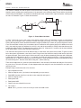
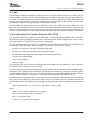
1 DESCRIPTION
The GC5016 is a flexible wideband 4-channel digital up-converter and down-converter. The GC5016 is designed for
high-speed, high bandwidth digital signal processing applications like 3G cellular base transceiver station transmit
and receive channels. The GC5016 is also applicable for general-purpose digital filtering applications. The four
identical processing channels can be independently configured for up-conversion, down-conversion, or a
combination of two up-conversion and two down-conversion channels.
In up-conversion mode, the channel accepts real or complex signals, interpolates them by programmable amounts
ranging from 1 to 4096, and modulates them up to selected center frequencies. The 4 digital up-converter signals
can be output individually, summed together on one or two outputs on a single GC5016, or optionally summed
between multiple GC5016s. Channels can be used in pairs to increase the output sample rate, to increase filtering
capacity, to increase the input bandwidth, or any combination. Each channel contains a user programmable input
filter (PFIR), which can be used to shape the transmitted signal’s spectrum or as a Nyquist transmit filter for shaping
digital data such as QPSK, GMSK, or QAM symbols.
In down-conversion mode, the channel accepts real or complex signals, demodulates them from selected carrier
frequencies, decimates them by programmable amounts ranging from 1 to 4096, applies a gain from a user defined
automatic gain control, and produces 20-bit outputs. The frequencies and phase offsets of the four sine/cosine
sequence generators can be independently specified, as can the decimation and filtering of each circuit. Channels
can be synchronized to support beam forming or frequency hopped systems. The output from the down-conversion
channel is formatted and output in up to four output ports as either real or complex data.
2 ORDERING INFORMATION
PART NAME
TEMPERATURE
PACKAGE
DESCRIPTION
GC5016-PB
−40°C to 85°C
GDJ (S-PBGA-N252)
252 ball PBGA
GC5016-PBZ
−40°C to 85°C
ZDJ (S-PBGA-N252)
252 ball lead free PBGA
3 OTHER REFERENCE MATERIALS
The TI Web site has developer toolkit and application notes that provide application specific programming and
configuration information. The CMD5016 configuration program, along with a user specified source and tap
coefficient file, is used to configure the GC5016 registers. The GC5016 register settings are intended to be configured
through the development toolkit software.
NOTE:Names in italics refer to parameter inputs to the cmd5016 software configuration program.
2
www.ti.com
SLWS142J − JANUARY 2003 − REVISED AUGUST 2007
These devices have limited built-in ESD protection. The leads should be shorted together or the device placed in conductive foam during
storage or handling to prevent electrostatic damage to the MOS gates.
4 ABSOLUTE MAXIMUM RATINGS
over operating free-air temperature range unless otherwise noted(1)
GC5016
Pad ring supply voltage, VPAD
−0.3 V to 4 V
Core supply voltage, VCORE
−0.3 V to 2.3 V
Input voltage (undershoot and overshoot), VIN
−0.5 V to VPAD+0.5 V
Storage temperature, Tstg
−65°C to 150°C
Junction temperature, TJ
105°C
Lead soldering temperature (10 seconds)
300°C
ESD classification
Human body model
2 kV
Machine body model
200 V
Charged device model
500 V
Moisture sensitivity
Level 3
(1) Stresses beyond those listed under “absolute maximum ratings” may cause permanent damage to the device. These are stress ratings only, and
functional operation of the device at these or any other conditions beyond those indicated under “recommended operating conditions” is not
implied. Exposure to absolute-maximum-rated conditions for extended periods may affect device reliability.
5 RECOMMENDED OPERATING CONDITIONS
Pad ring supply voltage, VPAD
MIN
MAX
3
3.6
UNITS
V
Core supply voltage, VCORE
1.6
2
V
Temperature ambient, no air flow, TA(1)
Junction temperature, TJ(2)
−40
85
_C
105
_C
(1) Chips specifications in the AC CHARACTERISTICS and DC CHARACTERISTICS tables are production tested at 100_C case temperature. QA
tests are performed at 85°C case temperature.
(2) Thermal management may be required for full rate operation (see the THERMAL CHARACTERISTICS table). The circuit is designed for junction
temperatures up to 125°C. Sustained operation at elevated temperatures reduces long-term reliability. Lifetime calculations based on maximum
junction temperature of 105°C.
6 DC CHARACTERISTICS
−40°C to 85°C case temperature unless otherwise noted
PARAMETER
VIL
VIH
Voltage input low (1)
Voltage input high (1)
VOL
VOH
Voltage output low (IOL = 2 mA) (1)
Voltage output high (IOH = −2 mA) (1)
| IIN |
| IPU |
Leakage current (VIN = 0 V or VPAD), inputs or outputs in high-impedance state condition (1)
Pullup current (VIN = 0 V) ( TDI, TMS, TCK) (1)
ICCQ
CIN
Quiescent supply current, ICORE or IPAD(VIN=0 or VPAD, RST = TRST = 0) (1)
Data input capacitance (all inputs except CK) (2)
VPAD = 3 V to 3.6 V
MIN
TYP
MAX
0.8
2
UNIT
V
V
0.5
2.4
V
V
5
1
µA
35
µA
4
mA
4
pF
CCK
13
(1) Each part is tested with a 100°C case temperature for the given specification.
(2) Controlled by design and process and not directly tested.
NOTE: General: Voltages are measured at low speed. Output voltages are measured with the indicated current load.
General: Currents are measured at nominal voltages, high temperature (100_C for production test, 85_C for QA).
pF
Clock input capacitance (CK input) (2)
3
www.ti.com
SLWS142J − JANUARY 2003 − REVISED AUGUST 2007
7 AC CHARACTERISTICS
−40°C to 85°C case, supplies across recommended range unless otherwise noted
PARAMETER
fCK
tCKL
tCKH
tr, tf
Clock frequency (1)
Clock low period (below VIL) (1)
Clock high period (above VIH) (1)
Input set up before CK goes high (AI, BI, CI, DI, SIA, or SIB) (1)
Input hold time after CK goes high (1)
td
th(o)
Data output delay from rising edge of CK. (AO, BO, CO, DO, IFLG, [A−D]FS, [A−D]CK, or SO) (1)
Data output hold from rising edge of CK (1)
fJCK
tJCKL
JTAG clock frequency (1)
th(J)
td(J)
MAX
UNITS
160
MHz
2
ns
2
ns
Clock rise and fall times (VIL to VIH) (4)
tsu
th
tJCKH
tsu(J)
MIN
(3)
JTAG clock low period (below VIL) (1)
JTAG clock high period (above VIH) (1)
JTAG input (TDI or TMS) set up before TCK goes high (1)
JTAG input (TDI or TMS) hold time after TCK goes high (1)
2
2
ns
ns
0.5
ns
4
ns
40
MHz
1
ns
10
ns
10
ns
1
ns
10
ns
JTAG output (TDO) delay from falling edge of TCK (1)
10
ns
tsu(C)
tsu(EWC)
Control setup during reads or writes. (1)(5)
2
ns
Control data setup during writes (normal mode). (1)(5)
4
ns
th(C)
tCSPW
Control hold during writes. (1)(5)
1
ns
20
ns
td(C)
tREC
Control output delay CE and RD low and A stable to C (read operation). (1)(5)
t(CZ)
IC(DYN)
Control strobe (CE and WR low) pulse width (write operation). (1)(5)
Control recovery time between reads or writes. (1)(5)
End of read to HI-Z (2)(5)
12
20
ns
ns
Core dynamic supply current nominal voltages, 100 MHz, four channels active, full length filters,
high temperature. (6)
5
ns
420
mA
(1) Each part is tested with a 100°C case temperature for the given specification. Lots are sample tested at −40°C.
(2) Controlled by design and process and not directly tested.
(3) The minimum clock rate is calculated in the cmd5016 configuration program. It may be estimated by (1 + ncic − nfir) x 200 kHz.
(4) Recommended practice
(5) See Figure 27 through Figure 32.
(6) Each port is tested with a 100°C case temperature for the given specification.
General: Timing is measured from CK at VPAD/2 to input or output at VPAD/2. Output loading is a 50-Ω transmission line whose delay is calibrated
out.
8 THERMAL CHARACTERISTICS
252 BGA
THERMAL CONDUCTIVITY
Theta junction to ambient, θJA
Theta junction to case, θJC
NOTE: Air flow reduces θJA and is highly recommended.
4
1W
UNITS
22
°C/W
5
°C/W
www.ti.com
SLWS142J − JANUARY 2003 − REVISED AUGUST 2007
9 POWER CONSUMPTION
The maximum power consumption depends on the operating mode of the chip. The following equation estimates the
typical power supply current for the chip. Chip-to-chip variation is typically ±5%. The AC Characteristics provides the
production test limit for current in a maximum configuration. It is 10% over the typical value.
Icore = (fCK/100 MHz) (Vcore/1.8 V) (Number_of_Active_Channels/4) (0.75 + FIRDutyCycle) 220 mA
The FIRDutyCycle is calculated in the cmd5016 programming software. The ’.ANL’ extension of the user
programming file contains the power analysis value.. It can be estimated by:
Down Converter Mode:
FIRDutyCycle = 1 for fCK/Fout ≤ 16
16 x Fout/fCK otherwise
Up Converter Mode:
FIRDutyCycle = 1 for fCK/Fin ≤ 32
32 x Fin/fCK otherwise
Current consumption on the pad supply is primarily due to the external loads and follows C x V x F. Internal loads
are estimated at 2 pF per pin. Data outputs transition from a zero to a one once per four clocks, while clock outputs
transition every cycle. The frame strobes consume negligible power due to the low transition frequency. In general:
Ipad = Σ DataPad/4 x C x F x V + Σ ClockPad x C x F x V
Typically loads are 20 pF per pin. A worst case current would be all four output ports operating at 125 MHz and the
four output clocks with [A−D]CK active at 125 MHz.
Ipad = (64/4 + 4) x (C+2pF) x Fout x Vpad = 20 x 22 pF x 125 MHz x 3.3 V = 180 mA
5
www.ti.com
SLWS142J − JANUARY 2003 − REVISED AUGUST 2007
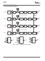
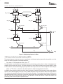
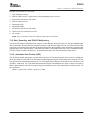
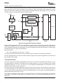
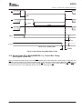
10 Functional Block Diagram
NCO
I
AI [15:0]
RINF
RSEL
Dual CIC
PFIR
Q
NCO
RINF
RSEL
ROUTF
AO [15:0]
AFS
ACK
TDM
Broadcast
Cross connect for double rate
I
BI [15:0]
Pwr Mtr
AGC
Dual CIC
PFIR
Pwr Mtr
AGC
ROUTF
BO [15:0]
BFS
BCK
Dual CIC
PFIR
Pwr Mtr
AGC
ROUTF
CO [15:0]
CFS
CCK
Pwr Mtr
AGC
ROUTF
DO [15:0]
DFS
DCK
Q
NCO
I
CI [15:0]
RINF
RSEL
Q
NCO
Cross connect for double rate
I
DI [15:0]
RINF
RSEL
Dual CIC
PFIR
Q
A [4:0]
TDI
SIA
CE
TMS
SIB
JTAG
TDO
WR
TCK
Control
C [15:0]
CK
RD
TRST
RST
WRMODE
Figure 1. GC5016 in Digital Down-Conversion Mode
6
CK
and
Syncs
SO
www.ti.com
SLWS142J − JANUARY 2003 − REVISED AUGUST 2007
CO [15:0]
NCO
AI [15:0]
AFS
ACK
TINF
GAIN
TDM
Broadcast
BI [15:0]
BFS
BCK
TINF
PFIR
Dual CIC
Cross connect for double rate
GAIN
PFIR
DO [15:0]
NCO
Dual CIC
IFLG
NCO
CI [15:0]
CFS
CCK
TINF
GAIN
PFIR
TINF
GAIN
PFIR
AO [15:0]
BO [15:0]
CO [15:0]
DO [15:0]
Dual CIC
Cross connect for double rate
DI [15:0]
DFS
DCK
SUM
and
FORMAT
NCO
Dual CIC
A [4:0]
TDI
SIA
CE
TMS
SIB
JTAG
TDO
WR
TCK
Control
C [15:0]
CK
RD
TRST
CK
and
Syncs
SO
RST
WRMODE
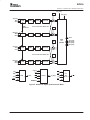
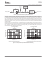
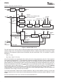
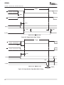
Figure 2. GC5016 in Digital Up-Conversion Mode
7
www.ti.com
SLWS142J − JANUARY 2003 − REVISED AUGUST 2007
NCO
AI
AFS
ACK
TINF
GAIN
TDM
Broadcast
BI
BFS
BCK
TINF
PFIR
Dual CIC
Cross connect for double rate
GAIN
PFIR
NCO
IFLG
SUM
and
FORMAT
AO [15:0]
BO [15:0]
Dual CIC
NCO
I
CI [15:0]
RINF
RSEL
Dual CIC
PFIR
Q
NCO
RINF
RSEL
Dual CIC
PFIR
Q
ROUTF
CO
CFS
CCK
TDM
Broadcast
Cross connect for double rate
I
DI [15:0]
Pwr Mtr
AGC
Pwr Mtr
AGC
ROUTF
DO
DFS
DCK
A [4:0]
TDI
SIA
CE
TMS
SIB
JTAG
TDO
WR
Control
C [15:0]
TCK
CK
RD
TRST
RST
WRMODE
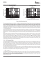
Figure 3. GC5016 in Transceiver Mode
8
CK
and
Syncs
SO
www.ti.com
SLWS142J − JANUARY 2003 − REVISED AUGUST 2007
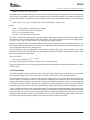
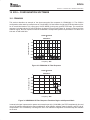
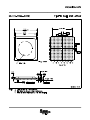
11 PIN ASSIGNMENTS
1
2
3
4
5
6
7
8
9
10
11
12
13
14
15
16
BCK BO14 BO13 AO11 AO10
BO8
GND
GND
AO6
BO4
BO3
AO1
IFLG
TMS
GND
AO9 VPAD VPAD BO5
AO4
BO2
BO0
TDI
TRST
RST
BO9
AO7
BO6
AO5
AO3
BO1
SO
GND
SIB
CI15
AO13 BO12
BO7
AO8
AO2
AO0
A
GND
B
AI1
BI0
C
BI3
BI2
AI0
AFS
BO15 AO12
D
AI5
AI3
AI2
BFS
ACK
TDO
TCK
DI15
DI14
CI13
E
BI6
AI6
BI5
BI1
GND VPAD VPAD VPAD VPAD VPAD VPAD GND
SIA
DI13
DI12
DI11
F
AI8
BI7
AI7
BI4
VCOR GND
GND VPAD VPAD GND
GND VCOR CI14
CI12
CI11
DI10
G
BI9
AI9
BI8
AI4
VCOR GND
GND
GND VCOR CI10
CI9
DI8
CI8
H
GND
AI10
BI11
J
GND
BI12
K
AI13
L
AO15 AO14 BO11 BO10
GND
GND
BI10 VCOR VCOR GND
/
/
GND VCOR VCOR
DI9
VPAD
DI7
GND
AI12
AI11 VCOR VCOR GND
/
/
GND VCOR VCOR
DI5
CI7
DI6
GND
BI13
AI14
BI14 VCOR GND
GND
GND
GND
CI5
DI4
CI4
CI6
AI15
BI15
CK
A0
GND VCOR CCK
DI2
CI3
DI3
M
A1
A2
A3
A4
CI1
DI1
CI2
N
CE
RD
WRMODE
C0
C3
C9
C10
DO1
CO2
CO7 CO12 DO13 CO15 DCK
CI0
DI0
P
WR
C1
GND
C5
C8
C14
DO2
CO4
DO4
CO6
DO8
CO11 CO13 GND DO15 CFS
R
C2
C4
C6
C12
C13
DO0
CO3 VPAD VPAD DO5
DO7
CO9 DO10 DO12 CO14 DO14
T
GND
C7
C11
C15
CO0
CO1
DO3
DO6
CO8
VCOR GND
GND
GND
GND VPAD VPAD GND
GND VCOR
GND VPAD VPAD VPAD VPAD VPAD VPAD GND
GND
GND
CO5
DFS
DO9 CO10 DO11 GND
/ = No Ball
9
www.ti.com
SLWS142J − JANUARY 2003 − REVISED AUGUST 2007
12 TERMINAL FUNCTIONS
Bit 0 is the least significant bit on all buses. All outputs are able to be put into a high-impedance state. JTAG related
inputs have pull-ups if an external pulldown is used, it must be less than 500 Ω. When I and Q are multiplexed, I comes
first. All clocked inputs are registered on the rising edge of CK and all clocked outputs are released on the rising edge
of CK, except for Jtag output (TDO). It is recommended that TRST have a user controlled pull-down. This input must
be a ’1’ for JTAG testing, and is recommended to be ’0’ for normal operation.
SIGNAL
TYPE
DESCRIPTION
CONTROL I/O
A[4..0]
C[15..0]
I
Control address bus – Active high inputs
These pins are used to address the control registers within the chip. Each of the control registers within the chip are
assigned a unique address. A control register can be written to or read from by having the page register set to the
appropriate page and then setting A[4..0] to the register’s address.
I/O
Control data I/O bus – Active high bidirectional I/O pins
This is the 16-bit control data I/O bus. Control registers are written to or read from through these pins. The chip drives
these pins when CE is low, RD is low, and WR is high.
CE
I
Chip enable – Active low input pin
This control strobe enables the read or write operations.
WR
I
Write enable – Active low input pin
The value on the C[15..0] pins is written into the register selected by the A[4..0] and page register when WR and CE are
low.
RD
I
Read enable – Active low input pin
The register selected by A[4..0] and the page register is output on the C[15..0] pins when RD and CE are low.
AI[15..0]
I
Clocked input port A, data bits 0 through 15
Can be configured for many possible input formats.
BI[15..0]
I
Clocked input port B, data bits 0 through 15
Can be configured for many possible input formats.
CI[15..0]
I
Clocked input port C, data bits 0 through 15
Can be configured for many possible input formats.
DI[15..0]
I
Clocked input port D, data bits 0 through 15
Can be configured for many possible input formats.
AO[15..0]
O
Clocked output port A, data bits 0 through 15
Can be configured for many possible output formats.
BO[15..0]
O
Clocked output port B, data bits 0 through 15
Can be configured for many possible output formats.
CO[15..0]
I/O
Dual function:
Clocked output − port C, data bits 0 through 15
Can be configured for many possible output formats.
Clocked input – Sum IO input data, data bits 0 through 15
Can be configured for many possible input formats.
DO[15..0]
I/O
Dual function:
Clocked output − port D, data bits 0 through 15
Can be configured for many possible output formats.
Clocked input – sum IO input data, data bits 0 through 15
Can be configured for many possible input formats.
[A..D]CK
O
Clocked output for ports [A..D]
The clock for input ports in up-conversion mode and output ports in down-conversion mode. When configured as a
transceiver, channels A and B are in up-conversion and channels C and D are in down-conversion mode.
[A..D]FS
O
Clocked output frame strobes for channels A..D
Used to signify the beginning of a data frame for each input port in up-conversion mode and output in down-conversion
mode. The frame strobes are set high by the GC5016 with the first word in a frame. The frame strobes can be programmed
to be sent early.
CK
I
Main input clock. The clock input to the chip.
DATA I/O
10
www.ti.com
SLWS142J − JANUARY 2003 − REVISED AUGUST 2007
SIGNAL
TYPE
DESCRIPTION
DATA I/O (CONTINUED)
IFLG
O
Clocked output A flag used to indicate which samples are real or imaginary in up-conversion mode when I and Q are time
multiplexed.
WRMODE
I
A static control input that changes the timing of control writes. Normally tied low. When low control write data must be
stable for a setup time ahead and hold time after the end of the write strobe. When high data must be stable for a setup
time ahead of the write strobe going active until a hold time after it goes inactive.
RST
I
Chip reset bar. Active low signal. Not clocked. RST requires an external pull-up resistor or connection to VCOR Power
Monitor “1” is OK.
SIA
I
Sync input A bar. Active low data input signal. SIA requires an external pull-up resistor if not used.
SIB
I
Sync input B bar. Active low data input signal. SIB requires an external pull-up resistor if not used.
SO
O
Sync output bar. Active low data output signal
I
JTAG clock – Active high input. Internal pullup
TDI
I
JTAG data in – Active high input clocked on TCK rising. Internal pullup
TDO
O
JTAG data out – High-impedance state output clocked on falling edge of TCK.
TMS
I
JTAG interface – Active high input clocked on TCK rising. Internal pullup
TRST
I
Asynchronous JTAG reset bar. Internal pullup
JTAG I/O
TCK
SUPPLIES
GND
Ground
VCOR(1)
VPAD(1)
Core supply voltage. Used to supply the core logic, nominally set to 1.8 V.
Interface voltage. Used to set the I/O levels for all pins, nominally set at 3.3 V.
(1) The VCore and VPad must both be powered before programming the GC5016 Control Bus. There is no required power sequence.
The recommendation is to power VCore before or simultaneously with VPad.
13 GC5016 DOWN-CONVERSION MODE
13.1 Overview
Figure 1 shows the functional block diagram for the GC5016 when configured as a 4-channel digital
down-converter(DDC). In a common configuration, each down-conversion channel demodulates ADC sampled data
down from an IF frequency to 0Hz, low pass filters the signal data, reduces the signal rate (decimation), and outputs
I and Q baseband data. The baseband signal is measured by the Power Meter, and a gain or gain + automatic gain
are applied to the IQ data. Several output formats are available for transmitting the IQ outputs.
The DDC input can be configured for real or complex inputs. The input data on ports AI[15..0], BI[15..0], CI[15..0],
are converted to a complex input format in the Receive Input Formatter (RINF).
The Mixer stage provides the Receive Input channel selection (RSEL), digital oscillator (NCO), and complex mixing
logic (mixer) to translate the input down to 0 Hz.
After the Mixer, the 5 stage Cascade Integrator Comb (CIC) provides complex filtering and decimation. The CIC
decimation is an integer value from 1 to 256. Special logic is used for double rate processing.
After the CIC complex filter, the Programmable Finite Impulse Response (PFIR) filter provides CIC correction,
spectral shaping, and further decimation. The PFIR decimates from 1 to 16.
The PFIR complex output is measured by the Complex Power Meter. The Power Meter integrates the IQ power. The
time integrated value can be read through the Microprocessor port.
The PFIR complex output is gain (manual + adaptive) scaled.An automatic gain (adaptive gain) is computed based
on the current IQ output level. The gain scaled output is rounded to a desired number of bits resolution, and is
formatted for the DDC output.
Channels can be synchronized to support beam forming or frequency hopped systems. Two channels can be
operated in tandem to allow double input bandwidth, double output bandwidth, or both.
11
www.ti.com
SLWS142J − JANUARY 2003 − REVISED AUGUST 2007
13.2 Receive Input Formatter (RINF)
The GC5016 has four 16-bit input ports AI[15..0], BI[15..0], CI[15..0], and DI[15..0]. The formatter converts the
representation of real or complex data at the input pins to a complex format output.
13.2.1 Receive Input Data Formats
Five data formats are supported (see Table 1):
D
D
D
D
D
Full Rate, Real Input, one signal per input port
Double Rate, Real Input, one signal per two input ports (even and odd)
Half Rate, Complex Input, one signal per input port
Full Rate, Complex Input, one signal per two input ports (I and Q)
Double Rate, Complex Input, one signal per four input ports (Ieven, Qeven, Iodd, Qodd)
NOTE:Full Rate means the sample input rate is equal to the GC5016 clock rate.
Each input port has a receive input data formatter. The data formatter accepts 2s complement format data 16 bits
from its input port and outputs a 16-bit I bus and a 16-bit Q bus (the rinf bus). When there is no data to send, the output
bus is held to zero.
For example:
If the input data is real, at full rate, the Q bus is zero.
If the input data is complex, at half rate, every second time sample is zero.
If the input data is complex at full rate, the I data is expected in port A (or C) and A’s Q bus is zero. The imaginary
data is expected in port B (or D) and B’s I bus is zero.
The input format can be specified to the cmd5016 software by setting pseudo-commands rin_rate and rin_cmplx.
NOTE:Pseudo-commands are user specified variables that the software uses to set the hardware register values.
Table 1 shows the modes, the pseudo-commands, and register variables, programmed through the cmd5016
software.
For example, for the mode with four complex inputs, data from source 1 is entered time multiplexed I, followed by
Q onto port AI. Configuration using the software requires that rin_cmplx be set to 1 and rin_rate be set to 0 (half rate).
Alternatively, if the user wishes to program the hardware register fields directly, rinf_sel_A should be set to 3,
mix_rcv_sel to 0 for channel A, and mix_rcv_cmplx to 0 for channel A (etc., for channels B, C, and D).
Table 1. Receive Input Modes and Controls
SOFTWARE
CONTROLS
INPUT PORTS
FIELDS FOR CHANNELS A, B, C, AND D
rinf_sel / mix_rcv_sel / mix_rcv_cmplx
MODE
AI
BI
CI
DI
rin_cmplx / rin_rate
A
B
C
D
Four real
1I
2I
3I
4I
0/1
4/0/0
4/1/0
4/2/0
4/3/0
Four complex
1I/1Q
2I/2Q
3I/3Q
4I/4Q
1/0
3/0/0
3/1/0
3/2/0
3/3/0
Two complex
1I
1Q
2I
2Q
1/1
4/0/1
1/x/x
4/2/1
1/x/x
Two double rate
real
1I(2k)
1I(2k+1)
2I(2k)
2I(2k+1)
0/2
4/0/0
4/1/0
4/2/0
4/3/0
One double rate
complex
I(2k)
Q(2k)
I(2k+1)
Q(2k+1)
1/2
4/0/1
1/x/1
4/2/x
1/x/x
13.2.2 Synchronization for IQ Multiplexed Mode
When I and Q are time multiplexed, a synchronization signal is used to determine which sample is I and which is Q.
The input data is delayed by one cycle to form the I stream and is directly output for the Q stream. Thus far the data
stream is (I0,Q0), (Q0, I1), (I1, Q1), — where I0 is the real portion of the sample at time 0. Then every other complex
sample is zeroed using receive interpolation as discussed below, so that the stream is now (I0,Q0), (0,0), (I1,Q1),
(0,0). — The timing for proper receive interpolation sync is shown in the next section.
12
www.ti.com
SLWS142J − JANUARY 2003 − REVISED AUGUST 2007
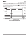
13.2.3 Receive Interpolation
If the GC5016 CK rate divided by the input sample rate is an integer ratio, receive interpolation can be used (see
Figure 4). In this case, the chip can be programmed to insert 0−15 zeros (rinf_zpad) between input samples. This
effectively interpolates the signal up by rinf_zpad+1. The higher CK rate means the chip is operating faster, so the
PFIR has more multiplication operations available per sample. It also allows greater flexibility in selecting the output
sample rate since:
Fs_out=Fck / (cic_dec x fir_dec), where Fck=Fadc x (1+rinf_zpad).
One sample is registered while the data input on the other rinf_zpad clocks are zeroed. The user has control over
which sample is used through rinf_zpad_sync. The zpad selected sync encounters a two CK cycle delay, then loads
a counter. When the counter reaches the terminal count, it is reloaded and a data sample is kept. All other data
samples are zeroed. The sample occurring two plus (rinf_zpad + 1) clock cycles after the sync is used, while the other
samples are ignored. The sync input may be periodic in any multiple of (rinf_zpad+1) or may occur just once.
If I and Q are time multiplexed, then the sync should be coincident with the Q sample.,
13
14
tSU
tSU
tH
N
1
DDC
Channel
Data
(int)
0
N
1
GC5016
Input
ZPAD
Counter
(Int)
Sync
Input
GC5016
CK
0
0
N+1
tH
N+1
1
0
0
N+2
N+2
1
0
0
N+3
N+3
1
0
0
N+4
N+4
1
0
0
N+5
N+5
1
0
0
N+6
N+6
1
0
0
N+7
N+7
1
0
0
N+8
N+8
1
0
0
N+9
N+9
1
0
0
SLWS142J − JANUARY 2003 − REVISED AUGUST 2007
www.ti.com
Figure 4. DDC Input Timing Diagram
www.ti.com
SLWS142J − JANUARY 2003 − REVISED AUGUST 2007
13.2.4 Receiver Desensitizing
In a few circumstances, it is necessary to reduce the receiver sensitivity, which can be done by adding noise to the
signal. The GC5016 allows this to be done digitally by adding pseudo random noise to selected bits in the input data
stream. The noise power is added by bit wise xoring the input data stream with a Pseudo-random Noise (PN)
sequence. The user has control over the noise power by programming which bits get the noise added. The noise
power can go from −3 dBFS (0xffff) to −99 dbFS (0x1). This is programmed using rcv_noise_A (or B, C, or D). The
noise uses the PN generator that is also used for diagnostics. The generator must be enabled for this feature to work
by setting cksum _sync.front to 0.
13.3 Receiver Diagnostic Selection
The Receiver RINF can select the counter (ramp), zero, a constant, or the PN sequence as the DDC channel real
input. The 0x4000 constant is used with the NCO setting to generate a known complex tone for output testing. The
rinf_sel and rinf_diag controls are used to select a diagnostic input for a DDC channel. See the Diagnostics section.
13.4 Receive Input Selection
In each channel an input selector exists at the input to the mixer. This selects I and Q data from one of four receive
input formatters. The field mix_rcv_sel allows selection of the rinf bus. Full rate real or 1/2 rate complex inputs are
selected with the mix_rcv_sel value as the input port. Special mix_rcv_sel values are needed for full rate complex,
and double rate processing. See Table 1.
13.5 Mixer
The DDC application of the mixer uses the selected RINF and RSEL with the NCO sine and cosine values. The Mixer
equations are:
Imixout = Iin × cos(Phase_NCO) − Qin × sin(Phase_NCO)
Qmixout = Qin × cos(Phase_NCO) + In × sin(Phase_NCO)
Each of the four multipliers (I x cos, I x sin, Q x cos, Q x sin) can be programmed in one of four modes (off, receive,
cross transmit, normal transmit) (see Figure 5). A programmable inversion is provided for each I or Q data source.
Programming Q x sin to be inverted corresponds to a mathematical view of down-conversion (mix with negative
frequency tone to get a positive spectrum). Programming I x sin to be inverted corresponds to a radio view (tune to
a frequency to get the signal at that frequency). The fields involved are mix_icos, mix_isin, mix_qcos, mix_qsin, and
mix_inv_icos, mix_inv_isin, mix_inv_qcos, and mix_inv_qsin. The cmd5016 software automatically programs these
fields assuming a mathematical view.
Selected RINF and RSEL data is accepted into the mixer as 16-bit data, placed into the upper bits of an 18-bit word,
and inverted if programmed. The 18bit input is multiplied by a 20-bit NCO word, summed with the output of a second
multiplier creating a 21-bit output. The Mixer output in the DDC application is sent to the CIC.
This means there is a 6dB attenuation going through the mixer. In other words, there is a 1-bit growth on top to allow
for the extreme case of both real and imaginary inputs at full scale being multiplied by an NCO word that is at 45
degrees. For real inputs, the attenuation is 6 dB, so the CIC can safely be programmed to have 6-dB gain. For
complex inputs, the attenuation is 3dB peak. The cmd5016 software includes this attenuation in its gain calculations
when gain is set using the overall-gain keyword.
15
www.ti.com
SLWS142J − JANUARY 2003 − REVISED AUGUST 2007
BI
AI
DI
BQ
CI
AQ
2
DQ
CQ
16
2
mix_rcv_sel
TI
GND
mix_rcv_cmplx
TQ
XI
GND
2
XQ
18
2
mix_qcos
mix_icos
mix_inv_icos
mix_inv_qcos
20
20
cos
real
TI
GND
TQ
XI
GND
2
XQ
2
mix_isin
mix_qsin
mix_inv_isin
20
mix_inv_qsin
20
sin
20
21
imag
Figure 5. Multiplexing Options in Mixer
13.6 Numerically Controlled Oscillator (NCO)
The tuning frequency of each up-converter is specified as a 48-bit word and the phase offset is specified as a 16-bit
word. The 48-bit tuning word is calculated based on:
Freq words = FTune(negative for DDC) / CK × 248
The NCO phase is computed as the integrated frequency word phase + phase_offset + dither. A block diagram of
the NCO circuit is shown in Figure 6. The tuning frequency is set to FREQ according to the formula FREQ = (248)
x F/fCK, where F is the desired tuning frequency and fCK is the chip’s clock rate. The 16-bit phase offset setting is
phase = (216) x Ph/2π , where Ph is the desired phase in radians ranging between 0 and 2π.
A negative tuning frequency should be used for down-conversion. A positive tuning frequency can be used to flip the
spectrum of the desired signal (if the input is real). FREQ and phase are set as shown in Table 53 through Table 56
or in software by specifying freq_msb, freq_mid, freq_lsb, and phase. The configuration software calculates the
appropriate settings for freq_msb, freq_mid, and freq_lsb given the chip clock frequency (fCK) and freq. (If both freq
and freq_msb are set freq_msb takes priority). The calculation includes the effects of zpad and double rate
processing. Both fck and freq are expressed in Mhz.
16
www.ti.com
SLWS142J − JANUARY 2003 − REVISED AUGUST 2007
Dither
Generator
Phase
Offset
48
16
48
7
18
23
Frequency Word
Sine/Cosine
Lookup Table
20
Sine/Cosine Out
Figure 6. Numerically Control Oscillator (NCO) Circuit
The NCOs can be synchronized with NCOs on other chips. This allows multiple down converter outputs to be
coherently combined, each with a unique phase and amplitude. The NCO’s frequency, phase and accumulator can
be initialized and synchronized with other channels using the freq_sync, phase_sync, and nco_sync controls. The
freq_sync and phase_sync controls determine when new frequency and phase settings become active. Normally,
these are set to Always so that they take effect immediately, but can be used to synchronize frequency hopping or
beam forming systems. The nco_sync control is usually set to Never, but can be used to synchronize the NCOs of
multiple channels.
The NCO’s spur level is reduced to below −113 dB through the use of phase dithering. The spectrums in Figure 7
show the NCO spurs for a worst case tuning frequency with and without dithering. Dithering decreases the spur level
from −105 dB to −116 dB. Dithering is turned on or off using the dith_sync controls. Holding dith_sync always on
freezes the dither value, effectively turning off dither.
NCO OUTPUT POWER
vs
FREQUENCY
NCO OUTPUT POWER
vs
FREQUENCY
0
FREQ = 5/24 fS
−50
−105 dB
−100
−150
0.0 0.1 0.2 0.3 0.4 0.5 0.6 0.7 0.8 0.9 1.0
Frequency − fS
a) Worst Case Spectrum Without Dither
NCO Output Power − dB
NCO Output Power − dB
0
FREQ = 5/24 fS
−50
−116 dB
−100
−150
0.0 0.1 0.2 0.3 0.4 0.5 0.6 0.7 0.8 0.9 1.0
Frequency − fS
b) Spectrum With Dither (Tuned to Same Frequency)
Figure 7. Example NCO Spurs With and Without Dithering
17
www.ti.com
SLWS142J − JANUARY 2003 − REVISED AUGUST 2007
NCO OUTPUT POWER
vs
FREQUENCY
NCO OUTPUT POWER
vs
FREQUENCY
0
−50
NCO Output Power − dB
NCO Output Power − dB
0
−107 dB
−100
−150
0.0 0.1 0.2 0.3 0.4 0.5 0.6 0.7 0.8 0.9 1.0
−50
−121 dB
−100
−150
0.0 0.1 0.2 0.3 0.4 0.5 0.6 0.7 0.8 0.9 1.0
Frequency − fS
Frequency − fS
a) Plot Without Dither or Phase Initialization
b) Plot With Dither and Phase Initialization
Figure 8. NCO Peak Spur Plot
The worst-case NCO spurs at −113 dB to −116 dB, such as the one shown in Figure 7(b), are due to a few frequencies
that are related to the sampling frequency by multiples of fCK/96 and fCK/124. In these cases, the rounding errors
in the sine/cosine lookup table repeat in a regular fashion, thereby concentrating the error power into a single
frequency, rather than spreading it across the spectrum. These worst-case spurs can be eliminated by selecting an
initial phase that minimizes the errors or by changing the tuning frequency by a small amount (50 Hz). Setting the
initial phase register value to 4 for multiples of fCK/96 or fCK/124 (and to 0 for other frequencies) results in spurs below
−115 for all frequencies.
Figure 8 shows the maximum spur levels as the tuning frequency is scanned over a portion of the frequency range
with the peak hold function of the spectrum analyzer turned on. Notice that the peak spur level is −107 dB before
dithering and is −121 dB after dithering has been turned on and the phase initialization described above has been
used.
Double rate processing is done by sending time samples (2k) to mixer A and time samples (2k+1) to mixer B. The
frequency is tuned to freq = (248) x F/fCK, where F is the desired tuning frequency and fCK is the chip’s clock rate as
before. The 16-bit phase offset for mixer A is set to phase = (216) x Ph/2π, where Ph is the desired phase in radians
ranging between 0 and 2π. The phase offset for mixer B is set to phase = (216) x Ph/2π + (215) x F/fCK. Note that the
second mixer phase offset is one frequency step at the sample rate of 2 fCK hence 215 rather than 216 scaling. The
configuration software automatically calculates these.
13.6.1 CIC Decimate Filter
The Cascade Integrator Comb (CIC) filter is a 5 stage decimating filter. The CIC filter is set to decimation mode using
the register variable cic_rcv. Each CIC channel contains two CIC filters (one for I and one for Q) allowing input rates
of CK complex samples per second. The CIC filter has several sections: scaling, integration, rate change, comb
filtering, and output scaling. The two CIC filter sections have special logic used in the double rate mode. The double
rate mode is discussed in a later section.
The mixer IQ input is scaled to the 60 bit range using cic_shift. The shifted mixer data is then input to the 5 integrator
M=1 stages. The 5th integrator is decimated in the rate changer, by ncic samples. The cic scaling is based on shifting
the input data to compensate for the 5 integrator stages’ (cic_dec ^ 5) gain.
Ncic = cic_dec − 1
The decimation logic samples the integrator output every cic_dec clocks. The cic_dec value can be set between 1
and 256. The value of cic_dec can actually be programmed up to 4096 but the gain restrictions normally limit the
usable range to 256 (up to 1024 in unusual circumstances).
[1]Hogenhauer, Eugene V., An Economical Class of Digital Filters for Decimation and Interpolation, IEEE transactions on Acoustics, Speech and
Signal Processing, April 1981.
18
www.ti.com
SLWS142J − JANUARY 2003 − REVISED AUGUST 2007
The decimated output is scaled to 24bits and input to the 5 stage comb section M=1. After the 5 comb sections, the
24bit output is scaled to 18 bits. The 18 bit output is saturated to 17 or 18 bits. The 17bit output is used when the
PFIR uses symmetry. A block diagram of the decimating CIC filter is shown in Figure 9.
The CIC filter has a gain equal to cic_dec5 that must be compensated for by the CIC scale circuit. and the scale circuit
must limit the peak signal gain from the rinf_zpad, mixer, and through the CIC to be 1 or less. The peak gain is:
peak gain = (1/(1+rinf_zpad)) × (mixer_gain) × (cic_dec^5 × 2^(cic_shift−39))
The cmd5016 program will set the gain properly if the overall-gain keyword is used.
The register field cic_sync controls the precise moment of decimation. The sync can be periodic at any multiple of
cic_dec without disturbing the processing. If sync is held active, the CIC freezes its output.
The output of the CIC can be attenuated in gain by 6 dB by clearing cic_rshift. This is appropriate only when cic_shift
has been set to zero, the signal gain to this point is greater than 0.5, and symmetry is being used in the PFIR filter.
In other words, cic_rshift should almost always be set to one. The rshift_gain is 2cic_rshift−1.
The CIC output data feeding the PFIR must be limited to half scale if the PFIR is using symmetry. Control bit field
cic_rcv_full must be cleared in this case. If the PFIR is not using symmetry, the data is limited to full scale and the
bit field cic_rcv_full should be set to one. The CIC gain is adjusted by the cmd5016 configuration software.
When the PFIR filter is in the normal IQ interleaved mode, the CIC filter output rate must not exceed CK/2.
+
+
+
+
+
Decimate by cic_dec
Data In
CIC Scale
The splitiq pseudo-command is used to determine the PFIR filter interleaved−IQ or non interleaved mode.
−
−
−
−
−
Data Out
Figure 9. 5-Stage CIC Decimate Filter
splitIQ Mode
In some cases, a signal that is input to the chip at CK rate needs to have more filtering capacity than the chip provides
in a single channel. As noted above, twice the filtering capacity is available if each filter only processes I or Q rather
than both I and Q. The splitIQ mode programs the I data to firA or firC, and the Q data to firB or firD. Data is mixed
in mixA/C (mixB/D are idle). This is set automatically by the cmd5016 software by setting splitiq to one.
It can be set manually by setting cic_rcv_cross in cicB, programming mixB to idle, and programming firA and firB to
process real signals.
CIC in Double Rate Mode
Each channel contains two CIC filters (one for I and one for Q) allowing the input sample rate to equal the clock rate
(ck). Double rate processing allows input rates of twice this. In this case, the dual CICs in each channel can be
configured to perform as a single CIC at double rate. Thus, channel A’s CIC can process the I portion of a double
rate signal. The time samples (2k+1) come from the I portion of mixer B and are routed to CIC A using the cross
receive input (cic_rcv_cross). Likewise, channel B’s CIC processes the Q portion of a double rate signal getting time
samples (2k) from the Q portion of mixer A using the cross receive input.
When data is input at 2x rate, the CIC must decimate by at least 2 and by an even number. The cmd5016 software
uses the rin_rate pseudo-command to identify this mode. When operating in double rate mode cicA outputs I data
only to firA, while cicB outputs Q data to firB. Likewise for C and D when they are operating in double rate mode. This
means the PFIRs are operating on real data only (splitiq mode).
13.7 Programmable Finite Impulse Response Filter (PFIR)
The decimating PFIR filter consists of:
19
www.ti.com
SLWS142J − JANUARY 2003 − REVISED AUGUST 2007
D
D
D
D
D
D
An input swap RAM
15 common-programmed FIR filter cells
A special 16th FIR end cell, and back-end control RAM
A common control and address generator
Accumulator logic
An output gain shift, round, and limit block
Each PFIR can process real or complex data.
CICsync
CKmaster
18
Clock
Generator
Data In
18
16x18-Bit
Tap Delay Ram
•••
16x18-Bit
Tap Delay Ram
•••
Fck
Control and
Address
Generator
Control
18
16x16-Bit
Coef
RAM
42
16
20
Scale,
Round, Limit
34
Data
Out
•••
38
Accumulator
PFIR Filter
Cell #1
PFIR Filter
Cell #16
Figure 10. Programmable Filter Block Diagram
Each FIR cell contains:
D A forward 16x18-bit (16 words with 18-bit width) tap delay RAM
D A backward 16 x 18-bit tap delay RAM (used for symmetric filters)
D A pre-adder with 18-bit output (limits the data to 17-bits when using forward and reverse RAMs with symmetric
filters)
D A 16x16-bit filter coefficient RAM
D A 16-bit x 18-bit (delay and coefficient) multiplier
D A 38-bit sum chain_adder
The output of the sum chain adder in cell # 1 is sent to a 42 bit accumulator. The accumulator output is then shifted
0−7 bits, rounded and limited. The 20-bit accumulator output is sent to the gain section.
The PFIR sections can be programmed independently for each channel.
The filter coefficients can be arranged in banks, allowing the user to change between multiple filter sets rapidly and
synchronously. Two sets of coefficients might be used in an adaptive application. While one set of FIR coefficients
is being used ,the other set is being updated over the control port.
The filter computes 16 taps (32 if symmetric) per clock cycle. The number of clocks available per output sample is
20
www.ti.com
SLWS142J − JANUARY 2003 − REVISED AUGUST 2007
Number_of_clocks = cic_dec x fir_dec
If the data stream is complex, then half the clock cycles are used computing the I output and half are used computing
the Q output. The tap delay line limits the filter length to 256 if non-symmetric and 512 if symmetric (half this with
complex data streams). The maximum number of taps is determined by the cmd5016 program. It can be estimated
by:
ntaps = sym x 16 x fir_dec x int(min(cic_dec,16/fir_dec)/(cmplx/fir_nchan)) − odd
Where:
cmplx = 1 for real data (or splitiq) and 2 for complex
sym = 1 for nonsymmetric and 2 for symmetric
odd = 1 for odd, symmetric filters
fir_nchan = 1 for up and down conversion
The PFIR coefficients are programmed using the cmd5016 configuration software.The cmd5016 program reports
the maximum number of taps available for the configuration. The cmd5016 program uses the mode_ab(cd), splitiq,
cic_dec, fir_dec, fir_diff, fir_nchan, and pfir_coef keywords to program the filters.
If there are multiple filter sets, the number of filters stored in memory will limit the number of coefficients per set . The
filter supports odd or even symmetry. If the user’s filter is significantly shorter than the maximum filter supported, the
clock is stopped to the filter block, saving power.
The filter coefficients are zero-appended to the allowable number of taps. The cmd5016 software in the .ANL
extension file reports the number of taps in the user-specified filter file, the PFIR filter mode, and the number of PFIR
taps in the programmed configuration.
Gain for the FIR is:
Gain = sum (coefficients) / 2(21 − fir_shift).
The overall_gain pseudo-command is normally used to set the PFIR gain.
There is an application note on DDC gain, and using cmd5016 has examples for specific applications of the PFIR
for DDC usage.
13.8 Power Meter
The PFIR output data is input to the power meter. The power meter integrates the I^2+Q^2 power over a number
of PFIR output samples. The power meter output is read as a 32bit result over the Microprocessor port.
The power meter squares the I or Q top 12 bits of the data, keeps the top 17 bits of the result, and integrates it for
up to 216 words. The number of words is I or Q samples. Handshaking is provided to let the user know when data
is ready. Note that the integration is over a number of words so if the data is complex the number of samples integrated
is one half the number of words. If the filters are configured in a splitiq mode then the power meters of the real and
imaginary channels need to be combined by reading both the I and Q channel power meters and adding the results..
A sync is available to start the power measurement period. The power meter automatically starts a new measurement
at the conclusion of the last one. The contents of the power meter registers should be considered unstable from eight
clocks after input sync to eight clocks plus an output sample time. (The actual unstable time is around 0.5 ns, so even
reading during this window provides correct answers most of the time.) Reading during data transfer results in an
erroneous output (some bits being updated, while others are not) but does no other harm.
21
www.ti.com
SLWS142J − JANUARY 2003 − REVISED AUGUST 2007
The customer software can read the power meter several times, to obtain a valid reading, or can use the handshake
signals to ensure reliable power measurements. If the processor is not sufficiently aware of time and the user wishes
to avoid using the handshake, it is possible to read the power meter several times in rapid succession, checking that
the value is consistent. Figure 11 shows the hardware.
17
12
32
uP Reg
24
20
6
8
Integration
Timer
(16 Bits)
Figure 11. Power Meter Hardware
A ”done” control bit is set in the power meter status register when the integration counter is synchronized
(pwr_mtr_sync) and again when it reaches terminal count (pwr_mtr_integ). The ”done” signal that comes from
syncing the integration counter should be discarded. Using the periodic sync counter to sync the integration counter
is not recommended. On done, the accumulator value is strobed into the registers (page 0x13 address 0x1a and
0x1b), the ready bit (page 0x13 address 0x1c bit 15) is set, and the accumulator is cleared. Note that there are four
independent power meters. The addresses here are for channel A . Channels B, C, and D are at the same address
but on page offsets of 0x20, 0x40, and 0x60 respectively.
The control bus and system clock are at different rates. In most cases, the system clock is faster. To get the control
bus to the system clock domain, a one shot is used. Firing the one shot clears the ready bit and lets the chip know
the power was read. There are two ways to fire the one shot. It may be done automatically, when the msb of the power
is read page 0x13 address 0x1c bit 10 = 1, or manually, by writing a 0 (arming) and then a 1 (firing) to page 0x13
address 0x1c bit 11, (page 0x13 address 0x12 bit10 must be 0). There should be two system clocks between writing
the 0 and writing the 1, and two clocks after writing the 1, before rearming.
There are two status bits, too_soon bit13 and missed bit14. If the one shot is fired when the ready bit 15 is low, then
too_soon is set. The user must reset it. If done happens when the ready bit is set, the missed bit is set. Again, it is
reset by the user.
Example using a read of the msb to fire one shot:
1. Sync integration counter
2. Wait for ready bit to be 1 (8 clocks or less depending on sync source)
3. Read MSB of power (also fires one shot to clear ready bit) and ignore it.
4. Wait for ready bit to be 1
5. Read power LSB
6. Read power MSB
7. Check to be sure missed bit is not set
8. Go to step 4
NOTE: The too_soon bit is never set if ready is active when MSB is read.
22
www.ti.com
SLWS142J − JANUARY 2003 − REVISED AUGUST 2007
Example using manual one shot firing:
1. Sync integration counter
2. Wait for ready bit to be 1 (eight clocks or less depending on sync source)
3. Arm and fire one shot to clear ready
4. Wait for ready bit to be 1
5. Read power LSB
6. Read power MSB
7. Arm and fire one shot to clear ready
8. Check to be sure missed bit is not set
9. Go to step 4
NOTE: The too_soon bit is never set if ready is active when one shot fires.
13.9 Gain, Rounding, and IQ/AGC Multiplexing
The 20-bit PFIR output is multiplied by the (manual + AGC) 19bit gain value (see Figure 12). The gain adjusted output
data is saturated to full scale and then rounded to between 4 and 20 bits in steps of one bit. The round circuit provides
a round-to-even and shift of the data into the specified upper bits of the 20 bit DDC output. If selected, a special output
multiplexing occurs to output the gain, I, and Q data. See Table 2. In the splitIQ mode, the I or Q is rounded and output.
The DDC Output formatter converts the I, Q interleaved and AGC gain into the selected output format.
13.10 Automatic Gain Control (AGC)
The GC5016 automatic gain control circuit is shown in Figure 12. The basic operation of the circuit is to multiply the
20-bit input data from the PFIR by a 19-bit gain word that represents a gain or attenuation in the range of 0 to 128.
The gain format is mixed integer and fraction. The 7-bit integer allows the gain to be boosted by up to a factor of 128
(42 dB) in .33db steps. The 12-bit fractional part allows the gain to be adjusted up or down in steps of one part in
4096 or approximately 0.002 dB. If the gain integer and fractional value is less than 4096, this is attenuation. The
gain equation is:
gainAv = ( (gain_msb × 65536) + gain_lsb ) / 4096
23
www.ti.com
SLWS142J − JANUARY 2003 − REVISED AUGUST 2007
Valid
DELAY
DELAY
Valid
agc_rnd
5
LS20
Data
In
20
28
20
ROUND
20 Data
Plus
8 Overflow
19
7 Integer
Plus
12 Fractional
Data Out
(Upper 20 − agc_rnd bits are valid,
lower bits are cleared)
agc_Dzro
agc_zero_cnt
MS16
agc_thresh
agc_Dadv
agc_Dsat
agc_Dblw
agc_sat_cnt
OVERFLOW
8
MS8
4
2
MAGNITUDE
LS8
COMPARE
8
4
UNDER/OVER
DETECT
4
4
4
2
4
5
SHIFT SELECT
S=±1, D=4-Bit Shift
agc_max
Sync
agc_min
Valid
16
agc_freeze
G(t)=Gain+A(t) 19
24
SHIFT
7 Integer
Plus
12 Fractional
19
Gain
7 Integer
Plus
12 Fractional
CLR
ACCUMULATE
Sign Plus
7 Integer A(t+1)=A(t)+S 2−(D+3)G(t)
Plus
16 Fractional
MS16
16 7 Integer
Plus
9 Fractional
LIMIT
*agc_min < A(t) <
agc_max
Under Limit
Over Limit
A(t)=Gain Adjust
19
Figure 12. GC5016 AGC Circuit
The AGC portion of the circuit is used to change the adaptive gain so that the median magnitude of the output data
matches a target value. The magnitude of the gain-adjusted (manual + adaptive) output data is compared to a target
threshold. If the magnitude is greater than the threshold, the gain is decreased. If not, it is increased. The gain is
adjusted as:
G(t) = G + A(t)
A(t) = A(t) + G(t) x S x 2−(D+3)
where G is the default, user supplied gain value, and A(t) is the time varying adjustment, where S=1 if the magnitude
is less than the threshold and is −1 if the magnitude exceeds the threshold, and where D sets the adjustment step
size. Note that the adjustment is a fraction of the current gain. This is designed to set the AGC noise level to a known
and acceptable level, while keeping the AGC convergence and tracking rate constant, independent of the gain level.
Because the adjustment is a fraction of the current gain, one can show that the AGC noise is an amplitude jitter in
the data output equal to ±(data output) x 2−(D+3). This means that the AGC noise is always 6 x (D+3) dB below the
output signal’s power level. The AGC attack and decay rate is exponential with a time constant equal to 2(D+1.75)
complex samples. This means the AGC covers to within 63% of the required gain change in one time constant and
to within 98% of the change in the four time constants.
If one assumes the data is random with a Gaussian distribution, which is valid for UMTS if more than 12 users with
different codes have been overlaid, then the relationship between the RMS level and the median is MEDIAN = 0.6745
x RMS.
Hence the threshold should be set to 0.6745 times the desired RMS level.
24
www.ti.com
SLWS142J − JANUARY 2003 − REVISED AUGUST 2007
The step size can be set using four values of D. The user can specify separate values of D for when the magnitude
is:
below threshold (agc_Dblw),
above threshold (agc_Dabv),
consistently equal to zero (agc_Dzro),
or consistently equal to maximum (agc_Dsat).
This allows the user to set different attack and decay time constants.
The agc_Dzro and agc_Dsat can have shorter time constants for when the signal falls too low (nearly zero) or goes
too high (saturates).
The magnitude is considered to be consistently nearly zero by using a 4-bit counter that counts up every time the
8-bit magnitude value is nearly zero and counts down otherwise. Nearly zero is defined by and’ing the magnitude
with a zero mask before checking to see if it is zero. If the counter’s value exceeds a user specified threshold, then
agc_Dzro is used.
The magnitude is considered too high by counting the number of cycles where the count is greater than a maximum
magnitude. If the counter value exceeds a user specified threshold, then the agc_Dsat is used.
The AGC is also subject to user specified upper and lower adjustment limits. The AGC stops incrementing the gain
if the adjustment exceeds agc_max. It stops decrementing the gain if the adjustment is less than −agc_min. The
agc_max and agc_min bits are 16-bit values that line up with the most significant 16 bits of gain_msb and gain_lsb.
The input data is validated by a signal. For complex data, the I and Q samples are processed as if they were two
real samples. An adjustment is made for the magnitude of the I sample, and then another adjustment is made for
the Q sample.
The cmd5016 software will automatically program the agc circuit using the keywords overall_gain, agc_mode,
agc_tc, and agc_cf. See the GC5016 automatic gain control application note for details.
13.11 Fixed Gain Control
The AGC can be turned off by setting the agc_freeze control bit. The AGC adjustment loop is cleared using the
gain_sync control bit field. A static gain is set by setting G0 using the gain_lsb and gain_msb bit fields, by setting
agc_freeze, and by setting gain_sync to be always active. The gain_sync control can also be used to synchronize
gain changes across multiple channels or across multiple chips. The cmd5016 software will put the chip into the
fixedgain mode and will automatically calculate the correct values for gain_lsb and gain_msb based upon the
overall-gain keyword.
13.12 Receiver Output Interface (ROUTF)
This section describes the output interface of the GC5016 as a DDC. The receiver output has several different modes,
and different numbers of output pins and bit configurations. The receiver Output has several formats:
D Parallel IQ or real output − in this mode, there is one output per Frame Strobe and each channel is output on
its own pins.
D Interleaved IQ − in this mode, the Frame Strobe identifies the start of I of the interleaved IQ output. In this format,
I is output first, followed by Q Each channel is output on its own pins.
D Time Division Multiplexed IQ − in this mode, all of the DDC channels are output from the D output port, The Frame
Strobe identifies the start of each TDM frame. The output order in 4 channel mode is: ID, QD, IC, QC, IB, QB,
IA, QA. The output order in 2 channel split IQ mode is: QD, IC, QB, IA.
The output interface also allows AGC gain data to be output with the data.
The GC5016 has four 16-bit output ports. Each output port consists of 16 parallel output pins, a programmable divided
clock, and a frame strobe. The parallel output data pins for the GC5016 are AO[15..0], BO[15..0], CO[15..0], and
DO[15..0]. The letters A..D refer to the four separate channels A..D.
25
www.ti.com
SLWS142J − JANUARY 2003 − REVISED AUGUST 2007
The clocks [A..D]CK for each port are generated by dividing the GC5016’s main clock CK by a programmable divider
for each port. Programming the divided port clock establishes the output rate for this port. The clock dividers can be
synchronized by the methods described in the Synchronization section. The polarity of each divided port clock
[A..D]CK] is user programmableThe clock, data and Frame Strobe outputs are output after the rising edge of the CK
clock. Figure 13 shows the td and th(o) timing between the CK and the Output (Out[ ]) Bus.
The divided port clocks [A..D]CK are output by the GC5016 as data signals, and therefore change nearly
simultaneously with the frame strobes and the output data pins. The divided clocks typically transition 0.5ns after
the frame strobe and the output data due to the xor gate for clock polarity. When ck_pol is 0 data transitions just before
the rising edge of [A..D]CK ,the falling edge of [A..D]CK should be used. If ck_pol is 1, then the rising edge should
be used. The serial clock output is valid starting six clocks after the incoming sync selected by sck_sync (see
Figure 14).
The frame strobe is one sck period in width. The divided port clock (sck_div + 1) should be a submultiple of the
decimation ratio (cic_dec × fir_dec). Otherwise the frame period varies between X sck periods and X+1 sck periods.
The output port data can be sampled on the rising edge of CK after the Frame Strobe is asserted. The Time Division
Multiplexed Output, and Interleaved IQ output require multiple samples to capture the output data. The customer
logic must generate the multiple cycles after the Frame Strobe is received.
The divided port clock can be used to hold the output data across several CK cycles. It is easier to design the logic
interfacing with the GC5016 receiver output if there is an integer number of channel divided clocks in the output frame.
A combination of the CK and channel clock can be used to register the GC5016 output data.
NOTE:The cmd5016 programming tool calculates the DDC output format settings. If the DDC output uses multiplexed
data, and the output frame has no idle time, an error may occur. The cmd5016 programming tool may issue a warning
for this configuration. The output mode needs to have at least one idle clock cycle, or needs timing verification with the
actual configuration.
26
I(Q)
I(Q)MSB
I(Q)MSB
I(Q)MSB
DDC
Output
DDC
Output
DDC
Output
7
DDC
Output
Sequence
Counter (int)
Channel
FS
Receive
Output
Clk Sck_div = 1
ckp_N = 1
Channel
Clk Sck_div = 1
ckp_N = 0
Channel
CK
I(Q)MID1
I(Q)MID
I(Q)LSB
6
td
I(Q)MID2
I(Q)LSB
5
th(o)
3
2
1
0
BITS=16, PINS=4
BITS=20, PINS=8, OR BITS=12, PINS=4
BITS=20, PINS=16, OR BITS=16,12,PINS=8, OR BITS=8, PINS=4
BITS=16, PINS=16, OR BITS=8,PINS=8, OR BITS=4, PINS=4
I(Q)LSB
4
Decimation = 16
I(Q)MSB
I(Q)MSB
I(Q)MSB
I(Q)
7
I(Q)MID1
I(Q)MID
I(Q)LSB
6
I(Q)MID2
I(Q)LSB
5
www.ti.com
SLWS142J − JANUARY 2003 − REVISED AUGUST 2007
Figure 13. DDC Output Real or SplitIQ Timing Diagram
27
www.ti.com
SLWS142J − JANUARY 2003 − REVISED AUGUST 2007
The frame strobes [A..D]FS are used to signify the beginning of a data frame for each port. The frame strobes are
set high by the GC5016 with the first word in a frame.
The GC5016 output can be a single data, interleaved complex data, or time division multiplexed data. The GC5016
may be configured to have one port for each channel. The GC5016 can be configured in time division multiplex data
mode to have all 4 channels’ data output on the D output port.
The number of pins used for a port is user programmable as 4, 8, or 16 . The number of bits in a word is user
programmable as 4, 8, 12, 16, or 20 . When the number of word bits is larger than the number of pins, the data is
sent time domain multiplexed at the divided port clock rate [A..D]CK. The most significant bits (MSBs) are sent first.
For complex data, I is followed by Q. The frame strobe is set high with the MSB of the first I word as shown in
Figure 14.
For example, in interleaved IQ mode, with16 bits (bits=16) and four pins (pins=4) selected, there are eight transfers
requiring at least 8 divided clocks, so (cic_int x fir_int/(sck_div+1) must be eight or greater. The keywords bits, pins,
sck_div, and routf_tdm are used to setup the output interface.
The GC5016 can round the output to any size from 4-bits to 20-bits and supplies zeros for the extra LSBs. The number
of bits after rounding can be smaller than the number of bits in a word.
28
IMSB
IMSB
IMSB
DDC
Output
DDC
Output
I
7
DDC
Output
DDC
Output
Sequence
Counter (int)
Channel
FS
Receive
Output
Clk Sck_div = 1
ckp_N = 1
Channel
Clk Sck_div = 1
ckp_N = 0
Channel
CK
IMID1
IMID
ILSB
Q
6
td
IMID2
ILSB
QMSB
5
th(o)
QMSB
ILSB
2
1
0
BITS=16, PINS=16, OR BITS=8,PINS=8, OR BITS=4, PINS=4
3
QMSB
QMID
QMID1
BITS=16, PINS=4
QLSB
QMID2
BITS=20, PINS=8, OR BITS=12, PINS=4
QLSB
BITS=20, PINS=16, OR BITS=16,12,PINS=8, OR BITS=8, PINS=4
QLSB
4
Decimation = 16
IMSB
IMSB
IMSB
I
7
IMID1
IMID
ILSB
Q
6
IMID2
ILSB
QMSB
5
www.ti.com
SLWS142J − JANUARY 2003 − REVISED AUGUST 2007
Figure 14. DDC Output Interleaved IQ Timing Diagram
29
www.ti.com
SLWS142J − JANUARY 2003 − REVISED AUGUST 2007
13.12.1 Multichannel Time Division Multiplex
Two or four channels can share one output port, with the data for each channel time multiplexed. In this case, the
frame strobe is set high with the MSB in the first I word in the frame as shown in Figure 15. The number of pins used
for a port is user programmable as 4, 8, or 16 , and the number of bits in a word is user programmable as 4, 8, 12,
16, or 20.
13.12.2 splitIQ Mode
Where a complex signal is split, so that the I and Q are processed in different channels, the outputs should be
configured to output real data, with the I portion output from one port and the Q from another. The splitIQ mode can
use the TDM IQ or real output mode.
13.12.3 Embedded AGC
The output formatter can be set up to output AGC information together with the data. This is appropriate for systems
with AGC enabled that need to know the current gain value with the 8 bit I and Q data. This is done by configuring
the round to 8 bits or less, while configuring the port to support 16 bits. The lower 8 bits of the I and Q word are then
replaced by the AGC information as shown in Table 2. The most significant 14 bits of gain are output together with
2 bits of state information. The state information shows whether the AGC is in a zero or max state that uses the faster
gain adaptive constants.
The embedded AGC only works for total decimation rates (cic_dec x fir_dec) of 5, 6, and 10 or more. The cmd5016
program issues a warning if this mode is enabled for total decimations of 1, 2, 3, 4, 7, 8, or 9.
Table 2. Bit Placement for Gain Output With Data
PINS
30
TIME
CONTENT
AO 15..8
0
I 7..0
AO 7..0
0
Gain 18..11
AO 15..8
1
Q 7..0
AO 7..2
1
Gain 10..5
AO 1
1
Zero signal state
AO 0
1
Saturated signal state
DDC
Output
DDC
Output
DDC
Output
Sequence
Counter (int)
Channel
FS
Receive
Output
Clk Sck_div = 1
ckp_N = 1
Channel
Clk Sck_div = 1
ckp_N = 0
Channel
CK
CH4I(D)
CH2Q(D)MSB
CH2Q(D)
7
CH4Q(D)
CH2Q(D)LSB
CH2I(C)
6
td
CH3I(C)
CH2Q(C)MSB
CH1Q(B)
5
th(o)
3
1
SPLITIQ=1, BITS=16, PINS=16
2
0
CH1Q(B)LSB
CH1I(A)MSB
CH1I(A)LSB
CH3Q(C)
CH2I(B)
CH2Q(B)
CH1I(A)
CH1Q(A)
SPLITIQ = 0, AND ( (BITS=16,PINS=16) OR (BITS=8, PINS=8))
CH1Q(B)MSB
SPLITIQ=1 AND ((BITS=20, PINS=16) OR (BITS=16, PINS=8))
CH2Q(C )LSB
CH1I(A)
4
Decimation = 16
CH4I(D)
CH2Q(D)MSB
CH2Q(D)
7
CH4Q(D)
CH2Q(D)LSB
CH2I(C)
6
CH3I(C)
CH2Q(C)MSB
CH1Q(B)
5
www.ti.com
SLWS142J − JANUARY 2003 − REVISED AUGUST 2007
Figure 15. DDC Output TDM Timing Diagram
31
www.ti.com
SLWS142J − JANUARY 2003 − REVISED AUGUST 2007
13.13 Overall Gain in Receive Mode
The overall gain in the receive mode is a function of zero padding (rinf_zpad), the CIC decimation (cic_dec), the cic
shift settings (cic_shift and cic_rshift), the sum of the programmable filter taps (PFIR_SUM), the filter output shift
(fir_shift) and the final gain in the agc circuit (G). The cmd5016 program, described later in the data sheet, sets the
cic_shift, cic_rshift, fir_shift, and G to their optimum levels for a targeted overall gain using the overall_gain keyword.
The calculated gain is done to limit the gain between stages, as well as provide an overall gain.
The overall gain is:
DDC_gain = zpad_gain x mix_gain x cic_gain x rshift_gain x fir_gain x agc_gain
Where the individual gains are:
zpad_gain = 1 / (rinf_zpad+1)
mix_gain = 1/2
cic_gain = cic_dec5 x 2(cic_shift−39)
rshift_gain = 2(cic_rshift−1)
fir_gain = PFIR_SUM x 2(fir_shift−21)
agc_gain = G / 4096
The restrictions on the gain settings are:
1. To prevent overflow in the CIC, cic_shift must be set such that:
zpad_gain x mix_gain x cic_gain ≤ 1
2. If rinf_zpad is greater than cic_dec, then cic_shift must be set such that:
(1/cic_dec) x mix_gain x cic_gain ≤ 1
3. For symmetric filters the maximum amplitude allowed into the fir is one-half, so cic_shift must be set such that:
zpad_gain x mix_gain x cic_gain x rshift_gain ≤ 1/2
4. The cic_rshift control is set to 1 (this control is only used to extend the allowable cic_dec range, and must be used
with care).
The fir_gain and agc_gain are used to adjust the overall gain to match the user’s desired gain (overall_gain). The
fir_shift control should be set such that:
zpad_gain x mix_gain x cic_gain x rshift_gain x fir_gain ≤ overall_gain
and the final agc_gain is set to give the desired overall_gain.
This equation gives unity gain for dc or complex data inputs. For real inputs, such as from an ADC, the DDC_gain
is typically set to 2 (6 dB). The gain of 2 compensates for the loss of 6 dB when tuning a signal to dc and filtering
out the negative image. Mathematically this is illustrated by using a an example input signal s(t) modulated up to a
frequency of ”ω”. The input is defined as:
d(t) = s(t) x cos(ωt) = s(t) x (ejωt + e−jωt) / 2
32
www.ti.com
SLWS142J − JANUARY 2003 − REVISED AUGUST 2007
14 GC5016 DIGITAL UP CONVERSION (DUC) MODE
The GC5016 can be configured as a digital up converter (DUC). The DUC interpolates, filters, mixes, and sums the
customer inputs into one or several output ports. The GC5016 DUC (See Figures 2 and 16) has several blocks:
Transmit Input Interface
Gain
PFIR
CIC
Mixer
Sum, SumIn, and Transmit Output Formatter
The GC5016 has either four independent DUC channels, or two Wideband (split IQ) DUC channels. The DUC
accepts real or complex inputs, with complex being the more common. The GC5016 can have one, two, or four real
or complex DUC outputs.
The up-conversion channel details are reproduced in Figure 16.
20
18
I
Gain
Q
20
18
127 to 255 Tap
PFIR
Interp. by 4*16
18
6 Stage
CIC Filter
Interp. by 1*256
18
20
21
20
21
20
19
20
48
Frequency
NCO
Phase
16
Figure 16. Up-Conversion Channel Detail
The Transmit input formatter generates the Frame Strobe and channel divided clock, and is used to receive the
customer IQ data. The data input can be parallel IQ, interleaved IQ, or Time Division Multiplexed (TDM) IQ. The
Frame Strobe signal is generated to indicate to customer logic that another input sample is required.
The gain block provides fine gain adjustment for the channel’s IQ data.
The PFIR provides the first stage of interpolation. The typical PFIR interpolation is 3, 4, or 5. The number of PFIR
taps is dependent on the number of data streams and number of clocks available to compute the FIR taps. The PFIR
can interpolate from 1 to 16.
The Cascade Integrator Comb (CIC)filter provides the second stage of interpolation. The 6 stage CIC M=1 filter can
interpolate from 1 to 256.
The interpolated IQ data and the NCO’s frequency output sinusoid are mixed together in the mixer to generate the
channel digital IF output. The mixer output can be real or complex.
The Sum block within the GC5016 can be used to combine other GC5016 outputs (using the SumIn path) with this
GC5016’s channels.
The Transmit Output Format logic converts the Sum or fixed scale data to the Real, Interleaved Complex, Parallel
Complex, Double Rate Real, or Double Rate Complex output modes. An IFLG signal is output.
14.1 Special Modes− Split IQ, and Double Rate DUC Output
There are two special DUC modes: SplitIQ, and double rate.
The splitIQ Mode combines two channels to provide for more PFIR filtering. The A and B, or C and D channels can
be used in the splitIQ mode. The A and C channels process the I data, and the B and D channels process the Q data.
The parallel IQ and TDM modes may be used with the splitiq mode. In the splitIQ mode, the channel A and C mixers
are used. The cmd5016 software keywords splitiQ, splitIQ_AB, and splitIQ_CD are used to control this function.
33
www.ti.com
SLWS142J − JANUARY 2003 − REVISED AUGUST 2007
The double rate DUC mode utilizes the splitIQ mode with special CIC filter special mixer, and special output port
programming. The double rate mode has two output ports versus one, as there are even and odd DUC outputs. The
CIC filters produce even and odd sample outputs at the CK rate. The cmd5016 software keyword ’toutf_rate 2’
controls the double rate mode,
14.2 Transmit Input Interface
The Transmit Input Interface connects the customer input with the Gain Block. The Transmit Input has several
formats, and programming modes:
Real Data − The channel input is real data.
8bit parallel IQ Data − The channel input is complex. Each 16 bit port accepts 8 bits of I and 8 bits of Q.
Parallel IQ Data − Two input ports are used for a complex input. I is input on one port, Q on the other. This mode
limits the chip to only two input ports.
Interleaved IQ Data − One input port is used to transfer each complex input. Several channel clocks are needed to
transfer the IQ input data.
Time Division Multiplexed (TDM) IQ Data − The A input port is used to input the channel IQ input data for all four
channels. Several channels clocks are needed to transfer in the IQ data.
Several cmd5016 software keywords are used to specify the Transmit Input Delay and Transmit Input Formatter
modes. The cmd5016 keywords are:
D
D
D
D
D
D
D
D
D
fir_int, cic_int − interpolation ratio
fir_coef − the filter symmetry and number of coefficients
sck_div −sets the Frame Strobe width and the input data clock rate (period in CK clocks)
tinf_fs_dly − term used to adjust the delay between the Frame Strobe output and the first IQ data sample in the
frame
splitiq, splitiq_AB, splitiq_CD − sets the split IQ mode
tinf_cmplx − identifies the input data as complex
tinf_tdm − identifies that all channels are Time Multiplexed on port A inputs
tinf_pariq −identifies the 8bit parallel IQ input mode
tinf_iqmux −identifies the interleaved IQ mode
MODE NAME
splitiq
tinf_cmplx
tinf_tdm
tinf_pariq
Real
1
0
0
0
8bit parallel IQ
0
1
0
1
Parallel IQ
1
0
0
0
Interleaved IQ
0
1
0
0
TDM IQ
0
1
1
0
TDM IQ(splitiQ)
1
0
1
0
TDM IQ(parIQ)
0
1
1
1
14.2.1 Frame Strobe
Each channel has its own Frame Strobe generator that outputs a Frame Strobe when it needs a new input sample.
The period between each Frame Strobe is determined by the interpolation ratio.
The divided clock determines the width of the Frame Strobe and data signals. The Frame Strobe, 1−>0 transition
is used to identify the start of the input frame. See Figures 17 through 19.
The DUC channel outputs the Frame Strobe when it needs a new sample. The user can program the delay in divided
clocks between the frame strobe output and when the first value for the frame is clocked into the chip. This delay
is set in the cmd5016 software using the tinf_fs_dly keyword.
14.2.2 Input Clocking
The incoming data is clocked by the rising edge of the GC5016 clock CK.
34
www.ti.com
SLWS142J − JANUARY 2003 − REVISED AUGUST 2007
The sck_div can be used to program the GC5016 receive data every second, third, etc., clock edge, allowing the data
source to supply data at a lower speed. The user controls the clock division using sck_div. A value of 0 means that
every clock edge is used; a value of 1 means that every other clock edge is used, etc. The clock division phasing
is controlled by a general sync (sck_sync).
The time (in CK clocks) between data frames is the product of PFIR interpolation (fir_int) and CIC interpolation
(cic_int). The divided clock must divide this evenly, so (cic_int x fir_int) modulo (sck_div+1) must be 0 for the framing
to be fixed length. Otherwise, the length varies between two values.
There need to be enough divided clocks per frame to receive the entire frame of data. This means that (cic_int x fir_int
)/(sck_div + 1) must be greater than or equal to (bits/pins) x (2 if complex) x (nchannels if TDM). The CMD5016
software checks these constraints.
The divided clock outputs [A..D]CK are used primarily in the GC5016’s DDC receive mode, but may be of use in some
transmit applications − either as a data bit to indicate when data should be valid or in low frequency applications as
a clock. They are generated by dividing the GC5016’s main clock CK by programmable dividers sck_div+1 for each
channel. The input data transfer clock rate is then CK/(sck_div+1). The clock dividers can be synchronized by the
methods described in the Synchronization section. The polarity of each divided port clock [A..D]CK is user
programmable. For many applications, the input data transfer clock rate is the same as the main clock CK. In this
case, the output [A−D]CK should be ignored.
The divided clocks [A..D]CK are clocked out of the chip on the rising edge CK . The input data is clocked into the
chip on the rising edge of CK just before the rising edge of the divided clock (see Figure 19).
14.2.3 Bits and Pins
The user can select the number of data bits input to the GC5016 per divided clock cycle. The bits keyword in the
cmd5016 software selects the total number of data bits per input word. The allowable values are 4,8,12, 16, and 20
bits. The pins keyword selects the number of input port pins to use. The allowable values for the pins are 4,8, or 16.
This means that there will be ”pins” bits transferred for every divided clock cycle.
Transmit Input Mode
Real, or Parallel IQ
8bit I and Q
Interleaved IQ Data
Bits
Pins
Port Pins Used
Number of Divided Clocks for I and Q, or I
20
16
15..0
2
16,12
16
15..0
1
20
8
15..8
3
16,12
8
15..8
2
8
8
15..8
1
20
4
15..12
5
16
4
15..12
4
12
4
15..12
3
8
4
15..12
2
8
16
15..0
1
20
16
15..0
4
16,12
16
15..0
2
20
8
15..8
6
16,12
8
15..8
4
8
8
15..8
2
20
4
15..12
10
16
4
15..12
8
12
4
15..12
6
8
4
15..12
4
35
www.ti.com
SLWS142J − JANUARY 2003 − REVISED AUGUST 2007
Transmit Input Mode
TDM(not splitiQ) IQ
Data
TDM(splitiQ) IQ Data
TDM(parIQ, splitiQ)
Bits
Pins
Port Pins Used
Number of Divided Clocks for I and Q, or I
20
16
15..0
8
16,12
16
15..0
4
20
8
15..8
24
16,12
8
15..8
16
8
8
15..8
8
20
4
15..12
40
16
4
15..12
32
12
4
15..12
24
8
4
15..12
16
20
16
15..0
8
16,12
16
15..0
4
20
8
15..8
12
16,12
8
15..8
8
8
8
15..8
4
20
4
15..12
20
16
4
15..12
16
8
16
15..0
4
14.2.4 Real or IQ Multiplexed
The GC5016 may be configured to have one input port for each channel. For complex data, I is followed by Q. The
Frame Strobe is set high and low, marking the start of the transmit input frame. The 1−>0 transitions of Frame Strobe
and clock transition mark time 0 (tinf_fs_dly = 0) of the input data sequence. The Real mode starts out the same as
IQ multiplexed but only the I data sample times are used.
36
I(Q)
I(Q)MSB
I(Q)MSB
I(Q)MSB
AIn[ ]
AIn[ ]
AIn[ ]
tinf_fs_dly = 1
AIn[ ]
AFS
ck_pol = 1
Sck_Div=1
ACK
Sck_Div=1
CK
ACK
I(Q)MID1
I(Q)MID
I(Q)LSB
I(Q)MID2
I(Q)LSB
I(Q)LSB
Interpolation Ratio = 24
BITS=16, PINS=4
(BITS=20, PINS=8) OR ( BITS=12, PINS=4)
(BITS=20, PINS=16) OR (BITS=12,16, PINS=8)
(BITS=16, PINS=16) OR (BITS=8, PINS=8)
I(Q)MSB
I(Q)MSB
I(Q)MSB
I(Q)
I(Q)MID1
I(Q)MID
I(Q)LSB
I(Q)MID2
I(Q)LSB
I(Q)LSB
www.ti.com
SLWS142J − JANUARY 2003 − REVISED AUGUST 2007
Figure 17. DUC Real or SplitIQ Input Timing Diagram, sck_div = 1, tinf_fs_dly 1
37
www.ti.com
SLWS142J − JANUARY 2003 − REVISED AUGUST 2007
14.2.5 8bit IQ Parallel
The GC5016 may also be configured to accept input data with 8 bits of I and 8 bits of Q in parallel. I MSB should be
placed at AI[15] and Q MSB at AI[7] (or BI, CI, or DI). This mode is valid only for 8-bit I and 8-bit Q using 16 pins.
Applications with fewer bits usually connect the unused bits to GND.
14.2.6 Multichannel Time Division Multiplex
The A port may also be used as the source for all channels configured to accept input data. In TDM mode, the channel
order is A, B, C, D. The Frame Strobe is set high and low marking the start of the transmit input frame. The 1−>0
transition of Frame Strobe and clock transition mark time 0 (tinf_fs_dly = 0) of the input data sequence. There are
three possible TDM sequences, depending on the desired number of bits, splitiq mode, and number of channels:
4 channel TDM, 12 or 16 bits for I or Q −> IA, QA, IB, QB, IC, QC, ID, and QD
4 channel TDM, 8bit IQ parallel mode −> IQA, IQB, IQC, IQD
2 channel TDM, split IQ, 12 or 16 bits −> IA, QA, IB, QB
38
CK
AI(MSB)
AIn[ ]
AI
AI
tinf_fs_dly = 1
AIn[ ]
AIn[ ]
AFS
ck_pol = 1
Sck_Div=1
ACK
Sck_Div=1
ACK
AI(LSB)
AQ
AQ
BQ
BQ
AQ(MSB) AQ(LSB)
BI
BI
BI(MSB)
CI
BI(LSB)
CQn
DQn
AI
BQ(MSB)
BQ(LSB)
AI(MSB)
AQ
AQ
AI(LSB)
SPLITIQ = 1 AND ( (BITS=20, PINS=16) OR (BITS=16,12, PINS=8))
AI
SPLITIQ = 1 AND ( (BITS=16, PINS=16) OR (BITS=8, PINS=8))
DIn
SPLITIQ = 0 AND ( (BITS=16, PINS=16) OR (BITS=8, PINS=8))
Interpolation Ratio = 24
AQ(MSB)
BI
BI
AQ(LSB)
BQ
BQ
www.ti.com
SLWS142J − JANUARY 2003 − REVISED AUGUST 2007
Figure 18. DUC TDM Input Timing Diagram, sck_div = 1, tinf_fs_dly 1
39
40
ACK
CK
I
IMSB
IMSB
IMSB
AIn[ ]
AIn[ ]
AIn[ ]
tinf_fs_dly = 1
AIn[ ]
AFS
ck_pol = 1
Sck_Div=1
ACK
Sck_Div=1
IMID1
IMID1
ILSB
Q
IMID2
ILSB
QMSB
ILSB
QMSB
QLSB
QMSB
QMID
QMID1
QLSB
(BITS=16, PINS=16) OR (BITS=8, PINS=8)
QMID2
QLSB
BITS=16, PINS=4
(BITS=20, PINS=8) OR ( BITS=12, PINS=4)
(BITS=20, PINS=16) OR (BITS=12,16, PINS=8)
Interpolation Ratio = 24
IMSB
IMSB
IMSB
I
IMID1
IMID1
ILSB
Q
IMID2
ILSB
QMSB
ILSB
QMSB
QLSB
SLWS142J − JANUARY 2003 − REVISED AUGUST 2007
www.ti.com
Figure 19. DUC IntIQ Input Timing Diagram, sck_div = 1, tinf_fs_dly 1
www.ti.com
SLWS142J − JANUARY 2003 − REVISED AUGUST 2007
14.3 Gain
Each 20-bit input sample is multiplied by a 19-bit gain word. The 16 gain LSB’s are stored in one register, gain_lsb
and three MSB’s in another, gain_msb. The gain adjustment is GAIN/212, where the gain word (gain) ranges from
0 to (+219 − 1). Negative gains are not allowed. This gives a 0.002-dB gain adjustment resolution. Setting gain_msb
and gain_lsb to zero clears the channel input. A different gain can be specified for each channel. The gain values
are usually set using the overall_gain keyword in the cmd5016 software.
The gain values are double buffered and are transferred to the active register at the first I sample after sync
(gain_sync). The gain block for each up-conversion channel contains a dedicated 20x20 multiplier to apply fine gain
control. The result is rounded to 18 bits, limited to one for non-symmetric filters or one-half for symmetric filters, and
sent to a programmable filter. This is controlled manually using gain_half or the software calculates it automatically.
14.4 Programmable Finite Impulse Response Filter (PFIR)
The interpolating PFIR filter consists of an input swap RAM, 15 common-programmed FIR filter cells, a special 16
FIR end cell, a control and address generator block, a final accumulator, and an output gain shift, round, and limit
block (see Figure 20). The PFIR can process real or complex data.
The DDC and DUC share the same PFIR. The configuration of the PFIR and surrounding blocks, changes some of
the functions( ie DDC decimation, DUC interpolation). The sections in the PFIR filter cells are:
16x18-bit (16 words with 18-bit width) forward tap delay RAM,
backward 16 x 18-bit tap delay RAM (used for symmetric filters),
pre-adder with 18-bit output (the reverse input is 0 for non-symmetric filters),
16x16-bit filter coefficient RAM,
16-bit x 18-bit multiplier,
38-bit sum chain.
The output of the sum chain is sent to an accumulator with 42-bit output and is then shifted up 0−7 bits, round and/or
limited with a 20-bit output that is sent to the AGC.
The PFIR sections are programmed independently for each channel. The filter coefficients can be arranged in banks
allowing the user to change between multiple filter sets rapidly and synchronously. Two sets of coefficients might be
used in an adaptive application, where one set is being used while the other set is being updated. On each clock cycle
the filter computes 16 taps (31 if symmetric). The number of clocks between PFIR outputs is cic_int.
If the data stream is complex then half the clock cycles are used computing the I output and half are used computing
the Q output. The tap delay line limits the filter length to 256 if non-symmetric and 511 if symmetric (half this with
complex data streams). The maximum number of taps is determined by the cmd5016 program. It can be estimated
by:
ntaps = sym x min(256, (16 x fir_int x int (cic_int/(cmplx*fir_nchan) − odd)))
where:
cmplx = 1 for real data (or splitiq) and 2 for complex
sym = 1 for nonsymmetric and 2 for symmetric
odd = 1 for symmetric filters
fir_nchan = 1 for up and down conversion.
41
www.ti.com
SLWS142J − JANUARY 2003 − REVISED AUGUST 2007
The PFIR coefficients are programmed through the cmd5016 configuration software, based on the number of filter
taps computed per clock cycle, the number of clock cycles per output, the number of data streams in the PFIR
channel, the symmetry of the filter taps, and the number of filter taps. The mode_ab(cd), splitiq, cic_int, fir_int, fir_diff,
fir_nchan, and pfir_coef tap filename are the cmd5016 inputs.
CICsync
CKmaster
18
Clock
Generator
Data In
18
Fck
16x18-Bit
Tap Delay Ram
•••
16x18-Bit
Tap Delay Ram
•••
Control and
Address
Generator
Control
18
16x16-Bit
Coef
RAM
42
16
18
Scale,
Round, Limit
34
Data
Out
•••
38
Accumulator
PFIR Filter
Cell #1
PFIR Filter
Cell #16
Figure 20. Programmable Filter Block Diagram
Multiple PFIR coefficient sets will limit the PFIR length of a specific filter. In interpolation mode, the PFIR supports
symmetry for interpolation of 1 or 2. If the user’s filter is significantly shorter than the maximum filter supported, the
clock is stopped to the filter block, saving power. The user can append zeros after the PFIR taps, to use the longest
possible filter tap-size to reduce the PFIR latency.
Gain for the FIR is:
Gain = sum (coefficients) / (fir_int x 2(21 − fir_shift)).
The overall_gain pseudo-command is used to set the PFIR gain, as part of the channel gain calculation.
The DUC gain application note and the cmd5016 software usage note have specific applications of the PFIR and
gain settings for DUC usage.
14.5 Dual CIC Filter
The 18-bit output from the PFIR is interpolated by a factor of cic_int in the 5 or 6-stage CIC filter, where cic_int is
any integer between 1 and 4096. The 6-stage CIC has a usable range from 1 to 294. The 5-stage CIC has a usable
interpolation range from 1 to 1217. The value of cic_int is programmed independently for each channel. A block
diagram of the CIC filter is shown in Figure 21.
The output rate of the CIC interpolation filter is equal to the mixer clock rate CK. The CIC filter has a gain equal to
cic_int(numCICstages−1) that must be removed by the scale and round circuit. This circuit has a gain equal to
2−41+cic_shift, where cic_shift ranges from 0 to 39. Overall CIC gain is 2−41+cic_shift x cic_int(numCICstages−1)
and should normally be set to be 1 or less.
The cmd5016 configuration software uses ncic overall_gain and cic_int to calculate the appropriate control settings
for cic_shift, cic_xmt_5stg, cic_xmt_d6stg, cic_2x, and ncic. ncic is cic_int−1 for normal cases and cic_int/2−1 for
double rate.
42
www.ti.com
SLWS142J − JANUARY 2003 − REVISED AUGUST 2007
NOTE:If overall-gain is not used, and if the gain is set too high, then the signal can overflow internally, which
causes CIC instability. A momentary high power noise spike is seen on the output before the autoflush forces
the CIC to zero. If the gain is set so high that the signal rapidly overflows internally, the output appears as
a pulsing signal as the CIC periodically overflows.
The CIC may be bypassed by setting bypass_cic or by setting cic_bypass bit, and setting cic_int = 1. This is
appropriate for small overall interpolation (< 6) where the CIC filter requirement for wide transition bandwidth would
be a problem, or when using the chip only for filtering operations. The CIC can by bypassed only in splitIQ mode.
14.5.1 CIC in SplitIQ Mode
In the standard configuration, a dual CIC is used in each channel, one for I and one for Q. In the splitIQ, non-double
rate configuration, the I portion of each channel’s dual CIC is used. The CIC outputs from channels A and B go to
channel A’s mixer, and the CIC outputs from channels C and D go to channel C’s mixer.
14.5.2 CIC in Double Rate Mode
−
−
−
−
−
+
+
+
+
+
Scale and Round
−
Data In
Zero Pad by
cic_int*1
In the double rate mode, each CIC channel outputs even and odd time samples rather than I and Q samples. The
CIC interpolators are configured to calculate two results with each clock cycle. In this configuration, the CIC
interpolation must be even value and the filters are in the split IQ mode . The software configures this mode if the
variable toutf_rate is set to 2.
+
Data Out
Figure 21. 6-Stage CIC Interpolate Filter
14.6 Numerically Controlled Oscillator (NCO) and Mixer
The DUC NCO is identical to the DDC NCO (see Figure 5). The mix_rev_sel, mixer_rcv_cmplx, mix_icos, mix_isin,
mix_qcos, and mix_qsin are selected by the cmd5016 software to get the proper IQ data into the DUC Mixer:
Mode
4 Channel
Channel (Mixer)
I Source
Q Source
A,B,C,D
TI
TQ
SplitIQ
A,C
TI
XQ
SplitIQ
B,D
not used
not used
DoubleRate
A,C
TI
XQ
DoubleRate
B,D
XI
TQ
The mixer equations are identical to the DDC mode, in that the inv_q_sin control is a ’1’ for subtraction:
IMixOut = selected(I) * cos(NCOphase) − selected(Q) * sin(NCOphase)
QMixOut = selected(I) * sin(NCOphase) + selected(Q) * cos(NCOphase)
The mixer can be configured in normal mode, splitiq mode, or double rate mode. Figure 22 shows the normal mode
where each FIR processes a complex data stream and feeds it to a dual CIC block. The dual CIC block is configured
to process two streams (I and Q) at the clock rate. The interpolated output is sent to the mixer.
43
www.ti.com
SLWS142J − JANUARY 2003 − REVISED AUGUST 2007
NCO
AI
AFS
ACK
TINF
GAIN
PFIR
Dual CIC
IFLG
B
TDM
Broadcast
C
SUM
and
FORMAT
AO [15:0]
BO [15:0]
CO [15:0]
DO [15:0]
D
Figure 22. Normal Mode Transmit Channel
14.6.1 splitIQ Mode
The SplitIQ mode uses channels A,B and C,D in pairs. The PFIR and CIC are used with real data into channel A or
C, and imaginary data into channels B or D. Figure 22 shows the standard configuration. The difference is that PFIR,
CIC A/C processes the I channels, and PFIR, CIC B/D processes only the Q channels. Channels B and D are
programmed as if real data is processed. The I and Q combination is done in the Channel A and C Mixer.
The SplitIQ mode can use the TDM IQ , and parallel I Q(16bit 2 ports) input modes. Each CIC is configured for the
I input data. The CIC channel A,C I, and B,D Q are modulated using mixers A and C. For the complex mixer, the XQ
input connects the B and D CIC I outputs.
The A and C Mixers are programmed with the freq differential phase, and phase, phase offset value. There are
pseudo-commands splitiq_AB and splitiq_CD for setting only one pair of channels in splitiq mode. The PFIR in this
configuration has twice the number of taps versus the standard configuration. This mode has the added benefit of
allowing the CIC filter to be bypassed.
14.7 Double Rate Mode
Figure 23 shows the double rate data flows from input to mixer output. The double rate mode input configuration
follows the splitIQ mode for the Transmit Input and PFIR configuration. The real portion of the data must be entered
to channel A, and the imaginary to channel B. TDM input may be used if desired. The filters A and B are configured
to process real data. Each dual CIC is configured to accept real input and interpolate (by an even ratio), and outputs
two samples per clock. The output of CICA is then I(2k) and I(2k+1), while the output of CICB is Q(2k) and Q(2k+1).
Mixer A is configured to accept cross-strapped input for the qcos and qsin multipliers, so that mixer A input is I(2k)
and Q(2k). Similarly, mixer B is configured to accept cross-strapped input for the icos and isin multipliers, so that mixer
B input is I(2k+1) and Q(2k+1). The output sample rate (fsample) is twice the chip clock rate (CK).
The cmd5016 configuration software controls this mode when the pseudo-command tout_rate is set to 2. The
cmd5016 configuration software sets the proper CIC and mixer settings. The user must provide the tuning frequency
(freq). In double-rate mode, the accumulated value in the NCO should be increased by 2 x (ftune / fsample) x 232
or (ftune / CK) x 232. This is set directly in freq_msb, freq_mid, and freq_lsb or by setting freq and fck in the software.
The phase setting for NCO B should be offset from A by one frequency step, so phase(NCO_B) = phase(NCO_A)
+ (ftune / fsample) x 216. NCO B gets a phase offset of (ftune / fsample) x 216.
44
www.ti.com
SLWS142J − JANUARY 2003 − REVISED AUGUST 2007
NCO
I(2k)
Real In
AI
AFS
ACK
TINF
GAIN
PFIR
I(2k)
Q(2k)
Dual CIC
I(2k+1)
TDM
Broadcast
Cross connect for double rate
IFLG
SUM
and
FORMAT
NCO
Q(2k)
Imag In
BI
BFS
BCK
TINF
GAIN
PFIR
AO [15:0]
BO [15:0]
CO [15:0]
DO [15:0]
I(2k+1)
Q(2k+1)
Dual CIC
Q(2k+1)
C
D
Figure 23. Double Rate Mode Transmit Channel
14.8 Transmit Output Interface
The complex mixer outputs are rounded to 21 bits and sent to the sum tree and transmit output formatter. The sum
tree optionally adds together DUC channel outputs, and the transmit output formatter rounds the results and formats
them for output on the 16 bit output ports: AO, BO, CO, and DO. The data pins for the output ports are AO[15..0],
BO[15..0], CO[15..0], and DO[15..0].
The rounded 21-bit mixer outputs can either be sent to separate output ports or summed into one or two output signals
in a sum tree. The summed signal can also be added to data from an external source such as other GC5016 chips.
In this case, ports CO and DO function as sum input ports and are not available for signal output. The sum input path
and sum output path are expected to be configured the same in all GC5016 chips in a summing chain except for
possible rounding in the final chip.
The possible output formats and the cmd5016 keyword settings that are used to select them are shown in Table 3.
The possible output modes are identified by the ”Rate”, ”Real or IQ”, and ”Sum” columns.
The ”Rate” can be either full, half or double. Full is the most common mode and indicates that a new sample is output
every clock cycle (CK). Half means that complex samples are output at half the clock rate in an interleaved I followed
by Q format. The IFLAG output signal identifies the I sample. Double means that the sample rate is twice the clock
rate so that two time samples are output every clock cycle: Even time samples on one port, odd on another.
The ”Real or IQ” mode identifies if the output is real or complex. If the output is complex, then the I and Q halves
can either come out on separate ports or interleaved onto a single output port as specified by the ”Rate” mode.
The ”Sum” mode can either be none, pairs or all. The ”none” mode means that each DUC channel is output on its
own port and is not added to the other DUC outputs. The ”pairs” mode means that the outputs from DUC channels
A and B are added together and the outputs from DUC channels C and D are added together. The ”all” mode means
that all of the DUC channels are added together.
Table 3 is divided into sections that show settings for:
D Using standard resolution output word size (tout_res=0 for16 bits or less)
D Using wide resolution word size (tout_res=1 for up to 22 bits). Output ports AO and BO are merged and output
ports CO and DO are merged to give 22 bit outputs in the wide resolution mode.
D Using external sum IO paths (tout_sumio=0 for no sumio, tout_sumio=1 for sumio turned on). Ports CO and DO
become input ports when the sumio path is turned on.
45
www.ti.com
SLWS142J − JANUARY 2003 − REVISED AUGUST 2007
D Using the split IQ mode that merges channels A and B together to give more taps (split_IQ=1).
D Using the double rate output mode (tout_rate=2).
The output from the transmit output format block can be rounded to 12, 14, 16 or 22 bits using the toutf_rnd_AB
control for the AO and BO ports, and toutf_rnd_CD control for the CO and DO ports. The settings are ”3” for 12 bits,
”2” for 14 bits, ”1” for 16 bits and ”0” for 22 bits. The output values are rounded into the MSBs of the final output word
and the unused LSBs are cleared. The tout_res control must also be set to 1 for the 22 bit output rounding option
to be used.
The MSB of the final output words can be inverted (toutf_offsetbin=1) to generate the offset binary output format
required by many DACs.
NOTE:The MSB of the GC5016 output port must be connected to the MSB of the receiving device’s input port.
46
www.ti.com
SLWS142J − JANUARY 2003 − REVISED AUGUST 2007
Table 3. DUC Output Formats
Modes
Output Ports
BO
CMD5016 Keyword Values
Rate
Real
or IQ
Sum
AO
CO
DO
full
real
none
AI
BI
CI
DI
full
real
pairs
(AI+BI)
(CI+DI)
off
full
real
all
(AI+BI+CI+DI)
off
off
full
IQ
pairs
(AI+BI)
(AQ+BQ)
full
IQ
all
(AI+BI+CI+DI)
half
IQ
none
half
IQ
half
tout_rate
tout_cmplx
tout_nsig
1
0
4
off
1
0
2
off
1
0
1
(CI+DI)
(CQ+DQ)
1
1
2
(AQ+BQ+CQ+DQ)
off
off
1
1
1
AI, AQ
BI, BQ
CI, CQ
DI, DQ
0
1
4
pairs
(AI+BI), (AQ+BQ)
(CI+DI), (CQ+DQ)
off
off
0
1
2
IQ
all
(AI+BI+CI+DI),
(AQ+BQ+CQ+DQ)
off
off
off
full
real
all
extI+(AI+BI+CI+DI)
off
extI (input port)
off
1
0
1
full
IQ
all
extI+ (AI+BI+CI+DI)
extQ+(AQ+BQ+CQ+DQ)
extI (input port)
extQ (input port)
1
1
1
half
IQ
all
extI+ (AI+BI+CI+DI),
extQ+(AQ+BQ+CQ+DQ)
off
extI, extQ
(input port)
off
0
1
1
full
real
all
16 MSBs of
extI+(AI+BI+CI+DI)
6 LSBs of
extI+(AI+BI+CI+DI)
16 MSBs of extI
(input port)
6 LSBs of extI
(input port)
1
0
1
half
IQ
all
16 MSBs of
extI+ (AI+BI+CI+DI),
extQ+(AQ+BQ+CQ+DQ)
6 LSBs of
extI+ (AI+BI+CI+DI),
extQ+(AQ+BQ+CQ+DQ)
16 MSBs of
extI, extQ
(input port)
6 LSBs of
extI, extQ
(input port)
0
1
1
full
real
none
ABI
CDI
off
off
1
0
2
full
real
all
(ABI+CDI)
off
off
off
1
0
1
full
IQ
none
ABI
ABQ
CDI
CDQ
1
1
2
full
IQ
all
(ABI+CDI)
ABQ+CDQ
off
off
1
1
1
half
IQ
none
(ABI, ABQ)
CDI, CDQ
off
off
0
1
2
half
IQ
all
ABI+ABQ, CDI+CDQ
off
off
off
0
1
1
The following modes assume no external sum IO with standard 16 bit resolution (tout_sumio=0 and tout_res=0)
The following modes assume external sum IO is used with standard 16 bit resolution (tout_sumio=1 and tout_res=0)
The following modes assume external sum IO is used with wide 22 bit resolution (tout_sumio=1 and tout_res=1)
The following modes are for splitIQ, no external sum IO, and standard resolution (split_IQ=1, tout_sumio=0, tout_res=0)
The following modes are for splitIQ, using external sum IO, and standard resolution (split_IQ=1, tout_sumio=1, tout_res=0)
full
real
all
extI+(ABI+CDI)
off
extI (input port)
off
1
0
1
full
IQ
all
extI+(ABI+CDI)
extQ+(ABQ+CDQ)
extQ (input port)
off
1
1
1
half
IQ
all
extI+(ABI+ABQ),
extQ+(CDI+CDQ)
off
extI, extQ
(input port)
off
0
1
1
full
real
all
16 MSBs of
extI+(ABI+CDI)
16 MSBs of
extI+(ABI+CDI)
16 MSBs of
extI (input port)
16 MSBs of
extI (input port)
1
0
1
half
IQ
all
16 MSBs of
extI+(ABI+ABQ),
extQ+(CDI+CDQ)
6 LSBs of
extI+(ABI+ABQ),
extQ+(CDI+CDQ)
16 MSBs of
extI, extQ
(input port)
6 LSBs of
extI, extQ
(input port)
0
1
1
The following modes are for splitIQ, using external sum IO, and wide resolution (split_IQ=1, tout_sumio=1, tout_res=1)
The following modes are for double rate output, no external sum IO, standard resolution (split_IQ=1, tout_rate=2, tout_sumio=0, tout_res=0)
doub
le
real
none
ABIeven
ABIodd
CDIeven
CDIodd
2
0
2
doub
le
real
all
ABIeven+CDIeven
ABIodd+CDIodd
off
off
2
0
1
doub
le
IQ
all
ABIeven+CDIeven
ABQeven+CDQeven
ABIodd+
CDIodd
ABQodd+
CDQodd
2
1
1
doub
le
real
The following mode is for double rate output, with external sum IO, and standard resolution (split_IQ=1, tout_rate=2, tout_sumio=1, tout_res=0)
all
extIeven +ABIeven+CDIeven
extIodd+
ABIodd+CDIodd
extIeven
(input port)
extIodd
(input port)
2
0
1
47
www.ti.com
SLWS142J − JANUARY 2003 − REVISED AUGUST 2007
14.9 The Sum Tree
Figures 24 and 25 show the sum tree and transmit output format blocks when all four channels are added together,
including the sum IO path. Figure 24 shows the data paths for the standard 16 bit resolution mode (tout_res=0).
Figure 25 shows the wide resolution mode (tout_res=1).
The mixer outputs are rounded to 21–bits. This includes a 1 bit growth as the partial products of the complex multiply
are added together (effectively a gain relative to the msb of 0.5). The sum tree adds up to four up–conversion
channels together producing a 23–bit output (and a gain for any channel of 1/4). The 23–bit sum tree output is shifted
down by four bits and rounded to 19 bits before being added into the LSBs of the external 22–bit sum input. The gain
through the mixer, sumtree, and sumIO is equal to 2−7. When sumIO is bypassed (no sum–in) or is in the 16–bit mode,
there is no shift down by the four bits, so the gain through the mixer, sumtree, and sumio are equal to 2−3.
The final 22–bit sum is scaled up by 0 to 7 bits (sum_shift), checked for overflow, and then sent on to the transmit
output formatter. After scaling, the output data is rounded. Overflows in the sum tree are saturated to plus or minus
full scale. Hard limiting occurs after shifting and rounding. In normal applications, the data would be rounded to the
size of the digital to analog converter (DAC). The data is rounded into the uppermost bits and the unused lower bits
are cleared. For applications using sum inputs from other GC5016 chips, rounding should be to 22 bits for all chips
except the GC5016 just prior to the DAC.
The latency from the sum input port CO and DO to the output ports AO and BO is 14 clock cycles.
Sum In
21
Sum Tree
I
16
Channel A
16
Q
21
Upshift 7
21
23
I
23
Channel B
Q
21
21
I
Channel C
Q
21
23
23
23
23
Downshift 7
and
Upshift 0−7
and
Limit
Transmit
Output
Formatter
sum_shift
21
I
Channel D
Q
21
Figure 24. Sum Tree and Transmit Output Formatter − 16-Bit SumIO Mode
48
www.ti.com
SLWS142J − JANUARY 2003 − REVISED AUGUST 2007
Sum In
Sum Tree
21
I
Channel A
Q
22
21
22
21
I
Channel B
Q
21
21
I
Channel C
23
23
Shift
Down
by 4
and
Round
19
22
19
22
Upshift
0−7
and
Limit
Transmit
Output
Formatter
sum_shift
Q
21
21
I
Channel D
Q
21
Figure 25. Sum Tree and Transmit Output Formatter − 22-Bit SumIO Mode
14.10 Sum and Format Details
Figure 26 shows the sum and format blocks in more detail. Normally the configuration software is used to set all these
parameters (see Table 4 and Figure 26).
Figure 26 shows the sum and format blocks in more detail. Normally the cmd5016 configuration software uses just
tout_res, tout_sumio, tout_cmplx, tout_nsig, overall_gain and split_IQ to set all the parameters shown in Figure 26.
Details of the implementation are provided in the following sections for special applications where the parameters
may want to be set manually. Using manual settings is discouraged and should not be necessary.
49
www.ti.com
SLWS142J − JANUARY 2003 − REVISED AUGUST 2007
DO
CO
sumin
sum_shift
a
ia
Asum
b
sum_ia
Mux,
Round
sum_selI
AO
c
qa
Bsum
d
sum_ib
a
ib
Asum
b
sum_qa
Mux,
Round
sum_selQ
BO
c
Bsum
qb
d
sum_qb
toutf_rnd_AB
toutf_halfcmplx_AB
toutf_quiet_AB
Mux,
Round,
Delay
Mux,
Round,
Delay
toutf_rnd_CD
toutf_halfcmplx_CD
toutf_quiet_CD
Transmit
Output
Mux
ic
CO
id
DO
toutf_bo
toutf_co
toutf_do
toutf_hold
toutf_offsetbin
Figure 26. Transmit Sum and Output Format Details
14.10.1 Sum Selection
Data from the four complex mixers (mixA−D) is sent to sum and selection blocks. The I data from the four mixers
is combined (controlled by sum_selI) into two outputs, Asum and Bsum. Likewise, Q data is combined (controlled
by sum_selQ). The sum_selI and sum_selQ controls are 8-bit values with bits (s7..0). The Asum output is:
Sum Select setting:
Asum = s0 x (s1 x a + s2 x b + s3 x c) + s4 x (s5 x d + s6 x b + s7 x c)
The Bsum output is:
Bsum = s5 x d + s6 x b + s7 x c.
Table 4 shows four common configurations. There is a constraint that s2 and s3 may not both be one. Likewise for
s6 and s7.
50
www.ti.com
SLWS142J − JANUARY 2003 − REVISED AUGUST 2007
Table 4. Sum Selection Settings
Sum_sel setting
Asum
Bsum
0x0
0
0
0x43
a
b
0xA7
a+b
c+d
0xB7
a+b+c+d
c+d
14.10.2 Sumin Port for Cascading Chips
If sumin is active, the ports CO and DO are used as inputs (reducing the number of outputs available). The control
sumin determines the format of the sum in port data. Both outputs are forced to zero when sumin=0.
When sumin = 1, a 22-bit half-rate complex sumin path is formed. The 22 bits are mapped to CO and DO as
sumin[21..6] ≥ CO[15..0] and sumin[5..0] ≥ DO[15..10]. The I word is identified by the cic sync. Iflag is high when
the I word is expected as an input. The sumin-to-sumout delay is 14 clocks, so when Iflag is high the I word is being
output. Summers ib and qb would be programmed off since only one path is available.
When sumin=2, CO[15..0] is passed as a 16-bit value to the sum node controlled by sum_ia. DO[15..0] is passed
to both sum_ib and sum_qa. This format is useful for using a sumin path with double rate real, full-rate complex, or
two full rate real channels. Due to the limitations of the 16-bit sumpath, gain and SNR need to be carefully analyzed
to see if they satisfy the system requirements. In the case of double rate, real summers qa and qb would be
programmed off, CO would add to ia, and DO would add to ib. CO should contain I(2k), while DO contains I(2k+1).
For full-rate complex summers, ib and qb would be programmed off, CO would add to ia, and DO would add to qa.
Finally, for two channels of full-rate real summers, qa and qb would be programmed off, while CO would add to ia
and DO would add to ib.
Finally, when sumin = 3, a 22-bit full rate sumin path is formed (most common application using sumin). In this case
summers ib, qa, and qb are all off. Gain is identical to the 22-bit half-rate complex case discussed above.
If an application calls for both a sumin port and transmit output hold, then the output hold should only be applied to
the last chip in a chain.
When cascading chips, sum_shift should be set only on the last chip in the chain, it should be 0 in the others. When
using a 22-bit sum chain, rounding should be set to 22 bits in all chips except the final one, where the rounding is
set appropriate to the next stage in processing (typically a DAC). Likewise, when using a 16-bit sum chain, rounding
should be set to 16 bits in all chips except the final one.
14.10.3 Sum Shift
The four paths (ia, qa, ib, and qb) are then upshifted by 0−7 (sum_shift). For most applications, different channels
added together are independent and their powers should be added in a root-sum-square manner. For optimal
performance, gains should be optimized into the D/A, since that is the dominant source of noise. Once the desired
level into the DAC is found, gains for the rest of the signal processing chain can be derived. The hardwired gains
through the mixer, sumtree, and sumio are set to allow maximal signal growth. The sum shifter allows adjustment
in gain for other situations. The mixer allows 1 bit of growth (when one adds real x sin + imag x cos). The 2-bit growth
in the sum tree allows for four channels to be added together inside the chip. The 3-bit growth in the sumio (22-bit
mode) allows up to 8 GC5016 chips to be cascaded without any clipping prior to the final output shift and round.
With a 16-bit sumio path we can not afford to be so generous with bit growth. Hence, gains with a 16-bit data path
are 1 bit in the mixer and 2 bits in the sum tree. This allows a total growth of 3 bits (maximum of four channels for
absolutely no clipping or 64 users using RMS) − the user is still limited by signal power per channel in the DAC.
Note that there is no shifter on paths ic and id. These paths are used only when there is no summing, no sum_in,
and four channels are output (or two channels at double rate). The gain on paths ia and ib can be forced to match
ic and id by setting sum_shift to 3.
51
www.ti.com
SLWS142J − JANUARY 2003 − REVISED AUGUST 2007
14.10.4 Output Rounding and I/Q Multiplexing
The data on paths A and B next enter mux and round. Multiplexing allows I and Q to be time multiplexed onto the
same set of pins. Effectively, this decimates the signal by two and the sync source for this decimation is the cic_sync.
Finally, toutf_rndAB controls rounding of bits from the bottom, so the resulting word is 12 (3), 14 (2), 16 (1), or 22
(0) bits. Bits below the round point are forced to zero. After rounding, the data is hard limited. Paths ia, qa, ib, and
qb are 22 bits.
Processing on paths C and D is similar. If channels are added together, channels C and D are routed up and added
into paths A and B. If all four channels are output separately then the mux, round, and delay blocks on paths C and
D are used. The C and D data is delayed to match hardware pipelining delay on paths A and B. Since there is no
summing gain, a fixed upshift of one bit is provided to compensate for the one bit of headroom in the mixer output.
The blocks can either output the real data or IQ multiplexed (toutf_halfcmplx_CD=1). Paths ic and id out of these
blocks are limited to 16 bits, since that matches the size of the output ports. Control toutf_rndCD determines the
round. Since the path is limited to 16 bits, both toutf_rndCD=0 and toutf_rndCD=1 round to 16 bits. If paths C and
D are unused here (for example when adding paths C and D into paths A and B), then setting toutf_quiet_CD forces
an overflow condition, thus holding the bus constant (and quiet).
14.10.5 Transmit Output Multiplexing
The final block can invert the msb (toutf_offsetbin) for systems that prefer offset binary output to two’s complement.
Port AO always outputs ia.
Port BO can output zeros (toutf_bo=0), ib (toutf_bo=1), qa (toutf_bo=2), the lsb’s of ia (toutf_bo=4), or the
complement of AO (toutf_bo=8). Setting 4 is used to support output word sizes greater than 16 bits. If 22 bits are
output, then AO gets bits 21..6, while BO[15..10] gets bits 5..0. The remainder of BO is zero. Finally, setting 8 sets
BO to be the complement of AO. This can be used together with external resistor packs to create LVDS outputs. Other
settings for toutf_bo are undefined.
Port CO can output zeros (toutf_co =0), ic (toutf_co =1), ib (toutf_co =2), or qa (toutf_co =4). Other settings for
toutf_co are undefined.
Port DO gets zeros (toutf_do =0), id (toutf_do =1), qb (toutf_do =2), ib lsb’s (toutf_do =4), qa lsb’s (toutf_do =8), or
CO complement (toutf_do =16). Other settings for toutf_do are undefined.
14.11 Overall Gain in Transmit Mode
The overall gain in the transmit mode is defined below. The gain is normally set using the overall_gain keywork in
the cmd5016 configuration software. The overall gain is set relative to the MSB of the input data to the MSB of the
output data. For example, if overall_gain is set to 1.0, then a full scale input sample will result in a full scale output
sample. This allows the user to set the gain based upon the desired input and output crest factors. Note that the gain
is for each channel, if multiple DUC channels are added together then the overall_gain should be decreased to
compensate for the increased crest factor. See the ”DUC Mode GAIN” application note for complete details.
The gain of the chip is a function of the input gain setting (G), the sum of the programmable filter coefficients, the
filter gain (fir_shift), the amount of interpolation in the CIC filters (cic_int), the scale circuit settings in the CIC filter
(cic_shift), and the sum tree scale factor (sum_shift). The overall gain (22-bit sumio mode) is:
GAIN +
NJǒ Ǔǒ
G
4096
Ǔ
Nj
PFIR_SUM
cic_int (5*cic_xmt_5stg) 2cic_shift*41 2 sum_shift*6
fir_int
221*fir_shift
where cic_int, G, PFIR_SUM, and fir_shift can be different for each channel, but sum_shift is common to all channels.
The term inside { } should be less than or equal to one. For no sumio or 16 bit sumio modes, the gain is:
GAIN +
GAIN +
52
NJǒ Ǔǒ
NJǒ Ǔǒ
Ǔ
Nj
Nj
G
4096
PFIR_SUM
cic_int (5*cic_xmt_5stg) 2cic_shift*41 2 sum_shift*3
fir_int
221*fir_shift
G
4096
PFIR_SUM
cic_int (5*cic_xmt_5stg) 2cic_shift*41
fir_int
221*fir_shift
Ǔ
www.ti.com
SLWS142J − JANUARY 2003 − REVISED AUGUST 2007
15 GC5016 IN TRANSCEIVER MODE
The GC5016 can also be configured in a transceiver mode as shown in Figure 3, where channels A and B function
in up-conversion mode and channels C and D function in down-conversion mode. The channel details for A and B
are identical to those described above for the up-conversion mode. The channel details for C and D are identical to
those above for down-conversion mode. Two input ports and two output ports are available each for the
up-conversion channels and down-conversion channels.
The down-conversion interfaces are described in the Receive (DDC) section. The up-conversion interfaces are
described in the Transmit (DUC) section. The Sumin port function is not available in transceiver mode.
The splitiq_AB, and splitiq_CD cmd5016 variables are used for special Transceiver conditions. In this example, the
Channel A and B are configured as a splitIQ DUC section, and Channels C and D are configured as individual DDC
channels.
16 GENERAL GC5016 FEATURES
16.1 Control Interface
Writing control information into control registers configures the GC5016. The control registers are grouped into eight
global registers and 88 pages of registers, each page containing up to 16 registers. The global registers are accessed
as addresses 0 through 0xF.
The non-global pages of registers are accessed as addresses x10 through x1f. The control register at global address
0x2 is the page register. The value written to the page register selects which page is accessed for addresses 16(x10)
through 31(x1f).
The contents of the control registers and how to use them are described in tables 8 through 67 later in the data sheet.
The registers are written to or read from using the C[15..0], A[4..0], CE, RD, and WR pins. Each control register has
been assigned a unique address within the chip. This interface is designed to allow the GC5016 chip to appear to
an external processor as a memory mapped peripheral (the pin RD is equivalent to a memory chip’s OE pin).
The dual strobe and single strobe cycles are selected based on the RD pin:
1. If the RD and WR pins are used as separate strobes, this is the dual strobe mode. CE and RD are required for
the read cycle. CE and WR are required for the write cycle.
2. If the RD pin is grounded, this is considered the single strobe mode. The level of the WR pin while the CE pin
is active, determines the read or write cycle.
Write timing is controlled by the WRMODE pin:
1. If the WRMODE pin is ’0’, the write timing is edge based. The data bus must be stable for a setup time before
and a hold time after (CE or WR) goes high
2. If the WRMODE pin is ’1’, the write timing is latch based. The data bus must be stable for a setup time before
(CE and WR) goes low and a hold time after (CE or WR) goes high.
NOTE:The suggested external processor interface is dual strobe and edge-WRMODE, where the WRMODE
pin is connected to GND.
53
www.ti.com
SLWS142J − JANUARY 2003 − REVISED AUGUST 2007
16.2 Dual Strobe, Edge Mode(WRMODE = 0), Control Bus Timing
(See Figures 27 and 28)
In this mode, an external processor (a microprocessor, computer, or DSP chip) can write into a register by setting
A[4..0] to the desired register address, setting RD high, selecting the chip by setting CE low, then strobing WR low.
The write cycle is active while both CE and WR are low. Data on the C[15..0] is registered into the chip on the rising
edge of WR. (see Figure 28)
The external processor reads from a control register by setting A[0:4] to the desired address, select the chip with
the CE pin, and then set RD low. The chip then drives C[0:15] with the contents of the selected register. After the
processor has read the value from C[0:15] it should set RD and CE high (see Figure 27).
The C[0:15] pins are turned off (high impedance) whenever CE or RD are high or when WR is low.
CE
tREC
WR
tCSPW
RD
tsu(C)
A [4:0]
td(C)
t(CZ)
C [15:0]
READ CYCLE − NORMAL MODE
Figure 27. Dual Strobe Read Timing
54
www.ti.com
ÓÓÓÓ
ÓÓÓÓ
ÓÓÓÓ
ÓÓÓÓ
ÓÓÓÓ
ÓÓÓÓ
ÓÓÓÓ
SLWS142J − JANUARY 2003 − REVISED AUGUST 2007
CE
tREC
WR
tsu(C)
tCSPW
RD
ÔÔÔ
ÔÔÔ
ÔÔÔÔ
ÔÔÔÔ
ÔÔÔÔ
ÔÔÔÔ
ÔÔÔÔ
A [4:0]
th(C)
C [15:0]
WRITE CYCLE − NORMAL MODE
tsu(EWC)
Figure 28. Dual Strobe Edge Mode Write Timing
16.3 Single Strobe, Edge Mode(WRMODE = 0), Control Bus Timing
(See Figures 29 and 30)
Some processors provide a single control RD/WR together with a chip strobe that controls timing. In this case, the
RD pin can be grounded. The control processor must set A[4..0] to the desired register address, set WR low for a
write or high for a read, and select the chip by setting CE low. The write cycle is active while both CE and WR are
low. Data on the C[15..0] is registered into the chip on the rising edge of CE.
55
www.ti.com
SLWS142J − JANUARY 2003 − REVISED AUGUST 2007
CE
ÓÓÓÓÓÓÓ
ÓÓÓÓÓÓÓ
ÓÓÓÓÓÓÓ
tCSPW
tREC
WR
tsu(C)
A [4:0]
td(C)
t(CZ)
C [15:0]
READ CYCLE − RD HELD LOW
Figure 29. Single Strobe Read Timing
CE
tCSPW
ÓÓÓÓÓÓÓÓ
ÓÓÓÓÓÓÓÓ
ÓÓÓÓÓÓÓÓ
ÓÓÓÓÓÓÓÓ
ÓÓÓÓÓÓÓÓ
ÔÔÔ
ÔÔÔ
ÔÔÔ
ÔÔÔ
ÔÔÔ
tREC
WR
tsu(C)
A [4:0]
th(C)
C [15:0]
WRITE CYCLE − RD HELD LOW
tsu(EWC)
Figure 30. Single Strobe, Edge Mode Write Timing
56
www.ti.com
SLWS142J − JANUARY 2003 − REVISED AUGUST 2007
16.4 Dual Strobe, Latch Mode(WRMODE = 1), Control Bus Timing (See Figure 31)
Latch mode (WRMODE=1) is used if the data is stable over the entire time period the write strobe is active. The data
on C[15..0] is transferred to the control registers during the entire time both WR and CE are low. Since some control
registers (such as most sync registers) are sensitive to transient values on the C[0:15] data bus, the data must be
stable during the entire write pulse in this mode.
ÓÓÓÓ
ÓÓÓÓ
ÓÓÓÓ
ÓÓÓÓ
CE
tREC
tCSPW
WR
ÓÓÓÓ
ÓÓÓÓ
ÓÓÓÓ
RD
tsu(C)
ÔÔÔ
ÔÔÔ
ÔÔÔ
ÔÔÔ
ÔÔÔ
ÔÔÔ
ÔÔÔ
ÔÔÔ
A [4:0]
tsu(EWC)
th(C)
C [15:0]
WRITE CYCLE − LATCH MODE
Figure 31. Dual Strobe Latch Mode Write Timing
57
www.ti.com
SLWS142J − JANUARY 2003 − REVISED AUGUST 2007
16.5 Single Strobe, Latch Mode(WRMODE = 1), Control Bus Timing (See Figure 32)
The user can also use the latch mode with a single strobe, as shown in Figure 32.
CE
WR
ÓÓÓÓÓÓÓ
ÓÓÓÓÓÓÓ
ÓÓÓÓÓÓÓ
ÓÓÓÓÓÓÓ
ÓÓÓÓÓÓÓ
tCSPW
tREC
tsu(C)
ÔÔÔ
ÔÔÔ
ÔÔÔ
ÔÔÔ
ÔÔÔ
A [4:0]
tsu(EWC)
th(C)
C [15:0]
WRITE CYCLE − RD HELD LOW
Figure 32. Single Strobe Latch Mode Write Timing
16.6 Clocking
The GC5016 uses a single clock, CK to sample, process, and output data. The same clock is used throughout the
chip (gated in some areas to save power). Note that rinf_zpad can be used to allow the input sample rate (in receive)
to be a fraction of the chip clock rate. The, toutf_hold can be used to allow the output sample rate (in transmit) to be
a fraction of the chip clock rate. All channels use the same clock.
16.7 Power-Down Modes
The GC5016 allows software control to power down each of the four channel filters and each of the two cic/mix blocks.
When a block is powered down, control registers are not altered. The state machines and data paths are put into
a reset state. This is used to reduce the core GC5016 power, for unused channels. Channels that have been placed
in power down mode, must be resynchronized after power-on, before use.
16.8 Synchronization
Each GC5016 chip can be synchronized through the use of internal or external signals. There are two sync input
signals, an internal one shot sync generator, or a sync counter. The sync to each circuit can also be set to be always
on (active) or always off (never asserted). The 3-bit sync mode control for each sync circuit is defined in Table 5. A
cmd5016 software command, sync_mode, can be used to setup the channel and start-up synchronization. The value
determined for synchronization, are shown in the TBL file.
In the Down Conversion process, the rinf_zpad_sync, cic filter, pfir filter, and sck_sync will typically require
synchronization. The rinf_zpad_sync is only used if the DDC input uses the receive interpolation or the IQ multiplexed
input modes. The cic_sync is used to select the synchronization of the cic filter decimation. The fir_sync and cic_sync
need to be selected to a common sync signal. The fir_sync selects the synchronization signal for the filter’s
decimation, address generators, and state machines. The coef_sync is used if multiple coefficient banks are desired,
and a sync is used for selection. The sck_sync is used to synchronize the divided clock (if used) for the Receive
Output interface.
58
www.ti.com
SLWS142J − JANUARY 2003 − REVISED AUGUST 2007
In the Up Conversion process, the sck_sync, pfir filter, cic filter, and toutf_hold_sync will typically require
synchronization. The sck_sync is used to synchronize the divided clock. The fir_sync is used to synchronize the
PFIR. The coef_sync is used to synchronize switching between two banks of coefficients. The cic_sync and fir_sync
need to be selected to a common sync signal. The toutf_hold_sync is used to synchronize the decimation of the real
or parallel IQ data DUC output.
Table 5. Sync Modes
MODE
0, 1
SYNC SOURCE
Off (never asserted)
2
SIA
3
SIB
4
one_shot
5
TC (terminal count (general timer)
6, 7
On (always active)
NOTE: The internal syncs are active high. The SIA and SIB inputs
have been inverted to be the active high syncs SIA and SIB
internally.
The one_shot can either be a level or a pulse as described in Table 15. The level mode is used to initialize the chip;
the pulse mode is used to synchronously switch frequency, phase, or gain values.
The SIA input can then be used to initialize and flush the channels and the SIB sync input can be used, if desired,
to synchronize the phases of the NCOs.
The recommended sync mode settings are summarized in Table 6.
The SIA and SIB sync inputs are either connected to a user defined sync generator, for example, an FPGA, or are
tied to a GC5016 chip’s sync output pin (SO). If there are multiple GC5016 chips in the system, then the SO pin of
one chip can be used to drive the SIA input of all chips, and the SO pin of another chip can drive the SIB inputs of
all chips. This arrangement allows the user to use the SO sync output to synchronously drive the SIA or SIB sync
inputs of other GC5016s. The sync source for SO is selected using the soB_sync control bits in address 1.
Table 6. Recommended Sync Settings
Global Syncs (Address 1)
Sync
Value
soB_sync
4 (OS)
Channel Syncs (Pages 0x14, 0x34, 0x54, and 0x74 Address
0x15)
Description
The SO output is used during
initialization
CIC and Mixer Syncs (Page 0x80 and 0xa0, Addresses 0x16 and
0x1E)
Sync
Value
fir_sync
2 (SIA)
coef_sync
7 (always)
Description
Sync FIR during initialization
For use with multiple coefficient
sets
Sync
Value
Description
gain_sync
4 (OS)
Sync gain when changing base
value. Manual Gain set to 6,7, for
DDC AGC set to initial sync
source. In DUC mode set to
always.
freq_sync
7 (always)
Use frequency settings as they are
loaded
pwr_mtr_sync
2 (SIA)
Synchronization starts a new
I^2+Q^2 accumulation cycle
phase_sync
7 (always)
Use phase settings as they are
loaded
sck_sync
2 (SIA)
Sync the serial clock during
initialization
dith_sync
0 (never)
Can free run. Set to 7 (always) to
disable
nco_sync
3 (SIB)
For NCO updates. Disrupts signal
processing when sync occurs.
flush_sync
0 (never)
Set CIC integrator to 0, set to 0 for
DDC, and sync source for DUC
(shouldn’t be repetitive sync)
cic_sync
2 (SIA)
Sync CIC during initialization
59
www.ti.com
SLWS142J − JANUARY 2003 − REVISED AUGUST 2007
It is important that the synchronization source has an active SYNC signal when the Reset signal is released during
the initial GC5016 programming.
Repetitive synchronization, if used, requires a logic low Sync input that is one CK period wide.
The cmd5016 programming software has a pseudo-command ’sync_mode’. The sync_mode is used to set up
common synchronization modes for all of the sync registers. It has the added benefit of adding the assert-sync,
remove-reset, and remove-sync. See the Programming GC5016 application note for more information on this
command and its use.
The sync_mode keyword can accept the following values:
0, SIA selected for sync source
1, SIB selected for sync source
4, One Shot Sync Out, (external SOB to SIA) connected to SIA, level
5, One Shot Sync Out, (external SOB to SIA) connected to SIA, pulse
6, One Shot Sync Out, (external SOB to SIB) connected to SIB, level
7, One Shot Sync Out, (external SOB to SIB) connected to SIB, pulse
8, internal one shot, level triggered
9, internal one shot, pulse triggered
16.9 Initialization
Three initialization procedures are recommended. The first is for standalone GC5016 chips, the second is for a
multi-GC5016 chip configuration synchronized by a master GC5016 chip, and the third is for a configuration where
the GC5016s are to be synchronized by to an external source.
16.9.1 Standalone GC5016 Chips
This procedure works if the GC5016 can free run and its timing doesn’t need to be synchronized with other chips
(FPGAs, other GC5016s, etc.).
1. Reset the chip by writing 0xFF00 to address 0.
2. Disable all outputs by writing 0 to address 3.
3. Force the one-shot to be a pulse by writing 0x04 to address 1.
4. Load the configuration generated by the cmd5016 program.
NOTE:All sync controls that need to select a sync source should be set to 4, (one shot).
This can be done by adding these lines to the cmd5016 input file:
soB_sync 4
fir_sync 4
sck_sync 4
nco_sync 4
cic_sync 4
5. Clear the reset by writing 0x100 to address 0.
6. Pulse the syncs by writing 0x04 to address 1
NOTE:The above procedure is selected by setting pseudo-command sync_mode to ’9’.
60
www.ti.com
SLWS142J − JANUARY 2003 − REVISED AUGUST 2007
16.9.2 Multiple GC5016 Chips Using SO From a Master GC5016 Chip
This procedure works if multiple GC5016 chips need to be synchronized. This assumes that the sync output pin (SO)
from the master GC5016 chip is connected to the SIA input pin on all GC5016 chips including the master chip.
1. Reset the chip by writing 0xFF00 to address 0 of all chips.
2. Disable all outputs except SO, by writing 0x100 to address 3 of all chips.
3. Force the one-shot to be a pulse and use the one shot to drive SO by writing 0x04 to address 1 in all chips.
4. Load the configuration generated by the cdm5016 program to all chips.
NOTE:All sync controls except for SO, should be set to 2 so that they are controlled by the SIA input sync.
This can be done by adding these lines to the cmd5016 input file:
soB_sync 4
fir_sync 2
sck_sync 2
nco_sync 2
cic_sync 2
5. Clear the reset by writing 0x100 to address 0 of all chips.
6. Pulse the syncs by writing 0x14 to address 1 of the master chip.
NOTE:The above procedure is selected by setting pseudo-command sync_mode to’ 5’.
16.9.3 Multiple GC5016 Chips Using an External Sync
Same as above, except the SIA input is tied to an FPGA or other sync source.
1. Reset the chip by writing 0xFF00 to address 0 of all chips.
2. Disable all outputs except SO, by writing 0x100 to address 3 of all chips.
3. Drive the SIA inputs low (active) using the external sync source.
4. Load the configuration generated by the cdm5016 program to all chips.
NOTE:All sync controls should be set to 2, so that they are controlled by the SIA input sync.
This can be done by adding these lines to the cmd5016 input file:
soB_sync 2
fir_sync 2
sck_sync 2
nco_sync 2
cic_sync 2
5. Clear the reset by writing 0x100 to address 0 of all chips.
6. Release the syncs by setting SIA high (inactive).
NOTE: SIA is clocked into the GC5016 chips by CK and the signal must meet the specified setup and hold times for all
of the GC5016 chips.
NOTE:The above procedure is selected by setting pseudo-command sync_mode to ’5’. Only the master
GC5016 has the Sync Output tied back to the FPGA. The other GC5016s have their SIAs tied to the FPGA
outputs.
61
www.ti.com
SLWS142J − JANUARY 2003 − REVISED AUGUST 2007
16.10 Diagnostics
The GC5016 provides self-test capability by providing a pattern generator at the inputs, a specific signal processing
setup condition, a linear feedback shift register LFSR to develop an output results, and a checksum register read
by the local bus. A general timer is used to sequence the load, run for n cycles, and capture the test results.
The diagnostic tests are provided in the gc5016 developer’s toolkit. There are 5 different tests, a local bus interface
test, and 4 separate checksum tests. More details on these tests are given in the application notes at the end of this
document.
The LFSR generator for the DDC inputs has specific register variable settings. The rinf_diag register variable selects
the diagnostic source, which can generate a linear feedback sequence, a constant, or a ramp. The
rinf_sel_[portA,B,C,D] selects the receiver input-bus, or a diagnostic input for each DDC input bus. The
cksum_sync_front register value selects the synchronization source for the pattern generator.
Once the local bus registers have been programmed, the general timer starts, which releases the GC5016 to perform
the test. The LFSR inputs are processed in the DDC channel, and after the gain output, the IQ data is input to the
receive checksum logic. The receive checksum computes another LFSR sequence, and when the general timer has
counted the number if tests cycles to be performed, the LFSR output is registered in the checksum register. Each
general timer cycle, the checksum generator is recycled to start the test.
There is a separate pattern generator at the transmit inputs, which can generate a linear feedback sequence or a
constant. The register variable tx_pat_gen controls the Transmit diagnostic source. The register variable tinf_src
selects the TINF data port input or the diagnostic input.
The same type of test cycle can be performed from the Transmit input LFSR generator, through the Transmit DUC
logic, to the Transmit output LFSR sequence, to the local bus register. At the start of the checksum test, the general
timer sync clears the cksum_sync_back selection synchronizes the rcv_checksum register feedback. The general
timer interval IQ events are processed in the checksum logic. At the completion of the general timer, the last LFSR
calculation is latched in the checksum register.
The cksum_sync_front selection synchronizes the transmit_cksum register feedback. The number of internal IQ
events are processed in the checksum logic, based on the general timer value. When the general timer completes,
the last LFSR calculation is latched in the checksum register.
The NCO must be sync’d with the data pattern (so the accumulated phase always starts at zero). The dither sync
must either be set to always on (thus freezing the dither) or sync’d to the sync source. The user should wait for at
least four sync periods to allow the checksum to stabilize before reading the checksum.
The checksum and console diagnostic tests are further described in the application section.
16.11 JTAG
The GC5016 supports JTAG with a 5-pin interface. The JTAG implementation supports the standard boundary scan
(used for board test), and chip identification. A BSDL file is available on the web. The GC5016 identification string
is a 1 followed by an 11-bit manufacturer number (0x8C), a 16-bit chip number (5016 = 0x1398), and a 4-bit revision
number (currently a 1).
The TRST inverted pin is not used on 4 wire JTAG testers. This pin should have at least a 1-kΩ pull-up resistor to
3.3 V during JTAG operation.
NOTE:The TRST pin must be connected to GND during normal operation.
16.12 Mask Revision Register
The mask revision register contains a simple 8-bit code that changes with any mask changes which may impact
software, so that users can deploy software that tests for which revision and changes the behavior accordingly. The
current revision value is 1.
62
www.ti.com
SLWS142J − JANUARY 2003 − REVISED AUGUST 2007
17 CMD5016 − CONFIGURATION SOFTWARE
The cmd5016 is a configuration software program used to calculate the register variable values and the initialization
sequence required for the GC5016. The TI Developer toolkit has the cmd5016.exe program, and a cmd5016 user’s
guide for programming the GC5016 through the cmd5016 software.
NOTE:The GC5016 is intended to be programmed through the supplied cmd5016 interface.
The configuration software accepts a user supplied configuration file. The configuration file contains general
commands and register variable values. The general commands are called pseudo-commands. The
pseudo-commands (listed in table 7) specify receive, transmit, io modes, 4 channel or splitiq modes. The register
commands (tables 8 through 66) provide more detailed control, and are normally not required. Example configuration
files are provided in the cmd5016 user’s guide.
The user specifies the configuration file, and the PFIR coefficient tap file to the cmd5016 software. The software
performs analysis to determine if the configuration is feasible, and converts the pseudo commands, and register
variables into the register values to program the GC5016.
NOTE:In the configuration file, a line beginning with ’#’ is considered a comment field.
The cmd5016 generates output files based on print directives in the configuration file:
print table − An output file is generated with a .TBL extension that lists all of the register settings generated for the
specified configuration.
print analysis − An output file is generated with a .ANL extension that provides information on configuration warnings,
configuration errors, the PFIR filter mode used, and a VCore power consumption estimate.
print gc101 − An output file is generated with a .GC101 extension that contains address and data programming for
the GC101 evaluation platform. This file is formatted as a list of write commands.
print debug − An output file is generated with a .DBG extension that contains more information on specific filter
modes, and GC5016 state information.
print hfile − An output file is generated with a .h extension that is formatted as a ”C” language structure which can
be used with embedded systems for programming the GC5016.
NOTE:Errors identified in the analysis file must be fixed before the gc101 or the outputs can be used.
Warnings are sent to the analysis file and indicate unusual but possibly legal conditions.
NOTE:The PFIR coefficient filename and local path are referenced in the configuration file. An error will occur
if the proper local path or filename are incorrect.
Each pair of-channels has two modes of operation transmit and receive. The chip may operate with all four channels
in transmit, all four in receive, or two in transmit (AB) and two in receive (CD). The mode settings must be declared
first.. The mode is specified using a mode command:
mode [AB | CD] [transmit | receive]
17.1 cmd5016 Keywords
The user sets variables in the configuration input file using keywords that are either pseudo-fields or variable fields.
In most cases, the table 7 pseudo_field settings will be used to configure the GC5016. The variables fields are bit
fields of the hardware control registers. The pseudo_fields are variables that exist in software only and have no
directly corresponding element in hardware. The keywords can be one of six types:
mandatory (M) − requires user selection,
defaulted (D), − variable set with an initial value
computed (C), − software controlled variable
unused (X), not−applicable (−).
expert(E) − Normally a calculated variable, that should not be set manually.
63
www.ti.com
SLWS142J − JANUARY 2003 − REVISED AUGUST 2007
Variables can have different types in transmit and receive mode. For example, the CIC interpolation (cic_int) is
mandatory in transmit and unused in receive. Any variable may be directly set by the user and that value is used both
to program the chip and in some cases to compute other fields.
A user should first let the software generate values for computed and expert fields before attempting to modify them.
Setting expert_only fields gives a warning and generally should not be attempted. Computed fields (such as gain_lsb
and gain_msb) can reasonably be changed by a user − but most commonly should not need be changed.
Defaulted values should be reviewed to see if they fit the user’s application. Mandatory values must be set − the
software does not generate a configuration without them. Unused variables are programmed to zero − though it does
not matter. Any user set variables are normally used to compute other fields.
The override command is used to allow the user to override the settings of specific variables without impact to any
other variables. The user’s control file is read up to the override command, all computations and analysis are done
and reported, the rest of the control file is read to override specific settings, and finally the control register settings
are written.
Table 7 describes the pseudo_fields. The Rcv column indicates the type in receive mode. The Xmt column indicates
the type in transmit mode. The TYPE column indicates if the variable is per channel or global. Names in the text in
italics refer to cmd5016 variable names described in the following tables.
Table 7. Pseudo Fields in cmd5016
Rcv
Xmt
D
X
agc_cf
channel
D
X
agc_mode
channel
D
X
agc_tc
channel
M
M
bits
channel
0
Bits in each word of the output data in receive or input data in transmit. Must be either
4, 8, 12, 16, or 20. An interface with 8-bit real and 8-bit imaginary data would be
programmed to 8.
D
D
bypass_cic
channel
0
Programs the CIC into bypass mode (1) or normal (0). It neither interpolates nor
decimates. Gain is unity in transmit, 1/2 in receive. The data still goes through the CIC.
D
D
bypass_fir
channel
0
Programs the FIR filter to an impulse, with a minimum latency and unity gain (1) or
normal.
D
D
bypass_mix
channel
0
Programs the mixers to be nearly unity gain (2^20−1)/2^20. The sin mixer multipliers
are programmed to multiply by zero. Also sets the frequency to be dc and phase to
zero.
M
X
cic_dec
channel
1
CIC decimation amount (only in receive).
1
CIC interpolation amount (only in transmit).
64
NAME
TYPE
DEFAULT
DESCRIPTION
Used for adjusting the agc crest factor, see AGC application note
0
Selects the AGC mode, see AGC application note. (default is agc off)
Calculates AGC time constant. See AGC application note.
X
M
cic_int
channel
M
X
fir_coef
channel
M
X
fir_dec
channel
1
FIR decimation (only in receive). Values from 1 to 16.
D
D
fir_diff
channel
0
If set, allows multiple data streams in the filter to get different coefficients.
X
M
fir_int
channel
1
FIR interpolation amount (only in transmit) (1−16).
D
D
fir_nchan
channel
1
Specifies how many data streams in the filter (1−16). Almost always the default of 1 is
correct.
D
D
gain
channel
1.0
ratio gain_lsb, and gain_msb adjustment − normally overall_gain is used
D
D
Overall_gai
n
global
1.0
Used for calculating the channel gain. . See Application notes.
M
M
pins
channel
0
Specifies how many pins are active in the output interface in receive or input interface
in transmit. Must be either 4, 8, or 16.
D
X
pwr_mtr_on
channel
0
(1) automatically configure the power meter ( DDC mode only)
D
X
rin_cmplx
global
0
Receive input data is complex (1) or real (0).
D
X
rin_rate
global
1
Receive input data rate is half (0) for IQ time multiplexed, full (1), or double (2). If double,
splitiq must also be set.
D
X
routf_tdm
global
0
Receive output data is TDM’d (1) onto port DO or normal (0).
FIR filter coefficient filename, must be entered for configuration
www.ti.com
SLWS142J − JANUARY 2003 − REVISED AUGUST 2007
Rcv
Xmt
TYPE
DEFAULT
DESCRIPTION
D
D
splitiqAB
NAME
channel
pair
0
If set, channel A and B are splitIQ mode, I data is processed in ChA, the Q data is
processed in ChB.
D
D
splitiqCD
channel
pair
0
If set, channel C and D are splitIQ mode, I data is processed in ChC, the Q data is
processed in ChD.
D
D
splitiq
global
0
If set, complex IQ data is split so the I data goes to one filter and Q data goes to another.
This applies to both pairs of channels AB and CD.
D
D
syncmode
global
0
Setting to combine channel and global sync options, adds one shot startup sequence
at end of file, if proper mode is selected
X
M
tinf_cmplx
channel
NA
Transmit input data is complex (1) or real (0). If splitiq is on tinf_cmplx must be real.
X
D
tinf_fs_dly
channel
3
Transmit input frame strobe delay. Delays internal strobe identifying the MSB from the
output frame strobe. 4 bits
X
D
tinf_tdm
global
0
TDM’d transmit input data is expected on port AI(1), or normal (0).
X
D
tout_cmplx
global
1
Transmit output data is complex (1) or real (0).
X
D
tout_nsig
global
NA
Number of transmit output signals. Defines how channels are summed together. The
number of input signals is derived from channels in transmit mode that are powered and
whether they are in splitiq or not.
X
D
tout_rate
global
1
Transmit output rate is half (0) for IQ time multiplexed, full (1) or double (2). If double,
splitiq must also be set.
X
D
tout_res
global
1
Transmit output resolution is normal (0) for 16 bits or less, high resolution (1) up to 22
bits, or complementary signaling (2).
X
D
tout_sumin
global
0
Sumin port active (1) or not (0).
M
M
freq
channel
Frequency. determines the fractional phase value with Fck, to be loaded into the 48bit
frequency registers freq_msb, freq_mid, and freq_lsb.
M
M
fck
global
The chip clock rate. It is used to compute estimated power as well as to convert freq.
17.2 DDC Mode Pseudo-Fields
mode AB(CD) receive − identifies DDC mode
rin_rate, rin_cmplx − determines the Receive Input Formatter mode, double rate processing
splitiq, splitiqAB, splitiqCD − determine the 2channel or 4 channel mode
freq, fck, bypass_mix − determine the complex mixer freq_msb, freq_mid, freq_lsb settings
bypass_cic, cic_dec − determines the dual CIC filter decimation
bypass_fir, fir_dec, fir_diff, fir_nchan, fir_coef − determine the PFIR mode, and filter taps
gain, overall_gain − manual gain settings
agc_cf, agc_mode, agc_tc − agc gain settings
pwr_mtr_on −setup of receive Power Meter
routf_tdm − receive output format control for PortD TDM mode
65
www.ti.com
SLWS142J − JANUARY 2003 − REVISED AUGUST 2007
17.3 DUC Mode Pseudo-Fields
mode AB(CD) transmit − identifies DUC mode
tinf_cmplx, tinf_tdm − identifies the Transmit Input Formatter mode
tinf_fs_dly − customer logic Transmit Input Formatter timing offset
splitiq, splitiqAB, splitiqCD − determine the 2channel or 4 channel mode
gain, overall_gain − manual gain settings
bypass_fir, fir_int, fir_diff, fir_nchan, fir_coef − determine the PFIR mode, and filter taps
bypass_cic, cic_int − determines the dual CIC filter decimation
freq, fck, bypass_mix − determine the complex mixer freq_msb, freq_mid, freq_lsb settings
tout_sumin − determines if the COut and DOut are used as the sum input port, activates sum input mode
tout_nsig − determines the two internal sum logic sets of A,B,C, and D channels
tout_rate, tout_cmplx, tout_res − determines the DUC output modes, and signal to pin mapping
17.4 Control Registers
This section describes the control registers of the GC5016. The control register addressing is divided into two
sections:
Page − the value of global address 2
Address − the hexadecimal value of the five address pins
The Global registers are accessed through addresses 0 through 0xF. The paged registers are accessed through
addresses x10 through 0x1F.
Table 8 provides an overview of the page allocations. FirA−D, cicAB, and cicCD are hardware blocks that contain
the signal processing blocks listed in Table 8.
The register values are not changed by the hardware-reset pin, software master reset, block reset, or clock loss. A
global register 0 (internal reset and power down) is set at power up (but not by any reset action). Global register 3
(output enables) is cleared at power up.
Table 8. Map of Control Pages
BLOCK
PAGES
DESCRIPTION
FirA
00−1F
Transmit input formatter, gain, PFIR, AGC, power meter, receive output formatter for A
FirB
20−3F
Transmit input formatter, gain, PFIR, AGC, power meter, receive output formatter for B
FirC
40−5F
Transmit input formatter, gain, PFIR, AGC, power meter, receive output formatter for C
FirD
60−7F
Transmit input formatter, gain, PFIR, AGC, power meter, receive output formatter for D
cicAB
80−81
CIC, NCO, mixers for channels A and B, common transmit blocks
cicCD
a0−A1
CIC, NCO, mixers for channels C and D, common receive blocks
Table 9 lists the global registers in the chip.
Table 9. Global Control Registers
PAGE
ADDRESS
REGISTER DESCRIPTION
Global
0
Reset and clock control
Global
1
General sync
Global
2
Page and revision
Global
3
Output enables
Table 10 lists the 4 FIR & Control blocks. Table 11 lists the registers in FirA. FirB, FirC, and FirD have Identical
registers with page offsets of 20, 40, and 60 respectively.
66
www.ti.com
SLWS142J − JANUARY 2003 − REVISED AUGUST 2007
Table 10. FirA Control RAMs
BLOCK
PAGES
DESCRIPTION
FirA
00−1F
Transmit input formatter, gain, PFIR, AGC, power meter, receive output formatter for A
FirB
20−3F
Transmit input formatter, gain, PFIR, AGC, power meter, receive output formatter for B
FirC
40−5F
Transmit input formatter, gain, PFIR, AGC, power meter, receive output formatter for C
FirD
60−7F
Transmit input formatter, gain, PFIR, AGC, power meter, receive output formatter for D
Table 11 lists the control registers for FirA.
Table 11. FirA Control Registers
PAGE
ADDRESS
REGISTER DESCRIPTION
0−F
10−1F
FIR coefficients
10
10−1F
Swap ram contents
11
10−1F
BE ram contents
12
10
Coefficient address generator
12
11
Common address generator
12
12
Forward read address generator
12
13
Forward write address generator
12
14
Backward read address generator
12
15
Backward write address generator
12
16
Backward end cell read address generator
12
17
Backward end cell write address generator
12
18
Forward write strobe
12
19
Backward write strobe
12
1a
Backward end cell read bypass
13
10
Transmit input formatter
13
11
Transmit frame strobe controls
13
12
Transmit frame counter
13
13
Gain 16 LSB’s
13
14
Gain controls
13
15
AGC minimum adaptation limit
13
16
AGC maximum adaptation limit
13
17
AGC counts and threshold
13
18
AGC loop gains
13
19
AGC gain read back
13
1a
Power meter least significant 16 bits
13
1b
Power meter most significant 16 bits
13
1c
Power meter status
13
1d
Power meter Integration time
13
1e
Receive output formatter
13
1f
Receive checksum
14
10
FIR swap ram controls
14
11
FIR accumulator controls
14
12
FIR output control
14
13
FIR sync count
14
14
FIR clock
14
15
Channel syncs
67
www.ti.com
SLWS142J − JANUARY 2003 − REVISED AUGUST 2007
Table 12 lists the control registers for cicAB.
Table 12. Control Registers for cicAB
PAGE
ADDRESS
REGISTER DESCRIPTION
80
10
A CIC mode
80
11
A phase
80
12
A frequency (LSB)
80
13
A frequency (mid)
80
14
A frequency (MSB)
80
15
A mixer
80
16
A NCO sync and dither control
80
17
A CIC count and sync
80
18
B CIC mode
80
19
B phase
80
1a
B frequency (LSB)
80
1b
B frequency (mid)
80
1c
B frequency (MSB)
80
1d
B mixer
80
1e
B NCO sync and dither control
80
1f
B CIC count and sync
81
10
Sum tree sum selection
81
11
Sum tree multiplexing
81
12
Receive sensitivity reduction path A
81
13
Receive sensitivity reduction path B
81
14
Receive sensitivity reduction path C
81
15
Receive sensitivity reduction path D
Table 13 lists the control registers for cicCD.
Table 13. Control Registers for cicCD
PAGE
68
ADDRESS
REGISTER DESCRIPTION
a0
10
C CIC mode
a0
11
C phase
a0
12
C frequency (LSB)
a0
13
C frequency (mid)
a0
14
C frequency (MSB)
a0
15
C mixer
a0
16
C NCO sync and dither control
a0
17
C CIC count and sync
a0
18
D CIC mode
a0
19
D phase
a0
1a
D frequency (LSB)
a0
1b
D frequency (mid)
a0
1c
D frequency (MSB)
a0
1d
D mixer
a0
1e
D NCO sync and dither control
a0
1f
D CIC count and sync
a1
10
Receive input formatter
a1
11
General timer
a1
12
Receive syncs
a1
13
Transmit output multiplexing
a1
14
Transmit output rounding and hold
a1
15
Transmit checksum
www.ti.com
SLWS142J − JANUARY 2003 − REVISED AUGUST 2007
17.5 Global Registers
The following tables describe the various bit fields contained in each of the global control registers.
Table 14. Global Register Reset and Clock Control Address 0x0 Bits 15.8 Set at Power Up
Rcv
Tx
FIELD
BITS
Dflt
DESCRIPTION
−
−
ck_loss_status
1..0
D
D
en_ck_loss
8
C
C
pwr_dwn_fir_A
9
Power down PFIR in A. Power down puts the GC5016 section in reset and disables the clock.
It does not reset the control registers.
C
C
pwr_dwn_fir_B
10
Power down PFIR in B
C
C
pwr_dwn_fir_C
11
Power down PFIR in C
C
C
pwr_dwn_fir_D
12
Power down PFIR in D
C
C
pwr_dwn_cic_AB
13
Power down cic/mix for A and B
C
C
pwr_dwn_cic_CD
14
Power down cic/mix for C and D
C
C
master_reset
15
Power down all sections
1
Enable clock loss detection. Highly recommended.
Table 15. General Sync Global Address 0x1
RCV
TX
FIELD
BITS
Dflt
D
D
soB_sync
2..0
2
−
−
one_shot
4..3
DESCRIPTION
Signal selection for sync_out_B
One shot control. (=0) Armed issue one shot when LSB goes high; (=1) issues one shot on
transition of LSB to high safe state to be left in; (=2) level output 0; (=3) level output 1
Table 16. Page and Revision Global Address 0x2
Rcv
Tx
FIELD
BITS
Dflt
DESCRIPTION
−
−
page
7..0
Page register
−
−
chip_rev
15..8
Chip revision. Read only. Currently 1.
Table 17. Output Enables Global Address 0x3 Cleared at Power Up
Rcv
Tx
FIELD
BITS
C
C
en_AO
0
Dflt
Enable data output AO
DESCRIPTION
C
C
en_AFS
1
Enable frame strobe and output clock for A
C
C
en_BO
2
Enable data output BO
C
C
en_BFS
3
Enable frame strobe and output clock for B
C
C
en_CO
4
Enable data output CO
C
C
en_CFS
5
Enable frame strobe and output clock for C
C
C
en_DO
6
Enable data output DO
C
C
en_DFS
7
Enable frame strobe and output clock for D
C
C
en_soB
8
Enable sync_out_B and iflag
D
D
ckp_A
9
0
Invert ACK
D
D
ckp_B
10
0
Invert BCK
D
D
ckp_C
11
0
Invert CCK
D
D
ckp_D
12
0
Invert DCK
X
D
sumin_clr
13
0
Force sumin port to zero
69
www.ti.com
SLWS142J − JANUARY 2003 − REVISED AUGUST 2007
17.6 FIR Control RAMs
The programmable filter has three RAM’s used to control its operation.
PAGE
ADDRESS
REGISTER DESCRIPTION
0−F
10−1F
FIR coefficients
10
10−1F
Swap ram address index
11
10−1F
BE ram Bit Map
The filter coefficients are stored in a 16-word (by 16 bit) RAM, in each of 16 filter cells. The coefficients are 16-bit
two’s complement. The coefficients can be read without interrupting normal operation. Changing the coefficients
during normal operation can cause erroneous output should the hardware be reading a coefficient value
simultaneously. The coefficients can be divided into banks to allow safe updating and synchronous changing to a new
set. The coefficients are stored in addresses 0x10 to 0x1F on the FIR Control RAM pages:
0x0 to 0xF (for channel A),
0x20 to 0x2F (for channel B),
0x40 to 0x4F (for channel C),
0x60 to 0x6F (for channel D)
The configuration software takes the filter coefficients from a file and writes them to the appropriate RAM locations.
17.7 Swap RAMs
The Swap RAM can re-order the data for use by the forward delay line. The Swap RAM is divided into two halves.
The PFIR reads from the last stored set of data, and the input is written to the other half. The programmed portion
of the swap RAM, is the address of the new written data. A counter is used to read the address-pointer-value, and
write the newly received data at the pointed address.
Normally, this RAM is programmed so the content of each location equals its address (effectively bypassing it). In
the future, this RAM can be used to allow complex coefficients by allowing the same data to be read twice. The swap
RAM is on page 0x10 addresses 0x10 to 0x1F. Table 46 has additional Swap RAM controls for the write and read
address counters. The configuration software automatically writes this RAM. Currently there is no manual override
within the configuration software.
17.8 Backend RAM
The backend RAM encodes several fields into a 16 word by 16-bit RAM. The backend RAM is used to control the
16th FIR cell. There is a generic address that is programmed for all 16 cells. The 16th fir-cell functions may be different
from the other 15 cells, and may require different configuration. The bits are mapped as shown in Table 18.
The configuration software calculates the appropriate values for this RAM. There is no manual override option in the
configuration software.
Table 18. Backward End Cell Control RAM Bit Map
BITS
70
DESCRIPTION
3..0
Backward end cell write address map for first iteration
7..4
Backward end cell write address map for second iteration
8
Backward end cell write enable
12..9
Backward end cell read address map
13
Blank feedback (end cell only) for odd symmetry first iteration
14
Blank feedback (end cell only) for odd symmetry second iteration
15
Unused
www.ti.com
SLWS142J − JANUARY 2003 − REVISED AUGUST 2007
17.9 Programmable FIR, Gain, Transmit Input, and Receive Output Control Registers
The following tables detail the various control registers for a single PFIR filter. Note that the configuration software
calculates these registers. The PFIR has several sets of memories that are synchronized to read the data to be
filtered, and the coefficient memory. The Common Address Generator is used to read from the Forward and Reverse
Delay memory in each cell. This represents the data to be filtered. Different filtering modes, can have I or Q data at
different offset positions. The Coefficient Address generator is used to read the coefficient memory.
The Forward Read address and Forward Write address are used at the end of each computational cycle, to pass
the Forward Delay data between the FIR cells. The Forward Write strobe indicates the times within the PFIR
calculates that the data is written to the next cell.
The Backward Read address, Backward Write address, Backward End Cell Read address, Backward End Cell Write
address, and Backward End Cell Read Bypass are used to develop the address to pass the reverse delay line data
from the 16th FIR cell back towards the 1st FIR cell. The Backward Write strobe indicates the times within the PFIR
calculates that the data is written to the next cell.
Table 19. Coefficient Address Generator Page 0x12 Address 0x10
Rcv
Tx
FIELD
BITS
Dflt
DESCRIPTION
E
E
coef_ofsc
3..0
FIR coefficient address offset
E
E
coef_modc
7..4
FIR coefficient modulo count
E
E
coef_repc
11..8
FIR coefficient repeat count
E
E
coef_sym
12
FIR hardware exploits symmetry (1) or not (0)
E
E
coef_zerofr
13
FIR zero forward read
Table 20. Common Address Generator Page 0x12 Address 0x11
Rcv
Tx
FIELD
BITS
E
E
Dflt
DESCRIPTION
E
agen_recr
3..0
FIR recirculate count
E
agen_depd
7..4
FIR depth count
E
E
agen_modd
11..8
FIR modulo count
E
E
agen_togen
12
FIR toggle enable for back end read and write
Table 21. Forward Read Address Generator Page 0x12 Address 0x12
Rcv
Tx
E
E
fragen_soff
FIELD
3..0
BITS
Dflt
FIR forward read address generator offset
DESCRIPTION
E
E
fragen_srecr
7..4
FIR forward read address generator recirculate count
E
E
fragen_sdepd
11..8
FIR forward read address generator depth count
E
E
fragen_stepn
15..12
FIR forward read address generator step
Table 22. Forward Write Address Generator Page 0x12 Address 0x13
Rcv
Tx
E
E
fwagen_soff
FIELD
3..0
BITS
Dflt
FIR forward write address generator offset
DESCRIPTION
E
E
fwagen_srecr
7..4
FIR forward write address generator recirculate count
E
E
fwagen_sdepd
11..8
FIR forward write address generator depth count
E
E
fwagen_wrecrl
15..12
FIR forward write address generator step
71
www.ti.com
SLWS142J − JANUARY 2003 − REVISED AUGUST 2007
Table 23. Backward Read Address Generator Page 0x12 Address 0x14
Rcv
Tx
FIELD
BITS
Dflt
DESCRIPTION
E
E
bragen_soff
3..0
FIR backward read address generator offset
E
E
bragen_srecr
7..4
FIR backward read address generator recirculate count
E
E
bragen_sdepd
11..8
FIR backward read address generator depth count
E
E
bragen_stepn
15..12
FIR backward read address generator step
Table 24. Backward Write Address Generator Page 0x12 Address 0x15
Rcv
Tx
E
E
bwagen_soff
FIELD
3..0
BITS
Dflt
FIR backward write address generator offset
DESCRIPTION
E
E
bwagen_srecr
7..4
FIR backward write address generator recirculate count
E
E
bwagen_sdepd
11..8
FIR backward write address generator depth count
E
E
bwagen_wrecrl
15..12
FIR backward write address generator step
Table 25. Backward End Cell Read Address Generator Page 0x12 Address 0x16
Rcv
Tx
E
E
beragen_soff
FIELD
3..0
BITS
Dflt
FIR backward end cell read address generator offset
DESCRIPTION
E
E
beragen_srecr
7..4
FIR backward end cell read address generator recirculate count
E
E
beragen_sdepd
11..8
FIR backward end cell read address generator depth count
E
E
beragen_stepn
15..12
FIR backward end cell read address generator step
Table 26. Backward End Cell Write Address Generator Page 0x12 Address 0x17
Rcv
Tx
FIELD
BITS
Dflt
DESCRIPTION
E
E
bewagen_soff
3..0
FIR backward end cell write address generator offset
E
E
bewagen_srecr
7..4
FIR backward end cell write address generator recirculate count
E
E
bewagen_sdepd
11..8
FIR backward end cell write address generator depth count
E
E
bewagen_wrecrl
15..12
FIR backward end cell write address generator step
Table 27. Forward Write Strobe Page 0x12 Address 0x18
Rcv
Tx
FIELD
BITS
E
E
fwa_strobe
15..0
Dflt
DESCRIPTION
FIR forward write strobe
Table 28. Backward Write Strobe Page 0x12 Address 0x19
Rcv
Tx
FIELD
BITS
E
E
bwa_strobe
15..0
Dflt
DESCRIPTION
FIR backward write strobe
Table 29. Backward End Cell Read Bypass Page 0x12 Address 0x1A
Rcv
Tx
FIELD
BITS
E
E
beagen_rbypass
15..0
72
Dflt
DESCRIPTION
FIR backward end cell read bypass
www.ti.com
SLWS142J − JANUARY 2003 − REVISED AUGUST 2007
17.10 Transmit Input Formatter Controls
The Transmit Input Formatter section is used to set the mode of the Transmit Input logic, control the Frame Strobe
timing in Transmit mode, and to control the time when the customer logic − Transmitter input(s) are sampled.
Table 30. Transmit Input Formatter Page 0x13 Address 0x10
Rcv
Tx
X
C
tinf_bits
FIELD
2..0
BITS
Dflt
Bits per word 0 − quiet, else bits = 4 x tinf_bits. Values 6 and 7 are illegal.
DESCRIPTION
X
C
tinf_pins
5..3
Active pins quiet (0), four pins (1), 8 pins (2), 16 pins (4), illegal (else)
X
C
tinf_iqmux
6
IQ multiplexed (1) or real (0) inputs
X
C
tinf_pariq
7
IQ parallel (1) or not (0) I is bits 15..8 Q is bits 7..0
X
C
tinf_src
10..8
Source channel A normal (2),TDM (6), test (0); channels B−D normal (2), TDM (1), test (0)
C
C
tinf_xmt
11
Transmit (1) or receive (0)
C
C
fso_sel
13..12
Frame strobe output select quiet (0), xmt (1), receive (2), illegal (3)
Table 31. Transmit Frame Strobe Page 0x13 Address 0x11
Rcv
Tx
FIELD
BITS
X
E
tinf_first
3..0
X
E
tinf_second
7..4
D
D
sck_div
11..8
X
C
tinf_fso_dly
14..12
Dflt
DESCRIPTION
Transmit input frame strobe load first word
Transmit input frame strobe load second word
0
divided clock, develops channel clock as sck_period = (1 + sck_div) * ck_period
Transmit input frame strobe output delay values from 1 to 7 divided clocks * (sck_div+1)
Table 32. Transmit Frame Counter Page 0x13 Address 0x12
Rcv
Tx
X
E
tinf_fs_cnt
FIELD
11..0
BITS
Dflt
Transmit frame strobe count distance between frame strobes in divided clocks
DESCRIPTION
X
E
tinf_nfs
15..12
Transmit number of frame strobes between fir_swap toggles
17.11 Gain and AGC Controls
The Gain Controls, gain_lsb, and gain_msb, and agc controls set the scale of the Receive output, or Transmit input
after formatting. The agc controls can be used in the receive mode. See the DUC Gain, DDC Gain, and AGC
application notes.
Table 33. gain_lsb Page 0x13 Address 0x13
Rcv
Tx
C
C
FIELD
BITS
gain_lsb
Dflt
15..0
DESCRIPTION
Lower 16 bits of gain (gain is scaled by 4096)
Table 34. Gain Controls Page 0x13 Address 0x14
Rcv
Tx
FIELD
BITS
Dflt
DESCRIPTION
C
C
gain_msb
2..0
D
D
agc_freeze
3
C
C
gain_rnd
8..4
C
C
gain_half
9
D
D
agc_hold
10
0
Gain tracks when low, holds when high for uP gain read back
D
D
agc_gain_out
11
0
Puts agc information into lower 8 bits of output data
D
D
agc_zmag
15..12
0
AGC mask for defining zero signal for faster AGC adaptation. Masks off bottom 0, 1, 2, 3, or
4 bits (0xF, E, C, 8, or 0)
Upper 3 bits of gain
1
Freezes adaptive gain
Rounds off bottom 0 to 16 bits of a 20-bit word
Saturates gain output at 1/2. Used in xmt for symmetric filters
Table 35. AGC Minimum Adaptation Limit Page 0x13 Address 0x15
Rcv
Tx
D
D
FIELD
agc_min
BITS
Dflt
15..0
0
DESCRIPTION
AGC minimum adaptation limit. Lower limit for adapted gain is manual_gain − agc_min
73
www.ti.com
SLWS142J − JANUARY 2003 − REVISED AUGUST 2007
Table 36. AGC Maximum Adaptation Limit Page 0x13 Address 0x16
Rcv
Tx
D
D
FIELD
agc_max
BITS
Dflt
15..0
0
DESCRIPTION
AGC maximum adaptation limit. Upper limit for adapted gain is manual_gain + agc_max
Table 37. AGC Counts and Threshold Page 0x13 Address 0x17
Rcv
Tx
FIELD
BITS
Dflt
D
D
agc_zero_cnt
3..0
0
Run of zeros before fast adaptation gain increase step Dzro is used
DESCRIPTION
D
D
agc_sat_cnt
7..4
0
Run of saturated values before fast adaptation gain reduction step Dsat is used
D
D
agc_thresh
15..8
0
Threshold for AGC adaptation
Table 38. AGC Loop Gains Page 0x13 Address 0x18
Rcv
Tx
FIELD
BITS
Dflt
D
D
agc_Dblw
3..0
0
Gain shift for below threshold
DESCRIPTION
D
D
agc_Dabv
7..4
0
Gain shift for above threshold
D
D
agc_Dzro
11..8
0
Gain shift for zero data
D
D
agc_Dsat
15..12
0
Gain shift for saturated
Table 39. AGC Gain Read Back Page 0x13 Address 0x19
Rcv
Tx
FIELD
BITS
−
−
gain_read
15..0
Dflt
DESCRIPTION
Read back of top 16 of 19 bits, current gain setting (read only)
17.12 Power Meter
The Power Meter integrates the I squared and Q squared values, over the integration counts. Table 43 is the
integration counts. Table 42 is the controller setup, Tables 40 and 41 are the 32bit accumulated value.
Table 40. Power Meter (LSB) Page 0x13 Address 0x1A
Rcv
Tx
FIELD
BITS
−
−
pwr_meter_lsb
15..0
Dflt
DESCRIPTION
Read back of power meter least significant 16 bits (read only)
Table 41. Power Meter (MSB) Page 0x13 Address 0x1B
Rcv
Tx
FIELD
BITS
−
−
pwr_meter_msb
15..0
Dflt
DESCRIPTION
Read back of power meter most significant 16 bits (read only)
Table 42. Power Meter Status Page 0x13 Address 0x1C
Rcv
Tx
−
−
ready
FIELD
15
BITS
1 means power sample ready to read, user must reset to 0
−
−
missed
14
Set if power sample missed; reset by user
−
−
too_soon
13
Set if power sample reads too soon; reset by user
12
Factory test bit keep 0
Power Meter One shot control keep 0 if pwr_msr = 1, if pwr_msr = 0, then use to fire one
shot. 0 = armed, 1 = triggered; be sure that there are 2 clocks between arming and
triggering
−
−
pwr_os
11
D
D
pwr_msr
10
−
74
−
gain_sign
Dflt
0
DESCRIPTION
1 = use read of register (address 0x1B) to fire one shot; 0 = manually fire one shot
9..8
Unused
7
Read only, sign bit from gain. Only useful if one collects statistics over time.
6
Sticky bit, set if gain zero = 1, reset by user (See Table 2)
5
Sticky bit, set if gain saturated = 1, reset by user (See Table 2)
4..0
Unused
www.ti.com
SLWS142J − JANUARY 2003 − REVISED AUGUST 2007
Table 43. Power Meter Integration Time Page 0x13 Address 0x1D
Rcv
Tx
FIELD
BITS
Dflt
D
D
pwr_mtr_integ
15..0
0
DESCRIPTION
Power meter integration time in words
17.13 DDC Receive Output Formatter Controls
The output modes TDM, interleavedIQ, parallel IQ, or embedded gain and IQ are controlled from table 44. Although
these are channel controls, the setup between channels must be correct for TDM mode, which is setup for all DDC
channels. The Transmit DUC diagnostic source is also in this table. Table 45 if the checksum value read in the
diagnostic test for a specific channel.
Table 44. Receive Output Formatter Page 0x13 Address 0x1E
Rcv
Tx
FIELD
BITS
Dflt
DESCRIPTION
C
X
routf_pins
2..0
Receive output formatter active pins. Active pins are always the MSBs. Set to 1, 2, or 4 for 4,
8, or 16 active pins.
C
X
routf_bits
7..3
Receive output formatter bits in a word. Set to 1, 2, 4, 8, 16, or 32 to get a word size of 4, 8,
12, 16, or 20.
C
X
routf_iqmux
8
Receive output complex (1) or real (0) per port. Note that when splitiq is active, routf_iqmux
should be set to real.
C
C
C
X
D
D
routf_pwrdown 9
Power down receive output formatter block.
routf_ctdm
11
Activate TDM receive output.
D
pwr_test
12
0
Test mode for power meter. 0 for normal operation
D
tx_pat_gen
14..13
0
Transmit pattern generator enable and source selection off (0), random (1), constant 0x4000
(2), random with bit 14 inverted (3).
Table 45. Receive Checksum Page 0x13 Address 0x1F
Rcv
Tx
FIELD
BITS
Dflt
−
−
Rcv_checksum
15..0
−
DESCRIPTION
Checksum results for receive (read only).
17.14 Additional FIR Filter Controls
The Swap RAM controls are for the counters that write and read data from the FIR input to the Forward Delay Line.
This register is calculated through the cmd5016 software. The FIR Accumulator controls adds the partial sums from
the FIR cells, and controls the local FIR accumulator memory.
The FIR Output page, determines the FIR output format, provides scaling and rounding. The FIR Sync Count is used
to maintain the internal FIR cycle count. The FIR sync is used at the beginning of each new FIR cycle.
The FIR Clock Control is used to determine the number of active clocks within the FIR cycle count. Reducing the
FIR clocks within a cycle is used to lower the average Core power.
Table 46. FIR Swap Ram Controls Page 0x14 Address 0x10
Rcv
Tx
FIELD
BITS
Dflt
DESCRIPTION
E
E
swap_wa_cnt
3..0
FIR swap write address down count
E
E
swap_ra_cnt
7..4
FIR swap read address down count
E
E
swap_xmt
8
FIR swap RAM in transmit (1) or receive (0)
E
E
swap_cmplx
9
FIR swap expects complex from CIC (1) or real (0)
E
E
fir_fb
10
FIR forward broadcast (1) or not (0)
E
E
swap_fb
11
FIR swap RAM in forward broadcast (1) or not (0)
E
E
swap_rcv_tdly
12
FIR swap RAM. Reduces cic to FIR data valid delay by 1 when cic is bypassed – helps with
data alignment in certain cases. Calculated by software.
75
www.ti.com
SLWS142J − JANUARY 2003 − REVISED AUGUST 2007
Table 47. FIR Accumulator Controls Page 0x14 Address 0x11
Rcv
Tx
FIELD
BITS
E
E
E
E
E
Dflt
DESCRIPTION
E
acc_dly
3..0
FIR accumulator delay minus 1
E
acc_cnt
7..4
FIR number of partial products to accumulate
E
acc_dly0
8
FIR no accumulator delay (1) or not (0)
E
acc_bypass
9
FIR accumulator bypass (1) or normal (0). Must also set acc_cnt to zero for bypass.
E
acc_enram
10
FIR enable accumulate ram (1) normal. Set to 0 when acc_dly0 is 1.
Table 48. FIR Output Page 0x14 Address 0x12
Rcv
Tx
FIELD
BITS
C
C
Dflt
DESCRIPTION
C
fir_shift
2..0
FIR shift up. Increase filter gain
C
fir_xenq
3
FIR transmit enable q. Set for transmit and complex filtering.
C
C
fir_xeni
4
FIR transmit enable i. Set for transmit, clear in receive.
C
C
fir_half
5
FIR half scale. Set to 0.
C
C
fir_rnd20
6
FIR round For receive, set to 1 for 20 bits to gain. In transmit, set to 0 for 18 bits to CIC.
C
C
fir_cmplx
7
FIR outputs complex data. Normally set, clear for splitiq or some bypass modes.
Table 49. FIR Sync Count Page 0x14 Address 0x13
Rcv
Tx
FIELD
BITS
E
E
fir_sync_cnt
15..0
Dflt
DESCRIPTION
FIR internal sync count to periodically resync various FIR counters
Table 50. FIR Clock Page 0x14 Address 0x14
Rcv
Tx
FIELD
Bits
Dflt
Description
E
E
fir_clk_cnt
7..0
Number of FIR clocks per CIC input (xmt) or output (rcv) minus 1
E
E
fir_clk_cnt_en
8
1 for normal operation; set to 0 and fir_clk_cnt+1 for FIR clock always on
E
E
fir_test
9
Set to 0 for normal operation
E
E
fir_en_sync_cnt
10
D
D
cksum_sync_back
Enable fir sync counter (1)
14..12
7
Receive checksum sync and transmit pattern generator sync
17.15 FIR, Gain, Power Meter, and Channel Clock Synchronization
The channel synchronization is programmed through the sync_mode command, or register value commands. It is
recommended that the cic_sync, fir_sync, and sck_sync are selected to the same synchronization source. In normal
use the gain_sync value is set to always. The pwr_mtr_sync, and coef_sync can be synchronized to the manual or
one shot sources.
Table 51. Channel Syncs Page 0x14 Address 0x15
Rcv
Tx
D
D
D
D
D
76
FIELD
BITS
Dflt
DESCRIPTION
D
fir_sync
2..0
2
Sync source selection for FIR
D
coef_sync
5..3
6
Sync source selection for coefficient swapping. Used with multiple coefficient sets.
D
gain_sync
8..6
6
Sync source selection for gain updates
D
pwr_mtr_sync
11..9
7
Sync source selection for starting power meter
D
sck_sync
14..12
4
Sync source selection for slow clock divider
www.ti.com
SLWS142J − JANUARY 2003 − REVISED AUGUST 2007
17.16 CIC and MIXER Control Registers
There are two cicmix blocks. The blocks are arranged as channel AB and channel CD:
page 0x80, addresses 0x10−0x17
channel A,
page 0x80, addresses 0x18 to 0x1F
channel B,
page 0xA0, addresses 0x10−0x17
channel C,
page 0xA0, addresses 0x18 to 0x1F
channel D.
Table 52 and 59 lists the CIC controls. The cic_shift, cic_rshift, cic_rcv_full, are the cic gain controls. The cic_rcv,
cic_xmt_5stg, cic_2x, cic_xmt_d6stg, and cic_bypass are the mode controls. The cic_rcv_cross is used to select
the DDC input for the dual CIC in channels B and D.
Table 53, 54, 55, and 56 set the frequency register (delta phase) and phase (initial phase) values.
Table 57 is the mixer configuration, this sets the I and Q data source, and the cosine and sine multiplier selections.
Table 58 is the mixer synchronization register.
Table 52. CIC Mode Page 0x80 Address 0x10
Rcv
Tx
FIELD
BITS
C
C
cic_shift
5..0
Dflt
CIC is followed by a shifter by a shifter to compensate for CIC gain. 0 ≤ cic_shift ≤ 39.
DESCRIPTION
C
C
cic_rcv
7..6
CIC mode is quiet (0), receive (1), transmit (2), or illegal (3)
X
C
cic_xmt_5stg
8
CIC transmits five stages (1), rather than the normal six stages (0)
C
X
cic_rshift
9
Upshift 1 bit in receive mode after CIC filtering before rounding
C
C
cic_2x
10
Operate the CIC in double rate mode
X
C
cic_xmt_d6stg
11
Must be set for CIC in double rate and six stage, else clear
C
X
cic_rcv_cross
12
Use cross-strapped CIC inputs in receive. Set for splitiq mode
C
X
cic_rcv_full
13
Saturate CIC output at full scale (1) for nonsymmetrical FIR or half scale (0) for symmetric
FIR. Only affects receive outputs.
C
C
cic_bypass
14
Bypass CIC in transmit (1), must also set cic_shift (39) and ncic (0). Clear in receive.
−
−
cic_fl_status
15
CIC flush status sticky bit. Chip sets if autoflushed. User must clear.
Table 53. Phase Page 0x80 Address 0x11
Rcv
Tx
FIELD
BITS
Dflt
D
D
phase
15..0
0
DESCRIPTION
Phase is phase/216 Hz
Table 54. Frequency (LSB) Page 0x80 Address 0x12
Rcv
Tx
FIELD
BITS
Dflt
D
D
freq_lsb
15..0
0
DESCRIPTION
Bottom 16 bits of frequency
Table 55. Frequency (mid) Page 0x80 Address 0x13
Rcv
Tx
FIELD
BITS
Dflt
D
D
freq_mid
15..0
0
DESCRIPTION
Middle 16 bits of frequency
Table 56. Frequency (MSB) Page 0x80 Address 0x14
Rcv
Tx
FIELD
BITS
M
M
freq_msb
15..0
Dflt
DESCRIPTION
Top 16 bits of frequency. Values in Table 54 through Table 56 may be set using the pseudo
field freq.
77
www.ti.com
SLWS142J − JANUARY 2003 − REVISED AUGUST 2007
Table 57. Mixer Page 0x80 Address 0x15
Rcv
Tx
FIELD
BITS
Dflt
DESCRIPTION
M
X
mix_rcv_sel
1..0
Mixer input selection in receive (paths a, b, c, or d for 0, 1, 2, or 3 respectively).
C
X
mix_rcv_cmplx
2
Set for receive complex input at full rate or double rate.
C
C
mix_inv_qsin
4
Invert the output of Qdata by sin in the mixer.
C
C
mix_qsin
6..5
Select data input to qsin multiplier as zero (0), receive (1), transmit cross-strapped (2), or
transmit (3). Transmit cross-strapped is for transmit in splitiq or double rate modes.
C
C
mix_inv_qcos
7
Invert the output of Qdata by cos in the mixer.
C
C
mix_qcos
9..8
Select data input to qcos multiplier as zero (0), receive (1), transmit cross-strapped (2), or
transmit (3). Transmit cross-strapped is for transmit in splitiq or double rate modes.
C
C
mix_inv_isin
10
Invert the output of Idata by sin in the mixer.
C
C
mix_isin
12..11
Select data input to isin multiplier as zero (0), receive (1), transmit cross-strapped (2), or
transmit (3). Transmit cross-strapped is for transmit in splitiq or double rate modes.
C
C
mix_inv_icos
13
Invert the output of Idata by cos in the mixer.
C
C
mix_icos
15..14
Select data input to icos multiplier as zero (0), receive (1), transmit cross-strapped (2), or
transmit (3). Transmit cross-strapped is for transmit in splitiq or double rate modes.
Table 58. NCO Syncs Page 0x80 Address 0x16
Rcv
Tx
FIELD
BITS
Dflt
D
D
freq_sync
2..0
6
Sync source for frequency word update
DESCRIPTION
D
D
phase_sync
5..3
6
Sync source for phase word update
D
D
dith_sync
8..6
0
Sync source for dither update. Typically set to never. Set to always to disable.
D
D
nco_sync
11..9
0
Sync source for nco word update. Disrupts signal processing when sync occurs
D
D
flush_sync
14..12
0
Sync source for cic flush. Disrupts signal processing when sync occurs.
D
D
dith_test
15
0
Experimental dither mode, set to 0.
Table 59. CIC Count and Sync Page 0x80 Address 0x17
Rcv
Tx
FIELD
C
C
ncic
D
D
cic_sync
BITS
Dflt
11..0
14..12
DESCRIPTION
CIC decimation / interpolation count minus one
2
Sync source for cic counter. suggested value matches the fir_sync setting
17.17 Transmit Sum Tree Registers
The Table 60 register variables select the sum tree logic selection. See Table 4, and figures 24 through 26.
Table 60. Sum Tree Sum Selection Page 0x81 Address 0x10
Rcv
Tx
X
C
sum_sell
7..0
Selects inputs for I sum both A and B paths.
X
C
sum_selQ
15..8
Selects inputs for Q sum both A and B paths.
78
FIELD
BITS
Dflt
DESCRIPTION
www.ti.com
SLWS142J − JANUARY 2003 − REVISED AUGUST 2007
Table 61. Sum Tree Multiplexing Page 0x81 Address 0x11
Rcv
Tx
FIELD
BITS
Dflt
DESCRIPTION
X
C
sum_shift
2..0
Upshifts sum before output (0−7).
X
C
sum_ia
4..3
Summing mode off (0), 22 bit sumin (1), bypass (2), 16 bit sumin (3)
X
C
sum_ib
6..5
Summing mode off (0), 22 bit sumin (1), bypass (2), 16 bit sumin (3)
X
C
sum_qa
8..7
Summing mode off (0), 22 bit sumin (1), bypass (2), 16 bit sumin (3)
X
C
sum_qb
9
Summing mode normal (0), quiet (1)
X
C
sum_in
11..10
Sum in mode off (0), IQ multiplexed (1), 16 bit (2), 22 bit (3)
−
−
sum_of_Ia
12
Sum tree overflow sticky status bit for Ia
−
−
sum_of_Ib
13
Sum tree overflow sticky status bit for Ib
−
−
sum_of_Qa
14
Sum tree overflow sticky status bit for Qa
−
−
sum_of_Qb
15
Sum tree overflow sticky status bit for Qb
17.18 Receive Sensitivity Registers
The Tables 62, 63,64, and 65 are used to add bit-wise controlled noise to the DDC input path. Normally these bits
are 0, setting a bit to ’1’ adds the Receive LFSR noise generator data to the DDC input data bit.
Table 62. Receive Sensitivity Reduction Path A Page 0x81 Address 0x12
Rcv
Tx
FIELD
BITS
Dflt
D
X
rcv_noise_A
15..0
0
DESCRIPTION
Adds noise to input A to desensitize the digital down converters. Must also release pn
generator sync and set test mode to random.
Table 63. Receive Sensitivity Reduction Path B Page 0x81 Address 0x13
Rcv
Tx
FIELD
BITS
Dflt
D
X
rcv_noise_B
15..0
0
DESCRIPTION
Adds noise to input B to desensitize the digital down converters. Must also release pn
generator sync and set test mode to random.
Table 64. Receive Sensitivity Reduction Path C Page 0x81 Address 0x14
Rcv
Tx
FIELD
BITS
Dflt
D
X
rcv_noise_C
15..0
0
DESCRIPTION
Adds noise to input C to desensitize the digital down converters. Must also release pn
generator sync and set test mode to random.
Table 65. Receive Sensitivity Reduction Path D Page 0x81 Address 0x15
Rcv
Tx
FIELD
BITS
Dflt
D
X
rcv_noise_D
15..0
0
DESCRIPTION
Adds noise to input D to desensitize the digital down converters. Must also release pn
generator sync and set test mode to random.
17.19 Receive Input Formatter
The Table 66 values select the complex output bus for each of the 4 DDC channels.
Table 66. Receive Input Formatter Page 0xa1 Address 0x10
Rcv
Tx
FIELD
BITS
Dflt
DESCRIPTION
C
X
rinf_sel_A
3..0
Receive input formatting. Normal usage quiet (0), Q part of nonmultiplexed complex (1), IQ
multiplexed (3), real or real portion of nonmultiplexed complex (4), and test (8). Detailed settings
are quiet (0), input to Q (1), input delayed by 1 to I (2), input to I (4), and test to both I and Q (8).
C
X
rinf_sel_B
7..4
Same as above, but for path B
C
X
rinf_sel_C
11..8
Same as above, but for path C
C
X
rinf_sel_D
15..12
Same as above, but for path D
79
www.ti.com
SLWS142J − JANUARY 2003 − REVISED AUGUST 2007
17.20 General Timer
Table 67. General Timer Page 0xA1 Address 0x11
Rcv
Tx
FIELD
BITS
Dflt
DESCRIPTION
D
D
gen_timer
15..0
65535
General-purpose timer. A 24-bit counter. The bottom eight bits of the count value are normally
assumed to be zero. Timer counts down from 256 x (gen_timer + 1) to zero, then repeats. The
timer starts over with every sync, provides ramp data for receive testing, and outputs a pulse at
restart plus five clocks.
Table 68. Receive Syncs Page 0xA1 Address 0x12
Rcv
Tx
FIELD
BITS
Dflt
D
X
D
D
D
D
D
DESCRIPTION
rinf_zpad
3..0
0
Receive input formatter zero pad count. Effectively interpolates by (rinf_zpad+1) up to the
CK rate.
X
rinf_diag
5..4
0
Receive diagnostic test pattern ramp (0), 0 (1), random (2), constant 0x4000 (3).
D
gen_timer_test
6
0
Shorten gen_timer for test (1) (bottom 8 bits are forced high). Normally 0.
D
gen_timer_sync
9..7
7
Sync control for general timer
D
cksum_sync_front
12..10
7
Sync control for receive input pattern generator and transmit check sum.
X
rinf_zpad_sync
15..13
7
Sync control for receive zero padding
17.21 Transmit Output
Table 69. Transmit Output Multiplexing Page 0xA1 Address 0x13
Rcv
Tx
FIELD
Bits
Dflt
X
D
X
C
X
X
Description
toutf_hold_sync
2..0
7
toutf_do
8..4
Transmit output format control for DO. quiet (0), id (1), qb (2), ib LSB’s (4), qa LSB’s (8), CO
complement (16). Others illegal.
C
toutf_co
11..9
Transmit output format control for CO. quiet (0), ic (1), ib (2), qa (4).
C
toutf_bo
15..12
Transmit output format control for BO. quiet (0), ib (1), qa (2), LSB of ia (4), or AO
complement (8).
Sync control for transmit output hold
Table 70. Transmit Output Round and Hold Page 0xA1 Address 0x14
Rcv
Tx
FIELD
BITS
X
X
Dflt
DESCRIPTION
C
toutf_rnd_AB
1..0
D
toutf_offsetbin
3
X
C
toutf_halfcmplx_AB
4
X
D
toutf_hold
7..5
X
C
toutf_rnd_CD
9..8
Round transmit outputs for CO and DO to 16 (1), 14 (2), 12 (3), bits or no round (0).
X
C
toutf_quiet_CD
10
Quiet CD path (1) when unused.
X
C
toutf_halfcmplx_CD
11
Time multiplex IQ for channels C and D.
E
C
toutf_xmt_CD
12
Channels C and D setup in transmit (1) or receive (0).
X
C
toutf_sumin
13
CO and DO setup as inputs for sumin (1), or outputs (0).
E
C
toutf_xmt_AB
14
Channels A and B setup in transmit (1) or receive (0).
Round transmit outputs AO, and BO to 16 (1), 14 (2), 12 (3) bits, or no round (0).
0
Offset binary format (1) or two’s complement (0). Common to all transmit outputs.
Time multiplex IQ data by decimating by two at output.
0
Hold output for toutf_hold+1 clocks − effectively decimating the signal.
Table 71. Transmit Checksum Page 0xA1 Address 0x15
Rcv
Tx
FIELD
BITS
−
−
transmit_cksum
15..0
80
Dflt
DESCRIPTION
Checksum results for transmit (read only)
www.ti.com
SLWS142J − JANUARY 2003 − REVISED AUGUST 2007
18 5016 − CONFIGURATION SOFTWARE
18.1 CDMA2000
This section describes an example of the down-conversion filter response for CDMA2000 1X. The GC5016
configuration values were input sample rate of 78.643 MSPS, CIC decimation of eight, and PFIR decimation of four
for an overall decimation of 32, output rate of 2.4576 MSPS (2x chip rate), and 255 PFIR taps. The overall filter
response, including both the CIC and PFIR filters, is shown in Figure 33 and Figure 34. As seen in Figure 34 of the
transition region, the filter response meets the CDMA2000 1X stop-band rejection requirements of −50 dB at 750
kHz and −87 dB at 900 kHz.
FILTER RESPONSE
vs
FREQUENCY
Filter Response − dB
0
−20
−40
−60
−80
−100
−120
−5
−4
−3
−2
−1
0
1
2
3
4
5
Frequency − MHz
Figure 33. CDMA2000 1X Filter Response
FILTER RESPONSE
vs
FREQUENCY
Filter Response − dB
0
−20
−40
−50 dbc
−60
−87
dBc
−80
−100
−120
0.0
0.2
0.4
0.6
0.8
1.0
Frequency − MHz
Figure 34. CDMA2000 1X Filter Response Transition Region with Spectral Mask
In transmit the input is presumed to operate at one sample per chip (1.2288 MHz), the PFIR interpolates by four and
uses a 192 tap filter that applies the phase predistortion, pulse shaping, adjacent channel rejection, and CIC roll-off
compensation. This is followed by a six stage CIC filter. The cmd5016 configuration file and filter taps are available
on the web.
81
www.ti.com
SLWS142J − JANUARY 2003 − REVISED AUGUST 2007
18.2 WCDMA (UMTS)
This section describes an example of the down-conversion filter response for WCDMA. The GC5016 configuration
values were input sample rate of 122.88 MHz, a CIC and PFIR decimation of four each for an overall decimation of
16, output rate of 7.68 MSPS, and 255 PFIR taps. The overall filter response filter, including both the CIC and PFIR
filters, an optimized raised root cosine filter with α = 0.22, is shown in Figure 35 and Figure 36. The stop-band
attenuation is better than –80 dBc for frequencies more than 2.5 MHz from the band center.
FILTER RESPONSE
vs
FREQUENCY
Filter Response − dB
0
−20
−40
−60
−80
−100
−120
−15
−10
−5
0
5
10
15
Frequency − MHz
Figure 35. UMTS Filter Response
FILTER RESPONSE
vs
FREQUENCY
Filter Response − dB
0
−20
−40
−60
−80
−100
−120
0
1
2
3
4
5
Frequency − MHz
Figure 36. UMTS Filter Response Transition Region
The cmd5016 configuration file and filter taps are available on the web.
82
www.ti.com
SLWS142J − JANUARY 2003 − REVISED AUGUST 2007
APPLICATION INFORMATION
19 BOARD BRING-UP PROCEDURE
This section describes a recommended procedure for checkout of a board using the GC5016. The various test files
are available on the website.
19.1 JTAG
The 1.8-Vdc VCore and 3.3-Vdc VPad should be within nominal values before using the JTAG or the Control Bus.
The TRST JTAG signal is a logic ’1’ for JTAG testing. The TRST JTAG signal is a logic ’0’ for nominal operation. The
TRST signal forces the JTAG Tap Controller to be in an idle state when the signal is logic ’0’.
If JTAG is not used, the TRST signal should be tied to GND.
19.1.1 Basic Control Path
Write reset value (0xFFFF) to register 0. Read back to see 0xFFF[C−F]. The bottom two bits are status bits and can
be any value. Write and read the page register (address 0x2). The lower byte should be just what you write in. The
upper byte should read back the revision (currently 1), regardless of what was written. If possible, use a scope to
capture the event so you can confirm setup/hold, output delay, strobe pulse width, voltage levels, and signal integrity.
19.1.2 Thorough Control Path Test
Use the control_check.gc101 script to read and write every control register and coefficient RAM in the chip with all
0’s, 1’s, 5’s and A’s and it then tests to see that the proper results are returned. Two commands are used (dwr16 and
dcm16) as shown in the following table:
dwr16 address data
dcm16 address mask expected_data
Write to the chip (both address and data are in hex)
Reads from the chip, masks the results, and checks against
the expected data.
The user software should accumulate errors as miscompared values. The control path test should have no errors.
The files are contained in the GC5016 Diagnostic Configuration File on the TI Web site at www.ti.com.
19.1.3 Built-in Self-test
These built-in self-tests provide the chip with input data using an internal pattern generator, an internal sync using
the general timer in the chip, and analyzes the output using a checksum generator. These tests depend on the board
to provide a solid control path, good clock, and good power. They generally work by setting the chip into a particular
mode, then running the patterns (typically for at least four million clocks), then reading out the checksum result. Four
checksum configurations are provided to provide good coverage of chip internals. If possible, use a scope to check
the quality of the clock, power, and ground. Table 72 provides the addresses to find the resultant checksums.
Table 72. Checksum Addresses
Transmit
Receive
Channel A
Receive
Channel B
Receive
Channel C
Receive
Channel D
Page
0xA1
0x13
0x33
0x53
0x73
Address
0x15
0x1F
0x1F
0x1F
0x1F
83
www.ti.com
SLWS142J − JANUARY 2003 − REVISED AUGUST 2007
The user should configure the chip as specified in the configuration file, wait the recommended time, and then read
the checksum results and compare them to the expected results shown in Table 73.
Table 73. Expected Checksum Results
Configuration Name
Wait Time
(in clocks)
Expected Results
Transmit
Chan A
Chan B
Chan C
Chan D
TCK10R0.GC101
4,000,000
0x121D
−
−
−
−
TCK100R0.GC101
4,000,000
0x61EF
−
−
−
−
RCK100R0.GC101
4,000,000
−
0x64CF
0x4747
0x7BD9
0x4747
TRCK100R0.GC101
4,000,000
0x15C8
−
−
0x7BD9
0xE1CB
The files are contained in the GC5016 Diagnostic Configuration File on the TI Web site at www.ti.com.
19.1.4 Output Test Configuration
In these tests the chip is setup using the internal pattern generator to provide a simple sin wave output regardless
of the input. There is a transmit configuration (tsin_r0) and a receive configuration (rsin_r0). The transmit
configuration outputs a single real tone on each of the four output ports (AO, BO, CO, and DO) at a rate of one new
sample for each clock. The frequencies are 0.0633, 0.0711, 0.1297, and 0.1378 respectively. The receive
configuration outputs one complex tone on each port as I followed by Q followed by 14 zeros. The four frequencies
are 0.0249, 0.0498, 0.0996, and 0.1992 (of Fsout). In both cases, SO can be used to synchronize the capture of the
output if desired - its period is 2^20 clocks. The frequencies have been chosen so that the output is also periodic in
2^20 to avoid glitches at the repetition point. While the output is periodic in a general sense, it is not digitally precise
periodic due to dithering of the NCO. Use a scope to check that output data from GC5016 provides sufficient setup
and hold and signal integrity for the receiving device.
The files rsin_r0 and tsin_r0 are contained in the GC5016 Diagnostic Configuration File on the TI Web site at
www.ti.com.
19.1.5 Input Test Configuration
In this configuration (rby_r0), the chip output is the same as the chip input, only delayed by 50 cycles. This test can
be used to be sure that the input is read properly by the GC5016. Use a scope to check that input setup and hold
times are met and that the signal doesn’t have excessive ringing.
84
PACKAGE OPTION ADDENDUM
www.ti.com
14-Sep-2007
PACKAGING INFORMATION
Orderable Device
Status (1)
Package
Type
Package
Drawing
Pins Package Eco Plan (2)
Qty
GC5016-PB
ACTIVE
BGA
GDJ
252
90
TBD
Call TI
Level-3-220C-168 HR
GC5016-PBZ
ACTIVE
BGA
ZDJ
252
90
Pb-Free
(RoHS)
SNAGCU
Level-3-260C-168 HR
Lead/Ball Finish
MSL Peak Temp (3)
(1)
The marketing status values are defined as follows:
ACTIVE: Product device recommended for new designs.
LIFEBUY: TI has announced that the device will be discontinued, and a lifetime-buy period is in effect.
NRND: Not recommended for new designs. Device is in production to support existing customers, but TI does not recommend using this part in
a new design.
PREVIEW: Device has been announced but is not in production. Samples may or may not be available.
OBSOLETE: TI has discontinued the production of the device.
(2)
Eco Plan - The planned eco-friendly classification: Pb-Free (RoHS), Pb-Free (RoHS Exempt), or Green (RoHS & no Sb/Br) - please check
http://www.ti.com/productcontent for the latest availability information and additional product content details.
TBD: The Pb-Free/Green conversion plan has not been defined.
Pb-Free (RoHS): TI's terms "Lead-Free" or "Pb-Free" mean semiconductor products that are compatible with the current RoHS requirements
for all 6 substances, including the requirement that lead not exceed 0.1% by weight in homogeneous materials. Where designed to be soldered
at high temperatures, TI Pb-Free products are suitable for use in specified lead-free processes.
Pb-Free (RoHS Exempt): This component has a RoHS exemption for either 1) lead-based flip-chip solder bumps used between the die and
package, or 2) lead-based die adhesive used between the die and leadframe. The component is otherwise considered Pb-Free (RoHS
compatible) as defined above.
Green (RoHS & no Sb/Br): TI defines "Green" to mean Pb-Free (RoHS compatible), and free of Bromine (Br) and Antimony (Sb) based flame
retardants (Br or Sb do not exceed 0.1% by weight in homogeneous material)
(3)
MSL, Peak Temp. -- The Moisture Sensitivity Level rating according to the JEDEC industry standard classifications, and peak solder
temperature.
Important Information and Disclaimer:The information provided on this page represents TI's knowledge and belief as of the date that it is
provided. TI bases its knowledge and belief on information provided by third parties, and makes no representation or warranty as to the
accuracy of such information. Efforts are underway to better integrate information from third parties. TI has taken and continues to take
reasonable steps to provide representative and accurate information but may not have conducted destructive testing or chemical analysis on
incoming materials and chemicals. TI and TI suppliers consider certain information to be proprietary, and thus CAS numbers and other limited
information may not be available for release.
In no event shall TI's liability arising out of such information exceed the total purchase price of the TI part(s) at issue in this document sold by TI
to Customer on an annual basis.
Addendum-Page 1
IMPORTANT NOTICE
Texas Instruments Incorporated and its subsidiaries (TI) reserve the right to make corrections, modifications, enhancements, improvements,
and other changes to its products and services at any time and to discontinue any product or service without notice. Customers should
obtain the latest relevant information before placing orders and should verify that such information is current and complete. All products are
sold subject to TI’s terms and conditions of sale supplied at the time of order acknowledgment.
TI warrants performance of its hardware products to the specifications applicable at the time of sale in accordance with TI’s standard
warranty. Testing and other quality control techniques are used to the extent TI deems necessary to support this warranty. Except where
mandated by government requirements, testing of all parameters of each product is not necessarily performed.
TI assumes no liability for applications assistance or customer product design. Customers are responsible for their products and
applications using TI components. To minimize the risks associated with customer products and applications, customers should provide
adequate design and operating safeguards.
TI does not warrant or represent that any license, either express or implied, is granted under any TI patent right, copyright, mask work right,
or other TI intellectual property right relating to any combination, machine, or process in which TI products or services are used. Information
published by TI regarding third-party products or services does not constitute a license from TI to use such products or services or a
warranty or endorsement thereof. Use of such information may require a license from a third party under the patents or other intellectual
property of the third party, or a license from TI under the patents or other intellectual property of TI.
Reproduction of TI information in TI data books or data sheets is permissible only if reproduction is without alteration and is accompanied
by all associated warranties, conditions, limitations, and notices. Reproduction of this information with alteration is an unfair and deceptive
business practice. TI is not responsible or liable for such altered documentation. Information of third parties may be subject to additional
restrictions.
Resale of TI products or services with statements different from or beyond the parameters stated by TI for that product or service voids all
express and any implied warranties for the associated TI product or service and is an unfair and deceptive business practice. TI is not
responsible or liable for any such statements.
TI products are not authorized for use in safety-critical applications (such as life support) where a failure of the TI product would reasonably
be expected to cause severe personal injury or death, unless officers of the parties have executed an agreement specifically governing
such use. Buyers represent that they have all necessary expertise in the safety and regulatory ramifications of their applications, and
acknowledge and agree that they are solely responsible for all legal, regulatory and safety-related requirements concerning their products
and any use of TI products in such safety-critical applications, notwithstanding any applications-related information or support that may be
provided by TI. Further, Buyers must fully indemnify TI and its representatives against any damages arising out of the use of TI products in
such safety-critical applications.
TI products are neither designed nor intended for use in military/aerospace applications or environments unless the TI products are
specifically designated by TI as military-grade or "enhanced plastic." Only products designated by TI as military-grade meet military
specifications. Buyers acknowledge and agree that any such use of TI products which TI has not designated as military-grade is solely at
the Buyer's risk, and that they are solely responsible for compliance with all legal and regulatory requirements in connection with such use.
TI products are neither designed nor intended for use in automotive applications or environments unless the specific TI products are
designated by TI as compliant with ISO/TS 16949 requirements. Buyers acknowledge and agree that, if they use any non-designated
products in automotive applications, TI will not be responsible for any failure to meet such requirements.
Following are URLs where you can obtain information on other Texas Instruments products and application solutions:
Products
Amplifiers
Data Converters
DLP® Products
DSP
Clocks and Timers
Interface
Logic
Power Mgmt
Microcontrollers
RFID
RF/IF and ZigBee® Solutions
amplifier.ti.com
dataconverter.ti.com
www.dlp.com
dsp.ti.com
www.ti.com/clocks
interface.ti.com
logic.ti.com
power.ti.com
microcontroller.ti.com
www.ti-rfid.com
www.ti.com/lprf
Applications
Audio
Automotive
Broadband
Digital Control
Medical
Military
Optical Networking
Security
Telephony
Video & Imaging
Wireless
www.ti.com/audio
www.ti.com/automotive
www.ti.com/broadband
www.ti.com/digitalcontrol
www.ti.com/medical
www.ti.com/military
www.ti.com/opticalnetwork
www.ti.com/security
www.ti.com/telephony
www.ti.com/video
www.ti.com/wireless
Mailing Address: Texas Instruments, Post Office Box 655303, Dallas, Texas 75265
Copyright © 2009, Texas Instruments Incorporated