1
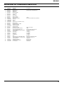
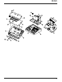
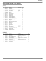
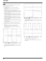
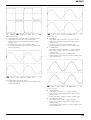
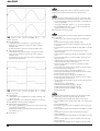
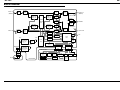
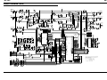
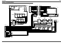
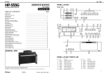
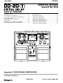
DD-20(T)
Mar.2003
SERVICE NOTES
Issued by RJA
TABLE OF CONTENTS
SPECIFICATIONS.............................................................2
LOCATION OF CONTROLS ..........................................4
LOCATION OF CONTROLS PARTS LIST ...................5
EXPLODED VIEW ............................................................6
EXPLODED VIEW PARTS LIST .....................................9
PARTS LIST......................................................................10
CHECKING THE VERSION NUMBER.......................14
RESTORING THE FACTORY SETTINGS...................14
TEST MODE.....................................................................14
BLOCK DIAGRAM.........................................................22
CIRCUIT BOARD (JK-A) ...............................................24
CIRCUIT BOARD (JK-B) ................................................25
CIRCUIT BOARD (PANEL-A)......................................26
CIRCUIT BOARD (PANEL-B).......................................27
CIRCUIT DIAGRAM (JACK) ........................................28
CIRCUIT DIAGRAM(PANEL)......................................30
Copyright © 2003 ROLAND CORPORATION
All rights reserved. No part of this publication may be reproduced in any form without the written permission
of ROLAND CORPORATION.
17058152E0
Printed in Japan (0800) (NB)
Mar.2003
SPECIFICATIONS
Connectors
INPUT A (MONO) Jack (1/4 inch phone type)
DD-20: DIGITAL DELAY
Nominal Input Level
•
20 dBu (GUITAR/BASS)
+4 dBu (AMPLIFIER SEND/RETURN)
INPUT B Jack (1/4 inch phone type)
PHONES Jack (stereo 1/4 inch phone type)
CTL PEDAL Jack (1/4 inch phone type)
OUTPUT A (MONO) Jack (1/4 inch phone type)
OUTPUT B Jack (1/4 inch phone type)
AC Adaptor Jack
Input Impedance
Power Supply
1 M[ohm]
Dry battery (R6/LR6 (AA) type) x 6: DC 9V
Nominal Output Level
•
20 dBu (GUITAR/BASS)
+4 dBu (AMPLIFIER SEND/RETURN)
AC Adaptor (DC 9V)
Current Draw
200 mA (9 V max.)
*
Expected battery life under continuous use:
Output Impedance
Carbon:
2 hours
1 k[ohm] (OUTPUT A (MONO), B)
Alkaline:
7 hours
33 [ohm] (PHONES)
These figures will vary depending on the actual conditions of use.
Recommended Load Impedance
Dimensions
10 k[ohm]
173 (W) x 158 (D) x 57 (H) mm
Residual Noise Level
•
93 dBu or less (IHF-A typ.)
*
E. LEVEL/F. BACK/TONE knobs are set to the center position
6-13/16 (W) x 6-1/4 (D) x 2-1/4 (H) inches
Weight
1.2 kg / 2 lbs 11 oz (including batteries)
Display
Accessories
Custom LCD (with backlit)
Owner’s Manual JAPANESE:(#G6017365)
Controls
Dry battery (LR6 (AA) type) x 6(#********)
ENGLISH:(#G6017366)
ON/OFF Pedal
MEMORY/TAP Pedal
DELAY TIME Knob
E.LEVEL Knob
F. BACK Knob
TONE Knob
MODE Knob
TAP Button
TEMPO Button
MEMORY WRITE Button
MEMORY SELECT Button
Indicators
POWER Indicator
(serves also as battery check indicator)
ON/OFF Indicator
MEMORY Indicator
TAP Indicator
MANUAL Indicator
MEMORY Number Indicator 1-4
TEMPO Indicator
2
*
We recommend that alkaline batteries be used when replacing the batteries.
Options
AC Adaptor (PSA-series)
*
0 dBu = 0.775 Vrms
*
In the interest of product improvement, the specifications and/or appearance of
this unit are subject to change without prior notice.
DD-20(T)
3
Mar.2003
LOCATION OF CONTROLS
fig.panel-p
L
16
M
21
22
17 N
18 19 20
2
H
6
7
3
B
4
1
C
A
D
5
I
J
15
E
9
F
G
10
K
D
11
13
4
14
8
12
DD-20(T)
LOCATION OF CONTROLS PARTS LIST
No.
1
2
3
4
5
6
7
8
9
10
11
12
13
14
15
16
17
18
19
20
21
22
A
B
C
D
E
F
G
H
I
J
K
L
M
N
Part Code
G2477122
H5029855
G2567155
G2477130
G2497001
G2567156
G2217180
G2217181
H5029851
G2357116
H5029852
75E041R000
75E041L000
75E041C000
G247751301
G2217182
G2537731
G2017621
75D422E000
G2357118
40123545
40016467
03231912
F3279802
F5029106
1502928100
F5029133
F3129306
F5029126
F5029414
F3279819
F3279803
13129778
F3449707
13449150MF
F344941501
Part Name
R-KNOB
SCREW M4X8
ENC ESC
ENC KNOB
KEYTOP S(RED)
LCD PANEL
PANEL
LED PANEL
PEDAL SHAFT
PEDAL PLATE
SCREW 4M3 FEBZC
PEDAL R
PEDAL L
CASE
VGA KEYTOP S WITHOUT LENS
REAR PANEL
QUICK MANUAL LABEL
BATTERY COVER
BOTTOM COVER
BOTTOM FOOT
JACK NUT 9X11X2
JACK WASHER M9.2X14X0.5
ROTARY ENCODER W/SW
POTENTIOMETERNO CLICK 50KB
LED (GREEN)
LED (RED)
LED (BLUE)
SWITCH
POWER LED
LCD
ROTARY POT. W/CENTER CLICK
POTENTIOMETER 11 CLICKS 50KB
TACT SWITCH
PHONE JK(STREO)
PHONE JACK (STEREO)
ADAPTOR JK
Description
HEXAGON BUTTON HEAD NI
62X53
HEXAGON SOCKET BUTTON HEAD
HLJ0999-01-240 NI
FENI
R-ENCODER EVQB1SZ1720B
RD901-40-125F-B54-00D
L-32GDSL
L-34HDSL
L-934MBD
SKQKAB
L-113GDT
DC-320 A
RD901-40-125F-B54-0CD 50KB
RD901-40-125F-B54-11D
SKQKAH
HTJ-064-12DS
HTJ-064-12D
KM02009BB
5
Mar.2003
EXPLODED VIEW
FIG.EXPLO2
11
12
a
17
18
10
a
14
13
j
15
16
18
11
6
DD-20(T)
BG223
b
21
27
k
c
20
m
44
29
n
43
33
28
23
32
32
22
30
24
31
b
45
45
26
1
1
f
e
25
7
Mar.2003
fig.explo3
7
6
h
8 RIGHT SIDE
9 LEFT SIDE
2
g
1
5
i
4
8
3
DD-20(T)
EXPLODED VIEW PARTS LIST
[PARTS]
No.
1
2
3
4
5
6
7
8
9
10
11
12
13
14
15
16
17
18
20
21
22
23
24
25
26
27
28
29
30
31
32
33
43
44
45
Part Code
75E041C000
G2357111
H5029851
2215770201
2217710900
G2357116
G2357115
75E041R000
75E041L000
G2017148
G2357118
G2017621
G2017620
G2177308
G2177309
G2177307
G2257130
G2537731
G2477130
G2477122
G2567155
G2257129
G2217180
G2217182
G2217181
G2567156
G2197127
F5029414
G224780201
F5029410
G247751301
G2497001
G2147807
75E041M000
75E041P000
Part Name
CASE
CUSHION R
PEDAL SHAFT
PEDAL GUIDE BUSH
COIL SPRING
PEDAL PLATE
PEDAL FOOT
PEDAL R
PEDAL L
BOTTOM COVER
BOTTOM FOOT
BATTERY COVER
BATTERY CASE
BATTERY TERMINAL(+)
BATTERY TERMINAL(-)
BATTERY TERMINAL(+-)
BATTERY INSULATING SHEET
QUICK MANUAL LABEL
ENC KNOB
R-KNOB
ENC ESC
INSULATING SHEET CENTER
PANEL
REAR PANEL
LED PANEL
LCD PANEL
JACK SPACER
LCD
DIFFUSION SHEET
LCD BACKLIT
VGA KEYTOP S WITHOUT LENS
KEYTOP S(RED)
JACK HOLDER
JACK BOARD ASSY
PANEL BOARD ASSY
Description
215-702
217-109
62X53
M8
DC-320 A
43.3X23.6
Q’ty
1
2
2
2
2
2
2
1
1
1
2
1
1
1
1
1
1
1
1
4
1
1
1
1
1
1
1
1
1
1
3
1
1
1
1
[SCREWS]
No.
a
b
c
e
f
g
h
I
j
k
m
n
Part Code
H5029115
H5019110
H5029855
40016467
40123545
H5029852
H5039413
H5039413
H5019430
H5039521
H5039521
H5039127
Part Name
SCREW 3X8
SCREW M3X6
SCREW M4X8
JACK WASHER M9.2X14X0.5
JACK NUT 9X11X2
SCREW 4M3 FEBZC
NYLON WASHER M4.1X7.5X0.5
NYLON WASHER M4.1X7.5X0.5
SCREW M2.6X5
VR ACCESSORY NUT M7
VR ACCESSORY NUT M7
VR WASHER M7
Description
PAN TATITE FEBZC
PAN TAPTITE FEZC
HEXAGON BUTTON HEAD NI
FENI
HLJ0999-01-240 NI
HEXAGON SOCKET BUTTON HEAD
BLACK
BLACK
BINDING HEAD TAPTITE P FEZC
Q’ty
7
13
4
6
6
2
2
2
2
4
1
1
9
Mar.2003
PARTS LIST
fig.part1e
SAFETY PRECAUTIONS:
The parts marked
have
safety-related characteristics. Use
only listed parts for replacement.
CONSIDERATION ON PARTS ORDRING
When ordering any parts listed in the parts list, please specify the following items in the order sheet.
QTY
PART NUMBER
DESCRIPTION
MODEL NUMBER
Ex.
10
22575241
Sharp Key
C-20/50
15
2247017300
Knob (orange)
DAC-15D
Failure to completely fill the above items with correct number and description will result in delayed or even
undelivered replacement.
NOTE: The parts marked # are new. (initial parts)
Q’ty
2
1
1
1
2
1
1
1
1
1
2
1
CASING
#
#
#
#
#
#
G2357116
G2017620
G2017621
75D422E000
G2357118
75E041C000
G2217181
G2217180
75E041L000
75E041R000
H5029851
G2217182
KNOB,BUTTON
#
G2567155
#
G2477130
#
G2497001
#
G2567156
G2477122
G247751301
PEDAL PLATE
BATTERY CASE
BATTERY COVER
BOTTOM COVER
BOTTOM FOOT
CASE
LED PANEL
PANEL
PEDAL L
PEDAL R
PEDAL SHAFT
REAR PANEL
62X53
ENC ESC
ENC KNOB
KEYTOP S(RED)
LCD PANEL
R-KNOB
VGA KEYTOP S WITHOUT LENS
1
1
1
1
4
3
SWITCH
13129778
F3129306
SKQKAH
SKQKAB
TACT SWITCH
SWITCH
SW6,SW1 on panel
SW2,SW3,SW4,SW5 on panel
2
4
JACK,EXT TERMINAL
#
F3449707
13449150MF
#
F344941501
HTJ-064-12DS
HTJ-064-12D
KM02009BB
PHONE JK(STREO)
PHONE JACK (STEREO)
ADAPTOR JK
JK1,JK2 on Jack
JK3,JK4,JK5,JK8 on Jack
JK6 on Jack
2
4
1
DISPLAY UNIT
F5029410
#
F5029414
43.3X23.6
DC-320 A
LCD BACKLIT
LCD
LCD1 on panel
1
1
PWB ASSY
#
75E041M000
#
75E041P000
JACK BOARD ASSY
PANEL BOARD ASSY
IC
#
#
#
#
#
#
#
#
#
10
F5199108
F5179307
F5209130
15289216
F5279308
03232367
03236601
F5289102
F5179604
02565501
F5179125
01679990
F5279305
F5179171
15189250
NJM2374AM-TE1
M12L6416-7T
M51957BFP
M5218AFP-600E
BU2090F
DRIVER BU9728AKV-E2
UPD703105AGJ-019-UEN DD-20 1.
NJM2100M 8P SOP
CAT24WC02J
TC220CCA0AF-B01(MR3)
S-8520E33MC-BJS-T2
AK4524VF-E2
TC4066BFT
TC7S14FU-TE85L
M5218AL
1
1
IC (SWITING REGULATOR)
IC (SDRAM)
IC (RESET)
IC (OP AMP)
IC (LED DRIVER)
IC (LCD DRIVER)
IC (CPU)
IC (OP.AMP)
IC (EEPROM)
IC (DSP)
IC (DC-DC)
IC (AD/DA)
IC
IC
IC (OP AMP)
IC11 on Jack
IC16 on Jack
IC7 on Jack
IC1,IC4,IC5 on Jack
IC1on panel
IC2 on panel
IC8 on Jack
IC3 on Jack
IC10 on Jack
IC9 on Jack
IC12 on Jack
IC6 on Jack
IC18 on Jack
IC15 on Jack
IC13 on Jack
1
1
1
3
1
1
1
1
1
1
1
1
1
1
1
DD-20(T)
TRANSISTOR
15319107
15329521
#
F5329536
15329103
F5329530
#
F5119901
DIODE
#
#
2SC4116-GR(TE85R)
RN1307(TE85R)
CPH6302
2SK880GR-TE85R
2SK879Y
RN1207-TE85R
TRANSISTOR
TRANSISTOR
POWER MOS FET
FET TRANSISTOR
FET
DIGITAL TRANSISTOR
Q9,Q10,Q11,Q12,Q13,Q14,Q15 on Jack
Q7 on Jack
Q17 on Jack
Q1,Q5 on Jack
Q2,Q3,Q4,Q6,Q8 on Jack
Q1 on panel
7
1
1
2
5
1
15019523CH
15019126
F5029126
1502928100
RD 5.1EB3
1SS133 T-77
L-113GDT
L-34HDSL
ZENNER DIODE
SWITCHING DIODE
POWER LED
LED (RED)
1
6
1
7
F5029106
F5029133
15339120
F5339138
F5339137
F5029129
L-32GDSL
L-934MBD
1SS302
1SS355
SS14 VF=0.45V
SML-110MT
LED (GREEN)
LED
DIODE
DIODE
DIODE
CHIP LED(GREEN)
D1 on panel
D2,D3,D4,D5,D6,D7 on panel
LED1 on panel
LED10,LED11,LED12,LED14,LED15,LED16,LED
17 on panel
LED9 on panel
LED6 on panel
DA1,DA2,DA3,DA4,DA5,DA6,DA7 on Jack
D1,D2,D3,D4,D5,D6 on Jack
D7,D9,D10 on Jack
LED2,LED3,LED4,LED5 on panel
F5419707
F5419764
CRN34101J
CRN34470J
RESISTOR ARRAY
RESISTOR ARRAY
4
9
F5419714
F5429366
F5419716
F5419726
F2569127
00566867
00567023
00567156
EXBA10P103J
15K OHM F RANK (1%)
CRN34103J
CRN34473J
MINISMDC075
RPC05T 100 J
RPC05T 101 J
RPC05T 102 J
RESISTOR ARRAY
RESISTOR (CHIP)
RESISTOR (CHIP)
RESISTOR ARRAY
POLY SWITCH
MTL.FILM RESISTOR
MTL.FILM RESISTOR
MTL.FILM RESISTOR
00567289
RPC05T 103 J
MTL.FILM RESISTOR
00567412
RPC05T 104 J
MTL.FILM RESISTOR
00567556
RPC05T 105 J
MTL.FILM RESISTOR
00567290
00567334
00567367
00566967
RPC05T 123 J
RPC05T 273 J
RPC05T 393 J
RPC05T 470 J
MTL.FILM RESISTOR
MTL.FILM RESISTOR
MTL.FILM RESISTOR
MTL.FILM RESISTOR
00567245
00567378
RPC05T 472 J
RPC05T 473 J
MTL.FILM RESISTOR
MTL.FILM RESISTOR
00567278
F5399950
F5399908
F5429392
01788301
01897556
01788312
01897578
F5399296
00567112
00567501
RPC05T 822 J
R-33_1/2W
1 J (3225TYPE)
287K F (1608TYPE)
RD16ST26A 102 J
RD16ST26A 221 J
RD16ST26A 222 J
RD16ST26A 331 J
R-603/4R7
RPC05T 471 J
RPC05T 474 J
MTL.FILM RESISTOR
CHIP RESISTOR(1/2W)
CHIP RESISTOR
CHIP RESISTOR
CARBON RESISTOR
CARBON RESISTOR
CARBON RESISTOR
CARBON RESISTOR
MTL.FILM RESISTOR
CHIP RESISTOR
CHIP RESISTOR
RA9,RA12,RA15,RA16 on Jack
RA3,RA5,RA6,RA7,RA8,RA10,RA11,RA13,RA17
on Jack
RA2,RA4 on Jack
R86 on Jack
RA14,RA18,RA20 on Jack
RA1 on Jack
R76 on Jack
R126 on Jack
R73,R145,R146 on Jack
R7,R31,R51,R70,R74,R78,R90,R120,R129 on Jack
R12,R13,R14,R15 on panel
R3,R8,R13,R15,R18,R23,R26,R29,R32,R34,R37,
R42,R71,R72,R83,R101,R102,R119,R130,R157,
R160,R163,R166 on Jack
R10,R11,R22,R36,R50,R55,R56,R57,R58,R59,R108,
R115,R117,R127,R154,R156 on Jack
R4,R9,R16,R17,R25,R27,R33,R45,R46,R60,R61,
R62,R63,R64,R88 on Jack
R161,R162 on Jack
R82 on Jack
R12,R14,R30,R43 on Jack
R75,R92,R93,R95,R137,R138,R139,R140,R141,
R142 on Jack
R48,R49,R79,R80,R85,R153,R155 on Jack
R1,R2,R5,R6,R19,R20,R21,R28,R35,R40,R41,R44,
R47,R65,R66,R67,R68,R69,R103,R104,R105,R106,
R110,R111,R112,R113,R118,R124,R136,R159 on
Jack
R24,R38,R39,R52 on Jack
R109,R116 on Jack
R77 on Jack
R81 on Jack
R5,R6,R11,R17,R18,R19,R20 on panel
R7 on panel
R3 on panel
R4 on panel
R53 on Jack
R1,R2 on panel
R16 on panel
RD901-40-125F-B54-0CD 50KB
RD901-40-125F-B54-00D
RD901-40-125F-B54-11D
ROTARY POT. W/CENTER CLICK
POTENTIOMETERNO CLICK 50KB
POTENTIOMETER 11 CLICKS 50KB
1
1
7
6
3
4
RESISTOR
#
#
#
#
#
POTENTIOMETER
F3279819
F3279802
F3279803
VR2 on panel
VR3,VR4 on panel
VR1 on panel
2
1
3
1
1
1
3
9
23
16
15
2
1
4
10
7
30
4
2
1
1
7
1
1
1
1
2
1
1
2
1
CAPACITOR
#
#
13639581M0
10/35V
ELECTROLYTIC CAPACITOR (7MM)
F5239252
F5349400
F5359332
F5359354
47/50V
B0805F105ZNT
C-603/105P
C-603/334P
ELECTROLYTIC CAPACITOR (7MM)
CHIP CAPACITOR (2012TYPE)
CHIP CAPACITOR
CHIP CAPACITOR
C4,C6,C8,C12,C13,C18,C20,C28,
C34,C58,C59,C82
C79,C80 on Jack
C108,C33 on Jack
C170 on Jack
C40,C41,C42,C43,C44 on Jack
14
2
2
1
5
11
Mar.2003
CAPACITOR
15359701
#
#
CERAMIC CAPACITOR ECUV1H104ZF
CHIP CAPACITOR
00239601
13629624S0
02891767
0.1U/50V
6SC10M+T (OS) 6.3V10
RC2-16V100M-T2
POLYEST CAPACITOR
CHEMICAL CAPACITOR
CHEMICAL CAPACITOR
02891745
RC2-16V101M-T2
CHEMICAL CAPACITOR
02897889
02782723
02129534
RC2-16V470M-T2
RC2-50V010M-T2
ECJ1VB1H102K
CHEMICAL CAPACITOR
CHEMICAL CAPACITOR
CERAMIC CAPACITOR
01674612
ECJ1VB1H103K
CERAMIC CAPACITOR
F5359816
01674334
01674356
01674201
01674212
01674234
01674423
15359612
C-603/683P
ECUV1H101JCV
ECUV1H151JCV
ECUV1H180JCV
ECUV1H220JCV
ECUV1H330JCV
ECUV1H471JCV
ECUV1H100DN
CERAMIC CAPACITOR
CERAMIC CAPACITOR
CERAMIC CAPACITOR
CERAMIC CAPACITOR
CERAMIC CAPACITOR
CERAMIC CAPACITOR
CERAMIC CAPACITOR
CERAMIC CAPACITOR
13519452
DD-306-959F104Z25
CERAMIC CAPACITOR
C23,C27,C46,C47,C48,C49,C50,
C52,C54,C55,C56,C57,C60,C74,
C76,C78,C84,C96,C97,C103,C134,
C136,C140,C141,C142,C143,C144,
C147,C149,C154,C155,C156,C157,
C158,C159,C160,C161,C162,C163,
C180,C181 on Jack, C1 on panel
C2,C16 on Jack
C5 on Jack
C26,C31,C35,C75,C135,C145 on
Jack, C3 on panel
C45,C61,C83,C95,C98,C100,C106,
C112,C139,C164 on Jack
C148 on Jack
C137 on Jack
C21,C22,C114,C119,C131 on Jack,
C4 on panel
C150,C152,C165,C166,C167,C168
on Jack
C77 on Jack
C3,C17 on Jack
C86,C104,C110 on Jack
C92 on Jack
C91 on Jack
C1,C10,C15,C30 on Jack
C11,C32 on Jack
C51,C101,C102,C107,C113,C120,
C130,C151,C153 on Jack
C2 on panel
42
2
1
7
10
1
1
6
6
1
2
3
1
1
4
2
9
1
INDUCTOR,COIL,FILTER
F2449214
#
F5409134
#
F5409102
#
F5409133
F5409114
F2449209
SLF12555T-681MR43 680UH
BLM18BD152SD1
N1608Z601T02
QT1608RL600HC1A
NFM4516P13C204F
SLF7032T-151MR29-2(150UH)
SMD COIL
FERRITE-BEAD
FERRITE-BEAD
FERRITE-BEAD
EMI FILTER
COIL
L2 on Jack
L16,L17 on Jack
L1,L4,L8,L9,L12,L13,L18,L21,L24,L25 on Jack
L19,L20,L22 on Jack
C62 on Jack
L3,L5 on Jack
1
2
10
3
1
2
CRYSTAL,RESONATOR
F5299307
F5299114
HC-49SM 11.2896MHZ
HC-49SM 5MHZ
CRYSTAL
CRYSTAL
X2 on Jack
X3 on Jack
1
1
ENCODER
#
R-ENCODER EVQB1SZ1720B
ROTARY ENCODER W/SW
ENC_on panel
1
CONNECTOR
F3439160
F3439161
#
F3439197
53015-0210 2P P=2MM
A2001WR2-16P P=2MM
A2541WV2-2AX12P
CONNECTOR
CONNECTOR
SOCET
CN3 on Jack
CN2,CN1 on Jack
CN3,CN4 on panel
1
2
2
WIRING,CABLE
G3477154
G3489223
G3487163
FLAT CABLE
WIRING 16P
WIRING BATTERY
3P P=2MM
16P
L=80MM 2P
CN4,CN5 on Jack
CN1,CN2 on panel
2
2
1
03231912
SCREWS
#
H5029115
H5019110
40123545
H5029852
H5029855
40016467
H5039413
H5019430
G2197127
G2147807
H5039414
H5039521
H5039127
SCREW 3X8
SCREW M3X6
JACK NUT 9X11X2
SCREW 4M3 FEBZC
SCREW M4X8
JACK WASHER M9.2X14X0.5
NYLON WASHER M4.1X7.5X0.5
SCREW M2.6X5
JACK SPACER
JACK HOLDER
NYLON WASHER M7.5X4.1X0.5
VR ACCESSORY NUT M7
VR WASHER M7
H2679505
G2607110
G2607212
POLYETHYLENE BAG
PACKIN CASE UPPER
PACKING CASE LOWER
PAN TATITE FEBZC
PAN TAPTITE FEZC
HLJ0999-01-240 NI
HEXAGON SOCKET BUTTON HEAD
HEXAGON BUTTON HEAD NI
FENI
BLACK
BINDING HEAD TAPTITE P FEZC
BLACK
7
13
6
2
4
6
4
2
1
1
2
5
1
PACKING
#
12
220X340X0.03
1
1
1
DD-20(T)
PACKING
G2237613
G2237614
REAR PAD
SIDE PAD
MISCELLANEOUS
G2357115
H2369450
2217710900
2215770201
G2257130
G2177308
G2177307
G2177309
G2357111
G2257129
G2197126
#
H2369429
#
G2537731
#
G224780201
PEDAL FOOT
LED SPACER
COIL SPRING
PEDAL GUIDE BUSH
BATTERY INSULATING SHEET
BATTERY TERMINAL(+)
BATTERY TERMINAL(+-)
BATTERY TERMINAL(-)
CUSHION R
INSULATING SHEET CENTER
LED GUIDE
LED SPACER 3-9
QUICK MANUAL LABEL
DIFFUSION SHEET
ACCESSORIES (Standard)
G601730301
#
G6017365
#
G6017366
#
********
IMPORTANT NOTES
OWNER’S MANUAL
OWNER’S MANUAL
ALKALINE BATTERY GP15A
1
1
M8
H=8MM
217-109
215-702
LED6
JAPANESE/ENGLISH
JAPANESE
ENGLISH
a pair of batteries
2
5
2
2
1
1
1
1
2
1
1
1
1
1
1
1
1
3
13
Mar.2003
CHECKING THE VERSION
NUMBER
1.
Turn all volume controls completely to the left.
2.
While holding down the left pedal’s ON/OFF and the right pedal’s TAP/
MEMORY, connect the AC ADAPTOR to the ADAPTOR jack (which
turns on the power).
3.
Only the POWER LED lights up.
4.
Release the left and right pedals.
5.
Within four seconds, press the left pedal and the right pedal, in that
order.
6.
The unit switches to Test mode, and all of the LEDs light up or flash.
7.
The version number will be shown in the LCD.
In “2,” if no AC ADAPTOR is connected to the ADAPTOR jack, the power can
be turned on by inserting batteries in the unit and connecting the INPUT
A(MONO) plug.
TEST MODE
Test Items
1.
DSP, EEPROM Check (also used to indicate the version)
2.
LCD, Switch, LED Checks, Foot Switch Operational Check
3.
VR, Encoder Check
4.
DAC, PHONES Check (includes OUTPUT A (MONO), B jack detection
check)
5.
ANALOG BYPASS Check (includes INPUT B jack detection check)
6.
MUTE Check
7.
DSP THRU Check
8.
AD MUTE Check
9.
ANALOG BYPASS Check
10. DSP MUTE Check
11. INPUT Level Switch Check
12. SDRAM Check
13. MODE Volume Operational Check
RESTORING THE FACTORY
SETTINGS
Carrying out the following procedure completely clears the content currently
stored in the memories (1-4).
1.
2.
Switch off the power.
While holding down the WRITE button, switch on the power.
The MEMORY Number indicators (1-4) flash.
fig.50
14. Factory Reset
15. Residual Noise, Shock Noise Check
16. Battery Operation Check
Tools Required
•
Oscillator
•
Parallel box (BOSS J-5)
•
Oscilloscope
•
Noise meter
•
47 k[ohm] short plug (#17048536) Please refer to the following figure.
•
Stereo/monaural converter cable (PCS-31 or similar)
•
FS-5U (BOSS) (2)
•
AC ADAPTOR (PSA-100)
fig.plug
3.
Press the WRITE button.
After the MEMORY Number indicators (1-4) begin flashing rapidly, the setting
is stored in memory and the unit returns to its ordinary state.
To cancel the setting change and the unit returns to its ordinary state, then
before you press the WRITE button, operate the MEMORY/TAP or ON/OFF
pedal.
14
DD-20(T)
Entering Test Mode
Detailed Test Items
1.
1.
Connect standard audio (mono) cables to all of the INPUT A(MONO)
and B jacks and OUTPUT A(MONO) and B jacks, and connect a stereo/
monaural converter cable (PCS-31 or similar) to the CTL jack. Connect the
other ends to the two FS-5U foot switches, and set the “POLARITY”
switch on the FS-5Us towards the FS-5U jacks.
2.
Turn all volume controls completely to the left (to minimum).
3.
While holding down the left pedal’s ON/OFF and the right pedal’s TAP/
MEMORY, connect the +9V DC plug to the ADAPTOR jack (which turns
on the power).
DSP, EEPROM Check (also used to indicate the version)
•
Enter Test mode.
•
After the unit is switched to Test mode, the version number
automatically appears in the LCD as a four-digit number, while
simultaneously the DSP and EEPROM check is performed.
•
Confirm that all of the LEDs are lit, indicating that no problem was
detected.
If there is a problem, the cause is indicated by the LEDs as described below.
ON/OFF flashing:EEPROM error
MEMORY flashing:DSP PRAM error
4.
Only the POWER LED lights up.
5.
Release the left and right pedals.
MEMORY, TAP flashing:DSP ERAM error
6.
Within four seconds, press the left pedal and the right pedal, in that
order.
ON/OFF, MEMORY flashing:DSP INT error
7.
The unit switches to Test mode, and all of the LEDs light up or flash.
2.
TAP flashing:
IRAM error
ON/OFF, TAP flashing:DSP DRQ error
LCD, Switch, LED Checks, Foot Switch Operational Check
Press the [TAP] switch. Confirm that the LCD’s “8.8.8.8” lights up and go off in
the sequence shown below.
In “2”, if no +9V DC plug is connected to the ADAPTOR jack, the power can
be turned on by inserting batteries in the unit and connecting the INPUT
A(MONO) plug.
The “DSP, EEPROM Check” commences automatically with entry into Test
mode.
The status of the LEDs differs when entering into Test mode. For more detailed
information, refer to the item “DSP, EEPROM Check.”
The unit cannot enter Test mode unless all of the volume controls are turned to
minimum (MODE: “SOS”).
To conduct only a specific test, after entering Test mode, switch the MODE
volume control to the setting corresponding to the desired test.
Although carrying out the procedure in “1” switches the unit to Test mode, “2.
LCD, Switch, LED Checks, Foot Switch Operational Check” cannot be run
alone.
15
Mar.2003
fig.1
If the LCD display does not change even after the [TAP] switch is pressed,
confirm that all of the cables are connected to the jacks and the FS-5U
“POLARITY” switches are set correctly as described in “1” in “Entering Test
Mode.”
16
DD-20(T)
•
Press the [TEMPO] switch. Confirm that the characters light up and go
off in the sequence shown below.
fig.2
•
Press the [WRITE] switch. Confirm that the notes light up and go off in
the sequence shown below.
fig.3
•
Press the [SELECT] switch. Confirm that the entire LCD is on and that all
of the LEDs are lit.
•
Confirm that the LEDs go off in the following sequence, one each time
the [SELECT] switch is pressed: “LCD backlighting” “4,” “3,” “2,” “1,”
“MANUAL,” “TEMPO,” “MEMORY,” “TAP,” and “ON/OFF.” When
“ON/OFF” goes off (all LEDs all unlit), press the [SELECT] switch to
turn on all of the LEDs again.
•
Press the FS-5U connected to the left channel of the stereo/monaural
converter cable (PCS-31 or similar). Confirm that “C 1” appears in the
display.
•
Press the FS-5U connected to the tight channel of the stereo/monaural
converter cable (PCS-31 or similar). Confirm that “C 12” appears in the
display.
17
Mar.2003
fig.5
Nothing will appear in the display if the right channel’s FS-5U is pressed
before the one connected to the left channel.
3.
VR, Encoder Check
•
Set the MODE control to “TWIST.” “2” appears in the LCD.
•
Input a sine wave (200 Hz, 16Vp-p) from the oscillator to INPUT
A(MONO) and B.
•
Connect the oscilloscope to OUTPUT A(MONO) and B.
•
Rotate the E.LEVEL volume from the far left (minimum) to far right
(maximum). Confirm that the LCD changes from “O” to “127” and that
the waveform output from OUTPUT A(MONO) and B changes from
minimum to maximum size.
•
Rotate the F.BACK volume from the far left (minimum) to far right
(maximum). Confirm that the LCD changes from “O” to “127” and that
the waveform output from OUTPUT A(MONO) and B changes from
minimum to maximum size.
•
Rotate the TONE volume from the far left (minimum) to far right
(maximum). Confirm that the LCD changes from “O” to “127” and that
the waveform output from OUTPUT A(MONO) and B changes from
minimum to maximum size.
•
Rotate ENC at least two clicks from the far right position. Confirm that
“E-” appears in the LCD.
•
Rotate ENC at least two clicks from the far left position. Confirm that “E-” appears in the LCD.
•
Press the ENC switch. Confirm that “E-O-” appears in the LCD.
4.
(200 mV/DIV, 1 mS/DIV)
•
Connect the oscilloscope to OUTPUT A(MONO), and disconnect the
cable from the OUTPUT B jack.
•
Confirm that the waveform output from OUTPUT A matches the figure
below.
fig.6
DAC, PHONES Check (includes OUTPUT A (MONO), B jack detection
check)
•
Set the MODE control to “WARP.” “3” appears in the LCD.
•
Connect the oscilloscope to OUTPUT A(MONO) and B.
•
Confirm that the waveform output from OUTPUT A(MONO) and B
matches the figure below.
fig.4
(200 mV/DIV, 1 mS/DIV)
(200 mV/DIV, 1 mS/DIV)
•
Disconnect the cable from the OUTPUT A(MONO) jack, leaving the
oscilloscope connected only to OUTPUT B.
•
Confirm that the waveform output from OUTPUT B matches the figure
below.
18
•
Connect the cables to the OUTPUT A(MONO) and B jacks.
•
Connect the oscilloscope to PHONES L/R.
•
Confirm that the waveform output from PHONES L/R matches the
figure below.
DD-20(T)
fig.7
fig.9
(200 mV/DIV, 1 mS/DIV)
(5V/DIV, 1 mS/DIV)
5.
6.
ANALOG BYPASS Check (includes INPUT B jack detection check)
MUTE Check
•
Set the MODE control to “TAPE.” “4” appears in the LCD.
•
Set the MODE control to “ANALOG.” “5” appears in the LCD.
•
Input a sine wave (200 Hz, 16Vp-p) from the oscillator to INPUT
A(MONO) and B.
•
Input a sine wave (200 Hz, 16Vp-p) from the oscillator to INPUT
A(MONO) and B.
•
Connect the oscilloscope to OUTPUT A(MONO) and B.
•
Connect the oscilloscope to OUTPUT A(MONO) and B.
•
Confirm that the waveform output from OUTPUT A(MONO) and B
matches the figure below.
•
Confirm that nothing is output from OUTPUT A(MONO) and B.
fig.8
7.
DSP THRU Check
•
Set the MODE control to “STANDARD.” “6” appears in the LCD.
•
Input a sine wave (200 Hz, 16Vp-p) from the oscillator to INPUT
A(MONO) and B.
•
Connect the oscilloscope to OUTPUT A(MONO) and B.
•
Confirm that the waveform output from OUTPUT A(MONO) and B
matches the figure below.
fig.10
(5V/DIV, 1 mS/DIV)
Disconnect the cable from the OUTPUT B jack.
•
Confirm that the waveform output from OUTPUT A(MONO) and B
matches the figure below.
(5 V/DIV, 1 mS/DIV)
8.
AD MUTE Check
•
Set the MODE control to “DUAL.” “7” appears in the LCD.
•
Input a sine wave (200 Hz, 16Vp-p) from the oscillator to INPUT
A(MONO) and B.
•
Confirm that nothing is output from OUTPUT A(MONO) and B.
9.
ANALOG BYPASS Check
•
Set the MODE control to “PAN.” “8” appears in the LCD.
•
Input a sine wave (200 Hz, 16Vp-p) from the oscillator to INPUT
A(MONO) and B.
•
Confirm that the waveform output from OUTPUT A(MONO) and B
matches the figure below.
19
Mar.2003
fig.11
Executing Factory Reset results in the loss of all data saved by the user. If
Factory Reset is not required, turn off the power to quit Test mode.
Factory Reset may be run without entering Test mode. To run Factory Reset
only, refer to “Instructions for Running Factory Reset” in these service notes.
•
Following the “MODE Volume Operational Check,” rotate MODE from
“SOS” to “STANDARD.”
•
”FAct” appears in the LCD, and the “1,” “2,” “3,” and “4” LEDs flash.
•
Press the [WRITE] button. The “1,” “2,” “3,” and “4” LEDs flash more
rapidly, then return to normal condition.
15. Residual Noise, Shock Noise Check
Conduct the “Residual Noise, Shock Noise Check” with the noise meter set to
IHF-A, AVERAGE.
(5 V/DIV, 1 mS/DIV)
10. DSP MUTE Check
•
Set the MODE control to “SMOOTH.” “9” appears in the LCD.
•
Input a sine wave (200 Hz, 16Vp-p) from the oscillator to INPUT
A(MONO) and B.
•
Confirm that nothing is output from OUTPUT A(MONO) and B.
11. INPUT Level Switch Check
•
Switch to Test mode according to the instructions in “Entering Test
mode.”
•
Connect a 47-kΩ short plug to INPUT A(MONO) and B.
•
Connect the noise meter to OUTPUT A(MONO). Connect an open plug
to OUTPUT B.
•
Confirm that the measured value with the noise meter (IHF-A) is -82 dBu
or less.
•
Connect the noise meter to OUTPUT B. Connect the open plug to
OUTPUT A(MONO).
•
Set the MODE control to “MODULATE.” “10” appears in the LCD.
•
Input a sine wave (200 Hz, 16Vp-p) from the oscillator to INPUT
A(MONO) and B.
•
Confirm that the measured value with the noise meter (IHF-A) is -82 dBu
or less.
•
Confirm that the waveform output from OUTPUT A(MONO) and B is
distorted as in the figure below.
•
Connect a monitor speaker to OUTPUT A(MONO). Connect the open
plug to OUTPUT B.
•
Subject the unit to shock by dropping it from a height of 10 cm, then
confirm that the unit produces no unusual noise.
•
Connect a monitor speaker to OUTPUT B. Connect the open plug to
OUTPUT A(MONO).
•
Shock-test the unit by dropping it from a height of 10 cm, then confirm
that the unit produces no unusual noise.
•
Connect a monitor speaker to the left side of PHONE L/R.
•
Shock-test the unit by dropping it from a height of 10 cm, then confirm
that the unit produces no unusual noise.
•
Connect a monitor speaker to the right side of PHONE L/R.
•
Shock-test the unit by dropping it from a height of 10 cm, then confirm
that the unit produces no unusual noise.
•
Press the pedal’s ON/OFF switch to return from Test mode to the normal
operating mode.
•
Adjust the volume as described below.
E.LEVEL: Maximum (turned completely to the right)
E.LEVEL: Minimum (turned completely to the left)
E.LEVEL: Maximum (turned completely to the right)
MODE: STANDARD
fig.12
(5 V/DIV, 1 mS/DIV)
12. SDRAM Check
•
Set the MODE control to “REVERSE.” If no problem is detected, “Sd 0”
appears in the LCD.
If a problem is detected, the cause is indicated by the LEDs as shown below.
If “+4” appears in the LCD, first turn off the power, then use the procedure
below to turn the power back on, and perform the following test.
•
While holding down the left pedal (ON/OFF), turn on the power.
•
Press the [SELECT] switch a number of times until “out1” appears in the
LCD.
ON/OFF, MEMORY, TAP LEDs flashing: SDRAM error
•
Press the [WRITE] switch.
•
Following the “SDRAM Check,” rotate the knob one click at a time in the
left (counterclockwise) direction.
•
Connect the noise meter to OUTPUT A(MONO). Connect an open plug
to OUTPUT B.
•
Confirm that the numbers appearing in the LCD change one by one with
each click from “10” to “1.”
•
Confirm that the measured value with the noise meter (IHF-A) is -85 dBu
or less.
•
Connect the noise meter to OUTPUT B. Connect the open plug to
OUTPUT A(MONO).
•
Confirm that the measured value with the noise meter (IHF-A) is -85 dBu
or less.
•
Connect a monitor speaker to OUTPUT A(MONO). Connect the open
plug to OUTPUT B.
•
Shock-test the unit by dropping it from a height of 10 cm, then confirm
13. MODE Volume Operational Check
14. Factory Reset
20
DD-20(T)
that the unit produces no unusual noise.
•
Connect a monitor speaker to OUTPUT B. Connect the open plug to
OUTPUT A(MONO).
•
Shock-test the unit by dropping it from a height of 10 cm, then confirm
that the unit produces no unusual noise.
•
Connect a monitor speaker to OUTPUT A(MONO). Connect the open
plug to OUTPUT B.
•
Shock-test the unit by dropping it from a height of 10 cm, then confirm
that the unit produces no unusual noise.
•
Rotate F.BACK from the far left (minimum) to far right (maximum)
several times, and confirm that there is no scratching or other such noise
from the monitor speakers.
•
Set F.BACK to the far left (minimum).
•
Rotate TONE from the far left (minimum) to far right (maximum) several
times, and confirm that there is no scratching or other such noise from
the monitor speakers.
•
Set TONE to the far right (maximum).
•
Rotate E.LEVEL from the far left (minimum) to far right (maximum)
several times, and confirm that there is no scratching or other such noise
from the monitor speakers.
•
Set E.LEVEL to the far right (maximum).
•
Rotate MODE from the “SOS” to “REVERSE” several times, and confirm
that there is no scratching or other such noise from the monitor speakers.
•
Set MODE to “STANDARD.”
•
Rotate ENCODER back and forth from left to right several times, and
confirm that there is no scratching or other such noise from the monitor
speakers.
•
Set the volumes as follows.
E.LEVEL: CENTER
F.BACK: CENTER
TONE: CENTER
MODE: STANDARD
DELAY TIME: 300ms
•
Connect the noise meter to OUTPUT A(MONO). Connect an open plug
to OUTPUT B.
•
Confirm that the measured value with the noise meter (IHF-A) is -93 dBu
or less.
•
Connect the noise meter to OUTPUT B. Connect the open plug to
OUTPUT A(MONO).
•
Confirm that the measured value with the noise meter (IHF-A) is -93 dBu
or less.
16. Battery Operation Check
•
Insert batteries in the battery box, and plug into INPUT A(MONO).
•
Confirm that the unit starts in the normal mode.
•
Confirm that effect sounds are output.
21
DD-20(T)
Mar.2003
BLOCK DIAGRAM
fig.block
INPUT A
(MONO)
BUFFER
Q1
BUFFER
(INV)
IC1B
FET SW
Q2
DE EMPH/
LEVEL CTL
IC5A/IC18D
PRE EMPH/
LEVEL CTL
IC3B/IC18A
CODEC
AD/DA
IC6
INPUT B
BUFFER
Q5
(JK IN/NO INPUT)
MIXER
IC4A
OUTPUT B
(JK IN/NO INPUT)
RESET
IC7
+9V
+23V
RIPPLE
FILTER
Q15
DC-DC
CONVERTER
(STEP DOWN)
IC12,Q17
LOGIC
IC15B,C
EEPROM
IC10
TR
Q7
(JK IN/NO INPUT)
TR
Q9
CTL
CPU
IC8
LOGIC
IC15A
DSP
IC9
SDRAM
IC16
+3.3V
CN3
PHONES
FET SW
Q8
FET SW
Q6
(JK IN/NO INPUT)
BATTERY
BUFFER
IC13A
BUFFER
IC13B
BUFFER
(INV)
IC1A
DC-DC
CONVERTER
(STEP UP)
IC11
(JK IN/NO INPUT)
FET SW
Q3
FET SW
Q4
DE EMPH/
LEVEL CTL
IC5B/IC18C
PRE EMPH/
LEVEL CTL
IC3A/IC18B
OUTPUT A
(MONO)
MIXER
IC4A
+9V
CN2
CN1
16 PIN
16PIN
CN2
CN1
PANEL BOARD
CN4
RIBON
3P
LCD DRIVER
IC2
CN5
DC IN
22
JACK BOARD
CN31,CN41
CN3,CN4
SW1-6
VR
1-4
LCD1
LED DRIVER
IC1
LED6
ENC1
LED1
LED2 - 5
LED9 -12
LED13-17
23
Mar.2003
CIRCUIT BOARD (JK-A)
fig.B-JK-A
24
DD-20(T)
CIRCUIT BOARD (JK-B)
fig.B-JK-B
25
Mar.2003
CIRCUIT BOARD (PANEL-A)
fig.B-PANEL-A
26
DD-20(T)
CIRCUIT BOARD (PANEL-B)
fig.B-PANEL-B
27
DD-20(T)
Mar.2003
CIRCUIT DIAGRAM (JACK)
fig.C-JK
+8.6V
C3
100p
R2
47k
C8
10/35
C118
10/35
R119
10k
R24
8.2k
2
6
5
-
3
R40
47k
C26
10/16
10/16
1
2
IN-B
+
C124
N.I.U
AD
DA
LRCK
MCLK
BCLK
PD
C27
0.1
6
7
8
9
10
11
12
13
LIN
16
ROUT
15
DEMO
DEM1
SDTO
SDTI
LRCK
MCLK
BCLK
PDN
C137
1/50
79
73
64
59
56
49
38
33
24
23
14
7
53015-0210
D +3. 3
R76
miniSMDC075
R78
680uH
1k IC11
8
CD
CS
7
IPK
ES
6
JK6
KM02009BB
VCC
VIN-
C83
100/16
1
2
3
4
GND
CT
Q15
2SC4116GR
3
R79
4.7k
1
+23V
+
+11.5V
2
+
1
L2
D7
SLF12555T-681MR43 SS14
1
2
D +3. 3 D +3. 3
IC5C
+
M5218AFP
R55
100k
2
C78
0.1
C79
47/50
C80
47/50
5
C82
10/35
R85
4.7k
R86
15kF
3
78
32
77
13
10
C100
100/16
C74
0.1
D
C76
D 0.1
C75
10/16
D +3. 3
VDD
PLLVAA
PLLRO
PLLLP
PLLAGS
PLLAGD
VSS
9
8
2
4
2
D
D
DIVS1
DIVS0
D
D
S
G
IC9
TC220C120AF-006
3
VOUT
C97
0.1
C98
100/16
R161
12k
D6
1SS355
3
RESET
5
VCC
D +3. 3
C169
N.I.U.
C170
1.0u
6
R163
10k
D
D
3
A
Q13
C43
2SC4116GR 0.33
A
A
A0
A1
A2
VCC
WP
5
6
D +3. 3
SDA
SCL
Q14
2SC4116GR
IC15A
TC7W14FU
1
7
5
IC15B
TC7W14FU
VSS
LED_DATA
LED_CLK
SW_SCAN0
SW_SCAN1
SW_DATA0
SW_DATA1
SW_DATA2
ENC_SW
8
C149
0.1
4
E.LEVEL
E.TONE
F.BACK
MODE
100
RA12 CRN34101J
1
8
2
7
3
6
4
5
1
8
2
7
3
6
4
5
19
20
21
22
23
24
25
26
29
30
31
32
33
34
35
36
C23
0.1
D
EEPROM
39
40
41
42
43
44
45
46
D
IC15D
D TC7W14FU
SCK1/P45
RXD1/SI1/P44
TXD1/SO1/P43
SCK0/P42
RXD0/SIO/P41
TXD0/SO0/P40
AVDD/AVREF
AVSS
P77/ANI7
P76/ANI6
P75/ANI5
P74/ANI4
P73/ANI3
P72/ANI2
P71/ANI1
P70/ANI0
DRQ3/IP103/P07
DRQ2/IP102/P06
DRQ1/IP101/P05
DRQ0/IP100/P04
TO00/P03
IP001/P02
TIO00/IP000/P01
PWM0/P00
DMAAK3/PBD3
DMAAK2/PBD2
DMAAK1/PBD1
DMAAK0/PBD0
TO01/P13
IP011/P12
TIO10/IP010/P11
PWM1/P10
TC3/IP113/P27
TC2/IP112/P26
TC1/IP111/P25
TC0/IP110/P24
TO02/P23
IP021/P22
TIO20/IP020/P21
NMI/P20
D
C150
0.01
83
84
85
86
INT1
INT0
3.3V_CPU
C152
0.01
1
2
3
4
5
6
7
1
2
3
4
5
6
7
NIU(IL-S-7P-S2T2)
60
C151
Serial_IO_SO
Serial_IO_SI
Serial_IO_SCK
RESET
10p
C153
Vpp
62
2
D
1
R155
4.7k
R156
100k
SCK2/IP132/P32
SI2/IP131/P31
SO2/IP130/P30
RA15 CRN34101J
CN8
D
RXD2/IP120/P34
TXD2/IP133/P33
D
ENC-A1
ENC-A2
100
ENC-B
DRQ0
R145
7
72
73
74
75
76
77
78
79
80
D
RA9
CRN34101J
1
8
2
7
3
6
4
5
D
2 3
X3
CX-49G/5MHz
63
CPU
PDL15/D15
D14/PDL14
D13/PDL13
D12/PDL12
D11/PDL11
D10/PDL10
D9/PDL9
D8/PDL8
D7/PDL7
D6/PDL6
D5/PDL5
D4/PDL4
D3/PDL3
D2/PDL2
D1/PDL1
D0/PDL0
PCM0/WAIT
PCT6/OE
PCT7/BCYST
PCM4/REFRQ
PCM3/HLDRQ
PCM2/HLDAK
PCM1/CLKO/BUSCL
PCT5/WE
PCT4/RD
PCT1/UCS/UW/UDQ
PCT0/LCS/LW/LDQ
PCS7/CS7
PCS6/CS6/RAS6
PCS5/CS5/IORD
PCS4/CS4/RAS4
PCS3/CS3/RAS3
PCS2/CS2/IOWR
PCS1/CS1/RAS1
PCS0/CS0
PCD3/UBE/SDRAS
PCD2/LBE/SDCAS
PCD1/SDCLK
PCD0/SDCKE
114
115
116
117
118
119
120
121
122
123
126
127
128
129
130
131
132
133
136
137
138
139
140
141
142
143
144
1
2
3
4
5
6
7
10
11
12
13
14
15
16
17
91
93
92
87
88
89
90
94
95
96
97
100
101
102
103
104
105
106
107
108
109
110
111
R166
10k
VPP/MODE2
MODE1
MODE0
47
47
R18
10k
L17
BLM18BD152SD1
R116
33(1/2W)
JK3
HTJ-064-12D
L18
N1608Z601T01
A
7
+
R115
100k
C113
10p
A
A
C61
100/16
D15
D14
D13
D12
D11
D10
D9
D8
D7
D6
D5
D4
D3
D2
D1
D0
IC16
M12L64164A-7T
R142
1
2
3
4
1
2
3
4
1
2
3
4
1
2
3
4
1
2
3
4
1
2
3
4
1
2
3
4
1
2
3
4
1
2
3
4
RA13
R95
R93
R92
1
2
3
4
47
8
7
6
5
8
7
6
5
8
7
6
5
A22
A21
A12
A11
A10
A9
A8
A7
A6
A5
A4
A3
A2
A1
A12
A11
A10
A9
A8
A7
A6
A5
A4
A3
A2
A1
A0
8
7
6
5
8
7
6
5
8
7
6
5
8
7
6
5
D15
D14
D13
D12
D11
D10
D9
D8
D7
D6
D5
D4
D3
D2
D1
D0
SDCKE
SDCLK
37
38
UDQM
LDQM
39
15
64M
SDRAM
BA0(A13)
BA1(A12)
A11
A10
A9
A8
A7
A6
A5
A4
A3
A2
A1
A0
CS
RAS
CAS
WE
CKE
CLK
DQMU
DQML
36
D +3. 3
DQ15
DQ14
DQ13
DQ12
DQ11
DQ10
DQ9
DQ8
DQ7
DQ6
DQ5
DQ4
DQ3
DQ2
DQ1
DQ0
VDD
VDD
VDD
VDDQ
VDDQ
VDDQ
VDDQ
NC
53
51
50
48
47
45
44
42
13
11
10
8
7
5
4
2
D15
D14
D13
D12
D11
D10
D9
D8
D7
D6
D5
D4
D3
D2
D1
D0
2
3
4
5
7
8
9
10
2
3
4
5
7
8
9
10
D15
D14
D13
D12
D11
D10
D9
D8
D7
D6
D5
D4
D3
D2
D1
D0
1
RA2
EXBA10P103J
6
1
RA4
EXBA10P103J
6
D +3. 3
L22
1
14
27
3
49
9
43
QT1608RL600HC1A
C141
0.1
VSSQ
VSSQ
VSSQ
VSSQ
VSS
VSS
VSS
NC
40
D +3. 3
R160
10k
RA20
CRN34103J
1
8
2
7
3
6
4
5
RA16
8 CRN34101J
7
6
5
8 WE
7 RD
6 UDQM
5 LDQM
CRN34470J
47
20
21
35
22
34
33
32
31
30
29
26
25
24
23
19
18
17
16
CS3
SDRAS
SDCAS
WE
C142
0.1
C143
0.1
C144
0.1
C145
10/16
12
46
6
52
28
41
54
D
WE
RD
UDQM
LDQM
1
2
3
4
8
7
6
5
RA14
CRN34103J
D +3. 3
CS6
47
47
CS3
IOWR
8
7
6
5
SDRAS
SDCAS
SDCLK
SDCKE
D +3. 3
3.3V_CPU
IOWR R29
CS6 R37
CS3 R34
10k
10k
10k
SDRAS 1
SDCAS 2
SDCLK 3
SDCKE 4
8
7
6
5
RA18
CRN34103J
18
57
58
R157
10k
CVDD
VDD
VDD
VDD
VDD
VDD
VDD
VDD
VDD
VDD
*2:For Lot no.1.00 to 7.00 Lot the pin number for CN1,CN2 which
is printed on JK Board is opposite from that is written from that
is written in the circuit diagram.
CVSS
VSS
VSS
VSS
VSS
VSS
VSS
VSS
VSS
VSS
RESET
134
124
112
98
81
37
47
27
8
CN1(1.00 LOT to 7.00LOT)SILK:1,2,3.......14,15,16
CN1 CIRCUIT:16,15,14.......1,2,3
CN2(1.00 LOT to 7.00LOT)SILK:1,2,3.......14,15,16
CN2 CIRCUIT:16,15,14.......1,2,3
C164
100/16
9
28
48
38
82
99
113
125
135
R23
10k
5
-
L16
BLM18BD152SD1
2
3
1
D
D
RESET
LCD_SCK
LCD_C/D
LCD_SD
C165
0.01
R102
10k
A22
A21
X1
C154
0.1
64
R165
N.I.U
59
C166
0.01
6
PHONES
L20
QT1608RL600HC1A
CKSEL
X2
R137
R138
D
61
D
*2
C167
0.01
A
D[0:15]
D
D
SW_DATA2
SW_DATA1
SW_DATA0
SW_SCAN1
SW_SCAN0
RESET
LCD_SCK
LCD_C/D
LCD_SD
VR_VDD
MODE
F.BACK
E.TONE
E.LEVEL
VR_GND
A
L25
C112
N1608Z601T01 100/16
R111
47k
R101
10k
CRN34470J
CRN34470J
CRN34470J
CRN34470J
CRN34470J
CRN34470J
CRN34470J
RA17
CRN34470J
P52/TO03
P51/IP031
P50/IP030/TI030
PCM5/SELFREF
10p
D +3. 3
C108
1/16
C107
10p
1
1
1
1
1
1
1
1
1
1
1
1
1
1
1
1
RA3
RA5
RA6
RA7
RA8
RA10
RA11
PAH9/A25
PAH8/A24
PAH7/A23
PAH6/A22
PAH5/A21
PAH4/A20
PAH3/A19
PAH2/A18
PAH1/A17
PAH0/A16
PAL15/A15
PAL14/A14
PAL13/A13
PAL12/A12
PAL11/A11
PAL10/A10
PAL9/A9
PAL8/A8
PAL7/A7
PAL6/A6
PAL5/A5
PAL4/A4
PAL3/A3
PAL2/A2
PAL1/A1
PAL0/A0
C140
0.1
ENC-A
ENC-B
D +3. 3
68
69
70
ADTRG/IP123/P37
IP122/P36
IP121/P35
VR_VDD
R153
4.7k
R154
100k
C168
0.01
R110
47k
+8.6V
A
R108
100k
R113
47k
C44
0.33
A22
A21
C92
18p
R146
1
2
3
4
D +3. 3
C139
100/16
R71
10k
C55
LCD_SCK 54
LCD_C/D 55
LCD_SD 56
65
66
67
IC10
CAT24WC02J
D
R159
47k
C91
22p
D
C114
0.001
0.1
2
IC7
M51957BFP
R109
33(1/2W)
M5218AL
C110
150p
R64
1M
8
47
47
47
X2
49US SMD
11.2896MHz
D
7
R162
12k
IN
4
DLY
RST
NC
NC
NC
GND
1
3
8
C106
100/16
1
+
R59
100k
1
1
1
D
D
R72
10k
52
53
71
72
D +3. 3
1
VSS
*2
D +3. 3
R139
R140
R141
8
ON/OFF
D
1
2
3
4
5
6
7
8
9
10
11
12
13
14
15
16
Q12
C42
2SC4116GR 0.33
A
IC8
DD-20 MASK CPU(UPD703105AGJ-019-UEN)
49
50
51
R90
1k
25
42
D +3. 3
D10
SS14
4
IC12
S-8520E33MC-BJS-T2
R164
N.I.U
A
R143
N.I.U
IC15C
TC7W14FU
R73
100
6
1
EXT
2
C84
0.1
2
VR_VDD
C41
0.33
A
R68
47k
R63
1M
1
RA1
CRN34473J
FET_EFX-R
FET_DIR-R
D +3. 3
2
C96
0.1
VIN
1
5
CN2
A2001WR2-16P
R58
100k
R67
47k
R62
1M
1
R88
1M
D
L5
SLF7032T-151MR37-2
5
-
D +3. 3
Serial_IO_SCK
Serial_IO_SI
Serial_IO_SO
6
5
XTI
XTO
RST
DRST
+3.3V
D +3. 3
6
D9
SS14
1
2
3
4
5
6
7
8
9
10
11
12
13
14
15
16
Q11
2SC4116GR
INT1
INT0
DRQ0
VSS
VSS
VSS
VSS
VSS
VSS
VSS
VSS
VSS
VSS
VSS
VSS
VSS
VSS
L3
SLF7032T-151MR37-2
+9V
+9V
AGND
DGND
DGND
DGND
D+3.3V
D+3.3V
ENC-B
DGND
ENC-A
ENC_SW
DGND
LED_CLK
LED_DATA
TEMPO(BLU)
A
D +3. 3
RD
CS6
IOWR
80
71
66
61
54
52
43
31
26
22
12
11
4
2
1
2
3
1
2
3
1
3
R112
47k
+
R136
47k
D7
D6
D5
D4
D3
D2
D1
D0
55
1
3
DIV
OSC
OSCSEL
A
+8.6V
C95
100/16
C40
0.33
D +3. 3
Q17
CPH6302
D
A
41
40
39
76
INT1
INT0
DRQ
SYI
D
C86
150p
A
+
50
51
53
RD
CS
WR
DSP
CTYPE
1
R65
47k
A
R57
100k
R66
47k
R61
1M
1
8
7
6
5
TESTT
TESTS
TESTB
TESTP
PLLBP
CN4
C62
NFM4516P13C204F
R56
100k
R60
1M
+
IC13C
M5218AL
A4
A3
A2
A1
A0
1
2
3
C103
0.1
RIBON 3P
+
-
27
28
29
30
34
35
36
37
CD7
CD6
CD5
CD4
CD3
CD2
CD1
CD0
DA1
AD1
DA2
AD2
DA3
AD3
D
NJM2374AM-TE1
FLAT
CABLE
2mm
3P
+
1
A
44
45
46
47
48
CA4
CA3
CA2
CA1
CA0
BCK
LRCK0
LRCK1
MCK
15
R82 27k 16
17
18
19
C77
20
0.068 21
R80
4.7k
R81
287kF
D
2
JK5
HTJ-064-12D
TP18
TP19
TP20
TP21
TP22
TP23
TP24
TP25
TP26
TP27
TP28
TP29
TP30
TP31
TP32
TP33
DA0
AD0
R75 67
47
68
69
70
74
75
2
1
1
R104
47k
1
2
3
4
CN3
VDD
VDD
VDD
VDD
VDD
VDD
VDD
VDD
VDD
VDD
VDD
VDD
60
62
63
65
LRCK
MCLK
C33
1/16
2
3
1
R129
1k
L24
N1608Z601T01
IC13A
TP1
TP2
3
BCLK
D
RIBON 3P
R103
47k
7
OUTPUT B
N1608Z601T01
L13
L15
N.I.U
D
C130
10p
R106
47k
C104
150p
D
R48
4.7k
R77
1(1W)
R105
47k
C46 0.1
C47 0.1
C48 0.1
C49
0.1
C50 0.1
C52 0.1
C54 0.1
C56
C57 0.1
0.1
C60
0.1
D
57
58
A
L12
N1608Z601T01
IC13B M5218AL
L19
QT1608RL600HC1A
DA
AD
A
DA6
D +3. 31SS302
2
+
A
+
+
A
C102
10p
-
R17
1M
+
C45 100/16
C181
0.1
CN5
-
2
A
D
1
2
3
4
5
6
7
8
9
10
11
12
13
14
15
16
C136
0.1
IC6
AK4552VT
D
R49
4.7k
IC4C
M5218AFP
+
3
1
R47
47k
2
1
3
5
R36
100k
+
IC4B
M5218AFP
D +3. 3
R83
10k
1SS302
2
D
1
2
3
4
5
6
7
8
9
10
11
12
13
14
15
16
+
14
VCOM
C180
0.1
DA3
D +3. 3
5
D5
1SS355
100k
R69
A
47k Q10
2SC4116GR
Q9
2SC4116GR
R74
1k
+
7
IC5B
M5218AFP
D
1
L21
N1608Z601T01
CN1
A2001WR2-16P
OUT-B
D
R51
1k
L4
N1608Z601T01
R45
1M
+
470p
R127
3
L1
N1608Z601T01
C131
0.001
A
R31
1k
+
-
Q8
2SK879Y
2
1
OUT-A
3
1
R44
47k
2
3
1
2
1
R52
8.2k
6
AD/DA
LOUT
A
D +3. 3
R130
10k
6
2
RIN
2
JK8
HTJ-064-12D
C35
IC3A
NJM2100M
R35
47k
CTL PEDAL
-
C129
10/35
A
1
IN-A
D +3. 3
9
R30
39k
C32
D
10/16
R50
100k
2
C148
47/16
1
D
C20
10/35
1
C30
33p
C147
0.1
JK4
HTJ-064-12D
D
R21
47k
3
R38
8.2k
C31
C34
10/35
D
C5
10/6.3(OS)
5
C21
0.001
C51
10p
C134
0.1
R41
47k
2
3
1
N1608Z601T01
L9
L10
N.I.U
C120R120
10p 1k
2
C135
10/16
C28
10/35
A
C17
100p
Q6
2SK879Y
2
1
D4
1SS355
2
1
2
3
R43
39k
R53
4.7
3
4
3
A
R33
1M
2
4
R42
10k
D
2
R124
47k
+
IC18C
TC4066BF
8
*1
3
+
1
D +3. 3
R126
10
2
IC3C
NJM2100M
3
8
IC18B
TC4066BF
6
D +3. 3
-
1SS302
D3
1SS355
2
1
C18
10/35
+
8
+
A
DA7
R25
1M
+
1
A
DA5
D +3. 31SS302
2
Q4
2SK879Y
2
1
1
10k
D +3. 3
R20
47k
+
IC5A
M5218AFP
A
R70
1k
-
3
4
3
R32
DA4
D +3. 31SS302
2
2
+
C12
10/35
100k
4
+
A
7
+
VA
2
+
L23
N.I.U
-
IC1A
M5218AFP
5
C116
N.I.U
L14
N.I.U
1
R27
1M
R28
47k
D2
1SS355
2
1
470p
R117
R46
1M
C101
10p
TP3
TP4
TP5
TP6
TP7
TP8
TP9
TP10
TP11
TP12
TP13
TP14
TP15
C15
33p
Q5
2SK880GR
3
C59
10/35
C11
IC3B
NJM2100M
Q3
2SK879Y
1
R10
100k
OUTPUT A
(MONO)
1
1
1
1
1
1
1
1
1
1
1
1
1
2
A
R16
1M
+
C10
33p
R22
100k
VD
C16
0.1(Film)
3
R26
10k
2
3
1
2
JK2
HTJ-064-12DS
C13
10/35
VSS
1
L11
N.I.U
INPUTB
R39
8.2k
R19
47k
IC4A
M5218AFP
L8
N1608Z601T01
A12
A11
A10
A9
A8
A7
A6
A5
A4
A3
A2
A1
A0
C22
0.001
A
+
DA2
1SS302
R118
47k
C119
0.001
4
R12
39k
R7
1k
3
10
R14
39k
C6
10/35
1
+
3
11
R13
10k
IC1C
M5218AFP
-
3
3
IC18D
TC4066BF
+
4
2
D1
1SS355
2
1
4
8
1
R9
1M
+
3
IC18A
TC4066BF
2
3
+
Q2
2SK879Y
1
3
2
A
+
R6
47k
7
+
-
C4
10/35
A
A
-
3
R8
10k
5
2
IC1B
M5218AFP
12
R5
47k
6
A
R11
100k
Q7
RN1307
1
8
IC18E
TC4066BF
+
A
3
C1
33p
Q1
2SK880GR
C58
10/35
13
1
3
R4
1M
+
L7
N.I.U
2
A
2
3
1
C115
N.I.U
2
3
C2
0.1(Film)
14
1
R3
10k
+8.6V
7
L6
N.I.U
JK1
HTJ-064-12DS
R1
47k
+
DA1
1SS302
INPUT A
(MONO)
*1: 1.00LOT - 6.00LOT R53:5
D
C155
0.1
C156 C157C158C159C160C161C162C163
0.1 0.1 0.1 0.1 0.1 0.1 0.1 0.1
D
R15
10k
D
28
29
DD-20(T)
Mar.2003
CIRCUIT DIAGRAM(PANEL)
4
LED14
CN2-16
D2
1SS133
1
2
3
4
5
6
7
8
9
10
11
12
13
14
15
16
1 +9V
2 +9V
3 AGND
4 DGND
5 DGND
6 DGND
7 D+3.3V
8 D+3.3V
9 ENC-B
10 ENC_GND
11 ENC-A
12 ENC_SW
13 ENC_GND
14 LED_CLK
15 LED_DATA
16 TEMPO_BLU
CN1
A2001WR2-16P
30
36
35
34
33
32
31
30
29
28
27
SEG19
SEG18
SEG17
SEG16
SEG15
SEG14
SEG12
SEG11
SEG10
SEG13
VDD
OSC2
OSC1
7
2
1
V1
V2
4
3
R12
1k
R16
470k
C1
0.1
1
SW1
SKQKAH
1
2
SELECT
SW2
SKQKAB
1
2
D4
1SS133
5
4
2
2
MEMORY
/TAP
HYPER MODE
D6
1SS133
D5
1SS133
TAP
SW5
SKQKAB
1
2
B
EN
A
ENC_A
EVQB1SA1320B
DELAY
TIME
CN2-14
CN2-13
CN2-12
ENC-B
ENC_GND
ENC-A
ENC_SW
MODE
RD901-40-125F-B54-11D
1
3
VR1
F.BACK
RD901-40-125F-B54-00D
1
3
VR3
TONE
RD901-40-125F-B54-00D
1
3
VR2
E.LEVEL
RD901-40-125F-B54-00D
1
3
VR4
2
SW_DATA2
SW_DATA1
SW_DATA0
SW_SCAN1
SW_SCAN0
RESET
LCD_SCK
LCD_C/S
LCD_SD
VR_VDD
MODE
F.BACK
E.TONE
E.LEVEL
VR_GND
2
1 SW_DATA2
2 SW_DATA1
3 SW_DATA0
4 SW_SCN1
5 SW_SCN0
6 RESET
7 LCD_SCK
8 LCD_C/S
9 LCD_SD
10 VR_VDD
11 MODE
12 F.BACK
13 E.TONE
14 E_LEVEL
15 VR_GND
16 VR_GND
D +3. 3
CN2-15
CN2
A2001WR2-16P
1
2
3
4
5
6
7
8
9
10
11
12
13
14
15
16
SW6
SKQKAH
1
2
2
1
1
2
1k
1k
ON/OFF
SW4
SKQKAB
1
2
D3
1SS133
2
R6
R5
D7
1SS133
L-34HDSL
2
220
1k
1k
1k
1k
2
R7
R20
R19
R18
R17
2
1k
TAP
LED12
TEMPO
2
D
R11
SW3
SKQKAB
1
2
2
1
Q11
Q10
DATA
Q9
Q8
CLOCK Q7
Q6
Q5
Q4
VSS
Q3
Q2
Q1
Q0
15
14
13
12
11
10
9
8
7
6
5
4
LED10
L-34HDSL
R13
1k
1
WRITE
1
3
VDD
IC1
BU2090AFP
2
1
1
16
LED11
L-34HDSL
D
R14
1k
37
38
39
40
41
42
43
44
45
46
47
48
D
ON/OFF MEMORY
D +3. 3
26
C3
10/16
2
C4
0.001
D
C2
0.1
SEG9
R15
1k
L-34HDSL
1
L-34HDSL
3
2
1
1
3
LED15
CN31
A2541WV-2A*12P
1 RESET
1
2 SEG0
2
3 COM2
3
4 COM3
4
5 COM0
5
6 COM1
6
7 SD
7
8 C/S
8
9 SCK
9
10
10
11
11
12
12
1
L-34HDSL
2
2
LED16
2
L-34HDSL
1
1
1
LED17
2
2
LED9
L-34GDSL
2
1
MANUAL
1
D +3. 3
CN3
A2541WV-2A*12P
RESET
1
1
SEG9
2
IC_COM2 3 2
IC_COM3 4 3
IC_COM0 5 4
IC_COM1 6 5
LCD_SD 7 6
LCD_C/S 8 7
LCD_SCK 9 8
9
10
10
11
11
12
12
SEG20
SEG21
SEG22
SEG23
SEG24
SEG25
SEG26
SEG27
SEG28
SEG29
SEG30
SEG31
V3
17
16
15
14
SEG7
SEG6
SEG5
SEG4
SEG3
SEG2
SEG1
SEG0
RESET
COM3
COM2
COM1
5
BACKLIT
COM4
COM3
COM2
COM1
24
23
22
21
20
19
18
17
16
15
14
13
VSS
D
IC2
BU9728AKV
6
2
1
LED5
SML-110MT
10
11
12
13
1
2
3
4
5
6
7
8
9
CN41
A2541WV-2A*12P
12 SEG12
12
11 SEG11
11
10 SEG10
10
9 SEG9
9
8 SEG8
8
7 SEG7
7
6 SEG6
6
5 SEG5
5
4 SEG4
4
3 SEG3
3
2 SEG2
2
1 SEG1
1
SEG8
LED4
SML-110MT
LED3
SML-110MT
SEG 10
SEG 11
SEG 12
SEG 13
SEG 1
SEG 2
SEG 3
SEG 4
SEG 5
SEG 6
SEG 7
SEG 8
SEG 9
CN4
A2541WV-2A*12P
12
SEG10
12
11
SEG11
11
SEG12
10
10
9
SEG13
9
8
SEG1
8
SEG2
7
7
SEG3
6
6
5
SEG4
5
4
SEG5
4
SEG6
3
3
2
SEG7
2
1
SEG8
1
COM0
C/S
CS
SD
SCK
Q1
RN1207
3
(GRN)
1 2
LED2
SML-110MT
1 2
LED6
L-934MBD
2 2
2
(BLU)
R2
470
1
TEMPO
1
(GRN)
LED1
L-113GDT
R1
470
1
POWER
1
R4
330
R3
2.2k
2
D1 02D5.1Y
2
1
12
11
10
9
8
LCD1
TA0021
25
fig.C-PANEL-S
CN2-7
CN2-6
CN2-5
CN2-4
CN2-3
CN2-2
CN1-8
CN1-7
CN1-6
CN1-5
D +3. 3
D
D
31
Mar.2003
32