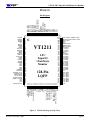
1
Low Pin Count
Super I/O
And Hardware Monitor
Revision 1.0
January 8, 2002
VIA TECHNOLOGIES, INC.
Copyright Notice:
Copyright © 2000, 2001, 2002 VIA Technologies Incorporated. Printed in the United States. ALL RIGHTS RESERVED.
No part of this document may be reproduced, transmitted, transcribed, stored in a retrieval system, or translated into any language,
in any form or by any means, electronic, mechanical, magnetic, optical, chemical, manual or otherwise without the prior written
permission of VIA Technologies Incorporated.
VT1211 may only be used to identify a product of VIA Technologies, Inc.
is a registered trademark of VIA Technologies, Incorporated.
Windows 98TM, Windows NTTM, Windows 2000TM, and Plug and PlayTM are registered trademarks of Microsoft Corp.
PCITM is a registered trademark of the PCI Special Interest Group.
All trademarks are the properties of their respective owners.
Disclaimer Notice:
No license is granted, implied or otherwise, under any patent or patent rights of VIA Technologies. VIA Technologies
makes no warranties, implied or otherwise, in regard to this document and to the products described in this document.
The information provided by this document is believed to be accurate and reliable to the publication date of this
document. However, VIA Technologies assumes no responsibility for any errors in this document. Furthermore, VIA
Technologies assumes no responsibility for the use or misuse of the information in this document and for any patent
infringements that may arise from the use of this document. The information and product specifications within this
document are subject to change at any time, without notice and without obligation to notify any person of such change.
Offices:
USA Office:
440 Mission Court, Suite 220
Fremont, CA 94539
USA
Tel: (510) 683-3300
Fax: (510) 683-3301 or (510) 687-4654
Taipei Office:
8th Floor, No. 533
Chung-Cheng Road, Hsin-Tien
Taipei, Taiwan ROC
Tel: (886-2) 218-5452
Fax: (886-2) 218-5453
Online Services:
Web Page:
FTP Server:
BBS:
http://www.via.com.tw –or- http://www.viatech.com
ftp://ftp.via.com.tw
886-2-2185208
Technologies, Inc.
VT1211 LPC SuperIO and Hardware Monitor
We Connect
REVISION HISTORY
Document Release
1.0
Date
1/8/02
Revision 1.0 January 8, 2002
Revision
Initial release (same as internal rev 0.95 with confidential watermark removed)
-i-
Initials
DH
Revision History
Technologies, Inc.
VT1211 LPC SuperIO and Hardware Monitor
We Connect
TABLE OF CONTENTS
REVISION HISTORY .......................................................................................................................................................................I
TABLE OF CONTENTS ................................................................................................................................................................. II
LIST OF FIGURES .........................................................................................................................................................................IV
LIST OF TABLES ...........................................................................................................................................................................IV
PRODUCT FEATURES ................................................................................................................................................................... 1
OVERVIEW....................................................................................................................................................................................... 3
PINOUTS............................................................................................................................................................................................ 4
PIN DIAGRAM ................................................................................................................................................................................ 4
PIN LIST ......................................................................................................................................................................................... 5
PIN DESCRIPTIONS......................................................................................................................................................................... 6
REGISTERS..................................................................................................................................................................................... 14
REGISTER OVERVIEW ................................................................................................................................................................. 14
REGISTER ORGANIZATION .......................................................................................................................................................... 14
CONFIGURATION SEQUENCE ....................................................................................................................................................... 14
REGISTER SUMMARY TABLES ..................................................................................................................................................... 16
Index Port and Data Port Registers.................................................................................................................................... 16
Configuration Space Registers ............................................................................................................................................ 16
Logical Device Number (LDN) Assignments ..................................................................................................................... 16
FDC Control Registers (LDN 0).......................................................................................................................................... 17
Parallel Port Control Registers (LDN 1) ............................................................................................................................ 17
Serial Port 1 Control Registers (LDN 2) ............................................................................................................................ 17
Serial Port 2 Control Registers (LDN 3) ............................................................................................................................ 17
MIDI Control Registers (LDN 6) ........................................................................................................................................ 17
Game Port Control Registers (LDN 7) ............................................................................................................................... 17
GPIO Control Registers (LDN 8)........................................................................................................................................ 17
Watchdog Timer Control Registers (LDN 9)..................................................................................................................... 17
Wake-Up Control Registers (LDN A)................................................................................................................................. 17
Hardware Monitor Control Registers (LDN B)................................................................................................................. 17
Fast IR Control Registers (LDN C) .................................................................................................................................... 17
ROM Control Registers (LDN D) ....................................................................................................................................... 17
REGISTER DESCRIPTIONS ........................................................................................................................................................... 21
Chip (Global) Control Registers ......................................................................................................................................... 21
Floppy Disk Controller Registers (LDN 0)......................................................................................................................... 23
Parallel Port Registers (LDN 1) .......................................................................................................................................... 24
Serial Port 1 Registers (LDN 2)........................................................................................................................................... 25
Serial Port 2 Registers (LDN 3)........................................................................................................................................... 25
MIDI Registers (LDN 6) ...................................................................................................................................................... 26
Game Port Registers (LDN 7) ............................................................................................................................................. 26
GPIO Registers (LDN 8) ...................................................................................................................................................... 26
Watch Dog Registers (LDN 9) ............................................................................................................................................. 27
Wake-Up Control Registers (LDN A)................................................................................................................................. 27
Hardware Monitor Registers (LDN B)............................................................................................................................... 27
FIR Registers (LDN C) ........................................................................................................................................................ 27
Revision 1.0 January 8, 2002
-ii-
List of Figures & Table
Technologies, Inc.
VT1211 LPC SuperIO and Hardware Monitor
We Connect
ROM Registers (LDN D)...................................................................................................................................................... 27
I/O SPACE REGISTERS................................................................................................................................................................. 28
Floppy Disk Controller I/O Registers................................................................................................................................. 28
Parallel Port I/O Registers................................................................................................................................................... 29
Serial Port 1 I/O Registers ................................................................................................................................................... 30
Serial Port 2 I/O Registers ................................................................................................................................................... 32
MIDI I/O Registers............................................................................................................................................................... 34
Game Port I/O Registers...................................................................................................................................................... 34
GPIO I/O Registers .............................................................................................................................................................. 35
Watch Dog I/0 Registers ...................................................................................................................................................... 37
Wake-Up Control I/0 Registers........................................................................................................................................... 38
Hardware Monitor I/0 Registers ......................................................................................................................................... 42
IrDA (VFIR) Host Controller I/0 Registers ....................................................................................................................... 51
ELECTRICAL SPECIFICATIONS .............................................................................................................................................. 59
MECHANICAL SPECIFICATIONS ............................................................................................................................................ 60
Revision 1.0 January 8, 2002
-iii-
List of Figures & Table
Technologies, Inc.
VT1211 LPC SuperIO and Hardware Monitor
We Connect
LIST OF FIGURES
FIGURE 1.
FIGURE 2.
FIGURE 3.
FIGURE 4.
VT1211 PIN DIAGRAM (TOP VIEW)...................................................................................................................... 4
LPC INTERFACE BLOCK DIAGRAM ................................................................................................................... 6
REGISTER MAP ....................................................................................................................................................... 15
128-PIN LQFP – LOW-PROFILE QUAD FLAT PACK....................................................................................... 60
LIST OF TABLES
TABLE 1. VT1211 PIN LIST (ALPHABETICAL ORDER)........................................................................................................ 5
TABLE 2. PIN DESCRIPTIONS .................................................................................................................................................... 6
TABLE 3. REGISTER SUMMARY – CONFIGURATION INDEX ........................................................................................ 16
TABLE 4. REGISTER SUMMARY – LDN ASSIGNMENTS................................................................................................... 16
TABLE 5. REGISTER SUMMARY – LDN REGISTERS......................................................................................................... 17
TABLE 6. REGISTER SUMMARY – I/O SPACE REGISTERS.............................................................................................. 18
TABLE 7. IR OPERATIONAL MODES ..................................................................................................................................... 52
TABLE 8. ABSOLUTE MAXIMUM RATINGS......................................................................................................................... 59
TABLE 9. DC CHARACTERISTICS .......................................................................................................................................... 59
TABLE 10. POWER SPECIFICATIONS .................................................................................................................................... 59
Revision 1.0 January 8, 2002
-iv-
List of Figures & Table
Technologies, Inc.
VT1211 LPC SuperIO and Hardware Monitor
We Connect
VT1211
LPC SuperIO and Hardware Monitor
PRODUCT FEATURES
•
LPC (Low Pin Count) Interface
–
–
•
Hardware Monitor Controller
–
–
–
–
–
–
–
–
–
–
–
–
•
Provides automatic temperature to fan speed control
Supports mix-and-match for temperature inputs and fan speed control outputs
Overrides fan speed controller during catastrophic situations
Provides over-temperature beep tone warning
Two 16C550 UARTs
–
–
•
Supports up to 4MB flash ROM
SmartGuardian Controller
–
–
–
–
•
Provides fan on-off and speed control
Supports 2 programmable Pulse Width Modulation (PWM) outputs
Duty cycle resolution of 1/256
Flash-ROM Interface
–
•
Built-in 8-bit Analog to Digital Converter
One thermal input for Pentium II type thermal diode
1 intrinsic Vcc voltage monitor input
5 external Universal Channels for monitor inputs
Monitors 2 fan tachometer inputs
1 chassis open detection input
WatchDog comparison of all monitored values
Provides VID0 - VID4 support for P6 class CPU
Over temperature indicator output
Over limit of fan and voltage indicator output
Provides beep tone warning
Serial Bus slave mode supported
Fan Speed Controller
–
–
–
•
Complies with Intel Low Pin Count Interface Specification Revision 1.0
Supports LDRQ#, SERIRQ protocols
Supports two standard Serial Ports
Each port supports Serial Port
IEEE1284 Parallel Port
–
–
–
–
–
Standard mode -- Bi-directional SPP
Enhanced mode -- EPP V1.7 and 1.9 compliant
High speed mode -- ECP, IEEE1284 compliant
Backdrive current reduction
Printer power-on damage reduction
Revision 1.0 January 8, 2002
-1-
Product Features
Technologies, Inc.
VT1211 LPC SuperIO and Hardware Monitor
We Connect
•
Floppy Disk Controller
–
–
–
•
Game Port
–
–
•
Input mode supports switch de-bounce
Output mode supports one set of programmable LED blinking periods
Watch Dog Timer
–
–
•
UART implementation
Supports direct connect to MPU-401 MIDI
56 General Purpose I/O Pins
–
–
•
Built-in 558 quad timers and buffer chips
Supports direct connection to two joysticks
Dedicated MIDI Interface
–
–
•
Supports two 360K / 720K / 1.2M / 1.44M / 2.88M floppy disk drives
Enhanced digital data separator
3-Mode drives supported
Times out the system, based on a user-programmable time-out period
Time resolution 1 minute, maximum 255 minutes
Dedicated Infrared pins
–
Compliant with IrDA 1.4 for VFIR
•
Single 48MHz Clock Input
•
Single 3.3V Power Supply
•
128-pin LPQF
Revision 1.0 January 8, 2002
-2-
Product Features
Technologies, Inc.
VT1211 LPC SuperIO and Hardware Monitor
We Connect
OVERVIEW
The VT1211 is a full function Super I/O chip that provides the most commonly used legacy Super I/O functionality plus the latest
Hardware monitor initiatives. The device uses an LPC interface that complies with “LPC Interface Specification Revision 1.0”.
The VT1211 contains a Floppy Disk Controller, an IEEE-1284 Parallel Port interface, two 16C550-UART-based serial port
interfaces, a VFIR (Very Fast IR) Controller, a game port which supports 2 joysticks, a MIDI interface, and a 4M Flash-ROM
interface. The integrated Hardware Monitor Controller controls the speed of 2 fans, monitors 2 fan tachometers, and has a
Pentium II thermal diode and 5 Universal analog inputs for measuring voltage or temperature (by connecting external thermistors).
The VT1211 meets the “Microsoft£ PC98 & PC99 system design guide” requirements and is ACPI ready. The device requires a
48 MHz clock input and operates at 3.3V power supply.
The VT1211 consists of following logical devices. One high-performance 2.88MB floppy disk controller, with digital data
separator, which supports one 360K / 720K / 1.2M / 1.44M / 2.88M floppy disk drive; One multi-mode high-performance parallel
port featuring support for bi-directional Standard Parallel Port (SPP), Enhanced Parallel Port (EPP v1.7 and v1.9), and IEEE1284
compliant Extended Capabilities Port (ECP) protocols; Two 16C550 standard compatible enhanced UARTs perform
asynchronous communication; One VFIR interface compliant with IrDA; One MIDI interface; One game port with built-in 558
and buffer chips to support direct connect of 2 joysticks; One Hardware Monitor; and Seven GPIO ports (56 GPIO pins).
A hardware monitor engine is built in to monitor system health. An enhanced 8 bit ADC is built inside. This is exploited to
simultaneously monitor 8 analog voltages or thermal inputs. The thermal inputs can be defined independently as thermistor or
PentiumTM II thermal diode. Besides the ADC, the Hardware Monitor subsystem is also equipped with one chassis-open
detection and 5 VID inputs for PentiumTM II Vcore identification.
All logical devices can be individually enabled or disabled via software configuration registers.
Revision 1.0 January 8, 2002
-3-
Overview
Technologies, Inc.
VT1211 LPC SuperIO and Hardware Monitor
We Connect
PINOUTS
128
127
126
125
124
123
122
121
120
119
118
117
116
115
114
113
112
111
110
109
108
107
106
105
104
103
JAB1 / GP10
JBB1 / GP11
JACX / GP12
JBCX / GP13
JBCY / GP14
JACY / GP15
JBB2 / GP16
JAB2 / GP17
MSO / OVOLT / DSEL1
MSI / OVFAN / WDTO
BEEP
OVTEMP#
FANOUT1
FANOUT2 / GP20
FANIO1 / DTEST
FANIO2 / GP21
GNDA
DTDP
DTDN
UIC5
UIC4
UIC3
VREF
VCCA
UIC2
UIC1
Pin Diagram
VT1211
LPC
SuperIO
/ Hardware
Monitor
128-Pin
LQFP
102
101
100
99
98
97
96
95
94
93
92
91
90
89
88
87
86
85
84
83
82
81
80
79
78
77
76
75
74
73
72
71
70
69
68
67
66
65
39
40
41
42
43
44
45
46
47
48
49
50
51
52
53
54
55
56
57
58
59
60
61
62
63
64
1
2
3
4
5
6
7
8
9
10
11
12
13
14
15
16
17
18
19
20
21
22
23
24
25
26
27
28
29
30
31
32
33
34
35
36
37
38
PLED / OVOLT / ITMOFF / GP22
COPEN / OVFAN / ATEST / GP23
IRRX1 / GP24
GNDD
SMI#
MEMW# / GP25
MEMR# / GP26
ROMCS# / GP27
XD0 / GP30
XD1 / GP31
XD2 / GP32
XD3 / GP33
GNDD
XD4 / GP34
XD5 / GP35
XD6 / GP36
XD7 / GP37
XA0 / GP40
XA1 / GP41
XA2 / GP42
XA3 / GP43
XA4 / GP44
XA5 / GP45
XA6 / GP46
XA7 / GP47
XA8 / GP50
XA9 / GP51
VCC
XA10 / GP52
XA11 / GP53
XA12 / GP54
XA13 / GP55
XA14 / GP56
XA15 / GP57
XA16 / GP60
XA17 / GP61
XA18 / GP62
IRTX
RDATA# / PD3
WRTPRT# / PD2
TRK00# / PD1
INDEX# / PD0
DIR# / PINIT#
DRVDEN0 / AUTOFD#
VCC
STB#
CTS1#
DSR1#
RTS1#
DTR1#
SIN1
SOUT1
DCD1#
RI1#
GP77 / VID4 / CTS2#
GP76 / VID3 / DSR2#
GP75 / VID2 / RTS2#
GP74 / VID1 / DTR2#
GP73 / VID0 / SIN2
GNDD
GP72 / SMBCK / SOUT2
GP71 / SMBDT / DCD2#
GP70 / SCLK / ITMOFF / RI2#
IRRX
DSEL0#
INDEX#
MTRA#
DRVB#
VCC
DRVA#
MTRB#
DIR#
STEP#
WDATA#
WGATE#
TRK0#
WPT#
RDATA#
HDSEL#
DSKCHG#
CLKIN
GNDD
PCICLK
LDRQ#
SERIRQ
VCC
LAD3
LAD2
LAD1
LAD0
LFRAME#
LRESET#
WGATE# / SLCT
WDATA# / PE
MTR1# / BUSY
DS1# / ACK#
HDSEL# / ERR#
STEP# / SLCTIN#
PD7
PD6
PD5
DSKCHG# / PD4
Figure 1. VT1211 Pin Diagram (Top View)
Revision 1.0 January 8, 2002
-4-
Pinouts
Technologies, Inc.
VT1211 LPC SuperIO and Hardware Monitor
We Connect
Pin List
Table 1. VT1211 Pin List (Alphabetical Order)
Pin Signal
Pin Signal
Pin Signal
Pin Signal
32
44
118
31
17
101
47
55
53
62
8
6
4
1
16
48
56
110
111
50
58
33
114
113
116
115
ACK#
AUTOFD#
BEEP
BUSY
CLKIN
COPEN / OVFAN / GP23 / ATEST
CTS1#
CTS2# / VID4 / GP77
DCD1#
DCD2 / GP71
DIR#
DRVA#
DRVB#
DSEL0#
DSKCHG#
DSR1#
DSR2# / VID3 / GP76
DTDN
DTDP
DTR1#
DTR2# / VID1 / GP74
ERR#
FANIO1 / DTEST
FANIO2 / GP21
FANOUT1
FANOUT2 / GP20
112
18
60
90
99
15
GNDA
GNDD
GNDD
GNDD
GNDD
HDSEL#
2
64
100
65
128
121
126
123
127
122
125
124
26
25
24
23
20
27
28
96
97
119
120
3
7
117
19
42
41
40
39
38
37
36
35
30
43
102
14
54
63
95
49
57
21
51
59
29
34
98
52
61
46
9
12
103
104
107
108
109
PD5
PD6
PD7
PE
PINIT#
PLED / OVOLT / ITMOFF / GP22
RDATA#
RI1#
RI2# / ITMOFF / SCLK / GP70
ROMCS# / GP27
RTS1#
RTS2# / VID2 / GP75
SERIRQ
SIN1
SIN2 / VID0 / GP73
SLCT
SLCTIN#
SMI#
SOUT1
SOUT2 / GP72
STB#
STEP#
TRK0#
UIC1
UIC2
UIC3
UIC4
UIC5
5
22
45
75
VCC
VCC
VCC
VCC
105
106
10
11
13
85
84
83
82
81
80
79
78
77
76
74
73
72
71
70
69
68
67
66
94
93
92
91
89
88
87
86
Revision 1.0 January 8, 2002
INDEX#
IRRX
IRRX1 / GP24
IRTX
JAB1 / GP10
JAB2 / GP17
JACX / GP12
JACY / GP15
JBB1 / GP11
JBB2 / GP16
JBCX / GP13
JBCY / GP14
LAD0
LAD1
LAD2
LAD3
LDRQ#
LFRAME#
LRESET#
MEMR# / GP26
MEMW# / GP25
MSI / OVFAN / WDTO
MSO / OVOLT / DSEL1
MTRA#
MTRB#
OVTEMP#
PCICLK
PD0
PD1
PD2
PD3
PD4
-5-
VCCA
VREF
WDATA#
WGATE#
WPT#
XA0 / GP40
XA1 / GP41
XA2 / GP42
XA3 / GP43
XA4 / GP44
XA5 / GP45
XA6 / GP46
XA7 / GP47
XA8 / GP50
XA9 / GP51
XA10 / GP52
XA11 / GP53
XA12 / GP54
XA13 / GP55
XA14 / GP56
XA15 / GP57
XA16 / GP60
XA17 / GP61
XA18 / GP62
XD0 / GP30
XD1 / GP31
XD2 / GP32
XD3 / GP33
XD4 / GP34
XD5 / GP35
XD6 / GP36
XD7 / GP37
Pinouts
Technologies, Inc.
VT1211 LPC SuperIO and Hardware Monitor
We Connect
Pin Descriptions
Table 2. Pin Descriptions
LPC BUS INTERFACE
Signal Name
Pin #
Type
LRESET#
LFRAME#
LAD[3:0]
LDRQ#
28
27
23-26
20
I
O
I
I
21
19
IO
I
SERIRQ
PCICLK
Description
LPC Reset.
LPC Frame. This signal indicates the start of an LPC cycle.
LPC Address / Data 3-0. 4-bit LPC address / bidirectional data lines. LAD0 is the lsb.
LPC DMA Request. An encoded signal for DMA channel select. Since there are three
DMA devices in the Super I/O module (VFIR, FDC, and ECP-mode parallel port), the LPC
Interface must provide LDRQ encoding for reflecting DREQ[3:0] status. Two LDRQ
messages or different DMA channels may be issued back-to-back for fast tracing DMA
requests. However, four PCI clocks will be inserted between two LDRQ messages of the
same DMA channel to guarantee that there is at least 10 PCI clocks for one DMA request to
change its status (the LPC Host will decode these LDRQ messages and send decoded
DREQn to the legacy DMA controller which runs off 4MHz or 33/8 MHz).
Serial IRQ.
LPC Clock. 33 MHz PCI clock input.
LPC Transactions
The LPC interface in the VT1211 supports LPC Host I/O Read / Write and DMA Read / Write transactions for the Super I/O
module. For LPC Host I/O Read or Write transactions, the Super I/O module processes a positive decoding, and the LPC interface
can depend on its result to respond to the current transaction via sending out SYNC values on the LAD[3:0] signals or leaving
LAD[3:0] in a tri-state condition. For DMA Read or Write transactions, the LPC interface depends on DMA requests from the
DMA devices in the Super I/O module, and may decide to ignore the current transaction or not.
The Floppy Controller (FDC) and Parallel Port (for ECP transactions) are 8 bit DMA devices, so if the LPC Host tries to initiate a
DMA transaction with a data size of 16 or 32 bits, the LPC interface will process the first 8 bit data and response with a SYNC
ready (0000b) which will terminate the DMA burst. Then the LPC interface will re-issue another LDRQ message to assert DREQi
after finishing the current DMA transaction.
LDRQ#
LDRQ Encoding
+ Sync./Monitor
DREQn
DACKn#
PCICLK
ISA DMA
LRESET#
State Machine
LPC
Interface
LAD_OE
State
Machine
AEN, TC
IOR#, IOW#
ISA PIO
LFRAME#
State Machine
IOCHRDY
SIO_SEL
Latch/select
LAD[3:0]
Configuration
Trigger
CMD, Start
MUX /
Latches
Configuration
SA[15:0]
SD[7:0]
Figure 2. LPC Interface Block Diagram
Revision 1.0 January 8, 2002
-6-
Pinouts
Technologies, Inc.
VT1211 LPC SuperIO and Hardware Monitor
We Connect
Floppy Disk Controller
Symbol
Pin #
Type
DRVB#
DRVA#
MTRA#
MTRB#
HDSEL#
DSEL0#
4
6
3
7
15
1
O
O
O
O
O
O
DSEL1# / MSO / OVOLT
STEP#
DIR#
WGATE#
WDATA#
RDATA#
TRK0#
INDEX#
WPT#
DSKCHG#
120
9
8
11
10
14
12
2
13
16
O
O
O
O
O
I
I
I
I
I
Description
Drive B Enable.
Drive A Enable.
Motor A Enable.
Motor B Enable
Side 1 Select.
Density Select 0. High for high data rates (500Kbps, 1Mbps), low for low data
rates (250Kbps, 300Kbps)
Density Select 1.
Step Pulse. Used to step the head in or out.
Head Direction. Step in when low, out when high.
Write Gate. Low to enable write.
Write Serial Data. Serial data stream to the drive.
Read Serial Data. Serial data stream from the drive.
Track 0. Indicates that the head of the selected drive is on track 0.
Index. Indicates the beginning of a disk track.
Write Protect. Indicates that the disk in the selected drive is write-protected.
Disk Change. Indicates whether the drive door has been opened or a diskette has
been changed.
Parallel Port
Signal Name
SLCT / WGATE#
PE / WDATA#
BUSY / MTR1#
Pin #
Type
29
30
31
I/O
I/O
I/O
Description
Printer Select. High indicates that the printer has been selected.
Printer Paper End. Set high by the printer when it runs out of paper.
Printer Busy. High indicates that the printer has a local operation in progress
and cannot accept data.
32
I / O Printer Acknowledge. Low indicates that the printer has received a character
ACK# / DS1#
and is ready to accept another.
33
O / O Printer Error. Low indicates that the printer has encountered an error. The
ERR# / HDSEL#
error message can be read from bit 3 of the printer status register.
34
O / O Printer Select Input. When low, the printer is selected. This signal is derived
SLCTIN# / STEP#
from the complement of bit 3 of the printer control register.
35-42 IO / – Parallel Port Data Bus. This bus provides a byte-wide input or output to the
PD7 / nc,
IO / – system. The eight (8) lines are held in a high impedance state when the port is
PD6 / nc,
IO / – deselected.
PD5 / nc,
IO / I
PD4 / DSKCHG#,
IO / I
PD3 / RDATA#,
IO / I
PD2 / WRTPRT#,
IO / I
PD1 / TRK00#,
IO / I
PD0 / INDEX#
43
O
/ O Printer Initialize. This signal is derived from bit 2 of the printer control register
PINIT# / DIR#
and is used to initialize the printer.
44
O / O Printer Auto Line Feed. This signal is derived from the complement of bit 1 of
AUTOFD# / DRVDEN0
the printer control register and is used to advance one line after each line is
printed.
46
O / – Printer Strobe. This signal is the complement of bit 0 of the printer control
STB# / nc
register and is used to strobe the printing data into the printer.
As shown by the alternate functions above, in mobile applications the parallel port pins can optionally be selected to function as a
floppy disk interface for attachment of an external floppy drive using the parallel port connector.
Revision 1.0 January 8, 2002
-7-
Pinouts
Technologies, Inc.
VT1211 LPC SuperIO and Hardware Monitor
We Connect
MIDI Interface
Signal Name
MSI / OVFAN / WDTO
MSO / OVOLT / DSEL1
Pin #
Type
119
120
I
O
Description
MIDI Input.
MIDI Output.
Game Port
Signal Name
Pin #
Type
JAB1 / GP10
JBB1 / GP11
JACX / GP12
JBCX / GP13
JBCY / GP14
JACY / GP15
JBB2 / GP16
JAB2 / GP17
128
127
126
125
124
123
122
121
I
I
I
I
I
I
I
I
Description
Joystick A Button # 1 Input.
Joystick B Button # 1 Input.
Joystick A X-axis Resistor Input.
Joystick B X-axis Resistor Input.
Joystick B Y-axis Resistor Input.
Joystick A Y-axis Resistor Input.
Joystick B Button # 2 Input.
Joystick A Button # 2 Input.
Serial Port 1
Signal Name
Pin #
Type
CTS1#
47
I
DSR1#
48
I
RTS1#
49
O
DTR1#
50
O
SIN1
SOUT1
51
52
I
O
DCD1#
53
I
RI1#
54
I
Revision 1.0 January 8, 2002
Description
Clear To Send. Low indicates that the modem is ready to accept data. CTS is a
modem status input whose condition can be tested by reading the MSR register.
Data Set Ready. Low indicates that the modem (“Data Set”) is ready to establish
a communications link. DSR is a modem status input whose condition can be
tested by reading the MSR register.
Request To Send. Low indicates to the modem that the device is ready to send
data. RTS is activated by setting the appropriate bit in the register of MCR to 1.
After a Master Reset operation or during Loop mode, RTS is set to its inactive
state.
Data Terminal Ready. DTR is used to indicate to the modem that the device is
ready to exchange data. DTR is activated by setting the appropriate bit in the
register of MCR to 1. After a Master Reset operation or during Loop mode, DTR
is set to its inactive state.
Serial Data In. This input receives serial data from the communications link.
Serial Data Out. This output sends serial data to the communications link. This
signal is set to a marking state (logic 1) after a Master Reset operation or when
the device is in one of the Infrared communications modes.
Data Carrier Detect. Low indicates that the modem has detected a carrier. The
DCD# signal is a modem status input whose condition can be tested by reading
the MSR.
Ring Indicator. Low indicates that a telephone ring signal has been received by
the modem. The RI signal is a modem status input whose condition can be tested
by reading the MSR register.
-8-
Pinouts
Technologies, Inc.
VT1211 LPC SuperIO and Hardware Monitor
We Connect
Serial Port 2
Signal Name
Pin #
Type
CTS2#
/ VID4
/ GP77
DSR2#
/ VID3
/ GP76
RTS2#
/ VID2
/ GP75
55
I
I
IO
I
I
IO
O
O
IO
DTR2#
/ VID1
/ GP74
58
O
I
IO
SIN2#
/ VID0
/ GP73
SOUT2#
/ SMBCK
/ GP72
DCD2#
/ SMBDT
/ GP71
RI2#
/ GP70
/ ITMOFF
/ SCLK
59
I
I
IO
O
IO
IO
I
IO
IO
I
IO
56
57
61
62
63
Description
Clear To Send. The default function of this pin is Clear To Send. Low indicates that the
modem is ready to accept data. The CTS signal is a modem status input whose condition can
be tested by reading the MSR register.
Data Set Ready. The default function of this pin is Data Set Ready. Low indicates that the
modem (“Data Set”) is ready to establish a communications link. The DSR signal is a
modem status input whose condition can be tested by reading the MSR register.
Request To Send. The default function of this pin is Request To Send. Low indicates to the
modem that the device is ready to send data. RTS is activated by setting the appropriate bit
in the register of MCR to 1. After a Master Reset operation or during Loop mode, RTS is set
to its inactive state.
Data Terminal Ready 2. The default function of this pin is Data Terminal Ready. DTR is
used to indicate to the modem that the device is ready to exchange data. DTR is activated by
setting the appropriate bit in the register of MCR to 1. After a Master Reset operation or
during Loop mode, DTR is set to its inactive state.
Serial Data In. The default function of this pin is Serial Data In. This input receives serial
data from the communications link.
Serial Data Out. The default function of this pin is Serial Data Out. This output sends serial
data to the communications link. This signal is set to a marking state (logic 1) after a Master
Reset operation or when the device is in one of the Infrared communications modes.
Data Carrier Detect. The default function of this pin is Data Carrier Detect. Low indicates
that the modem has detected a carrier. DCD is a modem status input whose condition can be
tested by reading the MSR.
Ring Indicator. The default function of this pin is Ring Indicator. Low indicates that a
telephone ring signal has been received by the modem. The RI signal is a modem status
input whose condition can be tested by reading the MSR register.
Infrared (IR) Controller
Signal Name
Pin #
Type
IRTX
IRRX
IRRX1
/ GP24
65
64
100
O
IO
I
ITMOFF
/ SCLK
/ GP70
/ RI2#
SCLK
/ ITMOFF
/ GP70
/ RI2#
63
IO
63
IO
Revision 1.0 January 8, 2002
Description
Infrared Data Transmit. Infrared Data Transmit.
Infrared Data Receive. Infrared Data Receive for SIR or FIR.
Infrared Data Receive 1. The default function of this pin is Infrared Data Receive for SIR
or transceiver mode control. The function of this pin decided by the GPIO configuration
register.
Infrared Transceiver Module Off. IR Transceiver Module On / Off control
IR Transceiver Serial Clock. For devices that meet specification 1.0 “Serial Interface of
Transceiver Control”
-9-
Pinouts
Technologies, Inc.
VT1211 LPC SuperIO and Hardware Monitor
We Connect
General Purpose I/O Group 1
Signal Name
Pin #
Type
GP10 / JAB1
GP11 / JBB1
GP12 / JACX
GP13 / JBCX
GP14 / JBCY
GP15 / JACY
GP16 / JBB2
GP17 / JAB2
128
127
126
125
124
123
122
121
IO
IO
IO
IO
IO
IO
IO
IO
Description
General Purpose I/O 10.
General Purpose I/O 11.
General Purpose I/O 12.
General Purpose I/O 13.
General Purpose I/O 14.
General Purpose I/O 15.
General Purpose I/O 16.
General Purpose I/O 17.
General Purpose I/O Group 2
Signal Name
GP20 / FANOUT2
GP21 / FANIO2
GP22 / PLED / ITMOFF / OVOLT
GP23 / COPEN / OVFAN / ATEST
GP24 / IRRX1
GP25 / MEMW#
GP26 / MEMR#
GP27 / ROMCS#
Pin #
Type
116
115
102
101
100
97
96
95
IO
IO
IO
IO
IO
IO
IO
IO
Description
General Purpose I/O 20.
General Purpose I/O 21.
General Purpose I/O 22.
General Purpose I/O 23.
General Purpose I/O 24.
General Purpose I/O 25.
General Purpose I/O 26.
General Purpose I/O 27.
General Purpose I/O Group 3
Signal Name
Pin #
Type
GP30 / XD0
GP31 / XD1
GP32 / XD2
GP33 / XD3
GP34 / XD4
GP35 / XD5
GP36 / XD6
GP37 / XD7
94
93
92
91
89
88
87
86
IO
IO
IO
IO
IO
IO
IO
IO
Revision 1.0 January 8, 2002
Description
General Purpose I/O 30.
General Purpose I/O 31.
General Purpose I/O 32.
General Purpose I/O 33.
General Purpose I/O 34.
General Purpose I/O 35.
General Purpose I/O 36.
General Purpose I/O 37.
-10-
Pinouts
Technologies, Inc.
VT1211 LPC SuperIO and Hardware Monitor
We Connect
General Purpose I/O Group 4
Signal Name
Pin #
Type
GP40 / XA0
GP41 / XA1
GP42 / XA2
GP43 / XA3
GP44 / XA4
GP45 / XA5
GP46 / XA6
GP47 / XA7
85
84
83
82
81
80
79
78
IO
IO
IO
IO
IO
IO
IO
IO
Description
General Purpose I/O 40.
General Purpose I/O 41.
General Purpose I/O 42.
General Purpose I/O 43.
General Purpose I/O 44.
General Purpose I/O 45.
General Purpose I/O 46.
General Purpose I/O 47.
General Purpose I/O Group 5
Signal Name
Pin #
Type
GP50 / XA8
GP51 / XA9
GP52 / XA10
GP53 / XA11
GP54 / XA12
GP55 / XA13
GP56 / XA14
GP57 / XA15
77
76
74
73
72
71
70
69
IO
IO
IO
IO
IO
IO
IO
IO
Description
General Purpose I/O 50.
General Purpose I/O 51.
General Purpose I/O 52.
General Purpose I/O 53.
General Purpose I/O 54.
General Purpose I/O 55.
General Purpose I/O 56.
General Purpose I/O 57.
General Purpose I/O Group 6
Signal Name
Pin #
Type
GP60 / XA16
GP61 / XA17
GP62 / XA18
68
67
66
O
O
O
Description
General Purpose Output 60.
General Purpose Output 61.
General Purpose Output 62.
General Purpose I/O Group 7
Signal Name
GP70 / RI2# / ITMOFF / SCLK
GP71 / DCD2# / SMBDT
GP72 / SOUT2#/SMBCK
GP73 / SIN2# / VID0
GP74 / DTR2# / VID1
GP75 / RTS2# / VID2
GP76 / DSR2# / VID3
GP77 / CTS2# / VID4
Revision 1.0 January 8, 2002
Pin #
Type
63
62
61
59
58
57
56
55
IO
IO
IO
IO
IO
IO
IO
IO
Description
General Purpose I/O 70.
General Purpose I/O 71.
General purpose I/O 72.
General Purpose I/O 73.
General Purpose I/O 74.
General purpose I/O 75.
General Purpose I/O 76.
General purpose I/O 77.
-11-
Pinouts
Technologies, Inc.
VT1211 LPC SuperIO and Hardware Monitor
We Connect
Hardware Monitor
Signal Name
Pin #
Type Description
103, 104,
107-109
106
I
Universal Input Channels 1–5. 0 to 2.60 V FSR Analog Inputs.
O
DTDP
DTDN
VID0
/ GP73
/ SIN2
VID1
/ GP74
/ DTR2#
VID2
/ GP75
/ RTS2#
VID3
/ GP76
/ DSR2#
VID4
/ GP77
/ CTS2#
COPEN
/ OVFAN
/ GP23
/ ATEST
OVTEMP#
OVFAN
/ WDTO
/ MSI
OVOLT
/ DSEL1
/ MSO
BEEP
111
110
59
I
I
I
58
I
57
I
56
I
55
I
101
IO
Reference Voltage Output. Regulated referenced voltage for external temperature
sensors. It can drive 3 thermistors (max.) and Vref = 1.65V
Thermal Diode Anode. Pentium thermal diode input positive junction.
Thermal Diode Cathode. Pentium thermal diode input negative junction.
Voltage ID 0. The Voltage ID is the voltage supply read outs from P6 CPUs. This
value is read in the VID register. The configuration of this pin is decided by the GPIO
configuration registers.
Voltage ID 1. The Voltage ID is the voltage supply read outs from P6 CPUs. This
value is read in the VID register. The configuration of this pin is decided by the GPIO
configuration registers.
Voltage ID 2. The Voltage ID is the voltage supply read outs from P6 CPUs. This
value is read in the VID register. The configuration of this pin is decided by the GPIO
configuration registers.
Voltage ID 3. The Voltage ID is the voltage supply read outs from P6 CPUs. This
value is read in the VID register. The configuration of this pin is decided by the GPIO
configuration registers.
Voltage ID 4. The Voltage ID is the voltage supply read outs from P6 CPUs. This
value is read in the VID register. The configuration of this pin is decided by the GPIO
configuration registers.
Case Open Detection. Indicates that the case is open.
117
119
O
O
Over Temperature. Indicates the thermal sensor is out of the high limit.
Over Fan Limit. Indicates the fan speed is out of limit.
120
O
Over Voltage Limit. Indicates the power supply voltage is out of the high or low
limits.
118
O
SMBDT
/ GP71
/ DCD2#
SMBCK
/ GP72
/ SOUT2
FANIO1
/ DTEST
FANIO2
/ GP21
FANOUT1
FANOUT2
/ GP20
WDTO
/ OVFAN
/ MSI
62
IO
Beep Warning. Warning that the hardware monitor has detected a fatal error in system
resources.
Serial Bus Data. Serial bus bi-directional data.
61
IO
Serial Bus Clock. Serial Bus clock.
114
I
Fan Tachometer Input 1. 0 to +5V amplitude fan tachometer input.
113
I
Fan Tachometer Input 2. 0 to +5V amplitude fan tachometer input.
116
115
O
O
Fan Speed Control Output 1. PWM output signal to fan FET.
Fan Speed Control Output 2. PWM output signal to fan FET.
119
O
Watch Dog Time Out.
UIC[1:5]
VREF
Revision 1.0 January 8, 2002
-12-
Pinouts
Technologies, Inc.
VT1211 LPC SuperIO and Hardware Monitor
We Connect
Flash ROM Interface
Signal Name
Pin #
Type
XA[18-16] / GP[62-60],
XA[15-8] / GP[57-50],
XA[7-0] / GP[47-40]
66-68,
69-74,
76-77,
78-85
86-89,
91-94
O
ROM Address[18:0]. The default function of these pins is for flash ROM
address input. The function of these pins decided by the GPIO configuration
register.
IO
ROM Data[7:0]. The default function of these pins is for flash ROM data
input. The function configuration of these pins decided by the GPIO
configuration register.
ROM Chip Select. The default function of this pin is for ROM chip select
input. The function of this pin decided by the GPIO configuration register.
Memory Read. The default function of this pin is memory read enable. The
function of this pin decided by the GPIO configuration register.
Memory Write. The default function of this pin is for a memory write
enable. The function of this pin decided by the GPIO configuration register.
XD7-XD0 / GP[37-30]
ROMCS# / GP27
95
O
MEMR# / GP26
96
O
MEMW# / GP25
97
O
Description
Miscellaneous
Signal Name
Pin #
Type
Description
PLED
/ OVOLT
/ ITMOFF
/ GP22
SMI#
CLKIN
102
IO
Power Indicator. The default function of this pin is an indicator of power on
after system reset. The function of this pin determined by the GPIO
configuration register.
98
17
O
I
System Management Interrupt.
48 MHz Clock.
Strap Configuration
Signal Name
Pin #
Type
BADDR
49
I
TEST
50
I
ENFROM
52
I
Description
Base Address. Sampled at reset to determine the base address of the
configuration index / data register pair, as follows:
10K external pull-up resistor selects 2Eh / 2Fh.
10K external pull-down resistor selects 4Eh / 4Fh.
Test. Force the device into test mode if an external pull-up resistor is
connected. Otherwise, this pin should be pulled-down by an external resistor
for normal operation.
Enable Flash ROM. Enabled Flash-ROM Interface if an external pull-up
resistor is connected. Otherwise, the Flash ROM pins function as GPIO ports
(from pin 66 to pin 97).
Power Supplies
Signal Name
Pin #
Type
Description
5, 22, 45, 75
Power
VCC
Digital Power. 3.3V
105
Power
VCCA
Analog Power.
18, 60, 90, 99 Ground Digital Ground.
GNDD
112
Ground Analog Ground.
GNDA
Note 1: A combination of high frequency decoupling capacitors is suggested on all analog power / ground pairs.
Note 2. All grounds should be connected to the primary circuit board ground plane (i.e., to the lowest impedance point available).
Revision 1.0 January 8, 2002
-13-
Pinouts
Technologies, Inc.
VT1211 LPC SuperIO and Hardware Monitor
We Connect
REGISTERS
Register Overview
Configuration Sequence
The following tables summarize the configuration and I/O
registers of the VT1211. These tables also document the
power-on default value (“Default”) and access type (“Acc”)
for each register. Access type definitions used are RW
(Read/Write), RO (Read/Only), “—” for reserved / used
(essentially the same as RO), and RWC (or just WC) (Read /
Write 1’s to Clear individual bits). Registers indicated as RW
may have some read/only bits that always read back a fixed
value (usually 0 if unused); registers designated as RWC or
WC may have some read-only or read write bits (see
individual register descriptions for details).
Accessing a specific device control and device configuration
register can be achieved through three basic steps:
Detailed register descriptions are provided in the following
section of this document. All offset and default values are
shown in hexadecimal unless otherwise indicated.
Register Organization
a) Enter configuration mode
b) Configure the chip
c) Escape from configuration mode
Enter Configuration Mode
To place the chip into the configuration mode, two successive
writes of 87h must be applied to Configuration Index Register
2Eh or 4Eh.
Configure the Chip
The Logical Device can be selected from as:
1. Write 07h to Configuration Index Register 2Eh or 4Eh
From the Index Port and Data Port Register table, the two
registers can be accessed to enter Configuration mode by
writing a specific value (87h) to Configuration Index Register
twice.
Logical Device Number (LDN) Assignments table shows
that each function block is associated with a Logical Device
Number (LDN). The configuration registers are grouped into
banks, where each bank holds the standard configuration
registers according to its assigned logical device.
Figure presents the standard structure of the configuration
register file. The Super I/O control and configuration
registers are not banked and are only accessed by the Index
Port and Data Port register. The device control and device
configuration registers are duplicated over 14 banks for 14
logical devices. Therefore, by accessing a specific register in
a specific bank is performed by two-step procedure. The
LDN register will first locate the logical device and the Index
register will select the register within that function block.
Revision 1.0 January 8, 2002
2. Write the number of the desired logical device to
Configuration Data Register 2Fh or 4Fh
The super I/O configuration registers can be read/write
from/to as:
1. Write index to Configuration Index Register 2Eh or
4Eh
2. Read/write data from/to Configuration Data Register
2Fh or 4Fh
Escape from Configuration Mode
Write AAh to the Configuration Index Register to disable
SuperI/O configuration mode.
-14-
Register Overview
Technologies, Inc.
VT1211 LPC SuperIO and Hardware Monitor
We Connect
I/O Port 2Eh or 4Eh Index
Floppy Disk I/O Regs
Offset 2 - Command
Offset 4 - Status / Rate Select
Offset 5 - Data
Offset 7 - Disk Change Status
Parallel Port I/O Regs
Offset 0 - Data
Offset 1 - Status
Offset 2 - Control
Offset 3 - ...
Serial Port 1 I/O Regs
Offset 0 - Tx / Rx Buffer
Offset 1 - Interrupt Enable
Offset 2 - Interrupt Status
Offset 3 - Control
Offset 4 - ...
FDC I/O Base
Parallel Port
I/O Base
Serial Port 1
I/O Base
Serial Port 2
I/O Base
...
Configuration Registers (Read / Write values via Port 2Fh or 4F)
0 -reserved...
...
6 -reserved7 Logical Device Number
8 -reserved...
...
1F -reserved20 Device ID
21 Device Revision
22 Power Down Control
23 LPC Wait State Select
24 GPIO Port 1 Pin Select
25 GPIO Port 2 Pin Select
26 GPIO Port 7 Pin Select
27 Multifunction Pin Select - Serial Port 2
28 Multifunction Pin Select - MIDI Port
29 Multifunction Pin Select - Hardware Mon
2A - reserved...
...
2D -reserved2E Test Mode A (Do Not Program)
2F Test Mode B (Do Not Program)
30 -reserved...
...
FF -reservedLDN 00h - Floppy Disk
3 0 LDN 01h - Parallel Port
60 30
6 1 6 0 LDN 02h - Serial Port 1
7 0 6 1 3 0 LDN 03h - Serial Port 2
74 70 60 30
F0 7 4 6 1 6 0 LDN 06h - MIDI
F1 F0 7 0 6 1 3 0 LDN 07h - Game Port
F0 7 0 6 0 3 0
LDN 08h - GPIO
61
F0 7 0 6 0 3 0
6 1 6 0 LDN 09h - Watchdog Timer
30
6 1 6 0 LDN 0Ah - Wakeup Control
7 0 6 1 3 0 LDN 0Bh - Hardware Monitor
F0 7 0 6 0 3 0
F1 F0 6 1 6 0 LDN 0Ch - Fast IR
7 0 6 1 3 0 LDN 0Dh - ROM Control
F2
60
7 0 6 1 30 ROM Interface Activate
F0 ROM Decoding Control
70
74
F0
...
Figure 3. Register Map
Revision 1.0 January 8, 2002
-15-
Register Overview
Technologies, Inc.
VT1211 LPC SuperIO and Hardware Monitor
We Connect
Register Summary Tables
Table 3. Register Summary – Configuration Index
Table 4. Register Summary – LDN Assignments
Index Port and Data Port Registers
Logical Device Number (LDN) Assignments
I/O Port
Function
2E or 4E Configuration Index
2F or 4F Configuration Data
Default Acc
00
RW
00
RW
Configuration Space Registers
Offset Super I/O Control
Default Acc
0-6
-reserved00
–
7
Logical Device Number
–
RW
8-1F
-reserved00
–
20
Device ID
3C
RO
21
Device Revision
01
RO
22
Power Down Control
00
RW
23
LPC Wait State Select
RW
11
24
GPIO Port 1 Pin Select
00
RW
25
GPIO Port 2 Pin Select
00
RW
26
GPIO Port 7 Pin Select
00
RW
27
UART2 Multi Function Pin Select
00
RW
28
MIDI Multi Function Pin Select
00
RW
29
HWM Multifunction Pin Select
00
RW
2A-2D -reserved00
–
2E
Test Mode A (Do not Program)
00
RW
2F
Test Mode B (Do not Program)
00
RW
30-FF -reserved00
–
Note: All offsets and default values above are in hexadecimal.
Revision 1.0 January 8, 2002
LDN Functional Block
00
Floppy Disk Controller (FDC)
01
Parallel Port (PP)
02
Serial Port 1 (UART1)
03
Serial Port 2 (UART2)
04
-reserved05
-reserved06
MIDI
07
Game Port (GMP)
08
GPIO
09
Watch Dog (WDG)
0A
Wake-up Control (WUC)
0B
Hardware Monitor (HM)
0C
Very Fast IR (VFIR)
0D
Flash ROM (ROM)
Note: All offsets above are in hexadecimal.
See following page for LDN register summary tables
-16-
Register Summary Tables
Technologies, Inc.
VT1211 LPC SuperIO and Hardware Monitor
We Connect
Table 5. Register Summary – LDN Registers
GPIO Control Registers (LDN 8)
FDC Control Registers (LDN 0)
Offset
30
61-60
70
74
F0
F1
Floppy Disk Controller
Floppy Controller Activate
FDC I/O Base Address
FDC IRQ Select
FDC DRQ Select
Floppy Controller Configuration
Floppy Drive Select
Default
00
03F0
06
01
00
00
Acc
RW
RW
RW
RW
RW
RW
Parallel Port
Parallel Port Activate
Parallel Port I/O Base Address
Parallel Port IRQ Select
Parallel Port DRQ Select
Parallel Port Control
Default
03
0378
05
00
00
Acc
RW
RW
RW
RW
RW
Offset Watch Dog Controller
30
Watch Dog Activate
61-60 Watch Dog I/O Base Address
70
Watch Dog IRQ Select
F0
Watch Dog Configuration
Serial Port 1
Serial Port 1 Activate
Serial Port 1 I/O Base Address
Serial Port 1 IRQ Select
Serial Port 1 Control
Offset Wake-Up Controller
30
WUC Activate
61-60 WUC I/O Base Address
70
WUC IRQ Select
Default
00
03F8
04
00
Acc
RW
RW
RW
RW
Serial Port 2
Serial Port 2 Activate
Serial Port 2 I/O Base Address
Serial Port 2 IRQ Select
Serial Port 2 Control
Default
00
02F8
03
00
Acc
RW
RW
RW
RW
Default
00
0330
00
Acc
RW
RW
RW
Offset Hardware Monitor
30
Hardware Monitor Activate
61-60 Hardware Monitor Address
70
Hardware Monitor IRQ Select
MIDI
MIDI Activate
MIDI I/O Base Address
MIDI IRQ Select
Game Port Control Registers (LDN 7)
Acc
RW
RW
RW
RW
Default
00
EB00
00
Acc
RW
RW
RW
Default
00
EC00
00
Acc
RW
RW
RW
Default
00
E800
00
06
00
Acc
RW
RW
RW
RW
RW
Fast IR Control Registers (LDN C)
Offset FIR Controller
30
FIR Activate
61-60 FIR I/O Base Address
70
FIR IRQ Select
74
FIR DRQ Select
F0
FIR One DMA Selection
MIDI Control Registers (LDN 6)
Offset
30
61-60
70
Default
00
EA00
00
00
Hardware Monitor Control Registers (LDN B)
Serial Port 2 Control Registers (LDN 3)
Offset
30
61-60
70
F0
Acc
RW
RW
RW
RW
RW
RW
Wake-Up Control Registers (LDN A)
Serial Port 1 Control Registers (LDN 2)
Offset
30
61-60
70
F0
Default
00
E900
00
00
00
00
Watchdog Timer Control Registers (LDN 9)
Parallel Port Control Registers (LDN 1)
Offset
30
61-60
70
74
F0
Offset General Purpose I/O
30
GPIO Activate
61-60 GPIO I/O Base Address
70
GPIO Event IRQ Select
F0
GPIO Port Select
F1
GPIO Pin Configuration
F2
GPIO Pin Polarity Define
ROM Control Registers (LDN D)
Offset ROM Controller
Default Acc
30
ROM Interface Activate
RW
01
F0
ROM Decoding Control
00
RW
Note: All offsets and default values above are in hexadecimal.
Offset Game Port
Default Acc
30
Game Port Activate
00
RW
61-60 Game Port I/O Base Address
0200 RW
Note: All offsets and default values above are in hexadecimal.
Revision 1.0 January 8, 2002
-17-
Register Summary Tables
Technologies, Inc.
VT1211 LPC SuperIO and Hardware Monitor
We Connect
Table 6. Register Summary – I/O Space Registers
FDC I/O Space Registers
Offset
02
04
04
05
07
Base = LDN 0 Rx61-60 (03F0h)
FDC Command
FDC Main Status
FDC Data Rate Select
FDC Data
FDC Disk Change Status
GPIO I/O Space Registers
Default
00
00
–
00
00
Acc
RW
RO
WO
RW
RW
Default
00
00
00
00
00
00
00
00
00
00
00
Acc
RW
RO
RW
RW
RW
RW
RW
RW
RW
RW
RW
Offset
00
01
02
03
04
05
06
07
08
09
0A
0B
0C
0D
0E
Parallel Port I/O Space Registers
Offset
00
01
02
03
04
05
06
07
400
401
402
Base = LDN 1 Rx61-60 (0378h)
Parallel Port Data
Parallel Port Status
Parallel Port Control
Parallel Port EPP Address
Parallel Port EPP Data 0
Parallel Port EPP Data 1
Parallel Port EPP Data 2
Parallel Port EPP Data 3
Parallel Port ECP Data / Config A
Parallel Port ECP Configuration B
Parallel Port ECP Extended
Control
Base = LDN 8 Rx61-60 (E900h)
GPIO Port 0 Data
GPIO Port 3 Data
GPIO Port 4 Data
GPIO Port 5 Data
GPIO Port 6 Data
GPIO Event Status A
GPIO Events Enable A
GPIO Event Status B
GPIO Events Enable B
GPIO Events Debounce Enable A
GPIO Events Polarity Type
GPIO Events Trigger Type A
GPIO Events Debounce Enable B
GPIO Events Polarity Type B
GPIO Events Trigger Type B
Default
00
00
00
00
00
00
00
00
00
00
00
00
00
00
00
Acc
RW
RW
RW
RW
RW
RW
RW
RW
RW
RW
RW
RW
RW
RW
RW
Default
01
00
00
Acc
RO
RW
RW
Watchdog Timer I/O Space Registers
Offset
00
01
02
Base = LDN 9 Rx61-60 (EA00h)
Watchdog Status
Watchdog Mask
Watchdog Timeout
Serial Ports 1 & 2 I/O Space Registers
Port 1 Base = LDN 2 Rx61-60
Offset Port 2 Base = LDN 3 Rx61-60
Default Acc
00
Transmit / Receive Buffer
00
RW
01
Interrupt Enable
00
RW
00
RW
01-00 Baud Rate Generator Divisor
02
Interrupt Status
00
RO
02
FIFO Control
–
WO
03
UART Control
00
RW
04
Handshake Control
00
RW
05
UART Status
00
RW
06
Handshake Status
00
RW
07
Scratchpad
00
RW
Serial Port 1 base address default = 03F8h; Port 2 = 02F8h
MIDI Port I/O Space Registers
Offset
00
01
01
Base = LDN 6 Rx61-60 (0330h)
MIDI Data
MIDI Status
MIDI Control
Default
00
00
–
Acc
RW
RO
WO
Game Port I/O Space Registers
Offset Base = LDN 7 Rx61-60 (0200h)
Default Acc
01
Game Port Status
00
RO
01
Start Game Port One Shot
00
WO
Note: All offsets and default values above are in hexadecimal.
Revision 1.0 January 8, 2002
Wakeup I/O Space Registers
Offset Base = LDN A Rx61-60 (EB00h) Default Acc
00
Wake-Up Status 0
00
RW
01
Wake-Up Status 1
00
RW
03
Wake-Up Event Enable 0
00
RW
04
Wake-Up Event Enable 1
00
RW
06
Wake-Up Configuration
00
RW
08
GPIO Port 0 Data
00
RW
09
GPIO Port 1 Data
00
RW
0A
Module IRQ Status 0
00
RO
0B
Module IRQ Status 1
00
RO
0C
Module IRQ Enable 0
00
RW
0D
Module IRQ Enable 1
00
RW
0E
SMI # Event Enable 0
00
RW
0F
SMI # Event Enable 1
00
RW
11
IRQ Event Enable 0
00
RW
12
IRQ Event Enable 1
00
RW
1C
Event Configuration
00
RW
1D
Event Debounce Enable
00
RW
1E
Event Polarity Type
00
RW
1F
Event Trigger Type
00
RW
20
GP2x Output Enable
00
RW
21
GP2x Polarity Inversion
00
RW
22
GP7x Output Enable
00
RW
23
GP7x Polarity Inversion
00
RW
Note: All offsets and default values above are in hexadecimal.
-18-
Register Summary Tables
Technologies, Inc.
VT1211 LPC SuperIO and Hardware Monitor
We Connect
Hardware Monitor I/O Space Registers
Offset Base = LDN B Rx61-60 (EC00h)
Default Acc
10 SELD0 [7:0] For AFE as Digital filter
00
RW
parameter SELD [7:0]
11 SELD1[7:0] for as SELD[15:8]
00
RW
12 SELD2[7:0] for as SELD[19:16]
00
RW
13 Analog data D[15:8]
00
RW
14 Analog data D[7:0]
00
RW
15 Digital data D[7:0]
00
RW
16 Channel Counter
00
RW
17 Data Valid & Channel Indications.
00
RW
18 SMBus Control (For Noise Avoiding)
00
RW
19 AFE Control
00
RW
1A AFE Test Control
00
RW
1B Channel Setting
00
RW
1C -reserved00
–
1D Hot Temp Limit (H) for temp reading 3
00
RW
1E Hot Temp Hysteresis Limit (Low)
00
RW
1F Temperature reading 1 (for Intel CPU
00
RW
Thermal Diode)
20 Temperature Reading 3 (Reserved for
00
RW
Internal Thermal Diode)
21 UCH 1 ,Default as Thermal input
00
RW
(Temperature reading 2) that setting for
NTC type thermistor input
22 UCH 2 ,Default for Voltage inputs
00
RW
23 UCH 3 ,Default for Voltage inputs
00
RW
24 UCH 4 ,Default for Voltage inputs
00
RW
25 UCH 5 ,Default for Voltage inputs
00
RW
26 +3.3V(Internal Vdd)
00
RW
27-28 -reserved00
–
29 FAN1 reading
00
RW
2A FAN 2 reading
00
RW
2B UCH2 High Limit
00
RW
2C UCH2 Low Limit
00
RW
2D UCH3 High Limit
00
RW
2E UCH3 Low Limit
00
RW
2F UCH4 High Limit
00
RW
30 UCH4 Low Limit
00
RW
31 UCH5 High Limit
00
RW
32 UCH5 Low Limit
00
RW
33 Internal +3.3V High Limit
00
RW
34 Internal +3.3V Low Limit
00
RW
35 - 38 - reserved 00
–
39 Hot Temp Limit (H) for temp reading 1
00
RW
3A Hot Temp Hysteresis Limit (Low)
00
RW
Note: All offsets and default values above are in hexadecimal.
Revision 1.0 January 8, 2002
3B
3C
3D
FAN 1 Fan Count Limit (FIN0)
00
RW
FAN 2 Fan Count Limit (FIN1)
00
RW
UCH1 High Limit (default for temp
00
RW
reading 2)
3E UCH1 Low Limit
00
RW
3F Stepping ID number
00
RW
40 Configuration
RW
08
41 Interrupt INT Status 1
00
RO
42 Interrupt INT Status 2
00
RO
43 INT Mask 1
00
RW
44 INT Mask 2
00
RW
45 VID
00
RO
46 Over Voltage & Over Fan Control
FF RW
47 Fan Speed Control
RW
25
48 Serial Bus Address
2D RW
49 VID 4
00
RW
4A Universal Channel Configuration
RW
07
4B Temperature Configuration 1
RW
15
4C Temperature Configuration 2
RW
55
4D Extended Temperature Resolution
00
RO
4E Over Temperature Control
RW
0F
50 PWM Clock Select
00
RW
51 PWM Control
00
RW
52 PWM Full Speed Temperature Value
00
RW
53 PWM High Speed Temperature Value
00
RW
54 PWM Low Speed Temperature Value
00
RW
55 PWM Fan Off Temperature Value
00
RW
56 PWM Output 1 Hi Speed Duty Cycle
FF RW
57 PWM Output 1 Lo Speed Duty Cycle
FF RW
58 PWM Output 2 Hi Speed Duty Cycle
FF RW
59 PWM Output 2 Lo Speed Duty Cycle
FF RW
5A PWM Output 3 Hi Speed Duty Cycle
FF RW
5B PWM Output 3 Lo Speed Duty Cycle
FF RW
5C BEEP Event Enable
00
RW
5D Fan Event BEEP Frequency Divisor
00
RW
5E Voltage Event BEEP Frequency Divisor
00
RW
5F Temperature Event BEEP Freq Divisor
00
RW
60 PWM1 Current Duty Cycle
00
RW
61 PWM2 Current Duty Cycle
00
RW
62-7F -reserved00
–
Note: All offsets and default values above are in hexadecimal.
-19-
Register Summary Tables
Technologies, Inc.
VT1211 LPC SuperIO and Hardware Monitor
We Connect
IrDA (VFIR) Host Controller I/O Space Registers
Offset
0-F
10
11
12
13
14
15
16
17
18
19
1A
1B
1E
1F
20
21
22
23
24
25
26
27
28
29
2A
2B
2C
2D
2E
2F
30-31
32
33
34
35
36-3E
3F
Base = LDN C Rx61-60 (E800h)
-reservedInfrared Configuration Low 0
Infrared Configuration High 0
Infrared SIR BOF
Infrared SIR EOF
Infrared Status High 0
Infrared Status and Control 0
Infrared Status Low 1
Infrared Status High 1
Infrared Configuration Low 1
Infrared Configuration High 1
Infrared Configuration Low 2
Infrared Configuration High 2
Infrared Configuration 3
-reservedHost Control
Host Status
Miscellaneous Control
Tx Control Low
Tx Control High
Tx Status
Rx Control
Rx Status
Reset Command
Packet Address
Rx Byte Count Low
Rx Byte Count High
Rx Ring Packet Pointer Low
Rx Ring Packet Pointer High
Tx Byte Count Low
Tx Byte Count High
-reservedGeneral Purpose Timer
Infrared Configuration 4
Infrared Transceiver Control Low
Infrared Transceiver Control High
-reservedStepping ID
Revision 1.0 January 8, 2002
Default
00
00
00
C0
C1
00
00
00
00
00
00
00
00
00
00
00
00
00
00
40
00
40
00
00
00
00
00
00
00
00
00
00
00
00
00
00
00
00
Acc
–
RW
RW
RW
RW
RO
RW
RO
RO
RW
RW
RW
RW
RW
–
RW
RO
RW
RW
RW
RO
RW
RO
RW
RW
RO
RO
RO
RO
RW
RW
–
RW
RW
RW
RW
–
-20-
Register Summary Tables
Technologies, Inc.
VT1211 LPC SuperIO and Hardware Monitor
We Connect
Register Descriptions
Chip (Global) Control Registers
Offset 07 - Logical Device Number..................................RW
7-0 Logical Device Number ....................... default = 00h
This register selects the current logical device.
Offset 20 - Device ID..........................................................RO
7-0 Device ID ..............................................default = 3Ch
Offset 21 - Device Revision................................................RO
7-0 Device Revision .................................... default = 01h
Offset 22 - Power Down Control......................................RW
7-6 Reserved ........................................ always reads 0
5
Clock Power Down .................................. default = 0
4
Parallel Port Power Down....................... default = 0
3
Reserved ........................................ always reads 0
2
Serial Port Power Down.......................... default = 0
1
Floppy Disk Controller Power Down..... default = 0
0
Reserved ........................................ always reads 0
Offset 23 - LPC Wait State Select (11h)..........................RW
7
Memory Cycle Wait State Disable ... .….default = 0
6-4 LPC I/O Cycle Wait State # Selection..... def =001b
3
Super I/O DMA Cycle 4 Wait................. default = 0
2-0 LPC DMA Cycle Wait State Number Selection
........................................ default = 001b
Revision 1.0 January 8, 2002
Offset 24 - GPIO Port 1 Pin Select.................................. RW
7
Pin 121
0 JAB2 .................................................... default
1 GP17
6
Pin 122
0 JBB2 .................................................... default
1 GP16
5
Pin 123
0 JACY .................................................... default
1 GP15
4
Pin 124
0 JBCY .................................................... default
1 GP14
3
Pin 125
0 JBCX .................................................... default
1 GP13
2
Pin 126
0 JACX .................................................... default
1 GP12
1
Pin 127
0 JBB1 .................................................... default
1 GP11
0
Pin 128
0 JAB1 .................................................... default
1 GP10
Offset 25 - GPIO Port 2 Pin Select.................................. RW
7
System Reset
0 Normal operation................................... default
1 Reset chip
6
Route SMI to Serial IRQ2
0 Disable................................................... default
1 Enable
5
Pin 97-66
0 ROM signal .......................................... default
1 GP25-GP62
4
Pin 100
0 IRRX1 ................................................... default
1 GP24
3
Pin 101
0 COPEN.................................................. default
1 GP23
2
Pin 102
0 PLED .................................................... default
1 GP22
1
Pin 113
0 FANIO2 ................................................ default
1 GP21
0
Pin 115
0 FANOUT2 ............................................ default
1 GP20
-21-
Register Descriptions – Global Control
Technologies, Inc.
VT1211 LPC SuperIO and Hardware Monitor
We Connect
Offset 26 - GPIO Port 7 Pin Select ..................................RW
7
Pin 55
0 CTS2# ...................................................default
1 GP77
6
Pin 56
0 DSR2# ...................................................default
1 GP76
5
Pin 57
0 RTS2# ...................................................default
1 GP75
4
Pin 58
0 DTR2# ..................................................default
1 GP74
3
Pin 59
0 SIN2 ......................................................default
1 GP73
2
Pin 61
0 SOUT2 ..................................................default
1 GP72
1
Pin 62
0 DCD2# ..................................................default
1 GP71
0
Pin 63
0 R12# ......................................................default
1 GP70
Offset 27 – Serial Port 2 Multi Function Pin Select .......RW
7
Pin 55
0 CTS2# ...................................................default
1 VID4
6
Pin 56
0 DSR2# ...................................................default
1 VID3
5
Pin 57
0 RTS2# ...................................................default
1 VID2
4
Pin 58
0 DTR2# ..................................................default
1 VID1
3
Pin 59
0 SIN2 ......................................................default
1 VID0
2
Pin 61
0 SOUT2 ..................................................default
1 SMBCK
1
Pin 62
0 DCD2# ..................................................default
1 SMBDT
0
Pin 63
0 RI2# .....................................................default
1 ITMOFF
Revision 1.0 January 8, 2002
Offset 28 – MIDI Port Multi Function Pin Select.......... RW
7
GPIO Event Group B Selection
0 GP4 ....................................................... default
1 GP5
6
GPIO Event Group A Selection
0 GP1 ....................................................... default
1 Depends on bit-5
5
GP Select
(ignored unless bit-6 = 1)
0 GP3x .................................................... default
1 GP7x
4
Pin 102
0 PLED .................................................... default
1 ITMOFF
3-2 Pin 119 Bit [1:0]
x0 MSI ....................................................... default
01 OVFAN
11 WDTO
1-0 Pin 120 Bit [1:0]
x0 MSO ..................................................... default
01 OVOLT
11 DSEL1
Offset 29 – Monitor Port Multi Function Pin Select ..... RW
7
Pin 102
0 Depends on Rx28[4].............................. default
1 OVOLT (Over Voltage)
6
Pin 101
0 COPEN.................................................. default
1 OVFAN (Over Fan)
5-0 Reserved
........................................always reads 0
Offset 2E – Test Mode Register A (Do Not Program)... RW
Offset 2F – Test Mode Register B (Do Not Program) ... RW
-22-
Register Descriptions – Global Control
Technologies, Inc.
VT1211 LPC SuperIO and Hardware Monitor
We Connect
Floppy Disk Controller Registers (LDN 0)
Offset 30 – Floppy Controller Activate...........................RW
7-1 Reserved
........................................ always reads 0
0
Floppy Disk Controller Enable.................. default = 0
Offset 60 – Floppy Controller Base Address (FCh) .......RW
7-1 ADR9 ~ ADR3..................... always reads 1111 110b
0
Must be 0 .............................................. default = 0
Offset 70 – FDC IRQ Select (06h) ...................................RW
7-4 Reserved .…................................... always reads 0
3-0 FDC Controller IRQ Number Select ... def = 0110b
Offset 74 – FDC DRQ Select (01h) ..................................RW
7-2 Reserved ........................................ always reads 0
1-0 FDC DRQ Number Select .................. default = 01b
Offset F0 – Floppy Controller Configuration ................ RW
7
Reserved ….. ..................................always reads 0
6
Hardware Floppy Disk Drive on Parallel Port
0 Disable................................................... default
1 Enable (see parallel port pin descriptions)
5
Software Floppy Disk Drive on Parallel Port
0 Disable................................................... default
1 Enable
4
Three-Mode Floppy Disk Drive
0 Disable................................................... default
1 Enable
3
Floppy Controller IRQ Polarity
0 Positive .................................................. default
1 Negative
2
Two / Four Floppy Disk Drive Select
0 Internal 2 drive decoder......................... default
1 External 4 drive decoder
1
Floppy Disk Controller DMA
0 Burst .................................................... default
1 Non-burst
0
Floppy Disk Drive Swap
0 Disable................................................... default
1 Enable
Offset F1 – Floppy Disk Drive Type (00h) ..................... RW
7-6 FDD3 (DT1, DT0)….…….................... default = 00b
DRVDEN0 DRVDEN1
00 DENSEL
DRATE 0
01 DRATE 1
DRATE 0
10 DENSEL#
DRATE 0
11 DRATE 0
DRATE 1
5-4 FDD2 (DT1, DT0)….…….................... default = 00b
3-2 FDD1 (DT1, DT0)................................. default = 00b
1-0 FDD0 (DT1, DT0)................................. default = 00b
Revision 1.0 January 8, 2002
-23-
Register Descriptions – LDN 0 FDC
Technologies, Inc.
VT1211 LPC SuperIO and Hardware Monitor
We Connect
Parallel Port Registers (LDN 1)
Offset 30 – Parallel Port Activate (03h) ..........................RW
7-2 Reserved ........................................ always reads 0
1-0 Parallel Port Enable….…… ............... default = 11b
00 SPP Mode
01 ECP Mode
10 EPP Mode
11 PIO Disable
Offset 60 – Parallel Port Base Address (DEh)................RW
7-0 ADR9 ~ ADR2................................... default = 0DEh
If EPP is not enabled, the parallel port can be set to
192 locations, on 4 bytes boundaries form 100h3FCh. If EPP is enabled, the parallel port can be set
to 96 locations, on 8 byte boundaries from 100h3F8h. In ECP Mode, upper address decode require
A10 active.
Offset F0 – Parallel Port Control.................................... RW
7
PS/2 Type Bi-directional Parallel Port Enable
.............................................. default = 0
6
EPP Direction by Register not by IOW . default = 0
5
EPP+ECP….............................................. default = 0
4
EPP Version (0: Ver 1.9)…. .................... default = 0
3
SPP Mode IRQ Polarity…. ..................... default = 0
2-0 Reserved …. ...................................always reads 0
Offset 70 – Parallel Port IRQ Select (05h)......................RW
7-4 Reserved ........................................ always reads 0
3-0 Parallel Port IRQ Select.................. default = 0101b
Offset 74 – Parallel Port DRQ Select (02h) ....................RW
7-2 Reserved ........................................ always reads 0
1-0 Parallel Port DRQ Select .................... default = 10b
Revision 1.0 January 8, 2002
-24-
Register Descriptions – LDN 1 Parallel Port
Technologies, Inc.
VT1211 LPC SuperIO and Hardware Monitor
We Connect
Serial Port 1 Registers (LDN 2)
Serial Port 2 Registers (LDN 3)
Offset 30 – Serial Port 1 Activate ....................................RW
7-1 Reserved ........................................ always reads 0
0
Serial Port 1 Function
0 Disable ...................................................default
1 Enable
Offset 30 – Serial Port 2 Activate................................... RW
7-1 Reserved
........................................always reads 0
0
Serial Port 2 Function
0 Disable................................................... default
1 Enable
Offset 60 – Serial Port 1 Base Address (FEh).................RW
7-1 ADR9 ~ ADR3........................... default = 1111 111b
0
Must be 0 ......................…...……..………default = 0
Offset 60 – Serial Port 2Base Address (BEh)................. RW
7-1 ADR9 ~ ADR3 ........................... default = 1011 111b
0
Must be 0 .............................................. default = 0
Offset 70 – Serial Port 1 IRQ Select (04h) ......................RW
7-4 Reserved (RO)…................................ always reads 0
3-0 Serial Port 1 IRQ Select ........................ def = 0100b
Offset 70 – Serial Port 2 IRQ Select (03h)..................... RW
7-4 Reserved (RO) ....................................always reads 0
3-0 Serial Port 2 IRQ Select................... default = 0011b
Offset F0 – Serial Port 1 Control.....................................RW
7-4 Must be 0 .............................................. default = 0
3
Serial Port 1 Output Pin Tri-State in Power Down
0 Disable ...................................................default
1 Enable
2
Reserved ........................................ always reads 0
1
Serial Port 1 High Speed
0 Disable ...................................................default
1 Enable
0
Serial Port 1 MIDI
0 Disable ...................................................default
1 Enable
Offset F0 – Serial Port 2 Control .................................... RW
7-4 Must be 0
3
Serial Port 2 Output Pin Tri-State in Power Down
0 Disable................................................... default
1 Enable
2
Reserved …. ...................................always reads 0
1
Serial Port 2 High Speed
0 Disable................................................... default
1 Enable
0
Serial Port 2 MIDI
0 Disable................................................... default
1 Enable
Revision 1.0 January 8, 2002
-25-
Register Descriptions – LDN 2/3 Serial Ports
Technologies, Inc.
VT1211 LPC SuperIO and Hardware Monitor
We Connect
MIDI Registers (LDN 6)
GPIO Registers (LDN 8)
Offset 30 – MIDI Activate (00h) ......................................RW
7-1 Reserved ........................................ always reads 0
0
MIDI Function
0 Disable ...................................................default
1 Enable
Offset 30 – GPIO Activate (00h) ..................................... RW
7-1 Reserved
........................................always reads 0
0
GPIO Function
0 Disable................................................... default
1 Enable
Offset 61-60 – MIDI Base Address (0330h) ....................RW
15-2 MIDI I/O Base Register ...…………default = 0330h
1-0 Reserved ........................................ always reads 0
Offset 61-60 – GPIO Base Address (E900h) .................. RW
15-4 GPIO I/O Base....................................default = E90h
3-0 Reserved
........................................always reads 0
Offset 70 – MIDI IRQ Select (00h)..................................RW
7-4 Reserved ........................................ always reads 0
3-0 MIDI IRQ Select...................................... default = 0
Offset 70 – GPIO Event IRQ Select................................ RW
7-4 Reserved
........................................always reads 0
3-0 GPIO Event IRQ Select............................. default=0
Game Port Registers (LDN 7)
Offset 30 – Game Port Activate .......................................RW
7-1 Reserved ........................................ always reads 0
0
Game Port Enable ................................... default = 0
Offset 61-60 – Game Port I/O Base Address (0200h) ....RW
15-3 Game Port I/O Base...………...……..default = 020h
2-0 Reserved .................................. always reads 000b
Revision 1.0 January 8, 2002
Offset F0 – GPIO Port Select .......................................... RW
7-3 Reserved
........................................always reads 0
2-0 GPIO Port Configuration Register Bank Select
.............................................. default = 0
Offset F1 – GPIO Pin Configuration.............................. RW
7-0 GPIO Pin Direction
0 Output.................................................... default
1 Input
Offset F0 – GPIO Pin Polarity ........................................ RW
7-0 GPIO Pin Polarity
0 Normal................................................... default
1 Inverted
-26-
Register Descriptions – LDN 6-8 MIDI, Game, GPIO
Technologies, Inc.
VT1211 LPC SuperIO and Hardware Monitor
We Connect
Watch Dog Registers (LDN 9)
FIR Registers (LDN C)
Offset 30 – Watch Dog Activate (00h).............................RW
7-1 Reserved .............................................. default = 0
0
Watch Dog Function….……................... default = 0
0 Disable ...................................................default
1 Enable
Offset 30 – Fast IR Activate (00h)................................... RW
7-1 Reserved
........................................always reads 0
0
Fast IR Function ...................................... default = 0
0 Disable................................................... default
1 Enable
Offset 61-60 – Watch Dog I/O Base Address (EA00h) ..RW
15-4 Watch Dog I/O Base ......................... default = EA0h
3-0 Reserved ........................................ always reads 0
Offset 61-60 – FIR I/O Base Address (E800h) ............... RW
15-8 FIR I/O Base .......................................default = E80h
7-0 Reserved
........................................always reads 0
Offset 70 – Watch Dog IRQ Select ..................................RW
7-4 Reserved ........................................ always reads 0
3-0 Watch Dog IRQ Select ............................ default = 0
Offset 70 – FIR IRQ Select (00h) .................................... RW
7-4 Reserved
........................................always reads 0
3-0 FIR IRQ Select ......................................... default = 0
Offset F0 – Watch Dog Timer Configuration.................RW
7-4 Reserved ........................................ always reads 0
3-0 Watch Dog Timer Pin Configuration .... default = 0
Offset 74 – FIR DRQ Select (06h)................................... RW
7-4 Reserved
........................................always reads 0
3-2 FIR DRQ 2 Select................................. default = 01b
1-0 FIR DRQ 1 Select................................. default = 10b
Offset F0 – FIR One DMA Select (00h).......................... RW
7-1 Reserved
........................................always reads 0
0
FIR IRQ Select ......................................... default = 0
Wake-Up Control Registers (LDN A)
Offset 30 – WUC Activate (00h) ......................................RW
7-1 Reserved ........................................ always reads 0
0
Wake Up Control (WUC) Function
0 Disable ...................................................default
1 Enable
Offset 61-60 – WUC I/O Base Address (EB00h) ............RW
15-4 WUC I/O Base….……...................... default = EB0h
3-0 Reserved ........................................ always reads 0
Offset 70 – WUC IRQ Select (00h)..................................RW
7-4 Reserved ........................................ always reads 0
3-0 WUC IRQ Select.….…… ........................ default = 0
Hardware Monitor Registers (LDN B)
Offset 30 – Hardware Monitor Activate (00h) ...............RW
7-1 Reserved
........................................ always reads 0
0 Hardware Monitor Function .................... default = 0
0 Disable ...................................................default
1 Enable
Offset 61-60 – HWM I/O Base Address (EC00h)...........RW
15-8 HWM I/O Base.................................... default = ECh
7-0 Reserved ........................................ always reads 0
ROM Registers (LDN D)
Offset 30 – ROM Interface Activate (01h) ..................... RW
7-1 Reserved
........................................always reads 0
0
ROM Interface
0 Disable
1 Enable................................................... default
Offset F0 – ROM Decoding Control (00h) ..................... RW
7
Flash ROM Write Cycles
0 Disable................................................... default
1 Enable
6
FFF00000h–FFF7FFFFh......................... default = 0
5
FFE80000h–FFEFFFFFh........................ default = 0
4
FFE00000h–FFE7FFFFh ........................ default = 0
3
FFD80000h–FFDF0000h ......................... default = 0
2
FFD00000h–FFD7FFFFh........................ default = 0
1
FFC80000h–FFCFFFFFh ....................... default = 0
0
FFC00000h–FFC7FFFFh........................ default = 0
Note: ROMCS# is always active for accesses to ISA Memory
FFF80000h – FFFFFFFFh and 000E0000h – 000FFFFFh.
Offset 70 – Hardware Monitor IRQ Select.....................RW
7-4 Reserved….…… ................................ always reads 0
3-0 HM IRQ Select.….……........................... default = 0
Revision 1.0 January 8, 2002
-27-Register Descriptions – LDN 9-D Watchdog, Wakeup, HWM, IR, ROM
Technologies, Inc.
VT1211 LPC SuperIO and Hardware Monitor
We Connect
I/O Space Registers
Floppy Disk Controller I/O Registers
These registers are normally accessed at standard FDC I/O
port addresses 3F0-3F7h (see LDN 0 Rx61-60 for the FDC
Port I/O Base setting).
Offset 2 – FDC Command................................................RW
7
Motor 3 (unused in VT82C686B: no MTR3# pin)
6
Motor 2 (unused in VT82C686B: no MTR2# pin)
5
Motor 1
0 Motor Off
1 Motor On
4
Motor 0
0 Motor Off
1 Motor On
3
DMA and IRQ Channels
0 Disable
1 Enable
2
FDC Reset
0 Execute FDC Reset
1 FDC Enable
1-0 Drive Select
00 Select Drive 0
01 Select Drive 1
1x -reservedOffset 4 – FDC Main Status ..............................................RO
7
Main Request
0 Data register not ready
1 Data register ready
6
Data Input / Output
0 CPU => FDC
1 FDC => CPU
5
Non-DMA Mode
0 FDC in DMA mode
1 FDC not in DMA mode
4
FDC Busy
0 FDC inactive
1 FDC active
3-2 Reserved ........................................ always reads 0
1
Drive 1 Active
0 Drive inactive
1 Drive performing a positioning change
0
Drive 0 Active
0 Drive inactive
1 Drive performing a positioning change
Revision 1.0 January 8, 2002
Offset 4 – FDC Data Rate Select ..................................... WO
7
Software Reset
0 Normal operation................................... default
1 Execute FDC reset (this bit is self clearing)
6
Power Down
0 Normal operation................................... default
1 Power down FDC logic
5
Reserved
........................................always reads 0
4-2 Precompensation Select
Selects the amount of write precompensation to be
used on the WDATA output:
000 Default................................................... default
001 41.7 ns
010 93.3 ns
011 125.0 ns
100 166.7 ns
101 208.3 ns
110 250.0 ns
111 0.0 ns (disable)
1-0 Data Rate
Drive Type
MFM FM
00 500K 250K bps 1.2MB 5” or 1.44 MB 3”
01 300K 150K bps 360KB 5”
10 250K 125K bps 720KB 3” ................ default
11
1M illegalbps
Note: these bits are not changed by software reset
Offset 5 – FDC Data ......................................................... RW
Offset 7 – FDC Disk Change Status................................ RW
7
Disk Change......................................................... RO
0 Floppy not changed ............................... default
1 Floppy changed since last instruction
6-2 Undefined ..................................... always reads 1’s
1-0 Data Rate ........................................................ WO
00 500 Kbit/sec (1.2MB 5” or 1.44 MB 3” drive)
01 300 Kbit/sec (360KB 5” drive)
10 250 Kbit/sec (720KB 3” drive)
11 1 Mbit/sec
-28-
Register Descriptions – Floppy Disk Controller I/O
Technologies, Inc.
VT1211 LPC SuperIO and Hardware Monitor
We Connect
Parallel Port I/O Registers
These registers are normally accessed at standard Parallel Port
I/O addresses 378-37Fh (see LDN 1 Rx61-60 for the Parallel
Port I/O Base setting).
Offset 0 – Parallel Port Data ............................................RW
7-0 Parallel Port Data
Offset 1 – Parallel Port Status...........................................RO
7
BUSY#
0 Printer busy, offline, or error
1 Printer not busy
6
ACK#
0 Data transfer to printer complete
1 Data transfer to printer in progress
5
PE
0 Paper available
1 No paper available
4
SLCT
0 Printer offline
1 Printer online
3
ERROR#
0 Printer error
1 Printer OK
2-0 Reserved ................................... always read 1 bits
Offset 2 – Parallel Port Control.......................................RW
7-5 Undefined ................................. always read back 1
4
Hardware Interrupt
0 Disable ...................................................default
1 Enable
3
Printer Select
0 Deselect printer ......................................default
1 Select printer
2
Printer Initialize
0 Initialize Printer .....................................default
1 Allow printer to operate normally
1
Automatic Line Feed
0 Host handles line feeds ..........................default
1 Printer does automatic line feeds
0
Strobe
0 No data transfer......................................default
1 Transfer data to printer
Revision 1.0 January 8, 2002
Offset 3 – Parallel Port EPP Address ............................. RW
Offset 4 – Parallel Port EPP Data Port 0 ....................... RW
Offset 5 – Parallel Port EPP Data Port 1 ....................... RW
Offset 6 – Parallel Port EPP Data Port 2 ....................... RW
Offset 7 – Parallel Port EPP Data Port 3 ....................... RW
Offset 400h – Parallel Port ECP Data / Config A.......... RW
Offset 401h – Parallel Port ECP Configuration B......... RW
Offset 402h – Parallel Port ECP Extended Control ...... RW
7-5 Parallel Port Mode Select
000 Standard Mode ...................................... default
001 PS/2 Mode
010 FIFO Mode
011 ECP Mode
100 EPP Mode
101 -reserved110 -reserved111 Configuration Mode
4
Parallel Port Interrupt Disable
0 Enable an interrupt pulse to be generated on
the high to low edge of the fault. An interrupt
will also be generated if the fault condition is
asserted and this bit is written from 1 to 0.
1 Disable the interrupt generated on the
asserting edge of the fault condition
3
Parallel Port DMA Enable
0 Disable DMA unconditionally
1 Enable DMA
2
Parallel Port Interrupt Pending
0 Interrupt not pending
1 Interrupt pending (DMA & interrupts
disabled)
This bit is set to 1 by hardware and must be written
to 0 to re-enable interrupts
1
FIFO Full ......................................................... RO
0 FIFO has at least 1 free byte
1 FIFO full or cannot accept byte
0
FIFO Empty ........................................................ RO
0 FIFO contains at least 1 byte of data
1 FIFO is completely empty
-29-
Register Descriptions – Parallel Port I/O
Technologies, Inc.
VT1211 LPC SuperIO and Hardware Monitor
We Connect
Serial Port 1 I/O Registers
These registers are normally accessed at standard Parallel Port
I/O addresses 3F8-3FFh (see LDN 1 Rx61-60 for the Parallel
Port I/O Base setting).
Offset 0 – Transmit / Receive Buffer...............................RW
7-0 Serial Data
Offset 1 – Interrupt Enable..............................................RW
7-4 Undefined ..........................................always read 0
3
Interrupt on Handshake Input State Change
2
Intr on Parity, Overrun, Framing Error or Break
1
Interrupt on Transmit Buffer Empty
0
Interrupt on Receive Data Ready
Offset 1-0 – Baud Rate Generator Divisor .....................RW
15-0 Divisor Value for Baud Rate Generator
Baud Rate = 115,200 / Divisor
(e.g., setting this register to 1 selects 115.2 Kbaud)
Offset 2 – Interrupt Status ................................................RO
7-3 Undefined ..........................................always read 0
2-1 Interrupt ID (0=highest priority)
00 Priority 3 (Handshake Input Changed State)
01 Priority 2 (Transmit Buffer Empty)
10 Priority 1 (Data Received)
11 Priority 0 (Serialization Error or Break)
0
Interrupt Pending
0 Interrupt Pending
1 No Interrupt Pending
Offset 2 – FIFO Control ...................................................WO
Offset 3 – UART Control .................................................RW
7
Divisor Latch Access
0 Access xmit / rcv & int enable regs at 0-1
1 Access baud rate generator divisor latch at 0-1
6
Break
0 Break condition off
1 Break condition on
5-3 Parity
000 None
001 Odd
011 Even
101 Mark
111 Space
2
Stop Bits
0 1
1 2
1-0 Data Bits
00 5
01 6
10 7
11 8
Offset 4 – Handshake Control......................................... RW
7-5 Undefined ......................................... always read 0
4
Loopback Check
0 Normal operation
1 Loopback enable
3
General Purpose Output 2 (unused in 82C686B)
2
General Purpose Output 1 (unused in 82C686B)
1
Request To Send
0 Disable
1 Enable
0
Data Terminal Ready
0 Disable
1 Enable
Offset 5 – UART Status ................................................... RW
7
Undefined ......................................... always read 0
6
Transmitter Empty
0 1 byte in transmit hold or transmit shift
register
1 0 bytes transmit hold and transmit shift regs
5
Transmit Buffer Empty
0 1 byte in transmit hold register
1 Transmit hold register empty
4
Break Detected
0 No break detected
1 Break detected
3
Framing Error Detected
0 No error
1 Error
2
Parity Error Detected
0 No error
1 Error
1
Overrun Error Detected
0 No error
1 Error
0
Received Data Ready
0 No received data available
1 Received data in receiver buffer register
Offset 6 – Handshake Status ........................................... RW
7
DCD Status (1=Active, 0=Inactive)
6
RI Status (1=Active, 0=Inactive)
5
DSR Status (1=Active, 0=Inactive)
4
CTS Status (1=Active, 0=Inactive)
3
DCD Changed (1=Changed Since Last Read)
2
RI Changed (1=Changed Since Last Read)
1
DSR Changed (1=Changed Since Last Read)
0
CTS Changed (1=Changed Since Last Read)
Offset 7 – Scratchpad....................................................... RW
7
Scratchpad Data
Revision 1.0 January 8, 2002
-30-
Register Descriptions – Serial Port 1
Technologies, Inc.
VT1211 LPC SuperIO and Hardware Monitor
We Connect
Revision 1.0 January 8, 2002
-31-
Register Descriptions – Serial Port 1
Technologies, Inc.
VT1211 LPC SuperIO and Hardware Monitor
We Connect
Serial Port 2 I/O Registers
These registers are normally accessed at standard Parallel Port
I/O addresses 2F8-2FFh (see LDN 1 Rx61-60 for the Parallel
Port I/O Base setting).
Offset 0 – Transmit / Receive Buffer...............................RW
7-0 Serial Data
Port COM2Base+1 – Interrupt Enable...........................RW
7-4 Undefined ..........................................always read 0
3
Interrupt on Handshake Input State Change
2
Intr on Parity, Overrun, Framing Error or Break
1
Interrupt on Transmit Buffer Empty
0
Interrupt on Receive Data Ready
Offset 1-0 – Baud Rate Generator Divisor .....................RW
15-0 Divisor Value for Baud Rate Generator
Baud Rate = 115,200 / Divisor
(e.g., setting this register to 1 selects 115.2 Kbaud)
Offset 2 – Interrupt Status ................................................RO
7-3 Undefined ..........................................always read 0
2-1 Interrupt ID (0=highest priority)
00 Priority 3 (Handshake Input Changed State)
01 Priority 2 (Transmit Buffer Empty)
10 Priority 1 (Data Received)
11 Priority 0 (Serialization Error or Break)
0
Interrupt Pending
0 Interrupt Pending
1 No Interrupt Pending
Offset 2 – FIFO Control ...................................................WO
Offset 3 – UART Control .................................................RW
7
Divisor Latch Access
0 Access xmit / rcv & int enable regs at 0-1
1 Access baud rate generator divisor latch at 0-1
6
Break
0 Break condition off
1 Break condition on
5-3 Parity
000 None
001 Odd
011 Even
101 Mark
111 Space
2
Stop Bits
0 1
1 2
1-0 Data Bits
00 5
01 6
10 7
11 8
Offset 4 – Handshake Control......................................... RW
7-5 Undefined ......................................... always read 0
4
Loopback Check
0 Normal operation
1 Loopback enable
3
General Purpose Output 2 (unused in 82C686B)
2
General Purpose Output 1 (unused in 82C686B)
1
Request To Send
0 Disable
1 Enable
0
Data Terminal Ready
0 Disable
1 Enable
Offset 5 – UART Status ................................................... RW
7
Undefined ......................................... always read 0
6
Transmitter Empty
0 1 byte in transmit hold or transmit shift
register
1 0 bytes transmit hold and transmit shift regs
5
Transmit Buffer Empty
0 1 byte in transmit hold register
1 Transmit hold register empty
4
Break Detected
0 No break detected
1 Break detected
3
Framing Error Detected
0 No error
1 Error
2
Parity Error Detected
0 No error
1 Error
1
Overrun Error Detected
0 No error
1 Error
0
Received Data Ready
0 No received data available
1 Received data in receiver buffer register
Offset 6 – Handshake Status ........................................... RW
7
DCD Status (1=Active, 0=Inactive)
6
RI Status (1=Active, 0=Inactive)
5
DSR Status (1=Active, 0=Inactive)
4
CTS Status (1=Active, 0=Inactive)
3
DCD Changed (1=Changed Since Last Read)
2
RI Changed (1=Changed Since Last Read)
1
DSR Changed (1=Changed Since Last Read)
0
CTS Changed (1=Changed Since Last Read)
Offset 7 – Scratchpad....................................................... RW
7
Scratchpad Data
Revision 1.0 January 8, 2002
-32-
Register Descriptions – Serial Port 2
Technologies, Inc.
VT1211 LPC SuperIO and Hardware Monitor
We Connect
Revision 1.0 January 8, 2002
-33-
Register Descriptions – Serial Port 2
Technologies, Inc.
VT1211 LPC SuperIO and Hardware Monitor
We Connect
MIDI I/O Registers
Game Port I/O Registers
These registers are accessed at I/O port addresses offset from
the MIDI I/O Base address (“Plug and Play” programmable
via LDN 6 Rx61-60). The MIDI port base address register
default value is 0300h so that these registers may normally be
accessed at standard MIDI I/O port addresses 300-301h (but
the base address may be changed via software to relocate
these registers to avoid conflicts with other system I/O
devices).
These registers are accessed at I/O port addresses offset from
the Game Port I/O Base address (“Plug and Play”
programmable via LDN 7 Rx61-60). The game port base
address register default value is 0200h so that these registers
may normally be accessed at standard Game Port I/O port
address 201h (but the base address may be changed via
software to relocate these registers to avoid conflicts with
other system I/O devices).
Offset 00h – MIDI Data In ................................................RO
Offset 01h – Game Port Status......................................... RO
7
Joystick B Button 2 Status
6
Joystick B Button 1 Status
5
Joystick A Button 2 Status
4
Joystick A Button 1 Status
3
Joystick B One-Shot Status for Y-Potentiometer
2
Joystick B One-Shot Status for X-Potentiometer
1
Joystick A One-Shot Status for Y-Potentiometer
0
Joystick A One-Shot Status for X-Potentiometer
Offset 00h – MIDI Data Out ............................................WO
Offset 01h – MIDI Status (80h) ........................................RO
7
Receive Data Input Buffer Empty
0 Receive buffer of FIFO contains data that can
be read via the MIDI Data In register ....default
1 Receive buffer is in pass-through mode or
FIFO is empty
6
Transmit Data Output Buffer Full
0 Transmit buffer of FIFO can accept data
written to the MIDI Data Out register....default
1 Transmit buffer or FIFO cannot accept data
5-0 Reserved ........................................ always reads 0
Offset 01h – Start One-Shot ............................................ WO
7-0 (Value Written is Ignored)
Offset 01h – MIDI Command ..........................................WO
Revision 1.0 January 8, 2002
-34-
Register Descriptions – MIDI / Game I/O
Technologies, Inc.
VT1211 LPC SuperIO and Hardware Monitor
We Connect
GPIO I/O Registers
These registers are normally accessed at I/O port addresses
starting at E900h (see LDN 8 Rx61-60 for the GPIO I/O Port
Base setting).
Offset 00 – GPIO Port 1 Data ..........................................RW
7-0 GPIO 1x Data....................................... default = 00h
If the corresponding pins are configured as outputs,
this register may be used to program the output level
of the corresponding GPIO pin when its output
buffer is enabled. Writing to the bit latches the
written data. Reading this register returns the latched
value, regardless of the state of the pins.
If the corresponding pins are configured as inputs,
reading this register returns the states of the
corresponding GPIO pins when their output buffers
are disabled (writes to this register are ignored).
The direction (I/O) configuration of the GPIO pins of
this port is decided by the GPIO Configuration
Register (LDN 8 RxF1) and pin functions are
configured by Global Register Rx24.
Offset 02 – GPIO Port 4 Data ......................................... RW
7-0 GPIO 4x Data ....................................... default = 00h
If the corresponding pins are configured as outputs,
this register may be used to program the output level
of the corresponding GPIO pin when its output
buffer is enabled. Writing to the bit latches the
written data. Reading this register returns the latched
value, regardless of the state of the pins.
If the corresponding pins are configured as inputs,
reading this register returns the states of the
corresponding GPIO pins when their output buffers
are disabled (writes to this register are ignored).
The direction (I/O) configuration of the GPIO pins of
this port is decided by the GPIO Configuration
Register (LDN 8 RxF1) and pin functions are
configured by Global Register Rx25.
Offset 01 – GPIO Port 3 Data ..........................................RW
7-0 GPIO 3x Data....................................... default = 00h
If the corresponding pins are configured as outputs,
this register may be used to program the output level
of the corresponding GPIO pin when its output
buffer is enabled. Writing to the bit latches the
written data. Reading this register returns the latched
value, regardless of the state of the pins.
If the corresponding pins are configured as inputs,
reading this register returns the states of the
corresponding GPIO pins when their output buffers
are disabled (writes to this register are ignored).
The direction (I/O) configuration of the GPIO pins of
this port is decided by the GPIO Configuration
Register (LDN 8 RxF1) and pin functions are
configured by Global Register Rx25.
Offset 03 – GPIO Port 5 Data ......................................... RW
7-0 GPIO 5x Data ....................................... default = 00h
If the corresponding pins are configured as outputs,
this register may be used to program the output level
of the corresponding GPIO pin when its output
buffer is enabled. Writing to the bit latches the
written data. Reading this register returns the latched
value, regardless of the state of the pins.
If the corresponding pins are configured as inputs,
reading this register returns the states of the
corresponding GPIO pins when their output buffers
are disabled (writes to this register are ignored).
The direction (I/O) configuration of the GPIO pins of
this port is decided by the GPIO Configuration
Register (LDN 8 RxF1) and pin functions are
configured by Global Register Rx25.
Offset 04 – GPIO Port 6 Data ......................................... RW
7-0 GPIO 6x Data ....................................... default = 00h
If the corresponding pins are configured as outputs,
this register may be used to program the output level
of the corresponding GPIO pin when its output
buffer is enabled. Writing to the bit latches the
written data. Reading this register returns the latched
value, regardless of the state of the pins.
If the corresponding pins are configured as inputs,
reading this register returns the states of the
corresponding GPIO pins when their output buffers
are disabled (writes to this register are ignored).
The direction (I/O) configuration of the GPIO pins of
this port is decided by the GPIO Configuration
Register (LDN 8 RxF1) and pin functions are
configured by Global Register Rx25.
Revision 1.0 January 8, 2002
-35-
Register Descriptions – GPIO I/O
Technologies, Inc.
VT1211 LPC SuperIO and Hardware Monitor
We Connect
Offset 05 – GPIO Events Status A................................ RWC
7-0 GPx [7:0] Event Status A
This register shows event detection status of either
GP1X or GP3X, according to Global Register
Rx28[6]. These bits are only set by hardware and
can only be reset by writing a 1 to relative bit
position.
0 Event undetected....................................default
1 Event detected
Offset 06 – GPIO Events Enable A .................................RW
7-0 GPx [7:0] Enable
This register enables event detection for the GPIO
pins of either GP2X or GP7x, according to Global
Register Rx28[6].
0 Disable ...................................................default
1 Enable
Offset 07 – GPIO Events Status B ................................ RWC
7-0 GPx [7:0] Event Status B
This register shows the event detection status of
either GP4X or GP5X, according to Global Register
28[7]. These bits are only set by hardware and can
only be reset by writing a 1 to relative bit position.
0 Event undetected....................................default
1 Event detected
Offset 08 – GPIO Events Enable B..................................RW
7-0 GPx [7:0] Enable
This register enables event detection on the GPIO
pins of either GP2X or GP7x, according to Global
Register Rx28[7].
0 Disable ...................................................default
1 Enable
Offset 09 – GPIO Events Debounce Enable A ............... RW
7-0 Event Debounce Enable A
This register enables the debounce of GPIO event
inputs of either GP1x or GP3x, according to Global
Register Rx28[6].
0 Disable................................................... default
1 Enable
Offset 0A – GPIO Events Polarity Type A..................... RW
7-0 Event Polarity Type A
This register selects the polarity of GPIO event
inputs of either GP1x or GP3x, according to Global
Register Rx28[6].
0 Not Inverted .......................................... default
1 Inverted
Offset 0B – GPIO Events Trigger Type A...................... RW
7-0 Event Trigger Type A
This register selects edge or level type of GPIO event
inputs of either GP1x or GP3x, according to register
bit of Global Register Rx28[6].
0 Edge....................................................... default
1 Level
Offset 0C – GPIO Events Debounce Enable B .............. RW
7-0 Event Debounce Enable B
This register enables the debounce of GPIO event
inputs of either GP4x or GP5x, according to Global
Register Rx28[7].
0 Disable................................................... default
1 Enable
Offset 0D – GPIO Events Polarity Type B..................... RW
7-0 Event Polarity Type
This register selects the polarity of GPIO event
inputs of either GP4x or GP5x, according to Global
Register Rx28[7].
0 Not Inverted .......................................... default
1 Inverted
Offset 0E – GPIO Events Trigger Type B...................... RW
7-0 Event Trigger Type B
This register selects edge or level type of GPIO event
inputs of GPIO of either GP4x or GP5x, according to
Global Register Rx28 [7].
0 Edge .................................................... default
1 Level
Revision 1.0 January 8, 2002
-36-
Register Descriptions – GPIO I/O
Technologies, Inc.
VT1211 LPC SuperIO and Hardware Monitor
We Connect
Watch Dog I/0 Registers
These registers are normally accessed at I/O port addresses
starting at EA00h (see LDN 9 Rx61-60 for the Watch Dog I/O
Port Base setting).
Offset 00 – Watch Dog Status 0 (01h) ..............................RO
7-1 Reserved….…… ................................ always reads 0
0
Watch Dog Time Out (WDTO) ..........................RO
0 Timeout period has expired
1 Timer still in activation or default on power up
reset values.............................................default
Offset 02 – Watch Dog Timeout (00h) ............................ RW
7-0 Watch Dog Timer Timeout Period
00h Timer halted, WDTO output inactive.... default
01h Time Period 1 minute
02h Time Period 2 minutes
… …
FFh Time Period 255 minutes
Offset 01 –Watch Dog Mask (00h) ..................................RW
7-3 Reserved….…… ................................ always reads 0
2
COM2 Interrupt Trigger Enable
This bit enables the COM2 IRQ to trigger Watchdog
Timer reloading and count down restart.
0 COM2 IRQ is not a trigger event...........default
1 An active COM IRQ enabled as a trigger event
1
COM1 Interrupt Trigger Enable
This bit enables the COM1 IRQ to trigger Watchdog
Timer reloading and count down restart.
0 COM1 IRQ is not a trigger event...........default
1 An active COM1 IRQ enabled as a trigger
event
0
Reserved….…… ................................ always reads 0
Revision 1.0 January 8, 2002
-37-
Register Descriptions – Watch Dog I/O
Technologies, Inc.
VT1211 LPC SuperIO and Hardware Monitor
We Connect
Wake-Up Control I/0 Registers
These registers are normally accessed at I/O port addresses
starting at EB00h (see LDN A Rx61-60 for the Wake Up
Control I/O Port Base setting).
Offset 00 –Wake-Up Status........................................... RWC
7
Module IRQ Status
0 Event not active .....................................default
1 Event active
This bit is only set by hardware and can only be reset
by writing a 1 to this bit position.
6
Software Event
0 Event not active .....................................default
1 Event active
This bit is only set and reset by writing a 1 to toggle
of this bit position.
5
Module GPIO
This sticky bit shows the status of the module GPIO
event detection.
0 Event not detected..................................default
1 Event detected
This bit is only set by hardware and can only be reset
by writing a 1 to this bit position.
4-3 Reserved ....................................... always reads 0
2
Ring Indicator 2#
0 Event not detected..................................default
1 Event detected
This bit is only set by hardware and can only be reset
by writing a 1 to this bit position.
1
Ring Indicator 1#
0 Event not detected..................................default
1 Event detected
This bit is only set by hardware and can only be reset
by writing a 1 to this bit position.
0
Reserved ....................................... always reads 0
Offset 01 – Wake-Up Status 1..........................................RW
7-0 GPX [7:0] Event….……...................................RWC
This register shows the status of either GP2X or
GP7X event detection, according to register bit of
Rx1C[7].
0 Event not detected..................................default
1 Event detected
These bits are only set by hardware and can only be
reset by writing a 1 to relative bit position.
Revision 1.0 January 8, 2002
Offset 03 – Wake-Up Event Enable 0 ............................. RW
7
Module IRQ Enable
0 Disable................................................... default
1 Enable
6
Software Enable
0 Disable................................................... default
1 Enable
5
Module GPIO Enable
0 Disable................................................... default
1 Enable
4-3 Reserved
...................................... always reads 0
2
RI2# Enable
0 Disable................................................... default
1 Enable
1
RI1# Enable
0 Disable................................................... default
1 Enable
0
Reserved
...................................... always reads 0
Offset 04 – Wake-Up Event Enable 1 ............................. RW
7-0 GPX [7:0] Enable
This register enables event detection on the GPIO
pins of either GP2X or GP7x, according to Wake-up
Configuration Register Rx1C[7].
0 Disable................................................... default
1 Enable
Offset 06 – Wake-Up Configuration (00h) ..................... RW
7
Initialization
Logic 1 restores power-up default values to all of
registers. This bit automatically clears itself since the
power on default is zero.
6-5 Reserved
...................................... always reads 0
4
Power LED On/Off Flag
Logic 1 enables LED pin 102 to turn on if Wake-up
Configuration Register Rx1C [2:0] are 0 (Power
LED Control).
3-0 Reserved
...................................... always reads 0
-38-
Register Descriptions – Wake Up Control I/O
Technologies, Inc.
VT1211 LPC SuperIO and Hardware Monitor
We Connect
Offset 08 – GPIO Port 0 Data ..........................................RW
7-0 GPIO Data 0......................................... default = 00h
If this register as GPO, it should be program with the
value of each bit determines the value drive on the
corresponding GPIO pin when its output buffer is
enabled. Writing to the bit latches the written data.
Reading the bit returns its value, regardless of the pin
value.
If as GPI and reads each bit should returns the value
of the corresponding GPIO pin when its output
buffer is disabled, regardless of the write value.
This direction (I/O) configuration of GPIO pin is
decided by register of GPOUTCFG0(Reg. 20h) and
pin function configured by Global Register offset
25h.
Offset 09 – GPIO Port 1 Data ..........................................RW
7-0 GPIO Data 0......................................... default = 00h
If this register as GPO, it should be program with the
value of each bit determines the value drive on the
corresponding GPIO pin when its output buffer is
enabled. Writing to the bit latches the written data.
Reading the bit returns its value, regardless of the pin
value.
If as GPI and reads each bit should returns the value
of the corresponding GPIO pin when its output
buffer is disabled, regardless of the write value.
The direction (I/O) configuration of the GPIO pins is
decided by Rx22 and pin functions are configured by
Global Register offset 26h.
Offset 0A – Module IRQ Status 0 .................................... RO
7-0 Module IRQ [7:0] Status
This register shows the status of device IRQs
(MIRQx) 7-0 detection. The MIRQ interrupts are
enabled by corresponding bits of Rx0C.
0 IRQx undetected.................................... default
1 IRQx detected
These bits are set by hardware and can only be
cleared when Module IRQ events have finished their
service
Offset 0B – Module IRQ Status 1 .................................... RO
7-0 Module IRQ [15:8] Status
This register shows the status of device IRQs
(MIRQx) 15-8 detection. The MIRQ interrupts are
enabled by corresponding bits of Rx0D.
0 IRQx undetected.................................... default
1 IRQx detected
These bits are set by hardware and can only be
cleared when Module IRQ events have finished their
service
Offset 0C – Module IRQ Enable 0 .................................. RW
7-0 Module IRQ [7:0] Enable
This register controls the status function of module
IRQs 7-0. Each bit enables the corresponding bit of
Rx0A.
0 IRQx undetected.................................... default
1 IRQx detected
Offset 0D – Module IRQ Enable 1 .................................. RW
7-0 Module IRQ [15:8] Enable
This register controls the status function of module
IRQs 15-8. Each bit enables the corresponding bit of
Rx0B.
0 IRQx undetected.................................... default
1 IRQx detected
Revision 1.0 January 8, 2002
-39-
Register Descriptions – Wake Up Control I/O
Technologies, Inc.
VT1211 LPC SuperIO and Hardware Monitor
We Connect
Offset 0E – SMI# Event Enable 0....................................RW
7
Module IRQ
0 Disable ...................................................default
1 Enable
6
Software Enable
0 Disable ...................................................default
1 Enable
5-3 Reserved ........................................ always reads 0
2
RI2# Enable
0 Disable ...................................................default
1 Enable
1
RI1# Enable
0 Disable ...................................................default
1 Enable
0
Reserved ........................................ always reads 0
Offset 11 –IRQ Event Enable 0 ....................................... RW
7
Module IRQ
0 Disable................................................... default
1 Enable
6
Software Enable
0 Disable................................................... default
1 Enable
5-3 Reserved
........................................always reads 0
2
RI2# Enable
0 Disable................................................... default
1 Enable
1
RI1# Enable
0 Disable................................................... default
1 Enable
0 Reserved
........................................always reads 0
Offset 0F – SMI# Event Enable 1 ....................................RW
7-0 GPx [7:0] Enable
This register enables the GPIO of either GP2x or
GP7x event detection, according to Wake-up
Configuration Register Rx1C[7].
0 Disable ...................................................default
1 Enable
Offset 12 – IRQ Event Enable 1 ..................................... RW
7-0 GPx [7:0] Enable (GPIEN [7:0])
This register enable the GPIO of either GP2x or
GP7x event detection, according to Wake-up
Configuration Register Rx1C[7].
0 Disable................................................... default
1 Enable
Revision 1.0 January 8, 2002
-40-
Register Descriptions – Wake Up Control I/O
Technologies, Inc.
VT1211 LPC SuperIO and Hardware Monitor
We Connect
Offset 1C – Event Configuration .....................................RW
7
GPIO Event Source Select
0 Select GPIO2x as event input source.....default
1 Select GPIO7x as event input source
6
Reserved ........................................ always reads 0
5
SMI# Output Select
0 Wake-up events that are enabled active the
SMI# signal control by SMIENx register and
regardless of the WUENx register .........default
1 Wake-Up events status bits (see Rx01) that are
enabled activate the SMI# signal on pin 98
4-3 Reserved ........................................ always reads 0
2-0 Power LED Output Control
There are some types that are enabled activate on the
PLED signal of pin 102.
000 Control by Wakeup Config Rx6[4]........default
001 LED with 1/4 Hz toggle rate
010 LED with 1/2 Hz toggle rate
011 LED with 1 Hz toggle rate
100 LED with 2 Hz toggle rate
101 LED with 4 Hz toggle rate
110 LED off
111 LED constant on
Offset 1D – Event Debounce Enable ..............................RW
7-0 Event Debounce Enable
This register enables the debounce of inputs of GPIO
of either GP2x or GP7x as event inputs, according to
Wake-up Configuration Register Rx1C[7].
0 Disable ...................................................default
1 Enable
Offset 20 – GP2x Output Enable .................................... RW
7-0 GP2x Output Enable
This register enables polarity inversion on the input
pins of GP2x.
0 GPI .................................................... default
1 GPO
Offset 21 – GP2x Polarity Inversion ............................... RW
7-0 GP2x Polarity Inversion
This register enables polarity inversion on the input
pins of GP2x.
0 Disable................................................... default
1 Enable
Offset 22 – GP7x Output Enable .................................... RW
7-0 GP7x Output Enable
This register selects GPI or GPO functions for GP7x.
0 GPI .................................................... default
1 GPO
Offset 23 – GP2x Polarity Inversion ............................... RW
7-0 GP2x Polarity Inversion
This register enables polarity inversion on the input
pins of GP7x.
0 Disable................................................... default
1 Enable
Offset 1E – Event Polarity................................................RW
7-0 Event Polarity Type
This register selects the polarity of inputs of GPIO of
either GP2x or GP7x as event inputs, according to
Wake-up Configuration Register Rx1C[7].
0 Not Inverted ...........................................default
1 Inverted
Offset 1F – Event Trigger Type......................................RW
7-0 Event Trigger Type
This register selects edge or level type of input for
GPIO event inputs of either GP2x or GP7x,
according to Wake-up Configuration Register
Rx1C[7].
0 Edge .....................................................default
1 Level
Revision 1.0 January 8, 2002
-41-
Register Descriptions – Wake Up Control I/O
Technologies, Inc.
VT1211 LPC SuperIO and Hardware Monitor
We Connect
Hardware Monitor I/0 Registers
These registers are normally accessed at I/O port addresses
starting at EC00h (see LDN B Rx61-60 for the Hardware
Monitor I/O Port Base setting).
Offset 10 –SELD0 [7:0] for AFE as Digital filter
parameter SELD [7:0] .....................................................RW
Offset 1D –Hot Temp Limit (H) (For Temp reading 3) RW
Offset 1E–Hot Temp Hysteresis Limit (Low) ................ RW
Offset 11 – SELD1 [7:0] for SELD [15:8] ......................RW
Offset 12 – SELD2 [7:0] for SELD [19:16] .....................RW
Offset 1F –Temp reading 1 (for Intel Thermal Diode) . RW
Offset 13 –Analog data D [15:8] .....................................RW
Offset 20 – Temperature Reading 3 (Reserved for Internal
Thermal Diode)................................................................. RW
Offset 14 –Analog data D [7:0] ........................................RW
Offset 15 –Digital data D [7:0] .........................................RW
Offset 16 – Channel Counter ...........................................RW
Offset 21 –UCH 1 Default as Thermal input
(Temperature reading 2) that setting for NTC type
thermistor input................................................................ RW
Offset 17 – Data Valid & Channel Indications...............RW
Offset 22 –UCH 2 ,Default setting for Voltage inputs... RW
Offset 18 –SMBus Control Register (Noise Avoiding) ..RW
Offset 23 – UCH 3 Default setting for Voltage inputs... RW
Offset 24 – UCH 4 Default setting for Voltage inputs... RW
Offset 19 –AFE Control ...................................................RW
7
AFE Internal current source select ........ default = 0
6
AFE Oscillator output select................... default = 0
5
AFE Clock source select.......................... default = 0
4
AFE Clock frequency select ................... default = 0
3
Negative voltage input select................... default = 0
2
Cycle time select....................................... default = 0
1
Cycle type select ....................................... default = 0
0
Data input select ..................................... default = 0
Offset 1A –AFE Test Control ..........................................RW
7
BIST Enabled........................................... default = 0
6-4 BIST mode select ..................................... default = 0
3-1 Reserved ............................................. always reads 0
0
Enable channel setting ............................ default = 0
Offset 1B – Channel Setting ............................................RW
7-4 Reserved ........................................ always reads 0
3-0 Channel Setting….................................. ..default = 0
Revision 1.0 January 8, 2002
Offset 25 – UCH 5 Default setting for Voltage inputs... RW
Offset 26 – +3.3V (Internal VDD) ................................... RW
Offset 27 – +2.5V_Sense/Vccp2 or –12v (Reserved)...... RW
Offset 29 – FAN1 reading ................................................ RW
Note: This location stores the number of counts of the internal
clock per-revolution.
Offset 2A – FAN 2 reading .............................................. RW
Note: This location stores the number of counts of the internal
clock per-revolution.
-42-
Register Descriptions – Hardware Monitor I/O
Technologies, Inc.
VT1211 LPC SuperIO and Hardware Monitor
We Connect
Offset 2B – UCH2 High Limit..........................................RW
Offset 3D – UCH1 High Limit (Default for Temperature
Reading 2) ......................................................................... RW
Offset 2C – UCH2 Low Limit ..........................................RW
Offset 3E – UCH1 Low Limit.......................................... RW
Offset 2D – UCH3 High Limit .........................................RW
Offset 3F – Stepping ID Number .................................... RW
Offset 2E – UCH3 Low Limit ..........................................RW
Offset 2F – UCH4 High Limit..........................................RW
Offset 30 – UCH4 Low Limit ...........................................RW
Offset 31 – UCH5 High Limit ..........................................RW
Offset 32 – UCH5 Low Limit ...........................................RW
Setting all ones to the high limits for voltages and fans (1111
1111 binary for temperature) means interrupts will never be
generated except the case when voltages go below the low
limits.
Note: For the high limits of the voltages, the device is doing a
greater-than comparison. For the low limits, however, it is
doing a less than or equal comparison.
Offset 33 – Internal +3.3V High Limit ............................RW
Offset 34 – Internal +3.3V Low Limit.............................RW
Offset 39 – Hot Temp Limit (H) (For Temp Reading 1)RW
Offset 3A – Hot Temperature Hysteresis Limit (Low) ..RW
Offset 3B – FAN 1 Fan Count Limit (FIN0)...................RW
Note: It is the number of counts of the internal clock for the
Low Limit of the fan speed.
Offset 3C – FAN 2 Fan Count Limit (FIN1)...................RW
Note: It is the number of counts of the internal clock for the
Low Limit of the fan speed.
Revision 1.0 January 8, 2002
-43-
Register Descriptions – Hardware Monitor I/O
Technologies, Inc.
VT1211 LPC SuperIO and Hardware Monitor
We Connect
Offset 40 – Configuration (08h).......................................RW
7
Initialization
0 Power-on default....................................default
1 Restore powerup default values to the
Configuration register, Interrupt Status
register, Interrupt Mask registers, Fan Divisor
/ RST# / OS# register, and OS# Configuration
/ Temperature resolution register. This bit
automatically clears itself.
6
CI Pulse
.............................................. default = 0
A one outputs a minimum 20ms active low pulse on
the Chassis Intrusion pin. This register bit clears
itself once the pulse is output.
5
AFE Data Out
0 Disable ...................................................default
1 Enable AFE test data output on ATEST pin
4
AFE Enable
0 Enable ....................................................default
1 Disable
3
INT Clear ................................................. default = 1
During the Interrupt Service Routine (ISR) this bitasserted logic 1 clears the INT output without
affecting the contents of the Interrupt Status Register.
The device will stop monitoring and resume after
clearing this bit.
2
Reserved ........................................ always reads 0
1
INT Output
0 Disable ...................................................default
1 Enable
0
Start
.............................................. default = 0
0 Put chip in standby mode.......................default
1 Enable startup of hardware monitoring
At startup, limit checking functions and scanning
begins. Note: Set all HIGH and LOW LIMITS into
the LANDesk Configuration Manager ASIC prior to
turning on this bit.
Caution: The outputs of the Interrupt pins will not be cleared
if the user writes a zero to this location after an interrupt has
occurred (see “INT Clear” bit).
Revision 1.0 January 8, 2002
Offset 41 – Interrupt Status 1........................................... RO
7
FAN2 Error (FANIN1) ............................ default = 0
A one indicates that a fan count limit has been
exceeded.
6
FAN1 Error (FANIN0) ............................ default = 0
A one indicates that a fan count limit has been
exceeded.
5
Reserved
........................................always reads 0
4
Temp1 Error (Thermal IN0) .................. default = 0
Low Hot Temperature limit has been exceeded. Only
‘Default Interrupt’ and ‘One-Time Interrupt’ modes
are supported. The mode is set by bit 0 and 1 of the
Temperature Resolution Register (for Intel type
thermal diode).
3
+5V Error (UCH4)................................... default = 0
A one indicates a High or Low limit has been
exceeded.(also CH5 of AFE).
2
+3.3V Error (Internal VDD) ................... default = 0
A one indicates a High or Low limit has been
exceeded.(also CH7 of AFE).
1
VCCP Error (UCH3) ............................... default = 0
A one indicates a High or Low limit has been
exceeded.(also CH4 of AFE).
0
+2.5V Error (UCH2)................................ default = 0
A one indicates a High or Low limit has been
exceeded. (also CH3 of AFE).
Offset 42 – Interrupt Status 2........................................... RO
7
Temp3 Error (THERMAL IN2) ............. default = 0
Reserved for Internal thermal diode.
6-5 Reserved .............................................always reads 0
4
Chassis Error (CHASSIS IN).................. default = 0
A one indicates Chassis Intrusion has gone high.
3
Temp2 Error (UCH1 or THERMAL IN1) .. def = 0
A one indicates a High or Low limit has been
exceeded. (also for CH2 of AFE).
2
Reserved .............................................always reads 0
1
–12V / VCCP2 Error (AIN5)................... default = 0
Reserved
0
+12V Error (UCH5)................................. default = 0
A one indicates a High or Low limit has been
exceeded.
Note: Any time the Status Register is read, the conditions (in
other words, Register) that are read are automatically reset. In
the case of voltage priority indication, if two or more voltages
were out of limits, then another indication would
automatically be generated if it was not handled during the
ISR. In the Control Register, the errant voltage may be
disabled until the operator has time to clear the errant
condition or set the limit higher or lower.
-44-
Register Descriptions – Hardware Monitor I/O
Technologies, Inc.
VT1211 LPC SuperIO and Hardware Monitor
We Connect
Offset 43 – Interrupt Mask 1 ...........................................RW
7
FAN2
.............................................. default = 0
A one disables the corresponding interrupt status bit
for the INT interrupt.
6
FAN1
.............................................. default = 0
A one disables the corresponding interrupt status bit
for the INT interrupt.
5
Over Temp 1(Intel Thermal TIN0) ....... default = 0
A one disables the Temp1 as input source to activate
Over Temperature (OVTEMP#) indication. (This bit
is independent of any interrupt status bit).
4
Temp1 (TIN0) ......................................... default = 0
A one disables the corresponding interrupt status bit
for the INT interrupt (for Intel type thermal diode).
3
+5V (UCH4) ............................................. default = 0
A one disables the corresponding interrupt status bit
for the INT interrupt.
2
+3.3V (Internal VDD).............................. default = 0
A one disables the corresponding interrupt status bit
for the INT interrupt.
1
+VCCP (UCH3) ....................................... default = 0
A one disables the corresponding interrupt status bit
for the INT interrupt.
0
+2.5V (UCH2) .......................................... default = 0
A one disables the corresponding interrupt status bit
for the INT interrupt.
Offset 44 – Interrupt Mask 2 ...........................................RW
7-6 Reserved ........................................ always reads 0
5
Over Temp2 (UCH1 & TIN1)................. default = 0
A one disables Temp2 as an input source to activate
Over Temperature (OVTEMP#) indication. (This bit
is independent of any interrupt status bit.
4
Chs_sec (Chassis Intrusion).................... default = 0
A one disables the corresponding interrupt status bit
for the INT interrupt.
3
Temp2 (UCH1 & TIN1) .......................... default = 0
A one disables the corresponding interrupt status bit
for the INT interrupt.
2-1 Reserved ........................................ always reads 0
0
+12V (UCH5) .......................................... default = 0
A one disables the corresponding interrupt status bit
for the INT interrupt.
Revision 1.0 January 8, 2002
Offset 45 – VID (00h) ........................................................ RO
7
Over Temperature
0 OVTEMP# output active (low)
1 OVTEMP# output inactive (high)
6
Over Voltage
0 OVOLT output inactive (low)
1 OVOLT output active (high)
5
Over Fan
0 OVFAN output inactive (low)
1 OVFAN output active (high)
4-0 VID[4-0]
These bits read the state of the Voltage ID readouts
from the CPU.
Offset 46 – Over Voltage & Over Fan Control (FFh) .. RW
7
Reserved
........................................always reads 1
6
Over FAN of FAN2 .................................. default = 1
A one disables FAN2 as an input source to activate
the Over FAN (OVFAN) indication. (This bit is
independent of any interrupt status bit).
5
Over FAN of FAN1 .................................. default = 1
A one disables FAN1 as an input source to activate
the Over FAN (OVFAN) indication. (This bit is
independent of any interrupt status bit).
4
Over Voltage of UCH5 ............................ default = 1
A one disables UCH5 as an input source to activate
the Over Voltage (OVOLT) indication. (This bit is
independent of any interrupt status bit).
3
Over Voltage of UCH4............................. default = 1
A one disables UCH4 as an input source to activate
the Over Voltage (OVOLT) indication. (This bit is
independent of any interrupt status bit).
2
Over Voltage of UCH3............................. default = 1
A one disables UCH3 as an input source to activate
the Over Voltage (OVOLT) indication. (This bit is
independent of any interrupt status bit).
1
Over Voltage of UCH2............................. default = 1
A one disables UCH2 as an input source to activate
the Over Voltage (OVOLT) indication. (This bit is
independent of any interrupt status bit).
0
Over Voltage of UCH1............................. default = 1
A one disables UCH1 as an input source to activate
the Over Voltage (OVOLT) indication. (This bit is
independent of any interrupt status bit)
-45-
Register Descriptions – Hardware Monitor I/O
Technologies, Inc.
VT1211 LPC SuperIO and Hardware Monitor
We Connect
Offset 47 – Fan Speed Control (25h) ..............................RW
7-6 FAN2 RPM Control
FAN2 Speed Control
00 Divide by 1
01 Divide by 2.............................................default
10 Divide by 4
11 Divide by 8
5-4 FAN1 RPM Control
FAN1 Speed Control
00 Divide by 1
01 Divide by 2.............................................default
10 Divide by 4
11 Divide by 8
3-0 Reserved ........................................ always reads 0
Offset 48 – Interrupt Mask 2 (2Dh) ................................RW
7
SMBus Busy ......................................................... RO
A one indicates that the Hardware Monitor is busy
for a Serial Bus transaction.
6-0 SMBus Address................................................... RW
[6:0] = 0101101
Offset 49 –VID4 / Device ID.............................................RW
7-6 Reserved ........................................ always reads 0
5-4 Temp2 (UCH1, TIN1).......................................... RO
For thermal input 2:10-bit temperature resolution
(LSB TEMP2[1:0]).
3
BEEP
.........................................................RW
Beep Output
2
Chassis
.......................................................... RO
Chassis active low output 20ms.
1
Interrupt .......................................................... RO
Interrupt active high output.
0
AFE Enable .......................................................... RO
If High Enable AFE operation and Low would be
enter to standby mode of AFE.
Revision 1.0 January 8, 2002
Offset 4A –Universal Channel Configuration (07h)...... RW
7
Reserved
........................................always reads 0
6
UCH5
.............................................. default = 0
Logic 1 enables the Thermal input of Universal
Channel 1 (UCH5), Logic 0 for Voltage inputs.
(Powerup default = 0).
5
UCH4
.............................................. default = 0
Logic 1 enables the Thermal input of Universal
Channel 1 (UCH4), Logic 0 for Voltage inputs.
(Powerup default = 0)
4
UCH3
.............................................. default = 0
Logic 1 enables the Thermal input of Universal
Channel 1 (UCH3), Logic 0 for Voltage inputs.
(Powerup default = 0)
3
UCH2
.............................................. default = 0
Logic 1 enables the Thermal input of Universal
Channel 1 (UCH2), Logic 0 for Voltage inputs.
(Powerup default = 0)
2
UCH1
.............................................. default = 1
Logic 1 enables the Thermal input of Universal
Channel 1 (UCH1), Logic 0 for Voltage inputs.
(Powerup default = 1)
1-0 Reserved
........................................always reads 0
-46-
Register Descriptions – Hardware Monitor I/O
Technologies, Inc.
VT1211 LPC SuperIO and Hardware Monitor
We Connect
Offset 4B – Temperature Configuration 1 (15h)............RW
7-6 Temperature 1….................................................. RO
For thermal input 1:10- bit temperature resolution.
(LSB temp1 [1:0]).
5-4 Same as Bits 1-0 But For Internal Thermal Input
3
Same as above bit 1 & 0, but for thermal input 3
(Reserved for internal thermal diode).......... def = 01b
3
Hot Temperature Interrupt mode select Bit 1 of
Thermal Input of UCH1……….............. default = 0
A one on this bit (Bit 1) and a zero on Bit 0 selects
the comparator mode. This gives an INT when the
temperature exceeds the hot limit. This INT remains
active until the temperature goes below the hot limit
(no hysteresis). When the INT will become inactive.
2
Hot Temperature Interrupt Mode Select Bit 0 of
Thermal Input of UCH1……….............. default = 1
If Bits 0 and Bits 1 of this register are both zero or
one, this selects the default interrupt mode, which
gives the user an interrupt if the temperature goes
above the hot limit. The interrupt will be cleared
once the status register is read, but it will again be
generated when the next conversion has completed. It
will continue to do so until the temperature goes
below the hysteresis limit.
A zero on Bit 1 and a one on Bit 0 selects the onetime interrupt mode that gives the user an indefinite
interrupt when it goes above the hot limit. The
interrupt will be cleared once the status register is
read. Another interrupt will not be generated until the
temperature first goes below the hysteresis limit. It
will also be cleared if the status register is read.
No more interrupts will be generated until the
temperature goes above hot limit again. The
corresponding bit will be cleared in the status register
every time it is read but may not set again when the
next conversion is done.
Revision 1.0 January 8, 2002
1
0
-47-
Hot Temperature Interrupt Mode Select Bit 1 of
Thermal Input of Intel Type Thermal Diodedef = 0
A one on this bit (Bit 1) and a zero on Bit 0 selects
the comparator mode. This gives an INT when the
temperature exceeds the hot limit. This INT remains
active until the temperature goes below the hot limit
(no hysteresis). When the INT will become inactive.
Hot Temperature Interrupt Mode Select Bit 0 of
Thermal Input of Intel Type Thermal Diodedef = 1
If Bits 0 and Bits 1 of this register are both zero or
one, this selects the default interrupt mode, which
gives the user an interrupt if the temperature goes
above the hot limit. The interrupt will be cleared
once the status register is read, but it will again be
generated when the next conversion has completed. It
will continue to do so until the temperature goes
below the hysteresis limit.
A zero on Bit 1 and a one on Bit 0 selects the onetime interrupt mode that gives the user an indefinite
interrupt when it goes above the hot limit. The
interrupt will be cleared once the status register is
read. Another interrupt will not be generated until the
temperature first goes below the hysteresis limit. It
will also be cleared if the status register is read.
No more interrupts will be generated until the
temperature goes above the hot limit again. The
corresponding bit will be cleared in the status register
every time it is read but may not set again when the
next conversion is done.
Register Descriptions – Hardware Monitor I/O
Technologies, Inc.
VT1211 LPC SuperIO and Hardware Monitor
We Connect
1
Offset 4C – Temperature Configuration 2 (55h) ...........RW
7-6 Same as bit 1-0 but for Thermal input of UCH5
.......................................... default = 00b
Same as above bit 1 & 0,but for Thermal input of
UCH5
5-4 Same as bit 1-0 but for Thermal input of UCH4
.......................................... default = 10b
Same as above bit 1 & 0 ,but for Thermal input of
UCH4
3
Hot Temperature Interrupt Mode select bit 1 of
thermal input of UCH3 ........................... default = 0
A one on this bit (Bit 1) and a zero on Bit 0 selects
the comparator mode. This gives an INT when the
temperature exceeds the hot limit. This INT remains
active until the temperature goes below the hot limit
(no hysteresis). When the INT will become inactive.
2
Hot Temperature Interrupt mode select bit 1 of
thermal input of UCH3 .......................... default = 0
If Bits 0 and Bits 1 of this register are both zero or
one, this selects the default interrupt mode, which
gives the user an interrupt if the temperature goes
above the hot limit. The interrupt will be cleared
once the status register is read, but it will again be
generated when the next conversion has completed. It
will continue to do so until the temperature goes
below the hysteresis limit.
A zero on Bit 1 and a one on Bit 0 selects the onetime interrupt mode that gives the user an indefinite
interrupt when it goes above the hot limit. The
interrupt will be cleared once the status register is
read. Another interrupt will not be generated until the
temperature first goes below the hysteresis limit. It
will also be cleared if the status register is read.
No more interrupts will be generated until the
temperature goes above hot limit again. The
corresponding bit will be cleared in the status register
every time it is read but may not set again when the
next conversion is done.
Revision 1.0 January 8, 2002
0
-48-
Hot Temperature Interrupt mode select Bit 1 of
thermal input of UCH2............................ default = 1
A one on this bit (Bit 1) and a zero on Bit 0 selects
the comparator mode. This gives an INT when the
temperature exceeds the hot limit. This INT remains
active until the temperature goes below the hot limit
(no hysteresis). When the INT will become inactive.
Hot Temperature Interrupt mode select Bit 0 of
thermal input of UCH2............................ default = 0
If Bits 0 and Bits 1 of this register are both zero or
one, this selects the default interrupt mode, which
gives the user an interrupt if the temperature goes
above the hot limit. The interrupt will be cleared
once the status register is read, but it will again be
generated when the next conversion has completed. It
will continue to do so until the temperature goes
below the hysteresis limit.
A zero on Bit 1 and a one on Bit 0 selects the onetime interrupt mode that gives the user an indefinite
interrupt when it goes above the hot limit. The
interrupt will be cleared once the status register is
read. Another interrupt will not be generated until the
temperature first goes below the hysteresis limit. It
will also be cleared if the status register is read.
No more interrupts will be generated until the
temperature goes above hot limit again. The
corresponding bit will be cleared in the status register
every time it is read but may not set again when the
next conversion is done.
Register Descriptions – Hardware Monitor I/O
Technologies, Inc.
VT1211 LPC SuperIO and Hardware Monitor
We Connect
Offset 4D – Temperature Resolution ...............................RO
7-6 Temp of UCH5
For thermal input of UCH5: 10-bit temperature
resolution (LSB TEMP [1:0]).
5-4 Temp of UCH4
For thermal input of UCH4: 10-bit temperature
resolution (LSB TEMP [1:0]).
3-2 Temp of UCH3
For thermal input of UCH3: 10-bit temperature
resolution (LSB TEMP [1:0]).
1-0 Temp of UCH2
For thermal input of UCH2: 10-bit temperature
resolution (LSB TEMP [1:0]).
Revision 1.0 January 8, 2002
Offset 4E – Over Temperature Control (0Fh) ............... RW
3
Over Temperature of UCH5 ................... default = 1
A one disables the UCH5 as input source to activate
the Over Temperature (OVTEMP_) occurs. (This bit
is independent with any interrupt status bit).
(Powerup default = 1).
2
Over Temperature of UCH4 ................... default = 1
A one disables the UCH4 as input source to activate
the Over Temperature (OVTEMP_) occurs. (This bit
is independent with any interrupt status bit).
(Powerup default = 1).
1
Over Temperature of UCH3 ................... default = 1
A one disables the UCH3 as input source to activate
the Over Temperature (OVTEMP_) occurs. (This bit
is independent with any interrupt status bit).
(Powerup default = 1).
0
Over Temperature of UCH2 ................... default = 1
A one disables the UCH2 as input source to activate
the Over Temperature (OVTEMP_) occurs. (This bit
is independent with any interrupt status bit).
(Powerup default = 1).
-49-
Register Descriptions – Hardware Monitor I/O
Technologies, Inc.
VT1211 LPC SuperIO and Hardware Monitor
We Connect
Offset 50 – PWM Clock Selection (00h)..........................RW
7-3 Reserved ........................................ always reads 0
2-0 PWM Clock Selection........................ default = 000b
000 90K Hz
001 45K Hz
010 22.5K Hz
011 11.25K Hz
100 5.63K Hz
101 2.8K Hz
110 1.4K Hz
111 700 Hz
Offset 51 – PWM Control (00h).......................................RW
7
Reserved ........................................ always reads 0
6-4 PWM 2 Input Selection
000 External Intel Thermal Sensor ...............default
001 Internal Thermal Sensor
010 External UCH1
011 External UCH2
100 External UCH3
101 External UCH4
110 External UCH5
111 External Intel Thermal Sensor
3
Reserved ........................................ always reads 0
2-0 PWM 1 Input Selection
000 External Intel Thermal Sensor ...............default
001 Internal Thermal Sensor
010 External UCH1
011 External UCH2
100 External UCH3
101 External UCH4
110 External UCH5
111 External Intel Thermal Sensor
Offset 52 –PWM Full Speed Temperature (00h) ...........RW
7-0 PWM Full Speed Temperature Value ..... def = 00h
Offset 53 – PWM High Speed Temperature (00h).........RW
7-0 PWM High Speed Temperature Value.... def = 00h
Offset 54 – PWM Low Speed Temperature (00h)..........RW
7-0 PWM Low Speed Temperature Value..... def = 00h
Offset 55 – PWM Fan Off Temperature (00h) ...............RW
7-0 PWM Fan Off Temperature Value .......... def = 00h
Revision 1.0 January 8, 2002
Offset 56 – PWM 1 High Speed Duty Cycle (FFh) ........ RW
Offset 57 – PWM 1 Low Speed Duty Cycle (FFh)........ RW
Offset 58 – PWM 2 High Speed Duty Cycle (FFh) ........ RW
Offset 59 – PWM 2 Low Speed Duty Cycle (FFh)......... RW
Note: For these registers 00h = 0% duty cycle, FFh = 100%
Offset 5C – BEEP Event Enable ..................................... RW
7-3 Reserved
........................................always reads 0
2
Temperature Beep
0 Disable................................................... default
1 Enable (Beep when the temperature value
exceeds the limit)
1
Voltage Beep
0 Disable................................................... default
1 Enable (Beep when the voltage value exceeds
the limit)
0
Fan Beep
0 Disable................................................... default
1 Enable (Beep when the fan counter value
exceeds the limit)
Offset 5D – Fan Beep Frequency Divisor ....................... RW
7-4 Fan Event Tone Divisor........................... default = 0
Tone = 8Hz / (bits [7:4] + 1)
3-0 Fan Event Frequency Divisor ................. default = 0
Frequency = 8Kz / (bits [3:0] +1)
Offset 5E – Voltage Beep Frequency Divisor................. RW
7-4 Voltage Event Tone Divisor .................... default = 0
Tone = 8Hz / (bits [7:4] + 1)
3-0 Voltage Event Frequency Divisor ........... default = 0
Frequency = 8Kz / (bits [3:0] +1)
Offset 5F – Temperature Beep Frequency Divisor........ RW
7-4 Temperature Event Tone Divisor ........... default = 0
Tone = 8Hz / (bits [7:4] + 1)
3-0 Temperature Event Frequency Divisor . default = 0
Frequency = 8Kz / (bits [3:0] +1)
Offset 60 – PWM1 Current Duty Cycle ......................... RW
Offset 61 – PWM2 Current Duty Cycle ......................... RW
-50-
Register Descriptions – Hardware Monitor I/O
Technologies, Inc.
VT1211 LPC SuperIO and Hardware Monitor
We Connect
IrDA (VFIR) Host Controller I/0 Registers
These registers are normally accessed at I/O port addresses
starting at E800h (see LDN C Rx61-60 for the VFIR
Controller I/O Port Base setting).
Offset 10 – Infrared Configuration Low 0......................RW
7
CRC Length
0 32-bit CRC.............................................default
1 16-bit CRC
6
FIR Mode
0 Disable ...................................................default
1 Enable
5
MIR Mode
0 Disable ...................................................default
1 Enable
4
SIR Mode
0 Disable ...................................................default
1 Enable
3
SIR Configuration Enable
0 Disable ...................................................default
1 Enables SIR Byte FILTER on the receiver
when SIR mode bit is set
2
SIR Test
0 Disable ...................................................default
1 Enables SIR FILTER to be used when not in
SIR mode
1
Invert Transmit LED
0 Do not invert ..........................................default
1 Invert TX LED (TXD pin) output
0
Invert Receive LED
0 Do not invert ..........................................default
1 Invert RX LED (FIRRXD and SIRRXD) input
Revision 1.0 January 8, 2002
Offset 11 – Infrared Configuration High 0 .................... RW
7-6 Reserved.….........................................always reads 0
5
VFIR Mode (16 Mbit)
0 Disable................................................... default
1 Enable
4
Transmit Enable
0 Disable................................................... default
1 Enables the transmitter at the physical layer
3
Receive Enable
0 Disable................................................... default
1 Enables the receiver at the physical layer
(The receiver will not be enabled if ENTX is
on and loop back is not active).
2
Memory Sequencer Enable
0 Disable................................................... default
1 Enable the memory sequencer to allow
memory access through by ISA DMA
controller
1
Receive Small / Runtime Packets (<4 Bytes)
0 Disable................................................... default
1 Enable (used for SIR mode only)
0
FIFO Size
0 64 bytes of FIFO level for each of Rx and Tx
.................................................... default
1 32 bytes of FIFO level for each of Rx and Tx
-51-
Register Descriptions – VFIR I/O
Technologies, Inc.
VT1211 LPC SuperIO and Hardware Monitor
We Connect
Offset 12 – Infrared SIR BOF (C0h)...............................RW
7-0
BOF Flag.............................................default = C0h
Value used as Begin-of-Flag for SIR format.
Offset 13 – Infrared SIR EOF (C1h)...............................RW
7-0
EOF Flag.............................................default = C1h
Value used as of End-of-Flag for SIR format.
Offset 14 – Infrared Status High 0 ..................................RO
7-1
Reserved............................................ always reads 0
0
VFIR On.. ............................................... default = 0
‘1’ indicates a valid VFIR configuration
Offset 15 – Infrared Status and Control 0 (00h) ............RW
7
IR Enable .........................................................RW
0 Disable ...................................................default
1 Enables both circuits of physical layer
interface and clock generation
6
Configuration Error ............................................ RO
When set to ‘1’, indicates an error occurs by more
than one mode was selected. (Powerup Default=0).
5
FIR On
.......................................................... RO
When set to ‘1’, indicates a valid FIR configuration.
(Powerup Default=0).
4
MIR On
.......................................................... RO
When set to ‘1’, indicates a valid MIR configuration.
(Powerup Default=0).
3
SIR On .................................................................. RO
When set to ‘1’, indicates a valid SIR configuration.
(Powerup Default=0).
2
Transmit ............................................................... RO
0 Disabled .................................................default
1 Enabled at the physical layer
1
Receive .................................................................. RO
0 Disabled .................................................default
1 Enabled at the physical layer
0
CRC 16 / 32 .......................................................... RO
0 32-bit CRC generation
1 16-bit CRC generation
Offset 16 – Infrared Status Low 1 (00h).......................... RO
7-5 SIR/MIR Pulse Width [2:0] (see Table 7 below) RO
4-0 Preamble [4:0] ......................................................RO
Number of Preamble bytes to send in MIR and FIR
mode. For MIR this is the number of start flags plus
1, for FIR it is the number of preamble bytes plus 1.
(i.e., 0 means 1 byte). (see Table 7 below).
Offset 17 – Infrared Status High 1 (00h)......................... RO
7-2 Data Baud Rate [5:0] (see Table 7 below)...........RO
1-0 SIR/MIR Pulse Width [4:3] (see Table 7 below) RO
Offset 18 – Infrared Configuration Low 1 (00h).. ......... RW
7-5 SIR/MIR Pulse Width [2:0] (see Table 7 below)
.............................................. default = 0
4-0 Preamble [4:0] (see Table 7 below).......... default = 0
Number of Preamble bytes to send in MIR and FIR
mode. For MIR this is the number of start flags plus
1, for FIR it is the number of preamble bytes plus 1.
(ie, 0 means 1 byte).
Offset 19 – Infrared Configuration High 1 (00h) .......... RW
7-2 Data Baud Rate [5:0] (see Table 7 below)
.............................................. default = 0
1-0 SIR/MIR Pulse Width [4:3] (see Table 7 below)
.............................................. default = 0
Table 7. IR Operational Modes
Mode
SIR (2400)
SIR (9600)
SIR (19200)
SIR (38400)
SIR (57600)
SIR (115200)
MIR
FIR
Baud
Rate
47d
11d
5d
2d
1d
0d
0
0
Pulse Width
Min Nom Max
0d
12d
12d
0d
12d
12d
1d
12d
12d
3d
12d
14d
5d
12d
16d
11d
12d
20d
8d
don’t care
Preamble
don’t care
don’t care
don’t care
don’t care
don’t care
don’t care
1
14d (0Eh)
Offset 1A – Infrared Configuration Low 2 (00h) .......... RW
7-0 Max Allowable Receive Packet [7:0] ............ def = 0
This is used to indicate the maximum length in bytes
of a receive packet (see Rx1B below for bits 12-8).
Offset 1B – Infrared Configuration High 2 (00h).......... RW
7-5 Reserved. ............................................always reads 0
4-0 Max Allowable Receive Packet [12:8] .......... def = 0
Used to indicate the maximum length in bytes of a
receive packet (see Rx1A above for bits 7-0).
Revision 1.0 January 8, 2002
-52-
Register Descriptions – VFIR I/O
Technologies, Inc.
VT1211 LPC SuperIO and Hardware Monitor
We Connect
Offset 1E – Infrared Configuration 3 (00h)....................RW
7-6 Filter Select
00 Highest filter ..........................................default
01 Medium high filter
10 Medium low filter
11 Lowest filter
5
FIR Adjacent Pulse Width Packet Circuit
0 Enable ....................................................default
1 Disable
4
FIR Pulse Width Adjustment.
0 Enable ....................................................default
1 Disable
3-2 Reserved ............................................. always reads 0
1
Number of Receive Pins
One receive pin instead of two.
0 2 receiver paths. (use IRRX for FIR and
IRRX1 for SIR).................................................
1 1 receiver (i.e., use IRRX for FIR and SIR)
0
Invert RX Mode
When one receive pin is configured, this bit defines
polarity for the mode pin to the Optical module.
0 Slow speed is chosen by a logic ‘0’ .......default
1 Slow speed is chosen by a logic ‘1’
Revision 1.0 January 8, 2002
Offset 20 – Host Control .................................................. RW
7
Interrupt Enable
0 Disable................................................... default
1 Enables all FIR Controller interrupts
6
Transmit Start .......................................... default = 0
Start execution of transmit. Logic 1 initiates the
transmitter logic of controller to execute the
transmitting mode of IR programmed in the infrared
configuration registers and also need to setup DMA
and all necessary registers prior to writing a 1 to this
bit position. Writing a 0 has no effect. This bit
always reads 0. The Host_Busy bit can be used to
identify when the IR host controller has finished
executing the Transmission.
5
Receive Start…......................................... default = 0
Start receive execution.
Logic 1 initiates the
controller receiver logic to execute the receiving
default
mode of IR programmed in the infrared configuration
registers. DMA and all necessary registers need to
be set up prior to writing a 1 to this bit position.
Writing a 0 has no effect. This bit always reads 0.
The Host_Busy bit can be used to identify when the
IR host controller has finished executing the
reception.
4
Clear Rx Interrupt
0 Don’t clear............................................. default
1 Clear Rx Interrupt output
3-0 Reserved..............................................always reads 0
-53-
Register Descriptions – VFIR I/O
Technologies, Inc.
VT1211 LPC SuperIO and Hardware Monitor
We Connect
Offset 21 – Host Status (00h) ............................................RO
7
Reserved ........................................ always reads 0
6
Timer Interrupt ................................................... RO
‘1’ indicates that a timer interrupt is pending.
5
Tx Interrupt ......................................................... RO
‘1’ indicates that a transmitter interrupt is pending.
4
Rx Interrupt ......................................................... RO
‘1’ indicates that a receiver interrupt is pending. The
following conditions clear the Rx Interrupt condition:
n Reading the Rx Ring Packet Counter Low
Register
n Issuing a Reset Rx Special Condition Interrupt
command
n Hardware Reset
n Software Reset
3-1 Interrupt Identification [2:0].............................. RO
This 3-bit identification code provides an alternative
method for identifying the interrupt source by
indicating the interrupt type and priority level.
Priority
Interrupt Type
0xx -reservedn/a
100 Rx Special Condition
Highest
– FIFO Overrun
– CRC Error
– End of Packet (EOF)
– Phy Error
– Max Length
– Bad SIR
101 Rx Data Available
Second
110 Tx Buffer Empty
Third
111 Tx Special Condition
Fourth
– FIFO Underrun
– EOM
– Early EOM
0
Host Busy .......................................................... RO
0 IR controller host interface is not processing a
transaction.
1 IR controller host interface is in the process of
completing a transaction (any transmit or
receive).
Revision 1.0 January 8, 2002
Offset 22 – Miscellaneous Control .................................. RW
7
Transmit DMA Enable
0 Disable................................................... default
1 Enable DREQ1 (if dual DMA channel is
selected) as a transmit DMA channel
6
Receive DMA Enable
0 Disable the receive DMA channel (but
DREQ0 is used also for transmit if both of bits
of single DMA channel DREQ0 and Transmit
DMA Enable are set)............................. default
1 Enable DREQ0 as a receive DMA channel
(DREQ0 is also used for the transmit DMA
channel if a single DMA channel is selected)
5
Swap DMA Channel
0 Disable................................................... default
1 Enable swap of DREQ0 and DREQ1
4
Internal Loopback
0 Disable................................................... default
1 Enable internal loopback at the physical layer
3
Enable Transmit on Loop
0 Disable................................................... default
1 Enable transmission to LED when internal
loopback is enabled
2-0 Reserved
........................................always reads 0
Offset 23 – Transmit Control 1 (00h) ............................. RW
7
Reserved
........................................always reads 0
6
Transmit FIFO Ready Interrupt
0 Disable................................................... default
1 Enable TxFIFO Ready interrupt (when
TXFIFO reaches its threshold level).
5
Transmit FIFO Underrun/EOM Interrupt Enable
0 Disable................................................... default
1 Enable TxFIFO Underrun and EOM
interrupts.
4-3 Transmit FIFO Level
An interrupt occurs when bit-6 (Transmit FIFO
Ready Interrupt) is set and the Transmit FIFO level is
below the trigger level per the following setting
(settings depend on the FIFO size):
00 FIFO Full............................................... default
01 FIFO 3/4 Full
10 FIFO 1/2 Full
11 FIFO 1/4 Full
2-0 Reserved
........................................always reads 0
-54-
Register Descriptions – VFIR I/O
Technologies, Inc.
VT1211 LPC SuperIO and Hardware Monitor
We Connect
Offset 24 – Tx Control 2 (40h) .........................................RW
7
Force Underrun
0 Disable ...................................................default
1 Enable an underrun on this packet for testing
(for an underrun occur, the Tx count should be
greater than 18 bytes)
6
Transmit CRC
0 Setting for SIR mode or bridging application
where CRC should not be generated by
hardware
1 Enable Tx CRC for synchronous packets ... def
5
Bad CRC
0 Disable ...................................................default
1 Send out inverted CRC or bad CRC (used to
test the receiver CRC verification hardware)
4
Need Pulse
0 Disable ...................................................default
1 Transmit an indication pulse after this packet
has been transmitted
3
Request To Clear Enable Tramit
0 Disable ...................................................default
1 Enables the hardware to clear the ENTX bit
(Rx10[5]) after this packet is completed.
Should be set on a least packet of a transmit
sequence.
2-0 Early EOM Interrupt Level.............. default = 000b
Specifies the number of bytes that must remain in Tx
Byte Count before an Early EOM interrupt is
generated. The reason for having an interrupt occur
before transmission has actually completed is to
allow enough time for the software to enter the
proper interrupt handler routine, turn the DMA
channel around for reception (Single DMA mode), or
prepare for another back-to-back transmission. Once
in the interrupt handler routine, the software can poll
the EOM bit in TxStatus Register to determine
exactly when the transmission ends.
000 Interrupt by EOM...................................default
001 EOM intr occurs when remaining count = 16
010 EOM intr occurs when remaining count = 32
011 EOM intr occurs when remaining count = 64
100 EOM intr occurs when remaining count = 128
101 EOM intr occurs when remaining count = 256
110 EOM intr occurs when remaining count = 512
111 EOM intr occurs when remaining count =
1024
Revision 1.0 January 8, 2002
Offset 25 – Tx Status ......................................................... RO
7-4 Reserved…..........................................always reads 0
3
TxFIFO Underrun ................................... default = 0
‘1’ indicates that the TxFIFO ran out of data before
the transmitter could finish transmitting all the data
(i.e., TxFIFO is empty, and the Tx Byte Count value
is greater than zero). This bit must be reset by an
explicit FIFO Underrun/EOM Latch command.
2
EOM (End of Message)............................ default = 0
‘1’ indicates transmission completed successfully.
The EOM interrupt occurs immediately after the
CRC and ending flag have been transmitted. The
EOM bit would be clear by a reset FIFO
Underrun/EOM Latch command from the Reset
Command Register.
1
TxFIFO Ready ......................................... default = 0
‘1’ indicates that the Transmit FIFO is ready for
more data transfers. When the En_TXFIFO_Ready
Int bit (Bit 6 of the ‘TxControl 1’ Register) is set, an
interrupt is generated whenever this condition
becomes true.
0
Early End of Message (EOM) ................. default = 0
‘1’ indicates that the Tx Byte Count has reached the
count level set by the Early EOM Interrupt Level
(Bits 2:0 in ‘TxControl 2’ Register). This bit is
cleared by reading TxStatus.
-55-
Register Descriptions – VFIR I/O
Technologies, Inc.
VT1211 LPC SuperIO and Hardware Monitor
We Connect
Offset 26 – Rx Control (40h)............................................RW
7-6 RxFIFO Level
An interrupt occurs when bit-1 (Rx FIFO Ready
Interrupt) is set and the Receive FIFO level reaches
the following setting (settings depend on FIFO Size
bits 1-0):
00 Full level ................................................default
01 1/4
10 1/2
11 3/4
5-4 Rx Address Mode [1:0]
Specifies the type of address filtering to apply for
determining which receive packets to accept.
00 All packets are received with no filter applied
.....................................................default
01 Packets with addresses that match the address
aetting in bits 7-1 of the Packet Address
register will be received
10 Packets with addresses that match the address
aetting in bits 7-4 of the Packet Address
register will be received
11 Packets with addresses that match the address
aetting in bits 7-0 of the Packet Address
register will be received
3-2 Reserved ........................................ always reads 0
1
Rx FIFO Ready Interrupt
0 Disable ...................................................default
1 Enable
0
Rx Special Condition Interrupt
0 Disable ...................................................default
1 Enable the following receive special condition
interrupts:
– Overrun
– CRC Error
– End of Packet (EOF)
– PHY Error: The physical layer detected an
encoding error.
– Max Length: The maximum length packet was
encountered.
– SIR Bad
Revision 1.0 January 8, 2002
Offset 27 – Rx Status......................................................... RO
7
PHY Error .............................................. default = 0
‘1’ indicates the physical layer has detected an error
encoding. This bit is automatically cleared upon
detection of the ending/stop flag of the next incoming
packet.
6
CRC Error .............................................. default = 0
‘1’ indicates that a CRC error occurred. The CRC is
checked against known constants for either 16 or 32
bits depending on the length of the CRC chosen in
the IRCONFIG0 register (Rx10h). Valid for VFIR,
MIR, and FIR modes only. This bit is automatically
cleared upon detection of the ending/stop flag of the
next incoming packet.
5
FIFO Overrun Interrupt ......................... default = 0
‘1’ indicates that the RxFIFO overflowed. This bit is
cleared by a reset Rx Special Condition Interrupt
command from the Reset Command Register.
4
EOF (End of Packet)................................ default = 0
‘1’ indicates that a packet has completed reception.
This bit is automatically cleared upon starting of the
next packet.
3
Rx Data Available
0 RxFIFO is empty ................................... default
1 RxFIFO is not empty (i.e., the FIFO contains
receive data).
This bit doesn’t cause an interrupt.
2
Reserved
........................................always reads 0
1
Rx Max Length......................................... default = 0
‘1’ indicates the maximum length packet was
encountered. For SIR this means the packet was
closed and another will be open without any data
being truncated. In other modes once the maximum
length is hit, no other data will be received. This bit
is automatically cleared upon starting the next packet.
0
SIR Bad
.............................................. default = 0
If the SIR filter is on and this bit is ‘1’, it indicates
that a begin flag is seen followed by valid data and
then followed by another begin flag (without an end
flag). This bit is automatically cleared upon starting
of the next packet.
-56-
Register Descriptions – VFIR I/O
Technologies, Inc.
VT1211 LPC SuperIO and Hardware Monitor
We Connect
Offset 28 – Reset Command (00h)...................................RW
7-4 Reset Command [3:0].........................................WO
Used to send a reset signal to the appropriate
hardware in order to clear a particular status
condition, a counter , or general reset. These bits are
self-clearing (i.e., the programmer does not need to
reset the Reset Command bit value to 0000).
0000 No reset command .................................default
0001 -reserved0010 Reset Rx FIFO Pointer
0011 Reset Rx Special Condition Interrupt
0100 Reset Rx Ring Packet Pointer
0101 Reset FIFO Underrun / EOM Latch
0110 Reset Tx FIFO Pointer
0111 Software Reset
1xxx -reserved3-0 Reserved ........................................ always reads 0
Offset 29 – Packet Address ..............................................RW
7-0 Rx Packet Address................................... default = 0
Specifies the address value that must be contained in
the address field of incoming packets.
See also the Rx Address Mode setting (BITS 5-4 in
RxControl Register) in the ‘Rx Control ‘ Register.
Offset 2A – Rx Byte Count Low .......................................RO
7-0 Rx Byte Count [7:0]................................. default = 0
Provides a running count (low-order value) of the
number of bytes of data being received. This
information is useful for checking if a reception is in
progress. It should not be used to determine packet
length (RFP would be used to do this).
Offset 2B – Rx Byte Count High (00h).............................RO
7-5 Reserved ........................................ always reads 0
4-0 Rx Byte Count [12:8]
Provides a running count (high-order value) of the
number of bytes of data being received. This
information is useful for checking if a reception is in
progress. It should not be used to determine packet
length (RFP would be used to do this).
Revision 1.0 January 8, 2002
Offset 2C – Rx Ring Packet Pointer Low........................ RO
7-0 Ring Frame Pointer [7:0] ........................ default = 0
Used in back-to-back packet reception to provide the
end-of-packet pointer value (i.e., a pointer to the last
byte of a frame received in the receive buffer).
The order of byte access to the Ring Packet Pointer is
critical for obtaining a valid pointer value. The
programmer must ensure that the low byte is read
first, followed by the high byte.
Offset 2D – Rx Ring Packet Pointer High (00h) ............. RO
7
Reserved
........................................always reads 0
6-0 Rx Frame Pointer [14:8]
Used in back-to-back packet reception to provide the
end-of-packet pointer value (i.e., a pointer to the last
byte of a frame received in the receive buffer).
The order of byte access to the Ring Packet Pointer is
critical for obtaining a valid pointer value. The
programmer must ensure that the low byte is read
first, followed by the high byte.
Offset 2E – Tx Byte Count Low ...................................... RW
7-0 Tx Byte Count [7:0] ................................. default = 0
Provides a running count of the number of bytes of
remaining to be transmitted. Before enabling
transmission, software loads this register with the
low-order byte length of the data packet. Each time
TxFIFO is written to, the value of this counter
decrements by 1. When the counter reaches zero, the
transmitter ceases to make DMA requests.
Transmission continues until TxFIFO is depleted.
Offset 2F – Tx Byte Count High ..................................... RW
7-4 Reserved
........................................always reads 0
3-0 Tx Byte Count [11:8] ....................... default = 0000b
Provides a running count of the number of bytes
remaining to be transmitted.
Before enabling
transmission, software loads this register with the
high-order byte length of the data packet. Each time
the TxFIFO is written to, the value of this counter
decrements by 1. When the counter reaches zero, the
transmitter ceases to make DMA requests.
Transmission continues until the TxFIFO is depleted.
-57-
Register Descriptions – VFIR I/O
Technologies, Inc.
VT1211 LPC SuperIO and Hardware Monitor
We Connect
Offset 32 – General Purpose Timer.................................RW
7-0 Timer
.............................................. default = 0
The current value of the up-counter is returned when
host reading this register. The running value is reset
to ‘0’ if host write to this register.
The up-counter has a count time of 125us per
increment. The counter will stop incrementing when
it reaches the programmed target value.
Offset 33 – Infrared Configuration .................................RW
7
GPIO0 Source .......................................... default = 0
0 GPIO0 source depends on the IrDA mode
select (Rx10[6:4]) and Infrared Configuration
Register 3 (Rx1Eh) bits 1-0.
1 Select the GPIO0 source as IRRX1
6-2 Reserved ........................................ always reads 0
1
Enable Timer Interrupt
0 Disable ...................................................default
1 Enable
0
Timer Interrupt Pending ...................................WC
0 No timer interrupt pending.....................default
1 Timer interrupt pending
A timer interrupt occurs when the value in the
General Purpose Timer register reaches the
programmed target value. To clear the interrupt,
software writes a 1 to this bit.
Revision 1.0 January 8, 2002
Offset 34 – Infrared Transceiver Control Low.............. RW
7
GPIO 0
.............................................. default = 0
For data input/output and from/to IRRX1 pin. This
bit is controlled by Rx33[7].
6
GPIO 1 .................................................. default = 0
For data input/output and from/to ITMOFF pin.
5-4 Reserved
........................................always reads 0
3
IRRX Pin ......................................................... RO
Used for reading the state of the IRRX pin
2-1 Reserved
........................................always reads 0
0
IRTX Force
0 IRTX pin deasserted.............................. default
1 IRTX pin asserted
Offset 35 – Infrared Transceiver Control High............. RW
7
Drive IRRX1
This bit controls and reads the IRRX1 pin.
0 Disable................................................... default
1 Enables mode programming of the Infrared
Transceiver
6
Drive ITMOFF
0 Disable................................................... default
1 Enables the SCLK pin as an interface signal
for a device that meets revision 1.0 of the
Transceiver
Control
Serial
Interface
specification.
5-0 Reserved
........................................always reads 0
-58-
Register Descriptions – VFIR I/O
Technologies, Inc.
VT1211 LPC SuperIO and Hardware Monitor
We Connect
ELECTRICAL SPECIFICATIONS
Table 8. Absolute Maximum Ratings
Symbol Parameter
TSTG
Storage temperature
Min
Max
Unit
–55
125
oC
0
55
oC
TC
Case operating temperature
VCC
Power supply voltages
–0.5
4.0
Volts
VI
Input voltage
–0.5
5.5
Volts
VO
Output voltage at any output
–0.5
VCC +
0.5
Volts
2
kV
VESD
Electrostatic discharge
Comment
Human Body Model
Note: Stress above the conditions listed may cause permanent damage to the device. Functional
operation of this device should be restricted to the conditions described under operating
conditions.
Table 9. DC Characteristics
TC = 0-55oC, VCC = VCCA =3.3V±5%, GND = 0V
Symbol Parameter
Min
Max
Unit
Condition
VIL
Input Low Voltage
–0.50
0.8
Volts
VIH
Input High Voltage
2.0
VCC + 0.5
Volts
VOL
Output Low Voltage
–
0.45
Volts
IOL=4.0mA
VOH
Output High Voltage
2.4
–
Volts
IOH=-1.0mA
IIL
Input Leakage Current
–
± 10
uA
0<VIN<VCC
IOZ
Tristate Leakage Current
–
± 20
uA
0.45<VOUT<VCC
Typ
Max
Unit
Table 10. Power Specifications
TC = 0-55oC, VCC = VCCA =3.3V±5%, GND = 0V
Symbol Parameter
Condition
ICC-PD
Power Supply Current – VCC
mA
Power down or suspend
ICCA-PD
Power Supply Current – VCCA
mA
Power down or suspend
ICC
Power Supply Current – VCC
mA
Normal Operation
ICCA
Power Supply Current – VCCA
mA
Normal Operation
Revision 1.0 January 8, 2002
-59-
Electrical Specifications
Technologies, Inc.
VT1211 LPC SuperIO and Hardware Monitor
We Connect
MECHANICAL SPECIFICATIONS
D
D1
D2
A
A2
103
A1
0.05 s
65
102
-D64
-B-
E
E1
E2
-A-
128
38
4X
e
b
D
4X
D
39
1
aaa C A-B D
c
bbb H A-B D
ddd M C A-B s D s
SEE DETAIL
"F"
0- 1
0
D
-C- SEATING PLANE
CONTROL DIMENSIONS ARE IN MILLIMETERS.
MILLIMETER
INCH
SYMBOL
MIN. NOM. MAX. MIN. NOM. MAX.
0.063
1.60
A
0.006
0.05
0.15 0.002
A1
1.35 1.40 1.45 0.053 0.055 0.057
A2
22.00 BSC.
0.866 BSC.
D
20.00 BSC.
0.787 BSC.
D1
16.00 BSC.
0.630 BSC.
E
14.00 BSC.
0.551 BSC.
E1
0.08
0.20 0.003
0.008
R2
0.08
0.003
R1
03.5
7
3.5
7
0
0
0
0
0- 1
0- 2
11
12
13
11
12
13
0- 3
11
12
13
11
12
13
0.008
0.20 0.004
0.09
c
0.45 0.60 0.75 0.018 0.024 0.030
L
1.00 REF
0.039 REF
L1
0.008
0.20
S
0.17 0.20 0.27 0.007 0.008 0.011
b
0.020 BSC.
0.50 BSC.
e
0.728
18.50
D2
0.492
12.50
E2
TOLERANCES OF FORM AND POSITION
0.20
0.008
aaa
0.20
0.008
bbb
0.08
0.003
ccc
0.08
0.003
ddd
ccc C
0- 2
R1
R2
GAGE PLANE
S
0- 3
L
0.25 mm
L1
DETAIL "F"
NOTES :
1. DIMENSIONS D1 AND E1 DO NOT INCLUDE
MOLD PROTRUSION. ALLOWABLE
PROTRUSION IS 0.25 mm PER SIDE. D1 AND
E1 ARE MAXIMUM PLASTIC BODY SIZE
DIMENSIONS INCLUDING MOLD MISMATCH.
2. DIMENSION b DOES NOT INCLUDE DAMBAR
PROTRUSION. ALLOWABLE DAMBAR
PROTRUSION SHALL NOT CAUSE THE LEAD
WIDTH TO EXCEED THE MAXIMUM b
DIMENSION BY MORE THAN 0.08mm.
DAMBAR CAN NOT BE LOCATED ON THE
LOWER RADIUS OR THE FOOT. MINIMUM
SPACE BETWEEN PROTRUSION AND AN
ADJACENT LEAD IS 0.07mm.
Figure 4. 128-Pin LQFP – Low-Profile Quad Flat Pack
Revision 1.0 January 8, 2002
-60-
Mechanical Specifications