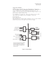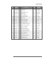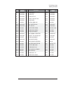
1
bus
VT1433B
8-Channel 196 kSamples/s Digitizer plus DSP
User’s Guide
Part Number 82-0068-000
Printed in U.S.A
Print Date: July 30, 2004
© VXI Technology, Inc., 2004. All rights reserved.
2031 Main Street, Irvine, CA 92614-6509 U.S.A.
NOTICE
The information contained in this document is subject to change without notice.
VXI TECHNOLOGY MAKES NO WARRANTY OF ANY KIND WITH REGARD TO THIS
MANUAL, INCLUDING, BUT NOT LIMITED TO, THE IMPLIED WARRANTIES OF
MERCHANTABILITY AND FITNESS FOR A PARTICULAR PURPOSE. VXI Technology shall not
be liable for errors contained herein or direct, indirect, special, incidental or consequential damages in
connection with the furnishing, performance or use of this material.
WARRANTY
A copy of the specific warranty terms applicable to your VXI Technology product and replacement
parts can be obtained from your local Sales and Service Office.
This document contains proprietary information which is protected by copyright. All rights are
reserved. No part of this document may be photocopied, reproduced or translated to another language
without the prior written consent of VXI Technology, Inc. This information contained in this document
is subject to change without notice.
Use of this manual and flexible disk(s) or tape cartridge(s) supplied for this pack is restricted to this
product only. Additional copies of the programs can be made for security and back-up purposes only.
© Copyright 2003 VXI Technology, Inc.
© Copyright 1979 The Regents of the University of Colorado, a body corporate.
© Copyright 1979, 1980, 1983 The Regents of the University of California.
© Copyright 1980, 1984 AT&T Technologies. All Rights Reserved.
© Copyright 1986, 1987 Sun Microsystems, Inc.
© Copyright 1984, 1985 Productivity Products Intl.
RESTRICTED RIGHTS LEGEND
Use, duplication or disclosure by the government is subject to restrictions as set forth in subdivision (c)
(1) (ii) of the Rights in Technical Data and Computer Software clause at 52.227-7013.
VXI Technology, Inc.
2031 Main Street
Irvine, CA 92614-6509
Rights for non-DOD U.S. Government Departments and Agencies are set forth in FAR 52.227-19 (c)
(1,2)
Copyright (c) 2004 VXI Technology, Inc. All rights reserved
ii
VT1433B User's Guide
In This Book
The VT1433B 8-Channel 196 kSamples/s Digitizer plus DSP is a C-size VXI
module. “196 kSamples/s” refers to the maximum sample rate of 196608 samples
per second. The VT1433B may contain either one or two 4-channel input
assemblies so that the module may have a total of up to eight inputs. The
module plugs into a single, C-size slot in a VXI mainframe.
This book documents the VT1433B module, including information on how to use
it. It provides:
q Installation information.
q Examples to expedite getting started, with information on how to use the
q
q
q
q
q
q
VXIplug&play Host Interface Library functions. There is also a chapter about the
C-Language version of the Host Interface Library. There are instructions for printing
the Function Reference for the Host Interface Library if desired. The Function
Reference can be accessed by way of online manual pages and online help.
Information on how to use the VT1433B.
A descriptions of the module.
Descriptions of the Arbitrary Source and Tachometer options.
Descriptions of the Break Out Boxes which can be used with the module.
Service information (troubleshooting and replacing assemblies).
Details about the module’s VXI registers (as an appendix for those who may want this
additional information).
iii
VT1433B User's Guide
iv
Table of Contents
In This Book . . . . . . . . . . . . . . . . . . . . . . . . . . . . . . . . . . . . . . . . . . . . . . . . . . . . . iii
Support Resources. . . . . . . . . . . . . . . . . . . . . . . . . . . . . . . . . . . . . . . . . . . . . . . . . ix
Chapter 1. Installing the VT1433B
Installing the VT1433B. . . . . . . . . . . . . . . . . . . . . . . . . . . . . . . . . . . . . . . . . . . .
To inspect the VT1433B . . . . . . . . . . . . . . . . . . . . . . . . . . . . . . . . . . . . . . . . . . .
To install the VT1433B . . . . . . . . . . . . . . . . . . . . . . . . . . . . . . . . . . . . . . . . . . .
Install the host interface libraries . . . . . . . . . . . . . . . . . . . . . . . . . . . . . . . . . . . .
To store the module . . . . . . . . . . . . . . . . . . . . . . . . . . . . . . . . . . . . . . . . . . . . . .
To transport the module . . . . . . . . . . . . . . . . . . . . . . . . . . . . . . . . . . . . . . . . . . .
1-2
1-2
1-3
1-6
1-6
1-7
Chapter 2. Getting Started With the VT1433B
Introduction. . . . . . . . . . . . . . . . . . . . . . . . . . . . . . . . . . . . . . . . . . . . . . . . . . . . . 2-2
To install the VXIplug&play libraries . . . . . . . . . . . . . . . . . . . . . . . . . . . . . . . . 2-3
System Requirements (Microsoft Windows). . . . . . . . . . . . . . . . . . . . . . . . 2-3
System Requirements (HP-UX 10.20). . . . . . . . . . . . . . . . . . . . . . . . . . . . . 2-3
VT1432A Software Distribution . . . . . . . . . . . . . . . . . . . . . . . . . . . . . . . . . 2-3
To install the Windows VXIplug&play drivers for the VT1433B
(for Windows 95 and Windows NT) . . . . . . . . . . . . . . . . . . . . . . . . . . . . . . 2-5
To install the HP-UX VXIplug&play drivers for the VT1433B
(for HP-UX systems) . . . . . . . . . . . . . . . . . . . . . . . . . . . . . . . . . . . . . . . . . . 2-6
The Resource Manager . . . . . . . . . . . . . . . . . . . . . . . . . . . . . . . . . . . . . . . . 2-6
The VXIplug&play Soft Front Panel (SFP) . . . . . . . . . . . . . . . . . . . . . . . . . . . . 2-7
Using the soft front panel. . . . . . . . . . . . . . . . . . . . . . . . . . . . . . . . . . . . . . . 2-7
VEE example programs . . . . . . . . . . . . . . . . . . . . . . . . . . . . . . . . . . . . . . . . . . 2-10
scope.vee . . . . . . . . . . . . . . . . . . . . . . . . . . . . . . . . . . . . . . . . . . . . . . . . . . 2-10
minimum.vee . . . . . . . . . . . . . . . . . . . . . . . . . . . . . . . . . . . . . . . . . . . . . . . 2-14
Other Agilent VEE example programs . . . . . . . . . . . . . . . . . . . . . . . . . . . 2-16
C-Language Host Interface Library example programs . . . . . . . . . . . . . . . . . . 2-17
Demo Programs . . . . . . . . . . . . . . . . . . . . . . . . . . . . . . . . . . . . . . . . . . . . . 2-17
Running a demo program: semascope.c . . . . . . . . . . . . . . . . . . . . . . . . . . 2-18
Visual Basic example programs . . . . . . . . . . . . . . . . . . . . . . . . . . . . . . . . . . . . 2-19
Chapter 3. Using the VT1432A
Introduction. . . . . . . . . . . . . . . . . . . . . . . . . . . . . . . . . . . . . . . . . . . . . . . . . . . . . 3-2
What is VXIplug&play? . . . . . . . . . . . . . . . . . . . . . . . . . . . . . . . . . . . . . . . . . . . 3-3
Overview . . . . . . . . . . . . . . . . . . . . . . . . . . . . . . . . . . . . . . . . . . . . . . . . . . . 3-3
VXIplug&play drivers . . . . . . . . . . . . . . . . . . . . . . . . . . . . . . . . . . . . . . . . . 3-3
Manufacturer and model codes . . . . . . . . . . . . . . . . . . . . . . . . . . . . . . . . . . 3-4
The Soft Front Panel (SFP) . . . . . . . . . . . . . . . . . . . . . . . . . . . . . . . . . . . . . 3-5
Header and Library Files . . . . . . . . . . . . . . . . . . . . . . . . . . . . . . . . . . . . . . . . . . 3-6
Channels and groups . . . . . . . . . . . . . . . . . . . . . . . . . . . . . . . . . . . . . . . . . . . . . . 3-7
Channel Groups . . . . . . . . . . . . . . . . . . . . . . . . . . . . . . . . . . . . . . . . . . . . . . 3-7
Initialization . . . . . . . . . . . . . . . . . . . . . . . . . . . . . . . . . . . . . . . . . . . . . . . . . 3-7
Creating a Channel Group . . . . . . . . . . . . . . . . . . . . . . . . . . . . . . . . . . . . . . 3-8
Input, Source and Tach Channels . . . . . . . . . . . . . . . . . . . . . . . . . . . . . . . . 3-8
Multiple-module/mainframe Measurements . . . . . . . . . . . . . . . . . . . . . . . . . . . . 3-9
Grouping of Channels/Modules. . . . . . . . . . . . . . . . . . . . . . . . . . . . . . . . . . 3-9
Multiple-module Measurements . . . . . . . . . . . . . . . . . . . . . . . . . . . . . . . . . 3-9
Possible Trigger Line Conflict. . . . . . . . . . . . . . . . . . . . . . . . . . . . . . . . . . 3-10
Managing Multiple-mainframe Measurements . . . . . . . . . . . . . . . . . . . . . 3-11
v
Synchronization in Multiple-mainframe Measurements . . . . . . . . . . . . . . 3-14
Module Features . . . . . . . . . . . . . . . . . . . . . . . . . . . . . . . . . . . . . . . . . . . . . . . . 3-15
Data Flow Diagram and FIFO Architecture . . . . . . . . . . . . . . . . . . . . . . . 3-15
Base Sample Rates. . . . . . . . . . . . . . . . . . . . . . . . . . . . . . . . . . . . . . . . . . . 3-17
Measurement Process . . . . . . . . . . . . . . . . . . . . . . . . . . . . . . . . . . . . . . . . . . . . 3-25
Measurement Setup and Control . . . . . . . . . . . . . . . . . . . . . . . . . . . . . . . . 3-25
Parameter Settings . . . . . . . . . . . . . . . . . . . . . . . . . . . . . . . . . . . . . . . . . . . 3-26
Measurement Initiation . . . . . . . . . . . . . . . . . . . . . . . . . . . . . . . . . . . . . . . 3-26
Measurement Loop . . . . . . . . . . . . . . . . . . . . . . . . . . . . . . . . . . . . . . . . . . 3-27
Register-based VXI Devices . . . . . . . . . . . . . . . . . . . . . . . . . . . . . . . . . . . 3-28
Arm and Trigger . . . . . . . . . . . . . . . . . . . . . . . . . . . . . . . . . . . . . . . . . . . . 3-29
VT1433B Triggering . . . . . . . . . . . . . . . . . . . . . . . . . . . . . . . . . . . . . . . . . 3-30
Trigger Level . . . . . . . . . . . . . . . . . . . . . . . . . . . . . . . . . . . . . . . . . . . . . . . 3-31
Data Transfer Modes . . . . . . . . . . . . . . . . . . . . . . . . . . . . . . . . . . . . . . . . . 3-32
VT1433B Interrupt Behavior . . . . . . . . . . . . . . . . . . . . . . . . . . . . . . . . . . . . . . 3-34
Data Gating . . . . . . . . . . . . . . . . . . . . . . . . . . . . . . . . . . . . . . . . . . . . . . . . 3-36
VT1433B Parameters. . . . . . . . . . . . . . . . . . . . . . . . . . . . . . . . . . . . . . . . . 3-36
New features of the VT1433B software . . . . . . . . . . . . . . . . . . . . . . . . . . . . . . 3-38
Span and center frequency . . . . . . . . . . . . . . . . . . . . . . . . . . . . . . . . . . . . . 3-38
Zoom mode . . . . . . . . . . . . . . . . . . . . . . . . . . . . . . . . . . . . . . . . . . . . . . . . 3-38
Where to get more information . . . . . . . . . . . . . . . . . . . . . . . . . . . . . . . . . . . . . 3-39
The Function Reference for VXIplug&play . . . . . . . . . . . . . . . . . . . . . . . 3-39
The Function Reference for the Host Interface Library
(C-language version) . . . . . . . . . . . . . . . . . . . . . . . . . . . . . . . . . . . . . . . . . 3-39
Chapter 4. The Host Interface Library
Introduction. . . . . . . . . . . . . . . . . . . . . . . . . . . . . . . . . . . . . . . . . . . . . . . . . . . . . 4-2
Header and Library Files . . . . . . . . . . . . . . . . . . . . . . . . . . . . . . . . . . . . . . . 4-3
Parameter Information . . . . . . . . . . . . . . . . . . . . . . . . . . . . . . . . . . . . . . . . . . . . 4-4
Description of VT1433B Parameters. . . . . . . . . . . . . . . . . . . . . . . . . . . . . . 4-4
Parameter Lists . . . . . . . . . . . . . . . . . . . . . . . . . . . . . . . . . . . . . . . . . . . . . . 4-5
Channel and Group IDs . . . . . . . . . . . . . . . . . . . . . . . . . . . . . . . . . . . . . . . 4-10
Multiple-module/Mainframe Measurements. . . . . . . . . . . . . . . . . . . . . . . . . . . 4-12
Grouping of Channels/Modules. . . . . . . . . . . . . . . . . . . . . . . . . . . . . . . . . 4-12
Multiple-module Measurements . . . . . . . . . . . . . . . . . . . . . . . . . . . . . . . . 4-12
Possible Trigger Line Conflict. . . . . . . . . . . . . . . . . . . . . . . . . . . . . . . . . . 4-13
Managing Multiple-mainframe Measurements . . . . . . . . . . . . . . . . . . . . . 4-14
Synchronization in Multiple-mainframe Measurements . . . . . . . . . . . . . . 4-17
Measurement Process . . . . . . . . . . . . . . . . . . . . . . . . . . . . . . . . . . . . . . . . . . . . 4-18
Measurement Setup and Control . . . . . . . . . . . . . . . . . . . . . . . . . . . . . . . . 4-18
Parameter Settings . . . . . . . . . . . . . . . . . . . . . . . . . . . . . . . . . . . . . . . . . . . 4-19
Measurement initialization. . . . . . . . . . . . . . . . . . . . . . . . . . . . . . . . . . . . . 4-19
Measurement Loop . . . . . . . . . . . . . . . . . . . . . . . . . . . . . . . . . . . . . . . . . . 4-20
Register-based VXI Devices . . . . . . . . . . . . . . . . . . . . . . . . . . . . . . . . . . . 4-21
Arm and Trigger . . . . . . . . . . . . . . . . . . . . . . . . . . . . . . . . . . . . . . . . . . . . 4-22
VT1433B Triggering . . . . . . . . . . . . . . . . . . . . . . . . . . . . . . . . . . . . . . . . . 4-23
Data Transfer Modes . . . . . . . . . . . . . . . . . . . . . . . . . . . . . . . . . . . . . . . . . 4-24
VT1433B Interrupt Behavior . . . . . . . . . . . . . . . . . . . . . . . . . . . . . . . . . . . . . . 4-26
Data Gating . . . . . . . . . . . . . . . . . . . . . . . . . . . . . . . . . . . . . . . . . . . . . . . . 4-28
VT1433B Parameters. . . . . . . . . . . . . . . . . . . . . . . . . . . . . . . . . . . . . . . . . 4-29
For More Information . . . . . . . . . . . . . . . . . . . . . . . . . . . . . . . . . . . . . . . . 4-29
Chapter 5. Module Description
Module Features . . . . . . . . . . . . . . . . . . . . . . . . . . . . . . . . . . . . . . . . . . . . . . . . .
General Features . . . . . . . . . . . . . . . . . . . . . . . . . . . . . . . . . . . . . . . . . . . . .
Arbitrary Source Features (Option VT1433B-1D4) . . . . . . . . . . . . . . . . . .
Tachometer Features (VT1433B-AYF). . . . . . . . . . . . . . . . . . . . . . . . . . . .
Other Options. . . . . . . . . . . . . . . . . . . . . . . . . . . . . . . . . . . . . . . . . . . . . . . .
Block Diagram. . . . . . . . . . . . . . . . . . . . . . . . . . . . . . . . . . . . . . . . . . . . . . .
vi
5-2
5-2
5-2
5-2
5-2
5-3
VT1433B Front Panel Description . . . . . . . . . . . . . . . . . . . . . . . . . . . . . . . . . . . 5-5
Front panels for four or eight channels . . . . . . . . . . . . . . . . . . . . . . . . . . . . 5-5
Standard Front Panel . . . . . . . . . . . . . . . . . . . . . . . . . . . . . . . . . . . . . . . . . . 5-6
VXI Backplane Connections. . . . . . . . . . . . . . . . . . . . . . . . . . . . . . . . . . . . . . . . 5-8
Power Supplies and Ground . . . . . . . . . . . . . . . . . . . . . . . . . . . . . . . . . . . . 5-8
Data Transfer Bus . . . . . . . . . . . . . . . . . . . . . . . . . . . . . . . . . . . . . . . . . . . . 5-8
DTB Arbitration Bus . . . . . . . . . . . . . . . . . . . . . . . . . . . . . . . . . . . . . . . . . . 5-8
Priority Interrupt Bus . . . . . . . . . . . . . . . . . . . . . . . . . . . . . . . . . . . . . . . . . . 5-8
Utility Bus . . . . . . . . . . . . . . . . . . . . . . . . . . . . . . . . . . . . . . . . . . . . . . . . . . 5-8
The Local Bus (VT1433B-UGV) . . . . . . . . . . . . . . . . . . . . . . . . . . . . . . . . 5-9
The VT1433B VXI Device . . . . . . . . . . . . . . . . . . . . . . . . . . . . . . . . . . . . . . . . 5-10
Address Space . . . . . . . . . . . . . . . . . . . . . . . . . . . . . . . . . . . . . . . . . . . . . . 5-10
Shared Memory . . . . . . . . . . . . . . . . . . . . . . . . . . . . . . . . . . . . . . . . . . . . . 5-10
Memory Map . . . . . . . . . . . . . . . . . . . . . . . . . . . . . . . . . . . . . . . . . . . . . . . 5-10
List of A16 Registers . . . . . . . . . . . . . . . . . . . . . . . . . . . . . . . . . . . . . . . . . 5-12
Trigger Lines (TTLTRG). . . . . . . . . . . . . . . . . . . . . . . . . . . . . . . . . . . . . . 5-13
Providing an External Clock . . . . . . . . . . . . . . . . . . . . . . . . . . . . . . . . . . . 5-14
Calibration Description . . . . . . . . . . . . . . . . . . . . . . . . . . . . . . . . . . . . . . . . . . . 5-15
Chapter 6. The Arbitrary Source Option (VT1433B-1D4)
Arbitrary Source Description . . . . . . . . . . . . . . . . . . . . . . . . . . . . . . . . . . . . . . . 6-2
Trigger . . . . . . . . . . . . . . . . . . . . . . . . . . . . . . . . . . . . . . . . . . . . . . . . . . . . . 6-2
Arbitrary Output . . . . . . . . . . . . . . . . . . . . . . . . . . . . . . . . . . . . . . . . . . . . . 6-2
Source Output Modes . . . . . . . . . . . . . . . . . . . . . . . . . . . . . . . . . . . . . . . . . 6-2
COLA (and Summer) . . . . . . . . . . . . . . . . . . . . . . . . . . . . . . . . . . . . . . . . . 6-2
External Shutdown. . . . . . . . . . . . . . . . . . . . . . . . . . . . . . . . . . . . . . . . . . . . 6-2
Block Diagram . . . . . . . . . . . . . . . . . . . . . . . . . . . . . . . . . . . . . . . . . . . . . . 6-3
The Arbitrary Source Option Front Panel. . . . . . . . . . . . . . . . . . . . . . . . . . . . . . 6-4
LEDs and Connectors for the Arbitrary Source Option. . . . . . . . . . . . . . . . 6-5
Updating the arbitrary source firmware . . . . . . . . . . . . . . . . . . . . . . . . . . . . 6-5
Chapter 7. The Tachometer Option (VT1433B-AYF)
Tachometer Description . . . . . . . . . . . . . . . . . . . . . . . . . . . . . . . . . . . . . . . . . . .
Tachometer Inputs . . . . . . . . . . . . . . . . . . . . . . . . . . . . . . . . . . . . . . . . . . . .
External Trigger Input . . . . . . . . . . . . . . . . . . . . . . . . . . . . . . . . . . . . . . . . .
Trigger Level . . . . . . . . . . . . . . . . . . . . . . . . . . . . . . . . . . . . . . . . . . . . . . . .
Tachometer Monitoring . . . . . . . . . . . . . . . . . . . . . . . . . . . . . . . . . . . . . . . .
Exact RPM Triggering. . . . . . . . . . . . . . . . . . . . . . . . . . . . . . . . . . . . . . . . .
Input Count Division . . . . . . . . . . . . . . . . . . . . . . . . . . . . . . . . . . . . . . . . . .
Holdoff Time . . . . . . . . . . . . . . . . . . . . . . . . . . . . . . . . . . . . . . . . . . . . . . . .
Block Diagram. . . . . . . . . . . . . . . . . . . . . . . . . . . . . . . . . . . . . . . . . . . . . . .
The Tachometer Option Front Panel. . . . . . . . . . . . . . . . . . . . . . . . . . . . . . . . . .
LEDs and Connectors for the Tachometer Option. . . . . . . . . . . . . . . . . . . .
7-2
7-2
7-2
7-2
7-2
7-2
7-3
7-3
7-3
7-4
7-5
Chapter 8. Break Out Boxes
Introduction. . . . . . . . . . . . . . . . . . . . . . . . . . . . . . . . . . . . . . . . . . . . . . . . . . . . .
Service . . . . . . . . . . . . . . . . . . . . . . . . . . . . . . . . . . . . . . . . . . . . . . . . . . . . .
The VT3240A and VT3241A Break Out Boxes. . . . . . . . . . . . . . . . . . . . . . . . .
VT3240AVoltage-type Break Out Box . . . . . . . . . . . . . . . . . . . . . . . . . . . .
VT3241A ICP®-type Break Out Box . . . . . . . . . . . . . . . . . . . . . . . . . . . . .
Break Out Box Grounding . . . . . . . . . . . . . . . . . . . . . . . . . . . . . . . . . . . . . .
Break Out Box Cables . . . . . . . . . . . . . . . . . . . . . . . . . . . . . . . . . . . . . . . . . . . .
Making a Custom Break Out Box Cable . . . . . . . . . . . . . . . . . . . . . . . . . . .
Recommendations on wiring for the VT1432A/33B 4-Channel Input
Connector. . . . . . . . . . . . . . . . . . . . . . . . . . . . . . . . . . . . . . . . . . . . . . . . . . .
8-2
8-2
8-3
8-4
8-4
8-4
8-5
8-5
8-7
Chapter 9. Troubleshooting the VT1433B
Diagnostics . . . . . . . . . . . . . . . . . . . . . . . . . . . . . . . . . . . . . . . . . . . . . . . . . . . . . 9-2
vii
Chapter 10. Replacing Assemblies
Replaceable Parts . . . . . . . . . . . . . . . . . . . . . . . . . . . . . . . . . . . . . . . . . . . . . . . 10-2
Ordering Information . . . . . . . . . . . . . . . . . . . . . . . . . . . . . . . . . . . . . . . . . 10-2
Direct Mail Order System . . . . . . . . . . . . . . . . . . . . . . . . . . . . . . . . . . . . . 10-2
CAGE Code Numbers . . . . . . . . . . . . . . . . . . . . . . . . . . . . . . . . . . . . . . . . 10-3
Assemblies: without VT1433B-AYF or VT1433B-1D4 . . . . . . . . . . . . . . 10-4
Assemblies: with VT1433B-AYF . . . . . . . . . . . . . . . . . . . . . . . . . . . . . . . 10-6
Assemblies: with VT1433B-1D4. . . . . . . . . . . . . . . . . . . . . . . . . . . . . . . . 10-8
Cables: without VT1433B-AYF or VT1433B-1D4 . . . . . . . . . . . . . . . . 10-10
Cables: with VT1433B-AYF . . . . . . . . . . . . . . . . . . . . . . . . . . . . . . . . . . 10-11
Cables: with VT1433B-1D4 . . . . . . . . . . . . . . . . . . . . . . . . . . . . . . . . . . 10-12
Front Panel. . . . . . . . . . . . . . . . . . . . . . . . . . . . . . . . . . . . . . . . . . . . . . . . 10-13
To remove the top cover . . . . . . . . . . . . . . . . . . . . . . . . . . . . . . . . . . . . . . . . . 10-14
To remove the front panel. . . . . . . . . . . . . . . . . . . . . . . . . . . . . . . . . . . . . . . . 10-15
To remove the input assemblies . . . . . . . . . . . . . . . . . . . . . . . . . . . . . . . . . . . 10-18
To remove the VT1433B-AYF assembly . . . . . . . . . . . . . . . . . . . . . . . . . . . . 10-20
To remove the VT1433B-1D4 assembly . . . . . . . . . . . . . . . . . . . . . . . . . . . . 10-21
To remove the A22 assembly . . . . . . . . . . . . . . . . . . . . . . . . . . . . . . . . . . . . . 10-22
To remove the A10/A11 assembly . . . . . . . . . . . . . . . . . . . . . . . . . . . . . . . . . 10-23
Chapter 11. Backdating
Backdating . . . . . . . . . . . . . . . . . . . . . . . . . . . . . . . . . . . . . . . . . . . . . . . . . . . . 11-2
Appendix A. Register Definitions
The VT1433B VXI Registers . . . . . . . . . . . . . . . . . . . . . . . . . . . . . . . . . . . . . . A-2
The A16 Registers. . . . . . . . . . . . . . . . . . . . . . . . . . . . . . . . . . . . . . . . . . . . A-2
The A24 Registers. . . . . . . . . . . . . . . . . . . . . . . . . . . . . . . . . . . . . . . . . . . . A-4
32-bit Registers . . . . . . . . . . . . . . . . . . . . . . . . . . . . . . . . . . . . . . . . . . . . . A-10
Command/Response Protocol . . . . . . . . . . . . . . . . . . . . . . . . . . . . . . . . . . A-11
DSP Protocol. . . . . . . . . . . . . . . . . . . . . . . . . . . . . . . . . . . . . . . . . . . . . . . A-13
DSP Bus Registers . . . . . . . . . . . . . . . . . . . . . . . . . . . . . . . . . . . . . . . . . . A-14
Glossary
Index
viii
Support Resources
Support resources for this product are available on the Internet and at VXI Technology
customer support centers.
VXI Technology
World Headquarters
VXI Technology, Inc.
2031 Main Street
Irvine, CA 92614-6509
Phone: (949) 955-1894
Fax: (949) 955-3041
VXI Technology
Cleveland Instrument Division
VXI Technology, Inc.
7525 Granger Road, Unit 7
Valley View, OH 44125
Phone: (216) 447-8950
Fax: (216) 447-8951
VXI Technology
Lake Stevens Instrument Division
VXI Technology, Inc.
1924 - 203 Bickford
Snohomish, WA 98290
Phone: (425) 212-2285
Fax: (425) 212-2289
Technical Support
Phone: (949) 955-1894
Fax: (949) 955-3041
E-mail: [email protected]
Visit http://www.vxitech.com for worldwide support sites and service plan information.
ix
x
VT1433B User's Guide
Installing the VT1433B
1
Installing the VT1433B
1-1
VT1433B User's Guide
Installing the VT1433B
Installing the VT1433B
This chapter contains instructions for installing the VT1433B 8-Channel
196 kSamples/s Digitizer plus DSP Module and its drivers. This chapter also
includes instructions for transporting and storing the module.
To inspect the VT1433B
The VT1433B 8-Channel 196 kSamples/s Digitizer plus DSP Module was
carefully inspected both mechanically and electrically before shipment. It should
be free of marks or scratches and it should meet its published specifications upon
receipt.
If the module was damaged in transit, do the following:
q Save all packing materials.
q File a claim with the carrier.
q Call a VXI Technology sales and service office.
1-2
VT1433B User's Guide
Installing the VT1433B
To install the VT1433B
Caution
To protect circuits from static discharge, observe anti-static techniques whenever
handling the VT1433B 8-Channel 196 kSamples/s Digitizer plus DSP Module.
1 Set up the VXI mainframe. See the mainframe's installation guide for assistance.
2 Select a slot in the VXI mainframe for the VT1433B module.
The VT1433B module’s local bus receives ECL-level data from the module
immediately to its left and outputs ECL-level data to the module immediately to
its right. Every module using the local bus is keyed to prevent two modules
from fitting next to each other unless they are compatible. If using the local
bus, select adjacent slots immediately to the left of the data-receiving module.
The local bus can support up to four VT1433B modules at full span at real time
data rates. If the VXI Bus is used, maximum data rates will be reduced but the
module can be placed in any available slot.
3 Using a small screwdriver or similar tool, set the logical address configuration switch
on the VT1433B.
(See the illustration on the next page.) Each module in the system must have a
unique logical address. The factory default setting is 0000 1000 (8). If an
GPIB command module will be controlling the VT1433B module, select an
address that is a multiple of 8. If the VXI system dynamically configures logical
addresses, set the switch to 255.
1-3
VT1433B User's Guide
Installing the VT1433B
4 Check the settings of the Boot Source and ROM Programming switches on the bottom
of the module.
Set switches 1 and 3 (BS1 and BS3) up and all the other switches down.
Logical Address
0
1
Boot Source
&
Programming
1
0
1-4
VT1433B User's Guide
Installing the VT1433B
5 Set the mainframe’s power switch to standby ( OI ).
Caution
Installing or removing the module with power on may damage components in the
module.
6 Place the module’s card edges (top and bottom) into the module guides in the slot.
7 Slide the module into the mainframe until the module connects firmly with the
backplane connectors. Make sure the module slides in straight.
8 Attach the module’s front panel to the mainframe chassis using the module’s captive
mounting screws.
VXI Mainframe
V T1
43
3B
Slotted
Captive Screws
bus
Power Switch
1-5
VT1433B User's Guide
Installing the VT1433B
Install the host interface libraries
After the hardware has been assembled, the next step in installing the VT1433B
is to install the host interface libraries. Refer to the chapter titled “Getting
Started With the VT1433B” to continue the installation process.
To store the module
Store the module in a clean, dry and static free environment.
For other requirements, see storage and transport restrictions in the chapter titled:
“Specifications.”
1-6
VT1433B User's Guide
Installing the VT1433B
To transport the module
• Package the module using the original factory packaging or packaging identical to the
factory packaging.
Containers and materials identical to those used in factory packaging are available
through VXI Technology.
• If returning the module to VXI Technology for service, attach a tag describing the
following:
q Type of service required
q Return address
q Model number
q Full serial number
In any correspondence, refer to the module by model number and full serial
number.
• Mark the container FRAGILE to ensure careful handling.
• If necessary to package the module in a container other than original packaging,
observe the following (use of other packaging is not recommended):
q Wrap the module in heavy paper or anti-static plastic.
q Protect the front panel with cardboard.
q Use a double-wall carton made of at least 350-pound test material.
q Cushion the module to prevent damage.
Caution
Do not use styrene pellets in any shape as packing material for the module. The
pellets do not adequately cushion the module and do not prevent the module from
shifting in the carton. In addition, the pellets create static electricity which can
damage electronic components.
1-7
VT1433B User's Guide
Installing the VT1433B
1-8
VT1433B User's Guide
Getting Started With the VT1433B
2
Getting Started With the
VT1433B
2-1
VT1433B User's Guide
Getting Started With the VT1433B
Introduction
This chapter provides assistance in getting the VT1433B running and making
simple measurements. It shows how to install the software libraries and how to
run some of the example programs that are included.
For more information see the other chapters in this book and the on-line function
reference. (See “Where to get more information” in the chapter titled “Using the
VT1433B).”
Two versions of the Host Interface Library are available. One is HP-UX
C-Language Host Interface Library which uses SICL (the Standard Instrument
Interface Library) to communicate to the VT1433B hardware. The other is the
HP-UX, Windows 95 or later and Windows NT VXIplug&play Library which
communicates with the hardware using VISA (Virtual Instrument Software
Architecture). VISA is the input/output standard upon which all the
VXIplug&play software components are based.
This chapter mainly covers the VXIplug&play version and it also includes some
examples using the C-Language version. If using the C-Language version, refer
to the chapter titled “The Host Interface Library” as well.
NOTE
The C-Language Host Interface Library has been provided for the purpose of
backward compatibility and is no longer supported. New users should use the
VXIplug&play Library while older users are encouraged to migrate their applications
to the VXIplug&play library.
2-2
VT1433B User's Guide
Getting Started With the VT1433B
To install the VXIplug&play libraries
System Requirements (Microsoft Windows)
• An IBM compatible personal computer with either Microsoft Windows 95 or later or
Microsoft Windows NT. (With either Windows OS, use the VXIplug&play library)
• Additional hardware and software to connect the IBM compatible computer to a VXI
mainframe.
• Software is supplied on CD-ROM.
System Requirements (HP-UX 10.20)
• One of the following workstations:
q An HP V743 VXI-embedded workstation.
q A stand-alone HP Series 700 workstation with an Agilent/HP E1489I EISA-to-MXIbus
card and an Agilent/HP E1482B VXI-MXI Bus Extender.
• Software is supplied on CD-ROM, so a CD-ROM drive is needed
• HP-UX Version 10.20. This version of HP-UX can use either the C-language library
or the VXIplug&play library.
• SICL/VISA (product number E2091E, version E.01.01 or later).
VT1432A Software Distribution
The VT1432A distribution (software) is shipped on CD-ROM with the VT1433B
module. This software works with the VT1432A, VT1433B and VT1434A
modules. This distribution includes the the VT1432A C-Language Host Interface
Library for HP-UX, the VT1432A VXIplug&play Host Interface library for
HP-UX, Windows 95 or later and Windows NT with associated examples and
manual pages.
2-3
VT1433B User's Guide
Getting Started With the VT1433B
Getting Updates (Windows)
The latest version of the VT1433B instrument drivers can be found on-line at
www.vxitech.com.
Getting Updates (HP-UX)
For the latest HP-UX instrument drivers, please contact VXI Technology
Customer Support Services. Contact information can be found in the Support
section of the manual on page ix.
2-4
VT1433B User's Guide
Getting Started With the VT1433B
To install the Windows VXIplug&play drivers for the VT1433B
(for Windows 95 and Windows NT)
1 Insert the VXIplug&play Drivers and Product Manuals CD into the CD-ROM drive.
2 Run the program: d:\drivers\DAQ Drivers\driver_vxipnp_e1432_a_06_13.exe.
(If the disc is in a driver other than "drive d:," replace "d:\" with the letter of the drive
containing the driver disc.) Note that the driver for the VT1433B are the same as the
driver used by the VT1432A. Also note that the "a_06_13" references the software
revision and will vary. Follow the on-screen instructions to continue.
3 The VISA Installation Information dialogue box will appear. This indicates window
will indicate whether or not the VISA library has been correctly installed previously.
If not installed, an error message will appear as a reminder to install the library. Click
Next to continue.
4 The Choose Program Folder Items dialogue box provides options that can be included
in the Start Menu Program Folder for the VT1432A. Click Next when finished with
selections to continue.
5 The Select Program Folder dialogue box appears providing the opportunity to change
the name of the program folder that will be created in the Start Menu. The default
name is "VXIPNP." Click Next to continue.
6 Setup creates a program group called “Hpe1432” (typically in c:\VXIPNP\WINNT).
It includes:
An icon to run the Soft Front Panel
An icon for HELP text
An icon for UNISTALL the README text can be included optionally.
These icons can also appear in the Startup Menu Program Files (see step 6).
7 After the program files load, the Setup Complete dialogue box will appear. It provides
the opportunity to view the Readme file and to run the Soft Front Panel upon
completion of set up. Click Next after the desired selections are made.
2-5
VT1433B User's Guide
Getting Started With the VT1433B
To install the HP-UX VXIplug&play drivers for the VT1433B
(for HP-UX systems)
1 Log in as root.
2 Insert the VT1432A CD-ROM into the CD-ROM drive or obtain the latest VT1432A
distribution.
3 Type swinstall.
See the HP-UX Reference manual for information on the swinstall command.
The VT1432A distribution is normally installed in the /opt/vxipnp/hpe1432/
directory. The files have extensions such as .h, .fp, .sl and .hlp.
The Resource Manager
The Resource Manager is a program from the hardware interface manufacturer. It
looks at the VXI mainframe to determine what modules are installed. It is
necessary to run it every time the mainframe is powered up. If the “No VT1433B
can be found in this system” is found, then run the Resource Manager.
Before running the VT1432A/33B software make sure that the hardware is
configured correctly and that the Resource Manager runs successfully. Before
using the measurement system, all of its devices must be set up, including setting
their addresses and local bus locations. No two devices can have the same
address. Usually addresses 0 and 1 are taken by the Resource Manager and are
not available.
For more information about the Resource Manager, see the hardware interface’s
documentation.
2-6
VT1433B User's Guide
Getting Started With the VT1433B
The VXIplug&play Soft Front Panel (SFP)
Using the soft front panel
If running the VT1432A/33B software in Microsoft Windows 95 or Windows NT,
the Soft Front Panel (SFP) program can be used to interface with the VT1433B.
The Soft Front Panel can be useful for checking the system to make sure that it
is installed correctly and that all of its parts are working. However, it is not very
useful for making measurements. It cannot be controlled from a program and it
does not access all of the VT1433B’s functionality.
Note
The software examples provided in this manual contain “E” references (e.g. “E1432")
used by the previous manufacturer. The VXI Technology equivalent can be derived at
by exchanging the ”E" references with “VT” references (e.g. “VT1432").
Figure 2-1: The Soft Front Panel Interface
2-7
VT1433B User's Guide
Getting Started With the VT1433B
The buttons on the right side of the SFP display are defined as follows:
Meas
This button opens the Measurement Control dialog box. It can set:
q
q
q
q
q
Measurement single/repeat
Mode block/continuous
Trigger auto/manual/input/source
Frequency span
Blocksize
Input
This button opens a dialog box where the VT1433B’s inputs can be setup. It can
set:
q
q
q
q
q
q
q
q
q
q
q
Channel number
Range
AC or DC coupling
Grounding method
Digital anti-alias filter
Analog anti-alias filter
Trigger on/off
Trigger mode level/bound
Trigger level
Hysteresis
Trigger Slope
There is a checkbox to make all channels identical.
Source
This opens a dialog box for controlling the source output of the VT1433B’s
source. This is only available for VT1433B’s that have the Arbitrary Source
VT1433B-1D4. It can set:
q
q
q
q
q
q
q
q
q
q
q
q
q
2-8
Channel number
Active on/off
Mode sine/burst sine/random/burst random
Ramp rate
Sine frequency
Sine phase
Output normal/grounded/open/cal/multi
Trigger on/off
Cola (Constant Output Level Amplifier) off/on
Duty Cycle
Sum off/on
Seed
Range
VT1433B User's Guide
Getting Started With the VT1433B
Display
This button opens a dialog box which specifies how the data will be displayed.
For each trace, an input channel (or OFF) and an output file can be specified.
VXI
This button opens a dialog box showing the modules installed in the VXI
mainframe and indicating which are active and inactive. The “resource name” for
each module is the interface card name that has been assigned to it.
Go
Use the Go button to start the measurement.
Exit
Use the Exit button to exit the Soft Front Panel.
2-9
VT1433B User's Guide
Getting Started With the VT1433B
VEE example programs
scope.vee
This program displays four channels with time record and FFT for each channel.
For the examples provided below, Agilent© VEE is used.
The scope.vee program is located at VXIPNP\Hpe1432\examples\vee\ on a
Microsoft Windows system or at /usr/e1432/vee-examples on an HP-UX system.
To run scope.vee, first type:
veetest
To begin using Agilent VEE.
In Agilent VEE click on File, then Open. In the Open File dialog box select
scope.vee from the list of files. Then click Ok.
Figure 2-2: Agilent VEE - Open Dialogue Box
2-10
VT1433B User's Guide
Getting Started With the VT1433B
The program scope.vee starts, showing four channels, with time record and FFT
for each channel.
Figure 2-3: scope.vee - Panel View
To start a measurement, click the Run button on the toolbar (triangle symbol).
To pause, click on the Pause button (two vertical bars, next to the Run button).
To stop the measurement, click the Stop button (square symbol).
This screen is VEE’s panel view, where interaction with the system can be
performed much as one would with the front panel of a standalone instrument.
The VEE detail view screen allows for configuration of the system and a view
panel which can be used to make measurements.
To look at the scope.vee program “behind the scenes,” click on the View Detail
button on the toolbar (chart symbol). To return to the original (panel) view, click
on the View Panel button (sine wave symbol).
Click on the View Detail button again to look at the detail view screen.
2-11
VT1433B User's Guide
Getting Started With the VT1433B
To use and modify scope.vee, it is necessary to be familiar with using the
Agilent VEE program. Refer to Agilent VEE documentation if necessary. In
View Detail mode, click on Help on the menu bar for assistance in using
Agilent VEE.
Figure2-4: Agilent VEE Help Text
2-12
VT1433B User's Guide
Getting Started With the VT1433B
In detail view there are boxes representing parts of the scope.vee program. For
programs that are too large to be viewed all at one time, use the scroll bars at the
bottom and left side of the screen to scroll the display. To see more detail,
double-click on a box or click on the View Detail (chart symbol) button on the
top bar of the box. Some of the boxes contain a function. Clicking on a
function displays the parameters associated with it.
Figure 2-5: scope.vee - Detail View
To specify a new function, click on the blank space in the box where the
function is to be. A dialog box appears with a list of functions. After selecting
a function, choose Panel to “hard code” constants that the function will use or
choose Parameters to allow a parameter to be input from elsewhere (from the user
or another function). The input appears as a “pin” on the chart diagram. In the
scope.vee program the user can select the blocksize, span and range.
Clicking Add To Panel in the Edit menu makes a box in the detail view visible
on the panel view. This gives the user access to enter parameters or view
results.
2-13
VT1433B User's Guide
Getting Started With the VT1433B
Clicking on Alphnumeric in the Display menu sets up a box that specifies how to
display the output of a function.
Use Agilent VEE to look at the functions that make up the simple “scope.vee”
program. This is an example of how the VT1433B can be programmed using
Agilent VEE.
Click on the Panel View button (sine wave symbol) to go to panel view. Set up
the system to provide input signals to some of the input connectors of the
VT1433B. Then use the scope.vee interface to view the time records and FFTs
of the input signals.
When Agilent VEE is exited, the program will ask if any changes made to
scope.vee are to be made. Click No or, if desired, click Cancel and then use
File/Save As to save the changes with a different filename.
minimum.vee
This program provides a simple example to assist in the learning to use the
VT1432A library, although it is not intended to be a finished “user-friendly”
program. It contains the minimum number of functions needed (nine functions) to
get data from the VT1433B module. It does not even include a “panel” user
interface, so the first screen seen is the VEE View Detail screen. Use the scroll
bar at the bottom of the screen to scroll the display and see all of the detail view.
The minimum.vee program simply takes data for one channel and then stops. It
may be useful to examine this program and use it as a starting point for learning
to write VEE programs for the VT1433B.
2-14
VT1433B User's Guide
Getting Started With the VT1433B
Figure 2-6: minimum.vee (scroll to see entire display)
2-15
VT1433B User's Guide
Getting Started With the VT1433B
Other Agilent VEE example programs
There are several other example programs that can be examined in the same way
as scope.vee. These programs are in the path VXIPNP\Hpe1432\examples\vee\ on
a Microsoft Windows system or /usr/e1432/vee-examples on an HP-UX system.
bsrcsine.vee (Burst SouRCe SINE)
This program is similar to scope.vee. It displays eight (rather than four) channels,
with time record and FFT for each channel. It also turns on the source in burst
sine mode and ramps up the source output. The user can specify the duty cycle,
ramp rate, level of the source and frequency of the source. This program works
with VT1433B’s which are equipped with the source VT1433B-1D4.
bsrcrand.vee (Burst SouRCe RANDom)
This program is like bsrcsine.vee except the source is turned on in burst random
mode.
frf_rand.vee. (Frequency Response Function RANDom)
This program displays the frequency response of four channels. One way to set
up this example is to connect a cable between the channel 1 and channel 2
inputs. Then connect channel 3 to channel 1 through a “black box” containing
the circuit to be tested (using a “T” on channel 1). Channel 4 remains
unconnected. On the display, a response for channel 2 over channel 1 (a flat
response for the bare cable) will be seen and a response for channel 3 over
channel 1 (representing the frequency response of the “unknown” circuit).
Channel 4 will show a random signal since it has no input.
order.vee
This program can be used only with a VT1432A with the tachometer option. It
takes four channels of data and displays two channels. It shows raw time domain
data and resampled data for each rpm value. The raw data can then be processed
with a program such as Matlab to make order ratio maps.
2-16
VT1433B User's Guide
Getting Started With the VT1433B
C-Language Host Interface Library example programs
The VT1432A C-Language Host Interface Library comes with several example
programs, which help demonstrate how to use the library. These example
programs are found in the the VXIPNP\Hpe1432\examples\ directory. The
programs in this directory are all very small, so that they will be easily
understood and easy to copy into a real application.
The files in the examples directory are:
Makefile
README
detect.c
example.c
intr.c
src_intr.c
tachmon.c
throughput
A UNIX Makefile which can be used to compile all of the programs in the
examples directory.
A file containing the information given here.
Shows how to use SICL calls to find the logical addresses of the VT1433B
modules in a system.
Shows the basics of setting up a VT1433B, starting a measurement and
reading a block of data.
Shows how to set up SICL and a VT1433B to use interrupts for data collection.
Shows how to set up SICL and a VT1433B to use interrupts with a
VT1433B-1D4 Source board, for overload shutdown and overread.
Shows how to monitor a tach channel signal using the other inputs in the
VT1433B module.
A directory containing example programs for throughput to and post-processing
from a VT2216A disk module.
Demo Programs
In addition to example programs, the VT1432A Host Interface library also comes
with demo programs. These programs are found in the
VXIPNP\Hpe1432\examples\ directory.
One of these demo programs, called “semascope”, demonstrates that the VT1433B
hardware and software are working properly. When run, it identifies the
VT1433B modules in the VXI system, runs a measurement using the VT1433B
modules that it finds and plots the results in X11 windows. This program is not
meant to be an example of how to use the VT1432A library, although the source
code is not provided.
Other demo programs include “rpmtrig” and “rpmtrig2” and “semascope3.”
2-17
VT1433B User's Guide
Getting Started With the VT1433B
Running a demo program: semascope.c
To run this program, type:/opt/e1432/demo/semascope. This program displays the
time records for 32 channels (when hooked up to two VT1433B modules with
16 channels each). The channel that is active for changing the display is
highlighted. To exit, double-click the horizontal bar symbol in the upper left
corner of the window.
To see a list of parameters for semascope, type:
semascope -u
To specify a parameter, type its letter code after “semascope” on the command
line.
The source code for this program is at:
/opt/e1432/demo/semascope.c
Use a text viewer or editor (such as the “more” utility in UNIX) to list the source
code for semaphore.c. Examine the code to learn more about how this example
program works.
2-18
VT1433B User's Guide
Getting Started With the VT1433B
Visual Basic example programs
VEE programs and the VXIplug&play Library can be used on both UNIX and PC
systems. In addition, the PC can use Visual Basic. Visual Basic example
programs are at \Hpe1432\examples\vb\ on a Microsoft Windows system.
2-19
VT1433B User's Guide
Getting Started With the VT1433B
2-20
3
Using the VT1432A
3-1
VT1433B User's Guide
Using the VT1433B
Introduction
This chapter shows how to use the VT1433B using the VXIplug&play Host
Interface Library.
The Host Interface Library for the VT1433B is a set of functions that allow the
user to program the register-based VT1433B at a higher level than register reads
and writes. The library allows groups of VT1433Bs to be set up and
programmed as if they were one entity
Two versions of the Host Interface Library are included. One is the HP-UX
C-Language Host Interface Library which uses SICL (the Standard Instrument
Interface Library) to communicate to the VT1433B hardware. It works for
HP-UX 10.20. The other is the VXIplug&play Library for Windows 95 or later,
Windows NT and HP-UX 10.20 which communicates with the hardware using
VISA (Virtual Instrument Software Architecture). VISA is the input/output
standard upon which all the VXIplug&play software components are based.
This chapter covers the VXIplug&play version, but it will also be useful to users
of the C-Language version. If using the C-Language version, refer to the chapter
titled "The Host Interface Library" was well.
The library includes routines to set up and query parameters, start and stop
measurements, read and write data and control interrupts. Routines to aid
debugging and perform low-level I/O are also included.
For information on diagnostics see the chapter titled “Troubleshooting the
VT1433B.”
3-2
VT1433B User's Guide
Using the VT1433B
What is VXIplug&play?
Agilent uses VXIplug&play technology in the VT1433B. This section outlines
some of the details of VXIplug&play technology.
Overview
The fundamental idea behind VXIplug&play is to provide VXI users with a level
of standardization across different vendors well beyond what the VXI standard
specifications spell out. The VXIplug&play Alliance specifies a set of core
technologies centering on a standard instrument driver technology.
Agilent offers VXIplug&play drivers for VEE-Windows. The VXIplug&play
instrument drivers exist relative to so-called “frameworks”. A framework defines
the environment in which a VXIplug&play driver can operate. The VT1433B has
VXIplug&play drivers for the following frameworks: Windows 95 or later,
Windows NT and HP-UX.
VXIplug&play drivers
The VT1433B VXIplug&play driver is based on the following architecture:
User Program (.EXE & .HLP files, such as soft front panel)
Programmatic Developer's
Interface Library
Function Panel
(based on .FP file
Instrument Driver
(.KB, .DLL, .C, .H, .LIB, .HLP file)
VTL/VISA
I/O Interface
Figure 3-1: VXI Plug&Play driver architecture
It is most useful to discuss this architecture from the bottom up.
The VISA/VTL I/O interface allows interoperability of the VXIplug&play driver
technology across interfaces.
3-3
VT1433B User's Guide
Using the VT1433B
The actual instrument driver itself is a DLL (Dynamic Linked Library) created
from:
q A set of source (.C) files.
q A set of header (.H) files, used for compiling the file as well as to describe the
driver’s calls to any program using the driver.
q A standard driver library (.LIB) file, to provide the standard functionality all the
drivers would require.
This DLL is a set of calls to perform instrument actions — at heart, that’s all a
VXIplug&play driver is — a library of instrument calls.
This driver is accessed by Windows applications programs written in languages
such as Visual C++ or Visual BASIC, using programming environments such as
VEE or NI LabView.
A Windows Help (.HLP) file is included which provides descriptive information
and code samples for the functions in the VXIplug&play DLL. This help file can
be viewed in the standard Windows Help viewer. A viewer for HP-UX is
provided in /opt/hyperhelp - see the READ.ME file.
Manufacturer and model codes
If desired, the manufacturer code, model code and name of the VXI instruments
can be read from the file :\hpe1432\lib\vximodel.cf (on PC systems) or
/opt/e1432/lib/vximodel.cf (on UNIX systems).
The following list identifies the VXI models in this file:
Manufacturer Code
0xFFF
0xFFF
0xFFF
0xFFF
0xFFF
3-4
Model Code
0x200
0x201
0x202
0x203
0x210
Model Name
Agilent/HP E143xA Non-booted Substrate Board
VT1432A 16 Channel 51.2 kSamples/s Digitizer + DSP
VT1433B 8 Channel 196 kSamples/s Digitizer + DSP
VT1434A 4 Channel 65 kSamples/s Arbitrary Source
VT2216A VXI/SCSI Interface Module
VT1433B User's Guide
Using the VT1433B
The Soft Front Panel (SFP)
The Soft Front Panel is a stand-alone Windows application, built on top of the
VXIplug&play driver DLL; it is used for instrument evaluation and debugging
and as a demo. It is not a programmable interface to the instrument, nor can it
be used to generate code.
The soft front panel also accesses the same Windows Help file as provided with
the DLL.
Figure 3-2: An example of a soft front panel (SFP)
3-5
VT1433B User's Guide
Using the VT1433B
Header and Library Files
In the Windows environment, the following files are in the directory
\Vxipnp\WinXX\Hpe1432
hpe1432.fp
The “FP” file used by VEE and CVI
hpe1432.hlp
Windows help file
hpe1432.kb
Knowledge base file
hpe1432.bas
header for Visual Basic
hpe1432.exe
Soft front panel program
Bin\hpe1432_32.dll
The VXIplug&play driver
Include\hpe1432.h
Header for linking to the VXIplug&play driver
Lib\Msc\
hpe1432_32.lib
Lib for linking C programs to VXIplug&play
The following files are in the directory \Hpe1432
Read.me
The latest information for the product
lib\sema.bin
Firmware program for the VT1433B
lib\sfp.ico
Icon for help file
lib\sinewave.ico
Icon for Soft Front Panel
source\*
Source files for hpe1432_32.dll
examples\vb\*
Visual Basic example programs
examples\c\*
C example programs
examples\hpvee\*
Agilent VEE example programs
In the HP-UX environment, the following files are in the directory
/opt/vxipnp/hpux/hpe1432:
hpe1432.fp
The “FP” file used by VEE
.h
Header file
.hlp
Hyperhelp file (see /opt/hyperhelp/README for information on how to
view hpe1432.hpl In the HP-UX environment.)
.sl (lower-case “SL”)
The VXIplug&play shared library
3-6
VT1433B User's Guide
Using the VT1433B
Channels and groups
This section gives some information about using channels and groups. For more
detailed information see the VT1433B help text.
Channel Groups
In the VT1433B VXIplug&play driver, a channel group is the basic unit of
hardware control. To control any channel, it must first be assigned to a group
with the hpe1432_createChannelGroup function. In addition to creating the group,
this function returns a “handle” that uniquely identifies the group. This handle
can then be used to direct functions to all channels in the group.
When a channel group is created, all input and tach channels in the group are
automatically activated and all source channels are inactivated. But when deleted,
input and tach channels are not automatically inactivated. Any input or tach
channel that remains active after its group is deleted will continue to supply data
to its module’s FIFO buffer during a measurement — consuming module
resources. For this reason, the channels in group should always be explicitly
inactivated before deleting them. Channels can be inactivated with
hpe1432_setActive. Channel groups can be deleted with
hpe1432_deleteChannelGroup and hpe1432_deleteAllChanGroups.
Also when creating a channel group, channels which are not mentioned in the
new group are not turned off. Any channels that are not to be active must be
explicitly inactivated. (An exception is a power-up when only the channels in the
initial channel group are active.)
Initialization
The command used to initialize the system is hpe1432_init. This function
initializes the VXIplug&play library and registers all VT1433B modules. It also
checks the existence of a VT1432A module at each of the logical addresses given
in the resource list and allocates logical channel identifiers for each channel in all
of the VT1432As. Input channels, source channels and tach/trigger channels are
kept logically separated.
Most other functions cannot be used until after hpe1432_init, but there are two
functions which can be used before initialization to get information needed by
hpe1432_init. These are hpe1432_find and hpe1432_getHWConfig. hpe1432_find
searches the VXI mainframe and returns the VXI Logical Address for every
VT1433B found. hpe1432_getHWConfig returns additional information about the
hardware.
After hpe1432_init is run, use hpe1432_getNumChans to get the total count of
inputs, sources and tachometers for all VT1433B modules named in the
hpe1432_init call.
3-7
VT1433B User's Guide
Using the VT1433B
Creating a Channel Group
The function hpe1432_createChannelGroup creates and initializes a channel group.
A channel group allows commands to be issued to several VT1433B channels at
once, simplifying system setup. Channel groups can be overlapped. The state of
an individual VT1433B channel that is in more than one channel group is
determined by the most recent operation performed on any group to which this
channel belongs.
As a side effect, this function makes all input and tach channels in the channel
group active and all source channels in the channel group inactive. This function
does not inactivate other channels within the modules that the channels are in and
does not preset the channels in the new group.
After a channel group has been created, use hpe1432_getGroupInfo to get selected
information about the group. It is possible for hpe1432_getGroupInfo to be set
up to return the number of modules, channels, inputs, sources or tachs in the
group. It can also return a list of the modules, channels, inputs, sources or tachs.
Input, Source and Tach Channels
Channel numbers must fall in particular ranges for different types of channels.
Input channel numbers range from 1 to 4095. Source channel numbers range from
4097 to 8191. Tach channel numbers range from 8193 to 12287.
A mixture of input, source and tach channels can be present in one group.
However it is also important for many functions to be sent only to the appropriate
type of channel. For example, asking for a blocksize from a tach channel can
cause an error. It may be useful to set up several channel groups at the
beginning of the program: one for input channels, one for source channels, one
for tach channels and one that combines all three channel types. The input
handle can then be used for input-only functions, the source for source-only
functions and the tach handle for tach-only functions. The “all-channels” handle
would be used for all other functions.
3-8
VT1433B User's Guide
Using the VT1433B
Multiple-module/mainframe Measurements
Grouping of Channels/Modules
The interface library for the VT1433B is designed to allow programming of
several channels from one or several distinct modules, as if they were one entity.
Each VT1433B module has up to eight channels. The library may control up to
a maximum of 255 VT1433B modules (8160 channels).
The function hpe1432_createChannelGroup can be used to declare any number of
groups of channels, possibly overlapping. Each group can be uniquely identified
by a group ID.
The ‘target’ of a library function is either a channel, a group or (rarely) a
module, depending on the nature of the call. When the same library function
may be called with either a channel or a group identifier, its ‘target’ is shown by
a parameter named ID.
Multiple-module Measurements
A channel group that spans more than one module will need to be configured to
use the TTL trigger lines on the VXI Bus for inter-module communications. This
configuration is automatically performed in the hpe1432_initMeasure call unless
defeated using hpe1432_setAutoGroupMeas.
The following discussion outlines what hpe1432_initMeasure does automatically.
This must be done by the user if hpe1432_setAutoGroupMeas has been used to
defeat auto configuration.
There are eight VXI TTL trigger lines that can be used for multi-module
synchronization. Often, these lines are used in pairs, one for sample clock and
one for Sync/Trigger. The hpe1432_setTtltrgLines function selects which TTL
trigger lines to use; this function always uses the TTL trigger lines in pairs.
Calling hpe1432_setClockSource with the group ID will set all modules to the
same pair.
All modules need to be set to use the shared sync line rather than the default
setting of internal sync. This can be done with the hpe1432_setMultiSync
function, using the group ID.
One module of the set of modules needs to be set to output the sync pulse. The
module with the lowest VXI logical address is called the “system module” and is
assigned this duty. This can be set with the hpe1432_setMultiSync function call,
using the lowest channel ID in the group (NOT the group ID).
3-9
VT1433B User's Guide
Using the VT1433B
All modules except the “system module” need to be set to use the VXI TTL
trigger lines as the clock source. Use hpe1432_setClockSource for this.
Set the “system module” to output the clock. Use hpe1432_setClockMaster for
this. After this is done, all system sync pulses come from the “system module”
and drive the measurement state machines on all boards in the group.
Possible Trigger Line Conflict
The following describes a scenario where VT1433B modules might conflict and
prevent a proper measurement. The conditions allowing the conflict are complex
but must be understood by the user.
After a measurement has completed, the modules are left set up. If a module
(call it module ‘A’) is driving the TTL trigger lines and a different group is
started which also drives the TTL trigger lines (and that different group does not
include module ‘A’), then module ‘A’ will conflict and prevent the other group
from functioning. In this case make a call to hpe1432_finishMeasure (using the
old group ID which includes ‘A’) to turn off module ‘A’ and allow the new
group to function.
Note that if the new group includes all modules of the old group, the conflict will
not occur since hpe1432_initMeasure will reset all modules as needed. Also note
that single-module groups do not drive the TTL trigger lines, so single-module
groups are immune from causing or receiving this conflict.
3-10
VT1433B User's Guide
Using the VT1433B
Managing Multiple-mainframe Measurements
In a single-mainframe measurement, the VT1433B communicates with other
VT1433Bs through the TTLTRG lines. However, when using the VXI-MXI bus
extender modules, the TTLTRG lines, which carry the group synchronization
pulse and sample clock, are extended only in one direction. This unidirectional
signal connection restricts the types of measurements that can be made in a
multiple mainframe environment.
The following types of multiple mainframe measurements cannot be performed:
q Unequal pre-trigger delay settings between mainframes
q Channel triggering by channels in Mainframe B
q Lower spans or longer blocksizes in Mainframe B
q Different digital filter settling times between VT1433B modules
Ethernet or Firewire
Embedded Controller
VT1433B
VT1433B
Fail Acs
ExSamp
Trigger
Cal
ExTrig
8-CHANNEL 196
kSa/s DIGITIZER
+DSP
S
l
o
t
Chan
5-8
0
VT1433B
Fail Acs
ExSamp
Fail Acs
ExSamp
ExTrig
8-CHANNEL 196
kSa/s DIGITIZER
+DSP
Trigger
Cal
ExTrig
8-CHANNEL 196
kSa/s DIGITIZER
+DSP
Chan
5-8
Chan
1-4
VT1433B
VT1433B
Trigger
Cal
MXI-2
Extender Interface
Chan
5-8
Chan
1-4
VT1433B
Fail Acs
ExSamp
Trigger
Cal
ExTrig
8-CHANNEL 196
kSa/s DIGITIZER
+DSP
Chan
5-8
Chan
1-4
Chan
1-4
VXI Mainframe A
bus
VXI Mainframe A
bus
bus
bus
MXI-2
Extender
Interface
VT1433B
Fail Acs
ExSamp
Trigger
ExTrig
Cal
8-CHANNEL 196
kSa/s DIGITIZER
+DSP
Chan
5-8
VT1433B
Fail Acs
ExSamp
VT1433B
Trigger
Cal
Fail Acs
ExTrig
ExSamp
8-CHANNEL 196
kSa/s DIGITIZER
+DSP
bus
MXI-2 Extender Interface
ExTrig
8-CHANNEL 196
kSa/s DIGITIZER
+DSP
Chan
5-8
Chan
1-4
Trigger
Cal
Chan
5-8
Chan
1-4
bus
VXI Mainframe B
Example 1: Slot 0 Controller
Trigger
Cal
ExTrig
8-CHANNEL 196
kSa/s DIGITIZER
+DSP
Chan
5-8
Chan
1-4
VT1433B
VT1433B
Fail Acs
ExSamp
bus
MXI-2 Extender Interface
Chan
1-4
bus
VXI Mainframe B
VT1433B
Example 2: MXI-2 Daisy Chain
Figure 3-3: Multiple mainframes - two mainframes
3-11
VT1433B User's Guide
Using the VT1433B
In the example above, Mainframe A contains the Slot 0 Controller for a multiple
mainframe system. Mainframe A is connected to Mainframe B with a VXI-MXI
interface, Agilent/HP E1482B. To successfully manage this multiple mainframe
environment, use the following guidelines.
q Locate modules with logical addresses less than 128 in Mainframe A.
q Locate modules with logical addresses greater than 127 in Mainframe B.
q Locate the highest-numbered channels in Mainframe A.
q Locate the last module in the module list specified in the call to hpe1432_init in
q
q
q
q
q
Mainframe A.
Locate the module that generates the group synchronization pulse in Mainframe A.
Locate the channels performing channel triggering in Mainframe A.
Locate the module with the shared sample clock in Mainframe A.
If a groupID is not used with the call hpe1432_readRawData or
hpe1432_readFloat64Data, empty the VT1433Bs’ FIFOs in Mainframe B before
Mainframe A. In other words, do not empty the FIFOs in Mainframe A unless the
FIFOs in Mainframe B have been emptied. For more information about groupID
see “Grouping of Channels/Modules” in this chapter.
If more than two mainframes are needed, daisy-chain them together. Treat each
mainframe after the first as a Mainframe B. See the example on the next page.
Phase Performance in Multiple Mainframe Measurements
Phase specifications are degraded by the delay that the inter-mainframe interface
gives the sample clock. This delay is insignificant for many low-frequency
applications because the phase error is proportional to frequency. A system with
two VXI-MXI modules and a one-meter cable, typically has a 76 nanosecond (ns)
sample clock delay in Mainframe B. This corresponds to an additional
0.007 degree phase error at 256 Hz and an additional 0.55 degree phase error at
20 kHz.
Using a four-meter cable (which adds approximately 18 ns of delay) causes a
total of 94 ns clock delay in Mainframe B. This corresponds to an additional
0.0087 degree phase error at 256 Hz and an additional 0.68 degree phase error at
20 kHz.
The cable adds approximately 6 ns per meter of cable.
Each daisy-chained mainframe adds another increment of delay, but only for the
additional cabling length.
3-12
VT1433B User's Guide
Using the VT1433B
VT1433B
Ethernet/Firewire
Embedded Controller
VT1433B
Fail Acs
ExSamp
Trigger
Cal
ExTrig
8-CHANNEL 196
kSa/s DIGITIZER
+DSP
S
l
o
t
Chan
5-8
VT1433B
Fail Acs
ExSamp
ExSamp
Trigger
Cal
ExTrig
8-CHANNEL 196
kSa/s DIGITIZER
+DSP
Chan
5-8
Chan
5-8
Chan
1-4
bus
MXI-2
Extender
Interface
Fail Acs
ExTrig
8-CHANNEL 196
kSa/s DIGITIZER
+DSP
Chan
1-4
0
VT1433B
Trigger
Cal
VT1433B
MXI-2
Extender Interface
bus
VT1433B
Fail Acs
ExSamp
Trigger
Cal
Chan
5-8
Chan
1-4
VXI Mainframe A
Chan
1-4
bus
MXI Bus
Cable
ExTrig
8-CHANNEL 196
kSa/s DIGITIZER
+DSP
bus
VXI Mainframe A
MXI Bus
Cable
VT1433B
Fail Acs
ExSamp
Trigger
Cal
ExTrig
8-CHANNEL 196
kSa/s DIGITIZER
+DSP
Chan
5-8
VT1433B
Fail Acs
ExSamp
VT1433B
Trigger
Cal
Fail Acs
ExTrig
ExSamp
8-CHANNEL 196
kSa/s DIGITIZER
+DSP
bus
ExTrig
8-CHANNEL 196
kSa/s DIGITIZER
+DSP
Chan
5-8
Chan
1-4
Trigger
Cal
Chan
5-8
Chan
1-4
bus
bus
VT1433B
MXI-2
Extender
Interface
Trigger
Cal
ExTrig
8-CHANNEL 196
kSa/s DIGITIZER
+DSP
Chan
5-8
Chan
1-4
VXI Mainframe B
VT1433B
Fail Acs
ExSamp
Chan
1-4
bus
VXI Mainframe B
VT1433B
MXI-2
Extender
Interface
VT1433B
VT1433B
Fail Acs
ExSamp
Trigger
Cal
VT1433B
VT1433B
Fail Acs
ExTrig
ExSamp
8-CHANNEL 196
kSa/s DIGITIZER
+DSP
Trigger
Cal
ExTrig
8-CHANNEL 196
kSa/s DIGITIZER
+DSP
Chan
5-8
Chan
5-8
Chan
1-4
bus
Chan
1-4
VXI Mainframe C
Example 3: Embedded Slot 0 Controller
bus
VXI Mainframe C
Example 4: MXI-2 Daisy Chain
Figure3-4: Multiple mainframes - three mainframes
3-13
VT1433B User's Guide
Using the VT1433B
Synchronization in Multiple-mainframe Measurements
A TTL Trigger line between VT1433Bs making group measurements keeps all
modules synchronized. This is an open-collector line where each module holds
the one designated as the SYNC line low until the module is ready to advance to
the next measurement state. Another TTL Trigger line is designated to carry the
sample clock to all modules. This shared sample clock may come from any
VT1433B module in Mainframe A or from an external signal routed through the
Slot 0 Commander in Mainframe A.
One module is responsible for pulling the SYNC line low to start each group’s
state transition. Then, each module holds the line low until it is ready. When all
modules are ready, the SYNC line drifts high. The unidirectional line prevents
modules in Mainframe B from holding-off modules in Mainframe A.
The lowest logical address must be in Mainframe A because of VXI-MXI and
Resource Manager (RM) constraints. Group constraints with the VXIplug&play
Library force modules in Mainframe A to have their FIFOs emptied last. The
VXIplug&play reads data in channel order, so the highest channel is read last. To
get this to work automatically, the call to hpe1432_init must list the logical
addresses in descending order.
Channel triggering must be done only by modules in Mainframe A. A trigger in
any other mainframe would not be communicated back on the SYNC line to
Mainframe A. The VXIplug&play Library itself selects the VT1432A with the
highest channel number for synchronization.
VXI-MXI Module Setup and System Configuration
The VXI-MXI Module setup in Mainframe A needs to be changed from those set
by the factory. The VXI-MXI module is not the Slot 0 Controller for
Mainframe A. See Table 2-1: Configuration Settings in the Agilent/HP E1482B
VXI-MXI Bus Extender User’s Manual. This requires changing several switch
settings.
q Set the module as not being the Slot 0 Controller.
q Set the VME timeout to 200 µs.
q Set the VME BTO chain position to 1 extender, non-slot0.
q Do not source CLK10.
q Set the proper logical address.
3-14
VT1433B User's Guide
Using the VT1433B
Module Features
Data Flow Diagram and FIFO Architecture
The illustration on the next page shows data flow in the VT1433B. In this
example there are four 4-channel input assemblies for a total of sixteen input
channels. The data for all channels is sent to the FIFO. The FIFO is divided
into sections, one for each channel. The data moves through a circular buffer
(first-in-first-out) until a trigger causes it to be sent on to the VME Bus. The
data can also be sent to the Local Bus if option UGH is present.
The size of the sections in the FIFO is flexible. The amount of DRAM memory
for each channel is the total DRAM memory divided by the number of channels.
The standard DRAM size is 4 MB; an optional 32 MB DRAM is available.
The trigger can be programmed to trigger on the input or on information from the
software. The following are examples of ways a trigger can be generated.
q input level or bound
q source
q external trigger
q RPM level (with tachometer option VT1433B-AYE)
q ttl_trigger (VXI backplane)
q freerun (automatic)
3-15
VT1433B User's Guide
Using the VT1433B
96002
trigger
96002
host
port
VME Bus
Input 1
Local
Bus
FIFO
Local Bus
ch 1
Static
Input 2
FIFO
RAM
ch 8
FIFO (DRAM)
circular
buffer
trigger
ch 1
ch 2
to VME Bus
or Local Bus
ch 3
ch 4
ch 5
Figure 3-5: Data flow and FIFO architecture
3-16
VT1433B User's Guide
Using the VT1433B
Base Sample Rates
Baseband Measurement Spans
The table on the following page shows the measurement spans available for base
sample rates, for baseband measurements.
“Fs” is the sample frequency or sample rate. The value for zero divide-by-two
steps and no divide-by-five step is the top measurement span corresponding to the
sample rate. This is with no decimation and using 400 lines to avoid alias. The
other values on the table are for this top span decimated by five and/or two.
For a VT1433B which has option 1D4, the Arbitrary Source, the sample rate for
the source is automatically set to be the same as the sample rate selected for the
inputs. When the source is active the sample rate cannot be greater than
65.536 kHz.
Decimation Filter Diagram
The drawing below illustrates the way the spans in the table are generated. In
the case of baseband spans (lower limit of span fixed at zero), the frequency can
(optionally) be divided by five and then (optionally) divided by two up to eight
times.
ADC
÷5
zero or
one time
÷2
zero or
sixteen times
Figure 3-6: Decimation filter diagram - baseband
3-17
VT1433B User's Guide
Using the VT1433B
Table of Baseband Measurement Spans (part 1 of 6)
All values are in Hertz (Hz).
sample
frequency
(Fs) —>
48000
50000
51200
number of ÷2
steps
with ÷5
without ÷5
with ÷5
without ÷5
with ÷5
without ÷5
0
3750.000000
18750.000000*
3906.250000
19531.250000*
4000.000000
20000.000000*
1
1875.000000
9375.000000
1953.125000
9765.625000
2000.000000
10000.000000
2
937.500000
4687.500000
976.562500
4882.812500
1000.000000
5000.000000
3
468.750000
2343.750000
488.281250
2441.406250
500.000000
2500.000000
4
234.375000
1171.875000
244.140625
1220.703125
250.000000
1250.000000
5
117.187500
585.937500
122.070312
610.351562
125.000000
625.000000
6
58.593750
292.968750
61.035156
305.175781
62.500000
312.500000
7
29.296875
146.484375
30.517578
152.587891
31.250000
156.250000
8
14.648438
73.242188
15.258789
76.293945
15.625000
78.125000
9
7.324219
36.621094
7.629395
38.146973
7.812500
39.062500
10
3.662109
18.310547
3.814697
19.073486
3.906250
19.531250
11
1.831055
9.155273
1.907349
9.536743
1.953125
9.765625
12
0.915527
4.577637
0.953674
4.768372
0.976562
4.882812
13
0.457764
2.288818
0.476837
2.384186
0.488281
2.441406
14
0.28882
1.144409
0.238419
1.192093
0.244141
1.220703
15
0.114441
0.572205
0.119209
0.596046
0.11207
0.610352
16
0.057220
0.286102
0.059605
0.298023
0.061035
0.305176
Notes:
* For the top span, the 3 dB bandwidth is 1.15 times span shown.
To select sample frequency for time domain data, first divide the desired sample
frequency by 2.56 to convert it to a measurement span. Then locate the closest
measurement span on this table and choose the corresponding sample frequency at
the top of the table.
3-18
VT1433B User's Guide
Using the VT1433B
Table of Baseband Measurement Spans (part 2 of 6)
All values are in Hertz (Hz).
sample frequency
(Fs) —>
64000
65536
51200
number of
÷2 steps
with ÷5
without ÷5
with ÷5
without ÷5
with ÷5
without ÷5
0
5000.000000
25000.000000*
5120.000000
25600.000000*
6000.000000
30000.000000*
1
25000.000000
12500.000000
2560.000000
12800.000000
3000.000000
15000.000000
2
1250.000000
6250.000000
1280.000000
6400.000000
1500.000000
7500.000000
3
625.000000
3125.000000
640.000000
6200.000000
750.000000
3750.000000
4
312.5000000
1562.500000
320.000000
1600.000000
375.000000
1875.000000
5
156.250000
781.250000
160.000000
800.000000
187.500000
937.500000
6
78.125000
390.625000
80.000000
400.000000
93.750000
468.750000
7
39.062500
195.312500
40.000000
200.000000
46.875000
234.375000
8
19.531250
97.656250
20.000000
100.000000
23.437500
117.187500
9
9.765625
48.828125
10.000000
50.000000
11.718750
58.593750
10
4.882812
24.414062
5.000000
25.000000
5.859375
29.296875
11
2.441406
12.207031
2.500000
12.500000
2.929688
14.648438
12
1.220703
6.103516
1.250000
6.250000
1.464844
7.324219
13
0.610352
3.051758
0.625000
3.125000
0.732422
3.662109
14
0.305176
1.525879
0.312500
1.562500
0.366211
1.831055
15
0.152588
0.762939
0.156250
0.781250
0.183105
0.915527
16
0.076294
0.381470
0.078125
0.390625
0.091553
0.457764
Notes:
* For the top span, the 3 dB bandwidth is 1.15 times span shown.
To select sample frequency for time domain data, first divide the desired sample
frequency by 2.56 to convert it to a measurement span. Then locate the closest
measurement span on this table and choose the corresponding sample frequency at
the top of the table.
3-19
VT1433B User's Guide
Using the VT1433B
Table of Baseband Measurement Spans (part 3 of 6)
All values are in Hertz (Hz).
sample frequency
(Fs) —>
80000
81920
96000
number of
÷2 steps
with ÷5
without ÷5
with ÷5
without ÷5
with ÷5
without ÷5
0
6250.000000
31250.000000*
6400.000000
32000.000000*
7500.000000
37500.000000*
1
3125.000000
15625.000000
3200.000000
16000.000000
3750.000000
18750.000000
2
1562.500000
7812.500000
1600.000000
8000.000000
1875.000000
9375.000000
3
781.250000
3906.250000
800.000000
4000.000000
937.500000
4687.500000
4
390.625000
1953.125000
200.000000
2000.000000
468.750000
2343.750000
5
195.312500
976.562500
200.000000
1000.000000
234.375000
1171.87500
6
97.656250
488.281250
100.000000
500.000000
117.187500
585.937500
7
48.828125
244.140625
50.000000
250.000000
58.593750
292.968750
8
24.414062
122.070312
25.000000
125.000000
29.296875
146.484375
9
12.207031
61.035156
12.500000
65.500000
14.648438
73.242188
10
6.103516
30.517578
6.250000
31.250000
7.324219
36.621094
11
3.051758
15.258789
3.125000
15.625000
3.662109
18.310547
12
1.525879
7.629395
1.562500
7.812500
1.831055
9.155273
13
0.762939
3.814697
0.781250
3.906250
0.915527
4.577637
14
0.381470
1.907349
0.390625
1.953125
0.457764
2.288818
15
0.190735
0.953674
0.195312
0.976562
0.228882
1.144409
16
0.095367
0.476837
0.097656
0.488281
0.114441
0.572205
Notes:
* For the top span, the 3 dB bandwidth is 1.15 times span shown.
To select sample frequency for time domain data, first divide the desired sample
frequency by 2.56 to convert it to a measurement span. Then locate the closest
measurement span on this table and choose the corresponding sample frequency at
the top of the table.
3-20
VT1433B User's Guide
Using the VT1433B
Table of Baseband Measurement Spans (part 4 of 6)
All values are in Hertz (Hz).
sample frequency
(Fs) —>
10000
102400
128000
number of
÷2 steps
with ÷5
without ÷5
with ÷5
without ÷5
with ÷5
without ÷5
0
7812.500000
39062.500000*
8000.000000
40000.000000*
10000.000000
50000.000000*
1
3906.250000
19531.250000
2000.000000
20000.000000
5000.000000
25000.000000
2
1953.125000
9765.625000
2000.000000
10000.000000
2500.000000
12500.000000
3
976.562500
4882.812500
1000.000000
5000.000000
1250.000000
6250.000000
4
488.281250
2441.406250
500.000000
2500.000000
625.000000
3120.500000
5
244.140625
1220.703125
250.000000
1250.000000
312.500000
1562.500000
6
122.070312
610.351562
125.000000
655.000000
156.250000
781.250000
7
61.035156
305.175781
60.250000
312.500000
78.125000
390.625000
8
30.517578
152.587891
30.125000
156.250000
39.062500
195.312500
9
15.258789
76.293945
15.625000
78.125000
19.531250
97.656250
10
7.629395
38.146973
7.812500
39.062500
9.765625
48.828125
11
3.814697
19.073486
3.906250
19.531250
4.882812
24.414062
12
1.907349
9.536743
1.953125
9.765625
2.441406
12.207031
13
0.953674
4.768372
0.976562
4.882812
1.220703
6.103516
14
0.476837
2.384186
0.488281
2.441406
0.610352
3.051758
15
0.238419
1.192093
0.244141
1.220703
0.305176
1.525879
16
0.119209
0.596046
0.122070
0.610352
0.152588
0.762939
Notes:
* For the top span, the 3 dB bandwidth is 1.15 times span shown.
To select sample frequency for time domain data, first divide the desired sample
frequency by 2.56 to convert it to a measurement span. Then locate the closest
measurement span on this table and choose the corresponding sample frequency at
the top of the table.
3-21
VT1433B User's Guide
Using the VT1433B
Table of Baseband Measurement Spans (part 5 of 6)
All values are in Hertz (Hz).
sample frequency
(Fs) —>
133333
153600
156250
number of
÷2 steps
with ÷5
without ÷5
with ÷5
without ÷5
with ÷5
without ÷5
0
10416.666667
52083.333333*
12000.000000
60000.000000*
12207.031250
61035.156250*
1
5208.333333
26041.666667
6000.000000
30000.000000
6103.515625
30517.578125
2
2604.166667
13020.833333
3000.000000
15000.000000
3051.757813
15258.789063
3
1302.083333
6510.416667
1500.000000
7500.000000
1525.878906
7629.394531
4
651.041667
3255.208333
750.000000
3750.000000
762.939453
3814.697266
5
325.520833
1627.604167
375.000000
1875.000000
381.469727
1907.348633
6
162.760417
813.802083
187.500000
937.5000000
190.734863
953.674316
7
81.380208
406.901042
93.750000
468.750000
95.367432
476.837158
8
40.690104
203.450521
46.875000
234.375000
47.683716
238.418579
9
20.345052
101.725260
23.437500
117.187500
23.841858
119.209290
10
10.172526
50.862630
11.718750
58.593750
11.920929
59.604645
11
5.086263
25.431315
5.859375
29.296875
5.960464
29.802322
12
2.543132
12.715658
2.929688
14.648438
2.980232
14.901161
13
1.271566
6.357829
1.464844
7.324219
1.490166
7.450581
14
0.635783
3.178914
0.732422
3.662109
0.745058
3.725290
15
0.317891
1.58947
0.366211
1.831055
0.372529
1.862645
16
0.158946
0.79729
0.183105
0.915527
0.186265
0.931323
Notes:
* For the top span, the 3 dB bandwidth is 1.15 times span shown.
To select sample frequency for time domain data, first divide the desired sample
frequency by 2.56 to convert it to a measurement span. Then locate the closest
measurement span on this table and choose the corresponding sample frequency at
the top of the table.
3-22
VT1433B User's Guide
Using the VT1433B
Table of Baseband Measurement Spans (part 6 of 6)
All values are in Hertz (Hz).
sample frequency
(Fs) —>
163840
192000
196608
number of
÷2 steps
with ÷5
without ÷5
with ÷5
without ÷5
with ÷5
without ÷5
0
12800.000000
64000.000000*
15000.000000
75000.000000*
15360.000000
76800.000000*
1
6400.000000
32000.000000*
7500.000000
37500.000000
7680.000000
38400.000000
2
3200.000000
16000.000000
3750.000000
18750.000000
3840.000000
19200.000000
3
1600.000000
8000.000000
1875.000000
9375.000000
1920.000000
9600.000000
4
800.000000
4000.000000
937.500000
4687.500000
960.000000
4800.000000
5
200.000000
2000.000000
468.750000
2343.750000
480.000000
2400.000000
6
200.000000
1000.000000
234.375000
1171.875000
240.000000
1200.000000
7
100.000000
500.000000
117.187500
585.937500
120.000000
600.000000
8
50.000000
250.000000
58.593750
292.968750
60.000000
300.000000
9
25.000000
125.000000
29.296875
146.484375
30.000000
150.000000
10
12.500000
65.500000
14.648438
73.242188
15.000000
75.000000
11
6.250000
31.250000
7.324219
36.621094
7.500000
37.500000
12
3.125000
15.625000
3.662109
18.310547
3.750000
18.750000
13
1.562500
7.812500
1.831055
9.155273
1.875000
9.375000
14
0.781250
3.906250
0.915527
4.577637
0.937500
4.687500
15
0.390625
1.953125
0.457764
2.88818
0.468750
2.343750
16
0.195312
0.976562
0.228882
1.144409
0.234375
1.171875
Notes:
* For the top span, the 3 dB bandwidth is 1.15 times span shown.
To select sample frequency for time domain data, first divide the desired sample
frequency by 2.56 to convert it to a measurement span. Then locate the closest
measurement span on this table and choose the corresponding sample frequency at
the top of the table.
3-23
VT1433B User's Guide
Using the VT1433B
VT1433B sample frequencies
The following is a list of all sample frequencies (in Hz) available on the
VT1433B, including those not listed in the preceding table.
48000.0
49152.0
50000.0
51200.0
52400.852878
61440.0
62500.0
64000.0
65536.0
66666.666667
76800.0
78125.0
80000.0
81920.0
69000.0
98304.0
10000.0
102400.0
123880.0
125000.0
128000.0
133333.333333
153600.0
156250.0
163840.0
19.200.0
196608.0
3-24
VT1433B User's Guide
Using the VT1433B
Measurement Process
Measurement Setup and Control
When the VT1433B makes a measurement, the measurement itself consists of two
phases: the measurement initialization and the measurement loop. Each of these
phases consists of several states, through which the measurement progresses.
The transition from one state to the next is tied to a transition in the Sync/Trigger
line (one of the TTL trigger lines on the VXI back plane). A state (such as Idle)
begins when the Sync/Trigger line goes low. The Sync/Trigger line then remains
low as long as the state is in effect. When the Sync/Trigger line goes high it
signals the transition to the next state. See the sections “Measurement
Initialization” and “Measurement Loop” below for more details about these
transitions. During all the transitions of the Sync/Trigger line, the clock line
continues with a constant pulse.
The Sync/Trigger line is “wire-OR’d” such that all modules in a multiple-module
system (within one mainframe) must release it for it to go high. Only one
VT1433B is required to pull the Sync/Trigger line low. In a system with only
one VT1433B, the Sync/Trigger line is local to the module and not is routed to a
TTL TRIGGER line on the VXI back plane.
Idle
Sync/Trigger Line
Pre-arm
Start of
State
Trigger
Arm
Meas
End of
State
Figure 3-7: Transitions between states
3-25
VT1433B User's Guide
Using the VT1433B
Parameter Settings
Many parameters are channel-dependent, meaning that each channel can be set
independently of the others in the module. Other parameters are
module-dependent; changing a module-dependent parameter for a channel will
change it for all channels on that module. For example, changing blocksize, a
module-dependent parameter, for input channel 3 will also change the block size
for all other channels in the same VT1433B module as channel 3.
When possible, parameters are written to the hardware as soon as they are
received. Sometimes, the parameter can’t be written to the hardware until the
start of a measurement; in this case the value of the parameter is saved in RAM
in the VT1433B module until the measurement is started with
hpe1432_initMeasure. Some parameters can be changed while a measurement is
running, but many do not take effect until the next start of a measurement.
Measurement Initiation
This section describes the measurement initiation process in the VT1433B.
The measurement initialization states and the corresponding Sync/Trigger line
transitions (with ‘H’ for high, ‘L’ for Low) are:
Booting
Tested
H
L
Settling
Booted
L
H
H
L
Pre-arm
L
Idle
H
Sync/Trigger Line
Figure 3-8: Measurement initialization
The module enters the TESTED state after a reset. In this state, all of the
module parameters may be set. The VT1433B stays in the TESTED state until it
sees a high-to-low transition of the Sync/Trigger line.
3-26
VT1433B User's Guide
Using the VT1433B
In the BOOTING state, the digital processors of the module load their parameters
and their program. Once done, the module releases the Sync/Trigger line and
moves to the BOOTED state. The VT1433B stays in the BOOTED state until it
sees a high-to-low transition of the Sync/Trigger line (that is, all the VT1433Bs in
the system have booted).
In the SETTLING state, the digital filters are synchronized and the digital filter
output is ‘settled’ (it waits N samples before outputting any data). Once the
module is settled, it advances to the PRE_ARM state.
In the PRE_ARM state, the module waits for a pre-arm condition to take place.
The default is to auto-arm, so the module would not wait at all in this case.
When the pre-arm condition is met, the module releases the Sync/Trigger line and
advances to the IDLE state.
This complete measurement sequence initialization, from TESTED through
BOOTING, BOOTED, SETTLING, PRE-ARM and IDLE, can be performed with
a call to the function hpe1432_initMeasure.
Measurement Loop
This section describes the measurement loop in the VT1433B.
The progression of measurement states and the corresponding Sync/Trigger line
transitions are:
Idle
Trigger
Arm
H
L
L
H
Measure
H
L
L
H
Sync/Trigger Line
Figure 3-9: Measurement loop
In the IDLE state the VT1433B writes no data into the FIFO. The VT1433B
remains in the IDLE state until it sees a high-to-low transition of the Sync/Trigger
line or an RPM arm/trigger point is calculated. If any of the VT1433Bs in the
system is programmed for auto arming (with hpe1432_setArmMode), the
Sync/Trigger line is immediately pulled low by that VT1433B. The VT1433B
may also be moved to the ARM state by an explicit call to the function
hpe1432_armMeasure.
3-27
VT1433B User's Guide
Using the VT1433B
Upon entering the ARM state the VT1433B starts saving new data in its FIFO.
It remains in the ARM state until the Sync/Trigger line goes high. If the
VT1433B is programmed with a pre-trigger delay, it collects enough data samples
to satisfy this pre-trigger delay and then releases the Sync/Trigger line. If no
pre-trigger delay has been programmed, it releases the Sync/Trigger line
immediately. When all modules in a system have released the Sync/Trigger line
(allowing it to go high), a transition to the TRIGGER state occurs.
Upon entering the TRIGGER state the VT1433B continues to collect data into the
FIFO, discarding any data prior to the pre-trigger delay. The VT1433B remains
in the TRIGGER state until it sees a high-to-low transition of the Sync/Trigger
line. The Sync/Trigger line is pulled low by any VT1433B which encounters a
trigger condition and is programmed to pull the Sync/Trigger line. If any
VT1433B is programmed for auto triggering (with hpe1432_setAutoTrigger), the
Sync/Trigger line is pulled low immediately. The Sync/Trigger line may also be
pulled low by an explicit call to the function hpe1432_triggerMeasure.
Upon entering the MEASURE state the VT1433B continues to collect data. The
VT1433B also presents the first data from the FIFO to the selected output port,
making it available to the controller to read. The VT1433B holds the
Sync/Trigger line low as long as it is actively collecting data. In overlap block
mode the VT1433B stops taking data as soon as a block of data has been
collected, including any programmed pre- or post-trigger delays. (It starts again
when another trigger occurs). In continuous mode, the VT1433B stops taking
data only when the FIFO overflows. When data collection stops, the VT1433B
releases the Sync/Trigger line. When all VT1433Bs are finished and the
Sync/Trigger line goes high, the VT1433B goes into the IDLE state again.
The measurement initialization and loop may be interrupted at any time with a
call to hpe1432_resetMeasure, which puts the module in the TESTED state.
Register-based VXI Devices
The VT1433B is a register-based VXI device. Unlike message-based devices
which use higher-level programming using ASCII characters, register-based
devices are programmed at a very low level using binary information. The
greatest advantage of this is speed. Register-based devices communicate at the
level of direct hardware manipulation and this can lead to much greater system
throughput.
Users do not need to access the registers in order to use the VT1433B. The
VT1433B’s functions can be more easily accessed using the VT1433B Host
Interface Library software. However, if more information about the registers are
provided in Appendix A: Register Definitions for reference.
3-28
VT1433B User's Guide
Using the VT1433B
Arm and Trigger
This section explains some terminology relating the the “Arm” and “Trigger”
steps in the measurement loop. As an example a measurement might be set up to
arm at a certain RPM level and then subsequently trigger at an external event
corresponding to top dead center (TDC). The settings would be:
q Arm:
q Trigger:
RPM Step Arm
External Trigger
To begin a throughput session at this same RPM/TDC event, then the first
external trigger after a specified RPM would start a continuous mode
measurement. Now (using overlap block mode) the settings would be:
q Pre-Arm:
q Arm:
q Trigger:
RPM Step Arm
Auto
Auto
In the measurement loop, an arm must take place before a trigger. The number
of triggers that occur before waiting for another arm condition can be
programmed. The default is one trigger for each arm. For each trigger, a
block of data is sent to the host.
The first arm in a measurement is the pre-arm. By default, the pre-arm condition
is the same as the regular arm conditions.
Valid Arm (and Pre-Arm) conditions are:
q Auto Arm
q Manual Arm
q RPM Step Arm
Valid trigger conditions are:
q Auto Trigger
q Input Trigger
q Source Trigger
q External Trigger
q Manual Trigger
q Tachometer Edge Trigger
3-29
VT1433B User's Guide
Using the VT1433B
VT1433B Triggering
The following is a short discussion of triggering for the VT1433B.
Triggering is defined as the transition from the armed state to the triggered state.
This transition is caused by a low going edge on a TTL trigger line. The
function hpe1432_getTtltrgLines selects which of the eight TTL trigger lines is to
be used.
The low-going transition of the TTL trig line can be caused by any of the
following items:
trigger type
enabling function
the AUTO TRIGGER circuitry
hpe1432_setAutoTrigger
the hpe1432_triggerMeasure function
hpe1432_triggerMeasure
a source trigger
hpe1432_setTriggerChannel
a tach trigger
hpe1432_setTriggerChannel
an external trigger
hpe1432_setTriggerExt
an input level or bound trigger event
hpe1432_setTriggerChannel
and hpe1432_setTriggerMode
Each of these trigger sources can be enabled or disabled independently, so quite
complex trigger setups are possible. In all cases, however, the first trigger event
kicks off the measurement and the following trigger events become superfluous.
Note that for hpe1432_setAutoTrigger the setting HPE1432_MANUAL_TRIGGER
really means “don’t auto trigger” not “expect a manual trigger”.
For single-VT1433B systems, the TTL trigger signal is not connected to the VXI
backplane. For multiple VT1433B systems, the hpe1432_initMeasure function
connects the VT1433B trigger lines to the VXI backplane and at that point, the
selection of which TTL trigger lines through hpe1432_getTtltrgLines is relevant.
Multiple mainframe systems will need to account for the unidirectional nature of
the inter-mainframe MXI extenders which will prevent all but the “upstream”
mainframe from triggering the system.
3-30
VT1433B User's Guide
Using the VT1433B
Trigger Level
To set the trigger level, use hpe1432_setTriggerMode to select “level” or “bound”
mode; and use hpe1432_setTriggerLevel twice to set both the upper and lower
trigger levels. The difference between the upper and lower trigger levels must be
at least 10% of full scale (and 10% is usually the best amount).
Also use hpe1432setTriggerSlope to specify a positive or negative trigger slope.
Level mode
If the mode is set to “level” and the trigger slope is positive, then the module
triggers when the signal crosses both the upper and lower trigger levels in the
positive direction. If the trigger slope is negative, the module triggers when the
signal crosses both levels in the negative direction. Setting two trigger levels
prevents the module from triggering repeatedly when a noisy signal crosses the
trigger level.
Bound mode
If the mode is set to “bound” and the trigger slope is positive, then the module
triggers when the signal exits the zone between the upper and lower trigger levels
in either direction. If the trigger slope is negative, the module triggers when the
signal enters the zone between the upper and lower trigger levels.
3-31
VT1433B User's Guide
Using the VT1433B
Data Transfer Modes
The VT1433B can be programmed to use either of two data transfer modes:
overlap block mode and continuous mode. Block mode will be discussed first.
Block Mode (Agilent/HP E1431A)
The VT1433B’s overlap block mode is similar the block mode which is used in
some Agilent instruments such as the Agilent/HP E1431A. In block mode, the
input hardware acquires one block after getting an arm and trigger. It does not
allow the system to trigger until it is ready to process the trigger and it acquires
pre-trigger data if necessary. The hardware does not accept a new arm and trigger
until the acquired block is sent to the host. There is no provision for overlap or
queuing up more than one block when in block mode. There is also no way for
a FIFO overflow to occur.
The VT1433B’s overlap block mode can be configured to act exactly like
traditional block mode. It also has additional capabilities as described below.
Continuous Mode
Both the VT1433B and the Agilent/HP E1431A use continuous mode. In this
mode, the input hardware waits for an arm and trigger and then starts acquiring
data continuously. If the host is slow, several blocks can be queued up in the
input hardware. If the host gets far enough behind, a FIFO overflow occurs and
the input stops acquiring data.
The VT1433B’s overlap block mode can be configured to act similarly to
continuous mode, but not identically. The VT1433B can also use the traditional
continuous mode.
Overlap Block Mode
Overlap block mode combines features of both block mode and continuous mode.
The main difference between overlap block mode and traditional block mode is
that overlap block mode allows additional arms and triggers to occur before an
already-acquired block is sent to the host. A trigger can occur before the end of
the previous block, so overlapping blocks are possible (hence the name “overlap
block mode”). As in continuous mode, there is an overlap parameter which
controls how much overlap is allowed between consecutive blocks.
3-32
VT1433B User's Guide
Using the VT1433B
Limit on Queuing of Data
In overlap block mode, a number of trigger events may be queued up before the
host reads the data for those triggers. The host may get further and further behind
the data acquisition.
However, if the host gets far enough behind that the FIFO fills up, data
acquisition must momentarily stop and wait for data to get transferred to the host.
This places a limit on how far in time the host can be behind the data
acquisition. By setting the size of the FIFO, one can control how far behind the
host can get.
Making Overlap Block Mode Act Like Traditional Block Mode
If the FIFO size is set the same as the block size or if the number of pending
triggers is limited to zero, then overlap block mode becomes identical to
traditional block mode.
Making Overlap Block Act Like Continuous Mode
If the module is in auto-arm and auto-trigger mode, then overlap block mode
becomes nearly the same as continuous mode.
One difference is that traditional continuous mode has a single arm and trigger,
while overlap block mode may have multiple arms and triggers. Another is that
continuous mode can be configured to start at any type of trigger event, while
overlap block mode must be in auto-trigger mode to act like continuous mode.
Finally, continuous mode always stops when a FIFO overflow occurs, but overlap
block mode does not.
3-33
VT1433B User's Guide
Using the VT1433B
VT1433B Interrupt Behavior
Interrupt Setup
For an example of interrupt handling see the program event.c in the examples
directory.
The VT1433B VXI module can be programmed to interrupt a host computer
using the VME interrupt lines. VME provides seven such lines. Using
hpe1432_setInterruptPriority, the VT1433B module can be set up to use any one
of them.
The VT1432A can interrupt the host computer in response to different events.
Use hpe1432_setInterruptMask to specify a mask of events on which to interrupt.
This mask is created by OR'ing together the various conditions for an interrupt.
The following table shows the conditions that can cause an interrupt:
Interrupt Mask Bit Definitions
Define (in e1432.h)
Description
HPE1432_IRQ_BLOCK_READY
Scan of data ready in FIFO
HPE1432_IRQ_MEAS_ERROR
FIFO overflow
HPE1432_IRQ_MEAS_STATE_CHANGE
Measurement state machine changed state
HPE1432_IRQ_MEAS_WARNING
Measurement warning
HPE1432_IRQ_OVERLOAD_CHANGE
Overload status changed
HPE1432_IRQ_SRC_STATUS
Source channel interrupt
HPE1432_IRQ_TACHS_AVAIL
Raw tach times ready for transfer to other modules
HPE1432_IRQ_TRIGGER
Trigger ready for transfer to other modules
VT1433B Interrupt Handling
To make the VT1433B module do the interrupt, both a mask and a VME
Interrupt line must be specified, by calling hpe1432_setInterruptMask and
hpe1432_setInterruptPriority respectively. Once the mask and line have been set
and an interrupt occurs, the cause of the interrupt can be obtained by reading the
HPE1432_IRQ_STATUS_REG register (using hpe1432_getInterruptReason). The
bit positions of the interrupt mask and status registers match so the defines can be
used to set and check IRQ bits.
3-34
VT1433B User's Guide
Using the VT1433B
Once it has done this interrupt, the module will not do any more VME interrupts
until re-enabled with hpe1432_reenableInterrupt. Normally, the last thing a host
computer’s interrupt handler should do is call hpe1432_reenableInterrupt.
Events that would have caused an interrupt, but which are blocked because
hpe1432_reenableInterrupt has not yet been called, will be saved. After
hpe1432_reenableInterrupt is called, these saved events will cause an interrupt, so
that there is no way for the host to “miss” an interrupt. However, the module will
only do one VME interrupt for all of the saved events, so that the host computer
will not get flooded with too many interrupts.
For things like “HPE1432_IRQ_BLOCK_READY”, which are not events but are
actually states, the module will do an interrupt after hpe1432_reenableInterrupt
only if the state is still present. This allows the host computer’s interrupt handler
to potentially read multiple scans from a VT1433B module and not get flooded
with block ready interrupts after the fact.
Host Interrupt Setup
This is a summary of how to set up a VT1433B interrupt:
q Look at the Resource Manager to find out which VME interrupt lines are available.
q Tell the VT1433B module to use the a VME interrupt line found in step one, using
hpe1432_setInterruptPriority.
q Set up an interrupt handler routine, using hpe1432_callBackInstall. The interrupt
handler routine will get called when the interrupt occurs.
q Set up interrupt mask in the VT1433B module, using hpe1432_setInterruptMask.
3-35
VT1433B User's Guide
Using the VT1433B
Host Interrupt Handling
When the VT1433B asserts the VME interrupt line, the program will cause the
specified interrupt handler to get called. Typically the interrupt handler routine
will read data from the module and then re-enable VT1433B interrupts with
hpe1432_reenableInterrupt. The call to hpe1432_reenableInterrupt must be done
unless the host is not interested in any more interrupts.
Inside the interrupt handler, almost any VT1433B Host Interface library function
can be called. This works because the Host Interface library disables interrupts
around critical sections of code, ensuring that communication with the VT1433B
module stays consistent. Things that are not valid in the handler are:
q Calling hpe1432_createChannelGroup to delete a group that is simultaneously
being used by non-interrupt-handler code.
q Calling one of the read data functions (hpe1432_readRawData or
hpe1432_readFloat64Data), if the non-interrupt-handler code is also calling one of
these functions.
q Calling hpe1432_init to reset the list of channels that are available to the VT1433B
library.
As is always the case with interrupt handlers, it is easy to introduce bugs into a
program and generally difficult to track them down. Be careful when writing this
function.
Data Gating
Sometimes it is desirable to to monitor data from some input channels and not
others. The function hpe1432_setEnable enables or disables data from an input
channel (or group of channels). If data is enabled, then the data can be read
using hpe1432_blockAvailable and hpe1432_readRawData or
hpe1432_readFloat64Data. If data is disabled, data from the specified channel is
not made available to the host computer.
This parameter can be changed while a measurement is running, to allow the host
computer to look at only some of the data being collected by the VT1433B
module. While data from a channel is disabled the input module continues to
collect data but it is not made available to the host computer. The host can then
switch from looking at some channels to looking at others during the
measurement. In contrast, the function hpe1432_setActive completely enables or
disables a channel and can’t be changed while a measurement is running.
For order tracking measurements this function can be used to switch between
receiving order tracking data ordinary time data or both.
VT1433B Parameters
Some parameters, such as range or coupling, apply to specific channels. When a
channel ID is given to a function that sets a channel-specific parameter, only that
channel is set to the new value.
3-36
VT1433B User's Guide
Using the VT1433B
Some parameters, such as clock frequency or data transfer mode, apply globally
to a module. When a channel ID is used to change a parameter that applies to a
whole module, the channel ID is used to determine which module. The parameter
is then changed for that module.
Starting and stopping a measurement is somewhat like setting a global parameter.
Starting a measurement starts each active channel in each module that has a
channel in the group.
After firmware is installed and after a call to hpe1432_preset, all of the
parameters (both channel-specific and global) in a VT1433B module are set to
their default values. For channel-specific parameters, the default value may
depend on the type of channel. Some channel-specific parameters apply only to a
specific type of channel. For example, tach holdoff applies only to tach channels.
Setting such a parameter for a channel that doesn’t make sense will result in an
error.
At the start of a measurement, the VT1433B firmware sets up all hardware
parameters and ensures that the input hardware is settled before starting to take
data. The firmware also ensures that any digital filters have time to settle. This
ensures that all data read from the module will be valid.
However, after a measurement starts, VT1432A parameters can still be changed.
The effect of this change varies, depending on the parameter. For some
parameters, changing the value aborts the measurement immediately. For other
parameters, the measurement is not aborted, but the changed parameter value is
saved and not used until a new measurement is started. For still other parameters,
the parameter change takes place immediately and the data coming from the
module may contain glitches or other effects from changing the parameter. For
more information, please see the “Programming Information” chapter of the
VT1433B VXIplug&play Library online help.
The module cannot be told to wait for settling when changing a parameter in the
middle of a measurement. The only way to wait for settling is to stop and
re-start the measurement. The settling that takes place at the start of a
measurement also cannot be disabled.
Refer to the (on-line) VT1433B Function Reference for the parameters needed for
each function. (See “Where to get more information” in this chapter.)
3-37
VT1433B User's Guide
Using the VT1433B
New features of the VT1433B software
Span and center frequency
Decimation spans are now allowed for all legal sample rates with the VT1433B.
Zoom mode
Zoom mode is available for all legal sample rates with the VT1433B. The zoom
span will be allowed to go as high as ctock-freq/2.56 (the maximum non-zoom
span). In addition, the maximum center frequency for both the VT1433B has
been moved up from clock-freq/2.56 to clock-freq/2.
3-38
VT1433B User's Guide
Using the VT1433B
Where to get more information
There is more information available about the VT1432A. This section shows how
to access it and print it, if desired.
The Function Reference for VXIplug&play
On a PC, the VT1432A Function Reference is in Microsoft Help text. Select the
Help icon in the “VXIPNP” folder. Refer to Microsoft Windows documentation
(including Help text) for information on using and printing Help.
On a UNIX system, look at the README file at /opt/hyperhelp. It includes
instructions on how to install and use the VXIplug&play help.
The Function Reference for the Host Interface Library (C-language version)
The VT1432A distribution includes manual pages for the VT1432A HostInterface
library. These manual pages can be examined on-line, using the“ptman”
command that is shipped in “/opt/e1432/bin.” For example, the manual page for
the “e1432_init_measure” function can be read by typing:
ptman e1432_init_measure
The distribution also includes a nicely formatted set of these manual pages,that
can be printed on any postscript printer. This manual in postscript form is in file
“/opt/e1432/man/man.ps.” Typically, this manual can be printed by typing:
lp -opostscript /opt/e1432/man/man.ps
Alternatively, if there is no postscript printer available, a plain text version of the
manual is in file “/opt/e1432/man/man.txt.” This can be printed on any line
printer.
Users of the C-language library will also find useful information about
theVT1432A in the VT1432A help text (see above).
3-39
VT1433B User's Guide
Using the VT1433B
3-40
4
The Host Interface Library
4-1
VT1433B User's Guide
The Host Interface Library
Introduction
The Host Interface Library for the VT1433B is a set of functions that allows the
register-based VT1433B to be programed at a higher level than register reads and
writes. The library allows groups of VT1433Bs to be set up and programmed as
if they were one entity.
The VT1433B uses the same software as the VT1432A 16 Channel
51.2 kSamples/s Digitizer plus DSP.
Two version of the Host Interface Library are available. One is the HP-UX
C-Language Host Interface Library which uses SICL (the Standard Instrument
Interface Library) to communicate to the VT1433B hardware. The other is the
VXIplug&play Library which communicates with the hardware using the
VXIplug&play standard. This chapter covers the C-Language version. If using
the VXIplug&play version, this chapter will not be needed. Instead, see the
chapters titled “Getting Started With the VT1433B” and “Using the VT1433B”.
NOTE
The C-Language Host Interface Library has been provided for the purpose of
backward compatibility and is no longer supported. New users should use the
VXIplug&play Library while older users are encouraged to migrate their applications
to the VXIplug&play library.
The library includes routines to set up and query parameters, start and stop
measurements, read and write data and control interrupts. Routines to aid
debugging and perform low-level I/O are also included.
For information on diagnostics see the chapter titled “Troubleshooting the
VT1433B.”
Almost all functions in this library return 0 if they complete successfully and a
negative error number if there is a problem. The return value of the function
should always be checked and appropriate action taken for non-zero values. See
the on-line man pages for more information on error messages.
4-2
VT1433B User's Guide
The Host Interface Library
Header and Library Files
The /opt/e1432/lib directory contains several versions of the VT1432A Host
Interface library:
lib1432.a
A normal HP-UX archive library, used by host programs wanting to talk to VT1433B
hardware.
lib1432.sl
An HP-UX shared library, used by host programs wanting to talk to VT1433B
hardware. This and the above archive library do exactly the same things. Usually,
host programs would use the shared library, because it makes the host program
smaller.
llib-l1432.ln
A lint library for the VT1432A C-Language Host Interface Library. If lint (a UNIX tool
for checking source code for problems) is not used, this file is superfluous.
An application using the VT1432A C-Language Host Interface Library must link
in one of these libraries, typically lib1432.sl. The HP-UX versions of the
VT1432A library use SICL to communicate with the VT1433B hardware, so an
application using the VT1432A library must also link in the SICL library.
Normally, this is found in /usr/lib/libsicl.sl.
Any application source code which uses any of the VT1432A C-Language Host
Interface Library functions must include the e1432.h include file, found in
/opt/e1432/include. Internally, this file includes machType.h, which is also found
in /opt/e1432/include. If the application refers to specific VT1433B error
numbers, it must also include err1432.h.
4-3
VT1433B User's Guide
The Host Interface Library
Parameter Information
Description of VT1433B Parameters
Some parameters, such as range or coupling, apply to specific channels. When a
channel ID is given to a function that sets a channel-specific parameter, only that
channel is set to the new value.
Some parameters, such as clock frequency or data transfer mode, apply globally
to a module. When a channel ID is used to change a parameter that applies to a
whole module, the channel ID is used to determine which module. The parameter
is then changed for that module.
Starting and stopping a measurement is somewhat like setting a global parameter.
Starting a measurement starts each active channel in each module that has a
channel in the group.
After firmware is installed and after a call to e1432_preset, all of the parameters
(both channel-specific and global) in a VT1433B module are set to their default
values. For channel-specific parameters, the default value may depend on the
type of channel. Some channel-specific parameters apply only to a specific type
of channel. For example, tach holdoff applies only to tach channels. Setting such
a parameter for a channel that doesn’t make sense will result in an error.
At the start of a measurement, the VT1433B firmware sets up all hardware
parameters and ensures that the input hardware is settled before starting to take
data. The firmware also ensures that any digital filters have time to settle. This
ensures that all data read from the module will be valid.
However, after a measurement starts, VT1433B parameters can still be changed.
The effect of this change varies, depending on the parameter. For some
parameters, changing the value aborts the measurement immediately. For other
parameters, the measurement is not aborted, but the changed parameter value is
saved and not used until a new measurement is started. For still other
parameters, the parameter change takes place immediately and the data coming
from the module may contain glitches or other effects from changing the
parameter.
The module cannot be told to wait for settling when changing a parameter in the
middle of a measurement. The only way to wait for settling is to stop and
re-start the measurement. The settling that takes place at the start of a
measurement cannot be disabled as well.
4-4
VT1433B User's Guide
The Host Interface Library
Parameter Lists
This section shows which parameters are global parameters, which are
channel-specific and what types of channels the channel-specific parameters apply
to. Default values are shown for all of these parameters. In addition, each
parameter is categorized as “abort”, “wait”, “immediate” or “glitch” depending on
the behavior when this parameter is changed during a running measurement.
Those with “abort” cause the measurement to abort. Those with “wait” don’t take
effect until the start of the next measurement. Those with “immediate” take
effect immediately. Those with “glitch” take effect immediately and may cause
glitches in the data that is read back or on the source output if the parameter is
applied to a source channel.
Global Parameters
Parameter
Default Value
Changes
append_status
Off
Immediate
arm_channel
None
Immediate
arm_mode
Auto Arm
Immediate
arm_time_interval
1s
Immediate
auto_group_meas
On
Wait
avg_mode
None
Wait
avg_number
10
Wait
auto_trigger
Auto Trigger
Abort
avg_update
10
Wait
avg_weight
1
Immediate
blocksize
1024
Abort
cal_dac
0
Immediate
cal_voltage
0V
Immediate
calin
Grounded
Immediate
center_freq
2 kHz
Immediate
clock_freq
51.2 kHz
Abort
clock_master
Off
Abort
clock_source
Internal
Abort
data_mode
Block Mode
Abort
data_port
VME
Abort
data_size
16 Bit Integer
Abort
4-5
VT1433B User's Guide
The Host Interface Library
4-6
Parameter
Default Value
Changes
decimation_output
Single Pass
Wait
decimation_oversample
Off
Wait
decimation_undersamp
1
Wait
delta_order
0.1
Wait
fifo_size
0 (Use All DRAM)
Wait
filter_settling_time
64 samples
Wait
internal_debug
0x100
Immediate
interrupt_mask
0
Immediate
interrupt_priority
None
Immediate
lbus_mode
Pipe
Immediate
lbus_reset
Off (Not Reset)
Immediate
max_order
10
Wait
meas_time_lengh
0 (run forever)
Immediate
mmf_delay
0
Immediate
multi_sync
Off
Abort
overlap
0
Wait
pre_arm_mode
Auto Arm
Immediate
ramp
Off
Immediate
span
20000 Hz
Wait
sumbus
Off
Immediate
trigger_delay
0
Wait
trigger_ext
Off
Immediate
trigger_master
Off
Immediate
triggers_per_arm
1
Immediate
ttltrg_clock
TTLTRG1
Abort
ttltrg_gclock
TTLTRG1
Abort
ttltrg_satrg
TTLTRG0
Abort
ttltrg_trigger
TTLTRG0
Abort
window
Uniform
Glitch
xfer_size
0 (Use Blocksize)
Wait
zoom
Off
Wait
VT1433B User's Guide
The Host Interface Library
196.608 kHz 4-channel Input Parameters
Parameter
Default Value
Changes
active
Off
Abort
anti_alias_digital(*)
On
Abort
auto_range_mode
Up/Down
Immediate
calc_data
Time
Wait
coupling
DC
Glitch
enable
On
Immediate
filter_freq
200 kHz
Immediate
input_high
Normal
Glitch
input_low
Floating
Glitch
input_mode(*)
Volt
Glitch
range
10 V
Glitch
range_charge
50,000 pC
Glitch
range_mike
10 V
Glitch
trigger_channel
Off
Immediate
trigger_level_lower
-10%
Immediate
trigger_level_upper
0%
Immediate
trigger_mode
Level
Immediate
trigger_slope
Positive
Immediate
(*) Input mode is listed as channel-specific, but it actually applies to all channels within an SCA (such as
a 4-channel input assembly).
4-7
VT1433B User's Guide
The Host Interface Library
Option 1D4 Single-channel Source Parameters
4-8
Parameter
Default Value
Changes
active
Off
Abort
amp_scale
1.0
Immediate
anti_alias_digital
On
Wait
duty_cycle
0.5
Immediate
filter_freq
25.6 kHz
Wait
ramp_rate
1s
Wait
range
0.041567 volt
Immediate
sine_freq
1000 Hz
Immediate
sine_phase
0 Degrees
Immediate
source_blocksize
0 (Use Input Blocksize)
Wait
source_centerfreq
0 Hz
Wait
source_cola
Off
Wait
source_mode
Sine
Abort
source_output
Normal
Abort
source_speed
3
Wait
source_span
0 (Use Input Span)
Wait
source_sum
Off
Wait
srcbuffer_init
Empty
Wait
srcbuffer_mode
Periodic_A
Wait
srcbuffer_size
1024
Wait
srcparm_mode
Immediate
Immediate
trigger_channel
Off
Wait
VT1433B User's Guide
The Host Interface Library
Option AYF Tachometer Parameters
Parameter
Default Value
Changes
active
Off
Abort
input_high
Normal
Immediate
pre_arm_rpm
600 RPM
Immediate
rpm_high
6000 RPM
Immediate
rpm_interval
25 RPM
Immediate
rpm_low
600 RPM
Immediate
rpm_smoothing
0
Immediate
tach_decimate
0
Immediate
tach_holdoff
10 µs
Immediate
tach_max_time
30 s
Immediate
tach_ppr
1
Immediate
trigger_channel
Off
Wait
trigger_level_lower
-0.05 volts
Immediate
trigger_level_upper
0 volts
Immediate
trigger_slope
Positive
Immediate
4-9
VT1433B User's Guide
The Host Interface Library
Channel and Group IDs
Most functions in the VT1432A C-Language Host Interface Library take an ID
parameter which specifies what channel or group of channels the function should
apply to. The ID can either be a channel ID or a group ID. If a group ID is
used, then the function is applied to each channel contained in the group.
Channel IDs
Channel IDs are logical IDs which are created by a call to
e1432_assign_channel_numbers. The e1432_assign_channel_numbers function
must be called exactly once, following the call to e1432_init_io_driver, in order
to declare to the library the logical addresses of the VT1433B modules that will
be used.
This function checks the existence of a VT1433B module at each of the logical
addresses given in a list of logical addresses and allocates logical channel
identifiers for each channel in all of the VT1433Bs. Input channels, source
channels and tach/trigger channels are kept logically separated. Channel numbers
for each type of channel are numbered starting from one, so there will be input
channels 1 through M, source channels 1 through N and tach/trigger channels 1
through P, where M is the number of input channels, N is the number of source
channels and P is the number of tach/trigger channels.
As an example, suppose two logical addresses 100 and 101 are passed to the
function and the logical address 100 has two 4-channel input SCAs and a
2-channel tach/trigger board, while logical address 101 has three 4-channel input
SCAs and a 1-channel source board. In this case, input channel IDs 1 through 8
are assigned to the eight input channels at logical address 100, while input
channel IDs 9 through 20 are assigned to the twelve input channels at logical
address 101. Tach/trigger channel IDs number 1 and 2 are assigned to the two
tach/trigger channels at logical address 100 and Source channel ID number 1 is
assigned to the source channel at logical address 101.
To use the ID of an input channel, the input channel number is given as an
argument to the E1432_INPUT_CHAN() macro. (For backwards compatibility
with the Agilent/HP E1431A, the macro does nothing.) To use the ID of a
source channel, the source channel number is given as an argument to the
E1432_SOURCE_CHAN() macro. To use the ID of a tach/trigger channel, the
tach/trigger channel number is given as an argument to the
E1432_TACH_CHAN() macro. A channel ID is always positive.
For example, to set the range of the third input channel to 10 volts, the source
code would look something like:
status = e1432_set_range(hwid, E1432_INPUT_CHAN(3), 10.0);
4-10
VT1433B User's Guide
The Host Interface Library
Group IDs
Group IDs are logical IDs which are created by a call to
e1432_create_channel_group. This function can be called multiple times to create
multiple groups and each group can contain any combination of channels,
including mixtures of different types of channels. The channel groups can
overlap as well.
This function creates and initializes a channel group. A channel group allows
commands to be issued to several VT1433B channels at once, simplifying system
setup. The state of an individual VT1433B channel that is in more than one
channel group, is determined by the most recent operation performed on any
group to which this channel belongs.
If successful, this function returns the ID of the group that was created, which is
then used to reference the channel group in most other functions in this library.
A group ID is always negative.
As a side effect, this function makes all input channels in the channel group
active and all source and tach channels in the channel group inactive. Unlike the
Agilent/HP E1431A library, this function does not inactivate other channels within
the modules that the channels are in. Also unlike the Agilent/HP E1431A library,
this function does not preset the channels in the new group.
As an example, to create a group consisting of the first three input channels and
the eighth and ninth input channels, the code would like something like this:
SHORTSIZ16 chan_list[5];
SHORTSIZ16 input_group;
chan_list[0] = E1432_INPUT_CHAN(1);
chan_list[1] = E1432_INPUT_CHAN(2);
chan_list[2] = E1432_INPUT_CHAN(3);
chan_list[3] = E1432_INPUT_CHAN(8);
chan_list[4] = E1432_INPUT_CHAN(9);
input_group = e1432_create_channel_group(hw, 5, chan_list);
To create a group consisting of the first two source channels, the code would
look something like this:
SHORTSIZ16 chan_list[2];
SHORTSIZ16 source_group;
chan_list[0] = E1432_SOURCE_CHAN(1);
chan_list[1] = E1432_SOURCE_CHAN(2);
source_group = e1432_create_channel_group(hw, 2, chan_list);
4-11
VT1433B User's Guide
The Host Interface Library
Multiple-module/Mainframe Measurements
Grouping of Channels/Modules
The interface library for the VT1433B is designed to allow programming of
several channels from one or several distinct modules, as if they were one entity.
Each VT1433B module has up to 16 channels. The library may control up to a
maximum of 255 VT1433B modules (8160 channels).
When initializing the interface library, all module logical addresses are passed in
the call to e1432_assign_channel_numbers. This function associates a logical
channel ID with each channel. From then on, library functions use these logical
IDs rather than the logical address.
The function e1432_create_channel_group can be used to declare any number of
groups of channels, possibly overlapping. Each group can be uniquely identified
by a group ID.
The ‘target’ of a library function is either a channel, a group or (rarely) a
module, depending on the nature of the call. When the same library function
may be called with either a channel or a group identifier, its ‘target’ is shown by
a parameter named ID.
Multiple-module Measurements
A channel group that spans more than one module will need to be configured to
use the TTL trigger lines on the VXI Bus for inter-module communications. This
configuration automatically performed in the e1432_init_measure call unless
defeated using e1432_set_auto_group_meas.
The following discussion outlines what e1432_init_measure does automatically.
This must be done by the user if e1432_set_auto_group_meas has been used to
defeat auto configuration.
There are eight VXI TTL trigger lines that can be used for multi-module
synchronization. Often, these lines are used in pairs, one for sample clock and
one for Sync/Trigger. The e1432_set_ttltrg_lines function selects which TTL
trigger lines to use; this function always uses the TTL trigger lines in pairs.
Calling e1432_set_clock_source with the group ID will set all modules to the
same pair.
4-12
VT1433B User's Guide
The Host Interface Library
All modules need to be set to use the shared sync line rather than the default
setting of internal sync. This can be done with the e1432_set_multi_sync
function, using the group ID.
One module of the set of modules needs to be set to output the sync pulse. The
module with the lowest VXI logical address is called the “system module” and
assigned this duty. This can be set with the e1432_set_multi_sync function call,
using the lowest channel ID in the group (NOT the group ID).
All modules except the “system module” need to be set to use the VXI TTL
trigger lines as the clock source. Use e1432_set_clock_source for this.
Set the “system module” to output the clock. Use e1432_set_clock_master for
this. After this is done, all system sync pulses come from the “system module”
and drive the measurement state machines on all boards in the group.
Possible Trigger Line Conflict
The following describes a scenario where VT1433B modules might conflict and
prevent a proper measurement. The conditions allowing the conflict are complex
but must be understood by the user.
After a measurement has completed, the modules are left set up. If a module
(call it module ‘A’) is driving the TTL trigger lines and a different group is
started which also drives the TTL trigger lines (and that different group does not
include module ‘A’), then module ‘A’ will conflict and prevent the other group
from functioning. In this case make a call to e1432_finish_measure (using the
old group ID which includes ‘A’) to turn off module ‘A’ and allow the new
group to function.
Note that if the new group includes all modules of the old group, the conflict will
not occur since e1432_init_measure will reset all modules as needed. Also note
that single module groups do not drive the TTL trigger lines, so single modules
groups are immune from causing or receiving this conflict.
4-13
VT1433B User's Guide
The Host Interface Library
Managing Multiple-mainframe Measurements
In a single mainframe measurement, the VT1433B communicates with other
VT1433Bs through the TTLTRG lines. However, when using the VXI-MXI bus
extender modules, the TTLTRG lines, which carry the group synchronization
pulse and sample clock, are extended only in one direction. This unidirectional
signal connection restricts the types of measurements that can be made in a
multiple mainframe environment.
The following types of multiple mainframe measurements cannot be performed:
q Unequal pre-trigger delay settings between mainframes
q Channel triggering by channels in Mainframe B
q Lower spans or longer blocksizes in Mainframe B
q Different digital filter settling times between VT1433B modules
Ethernet or Firewire
Embedded Controller
VT1433B
VT1433B
Fail Acs
ExSamp
Trigger
Cal
ExTrig
8-CHANNEL 196
kSa/s DIGITIZER
+DSP
S
l
o
t
Chan
5-8
0
VT1433B
Fail Acs
ExSamp
Fail Acs
ExSamp
ExTrig
8-CHANNEL 196
kSa/s DIGITIZER
+DSP
Trigger
Cal
ExTrig
8-CHANNEL 196
kSa/s DIGITIZER
+DSP
Chan
5-8
Chan
1-4
VT1433B
VT1433B
Trigger
Cal
MXI-2
Extender Interface
Chan
5-8
Chan
1-4
VT1433B
Fail Acs
ExSamp
Trigger
Cal
ExTrig
8-CHANNEL 196
kSa/s DIGITIZER
+DSP
Chan
5-8
Chan
1-4
Chan
1-4
VXI Mainframe A
bus
VXI Mainframe A
bus
bus
bus
MXI-2
Extender
Interface
VT1433B
Fail Acs
ExSamp
Trigger
ExTrig
Cal
8-CHANNEL 196
kSa/s DIGITIZER
+DSP
Chan
5-8
VT1433B
Fail Acs
ExSamp
VT1433B
Trigger
Cal
Fail Acs
ExTrig
ExSamp
8-CHANNEL 196
kSa/s DIGITIZER
+DSP
Chan
5-8
Chan
1-4
bus
MXI-2 Extender Interface
Trigger
ExTrig
Cal
8-CHANNEL 196
kSa/s DIGITIZER
+DSP
Chan
5-8
Chan
1-4
bus
VXI Mainframe B
Example 1: Slot 0 Controller
bus
MXI-2 Extender Interface
ExTrig
Chan
1-4
bus
VXI Mainframe B
VT1433B
Example 2: MXI-2 Daisy Chain
Figure 4-1: Multiple mainframes - two mainframes
4-14
Trigger
Cal
8-CHANNEL 196
kSa/s DIGITIZER
+DSP
Chan
5-8
Chan
1-4
VT1433B
VT1433B
Fail Acs
ExSamp
VT1433B User's Guide
The Host Interface Library
In the example above, Mainframe A contains the Slot 0 Controller for a multiple
mainframe system. Mainframe A is connected to Mainframe B with a VXI-MXI
interface, Agilent/HP E1482B. To successfully manage this multiple mainframe
environment, use the following guidelines.
q Locate modules with logical addresses less than 128 in Mainframe A.
q Locate modules with logical addresses greater than 127 in Mainframe B.
q Locate the highest-numbered channels in Mainframe A.
q Locate the last module in the module list specified in the call to
q
q
q
q
q
e1432_assign_channels() in Mainframe A.
Locate the module that generates the group synchronization pulse in Mainframe A.
Locate the channels performing channel triggering in Mainframe A.
Locate the module with the shared sample clock in Mainframe A.
If a groupID is not used with the call e1432_read_data(), empty the VT1433Bs’
FIFOs in Mainframe B before Mainframe A. In other words, do not empty the
FIFOs in Mainframe A unless the FIFOs in Mainframe B have been emptied. For
more information about groupID see “Grouping of Channels/Modules.”
If more than two mainframes are needed, daisy-chain them together. Treat each
mainframe after the first as a Mainframe B. See the example on the next page.
Phase Performance in Multiple Mainframe Measurements
Phase specifications are degraded by the delay that the inter-mainframe interface
gives the sample clock. This delay is insignificant for many low-frequency
applications because the phase error is proportional to frequency. A system with
two VXI-MXI modules and a 1 meter cable, typically has a 76 nanosecond (ns)
sample clock delay in Mainframe B. This corresponds to an additional
0.007 degree phase error at 256 Hz and an additional 0.55 degree phase error at
20 kHz.
A 4-meter cable adds approximately 18 ns of delay for a total of 94 ns clock
delay in Mainframe B. This corresponds to an additional 0.0087 degree phase
error at 256 Hz and an additional 0.68 degree phase error at 20 kHz.
The cable adds approximately 6 ns per meter of cable.
Each daisy-chained mainframe adds another increment of delay, but only for the
additional cabling length.
4-15
VT1433B User's Guide
The Host Interface Library
VT1433B
Ethernet/Firewire
Embedded Controller
VT1433B
Fail Acs
ExSamp
Trigger
Cal
ExTrig
8-CHANNEL 196
kSa/s DIGITIZER
+DSP
S
l
o
t
Chan
5-8
VT1433B
Fail Acs
ExSamp
ExSamp
Trigger
ExTrig
Cal
8-CHANNEL 196
kSa/s DIGITIZER
+DSP
Chan
5-8
Chan
5-8
Chan
1-4
bus
MXI-2
Extender
Interface
Fail Acs
ExTrig
8-CHANNEL 196
kSa/s DIGITIZER
+DSP
Chan
1-4
0
VT1433B
Trigger
Cal
VT1433B
MXI-2
Extender Interface
bus
Trigger
Cal
ExTrig
8-CHANNEL 196
kSa/s DIGITIZER
+DSP
Chan
5-8
Chan
1-4
VXI Mainframe A
Chan
1-4
bus
MXI Bus
Cable
bus
VXI Mainframe A
MXI Bus
Cable
VT1433B
Fail Acs
ExSamp
Trigger
Cal
ExTrig
8-CHANNEL 196
kSa/s DIGITIZER
+DSP
Chan
5-8
VT1433B
Fail Acs
ExSamp
VT1433B
Trigger
Cal
Fail Acs
ExTrig
ExSamp
8-CHANNEL 196
kSa/s DIGITIZER
+DSP
bus
Trigger
ExTrig
Cal
8-CHANNEL 196
kSa/s DIGITIZER
+DSP
Chan
5-8
Chan
1-4
Chan
5-8
Chan
1-4
bus
VT1433B
Fail Acs
ExSamp
Trigger
Cal
ExTrig
8-CHANNEL 196
kSa/s DIGITIZER
+DSP
Chan
5-8
Chan
1-4
VXI Mainframe B
bus
VT1433B
MXI-2
Extender
Interface
Chan
1-4
bus
VXI Mainframe B
VT1433B
MXI-2
Extender
Interface
VT1433B
VT1433B
Fail Acs
ExSamp
Trigger
Cal
VT1433B
VT1433B
Fail Acs
ExTrig
ExSamp
8-CHANNEL 196
kSa/s DIGITIZER
+DSP
Trigger
ExTrig
Cal
8-CHANNEL 196
kSa/s DIGITIZER
+DSP
Chan
5-8
Chan
5-8
Chan
1-4
bus
Chan
1-4
VXI Mainframe C
Example 3: Embedded Slot 0 Controller
bus
VXI Mainframe C
Example 4: MXI-2 Daisy Chain
Figure 4-2: Multiple mainframes - three mainframes
4-16
VT1433B
Fail Acs
ExSamp
VT1433B User's Guide
The Host Interface Library
Synchronization in Multiple-mainframe Measurements
A TTL Trigger line between VT1433Bs making group measurements keeps all
modules synchronized. This is an open-collector line where each module holds
the one designated as the SYNC line low until the module is ready to advance to
the next measurement state. Another TTL Trigger line is designated to carry the
sample clock to all modules. This shared sample clock may come from any
VT1433B module in Mainframe A or from an external signal routed through the
Slot 0 Commander in Mainframe A.
One module is responsible for pulling the SYNC line low to start each group’s
state transition. Then, each module holds the line low until it is ready. When all
modules are ready, the SYNC line drifts high. The unidirectional line prevents
modules in Mainframe B from holding-off modules in Mainframe A.
The lowest logical address must be in Mainframe A because of VXI-MXI and
Resource Manager (RM) constraints. Group constraints with the C-Library force
modules in Mainframe A to have their FIFOs emptied last. The C-Library reads
data in channel order, so the highest channel is read last. To get this to work
automatically, the call to e1432_assign_channels() must list the logical addresses
in descending order.
Channel triggering must be done only by modules in Mainframe A. A trigger in
any other mainframe would not be communicated back on the SYNC line to
Mainframe A. The C-Library itself selects the VT1433B with the highest channel
number for synchronization.
VXI-MXI Module Setup and System Configuration
To set up a multiple mainframe system, follow the “Hardware Installation Rules”
which appear in Chapter 2 of the Agilent/HP E1482B VXI-MXI Bus Extender
User’s Manual. This allows the Resource Manager to configure the system.
The VXI-MXI Module setup in Mainframe A needs to be changed from those set
by the factory. The VXI-MXI module is not the Slot 0 Controller for
Mainframe A. See Table 2-1. Configuration Settings in the Agilent/HP E1482B
VXI-MXI Bus Extender User’s Manual. This requires changing several switch
settings.
q Set the module as not being the Slot 0 Controller.
q Set the VME timeout to 200 µs.
q Set the VME BTO chain position to 1 extender, non-slot0.
q Do not source CLK10.
q Set the proper logical address.
4-17
VT1433B User's Guide
The Host Interface Library
Measurement Process
Measurement Setup and Control
When the VT1433B makes a measurement, the measurement itself consists of two
phases: the measurement initialization and the measurement loop. Each of these
phases consists of several states, through which the measurement progresses.
The transition from one state to the next is tied to a transition in the Sync/Trigger
line (one of the TTL trigger lines on the VXI back plane). A state (such as Idle)
begins when the Sync/Trigger line goes low. The Sync/Trigger line then remains
low as long as the state is in effect. When the Sync/Trigger line goes high it
signals the transition to the next state. See the sections “Measurement
Initialization” and “Measurement Loop” below for more details about these
transitions. During all the transitions of the Sync/Trigger line, the clock line
continues with a constant pulse.
The Sync/Trigger line is “wire-OR’d” such that all modules in a multiple-module
system (within one mainframe) must release it for it to go high. Only one
VT1433B is required to pull the Sync/Trigger line low. In a system with only
one VT1432A, the Sync/Trigger line is local to the module and not is routed to a
TTL TRIGGER line on the VXI back plane.
Idle
Sync/Trigger Line
Pre-arm
Start of
State
Trigger
Arm
End of
State
Figure 4-3: Transitions between states
4-18
Meas
VT1433B User's Guide
The Host Interface Library
Parameter Settings
Many parameters are channel-dependent, meaning that each channel can be set
independently of the others in the module. Other parameters are
module-dependent; changing a module-dependent parameter for a channel will
change it for all channels on that module. For example, changing blocksize, a
module-dependent parameter, for input channel 3 will also change the block size
for all other channels in the same VT1433B module as channel 3.
When possible, parameters are written to the hardware as soon as they are
received. Sometimes, the parameter can’t be written to the hardware until the
start of a measurement; in this case the value of the parameter is saved in RAM
in the VT1433B module until the measurement is started with
e1432_init_measure. Some parameters can be changed while a measurement is
running, but many do not take effect until the next start of a measurement.
Measurement initialization
This section describes the measurement initialization process in the VT1433B.
The measurement initialization states and the corresponding Sync/Trigger line
transitions (with ‘H’ for high, ‘L’ for Low) are:
Booting
Tested
H
L
Settling
Booted
L
H
H
L
Pre-arm
L
Idle
H
Sync/Trigger Line
Figure 4-4: Measurement initialization
The module enters the TESTED state after a reset. In this state, all of the
module parameters may be set. The VT1433B stays in the TESTED state until it
sees a high-to-low transition of the Sync/Trigger line.
4-19
VT1433B User's Guide
The Host Interface Library
In the BOOTING state, the digital processors of the module load their parameters
and their program. Once done, the module releases the Sync/Trigger line and
moves to the BOOTED state. The VT1433B stays in the BOOTED state until it
sees a high-to-low transition of the Sync/Trigger line (that is, all the VT1433Bs in
the system have booted).
In the SETTLING state, the digital filters are synchronized and the digital filter
output is ‘settled’ (it waits N samples before outputting any data). Once the
module is settled, it advances to the PRE_ARM state.
In the PRE_ARM state, the module waits for a pre-arm condition to take place.
The default is to auto-arm, so the module would not wait at all in this case.
When the pre-arm condition is met, the module releases the Sync/Trigger line and
advances to the IDLE state.
This complete measurement sequence initialization, from TESTED through
BOOTING, BOOTED, SETTLING, PRE-ARM and IDLE, can be performed with
a call to the function e1432_init_measure.
Measurement Loop
This section describes the measurement loop in the VT1433B.
The progression of measurement states and the corresponding Sync/Trigger line
transitions are:
Idle
Trigger
Arm
H
L
L
H
Measure
H
L
L
H
Sync/Trigger Line
Figure 4-5: Measurement loop
In the IDLE state the VT1433B writes no data into the FIFO. The VT1433B
remains in the IDLE state until it sees a high-to-low transition of the Sync/Trigger
line or an RPM arm/trigger point is calculated. If any of the VT1433Bs in the
system is programmed for auto arming (with e1432_set_auto_arm), the
Sync/Trigger line is immediately pulled low by that VT1433B. The VT1433B
may also be moved to the ARM state by an explicit call to the function
e1432_arm_measure.
4-20
VT1433B User's Guide
The Host Interface Library
Upon entering the ARM state the VT1433B starts saving new data in its FIFO.
It remains in the ARM state until the Sync/Trigger line goes high. If the
VT1433B is programmed with a pre-trigger delay, it collects enough data samples
to satisfy this pre-trigger delay and then releases the Sync/Trigger line. If no
pre-trigger delay has been programmed, it releases the Sync/Trigger line
immediately. When all modules in a system have released the Sync/Trigger line
(allowing it to go high), a transition to the TRIGGER state occurs.
Upon entering the TRIGGER state the VT1433B continues to collect data into the
FIFO, discarding any data prior to the pre-trigger delay. The VT1433B remains
in the TRIGGER state until it sees a high-to-low transition of the Sync/Trigger
line. The Sync/Trigger line is pulled low by any VT1433B which encounters a
trigger condition and is programmed to pull the Sync/Trigger line. If any
VT1433B is programmed for auto triggering (with e1432_set_auto_trigger), the
Sync/Trigger line is pulled low immediately. The Sync/Trigger line may also be
pulled low by an explicit call to the function e1432_trigger_measure.
Upon entering the MEASURE state the VT1433B continues to collect data. The
VT1433B also presents the first data from the FIFO to the selected output port,
making it available to the controller to read. The VT1433B holds the
Sync/Trigger line low as long as it is actively collecting data. In overlap block
mode the VT1433B stops taking data as soon as a block of data has been
collected, including any programmed pre- or post-trigger delays. (It starts again
when another trigger occurs). In continuous mode, the VT1433B stops taking
data only when the FIFO overflows. When data collection stops, the VT1433B
releases the Sync/Trigger line. When all VT1433Bs are finished and the
Sync/Trigger line goes high, the VT1433B goes into the IDLE state again.
The measurement initialization and loop may be interrupted at any time with a
call to e1432_reset_measure, which puts the module in the TESTED state.
Register-based VXI Devices
The VT1433B is a register-based VXI device. Unlike message-based devices
which use higher-level programming using ASCII characters, register-based
devices are programmed at a very low level using binary information. The
greatest advantage of this is speed. Register-based devices communicate at the
level of direct hardware manipulation and this can lead to much greater system
throughput.
It is not necessary to access the registers to use the VT1433B. The VT1433B’s
functions can be more easily accessed using the VT1432A Host Interface Library
software. However, if information about the registers is provided see
Appendix A: Register Definitions for reference.
4-21
VT1433B User's Guide
The Host Interface Library
Arm and Trigger
This section explains some terminology relating the the “Arm” and “Trigger”
steps in the measurement loop. As an example a measurement might be set up to
arm at a certain RPM level and then subsequently trigger at an external event
corresponding to top dead center (TDC). The settings would be:
q Arm:
q Trigger:
RPM Step Arm
External Trigger
To begin a throughput session at the same RPM/TDC event, the first external
trigger after a specified RPM would then start a continuous mode measurement.
Now (using overlap block mode) the settings would be:
q Pre-Arm:
q Arm:
q Trigger:
RPM Step Arm
Auto
Auto
In the measurement loop, an arm must take place before a trigger. The number
of triggers that occur before waiting for another arm condition can be specified.
The default is one trigger for each arm. For each trigger, a block of data is sent
to the host.
The first arm in a measurement is the pre-arm. By default, the pre-arm condition
is the same as the regular arm conditions.
Valid Arm (and Pre-Arm) conditions are:
q Auto Arm
q Manual Arm
q RPM Step Arm
Valid trigger conditions are:
q Auto Trigger
q Input Trigger
q Source Trigger
q External Trigger
q Manual Trigger
q Tachometer Edge Trigger
4-22
VT1433B User's Guide
The Host Interface Library
VT1433B Triggering
The following is a short discussion of triggering for the VT1433B.
Triggering is defined as the transition from the armed state to the triggered state.
This transition is caused by a low going edge on a TTL trigger line. Which one
of the eight TTL trigger line is chosen by e1432_get_ttltrg_lines().
The low-going transition of the TTL trig line can be caused by any of the
following items:
trigger type
enabling function
the AUTO TRIGGER circuitry
e1432_set_auto_trigger()
the e1432_trigger_measure() function
e1432_trigger_measure()
a source trigger
e1432_set_trigger_channel()
a tach trigger
e1432_set_trigger_channel()
an external trigger
e1432_set_trigger_ext()
an input level or bound trigger event
e1432_set_trigger_channel()
and e1432_set_trigger_mode()
Each of these trigger sources can be enabled or disabled independently, so quite
complex trigger setups are possible. In all cases, however, the first trigger event
kicks off the measurement and the following trigger events become superfluous.
Note that for e1432_set_auto_trigger() the setting E1432_MANUAL_ARM really
means “don’t auto trigger” not “expect a manual trigger”.
For single VT1433B systems, the TTL trigger signal is not connected to the VXI
backplane. For multiple VT1433B systems, the e1432_init_measure() function
connects the VT1433B trigger lines to the VXI backplane and at that point, the
selection of which TTL trigger lines through e1432_get_ttltrg_lines() is relevant.
Multiple mainframe systems will need to account for the unidirectional nature of
the inter-mainframe MXI extenders which will prevent all but the “upstream”
mainframe from triggering the system.
4-23
VT1433B User's Guide
The Host Interface Library
Data Transfer Modes
The VT1433B can be programmed to use either of two data transfer modes:
overlap block mode and continuous mode. Block mode will be discussed first.
Block Mode (Agilent/HP E1431A)
In block mode, the input hardware acquires one block after getting an arm and
trigger. It does not allow the system to trigger until it is ready to process the
trigger and it acquires pre-trigger data if necessary. The hardware does not accept
a new arm and trigger until the acquired block is sent to the host. There is no
provision for overlap or queuing up more than one block when in block mode.
There is also no way for a FIFO overflow to occur.
The VT1433B’s overlap block mode can be configured to act exactly like
traditional block mode. It also has additional capabilities as described below.
Continuous Mode
In this mode, the input hardware waits for an arm and trigger and then starts
acquiring data continuously. If the host is slow, several blocks can be queued up
in the input hardware. If the host gets far enough behind, a FIFO overflow
occurs and the input stops acquiring data.
The VT1433B’s overlap block mode can be configured to act similarly to
continuous mode, but not identically. The VT1433B can also use the traditional
continuous mode.
Overlap Block Mode
Overlap block mode combines features of both block mode and continuous mode.
The main difference between overlap block mode and traditional block mode is
that overlap block mode allows additional arms and triggers to occur before an
already-acquired block is sent to the host. A trigger can occur before the end of
the previous block, so overlapping blocks are possible (hence the name “overlap
block mode”). As in continuous mode, there is an overlap parameter which
controls how much overlap is allowed between consecutive blocks.
4-24
VT1433B User's Guide
The Host Interface Library
Limit on Queuing of Data
In overlap block mode, a number of trigger events may be queued up before the
host reads the data for those triggers. The host may get further and further behind
the data acquisition.
However, if the host gets far enough behind that the FIFO fills up, data
acquisition must momentarily stop and wait for data to get transferred to the host.
This places a limit on how far in time the host can be behind the data
acquisition. By setting the size of the FIFO, it is possible to control how far
behind the host can get.
Making Overlap Block Mode Act Like Traditional Block Mode
If the FIFO size is set the same as the block size or if the number of pending
triggers is limited to zero, then overlap block mode becomes identical to
traditional block mode.
Making Overlap Block Act Like Continuous Mode
If the module is in auto-arm and auto-trigger mode, then overlap block mode
becomes nearly the same as continuous mode.
One difference is that traditional continuous mode has a single arm and trigger,
while overlap block mode may have multiple arms and triggers. Another is that
continuous mode can be configured to start at any type of trigger event, while
overlap block mode must be in auto-trigger mode to act like continuous mode.
Finally, continuous mode always stops when a FIFO overflow occurs, but overlap
block mode does not.
4-25
VT1433B User's Guide
The Host Interface Library
VT1433B Interrupt Behavior
Interrupt Setup
The VT1433B VXI module can be programmed to interrupt a host computer
using the VME interrupt lines. VME provides seven such lines and the VT1433B
module can be told to use any one of them (see e1432_set_interrupt_priority).
The VT1432A can interrupt the host computer in response to different events. A
mask of events can be specified on which to interrupt. This mask is created by
OR'ing together the various conditions that are desired. The following table,
copied from the e1432_set_interrupt_mask manual page, shows the conditions that
can cause an interrupt:
Interrupt Mask Bit Definitions
Define (in e1432.h)
Description
E1432_IRQ_MEAS_WARNING
Non-fatal measurement warning
E1432_IRQ_BLOCK_READY
Block of data ready in FIFO
E1432_IRQ_MEAS_STATE_CHANGE
Measurement state machine changed state
E1432_IRQ_TRIGGER
Trigger ready for transfer to other modules
E1432_IRQ_OVERLOAD_CHANGE
Overload status changed
E1432_IRQ_MEAS_ERROR
FIFO overflow
E1432_IRQ_TACHS_AVAIL
Raw tach-times available
E1432_IRQ_SRC_STATUS
Source status change
4-26
VT1433B User's Guide
The Host Interface Library
VT1433B Interrupt Handling
To make the VT1433B module do the interrupt, both a mask and a VME
Interrupt line must be specified, by calling e1432_set_interrupt_mask and
e1432_set_interrupt_priority respectively. Once the mask and line have been set
and an interrupt occurs, the cause of the interrupt can be obtained by reading the
E1432_IRQ_STATUS_REG register (using e1432_read_register). The bit
positions of the interrupt mask and status registers match so the defines can be
used to set and check IRQ bits.
Once it has done this interrupt, the module will not do any more VME interrupts
until re-enabled with e1432_reenable_interrupt. Normally, the last thing a host
computer’s interrupt handler should do is call e1432_reenable_interrupt.
Events that would have caused an interrupt, but which are blocked because
e1432_reenable_interrupt has not yet been called, will be saved. After
e1432_reenable_interrupt is called, these saved events will cause an interrupt, so
that there is no way for the host to “miss” an interrupt. However, the module will
only do one VME interrupt for all of the saved events, so that the host computer
will not get flooded with too many interrupts.
For things like “E1432_IRQ_BLOCK_READY”, which are not events but are
actually states, the module will do an interrupt after e1432_reenable_interrupt only
if the state is still present. This allows the host computer’s interrupt handler to
potentially read multiple scans from a VT1433B module and not get flooded with
block ready interrupts after the fact.
Host Interrupt Setup
The VT1432A Host Interface library normally uses the SICL I/O library to
communicate with the VT1432A hardware. To receive VME interrupts, a variety
of SICL setup calls must be made. The “examples” directory of the VT1433B
distribution contains an example of setting up SICL to receive interrupts from a
VT1433B module.
This is a summary of how to set up SICL to receive a VT1433B interrupt:
q Query SICL for which VME interrupt lines are available, using ivxibusstatus and
ivxirminfo.
q Tell the VT1433B module to use the VME interrupt line found in step one, using
e1432_set_interrupt_priority.
q Set up an interrupt handler routine, using ionintr and isetintr. The interrupt handler
routine will get called when the interrupt occurs.
q Set up interrupt mask in the VT1433B module, using e1432_set_interrupt_mask.
4-27
VT1433B User's Guide
The Host Interface Library
Host Interrupt Handling
When the VT1433B asserts the VME interrupt line, SICL will cause the specified
interrupt handler to get called. Typically the interrupt handler routine will read
data from the module and then re-enable VT1433B interrupts with
e1432_reenable_interrupt. The call to e1432_reenable_interrupt must be done
unless the host is not interested in any more interrupts.
Inside the interrupt handler, almost any VT1432A Host Interface library function
can be called. This works because the Host Interface library disables interrupts
around critical sections of code, ensuring that communication with the VT1433B
module stays consistent. Things that are not valid in the handler are:
q Calling e1432_delete_channel_group to delete a group that is simultaneously being
used by non-interrupt-handler code.
q Calling one of the read data functions (e1432_read_raw_data,
e1432_read_float32_data or e1432_read_float64_data), if the non-interrupt-handler
code is also calling one of these functions.
q Calling e1432_assign_channel_numbers to reset the list of channels that are
available to the VT1432A library.
As is always the case with interrupt handlers, it is easy to introduce bugs into a
program and generally difficult to track them down. Be careful when writing this
function.
Data Gating
Sometimes monitoring data from some input channels and not others is desirable.
The function e1432_set_enable enables or disables data from an input channel (or
group of channels). If data is enabled, then the data can be read using
e1432_block_available and e1432_read_xxx_data. If data is disabled, data from
the specified channel is not made available to the host computer.
This parameter can be changed while a measurement is running, to allow the host
computer to look at only some of the data being collected by the VT1433B
module. While data from a channel is disabled the input module continues to
collect data but it is not made available to the host computer. The host can then
switch from looking at some channels to looking at others during the
measurement. In contrast, the function e1432_set_active completely enables or
disables a channel and can’t be changed while a measurement is running.
For order tracking measurements this function can be used to switch between
receiving order tracking data ordinary time data or both.
4-28
VT1433B User's Guide
The Host Interface Library
VT1433B Parameters
Some parameters, such as range or coupling, apply to specific channels. When a
channel ID is given to a function that sets a channel-specific parameter, only that
channel is set to the new value.
Some parameters, such as clock frequency or data transfer mode, apply globally
to a module. When a channel ID is used to change a parameter that applies to a
whole module, the channel ID is used to determine which module. The parameter
is then changed for that module.
Starting and stopping a measurement is somewhat like setting a global parameter.
Starting a measurement starts each active channel in each module that has a
channel in the group.
After firmware is installed and after a call to e1432_preset, all of the parameters
(both channel-specific and global) in an VT1432A module are set to their default
values. For channel-specific parameters, the default value may depend on the
type of channel. Some channel-specific parameters apply only to a specific type
of channel. For example, tach holdoff applies only to tach channels. Setting such
a parameter for a channel that doesn’t make sense will result in an error.
At the start of a measurement, the VT1433B firmware sets up all hardware
parameters and ensures that the input hardware is settled before starting to take
data. The firmware also ensures that any digital filters have time to settle. This
ensures that all data read from the module will be valid.
However, after a measurement starts, VT1433B parameters can still be changed.
The effect of this change varies, depending on the parameter. For some
parameters, changing the value aborts the measurement immediately. For other
parameters, the measurement is not aborted, but the changed parameter value is
saved and not used until a new measurement is started. For still other
parameters, the parameter change takes place immediately and the data coming
from the module may contain glitches or other effects from changing the
parameter.
There is no way to tell the module to wait for settling when changing a
parameter in the middle of a measurement. The only way to wait for settling is
to stop and re-start the measurement. Also, there is no way to disable the settling
that takes place at the start of a measurement.
For More Information
Refer to the (on-line) VT1432A Function Reference for a list of all functions and
the parameters needed for each function. (See “Where to get more information” in
the chapter titled “Using the VT1433B”).
4-29
VT1433B User's Guide
The Host Interface Library
4-30
VT1433B User's Guide
Module Description
5
Module Description
5-1
VT1433B User's Guide
Module Description
Module Features
The VT1433B 8-Channel 196 kSamples/s Digitizer plus DSP is a VXI C-sized,
scalable input module. The VT1433B may contain one or two 4-channel input
assemblies so that the module may have a total of up to eight inputs.
The following is a list of some of the features of the VT1433B. See
“Specifications” for more detailed information.
The standard VT1433B is described in this chapter. The Arbitrary Source and
Tachometer options are described in other chapters.
General Features
q Fundamental sample rate selectable within the range of 32768 Hz to 196,608 Hz.
q Digital sample rate decimation in a 1, 2, 5 sequence.
q Variable Block Size (binary)
q Optional Large Data Buffer (2 MSamples, expandable to 16 MSamples)
q Data from FIFO available with overlap
q VXI Shared Memory
q Flexible triggering, including pre- and post-triggering
q AC/DC coupling
q ICP® power supplies, with the optional ICP® 8-Channel Input (breakout box)
q Overload detection
q Synchronous sampling over multiple channels and VT1433B modules
q Large FIFO for long pre-trigger delays
q D32 VME Bus data transfer
q VXI Local Bus data transfer (with Local Bus option)
Arbitrary Source Features (Option VT1433B-1D4)
q Sine output
q Random noise output
q Arbitrary output
Tachometer Features (VT1433B-AYF)
q Current RPM value measurements
q Up/Down RPM triggered measurements
Other Options
q Local Bus, VT1433B-UGV
®
ICP is a registered trademark of PCB Piezotronics, Inc. All rights reserved.
5-2
VT1433B User's Guide
Module Description
Block Diagram
LBUS/FIFO
(optional)
Local bus
VXI bus
Bus connector
96002
SRAM
512 kB
SRAM
512 kB
microprocessor
Hardware
registers
DRAM
32 MB
DMA/
memory
control
VXI
interface
B bus
A bus
Input 1
PLL
clock/
trigger
Input 2
(optional)
Tachometer
(optional)
or...
Source
(optional)
Figure 5-1: VT1433B block diagram
For block diagrams of the Arbitrary Source and the Tachometer, see the chapters
on the Arbitrary Source option and the Tachometer option.
5-3
VT1433B User's Guide
Module Description
+
Input
Circuit
Differential
Amp
Range
Selection
Anti-Alias
Filter
DeltaSigma ADC
DSP
Input
Circuit
Differential
Amp
Range
Selection
Anti-Alias
Filter
DeltaSigma ADC
DSP
Input
Circuit
Differential
Amp
Range
Selection
Anti-Alias
Filter
DeltaSigma ADC
DSP
Input
Circuit
Differential
Amp
Range
Selection
Anti-Alias
Filter
DeltaSigma ADC
DSP
–
+
–
+
–
+
–
Figure 5-2: Input section diagram
5-4
VT1433B User's Guide
Module Description
VT1433B Front Panel Description
Front panels for four or eight channels
The VT1433B may have any of several front panels depending on options and
number of input channels. The following illustration shows front panels for four
or eight channels.
VT1433B
Fail Acs
COLA
VT1433B
Trigger
Shut
Out
8-CHANNEL 196
kSa/s DIGITIZER
+DSP
Fail Acs
COLA
Trigger
Shut
Out
8-CHANNEL 196
kSa/s DIGITIZER
+DSP
Chan
5-8
Chan
1-4
Chan
1-4
bus
bus
Figure 5-3: Front panels for 4 or 8 channels
5-5
VT1433B User's Guide
Module Description
Standard Front Panel
This is the front panel for a standard VT1433B (this example has eight inputs).
The LEDs and connectors are described on the next page.
If the VT1433B has an Arbitrary Source (VT1433B-1D4) or a Tachometer
(VT1433B-AYF) its front panel will be different. See the chapter on the
Arbitrary Source or the chapter on the Tachometer for a description of its front
panel.
VT1433B
Fail Acs
Trigger
VT1433B
ExSamp
Cal
ExTrig
8-CHANNEL 196
kSa/s DIGITIZER
+DSP
Fail Acs
ExSamp
Trigger
Cal
8-CHANNEL 196
kSa/s DIGITIZER
+DSP
Chan
5-8
Chan
1-4
bus
Figure 5-4: VT1433B standard front panel
5-6
ExTrig
VT1433B User's Guide
Module Description
Status LEDs
q Fail: This is the standard VXI “Failed” indicator. It lights briefly when powering up
and normally goes out after a few seconds. If it stays on it indicates a hardware failure
in the module.
q Acs: This is the standard VXI “Access” indicator. When it is on, it indicates that
another device on the bus is contacting the module, for example to transfer data or read
registers.
q Trigger: This LED flashes on each time the measurement triggers, so when it is
blinking it indicates that the measurement is triggering.
If the VT1433B has the Tachometer option, this LED is defined differently. See the
chapter: The Tachometer Option (VT1433B-AYF).
SMB Connectors
q FExSamp: This is an input connector for an external sample clock. The sample clock
must be TTL level and have a frequency between 40.96 kHz and 100 kHz. Internally
this frequency can be decimated.
q Cal: This connector is used for calibration. It can be configured to output a calibration
signal or to accept an input calibration signal. See the calibration section in this
chapter.
q ExTrig: This allows for an external trigger input to the VT1433B. The input signal
must be TTL, other characteristics can be defined in software. ExTrig can be enabled
or disabled in software.
Input Connectors (One or Two)
These connectors are attached to the cables from an 8-Channel Input (breakout
box). They connect the input signal to the VT1433B. Each connector carries
four channels. Depending on options, there can be one or two input connectors
(four or eight channels).
5-7
VT1433B User's Guide
Module Description
VXI Backplane Connections
Power Supplies and Ground
The VT1433B conforms to the VME and VXI specifications for pin assignment.
The current drawn from each supply is given in the specifications chapter.
Data Transfer Bus
The VT1433B conforms to the VME and VXI specifications for pin assignment
and protocol. A16, A24, D16 and D32 data transfers are supported.
DTB Arbitration Bus
The VT1433B module is not capable of requesting bus control. Thus it does not
use the Arbitration bus. To conform to the VME and VXI specifications, it
passes the bus lines through.
Priority Interrupt Bus
The VT1433B generates interrupts by applying a programmable mask to its status
bits. The priority of the interrupt is determined by the interrupt priority setting in
the control register.
Utility Bus
The VME specification provides a set of lines collectively called the utility bus.
Of these lines, the VT1433B only uses the SYSRESET* line.
Pulling the SYSRESET* line low (a hardware reset) has the same effect as setting
the reset bit in the Control Register (a software reset), except that pulling the
SYSRESET* line low also resets the Control Register itself, while a software
reset does not.
5-8
VT1433B User's Guide
Module Description
The Local Bus (VT1433B-UGV)
The VXI specification includes a 12-wire Local Bus between adjacent module
slots. Using the Local Bus, VXI Technology has defined a standard byte-wide
ECL protocol which can transfer data from left to right at up to 15.7 Mbytes/s
using VT1433B. If equipped with VT1433B-UGV, the VT1433B can be
programmed to output its data using this high speed port instead of the VME data
output register. The Data Port Control register determines which output port is
used.
Local Bus vs VME Transfers
With this option, data can be transferred from the VT1433B two different ways;
via the VME Bus or via the Local Bus.
The VME Bus is the universal data bus for VXI architecture. It provides
flexibility and versatility in transferring data. Transfers over the VME Bus can
be 16 or 32 bits wide.
The Local Bus supports faster transfer rates than the VME Bus. For example, if
data is being transferred from the VT1433B to the VT2216A VXI/SCSI Interface
Module, the Local Bus provides a direct pipeline to the VT2216A.
Using the Local Bus, data can be transferred in the background while processing
data in a signal-processing module.
All Local Bus data-transfers originate in an input module and move towards a
signal processing or disk throughput module to the right of the input module. If
other modules generate data to the left of the input module, the input module will
pass the data to its right and append its own data to the data blocks from
previous modules.
5-9
VT1433B User's Guide
Module Description
The VT1433B VXI Device
Address Space
The VXI system architecture defines two types of address space. A16 space
consists of 64 kBytes and A24 consists of 16 MBytes.
The VT1433B has a 32-bit port through which it has access to the A16 and A24
space. It can also use D32 to send and receive data though the port. Or it can
use the port for 16-bit data transfers by using only 16 of the 32 bits available.
The VT1433B performs a different type of VME cycle depending on the number
of bits transferred per cycle (two cycles for 16-bit transfers and one cycle for
32-bit).
Shared Memory
Shared memory provides a way for the VT1433B to transfer data to a controller.
The shared memory in the VT1433B is mapped to the A24 VXI address space.
The controller can then access that same address space to receive or write data.
A function can be called to retrieve the data. See the chapter on “The Host
Interface Library.”
Memory Map
The following discussion of memory mapping is included as supplemental
information. It is not needed to operate the VT1433B because this functionality
is hidden when using the VT1432A Host Interface Library software.
Refer to the VT1433B block diagram (Figure 5-1). The VXI interface maps some
of the VT1433B’s B-bus internal memory space so that it is visible to the VXI
Bus. The port connecting the A and B busses also allows the VXI Bus access to
the SRAM, DRAM and inputs which are on the A bus. (SRAM stands for Static
RAM; DRAM is Dynamic RAM.)
The VXI interface has two “windows” on the B bus memory space. Each is
512 kbytes, which is 128 32-bit words. One of the windows is fixed and the
other is movable. The movable window allows the VXI Bus access to many
different parts of the memory space. The fixed window contains:
q
q
q
q
The A16 registers
The B-bus SRAM
The hardware registers
The FIFO (which is in DRAM)
5-10
VT1433B User's Guide
Module Description
The mapping of the fixed and movable windows is illustrated as follows:
Address
FFFFF16
8000 016
Movable DSP
Bus Window
7FFFF16
3000 016
Fixed DSP
Bus Window
2FFFF16
2000 016
Send/Receive
Data Registers
1FFFF16
0004 F16
Fixed DSP
Bus Window
0003 F16
0000 016
VXI Bus A16
Registers
Movable
Fixed
For more information, see “The A24 Registers” in the chapter titled Register
Definitions.
5-11
VT1433B User's Guide
Module Description
List of A16 Registers
The following lists the A16 registers. For more information see “The A16
Registers” in the chapter titled Register Definitions.
Address
3E16
3C16
3A16
3816
3616
3416
3216
3016
2E16
2C16
2A16
2816
2616
2416
2216
2016
1E16
1C16
1A16
1816
1616
1416
1216
1016
0E16
0C16
0A16
0816
0616
0416
0216
0016
5-12
Read
Write
Parameter 7 Register
Parameter 6 Register
Parameter 5 Register
Parameter 4 Register
Parameter 3 Register
Parameter 2 Register
Parameter 1 Register
Query Response Register
Command Register
FIFO Count
Send Data
Receive Data
RAM 1
RAM 0
IRQ Status Register
IRQ Reset Register
IRQ Config Register
Page Map Register
Port Control Register
Offset Register
Status Register
Device Type
ID Register
Control Register
Logical Address Register
VT1433B User's Guide
Module Description
Trigger Lines (TTLTRG)
TTLTRG consist of eight TTL lines on the VXI backplane on connector P2.
They are available to provide synchronization between devices. VXI devices can
use the TTLTRG lines for simple communication with other devices. For
example, a device can wait for a line to go high before taking an action or it can
assert a line as a signal to another device.
The VT1433B uses two trigger lines. These can be placed on any two of the
eight TTLTRG lines available on the VXI backplane. The lines are:
q Sync/Trigger line
q Free-running clock line
VXI bus
When programmed in a multiple-module configuration, only one of the VT1433B
modules can provide the clock signal but any of them can trigger.
External Sample
VXI 10 MHz Clock
24.576 MHz Clock
Clock
MUX
Sample 0
Logic
Sample 0
(word rate)
10 MHz Crystal Clock
Sample 1
Sample 2
Sample 3
External Trigger
Input Trigger
Trigger
Source or Tach Trigger
96002 Trigger
Trigger
Sync
Gate Array
to input circuits
PPL
Oversampled
Clock
Generator
Sync
10 MHz, Sample 0, none
Note: External Sample and External Trigger
inputs are not available on VT1433B’s
with a source option. The External Sample
input is not available on VT1433B’s with a
tachometer option.
Figure 5-5: Clock/sync diagram
5-13
VT1433B User's Guide
Module Description
Providing an External Clock
The VT1433B can be programed to accept an external word rate clock from the
Sample 0 line on the VXI Bus. The digital filters are still functional, providing a
range of effective word rates. All sampling is done simultaneously and is not
multiplexed.
To connect an External Sample Clock, use the External Sample SMB connector
on front panel of the VT1433B. External Sample at word rate and External
Trigger are available on the front panel of VT1433B’s which do not have an
arbitrary source or tachometer option.
The external clock must be a fixed frequency. Its maximum frequency must not
be higher than 100 kHz. Its minimum frequency must be at least 40.96 kHz.
5-14
VT1433B User's Guide
Module Description
Calibration Description
The Cal connector on the front panel of the standard VT1433B can be configured
(in software) as either an input or an output. It can be set to any of four
settings:
q DC - The VT1433B outputs a DC calibration signal from the millivolt range up to
15 volts.
q AC - The VT1433B outputs a signal from an Arbitrary Source option (in the same
module or a different VT1433B module in the system.)
q Ground - The connector is shunted to ground for a zero-volt reference.
q Open Circuit - In this mode the connector becomes an input which can receive a
calibration signal up to ±15 volts.
The VT1433B is calibrated at the factory and the calibration placed in EPROM
memory for use at each power-up. In addition an auto-zero function is provided.
Front panel connector
VT1433A Substrate
Input Circuitry
to ADC
DC Voltage
Reference
CALIN
from
DC_BUS
Source
CALOUT
from
Output
Tachometer
VXI SUMBUS
trigger
monitor
Figure 5-6: Calibration block diagram
5-15
VT1433B User's Guide
Module Description
5-16
VT1433B User's Guide
The Arbitrary Source Option
6
The Arbitrary Source Option
(VT1433B-1D4)
6-1
VT1433B User's Guide
The Arbitrary Source Option
Arbitrary Source Description
An arbitrary source can be included with the VT1433B 8-Channel 196 kSamples/s
Digitizer plus DSP as VT1433B-1D4. (It cannot be installed with a Tachometer
Option, VT1433B-AYF.) The Arbitrary Source Option can supply arbitrary or
sine signals under control of measurement software.
Trigger
The Arbitrary Source can be used to trigger the measurement and to trigger other
modules in the measurement system.
Arbitrary Output
The Arbitrary Source can be programmed to output any signal that is described
by data downloaded by the software.
Source Output Modes
The Arbitrary Source has several output modes including the following:
q
q
q
q
q
arbitrary
sine
noise
random
burst
COLA (and Summer)
The COLA (Constant Output Level Amplifier) output supplies a signal similar to
the Source “Out” output except that it is at a constant output level of about one
volt peak.
The same connector (labeled “COLA”) can also be programmed as a summer
input. A signal connected to this input is summed with the internal source output
to create the final output.
External Shutdown
Shorting the center pin of the shutdown connector to its shield causes the source
to ramp down and shut off.
6-2
VT1433B User's Guide
The Arbitrary Source Option
Block Diagram
Analog
registers
128k x 24
RAM
COLA
56002
Signal
DAC
6.4 kHz
AMP
Range
DAC
Gate array
control
OUT
Shutdown
circuitry
8
Digital
interpolation
filter
25.6 kHz
Summer
input
96002 “B” Bus
or A24 VXI
Figure 6-1: Arbitrary source option block diagram
6-3
VT1433B User's Guide
The Arbitrary Source Option
The Arbitrary Source Option Front Panel
The VT1433B with the Arbitrary Source Option may have four or eight input
channels. The following illustration shows a front panel for eight channels. The
LEDs and connectors are described on the next page.
VT1433B
Fail Acs
Trigger
VT1433B
COLA
Shut
Out
8-CHANNEL 196
kSa/s DIGITIZER
+DSP
Fail Acs
COLA
Shut
Trigger
Out
8-CHANNEL 196
kSa/s DIGITIZER
+DSP
Chan
5-8
Chan
1-4
bus
Figure 6-2: VT1433B with source option - front panel
6-4
VT1433B User's Guide
The Arbitrary Source Option
LEDs and Connectors for the Arbitrary Source Option
Status LEDs
q Fail: This is the standard VXI “Failed” indicator. It lights briefly when powering up
and normally goes out after a few seconds. If it stays on it indicates a hardware failure
in the module.
q Acs: This is the standard VXI “Access” indicator. When it is on, it indicates that
another device on the bus is contacting the module, for example to transfer data or read
registers.
q Source: If this LED is lighted it indicates that the source is on and producing output.
SMB Connectors
q COLA: This is the output connector for the COLA (Constant Output Level Amplifier)
output. This connector can also be configured as a Summer input. A signal connected
to this input is summed with the internal source output to create the final output.
q Shut (Shutdown): Shorting the center pin of this connector to its shield causes the
source to ramp down and shut off.
q Out: This is the main output of the Arbitrary Source. The Out connector can also be
configured to output a calibration signal. This is not quite the same as the calibration
signal described in Chapter 5 because it comes directly from the internal source
without going through the other circuitry of the calibration section.
Input Connectors (One or Two)
These connectors are attached to the cables from an 8-Channel Input (breakout
box.) There are two input connectors for each 8-Channel Input. They connect
the input signal to the VT1433B. Each connector carries four channels.
Depending on options, there can be one or two input connectors (four or eight
channels).
Updating the arbitrary source firmware
When updated firmware for the arbitrary source is available, the ROM in the
module can be updated by using the procedure documented in
/usr/e1432/arbsrc/README.
6-5
VT1433B User's Guide
The Arbitrary Source Option
6-6
VT1433B User's Guide
The Tachometer Option
7
The Tachometer
Option (VT1433B-AYF)
7-1
VT1433B User's Guide
The Tachometer Option
Tachometer Description
A tachometer input can be included with the VT1433B 8-Channel 196 kSamples/s
Digitizer plus DSP as VT1433B-AYF. (It cannot be installed with an Arbitrary
Source Option, VT1433B-1D4.) The Tachometer Option is a two channel
tachometer input used to capture the contents of a freerun counter whenever an
external input crosses a programmable threshold.
Tachometer Inputs
The tachometer has two inputs which connect to analog conditioning, holdoff and
FIFO circuitry. See the block diagram in this chapter. The inputs can be
configured so that one input connector (Tach 2) becomes an external trigger input
and the other (Tach 1) remains a tachometer input. (The Tach 1 connector cannot
be a trigger input.) The switch that determines this configuration is controlled by
software.
External Trigger Input
A VT1433B without a tachometer option can accept a TTL external trigger
signal (see “Trigger Lines” in the chapter titled “Module Description”). With the
tachometer option the VT1433B still has that capability and is also able to accept
an analog external trigger signal at the Tach 2 input.
Trigger Level
The trigger level of the tachometer can be set by software.
Tachometer Monitoring
The tachometer is capable of sending its analog input signal onto the VT1433B
module’s internal calibration line. The calibration line can be connected to the
196 kHz 4-channel input assembly, so that the signal on the tachometer’s
connector can be monitored via an input channel. This can be useful when
deciding where to set the trigger level of the tachometer. An example program is
supplied with the VT1433B Host Interface library, which shows how to perform
this tachometer monitoring.
Exact RPM Triggering
The tachometer can be used to create exact RPM triggering, controlled by
software. The RPM of the tach channel is calculated from tach transition times.
Then the sample numbers in the data FIFO are determined for exact RPM
triggering.
7-2
VT1433B User's Guide
The Tachometer Option
Input Count Division
The tachometer can be programmed to divide the input signal. For example if a
signal is coming in at 100 counts per second, the tachometer can be set to look at
only every 10th count for a result of 10 counts per second.
Holdoff Time
The tachometer can be programmed to wait for a specified period of time between
counts that it will detect. After a count is detected, subsequent counts will be
ignored until the holdoff time has passed.
Block Diagram
System
Trigger
Channel 2
Tach/Ext Trig
Analog
Conditioning
Holdoff Ctrl
1 of N select
10 - 20 MHz
Reset
Channel 2
Tach
Analog
Conditioning
Holdoff Ctrl
1 of N select
32-bit
Latch
FIFO
32-bit
Counter
Ctrl & Status
Registers
32-bit
Latch
FIFO
DSP “B” Bus
or paged A24 VXI
Figure 7-1: Tachometer option block diagram
7-3
VT1433B User's Guide
The Tachometer Option
The Tachometer Option Front Panel
The VT1433B with the Tachometer Option may have four or eight input
channels. The following illustration shows a front panel for eight channels. The
LEDs and connectors are described on the next page.
VT1433B
Fail Acs
Trigger
VT1433B
Tach 1 Tach 2 ExTrig
8-CHANNEL 196
kSa/s DIGITIZER
+DSP
Fail Acs
Trigger
Tach 1 Tach 2 ExTrig
Chan
5-8
8-CHANNEL 196
kSa/s DIGITIZER
+DSP
Chan
1-4
bus
Figure 7-2: VT1433B with tachometer - front panel
7-4
VT1433B User's Guide
The Tachometer Option
LEDs and Connectors for the Tachometer Option
Status LEDs
q Fail: This is the standard VXI “Failed” indicator. It lights briefly when powering up
and normally goes out after a few seconds. If it stays on it indicates a hardware failure
in the module.
q Acs: This is the standard VXI “Access” indicator. When it is on, it indicates that
another device on the bus is contacting the module, for example to transfer data or read
registers.
q Trigger: This LED flashes on each time an edge is detected on the tachometer signal,
so when it is blinking it indicates that the tachometer signal is on. (For a VT1433B
that does not have the Tachometer option, this LED is defined differently.)
SMB Connectors
q Tach1: This is one of the two tachometer inputs. Tach1 cannot be configured as an
external trigger.
q Tach2: This is the second of the two tachometer inputs. Tach2 can also be configured
(via software) to be an external trigger input
q ExTrig: This allows for an external trigger input to the VT1433B. The input signal
must be TTL, other characteristics can be defined in software. ExTrig can be enabled
or disabled in software.
Input Connectors (One or Two)
These connectors are attached to the cables from an 8-Channel Input (breakout
box) — two input connectors for each 8-Channel Input). They connect the input
signal to the VT1433B. Each connector carries four channels. Depending on
options, there can be one or two input connectors (four or eight channels).
7-5
VT1433B User's Guide
The Tachometer Option
7-6
VT1433B User's Guide
Break Out Boxes
8
Break Out Boxes
8-1
VT1433B User's Guide
Break Out Boxes
Introduction
A Break Out Box connects the VT1432A or VT1433B to a set of connectors to
receive input signals.
Several types of Break Out Boxes are available. This chapter covers:
q VT3240A Voltage Break Out Box
q VT3241A ICP® Break Out Box
Other Break Out Boxes include the VT3242A Charge Break Out Box and the
VT3243A Microphone Break Out Box. See the documentation supplied with
those products for more information.
Service
For service on the Break Out Boxes contact the nearest VXI Technology
Customer Support center listed at the end of this manual.
8-2
VT1433B User's Guide
Break Out Boxes
The VT3240A and VT3241A Break Out Boxes
Each of the Break Out Boxes described in this section has eight BNC connectors
for input. They each have two cables which connect to the sub-miniature “D”
connectors on the front panel of the VT1432A/33B. Each of the two cables
carries four channels.
VOLTAGE
8 CH INPUT
Figure 8-1: VT3240A Break Out Box
8-3
VT1433B User's Guide
Break Out Boxes
VT3240AVoltage-type Break Out Box
In this type of Break Out Box the signal is sent straight through to the
sub-miniature “D” connectors on the VT1432A/33B.
VT3241A ICP®-type Break Out Box
Each of the eight connectors in this type of Break Out Box is connected to an
independent, floating current source. These are intended to power
integrated-circuit piezo-electric (ICP®) transducers. They supply 4.5 mA
(nominal) at up to 28 volts. The current sources are controllable by software in
groups of four. That is, the current sources for connectors 1-4 can be turned on
or off as a group, as can the current sources for connectors 5-8.
Break Out Box Grounding
Each connector on the VT3240A and VT3241A Break Out Box has a small
manual switch next to it. When this switch is in the “GND” position the outer
shell of the connector is grounded to the chassis ground of the VXI mainframe.
When it is in the “DIFF” position it is not grounded to the mainframe and will
float if not grounded elsewhere in the system (such as at the sensor). The
connector shell should not be allowed to float: if the switch is in the “DIFF”
position the shell should be grounded elsewhere in the system.
8-4
VT1433B User's Guide
Break Out Boxes
Break Out Box Cables
Making a Custom Break Out Box Cable
A cable to connect the Break Out Box with the VT1432A/33B is supplied with
the each of the Break Out Boxes described in this chapter. However, this section
is included for those users who may want to make their own connecting cable.
The drawing on this page shows the AMP part numbers for the parts needed to
make the plug end of the cable. This illustration shows a VT3240A Voltage
Break Out Box, a VT3242A Break Out Box requires a single cable with
connectors at both ends.
The next page shows the pinout for the connector.
Shielded Cable
Qty: 2
Backshell Kit, plug
part number AMP 750850-3
Qty: 2
Cable Connector, plug
part number AMP 750833-1
Qty: 2
VOLTAGE
8 CH INPUT
Figure 8-2: Break Out Box cable and part numbers
8-5
VT1433B User's Guide
Break Out Boxes
VT1433B
Fail Acs
COLA Shut
Source
Out
8-CHANNEL 196
kSa/s DIGITIZER
+DSP
pin 26
pin 13
pin 14
pin 1
Chan
5-8
Chan
1-4
Pin definitions for input connector
8-6
definition
pin #
pin #
definition
RFI GND/Cable Shield
26
13
- Diff 1
+24V Power
25
12
+Diff 1
GND Return for ± 24V
24
11
RFI GND/Drain Shield 1
-24 Power
23
10
RFI GND/Drain Shield 2
RFI GND
22
9
- Diff 2
I2C SCL
21
8
+ Diff 2
CAL HIGH
20
7
CAL LOW
BoB_EN
19
6
- Diff 3
RFI GND
18
5
+ Diff 3
I2C SDA
17
4
RFI GND/Drain Shield 3
RFI GND
16
3
RFI GND/Drain Shield 4
I2C_EN
15
2
- Diff 4
RFI GND/Cable Shield
14
1
+ Diff 4
VT1433B User's Guide
Break Out Boxes
Recommendations on wiring for the VT1432A/33B 4-Channel Input Connector
Allowed Connections
Differential Input Channels
Connect at VT1432A/33B end of cabling and at DUT
Recommended: shielded twisted pair
1
+ Diff 4
2
- Diff 4
5
+ Diff 3
6
- Diff 3
8
+ Diff 2
9
- Diff 2
12
+ Diff 1
13
- Diff 1
Input Channel Shielding
Connect at VT1432A/33B end of cabling ONLY
3
RFI GND/Drain Shield 4
4
RFI GND/Drain Shield 3
10
RFI GND/Drain shield 2
11
RFI GND/Drain Shield 1
Additional shielding of entire cable
GND for grounded measurements if required
14
RFI GND/Cable Shield
26
RFI GND/Cable Shield
8-7
VT1433B User's Guide
Break Out Boxes
Dis-allowed Connections
Do NOT connect these pins on VT1432A/33B end of cabling. These signals and
supplies are provided for VXI Technology specified break out boxes and are
unspecified for other usage
Do not use:
15
I2C_EN
17
I2C_SDA
21
I2C_SCL
16
RFI GND/I2C Shield
18
RFI GND/I2C Shield
22
RFI GND/I2C Shield
19
BOB_EN
7
CAL_LOW
20
CAL_HIGH
23
-24 V Power
24
±24 V GND Return
25
+24 V Power
In general:
q ± DIFF n lines are the differential inputs for each channel. Shielded twisted-pair is
q
q
q
q
q
q
q
8-8
recommended.
RFI GND/Drain Shield n are the grounds for the shield on the twisted-pair for each
input channel. Connect at the VT1432A/33B end of the cable only.
RFI GND/Cable Shield are the grounds for a shield around the entire cable and the
ground points for making individual channels single-ended.
I2C_xxx supply control signals to the active break out boxes. Support is not provided
for any other use. These are not used with the VT3240/1A Voltage and Voltage/ ICP®
break out boxes.
RFI GND/I2C Shield protects the analog input lines.
BOB_EN is another break out box control signal. Support is not provided for usage
with anything except certain VXI Technology-specified break out boxes.
CAL_HIGH/LOW are signal lines to send calibration signals to the
VXI Technology-specified break out boxes. The signals available on these lines are
not specified and their usage is discouraged.
±24V Power and GND supply power to the signal conditioning circuitry in the active
break out boxes and ICP® in the active ICP® break out box. The power available on
these lines is not specified and their usage is discouraged.
VT1433B User's Guide
Troubleshooting the VT1433B
9
Troubleshooting the
VT1433B
9-1
VT1433B User's Guide
Troubleshooting the VT1433B
Diagnostics
The following describes a limited diagnostic program for the VT1432A, VT1433B
and VT1434A. It is to be run from an HP-UX host. The program is called
“hostdiag.” It can be found with the VT1432A Host Interface Software Library
at location /usr/e1432/bin.
location: /usr/e1432/bin
Usage: hostdiag [-hPsuvV] [-f file] [-L laddr] [-S slot] [-O list]
-h
Does a quick, partial test by bypassing the tests which involve downloading code
to the module.
-f file
Uses “file” as the source of code to download to the module instead of the
default sema.bin.
-L logical_addr
Specifies the logical address of the module to be tested. The default value is 8.
-O option_list
Tests the module against a list model/options. For example -O
“E1432,1DE,AYF” tests the module as an 8-channel VT1432A with the
tachometer option. Without this option, hostdiag only tests what it finds present.
Hardware which has failed in such a way that it appears to be absent will not be
detected without this option.
-P
Prints only a pass/fail message - no diagnostic printouts.
-s
Additionally runs the “standard input/output” tests. Sources finish testing with
1 VPK, 1 kHz sine on each output for manual verification of output functionality.
Input testing (both VT1432A and VT1433B inputs and the Tachometer input)
assumes 1 VPK, 1 kHz sine input on each channel. This allows testing of
additional portions of the signal path which inaccessible from the internal tests.
-S vxi_slot
Test the module in the vxi slot, vxi_slot. Default is to test the module at logical
address 8.
9-2
VT1433B User's Guide
Troubleshooting the VT1433B
-u
Display usage message.
-v
Specifies the verbose printing. Normally, hostdiag does not print anything unless
an error is found. With this option, hostdiag prints status messages as it operates.
This option also enables additional diagnostic information which is not generally
useful.
-V
Print version info.
Hostdiag returns 0 upon success or returns non-zero if an error is detected.
Coverage:
q
q
q
q
q
q
Main board
DRAM SIMMs
Input SCAs (Signal Conditioning Assemblies)
Source SCAs (VT1434A)
Optional source
Optional tachometer (VT1432A and VT1433B)
Notes:
q Tests are somewhat limited but will catch many hardware errors
q No errors printed means that all tests passed
9-3
VT1433B User's Guide
Troubleshooting the VT1433B
9-4
VT1433B User's Guide
Replacing Assemblies
10
Replacing Assemblies
10-1
VT1433B User's Guide
Replacing Assemblies
Replaceable Parts
For information on upgrading the module or replacing parts, contact a
VXI Technology sales and service office. See the inside back cover of this guide
for a list of office locations and address.
Replacement parts are listed in the following tables:
q
q
q
q
q
q
q
Assemblies: without VT1433B-AYF or VT1433B-1D4
Assemblies: with VT1433B-AYF
Assemblies: with VT1433B-1D4
Cables: without VT1433B-AYF or VT1433B-1D4
Cables: with VT1433B-AYF
Cables: with VT1433B-1D4
Front Panel
Ordering Information
To order a part listed in one of the tables, quote the VXI Technology part
number (VTI Part Number), indicate the quantity required and address the order
to VXI Technology (see the Need Assistance? section at the end of the manual).
The first time a part is listed in the table, the quantity column (Qty) lists the total
quantity of the part used in the module. For the corresponding name and address
of the manufacturer’s codes shown in the tables, see “CAGE Code Numbers.”
Caution
The module is static sensitive. Use the appropriate precautions when removing,
handling and installing to avoid unnecessary damage.
Direct Mail Order System
Within the U.S.A., VXI Technology can supply parts through a direct mail order
system. Advantages of the Direct Mail Order System are:
q Direct ordering and shipment from the VXI Technology Parts Center.
q No maximum or minimum on any mail order. There is a minimum order for parts
ordered through a local VXI Technology sales and service office when the orders
require billing and invoicing.
q Transportation charges are prepaid. A small handling charge is added to each order.
q No invoicing. A check or money order must accompany each order.
q Mail order forms and specific ordering information are available through a local
VXI Technology sales and service office. See the inside back cover of this guide for a
list of VXI Technology Division locations and addresses.
10-2
VT1433B User's Guide
Replacing Assemblies
CAGE Code Numbers
The following table provides the name and address for the manufacturers’ CAGE
code numbers (Mfr Code) listed in the replaceable parts tables.
Mfr Code
Mfr Name
Address
03LB1
VXI Technology, Inc.
Irvine, CA 92614 U.S.A.
30817
Laird Technologies
Delaware Water Gap, PA 18327 U.S.A.
83486
Elco Industries Inc.
Rockford, IL 61101 U.S.A.
10-3
VT1433B User's Guide
Replacing Assemblies
Assemblies: without VT1433B-AYF or VT1433B-1D4
10-4
VT1433B User's Guide
Replacing Assemblies
Ref
Des
VXI Part
Number
Qty
Description
Mfr
Code
Mfr Part
Number
A2
E1433-66534
2
PC ASSY-INPUT
03LB1
E1433-66534
A4
E1432-66504
1
PC ASSY-LED
03LB1
E1432-66504
A10
E1433-66510
1
PC ASSY-MAIN OPT UGV
03LB1
E1433-66510
A11
E1433-66511
1
PC ASSY-MAIN
03LB1
E1433-66511
A22
1818-5622
1
ICM DRAM, SIMM, 8x32
03LB1
1818-5622
MP001
E1433-00615
1
SHTF CVR-BTTM ALSK
03LB1
E1433-00615
MP002
E1432-00613
1
SHTF CVR-TOP
03LB1
E1432-00613
MP003
8160-0862
0
GSKT RFI STRIP FNGRS
30817
0097-553-17-020
MP004
0515-2033
5
SCR-MCH M3.0 10MMLG
03LB1
0515-2033
MP005
0515-2028
4
SCR-MCH M2.5 6MMLG
03LB1
0515-2028
MP006
E1432-44101
1
GSKT THERMAL CONDUCTOR
03LB1
E14320-44101
MP007
E1485-40601
1
GSKT-RFT, TOP CVR ADH SHT
03LB1
E1485-40601
MP008
0515-0372
3
SCR-MCH M3.0 8MMLG
03LB1
0515-0372
MP009
E1450-01202
4
STMP SHLD-RFI GRND
03LB1
E1450-01202
MP010
8160-0686
STMP FNGRS-RFI STRP BECU
30817
786-185
MP011
8160-0683
1
STMP STRP-SPNG FLTR GRD
30817
0097-551-17-X
MP012
8160-0869
6
GSKT RFI, 2MM X 4MM
03LB1
8160-0869
MP013
0515-0368
2
SCR-MCH M2.5 X 0.45
03LB1
0515-0368
MP014
0380-4042
5
STDF-HXMF M3.0 16.7MMLG
03LB1
0515-4042
MP016
0515-2383
4
SCR-MCH M3. X .50
03LB1
0515-2383
MP017
0515-0664
4
SCR-MCH M3.0 12MMLG
03LB1
0515-0664
10-5
VT1433B User's Guide
Replacing Assemblies
Assemblies: with VT1433B-AYF
A22
A10/A11
10-6
VT1433B User's Guide
Replacing Assemblies
Ref
Des
VTI Part
Number
Qty
Description
Mfr
Code
Mfr Part
Number
A2
E1433-66534
2
PC ASSY-INPUT
03LB1
E1433-66534
A4
E1432-66504
1
PC ASSY-LED
03LB1
E1432-66504
A5
E1432-66505
1
PC ASSY-OPT AYF
03LB1
E1432-66505
A10
E1433-66510
1
PC ASSY—MAIN OPT UGV
03LB1
E1433-66510
A11
E1433-66511
1
PC ASSY-MAIN
03LB1
E1433-66511
A22
1818-5622
1
ICM DRAM, SIMM, 8x32
03LB1
1818-5622
MP001
E1433-00615
1
SHTF CVR-BTTM ALSK
03LB1
E1432-00615
MP002
E1432-00613
1
SHTF CVR-TOP
03LB1
E1432-00613
MP003
8160-0862
0
GSKT RFI STRIP FNGRS
30817
0097-553-17-020
MP004
0515-2033
5
SCR-MCH M3.0 10MMLG
03LB1
0515-2033
MP005
0515-2028
4
SCR-MCH M2.5 6MMLG
03LB1
0515-2028
MP006
E1432-44101
1
GSKT THERMAL CONDUCTOR
03LB1
E14320-44101
MP007
E1485-40601
1
GSKT-RFT, TOP CVR ADH SHT
03LB1
E1485-40601
MP008
0515-0372
3
SCR-MCH M3.0 8MMLG
03LB1
0515-0372
MP009
E1450-01202
4
STMP SHLD-RFI GRND
03LB1
E1450-01202
MP010
8160-0686
STMP FNGRS-RFI STRP BECU
30817
786-185
MP011
8160-0683
1
STMP STRP-SPNG FLTR GRD
30817
0097-551-17-X
MP012
8160-0869
6
GSKT RFI, 2MM X 4MM
03LB1
8160-0869
MP013
0515-0368
2
SCR-MCH M2.5 X 0.45
03LB1
0515-0368
MP014
0380-4042
5
STDF-HXMF M3.0 16.7MMLG
03LB1
0515-4042
MP015
0380-4041
3
STDF-HXMF M3.0
03LB1
0515-4041
MP016
0515-2383
4
SCR-MCH M3. X .50
03LB1
0515-2383
MP017
0515-0664
4
SCR-MCH M3.0 12MMLG
03LB1
0515-0664
10-7
VT1433B User's Guide
Replacing Assemblies
Assemblies: with VT1433B-1D4
10-8
VT1433B User's Guide
Replacing Assemblies
Ref
Des
VTI Part
Number
Qty
Description
Mfr
Code
Mfr Part
Number
A2
E1433-66534
2
PC ASSY
03LB1
E1433-66534
A4
E1432-66504
1
PC ASSY-LED
03LB1
E1432-66504
A10
E1433-66510
1
PC ASSY-MAIN OPT UGV
03LB1
E1433-66510
A11
E1433-66511
1
PC ASSY-MAIN
03LB1
E1432-66511
A22
1818-5622
1
ICM DRAM, SIMM, 8x32
03LB1
1818-5622
A41
E1432-66541
1
PC ASSY-OPT 1D4
03LB1
E1432-66541
MP001
E1433-00615
1
SHTF CVR-BTTM ALSK
03LB1
E1433-00615
MP002
E1432-00613
1
SHTF CVR-TOP
03LB1
E1432-00613
MP003
8160-0862
0
GSKT RFI STRIP FNGRS
30817
0097-553-17-020
MP004
0515-2033
5
SCR-MCH M3.0 10MMLG
03LB1
0515-2033
MP005
0515-2028
4
SCR-MCH M2.5 6MMLG
03LB1
0515-2028
MP006
E1432-44101
1
GSKT THERMAL CONDUCTOR
03LB1
E14320-44101
MP007
E1485-40601
1
GSKT-RFT, TOP CVR ADH SHT
03LB1
E1485-40601
MP008
0515-0372
3
SCR-MCH M3.0 8MMLG
03LB1
0515-0372
MP009
E1450-01202
4
STMP SHLD-RFI GRND
03LB1
E1450-01202
MP010
8160-0686
STMP FNGRS-RFI STRP BECU
30817
786-185
MP011
8160-0683
1
STMP STRP-SPNG FLTR GRD
30817
0097-551-17-X
MP012
8160-0869
6
GSKT RFI, 2MM X 4MM
03LB1
8160-0869
MP013
0515-0368
2
SCR-MCH M2.5 X 0.45
03LB1
0515-0368
MP014
0380-4042
3
STDF-HXMF M3.0 16.7MMLG
03LB1
0515-4042
MP015
0380-4041
5
STDF-HXME M3.0
03LB1
0515-4041
MP016
0515-2383
4
SCR-MCH M3. X .50
03LB1
0515-2383
MP017
0515-0664
4
SCR-MCH M3.0 12MMLG
03LB1
0515-0664
MP018
0340-0677
1
PLASTIC SHIELD
03LB1
0340-0677
10-9
VT1433B User's Guide
Replacing Assemblies
Cables: without VT1433B-AYF or VT1433B-1D4
Ref
Des
VTI Part
Number
Qty
Description
Mfr
Code
Mfr Part
Number
W1
8120-6767
1
CBL-ASM CXL, 290MM
03LB1
8120-6767
W2
8120-6765
2
CBL-ASM CXL, 255 MM
03LB1
8120-6765
W4
8120-6762
1
CBL-FLEX, 5-COND, 225 MML
03LB1
8120-6762
10-10
VT1433B User's Guide
Replacing Assemblies
Cables: with VT1433B-AYF
Ref
Des
VTI Part
Number
Qty
Description
Mfr
Code
Mfr Part
Number
W2
8120-6765
1
CBL-ASM CXL, 255MM
03LB1
8120-6765
W3
8120-6766
2
CBL-ASM CXL,
03LB1
8120-6766
W4
8120-6762
1
CBL-FLEX, 5-COND, 225MML
03LB1
8120-6762
10-11
VT1433B User's Guide
Replacing Assemblies
Cables: with VT1433B-1D4
Ref
Des
VTI Part
Number
Qty
Description
Mfr
Code
Mfr Part
Number
W2
8120-6765
1
CBL-ASM CXL, 255MM
03LB1
8120-6765
W3
8120-6766
2
CBL-ASM CXL,
03LB1
8120-6766
W4
8120-6762
1
CBL-FLEX, 5-COND, 225MML
03LB1
8120-6762
10-12
VT1433B User's Guide
Replacing Assemblies
Front Panel
P2
M
7
0
P2
M
1
P2
M
0
1
P2
M
6
0
P2
M
8
0
Ref
Des
VTI Part
Number
Qty
MP200
E1433-00207
1
MP201
E1433-00208
MP203
Description
Mfr
Code
Mfr Part
Number
PNL-FRT, STANDARD
03LB1
E1433-00207
1
PNL-FRT, OPT 1DL
03LB1
E1433-00208
E1432-44301
1
LBL-FRT PNL SMB’S, STD
03LB1
E1432-44301
MP204
E1432-44302
1
LBL-FRT PNL SMB’S, OPT 1D4
03LB1
E1432-44302
MP205
E1432-44303
1
LBL-FRT PNL SMB’S, OPT AYF
03LB1
E1432-44303
MP206
E1400-84106
1
MOLD KIT-TOP EXTR HNDL
03LB1
E1400-84106
MP207
E1400-84105
1
MOLD KIT-BTTM EXTR HNDL’
03LB1
E1400-84105
MP208
0515-1968
2
SCR-MCH M2.5 6MMLG
03LB1
0515-1968
MP209
0515-1375
2
SCR-MCH M2.5 6MMLG
03LB1
0515-1375
MP210
43-0016-003
1
LABEL, VXI EXT, VXI TECH, NEW LOGO
03LB1
43-0016-003
MP211
43-0016-002
1
LABEL, VXI EXT, VXIBUS
03LB1
43-0016-002
P2
M
0 ,M 2
0
P1
P2
M
3 ,M 2
0
0
P4
,M 2
0
P5
M
P2
9
0
10-13
VT1433B User's Guide
Replacing Assemblies
To remove the top cover
1using
Remove the five long screws using a T-10 Torx driver and remove the three short screws
a T-8 Torx driver. Lift cover off.
10-14
VT1433B User's Guide
Replacing Assemblies
To remove the front panel
1assemblies.
Remove top cover, see “To remove the top cover.” Gently disconnect cables from the printed circuit
Using a T-8 Torx driver, remove the two screws that attach the handles to the assembly. Pull
out the handles making sure not to lose the two spacers.
2Gently
Using a T-8 Torx driver, remove the screw that attaches the front panel to the bottom cover.
pull the front panel off.
10-15
VT1433B User's Guide
Replacing Assemblies
3 Remove the nuts that fasten the cables and assembly to the front panel. Using a 1/4-inch nut driver.
4andRemove
ribbon cable from the A4 assembly, by pulling back the latch on the connector and
removing cable. Be sure to note the orientation of the cable.
10-16
VT1433B User's Guide
Replacing Assemblies
5fromTothereplace
the front panel with another that does not have its own side brackets, remove the brackets
old front panel using a T-8 Torx driver. Be sure to note the positioning of the brackets, alignment
is critical.
6backing
To replace the front panel with another that does not have the label already attached, remove the tape
and place it on the front panel as shown.
10-17
VT1433B User's Guide
Replacing Assemblies
To remove the input assemblies
1remove
Remove top cover, see “To remove the top cover.” Remove the front panel, see steps 1 and 2 in “To
the front panel.” Note that the following steps are showing illustrations of an VT1433B with a
standard configuration (two input assemblies). If the VT1433B has option 1DL (one input assembly) , the
following steps will be the same except the length of the screws and the number of input assemblies to be
removed.
2 Using a T-10 Torx driver, remove the four screws that attach the assemblies to the bottom cover.
10-18
VT1433B User's Guide
Replacing Assemblies
3 Remove the top assembly by gently pulling it forward, releasing it from the connectors.
4 Remove the remaining input assembly.
10-19
VT1433B User's Guide
Replacing Assemblies
To remove the VT1433B-AYF assembly
1
Remove the top cover, see “To remove the top cover.” Disconnect the two cables leading to the A5
assembly and move cables aside.
2
Using a T-10 Torx driver, remove the three screws that attach the assembly to the VT1433B and lift
the assembly off.
10-20
VT1433B User's Guide
Replacing Assemblies
To remove the VT1433B-1D4 assembly
1
Remove the top cover, see “To remove the top cover.” Disconnect the three cables leading to the A41
assembly and move cables aside.
2
Using a T-10 Torx driver, remove the three screws that attach the assembly to the VT1433B and lift
the assembly off.
10-21
VT1433B User's Guide
Replacing Assemblies
To remove the A22 assembly
1
Remove the top cover, see “To remove the top cover.” Gently push the silver tabs outward and tilt the
A22 assembly forward releasing it from the connector.
10-22
VT1433B User's Guide
Replacing Assemblies
To remove the A10/A11 assembly
1assemblies.”
Remove top cover and input assemblies. See “To remove the top cover,” and “To remove the input
2A
If the module does NOT have VT1433B-AYF or VT1433B-1D4 do the following: Remove the five
standoffs using a 1/4-inch nut driver and remove the three screws using a T-8 Torx driver.
10-23
VT1433B User's Guide
Replacing Assemblies
2B
If the module has VT1433B-AYF do the following: Remove the VT1433B-AYF assembly, see “To
remove the VT1433B-AYF assembly.” Remove the five long and the three short standoffs using a
1/4-inch nut driver.
2C
If the module has VT1433B-1D4 do the following: Remove the 1D4 option assembly, see
“To remove the VT1433B-1D4 assembly.” Remove the three long and the five short standoffs using a
1/4-inch nut driver.
10-24
VT1433B User's Guide
Backdating
11
Backdating
11-1
VT1433B User's Guide
Backdating
Backdating
This chapter documents modules that differ from those currently being produced.
With the information provided in this chapter, this guide can be modified so that
it applies to any earlier version or configuration of the module.
11-2
VT1433B User's Guide
Register Definitions
Appendix A
Register Definitions
A-1
VT1433B User's Guide
Register Definitions
The VT1433B VXI Registers
The VT1433B 8-Channel 196 kSamples/s Digitizer plus DSP is a register-based
VXI device. Unlike message-based devices which use higher-level programming
using ASCII characters, register-based devices are programmed at a very low
level using binary information. The greatest advantage of this is speed.
Register-based devices communicate at the level of direct hardware manipulation
and this can lead to much greater system throughput.
Users do not need to access the registers in order to use the VT1433B. The
VT1433B’s functions can be more easily accessed using the VT1432A Host
Interface Library software (which is used for both the VT1433B and the
VT1432A 16 Channel 51.2 kSamples/s Digitizer plus DSP). However this chapter
describing the registers is provided as supplemental information.
The A16 Registers
The following A16 registers are accessible at the base address defined by the
device’s logical address. The register at offsets 0016 to E16 are not accessible
using longword (D32) accesses. The registers at offsets 1016 to 3E16 may be
accessed by any of the D08(EO), D16 or D32 modes. All of these registers are
also accessible at the device A24 base address.
A-2
VT1433B User's Guide
Register Definitions
Address
3E16
Read
Parameter 7 Register
3C16
3A16
Parameter 6 Register
3816
3616
Parameter 5 Register
3416
3216
Parameter 4 Register
3016
2E16
Parameter 3 Register
2C16
2A16
Parameter 2 Register
2816
2616
Parameter 1 Register
2416
2216
2016
1E16
Write
Query Response Register
Command Register
FIFO Count
1C16
1A16
1816
Send Data
1616
RAM 1
1416
1216
RAM 0
1016
0E16
Receive Data
IRQ Status Register
IRQ Reset Register
0C16
IRQ Config Register
0A16
Page Map Register
0816
Port Control Register
0616
Offset Register
0416
Status Register
0216
Device Type
0016
ID Register
Control Register
Logical Address Register
A-3
VT1433B User's Guide
Register Definitions
The A24 Registers
The following A24 registers are accessible at the base address defined by the
device’s offset Register. The registers at offsets 0 to E16 are not accessible using
longword (D32) accesses. The registers at offsets 1016 to FFFFF16 may be
accessed by any of the of the D08(EO), D16 or D32 modes.
FFFFF16
8000 016
7FFFF16
3000 016
2FFFF16
2000 016
1FFFF16
0004 F16
0003 F16
0000 016
Movable DSP
Bus Window
Fixed DSP
Bus Window
Send/Receive
Data Registers
Fixed DSP
Bus Window
VXI Bus A16
Registers
The A24 registers are defined as follows:
q VXI Bus A16 Registers: These are the same registers accessed at the device’s A16
base address.
q Fixed DSP Bus Window: Accesses to this region are mapped to the corresponding
locations at the base of the internal DSP’s memory map, also accessible through Page 0
of the moveable DSP bus window.
q Send/Receive Data Registers: Accesses to any address in this region will read/write
the Send and Receive Data registers defined in the A16 register set. VME Bus D32
Block Transfers are supported for these addresses only.
q Movable DSP Bus Window: Accesses to this region are mapped (by the Page Map
register) to different 512 kB regions of the internal DSP bus.
A-4
VT1433B User's Guide
Register Definitions
The VXI Bus Registers are defined as follows:
q Id Register: A read of this 16 bit register provides information about the device ’s
configuration. Its value is always CFFF16 as defined in the following table.
Bit
15-14
11
(Register Based Device)
Contents
13-12
00
(A16/A24)
11-0
111111111111
(Agilent’s ID)
q Logical Address Register: A write to this register changes the device’s logical address
according to the VXI Bus Dynamic Configuration protocol. Its format is defined in the
following table.
Bit
15-8
Contents
No effect
7-0
Logical
Address
q Device Type Register: A read of this register provides information about the device ’s
configuration. Its format is defined in the following table.
Bit
15-12
0011
(1MB of A24)
Contents
11-0
Model Code
(20216 for VT1433B)
q Status Register: A read of this register provides information about the device’s status as
defined in the following table.
Bit
Contents
15
A24
Active
14
13-12
MODID*
Unused
Bit
7
6
5
Contents
Done
Err*
Unused
11
Block
Ready
4
HW
OK
10
Data
Ready
9
ST
Done
3
2
Ready
Passed
8
Loaded
1
Q Resp
Ready
0
Cmd
Ready
A24 Active: A one (1) in this field indicates that the A24 registers can be
accessed. It reflects the state of the Control register’s A24 Enable bit.
MODID*: A one (1) in this field indicates that the device is not selected via the
P2 MODID line. A zero (0) indicates that the device is selected by a high state
on the P2 MODID line.
Unused: A read of these bits will always return zero (0).
A-5
VT1433B User's Guide
Register Definitions
Block Ready: A one (1) indicates that there is a block of data available to be
read from the Send Data registers. A zero (0) indicates that less than a full block
is available.
Data Ready: A one (1) indicates that there is at least one word (32 bits) of data
available in the Send Data register. A zero (0) indicates that there is not valid
data in the Send Data register.
ST Done: A one (1) indicates that the internal DSP has competed and passed its
self test.
Loaded: A one (1) indicates that the internal DSP has successfully booted and
has loaded a valid model code.
Done: A zero (0) indicates that the on-card microprocessor has not finished
processing the last command and the Err* bit is not valid. This bit is set and
cleared by the DSP.
Err*: A zero (0) indicates that an error has occurred in communicating with the
DSP (for example: invalid parameters). This bit is set and cleared by the DSP.
Ready: The meaning of this depends on the state of the Passed bit. While
Passed is false, a one(1) indicates that the device is in the Config Reg Init state
and the Model Code bits of the Device Type register are not valid, while a zero
(0) indicates that the device is in either the self test or failed state. When Passed
is true, a one (1) indicates that the DSP has finished its initialization and is ready
for normal operation, while a zero (0) indicates that the device is in the passed
state.
Passed: A zero (0) indicates that the device is in either the Hard Reset, Soft
Reset, Config Reg Init, Failed or Init Failed state. A one (1) indicates that the
device is in the passed state.
HW OK: A one (1) indicates that all the on-card FPGAs have successfully be
initialized.
Q Resp Ready (Query Response Ready): A one (1) indicates that the Query
Response Register is loaded and ready to be read. It is set by the DSP and
cleared in hardware by a write to the Command Register.
Cmd Ready: A one (1) indicates that the command register and parameter
register are available for writing. It is set by the DSP microprocessor and cleared
in hardware by a write to the Command Register. This bit, when zero (0)
additionally indicates that the Done bit is not valid.
A-6
VT1433B User's Guide
Register Definitions
q Control Register: A write to this register causes specific actions to be executed by the
device. The actions are described in the following table.
Bit
Contents
15
A24/A32
Enable
14-2
1
0
Unused
Sysfail Inhibit
Reset
A24/A32 Enable: A one (1) in this field enables access to the device’s A24
VME Bus registers. A zero (0) disables such access.
Sysfail Inhibit: A one (1) disables the device from driving the SYSFAIL* line.
Reset: A one (1) forces the device into a reset state.
q Offset Register: This read/write register defines the base address of the device’s A24
registers. The four most significant bits of the Offset register are the values of the four
most significant bits of the device’s A24 register addresses. The 12 least significant
bits of the Offset register are always zero (0). Thus, the Offset register bits 15-12 map
the VME Bus address lines A23-A20 for A24 register accesses. A read of the Offset
register always returns the address offset most recently written to the Offset register.
q Port Control Register: This register is used to override the Local Bus control of the
device. (This applies to VT1433B modules that are equipped to use Local Bus). It has
the following format:
Bit
15-2
Contents
Unused
1
LBus
Pipe
0
LBus
Enable
LBus Pipe: Writing a one (1) puts the Local Bus into pipeline mode, if the LBus
Enable bit is also set. Writing a zero (0) allows the Local Bus to operate in
some other mode.
LBus Enable: Writing a one (1) enables the Local Bus interface. Writing a zero
(0) disables the local bus interface. RESET VALUE: 0
A-7
VT1433B User's Guide
Register Definitions
q Page Map Register: This read/write register defines the internal location of the
movable window into the device’s DSP bus. (This 512 kB window begins at 512 kB
into the device’s A24 registers.) The eight least significant bits of the Page Map
register are the page number. These bits are mapped to the internal DSP bus address
lines as follows:
Bit 0:
DSP A(17)
Bit 1:
DSP A(18)
Bit 2:
DSP A(19)
Bit 3:
DSP A(20)
Bit 4:
DSP A(21)
Bit 5:
DSP A(22)
Bit 6:
DSP A(30) and A(24)
Bit 7:
DSP A(31)
The eight most significant bits of the Page Map Register are always zero (0).
q IRQ Config Register: This register configures the first VME Bus interrupt source. It
provides for selection of the VME Bus IRQ level used and a bit mask. It has the
following format:
Bit
15-8
7-4
Contents
Mask
Unused
3
IRQ
Enabled
2-0
IRQ
Line
Mask: This is a bit mask used to enable up to eight interrupt causes. A bit
value of zero (0) disables the corresponding interrupt source. RESET VALUE: 0
IRQ Enable: A one (1) in this bit enables the generation of IRQ’s. A zero (0)
resets each of the eight interrupt causes and status bits. RESET VALUE: 0
IRQ Line: This field select which VME Bus IRQ line is driven by this device.
A value of zero (0) disconnect the interrupt source. RESET VALUE: 0
A-8
VT1433B User's Guide
Register Definitions
q IRQ Status Register: This read-only register indicates the reason for asserting the VME
Bus interrupt. The format of the data is identical to that of the Status/ID word returned
by an interrupt acknowledge (IACK) cycle. It differs from the IACK cycle in that the
IACK cycle will clear the status bits and cause the de-assertion of the IRQ line. The
register has the following format:
Bit
15-8
Contents
Status
7-0
Logical
Address
Status: Each of these bits indicates the status of a cause of interrupt. A one (1)
in a bit position indicates that the corresponding source is actively requesting and
interrupt.
Logical Address: This is the device’s current logical address.
q IRQ Reset Register: This register is used to resent the interrupt function. It has the
following format:
Bit
Contents
15-8
Reset
Bits
7-0
Unused
Reset Bits: Writing a one (1) to any of these bits will clear the corresponding bit
in the IRQ status register. This will not disable subsequent interrupt generation.
Clearing all of the IRQ status bits will cause the de-assertion of the IRQ line.
Writing a zero (0) has no effect.
q Ram 0-1: These are 32-bit general purpose RAM locations which are also accessible to
q
q
q
q
the on-board DSP. See the following section regarding D16/D08 access of 32-bit
registers.
Send Data Register: Reading this register gets the next available word from the
measurement data FIFO. The measurement data FIFO is a 32-bit device. See the
following section regarding D16/D08 access of 32-bit registers.
Receive Data Register: Writing to this register puts a word into the source data FIFO.
The source data FIFO is a 32-bit device. See the following section regarding D16/D08
access of 32-bit registers.
Count Register: The Count register contains an unsigned 16-bit integer which is the
number of 16-bit words of data which are currently available from the Send Data
register or which the Receive Data register is currently ready to accept. While a device
is generating or accepting data, the Count register may indicate fewer than the actual
number of words available.
Query Response/Command Register: This register is used to send commands to and
receive responses from the device. It is implemented as a 32-bit RAM location.
Writing the least significant byte (highest address) clears the Command/Parameter
Ready and Query Response Ready bits in the status register and interrupts the on-board
DSP. See the following section regarding D16/D08 access of 32-bit registers and the
communication protocol.
A-9
VT1433B User's Guide
Register Definitions
q Parameter 1-7 Registers: These are 32-bit RAM locations used to pass parameters
along with commands to the device or query responses from the device. See the
following section regarding D16/D08 access of 32-bit registers and the communication
protocol.
32-bit Registers
Several of the A16 registers (and all other 24-bit registers) are implemented as
32-bit-only resources. These are accessible using VME Bus D16 and D08(EO)
accesses. However certain restrictions apply. The affected A16 registers are:
q
q
q
q
q
RAM 0-1
Send Data
Receive Data
Query Response Command
Parameter 1-7
Reading 32-bit Registers
When reading a 32-bit register using 8- or 16-bit modes, a simple caching
mechanism is used. On any read including the most significant byte (lowest
address), the 32-bit register is read and all 32-bits are latched into the read cache.
A read not including the most significant byte fetches data from the read cache,
without re-reading the register. This insures that the data will be unchanged by
any intervening write by the DSP (which would result in garbled data).
This mechanism also introduces a hazard. Reads of less significant bytes get data
from the 32-bit register last read by a most-significant-byte read. In other words,
the least significant byte can’t be read first or by itself. Thus there are two
important rules:
1 Always read all 32 bits of a 32-bit register.
2 Always read the most significant part first.
Writing 32-bit Registers
When writing to a 32-bit register using 8- or 16-bit modes, a simple caching
scheme is also employed. On any write not including the least significant byte
(highest address), the data is latched into the write cache. A write to the least
significant byte causes the cached data to be written to the 32-bit register (in
parallel with the current data for the least significant bytes(s).
This mechanism has its own hazards. Writes to the least significant byte will
always include the most recently cashed data, whether intended for that register or
not. Lone writes to the most significant part of a 32-bit register will be lost if
not followed by a write to the least significant part of the same register. Thus
there are two important rules:
3 Always write all 32 bits of a 32-bit register.
4 Always write the least significant part last.
A-10
VT1433B User's Guide
Register Definitions
Command/Response Protocol
The Command/Response protocol uses the following resources:
q
q
q
q
Command/Query Response register implemented as a general purpose RAM
Three parameter registers implemented as a general purpose RAM
Additional A24 accessible RAM contiguous with the parameter registers
The Command Ready, Query Response Ready, Err* and Done bits of the Status
register.
The RAM registers are the communications media, while the Status register bits
provide synchronization. In general, a controller sends a command to the DSP by
first writing any parameters to the parameter registers and the following RAM
location. It then writes the command to the command register, which clears the
Command/Parameter Ready bit and interrupts the DSP. At this point, the DSP
has exclusive access to the RAM registers. The controller may not access that
RAM again until the Command/Parameter Ready bit is true.
When interrupted, the DSP reads the command and its parameters, writes any
response data back to the Query Response Register and any other data to the
parameter registers and the following RAM and set the Command/Parameter
Ready bit true.
The Query Response Ready bit is used to indicate that the DSP has written query
data to the RAM registers. It is set by the software and cleared by a write of the
Command Register.
The Done bit is set by DSP software when it finishes execution of a command or
a command sequence. This may by long after it has set the Command/Parameter
Ready bit. The DSP software clears the Done bit immediately on receipt of a
new command, before it sets the Command/Parameter Ready bit.
The Err* bit is asserted (to 0) by the DSP software to indicate an error in the
decoding or execution of a command. It is asserted (to 1) if the command was
executed with no error. This bit must be valid before Done is set at the end of a
command.
A-11
VT1433B User's Guide
Register Definitions
In order to avoid contention and/or invalid data reads, there are certain rules that
must be observed:
5 A controller must not write to any of the RAM registers when Command/Parameter
Ready is false.
6 The DSP must not write to any of the RAM registers when either
Command/Parameter Ready or Query Response Ready is true.
7 A controller must not read any of the RAM registers when Query Response Ready
is false.
8 The DSP must not read any of the RAM registers when Command/Parameter
Ready is true.
9 When writing a command together with parameter, a controller must always write
to the Command Register last.
10 When executing a command that requires it to return response data, the DSP must
set the Query Response Ready bit no later than the Command/Parameter Ready bit.
11 The DSP must not clear the Done bit while Command/Parameter Ready is true.
12 The DSP must not change the Err* bit while Done is true.
13 A controller must not regard the done bits a valid while Command/Parameter
Ready is false.
14 A controller must not regard the Err* bit as valid while Done is false.
Controller Protocol Examples
There are three basic procedures used by a controller, Write Command, Read
Response and Wait for Done. These can be combined for more complex
sequences.
Write Command
This is the procedure to send a command to the DSP.
15 Wait for Command/Parameter Ready true.
16 Write any parameters to the Parameter registers and RAM.
17 Write the command to the Command register.
Read Response
This is the procedure for reading a response to query command.
18 Wait for Query Response Ready true.
19 Read the data from the Query Response register and any additional data from the
Parameter registers and RAM.
A-12
VT1433B User's Guide
Register Definitions
Wait for Done
This is the procedure to wait for command completion and check for error.
20 Wait for Command/Parameter Ready true.
21 Wait for Done true.
22 If Err* = 0 , handle error.
Complex Sequences
A robust procedure for sending a query and reading the response would look like
this:
23 Send Command.
24 Wait for Done.
25 If no error then Read Response.
Multiple commands may be sent with a test for errors at the end of the sequence.
This example sends three commands before checking for errors.
26
27
28
29
Send Command.
Send Command.
Send Command.
Wait for Done.
DSP Protocol
When a controller writes to the Command register, a DSP interrupt is generated.
When responding to this interrupt, the DSP will follow this procedure.
30
31
32
33
34
35
36
37
Clear the Done bit.
Read and decode the command from the Command register.
Read any parameters from the Parameter registers and RAM.
If a response data is required:
Set Command/Parameter Ready true.
Finish command execution.
If any errors are pending set Err* = 0, else set Err* = 1.
Set Done true.
There are two additional requirement for the DSP:
38 Once it begins processing a command interrupt, the DSP must defer processing
subsequent commands until it has finished.
39 The DSP software maintains an error(s) pending flag (and possibly and error
queue) that is set by any command decoding or execution error and cleared by
some other method such as an error query.
A-13
VT1433B User's Guide
Register Definitions
DSP Bus Registers
There are two 32-bit registers in the DSP bus address space. The VXI FPGA
does not assert TA* when these registers are accessed.
200A16
200B16
DSP Command Register
Boot Register
Note that these registers appear multiple times in the memory map, since only the
address lines A31-30, A17-13, A9-8 and A3-0 are used for decoding.
The A24 registers are defined as follows:
q Boot Register: This read/write register is used to configure the device after a device
reset. It has the following format:
Bit
31-16
15
14
13
12
Contents
Unused
Spare
ST Done
Loaded
Ready
11-0
Model
Code
Spare: This read/write bit has no pre-defined function.
ST Done: This bit should be written to a one (1) when the DSP successfully
competes its self-test, within five seconds after SYSRESET* is de-asserted. Its
initial value is zero (0).
Loaded: This bit should be written to a one (1) when (or immediately after) the
DSP loads the model code, before competing its self-test. Its initial value is zero
(0).
Ready: This bit is written to a one (1) to indicate that the device is ready for
normal operation. Its initial value is zero (0).
Model Code: As soon as possible and within 25 ms after coming out of reset,
when the DSP has valid code loaded, it should write the VXI model code to
these bits. Their initial value is 0x0200.
A-14
VT1433B User's Guide
Register Definitions
q DSP Command Register: This register is used to assert VXI interrupts and toggle
various status register bits. Many of the bits in this register are grouped into related
Clock and Value pairs. This allow the bits to be modified independently with single
register writes. In order to change an output value, the Clock bit must be written as a
one (1), while the Value is written as the desired output value. Writing the Clock bit as
a zero (0) will not change the output state. The current state is read from the Value bit.
The DSP Command register has the following format:
Bit
31-24
Contents Unused
Bit
Contents
15
Q Resp
Ready
Clock
23
FIFO
Enable
Clock
14
Q Resp
Ready
Value
22
FIFO
Enable
Value
13
Cmd
Ready
Clock
21
FIFO
In
Clock
20
FIFO
In
Value
12
Cmd
Ready
Value
19
18
17
16
DONE
Clock
DONE
Value
ERRn
Clock
ERRn
Value
9-8
7-0
Unused
IRQ7-0
11
IRQ
Enable
Clock
10
IRQ
Enable
Value
A-15
VT1433B User's Guide
Register Definitions
A-16
VT1433B User's Guide
Glossary
Glossary
A16 registers
Address space using 16 address lines. The VXI definition gives each VXI
module 64 bytes of A16 registers.
A24 registers
Address space using 24 address lines. VXI modules can configure how much
A24 address space they use.
Agilent VEE
An Agilent program for graphical programming. See VEE.
arbitrary source
A signal source capable of producing an arbitrary waveform according to the way
it is programmed.
arbitration bus
See DTB arbitration bus.
ASCII
American Standard Code for Information Interchange, a standard format for data
or commands.
backplane
A set of lines that connects all the modules in a VXI system.
baseband
A band in the frequency spectrum that begins at zero. In contrast a zoomed band
is centered on a specified center frequency.
block mode
A mode of data-collecting used in instruments such as the Agilent/HP E1431A.
The instrument stops taking data as soon as a block of data has been collected.
Overlap block mode in the VT1432A and VT1433B can be configured to act
exactly like block mode.
block size
The number of sample points in a block of data.
breakout box
Another name for the 8-channel input connector.
G-1
VT1433B User's Guide
Glossary
C-Library (interface library)
A library of functions, written in C language, which can be used to operate the
VT1432A and VT1433B.
C-size
One of several possible sizes for VXI modules. The VT1432A and VT1433B are
C-size modules.
channel-dependent commands
Commands that are channel-dependent change a parameter for each channel
independently.
COLA
Constant Output Level Amplifier.
continuous mode
A mode of data-collecting used in the VT1432A, the VT1433B and in other
instruments such as the Agilent/HP E1431A. The instrument collects data
continuously and stops only if the FIFO overflows.
D32, D16 and D08 (EO)
The VXI Bus provides 32 data lines. Modules can use all 32 lines or 16 lines or
8 lines. For example, “D16 access” refers to data read across 16 lines.
daisy-chain
A set of instruments or modules connected together in a line. Data and
instructions enter each one before being buffered and passed out to the next
module in line.
decimation filter
A digital filter that simultaneously decreases the bandwidth of the signal and
decreases the sample rate. The digital filter provides alias protection and
increases frequency resolution. For more information, see Spectrum & Network
Measurements available through VXI Technology.
delta sigma
A method for converting an analog input to digital data. It involves using a
difference of two voltages (delta) and a summation of signals (sigma) to improve
accuracy.
digitizer
An instrument which converts analog signals into digital data suitable for digital
signal processing.
DRAM
Dynamic Random Access Memory.
G-2
VT1433B User's Guide
Glossary
DSP
Digital Signal Processing.
DTB arbitration bus
The VT1432A does not use the arbitration bus. The arbitration bus is part of the
VXI specification and is used by some modules to request bus control.
ECL
Emitter-Collector Logic, a standard for electrical signals.
Engineering Unit (EU)
A scale factor used to convert the output of a transducer (in volts) into another
unit (for example: g’s).
FFT
Fast Fourier Transform.
FIFO
First-In First-Out. A buffer and controller used to transmit data. The FIFO in the
VT1432A/33B input is implemented using DRAM.
freerun counter
A counter in which the bits always increment. When the freerun counter reaches
all ones it resets to all zeros and continues counting.
Fs
Sample Frequency or sample rate.
group ID
Any number of channels may be declared and uniquely identified by a groupID.
A channel can be a member of more than one group.
holdoff time
A circuit that detects a trigger signal will not respond to another trigger until the
holdoff time has passed. This prevents a ringing signal from be detected as
multiple triggers.
IACK
Interrupt ACKnowledge.
ICP®
Integrated-Circuit Piezo-electric transducer.
IRQ
Interrupt ReQuest.
G-3
VT1433B User's Guide
Glossary
kSamples/s
Kilosamples per second.
LED
Light Emitting Diode.
Local Bus
A high-speed port that is defined as a standard byte-wide ECL protocol which can
transfer measurement data at up to 2.62 MSamples per second from left to right
on the VXI backplane.
logical address
The VXI logical address identifies where each module is located in the memory
map of the VXI system.
message-based VXI device
Message-based devices communicate with the VXI Bus using high-level ASCII
commands. Programming is easier and more sophisticated, but communication is
slower than with register-based devices. Message-based devices can also be
programmed at the register level. The VT1432A and VT1433B are register-based
VXI devices.
module-dependent commands
Commands that are module-dependent change a parameter for all channels of the
module; even when only one channel has been specified in the channel list.
MXI bus
A bus standard which can be used to connected multiple VXI mainframes.
overlap block mode
A mode of data-collecting in used in the VT1432A and VT1433B. It is similar to
block mode except that it allows additional arms and triggers to occur before an
already-acquired block is sent to the host.
pipeline mode
A Local Bus mode in which data is sent through a module and on to the next
one.
Plug&Play
See VXIplug&play
RAM
Random Access Memory.
G-4
VT1433B User's Guide
Glossary
register-based VXI device
Register-based devices communicate with the VXI Bus by way of registers. They
must be programmed with low-level binary commands but they can communicate
faster than message-based devices. The VT1432A and VT1433B are
register-based VXI devices.
registers
Memory locations in the hardware of a VXI module which can be used to
program the module at a low level.
RPM
Revolutions Per Minute.
ROM
Read-Only Memory
SCA
Signal Conditioning Assembly. An example is the 4-channel input assemblies
used in the VT1432A (also called Vibrato).
sample rate
The rate at which the measurement data is sampled. For the VT1432A, the
sample rate is 2.56 times the frequency span. Sample rate is abbreviated “Fs”
(for “sample Frequency”).
settling
When settling, the digital filter waits a designated number samples before
outputting any data.
SFP
see Soft Front Panel
shared memory
Memory locations in both a VXI module and in a host or controller which are
shared and can be used to transmit data between the host and module.
slot 0 commander
The module which occupies the left-most slot in a VXI mainframe. It supplies
important signals for the rest of the system.
SMB
Sub-Miniature “B”; a type of connector.
G-5
VT1433B User's Guide
Glossary
Soft Front Panel (SFP)
A VXIplug&play program which provides and easy-to-use interface for the
VT1432A. It can be used in Microsoft Windows 95 or later or Windows NT.
SRAM
Static Random Access Memory.
summer
A circuit that outputs the sum of two input signals.
sync/trigger line
A TTL line on the VXI back plane, used for synchronization or triggering signals.
SYSRESET*
SYStem RESET line, part of the VXI Bus.
system module
The module with the lowest VXI logical address. It needs to be set to output the
synchronization pulse for a multiple module group. All system sync pulses come
from the system module.
tachometer
The tachometer produces a signal which is proportional to the rotation of a
device. It can be programmed to produce one or more signals per revolution.
target
The ‘target’ of a library function is either a channel, a group or (rarely) a
module, depending on the nature of the call. When the same library function
may be called with either a channel or a group identifier, its ‘target’ is shown by
a parameter named ID.
TTL
Transistor-Transistor Logic, a standard for electrical signals.
TTLTRG
TTL TRiGger lines, part of the VXI Bus.
VEE
Virtual Engineering Environment, a program which facilitates the setup and
programming of instruments by employing a graphic user interface.
G-6
VT1433B User's Guide
Glossary
VME Bus
An industry-standard bus on the VXI backplane for module control, setup and
measurement data transfers. For measurement data transfers, the Local Bus offers
higher transfer rates.
VXI
VME Extensions for Instrumentation, a standard specification for instrument
systems.
VXIplug&play
A set of standards which provides VXI users with a level of standardization
across different vendors beyond what the VXI standard specifications spell out.
zoom
In instruments that support zoom, a frequency span can be selected around a
specified center frequency so that a specific frequency band can be focused on.
G-7
VT1433B User's Guide
Glossary
G-8
VT1433B User's Guide
Index
Index
Numerics
32-bit registers, A-10
writing, A-10
4-channel input, 4-7, 4-10, 7-2
8-channel input, 5-7, 6-5, 7-5
8-channel input (break out box), 8-3
A
A16 address space, 5-10
A16 registers, 5-12, A-2
A24 address space, 5-10
A24 registers, 5-11, A-4
A32 address space, 5-10
A-bus, 5-10
AC/DC coupling, 5-2
access LED, 5-7, 6-5, 7-5
acs LED, 5-7, 6-5, 7-5
address space, 5-10
Agilent VEE
example programs, 2-10
help, 2-11
amplifier, constant output level , 6-2
arbitrary mode, 6-2
arbitrary output, 5-2, 6-2
arbitrary source
block diagram, 6-3
connectors, 6-5
front panel, 6-4
LEDs, 6-5
arbitrary source firmware, 6-5
arbitrary source option, 6-2
arm, 3-29, 4-22
ARM state, 3-27, 3-28, 4-20, 4-21
assembly
removing A1/A11, 10-23
removing A2, 10-18
removing A22/A24, 10-22
removing A41, 10-21
removing A5, 10-20
replaceable parts, 10-5, 10-7, 10-9
auto arm, 3-29, 4-22
auto trigger, 3-29, 4-22
auto-zero, 5-15
B
backdating, 11-2
backplane connections, 5-8
base sample rate, 3-17
baseband, 3-17
baseband decimation filter, 3-17
B-bus, 5-10
block diagram, 5-10
arbitrary source, 6-3
decimation filter, 3-17
tachometer, 7-3
VT1433A, 5-3
block mode, 3-32, 3-33, 4-24, 4-25
block size, 5-2
BOOTED state, 3-26, 3-27, 4-19, 4-20
BOOTING state, 3-26, 3-27, 4-19, 4-20
bound mode, 3-31
break out box, 8-3
grounding, 8-4
ICP, 8-3, 8-4
voltage, 8-3, 8-4
break out box cable, 8-5
breakout box, 5-7, 6-5, 7-5
bsrcrand.vee (example program), 2-16
bsrcsine.vee (example program), 2-16
burst mode, 6-2
burst source random, 2-16
burst source sine, 2-16
bus
A, 5-10
B, 5-10
data transfer, 5-8
DTB, 5-8
local, 5-9
priority interrupt, 5-8
utility, 5-8
VME, 5-9
Bus
VXI, 3-9, 4-12, 5-10, 5-14
C
cable part numbers, 10-10, 10-11, 10-12
cable, break out box, 8-5
Cal, 5-7
cal connector, 5-15
calibration, 5-15
channel group, 3-7
channel ID, 3-36, 4-4, 4-10, 4-29
clock, 3-25, 4-18
external sample, 5-14
COLA, 6-2, 6-5
command/response protocol, A-11
complex sequences, A-13
configuration, hardware, 3-7
connectors
Cal, 5-7
COLA, 6-5
ExSamp, 5-7
ExTrig, 5-7, 7-5
input, 5-7, 6-5, 7-5
VT1433B User's Guide
Index
Shut, 6-5
Tach1, 7-5
Tach2, 7-5
connectors SMB, 5-7, 6-5, 7-5
constant output level amplifier, 6-2, 6-5
continuous mode, 3-32, 3-33, 4-24, 4-25
control
measurement, 3-25, 4-18
control register, A-7
controller protocol examples, A-12
count division, 7-3
count register, A-9
coupling, 5-2
covers
part numbers, 10-5, 10-7, 10-9
removing, 10-14
create group, 3-7, 3-8, 4-11
current RPM value, 5-2
D
D32, 5-2
data
transfer bus, 5-8
transferring, 5-9
data buffer, 5-2
data flow diagram, 3-15
data transfer modes, 3-32, 4-24
decimation, 5-2
decimation filter
baseband, 3-17
default logical address, 1-4
default values, parameters, 4-5
delete group, 3-7
device
message-based, A-2
register-based, A-2
device type register, A-5
diagnostics, 9-2
disassembly, 10-14
display button (SFP), 2-9
division
input count, 7-3
dll file, 3-6
done, wait for, A-13
DRAM, 3-15, 5-10
driver
VXIplug&play, 2-5, 2-6, 3-3, 3-6
DSP bus registers, A-14
DSP command register, A-15
DSP protocol, A-13
DTB arbitration bus, 5-8
dynamic configuration protocol, A-5
Dynamic RAM, 5-10
E
eight-channel input
See 8-channel input
error messages, 4-2
errornumbers, 4-2
exact RPM triggering, 7-2
example programs
Agilent VEE , 2-10
Visual Basic, 2-19
exit button (SFP), 2-9
ExSamp, 5-7
external access, 5-10
external sample clock, 5-14
external shutdown, 6-2
external trigger, 3-29, 4-22, 5-13, 5-14, 7-2
external trigger input, 7-2
ExTrig, 5-7, 7-5
F
failed LED, 5-7, 6-5, 7-5
features, 5-2
FIFO architecture, 3-15
files
header, 3-6, 4-3
library, 3-6, 4-3
find module, 3-7
firmware, source, 6-5
FP file, 3-6
free-running clock line, 5-13
frequency response function random, 2-16
frequency, external clock, 5-14
frf_rand.vee (example program), 2-16
front panel, 5-5, 5-6, 5-7, 6-5, 7-5
arbitrary source, 6-4
part numbers, 10-13
removing, 10-15
G
general features, 5-2
getting started, 2-2
global parameters, 4-5
glossary (rear of manual), 2-1
go button (SFP), 2-9
ground, 5-8
group
channels, 3-7, 3-9
create, 3-7, 3-8, 4-11
delete, 3-7
get info, 3-8
input channels, 3-8
modules, 3-9
source channels, 3-8
tach channels, 3-8
group ID, 4-10, 4-11
grouping of channels, 4-12
grouping of modules, 4-12
H
hardware configuration, 3-7
header files, 3-6, 4-3
help
Agilent VEE, 2-11
SFP, 2-5
VT1433B User's Guide
Index
VXIplug&play , 3-39
Windows, 3-5
holdoff time, 7-3
host interface libraries
installing, 2-3, 2-5, 2-6
host interface library, 4-2
Host Interface Library, 5-10, A-2
hpe1432_32.dll, 3-6
HP-UX 10.2, 2-3
HP-UX 9.05, 2-3
I
icon, 3-6
ICP, 5-2, 8-4
IDLE state, 3-26, 3-27, 3-28, 4-19, 4-20,
4-21
incoming inspection, 1-2
initialization, 3-7
initiation, 3-26, 4-19
input, 5-2, 5-7, 6-5, 7-5
external trigger, 7-2
ICP, 8-4
tachometer, 7-2
trigger, 3-29, 4-22
voltage, 8-4
input button (SFP), 2-8
input count division, 7-3
input, 4-channel, 4-7, 4-10, 7-2
interface libraries
installing, 2-3, 2-5, 2-6
interrupts
handling, 3-34, 4-27
host handling, 3-36, 4-28
host setup, 4-27
mask, 3-34, 4-26
setup, 3-34, 4-26
IRQ config register, A-8
IRQ reset register, A-9
IRQ status register, A-9
L
LEDs, 5-7, 6-5, 7-5
level mode, 3-31
level, trigger , 7-2
libraries
installing, 2-3, 2-5, 2-6
library files, 3-6, 4-3
library, host interface, 4-2
local bus, 5-9
Local Bus, 5-2
logic level, 1-3
logical address register, A-5
logical address setting, 1-4
loop, measurement, 3-27, 4-20
M
mainframes, more than one, 3-9, 3-11, 3-12,
3-14, 4-12, 4-14, 4-15, 4-17
manual arm, 3-29, 4-22
manual trigger, 3-29, 4-22
meas button (SFP), 2-8
MEASURE state, 3-27, 3-28, 4-20, 4-21
measurement control, 3-25, 4-18
measurement control (SFP), 2-8
measurement initiation, 3-26, 4-19
measurement loop, 3-27, 4-20
measurement process, 3-25, 4-18
measurement setup, 3-25, 4-18
memory map, 5-10
memory, shared, 5-10
message-based _device, A-2
messages, error, 4-2
minimum.vee (example program), 2-14
mode
block, 3-32, 3-33, 4-24, 4-25
continuous, 3-32, 3-33, 4-24, 4-25
data transfer, 3-32, 4-24
overlap block, 3-32, 3-33, 4-24, 4-25
module features, 5-2
module, find, 3-7
modules, more than one, 3-9, 4-12
monitoring, tachometer, 7-2
multiple channels, 5-2
multiple mainframes, 3-11, 4-14
limitations, 3-11, 4-14
phase performance, 3-12, 4-15
setup, 3-14, 4-17
multiple modules, 5-2
multiple-mainframe measurements, 3-9, 4-12
multiple-module measurements, 3-9, 4-12
N
noise mode, 6-2
numbers, error, 4-2
O
offset register, A-7
order.vee (example program), 2-16
Out (source output), 6-5
output level amplifier, constant, 6-2
overlap, 5-2
overlap block mode, 3-32, 3-33, 4-24, 4-25
overload detection, 5-2
P
page map register, A-8
parameter 1-7 registers, A-10
parameters
changes, 4-5
channel-specific, 3-36, 4-4, 4-5, 4-29
default values, 4-5
global, 3-36, 4-4, 4-5, 4-29
list, 4-5
settings, 3-26, 4-19
settling, 4-5
source, 4-8
VT1433B User's Guide
Index
tachometer, 4-9
types, 3-36, 4-4, 4-29
part numbers
assemblies, 10-5, 10-7, 10-9
cables, 10-10, 10-11, 10-12
front panel, 10-13
port control register, A-7
power supplies, 5-8
pre-arm, 3-29, 4-22
pre-trigger delay, 5-2
priority interrupt bus, 5-8
programs
example, 2-10
Visual Basic, 2-19
protocol
command/response, A-11
controller, A-12
DSP, A-13
VXI Bus dynamic configuration, A-5
Q
query response/command register, A-9
R
RAM, 5-10
RAM locations (registers), A-9
random mode, 6-2
random noise, 5-2
read response, A-12
receive data register, A-9
register
32-bit, A-10
A16, 5-12, A-2
A24, 5-11, A-4
control, A-7
count, A-9
definitions, A-2
device type, A-5
DSP bus, A-14
DSP command, A-15
IRQ config, A-8
IRQ reset, A-9
IRQ status, A-9
logical address, A-5
offset, A-7
page map, A-8
parameter 1-7 registers, A-10
port control, A-7
query response/command, A-9
RAM locations, A-9
send data, A-9
status, A-5
VXI Bus, A-5
register-based devices, 3-28, 4-21, A-2
removing
A1/A11 assembly, 10-23
A2 assembly, 10-18
A22/A24 assembly, 10-22
A41 assembly, 10-21
A5 assembly, 10-20
replaceable parts
assemblies, 10-5, 10-7, 10-9
cables, 10-10, 10-11, 10-12
front panel, 10-13
reset
hardware, 5-8
software, 5-8
response, read, A-12
RPM, 5-2
RPM step arm, 3-29, 4-22
RPM triggering, 7-2
S
sample clock
external, 5-14
sample rate, 3-17, 5-2
source, 3-17, 3-24
scenarios (examples)
Agilent VEE, 2-10
Visual Basic, 2-19
scope.vee (example program), 2-10
send data register, A-9
sequences
complex, A-13
SETTLING state, 3-26, 3-27, 4-19, 4-20
settling, parameters, 4-5
setup, measurement, 3-25, 4-18
SFP (Soft Front Panel), 2-7
help, 2-5
shared memory, 5-2, 5-10
Shut, 6-5
shutdown, 6-2
SICL, 2-3, 4-2
sine mode, 6-2
sine output, 5-2
SMB connectors, 6-5, 7-5
SMB Connectors, 5-7
source
See arbitrary source
button (SFP), 2-8
features, 5-2
parameters, 4-8
sample rate, 3-17
trigger, 3-29, 4-22
source firmware, 6-5
Source LED, 6-5
source option, 6-2
span, 3-17
Splug&play
VXIplug&play, 3-3
SRAM, 5-10
starting, 2-2
state
ARM, 3-27, 3-28, 4-20, 4-21
BOOTED, 3-27, 4-20
BOOTED , 3-26, 4-19
BOOTING, 3-26, 3-27, 4-19, 4-20
IDLE, 3-26, 3-27, 3-28, 4-19, 4-20, 4-21
MEASURE, 3-27, 3-28, 4-20, 4-21
VT1433B User's Guide
Index
SETTLING, 3-26, 3-27, 4-19, 4-20
TESTED, 3-26, 3-27, 3-28, 4-19, 4-20,
4-21
TRIGGER, 3-27, 3-28, 4-20, 4-21
static RAM, 5-10
status LEDs, 5-7, 6-5, 7-5
status register, A-5
summer, 6-2
Support, ix
Support Resources, ix
sync/trigger line, 3-25, 3-26, 3-27, 3-28,
4-18, 4-19, 4-20, 4-21, 5-13
synchronization
multiple-mainframe, 3-14, 4-17
TTLTRG, 5-13
synchronous sampling, 5-2
SYSRESET*, 5-8
system requirements, 2-3
T
Tach1, 7-5
Tach2, 7-5
tachometer
block diagram, 7-3
edge trigger, 3-29, 4-22
features, 5-2
parameters, 4-9
tachometer input, 7-2
tachometer monitoring, 7-2
tachometer option, 7-2
Technical Support, ix
TESTED state, 3-26, 3-27, 3-28, 4-19, 4-20,
4-21
transferring data, 5-9
trigger, 3-15, 3-29, 4-22, 5-2
analog, 7-2
arbitrary source, 6-2
auto, 3-29, 4-22
external, 3-29, 4-22, 5-13, 5-14, 7-2
input, 3-29, 4-22
LED, 5-7
lines, 5-13
manual, 3-29, 4-22
source, 3-29, 4-22
tachometer edge, 3-29, 4-22
TTL, 5-13, 7-2
Trigger LED, 7-5
trigger level, 3-31, 7-2
TRIGGER state, 3-27, 3-28, 4-20, 4-21
triggering
exact RPM, 7-2
troubleshooting, 9-2
TTLTRG lines, 5-13
U
up/down RPM, 5-2
update source firmware, 6-5
utility bus, 5-8
V
veetest, 2-10
Vibrato
See 4-channel input
view detail button (Agilent VEE), 2-11
view panel button (Agilent VEE), 2-11
VISA, 2-3
Visual Basic example programs, 2-19
VME Bus, 5-2, 5-9
VXI
backplane connections, 5-8
button (SFP), 2-9
Local Bus, 5-2
VXI Bus, 3-9, 4-12, 5-10, 5-14
dynamic configuration protocol, A-5
registers, A-5
VXIplug&play
driver, 2-5, 2-6, 3-3, 3-6
help, 3-39
overview, 3-3
VXIplug&play library, 2-3
W
wait for done, A-13
Windows Help, 3-5
write command, A-12