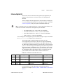
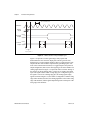
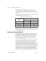
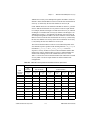
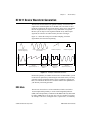
1
DAQ DAQ Hardware Overview Guide DAQ Hardware Overview Guide January 2000 Edition Part Number 370097A-01 Worldwide Technical Support and Product Information www.ni.com National Instruments Corporate Headquarters 11500 North Mopac Expressway Austin, Texas 78759-3504 USA Tel: 512 794 0100 Worldwide Offices Australia 03 9879 5166, Austria 0662 45 79 90 0, Belgium 02 757 00 20, Brazil 011 284 5011, Canada (Calgary) 403 274 9391, Canada (Ontario) 905 785 0085, Canada (Québec) 514 694 8521, China 0755 3904939, Denmark 45 76 26 00, Finland 09 725 725 11, France 01 48 14 24 24, Germany 089 741 31 30, Greece 30 1 42 96 427, Hong Kong 2645 3186, India 91805275406, Israel 03 6120092, Italy 02 413091, Japan 03 5472 2970, Korea 02 596 7456, Mexico (D.F.) 5 280 7625, Mexico (Monterrey) 8 357 7695, Netherlands 0348 433466, Norway 32 27 73 00, Poland 48 22 528 94 06, Portugal 351 1 726 9011, Singapore 2265886, Spain 91 640 0085, Sweden 08 587 895 00, Switzerland 056 200 51 51, Taiwan 02 2377 1200, United Kingdom 01635 523545 For further support information, see the Technical Support Resources appendix. To comment on the documentation, send e-mail to [email protected] © Copyright 2000 National Instruments Corporation. All rights reserved. Important Information Warranty DAQ hardware is warranted against defects in materials and workmanship for a period of one year from the date of shipment, as evidenced by receipts or other documentation. National Instruments will, at its option, repair or replace equipment that proves to be defective during the warranty period. This warranty includes parts and labor. The media on which you receive National Instruments software are warranted not to fail to execute programming instructions, due to defects in materials and workmanship, for a period of 90 days from date of shipment, as evidenced by receipts or other documentation. National Instruments will, at its option, repair or replace software media that do not execute programming instructions if National Instruments receives notice of such defects during the warranty period. National Instruments does not warrant that the operation of the software shall be uninterrupted or error free. A Return Material Authorization (RMA) number must be obtained from the factory and clearly marked on the outside of the package before any equipment will be accepted for warranty work. National Instruments will pay the shipping costs of returning to the owner parts which are covered by warranty. National Instruments believes that the information in this document is accurate. The document has been carefully reviewed for technical accuracy. In the event that technical or typographical errors exist, National Instruments reserves the right to make changes to subsequent editions of this document without prior notice to holders of this edition. The reader should consult National Instruments if errors are suspected. In no event shall National Instruments be liable for any damages arising out of or related to this document or the information contained in it. EXCEPT AS SPECIFIED HEREIN, NATIONAL INSTRUMENTS MAKES NO WARRANTIES, EXPRESS OR IMPLIED, AND SPECIFICALLY DISCLAIMS ANY WARRANTY OF MERCHANTABILITY OR FITNESS FOR A PARTICULAR PURPOSE. CUSTOMER’S RIGHT TO RECOVER DAMAGES CAUSED BY FAULT OR NEGLIGENCE ON THE PART OF NATIONAL INSTRUMENTS SHALL BE LIMITED TO THE AMOUNT THERETOFORE PAID BY THE CUSTOMER. NATIONAL INSTRUMENTS WILL NOT BE LIABLE FOR DAMAGES RESULTING FROM LOSS OF DATA, PROFITS, USE OF PRODUCTS, OR INCIDENTAL OR CONSEQUENTIAL DAMAGES, EVEN IF ADVISED OF THE POSSIBILITY THEREOF. This limitation of the liability of National Instruments will apply regardless of the form of action, whether in contract or tort, including negligence. Any action against National Instruments must be brought within one year after the cause of action accrues. National Instruments shall not be liable for any delay in performance due to causes beyond its reasonable control. The warranty provided herein does not cover damages, defects, malfunctions, or service failures caused by owner’s failure to follow the National Instruments installation, operation, or maintenance instructions; owner’s modification of the product; owner’s abuse, misuse, or negligent acts; and power failure or surges, fire, flood, accident, actions of third parties, or other events outside reasonable control. Copyright Under the copyright laws, this publication may not be reproduced or transmitted in any form, electronic or mechanical, including photocopying, recording, storing in an information retrieval system, or translating, in whole or in part, without the prior written consent of National Instruments Corporation. Trademarks AMUX-64T™, CVI™, DAQCard™, DAQPad™, DAQ-PnP™, DAQ-STC™, LabVIEW™, National Instruments™, ni.com™, NI-DAQ™, NI-DSP™, NI-PGIA™, PXI™, RTSI™, SCXI™, and VirtualBench™ are trademarks of National Instruments Corporation. Product and company names mentioned herein are trademarks or trade names of their respective companies. WARNING REGARDING USE OF NATIONAL INSTRUMENTS PRODUCTS (1) NATIONAL INSTRUMENTS PRODUCTS ARE NOT DESIGNED WITH COMPONENTS AND TESTING FOR A LEVEL OF RELIABILITY SUITABLE FOR USE IN OR IN CONNECTION WITH SURGICAL IMPLANTS OR AS CRITICAL COMPONENTS IN ANY LIFE SUPPORT SYSTEMS WHOSE FAILURE TO PERFORM CAN REASONABLY BE EXPECTED TO CAUSE SIGNIFICANT INJURY TO A HUMAN. (2) IN ANY APPLICATION, INCLUDING THE ABOVE, RELIABILITY OF OPERATION OF THE SOFTWARE PRODUCTS CAN BE IMPAIRED BY ADVERSE FACTORS, INCLUDING BUT NOT LIMITED TO FLUCTUATIONS IN ELECTRICAL POWER SUPPLY, COMPUTER HARDWARE MALFUNCTIONS, COMPUTER OPERATING SYSTEM SOFTWARE FITNESS, FITNESS OF COMPILERS AND DEVELOPMENT SOFTWARE USED TO DEVELOP AN APPLICATION, INSTALLATION ERRORS, SOFTWARE AND HARDWARE COMPATIBILITY PROBLEMS, MALFUNCTIONS OR FAILURES OF ELECTRONIC MONITORING OR CONTROL DEVICES, TRANSIENT FAILURES OF ELECTRONIC SYSTEMS (HARDWARE AND/OR SOFTWARE), UNANTICIPATED USES OR MISUSES, OR ERRORS ON THE PART OF THE USER OR APPLICATIONS DESIGNER (ADVERSE FACTORS SUCH AS THESE ARE HEREAFTER COLLECTIVELY TERMED “SYSTEM FAILURES”). ANY APPLICATION WHERE A SYSTEM FAILURE WOULD CREATE A RISK OF HARM TO PROPERTY OR PERSONS (INCLUDING THE RISK OF BODILY INJURY AND DEATH) SHOULD NOT BE RELIANT SOLELY UPON ONE FORM OF ELECTRONIC SYSTEM DUE TO THE RISK OF SYSTEM FAILURE. TO AVOID DAMAGE, INJURY, OR DEATH, THE USER OR APPLICATION DESIGNER MUST TAKE REASONABLY PRUDENT STEPS TO PROTECT AGAINST SYSTEM FAILURES, INCLUDING BUT NOT LIMITED TO BACK-UP OR SHUT DOWN MECHANISMS. BECAUSE EACH END-USER SYSTEM IS CUSTOMIZED AND DIFFERS FROM NATIONAL INSTRUMENTS' TESTING PLATFORMS AND BECAUSE A USER OR APPLICATION DESIGNER MAY USE NATIONAL INSTRUMENTS PRODUCTS IN COMBINATION WITH OTHER PRODUCTS IN A MANNER NOT EVALUATED OR CONTEMPLATED BY NATIONAL INSTRUMENTS, THE USER OR APPLICATION DESIGNER IS ULTIMATELY RESPONSIBLE FOR VERIFYING AND VALIDATING THE SUITABILITY OF NATIONAL INSTRUMENTS PRODUCTS WHENEVER NATIONAL INSTRUMENTS PRODUCTS ARE INCORPORATED IN A SYSTEM OR APPLICATION, INCLUDING, WITHOUT LIMITATION, THE APPROPRIATE DESIGN, PROCESS AND SAFETY LEVEL OF SUCH SYSTEM OR APPLICATION. Contents About This Guide Conventions ...................................................................................................................xiii MIO and AI Device Terminology ...................................................................xvi Related Documentation..................................................................................................xviii Chapter 1 MIO and AI Devices MIO and AI Multifunction I/O Devices ........................................................................1-1 MIO and AI Device Analog Input...................................................................1-1 E Series Data Acquisition .................................................................1-3 E Series Data Acquisition Timing...................................................................1-5 E Series Data Acquisition Rates .......................................................1-7 MIO Device Analog Output ............................................................................1-7 MIO Device Waveform Generation..................................................1-7 E Series Waveform Generation Using Onboard Memory ................1-8 E Series Digital I/O .........................................................................................1-9 E Series Counter/Timer Operation ..................................................................1-10 E Series Programmable Frequency Output Operation ......................1-10 E Series PFI Pins...............................................................................1-10 Chapter 2 Lab and 1200 Devices Lab and 1200 Devices Analog Input .............................................................................2-1 Lab and 1200 Devices Data Acquisition .........................................................2-2 Lab and 1200 Devices Data Acquisition Timing..............................2-3 Lab and 1200 Devices Data Acquisition Rates.................................2-5 Lab and 1200 Devices Analog Output...........................................................................2-5 Lab and 1200 Devices Waveform Generation ................................................2-6 Lab and 1200 Devices Digital I/O .................................................................................2-6 Lab and 1200 Devices Groups ........................................................................2-6 Lab and 1200 Devices Interval Counter/Timer Operation ............................................2-7 Lab and 1200 Devices Counter/Timers...........................................................2-7 1200 Device Acquisition Rate .......................................................................................2-8 DAQPad-1200 Printer Connection ................................................................................2-9 1200 Device Calibration ................................................................................................2-9 © National Instruments Corporation v DAQ Hardware Overview Guide Contents Chapter 3 LPM Devices LPM Device Analog Input ............................................................................................ 3-1 LPM Device Data Acquisition ........................................................................ 3-1 LPM Device Data Acquisition Timing............................................. 3-2 LPM Device Data Acquisition Rates................................................ 3-3 LPM Device Digital I/O ................................................................................................ 3-3 LPM Device Interval Counter/Timer Operation ........................................................... 3-3 LPM Device Counter/Timers.......................................................................... 3-4 Chapter 4 516 Devices and DAQCard-500/700 Devices 516 Devices and DAQCard-500/700 Analog Input ...................................................... 4-1 516 Devices and DAQCard-500/700 Data Acquisition .................................. 4-2 516 Devices and DAQCard-500/700 Data Acquisition Timing....... 4-2 516 Devices and DAQCard-500/700 Digital I/O .......................................................... 4-3 516 Devices and DAQCard-500/700 Interval Counter/Timer Operation ..................... 4-4 DAQCard-700 Counter/Timers....................................................................... 4-4 516 Devices and DAQCard-500 Counter/Timers ........................................... 4-5 Chapter 5 AT-AO-6/10 Analog Output Devices AT-AO-6/10 Analog Output ......................................................................................... 5-1 AT-AO-6/10 Waveform Generation ............................................................... 5-1 Waveform Generation Using Onboard Memory ............................................ 5-1 Hardware Restrictions for the AT-AO-6/10 ................................................... 5-2 AT-AO-6/10 Digital I/O................................................................................................ 5-3 Chapter 6 6703/6704 Devices PCI/PXI-6703/6704 Analog Output Devices ................................................................ 6-1 PCI/PXI-6703/6704 Digital I/O ...................................................................... 6-1 Chapter 7 PC-TIO-10 Timing I/O Device PC-TIO-10 Counter/Timer Operation ........................................................................... 7-1 Am9513-Based Device Counter/Timer Operation ......................................... 7-1 Programmable Frequency Output Operation.................................... 7-5 PC-TIO-10 Counter/Timers ............................................................................ 7-5 PC-TIO-10 Digital I/O .................................................................................................. 7-6 DAQ Hardware Overview Guide vi www.ni.com Contents Chapter 8 DIO-96 Digital I/O Devices DIO-96 Digital I/O.........................................................................................................8-1 DIO-96 Groups................................................................................................8-2 Chapter 9 DIO-24 (6503), AT-MIO-16DE-10, and 6025E Devices DIO-24 (6503), AT-MIO-16DE-10, and 6025E Digital I/O .........................................9-1 DIO-24 (6503), AT-MIO-16DE-10, and 6025E Device Groups...................................9-2 Chapter 10 DIO-32F and 6533 Digital I/O Devices DIO-32F and 6533 Digital I/O Devices.........................................................................10-1 Chapter 11 AMUX-64T External Multiplexer Accessory AMUX-64T External Multiplexer Accessory ...............................................................11-1 Scanning Order Using the AMUX-64T ..........................................................11-2 Chapter 12 SC-204X Accessories SC-2040 Track-and-Hold Accessory.............................................................................12-1 SC-2042-RTD Accessory ..............................................................................................12-2 SC-2043-SG Accessory .................................................................................................12-2 Chapter 13 SCC Series Modules SCC Shielded Carrier.....................................................................................................13-1 SCC Series Modules ......................................................................................................13-2 SCC-A10 Voltage Attenuator Module ............................................................13-2 SCC-AI Series Isolated Analog Input Modules ..............................................13-2 SCC-CI20 Current Input Module ....................................................................13-3 SCC-SG Series Strain-Gauge Modules ...........................................................13-3 SCC-TC01/02 Thermocouple Input Modules .................................................13-4 SCC-FT01 Feedthrough/Breadboard Module .................................................13-4 SCC-LP Lowpass Filter Modules....................................................................13-4 SCC-DI01 Isolated Digital Input Module .......................................................13-5 © National Instruments Corporation vii DAQ Hardware Overview Guide Contents SCC-DO01 Isolated Digital Output Module................................................... 13-5 SCC Configuration ........................................................................................................ 13-5 Chapter 14 SCXI Hardware SCXI Installation and Configuration............................................................................. 14-2 SCXI Operating Modes ................................................................................................. 14-2 Multiplexed Mode for Analog Input Modules................................................ 14-2 Multiplexed Mode for the SCXI-1200............................................................ 14-3 Multiplexed Mode for Analog Output Modules ............................................. 14-4 Multiplexed Mode for Digital and Relay Modules ......................................... 14-4 Parallel Mode for Analog Input Modules ....................................................... 14-4 Parallel (Standalone) Mode for the SCXI-1200.............................................. 14-5 Parallel Mode for Digital Modules ................................................................. 14-5 SCXI Modules and Compatible DAQ Devices ............................................................. 14-6 SCXI Data Acquisition Device ....................................................................... 14-6 SCXI-1200........................................................................................ 14-6 SCXI Analog Input Modules .......................................................................... 14-7 SCXI-1100........................................................................................ 14-7 SCXI-1101........................................................................................ 14-8 SCXI-1102, SCXI-1102B, and SCXI-1102C................................... 14-8 SCXI-1104/C .................................................................................... 14-9 SCXI-1112........................................................................................ 14-9 SCXI-1120, SCXI-1120D, and SCXI-1121 ..................................... 14-10 SCXI-1125........................................................................................ 14-11 SCXI-1122........................................................................................ 14-11 SCXI-1126........................................................................................ 14-12 SCXI-1127........................................................................................ 14-13 SCXI-1140........................................................................................ 14-13 SCXI-1141, SCXI-1142, and SCXI-1143 ........................................ 14-14 SCXI Analog Output Module ......................................................................... 14-15 SCXI-1124........................................................................................ 14-15 SCXI Digital Modules .................................................................................... 14-16 SCXI-1160 and SCXI-1161.............................................................. 14-16 SCXI-1162 and SCXI-1162HV........................................................ 14-17 SCXI-1163 and SCXI-1163R ........................................................... 14-17 SCXI-1530, SCXI-1531 ................................................................... 14-18 SCXI-1540........................................................................................ 14-18 MIO and AI DAQ Devices (Except Parallel Port Devices)............................ 14-19 Lab and 1200 Devices (Except Parallel Port Devices) ................................... 14-21 DIO-24 and the DIO-96 .................................................................................. 14-22 DIO-32F and 6533 Device .............................................................................. 14-23 DAQ Hardware Overview Guide viii www.ni.com Contents Chapter 15 VXI-DAQ Devices RTSI...............................................................................................................................15-1 VXI-DIO-128 Digital I/O Device..................................................................................15-2 VXI-AO-48XDC Analog Output Device ......................................................................15-2 VXI-AO-48XDC Digital I/O...........................................................................15-3 VXI-MIO-64E-1 and VXI-MIO-64XE-10 Multifunction VXIbus Devices .................15-3 VXI-DAQ Signal Conditioning .....................................................................................15-4 VXI-SC-1102 Submodule ...............................................................................15-5 VXI-SC-1102B and the VXI-SC-1102C Submodules ....................................15-5 VXI-SC-1150 Submodule ...............................................................................15-5 Chapter 16 PXI DAQ Devices RTSI...............................................................................................................................16-1 PXI DAQ Signal Conditioning ......................................................................................16-2 Chapter 17 NI 5411 Devices NI 5411 Arbitrary Waveform and Pattern Generator Devices ......................................17-1 NI 5411 Device Characteristics .....................................................................................17-1 NI 5411 Device Waveform Generation .........................................................................17-3 DDS Mode.......................................................................................................17-3 NI 5411 Device Waveform Pattern Generation.............................................................17-4 NI 5411 Device Pattern Generation Timing ..................................................................17-4 NI 5411 Device Waveform Generation Triggering .......................................................17-5 NI 5411 Device Feature Settings ...................................................................................17-6 Chapter 18 NI 435X Devices NI 435X Device Analog Input .......................................................................................18-1 NI 435X Data Acquisition..............................................................................................18-2 NI 435X Acquisition Timing .........................................................................................18-3 NI 435X Current Source ................................................................................................18-4 NI 435X Digital I/O .......................................................................................................18-4 © National Instruments Corporation ix DAQ Hardware Overview Guide Contents Chapter 19 NI 40XX Devices NI 40XX Device Input ................................................................................................... 19-1 NI 40XX Data Acquisition............................................................................................. 19-2 NI 40XX Data Acquisition Filtering and Timing .......................................................... 19-2 Chapter 20 DSA Devices PCI-445X and NI 455X Devices.................................................................................... 20-1 PCI-445X and NI 455X Analog Input Channels............................................................ 20-2 Data Acquisition ............................................................................................. 20-2 Data Acquisition Timing................................................................................. 20-3 PCI-4451, PCI-4453, and NI 4551 Analog Output Channels ....................................... 20-4 Waveform Generation..................................................................................... 20-4 PCI-445X and NI 455X Digital I/O ............................................................................... 20-5 PCI-445X Digital I/O ...................................................................................... 20-5 NI 455X Digital I/O......................................................................................... 20-6 PCI-445X and NI 455X Counter/Timer Operation........................................................ 20-6 PCI-445X Counter/Timers .............................................................................. 20-6 NI 455X Counter/Timers................................................................................. 20-6 Chapter 21 671X Devices 671X Device Analog Output ......................................................................................... 21-1 671X Device Waveform Generation ............................................................................. 21-1 671X Waveform Generation Using Onboard Memory ................................................. 21-2 671X Digital I/O ............................................................................................................ 21-3 671X Counter/Timer Operation..................................................................................... 21-3 671X Programmable Frequency Output Operation ....................................................... 21-3 671X PFI Pins ................................................................................................................ 21-3 Chapter 22 652X Devices Appendix A Technical Support Resources DAQ Hardware Overview Guide x www.ni.com Contents Glossary Index Figures Figure 2-1. Figure 2-2. Lab and 1200 Device Interval Counter Block Diagram........................2-7 Lab and 1200 Devices Counter/Timer Signal Connections ..................2-8 Figure 3-1. LPM Device Counter/Timer Signal Connections .................................3-4 Figure 4-1. Figure 4-2. DAQCard-700 Counter/Timer Signal Connections ..............................4-4 516 Devices and DAQCard-500 Counter/Timer Signal Connections ...........................................................................................4-5 Figure 7-1. Figure 7-2. Counter Block Diagram.........................................................................7-1 Am9513 Counter Timing and Output Types.........................................7-4 Figure 17-1. Examples of Waveform Generation ......................................................17-3 Tables Table 1. MIO and AI Device Classification ........................................................xvi Table 1-1. MIO and AI Multifunction I/O Device Analog Input Characteristics..............................................................................1-1 AT-MIO-16DE-10 and 6025E Device Ports.........................................1-9 Table 1-2. Table 2-1. Table 2-2. Lab and 1200 Devices and Corresponding FIFO Size ..........................2-1 Typical Settling Accuracies for Maximum Multiple-Channel Scanning Rates for the Lab and 1200 Devices......................................2-5 Table 3-1. Maximum Recommended Data Acquisition Rates for the LPM Devices.........................................................................................3-3 Table 7-1. PC-TIO-10 Adjacent Counter Sequence ...............................................7-6 Table 8-1. DIO-96 Port Labels, Numbers, and Modes...........................................8-1 Table 9-1. Digital I/O Device Port Numbers..........................................................9-1 Table 10-1. Table 10-2. DIO-32F Extra Inputs and Outputs .......................................................10-2 6533 Extra Inputs and Outputs..............................................................10-3 © National Instruments Corporation xi DAQ Hardware Overview Guide Contents Table 11-1. Table 11-2. Table 11-3. Analog Input Channel Range................................................................ 11-1 AMUX-64T Channel Numbers............................................................. 11-2 AMUX-64T Scanning Order for Each MIO or AI Device Input Channel........................................................................................ 11-3 Table 13-1. SCC-AI Series Module Input/Output Range, Gain, and Bandwidth .... 13-3 Table 15-1. RTSI Bus Line and VXIbus Trigger Mapping ..................................... 15-1 Table 16-1. RTSI Bus Line and PXI Bus Trigger Mapping .................................... 16-1 Table 17-1. Table 17-2. NI 5411 Device Characteristics ............................................................ 17-1 NI 5411 Operational Modes.................................................................. 17-5 Table 18-1. Table 18-2. Table 18-3. Analog Input Ranges for the 435X Devices.......................................... 18-2 Ranges for 435X Device Data Acquisition ........................................... 18-2 Relationship between Filtering and Available Sample Rates ............... 18-3 Table 19-1. Relationship between Notch Filter Frequency and Power Line Frequencies Filtered.............................................................................. 19-2 Relationship between Notch Filter Frequency and Single-Channel Acquisition Rate.......................................................... 19-2 Relationship between Notch Filter Frequency and Single-Channel Acquisition Rate when AutoZero Is Enabled ............. 19-3 Table 19-2. Table 19-3. Table 20-1. PCI-445X and NI 455X Hardware Features.......................................... 20-1 Table 22-1. Port Directions for the PCI/PXI-6527................................................... 22-1 DAQ Hardware Overview Guide xii www.ni.com About This Guide The DAQ Hardware Overview Guide is for users of the NI-DAQ software for PC compatibles version 6.7. NI-DAQ software is a powerful application programming interface (API) between your data acquisition (DAQ) application and your National Instruments DAQ devices. Conventions The following conventions appear in this guide: This icon denotes a note, which alerts you to important information. 1102/B/C modules Refers to the SCXI-1102, SCXI-1102B, and SCXI-1102C modules and the VXI-SC-1102, VXI-SC-1102B, and VXI-SC-1102C submodules. 1200 and 1200AI device Refers to the DAQCard-1200, DAQPad-1200, Lab-PC-1200, Lab-PC-1200AI, PCI-1200, and SCXI-1200. 12-bit device These MIO and AI devices are listed in Table 1. 16-bit device These MIO and AI devices are listed in Table 1. 1394 Refers to a high-speed external bus that implements the IEEE 1394 serial bus protocol. 435X device Refers to the NI 4350 for ISA, PCMCIA, USB, and NI 4351 for PCI and PXI. 445X device Refers to the PCI-4451, PCI-4452, PCI-4453,and PCI-4454. 455X device Refers to the NI 4551 and NI 4552. 516 device Refers to the DAQCard-516 and PC-516. 6025E device Refers to the PCI-6025E and PXI-6025E. 6052E device Refers to the PCI-6052E, PXI-6052E, and DAQPad-6052E for 1394. 611X device Refers to the PCI-6110E and PCI-6111E. 6602 device Refers to the PCI-6602 and PXI-6602. 6703/6704 device Refers to the PCI-6703/6704 and PXI-6703/6704. © National Instruments Corporation xiii DAQ Hardware Overview Guide About This Guide 671X device Refers to the DAQCard-6715, PCI-6711, PXI-6711, PCI-6713, and PXI-6713. AI device These analog input devices are listed in Table 1. bold Bold text denotes items that you must select or click on in the software, such as menu items and dialog box options. Bold text also denotes parameter names. DAQCard-500/700 Refers to the DAQCard-500 and DAQCard-700. DIO 6533 Refers to the AT-DIO-32HS, PCI-DIO-32HS, DAQCard-6533, and PXI-6533. DIO-24 Refers to the PC-DIO-24, PC-DIO-24PnP, DAQCard-DIO-24 and 6503 devices. DIO-32F Refers to the AT-DIO-32F. DIO-96 Refers to the PC-DIO-96, PC-DIO-96PnP, PCI-DIO-96, DAQPad-6507, DAQPad-6508, and PXI-6508. DIO device Refers to any DIO-24, DIO-32, DIO-6533, or DIO-96. DSA device Refers to the PCI-4451, PCI-4452, PCI-4453, PCI-4454, NI 4551, and NI 4552. E Series device These are MIO and AI devices. Refer to Table 1 for a complete list of these devices. italic Italic text denotes variables, emphasis, a cross reference, or an introduction to a key concept. This font also denotes text that is a placeholder for a word or value that you must supply. Lab and 1200 device Refers to the DAQCard-1200, DAQPad-1200, Lab-PC+, Lab-PC-1200, Lab-PC-1200AI, PCI-1200, and SCXI-1200. Lab and 1200 analog output device Refers to the DAQCard-1200, DAQPad-1200, Lab-PC+, Lab-PC-1200, PCI-1200, and SCXI-1200. LPM device Refers to the PC-LPM-16 and PC-LPM-16PnP. MIO device Refers to multifunction I/O devices. See Table 1 for a list of these devices. MIO-16XE-50 device Refers to the AT-MIO-16XE-50, DAQPad-MIO-16XE-50, and NEC-MIO-16XE-50, and PCI-MIO-16XE-50. DAQ Hardware Overview Guide xiv www.ni.com About This Guide MIO-64 Refers to the AT-MIO-64E-4, PCI-6031E, PCI-6071E, VXI-MIO-64E-1, and VXI-MIO-64XE-10. monospace Text in this font denotes text or characters that you should enter from the keyboard, sections of code, programming examples, and syntax examples. This font is also used for the proper names of disk drives, paths, directories, programs, subprograms, subroutines, device names, functions, operations, variables, filenames and extensions, and code excerpts. NI 40XX device Refers to the NI 4050 for PCMCIA, and NI 4060 for PCI and PXI. NI 5411 device Refers to the NI 5411 for ISA and PCI. NI-DAQ Refers to the NI-DAQ software for PC compatibles, unless otherwise noted. NI-TIO based device Refers to the NI 4551, PCI-6608, PCI-6602, and PXI-6602. PC Refers to the IBM PC/XT, IBM PC AT, and compatible computers. PCI Series Refers to the National Instruments products that use the high-performance expansion bus architecture originally developed by Intel to replace ISA and EISA. Remote SCXI Refers to an SCXI configuration where either an SCXI-2000 chassis or an SCXI-2400 remote communications module is connected to the PC serial port. SCXI-1102/B/C SCXI-1102/B/C refers to the SCXI-1102, SCXI-1102B, and SCXI-1102C devices. SCXI-1104/C SCXI-1104/C refers to the SCXI-1104 and SCXI-1104/C. SCXI-1120/D SCXI-1120/D refers to the SCXI-1120 and SCXI-1120D. SCXI analog input module Refers to the SCXI-1100, SCXI-1101, SCXI-1102, SCXI-1104, SCXI-1112, SCXI-1120, SCXI-1120D, SCXI-1121, SCXI-1122, SCXI-1125, SCXI-1127, SCXI-1140, SCXI-1141, SCXI-1142, and SCXI-1143. SCXI chassis Refers to the SCXI-1000, SCXI-1000DC, SCXI-1001, and SCXI-2000. SCXI communication module Refers to the SCXI-2400. SCXI DAQ module Refers to the SCXI-1200. © National Instruments Corporation xv DAQ Hardware Overview Guide About This Guide SCXI digital module Refers to the SCXI-1160, SCXI-1161, SCXI-1162, SCXI-1162HV, SCXI-1163, and SCXI-1163R. Simultaneous sampling device Refers to the PCI-6110E, PCI-6111E, PCI-4451, PCI-4452, NI 4551, and NI 4552. VXI-MIO device Refers to the VXI-MIO-64E-1 and VXI-MIO-64XE-10. VXI-SC-1102/B/C Refers to the VXI-SC-1102, VXI-SC-1102B, and VXI-SC-1102C. MIO and AI Device Terminology This guide uses generic terms to describe groups of devices whenever possible. The generic terms for the MIO and AI devices are based on the number of bits, the platform, and the functionality. These devices are also collectively known as E Series devices. Table 1 lists each MIO and AI device and the possible classifications for each. Table 1. MIO and AI Device Classification Number of SE Channels Bit Type Functionality AT-AI-16XE-10 16 16-bit AT AI AT-MIO-16DE-10 16 12-bit AT MIO AT-MIO-16E-1 16 12-bit AT MIO AT-MIO-16E-2 16 12-bit AT MIO AT-MIO-16E-10 16 12-bit AT MIO AT-MIO-16XE-10 16 16-bit AT MIO AT-MIO-16XE-50 16 16-bit AT MIO AT-MIO-64E-3 64 12-bit AT MIO DAQCard-AI-16E-4 16 12-bit PCMCIA AI DAQCard-AI-16XE-50 16 16-bit PCMCIA AI DAQCard-6023E 16 12-bit PCMCIA AI DAQCard-6024E 16 12-bit PCMCIA MIO DAQCard-6062E 16 12-bit PCMCIA MIO DAQPad-MIO-16XE-50 16 16-bit Parallel Port MIO DAQPad-6020E 16 12-bit USB MIO Device DAQ Hardware Overview Guide xvi www.ni.com About This Guide Table 1. MIO and AI Device Classification (Continued) Number of SE Channels Bit Type Functionality DAQPad-6052E 16 16-bit 1394 MIO DAQPad-6070E 16 12-bit 1394 MIO NEC-AI-16E-4 16 12-bit NEC AI NEC-AI-16XE-50 16 16-bit NEC AI NEC-MIO-16E-4 16 12-bit NEC MIO NEC-MIO-16XE-50 16 16-bit NEC MIO PCI-6023E 16 12-bit PCI AI PCI-6024E 16 12-bit PCI MIO PCI-6025E 16 12-bit PCI MIO PCI-6031E (MIO-64XE-10) 64 16-bit PCI MIO PCI-6032E (AI-16XE-10) 16 16-bit PCI AI PCI-6033E (AI-64XE-10) 64 16-bit PCI AI PCI-6052E 16 16-bit PCI MIO PCI-6071E (MIO-64E-1) 64 12-bit PCI MIO PCI-6110E 4 DIFF only 12-bit AI, 16-bit AO PCI MIO PCI-6111E 2 DIFF only 12-bit AI, 16-bit AO PCI MIO PCI-MIO-16E-1 16 12-bit PCI MIO PCI-MIO-16E-4 16 12-bit PCI MIO PCI-MIO-16XE-10 16 16-bit PCI MIO PCI-6034E 16 16-bit PCI AI PXI-6034E 16 16-bit PXI AI PCI-6035E 16 16-bit AI 12-bit AO PCI MIO PXI-6035E 16 16-bit AI 12-bit AO PXI MIO PCI-MIO-16XE-50 16 16-bit PCI MIO PXI-6011E 16 16-bit PXI MIO Device © National Instruments Corporation xvii DAQ Hardware Overview Guide About This Guide Table 1. MIO and AI Device Classification (Continued) Number of SE Channels Bit Type Functionality PXI-6023E 16 12-bit PXI AI PXI-6024E 16 12-bit PXI MIO PXI-6025E 16 12-bit PXI MIO PXI-6030E 16 16-bit PXI MIO PXI-6040E 16 12-bit PXI MIO PXI-6052E 16 16-bit PXI MIO PXI-6070E 16 12-bit PXI MIO VXI-MIO-64E-1 64 12-bit VXI MIO VXI-MIO-64XE-10 64 16-bit VXI MIO Device Related Documentation For detailed hardware information, refer to the user manual included with each device. For detailed software information, refer to your NI-DAQ for PC compatibles documentation. DAQ Hardware Overview Guide xviii www.ni.com 1 MIO and AI Devices This chapter contains overview information on the MIO and AI devices. These devices are listed in Table 1-1. MIO and AI Multifunction I/O Devices The National Instruments MIO and AI devices are collectively known as E Series devices. Timing and control on these devices is performed by the National Instruments Data Acquisition System Timing Controller (DAQ-STC) chip. MIO and AI Device Analog Input Table 1-1 summarizes the key analog input characteristics for the MIO and AI multifunction I/O devices. Table 1-1. MIO and AI Multifunction I/O Device Analog Input Characteristics Number of Channels ADC Resolution (Bits) Gains Range (V) Input FIFO (Words) AT-MIO-16DE-10, AT-MIO-16E-10 DAQPad-6020E 16 12 0.5, 1, 2, 5, 10, 20, 50, 100 ±5, 0 to 10 512 no AT-MIO-16E-1 16 12 0.5, 1, 2, 5, 10, 20, 50, 100 ±5, 0 to 10 8,192 yes AT-MIO-16E-2, NEC-AI-16E-4, NEC-MIO-16E-4 16 12 0.5, 1, 2, 5, 10, 20, 50, 100 ±5, 0 to 10 2,048 yes 6023E, 6024E, 6025E devices 16 12 0.5, 1, 10, 100 ±5 512 no 6034E, 6035E devices 16 16 0.5, 1, 10, 100 ±5 512 no DAQPad-6070E 16 12 0.5, 1, 2.5, 5, 10, 20, 50, 100, ±5, 0 to 10 2,048 yes Device © National Instruments Corporation 1-1 Hardware Analog Trigger DAQ Hardware Overview Guide Chapter 1 MIO and AI Devices Table 1-1. MIO and AI Multifunction I/O Device Analog Input Characteristics (Continued) Number of Channels ADC Resolution (Bits) Gains Range (V) Input FIFO (Words) PCI-MIO-16E-4, PCI-MIO-16E-1, PXI-6040E, PXI-6070E 16 12 0.5, 1, 2.5, 5, 10, 20, 50, 100, ±5, 0 to 10 512 yes DAQCard-AI-16E-4 16 12 0.5, 1, 2, 5, 10, 20, 50, 100 ±5, 0 to 10 1,024 yes AT-MIO-16XE-10, AT-AI-16XE-10 16 16 1, 2, 5, 10, 20, 50, 100 ±10, 0 to 10 2,048 yes AT-MIO-16XE-50, DAQPad-MIO-16XE-50, NEC-AI-16XE-50, NEC-MIO-16XE-50, PCI-MIO-16XE-50 16 16 1, 2, 10, 100 ±10, 0 to 10 512 no DAQCard-AI-16XE-50 16 16 1, 2, 10, 100 ±10, 0 to 10 1,024 no AT-MIO-64E-3 64 12 0.5, 1, 2, 5, 10, 20, 50, 100 ±5, 0 to 10 2,048 yes PCI-MIO-16XE-10, PCI-6032E (AI-16XE-10) PXI-6030E 16 16 1, 2, 5, 10, 20, 50, 100 ±10, 0 to 10 512 yes 6052E devices 16 16 0.5, 1, 2.5, 5, 10, 20, 50, 100 ±5, 0 to 10 512 yes VXI-MIO-64E-1 64 12 0.5, 1, 2, 5, 10, 20, 50, 100 ±5, 0 to 10 8,192 yes PCI-6110E 4 12 0.2, 0.5, 1, 2, 5, 10, 20, 50 ±10 512 yes PCI-6111E 2 12 0.2, 0.5, 1, 2, 5, 10, 20, 50 ±10 512 yes PCI-6031E (MIO-64XE-10), PCI-6033E (AI-64XE-10) VXI-MIO-64XE-10 64 16 1, 2, 5, 10, 20, 50,100 ±10, 0 to 10 512 yes PXI-6071E (MIO-64E-1) 64 12 0.5, 1, 2, 5, 10, 20, 50, 100 ±5, 0 to 10 512 yes Device DAQ Hardware Overview Guide 1-2 Hardware Analog Trigger www.ni.com Chapter 1 MIO and AI Devices Table 1-1. MIO and AI Multifunction I/O Device Analog Input Characteristics (Continued) Number of Channels ADC Resolution (Bits) Gains DAQCard-6023E 16 12 DAQCard-6024E 16 DAQCard-6062E 16 Device Range (V) Input FIFO (Words) Hardware Analog Trigger 0.5, 1, 10, 100 ±5 2048 no 12 0.5, 1, 10, 100 ±5 2048 no 12 0.5, 1, 2, 5, 10, 20, 50, 100 ±5 8192 yes Note Terms such as ADC resolution and analog trigger are defined in the Glossary. E Series Data Acquisition The E Series devices can perform single-channel data acquisitions and multiple-channel scanned data acquisitions. For single-channel data acquisition, select a single analog input channel and gain setting. The device performs a single A/D conversion on that channel every sample interval. For multiple-channel scanned data acquisition, the device scans a set of analog input channels, each with its own gain setting. In this method, a scan sequence indicates which analog channels to scan and the gain settings for each channel. The length of this scan sequence can be 1 to 512 channel/gain pairs. For the PCI-6110E and the PCI-6111E each channel can appear only once in the scan sequence. During scanning, the analog input circuitry performs an A/D conversion on the next entry in the scan sequence. The device performs an A/D conversion once every sample interval. For maximum performance, this operation is pipelined so that the device switches to the next channel while the current A/D conversion is performed. The device waits for a specified scan interval before scanning the channels again. The channels are scanned repeatedly at the beginning of each scan interval until the required number of samples has been acquired. For example, you can scan a sequence of four channels once every 10 s. The device could sample the channels at the beginning of the 10 s interval, within 20 µs, with a 5 µs sample interval between channels. If you set the scan interval to 0, the scan sequence starts over again immediately at the end of each scan sequence without waiting for a scan interval. The 0 scan interval setting causes the device to scan the channels repeatedly as fast as possible. Note The 611X devices sample all channels simultaneously. The scan interval controls the sampling rate, therefore the scan interval of zero is not allowed. © National Instruments Corporation 1-3 DAQ Hardware Overview Guide Chapter 1 MIO and AI Devices You can combine both single-channel and multiple-channel acquisition with any of the following additional modes: • Posttrigger mode • Pretrigger mode • Double-buffered mode • AMUX-64T mode • SCXI mode Note The 611X devices do not support the AMUX-64T or SCXI modes. Posttrigger mode collects a specified number of samples after the device receives a trigger. Refer to the stop trigger discussion in the appropriate data acquisition timing section for your device later in this chapter for details. After the user-specified buffer is full, the data acquisition stops. Pretrigger mode collects data both before and after the device receives a trigger, either through software or by applying a hardware signal. The device collects samples and fills the user-specified buffer without stopping until the device receives the stop trigger signal. Refer to the stop trigger discussion in the appropriate data acquisition timing section for your device later in this chapter for details. The device then collects a specified number of samples and stops the acquisition. The buffer is treated as a circular buffer—when the entire buffer has been written to, data is stored at the beginning again, overwriting the old data. When data acquisition stops, the buffer has samples from before and after the stop trigger occurred. The number of samples saved depends on the length of the user-specified buffer and on the number of samples specified to be acquired after receipt of the trigger. Double-buffered mode, like pretrigger mode, also fills the user-specified buffer continuously. You can call DAQ_DB_Transfer to transfer old data into a second buffer before it is overwritten by new data. DAQ_DB_Transfer transfers data out of one half of the buffer while the other half is filled with new data. In the AMUX-64T mode, you use one, two, or four external AMUX-64T devices to extend the number of analog input channels available. You connect the external signals to the AMUX-64T device pins, instead of directly to the DAQ device pins. DAQ Hardware Overview Guide 1-4 www.ni.com Chapter 1 MIO and AI Devices You can use SCXI modules as a data acquisition front end for the device to condition the input signals and multiplex the channels. You can use all the modes just described in conjunction with SCXI. The SCXI Modules and Compatible DAQ Devices section in Chapter 14, SCXI Hardware, describes how to use the SCXI functions to set up the SCXI modules for a data acquisition to be performed by a DAQ device. Note The DAQPad-MIO-16XE-50 uses half-FIFO mode by default when doing interrupt data transfer operations for analog input with rates faster than 256 samples per second. The PCI E Series and DAQCard E Series devices use half-FIFO when performing interrupt data transfers for analog input with rates faster than 1000 samples per second. You can override the default setting and select between interrupt on every sample and interrupt on half-FIFO. When using external conversions, you should select the mode appropriate for the acquisition rate. To set the interrupt generation mode, see the Set_DAQ_Device_Info function in the NI-DAQ Function Reference Online Help or the Set_DAQ_Device_Info.vi in the LabVIEW DAQ Online Reference. E Series Data Acquisition Timing The following DAQ-STC counters are used for data acquisition timing and control: • The scan counter is used to control the number of scans you will acquire. If you want to perform pretriggered acquisition, this counter will ensure that you acquire selected number of scans before the stop trigger is recognized. • The scan timer is a counter that you can use for start scan timing. • The sample-interval timer is a counter that you can use for conversion timing. The DAQPad-6020E uses half-FIFO mode when doing interrupt data transfer operations for analog input rates of > 256 samples per second. Data acquisition timing involves the following timing signals: • A start trigger is a signal that initiates a data acquisition sequence. You can supply this signal externally through a selected I/O connector pin, through a RTSI bus trigger line, or by software. • A start scan signal initiates individual scans. This signal can be supplied from the onboard programmable scan timer, externally through a selected I/O connector pin, through a RTSI bus trigger line, or by software. © National Instruments Corporation 1-5 DAQ Hardware Overview Guide Chapter 1 MIO and AI Devices • A conversion signal initiates individual analog-to-digital (A/D) conversions. This signal can be supplied from the onboard programmable sample timer, externally through a selected I/O connector pin, through a RTSI bus trigger line, or by software. • A stop trigger is a signal used for pretriggered data acquisition to notify your device to stop acquiring data after a specified number of scans. Data acquisition operation is continuously performed until the device receives this signal. This signal can be supplied externally through a selected I/O connector pin, through a RTSI bus trigger line, or by software. • A gate is a signal used for gating the data acquisition. When you enable gating, the data acquisition will proceed only on selected level of the gate signal. This signal can be supplied externally through a selected I/O connector pin, through a RTSI bus trigger line. • A scan timer timebase is a signal used by the scan timer for scan interval timing. This signal is used only when the scan timer is used. This signal can be supplied from one of the onboard timebase sources, externally through a selected I/O connector pin, or through a RTSI bus trigger line. • A sample-interval timer timebase is a signal used by the sample interval timer for conversion timing. This signal is used only when the sample interval timer is used. This signal can be supplied from one of the onboard timebase sources, externally through a selected I/O connector pin, or through a RTSI bus trigger line. See your DAQ device user manual for more information regarding these signals. DAQ devices with the DAQ-STC use two counters, the scan interval counter and the sample interval counter. The E Series devices support both internal and external timebases. The internal timebases available on the DAQ-STC are 20 MHz (50 ns) and 100 kHz (10 µs). The scan interval counter is a 24-bit counter, and the sample interval counter is a 16-bit counter. While the scan interval counter has the freedom to work with both internal and external timebases, the sample interval counter can use either the 20 MHz timebase or the timebase used by the scan interval counter. When you specify a timebase value different from the internal timebases the DAQ-STC uses, NI-DAQ tries to convert the timebase and interval values you specified into those that the DAQ-STC can use. If NI-DAQ cannot make the translation without a loss of resolution, it returns DAQ Hardware Overview Guide 1-6 www.ni.com Chapter 1 MIO and AI Devices rateNotSupportedError. This typically occurs if you specified a timebase of 5 (100 Hz) and a sample interval of 100, for example, for a resulting sample interval of 1 s. This generates an error because the sample interval counter rolls over before 1 s. Note The 611X devices use the scan interval counter to control the acquisition rate. The sample interval counter does not affect conversion timing since all channels are sampled simultaneously. The pipelined ADC used on 611X devices requires four conversions before the first sample becomes available; therefore, if you are using external conversions, you should allow for this behavior. E Series Data Acquisition Rates Refer to the appropriate user manual for single-channel and multiple-channel DAQ rates and settling accuracy. If you are using SCXI with your DAQ device, refer to the SCXI Data Acquisition Rates section in Chapter 3, Software Overview, of the NI-DAQ User Manual for PC Compatibles, for the effect of SCXI module settling time on your data acquisition device rates. MIO Device Analog Output The MIO devices contain two analog output channels numbered 0 and 1. Each analog output channel contains either a 12-bit DAC or a 16-bit DAC, depending on the AO resolution of your device. You can configure each analog output channel for unipolar or bipolar voltage output except on the MIO-16XE-50 and the 611X devices, which are always in bipolar mode. An onboard voltage reference of +10 V is available for the analog output channels. An external reference voltage signal can also drive the analog output channels except on the MIO-16XE-10, MIO-16XE-50 and the 611X devices. See the AO_Configure function in the NI-DAQ Function Reference Online Help or the AO_Configure.vi in the LabVIEW DAQ Online Reference for more information about configuring the DACs. Note The 611X devices require an even number of samples in the waveform buffer due to a 32-bit wide output FIFO necessary for high-speed data transfers. MIO Device Waveform Generation The Waveform Generation functions can write values to either one or both analog output channels continuously using an onboard or external clock to update the DACs at regular intervals. The values are contained in a buffer that you allocate and fill. The resultant voltages produced at the analog © National Instruments Corporation 1-7 DAQ Hardware Overview Guide Chapter 1 MIO and AI Devices output channels depend on the value of the numbers in the buffer, the level of the reference voltage, and the polarity setting. Note (E Series devices on VXI, ISA, PCI, PXI and 1394 buses only) NI-DAQ can use either DMA or interrupt service routines to generate waveforms on the analog output channels. By default, NI-DAQ uses DMA because DMA is simply more efficient. If you prefer to reserve the DMA channels for the Data Acquisition functions or for other devices in the system, call Set_DAQ_Device_Info, described in the NI-DAQ Function Reference Online Help, or the Set_DAQ_Device_Info.vi in the LabVIEW DAQ Online Reference to force NI-DAQ not to use DMA for waveform generation. E Series Waveform Generation Using Onboard Memory All E Series devices with analog output FIFOs support FIFO mode waveform generation. In this mode, waveform data is transferred to the onboard DAC FIFO memory only once. These values are then cycled through to generate the waveform continuously or for a finite number of iterations. No interrupt service or DMA operation is required to transfer more data to the device during waveform generation. The following conditions must be satisfied to use FIFO mode waveform generation: • One cycle worth of waveform data can be held entirely on the device DAC FIFO memory. • Double-buffered waveform generation mode is disabled. • The number of cycles to generate can be infinite, denoted by the value 0, or between 1 and 16,777,216 inclusive. There are two variations possible in FIFO mode waveform generation: • Continuous cyclic waveform generation—An onboard counter or an external signal provides the update pulses. Once started, the waveform generation continues until you call the clear function to stop the waveform. • Programmed cyclic waveform generation—An onboard counter or an external signal provides the update pulses. A separate onboard counter terminates the waveform after a finite number of cycles has been generated. Refer to your DAQ device manual to determine the size of the analog output FIFO and for more information on waveform generation. DAQ Hardware Overview Guide 1-8 www.ni.com Chapter 1 MIO and AI Devices E Series Digital I/O The E Series devices contain one 8-bit digital I/O port supplied by the DAQ-STC chip. This port is referred to as port 0 by the Digital I/O functions. You can configure the entire digital port as either an input or an output port, or you can configure individual lines for either input or output. The port has read-back capability. This port operates in nonlatched mode only. Note Connecting one or more AMUX-64T devices or a non-remote SCXI chassis to an E Series device renders various lines of the digital I/O port unavailable: • One AMUX-64T device—Lines 0 and 1 are unavailable. • Two AMUX-64T devices—Lines 0, 1, and 2 are unavailable. • Four AMUX-64T devices—Lines 0, 1, 2, and 3 are unavailable. • SCXI—Lines 0, 1, 2, and 4 are unavailable. The remaining lines of the digital I/O port are available for input or output. You should use DIG_Line_Config to configure these remaining lines. The AT-MIO-16DE-10 and the 6025E devices have one 8-bit line-configurable port named port 0 that does not support handshaking or asynchronous operations. The DAQ-STC chip supplies this port. The AT-MIO-16DE-10 and the 6025E devices also have three 8-bit ports named ports 2, 3, and 4 that do support handshaking and asynchronous operations and are directionally configurable only on a per-port basis. An 8255 chip supplies these three ports. The three 8255 ports are numbered 2, 3, and 4 for compatibility with an older product. Table 1-2 summarizes the four ports available on the AT-MIO-16DE-10 and the 6025E devices. Table 1-2. AT-MIO-16DE-10 and 6025E Device Ports Port Size Configuration Type Supplied by 0 8-bit Line configurable Immediate DAQ-STC chip 2 8-bit Handshaking Asynchronous or immediate 8255 chip 3 8-bit Handshaking Asynchronous or immediate 8255 chip 4 8-bit — Immediate 8255 chip For a description of the AT-MIO-16DE-10 and the 6025E device digital I/O, see Chapter 9, DIO-24 (6503), AT-MIO-16DE-10, and 6025E Devices. © National Instruments Corporation 1-9 DAQ Hardware Overview Guide Chapter 1 MIO and AI Devices E Series Counter/Timer Operation The E Series devices use the National Instruments DAQ-STC counter/timer chip. The DAQ-STC has two 24-bit counter/timers that are always available for general-purpose counter/timer applications. Refer to the GPCTR functions in the NI-DAQ Function Reference Online Help for more information. E Series Programmable Frequency Output Operation The E Series devices have one I/O connector pin (FREQ_OUT) capable of outputting a programmable frequency signal. This signal is a divided-down version of the selected timebase. Available timebases for this operation are 10 MHz and 100 kHz, and you can divide them by numbers 1 through 16. E Series PFI Pins You can route internal device signals to and from the I/O connector programmatically by using the PFI pins on the E Series devices. Refer to your E Series device user manual for a complete discussion of PFI pins. See the Select_Signal function description in the NI-DAQ Function Reference Online Help for programming information on routing. DAQ Hardware Overview Guide 1-10 www.ni.com Lab and 1200 Devices 2 This chapter contains overview information on the DAQCard-1200, DAQPad-1200, Lab-PC+, Lab-PC-1200, Lab-PC-1200AI, PCI-1200, and SCXI-1200 devices. Lab and 1200 Devices Analog Input The Lab and 1200 devices contain eight single-ended analog input channels numbered 0 through 7. The analog input channels are multiplexed into a single programmable gain stage and 12-bit ADC. The devices have gains of 1, 2, 5, 10, 20, 50, and 100. You can configure the input channels to be differential or nonreferenced single ended. In differential mode, four channels are available, namely, 0, 2, 4, and 6. All Lab and 1200 devices except the Lab-PC+ support software configuration of the input mode; on the Lab-PC+, configure the mode via jumper W4. You can hardware jumper-configure analog input on the Lab-PC+ and software configure analog input on all other Lab and 1200 devices for two different input ranges: • 0 to +10 V (unipolar) • −5 to +5 V (bipolar) You can initiate A/D conversions through software or by applying active low pulses to the EXTCONV* input on the device I/O connector. Each of the devices has a FIFO on the device in which to store the results of A/D conversions temporarily. Table 2-1 shows the FIFO sizes. Table 2-1. Lab and 1200 Devices and Corresponding FIFO Size Device Lab-PC+ 512 DAQCard-1200, DAQPad-1200, Lab-PC-1200, Lab-PC-1200AI, PCI-1200, SCXI-1200 © National Instruments Corporation FIFO Size (in words) 2-1 2,048 DAQ Hardware Overview Guide Chapter 2 Lab and 1200 Devices Lab and 1200 Devices Data Acquisition The Lab and 1200 devices can perform single-channel data acquisition and multiple-channel scanned data acquisition. For single-channel data acquisition, you select a single analog input channel and gain setting. The device performs a single A/D conversion on that channel every sample interval. For multiple-channel scanned data acquisition, the devices scan a sequence of analog input channels. A single gain setting is used for all channels scanned. A sample interval indicates the time to elapse between A/D conversions on each channel in the sequence. You need only to select a single starting channel to select the sequence of channels to scan. The device then scans the channels in consecutive order until channel 0 is reached, and then the scan begins anew with the starting channel. For example, if the starting channel is channel 3, the scan sequence is as follows: channel 3, channel 2, channel 1, channel 0, channel 3, and so on The Lab and 1200 devices support interval scanning. A scan interval is the time that elapses between two channel-scanning cycles. You can combine both the single-channel and multiple-channel acquisitions with any of the following additional modes: • Posttrigger mode • Pretrigger mode • Double-buffered mode • SCXI mode (except the DAQPad-1200) Posttrigger mode collects a specified number of samples after the device receives a trigger. You can initiate posttrigger acquisition through software or when a pulse edge is applied to the EXTTRIG input. After the user-specified buffer has been filled, the data acquisition stops. Pretrigger mode collects data both before and after the device receives a trigger. You can initiate data acquisition through software. The device collects samples and fills the user-specified buffer without stopping or counting samples until the device receives a pulse at the EXTTRIG input. The device then collects a specified number of samples and stops the acquisition. The buffer is treated as a circular buffer—when the entire buffer has been written to, data is stored at the beginning again, overwriting the old data. When data acquisition stops, the buffer has samples from before and after the stop trigger occurred. The number of samples saved DAQ Hardware Overview Guide 2-2 www.ni.com Chapter 2 Lab and 1200 Devices depends on the length of the user-specified buffer and on the number of samples specified to be acquired after receipt of the trigger. Because there is only one EXTTRIG input on the device I/O connector, a single acquisition cannot employ both of these trigger modes. Double-buffered mode, like pretrigger mode, also fills the user-specified buffer continuously. Unlike pretrigger mode, however, double-buffered mode transfers old data into a second buffer before overwriting the old data with new data. Data is transferred out of one half of the buffer while the other half is being filled with new data. You can use double-buffered mode in conjunction with either pretrigger or posttrigger modes. You can use SCXI modules as a data acquisition front end for all Lab and 1200 devices except the DAQPad-1200 to signal condition the input signals and multiplex the channels. You can use all the modes just described in conjunction with SCXI for single-channel acquisitions; however, onboard multiple-channel acquisitions are only supported when using the SCXI-1120, SCXI-1120D, or SCXI-1121 modules in parallel mode. Chapter 14, SCXI Hardware, describes how the SCXI functions are used to set up the SCXI modules for a data acquisition to be performed by a DAQ device. Note Refer to the Set_DAQ_Device_Info function in the NI-DAQ Function Reference Online Help or the Set_DAQ_Device_Info.vi in the LabVIEW DAQ Online Reference for information on data transfer modes. Lab and 1200 Devices Data Acquisition Timing Timing for data acquisition can be performed by the two onboard 8253 Counters/Timers or externally. Each 8253 Counter/Timer has three independent 16-bit counters/timers. • Counter A0 is a sample-interval counter reserved for data acquisition. • Counter A1 is a sample counter reserved for data acquisition. • Counter A2 is an update-interval counter reserved for waveform generation. • Counter B0 is used for extending the timebase for data acquisition or waveform generation when the interval between samples or updates is greater than 65,535. • Counter B1 is available for general-purpose counting functions. However, it is reserved during data acquisition interval scanning. • Counter B2 is available for general-purpose counting functions. © National Instruments Corporation 2-3 DAQ Hardware Overview Guide Chapter 2 Lab and 1200 Devices Data acquisition timing involves the following timing signals: • A start trigger is an edge-triggered signal that initiates a data acquisition sequence. You can supply a trigger pulse either externally through the I/O connector EXTTRIG input or from software control. You can enable a hardware start trigger by calling the DAQ function DAQ_Config or specifying trigger mode in the AI_Start.vi or AI_Trigger_Config.vi. • A conversion pulse is a signal that generates a pulse once every sample interval, causing an A/D conversion to be initiated. This signal can be generated by the onboard, programmable sample-interval clock supplied by the 8253 Counter/Timer on the Lab and 1200 device, or can be supplied externally through the I/O connector EXTCONV* input. You can select external conversion pulses by calling DAQ_Config. If you do not want to use external conversion pulses, you should disconnect the EXTCONV* pin on the I/O connector to prevent extra conversions. • A scan interval pulse is a signal that generates a pulse every scan. The scan clock for interval scanning pulses can be generated by the onboard, programmable scan-interval counter, or can be supplied through the OUTB1 pin on the I/O connector. • A sample counter is used when conversion pulses are generated either by the onboard sample-interval counter or externally. The sample counter tallies the number of A/D conversions (samples) and shuts down the data acquisition timing circuitry when the device has acquired the desired number of samples. • A stop trigger is a signal used for pretriggered data acquisition to notify the Lab and 1200 device to stop acquiring data after a specified number of samples. Until you apply the stop trigger pulse at the EXTTRIG input, a data acquisition operation remains in a continuous acquisition mode, indefinitely writing and rewriting data to the buffer. You can select pretriggering by calling the DAQ function DAQ_StopTrigger_Config. • A timebase clock is a clock signal that is the timebase for the sample-interval or scan-interval counter. Counter B0 is used to provide the timebase clock when the interval between samples or updates is greater than 65,535 µs. The timebase for sample and scan interval is the same. See your device user manual for more information regarding these signals. Note The Lab and 1200 devices use half-FIFO mode by default when doing interrupt data transfer operations for analog input with rates faster than 1500 S/s. You can select between DAQ Hardware Overview Guide 2-4 www.ni.com Chapter 2 Lab and 1200 Devices interrupt on every sample and interrupt on half-FIFO. When using external conversions, you should select the mode appropriate for the acquisition rate. See the Set_DAQ_Device_Info function in the NI-DAQ Function Reference Online Help or the Set_DAQ_Device_Info.vi in the LabVIEW DAQ Online Reference to set the interrupt generation mode. Lab and 1200 Devices Data Acquisition Rates Table 2-2 shows the maximum recommended data acquisition rates and the recommended values for settling time versus gain. The required settling time depends on the gain setting used for each channel. This settling time also limits data acquisition rates. Table 2-2. Typical Settling Accuracies for Maximum Multiple-Channel Scanning Rates for the Lab and 1200 Devices Gain Maximum Acquisition Rate* (kS/s) Settling Time (µs) 1 83.3 12 2, 5, 10, 20, 50 62.5 16 100 20 50 * If you are using remote SCXI, the maximum acquisition rate depends on baud rate and will most likely be much slower than the rates listed here. The settling accuracy is always ±0.5 LSB. If you are using SCXI, refer to the SCXI Data Acquisition Rates section in Chapter 3, Software Overview, of the NI-DAQ User Manual for PC Compatibles for the effect of SCXI module settling time on your DAQ device rates. Lab and 1200 Devices Analog Output The Lab and 1200 devices contain two analog output channels numbered 0 and 1. Each analog output channel contains a 12-bit DAC. The DACs are double buffered, which facilitates accurate waveform generation via the delayed update mode. On the Lab-PC+, you can hardware jumper configure each analog output channel for unipolar or bipolar voltage output. On all other Lab and 1200 devices, you can software configure each analog output channel. An onboard voltage reference of +5 V is provided for the analog output channels. © National Instruments Corporation 2-5 DAQ Hardware Overview Guide Chapter 2 Lab and 1200 Devices Lab and 1200 Devices Waveform Generation The Waveform Generation functions can continuously write values to either one or both analog output channels using an onboard or external clock to update the DACs at regular intervals. The values are contained in a buffer that you allocate and fill. The resultant voltages produced at the analog output channels depend on the value of the integer numbers in the buffer, the level of the reference voltage, and the polarity setting. Lab and 1200 Devices Digital I/O The Lab and 1200 devices contain 24 bits of digital I/O. These bits are divided into a set of three digital I/O ports of eight bits each. The Intel 8255A Parallel Peripheral Interface chip controls digital I/O. The digital I/O ports are labeled as ports PA, PB, and PC on the I/O connectors, as shown in your device user manual. You can configure all three ports as either input ports or output ports. These ports are referred to as ports 0, 1, and 2 for the Digital I/O functions, in which: • Port PA = port 0 • Port PB = port 1 • Port PC = port 2 Ports 0 and 1 support both handshaking and no-handshaking modes. Port 2 supports no-handshaking mode only. The digital lines making up port 2 (PC) are used as handshaking lines for both ports 0 and 1 whenever either is configured for handshaking mode; therefore, port 2 is not available for Digital I/O functions whenever either port 0 or port 1 is configured for handshaking mode. Using a non-remote SCXI chassis with a Lab-PC+ or a DAQCard-1200 or using an SCXI-1200 in multiplexed mode renders port PB unavailable. NI-DAQ also reserves line 0 of port PC for input from the SCXI hardware if you have SCXI configured. The remaining lines of port PC are available for input only. Lab and 1200 Devices Groups You can group any combination of ports 0 and 1 together to make up larger ports. DAQ Hardware Overview Guide 2-6 www.ni.com Chapter 2 Lab and 1200 Devices Lab and 1200 Devices Interval Counter/Timer Operation Figure 2-1 diagrams the available 16-bit counters. CLOCK Counter OUT GATE Figure 2-1. Lab and 1200 Device Interval Counter Block Diagram Each counter has a clock input, a gate input, and an output. You can use a counter to count the falling edges of the signal applied to the CLK input. The Lab and 1200 devices use the counter gate input to gate counting operations. Refer to the counter data sheet included in your device user manual to see how the gate inputs affect the counting operation in different counting modes. Lab and 1200 Devices Counter/Timers The Lab and 1200 devices contain two onboard 8253 Programmable Interval Timer chips that have three independent 16-bit counter/timers. One of these chips, the 8253-A, is reserved for data acquisition and waveform generation operations. You can use the three counters on the other chip, the 8253-B, for counting/timing operations. NI-DAQ uses the three counter/timers from the 8253-B as follows: • Counter 0 is used for extending the timebase for data acquisition or waveform generation when the interval between samples or updates is greater than 65,535 µs. • Counter 1 can be reserved for data acquisition using interval scanning on all Lab and 1200 devices or Track*/Hold manipulation for the SCXI-1140 with all Lab and 1200 devices except the DAQPad-1200. Counter 1 is otherwise available for counting/timing operations. • Counter 2 is always available. © National Instruments Corporation 2-7 DAQ Hardware Overview Guide Chapter 2 Lab and 1200 Devices GATB2 CLKB2 OUTB2 GATB1 CLKB1 OUTB1 CLKB0 I/O Connector Figure 2-2 shows the connections of the 8253-B Counter/Timer signals to the device I/O connector. OUTB0 GATB0 8253 Counter/Timer Group B 2 MHz Source Figure 2-2. Lab and 1200 Devices Counter/Timer Signal Connections Each counter has a clock input, a gate input, and an output labeled CLK, GAT, and OUT, respectively. The clock pin for counters B1 and B2 and the gate and output pins for counter B0, B1, and B2 are on the Lab and 1200 device I/O connector. 1200 Device Acquisition Rate All I/O operations for the DAQCard-1200, DAQPad-1200, and SCXI-1200 are interrupt driven. Note If you are using the parallel port of your PC to communicate with the SCXI-1200 or the DAQPad-1200, your acquisition rates will be limited by the type of parallel port you have in your system (either a standard Centronics port or an Enhanced parallel port). Because both devices have a 2,048-word-deep FIFO, you can acquire bursts of less than 2,048 samples at maximum speed. If you are using the serial port of your PC to communicate with the SCXI-1200 in a Remote SCXI configuration, your acquisition rates are limited by the serial port baud rate you are using. DAQ Hardware Overview Guide 2-8 www.ni.com Chapter 2 Lab and 1200 Devices As with all interrupt-driven operations, you can exceed the ability of your system to handle the interrupt traffic if you increase your analog input sampling rate or analog output update rate beyond your system’s capability. To determine the limits of your system, start at lower rates and gradually increase them until your computer operations begin to slow down. DAQPad-1200 Printer Connection The DAQPad-1200 is equipped with a pass-through parallel port to connect to a printer. To print with this configuration, the DAQPad-1200 must be in an idle state. The DAQPad-1200 is idle when it is not generating any interrupts. In other words, do not try to print while running an asynchronous analog I/O or digital I/O operation. 1200 Device Calibration All 1200 devices are shipped with factory-calibration coefficients stored in an EEPROM. If you want to recalibrate either coefficient, use the Calibrate_1200 NI-DAQ function or the 1200_Calibrate.vi. Note Calling Calibrate_1200 on an SCXI-1200 with remote SCXI can take an extremely long time. We strongly recommend that you switch your SCXI-1200 to use a parallel port connection before performing the calibration and store the calibration constants in one of the EEPROM storage locations. © National Instruments Corporation 2-9 DAQ Hardware Overview Guide 3 LPM Devices This chapter contains overview information on the PC-LPM-16 and PC-LPM-16PnP. LPM Device Analog Input The LPM devices contain 16 multiplexed, single-ended analog input channels numbered 0 through 15. The analog input channels are driven into a 12-bit, self-calibrating ADC. The devices have no gains on the analog input. You can configure analog input (hardware jumpers on the PC-LPM-16 or software configuration on the PC-LPM-16PnP) for four different input ranges: • 0 to +5 V (unipolar) • 0 to +10 V (unipolar) • −2.5 to +2.5 V (bipolar) • −5 to +5 V (bipolar) You can initiate A/D conversions through software or by applying active low pulses to the EXTCONV* input on the I/O connector. On the PC-LPM-16, a 16-word-deep FIFO memory on the device stores up to 16 A/D conversion results; on the PC-LPM-16PnP, a 256-word-deep FIFO stores up to 256 A/D conversion results. LPM Device Data Acquisition The LPM devices can perform single-channel data acquisition and multiple-channel scanned data acquisition. For single-channel data acquisition, you select a single analog input channel. The device performs a single A/D conversion on that channel every sample interval. For multiple-channel scanned data acquisition, the device scans a sequence of analog input channels. A sample interval indicates the time to elapse between A/D conversions on each channel in the sequence. You need to select only a single starting channel to select the sequence of channels to scan. The device then scans the channels in consecutive order until © National Instruments Corporation 3-1 DAQ Hardware Overview Guide Chapter 3 LPM Devices channel 0 is reached and the scan begins anew with the starting channel. If the starting channel is channel 3, for example, the scan sequence is as follows: channel 3, channel 2, channel 1, channel 0, channel 3, and so on You can use both the single-channel and multiple-channel acquisitions with the double-buffered mode. Double-buffered mode fills the user-specified buffer continuously. You can call the NI-DAQ function DAQ_DB_Transfer or the LabVIEW AI_Read.vi or AI_Buffer_Read.vi to transfer old data into a second buffer before overwriting the old data with new data. NI-DAQ transfers data out of one half of the buffer while filling the other half with new data. LPM Device Data Acquisition Timing Timing for data acquisition can be performed by the onboard MSM82C53 counter/timer or externally. The MSM82C53 Counter/Timer has three independent 16-bit counters/timers, which are assigned as follows: • Counter 0 is a sample-interval counter for data acquisition that is available if no data acquisition is in progress. • Counter 1 is available for general-purpose counting functions. • Counter 2 is available for general-purpose counting functions. Data acquisition timing involves the following timing signals: • A conversion pulse is a signal that generates a pulse once every sample interval, causing the device to initiate an A/D conversion. This signal can be generated by the onboard, programmable sample-interval clock supplied by the MSM82C53 Counter/Timer on the LPM device, or can be supplied externally through the I/O connector EXTCONV* input. You can select external conversion pulses by calling DAQ_Config. If you do not want to use external conversion pulses, you should disconnect the EXTCONV* pin on the I/O connector to prevent extra conversions. • A timebase clock is a clock signal that is the timebase for the sample-interval counter. Counter 0 of the MSM82C53 uses a 1 MHz clock as its timebase. See your device user manual for more information regarding these signals. DAQ Hardware Overview Guide 3-2 www.ni.com Chapter 3 LPM Devices LPM Device Data Acquisition Rates Table 3-1 shows the maximum recommended data acquisition rates. Table 3-1. Maximum Recommended Data Acquisition Rates for the LPM Devices Maximum Acquisition Rate (kS/s) Sample Interval (µs) Single-channel scan 50 20 Multiple-channel scan (0 to +5 V, −2.5 to +2.5 V, and −5 to +5 V input ranges) 50 20 50 (typical) 45 (worst case) 20 22 Sample Mode Multiple-channel scan (0 to 10 V input range) LPM Device Digital I/O The LPM devices contain one 8-bit digital input port and one 8-bit digital output port. The digital I/O ports are labeled DIN and DOUT on the I/O connector, as shown in your device user manual. The ports are referred to as ports 0 and 1 for the Digital I/O functions, in which: • DOUT = port 0 • DIN = port 1 You can program ports 0 and 1 for no-handshaking mode only. You can use port 0 for no-handshaking digital output mode. You can use port 1 for no-handshaking digital input mode. LPM Device Interval Counter/Timer Operation The LPM device interval counter/timer operation is the same as for the Lab-PC+, except that the LPM devices have a single counter. Refer to the Lab and 1200 Devices Interval Counter/Timer Operation section in Chapter 2, Lab and 1200 Devices, for detailed information. © National Instruments Corporation 3-3 DAQ Hardware Overview Guide Chapter 3 LPM Devices LPM Device Counter/Timers The LPM devices contain an onboard MSM82C53 Programmable Interval Timer chip that has three independent 16-bit counter/timers. NI-DAQ uses the three counter/timers from the 82C53 as follows: • Counter 0 is used for data acquisition operations. • Counter 1 is available for counting/timing operations. GATB2 CLKB2 OUTB2 GATB1 CLKB1 OUTB1 CLKB0 I/O Connector Figure 3-1 shows the connections of the MSM82C53 Counter/Timer signals to the device I/O connector. OUTB0 GATB0 8253 Counter/Timer Group B 2 MHz Source Figure 3-1. LPM Device Counter/Timer Signal Connections The counter has a clock input, a gate input, and an output labeled CLK, GAT, and OUT, respectively. The clock pin for counters 1 and 2 and the gate and output pins for counters 1, 2, and 3 are available on the device I/O connector. The inverted OUT1 signal is also available on the I/O connector. DAQ Hardware Overview Guide 3-4 www.ni.com 4 516 Devices and DAQCard-500/700 Devices This chapter contains overview information on the DAQCard-500, DAQCard-516, DAQCard-700, and PC-516. 516 Devices and DAQCard-500/700 Analog Input The DAQCard-500 provides eight multiplexed, single-ended analog input channels. The DAQCard-700 provides 16 multiplexed, single-ended or eight multiplexed differential analog input channels. The analog input channels for both are driven into a 12-bit ADC. Neither device has gains on the analog input. The 516 devices have eight single-ended or four differential analog inputs. Both devices use a 16-bit ADC and have no gains. You can configure the DAQCard-700 analog input for three different bipolar input ranges: • −2.5 to +2.5 V • −5 to +5 V • −10 to +10 V You can configure the 516 devices and the DAQCard-500 for only the −5 to +5 V range. You can initiate A/D conversions through software or by applying active low pulses to the EXTCONV* input on the device I/O connector. A 512-word-deep FIFO memory on the DAQCard-700 stores up to 512 A/D conversion results. On the DAQCard-500, a 16-word-deep FIFO stores up to 16 A/D conversion results. The DAQCard-516 has a 512-word-deep FIFO; the PC-516 has a 16-word-deep FIFO. © National Instruments Corporation 4-1 DAQ Hardware Overview Guide Chapter 4 516 Devices and DAQCard-500/700 Devices 516 Devices and DAQCard-500/700 Data Acquisition The 516 devices and DAQCard-500/700 can perform single-channel data acquisition and multiple-channel scanned data acquisition. For single-channel data acquisition, you select a single analog input channel. The device performs a single A/D conversion on that channel every sample interval. For multiple-channel scanned data acquisition, the device scans a sequence of analog input channels. A sample interval indicates the time to elapse between A/D conversions on each channel in the sequence. You need only to select a single starting channel to select the sequence of channels to scan. The device then scans the channels in consecutive order until channel 0 is reached and the scan begins anew with the starting channel. If the starting channel is channel 3, for example, the scan sequence is as follows: channel 3, channel 2, channel 1, channel 0, channel 3, and so on You can use both the single-channel and multiple-channel acquisitions with the double-buffered mode. Double-buffered mode fills the user-specified buffer continuously. You can call the NI-DAQ function DAQ_DB_Transfer or the LabVIEW AI_Read.vi or AI_Read_Buffer.vi to transfer old data into a second buffer before overwriting the old data with new data. NI-DAQ transfers data out of one half of the buffer while filling the other half with new data. You cannot use SCXI with the 516 devices or the DAQCard-500. Note The DAQCard-700 uses half-FIFO mode by default when doing interrupt data transfer operations for analog input with rates faster than 1.5 kS/s. You can select between interrupt on every sample and interrupt on half-FIFO. When using external conversions, you should select the mode appropriate for the acquisition rate. See Set_DAQ_Device_Info function in the NI-DAQ Function Reference Online Help or the Set_DAQ_Device_Info.vi in the LabVIEW DAQ Online Reference to set the interrupt generation mode. 516 Devices and DAQCard-500/700 Data Acquisition Timing Timing for data acquisition can be performed by the onboard MSM82C54 Counter/Timer or externally. The MSM82C54 Counter/Timer has three independent 16-bit counters/timers, which are assigned as follows: • DAQ Hardware Overview Guide Counter 0 is a sample-interval counter for data acquisition that is available if no data acquisition is in progress. Signals for Counter 0 4-2 www.ni.com Chapter 4 516 Devices and DAQCard-500/700 Devices are not available on the I/O connector for the 516 devices and DAQCard-500. • Counter 1 is available for general-purpose counting functions. • Counter 2 is available for general-purpose counting functions. Data acquisition timing involves the following timing signals: • A conversion pulse is a signal that generates a pulse once every sample interval, causing the device to initiate an A/D conversion. This signal can be generated by the onboard, programmable sample-interval clock supplied by the MSM82C54 Counter/Timer, or can be supplied externally through the I/O connector EXTCONV* input. You can select external conversion pulses by calling DAQ_Config. If you do not want to use external conversion pulses, you should disconnect the EXTCONV* pin on the I/O connector to prevent extra conversions. • A timebase clock is a clock signal that is the timebase for the MSM82C54 sample-interval counter. Counter 0 of the MSM82C54 uses a 1 MHz clock as its timebase. See your device user manual for more information regarding these signals. 516 Devices and DAQCard-500/700 Digital I/O The 516 devices and DAQCard-500 have one 4-bit digital input port and one 4-bit digital output port. The DAQCard-700 contains one 8-bit digital input port and one 8-bit digital output port. The digital I/O ports are labeled DIN and DOUT on the I/O connector, as shown in the appropriate device user manual. The ports are referred to as ports 0 and 1 by the Digital I/O functions, in which: • DOUT = port 0 • DIN = port 1 You can program ports 0 and 1 for no-handshaking mode only. You can use port 0 for no-handshaking digital output mode. You can use port 1 for no-handshaking digital input mode. © National Instruments Corporation 4-3 DAQ Hardware Overview Guide Chapter 4 516 Devices and DAQCard-500/700 Devices 516 Devices and DAQCard-500/700 Interval Counter/Timer Operation This section describes the operation of the 516 devices and the DAQCard-500/700 interval counter/timer operation. DAQCard-700 Counter/Timers The DAQCard-700 contains an onboard MSM82C54 Programmable Interval Timer chip that has three independent 16-bit counter/timers. NI-DAQ uses the three counter/timers from the 82C54 as follows: • Counter 0 is used for data acquisition operations. • Counter 1 is available for counting/timing operations. • Counter 2 can be reserved for Track*/Hold manipulation for the SCXI-1140, and is otherwise available for counting/timing operations. OUT2 CLK2 GAT2 OUT1 CLK1 GAT1 CLK0 1 MHz Source I/O Connector Figure 4-1 shows the connections of the MSM82C54 Counter/Timer signals to the DAQCard-700 I/O connector. OUT0 GAT0 MSM82C54 Counter/Timer Figure 4-1. DAQCard-700 Counter/Timer Signal Connections The counter has a clock input, a gate input, and an output labeled CLK, GATE, and OUT, respectively. The clock pin for counters 1 and 2 and the gate and output pins for counters 1, 2, and 3 are available on the device I/O DAQ Hardware Overview Guide 4-4 www.ni.com Chapter 4 516 Devices and DAQCard-500/700 Devices connector. The inverted OUT1 signal is also available on the DAQCard-700 I/O connector. 516 Devices and DAQCard-500 Counter/Timers The 516 devices and DAQCard-500 contain an onboard MSM82C54 Programmable Interval Timer chip that has three independent 16-bit counter/timers. NI-DAQ uses the three counter/timers from the 82C54 as follows: • Counter 0 is used for data acquisition operations. • Counter 1 is available for counting/timing operations. • Counter 2 is available for counting/timing operations. OUT2 CLK2 GATE2 OUT1 CLK1 GATE1 CLK0 1 MHz Source I/O Connector Figure 4-2 shows the connections of the MSM82C54 Counter/Timer signals to the 516 devices and DAQCard-500 I/O connector. OUT0 GATE0 MSM82C54 Counter/Timer Figure 4-2. 516 Devices and DAQCard-500 Counter/Timer Signal Connections The counter has a clock input, a gate input, and an output labeled CLK, GATE, and OUT, respectively. The clock pin for counters 1 and 2 and the output pins are available on the device I/O connector. The gate pin for counter 2 is also available on the I/O connector. © National Instruments Corporation 4-5 DAQ Hardware Overview Guide 5 AT-AO-6/10 Analog Output Devices This chapter contains overview information on the AT-AO-6/10 analog output devices, including the AT-AO-6 and the AT-AO-10. AT-AO-6/10 Analog Output The AT-AO-6 and AT-AO-10 contain six or 10 analog output channels, respectively. Each analog output channel contains a 12-bit DAC. The DACs are double buffered, which facilitates accurate waveform generation via the delayed update mode. You can hardware jumper configure each analog output channel for unipolar or bipolar voltage output. An onboard voltage of +10 V or an externally connected voltage signal is available for analog output channel pairs as a voltage reference. There is a 4 to 20 mA current output associated with each analog output channel. You control the current output by writing voltages to the DACs with the NI-DAQ function AO_Write or AO_VWrite or the LabVIEW AO_Single_Update.vi. See the AT-AO-6/10 User Manual for the voltage/current relationship. AT-AO-6/10 Waveform Generation The waveform generation functions (WFM) can write values continuously to any number of analog output channels using an onboard or external clock to update the DACs at regular intervals. You can assign output channels to one of two groups. Each group has its own dedicated update clock. The values written to the DACs are contained in a buffer that you allocate and fill. The resultant voltages produced at the analog output channels depend on the value of the integer numbers in the buffer, the level of the reference voltage, and the polarity setting. Waveform Generation Using Onboard Memory The AT-AO-6/10 supports FIFO mode waveform generation. In this mode, the device transfers the values for one cycle of waveform to onboard DAC FIFO memory only once. Then the device cycles through these values to © National Instruments Corporation 5-1 DAQ Hardware Overview Guide Chapter 5 AT-AO-6/10 Analog Output Devices generate continuous waveform. Thus, no interrupt service or DMA operation is required to transfer more data to the FIFO. The following conditions must be satisfied to use FIFO mode waveform generation: • The waveform buffer fits in the DAC FIFO. • Double-buffered waveform generation mode is disabled. • The number of iterations is equal to 0 (continuous). Note This mode is available for group 1 only. Hardware Restrictions for the AT-AO-6/10 The following hardware restriction applies to the AT-AO-6/10: • You cannot split channel pairs between groups (channel pairs are 0 and 1, 2 and 3, 4 and 5, and so on). For example, you can assign channel 4 alone to group 1, but you cannot then assign channel 5 to group 2. AT-AO-6 group 1 assignments are as follows: • 0 to n, where n ≤ 5 and the channel list is consecutive, or any one channel. • Uses interrupts/DMA with FIFO. • Interrupt when the FIFO is half full; thus, group 1 will be faster than group 2, even when interrupts are used for both. • If more than one channel is in the channel list, channel 0 must be the first channel in that list. AT-AO-6 group 2 assignments are as follows: • Channels 0 or 1 cannot be in group 2. • Uses interrupts only. AT-AO-10 group assignments are as follows: DAQ Hardware Overview Guide • All rules of assignment for the AT-AO-6 apply to the AT-AO-10. • 0 to n, where n ≤ 9 and the channel list is consecutive, or any one channel. • If exactly one channel is assigned to group 1, it cannot be channel 8 or 9. 5-2 www.ni.com Chapter 5 AT-AO-6/10 Analog Output Devices AT-AO-6/10 Digital I/O The AT-AO-6/10 contains eight bits of digital I/O. These bits are divided into a set of two digital I/O ports of four bits each. The 4-bit digital I/O ports are labeled as ports DIOA and DIOB. These ports are referred to as ports 0 and 1 by the Digital I/O functions, in which: • Port DIOA = port 0 • Port DIOB = port 1 You can configure port 0 or 1 as either an input or an output port. Any port that you configured as an output port has read-back capability. The AT-AO-6/10 digital I/O ports operate in nonlatched mode only. © National Instruments Corporation 5-3 DAQ Hardware Overview Guide 6 6703/6704 Devices This chapter contains overview information on the PCI-6703, PCI-6704, PXI-6703, and PXI-6704 analog output devices. PCI/PXI-6703/6704 Analog Output Devices The 6703 and 6704 devices are precise DC setpoint analog output devices. The 6704 devices contain 16 voltage outputs plus 16 separate current outputs for a total of 32 analog output channels with 16-bit DAC resolution. Each channel is independently programmable. The voltage channels are numbered 0 through 15, and the current channels are 16 though 31. The analog output range is ±10.1 V for the voltage channels and 0.1 to 20.2 mA for the current channels. The 6703 devices contain 16 voltage output channels with 16-bit resolution. The channels are numbered 0 through 15. The analog output range is ±10.1 V. The 6703/6704 devices have one 16-bit DAC that is time-division multiplexed to create the output channels. The 6703/6704 have 16 voltage output channels. The 6704 also has 16 current output channels. The devices support two update modes: update when written to, and later internal update mode. The devices can store the channel data in nonvolatile RAM which provides power-on values for all the analog output channels. All analog channels are guaranteed to be at their power-on values 5 ms after de-assertion of system reset. PCI/PXI-6703/6704 Digital I/O The 6703/6704 devices contain eight lines of digital I/O. These lines are contained in one 8-bit port. You can configure each line individually for input or output. Each line you configure as an output line has read-back capability. These digital I/O ports operate in nonlatched mode only. © National Instruments Corporation 6-1 DAQ Hardware Overview Guide 7 PC-TIO-10 Timing I/O Device This chapter contains overview information on the PC-TIO-10 timing I/O device. PC-TIO-10 Counter/Timer Operation This section describes the operation of the counter/timer chips in the PC-TIO-10 device. Am9513-Based Device Counter/Timer Operation The PC-TIO-10 contains two Advanced Micro Devices (AMD) Am9513 System Timing Controller (STC) chips, each of which provides five independent 16-bit counter/timers and a 4-bit programmable frequency output, FOUT. Figure 7-1 illustrates the 16-bit counters available on the TIO devices. SOURCE Counter OUT GATE Figure 7-1. Counter Block Diagram Each counter has a SOURCE input, a GATE input, and an output labeled OUT. The counters can use several timebases for counting operations. A counter can use the signal supplied at any of the Am9513 five SOURCE or GATE © National Instruments Corporation 7-1 DAQ Hardware Overview Guide Chapter 7 PC-TIO-10 Timing I/O Device inputs for counting operations. The Am9513 also makes available five internal timebases that any counter can use: • 1 MHz clock (1 µs resolution) • 100 kHz clock (10 µs resolution) • 10 kHz clock (100 µs resolution) • 1 kHz clock (1 ms resolution) • 100 Hz clock (10 ms resolution) In addition, you can program the counter to use the output of the next lower-order counter as a signal source. This arrangement is useful for cascading-counters. For example, you can program counter 2 to count the output of counter 1, thus creating a 32-bit counter. You can configure a counter to count either falling or rising edges of the selected internal timebase, SOURCE input, GATE input, or the next lower-order counter signal. You can use the counter GATE input to gate counting operations. After you configure a counter through software for an operation, you can use a signal at the GATE input to start and stop the counter operation. There are eight gating modes available in the Am9513: DAQ Hardware Overview Guide • No Gating—the counter is started and stopped by software. • High-Level Gating—the counter is active when its gate input is at high-logic state. The counter is suspended when its gate input is at low-logic state. • Low-Level Gating—the counter is active when its gate input is at low-logic state. The counter is suspended when its gate input is at high-logic state. • Rising Edge Gating—the counter starts counting when it receives a low-to-high edge at its gate input. • Falling Edge Gating—the counter starts counting when it receives a high-to-low edge at its gate input. • High Terminal Count Gating—the counter is active when the next lower-order counter reaches terminal count (TC) and generates a TC pulse. • High-Level Gate N+1 Gating—the counter is active when the gate input of the next higher-order counter is at high-logic state. Otherwise, the counter is suspended. 7-2 www.ni.com Chapter 7 • PC-TIO-10 Timing I/O Device High-Level Gate N–1 Gating—the counter is active when the gate input of the next lower-order counter is at high-logic state. Otherwise, the counter is suspended. Counter operation starts and stops relative to the selected timebase. When you configure a counter for no gating, the counter starts at the first timebase/source edge (rising or falling, depending on the selection) after the software configures the counter. When you configure a counter for gating modes, gate signals take effect at the next timebase/source edge. For example, if you configure a counter to count rising edges and to use the falling edge gating mode, the counter starts counting on the next rising edge after it receives a high-to-low edge on its GATE input. Thus, some time is spent synchronizing the GATE input with the timebase/source. This synchronization time creates a time lapse uncertainty from zero to one timebase period between the application of the signal at the GATE input and the start of the counter operation. The counter generates timing signals at its OUT output. If the counter is not operating, you can set its output to one of three states—high-impedance state, low-logic state, or high-logic state. The counters generate two types of output signals during counter operation: TC pulse output and TC toggled output. A counter reaches TC when it counts up (to 65,535) or down (to 0) and rolls over. In many counter applications, the counter reloads from an internal register when it reaches TC. In TC pulse output mode, the counter generates a pulse during the cycle in which it reaches TC. In TC toggled output mode, the counter output changes state on the next source edge after reaching TC. In addition, you can configure the counters for positive logic output or negative (inverted) logic output. Figure 7-2 shows examples of the four types of output signals generated. © National Instruments Corporation 7-3 DAQ Hardware Overview Guide Chapter 7 PC-TIO-10 Timing I/O Device 1 units = timebase period Timebase Starting Signal TC Toggle Output TC Pulse Output Positive Negative Positive 1 1 Negative 0 < sync period < 1 Figure 7-2. Am9513 Counter Timing and Output Types Figure 7-2 represents a counter generating a delayed pulse and demonstrates the four forms the output pulse can take given the four different types of output signals supported. The TC toggled positive logic output looks like what would be expected when generating a pulse. For most of the Counter/Timer functions, TC toggled output is the preferred output configuration; however, the other signal types are also available. The starting signal shown in Figure 7-2 represents either a software starting of the counter, for the No-Gating mode, or some sort of signal at the GATE input. The signal could be either a rising edge gate or a high-level gate. If the signal is a low-level or falling edge gate, the starting signal simply appears inverted. In Figure 7-2, the counter is configured to count the rising edges of the timebase; therefore, the starting signal takes effect on the rising edge of the timebase, and the signal output changes state with respect to the rising edge of the timebase. DAQ Hardware Overview Guide 7-4 www.ni.com Chapter 7 PC-TIO-10 Timing I/O Device Programmable Frequency Output Operation The Am9513-based devices have a 4-bit programmable frequency output signal. This signal is a divided-down version of the selected timebase. You can select any of five internal timebases, counter SOURCE inputs, and counter GATE inputs as the FOUT source. See the CTR_FOUT_Config function in the NI-DAQ Function Reference Online Help or the CTR_Control.vi in the LabVIEW DAQ Online Reference for FOUT use and timing. PC-TIO-10 Counter/Timers The PC-TIO-10 contains two Advanced Micro Devices (AMD) Am9513 System Timing Controller (STC) chips, each of which provides five independent 16-bit counter/timers and a 4-bit programmable frequency output, FOUT. Each of the STCs is connected to an onboard 1 MHz frequency source, thus giving internal frequencies as specified previously. In addition, the SOURCE5 and SOURCE10 inputs are connected to a 5 MHz frequency source that yields increased timing resolution. All counter/timers are available for general-purpose counting functions. All 10 counters and both FOUT outputs are connected to the I/O connector. The GATE, SOURCE, and OUTPUT lines of each of the counters except counters 5 and 10 are connected to the I/O connector. SOURCE5 and SOURCE10 are used as additional frequency inputs; consequently, only the GATE and OUTPUT lines of counters 5 and 10 are connected to the I/O connector. Some applications use two counters. Typically the two counters used are adjacent counters. The PC-TIO-10 uses two AMD 9513 ICs. Counter 1 through 5 are in one IC and counters 6 through 10 are in the other IC. Therefore, the upper adjacent counter for counter 5 is counter 1 not counter 6. The entire sequence of adjacent counters is shown in Table 7-1. © National Instruments Corporation 7-5 DAQ Hardware Overview Guide Chapter 7 PC-TIO-10 Timing I/O Device Table 7-1. PC-TIO-10 Adjacent Counter Sequence Counter Number Upper Adjacent Counter Lower Adjacent Counter 1 2 5 2 3 1 3 4 2 4 5 3 5 1 4 6 7 10 7 8 6 8 9 7 9 10 8 10 1 9 PC-TIO-10 Digital I/O The PC-TIO-10 device contains 16 bits of digital I/O. These bits are divided into a set of two digital I/O ports of eight bits each. The digital I/O ports are labeled as ports A and B on the I/O connector as shown in the PC-TIO-10 User Manual. These ports are referred to as ports 0 and 1 by the Digital I/O functions in which: • Port A = port 0 • Port B = port 1 Digital I/O on this device is controlled by the Motorola MC6821 Peripheral Interface Adapter chip, the ports of which you can program on a bit-by-bit basis—you can configure each bit individually for input or output. In addition, any bit that you configure as an output bit has read-back capability. DAQ Hardware Overview Guide 7-6 www.ni.com 8 DIO-96 Digital I/O Devices This chapter contains overview information on the DIO-96 digital I/O devices, including the PC-DIO-96, PC-DIO-96PnP, PCI-DIO-96, DAQPad-6507, DAQPad-6508, and PXI-6508. DIO-96 Digital I/O The DIO-96 devices contain 96 bits of digital I/O. These bits are divided into a set of 12 digital I/O ports of eight bits each. Digital I/O on this device is controlled by four Intel 8255A Parallel Peripheral Interface chips. The digital I/O ports are labeled as ports APA, APB, APC, BPA, BPB, BPC, CPA, CPB, CPC, DPA, DPB, and DPC on the I/O connector as shown in the PC-DIO-96/PnP User Manual. You can configure all 12 ports as either input ports or output ports. These ports are referred to as ports 0 through 11 for the Digital I/O functions. Table 8-1 shows which port labels map to which port numbers and the modes you can use them in. Table 8-1. DIO-96 Port Labels, Numbers, and Modes © National Instruments Corporation Port Label Port Number APA 0 handshaking no-handshaking APB 1 handshaking no-handshaking APC 2 no-handshaking BPA 3 handshaking no-handshaking BPB 4 handshaking no-handshaking BPC 5 no-handshaking 8-1 Modes DAQ Hardware Overview Guide Chapter 8 DIO-96 Digital I/O Devices Table 8-1. DIO-96 Port Labels, Numbers, and Modes (Continued) Port Label Port Number Modes CPA 6 handshaking no-handshaking CPB 7 handshaking no-handshaking CPC 8 no-handshaking DPA 9 handshaking no-handshaking DPB 10 handshaking no-handshaking DPC 11 no-handshaking If you configure ports 0, 1, 3, 4, 6, 7, 9, and/or 10 for handshaking mode, you cannot use ports 2, 5, 8, and/or 11 with the Digital I/O functions because the device uses the digital lines in the latter ports as handshaking lines for other former ports. For example, when you configure either port 0 or port 1 for handshaking mode, the device uses port 2 as the handshaking lines, and you cannot use port 2 with Digital I/O functions. The criteria are as follows: • Port 2 (APC) is unavailable when you configure either port 0 or 1 for handshaking mode. • Port 5 (BPC) is unavailable when you configure either port 3 or 4 for handshaking mode. • Port 8 (CPC) is unavailable when you configure either port 6 or 7 for handshaking mode. • Port 11 (DPC) is unavailable when you configure either port 9 or 10 for handshaking mode. DIO-96 Groups You can group any combination of ports 0, 1, 3, 4, 6, 7, 9, and 10 on the DIO-96 to make up larger ports. For example, you can program ports 0, 3, 9, and 10 to make up a 32-bit handshaking port, or all eight ports to make up a 64-bit handshaking port. See the Digital I/O Application Tips section in Chapter 3, Software Overview, in the NI-DAQ User Manual for PC Compatibles for more details. DAQ Hardware Overview Guide 8-2 www.ni.com 9 DIO-24 (6503), AT-MIO-16DE-10, and 6025E Devices This chapter contains overview information on the DIO-24 (PC-DIO-24, PC-DIO-24PnP, DAQCard-DIO-24, 6503 devices), AT-MIO-16DE-10, and 6025E digital I/O devices. DIO-24 (6503), AT-MIO-16DE-10, and 6025E Digital I/O The DIO-24 (6503), AT-MIO-16DE-10, and 6025E devices contain 24 bits of digital I/O. These bits are divided into a set of three digital I/O ports of eight bits each. The digital I/O ports are labeled as ports PA, PB, and PC on the I/O connectors, as shown in your device user manual. You can configure all three ports as either input ports or output ports. Table 9-1 lists the port numbers to use in the digital I/O functions. Table 9-1. Digital I/O Device Port Numbers Device Port Names Port Numbers DIO-24 (6503) PA, PB, PC 0, 1, 2 AT-MIO-16DE-10, 6025E devices PA, PB, PC 2, 3, 4 Ports PA and PB support both handshaking and no-handshaking modes. You can use port PC for no-handshaking mode only. The device uses the digital lines making up port PC as handshaking lines for both ports PA and PB whenever you configure either for handshaking mode; therefore, port PC is not available for Digital I/O functions whenever you configure either port PA or port PB for handshaking mode. © National Instruments Corporation 9-1 DAQ Hardware Overview Guide Chapter 9 DIO-24 (6503), AT-MIO-16DE-10, and 6025E Devices Note As discussed in Chapter 1, MIO and AI Devices, the AT-MIO-16DE-10 and 6025E devices also contain eight additional bits of digital I/O called port 0. The AT-MIO-16DE-10 and 6025E devices do not have a port 1. DIO-24 (6503), AT-MIO-16DE-10, and 6025E Device Groups You can group ports PA and PB together to make up a 16-bit port. See Digital I/O Application Tips in Chapter 3, Software Overview, in the NI-DAQ User Manual for PC Compatibles for more details. DAQ Hardware Overview Guide 9-2 www.ni.com 10 DIO-32F and 6533 Digital I/O Devices This chapter contains overview information on the DIO-32F and 6533 digital I/O devices, including the AT-DIO-32F, AT-DIO-32HS, PCI-DIO-32HS, DAQCard-6533, and PXI-6533. DIO-32F and 6533 Digital I/O Devices The DIO-32F and 6533 provide 32 bits of bidirectional I/O, in addition to extra input and output lines that differ from device to device. The 32 bidirectional I/O lines are divided into four digital I/O ports of eight bits each. The 8-bit digital I/O ports are labeled DIOA, DIOB, DIOC, and DIOD. Refer to your device user manual for the locations of I/O lines on the I/O connector. The Digital I/O functions refer to these ports, along with the extra input and output ports, by the numbers from 0 to 4: • Port DIOA = port 0 • Port DIOB = port 1 • Port DIOC = port 2 • Port DIOD = port 3 • Extra inputs and extra outputs = port 4 An AT-DIO-32F provides two extra dedicated input lines and two extra dedicated output lines. The extra inputs are labeled IN1 and IN2. The extra outputs are labeled OUT1 and OUT2. Refer to your device user manual for the locations of these lines on the I/O connector. A 6533 provides up to four extra input and four extra output lines, depending on the handshaking configuration you select. Any control lines unused in your handshaking configuration are available as extra input and output lines. You can use handshaking lines STOPTRIG1, STOPTRIG2, REQ1, and REQ2 as extra inputs, in which case they functions as IN1 through IN4 lines. You can use handshaking lines PCLK1, PCLK2, ACK1 © National Instruments Corporation 10-1 DAQ Hardware Overview Guide Chapter 10 DIO-32F and 6533 Digital I/O Devices and ACK2 as extra outputs, in which case they functions as OUT1 through OUT4 lines. Refer to your hardware user manual for the locations of these lines on the I/O connector. You can configure ports 0 through 3 for both handshaking and no-handshaking modes. To configure the ports for handshaking mode, you must assign the ports to one of two handshaking groups. The digital I/O connector has handshaking lines for the groups. These handshaking lines include the REQ1 and REQ2 lines for request, and the ACK1 and ACK2 lines for acknowledge. The 6533 also has STOPTRIG1 and STOPTRIG2 for stop triggers, and PCLK1 and PCLK2 lines for clocks. Signals received or generated on the handshaking lines affect only the ports assigned to the group. Port 4 is always configured as an I/O port. Writing to port 4 affects the extra output lines. Reading from port 4 returns the digital values of the extra input lines. Table 10-1 shows the lines that are mapped to the bits within the byte written to or read from port 4. Table 10-1. DIO-32F Extra Inputs and Outputs Bit Number DIO-32F Line Used Input Operation DIO-32F Line Used Output Operation Restrictions 7 to 2 None None None 1 IN2 OUT2 None 0 IN1 OUT1 None On a 6533, when group 1 is configured for handshaking, you cannot use the group 1 handshaking lines as extra inputs or outputs. In this case, port 4 output operations have no effect on the ACK1 (OUT1) and PCLK1 (OUT3) lines. Port 4 input operations do not return valid data bits for the REQ1 (IN1) and STOPTRIG1 (IN3) lines. Similarly, when group 2 is configured for handshaking, you cannot use the group 2 handshaking lines as extra inputs or outputs. DAQ Hardware Overview Guide 10-2 www.ni.com Chapter 10 DIO-32F and 6533 Digital I/O Devices Table 10-2. 6533 Extra Inputs and Outputs Bit Number 6533 Line Used Input Operation 6533 Line Used Output Operation 7 to 4 None None 3 REQ2 (IN4) ACK2 (OUT4) Ignore this bit number if group 2 is configured for handshaking. 2 REQ1 (IN3) ACK1 (OUT3) Ignore this bit number if group 1 is configured for handshaking. 1 STOPTRIG2 (IN2) PCLK2 (OUT2) Ignore this bit number if group 2 is configured for handshaking. 0 STOPTRIG1 (IN1) PCLK1 (OUT1) Ignore this bit number if group 1 is configured for handshaking. Restrictions None You cannot configure port 4 for handshaking mode. Note On the AT-DIO-32F at least one DMA channel must be available if you are to use buffered operations (NI-DAQ DIG_Block and DIG_DB function calls and LabVIEW DIO_Read.vi, DIO_Write.vi, Digital_Buffer_Read.vi and Digital_Buffer_Write.vi). © National Instruments Corporation 10-3 DAQ Hardware Overview Guide 11 AMUX-64T External Multiplexer Accessory This chapter contains overview information on the AMUX-64T accessory. AMUX-64T External Multiplexer Accessory An AMUX-64T external multiplexer accessory expands the number of analog input signals that the MIO or AI device can measure. The AMUX-64T has 16 separate four-to-one analog multiplexer circuits. One AMUX-64T accessory can multiplex up to 64 analog input signals. You can cascade four AMUX-64T Accessories to permit up to 256 single-ended (128 differential) signals to be multiplexed by one MIO or AI device. Table 11-1 shows the number of channels available on the MIO or AI device with an external multiplexer. Table 11-1. Analog Input Channel Range Number of External Multiplexer (AMUX-64T) Devices Channel Range Single-Ended Differential 0 0–15 0–7 1 0–63 0–31 2 0–127 0–31, 64–95 4 0–255 0–31, 64–95, 128–159, 192–223 The NI-DAQ function AI_Mux_Config and LabVIEW AI_Config.vi or AI_Group_Config.vi configures the number of multiplexer devices connected to the MIO or AI device. You then use the input channels in subsequent data acquisition calls with respect to the external AMUX-64T analog input channel numbers rather than the MIO or AI device onboard channel numbers. For example, with one external device, channel can have a value of 0 through 63 (single-ended), or 0 through 31 (differential). With two or four AMUX-64T devices, © National Instruments Corporation 11-1 DAQ Hardware Overview Guide Chapter 11 AMUX-64T External Multiplexer Accessory channel numbering of the second device can be from 64 through 127 (single-ended), or from 64 through 95 (differential). Therefore, single-ended and differential channels always begin at the same number on each device. When you use more than one AMUX-64T accessory, address the channels on the different devices, as shown in Table 11-2. Table 11-2. AMUX-64T Channel Numbers Channel Number AMUX-64T Device Single-Ended Differential Device A 0–63 0–31 Device B 64–127 64–95 Device C 128–191 128–159 Device D 192–255 192–223 The channel address on each AMUX-64T depends on the switch setting on each device. See the AMUX-64T User Manual for more information on the external multiplexer device. Scanning Order Using the AMUX-64T The scanning counters on the AMUX-64T and on the MIO or AI accessory perform automatic scanning of the AMUX-64T analog input channels. When you perform a multiple-channel scanned data acquisition with an AMUX-64T, one of the counter/timers on the MIO or AI device normally available to you. Counter 1, is used for switching the MIO or AI device onboard multiplexers. Scanning is a simple operation for one AMUX-64T device but becomes more complex for multiple AMUX-64T accessories. The following paragraphs explain in detail how channels are scanned from the AMUX-64T. You must know this scanning order so that you can determine from which analog input channel the data was scanned during a data acquisition operation. When a single AMUX-64T accessory is connected to the MIO or AI device, you must scan four AMUX-64T input channels for every MIO or AI device channel. If two AMUX-64T accessories are attached to the MIO or AI device, you must scan eight AMUX-64T channels for every MIO or AI device input channel. For example, channels 0 through 3 on AMUX-64T accessory A and channels 64 through 67 on DAQ Hardware Overview Guide 11-2 www.ni.com Chapter 11 AMUX-64T External Multiplexer Accessory AMUX-64T accessory B are multiplexed together into MIO or AI device channel 0. Notice that the MIO or AI device scans the first four channels on accessory A, followed by the first four channels on accessory B. If four AMUX-64T devices are attached to the MIO or AI device, you must scan 16 AMUX-64T channels for every MIO or AI device input channel. For example, channels 0 through 3 on AMUX-64T accessory A, channels 64 through 67 on AMUX-64T accessory B, channels 128 through 131 on AMUX-64T accessory C, and channels 192 through 195 on accessory D are multiplexed together into MIO or AI device channel 0. Notice that the MIO or AI device scans the first four channels on accessory A, followed by the first four channels on accessory B, the first four channels on accessory C, and, finally, the first four channels on accessory D. The order in which the MIO or AI device scans channels depends on the scan channel sequence specified in the NI-DAQ function SCAN_Setup or LabVIEW AI_Config.vi or AI_Group_Config.vi. This scan sequence is an array of MIO or AI device onboard channel numbers that indicates the order in which the MIO or AI device onboard channels are scanned. The scanning order on the AMUX-64T, however, is fixed. Table 11-3 shows the order in which the AMUX-64T channels are scanned for every MIO or AI device input channel for different AMUX-64T configurations. Table 11-3. AMUX-64T Scanning Order for Each MIO or AI Device Input Channel AMUX-64T Channels One Accessory Two Accessories Four Accessories MIO or AI Device Channel Accessory A Accessory A Accessory B Accessory A Accessory B Accessory C Accessory D 0 0–3 0–3 64–67 0–3 64–67 128–131 192–195 1 4–7 4–7 68–71 4–7 68–71 132–135 196–199 2 8–11 8–11 72–75 8–11 72–75 136–139 200–203 3 12–15 12–15 76–79 12–15 76–79 140–143 204–207 4 16–19 16–19 80–83 16–19 80–83 144–147 208–211 5 20–23 20–23 84–87 20–23 84–87 148–151 212–215 6 24–27 24–27 88–91 24–27 88–91 152–155 216–219 7 28–31 28–31 92–95 28–31 92–95 156–159 220–223 8 32–35 32–35 96–99 32–35 96–99 160–163 224–227 © National Instruments Corporation 11-3 DAQ Hardware Overview Guide Chapter 11 AMUX-64T External Multiplexer Accessory Table 11-3. AMUX-64T Scanning Order for Each MIO or AI Device Input Channel (Continued) AMUX-64T Channels One Accessory Two Accessories Four Accessories MIO or AI Device Channel Accessory A Accessory A Accessory B Accessory A Accessory B Accessory C Accessory D 9 36–39 36–39 100–103 36–39 100–103 164–167 228–231 10 40–43 40–43 104–107 40–43 104–107 168–171 232–235 11 44–47 44–47 108–111 44–47 108–111 172–175 236–239 12 48–51 48–51 112–115 48–51 112–115 176–179 240–243 13 52–55 52–55 116–119 52–55 116–119 180–183 244–247 14 56–59 56–59 120–123 56–59 120–123 184–187 248–251 15 60–63 60–63 124–127 60–63 124–127 188–191 252–255 For example, if you use one AMUX-64T accessory, whenever NI-DAQ selects channel 0 on the MIO or AI device in the scan sequence, channels 0 through 3 on the AMUX-64T are automatically scanned. If you use two AMUX-64T accessories, channels 0 through 3 (accessory A) and channels 64 through 67 (accessory B) are automatically scanned whenever channel 0 is selected in the scan sequence. If you use four AMUX-64T accessories, channels 0 through 3 (accessory A), channels 64 through 67 (accessory B), channels 128 through 131 (accessory C), and channels 192 through 195 (accessory D) are automatically scanned whenever channel 0 is selected in the scan sequence. If you program the MIO or AI device with a sequential channel scan sequence of 0 through 7 or 0 through 15, the AMUX-64T channels are scanned from top to bottom in the order given in Table 10-3. Notice that if you use differential input configuration, you should enter only MIO or AI device channels 0 through 7 in the scan sequence in the NI-DAQ function SCAN_Setup or the LabVIEW AI_Config.vi or AI_Group_Config.vi, in which case only the information pertaining to those channels in Table 11-3 applies. See the AMUX-64T User Manual for more information on the external multiplexer device. DAQ Hardware Overview Guide 11-4 www.ni.com Chapter 11 AMUX-64T External Multiplexer Accessory Note The MIO-64 devices have onboard analog input channels that are numbered as follows: 0 through 63, in single-ended mode 0 through 7, 16 through 23, 32 through 39, and 48 through 55, in differential mode If you plan to use the AMUX-64T with any of these devices, the AMUX-64T channel numbers overlap with the onboard channels. For example, if you have one AMUX-64T device connected to the AT-MIO-64E-3, AMUX-64T channels 16 through 63 conflict with onboard single-ended channels (with the same numbers) on the analog input connector. Because of this overlapping of channel numbers, you must call the NI-DAQ function MIO_Config or MIO_Configure.vi whenever you want to use an AMUX-64T channel. For further details on the NI-DAQ function MIO_Config, refer to the NI-DAQ Function Reference Online Help. If you are using your MIO or AI device to power the AMUX-64T, not only must the fuses on the AMUX-64T be intact, but the fuse on the MIO or AI device must also work. All fuses are in working order when you receive them, but inadvertent contact between +5 V and ground can short the fuse. © National Instruments Corporation 11-5 DAQ Hardware Overview Guide SC-204X Accessories 12 This chapter contains overview information on the SC-2040, SC-2042-RTD, and SC-2043-SG. SC-2040 Track-and-Hold Accessory The SC-2040 simultaneously amplifies and samples up to eight differential inputs and sends them in parallel as differential signals to an E Series DAQ device. The SC-2040 has eight amplifiers, each with a DIP-switch programmable gain of 1, 10, 100, 200, 300, 500, 600, 700, or 800. You can power the SC-2040 from either the DAQ device or from an external 5 V power supply. You can initiate scanning of the SC-2040 channels through software or through an external trigger. The track-and-hold circuitry acquires signals within 7 µs, and when hold mode is enabled, the signals settle within 1 µs. Then the E Series device samples the SC-2040 channels as fast as possible, after which the SC-2040 is put into track mode again. If you have configured your SC-2040 in Measurement & Automation Explorer, you do not have to call SC_2040_Configure because NI-DAQ will retrieve the SC-2040 settings from the configuration file. To take a single snapshot of voltages from several channels with NI-DAQ functions, you use the SCAN_Setup function followed by either AI_Read_Scan or AI_VRead_Scan. To scan a group of channels repeatedly, use the SCAN functions. © National Instruments Corporation 12-1 DAQ Hardware Overview Guide Chapter 12 SC-204X Accessories SC-2042-RTD Accessory The SC-2042-RTD is a low-cost input accessory that connects directly to RTDs and provides current source excitation and RTD input signal routing to the Lab and 1200 Series devices, and the MIO and AI E Series devices. The SC-2042-RTD has eight channels, each of which has one current excitation source (1 mA) and differential input signal routing to the DAQ device. The SC-2042-RTD works with RTDs from 10 Ω to 2 kΩ over their full temperature range, 4-wire ohms measurements of up to 6 kΩ, and overvoltage protection of 25 VDC. To use the SC-2042-RTD, you must configure your DAQ device for differential mode. SC-2043-SG Accessory The SC-2043-SG is a low-cost input accessory for bridge completion and calibration of strain gauge bridge circuits and input signal routing to the Lab and 1200 Series devices, and the MIO and AI E Series devices. The SC-2043-SG has eight channels; each channel has one-quarter or one-half (and full) bridge completion, a bridge-balancing circuit, and nonreferenced single-ended input signal routing to the DAQ device. There is one half-bridge reference common to all channels, with a jumper disable for full-bridge connections. The excitation supply is external and is common to all channels. If you have configured your device in Measurement & Automation Explorer, you do not have to call the NI-DAQ function Set_DAQ_Device_Info or LabVIEW Set_DAQ_Device_Information because NI-DAQ will retrieve the SC-2043-SG settings from the configuration file. Configure your DAQ device for NRSE mode to use the SC-2043-SG using the NI-DAQ function AI_Configure or LabVIEW AI_Config.vi or AI_Hardware_Config.vi. DAQ Hardware Overview Guide 12-2 www.ni.com SCC Series Modules 13 This chapter contains overview information on SCC modules. Signal Conditioning Components (SCCs) are used with a shielded carrier that connects to your 68-pin E Series device for conditioning I/O signals on a per channel basis. Currently, SCC modules are available for voltage attenuation, isolation, current input, strain gauge, and thermocouple input to your E Series device. SCCs are also available for optically isolating digital I/O signals. SCC Shielded Carrier The SC-2345 is a shielded carrier for SCCs that connects directly to 68-pin E Series DAQ devices. The SC-2345 includes sockets for SCC modules, along with a screw terminal block for convenient connection to digital and counter/timer (GPCTR) signals of the E Series DAQ device. The SC-2345 is available with three power options. The SC-2345 includes 20 SCC sockets, J1–J20. Sockets J1–8 accommodate SCC modules for conditioning the analog input channels of the E Series DAQ device. Sockets J9–16 are used for dual-stage conditioning of analog input channels. Alternatively, you can use sockets J9–16 to access the eight digital I/O (DIO) lines of the E Series DAQ device using either an SCC-FT01 feedthrough/breadboard module or future digital SCC modules. DIO lines are also accessible via the screw terminal block. Likewise, sockets J17–18 access the two analog output channels and sockets J19–20 access the two GPCTR channels. The SC-2345 carrier includes a 42-position screw terminal block for simple access to digital lines of the E Series DAQ device, including DIO <0:7>, PFI <0:9>, GPCTR, +5 V, DGND, AISENSE, FREQ_OUT, EXTSTROBE, and SCANCLK. The SC-2345 is available with three power options. Each SC-2345 kit includes a power module that supplies digital power (+5 VDC) and analog power (±15 V) to each SCC module. With the SCC-PWR01, you can power the SC-2345 and SCC modules either with +5 VDC from the DAQ device © National Instruments Corporation 13-1 DAQ Hardware Overview Guide Chapter 13 SCC Series Modules or from an external 5 V source. If external 7–42 VDC power is preferred, you can use the SCC-PWR03 option. Finally, for high-power requirements (>2 W), you can use the SCC-PWR02 option. SCC Series Modules SCCs are available for voltage attenuation, isolation, current input, strain gauge, and thermocouple input to your E Series device. A feedthrough SCC allows direct connection to the analog input or analog output signals. You can customize this feedthrough SCC to meet your specific signal conditioning needs by adding your circuit design inside the feedthrough module. SCCs are also available for optically isolating digital I/O signals. SCC-A10 Voltage Attenuator Module The SCC-A10 is a dual-channel module that accepts input voltage sources up to 100 V. Each channel of the SCC-A10 includes a divide-by-10 attenuation circuit and a differential instrumentation amplifier with low-impedance outputs for maximum scanning rates by the DAQ device. SCC-AI Series Isolated Analog Input Modules The SCC-AI series modules isolate, amplify or attenuate, and filter input signals. Each module has two single-ended analog input channels with a common input ground. Therefore each channel is not isolated from each other, but one SCC-AI module is isolated from the next. DAQ Hardware Overview Guide 13-2 www.ni.com Chapter 13 SCC Series Modules Each version of the SCC-AI series modules is used for measuring signals within specific ranges, as shown in Table 13-1. Table 13-1. SCC-AI Series Module Input/Output Range, Gain, and Bandwidth Model Input Range Output Range Gain Bandwidth SCC-AI01 ±42 V ±8.4 V 0.2 10 kHz SCC-AI02 ±20 V ±10 V 0.5 10 kHz SCC-AI03 ±10 V ±10 V 1 10 kHz SCC-AI04 ±5 V ±10 V 2 10 kHz SCC-AI05 ±1 V ±10 V 10 10 kHz SCC-AI06 ±100 mV ±10 V 100 10 kHz SCC-AI07 ±50 mV ±10 V 200 10 kHz SCC-AI13 ±10 V ±10 V 1 4 Hz SCC-AI14 ±5 V ±10 V 2 4 Hz SCC-CI20 Current Input Module The SCC-CI20 is a dual-channel module that accepts 0–20 mA current inputs. Each channel of the SCC-CI20 includes a precision 249 Ω current conversion resistor that converts a 0–20 mA signal to a 0–5 V signal and a differential instrumentation amplifier with low-impedance outputs for maximum scanning rates by the DAQ device. SCC-SG Series Strain-Gauge Modules The SCC-SG series modules are strain-gauge modules designed for full-bridge, half-bridge, 120 Ω quarter-bridge and 350 Ω quarter-bridge strain-gauge measurements. The SCC-SG family consists of two groups— the SCC-SG0x strain-gauge input series modules and the SCC-SG11 shunt calibration module. The SCC-SG0x strain-gauge series consists of the SCC-SG01, SCC-SG02, SCC-SG03, and SCC-SG04. Each module consists of two strain-gauge input channels, offset-nulling circuitry for each channel, and a 2.5 V excitation circuit. Each input channel includes an instrumentation amplifier with differential inputs and a fixed gain of 100. The output of each amplifier is filtered and buffered to prevent settling time delays. The SCC-SG01 works with 120 Ω quarter-bridge setups. The SCC-SG02 works with 350 Ω © National Instruments Corporation 13-3 DAQ Hardware Overview Guide Chapter 13 SCC Series Modules quarter-bridge setups. The SCC-SG03 works with half-bridge setups. The SCC-SG04 works with full-bridge setups. The SCC-SG11 is a shunt calibration module. It contains two shunt calibration circuits you connect across your bridge setups where you want to perform shunt calibration. The circuits are controlled by an E Series digital output channel DIO(X). SCC-TC01/02 Thermocouple Input Modules The SCC-TC01 and SCC-TC02 are single-channel modules for conditioning a variety of thermocouple types including J, K, B, E, N, R, S, and T, and millivolt inputs with a range of ±100 mV. The SCC-TC modules include an onboard thermistor for cold-junction compensation. The SCC-TC01 includes a two-prong uncompensated thermocouple miniconnector that accepts any miniature or subminiature two-prong male thermocouple connector. The SCC-TC02 includes a removable screw terminal plug that includes an additional connection for grounding thermocouple shields. SCC-FT01 Feedthrough/Breadboard Module The SCC-FT01 is a feedthrough module that offers direct connection to analog input or output channels of the E Series DAQ device. The SCC-FT01 includes breadboard area for development of custom signal conditioning circuitry for analog input, analog output, digital I/O, and GPCTR channels of the E Series DAQ device. SCC-LP Lowpass Filter Modules The SCC-LP series modules are fourth-order Butterworth filter modules that accept signals within a ±10 V range. The input signals pass through a differential amplifier providing a differential measurement, attenuated by a factor of two. The output of the amplifier passes through a fourth-order Butterworth filter circuit that is buffered to allow maximum scan rates. The SCC-LP series consist of the following modules: DAQ Hardware Overview Guide • The SCC-LP01—cutoff frequency, 25 Hz • The SCC-LP02—cutoff frequency, 50 Hz • The SCC-LP03—cutoff frequency, 150 Hz 13-4 www.ni.com Chapter 13 SCC Series Modules SCC-DI01 Isolated Digital Input Module The SCC-DI01 is a single-channel optically isolated digital input module. You can sense digital levels up to 30 VDC. Because the SCC-DI01 is optically isolated, you can decouple the noise and harsh ground of the PC from the real-world signals and vice versa. SCC-DO01 Isolated Digital Output Module The SCC-DO01 is a single-channel, optically isolated digital output module. You can switch external devices, such as transistors and solid-state relays. Because the SCC-DO01 is optically isolated, you can decouple the noise and harsh ground of the PC from the real-world signals and vice versa. SCC Configuration You must configure your SCC carrier and modules with Measurement & Automation Explorer. NI-DAQ will retrieve the SCC settings from the configuration file. Configure your DAQ device for NRSE mode to use the SCC modules using the NI-DAQ function AI_Configure or LabVIEW AI_Config.vi or AI_Hardware_Config.vi. © National Instruments Corporation 13-5 DAQ Hardware Overview Guide 14 SCXI Hardware This chapter contains overview information on SCXI hardware. The information in this chapter is modified by information in the VXI-DAQ Signal Conditioning section of the VXI-DAQ chapter and the SCXI section of the PXI chapter. Note In this chapter, the term Lab and 1200 Device does not include the DAQPad-1200. SCXI modules provide signal conditioning for analog input signals, isolation for analog and digital I/O signals, and channel multiplexing to increase the number of analog and digital signals provided by a DAQ device. You connect signals to your SCXI modules using shielded SCXI terminal blocks that plug into the front of the modules. You can use a plug-in DAQ device in your computer to control the SCXI modules and perform A/D conversions on the conditioned analog input signals. You use an SCXI ribbon cable assembly to connect one of the SCXI modules in your chassis to the plug-in DAQ device in your PC. You also can use the SCXI-1200 data acquisition and control module in your SCXI chassis to control the other SCXI modules and perform A/D conversions remotely at the SCXI chassis. NI-DAQ uses either the parallel port on your PC to communicate with the SCXI-1200 or the serial port on your PC to communicate with the remote SCXI unit that houses the SCXI-1200. You do not need to cable anything to other modules in the chassis. NI-DAQ supports the following DAQ devices for use with non-remote SCXI: • Lab and 1200 Devices (except for the DAQPad-1200) • DIO-24 • DIO-32F • DIO-96 • MIO and AI devices (except DAQPad devices) © National Instruments Corporation 14-1 DAQ Hardware Overview Guide Chapter 14 SCXI Hardware Please refer to the SCXI Modules and Compatible DAQ Devices section later in this chapter for information about the functionality of each DAQ device with each type of SCXI module. SCXI Installation and Configuration To install your SCXI system, follow the instructions in your SCXI hardware manual. After you assemble your SCXI system, you must run Measurement & Automation Explorer to enter your SCXI configuration; NI-DAQ needs the configuration information to program your SCXI system correctly. Measurement & Automation Explorer Online Help contains instructions for entering your SCXI configuration. SCXI Operating Modes The way that NI-DAQ has access to the signals from the modules depends on the operating modes of the modules. There are two basic operating modes for SCXI modules—multiplexed and parallel. The operating mode is a parameter that you enter in the configuration utility. Note It is recommended that you use the multiplexed mode. Multiplexed Mode for Analog Input Modules When an analog input module operates in multiplexed mode, all of its input channels are multiplexed to one module output. When you cable a DAQ device to a multiplexed analog input module, the DAQ device has access to that module’s multiplexed output, as well as the outputs of all other multiplexed modules in the chassis via the SCXIbus. The SCXI functions route the multiplexed analog signals on the SCXIbus for you transparently. So, if you operate all modules in the chassis in multiplexed mode, you only need to cable one of the modules directly to the DAQ device. The module you cable to the DAQ device must be an analog input module. Only analog input modules can route the analog signal from the SCXI bus to the DAQ device. You can use the SCXI-1345 cable assembly to connect an MIO or AI device directly to an analog input module in a non-remote SCXI configuration. You must use the SCXI-1341 cable assembly for a Lab-PC+, PCI-1200, Lab-PC-1200, Lab-PC-1200AI or DAQCard-1200. You cannot cable a DIO device to an analog input module. If you are using multiple analog input modules in multiplexed mode, you only need to cable one of the modules in each chassis to the DAQ device, or you can control the modules using the SCXI-1200 DAQ module. DAQ Hardware Overview Guide 14-2 www.ni.com Chapter 14 SCXI Hardware If you use the SCXI-1200 DAQ module in multiplexed mode, it also has access to the multiplexed output of all analog input modules in the chassis that are operated in multiplexed mode. If you use an MIO or AI device, Lab or 1200 device (except for the DAQPad-1200), or an SCXI-1200 DAQ module, you can multiplex all the analog input channels in the SCXI chassis to one onboard channel dynamically during a timed acquisition. The SCXI functions program the chassis with a module scan list that dynamically controls which module sends its output to the SCXIbus during a scan. You can specify that the modules be scanned in any order and specify an arbitrary number of channels for each module; however, the channels on each module must be scanned in consecutive, ascending order. By default, when you cable a DAQ device to a multiplexed module, the multiplexed output of the module (and all other multiplexed modules in the chassis) appears at analog input channel 0 of the DAQ device. You can use more than one SCXI chassis connected by a cable with one MIO or AI device (except parallel ports) if the modules operate in multiplexed mode. You must use one SCXI-1346 multichassis adapter for each additional chassis (refer to your SCXI module user manuals). You also should set a unique address for each chassis. The multichassis adapter scheme sends the output of the module in the first chassis to analog input channel 0 of the MIO or AI device, the output of the module in the second chassis to analog input channel 1 of the MIO or AI device, and so on. When you want to acquire data from the additional chassis, you must specify the correct onboard MIO or AI device channel in the channel scan list that you pass to the SCAN functions. You can operate the SCXI-1100, SCXI-1101, SCXI-1102, and SCXI-1122 modules only in multiplexed mode. Multiplexed Mode for the SCXI-1200 In multiplexed mode, the SCXI-1200 can access the analog bus on the SCXI backplane. When you configure other analog input modules in the chassis for multiplexed mode, the SCXI functions can multiplex their input channels and send them on the analog bus on the SCXI backplane. So, if you configure the SCXI-1200 for multiplexed mode, you can use it to read the multiplexed output from other SCXI analog input modules in the chassis. In addition, you can multiplex the analog input channels on the © National Instruments Corporation 14-3 DAQ Hardware Overview Guide Chapter 14 SCXI Hardware SCXI-1200 with the input channels from other analog input modules in the chassis during the same scanning operation. You cannot use the SCXI-1200 to read channels from other analog input modules that are configured for parallel mode. Multiplexed Mode for Analog Output Modules The SCXI-1124 analog output module supports only multiplexed mode (sometimes referred to as serial mode in the SCXI-1124 User Manual). This means that NI-DAQ sets the analog output channel states by communicating serially over the SCXIbus. Because NI-DAQ can communicate with the multiplexed modules over the SCXIbus backplane, you only need to cable one multiplexed module in each chassis directly to a DAQ device in the computer, or you can use the SCXI-1200 DAQ module to communicate with all other multiplexed modules in the chassis. Multiplexed Mode for Digital and Relay Modules Multiplexed mode is referred to as serial mode in the digital and relay module hardware manuals. When you operate your digital or relay module in multiplexed (or serial) mode, NI-DAQ communicates the module channel states serially over the SCXIbus backplane. The SCXI-1162, SCXI-1162HV, SCXI-1163, and SCXI-1163R modules have jumpers that you must set correctly for the module to operate in multiplexed (or serial) mode. Because NI-DAQ can communicate with the multiplexed modules over the SCXIbus backplane, you only need to cable one multiplexed module in each chassis directly to a DAQ device in the computer, or you can use the SCXI-1200 DAQ module to communicate with all other multiplexed modules in the chassis. Parallel Mode for Analog Input Modules When an analog input module operates in parallel mode, it sends each of its input channels directly to a separate analog input channel of the DAQ device cabled to the module. You cannot multiplex parallel outputs of a module on the SCXIbus; only a DAQ device that you cable directly to a module in parallel mode has access to its input channels. In this configuration, the total number of analog input channels is limited to the number of channels available on the DAQ device. In some cases, however, you can cable more than one DAQ device to modules in an SCXI chassis. For example, you can use two Lab-PC+ devices and cable each one to a separate SCXI-1120 module in the chassis operating in parallel mode. You DAQ Hardware Overview Guide 14-4 www.ni.com Chapter 14 SCXI Hardware must be sure to enter the correct device numbers in the Connected to field of Measurement & Automation Explorer for each module you operate in parallel mode. By default, when a module operates in parallel mode, the module sends its channel 0 output to analog input channel 0 of the DAQ device, the channel 1 output to analog input channel 1 of the DAQ device, and so on. You cannot use an SCXI-1200 to read channels from another analog input module in parallel mode. Parallel (Standalone) Mode for the SCXI-1200 In parallel mode, the SCXI-1200 can read only its own analog input channels. The SCXI-1200 does not have access to the analog bus on the SCXI backplane if you configure it for parallel mode. You should use parallel mode if you are not using other SCXI analog input modules in the chassis in addition to the SCXI-1200. Parallel Mode for Digital Modules When you operate a digital module in parallel mode, the digital lines on your DAQ device directly drive the individual digital channels on your SCXI module. You must cable a separate DAQ device directly to every module that you operate in parallel mode. The SCXI-1162, SCXI-1162HV, SCXI-1163, and SCXI-1163R modules have jumpers that you must set correctly for the module to operate in parallel mode. Only the DIO devices, AT-MIO-16DE-10, and the 6025E devices can use the digital modules in parallel mode. The MIO or AI devices and the Lab and 1200 devices cannot use the digital modules in parallel mode. You may want to use parallel mode instead of multiplexed mode for faster updating or reading of the SCXI digital channels. For the fastest performance in parallel mode, you can use the Digital I/O functions described in Chapter 3, Software Overview, of the NI-DAQ User Manual for PC Compatibles with the appropriate onboard port numbers instead of using the SCXI functions. Refer to the SCXI Modules and Compatible DAQ Devices section later in this chapter for information about which digital ports on each DAQ device are actually used in parallel mode. Note A DAQ device that is cabled to an SCXI-1162, SCXI-1162HV, SCXI-1163, and SCXI-1163R in parallel mode cannot be the communication path in the Measurement & Automation Explorer. © National Instruments Corporation 14-5 DAQ Hardware Overview Guide Chapter 14 SCXI Hardware If you are using a DIO-96, AT-MIO-16DE-10, or 6025E device, you can also operate a digital module in parallel mode using the digital ports on the second half of the ribbon cable—pins 51 through 100. Therefore, the DIO-96 can operate two digital modules in parallel mode—one module using the first half of the ribbon cable, pins 1 through 50, and another module using the second half of the ribbon cable, pins 51–100. Set the operating mode in Measurement & Automation Explorer to parallel (secondary) for the module that will use the second half of the ribbon cable. SCXI Modules and Compatible DAQ Devices The capabilities and limitations described in this section should help you determine how your hardware components can work together in your application and help you determine the best SCXI configuration for your application. Please refer to your SCXI module and chassis user manuals and DAQ device user manuals for detailed information about the capabilities and limitations of your hardware. SCXI Data Acquisition Device The following device is an SCXI data acquisition device. SCXI-1200 The SCXI-1200 is a 12-bit data acquisition and control module. NI-DAQ communicates with the SCXI-1200 through either your PC parallel port or through a remote SCXI configuration connected to your PC serial port. The SCXI-1200 is functionally similar to the Lab-PC+ plug-in DAQ device. After you configure this module in Measurement & Automation Explorer, you assign a logical device number to it. Using the device number, you can use the SCXI-1200 with almost any NI-DAQ function supported by the Lab-PC+ as if it were a plug-in device inside the PC; you can use the analog input functions, the analog output functions, the data acquisition functions, the waveform generation functions, the Digital I/O functions, and the Counter/Timer Functions, which are all described in Chapter 3, Software Overview, of the NI-DAQ User Manual for PC Compatibles. The NI-DAQ Function Reference Online Help shows exactly which NI-DAQ functions support the SCXI-1200. If you configure the SCXI-1200 for multiplexed mode, it can access the analog bus on the SCXI backplane. When you configure other analog input modules in the chassis for multiplexed mode, the SCXI functions can DAQ Hardware Overview Guide 14-6 www.ni.com Chapter 14 SCXI Hardware multiplex their input channels and send them on the analog bus on the SCXI backplane. So, if you configure the SCXI-1200 for multiplexed mode, you can use it to read the multiplexed output from other SCXI analog input modules in the chassis. In addition, you can multiplex the analog input channels on the SCXI-1200 with the input channels from other analog input modules in the chassis during the same scanning operation. The SCXI-1200 switches its analog input channels in descending order (the other analog input modules switch their channels in ascending order). The SCXI Application Tips section in Chapter 3, Software Overview, of the NI-DAQ User Manual for PC Compatibles explains how to use the SCXI functions in analog input applications with the SCXI-1200 in multiplexed mode. If you are not using other analog input modules in the chassis along with the SCXI-1200, you should configure the SCXI-1200 for stand-alone mode. In stand-alone mode you do not need the SCXI functions to perform analog input operations, you simply use the SCXI-1200 with the DAQ and Lab_ISCAN functions as if it were a plug-in device inside your PC. You can still use digital or relay modules or analog output modules in the chassis with the SCXI-1200 configured for parallel mode; you need SCXI functions to operate those modules. When you perform analog input data acquisition with the SCXI-1200 connected to the parallel port of the PC, the module issues an interrupt through the parallel port, which the PC services to retrieve data. When the SCXI-1200 is connected to the PC through a remote SCXI configuration, NI-DAQ will query the remote SCXI unit for the presence of acquired data, and the remote SCXI unit will send data back serially to the PC. SCXI Analog Input Modules The following modules are the SCXI analog input modules. SCXI-1100 The SCXI-1100 module has 32 differential analog input channels. The input voltage range is −10 to +10 V. The SCXI-1100 has a software-selectable module gain with values of 1, 2, 5, 10, 20, 50, 100, 200, 500, 1,000, and 2,000. The gain applies to all channels on the module; use the SCXI_Set_Gain function to select the module gain. The gain fields in Measurement & Automation Explorer are not used by NI-DAQ; those fields are used only by LabVIEW. The SCXI-1100 also has a software-selectable Calibration mode that you can use to determine the zero offset of the module—see the SCXI_Calibrate_Setup function description. © National Instruments Corporation 14-7 DAQ Hardware Overview Guide Chapter 14 SCXI Hardware The SCXI-1300 and SCXI-1303 terminal blocks that you can use with the SCXI-1100 module each have an onboard temperature sensor that is jumper configurable to be either multiplexed with the other input channels (MTEMP configuration), or to be sent directly to a different DAQ device channel (DTEMP configuration). In the MTEMP configuration, you can select the temperature sensor in software using the SCXI_Single_Chan_Setup function. If you use the DTEMP configuration, the temperature sensor output appears on DAQ device channel 1. When you use the SCXI-1300, multiply the voltage you read from the temperature sensor by 100 to get degrees Celsius. The SCXI-1303 temperature sensor is a thermistor; you can use the thermistor conversion routine described in Chapter 5, Transducer Conversion Functions in the NI-DAQ User Manual for PC Compatibles to convert the thermistor voltage to temperature. Please refer to the SCXI-1100 User Manual for more information on the hardware-selectable signal conditioning features on the module. The SCXI-1100 supports the multiplexed operating mode only; it does not support parallel mode. SCXI-1101 The SCXI-1101 has 32 differential analog input channels and one cold-junction sensor channel (CJTEMP) that is selectable through the SCXI_Single_Chan_Setup function. When you use this module with an SCXI-1300, SCXI-1303, or SCXI-1311 terminal block, the terminal block temperature sensor connects to CJTEMP; the sensor on the SCXI-1311 has a voltage range of 200 to 24 mV at 0 to 50 °C and on the other terminal blocks, a range of 1.91 to 0.58 V at 0 to 50 °C. The module can multiplex CJTEMP with the other 32 input channels during a hardware-controlled scan. All channels have a fixed gain of 1. You can scan channels on the SCXI-1101 in any order, except for the CJTEMP channel that has to be the first channel in a scan. The SCXI-1101 supports the multiplexed operating mode only; it does not support parallel mode. SCXI-1102, SCXI-1102B, and SCXI-1102C The SCXI-1102 has 32 differential analog input channels and one cold-junction sensor channel (CJTEMP) that is selectable through the SCXI_Single_Chan_Setup function. When you use the module with an SCXI-1300 or SCXI-1303 terminal block, the terminal block temperature sensor connects to CJTEMP. The module can multiplex CJTEMP with the DAQ Hardware Overview Guide 14-8 www.ni.com Chapter 14 SCXI Hardware other 32 input channels during a hardware-controlled scan. On each channel, including CJTEMP, the SCXI-1102 has a 3-pole lowpass filter with a 2 Hz cutoff frequency to reject 60 Hz noise. Each of the 32 differential analog input channels, but not CJTEMP, also has an amplifier with a selectable gain of 1 or 100, selected through the SCXI_Set_Gain function. The amplification and filtering occur before multiplexing. Note When you change the gain on a channel, the output will take several seconds to settle. The module contains a Status Register to indicate that the output is in the process of settling, and this information is available to applications through the SCXI_Get_Status function. The SCXI-1102 supports multiplexed operating mode only; it does not support parallel mode. The SCXI-1102B and the SCXI-1102C are variants of the SCXI-1102. They are functionally identical to the SCXI-1102 except for their higher bandwidth support: 200 Hz for SCXI-1102B and 10 kHz for the SCXI-1102C, as compared to the 2 Hz bandwidth limitation for the SCXI-1102. SCXI-1104/C The SCXI-1104/C has 32 differential analog input channels that you can select through the SCXI_Single_Chan_Setup function. The SCXI-1104 has a 3-pole lowpass filter with a 2 Hz cutoff frequency on each channel to reject 60 Hz noise. The SCXI-1104/C has a 3-pole lowpass filter with a 10 kHz cutoff frequency on each channel. Each of the 32 differential analog input channels also has an amplifier with a fixed gain of 1. There is a divide-by-10 resistor network before the amplifier inputs so the effective gain on all channels is 0.1. The amplification and filtering occur before multiplexing. SCXI-1112 The SCXI-1112 has eight differential analog input channels and one cold-junction sensor channel (CJTEMP) for each analog input channel <CJTEMP0...CJTEMP7> that you can select through the SCXI_Single_Chan_Setup function. The module can multiplex CJTEMP with the other eight input channels during a hardware-controlled scan. On each channel, including the CJTEMP, the SCXI-1112 has a 3-pole lowpass filter with a 2 Hz cutoff frequency to reject 60 Hz noise. Each of the eight differential analog input channels, but not the CJTEMP channels, © National Instruments Corporation 14-9 DAQ Hardware Overview Guide Chapter 14 SCXI Hardware also has an amplifier with a fixed gain of 100. The amplification and filtering occur before multiplexing. SCXI-1120, SCXI-1120D, and SCXI-1121 The SCXI-1120, SCXI-1120D, and SCXI-1121 are 8-channel and 4-channel isolation modules, respectively. The input voltage range on all three modules is ±5 V. The modules have a hardware-selectable gain on each input channel with values of 1, 2, 5, 10, 20, 50, 100, 200, 250, 500, 1,000, and 2,000 for the SCXI-1120 and SCXI-1121. The hardware-selectable gain on each input channel for the SCXI-1120D have values of 0.5, 1, 2.5, 5, 10, 25, 50, 100, 250, 500, 1000. The gain fields in Measurement & Automation Explorer are not used by NI-DAQ; those fields are used only by LabVIEW. You use the SCXI_Scale function to compensate for SCXI-1120, SCXI-1120D, and SCXI-1121 gains. The SCXI-1121 also has four excitation channels that you can use for voltage or current excitation. The SCXI-1305 AC/DC coupling BNC terminal block works with the SCXI-1120, SCXI-1120D, SCXI-1121, SCXI-1140, SCXI-1141, SCXI-1142, and SCXI-1143. The maximum common-mode voltage is limited to 42 Vpeak or DC with the SCXI-1120, SCXI-1120D, and SCXI-1121. The SCXI-1320 and SCXI-1328 terminal blocks that you can use with the SCXI-1120, SCXI-1120D, and SCXI-1121 modules each have an onboard temperature sensor that is jumper-configurable to be either multiplexed with the other input channels in multiplexed mode (MTEMP configuration), or to be sent directly to a different DAQ device channel (DTEMP configuration). In the MTEMP configuration, you can select the temperature sensor in software using the SCXI_Single_Chan_Setup function. If you use the DTEMP configuration, the temperature sensor output appears on DAQ device channel 15 for the SCXI-1120/D, and channel 4 for the SCXI-1121. To read the temperature sensor in the DTEMP configuration with the SCXI-1120/D, the DAQ device must be in NRSE mode. When you use the SCXI-1320, multiply the voltage you read from the temperature sensor by 100 to get degrees Celsius. The SCXI-1328 temperature sensor is a thermistor; you can use the thermistor conversion routine described in Chapter 5, Transducer Conversion Functions in the NI-DAQ User Manual for PC Compatibles to convert the thermistor voltage to temperature. You can use the SCXI-1321 terminal block only with the SCXI-1121 (Revision C and later). In addition to the features of SCXI-1320, the SCXI-1321 also has shunt resistors that you can enable using the DAQ Hardware Overview Guide 14-10 www.ni.com Chapter 14 SCXI Hardware SCXI_Calibrate_Setup function to check your bridge circuit. The SCXI-1327 terminal block has DIP switch configurable attenuators that can divide the input signals applied to the SCXI-1120 or SCXI-1121 by 100. You use the SCXI_Scale function to compensate for the attenuation when you scale your binary data to voltage. Please refer to the SCXI-1120, SCXI-1120D, and SCXI-1121 user manuals for information on the hardware-selectable signal conditioning features available on the modules. The SCXI-1120, SCXI-1120D, and the SCXI-1121 modules support both multiplexed and parallel operating modes. SCXI-1125 The SCXI-1125 is a jumperless version of the SCXI-1120 described in the SCXI-1120, SCXI-1120D, and SCXI-1121 section. The SCXI-1120 description applies to the SCXI-1125 except that you configure the gains and filter settings on the SCXI-1125 through software not jumpers. In addition, the SCXI-1125 only has support for the MTEMP configuration of the terminal block onboard temperature sensor. SCXI-1122 The SCXI-1122 has 16 differential analog input channels. The input voltage range is −5 to +5 V. The SCXI-1122 has a software-selectable gain that applies to all channels on the module; use the SCXI_Set_Gain function to program the module gain. The gain fields in Measurement & Automation Explorer are not used by NI-DAQ; those fields are used only by LabVIEW. This module also has a programmable lowpass filter with cut-off frequencies of 4 Hz and 4 kHz. Use the SCXI_Configure_Filter function to select the filter setting. The SCXI-1122 supports multiplexed mode only; it does not support parallel mode. You can use the SCXI-1322 terminal block with the SCXI-1122 that has an onboard thermistor that you can use to do cold-junction compensation for temperature readings. Use the SCXI_Single_Chan_Setup function to select the sensor for reading. You can use the thermistor conversion routine described in Chapter 5, Transducer Conversion Functions in the NI-DAQ User Manual for PC Compatibles to convert the thermistor voltage to temperature. © National Instruments Corporation 14-11 DAQ Hardware Overview Guide Chapter 14 SCXI Hardware If you are measuring RTDs, you can configure the SCXI-1122 for four-wire scanning mode, which means that the module will switch the current excitation source to drive one of the channels 8 through 15 as an excitation output channel whenever the corresponding input channel 0 through 7 is selected. In this mode the module has 8 analog input channels and 8 corresponding current excitation channels. See the SCXI_Set_Input_Mode function description in the NI-DAQ Function Reference Online Help. The SCXI-1122 uses relays to switch the input channels; these relays require 10 ms to switch. As a result, you cannot use a sampling rate greater than 100 Hz in a channel-scanning operation. In addition, the relays have a finite lifetime. If you plan to take many samples from each channel and average them to eliminate noise, you should use the single-channel or software scanning applications described in the SCXI Application Tips section in Chapter 3, Software Overview, of the NI-DAQ User Manual for PC Compatibles. This means you should select one channel on the module, acquire many samples from that channel, then select the next channel, and so on. You should not use the channel-scanning method if you want to take many samples from each channel and average them. The SCXI-1122 has an onboard EEPROM that contains a set of factory-calibration constants for the amplifier on the module. NI-DAQ automatically reads these constants and uses them in the SCXI_Scale function to compensate for amplifier gain and offset errors when scaling binary data to voltage. You can also perform your own module calibration by taking readings and using the SCXI_Cal_Constants function to store your own calibration constants in the EEPROM. The SCXI-1122 has two software-selectable calibration modes that you use the SCXI_Calibrate_Setup function to select. You can ground the module amplifier inputs so that you can read the amplifier offset. You can also switch a shunt resistor across your bridge circuit to test your circuit (refer to the SCXI-1122 User Manual for more information about the shunt resistor). SCXI-1126 The SCXI-1126 is an 8-channel frequency input module that supports input range of 250 Hz, 500 Hz, 1 kHz, 2 kHz, 4 kHz, 8 kHz, 16 kHz, 32 kHz, 64 kHz, and 128 kHz. All conversions between voltages and frequencies are handled by NI-DAQ, so when you use the SCXI-Scale function, frequency data is returned automatically. You can select one of four programmable filter settings through the SCXI_Configure_Filter DAQ Hardware Overview Guide 14-12 www.ni.com Chapter 14 SCXI Hardware function: 1 Hz, 40 Hz, 320 Hz, and 1 kHz. Use the SCXI_Set_Threshold function to select the level and offset for a hysteresis setting. The SCXI-1126 has an onboard EEPROM that contains a set of factory-calibration constants for the amplifier on the module. NI-DAQ automatically reads these constants and uses them in the SCXI_Scale function to compensate for amplifier gain and offset errors when scaling binary data to frequency. You can also perform your own module calibration by taking readings and using the SCXI_Cal_Constants function to store your own calibration constants in the EEPROM. You can use the SCXI-1327, SCXI-1305, SCXI-1328, TBX-1328, and TBX-1329 terminal blocks with the SCXI-1126. The SCXI-1126 module supports both multiplexed and parallel operating modes. SCXI-1127 The SCXI-1127 has 32 high-voltage differential channels and one cold-junction sensor channel (CJTEMP) that you can select through the SCXI_Single_Chan_Setup function. When you use this module with an SCXI-1331 terminal block, the terminal block temperature sensor connects to CJTEMP. The sensor on the SCXI-1331 has a voltage range of 23 mV (at 50 °C) to 200 mV (at 0 °C). The module can multiplex CJTEMP with the other 32 input channels during a hardware controlled scan. You can scan channels on the SCXI-1127 in any order, except for the CJTEMP channel that must be the first channel in the scan. SCXI-1140 The SCXI-1140 is an 8-channel simultaneously sampling differential amplifier module. The input voltage range of the module is −10 to +10 V. It has a hardware-selectable gain on each input channel with values of 1, 10, 100, 200, and 500. The gain fields in Measurement & Automation Explorer are not used by NI-DAQ; those fields are used only by LabVIEW. You use the SCXI_Scale function to compensate for SCXI-1140 gains. The SCXI-1140 module supports both multiplexed mode and parallel mode. The SCXI-1140 simultaneously samples all the input signals and holds those values while the DAQ device reads the desired channels one by one. When the module is holding the input channel values, it is in hold mode; when it comes out of hold mode so that it can sense the new values on the input channels, it is in track mode. A control signal on the module determines when the module is in track mode and when the module will go into hold mode. This signal is derived either from a counter/timer output on © National Instruments Corporation 14-13 DAQ Hardware Overview Guide Chapter 14 SCXI Hardware the DAQ device, from an external source connected to a pin on the front connector of the module, or from a trigger line on the SCXIbus. The SCXI-1140 track/hold setup is software-configurable for single-channel operations or for interval-scanning operations. During single-channel operations, an SCXI function call can put the module into hold mode before AI functions acquire the data, and put the module back into track mode to sense new input values. During interval-scanning operations, the scan interval timer causes the module to go into hold mode at the beginning of each scan and go back into track mode at the end of each scan. Effectively, the input channels of the SCXI-1140 are simultaneously sampled at the beginning of each scan. The scan interval timer can either be a counter on the DAQ device or an external source connected to the front connector of the module. In addition, you can synchronize multiple SCXI-1140 modules by using the SCXIbus so that all SCXI-1140 modules will go into hold mode at the same time. If you are scanning multiple SCXI-1140 modules in multiplexed mode along with other types of SCXI modules, the module that is cabled to the DAQ device must be an SCXI-1140 module for the track/hold control signals to be properly routed and synchronized. It is important to be aware of the track/hold timing requirements of the SCXI-1140. For accurate data, the module must be in track mode for at least 7 µs before going into hold mode. During an interval-scanning operation, this means that the scan interval should be at least 7 µs longer than the total sample interval. After the module is in hold mode, the latched data at the input channels will droop at a rate of 10 mV/s, so you must be careful to sample all the desired channels relatively quickly after putting the module into hold mode. SCXI-1141, SCXI-1142, and SCXI-1143 The SCXI-1141, SCXI-1142, and SCXI-1143 are 8-channel analog input modules with programmable gains and filters. The SCXI-1141, SCXI-1142, and SCXI-1143 modules have elliptic, Bessel, and Butterworth filters respectively. The input range of the modules is −5 to +5 V. Each channel has programmable gains of 1, 2, 5, 10, 20, 50, and 100; use the SCXI_Set_Gain function to program the gain on a per-channel basis. The filters have a programmable cutoff frequency from 10 Hz to 25 kHz, and you can derive this frequency from an external clock. Use the SCXI_Configure_Filter function to select the filter settings for the module or to enable the filters on a per-channel basis. The SCXI-1141, SCXI-1142, and SCXI-1143 support both multiplexed and parallel mode. DAQ Hardware Overview Guide 14-14 www.ni.com Chapter 14 SCXI Hardware The SCXI-1141, SCXI-1142, and SCXI-1143 have a software-selectable calibration mode that you can select with the SCXI_Calibrate_Setup function. You can ground each input of each amplifier so that you can read the amplifier offsets. The SCXI-1141, SCXI-1142, and SCXI-1143 also have an onboard EEPROM that contains a set of factory gain adjustment calibration constants for each amplifier on the module. NI-DAQ automatically reads these constants and uses them in the SCXI_Scale function to compensate for amplifier gain errors when scaling binary data to voltage data. You also can perform your own amplifier calibration by taking readings and using the SCXI_Cal_Constants function to store your own calibration constants in the EEPROM. The SCXI-1304 terminal block provides either AC or DC coupling of input signals. This terminal block also has a ground reference for floating signals. SCXI Analog Output Module The following device is an SCXI analog output module. SCXI-1124 The SCXI-1124 is a 6-channel analog output module capable of generating voltages between −10 and +10 V or currents between 0 and 20 mA. The SCXI-1124 has six independent 12-bit DACs. Each DAC channel has a software-selectable voltage or current output range. Use the SCXI_AO_Write function to set the output range and write voltages, currents, or binary values to the DACs. The SCXI-1124 is designed for single-point output operations rather than waveform generation. The SCXI-1124 has an onboard EEPROM that contains a set of factory-calibration constants for each DAC. NI-DAQ automatically loads these constants so that the SCXI_AO_Write function can compute the 12-bit binary pattern needed to produce your desired voltage at the output. You can also compute your own calibration constants by writing binary values to the DACs, measuring the output voltage with a voltmeter, and using the SCXI_Cal_Constants function to calculate and store the constants in the module EEPROM. The SCXI-1124 supports multiplexed mode only. You can cable an MIO or AI device, Lab-PC-1200, Lab-PC-1200AI, Lab-PC+, PCI-1200, or DAQCard-1200 to the SCXI-1124, in which case you should set the jumpers on the module for MIO operation. You can cable a DIO device to the SCXI-1124, in which case you should set the jumpers on the module for DIO operation. If there is another module in the chassis cabled to a DAQ device in multiplexed mode or if there is an SCXI-1200 module in the © National Instruments Corporation 14-15 DAQ Hardware Overview Guide Chapter 14 SCXI Hardware chassis, you do not need to cable the SCXI-1124 to anything; NI-DAQ will communicate with the module using the SCXIbus backplane. In this case, the MIO/DIO jumpers on the module are irrelevant. If you plan to use analog input SCXI modules in addition to the SCXI-1124, and you are not using an SCXI-1200 DAQ module, you should cable one of the analog input modules to the DAQ device. If you are using remote SCXI, you can use the SCXI-1124 with or without the SCXI-1200 DAQ module, because NI-DAQ will communicate with the SCXI-1124 via the backplane and through the serial port cable. SCXI Digital Modules The following devices are SCXI digital modules. SCXI-1160 and SCXI-1161 The SCXI-1160 is a 16-channel power relay module with 16 independent one-form C relays. The relays are latched—the module powers up with its relays in the position in which they were left at power down. You can set or reset each relay without affecting the other relays, or all relays can change state at the same time. The SCXI-1161 is an 8-channel power relay module with eight independent one-form C relays. The relays are nonlatched, and the module powers up with its relays in the Normally Closed (NC) position or when the hardware reset is set on the module. You can set or reset each relay without affecting the other relays, or all the relays can change state at the same time. The SCXI-1160 and SCXI-1161 modules only support multiplexed (also known as serial) mode. If you cable an MIO or AI device, or Lab or 1200 device, to one of these modules, you must set jumpers on the module to the MIO position. If you cable a DIO device to one of these modules, you must set jumpers on the module to the DIO position. If you have not cabled any device to the module, NI-DAQ will be using the SCXIbus backplane to communicate with the module, therefore the MIO/DIO jumpers are irrelevant. If you are using remote SCXI, you can use the SCXI-1160 or SCXI-1161 with or without the SCXI-1200 DAQ module, because NI-DAQ will communicate with the SCXI-1160 or SCXI-1161 via the backplane and through the serial port cable. DAQ Hardware Overview Guide 14-16 www.ni.com Chapter 14 SCXI Hardware SCXI-1162 and SCXI-1162HV The SCXI-1162 and SCXI-1162HV are 32-channel optically isolated digital input modules. They accept 32 input signals from external equipment and condition the signals for input to a DAQ device while maintaining optical isolation from the host computer. The SCXI-1162 accepts 0 to +5 V digital signals; the SCXI-1162HV senses AC or DC signals up to 250 V. You can call the SCXI_Get_State function to read the logical states of the digital input lines on the module. The SCXI-1162 and SCXI-1162HV modules support both multiplexed (or serial) mode and parallel mode. You must set jumpers on the module correctly for multiplexed or parallel mode. If you cable an MIO or AI device, Lab-PC+, PCI-1200, or DAQCard-1200 to the SCXI-1162 or SCXI-1162HV, you must set jumpers on the module to the MIO position. If you cable a DIO device to the module, you must set jumpers on the module to the DIO position. If you have not cabled any device to the module and NI-DAQ will be using the SCXIbus backplane to communicate with the module, the MIO/DIO jumpers are irrelevant. If you are using remote SCXI, you can use the SCXI-1162 or SCXI-1162HV with or without the SCXI-1200 DAQ module, because NI-DAQ will communicate with the SCXI-1162 or SCXI-1162HV via the backplane and through the serial port cable. SCXI-1163 and SCXI-1163R The SCXI-1163 and SCXI-1163R are 32-channel optically isolated digital output modules. The SCXI-1163 makes available to external equipment up to 32 digital outputs from a DAQ device while maintaining optical isolation from the host computer and eliminating ground-loop problems. The SCXI-1163R is functionally equivalent to the SCXI-1163 but incorporates solid-state relays in place of the digital outputs. You can open or close each relay independently. You can call the SCXI_Set_State function to control the digital output lines or relays of the module. You can call the SCXI_Get_State function to obtain the current states of the module. It is important to remember that SCXI_Get_State makes a hardware read only if the module is jumper-configured for and operating in parallel mode. When operated in serial mode, the driver retains the states of the digital output lines in memory. Consequently, a hardware write must take place before you can obtain the states on the module. © National Instruments Corporation 14-17 DAQ Hardware Overview Guide Chapter 14 SCXI Hardware The module powers up with its digital output lines in a high state or its relays open. Calling SCXI_Reset also sets all the digital output lines to a high state. The SCXI-1163 and SCXI-1163R modules support both multiplexed (or serial) mode and parallel mode. You must set jumpers on the module correctly for multiplexed or parallel mode. If you cable an MIO or AI device, or Lab or 1200 device to the SCXI-1163 or SCXI-1163R, you must set jumpers on the module to the MIO position. If you cable a DIO device to the module, you must set jumpers on the module to the DIO position. If you have not cabled any device to the module and NI-DAQ will be using the SCXIbus backplane to communicate with the module, the MIO/DIO jumpers are irrelevant. If you are using remote SCXI, you can use the SCXI-1163 or SCXI-1163R with or without the SCXI-1200 DAQ module, because NI-DAQ will communicate with the SCXI-1163 or SCXI-1163R via the backplane and through the serial port cable. SCXI-1530, SCXI-1531 The SCXI-1530 and SCXI-1531 are four-channel and eight-channel, respectively, modules for interfacing Integrated Circuit Piezoelectric (ICP) and other current excited accelerometers. The provide BNC connectors for direct connectivity to accelerometer cables. You can turn the 4 mA current excitation on or off. You can set the bandwidth of the four pole Bessel filter to 2.5, 5, 10 or 20 kHz. You can set the gain to 1, 10, or 100X. All channels are simultaneously sampled and held to preserve timing and phase information. Excitation, bandwidth, and gain are set on a per-channel basis without the use of jumpers. You configure the SCXI-1530 and SCXI-1531 using the Measurement and Automation Explorer or through function calls to NI-DAQ. SCXI-1540 The SCXI-1540 module is an eight-channel module that interfaces directly to LVDTs, RVDTs, and resolvers. The SCXI-1540 supports only the multiplexed mode. Excitation level, frequency, wire mode (4-wire or 5-wire), and external synchronization is set from the configuration utility on a per channel basis. The gain of each input channel is automatically set from the input limits settings of the AI_Config.vi when using LabVIEW. Direct function calls to NI-DAQ can also be used for configuration, calibration, and scaling of data. Use SCXI_Set_Gain to set the analog DAQ Hardware Overview Guide 14-18 www.ni.com Chapter 14 SCXI Hardware input gain within the allowable range of X0.8 to X25. Use SCXI_Set_Excitation to set the excitation level and frequency. The allowable level settings are 1 Vrms and 3 Vrms. The allowable frequency settings are 2.5, 3.3, 5, or 10 kHz. Use SCXI_Configure_Connection to set the wiring configuration to 4-wire or 5-wire and to enable external synchronization for channels that need their frequency slaved to a master channel. The SCXI-1540 also has an onboard EEPROM that has gain and offset calibration constants for each channel on the module. NI-DAQ automatically uses these constants in the SCXI_Scale function to compensate for amplifier gain and offset errors when scaling binary data to voltage data. You can initiate a loop-back calibration at any time by calling the SCXI_Calibrate, which updates the user calibration constants in EEPROM. SCXI_Calibrate is also used to overwrite these constants with the original factory-calibration data. The SCXI-1315 terminal block provides a convenient method of connecting field wiring from LVDTs, RVDTs, and resolvers to the front signal connector of the SCXI-1540. MIO and AI DAQ Devices (Except Parallel Port Devices) The MIO and AI DAQ devices (except parallel port devices) support the following analog input functionality when using the SCXI analog input modules: • Single-channel analog input using the analog input functions described in Chapter 3, Software Overview, of the NI-DAQ User Manual for PC Compatibles. • Single-channel data acquisition using the data acquisition functions described in Chapter 3, Software Overview, of the NI-DAQ User Manual for PC Compatibles. • Multiple-channel and interval scanning using the SCAN functions described in Chapter 3, Software Overview, of the NI-DAQ User Manual for PC Compatibles. You also can use the analog output modules and digital modules in multiplexed mode with the MIO and AI devices (except parallel ports). If you are using analog input modules with digital or analog output modules, you must cable the MIO or AI device to an analog input module. It is important to remember that when a DAQ device is cabled to an SCXI module, some of the DAQ device I/O connector pins and therefore some of the device resources will be reserved for SCXI use. © National Instruments Corporation 14-19 DAQ Hardware Overview Guide Chapter 14 SCXI Hardware The following MIO and AI device resources are reserved by SCXI: DAQ Hardware Overview Guide • The E Series devices use digital I/O lines 0, 1, 2, and 4 for communication with SCXI. Other digital I/O lines are available for Digital I/O functions and you can configure them for either input or output on an individual basis. • When you use an SCXI-1140 module, the scan interval counter on the MIO or AI device controls the track/hold state of the module. When you set up the module for a single-channel operation, NI-DAQ reserves the scan interval counter. Refer to the SCXI_Track_Hold_Setup function for more information. • The SCXI-1100 module drives the MIO or AI device analog input channel 0; if you use the SCXI terminal block with the temperature sensor in the DTEMP configuration, the SCXI-1100 also drives analog input channel 1 of the MIO or AI device (except parallel ports). • The SCXI-1120, SCXI-1120D, and SCXI-1125 modules drive analog input channels 0 through 7 on the MIO or AI device, even if you are operating the module in multiplexed mode. In addition, if the temperature sensor on the terminal block is in the DTEMP configuration, the SCXI-1120 and SCXI-1120D also drive analog input channel 15. Notice that you must operate the MIO or AI device in or NRSE mode to read the temperature sensor in the DTEMP configuration. • The SCXI-1121 module drives analog input channels 0 through 3 on the MIO or AI device, even if you are operating the module in multiplexed mode. In addition, if the temperature sensor on the terminal block is in the DTEMP configuration, the SCXI-1121 also drives analog input channel 4. • The SCXI-1122 module drives analog input 0; if you use the SCXI terminal block with the temperature sensor in the DTEMP configuration, the SCXI-1122 also drives analog input channel 1 of the MIO or AI device. • The SCXI-1140 module drives analog input channels 0 through 7 on the MIO or AI device, even if you are operating the module in multiplexed mode. • The SCXI-1141, SCXI-1142, and SCXI-1143 modules drive analog input channels 0 through 7 on the MIO or AI device, even if you are operating the module in multiplexed mode. 14-20 www.ni.com Chapter 14 SCXI Hardware Lab and 1200 Devices (Except Parallel Port Devices) These DAQ devices support the following analog input functionality when using the SCXI analog input modules: • Single-channel analog input using the analog input functions described in Chapter 3, Software Overview, of the NI-DAQ User Manual for PC Compatibles. • Single-channel data acquisition using the data acquisition functions described in Chapter 3, Software Overview, of the NI-DAQ User Manual for PC Compatibles. • The Lab and 1200 devices support continuous and interval scanning on all analog input modules in both multiplexed and parallel mode. It is important to remember that when a DAQ device is cabled to an SCXI module, some of the device resources will be reserved for SCXI use. The following resources are reserved by SCXI: • Lab and 1200 devices digital I/O lines PB4 to PB7 are used as output communication lines to SCXI. If the SCXI-1200 is the only module in the chassis, these communication lines are not needed, and they are not reserved by NI-DAQ. • Lab and 1200 devices digital I/O line PC1 is used as an input communication line to SCXI. The remaining lines of these ports are available for input only. If the SCXI-1200 is the only module in the chassis, these communication lines are not needed, and they are not reserved by NI-DAQ. • When you use an SCXI-1140 module, counter B1 of the Lab or 1200 devices controls the track/hold state of the module. When the module is not set up for an input operation, these counters are available for general use; otherwise, they are reserved. Refer to the SCXI_Track_Hold_Setup function description in the NI-DAQ Function Reference Online Help for more information. • The SCXI-1100 module drives analog input channel 0 of the DAQ device; if you use the SCXI-1300 terminal block with the temperature sensor in the DTEMP configuration, the SCXI-1100 also drives analog input channel 1. The SCXI-1200 cannot read the temperature sensor in DTEMP mode because it reads all analog voltages off the analog lines of the SCXIbus backplane. • The SCXI-1120, SCXI-1120D, and SCXI-1125 modules drive analog input channels 0 to 7, even if you are operating the module in multiplexed mode. In addition, if the temperature sensor on the terminal block is in the DTEMP configuration, the SCXI-1120 also drives analog input channel 15. Notice that a Lab or 1200 device © National Instruments Corporation 14-21 DAQ Hardware Overview Guide Chapter 14 SCXI Hardware cannot read the temperature sensor on the SCXI-1320 terminal block if the SCXI-1320 is in the DTEMP configuration. • The SCXI-1121 module drives analog input channels 0 to 3, even if you are operating the module in multiplexed mode. In addition, if the temperature sensor on the terminal block is in the DTEMP configuration, the SCXI-1121 also drives analog input channel 4. The SCXI-1200 cannot read the temperature sensor in DTEMP mode because it reads all analog voltages off the analog lines of the SCXIbus backplane. • The SCXI-1122 module drives analog input channel 0 of the DAQ device; if you use the SCXI-1300 terminal block with the temperature sensor in the DTEMP configuration, the SCXI-1122 also drives analog input channel 1. The SCXI-1200 cannot read the temperature sensor in DTEMP mode because it reads all analog voltages off the analog lines of the SCXIbus backplane. • The SCXI-1140 module drives analog input channels 0 to 7, even if you are operating the module in multiplexed mode. • The SCXI-1141, SCXI-1142, and SCXI-1143 modules drive analog input channels 0 to 7, even if you are operating the module in multiplexed mode. DIO-24 and the DIO-96 The DIO-24 and DIO-96 digital I/O devices work with the digital modules and analog output modules. It is important to remember that when a digital I/O device is cabled to an SCXI module, some of the device I/O pins, and therefore some of the device resources, are reserved for SCXI use. SCXI reserves the following DIO-24 and DIO-96 resources when cabled to a digital or analog output module in multiplexed mode: • DIO-24 digital I/O lines PB0 to PB3 and the DIO-96 digital output lines APB0 to APB3 are the output communication lines to SCXI. The entire port is reserved by NI-DAQ. • DIO-24 digital I/O line PA0 and DIO-96 digital I/O line APA0 are the input communication lines from SCXI. The remaining lines of these ports are available only for input. When you cable a DIO-24 to an SCXI-1162, SCXI-1162HV, SCXI-1163, or SCXI-1163R in parallel mode, the 24 digital lines on the DIO-24 are directly connected to channels 0 through 23 on the module; you cannot access channels 24 to 31 on the module in parallel mode with a DIO-24. DAQ Hardware Overview Guide 14-22 www.ni.com Chapter 14 SCXI Hardware When you cable a DIO-96 to an SCXI-1162, SCXI-1162HV, SCXI-1163, or SCXI-1163R in parallel mode, the lines in DIO-96 ports 0 to 3 are directly connected to the channels on the module. If you configure the module for parallel (secondary) mode and cable the second half of the ribbon cable to the module, DIO-96 ports 6 to 9 are directly connected to the digital channels on the module. You can use the DIG_In_Prt and DIG_Out_Prt functions to access the SCXI-1162, SCXI-1162HV, SCXI-1163, and SCXI-1163R digital channels in parallel mode by using the correct onboard port numbers, listed above. You cannot cable a DIO-24 or DIO-96 to an analog input module. DIO-32F and 6533 Device The DIO-32F and the 6533 device digital I/O devices support the digital modules and analog output modules. It is important to remember that when a digital I/O device is cabled to an SCXI module, some of the digital device I/O pins, and therefore some of the device resources, are reserved for SCXI use. SCXI reserves the following DIO-32F and 6533 device resources when cabled to a digital or analog output module in multiplexed mode: • DIO-32F digital I/O lines DIOB0 to DIOB3 are the output communication lines to the SCXI module. The entire port is reserved by NI-DAQ. • DIO-32F digital I/O line DIOA0 is the input communication line from the SCXI module. The remaining lines of this port are available only for input. • 6533 digital I/O lines DIOB0 to DIOB3 are output communication lines to the SCXI module. The remaining lines of this port are available for either input or output. • 6533 digital I/O line DIOA0 is the input communication line from the SCXI module. The remaining lines of this port are available for either input or output. Use an SCXI-1348 cable assembly to cable a DIO-32F or an SCXI-1355 cable assembly to cable a 6533 device to an SCXI-1162, SCXI-1162HV, SCXI-1163, or SCXI-1163R in parallel mode. The 32 digital lines on the DIO-32F or 6533 device are directly connected to the 32 channels on the module. You can use the DIG_In_Port and DIG_Out_Port functions to © National Instruments Corporation 14-23 DAQ Hardware Overview Guide Chapter 14 SCXI Hardware access the SCXI-1162, SCXI-1162HV, SCXI-1163, or SCXI-1163R channels in parallel mode by using the correct onboard port numbers. You cannot cable a DIO-32F or 6533 device to an analog input module. DAQ Hardware Overview Guide 14-24 www.ni.com 15 VXI-DAQ Devices This chapter contains overview information on VXI-DAQ devices, including the VXI-DIO-128, VXI-AO-48XDC, VXI-SC-1102, VXI-SC-1102B, VXI-SC-1102C, VXI-SC-1150, VXI-MIO-64E-1, and VXI-MIO-64XE-10. National Instruments VXI-DAQ devices are in many respects similar to their plug-in counterparts, but they have higher performance and more features. They provide a high-end solution for applications that demand larger channel counts and greater throughput. See Chapter 1, MIO and AI Devices, for more information on the VXI-MIO devices. RTSI On a VXI chassis, the RTSI bus is implemented with VXI trigger bus lines. Each trigger bus line connects to all the VXI slots. The following table shows the mapping between the RTSI bus line (identifier) and the corresponding VXIbus trigger line. Table 15-1. RTSI Bus Line and VXIbus Trigger Mapping RTSIbus Line Identifier © National Instruments Corporation VXIbus Trigger Line ND_RTSI_0 VXIbus TTL Trigger 0 (TTLTRG0) ND_RTSI_1 VXIbus TTL Trigger 1 (TTLTRG1) ND_RTSI_2 VXIbus TTL Trigger 2 (TTLTRG2) ND_RTSI_3 VXIbus TTL Trigger 3 (TTLTRG3) ND_RTSI_4 VXIbus TTL Trigger 4 (TTLTRG4) ND_RTSI_5 VXIbus ECL Trigger 0 (ECLTRG0) ND_RTSI_6 VXIbus ECL Trigger 1 (ECLTRG1) ND_RTSI_CLOCK VXIbus ECL Trigger 0 (ECLTRG0) 15-1 DAQ Hardware Overview Guide Chapter 15 VXI-DAQ Devices Note Unpredictable behavior can result if other VXIbus devices simultaneously use the same VXIbus trigger line the VXI-MIO devices are using to synchronize their operations. VXI-DIO-128 Digital I/O Device The VXI-DIO-128 is a 128-channel parallel digital I/O module for the VXIbus. The module uses eight 16-bit programmable peripheral interfaces (PPIs) that can be subdivided further into 16 8-bit ports. Four 82C55 PPI chips control 64 open-drain output channels. Four 82C55 PPI chips control 64 input channels with programmable thresholds. These 16 ports are referred to as ports 0 through 15 by the Digital I/O functions. You can configure ports 0 through 7 only as input ports. The threshold voltage for each of these input ports you can program independently by selecting a voltage between −32 and +31.75 V in 250 mV steps. By comparing the input digital signal to the threshold values, the module can translate the input voltage levels above the threshold to active high readings and below the threshold to active low readings. You can configure ports 8 through 15 only as output ports. However, each of these ports is equipped with read-back capability. Each output line has built-in transient suppression diodes, which protect against the voltage spikes that are generated when relays turn off and on. Writing 1 to a given line turns the relay driver on, which grounds the output pin. Thus, when you use a line as a general-purpose output, an inversion occurs. VXI-AO-48XDC Analog Output Device The VXI-AO-48XDC is a precise DC setpoint module for the VXIbus. This module contains 48 voltage outputs plus 48 separate current outputs for a total of 96 analog output channels with 18-bit DAC resolution. Each one of these channels is independently programmable. The channel numbering is 0 through 47, with each channel controlling a pair of voltage and current outputs. Whether a channel controls its voltage or current output is determined by a call to NI-DAQ function AO_Change_Parameter or the LabVIEW AI_Config.vi or AO_Hardware_Config.vi. The VXI-AO-48XDC has one 18-bit DAC that is time-division multiplexed to create the 48 voltage output channels and the 48 current output channels. The channel data is stored in nonvolatile RAM. This feature enables the module to support the following two update modes: update when written to and later internal update mode. Furthermore, this design allows power on DAQ Hardware Overview Guide 15-2 www.ni.com Chapter 15 VXI-DAQ Devices values for all the analog output channels. All analog channels are guaranteed to be at their power-on values 5 ms after deassertion of system reset. VXI-AO-48XDC Digital I/O The VXI-AO-48XDC contains 32 lines of digital I/O. These lines are divided into four ports of 8 lines each. These four ports are referred to as ports 0 through 3 by the digital I/O functions. You can program each of these ports on a line basis; you can configure each line individually for input or output. In addition, each line that you configure as an output line has read-back capability (that is, by reading the port associated with a particular line, you can determine what digital value the output line is currently asserting). These digital I/O ports operate only in nonlatched mode. VXI-MIO-64E-1 and VXI-MIO-64XE-10 Multifunction VXIbus Devices The VXI-MIO Series includes the following modules: • VXI-MIO-64E-1 • VXI-MIO-64XE-10 The VXI-MIO Series modules are high-performance multifunction analog, digital, and timing I/O modules for VXIbus. This family of modules features 12-bit and 16-bit ADCs with 64 analog inputs, 12-bit and 16-bit DACs with voltage outputs, eight lines of TTL-compatible digital I/O, and two 24-bit counter/timers for timing I/O. The VXI-MIO Series modules use the National Instruments DAQ-STC system timing controller for timer-related functions. The DAQ-STC consists of three timing groups that control analog input, analog output, and general-purpose counter/timer functions. These groups include a total of seven 24-bit and three 16-bit counters and a maximum timing resolution of 50 ns. A common problem with other VXI modules is that you cannot easily synchronize several measurement functions to a common trigger or timing event. The VXI-MIO Series modules solve this problem by using VXIbus triggers to synchronize measurements on several VXI-MIO Series modules. © National Instruments Corporation 15-3 DAQ Hardware Overview Guide Chapter 15 VXI-DAQ Devices You can interface the VXI-MIO Series modules to an SCXI signal conditioning and multiplexing system to acquire over 3,000 analog signals from thermocouples, RTDs, strain gauges, voltage sources, and current sources. You can also acquire or generate digital signals for communication and control. The digital I/O signals are DIO<0..7> and DGND. DIO<0..7> are the signals making up the DIO port, and DGND is the ground reference signal for the DIO port. You can program all lines individually to be inputs or outputs. Digital input applications include receiving TTL signals and sensing external device states such as the state of the switch. Digital output applications include sending TTL signals and driving external devices such as the LED. VXI-DAQ Signal Conditioning VXI-DAQ signal conditioning behaves like traditional (external) SCXI, but with some important differences: • The VXI-MIO controls the VXI-SC-1000 and the VXI-SC submodules using the VXI local bus. Up to two signal conditioning submodules plug into a single carrier module. • A VXI-SC-1000 consists of all of the physically contiguous modules (and associated carrier modules) that are inserted to the right of a given VXI-MIO device, which is the cabled device. • Conditioned data is multiplexed onto a special VXI AI channel (ND_VXI_SC), rather than the user-addressable AI channels for the MIO device. • You can still cable an external SCXI to a VXI-MIO device and, in fact, you can use it simultaneously with VXI-DAQ signal conditioning. • Each VXI-DAQ module, as well as the carrier module, has a unique VXI-DAQ logical address. • Modules are numbered as follows: for a VXIbus chassis in the upright position, the modules are numbered sequentially, first from top to bottom (slot 1 to the left), then from left to right. Although it is important to understand these differences, the NI-DAQ programming model is the same, with one exception: if you are using the C API, you must use the special AI channel (ND_VXI_SC) to read your conditioned data. In LabVIEW, however, the onboard channel string is ignored when communicating with a VXI-SC-1000. In either case, you DAQ Hardware Overview Guide 15-4 www.ni.com Chapter 15 VXI-DAQ Devices specify the chassis ID and module number of the VXI-SC-1000 and VXI-SC submodule, exactly as if you were communicating with a traditional SCXI chassis. VXI-SC-1102 Submodule The hardware features of this module are identical to those of the SCXI-1102. See the SCXI-1102, SCXI-1102B, and SCXI-1102C section of Chapter 14, SCXI Hardware, for more details. VXI-SC-1102B and the VXI-SC-1102C Submodules The VXI-SC-1102B and the VXI-SC-1102C are variants of the VXI-SC-1102. They are functionally identical to the VXI-SC-1102 submodule except for their higher bandwidth support: 200 Hz for the VXI-SC-1102B and 10 kHz for the VXI-SC-1102C, in comparison with to the 2 Hz bandwidth limitation of the VXI-SC-1102. VXI-SC-1150 Submodule The VXI-SC-1150 submodule plugs directly into the VXI-SC-1000 carrier module and holds up to four signal conditioning minipods (SCMPs). The VXI-SC-1150 is designed to work in conjunction with other VXI-SC submodules, such as the VXI-SC-1102, to support transducer conditioning. When the VXI-SC-1150 is populated with the current excitation minipods and voltage excitation minipods, you can use these sources to excite transducers, including RTDs, strain gauges, thermistors, and resistances. The VXI-SC-1150 is divided into four SCMP sockets. Each socket has two connectors. The 24-pin connector provides excitation to the front panel 96-pin DIN connector. The other 28 pin connector supplies power and a communication channel to the SCMP from the VXI-SC-1000 carrier module. Each SCMP has an individual ID that the VXI-SC-1150 recognizes and passes along to Measurement & Automation Explorer, which reports the ID to you. Therefore, you can use auto-configuration to control and recognize your setup. In addition, the VXI-SC-1150 has its own module ID (44 decimal) and its own VXI device ID (812 decimal). © National Instruments Corporation 15-5 DAQ Hardware Overview Guide 16 PXI DAQ Devices This chapter contains overview information on PXI DAQ hardware. RTSI On a PXI chassis the RTSI bus is implemented with PXI trigger bus lines. Each trigger bus line connects to all the PXI slots. The following table shows the mapping between the RTSI bus line (identifier) and the corresponding PXI trigger bus line. Table 16-1. RTSI Bus Line and PXI Bus Trigger Mapping RTSIbus Line Identifier PXI Trigger Bus Line ND_RTSI_0 PXI Trigger 0 ND_RTSI_1 PXI Trigger 1 ND_RTSI_2 PXI Trigger 2 ND_RTSI_3 PXI Trigger 3 ND_RTSI_4 PXI Trigger 4 ND_RTSI_5 PXI Trigger 5 ND_RTSI_6 PXI Star ND_RTSI_CLOCK PXI Trigger 7 Note Unpredictable behavior can result if other PXI devices simultaneously use the same PXI trigger bus line the PXI DAQ devices are using to synchronize their operations. © National Instruments Corporation 16-1 DAQ Hardware Overview Guide Chapter 16 PXI DAQ Devices PXI DAQ Signal Conditioning The PXI-1010 chassis has four slots for SCXI modules. You can use these four SCXI slots the same way you would use a traditional (external) SCXI chassis by cabling a DAQ device to one of the SCXI modules. See Chapter 14, SCXI Hardware, for more information. In addition, there is an internal connection between PXI slot 8 and the SCXI bus. You can use a device in slot 8 to program the SCXI modules, sample analog signals from the modules, and provide clock signals for scanning the channels on the modules. If you use this internal connection, you do not need to connect a cable from your device to an SCXI module. However, any modules that you want to use in parallel mode must still be cabled to a device. A PXI E Series device in slot 8 can sample SCXI analog input channels via a special channel connected to the SCXI bus (ND_PXI_SC). See the NI-DAQ Function Reference Online Help for more information. If you use the internal connection to the SCXI bus instead of cabling to an SCXI module, all the regular analog input channels on your device are available for other uses. Some resources of the device are reserved whether you use the internal connection to the SCXI bus or cable the device to a module. Some of the digital I/O lines (and the scan interval counter in the case of the SCXI-1140) are reserved for SCXI. A PXI E Series device in slot eight can use the SCXI slots in the PXI-1010 and one or more external SCXI chassis at the same time. You need an SCXI-1346 multichassis adapter for each external chassis after the first. The modules cabled to the device must all be in multiplexed mode. The first external chassis uses analog input channel zero, the second uses analog input channel one, and so on. You must set a unique chassis address for each chassis, including the internal chassis. DAQ Hardware Overview Guide 16-2 www.ni.com 17 NI 5411 Devices This chapter contains overview information on the NI 5411 arbitrary waveform generator devices for ISA and PCI. NI 5411 Arbitrary Waveform and Pattern Generator Devices The NI 5411 devices are high-speed arbitrary waveform and pattern generator devices. The NI 5411 is available for the ISA and the PCI buses. NI 5411 devices for both buses are identical in all other respects. NI 5411 Device Characteristics Table 17-1 summarizes the key analog and digital output characteristics for the NI 5411 devices. Refer to your NI 5411/5431 User Manual for a description of all the features of your device. Table 17-1. NI 5411 Device Characteristics Characteristics NI 5411 for ISA and PCI Number of channels One Maximum update rate 40 MHz DAC resolution 12-bit DDS accumulator size (only for DDS mode) 32-bit Digital patterns 16 bits with clock signal Output range ±5 V into 50 Ω load ±10 V into unterminated load Output attenuation (after the DAC) 0–73.000 dB in 0.001 dB steps © National Instruments Corporation 17-1 DAQ Hardware Overview Guide Chapter 17 NI 5411 Devices Table 17-1. NI 5411 Device Characteristics (Continued) Characteristics NI 5411 for ISA and PCI Waveform memory depth ARB mode 2,000,000, 16-bit samples (standard) Direct digital synthesis (DDS) mode 16,384, 16-bit samples Waveform segment size ARB mode 256 samples minimum Memory depth maximum Note: Segment size should be a multiple of 8 samples. Waveform segment loops 65,535 maximum Waveform links 290 different segments Marker output TTL level, one available for every segment SYNC output TTL level with variable duty cycle External trigger TTL level RTSI trigger bus Available Phase locking 1 MHz or 10 MHz reference clock, software selectable Output impedance 50 or 75 Ω (video), software selectable Lowpass filter 16 MHz, software-switchable to ON or OFF Digital half-band interpolating filter 80 MSPS, software-switchable to ON or OFF Operation modes Single Continuous Stepped Burst Fully software-configurable Plug and Play DAQ Hardware Overview Guide 17-2 www.ni.com Chapter 17 NI 5411 Devices NI 5411 Device Waveform Generation The NI 5411 for ISA and PCI can generate arbitrary waveforms at the output at the sustained update rate of 40 MHz. The waveforms are first loaded as segments into the waveform memory on the device. Waveforms then can be generated as a sequence of any combination of segments. Because you can loop over the segments and link to any other looped segments, the effective waveform memory becomes even larger. Figure 17-1 shows the concept of waveform sampling, waveform segmentation, and waveform sequencing. Waveform Points Form A Waveform Segment(1) Wavelet1 Loops of Waveform Segment(1) Form A Wavelet Wavelet2 Segment Loop Count = 3 Wavelet3 Wavelet4 Segment Loop Count = 1 Waveform Segment(2) Wavelet5 Segment Loop Count = 2 Waveform Segment(3) Wavelet6 Segment Loop Count = 4 Figure 17-1. Examples of Waveform Generation Because deep memory is available on the NI 5411 for ISA and PCI, you do not need to tie up the bus by transferring the waveforms as they are being generated. Various operational modes, such as continuous, stepped, and burst, are available on these devices to further enhance the capabilities of your arbitrary waveform generation. DDS Mode The NI 5411 devices have a 32-bit accumulator, which is used with a 16,384-sample lookup memory to create a Direct Digital Synthesizer (DDS). The lookup memory is dedicated to the DDS mode only and cannot be used in ARB mode. You can store one cycle of a repetitive waveform; for example, a sine wave, a triangular wave, a square wave, or an arbitrary © National Instruments Corporation 17-3 DAQ Hardware Overview Guide Chapter 17 NI 5411 Devices wave in the lookup memory. Then, you can change the frequency of that waveform by just sending one instruction. The frequency switching is phase continuous. This mode is extremely useful for very fine resolution function generation. You can generate sine tones up to 16 MHz with a resolution of 10 MHz. Because this mode uses an accumulator, waveform generation loops back to the beginning of the lookup memory after passing through the end of the lookup memory. The SYNC output is a transistor-transistor-logic (TTL) version of the sine waveform being generated at the output. You can think of the SYNC output as a very high-resolution, software-programmable clock source for many applications. You also can vary the duty cycle of SYNC output on the fly by using software control. The SYNC output might not carry any meaning for any other types of waveforms being generated. No linking or looping capabilities are available in this mode; however, very simple triggering is available. DDS mode should be used for standard function generation rather than for arbitrary waveform generation. NI 5411 Device Waveform Pattern Generation The NI 5411 devices can generate 16-bit digital TTL patterns that correspond to the analog waveform being generated. The NI 5411 provides a clock signal with this 16-bit digital output so that you can test your digital device by latching these digital patterns. The digital pattern generation also can use the full linking and looping features, triggering and timing features of the NI 5411 for ISA and PCI. The pattern generation feature is useful for testing digital devices like parallel DACs and serial DACs. It is useful in testing semiconductor devices. NI 5411 Device Pattern Generation Timing The NI 5411 devices can generate waveforms based on an internal 40 MHz update clock. Further division of the clock up to 65,535 segment loops is possible by using an internal interval counter that is 16-bit wide. Set the interval settings before starting the waveform generation. You also can phase-lock the internal timebase to an external reference frequency of 1 or 10 MHz. This feature is very useful for multiple-device synchronization. You can do the phase-locking by using an external I/O connector or by way of a RTSI clock line on a RTSIbus. DAQ Hardware Overview Guide 17-4 www.ni.com Chapter 17 NI 5411 Devices NI 5411 Device Waveform Generation Triggering The NI 5411 devices have four different operational modes that you can set up before starting the waveform generation. Table 17-2. NI 5411 Operational Modes Mode Description Single The waveform described by the user in the sequence list is generated once by going through all the sequence list. Only the start trigger is required. Continuous The waveform described by the user in the sequence list is generated infinitely by recycling through all the sequence list. Only the start trigger is required. Stepped After the start trigger is received, the waveform described by the first sequence entry is generated. Then, the device waits for the next trigger signal. At triggering, the waveform described by the second sequence entry is generated, and so on. When all of the sequence list is exhausted, the cycle returns to first sequence entry. Burst After the start trigger is received, the waveform described by the first sequence entry is generated until another trigger is received. At triggering, the previous waveform is completed before the waveform described by the second sequence entry is generated, and so on. When all of the sequence list is exhausted, the cycle returns to the first sequence entry. Note Refer to the AO_Change_Parameter, WFM_Group_Control, and WFM_Load function descriptions in the NI-DAQ Function Reference Online Help for more information on NI 5411 operational modes. © National Instruments Corporation 17-5 DAQ Hardware Overview Guide Chapter 17 NI 5411 Devices NI 5411 Device Feature Settings You can change the following feature settings even when the waveform generation is in process: • Duty cycle of the SYNC output. • Output (relay) to ON or OFF. • Output Impedance to 50 or 75 Ω. • Switching the analog filter ON or OFF. • Switching the digital filter ON or OFF. Note Refer to the AO_Change_Parameter function description in the NI-DAQ Function Reference Online Help for more information on setting these features. You can change the method used to transfer data using Set_DAQ_Device_Info. Possible values are: • DMA—data transfers done via DMA (PCI-5411 only). • Foreground—data transfers done via the CPU. • Automatic—selects most appropriate transfer method. Transfers done via DMA require memory to be page locked. If a computer is having a hard time locking the memory it needs to do a data transfer, switch the data transfer method to Foreground. Note Refer to the Set_DAQ_Device_Info function description in the NI-DAQ Function Reference Online Help for more information on setting this feature. DAQ Hardware Overview Guide 17-6 www.ni.com 18 NI 435X Devices This chapter contains overview information on the NI 435X devices, including the NI 4350 for ISA, USB, and PCMCIA, and the NI 4351 for PCI and PXI. For more detailed descriptions of the hardware functionality and specifications, see the NI 4350/4351 User Manual. Also, the 435X instrument driver software documentation contains detailed information on how to write programs to control the 435X device for making measurements. NI 435X devices are designed especially for data logging applications and feature accurate DC voltage. This family of devices can also provide thermocouple measurements as well as resistance temperature detector (RTD), thermistor, and ohm measurements using the built-in precision current source. The ultra-low leakage construction, in addition to analog and digital filtering, gives the 435X devices excellent resolution, accuracy, and noise rejection. You can reference your floating voltage signal by using software-programmable ground-referencing, without compromising the measurement, even if the signal is ground-referenced. Software-programmable open-thermocouple detection enables you to quickly detect a thermocouple, which may have broken before or during measurement. The current source supplies 25 µA for measuring a maximum resistance of 600 kΩ. NI 4351 also has a 1 mA current source for providing excitation to resistive sensors such as RTDs. In addition, the 435X devices have TTL-compatible digital I/O for monitoring TTL level inputs, alarms, and external device interfacing. NI 435X Device Analog Input The NI 4350 for PCMCIA has eight differential analog channels numbered 0 through 7, and the NI 435X for ISA, USB, PCI, and PXI has 16 differential channels numbered 0 through 15. The analog input channels are multiplexed into a 24-bit sigma-delta ADC. All analog channels have a low-pass filter to reject high frequency noise. Every channel has two switch settings: ground-referencing and open-thermocouple detection. If you © National Instruments Corporation 18-1 DAQ Hardware Overview Guide Chapter 18 NI 435X Devices switch on the ground-referencing, CH− is referenced to analog ground through a 10 MΩ internal resistance. If you switch on open-thermocouple detection, CH+ is connected to +2.5 V through a weak pull-up of 10 MΩ internal resistance. You can set ground-referencing and open-thermocouple detection on a per channel basis. Table 18-1 summarizes the analog input ranges for the 435X devices. Table 18-1. Analog Input Ranges for the 435X Devices Range Volts Analog Input ±0.625 ±1.25 ±2.5 ±3.75 +7.5 ±15 Ohms (25 µA) 25 k 50 k 100 k 150 k 300 k 600 k Ohms (1 mA) 625 1.25 k 2.5 k 3.75 k 7.5 k 15 k NI 435X Data Acquisition The NI 435X devices can perform single-channel data acquisition and multiple-channel data acquisition. You select a single analog input channel and input range setting for single-channel data acquisition. The device performs a single A/D conversion on that channel for every sample interval. For multiple-channel scanned data acquisition, the NI 435X scans a set of analog input channels, all with the same input range. In this method, a scan sequence indicates which analog channels to scan. The length of this scan sequence can be one to eight for the NI 4350 for PCMCIA and one to 16 for the NI 435X for ISA, USB, PCI, and PXI. Table 18-2 summarizes the ranges for the 435X device data acquisition. Table 18-2. Ranges for 435X Device Data Acquisition Notch Frequency (Hz) Number of Channels Reading Rate (Hz) Harmonics of Noise Frequencies Filtered (Hz) 10 1 10 10 50 1 50 50 60 1 60 60 DAQ Hardware Overview Guide 18-2 www.ni.com Chapter 18 NI 435X Devices Table 18-2. Ranges for 435X Device Data Acquisition (Continued) Notch Frequency (Hz) Number of Channels Reading Rate (Hz) Harmonics of Noise Frequencies Filtered (Hz) 10 N>1 2.8 10 50 N>1 8.8 50 60 N>1 9.7 60 You can scan any combination of channels in any order. You can also scan the same channel multiple times in the scan sequence. An example sequence follows: channel 7, channel 3, channel 0, channel 3, channel 7, channel 5, channel 6, channel 4. You can use the 435X devices to perform buffered scans. When the device is configured, you can use it to acquire data one scan at a time or repeatedly using a timed buffered acquisition. The NI 435X performs an A/D conversion once every sample interval. When the end of the scan sequence is reached, the device continues acquiring data starting from the first entry in the sequence. NI 435X Acquisition Timing The onboard counter can perform timing for data acquisition, or you can perform timing externally in software. The onboard counter controls the sample rate, which also affects the filtering as shown in Table 18-3. Table 18-3. Relationship between Filtering and Available Sample Rates © National Instruments Corporation Harmonics of Noise Frequencies Filtered (Hz) Single Channel Measurement Mode (reading/s) Multiple Channel Measurement Mode (reading/s) 10, 50, and 60 10 2.8 50 50 8.8 60 60 9.7 18-3 DAQ Hardware Overview Guide Chapter 18 NI 435X Devices NI 435X Current Source The NI 435X device has a built-in 25 µA current source (exact value stored on board). You can use it to provide excitation to RTDs, thermistors, and other resistors. Use the ohms mode to make measurements using the current source. NI 4351 devices also have an addition 1 mA current source for more accurate measurements with RTDs. NI 435X Digital I/O The NI 4350 for PCMCIA has one 4-bit digital port. The NI 435X for ISA, USB, PCI, and PXI has one 8-bit digital port. These ports are referred to as port 0 by the digital I/O functions. You can configure the entire digital port as either input or output, or you can configure individual lines for either input or output. The port has read-back capability (that is, by reading the port, you can determine what digital value the outport port is currently asserting). This port operates in a nonlatched mode only. DAQ Hardware Overview Guide 18-4 www.ni.com 19 NI 40XX Devices This chapter contains overview information on the NI 40XX devices, including the NI 4050 and NI 4060 instruments. For detailed descriptions of the hardware functionality and specifications on the 4050 and 4060 instruments, see the user manual that shipped with your device. Also, the 40XX instrument driver software documentation contains detailed information on how to write programs to control the 4050 and 4060 devices for making measurements. NI 40XX Device Input The NI 40XX devices have one input channel. NI 4050 instruments have four measurement modes: 2-wire ohms, DC volts, true RMS AC, and diode. NI 4060 instruments have additional modes: DC current, RMS AC current, and 4-wire ohms. Both the 4050 and 4060 devices have five input ranges for measuring DC voltages: ±250 V, ± 25 V, ±2 V, ±200 mV, and ±20 mV. The devices isolate signals up to 250 V. The 4050 and 4060 devices have five input ranges for measuring AC voltages: 250 VRMS, 25 VRMS, 2 VRMS, 200 mVRMS, and 20 mVRMS. The 4050 and 4060 devices have five input ranges for measuring resistance: 2 MΩ, 200 kΩ, 20 kΩ, 2 kΩ, and 200 Ω. The devices measure resistance by sending a current through the resistor under test and measuring the voltage this current produces across the resistor. The devices also have an extended ohms range. In this range, the device adds a 1 MΩ resistor in parallel with the resistor under test, then calculates the value of the resistor being tested. NI 4060 devices have 4-wire in addition to 2-wire ohms mode. In these modes, the current used to excite the resistance under test is routed externally to the device. NI 4060 instruments have two input ranges for measuring current: 200 mA and 20 mA. In current mode, the device measures current by routing the signal through an internal shunt resistor; the current excites the shunt resistor to produce a voltage. The device also has two ranges for measuring true RMS AC current—200 mA RMS and 20 mA RMS. © National Instruments Corporation 19-1 DAQ Hardware Overview Guide Chapter 19 NI 40XX Devices You can measure diode drops of up to 2 V in the diode mode on both 4050 and 4060 devices. On the NI 4050 device, you can also measure AC and DC current by using the optional current shunt accessories. NI 40XX Data Acquisition The NI 4050 device can perform single-channel data acquisition. Before you make an acquisition, you must select the mode, range, and notch filter frequency. On the 4060, you may also select whether to perform offset compensation with the measurement and how many conversions to average per measurement. NI 40XX Data Acquisition Filtering and Timing NI 40XX devices have three notch filter frequencies:10, 50, and 60 Hz. The device filters out noise at harmonics of its notch frequency. Table 19-1 shows available notch filter frequencies and common power line frequencies filtered at these frequencies. Table 19-1. Relationship between Notch Filter Frequency and Power Line Frequencies Filtered Notch Filter Frequency (Hz) Common Power Line Frequencies Filtered (Hz) 10 10, 50, 60, 400 50 50, 400 60 60 The reading rate on the 4050 and 4060 devices varies with notch filter frequency settings, as shown in Table 19-2. Table 19-2. Relationship between Notch Filter Frequency and Single-Channel Acquisition Rate DAQ Hardware Overview Guide Notch Filter Frequency (Hz) Single-Channel Acquisition Rate (S/s) 10 10 50 50 60 60 19-2 www.ni.com Chapter 19 NI 40XX Devices On the NI 4060, the reading rate is dependent on whether offset compensation (autozero) is used, as shown in Table 19-3. Table 19-3. Relationship between Notch Filter Frequency and Single-Channel Acquisition Rate when AutoZero Is Enabled Notch Filter Frequency (Hz) Single-Channel Acquisition Rate When Autozero is Engaged (S/s) 10 1.4 50 4.4 60 4.9 The NI 4060 acquisition rate also varies based on the number of conversions averaged per measurement. See the hardware user manual for details. © National Instruments Corporation 19-3 DAQ Hardware Overview Guide 20 DSA Devices This chapter contains overview information on the DSA PCI-4451, PCI-4452, PCI-4453, PCI-4454, NI 4551, and NI 4552 devices. PCI-445X and NI 455X Devices The 445X and 455X devices feature simultaneously sampled input channels using oversampling delta-sigma modulating ADCs. The PCI-4451, PCI-4453, and NI 4551 also feature simultaneously generated output channels using delta-sigma DACs. The hardware features on these devices are summarized in Table 20-1. Table 20-1. PCI-445X and NI 455X Hardware Features Characteristic PCI-4451/4453 PCI-4452/4454 NI 4551 NI 4552 Number of analog inputs 2 4 2 4 Number of analog outputs 2 0 2 0 Counter/Timer Chip DAQ-STC DAQ-STC DAQ-TIO DAQ-TIO Number of counters 2 2 2 2 Digital I/O 1 port with 8 lines 1 port with 8 lines 4 ports with 8 lines each 4 ports with 8 lines each © National Instruments Corporation 20-1 DAQ Hardware Overview Guide Chapter 20 DSA Devices PCI-445X and NI 455X Analog Input Channels The 445X and 455X devices contain simultaneously sampled differential analog input channels based on delta-sigma ADCs. These converters use an oversampling and filtering technique to antialias the input signal. The converters produce 16-bit resolution readings. Each channel has software configurable coupling settings. The PCI-4451, PCI-4452, NI 4551, and NI 4552 also has software configurable gain settings. All DSA devices except for the PDI-4453 and PCI-4454 have software configurable gain. These gains range from −20 to 60 dB in steps of 10 dB. The signal range of each input channel is ±10 V when set to DC coupling and 0 dB gain. When the input channels are set to AC coupling and 0 dB gain, the signal range is ±10 VAC with a maximum input voltage of 42 VDC. Data Acquisition For data acquisition operations, the devices scan the channels in ascending order, but you can individually include or exclude a channel in a scan. For example, you can configure a data acquisition operation that scans channels 1 and 3 or channels 0, 1, and 2. DSA devices format samples in a left-justified format in 32-bit data words. This means that the most significant bits of the data word contain the bits generated by the converter. When allocating data buffers, be sure to account for the 32-bit data width. Even though a number of DAQ and SCAN functions are declared to accept pointers to 16-bit data buffers, you should pass the pointers to 32-bit data buffers for the DSA devices. You can configure a data acquisition operations to use any of the following additional modes: • Posttrigger mode • Pretrigger mode • Double-buffered mode Posttrigger mode collects a specified number of samples after the device receives a trigger. Refer to the start trigger discussion in the data acquisition timing section later in this chapter for details. After the user-specified buffer is full, the data acquisition stops. DAQ Hardware Overview Guide 20-2 www.ni.com Chapter 20 DSA Devices Pretrigger mode collects data both before and after the device receives a trigger in posttrigger mode, either through software or by applying a hardware signal. The device collects samples and fills the user-specified buffer without stopping until the device receives the stop trigger signal. Refer to the stop trigger discussion in the data acquisition timing section later in this chapter for details. The device then collects a specified number of samples and stops the acquisition. The buffer is treated as a circular buffer—when the entire buffer has been written to, data is stored at the beginning again, overwriting the old data. When data acquisition stops, the buffer has samples from before and after the stop trigger occurred. The number of samples saved depends on the length of the user-specified buffer and on the number of samples specified to be acquired after receipt of the trigger. Double-buffered mode, like pretrigger mode, also fills the user-specified buffer continuously. You can call DAQ_DB_Transfer to transfer old data into a second buffer before it is overwritten by new data. DAQ_DB_Transfer transfers data out of one half of the buffer while the other half is filled with new data. Data Acquisition Timing A direct digital synthesis (DDS) clock generation circuit generates an extremely stable clock signal that can drive the converters at scan rates up to 204.8 kHz in increments of 200 µHz. The antialiasing filter in the converter adjusts to the scan rate to reject frequency components from frequencies above the scan rate. Because the converters require the stability of the DDS clock, you cannot supply an external clock. Clock signals can be synchronized between multiple PCI-445X and NI 455X devices over the RTSIbus. You can configure a data acquisition operation to use the following trigger signals: • A start trigger is a signal that initiates a data acquisition sequence. You can supply this signal externally through a selected I/O connector pin, through a RTSIbus trigger line, or by software. • A stop trigger is a signal used for pretriggered data acquisition to notify your device to stop acquiring data after a specified number of scans. Data acquisition operation is continuously performed until the device receives this signal. You can supply this signal externally through a selected I/O connector pin, through a RTSIbus trigger line, or by software. © National Instruments Corporation 20-3 DAQ Hardware Overview Guide Chapter 20 DSA Devices There are two hardware trigger sources—analog or digital. The device can receive the analog trigger from any one of the input channels, even if that channel is not included in the scan list of the acquisition. The analog trigger circuitry generates a trigger when the selected input channel reaches a specified slope and level. If you want a digital trigger, you can configure the device to receive the trigger from the digital I/O connector or from the RTSIbus. When using a digital trigger, notice that the first sample after the trigger does not appear in the acquisition buffer until 42 scans have been acquired. This means that in posttrigger mode the acquisition buffer contains 42 pretrigger samples when the acquisition is finished. This behavior is a feature of the digital antialiasing filter in the converter and cannot be disabled. PCI-4451, PCI-4453, and NI 4551 Analog Output Channels The PCI-4451, PCI-4453, and NI 4551 contain simultaneously updated analog output channels based on delta-sigma DACs. The converters accept 18-bit resolution samples. On the PCI-4451 and NI- 4551, each channel also has software configurable attenuation settings of 0, 20, and 40 dB. The converters continuously generate samples while the update clock is running. A DDS clock generation circuit generates an extremely stable clock signal that can drive the converters at update rates up to 51.2 kHz in increments of 200 µHz. The anti-imaging filter in the converters adjusts to the update rate to reject frequency components from frequencies above the update rate. Because the converters require the stability of the DDS clock, you cannot supply an external clock. Clock signals can be synchronized between multiple 445X and 455X devices over the RTSIbus. Waveform Generation The waveform generation (WFM) functions can write values to either one or both analog output channels continuously using the onboard DDS clock to update the DACs at regular intervals. The values are contained in a buffer that you allocate and fill. The resultant voltages produced at the analog output channels depend on the value of the numbers in the buffer. DAQ Hardware Overview Guide 20-4 www.ni.com Chapter 20 DSA Devices DSA devices accept data values in a left-justified 32-bit data format. This means that the most significant bits of the data value contain the bits that will be written to the converter. Even though the WFM functions are declared to accept pointers to 16-bit data buffers, you should pass the pointers to 32-bit data buffers for the DSA devices. The DDS clock signal is shared by the input and the output sections of the device. The ADCs and DACs have separate internal divides of the DDS clock, so that at the maximum DDS rate the input ADCs run at four times the sample rate of the DACs. The device does have an independent divide down circuit for each analog section, so that you can adjust the DDS clock by powers of two. This circuitry allows you to set the rate for both the ADCs and DACs to the same scan clock rate. The WFM_Set_Clock function automatically makes this adjustment and tries to make a setting compatible with the analog input clock setting mode. If a data acquisition operation is already running, the waveform clock is constrained to frequencies compatible with the data acquisition clock. You can configure the waveform generation to start when the device receives a digital trigger. The device can receive the digital trigger from either the digital I/O connector or the RTSIbus. Notice that the first update after the trigger does not appear at the outputs until 30 to 40 updates have been generated. This behavior is a feature of the digital anti-imaging filter in the converter and cannot be disabled. PCI-445X and NI 455X Digital I/O This section contains information regarding the port configuration for the 445X and 455X, which support DIO lines. PCI-445X Digital I/O The PCI-4451 and PCI-4452 contain one 8-bit digital I/O port supplied by the DAQ-STC chip. This port is referred to as port 0 by the Digital I/O functions. You can configure the entire digital port as either an input or an output port, or you can configure individual lines for either input or output.The port has read-back capability. This port operates in nonlatched mode only. The PCI-4453 and PCI-4454 do not support digital I/O. © National Instruments Corporation 20-5 DAQ Hardware Overview Guide Chapter 20 DSA Devices NI 455X Digital I/O The NI 455X devices contain four 8-bit digital I/O ports supplied by the DAQ-TIO chip. These ports are referred to as ports 0 through 3 by the Digital I/O functions. You can configure each port entirely as either an input or an output port, or you can configure individual lines for either input or output. Each port and line has read-back capability, and these ports operate in nonlatched mode only. Note The pins on the I/O connector that correspond to digital port 3 are the same pins that correspond to the inputs and outputs of the two general-purpose counters. Thus, if you configure any lines of port 3 for digital input or output, you disable the counters from using the lines as input or output signals if a counter operation has been previously configured. Similarly, enabling the counter input and output signals disables the digital signals on the corresponding lines. National Instruments recommends that you do not use digital port 3 if you are using counters and vice versa. PCI-445X and NI 455X Counter/Timer Operation This section contains information regarding the operation of the counter/timer for the 445X and 455X. PCI-445X Counter/Timers The PCI-445X devices use the National Instruments DAQ-STC counter/timer chip. The DAQ-STC has two 24-bit counter/timers that are always available for general-purpose counter/timer applications. Note When synchronizing multiple devices for master/slave operations, GPCTR0 on slave devices are reserved for internal use and are not available for general use. Refer to the GPCTR functions in the NI-DAQ Function Reference Online Help for more information. NI 455X Counter/Timers The NI 455X devices use the National Instruments DAQ-TIO counter/timer chip. The DAQ-TIO has two 32-bit counter/timers that are always available for general-purpose counter/timer applications. Refer to the GPCTR functions in the NI-DAQ Function Reference Online Help for more information. DAQ Hardware Overview Guide 20-6 www.ni.com 21 671X Devices This chapter contains overview information on the 671X devices, including the DAQCard-6715, PCI-6711, PCI-6713, PXI-6711, and PXI-6713. For more detailed descriptions of the hardware functionality and specifications, refer to your device user manual. 671X Device Analog Output The 671X devices contain four or eight analog output channels numbered 0 through 7. Each analog output channel contains a 12-bit DAC, which is always configured in bipolar mode. An onboard voltage reference of +10 V is available for the analog output channels. An external reference voltage signal can also drive the analog output channels. See the AO_Configure function in the NI-DAQ Function Reference Online Help for more information about configuring the DACs. Note The 671X devices require an even number of samples in the waveform buffer due to FIFO requirements necessary for high-speed data transfers. 671X Device Waveform Generation Timing and control on the 671X devices is performed by the National Instruments Data Acquisition System Timing Controller (DAQ-STC) chip. The Waveform Generation functions can write values to either one or more analog output channels continuously using an onboard or external clock to update the DACs at regular intervals. The values are contained in a buffer that you allocate and fill. The resultant voltages produced at the analog output channels depend on the value of the numbers in the buffer and the level of the reference voltage. Note NI-DAQ can use either DMA or interrupt service routines to generate waveforms on the analog output channels. By default, NI-DAQ uses DMA because DMA is simply more efficient. Call Set_DAQ_Device_Info, described in the NI-DAQ Function Reference Online Help, to force NI-DAQ not to use DMA for waveform generation. DMA is not supported on DAQCard PCMCIA devices. Interrupts are used by default. © National Instruments Corporation 21-1 DAQ Hardware Overview Guide Chapter 21 671X Devices 671X Waveform Generation Using Onboard Memory All 671X devices support FIFO mode waveform generation. In this mode, waveform data is transferred to the onboard DAC FIFO memory only once. These values are then cycled through to generate the waveform continuously or for a finite number of iterations. No interrupt service or DMA operation is required to transfer more data to the device during waveform generation. The following conditions must be satisfied to use FIFO mode waveform generation: • One cycle worth of waveform data can be held entirely on the device DAC FIFO memory. • Double-buffered waveform generation mode is disabled. • The number of cycles to generate can be infinite (denoted by the value 0), or between 1 and 16,777,216 inclusive. There are two variations possible in FIFO mode waveform generation: • Continuous cyclic waveform generation—An onboard counter or an external signal provides the update pulses. Once started, the waveform generation continues until you call the clear function (WFM_Group_Control) to stop the waveform. • Programmed cyclic waveform generation—An onboard counter or an external signal provides the update pulses. A separate onboard counter terminates the waveform after a finite number of cycles has been generated. Refer to your DAQ device manual to determine the size of the analog output FIFO and for more information on waveform generation. DAQ Hardware Overview Guide 21-2 www.ni.com Chapter 21 671X Devices 671X Digital I/O The 671X devices contain one 8-bit digital I/O port supplied by the DAQ-STC chip. This port is referred to as port 0 by the Digital I/O functions. You can configure the entire digital port as either an input or an output port, or you can configure individual lines for either input or output. The port has read-back capability. This port operates in nonlatched mode only. Note Connecting a non-remote SCXI chassis to a 671X device renders lines 0, 1, 2, and 4 of the digital I/O port unavailable. The remaining lines of the digital I/O port are available for input or output. Use DIG_Line_Config to configure these remaining lines. 671X Counter/Timer Operation The 671X devices use the National Instruments DAQ-STC counter/timer chip. The DAQ-STC has two 24-bit counter/timers that are always available for general-purpose counter/timer applications. Refer to the GPCTR functions in the NI-DAQ Function Reference Online Help for more information. 671X Programmable Frequency Output Operation The 671X devices have one I/O connector pin (FREQ_OUT) capable of outputting a programmable frequency signal. This signal is a divided-down version of the selected timebase. Available timebases are 10 MHz and 100 kHz, and you can divide them by numbers 1 through 16. 671X PFI Pins You can route internal device signals to and from the I/O connector programmatically by using the PFI pins on the 671X devices. Refer to your 671X device user manual for a complete discussion of PFI pins. © National Instruments Corporation 21-3 DAQ Hardware Overview Guide 22 652X Devices This chapter contains overview information on the 652X devices, including the PCI-6527 and PXI-6527. The 652X devices have 48 bits of parallel, isolated digital I/O. These 48 bits are divided into six DIO ports of eight bits each and are referred to as ports 0 through 5 by the DIO functions. It is unnecessary to configure the port directions since the direction of each port is fixed. Output ports on these devices have read-back capabilities. Table 22-1 shows the direction of each port on the 6527. Table 22-1. Port Directions for the PCI/PXI-6527 © National Instruments Corporation Port Number Port Direction 0 Input 1 Input 2 Input 3 Output with read-back 4 Output with read-back 5 Output with read-back 22-1 DAQ Hardware Overview Guide Technical Support Resources A This appendix describes the comprehensive resources available to you in the Technical Support section of the National Instruments Web site and provides technical support telephone numbers for you to use if you have trouble connecting to our Web site or if you do not have internet access. NI Web Support To provide you with immediate answers and solutions 24 hours a day, 365 days a year, National Instruments maintains extensive online technical support resources. They are available to you at no cost, are updated daily, and can be found in the Technical Support section of our Web site at www.ni.com/support Online Problem-Solving and Diagnostic Resources • KnowledgeBase—A searchable database containing thousands of frequently asked questions (FAQs) and their corresponding answers or solutions, including special sections devoted to our newest products. The database is updated daily in response to new customer experiences and feedback. • Troubleshooting Wizards—Step-by-step guides lead you through common problems and answer questions about our entire product line. Wizards include screen shots that illustrate the steps being described and provide detailed information ranging from simple getting started instructions to advanced topics. • Product Manuals—A comprehensive, searchable library of the latest editions of National Instruments hardware and software product manuals. • Hardware Reference Database—A searchable database containing brief hardware descriptions, mechanical drawings, and helpful images of jumper settings and connector pinouts. • Application Notes—A library with more than 100 short papers addressing specific topics such as creating and calling DLLs, developing your own instrument driver software, and porting applications between platforms and operating systems. © National Instruments Corporation A-1 DAQ Hardware Overview Guide Appendix A Technical Support Resources Software-Related Resources • Instrument Driver Network—A library with hundreds of instrument drivers for control of standalone instruments via GPIB, VXI, or serial interfaces. You also can submit a request for a particular instrument driver if it does not already appear in the library. • Example Programs Database—A database with numerous, non-shipping example programs for National Instruments programming environments. You can use them to complement the example programs that are already included with National Instruments products. • Software Library—A library with updates and patches to application software, links to the latest versions of driver software for National Instruments hardware products, and utility routines. Worldwide Support National Instruments has offices located around the globe. Many branch offices maintain a Web site to provide information on local services. You can access these Web sites from www.ni.com/worldwide If you have trouble connecting to our Web site, please contact your local National Instruments office or the source from which you purchased your National Instruments product(s) to obtain support. For telephone support in the United States, dial 512 795 8248. For telephone support outside the United States, contact your local branch office: Australia 03 9879 5166, Austria 0662 45 79 90 0, Belgium 02 757 00 20, Brazil 011 284 5011, Canada (Calgary) 403 274 9391, Canada (Ontario) 905 785 0085, Canada (Québec) 514 694 8521, China 0755 3904939, Denmark 45 76 26 00, Finland 09 725 725 11, France 01 48 14 24 24, Germany 089 741 31 30, Greece 30 1 42 96 427, Hong Kong 2645 3186, India 91805275406, Israel 03 6120092, Italy 02 413091, Japan 03 5472 2970, Korea 02 596 7456, Mexico (D.F.) 5 280 7625, Mexico (Monterrey) 8 357 7695, Netherlands 0348 433466, Norway 32 27 73 00, Poland 48 22 528 94 06, Portugal 351 1 726 9011, Singapore 2265886, Spain 91 640 0085, Sweden 08 587 895 00, Switzerland 056 200 51 51, Taiwan 02 2377 1200, United Kingdom 01635 523545 DAQ Hardware Overview Guide A-2 www.ni.com Glossary Prefix Meaning Value µ- micro- 10 – 6 m- milli- 10 –3 k- kilo- 10 3 M- mega- 10 6 Numbers/Symbols α temperature coefficient at T = 0 °C ε strain Ω ohm ° degree % percent + plus – minus ± plus or minus > greater than A AC alternating current ACK acknowledge A/D analog-to-digital ADC A/D converter. An electronic device, often an integrated circuit, that converts an analog voltage to a digital number. © National Instruments Corporation G-1 DAQ Hardware Overview Guide Glossary ADC resolution The resolution of the ADC, which is measured in bits. An ADC with 16 bits has a higher resolution, and thus a higher degree of accuracy, than a 12-bit ADC. ADF adapter description file AI analog input AMD Advanced Micro Devices analog trigger A trigger that occurs at a user-selected point on an incoming analog signal. Triggering can be set to occur at a specific level on either an increasing or a decreasing signal (positive or negative slope). Analog triggering can be implemented either in software or in hardware. When implemented in software (LabVIEW), all data is collected, transferred into system memory, and analyzed for the trigger condition. When analog triggering is implemented in hardware, no data is transferred to system memory until the trigger condition has occurred. API application programming interface asynchronous (1) Hardware—A property of an event that occurs at an arbitrary time, without synchronization to a reference clock. (2) Software—A property of a function that begins an operation and returns prior to the completion or termination of the operation. DAQ Hardware Overview Guide G-2 www.ni.com Glossary B background acquisition Data is acquired by a DAQ system while another program or processing routine is running without apparent interruption. base address A memory address that serves as the starting address for programmable registers. All other addresses are located by adding to the base address. BCD binary-coded decimal BIOS basic input/output system bipolar A signal range that includes both positive and negative values (for example, −5 V to +5 V). bit One binary digit, either 0 or 1. block-mode A high-speed data transfer in which the address of the data is sent followed by a specified number of back-to-back data words. buffer temporary storage for acquired or generated data (software) bus The group of conductors that interconnect individual circuitry in a computer. Typically, a bus is the expansion vehicle to which I/O or other devices are connected. Examples of PC buses are the AT bus, NuBus, Micro Channel, and EISA bus. byte Eight related bits of data, an 8-bit binary number. Also used to denote the amount of memory required to store one byte of data. C C Celsius CI computing index cold-junction compensation A method of compensating for inaccuracies in thermocouple circuits. compiler A software utility that converts a source program in a high-level programming language, such as BASIC, C, or Pascal, into an object or compiled program in machine language. Compiled programs run 10 to 1,000 times faster than interpreted programs. © National Instruments Corporation G-3 DAQ Hardware Overview Guide Glossary conversion A signal that initiates individual A/D conversions. conversion pulse A signal that generates a pulse once every sample interval, initiating an A/D conversion. conversion time The time required, in an analog input or output system, from the moment a channel is interrogated (such as with a read instruction) to the moment that accurate data is available. counter/timer A circuit that counts external pulses or clock pulses (timing). coupling The manner in which a signal is connected from one location to another. CPU central processing unit D D/A digital-to-analog DAC D/A converter. An electronic device, often an integrated circuit, that converts a digital number into a corresponding analog voltage or current. DAQ Data acquisition. (1) Collecting and measuring electrical signals from sensors, transducers, and test probes or fixtures and inputting them to a computer for processing. (2) Collecting and measuring the same kinds of electrical signals with A/D and/or DIO devices plugged into a PC, and possibly generating control signals with D/A and/or DIO devices in the same PC. DAQ-STC Data acquisition system timing controller. An application-specific integrated circuit (ASIC) for the system timing requirements of a general A/D and D/A system, such as a system containing the National Instruments E Series devices. DC direct current DDS Direct Digital Synthesis device Device is used to refer to a DAQ device inside your computer or attached directly to your computer via a parallel port. Plug-in devices, PCMCIA cards, and devices such as the DAQPad-1200, which connects to your computer parallel port, are all examples of DAQ devices. SCXI modules are distinct from devices, with the exception of the SCXI-1200 and SCXI-2400, which are hybrids. DAQ Hardware Overview Guide G-4 www.ni.com Glossary differential input An analog input consisting of two terminals, both of which are isolated from computer ground, whose difference is measured. digital port See port. DIN Deutsche Industrie Norme DIO digital I/O DLL Dynamic-link library. A software module in Microsoft Windows containing executable code and data that can be called or used by Windows applications or other DLLs. Functions and data in a DLL are loaded and linked at run time when they are referenced by a Windows application or other DLLs. DMA Direct memory access. A method by which data can be transferred to/from computer memory from/to a device or memory on the bus while the processor does something else. DMA is the fastest method of transferring data to/from computer memory. driver Software that controls a specific hardware device such as a DAQ device or a GPIB interface device. DSA Dynamic Signal Acquisition DSP digital signal processing E EEPROM Electronically erasable programmable read-only memory. ROM that can be erased with an electrical signal and reprogrammed. EGA enhanced graphics adapter EISA Extended Industry Standard Architecture external trigger A voltage pulse from an external source that triggers an event such as A/D conversion. © National Instruments Corporation G-5 DAQ Hardware Overview Guide Glossary F FIFO A first-in first-out memory buffer; the first data stored is the first data sent to the acceptor. FIFOs are often used on DAQ devices to temporarily store incoming or outgoing data until that data can be retrieved or output. For example, an analog input FIFO stores the results of A/D conversions until the data can be retrieved into system memory, a process that requires the servicing of interrupts and often the programming of the DMA controller. This process can take several milliseconds in some cases. During this time, data accumulates in the FIFO for future retrieval. With a larger FIFO, longer latencies can be tolerated. In the case of analog output, a FIFO permits faster update rates, because the waveform data can be stored on the FIFO ahead of time. This again reduces the effect of latencies associated with getting the data from system memory to the DAQ device. FOUT frequency out G gain The factor by which a signal is amplified, sometimes expressed in decibels. gate A signal used for gating the data acquisition. group A collection of digital ports, combined to form a larger entity for digital input and/or output. H hold mode when a circuit stores an analog voltage on a capacitor for a short period of time hysteresis the lag time between making a change and the effect of the change Hz hertz I IBM International Business Machines ID identification DAQ Hardware Overview Guide G-6 www.ni.com Glossary IDE Integrated Development Environment IEEE Institute of Electrical and Electronics Engineers interrupt A computer signal indicating that the CPU should suspend its current task to service a designated activity. I/O input/output IRQ interrupt request ISA Industry Standard Architecture K kS 1,000 samples Kword 1,024 words of memory L LED light-emitting diode library A file containing compiled object modules, each comprised of one of more functions, that can be linked to other object modules that make use of these functions. NIDAQMSC.LIB is a library that contains NI-DAQ functions. The NI-DAQ function set is broken down into object modules so that only the object modules that are relevant to your application are linked in, while those object modules that are not relevant are not linked. linker A software utility that combines object modules (created by a compiler) and libraries, which are collections of object modules, into an executable program. LSB least significant bit LVDT Linear Variable Differential Transformer. Transformer-based sensor for measuring linear displacement. © National Instruments Corporation G-7 DAQ Hardware Overview Guide Glossary M MB megabytes of memory MIO multifunction I/O MS million samples multiplexed mode an SCXI operating mode in which analog input channels are multiplexed into one module output so that your cabled DAQ device has access to the module’s multiplexed output as well as the outputs on all other multiplexed modules in the chassis through the SCXI bus. Also called serial mode. mux Multiplexer; a switching device with multiple inputs that sequentially connects each of its inputs to its output, typically at high speeds, in order to measure several signals with a single analog input channel. N NBS National Bureau of Standards NC Normally Closed NIVDMAD National Instruments Virtual DMA Driver NIVISRD National Instruments Virtual Interrupt Service Routine Driver. NO normally open NRSE Nonreferenced single-ended mode. All measurements are made with respect to a common (NRSE) measurement system reference, but the voltage at this reference can vary with respect to the measurement system ground. O output settling time DAQ Hardware Overview Guide The amount of time required for the analog output voltage to reach its final value within specified limits. G-8 www.ni.com Glossary P paging A technique used for extending the address range of a device to point into a larger address space. parallel mode a type of SCXI operating mode in which the module sends each of its input channels directly to a separate analog input channel of the device to the module PC personal computer PCI peripheral component interconnect. A high-performance expansion bus architecture originally developed by Intel to replace ISA and EISA. It is achieving widespread acceptance as a standard for PCs and work-station; it offers a theoretical maximum transfer rate of 132 Mbytes/s. PCLK peripheral clock signal. The clock signal used to synchronize a 6533 device to a peripheral in the burst-mode handshaking protocol. PFI programmable function input port A digital port, consisting of four or eight lines of digital input and/or output. posttriggering The technique used on a DAQ device to acquire a programmed number of samples after trigger conditions are met. pretriggering The technique used on a DAQ device to keep a continuous buffer filled with data, so that when the trigger conditions are met, the sample includes the data leading up to the trigger condition. programmed I/O The standard method a CPU uses to access an I/O device—each byte of data is read or written by the CPU. pts points PXI PCI eXtensions for Instrumentation. R RAM random-access memory read-back capability The ability to read a port, associated to a particular line, to determine the digital value the output line is asserting. © National Instruments Corporation G-9 DAQ Hardware Overview Guide Glossary remote SCXI An SCXI configuration in which a serial port cable is connected to an SCXI-2000 chassis or an SCXI-100X chassis with an SCXI-2400 remote communications module. Multiple remote SCXI units can be connected to one serial port in a PC by using RS-485. You can use either an RS-485 interface card in your PC or an RS-485 converter on the RS-232 port. REQ request signal resolution The smallest signal increment that can be detected by a measurement system. Resolution can be expressed in bits, in proportions, or in percent of full scale. For example, a system has 12-bit resolution, one part in 4,096 resolution, and 0.0244 percent of full scale. ROM read-only memory RMS root mean squared RTD Resistance temperature detector. A metallic probe that measures temperature based upon its coefficient of resistivity. RTSI Real-Time System Integration (bus). The National Instruments timing bus that connects DAQ devices directly, for precise synchronization of functions. RVDT Rotary Variable Differential Transformer. Transformer-based sensor for measuring absolute angular displacement. Measurement range is typically between +/- and +/- degrees. S s seconds S samples Sample-and-Hold (S/H) A circuit that acquires and stores an analog voltage on a capacitor for a short period of time. sample counter A counter used to tally the number of A/D conversions (samples), generated either by the onboard sample-interval counter or externally, and shuts down the data acquisition timing circuitry when the number of samples you want have been acquired. DAQ Hardware Overview Guide G-10 www.ni.com Glossary sample interval An interval that indicates the time to elapse between A/D conversions on each channel in the sequence. sample-interval timer A counter that you can use for conversion timing. sample-interval timer timebase A signal used by the sample interval timer for conversion timing. This signal is only used when the sample interval timer is used. scan counter A counter used to control the number of scans you acquire. scan interval pulse A signal that generates a pulse every scan. scan timer A counter you can use for start scan timing. scan timer timebase A signal used by the scan timer for scan interval timing. SCC Signal Conditioning Components SCMP Signal Conditioning Minipods SCXI Signal Conditioning eXtensions for Instrumentation; the National Instruments product line for conditioning low-level signals within an external chassis near sensors. self-calibrating A property of a DAQ device that has an extremely stable onboard reference and calibrates its own A/D and D/A circuits without manual adjustments by the user. serial mode See multiplexed mode. simultaneously sampled during Sample-and-Hold, the input signals are held simultaneously Single-Ended (SE) Inputs An analog input that is measured with respect to a common ground. software trigger A programmed event that triggers an event such as data acquisition. S/s Samples per second; used to express the rate at which a DAQ device samples an analog signal. start scan A signal that initiates individual scans. start trigger An edge-triggered signal that initiates a data acquisition sequence. STC System Timing Controller © National Instruments Corporation G-11 DAQ Hardware Overview Guide Glossary stop trigger A signal used for pretriggered data acquisition to notify your device to stop acquiring data after a specified number of samples or scans. synchronous (1) Hardware—A property of an event that is synchronized to a reference clock. (2) Software—A property of a function that begins an operation and returns only when the operation is complete. T TC terminal count timebase clock A clock signal that is the time base for the sample-interval counter. TIO timing I/O track mode when Sample-and-Hold (S/H) is disabled transfer rate The rate, measured in bytes/s, at which data is moved from source to destination after software initialization and set up operations; the maximum rate at which the hardware can operate. U unipolar A signal range that is always positive (for example, 0 to +10 V). V V volts VDC volts direct current VPICD Virtual Programmable Interrupt Controller Device VRMS volts root mean squared VXI VMEbus eXtensions for Instrumentation. X XMS DAQ Hardware Overview Guide extended memory specification G-12 www.ni.com Index Numbers gating modes, 7-2 to 7-3 internal timebases, 7-2 PC-TIO-10 counter/timers, 7-5 to 7-6 adjacent counter sequence (table), 7-6 programmable frequency output operation, 7-5 timebases, 7-2 timing and output types (figure), 7-4 AMUX-64T external multiplexers, 11-1 to 11-5 analog input channel range (table), 11-1 channel numbers (table), 11-2 numbering of analog input channels (notes), 11-5 port unavailability with connection to SCXI chassis or E Series device (note), 1-9 purpose and use, 11-1 to 11-2 scanning order, 11-2 to 11-5 for MIO or AI devices (table), 11-3 to 11-4 AMUX-64T mode, E Series, 1-4 analog input 516 devices and DAQCard 500/700, 4-1 to 4-3 data acquisition, 4-2 to 4-3 data acquisition timing, 4-2 to 4-3 E Series data acquisition, 1-3 to 1-5 data acquisition rates, 1-7 timing and control, 1-5 to 1-7 Lab and 1200 devices, 2-1 to 2-5 data acquisition, 2-2 to 2-5 FIFO size (table), 2-1 LPM devices, 3-1 to 3-3 data acquisition, 3-1 to 3-3 data acquisition rates, 3-3 data acquisition timing, 3-2 445X and 455X devices. See DSA devices. 516 devices and DAQCard 500/700 analog input, 4-1 to 4-3 counter timers 516 devices and DAQCard-500, 4-5 DAQCard-700, 4-4 to 4-5 counter/timer signal connections (figure) 516 devices and DAQCard-500, 4-5 DAQCard-700, 4-4 data acquisition, 4-2 to 4-3 data acquisition timing, 4-2 to 4-3 digital I/O, 4-3 interval counter/timer operation, 4-4 to 4-5 652X devices, 22-1 1200 devices. See Lab and 1200 devices. 6025E devices available ports (table), 1-9 digital I/O, 9-1 to 9-2 groups of ports, 9-2 port 0, 1-9, 9-2 port numbers (table), 9-1 611X devices AMUX-64T and SCXI modes not supported (note), 1-4 scan interval counter (note), 1-7 scan interval limits (note), 1-3 6703/6704 devices, 6-1 671X devices. See PCI/PXI-671X devices. A AI multifunction I/O devices. See MIO and AI multifunction I/O devices. Am9513-based devices counter block diagram, 7-1 counter/timer operation, 7-1 to 7-5 © National Instruments Corporation I-1 DAQ Hardware Overview Guide Index C MIO and AI multifunction devices, 1-1 to 1-7 analog input characteristics (table), 1-1 to 1-3 E Series data acquisition, 1-3 to 1-5 NI 40XX device, 19-1 to 19-2 NI 435X device, 18-1 to 18-3 PCI-445X and NI-455X devices, 20-2 to 20-4 data acquisition, 20-2 to 20-3 data acquisition timing, 20-3 to 20-4 analog output AT-AO-6/10 devices, 5-1 to 5-2 Lab and 1200 devices, 2-5 to 2-6 MIO and AI multifunction devices, 1-7 to 1-8 E Series waveform generation, 1-8 MIO device waveform generation, 1-7 to 1-8 PCI-4451, PCI-4453, and NI 4551 devices, 20-4 to 20-5 PCI/PXI-671X devices, 21-1 VXI-AO-48XDC analog output device, 15-2 to 15-3 VXI-MIO-64E-1 multifunction device, 15-3 to 15-4 VXI_MIO-64XE-10 multifunction device, 15-3 to 15-4 AT-AO-6/10 devices analog output, 5-1 to 5-2 digital I/O, 5-3 hardware restrictions, 5-2 waveform generation, 5-1 using onboard memory, 5-1 to 5-2 AT-MIO-16DE-10 available ports (table), 1-9 digital I/O, 9-1 to 9-2 groups of ports, 9-2 port 0, 1-9 port 0 (note), 9-2 port numbers (table), 9-1 DAQ Hardware Overview Guide calibration for 1200 devices, 2-9 conversion pulse signal 516 devices and DAQCard 500/700, 4-3 Lab and 1200 devices, 2-4 LPM devices, 3-2 conversion signal, E Series, 1-6 counter/timers. See also data acquisition timing; interval counter/timer operation. 516 devices and DAQCard-500, 4-5 DAQCard-700, 4-4 to 4-5 E Series, 1-10 PFI pins, 1-10 programmable frequency output operation, 1-10 Lab and 1200 devices, 2-3 LPM devices, 3-2 PCI-445X and NI-455X devices, 20-6 PCI/PXI-671X devices, 21-3 PC-TIO-10 timing I/O device, 7-1 to 7-6 Am9513-based device operation, 7-1 to 7-5 counter/timers, 7-5 to 7-6 programmable frequency output operation, 7-5 current source, NI 435X device, 18-4 D DAQCard-500/700. See 516 devices and DAQCard 500/700. DAQCard-1200. See also Lab and 1200 devices. calibration, 2-9 data acquisition rate, 2-8 to 2-9 DAQCard-4350. See NI 435X devices. DAQPad-1200. See also Lab and 1200 devices. calibration, 2-9 data acquisition rate, 2-8 to 2-9 printer connection, 2-9 I-2 www.ni.com Index LPM devices, 3-3 NI 435X devices, 18-4 PCI-445X and NI-455X devices, 20-5 to 20-6 PCI/PXI-671X devices, 21-3 PCI/PXI-6703/6704 analog output devices, 6-1 PC-TIO-10 timing I/O device, 7-6 VXI-AO-48XDC analog output device, 15-3 VXI-DIO-128 digital I/O device, 15-2 VXI-MIO-64E-1 multifunction device, 15-3 to 15-4 VXI-MIO-64XE-10 multifunction device, 15-3 to 15-4 DIO-24 digital I/O, 9-1 to 9-2 groups of ports, 9-2 port numbers (table), 9-1 SCXI support, 14-22 to 14-23 DIO-32F and 6533 digital I/O, 10-1 to 10-3 extra inputs and outputs (table) 6533, 10-3 DIO-32F, 10-2 ports, 10-1 to 10-2 SCXI support, 14-23 to 14-24 DIO-96 devices digital I/O, 8-1 to 8-2 groups, 8-2 port labels, numbers, and modes (table), 8-1 to 8-2 support for SCXI modules, 14-22 to 14-23 Direct Digital Synthesizer (DDS) mode, NI 5411 devices, 17-3 to 17-4 documentation conventions used in manual, xiii-xvi MIO and AI device terminology (table), xvi-xviii related documentation, xviii data acquisition 516 devices and DAQCard 500/700, 4-2 to 4-3 E Series, 1-3 to 1-5 Lab and 1200 devices, 2-2 to 2-3 LPM devices, 3-1 to 3-3 NI 40XX devices, 19-2 NI 435X device, 18-2 to 18-3 PCI-445X and NI-455X devices, 20-2 to 20-3 data acquisition filtering, NI 40XX devices, 19-2 to 19-3 data acquisition rates E Series, 1-7 Lab and 1200 devices, 2-5, 2-8 to 2-9 LPM devices, 3-3 data acquisition timing 516 devices and DAQCard 500/700, 4-2 to 4-3 E Series, 1-5 to 1-7 Lab and 1200 devices, 2-3 to 2-5 LPM devices, 3-2 NI 40XX devices, 19-2 to 19-3 NI 435X device, 18-3 PCI-445X and NI-455X devices, 20-3 to 20-4 DDS (Direct Digital Synthesizer) mode, NI 5411 devices, 17-3 to 17-4 diagnostic resources, online, A-1 digital I/O 516 devices and DAQCard 500/700, 4-3 652X devices, 22-1 6025E devices, 9-1 to 9-2 AT-AO-6/10 devices, 5-3 AT-MIO-16DE-10, 9-1 to 9-2 DIO-24, 9-1 to 9-2 DIO-32F and 6533, 10-1 to 10-3 DIO-96 devices, 8-1 to 8-2 E Series, 1-9 Lab and 1200 devices, 2-6 © National Instruments Corporation I-3 DAQ Hardware Overview Guide Index G double-buffered mode 516 devices and DAQCard 500/700, 4-2 E Series, 1-4 Lab and 1200 devices, 2-3 LPM devices, 3-2 PCI-445X and NI-455X devices, 20-3 DSA devices, 20-1 to 20-6 analog input channels, 20-2 to 20-4 data acquisition, 20-2 to 20-3 data acquisition timing, 20-3 to 20-4 analog output channels, 20-4 to 20-5 waveform generation, 20-4 to 20-5 counter/timer operation, 20-6 digital I/O, 20-5 to 20-6 hardware features (table), 20-1 gate signal, E Series, 1-6 gating modes, Am9513-based devices, 7-2 to 7-3 groups of ports DIO-24, AT-MIO-16DE-10, and 6025E, 9-2 DIO-96 devices, 8-2 Lab and 1200 devices, 2-6 H half-FIFO mode DAQCard-700 (note), 4-2 DAQPad-MIO-16XE-50 (note), 1-5 Lab and 1200 devices (note), 2-4 PCI E-Series and DAQCard E-Series devices (note), 1-5 E E Series counter/timer operation, 1-10 PFI pins, 1-10 programmable frequency output operation, 1-10 data acquisition, 1-3 to 1-5 data acquisition rates, 1-7 data acquisition timing, 1-5 to 1-7 digital I/O, 1-9 AT-MIO-16DE-10 and 6025E device ports (table), 1-9 connecting one or more AMUX-64T devices or SCXI chassis (note), 1-9 waveform generation using onboard memory, 1-8 EXTCONV* input, Lab and 1200 devices, 2-1 I interval counter/timer operation. See also counter/timers. 516 devices and DAQCard 500/700, 4-4 to 4-5 516 devices and DAQCard-500, 4-5 counter/timer signal connections (figures), 4-4 to 4-5 DAQCard-700, 4-4 to 4-5 Lab and 1200 devices, 2-7 to 2-8 block diagram, 2-7 counter/timer signal connections (figure), 2-8 counter/timers, 2-7 to 2-8 LPM devices, 3-3 to 3-4 counter/timer signal connections (figure), 3-4 counter/timers, 3-4 interval scanning, Lab and 1200 devices, 2-2 F FIFO mode waveform generation, PCI/PXI-671X devices, 21-2 filtering, NI 40XX devices, 19-2 to 19-3 DAQ Hardware Overview Guide I-4 www.ni.com Index L E Series data acquisition rates, 1-7 E Series data acquisition timing, 1-5 to 1-7 analog output E Series waveform generation, using onboard memory, 1-8 MIO device waveform generation, 1-7 to 1-8 E Series counter/timer operation, 1-10 E Series digital I/O, 1-9 MIO device analog output, 1-7 to 1-8 SCXI support, 14-19 to 14-20 terminology (table), xvi-xviii multiple-channel scanned data acquisition 516 devices and DAQCard 500/700, 4-2 E Series, 1-3 Lab and 1200 devices, 2-2 LPM devices, 3-1 to 3-2 NI 435X, 18-2 multiplexed mode for SCXI modules analog input modules, 14-2 to 14-3 analog output modules, 14-4 digital and relay modules, 14-4 SCXI-1200, 14-3 to 14-4 Lab and 1200 devices analog input, 2-1 to 2-5 analog output, 2-5 to 2-6 calibration, 2-9 DAQPad-1200 printer connection, 2-9 data acquisition, 2-2 to 2-3 data acquisition rate, 2-8 to 2-9 data acquisition rates, 2-5 data acquisition timing, 2-3 to 2-5 digital I/O, 2-6 groups of ports, 2-6 interval counter/timer operation, 2-7 to 2-8 block diagram, 2-7 counter/timer signal connections (figure), 2-8 counter/timers, 2-7 to 2-8 pretrigger mode, 2-2 to 2-3 SCXI support, 14-21 to 14-22 waveform generation, 2-6 LPM devices analog input, 3-1 to 3-3 data acquisition, 3-1 to 3-3 data acquisition rates, 3-3 data acquisition timing, 3-2 digital I/O, 3-3 interval counter/timer operation, 3-3 to 3-4 counter/timer signal connections (figure), 3-4 counter/timers, 3-4 N National Instruments Web support, A-1 to A-2 NI 40XX devices, 19-1 to 19-3 data acquisition, 19-2 data acquisition filtering and timing, 19-2 to 19-3 input channel and ranges, 19-1 overview, 19-1 NI 435X devices, 18-1 to 18-4 analog input, 18-1 to 18-2 current source, 18-4 data acquisition, 18-2 to 18-3 data acquisition timing, 18-3 digital I/O, 18-4 overview, 18-1 M manual. See documentation. MIO and AI multifunction I/O devices analog input, 1-1 to 1-7 analog input characteristics (table), 1-1 to 1-3 E Series data acquisition, 1-3 to 1-5 © National Instruments Corporation I-5 DAQ Hardware Overview Guide Index PC-TIO-10 timing I/O device adjacent counter sequence (table), 7-6 counter/timer operation Am9513-based operation, 7-1 to 7-5 counter/timers, 7-5 to 7-6 programmable frequency output operation, 7-5 digital I/O, 7-6 PFI pins E Series, 1-10 PCI/PXI-671X devices, 21-3 ports 516 devices and DAQCard 500/700, 4-3 652X devices, 22-1 AT-AO-6/10 devices, 5-3 AT-MIO-16DE-10 and 6025E device ports (table), 1-9 DIO-24, AT-MIO-16DE-10, and 6025E, 9-1 to 9-2 groups of ports, 9-2 port numbers (table), 9-1 DIO-32F and 6533, 10-1 to 10-2 6533 extra inputs and outputs (table), 10-3 DIO-32F extra inputs and outputs (table), 10-2 DIO-96 devices configuration, 8-2 groups of ports, 8-2 port labels, numbers, and modes (table), 8-1 to 8-2 E Series, 1-9 Lab and 1200 devices groups of ports, 2-6 LPM devices, 3-3 NI 435X, 18-4 PCI-445X and NI-455X devices, 20-5 PCI/PXI-671X devices, 21-3 VXI-AO-48XDC analog output device, 15-3 VXI-DIO-128 digital I/O device, 15-2 NI 455X devices. See DSA devices. NI 5411 devices characteristics (table), 17-1 to 17-2 feature settings, 17-6 overview, 17-1 waveform generation, 17-3 to 17-5 DDS mode, 17-3 to 17-4 examples (figure), 17-3 operational modes (table), 17-5 pattern generation, 17-4 pattern generation timing, 17-4 triggering, 17-5 O online problem-solving and diagnostic resources, A-1 P parallel mode for SCXI modules analog input modules, 14-4 to 14-5 digital modules, 14-5 to 14-6 SCXI-1200, 14-5 PC-4350. See NI 435X devices. PCI 445X devices. See DSA devices. PCI/PXI 6527 devices, 22-1 PCI/PXI-671X devices, 21-1 to 21-3 analog output, 21-1 counter/timer operation, 21-3 digital I/O, 21-3 PFI pins, 21-3 programmable frequency output operation, 21-3 waveform generation, 21-1 using onboard memory, 21-2 PCI/PXI-6703/6704 analog output devices digital I/O, 6-1 overview, 6-1 PC-LPM-16 and PC-LPM-16/PnP. See LPM devices. DAQ Hardware Overview Guide I-6 www.ni.com Index scan counter, E Series, 1-5 scan timer, E Series, 1-5 scan timer timebase signal, E Series, 1-6 scan-interval pulse signal, Lab and 1200 devices, 2-4 SCC Series devices, 13-1 to 13-5 components, 13-2 to 13-5 configuration, 13-5 overview, 13-1 SCC-A10 voltage attenuator module, 13-2 SCC-AI Series isolated analog input module, 13-2 to 13-3 SCC-C120 current input component, 13-3 SCC-DI01 isolated digital input component, 13-5 SCC-DO01 isolated digital output component, 13-5 SCC-FT01 feedthrough/breadboard component, 13-4 SCC-LP lowpass filter component, 13-4 SCC-SG series strain-gauge module, 13-3 to 13-4 SCC-TC01/02 thermocouple input component, 13-4 SCXI modules analog input modules, 14-7 to 14-15 analog output modules, 14-15 to 14-16 data acquisition device, 14-6 to 14-7 for data acquisition front end E Series, 1-5 Lab and 1200 devices, 2-3 digital modules, 14-16 to 14-19 installation and configuration, 14-2 multiplexed mode analog input modules, 14-2 to 14-3 analog output modules, 14-4 digital and relay modules, 14-4 SCXI-1200, 14-3 to 14-4 operating modes, 14-2 to 14-6 overview, 14-1 to 14-2 parallel mode VXI-MIO-64E-1 multifunction device, 15-4 VXI-MIO-64XE-10 multifunction device, 15-4 posttrigger mode E Series, 1-4 Lab and 1200 devices, 2-2 PCI-445X and NI-455X devices, 20-2 pretrigger mode E Series, 1-4 Lab and 1200 devices, 2-2 to 2-3 PCI-445X and NI-455X devices, 20-3 problem-solving and diagnostic resources, online, A-1 programmable frequency output operation Am9513-based devices, PC-TIO-10 timing I/O device, 7-5 E Series, 1-10 PCI/PXI-671X devices, 21-3 programmable function input pins. See PFI pins. PXI DAQ devices, 16-1 to 16-2 RTSI bus implementation, 16-1 signal conditioning, 16-2 PXI-6703/6704 analog output devices, 6-1 R RTSI bus implementation PXI DAQ devices, 16-1 VXI-DAQ devices, 15-1 to 15-5 S sample counter, Lab and 1200 devices, 2-4 sample interval timer, E Series, 1-5 sample interval timer timebase, E Series, 1-6 SC-2040 track-and-hold accessory, 12-1 SC-2042 RTD accessory, 12-2 SC-2043-SG accessory, 12-2 SC-2345 shielded carrier, 13-1 to 13-2 © National Instruments Corporation I-7 DAQ Hardware Overview Guide Index SCXI-1530 module, 14-18 SCXI-1531 module, 14-18 SCXI-1540 module, 14-18 to 14-19 signal conditioning PXI DAQ devices, 16-2 VXI-DAQ devices, 15-4 to 15-5 Signal Conditioning Components. See SCC Series devices. single-channel scanned data acquisition 516 devices and DAQCard 500/700, 4-2 E Series, 1-3 Lab and 1200 devices, 2-2 LPM devices, 3-1 NI 435X, 18-2 software-related resources, A-2 start scan signal, E Series, 1-5 start trigger signal E Series, 1-5 Lab and 1200 devices, 2-4 PCI-445X and NI-455X devices, 20-3 stop trigger signal E Series, 1-6 Lab and 1200 devices, 2-4 PCI-445X and NI-455X devices, 20-3 analog input modules, 14-4 to 14-5 digital modules, 14-5 to 14-6 SCXI-1200, 14-5 support from specific devices DIO-24 and DIO-96, 14-22 to 14-23 DIO-32F and 6533, 14-23 to 14-24 Lab and 1200 devices, 14-21 to 14-22 MIO and AI DAQ devices, 14-19 to 14-20 SCXI-1100 module, 14-7 to 14-8 SCXI-1101 module, 14-8 SCXI-1102, SCXI-1102B, and SCXI-1102C modules, 14-8 to 14-9 SCXI-1104/C module, 14-9 SCXI-1112 module, 14-9 to 14-10 SCXI-1120 and SCXI-1120D modules, 14-10 to 14-11 SCXI-1121 module, 14-10 to 14-11 SCXI-1122 module, 14-11 to 14-12 SCXI-1124 module, 14-15 to 14-16 SCXI-1125 module, 14-11 SCXI-1126 module, 14-12 to 14-13 SCXI-1127 module, 14-13 SCXI-1140 module, 14-13 to 14-14 SCXI-1141 module, 14-14 to 14-15 SCXI-1142 module, 14-14 to 14-15 SCXI-1143 module, 14-14 to 14-15 SCXI-1160 module, 14-16 SCXI-1161 module, 14-16 SCXI-1162 and SCXI-1162HV modules, 14-17 SCXI-1163 and SCXI-1163R modules, 14-17 to 14-18 SCXI-1200 module. See also Lab and 1200 devices. calibration, 2-9 data acquisition rates, 2-8 to 2-9 multiplexed mode, 14-3 to 14-4 overview, 14-6 to 14-7 parallel (stand-alone) mode, 14-5 DAQ Hardware Overview Guide T technical support resources, A-1 to A-2 timebase clock signal 516 devices and DAQCard 500/700, 4-3 Lab and 1200 devices, 2-4 LPM devices, 3-2 timebases, Am9513-based devices, 7-2 V VXI-AO-48XDC analog output device, 15-2 to 15-3 VXI-DAQ devices, 15-1 to 15-5 overview, 15-1 RTSI bus implementation, 15-1 to 15-2 I-8 www.ni.com Index PCI-4451, PCI-4453, and NI 4551 devices, 20-4 to 20-5 PCI/PXI-671X devices, 21-1 using onboard memory AT-AO-6/10 devices, 5-1 to 5-2 E Series, 1-8 PCI/PXI-671X devices, 21-2 Web support from National Instruments, A-1 to A-2 online problem-solving and diagnostic resources, A-1 software-related resources, A-2 Worldwide technical support, A-2 signal conditioning, 15-4 to 15-5 VXI-DIO-128 digital I/O device, 15-2 VXI-MIO-64E-1 and VXI-MIO-64XE-10 multifunction devices, 15-3 to 15-4 VXI-SC-1102 submodule, 15-5 VXI-SC-1102B and VXI-SC-1102C submodules, 15-5 VXI-SC-1150 submodule, 15-5 W waveform generation AT-AO-6/10 devices, 5-1 Lab and 1200 devices, 2-6 MIO devices, 1-7 to 1-8 NI 5411 devices, 17-3 to 17-5 DDS mode, 17-3 to 17-4 examples (figure), 17-3 operational modes (table), 17-5 pattern generation, 17-4 pattern generation timing, 17-4 triggering, 17-5 © National Instruments Corporation I-9 DAQ Hardware Overview Guide