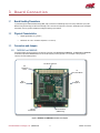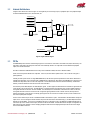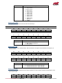
1
DM35820HR DM9820HR DM8820HR DM7820HR Versatile High Speed Digital I/O User’s Manual BDM-610010036 Rev. D RTD Embedded Technologies, Inc. AS9100 and ISO 9001 Certified RTD Embedded Technologies, Inc. 103 Innovation Boulevard State College, PA 16803 USA Telephone: 814-234-8087 Fax: 814-234-5218 www.rtd.com [email protected] [email protected] Revision History Rev A Rev B Rev C Rev D Initial Release Better DREQ description. Improved description of FIFO. Improved description of FIFOn_CON_STAT. Corrected PWM Period formula. Added DM9820 information. Added DM8820. Added AS9100. Changed to new manual format. Added ability to retrigger programmable clocks. Added register to read programmable clock current value. Added FIFO empty flag as a peripheral output. Added IDAN section. Advanced Analog I/O, Advanced Digital I/O, aAIO, aDIO, a2DIO, Autonomous SmartCal, “Catch the Express”, cpuModule, dspFramework, dspModule, expressMate, ExpressPlatform, HiDANplus, “MIL Value for COTS prices”, multiPort, PlatformBus, and PC/104EZ are trademarks, and “Accessing the Analog World”, dataModule, IDAN, HiDAN, RTD, and the RTD logo are registered trademarks of RTD Embedded Technologies, Inc (formerly Real Time Devices, Inc.). PS/2 is a trademark of International Business Machines Inc. PCI, PCI Express, and PCIe are trademarks of PCI-SIG. PC/104, PC/104-Plus, PCI-104, PCIe/104, PCI/104-Express and 104 are trademarks of the PC/104 Embedded Consortium. All other trademarks appearing in this document are the property of their respective owners. Failure to follow the instructions found in this manual may result in damage to the product described in this manual, or other components of the system. The procedure set forth in this manual shall only be performed by persons qualified to service electronic equipment. Contents and specifications within this manual are given without warranty, and are subject to change without notice. RTD Embedded Technologies, Inc. shall not be liable for errors or omissions in this manual, or for any loss, damage, or injury in connection with the use of this manual. Copyright © 2013 by RTD Embedded Technologies, Inc. All rights reserved. RTD Embedded Technologies, Inc. | www.rtd.com iii DMx820 User’s Manual Table of Contents 1 2 3 4 5 6 Introduction 8 1.1 Product Overview........................................................................................................................................................................ 8 1.2 Board Features ........................................................................................................................................................................... 8 1.3 Ordering Information ................................................................................................................................................................... 9 1.4 Contact Information .................................................................................................................................................................... 9 1.4.1 Sales Support ...................................................................................................................................................... 9 1.4.2 Technical Support ................................................................................................................................................ 9 Specifications 10 2.1 Operating Conditions ................................................................................................................................................................ 10 2.2 Electrical Characteristics .......................................................................................................................................................... 10 Notes ............................................................................................................................................................................ 10 Board Connection 11 3.1 Board Handling Precautions ..................................................................................................................................................... 11 3.2 Physical Characteristics ............................................................................................................................................................ 11 3.3 Connectors and Jumpers .......................................................................................................................................................... 11 3.3.1 DM7820HR and DM8820HR ............................................................................................................................. 11 3.3.1 DM35820HR and DM9820HR ........................................................................................................................... 12 3.3.2 External I/O Connectors..................................................................................................................................... 12 Connector CN10 – Digital Input / Output ...................................................................................................................... 12 Connector CN11 – Digital Input / Output ...................................................................................................................... 13 3.3.3 Bus Connectors ................................................................................................................................................. 14 PC/104-Express Bus Connectors (DM9820HR Only) .................................................................................................. 14 PC/104-Plus PCI Connector ......................................................................................................................................... 14 PC/104 ISA Connectors (DM7820HR Only)................................................................................................................. 15 3.4 Steps for Installing .................................................................................................................................................................... 16 IDAN Connections 17 4.1 Module Handling Precautions ................................................................................................................................................... 17 4.2 62D - Physical Characteristics .................................................................................................................................................. 17 4.3 62D - Connectors ...................................................................................................................................................................... 18 4.4 68S - Physical Characteristics .................................................................................................................................................. 19 4.5 68S – Connectors ..................................................................................................................................................................... 20 4.6 Bus Connectors ........................................................................................................................................................................ 21 PC/104-Express Bus Connectors (DM9820HR Only) .................................................................................................. 21 PC/104-Plus PCI Connector ......................................................................................................................................... 21 PC/104 ISA Connectors (DM7820HR Only)................................................................................................................. 21 4.7 Steps for Installing .................................................................................................................................................................... 22 Functional Description 23 5.1 Block Diagram........................................................................................................................................................................... 23 5.2 Internal Architecture .................................................................................................................................................................. 24 5.3 FIFOs ........................................................................................................................................................................................ 24 5.4 Board Interrupts ........................................................................................................................................................................ 25 5.5 Advanced Triggering Examples ................................................................................................................................................ 25 Board Operation and Programming 6.1 27 PCI Interface ............................................................................................................................................................................. 27 RTD Embedded Technologies, Inc. | www.rtd.com iv DMx820 User’s Manual 6.2 Device Memory ......................................................................................................................................................................... 27 6.2.1 Memory Map Overview ...................................................................................................................................... 27 6.3 Detailed Register Description ................................................................................................................................................... 36 6.3.1 System Block ..................................................................................................................................................... 36 FPGA_VERSION.......................................................................................................................................................... 36 SVN_VERSION ............................................................................................................................................................ 36 BOARD_RESET ........................................................................................................................................................... 37 BRD_STAT ................................................................................................................................................................... 37 INT_ENABLE................................................................................................................................................................ 37 INT_STATUS................................................................................................................................................................ 38 6.3.2 Standard I/O....................................................................................................................................................... 39 PORTx_OUTPUT ......................................................................................................................................................... 40 PORTx_INPUT ............................................................................................................................................................. 40 PORTx_TRISTATE ...................................................................................................................................................... 40 PORTx_MODE ............................................................................................................................................................. 40 PORTx_PERIPH_SEL_L ............................................................................................................................................. 41 PORTx_PERIPH_SEL_H ............................................................................................................................................. 41 STROBE_STATUS....................................................................................................................................................... 42 6.3.3 82C54 Timer Counter Control ............................................................................................................................ 43 TC_ID ........................................................................................................................................................................... 43 TC_INT ......................................................................................................................................................................... 43 TC_xy_CONTROL........................................................................................................................................................ 43 6.3.4 FIFO Channel n ................................................................................................................................................. 44 FIFOn_ID ...................................................................................................................................................................... 44 FIFOn_INT.................................................................................................................................................................... 45 FIFOn_IN_CLK ............................................................................................................................................................. 45 FIFOn_OUT_CLK ......................................................................................................................................................... 46 FIFOn_IN_DATA_DREQ .............................................................................................................................................. 46 FIFOn_CON_STAT ...................................................................................................................................................... 47 FIFOn_RW_PORT ....................................................................................................................................................... 47 6.3.5 Programmable Clock n ...................................................................................................................................... 48 PROGCLKn_ID ............................................................................................................................................................ 48 PROGCLKn_MODE ..................................................................................................................................................... 48 PRGCLKn_CLK ............................................................................................................................................................ 48 PRGCLKn_START_STOP ........................................................................................................................................... 49 PROGCLKn_PERIOD .................................................................................................................................................. 50 PROGCLKn_COUNT ................................................................................................................................................... 50 6.3.6 Advanced Interrupt n.......................................................................................................................................... 51 ADVINTn_ID ................................................................................................................................................................. 51 ADVINTn_INT_MODE .................................................................................................................................................. 51 ADVINTn_CLK ............................................................................................................................................................. 51 ADVINTn_PORTx_MASK ............................................................................................................................................ 52 ADVINTn_PORTx_CMP............................................................................................................................................... 52 ADVINTn_PORTx_CAPT ............................................................................................................................................. 52 6.3.7 Dual Incremental Encoder n .............................................................................................................................. 53 INCENCn_ID ................................................................................................................................................................ 53 INCENCn_INT .............................................................................................................................................................. 54 INCENCn_CLK ............................................................................................................................................................. 55 INCENCn_MODE ......................................................................................................................................................... 55 INCENCn_VALUEy ...................................................................................................................................................... 56 6.3.8 Quad Pulse Width Modulator n .......................................................................................................................... 56 PWMn_ID ..................................................................................................................................................................... 57 PWMn_MODE .............................................................................................................................................................. 57 PWMn_CLK .................................................................................................................................................................. 57 PWMn_PERIOD ........................................................................................................................................................... 58 PWMn_WIDTHx ........................................................................................................................................................... 58 6.3.9 82C54 Timer Counter n ..................................................................................................................................... 58 DESCRIPTION OF OPERATION ................................................................................................................................. 58 Control Word and Count Value Program...................................................................................................................... 58 Mode definition ............................................................................................................................................................. 60 Reading Counter Values .............................................................................................................................................. 63 6.4 PLX Registers ........................................................................................................................................................................... 67 6.4.1 Memory Map Overview ...................................................................................................................................... 67 6.4.2 DMA Register Description ................................................................................................................................. 67 DMAMODEn ................................................................................................................................................................. 67 RTD Embedded Technologies, Inc. | www.rtd.com v DMx820 User’s Manual DMAPADRn.................................................................................................................................................................. 69 DMALAPADRn ............................................................................................................................................................. 69 DMASIZn ...................................................................................................................................................................... 70 DMAPRn ....................................................................................................................................................................... 70 DMACSRn .................................................................................................................................................................... 70 DMAARB ...................................................................................................................................................................... 71 DMATHR ...................................................................................................................................................................... 71 DMADAn ....................................................................................................................................................................... 73 INTCSR ........................................................................................................................................................................ 73 7 Troubleshooting 76 8 Additional Information 77 9 8.1 PC/104 Specifications ............................................................................................................................................................... 77 8.2 PCI and PCI Express Specification .......................................................................................................................................... 77 8.3 PLX PCI9056 ............................................................................................................................................................................ 77 8.4 82C54 Timer/Counter Programming......................................................................................................................................... 77 8.5 Interrupt Programming .............................................................................................................................................................. 77 Limited Warranty RTD Embedded Technologies, Inc. | www.rtd.com 78 vi DMx820 User’s Manual Table of Figures Figure 1: DM7820HR and DM8820HR Connectors and Jumpers ......................................................................................................................... 11 Figure 2: DM7820HR and DM8820HR Connectors and Jumpers ......................................................................................................................... 12 Figure 3: Example 104™Stack ............................................................................................................................................................................... 16 Figure 4: IDAN Dimensions .................................................................................................................................................................................... 17 Figure 5: IDAN Dimensions .................................................................................................................................................................................... 19 Figure 6: Example IDAN System ............................................................................................................................................................................ 22 Figure 7: DMx820HR Block Diagram...................................................................................................................................................................... 23 Figure 8: Digital I/O Block Diagram ........................................................................................................................................................................ 24 Figure 9: Interrupt Diagram ..................................................................................................................................................................................... 25 Figure 10: Digital I/O Block Diagram ...................................................................................................................................................................... 40 Figure 11: Incremental Encoder Signals ................................................................................................................................................................ 53 Figure 12: PWM Output .......................................................................................................................................................................................... 57 Figure 13: Counter latching executed for counter #1 (Read/Load 2-byte setting)................................................................................................. 64 Table of Tables Table 1: Ordering Options ........................................................................................................................................................................................ 9 Table 2: Operating Conditions ................................................................................................................................................................................ 10 Table 3: Electrical Characteristics .......................................................................................................................................................................... 10 Table 4: CN10 Pin Assignments ............................................................................................................................................................................. 12 Table 5: CN11 Pin Assignments ............................................................................................................................................................................. 13 Table 6: CN10 Pin Assignments ............................................................................................................................................................................. 18 Table 7: CN10 Pin Assignments ............................................................................................................................................................................. 20 Table 8: PCI Configuration Registers ..................................................................................................................................................................... 27 Table 9: DMx820HR Memory Map ......................................................................................................................................................................... 28 Table 10: Peripheral Outputs .................................................................................................................................................................................. 41 Table 11: Incremental Encoder Inputs .................................................................................................................................................................... 53 Table 12: Select Counter SC[1:0]: Selection of set counter ................................................................................................................................... 59 Table 13: Read/Load RL[1:0]: Count Value Reading/Loading format setting ........................................................................................................ 59 Table 14: Mode M[2:0]: Operation waveform mode setting.................................................................................................................................... 59 Table 15: BCD: Operation count mode setting ....................................................................................................................................................... 59 Table 16: PLX DMx820HR Memory Map ............................................................................................................................................................... 67 Table 17: DMA Threshold Nybble Values............................................................................................................................................................... 72 RTD Embedded Technologies, Inc. | www.rtd.com vii DMx820 User’s Manual 1 Introduction 1.1 Product Overview The DM7820HR/DM8820HR/DM9820HR is designed to provide high speed digital I/O for PC/104-Plus, PCI-104, PCI/104-Express, and PCIe/104 Systems. It interfaces with the PCI or PCI Express bus and uses large FIFOs and DMA transfers to allow for efficient data management. Several peripherals, including Pulse Width Modulators, Incremental Encoders, and Programmable Clocks are also provided. 1.2 Board Features Digital I/O o 48 Diode protected I/O lines o 24 mA source and sink current o Compatible with DMR and DOP expansion boards Deep FIFOs with DMA o Two 2M-Word FIFOs o Each FIFO is attached to a separate DMA channel o 25 MHz bursted throughput o 12.5 MHZ continuous throughput o FIFO can be looped Pulse Width Modulators o Eight PWM outputs o Single-ended or Differential Outputs o 16-bit resolution o Separate period and width clocks provide full resolution at low duty cycles o Optional Interrupt generations Incremental Encoders o Four Incremental Encoder channels o Single-ended or Pseudo-differential Inputs o Variable frequency input filtering o Max input speed of 40ns per transition o 16-bit resolution o Two channels can be combined for 32-bit resolution o Connect to FIFO for position sampling Advanced Interrupts o Two Advanced Interrupt Modules o Interrupt on Match, Change, or Strobe o All 48 bits are captured when the interrupt is generated o Any combination of the 48 bits can be monitored Programmable Clocks o Four programmable clocks o Maximum frequency of 25 MHz o Can be started and stopped by an interrupt or another clock o Continuous or One-Shot Operation o Can be cascaded 82C54 Timer/Counters o Six Timer/Counter Channels o Fully programmable o Input clock and gate driven from internal or external source o 10 MHz maximum input RTD Embedded Technologies, Inc. | www.rtd.com 8 DMx820 User’s Manual 1.3 Ordering Information The DMx820HR is available with the following options: Table 1: Ordering Options Part Number DM35820HR DM9820HR DM8820HR DM7820HR IDAN-DM35820HR-62D IDAN-DM9820HR-62D IDAN-DM8820HR-68S IDAN-DM7820HR-68S Description PCIe/104 High-Speed Digital I/O DAQ Module PCI/104-Express High-Speed Digital I/O DAQ Module PCI-104 High-Speed Digital I/O DAQ Module PC/104-Plus High-Speed Digital I/O DAQ Module PCIe/104 High-Speed Digital I/O DAQ Module in IDAN enclosure PCI/104-Express High-Speed Digital I/O DAQ Module in IDAN enclosure PCI-104 High-Speed Digital I/O DAQ Module in IDAN enclosure PC/104-Plus High-Speed Digital I/O DAQ Module in IDAN enclosure The Intelligent Data Acquisition Node (IDAN™) building block can be used in just about any combination with other IDAN building blocks to create a simple but rugged 104™ stack. This module can also be incorporated in a custom-built RTD HiDAN™ or HiDANplus High Reliability Intelligent Data Acquisition Node. Contact RTD sales for more information on our high reliability systems. 1.4 Contact Information 1.4.1 SALES SUPPORT For sales inquiries, you can contact RTD Embedded Technologies sales via the following methods: Phone: E-Mail: 1.4.2 1-814-234-8087 Monday through Friday, 8:00am to 5:00pm (EST). [email protected] TECHNICAL SUPPORT If you are having problems with you system, please try the steps in the Troubleshooting section of this manual on page76. For help with this product, or any other product made by RTD, you can contact RTD Embedded Technologies technical support via the following methods: Phone: E-Mail: 1-814-234-8087 Monday through Friday, 8:00am to 5:00pm (EST). [email protected] RTD Embedded Technologies, Inc. | www.rtd.com 9 DMx820 User’s Manual 2 Specifications 2.1 Operating Conditions Table 2: Operating Conditions 2.2 Symbo l Vcc5 Ta Ts RH Parameter 5V Supply Voltage Operating Temperature Storage Temperature Relative Humidity MTBF Mean Time Before Failure Test Condition Non-Condensing Telcordia Issue 2 30°C, Ground benign, controlled Min 4.75 -40 -55 0 Max 5.25 +85 +125 90% Unit V C C % 3,292,579 Hour s Max 1.5 300 Unit W mA Electrical Characteristics Table 3: Electrical Characteristics Symbo l P Icc5 Parameter Power Consumption 5V Input Supply Current VIH VIL IIL IOZ VOH VOL Input High Voltage Input Low Voltage PCI Input Leakage PCI Hi-Z Leakage Output High Voltage Output Low Voltage Test Condition Vcc5 = 5.0V Active PCI Bus 0<VI<VIO 0<VI<VIO Min 1.65 0 -10 5.5 0.8 10 10 0.33 V V uA uA V V 0.8 95.2 1.2 116.9 V Ω 0.175 92.7 3.3 115.8 V Ω 61 173 2.97 PCIe Bus Differential Output Voltage DC Differential TX Impedance Differential Input Voltage DC Differential RX Impedance Electrical Idle Detect Threshold mV Digital I/O VIH Input High Voltage 2.0 5.5 V VIL Input Low Voltage -0.5 0.8 V VOH Output High Voltage IOH = -24mA 2.4 V VOL Output Low Voltage IOL = 24mA 0.4 V Notes 1. DIO Vin DC overshoot must be limited to either 5.5V or 10mA and DC undershoot must be limited to either -0.5V or 10mA. 2. DIO pins may be driven to - 2.0V or + 7.0V provided these voltages last no longer than 11ns with a forcing current no greater than 100mA. 3. Inputs are terminated with 33Ω resistors and protection diodes. 4. DIO inputs should not be tied to voltages when the board is not powered. RTD Embedded Technologies, Inc. | www.rtd.com 10 DMx820 User’s Manual 3 Board Connection 3.1 Board Handling Precautions To prevent damage due to Electrostatic Discharge (ESD), keep your board in its antistatic bag until you are ready to install it into your system. When removing it from the bag, hold the board at the edges, and do not touch the components or connectors. Handle the board in an antistatic environment, and use a grounded workbench for testing and handling of your hardware. 3.2 3.3 Physical Characteristics Weight: Approximately 100 g (0.22 lbs.) Dimensions: 90.17 mm L x 95.89 mm W (3.550 in L x 3.775 in W) Connectors and Jumpers 3.3.1 DM7820HR AND DM8820HR The following diagram shows the location of all connectors and jumpers on the DM7820HR and DM8820HR. The DM7820HR and DM8820HR are identical, except that the DM8820HR does not have the PC/104 (ISA) connector populated. For a description of each jumper and connector, refer to the following sections. PC/104-Plus Connector JP2 PCI Master Control B1 Force Three Master CN10 Digital I/O CN11 Digital I/O SW1 Slot Selection PC/104 Connector (DM7820 Only) Figure 1: DM7820HR and DM8820HR Connectors and Jumpers RTD Embedded Technologies, Inc. | www.rtd.com 11 DMx820 User’s Manual 3.3.1 DM35820HR AND DM9820HR The following diagram shows the location of all connectors and jumpers on the DM9820HR. For a description of each jumper and connector, refer to the following sections. PC/104-Plus Connector (DM9820HR only) CN10 Digital I/O CN11 Digital I/O PC/104-Express Connector Figure 2: DM7820HR and DM8820HR Connectors and Jumpers 3.3.2 EXTERNAL I/O CONNECTORS NOTE: Pin 1 can be identified by a square solder pad. Pins 2 – 50 have round solder pads. Connector CN10 – Digital Input / Output Connector CN10 provides 24 digital input/output lines, along with a +5V pin and ground pins. The pin assignments for CN10 are shown in Table 1. Table 4: CN10 Pin Assignments Signal P2[7] P2[6] P2[5] P2[4] P2[3] P2[2] P2[1] P2[0] RTD Embedded Technologies, Inc. | www.rtd.com Pin 1 3 5 7 9 11 13 15 Pin 2 4 6 8 10 12 14 16 12 Signal Strobe2 GND GND GND GND GND GND GND DMx820 User’s Manual Table 4: CN10 Pin Assignments Signal Pin Pin Signal P0[15] 17 18 GND P0[14] 19 20 GND P0[13] 21 22 GND P0[12] 23 24 GND P0[11] 25 26 GND P0[10] 27 28 GND P0[9] 29 30 GND P0[8] 31 32 GND P0[7] 33 34 GND P0[6] 35 36 GND P0[5] 37 38 GND P0[4] 39 40 GND P0[3] 41 42 GND P0[2] 43 44 GND P0[1] 45 46 GND P0[0] 47 48 GND +5V, 2A max 49 50 GND See Table 10 on page 41Table 10 and Table 11 on page 53 for peripheral pin assignments. Connector CN11 – Digital Input / Output Connector CN11 provides 24 digital input/output lines, along with a +5V pin and ground pins. The pin assignments for CN11 are shown in Table 2. Table 5: CN11 Pin Assignments Signal Pin Pin Signal P2[15] 1 2 Strobe1 P2[14] 3 4 GND P2[13] 5 6 GND P2[12] 7 8 GND P2[11] 9 10 GND P2[10] 11 12 GND P2[9] 13 14 GND P2[8] 15 16 GND P1[15] 17 18 GND P1[14] 19 20 GND P1[13] 21 22 GND P1[12] 23 24 GND P1[11] 25 26 GND P1[10] 27 28 GND P1[9] 29 30 GND P1[8] 31 32 GND P1[7] 33 34 GND P1[6] 35 36 GND P1[5] 37 38 GND P1[4] 39 40 GND P1[3] 41 42 GND P1[2] 43 44 GND P1[1] 45 46 GND P1[0] 47 48 GND +5V, 2A max 49 50 GND See Table 10 on page 41Table 10 and Table 11 on page 53 for peripheral pin assignments. RTD Embedded Technologies, Inc. | www.rtd.com 13 DMx820 User’s Manual 3.3.3 BUS CONNECTORS PC/104-Express Bus Connectors (DM9820HR Only) The PCIe connector is the connection to the system CPU. The position and pin assignments are compliant with the PCI/104-Express Specification. (See PC/104 Specifications on page 77) This board is a “Universal” board, and can connect to either a Type 1 or Type 2 PCIe/104 connector. PC/104-Plus PCI Connector The PC/104-Plus connector carries the signals of the PC/104-Plus PCI bus. Refer to PC/104-PlusTM Specification for the pinout of this connector. The DM9820HR connects to the power and ground pins only, and does not use any of the signals. The DM7820HR uses this connector for communication with the CPU. PCI Configuration Options (DM7820HR Only) To install the DM7820HR into the stack, the PCI Slot Number must be configured correctly. This is done by the PCI Slot Selector located at SW1. There are four possible PCI Slot Numbers (0 – 3). Each PCI device (PC/104-Plus or PCI-104) must a use a different slot number. The slot number is related to the position of the board in the stack. Slot 0 represents the PCI device closest to the CPU. Slot 3 represents the PCI devices farthest away from the CPU. NOTE: In a PC/104-Plus or PCI-104 system, all PCI devices should be located on one side of the CPU board (above or below the add-on cards). The CPU should not be located between two PCI devices. Switch SW1 – PCI Slot Selector When the PC/104-Plus Specification was first introduced, it only allowed for three PCI add-on cards to be bus masters. Version 2.0 of the PC/104-Plus specification was released in November 2003. This version of the specification (which the DM7820HR is designed for) adds support for all 4 PCI slots to be bus masters. There are two methods for compatibility with CPUs designed for the older PC/104-Plus Specification. One method is to use slot positions 4-7 instead of the usual 0-3. The second is to short solder jumper B1. The PCI Slot Number can be configured as follows: Switch Position 0 1 2 3 4 5 6 7 PCI Slot Number Slot 0 (closest to CPU) Slot 1 Slot 2 Slot 3 Slot 0 (closest to CPU) Slot 1 Slot 2 Slot 3 Compatibility 4 4 4 4 3 3 3 3 Master yes yes yes yes yes yes If JP2 If JP2 Jumper JP2 – Bus Master Control Install JP2 to enable bus mastering when in Slot 2 or Slot 3 in three bus master mode. RTD Embedded Technologies, Inc. | www.rtd.com 14 DMx820 User’s Manual Solder Blob B1 – Force Three Master The DM7820HR offers a configuration solder blob at location B1. If this solder blob is open (the default), the board supports bus mastering in all 4 PCI slots when SW1 is in position 0-3. If it is closed, the board will work in a 3 bus master configuration. If B1 is closed, SW1 positions 03 will be identical to positions 4-7. NOTE: The DM7820HR comes with solder blob B1 open by default. This should be compatible with most PC/104-Plus CPUs. There is no need to change this blob unless you are having compatibility problems with your specific CPU. PC/104 ISA Connectors (DM7820HR Only) The PC/104 connectors carry the signals of the PC/104-Plus ISA bus. Refer to PC/104-Plus Specification Revision 1.0 for the pinout of this connector. This is a pass-through connector. The DM7820HR connects to the power and ground pins only, and does not use any of the signals. RTD Embedded Technologies, Inc. | www.rtd.com 15 DMx820 User’s Manual 3.4 Steps for Installing 5. 6. 7. 8. 9. 10. 11. 12. 13. 14. 15. 16. Always work at an ESD protected workstation, and wear a grounded wrist-strap. Turn off power to the PC/104 system or stack. Select and install stand-offs to properly position the module on the stack. Remove the module from its anti-static bag. Check that pins of the bus connector are properly positioned. Check the stacking order; make sure all of the busses used by the peripheral cards are connected to the cpuModule. Hold the module by its edges and orient it so the bus connector pins line up with the matching connector on the stack. Gently and evenly press the module onto the PC/104 stack. If any boards are to be stacked above this module, install them. Attach any necessary cables to the PC/104 stack. Re-connect the power cord and apply power to the stack. Boot the system and verify that all of the hardware is working properly. Figure 3: Example 104™Stack RTD Embedded Technologies, Inc. | www.rtd.com 16 DMx820 User’s Manual 4 IDAN Connections 4.1 Module Handling Precautions To prevent damage due to Electrostatic Discharge (ESD), keep your module in its antistatic bag until you are ready to install it into your system. When removing it from the bag, hold the module by the aluminum enclosure, and do not touch the components or connectors. Handle the module in an antistatic environment, and use a grounded workbench for testing and handling of your hardware. 4.2 62D - Physical Characteristics Weight: Approximately 0.21 Kg (0.46 lbs.) Dimensions: 151.972 mm L x 129.978 mm W x 33.934 mm H (5.983 in L x 5.117 in W x 1.339 in H) 1.339” 5.983” 5.117” 62 pin High Density “D”: female Module Part #: Adam Tech HDT62SD Mating Part #: Adam Tech HDT62PD Figure 4: IDAN Dimensions RTD Embedded Technologies, Inc. | www.rtd.com 17 DMx820 User’s Manual 4.3 62D - Connectors Table 6: CN10 Pin Assignments IDAN P2 Pin Row 2 Row 3 CN10 Signal Pin P2.7 1 22 STROBE 2 2 43 P2.6 3 2 GND 4 23 P2.5 5 44 GND 6 3 P2.4 7 24 GND 8 45 P2.3 9 4 GND 10 25 P2.2 11 46 GND 12 5 P2.1 13 26 GND 14 47 P2.0 15 6 GND 16 27 P0.15 17 48 GND 18 7 P0.14 19 28 GND 20 49 P0.13 21 8 GND 22 29 P0.12 23 50 GND 24 9 P0.11 25 30 GND 26 51 P0.10 27 10 GND 28 31 P0.9 29 52 GND 30 11 P0.8 31 32 GND 32 53 P0.7 33 12 GND 34 33 P0.6 35 54 GND 36 13 P0.5 37 34 GND 38 55 P0.4 39 14 GND 40 35 P0.3 41 56 GND 42 15 P0.2 43 36 GND 44 57 P0.1 45 16 GND 46 37 P0.0 47 58 GND 48 17 5 VOLTS 49 38 GND 50 * Pins 51 to 62 of the IDAN connector are not connected. Row 1 1 RTD Embedded Technologies, Inc. | www.rtd.com Row 1 1 IDAN P3 Pin Row 2 Row 3 22 43 2 23 44 3 24 45 4 25 46 5 26 47 6 27 48 7 28 49 8 29 50 9 30 51 10 31 52 11 32 53 12 33 54 13 34 55 14 35 56 15 36 57 16 37 58 17 38 18 Signal P2.15 STROBE 2 P2.14 GND P2.13 GND P2.12 GND P2.11 GND P2.10 GND P2.9 GND P2.8 GND P1.15 GND P1.14 GND P1.13 GND P1.12 GND P1.11 GND P1.10 GND P1.9 GND P1.8 GND P1.7 GND P1.6 GND P1.5 GND P1.4 GND P1.3 GND P1.2 GND P1.1 GND P1.0 GND 5 VOLTS GND CN11 Pin 1 2 3 4 5 6 7 8 9 10 11 12 13 14 15 16 17 18 19 20 21 22 23 24 25 26 27 28 29 30 31 32 33 34 35 36 37 38 39 40 41 42 43 44 45 46 47 48 49 50 DMx820 User’s Manual 4.4 68S - Physical Characteristics Weight: Approximately 0.21 Kg (0.46 lbs.) Dimensions: 151.972 mm L x 129.978 mm W x 16.993 mm H (5.983 in L x 5.117 in W x 0.669 in H) Front 1.339” 5.983” 5.117” 68 pin Female Module Part #: Amphenol 5390378-7 Mating Part #: Amphenol 786090-7 Back Figure 5: IDAN Dimensions RTD Embedded Technologies, Inc. | www.rtd.com 19 DMx820 User’s Manual 4.5 68S – Connectors Table 7: CN10 Pin Assignments IDAN P2 Pin CN10 Row 1 Row 2 Signal Pin 1 P2.7 1 2 STROBE 2 2 3 P2.6 3 4 GND 4 5 P2.5 5 6 GND 6 7 P2.4 7 8 GND 8 9 P2.3 9 10 GND 10 11 P2.2 11 12 GND 12 13 P2.1 13 14 GND 14 15 P2.0 15 16 GND 16 17 P0.15 17 18 GND 18 19 P0.14 19 20 GND 20 21 P0.13 21 22 GND 22 23 P0.12 23 24 GND 24 25 P0.11 25 26 GND 26 27 P0.10 27 28 GND 28 29 P0.9 29 30 GND 30 31 P0.8 31 32 GND 32 33 P0.7 33 34 GND 34 35 P0.6 35 36 GND 36 37 P0.5 37 38 GND 38 39 P0.4 39 40 GND 40 41 P0.3 41 42 GND 42 43 P0.2 43 44 GND 44 45 P0.1 45 46 GND 46 47 P0.0 47 48 GND 48 49 5 VOLTS 49 50 GND 50 * Pins 51 to 68 of the IDAN connector are not connected. RTD Embedded Technologies, Inc. | www.rtd.com 20 IDAN P3 Pin Row 1 Row 2 1 2 3 4 5 6 7 8 9 10 11 12 13 14 15 16 17 18 19 20 21 22 23 24 25 26 27 28 29 30 31 32 33 34 35 36 37 38 39 40 41 42 43 44 45 46 47 48 49 50 Signal P2.15 STROBE 2 P2.14 GND P2.13 GND P2.12 GND P2.11 GND P2.10 GND P2.9 GND P2.8 GND P1.15 GND P1.14 GND P1.13 GND P1.12 GND P1.11 GND P1.10 GND P1.9 GND P1.8 GND P1.7 GND P1.6 GND P1.5 GND P1.4 GND P1.3 GND P1.2 GND P1.1 GND P1.0 GND 5 VOLTS GND CN11 Pin 1 2 3 4 5 6 7 8 9 10 11 12 13 14 15 16 17 18 19 20 21 22 23 24 25 26 27 28 29 30 31 32 33 34 35 36 37 38 39 40 41 42 43 44 45 46 47 48 49 50 DMx820 User’s Manual 4.6 Bus Connectors PC/104-Express Bus Connectors (DM9820HR Only) The PCIe connector is the connection to the system CPU. The position and pin assignments are compliant with the PCI/104-Express Specification. (See PC/104 Specifications on page 77) This board is a “Universal” board, and can connect to either a Type 1 or Type 2 PCIe/104 connector. PC/104-Plus PCI Connector The PC/104-Plus connector carries the signals of the PC/104-Plus PCI bus. Refer to PC/104-PlusTM Specification for the pinout of this connector. The DM9820HR connects to the power and ground pins only, and does not use any of the signals. The DM7820HR uses this connector for communication with the CPU. PCI Configuration Options (DM7820HR Only) See PCI Configuration Options (DM7820HR Only) on page 14. PC/104 ISA Connectors (DM7820HR Only) The PC/104 connectors carry the signals of the PC/104-Plus ISA bus. Refer to PC/104-Plus Specification Revision 1.0 for the pinout of this connector. This is a pass-through connector. The DM7820HR connects to the power and ground pins only, and does not use any of the signals. RTD Embedded Technologies, Inc. | www.rtd.com 21 DMx820 User’s Manual 4.7 Steps for Installing 1. 2. 3. 4. 5. 6. 7. 8. 9. 10. 11. 12. Always work at an ESD protected workstation, and wear a grounded wrist-strap. Turn off power to the IDAN system. Remove the module from its anti-static bag. Check that pins of the bus connector are properly positioned. Check the stacking order; make sure all of the busses used by the peripheral cards are connected to the cpuModule. Hold the module by its edges and orient it so the bus connector pins line up with the matching connector on the stack. Gently and evenly press the module onto the IDAN system. If any boards are to be stacked above this module, install them. Finish assembling the IDAN stack by installing screws of an appropriate length. Attach any necessary cables to the IDAN system. Re-connect the power cord and apply power to the stack. Boot the system and verify that all of the hardware is working properly. Figure 6: Example IDAN System RTD Embedded Technologies, Inc. | www.rtd.com 22 DMx820 User’s Manual 5 Functional Description 5.1 Block Diagram Below is a block diagram of the DMx820HR. Primary board components are in bold, while external I/O connections and jumpers are italicized. 48 Digital I/O SDRAM 25 MHz Clock Digital I/O FPGA 82C54 Timer/Counters PLX PCI9056 or PEX8311 PCI or PCIe Bus Figure 7: DMx820HR Block Diagram RTD Embedded Technologies, Inc. | www.rtd.com 23 DMx820 User’s Manual 5.2 Internal Architecture A diagram of the standard I/O is shown in Figure 10. Each digital I/O pin can be an input, output, or peripheral output. The peripheral outputs are the Pulse Width Modulators, FIFO, Timer/Counters, etc. Peripheral 3 Peripheral 2 1 Peripheral 1 D Peripheral 0 D D Q Q 0 Q D PORTx_OUTPUT PORTx_PERIPH_SEL Q PORTx_TRISTATE D Q PORTx_MODE Peripheral Input Data Readback Q D PORTx_INPUT Figure 8: Digital I/O Block Diagram 5.3 FIFOs The DMx820HR provides two FIFOs to buffer data going into and out of the board. Each FIFO is 16-bit wide and 2,097,661 Words deep. The input strobe, output strobe, and data input for each FIFO can be individually selected. The output data is made available to the peripheral outputs, and also the PCI interface. Each FIFO is attached to a DMA Channel in the PLX chip. FIFO0 is attached to DMA0, and FIFO1 is attached to DMA1. FIFO0 can have its input data attached to its output data. In this case, the same data is repeated forever. This is useful for some types of pattern generation. Internally, the FIFO system consists of a single 8MB SDRAM device, with 255-word input and output buffers for each channel. When data is available in the input buffer, it is moved into the area of SDRAM device for that channel. When data is in the SDRAM device, and there is room available in the output buffer, data is moved to the output buffer. All of the internal data movement is handled automatically. Greatest data efficiency is achieved when there are at least 128 words of data in the FIFO. The FIFO also provides “Write Request” and “Read Request” signals. For these signals, the internal buffers are monitored to signal when data can be sent into, and read from the FIFO. The “Write Request” is asserted when there are at least 256 words of space available in the FIFO, and negated when there are less than 128 words available. The “Read Request” is asserted when at least 256 words of data is in the FIFO, and negated when there is less than 128 words of data. Using these signals guarantees a burst of at least 128 words, which provides for efficient communication over the PCI bus, and robustly guards against over-run and under-run conditions. However, it does not allow for the FIFO to be completely filled of emptied. There is a total of 45 M-words per second of available bandwidth for the entire FIFO system. This bandwidth is allocated between all input and output sources. This is assuming that at least 256 Words stay in the FIFO at all times to maximize bursting (i.e., the Read Request and Write Request are used for DREQ). If only one word is available in the FIFO (i.e. Not Empty is used as for DREQ) the available bandwidth drops to 3.75 M-words per second. When a FIFO is looped, the data must be read and written. The table below shows examples of configurations and their maximum data rate. Note that for uniform sampling (samples are taken at uniform sampling intervals) the data rate must be an integer divisor of the 25 MHz overall clock. RTD Embedded Technologies, Inc. | www.rtd.com 24 DMx820 User’s Manual Description One FIFO in use, burst capture only One FIFO in use, burst output only One FIFO in use, continuous capture or output Two FIFOs in use, continuous capture/output Max Data Rate 25 MHz 25 MHz 12.5 MHz 12.5 MHz + 6.25 MHz 11 MHz + 11 MHz Two FIFOs in use, continuous capture/output, non-uniform sampling 5.4 Board Interrupts There are three levels of interrupt sources for this board: the interrupt sources generated in the PLX chip, the interrupt sources generated by the modules in the Control Block, and the interrupt sources within the modules. Each level must be enabled in the previous level. Figure 9 shows a block diagram of the interrupt sources. Note that there are some other sources in the PLX bridge chip; consult the datasheet for more details. DMA Channel 0 Done D Q DMAMODE0[10] DMA Channel 0 TC x_STAT[] D D Q D Q INTCSR[18], DMAMODE0[17] INTA# Q DMAPR0[2] ... x_ENA[] DMA Channel 1 Done D Q DMAMODE1[10] DMA Channel 1 TC D INT_STAT[16:0] D Q D Q INTCSR[19], DMAMODE1[17] DMAPR1[2] Q D Q INT_ENA[16:0] CNTRL[20] Modules Control Block PLX Figure 9: Interrupt Diagram 5.5 Advanced Triggering Examples The modules on the DMx820HR can be combined to generate a broad range of complex sampling scenarios. The following example shows how to use the Advanced Interrupt and 4 counters to capture N words before and M words after an event. Programmable Clock 0 is the sample clock, and is used to clock data into the FIFO. It is started after all of the other Programmable clocks are initialized. As soon as it starts, Programmable Clock 1 starts counting samples to be captured before the triggering event. This is also known as “pre-fill.” When it expires, it starts Programmable Clock 2, which removes samples from the FIFO at the same rate that they are stored, keeping a constant number of samples in the FIFO. When the triggering event happens, Programmable Clock 2 is stopped, and the FIFO begins to fill. Also, the triggering event starts Programmable Clock 3, which counts the number of samples to be captured after the triggering event. When Programmable Clock 3 expires, it stops Programmable Clock 0, and data collection ends. The triggering event can also generate an interrupt that changes the FIFO output to PCI Read, and start DMA transfers. This allows the data to be moved to system memory before data collection has ended. 1) 2) AdvInt0 a) Set to event desired b) During the Interrupt Service Routine… i) Change FIFO output clock to PCI Read ii) Start DMA transfers Prog Clock 0 - Sample Input Clock a) Period = sample period RTD Embedded Technologies, Inc. | www.rtd.com 25 DMx820 User’s Manual 3) 4) 5) 6) b) Master Clock = any c) Start Event = always d) Stop Event = Prog Clock 3 e) Continuous operation Prog Clock 1 - Pre-capture clock a) Period = N (samples before event) b) Master Clock = Prog Clock 0 c) Start Event = always d) One-shot Prog Clock 2 - Sample output clock a) Period = same as Prog Clock 0 b) Master Clock = same as Prog Clock 0 c) Start Event = Prog Clock 1 d) Stop Event = AdvInt 0 e) Continuous Prog Clock 3 - Post-Capture clock a) Period = M (samples after event) b) Master Clock = Prog Clock 0 c) Start Event = AdvInt0 d) One-Shot FIFO 0 a) Data In = any b) Data in clock = Prog Clock 0 c) Data out clock = Prog Clock 2 (before AdvInt0) d) Data out clock = PCI Read (after Adv Int0) e) DReq0 = Read Ready RTD Embedded Technologies, Inc. | www.rtd.com 26 DMx820 User’s Manual 6 Board Operation and Programming 6.1 PCI Interface This board attaches to the PCI bus using a PLX PCI9056. The PCI9056 is operating in “C Mode.” Most of the registers in the PLX chip are automatically programmed at power up by the on-board EEPROM or by the system BIOS. The only PLX registers that the user needs to access are the DMA registers found on page 67, and the Configuration Registers found in Table 8 below. For more information on the PLX PCI9056 bridge chip, contact PLX Technologies, (www.plxtech.com). Table 8: PCI Configuration Registers PCI Config. Register Address (Hex) 0x00 0x04 0x08 0x0C 0x10 0x14 0x18 0x1C 0x20 0x24 0x28 0x2C 0x30 0x34 0x38 0x3C 6.2 Register Name PCI Device ID = 0x7820 PCI Vendor ID = 0x1435 PCI Status PCI Command PCI Class Code = 0x118000 PCI Rev. ID = 0x00 PCI BIST PCI Header Type Bus Latency Timer Cache Line Size PCI Base Address Register 0: Memory Access to PLX9056 Registers PCI Base Address Register 1: I/O Access to PLX9056 Registers PCI Base Address Register 2: Memory Access to Digital I/O Registers PCI Base Address Register 3: Reserved Reserved Reserved Reserved PCI Subsystem ID = 0x9056 PCI Subsystem Vendor = 0x10B5 Reserved Reserved Reserved Reserved PCI Max Latency PCI Min Grant PCI Interrupt Pin PCI Interrupt Line Device Memory The DMx820HR is a memory mapped device. The address for the memory mapped registers can be found in Base Address Register 2. Generally, the registers are 16 bits wide. However, they can be read and written as 8, 16, or 32 bits. (There are a few exceptions as noted in the memory map.) 6.2.1 MEMORY MAP OVERVIEW Table 9 shows the memory map of the DMx820HR digital I/O registers. These are found at the offset from BAR2. RTD Embedded Technologies, Inc. | www.rtd.com 27 DMx820 User’s Manual Table 9: DMx820HR Memory Map Offset (Hex) Register Name Register Function Board Control 0x0000 FPGA_VERSION 0x0002 0x0004 0x0006 0x0008 SVN_VERSION BOARD_RESET Reserved BRD_STAT 0x0010 0x0012 INT_ENABLE INT_STAT 0x0014– 0x003E Reserved 0x0040 0x0042 0x0044 0x0046 0x0048 0x004A 0x004C 0x004E 0x0050 0x0052 0x0054 0x0056 0x0058 PORT0_OUTPUT PORT0_INPUT PORT0_TRISTATE PORT0_MODE PORT1_OUTPUT PORT1_INPUT PORT1_TRISTATE PORT1_MODE PORT2_OUTPUT PORT2_INPUT PORT2_TRISTATE PORT2_MODE STROBE_STATUS 0x005A– 0x005E 0x0060 Reserved b[15:8] Type ID b[7:0] Version b[15:0] Extended Version Write 0xA5A5 to reset board b[15:1] Reserved b0 MSTR – 0 = PCI Master Capable, 1 = Not PCI Master Capable (Read Only) b[15:0] Interrupt Enable – Set to ‘1’ to enable a specific interrupt b [15:0] Interrupt Status – Reading a ‘1’ indicates interrupt condition has occurred. Write a ‘1’ to clear an interrupt bit. Standard I/O PORT0_PERIPH_SEL_L 0x0062 PORT0_PERIPH_SEL_H 0x0064 0x0066 0x0068 PORT1_PERIPH_SEL_L PORT1_PERIPH_SEL_H PORT2_PERIPH_SEL_L RTD Embedded Technologies, Inc. | www.rtd.com b [15:0] Value to port 0 when it is an output. b [15:0] Read only value from Port 0. b [15:0] ‘1’ for output, ‘0’ for input. b[15:0] ‘1’ for peripheral output, ‘0’ for digital I/O b [15:0] Value to port 1 when it is an output. b [15:0] Read only value from Port 1. b [15:0] ‘1’ for output, ‘0’ for input. b[15:0] ‘1’ for peripheral output, ‘0’ for digital I/O b [15:0] Value to port 2 when it is an output. b [15:0] Read only value from Port 2. b [15:0] ‘1’ for output, ‘0’ for input. b[15:0] ‘1’ for peripheral output, ‘0’ for digital I/O b [9] STR2_TRI – ‘0’ = strobe2 is input, ‘1’ = srobe2 is output. b [8] STR1_TRI – ‘0’ = strobe1 is input, ‘1’ = srobe1 is output. b [5] STR2_OUT – Value for strobe2 when an output. b [4] STR1_OUT – Value for strobe1 when an output. b [1] STR2_IN – Current value of Strobe2. b [0] STR1_IN – Current value of Strobe1. b[15:14] b[13:12] b[11:10] b[9:8] b[7:6] b[5:4] b[3:2] b[1:0] b[15:14] b[13:12] b[11:10] b[9:8] b[7:6] b[5:4] b[3:2] b[1:0] Port0[7]_Periph_Select Port0[6]_Periph_Select Port0[5]_Periph_Select Port0[4]_Periph_Select Port0[3]_Periph_Select Port0[2]_Periph_Select Port0[2]_Periph_Select Port0[0]_Periph_Select Port0[15]_Periph_Select Port0[14]_Periph_Select Port0[13]_Periph_Select Port0[12]_Periph_Select Port0[11]_Periph_Select Port0[10]_Periph_Select Port0[9]_Periph_Select Port0[8]_Periph_Select 28 DMx820 User’s Manual Table 9: DMx820HR Memory Map Offset (Hex) 0x006A 0x0070– 0x007E Register Name Register Function PORT2_PERIPH_SEL_H Reserved 82C54 Timer Counter Control 0x0080 0x0082 TC_ID TC_INT 0x0084 0x0086 0x0088 0x008A 0x008C 0x008E TC_A0_CONTROL TC_A1_CONTROL TC_A2_CONTROL TC_B0_CONTROL TC_B1_CONTROL TC_B2_CONTROL 0x00C0 0x00C2 FIFO0_ID FIFO0_INT 0x00C4 FIFO0_IN_CLK 0x00C6 FIFO0_OUT_CLK b[15:0] ID Register – equals 0x1001 b[15:14] Reserved b [13:8] Interrupt Status – ‘1’ = Interrupt condition has occurred. Write ‘1’ to clear. Interrupts are asserted on the positive edge of the clock. b[7:6] Reserved b[5:0] Interrupt Enable – ‘1’ = Interrupt is enabled, ‘0’ = disabled Interrupt source are: 5 TC B2 4 TC B1 3 TC B0 2 TC A2 1 TC A1 0 TC A0 b[15:13] Reserved b[12:8] Gate Select 31-16 = Port 2 [15-0] 15-2 = Clock_Bus [15-2] 1 = ‘1’ 0 = ‘0’ b[7:4] Reserved b[3:0] Clock Select 15-2 = Clock_Bus [15-2] 1 = reserved 0 = 5 MHz FIFO Channel 0 RTD Embedded Technologies, Inc. | www.rtd.com b[15:0] ID Register = 0x2011 b [15:8] Interrupt Status – ‘1’ = Interrupt condition has occurred. Write ‘1’ to clear. b[7:0] Interrupt Enable – ‘1’ = Interrupt is enabled, ‘0’ = disabled Interrupt source are: 7 Reserved 6 Reserved 5 Underflow 4 Overflow 3 Empty 2 Full 1 Write Request 0 Read Request b[15:5] Reserved b[4:0] Input Clock Select 31 = PCI Write 30 = PCI Read 29-16 = Interrupts[13-0] 15-0 = Clock_Bus [15-0] b[15:5] Reserved b[4:0] Input Clock Select 31 = PCI Write 30 = PCI Read 29-16 = Interrupts[13-0] 15-0 = Clock_Bus [15-0] 29 DMx820 User’s Manual Table 9: DMx820HR Memory Map Offset (Hex) 0x00C8 Register Name FIFO0_IN_DATA_DREQ 0x00CA FIFO0_CON_STAT 0x00CC FIFO0_RW_PORT 0x00D0 0x00D2 FIFO1_ID FIFO1_INT 0x00D4 FIFO1_IN_CLK 0x00D6 FIFO1_OUT_CLK 0x00D8 FIFO1_IN_DATA_DREQ Register Function b[15:10] Reserved b[9:8] DREQ0 Source 3 = Not Full 2 = Write Request 1 = Not Empty 0 = Read Request b[7:4] Reserved b[3:0] Input Data Select 3 = FIFO0 Output 2 = Port 2 1 = Port 0 0 = PCI Data b[15:10] Reserved b[9] Write Request (non-sticky) b[8] Read Request (non-sticky) b[7:1] Reserved b[0] ‘1’ = Enable, ‘0’ = Clear b [15:0] Read/Write Port. (Word access only) FIFO Channel 1 RTD Embedded Technologies, Inc. | www.rtd.com b[15:0] ID Register = 0x2011 b [15:8] Interrupt Status – ‘1’ = Interrupt condition has occurred. Write ‘1’ to clear. b[7:0] Interrupt Enable – ‘1’ = Interrupt is enabled, ‘0’ = disabled Interrupt source are: 7 Reserved 6 Reserved 5 Underflow 4 Overflow 3 Empty 2 Full 1 Write Request 0 Read Request b[15:5] Reserved b[4:0] Input Clock Select 31 = PCI Write 30 = PCI Read 29-16 = Interrupts[13-0] 15-0 = Clock_Bus [15-0] b[15:5] Reserved b[4:0] Input Clock Select 31 = PCI Write 30 = PCI Read 29-16 = Interrupts[13-0] 15-0 = Clock_Bus [15-0] b[15:10] Reserved b[9:8] DREQ1 Source 3 = Not Full 2 = Write Request 1 = Not Empty 0 = Read Request b[7:4] Reserved b[3:0] Input Data Select 3 = Incremental Encoder B1 2 = Incremental Encoder B0 1 = Port 1 0 = PCI Data 30 DMx820 User’s Manual Table 9: DMx820HR Memory Map Offset (Hex) 0x00DA Register Name FIFO1_CON_STAT 0x00DC FIFO1_RW_PORT 0x0100 0x0102 PRGCLK0_ID PRGCLK0_MODE 0x0104 PRGCLK0_CLK 0x0106 PRGCLK0_START_STOP 0x0108 PRGCLK0_PERIOD Register Function b[15:10] Reserved b[9] Write Request (non-sticky) b[8] Read Request (non-sticky) b[7:1] Reserved b[0] ‘1’ = Enable, ‘0’ = Clear b [15:0] Read/Write Port. (Word access only) Programmable Clock 0 b[15:0] ID Register = 0x1000 b[15:2] Reserved b[1:0] ’00’ = Disabled ’01’ = Continuous ’10’ = Retrigger ’11’ = One-Shot b[15:4] Reserved b[3:0] Master Clock Source 15-0 = Clock_Bus [15-0] b[15:13] Reserved b[12:8] Stop Clock 31-16 = Interrupt_Bus[15-0] 15-1 = Clock_Bus [15-1] 0 = No Stop Clock b[7:5] Reserved b[4:0] Start Trigger 31-16 = Interrupt_Bus[15-0] 15-1 = Clock_Bus [15-1] 0 = Start Immediate b[15:0] Period of Clock Output frequency is: Master _ Clock _ Frequency ( PRG _ CLK _ PERIOD 1) 0x010A PRGCLK0_COUNT b[15:0] The current value of the clock counter Programmable Clock 1 0x0140 0x0142 PRGCLK1_ID PRGCLK1_MODE 0x0144 PRGCLK1_CLK 0x0146 PRGCLK1_START_STOP RTD Embedded Technologies, Inc. | www.rtd.com b[15:0] ID Register = 0x1000 b[15:2] Reserved b[1:0] ’00’ = Disabled ’01’ = Continuous ’10’ = Retrigger ’11’ = One-Shot b[15:4] Reserved b[3:0] Master Clock Source 15-0 = Clock_Bus [15-0] b[15:13] Reserved b[12:8] Stop Clock 31-16 = Interrupt_Bus[15-0] 15-1 = Clock_Bus [15-1] 0 = No Stop Clock b[7:5] Reserved b[4:0] Start Trigger 31-16 = Interrupt_Bus[15-0] 15-1 = Clock_Bus [15-1] 0 = Start Immediate 31 DMx820 User’s Manual Table 9: DMx820HR Memory Map Offset (Hex) 0x0148 Register Name PRGCLK1_PERIOD Register Function b[15:0] Period of Clock Output frequency is: Master _ Clock _ Frequency ( PRG _ CLK _ PERIOD 1) 0x014A PRGCLK1_COUNT b[15:0] The current value of the clock counter Programmable Clock 2 0x0180 0x0182 PRGCLK2_ID PRGCLK2_MODE 0x0184 PRGCLK2_CLK 0x0186 PRGCLK2_START_STOP 0x0188 PRGCLK2_PERIOD b[15:0] ID Register = 0x1000 b[15:2] Reserved b[1:0] ’00’ = Disabled ’01’ = Continuous ’10’ = Retrigger ’11’ = One-Shot b[15:4] Reserved b[3:0] Master Clock Source 15-0 = Clock_Bus [15-0] b[15:13] Reserved b[12:8] Stop Clock 31-16 = Interrupt_Bus[15-0] 15-1 = Clock_Bus [15-1] 0 = No Stop Clock b[7:5] Reserved b[4:0] Start Trigger 31-16 = Interrupt_Bus[15-0] 15-1 = Clock_Bus [15-1] 0 = Start Immediate b[15:0] Period of Clock Output frequency is: Master _ Clock _ Frequency ( PRG _ CLK _ PERIOD 1) 0x018A PRGCLK2_COUNT b[15:0] The current value of the clock counter Programmable Clock 3 0x01C0 0x01C2 PRGCLK3_ID PRGCLK3_MODE 0x01C4 PRGCLK3_SOURCE 0x01C6 PRGCLK3_START_STOP 0x01C8 PRGCLK3_PERIOD b[15:0] ID Register = 0x1000 b[15:2] Reserved b[1:0] ’00’ = Disabled ’01’ = Continuous ’10’ = Retrigger ’11’ = One-Shot b[15:4] Reserved b[3:0] Master Clock Source 15-0 = Clock_Bus [15-0] b[15:13] Reserved b[12:8] Stop Clock 31-16 = Interrupt_Bus[15-0] 15-1 = Clock_Bus [15-1] 0 = No Stop Clock b[7:5] Reserved b[4:0] Start Trigger 31-16 = Interrupt_Bus[15-0] 15-1 = Clock_Bus [15-1] 0 = Start Immediate b[15:0] Period of Clock Output frequency is: Master _ Clock _ Frequency ( PRG _ CLK _ PERIOD 1) RTD Embedded Technologies, Inc. | www.rtd.com 32 DMx820 User’s Manual Table 9: DMx820HR Memory Map Offset (Hex) 0x01CA Register Name PRGCLK3_COUNT 0x0200 0x0202 ADVINT0_ID ADVINT0_INT_MODE 0x0204 ADVINT0_CLK 0x0206 0x0208 Reserved ADVINT0_PORT0_MASK 0x020A ADVINT0_PORT1_MASK 0x020C ADVINT0_PORT2_MASK 0x020E 0x0210 0x0212 0x0214 0x0216 0x0218 Reserved ADVINT0_PORT0_CMP ADVINT0_PORT1_CMP ADVINT0_PORT2_CMP Reserved ADVINT0_PORT0_CAPT 0x021A ADVINT0_PORT1_CAPT 0x021C ADVINT0_PORT2_CAPT 0x021E Reserved 0x0240 0x0242 ADVINT1_ID ADVINT1_INT_MODE 0x0244 ADVINT1_CLK 0x0246 0x0248 Reserved ADVINT1_PORT0_MASK 0x024A ADVINT1_PORT1_MASK 0x024C ADVINT1_PORT2_MASK 0x024E 0x0250 0x0252 0x0254 Reserved ADVINT1_PORT0_CMP ADVINT1_PORT1_CMP ADVINT1_PORT2_CMP Register Function b[15:0] The current value of the clock counter Advanced Interrupt 0 b[15:0] ID Register = 0x0001 b[1:0] Interrupt Mode 3 = Event Mode 2 = Match Mode 1 = Strobe Mode 0 = Disabled b[3:0] Sample Clock Source 15-0 = Clock_Bus [15-0] b[15:0] Port 0 Mask ‘0’ = Bit is used for match/event ‘1’ = Bit is ignored b[15:0] Port 1 Mask ‘0’ = Bit is used for match/event ‘1’ = Bit is ignored b[15:0] Port 2 Mask ‘0’ = Bit is used for match/event ‘1’ = Bit is ignored b [15:0] Port 0 Compare – Value used for interrupt on match. b [15:0] Port 1 Compare – Value used for interrupt on match. b [15:0] Port 2 Compare – Value used for interrupt on match. b [15:0] Port 0 Capture – Value on Port 0 is written to this register when an interrupt occurs. b [15:0] Port 1 Capture – Value on Port 1 is written to this register when an interrupt occurs. b [15:0] Port 2 Capture – Value on Port 2 is written to this register when an interrupt occurs. Advanced Interrupt 1 RTD Embedded Technologies, Inc. | www.rtd.com b[15:0] ID Register = 0x0001 b[1:0] Interrupt Mode 3 = Event Mode 2 = Match Mode 1 = Strobe Mode 0 = Disabled b[3:0] Sample Clock Source 15-0 = Clock_Bus [15-0] b[15:0] Port 0 Mask ‘0’ = Bit is used for match/event ‘1’ = Bit is ignored b[15:0] Port 1 Mask ‘0’ = Bit is used for match/event ‘1’ = Bit is ignored b[15:0] Port 2 Mask ‘0’ = Bit is used for match/event ‘1’ = Bit is ignored b [15:0] Port 0 Compare – Value used for interrupt on match. b [15:0] Port 1 Compare – Value used for interrupt on match. b [15:0] Port 2 Compare – Value used for interrupt on match. 33 DMx820 User’s Manual Table 9: DMx820HR Memory Map Offset (Hex) 0x0256 0x0258 Register Name Reserved ADVINT1_PORT0_CAPT 0x025A ADVINT1_PORT1_CAPT 0x025C ADVINT1_PORT2_CAPT 0x025E Reserved 0x0280 0x0282 INCENC0_ID INCENC0_INT 0x0284 INCENC0_CLOCK 0x0286 INCENC0_MODE 0x0288 0x028A INCENC0_VALUEA INCENC0_VALUEB 0x02C0 0x02C2 INCENC1_ID INCENC1_INT 0x02C4 INCENC1_CLOCK Register Function b [15:0] Port 0 Capture – Value on Port 0 is written to this register when an interrupt occurs. b [15:0] Port 1 Capture – Value on Port 1 is written to this register when an interrupt occurs. b [15:0] Port 2 Capture – Value on Port 2 is written to this register when an interrupt occurs. Dual Incremental Encoder 0 b[15:0] ID Register = 0x0002 b [11:8] Interrupt Status – ‘1’ = Interrupt condition has occurred. Write ‘1’ to clear. b[3:0] Interrupt Enable – ‘1’ = Interrupt is enabled, ‘0’ = disabled Interrupt source are: 3 Encoder B Negative Rollover 2 Encoder B Positive Rollover 1 Encoder A Negative Rollover 0 Encoder A Positive Rollover b[3:0] Master Clock Source 15-0 = Clock_Bus [15-0] b [15:8] Phase Filter – Writing a ‘1’ to a specific bit masks out a phase transition. b[7:6] Reserved b[5] Differential Mode ‘1’ = Pseudo differential mode, ‘0’ = Single ended mode b[4] Input Filter – ‘1’ = Enable Input Filter, ‘0’ = Disable Input Filter b [3] Join – ‘1’ = Operate as single 32-bit Encoder, ‘0’ = Operate as two 16-bit Encoders. b [2] ‘0’ = External Index is disabled, ‘1’ = External Index is enabled. b [1] Hold Register – ‘1’ = Hold values register, ‘0’ = Allow value register to change. b [0] Count Enable – ‘1’ = Encoder is enabled, ‘0’ = Encoder is cleared. b[15:0] Value for Encoder A b[15:0] Value for Encoder B Dual Incremental Encoder 1 RTD Embedded Technologies, Inc. | www.rtd.com b[15:0] ID Register = 0x0002 b [11:8] Interrupt Status – ‘1’ = Interrupt condition has occurred. Write ‘1’ to clear. b[3:0] Interrupt Enable – ‘1’ = Interrupt is enabled, ‘0’ = disabled Interrupt source are: 3 Encoder B Negative Rollover 2 Encoder B Positive Rollover 1 Encoder A Negative Rollover 0 Encoder A Positive Rollover b[3:0] Master Clock Source 15-0 = Clock_Bus [15-0] 34 DMx820 User’s Manual Table 9: DMx820HR Memory Map Offset (Hex) 0x02C6 Register Name INCENC1_MODE 0x02C8 0x02CA INCENC1_VALUEA INCENC1_VALUEB Register Function b [15:8] Phase Filter – Writing a ‘1’ to a specific bit masks out a phase transition. b[7:6] Reserved b[5] Differential Mode ‘1’ = Pseudo differential mode, ‘0’ = Single ended mode b[4] Input Filter – ‘1’ = Enable Input Filter, ‘0’ = Disable Input Filter b [3] Join – ‘1’ = Operate as single 32-bit Encoder, ‘0’ = Operate as two 16-bit Encoders. b [2] ‘0’ = External Index is disabled, ‘1’ = External Index is enabled. b [1] Hold Register – ‘1’ = Hold values register, ‘0’ = Allow value register to change. b[0] Count Enable – ‘1’ = Encoder is enabled, ‘0’ = Encoder is cleared. b[15:0] Value for Encoder A b[15:0] Value for Encoder B Pulse Width Modulator 0 0x0300 0x0302 0x0304 PWM0_ID PWM0_MODE PWM0_CLK 0x0306 0x0308 Reserved PWM0_PERIOD b[15:0] ID Register = 0x0003 b[0] ‘1’ = Enable PWM, ‘0’ = Disable PWM b[7:4] Period Clock Source 15-0 = Clock_Bus [15-0] b[3:0] Width Clock Source 15-0 = Clock_Bus [15-0] b[15:0] Period of PWM Cycle is: Width _ Clock _ Frequency ( PWMx _ PERIOD 1) 0x030A0x030E 0x0310 0x0312 0x0314 0x0316 0x0318 0x031A 0x031C 0x031E Reserved 0x0340 0x0342 0x0344 PWM1_ID PWM1_MODE PWM1_CLK 0x0346 0x0348 Reserved PWM1_PERIOD PWM0_WIDTHA Reserved PWM0_WIDTHB Reserved PWM0_WIDTHC Reserved PWM0_WIDTHD Reserved b[15:0] Width of output A pulse in Period Clock cycles b[15:0] Width of output B pulse in Period Clock cycles b[15:0] Width of output C pulse in Period Clock cycles b[15:0] Width of output D pulse in Period Clock cycles Pulse Width Modulator 1 b[15:0] ID Register = 0x0003 b[0] ‘1’ = Enable PWM, ‘0’ = Disable PWM b[7:4] Period Clock Source 15-0 = Clock_Bus [15-0] b[3:0] Width Clock Source 15-0 = Clock_Bus [15-0] b[15:0] Period of PWM Cycle is: Width _ Clock _ Frequency ( PWMx _ PERIOD 1) 0x034A0x034E 0x0350 Reserved PWM1_WIDTHA RTD Embedded Technologies, Inc. | www.rtd.com b[15:0] Width of output A pulse in Period Clock cycles 35 DMx820 User’s Manual Table 9: DMx820HR Memory Map Offset (Hex) 0x0352 0x0354 0x0356 0x0358 0x035A 0x035C 0x035E Register Name Reserved PWM1_WIDTHB Reserved PWM1_WIDTHC Reserved PWM1_WIDTHD Reserved 0x1000 0x1004 0x1008 0x100C TCA_COUNTER_0 TCA_COUNTER_1 TCA_COUNTER_2 TCA_CON_WORD 0x1010 0x1014 0x1018 0x101C TCB_COUNTER_0 TCB_COUNTER_1 TCB_COUNTER_2 TCB_CON_WORD Register Function b[15:0] Width of output B pulse in Period Clock cycles b[15:0] Width of output C pulse in Period Clock cycles b[15:0] Width of output D pulse in Period Clock cycles 82C54 Timer Counter A b[7:0] b[7:0] b[7:0] b[7:0] Counter 0 Register Counter 1 Register Counter 2 Register Control Word Register 82C54 Timer Counter B 6.3 b[7:0] b[7:0] b[7:0] b[7:0] Counter 0 Register Counter 1 Register Counter 2 Register Control Word Register Detailed Register Description The following sections provide a detailed description of the individual registers. In the following register description sections, each register is described by a register table. The first row of the table lists the bits, D15 through D0. The second row lists the field name for each bit. The third row lists the properties of that bit; ’R’ = bit can be read, ’W’ = bit can be written to, and ’C’ = bit can be cleared. The last row lists the value of the bit after reset. The register table is then followed by a description of each of the fields where applicable. An "N/A" for the reset value indicates that the reset value is not applicable - read the field descriptions for more information. Bits marked as "Reserved" in the field name are unused, and reads will always return their reset value. These bits should not be modified during writes for future compatibility. 6.3.1 SYSTEM BLOCK FPGA_VERSION This register provides the version and type ID of the Digital I/O FPGA. The version can be used to identify the specific build of the board. The type ID can be used to identify a particular feature set. 15 8 7 0 TYPE_ID R,+xxxx xxxx VERSION R, +xxxx xxxx Field TYPE_ID VERSION Description FPGA Type Identifier. 0x10 = Standard FPGA FPGA Version Identifier SVN_VERSION This register provides the source code revision control version. It is updated every time the FPGA is compiled. 15 0 VERSION R,+xxxx xxxx xxxx xxxx RTD Embedded Technologies, Inc. | www.rtd.com 36 DMx820 User’s Manual Field Description VERSION FPGA Source Version Identifier BOARD_RESET Writing a value of 0xA5A5 to this register resets the board. All internal registers are set to their default values. Note: The 82C54 Timer/Counters are not affected by this register 15 0 RESET W,+0000 0000 0000 0000 Field Description RESET Write 0xA5A5 to reset the board. All other writes are ignored. Reads will return all zeros. BRD_STAT This register contains status information for the board. 15 1 Reserved R,+0 0 MSTR R,+N Field Description MSTR Indicates if the board is PCI master capable based on the rotary switch and jumper settings. ’0’ = PCI Master ’1’ = Not PCI Master INT_ENABLE This register controls which interrupt sources are used to generate a local interrupt. 15 14 13 12 11 10 9 8 FIFO1 RW,+0 FIFO0 RW,+0 PClk3 RW,+0 PClk2 RW,+0 PClk1 RW,+0 PClk0 RW,+0 PWM1 RW,+0 PWM0 RW,+0 7 6 Reserved R,+00 5 4 3 2 1 0 IncEnc1 RW,+0 IncEnc0 RW,+0 Rsvd R,+0 82C54 RW,+0 AdvInt1 RW,+0 AdvInt0 RW,+0 Field AdvInt0 AdvInt1 82C54 Description Interrupt from Advance Interrupt block at 0x0200 ’0’ = Interrupt Disabled ’1’ = Interrupt Enabled Interrupt from Advance Interrupt block at 0x0240 ’0’ = Interrupt Disabled ’1’ = Interrupt Enabled Interrupt 82C54 Timer/Counter block at 0x0080 ’0’ = Interrupt Disabled ’1’ = Interrupt Enabled RTD Embedded Technologies, Inc. | www.rtd.com 37 DMx820 User’s Manual IncEnc0 Interrupt from Incremental Encoder block at 0x0280 ’0’ = Interrupt Disabled ’1’ = Interrupt Enabled Interrupt from Incremental Encoder block at 0x02C0 ’0’ = Interrupt Disabled ’1’ = Interrupt Enabled Interrupt from Pulse Width Modulator block at 0x0300 ’0’ = Interrupt Disabled ’1’ = Interrupt Enabled Interrupt from Pulse Width Modulator block at 0x0340 ’0’ = Interrupt Disabled ’1’ = Interrupt Enabled Interrupt from Programmable Clock block at 0x0100 ’0’ = Interrupt Disabled ’1’ = Interrupt Enabled Interrupt from Programmable Clock block at 0x0140 ’0’ = Interrupt Disabled ’1’ = Interrupt Enabled Interrupt from Programmable Clock block at 0x0180 ’0’ = Interrupt Disabled ’1’ = Interrupt Enabled Interrupt from Programmable Clock block at 0x01C0 ’0’ = Interrupt Disabled ’1’ = Interrupt Enabled Interrupt from FIFO block at 0x00C0 ’0’ = Interrupt Disabled ’1’ = Interrupt Enabled Interrupt from FIFO block at 0x00D0 ’0’ = Interrupt Disabled ’1’ = Interrupt Enabled IncEnc1 PWM0 PWM1 PClk0 PClk1 PClk2 PClk3 FIFO0 FIFO1 INT_STATUS This register shows if any of the interrupt conditions has occurred. This is a sticky register – bits remain set until cleared by writing a ‘1’. Interrupts do not have to be enabled in INT_ENABLE in order for status bits to be set. 15 14 13 12 11 10 9 8 FIFO1 RC,+0 FIFO0 RC,+0 PClk3 RC,+0 PClk2 RC,+0 PClk1 RC,+0 PClk0 RC,+0 PWM1 RC,+0 PWM0 RC,+0 7 6 Reserved R,+00 5 4 3 2 1 0 IncEnc1 RC,+0 IncEnc0 RC,+0 Rsvd R,+0 82C54 RC,+0 AdvInt1 RC,+0 AdvInt0 RC,+0 Field AdvInt0 AdvInt1 82C54 IncEnc0 IncEnc1 Description Interrupt from Advance Interrupt block at 0x0200 ’0’ = Interrupt has not occurred ’1’ = Interrupt has occurred. Write ‘1’ to clear. Interrupt from Advance Interrupt block at 0x0240 ’0’ = Interrupt has not occurred ’1’ = Interrupt has occurred. Write ‘1’ to clear. Interrupt 82C54 Timer/Counter block at 0x0080 ’0’ = Interrupt has not occurred ’1’ = Interrupt has occurred. Write ‘1’ to clear. Interrupt from Incremental Encoder block at 0x0280 ’0’ = Interrupt has not occurred ’1’ = Interrupt has occurred. Write ‘1’ to clear. Interrupt from Incremental Encoder block at 0x02C0 RTD Embedded Technologies, Inc. | www.rtd.com 38 DMx820 User’s Manual ’0’ = Interrupt has not occurred ’1’ = Interrupt has occurred. Write ‘1’ to clear. Interrupt from Pulse Width Modulator block at 0x0300 ’0’ = Interrupt has not occurred ’1’ = Interrupt has occurred. Write ‘1’ to clear. Interrupt from Pulse Width Modulator block at 0x0340 ’0’ = Interrupt has not occurred ’1’ = Interrupt has occurred. Write ‘1’ to clear. Interrupt from Programmable Clock block at 0x0100 ’0’ = Interrupt has not occurred ’1’ = Interrupt has occurred. Write ‘1’ to clear. Interrupt from Programmable Clock block at 0x0140 ’0’ = Interrupt has not occurred ’1’ = Interrupt has occurred. Write ‘1’ to clear. Interrupt from Programmable Clock block at 0x0180 ’0’ = Interrupt has not occurred ’1’ = Interrupt has occurred. Write ‘1’ to clear. Interrupt from Programmable Clock block at 0x01C0 ’0’ = Interrupt has not occurred ’1’ = Interrupt has occurred. Write ‘1’ to clear. Interrupt from FIFO block at 0x00C0 ’0’ = Interrupt has not occurred ’1’ = Interrupt has occurred. Write ‘1’ to clear. Interrupt from FIFO block at 0x00D0 ’0’ = Interrupt has not occurred ’1’ = Interrupt has occurred. Write ‘1’ to clear. PWM0 PWM1 PClk0 PClk1 PClk2 PClk3 FIFO0 FIFO1 6.3.2 STANDARD I/O A diagram of the standard I/O is shown in Figure 10. Each digital I/O pin can be an input, output, or peripheral output. The peripheral outputs are the Pulse Width Modulators, FIFO, Timer/Counters, etc. Peripheral 3 Peripheral 2 1 Peripheral 1 D Peripheral 0 D D Q Q 0 Q D PORTx_OUTPUT PORTx_PERIPH_SEL Q PORTx_TRISTATE D Q PORTx_MODE Peripheral Input Data Readback RTD Embedded Technologies, Inc. | www.rtd.com Q D PORTx_INPUT 39 DMx820 User’s Manual Figure 10: Digital I/O Block Diagram PORTx_OUTPUT Sets the value for Port 0, Port 1, or Port 2 when it is a standard output. 15 14 13 12 11 10 9 8 Px_15 RW,+0 Px_14 RW,+0 Px_13 RW,+0 Px_12 RW,+0 Px_11 RW,+0 Px_10 RW,+0 Px_9 RW,+0 Px_8 RW,+0 7 6 5 4 3 2 1 0 Px_7 RW,+0 Px_6 RW,+0 Px_5 RW,+0 Px_4 RW,+0 Px_3 RW,+0 Px_2 RW,+0 Px_1 RW,+0 Px_0 RW,+0 Field Px_[15:0] Description Value to output ’0’ = Low ’1’ = High PORTx_INPUT Returns the current value of Port 0, Port 1, or Port 2. 15 14 13 12 11 10 9 8 Px_15 R,+0 Px_14 R,+0 Px_13 R,+0 Px_12 R,+0 Px_11 R,+0 Px_10 R,+0 Px_9 R,+0 Px_8 R,+0 7 6 5 4 3 2 1 0 Px_7 R,+0 Px_6 R,+0 Px_5 R,+0 Px_4 R,+0 Px_3 R,+0 Px_2 R,+0 Px_1 R,+0 Px_0 R,+0 Field Px_[15:0] Description Current pin value ’0’ = Pin is Low ’1’ = Pin is High PORTx_TRISTATE This register selects if each bit in Port 0, Port 1, or Port 2 is an input or an output. 15 14 13 12 11 10 9 8 Px_15 RW,+0 Px_14 RW,+0 Px_13 RW,+0 Px_12 RW,+0 Px_11 RW,+0 Px_10 RW,+0 Px_9 RW,+0 Px_8 RW,+0 7 6 5 4 3 2 1 0 Px_7 RW,+0 Px_6 RW,+0 Px_5 RW,+0 Px_4 RW,+0 Px_3 RW,+0 Px_2 RW,+0 Px_1 RW,+0 Px_0 RW,+0 Field Px_[15:0] Description Select input or output ’0’ = Input ’1’ = Output PORTx_MODE Selects if each pin in Port 0, Port 1, or Port 2 is a standard I/O (controlled by PORTx_TRISTATE) or a peripheral output (controlled by PORTx_PERIPH_SEL). RTD Embedded Technologies, Inc. | www.rtd.com 40 DMx820 User’s Manual 15 14 13 12 11 10 9 8 Px_15 RW,+0 Px_14 RW,+0 Px_13 RW,+0 Px_12 RW,+0 Px_11 RW,+0 Px_10 RW,+0 Px_9 RW,+0 Px_8 RW,+0 7 6 5 4 3 2 1 0 Px_7 RW,+0 Px_6 RW,+0 Px_5 RW,+0 Px_4 RW,+0 Px_3 RW,+0 Px_2 RW,+0 Px_1 RW,+0 Px_0 RW,+0 Field Description Px_[15:0] Port Mode ’0’ = Standard I/O (controlled by PORTx_ TRISTATE) ’1’ = Peripheral (controlled by PORTx_PERIPH_SEL) PORTx_PERIPH_SEL_L This register selects the peripheral for Port 0, Port 1, or Port 2 when it is a peripheral output (i.e. PORTx_MODE[] = ‘1’). This register selects the peripheral for bits [7:0]. 15 14 13 Px_7 RW,+00 7 12 11 Px_6 RW,+00 6 5 Px_3 RW,+00 10 9 Px_5 RW,+00 4 3 Px_2 RW,+00 8 Px_4 RW,+00 2 1 Px_1 RW,+00 0 Px_0 RW,+00 PORTx_PERIPH_SEL_H This register selects the peripheral for Port 0, Port 1, or Port 2 when it is a peripheral output (i.e. PORTx_MODE[] = ‘1’). This register selects the peripheral for bits [15:8]. 15 14 13 Px_15 RW,+00 7 12 11 Px_14 RW,+00 6 5 Px_11 RW,+00 10 9 Px_13 RW,+00 4 3 Px_10 RW,+00 8 Px_12 RW,+00 2 Px_9 RW,+00 1 0 Px_8 RW,+00 Table 10: Peripheral Outputs Pin 00 PORTx_PERIPH_SEL 01 10 Port0[0] Port0[1] Port0[2] Port0[3] Port0[4] Port0[5] Port0[6] Port0[7] Port0[8] Port0[9] Port0[10] Port0[11] Port0[12] Port0[13] RTD Embedded Technologies, Inc. | www.rtd.com FIFO0_Out[0] FIFO0_Out[1] FIFO0_Out[2] FIFO0_Out[3] FIFO0_Out[4] FIFO0_Out[5] FIFO0_Out[6] FIFO0_Out[7] FIFO0_Out[8] FIFO0_Out[9] FIFO0_Out[10] FIFO0_Out[11] FIFO0_Out[12] FIFO0_Out[13] 41 11 FIFO1_Out[0] FIFO1_Out[1] FIFO1_Out[2] FIFO1_Out[3] FIFO1_Out[4] FIFO1_Out[5] FIFO1_Out[6] FIFO1_Out[7] FIFO1_Out[8] FIFO1_Out[9] FIFO1_Out[10] FIFO1_Out[11] FIFO1_Out[12] FIFO1_Out[13] DMx820 User’s Manual Table 10: Peripheral Outputs Pin PORTx_PERIPH_SEL 01 10 00 Port0[14] Port0[15] Port1[0] Port1[1] Port1[2] Port1[3] Port1[4] Port1[5] Port1[6] Port1[7] Port1[8] Port1[9] Port1[10] Port1[11] Port1[12] Port1[13] Port1[14] Port1[15] Port2[0] Port2[1] Port2[2] Port2[3] Port2[4] Port2[5] Port2[6] Port2[7] Port2[8] Port2[9] Port2[10] Port2[11] Port2[12] Port2[13] Port2[14] Port2[15] FIFO0_Empty FIFO1_Empty PWM0_A+ PWM0_APWM0_B+ PWM0_BPWM0_C+ PWM0_CPWM0_D+ PWM0_DPWM1_A+ PWM1_APWM1_B+ PWM1_BPWM1_C+ PWM1_CPWM1_D+ PWM1_D- 11 FIFO0_Out[14] FIFO0_Out[15] FIFO0_Out[0] FIFO0_Out[1] FIFO0_Out[2] FIFO0_Out[3] FIFO0_Out[4] FIFO0_Out[5] FIFO0_Out[6] FIFO0_Out[7] FIFO0_Out[8] FIFO0_Out[9] FIFO0_Out[10] FIFO0_Out[11] FIFO0_Out[12] FIFO0_Out[13] FIFO0_Out[14] FIFO0_Out[15] FIFO0_Out[0] FIFO0_Out[1] FIFO0_Out[2] FIFO0_Out[3] FIFO0_Out[4] FIFO0_Out[5] FIFO0_Out[6] FIFO0_Out[7] FIFO0_Out[8] FIFO0_Out[9] FIFO0_Out[10] FIFO0_Out[11] FIFO0_Out[12] FIFO0_Out[13] FIFO0_Out[14] FIFO0_Out[15] TC_A0_OUT TC_A1_OUT TC_A2_OUT TC_B0_OUT TC_B1_OUT TC_B2_OUT ProgClk0_OUT ProgClk1_OUT ProgClk2_OUT ProgClk3_OUT Strobe1_pos Strobe2_pos Strobe1_neg Strobe2_neg FIFO1_Out[14] FIFO1_Out[15] FIFO1_Out[0] FIFO1_Out[1] FIFO1_Out[2] FIFO1_Out[3] FIFO1_Out[4] FIFO1_Out[5] FIFO1_Out[6] FIFO1_Out[7] FIFO1_Out[8] FIFO1_Out[9] FIFO1_Out[10] FIFO1_Out[11] FIFO1_Out[12] FIFO1_Out[13] FIFO1_Out[14] FIFO1_Out[15] FIFO1_Out[0] FIFO1_Out[1] FIFO1_Out[2] FIFO1_Out[3] FIFO1_Out[4] FIFO1_Out[5] FIFO1_Out[6] FIFO1_Out[7] FIFO1_Out[8] FIFO1_Out[9] FIFO1_Out[10] FIFO1_Out[11] FIFO1_Out[12] FIFO1_Out[13] FIFO1_Out[14] FIFO1_Out[15] STROBE_STATUS This register can be used to check the status of the strobe signals, as well as configure the strobes as outputs. 15 10 Reserved R,+0000 00 7 6 Reserved R,+00 5 4 STR2_OUT RW,+0 STR1_OUT RW,+0 3 Field STR1_IN STR2_IN STR1_OUT 2 Reserved R,+00 9 8 STR2_TRI RW,+0 STR1_TRI RW,+0 1 0 STR2_IN R,+x STR1_IN R,+x Description Current State of Strobe 1 ’0’ = Low ’1’ = High Current State of Strobe 2 ’0’ = Low ’1’ = High Value to drive on Strobe 1 when an output ’0’ = Low ’1’ = High RTD Embedded Technologies, Inc. | www.rtd.com 42 DMx820 User’s Manual Field STR2_OUT STR1_TRI STR2_TRI 6.3.3 Description Value to drive on Strobe 2 when an output ’0’ = Low ’1’ = High Selects Input or Output for strobe 1 ’0’ = Input ’1’ = Output Selects Input or Output for strobe 2 ’0’ = Input ’1’ = Output 82C54 TIMER COUNTER CONTROL The Timer/Counter Control section is used to select the clock, gates and interrupt sources for the 82C54 Timer/Counters. The actual Timer/Counter registers are found in the 82C54 Timer Counter n section on page 58. TC_ID ID register to identify the Timer/Counter Block. 15 0 ID_Register R Field Description ID_Register15:0] Value of 0x1001 indicates Timer Counter Control Block TC_INT Enable and status for the interrupts generated by the 82C54 Timer Counters 15 14 13 Reserved R,+00 8 7 INT_STAT[5:0] RC,+0 Field INT_STAT[5:0] INT_ENA[5:0] 6 5 Reserved R,+00 0 INT_ENA[5:0] RW,+0 Description Interrupt Status – ‘1’ = Interrupt condition has occurred. Write ‘1’ to clear. Interrupts are asserted on the positive edge of the clock. Interrupt Enable – ‘1’ = Interrupt is enabled, ‘0’ = disabled Interrupt source are: 5 TC B2 4 TC B1 3 TC B0 2 TC A2 1 TC A1 0 TC A0 TC_xy_CONTROL This register selects the input clock and gate source for the 82C54 Timer Counters. Note that the maximum input frequency to the Timer/Counters is 10 MHz. Also, no provision is made in hardware to prevent a Timer/Counter from using its own output clock as its input clock. 15 13 Reserved R,+00 12 8 7 GATE_SEL[4:0] RW,+0 Field RTD Embedded Technologies, Inc. | www.rtd.com 4 Reserved R,+00 3 0 CLOCK_SEL[3:0] RW,+0 Description 43 DMx820 User’s Manual Field GATE_SEL[4:0] CLOCK_SEL[3:0] Description Selects the gate input to this channel of the Timer/ Counter. Value definitions are: 31 Port2[15] … 16 Port2[0] 15 Inverted Strobe2 14 Inverted Strobe1 13 Strobe2 12 Strobe1 11 Prog. Clock 3 10 Prog. Clock 2 9 Prog. Clock 1 8 Prog. Clock 0 7 82C54 TC B2 6 82C54 TC B1 5 82C54 TC B0 4 82C54 TC A2 3 82C54 TC A1 2 82C54 TC A0 1 ‘1’ 0 ‘0’ Selects the clock input to this channel of the Timer/ Counter. Value definitions are: 15 14 13 12 11 10 9 8 7 6 5 4 3 2 1 0 6.3.4 Inverted Strobe2 Inverted Strobe1 Strobe2 Strobe1 Prog. Clock 3 Prog. Clock 2 Prog. Clock 1 Prog. Clock 0 82C54 TC B2 82C54 TC B1 82C54 TC B0 82C54 TC A2 82C54 TC A1 82C54 TC A0 Reserved 5 MHz FIFO CHANNEL N The DMx820HR provides two FIFOs to buffer data going into and out of the board. Each FIFO is 4MB in size. The input strobe, output strobe, and data input for each FIFO can be individually selected. The output data is made available to the peripheral outputs, and also the PCI interface. Each FIFO is attached to a DMA Channel in the PLX chip. FIFO0 is attached to DMA0, and FIFO1 is attached to DMA1. FIFOn_ID ID register to identify a FIFO Block. 15 0 ID_Register R Field ID_Register15:0] Description Value of 0x2011 indicates SDRAM/FIFO Block RTD Embedded Technologies, Inc. | www.rtd.com 44 DMx820 User’s Manual FIFOn_INT Enable and status for the interrupts generated by the FIFOs. An Overflow condition occurs when the FIFO is full, and it is written to. It can also occur when the FIFO is written to too fast. An Underflow occurs when the FIFO is empty and the output clock toggles, or when the FIFO is read from too fast. When the FIFO is disabled, the “Full,” “Empty,” and both requests are asserted. 15 8 7 0 INT_STAT[7:0] RC,+0 INT_ENA[7:0] RW,+0 Field INT_STAT[7:0] INT_ENA[7:0] Description Interrupt Status – ‘1’ = Interrupt condition has occurred. Write ‘1’ to clear. Interrupts are asserted on the positive edge of the clock. Interrupt Enable – ‘1’ = Interrupt is enabled, ‘0’ = disabled Interrupt source are: 7 Reserved 6 Reserved 5 Underflow 4 Overflow 3 Empty 2 Full 1 Write Request 0 Read Request FIFOn_IN_CLK This register selects the input clock to the FIFO. At every positive edge of the input clock, a word is read into the FIFO from the input source. 15 5 Reserved R,+0 0 CLOCK_SEL[4:0] RW,+0 Field CLOCK_SEL[4:0] 4 Description Selects the input clock input to this FIFO channel. Value definitions are: 31 30 29 28 27 26 25 24 23 22 21 20 19 18 17 16 15 14 13 12 11 10 9 8 7 6 RTD Embedded Technologies, Inc. | www.rtd.com PCI Write to FIFOn_RW_PORT PCI Read from FIFOn_RW_PORT Prog. Clock 3 Interrupt Prog. Clock 2 Interrupt Prog. Clock 1 Interrupt Prog. Clock 0 Interrupt PWM1 Interrupt PWM0 Interrupt Reserved Reserved Incremental Encoder 1 Interrupt Incremental Encoder 0 Interrupt Reserved 82C54 Interrupt Advanced Interrupt 1 Interrupt Advanced Interrupt 0 Interrupt Inverted Strobe2 Inverted Strobe1 Strobe2 Strobe1 Prog. Clock 3 Prog. Clock 2 Prog. Clock 1 Prog. Clock 0 82C54 TC B2 82C54 TC B1 45 DMx820 User’s Manual Field Description 5 4 3 2 1 0 82C54 TC B0 82C54 TC A2 82C54 TC A1 82C54 TC A0 Reserved 25 MHz FIFOn_OUT_CLK This register selects the output clock to the FIFO. At every positive edge of the output clock, a new word available at the FIFO output. 15 5 Reserved R,+0 0 CLOCK_SEL[4:0] RW,+0 Field CLOCK_SEL[4:0] 4 Description Selects the input clock input to this FIFO channel. Value definitions are: 31 30 29 28 27 26 25 24 23 22 21 20 19 18 17 16 15 14 13 12 11 10 9 8 7 6 5 4 3 2 1 0 PCI Write to FIFOn_RW_PORT PCI Read from FIFOn_RW_PORT Prog. Clock 3 Interrupt Prog. Clock 2 Interrupt Prog. Clock 1 Interrupt Prog. Clock 0 Interrupt PWM1 Interrupt PWM0 Interrupt Reserved Reserved Incremental Encoder 1 Interrupt Incremental Encoder 0 Interrupt Reserved 82C54 Interrupt Advanced Interrupt 1 Interrupt Advanced Interrupt 0 Interrupt Inverted Strobe2 Inverted Strobe1 Strobe2 Strobe1 Prog. Clock 3 Prog. Clock 2 Prog. Clock 1 Prog. Clock 0 82C54 TC B2 82C54 TC B1 82C54 TC B0 82C54 TC A2 82C54 TC A1 82C54 TC A0 Reserved 25 MHz FIFOn_IN_DATA_DREQ This register selects the FIFO data input and PLX DMA Request source. For the “Write Request” and “Read Request” signals, internal buffers are monitored to signal when data can be sent into, and read from the FIFO. The “Write Request” is asserted when there are at least 256 words of space available in the FIFO, and negated when there are less than 128 words available. The “Read Request” is asserted when at least 256 words of data is in the FIFO, and negated when there is less than 128 words of data. Using these signals guarantees a burst of at least 128 words, which provides for efficient communication over the PCI bus, and robustly guards against over-run and under-run conditions. However, it does not allow for the FIFO to be completely filled of emptied. RTD Embedded Technologies, Inc. | www.rtd.com 46 DMx820 User’s Manual The “Not Full” and “Not Empty” request source should only be used if the amount of data in the FIFO is known, or to finish filling/emptying the FIFO. The DMA engine on the PLX PCI9056 will complete an additional double-word transfer after the request is negated. Therefore, using the “Not Full” and “Not Empty” request source will generally result in an over-run/under-run condition whenever the signal is negated. The DREQ signals are in an undefined state when the FIFO is disabled. The DMA engine should only be enabled after the FIFO is enabled (FIFOn_CON_STAT[ENA]). 15 10 Reserved R,+0 9 8 7 2 DREQ_SRC[1:0] RW,+0 1 0 Reserved R,+0 Field IN_DATA[1:0] RW,+0 Description DREQ_SRC[1:0] IN_DATA[1:0] Selects the source for the DREQn signal to the PLX chip. Value definitions are: 3 = Not Full 2 = Write Request 1 = Not Empty 0 = Read Request Selects the FIFO Input Data. Value definitions for FIFO0 are: 3 = FIFO0 Output 2 = Port 2 1 = Port 0 0 = PCI Data Value definitions for FIFO1 are: 3 = Incremental Encoder 1 Channel B Value 2 = Incremental Encoder 1 Channel A Value 1 = Port 1 0 = PCI Data FIFOn_CON_STAT This register is used to enable the FIFO. When the FIFO is disabled, it is internally reset, and all data is flushed from it. This register also is used to read the current status of the “Write Request” and “Read Request” signals that are used for DMA Requests. For these signals, internal buffers are monitored to signal when data can be sent into, and read from the FIFO. The “Write Request” is asserted when there are at least 256 words of space available in the FIFO, and negated when there are less than 128 words available. The “Read Request” is asserted when at least 256 words of data is in the FIFO, and negated when there is less than 128 words of data. Using these signals guarantees a burst of at least 128 words, which provides for efficient communication over the PCI bus, and robustly guards against over-run and under-run conditions. However, it does not allow for the FIFO to be completely filled of emptied. 15 10 Reserved R,+0 9 8 WRITE_REQ R,+x READ_REQ R,+0 Field WRITE_REQ READ_REQ ENA 7 1 Reserved R,+0 0 ENA RW,+0 Description Current Write Request Status. ’0’ = Not ready to receive data ’1’ = Ready to receive data. Current Read Request Status. ’0’ = Not ready to send data ’1’ = Ready to send data. FIFO Enable. ’0’ = FIFO is disabled and cleared ’1’ = FIFO is enabled. FIFOn_RW_PORT This register provides the PCI bus access to the FIFO. Reads from this register return the current data that is available at the output of the FIFO, and can be programmed to clock the next data out of the FIFO. Writes to this register can be programmed to write data into the FIFO. Accesses to this register must be word (16-bit) or larger. RTD Embedded Technologies, Inc. | www.rtd.com 47 DMx820 User’s Manual 15 0 DATA[15:0] RW,+0 Field DATA 6.3.5 Description The read or write data to the FIFO. PROGRAMMABLE CLOCK N There are four programmable clocks on the DMx820HR. They can be cascaded. The Programmable Clocks use a master clock and divide it down by an integer, An interrupt is generated at every positive edge of the clock output. PROGCLKn_ID ID register to identify a Programmable Clock Block. 15 0 ID_Register R Field ID_Register15:0] Description Value of 0x1000 indicates Programmable Clock PROGCLKn_MODE Selects the mode that the Programmable Clock. 15 2 1 Reserved RW,+0 Field MODE 0 MODE RW,+00 Description Selects continuous or one-shot mode. The clock must be disabled when transitioning between modes. ’00’ = Disabled ’01’ = Continuous -The clock will generate a pulse train with the specified period. After the Stop Trigger, it will not retrigger. ’10’ = Retrigger - The clock will generate a pulse train with the specified period. After the Stop Trigger, it will wait for another Start Trigger. ’11’ = One-Shot – The clock will generate a single pulse one period time after it is started. Must be disabled and reenabled to produce a second pulse. PRGCLKn_CLK This register selects the master clock for the programmable clock. The clock should be disabled before modifying this register. 15 4 3 Reserved R,+0 Field CLOCK_SEL[3:0] 0 CLOCK_SEL[3:0] RW,+0 Description Selects the master clock. Value definitions are: 15 Inverted Strobe2 14 Inverted Strobe1 RTD Embedded Technologies, Inc. | www.rtd.com 48 DMx820 User’s Manual Field Description 13 12 11 10 9 8 7 6 5 4 3 2 1 0 Strobe2 Strobe1 Prog. Clock 3 Prog. Clock 2 Prog. Clock 1 Prog. Clock 0 82C54 TC B2 82C54 TC B1 82C54 TC B0 82C54 TC A2 82C54 TC A1 82C54 TC A0 Reserved 25 MHz PRGCLKn_START_STOP This register selects the Start and Stop Trigger for the programmable clock. The clock will not begin generating an output until the first positive edge of the Start Trigger. The first edge of the programmable clock output will occur one period after the Start Trigger edge. If in continuous mode, the clock will continue to run until the first edge of the Stop Trigger. After the clock has stopped, it must be disabled and re-enabled for it to start again if in Continuous mode. The clock should be disabled before modifying this register. 15 13 12 Reserved R,+0 8 7 STOP _TRG[4:0] RW,+0 Field START_TRG[4:0] 5 4 Reserved R,+0 0 START _TRG[4:0] RW,+0 Description Selects the start trigger. Value definitions are: 31 FIFO1 Interrupt 30 FIFO0 Interrupt 29 Prog. Clock 3 Interrupt 28 Prog. Clock 2 Interrupt 27 Prog. Clock 1 Interrupt 26 Prog. Clock 0 Interrupt 25 PWM1 Interrupt 24 PWM0 Interrupt 23 Reserved 22 Reserved 21 Incremental Encoder 1 Interrupt 20 Incremental Encoder 0 Interrupt 19 Reserved 18 82C54 Interrupt 17 Advanced Interrupt 1 Interrupt 16 Advanced Interrupt 0 Interrupt 15 Inverted Strobe2 14 Inverted Strobe1 13 Strobe2 12 Strobe1 11 Prog. Clock 3 10 Prog. Clock 2 9 Prog. Clock 1 8 Prog. Clock 0 7 82C54 TC B2 6 82C54 TC B1 5 82C54 TC B0 4 82C54 TC A2 3 82C54 TC A1 2 82C54 TC A0 1 Reserved 0 Start Immediate RTD Embedded Technologies, Inc. | www.rtd.com 49 DMx820 User’s Manual Field Description STOP_TRG[4:0] Selects the stop trigger. Value definitions are: 31 FIFO1 Interrupt 30 FIFO0 Interrupt 29 Prog. Clock 3 Interrupt 28 Prog. Clock 2 Interrupt 27 Prog. Clock 1 Interrupt 26 Prog. Clock 0 Interrupt 25 PWM1 Interrupt 24 PWM0 Interrupt 23 Reserved 22 Reserved 21 Incremental Encoder 1 Interrupt 20 Incremental Encoder 0 Interrupt 19 Reserved 18 82C54 Interrupt 17 Advanced Interrupt 1 Interrupt 16 Advanced Interrupt 0 Interrupt 15 Inverted Strobe2 14 Inverted Strobe1 13 Strobe2 12 Strobe1 11 Prog. Clock 3 10 Prog. Clock 2 9 Prog. Clock 1 8 Prog. Clock 0 7 82C54 TC B2 6 82C54 TC B1 5 82C54 TC B0 4 82C54 TC A2 3 82C54 TC A1 2 82C54 TC A0 1 Reserved 0 Do Not Stop PROGCLKn_PERIOD Sets the period of the programmable clock. 15 0 PERIOD[15:0] RW,+0 Field PERIOD[15:0] Description The frequency of the output clock is: Master _ Clock _ Frequency ( PERIOD 1) PROGCLKn_COUNT The current value of the clock counter. 15 0 COUNT[15:0] RW,+0 Field COUNT[15:0] RTD Embedded Technologies, Inc. | www.rtd.com Description The current value of the clock counter. This starts at a value of PERIOD, and counts down to 0. 50 DMx820 User’s Manual 6.3.6 ADVANCED INTERRUPT N Two Advanced Interrupt block are provided that can generate an interrupt on a match, event, or strobe. The match and event interrupts are across all 48 digital I/O. The bits can be individually selected. When an interrupt is generated, the data on all of the ports is latched into the Capture registers. Bits are tested regardless of if a pin is an input or output. A Match interrupt is generated when all un-masked bits in the Compare register match the input value of the port. This is when the following expression is true for ALL ports (x) and bits (y): ((PORTx[y] xor ADVINTn_PORTx_CMP[y]) and not ADVINTn_PORTx_MASK[y]) = ‘0’ An Event interrupt is generated when any un-masked input port bit changes. This is when the following expression is true for ANY ports (x) and bits (y). Note that the Capture register is updated at every interrupt or event: ((PORTx[y] xor ADVINTn_PORTx_CAPT[y]) and not ADVINTn_PORTx_MASK[y]) = ‘1’ ADVINTn_ID ID register to identify an Advanced Interrupt Block. 15 0 ID_Register R Field ID_Register15:0] Description Value of 0x0001 indicates Advanced Interrupt ADVINTn_INT_MODE Selects the mode for this interrupt. Event mode will generate an interrupt when any selected input pin changes. Match mode will generate an interrupt when the port(s) match a pre-set value (bits can be individually selected or masked). Strobe mode will generate an interrupt on the rising edge of the Strobe1 or Strobe2 signal. 15 2 1 Reserved RW,+0 0 MODE[1:0] RW,+0 Field Description MODE[1:0] Interrupt Mode. Value definitions are: 3 Event Mode 2 Match Mode 1 Strobe Mode 0 Disabled ADVINTn_CLK This register selects the clock source for sampling the ports when in Match or Compare mode. In Strobe mode, this register selects the actual strobe signal, and the 25 MHz clock always serves as the sampling clock. 15 4 3 Reserved R,+0 Field CLOCK_SEL[3:0] 0 CLOCK_SEL[3:0] RW,+0 Description Selects the master clock. Value definitions are: 15 Inverted Strobe2 14 Inverted Strobe1 13 Strobe2 RTD Embedded Technologies, Inc. | www.rtd.com 51 DMx820 User’s Manual Field Description 12 11 10 9 8 7 6 5 4 3 2 1 0 Strobe1 Prog. Clock 3 Prog. Clock 2 Prog. Clock 1 Prog. Clock 0 82C54 TC B2 82C54 TC B1 82C54 TC B0 82C54 TC A2 82C54 TC A1 82C54 TC A0 Reserved 25 MHz ADVINTn_PORTx_MASK This register determines if a bit is checked for the match and event interrupts. Note: If Match mode is selected, and all bits are masked, an interrupt will be generated immediately. 15 14 13 12 11 10 9 8 Px_15 RW,+0 Px_14 RW,+0 Px_13 RW,+0 Px_12 RW,+0 Px_11 RW,+0 Px_10 RW,+0 Px_9 RW,+0 Px_8 RW,+0 7 6 5 4 3 2 1 0 Px_7 RW,+0 Px_6 RW,+0 Px_5 RW,+0 Px_4 RW,+0 Px_3 RW,+0 Px_2 RW,+0 Px_1 RW,+0 Px_0 RW,+0 Field Px_[15:0] Description Bit mask. Bit definitions are: ‘0’ = Bit is used for match/event ‘1’ = Bit is ignored ADVINTn_PORTx_CMP The compare register is used for the Match interrupt. When all selected bits in this register match all selected bits on the input ports, an interrupt is generated. 15 14 13 12 11 10 9 8 Px_15 RW,+0 Px_14 RW,+0 Px_13 RW,+0 Px_12 RW,+0 Px_11 RW,+0 Px_10 RW,+0 Px_9 RW,+0 Px_8 RW,+0 7 6 5 4 3 2 1 0 Px_7 RW,+0 Px_6 RW,+0 Px_5 RW,+0 Px_4 RW,+0 Px_3 RW,+0 Px_2 RW,+0 Px_1 RW,+0 Px_0 RW,+0 Field Px_[15:0] Description Compare Value. Bit definitions are: ‘0’ = Interrupt when this bit is ‘0’ (when selected) ‘1’ = Interrupt when this bit is ‘1’ (when selected) ADVINTn_PORTx_CAPT The Capture register latches the input ports when an interrupt is generated. All values are latched, regardless of the Mask register, or if the port is an input or output. 15 14 13 12 11 10 9 8 Px_15 R,+0 Px_14 R,+0 Px_13 R,+0 Px_12 R,+0 Px_11 R,+0 Px_10 R,+0 Px_9 R,+0 Px_8 R,+0 RTD Embedded Technologies, Inc. | www.rtd.com 52 DMx820 User’s Manual 7 6 5 4 3 2 1 0 Px_7 R,+0 Px_6 R,+0 Px_5 R,+0 Px_4 R,+0 Px_3 R,+0 Px_2 R,+0 Px_1 R,+0 Px_0 R,+0 Field Description Px_[15:0] 6.3.7 Captured Value. Bit definitions are: ‘0’ = Input was ‘0’ at last interrupt. ‘1’ = Input was ‘1’ at last interrupt. DUAL INCREMENTAL ENCODER N Each Incremental Encoder block provides two encoder channels with 16 bit counters. These two channels can be linked into a single 32 counter. An Incremental Encoder is used to detect the relative position of a shaft or linear actuator. A typical implementation is a slotted wheel with two optical sensors positioned such that when one sensor is positioned over a slot, the other is positioned between slots. The output of the optical sensors is shown in Figure 11, with one sensor named “A,” and the other named “B.” At every edge of the “A” or “B” input, the counter either increments or decrements. The direction can be interpreted from the state of the signals, i.e. which signal leads. Figure 11: Incremental Encoder Signals The encoders include a “Phase Filter” that prevents the counter from counting on certain transitions. This allows the encoders to count pulses, and other specialized applications. Encoder inputs can be configured as single ended or pseudo-differential. In pseudo-differential mode, the “+” and “-“ inputs must be the inverse of each other in order for the encoder to see a change. Digital filtering can be selected. With digital filtering, a transition on a line is only considered valid if it remains constant for four clock cycles. The clock can be selected. Separate interrupts are generated for positive and negative rollover. Positive rollover occurs when the counter is at its maximum value, and receives a signal to count up. Negative rollover occurs when the counter is at 0, and receives a signal to count down. Because separate interrupts are generated, the counter can be easily expanded in software. The Incremental Encoder inputs are show in Table 11 below. Table 11: Incremental Encoder Inputs Pin A+ AB+ BIndex + Index - Encoder 0 Channel A Channel B Port0[0] Port0[1] Port0[2] Port0[3] Port0[4] Port0[5] Port0[8] Port0[9] Port0[10] Port0[11] Port0[12] Port0[13] Encoder 1 Channel A Channel B Port1[0] Port1[1] Port1[2] Port1[3] Port1[4] Port1[5] Port1[8] Port1[9] Port1[10] Port1[11] Port1[12] Port1[13] INCENCn_ID ID register to identify this block. RTD Embedded Technologies, Inc. | www.rtd.com 53 DMx820 User’s Manual 15 0 ID_Register R Field Description ID_Register15:0] Value of 0x0002 indicates Dual Incremental Encoder INCENCn_INT This register provides the status and enables for the encoder interrupts. 15 14 Reserved R,+0 7 4 Reserved R,+0 11 10 9 8 STAT_B_NEG RC,+0 STAT_B_POS RC,+0 STAT_A_NEG RC,+0 STAT_A_POS RC,+0 3 2 1 0 ENA_B_NEG RW,+0 ENA_B_POS RW,+0 ENA_A_NEG RW,+0 ENA_A_POS RW,+0 Field STAT_B_NEG STAT_B_POS STAT_A_NEG STAT_A_POS ENA_B_NEG ENA_B_POS ENA_A_NEG ENA_A_POS Description Indicates channel B has transitioned from 0x0000 to 0xFFFF. (Negative rollover) ’0’ = Interrupt has not occurred ’1’ = Interrupt has occurred. Write ‘1’ to clear. Indicates channel B has transitioned from 0xFFFF to 0x0000. (Positive rollover) ’0’ = Interrupt has not occurred ’1’ = Interrupt has occurred. Write ‘1’ to clear. Indicates channel A has transitioned from 0x0000 to 0xFFFF. (Negative rollover) ’0’ = Interrupt has not occurred ’1’ = Interrupt has occurred. Write ‘1’ to clear. Indicates channel A has transitioned from 0xFFFF to 0x0000. (Positive rollover) ’0’ = Interrupt has not occurred ’1’ = Interrupt has occurred. Write ‘1’ to clear. Enables interrupt when channel B transitions from 0x0000 to 0xFFFF. (Negative rollover) ’0’ = Interrupt is disabled ’1’ = Interrupt is enabled. Enables interrupt when channel B transitions from 0xFFFF to 0x0000. (Positive rollover) ’0’ = Interrupt is disabled ’1’ = Interrupt is enabled. Enables interrupt when channel A transitions from 0x0000 to 0xFFFF. (Negative rollover) ’0’ = Interrupt is disabled ’1’ = Interrupt is enabled. Enables interrupt when channel A transitions from 0xFFFF to 0x0000. (Positive rollover) ’0’ = Interrupt is disabled ’1’ = Interrupt is enabled. RTD Embedded Technologies, Inc. | www.rtd.com 54 DMx820 User’s Manual INCENCn_CLK This register selects the clock source for sampling the encoder inputs. 15 4 3 Reserved R,+0 Field CLOCK_SEL[3:0] 0 CLOCK_SEL[3:0] RW,+0 Description Selects the master clock. Value definitions are: 15 Inverted Strobe2 14 Inverted Strobe1 13 Strobe2 12 Strobe1 11 Prog. Clock 3 10 Prog. Clock 2 9 Prog. Clock 1 8 Prog. Clock 0 7 82C54 TC B2 6 82C54 TC B1 5 82C54 TC B0 4 82C54 TC A2 3 82C54 TC A1 2 82C54 TC A0 1 Reserved 0 25 MHz INCENCn_MODE This register selects the mode of operation for the Incremental Encoder. 15 8 PHASE_FLT[7:0] RW,+0 7 6 5 4 3 2 1 0 Reserved DIFF FILTER JOIN IDX_EN HOLD ENA R,+0 RW,+0 RW,+0 RW,+0 RW,+0 RW,+0 RW,+0 Field PHASE_FLT[7:0] DIFF Description Phase Filter: Selects if a particular state transition will cause the encoder counter to change. For each bit: ’0’ = Transition will change counter ’1’ = Transition will not change counter. The bit assignments for the transitions are: Bit Previous Current Direction State [B:A] State [B:A] 7 00 10 Down 6 10 11 Down 5 11 01 Down 4 01 00 Down 3 10 00 Up 2 11 10 Up 1 01 11 Up 0 00 01 Up Selects single-ended or differential mode ’0’ = Single Ended. Only “+” inputs are used ’1’ = Pseudo-Differential RTD Embedded Technologies, Inc. | www.rtd.com 55 DMx820 User’s Manual Field FILTER JOIN IDX_EN HOLD ENA Description Enable the input filter ’0’ = Filter is disabled ’1’ = Filter is enabled Used to join the two channels into a single 32 bit counter. When the channels are joined, only the Channel A inputs are used. ’0’ = Channels are independent ’1’ = Channels are joined. Index Enable: When enabled, a high input on the Index input clears the counter ’0’ = Index Inputs Disabled ’1’ = Index Input Enabled Register Hold: When enabled, the encoder continues counting in the background, but the VALUE registers remain constant. ’0’ = VALUE registers are not held ’1’ = VALUE registers are held Enable for this incremental encoder ’0’ = Encoder is disabled ’1’ = Encoder is enabled INCENCn_VALUEy Returns the current value of this incremental encoder channel. When INCENCx_MODE[JOIN] = 1, INCENCx_VALUEB contains the most significant word, and INCENCx_VALUEA contains the least significant word. A 16 bit read should be used to read this register when not joined (INCENCx_MODE[JOIN] = 0), and a 32 bit read should be used when joined (INCENCx_MODE[JOIN] = 1). Otherwise, the value can change between read operations. Another option is to set INCENCx_MODE[HOLD] = 1, read the contents of the register, and then set INCENCx_MODE[HOLD] = 0. This register can only be written to when INCENCx_MODE[ENA] = 0. This allows the counter to be pre-loaded with a known position value. 15 0 VALUE[15:0] R(W),+0 Field VALUE[15:0] 6.3.8 Description The current value of this incremental encoder channel. QUAD PULSE WIDTH MODULATOR N The Pulse Width Modulator block provides four PWM outputs. Each output consists of a non-inverted and inverted signal. These signals are available on select pins as peripheral outputs. The period and width of the output is set with 16 bit resolution. (PERIOD+1)/( Width_Clock_Freq) (WIDTH)/(Width_Clock_Freq) Period_Clock Edge Output + Output - Interrupt RTD Embedded Technologies, Inc. | www.rtd.com 56 DMx820 User’s Manual Figure 12: PWM Output All of the PWM outputs have the same period. The pulse width of each of the four outputs is individually adjustable. The PWM can use separate clocks for width and period. The width clock is used to decrement the counter. When the counter reaches zero, it will wait for the next period clock to re-load the counter with the period value. In a typical PWM implementation, the same clock is used for width and period. By using separate clocks, a high resolution can be achieved with low duty cycle outputs. For example, if a 1 MHz clock is used for the period clock and the PERIOD register is set to its maximum value, and a 10 MHz clock is used for the width clock, the duty cycle range is 0% to 10%, with a full 16 bit resolution across that range. Note that if the PERIOD register is set to its maximum value, a duty cycle of 100% cannot be achieved. An interrupt is generated at the beginning of every period. The width register is checked at the beginning of every period. If the width register is modified in the middle of a period, the output will not be affected until the next period. PWMn_ID ID register to identify this block. 15 0 ID_Register R Field ID_Register15:0] Description Value of 0x0003 indicates Pulse Width Modulator PWMn_MODE This register is used to enable and disable the Pulse Width Modulator. When disabled, all non-inverted outputs are low, and all inverted outputs are high, and interrupts are not generated. 15 1 Reserved R,+0 Field ENA 0 ENA RW,+0 Description Enables or disabled the PWM. ’0’ = Disabled ’1’ = Enabled PWMn_CLK This register selects the clock sources for the period and width of the PWM output. 15 8 7 4 Reserved R,+0 PER_CLK[3:0] RW,+0 Field PER_CLK [3:0] 3 0 WIDTH_CLK[3:0] RW,+0 Description Selects the master clock for the period counter. Value definitions are: 15 Inverted Strobe2 14 Inverted Strobe1 13 Strobe2 12 Strobe1 11 Prog. Clock 3 10 Prog. Clock 2 9 Prog. Clock 1 RTD Embedded Technologies, Inc. | www.rtd.com 57 DMx820 User’s Manual Field Description 8 Prog. Clock 0 7 82C54 TC B2 6 82C54 TC B1 5 82C54 TC B0 4 82C54 TC A2 3 82C54 TC A1 2 82C54 TC A0 1 Reserved 0 25 MHz Selects the master clock for the width counter. See above for value definitions. WIDTH_CLK[3:0] PWMn_PERIOD Sets the maximum width of the PWM outputs. If the period clock and width clock are the same (PWMn_CLK[PER_CLK] = PWMn_CLK[WIDTH_CLK]), this will also set the PWM period. See Figure 12 on page 57 for more details. 15 0 PERIOD[15:0] RW,+0 Field PERIOD[15:0] Description The period of the output is the next period clock after: ( PERIOD 1) Width _ Clock _ Frequency PWMn_WIDTHx Sets the width of output x of the pulse width modulator. The width is based on the clock selected in PWMn_CLK[WIDTH_CLK]. The width is defined as the time that the non-inverted output is high, and the inverted output is low. The width register is checked at the beginning of every period. If the width register is modified in the middle of a period, the output will not be affected until the next period. Note that with PWMn_PERIOD set to the maximum value, and the period clock and width clock set to the same source, a 100% duty cycle is not possible. 15 0 WIDTH[15:0] RW,+0 Field WIDTH[15:0] Description The width of the output: WIDTH Width _ Clock _ Frequency 6.3.9 82C54 TIMER COUNTER N The following section is taken from the MSM82C54 Datasheet from Oki Semiconductors. For information on programming the 82C54 timer counters, please consult the datasheet. DESCRIPTION OF OPERATION MSM82C54-2 functions are selected by control words from the CPU. In the required program sequence, the control word setting is followed by the count value setting and execution of the desired timer operation. Control Word and Count Value Program Each counter operating mode is set by control word programming. The control word format is outlined below. RTD Embedded Technologies, Inc. | www.rtd.com 58 DMx820 User’s Manual Table 12: Select Counter SC[1:0]: Selection of set counter SC[1:0] 00 01 10 11 Set Contents Counter #0 Selection Counter #1 Selection Counter #2 Selection Read Back Command Table 13: Read/Load RL[1:0]: Count Value Reading/Loading format setting RL[1:0] 00 01 10 11 Set Contents Counter Latch Operation Reading/Loading of Least Significant Byte (LSB) Reading/Loading of Most Significant Byte (MSB) Reading/Loading of LSB followed by MSB Table 14: Mode M[2:0]: Operation waveform mode setting M[1:0] Set Contents 000 Mode 0 (Interrupt on Terminal Count) 001 Mode 1 (Programmable One-Shot) x10 Mode 2 (Rate Generator) x11 Mode 3 (Square Wave Generator) 100 Mode 4 (Software Triggered Strobe) 101 Mode 5 (Hardware Triggered Strobe) x denotes “not specified” Count value of 0 executed 0x10000 count Min Count Value Max Count Value 1 1 2 2 1 1 0 0 0 0 0 0 Table 15: BCD: Operation count mode setting BCD Set Contents 0 Binary Count (16-bit Binary) 1 BCD Count (4-decade Binary Coded Decimal) After setting Read/Load, Mode and BCD in each counter as outlined above, next set the desired count value. (In some Modes, the count value is set first. In next clock, loading is performed, and then counting starts.) This count value setting must conform to the Read/Load format set in advance. Note that the internal counters are reset to 0000H during control word setting. The counter value (0000H) can’t be read. The program sequence of the MSM82C54-2 is flexible. Free sequence programming is possible as long as the two following rules are observed: (i) Write the control word before writing the initial count value in each counter. (ii) Write the initial count value according to the count value read/write format specified by the control word. Note: Unlike the MSM82C53-2, the MSM82C54-2 allows count value setting for another counter between LSB and MSB settings. RTD Embedded Technologies, Inc. | www.rtd.com 59 DMx820 User’s Manual Mode definition Mode 0 Application: Event counter Output operation: The output is set to “L” level by the control word setting, and kept at “L” level until the counter value becomes 0. Gate function: “H” level validates the count operation, and “L” level invalidates it. The gate does not affect the output. Count value load timing: after the control word and initial count value are written, the count value is loaded to the CE at the falling edge of the next clock pulse. The first clock pulse does not cause the count value to be decremented. In other words, if the initial count value is N, the output is not set to “H” level until the input of (N+1) the clock pulse after the initial count value writing. Count value writing during counting: The count value is loaded in the CE at the falling edge of the next clock, and counting with the new count value continues. The operation for 2-byte count is as follows: The counting operation is suspended when the first byte is written. The output is immediately set to “L” level. (No clock pulse is required.) After the second byte is written, the new count value is loaded to the CE at the falling edge of the next clock. For the output to go to “H” level again, N+1 clock pulse are necessary after new count value N is written. Count value writing when the gate signal is “L” level: The count value is also loaded to the CE at the falling edge of the next clock pulse in this case. When the gate signal is set to “H” level, the output is set to “H” level after the lapse of N clock pulses. Since the count value is already loaded in the CE, no clock pulse for loading in the CE is necessary. Mode 1 Application: Digital one-shot Output operation: The output is set to “H” level by the control word setting. It is set to “L” level at the falling edge of the clock succeeding the gate trigger, and kept at “L” level until the counter value becomes 0. Once the output is set to “H” level, it is kept at “H” level until the clock pulse succeeding the next trigger pulse. Count value load timing: After the control word and initial count value are written, the count value is loaded to the CE at the falling edge of the clock pulse succeeding the gate trigger and set the output to “L” level. The one-shot pulse starts in this way. If the initial count value is N, the one-shot pulse interval equals N clock pulses. The one-shot pulse is not repetitive. Gate function: The gate signal setting to “L” level after the gate trigger does not affect the output. When it is set to “H” level again from “L” level, gate retriggering occurs, the CR count value is loaded again, and counting continues. Count value writing during counting: It does not affect the one-shot pulse being counted until retriggering occurs. Mode 2 Application: Rate generator, real-time interrupt clock. Output operation: The output is set to “H” level by control word setting. When the initial count value is decremented to 1, the output is set to “L” level during one clock pulse, and is then set to “H” level again. The initial count value is reloaded, and the above sequence repeats. In mode 2, the same sequence is repeated at intervals of N clock pulses if the initial count value is N for example. Gate function: “H” level validates counting and “L” level invalidates it. If the gate signal is set to “L” level when the output pulse is “L” level, the output is immediately set to “H” level. At the falling edge of the clock pulse succeeding the trigger, the count value is reloaded and counting starts. The gate input can be used for counter synchronization in this way. Count value load timing: After the control word and initial count value is written, the count value is loaded to the CE at the falling edge of the next clock pulse. The output is set to “L” level upon lapse of N clock pulses after writing the initial count value N. Counter synchronization by software is possible in this way. Count value writing during counting: Count value writing does not affect the current counting operation sequence. If new count value writing completes and the gate trigger arrives before the end of current counting operation, the count value is loaded to the CE at the falling edge of next clock pulse and counting continues from the new count value. If no gate trigger arrives, the new count value is loaded to the CE at the end of the current counting operation cycle. In mode 2, count value of 1 is prohibited. RTD Embedded Technologies, Inc. | www.rtd.com 60 DMx820 User’s Manual Mode 3 Application: Baud rate generator, square wave generator Output operation: Same as mode 2 except that the output duty is different. The output is set to “H” level by control word setting. When the count becomes half the initial count value, the output is set to “L” level and kept at “L” level during the remainder of the count. Mode 3 repeats the above sequence periodically. If the initial count value is N, the output becomes a square wave with a period of N. Gate operation: “H” level validates counting and “L” level invalidates it. If the gate signal is set to “L” level when the output is “L” level, the output is immediately set to “H” level. The initial count value is reloaded at the falling edge of the clock pulse succeeding the next gate trigger. The gate can be used for counter synchronization in this way. Count value load timing: After the control word and initial count value are written, the count value is loaded to the CE at the falling edge of the next clock pulse; Counter synchronization by software is possible in this way. Count value writing during counting: The count value writing does not affect the current counting operation. When the gate trigger input arrives before the end of a half cycle of the square wave after writing the new count value, the new count value is loaded in the CE at the falling edge of the next clock pulse, and counting continues using the new count value. If there is no gate trigger, the new count value is loaded at the end of the half cycle and counting continues. Even number counting operation: The output is initially set to “H” level. The initial count value is loaded to the CE at the falling edge of the next clock pulse, and is decremented by 2 by consecutive clock pulses. When the counter value becomes 2, the output is set to “L” level, the initial value is reloaded and then the above operation is repeated. Odd number counting operation: The output is initially set to “H” level. At the falling edge of the next clock pulse, the initial count value minus one is loaded in the CE, and then the value is decremented by 2 by consecutive clock pulses. When the counter value becomes 0, the output is set to “L” level, and then the initial count value minus 1 is reloaded to the CE. The value is then decremented by 2 by consecutive clock pulses. When the counter value becomes 2, the output is again set to “H” level and the initial count value minus 1 is again reloaded. The above operations are repeated. In other words, the output is set to “H” level during (N+1)/2 counting and to “L” level during (N-1)/2 counting in the case of odd number counting. Mode 4 Application: Software trigger strobe Output operation: The output is initially set to “H” level. When the counter value becomes 0, the output goes to “L” level during one clock pulse, and then restores “H” level again. The count sequence starts when the initial count value is written. Gate function: “H” level validates counting and “L” level invalidates counting. The gate signal does not affect the output. Count value load timing: After the control word and initial count value are written, the count value is loaded to the CE at the falling edge of the next clock pulse. The clock pulse does not decrement the initial count value. If the initial count value is N, the strobe is not output unless N+1 clock pulses are input after the initial count value is written, Count value writing during counting: The new count value is written to the CE at the falling edge of the next clock pulse, and counting continues using the new count value. The operation for 2-byte count is as follows: o First byte writing does not affect the counting operation. o After the second byte is written, the new count value is loaded to the CE at the falling edge of the next clock pulse. This means that the counting operation is retriggered by software. The output strobe is set to “L” level upon input of N+1 clock pulses after the new count value N is written. Mode 5 Application: Hardware trigger strobe Output operation: The output is initially set to “H” level. When the counter value becomes 0 after triggering by the rising edge of the gate pulse, the output goes to “L” level during one clock pulse, and then restores “H” level. Count value load timing: Even after the control word and initial count value are written, loading to the CE does not occur until the input of the clock pulse succeeding the trigger. For the clock pulse for CE loading, the count value is not decremented. If the initial count value is N, therefore, the output is not set to “L” level until N+1 clock pulses are input after triggering. Gate function: The initial count value is loaded to the CE at the falling edge of the clock pulse succeeding gate triggering. The count sequence can be retriggered. The gate pulse does not affect the output. RTD Embedded Technologies, Inc. | www.rtd.com 61 DMx820 User’s Manual Count value writing during counting: The count value writing does not affect the current counting sequence. If the gate trigger is generated after the new count value is written and before the current counting ends, the new count value is loaded to the CE at the falling edge of the next clock pulse, and counting continues using the new count value. The various roles of the gate input signals in the above modes are summarized in the following table. RTD Embedded Technologies, Inc. | www.rtd.com 62 DMx820 User’s Manual Reading Counter Values All MSM82C54-2 counting is down-counting, the counting being in steps of 2 in mode 3. Counter values can be read during counting by: (1) direct reading, (2) counter latching (“read on the fly”), and (3) read back command. RTD Embedded Technologies, Inc. | www.rtd.com 63 DMx820 User’s Manual Direct reading Counter values can be read by direct reading operations. Since the counter value read according to the timing of the RD and CLK signals is not guaranteed, it is necessary to stop the counting by a gate input signal, or to interrupt the clock input temporarily by an external circuit to ensure that the counter value is correctly read. Counter latching In this method, the counter value is latched by writing counter latch command, thereby enabling a stable value to be read without effecting the counting in any way at all. The output latch (OL) of the selected counter latches the count value when a counter latch command is written. The count value is held until it is read by the CPU or the control word is set again. If a counter latch command is written again before reading while a certain counter is latched, the second counter latch command is ignored and the value latched by the first counter latch command is maintained. The MSM82C54-2 features independent reading and writing from and to the same counter. When a counter is programmed for the 2-byte counter value, the following sequence is possible: 1. Count value (LSB) reading 2. New count value (LSB) writing 3. Count value (MSB) reading 4. New count value (MSB) writing An example of a counter latching program is given below. Figure 13: Counter latching executed for counter #1 (Read/Load 2-byte setting) Read Back Command Operation Use of the read back command enables the user to check the count value, program mode, output pin state and null count flag of the selected counter. The command is written in the control word register, and the format is as shown below. For this command, the counter selection occurs according to bits D3, D2 and D1. RTD Embedded Technologies, Inc. | www.rtd.com 64 DMx820 User’s Manual It is possible to latch multiple counters by using the read back command. Latching of a read counter is automatically canceled but other counters are kept latched. If multiple read back commands are written for the same counter, commands other than the first one are ignored. It is also possible to latch the status information of each counter by using the read back command. The status of a certain counter is read when the counter is read. The counter status format is as follows: Bits D5 to D0 indicate the mode programmed by the most recently written control word. Bit D7 indicates the status of the output pin. Use of this bit makes it possible to monitor the counter output, so the corresponding hardware may be omitted. Null count indicates the count value finally written in the counter register (CR) has been loaded in the counter element (CE). The time when the count value was loaded in the CE depends on the mode of each counter, and it cannot be known by reading the counter value because the count value does not tell the new count value if the counter is latched. The null count operation is shown below. Operation Result A. Control word register writing Null count = 1 B. Count register (CR) writing Null count = 1 RTD Embedded Technologies, Inc. | www.rtd.com 65 DMx820 User’s Manual C. New count loading to CE (CR->CE) Null count = 0 Note: The null count operation for each counter is independent. When the 2-byte count is programmed, the null count is set to 1 when the count value of the second byte is written. If status latching is carried out multiple times before status reading, other than the first status latch is ignored. Simultaneous latching of the count and status of the selected counter is also possible. For this purpose, set bits D4 and D3, COUNT and STATUS bits, to 00. This is functionally the same as writing two separate read back commands at the same time. If counter/status latching is carried out multiple times before each reading, other than the first one is ignored here again. The example is shown below. Note: The latch command at this time point is ignored, and the first latch command is valid. If both the count and status are latched, the status latched in the first counter read operation is read. The order of count latching and status latching is irrelevant. The count(s) of the next one or two reading operations is or are read. RTD Embedded Technologies, Inc. | www.rtd.com 66 DMx820 User’s Manual 6.4 PLX Registers The PLX9056 PCI Accelerator on the DMx820HR contains several registers to control interrupts and the two DMA engines. These engines allow data to be transferred on-demand with no load on the processor. The following sections describe the registers used for programming the DMA engines. This information is taken from PLX PCI9065BA Datasheet. For more information, please consult the datasheet. 6.4.1 MEMORY MAP OVERVIEW Table 16 shows the memory map of the DMx820HR DMA registers. These are found at the memory offset from BAR0, or the I/O offset from BAR1. Table 16: PLX DMx820HR Memory Map Offset (Hex) Register Name Register Description DMA Channel 0 0x80 0x84 0x88 0x88 0x8C 0x8C 0x84 0x90 DMAMODE0 DMAPADR0 DMALADR0 DMASIZ0 DMADPR0 0x94 0x98 0x9C 0x9C 0xA0 0xA0 0x98 0xA4 DMAMODE1 DMAPADR1 DMALADR1 DMASIZ1 DMADPR1 DMA Channel 0 Mode DMA Channel 0 PCI Address DMA Channel 0 Local Address DMA Channel 0 Transfer Size (Bytes) DMA Channel 0 Descriptor Pointer DMA Channel 1 DMA Channel 1 Mode DMA Channel 1 PCI Address DMA Channel 1 Local Address DMA Channel 1 Transfer Size (Bytes) DMA Channel 1 Descriptor Pointer Command and Status 0xA8 0xA9 0xAC 0xB0 0xB4 DMACSR0 DMACSR1 DMAARB DMATHR DMADA0 0xB8 DMADA1 DMA Channel 0 Command/Status DMA Channel 1 Command/Status DMA Arbitration DMA Threshold DMA Channel 0 PCI Dual Address Cycle Upper Address DMA Channel 1 PCI Dual Address Cycle Upper Address Interrupt INTCSR Interrupt Control/Status Where two addresses are given, the left column is the address when DMAMODEn[20] =0, and the right column is the address when DMAMODEn[20] =1. 0x68 6.4.2 DMA REGISTER DESCRIPTION DMAMODEn DMA Mode Bit 1:0 Description Local Bus Data Width. Writing of the following values indicates the associated bus data width: 00b = 8 bit 01b = 16 bit 10b or 11b = 32 bit RTD Embedded Technologies, Inc. | www.rtd.com 67 Read Write Yes Yes Value after Reset 11b Value to Use 11b DMx820 User’s Manual 5:2 6 7 8 9 10 11 12 13 14 15 16 Internal Wait State Counter (Address-to-Data; Data-toData; 0 to 15 Wait States). TA#/READY# Input Enable. Writing 1 enables READY# input. Writing 0 disables READY# input. Continuous Burst Enable. When bursting is enabled (DMAMODE0[8]=1), writing 1 enables Continuous Burst mode and writing 0 enables Burst-4 mode. Writing 1 additionally enables BTERM# input, which when asserted overrides the READY# input state (if READY# is enabled, DMAMODE0[6]=1). Notes: This bit is referred to as the “BTERM# Input Enable” bit. Refer to Section 4.2.5 of the PCI9056 datasheet for further details. Yes Yes 0h 0h Yes Yes 1 1 Yes Yes 0 1 Local Burst Enable. Writing 1 enables Local bursting. Writing 0 disables Local bursting. Scatter/Gather Mode. Writing 1 indicates DMA Scatter/Gather mode is enabled. For Scatter/Gather mode, the DMA source and destination addresses and byte count are loaded from memory in PCI or Local Address spaces. Writing 0 indicates DMA Block mode is enabled. Done Interrupt Enable. Writing 1 enables an interrupt when done. Writing 0 disables an interrupt when done. If DMA Clear Count mode is enabled (DMAMODE0[16]=1), the interrupt does not occur until the byte count is cleared Local Addressing Mode. Writing 1 holds the Local Address Bus constant. Writing 0 indicates the Local Address is incremented. Demand Mode. Writing 1 causes the DMA Controller to operate in Demand mode. In Demand mode, the DMA Controller transfers data when its DREQ0# input is asserted. Asserts DACK0# to indicate the current Local Bus transfer is in response to DREQ0# input. The DMA Controller transfers Lwords (32 bits) of data. This may result in multiple transfers for an 8- or 16-bit bus. Memory Write and Invalidate Mode for DMA Transfers. When set to 1, the PCI 9056 performs Memory Write and Invalidate cycles to the PCI Bus. The PCI 9056 supports Memory Write and Invalidate sizes of 8 or 16 Lwords. The size is specified in the System Cache Line Size bits (PCICLSR[7:0]). If a size other than 8 or 16 is specified, the PCI 9056 performs Write transfers, rather than Memory Write and Invalidate transfers. Transfers must start and end at cache line boundaries. PCICR[4] must be set to 1. EOT# Enable. Writing 1 enables the EOT# input pin. Writing 0 disables the EOT# input pin. If DMAMODE0[14] and DMAMODE1[14]=00b, the EOT# pin becomes the DMPAF pin. Fast/Slow Terminate Mode Select. Writing 0 sets the PCI 9056 into Slow Terminate mode. As a result, BLAST# is asserted on the last Data transfer to terminate the DMA transfer. Writing 1 sets the PCI 9056 into Fast Terminate mode, and indicates the PCI 9056 DMA transfer terminates immediately when EOT# (if enabled) is asserted, or during DMA Demand mode when DREQ0# is de-asserted. Clear Count Mode. Writing 1 clears the byte count in each Scatter/Gather descriptor when the corresponding DMA transfer is complete. Yes Yes 0 1 Yes Yes 0 x Yes Yes 0 x Yes Yes 0 1 Yes Yes 0 1 Yes Yes 0 x Yes Yes 0 0 Yes Yes 0 0 Yes Yes 0 x RTD Embedded Technologies, Inc. | www.rtd.com 68 DMx820 User’s Manual 17 18 19 20 21 31:22 Interrupt Select. Writing 1 routes the interrupt to the PCI interrupt (INTA#). Writing 0 routes the interrupt to the Local interrupt output (LINTo#). DAC Chain Load. When set to 1, enables the descriptor to load the PCI Dual Address Cycles value. Otherwise, the descriptor loads the DMADAC0 register contents. EOT# End Link. Used only for DMA Scatter/Gather transfers. Value of 1 indicates that when EOT# is asserted, the DMA transfer ends the current Scatter/Gather link and continues with the remaining Scatter/Gather transfers. Value of 0 indicates that when EOT# is asserted, the DMA transfer ends the current Scatter/Gather transfer and does not continue with the remaining Scatter/Gather transfers. Ring Management Valid Mode Enable. Value of 0 indicates the Ring Management Valid bit (DMASIZ0[31]) is ignored. Value of 1 indicates the DMA descriptors are processed only when the Ring Management Valid bit is set (DMASIZ0[31]=1). If the Valid bit is set, the transfer count is 0, and the descriptor is not the last descriptor in the chain. The DMA Controller then moves to the next descriptor in the chain. Note: Descriptor Memory fields are re-ordered when this bit is set. Yes Yes 0 1 Yes Yes 0 x Yes Yes 0 0 Yes Yes 0 x Ring Management Valid Stop Control. Value of 0 indicates the DMA Scatter/Gather controller continuously polls a descriptor with the Valid bit set to 0 (invalid descriptor) if Ring Management Valid Mode is enabled (DMAMODE0[20]=1). Value of 1 indicates the Scatter/Gather controller stops polling when the Ring Management Valid bit with a value of 0 is detected (DMASIZ0[31]=0). In this case, the CPU must restart the DMA Controller by setting the Start bit (DMACSR0[1]=1). A pause clearing the Start bit (DMACSR0[1]=0) sets the DMA Done bit (DMACSR0[4]=1). Reserved Yes Yes 0 x Yes No 0 0 Read Write Yes Yes Read Write Yes Yes DMAPADRn DMA PCI Address Bit 31:0 Description PCI Address. Indicates from where in PCI Memory space DMA transfers (reads or writes) start. Value is a physical address. Value after Reset 0h Value to Use x DMALAPADRn DMA Local Address Bit 31:0 Description DMA Channel Local Address. Indicates from where in Local Memory space DMA transfers (reads or writes) start. RTD Embedded Technologies, Inc. | www.rtd.com 69 Value after Reset 0h Value to Use x DMx820 User’s Manual DMASIZn DMA Transfer Size Bit 22:0 30:23 31 Description Transfer Size (Bytes). Indicates the number of bytes to transfer during a DMA operation. Reserved Ring Management Valid. When Ring Management Valid Mode is enabled (DMAMODE0[20]=1), indicates the validity of this DMA descriptor. Read Write Value after Reset Value to Use Yes Yes 0h x Yes Yes No Yes 0h 0 0h x Read Write DMAPRn DMA Channel n Descriptor Pointer Bit Description Value after Reset Value to Use 0 Descriptor Location. Writing 1 indicates PCI Address space. Writing 0 indicates Local Address space. Yes Yes 0h 1 1 End of Chain. Writing 1 indicates end of chain. Writing 0 indicates not end of chain descriptor. (Same as DMA Block mode.) Yes Yes 0h x 2 Interrupt after Terminal Count. Writing 1 causes an interrupt to be asserted after the terminal count for this descriptor is reached. Writing 0 disables interrupts from being asserted. Yes Yes 0h x 3 Direction of Transfer. Writing 1 indicates transfers from the Local Bus to the PCI Bus. Writing 0 indicates transfers from the PCI Bus to the Local Bus. Yes Yes 0h x 31:4 Next Descriptor Address. X0h-aligned (DMADPR0[3:0]=0h). Yes Yes 0h x Read Write DMACSRn DMA Channel n Command/Status Bit Description Value after Reset Value to Use 0 Enable. Writing 1 enables the channel to transfer data. Writing 0 disables the channel from starting a DMA transfer, and if in the process of transferring data, suspends the transfer (pause). Yes Yes 0h 1 1 Start. Writing 1 causes the channel to start transferring data if the channel is enabled. Yes Yes/ Set 0h x RTD Embedded Technologies, Inc. | www.rtd.com 70 DMx820 User’s Manual 2 Abort. Writing 1 causes the channel to abort the current transfer. The DMA Channel 0 Enable bit must be cleared (DMACSR0[0]=0). Sets the DMA Channel 0 Done bit (DMACSR0[4]=1) when the abort is complete. Yes Yes/ Set 0h x 3 Clear Interrupt. Writing 1 clears DMA Channel 0 interrupts. Yes Yes/ Clr 0h x 4 Done. Reading 1 indicates the transfer is complete. The transfer may be complete either because the DMA transfer finished successfully, or that the DMA transfer was aborted when software set the Abort bit (DMACSR0[2]=1). Reading 0 indicates the Channel transfer is not complete. Yes No 0h x Yes No 000b 000b 7:5 Reserved. DMAARB DMA Arbitration Bit Description 18:0 20:19 31:21 Read Reserved. Yes DMA Channel Priority. Writing 00b indicates a rotational priority scheme. Writing 01b indicates Channel 0 has priority. Writing 10b indicates Channel 1 has priority. Value of 11b is reserved. Yes Reserved. Yes Write Value after Reset Value to Use (Do not Modify) Yes 0 0 00b 00b (Do not Modify) 0000 0000 001b 0000 0011 001b DMATHR DMA Threshold Bit 3:0 7:4 11:8 Description DMA Channel 0 PCI-to-Local Almost Full (C0PLAF). Number of full (Lword x 2) entries (plus 1, times 2) in the FIFO before requesting the Local Bus for writes. Nybble values 0h through Eh may be used. (Refer to Table 17.) (15 - C0PLAF) > C0LPAE. DMA Channel 0 Local-to-PCI Almost Empty (C0LPAE). Number of empty (Lword x 2) entries (plus 1, times 2) in the FIFO before requesting the Local Bus for reads. Nybble values 0h through Eh may be used. (Refer to Table 17.) (15 - C0PLAF) > C0LPAE. DMA Channel 0 Local-to-PCI Almost Full (C0LPAF). Number of full (Lword x 2) entries (plus 1, times 2) in the FIFO before requesting the PCI Bus for writes. Nybble values 0h through Eh may be used. (Refer to Table 17.) RTD Embedded Technologies, Inc. | www.rtd.com 71 Read Write Value after Reset Value to Use Yes Yes 0h x Yes Yes 0h x Yes Yes 0h x DMx820 User’s Manual 15:12 DMA Channel 0 PCI-to-Local Almost Empty (C0PLAE). Number of empty (Lword x 2) entries (plus 1, times 2) in the FIFO before requesting the PCI Bus for reads. Nybble values 0h through Eh may be used. (Refer to Table 17.) Yes Yes 0h x 19:16 DMA Channel 1 PCI-to-Local Almost Full (C1PLAF). Number of full (Lword x 2) entries (plus 1, times 2) in the FIFO before requesting the Local Bus for writes. Nybble values 0h through Eh may be used. (Refer to Table 17.) (15 - C1PLAF) > C1LPAE. DMA Channel 1 Local-to-PCI Almost Empty (C1LPAE). Number of empty (Lword x 2) entries (plus 1, times 2) in the FIFO before requesting the Local Bus for reads. Nybble values 0h through Eh may be used. (Refer to Table 17.) (15 - C1PLAF) > C1LPAE. DMA Channel 1 Local-to-PCI Almost Full (C1LPAF). Number of full (Lword x 2) entries (plus 1, times 2) in the FIFO before requesting the PCI Bus for writes. Nybble values 0h through Eh may be used. (Refer to Table 17.) Yes Yes 0h x Yes Yes 0h x Yes Yes 0h x DMA Channel 1 PCI-to-Local Almost Empty (C1PLAE). Number of empty (Lword x 2) entries (plus 1, times 2) sin the FIFO before requesting the PCI Bus for reads. Nybble values 0h through Eh may be used. (Refer to Table 17.) Yes Yes 0h x 23:20 27:24 31:28 Table 17: DMA Threshold Nybble Values Nybble Value 0h 1h 2h 3h 4h Setting 4 Lwords 8 Lwords 12 Lwords 16 Lwords 20 Lwords Nybble Value 5h 6h 7h 8h 9h RTD Embedded Technologies, Inc. | www.rtd.com Setting 24 Lwords 28 Lwords 32 Lwords 38 Lwords 40 Lwords 72 Nybble Value Ah Bh Ch Dh Eh Setting 44 Lwords 48 Lwords 52 Lwords 58 Lwords 60 Lwords DMx820 User’s Manual DMADAn DMA PCI Dual Address Cycle Upper Address Bit 31:0 Description Upper 32 Bits of the PCI Dual Address Cycle PCI Address during DMA Cycles. If set to 0h, the PCI 9056 performs a 32-bit address DMA access. Read Write Yes Yes Value after Reset Value to Use 0h x INTCSR Interrupt Control/Status Register Bit 0 1 2 3 4 5 6 7 8 Description Read Writing 1 enables LSERR# to be asserted upon detection of a Local parity error or PCI Abort. Writing 1 enables LSERR# to be asserted upon detection of an SERR# assertion in Host mode, or detection of a PCI parity error or a messaging queue outbound overflow. Generate PCI Bus SERR# Interrupt. When set to 0, writing 1 asserts the PCI Bus SERR# interrupt. Mailbox Interrupt Enable. Writing 1 enables a Local interrupt output (LINTo#) to be asserted when the PCI Bus writes to MBOX0 through MBOX3. To clear a LINTo# interrupt, the Local Bus Master must read the Mailbox. Used in conjunction with the Local Interrupt Output Enable bit (INTCSR[16]). Power Management Interrupt Enable. Writing 1 enables a Local interrupt output (LINTo#) to be asserted when the Power Management Power State changes. Power Management Interrupt. When set to 1, indicates a Power Management interrupt is pending. A Power Management interrupt is caused by a change in the Power Management Control/Status register Power State bits (PMCSR[1:0]). Writing 1 clears the interrupt. Writable from the PCI Bus only in the D0 power state. Direct Master Write/Direct Slave Read Local Data Parity Check Error Enable. Writing 1 enables a Local Bus Data Parity Error signal to be asserted through the LSERR# pin. INTCSR[0] must be enabled for this to have an effect. Direct Master Write/Direct Slave Read Local Data Parity Check Error Status. When set to 1, indicates the PCI 9056 has detected a Local data parity check error, even if Parity Check Error is disabled (INTCSR[6]=0). Writing 1 clears this bit to 0. PCI Interrupt Enable. Writing 1 enables PCI interrupts (INTA#). RTD Embedded Technologies, Inc. | www.rtd.com 73 Write Value after Reset Value to Use Yes Yes 0 0 Yes Yes 0 0 Yes Yes 0 0 Yes Yes 0 0 Yes Yes 0 0 Yes Yes/Clr 0 0 Yes Yes 0 0 Yes Yes/Clr 0 0 Yes Yes 1 1 DMx820 User’s Manual 9 10 11 12 13 14 15 16 17 18 19 20 21 22 23 PCI Doorbell Interrupt Enable. Writing 1 enables Local-to-PCI Doorbell interrupts. Used in conjunction with the PCI Interrupt Enable bit (INTCSR[8]). Clearing the L2PDBELL register bits that caused the interrupt also clears the interrupt. PCI Abort Interrupt Enable. Value of 1 enables a Master Abort or Master detection of a Target Abort to assert a PCI interrupt (INTA#). Used in conjunction with the PCI Interrupt Enable bit (INTCSR[8]). Clearing the Received Master and Target Abort bits (PCISR[13:12]) also clears the PCI interrupt. Local Interrupt Input Enable. Writing 1 enables a Local interrupt input (LINTi#) assertion to assert a PCI interrupt (INTA#). Used in conjunction with the PCI Interrupt Enable bit (INTCSR[8]). De-asserting LINTi# also clears the interrupt. Retry Abort Enable. Writing 1 enables the PCI 9056 to treat 256 consecutive Master Retries to a Target as a Target Abort. Writing 0 enables the PCI 9056 to attempt Master Retries indefinitely. PCI Doorbell Interrupt Active. When set to 1, indicates the PCI Doorbell interrupt is active. PCI Abort Interrupt Active. When set to 1, indicates the PCI Master or Target Abort interrupt is active. Local Interrupt Input Active. When set to 1, indicates the Local interrupt input (LINTi#) is active. Local Interrupt Output Enable. Writing 1 enables Local interrupt output (LINTo#). Local Doorbell Interrupt Enable. Writing 1 enables PCI-to-Local Doorbell interrupts. Used in conjunction with the Local Interrupt Output Enable bit (INTCSR[16]). Clearing the P2LDBELL register bits that caused the interrupt also clears the interrupt. DMA Channel 0 Interrupt Enable. Writing 1 enables DMA Channel 0 interrupts. Used in conjunction with the DMA Channel 0 Interrupt Select bit (DMAMODE0[17]). Setting the DMA Channel 0 Clear Interrupt bit (DMACSR0[3]=1) also clears the interrupt. DMA Channel 1 Interrupt Enable. Writing 1 enables DMA Channel 1 interrupts. Used in conjunction with the DMA Channel 1 Interrupt Select bit (DMAMODE1[17]). Setting the DMA Channel 1 Clear Interrupt bit (DMACSR1[3]=1) also clears the interrupt. Local Doorbell Interrupt Active. Reading 1 indicates the Local Doorbell interrupt is active. DMA Channel 0 Interrupt Active. Reading 1 indicates the DMA Channel 0 interrupt is active. DMA Channel 1 Interrupt Active. Reading 1 indicates the DMA Channel 1 interrupt is active. Built-In Self-Test (BIST) Interrupt Active. Reading 1 indicates the BIST interrupt is active. The BIST interrupt is enabled by writing 1 to the PCI Built-In Self-Test Interrupt Enable bit (PCIBISTR[6]=1). Clearing the Enable bit (PCIBISTR[6]=0) also clears the interrupt. Note: Refer to the PCIBISTR register for a description of the self-test. RTD Embedded Technologies, Inc. | www.rtd.com 74 Yes Yes 0 0 Yes Yes 0 0 Yes Yes 0 0 Yes Yes 0 0 Yes No 0 0 Yes No 0 0 Yes No 0 0 Yes Yes 1 1 Yes Yes 0 0 Yes Yes 0 0/1 Yes Yes 0 0/1 Yes No 0 0 Yes No 0 0 Yes No 0 0 Yes No 0 0 DMx820 User’s Manual 24 25 26 27 28 29 30 31 Reading 0 indicates the Direct Master was the Bus Master during a Master or Target Abort. Reading 0 indicates that DMA Channel 0 was the Bus Master during a Master or Target Abort. Reading 0 indicates that DMA Channel 1 was the Bus Master during a Master or Target Abort. Reading 0 indicates that the PCI 9056 asserted a Target Abort after 256 consecutive Master Retries to a Target. Reading 1 indicates that the PCI Bus wrote data to MBOX0. Enabled only if the Mailbox Interrupt Enable bit is set (INTCSR[3]=1). Reading 1 indicates that the PCI Bus wrote data to MBOX1. Enabled only if the Mailbox Interrupt Enable bit is set (INTCSR[3]=1). Reading 1 indicates that the PCI Bus wrote data to MBOX2. Enabled only if the Mailbox Interrupt Enable bit is set (INTCSR[3]=1). Reading 1 indicates that the PCI Bus wrote data to MBOX3. Enabled only if the Mailbox Interrupt Enable bit is set (INTCSR[3]=1). RTD Embedded Technologies, Inc. | www.rtd.com 75 Yes No 1 1 Yes No 1 1 Yes No 1 1 Yes No 1 1 Yes No 0 0 Yes No 0 0 Yes No 0 0 Yes No 0 0 DMx820 User’s Manual 7 Troubleshooting If you are having problems with your system, please try the following initial steps: Simplify the System – Remove modules one at a time from your system to see if there is a specific module that is causing a problem. Perform you troubleshooting with the least number of modules in the system possible. Swap Components – Try replacing parts in the system one at a time with similar parts to determine if a part is faulty or if a type of part is configured incorrectly. If problems persist, or you have questions about configuring this product, contact RTD Embedded Technologies via the following methods: Phone: E-Mail: +1-814-234-8087 [email protected] Be sure to check the RTD web site (http://www.rtd.com) frequently for product updates, including newer versions of the board manual and application software. RTD Embedded Technologies, Inc. | www.rtd.com 76 DMx820 User’s Manual 8 Additional Information 8.1 PC/104 Specifications A copy of the latest PC/104 specifications can be found on the webpage for the PC/104 Embedded Consortium: www.pc104.org 8.2 PCI and PCI Express Specification A copy of the latest PCI and PCI Express specifications can be found on the webpage for the PCI Special Interest Group: www.pcisig.com 8.3 PLX PCI9056 For more information about the PLX PCI9056 PCI Accelerator, contact PLX Technologies at: www.plxtech.com 8.4 82C54 Timer/Counter Programming For more information about programming the MSM82C54 Timer/Counter Chips, contact Oki Semiconductor at: www2.okisemi.com 8.5 Interrupt Programming For more information about interrupts and writing interrupt service routines, refer to the following book: Interrupt-Driven PC System Design by Joseph McGivern ISBN: 0929392507 RTD Embedded Technologies, Inc. | www.rtd.com 77 DMx820 User’s Manual 9 Limited Warranty RTD Embedded Technologies, Inc. warrants the hardware and software products it manufactures and produces to be free from defects in materials and workmanship for one year following the date of shipment from RTD Embedded Technologies, Inc. This warranty is limited to the original purchaser of product and is not transferable. During the one year warranty period, RTD Embedded Technologies will repair or replace, at its option, any defective products or parts at no additional charge, provided that the product is returned, shipping prepaid, to RTD Embedded Technologies. All replaced parts and products become the property of RTD Embedded Technologies. Before returning any product for repair, customers are required to contact the factory for a Return Material Authorization (RMA) number. This limited warranty does not extend to any products which have been damaged as a result of accident, misuse, abuse (such as: use of incorrect input voltages, improper or insufficient ventilation, failure to follow the operating instructions that are provided by RTD Embedded Technologies, “acts of God” or other contingencies beyond the control of RTD Embedded Technologies), or as a result of service or modification by anyone other than RTD Embedded Technologies. Except as expressly set forth above, no other warranties are expressed or implied, including, but not limited to, any implied warranties of merchantability and fitness for a particular purpose, and RTD Embedded Technologies expressly disclaims all warranties not stated herein. All implied warranties, including implied warranties for merchantability and fitness for a particular purpose, are limited to the duration of this warranty. In the event the product is not free from defects as warranted above, the purchaser's sole remedy shall be repair or replacement as provided above. Under no circumstances will RTD Embedded Technologies be liable to the purchaser or any user for any damages, including any incidental or consequential damages, expenses, lost profits, lost savings, or other damages arising out of the use or inability to use the product. Some states do not allow the exclusion or limitation of incidental or consequential damages for consumer products, and some states do not allow limitations on how long an implied warranty lasts, so the above limitations or exclusions may not apply to you. This warranty gives you specific legal rights, and you may also have other rights which vary from state to state. RTD Embedded Technologies, Inc. | www.rtd.com 78 DMx820 User’s Manual RTD Embedded Technologies, Inc. 103 Innovation Boulevard State College, PA 16803 USA Telephone: 814-234-8087 Fax: 814-234-5218 www.rtd.com [email protected] [email protected] Copyright 2013 by RTD Embedded Technologies, Inc. All rights reserved.