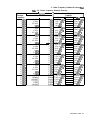
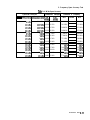
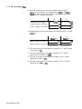
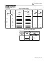
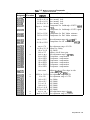
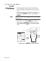
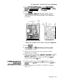
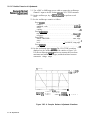
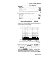
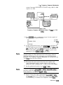
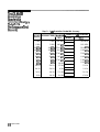
1
About this Manual
We’ve added this manual to the Agilent website in an effort to help you support
your product. This manual is the best copy we could find; it may be incomplete
or contain dated information. If we find a more recent copy in the future, we will
add it to the Agilent website.
Support for Your Product
Agilent no longer sells or supports this product. Our service centers may be able
to perform calibration if no repair parts are needed, but no other support from
Agilent is available. You will find any other available product information on the
Agilent Test & Measurement website, www.tm.agilent.com.
HP References in this Manual
This manual may contain references to HP or Hewlett-Packard. Please note that
Hewlett-Packard's former test and measurement, semiconductor products and
chemical analysis businesses are now part of Agilent Technologies. We have
made no changes to this manual copy. In other documentation, to reduce
potential confusion, the only change to product numbers and names has been in
the company name prefix: where a product number/name was HP XXXX the
current name/number is now Agilent XXXX. For example, model number
HP8648A is now model number Agilent 8648A.
Performance Tests and
Adjustments Manual
HP 8566B Spectrum Analyzer
F!a HEWLETT
PACKARD
HP Part No. 08566-90168
Printed in USA September 1993
Notice.
The information contained in this document is subject to change
without notice.
Hewlett-Packard makes no warranty of any kind with regard to this
material, including but not limited to, the implied warranties of
merchantability and fitness for a particular purpose. Hewlett-Packard
shall not be liable for errors contained herein or for incidental
or consequential damages in connection with the furnishing,
performance, or use of this material.
@ Copyright Hewlett-Packard Company 1993
All Rights Reserved. Reproduction, adaptation, or translation without
prior written permission is prohibited, except as allowed under the
copyright laws.
1400 Fountaingrove Parkway, Santa Rosa CA, 95403-1799, USA
Certification
Hewlett-Packard Company certifies that this product met its
published specifications at the time of shipment from the factory.
Hewlett-Packard further certifies that its calibration measurements
are traceable to the United States National Institute of Standards and
Technology, to the extent allowed by the Institute’s calibration facility,
and to the calibration facilities of other International Standards
Organization members.
Warranty
This Hewlett-Packard instrument product is warranted against defects
in material and workmanship for a period of one year from date of
shipment. During the warranty period, Hewlett-Packard Company
will, at its option, either repair or replace products which prove to be
defective.
For warranty service or repair, this product must be returned to a
service facility designated by Hewlett-Packard. Buyer shall prepay
shipping charges to Hewlett-Packard and Hewlett-Packard shall pay
shipping charges to return the product to Buyer. However, Buyer shall
pay all shipping charges, duties, and taxes for products returned to
Hewlett-Packard from another country.
Hewlett-Packard warrants that its software and firmware designated
by Hewlett-Packard for use with an instrument will execute
its programming instructions when properly installed on that
instrument. Hewlett-Packard does not warrant that the operation
of the instrument, or software, or firmware will be uninterrupted or
error-free.
L IMITATION
OF
W ARRANTY
The foregoing warranty shall not apply to defects resulting from
improper or inadequate maintenance by Buyer, Buyer-supplied
software or interfacing, unauthorized modification or misuse,
operation outside of the environmental specifications for the
product, or improper site preparation or maintenance.
NO OTHER WARRANTY IS EXPRESSED OR IMPLIED.
HEWLETT-PACKARD SPECIFICALLY DISCLAIMS THE IMPLIED
WARRANTIES OF MERCHANTABILITY AND FITNESS FOR A
PARTICULAR PURPOSE.
E XCLUSIVE
R EMEDIES
THE REMEDIES PROVIDED HEREIN ARE BUYER’S SOLE AND
EXCLUSIVE REMEDIES. HEWLETT-PACKARD SHALL NOT BE
LIABLE FOR ANY DIRECT, INDIRECT, SPECIAL, INCIDENTAL, OR
CONSEQUENTIAL DAMAGES, WHETHER BASED ON CONTRACT,
TORT, OR ANY OTHER LEGAL THEORY.
...
III
Assistance
Product maintenance agreements and other customer omistance
agreemxmts are available for Hewlett-Rzckard products.
Fbr any assistance, contact your nearest Hewlett-Fbckard Sales and
Service Ome.
Safety Notes
Caution
Caution denotes a hazard. It calls attention to a procedure that, if
not correctly performed or adhered to, could result in damage to or
destruction of the instrument. Do not proceed beyond a caution sign
until the indicated conditions are fully understood and met.
Warning
Warning denotes a hazard. It calls attention to a procedure
which, if not correctly performed or adhered to, could result in
injury or loss of life. Do not proceed beyond a warning note until
the indicated conditions are fully understood and met.
Instruction
Manual
iv
The following safety notes are used throughout this manual.
Familiarize yourself with each of the notes and its meaning before
operating this instrument.
The instruction manual symbol. The product is marked with this
symbol when it is necessary for the user to refer to the instructions in
the manual.
General Safety
Considerations
Warning
Before this instrument is switched on, make sure it has been
properly grounded through the protective conductor of the ac
power cable to a socket outlet provided with protective earth
contact.
Any interruption of the protective (grounding) conductor, inside
or outside the instrument, or disconnection of the protective
earth terminal can result in personal injury.
Warning
There are many points in the instrument which can, if contacted,
cause personal injury. Be extremely careful.
Any adjustments or service procedures that require operation
of the instrument with protective covers removed should be
performed only by trained service personnel.
Caution
Before this instrument is switched on, make sure its primary power
circuitry has been adapted to the voltage of the ac power source.
Failure to set the ac power input to the correct voltage could cause
damage to the instrument when the ac power cable is plugged in.
V
How to Use This
Manual
This manual uses the
following
conventions:
HP 8566B
Documentation
Description
Front-Panel Ke
r)
Screen Text
This represents a key physically located on the
instrument.
This indicates text displayed on the instrument’s
screen.
Included with the HP Model 8566B spectrum analyzer are manuals:
The Installation and Verification Manual, the Operating and
Programming Manual, and the Performance Tests and Adjustments
Manual.
HP 8566B Installation
and Verification
Manual
HP part number 08566-90169
HP 8566B Operating
and Programming
Manual
HP part number 08566-90040
HP 8566B
Performance Tests and
Adjustments Manual
HP part number 08566-90168
HP 8566B RF Section
Troubleshooting and
Repair Manual
HP part number 08566-90210
HP 8566B IF-Display
Section
Troubleshooting and
Repair Manual
HP part number 08566-90085
vi
Contents: General information, installation, specifications,
characteristics, and operation verification.
Contents: Manual and remote operation, including complete syntax
and command description. Accopanying this manual is the seperate,
pocket-sized Quick Reference Guide, HP part number 5955-8970.
Contents: Electrical performance tests and adjustment procedures.
Contents: RF section service information.
Contents: IF-Display section service information.
Contents
1. General Information
Introduction . . . . . . . . . . . .
Instruments Covered by this Manual
Operation Verification . . . . . . .
Option 462 Instruments . . . . . .
Option 857 Instruments . . . . . .
.
.
.
.
.
.
.
.
.
.
.
.
.
.
.
.
.
.
.
.
.
.
.
.
.
.
.
.
.
.
.
.
.
.
.
.
.
.
.
.
.
.
.
.
.
l-l
l-2
l-2
l-2
l-2
2. Performance Tests
Introduction . . . . . . . . . . . . . . . . . . . . .
2-l
Verification of Specifications . . . . . . . . . . . . .
2-l
Calibration Cycle . . . . . . . . . . . . . . . . . .
2-2
Equipment Required . . . . . . . . . . . . . . . .
2-3
Performance Test Record . . . . . . . . . . . . . .
2-3
2-4
1. Center Frequency Readout Accuracy Test . . . .
2. Frequency Span Accuracy Test . . . . . . . . .
2-8
3. Resolution Bandwidth Accuracy Test . . . . . . 2-12
4. Resolution Bandwidth Selectivity Test . . . . . . 2-14
5. Resolution Bandwidth Switching Uncertainty Test 2-17
6. Log Scale Switching Uncertainty Test . . . . . . 2-19
7. IF Gain Uncertainty Test . . . . . . . . . . . . 2-21
8. Amplitude Fidelity Test . . . . . . . . . . . . 2-27
2-31
9. Calibrator Amplitude Accuracy Test . . . . . . .
10. Frequency Response Test . . . . . . . . . . . 2-32
11. Sweep Time Accuracy Test . . . . . . . . . . 2-46
2-49
12. Noise Sidebands Test . . . . . . . . . . . . .
13. Line-Related Sidebands Test . . . . . . . . . . 2-53
14. Average Noise Level Test . . . . . . . . . . . 2-58
2-61
15. Residual Responses Test . . . . . . . . . . . .
16. Harmonic and Intermodulation Distortion Test . 2-65
17. Image, Multiple, and Out of Band Responses Test 2-73
18. Gain Compression Test . . . . . . . . . . . . 2-77
19. 1st LO Output Amplitude Test . . . . . . . . . 2-81
2-82
20. Sweep + Tune Out Accuracy Test . . . . . . .
21. Fast Sweep Time Accuracy Test (~20 ms) . . . . 2-84
22. Frequency Reference Error Test . . . . . . . . 2-87
‘Iable 2-24. Performance Test Record . . . . . . . . . . 2-89
Test 1. Center Frequency Readout Accuracy . . . . . 2-90
Test 2. Frequency Span Accuracy Test . . . . . . . . 2-91
Test 3. Resolution Bandwidth Accuracy Test . . . . . 2-92
Test 4. Resolution Bandwidth Selectivity . . . . . . . 2-93
Test 5. Resolution Bandwidth Switching Uncertainty . 2-94
Test 6. Log Scale Switching Uncertainty Test . . . . . 2-95
2-96
Test 7. IF Gain Uncertainty . . . . . . . . . . . . .
2-99
Test 8. Amplitude Fidelity . . . . . . . . . . . . .
2-100
.
.
.
.
.
.
.
.
Test 9. Calibrator Amplitude Accuracy
Test 10. Frequency Response Test . . . . . . . . . . 2-101
Contents-l
Test 11. Sweep Time Accuracy . . . . . . . . . . . 2-103
Test 12. Noise Sidebands Test . . . . . . . . . . . . 2-104
Test 13. Line-Related Sidebands . . . . . . . . . . . 2-105
Test 14. Average Noise Level . . . . . . . . . . . . 2-106
Test 15. Residual Responses . . . . . . . . . . . . . 2-107
Test 16. Harmonic And Intermodulation Distortion . . 2-108
Test 17. Image, Multiple, and Out-of-Band Responses . 2-109
Test 18. Gain Compression . . . . . . . . . . . . . 2-l 11
Test 19. 1st LO Output Amplitude . . . . . . . . . . 2-112
Test 20. Sweep + Tune Out Accuracy . . . . . . . . 2-113
Test 21. Fast Sweep Time Accuracy (< 20 ms) . . . . 2-l 14
Test 22. Frequency Reference Error Test . . . . . . . 2-115
3. Adjustments
Introduction . . . . . . . . . . . . . . . . . . . . .
Safety Considerations . . . . . . . . . . . . . . . . .
Equipment Required . . . . . . . . . . . . . . . . .
Adjustment Tools . . . . . . . . . . . . . . . . . . .
Factory-Selected Components . . . . . . . . . . . . .
Related Adjustments . . . . . . . . . . . . . . . . .
Location of Test Points and Adjustments . . . . . . . .
1. Low-Voltage Power Supply Adjustments . . . . . .
2. High-Voltage Adjustment (SN 3001A and Below) . .
2. High-Voltage Adjustment (SN 3004A and Above) . .
3. Preliminary Display Adjustments (SN 3001A and
Below) . . . . . . . . . . . . . . . . . . . . .
3. Preliminary Display Adjustments (SN 3004A and
Above) . . . . . . . . . . . . . . . . . . . . .
4. Final Display Adjustments (SN 3001A and Below) .
4. Final Display Adjustments (SN 3004A and Above) .
5. Log Amplifier Adjustments . . . . . . . . . . . .
6. Video Processor Adjustments . . . . . . . . . . .
7. 3 MHz Bandwidth Filter Adjustments . . . . . . .
8. 21.4 MHz Bandwidth Filter Adjustments . . . . .
9. 3 dB Bandwidth Adjustments . . . . . . . . . .
10. Step Gain and 18.4 MHz Local Oscillator
Adjustments . . . . . . . . . . . . . . . . . .
11. Down/Up Converter Adjustments . . . . . . . .
12. 10 MHz Standard Adjustment (SN 2637A and
Below) . . . . . . . . . . . . . . . . . . . . .
12. 10 MHz Standard Adjustment (SN 2728A and
Above) . . . . . . . . . . . . . . . . . . . . .
13. Sweep, DAC, and Main Coil Driver Adjustments . .
14. 100 MHz VCXO Adjustments . . . . . . . . . . .
15. MN Loop Adjustments . . . . . . . . . . . . .
16. YT.0 Loop Adjustments . . . . . . . . . . . . .
17. 20/30 Loop Phase Lock Adjustments . . . . . . .
18. RF Module Phase Lock Adjustments . . . . . . .
19. CAL Output Adjustment . . . . . . . . . . . . .
20. Last Converter Adjustments . . . . . . . . . . .
2 1. Frequency Response Adjustments . . . . . . . .
22. Analog-To-Digital Converter Adjustments . . . . .
23. Track and Hold Adjustments . . . . . . . . . . . .
24. Digital Storage Display Adjustments . . . . . . .
Low-Noise DC Supply . . . . . . . . . . . . . . . .
Contents-2
3-l
3-2
3-2
3-2
3-3
3-3
3-3
3-25
3-31
3-41
3-48
3-56
3-63
3-65
3-69
3-73
3-76
3-82
3-89
3-94
3-100
3-104
3-108
3-113
3-126
3-132
3-135
3-146
3-160
3-166
3-169
3-174
3-206
3-209
3-212
3-218
Crystal Filter Bypass Network Configuration . . . . . 3-219
4. Option 462
Introduction . . . . . . . . . . . . . . . . . . . . .
3. 6 dB Resolution Bandwidth Accuracy Test . . . . .
3. Impulse and Resolution Bandwidth Accuracy Test .
4. 6 dB Resolution Bandwidth Selectivity Test . . . .
4. Impulse and Resolution Bandwidth Selectivity Test .
5. Impulse and Resolution Bandwidth Switching
Uncertainty Test . . . . . . . . . . . . . . . .
Test 3. 6 dB Resolution Bandwidth Accuracy Test (p/o
lhble 2-24, Performance Test Record) . . . . . . .
Test 3. Impulse and Resolution Bandwidth Accuracy
Test (p/o ‘Ihble 2-24, Performance Test Record) . .
Test 4. 6 dB Resolution Bandwidth Selectivity (p/o
Table 2-24, Performance Test Record) . . . . . . .
Test 4. Impulse and Resolution Bandwidth Selectivity
(p/o Table 2-24, Performance Test Record) . . . . .
Test 5. Impulse and Resolution Bandwidth Switching
Uncertainty (p/o ‘Ihble 2-24, Performace Test
Record) . . . . . . . . . . . . . . . . . . . . .
9. 6 dB Resolution Bandwidth Adjustments . . . . .
9. Impulse Bandwidth Adjustments . . . . . . . . .
4-l
4-2
4-4
4-10
4-13
4-16
4-18
4-19
4-21
4-22
4-23
4-24
4-27
5. Option 857
Introduction . . . . . . . . . . . . . . . . . . . . .
8. Option 857 Amplitude Fidelity Performance Test . .
Performance Test Record . . . . . . . . . . . . . . .
Test 8. Option 857 Amplitude Fidelity . . . . . . . .
5-l
5-2
5-6
5-7
6. Major Assembly and Component Locations
IF-Display Section Figure Index . . . . . . . . . . . .
RF Section Figure Index . . . . . . . . . . . . . . .
6-l
6-2
Contents3
Figures
l-l. Service Accessories, HP Part Number 08566-60001 . .
2-l. Center Frequency Test Setup . . . . . . . . . . . .
2-2. Center Frequency Accuracy Measurement . . . . . .
2-3. Narrow Span Test Setup . . . . . . . . . . . . . . .
2-4. Wide Span Test Setup . . . . . . . . . . . . . . . .
2-5. Resolution Bandwidth Measurement . . . . . . . . .
2-6. 60 dB Bandwidth Measurement . . . . . . . . . . .
2-7. Bandwidth Switching Uncertainty Measurement . . .
2-8. Log Scale Switching Uncertainty Measurement . . . .
2-9. IF Gain Uncertainty Test Setup . . . . . . . . . . .
2-10. IF Gain Uncertainty Measurement . . . . . . . . . .
2-l 1. Amplitude Fidelity Test Setup . . . . . . . . . . . .
2-12. Amplitude Fidelity Measurement . . . . . . . . . .
2-13. Calibrator Amplitude Accuracy Test Setup . . . . . .
2-14. Frequency Response Test Setup (100 Hz to 100 kHz) .
2-15. Frequency Response Measurement (1 kHz to 100 kHz)
2-16. Frequency Response Test Setup (100 kHz to 60 MHz) .
2-17. Frequency Response Measurement (100 kHz to 4 MHz)
2-18. Frequency Response Measurement (4 MHz to 60 MHz)
2-19. Frequency Response Test Setup (60 MHz to 2.5 GHz, 2
to22GHz) . . . . . . . . . . . . . . . . . . .
2-20. Frequency Response Measurement (60 MHz to 2.5 GHz)
2-21. Sweep Time Accuracy Test Setup . . . . . . . . . .
2-22. Noise Sidebands Test Setup . . . . . . . . . . . . .
2-23. Noise Sidebands Measurement . . . . . . . . . . . .
2-24. Line Related Sidebands Test Setup . . . . . . . . . .
2-25. Line-Related Sidebands Measurement . . . . . . . .
2-26. Average Noise Level Measurement . . . . . . . . . .
2-27. Residual Responses Measurement . . . . . . . . . .
2-28. Harmonic Distortion Test Setup . . . . . . . . . . .
2-29. Intermodulation Distortion Test Setup . . . . . . . .
2-30. Third Order Intermodulation Products . . . . . . . .
2-31. Image, Multiple, and Out-of-Band Responses Test Setup
2-32. Gain Compression Test Setup . . . . . . . . . . . .
2-33. 1st LO Output Amplitude Test Setup . . . . . . . . .
2-34. Sweep + Tune Out Accuracy Test Setup . . . . . . .
2-35. Fast Sweep Time Accuracy (~20 ms) Test Setup . . . .
2-36. Fast Sweep Time Measurement (~20 ms) . . . . . . .
2-37. Frequency Reference Test Setup . . . . . . . . . . .
3-l. Low-Voltage Power Supply Adjustments Setup . . . .
3-2. IF-Display Section Adjustments (SN 3001A and Below)
3-3. IF-Display Section Adjustments (SN 3004A and Above)
3-4. Location of RF Section Low-Voltage Adjustments . . .
3-5. High Voltage Adjustment Setup . . . . . . . . . . .
3-6. Location of High Voltage Adjustments . . . . . . . .
3-7. Location of Label and Test Point . . . . . . . . . . .
Contents-4
l-9
2-4
2-6
2-8
2-10
2-13
2-15
2-18
2-20
2-21
2-23
2-27
2-29
2-31
2-33
2-35
2-36
2-37
2-38
2-39
2-41
2-46
2-50
2-51
2-53
2-55
2-59
2-62
2-66
2-69
2-71
2-73
2-77
2-81
2-82
2-84
2-85
2-88
3-25
3-26
3-27
3-29
3-32
3-33
3-34
3-8. Location of AlA Components . . . . . . . . . . .
3-9. CRT Cut-Off Voltage
3-10. Waveform at AlA3TP5’ : : : : : : : : : : : : 1 : :
3-l 1. Discharging the CRT Post-Accelerator Cable . . . . .
3-12. High Voltage Adjustment Setup . . . . . . . . . . .
3-13. Location of High Voltage Adjustments . . . . . . . .
3-14. Location of AlA Label and Test Point . . . . . . . .
3-15. Discharging the CRT Post-Accelerator Cable . . . . .
3-16. Preliminary Display Adjustments Setup . . . . . . .
3-17. Location of AlA2, AlA4, AlA5, and A3A2 . . . . .
3-18. AlA2, AlA4, and AlA Adjustment Locations . . . .
3-19. X+ and X- Waveforms . . . . . . . . . . . . . . .
3-20. Composite X Deflection Waveform . . . . . . . . . .
3-21. Rise and Fall Times and Overshoot Adjustment
Waveform . . . . . . . . . . . . . . . . . . .
3-22. 5OV,, Signal . . . . . . . . . . . . . . . . . . . .
3-23. Preliminary Display Adjustments Setup . . . . . . .
3-24. Location of AlA and A3A2 . . . . . . . . . . . .
3-25. AlA Adjustment Locations . . . . . . . . . . . . .
3-26. X+ and X- Waveforms . . . . . . . . . . . . . . .
3-27. Composite X Deflection Waveform . . . . . . . . . .
3-28. Rise and Fall Times and Overshoot Adjustment
Waveform . . . . . . . . . . . . . . . . . . .
3-29. 5OV,, Signal . . . . . . . . . . . . . . . . . . . .
3-30. Location of Final Display Adjustments on AlA2, AlA4,
and AlA5. . . . . . . . . . . . . . . . . . . .
3-31. Final Display Adjustments Setup . . . . . . . . . . .
3-32. Location of Final Display Adjustments on AlA . . .
3-33. Log Amplifier Adjustments Setup . . . . . . . . . .
3-34. Location of Log Amplifier Adjustments . . . . . . . .
3-35. Video Processor Adjustments Setup . . . . . . . . .
3-36. Location of Video Processor Adjustments . . . . . . .
3-37. 3 MHz Bandwidth Filter Adjustments Setup . . . . .
3-38. Location of Center, Symmetry, and 10 Hz Amplitude
Adjustments . . . . . . . . . . . . . . . . . .
3-39. Location of 3 MHz Peak Adjustments . . . . . . . . .
3-40. 21.4 MHz Bandwidth Filter Adjustments Setup . . . .
3-41. Location of A4A4 21.4 MHz LC Filter Adjustments . .
3-42. Location of A4A4 21.4 MHz Crystal Filter Adjustments
3-43. Location of A4A8 21.4 MHz LC Filter and Attenuation
Adjustments . . . . . . . . . . . . . . . . . .
3-44. Location of A4A8 21.4 MHz Crystal Filter Adjustments
3-45. Location of 3 dB Bandwidth Adjustments . . . . . .
3-46. Step Gain and 18.4 MHz Local Oscillator Adjustments
Setup . . . . . . . . . . . . . . . . . . . . . .
3-47. Location of IF Gain Adjustment . . . . . . . . . . .
3-48. Location of 10 dB Gain Step Adjustments . . . . . .
3-49. Location of .l dB Gain Step, 18.4 MHz LO, and + 1OV
Adjustments . . . . . . . . . . . . . . . . . .
3-50. Down/Up Converter Adjustments Setup . . . . . . .
3-51. Location of Down/Up Converter Adjustments . . . . .
3-52. 10 MHz Frequency Standard Adjustments Setup . . .
3-53. Location of 10 MHz Standard Adjustments . . . . . .
3-54. 10 MHz Frequency Standard Adjustments Setup . . .
3-55. Location of 10 MHz Standard Adjustments . . . . . .
3-36
3-37
3-38
3-40
3-42
3-43
3-44
3-47
3-49
3-50
3-50
3-51
3-52
3-53
3-54
3-57
3-58
3-58
3-59
3-60
3-60
3-62
3-64
3-65
3-66
3-69
3-70
3-73
3-74
3-76
3-78
3-80
3-82
3-83
3-84
3-85
3-86
3-90
3-94
3-96
3-97
3-98
3-100
3-101
3-105
3-107
3-109
3-112
Contents-5
3-56. Sweep and DAC Adjustments Setup . . . . . . . . . 3-114
3-57. OV to + 1OV Sweep Ramp at A16TP3 . . . . . . . . . 3-115
3-58. Location of Sweep and DAC Adjustments . . . . . . . 3-116
3-59. Properly Adjusted DC Levels Between Sweep Ramps . 3-117
3-60. Improperly Adjusted DC Levels Between Sweep Ramps 3-117
3-61. YTO Main Coil Driver Adjustments Setup . . . . . . . 3-120
3-62. Location of YTO Main Coil Driver Adjustments . . . . 3-121
3-63. YTO Main Coil Driver Adjustments Setup (Alternate
Procedure) . . . . . . . . . . . . . . . . . . . 3- 122
3-64. 100 MHz VCXO Adjustment Setup . . . . . . . . . . 3-126
3-65. Location of 100 MHz VCXO Adjustments . . . . . . . 3-127
3-66. Typical Tuning Range of A7A2 100 MHz VCXO . . . . 3-128
3-67. M/N Loop Adjustment Setup . . . . . . . . . . . . . 3-132
3-68. Location of PLL Adjustments . . . . . . . . . . . . 3-133
3-69. YTO Loop Adjustment Setup . . . . . . . . . . . . 3-136
3-70. Location of Assemblies, Cables, and Test Points . . . . 3-136
3-71. All YTO Loop Service Position . . . . . . . . . . . 3-137
3-72. Typical YTO Loop Swept Frequency Response at AllAl 3-139
3-73. AllA Adjustment Locations . . . . . . . . . . . . 3-140
3-74. Sampler Waveform at AllA5TPl . . . . . . . . . . 3-142
3-75. 30 MHz YTO Loop Sampler Response at AllJ5 IF OUT 3-143
3-76. Tuning the IF OUT Fundamental . . . . . . . . . . 3-144
3-77. 20/30 PLL Adjustment Setup . . . . . . . . . . . . 3-147
3-78. Location of PLLl Adjustments . . . . . . . . . . . . 3-149
3-79. Location of PLL2 Adjustments . . . . . . . . . . . . 3-154
3-80. Location of PLL3 Adjustments . . . . . . . . . . . . 3-156
3-81. RF Module Phase Lock Adjustments Setup . . . . . . 3-161
3-82. Location of RF Module Phase Lock Adjustments . . . 3-161
3-83. A Sampler Balance Adjustment Waveform . . . . . . 3-164
3-84. Cal Output Adjustment Setup . . . . . . . . . . . . 3-166
3-85. Location of CAL OUTPUT Adjustment . . . . . . . . 3-167
3-86. CAL OUTPUT Harmonics . . . . . . . . . . . . . . 3-168
3-87. Last Converter Adjustments Setup . . . . . . . . . . 3-170
3-88. Location of Last Converter Adjustments . . . . . . . 3-171
3-89. Frequency Response Preliminary Adjustments Setup . 3-176
3-90. Location of Frequency Response Adjustments . . . . 3-177
3-91. Frequency Response Adjustments Setup (10 MHz to 2.5
GHz) . . . . . . . . . . . . . . . . . . . . . . 3-179
3-92. Typical Coarse Frequency Response (10 MHz - 2.5 GHz) 3-181
3-93. Typical Frequency Response (10 MHz - 2.5 GHz) . . . 3-182
3-94. Frequency Response Adjustments Setup (2.0 GHz to
22.0 GHz) . . . . . . . . . . . . . . . . . . . . 3-185
3-95. Typical Coarse Frequency Response (2 GHz - 5.8 GHz) 3-187
3-96. Typical Frequency Response (2.0 GHz - 5.8 GHz) . . . 3-188
3-97. Typical Coarse Frequency Response (5.8 GHz - 12.5
GHz) . . . . . . . . . . . . . . . . . . . . . . 3-191
3-98. Typical Frequency Response (5.8 GHz - 12.5 GHz) . . 3-193
3-99. Frequency Response Adjustments Setup (18.6 to 325
GHz) . . . . . . . . . . . . . . . . . . . . . . 3-204
3-100. Analog-To-Digital Converter Adjustments Setup . . . . 3-206
3-101. Location of Analog-To-Digital Converter Adjustments . 3-208
3-102. Track and Hold Adjustments Setup : . . . . . . . . 3-209
3-103. Location of Track and Hold Adjustments . . . . . . . 3-210
3-104. Digital Storage Display Adjustments Setup . . . . . . 3-212
3-105. Location of Digital Storage Display Adjustments . . . 3-213
Contents-6
3-106. Sample and Hold Balance Adjustment Waveforms .
3-107. Waveform Before Adjustment . . . . . . . . . .
3-108. Low-Noise DC Supply . . . . . . . . . . . . . .
3-109. Crystal Filter Bypass Network Configurations . . .
4-l. Resolution Bandwidth Measurement . . . . . . .
4-2. Impulse Bandwidth Test Setup . . . . . . . . . .
4-3. 6 dB Resolution Bandwidth Measurement . . . .
4-4. 60 dB Bandwidth Measurement . . . . . . . . .
4-5. 60 dB Bandwidth Measurement . . . . . . . . .
4-6. Bandwidth Switching Uncertainty Measurement .
4-7. Location of Bandwidth Adjustments . . . . . . .
4-8. Location of Bandwidth Adjustments . . . . . . .
5-l. Option 857 Amplitude Fidelity Test Setup . . . .
6-l. RF Section, Top View . . . . . . . . . . . . . .
6-2. RF Section, Front View . . . . . . . . . . . . .
6-3. RF Section, Bottom View . . . . . . . . . . . .
6-4. IF Section, Top View (SN 3001A and Below) . . .
6-5. IF Section, ‘Ibp View (SN 3004A and Above) . . .
6-6. IF Section, Front View . . . . . . . . . . . . .
6-7. IF Section, Bottom View . . . . . . . . . . . .
.
.
.
.
.
.
.
.
.
.
.
.
.
.
.
.
.
.
.
.
.
.
.
.
.
.
.
.
.
.
.
.
.
.
.
.
.
.
.
.
3-215
3-215
3-218
3-219
4-3
4-4
4-8
4-11
4-14
4-17
4-25
4-28
5-2
6-3
6-4
6-5
6-6
6-7
6-8
6-9
Contents-7
!Ihbles
2-l. Performance Test Cross-Reference . . . . . . . . . .
2-2. Center Frequency Readout Accuracy . . . . . . . . .
2-3. Narrow Span Accuracy . . . . . . . . . . . . . . .
2-4. Wide Span Accuracy . . . . . . . . . . . . . . . .
2-5. Bandwidth Accuracy . . . . . . . . . . . . . . . .
2-6. Resolution Bandwidth Selectivity . . . . . . . . . .
2-7. Bandwidth Switching Uncertainty . . . . . . . . . .
2-8. Log Scale Switching Uncertainty . . . . . . . . . . .
2-9. IF Gain Uncertainty, 10 dB Steps . . . . . . . . . .
2-10. IF Gain Uncertainty, 2 dB Steps . . . . . . . . . . .
2-l 1. IF Gain Uncertainty, 0.1 dB Steps . . . . . . . . . .
2-12. Log Scale Fidelity . . . . . . . . . . . . . . . . .
2-13. Linear Amplitude Fidelity . . . . . . . . . . . . . .
2-14. 100 Hz to 2.5 GHz Frequency Band . . . . . . . . .
2-15. Frequency Response (Flatness) . . . . . . . . . . .
2-16. Sweep Time Accuracy, Sweep Times 220 ms . . . . .
2-17. Sweep Time Accuracy . . . . . . . . . . . . . . .
2-18. Average Noise Level . . . . . . . . . . . . . . . .
2-19. TO1 Measurement Settings . . . . . . . . . . . . .
2-20. Image and Out-of-Band Response . . . . . . . . . .
2-2 1. Multiple Responses . . . . . . . . . . . . . . . . .
2-22. Sweep + Tune Out Accuracy . . . . . . . . . . . .
2-23. Fast Sweep Time Accuracy (~20 ms) . . . . . . . . .
2-24. Frequency Response (Flatness) . . . . . . . . . . .
3-l. Adjustment Cross Reference . . . . . . . . . . . . .
3-2. Adjustable Components . . . . . . . . . . . . . . .
3-3. Factory-Selected Components . . . . . . . . . . . .
3-4. Standard Value Replacement Capacitors . . . . . . .
3-5. Standard Value Replacement 0.125 Resistors . . . . .
3-6. Standard Value Replacement 0.5 Resistors . . . . . .
3-5. Initial Adjustment Positions . . . . . . . . . . . . .
3-6. Initial Adjustment Positions . . . . . . . . . . . . .
3-7. Standard Values for A7A2L4 . . . . . . . . . . . .
3-8. Limits for 100 MHz Harmonics . . . . . . . . . . . .
3-9. Selection Chart for Attenuator Resistors . . . . . . .
3-10. Resistor Values . . . . . . . . . . . . . . . . . . .
3-11. Power Level of Fundamental Signal . . . . . . . . .
3-12. Standard Values for AlOA4C49
3-13. Standard Values for AlOA4R29 and’AliA4R33 : : : :
3-14. Frequency Bands . . . . . . . . . . . . . . . . . .
3-15. Preselector Delay Compensation DAC Values . . . . .
3-16. A6A12 YTX Driver Assembly Factory-Select Capacitor
Values . . . . . . . . . . . . . . . . . . . . .
3-17. Parts for Low-Noise DC Supply . . . . . . . . . . .
3-18. Crystal Filter Bypass Network Configuration for A4A4
and A4A8 (21.4 MHz) . . . . . . . . . . . . . .
Contents-8
2-2
2-7
2-9
2-11
2-13
2-16
2-18
2-20
2-23
2-24
2-25
2-29
2-30
2-37
2-45
2-48
2-48
2-60
2-72
2-75
2-76
2-83
2-86
2-102
3-4
3-5
3-13
3-20
3-21
3-23
3-63
3-66
3-128
3-130
3-130
3-131
3-144
3-157
3-158
3-174
3-202
3-203
3-218
3-219
3-19. Crystal Filter Bypass Network Configuration for A4A7
(3MHz) . . . . . . . . . . . . . . . . . . . . . 3-219
4-l. 6 dB Resolution Bandwidth Accuracy . . . . . . . .
4-3
4-2. Impulse Bandwidth Accuracy . . . . . . . . . . . .
4-9
4-3. 6 dB Resolution Bandwidth Accuracy . . . . . . . .
4-9
4-4. 6 dB Resolution Bandwidth Selectivity . . . . . . . .
4-12
4-5. Impulse and Resolution Bandwidth Selectivity . . . . 4-15
4-6. Bandwidth Switching Uncertainty . . . . . . . . . . 4-17
5-l. Log Amplitude Fidelity (10 Hz RBW; Option 857) . . .
5-4
5-2. Log Amplitude Fidelity (10 kHz RBW; Option 857) . .
5-5
5-3. Linear Amplitude Fidelity . . . . . . . . . . . . . .
5-5
Contents-9
1
General Information
Introduction
This HP 8566B Tests and Adjustments Manual contains two main
sections: Performance Tests and Adjustments Procedures. This
chapter lists the required test equipment for both sections. The
performance tests provided should be performed for the following
reasons:
w If the test equipment for the Operation Verification Program is not
available.
w If the instrument does not pass all of the Operation Verification
tests.
n
For complete verification of specifications not covered by the
Operation Verification program.
The adjustment procedures should be performed for the following
reasons:
w If the results of a performance test are not within the specifications.
w After the replacement of a part or component that affects electrical
performance.
Warning
The adjustment procedures require access to the interior of the
instrument and therefore should only be performed by qualified
service personnel. There are voltages at many points in the
instrument which can, if contacted, cause personal injury. Be
extremely careful. Adjustments should be performed only by
trained service personnel.
Power is still applied to this instrument with the LINE switch in
STANDBY. There is no OFF position on the LINE switch. Before
removing or installing any assembly or printed circuit board,
remove the power cord from the rear of both instruments and
wait for the MAINS indicators (red LEDs) to go completely out.
Capacitors inside the instrument may still be charged even if the
instrument has been disconnected from its source of power. Use a
non-metallic tuning tool whenever possible.
General Information 1-l
Instruments Covered
by this Manual
This manual contains procedures for testing and adjusting HP
8566B spectrum analyzers, including those with Option 400 (400 Hz
operation), Option 462 (impulse bandwidths and 6 dB bandwidths),
and Option 857 installed. The procedures in this manual can also
be used to adjust HP 8566A spectrum analyzers that have been
converted into HP 8566B spectrum analyzers through the installation
of an HP 8566AB Retrofit Kit (formerly HP 8566A+OlK Retrofit Kit).
Operation Verification
A high confidence level in the instrument’s operation can be achieved
by running only the Operation Verification Program, since it tests
most of the instrument’s specifications. It is recommended that the
Operation Verification Program be used for incoming inspection and
after repairs, since it requires much less time and test equipment.
A description of the program can be found in the Installation and
Verification manual.
Option 462
Instruments
Option 462 instruments require that the performance tests and
adjustment procedures listed below be performed instead of their
standard versions included in chapters two and three. Information on
Option 462 versions is located in Chapter 4, Option 462.
6 dB Bandwidths:
Test 3, 6 dB Resolution Bandwidth Accuracy Test
Test 4, 6 dB Resolution Selectivity Test
Adjustment 9, 6 dB Bandwidth Adjustment Procedure
Impulse Bandwidths:
Test 3, Impulse Resolution Bandwidth Accuracy Test
Test 4, Impulse and Resolution Selectivity Test
Test 5, Impulse and Resolution Bandwidth
Switching Uncertainty Test
Adjustment 9, Impulse Bandwidth Adjustment Procedure
Option 867
Instruments
1-2 General Information
Option 857 instruments are used in EMC receiver applications.
Information on Option 857 is located in Chapter 5, Option 857.
‘lhble l-l. Recommended Test Equipment (1 of 6)
Critical Specifications for
Equipment Substitution
Instrumenl
Recommended Perf. Adj.
Model
Test
SIGNAL
SOURCES
HP 8340A/B
X
X
Synthesized Frequency: 2 - 18 GHz
Signal
Stability: ~5 x lo-lo
Generator
HP 8672A
X
X
Frequency Frequency: 200 Hz to 80 MHz
Synthesizer Stability: fl x IO-“/day
Amplitude Range: + 13 to -86 dBm with 0.01 dB
resolution
Attenuator Accuracy: < f0.07 dB (+ 13 to -47 dBm)
HP 3335A
X
X
Pulse
Generator
HP 8116A
Synthesized Frequency: 10 MHz to 22 GHz
Sweeper
Output Power: + 10 dBm maximum (leveled)
Aging Rate: ~1 x 10mg/day
Spurious Signals: 135 dBc (~7 GHz)
125 dBc (<20 GHz)
Amplitude Modulation: dc to 100 kHz
Leveling: Internal, External Power Meter
Function
Generator
Pulse Width: 10 nsec to 250 nsec
Rise and Fall Times: ~6 ns
Output Level: +2.5V
Output: Sine Wave and Triangle Wave, BVp-p
Range: 100 Hz to 500 kHz (Sweep Function Available)
X
HP 3312A
X
X
HP 5061B
X
X
(2 required)
Frequency
Standard
Output: 1, 2, 5, or 10 MHz
Accuracy: <hl x lo-lo
Aging Rate: < 1 x lo-lo/day
General Information 1-3
‘able l-l. Recommended Test Equipment (2 of 6)
Instrument
Critical Specifications for
Equipment Substitution
Recommenda
Model
Perf
Test
X
ANALYZERS
-
Adj
X
Spectrum
Analyzer
Frequency: 100 Hz to 2.5 GHz
2 to 22 GHz Preselected
HP 8566A/B
Active Probe
Resistive Divider for measuring fast
transition signals
HP 10020A
X
Probe Power
SUPPIY
For use with HP 10020A
HP 1122A
X
High Frequency
Active Probe
Bandwidth: 5 Hz to 500 MHz
Input R:lOO k62 Input C: 3 pF
HP 41800A
X
Frequency
Counter
Frequency: 20 MHz to 400 MHz
Sensitivity: -30 dBm
HP-IB Compatible
HP 5343A
X
Electronic
Counter
bnge: >lO MHz
Xesolution: 2 x 10Wg gate time
Zxt. Time Base: 1, 2, 5, or 10 MHz
HP 5345A
X
UniversaI
Counter
+equency: dc to 100 MHz
Time Interval A + B: 100 ns to 200s
sensitivity: 50 mV rms
Eange: 30 mV to 5V p-p
HP 5316B
HP 5334AB
X
Digitizing
3scilloscope
1 Channel
“requency: 100 MHz
sensitivity: .005V/Division
HP 54501A
X
1scilloscope
‘robe
.O: 1 Divider, compatible with oscilloscope
HP 10432A
X
COUNTERS
DSCILLOSCOPE
1-4 General Information
2 reauired 1
-
‘Ihble l-l. Recommended Test Equipment (3 of 6)
Instrument
Critical Specifications for
Equipment Substitution
Recommended Perf,
Model
Test
Adj
METERS
Digital
Voltmeter
Resolution: fO.l mV
Range: 0 Vdc to 100 Vdc
Input Impedance 100 V Range: 10 M62
HP-IB Compatible
DC High Voltage 1000: 1 Divider
Probe
Impedance: lOM62
HP 3456A
or
HP 3455A
HP 34111A
Power Meter
Range: -20 dBm to + 10 dBm
Accuracy: f0.02dB
Power Sensor
Frequency: .Ol to 18 GHz
Compatible with HP 436A Power Meter
HP 8481A
Power Sensor
Frequency: 50 MHz to 26.5 GHz
Compatible with HP 436A Power Meter
HP8485A
Digital
Photometer
X
HP436A
X
X
X
X
X
X
Tektronix J-16
Option 02
X
Tektronix
56503
X
Photometer
Probe
for Tektronix J-16
range: 1 to 100 NITS (cd/m”)
acceptance angle: 8”
spectral response: CIE Photopic curve
Interconnect
Zable
for Tektronix J-16
Tektronix
012-0414-02
X
Photometer
Light Occluder
Por Tektronix J-16
Tektronix
016-0305-00
X
HP 355D-H89
X
YITENUATORS
10 dB Step
4ttenuator
3teps: 10 dB from 0 to 120 dB
?requency: 20 MHz to 1500 MHz
2alibrated to uncertainty error of ~t(O.02 dB
to.01 dB/lO dB step) at 20 MHz from
1 dB to 120 dB
General information l-5
‘Ihble l-l. Recommended Test Equipment (4 of 6)
Instrument
Critical Specifications for
Equipment Substitution
Recommended Perf, Adj,
Model
Test
X
1 dB Step
Attenuator
Steps: 1 dB from 0 to 12 dB
Frequency: 20 MHz to 1500 MHz
Calibrated to uncertainty error of f(0.02 dB
+O.Ol dB/lO dB step) at 20 MHz from
0 dB to 12 dB
3 dB
Attenuator
Frequency: 200 Hz to 18 GHz
SMA Connectors
HP 8493B,
Option 003
X
30 dB
Attenuator
Frequency: 200 Hz to 18 GHz
SMA Connectors (2 required)
HP 8493B,
Option 020
X
krmination
Impedance: 5OQ; BNC
HP 11593A
X
rermination
Impedance: 500; SMA (m)
HP 1810-0118
X
Fermination
I’ype N Male Connector
Frequency: dc to 18 GHz
[mpedance: 5061
HP 909A,
Option 012
X
kt-off Frequency: 250 MHz
Rejection at 460 MHz: >60 dB
kt-off Frequency: 8 GHz
iejection at 14 GHz: >80 dB
K&L 5L380250-B/B
K&L 6L2508000-NP/N
X
ht-off Frequency: 1200 MHz
Xejection at 1500 MHz: >50 dB
HP 360B
I-20 volts, O-2 amperes
HP 6114A
HP 355C-H25
I’ERMINATIONS
FIIXERS
Jaw-Pass Filter
Jaw-Pass Filter
Jaw-Pass Filter
X
X
vlISCELLANEOUS
IEVICES
‘recision
‘ower Supply
l-6 General information
X
‘able l-l. Recommended Test Equipment (5 of 6)
Instrument
AC Line-Power
Source
Critical Specifications for
Equipment Substitution
Recommended
Model
Perf, Adj.
Test
California Instr- X
(Rx- Option 400)
Frequency: 400 Hz
Voltage :lOO, 120, 220, or 240 V,,
Power: >6OOVA
Power
Splitter
Frequency: 1 MHz to 22 GHz
Tracking: ~0.2 dB
HP 11667B
X
Planar-doped
Barrier Diode
Detector
10 MHz to 33 GHz
HP 8473D/
HP 8474C
X
Reactive Power
Divider
Range: 2 to 22 GHz
Isolation: 220 dB
Omni-Spectra
2090-6202-00
uments Model
153T Opt. 400
X
SPECIAL
DEVICES
Display
Adjustment
PC Board*
Required for preliminary display adjustment! IP 85662-60088
X
Low-Noise
DC Supply
(Optional) Refer to Figure 3-108.
X
Crystal Filter
Bypass Network
Refer to Figure 3-109. (4 required)
X
CABLES
Low-Loss Microwave APC 3.5 (m)
Cable
Cable
BNC, 122 cm (48 in.) (3 required)
Cable
SMA (m) to SMA (m)
Test Cable*
BNC (m) to SMB Snap-On (f)
HP 8120-4921
X
10503A
X
5061-1086
IP 85680-60093
X
X
General Information 1-7
‘Ihble l-l. Recommended Test Equipment (6 of 6)
Instrument
Critical Specifications for
Equipment Substitution
Recommended
Model
Perf.
Test
Adj,
ADAPTERS
Adapter
Adapter
Adapter
Adapter
Adapter
Adapter
Adapter
Adapter
Adapter
Adapter
Adapter
Adapter
Adapter
Adapter
Adapter
Adapter
Adapter
Adapter
Adapter
Adapter
Adapter
Adapter
Type N (f) to BNC (m)
1250-0077
1250-0672
SMB snap on (m) (m)
1250-0674
SMB (m) to SMA (f)
SMB (m) bulkhead
1250-0691
1250-1477
Type N (f) to N (f)
Type N (m) to N (m)
1250-0778
1250-0780
Type N (m) to BNC (f) (2 required,
1250-0781
BNC Tee (m)(f)(f) (2 required)
SMA (f) to SMA (f)
1250-l 158
1250-1159
SMA (m) to SMA (m)
1250-1200
BNC (f) to SMA (m)
BNC (f) to SMB (f)
1250-1236
1250-1250
Type N (m) to SMA (f)
1250-1292
BNC to aligator clip
1250-1477
Type N (f) to BNC (m)
1250-1743
APC-3.5 (m) to Type N (m)
1250-1744
Type N (m) to APC-3.5 (f)
1250-1745
APC-3.5 (f) TO N (f) (2 required)
1250-1749
APC-3.5 (f) to APC-3.5 (f)
1250-1750
APC-3.5 (m) to Type N (f)
1251-2277
BNC (f) to dual bannana plug
HP 86290-60005
Type N (f) to SMA (f)
X
X
X
X
X
X
X
X
X
X
X
X
X
X
X
X
X
X
X
X
X
X
X
BOARD
EXTENDERS
See Figure l-l.
?C Board
PC Board extracting tool
Xxtractor
t Part of Service Accessories
l-8 General Information
HP 03950-4001
X
6X2
18 x 2
18 x 2
kern
G
1
1
Extender Board: 20 contacts, 2 rows of 10
85680-60028
2
2
Extender Board: 12 contacts, 2 rows of 6
08505-60109
3
2
Cable: 4-foot long; BNC to SMB snap-on
85680-60093
4
1
Adapter: SMB snap-on male to SMB snap-on male
5
1
PC Board: Display Adjustment Test
85662-60088
6
3
Extender Board: 30 contacts; 2 rows of 15
08505-60041
7
1
Extender Board: 44 contacts; 2 rows of 22
08505-60107
8
1
Extender Board: 50 contacts; 2 rows of 25
85680-60034
9
2
Extender Board: 36 contacts; 2 rows of 18
08505-60042
Description
I HP Fart Number I
1250-0669
Figure l-l. Service Accessories, HP Part Number 08566-60001
General Information l-9
2
Performance Tksts
Introduction
Verifkation of
Specifications
The procedures in this section test the instrument’s electrical
performance using the Specifications in the Installation and
Verification Manual as the performance standards. None of the
tests require access to the interior of the instrument. The manual
Performance Tests provided in this section should be performed only
if semi-automatic test equipment (for Operation Verification) is not
available or the Performance Test is not in the Operation Verification
Program. (Refer to the Installation and Verification Manual for
information on Operation Verification.)
When a complete verification of specifications is required, proceed as
follows:
1. Run the Operation Verification Program.
2. The Operation Verification Program verifies compliance with
specifications of all tests it performs. The tests not performed by
the Operation Verification Program must be done manually and are
as follows:
n
Sweep Time Accuracy (including Fast Sweep Time Accuracy)
n
Noise Sidebands
n
Harmonic and Intermodulation Distortion
n
Image, Multiple, and Out-of-Band Responses
n
Frequency Reference Error
n
Center Frequency Readout Accuracy
If the results of a performance test are marginally within
specification, go to the Adjustments section of this manual and
perform the related adjustments procedures. When an adjustment is
directly related to a performance test, the adjustment procedure is
referenced under RELATED ADJUSTMENT in the performance test.
Performance Tests 2-l
‘Ihble 2-1. Performance Test Cross-Reference
Function or Characteristic Tested
Test
No.
Performance Test
Center Frequency Readout
1
Center Frequency Readout Accuracy Test
Frequency Spans
2
Frequency Span Accuracy Test
3-dB Bandwidths*
3
Resolution Bandwidth Accuracy Test
Bandwidth Shape*
4
Resolution Bandwidth Selectivity Test
Bandwidth Amplitudes*
5
Resolution Bandwidth Switching Uncertainty Test
Log Scales
6
Log Scale Switching Uncertainty Test
IF Gains
7
IF Gain Uncertainty Test
Log and Linear Amplifier Fidelityt
8
Scale Fidelity Test
CAL OUTPUT Level
9
Calibrator Amplitude Accuracy Test
Frequency Response
10 Frequency Response Test
Sweep Times
11
Noise Sidebands
12 Noise Sidebands Test
Line-Related Sidebands
13 Line-Related Sidebands Test
Noise Floor
14
Residual Responses
15 Residual Responses Test
Harmonic and Intermodulation Distortion
16
Harmonic and Intermodulation Distortion Test
Image, Multiple, and Out-of-Band Responses
17
Image, Multiple, and Out-of-Band Responses Test
Gain Compression
18 Gain Compression Test
1ST LO OUTPUT Amplitude
19
1ST LO OUTPUT Amplitude Test
SWEEP+ TUNE OUT
20
SWEEP + TUNE OUT Amplitude Test
Fast Sweep Times
21
Fast Sweep Time Accuracy Test (~20 ms)
Frequency Reference
22
Frequency Reference Error Test
Sweep Time Accuracy Test
Average Noise Level Test
‘For Option 462 instruments, refer to Chapter 4.
tFor Option 857 instruments, refer to Chapter 5.
Calibration Cycle
2-2 Performance Tests
This instrument requires periodic verification of performance. The
instrument should have a complete verification of specifications at
least every six months.
Equipment Required
Performance Test
Record
Note
Equipment required for the manual performance tests and
adjustments is listed in ‘Ikble l-l, Recommended Test Equipment. Any
equipment that satisfies the critical specifications given in the list may
be substituted for the recommended model.
The Operation Verification Program provides a detailed test record
when a printer is used with the controller. If manual performance
tests are done, the results of the performance tests may be tabulated
on the HP 8566B Performance Test Record at the end of this chapter.
The HP 8566B Performance Test Record lists all of the tested
specifications and the acceptable ranges for the measurement values
obtained during the tests.
Allow l/2 hour warm up time for the HP 8566B before beginning the
Performance Tests.
Performance Tests 2-3
1. Center
Frequency Readout
Accuracy ‘l&t
Related Adjustments
10 MHz Standard Adjustment
Sweep, DAC, and Main Coil Driver Adjustments
Specifications
For spans <n X 5 MHz, f (2% of frequency span + frequency
reference error X center frequency + 10 Hz).
For spans >n X 5 MHz, f (2% of frequency span + n X 100 kHz +
frequency reference error X center frequency).
n*
1
Center Frequency
100 Hz to 5.8 GHz
2 5.8
3
GHz to 12.5 GHz
12.5
GHz to 18.6 GHz
4 >18.6
GHz
* n is the harmonic mixing number, depending on center
frequency.
SPECTRUM ANALYZER
FAEOUENCY
STANDARD
Figure 2-l. Center Frequency Test Setup
24 Performance Tests
1. Center Frequency Readout Accuracy Test
Description
A synthesized signal source that is phase-locked to a known frequency
standard is used to input a signal to the analyzer. The frequency
readout of the analyzer is compared to the actual input frequency
for several different frequency settings over the analyzer’s range.
The signal source is phase-locked to a standard known to be as
accurate as the analyzer’s internal frequency reference to minimize
the “frequency reference error X center frequency” term of the
specifications.
Equipment
Synthesized Sweeper . . . . . . . . . . . . . . . . . . . . . . . . . . . . HP 8340A
Frequency Standard . . . . . a 10 MHz standard with accuracy within
f 1 part in lOlo such as HP 5061A
Adapter, Type N (m) to SMA (f) , . . . . . . . . . . . . . . . . . . . . . 1250-1250
Adapter, SMA (f) to SMA (f) . . . . . . . . . . . . . . . . . . . . . . .1250-1158
Cable Assembly, SMA Male Connectors . . . . . . . . . . . . . . . . . .5061-1086
Procedure
1. Connect CAL OUTPUT to RF INPUT.
2. Press c$???KJ IRECALL) @.
3. Adjust FREQ ZERO for a maximum amplitude trace.
4. Press (2-j.
5. Set the synthesized sweeper for a 2.000000 GHz signal at a level of
approximately 0 dBm.
6. Connect equipment as shown in Figure 2-l.
7. Set analyzer CCENTER FREQUENCY) and (FREQUENCY SPAN) and
synthesized sweeper frequency according to Table 2-2. At each
setting, press CPEAK SEARCH], c-1 to center the signal.
Adjust CREFERENCE LEVEL) as necessary to place signal peak at a
convenient level.
8. Record the CENTER FREQUENCY readout in the table for each
setting. The limits for this frequency are given in the table. Refer
to Figure 2-2.
Performance Tests 2-5
1. Center Frequency Readout Accuracy Test
Figure 2-2. Center Frequency Accuracy Measurement
Note
2-6 Performance Tests
The spectrum analyzer CENTER FREQUENCY readout may fall
outside of the specified limits if the internal frequency reference
of the analyzer has not been calibrated within the past year. To
eliminate the “frequency reference error X center frequency” error,
the analyzer’s 10 MHz Frequency Reference Output (on the rear
panel) may be substituted for the frequency standard.
1. Center Frequency Readout Accuracy Test
‘lhble 2-2. Center Frequency Readout Accuracy
synthesized
Sweeper
Frequency
2
2
2
2
3
3
3
3
6
6
6
6
9
9
9
9
9
12
12
12
12
12
15
15
15
15
15
18
18
18
18
18
GHz
GHz
GHz
GHz
GHz
GHz
GHz
GHz
GHz
GHz
GHz
GHz
GHz
GHz
GHz
GHz
GHz
GHz
GHz
GHz
GHz
GHz
GHz
GHz
GHz
GHz
GHz
GHz
GHz
GHz
GHz
GHz
( FREQUENCY
SPAN ]
I
I [CENTER
FREQUENCY ]
I
1 MHz
10 MHz
100 MHz
1 GHz
1 MHz
10 MHz
100 MHz
1 GHz
1 MHz
10 MHz
100 MHz
1 GHz
1 MHz
10 MHz
100 MHz
1 GHz
10 GHz
1 MHz
10 MHz
100 MHz
1 GHz
10 GHz
1 MHz
10 MHz
100 MHz
1 GHz
10 GHz
2 GHz
2 GHz
2 GHz
2 GHz
3 GHz
3 GHz
3 GHz
3 GHz
6 GHz
6 GHz
6 GHz
6 GHz
9 GHz
9 GHz
9 GHz
9 GHz
9 GHz
12 GHz
12 GHz
12 GHz
12 GHz
12 GHz
15 GHz
15 GHz
15 GHz
15 GHz
15 GHz
T
Min
Center Frequency
Readout
1A c t u a l
1.999 98 GHz
1.999 7 GHz
1.998 GHz
1.98 GHz
2.999 98 GHz
2.999 7 GHz
2.998 GHz
2.98 GHz
5.999 98 GHz
5.999 8 GHz
5.998 GHz
5.98 GHz
8.999 98 GHz
8.999 8 GHz
8.998 GHz
8.98 GHz
8.8 GHz
11.999 98 GHz
11.999 8 GHz
11.998 GHz
11.98 GHz
11.8 GHz
14.999 98 GHz
14.999 8 GHz
14.998 GHz
14.98 GHz
14.8 GHz
17.999 98 GHz
17.999 8 GHz
17.998 GHz
17.98 GHz
17.8 GHz
l&IX
2.000 02 GHz
2.000 3 GHz
2.002 GHz
2.02 GHz
3.000 02 GHz
3.000 3 GHz
3.002 GHz
3.02 GHz
6.000 02 GHz
6.000 2 GHz
6.002 GHz
6.02 GHz
9.000 02 GHz
9.000 2 GHz
9.002 GHz
9.02 GHz
9.2 GHz
12.000 02 GHz
12.000 2 GHz
12.002 GHz
12.02 GHz
12.2 GHz
15.000 02 GHz
15.000 2 GHz
15.002 GHz
15.02 GHz
15.2 GHz
18.000 02 GHz
18.000 2 GHz
18.002 GHz
18.02 GHz
18.2 GHz
Performance Tests 2-7
2. Frequency Span
Accuracy ‘I&t
Related Adjustment
Specification
Sweep, DAC, and Main Coil Driver Adjustments
For spans In X 5 MHz, fl% of indicated frequency separation.
For spans >n X 5 MHz, f 3% of indicated frequency separation.
1
1 n* 1 Center Frequency
1
100 Hz to 5.8 GHz
2 5.8 GHz to 12.5 GHz
3
12.5 GHz to 18.6 GHz
4 >18.6 GHz
* n is the harmonic mixing number, depending on center
frequency.
Description
Spans less than 100 MHz are checked with a frequency synthesizer
by comparing the displayed frequency span of two signals with their
known span. Wider spans are tested by tuning a synthesized sweeper
from one edge of the analyzer display to the other and measuring the
frequency change with a frequency counter.
FAEOUENCY SYNTHESIZER
SPECTRUM ANALYZER
Figure 2-3. Narrow Span Test Setup
Note
2-8 Performance Tests
Equipment listed is for two test setups, Figure 2-3 and Figure 2-4.
2. Frequency Span Accuracy Test
Equipment
Procedure
Frequency Synthesizer . . . . . . . . . . . . . . . . . . . . . . . . . . . . . . . . . . . . HP 3335A
Synthesized Sweeper . . . . . . . . . . . . . . . . . . . . . . . . . . . . . . . . . . HP 8340A
Adapter, Type N (m) to BNC (f) . . . . . . . . . . . . . . . . . . 1250-0780
Adapter, Type N (m) to SMA (f) . . . . . . . . . . . . . . . . . . . . . . . . . . 1250-1250
Adapter, SMA Female Connectors . . . . . . . . . . . . . . . . . . . . .1250-1158
Cable Assembly, SMA Male Connectors . . . . . . . . . . . . . .5061-1086
1. Press (2].
2. Connect equipment as shown in Figure 2-3.
3. Set the frequency synthesizer for an output frequency of 40 MHz
and an output power level of -10 dBm.
4. Key in the following analyzer settings:
[ CENTER
FREQUENCY )
( FREQUENCY
SPAN ]
. . . . . . . . . . . . . . . . . . . . . . . . . . . . . . . . . . . . . . .40
MHZ
. . . . . . . . . . . . . . . . . . . . . . . . . . . . . . . . . . . . . . . . . .20
kHz
5. Set the frequency synthesizer to 39,992,OOO Hz. (See Table 2-3.)
6. Press MARKER
(~j
and
(PEAK
SEARCH).
7. Press MARKER la] and set the frequency synthesizer to
40,008,OOO Hz. (See ‘Ihble 2-3.) Press MARKER (PEAK SEARCH].
8. Using the procedure of steps 5, 6, and 7, measure the frequency
separation of the indicated signals for each setting in ‘fable 2-3.
The MARKER A frequency should be within the limits given in the
table.
‘Ihble 2-3. Narrow Span Accuracy
Spectrum Analyzer Frequency Synthesizer
MARKER A Frequency
High
m
Min
20 kHz 39,992,OOO
40,008,OOO
15.84 kHz
16.16 kHz
50 kHz 39,980,OOO
40,020,OOO
39.60 kHz
40.40 kHz
150 kHz 39,940,OOO
40,060,OOO 118.80 kHz
121.20 kHz
200 kHz 39,920,OOO
40,080,OOO 158.4 kHz
161.6 kHz
1 MHz 39,600,OOO
40,400,000 792.00 kHz
808.00 kHz
2 MHz 39,200,OOO
40,800,OOO
1.584 MHz
1.616 MHz
6 MHz 37,600,OOO
42,400,OOO
4.656 MHz
4.944 MHz
10 MHz 36,000,OOO
44,000,000
7.76 MHz
8.240 MHz
50 MHz 20,000,OOO
60,000,OOO
38.80 MHz
[ FREQUENCY SPAN)
Low
w
Actual
Max
41.2 MHz
9. Disconnect the frequency synthesizer from the analyzer input.
Connect equipment as shown in Figure 2-4.
Performance Tests 2-9
2. Frequency Span Accuracy Test
SPECTRUM ANALYZER
SYNTHESIZED SWEEPER
'PUT
ADAPTER
P
AD1APTER
Figure 2-4. Wide Span Test Setup
10. Press ~NSTR
PRESET)
on HP 8340A Synthesized Sweeper.
11. Set the synthesized sweeper to a 4 GHz CW signal and power level
of -10 dBm.
12. Press C-1 on the analyzer.
13. Set spectrum analyzer as follows:
[CENTER FREQUENCY ) . . . . . . . . . . . . . . . . . . . . . . . . . . . . . . . . . . . . . . . . 4 GH~
(FREQUENCY SPAN) . . . . . . . . . . . . . . . . . . . . . . . . . . . . . . . . . . . . . . ..50 0 MHZ
14. Set the synthesized sweeper to 3.8 MHz. (See ‘fable 2-4.) Press
[PEAK SEARCH).
15. Press MARKER
[NORMAL-)
and
[PEAK
SEARCH).
16. Press MARKER A and set the synthesized sweeper to 4.2 GHz.
(See Table 2-4.) Press CPEAK SEARCH).
17. The MARKER A frequency should be between 388 MHz and 412
MHz.
18. Set spectrum analyzer ~FREQUENCY SPAN) and (CENTER FREQUENCY)
according to Table 2-4 and measure the frequency span by the
procedure of steps 13 through 16. The limits for the difference
between the two frequency measurements are given in the table.
2-10 Performance Tests
2. Frequency Span Accuracy Test
‘able 2-4. Wide Span Accuracy
Spectrum Analyzer
Synthesized Sweeper
C E N T E R FREQUENCY I [FREQUENCYSPAN)
Low
GW
High
WW
MARKER A Frequency
Min
Actual
Max
4GHz
500 MHz
3.800
4.200
388MHz
412 MHz
10GHz
500MHz
9.800 10.200
388 MHz
412 MHz
15GHz
500MHz 14.800 15.200
388MHz
412 MHz
20GHz
500MHz 19.800 20.200
388MHz
412 MHz
4GHz
1 GHz
3.600
4.400
776MHz
824MHz
10GHz
1 GHz
9.600 10.400
776MHz
824 MHz
15GHz
1 GHz 14.600 15.400
776 MHz
824MHz
20GHz
1 GHz 19.600 20.400
776 MHz
824MHz
10GHz
5 GHz
8.000 12.000
3.88 GHz
4.12 GHz
15GHz
5 GHz 13.000 17.000
3.88 GHz
4.12 GHz
18GHz
5 GHz 16.000 20.000
3.88 GHz
4.12 GHz
10GHz
10 GHz
6.000 14.000
7.76 GHz
8.24 GHz
15GHz
10GHz 11.000 19.000
7.76 GHz
8.24 GHz
Performance Tests 2-11
3. Resolution
Bandwidth
Accuracy ‘Ikst
Related Adjustment
Specification
(For instruments with Option 462, refer to Chapter 4.)
3 dB Bandwidth Adjustments
f20%, 10 Hz to 1 kHz and 3 MHz bandwidths
f lO%, 3 kHz to 1 MHz bandwidths
30 kHz and 100 kHz bandwidth accuracy figures only applicable 190%
Relative Humidity.
Description
Equipment
Procedure
The 3 db bandwidth for each resolution bandwidth setting is
measured with the MARKER function to determine bandwidth
accuracy. The CAL OUTPUT is used for a stable signal source.
None required
1. Press @YZiG].
2. Connect CAL OUTPUT to RF INPUT.
3. Key in spectrum analyzer settings as follows:
[CENTER
FREQUENCY)
. . . . . . . . . . . . . . . . . . . . . . . . . . . . . . . ,100
MHZ
FREQUENCY SPAN) . . . . . . . . . . . . . . . . . . . . . . . . . . . . . . . . . . . . . . .5
MHz
;-, . . . . . . . . . . . . . . . . . . . . . . . . . . . . . . . . . . . . . . . . . . . . . 3 MHz
(REFERENCE LEVEL) . . . . . . . . . . . . . . . . . . . . . . . . . . . . . . . . . . . . -10 dBm
4. Press SCALE LIN pushbutton. Press (SHIFT, m (resolution
bandwidth) for units in dBm.
5. Adjust [REFERENCE LEVEL) to position peak of signal trace at (or just
below) reference level (top) graticule line. Press SWEEP (SINGLE).
6. Press MARKER [NORMAL] and place marker at peak of signal trace
with DATA knob. Press MARKER [al and position movable marker
3 dB down from the stationary marker on the positive-going edge
of the signal trace (the MARKER A amplitude readout should be
-3.00 dB &0.05 dB). It may be necessary to press SWEEP ICONT)
and adjust [CENTER FREQUENCY) to center trace on screen.
7. Press MARKER @ and position movable marker 3 dB down
from the signal peak on the negative-going edge of the trace (the
MARKER A amplitude readout should be .OO dB f0.05 dB). The 3
dB bandwidth is given by the MARKER A frequency readout. (See
Figure 2-5.) Record this value in ‘Ihble 2-5.
2-12 Performance Tests
3. Resolution Bandwidth Accuracy Test
i
Figure 2-5. Resolution Bandwidth Measurement
8. Vary spectrum analyzer settings according to ‘Ihble 2-5. Press
SWEEP (SINGLE) and measure the 3 dB bandwidth for each
resolution bandwidth setting by the procedure of steps 6 and 7 and
record the value in Table 2-5. The measured bandwidth should fall
between the limits shown in the table.
‘Ihble 2-5. Bandwidth Accuracy
‘RESJ
~FREQUENCY
SPAN]
MARKER A Readout of 3 dB Bandwidth 1
Min
Actual
3 MHz
5 MHz 2.400 MHz
3.600 MHz
1 MHz
2 MHz
900 kHz
1.100 MHz
300 kHz
500 kHz 270.0 kHz
330.0 kHz
100 kHz
200 kHz
90.0 kHz
110.0 kHz
30 kHz
50 kHz 27.00 kHz
33.00 kHz
10 kHz
20 kHz
9.00 kHz
11.00 kHz
3 kHz
5 kHz 2.700 kHz
3.300 kHz
1 kHz
2 kHz
800 Hz
1.200 kHz
300 Hz
500 Hz
240 Hz
360 Hz
100 Hz
200 Hz
80 Hz
120 Hz
30 Hz
100 Hz
24.0 Hz
36.0 Hz
10 Hz
100 Hz
8.0 Hz
12.0 Hz
Performance Tests 2-13
4. Resolution
Bandwidth
Selectivity YLkst
Related Adjustments
(For instruments with Option 462, refer to Chapter 4.)
3 MHz Bandwidth Filter Adjustments
21.4 MHz Bandwidth Filter Adjustments
Step Gain and 18.4 MHz Local Oscillator Adjustments
Specification
60 dB/3 dB bandwidth ratio:
<15:1, 3 MHz to 100 kHz bandwidths
<13:1, 30 kHz to 10 kHz bandwidths
< 11: 1, 3 kHz to 30 Hz bandwidths
60 dB points on 10 Hz bandwidths are separated by ~100 Hz
Description
Equipment
Note
Procedure
Bandwidth selectivity is found by measuring the 60 dB bandwidth
and dividing this value by the 3 dB bandwidth for each resolution
bandwidth setting from 30 Hz to 3 MHz. The 60 dB points for the 10
Hz bandwidth setting are also measured. The CAL OUTPUT provides
a stable signal for the measurements.
None required
Performance Test 3, RESOLUTION BANDWIDTH ACCURACY TEST,
must be performed before starting this test.
1. Press @7ZiZj.
2. Connect CAL OUTPUT to RF INPUT.
3. Key in analyzer control settings as follows:
&ENTER FREQUENCY] . . . . . . . . . . . . . . . . . . . . . . .
100 MHz
.20 MHz
I-, ~ . . . . . . . . . . . . . . . . . . . . . . . . . . . . . . . . . . . . 3 MHz
VIDEO BW . . . . . . . . . . . . . . . . . . . . . . . . . . . . . . . . . . . . . . . . . . . . . . . . . 100 Hz
SWEEP @Z%j
FREQUENCY SPAN) . . . . . . . . . . . . . . . . . . . . . . . . .
4. Press MARKER (j-j and position marker at peak of signal
trace. Press MARKER (ZJ and position movable marker 60 dB
down from the stationary marker on the positive-going edge
of the signal trace (the MARKER A amplitude readout should
be -60.00 dB f 1.00 dB). It may be necessary to press SWEEP
ICONT) and adjust (CENTER FREQUENCY) so that both 60 dB points
are displayed. (See Figure 2-6.)
5. Press MARKER In] and position movable marker 60 dB down from
the signal peak on the negative-going edge of the signal trace (the
MARKER A amplitude readout should be .OO dB f0.50 dB).
6. Read the 60 dB bandwidth for the 3 MHz resolution bandwidth
setting from the MARKER A frequency readout (Figure 2-6) and
record the value in Table 2-6.
2-14 Performance Tests
4. Resolution Bandwidth Selectivity Test
7. Vary spectrum analyzer settings according to Table 2-6. Press
SWEEP [SINGLE) and measure the 60 dB bandwidth for each
resolution bandwidth setting by the procedure of steps 4 through
6. Record the value in ‘lhble 2-6.
8. Record the 3 dB bandwidths from Table 2-5 in Table 2-6.
9. Calculate the bandwidth selectivity for each setting by dividing
the 60 dB bandwidth by the 3 dB bandwidth. The bandwidth
ratios should be less than the maximum values shown in
Table 2-6.
10. The 60 dB bandwidth for the 10 Hz resolution bandwidth setting
should be less than 100 Hz.
Figure 2-6. 60 dB Bandwidth Measurement
Performance Tests
2-l 5
4. Resolution Bandwidth Selectivity Test
‘Ihble 2-6. Resolution Bandwidth Selectivity
Spectrum Analyzer
L-1 (FREQUENCY
SPAN ]
Measured
(VIDEOJ
Measured Bandwidth
Maximum
3dB
Selectivity Selectivity Ratia
Bandwidth Bandwidth (60 dB BW +
3dBBW)
60 dB
3 MHz
20 MHz
100 Hz
15:l
1 MHz
15 MHz
300 Hz
15:l
300 kHz
5 MHz
AUTO
15:l
100 kHz
2 MHz
AUTO
15:l
30 kHz
500 kHz
AUTO
13:l
10 kHz
200 kHz
AUTO
13:l
3 kHz
50 kHz
AUTO
11:l
1 kHz
10 kHz
AUTO
11:l
300 Hz
5 kHz
AUTO
11:l
100 Hz
2 kHz
AUTO
11:l
30 Hz
500 Hz
AUTO
11:l
10 Hz
100 HZ
AUTO
2-15 Performance Tests
60 dB points separated by cl00 Hz
5. Resolution Bandwidth Switching Uncertainty Test
5. Resolution
Bandwidth
Switching
Uncertainty TLkst
Related Adjustments
(For instruments with Option 462, refer to Chapter 4.)
3 MHz Bandwidth Filter Adjustments
21.4 MHz Bandwidth Filter Adjustments
Down/Up Converter Adjustments
Specification
(uncorrected; referenced to 1 MHz bandwidth; 20 to 30” C)
I Resolution Bandwidth
f2.0
dB
f0.8 dB
f0.5
dB
fl.O dB
Description
Equipment
Procedure
10 Hz
30
Hz
100 Hz to 1 MHz
3
MHz
The CAL OUTPUT signal is applied to the input of the spectrum
analyzer. The deviation in peak amplitude of the signal trace is then
measured as each resolution bandwidth filter is switched in.
None required
1. Press (j-j.
2.
Connect CAL OUTPUT to RF INPUT.
3.
Key in the following control settings:
. . . . . . . . . . . . . . . . . . . . . . . . . 100
MHZ
. . . . . . . . . . . . . . . . . . . . . . . . . . . . . . . .5
MHZ
[CENTER FREQUENCY~
(FREQUENCY
SPAN)
REFERENCE LEVEL] . . . . . . . . . . . . . . . . . . . . . . . .-8 dBm
t&Q . . . . . . . . . . . . . . . . . . . . . . . . . . . . . . . . . . . . . . . 1 MHz
4.
Press LOG [ENTER da/oh/j and key in 1 dB. Press MARKER
[PEAK SEARCH], [al.
5.
Key in settings according to ‘Ihble 2-6. Press MARKER
SEARCH] at each setting, then read the amplitude deviation
from the MARKER A readout at the upper right of the display. (See
Figure 2-7.) The allowable deviation for each resolution bandwidth
setting is shown in the table.
[PEAK
Performance Tests 2.17
5. Resolution Bandwidth Switching Uncertainty Test
Figure 2-7. Bandwidth Switching Uncertainty Measurement
able 2-7. Bandwidth Switching Uncertainty
2-18 Performance Tests
i
o
n
(MKR A
Readout, dB)
Allowable
Deviation
WV
D
RES)
e
CFREQUENCY
v
i
a SPANt ]
1 MHz
5 MHz
3 MHz
5 MHz
fl.OO
300 kHz
5 MHz
f0.50
100 kHz
500 kHz
f0.50
30 kHz
500 kHz
f0.50
10 kHz
50 kHz
f0.50
3 kHz
50 kHz
f0.50
1 kHz
10 kHz
f0.50
300 Hz
1 kHz
f0.50
100 Hz
1 kHz
f0.50
30 Hz
200 Hz
f0.80
10 Hz
100 Hz
f2.00
0 (ref)
0 (ref)
6. Log Scale Switching Uncertainty Test
6. Log Scale
Switching
Uncertainty Tkst
Related Adjustment
Specification
Description
Equipment
Procedure
Video Processor Adjustments
f0.5 dB (uncorrected; 20” to 30°C)
The log scale is stepped from 1 dB/DIV to 10 dB/DIV and the variation
in trace amplitude from the 1 dB/DIV setting at each step is measured.
None required
1. Press @ZZiZj.
2. Key in analyzer settings as follows:
[CENTER
FREQUENCY ]
. . . . . . . . . . . . . . . . . . . . . . . . . . . . . . . . . . . . . . ,100
MHZ
( FREQUENCY SPAN) . . . . . . . . . . . . . . . . . . . . . . . . . . . . . . . . . . . . . . . . . .
100 kHz
REFERENCE LEVEL ] . . . . . . . . . . . . . . . . . . . . . . . . . . . . . . . . . . . . . . . . . .-8 dBm
&TiQ . . . . . . . . . . . . . . . . . . . . . . . . . . . . . . . . . . . . . . . . . . . . . . . . . . . . .30 kHz
3. Press LOG (ENTER dB/DIv) and key in a log scale of 1 dB per
division.
4. Connect CAL OUTPUT to RF INPUT.
5. Press MARKER (PEAK SEARCH] and (MKR + REF LVL). Record the
marker amplitude (upper right of display) in ‘Iable 2-8.
6. Step up through the log scales with @. At each step, press
MARKER [PEAK SEARCH], then record the marker amplitude in
Table 2-8. Refer to Figure 2-8.
7. Subtract the marker amplitude at the 1 dB/DIV setting from the
marker amplitudes recorded for the 2, 5, and 10 dB/DIV settings to
obtain the amplitude deviations. The deviation should be less than
f0.5 dB for each log scale.
Performance Tests 2-19
6. Log Scale Switching Uncertainty Test
rp
REF
-8.8 d0m
MKR
ATTEN 10 aB
100.001 0 Mr.
-9.02 ah
2 aw
/
CENTER
I
\
,
I
,
100.000 MHz
RES DW 30 kHt
I
VW
100 ktiz
SPAN 100 Is!42
SWP 20.0 InPPC
Figure 2-8. Log Scale Switching Uncertainty Measurement
‘Ihble 2-8. Log Scale Switching Uncertainty
I
SCALE MKR Amplitude
(dB/DIV)
PW
I
Deviation
W)
Allowable
Deviation
WV
0 (ref)
0 (ref)
f0.5
f0.5
f0.5
2-20 Performance Tests
7. IF Gain Uncertainty Test
7. IF Gain
Uncertainty Tkst
Related Adjustments
Step Gain and 18.4 MHz Local Oscillator Adjustments
21.4 MHz Bandwidth Filter Adjustments
Specification
Assuming the internal calibration signal is used to calibrate the
reference level at -10 dBm and the input attenuator is fixed at 10 dB,
any changes in reference level from the -10 dB setting will contribute
to IF gain uncertainty as shown:
Uncertainty (uncorrected; 20 to 30°C)
Range
0 dBm to -55.9 dBm
Res BW 230 Hz, f0.6 dB; Res BW = 10 Hz, f1.6 dB
-56.0 dBm to -129.9 dBm Res BW 230 Hz, &l.O dB; Res BW = 10 Hz, f2.0 dB
Description
The IF gain steps are tested over the entire range from 0 dBm to
-129.9 dBm using an RF substitution method. The 10 dB, 2 dB, and
0.1 dB steps are compared against a calibrated signal source provided
by an HP 3335A Frequency Synthesizer.
FREOUENCY SYNTHESIZER
SPECTRUMANALYZEA
.I-W. CUT
Q
ADAPTER
Figure 2-9. IF Gain Uncertainty Test Setup
Performance Tests 2-21
7. IF Gain Uncertainty Test
Equipment
Procedure
Frequency Synthesizer . . . . . . . . . . . . . . . . . . . . . . . . . . . . . . . . . . . . HP 3335A
Adapter, Type N (m) to BNC (f) . . . . . . . . . . . . . . . . . . . . . . . . . . 1250-0780
1. Press (j2).
2. Connect CAL OUTPUT to RF INPUT.
3. Press m @. Adjust AMPTD CAL for a MARKER amplitude
of -10.00 dBm f0.02 dB.
4. Press @YZZQ
10 dB Gain Steps
5. Set the frequency synthesizer for an output frequency of 20.0010
MHz and an output power level of -2.0 dBm. Set the amplitude
increment for 10 dB steps.
6. Connect the equipment as shown in Figure 2-9.
7. Key in analyzer settings as follows:
(CENTER FREQUENCY) . . . . . . . . . . . . . . . . . . . . . . . . . . . . . . . .
[ FREQUENCY
SPAN ]
8. Press MARKER
[CENTER
...................................
20.001 MHz
. . . . . . 2 kHz
(PEAK
FREQUENCY)
SEARCH], (j-1 or adjust
to center signal trace on display.
9. Set analyzer as follows:
@iEEGii- . . . . . . . . . . . . . . . . . . . . . . . . . . . . . . . . . . . . . . . . . . . . . . . . . 100 Hz
(RES=j ..................................................... 1 kHz
LOG [ENTER dB/DIvj . . . . . . . . . . . . . . . . . . . . . . . . . . . . . . . . . . . . . . . . . . 1 dB
10. Press MARKER
(PEAK SEARCHJ Ia].
11. Press [sHIFTI), CATTEN)’ to permit extended reference level settings.
12. Set the analyzer (REFERENCE LEVEL], (j\/IDEOj, and frequency
synthesizer amplitude according to ‘Iable 2-9 settings. (Use the
frequency synthesizer QlJ for 10 dB steps.) At eachsetting, note
the MKR A amplitude displayed in the upper right corner of the
analyzer display (deviation from the 0 dB reference setting) and
record it in the table. See Figure 2-10.
Note
2-22 Performance Tests
After measurement at the (REFERENCE LEVEL] = -70 dBm setting, press
as indicated in Table 2-9.
m), CENTER dB/DIVp
7. IF Gain Uncertainty Test
cENTE*
I’
I
1
22.021 04 LHI
PIES mu I Ill41
I
I
I
van
100
Ye
I
I
I
y
Pm 2.22 L”,
se soa -..e
Figure 2-10. IF Gain Uncertainty Measurement
‘Ihble 2-9. IF Gain Uncertainty, 10 dB Steps
CREFERENCE
LEVEL)
Pm)
Frequency @iE?EZBW) Deviation
(Marker A
Synthesizer
m
Amplitude
Amplitude
WV
ww
0
-2
100
-10
-12
100
-20
-22
100
-30
-32
100
-40
-42
100
-50
-52
100
-60
-62
10
-70
-72
10
-80
-32
100
-90
-42
100
-100
-52
10
-110
-62
10
-120
-72
10
0 (ref.)
(rn]
[ENTER dB/DIv~
Performance Tests 2-23
7. IF Gain Uncertainty Test
2 dB Gain Steps
13. Press [2], ~jG?iTLT) (FJ.
14. Set
[REFERENCE
LEVEL]
to -1.9 dBm.
15. Press MARKER (OFFS. Set (jVloEoj to 100 Hz.
16. Set the frequency synthesizer for an output power level of -3.9
dBm. Set the amplitude increment for 2 dB steps.
17. Press MARKER CPEAK
SEARCH),
(KJ
18. Set the analyzer REFERENCE LEVEL] and the frequency synthesizer
amplitude according to Table 2-10. At each setting, note the MKR
A amplitude and record it in the table.
‘Ihble 2-10. IF Gain Uncertainty, 2 dB Steps
( REFERENCE
LEVEL )
Pm)
0.1 dB Gain Steps
19. Set
Frequency
Deviation
Synthesizer (MARKER A
Amplitude
Amplitude
Wm)
(W
-1.9
-3.9
-3.9
-5.9
-5.9
-7.9
-7.9
-9.9
L-9.9
-11.9
[REFERENCE
LEVEL)
0 (ref)
to 0 dB.
20. Set the frequency synthesizer for an output power level of -2.00
dBm. Set the amplitude increment for 0.1 dB steps.
21. Press MARKER
[PEAK
SEARCH),
a.
22. Set the analyzer (REFERENCE LEVEL] and the frequency synthesizer
amplitude according to ‘fable 2-11. At each setting, note the MKR
A amplitude and record it in the table.
2-24 Performance Tests
7. IF Gain Uncertainty Test
‘lhble 2-11. IF Gain Uncertainty, 0.1 dR Steps
(REFERENCE
WW
LEVEL ’
Frequency
Synthesize1
Amplitude
WW
0.0
-2.00
-0.1
-2.10
-0.2
-2.20
-0.3
-2.30
-0.4
-2.40
-0.5
-2.50
-0.6
-2.60
-0.7
-2.70
-0.8
-2.80
-0.9
-2.90
-1.0
-3.00
-1.1
-3.10
-1.2
-3.20
-1.3
-3.30
-1.4
-3.40
-1.5
-3.50
-1.6
-3.60
-1.7
-3.70
-1.8
-3.80
-1.9
-3.90
Deviation
(MKR A
AAplitude
w9
0 (ref)
Performance Tests 2-25
7. IF Gain Uncertainty Test
23. Find the largest positive deviation and the largest negative
deviation for reference level settings from 0 dBm to -70 dBm in
‘fable 2-9. Also, find the largest positive and negative deviations
for the last five settings in the table.
I
Reference Level Range:
A
B
0 to -70 dBm
-80 to -120 dBm
Largest Positive Deviation:
dB
dB
Largest Negative Deviation:
dB
dB
24. Find the largest positive and negative deviations in Table 2-10 and
Table 2-11:
C
‘able 10
Largest Positive Deviation:
Largest Negative Deviation:
D
Yhble 11
dB
dB
dB
dB
25. The sum of the positive deviations recorded in A, C, and D should
not exceed 0.6 dB.
26. The sum of the negative deviations recorded in A, C, and D
should not be less than -0.6 dB.
27. The sum of the positive deviations recorded in A, B, C, and D
should not exceed 1.0 dB.
28. The sum of the negative deviations recorded in A, B, C, and D
should not exceed - 1 .O dB.
2-26 Performance Tests
8. Amplitude Fidelity Test
8. Amplitude
Fidelity Test
Related Adjustment
Specification
(For instruments with Option 857, refer to Chapter 5.)
Log Amplifier Adjustments
Log:
Incremental
fO.l dB/dB over 0 to 80 dB display
Cumulative
3 MHz to 30 Hz Resolution Bandwidth
s&l.0 dB over 0 to 80 dB display (20 to 30°C)
sf1.5 dB over 0 to 90 dB display Linear:
4~3% of Reference Level for top 9 l/2 divisions of display
Description
Amplitude fidelity in log and linear modes is tested by decreasing the
signal level to the spectrum analyzer in 10 dB steps with a calibrated
signal source and measuring the displayed amplitude change with the
analyzer’s MARKER A function.
FREOUENCY SYNTHESIZER
SPECTRUM ANALYZER
TER
Figure 2-11. Amplitude Fidelity Test Setup
Performance Tests 2-27
8. Amplitude Fidelity Test
Equipment
Procedure
Frequency Synthesizer . . . . . . . . . . . . . . . . . . . . . . . . . . . . . . . . . . . . . HP 3335A
Adapter, Type N (m) to BNC (f) . . . . . . . . . . . . . . . . . . . . . . . . . . . . 1250-0780
Log Fidelity
1. Set the frequency synthesizer for an output frequency of 20.000
MHz and an output power level of + 10 dBm. Set the amplitude
increment for 10 dB steps.
2. Connect equipment as shown in Figure 2-l 1.
3. Press [mj on the analyzer. Key in analyzer settings as
follows:
[ CENTER
FREQUENCY )
( FREQUENCY
SPAN )
( REFERENCE
LEVEL ]
......................................
.20 MHz
kHz
. . . . . . . . . . . . . . . . . . . . . . . . . . . . . . . . . . . . . . . + 10 dBm
. . . . . . . . . . . . . . . . . . . . . . . . . . . . . . . . . . . . . . . . . .50
4. Press MARKER [PEAK SEARCH], I-1,
center the signal on the display.
[MKR +
REF
LVL]
to
5. Key in the following analyzer settings:
FREQUENCY SPAN) . . . . . . . . . . . . . . . . . . . . . . . . . . . . . . . . . . . . . . . . . . . . .O Hz
km, . . . . . . . . . . . . . . . . . . . . . . . . . . . . . . . . . . . . . . . . . . . . . . . . . . 1 Hz
6. Press MARKER Ia]. Step the frequency synthesizer output
amplitude from + 10 dBm to -80 dBm in 10 dB steps, noting
the MARKER A amplitude (a negative value) at each step and
recording it in column 2 of Table 2-12. Allow several sweeps after
each step for the video filtered trace to reach its final amplitude.
(See Figure 2-12.)
7. Subtract the value in column 1 from the value in column 2 for
each setting to find the fidelity error.
8. Subtract the greatest negative fidelity error from the greatest
positive fidelity error for calibrated amplitude steps from -10 dB
to -80 dB. The result should be 51.0 dB
dB
9. Subtract the greatest negative fidelity error from the greatest
positive fidelity error for calibrated amplitude steps from -10 dB
to -90 dB. The result should be 5 1.5 dB
dB
2-28 Performance Tests
8. Amplitude Fidelity Test
‘Ihble 2-12. Log Scale Fidelity
Fidelity Error
2
1
Frequency
Synthesizer Calibrated MARKER A Amplitude (Column 2 - Column 1)
Amplitude Amplitude
W)
c-1
Step
(am)
w9
+lO
0 (ref)
0
-10
-10
-20
-20
-30
-30
-40
-40
-50
-50
-60
-60
-70
-70
-80
-80
-90
ip R’EF
0 (ref)
0 (ref)
9.7
dBm
ATTEN
WKR A 0.000 w-c
-i0.00 dB
20 d0
10 dB/
CENTER 20.000 iS0 MHz
AES EW 1 kHz
VBW
i
HZ
SPAN 0 Hz
SWP 300 “em=
Figure 2-12. Amplitude Fidelity Measurement
Performance Tests 2-29
8. Amplitude Fidelity Test
Linear Fidelity
10. Key in analyzer settings as follows:
(VIDEOj . . . . . . . . . . . . . . . . . . . . . . . . . . . . . . . . . . . . . . . . . . . . . . . . ,300 Hz
FREQUENCY SPAN) . . . . . . . . . . . . . . . . . . . . . . . . . . . . . . . . . . . . . . . . . . . 1 MHz
km, . . . . . . . . . . . . . . . . . . . . . . . . . . . . . . . . . . . . . . . . . . . . . . . . . . . . 1 MHz
11. Set the frequency synthesizer for an output power level of + 10
dBm.
12. Press SCALE LIN pushbutton. Press MARKER (PEAK SEARCH),
(MKR’ to center the signal on the display.
13. Set CFREQUENCY SPAN] to 0 Hz and (V1DEOj to 1 Hz. Press (SHIFT),
(AUTOP (resolution bandwidth), MARKER [a.
14. Decrease frequency synthesizer output amplitude by 10 dB steps,
noting the MARKER A amplitude and recording it in column 2 of
Table 2-13.
‘lhble 2-13. Linear Amplitude Fidelity
2-30 Performance Tests
0
-10.87 -9.21
-10
-23.10 -17.72
9. Calibrator Amplitude Accuracy Test
9. Calibrator
Amplitude
Accuracy Test
Related Adjustment
Specification
Description
CAL OUTPUT Adjustment
-10 dBm f0.3 dB; 100 MHz
The output level of the calibrator signal is measured with a power
meter.
SPECTRUM ANALYZER
POWER METER
POWER
SENSOR
Figure 2-13. Calibrator Amplitude Accuracy Test Setup
Equipment
Procedure
Power Meter . . . . . . . . . . . . . . . . . . . . . . . . . . . . . . . . . . . . . . . . . . . . . . . ..HP436 A
Power Sensor . . . . . . . . . . . . . . . . . . . . . . . . . . . . . . . . . . . . . . . . . . . . . ..HP8481 A
Adapter, Type N (f) to BNC (m) . . . . . . . . . . . . . . . . . . . . . . . . . . . .1250-1477
1. Connect equipment as shown in Figure 2-13.
2. Measure output level of the CAL OUTPUT signal. The value should
be - 10.0 dBm f0.3 dB.
dBm
Performance Tests 2-31
10. Frequency
Response ‘Ikst
Related Adjustments
Specifications
Frequency Response Adjustments
(Includes input attenuator flatness in the 10 dB setting and mixing
mode gain variations, and assumes PRESELECTOR PEAK in current
instrument state.)
I Flatness (20 to 30°C)
Tuned Frequency
100 Hz to 2.5 GHz non-preselected band
4~0.6 dB
2 to 12.5 GHz preselected bands
f1.7 dB
12.5 to 18.6 GHz preselected band
f2.2 dB
18.6 to 20 GHz preselected band
f2.2 dB
20 to 22 GHz preselected band
f3.0 dB
Cumulative
Description
2-32 Performance Tests
100 Hz to 20 GHz
k2.2 dB
100 Hz to 22 GHz
4~3.0 dB
Absolute Amplitude Calibration
f0.6 dB
Frequency response is checked across the full range of the spectrum
analyzer. In the non-preselected range from 100 Hz to 2.5 GHz, three
signal sources are used to make swept measurements: a function
generator (100 Hz to 100 kHz), a frequency synthesizer (100 kHz
to 60 MHz), and a synthesized sweeper (60 MHz to 2.5 GHz). In the
preselected bands from 2 GHz to 22 GHz, a synthesized sweeper is
used to check the frequency response. From 100 Hz to 60 MHz, the
source flatness permits a direct display of analyzer response. Above
60 MHz, the externally levelled source is first characterized with
a power meter. The power sensor Cal Factor % switch is used to
compensate for the frequency response of the power meter.
10. Frequency Response Test
FUNCTION
GENERATOR
SPECTRUM ANALYZER
OUTPUT V,p.p
4
RF
INPUT
ADAPTER
/
Figure 2-14. Frequency Response Test Setup (100 Hz to 100 Id&)
Note
Equipment
Equipment listed is for three test setups, Figure 2-14, Figure 2-16, and
Figure 2-18.
Synthesized Sweeper . . . . . . . . . . . . . . . . . . . . . . . . . . . . . . . . . . . . .HP 8340A/B
Frequency Synthesizer . . . . . . . . . . . . . . . . . . . . . . . . . . . . . . . . . . . . . HP 3335A
Function Generator . . . . . . . . . . . . . . . . . . . . . . . . . . . . . . . . . . . . . . . . HP 3312A
Power Meter . . . . . . . . . . . . . . . . . . . . . . . . . . . . . . . . . . . . . . . . . . . . . . . ..HP436 A
Power Sensor . . . . . . . . . . . . . . . . . . . . . . . . . . . . . . . . . . . . . . . . . . . . . ..H P 8485A
Adapter, Type N (m) to APC 3.5 (m) . . . . . . . . . . . . . . . . . . . . . . . 1250-1743
Adapter, Type N Male Connectors . . . . . . . . . . . . . . . . . . . . . . . . . 1250-0778
Adapter, Type N (m) to BNC (f) . . . . . . . . . . . . . . . . . . . . . . . . . . . . 1250-0780
Adapter, APC 3.5 (f) to APC 3.5 (f) (two required) ........ 1250-1749
Power Splitter . . . . . . . . . . . . . . . . . . . . . . . . . . . . . . . . . . . . . . . . . . . . . HP 11667B
Low-loss Microwave Test Cable (APC 3.5) . . . . . . . . . . . . . . . . .8120-4921
Performance Tests 2-33
10. Frequency Response Test
Procedure
100Hzto 1OOkHz
1. Connect CAL OUTPUT to the RF INPUT on the spectrum analyzer.
2. Press C-J, (RECALL) @, MARKER (PEAK SEARCH], and adjust
AMPTD CAL for a MARKER amplitude of -10.00 dBm f0.02 dB.
3. Press (-1 on the spectrum analyzer. Connect function
generator to analyzer RF INPUT as shown in Figure 2-14.
4. Key in analyzer settings as follows:
@TART FREQ)
. . . . . . . . . . . . . . . . . . . . . . . . . . . . . . . . . . . . . . . . . . . . . . . . . kHz
(sTop- . . . . . . . . . . . . . . . . . . . . . . . . . . . . . . . . . . . . . . . . . . . . . ..10 0 kHz
5. Set function generator controls as follows:
RANGE Hz . . . . . . . . . . . . . . . . . . . . . . . . . . . . . . . 10 K
FUNCTION . . . . . . . . . . . . . . . . . . . . . . . . . . . . . . . . . . . . . .2,
OFFSET . . . . . . . . . . . . . . . . . . . . . . . . . . . . . . . . . . . . . . . . . . . . . . CAL
AMPLITUDE . . . . . . . . . . . . . . . . . . . . . . . . . . . . . . . . . . . . . . . . . 1 V
AMPLITUDE VERNIER . . . . . . . . . . . . . . . . . . . . . . . . . midrange
SYM . . . . . . . . . . . . . . . . . . . . . . . . . . . . . . . . . . . . . . . . . . . CAL
TRIGGER PHASE . . . . . . . . . . . . . . . . . . . . . . . . . . . FREE RUN
MODULATION . . . . . . . . . . . . . . . . . . . . . . . . . . . . . . . . . . . . . . . all out
MODULATION RANGE Hz . . . . . . . . . . . . . . . . . . . . . . . . . . . . . 1
MODULATION RANGE Hz VERNIER . . . . . . . . 10 o’clock
MODULATION SYM . . . . . . . . . . . . . . . . . . . . . . . . . . . . . . . . . . CAL
Percent Modulation . . . . . . . . . . . . . . . . . . . . . . . . . . . . . . . . . . . . ..fullycw
6. Adjust function generator FREQUENCY to place generator signal
near the center graticule on the analyzer display.
7. Adjust the AMPLITUDE VERNIER on the function generator until
the peak of the generator signal is at the reference level line on
the analyzer display.
8.
Press LOG
division.
[ENTER
dB/plv] on the analyzer and key in 1 dB per
9. Adjust function generator AMPLITUDE VERNIER to place peak of
generator signal 2 dB (2 divisions) down from the reference level.
Do not readjust AMPLITUDE VERNIER during test.
10. Adjust FREQUENCY on the function generator to position the
signal trace at the right edge of the analyzer display.,
11. Press TRACE A (MAX]. Press MODULATION SWP on
the function generator. When function generator completes
one sweep, press TRACE A (VIEW). Trace should appear as in
Figure 2-15.
2-34 Performance Tests
10. Frequency Response Test
Figure 2-15.
Frequency Response Measurement (1 kHz to 100 kHz)
12. The closely spaced series of signal peaks on the display defines the
analyzer response over this frequency range. The maximum and
minimum peak amplitudes should not differ by more than 1.2 dB.
The MARKER A function may be used to measure this amplitude
difference.
Deviation 1 kHz to 100 kHz
13. Press [2-22GHT) on the analyzer. Key in the following settings:
[CENTER
FREQUENCY)
. . . . . . . . . . . . . . . . . . . . . .
[FREQUENCY SPAN) . . . . . . . . . . . . . . . . . . . . . . . . . . . . . . . . . . .
100 HZ
100 Hz
14. Press LOG (ENTER dB/DIv) and key in 1 dB.
15. Set function generator controls as follows:
RANGE Hz . . . . . . . . . . . . . . . . . . . . . . . . . . . . . . . . . . . . . . . . . . . 100
FREQUENCY . . . . . . . . . . . . . . . . . . . . . . . . . . . . . . . . . . . . . . . . . . . 1
MODULATION . . . . . . . . . . . . . . . . . . . . . . . . . . . . . . . . . . all out
16. Adjust function generator FREQUENCY to center signal on
analyzer display.
17. Press MARKER [PEAK SEARCH). The MKR amplitude should be
-2.00 dBm f0.6 dB.
Performance Tests 2-35
10. Frequency Response Test
18. Set [CF STEP SIZE) to 100 Hz. Step analyzer (CENTER FREQUENCY)
from 100 Hz to 1 kHz with 0J and set function generator
FREQUENCY to center signal on display at each step. Press
MARKER CPEAK SEARCH) at each frequency. The MKR amplitude
should be -2 dBm f0.6 dB.
Deviation 100 Hz to 1 kHz
100 kHzt0 4MHz
19. Connect equipment as shown in Figure 2-16.
SPECTRUM ANALYZER
FREQUENCY SYNTHESIZER
Figure 2-16.
Frequency Response Test Setup (100 kHz to 60 MHz)
20. Press @7ZX) on the analyzer. Key in the following settings:
[ CEN T ER
FREQUENCY )
. . . . . . . . . . . . . . . . . . . . . . . . . . . . . . . . . . . . . . . .4
MHZ
( FREQUENCY SPAN ] . . . . . . . . . . . . . . . . . . . . . . . . . . . . . . . . . . . . . . . . . . .2
CENTER dB/DIV) . . . . . . . . . . . . . . . . . . . . . . . . . . . . . . . . . . . . . . . . . . . . . . . .
MHz
1 dB
21. Set the controls of the frequency synthesizer as follows:
FREQUENCY . . . . . . . . . . . . . . . . . . . . . . . . . . . . . . . . . . .4 MHz
AMPLITUDE . . . . . . . . . . . . . . . . . . . . . . . . . . . . . . . . . . . . . . . . . -2 dBm
22. Adjust the output amplitude of the frequency synthesizer to place
the signal at the 8th graticule line.
23. Key in the analyzer settings as follows:
(jsTop) . . . . . . . . . . . . . . . . . . . . . . . . . . . . . . . . . . . . . . . . . . . . . . . . .4 MHz
( START FREQ) . . . . . . . . . . . . . . . . . . . . . . . . . . . . . . . . . . . . . . . . . . . . . . . . . .O Hz
24. Key in the frequency synthesizer settings as follows:
FREQUENCY . . . . . . . . . . . . . . . . . . . . . . . . . . . .2,000,100 Hz
SWEEP WIDTH . . . . . . . . . . . . . . . . . . . . . . . 3,998,OOO Hz
25. Press TRACE A
2-36 Performance Tests
[CLEAR-WRITE]
and [MAX) on the analyzer.
10. Frequency Response Test
26. Press START SINGLE 50 SEC SWEEP on the frequency
synthesizer. Wait for completion of the sweep.
27. Activate MARKER [NORMAL) on the analyzer. Determine minimum
and maximum amplitude points by using DATA knob to position
the marker. Record the amplitude and frequency for each of the
minimum and maximum points in ‘l%ble 2-14.
Note
Disregard any response 1100 kHz.
L
REP,
‘?1 dB/
START
0.0 darn
ATTLN 10 dB
II
SWP
20.0
In.*=
Figure 2-17.
Frequency Response Measurement (100 kHz to 4 MHz)
lfdble 2-14. 100 Flz to 2.5 GHz Frequency Rand
Spectrum
Analyzer
~START STOP
FRJ3Q F R E Q
I
100 Hz
Frequency
Synthesizer
Freq
Sweep
Width
Synthesized
Sweeper
Trace
Limits
Sweep Time
150 s
Spec f0.6 dEI
START STOP
FmQ
J=EQ
Minimum
Maximum
Freq
Amp
Freq
Amp
4 MHz 2,000,lOO Hz 3,998,OOO Hz
4 MHz 60 MHz
60 MHz 2.5 GHz
30050 kHz
59900 kHz
60MH]Ilb/l
1
1
1
/
Performance Tests 2-37
10. Frequency Response Test
4MHzto60MHz
28. Press t-1 on the spectrum analyzer. Set the spectrum
analyzer controls as follows:
[ CENTER
FREQUENCY ]
. . . . . . . . . . . . . . . . . . . . . . . . . . . . . . . . . . . . . . . .4
FREQUENCY SPAN) . . . . . . . . . . . . . . . . . . . . . . . . . . . . . . . . . . . . . . . . . .
.4
MHZ
MHz
km, . . . . . . . . . . . . . . . . . . . . . . . . . . . . . . . . . . . . . . . . . . . . . . . . . .300 kHz
(ENTER dB/DIV_) . . . . . . . . . . . . . . . . . . . . . . . . . . . . . . . . . . . . . . . . . . . . . . . . . dB
29. Set the frequency of the frequency synthesizer to 4 MHz.
30. Adjust the output amplitude of the frequency synthesizer to place
the signal at the 8th graticule line.
31. Key in the analyzer settings as follows:
START FREQ] . . . . . . . . . . . . . . . . . . . . . . . . . . . . . . 100 kHz
[m,
. . . . . . . . . . . . . . . . . . . . . . . . . . . . . . . . . . . . . . . 60 MHz
32. Key in the frequency synthesizer settings as follows:
FREQUENCY . . . . . . . . . . . . . . . . . . . . . . . . . . . . . 30,050,OOO Hz
SWEEP WIDTH . . . . . . . . . . . . . . . . . . . . . . . . . . . . . . .59,900,000 Hz
33. Press TRACE A
(CLEAR-WRITE)
and C-1 on the analyzer.
34. Press START SINGLE 50 SEC SWEEP on the frequency
synthesizer. Wait for completion of the sweep.
35. Activate MARKER [NORMAL] on the analyzer. Determine minimum
and maximum amplitude points by using the DATA knob to
position the marker. Record the amplitude and frequency for each
of the minimum and maximum points in ‘Iable 2-14.
Note
Disregard any response below 4 MHz.
iTTEN 10 QB
1
t
i
100 *Hz
AES S W
i
300 kHz
i
i
i
VBW 1 M H Z
i
i
i
i
S T O P 6 0 . 0 NH,
SWP 2 8 . 0 rnew2
Figure 2-18.
Frequency Response Measurement (4 MHz to 60 MHz)
2.36 Performance Tests
10. Frequency Response Test
PDWER UETER
\
ADAPTER
’
Q
B
SENSOR
Figure 2-19.
Frequency Response Test Setup (60 MHz to 2.5 GHz, 2 to 22 GEIz)
60 MHz to 2.5 GHz
36. Connect equipment as shown in Figure 2-19, with one resistive
output of the power splitter connected to the power meter/power
sensor, and the second resistive output connected to the spectrum
analyzer RF INPUT using an APC 3.5 (m) to Type N (m) adapter.
Connect the power meter rear panel RECORDER OUTPUT to the
synthesized sweeper front panel LEVELING EXT INPUT.
37. On the power meter, verify that the
[RANGE
HOLD)
switch is off.
Consult the power sensor Cal Factor versus Frequency graph or
table and set the power meter CAL FACTOR % switch to the 100
MHz calibration setting.
38. Press ~NSTR PRESET] on the synthesized sweeper. Set the controls
of the synthesized sweeper as follows:
CW . . . . . . . . . . . . . . . . . . . . . . . . . . . . . . . . . . . . . . . . . 100 MHz
POWER LEVEL . . . . . . . . . . . . . . . . . . . . . -9.0 dBm
RF . . . . . . . . . . . . . . . . . . . . . . . . . . . . . . . . . . . . . . . . . . on
LEVELING . . . . . . . . . . . . . . . . . . . . . . . . . . . . INT
39. On the synthesized sweeper, press (POWER LEVELS and adjust the
ENTRY knob for a power meter indication of -15.00 dBm fO.10
dB at 100 MHz.
40. On the power meter, press
41.
(RANGE
HOLD)
(turning it on).
the synthesized sweeper, press [POWER LEVEL) and adjust the
ENTRY knob for a power meter indication of -10.00 ho.03 dB at
100 MHz.
On
42. On the synthesized sweeper, press (meter_) leveling and adjust the
ENTRY knob (REF in dBV with ATN: 0 dB) for a power meter
indication of -10.00 dBm f0.03 dB at 100 MHz.
Note
Do not vary the synthesized sweeper POWER LEVEL setting (internal
leveling) or METER REF and METER ATN settings (external power
meter leveling) for the remaining steps in this test procedure.
Performance Tests 2-39
10. Frequency Response Test
Note
lb provide the spectrum analyzer with a 60 MHz to 22 GHz input
signal of sufficient flatness for measuring frequency response and
absolute amplitude accuracy, the synthesized sweeper must be
externally leveled with a power meter, using a relatively slow sweep
time (at least 40 seconds).
43. On the spectrum analyzer, key in (2-22J, LSHIFT) TRACE A
fjW)
t
(KSb). Set he spectrum analyzer controls as follows:
CENTER FREQUENCY . . . . . . . . . . . . . . . . . . . . . . . . . . . . . 100 MHz
FREQUENCY SPAN . . . . . . . . . . . . . . . . . . . . . . . . . . . . . . . .5 MHz
RES BW . . . . . . . . . . . . . . . . . . . . . . . . . . . . . . . , . . . . . . . . . . . . . . .3 MHz
VIDEO BW . . . . . . . . . . . . . . . . . . . . . . . . . . . . . . . . . . . .3 MHz
LOG SCALE . . . . . . . . . . . . . . . . . . . . . . . . . . . . . . . . . . . . . . 1 dB/DIV
REFERENCE LEVEL . . . . . . . . . . . . . . . . . . . . . . . . . . . . . -7 dBm
44. On the spectrum analyzer, press MARKER [PEAK SEARCH) and
adjust the front-panel AMPTD CAL control for a MARKER
indication of -10.00 dBm fO.O1 dB.
45. On the synthesized sweeper, key in [START FREQ] 60 MHz,
kz] 2.5 GHz, CsWEEPj 150 s, SWEEP C-1, SWEEP
46. On the spectrum analyzer, key in @TART FREQ) 60 MHz,
k-1 2.5 GHz, TRACE B (CLEAR-WRITE), TRACE B
MAX HOLD .
47. On the synthesized sweeper, press SWEEP (SINGLE_) and wait for a
sweep to complete (150 seconds) and the SWEEP LED to turn off.
As the synthesized sweeper tunes from 60 MHz to 2.5 GHz, the
spectrum analyzer frequency response is displayed as TRACE B
(TRACE A displays the current input signal). When the sweep has
completed, the display should appear as shown in Figure 2-20.
2-40 Performance Tests
10. Frequency Response Test
l~~a,“‘i,
-7.0,
I
POS PK
START
dBm
6 0 M H z
R E S
,
ATTiN
I
BW 3
MHz
I
‘0
,dS
I
0.a5
dB
I
VBW 3 MHz
S T O P 2 . 5 0 GHz
S W P 6 2 . 3 rnsec
Figure 2-20.
Frequency Response Measurement (60 MHz to 2.5 GHz)
48. On the spectrum analyzer, key in TRACE B LVIEW), TRACE A
c-1, MARKER (NORMAL_) and use the DATA knob to position
a marker on the highest point on the TRACE B waveform.
Record the amplitude and frequency for this maximum point in
‘Iable 2-14. The maximum absolute amplitude should be less than
-8.80 dBm.
49. On the spectrum analyzer, use the DATA knob to position
a marker on the lowest point on the TRACE B waveform.
Record the amplitude and frequency for this minimum point in
‘Iable 2-14. The minimum absolute amplitude should be greater
than - 11.20 dBm.
50. On the spectrum analyzer, press MARKER [al and use the DATA
knob to position a second marker on the highest point on the
TRACE B waveform. Flatness (total peak-to-peak amplitude
deviation) of the displayed trace should be less than 1.20 dB.
2 to 22 GHz
(Preselected Range)
51. On the spectrum analyzer, key in (2-221, [SHIFT) [PRESEL PEAK)
(KS=), ISHIFT) TRACE A C-1 (KSb). Set the spectrum
analyzer controls as follows:
START FREQ . . . . . . . . . . . . . . . . . . . . . . . . . . . . . . . . . . . . . . . . . . . . .2.0 GHz
STOP FREQ . . . . . . . . . . . . . . . . . . . . . . . . . . . . . . . . . . . . . . . . . . . . . . .3.9 GHz
RES BW . . . . . . . . . . . . . . . . . . . . . . . . . . . . . . . . . . . . . . . . . . . . . . . . . . . .3 MHz
VIDEO BW . . . . . . . . . . . . . . . . . . . . . . . . . . . . . . . . . . . . . . . . . . . . . . . . .3 MHz
REFERENCE LEVEL . . . . . . . . . . . . . . . . . . . . . . . . . . . . . . . . . . . . . -7 dBm
LOG SCALE . . . . . . . . . . . . . . . . . . . . . . . . . . . . . . . . . . . . . . . . . . . . . 1 dB/DIV
52. Consult the power sensor Cal Factor versus Frequency graph or
table and set the power meter CAL FACTOR % switch to the 3
GHz calibration setting.
Performance Tests 2-41
10. Frequency Response Test
53. On the synthesized sweeper, key in Icw) 3.0 GHz, CSTART FREQ) 2.0
GHz, @7?FEZT) 3.9 GHz, [SWEEP TIME) 150 s, SWEEP [ml,
SWEEP (-1.
54. On the spectrum analyzer, key in TRACE B [CLEAR-WRITE), TRACE
B (j-1, (SHIFT) (GHz) (KS/).
55. On the synthesized sweeper, key in [START FREQ), SWEEP [SINGLE]
and wait for a sweep to complete (150 seconds) and the SWEEP
LED to turn off. As the synthesized sweeper tunes from 2.0 GHz
to 3.9 GHz, the spectrum analyzer frequency response is displayed
as TRACE B (TRACE A displays the current input signal).
56. On the synthesized sweeper, press Icw) and use the ENTRY knob
to position the peak of the displayed TRACE A signal at the
lowest point on the TRACE B waveform.
57. On the spectrum analyzer, key in (PRESEL PEAK) and wait for
PEAKING! message to clear from the CRT.
the
58. Repeat steps 55 through 57 until the level of the lowest point on
the TRACE B waveform does not change.
59. On the spectrum analyzer, key in TRACE B (VIEW), TRACE A
ljj], MARKER (J-1 and use the DATA knob to position a
marker on the highest point on the TRACE B waveform. Record
the amplitude and frequency for this maximum point in Column
4 of Table 2-15. The maximum absolute amplitude should be less
than -7.70 dBm.
60. On the spectrum analyzer, use the DATA knob to position a
marker on the lowest point on the TRACE B waveform. Record
the amplitude and frequency for this minimum point in Column 4
of Table 2-15. The minimum absolute amplitude should be greater
than -12.30 dBm.
61. On the spectrum analyzer, press MARKER [al, and use the DATA
knob to position a second marker on the highest point on the
TRACE B waveform. Flatness (total peak-to-peak amplitude
deviation) of the displayed trace should be less than 3.40 dB.
62. Set the spectrum analyzer controls as follows:
START FREQ . . . . . . . . . . . . . . . . . . . . . . . . . . . . . . . . . . . . 3.9 GHz
STOP FREQ . . . . . . . . . . . . . . . . . . . . . . . . . . . . . . . . . . . .5.8 GHz
63. Consult the power sensor Cal Factor versus Frequency graph or
table and set the power meter CAL FACTOR % switch to the 5
GHz calibration setting.
64. On the synthesized sweeper, key in
GHz, CsTop- 5.8 GHz.
Icw]
5.0 GHz,
CSTART
FREQ)
3.9
65. On the spectrum analyzer, key in TRACE A [CLEAR-WRITE), TRACE
B (CLEAR-WRITE), TRACE B l-1, [SHIFT] IGHz) (KS/).
66. On the synthesized sweeper, key in [START FREQ), SWEEP (-1
and wait for a sweep to complete (150 seconds) and the SWEEP
LED to turn off. As the synthesized sweeper tunes from 3.9 GHz
to 5.8 GHz, the input signal is displayed as a TRACE A response,
and the spectrum analyzer frequency response is displayed as
TRACE B.
2-42 Performance Tests
10. Frequency Response Test
67. On the synthesized sweeper, press [cwl and use the ENTRY knob
to position the peak of the displayed TRACE A signal at the
lowest point on the TRACE B waveform.
68. On the spectrum analyzer, key in CPRESEL PEAK) and wait for the
PEAKING! message to clear from the CRT.
69. Repeat steps 66 through 68 until the level of the lowest point on
the TRACE B waveform does not change.
70. On the spectrum analyzer, key in TRACE B (VIEW], TRACE A
(XXX], MARKER (ml and use the DATA knob to position a
marker on the highest point on the TRACE B waveform. Record
the amplitude and frequency for this maximum point in Column
4 of ‘Iable 2-15. The maximum absolute amplitude should be less
than -7.70 dBm.
71. On the spectrum analyzer, use the DATA knob to position a
marker on the lowest point on the TRACE B waveform. Record
the amplitude and frequency for this minimum point in Column 4
of Table 2-15. The minimum absolute amplitude should be greater
than -12.30 dBm.
72. On the spectrum analyzer, press MARKER a], and use the DATA
knob to position a second marker on the highest point on the
TRACE B waveform. Flatness (total peak-to-peak amplitude
deviation) of the displayed trace should be less than 3.40 dB.
73. Repeat steps 62 through 72 for the six remaining frequency ranges
listed in ‘Ihble 2-15, setting both the power meter CAL FACTOR 96
switch and the synthesized sweeper Icw] frequency for the power
sensor Cal Frequency listed in Column 3.
74. For each frequency band tested, calculate the overall flatness by
subtracting the maximum amplitude value from the minimum
amplitude value recorded in Column 4 of ‘Ihble 2-15. Record
the result for each frequency band in Column 5 of ‘Iable 2-15.
Flatness (total peak-to-peak amplitude deviation) for each
frequency band should be less than the specified values listed in
Column 5 of Table 2-15.
75. Calculate the cumulative flatness for both the 100 Hz to 20 GHz
and the 100 Hz to 22 GHz frequency ranges by subtracting the
appropriate maximum amplitude value from the appropriate
minimum amplitude value recorded in either ‘Iable 2-14 or Column
4 of Table 2-15. Record the result for both frequency ranges at
the bottom of ‘Ihble 2-15.
External Mixer Bands
(18.6 GHz to 325 GHz)
76. Connect the low-loss microwave test cable to the synthesized
sweeper RF OUTPUT using an APC 3.5 (f) to APC 3.5 (f) adapter.
Connect the power meter/power sensor to the opposite end of the
test cable using an APC 3.5 (f) to APC 3.5 (f) adapter.
77.
Press ~NSTR PRESET) on the synthesized sweeper. Set the controls
of the synthesized sweeper as follows:
CW . . . . . . . . . . . . . . . . . . . . . . . . . . . . . . . . . . . . . . . . . . . . . . . . . . . . .321.4 MHz
POWER LEVEL . . . . . . . . . . . . . . . . . . . . . . . . . . . . . . . . . . . . . . . -20.0 dBm
RF . . . . . . . . . . . . . . . . . . . . . . . . . . . . . . . . . . . . . . . . . . . . . . . . . . . . . . . . . . . . . . on
Performance Tests 2-43
10. Frequency Response Test
LEVELING . . . . . . . . . . . . . . . . . . . . . . . . . . . . . . . . . . . . . . . . . . . . . . INT
78. On the synthesized sweeper, press (POWER LEVEL] and adjust the
ENTRY knob for a power meter indication of -20.00 dBm f0.03
dB at 321.4 MHz (with the power meter RANGE HOLD switch
off).
79. On the synthesized sweeper, key in [POWER LEVEL) (JJ to decrease
the output power by 10.0 dB to -30 dBm.
80. Disconnect the jumper cable from between the spectrum analyzer
front panel 321.4 MHz IF INPUT and IF OUTPUT connectors.
81. Disconnect the low-loss microwave test cable from the power
meter/power sensor, and connect the test cable to the spectrum
analyzer front panel 321.4 MHz IF INPUT connector.
82. On the spectrum analyzer, key in @??i%), ISHIFT) @) (KSU),
6 Hz, ISHIFT) [REFERENCE LEVEL) (KSZ) 0 dB, setting the K-band
conversion loss to 30 dB. Set the spectrum analyzer controls as
follows:
RES BW . . . . . . . . . . . . . . . . . . . . . . . . . . . . . . . . . . . . . . . . 1 MHz
REFERENCE LEVEL . . . . . . . . . . . . . . . . . . . . . . . . . . . . . . . . +3 dBm
LOG SCALE . . . . . . . . . . . . . . . . . . . . . . . . . . . . . . . . . 1 dB/DIV
83. On the spectrum analyzer, press MARKER [????%Q The
MARKER indication should be 0.00 dBm fl.OO dB. Subtract 0.00
dBm from the MARKER amplitude, and record the result.
dB
321.4 MHz IF INPUT Sensitivity
84. Disconnect the low-loss microwave test cable from the spectrum
analyzer front panel 321.4 MHz IF INPUT connector. Reconnect
the jumper cable between the spectrum analyzer front panel
321.4 MHz IF INPUT and IF OUTPUT connectors.
85. On the spectrum analyzer, key in (SHIFT) m (KSU), 6 Hz, (SHIFT)
[REFERENCE LEVEL) (KSZ) -12 dBm, setting the K-band conversion
loss to 18 dBm (default value).
2-44 Performance Tests
10. Frequency Response Test
‘Ihble 2-15. Frequency Response (Flatness)
2
3
Spectrum Analyzer
Cd
and
Frequent y
Synthesized Sweeper
1
Frequent y
Rand
START
FREQ
i0 MHz - 2.5 GHz 60 MHz
STOP
FREQ
2.5 GHz
Power
Sensor
-
5.8
GHz
GHz
3.9 GHz
3 GHz
3.9 GHz
5.8 GHz
5 GHz
2
Spec
5 . 8 - 1 2 . 5 GHz 5 . 8 GHz
9.15 GHz
7 GHz
9.15 GHz
12.5 GHz
11 GHz
Spec
12.5 - 18.6 GHz 12.5 GHz
15.55 GHz
14 GHz
15.55 GHz
18.6 GHz
17 GHz
spec
18.6 - 20 GHz 18.6 GHz
20 GHz
-
22
GHz
20
GHz
Spec
22 GHz
Maximum
Flatness
(W
Amplitude Frequent y Amplitude Frequent y
@Bm)
WW
-11.20
-8.80
1.20
- 12.30
-7.70
3.40
- 12.30
-7.70
3.40
-12.80
-7.20
4.40
- 12.80
-7.20
4.40
-13.60
-6.40
6.00
19 GHz
Spec
20
Minimum
6
100 MHz
Spec
2
4
Trace Limits
21 GHz
umulative Flatness (dB)
100 Hz to 20 GHz
Specification: 4.40 dB
100 Hz to 22 GHz
Specification: 6.00 dB
Performance Tests 2-45
11. Sweep Time Accuracy Test
Procedure
1. Connect equipment as shown in Figure 2-21.
2. Press [mj SWEEP C-1 on the analyzer.
3. Key in the following settings:
[CENTER FREQUENCY_) . . . . . . . . . . . . . . . . . . . . . . . . . . . . . . . . . . . . . 500 MHz
( FREQU ENCY SPAN ) . . . . . . . . . . . . . . . . . . . . . . . . . . . . . . . . . . . . . . . . . . . . . OHz
4. Set up the universal counter as follows:
a. Set all front panel keys in “out” position.
b. Set POWER switch to ON.
c. Set GATE TIME vernier control to 9 o’clock.
d. Set SEP/COM A switch to COM A position.
e. Depress T.I. A + B switch (making sure the blue shift key is
out).
f. Set Channel A trigger level to trigger on negative slope.
g. Set Channel B trigger level to trigger on positive slope.
h. Set both Channel A and Channel B ac/dc switches to dc.
i. Connect the digital voltmeter to Channel A TRIGGER LEVEL
OUT. (Be sure to ground the DVM properly.)
j. Adjust Channel A trigger level to set a DVM voltage reading of
0.3 v.
k. Repeat steps i and j for Channel B.
5. Set analyzer @WEEP TIME] to 20 ms. Reset the universal counter
and press SWEEP C-1 on the spectrum analyzer.
6. Note the measured sweep time on the universal counter and
record this value in ‘Ihble 2-16. The measured sweep time should
be a value between the minimum and maximum values given in
‘Ihble 2-16.
7. Repeat steps 5 and 6 for each sweep time setting in Iable 2-16.
Performance Tests 2-47
11. Sweep Time Accuracy Test
‘Ihble 2-16.
Sweep Time Accuracy, Sweep Times 120 ms
Sweep Time
LSWEEP TIME]
Min
Max
Measured
ms
20 ms
18 ms
22
30 ms
27 ms
33 ms
50 ms
45 ms
55 ms
70 ms
63 ms
77 ms
90 ms
81 ms
99 ms
110 ms
99 ms
121 ms
170 ms 153 ms
187 ms
200 ms 180 ms
220 ms
2s
2.2 s
1.8 s
8. Press MARKER @Z%iQ
9. Use ($J to place the marker at the second vertical graticule.
10. Press (SHIFT), (GZiX~.
11. Set analyzer [SWEEP TIME) to 20 s. Allow the universal counter
enough time to settle at this sweep time.
12. Note the measured sweep time on the universal counter and
record this value in Table 2-17. The measured sweep time should
be a value between the minimum and maximum values given in
‘Iable 17.
13. Repeat steps 11 and 12 for 200 s and 240 s sweep times.
‘Ihble 2-17. Sweep Time Accuracy
MARKER A Time
[SWEEP TIME)
Min
246 Performance Tests
Measured Max
20 s
3.6 s
4.4 s
200 s
36 ms
44 ms
240 s
33.6 ms
62.4 ms
12. Noise Sidebands Test
12. Noise
Sidebands ‘lkst
Related Adjustments
100 MHz Voltage-Controlled Crystal Oscillator Adjustments
Sweep, DAC, and Main Coil Driver Adjustments
M/N Loop Adjustments
RF Module Phase Lock Adjustments
YTO Loop Adjustments
20/30 Phase Lock Adjustments
Specification
For Frequency Span 125 kHz (except 100 kHz offset) and Center
Frequencies from 100 Hz to 5.8 GHz:
Offset from Carrier Sideband Level
(dBc/Hz)
Description
320 Hz
-80
1 kHz
-85
10 kHz
-90
100 kHz
-105
A 5.7 GHz signal with low phase noise is input to the spectrum
analyzer. The signal and noise sidebands are displayed on the analyzer
and the trace is video-averaged. The displayed noise sideband level
at various frequency offsets is measured and the measured values are
corrected for log amplification and detection errors, then normalized
to a 1 Hz bandwidth. A second HP 8566A/B Spectrum Analyzer is
used as the signal source for this test. Therefore, if the measured
values are not within specification limits, either analyzer may be at
fault.
Performance Tests 2-49
12. Noise Sidebands Test
SPECTRUM ANALYZER
(SOURCE)
ADAPTER
ADAPTER
L
CAUE AssElluv
Figure 2-22. Noise Sidebands Test Setup
Equipment
Procedure
Spectrum Analyzer (1ST LO OUTPUT) . . . . . . . . . . . . . . . . . . . HP 8566A/B
Adapter, Type N (m) to SMA (f) (2 required) . . . . . . . . . . . . . . .1250-1250
Adapter, Type N (f) to BNC (m) . . . . . . . . . . . . . . . . . . . . . . . . . . . . 1250-0077
Cable Assembly, SMA Male Connectors . . . . . . . . . . . . . . . . . . . .5061-1086
1. Allow both analyzers to warm up for at least one-half hour with
LINE switch in either the STANDBY or ON position.
2. On one of the analyzers, connect the CAL OUTPUT to the RF
INPUT. Press (2) then LRECALL) @ and adjust FREQ ZERO
control for maximum signal amplitude. Repeat this frequency
calibration on the other analyzer. When completed, press
(21 again on each of the analyzers.
3. Connect 1ST LO OUTPUT of source analyzer to RF INPUT of
analyzer under test as shown in Figure 2-22.
Note
Do not connect the frequency reference (on the rear panel) of the
analyzers to a common frequency reference.
4. Key in the following on the source analyzer:
.
.
. 5.7 GHz
. . . . . . . . . . . . . . . . OHz
(Display diagnostics for convenience)
SHIFT MKR + REF LVL
[SHIFT] lREsBW_)P (YTO Pretest Mode)
SWEEP (SINGLE]
(CENTER FREQUENCY) . . . . . . . . . . . . . . . . . . . .
(FREQUENCY SPAN) . . . . . . . . . . . . .
.
The first line of the diagnostic display and the CENTER readout
should both now indicate 5.700 000 000 GHz. This is the 1ST LO
OUTPUT frequency.
2-50 Performance Tests
12. Noise Sidebands Test
Figure 2-23. Noise Sidebands Measurement
5. Key in the following on the analyzer under test:
(CENTER
FREQUENCY ]
[ FREQUENCY
......................................
5.7 GHZ
kHz
SPAN ) . . . . . . . . . . . . . . . . . . . . . . . . . . . . . . . . . . . . . . . . . . .5
6. Wait for completion of the sweep (the asterisk * at the upper right
of the display will disappear), then press MARKER [PEAK SEARCH),
(j-1, CMKR + REF LVL).
7. Change [FREQUENCY SPAN) to 700 Hz. Wait for completion of the
sweep, then press MARKER (PEAK SEARCH), (j-1. Wait again
for the completion of the sweep.
8. Press [SHIFT) (VIDEoJG to initiate video averaging. When the
VID AVG readout at the left edge of the display reaches 20, press
m), TRACE B (mj.
9. Press MARKER [PEAK SEARCH], In] and key in 320 Hz.
dBc.
Record the MARKER A amplitude:
See Figure 2-23.
10. Find the equivalent noise power bandwidth, BWenp, for the 10 Hz
resolution bandwidth filter by multiplying the 3 dB bandwidth
recorded in Table 2-5 of the Resolution Bandwidth Accuracy Test
by 1.13:
BWen, = 1 . 1 3
= Hz
x
H z
Performance Tests 2-51
12. Noise Sidebands Test
11. A correction factor of 2.5 dB must be added to the value
measured in step 9 to compensate for logarithmic amplification
and envelope detection. Add this correction, then subtract 10 log
(BW,,,) to compute the noise sideband level in dBc referenced to
a 1 Hz bandwidth:
dBc + 2.5 dB - 10 log(BW enp) =
dBcil Hz
The result should be < -80 dBc/l Hz.
12. Press
(SHIFT) [SWEEP TIMES.
13. Change
CFREQUENCY
SPAN)
to 2.5 kHz.
14. Press [SHIFT) (VlDEoJ G. When the VID AVG readout reaches 10,
press @iYiF), TRACE B @LXiZ].
15. Press MARKER
(PEAK
SEARCH),
Ln]
and key in 1 kHz.
Record the MARKER A amplitude:
dBc.
16. Compute the noise sideband level at a 1 kHz offset by the
procedure of steps 10 and 11, but find BW,,, for the 30 Hz
resolution bandwidth filter:
dBc + 2.5 dB -10 log(BW,,,) = dBcil Hz
The result should be c-85 dBc/l Hz.
17. Press
@iF) [SWEEP m4tE~.
18. Change
~FREQUENCY
SPAN)
to 25 kHz.
19. Press (SHIFT) (VIDEO]G. When the VID AVG readout reaches 20
or higher, press cm] TRACE B @FiFJ
20. Press MARKER
(PEAK
SEARCH],
la]
and key in 10 kHz.
Record the MARKER A amplitude:
dBc.
21. Compute the noise sideband level at a 10 kHz offset by the
procedure of steps 10 and 11, using the 3 dB bandwidth recorded
in Table 2-5 for the 300 Hz resolution bandwidth filter:
dBc + 2.5 dB - 10 log(BW,,,) =
dBc/l Hz
The result should be c-90 dBc/l Hz.
22. P r e s s (SiYiFj ( S W E E P .
23. Change
[FREQUENCY
SPAN]
to 250 kHz.
24. Press [SHIFT) I-1G. When the VID AVG readout reaches 30
or greater, press (*I, TRACE B (j-j.
25. Press MARKER (PEAK SEARCH) Ia] and key in 100 kHz.
Record the MARKER A amplitude:
dBc.
26. Compute the noise sideband level at a 100 kHz offset by the
procedure of steps 10 and 11, using BW,,, for the 3 kHz filter:
dBc + 2.5 dB - 10 log (BW,,,) = dBc/l Hz.
The result should be c-105 dBc/I Hz.
2-52 Performance Tests
13. Line-Related Sidebands Test
13. Line-Related
Sidebands Test
Specification
I Offset from CarrierI Center Frequency I Sidebands I
1
<360 HZ
100
5.8MHz
GHz I -60
100 MHz
Hz toto100
- 7 0 dBc I
360 Hz to 2 kHz
1 100 Hz to 100 MHz 1 -75 dBc 1
Option 400: For center frequencies >lOO Hz and ~5.8 GHz:
3
Offset from Carrier Center Frequency Sidebands
Description
The line-related sidebands are measured on signals of 100 MHz, 2.4
GHz, 2.6 GHz, and 5.7 GHz. A second HP 8566AIB Spectrum Analyzer
is used as the signal source for this test. Therefore, if measured
values are not within specified limits, either analyzer may be at fault.
SPECTRUN A N A L Y Z E R
fSOURCEl
SPECTRUN ANALYZER
ADAPTER
7
ADAPTER
ADAPTER
t
1 I
CAUE AUENDLV
Ii
Figure 2-24. Line Related Sidebands Test Setup
Performance Tests 2-53
13. Line-Related Sidebands Test
Equipment
Procedure 1
Spectrum Analyzer (1ST LO OUTPUT) . . . . . . . . . . . . . . . . HP 8566A/B
AC Power Source (Option 400 ONLY) . . California Instruments Model
153T
Adapter, Type N (m) to SMA (f) (2 required) . . . . . . . . . . .1250-1250
Adapter, Type N (f) to BNC (m) . . . . . . . . . . . . . . . . . . . . . 1250-0077
Cable Assembly, SMA Male Connectors . . . . . . . . . . . . . . . . .5061-1086
. Allow both analyzers to warm up for at least one-half hour with
LINE switch in either the STANDBY or ON position.
2. Connect CAL OUTPUT to RF INPUT on one of the analyzers.
Press C-1 then m @ and adjust FREQ ZERO control
for maximum signal amplitude. Repeat this frequency calibration
on the other analyzer. When complete, press C-22 on each
analyzer.
3. Connect CAL OUTPUT of source analyzer to RF INPUT of
analyzer under test as shown in Figure 2-24.
4. Key in the following on the analyzer under test:
[CENTER
FREQUENCY ]
CFREQUENCY
SPAN )
.....................................
.........................................
100 MHZ
1.2 kHz
Wait for asterisk (*) in upper-right of display to disappear.
5. Press MARKER (PEAK SEARCH], (jMKR], (MKR + REF LVL] and
wait for asterisk (*) to disappear. Trace should now be centered
on display.
6. Press cm] (mjG, SWEEP m, (iJ @J (J-1 to
initiate video averaging of 10 sweeps.
7. When VID AVG = 10, press [SHIFT), TRACE B (j-1, TRACE A
IVIEW).
8. Press MARKER [PEAK SEARCH) [al and position the marker at the
peaks of the line-related sidebands separated from the signal by
multiples of the line frequency (e.g., 120, 180, 240, 300, 360, 420,
480, and 540 Hz for a 60 Hz line frequency). The fundamental
line frequency cannot be resolved. Refer to Figure 2-25.
2-54 Performance Tests
13. Line-Related Sidebands Test
Figure 2-25. Line-Related Sidebands Measurement
9. The MARKER A amplitude for all line-related sidebands ~360
Hz away from the signal should be c-70 dB. The MARKER A
amplitude for all line-related sidebands from 360 Hz to 600 Hz
away from the signal should be c-75 dB.
Largest Level ~360 Hz
dB a
Largest Level 360 to 600 Hz
H
t
H
z
dB at
Z
10. Press Cm) (SWEEP TIMES, SWEEP (CONT), TRACE A
(-).
11. Connect 1ST LO OUTPUT of source analyzer to RF INPUT of
analyzer under test as shown in Figure 2-24.
12. Key in the following on the source analyzer:
. . . . . 2.4 GHz
.
.
.
.
. . . . . . . . . . . . OHz
[FREQUENCY SPAN) . . . . . . . . . . . . . . . . . . . . . . . . . . . . .
&ENTER FREQUENCY_) . . . . . . . . . . . . . . . . . .
(Display diagnostics for convenience)
CSHIFT] [REsjr (YTO Pretest Mode)
SWEEP [SINGLESHIFT]
[MKR +
REF
LVL
The first line of the diagnostic display and the CENTER readout
should both now indicate 2.400 000 000 GHz. This is the 1ST LO
OUTPUT frequency.
13. Key in (CENTER FREQUENCY] 2.4 GHz and [REFERENCE LEVEL) + 10
dBm on the analyzer under test. Wait for asterisk (*) to disappear.
14. Repeat steps 5 through 8.
15. The MARKER A amplitude for all line-related sidebands ~360 Hz
away from the signal should be c-60 dB.
dB a
t
H
z
Largest Level ~360 Hz
Performance Tests 2-55
13. Line-Related Sidebands Test
16. Press CsHlFTl (SWEEP TIMEJ*, SWEEP (CONT), TRACE A
f--).
17. Change (CENTER FREQUENCY) of both the source and test analyzer
to 2.6 GHz. Wait for asterisk (*) to disappear.
18. Press MARKER (OFF), CPRESEL PEAK] and wait for PEAKING!
message to disappear from the CRT.
19. Repeat steps 5 through 8.
20. The MARKER A amplitude for all line-related sidebands ~360 Hz
away from the signal should be c-60 dB.
Largest Level ~360 Hz
dB a
t
H
z
21. Press (SHIFT] (SWEEP TIMES, SWEEP (CONT), TRACE A
@ExiGEEj.
22. Change [CENTER FREQUENCY] of both the source and test analyzer
to 5.7 GHz. Wait for asterisk (*) to disappear.
23. Press MARKER m CPRESEL PEAK] and wait for the PEAKING!
message to disappear from the CRT.
24. Repeat steps 5 through 8.
25. The MARKER A amplitude for all line-related sidebands ~360 Hz
away from the signal should be c-60 dB.
dB a
Largest Level ~360 Hz
Option 400
t
H
z
1. Set the AC power source output equal to the required line voltage
and frequency. The analyzer under test should be operated at 400
Hz and the source analyzer at 50 to 60 Hz.
2. Allow both analyzers to warm up for at least one-half hour with
LINE switch in either STANDBY or ON position.
3. Perform frequency calibration of each analyzer as specified in step
2 of standard instrument procedure.
4. Connect 1ST LO OUTPUT of source analyzer to RF INPUT of
analyzer under TEST and key in settings on source analyzer as
specified in step 12 of standard instrument procedure.
5. Key in (CENTER FREQUENCY) 2.4 GHz,
analyzer under test.
[FREQUENCY
SPAN]
1 MHz on
6. Press MARKER (PRESEL PEAK) and wait for PEAKING! message to
disappear from display.
7. Press MARKER
[PEAK
SEARCH],
(jj), (MKR --)
REF
LVL],
CSIGNAL TRACK).
8.
Change [FREQUENCY
SPAN]
to 12 kHz. Wait for signal trace to be
centered.
9. Change L-j to 30 Hz.
10. Press ISHIFT), (jjjG, SWEEP Cm], (iJ @ (j-/Iv to
initiate video averaging of 10 sweeps.
11. When the VID AVG readout reaches 10, press [SHIFT), TRACE B
C-j, TRACE A (VIEW).
2-56 Performance Tests
13. Line-Related Sidebands Test
12. Press MARKER [PEAK SEARCH), [al and position the marker at the
peaks of the line-related sidebands separated from the signal by
multiples of the line frequency; for example, 400 Hz, 800 Hz, 1200
Hz, . . .
13. The MARKER A amplitude for all line sidebands below 2 kHz
should be c-55 dB. The A amplitude for sidebands from 2 kHz to
5.5 kHz should be c-65 dB.
Largest Level <2 kHz
Largest Level <2 kHz to 5.5 kHz
H
dB a
t
H
z
dB at
Z
14. Change (CENTER FREQUENCY) of source analyzer to 5.7 GHz and
repeat steps 5 through 13 for 5.7 GHz.
Performance Tests 2-57
14. Average Noise
Level Test
Related Adjustment
Specification
Last Converter Adjustments
Displayed average noise level (0 dB input attenuation, 10 Hz
resolution bandwidth):
Non-Preselected
Preselected
c-95 dBm, 100 Hz to 50 kHz
c-132 dBm, 2.0 GHz to 5.8 GHz
c-112 dBm, 50 kHz to 1 MHz
c-125 dBm, 5.8 GHz to 12.5 GHz
c-134 dBm, 1 MHz to 2.5 GHz c-119 dBm, 12.5 GHz to 18.6 GHz
c-114 dBm, 18.6 GHz to 22 GHz
Description
The displayed average noise level is measured in a 10 Hz bandwidth at
various frequencies with no signal applied to the analyzer input.
Equipment
50 Ohm Coaxial Termination . . . . . . . . . . . . . . . HP 909A, Option 012
Procedure
1. Press C-1.
2. Connect CAL OUTPUT to RF INPUT.
3. Press LRECALL) @. Adjust AMPTD CAL for a MARKER amplitude
of -10.00 dBm f0.02 dB.
4. Disconnect CAL OUTPUT. Terminate RF INPUT with a 50 ohm
coaxial termination.
5. Press @YYZZ]. Key in settings as follows:
START FREQ] . . . . . . . . . . . . . . . . . . . . . . . . . . . . . . . . . . . . . . . . . . . . . . ..8 0 Hz
[&Ti?Ei, . . . . . . . . . . . . . . . . . . . . . . . . . . . . . . . . . . . . . . . . . . . . . . . . 180 Hz
REFERENCE LEVEL ] . . . . . . . . . . . . . . . . . . . . . . . . . . . . . . . . . . . . . . . -70 dBm
[m, ......................................................0 dB
VIDEO BW . . . . . . . . . . . . . . . . . . . . . . . . . . . . . . . . . . . . . . . . . . . . . . . . .
Hz
6.
Press (SHIFT) (VIDEO) G. Wait about 2 minutes for the VID AVG
readout to reach 10 sweeps or more, then press [SHIFT), TRACE B
@iiimJ
7. Press MARKER (NORMAL). Tune to 100 Hz, or the nearest
frequency that is not on the slope of the LO feedthrough or on a
line-related sideband (e.g., 120 Hz). Refer to Figure 2-26.
2-58 Performance Tests
14. Average Noise Level Test
Figure 2-26. Average Noise Level Measurement
8. Read the noise level from the MARKER amplitude readout. The
value should be less than -95 dBm.
dBm
9. Key in the following settings:
51 kHz
. OHz
.........
.
.
.
.
.
.
.
.
.
.
.
.
.
.
.
.
.
.
.
20 ms
.
.
.
.
.
.
.
.
.
.............
10. Wait several seconds for the trace to stabilize (VID AVG >20).
Read the amplitude from the MARKER readout. The value should
be less than -112 dBm.
11. Set (CENTER FREQUENCY) according to Table 2-18. At each setting
allow several seconds for the trace to stabilize before reading the
amplitude from the MARKER readout. The maximum allowable
level for each frequency is given in the table.
Performance Tests 2-59
14. Average Noise Level Test
lttble 2-18. Average Noise Level
(CENTER FREQUENCY]
2-60 Performance Tests
MARKER Amplitude Maximum Amplitude
WW
Pm)
2.0 MHz
-134
1.001 GHz
-134
2.499 GHz
-134
2.510 GHz
-132
5.799 GHz
-132
5.810 GHz
-125
12.499 GHz
-125
12.510 GHz
-119
18.59 GHz
-119
18.61 GHz
-114
22.0 GHz
-114
15. Residual Responses Test
15. Residual
Responses ‘Ikst
Specification
c-100 dBm, 100 Hz to 5.8 GHz
c-95 dBm, 5.8 GHz to 12.5 GHz
c-85 dBm, 12.5 GHz to 18.6 GHz c-80 dBm, 18.6 GHz to 22 GHz
Description
Equipment
Procedure
The spectrum analyzer is tested for residual responses across its
frequency range with no signal applied and 0 dB input attenuation.
50 Ohm Coaxial Termination . . . . . . . . . . . . . . . . . . HP 909A, Option 012
1. Press 1-j.
2. Connect CAL OUTPUT to RF INPUT. Press (RECALL) @J.
3. Adjust AMPTD CAL for a MARKER amplitude of -10.00 dBm
f0.02 dB.
4. Press (O]. Disconnect CAL OUTPUT and terminate RF
INPUT with a 50 ohm coaxial termination.
5. Key in the following:
REFERENCE LEVEL] . .
km, . . . . . . . .
[RES. . . . . . . . .
(VIDEO) . . . . . . .
[sTop) . . . .
. . . . . . . . . . . . . . . . . -20 dBm
. . . . . . . . . . . . . . . . . . . . . . . 0 dB
. . . . . . . . . . . . . . . 30 kHz
. . . . . . . . . . . . . . . . . . . . . . . 1 kHz
. . . . . . . . . . . . . . . 1.5 GHz
6. Press DISPLAY LINE [ENTER] and key in -100 dBm.
Note
There should be at least 3 dB margin between the noise trace and
the display line so that any residual responses may be distinguished
from the noise. It may be necessary to reduce the resolution or video
bandwidths from the settings given in this procedure to achieve this
margin. If this causes the MEAS UNCAL message to appear, it will be
necessary to reduce the frequency span and use more sweeps to cover
the frequency range.
7. Press TRACE A (CLEAR-WRITE), SWEEP [SINGLEj. Wait for
completion of the sweep. (See Figure 2-27.)
Performance Tests 2-61
15. Residual Responses Test
Figure 2-27. Residual Responses Measurement
8. Look for any residual responses at or above the display line. If a
residual is suspected, press SWEEP C-j again and see if the
response persists. A residual will persist on repeated sweeps, but
a noise peak will not. Any residual responses must be below the
display line.
dBm at
Largest Residual Level
H
Z
9. If a response appears to be marginal, perform the following check
to determine whether or not it exceeds the specification:
a. Press ISAVE_) 0.
b. Press MARKER (-1 and place the marker on the peak of
the response in question.
C.
Press MARKER
(SIGNAL TRACK)
then activate SWEEP ICONT).
d. Reduce (FREQUENCY SPAN) to 1 MHz. Reduce (RESJ until
there is at least a ‘7 dB margin between the display line and the
average noise level. The amplitude of the response must be
less than the display line setting.
e. Press B @ to resume the search for residuals.
10. Key in control settings as follows:
START FREQ) . . . . . . . . . . . . . . . . . . . . . . . . . . . . . . . . . . . 1.4 GHz
[&FTEj-) . . . . . . . . . . . . . . . . . . . . . . . . . . . . . . . . . . . . . . . . . . . . . . . 2.5GHz
2-62 Performance Tests
15. Residual Responses Test
11. Follow the procedure of steps 7 through 9 to determine if there
are any residuals >-lo0 dBm in this frequency range.
Largest Residual Level
H
dBm at
Z
12. Key in the following settings:
(jREsj . . . . . . . . . . . . . . . . . . . . . . . . . . . . . . . . . . . . . . . . . . . . . . . . . . . . .3 kHz
[V’DEOBW) . . . . . . . . . . . . . . . . . . . . . . . . . . . . . . . . . . . . . . . . . . . . . . . . . . 3 kHz
START FREQ) . . . . . . . . . . . . . . . . . . . . . . . . . . . . . . . . . . . . . . . . . . . . . .2.4 GHz
km) . . . . . . . . . . . . . . . . . . . . . . . . . . . . . . . . . . . . . . . . . . . . . . .5.8 GHz
13. Look for residual responses >-lo0 dBm by using steps 7 through
9.
Largest Residual Level
H
dBm at
Z
14. Key in settings as follows:
6.2 GHz
‘990 MHz
. . . 1 GHz
. . . . . . . . . . . . . . . . . . . . . . . . . . . . . . . . . . . . . . . . 1 kHz
15. Set the display line at -95 dBm. Check for residual responses
>-95 dBm by using steps 7 through 9.
Largest Residual Level
Hz
dBm at
16. Step [CENTER FREQUENCY) to 11.150 GHz with Q) and check for
residual responses >-95 dBm at each step by using steps 7
through 9.
dBm at
Largest Residual Level
H
Z
17. Key in the following settings:
START FREQ) . . . . . . . . . . . . . . . . . . . . . . . . . . . . . . . . . . .11.6 GHz
$TFEj-) . . . . . . . . . . . . . . . . . . . . . . . . . . . . . . . . . . . 12.5 GHz
(jiiZZTBW_) . . . . . . . . . . . . . . . . . . . . . . . . . . . . . . . . . . . . . . . 3 kHz
18. Check for residual responses >-95 dBm by using steps 7 through
9.
dBm at
Largest Residual Level
Hz
19. Key in analyzer settings as follows:
FREQ ) . . . . . . . . . . . . . . . . . . . . . . . . . . . . . . . . . . . . . . . . . . . . .12.4 GHz
(-j . . . . . . . . . . . . . . . . . . . . . . . . . . . . . . . . . . . . . . . . . . . . ..18.6 GHz
(RES) . . . . . . . . . . . . . . . . . . . . . . . . . . . . . . . . . . . . . . . . . . . . . . . . . . 100 kHz
(VlDEo) . . . . . . . . . . . . . . . . . . . . . . . . . . . . . . . . . . . . . . . . . . . . . . . . . . 3 kHz
( START
Performance Tests 2-63
15. Residual Responses Test
20. Set the display line at -85 dBm.
21. Check for residual responses x-85 dBm by using steps 7 through
9.
Largest Residual Level
H
dBm at
Z
22. Key in the following:
@TART FREQ] . . . . . . . . . . . . . . . . . . . . . . . . . . . . . . . . . . . . . . . . . . . . .18.5 GHz
[sTopI . . . . . . . . . . . . . . . . . . . . . . . . . . . . . . . . . . . . . . . . . . . . . . ..2 2 GHz
23. Set the display line at -80 dBm.
24. Check for residual responses >-80 dBm by using steps 7 through
9.
Largest Residual Level
H
2-64 Performance Tests
Z
dBm at
16. Harmonic and Intermodulation Distortion Test
16. Harmonic and
Intermodulation
Distortion Test
Specification
Second Harmonic Distortion
Center Frequency Level at Mixer Harmonic Distortion
50 MHz to 700 MHz
S-40 dBm
<-80 dBc
s-40 dBm
<-70 dBc
s-10 dBm
<-100 dBc
Non-Preselected
100 Hz to 2.5 GHz
Non-Preselected
2 to 22 GHz
Preselected
Third Order Intermodulation Distortion
Third-Order Intercept (TOI): > +5 dBm, 100 Hz to 5 MHz
> +7 dBm, 5 MHz to 5.8 GHz
> +5 dBm, 5.8 GHz to 18.6 GHz
Description
Second harmonic distortion in the non-preselected and preselected
bands is checked with a signal source and low-pass filter. The
low-pass filter ensures that the harmonics measured are due to the
analyzer and not the source. Third-order intermodulation distortion
is measured in the non-preselected and preselected bands with two
signal sources. To prevent source interaction, the synthesizer outputs
are padded and combined in a reactive power divider.
Performance Tests 2-65
16. Harmonic and Intermodulation Distortion Test
SPECTRUM ANALYZER
SYNTHESIZE0 WEEPER
‘TER
‘TER
ADAPTER
L P F
(PI0 WHZl
L P F 11200 M H Z )
-
-
-
-
-
-
----_
Figure 2-28. Harmonic Distortion Test Setup
Note
Equipment
Procedure
2-66 Performance Tests
Equipment listed is for two test setups, Figure 2-28 and Figure 2-29.
Synthesized Sweeper . . . . . . . . . . . . . . . . . . . . . . . . . . . . . . . . . . . . . . . HP 8340A
Synthesized Signal Generator . . . . . . . . . . . . . . . . . . . . . . . . . . . . . . HP 8672A
Power Meter . . . . . . . . . . . . . . . . . . . . . . . . . . . . . . . . . . . . . . . . . . . . . . . ..HP436 A
Power Sensor . . . . . . . . . . . . . . . . . . . . . . . . . . . . . . . . . . . . . . . . . . . . . . . HP 8485A
Reactive Power Divider . . . . . . . . . . . . . . . . . . Omni-Spectra 2090-6202-00
20 dB Attenuator (2 required) . . . . . . . . . . . . . . . . . HP 8493B, Option 020
3 dB Attenuator . . . . . . . . . . . . . . . . . . . . . . . . . . . . . . . HP 8493B, Option 003
Low-Pass Filter (250 MHz) . . . . . . . . . . . . . . . . . . . . . . . K&L 5L380-250-B/B
Low-Pass Filter (8 GHz) . . . . . . . . . . . . . . . . . . . . . . . K&L 6L250-8000-NP/N
Low-Pass Filter (1200 MHz) . . . . . . . . . . . . . . . . . . . . . . . . . . . . . . . . . . HP 360B
61 cm (24 in.) Cable Assembly, SMA Male Connectors (2 required)
5061-1086
Adapter, Type N (m) to BNC (f) (2 required) . . . . . . . . . . . . . . .1250-0780
Adapter, Type N (m) to SMA (f) . . . . . . . . . . . . . . . . . . . . . . . . . . . .1250-1250
Adapter, Type N (f) to SMA (f) . . . . . . . . . . . . . . . . . . . . . . . . . . 86290-60005
Adapter, SMA Female Connectors . . . . . . . . . . . . . . . . . . . . . . . . . .1250-l 158
Adapter, SMA Male Connectors . . . . . . . . . . . . . . . . . . . . . . . . . . . . 1250-1159
BNC Tee (2 required) . . . . . . . . . . . . . . . . . . . . . . . . . . . . . . . . . . . . . . .1250-0781
16. Harmonic and Intermodulation Distortion Test
Harmonic
Distortion
1. Set the synthesized sweeper for an output CW frequency of
230.00 MHz and an output level of approximately -30 dBm.
2. Press C2J on the analyzer. Key in the following settings:
CCENTER
FREQUENCY ]
( FREQUENCY
( REFERENCE
.....................................
230 MHz
SPAN ]
......................................... 100 kHz
LEVEL )
. . . . . . . . . . . . . . . . . . . . . . . . . . . . . . . . . . . . . . . -30 dBm
3. Connect equipment as shown in Figure 2-28, using the 250 MHz
low-pass filter. Adjust the synthesized sweeper output level to
place peak of signal trace at the top graticule line.
4. Press DISPLAY LINE (ENTER] and key in - 110 dBm.
(PEAK
5. Press MARKER
SEARCH],
(j-j, CMKR/A-+
STP SIZE).
6. Activate (CENTER FREQUENCY] and press ch) to tune to the second
harmonic of the input signal.
7. Reduce (FREQUENCY SPAN) to 10 kHz and c-1 to 30 Hz.
Reduce (RES] if necessary, for a margin of 15 dB between the
displayed noise and the display line.
8. The second harmonic should be below the display line (c-80
dBc).
dBc
Second harmonic level of 230 MHz
9. Replace the 250 MHz low-pass filter with the 1200 MHz low-pass
filter.
10. Set the synthesized sweeper for an output CW frequency of
800.000 MHz.
11. Press (21 on the analyzer. Key in:
FREQUENCY ) . . . . . . . . . . . . . . . . . . . . . . . . . . . . . . . . . . . . . 800 MHz
[ FREQUENCY SPAN] . . . . . . . . . . . . . . . . . . . . . . . . . . . . . . . . . . . . . . . . ,100 kHz
[ REFERENCE LEVEL ) . . . . . . . . . . . . . . . . . . . . . . . . . . . . . . . . . . . . . . . -30 dBm
[ CENTER
12. Adjust synthesized sweeper output level to place peak of signal
trace at the reference level line.
Note
If unable to locate a harmonic distortion product, increase the output
level by 10 dB. Be sure to return the output level to the original
setting before making a measurement.
13. Press DISPLAY LINE fjjj and key in -100 dBm.
14. Press MARKER
[CENTER
CPEAK
FREQUENCY)
SEARCH),
(MKR), [MKR/A+
m, @EQUENCY
SPAN)
STP
SIZE],
10 kHz.
15. The second harmonic of the input signal should be below the
display line (c-70 dBc).
dBc
Second harmonic level of 800 MHz
16. Replace the 1200 MHz low-pass filter with the 8 GHz low-pass
filter.
17. Set the synthesized sweeper for an output frequency of 7200.000
MHz and an output level of 0 dBm.
Performance Tests 2-67
16. Harmonic and Intermodulation Distortion Test
18. Press @ZZi%J on the analyzer. Key in the following:
&ENTER FREQUENCY_) . . . . . . . . . . . . . . . . . . . . . . . . . . . . . . . . . . . . . .
CFREQUENCY SPAN) .........................................
19. Press MARKER
20. Set
(PEAK
(FREQUENCY SPAN)
I-),
[
SEARCH),
7.2 GHz
100 kHz
(GiCCXF].
to 10 kHz. Press MARKER
[PEAK
SEARCH),
MKR/A+ STP SIZE .
21. Adjust synthesized sweeper output level to place peak of signal
trace at the reference level line.
22. Press DISPLAY LINE CENTER] and key in -80 dBm.
23. Activate (CENTER FREQUENCY) and press @) to tune to the second
harmonic of the input signal.
24. Key in the following:
( REFERENCE
LEVEL ]
[ FREQUENCY
SPAN ]
. . . . . . . . . . . . . . . . . . . . . . . . . . . . . . . . . . . . . . . -20 dBm
1 kHz
...........................................
25. The second harmonic should be below the display line (<- 100
dBc).
Second harmonic level of 7200 MHz
dBc
Intermodulation 2 6 . Set both synthesized sources as follows:
Distortion
RANGE . . . . . . . . . . . . . . . . . . . . . . . . . . . . . . . . . . . . . . . . . . . + 10 dBm
METER MODE . . . . . . . . . . . . . . . . . . . . . . . . . . . . . . . . . . . . . . . LEVEL
RF OUTPUT . . . . . . . . . . . . . . . . . . . . . . . . . . . . . . . . . . . . . . . . OFF
ALC . . . . . . . . . . . . . . . . . . . . . . . . . . . . . . . . . . . . . . . . . . . . INT
AM . . . . . . . . . . . . . . . . . . . . . . . . . . . . . . . . . . . . . . . . . . . . . . . . . OFF
FM DEVIATION MHz . . . . . . . . . . . . . . . . . . . . . . . . . . . . . . . . . . OFF
27. Connect equipment as shown in Figure 2-29 with “output”
of power divider connected to power sensor. The FREQ
REFERENCE switch on the rear panel of the analyzer should be
set to INT and the FREQ REFERENCE switch on both synthesized
source rear panels should be set to EXT.
28. Set one synthesized source for an output frequency of 2099.500
MHz, the other to 2100.500 MHz.
29. Set one synthesized source RF OUTPUT switch to ON and adjust
the output power level for a power meter indication of -25.00
dBm f0.20 dB. Return the RF OUTPUT switch to the OFF setting.
2-66 Performance Tests
16. Harmonic and Intermodulation Distortion Test
30. Set the other synthesized source RF OUTPUT switch to ON and
adjust the output power level for a power meter indication of
-25.00 dBm f0.20 dB. Set both synthesized source RF OUTPUT
switches to the ON position (power meter reading should be
approximately -22 dBm).
31. Connect output of power divider to analyzer RF INPUT as shown
in Figure 2-29.
Note
Be careful to flex the cable assemblies as little as possible, as flexing
can cause a change in the measured power level. To minimize flexing,
place the power sensor close to the analyzer input.
32. Press @7GZiZJ on the spectrum analyzer.
SPECTRUM ANALYZER
l-4
JUT
FllEO
RVElEYCE
POWER NETER
%
I
‘I
SIBNAL
POWER
SENSOR
BENERATOR
ADAPTER
3 DB
ATTENUATOR
POWER
DIVIDER
Figure 2-29. Intermodulation Distortion Test Setup
33. Key in analyzer settings as follows:
[ CENTER
FREQUENCY ]
. . . . . . . . . . . . . . . . . . . . . . . . . . . . . . . . . .2099.5
MHZ
1
MHz
[CF STEP SIZEj . . . . . . . . . . . . . . . . . . . . . . . . . . . . . . . . . . . . . . . . . . . . . . .
2
kHz
FREQUENCY SPAN) . . . . . . . . . . . . . . . . . . . . . . . . . . . . . . . . . . . . . . . . . . .
0
t&E@ ....................................................... dB
34. Wait for completion of the sweep (asterisk should not appear on
display), then press MARKER (PEAK SEARCH), (MKR). Wait for
completion of the sweep.
35. Press MARKER a]. Activate [CENTER FREQUENCY] and press @J
once to tune to the third order product at 2098.5 MHz.
Performance Tests 2-69
16. Harmonic and Intermodulation Distortion Test
36. Wait for completion of the sweep, then press MARKER
(PEAK SEARCH].
Record the MKR A amplitude:
dB.
37. Press @J three times to tune to the third order product at 2101.5
MHz. Wait for completion of the sweep, then press MARKER
SPEAK SEARCH].
Record the MKR A amplitude:
dB.
38. Choose the smallest MKR A amplitude in steps 36 and 37.
Record its absolute value:
dB.
(For example, if one MKR A amplitude is -82 dB and the other
is -79 dB, record +79 dB.) This value is S, the third order
suppression.
39. Compute the third order intercept (TOI) as follows:
TO1 = P + S/2, where P = input signal power, and S = third order suppression from step 38.
dBl2
TO1 = -25 dBm +
=
dBm
40. The result should be > + 7 dBm. Refer to Figure 2-30.
TO1 for signals of 2099.5 MHz and 2100.5 MHz
dBm
2-70 Performance Tests
16. Harmonic and Intermodulation Distortion Test
.
-
-
-
--
---
2f1-1,
f2
‘I
---r
212-f,
FREQUENCY
Figure 2-30. Third Order Intermodulation Products
41. Set one synthesizer to 3999.500 MHz, the other to 4000.500 MHz.
42. Connect the output of the power divider to the power sensor as
shown in Figure 2-29.
43. Set RF OUTPUT switch on both synthesizers to the OFF position.
Set output levels of synthesizers according to the procedure of
steps 29 and 30.
44. Connect the output of the power divider to the analyzer input as
shown in Figure 2-29.
45. Key in the following analyzer settings:
CCENTER
. . . . . . . . . . . . . . . . . . . . . . . . . . . . . . . . . .3999.5
MHZ
.......................................... .l
MHZ
FREQUENCY ]
( FREQUENCY
SPAN )
[ REFERENCE
LEVEL )
. . . . . . . . . . . . . . . . . . . . . . . . . . . . . . . . . . . . . . . -20 dBm
46. Press MARKER (OFF), (PEAK SEARCH] and wait for PEAKING!
message to disappear from display.
47. Set (FREQUENCY
sweep.
SPAN)
to 2 kHz and wait for completion of the
48. Press MARKER (PEAK SEARCH],
completion of the sweep.
[MKR -+
REF
LVL).
Wait for
Performance Tests 2-71
16. Harmonic and Intermodulation Distortion Test
49. Press MARKER @. Activate [CENTER FREQUENCY) and press (JJ
once to tune to the third order product at 3998.5 MHz. Wait for
completion of the sweep.
50. Press MARKER
[PEAK
SEARCH)
Record the MKR A amplitude:
dB
51. Press @) three times to tune to the third order product at 4001.5
MHz. Wait for completion of the sweep, then press MARKER
(PEAK SEARCH].
Record the MKR A amplitude:
dB.
52. Choose the smallest MKR A amplitude in steps 50 and 51.
Record its absolute value: S =
dB.
53. Compute the TOI:
TO1 = P + S/2
= -25 dBm +
=
dB/2
dBm
54. The result should be > + 7 dBm.
TO1 for signals of 3999.5 MHz and 4000.5 MHz
dBm
55. Repeat steps 41 through 53 for the input signal frequencies and
the third order products shown in ‘Ikble 2-19. The TO1 for each
setting should be > + 5 dBm.
‘Ihble 2-19. TO1 Measurement Settings
Input Signal Frequencies Third Order Products Third Order Suppression TOI
PW
0-w
Pm)
ww
8999.500
9000.500
13999.500 14000.499
2-72 Performance Tests
8998.500
9001.500
13998.501 14001.498
17. Image, Multiple, and Out of Rand Responses Test
17. Image,
Multiple, and Out
of Band Responses
Tkst
Description
Image and out-of-band responses are checked by setting the analyzer
center frequency to several frequencies across the analyzer range and
tuning a leveled signal source to the frequencies determined by the
tuning equation, Fsiz = nFLof FIF. Input signals at these frequencies
will excite all possible image and out-of-band responses for a given
1st LO frequency and all positive integer values of n. In this test,
only values of n corresponding to the analyzer mixing modes are
used. Multiple responses are checked by applying an input signal
and measuring the response at those center frequencies for which a
harmonic of the 1st LO mixes with the input signal.
SPECTRUM ANALYZER
BNC
‘TEE
Q
lPo1
ADAPTER
ADAPl ‘ER
MA CMLE ACNIIBLV
Figure 2-31. Image, Multiple, and Out-of-Rand Responses Test Setup
Equipment
Synthesized Sweeper . . . . . . . . . . . . . . . . . . . . . . . . . . . . . . . . . . . . . . . HP 8340A
61 cm (24 in.) Cable Assembly, SMA Male Connectors .... 5061-1086
Adapter, Type N (m) to SMA (f) . . . . . . . . . . . . . . . . . . . . . . . . . . . . 1250-1250
Adapter, SMA Female Connectors . . . . . . . . . . . . . . . . . . . . . . . . . .1250-1158
BNC Tee . . . . . . . . . . . . . . . . . . . . . . . . . . . . . . . . . . . . . . . . . . . . . . . . . . . . 1250-0781
Performance Tests 2-73
17. Image, Multiple, and Out of Rand Responses Test
Procedure
1. Connect equipment as shown in Figure 2-31 with the synthesized
sweeper RF OUTPUT connected to the analyzer input.
2. Press INSTR PRESET on the synthesized sweeper. Key in the
following sweeper settings:
CW FUNCTION . . . . . . . . . . . . . . . . . . . . . . . . . . . . . . . . . . . . 3000.000 MHz
POWER LEVEL .......................................... 0.0 dBm
3. Press (2) on the analyzer. Key in the following analyzer
settings:
[CENTER FREQUENCY) . . . . . . . . . . . . . . . . . . . . . . . . . . . . . . . . . . . . . . . . 3
[ FREQUENCY SPAN) ......................................... 100
GHz
kHz
4. Press DISPLAY LINE (ENTER) and key in -70 dBm.
5. Press MARKER [PRESEL PEAK) and wait for PEAKING! message to
disappear from the display. Press MARKER (j).
6. Adjust the power level of the synthesized sweeper to place the
peak of the signal trace at the top CRT graticule line.
Note
If the maximum output power level of the synthesized sweeper is not
enough to place the signal peak at the top CRT graticule line, then
adjust the spectrum analyzer REFERENCE LEVEL as.required to
place the signal peak at the top CRT graticule line.
7. Press MARKER Ia]. Using the DATA knob, determine the
amplitude of the spurious response and enter the result in
‘Ihble 2-20.
8. Set the synthesized sweeper to the frequencies in ‘Pable 2-20
corresponding to an analyzer center frequency of 3 GHz. The
maximum allowable amplitude of the spurious response at the
analyzer center frequency for each setting is shown in the table.
2-74 Performance Tests
17. Image, Multiple, and Out of Band Responses Test
‘I&ble Z-20. Image and Out-of-Rand Response
1
Spectrum Analyze]r ISynthesized Sweeper r
[CENTER FREQUENCY]I
Frequency
WW
(MW
3
6
9
12
5
7
9
1
3642.800
6321.400
6964.200
2517.900
3160.700
5357.200
4017.900
4660.700
8357.200
112696.500
I13339.300
5517.900
6160.700
1-1357.200
1.7196.500
1 7839.300
4571.500
5214.300
9464.300
1 0107.100
1 4357.200
5238.100
5880.900
1 0797.700
1 1440.500
1 6357.200
4348.300
4991.100
9017.900
9660.700
1 3687.600
1 4330.400
1 8357.200
4848.300
5491.100
10017.900
110660.700
115187.600
115830.400
;-ZO357.200
Displayed Spurious
Ampljit.1
it.1 ide
Measured ’ Maximum
WC)
WC)
- -70
- -60
-60
-60
-60
-70
- -60
- -60
-70
- -60
- -60
- -60
-60
-70
- -60
-60
-60
-60
-60
-60
-70
-60
-60
-60
-60
-70
-60
-60
-60
-60
-60
-60
-60
-60
-60
-60
-60
-60
-60
-50
L
Performance Tests 2-75
17. Image, Multiple, and Out of Rand Responses Test
9. Repeat steps 4 through 9 for all remaining (CENTER FREQUENCY]
and synthesized sweeper settings in Table 2-20. Steps 4 through 8
need only be done once for each (CENTER FREQUENCY) setting.
10. Set the synthesized sweeper for an output CW frequency of
5700.000 MHz.
11. Key in the following analyzer settings:
(CENTER
......................................
FREQUENCY )
( REFERENCE
5.7
GHZ
LEVEL ] ........................................ 0.0 dBm
12. Press MARKER CPRESEL PEAK) and wait for PEAKING! message to
disappear from display. Press MARKER (jj].
13. Change FREQUENCY SPAN] to 5 kHz. Adjust the synthesized
sweeper output power level to place peak of signal trace at the
top CRT graticule line.
14. Press MARKER a]. Using the DATA knob, determine the
amplitude of the spurious response and enter the result in
Iable 2-21.
15. Change (CENTER FREQUENCY) to 2.36790 GHz. The multiple
response at the center frequency should be below the m),
SWEEP (CONT)’ display line (s-70 dBc).
dBc
Multiple response at 2.36790 GHz
16. Press
ISHIFT), (MKR/A+
STP
SIZE)Q.
17. Set the synthesized sweeper output CW frequency and analyzer
(CENTER FREQUENCY) according to Table 2-21. Before checking the
amplitude of the multiples for a given signal frequency, set the
input signal amplitude by the procedure of steps 11 through 14.
‘Ibble 2-2 1. Multiple Responses
Displayed S purious
Amplit tde
I
I
Measured
ww
5700.000
I
2.68930
-70
6000.000
I
1.18930
-50
8.107133
-70
8.535667
-70
1.06790
-45
1.9107
-45
0.53395
-45
10.107133
-60
10.535667
-60
12000.000
13000.000
15000.000
2-76 Performance Tests
Maximum
WV
18. Gain Compression Test
18. Gain
Compression Wst
Specification
Description
cl.0 dB, 100 Hz to 22 GHz with s-5 dBm at the input mixer
Gain compression is measured by changing the power level at the
spectrum analyzer input mixer from -15 dBm to -5 dBm (2 to 22
GHz). The displayed signal level will change by less than 10 dB,
indicating gain compression of the input mixer. Since a 10 dB change
in IF gain is used to keep the signal trace near the same point on
the display when the input power is increased, the error due to this
IF gain change is first measured, then subtracted from the displayed
deviation to give the deviation due to gain compression only.
SPECTAUW ANALYZER
YER
Figure 2-32. Gain Compression Test Setup
Equipment
Synthesized Signal Generator . . . . . . . . . . . . . . . . . . . . . . . . . . . . . . HP 8340A
Power Meter . . . . . . . . . . . . . . . . . . . . . . . . . . . . . . . . . . . . . . . . . . . . . . . ..HP436 A
Power Sensor . . . . . . . . . . . . . . . . . . . . . . . . . . . . . . . . . . . . . . . . . . . . . ..HP8485 A
Adapter, Type N (m) to SMA (f) (2 required) . . . . . . . . . . . . . . .1250-1250
Adapter, Type N Female Connectors . . . . . . . . . . . . . . . . . . . . . . . 1250-0777
Adapter, SMA (f) to SMA (f) . . . . . . . . . . . . . . . . . . . . . . . . . . . . . . . .1250-1158
Adapter, BNC Tee (m)(f)(f) . . . . . . . . . . . . . . . . . . . . . . . . . . . . . . . . . 1250-0781
Low Loss Microwave Test Cable (APC 3.5) . . . . . . . . . . . . . . . . 8120-4921
Procedure
1. Press (21, lsHlFTl lATTENj, CsHiFTl $oj 0 dBm on the
spectrum analyzer. Set FREQ REFERENCE switch on rear panel
of analyzer to INT and set FREQ STANDARD switch on rear panel
of synthesizer to EXT.
2. Set synthesizer frequency to 2000.000 MHz. Set other synthesizer
controls as follows:
ALC . . . . . . . . . . . . . . . . . . . . . . . . . . . . . . . . . . . . . . . . . . . . . . INT
AM . . . . . . . . . . . . . . . . . . . . . . . . . . . . . . . . . . . . . . . . . . . OFF
FM . . . . . . . . . . . . . . . . . . . . . . . . . . . . . . . . . . . . . . . . . . . . . . . OFF
RF OUTPUT . . . . . . . . . . . . . . . . . . . . . . . . . . . . . . . . . . . ON
Performance Tests 2-77
18. Gain Compression Test
OUTPUT LEVEL RANGE . . . . . . . . . . . . . . . . . . . . . . . . . . . -20 dBm
Note
Care should be taken to disturb the cable assembly as little as possible,
since flexing may cause a change in the measured power level. The
power sensor should be placed near the spectrum analyzer input to
minimize flexing when the cable is moved.
3. Connect equipment as shown in Figure 2-32, with output of
synthesizer connected to power sensor. Power is measured at
the end of the cable assembly, not at the synthesizer output
connector. Adjust synthesizer output level for a power meter
indication of -25.00 dBm f0.05 dB.
4. Disconnect cable assembly from power sensor and connect free
end to spectrum analyzer RF INPUT as indicated in Figure 2-32.
Key in analyzer settings as follows:
. . . 2 GHz
. . . OHz
.OdB
. . . . . . . . . . . . . . . . . . . . . . . . . . . . . . . . . . . . . -15 dBm
. . . 30 Hz
. . . 3 MHz
5. Press the SCALE LIN pushbutton, then press (SHIFT) IREs]
(AUTOY to obtain amplitude readouts in dBm. Turn the AMPTD
CAL control fully clockwise.
6. Press MARKER (NORMAL) @.
7. Connect cable to power sensor and adjust synthesizer output level
for a power meter reading of -15.00 dBm f0.02 dB.
8. Reconnect cable to the spectrum analyzer RF INPUT.
9. Change spectrum analyzer
[REFERENCE
LEVEL)
to -5 dBm.
dB. This is the IF
Record the MKR A amplitude:
gain error in changing the reference level from -15 dBm to -5
dBm with 0 dB input attenuation.
10. Set [REFERENCE LEVEL) to -15 dBm. Adjust AMPTD CAL to place
the signal trace approximately 1 division down from the reference
level line.
11. Press MARKER w, a.
12. Connect cable to power sensor and adjust synthesizer output level
for a power meter indication of -5 dBm f0.02 dB. Reconnect
cable to spectrum analyzer input.
13. Change
[REFERENCE
LEVEL)
to -5 dBm.
Record the MKR A amplitude:
dB.
14. Subtract the value obtained in step 9 from the value recorded
dB. The
in step 13 to find the gain compression:
result should be >-1.0 dB (less than 1 dB compression).
15. Press Cm) on the spectrum analyzer. Press (SHIFT) 1-J)
[SHIFT) v[o) 0 dBm.
2-76 Performance Tests
18. Gain Compression Test
16. Set synthesizer to 3000.000 MHz. Connect cable to power sensor
and adjust output level of synthesizer for an indication of -15.00
f0.05 dB on the power meter. Reconnect cable to the spectrum
analyzer input.
17. Key in the following settings:
3 GHZ
MHz
& . . . . . . . . . . . . . . . . . . . . . . . . . . . . . . . . . . . . . . . . . . . . . . . . . . . . . . . . OdB
[CENTER
FREQUENCY)
........................................
FREQUENCY SPAN) . . . . . . . . . . . . . . . . . . . . . . . . . . . . . . . . . . . . . . . . . . .1
18. Press MARKER (PRESEL PEAK) and wait for PEAKING! message to
disappear from the display.
19. Press SCALE LIN pushbutton, then press [SHIFT) (RES) (AUTOP.
Key in:
( REFERENCE
LEVEL ]
. . . . . . . . . . . . . . . . . . . . . . . . . . . . . . . . . . . . . . . -15 dBm
.O Hz
17,...................................................................................................... 30 Hz
RES BW
. MHz
FREQUENCY SPAN] . . . . . . . . . . . . . . . . . . . . . . . . . . . . . . . . . . . . . . . . . . . .
20. Press MARKER INORMAL_), Ia].
21. Connect the cable to the power sensor and adjust synthesizer
level for a power meter indication of -5.00 dBm f0.02 dB.
Reconnect cable to spectrum analyzer input.
22. Change [REFERENCE
Aamplitude:
LEVEL)
to -5 dBm. Record the MKR
dB.
23. Subtract the value recorded in step 9 from the value obtained
dB. The
in step 22 to find the gain compression:
result should be >-1.0 dB (less than 1 dB compression).
24. Press @FZiYYJ on the spectrum analyzer. Press CsHlFTl [ATTENY,
(SHIFT) ~1~~ 0 dBm.
25. Set synthesizer to 9000.000 MHz. Connect cable from synthesizer
to power sensor and adjust synthesizer output level for a power
meter reading of -15.00 ho.02 dB. Reconnect cable to spectrum
analyzer input.
26. Key in the following analyzer settings:
&ENTER FREQUENCY) . . . . . . . . . . . . . . . . . . . . . . . . . . . . . . . . . . . . . . . . 9 GHz
FREQUENCY SPAN) . . . . . . . . . . . . . . . . . . . . . . . . . . . . . . . . . . . . . . . . . . .1 MHz
;EEi-) ....................................................... 0 dB
27. Press MARKER [PRESEL PEAK) and wait for the PEAKING! message
to disappear from the display.
28. Press the SCALE LIN pushbutton, then press (SHIFT) [BW]
(AUTO). Key in the following:
PREFERENCE LEVEL) . . . . . . . . . . . . . . . . . . . . . . . . . . . . . . . . . . . . . . . -15 dBm
FREQUENCY SPAN] . . . . . . . . . . . . . . . . . . . . . . . . . . . . . . . . . . . . . . . . . . . . .o Hz
17,. . . . . . . . . . . . . . . . . . . . . . . . . . . . . . . . . . . . . . . . . . . . . . . . . . . . 30 Hz
. MHz
RES BW . . . . . . . . . . . . . . . . . . . . . . . . . . . . . . . . . . . . . . . . . . . . . . . . . .
29. Press MARKER [NORMAL), [a.
Performance Tests 2.79
18. Gain Compression Test
30. Connect cable to power sensor and adjust output level of
synthesizer for a power meter indication of -5.00 ho.02 dB.
Reconnect cable to spectrum analyzer input.
31. Change
[REFERENCE
LEVEL)
to -5 dBm.
Record the MKR A amplitude:
dB.
32. Subtract the value recorded in step 9 from the value obtained
dB. The
in step 31 to find the gain compression:
result should be >- 1.0 dB (less than 1 dB compression).
33. Disconnect cable from the spectrum analyzer RF INPUT. Connect
the spectrum analyzer CAL OUTPUT to RF INPUT.
34. Press c-1 @, MARKER (PEAK SEARCH). Adjust AMPTD CAL
for a MARKER amplitude of -10.00 dBm f0.02 dB.
2-90 Performance Tests
19. 1st LO Output Amplitude Test
19. 1st LO output
Amplitude Test
Specification
Description
> + 5 dBm from 2.3 GHz to 6.1 GHz
The power level at the 1ST LO OUTPUT connector is measured as the
first LO is swept over its 2.3 GHz to 6.1 GHz range.
SPECTRUM
B
ANALYZER
SENSOR
Figure 2-33. 1st LO Output Amplitude Test Setup
Equipment
Procedure
Power Meter . . . . . . . . . . . . . . . . . . . . . . . . . . . . . . . . . . . . . . . . . . . . . . . ..HP436A
Power Sensor . . . . . . . . . . . . . . . . . . . . . . . . . . . . . . . . . . . . . . . . . . . . . ..HP8485A
1. Press (2’. Key in a (sTop) of 5.8 GHz.
2.
Set
[SWEEP TIME)
to 100 seconds.
3. Calibrate power meter and sensor. Connect equipment as shown in
Figure 2-33.
4. Observe the meter indication as the analyzer sweeps from 2.0 to
5.8 GHz. The indication should be > + 5 dBm across the full sweep
range.
dBm
Performance Tests 2-91
20. Sweep + Tune
Out Accuracy List
Specification
Description
-1 V/GHz X Center Frequency (GHz) f(2% + 10 mV)
The spectrum analyzer is set to zero frequency span and the SWEEP
+ TUNE OUT auxiliary output is measured with a voltmeter as the
analyzer is tuned across its frequency range.
SPECTRUM ANALYZER
DIGITAL VOLTMETER
Figure 2-34. Sweep + Tune Out Accuracy Test Setup
Equipment
Procedure
Digital Voltmeter . . . . . . . . . . . . . . . . . . . . . . . . . . . . . . . HP 3456A
1. Press
@7ZK)
on the analyzer. Set
(FREQUENCY
SPAN)
to 0 Hz
2. Connect digital voltmeter to the SWEEP + TUNE OUT auxiliary
output on the rear panel of the analyzer as indicated in
Figure 2-34.
3. Set
(CENTER FREQUENCY) according to Table 2-22 and record the
voltmeter readings in the table. The allowable range for each
measurement is shown in the table.
2-92 Performance Tests
20. Sweep + Tune Out Accuracy Test
‘able 2-22. Sweep + Tune Out Accuracy
Voltmeter Reading
(Volts)
CENTER
FREQUENCY
Min
1
Actual
I
Max
0 Hz
-0.010
+ 0.010
1 MHz
-0.011
+ 0.009
MHz
-0.022
-0.002
130 MHz
-0.143
-0.117
670 MHz
-0.693
-0.647
1.3 GHz
- 1.336
-1.264
5.7 GHz
-5.824
-5.576
12.5 GHz -12.760
-12.240
18.6 GHz -18.982
-18.218
22 GHz -22.450
-21.550
12
Performance Tests 2-83
21. Fast Sweep
Time Accuracy
YLkst (<20 ms)
Related Adjustment
Specification
Description
None
flO% for sweep times 1100 seconds
The triangular wave output of a function generator is used to
modulate a 500 MHz signal which is applied to the spectrum analyzer
RF INPUT. The signal is demodulated in the zero span mode to display
the triangular waveform. Sweep time accuracy for sweep times
~20 ms is tested by checking the spacing of the signal peaks on the
displayed waveform.
SPECTRUMANALVZER
SYNTHESIZED SWEEPER
Figure 2-35. Fast Sweep Time Accuracy (~20 ms) Test Setup
Equipment
Procedure
Function Generator . . . . . . . . . . . . . . . . . . . . . . . . . . . . . . . . . . . . . . . . HP 3312A
Universal Counter . . . . . . . . . . . . . . . . . . . . . . . . . . . . . . . . . . . . . . . . ..HP5316 A
Signal Generator . . . . . . . . . . . . . . . . . . . . . . . . . . . . . . . . . . . . . . . . . . . HP 8340A
1. Connect equipment as shown in Figure 2-35.
2. Press @ZZQ on spectrum analyzer.
3. Key in analyzer settings as follows:
( CENTER FREQUENCY ] . . . . . . . . . . . . . . . . . . . . . . . . . . . . . . . . . . . . . 500 MHZ
[FREQUENCY) . . . . . . . . . . . . . . . . . . . . . . . . . . . . . . . . . . . . . . . ..10 0 kHz
4. Set synthesized sweeper for an output frequency of 500 MHz and
an output power level of -10 dBm.
2-84 Performance Tests
21. Fast Sweep Time Accuracy Test (~20 ms)
5. Press MARKER
6.
[PEAK
SEARCH),
(MKR], loFF).
Set [FREQUENCY SPAN] to 0 Hz, (RES] to 3 MHz, [VlDEoj to 3
MHz, and press TRIGGER [VIDEO).
7. Set synthesized sweeper for an amplitude-modulated output.
8. Set function generator controls as follows:
FUNCTION . . . . .
AMPLITUDE . . . .
OFFSET . . . . . . . . . . .
SYM . . . . . . . . . . . . . .
TRIGGER PHASE .
MODULATION . . . .
..
..
..
..
.
..
..
..
..
..
..
..
.
..
..
. .
..
..
.
..
.
. . . . . . triangular wave
.. ..
.. ..
..
.. ..
.. ..
..
approximately 1 Vp-p
. . . . . CAL position (in)
..
. . . . . . . . CAL position (in)
. . . . . . . . . . . . . . . FREE RUN
. . . . . . . . . . . . . . . . . . . all out
9. Key in (SWEEP TIME] 5 ms and set function generator for a reading
of 2.00 f0.02 kHz.
10. Adjust spectrum analyzer TRIGGER LEVEL to place a peak of
the triangular waveform on the first graticule from the left edge
of the CRT display as a reference. (Adjust function generator
amplitude, if necessary, to provide a signal large enough to
produce a stable display.) The fifth peak from the reference
should be within ~tO.5 division of the sixth graticule from the left
edge of the display. (See Figure 2-36.)
11. Using sweep times and function generator frequencies in
Table 2-23, check sweep time accuracy for sweep times ~20 ms by
the procedure of step 10.
Figure 2-36. Fast Sweep Time Measurement (~20 ms)
Performance Tests 2-85
21. Fast Sweep Time Accuracy Test (~20 ms)
‘Jhble 2-23. Fhst Sweep Time Accuracy (~20 ms)
SWEEP TIME ]
2-86 Performance Tests
Function Generator Frequency Sweep Time Error
(divisions)
wa
5 ms
2.00 f0.02
2 ms
5.00 f0.05
1 ms
10.0 zto. 1
200 ps
50.0 f0.5
100 ps
100 fl
22. Frequency Reference Error Test
22. Frequency
Reference Error
Test
Related Adjustment
Specification
10 MHz Standard Adjustment
Aging Rate: <l X 10mg/day and ~2.5 X 10s7 year; attained after 30
days warm-up from cold start at 25’C.
Temperature Stability: <7 X 1O-gOo to 55°C
Frequency is within 1 X lo-” of final stabilized frequency within 30
minutes.
Description
Note
The frequency of the spectrum analyzer time base oscillator is
measured directly using a frequency counter locked to a frequency
reference which has an aging rate less than one-tenth that of the
time base specification. After a 30-day warm-up period, a frequency
measurement is made. The analyzer is left undisturbed for a 24-hour
period and a second reading is taken. The frequency change over this
24-hour period must be less than one part in log.
This test requires that the spectrum analyzer be turned on (not in
STANDBY) for a period of 30 days to ensure that the frequency
reference attains its specified aging rate. However, after the aging
rate is attained, the frequency reference typically attains its aging
rate again in 72 hours of operation after being off for a period not
exceeding 24 hours.
Because the frequency reference is sensitive to shock and vibration,
care must be taken not to disturb the spectrum analyzer during the 24
hour period in which the frequency measurement is made.
The frequency reference should remain within its attained aging
rate if: the instrument is left on; the instrument orientation with
respect to the earth’s magnetic field is maintained; and the instrument
does not sustain any mechanical shock. Frequency changes due to
orientation with respect to the earth’s magnetic field and altitude
changes will usually be nullified when the instrument is returned to
its original position. Frequency changes due to mechanical shock will
usually appear as a fixed frequency error.
The frequency reference is also sensitive to temperature changes;
for this reason, the ambient temperature near the instrument at the
first measurement time and the ambient temperature at the second
measurement time should not differ by more than 1°C. Placing the
spectrum analyzer in STANDBY turns the instrument off while
continuing to provide power for the frequency reference oven, which
minimizes warm up time. However, the spectrum analyzer must be ON
to allow the frequency reference to attain its specified aging rate.
Performance Tests 2-87
22. Frequency Reference Error Test
FREQUENCY
STANDARD
ElECTRONiC COUNTER
SPECTRUM ANALYZER
Figure 2-37. Frequency Reference Test Setup
Equipment
Procedure
Electronic Counter . . . . . . . . . . . . . . . . . . . . . . . . . . . . . . . . . . . . . . . . . HP 5345A
1, 2, 5, or 10 MHz Frequency Reference with again rate <l X
lo-lo/day . . . . . . . . . . . . . . . . . . . . . . . . . . . . . . . . . . . . . . . . . . . . . . . . . . HP 5061A
BNC Tee . . . . . . . . . . . . . . . . . . . . . . . . . . . . . . . . . . . . . . . . . . . . . . . . . . . . 1250-0781
1. Allow analyzer to warm up at 25’C ambient temperature for a
period of 30 days.
2. Set controls of electronic counter as follows:
FUNCTION . . . . . . . . . . . . . . . . . . . . . . . . . . . . . . . . . . . FREQ A
DISPLAY POSITION . . . . . . . . . . . . . . . . . . . . . . . . . . . . . . . . . . . AUTO
GATE TIME . . . . . . . . . . . . . . . . . . . . . . . . . . . . . . . . . . . . . . . . . . . . 100 S
CHANNEL A Input Impedance . . . . . . . . . . . . . . . . . . . . . . . . . . . . . . .50
CHANNEL A ATTEN . . . . . . . . . . . . . . . . . . . . . . . . . . . . . . . . . . . . . . . xl
CHANNEL A Coupling . . . . . . . . . . . . . . . . . . . . . . . . . . . . . . . . . . . . AC
CHANNEL A LEVEL . . . . . . . . . . . . . . . . . . . . . . . . . . . . . . midrange
3. Connect equipment as shown in Figure 2-37.
4. Record the frequency of the analyzer time base as measured by the
counter:
Frequency: 10. M
H
Time:
Date:
Ambient Temperature:
z
5. Allow the analyzer to remain undisturbed for 24 hours, then note
the time base frequency again:
Frequency: 10. M
H
Time:
Date:
Ambient Temperature:
Note
z
If the ambient temperatures recorded in steps 4 and 5 differ by more
than l°C, the frequency measurements may be invalid.
6. The difference in frequency between the two measurements should
be <l part in log (co.01 Hz at 10 MHz).
H
2-88 Performance Tests
Z
Table 2-24.
Performance Tkst
Record
Hewlett-Packard Company
Model HP 8566B
Tested by
Report No.
Serial No.
IF-Display Section
RF Section
Date
Performance Tests 2-89
Tkst 1. Center
Frequency Readout
Accuracy
Synthesized
Sweeper
Frequency
2GHz
2 GHz
2 GHz
2 GHz
3GHz
3GHz
3GHz
3GHz
6GHz
6GHz
6GHz
6GHz
9GHz
9GHz
9GHz
9GHz
9GHz
1 2 GHz
1 2 GHz
1 2 GHz
1 2 GHz
1 2 GHz
15 GHz
15GHz
15GHz
1 5 GHz
1 5 GHz
18GHz
18GHz
18GHz
1 8 GHz
1 8 GHz
2-90
PerformanceTests
( FREQUENCY
SPAN ]
1MHz
10MHz
100MHz
1GHz
1MHz
10MHz
100 MHz
1GHz
1MHz
10MHz
100MHz
1GHz
1MHz
10MHz
100MHz
1GHz
10GHz
1MHz
10MHz
100 MHz
1GHz
10GHz
1MHz
10MHz
100MHz
1GHz
10GHz
1MHz
10MHz
100MHz
1GHz
10GHz
T
Step 8. CENTER Readout
[CENTER FREQUENCY_)
Min
2 GHz
2 GHz
2 GHz
2 GHz
3 GHz
3 GHz
3 GHz
3 GHz
6 GHz
6GHz
6 GHz
6 GHz
9GHz
9GHz
9 GHz
9GHz
9GHz
12 GHz
12 GHz
12 GHz
12 GHz
12 GHz
15 GHz
15 GHz
15 GHz
15 GHz
15 GHz
18 GHz
18 GHz
18 GHz
18 GHz
18 GHz
Center Frequency
Readout
Actual I
1.999 98GHz
1.999 7GHz
1.998 GHz
1.98 GHz
2.999 98 GHz
2.999 7 GHz
2.998 GHz
2.98 GHz
5.999 98 GHz
5.999 8GHz
5.998 GHz
5.98 GHz
8.999 98GHz
8.999 8GHz
8.998 GHz
8.98 GHz
8.8GHz
11.999 98 GHz
11.999 8 GHz
11.998 GHz
11.98 GHz
11.8 GHz
14.999 98 GHz
14.999 8 GHz
14.998 GHz
14.98 GHz
14.8 GHz
17.999 98GHz
17.999 8 GHz
17.998 GHz
17.98 GHz
17.8 GHz
I&%X
2.000 02 GHz
2.000 3 GHz
2.002 GHz
2.02 GHz
3.000 02 GHz
3.000 3 GHz
3.002 GHz
3.02 GHz
6.000 02 GHz
6.000 2 GHz
6.002 GHz
6.02 GHz
~ 9.000 02 GHz
~ 9.000 2 GHz
~ 9.002 GHz
9.02 GHz
9.2 GHz
12.000 02 GHz
12.000 2 GHz
12.002 GHz
12.02 GHz
12.2 GHz
15.000 02 GHz
15.000 2 GHz
15.002 GHz
15.02 GHz
15.2 GHz
18.000 02 GHz
18.000 2 GHz
18.002 GHz
18.02 GHz
18.2 GHz
1
Test 2. Frequency Span Accuracy Test
Test 2. Frequency
Span Accuracy Test
T
Step 7. Narrow Span Accuracy
Spectrum Analyzer Frequency Synthesizer
1
MARKER A Frequency
High
(W
Min
20 kHz 39,992,ooo
40,008,OOO
15.84 kHz
16.16 kHz
50 kHz 39,980,OOO
40,020,OOO
39.60 kHz
40.40 kHz
150 kHz 39,940,ooo
40,060,OOO 118.80 kHz
121.20 kHz
200 kHz 39,920,ooo
40,080,OOO 158.4 kHz
161.6 kHz
1 MHz 39,600,OOO
40,400,000 792.00 kHz
808.00 kHz
2 MHz 39,200,000
40,800,OOO
1.584 MHz
1.616 MHz
6 MHz 37,600,OOO
42,400,OOO
4.656 MHz
4.944 MHz
10 MHz 36,000,OOO
44,000,000
7.76 MHz
8.240 MHz
50 MHz 20,000,000
60,000,OOO
38.80 MHz
[FREQUENCYSPAN]
Low
m
T
Actual
41.2 MHz
Step 18. Wide Span Accuracy
Spectrum Analyzer
( C E N T E R FREcjumc~J
1 Synthesized Sweeper
CFREQUENCYSPAN)
Low
(GW
High
WW
MARKER A Fret lency
Min
Actual
1
Max
4 GHz
500 MHz
3.800
4.200
388 MHz
412 MHz
10 GHz
500 MHz
9.800 10.200
388 MHz
412 MHz
15 GHz
500 MHz 14.800 15.200
388 MHz
412 MHz
20 GHz
500 MHz 19.800 20.200
388 MHz
412 MHz
4 GHz
1 GHz
3.600
4.400
776 MHz
824 MHz
10 GHz
1 GHz
9.600 10.400
776 MHz
824 MHz
15 GHz
1 GHz 14.600 15.400
776 MHz
824 MHz
20 GHz
1 GHz 19.600 20.400
776 MHz
824 MHz
10 GHz
5 GHz
8.000 12.000
3.88 GHz
4.12 GHz
15 GHz
5 GHz 13.000 17.000
3.88 GHz
4.12 GHz
18 GHz
5 GHz 16.000 20.000
3.88 GHz
4.12 GHz
10 GHz
10 GHz
6.000 14.000
7.76 GHz
8.24 GHz
15 GHz
10 GHz I 11.000 I 19.000
7.76 GHz
8.24 GHz
Performance Tests 2-91
Test 3. Resolution
Bandwidth
Accuracy Test
Step 8. Bandwidth Accuracy
MARKER A Readout of 3 dB Bandwidth 1
Min
2-92 Performance Tests
Actual
3 MHz
5 MHz 2.400 MHz
3.600 MHz
1 MHz
2 MHz
900 kHz
1.100 MHz
300 kHz
500 kHz 270.0 kHz
330.0 kHz
100 kHz
200 kHz
90.0 kHz
110.0 kHz
30 kHz
50 kHz 27.00 kHz
33.00 kHz
10 kHz
20 kHz
9.00 kHz
11.00 kHz
3 kHz
5 kHz 2.700 kHz
3.300 kHz
1 kHz
2 kHz
800 Hz
1.200 kHz
300 Hz
500 Hz
240 Hz
360 Hz
100 Hz
200 Hz
80 Hz
120 Hz
30 Hz
100 Hz
24.0 Hz
36.0 Hz
10 Hz
100 Hz
8.0 Hz
12.0 Hz
Test 4. Resolution Bandwidth Selectivity
Test 4. Resolution
Bandwidth
Selectivity
r
Step 9. Resolution Bandwidth Selectivity
Spectrum Analyzer
ESBW)
FREQUENCY SPAN) (jjBW]
T Measured
60 dB
Bandwidth
Measured
3dFS
Bandwidth
Maximum
Bandwidth
Selectivity Selectivity Ratic
(60 dH BW +
3dBBW)
3 MHz
20 MHz
100 Hz
15:l
1 MHz
15 MHz
300 Hz
15:l
10 kHz
5 MHz
AUTO
15:l
IO kHz
2 MHz
AUTO
15: 1
30 kHz
500 kHz
AUTO
13:l
10 kHz
200 kHz
AUTO
13:l
3 kHz
50 kHz
AUTO
11:l
1 kHz
10 kHz
AUTO
11:l
300 Hz
5 kHz
AUTO
11:l
100 Hz
2 kHz
AUTO
11:l
30 Hz
500 Hz
AUTO
11:l
10 Hz
100 HZ
AUTO
SO dB points sewrated bs cl00 Hz
Performance Tests 2-93
lkst 5. Resolution
Bandwidth
Switching
Uncertainty
2-94 Performance Tests
Step 5. Bandwidth Switching Uncertainty
Deviation
(MKR A
Readout, dB)
Allowable
Deviation
WV
:RES-
FREQUENCY SPAN)
1 MHz
5 MHz
3 MHz
5 MHz
fl.OO
300 kHz
5 MHz
f0.50
100 kHz
500 kHz
f0.50
30 kHz
500 kHz
kO.50
10 kHz
50 kHz
Ito.
3 kHz
50 kHz
f0.50
1 kHz
10 kHz
f0.50
300 Hz
1 kHz
f0.50
100 Hz
1 kHz
f0.50
30 Hz
200 Hz
f0.80
10 Hz
100 Hz
f2.00
0 (ref)
3 (ref)
Test 6. Log Scale Switching Uncertainty Test
lkst 6. Log Scale
Switching
Uncertainty Test
Step 6. Log Scale Switching Uncertainty
SCALE MKR Amplitude
(dB/DIV)
Wm)
1
2
5
10
I
Deviation
WV
0 (ref)
Allowable
Deviation
(ml
I
I
I
0 (ref)
f0.5
f0.5
f0.5
Performance Tests 2-95
‘I&t 7. IF Gain
Uncertainty
Step 12. IF Gain Uncertainty, 10 dB Steps
[REFERENCE
LEVEL)
VW
Frequency (VlDEo] Deviation
Synthesizer
(Marker A
(W
Amplitude
Amplitude
Wm)
@J%
0
-2
100
-10
-12
100
-20
-22
100
-30
-32
100
-40
-42
100
-50
-52
100
-60
-62
10
-70
-72
10
-80
-32
100
-90
-42
100
-100
-52
10
-110
-62
10
-120
-72
10
0 (ref.)
ISHIFT)
( ENTER df3pvJ
Step 18. IF Gain Uncertainty, 2 dB Steps
( REFERENCE
Wm)
2-96 Performance Tests
LEVEL )
Frequency
Synthesizer
Amplitude
VW
-1.9
-3.9
-3.9
-5.9
-5.9
-7.9
-7.9
-9.9
-9.9
-11.9
Deviation
(MARKER A
Amplitude
0-m
u
0 (ref)
Test 7. IF Gain Uncertainty
Step 22. IF Gain Uncertainty, 0.1 dB Steps
[ REFERENCE
Wm)
LEVEL ]
Frequency
Synthesizer
Amplitude
ww
0.0
-2.00
-0.1
-2.10
-0.2
-2.20
-0.3
-2.30
-0.4
-2.40
-0.5
-2.50
-0.6
-2.60
-0.7
-2.70
-0.8
-2.80
-0.9
-2.90
-1.0
-3.00
-1.1
-3.10
-1.2
-3.20
-1.3
-3.30
-1.4
-3.40
-1.5
-3.50
-1.6
-3.60
-1.7
-3.70
-1.8
-3.80
-1.9
-3.90
Deviation
(MKR A
Amplitude
(9
0 (ref>
Performance Tests 2-97
Test 7. IF Gain Uncertainty
Steps 23 through 28.
Steps
Min
Measured Max
23. Recorded deviations from step 12.
Largest Positive 0 to -70 dBm
Largest Negative 0 to -70 dBm
Largest Positive -80 to -120 dBm
Largest Negative -80 to -120 dBm
24. Recorded deviation from steps 18 and 22.
Largest Positive step 18
Largest Negative step 18
Largest Positive step 22
Largest Negative step 22
25.
0.6 dB
Sum of Positive Deviations of steps 23 and 24
26.
Sum of Negative Deviations of steps 23 and 24
-0.6 dB
27.
1.0 dB
Sum of Positive Deviations of steps 23 and 24
28.
Sum of Positive Deviations of steps 23 and 24
2.99 Performance Tests
-1.0 dB
lkst 8. Amplitude Fidelity
l&t 8. Amplitude
Fidelity
Step 6. Log Scale Fidelity
1
Frequency
2
Fidelity Error
Cumulative Cumulative
Synthesizer Calibrated MARKER A Amplitude :Column 2 - Column 1)
Error
Error
Amplitude Amplitude
0
to
80
dB
0
to
90 dB
WV
P9
Step
WW
WV
(9
+ 10
0 (ref)
0
-10
-10
-20
-20
-30
-30
-40
-40
-50
-50
-60
-60
-70
-70
-80
-80
-90
0 (ref)
0 (ref)
sk1.0 dB
sf1.5 dB
Step 14. Linear Scale Fidelity
MARKER A
Allowable Range
Amplitude (53% of Reference Level)
WV
WV
0
-10
-10.87
-9.21
-23.10 - 17.72
Performance Tests 2-99
Test 9. Calibrator
Amplitude
Accuracy
Step 2. CAL OUTPUT Level
Min
1 Cal OUTPUT level I- 10.30 dB 1
2-100 Performance Tests
Measured
Max
I-9.70 dB I
Test 10. Frequency Response Test
Test 10. Frequency
Response ‘I&t
Step 12
Min Measured Max
1.2 dB
Deviation 1 kHz to 100 kHz
Step 18
Signal Level
Min
100 Hz
-1.4 dB
-2.6 dB
200 Hz
-1.4 dB
-2.6 dB
300 Hz
-1.4 dB
-2.6 dB
400 Hz
-1.4 dB
-2.6 dB
500 Hz
-1.4 dB
-2.6 dB
600 Hz
-1.4 dB
-2.6 dB
700 Hz
-1.4 dB
-2.6 dB
800 Hz
-1.4 dB
-2.6 dB
900 Hz
-1.4 dB
-2.6 dB
1 kHz
-1.4 dB
-2.6 dB
Measured
Max
Deviation
100 Hz to 1 kHz
1.2 dB
Steps 27, 35 and 49. 100 Hz to 2.5 GHz Frequency Rand
Frequency
Synthesizer
Spectrum
Analyzer
START STOP
mQ
F=Q
Freq
Sweep
Width
Synthesized
Sweeper
Trace
Limits
Sweep Time
150 s
Spec f0.6 dR
START STOP
FRRQ
FRRQ
Minimum
Maximum
Amp 1 Freq 1 Amp 1 Freq
100 kHz 4 MHz 2,000,lOO Hz 3,998,OOO Hz
4 MHz 60 MHz
60 MHz 12.5 GHz
30050 kHz
-
59900 kHz
60 MHz 2.5 GHz
Performance Tests 2-101
Test 10. Frequency Response Test
‘Bble 2-24. Frequency Response (Flatness)
2
Spectrum Analyzer
and
Synthesized Sweeper
1
Frequent y
Rand
START
FREQ
MHz - 2.5 GHz 60 MHz
STOP
FREQ
2.5 GHz
3
Cal
Frequent y
Power
Sensor
-
5.8
GHz
2
GHz
3.9 GHz
3 GHz
3.9 GHz
5.8 GHz
5 GHz
Spec
i.8 - 12.5 GHz 5.8 GHz
9.15 GHz
7 GHz
9.15 GHz
12.5 GHz
11 GHz
Spec
2.5 - 18.6 GHz 12.5 GHz
15.55 GHz
14 GHz
15.55 GHz
18.6 GHz
17 GHz
Spec
18.6 - 20 GHz 18.6 GHz
20 GHz
-
22 GHz
20
GHz
Spec
emulative Flatness (dB)
100 Hz to 20 GHz
Specikation: 4.40 dB
100 Hz to 22 GHz
Specification: 6.00 dB
2-102 Performance Tests
22 GHz
Maximum
Flatness
WI
Amplitude Frequent y Amplitude Frequent y
Wm)
VJW
-11.20
-8.80
1.20
- 12.30
-7.70
3.40
- 12.30
-7.70
3.40
- 12.80
-7.20
4.40
- 12.80
-7.20
4.40
- 13.60
-6.40
6.00
19 GHz
spec
20
Minimum
6
100 MHz
Spec
2
4
Trace Limits
21 GHz
Test 11. Sweep Time Accuracy
Test 11. Sweep
Time Accuracy
Step 6. Sweep Time Accuracy, Sweep Times 220 ms
Sweep Time
[ SWEEP TIME)
Min
20 ms
18 ms
22 ms
30 ms
27 ms
33 ms
50 ms
45 ms
55 ms
70 ms
63 ms
77 ms
90 ms
81 ms
99 ms
110 ms
99 ms
121 ms
170 ms 153 ms
187 ms
200 ms 180 ms
220 ms
1.8 s
2.2 s
2s
I
I
( SWEEP
Measured Max
Step 12. Sweep Time Accuracy
I
MARKER A Time
TIME )
I
I
Performance Tests 2-103
‘I&t 12. Noise
Sidebands lkst
Steps
~Min Measured
Max
11. Noise Sideband Level
320 Hz
offset
-80 dBc
16. Noise Sideband Level
1 kHz offset
-85 dBc
2 1. Noise Sideband Level
10 kHz offset
-90 dBc
26. Noise Sideband Level
100 kHz offset
2-104 Performance Tests
-105 dBc
Test 13. Line-Related Sidebands
Tkst 13.
Line-Related
Sideb nds
Steps
Min
Measured
Max
9. Line-Related Sidebands Levels for 100 MHz signal
Largest level ~360 Hz away from signal
-dB a t
H z
Largest level 360 Hz to 600 Hz away from signal
-dB a t
H z -75 dBm
-dB a t
H z -60 dBm
-dB a t
H z
- 6 0
dB
-dB a t
H z
- 6 0
dB
Largest level ~2 kHz away from signal
-dB a t
H z
- 5 5
dB
Largest level 2 kHz to 5.5 kHz away from signal
-dB a t - H z
- 6 5
dB
- 7 0
dB
15. Line-Related Sidebands Levels for 2.4 GHz signal
Largest level ~360 Hz away from signal
20. Line-Related Sidebands Levels for 2.6 GHz signal
Largest level ~360 Hz away from signal
25. Line-Related Sidebands Levels for 5.7 GFlz signal
Largest level ~360 Hz away from signal
Option 400
13. Line-Related Sidebands Levels for 5.7 GHz signal
Performance Tests 2-105
‘I&t 14. Average
Noise Level
Steps
I Min Measured
Max
8 and 10. Marker Amplitude Readout
100 Hz
-95 dBm
51 kHz
-112 dBm
Step 11. Average Noise Level
CENTER FREQUENCY]
2-106 Performance Tests
MARKER Amplitude Maximum Amplitude
ww
tam)
2.0 MHz
-134
1.001 GHz
-134
2.499 GHz
-134
2.510 GHz
-132
5.799 GHz
- 132
5.810 GHz
-125
12.499 GHz
-125
12.510 GHz
-119
18.59 GHz
-119
18.61 GHz
-114
!2.0 GHz
-114
Test 15. Residual Responses
II&t 15. Residual
Response!
-
Steps
MinI
-
Measured
MaX
8. Residual Responses 0 Hz to 1.5 GHZ
Largest Residual Level
-dBm a t
H z -100 dBm
-dBm a t
H z -100 dBm
-dBm a t
H z -100 dBm
-dBm a t
H z -95 dBm
-dBm a t
H z -95 dBm
-dBm a t
H z -95 dBm
-dBm a t
H z -85 dBm
-dBm a t
H z -80 dBm
11. Residual Responses 1.4 to 2.5 GE&
Largest Residual Level
13. Residual Responses 2.4 to 5.8 GHz
Largest Residual Level
15. Residual Responses 5.7 to 6.7 GHz
Largest Residual Level
16. Residual Responses 6.690 to 11.650 GHJ
Largest Residual Level
18. Residual Responses 11.6 to 12.5 GHz
Largest Residual Level
21. Residual Responses 12.4 to 18.6 GHz
Largest Residual Level
24. Residual Responses 18.5 to 22 GEz
Largest Residual Level
-
Performance Tests 2-107
‘I&t 16. Harmonic
And
Intermodulation
Distortion
Steps
Min
Max
8. Second Harmonic Level of 230 MHz
-80 dBc
15. Second Harmonic Level of 800 MHz
-70 dBc
25. Second Harmonic Level of 7200 MHz
-100 dBc
40. TO1 for signals of 2099.5 and 2100.5 MHz
+7 dBm
54. TO1 for signals of 3999.5 and 4000.5 MHz
+7 dBm
55. TO1 for signals of 8999.5 and 9000.5 MHz
+5 dBm
TO1 for signals of 13999.500 and 14000.499 MHz +5 dBm
2-l 08
Measured
Performance Tests
Test 17. Image, Multiple, and Out-of-Rand Responses
Test 17. Image,
Multiple, and
Out-of-Band
Responses
.1
Step 8. Image and Out-of-Rand Response
Spectrum Analyzer Synthesized Sweeper
Frequency
(CENTER FREQUENCY)
(GW
(MW
3
6
9
12
15
17
3642.800
6321.400
6964.200
2517.900
3160.700
5357.200
4017.900
4660.700
8357.200
12696.500
13339.300
5517.900
6160.700
11357.200
17196.500
17839.300
4571.500
5214.300
9464.300
10107.100
14357.200
5238.100
5880.900
10797.700
11440.500
16357.200
-
-
-
-
Displayed Spurious
Amplit [de
Maximum
Measured
VW
ww
1
-70
-60
-60
-60
-60
-70
-60
-60
-70
-60
-60
-60
-60
-70
-60
-60
-60
-60
-60
-60
-70
-60
-60
-60
-60
-70
Performance Tests 2-109
Test 17. Image, Multiple, and Out-of-Rand Responses
Step 8. Image and Out-of-Rand Response (continued)
Spectrum Analyzer Synthesized Sweeper
[CENTER FREQUENCY]
Frequency
WW
WW
T
Displayed Spurious
Amplit [de
Measured
Maximum
ww
WC)
4348.300
4991.100
9017.900
9660.700
13687.600
14330.400
18357.200
4848.300
5491.100
10017.900
10660.700
15187.600
15830.400
20357.200
-60
-60
-60
-60
-60
-60
-60
-60
-60
-60
-60
-60
-60
-50
Step 17. Multiple Responses
Synthesized
[CENTER FREQUENCY)
Sweeper
(Multiple Response)
Frequency (MHz)
W-W
I
Measured
WC)
Maximum
tdw
5700.000
2.68930
-70
6000.000
1.18930
-50
12000.000
8.107133
-70
8.535667
-70
1.06790
-45
1.9107
-45
0.53395
-45
10.107133
-60
10.535667
-60
13000.000
15000.000
2-110 Performance Tests
Displayed s purious
Amplit tde
I
1
Test 18. Gain Compression
Wst 18. Gain
Compression
Steps
14. Gain Compression for input -10 to 0 dBm at 2 GHz
Min
-1.0 dB
27. Gain Compression for input -15 to -5 dBm at 3 GHz -1.0 dB
36. Gain Compression for input -15 to -5 dBm at 9 GHz -1.0 dB
7l
Measured Max
Performance Tests 2-111
Test 19. 1st LO
Output Amplitude
Steps
Min
4. 1st LO OUTPUT Level + 5 dBm
2-112 Performance Tests
Measured Max
Test 20. Sweep + Tune Out Accuracy
Test 20. Sweep +
Tune Out Accuracy
Step 3. Sweep + Tune Out Accuracy
Voltmeter Reading
(Volts)
CENTER
FREQUENCY
Min
Actual
1
Max
0 Hz
-0.010
+ 0.010
1 MHz
-0.011
+ 0.009
MHz
-0.022
-0.002
130 MHz
-0.143
-0.117
670 MHz
-0.693
-0.647
1.3 GHz
-1.336
-1.264
5.7 GHz
-5.824
-5.576
12.5 GHz -12.760
-12.240
18.6 GHz - 18.982
-18.218
22 GHz -22.450
-21.550
12
Performance Tests
2-l 13
‘l&t 21. Fast
Sweep Time
Accuracy (< 20 ms)
Step 10. Fhst Sweep Time Accuracy (~20 ms)
Function Generator Frequency
(W)
2.00 f0.02
5.00 f0.05
10.0 fO.1
50.0 f0.5
100 fl
2-l 14
Performance Tests
I
Test 22. Frequency Reference Error Test
Test 22. Frequency
Reference Error
T&t
Steps
IMinI
Measured
I Max I
4. Initial Frequency
1 0 .
M H z
5. Frequency after 24 hours
1 0 .
M H z
6. Difference between 4 and 5
H
Z
0.01 Hz
Performance Tests
2-l 15
3
Adjustments
Introduction
Warning
The procedures in this section are for the adjustment of the
instrument’s electrical performance characteristics.
The procedures require access to the interior of the instrument
and therefore should only be performed by qualified service
personnel. Refer to S’uJZ%z/ Considerations in this introduction.
1. Low-Voltage Power Supply Adjustments . . . . . . . . . . . . . . . . . . . . . .3-25
2. High-Voltage Adjustment (SN 3001A and Below) ............. 3-31
2. High-Voltage Adjustment (SN 3004A and Above) ............ .3-41
3. Preliminary Display Adjustments (SN 3001A and Below) .... .3-48
3. Preliminary Display Adjustments (SN 3004A and Above) .... 3-56
4. Final Display Adjustments (SN 3001A and Below) ........... .3-64
4. Final Display Adjustments (SN 3004A and Above) ........... .3-66
5. Log Amplifier Adjustments . . . . . . . . . . . . . . . . . . . . . . . . . . . . . . . . . . . .3-70
6. Video Processor Adjustments . . . . . . . . . . . . . . . . . . . . . . . . . . . . . . . . . 3-75
7. 3 MHz Bandwidth Filter Adjustments . . . . . . . . . . . . . . . . . . . . . . . . .3-78
8. 21.4 MHz Bandwidth Filter Adjustments . . . . . . . . . . . . . . . . . . . . . .3-84
9. 3 dB Bandwidth Adjustments . . . . . . . . . . . . . . . . . . . . . . . . . . . . . . . . .3-92
10. Step Gain and 18.4 MHz Local Oscillator Adjustments ...... 3-96
11. Down/Up Converter Adjustments . . . . . . . . . . . . . . . . . . . . . . . . . . 3-102
12. 10 MHz Standard Adjustment (SN 2637A and Below) ..... .3-106
12. 10 MHz Standard Adjustment (SN 2728A and Above) ..... .3-110
13. Sweep, DAC, and Main Coil Driver Adjustments ........... 3-114
14. 100 MHz VCXO Adjustments . . . . . . . . . . . . . . . . . . . . . . . . . . . . . . . .3-126
15. M/N Loop Adjustments . . . . . . . . . . . . . . . . . . . . . . . . . . . . . . . . . . . . . .3-133
16. YTO Loop Adjustments . . . . . . . . . . . . . . . . . . . . . . . . . . . . . . . . . . . . . 3-137
17. 20/30 Loop Phase Lock Adjustments . . . . . . . . . . . . . . . . . . . . . . . 3-148
18. RF Module Phase Lock Adjustments . . . . . . . . . . . . . . . . . . . . . . . .3-161
19. CAL Output Adjustment . . . . . . . . . . . . . . . . . . . . . . . . . . . . . . . . . . . .3-167
20. Last Converter Adjustments . . . . . . . . . . . . . . . . . . . . . . . . . . . . . . . .3-171
21. Frequency Response Adjustments . . . . . . . . . . . . . . . . . . . . . . . . . .3-176
22. Analog-To-Digital Converter Adjustments . . . . . . . . . . . . . . . . . . 3-207
23. Track and Hold Adjustments . . . . . . . . . . . . . . . . . . . . . . . . . . . . . . . 3-210
24. Digital Storage Display Adjustments . . . . . . . . . . . . . . . . . . . . . . . .3-213
The adjustment procedures should not be performed as routine
maintenance, but only when Performance Tests cannot meet
specifications. Before attempting any adjustment, allow the
instrument to warm up for one hour. Table 3-l is a cross reference of
Function Adjusted to the related Adjustment procedure. Table 3-2
lists all adjustable components by name, reference designator, and
function.
Adjustments 3-1
Safety
Considerations
Warning
Although this instrument has been designed in accordance with
international safety standards, this manual contains information,
cautions, and warnings which must be followed to ensure safe
operations and to retain the instrument in safe condition. Service and
adjustments should be performed only by qualified service personnel.
Adjustments in this section are performed with power supplied
to the instrument while protective covers are removed. There
are voltages at many points in the instrument which can,
if contacted, cause personal injury. Be extremely careful.
Adjustment should be performed only by trained service
personnel.
Power is still applied to this instrument with the LINE switch in
STANDBY. There is no OFF position on the LINE switch. Before
removing or installing any assembly or printed circuit board,
remove the power cord from the rear of both instruments and
wait for the MAINS indicators (red LEDs) to go completely out.
Capacitors inside the instrument may still be charged even if the
instrument has been disconnected from its source of power.
Use a non-metallic tuning tool whenever possible.
Equipment
Required
The equipment required for the adjustment procedures is listed
in Table l-l, Recommended Test Equipment, at the beginning of
this manual. If the test equipment recommended is not available,
substitutions may be used if they meet the “Critical Specifications”
listed in the table. The test setup used for an adjustment procedure is
referenced in each procedure.
Adjustment Tools
For adjustments requiring a non-metallic tuning tool, use fiber
tuning tool HP Part Number 8710-0033. In situations not requiring
non-metallic tuning tools, an ordinary small screwdriver or other
suitable tool is sufficient. However, it is recommended that you use a
non-metallic adjustment tool whenever possible. Never try to force
any adjustment control in the analyzer. This is especially critical when
tuning variable slug-tuned inductors and variable capacitors.
3-2 Adjustments
Factory-Selected
Components
Factory-selected components are identified with an asterisk (*) on the
schematic diagram. For most components, the range of their values
and functions are listed in ‘Iable 3-3, Factory-Selected Components.
Part numbers for selected values are located in ‘Iable 3-4 through
‘Iable 3-6, Standard Value Replacement components.
Related
Adjustments
Any adjustments which interact with, or are related to, other
adjustments are indicated in the adjustments procedures. It is
important that adjustments so noted are performed in the order
indicated to ensure that the instrument meets specifications.
Location of Test
Points and
Adjustments
Illustrations showing the locations of assemblies containing
adjustments, and the location of those adjustments within the
assemblies, are contained within the adjustment procedures to which
they apply. Major assembly and component location illustrations are
located at the rear of this manual.
Adjustments 3-3
‘Ihble 3-1. Adjustment Cross Reference
Function Adiusted
Low Voltage
High Voltage
CRT Display (Standard)
CRT Display (Digital Storage)
IF Gains
Log Scales
Bandwidth Amplitudes
3 dB Bandwidth
10 MHz Internal Time Base
CAL OUTPUT Level
Frequency Span
START and STOP Frequency
Sweep Times
Frequency Tuning
Phase Lock Loops
RF Signal Conversion and RF Gains
Frequency Response
Digital Storage Video Processing
3-4 Adjustments
lkst Number
Adjustment Procedure
1
2
3
4
24
5
10
6
7
8
11
9
12
19
13
13
13
13
14
15
18
16
17
20
21
21
22
23
Low Voltage Power Supply Adjustments
High Voltage Adjustment
Preliminary Display Adjustment
Final Display Adjustments
Digital Storage Display Adjustments
Log Amplifier Adjustments
Step Gain and 18.4 MHz Local Oscillator Adjustments
Video Processor Adjustments
3 MHz Bandwidth Filter Adjustments
21.4 MHz Bandwidth Filter Adjustments
Down/Up Converter Adjustments
3 dB Bandwidth Adjustments
10 MHz Standard Adjustment
CAL Output Adjustments
Sweep, DAC, and Main Coil Driver Adjustments
Sweep, DAC, and Main Coil Driver Adjustments
Sweep, DAC, and Main Coil Driver Adjustments
Sweep, DAC, and Main Coil Driver Adjustments
100 MHz VCXO Adjustments
MM Loop Adjustments
RF Module Phase Lock Adjustments
YTO Loop Adjustments
20/30 Loop Phase Lock Adjustments
Last Converter Adjustments
Frequency Response Adjustments
Frequency Response Adjustments
Analog-to-Digital Converter Adjustments
Track and Hold Adjustments
‘Ihble 3-2. Adjustable Components
Reference
Designator
Adjustment
Name
Adjustment
Number
Adjustment Function
AlA2C308
AlA2R308
AlA2R319
c307
ZHF GAIN
INT GAIN
3
3
3
AlA2R409
AlA2R426
AlA2R427
AlA2R437
AlA2R440
AlA2R512
AlA2R513
AlA2R515
3
AlA2R517
FOCUS COMP
T/B FOC
TB CTR
R/L FOC
R/L CTR
ORTHO
3D
INTENSITY
LIMIT
ASTIG
3
Adjusts rise and fall times of Z axis amplifier pulse.
Adjusts rise and fall times of Z axis amplifier pulse.
Sets adjustment range of front-panel INTENSITY
control.
Corrects focus for beam intensity.
Magnitude of top/bottom focus correction.
Centering of top/bottom focus correction.
Magnitude of right/left focus correction.
Centering of right/left focus correction.
Sets orthogonality of CRT.
Adjusts spot size.
Sets adjustment range of front-panel INTENSITY
control.
Adjusts astigmatism of CRT.
AlA3R14
FOCUS LIMIT
3
Coarse adjusts CRT focus.
AlA4C204
c204
3
AlA4C209
c209
3
AlA4R227
AlA4R219
AlA4R217
X POSN
X GAIN
XHF GAIN
3
3,4
3
Adjusts
pulse.
Adjusts
pulse.
Adjusts
Adjusts
Adjusts
pulse.
AlA5C104
Cl04
3
AlA5C109
Cl09
3
AlA5R127
AlA5R120
AlA5R117
Y POSN
Y GAIN
YHF GAIN
374
3,4
394
AlA6R9
AlA6R103
+ 15 ADJ
HV ADJUST
1
2
3
3
3
Adjusts
pulse.
Adjusts
pulse.
Adjusts
Adjusts
Adjusts
pulse.
rise and fall times of X deflection amplifier
rise and fall times of X deflection amplifier
horizontal position of trace.
horizontal gain of trace.
rise and fall times or X deflection amplifier
rise and fall times of Y deflection amplifier
rise and fall times of Y deflection amplifier
vertical position of trace.
vertical gain of trace.
rise and fall times of Y deflection amplifier
Adjusts + 15 V dc supply voltage.
Adjusts CRT high voltage.
par Serial Prefix 3001A and below, see back of table for
exceptions to AlA through AlA6.
Adjustments 3-5
‘lhble 3-2. Adjustable Components (continued)
Adjustment
Name
idjustmenl t
Number
A3AlR34
SWEEP OFFSET
25
A3A2R12
LL THRESH
25
A3A2R50
A3A2R5 1
X S&H
Y S&H
25
25
A3A3Rl
A3A3R2
A3A3R4
A3A3R5
A3A3R6
X EXP
Y EXP
X GAIN
Y GAIN
XLL
25
25
25
25
25
A3A3R7
XSL
25
A3A3R8
A3A3R9
A3A3R43
YSL
YLL
YOS
25
25
25
A3A8R5
A3A8R6
GAIN
OFFS
23
23
Adjusts high end of digitized sweep.
Adjusts low end of digitized sweep.
A3A9R36
A3A9R39
A3A9R44
A3A9R52
A3A9R57
A3A9R59
OFS NEG
GPOS
OFS POS
GNEG
T/II GAIN
(T/H) OFS
24
24
24
24
24
24
Adjusts offset of negative peak detect mode.
Adjusts gain for positive peak detect mode.
Adjusts offset of positive peak detect mode.
Adjusts gain for negative peak detect mode.
Adjusts overall gain of track and hold.
Adjusts overall offset of track and hold.
A4AlR2
A4AlR14
A4AlR32
A4AlR36
LG OS
OS
ZERO
FS
6
6
6
6
Adjusts
Adjusts
Adjusts
Adjusts
A4A2R14
A4A2R79
A4A2R61
LG20
ZERO
-12 VTV
Adjusts 20 dB linear gain step.
Adjusts log amplifier offset.
Adjusts log amplifier tuning voltage.
A4A3C55
A4A3R67
A4A3R83
CTR
AMPTD
LGlO
Adjusts log amplifier center to IF
Adjusts amplitude of log amplifier bandpass filter.
Adjusts 10 dB linear gain step.
Reference
Designatol
3-6 Adjustments
Adjustment Function
Adjusts digital sweep to begin at left edge of
graticule.
Adjusts point at which graticule lines switch from
short to long lines.
Adjusts horizontal sample and hold pulse.
Adjusts vertical sample and hold pulse.
Adjusts horizontal position of annotation.
Adjusts vertical position of annotation.
Adjusts horizontal gain of graticule lines.
Adjusts vertical gain of graticule lines.
Adjusts horizontal long lines on graticule
information.
Adjusts horizontal short lines on graticule
information.
Adjusts vertical short lines on graticule information.
Adjusts vertical long lines on graticule information.
Adjusts bottom line of graticule to align with fast
sweep signal.
linear gain offsets.
video processor offset.
low end of video processor sweep.
high end of video processor sweep.
‘Ihble 3-2. Adjustable Components (continued)
Reference
Designator
Adjustment
Number
A4A4C9
Adjustment
Name
SYM
A4A4C19
A4A4C20
A4A4C39
LC CTR
CTR
SYM
8
8
8
A4A4C41
A4A4C43
A4A4C65
LC DIP
LC DIP
SYM
8
8
8
A4A4C67
A4A4C73
A4A4C74
A4A4R43
A4A4R49
LC CTR
CTR
CTR
LC
XTAL
8
8
8
8
8
A4A5ClO
FREQ ZERO
COARSE
10
A4A5R2
A4A5R32
A4A5R33
A4A5R44
A4A5R5 1
A4A5R54
+ 1OV ADJ
SGlO
CAL
SG20- 1
VR
SG20-2
10
10
10
10
10
10
Coarse-adjusts 18.4 MHz Local Oscillator to set
adjustment range of front-panel FREQ ZERO
control.
Adjusts + 1OV temperature compensation supply.
Adjusts 10 dB step gain.
Adjusts IF gain.
Adjusts first 20 dB step gain.
Adjusts variable step gain.
Adjusts second 20 dB step gain.
A4A6AlC31 18.4 MHz NULL
WIDE GAIN
A4A6AlR29
10
11
Nulls 18.4 MHz local oscillator signal.
Adjusts gain of down/up converter.
A4A7C6
A4A7C7
A4A7C13
A4A7C14
A4A7C15
A4A7C22
A4A7C23
A4A7C24
A4A7C3 1
A4A7C32
A4A7C33
A4A7C40
A4A7C4 1
7
7
7
7
7
7
7
7
7
7
7
7
7
Adjusts 3 MHz bandwidth filter pole #l symmetry.
Centers 3 MHz bandwidth filter pole #l.
Peaks 3 MHz bandwidth filter pole #2.
Adjusts 3 MHz bandwidth filter pole #2 symmetry.
Centers 3 MHz bandwidth filter pole #2.
Peaks 3 MHz bandwidth filter pole #3.
Adjusts 3 MHz bandwidth filter pole #3 symmetry.
Centers 3 MHz bandwidth filter pole #3.
Peaks 3 MHz bandwidth filter pole #4.
Adjusts 3 MHz bandwidth filter pole #4 symmetry.
Centers 3 MHz bandwidth filter pole #4.
Peaks 3 MHz bandwidth filter pole #5.
Adjusts 3 MHz bandwidth filter pole #5 symmetry.
SYM
CTR
PK
SYM
CTR
PK
SYM
CTR
PK
SYM
CTR
PK
SYM
8
Adjustment Function
Centers A4A4 bandwidth filter crystal pole #l
symmetry.
Centers A4A4 bandwidth filter LC pole #l.
Centers A4A4 bandwidth filter crystal pole #l.
Adjusts A4A4 bandwidth filter crystal pole #2
symmetry.
Dips A4A4 bandwidth filter LC pole #l.
Dips A4A4 bandwidth filter LC pole #2.
Adjusts A4A4 bandwidth filter crystal pole #3
symmetry.
Centers A4A4 bandwidth filter LC pole #2.
Centers A4A4 bandwidth filter crystal pole #3.
Centers A4A4 bandwidth filter crystal pole #2.
Adjusts LC filter amplitudes.
Adjusts crystal filter amplitudes.
Adjustments 3-7
‘Ihble 3-2. Adjustable Components (continued)
Reference
Designator
Adjustment
Name
Adjustmen
Number
A4A7C42
A4A7R30
CTR
10 Hz AMPTD
7
7
A4A7R41
10 Hz AMPTD
7
A4A8C13
SYM
8
A4A8C29
A4A8C32
A4A8C42
CTR
LC CTR
SYM
8
8
8
A4A8C44
A4A8C46
A4A8C66
A4A8C67
A4A8R6
CTR
LC CTR
LC DIP
LC DIP
A20 dB
8
8
8
8
8
A4A8R7
A10 dB
8
A4A8R35
A4ASR40
LC
XTAL
8
8
Centers 3 MHz bandwidth filter pole #5.
Adjusts 3 MHz bandwidth filter 10 Hz bandwidth
amplitude.
Adjusts 3 MHz bandwidth filter 10 Hz bandwidth
amplitude.
Adjusts A4A8 bandwidth filter crystal pole #l
symmetry.
Centers A4A8 bandwidth filter crystal pole #l.
Centers A4A8 bandwidth filter LC pole #l.
Adjusts A4A8 bandwidth filter crystal pole #2
symmetry.
Centers A4A8 bandwidth filter crystal pole #2.
Centers A4A8 bandwidth filter LC pole #2.
Dips A4A8 bandwidth filter LC pole #l.
Dips A4A8 bandwidth filter LC pole #2.
Adjusts attenuation of 21.4 MHz bandwidth filter
20 dB step.
Adjusts attenuation of 21.4 MHz bandwidth filter
10 dB step.
Adjusts LC filter amplitudes.
Adjusts crystal filter amplitudes.
A4A9R60
A4A9R6 1
A4A9R62
A4A9R65
A4A9R66
A4A9R73
3 MHz
1 MHz
300 kHz
10 kHz
3 kHz
1 kHz
9
9
9
9
9
9
Adjusts
Adjusts
Adjusts
Adjusts
Adjusts
Adjusts
A6A3AlC8
A6A3AlC9
A6A3AlClO
A6A3AlCll
A6A3AlC12
A6A3AlC23
C8
c9
Cl0
Cl1
Cl2
10.7 MHz
NOTCH
20
20
20
20
20
20
Adjusts 321.4 MHz bandpass filter.
Adjusts 321.4 MHz bandpass filter.
Adjusts 321.4 MHz bandpass filter.
Adjusts 321.4 MHz bandpass filter.
Adjusts 32 1.4 MHz bandpass filter.
Adjusts 10.7 MHz notch filter.
A6A9AlC29
TRIPLER
MATCH
CAL OUTPUT
BALANCE
18
Adjusts for maximum 300 MHz output.
19
21
Adjusts output level of CAL OUTPUT.
Adjusts phase lock tune voltage level.
A6A9AlRll
A6A9AlR38
3-8 Adjustments
Adjustment Function
3 MHz bandwidth.
1 MHz bandwidth.
300 kHz bandwidth.
10 kHz bandwidth.
3 kHz bandwidth.
1 kHz bandwidth (Option 067).
lfdble 3-2. Adjustable Components (continued)
Adjustment Function
Reference
Designator
Adjustment
Name
Adjustment
Number
AGAlORl
A6AlOR9
A6AlOR12
A6AlOR15
A6AlOR18
A6AlOR21
A6AlOR23
A6AlOR25
A6AlOR27
A6AlOR29
A6AlOR31
A6AlOR34
A6AlOR37
A6AlOR40
A6AlOR41
A6AlOR42
A6AlOR70
A6AlOR76
A6AlOR81
IO
VE
VD
vc
VB
GA
GB
GC
GD
GE
LRl
LR2
LR3
LB1
LB2
LB3
LB4
LR4
GF
21
21
21
21
21
21
21
21
21
21
21
21
21
21
21
21
21
21
21
Adjusts 3.3 GHz oscillator drive current.
Adjusts mixer bias 18.6 to 22 GHz.
Adjusts mixer bias 12.5 to 18.6 GHz.
Adjusts mixer bias 5.8 to 12.5 GHz.
Adjusts mixer bias 2 to 5.8 GHz.
Adjusts IF gain 0.01 to 2.5 GHz.
Adjusts IF gain 2 to 5.8 GHz.
Adjusts IF gain 5.8 to 12.5 GHz.
Adjusts IF gain 12.5 to 18.6 GHz.
Adjusts IF gain 18.6 to 22 GHz.
Adjusts linearity 5.8 to 12.5 GHz (high end).
Adjusts linearity 12.5 to 18.6 GHz (low end).
Adjusts linearity 12.5 to 18.6 GHz (high end).
Adjusts linearity 5.8 to 12.5 GHz.
Adjusts linearity 12.5 to 18.6 GHz (low end).
Adjusts linearity 12.5 to 18.6 GHz (high end).
Adjusts linearity 18.6 to 22 GHz.
Adjusts linearity 18.6 to 22 GHz (high end).
Adjusts IF gain in external mixer band.
A6Al lR48
A6Al lR51
A6Al lR54
A6Al lR57
A6Al lR60
A6A 1 lR66
A6Al lR69
A6Al lR72
A6Al lR75
A6Al lR78
A6Al lR84
Al
Bl
Cl
Dl
El
A2
B2
c2
D2
E2
GAIN
21
21
21
21
21
21
21
21
21
21
21
Adjusts flatness 0.01 to 2.5 GHz (low end).
Adjusts flatness 2 to 5.8 GHz (low end).
Adjusts flatness 5.8 to 12.5 GHz (low end).
Adjusts flatness 12.5 to 18.6 GHz (low end).
Adjusts flatness 18.6 to 22 GHz (low end).
Adjusts flatness 0.01 to 2.5 GHz (high end).
Adjusts flatness 2 to 5.8 GHz (high end).
Adjusts flatness 5.8 to 12.5 GHz (high end).
Adjusts flatness 12.5 to 18.6 GHz (high end).
Adjusts flatness 18.6 to 22 GHz (high end).
Adjusts overall slope gain.
A6A12R24
A6A12R25
A6A12R26
A6A12R63
A6A12R66
D3
D2
Dl
5.8 GHz
2 GHz
21
21
21
21
21
Adjusts auto-sweep tracking.
Adjusts auto-sweep tracking.
Adjusts auto-sweep tracking.
Adjusts tracking at 5.8 GHz (2 to 5.8).
Adjusts tracking at 2 GHz (2 to 5.8).
Adjustments 3-9
‘Ihble 3-2. Adjustable Components (continued)
Adjustment
Name
Adjustmen
Number
E
D
C
B
ZERO
-9v
21
21
21
21
21
21
Adjusts tracking at 18.6 GHz (18.6 to 22).
Adjusts tracking at 12.5 GHz (12.5 to 18.6).
Adjusts tracking at 5.8 GHz (5.8 to 12.5).
Adjusts tracking at 4 GHz (2 to 5.8).
Sets SWEEP + TUNE OUT zero indication.
Sets -9 V and +9 V dc reference supplies.
A7A2C 1
A7A2C2
A7A2C3
A7A2C4
400 MHz OUT
400 MHz OUT
400 MHz OUT
100 MHz
14
14
14
14
Peaks 400 MHz output signal.
Peaks 400 MHz output signal.
Peaks 400 MHz output signal.
Adjusts VCXO frequency.
A7A4AlAlCl
A7A4AlAlC5
FREQ ADJUST
PWR ADJUST
15
15
Adjusts VCO frequency.
Adjusts VCO output level.
A8R2
+ 22V ADJUST
1
Sets +22 V dc supply voltage.
AlOAlL7
AlOAlL8
50 kHz NULL
50 kHz NULL
17
17
Nulls 50 kHz output.
Nulls 50 kHz output.
AlOA3Lll
AlOA3L12
AlOA3L13
165 MHz NULL
160 MHz NULL
170 MHz NULL
17
17
17
Nulls signal at 165 MHz.
Nulls signal at 160 MHz.
Nulls signal at 170 MHz.
AlOA4C50
4lOA4Lll
410A4L16
910A4L17
160 MHz PEAK
VCO ADJ
160 MHz PEAK
160 MHz PEAK
17
17
17
17
Peaks 160 MHz output signal.
Adjusts PLL3 VCO frequency.
Peaks 160 MHz output signal.
Peaks 160 MHz output signal.
410A5R2
410A5R4
150 MHz ADJ
100 MHz ADJ
17
17
Adjusts VCO TUNE voltage at 150 MHz.
Adjusts VCO TUNE voltage at 100 MHz.
410A8R4
410A8R9
410A8R25
410A8R27
.2 MHz
.3 MHz
.5 MHz SCAN
5 MHz SCAN
17
17
17
17
Sets discriminator pretune at 0.2 MHz.
Sets discriminator pretune at 0.3 MHz.
Adjusts frequency span accuracy (20/30 sweep).
Adjusts frequency span accuracy (20/30 sweep).
41 lA2R2
;ATE BIAS ADJ
16
Adjusts CIA amplifier gate biasing.
Reference
Designator
A6A12R82
A6A12R83
A6A12R84
A6A12R85
A6A12R98
A6A12Rll3
3-10 Adjustments
Adjustment Function
‘Ihble 3-2. Adjustable Components (continued)
Reference
Designator
Adjustment
Name
Adjustment
Number
Al lA5Cl
16
Optimizes sampler output.
16
Optimizes sampler output.
Al lA5Rl
IMPEDANCE
MATCH
IMPEDANCE
MATCH
IF GAIN
13
Adjusts level of 30 MHz output.
A16R62
A16R67
A16R68
A16R71
A16R72
OFFSET
SWEEPTIME
AUX
GAIN 2
GAIN 1
13
13
13
13
13
Adjusts scan ramp offset.
Adjusts time of sweep ramp.
Adjusts AUX OUT sweep ramp.
Adjusts frequency span accuracy (YTO sweep).
Adjusts frequency span accuracy (YTO sweep).
A17R50
+ 20V ADJ
1
Adjusts + 20 V dc supply voltage.
A19R9
-12.6 VR
13
A19R19
A19R32
A19R41
OFFSET
2.5 GHz SPAN
25 GHz SPAN
OFFSET
25 GHz SPAN
+lOVR
13
13
13
Adjusts -12.6 V reference for YTO dAC high end
(6.2 GHz).
Adjusts summing amplifier offset.
Adjusts 5.8 GHz switchpoint overlap.
Adjusts 25 GHz span offset.
A19R56
2.5 GHz SPAN
OFFSET
13
Adjusts 5.8 and 12.5 GHz switchpoint overlaps.
Adjusts HOV reference for YTO DAC low end (2
GHz).
Adjusts 2.5 GHz span offset.
A20R25
A20R34
6.15 GHz
2.3 GHz
13
13
Sets high-end frequency of YTO.
Sets low-end frequency YTO.
A22A2
FREQ ADJ
12
Adjusts reference oscillator frequency.
Al lA5C2
A19R43
A19R50
13
13
Adjustment Function
For Serial Prefix 2737A and below, see back of table for A22
exceptions.
IF Serial Prefix 3001A and Below
AlABClO
AlA2R5
Cl0
INTENSITY
3
3
Adjusts rise and fall times of Z axis amplifier pulse.
Sets adjustment range of front-panel INTENSITY
control.
AlA2R22
AlA2R30
GAIN
HF GAIN
FOCUS GAIN
3
3
Adjusts rise and fall times of Z axis amplifier pulse.
Coarse adjusts CRT focus; sets range of front-panel
FOCUS control.
Adjustments 3-11
‘Ihble 3-2. Adjustable Components (continued)
Adjustment Function
Adjustment
Name
Adjustment
Number
AlA2R31
AlA2R32
ORTHO
PATTERN
3
3
AlA2R35
INTENSITY
3
AlA2R36
AlA2R30
LIMIT
ASTIG
FOCUS GAIN
3
4
Adjusts astigmatism of CRT.
Adjusts for optimum focus of CRT display.
AlA3R14
FOCUS LIMIT
3
Coarse adjusts CRT focus.
AlA4ClO
Cl0
3
rise and fall times of X deflection amplifier
AlA4Cll
Cl1
3
AlA4R7
AlA4R27
AlA4R28
X POSN
X GAIN
HFGAIN
3
3,4
3
Adjusts
pulse.
Adjusts
pulse.
Adjusts
Adjusts
Adjusts
pulse.
AlA5ClO
Cl0
3
rise and fall times of Y deflection amplifier
AlA5Cll
Cl1
3
AlA5R7
AlA5R27
AlA5R28
Y POSN
Y GAIN
HF GAIN
3,4
394
374
Adjusts
pulse.
Adjusts
pulse.
Adjusts
Adjusts
Adjusts
pulse.
AlA6R9
AlA6R32
+ 15 SV ADJ
HV ADJUST
1
2
Adjusts + 15 V dc supply voltage.
Adjusts CRT high voltage.
A3A8R9
A3A8R14
FS
ZERO
23
23
Adjusts high end of digitized sweep.
Adjusts low end of digitized sweep.
12
12
Coarse-adjusts reference oscillator frequency.
Fine-adjusts reference oscillator frequency.
Reference
Designator
Sets orthogonality of CRT.
Adjusts for optimum rectangular shape of CRT
display.
Sets adjustment range of front-panel INTENSITY
control.
rise and fall times of X deflection amplifier
horizontal position of trace.
horizontal gain of trace.
rise and fall times or X deflection amplifier
rise and fall times of Y deflection amplifier
vertical position of trace.
vertical gain of trace.
rise and fall times of Y deflection amplifier
IF Serial Prefix 2637A and Below
A22
A22
3-12 Adjustments
COARSE
FINE
‘Ikble 3-3. Fhctory-Selected Components
Reference Adjustment Range of Values
Designator Procedure
(0 or PF)
AlA2R9
A3AlR72
A3A2R17
A3A2R2 1
A3A3C27
3
2.87
K to 6.19 K
19.6 K to 42.2 K
121 K to 162 K
10.0 K to 26.1 K
Open or 1.0-10.0
A3A3C32
1.0 to 10.0
A3A3R47
A3A3R48
5.0 K to 12.5 K
5.0 K to 12.5 K
562
A4AlRlO
A4AlR67
A4A2R18
A4A2R22
A4A2R24
A4A2R36
A4A2R62
44A2R86
44A2R88
44A2R89
44A2R96
44A2R97
44A2R99
to 1.33 K
56.2 K to 825 K
5
to 178
1.96 K to 5.11 K
1 K to 31.6 K
90.9 to 237
5
16.2 to 46.4
100 to OPEN
1 K to OPEN
1 K to OPEN
1 K to OPEN
1 K to OPEN
1 K to OPEN
Sets intensity level.
Sets intensity level.
Sets intensity level.
Sets intensity level.
Compensates for feedthrough of INTG signal
to Ul.
Compensates for feedthrough of INTG signal
to Ull.
Compensates for DAC ladder resistance.
Compensates for DAC ladder resistance.
Sets adjustment range of A4AlR36 FS
Compensates for ON resistance of A4AlQ6
Sets adjustment range of LG20.
Adjusts log fidelity.
Log fidelity.
Adjusts overall linear gain.
Sets adjustment range of ATTEN.
Temperature compensation
Temperature compensation
Temperature compensation
Temperature compensation
Temperature compensation
Temperature compensation
390 to 680
44A3C51
A4A3C52
A4A3C53
A4A3R15
A4A3R25
A4A3R29
A4A3R35
A4A3R38
A4A3R47
A4A3R54
A4A3R66
68.1
Function of Component
5
5
5
5
Adjusts bandpass filter shape in wide
bandwidths (> 100 kHz).
OPEN or 5.6-15.0 Sets adjustment range of CTR.
91 to 130
Sets adjustment range of CTR.
10.0 to 82.5
Log fidelity
Log fidelity
19.6 to 82.5
Log fidelity
51.1 to 1 K
Log fidelity
10.0 to 61.9
61.9 to 1.96 K
Log fidelity
2.15 K to 13.3 K Log fidelity
Sets adjustment range of LGlO.
51.1 to 133
Sets adjustment range of AMPTD.
46.4 K to 215 K
Adjustments 3-13
‘Ihble 3-3. F&tory-Selected Components (continued)
Reference Adjustment Range of Values
Designator Procedure
(0 or PF)
A4A3R74
A4A3R79
A4A3R80
A4A3R81
A4A4ClO
A4A4C 17
A4A4C38
A4A4C66
A4A4C70
A4A4C92
A4A4C97
A4A4R3
A4A4R16
A4A4R20
A4A4R35
A4A4R40
A4A4R42
A4A4R44
A4A4R45
A4A4R60
A4A4R64
A4A4R65
A4A4R94
A4A5C9
A4A5RlO
A4A5R62
A4A5R70
A4A5R86
8
8
8
8
8
8
8
10
11
10
10
10
A4A6A2R33
A4A7C5
A4A7C 12
A4A7C2 1
A4A7C30
A4A7C39
A4A7C93
A4A7R12
A4A7R13
A4A7R23
A4A7R24
3-14 Adjustments
Log fidelity
Bandpass filter temperature compensation
Bandpass filter temperature compensation
Bandpass filter temperature compensation
Sets adjustment range of SYM.
Sets adjustment range of LC CTR.
Sets adjustment range of SYM.
Sets adjustment range of SYM.
Sets adjustment range of LC CTR.
Sets adjustment range of LC CTR.
1.78 K to 13.3 K
8.25 K to 82.5 K
1.0 K to 6.81 K
1 K-OPEN
1.0 to 8.2
180 to 270
1.0 to 8.2
1.0 to 8.2
180 to 270
180 to 270
180 to 270
0 to 9.09
3.16 K to 8.25 K
6.19 K to 12.1 K
383 to 825
6.19 K to 12.1 K
1 K to OPEN
1 K to OPEN
0 to 100
3.1 6 K to 8.25 K
6.19 K to 12.1 K
909 to 2.73 K
100 K to 1M
Matches amplitude of LC to XTAL bandwidths.
Adjusts LC filter bandwidth.
Adjusts crystal filter bandwidth.
Matches amplitude of LC to XTAL bandwidths.
Adjusts crystal filter bandwidth.
Sets level of + 10 V TC supply.
Sets level of + 10 V TC supply.
Adjusts bandwidth shape in 10 kHz bandwidth.
Adjusts LC filter bandwidth.
Adjusts crystal filter bandwidth.
Adjusts positive feedback.
Sets adjustment range of LC amplitudes.
O-16
1.62 K to 2.61 K
1.33 K to 3.48 K
472 to 1.62 K
215 to OPEN
Sets adjustment range of FREQ ZERO COARSE.
Sets 18.4 MHz Local Oscillator power.
Adjusts A8dB step.
Adjust A4dB step.
Adjusts A2dB step.
42.2 to 75.0
7
7
7
7
7
Function of Component
56 to 82
56 to 82
56 to 82
56 to 82
56 to 82
1.5 to 12.0
10.0 K to 17.8 K
10.0 K to 17.8 K
10.0 K to 17.8 K
10.0 K to 17.8 K
Adjusts level of 3 MHz output.
Centers first pole.
Sets adjustment range of second pole P K.
Sets adjustment range of third pole P K.
Sets adjustment range of fourth pole P K.
Sets adjustment range of fifth pole P K.
Centers first pole.
Adjusts crystal filter bandwidth.
Adjusts crystal filter bandwidth.
Adjusts crystal filter bandwidth.
Adjusts crystal filter bandwidth.
‘Ihble 3-3. Factory-Selected Components (continued)
Reference adjustment
Designator Procedure
Range of Values
(0 or PF)
A4A7R34
A4A7R35
A4A7R45
A4A7R46
A4A7R56
A4A7R57
A4A7R60
A4A7R66
A4A7R68
A4A7R70
A4A7R72
A4A7R74
A4A7R76
A4A7R78
A4A7R80
A4A7R82
A4A7R84
A4A7R86
A4A7R88
A4A7R90
A4A7R92
A4A7R94
A4A7R96
A4A7R98
A4A7RlOO
A4A7R102
A4A7R104
10.0 K to 17.8
10.0 K to 17.8
10.0 K to 17.8
10.0 K to 17.8
7.50 K to 13.3
7.50 K to 13.3
38.3 to 68.1
38.3 to 68.1
100 to 178
383 to 681
1.47 K to 2.61
38.3 to 68.1
100 to 178
383 to 681
1.47 K to 2.61
38.3 to 68.1
100 to 178
383 to 681
1.47 K to 2.61
3.83 to 68.1
100 to 178
383 to 681
1.47 K to 2.61
3.83 to 68.1
100 to 178
383 to 681
1.47 K to 2.61
10
K
K
K
K
K
K
K
K
K
K
K
Function of Component
Adjusts crystal filter bandwidth.
Adjusts crystal filter bandwidth.
Adjusts crystal filter bandwidth.
Adjusts crystal filter bandwidth.
Adjusts crystal filter bandwidth.
Adjusts crystal filter bandwidth.
Compensates for gain of A4A6Al.
Adjusts crystal filter bandwidth.
Adjusts crystal filter bandwidth.
Adjusts crystal filter bandwidth.
Adjusts crystal filter bandwidth.
Adjusts crystal filter bandwidth.
Adjusts crystal filter bandwidth.
Adjusts crystal filter bandwidth.
Adjusts crystal filter bandwidth.
Adjusts crystal filter bandwidth.
Adjusts crystal filter bandwidth.
Adjusts crystal filter bandwidth.
Adjusts crystal filter bandwidth.
Adjusts crystal filter bandwidth.
Adjusts crystal filter bandwidth.
Adjusts crystal filter bandwidth.
Adjusts crystal filter bandwidth.
Adjusts crystal filter bandwidth.
Adjusts crystal filter bandwidth.
Adjusts crystal filter bandwidth.
Adjusts crystal filter bandwidth.
1
Tar Ootion 462. see back of this (able for excentions to A4A7.
A4A8C14
A4A8C35
A4A8C43
A4A8C49
A4A8C78
A4A8C81
1.0 to 8.2
180 to 270
1.0 to 8.2
180 to 270
180-270
180-270
Sets adjustment range of SYM.
Sets adjustment range of LC CTR.
Sets adjustment range of WM.
Sets adjustment range of LC CTR.
Sets adjustment range of LC CTR.
Sets adjustment range of LC CTR.
Adjustments 3-15
‘Ihble 3-3. Fhctory-Selected Components (continued)
Reference Adjustment
Designator Procedure
Range of Values
(fl or PP)
Function of Component
A4A8R19
A4A8R24
A4A8R26
A4A8R29
A4A8R30
A4A8R34
A4A8R36
A4A8R36
A4A8R52
A4A8R55
100 Kl to 1M
0 to 100
3.83 K to 9.09 K
909 to 2.37 K
3.16 K to 8.25 K
100 K to OPEN
100 K to OPEN
10 K to OPEN
3.83 K to 9.09 K
3.16 K to 8.25 K
Sets adjustment range of LC amplitude.
Adjusts bandwidth shape in 10 kHz bandwidth.
Adjusts crystal filter bandwidth.
Adjusts LC mode feedback.
Adjusts LC filter bandwidth.
A4A9R3
A4A9R6
A4A9R7
A4A9RlO
A4A9R 11
A4A9R46
A4A9R48
A4A9R50
A4A9R52
A4A9R55
A4A9R57
A4A9R59
A4A9R70
A4A9R72
A4A9R74
A4A9R83
A4A9R84
A4A9R85
A4A9R86
A4A9R87
6.81 K to 10.0 K
38.3 K to 56.2 K
28.7 K to 42.2 K
6.19 K to 9.09 K
1.96 K to 2.87 K
82.5 K to 147 K
261 K to 464 K
56.2 K to 100 K
562 K to 1M
46.4 K to 82.5 K
316 K to 562 K
422 K to 750 K
619 K to l.lM
90.0 K to 162 K
61.9 K to 110 K
2.15 K to 8.25 K
42.2 K to 100 K
75 K to 178 K
10.0 K to 17.5 K
100 to 5.11 K
Sets TC of 3 kHz RBW
Sets TC of 10 kHz RBW
Sets TC of 300 kHz RBW
Sets TC of 1 MHz RBW
Sets TC of 3 MHz RBW
Sets 1.0 dB step size
Sets 0.2 dB step size
Sets 1.2 dB step size
Sets 0.4 dB step size
Sets 1.8 dB step size
Sets 0.6 dB step size
Sets 0.8 dB step size
Sets 0.1 dB step size.
Sets 1.6 dB step size.
Sets 1.4 dB step size.
Centers 3 kHz BW adjustment range.
Centers 10 kHz BW adjustment range.
Centers 300 kHz BW adjustment range.
Centers 1 MHz BW adjustment range.
Centers 3 MHz BW adjustment range.
(85662-60131 only)
(85662-60190 only)
Adjusts crystal filter bandwidth.
Adjusts LC filter bandwidth.
For Serial Prefix 2813A to 2816A, and Serial Prefix 2810A
md below, see the back of this table for exceptions to A4A9.
3-16 Adjustments
‘Ibble 3-3. F&tory-Selected Components (continued)
Reference
Designatol
Adjustmenl
Procedure
Range of Values
(0 or PF)
23.7 to 180
A6A9AlR5
A6A9AlRlf
18
19
A6A9AlR2;
18
56.2 K
A6AlOR86
A6AlOR87
A6AlOR88
A6AlOR89
A6AlOR90
A6AlOR91
21
21
21
21
21
21
10 to 40 K
10 to 40 K
10 to 40 K
10 to 40 K
10 to 40 K
10 to 40 K
A6Al lR2
21
100 K to 196 K
Adjusts band A breakpoint for best flatness.
A6A12Cl
A6A12C2
A6A12C3
A6A12Cll
A6A12C23
A6A12R64
21
21
21
21
21
0.1 to 0.68 PF
0.1 to 0.68 PF
OPEN
0.1 to 0.68 PF
0.1 to 0.68 PF
13.356 K/15 K
Sets YTX delay compensation.
Sets YTX delay compensation.
Not loaded for HP 85660B
Sets YTX delay compensation.
Sets YTX delay compensation.
Sets adjustment range of A6A12R63 5.8 GHz
A7A2C8
A7A2L4
14
14
Open to 15 pF
0.22 to 0.68 PH
A7A2R3
A7A2R67
14
196 to 511
Open to 825
A7A2R68
14
6.8 to 61.9
A7A2R69
14
110 to 825
Sets tuning range of A7A2C4.
Centers the adjustment range of A7A2 around
100 MHz.
Sets biasing of A7A2Q5
Sets -10 dBm output level of the 400 MHz
signal.
Sets -10 dBm output level of the 400 MHz
signal.
Sets -10 dBm output level of the 400 MHz
signal.
A8R6
1
213 to 261
Sets adjustment range of A8R2 +22 V ADJ
AlOA3C26
AlOA4C49
17
oto15
10 to 15 pF
AlOA4C49
17
10 to 15 pF
AlOA4R29
AlOA4R33
17
17
68.1 to 90.9
68.1 to 90.9
Selected to minimize mixer distortion.
Sets adjustment range of AlOA4C50 160 MHz
PEAK
Sets adjustment range of AlOA4C50 160 MHz
PEAK
Sets output power to -20 dBm at AlOA4J2
Sets output power to -20 dBm at AlOA4J2
909 to 1.21 K
Function of Component
Sets sampler drive level
Sets adjustment range of A6A9AlRll CAL
OUTPUT
Sets HET UNLOCK delay time constant for HP
85660B (10 K=HP 85660A)
Sets adjustment range of A6AlOR21 GA
Sets adjustment range of A6AlOR23 GB
Sets adjustment range of A6AlOR25 GC
Sets adjustment range of A6AlOR27 GD
Sets adjustment range of A6AlOR29 GE
Sets adjustment range of A6AlOR81 GF
Adjustments 3-17
Table 3-3. Fhctory-Selected Components (continued)
Reference Adjustment Range of Values
Designator Procedure
(0 or PF)
Al lA4R24
Al lA5C22
Al lA5LlO
Al lA5R22
348 to 562
16
16
16
130 to 220 pF
2.2 to 3.3 PF
15 to 51.1 62
A13C22
620 to 1300
A15ClO
62 to 91
A16R46
13
Function of Component
Sets YTO loop gain crossover to 20 f2 kHz.
Sets YTO loop response ~20 MHz.
Sets YTO loop response.
response
Sets YTO loop
20 to 30 MHz.
Sets period of microprocessor clock.
Sets oscillator frequency to 10 MHz ho.75
MHz.
73.874 K/74.25 K Sets adjustment range of A16R72 GAIN 1
Serial Prefix 2813A to 2816A
A4A9R3
A4A9R6
A4A9R7
A4A9RlO
A4A9R 11
A4A9R46
A4A9R48
A4A9R50
A4A9R52
A4A9R55
A4A9R57
A4A9R59
A4A9R70
A4A9R72
A4A9R74
8.25 to 12.1 K
82.5 to 121 K
110 to 162 K
14.7 to 21.5 K
162 to 237 K
82.5 to 147 K
261 to 464 K
56.2 to 100 K
562 K to 1 MO
46.4 to 82.5 K
316 to 562 K
422 to 750 K
619 K to 1.1 Mdl
90 to 162 K
61.9 to 110 K
Centers 3 kHz BW adjustment range
Centers 10 kHz BW adjustment range
Centers 300 kHz BW adjustment range
Centers 1 MHz BW adjustment range
Centers 3 MHz BW adjustment range
Sets 1.0 dB step size
Sets 0.2 dB step size
Sets 1.2 dB step size
Sets 0.4 dB step size
Sets 1.8 dB step size
Sets 0.6 dB step size
Sets 0.8 dB step size
Sets 0.1 dB step size
Sets 1.6 dB step size
Sets 1.4 dB step size
Serial Prefix 2810A and Below
A4A9R69
A4A9R70
A4A9R7 1
3-18 Adjustments
196 K to 348 K
215 K to 383 K
147 K to 261 K
Sets 1.4 dB step size.
Sets 1 dB step size.
Sets 1.8 dB step size.
able 3-3. Factory-Selected Components (continued)
Reference Adjustment Range of Values
Designator Procedure
(0 or PF)
Function of Component
Option 462
A4A7R12
A4A7Rl3
A4A7R23
A4A7R24
A4A7R34
A4A7R35
A4A7R45
A4A7R46
A4A7R56
A4A7R57
A4A7R68
A4A7R70
A4A7R76
A4A7R84
A4A7R86
A4A7R92
A4A7R94
A4A7RlOO
A4A7R102
A4A8R30
A4A8R55
A4A8C43
A4A9R3
A4A9R6
A4A9R7
A4A9RlO
A4A9Rll
A4A9R83
A4A9R85
A4A9R86
A4A9R87
5.62 K to 7.5 K
5.62 K to 7.5 K
5.62 K to 7.5 K
5.62 K to 7.5 K
5.62 K to 7.5 K
5.62 K to 7.5 K
5.11 K to 6.81 K
5.11 K to 6.81 K
5.11 K to 6.81 K
5.11 K to 6.81 K
99 to 133
383 to 681
99 to 133
99 to 133
316 to 619
99 to 133
316 to 619
99 to 133
316 to 619
6.19Kto 16K
6.8 K to 17.6 K
1.0 to 8.2
4.22 K to 6.19 K
21.5 K to 34.8 K
51.1 K to 75.0 K
11.0 K to 16.2 K
2.87 K to 4.22 K
7.50 K to 14.7 K
162 K to 348 K
28.7 K to 61.9 K
4.22 K to 8.25
Option 067
215 K to 316 K
100 K to 511 K
44A9R2
388 to 550 K
Sets TC of 1 kHz RBW (Opt 067)
Centers 1 kHz BW adjustment range. (Option
067)
1 Centers 1 kHz BW adjustment range (Opt 067)
Adjustments 3-l 9
‘Ihble 3-4. Standard Value Replacement Capacitors
r
Caoacitors
Type: Tubular
Range: 1 to 24 pF
I’olerance: 1 to 9.1 pF = f0.25 pF
10 to 24 DF = f5%
V&he (pF) KP Part Number CD
1.0
1.2
1.5
1.8
2.0
2.2
2.4
2.7
3.0
3.3
3.6
3.9
4.3
4.7
5.1
5.6
6.2
6.8
7.5
8.2
9.1
10.0
11.0
12.0
13.0
15.0
16.0
18.0
20.0
22.0
24.0
0160-2236
0160-2237
0150-0091
0160-2239
0160-2240
0160-2241
0160-2242
0160-2243
0160-2244
0150-0059
0160-2246
0160-2247
0160-2248
0160-2249
0160-2250
0160-2251
0160-2252
0160-2253
0160-2254
0160-2255
0160-2256
0160-2257
0160-2258
0160-2259
0160-2260
0160-2261
0160-2262
0160-2263
0160-2264
0160-2265
0160-2266
8
9
8
1
4
5
6
7
8
8
0
1
2
3
6
7
8
9
0
1
2
3
4
5
8
9
0
1
2
3
4
-
3-20 Adjustments
1
s
Type: Dipped Mica
Range: 27 to 680 pF
Tolerance: f5%
Value (pF) EP Part Number
27
30
33
36
39
43
47
51
56
62
68
75
82
91
100
110
120
130
150
160
180
200
220
240
270
300
330
360
390
430
470
510
560
620
680
0160-2306
0160-2199
0160-2150
0160-2308
0140-0190
0160-2200
0160-2307
0160-2201
0140-0191
0140-0205
0140-0192
0160-2202
0140-0193
0160-2203
0160-2204
0140-0194
0160-2205
0140-0195
0140-0196
0160-2206
0140-0197
0140-0198
0160-0134
0140-0199
0140-0210
0160-2207
0160-2208
0160-2209
0140-0200
0160-0939
0160-3533
0160-3534
0160-3535
0160-3536
0160-3537
CD
3
2
5
5
7
6
4
7
8
5
9
8
0
9
0
1
1
2
3
2
4
5
1
6
2
3
4
5
0
4
0
1
2
3
4
‘Ihble 3-5.
Standard Value Replacement 0.125 Resistors
Resistors
Type: Fixed-Film
Range: 10 to 464K Ohms
Wattage: 0.125 at 125°C
Tolerance: f 1 .O%
Value (fl) EIP Part Number CD
10.0
11.0
12.1
13.3
14.7
16.2
17.8
19.6
21.5
23.7
26.1
28.7
31.6
34.8
38.3
42.2
46.4
51.1
56.2
61.9
68.1
75.0
82.5
90.9
100
110
121
133
147
162
178
196
215
237
261
287
316
348
383
0757-0346
0757-0378
0757-0379
0698-3427
0698-3428
0757-0382
0757-0294
0698-3429
0698-3430
0698-3431
0698-3432
0698-3433
0757-0180
0698-3434
0698-3435
0757-0316
0698-4037
0757-0394
0757-0395
0757-0276
0757-0397
0757-0398
0757-0399
0757-0400
0757-0401
0757-0402
0757-0403
0698-3437
0698-3438
0757-0405
0698-3439
0698-3440
0698-3441
0698-3442
0698-3 132
0698-3443
0698-3444
0698-3445
0698-3446
2
0
1
0
1
6
9
2
5
6
7
8
2
9
0
6
0
0
1
7
3
4
5
9
0
1
2
2
3
4
4
7
8
9
4
0
1
2
3
Value (0) HP Fart Number CD
422
464
511
562
619
681
750
825
909
l.OK
l.lK
1.21K
1.33K
1.47K
1.62K
1.78K
1.96K
2.15K
2.37K
2.61K
2.87K
3.16K
3.4813
3.83K
4.22K
4.64K
5.11K
5.62K
6.19K
6.81K
7.50K
8.25K
9.09K
lO.OK
ll.OK
12.1K
13.3K
14.7K
16.2K
0698-3447
0698-0082
0757-0416
0757-0417
0757-0418
0757-0419
0757-0420
0757-0421
0757-0422
0757-0280
0757-0424
0757-0274
0757-03 17
0757-1094
0757-0428
0757-0278
0698-0083
0698-0084
0698-3150
0698-0085
0698-3151
0757-0279
0698-3152
0698-3153
0698-3154
0698-3155
0757-0438
0757-0200
0757-0290
0757-0439
0757-0440
0757-0441
0757-0288
0757-0442
0757-0443
0757-0444
0757-0289
0698-3156
0757-0447
4
7
7
8
9
0
3
4
5
3
7
5
7
9
1
9
8
9
6
0
7
0
8
9
0
1
3
7
5
4
7
8
1
9
0
1
2
2
4
Adjustments 3-21
‘Ihble 3-5.
Standard Value Replacement 0.125 Resistors
(continued)
Resistors
Type: Fixed-Film
Range: 10 to 464K Ohms
Wattage: 0.125 at 125°C
lbleran
Value (n) HP Fart Number
Value (0) BP Fart Number
17.8K
19.6K
21.5K
23.7K
26.1K
28.7K
31.6K
34.8K
38.3K
42.2K
46.4K
51.1K
56.2K
61.9K
68.1K
75.OK
82.5K
90.9K
0698-3136
0698-3157
0757-0199
0698-3158
0698-3159
0698-3449
0698-3160
0757-0123
0698-3161
0698-3450
0698-3162
0757-0458
0757-0459
0757-0460
0757-0461
0757-0462
0757-0463
0757-0464
A.
3-22 Adjustments
8
3
3
4
5
6
8
3
9
9
0
7
8
1
2
3
4
5
1OOK
1lOK
121K
133K
147K
162K
178K
196K
215K
237K
261K
287K
316K
348K
38313
422K
464K
0757-0465
0757-0466
0757-0467
0698-345 1
0698-3452
0757-0470
0698-3243
0698-3453
0698-3454
0698-3266
0698-3455
0698-3456
0698-3457
0698-3458
0698-3459
0698-3460
0698-3260
6
7
8
0
1
3
8
2
3
5
4
5
6
7
8
1
9
‘able 3-6. Standard Value Replacement 0.5 Resistors
Resistors
Type: Fixed-Film
Range: 10 to 1.47M Ohms
Watt w e: 0.5 at 125°C
TO1 an
fl.O%
Value (Q:
EP Part Number
5
-
10.0
11.0
12.1
13.3
14.7
16.2
17.8
19.6
21.5
23.7
26.1
28.7
31.6
34.8
38.3
42.2
46.4
51.1
56.2
61.9
68.1
75.0
82.5
90.0
100
110
121
133
147
162
178
196
215
237
261
287
316
348
0757-0984
0575-0985
0757-0986
4
5
6
6
2
9
3
6
7
8
8
9
0
1
2
3
4
7
8
9
4
5
6
7
2
8
9
5
9
5
8
9
0
8
5
7
1
2
-
0757-0001
0698-3388
0757-0989
0698-3389
0698-3390
0698-3391
0698-3392
0757-0003
0698-3393
0698-3394
0698-3395
0698-3396
0698-3397
0698-3398
0757-1000
0757-1001
0757-1002
0757-0794
0757-0795
0757-0796
0757-0797
0757-0198
0757-0798
0757-0799
0698-3399
0698-3400
0757-0802
0698-3334
0757- 1060
0698-3401
0698-3102
0757- 1090
0757-1092
0698-3402
0698-3403
Value (fl: ElP Fart Number
383
422
464
511
562
619
681
750
825
909
l.OOK
l.lOK
1.21K
1.33K
1.47K
1.62K
1.78K
1.96K
2.15K
2.37K
2.61K
2.87K
3.16K
3.48K
3.83K
4.22K
4.64K
5.11K
5.62K
6.19K
6.81K
7.50K
8.25K
9.09K
lO.OK
12.1K
13.3K
14.7K
0698-3404
0698-3405
0698-0090
0757-0814
0757-0815
0757-0158
0757-0816
0757-08 17
0757-08 18
0757-08 19
0757-0159
0757-0820
0757-082 1
0698-3406
0757-1078
0757-0873
0698-0089
0698-3407
0698-3408
0698-3409
0698-0024
0698-3101
0698-3410
0698-3411
0698-3412
0698-3346
0698-3348
0757-0833
0757-0834
0757-0196
0757-0835
0757-0836
0757-0837
0757-0838
0757-0839
0757-0841
0698-3413
0698-3414
5
3
4
7
9
0
4
1
2
3
4
5
7
8
5
9
0
4
6
7
8
7
7
1
2
3
2
4
2
3
0
4
5
6
7
8
2
4
5
Adjustments 3-23
‘able 3-6.
Standard Value Replacement 0.5 Resistors
(continued)
Resistors
Type: Fixed-Film
Range: 10 to 1.47M Ohms
Wattage: 0.5 at 125°C
To1 ‘an
fl.O%
Value (ff EIP Part Number iii
Value (a) EIP Fart Number
16.2K
17.8K
19.6K
21.5K
23.7K
26.1K
28.7K
31.6K
34.8K
38.313
42.2K
46.4K
51.1K
56.2K
61.9K
68.1K
75.OK
82.5K
90.9K
1OOK
1lOK
121K
133K
147K
0757-0844
0698-0025
0698-3415
0698-3416
0698-3417
0698-3418
0698-3103
0698-3419
0698-3420
0698-342 1
0698-3422
0698-3423
0757-0853
0757-0854
0757-0309
0757-0855
0757-0856
0757-0857
0757-0858
0757-0367
0757-0859
0757-0860
0757-0310
0698-3175
5
8
6
7
8
9
9
0
3
4
5
6
6
7
7
8
9
0
1
7
2
5
0
5
-
3-24 Adjustments
162K
178K
196K
215K
237K
261K
287K
316K
348K
383K
422K
464K
511K
562K
619K
681K
750K
825K
909K
1M
l.lM
1.21M
1.33M
1.47M
0757-0130
0757-0129
0757-0063
0757-0127
0698-3424
0757-0064
0757-0154
0698-3425
0757-0195
0757-0133
0757-0134
0698-3426
0757-0135
0757-0868
0757-0136
0757-0869
0757-0137
0757-0870
0757-0138
0757-0059
0757-0139
0757-0871
0757-0194
0698-3464
CD
2
9
0
7
7
1
0
8
9
5
6
9
7
3
8
4
9
7
0
4
1
8
8
5
-
1. Low-Voltage Power Supply Adjustments
1. Low-Voltage
Power Supply
Adjustments
Reference
IF-Display Section:
AlA f15 V Regulator
AlA + 120 V, +5.2 V Regulator (Serial Number Prefix 3004A and
above)
AlA + 100 V, +5.2 V Regulator (Serial Number Prefix 3001A and
below)
RF Section:
A8 Rectifier
Al7 Positive Regulator
A 18 Negative Regulator
Description
The + 15 Vdc power supply is adjusted for the IF-Display Section, and
the +22 Vdc and +20 Vdc power supplies are adjusted for the RF
Section. All other low-voltage supplies are measured to ensure that
they are within tolerance.
Figure 3-1. Low-Voltage Power Supply Adjustments Setup
Equipment
Digital Voltmeter (DVM) . . . . . . . . . . . . . . . . . . . . . . . . . . . . . . . HP 3456A
Adjustments 3-25
1. Low-Voltage Power Supply Adjustments
Procedure
IF-Display Section
1. Position the instrument on its right side with the IF-Display
Section facing right, as shown in Figure 3-l. Remove the top
cover of the IF-Display Section and the bottom cover of the RF
Section.
2. Set the spectrum analyzer LINE switch to ON. The MAINS
power-on indicator AlABDSl (red LED) in the IF-Display Section
should be lit. See Figure 3-2 or Figure 3-3 for the location of
AlABDSl.
Note
Use Figure 3-2 for IF-Display Sections with serial number prefix 3001A
and below. Use Figure 3-3 for IF-Display Sections with serial numbers
3004A and above.
3. Verify that the + 15 V indicator AlAGDSl (yellow LED) is lit.
4. Connect the DVM to AlA6TP3 on the IF-Display Section. The
DVM indication should be + 15.000 fO.O1O V dc. If the voltage
is out of tolerance, adjust AlA6R9 + 15 V ADJ for the specified
voltage.
AlA6R9
AlA’DS2
AlA6DS2
AlA7TP3
AlA6TP4
Figure 3-2.
IF-Display Section Adjustments (SN 3001A and Below)
3-26 Adjustments
1. Low-Voltage Power Supply Adjustments
/
,
AlAGDSl
AlA6TP3
AlA7TP2
AlA7DSl
/
AlA8DSl
AlAGR9
’ AlA7DS2
AlA6DS2
i AlA7TP3
Figure 3-3.
IF-Display Section Adjustments (SN 3004A and Above)
5. Verify that the -15 V indicator AlA6DS2 (yellow LED) is lit.
6. Connect the DVM to AlA6TP4. The DVM indication should be
-15.000 f0.050 V dc. The -15 V supply is referenced to the + 15
V supply; therefore, if the -15 V supply is out of tolerance, a
circuit malfunction is indicated.
7. Verify that the + 120 V indicator AlA7DS2 (yellow LED) is lit.
Note
On IF-Display Sections with serial number prefix 3001A and below,
indicator AlA7DS2 is a + 100 V indicator.
8. Connect the DVM to AlA7TP3. The DVM indication should be
+ 120.0 f3.0 V dc. The + 120 V supply is referenced to the + 15
V supply; therefore, if the + 120 V supply is out of tolerance, a
circuit malfunction is indicated.
Note
On IF-Display Sections with serial number prefix 3001A and below,
the DVM indication should be + 100.0 f2.0 V dc.
9. Verify that the +5.2 V indicator AlA7DSl (yellow LED) is lit.
10. Connect the DVM to AlA7TP2. The DVM indication should be
+5.200 f0.050 V dc. The +5.2 V supply is referenced to the + 15
V supply; therefore, if the +5.2 V supply is out of tolerance, a
circuit malfunction is indicated.
Adjustments 3-27
1. Low-Voltage Power Supply Adjustments
RF Section
11. With the LINE switch still ON, the RF Section’s +22 V indicator
A8DSl (yellow LED) should be lit. See Figure 3-4.
12. Connect the DVM to A8TPl and the DVM ground lead to chassis
ground. Adjust A8R2 +22 V ADJ for a DVM indication of
+22.000 f0.020 V dc.
Note
If A8R2 +22V ADJ does not provide sufficient adjustment range,
select a new value for factory-select component A8R6. An increase
in the value of A8R6 decreases the voltage at A8TPl. Conversely, a
decrease in the value of A8R6 increases the voltage at A8TPl. Refer
to ‘Ihble 3-3 for the acceptable range of values and corresponding HP
part numbers for A8R6, and to Figure 3-4 for the location of A8R6.
13. Verify that the +20 V indicator A17DS2 (yellow LED) is lit.
14. Connect the DVM to A17TP4. Adjust A17R50 +20 V ADJ for a
DVM indication of +20.000 fO.OO1 V dc.
15. Verify that the + 12 V indicator A17DS4 (yellow LED) is lit.
16. Connect the DVM to A17TP6. The DVM indication should
be + 12.25 LO.30 V dc. The + 12 V supply voltage is set by a
precision voltage regulator; therefore, if the + 12 V supply is out
of tolerance, a circuit malfunction is indicated.
17. Verify that the +5.2 V indicator A17DSl (yellow LED) is lit.
3-28 Adjustments
1. Low-Voltage Power Supply Adjustments
24. Connect the DVM to A18TP4. The DVM indication should be
-10.0 3~0.1 V dc. The -10 V supply is referenced to the +20 V
supply; therefore, if the -10 V supply is out of tolerance, a circuit
malfunction is indicated.
3-30 Adjustments
2. High-Voltage Adjustment (SN 3001A and Below)
2. High-Voltage
Adjustment (SN
3001A and Below)
Note
This procedure is for IF-Display Sections with serial number prefixes
3001A and below. The procedure for serial prefixes 3004A and above
is located immediately after this procedure.
Note
This procedure should be performed whenever the AlAll High
Voltage Multiplier, AlVl CRT, or AlA High Voltage Regulator
Assembly is repaired or replaced.
Reference
IF-Display Section:
AlA Z-Axis Amplifier
AlA High-Voltage Regulator
AlA f15 V Regulator
AlA + 100 V, +5.2 V Regulator
Description
Warning
This procedure is intended for adjustment purposes only.
Voltages are present which, if contacted, could cause serious
personal injury. Approximately -4000 V dc can be present on
the AlA High Voltage assembly even when the ac line cord is
disconnected. Do not attempt to remove the AlA High-Voltage
Assembly from the instrument. Do not disconnect the CRT’s
post-accelerator cable; the CRT can hold a + 18 kV dc charge for
several days.
If for any reason the AlA High Voltage Assembly or the
postaccelerator cable must be removed, refer to “Discharge
Procedure for High Voltage and CRT” at the end of this
adjustment procedure.
A 1OOO:l divider probe is used to measure the CRT cathode voltage.
First, the high-voltage probe is calibrated by comparing measurements
of the + 100 V dc supply voltage with and without the probe. Any
measurement error due to the use of the high-voltage probe is
calculated into the adjustment specification of the CRT cathode
voltage, which is adjusted with the AlA HV ADJUST control. When
the CRT cathode voltage is properly adjusted, the CRT filament
voltage will be +4.45 f0.04 V rms measured with CRT beam at
cut-off, which is required for maximum CRT life. The filament voltage
is referenced to the high-voltage cathode and can only be measured
directly with special equipment.
Adjustments 3-3 1
2. High-Voltage Adjustment (SN 3001A and Below)
DIGITIZING
DSCI LLOSCDPE
DIGITAL VDLTMTER
HI-VDLTAGE
SIGNAL ANALYZER
Figure 3-5. High Voltage Adjustment Setup
Equipment
Digital Voltmeter (DVM) . . . . . . . . . . . . . . . . . . . . . . . . . . . . . . . . . . . . HP 3456A
DC High-Voltage Probe (1000: 1 divider) . . . . . . . . . . . . . . . . . . HP 34lllA
Display Adjustment PC Board (service accessory) ... HP 85662-60088
Digitizing Oscilloscope . . . . . . . . . . . . . . . . . . . . . . . . . . . . . . . . . . . . HP 54501A
1O:l Divider Probe . . . . . . . . . . . . . . . . . . . . . . . . . . . . . . . . . . . . . . . . HP 10432A
Function Generator (2 required) . . . . . . . . . . . . . . . . . . . . . . . . . . . HP 3312A
High-Voltage
Adjustment Procedure
Warning
In the following procedure, it is necessary to probe voltages
which, if contacted, could cause serious personal injury. Use
a nonmetallic alignment tool when making adjustments. Be
extremely careful.
Warning
Do not attempt to measure the CRT filament voltage directly. The
filament voltage is referenced to the high-voltage cathode and
can only be measured safely with a special high-voltage true-rms
voltmeter and probe.
1. Set the spectrum analyzer LINE switch to STANDBY.
2. Remove the top cover from the IF-Display Section, and connect
the equipment as shown in Figure 3-5 and described in the
following steps.
3. Set the DVM to the 100 V range, and connect the DVM to
AlA7TP3 (+ 100 V). Do not use the high-voltage probe. See
Figure 3-6 for the location of AlA7TP3.
Note
3-32 Adjustments
The accuracy of the high-voltage probe is specified for a probe
connected to a dc voltmeter with 10 M62 input resistance. HP 3456A
and HP 3455A digital voltmeters have a 10 Md) input resistance on the
100 V and 1000 V ranges. All measurements in this procedure should
2. High-Voltage Adjustment (SN 3001A and Below)
be performed with the DVM manually set to the 100 V range (*OO.OOO
on the HP 3456A display).
,
AlA H I G H
VOLTAGE
REGULATOR
AlA8DSl
+ AlA7TP3
.
AlA6R32
Figure 3-6. Location of High Voltage Adjustments
4. Set the spectrum analyzer LINE switch to ON. Set the front-panel
INTENSITY control fully counterclockwise (CRT beam at cut-off)
to prevent possible damage to the CRT.
5. Note .the DVM indication at AlA7TP3.
DVM Indication:
6. Connect the high-voltage probe to the DVM. Connect the probe to
AlA7TP3.
7. Note the DVM indication.
DVM Indication:
8. Divide the DVM indication in step 7 by the DVM indication in
step 5. This gives the calibration factor needed to compensate for
high-voltage probe error.
Calibration Factor:
9. Disconnect the high-voltage probe from AlA7TP3. Set the
spectrum analyzer LINE switch to STANDBY. Remove the ac line
cord from both instrument sections.
Warning
The MAINS power-on indicator AlASDSl (red LED) should
be completely off before proceeding with this procedure. See
Figure 3-6. The indicator will remain lit for several seconds after
the ac line cord has been removed, and will go out slowly (the
light becomes dimmer until it is completely out).
Warning
With the protective cover removed in the following step, do not
place hands near the AlA High-Voltage assembly. High voltage
(approximately -4000 V dc) can be present even when the ac line
cord is disconnected.
Adjustments 3-33
2. High-Voltage Adjustment (SN 3001A and Below)
10. Wait at least one minute for capacitors to discharge to a safe
level.
11. Remove the protective cover from the AlA High-Voltage
Regulator. A label should be visible on the AlA3Tl High-Voltage
Transformer. Record the voltage listed on the label for use in step
15.
Note
If the label is missing, use the nominal value of -3790 Vdc.
12. Connect the high-voltage probe to AlA3TP3. See Figure 3-7 for
the location of the test point.
Warning
With power supplied to the instrument, AlA3TP3 is at a voltage
level of approximately -4000 V dc. Be extremely careful.
AlA
High Voltage
R e g u lotor
/
Lobe I
AlA3TP3
HV TP
AlA3TP5
Figure 3-7. Location of Label and Test Point
13. Reconnect ac line cords to both instrument sections. Set the
spectrum analyzer LINE switch to ON.
14. Wait approximately 30 seconds for the dc regulator circuits to
stabilize.
15. Adjust AlA6R32 HV ADJ for a DVM indication equal to the
calibration factor (calculated in step 8) times the voltage labeled
on the top of AlA High-Voltage Regulator (noted in step 11). See
Figure 3-6 for the location of the adjustment.
V dc
E XAMPLE :
If the calibration factor calculated in step 8 is 0.00099, and
AlA3Tl is labeled for -3875 V, then adjust AlA6R32 HV ADJ for
a DVM indication of:
0.00099 x (-3875 V) = -3.836 V dc
16. With the front-panel INTENSITY control fully counterclockwise,
wait approximately 30 minutes to allow the high-voltage supply to
3-34 Adjustments
2. High-Voltage Adjustment (SN 3001A and Below)
stabilize and the CRT to normalize. This so$ turn-on will extend
CRT life expectancy, particularly if a new CRT has just been
installed.
17. Readjust AlA6R32 HV ADJ for a DVM indication equal to the
voltage determined in step 15.
18. If a new CRT has just been installed do the following:
a. Set the front-panel INTENSITY control so the CRT trace is
barely visible.
b. Wait an additional 30 minutes for the CRT to normalize.
c. Readjust AlA6R32 HV ADJ for a DVM indication equal to the
voltage determined in step 15.
Focus and Intensity
Adjustments
19. Set the spectrum analyzer LINE switch to STANDBY. Remove the
ac line cord from each instrument section.
20. Wait at least one minute for the MAINS power-on indicator
AlA8DSl (red LED) to go out completely before proceeding.
21. Disconnect
the
high-voltage probe from AlA3TP3.
22. Remove the A3A2 Intensity Control Assembly from the IF-Display
Section and install in its place the Display Adjustment Board,
HP part number 85662-60088. Set the switch on the Display
Adjustment Board in the “down” position. (This applies
approximately +2.7 V dc to the front-panel INTENSITY control.)
23. Connect a calibrated 1O:l divider probe to the oscilloscope
Channel 1 input.
24. On the oscilloscope, press CRECALL) [ml to perform a soft reset.
25. On the oscilloscope, press m), rn~xe preae% probe , select
channel 1, and use the front-panel knob to select a 10: 1 probe.
26. Set the oscilloscope controls as follows:
Press (CHAN):
Channel 1 . . . . . . . . . . . . . . . . . . . . . . . . . . . . . . . . . . . . . . . . . . . .on
amplitude scale . . . . . . . . . . . . . . . . . . . . . . . . . . . . . . . . . . . . . . lO.OV/div
offset . . . . . . . . . . . . . . . . . . . . . . . . . . . . . . . . . . . . . . . . . . . . . . . ..6O.OOOOV
coupling . . . . . . . . . . . . . . . . . . . . . . . . . . . . . . . . . . . . . . . . . . . . . . . . . . . . ..dc
Press @iKXiZj+:
time scale . . . . . . . . . . . . . . . . . . . . . . . . . . . . . . . . . . . . . . . . . . . ..5O~s/div
Press ITRIG):
EDGE TRIGGER . . . . . . . . . . . . . . . . . . . . . . . . . . . . . . . . . . . . auto, edge
source . . . . . . . . . . . . . . . . . . . . . . . . . . . . . . . . . . . . . . . . . . . . . . . . . . . . . . . ..l
level . . . . . . . . . . . . . . . . . . . . . . . . . . . . . . . . . . .75.0000 V, rising edge
Press (DISPLAY):
connect dots . . . . . . . . . . . . . . . . . . . . . . . . . . . . . . . . . . . . . . . . . . . . . . . ..on
27. On the oscilloscope press m.
28. Connect the oscilloscope channel 1 probe to AlA3TP5 using a long
probe extension. See Figure 3-7 for the location of AlA3TP5.
29. Reconnect the ac line cords to each instrument section. Adjust
the front-panel INTENSITY control fully counter-clockwise, and
Adjustments 3-35
2. High-Voltage Adjustment (SN 3001A and Below)
then set the LINE switch to ON (the INSTR CHECK I LED will
light.)
30. Wait approximately 30 seconds for the dc regulator circuits to
stabilize again.
31. With the front-panel INTENSITY control fully counter clockwise,
adjust AlA2R35 INT LIMIT (clockwise) until a spot is just visible
in the lower left corner of the CRT. See Figure 3-8 for the location
of the adjustment.
Note
The AlA2R35 INT LIMIT adjustment compensates for the variation
in beam cut-off voltage of different CR’& and indirectly sets the
maximum beam intensity. AlA2R35 INT LIMIT should have enough
range to turn the CRT spot on and off. If the spot is always on,
decrease the value of AlA2R9. If the spot is always off, increase
the value of AlA2R9. Refer to %ble 3-3 for the acceptable range of
values, and to Table 3-4 for HP part numbers. Refer to Figure 3-8 for
the location of AlA2R9.
R36
ASTIG
\
R35
INT
L I M I T
I
R5
I NT
G A I N
R9
/
-I
/
Figure 3-8. Location of AlA Components
32. Using a non-metallic alignment tool, center the front panel FOCUS
control and adjust AlA2R36 ASTIG and AlA3R14 FOCUS LIMIT
for a sharp, focused dot on the CRT display.
33. Adjust AlA2R35 INT LIMIT until the dot just disappears.
34. On the oscilloscope, adjust the channel 1 offset voltage as
necessary to measure the peak-to-peak CRT cut-off voltage, V,,,
at AlA3TP5. See Figure 3-9. This peak-to-peak voltage should be
between 45-75 V,-,. Note this voltage for use in step 39.
V CO:
VW
3-36 Adjustments
2. High-Voltage Adjustment (SN 3001A and Below)
i ..___ -_...~................~.
-250.000 US
-
._..
i .._..... 0.00000 s
50.0 us/div
.._.........................................--.....................
!
250.000 us
1
f
75.00
v
Figure 3-9. CRT Cut-Off Voltage
35. Connect a separate function generator to each of the X and Y
inputs of the Display Adjustment Board, as shown in Figure 3-5.
Set the function generators as follows:
X input Jl:
frequency . .
wave . . . , ,
amplitude . .
Y input 52:
frequency . .
wave . . . . . .
amplitude . .
. .
..
..
.. .. .. ..
.
.. .. .. .
.. ..
. ..
.
. . . . . . . . 5 0 0 kHz
.. ..
..
.
..
.. .
. .
. .
.
.
. . . . . . . . . . . . . 1 kHz
..
..
36. Adjust AlA2R35 INT LIMIT clockwise until the display is just
visible.
37. Adjust AlA4R7 POS, AlA5R7 POS, and if necessary the function
generator dc offsets for a full-screen illumination.
38. Set the front-panel INTENSITY control fully counter-clockwise,
and, if it is not sealed, adjust AlA2R5 INT GAIN fully clockwise.
Adjust AlA2R35 INT LIMIT just below the threshold at which the
display illumination becomes visible.
39. Slowly adjust the front-panel INTENSITY control through its
entire range while monitoring the peak-to-peak voltage at
AlA3TP5. As the INTENSITY control is turned clockwise, the
peak-to-peak voltage at AlA3TP5 will drop. To prevent long-term
CRT damage, this voltage should not drop below (V,, - 5O)V,, or
Adjustments 3-37
2. High-Voltage Adjustment (SN 3001A and Below)
12 VP+, whichever is greater. See Figure 3-10. (The value of V,,
was recorded in step 34.)
If the front-panel INTENSITY control cannot be set fully
clockwise without dropping below this minimum peak-to-peak
voltage, then perform the following:
a. Set the INTENSITY control fully counter clockwise.
b. Set the LINE switch to STANDBY.
c. Increase the value of AlA2R9.
d. Return to step 34.
Note
Maximum CRT life expectancy is obtained when the peak-to-peak
voltage at AlA3TP5 is as large as possible with the INTENSITY
control set fully clockwise. The display illumination must fully
disappear with the INTENSITY control set fully counter clockwise.
+ running
1 0 . 0 V/dlv
4.
.+
..F
.+
.+
.+
,......,....,.......... i ..__.......................~....~.....
0.00000 s
5 0 . 0 us/div
1
f
85.00
v
Figure 3-10. Waveform at AlA3TP5
40. Replace the cover on the AlA High-Voltage Regulator Assembly.
3-36 Adjustments
2. High-Voltage Adjustment (SN 3001A and Below)
41. The High-Voltage Adjustment is completed. If an AlA2, AlA4,
or AlA assembly has been repaired or replaced, perform
adjustment procedure 3, “Preliminary Display Adjustment (SN
3001A and Below)“, and then adjustment procedure 4, “Final
Display Adjustments (SN 3001A and Below)“. If the AlA2,
AlA4, and AlA assemblies function properly and do not require
compensation, proceed directly to adjustment procedure 4, “Final
Display Adjustments (SN 3001A and Below)“.
Discharge Procedure
for High Voltage and
CRT
The adjustment procedures in this manual do not require the removal
or discharge of the AlA High-Voltage Regulator or CRT assemblies.
However, if for any reason the AlA High Voltage Regulator Assembly
or the post-accelerator cable must be removed, the following
procedure ensures the proper safety.
Warning
This procedure should be performed by qualified personel only.
Voltages are present which, if contacted, could cause serious
personal injury. Approximately -4000 V dc is present on the
AlA High-Voltage Regulator assembly even when the ac line
cord is disconnected. The CRT can hold a + 18 kV dc charge
for several days if the post-accelerator cable is improperly
disconnected.
Warning
Do not handle the AlA High-Voltage Regulator Assembly or
AlAl 1 High-Voltage Multiplier until the following high-voltage
discharge procedure has been performed.
1. Set the spectrum analyzer’s LINE switch to STANDBY, remove the
ac line cords, and remove the AlA High Voltage Regulator safety
cover.
Warning
With the ac power cord disconnected, voltages are still present
which, if contacted, could cause serious personal injury.
Warning
In the following step, a large arc of high voltage should be drawn.
Be careful.
2. Locate the snap connector on the CRT post-accelerator cable.
It is shown in Figure 3-11 as item 1. Using a long flat-bladed
screwdriver with an insulated handle, carefully pry the connector
loose but do not disconnect the cable.
a. Using one hand, remove the end of the cable labeled item 2
in Figure 3-l 1. As the end of the cable becomes free, touch
the end of the cable to the CRT’s metal cover. A large arc of
high voltage should ground to the CRT cover. The CRT is not
discharged yet!
b. Reconnect the CRT post-accelerator cable, and repeat the above
step until high-voltage arcs no longer appear.
3. Leave the CRT post-accelerator cable disconnected, and remove
the cover on the AlA High Voltage Regulator.
Adjustments 3-39
2. High-Voltage Adjustment (SN 3001A and Below)
4. Connect a jumper wire (insulated wire and two alligator clips)
between the shaft of a small screwdriver and the chassis ground
lug on the inside of the high-voltage shield.
5. While holding the insulated handle of the screwdriver, touch the
grounded blade to the following connections:
a. Both brown wires going to the rear of the CRT from AlA via
cable harness W2 1.
b. The yellow, blue, and orange wires in the same cable as “a. ”
above.
c. The top lead of each of the 11 large vertical capacitors on the
AlA High-Voltage Regulator Assembly.
6. Connect the jumper wire from chassis ground to the black wire
coming from the AlAll High-Voltage Multiplier at the wire’s
connection to AlASTl.
w21
AlAl 1
II
AIA3
High Voltage
Regulator
/
AlA3T
/
AlA3Tl
AlA
Figure 3-11. Discharging the CRT Post-Accelerator Cable
7. Remove all jumper wires. The AlA High-Voltage Regulator, AlAll
High-Voltage Multiplier, and AlVl CRT assemblies should now be
discharged.
8. A small bracket and screw secure the AlA High-Voltage Regulator
Assembly to the AlAlO Display Motherboard Assembly. The
bottom cover of the IF-Display Section must be removed to gain
access to this screw prior to removal of the AlA High-Voltage
Regulator Assembly.
3-40 Adjustments
2. High-Voltage Adjustment (SN 3004A and Above)
2. High-Voltage
Adjustment (SN
3004A and Above)
Note
This procedure is for IF-Display Sections with serial number prefixes
3004A and above. The procedure for serial prefixes 3001A and below
is located immediately before this procedure.
Note
This procedure should be performed whenever the AlVl CRT or
AlA High Voltage Regulator Assembly is repaired or replaced.
Reference
IF-Display Section:
AlA Z-Axis Amplifier
AlA High-Voltage Regulator
AlA f15 V Regulator
AlA + 120 V, +5.2 V Regulator
Description
Warning
This procedure is intended for adjustment purposes only.
Voltages are present which, if contacted, could cause serious
personal injury. Approximately -2400 V dc can be present on
the AlA High Voltage Regulator Assembly even when the ac
line cord is disconnected. Do not attempt to remove the AlA
High-Voltage Regulator Assembly from the instrument. Do not
disconnect the CRT’s post-accelerator cable; the CRT can hold a
+ 9500 V dc charge for several days.
If for any reason the AlA High Voltage Assembly or the
postaccelerator cable must be removed, refer to “Discharge
Procedure for High Voltage and CRT” at the end of this
adjustment procedure.
A 1OOO:l divider probe is used to measure the CRT cathode voltage.
First, the high-voltage probe is calibrated by comparing measurements
of the + 120 V dc supply voltage with and without the probe. Any
measurement error due to the use of the high-voltage probe is
calculated into the adjustment specification of the CRT cathode
voltage, which is adjusted with the AlA HV ADJUST control. When
the CRT cathode voltage is properly adjusted, the CRT filament
voltage will be +6.00 60.05 V rms measured with CRT beam at
cut-off, which is required for maximum CRT life. The filament voltage
is referenced to the high-voltage cathode and can only be measured
directly with special equipment.
Adjustments 3-41
2. High-Voltage Adjustment (SN 3004A and Above)
Equipment
Digital Voltmeter (DVM) . . . . . . . . . . . . . . . . . . . . . . . . . . . . . . . . . . . .HP 3456A
DC High-Voltage Probe (1OOO:l divider) . . . . . . . . . . . . . . . . . . HP 34111A
High-Voltage
Adjustment Procedure
Warning
In the following procedure, it is necessary to probe voltages
which, if contacted, could cause serious personal injury. Use
a nonmetallic alignment tool when making adjustments. Be
extremely careful.
Warning
Do not attempt to measure the CRT filament voltage directly. The
filament voltage is referenced to the high-voltage cathode and
can only be measured safely with a special high-voltage true-rms
voltmeter and probe.
1. Set the spectrum analyzer LINE switch to STANDBY.
2. Remove the top cover from the IF-Display Section and connect
the equipment as shown in Figure 3-12.
DIGITAL VOLTETER
cm$
SPECTRUM ANALYZER
Figure 3-12. High Voltage Adjustment Setup
3. Set the DVM to the 1OOV range, and connect the DVM to
AlA7TP3 (+ 120V) without the high-voltage probe. See
Figure 3-13.
Note
3-42 Adjustments
The accuracy of the high-voltage probe is specified for a probe
connected to a dc voltmeter with 10 MO input resistance. HP 3456A
and HP 3455A digital voltmeters have a 10 MO input resistance on the
100 V and 1000 V ranges. All measurements in this procedure should
be performed with the DVM manually set to the 100 V range (kOO.000
on the HP 3456A display).
2. High-Voltage Adjustment (SN 3004A and Above)
AlA8DSl
AlA7TP3
AlA H I G H
VOLTAGE
REGULATOR
AlA6R103
Figure 3-13. Location of High Voltage Adjustments
4. Set the spectrum analyzer LINE switch to ON. Set the front-panel
INTENSITY control fully counterclockwise (CRT beam at cut-off)
to prevent possible damage to the CRT.
5. Note the DVM indication at AlA7TP3.
DVM Indication:
6. Connect the high-voltage probe to the DVM, and connect the
probe to AlA7TP3.
7. Note the DVM indication.
DVM Indication:
8. Divide the DVM indication in step 7 by the DVM indication in
step 5. This gives the calibration factor needed to compensate for
high-voltage probe error.
Calibration Factor:
9. Disconnect the high-voltage probe from AlA7TP3. Set the
spectrum analyzer LINE switch to STANDBY. Remove the ac line
cord from both instrument sections.
Warning
The MAINS power-on indicator AlASDSl (red LED) should
be completely off before proceeding with this procedure. See
Figure 3-13 The indicator will remain lit for several seconds after
the ac line cord has been removed, and will go out slowly (the
light becomes dimmer until it is completely out).
Warning
With the protective cover removed in the following step, do not
place hands near the AlA High-Voltage assembly. High voltage
(approximately -2400 V dc) can present even when the ac line
cord is disconnected.
10. Wait at least one minute for capacitors to discharge to a safe
level.
Adjustments 3-43
2. High-Voltage Adjustment (SN 3004A and Above)
11. Remove the protective cover from the AlA High-Voltage
Regulator Assembly. A label should be visible on the
AlA3Al HighVoltage Assembly. (AlA3Al is mounted on the
non-component side of the High-Voltage Regulator Assembly as
shown in Figure 3-14.) Record the voltage listed on the label for
use in step 15. In cases where more than one voltage is listed on
this label, record the value which is closest to -2400 Vdc.
V dc
Warning
With power supplied to the instrument, AlA3TP2A is at a voltage
level of approximately -2400 V dc. Be extremely careful.
12. Connect the high-voltage probe to AlA3TP2A. See Figure 3-14 for
the location of the test point.
AlA3Al L A B E L
AlA3TPZA
AlA3TPZA
Figure 3-14. Location
’ AlA Label and Test Point
13. Reconnect ac line cords to both instrument sections. Set the LINE
switch to ON.
14. Wait approximately 30 seconds for the dc regulator circuits to
stabilize.
15. Adjust AlA6R103 HV ADJ for a DVM indication equal to the
calibration factor (calculated in step 8) times the voltage labeled
on the top of the AlA3Al High-Voltage Assembly (noted in step
11). See Figure 3-13 for the location of the adjustment.
V dc
E XAMPLE :
If the calibration factor calculated in step 8 is 0.00099, and
AlA3Al is labeled for -2400 V, then adjust AlA6R103 HV ADJ
for a DVM indication of:
0.00099 x (-2400 V) = -2.376 V dc
16. With the front-panel INTENSITY control fully counter clockwise,
wait approximately 10 minutes to allow the high-voltage supply to
stabilize and the CRT to normalize. This soj% turn-on will extend
3-44 Adjustments
2. High-Voltage Adjustment (SN 3004A and Above)
CRT life expectancy, particularly if a new CRT has just been
installed.
17. Readjust AlA6R103 HV ADJ for a DVM indication equal to the
voltage determined in step 15.
18. If a new CRT has just been installed do the following:
a. Set the front-panel INTENSITY control so the CRT trace is
barely visible.
b. Wait an additional 30 minutes for the CRT to normalize.
c. Readjust AlA6R103 HV ADJ for a DVM indication equal to the
voltage determined in step 15.
19. Set the LINE switch to STANDBY. Remove the ac line cord from
each instrument section.
20. Wait at least one minute for the MAINS power-on indicator
AlA8DSl (red LED) to go out completely before proceeding.
21. Disconnect the high-voltage probe from AlA3TP2A.
22. Replace the cover on the AlA High-Voltage Regulator Assembly.
23. The High-Voltage adjustments are now completed. If the AlA
assembly has been repaired or replaced, perform adjustment
procedure 3, “Preliminary Display Adjustment (SN 3004A and
Above)“, and then adjustment procedure 4, “Final Display
Adjustments (SN 3004A and Above)“. If the AlA assembly
functions properly and does not require compensation, proceed
directly to adjustment procedure 4, “Final Display Adjustments
(SN 3004A and Above)“.
Adjustments 3-45
2. High-Voltage Adjustment (SN 3004A and Above)
Discharge Procedure
for High Voltage and
CRT
Warning
The High-Voltage Adjustment procedure does not require the removal
or discharge of the AlA High-Voltage Regulator or AlVl CRT
assemblies. However, if for any reason the AlA High Voltage
Regulator Assembly, the CRT, or the CRT post-accelerator cable must
be removed, perform the following procedure to ensure proper safety.
This procedure should be performed by qualified personnel only.
Voltages are present which, if contacted, could cause serious
personal injury. Approximately -2400 V dc can be present on the
AlA High-Voltage Regulator assembly even when the ac line
cord is disconnected. The CRT can hold a +9500 V dc charge
for several days if the post-accelerator cable is improperly
disconnected.
1. Remove the ac line cord from both instrument sections.
Warning
With the ac power cords disconnected, voltages can still be
present which, if contacted, could cause serious personal injury.
2. Obtain an electrician’s screwdriver which has a thin blade at least
eight inches long. The handle of the screwdriver must be made of
an insulating material.
3. Connect one end of a jumper wire (made of insulated wire and
two alligator clips) to the blade of the screwdriver. Connect the
other end of the jumper wire to the metal chassis of the IFDisplay
Section. This grounds the screwdriver.
4. Slide the screwdriver’s blade between the CRT and the sheet metal
as shown in Figure 3-15. Gently work the tip of the screwdriver
under the post-accelerator cable’s rubber shroud. Make sure
that the screwdriver’s tip touches the connection between the
postaccelerator cable and the CRT. You should hear a cracking
sound when the cable discharges.
5. Remove the cover from the AlA High-Voltage Regulator assembly.
6. Touch the screwdriver’s tip to the top lead of each of the 11 large
vertical capacitors on the AlA High-Voltage Regulator assembly.
7. The AlA High-Voltage Regulator and AlVl CRT assemblies should
now be discharged.
3-46 Adjustments
2. High-Voltage Adjustment (SN 3004A and Above)
Grounding
Wire
Figure 3-15. Discharging the CRT Post-Accelerator Cable
Note
A small bracket and screw secure the AlA High-Voltage Regulator
Assembly to the AlAlO Display Motherboard Assembly. The bottom
cover of the IF-Display Section must be removed to gain access to this
screw prior to removal of the AlA High-Voltage Regulator Assembly.
Adjustments 3-47
3. Preliminary
Display
Adjustments (SN
3001A and Below)
Reference
AlAl Keyboard
AlA Z-Axis Amplifier
AlA X-Deflection Amplifier
AlA Y-Deflection Amplifier
Note
Adjustment 2, “High-Voltage Adjustment,” should be performed before
performing the following adjustment procedure.
Note
Perform this adjustment only if components have been replaced on
the AlA Z-Axis Amplifier, AlA X-Deflection Amplifier, or AlA
YDeflection Amplifier Assemblies. Components AlA2R22 HF GAIN,
AlA2C10, AlA4R28 HF GAIN, AlA$ClO, AlA4Cl1, AlA5R28 HF
GAIN, AlA5C10, and AlA5Cll are factory adjusted and normally do
not require readjustment.
Description
The Al Display Section is adjusted to compensate the CRT drive
circuits for proper horizontal and vertical characteristics. These
preliminary adjustments are necessary only when a major repair has
been performed in the display section (for example, replacement or
repair of the AlA Z Axis Amplifier, AlA X-Deflection Amplifier, or
AlA Y-Deflection Amplifier assemblies). For routine maintenance,
CRT replacement, or minor repairs, only adjustment procedure 4,
“Final Display Adjustments,” needs to be performed.
Caution
Be sure not to allow a high intensity spot to remain on the spectrum
analyzer CRT. A fixed spot of high intensity may permanently damage
the CRT’s phosphor coating. Monitor the CRT closely during the
following adjustment procedures. If a spot occurs, move it off-screen
by adjusting either the front-panel INTENSITY control, or the
horizontal or vertical deflection position controls.
Equipment
Digitizing Oscilloscope . . . . . . . . . . . . . . . . . . . . . . . . . . . HP 54501A
Pulse/Function Generator . . . . . . . . . . . . . . . . . . . . . . . . . . . . . . . . . . HP 8 116A
1O:l Divider Probe, 10 MW7.5 pF (2 required) . . . . . . . . . . . HP 10432A
Display Adjustment PC Board (serwice accessory) . . . . . . .85662-60088
Termination, BNC 5061 . . . . . . . . . . . . . . . . . . . . HP 11593A
Adapters:
Adapter, BNC tee . . . . . . . . . . . . . . . . . . . . . . . . . . . . . . . .1250-0781
Adapter, BNC(f) to SMB(f) . . . . . . . . . . . . . . . . . . .1250-1236
3-46 Adjustments
3. Preliminary Display Adjustments (SN 3001A and Below)
Procedure
X and Y Deflection
Amplifier Pulse
Response Adjustments
1. Connect a 10: 1 (10 MQ) divider probe to the oscilloscope’s channel
1 input and a 1O:l divider probe to the channel 4 input.
2. On the oscilloscope, press CRECALL] [GK] to perform a soft reset.
3. On the oscilloscope, press (CHAN] more preset probe , select
channel 1, and use the front-panel knob to select a 10: 1 probe.
4. Select channel 4, and use the front-panel knob to select a 10: 1
probe.
5. Press @iGiQ
6. Connect the channel 1 probe to the oscilloscope rear panel PROBE
COMPENSATION AC CALIBRATOR OUTPUT connector. Press
[AUTO- SCALE). Adjust the channel 1 probe for an optimum square
wave display on the oscilloscope.
7. Connect the channel 4 probe to the oscilloscope rear panel PROBE
COMPENSATION AC CALIBRATOR OUTPUT connector. Press
[AUTO- SCALE). Adjust the channel 4 probe for an optimum square
wave display on the oscilloscope.
Note
Each probe is now compensated for the oscilloscope input to which it
is connected. Do not interchange probes without recompensating.
8. Connect the channel 1 1O:l divider probe to AlA4E1,and the
channel 4 probe to AlA4E2, as shown in Figure 3-16. Connect
the probe ground leads to chassis ground. See Figure 3-17 and
Figure 3-18 for the location of the assemblies and test points.
DICITIZINC
OSCILLOSCOPE
PULSE/FUNCTION
GENERATOR
I
SPECTRUl ANALYZER
OUTPUT
Figure 3-16. Preliminary Display Adjustments Setup
9. Set the spectrum analyzer LINE switch to STANDBY. Remove the
cover over A3 Digital Storage Section and remove A3A2 Intensity
Control Assembly. Insert the Display Adjustment PC board (HP
part number 85662-60088) into the A3A2 slot. See Figure 3-17 for
the location of the A3A2 assembly.
Adjustments 3-49
3. Preliminary Display Adjustments (SN 3001A and Below)
AlA
AlA
AtA
/ A3A2
Figure 3-17. Location of AlA2, AlA4, AlA5, and A3A2
R22
Hf G A I N
IYT
GAIN
11 E.2
/
\
L
~ooooooooooooooor
AlA
AlA4/AlA5
GA15
Figure 3-18. AlA2, AlA4, and AlA Adjustment Locations
10. Set the pulse/funtion generator controls as follows:
MODE . . . . . . . . . . . . . . . . . . . . . . . . . . . . . . . . . . . . . . . . . . . NORM
Waveform . . . . . . . . . . . . . . . . . . . . . . . . . . . . . . . . . . . . . . . . . . . . . . . . . ..pulse
Frequency (FRQ) . . . . . . . . . . . . . . . . . . . . . . . . . . . . . . . . . .200 kHz
Width (WID) . . . . . . . . . . . . . . . . . . . . . . . . . . . . . . . . . . . . . . . . . 250 ns
Amplitude (AMP) . . . . . . . . . . . . . . . . . . . . . . . . . . . . . . . . .2.00 V
Offset (OFS) . . . . . . . . . . . . . . . . . . . . . . . . . . . . . . . . . . . . . . .OOO mV
Disable . . . . . . . . . . . . . . . . . . . . . . . . . . . . off (OUTPUT enabled)
11. Connect the output of the pulse/function generator to Jl (X input)
on the Display Adjustment PC board in the A3A2 slot as shown in
Figure 3-16.
Note
3-50 Adjustments
The pulse/function generator output must be terminated with 50
ohms. Use a BNC tee, a 500 termination, and a BNC female to SMB
female adapter. Install the 500 termination as close to the Display
Adjustment PC Board as possible.
3. Preliminary Display Adjustments (SN 3001A and Below)
12. Set the oscilloscope controls as follows:
Press (CHAN]:
Channel 1 . . . . . . . . . . . . . . . . . . . . . . . . . . . . . . . . . . . . . . . . . . . . . . . . . . . . on
amplitude scale ...................................... 10.0 V/div
offset . . . . . . . . . . . . . . . . . . . . . . . . . . . . . . . . . . . . . . . . . . . . . . ..25.0000 V
Channel 4 . . . . . . . . . . . . . . . . . . . . . . . . . . . . . . . . . . . . . . . . . . . . . . . . . . . . on
amplitude scale . . . . . . . . . . . . . . . . . . . . . . . . . . . . . . . . . . . . ..lO.OV/di v
offset . . . . . . . . . . . . . . . . . . . . . . . . . . . . . . . . . . . . . . . . . . . . . . ..60.000 0 V
Press ITRIG):
source . . . . . . . . . . . . . . . . . . . . . . . . . . . . . . . . . . . . . . . . . . . . . . . . . . . . . . . . . .
level . . . . . . . . . . . . . . . . . . . . . . . . . . . . . . . . . . . . . . . . . . . . . . . . . 25.0000 V
Press (TIME]:
time scale . . . . . . . . . . . . . . . . . . . . . . . . . . . . . . . . . . . . . .50.0 ns/div
delay . . . . . . . . . . . . . . . . . . . . . . . . . . . . . . . . . . . . . . . 125.000 ns
Press (-1:
connect dots . . . . . . . . . . . . . . . . . . . . . . . . . . . . . . . . . . . . . . . . . . . . . . . ..on
Press ISHOW).
13. Set the spectrum analyzer front-panel INTENSITY control fully
counterclockwise, and then set the LINE switch to ON.
14. The X+ deflection and X- deflection waveforms should be
superimposed on the oscilloscope display, as shown in Figure 3-19.
If necessary, adjust AlA4R7 X POSN and AlA4R27 X GAIN for a
centered display of at least four vertical divisions. See Figure 3-18
for the location of the adjustments.
hp s t o p p e d
t-mote l i s t e n
1 0 . 0
Vfdtv
1 0 . 0 V/div
I
.._._................... ..--..........
-125.000 “s
.I..I
(8
-1 2 5 . 0 0 0 “s
5 0 . 0 ns/dtv
;
-
10.00
:
1
dc
........ .._. I
3 7 5 . 0 0 0 ns
1
f
25.00
v
Figure 3-19. X + and X- Waveforms
15. Set the oscilloscope controls as follows:
Press [WF~RM MATH):
f l . . . . . . . . . . . . . . . . . . . . . . . . . . . . . . . . . . . . . . . . . . . . . . . . on
display . . . . . . . . . . . . . . . . . . . . . . . . . . . . . . . . . . . . . on
math . . . . . . . . . . . . . . . . . . . . . . . . . . . . .channel 1 - channel 4
sensitivity . . . . . . . . . . . . . . . . . . . . . . . . . . . . . . . . . . . . . . . . ...25.0 V/div
16. Three waveforms should be displayed on the oscilloscope, as
shown in Figure 3-20. The lower composite waveform represents
Adjustments 3-51
3. Preliminary Display Adjustments (SN 3001A and Below)
the combined X deflection voltage applied to the CRT. Use the
oscilloscope front-panel knob to adjust waveform fl sensitivity for
approximately 8 vertical divisions.
hp r u n n i n g
i
.
.
- 1 2 5 . 0 0 0 ns
..~...............~....
1 2 5 . 0 0 0 ns
5 0 . 0 ns/div
3 7 5 . 0 0 0 rls
1
f
25.00
v
Figure 3-20. Composite X Deflection Waveform
17. Adjust AlA4R28 HF GAIN, AlA4C10, and AlA4Cll for minimum
overshoot and minimum rise and fall times of the composite
X-deflection waveform. See Figure 3-18 for the location of the
adjustments.
Note
Always adjust AlA4ClO and AlA4Cll in approximately equal
amounts. Do not adjust one to its minimum value and the other to its
maximum value.
18. Use the oscilloscope m markers to measure the risetime,
falltime, and percent overshoot of the composite Xdefection
waveform. Rise and fall times should both be less than
approximately 65 ns between the 10% and 90% points on the
waveform. Overshoot should be less than 3% (approximately 0.25
divisions). See Figure 3-21.
3-52 Adjustments
3. Preliminary Display Adjustments (SN 3001A and Below)
OVERSHOOT
OVERSHOOl
Figure 3-2 1.
Rise and Fall Times and Overshoot Adjustment Waveform
19. Connect the oscilloscope channel 1 probe to AlA5El and the
channel 4 probe to AlA5E2. See Figure 3-18 for the location
of the test points. Connect the output of the pulse/function
generator to 52 (Y input) on the Display Adjustment PC board in
the A3A2 slot.
20. The Y Deflection Amplifier is identical to the X Deflection
Amplifier. Repeat steps 12 through 18 for the Y Deflection
Amplifier using R7, R27, R28, ClO, and Cl1 respectively.
Pulse Response of
Control Gate Z
Amplifler to BLANK
Input
21. Disconnect the oscilloscope channel 4 probe from the spectrum
analyzer. Connect the oscilloscope channel 1 probe to AlA2TP2,
and connect the probe ground lead to chassis ground.
22. On the oscilloscope, press [RECALL) (CLEAR) to perform a soft reset.
23. Press (CHAN), CHHNEL 1 on, more preset probe , and use the
front-panel knob to set the probe to lO.OO:l. Press more .
24. Set the oscilloscope controls as follows:
Press m):
amplitude scale . . . . . . . . . . . . . . . . . . . . . . . . . . . . . . . . 10.0 V/div
offset . . . . . . . . . . . . . . . . . . . . . . . . . . . . . . . . . . . . . . . . . . . . . . ..25.OOOOV
Press (TIME]:
time scale . . . . . . . . . . . . . . . . . . . . . . . . . . . . . . . . . . . . . . . . . . .50.0 ns/div
delay . . . . . . . . . . . . . . . . . . . . . . . . . . . . . . . . . . . . . 125.000 ns
Press L‘TRIG]:
level . . . . . . . . . . . . . . . . . . . . . . . . . . . . . . . . . . . . 5.00000 v
connect dots . . . . . . . . . . . . . . . . . . . . . . . . . . . . . . . . . . . . . . . . . . . . . . . ..on
Press m).
25. Connect the output of the pulse/function generator to 53 (Z input)
on the Display Adjustment PC Board in the A3A2 slot. Set the
board’s switch to the down position.
Adjustments 3-53
3. Preliminary Display Adjustments (SN 3001A and Below)
Note
The pulse/function generator output must be terminated with 50
ohms. Use a BNC tee, a 509 termination, and a BNC female to SMB
female adapter. Install the 500 termination as close to the Display
Adjustment PC Board as possible.
26. Set the pulse/function generator controls as follows:
MODE . . . . . . . . . . . . . . . . . . . . . . . . . . . . . . . . . . . . . . . . . . . . . . NORM
Waveform . . . . . . . . . . . . . . . . . . . . . . . . . . . . . . . . . . . . . . . . . . . . . . . . . ..pulse
Frequency (FRQ) . . . . . . . . . . . . . . . . . . . . . . . . . . . . . . . .200 kHz
Width (WID) . . . . . . . . . . . . . . . . . . . . . . . . . . . . . . . . . . . . 250 ns
Amplitude (AMP) . . . . . . . . . . . . . . . . . . . . . . . . . . . . . . . . . . . . . . . . .4.OOV
Offset (OFS) . . . . . . . . . . . . . . . . . . . . . . . . . . . . . . . . . . . . . . . . . .2.OOV
27. Set the spectrum analyzer front-panel INTENSITY control fully
clockwise. Adjust the oscilloscope trigger level for a stable display.
Note the display on the oscilloscope. The pulse should be >55V
peak-to-peak.
28. Set the oscilloscope controls as follows:
Press m):
Channel 1 . . . . . . . . . . . . . . . . . . . . . . . . . . . . . . . . . . . . . . . . . . on
amplitude scale . . . . . . . . . . . . . . . . . . . . . . . . . . . . . . . . . . . . ...8.0 V/div
Press m).
29. Adjust AlA4R7 X POS and AlA5R7 Y POS to either extreme to
position the CRT beam off-screen (to prevent possible damage to
the CRT phosphor). If it is not sealed, adjust AlA2R5 INT GAIN
fully clockwise.
30. Adjust the spectrum analyzer front-panel INTENSITY control for
50 V peak-to-peak (6.25 divisions) as indicated on the oscilloscope.
See Figure 3-22.
.
i
.._...............
_...................
,..
,..
_._
.._.............................-...........~......~...........................................
- 1 2 5 . 0 0 0 ns
.I.
.
..-.....................................................~
.:.
I .._.............................................................................
125.000 “s
5 0 . 0 ns/div
.._.............
8 . 0 0 V/div
1
,rrset: 4 5 . 0 0 v
10.00
:
I
dc
“.. ,,,,,,.,,,,,,,..,.*
37s.000
ns
1
f
50.00
v
Figure 3-22. 5OV,., Signal
31. Adjust AlA2R22 HF GAIN and AlA2ClO for minimum overshoot
on rise and minimum rise and fall times of the pulse waveform.
3-54 Adjustments
3. Preliminary Display Adjustments (SN 3001A and Below)
32. Use the oscilloscope [@iGJ markers to measure the risetime,
falltime, and percent overshoot of the pulse waveform. Rise
and falltimes should be less than 50 ns and 90 ns respectively.
Overshoot on the rise should be less than 5% (approximately 0.4
divisions).
33. Set the spectrum analyzer LINE switch to STANDBY, and center
potentiometers AlA4R7 X POSN and AlA5R7 Y POSN.
34. Disconnect the oscilloscope channel 1 probe from the spectrum
analyzer. Remove the Display Adjustment PC board from the
A3A2 slot, and reinstall the A3A2 Intensity Control Assembly.
Replace the A3 Section cover and cables.
35. Perform Adjustment Procedure 4, Final Display Adjustment (SN
3001A and Below).
Adjustments 3-55
3. Preliminary
Display
Adjustments (SN
3004A and Above)
Reference
AlAl Keyboard
AlA X, Y, Z Axis Amplifier
Note
Adjustment Procedure 2, “High-Voltage Adjustment,” should be
performed before performing the following adjustment procedure.
Note
Perform this adjustment only if components have been replaced on
the AlA X, Y, Z Axis Amplifier Assembly. Components R117, R217,
R308, C104, C109, C204, C209, and C307 are factory adjusted and
normally do not require readjustment. Components affecting these
adjustments are located in function blocks F, H, M, N, 0, P, R, and S
of the AlA X, Y, Z Axis Amplifier Assembly schematic diagram.
Description
The X, Y, Z Axis Amplifier Assembly is adjusted to compensate the
CRT drive circuits for proper horizontal and vertical characteristics.
These preliminary adjustments are necessary only after replacement
or repair of the AlA X, Y, Z Axis Amplifier Assembly). For routine
maintenance, CRT replacement, or minor repairs, only Adjustment
Procedure 4, “Final Display Adjustments,” needs to be performed.
Caution
Be sure not to allow a fixed spot of high intensity to remain on the
spectrum analyzer CRT. A high intensity spot may permanently
damage the CRT’s phosphor coating. Monitor the CRT closely during
the following adjustment procedures. If a spot occurs, move it
off-screen by adjusting either the front-panel INTENSITY control, or
the horizontal or vertical deflection position controls.
Equipment
Digitizing Oscilloscope . . . . . . . . . . . . . . . . . . . . . . . . . . . . . HP 545OlA
Pulse/Function Generator . . . . . . . . . . . . . . . . . . . . . . . . . HP 8116A
10: 1 Divider Probe, 10 MW7.5 pF, (2 required) . . . . . HP 10432A
Display Adjustment PC Board (service accessory) . . . . . .85662-60088
Termination, BNC 500 . . . . . . . . . . . . . . . . . . . . . . . . . . . . . . HP 11593A
Adapters:
Adapter, BNC(f) to SMB(f) . . . . . . . . . . . . . . . . . . . . . . . . .1250-1236
Adapter, BNC tee . . . . . . . . . . . . . . . . . . . . . . . . . . . . . .1250-0781
3-56 Adjustments
3. Preliminary Display Adjustments (SN 3004A and Above)
Procedure
X and Y Deflection
Amplifier Pulse
Response Adjustments
1. Connect a 10: 1 (10 Ma) divider probe to the oscilloscope’s channel
1 input and a 10: 1 divider probe to the channel 4 input.
2. On the oscilloscope, press [RECALL) [ZK) to perform a soft reset.
3. On the oscilloscope, press (CHAN) more preset probe , select
channel 1, and use the front-panel knob to select a 10: 1 probe.
4. Select channel 4, and use the front-panel knob to select a 1O:l
probe.
5. Press @iG].
6. Connect the channel 1 probe to the oscilloscope rear panel PROBE
COMPENSATION AC CALIBRATOR OUTPUT connector. Press
CAUTO- SCALE). Adjust the channel 1 probe for an optimum square
wave display on the oscilloscope.
7. Connect the channel 4 probe to the oscilloscope rear panel PROBE
COMPENSATION AC CALIBRATOR OUTPUT connector. Press
[AUTO- SCALE). Adjust the channel 4 probe for an optimum square
wave display on the oscilloscope.
Note
Each probe is now compensated for the oscilloscope input to which it
is connected. Do not interchange probes without recompensating.
8. Connect the channel 1 1O:l divider probe to AlA2TP204, and
the channel 4 probe to AlA2TP205, as shown in Figure 3-23.
Connect the probe ground leads to AlA2TP106. See Figure 3-24
and Figure 3-25 for the location of the assemblies and test points.
500
TERYINATION
PULSE/FUNCTION
GENERATOR
SPECTRIJY ANALYZER
L
WIrYI
Figure 3-23. Preliminary Display Adjustments Setup
9. Set the spectrum analyzer LINE switch to standby. Remove the
cover over A3 Digital Storage Section and remove A3A2 Intensity
Control Assembly. Insert the Display Adjustment PC board (HP
part number 85662-60088) into the A3A2 slot. See Figure 3-24 for
the location of the A3A2 assembly.
Adjustments 3-57
3. Preliminary Display Adjustments (SN 3004A and Above)
A3A2
A3Al
Figure 3-24. Location of AlA and A3A2
R 1 2 7 R120 C l 0 9 T P 1 0 5 R 2 2 7
C204
R220
R217
JS
TP501
GND
c307
Figure 3-25. AlA Adjustment Locations
10. Set the pulse/funtion generator controls as follows:
MODE . . . . . . . . . . . . . . . . . . . . . . . . . . . . . . . . . . . . . . . . NORM
Waveform . . . . . . . . . . . . . . . . . . . . . . . . . . . . . . . . . . . . . . . . . . . . . . . . . ..pulse
Frequency (FRQ) . . . . . . . . . . . . . . . . . . . . . . . . . . . . . . . . . ,200 kHz
Width (WID) . . . . . . . . . . . . . . . . . . . . . . . . . . . . . . . . . . 250 ns
Amplitude (AMP) . . . . . . . . . . . . . . . . . . . . . . . . . . . . . . . . . . . . . .2.00 V
Offset (OFS) . . . . . . . . . . . . . . . . . . . . . . . . . . . . . . . . . . . . . . . .O.OOO mV
Disable . . . . . . . . . . . . . . . . . . . . . . . . . . . . . off (OUTPUT enabled)
11. Connect the output of the pulse/function generator to Jl (X input)
on the Display Adjustment PC board in the A3A2 slot as shown in
Figure 3-23.
Note
3-58 Adjustments
The pulse/function generator output must be terminated with 50
ohms. Use a BNC tee, a 500 termination, and a BNC female to SMB
female adapter. Install the 500 termination as close to the Display
Adjustment PC Board as possible.
3. Preliminary Display Adjustments (SN 3004A and Above)
12. Set the oscilloscope controls as follows:
Press m):
Channel 1 . . . . . . . . . . . . . . . . . . . . . . . . . . . . . . . . . . . . . . . . . . . . .on
amplitude scale . . . . . . . . . . . . . . . . . . . . . . . . . . . . . . . . . . 10.0 V/div
offset . . . . . . . . . . . . . . . . . . . . . . . . . . . . . . . . . . . . . . . . . . . . . . ..25.OOOOV
Channel 4 . . . . . . . . . . . . . . . . . . . . . . . . . . . . . . . . . . . . . . . . on
amplitude scale . . . . . . . . . . . . . . . . . . . . . . . . . . . . . . . . . . . . 10.0 V/div
offset . . . . . . . . . . . . . . . . . . . . . . . . . . . . . . . . . . . . . . . . . . . . . . ..6O.OOOOV
Press (TRIG):
source . . . . . . . . . . . . . . . . . . . . . . . . . . . . . . . . . . . . . . . . . . . . . . . . . . . . . . . ..l
level . . . . . . . . . . . . . . . . . . . . . . . . . . . . . . . . . . . . . . . . . . . 25.0000 V
Press @KKK]:
time scale . . . . . . . . . . . . . . . . . . . . . . . . . . . . . . . . .50.0 ns/div
delay . . . . . . . . . . . . . . . . . . . . . . . . . . . . . . . . 125.000 ns
Press (jjj:
connect dots . . . . . . . . . . . . . . . . . . . . . . . . . . . . . . . . . . . . . . . . . . . . . . . ..on
Press m.
13. Set the spectrum analyzer front-panel INTENSITY control fully
counterclockwise, and then set the LINE switch to ON.
14. The X+ deflection and X- deflection waveforms should be
superimposed on the oscilloscope display, as shown in Figure 3-26.
If necessary, adjust AlA2R227 X POSN and AlA2R220 X GAIN
for a centered display of at least four vertical divisions. See
Figure 3-25 for the location of the adjustments.
: . ~.-.-. . . . . . . . . . . . -. . . . . . . . . . . . . . . . . . . . . . . .
” .,. ,. ._. _. . .,. . .”
, ,. , , ,. , .,. .,. , . .,. .,.,. ,. ~.,. . .~. ~. ~. . . i
‘T
1 0 . 0 V/diV
!I
/
.+
I
'Y"
.j.
.i.
.:.
i
:
..__................_................._... 1.. .._..............................................-~...................
3 7 5 . 0 0 0 ns
125.000 "s
- 1 2 5 . 0 0 0 ns
5 0 . 0 ns/div
!
1
f
25.00
v
Figure 3-26. X+ and X- Waveforms
15. Set the oscilloscope controls as follows:
Press CWFORM rani]:
f l . . . . . . . . . . . . . . . . . . . . . . . . . . . . . . . . . . . . . . . . . . . . . . . . . . . . . . . . . . . . on
display . . . . . . . . . . . . . . . . . . . . . . . . . . . . . . . . . . . . . . . . . . . . . . . . . . . . . . . on
math . . . . . . . . . . . . . . . . . . . . . . . . . . . . . . . . . . . . channel 1 - channel 4
sensitivity . . . . . . . . . . . . . . . . . . . . . . . . . . . . . . . . . . . . . . . . . ..25.0V/di v
16. Three waveforms should be displayed on the oscilloscope, as
shown in Figure 3-27. The lower composite waveform represents
Adjustments 3-59
3. Preliminary Display Adjustments (SN 3004A and Above)
the combined X deflection voltage applied to the CRT. Use the
oscilloscope front-panel knob to adjust waveform fl sensitivity for
approximately 8 vertical divisions.
hp r u n n i n g
i_,..._......_,........................
2 0 . 0
V/div
1 2 5 . 0 0 0 ns
5 0 . 0 ns/div
1
f
25.00
v
Figure 3-27. Composite X Deflection Waveform
17. Adjust AlA2R217 HF GAIN, AlA2C204, and AlA2C209 for
minimum overshoot and minimum rise and fall times of the
composite Xdeflection waveform.
Note
Always adjust AlA2C204 and AlA2C209 in approximately equal
amounts. Do not adjust one to its minimum value and the other to its
maximum value.
18. Use the oscilloscope Cntav) markers to measure the risetime,
falltime, and percent overshoot of the composite Xdefection
waveform. Rise and fall times should both be less than
approximately 65 ns between the 10% and 90% points on the
waveform. Overshoot should be less than 3% (approximately 0.25
divisions). See Figure 3-28.
OVERSHOOT
OVERSHOOT
Figure 3-28.
Rise and I%11 Times and Overshoot Adjustment Waveform
3-60 Adjustments
3. Preliminary Display Adjustments (SN 3004A and Above)
19. Connect the oscilloscope channel 1 probe to AlA2TP104 and the
channel 4 probe to AlA2TP105. See Figure 3-25 for the location
of the test points. Connect the output of the pulse/function
generator to 52 (Y input) on the Display Adjustment PC board in
the A3A2 slot.
20. The Y Deflection Amplifier is identical to the X Deflection
Amplifier. Repeat steps 12 through 18 for the Y Deflection
Amplifier using R127, R120, R117, C104, and C109, respectively.
Pulse Response of 21. Disconnect the oscilloscope channel 4 probe from the spectrum
analyzer. Connect the oscilloscope channel 1 probe to
Control Gate Z
AlA2TP301,
and connect the probe ground lead to AlA2TP501.
Amplifier to BLANK
Input
22. On the oscilloscope, press [RECALL) [m) to perform a soft reset.
23. Press CCHAN], CHAl&EL 1 on, more preset probe, and use the
front-panel knob to set the probe to lO.OO:l. Press more .
24. Set the oscilloscope controls as follows:
Press -1:
amplitude scale . . . . . . . . . . . . . . . . . . . . . . . . . . . . . . . . . . .20.0 V/div
offset . . . . . . . . . . . . . . . . . . . . . . . . . . . . . . . . . . . . . . . . . . . . . ...45.0000 V
Press I-):
time scale . . . . . . . . . . . . . . . . . . . . . . . . . . . . . . . . . . . . . . . . .50.0 ns/div
delay . . . . . . . . . . . . . . . . . . . . . . . . . . . . . . . . . . . . . . . . 125.000 ns
Press (TRIG]:
level . . . . . . . . . . . . . . . . . . . . . . . . . . . . . . . . . . . . .50.00000 V
Press (jjj:
connect dots . . . . . . . . . . . . . . . . . . . . . . . . . . . . . . . . . . . . . . . . . . . . . . . ..on
Press [SHOW).
25. Connect the output of the Pulse/Function Generator to 53 (Z
input) on the Display Adjustment PC Board in the A3A2 slot. Set
the board’s switch to the down position.
Note
The pulse/function generator output must be terminated with 50
ohms. Use a BNC tee, a 506) termination, and a BNC female to SMB
female adapter. Install the 500 termination as close to the Display
Adjustment PC Board as possible.
26. Set the pulse/function generator’s controls as follows:
MODE . . . . . . . . . . . . . . . . . . . . . . . . . . . . . . . . . . . . . . . . . . . . . . . NORM
Waveform . . . . . . . . . . . . . . . . . . . . . . . . . . . . . . . . . . . . . . . . . . . . . . . . . ..pulse
Frequency (FRQ) . . . . . . . . . . . . . . . . . . . . . . . . . . . . . . . . . . . . .200 kHz
Width (WID) . . . . . . . . . . . . . . . . . . . . . . . . . . . . . . . . . . . . . . . 250 ns
Amplitude (AMP) . . . . . . . . . . . . . . . . . . . . . . . . . . . . . . . . . . .4.OOV
Offset (OFS) . . . . . . . . . . . . . . . . . . . . . . . . . . . . . . . . .2.OOV
27. Disconnect the black connector with three wires (8, 98, and 96)
from AlA2J5, and set AlA2R319 INT GAIN fully clockwise.
28. Set the spectrum analyzer front-panel INTENSITY control fully
clockwise. Adjust the oscilloscope trigger level for a stable display.
Note the display on the oscilloscope. The pulse should be L55V
peak-to-peak.
Adjustments 3-61
3. Preliminary Display Adjustments (SN 3004A and Above)
29. Set the oscilloscope controls as follows:
Press (ZiZi):
Channel 1 . . . . . . . . . . . . . . . . . . . . . . . . . . . . . . . . . . . . . . . . . . . . . . . . . on
amplitude scale . . . . . . . . . . . . . . . . . . . . . . . . . . . . . . . . . . . .8.00 V/div
Press (SHOW].
30. Adjust the spectrum analyzer front-panel INTENSITY control for
50 V peak-to-peak (6.25 divisions) as indicated on the oscilloscope.
See Figure 3-29.
hp r u n n i n g
8 . 0 0 V/div
1
offset: 4 5 . 0 0 v
10.00
:
1
dc
..!..
1,
.I,.$
..p
.$
.p
.:.
I
; ,..,_............................................. -. .._.................._......................
i
1 2 5 . 0 0 0 “s
-125.000 “s
5 0 . 0 “s/div
I
..~..~.................~.....~....~.~~.
3 7 5 . 0 0 0 “5
1
f
50.00
v
Figure 3-29. 5OV,, Signal
31. Adjust AlA2R308 HF GAIN and AlA2C307 for minimum
overshoot on rise and minimum rise and fall times of the pulse
waveform.
32. Use the oscilloscope Intav] markers to measure the risetime,
falltime, and percent overshoot of the pulse waveform. Rise
and falltimes should be less than 50 ns and 90 ns respectively.
Overshoot on the rise should be less than 5% (approximately 0.4
divisions).
33. Set the spectrum analyzer LINE switch to STANDBY.
34. Disconnect the oscilloscope channel 1 probe from the spectrum
analyzer. Remove the Display Adjustment PC board from the
A3A2 slot, and reinstall the A3A2 Intensity Control Assembly.
Replace the A3 Section cover and cables.
35. Reconnect the black connector with three wires (8, 98, and 96) to
AlA2J5, and set AlA2R319 INT GAIN approximately two-thirds
clockwise.
36. Perform Adjustment Procedure 4 Final Display Adjustment (SN
3004A and Above).
3.62 Adjustments
4. Final Display Adjustments (SN 3001A and Below)
4. Final Display
Adjustments (SN
3001A and Below)
Reference
Description
Note
Procedure
Note
AlAl Keyboard
Al A2 Z Axis Amplifier
AlA X Deflection Amplifier
AlA Y Deflection Amplifier
This procedure is used to optimize the appearance of the CRT display
during routine maintenance or after CRT replacement or minor
repairs. First, the display is adjusted for best focus over the full CRT,
then the graticule pattern is adjusted for optimum rectangular display.
Adjustment Procedure 2, High Voltage Adjustment (SN 3001A and
Below) should be performed prior to performing the following
adjustment procedure.
1. With the spectrum analyzer LINE switch set to STANDBY, set the
potentiometers listed in Table 3-5 as indicated. See Figure 3-30 for
the location of the adjustments.
In this procedure, do not adjust the following potentiometers and
precision variable capacitors on the AlA Z-Axis Amplifier, AlA
X-Axis Amplifier, or AlA Y-Axis Amplifier Assemblies: AlA2R36
INT LIMIT, AlA2R22 HF GAIN, AlABClO, AlA4R28 HF GAIN,
AlA4C10, AlA4Cl1, AlA5R28 HF GAIN, AlA5C10, or AlA5Cll.
These components are adjusted in Adjustment Procedure 2, High
Voltage Adjustments (SN 3001A and Below) and Adjustment Procedure
3, Preliminary Display Adjustments (SN 3001A and Below).
‘Ihble 3-5. Initial Adjustment Positions
Front-panel INTENSITY fully clockwise
~
2. Set the spectrum analyzer LINE switch to ON and wait at least 5
minutes to allow the CRT and high-voltage circuits to warm up.
The spectrum analyzer power-up annotation should be visible on
the CRT display.
3. For an initial coarse focus adjustment, adjust AlA3R15 FOCUS
LIMIT, AlA2R36 ASTIG, and AlA2R30 FOCUS GAIN in sequence
for best displayed results.
4. Adjust AlA4R7 X POSN, AlA4R27 X GAIN, AlA5R7 Y POSN, and
AlA5R27 Y GAIN for optimum centering of the display annotation
and graticule pattern.
Adjustments 3-63
4. Final Display Adjustments (SN 3001A and Below)
5. For best overall focusing of the display, adjust the following
potentiometers in the sequence listed below:
a. AlA3R14 FOCUS LIMIT for best focus of graticule lines (long
vectors)
b. AlA2R36 ASTIG
c. AlA2R30 FOCUS GAIN for best focus of annotation (short
vectors)
6. Adjust AlA2R31 ORTHO, the front-panel ALIGN control, and
AlA2R32 PATT to optimize the orientation and appearance of the
rectangular graticule pattern on the CRT display.
7. Repeat steps 4 through 6 as needed to optimize overall display
focus and appearance.
PZN
\
R27
GAIN
AlA4/AlA5
R31
ORTHO
R32
PATT
R36
ASTIG
R30
FOCUS GAIN
AlA
Figure 3-30.
Location of Final Display Adjustments on AlA2, AlA4, and AlA
3-64 Adjustments
4. Final Display Adjustments (SN 3004A and Above)
4. Final Display
Adjustments (SN
3004A and Above)
Reference
AlAl Keyboard
AlA X, Y, Z Axis Amplifiers
Description
This procedure is used to optimize the appearance of the CRT display
during routine maintenance or after CRT replacement or minor
repairs. First, the display is adjusted for best focus over the full CRT,
then the graticule pattern is adjusted for optimum rectangular display.
Equipment
Digital Photometer . . . . . . . . . . . . . . . . . . . . . . . . .Tektronix J-16, Option 02
Photometer Probe . . . . . . . . . . . . . . . . . . . . . . . . . . . . . . . . . . . .Tektronix 56503
Photometer interconnect cable . . . . . . . . . . . . . . . Tektronix 012-0414-02
Photometer light occluder . . . . . . . . . . . . . . . . . . . . .Tektronix 016-0305-00
Procedure
Note
Adjustment Procedure 2, High Voltage Adjustment (SN 3004A and
Above) should be performed prior to performing the following
adjustment procedure.
1. Connect the equipment as shown in Figure 3-31.
Figure 3-31. Final Display Adjustments Setup
2. Set the photometer probe to NORMAL. Press [POWER] on the
photometer to turn it on and allow 30 minutes warm-up. Zero the
photometer according to the manufacturer’s instructions.
3. With the spectrum analyzer LINE switch set to STANDBY, set
the potentiometers listed in the Table 3-6 as indicated. See
Figure 3-32 for the location of the adjustments.
Note
In this procedure, do not adjust the following potentiometers and
variable capacitors on the AlA X, Y, Z Amplifier Assembly: C104,
C109, C204, C209, C307, R117, R217, or R308. These components are
adjusted in the factory and in Adjustment Procedure 3, Preliminary
Display Adjustments (SN 3004A and Above).
Adjustments 3-65
4. Final Display Adjustments (SN 3004A and Above)
R120
R220
R512
R513
R319
R426
R437
Figure 3-32. Location of Final Display Adjustments on AlA
‘Ihble 3-6. Initial Adjustment Positions
Adjustment
Position
AlA R120 Y GAIN
centered
AlA R127 Y POSN
centered
AlA R220 X GAIN
centered
AlA R227 X POSN
centered
two-thirds clockwise
AlA R319 INT GAIN
AlA R409 FOCUS COMP centered
AlA R426 T/B FOC
centered
Al A2 R427 T/B CTR
centered
centered
AlA R437 R/L FOC
Al A2 R440 R/L CTR
centered
AlA R512 ORTHO
centered
AlA R513 3D
centered
fully counterclockwise
AlA R516 INT LIM
AlA R517 ASTIG
centered
Front-panel INTENSITY fully counterclockwise
Front-panel FOCUS
centered
centered
Front-panel ALIGN
4. Set the spectrum analyzer’s LINE switch to ON, and wait at least
5 minutes to allow the CRT and high-voltage circuits to warm up.
5. Set the front panel INTENSITY control fully counterclockwise and
adjust AlA2R516 INT LIM until the display is just visable. See
Figure 3-32.
6. Set the front-panel INTENSITY control fully clockwise.
7. Adjust AlA2R220 X GAIN, AlA2R227 X POSN, AlA2R120 Y
GAIN, and AlA2R127 Y POSN for optimum centering of the
display annotation and graticule pattern.
8. For an initial coarse focus, adjust the following potentiometers in
the sequence listed:
AlA3R14 FOCUS LIMIT
3-66 Adjustments
4. Final Display Adjustments (SN 3004A and Above)
AlA2R517 ASTIG
AlA2R513 3D
AlA2R409 FOCUS COMP
9. Press
(o--2.5), (REFERENCE LEVEL] and then adjust the reference
level to bring the displayed noise to the top division of the
graticule ((REFERENCE-LEVEL]). Press (ENTER~~B/DIV) and key in 1
dB/DIV. The noise should now completely fill the CRT graticule
pattern, illuminating a large rectangular area. If necessary, adjust
the reference level until the graticule pattern is completely filled.
10. Press SWEEP CslNGLE), [SHIFT) DISPLAY LINE m, and then
@i!iKj THRESHOLD (OFFS to turn off the CRT annotation and
graticule pattern.
Connect a 56503 photometer probe to the Tektronix J-16 digital
photometer. Set the photometer to the Xl range.
11. Place the photometer light probe hood against the IF-Display
Section glass RF1 filter, and adjust AlA2R319 INT GAIN for a
photometer reading of 80 NITS (cd/m2).
Note
This reading must be made with the glass RF1 filter in place in front of
the CRT. It might be necessary to slightly trim the top and bottom of
the photometer probe’s hood so that it will fit flush against the glass
RF1 filter.
Note
If a standard J-16 photometer is used (instead of metric option 02),
adjust AlA2R319 for a photometer reading of 23.5 fl (foot-lamberts).
12. Set the spectrum analyzer LINE switch to STANDBY and then
back to ON. The spectrum analyzer power-up annotation should
be visible on the CRT display. (This includes the firmware
datecode.)
13. For the best focus near the center of the CRT display, adjust the
following potentiometers in the sequence listed below. Repeat as
needed to optimize center-screen focus.
AlA3R14 FOCUS LIMIT
AlA2R517 ASTIG
AlA2R513 3D for best focus of annotation (short vectors)
AlA2R409 FOCUS COMP for best focus of graticule lines (long
vectors)
14. Adjust AlA2R426 T/B FOC for best focus at the top and bottom of
the display.
15. Adjust AlA2R437 R/L FOC for best focus at the right and left
sides of the display.
16. If the top and bottom (or right and left sides) of the display
achieve best focus at different potentiometer settings, adjust
AlA2R427 T/B CTR or AlA2R440 R/L CTR, and then readjust
AlA2R426 T/B FOC or AlA2R437 R/L FOC to optimize overall
focus.
Adjustments 3-67
4. Final Display Adjustments (SN 3004A and Above)
17. Adjust AlA2R512 ORTHO and the front-panel ALIGN control
to optimize the orientation and appearance of the rectangular
graticule pattern on the CRT display.
18. Repeat steps 13 through 17 as needed to optimize overall display
focus and appearance.
3-66 Adjustments
5. Log Amplifier Adjustments
5. Log Amplifier
Adjustments
Reference
Related Performance
Tests
Note
Description
IF-Display Section
A4A3 Log Amplifier-Filter
A4A2 Log Amplifier-Detector
Scale Fidelity Test
The A4A3 Log Amplifier-Filter and A4A2 Log Amplifier Detector
are temperature compensated as a matched set at the factory. In
the event of a circuit failure, a new matched set must be ordered.
Contact your nearest HP Service Center.
The A4A2 Log Amplifier-Detector ZERO adjustment is checked and
adjusted if necessary, then the A4A3 Log Amplifier-Filter is set for
center frequency by injecting a signal and adjusting the bandpass filter
center adjustment for maximum DVM indication. The bandpass filter
amplitude is adjusted by monitoring the output of the filter control
line shorted and not shorted to the + 15V supply. Next, log fidelity
(gain and offset of the log curve) is adjusted by adjusting the -12 VTV
and the PIN diode attenuator. Last, the linear gain step adjustments
are performed to set the proper amount of step gain in the linear
mode of operation.
Figure 3-33. Log Amplifier Adjustments Setup
Equipment
Digital Voltmeter (DVM) . . . . . . . . . . . . . . . . . . . . . . . . . . . . . . . . . . . HP 3456A
Frequency Synthesizer . . . . . . . . . . . . . . . . . . . . . . . . . . . . . . . . HP 3335A
Adjustments 3-69
5. Log Amplifier Adjustments
Procedure
1. Position the spectrum analyzer upright as shown in Figure 3-33.
Remove the IF-Display section top cover.
2. Set spectrum analyzer LINE switch to ON and press (2-22).
Offset Adjustment
Check
3. Key in
FREQUENCY
(REFERENCE
LEVEL_)
SPAN] 0 Hz, CCENTER FREQUENCY) 7.6 MHz,
+ 10 dBm, (jREs) 10 kHz, and press LIN
pushbutton.
4. Connect
DVM to A4AlTPl and DVM ground to the IF casting.
Connect the frequency synthesizer to the RF INPUT. Key in
cm) 80 MHz and c-1 -86.98 dBm. The frequency
synthesizer provides a 5OQ load to the spectrum analyzer RF
INPUT.
5. Check A4A2R79 ZERO for a DVM indication of 0.0000 f0.0005 V
dc. See Figure 3-34 for location of adjustment. If A4A2R79 ZERO
requires adjustment, perform Adjustment Procedure 6, “Video
Processor Adjustment” before continuing.
R62
R91
R79
R6 1
Z E R O ATTEN - 1 2 V T V
RI4
LG 20
R18
/
A4A3
A4A2
IFIEROR
A4A3
Figure 3-34. Location of Log Amplifier Adjustments
3.70 Adjustments
5. Log Amplifier Adjustments
Bandpass Filter
Center Adjustment
6. Press LOG CENTER dB/DIv).
7. Set the frequency synthesizer for 7.6000 MHz at +5.0 dBm outpu t
level.
8. Adjust A4A3C55 CTR for maximum DVM indication. See
Figure 3-34 for location of adjustment. If A4A3C55 is at an
extreme of its adjustment range (fully meshed, maximum
capacitance, or unmeshed, minimum capacitance), increase or
decrease value of A4A3C52 and A4A3C53. Refer to lhble 3-3 for
range of values.
Note
Bandpass Filter
Amplitude Adjustment
A4A3C52 is a fine adjustment, and A4A3C53 is a coarse adjustment.
If A4A3C55 is fully meshed, increase the value of A4A3C52 or
A4A3C53.
9. Connect one end of a jumper wire to A4A3TP8. Connect the
other end of the jumper to A4A3TP7 (+ 15V). Connecting the
jumper to A4A3TP8 first reduces the chance of shorting the + 15V
to ground. Note DVM indication.
V dc
10. Remove the jumper from between A4A3TP7 and A4A3TP8.
11. Adjust A4A3R67 AMPTD for DVM indication the same as that
noted in step 9 f0.0005 V dc. See Figure 3-34 for location of
adjustment. If unable to adjust A4A3R67 AMPTD for proper
indication, increase or decrease value of A4A3R66. (If A4A3R67
is fully counter-clockwise, increase the value of A4A3R66.)
Refer to ‘Ihble 3-3 for range of values.
12. Repeat steps 9 through 11 until DVM indication is the same
f0.0005 V dc with A4A3TP7 jumpered to A4A3TP8, and with
A4A3TP7 and A4A3TP8 not jumpered. Remove the jumper.
-12 VTV and ATTEN
Adjustments
13. Press the LIN pushbutton.
14. Adjust frequency synthesizer output level for DVM indication
of + 1.000 f0.0002 V dc, and note the frequency synthesizer
amplitude setting.
dBm
Frequency Synthesizer output level:
15.
Press LOG
[ENTER dB/DIV).
16. Wait three minutes for the A4A3 Log Amplifier-Filter and A4A2
Log Amplifier Detector to stabilize.
17. Decrease the frequency synthesizer output level by 50 dB.
18. Adjust A4A2R91 -12 VTV for DVM indication of +500 fl mV dc.
See Figure 3-34 for location of adjustment.
19. Increase the frequency synthesizer output level by 50 dB (to the
level of step 14).
Adjustments 3-71
5. Log Amplifier Adjustments
20. Adjust A4A2R61 ATTEN for DVM indication of + 1.000 fO.OOO1 V
dc. See Figure 3-34 for location of adjustment. If unable to adjust
A4A2R61 ATTEN for proper indication, increase or decrease value
of A4A2R62. (If A4A2R61 is fully clockwise, increase the value of
A4A2R62.) Refer to ‘Ihble 3-3 for range of values.
21. Repeat steps 17 through 20, until specifications of steps 18 and 20
are achieved without further adjustment. Because adjustments
A4A2R61 and A4A2R91 are interactive, several iterations are
needed.
Linear Gain
Adjustments
22. Press the LIN pushbutton. DVM indication at A4AlTPl should be
+ 1.000 f0.020 V dc (+0.980 to + 1.020 V dc). If indication is
not within this range, repeat steps 14 through 21. If indication is
within this range, press (ml [ENTER dB/DIv] q. This disables the
IF step gains.
23. Decrease the frequency synthesizer output level 10 dB. Press
(REFERENCE LEVEL) 0 dBm, and adjust the frequency synthesizer
output level for a DVM indication of + 1.00 f.OO1 Vdc.
24. Verify that attenuator is set at 10 dB. Decrease the frequency
synthesizer output level by 10 dB. Press (‘JEFERENCE LEVEL) -60 dB.
25. Adjust A4A3R83 LGlO for DVM indication of + 1.000 fO.O1O V dc.
See Figure 3-34 location of adjustment. If unable to adjust LGlO
for proper indication, increase or decrease value of A4A3R54.
Refer to ‘Iable 3-3 for range of values.
26. Decrease the frequency synthesizer output level by 10 dB.
27. Key in
(REFERENCE
LEVEL)
-70 dB.
28. Adjust A4A2R14 LG20 for DVM indication of + 1.000 fO.O1O
V dc. See Figure 3-34 for location of adjustment. If unable to
adjust LG20 for proper indication, increase or decrease value of
A4A2R18. Refer to Table 3-3 for range of values.
29. Press (2-22) to reenable the IF step gains.
3-72 Adjustments
6. Video Processor Adjustments
6. Video Processor
Adjustments
Reference
Related Performance
Test
Description
IF-Display Section
A4Al Video Processor
Log Scale Switching Uncertainty Test
The CAL OUTPUT signal is connected to the RF INPUT through a
step attenuator. The instrument is placed in zero frequency span to
produce a dc level output from the log amplifier. The A4A2R79 ZERO
adjustment, which sets the dc offset of the output buffer amplifier of
the log board, is checked and adjusted if necessary. The dc level into
the video processor is is adjusted by’varying the input signal level and
reference level. The offsets and gains on the A4Al Video Processor
are adjusted for proper levels using a DVM.
0
cd
1OdB S T E P A T T E N U A T O R
Figure 3-35. Video Processor Adjustments Setup
Equipment
Note
Procedure
Digital Voltmeter (DVM) . . . . . . . . . . . . . . . . . . . . . . . . . . . . . . . . . . . . HP 3456A
10 dB Step Attenuator . . . . . . . . . . . . . . . . . . . . . . . . . . . . . . . . . . . . . . .HP 355D
The voltage at A4AlTP3 may drift noticeably with temperature
during this adjustment. Allow the A4Al Video Processor to warm up
at least one-half hour prior to adjustment.
1. Position the spectrum analyzer upright as shown in Figure 3-35.
Remove the IF-Display Section top cover.
2. Set the spectrum analyzer LINE switch to ON and press @YXiGJ
3. Connect DVM to A4AlTPl and DVM ground to the IF casting.
4. Connect CAL OUTPUT to RF INPUT through 10 dB step
attenuator.
5. Key in
[CENTER
FREQUENCY]
100 MHz and
[FREQUENCY
SPAN)
0 Hz.
Press the LIN pushbutton.
Adjustments 3-73
6. Video Processor Adjustments
6. Set step attenuator to 120 dB. DVM indication should be 0.0000
f0.0005 V dc. If DVM indication is out of tolerance, adjust
A4A2R79 ZERO on A4A2 Log Amplifier-Detector. See Figure 3-34
for the adjustment location.
7. Set the step attenuator to 0 dB.
8. Key in (REFERENCE LEVEL) and adjust DATA knob, and then the
front panel AMPTD CAL control, for DVM indication as close to
+ 1.000 fO.OO1 Vdc as possible.
9. Connect DVM to A4AlTP2.
10. Adjust A4AlR14 OS for a DVM indication of 0.000 ho.003 Vdc.
See Figure 3-36 for the location of the adjustment.
R36
R32
FS ZERO
A4Al V i d e o P r o c e s s o r
A4Al
Figure 3-36. Location of Video Processor Adjustments
11. Connect the DVM to A4AlTP3.
12. Set the step attenuator to 120 dB.
13. Adjust A4AlR32 ZERO for a DVM indication of 0.000 fO.OO1 Vdc.
14. Set the step attenuator to 0 dB.
15. Adjust A4AlR36 FS for DVM indication of +2.000 f 0.001 Vdc.
16. Repeat steps 12 through 15 until
required.
LOG Offset Adjust
no
17. Set step attenuator to 40 dB.
18. Key in m), CATTEN] I, LOG [ENTER
q, ( REFERENCE LEVEL) -50 dBm.
further adjustments are
dB/DwJ, @iTiF] [ENTER dB/DIv)
19. Connect DVM to A4AlTPl. Record DVM indication. Indication
should be approximately +0.500 Vdc.
Vdc
20. Decrease reference level to -60 dBm using the step key.
21. Adjust A4AlR2 LG OS for DVM indication of +O.lOO fO.OO1
Vdc greater than the DVM indication recorded in step 19. See
Figure 3-36 for location of adjustment.
3-74 Adjustments
6. Video Processor Adjustments
22. Decrease reference level to -70 dBm using the step key.
23. DVM indication should be +0.200 f0.002 V dc greater than the
indication recorded in step 19. If not, readjust A4AlR2 LG OS.
24. Decrease reference level to -90 dBm using the step key.
25. DVM indication should be +0.400 ho.004 V dc greater than the
indication recorded in step 19. If not, readjust A4AlR2 LG OS.
26. Repeat steps 17 through 25 until no further adjustments are
required.
Adjustments 3-75
7. 3 MHz
Bandwidth Filter
Adjustments
Reference
Related Performance
Test
Description
IF-Display Section
A4A7 3 MHz Bandwidth Filter
Resolution Bandwidth Switching Uncertainty Test
Resolution Bandwidth Selectivity Test
With the CAL OUTPUT signal connected to the RF INPUT, the 18.4
MHz oscillator is adjusted with the FREQ ZERO control (on the front
panel) to peak the IF signal for maximum amplitude for the center of
the 3 MHz bandpass. Each of the five stages of the 3 MHz Bandwidth
Filter is adjusted for bandpass centering and symmetry. Four crystal
filter bypass networks are required for alignment of the filter stages.
See Figure 3-109 or information concerning the bypass networks.
A stable 21.4 MHz signal is then applied to the IF section of the
instrument from a frequency synthesizer. Each of the first four stages
of the 3 MHz Bandwidth Filter is peaked in a 10 Hz bandwidth using
an oscilloscope display. The final stage is peaked using the spectrum
analyzer CRT display.
After all five filter stages are adjusted for centering, symmetry, and
peaking, the CAL OUTPUT signal is used to match the 10 Hz and 1
kHz bandwidth amplitudes.
OlClTlZlNC
OSCILLO!XOPE
SPECTRUM
ANALYZER
Figure 3-37. 3 MHz Bandwidth Filter Adjustments Setup
3-76 Adjustments
7. 3 MHz Bandwidth Filter Adjustments
Equipment
Procedure
1O:l Divider Probe, 10 MW7.5 pF (2 required). ........... HP 10432A
Frequency Synthesizer . . . . . . . . . . . . . . . . . . . . . . . . . . . . . . . . . . . . . . HP3335A
Oscilloscope . . . . . . . . . . . . . . . . . . . . . . . . . . . . . . . . . . . . . . . . . . . . . . . HP 54501A
Crystal Filter Bypass Network (4 req&-ed) ......... See Figure 3-109
Test Cable: BNC to SMB snap-on . . . . . . . . . . . . . . . . . . . . HP 85680-60093
1. Position the spectrum analyzer upright as shown in Figure 3-37
and remove the IF-Display Section top cover.
2. Set the spectrum analyzer LINE switch to ON and press (2-22).
Frequency Zero Check
3. Connect CAL OUTPUT signal to RF INPUT
4. Key in IRECALL) @.
5. Adjust front panel FREQ ZERO control for maximum signal
amplitude on the CRT display.
Filter Center and
Symmetry
Adjustments
6. Key in (CENTER FREQUENCY) 100 MHz, [FREQUENCY SPA~I~
s
Press
10 kHz, (BW) 1 kHz, and press LIN pushbutton.
[REFERENCE LEVEL) and adjust reference level, using step keys and
front-panel knob to place signal peak near top CRT graticule line.
7. On A4A7 3 MHz Bandwidth Filter Assembly connect crystal filter
bypass networks between the two test points above C41 SYM, C32
SYM, C23 SYM, and Cl4 SYM. See Figure 3-38 for the location of
A4A7 3MHz Bandwidth filter.
8. Adjust A4A7C7 CTR for minimum amplitude of the displayed
signal peak. Adjust A4A7C6 SYM for best symmetry of the
displayed signal. Repeat adjustments to ensure that the displayed
signal is nulled and adjusted for best symmetry. See Figure 3-38
for location of adjustments.
Note
You may find it helpful to widen and narrow the spectrum analyzer
frequency span to adjust the bandpass symmetry and centering for
each filter stage.
Adjustments 3-77
7. 3 MHz Bandwidth Filter Adjustments
3
MHz
A4A7
Bandwidth
Filter
A4A7
Figure 3-38.
Location of Center, Symmetry, and 10 Hz Amplitude
Adjustments
9. Remove crystal filter bypass network near Cl4 SYM.
10. Adjust A4A7C15 CTR for minimum amplitude of the displayed
signal peak. Adjust A4A7C14 SYM for best symmetry of the
displayed signal. Repeat adjustments to ensure that the signal
is nulled and adjusted for best symmetry. See Figure 3-38 for
location of adjustments.
11. Remove crystal filter bypass network near C23 SYM.
12. Adjust A4A7C24 CTR for minimum amplitude of the displayed
signal peak. Adjust A4A7C23 SYM for best symmetry of the
displayed signal. Repeat adjustments to ensure that signal is
nulled and adjusted for best symmetry. See Figure 3-38 for
location of adjustments.
13. Remove crystal filter bypass network near C32 SYM.
14. Adjust A4A7C33 CTR for minimum amplitude of the displayed
signal peak. Adjust A4A7C32 SYM for best symmetry of the
displayed signal. Repeat adjustments to ensure that signal is
nulled and adjusted for best symmetry. See Figure 3-38 for
location of adjustments.
15. Remove crystal filter bypass network near C41 SYM.
16. Adjust A4A7C42 CTR for minimum amplitude of the displayed
signal peak. Adjust A4A7C41 SYM for best symmetry of the
displayed signal. Repeat adjustments to ensure that the signal
is nulled and adjusted for best symmetry. See Figure 3-38 for
location of adjustments.
17. Signal should be centered on center graticule line on CRT display.
If signal is not centered, repeat steps 3 through 16 to readjust
each filter stage.
3-78 Adjustments
7. 3 MHz Bandwidth Filter Adjustments
Filter Peak Adjust
Note
The adjustment ranges of A4A7C13 PK, A4A7C22 PK, A4A7C31
PK, and A4A7C40 PK are all indirectly affected by factory-select
components A4A7C93 and A4A7C5. A4A7C93 and A4A7C5 set the
peak frequency for the first 3 MHz filter pole, setting the reference for
peaking the amplitudes of the remaining 4 poles. In the following
steps, decrease or increase the value of A4A7C93 and A4A7C5 as
necessary only if adjustments A4A7C13 PK, A4A7C22 PK, A4A7C31
PK, and A4A7C40 PK are all near the same end of their adjustment
range (fully meshed, maximum capacitance, or unmeshed, minimum
capacitance). If the adjustable capacitors are fully meshed, decrease
the value of A4A7C93.
18. Press @?ZZiQ
19. Key in
[SWEEP
( REFERENCE
TIME]
LEVEL ]
20 ms, [FREQUENCY
-20 dBm.
SPAN)
0 Hz, @iZZZ@ 10 Hz,
20. Set the frequency synthesizer for 21.400 MHz at an amplitude
level of -25.0 dBm.
21. Disconnect cable 97 (white/violet) from A4A8Jl and connect
output of the frequency synthesizer to A4A8Jl using BNC to SMB
snap-on cable.
22
Set the oscilloscope following Settings:
Press ICHANl
Channel 1 . . . . . . . . . . . . . . . . . . . . . . . . . . . . . . . . . . . . . . .on
probe . . . . . . . . . . . . . . . . . . . . . . . . . . . . . . . . . . . . . . . . . . . . . . . . . . 1O:l
amplitude scale . . . . . . . . . . . . . . . . . . . . . . . . . . . . . . . . . .50 mV/div
coupling . . . . . . . . . . . . . . . . . . . . . . . . . . . . . . . . . . . . . . . . . . . . . . . . . . . . ..ac
Channel 4 . . . . . . . . . . . . . . . . . . . . . . . . . . . . . . . . . . . . . . . . on
probe . . . . . . . . . . . . . . . . . . . . . . . . . . . . . . . . . . . . . . . . . . . 1O:l
amplitude scale . . . . . . . . . . . . . . . . . . . . . . . . . . . . . . . . .50 mV/div
coupling . . . . . . . . . . . . . . . . . . . . . . . . . . . . . . . . . . . . . . . . . . . . . . . . . . . . ..ac
Press m
EDGE TRIGGER . . . . . . . . . . . . . . . . . . . . . . . . . . . . . . . auto, edge
source . . . . . . . . . . . . . . . . . . . . . . . . . . . . . . . . . . . . . . . . . . . . . ..Channell
Press (TIME)
time scale . . . . . . . . . . . . . . . . . . . . . . . . . . . . . . . . . . . . . . . . . . . 200 ns/div
Press (DISPLAY)
connect dots . . . . . . . . . . . . . . . . . . . . . . . . . . . . . . . . . . . . . . . . . . . . . . . ..on
Press (SHOWI)
23. Connect the oscilloscope channel 1 probe to A4A7TP7 (left side of
Cl4 SYM) and the channel 4 probe to A4A7TP5 (left side of C23
SYM).
24. Adjust the frequency synthesizer output frequency for maximum
peak-to-peak signal on the oscilloscope channel 1 display.
25. Adjust A4A7C13 PK for maximum peak-to-peak signal on channel
4 display. See Figure 3-39 for location of adjustment. If unable to
achieve 1 “peak” in signal amplitude, increase or decrease value
of A4A7C12. Refer to ‘Ihble 3-3 for range of values.
Adjustments 3-79
7. 3 MHz Bandwidth Filter Adjustments
3
MHz
A4A7
Bandwidth
Filter
Figure 3-39. Location of 3 MHz Peak Adjustments
26. Move the oscilloscope channel 4 probe to A4A7TP3 (left side of
C32 SYM).
27. Adjust frequency synthesizer output frequency to peak
oscilloscope channel 1 display.
the
28. Adjust A4A7C22 PK for maximum peak-to-peak signal on channel
4 display. See Figure 3-39 for location of adjustment. If unable to
achieve a “peak” in signal amplitude, increase or decrease value
of A4A7C21. Refer to l%ble 3-3 for range of values.
29. Move the oscilloscope channel 4 probe to A4A7TPl (left side of
C41 SYM).
30. Adjust frequency synthesizer output frequency to peak the
oscilloscope channel 1 display.
31. Adjust A4A7C31 PK for maximum peak-to-peak signal on the
oscilloscope channel 4 display. See Figure 3-39 for location of
adjustment. If unable to achieve a “peak” in signal amplitude,
increase or decrease value of A4A7C30. Refer to Table 3-3 for
range of values.
32. Disconnect the oscilloscope channel 4 probe from A4A7TPl.
33. Adjust frequency synthesizer output frequency to peak the
oscilloscope channel 1 display.
34. On the spectrum analyzer, adjust (REFERENCE LEVEL] using step
keys to place signal near top CRT graticule line.
35. Adjust A4A7C40 PK for maximum signal amplitude on the
spectrum analyzer CRT display. See Figure 3-39 for the location
of adjustment. If unable to achieve a “peak” in signal amplitude,
increase or decrease value of A4A7C39. Refer to ‘Iable 3-3 for
range of values.
36. Disconnect the oscilloscope channel 1 probe from A4A7TP7.
Disconnect frequency synthesizer output from A4A8Jl and
reconnect cable 97 (white/violet) to A4A8Jl.
3-90 Adjustments
7. 3 MHz Bandwidth Filter Adjustments
10 Hz Amplitude
Adjustments
37. Connect CAL OUTPUT to RF INPUT. Key in (-1, C-1 9,
@E--ET) 10 Hz.
38. Adjust the spectrum analyzer front panel FREQ ZERO control for
maximum signal amplitude on the CRT display.
39. Key in [RESBW) 1 kHz and DISPLAY LINE C-1. Using the
DATA knob, place the display line at the signal trace.
40.
Key in (REs] 10 Hz.
41. Adjust the spectrum analyzer front panel FREQ ZERO control for
maximum signal amplitude on the CRT display.
42. Adjust A4A7R30 10 Hz AMPTD and A4A7R41 10 Hz AMPTD equal
amounts to set the signal level the same as the reference level set
in step 39. See Figure 3-38 for location of 10 Hz AMPTD adjusts.
43. Repeat steps 37 through 42 until no further adjustment is
required.
Note
Factory-select component A4A7R60 sets the overall gain of the A4A7
3 MHz Bandwidth Filter, and is selected as required in Adjustment
Procedure 10, “Step Gain and 18.4 MHz Local Oscillator Adjustments.”
This procedure should be performed if the A4A7 3 MHz Bandwidth
Filter or the A4A5 Step Gain Assembly is replaced or repaired.
Note
The remaining adjustments and selection of factory-select components
for the A4A7 3 MHz Bandwidth Filter are performed in Adjustment
Procedure 9, “3-dB Bandwidth Adjustments. n This procedure should
be performed if the A4A7 3 MHz Bandwidth Filter is replaced or
repaired.
Adjustments 3.91
8. 21.4 MHz
Bandwidth Filter
Adjustments
Reference
Related Performance
Tests
Description
IF-Display Section
A4A4 Bandwidth Filter
A4A8 Attenuator-Bandwidth Filter
IF Gain Uncertainty Test
Resolution Bandwidth Switching Uncertainty test
Resolution Bandwidth Selectivity Test
First the LC Filters (100 kHz to 3 MHz bandwidths) on the A4A4
Bandwidth Filter are adjusted. The crystal filter poles (3 kHz to 30
kHz bandwidths) are then adjusted for center and symmetry by
bypassing all but one pole at a time and adjusting the active pole.
Next, the LC filters and the crystal filter poles on the A4A8
Attenuator-Bandwidth Filter are adjusted in the same manner as on
the A4A4 Bandwidth Filter.
Last, the 10 dB and 20 dB attenuators on the A4A8 AttenuatorBandwidth Filter are adjusted for the proper amount of attenuation.
This is done by connecting the CAL OUTPUT signal to the RF INPUT
through two step attenuators, keying in the necessary reference level
to activate the 10 dB and the 20 dB control lines, adjusting the step
attenuators to compensate for the attenuation, and adjusting the
attenuators for the proper amount of attenuation.
1OdB STEP
ATTENUATOR
1dB STEP
ATTENUATOR
Figure 3-40. 21.4 MHz Bandwidth Filter Adjustments Setup
3-92 Adjustments
8. 21.4 MHz Bandwidth Filter Adjustments
Equipment
Procedure
Digital Voltmeter (DVM) . . . . . . . . . . . . . . . . . . . . . . . . . . . . . . . HP 3456A
10 dB Step Attenuator . . . . . . . . . . . . . . . . . . . . . . . HP 355D, Option H89
1 dB Step Attenuator . . . . . . . . . . . . . . . . . HP 3556, Option H25
Crystal Filter Bypass Network (2 required) . . Refer to Figure 3-109
1. Position the spectrum analyzer upright as shown in Figure
Figure 3-40 and remove the IF-Display Section cover.
2. Set the spectrum analyzer LINE switch to ON and press @Y??iQ.
+ 10 V Temperature
Compensation Supply
Check
A4A4 LC Adjustments
3. Connect DVM to A4A5TPl(+ 10 VF).
4. DVM indication should be between +9.0 V dc and + 10.0 V dc. If
voltage is not within tolerance, perform Adjustment Procedure 10,
“Step Gain and 18.4 MHz Local Oscillator Adjustments,” before
continuing.
5. Connect spectrum analyzer CAL OUTPUT to RF INPUT through 1
dB and 10 dB step attenuators, as shown in Figure 3-40. Set step
attenuators to 0 dB.
6. Disconnect cable 97 (white/violet) from A4A8Jl and connect to
cable A4A6J 1.
7. Key in (CENTER FREQ] 100 MHz, CREs] 100 kHz,
CFREQUENCY SPAN) 200 kHz, and press LIN pushbutton.
8. Press [REFERENCE LEVEL] and adjust front-panel knob to set signal
peak approximately 2 divisions down from top CRT graticule line.
9. Adjust A4A4C67 LC CTR and A4A4C19 LC CTR for maximum
MARKER level as indicated by CRT annotation. See Figure 3-41
for location of adjustments. If unable to adjust LC CTR
adjustments for satisfactory signal amplitude, increase or decrease
value of A4A4C17 and A4A4C70. Refer to Table 3-3 for range of
values.
Figure 3-41.
Location of A4A4 21.4 MHz LC Filter Adjustments
10. Key in (RESBW) 1 MHz, and (SPAN) 2 MHz, MARKER (PEAK SEARCH),
MARKER a.
Adjustments 3-93
8. 21.4 MHz Bandwidth Filter Adjustments
11. Key in [RESBW) 100 kHz, C-SPAN) 200 kHz and MARKER
(PEAK SEARCH).
12. Adjust A4A4R43 LC to align markers on display. MARKER A level
should indicate 1.00 X. See Figure 3-41 for location of adjustment.
13. Repeat steps 10 through 12 until no further adjustment is
necessary.
A4A4 XTAL 1 4 . Key in MARKER loFF) @TiiT) 30 kHz and [FREQUENCY SPAN) 100
kHz.
Adjustments
15. Press [REFERENCE LEVEL] and adjust DATA knob to set signal peak
approximately 2 divisions down from the top CRT graticule line.
16. Connect crystal filter bypass networks between A4A4TPl and
A4A4TP2 and between A4A4TP4 and A4A4TP5.
17. Adjust A4A4C20 CTR to center signal on center graticule
line. Adjust A4A4C9 SYM for best symmetry of signal. See
Figure 3-42 for location of adjustments. If unable to adjust SYM
for satisfactory signal symmetry, increase or decrease value of
A4A4ClO. Refer to Table 3-3 for range of values.
A4A4
Bandwidt\h Fi I ter
L
A4A4
Figure 3-42.
Location of A4A4 21.4 MHz Crystal Filter Adjustments
18. Remove crystal filter bypass network from between A4A4TP4 and
A4A4TP5.
19. Adjust A4A4C74 CTR to center signal on center graticule line.
Adjust A4A4C39 SYM for best symmetry of signal. See Figure 3-42
for location of adjustments. If unable to adjust A4A4C39 SYM
for satisfactory signal symmetry, increase or decrease value of
A4A4C38. Refer to l?rble 3-3 for range of values.
20. Remove crystal filter bypass network from between A4A4TPl and
A4A4TP2.
21. Adjust A4A4C73 CTR to center signal on center graticule line.
Adjust A4A4C65 SYM for best symmetry of signal. See Figure 3-42
for location of adjustments. If unable to adjust A4A4C65 SYM
3.94 Adjustments
8. 21.4 MHz Bandwidth Filter Adjustments
for satisfactory signal symmetry, increase or decrease value of
A4A4C66. Refer to ‘Iable 3-3 for range of values.
22. All crystal filter bypass networks are removed. Signal should be
centered and symmetrical. If not, go back to step 14 and repeat
adjustments.
23. Press MARKER
24. Key in
[PEAK
(FREQUENCY
SEARCH)
SPAN)
and MARKER Ln].
20 kHz, (RES] 3 kHz, and MARKER
[PEAK SEARCH).
25. Adjust A4A4R49 XTAL to align markers on display. MARKER
A level should indicate 1.00 X. See Figure 3-42 for location of
adjustment.
A4A8 LC Adjustments
26. Disconnect cable 97 (white/violet) from A4A6Jl and reconnect
cable to A4A8Jl. Reconnect cable 89 (gray/white) to A4A6Jl.
27. Key in (jj] 100 kHz and
(FREQUENCY
SPAN]
200 kHz.
28. Press CREFERENCE LEVEL_) and adjust DATA knob to place signal peak
approximately two divisions down from the top graticule line.
29. Adjust A4A8C32 LC CTR and A4A8C46 LC CTR for maximum
MARKER level as indicated by CRT annotation. See Figure 3-43
for location of adjustments. If unable to adjust A4ASC32 and
A4A8C46 LC CTR adjustments for satisfactory signal amplitude,
increase or decrease value of A4A8C35 and A4A8C49. Refer to
‘Iable 3-3 for range of values.
A4A8
Attenuator Bandwidth Filter
A4A8
Figure 3-43.
Location of A4A8 21.4 MHz LC Filter and Attenuation
Adjustments
30. Key in (j-1 1 MHz and (j-1 2 MHz, MARKER
(PEAK SEARCH] and MARKER la].
31. Key in (REs) 100 kHz, (j-1 200 kHz, and MARKER
(PEAK SEARCH].
Adjustments 3-95
8. 21.4 MHz Bandwidth Filter Adjustments
32. Adjust A4A8R35 LC to align markers on display. MARKER A level
should indicate 1.00 X. See Figure 3-43 for location of adjustment.
33. Repeat steps 30 through 32 until no further adjustment is
necessary.
A4A8 XTAL
Adjustments
34. Key in
(RESBW,)
30 kHz,
[FREQUENCY
SPAN)
100 kHz MARKER m).
35. Press CREFERENCE) and adjust DATA knob to set signal peak
approximately 2 divisions down from top CRT graticule line.
36. Connect crystal filter bypass network between A4A8TPl and
A4A8TP2.
37. Adjust A4A8C44 CTR to center signal on center graticule line.
Adjust A4A8C42 SYM for best symmetry of signal. See Figure 3-44
for location of adjustments. If unable to adjust A4A8C42 SYM
for satisfactory signal symmetry, increase or decrease value of
A4A8C43. Refer to ‘Iable 3-3 for range of values.
A4A8
At tenuator-Bandwidth
Filter
A4A8
Figure 3-44.
Location of A4A8 21.4 MHz Crystal Filter Adjustments
38. Remove crystal filter bypass network from between A4A8TPl and
A4A8TP2.
39. Adjust A4A8C29 CTR to center signal on center graticule line.
Adjust A4A8C13 SYM for best symmetry of signal. See Figure 3-44
for location of adjustments. If unable to adjust A4A8C13 SYM
for satisfactory signal symmetry, increase or decrease value of
A4A8C14. Refer to Table 3-3 for range of values.
40. Key in
CFREQUENCY SPAN]
10 kHz, MARKER
[PEAK
SEARCH),
and
MARKER [LI)
41. Key in CRESBW) 3 kHz and MARKER [PEAK SEARCH).
42. Adjust A4A8R40 XTAL to align markers on display. MARKER
A level should indicate 1.00 X. See Figure 3-44 for location of
adjustment.
3-86 Adjustments
8. 21.4 MHz Bandwidth Filter Adjustments
A10 dB and A20 dB
Adjustments
43. Connect
CAL OUTPUT to RF INPUT through 1 dB and 10 dB step
attenuators. Set step attenuators to 25 dB.
44.
Key in ( CENTER FREQUENCY_) 100 MHz, ( FREQUENCY SPAN] 3 kHz,
(mj 0 dB, [RES’ 1 kH z, (REFERENCE LEVEL) -30 dBm.
45. Key
46.
in LOG CENTER dB/blv] 1 dB, MARKER [al
Key in
(REFERENCE
LEVEL]
-20 dBm. Set step attenuators to 15 dB.
47. Adjust A4A8R7 AlOdB to align markers on display. MARKER
A level should indicate 0.00 dB. See Figure 3-43 for location of
adjustment.
48.
Key in
[REFERENCE
LEVEL]
-10 dBm. Set step attenuators to 5 dB.
49. Adjust A4A8R6 A2OdB to align markers on display. MARKER
A level should indicate 0.00 dB. See Figure 3-43 for location of
adjustment.
50. Refer to Performance Test 5, “Resolution Bandwidth Switching
Uncertainty Test”, and check the amplitudes of resolution
bandwidths from 1 kHz through 3 MHz. If the amplitude of the
300 kHz resolution bandwidth is more than 0.3 dB low relative to
the 100 kHz and 1 MHz resolution bandwidths, perform steps 51
through 71, LC Dip Adjustments.
If the amplitudes of the 3 kHz, 10 kHz, and 30 kHz resolution
bandwidths are not within 50.4 dB of the amplitude of the 1
MHz resolution bandwidth, perform steps 1 through 12 (Bandpass
Filter Adjustments) of Adjustment Procedure 5, “Log Amplifier
Adjustments” and then check the amplitudes of the resolution
bandwidths from 3 kHz through 3 MHz again. If the amplitudes
of the 3 kHz, 10 kHz, and 30 kHz resolution bandwidths are still
not within f0.4 dB of the 1 MHz resolution bandwidth, change
the value of factory-select component A4A4R35 or A4A4R3.
An increase of one standard value of A4A4R35 decreases the
amplitudes of the 100 kHz through 3 MHz resolution bandwidths
by approximately 0.15 dB. An increase of one standard value of
A4A4R3 decreases the amplitudes of the 3 kHz through 30 kHz
resolution bandwidths by approximately 0.05 dB.
If the amplitudes of the 3 kHz through 3 MHz resolution
bandwidths are not within f0.4 dB of the amplitude of the 1 kHz
resolution bandwidth, perform Adjustment Procedure 7, “3 MHz
Bandwidth Filter Adjustments, n and Adjustment Procedure 11,
“Down/Up Converter Adjustments. n
LC Dip Adjustments
51. Set spectrum analyzer LINE switch to STANDBY.
52. Disconnect cable 97 (white/violet) from A4A8Jl and connect cable
to A4A6Jl.
53. Remove A4A4 Bandwidth Filter and install on 2 extender boards.
54. Set spectrum analyzer LINE switch to ON. Press (2-22-I.
55.
Key in ( C E N T E R
FREQUENCY]
CFREQUENCY SPAN)
100 MHz, (jREsBW) 100 kHz,
1 MHz, (m) 0 dB, LOG [ENTER dB/DIv]
2
dB.
56. Set step attenuators to 0 dB. Short A4A4TP3 to ground.
Adjustments 3-67
8. 21.4 MHz Bandwidth Filter Adjustments
57. Adjust A4A4C41 LC DIP for minimum amplitude of signal
peak. See Figure 3-41 for location of adjustment. Key in
MARKER (PEAK SEARCH), MARKER a], and then press MARKER
(PEAK SEARCH) and re-adjust LC DIP to offset the signal peak
approximately -17 kHz (to the left). This is done to compensate
for operating the A4A4 Bandwidth Filter on extender boards. If
unable to achieve a “dip” in signal amplitude, increase or decrease
value of A4A4R16. Refer to ‘Pable 3-3 for range of values.
58. Remove short from A4A4TP3 and short A4A4TP8 to ground.
59. Adjust A4A4C43 LC DIP for minimum amplitude of signal
peak. See Figure 3-41 for location of adjustment. Key in
MARKER (PEAK SEARCH] MARKER a], and then press MARKER
(PEAK SEARCH] and re-adjust LC DIP to offset the signal peak
approximately -17 kHz (to the left). If unable to achieve a “dip”
in signal amplitude, increase or decrease value of A4A4R60. Refer
to ‘Ihble 3-3 for range of values.
60. Set spectrum analyzer LINE switch to STANDBY.
61. Reinstall A4A4 Bandwidth Filter without extender boards.
Short A4A4TP3 and A4A4TP8 to ground. Remove A4A8
Attenuator-Bandwidth Filter and install on extenders. Reconnect
cable 97 to A4A8Jl and reconnect cable 89 to A4A6Jl.
62. Set spectrum analyzer LINE switch to ON. Press (2-22).
63. Key in
(CENTER
FREQUENCY)
(FREQUENCY SPANS
1 MHz,
100 MHz, (j-1 100 kHz,
0 dB, LOG (ENTER dB/DIvj 2 dB.
[m)
64. Short A4A8TP6 to ground.
65. Adjust A4A8C66 LC DIP for minimum amplitude of signal
peak. See Figure 3-43 for location of adjustment. Key in
MARKER (PEAK SEARCH) MARKER Ia], and then press MARKER
(PEAK SEARCH) and re-adjust LC DIP to offset the signal peak
approximately -17 kHz (to the left). If unable to achieve a “dip”
in signal amplitude, increase or decrease value of A4A8R30. Refer
to ‘Ihble 3-3 for range of values.
66. Remove short from A4A8TP6 and short A4A8TP3 to ground.
67. Adjust A4A8C67 LC DIP for minimum amplitude of signal
peak. See Figure 3-43 for location of adjustment. Key in
MARKER (PEAK SEARCH] MARKER [a, and then press MARKER
(PEAK SEARCH) and re-adjust LC DIP again to offset the signal peak
approximately -17 kHz (to the left). If unable to achieve a “dip”
in signal amplitude, increase or decrease value of A4A8R55. Refer
to ‘Ihble 3-3 for range of values.
68. Set spectrum analyzer LINE switch to STANDBY.
69. Reinstall A4A8 Attenuator-Bandwidth Filter without extender
boards. Remove short from A4A8TP3.
70. Set spectrum analyzer LINE switch to ON. Press [m).
71. Repeat LC adjustments for both the A4A4 Bandwidth filter (steps
5 through 13) and the A4A8 Attenuator-Bandwidth Filter (steps
26 through 33).
3-66 Adjustments
9. 3 dB Bandwidth Adjustments
9. 3 dB Bandwidth
Adjustments
Reference
Related Performance
Test
Description
Equipment
Procedure
(For instruments with Option 462, refer to Chapter 4.)
IF-Display Section
A4A9 IF Control
Resolution Bandwidth Accuracy Test
The spectrum analyzer CAL OUTPUT signal is connected to the RF
INPUT. Each of the adjustable resolution bandwidths is selected and
adjusted for the proper 3-dB bandwidth.
No test equipment is required for this adjustment.
1. Position the spectrum analyzer upright and remove the IF-Display
Section top cover.
2. Set the spectrum analyzer LINE switch to ON and press 1-J.
3. Connect the spectrum analyzer CAL OUTPUT to the RF INPUT.
4. On the spectrum analyzer, key in the following settings:
( CENTER FREQUEN CY) . . . . . . . . . . . . . . . . . . . . . . . . . . . . . . . . . . . . .
100 MHz
........................................................
5.
On
the spectrum analyzer, key in (SHIFT) RES BW A [AUTO),
LEVEL] and use the DATA knob to position the signal
peak near the reference level (top graticule line).
(REFERENCE
6. On the spectrum analyzer, key in (PEAK SEARCH), MARKER @,
and press @J several times to position the second marker at the
leftmost graticule line.
7. Adjust A4A9R60 3 MHz for a MARKER A indication of -3.00 dB
*0.05 dB. See Figure 3-45 for location of adjustment.
8. On the spectrum analyzer, press m several times to position
the second marker at the rightmost graticule line. Then, press
($sTopFREQ) and use the DATA knob to adjust the centering of the
displayed signal for a MARKER A indication of -3.00 dB f0.05
dB.
Adjustments 3.69
9. 3 dB Bandwidth Adjustments
A4A9
IF CONTROL
A4A9
Figure 3-45. Location of 3 dB Bandwidth Adjustments
9. On the spectrum analyzer, key in [FREQUENCY SPAN) 3 MHz,
MARKER (OFF), (PEAK SEARCHJ, MARKER Ia], and press @J several
times to position the second marker at the leftmost graticule line.
10. Readjust A4A9R60 3 MHz for a MARKER A indication of -3.00 dB
410.05 dB.
11. Repeat steps 8 through 10 as necessary until no further
adjustment is required.
12. On the spectrum analyzer, key in the following settings:
&ENTER
FREQUENCY ) ..................................... 100 MHZ
FREQUENCY SPAN) . . . . . . . . . . . . . . . . . . . . . . . . . . . . . . . . . . . . . . . . . . .1 MHz
km, . . . . . . . . . . . . . . . . . . . . . . . . . . . . . . . . . . . . . . . . . . . . . . . . . . . . 1 MHz
13. On the spectrum analyzer, press [REFERENCE LEVEL) and use the
DATA knob to position the signal peak near the reference level
(top graticule line).
14. On the spectrum analyzer, key in [PEAK SEARCH), MARKER @,
and press @) several times to position the second marker at the
leftmost graticule line.
15. Adjust A4A9R61 1 MHz for a MARKER A indication of -3.00 dB
f0.05 dB.
16. On the spectrum analyzer, press m several times to position
the second marker at the rightmost graticule line. Then, press
[sTopI and use the DATA knob to adjust the centering of the
displayed signal for a MARKER A indication of -3.00 dB f0.05
dB.
17. On the spectrum analyzer, key in [FREQUENCY SPAN) 1 MHz,
MARKER m), [PEAK SEARCHI), MARKER la], and press @j several
times to position the second marker at the leftmost graticule line.
18. Readjust A4A9R61 1 MHz for a MARKER A indication of -3.00 dB
410.05 dB.
19. Repeat steps 16 through 18 as necessary until no further
adjustment is required.
3-90 Adjustments
9. 3 dB Bandwidth Adjustments
20. On the spectrum analyzer, key in the following settings:
( CENTER FR E QUENCY ) . . . . . . . . . . . . . . . . . . . . . . . . . . . . . . . . . . . . . 100 MHz
FREQUENCY SPAN) . . . . . . . . . . . . . . . . . . . . . . . . . . . . . . . . . . . . . . . . .300 kHz
;&VT) . . . . . . . . . . . . . . . . . . . . . . . . . . . . . . . . . . . . . . . . . . . . . . . . . .300 kHz
21. On the spectrum analyzer, press (REFERENCE LEVEL] and use the
DATA knob to position the signal peak near the reference level
(top graticule line).
22. On the spectrum analyzer, key in (PEAK SEARCH], MARKER [n],
and press Q) several times to position the second marker at the
leftmost graticule line.
23. Adjust A4A9R62 300 kHz for a MARKER A indication of -3.00 dB
f0.05 dB.
24. On the spectrum analyzer, press ch) several times to position
the second marker at the rightmost graticule line. Then, press
[STOPFREQJ and use the DATA knob to adjust the centering of the
displayed signal for a MARKER A indication of -3.00 dB f0.05
dB.
25. On the spectrum analyzer, key in (FREQUENCY SPAN) 300 kHz,
MARKER (OFF), (PEAK SEARCH], MARKER a], and press (JIJ several
times to position the second marker at the leftmost graticule line.
26. Readjust A4A9R62 300 kHz for a MARKER A indication of -3.00
dB f0.05 dB.
27. Repeat steps 24 through 26 as necessary until no further
adjustment is required.
Note
The 100 kHz 3-dB bandwidth is set with factory-select components
A4A8R30, A4A8R55, A4A4R16, and A4A4R60. If it is necessary to
increase the 100 kHz 3-dB bandwidth, increase the value of one or
more of these factory-select components. The 30 kHz 3-dB bandwidth
is set with factory-select components A4A8R26, A4A8R52, A4A4R20,
A4A4R40, and A4A4R64. If it is necessary to increase the 30 kHz
3-dB bandwidth, decrease the value of one or more of these factoryselect components. Refer to ‘Ihble 3-3 for the acceptable range of
values for A4A8R30, A4A8R55, A4A4R16, A4A4R60, A4A8R26,
A4A8R52, A4A4R20, A4A4R40, and A4A4R64, and to Table 3-4 for HP
part numbers.
28. On the spectrum analyzer, key in the following settings:
( CENTER
FREQUENCY )
..................................... 100
FREQUENCY SPAN] . . . . . . . . . . . . . . . . . . . . . . . . . . . . . . . . . . . . . . . . . .
MHZ
10
kHz
&CiiV, . . . . . . . . . . . . . . . . . . . . . . . . . . . . . . . . . . . . . . . . . . . . . . . . . . . 10 kHz
29. On the spectrum analyzer, press [REFERENCE LEVEL) and use the
DATA knob to position the signal peak near the reference level
(top graticule line).
30. On the spectrum analyzer, key in (PEAK SEARCH], MARKER (a,
and press (JJJ several times to position the second marker at the
leftmost graticule line.
Adjustments 3-91
9. 3 dB Bandwidth Adjustments
31. Adjust A4A9R65 10 kHz for a MARKER A indication of -3.00 dB
&0.05 dB.
32. On the spectrum analyzer, press QfJ several times to position
the second marker at the rightmost graticule line. Then, press
[sTopI and use the DATA knob to adjust the centering of the
displayed signal for a MARKER A indication of -3.00 dB f0.05
dB.
33. On the spectrum analyzer, key in CFREQUENCY SPAN] 10 kHz,
MARKER (OFF, [PEAK SEARCH], MARKER (iYJ and press @ several
times to position the second marker at the leftmost graticule line.
34. Readjust A4A9R65 10 kHz for a MARKER [nl indication of -3.00
dB f0.05 dB.
35. Repeat steps 32 through 34 as necessary until no further
adjustment is required.
36. On the spectrum analyzer, key in the following settings:
[ CENTER FREQUENCY ) ..................................... 100 MHZ
FREQUENCY SPAN) . . . . . . . . . . . . . . . . . . . . . . . . . . . . . . . . . . . . . . . . . . . 3 kHz
)W, . . . . . . . . . . . . . . . . . . . . . . . . . . . . . . . . . . . . . . . . . . . . . . . . . . . . .3 kHz
37.
the spectrum analyzer, press CREFERENCE LEVEL) and use the
DATA knob to position the signal peak near the reference level
(top graticule line).
On
38. On the spectrum analyzer, key in CPEAK SEARCH], MARKER [n],
and press (JJ several times to position the second marker at the
leftmost graticule line.
39. Adjust A4A9R66 3 kHz for a MARKER A indication of -3.00 dB
f0.05 dB.
40. On the spectrum analyzer, press Q) several times to position
the second marker at the rightmost graticule line. Then, press
[SToPI and use the DATA knob to adjust the centering of the
displayed signal for a MARKER A indication of -3.00 dB f0.05
dB.
41. On the spectrum analyzer, key in FREQUENCY SPAN) 3 kHz,
MARKER IOFF), (SPEAK SEARCH], MARKER Ln], and press a several
times to position the second marker at the leftmost graticule line.
42. Readjust A4A9R66 3 kHz for a MARKER A indication of -3.00 dB
f0.05 dB.
43. Repeat steps 40 through 42 as necessary until no further
adjustment is required.
Note
3-92 Adjustments
The 1 kHz 3-dB bandwidth is set with factory-select components
A4A7R12lA4A7R13, A4A7R23iA4A7R24, A4A7R34lA4A7R35,
A4A7R45lA4A7R46, and A4A7R56lA4A7R57. If it is necessary to
increase the 1 kHz 3-dB bandwidth, increase the value of one or
more pairs of these factory-select components. The 300 Hz, 100
Hz, 30 Hz, and 10 Hz 3-dB bandwidths are set with factory-select
components A4A7R66, A4A7R68, A4A7R70, A4A7R72, A4A7R74,
A4A7R76, A4A7R78, A4A7R80, A4A7R82, A4A7R84, A4A7R86,
A4A7R88,A4A7R90, A4A7R92,A4A7R94,A4A7R96,A4A7R98,
9. 3 dB Bandwidth Adjustments
A4A7R100, A4A7R102, and A4A7R104. If it is necessary to increase
one of these 3-dB bandwidths, increase the value of one or more of
these factory-select components. Refer to Table 3-3 for the acceptable
range of values for A4A7R12lA4A7R13, A4A7R23/A4A7R24,
A4A7R34lA4A7R35, A4A7R45lA4A7R46, A4A7R56lA4A7R57,
A4A7R66, A4A7R68, A4A7R70, A4A7R72, A4A7R74, A4A7R76,
A4A7R78, A4A7R80, A4A7R82, A4A7R84, A4A7R86, A4A7R88,
A4A7R90, A4A7R92, A4A7R94, A4A7R96, A4A7R98, A4A7R100,
A4A7R102, and A4A7R104, and to ‘lhble 3-4 for HP part numbers.
Adjustments 3-93
10. Step Gain and
18.4 MHz Local
Oscillator
Adjustments
Reference
Related Performance
Tests
Description
IF-Display Section
A4A7 3 MHz Bandwidth Filter
A4A5 Step Gain
Resolution Bandwidth Selectivity Test
IF Gain Uncertainty Test
Center Frequency Readout Accuracy Test
First, the IF signal from the RF Section is measured with a power
meter and adjusted for proper level. Next, the 10 dB gain steps are
adjusted by connecting the CAL OUTPUT signal through two step
attenuators to the RF INPUT and keying in the REFERENCE LEVEL
necessary to activate each of the gain steps, while compensating for
the increased gain with the step attenuators. The 1 dB gain steps
are checked in the same fashion as the 10 dB gain steps, and then
the variable gain is adjusted. The 18.4 MHz oscillator frequency is
adjusted to provide adequate adjustment range of front-panel FREQ
ZERO control; and last, the + 1OV temperature compensation supply
used by the A4A4 Bandwidth Filter and A4A8 Attenuator-Bandwidth
Filter is checked and adjusted if necessary.
DIGITAL VOLTMETER
ATTENUATOR
ATTENUATOR
Figure 3-46.
Step Gain and 18.4 MHz Local Oscillator Adjustments Setup
3-94 Adjustments
10. Step Gain and 18.4 MHz Local Oscillator Adjustments
Equipment
Digital Voltmeter (DVM) . . . . . . . . . . . . . . . . . . . . . . . . . . . . . . . . . . . . HP 3456A
Power Meter . . . . . . . . . . . . . . . . . . . . . . . . . . . . . . . . . . . . . . . . . . . . . . . ..HP436 A
Power Sensor . . . . . . . . . . . . . . . . . . . . . . . . . . . . . . . . . . . . . . . . . . . . . . . HP 8481A
10 dB Step Attenuator . . . . . . . . . . . . . . . . . . . . . . . . . HP 3&D, Option H89
1 dB Step Attenuator . . . . . . . . . . . . . . . . . . . . . . . . . . HP 355C, Option H25
Procedure
Note
Adjustment A4A5R33 CAL sets the gain of the A4A5 Step Gain
Assembly with no gain steps enabled. Perform Adjustment Procedure
5, “Log Amplifier Adjustments,” (steps 1-12) Adjustment Procedure 6,
“Video Processor Adjustments, ” Adjustment Procedure 8, “2 1.4 MHz
Bandwidth Filter Adjustments,” and Adjustment Procedure 23, “Track
and Hold Adjustments” to ensure that the signal level at the top CRT
graticule line is properly set before adjusting A4A5R33 CAL.
1. Position the spectrum analyzer upright as shown in Figure
Figure 3-46 and remove the IF-Display Section top cover.
2. Set the spectrum analyzer LINE switch to ON and press 1-1.
3. Connect the spectrum analyzer CAL OUTPUT to the RF INPUT.
4. On the spectrum analyzer, key in (j-1 8 and adjust the front
panel AMPTD CAL control for a displayed signal level of -10.00
dBm.
5. On the spectrum analyzer, key in (jj] 9 and adjust the
front panel FREQ ZERO control for maximum amplitude of the
displayed signal trace.
+ 10 V Temperature
Compensation Supply
Adjustment
6. Connect DVM to A4A5TPl (+ 1OVF).
7. If DVM indication is between +9 V dc and 10.0 V dc, no
adjustment is required.
8. If DVM indication is not within tolerance of step 5, adjust A4A5R2
+ 1OV ADJ for DVM indication of +9.5 fO.l V dc at normal
room temperature of approximately 25’C. Voltage change is
approximately 30 mV/OC. Therefore, if room temperature is higher
or lower than 25”C, adjustment should be made higher or lower,
accordingly.
IF Gain Adjustment
9. Key in
FREQUENCY] 100 MHz, CREFERENCE LEVEL] -10 dBm,
0 dB, CFREQUENCY SPAN) 0 Hz, [RES- 1 kHz, [V’DEOBW]
100 Hz, and [SWEEP TIME) 20 ms.
(CENTER
@EEKQ
10. Disconnect cable 97 (white/violet) from A4A8Jl and connect cable
to the calibrated power meter/power sensor. Refer to Figure 3-47
for location of cable 97 and A4A8Jl.
11. Adjust front-panel AMPTD CAL adjustment for a power meter
indication of -5 dBm.
12. Disconnect power meter and reconnect cable 97 to A4A8Jl.
13. Press LIN pushbutton and MARKER fjj).
Adjustments 3-95
10. Step Gain and 18.4 MHz Local Oscillator Adjustments
14. Note MARKER amplitude in mV and adjust A4A5R33 CAL to
70.7 mV (top CRT graticule line). See Figure 3-47 for location of
adjustment.
A4A8Jl
A4A7
3 MHz BANDWIDTH
F I LTER
A4A5
STEP GAIN
R33
CAL
A4A.5
Figure 3-47. Location of IF Gain Adjustment
15. If A4A5R33 CAL adjustment does not have sufficient range to
adjust trace to the top CRT graticule line, increase or decrease the
value of A4A7R60 as necessary to achieve the proper adjustment
range of A4A5 CAL adjustment. See Figure 3-39 for the location
of A4A7R60. Refer to Table 3-3 for range of values for A4A7R60.
10 dB Gain Step
Adjustment
16. Connect CAL OUTPUT to RF INPUT through 10 dB step
attenuator and 1 dB step attenuator.
17. Key in LOG CENTER dB/DIvI) 1 dB, c-1 3 Hz, and
( REFERENCE LEVEL] -30 dBm.
18. Set step attenuators to 25 dB.
19. Key in MARKER A. Signal trace should be at the center CRT
graticule line, and MKR A level, as indicated by CRT annotation,
should be .OO dB.
20. Key in
(REFERENCE
LEVEL]
-40 dBm. Set step attenuators to 35 dB.
21. Adjust A4A5R32 SGlO for MKR A level of .OO dB (CRT MKR A
annotation is now in upper right corner of CRT display). See
Figure 3-48 for location of adjustment.
3-96 Adjustments
10. Step Gain and 18.4 MHz Local Oscillator Adjustments
A4A5 S T E P G A I N
R32
SGlO
R44
SGZO-1
R54
SGZO-2
R 7 0 R 6 2
A4A5
Figure 3-48. Location of 10 dB Gain Step Adjustments
22. If A4A5R32 SGlO adjustment does not have sufficient range to
perform adjustment in step 19, increase or decrease the value of
A4A7R60 as necessary to achieve the proper adjustment range of
A4A5 SGlO. See Figure 3-39 for the location of A4A7R60. Refer
to ‘Ihble 3-3 for range of values for A4A7R60. Repeat steps 9
through 21 if the value of A4A7R60 is changed.
23. Key in
[REFERENCE
LEVEL)
-50 dBm. Set step attenuators to 45 dB.
24. Adjust A4A5R44 SG20-1 for MKR A level of .OO dB. See
Figure 3-48 for location of adjustment.
25. Key in
[REFERENCE
LEVEL]
-70 dBm. Set step attenuators to 65 dB.
26. Adjust A4A5R54 SG20-2 for MKR A level of .OO dB. See
Figure 3-48 for location of adjustment.
1 dB Gain Step Checks
27. Key in CREFERENCE LEVEL] -19.9 dBm. Set step attenuators to 15
dB. Press MARKER Ia] twice to establish a new reference.
28. Key in
dB.
REFERENCE
LEVEL)
-17.9 dBm. Set step attenuators to 13
29. MKR A level, as indicated by CRT annotation, should be .OO f0.05
dB. If not, increase or decrease the value of A4A5R86. Refer to
Table 3-3 for range of values.
30. Key in
dB.
(REFERENCE
LEVEL]
-15.9 dBm. Set step attenuators to 11
31. MKR A level should be .OO f0.05 dB. If not, increase or decrease
the value of A4A5R70. Refer to ‘Ikble 3-3 for range of values.
32. Key in
[REFERENCE
LEVEL)
-11.9 dBm. Set step attenuators to 7 dB.
33. MKR A level should be .OO f0.05 dB. If not, increase or decrease
the value of A4A5R62. Refer to ‘Ihble 3-3 for range of values.
Adjustments 3-97
10. Step Gain and 18.4 MHz Local Oscillator Adjustments
0.1 dB Gain Step
Adjustment
34. Key in LIN, ISHIFT) * [AUTO) (resolution bandwidth), and
(REFERENCE LEVEL] -19.9 dBm. Set step attenuators to 13 dB. Press
MARKER [nl twice to establish a new reference.
35. Key in
dB.
(REFERENCE
LEVEL]
-18.0 dBm. Set step attenuators to 11
36. Adjust A4A5R51 VR for MKR A level of +O.lO dB. See Figure 3-49
for location of adjustment.
37. Remove all test equipment from the spectrum analyzer. Connect
CAL OUTPUT to RF INPUT.
18.4 MHz Local
Oscillator Adjustment
38. Press (2-22] and IRECALL) @.
39. Set front-panel FREQ ZERO control to midrange.
40. Adjust A4A5ClO FREQ ZERO to peak signal trace on CRT. See
Figure 3-49 for location of adjustment.
A4A5
STEP GAIN
R2
+lOV A D J
RlO
Cl0 F R E Q
ZERO COARSE
C9
R51
VR
A4A5
Figure 3-49.
Location of .l dB Gain Step, 18.4 MHz LO, and + 1OV
Adjustments
41. Key in
(FREQUENCY
SPAN]
1 kHz, l-j-j] 100 Hz, and
(PEAK SEARCH] [a.
42. Adjust front-panel FREQ ZERO control fully clockwise. Press
CPEAK SEARCH]. Signal should move at least 60 Hz away from
center CRT graticule line.
43. Adjust front-panel FREQ ZERO control fully counterclockwise.
Press (PEAK SEARCH). Signal should move at least 60 Hz away from
center CRT graticule line.
44. If proper indications are not achieved, increase or decrease value
of A4A5C9 and repeat adjustment from step 33. Refer to ‘Iable
3-3 for range of values.
45. Press @?XiGj and (RECALL) @.
46. Adjust front panel FREQ ZERO for maximum amplitude of the
displayed signal trace.
3-99 Adjustments
10. Step Gain and 18.4 MHz Local Oscillator Adjustments
Note
Factory-select component A4A7R60 affects the adjustment of
A4A6AlR29 WIDE GAIN. If the value of A4A7R60 is changed,
perform Adjustment Procedure 11, “Down/Up Converter
Adjustments”.
Adjustments 3-99
11. Down/Up
Converter
Adjustments
Reference
Related Performance
Test
Description
IF-Display Section
A4A6 Down/Up Converter
Resolution Bandwidth Switching Uncertainty Test
The CAL OUTPUT signal is connected to the RF INPUT connector of
the spectrum analyzer and controls are set to display the signal in a
narrow bandwidth. A marker is placed at the peak of the signal to
measure the peak amplitude. The bandwidth is changed to a wide
bandwidth and the Down/Up Converter is adjusted to place the peak
amplitude of the signal the same as the level of the narrow bandwidth
signal. Optionally, the input signal is removed and the IF signal is
monitored at the output of the Bandwidth Filters using a spectrum
analyzer with an active probe. The 18.4 MHz Local Oscillator and all
harmonics are then adjusted for minimum amplitude.
HP 55024A
HIGH FREQUENCY PROBE
SPECTRW
ANALYZER I MA*TPJ
SPECTRUM
ANALYZER
PROBE
PWER SUPPLY
Figure 3-50. Down/Up Converter Adjustments Setup
Equipment
Spectrum Analyzer . . . . . . . . . . . . . . . . . . . . . . . . . . . . . . . . . . . . . . . . . HP 8566B
Active Probe . . . . . . . . . . . . . . . . . . . . . . . . . . . . . . . . . . . . . . . . . . . . . . HP 85024A
Probe Power Supply . . . . . . . . . . . . . . . . . . . . . . . . . . . . . . . . . . . . . . . . HP 1122A
Procedure
Note
3-100 Adjustments
Adjustment A4A6AlR29 WIDE GAIN adjusts the amplitude of the
21.4 MHz Bandwidth Filters (3 kHz through 3 MHz) relative to the
amplitude of the 3 MHz Bandwidth Filters (1 kHz through 10 Hz).
Perform Adjustment Procedure 6, “Log Amplifier Adjustments,”
(steps 1-12) Adjustment Procedure 8, “21.4 MHz Bandwidth Filter
Adjustments,” and Adjustment Procedure 7, “3 MHz Bandwidth Filter
Adjustments” to ensure that the amplitudes of the bandwidth filters
are optimized before adjusting A4A6AlR29 WIDE GAIN (steps 14-17).
11. Down/Up Converter Adjustments
Note
The adjustment of A4A6AlR29 WIDE GAIN is affected by
factory-select component A4A7R60, which sets the overall gain of
the A4A7 3 MHz Bandwidth Filter Assembly. If the A4A7 3 MHz
Bandwidth Filter Assembly or the A4A5 Step Gain Assembly is
repaired or replaced, perform Adjustment Procedure 10, “Step Gain
and 18.4 MHz Local Oscillator Adjustments” to select (if necessary)
A4A7R60 before adjusting A4A6AlR29 WIDE GAIN (steps 14-17).
1. Position the spectrum analyzer upright as shown in Figure 3-50
and remove the IF-Display Section top cover.
2. Set the spectrum analyzer LINE switch to ON and press [GHz_).
3. Connect the spectrum analyzer CAL OUTPUT to the RF INPUT.
4. On the spectrum analyzer, key in [RECALL-] 8 and adjust the
front-panel AMPTD CAL control for a displayed signal level of
-10.00 dBm.
5. On the spectrum analyzer, key in (ml 9 and adjust the
front-panel FREQ ZERO control for maximum amplitude of the
displayed signal.
A4A6 D O W N / U P C O N V E R T E R
A4A6
Figure 3-51. Location of Down/Up Converter Adjustments
Down Converter Gain
Adjustment
Note
Perform steps 6 through 15 if the A4A6 Down/Up Converter Assembly
has been repaired, or if factory-select component A4A7R60 has
insufficient adjustment range. Otherwise, skip to step 17.
6. Set the spectrum analyzer LINE switch to STANDBY. Remove
A4A6 Down/Up Converter Assembly from the IF-Display Section
and install on two extender boards.
7. Set the spectrum analyzer LINE switch to ON, and key in
(2-22GHz), (CENTER FREQUENCY) 100 MHZ, (FREQUENCY SPAN] 0
(mBW) 1 kHz, [REFERENCE LEVEL) -10 dBm.
HZ,
8. Connect the active probe to the probe power supply and the
RF INPUT of the second spectrum analyzer, as shown in Figure
3-50. On the second spectrum analyzer, key in 1-1,
Adjustments 3-l 01
11. Down/Up Converter Adjustments
~CENTER
10 kHz,
FREQUENCY)
21.4 MHz, CFREQUENCY
LEVEL) -30 dBm.
SPAN]
50 kHz, fj’j]
[REFERENCE
9. Connect the tip of the active probe to A4A6A2TP4. On the
second spectrum analyzer, press CREFERENCE LEVEL] and use the
DATA knob to position the peak of the displayed 2 1.4 MHz signal
near the top CRT graticule line.
10. On the second spectrum analyzer, key in (jj’ 2 dB,
MARKER (PEAK SEARCH] and record the level of the displayed 21.4
MHz signal:
dBm
Signal level at A4A6A2TP4:
11. On the second spectrum analyzer, key in MARKER [al,
~CENTER FREQUENCY] 3 MHZ.
12. Connect the tip of the active probe to A4A6A2Pl-9. On the
second spectrum analyzer, key in MARKER [PEAK SEARCH] and
record the level of the displayed 3 MHz signal:
dB
Signal level at A4A6A2Pl-9:
13. The 3 MHz signal level at A4A6A2Pl-9 measured in step 12
should be 10.0 dB f0.6 dB lower than the 21.4 MHz signal level
at A4A6A2TP4 measured in step 10. If not, change the value
of factory-select resistor A4A6A2R33. A 10% decrease in the
value of A4A6A2R33 increases the signal level at A4A6A2Pl-9 by
approximately 0.6 dB. Refer to Table 3-3 for the acceptable range
of values for A4A6A2R33 and to Table 3-4 for HP part numbers.
14. Set the spectrum analyzer LINE switch to STANDBY.
15. Remove A4A6 Down/Up Converter Assembly from the two
extender boards and reinstall in the IF-Display Section.
21.4 MHz Gain
16. Set the spectrum analyzer LINE switch to ON and press C-1.
17. On the spectrum analyzer, key in [CENTER FREQUENCY) 100 MHz,
~FREQUENCY SPAN_) 10 kHz, (RES] 1 kHz, [REFERENCE LEVELS -7
dBm, and press the LIN pushbutton.
18. On the spectrum analyzer, key in MARKER (PEAK SEARCH),
MARKER Ia], (jj- 1 MHz.
19. Adjust A4A6AlR29 WIDE GAIN for a MKR A indication of 1.00 X,
aligning the two markers on the CRT display. See Figure 3-51 for
the adjustment location.
18.4 MHz Null
Adjustment
20. Disconnect the spectrum analyzer CAL OUTPUT from the RF
INPUT.
21. On the spectrum analyzer, key in
(jj) 1 kHz, MARKER (OFF).
(REFERENCE LEVELI)
22. On the second spectrum analyzer, key in c-1,
MHz, CsTopFREQ) 50 MHz, IjREs) 100 kHz.
3-102 Adjustments
-70 dBm,
[START FREQ]
5
11. Down/Up Converter Adjustments
23. Connect the tip of the active probe to A4A4TP7, and adjust
A4A6AlC31 18.4 MHz NULL for minimum amplitudes of the
displayed 18.4 MHz and 36.8 MHz signals on the second spectrum
analyzer. The level of the displayed 18.4 MHz signal should be
below -10 dBm.
If A4A6AlC31 has insufficient adjustment range, increase the
value of factory-select resistor A4A5RlO. See Figure 3-49 for the
location of A4A5RlO. Refer to ‘Ikble 3-3 for the acceptable range
of values for A4A5RlO and to lkble 3-4 for HP part numbers.
Adjustments 3-103
12. 10 MHz
Standard
Adjustment (SN
2637A and Below)
Reference
Description
Equipment
RF-Section:
A22 10 MHz Frequency Standard
A22A2 Frequency Standard Regulator
The frequency of the internal 10 MHz Frequency Standard is
compared to a known frequency standard and adjusted for minimum
frequency error. This procedure does not adjust the short-term
stability or long-term stability of the 10 MHz Quartz Crystal Oscillator,
which are determined by characteristics of the particular oscillator
and the environmental and warmup conditions to which it has been
recently exposed. The spectrum analyzer must be ON continuously
(not in STANDBY) for at least 72 hours immediately prior to oscillator
adjustment to allow both the temperature and frequency of the
oscillator to stabilize.
Frequency Standard
(10 iW?Yz with aging rate of -~flX10-‘~) . . . . . . . . . . . . . . . . . HP 5061B
Frequency Counter . . . . . . . . . . . . . . . . . . . . . . . . . . . . . . HP 5334A/B
Cables:
BNC cable, 122 cm (48 in) (2 required) . . . . . . . . . . . . . . HP 10503A
Procedure
Note
The spectrum analyzer must be ON continuously (not in STANDBY) for
at least 72 hours immediately prior to oscillator adjustment to allow
both the temperature and frequency of the 10 MHz Quartz Crystal
Oscillator to stabilize. Adjustment should not be attempted before the
oscillator is allowed to reach its specified aging rate. Failure to allow
sufficient stabilization time could result in oscillator misadjustment.
The A22Al 10 MHz Quartz Crystal Oscillator (HP P/N 0960-0477)
will typically reach its specified aging rate again within 72 hours
after being switched off for a period of up to 24 hours. If extreme
environmental conditions were encountered during storage or
shipment (i.e. mechanical shock, temperature extremes) the oscillator
could require up to 30 days to achieve its specified aging rate.
1. Set the rear-panel FREQ REFERENCE switch on the spectrum
analyzer RF Section to INT.
Note
3-104 Adjustments
The +22 Vdc STANDBY supply provides power to the heater circuit in
the A22 10 MHz Frequency Standard assembly whenever line power
is applied to the RF Section. This allows the A22 10 MHz Frequency
Standard oven to remain at thermal equilibrium, minimizing
frequency drift due to temperature variations. The OVEN COLD
12. 10 MHz Standard Adjustment (SN 2637A and Below)
message should typically appear on the spectrum analyzer display for
10 minutes or less after line power is first applied to the RF Section.
Note
The rear-panel FREQ REFERENCE switch enables or disables the RF
Section +20 Vdc switched supply, which powers the oscillator circuits
in the A22 10 MHz Frequency Standard. This switch must be set to
INT and the spectrum analyzer must be switched ON continuously
(not in STANDBY) for at least 72 hours before adjusting the frequency
of the A22 10 MHz Frequency Standard.
2. Set the LINE switch to ON. Leave the spectrum analyzer ON
(not in STANDBY) and undisturbed for at least 48 hours to allow
the temperature and frequency of the A22 10 MHz Frequency
Standard to stabilize.
Note
‘lb prolong CRT life, press ISHIFT) [CLEAR-WRITES to turn off the CRT
display while the spectrum analyzer is unattended, and (m’
[my to turn the CRT back on.
3. Connect the (Cesium Beam) Frequency Standard to the Frequency
Counter rear-panel TIMEBASE IN/OUT connector as shown in
Figure 3-52.
FREQUENCY COUNTER
T IMBASE
IN/OUT
l9
FREQUENCY STANDARD
Figure 3-52. 10 MHz Frequency Standard Adjustments Setup
4. Disconnect the short jumper cable on the RF Section rear panel
from the FREQ REFERENCE INT connector. Connect this output
(FREQ REFERENCE INT) to INPUT A on the Frequency Counter.
A REF UNLOCK message should appear on the CRT display.
5. Set the Frequency Counter controls as follows:
FUNCTION/DATA . . . . . . . . . . . . . . . . . . . . . . . . . . . . . . . . . . . . . . . FREQ A
INPUT A:
x10ATTN . . . . . . . . . . . . . . . . . . . . . . . . . . . . . . . . . . . . . . . . . . . . . . . . ..OFF
AC . . . . . . . . . . . . . . . . . . . . . . . . . . . . . . . . . OFF (DC coupled)
500 Z . . . . . . . . . . . . . . . . . . .OFF (1 MO input impedance)
AUTO TRIG . . . . . . . . . . . . . . . . . . . . . . . . . . . . . . . . . . . . . . . . ON
100 kHz FILTER A . . . . . . . . . . . . . . . . . . . . . . . . . . . . . . . OFF
INT/EXT switch (rear panel) . . . . . . . . . . . . . . . . . . . . EXT
6. On the Frequency Counter, select a 10 second gate time by
pressing O
C-TIME)
f f s e 10
t t[GATE).
h e d i s p l a y e d
frequency by -10.0 MHz by pressing MATH (SELECT/ENTER
(CHS/EEX) 10 C-1 6 @ELECT/ENTER) (SELECT/ENTER). T!te
Adjustments 3.105
12. 10 MHz Standard Adjustment (SN 2637A and Below)
Frequency Counter should now display the difference between
the frequency of the INPUT A signal (A22 10 MHz Frequency
Standard) and 10.0 MHz with a displayed resolution of 1 mHz
(0.001 Hz).
7. Wait at least two gate periods for the Frequency Counter to settle,
and record the frequency of the A22 10 MHz Frequency Standard
as reading #l .
Reading # 1:
mHz
8. Allow the spectrum analyzer to remain powered (not in
STANDBY) and undisturbed for an additional 24 hours.
9. Repeat steps 3 through 7 and record the frequency of the A22 10
MHz Frequency Standard as reading #2.
Reading #2:
mHz
10. If the difference between reading #2 and reading #l is greater
than 1 mHz, the A22 10 MHz Frequency Standard has not
achieved its specified aging rate; the spectrum analyzer should
remain powered (not in STANDBY) and undisturbed for an
additional 24-hour interval. Then, repeat steps 3 through 7,
recording the frequency of the 10 MHz Frequency Standard at
end of each 24-hour interval, until the specified aging rate of 1
mHz/day ( lX1O-g/day) is achieved.
the
Reading #3:
mHz
Reading #4:
mHz
Reading #5:
mHz
Reading #6:
mHz
Reading #7:
mHz
Reading #8:
mHz
Reading #9:
mHz
Reading #lo:
mHz
Reading # 11:
mHz
11. Position the spectrum analyzer on its right side as shown
in Figure 3-52,and remove the bottom cover. Typically, the
frequency of the A22 10 MHz Frequency Standard will shift
slightly when the spectrum analyzer is reoriented. Record this
shifted frequency of the A22 10 MHz Frequency Standard.
Reading # 11:
mHz
12. Subtract the shifted frequency reading in step 11 from the
last recorded frequency in step 10. This gives the frequency
correction factor needed to adjust the A22 10 MHz Frequency
Standard.
mHz
Frequency Correction Factor:
13. On the Frequency Counter, select a 1 second gate time by pressing
(GATETIME_) 1 C-TIME). The Frequency Counter should now
display the difference between the frequency of the INPUT A
signal and 10.0 MHz with a resolution of 0.01 Hz (10 mHz).
3.106 Adjustments
12. 10 MEtz Standard Adjustment (SN 2637A and Below)
14. Remove the two adjustment cover screws from the A22 10 MHz
Frequency Standard. Refer to Figure 3-53 for the location of the
A22 10 MHz Frequency Standard.
Note
Do not use a metal adjustment tool to tune an oven-controlled
crystal oscillator (OCXO). The metal will conduct heat away from the
oscillator circuit, shifting the operating conditions.
m
A22
10 MHz
/Standard
TOP VIEW
Figure 3-53. Location of 10 MHz Standard Adjustments
15. Use a nonconductive adjustment tool to adjust the 16-turn FINE
frequency adjustment on the A22 10 MHz Frequency Standard for
a Frequency Counter indication of 0.00 Hz. If the FINE frequency
adjustment has insufficient range, center the adjustment and
then adjust the COARSE frequency adjustment for a Frequency
Counter indication of 0.00 Hz.
16. On the Frequency Counter, select a 10 second gate time by
pressing (GATE) 10 C-1. The Frequency Counter
should now display the difference between the frequency of the
INPUT A signal and 10.0 MHz with a resolution of 0.001 Hz (1
mHz).
17. Wait at least 2 gate periods for the Frequency Counter to settle,
and then adjust the 16-turn FINE adjustment on the A22 10 MHz
Frequency Standard for a stable Frequency Counter indication of
(0.000 + Frequency Correction Factor) f0.010 Hz.
18. Replace the two adjustment cover screws on the A22 10 MHz
Frequency Standard.
19. Replace the RF Section bottom cover and reconnect the short
jumper cable between the FREQ REFERENCE INT and EXT
connectors.
Adjustments 3-107
12. 10 MHz
Standard
Adjustment (SN
2728A and Above)
Reference
Description
Equipment
RF-Section:
A22 10 MHz Frequency Standard
A22Al Frequency Standard Regulator
A22A2 10 MHz Quartz Crystal Oscillator
The frequency of the internal 10 MHz Frequency Standard is
compared to a known frequency standard and adjusted for minimum
frequency error. This procedure does not adjust the short-term
stability or long-term stability of the 10 MHz Quartz Crystal Oscillator,
which are determined by characteristics of the particular oscillator
and the environmental and warmup conditions to which it has been
recently exposed. The spectrum analyzer must be ON continuously
(not in STANDBY) for at least 72 hours immediately prior to oscillator
adjustment to allow both the temperature and frequency of the
oscillator to stabilize.
Frequency Standard
(10 MHz with aging rate of -ctlX1O-lo) . . . . . . . . . . . . . . . . . . .HP 5061B
Frequency Counter . . . . . . . . . . . . . . . . . . . . . . . . . . . . . . . . . . . . . . HP 5334A/l3
Cables:
BNC cable, 122 cm (48 in) (2 required) . . . . . . . . . . . . . . . HP 10503A
Procedure
Note
The spectrum analyzer must be ON continuously (not in STANDBY) for
at least 72 hours immediately prior to oscillator adjustment to allow
both the temperature and frequency of the oscillator to stabilize.
Adjustment should not be attempted before the oscillator is allowed to
reach its specified aging rate. Failure to allow sufficient stabilization
time could result in oscillator misadjustment.
The A22A2 10 MHz Quartz Crystal Oscillator (HP P/N 10811-60111)
will typically reach its specified aging rate again within 72 hours
after being switched off for a period of up to 30 days, and within
24 hours after being switched off for a period less than 24 hours. If
extreme environmental conditions were encountered during storage or
shipment (i.e. mechanical shock, temperature extremes) the oscillator
could require up to 30 days to achieve its specified aging rate.
3-106 Adjustments
12. 10 MHz Standard Adjustment (SN 2728A and Above)
Replacement oscillators are factory-adjusted after a complete warmup
and after the specified aging rate has been achieved. Readjustment
should typically not be necessary after oscillator replacement, and is
generally not recommended.
1. Set the rear-panel FREQ REFERENCE switch on the spectrum
analyzer RF Section to INT.
Note
The +22 Vdc STANDBY supply provides power to the heater circuit in
the A22 10 MHz Frequency Standard assembly whenever line power
is applied to the RF Section. This allows the A22 10 MHz Frequency
Standard oven to remain at thermal equilibrium, minimizing
frequency drift due to temperature variations. The OVEN COLD
message should typically appear on the spectrum analyzer display for
10 minutes or less after line power is first applied to the RF Section.
Note
The rear-panel FREQ REFERENCE switch enables or disables the RF
Section +20 Vdc switched supply, which powers the oscillator circuits
in the A22 10 MHz Frequency Standard. This switch must be set to
INT and the spectrum analyzer must be switched ON continuously
(not in STANDBY) for at least 72 hours before adjusting the frequency
of the A22 10 MHz Frequency Standard.
2. Set the LINE switch to ON. Leave the spectrum analyzer ON
(not in STANDBY) and undisturbed for at least 48 hours to allow
the temperature and frequency of the A22 10 MHz Frequency
Standard to stabilize.
Note
To prolong CRT life, press (SHIFT] (CLEAR-WRITES) to turn off the
CRT display while the spectrum analyzer is unattended, and (SHIFT]
(NlAXy to turn the CRT back on.
3. Connect the (Cesium Beam) Frequency Standard to the Frequency
Counter rear-panel TIMEBASE IN/OUT connector as shown in
Figure 3-54.
F
\
FREQUENCY STANDARD
/
/
Figure 3-54. 10 MHz Frequency Standard Adjustments Setup
Adjustments 3-l 09
12. 10 MHz Standard Adjustment (SN 2728A and Above)
4. Disconnect the short jumper cable on the RF Section rear panel
from the FREQ REFERENCE INT connector. Connect this output
(FREQ REFERENCE INT) to INPUT A on the Frequency Counter.
A REF UNLOCK message should appear on the CRT display.
5. Set the Frequency Counter controls as follows
FUNCTION/DATA . . . . . . . . . . . . . . . . . . . . . . . . . . . . . . . . . . FREQ A
INPUT A:
x10 A’ITN . . . . . . . . . . . . . . . . . . . . . . . . . . . . . . . . . . . . . . . . . . . . . . . . ..OFF
AC . . . . . . . . . . . . . . . . . . . . . . . . . . . . . . . . . . . . . . . . . . OFF (DC coupled)
508 Z . . . . . . . . . . . . . . . . . . . . . . . . . . . . . OFF (1 Mfl input impedance)
AUTO TRIG . . . . . . . . . . . . . . . . . . . . . . . . . . . . . . . . . . . . . . . . . . . . . . . . . ON
100 kHz FILTER A . . . . . . . . . . . . . . . . . . . . . . . . . . . . . . . OFF
INT/EXT switch (rear panel) . . . . . . . . . . . . . . . . . . . . . . . . . . . . . . . . . EXT
6. On the Frequency Counter, select a 10 second gate time by
pressing L-1 10 [GATE]. Offset the displayed
frequency by - 10.0 MHz by pressing MATH @ELECT/ENTER]
@TJEETj
T
10 [ZTZZKJ 6 &ELECT
h /ENTER) (SELECT/ENTER].
e
Frequency Counter should now display the difference between
the frequency of the INPUT A signal (A22 10 MHz Frequency
Standard) and 10.0 MHz with a displayed resolution of 1 mHz
(0.001 Hz).
7. Wait at least two gate periods for the Frequency Counter to settle,
and record the frequency of the A22 10 MHz Frequency Standard
as reading #l.
mHz
Reading # 1:
Note
The A22A2 Quartz Crystal Oscillator has a typical adjustment range of
10 MHz f10 Hz. The oscillator frequency should be within this range
after 48 hours of continuous operation.
8. Allow the spectrum analyzer to remain powered (not in
STANDBY) and undisturbed for an additional 24 hours.
9. Repeat steps 3 through 7 and record the frequency of the A22 10
MHz Frequency Standard as reading #2.
mHz
Reading #2:
3-110 Adjustments
12. 10 MHz Standard Adjustment (SN 2728A and Above)
10. If the difference between reading #2 and reading #l is greater
than 1 mHz, the A22 10 MHz Frequency Standard has not
achieved its specified aging rate; the spectrum analyzer should
remain powered (not in STANDBY) and undisturbed for an
additional 24-hour interval. Then, repeat steps 3 through 7,
recording the frequency of the 10 MHz Frequency Standard at the
end of each 24-hour interval, until the specified aging rate of 1
mHz/day (lX1O-g/day) is achieved.
Reading #3:
mHz
Reading #4:
mHz
Reading #5:
mHz
Reading #6:
mHz
Reading #7:
mHz
11. Position the spectrum analyzer on its right side as shown in
Figure 3-54, and remove the bottom cover. Typically, the
frequency of the A22 10 MHz Frequency Standard will shift
slightly when the spectrum analyzer is reoriented. Record this
shifted frequency of the A22 10 MHz Frequency Standard.
Reading #8:
mHz
12. Subtract the shifted frequency reading in step 11 from the
last recorded frequency in step 10. This gives the frequency
correction factor needed to adjust the A22 10 MHz Frequency
Standard.
mHz
Frequency Correction Factor:
13. On the Frequency Counter, select a 1 second gate time by pressing
[GATE] 1 [GATE]. The Frequency Counter should now
display the difference between the frequency of the INPUT A
signal and 10.0 MHz with a resolution of 0.01 Hz (10 mHz).
Note
Do not use a metal adjustment tool to tune an oven-controlled
crystal oscillator (OCXO). The metal will conduct heat away from the
oscillator circuit, shifting the operating conditions.
14. Use a nonconductive adjustment tool to adjust the 18-turn FREQ
ADJ capacitor on the A22A2 10 MHz Quartz Crystal Oscillator for
a Frequency Counter indication of 0.00 Hz. Refer to Figure 3-55
for the location of the A22A2 10 MHz Quartz Crystal Oscillator.
Adjustments 3-111
12. 10 MHZ Standard Adjustment (SN 2728A and Above)
L.
TOP VIEW
Figure 3-55. Location of 10 MHz Standard Adjustments
15. On the Frequency Counter, select a 10 second gate time by
pressing (GATE-1 10 C-1. The Frequency Counter
should now display the difference between the frequency of the
INPUT A signal and 10.0 MHz with a resolution of 0.001 Hz (1
mHz).
16. Wait at least 2 gate periods for the Frequency Counter to settle,
and then adjust the FREQ ADJ capacitor on the A22A2 10
MHz Quartz Crystal Oscillator for a stable Frequency Counter
indication of (0.000 + Frequency Correction Factor) fO.O1O Hz.
17. Replace the RF Section bottom cover and reconnect the short
jumper cable between the FREQ REFERENCE INT and EXT
connectors.
3-l 12 Adjustments
13. Sweep, DAC, and Main Coil Driver Adjustments
13. Sweep, DAC,
and Main Coil
Driver
Adjustments
Reference
RF-Section:
Al6 Scan Generator
A19 Digital-to-Analog Converter (DAC)
A20 Main Coil Driver
Related Performance
Tests
Center Frequency Readout Accuracy Test
Frequency Span Accuracy Test
Sweep Time Accuracy Test
Description
Note
Equipment
The Sweep Time is adjusted first by viewing the Scan Ramp on an
oscilloscope and adjusting for proper levels. Next, the AUX OUT Ramp
(SWEEP RECORDER OUTPUT) is adjusted to produce a continuous
stepped ramp over multi-band sweeps. Offset adjustments are
performed on both the Al6 Scan Generator and A19 DAC Assemblies
to set the start voltages of the various sweep and span ramps. The
A20 Main Coil Driver Assembly is adjusted to set the two frequency
end-points of the YIG-tuned oscillator. Finally, frequency span
accuracy for YTO Spans (>5 MHz) is adjusted by adjusting the Sweep
Attenuator gains on the Al6 Scan Generator Assembly and the 5.8
and 12.5 GHz Band Overlap adjustments on the A19 DAC Assembly.
Adjustments in this procedure affect YTO/YTX tracking. Adjustment
Procedure 2 1, “Frequency Response Adjustments” should be
performed after this procedure to ensure specified performance.
Universal Counter . . . . . . . . . . . . . . . . . . . . . . . . . . . . . . . . . . . HP 5316A
Synthesized Sweeper . . . . . . . . . . . . . . . . . . . . . . . . . . . . .HP 8340A/B
Digitizing Oscilloscope . . . . . . . . . . . . . . . . . . . . . . . . . . . . . . . . HP 54501A
1O:l Divider Probe, 10 MHz/7.5 pF . . . . . . . . . . . . . . . . . . HP 10432A
Digital Voltmeter (DVM) . . . . . . . . . . . . . . . . . . . . . . . . . . . HP 3456A
Frequency Counter . . . . . . . . . . . . . . . . . . . . . . . . . . . . HP 5343A
Adapters:
Adapter, BNC (f) to SMA (m) . . . . . . . . . . . . . . . . . . . . . . . HP 1250-1200
Cables:
Low-Loss Microwave Test Cable (APC 3.5) . . . . . . . . . . . HP 8120-4921
Adjustments 3-l 13
13. Sweep, DAC, and Main Coil Driver Adjustments
Procedure
1. Position the spectrum analyzer on its right side as shown in
Figure 3-56, with bottom cover removed. Remove RF Digital
Section cover over the Al2 through Al6 assemblies. Jumper
A12TP2 to A12TP3 (Lock Indicator Disable).
SYNTHESIZED SWEEPER
:R
GA18
SPECTRW ANALTZER
Figure 3-56. Sweep and DAC Adjustments Setup
2. Set the spectrum analyzer LINE
3. Key in
@iZTEiZGHz_), [SWEEP
TIME]
switch to ON.
500 ms.
4. Connect the oscilloscope channel 1 probe to A16TP3 (Scan Ramp).
Connect rear panel SWEEP + TUNE OUT to the oscilloscope
channel 2 input.
5. Set the oscilloscope controls as follows:
Press (CHAN)
Channel 1 . . . . . . . . . . . . . . . . . . . . . . . . . . . . . . . . . . . . . . . . . . . . . . . . . . . .on
probe . . . . . . . . . . . . . . . . . . . . . . . . . . . . . . . . . . . . . . . . . . . . . . . . . . . . . . 1O:l
amplitude scale . . . . . . . . . . . . . . . . . . . . . . . . . . . . . . . . . . . . . . . . . . V/div
offset . . . . . . . . . . . . . . . . . . . . . . . . . . . . . . . . . . . . . . . . . . . . . . . . . . . ..3.5 V
coupling . . . . . . . . . . . . . . . . . . . . . . . . . . . . . . . . . . . . . . . . . . . . . . . . . . . . ..d c
Channel 2 . . . . . . . . . . . . . . . . . . . . . . . . . . . . . . . . . . . . . . . . . . . . . . . . . . . . . . off
amplitude scale . . . . . . . . . . . . . . . . . . . . . . . . . . . . . . . . . . . . 500 mVldiv
offset . . . . . . . . . . . . . . . . . . . . . . . . . . . . . . . . . . . . . . . . . . . . . . . . . . . ..-1.2 5
coupling . . . . . . . . . . . . . . . . . . . . . . . . . . . . . . . . . . . . . . . . . . . . . . . . . . . . ..d c
probe . . . . . . . . . . . . . . . . . . . . . . . . . . . . . . . . . . . . . . . . . . . . . . . . . . . . . . . .l:l
Press [TRIG)
EDGE TRIGGER . . . . . . . . . . . . . . . . . . . . . . . . . . . . . . . . . . . . . auto, edge
source . . . . . . . . . . . . . . . . . . . . . . . . . . . . . . . . . . . . . . . . . . . . . ..Channel 2
level . . . . . . . . . . . . . . . . . . . . . . . . . . . . . . . . . . . . . . . 1.375 V, rising edge
Press (TIME)
time Scale . . . . . . . . . . . . . . . . . . . . . . . . . . . . . . . . . . . . . . . . . . ..50ms/di v
3-114 Adjustments
13. Sweep, DAC, and Main Coil Driver Adjustments
Press [j)
connect dots . . . . . . . . . . . . . . . . . . . . . . . . . . . . . . . . . . . . . . . . . . . . . . . ..on
Press ($K%ij
hp s t o p p e d
2 . 0 0 V/div
1
offset: 3 . 5 0 0 v
:
I
dc
10.00
- 2 5 0 . 0 0 0 IS
2 5 0 . 0 0 0 IIS
5 0 . 0 as/div
2
f
1.375
v
Figure 3-57. OV to + 1OV Sweep Ramp at A16TP3
Sweep Time
Adjustment (Preferred
Procedure)
6. Connect universal counter INPUT A to the spectrum analyzer rear
panel PENLIFT RECORDER OUTPUT.
7. Set universal counter controls as follows:
Counter mode . . . . . . . . . . . . . . . . . . . . . . . . . . . . . . . . . . . . . . . . . . ..TI A-B
FILTER NORM/100 kHz . . . . . . . . . . . . . . . . . . . .FILTER NORM
SEPKOM A . . . . . . . . . . . . . . . . . . . . . . . . . . . . . . . . . . . . . . . . . . . . . . . COM A
GATE TIME . . . . . . . . . . . . . . . . . . . . . . . . . . . . . . . . . . . . . . . . . . . . fully ccw
Channel A/Channel B:
Trigger Slope (A) . . . . . . . . . . . . . . . . . . . . . . . . . . . . . . . . .in (negative)
Trigger Slope (B) . . . . . . . . . . . . . . . . . . . . . out (positive)
TRIGGER LEVEL/SENSITIVITY . . . . . . . . . . . . . . . . . . . . . . . . . . . . out
AC/DC . . . . . . . . . . . . . . . . . . . . . . . . . . . . . . . . . . . . . . . . . DC
ATTEN Xl/X20 . . . . . . . . . . . . . . . . . . . . . . . . . . . . . . . . .X20
8. Adjust universal counter channel A and channel B TRIGGER
LEVEL controls as necessary to trigger both channels on PENLIFT
RECORDER OUTPUT signal.
9. Adjust A16R67 SWEEP TIME adjustment for counter time interval
indication of 500 fl ms. See Figure 3-58 for the location of
A16R67.
Adjustments 3-l 15
13. Sweep, DAC, and Main Coil Driver Adjustments
A19
DAC
Al6
SCAN
GENERATOR
A19
TOP VIEW
Al6
(85660-60212)
(85660-60247)
Figure 3-58. Location of Sweep and DAC Adjustments
Sweep Time
Adjustment (Alternate
Procedure)
Aux Out Adjustment
10. Adjust A16R67 SWEEP TIME adjustment for sweep ramp of 500
ms duration (not including dead time at beginning and end of
each ramp) as measured on the oscilloscope.
11. Press
(2-22).
12. Connect the oscilloscope channel 1 to A16TP4 (AUX OUT). Display
should be a stepped series of 4 sweep ramps similar to that shown
in Figure 3-59.
3-l 16 Adjustments
13. Sweep, DAC, and Main Coil Driver Adjustments
h, s t o p p e d
2 . 0 0 V/div
1
offset: 3 . 5 0 0 v
10.00
:
I
dc
..-...........; ..-... i -... _ . . . . . . . ..i .._...... ~..I..&_-i ..__............. / ..__. i .__.._........_; ._...... LB+
i
1
/
;
;
j
;
i
/
i
/
./.
i
;
;
:
g
i
/
1
.i.
i
i
. + _.... + _......._....... /: .._.......... + ._._......,.__; .._..... _ k $-.--~. T
]
:
;
/
i
1
1;:
/
1
I
I
f
/
i
./
i
i
.._...._....
i .,,. i I ...._._._.I..._ i .._. I . . . . . . _ . . _ . . _ . . . _ i .._.............. i .._._........... i ..___........... /
-1.00000 s
0.00000 s
1.00000 s
2 0 0 nsldiv
i w
i
i
;
I ..[
2
f
1.375
v
Figure 3-59. Properly Adjusted DC Levels Between Sweep Ramps
13. Adjust A16R68 AUX adjustment to align dc level of 3 dead time
steps with upper dc level of each preceding sweep ramp. Refer
to Figure 3-59 and Figure 3-60 for typical display of proper and
improper adjustment.
h, s t o p p e d
2 . 0 0 V/div
1
offset: 3 . 5 0 0 v
10.00
:
I
dc
i . . .+. .! .++.~
b 4 ,. . :. I 1_.. . ,. . . . ,.
:I:. .,. . .,. ,. ,_ i _,- _.._. _I ~.__.. . . .,. . . ~.. . . . . _ 1
t-.. , . ,(, , ~11111’:1:::~~~,~ ,__,, , 1,
; ...!.” + . ../.( .j...... /
i
i
I:
2 0 0
ms/div
2
f
1.375
v
Figure 3-60. Improperly Adjusted DC Levels Between Sweep Ramps
14. Disconnect the oscilloscope (and universal counter) from the
spectrum analyzer.
Adjustments 3-l 17
13. Sweep, DAC, and Main Coil Driver Adjustments
Offset and YTO DAC
Adjustments
15. Perform this step only if the Al6 Scan Generator is P/N
85660-60134 or 85660-60034. (HP 85660AB with serial number
prefix 2235A or below.)
a. Connect DVM to A16TP3 and DVM ground to A16TPl GND.
b. Key in (jZZi%J SWEEP (SINGLE), (SHIFT) (RES)r (forces
spectrum analyzer to reset Scan Ramp to 0 Vdc after each
single sweep).
C.
Press SWEEP (ZiYZXQ.
d. After sweep has completed, adjust A16R74 Scan Reset
OFFSET for stable DVM indication of 0.0000 f0.0005 Vdc.
e. Repeat steps c through d until no further adjustment is
necessary.
f. Connect DVM to A16TP5 and DVM ground to Al6TP6 GND.
8. Key in
[W] (iEZT)), [CENTER
SPAN ) 2.4 GHz, [SAVE)
( FREQUENCY
@EJ 2, @~EENCY
80 MHz,
SPAN)
240
FREQUENCY) 4 GHz,
1, (FREQUENCY SPAN) 260 MHz,
MHz, m 3, [FREQUENCY SPAN)
IsAvE_] 4.
h. Key in (-1 1 and note stable DVM indication after sweep
has completed.
i. Key in (jj] 2 and note change in stable DVM indication
from previous step.
j. Adjust A16R75 Scan Width DAC OFFSET while alternating
between (-1 1 and [RECALL_) 2 so that stable DVM
indication varies less than 1 mVdc.
k. Connect DVM to A16TP8 and DVM ground to A16TP7 GND.
1. Key in C-1 3 and note stable DVM indication after sweep
has completed.
m. Key in @ZXiIiJ 4 and note change in stable DVM indication
from previous step.
n. Adjust A16R76 Integer Number Attenuator OFFSET while
alternating between [mj 3 and (j-1 4 so that stable
DVM indication varies less than 1 mVdc.
16. Perform this step only if the Al6 Scan Generator is P/N
85660-60188, 85660-60198, or 85660-60247. (HP 85660AB with
serial number prefix 2240A or above.)
a. Connect DVM to Al6TP8 and DVM ground to A16TP7.
b. Key in (2--22j, SWEEP [SINGLE], CSHIFT) (REsBWr (forces
instrument to reset Scan Ramp to 0 Vdc after each single
sweep).
c. Press SWEEP [SINGLEI).
d. After sweep is completed, adjust A16R62 RAMP OFFSET for
stable DVM indication of 0.0000 f0.0005 Vdc.
e. Repeat steps c through d until no further adjustment is
necessary.
3-l 18 Adjustments
13. Sweep, DAC, and Main Coil Driver Adjustments
17. Perform this step only if the A19 Digital-to-Analog Converter
is P/N 85660-60164 or 85660-60038. (HP 85660A/B with serial
number prefix 2407A or below.)
a. Connect DVM to A19TP2 and DVM ground to A19 GND.
b. Key in C-1, [SHIFT) [ml), SWEEP C-J, LSHIFT)
@EiGT~, @TART FREQ) 2.5 GHz, LsTopFREQ) 4.9 GHz, (SAVE_) 1,
@KFEij-- 2.51 GHz, (SAVE) 2, [sTop) 22 GHz, m 3,
[FREQUENCY SPAN) 0 HZ, &ENTER FREQUENCY) 2.0 GHZ, (SAVE_) 4,
( CENTER FREQUENCY ] 6.2 GHz, IsAVEJ 5, [ CENTER FREQUENCY ] 2.3
GHz, (SAVE) 6.
c. Key in (ml 1 and note stable DVM indication after sweep
has completed (approximately -7.5 Vdc).
d. Key in @ZZXiJ 2 and note change in stable DVM indication
from previous step.
e. Adjust A19R19 Summing Amplifier OFFSET while alternating
between@=] 1 and (m) 2 so that stable DVM
indication varies less than 1 mVdc.
f. Key in (RECALL] 1 and note stable DVM indication after sweep
has completed.
g. Key in (w) 3 and note change in stable DVM indication
from previous step.
h. Adjust A19R41 25 GHz SPAN OFFSET while alternating
between @ZiiQ 1 and [RECALL_) 3 so that stable DVM
indication varies less than 3 mVdc.
i. Key in (?ZZZiIQ 4 (to set YTO Pretune DAC to 0).
j. After sweep has completed, adjust A19R5 DC for stable DVM
indication of -6.0000 f0.0005 Vdc.
k. Key in Cm] 5 (to set YTO Pretune DAC to 4095).
1. After sweep has completed, adjust A19R2 AV for stable DVM
indication of -18.6000 f0.0005 Vdc.
m. Key in km) 6 (to set YTO Pretune DAC to 293).
n. After sweep has completed, readjust Al9R5 DC for stable
DVM indication of -6.9010 f0.0005 Vdc.
o. Repeat steps k through n until no further adjustments are
necessary.
18. Perform this step only if the A19 Digital-to-Analog Converter is
P/N 85660-60212. (HP 85660A/EI with serial number prefix 2409A
and above.)
a. Connect DVM to A19TP5 and DVM ground to A19TP3.
CsHlFTJ [IZZXQ), SWEEP (WJ, (SHIFT)
SPAN) 0 HZ, (CENTER FREQUENCY]
2 GHz, (SAVE) 1, [CENTER FREQUENCY) 6.2 GHz, m 2,
[CENTER FREQUENCY_) 2.3 GHz,w 3, [START FREQ) 2.5 GHz,
@EEiKQ 2.51 GHz, ISAVE) 4, c-1 5 GHz, m 5,
(sTopI 10 GHz, LSAVE) 6.
b. Key in
C-J,
(jRESy, [FREQUENCY
Adjustments 3-l 19
13. Sweep, DAC, and Main Coil Driver Adjustments
C.
Key in @Z?XiYj 1 (to set YTO Pretune DAC to 0).
d. Adjust A19R50 for DVM indication of + 10.0000 f0.0005 Vdc.
e. Connect DVM to A19TP2 (DVM ground to A19TP3).
f. Key in [RECALL] 2 (to set YT.0 Pretune DAC to 4095).
8. After sweep has completed, adjust A19R9 for stable DVM
indication of -18.6000 f0.0005 Vdc.
h. Key in [RECALL_) 3 (to set YTO Pretune DAC to 293).
i. After sweep has completed, adjust A19R19 Summing Amplifier
OFFSET for a stable DVM indication of -6.9010 f0.0005 Vdc.
.i. Repeat steps f through i until no further adjustments are
necessary.
k. Key in (ml 4 and note stable DVM indication after sweep
has completed.
1. Key in (RECALL) 5 and note change in stable DVM indication
from previous step.
m. Adjust A19R56 2.5 GHz SPAN OFFSET while alternating
between (RECALL_) 4 and (m) 5 so that stable DVM
indication varies less than 1 mVdc.
n. Key in [RECALL) 4 and note stable DVM indication after sweep
has completed.
0.
Key in (jj] 6 and note change in stable DVM indication
from previous step.
P. Adjust A19R41 25 GHz SPAN OFFSET while alternating
between (RECALL) 4 and [Wj 6 so that stable DVM
indication varies less than 1 mVdc.
19. Jumper A20TP5 GND to A21TP2 and disconnect DVM from
YTO Main Coil Driver
A19TP2 and A19TP3.
Adjustments
(Preferred Procedure) 20. Disconnect the cable 8 (grey) from All YTO Loop Assembly at
AllJl 0 DET OUT.
21. Connect frequency counter to front-panel 1ST LO OUTPUT as
shown in Figure 3-61.
FREOUENCY COUNTER
ADAPTER
i-
Figure 3-61. YTO Main Coil Driver Adjustments Setup
3-120 Adjustments
13. Sweep, DAC, and Main Coil Driver Adjustments
22. Key in (2--22), [SHIFT) I-]), SWEEP C-J, m
@i%EiF~, CFREQUENCY SPAN) 0 Hz, (CENTER FREQUENCY) 2.3 GHz,
ISAVE_) 1, [CENTER FREQUENCY) 6.15 GHz, IsAvE_) 2.
23. Key in Cm] 1.
24. Adjust A20R34 2.3 GHz adjustment for frequency counter
indication of 2300.0 fO.l MHz, allowing time for frequency
counter display to settle. Refer to Figure 3-62 for location of
adjustments.
A20
MAIN COIL DRIVER
A l l J l
0 DET
OUT
0 DET
2.;
I
A20
Figure 3-62. Location of YTO Main Coil Driver Adjustments
25. Key in Cm) 2.
26. Adjust A20R25 6.15 GHz adjustment for frequency counter
indication of 6150.0 fO.l MHz, allowing time for frequency
counter display to settle.
27. Repeat steps 23 through 26 several times until no further
adjustments are necessary.
28. Remove jumpers from between A20TP5 and A21TP2 and between
A12TP2 and A12TP3. Reconnect cable 8 (grey) to AllJl 0 DET
OUT. Disconnect frequency counter from front-panel 1ST LO
OUTPUT and reconnect 5012 load.
YTO Main Coil Driver
Adjustments
(Alternate Procedure)
29. Disconnect cable 8 (grey) from AllJl O/ DET OUT. Jumper
A20TP5 GND to A21TP2 and disconnect DVM from A19TP2 and
A19TP3.
30. Connect front-panel CAL OUTPUT to RF INPUT as shown in
Figure 3-63.
Adjustments 3-121
13. Sweep, DAC, and Main Coil Driver Adjustments
SPECTRLU ANALYZER
Figure 3-63.
YTO Main Coil Driver Adjustments Setup (Alternate
Piocedure)
31. Key in @Z?iTKJ, CCENTER FREQUENCY) 0 Hz (Frequency Span
readout should indicate 2 GHz).
32. Adjust A20R25 6.15 GHz adjustment to obtain two comb teeth
(f100 MHz harmonics of CAL OUTPUT signal) per division on
display. Comb teeth should be evenly spaced but not necessarily
aligned with CRT graticule lines (counterclockwise rotation of
adjustment increases spacing between comb teeth).
33. Adjust A20R34 2.3 GHz adjustment to align LO feedthrough signal
(0 Hz) with center CRT graticule line. It might be necessary
to disconnect RF INPUT to locate LO feedthrough signal
(counterclockwise rotation of adjustment moves signal to right).
34. Repeat steps 32 through 33 until comb teeth are spaced two per
division and aligned with CRT graticule lines (every other comb
tooth will align with a graticule line).
35. Key in (CENTER FREQUENCYI) 2 GHz, [FREQUENCY SPAN) 100 MHz,
(RES) 30 KHz, (SAVE_] 1, [CENTER] (SHIFT) (WJ .9
GHz, m 2, &ENTER FREQUENCY] 2 GHz, ~EQUENCY SPANS 10
MHz, &iEEiiij 10 kHz, ISAVE_) 3, (CENTER FREQUENCY) CsHlFTl [=J
.9 GHz, (SAVE) 4.
36. Key in [RECALL] 1. With CAL OUTPUT connected to RF INPUT, at
least one comb tooth should be visible on display.
37. Adjust A20R25 6.15 GHz to align nearest comb tooth with center
CRT graticule line.
38. Key in [j?EZXQ 2.
39. Adjust A20R34 2.3 GHz to align nearest comb tooth with center
CRT graticule line.
40. Repeat steps 36 through 39 until no further adjustments are
necessary.
41. Key in (RECALL) 3.
3-122 Adjustments
13. Sweep, DAC, and Main Coil Driver Adjustments
42. Adjust A20R25 6.15 GHz to align nearest comb tooth with center
CRT graticule line.
43. Key in (RECALL) 4.
44. Adjust A20R34 2.3 GHz to align nearest comb tooth with center
CRT graticule line.
45. Repeat steps 41 through 44 until no further adjustments are
necessary.
46. Reconnect cable 8 (grey) to AllJl O/ DET OUT. Remove jumpers
from between A12TP2 and A12TP3 and between A20TP5 GND
and A21TP2. Connect the oscilloscope channel 1 to A21TP2.
47. Key in C-13.
48. Adjust A20R25 6.15 GHz for oscilloscope indication of 0.0 f0.2
Vdc.
49. Key in (RECALL) 4.
50. Adjust A20R34 2.3 GHz for oscilloscope indication of 0.0 f0.2
Vdc.
51. Repeat steps 47 through 50 until
necessary.
no
further adjustments are
52. Disconnect the oscilloscope from A21TP2.
Sweep Attenuator 53. Key in (jZ?TKj, m, [PRESEL
(STOP) 4008 MHz.
Gain Adjustments
PEAK]=, (START
FREQ)
3928 MHz,
54. Connect synthesized sweeper RF OUTPUT to front-panel RF
INPUT with low-loss microwave test cable. Set synthesized
sweeper for output of 4000.000 MHz at 0 dBm.
55. Signal should be visible at right side of CRT display. Press
(PEAK SEARCH), MARKER C-1 to place display marker on
signal peak.
56. Alternately press (PEAK SEARCH) and adjust A16R72 GAIN 1
for marker frequency of 4.000 00 GHz as indicated by display
annotation.
Note
If adjustment A16R72 GAIN 1 has insufficient range, perform
Adjustment Procedure 22, “Analog-To-Digital Converter Adjustments”
to ensure that adjustments A3ASR6 OFFS and A3ASR5 GAIN are
properly set (for a 0.00 V dc to 10.00 V dc Scan Ramp). If adjustment
A16R72 GAIN 1 still has insufficient range, check the value of
factory-select precision resistor A16R46, which has allowable values
of 74.25K (HP Part Number 0699-0311) or 73.874K (HP Part Number
0699-0380).
57. Key in
(START FREQ]
3784 MHz, [sTopFREQ) 4024 MHz.
58. Signal should be visible at right side of CRT display. Press
(PEAK SEARCH), MARKER (-1 to place display marker on
signal peak.
Adjustments 3-123
13. Sweep, DAC, and Main Coil Driver Adjustments
59. Alternately press [PEAK SEARCH) and adjust A16R71 GAIN 2
for marker frequency of 4.000 GHz as indicated by display
annotation.
Band Overlap 6 0 . Key in (2--22GHz), (SHIFT),
(sTopFREQI) 7.1 GHz.
Adjustments
[PRESEL
PEAK)=,
(START FREQ)
4.5 GHz,
61. Adjust A19R43 25 GHz SPAN and A19R32 2.5 GHz SPAN fully
counterclockwise.
62. For HP 8566A, set synthesized sweeper for output of 5.820 GHz
at 0 dBm. For HP 8566B, set synthesized sweeper for output of
5.805 GHz at 0 dBm.
63. Two separate signal peaks should be visible on display. Readjust
A19R43 25 GHz SPAN until separate peaks are barely discernible
from each other.
64. Use synthesized sweeper TUNING control to vary synthesized
sweeper output frequency f50 MHz from frequency in step 62,
pressing [PRESEL PEAK) both times to peak preselector on each side
of band overlap point.
65. Use synthesized sweeper TUNING control to vary synthesized
sweeper output frequency f50 MHz (from frequency in step
62) in 1 MHz steps. Readjust A19R43 25 GHz SPAN slightly as
necessary so that amplitude of displayed signal peak varies less
than 3 dB over entire f50 MHz range bracketing band overlap
point.
66. For HP 8566A, set synthesized sweeper for output of 5.800 GHz
at 0 dBm. For HP 8566B, set synthesized sweeper for output of
5.800 GHz at 0 dBm.
67. Key in
kHz.
[START
FREQ)
5.55 GHz, CsTopj 6.05 GHz, [REsBW_) 300
68. Two separate signal peaks should be visible on display. Readjust
A19R32 2.5 GHz SPAN until separate peaks are barely discernible
from each other.
69. Use synthesized sweeper TUNING control to vary synthesized
sweeper output frequency -5 MHz (from frequency in step 66)
in 100 kHz steps. Readjust A19R32 2.5 GHz SPAN slightly as
necessary so that amplitude of displayed signal peak varies less
than 3 dB over entire f5 MHz range bracketing band overlap
point.
70. For HP 8566A, set synthesized sweeper for output of 12.520 GHz
at 0 dBm. For HP 8566B, set synthesized sweeper for output of
12.510 GHz at 0 dBm.
71. Key in m), (PRESEL PEAK)=,
13.8 GHz, RES BW (AUTO.
(START FREQ) 11.2 GHz, Cm)
72. Use synthesized sweeper TUNING control to vary synthesized
sweeper output frequency flO0 MHz from frequency in step 70,
pressing (PRESEL PEAK) both times to peak preselector on each side
of band overlap point.
3-124 Adjustments
13. Sweep, DAC, and Main Coil Driver Adjustments
73. Use signal generator TUNING control to vary signal generator
output frequency flO0 MHz (from frequency in step 70) in 1 MHz
steps. Readjust A19R43 25 GHz SPAN slightly as necessary so that
amplitude of displayed signal peak varies less than 3 dB over
entire flO0 MHz range bracketing band overlap point.
74.
Key in
(SHIFT), [PRESEL
PEAK)=.
75. Verify that jumper between A12TP2 and A12TP3 (Lock Indicator
Disable) has been removed. Replace RF Digital Section cover over
Al2 through Al6 assemblies.
Adjustments 3-125
14. 100 MHz
Adjustments
VCXO
Reference
RF-Section:
A7A2 100 MHz VCXO
Related Performance
Tests
Noise Sidebands Test
Residual Responses Test
Description
The open loop frequency and maximum power output of the 100 MHz
VCXO is centered around 100 MHz. The 400 MHz signal is adjusted for
maximum 400 MHz output with minimum spurious output. The 400
MHz output is set to -10 dBm by selecting proper resistor values for
the attenuator network A7A2R67, R68, and R69.
Equipment
Frequency Counter . . . . . . . . . . . . . . . . . . . . . . . . . . . . . . . . . . . . . . . . . HP 5343A
Spectrum Analyzer . . . . . . . . . . . . . . . . . . . . . . . . . . . . . . . . . . . . . . . . . HP 8566B
Precision Power Supply . . . . . . . . . . . . . . . . . . . . . . . . . . . . . . . . . . . . HP 6114A
Adapters:
Adapter, SMB (snap-on) (m) (m) . . . . . . . . . . . . . . . . . . . . . . . . . .1250-0672
Cables:
BNC to SMB Snap-On Test Cable (2 required) . . . . . . . . . . .85680-60093
Procedure
Note
The A7A2 100 MHz VCXO Assembly must be installed in the RF
Section with all cover screws in place during this adjustment
procedure.
1. Position the spectrum analyzer on its right side as shown in
Figure 3-64, and remove the bottom cover.
PRECISION
DC PWER SUPPLY
SPECTRW ANALYZER
FREWENCY CCUNTER
Figure 3-64. 100 MHz VCXO Adjustment Setup
2. Set the spectrum analyzer LINE switch to ON. Verify that the
rear-panel FREQ REFERENCE switch is set to INT and that the
3-126 Adjustments
14. 100 MFIz VCXO Adjustments
short BNC jumper cable W15 is connected between 52 FREQ
REFERENCE EXT and 53 FREQ REFERENCE INT.
3. Set the dc power supply for an output of -8 Vdc. Connect the -8
Vdc output of the dc power supply to the A7A2TPl TUNE test
point. Refer to Figure 3-65 for the location of the A7A2 100 MHz
VCXO Assembly and test point A7A2TPl TUNE.
A7A2
100 MHZ
vcxo
(Adlustment l o c a t i o n s
lobled 9” c o v e r )
TOP VIEW
A7A2
Figure 3-65. Location of 100 MHz VCXO Adjustments
4. Disconnect the cable 83 (gray/orange) from A7A2J2 100 MHz OUT,
and connect the RF INPUT of the second spectrum analyzer to
A7A2J2 using a BNC to SMB snap-on test cable.
5. Press (2--22GHz) on the second spectrum analyzer, and then set the
controls as follows:
CENTER FREQUENCY . . . . . . . . . . . . . . . . . . . . . . . . . . 100 MHz
FREQUENCY SPAN . . . . . . . . . . . . . . . . . . . . . . . . . . . . . . . . . . . . .3 kHz
REFERENCE LEVEL . . . . . . . . . . . . . . . . . . . . . . . . . . . +3 dBm
RES BW . . . . . . . . . . . . . . . . . . . . . . . . . . . . . . . . . . . . . . . . . . . . . . . . 1 kHz
LOG SCALE . . . . . . . . . . . . . . . . . . . . . . . . . . . . . . . . . . . . . . 1 dB/div
TRACE A . . . . . . . . . . . . . . . . . . . . . . . . . . . . . . . . . . . . CLEAR-WRITE
TRACE B . . . . . . . . . . . . . . . . . . . . . . . . . . . . . . . . . . . . . . MAX HOLD
6. Adjust A7A2C4 100 MHz slowly through its full range while
monitoring the display of the second spectrum analyzer. A7A2C4
100 MHz should provide enough adjustment range to shift the
frequency of the 100 MHz VCXO a minimum of f300 Hz from 100
MHz (99.999700 MHz to 100.000300 MHz), and the output power
should not vary by more than 1 dB within this range, as shown in
Figure 3-66.
Adjustments 3-127
14. 100 MHz VCXO Adjustments
CENTER iD8.000 00 MHZ
RES BW 1 kHZ
“BW 3 ktiZ
\
I
SPAN 3.00 kHZ
SWP 3Em msec
Figure 3-66. Typical Tuning Range of A7A2 100 MHz VCXO
Note
If the output power of the 100 MHz VCXO drops off by more than 1
dB within f300 Hz of 100 MHz, select a new value for factoryselect
component A7A2L4. An increase of A7A2L4 by one standard value
will shift the tuning range of the 100 MHz VCXO lower in frequency
by approximately 500-600 Hz; conversely, a decrease in the value
of A7A2L4 will shift the 100 MHz VCXO tuning range higher in
frequency by the same amount. Refer to Table 3-7 for the acceptable
range of values and corresponding HP part numbers for A7A2I.4, and
to Figure 3-65 for the location of A7A2L4.
Note
If A7A2C4 100 MHz does not have sufficient adjustment range to tune
the 100 MHz VCXO +300 Hz to 100.000300 MHz, select a lower value
for factory- selected component A7A2C8; conversely, select a higher
value for A7A2C8 if A7A2C4 does not have sufficient range to tune
the 100 MHz VCXO -300 Hz to 99.999700 MHz. Refer to ‘lhble 3-3 for
the acceptable range of values, and to ‘Ihble 3-4 for HP part numbers;
refer to Figure 3-65 for the location of A7A2C8.
Table 3-7. Standard Values for A7A2L4
Value HP Fart Number
560 nH
470 nH
390 nH
330 nH
270 nH
220 nH
9100-2256
9100-2255
9100-2254
9100-0368
9100-2252
9100-2251
7. Set the controls of the second spectrum analyzer as follows:
CENTER FREQUENCY . . . . . . . . . . . . . . . . . . . . . . . . . . . . . . . . . . 100 MHz
FREQUENCY SPAN . . . . . . . . . . . . . . . . . . . . . . . . . . . . . . . . . . . . . ,200 MHz
REFERENCE LEVEL . . . . . . . . . . . . . . . . . . . . . . . . . . . . . . . . . . . . +3 dBm
RES BW . . . . . . . . . . . . . . . . . . . . . . . . . . . . . . . . . . . . . . . . . . . . . . . . . . . . AUTO
LOG SCALE . . . . . . . . . . . . . . . . . . . . . . . . . . . . . . . . . . . . . . . . . . . . 10 dB/div
3-128 Adjustments
14. 100 MHz VCXO Adjustments
TRACE A . . . . . . . . . . . . . . . . . . . . . . . . . . . . . . . . . . . . . CLEAR-WRITE
TRACE B . . . . . . . . . . . . . . . . . . . . . . . . . . . . . . . . . . . . . . . . . . . . BLANK
8. Adjust A7A2C4 100 MHz slowly through its full range while
monitoring the display of the second spectrum analyzer. The
output of the 100 MHz VCXO should be a single output signal
near 100 MHz, with no spurious oscillations at other frequencies.
If spurious oscillations are present, increase the value of
factoryselected component A7A2R3 by one standard value and
check again for spurious oscillations. Refer to ‘lhble 3-3 for the
acceptable range of values, and to Table 3-4 for HP part numbers;
refer to Figure 3-65 for the location of A7A2R3.
9. Disconnect the second spectrum analyzer from A7A2J2 100 MHz
OUT, and connect the frequency counter to A7A2J2.
10. Adjust A7A2C4 100 MHz for a frequency counter indication of
100.0000 fO.0001 MHz (f100 Hz).
11. Disconnect the dc power supply from the A7A2TPl TUNE test
point, and jumper A7A2TPl TUNE to ground.
12. Verify that the frequency counter indication is less than 100.0000
MHz. If it is not, repeat, steps 3 through 11.
13. Disconnect, the jumper from A7A2TPl TUNE and ground. Set the
dc power supply for an output of -25 Vdc, and connect the -25
Vdc output of the dc power supply to A7A2TPl TUNE.
14. Verify that the frequency counter indication is greater than
100.0000 MHz. If it is not, repeat steps 3 through 13.
15. Disconnect the dc power supply from A7A2TPl TUNE, and
reconnect the cable 83 (gray/orange) to A7A2J2 100 MHz OUT.
400 MHz output
Adjustment
16. Disconnect the cable 96 (white/blue) from A7A3Jl 400 MHz IN,
and connect this cable to the RF INPUT of the second spectrum
analyzer using a BNC-to-SMB snap-on test cable and an SMB
male-to-male adapter.
17. Set the controls of the second spectrum analyzer as follows:
CENTER FREQUENCY . . . . . . . . . . . . . . . . . . . . . . . . . . . . . .500 MHz
FREQUENCY SPAN . . . . . . . . . . . . . . . . . . . . . . . . . . . . . . . . 1 GHz
REFERENCE LEVEL . . . . . . . . . . . . . . . . . . . . . . . . . . . . . . . . -7 dBm
RES BW . . . . . . . . . . . . . . . . . . . . . . . . . . . . . . . . . . . . . . . . . . AUTO
LOG SCALE . . . . . . . . . . . . . . . . . . . . . . . . . . . . . . . . . . . . . . . 10 dB/div
TRACE A . . . . . . . . . . . . . . . . . . . . . . . . . . . . . . CLEAR-WRITE
18. The 400 MHz output signal should be visible on the display of
the second spectrum analyzer, along with other harmonics of
100 MHz. Adjust the A7A2C3, A7A2C2, and A7A2Cl 400 MHz
adjustments in sequence to maximize the power level of the 400
MHz output signal and minimize all other harmonics of 100 MHz.
Be sure to perform the adjustments in the proper sequence; it
might be necessary to repeat the sequence more than once.
19. Note the level of any 100 MHz harmonics displayed on the second
spectrum analyzer relative to the power level of the 400 MHz
Adjustments 3-129
14. 100 MHz VCXO Adjustments
output signal. Verify that the 100 MHz harmonics do not exceed
the levels listed in ‘Iable 3-8
‘Ihble 3-8. Limits for 100 MHz Harmonics
20. Set the controls of the second spectrum analyzer as follows:
CENTER FREQUENCY . . . . . . . . . . . . . . . . . . . . . . . . . . . . . . . .400 MHz
FREQUENCY SPAN . . . . . . . . . . . . . . . . . . . . . . . . . . . . . . . . . . . . . 1 kHz
REFERENCE LEVEL . . . . . . . . . . . . . . . . . . . . . . . . . . . . . . . . -7 dBm
RES BW . . . . . . . . . . . . . . . . . . . . . . . . . . . . . . . . . . . . . . . . . . . 300 Hz
LOG SCALE . . . . . . . . . . . . . . . . . . . . . . . . . . . . . . . . . . . 1 dB/div
21. Slightly readjust the A7A2C3, A7A2C2, and A7A2Cl 400 MHz
adjustments in sequence to maximize the power level of the 400
MHz output signal, and then verify that the maximized power
level of the 400 MHz output signal is -10 dBm f2 dB. If it is not,
note the amplitude and change the values of attenuator network
resistors A7A2R67, A7A2R68, and A7A2R69 as necessary.
‘Iable 3-9 contains a list of attenuations in 1-dB steps and the
corresponding
values for the attenuator resistors to adjust the 400 MHz
output power level to -10 dBm. Refer to Table 3-10 for HP
part numbers, and to Figure 3-65 for the location of A7A2R67,
A7A2R68, and A7A2R69.
‘Ihble 3-9.
Selection Chart for Attenuator Resistors
Resistors
Attenuation (dB) R67 R68 R69
open short open
0
1
1
-1
-2
-3
-4
-5
-6
-7
-8
-9
3-130 Adjustments
825
422
261
215
178
147
133
121
110
6.8
12.1
17.8
23.7
31.6
38.3
46.4
51.1
61.9
825
422
261
215
178
147
133
121
110
14. 100 MHz VCXO Adjustments
‘able 3-10. Resistor Values
Resistor FIP Fart Number
6.8
12.1
17.8
23.7
31.6
38.3
46.4
51.1
61.9
110
121
133
147
178
215
261
422
825
0683-0685
0757-0379
0757-0294
0698-343 1
0757-0180
0698-3435
0698-4037
0757-0394
0757-0276
0757-0402
0757-0403
0698-3437
0698-3438
0698-3439
0698-3441
0698-3132
0698-3447
0757-042 1
22. Set the controls of the second spectrum analyzer as follows:
CENTER FREQUENCY . . . . . . . . . . . . . . . . . . . . . . . . . . . . . . . . .400 MHz
FREQUENCY SPAN . . . . . . . . . . . . . . . . . . . . . . . . . . . . . . . . . . . . .50 MHz
REFERENCE LEVEL . . . . . . . . . . . . . . . . . . . . . . . . . . . . -7 dBm
LOG SCALE . . . . . . . . . . . . . . . . . . . . . . . . . . . . . . . . . . . . . . . . 10 dB/div
RES BW . . . . . . . . . . . . . . . . . . . . . . . . . . . . . . . . . . . . . . . . . 30 kHz
VIDEO BW . . . . . . . . . . . . . . . . . . . . . . . . . . . . . . . . . . . . . . 10 kHz
23. Check for 10 MHz sidebands on the 400 MHz output signal at 390
MHz and 410 MHz. If 10 MHz sidebands are visible, they should
be greater than 70 dB down (>-70 dBc) from the power level of
the 400 MHz output signal.
24. Disconnect the second spectrum analyzer from the A7A2 100 MHz
VCXO Assembly. Reconnect the cable 96 (white/blue) to A7A3Jl
400 MHz IN.
Adjustments
3-l 3 1
15. M/N Loop
Adjustments
Reference
Description
Equipment
RF-Section:
A7A4 M/N Output
The M/N VCO tuning range end points and output level are set and
checked to ensure an adequate RF output level across the tuning
range of the M/N phase-lock loop.
Frequency Counter . . . . . . . . . . . . . . . . . . . . . . . . . . . . . . . . . . . . . . . . . HP 5343A
Spectrum Analyzer . . . . . . . . . . . . . . . . . . . . . . . . . . . . . . . . . . . . . . . . . HP 8566B
Digital Voltmeter (DVM) . . . . . . . . . . . . . . . . . . . . . . . . . . . . . . . . . . . . HP 3456A
Precision Power Supply . . . . . . . . . . . . . . . . . . . . . . . . . . . . . . . . . . . . HP 6114A
15x2 Extender Board (semvice accessory) . . . . . . . . . . . . . . . .08505-60041
Adapters:
Adapter, SMB Male-to-Male (serwice accessov) . . . . 1250-0669
Cables:
BNC to SMB Test Cable (service accessory) . . . . . . . . . . . .085680-60093
Procedure
1. Position the spectrum analyzer on its right side as shown in
Figure 3-67. Remove the bottom cover of the RF Section.
2. Connect the frequency counter’s rear-panel 10 MHz FREQ STD
OUT connector to the RF Section’s rear-panel FREQ REFERENCE
EXT connector. See Figure 3-67. Set the RF Section’s rear-panel
switch to EXT.
3. Connect a jumper between A12TP2 and A12TP3 (LOCK
INDICATOR DISABLE) in the RF Section. Refer to Figure 3-68 for
the location of A12TP2 and A12TP3.
PRECISION
PMKR SUPPLY
DIGITAL VDLTKTER
SPECTRW ANALYZER
(Devise Under Tort)
Figure 3-67. M/N Loop Adjustment Setup
3-132 Adjustments
15. M/N Loop Adjustments
A7A4
M/N
OUTPUT
AlZTPZ/A12TP3
LOCK INDICATOR
DISABLE
AlAlCl
FREO ADJ
TPl
TUNE
AlAlC5
POWER
A2J3
I
AlA2Wl
A7A4
Figure 3-68. Location of PLL Adjustments
4. Disconnect the cable 93 (white/orange) from A7A4J2 M/N OUT in
the RF Section. Refer to Figure 3-68 for the location of the A7A4
M/N Output Assembly.
5. Connect the frequency counter BNC input to A7A4J2 M/N OUT
using a BNC to SMB Snap-on Test Cable. Set the input selector
switch on the frequency counter to (lo HZ - 500 MHZ , and set the
impedance switch to m.
6. Set the RF Section LINE switch to ON and press @ZZiZj.
Key in (SHIFT) (RESBWY, [CENTER FREQUENCY) 6090.000 MHz,
(FREQUENCY SPAN) 0 Hz. The frequency counter indication should
be 197.419355 MHz fl count.
7. Connect the DVM to A7A4TPl TUNE test point.
8. Adjust A7A4AlAlCl FREQ ADJ tuning slug for a DVM indication
of -35.0 f0.5 Vdc. Slightly loosen the hex locking nut before
adjusting the FREQ ADJ tuning slug, and tighten the nut after the
appropriate voltage is set.
9. Key in (CENTER FREQUENCY) 2100.000 MHz on the RF Section.
The frequency counter indication should be 177.500000 MHz fl
count, and the DVM indication should be -2.3 f0.5 Vdc.
10. Set the RF Section LINE switch to STANDBY.
11. Disconnect the frequency counter and DVM from the A7A4 M/N
Output Assembly.
12. Disconnect the cable 92 (white/red) from A7A4Jl 355-395 MHz
OUT on the A7A4 M/N Output Assembly. Remove the A7A4
M/N Output Assembly from the RF Section, and install it on an
extender board.
13. Press @ZGX~ on the second spectrum analyzer. Connect the CAL
OUTPUT signal to the RF INPUT on the second spectrum analyzer,
and press ljjj 8.
Adjustments 3-133
15. M/N Loop Adjustments
14. Adjust the AMPTD CAL control on the second spectrum analyzer
for a -10.00 dBm displayed signal, and then press (SHIFT)
(FREQUENCY SPAN]~.
15. Set the controls of the second spectrum analyzer as follows:
CENTER FREQUENCY . . . . . . . . . . . . . . . . . . . . . . . . . . . . . . . . .375 MHz
FREQUENCY SPAN . . . . . . . . . . . . . . . . . . . . . . . . . . . . . . . . . . . 100 MHz
REFERENCE LEVEL . . . . . . . . . . . . . . . . . . . . . . . . . . . . . +5 dBm
LOG SCALE . . . . . . . . . . . . . . . . . . . . . . . . . . . . . . . . . . . . . . . . . .2 dB/DIV
16. Disconnect the cable 9 (white) A7A4AlA2Wl from A7A4A2J3
on the A7A4 M/N Output Assembly. Refer to Figure 3-68 for
the location of A7A4AlA2Wl and A7A4A2J3. Use an SMB
male-to-male adapter and a BNC to SMB Snap-on Test Cable to
connect the white cable to the input of the second spectrum
analyzer.
17. Set the RF Section LINE switch to ON.
Caution
Damage might occur to the M/N VCO tuning diodes on A7A4 M/N
Output Assembly if a positive voltage is applied to A7A4TPl TUNE
test point.
18. Set the dc power supply for an output of -35.0 f 0.5 Vdc.
Connect the positive lead of the dc power supply to the RF
Section chassis (ground). Then, connect the negative lead to
A7A4TPl TUNE test point.
19. Adjust A7A4AlAlC5 PWR for an M/N VCO output level of 0.0
dBm f 2.0 dB as indicated on the second spectrum analyzer
display. Refer to Figure 3-68 for the location of A7A4AlAlC5
PWR adjustment.
20. Slowly reduce the output voltage of the dc power supply from
-35.0 Vdc to -2.3 Vdc while monitoring the M/N VCO output
level displayed on the second spectrum analyzer. The M/N VCO
output level at A7A4A2J3 should be greater than -2.0 dBm
between 355 MHz (-2.3 Vdc) and 395 MHz (-35 Vdc).
21. Set the RF Section LINE switch to STANDBY.
22. Reconnect the white cable to A7A4A2J3 on the A7A4 M/N Output
Assembly, and then reinstall the A7A4 M/N Output Assembly in
the RF Section. Reconnect the cable 92 (white/red) to A7A4Jl
355-395 OUT.
23. Repeat steps 5 through 11.
24. Reconnect the cable 93 (white/orange) to A7A4J2 M/N OUT.
25. Remove the LOCK INDICATOR DISABLE jumper from A12TP2
and A12TP3. Disconnect the frequency counter from the RF
Section rear-panel FREQ REFERENCE INT connector, and
reconnect the short jumper cable between the FREQ REFERENCE
INT and EXT connectors. Set the RF Section rear-panel switch to
INT.
3-134 Adjustments
16. YTO Loop Adjustments
16. YTO Loop
Adjustments
Reference
Related Performance
Tests
RF-Section:
Al lA5 Sampler
AllA YTO Loop Interconnect
Average Noise Level Test
Description
The output power level of the AllAl Coupler/Isolator/Amplifier (CIA)
is checked over the 2.2 GHz to 6.2 GHz tuning range of the All YTO
Loop, and the Al lA3 YTO is tuned to the minimum power frequency.
Then, the CIA GATE BIAS is adjusted for a -5.0 dBm output power
level at the coupled output of the AllAl CIA. The YTO Loop AllA
Sampler is driven by a synthesized sweeper and the dc output of
Sampler Al 1Ul is monitored with an oscilloscope. The Sampler Driver
circuit is adjusted for maximum amplitude and flatness over the
range of the M/N Loop. The YTO Loop Sampler IF amplifiers are then
adjusted for correct output level and frequency response.
Equipment
Spectrum Analyzer . . . . . . . . . . . . . . . . . . . . . . . . . . . . . . . . . . . . . . . . . HP 8566B
Synthesized Sweeper . . . . . . . . . . . . . . . . . . . . . . . . . . . . . . . . . . . . .HP 8340A/B
Digitizing Oscilloscope . . . . . . . . . . . . . . . . . . . . . . . . . . . . . . . . . . . . HP 545OlA
Power Meter/Power Sensor . . . . . . . . . . . . . . . . . . . . . . . . . . HP 436A/8481A
SMA (m) 50 ohm Termination . . . . . . . . . . . . . . . . . . . . . . . . . . . . . . 1810-0118
Adapters:
Type N (m) to APC 3.5 (f) Adapter . . . . . . . . . . . . . . . . . . . 1250-1744
Adapter, BNC to Alligator Clip . . . . . . . . . . . . . . . . . . . . . . 1250-1292
Cables:
Low-loss Microwave Test Cable, APC 3.5 . . . . . . . . . . . . . . .8120-4921
BNC TO SMB Snap-On Test Cable (2 required) . . . . . . . . . .85680-60093
Procedure
1. Set the spectrum analyzer (DUT) LINE switch to STANDBY. Turn
the spectrum analyzer over to position the RF Section on top, as
shown in Figure 3-69. Remove the RF Section’s bottom cover.
2. Disconnect semi-rigid coax cable Wll from AllAl CIA Assembly’s
YTO OUT connector. Disconnect the opposite end of Wll from
AT2 (for RF Sections 2526A and below, disconnect from cable
A6W6). See Figure 3-70 for the location of AllAl, Wll, A6W6,
and AT2.
Adjustments 3-135
16. YTO Loop Adjustments
I
SPECTRW ANALYZER
Figure 3-69. YTO Loop Adjustment Setup
AZlTP2
AllJl
AllJ2
AllAl
AllJ3
Wll
A12TP2
A12TP3
AllJ5
AllJ4
AT2,'A6W6
e
.
.
e
.
-a-,
Figure 3-70. Location of Assemblies, Cables, and Test Points
3. On the All YTO Loop Assembly, disconnect the cable 8 (gray)
from AllJl PHASE DET OUT, the cable 93 (white/orange) from
AllJ2 M/N IN, and the cable 5 (green) from AllJ3 20/30 IN.
Disconnect cable 0 (black) from AllJ4 IF IN and AllJ5 IF OUT.
See Figure 3-70.
4. Connect a jumper between A12TP2 and A12TP3 (LOCK
INDICATOR DISABLE) on the Al2 Front Panel Interface Assembly
in the RF Section. Connect a jumper between A21TP2 TUNE
VOLTAGE and the RF Section chassis ground. See Figure 3-70.
5. Install the All YT.0 Loop Assembly in the Service Position by
removing the three screws (marked with the letter A) securing the
Al 1 YTO Loop Assembly in the RF Section. Figure 3-71 shows the
All service position. Grasp the two metal extractors on the All
assembly, and slide the assembly upwards until it just clears the
RF Section. Rotate the assembly 90” towards the front. of the RF
Section and secure the Servicing Support Screw to the threaded
3-136 Adjustments
16. YTO Loop Adjustments
mounting hole located on the chassis divider next, to the AlOAl
PLLl VCO Assembly.
Figure 3-71. All YTO Loop Service Position
6. Remove the SMA 50 ohm termination from the RF Section
frontpanel 1ST LO OUTPUT connector. Install the termination on
the YTO OUT connector of Al 1Al CIA Assembly.
CIA Gate Bias
Adjustment
Note
Al lA7 6.20 GHz Lowpass Filter/Attenuator/Cable Assembly and
semirigid cable W 11 can both be damaged if the semi-rigid coax cable
is bent excessively in the following steps.
7. Disconnect Al lA7 6.20 GHz Lowpass Filter/Attenuator/Cable
Assembly from the COUPLED OUT connector of AllAl CIA
Assembly. See Figure 3-71 for the location of AllA7.
8. Carefully unclip AllA from the YTO Loop cover allowing the
cable’s free end to be moved to one side.
9. Connect the SMA male end of Wll to the COUPLED OUT
connector of AllAl CIA Assembly. (Wll was removed from the
YTO OUT connector in step 2.)
10. Connect a low-loss microwave test cable to the RF INPUT of the
second spectrum analyzer using a Type N to APC 3.5 adapter.
Connect the opposite end of the cable to the SMA female end of
Wll (on the COUPLED OUT connector of AllAl CIA Assembly).
11. On the RF Section, adjust AllA2R2 GATE BIAS ADJ fully
counterclockwise. See Figure 3-71 for the location of AllA2R2.
12. Press @ZZi$ on the second spectrum analyzer. Set the controls
of the second spectrum analyzer as follows:
START FREQUENCY . . . . . . . . . . . . . . . . . . . . . . . . . . . . . . . . .2.2 GHz
STOP FREQUENCY . . . . . . . . . . . . . . . . . . . . . . . . . . . . .6.2 GHz
Adjustments 3-137
16. YTO Loop Adjustments
REFERENCE LEVEL . . . . . . . . . . . . . . . . . . . . . . . . . . . . . . . . . . +5 dBm
LOG SCALE . . . . . . . . . . . . . . . . . . . . . . . . . . . . . . . . . . 10 dB/DIV
13. Set the Spectrum Analyzer (DUT) LINE switch to ON, and key
in @REQUENCY SPAN] 0 Hz, (CENTER FREQUENCY] 5.6786 GHz. This
tunes the Al lA3 YTO to approximately 6.00 GHz.
14. On the second spectrum analyzer, key in (SHIFT) TRACE A
@iiKiEE], ISHIFT) LGHz) 1, [PEAK SEARCH) to position a marker on
the peak of the displayed 6.00 GHz signal. Press ~PRESEL PEAK)
on the second spectrum analyzer, and wait for the preselector
peaking routine to complete.
15. On the Spectrum Analyzer (DUT), key in (CENTER FREQUENCY)
3.6786 GHz. This tunes the AllA YTO to approximately 4.00
GHz.
16. On the second spectrum analyzer, key in [PEAK SEARCH) to position
a marker on the peak of the displayed 4.00 GHz signal. Press
[PRESEL PEAK) on the second spectrum analyzer and wait for the
preselector peaking routine to complete.
17. On the second spectrum analyzer. kes in LOG SCALE
ENTER dB/DIv) 2-dB, TRACE Ei (CLEAR-WRITE], TRACE B (j-j,
k-1.
18. On the spectrum analyzer (DUT), key in SWEEP (SINGLE),
[SWEEP TIME] 200 set, (mj SWEEP (CONT) t. A “HARMONIC
LOCK 1” message should appear on the CRT display of the
spectrum analyzer (DUT).
19. On the spectrum analyzer (DUT), key in [START FREQUENCY_) 1.8786
GHz, (STOP FREQUENCY) 5.8786 GHz, IsAvE_) 4, SWEEP C-1. This
tunes the AllA YTO from approximately 2.20 GHz to 6.20 GHz.
Wait for the sweep to complete (200 seconds) and the SWEEP
LED to turn off.
20. On the Spectrum Analyzer (DUT), key in [FREQUENCY SPAN] 0 Hz,
(CF STEP SIZE) 100 MHz, [CENTER FREQUENCY]. Using the DATA
knob and step keys, tune the AllA YTO to position the TRACE
A signal at the lowest point on the TRACE B waveform on the
display of the second spectrum analyzer. See Figure 3-72. Key in
lsAVEl5 on the SDectrum AnaIszer (DUT).
-
3.138 Adjustments
1
.
,
16. YTO Loop Adjustments
ST‘\RT 2
Figure 3-72.
Typical YTO Loop Swept Frequency Response at AllAl
21. On the second spectrum analyzer, key in [PEAK SEARCH) to position
a marker on the peak of the TRACE A displayed signal. Press
[PRESEL PEAK] on the second spectrum analyzer and wait for the
preselector peaking routine to complete.
22. On the Spectrum Analyzer (DUT), key in (j-14 and wait for
the sweep to complete (200 seconds) and the SWEEP LED to turn
Off.
23. On the Spectrum Analyzer (DUT), key in (RECALL] 5,
[CENTER FREQUENCY). Use the DATA knob to tune the AllA YTO
to position the TRACE A signal at the lowest point on the TRACE
B waveform on the display of the second spectrum analyzer, as
shown in Figure 3-72.
24. Repeat steps 21 through 23 as necessary until the lowest point in
the TRACE B waveform does not change.
25. On the spectrum analyzer (DUT), key in ISHIFT_) [MKR + REF LVL)
R to activate the Frequency Diagnostics function. Six lines of
numerical data should appear in the upper left corner of the
spectrum analyzer CRT; the top line is the 10 digit YTO Start
Frequency, ranging from 2.000 000 000 GHz to 6.200 000 000 GHz.
Note the currently-selected YTO Start Frequency (the minimum
power frequency of the All YTO Loop). This frequency should be
approximately the same as the marker frequency displayed on the
second spectrum analyzer.
All YTO Loop Minimum Power Frequency:
GHz
26. Disconnect the low-loss microwave test cable from the SMA
female end of Wll and from the RF INPUT of the second
spectrum analyzer.
27. Connect the power sensor to the power meter’s POWER REF
output, and zero and calibrate the power meter. Determine the
power sensor cal factor for the Al 1 YTO Loop Minimum Power
Adjustments 3-139
16. YTO Loop Adjustments
Frequency determined in step 25, and set the power meter CAL
FACTOR control accordingly. Connect the power sensor to the
SMA female end of W 11 (W 11 should still be connected to the
COUPLED OUT connector of AllAl CIA Assembly).
28. Adjust AllA2R2 GATE BIAS ADJ for a power meter indication of
-5.0 dBm fO.l dB.
29. Disconnect the power sensor from semi-rigid coax cable Wll.
Disconnect semi-rigid coax cable W 11 from the COUPLED OUT
connector of AllAl CIA Assembly, and reconnect AllA to the
AllAl CIA Assembly.
YTO Sampler
Adjustments
30. Remove the cover from AllA YTO Loop Sampler Assembly.
Locate DRIVER MATCHING adjustments Al lA5Cl and Al lA5C2,
SAMPLER DC test point AllA5TP1, and IF GAIN adjustment
AllA5Rl. These parts are indicated on the cover of the AllA
YTO Loop Sampler Assembly and in Figure 3-73.
AllA
c2
Cl
IMPEDANCE
MATCH
>
TPl
R22
c22
Rl
IF GAIN
Figure 3-73. Al lA5 Adjustment Locations
31. On the oscilloscope, key in [RECALL) [CLEAR) to perform a soft
reset.
3-140 Adjustments
16. YTO Loop Adjustments
32. Set the oscilloscope controls as follows:
Press (CHAN_):
Channel 1 . . . . . . . . . . . . . . . . . . . . . . . . . . . . . . . . . . . . . . . . . . . . . .on
amplitude scale . . . . . . . . . . . . . . . . . . . . . . . . . . . . . . . . . . 200 mV/div
offset . . . . . . . . . . . . . . . . . . . . . . . . . . . . . . . . . . . . . . . . . . . ..-3OO.OOOmV
coupling . . . . . . . . . . . . . . . . . . . . . . . . . . . . . . . . . . . . . . . . . . . . . . . . . . . . ..dc
Channel 4 . . . . . . . . . . . . . . . . . . . . . . . . . . . . . . . . . . . . . . . . . . . . . . on
amplitude scale . . . . . . . . . . . . . . . . . . . . . . . . . . . . . . .2.00 V/div
offset . . . . . . . . . . . . . . . . . . . . . . . . . . . . . . . . . . . . . . . . . . . . . . ..O.OOOOO V
coupling . . . . . . . . . . . . . . . . . . . . . . . . . . . . . . . . . . . . . . . . . . . . . . . . . . . . ..dc
Press LTRIG):
EDGE TRIGGER . . . . . . . . . . . . . . . . . . . . . . . . . . trig’d, edge
source . . . . . . . . . . . . . . . . . . . . . . . . . . . . . . . . . . . . . . . . . . . . . ..Channel4
level . . . . . . . . . . . . . . . . . . . . . . . . . . . . . . . . -3.00000 V, rising edge
Press [TlNlE):
time scale . . . . . . . . . . . . . . . . . . . . . . . . . . . . . . . . . . . . . . ..2.00msec/div
reference . . . . . . . . . . . . . . . . . . . . . . . . . . . . . . . . . . . . . . . . . . . . . . . . . ..left
Press (DISPLAY_):
connect dots . . . . . . . . . . . . . . . . . . . . . . . . . . . . . . . . . . . . . . . . . . . . . . . ..on
Press [SHOW)
33. Press [INSTR PRESET) on the synthesized sweeper. Set the
synthesized sweeper controls as follows:
START FREQUENCY . . . . . . . . . . . . . . . . . . . . . . .87.5 MHz
STOP FREQUENCY . . . . . . . . . . . . . . . . . . . .287.5 MHz
POWER LEVEL . . . . . . . . . . . . . . . . . . . . . . . . . +3.0 dBm
FREQUENCY MARKER Ml . . . . . . . . . . . . . . . . . . . . ,160 MHz
FREQUENCY MARKER M2 . . . . . . . . . . . . . . . . . . . . . . . ,210 MHz
FREQUENCY MARKER M3 . . . . . . . . . . . . . . . . . . . . . . . . .187.5 MHz
SWEEP TIME . . . . . . . . . . . . . . . . . . . . . . . . . . . . . . . . . . . .20 ms
AMPTD MKR . . . . . . . . . . . . . . . . . . . . . . . . . . . . . . . . . . . on
34. Connect the RF OUTPUT of the synthesized sweeper to AllJ2
M/N IN using a BNC to SMB snap-on test cable.
35. Use a BNC to alligator clip adapter to connect the oscilloscope
Channel 1 input to the RF Section AllA5TPl test point, and
connect the Channel 1 ground to the All YTO Loop cover.
Connect the oscilloscope Channel 4 input to the synthesized
sweeper rear-panel NEG BLANKING output. Adjust the
oscilloscope triggering as necessary for a stable display, and then
key in (CHAN) Channel 4 off, [SHOW).
36. The AllA5TPl SAMPLER DC waveform displayed on the
oscilloscope should be similar to Figure 3-74. The left, middle, and
right vertical spikes visible on the voltage waveform correspond
to synthesized sweeper marker frequencies of 160 MHz, 187
MHz, and 210 MHz, respectively. Adjust AllA5C2 to widen the
waveform as far to the left as possible.
Adjustments 3-141
16. YTO Loop Adjustments
hp running
j . .._..........^_.._..._.....................................~.......~.................
~__
.+.+ _.._.........._.....~-~-.~..............................................-..............!
.i
I
,......,...,..,.,,, .,,.,.. ..---...-..-..............--.....-.-..... i .._. - _............._...__...- - .
1 0 . 0 0 0 0 IIS
0 . 0 0 0 0 0 s
2 . 0 0 rs/div
VrarkerPC 1 )
275.000mV
VmarkerlC 1 I
-712.500nV
delta V( 1 I
9a7.500nv
;l
2 0 0 mV/div
~offset~-300.0 liv
..-...... I
2 0 . 0 0 0 0 IS
4
f - 3 . 0 0 0
v
Figure 3-74. Sampler Waveform at AllA5TPl
37. Adjust AllA5Cl for a minimum voltage level at the 210 MHz
(right) marker. Readjust AllA5C2 to make the voltages at the
160 MHz (left) and 210 MHz (right) markers equally negative.
Carefully readjust AllA5Cl and AllA5C2 as necessary for
maximum flatness and lowest possible voltage of the displayed
waveform between the 160 MHz and 210 MHz markers.
38. On the oscilloscope, press CaTav], and turn on the voltage markers
for the Channel 1 input. Place one voltage marker at the level
of the 160 MHz (left) and 210 MHz (right) markers, and place
the second voltage marker at the maximum voltage level of
the displayed waveform, as shown in Figure 3-74. The voltage
level of the displayed waveform between the 160 MHz and 210
MHz markers should be a minimum of 0.50 Vdc lower than the
maximum voltage level.
39. Disconnect the oscilloscope’s Channel 1 input from AllA5TPl
SAMPLER DC.
40. On the spectrum analyzer (DUT), note the fourth line of numerical
data appearing in the upper left corner of the spectrum analyzer
CRT; this is the g-digit M/N Loop Frequency, ranging from 177.500
000 MHz to 197.419 355 MHz. Note the currentlyselected M/N
Loop Frequency (corresponding to the minimum power YTO Start
Frequency from step 25).
3-142 Adjustments
16. YTO Loop Adjustments
MHz
All YTO Loop Frequency:
41. On the synthesized sweeper, press Icw) and key in the M/N Loop
Frequency from step 40.
42. Press @Z?ZiZ) on the second spectrum analyzer. Connect the CAL
OUTPUT signal on the second spectrum analyzer to the RF INPUT
on the second spectrum analyzer, and press Cm] 8.
43. Adjust the AMPTD CAL control on the second spectrum analyzer
for a -10.00 dBm displayed signal. Then, key in (2-221, (SHIFT_)
[FREQUENCY SPAN) w on the second spectrum analyzer and wait for
the self-correction routine to complete. Key in [m) TRACE A
[MAX) on the second spectrum analyzer.
44. Use a second BNC to SMB snap-on test cable to connect the RF
INPUT of the second spectrum analyzer to AllJ5 IF OUT.
45. Set the controls of the second spectrum analyzer as follows:
START FREQUENCY . . . . . . . . . . . . . . . . . . . . . . . . . . . . . . . . .5 MHz
STOP FREQUENCY . . . . . . . . . . . . . . . . . . . . . . . . . . . . . .70 MHz
REFERENCE LEVEL . . . . . . . . . . . . . . . . . . . . . . . . . . . + 10 dBm
LOG SCALE . . . . . . . . . . . . . . . . . . . . . . . . . . . . . . . . . . . . 10 dB/DIV
RESOLUTION BW . . . . . . . . . . . . . . . . . . . . . . . . . . . . . . . . .300 kHz
46. The IF OUT fundamental and second harmonics should be visible
at approximately 30 MHz and 60 MHz on the display of the second
spectrum analyzer, as shown in Figure 3-75. Key in MARKER
L-1 30 MHz to position a marker at 30.03 MHz on the display
of the second spectrum analyzer.
START 5 a MHZ
RES BW 300 kHZ
“BW
1 MHZ
STOP 70 0 MHZ
SWP 2B.e) nlsec
Figure 3-75.
30 MHz YTO Loop Sampler Response at A 1155 IF OUT
47. On the Spectrum Analyzer (DUT), turn the DATA knob as
necessary to tune the IF OUT fundamental to 30.0 MHz f 0.5
MHz, as indicated by the marker on the display of the second
spectrum analyzer.
Adjustments 3-143
16. YTO Loop Adjustments
48. On the second spectrum analyzer, key in (ENTER dB/DIv) 2 dB,
(j-1 3 MHz, MARKER (jNORMALj, (PEAK SEARCH] to position a
marker on the peak of the displayed 30 MHz fundamental signal.
Adjust AllA5Rl IF GAIN for an IF OUT power level (the 30 MHz
fundamental signal) of +4.0 dBm.
Note
If AllA5Rl IF GAIN does not have sufficient adjustment range,
change the value of factory-select component AllA5LlO. An increase
in the value of AllA5LlO will increase the IF OUT power level at
Al 155 IF OUT. Refer to Table 3-3 for the acceptable range of values
for AllA5L10, and to Table 3-4 for HP part numbers. See Figure 3-73
for the location of AllA5LlO.
49. On the second spectrum analyzer, press TRACE A c-1,
TRACE B (CLEAR-WRITE].
50. On the synthesized sweeper, key in [SHIFT) Icw) m to set the
CW RES to 0.001 MHz. Then, use the ENTRY knob to gradually
tune the synthesized sweeper up and down from the frequency
set in step 41, tuning the IF OUT fundamental (displayed on the
second spectrum analyzer) from 5 MHz to 70 MHz as shown in
Figure 3-76.
Figure 3-76. Tuning the IF OUT Fundamental
5 1. On the second spectrum analyzer, press MARKER (NORMAL), and
use the DATA knob to verify the power level of the displayed
fundamental signal over the frequency ranges listed in ‘Iable 3-11.
‘Ihble 3-11. Power Level of Fundamental Signal
1 Freauencs Range 1
Power Level
5 MHz to 20 MHz -3 dBm 2power
level 5 + 10 dBm
20 MHz to 30 MHz + 2 power
2 level 5 + 6 dBm
30 MHz to 70 MHz -10 dBm 2 power level 5 + 10 dBm
3-144 Adjustments
16. YTO Loop Adjustments
Note
If the power level of the displayed fundamental below 20 MHz is too
low, decrease the value of factory-select component AllA5C22. If
the power level of the displayed fundamental between 20 MHz and
30 MHz is too low, decrease the value of factory-select component
AllA5R22. If the power level of the displayed fundamental above
30 MHz is too high, increase the value of factory-select component
AllA5LlO. Refer to ‘Pable 3-3 for the acceptable range of values
for AllA5C22, AllA5R22, AllA5L10, and to ‘Ihble 3-4 for HP part
numbers. See Figure 3-73 for the location of AllA5C22, AllA5R22,
and Al lA5LlO.
52. Set the Spectrum Analyzer (DUT) LINE switch to STANDBY.
Disconnect the second spectrum analyzer from the RF Section
AllJ5 IF OUT. Disconnect the synthesized sweeper from the RF
Section AllJ2 M/N IN.
53. Replace the cover on AllA YTO Loop Sampler Assembly. Loosen
the Servicing Support Screw holding the All YTO Loop Assembly
in the Service Position. Grasp the two metal extractors on the
All YTO Loop Assembly and slide the assembly back into the RF
Section, mating the two guide pins with the corresponding guide
sleeves on the A23 Motherboard Assembly. Replace the three
screws (marked with the letter A) securing the All YTO Loop
Assembly in the RF Section.
54. Reconnect cable 8 (gray) to Al 1Jl PHASE DET OUT, cable 93
(white/orange) to Al 152 M/N IN, and the cable 5 (green) to Al 153
20/30 IN. Reconnect the cable 0 (black) to AllJ4 IF IN and Al 155
IF OUT.
55. Remove the SMA 50 ohm termination from the YTO OUT
connector of AllAl CIA Assembly. Install the termination on the
RF Section front-panel 1ST LO OUTPUT connector.
56. Reconnect semi-rigid coax cable W 11 to the YTO OUT connector
of AllAl CIA Assembly. Reconnect the opposite end of Wll to
AT2 (for RF Sections 2526A and below, Wll connects to cable
A6W6).
57. Remove the jumper from between A21TP2 and ground. Remove
the jumper between A12TP2 and A12TP3 (LOCK INDICATOR
DISABLE).
58. Replace the RF Section’s bottom cover.
Adjustments 3-145
17. 20/30 Loop
Phase Lock
Adjustments
Reference
Description
RF-Section:
A10 20/30 Synthesizer
AlOAl PLLl VCO
AlOA3 PLLl IF
AlOA4 PLL3 Up Converter
AlOA5 PLL2 VCO
A 1 OA8 PLL2 Discriminator
Phase Lock Loop 1 (PLU): On the AlOAl PLLl VCO Assembly, the
Loop Amplifier 40 kHz LPF is first adjusted for >65 dB rejection of
the 50 kHz subharmonics from fractional-n division. A frequency
synthesizer is used to inject a signal into the 40 kHz LPF, and the filter
output is measured with a spectrum analyzer using a high-impedance
active probe. Then, the centering and tuning range of the PLLl
VCO is checked and adjusted as required. On the AlOA3 PLLl IF
Assembly, the 140 MHz Lowpass Filter is checked and adjusted for
maximum rejection of mixing products between 160 MHz and 166
MHz. A synthesized sweeper is substituted for the PLLl VCO, and the
output of the AlOA3 PLLl IF Assembly is measured with a spectrum
analyzer.
Phase Lock Loop 2 (PLU): On the AlOA5 PLL2 VCO Assembly
and A10A8 PLL2 Discriminator Assembly, four interactive biasing
adjustments are used to set the centering and tuning range of the
PLL2 VCO. PLL2 VCO biasing is adjusted by setting up proper voltage
levels at AlOA8TP5 VCO TUNE and adjusting for corresponding PLL2
VCO frequencies at AlOA5J4 (SCAN 1.1 MHz OUT). If PLL2 will not
phase lock (PL2 UNLOCK indicated), the AlOA6 PLL2 Phase Detector
Assembly is first disabled for coarse biasing adjustments. Fine biasing
adjustments of the PLL2 VCO are made with the AlOA6 PLL2 Phase
Detector Assembly installed. Then, span accuracy for narrow spans is
checked and adjusted by positioning the 100 MHz CAL OUTPUT signal
on the 9th CRT graticule line.
Phase Lock Loop 3 (PIL3): On the AlOA4 PLL3 Up Converter
Assembly, the 160 MHz BPF is adjusted for maximum output of the
1.6 Frequency Multiplier. The PLL3 VCO biasing is then adjusted by
setting up proper voltage levels at AlOA4TP3, and the PLL3 VCO
output power level is verified.
3.146 Adjustments
17. 20/30 Loop Phase Lock Adjustments
Equipment
Spectrum Analyzer . . . . . . . . . . . . . . . . . . . . . . . . . . . . . . . . . . . . . . . . . HP 8566B
High-frequency Active Probe . . . . . . . . . . . . . . . . . . . . . . . . . . . . . HP 41800A
Probe Power Supply . . . . . . . . . . . . . . . . . . . . . . . . . . . . . . . . . . . . . . . . HP 1122A
Frequency Counter . . . . . . . . . . . . . . . . . . . . . . . . . . . . . . . . . . . . . . . . . HP 5343A
Frequency Synthesizer . . . . . . . . . . . . . . . . . . . . . . . . . . . . . . . . . . . . . HP 3335A
Synthesized Sweeper . . . . . . . . . . . . . . . . . . . . . . . . . . . . . . . . . . . . .HP 8340A/B
Precision Power Supply . . . . . . . . . . . . . . . . . . . . . . . . . . . . . . . . . . . . HP 6114A
Digital Voltmeter . . . . . . . . . . . . . . . . . . . . . . . . . . . . . . . . . . . . . . . . . . . HP 3456A
15x2 Extender Board (serwice acces.sory~ ............... .08505-60041
Adapters:
Adapter, SMB (m)(m) . . . . . . . . . . . . . . . . . . . . . . . . . . . . . . . . . . . 1250-0672
Adapter, BNC to Alligator Clip . . . . . . . . . . . . . . . . . . . . . . . . . . . . . 1250-1292
Cables:
BNC to SMB Test Cable (2 required) (service accessory) 85680-60093
Procedure
Phase Lock Loop 1
WJJ)
1. Set the spectrum analyzer LINE switch to STANDBY. Turn the
spectrum analyzer over to position the RF Section on top, as
shown in Figure 3-77 and remove the RF Section bottom cover.
PRECISIDR
PWER SUPPLY
DIBITAL VOLTMETER
SYNTHESIZER/LEVEL
I
/
I
I
I
SPECTRUl ANALYZER
UPOmR
SUPPLY
SPECTRUM AN IALYZER
Figure 3-77. 20/30 PLL Adjustment Setup
2. Remove the AlOAl PLLl VCO Assembly from the spectrum
analyzer. Disconnect cable 1 (brown) from AlOA5J5 SCAN .l-5
MHz OUT, cable 5 (green) from AlOAlJ2 OUT 20-30 MHz, and
the yellow cable from AlOAlJ3 OUT 200-300 MHz.
Adjustments 3-147
17. 20/30 Loop Phase Lock Adjustments
3. Set the frequency synthesizer for a 20 kHz, 0 dBm output.
Connect the frequency synthesizer 50-ohm OUTPUT to AlOAlTP3
using a BNC to Alligator clip adapter. Connect the ground lead of
the adapter to the metal cover of the AlOAl PLLl VCO Assembly.
4. Connect the high-frequency active probe to the RF INPUT of
the second spectrum analyzer and to the probe power supply, as
shown in Figure 3-77.
5. Press @ZZZJ on the second spectrum analyzer. Connect the
active probe tip to the CAL OUTPUT signal, and press (RECALL].
6. Adjust the AMPTD CAL control on the second spectrum analyzer
for a -10.00 dBm displayed signal, and then press ISYIFT)
[FREQUENCY wAN)~.
7. Set the controls of the second spectrum analyzer as follows:
CENTER FREQUENCY . . . . . . . . . . . . . . . . . . . . . . . . . . . . . . . . .35 kHz
FREQUENCY SPAN . . . . . . . . . . . . . . . . . . . . . . . . . . . . . . . . . 50 kHz
REFERENCE LEVEL . . . . . . . . . . . . . . . . . . . . . . . . . . . . . . 0 dBm
LOG SCALE . . . . . . . . . . . . . . . . . . . . . . . . . . . . . . . . . . . . . . . . . 10 dB/DIV
VIDEO BW . . . . . . . . . . . . . . . . . . . . . . . . . . . . . . . . . . . . . . . . . . . . . . .300 Hz
8. Connect the active probe tip to the lead of A10AlL7 closest to
AlOAlC22, as indicated in Figure 3-78. The 20 kHz signal (from
the 40 kHz LPF) should be visible on the display of the second
spectrum analyzer.
9. Press MARKER [PEAK SEARCH], ~MKR + REF LVL] on the second
spectrum analyzer to position the peak of the 20 kHz signal at the
top graticule line. Press MARKER la] on the second spectrum
analyzer.
10. Set the frequency synthesizer for an output frequency of 50 kHz.
Note
Adjustments AlOAlL7 and AlOAlL8 are sealed at the factory and
normally do not require readjustment unless a component failure has
occurred. To verify their proper adjustment, skip to step 12.
11. Adjust AlOAlL7 and AlOAlL8 50 kHz NULL adjustments to
minimize the amplitude of the 50 kHz signal displayed on the
second spectrum analyzer. Refer to Figure 3-78 for the location of
AlOAlL7 and AlOAlL8 50 kHz NULL adjustments.
3-148 Adjustments
17. 20/30 Loop Phase Lock Adjustments
Ll3 170MHz
NULL
AlOAl
PLLl v c o
\
L12 160MHz
NULL
AlOA3
PLLl I F
Lll 165MHz
NULL
n/
C26*
Al OA3
TP3
P l a c e A c t ive
Probe here
L 7 5OkHz
NULL
TOP VIEW
AlOAT
LN8UL5LOkHZ
Figure 3-78. Location of PLLl Adjustments
12. On the second spectrum analyzer, press [CENTER FREQUENCY) 100
MHz [FREQUENCY SPAN) 6 MHz MARKER [PEAK SEARCH) to place the
second marker on the displayed 50 kHz signal. This level should
be at least 65 dB down from the level of the 20 kHz signal in step
9.
13. Disconnect the active probe and frequency synthesizer from
AlOAl PLLl VCO Assembly.
14. Install AlOAl PLLl VCO Assembly in the RF Section using an
extender board. Reconnect the cable 1 (brown) to AlOA5J5 SCAN
.l-5 MHz OUT and the cable 5 (green) to AlOAlJ2 OUT 20-30
MHz.
15. Set the RF Section LINE switch to ON, and key in @Z!Zi@,
[FREQUENCY SPAN] 0 HZ.
16. Disconnect the active probe from the RF INPUT of the second
spectrum analyzer.
17. Press @ZZiZ] on the second spectrum analyzer. Connect the CAL
OUTPUT signal to the RF INPUT on the second spectrum analyzer,
and press (RECALL].
18. Adjust the AMPTD CAL control on the second spectrum analyzer
for a -10.00 dBm displayed signal, and then press m
CFREQUENCY sPAN)~.
19. Use a BNC to SMB Snap-on Test Cable to connect the RF INPUT of
the second spectrum analyzer to AlOAlJ3 OUT 200-300 MHz.
Adjustments 3-149
17. 20/30 Loop Phase Lock Adjustments
20. Press CmGHz_ on the second spectrum analyzer. Set the controls
of the second spectrum analyzer as follows:
CENTER FREQUENCY . . . . . . . . . . . . . . . . . . . . . . . . . . . . .300 MHz
FREQUENCY SPAN . . . . . . . . . . . . . . . . . . . . . . . . . . . . . . . . . . . .500 MHz
REFERENCE LEVEL . . . . . . . . . . . . . . . . . . . . . . . . . . . . . . . . +3 dBm
21. Set the dc power supply for an output of + 16.0 f 0.1 Vdc.
Connect the positive lead of the dc power supply to AlOAlTP3
and the negative lead to the RF Section chassis (ground).
22. Press MARKER (PEAK SEARCH) on the second spectrum analyzer.
The output frequency of the PLLl VCO should be 310 MHz f 10
MHz as indicated by the marker on the display of the second
spectrum analyzer. If it is not, remove the metal shield from
AlOAl PLLl VCO Assembly and increase or decrease the spacing
between turns of coil AlOAlL4.
The PLLl VCO frequency is increased by spreading the turns
of A10AlL4 apart (decreasing the inductance), and decreased
by compressing the turns of AlOAlL4 together (increasing the
inductance). Adjust AlOAlL4 for a PLLl VCO output frequency
of approximately 308 MHz, since the metal shield increases the
PLLl VCO frequency approximately 2 MHz when reinstalled.
23. Set
the
dc power supply for an output of +4.0 f 0.1 Vdc.
24. Press MARKER [PEAK SEARCH] on the second spectrum analyzer.
The frequency of the PLLl VCO output signal should drop below
200 MHz, and the power level should be at least -7 dBm, as
indicated by the marker on the display of the second spectrum
analyzer.
25. Repeat steps 21 through 24 as necessary until no further
adjustment is required.
26. Set the RF Section LINE switch to STANDBY. Replace the metal
shield on AlOAl PLLl VCO Assembly if it was removed, and
reinstall AlOAl PLLl VCO Assembly in the RF Section. Reconnect
the cable 1 (brown) to AlOA5J5 SCAN .l-5 MHz OUT and the
cable 5 (green) to AlOAlJ2 OUT 20-30 MHz.
27. Remove AlOA3 PLLl IF Assembly from the RF Section, and
install it on an extender board. Reconnect the cable 6 (blue)
to AlOA4J2 OUT 160-166 MHz. Leave the cable 4 (yellow)
disconnected from AlOAlJ3 OUT 200-300 MHz, and the cable 3
(orange) disconnected from AlOA3J3 OUT PLLl IF.
28. Use a BNC to SMB Snap-on Test Cable to connect the RF INPUT of
the second spectrum analyzer to AlOA3J3 OUT PLLl IF
3-150 Adjustments
17. 20130 Loop Phase Lock Adjustments
29. Set the controls of the second spectrum anaiyzer as follows:
CENTER FREQUENCY . . . . . . . . . . . . . . . . . . . . . . . . . 165 MHz
FREQUENCY SPAN . . . . . . . . . . . . . . . . . . . . . . . . . . . . . . . . . .15 MHz
RES BW . . . . . . . . . . . . . . . . . . . . . . . . . . . . . . . . . . . . . . . . . . . . . . . . 30 kHz
REFERENCE LEVEL . . . . . . . . . . . . . . . . . . . . . . . . . . . . . . . -7 dBm
LOG SCALE . . . . . . . . . . . . . . . . . . . . . . . . . . . . . . . . . . . . . . .I0 dB/DIV
MARKER . . . . . . . . . . . . . . . . . . . . . . . . . . . . . . . . . . . . . . . . . . . . . . . . . . OFF
30. Press QNSTR PRESET) on the synthesized sweeper, and key in @
330.3 MHz, (POWER LEVEL) 0 dBm.
31. Use a second BNC to SMB Snap-on Test Cable and an SMB adapter
to connect the cable 4 (yellow) from AlOA3Jl IN 200-300 MHz to
the RF OUTPUT of the synthesized sweeper.
32. Set the RF Section LINE switch to ON, and key in L-j,
(CENTER FREQUENCY) 42.57 MHz, (FREQUENCY SPAN) 0 Hz.
Note
Adjustments AlOA3Lll 165 MHz NULL, AlOA3L12 160 MHz NULL,
and AlOA3L13 170 MHz NULL are sealed at the factory and normally
do not require readjustment unless a component failure has occurred.
lb verify their proper adjustment, skip to step 39.
33. Adjust AlOA3Lll 165 MHz NULL, AlOA3L12 160 MHz NULL, and
AlOA3L13 170 MHz NULL fully clockwise.
34. Adjust AlOA3Ll3 170 MHz NULL to minimize the amplitude of
the 170 MHz signal displayed on the second spectrum analyzer.
Refer to Figure 3-78 for the location of AlOA3L3 170 MHz NULL
adjustment.
35. On the synthesized sweeper, key in Icw) 325.3 MHz.
36. Adjust AlOA3Lll 165 MHz NULL to minimize the amplitude of
the 165 MHz signal displayed on the second spectrum analyzer.
Refer to Figure 3-78 for the location of AlOA3Lll 165 MHz NULL
adjustment.
37. On the synthesized sweeper, key in Icw) 320.3 MHz.
38. Adjust AlOA3L12 160 MHz NULL to minimize the amplitude of
the 160 MHz signal displayed on the second spectrum analyzer.
Refer to Figure 3-78 for the location of AlOA3L12 160 MHz NULL
adjustment.
39. On the synthesized sweeper, key in Icw] 260.3 MHz.
40. On the second spectrum analyzer, press [CENTER FREQUENCY) 100
MHz CFREQUENCY SPAN) 6 MHz MARKER (PEAK SEARCH) to position a
marker on the peak of the displayed 100 MHz signal, and verify
that the output power level of the PLLl IF is at least -14 dBm.
If it is not, a lower value can be selected for factory-select
component AlOA3C26 to improve the impedance match between
the double-balanced mixer AlOA3Ul and the IF Input Amplifier
circuit on AlOA3 PLLl IF Assembly. Refer to Table 3-3 for the
acceptable range of values for AlOA3C26, and to Table 3-4 for HP
part numbers; refer to Figure 3-78 for the location of AlOA3C26.
41. On the synthesized sweeper, key in [START FREQ] 300.3 MHz.
Adjustments 3-151
17. 20/30 Loop Phase Lock Adjustments
42. On the second spectrum analyzer, press (CENTER FREQUENCY) 140
MHz MARKER (PEAK SEARCH] to position a marker on the peak of
the displayed 140 MHz signal, and verify that the output power
level of the PLLl IF is at least -14 dBm.
If it is not, slightly readjust AlOA3Lll 165 MHz NULL to increase
the amplitude of the 140 MHz signal displayed on the second
spectrum analyzer to -14 dBm. Refer to Figure 3-78 for the
location of AlOA3Lll 165 MHz NULL adjustment.
43. Key in MARKER (SPEAK SEARCH], [MKR + REF LVL) on the second
spectrum analyzer to position the peak of the 140 MHz signal at
the top graticule line. Press MARKER la] on the second spectrum
analyzer.
44. On the synthesized sweeper, key in CSTART FREQ) 320.3 MHz
(sTop) 326.3 MHz [sWEEPI 100 s Icw] 320.3 MHz.
45. Press [CENTER FREQUENCY) 163 MHz TRACE A (j-1 on the
second spectrum analyzer. Allow the synthesized sweeper to tune
slowly from 320.3 MHz to 326.3 MHz, noting the corresponding
160 MHz to 166 MHz signal on the display of the second spectrum
analyzer.
Note
The corresponding 160 MHz to 166 MHz signal might be below the
displayed noise level on the second spectrum analyzer.
46. On the second spectrum analyzer, press MARKER [PEAK SEARCH)
to position the second marker on the peak response between 160
MHz and 166 MHz. This level should be at least 60 dB down from
the level of the 140 MHz signal in step 42.
47. Set the RF Section LINE switch to STANDBY. Disconnect the
second spectrum analyzer from AlOA3J3 OUT PLLl IF, and
disconnect the synthesized sweeper from the cable 4 (yellow).
48. Reinstall AlOA3 PLLl IF Assembly in the RF Section. Reconnect
the cable 6 (blue) to AlOA4J2 OUT 160-166 MHz, the cable 4
(yellow) to AlOAlJ3 OUT 200-300 MHz, and the cable 3 (orange)
to AlOA3J3 OUT PLLl IF.
3-152 Adjustments
17. 20/30 Loop Phase Lock Adjustments
Phase Lock Loop 2
wJ4
Note
If PLL2 is phaselocked, proceed to step 12. If PLL2 will not phaselock
(PL2 UNLOCK indicated on CRT), start with step 1.
1. Set the RF Section LINE switch to STANDBY. Remove AlOA6
PLL2 Phase Detector Assembly from its connector on the A23
Motherboard Assembly. It is not necessary to completely remove
the AlOA6 PLL2 0 Detector Assembly from the RF Section.
2. Set the RF Section LINE switch to ON and press @ZZQ
3. Disconnect the cable 7 (violet) from AlOA5J4 SCAN I.1 MHz
OUT, and connect the frequency counter BNC input to AlOA5J4
using a BNC to SMB Snap-on Test Cable. Set the input selector
switch on the frequency counter to (lo HZ - 500 MHZ), and set the
impedance switch to 150.
4.
the RF Section, key in (STOP] 10 MHz, &TART FREQ)
8.600 MHz, (SHIFT) (MKR+ REF LVL~, SWEEP [j!ZZZj, TRACE A
On
[CLEAR-WRITE].
5. Connect the DVM to AlOA8TP5 VCO TUNE. Refer to Figure 3-79
for the location of AlOA8TP5 VCO TUNE.
Adjustments 3-153
17. 20/30 Loop Phase Lock Adjustments
AlOA5 P L L 2 V C O
AlOA8 PLLZ
DISCRIMINATOR
\
AlOA8
R2
150MHz
R 4
1OOMHz
I
TOP VIEW
AlOA5
Figure 3-79. Location of PLL2 Adjustments
6. Adjust AlOA5R2 150 MHz adjustment for a DVM indication of
+3.0 f 0.5 Vdc. Refer to Figure 3-79 for the location of AlOA5R2
150 MHz adjustment.
7. Adjust AlOA8R9 .3 MHz adjustment for a frequency counter
indication of 0.300 MHz f 0.001 MHz. Refer to Figure 3-79 for the
location of AlOA8R9 .3 MHz adjustment.
8. On the RF Section, key in [START FREQ] 8.599 MHz, SWEEP
@iKKJ, TRACE A (CLEAR-WRITEJ
Note
The CRT annotation will round off to 8.59 MHz, but the RF Section is
actually set to a start frequency of 8.599 MHz.
9. Adjust AlOA5R4 100 MHz adjustment for a DVM indication
of + 15.0 f 0.5 Vdc. Refer to Figure 3-79 for the location of
AlOA5R4 100 MHz adjustment.
10. Adjust AlOA8R41 .2 MHz adjustment for a frequency counter
indication of 0.200 f 0.001 MHz. Refer to Figure 3-79 for the
location of AlOA8R41 .2 MHz adjustment.
3-l 54 Adjustments
17. 20/30 Loop Phase Lock Adjustments
11. Set the RF Section LINE switch to STANDBY. Disconnect the
frequency counter from AlOA5J4 SCAN I.1 MHz OUT. Reinstall
AlOA6 PLL2 Phase Detector Assembly in the RF Section and
reconnect the cable 7 (violet) to AlOA5J4 SCAN I.1 MHz OUT.
12. Set the RF Section LINE switch to ON, and key in (jZZ@,
(STOP) 10 MHz, (START FREQ) 8.600 MHz, SWEEP @KKK),
TRACE A (CLEAR-WRITE).
13. Connect the DVM to AlOA8TP5 VCO TUNE.
14. Adjust AlOA5R2 150 MHz adjustment for a DVM reading of +3.00
f 0.05 Vdc.
15. Connect the DVM to AlOA6TP7 PHASE DET OUT, located on the
cover of the AlOA6 PLL2 Phase Detector Assembly.
16. Press SWEEP ICONT). Adjust AlOA8R9 .3 MHz adjustment for a
DVM indication of + 3.50 f 0.05 Vdc.
17. On the RF Section, key in (START FREQ] 8.599 MHz, SWEEP
(GKQ, TRACE A (CLEAR-WRITE).
Note
The CRT annotation will round off to 8.60 MHz, but
actually set to a start frequency of 8.599 MHz.
the
RF Section is
18. Connect the DVM to AlOA8TP5 VCO TUNE.
19. Adjust AlOA5R4 100 MHz adjustment for a DVM indication of
+ 15.00 f 0.05 Vdc.
20. Connect the DVM to AlOA6TP7 PHASE DET OUT.
21. Adjust AlOA8R41 .2 MHz adjustment for a DVM indication of 3.50
f 0.05 Vdc.
22. Repeat steps 12 through 21 as necessary until no further
adjustment is required.
23. On the RF Section, connect the front-panel CAL OUTPUT signal to
the RF INPUT.
24. On the RF Section, key in (sTopI 100.5 MHz, (START FREQ]
95.5 MHz, SWEEP LCONT), [SWEEP TIME) 100 ms.
25. Adjust AlOA8R27 5 MHz SCAN to center the 100 MHz CAL
OUTPUT signal on the center graticule line. Refer to Figure 3-79
for the location of AlOA8R27 5 MHz SCAN adjustment.
26. On the RF Section, key in [STOP] 100.05 MHz, (START FREQ]
99.55 MHz, [SWEEP TIME] 500 msec.
27. Adjust AlOA8R25 .5 MHz SCAN to center the 100 MHz CAL
OUTPUT signal on the center graticule line. Refer to Figure 3-79
for the location of AlOA8R25 .5 MHz SCAN adjustment.
Adjustments 3-l 55
17. 20/30 Loop Phase Lock Adjustments
Phase Lock Loop 3
(P=9
1. Set the RF Section LINE switch to STANDBY. Remove AlOA4
PLL3 Up Converter Assembly from the RF Section, and install it
on an extender board. Reconnect the cable 7 (violet) to AlOA5J4
SCAN I.1 MHz OUT and the cable 8 (gray) to AlOA4J3 IN 100
MHz.
2. Connect the RF INPUT of the second spectrum analyzer to SMB
test connector AlOA4J4. Refer to Figure 3-80 for the location of
test connector AlOA4J4.
AlOA4
PLLJ U P
CONVERTER
TOP VIEW
AlOA4
CA,10
Figure 3-80. Location of PLL3 Adjustments
3. Set the RF Section LINE switch to ON, and key in (j-1,
[FREQUENCY SPAN) 0 HZ.
4. On the second spectrum analyzer, key in @Z-G@, LSHIFT)
@TART FREQ~. Set the controls of the second spectrum analyzer
as follows:
CENTER FREQUENCY . . . . . . . . . . . . . . . . . . . . . . . . . . . . . . . . . 160 MHz
FREQUENCY SPAN . . . . . . . . . . . . . . . . . . . . . . . . . . . . . .200 kHz
RES BW (MANUAL) . . . . . . . . . . . . . . . . . . . . . . . . . . . . . 10 kHz
REFERENCE LEVEL . . . . . . . . . . . . . . . . . . . . . . . . . . -20 dBm
Note
In addition to the displayed 160 MHz signal, other signals should be
present at AlOA4J4 at approximately 160.3 MHz and 300 kHz.
5. On the second spectrum analyzer, key in MARKER (PEAK SEARCH),
MKR + REF LVL to position the peak of the displayed 160 MHz
signal at the top CRT graticule line. Then, key in [ENTER dB/DIv)
2 dB, [FREQUENCY SPAN) 50 kHz, [REFERENCELEVEL) STEP @‘j @
@) on the second spectrum analyzer to lower the peak of the
displayed signal by three major graticule divisions.
3-156 Adjustments
17. 20130 Loop Phase Lock Adjustments
Note
.Adjustments AlOA4L16 160 MHz PEAK and AlOA4L17 160 MHz
PEAK are sealed at the factory and normally do not require
readjustment unless a component failure has occurred. lb verify their
proper adjustment, skip to step 7.
6. Adjust AlOA4L16 160 MHz PEAK and AlOA4L17 160 MHz PEAK
to maximize the amplitude of the 160 MHz signal displayed on the
second spectrum analyzer. The two adjustments are interactive;
repeat the adjustment as necessary to ensure maximum signal
amplitude. Refer to Figure 3-80 for the location of AlOA4L16 160
MHz PEAK and AlOA4L17 160 MHz PEAK adjustments.
7. Adjust AlOA4C50 160 MHz PEAK to maximize the amplitude of
the 160 MHz signal displayed on the second spectrum analyzer. If
after adjustment AlOA4C50 is completely open, select a lower
value for factory-selected component AlOA4C49; conversely,
if after adjustment AlOA4C50 is completely closed, select a
higher value for factory-selected component AlOA4C49. Refer to
‘Ihble 3-12 for the acceptable range of values and corresponding
HP part numbers for AlOA4C49, and to Figure 3-80 for the
location of AlOA4C50 160 MHz PEAK and AlOA4C49.
‘Ihble 3-12. Standard Values for AlOA4C49
HP Part Number
0160-3874
0160-4520
0160-4521
0160-4522
0160-4289
8. On the RF Section, key in (CENTER FREQUENCY) 42.450 MHz,
(FREQUENCY SPAN) 100 kHz, SWEEP cm), TRACE A
(CLEARWRITE).
9. Set the controls of the second spectrum analyzer as follows:
CENTER FREQUENCY . . . . . . . . . . . . . . . . . . . . . . . . . . . . . . . . .6 MHz
FREQUENCY SPAN . . . . . . . . . . . . . . . . . . . . . . . . . . . . . . . . . . . 1 MHz
RES BW . . . . . . . . . . . . . . . . . . . . . . . . . . . . . . . . . . . . . . . . . . . . . . LAUTO)
REFERENCE LEVEL . . . . . . . . . . . . . . . . . . . . . . . . . . . . . -30 dBm
LOG SCALE . . . . . . . . . . . . . . . . . . . . . . . . . . . . . . . . . . 10 dB/DIV
MARKER . . . . . . . . . . . . . . . . . . . . . . . . . . . . . . . . . . . . . . . . . . . . . . m
10. On the second spectrum analyzer, press MARKER (PEAK SEARCH) to
position the marker on the peak response. If this level is not at
least -42 dBm, repeat steps 3 through 10.
11. Disconnect the second spectrum analyzer from SMB test
connector AlOA4J4. Connect the second spectrum analyzer to
AlOA4J2 OUT 160 - 166 MHz. Connect the DVM to AlOA4TP3.
Refer to Figure 3-80 for the location of AlOA4TP3.
Adjustments 3-l 57
17. 20/30 Loop Phase Lock Adjustments
12. Set the controls of the second spectrum analyzer as follows:
CENTER FREQUENCY . . . . . . . . . . . . . . . . . . . . . . . . . . . . . . . . . . 166 MHz
FREQUENCY SPAN . . . . . . . . . . . . . . . . . . . . . . . . . . . . . . . . . . . . . . .50 MHz
REFERENCE LEVEL . . . . . . . . . . . . . . . . . . . . . . . . . . . . . . . . . . . -14 dBm
MARKER . . . . . . . . . . . . . . . . . . . . . . . . . . . . . . . . . . . . . . . . . . . . . . . . (j-j
Note
Adjustment AlOA4Lll PLL3 VCO ADJ is sealed at the factory and
normally does not require readjustment unless a component failure
has occurred. AlOA4Lll PLL3 VCO ADJ should be adjusted with
the metal shield installed over the PLL3 VCO on AlOA4 PLL3 Up
Converter Assembly.
13. A 166 MHz signal should be centered on the display of the second
spectrum analyzer, indicating that PLL3 is phaselocked. If not,
coarse adjust AlOA4Lll PLL3 VCO ADJ to center the signal
displayed on the second spectrum analyzer and phaselock PLL3.
14. With PLL3 phaselocked, readjust AlOA4Lll PLL3 VCO ADJ as
necessary for a DVM indication of -7.0 f 0.1 Vdc.
RF Section, key in CCENTER FREQUENCY] 42.569999 MHz,
SPAN] 0 HZ, SWEEP (SINGLE), TRACE A (CLEARWRITE].
The DVM indication should be -3.5 f 0.6 Vdc.
15. On
the
[FREQUENCY
16. On the RF Section, key in (CENTER FREQUENCY) 42.6499
MHz, (FREQUENCY SPAN) 100 kHz, SWEEP (?iIGZ], TRACE A
( CLEARWRITE ).
17. Set the controls of the second spectrum analyzer as follows:
CENTER FREQUENCY . . . . . . . . . . . . . . . . . . . . . . . . . . . . .164.001 MHz
FREQUENCY SPAN . . . . . . . . . . . . . . . . . . . . . . . . . . . . . . . . . . . . . . . . 1 MHz
REFERENCE LEVEL . . . . . . . . . . . . . . . . . . . -14 dBm
18. On the second spectrum analyzer, press MARKER [PEAK SEARCH)
and verify that the output power level of the PLL3 VCO at
164.001 MHz is -20 dBm f 2 dB as indicated by the marker.
If it is not, note the amplitude and change the values of
factory-select resistors AlOA4R29 and AlOA4R33 as necessary.
Refer to ‘Iable 3-13 for a list of standard resistor values and
corresponding change in circuit gain to adjust the PLL3 VCO
output power level to -20 dBm, and to Table 3-4 for HP part
numbers.
‘lhble 3-13.
Standard Values for AlOA4R29 and AlOA4R33
T
Resistors
R29
68.1
68.1
75
68.1
75
3-l 56 Adjustments
R33
68.1
75
75
82.5
90.9
17. 20/30 Loop Phase Lock Adjustments
19. Set the RF Section LINE switch to STANDBY. Disconnect the DVM
from AlOA4TP3 and the second spectrum analyzer from AlOA4J2
OUT 160-166 MHz.
20. Reinstall AlOA4 PLL3 Up Converter Assembly in the RF Section.
Reconnect the cable 7 (violet) to AlOA5J4 SCAN 5.1 MHz OUT,
the cable 6 (blue) to AlOA4J2 OUT 160-166 MHz, and the cable 8
(gray) to AlOA4J3 IN 100 MHz.
Adjustments 3-159
18. RF Module
Phase Lock
Adjustments
Reference
Description
Equipment
RF-Section:
A6A9 Phase Lock
The 3.3 GHz Heterodyne Phase Lock Loop sampler circuits and 300
MHz Tripler circuits on the A6A9 Phase Lock Assembly are adjusted
and checked for proper operation. The match between the Sampler
Driver circuit and the A6A9Ul Sampler is adjusted. Then, the output
balance of the A6A9Ul Sampler is set. A second spectrum analyzer is
used to adjust the output match between the Tripler circuit and the
300 MHz Power Amplifier. Tripler match is adjusted for maximum 300
MHz output signal with all harmonics more than 15 dB down.
Spectrum Analyzer . . . . . . . . . . . . . . . . . . . . . . . . . . . . . . . . . . . . . . . . . HP 8566B
Digitizing Oscilloscope . . . . . . . . . . . . . . . . . . . . . . . . . . . . . . . . . . . . HP 545OlA
Digital Voltmeter . . . . . . . . . . . . . . . . . . . . . . . . . . . . . . . . . . . . . . . . . . . HP 3456A
15x2 Extender Board (service accessory) . . . . . . . . . . . . . . . .08505-60041
BNC 50-ohm Termination . . . . . . . . . . . . . . . . . . . . . . . . . . . . . . . . . HP 11593A
Cables:
BNC to SMB Cable (service accessory) . . . . . . . . . . . . .85680-60093
Procedure
1. Set the spectrum analyzer LINE switch to STANDBY. Turn the
spectrum analyzer over to position the RF Section on top, as
shown in Figure 3-81, and remove the RF Section bottom cover.
2. In the RF Section, disconnect the cable 84 gray/yellow from
A6A12Jl and the cable 82 (gray/red) from A6A12J2. Remove the
cover from the A6 RF Module, and then reconnect the cable 84
(gray/yellow) to A6A12Jl and the cable 82 (gray/red) to A6A12J2.
Refer to Figure 3-82 for the location of the A6A12 YTX Driver
Assembly and the A6 RF Module.
Sampler Match and
HET Unlock Detector
Delay Adjustments
Caution
3.160 Adjustments
A6A9Ul Sampler is very susceptible to damage from electrostatic
discharge (ESD). Be sure to use proper grounding techniques when
handling A6A9 Phase Lock assembly and when disconnecting
and connecting cables to A6A9J5 3.3 GHz INPUT and test points
A6A9AlE5 and A6A9AlE6.
18. RF Module Phase Lock Adjustments
SPECTRUU
ANALYZER
DIGITIZING
SPECTRM ANALYZER
Figure 3-81. RF Module Phase Lock Adjustments Setup
A6
A5%&3kI E S
u
A6A9
PHASE
COCK
A6A9
TOP VIEW
R 2 7
= 1 0 . 0
kQ ( 8 5 6 6 0 A )
56.2kQ (856608)
Figure 3-82. Location of RF Module Phase Lock Adjustments
3. Disconnect the cable 2 (red) from A6A9Jl 300 MHz OUTPUT,
the cable 0 (black) from A6A9J2 CAL OUTPUT, the cable 85
(gray/green) from A6A9J3 100 MHz INPUT, the cable 4 (yellow)
from A6A9J4 VCO TUNE, and the cable 5 (green) from A6A9J5
3.3 GHz INPUT. Remove the A6A9 Phase Lock Assembly from the
RF Section.
4. Remove the front cover from the A6A9 Phase Lock Assembly,
and install it in the RF Section on an extender board. Reconnect
the cable 85 (gray/green) to A6A9J3 100 MHz INPUT, the cable 4
(yellow) to A6A9J4 VCO TUNE, and cable 5 (green) to A6A9J5 3.3
GHz INPUT.
5. Set the spectrum analyzer LINE switch to ON, and press
@izEiFGHz).
Adjustments 3-161
18. RF Module Phase Lock Adjustments
6. Connect the DVM to A6A9AlE5, and connect the DVM ground to
the metal case/shield of the A6A9 Phase Lock Assembly. Refer to
Figure 3-82 for the location of A6A9AlE5 and A6A9AlE6.
7. Note
the
DVM indication at A6A9AlE5.
Voltage at A6A9AlE5:
Vdc
8. Connect the DVM to A6A9AlE6, and note the DVM indication.
Voltage at A6A9AlE6:
Vdc
9. Add the voltage measured in step 7 to the voltage measured
in step 8. The absolute value of the resulting sum should be
less than 0.20 Vdc. If the resulting sum is greater than 0.20
Vdc, suspect a failure of A6A9Ul Sampler or related circuit
components.
Note
The voltage at A6A9AlE5 should fall in the range of -0.55 Vdc and
-0.85 Vdc, and the voltage at A6A9AlE6 should fall in the range
of 0.55 Vdc to 0.85 Vdc. If either of the voltages at A6A9AlE5
and A6A9AlE6 do not fall within these ranges, change the value
of factory-select component A6A9AlR5. Decreasing the value
of A6A9AlR5 decreases the magnitude of the voltages at both
A6A9AlE5 and A6A9AlE6. Conversely, an increasing the value
of A6A9AlR5 increases the magnitude of the voltages at both
A6A9AlE5 and A6A9AlE6. Refer to Table 3-3 for the acceptable
range of values for A6A9AlR5, and to Table 3-4 for HP part numbers.
Refer to Figure 3-82 for the location of A6A9AlR5.
For example, if the voltage measured at A6A9AlE5 is -0.87 Vdc and
the voltage measured at A6A9AlE6 is 0.86 Vdc, then the absolute
value of the resulting sum is -0.87 + 0.86 = 0.01 Vdc. Since the
resulting sum is less than 0.20 Vdc, the A6A9Ul Sampler is probably
not faulty. For this example, the value of A6A9AlR5 should be
reduced to decrease the magnitude of both measured voltages to
within the recommended ranges. The magnitudes of the voltages
measured at A6A9AlE5 and A6A9AlE6 are:
Voltage at A6A9AlE5 = -0.87 = 0.87 Vdc
Voltage at A6A9AlE6 = 0.86 = 0.86 Vdc
10. Verify that the loaded value of factory-select resistor A6A9AlR27
is 56.2K ohms. Refer to Figure 3-82 for the location of
A6A9AlR27.
Note
Factory-select resistor A6A9AlR27 must be loaded with a value of
56.2K ohms for proper operation of the HET UNLOCK Detector circuit
in HP 85660B RF Sections (A6A9 Phase Lock Assembly HP Part
Number 85660-60226 and 85660-60256). A6A9AlR27 must be loaded
with a value of 10K ohms for use in HP 85660A RF Sections.
11. Set the spectrum analyzer LINE switch to STANDBY.
3-162 Adjustments
18. RF’ Module Phase Lock Adjustments
12. Disconnect cable 85 (gray/green) from A6A9J3 100 MHz INPUT,
cable 4 (yellow) from A6A9J4 VCO TUNE, and cable 5 (green)
from A6A9J5 3.3 GHz INPUT. Remove the A6A9 Phase Lock
Assembly from the extender board in the RF Section, and replace
the A6A9 Phase Lock Assembly front cover.
100 MHz Tripler
Adjustments
13. Install the A6A9 Phase Lock Assembly in the RF Section on
an extender board. Reconnect cable 0 (black) to A6A9J2 CAL
OUTPUT, cable 85 (gray/green) to A6A9J3 100 MHz INPUT, cable
4 (yellow) to A6A9J4 VCO TUNE, and cable 5 (green) to A6A9J5
3.3 GHz INPUT.
14. Set the spectrum analyzer LINE switch to ON and press
(j-1. Connect a 50-ohm termination to the RF Section
front-panel CAL OUTPUT connector.
15. Press CsGHz) on the second spectrum analyzer. Connect the
CAL OUTPUT signal on the second spectrum analyzer to the RF
INPUT on the second spectrum analyzer, and press [RECALL_) 8.
16. Adjust the AMPTD CAL control on the second spectrum analyzer
for a -10.00 dBm displayed signal, and then press m
[F REQUENCY SPAN)~.
17.
Connect the RF INPUT of the second spectrum analyzer to the RF
Section A6A9Jl 300 MHz OUTPUT. Set the controls of the second
spectrum analyzer as follows:
CENTER FREQUENCY . . . . . . . . . . . . . . . . . . . . . . . . . . . . .550 MHz
FREQUENCY SPAN . . . . . . . . . . . . . . . . . . . . . . . . . . . . . . . . . . . . . . . . 1 GHz
REFERENCE LEVEL . . . . . . . . . . . . . . . . . . . . . . . . . . . . . . . . . +25 dBm
A’ITEN . . . . . . . . . . . . . . . . . . . . . . . . . . . . . . . . . . . . . . . . . . . . . . . . . 40 dB
LOG dB/DIV . . . . . . . . . . . . . . . . . . . . . . . . . . . . . . . . . . . . . . . . . 10 dB
18. The 300 MHz output signal should be visible on the display of
the second spectrum analyzer, along with other harmonics of
100 MHz. Press MARKER CPEAK SEARCH) to position a marker on
the peak of the displayed 300 MHz signal. Adjust A6A9AlC29
TRIPLER MATCH to maximize the power level of the 300 MHz
signal.
19. Press MARKER (PEAK SEARCH) and verify that the power level of
the 300 MHz signal is greater than + 16.5 dBm. Press MARKER
Ia], and then press the m and meys (or turn the DATA knob)
to position the second marker on the peak of each of the other
displayed harmonics in succession, and verify that the level of
each harmonic is greater than 15 dB down relative to the peak of
the 300 MHz signal.
20. Disconnect the second spectrum analyzer from the RF Section
A6A9Jl 300 MHz OUTPUT. Remove the 50-ohm termination from
the RF Section front-panel CAL OUTPUT connector.
Adjustments 3-163
18. RF Module Phase Lock Adjustments
Sampler Output
Balance Adjustment
2 1. Use a BNC to SMB snap-on test cable to connect the oscilloscope
Channel 1 input to the RF Section A6A9J4 VCO TUNE connector.
22. On the oscilloscope, key in (j%ZiLQ [?KK) to perform a soft
reset.
23. Set the oscilloscope controls as follows:
Press m):
Channel 1 . . . . . . . . . . . . . . . . . . . . . . . . . . . . . . . . . . . . . . . . . . . . . . . . . . . on
amplitude scale . . . . . . . . . . . . . . . . . . . . . . . . . . . . . . . . . . . . . . lO.OV/div
offset . . . . . . . . . . . . . . . . . . . . . . . . . . . . . . . . . . . . . . . . . . . . . . . -1O.OOOOV
coupling . . . . . . . . . . . . . . . . . . . . . . . . . . . . . . . . . . . . . . . . . . . . . . . . . . . . ..dc
Press (TlME):
time scale . . . . . . . . . . . . . . . . . . . . . . . . . . . . . . . . . . . . . . . . . ..l msec/div
reference . . . . . . . . . . . . . . . . . . . . . . . . . . . . . . . . . . . . . . . . . . . . . . . . . ..left
Press (TRIG):
EDGE TRIGGER . . . . . . . . . . . . . . . . . . . . . . . . . auto, edge
source . . . . . . . . . . . . . . . . . . . . . . . . . . . . . . . . . . . . . . . . . . . . . . . . . . . . . . . ..l
level . . . . . . . . . . . . . . . . . . . . . . . . . . . . . . - lO.OOOOV, rising edge
Press (5iZKYj:
connect dots . . . . . . . . . . . . . . . . . . . . . . . . . . . . . . . . . . . . . . . . . . . . . . . ..on
24. On the oscilloscope press (SHOW). The VCO TUNE waveform
displayed on the oscilloscope should be similar to Figure 3-83.
Use the oscilloscope (aTav] markers to measure the waveform
maximum and minimum voltages, and the dead time between
consecutive voltage ramps.
hp r u n n i n g
5 . 0 0
V/div
l.OOOrl d
0.00000
s
Vmarker2Cl )
VnarkerlC 1)
d e l t a V( 1 )
5 . 0 0 0 0 0 IS
1 . 0 0 ns/div
3.75000 v
stop marker:
start marker:
-24.5313 V
28.2813 V
l / dd eel lt ta a trt:
c
1 0 . 0 0 0 0 IS
6.840001s
3.34000ns
3.50000ms
285.714 h
1
f - I O . 0 0
v
Figure 3-83. A Sampler Balance Adjustment Waveform
3-l 64 Adjustments
18. RF’ Module Phase Lock Adjustments
25. Adjust A6A9AlR38 BALANCE for a dead time between
consecutive voltage ramps of 3.5 f 0.1 msec. Each voltage ramp
should have a “flattened” top and reach a maximum voltage
of approximately +3.7 Vdc. The minimum voltage between
consecutive voltage ramps should be approximately -24.4 Vdc.
26. Set the spectrum ananlyzer LINE switch to STANDBY. Disconnect
the oscilloscope from the RF Section A6A9J4 VCO TUNE.
Disconnect cable 0 (black) from A6A9J2 CAL OUTPUT, the cable
85 (gray/green) from A6A9J3 100 MHz INPUT, and cable 5 (green)
from A6A9J5 3.3 GHz INPUT.
27. Remove the A6A9 Phase Lock Assembly from the extender board,
and remove the extender board from the RF Section. Reinstall the
A6A9 Phase Lock Assembly in the RF Section.
28. Disconnect cable 84 (gray/yellow) from A6A12Jl and the cable 82
(gray/red) from A6A12J2. Replace the cover to the A6 RF Module,
and then reconnect cable 84 (gray/yellow) to A6A12Jl and cable
82 (gray/red) to A6A12J2.
29. Reconnect cable 2 (red) to A6A9Jl 300 MHz OUTPUT, cable 0
(black) to A6A9J2 CAL OUTPUT, cable 85 (gray/green) to A6A9J3
100 MHz INPUT, cable 4 (yellow) to A6A9J4 VCO TUNE, and cable
5 (green) to A6A9J5 3.3 GHz INPUT on the A6A9 Phase Lock
Assembly.
30. Perform adjustment procedure 19, “CAL Output Adjustment”.
Adjustments 3-165
19. CAL Output
Adjustment
Reference
, RF-Section:
A6A9 Phase Lock
Related Performance Test:
Calibrator Amplitude Accuracy Test
Description
Equipment
Procedure
A power meter is used to measure the output level of the 100 MHz
CAL OUTPUT signal. The 100 MHz Calibrator circuit on the A6A9
Phase Lock Assembly is adjusted as necessary for a -10.00 dBm
output level. The harmonic level of the calibrator output signal is
then checked using a second spectrum analyzer.
Power Meter . . . . . . . . . . . . . . . . . . . . . . . . . . . . . . . . . . . . . . . . . . . . . . . ..HP436A
Power Sensor . . . . . . . . . . . . . . . . . . . . . . . . . . . . . . . . . . . . . . . . . . . . . ..HP8481A
Spectrum Analyzer . . . . . . . . . . . . . . . . . . . . . . . . . . . . . . . . HP 8566B
1. Set the spectrum analyzer LINE switch to STANDBY. Position the
spectrum analyzer on its right side as shown in Figure 3-84, and
remove the RF Section bottom cover.
PQWER METER
SPECTRIJU ANALYZ!ZR
(Device Under Tamt
Figure 3-84. Cal Output Adjustment Setup
2. Set the RF Section LINE switch to ON, and allow the RF Section
and power meter/power sensor to warm up for at least 5 minutes.
3. Connect the power sensor to the power meter POWER REF
output, and zero and calibrate the power meter. Connect the
power meter/power sensor to the RF Section front-panel CAL
OUTPUT connector.
4. Adjust A6A9AlRll CAL OUTPUT fully clockwise for maximum
circuit gain and verify that the power meter indication is
-9.0 dBm or greater. Adjust A6A9AlRll CAL OUTPUT fully
counterclockwise for minimum circuit gain and verify that the
power meter indication is - 11 .O dBm or less.
3-166 Adjustments
19. CAL Output Adjustment
A6
ASSEMBL I ES
COVER
A6A9AlRll
CAL ADJ
c29
TRIPLER M A T C H
Rll
CAL OUTPUT
RlO
A6A9Al
Figure 3-85. Location of CAL OUTPUT Adjustment
Note
A6A9AlRll CAL OUTPUT should have at least 2.0 dB of adjustment
range, centered at a front-panel CAL OUTPUT signal level of -10.0
dBm. If A6A9AlRll CAL OUTPUT does not have sufficient range
to adjust the CAL OUTPUT signal level to -9.0 dBm, decrease the
value of factory-select component A6A9AlRlO; conversely, increase
the value of A6A9AlRlO if A6A9AlRll CAL OUTPUT does not have
sufficient range to adjust the CAL OUTPUT signal level to - 11 .O dBm.
Select the value of factoryselect component A6A9AlRlO to center the
range of A6A9AlRll CAL OUTPUT as close as possible to the range of
-9.0 dBm to -11.0 dBm. Refer to Table 3-3 for the acceptable range
of values for A6A9AlR10, and Table 3-4 for HP part numbers. Refer
to Figure 3-85 for the location of A6A9AlRlO.
5. Adjust A6A9AlRll CAL OUTPUT for a power meter indication of
-10.00 f 0.01 dBm.
6. Disconnect the power meter/power sensor from the RF Section
front-panel CAL OUTPUT connector.
7. Press (2-22) on the second spectrum analyzer. Connect the CAL
OUTPUT signal on the second spectrum analyzer to the RF INPUT
on the second spectrum analyzer, and press (j) 8.
8. Adjust the AMPTD CAL control on the second spectrum analyzer
for a -10.00 dBm displayed signal, and then press (*)
CFREQUEN~Y SPAN]~.
9. Connect the second spectrum analyzer RF input to the RF Section
front-panel CAL OUTPUT connector. Set the controls of the
second spectrum analyzer as follows:
CENTER FREQUENCY . . . . . . . . . . . . . . . . . . . . . . . . . 550 MHz
FREQUENCY SPAN . . . . . . . . . . . . . . . . . . . . . . . . . . . . . . . . . 1 GHz
REFERENCE LEVEL . . . . . . . . . . . . . . . . . . . . . . . . . . . . . . . . . -7 dBm
LOG dB/DIV . . . . . . . . . . . . . . . . . . . . . . . . . . . . . . . . . . . . . . . . 10 dB
Adjustments 3-l 67
19. CAL Output Adjustment
CENTER
550 MHZ
RES BW 3 MHZ
“BW 3 MHZ
SPAN 1 an GHZ
SWP 25.a msec
Figure 3-86. CAL OUTPUT Harmonics
10. On the second spectrum analyzer, press MARKER [PEAK SEARCH),
[al to position a marker on the peak of the displayed 100
MHz signal. Then, press the Q) key (or turn the DATA knob)
to position the second marker on the peak of each displayed
harmonic of the 100 MHz signal in succession, and verify that the
level of each harmonic is greater than 25 dB down relative to the
peak of the 100 MHz CAL OUTPUT signal. See Figure 3-86.
If the level of each harmonic of the 100 MHz CAL OUTPUT is not
greater than 25 dB down perform the following steps:
a. On the second spectrum analyzer, press the Qf) and (7D keys to
place the second marker on the peak of the highest harmonic
of the 100 MHz signal.
b. Adjust A6A9AlC29 TRIPLER MATCH only as much as required
to lower the level of the highest harmonic to greater than 25
dB down relative to the peak of the 100 MHz CAL OUTPUT
signal. Refer to Figure 3-85 for the location of A6A9AlC29
TRIPLER MATCH.
C. Disconnect cable 2 (red) from A6A9Jl 300 MHz OUTPUT on
the A6A9 Phase Lock Assembly. Connect the RF INPUT of the
second spectrum analyzer to A6A9Jl 300 MHz OUTPUT.
d. On the second spectrum analyzer, key in PREFERENCE LEVEL] +25
dBm, [ATTEN] 40 dB, MARKER IOFF), MARKER [PEAK SEARCH) to
position a marker on the peak of the displayed 300 MHz signal.
Readjust A6A9AlC29 TRIPLER MATCH as necessary for a 300
MHz signal level of at least + 16.5 dBm.
e. Disconnect the second spectrum analyzer from A6A9Jl 300
MHZ OUTPUT, and reconnect cable 2 (red) to A6A9Jl 300 MHz
OUTPUT.
f. Repeat steps 9 through 10E until no further adjustment is
required.
11. Replace the RF Section bottom cover.
3-166 Adjustments
20. Last Converter Adjustments
20. Last Converter
Adjustments
Reference
RF-Section:
A6A3 Last Converter
Description
A 321.4 MHz signal from a synthesized sweeper is applied to the 321.4
MHz IF input of the A6A3 Last Converter Assembly, and the 321.4
MHz Bandpass Filter is adjusted. Then, a 310.7 MHz signal is applied
to the 321.4 MHz IF input, and the 10.7 MHz Notch Filter is adjusted
to null 10.7 MHz subharmonic spurious responses.
Equipment
Synthesized Sweeper . . . . . . . . . . . . . . . . . . . . . . . . . . . . . . .HP 8340A/B
Spectrum Analyzer . . . . . . . . . . . . . . . . . . . . . . . . . . . . . . . . . . . . . HP 8566B
15x2 Extender Board (service accessorgj . . . . . . . . . . . . . .08505-60041
Probe (SMB Male Bulkhead Connector) . . . . . . . . . . . . . . . . . . .1250-0691
Cables:
BNC to SMB Cable (2 required) (semice accessow) . . . . . 85680-60093
Procedure
1. Set the spectrum analyzer LINE switch to STANDBY. Turn the
spectrum analyzer over to position the RF Section on top, as
shown in Figure 3-87, and remove the RF Section bottom cover.
2. In the RF Section, disconnect cable 84 (gray/yellow) from
A6A12Jl and cable 82 (gray/red) from A6A12J2. Disconnect
cable 2 (red) from A6A9Jl 300 MHz OUTPUT, cable 0 (black) from
A6A9J2 CAL OUTPUT, cable 85 (gray/green) from A6A9J3 100
MHz INPUT, cable 4 (yellow) from A6A9J4 VCO TUNE, and cable
5 (green) from A6A9J5 3.3 GHz INPUT.
3. Remove the cover from the A6 RF Module. Remove the A6A9
Phase Lock Assembly, the A6AlO Miscellaneous Bias/Relay Driver
Assembly, the A6All Slope Generator Assembly, and the A6A12
YTX Driver Assembly from the RF Section.
Adjustments 3-l 69
20. Last Converter Adjustments
SPECTRW ANALYZER
Figure 3-87. Last Converter Adjustments Setup
4. Remove the RF Section right side cover (now on the left), and
remove the two screws attaching the A6A3 Last Converter
Assembly to the RF Section chassis.
5. Disconnect cable 1 (brown) from A6A3Jl 321.4 MHz IN, cable 2
(red) from A6A3J2 300 MHz IN, and cable 81 (gray/brown) from
A6A3J3 (21.4 MHz OUT) on the A6A3 Last Converter Assembly.
Remove the A6A3 Last Converter Assembly from the RF Section.
6. Adjust the five variable capacitors A6A3AlC8, A6A3AlC9,
A6A3AlC10, A6A3AlC11, and A6A3AlC12 in the 321.4 MHz
Bandpass Filter for maximum capacitance. The capacitors are
visible through five evenly-spaced, unlabeled access holes in the
bottom cover of the A6A3 Last Converter Assembly; position
each capacitor with its adjustment slot vertical and plates fully
meshed. Refer to Figure 3-88 for the location of A6A3AlC8,
A6A3AlC9, A6A3AlC10, A6A3AlC11, and A6A3AlC12.
7. Install the A6A3 Last Converter Assembly in the RF Section using
an extender board. Reconnect cable 2 (red) to ABA3J2 300 MHz
IN.
8. Reinstall the A6A9 Phase Lock Assembly, the A6AlO
Miscellaneous Bias/Relay Driver Assembly, the A6All Slope
Generator Assembly, and the A6A12 YTX Driver Assembly in the
RF Section.
9. Reconnect cable 2 (red) to A6A9Jl 300 MHz OUTPUT and cable 85
(gray/green) to A6A9J3 100 MHz INPUT.
3-170 Adjustments
20. Last Converter Adjustments
RIGHT
SIDE
COVER
ASSE&L I ES
COVER
A6A3
LAST
CONVERTER
A6A3AlC23
1 0 . 7 MHz N O T C H
FILTER ADJUST
I
L\A6A3ilC12
A6A3A.lClO
A6A3ilC8
,
Y
321.4 MHz BPF ADJUST
Figure 3-88. Location of Last Converter Adjustments
10. Set the spectrum analyzer LINE switch to ON, and key in
C-1, SWEEP [m). A HET UNLOCK message should
appear on the CRT display.
11. Connect a BNC to SMB snap-on test cable and probe (SMB male
bulkhead connector) to the RF INPUT of the second spectrum
analyzer.
12. Press (2--22GHz) on the second spectrum analyzer. Set the controls
of the second spectrum analyzer as follows:
CENTER FREQUENCY . . . . . . . . . . . . . . . . . . . . . . . . . . . . . . .321.4 MHz
FREQUENCY SPAN . . . . . . . . . . . . . . . . . . . . . . . . . . . . . . . .500 kHz
REFERENCE LEVEL . . . . . . . . . . . . . . . . . . . . . . . . . . . . . . . -30 dBm
13. Press 1-j on the synthesized sweeper, and key in Icw) 321.4
MHz, [POWER LEVEL) -20.0 dBm. Connect the RF OUTPUT of the
synthesized sweeper to A6A3Jl 321.4 MHz IN using a second BNC
to SMB snap-on test cable.
Note
In the following steps, an SMB male bulkhead connector is used as
an input probe for the second spectrum analyzer. The probe tip is
partially inserted through access holes in the bottom cover of the
A6A3 Last Converter Assembly. If the probe tip is allowed to touch
one of the adjustable capacitors, false readings will result as indicated
by a sudden jump in the amplitude of the 321.4 MHz signal displayed
on the second spectrum analyzer.
14. Partially insert the probe connected to the second spectrum
analyzer into the access hole above A6A3AlC9 (the second access
hole from the right). Using a non-metallic adjustment tool, adjust
A6A3AlC8 (the right-most of the five access holes) to maximize
the amplitude of the 321.4 MHz signal displayed on the second
spectrum analyzer.
Adjustments 3-17 1
20. Last Converter Adjustments
15. Move the probe to the access hole above A6A3AlC8 (the
rightmost access hole). Adjust A6A3AlC9 (second access hole
from the right) to minimize the amplitude of the 321.4 MHz signal
displayed on the second spectrum analyzer.
16. With the probe still in the access hole above A6A3AlC8, adjust
A6A3AlClO (center access hole) to maximize the amplitude of the
32 1.4 MHz signal displayed on the second spectrum analyzer.
17. Adjust A6A3AlCll (second access hole from the left) to minimize
the amplitude of the 321.4 MHz signal displayed on the second
spectrum analyzer.
18. Adjust A6A3AlC12 (left-most of the five access holes) to maximize
the amplitude of the 321.4 MHz signal displayed on the second
spectrum analyzer.
19. Remove the probe from the access hole above A6A3AlC8, and
disconnect the probe from the BNC to SMB snap-on test cable.
Use the BNC to SMB snap-on test cable to connect the RF INPUT
of the second spectrum analyzer to A6A3J3 (21.4 MHz OUT).
20. Set the spectrum analyzer controls as follows:
CENTER FREQUENCY . . . . . . . . . . . . . . . . . . . . . . . . . . . . 10.7 MHz
FREQUENCY SPAN . . . . . . . . . . . . . . . . . . . . . . . . .500 kHz
REFERENCE LEVEL . . . . . . . . . . . . . . . . . . . . . . . . . . . . . . . . . . . -30 dBm
21. On the synthesized sweeper, key in
-40 dBm.
Icw)
310.7 MHz,
[POWER
LEVEL]
22. Locate the 10.7 MHz Notch Filter adjustment, visible through the
remaining unlabeled access hole near the center of the bottom
cover of the A6A3 Last Converter Assembly (refer to Figure 3-88).
Adjust A6A3AlC23 to minimize the amplitude of the 10.7 MHz
signal displayed on the second spectrum analyzer.
23. Set the RF Section LINE switch to STANDBY.
24. Disconnect the synthesized sweeper from A6A3Jl 321.4 MHz IN.
Disconnect the second spectrum analyzer from A6A3J3 (21.4 MHz
OUT).
Disconnect cable 2 (red) from A6A3J2 300 MHz IN.
25. Disconnect cable 2 (red) from A6A9Jl 300 MHz OUTPUT and
cable 85 (gray/green) from A6A9J3 100 MHz INPUT. Remove the
A6A9 Phase Lock Assembly, the A6AlO Miscellaneous Bias/Relay
Driver Assembly, the A6All Slope Generator Assembly, and the
A6A12 YTX Driver Assembly from the RF Section.
26. Reinstall the A6A3 Last Converter Assembly in the RF Section,
and replace the two screws attaching the A6A3 Last Converter
Assembly to the RF Section chassis. Replace the RF Section right
side cover.
27. Reconnect cable 1 (brown) to A6A3Jl 321.4 MHz IN, cable 2 (red)
to A6A3J2 300 MHz IN, and cable 81 (gray/brown) to A6A3J3
(21.4 MHz OUT) on the A6A3 Last Converter Assembly.
28. Reinstall the A6A9 Phase Lock Assembly, the A6AlO
Miscellaneous Bias/Relay Driver Assembly, the A6All Slope
3-172 Adjustments
20. Last Converter Adjustments
Generator Assembly, and the A6A12 YTX Driver Assembly in the
RF Section. Replace the cover on the A6 RF Module.
29. Reconnect cable 84 (gray/yellow) to A6A12Jl and cable 82
(gray/red) to A6A12J2. Reconnect cable 2 (red) to A6A9Jl 300
MHz OUTPUT, cable 0 (black) to A6A9J2 CAL OUTPUT, cable
85 (gray/green) to A6A9J3 100 MHz INPUT, cable 4 (yellow) to
A6A9J4 VCO TUNE, and cable 5 (green) to A6A9J5 3.3 GHz
INPUT.
30. Replace the RF Section bottom cover.
Adjustments 3-173
2 1. Frequency
Response
Adjustments
Reference
RF Section:
A6A3 Last Converter
A6AlO Miscellaneous Bias/Relay Driver
A6All Slope Generator
A6A12 YTX Driver
Related Performance
Test
Description
Frequency Response Test
Sweep + Tune Output Test
The frequency response (flatness) and amplitude adjustments are
performed for each of the spectrum analyzer frequency bands listed
in ‘Iable 3-14.
‘Ihble 3-14. Frequency Bands
Bands Harmonic Mixing Frequency Range
Number/Mode
OBandA
l-
IF Frequency
100 Hz - 2.5 GHz
3.6214 GHz
2.0 GHz - 5.8 GHz
5.8 GHz - 12.5 GHz
12.5 GHz - 18.6 GHz
18.6 GHz - 22.0 GHz
0.3214
0.3214
0.3214
0.3214
Preselected Mixing Bands:
1BandB
2BandC
3BandD
4BandE
l2+
3+
4+
GHz
GHz
GHz
GHz
External Mixing Bands (Band F; nominal conversion losses listed):
6 W
7 (4
8
(Q>
9 uJ>
10 (V
11 (El
12
w>
13 09
14 CD)
15 ((3
16
U)
17 (J)
6+
8+
lO+
lO+
14+
16+
18+
24+
30+
36+
44+
54+
18.6 GHz - 26.5 GHz
26.5 GHz - 40.0 GHz
33.0 GHz - 50.0 GHz
40.0 GHz - 60.0 GHz
50.0 GHz - 75.0 GHz
60.0 GHz - 90.0 GHz
75.0 GHz - 110 GHz
90.0 GHz - 140 GHz
110 GHz - 170 GHz
140 GHz - 210 GHz
170 GHz - 260 GHz
170 GHz - 325 GHz
0.3214
0.3214
0.3214
0.3214
0.3214
0.3214
0.3214
0.3214
0.3214
0.3214
0.3214
0.3214
GHz
GHz
GHz
GHz
GHz
GHz
GHz
GHz
GHz
GHz
GHz
GHz
18
20
22
24
26
28
30
32
34
36
38
40
dB
dB
dB
dB
dB
dB
dB
dB
dB
dB
dB
dB
In Band A (100 Hz - 2.5 GHz), the A6A6 First Converter Assembly
functions as the spectrum analyzer input mixer. In Bands B, C, D, and
E (2 GHz - 22 GHz), the A6A8 YIG-Tuned Mixer (YTX) Assembly
functions as both a tracking preselector and an harmonic input mixer.
A preselector is a YIG-tuned bandpass filter that tunes in synchronism
with the tuning of the spectrum analyzer’s 1st LO. This prevents
undesired mixing products from being generated in the harmonic
3-174 Adjustments
2 1. Frequency Response Adjustments
input mixer. In Band F (the external mixing bands), the output of an
external harmonic mixer is connected to the front-panel 321.4 MHz IF
INPUT, bypassing the two internal mixers.
The frequency response of the spectrum analyzer is mainly
determined by the two input mixers - the A6A6 First Converter
Assembly and A6A8 YTX Assembly - and the associated A6A5
Amplifier/Coupler/Load Unit (ACLU) Assembly. Additional signal
path components that affect frequency response include the A6J3
RF INPUT Connector Assembly, A6Al Coaxial RF Switch, A6A2 RF
Attenuator, A6A14 Limiter, and semi-rigid cables A6W1, A6W2,
A6W3, A6W4, A6W5, and A6W20. When any of these components is
adjusted or replaced, the spectrum analyzer frequency response must
be verified and adjusted as necessary.
To adjust frequency response, an externally-leveled synthesized
sweeper is used as a reference signal source. The synthesized sweeper
output is connected to the spectrum analyzer RF INPUT using a
low-loss microwave cable, a precision resistive splitter, and a power
sensor or planar-doped, barrier diode detector. The power meter or
detector output is connected to the synthesized sweeper LEVELING
EXT INPUT to precisely level the signal power at the input of the
spectrum analyzer. Since the synthesized sweeper and spectrum
analyzer both sweep independently of each other, one must be swept
quickly relative to the other to review the frequency response across
a given frequency band.
The f9 Vdc precision reference is initially checked and adjusted.
Then, the drive current to the A6A4 Second Converter 3.3 GHz
oscillator is set at 15 mA, and the SWEEP+TUNE offset is adjusted
for Band A.
Over each frequency band, the leveled reference signal from the
synthesized sweeper is used to adjust the spectrum analyzer for
optimum flatness and amplitude. In Band A (100 Hz - 2.5 GHz, not
preselected), overall RF gain and flatness are adjusted. In Bands B,
C, D, and E (2 GHz - 22 GHz), the adjustments necessary to align
the A6A8 YIG-Tuned Mixer (YTX) include YTX mixer diode biasing,
YTX/YTO tracking and linearity, and YTX delay compensation. After
the A6A8 YTX is aligned in each of these four preselected bands,
RF Gain and flatness are then optimized with the Preselector DAC
centered at the default setting of 32 and the YTX modulated with a
20 Hz sinusoid. In the external mixing bands (Band F), the conversion
loss is set to 30 dB and the spectrum analyzer RF gain is adjusted with
a 321.4 MHz, -30 dBm reference signal connected to the front panel
32 1.4 MHz IF INPUT.
Equipment
Synthesized Sweeper . . . . . . . . . . . . . . . . . . . . . . . . . . . . . . . . . . . . . HP 8340A/B
Power Meter . . . . . . . . . . . . . . . . . . . . . . . . . . . . . . . . . . . . . . . . . . . . . . . ..HP436 A
Power Sensor (50 MHz to 18 GHz) . . . . . . . . . . . . . . . . . . . . . . . . . HP 8481A
Frequency Synthesizer . . . . . . . . . . . . . . . . . . . . . . . . . . . . . . . . . . . . . HP 3335A
Digital Voltmeter . . . . . . . . . . . . . . . . . . . . . . . . . . . . . . . . . . . . . . . . . . . HP 3456A
Pulse/Function Generator . . . . . . . . . . . . . . . . . . . . . . . . . . . . . . . . . . HP 8116A
Planar-doped Barrier Diode Detector (10 MHz to 33 GHz) ........ HP
8473D/8474C
Power Splitter . . . . . . . . . . . . . . . . . . . . . . . . . . . . . . . . . . . . . . . . . . . . . HP 11667B
Adjustments 3-175
2 1. Frequency Response Adjustments
Adapters:
Type N (f) to BNC (m) . . . . .
Type N (f) to APC 3.5 (f) . .
APC 3.5 (f) to APC 3.5 (f) . . .
SMB (m) to SMA (f) . . . . . . . . . .
APC 3.5 (m) to Type N (f) . .
APC 3.5 (m) to Type N (m) . .
BNC (f) to Dual Banana Plug
.....
.....
.....
.....
.....
.....
..
.
..
..
.....
.. . . . .
.. .....
.. .....
.
.. .....
.. .....
. HP
. HP
. HP
. HP
. HP
. HP
. HP
1250-1477
1250-1745
1250-1749
1250-0674
1250-1750
1250-1743
1251-2277
Cables:
Low Loss Microwave Test Cable (APC 3.5) . . . . . . . . . . HP 8120-4921
BNC to SMB Snap-on Test Cable . . . . . . . . . . . . . . . . . . HP 85680-60093
Note
Adjustment procedure 13, “Sweep, DAC, and Main Coil Driver
Adjustments” should be performed prior to this procedure,
particularly if the Al6 Scan Generator Assembly, A19 DAC Assembly,
A20 Main Coil Driver Assembly, or AllA YTO are adjusted, repaired,
or replaced. The YTX TUNE/YTO TUNE 1 (-3 V/GHz) signal from the
A19 DAC Assembly directly affects the tuning of both the AllA YTO
and A6A8 YTX. Adjustments on the Al6 Scan Generator Assembly,
A19 DAC Assembly, and A20 Main Coil Driver Assembly have a direct
affect on YTX/YTO tracking in the preselected (2 GHz - 22 GHz)
frequency bands.
Procedure
Preliminary
Adjustments
1. Set the spectrum analyzer LINE switch to STANDBY. Turn the
spectrum analyzer over to position the RF Section on top, as
shown in Figure 3-89 and remove the RF Section bottom cover.
PCWR KTER
SYNTHESIZED
SWZEPER
PWER SENSOR
DIGITAL VOLTMETER
Figure 3-89.
Frequency Response Preliminary Adjustments Setup
2. Connect a jumper between A12TP2 to A12TP3 (LOCK
INDICATOR DISABLE) on the Al2 Front Panel Interface
Assembly in the RF Section. See Figure 3-90 for the location of
A12TP2 and A12TP3.
3-176 Adjustments
2 1. Frequency Response Adjustments
Rl IO
RQ V E
R12 VD
R15 VC
R18 V B
R2i G A
R86
R23 GB
R25 GC
R 2 7 GD
R87
R29 GE
R81 G F
R89
R 3 1 LRl
R90
R34 LR2
R37 LR3
R76 LR4
R40 LB1
R41 LB2
R42 LB3
R70 LB4
A12TP2,TP3
LOCK INDICATOR
DISABLE
/
R84 GAIN
R48
03
Al
02
R51
Dl
R2
R 6 9 82
L
R54 Cl
B
D
R 7 2 C2
E
Dl
ZERO
3 - 9 V
R75
5.8GHz
R60
A6All
\R78 E2
\R66
A6A12
\
2GHz
R64
Figure 3-90. Location of Frequency Response Adjustments
3. In the RF Section, disconnect cable 84 (gray/yellow) from
A6A12Jl and cable 82 (gray/red) from A6A12J2. Remove the
cover from the A6 RF Module, and then reconnect cable 84
(gray/yellow) to A6A12Jl and cable 82 (gray/red) to A6A12J2.
See Figure 3-90 for the location of the A6A12 YTX Driver
Assembly and the A6 RF Module.
Note
The spectrum analyzer must be ON continuously (not in STANDBY)
and set to the (2--22-j settings for at least 30 minutes prior
to performing the following adjustment procedure to allow the
temperature and tuning of the A6A8 YTX and associated circuitry to
fully stabilize.
4. Set the RF Section LINE switch to ON, and allow the spectrum
analyzer to warm up for at least 30 minutes.
5. Connect the power sensor to the power meter POWER REF
output, and zero and calibrate the power meter. Connect the
power meter/power sensor to the RF Section front-panel CAL
OUTPUT connector using a Type N (f) to BNC (m) adapter, and
Adjustments 3-177
2 1. Frequency Response Adjustments
verify that the power meter indication is -10.00 dBm fO.10
dB. If the 100 MHz CAL OUTPUT power level is not within this
tolerance, perform adjustment procedure 19, “CAL OUTPUT
Adjustment”, before continuing with this adjustment procedure.
6. Disconnect the power meter/power sensor from the speqtrum
analyzer front-panel CAL OUTPUT connector.
7. Press (2-22) on the synthesized sweeper. Set the synthesized
sweeper controls as follows:
CW . . . . . . . . . . . . . . . . . . . . . . . . . . . . . . . . . . . . . . . . . . . . . .21.4 MHz
POWER LEVEL . . . . . . . . . . . . . . . . . . . . . . . . . . . . . . - 15.0 dBm
8. Connect the low-loss microwave test cable to the frequency
synthesizer RF OUTPUT using an APC 3.5 (f) to APC 3.5 (f)
adapter. Connect the power meter/power sensor to the opposite
end of the test cable using a Type N (f) to APC 3.5 (f) adapter.
9. On the synthesized sweeper, press (POWER LEVEL) and adjust the
ENTRY knob for a power meter indication of -15.00 dBm f0.03
dB at 21.4 MHz.
10. Disconnect cable 81 (gray/brown) Wl from A6A3J3 (21.4 MHz
OUT) on the A6A3 Last Converter Assembly. Disconnect the
power sensor from the low-loss microwave test cable, and
connect the test cable to cable 81 (gray/brown) Wl using an
SMB (m) to SMA (f) adapter. See Figure 3-90 for the location of
A6A3J3 (21.4 MHz OUT).
11. On the spectrum analyzer, key in [j) 8. Verify that the
displayed signal amplitude indicated by the MARKER is -10.00
dBm f0.40 dB. If the displayed signal amplitude is not within
this tolerance, perform the following adjustment procedures
as necessary to adjust the overall RF gain of the HP 85662A
IF/Display Section before continuing with this adjustment
procedure:
5. Log Amplifier Adjustments
6. Video Processor Adjustments
10. Step Gain and 18.4 MHz Local Oscillator Adjustments
8. 21.4 MHz Bandwidth Filter Adjustments
11. Down/Up Converter Adjustments
12. Disconnect the low-loss microwave test cable from cable 81
(gray/brown) Wl, and reconnect cable 81 (gray/brown) Wl to
A6A3J3 (21.4 MHz OUT) on the A6A3 Last Converter Assembly.
13. Connect the DVM to AGAlOTPl, and connect the DVM ground to
A6AlOTP2. See Figure 3-90 for the location of AGAlOTPl and
A6AlOTP2.
14. Adjust AGAlORl IO (3.3 GHz Oscillator Drive, to IE on A6A4
Second Converter) for a DVM indication of -0.15 ho.01 Vdc. See
Figure 3-90 for the location of AGAlORl.
15. Connect the DVM to A6A12TP3 (-9 V), and connect the
DVM ground to A6A12TP2 (YTX COM) in the RF Section. See
Figure 3-90 for the location of A6A12TP3 and A6A12TP2.
3-178 Adjustments
2 1. Frequency Response Adjustments
Note
f9 Vdc Reference Supplies adjustment A6A12R113 -9 V affects
YTX/YTO tracking, YTX diode bias, and Slope Generator Upper/Lower
Segment frequency breakpoints in all preselected frequency bands
(Bands B, C, D, and E, 2 GHz - 22 GHz).
16. Adjust 17-turn potentiometer A6A12R113 -9 V for a DVM
indication of -9.000 fO.OO1 Vdc. See Figure 3-90 for the
location of A6A12R113.
17. Press C2--22J on the spectrum analyzer. Set the controls of the
spectrum analyzer as follows:
CENTER FREQUENCY . . . . . . . . . . . . . . . . . . . . . . . . . 0 Hz
FREQUENCY SPAN . . . . . . . . . . . . . . . . . . . . . . . . . . . . . . . . . . . . . .O Hz
SWEEP . . . . . . . . . . . . . . . . . . . . . . . . . . . . . . . . . . . . . . . . . . . . . . . . SINGLE
18. Use a BNC cable and a BNC (f) to dual banana plug adapter to
connect the DVM to the RF Section rear-panel SWEEP+TUNE
OUT connector.
19. Adjust 25-turn potentiometer A6A12R98 ZERO for a DVM
indication of 0.000 fO.OO1 Vdc. See Figure 3-90 for the location
of A6A12R98.
Band A, 10 MHz to 2.5
GHz
20. Connect the equipment as shown in Figure 3-91, with one
resistive output of the power splitter connected to the power
meter/power sensor using an APC 3.5 (m) to Type N (f) adapter,
and the second resistive output connected to the spectrum
analyzer RF INPUT using an APC 3.5 (m) to Type N (m) adapter.
Connect the power meter rear panel RECORDER OUTPUT to the
synthesized sweeper front panel LEVELING EXT INPUT.
21. Press ~NSTR PRESET) on the synthesized sweeper. Set the controls
of the synthesized sweeper as follows:
CW . . . . . . . . . . . . . . . . . . . . . . . . . . . . . . . . . . . . . . . . . . . . . 100 MHz
POWER LEVEL . . . . . . . . . . . . . . . . . . . . . . . . . . -9.0 dBm
RF . . . . . . . . . . . . . . . . . . . . . . . . . . . . . . . . . . . . . . . . . . . . . . . . . . . . . . . . . . . . . on
LEVELING . . . . . . . . . . . . . . . . . . . . . . . . . . . . . . . . . . . . . . . . . .INT
f-4
POmR SPLITTER
I:
POmR METER
SPECTRW ANALYZER
Figure 3-91.
Frequency Response Adjustments Setup (10 MHz to 2.5 GHz)
Adjustments 3-179
2 1. Frequency Response Adjustments
22. On the synthesized sweeper, press CPOWER LEVEL] and adjust
the ENTRY knob as necessary for a power meter indication of
-15.00 dBm *2.00 dB at 100 MHz.
23. On the power meter, press
(RANGE
HOLD)
(turning it on).
24. On the synthesized sweeper, press (POWER LEVEL) and adjust the
ENTRY knob for a power meter indication of -10.00 dBm f0.03
dB at 100 MHz.
25. On the synthesized sweeper, press [mj LEVELING and adjust
the ENTRY knob (REF in dBV with ATN: 0 dB) for a power
meter indication of -10.00 dBm ho.03 dB at 100 MHz.
Note
Do not vary the synthesized sweeper POWER LEVEL setting
(internal leveling) or METER REF and METER ATN settings (external
power meter leveling) for the remaining steps in this section of the
adjustment procedure. The frequency response adjustments are
referenced to the -10.00 dBm power level at 100 MHz.
26. Press [2--22) on the spectrum analyzer. Set the RF Section
front-panel AMPTD CAL control to the approximate center of its
adjustment range.
Note
Do not vary the spectrum analyzer front-panel AMPTD CAL control
setting for the remaining steps in this adjustment procedure.
27. Set (Band A Lower Segment) A6AllR48 Al and (Band A Upper
Segment) A6AllR66 A2 each to the approximate center of its
adjustment range.
Then, adjust A6AllR84 GAIN fully clockwise for maximum
RF gain. See Figure 3-90 for the locations of A6AllR48 Al,
A6AllR66 A2, and A6AllR84 GAIN.
28. On the spectrum analyzer, key in @E5iCiJ 8, [REFERENCE LEVEL)
-4 dBm and then press the @) and @‘J keys as necessary to
position the peak of the displayed 100 MHz signal within one
division of the top graticule line. Key in MARKER (PEAK SEARCH),
MARKER [nl on the spectrum analyzer to position two markers
on the peak of the displayed 100 MHz signal.
29. Readjust A6AllR84 GAIN counterclockwise to decrease the RF
gain 5.00 dB *0.02 dB, as indicated by the MARKER A indication
on the spectrum analyzer display.
30. On
the
spectrum analyzer, key in (RECALL) 8.
31. Adjust 17-turn potentiometer (Band A Step Gain) A6AlOR21
GA to adjust the amplitude of the displayed 100 MHz signal to
- 10.00 dBm *O. 10 dB. Adjust A6AlOR21 GA counterclockwise
to increase the signal level, and clockwise to decrease the signal
level. If A6AlOR21 GA does not have sufficient range, adjust the
amplitude of the 100 MHz displayed signal as close as possible to
-10.00 dBm.
3-190 Adjustments
2 1. Frequency Response Adjustments
32. On the spectrum analyzer, key in 1-1, (SHIFT] TRACE A
@iXKKK] b. Set the spectrum analyzer controls as follows:
START FREQ . . . . . . . . . . . . . . . . . . . . . . . . . . . . . . . . . . . . . . . . . . . . 10 MHz
STOP FREQ . . . . . . . . . . . . . . . . . . . . . . . . . . . . . . . . . . . . . . . . . . . . . 2.5 GHz
RESBW.. . . . . . . . . . . . . . . . . . . . . . . . . . . . . . . . . . . . . . . . . . . . . . . . . .3MHz
REFERENCE LEVEL . . . . . . . . . . . . . . . . . . . . . . . . . . . . . . . . . . . -7 dBm
LOG SCALE ............................................ 1 dB/DIV
SWEEP TIME . . . . . . . . . . . . . . . . . . . . . . . . . . . . . . . . . . . . . . . . . . . . . . . . . .2s
33. Set the synthesized sweeper controls as follows:
START FREQ . . . . . . . . . . . . . . . . . . . . . . . . . . . . . . . . . . . . 10 MHz
STOP FREQ . . . . . . . . . . . . . . . . . . . . . . . . . . . . . . . . . . . . . . . . . 2.5 GHz
RF . . . . . . . . . . . . . . . . . . . . . . . . . . . . . . . . . . . . . . . . . . . . . . . . . . . . . . . . . . . . . on
LEVELING . . . . . . . . . . . . . . . . . . . . . . . . . . . . . . . . . . . . . .INT
SWEEP TIME . . . . . . . . . . . . . . . . . . . . . . . . . . . . . . . . . . . . . . . . . . . .30 ms
SWEEP . . . . . . . . . . . . . . . . . . . . . . . . . . . . . . . . . . . . . . . . . . . . . . CONT
34. On the spectrum analyzer, key in TRACE A
@LEAR-WRITE),
(SWEEP TIME) 2S, MARKER (j-1 500 MHZ, IHOLD). AS
the spectrum analyzer completes each sweep, a series of
approximately 18 new responses should be displayed, as shown
in Figure 3-92. The peaks of these responses coarsely outline the
spectrum analyzer frequency response.
Figure 3-92.
Typical Coarse Frequency Response (10 MHz - 2.5 GHz)
35. Gradually readjust (Band A Lower Segment) A6AllR48 Al and
(Band A Upper Segment) A6AllR66 A2 for maximum flatness of
the displayed signal responses. The adjustments are interactive,
with A6AllR48 Al having the most effect on the level of the
displayed signals below approximately 500 MHz (the marker
position), and A6AllR66 A2 having the most effect on the level
of the displayed signals above approximately 500 MHz. Adjust
A6AllR48 Al counterclockwise to increase the level of the
displayed signal responses below 500 MHz. Adjust A6AllR66 A2
Adjustments 3-181
2 1. Frequency Response Adjustments
clockwise to increase the level of the displayed signal responses
above 500 MHz.
Note
It might be helpful to increase or decrease the spectrum analyzer
TIME) setting while adjusting A6AllR66 A2 and A6AllR48 Al,
particularly when making fine adjustments. An increase in spectrum
analyzer sweep time results in closer spacing of the displayed
responses, but slows the adjustment.
[SWEEP
36. On the synthesized sweeper, key in (jZ%?] LEVELING,
[SWEEP TIME_) 150s, SWEEP Cm], SWEEP (SINGLEI).
37. On the spectrum analyzer, key in SWEEP TIME m), TRACE B
(CLEAR-WRITE], TRACE B [NlAXj.
38. On the synthesized sweeper, press SWEEP L-1 and wait for
a sweep to complete (150 seconds) and the SWEEP LED to turn
off. As the synthesized sweeper tunes from 10 MHz to 2.5 GHz,
the input signal should be displayed as a TRACE A response, and
the spectrum analyzer frequency response should be displayed as
TRACE B, as shown in Figure 3-93.
1 <
PO!
S T A R T i* M H Z
RES 8W 3 MHZ
“SW
3 MHZ
S T O P 2 58 GHZ
SWP 5 2 . 3 msec
Figure 3-93.
Typical Frequency Response (10 MHz - 2.5 GHz)
39. On the spectrum analyzer, key in TRACE B m, TRACE A
(ml, MARKER (j-1 and use the DATA knob to position a
marker on the lowest point on the TRACE B waveform. Then,
press MARKER Ia], MARKER (PEAK SEARCH) to position a second
marker on the highest point on the TRACE B waveform. Total
peak-to-peak deviation of the displayed trace should be less than
1.20 dB.
Note
3-l 82 Adjustments
To provide the spectrum analyzer with a 10 MHz to 2.5 GHz input
signal of sufficient flatness for measuring frequency response, the
synthesized sweeper must be leveled externally with a power meter
with a relatively slow sweep time (at least 40 seconds). However,
relative flatness adjustments are made with the synthesized sweeper
2 1. Frequency Response Adjustments
set to internal leveling, which introduces minor leveling errors but
permits much faster sweep times.
40. Repeat steps 33 through 39 as necessary until the total
peak-to-peak deviation of the TRACE B waveform is less than
1.20 dB. Leave the TRACE B reference waveform in VIEW for
steps 33 through 36 to indicate which portions of the frequency
response waveform require relative adjustment.
If necessary, change the value of factory-select component
A6AlOR2 to shift the Band A frequency breakpoint determining
the adjustment ranges of A6AllR48 Al and A6AllR66 A2. A
decrease in the value of A6AlOR2 shifts the Band A frequency
breakpoint higher in frequency, widening the Band A Lower
Segment and narrowing the Band A Upper Segment. Conversely,
an increase in the value of A6AlOR2 shifts the Band A
frequency breakpoint lower in frequency. See Table 3-3 for the
acceptable range of values for A6AlOR2, and Table 3-4 for HP
part numbers. See Figure 3-90 for the location of A6AlOR2.
41. On the synthesized sweeper, key in Icw) 100 MHz, (jjj
LEVELING.
42. On the spectrum analyzer, key in [mj 8, MARKER
[PEAK SEARCH) to position a marker on the peak of the displayed
100 MHz signal.
43. With the RF Section front-panel AMPTD CAL control still set to
the approximate center of its adjustment range, readjust 17-turn
potentiometer (Band A Step Gain) A6AlOR21 GA to adjust the
amplitude of the displayed 100 MHz marker to -10.00 dBm
fO.O1 dB. Adjust A6AlOR21 GA counterclockwise to increase the
signal level, and clockwise to decrease the signal level.
For A6AlO Miscellaneous Bias/Relay Driver Assembly, HP P/N
85660-60322 (HP 85660A/B RF Sections with serial number prefix
2747A or above):
If A6AlOR21 GA does not have sufficient range to adjust the
amplitude of the 100 MHz displayed signal to -10.00 dBm,
change the value of factory-select component A6AlOR86.
Increase the value of A6AlOR86 to decrease the signal level, and
decrease the value of A6AlOR86 to increase the signal level. See
Table 3-3 for the acceptable range of values for A6AlOR86, and
‘Iable 3-4 for HP part numbers. See Figure 3-90 for the location
of A6AlOR86.
44. On the synthesized sweeper, key in m LEVELING, RF (OFF).
Disconnect the power splitter from the spectrum analyzer RF
INPUT.
45. On the power meter, press LRANGE HOLD] (turning it off).
Disconnect the power meter rear panel RECORDER OUTPUT
from the synthesized sweeper front panel LEVELING EXT
INPUT.
Adjustments 3-l 83
2 1. Frequency Response Adjustments
Band B, 2.0 GHz to 5.8
GHz
46. On the spectrum analyzer, key in @?iTEiC), CFREQUENCY
Hz, (CENTER FREQUENCY) 4 GHz, SWEEP @iKZ].
SPAN)
0
47. Connect the DVM to A6AlZTP3 (-9 V), and connect the
DVM ground to A6A12TP2 (YTX COM) in the RF Section. See
Figure 3-90 for the location of A6A12TP3 and A6A12TP2.
Note
f9 Vdc Reference Supplies adjustment A6A12R113 -9 V affects
YTX/YTO tracking, YTX diode bias, and Slope Generator Upper/Lower
Segment frequency breakpoints in all preselected frequency bands
(Bands B, C, D, and E, 2 GHz - 22 GHz).
48. If necessary, readjust 17-turn potentiometer A6A12R113 -9 V
for a DVM indication of -9.000 fO.OO1 Vdc.
49. Connect the DVM to A6A12TP5 (-525 V/GHz). Leave the DVM
ground connected to A6A12TP2 (YTX COM). See Figure 3-90 for
the location of A6A12TP5.
50. Adjust 22-turn (YTX IF Offset) potentiometer A6A12R85 B for a
DVM indication of -2.100 f0.001 Vdc. See Figure 3-90 for the
location of A6A12R85 B.
Note
YTX Linearity adjustments A6AlOR40 LBl, A6AlOR41 LB2,
A6AlOR42 LB3, A6AlOR70 LB4, A6AlOR31 LRl, A6A610R34 LR2,
A6AlOR37 LR3, and A6AlOR76 LR4 affect YTX/YTO tracking in all
preselected frequency bands (Bands B, C, D, and E, 2 GHz - 22 GHz).
These adjustments overlap and have a cumulative effect on YTXKI’O
tracking with increasing frequency.
51. If the A6AlO Miscellaneous Bias/Relay Driver Assembly or A6A7
YTX Current Driver Assembly has been repaired or replaced,
or if the A6A8 YTX has been replaced, adjust 22-turn (YTX
Linearity) potentiometers A6AlOR40 LBl, A6AlOR41 LB2,
A6AlOR42 LB3, A6AlOR70 LB4, A6AlOR31 LRl, A6A610R34
LR2, A6AlOR37 LR3, and A6AlOR76 LR4 fully counterclockwise.
See Figure 3-90 for the location of YTX Linearity adjustments
A6AlOR40 LBl, A6AlOR41 LB2, A6AlOR42 LB3, A6AlOR70
LB4, A6AlOR31 LRl, A6A610R34 LR2, A6AlOR37 LR3, and
A6AlOR76 LR4.
52. On the spectrum analyzer, key in @=!ZTiCJ, m CPRESEL PEAK_)
=, ISHIFT_) TRACE A c-1 b. Set the spectrum analyzer
controls as follows:
START FREQ . . . . . . . . . . . . . . . . . . . . . . . . . . . . . . . . . . . . .2.0 GHz
STOP FREQ . . . . . . . . . . . . . . . . . . . . . . . . . . . . . . . . . . . . . . . . . 5.8 GHz
RES BW . . . . . . . . . . . . . . . . . . . . . . . . . . . . . . . . . . . . . . . . . . . .3 MHz
REFERENCE LEVEL . . . . . . . . . . . . . . . . . . . . -7 dBm
LOG SCALE . . . . . . . . . . . . . . . . . . . . . . . . . . . . . . . . . . . . . . 10 dB/DIV
SWEEP TIME . . . . . . . . . . . . . . . . . . . . . . . . . . . . . . . . . . . . . . . 500 ms
53. Connect the equipment as shown in Figure 3-94, with one
resistive output of the power splitter connected to the power
meter/power sensor using an APC 3.5 (m) to Type N (f) adapter,
and the second resistive output connected to the diode detector.
Connect the diode detector SMC output to the synthesized
3-184 Adjustments
2 1. Frequency Response Adjustments
sweeper front panel LEVELING EXT INPUT using a BNC to SMB
snap-on test cable.
POmR SENSOR
Figure 3-94.
Frequency Response Adjustments Setup (2.0 GHz to 22.0
GW
54. Press (2-22j on the synthesized sweeper. Set the controls of
the synthesized sweeper as follows:
CW . . . . . . . . . . . . . . . . . . . . . . . . . . . . . . . . . . . . . . . . . . . . 100 MHz
POWER LEVEL . . . . . . . . . . . . . . . . . . . . . . . . . . . -4.0 dBm
RF . . . . . . . . . . . . . . . . . . . . . . . . . . . . . . . . . . . . . . . . . . . . . . . . . . . . . . . . . . . . . on
LEVELING . . . . . . . . . . . . . . . . . . . . . . . . . . . . . . . . . . . . . . . . . .INT
55. On the synthesized sweeper, press ~POWER LEVEL] and adjust the
ENTRY knob for a power meter indication of -10.00 dBm f0.03
dB at 100 MHz. Then, press IXTAL) LEVELING and adjust the
ENTRY knob (REF in dBV with ATN: 0 dB) for a power meter
indication of -10.00 dBm *0.03 dB at 100 MHz.
Note
Do not vary the synthesized sweeper POWER LEVEL setting
(internal leveling) or XTAL REF and XTAL ATN settings (external
diode detector leveling) for the remaining steps in this adjustment
procedure. The frequency response adjustments are referenced to
-10.00 dBm power level at 100 MHz.
the
56. Disconnect the power sensor from the power splitter, and
connect this power splitter resistive output to the spectrum
analyzer RF INPUT using an APC 3.5 (m) to Type N (m) adapter.
57. On the synthesized sweeper, key in Icw) 5.7 GHz.
Note
YTX Drive adjustments A6A12R63 5.8 GHz and A6A12R66 2 GHz are
interactive and affect YTX/YTO tracking in all preselected frequency
bands (Bands B, C, D, and E, 2 GHz - 22 GHz).
58. Adjust 25-turn (YTX Drive) potentiometer A6A12R63 5.8 GHz
and 17-turn (Band B YTX Diode Bias) potentiometer A6AlOR18
VB as necessary to maximize the amplitude of the 5.7 GHz
Adjustments 3-185
21. Frequency Response Adjustments
signal on the spectrum analyzer display. See Figure 3-90 for the
locations of A6A12R63 5.8 GHz and A6AlOR18 VB.
Note
If A6A12 YTX Driver Assembly is HP P/N 85660-60235 (HP 85660AB
RF Sections serial number prefixed 2503A or above), and A6A12R63
5.8 GHz does not have sufficient adjustment range in this step (or
steps 61, 66, or 75), check the value of factory-select component
A6A12R64. The normal value of 15K ohms (HP P/N 0698-7133) for
A6A12R64 provides sufficient adjustment range of A6A12R63 5.8
GHz for most A6A8 YTX assemblies. The alternate value of 13.35613
ohms (HP P/N 0698-8079) for A6A12R64 provides additional range
of A6A12R63 5.8 GHz in cases where the adjustment will otherwise
not peak the A6A8 YTX tracking sufficiently. See Figure 3-90 for the
location of A6Al2R64.
59.
On the synthesized sweeper, key in Icw) 2.1 GHz.
60. Adjust 25-turn (YTX Drive) potentiometer A6A12R66 2 GHz as
necessary to maximize the amplitude of the 2.1 GHz signal on
the spectrum analyzer display. See Figure 3-90 for the location
of A6A12R66 2 GHz.
61. Repeat steps 57 through 60 as necessary until no further
adjustment is necessary.
62. On the synthesized sweeper, key in Icw) 3.9 GHz.
63. On
the
spectrum analyzer, key in MARKER C-J, MARKER
to position a marker at the peak of the displayed
3.9 GHz signal. Adjust 17-turn (Band B Step Gain) potentiometer
A6AlOR23 GB as necessary to adjust the amplitude of the
displayed 3.9 GHz marker to -10.00 dBm fO.10 dB. Adjust
A6AlOR23 GB counterclockwise to increase the signal level, and
clockwise to decrease the signal level. If A6AlOR23 GB does not
have sufficient range, adjust the amplitude of the displayed 3.9
GHz marker as close as possible to -10.00 dBm. See Figure 3-90
for the location of A6AlOR23 GB.
(PEAK
SEARCH)
64. On the spectrum analyzer, key in LOG SCALE
dB, MARKER t-1.
[ENTER dB/DIv)
2
65. On the synthesized sweeper, key in Icw] 5.7 GHz.
66. On the spectrum analyzer, key in MARKER (PEAK SEARCH] to
position a marker at the peak of the displayed 5.7 GHz signal.
Readjust 25-turn (YT.X Drive) potentiometer A6A12R63 5.8 GHz
as necessary to maximize the amplitude of the 5.7 GHz signal on
the spectrum analyzer display.
67. On the synthesized sweeper, key in Icw) 2.1 GHz.
68. On the spectrum analyzer, key in MARKER (PEAK SEARCH) to
position a marker at the peak of the displayed 2.1 GHz signal.
Readjust 25-turn (YTX Drive) potentiometer A6A12R66 2 GHz as
necessary to maximize the amplitude of the 2.1 GHz signal on
the spectrum analyzer display.
69. Repeat steps 65 through 68 as necessary until no further
adjustment is necessary.
3-186 Adjustments
2 1. Frequency Response Adjustments
70. Set the synthesized sweeper controls as follows:
START FREQ . . . . . . . . . . . . . . . . . . . . . . . . . . . . . . . . . .2.0 GHz
STOP FREQ . . . . . . . . . . . . . . . . . . . . . . . . . . . . . . . . . . . . . . . 5.8 GHz
RF . . . . . . . . . . . . . . . . . . . . . . . . . . . . . . . . . . . . . . . . . . . . . . . . . . . . . . . . . . . . . on
LEVELING . . . . . . . . . . . . . . . . . . . . . . . . . . . . . . . . . . . . . . . . . . . . . . .XTAL
SWEEP TIME . . . . . . . . . . . . . . . . . . . . . . . . . . . . . . . . .30 ms
SWEEP . . . . . . . . . . . . . . . . . . . . . . . . . . . . . . . . . . . . . . . . . . CONT
71. On the spectrum analyzer, key in TRACE A [CLEAR-WRITE),
CSWEEP TIME] 2s, MARKER (OFF), IHOLD). As the spectrum
analyzer completes each sweep, a series of approximately 22 new
responses should be displayed, as shown in Figure 3-95. The
peaks of these responses coarsely outline the spectrum analyzer
frequency response.
Figure 3-95.
Typical Coarse Frequency Response (2 GHz - 5.8 GHz)
72. Gradually adjust (Band B Lower Segment) A6AllR51 Bl and
(Band B Upper Segment) A6AllR69 B2 for maximum flatness of
the displayed signal responses. The adjustments are interactive,
with A6AllR51 Bl having the most effect on the level of the
displayed signals below mid-band (approximately 3.9 GHz),
and A6AllR69 B2 having the most effect on the level of
the displayed signals above mid-band. Adjust A6AllR51 Bl
counterclockwise to increase the level of the displayed signal
responses below mid-band. Adjust A6Al lR69 B2 clockwise
to increase the level of the displayed signal responses above
mid-band. See Figure 3-90 for the locations of A6AllR51 Bl and
A6Al lR69 B2.
Note
It might be helpful to increase or decrease the spectrum analyzer
TIME) setting while adjusting A6AllR66 B2 and A6AllR48 Bl,
particularly when making fine adjustments. An increase in spectrum
analyzer sweep time results in closer spacing of the displayed
responses, but slows the adjustment.
[SWEEP
Adjustments 3-187
2 1. Frequency Response Adjustments
spectrum analyzer, key in [SWEEP TIME) 5s, LOG SCALE
dB/Divj 1 dB, TRACE B IVIEW), m 4, C-1 2s,
TRACE B [j], IHOLD).
73. On
the
[ENTER
74. Readjust 17-turn (YTX Diode Bias) potentiometer A6AlOR18 VB
to maximize the overall level of the displayed signal responses
from 2.0 GHz to 5.8 GHz on the spectrum analyzer display.
75. Readjust 25-turn (YTX Drive) potentiometers A6A12R63 5.8
GHz and A6A12R66 2 GHz to maximize the overall level of
the displayed signal responses from 2.0 GHz to 5.8 GHz on the
spectrum analyzer display.
76. Gradually readjust (Band B Lower Segment) A6AllR51 Bl
and (Band B Upper Segment) A6AllR69 B2 as necessary for
maximum flatness of the displayed signal responses.
77. On the spectrum analyzer, key in SWEEP @FEE], &WEEP TIME)
15Os, TRACE A @KKQ, TRACE B (jj), (SAVEI) 6, TRACE B
( CLEAR- WRITE ], m
5, (jT5E).
78. Press SWEEP [SINGLE] on the spectrum analyzer and wait for the
sweep to complete (150 seconds) and the SWEEP LED to turn
off. As the spectrum analyzer tunes from 2.0 GHz to 5.8 GHz,
the spectrum analyzer frequency response should be displayed as
TRACE B, as shown in Figure 3-96.
S T ART
sSW P
Figure 3-96.
Typical Frequency Response (2.0 GHz - 5.8 GHz)
79. On the spectrum analyzer, key in (RECALL) 4, (HOLD) and repeat
steps 74 through 76 as necessary.
80. On the spectrum analyzer, key in [RECALL) 5 and wait for the
sweep to complete (150 seconds) and the SWEEP LED to turn
Off.
3-188 Adjustments
2 1. Frequency Response Adjustments
81. On the spectrum analyzer, key in [=I 4, m IGHz) / and
use the DATA knob to gradually change the PRESELECTOR DAC
setting from 32, maximizing the level of the TRACE A displayed
signal responses at the lowest point on the TRACE B waveform.
Note the PRESELECTOR DAC setting.
82. On the spectrum analyzer, key in L-1 6, LSHIFT) (GHz) /
and enter in the PRESELECTOR DAC setting from step 81.
Press SWEEP (SINGLE) and wait for the sweep to complete (150
seconds) and the SWEEP LED to turn off.
83. Repeat steps 81 and 82 until the level of the lowest point on
the TRACE B waveform does not change. Repeat step 82 with a
PRESELECTOR DAC value of 30 and 34.
84. On the spectrum analyzer, key in TRACE B [VIEW), MARKER
(NORMAL_) and use the DATA knob to position a marker on the
lowest point on the TRACE B waveform. Then, press MARKER
Ln], MARKER (PEAK SEARCH) to position a second marker on
the highest point on the TRACE B waveform. Note the total
peak-to-peak deviation of the displayed trace.
Band B total peak-to-peak deviation:
dB
85. On the spectrum analyzer, press MARKER @ZZiXj and note the
frequency of the highest point on the TRACE B waveform.
GHz
Band B highest point:
86. Repeat steps 79 through 85 if necessary until the total
peak-to-peak deviation of the TRACE B waveform is less than
3.40 dB. See the TRACE B reference waveform to indicate which
portions of the frequency response waveform require relative
adjustment.
87. On the spectrum analyzer, key in (RECALL) 4, IHOLD).
88. On the synthesized sweeper, press [cw) and enter the frequency
recorded in step 85, positioning the displayed TRACE A signal
response at the highest point on the TRACE B waveform.
Note
The RF Section front-panel AMPTD CAL control should still be set to
the approximate center of its adjustment range from step 26.
89. On the spectrum analyzer, key in MARKER (j-1, MARKER
[PEAK SEARCH) to position a marker at the peak of the displayed
TRACE A signal response. Adjust 17-turn (Band B Step Gain)
potentiometer A6AlOR23 GB to adjust the amplitude of the
marker to -10.00 dBm + (l/2 of Band B total peak-to-peak
deviation) f0.01 dB. Adjust A6AlOR23 GB counterclockwise to
increase the signal level, and clockwise to decrease the signal
level.
Note
If the A6AlO Miscellaneous Bias/Relay Driver Assembly is HP P/N
85660-60322 (HP 85660A/B RF Sections with serial number prefix
2747A or above), and A6AlOR23 GB does not have sufficient range,
change the value of factory-select component A6AlOR87. Increase
the value of A6AlOR87 to decrease the signal level, and decrease the
value of A6AlOR87 to increase the signal level. See ‘Iable 3-3 for the
Adjustments 3-189
2 1. Frequency Response Adjustments
acceptable range of values for A6AlOR87, and Table 3-4 for HP part
numbers. See Figure 3-90 for the location of A6AlOR87.
Band C, 5.8 GHz to
12.5 GHz
90. On the spectrum analyzer, key in @=TEZT@, @iYiE] [PRESEL PEAK_)
=, [SHIFT] TRACE A (HOLD] b. Set the spectrum analyzer
controls as follows:
START FREQ . . . . . . , . . . . . . . . . . . . . . . . . . . . . . . . . . . . . . . . . . .5.8 GHz
STOP FREQ . . . . . . . . . . . . . . . . . . . . . . . . . . . . . . . . . . . . . . . 12.5 GHz
RES BW . . . . . . . . . . . . . . . . . . . . . . . . . . . . . . . . . . . . . . . . . . . . . . . .3 MHz
REFERENCE LEVEL . . . . . . . . . . . . . . . . . . . . . . . . . . -7 dBm
LOG SCALE . . . . . . . . . . . . . . . . . . . . . . . . . . . . . . . . . . . . . 10 dB/DIV
SWEEP TIME . . . . . . . . . . . . . . . . . . . . . . . . . . . . . . . . 500 ms
91. On the synthesized sweeper, key in Icw] 6.0 GHz.
Note
The POWER LEVEL of the synthesized sweeper should still be leveled
to a calibrated -10.00 dBm at 100 MHz at the spectrum analyzer RF
INPUT from step 55.
92. Adjust 22-turn (IF Offset) potentiometer A6A12R84 C and
17-turn (YTX Bias) potentiometer A6AlOR15 VC for maximum
signal amplitude at 6.0 GHz on the spectrum analyzer display.
See Figure 3-90 for the locations of A6A12R84 C and A6AlOR15
vc.
93. On the spectrum analyzer, key in MARKER (j-1, MARKER
[PEAK
SEARCH) to position a marker at the peak of the displayed
6.0 GHz signal. Adjust 17-turn (Band C Step Gain) potentiometer
A6AlOR25 GC as necessary to adjust the amplitude of the
displayed 6.0 GHz marker to -10.00 dBm fO.10 dB. Adjust
A6AlOR25 GC counterclockwise to increase the signal level, and
clockwise to decrease the signal level. If A6AlOR25 GC does not
have sufficient range, adjust the amplitude of the displayed 6.0
GHz marker as close as possible to -10.00 dBm. See Figure 3-90
for the location of A6AlOR25 GC.
94. On the spectrum analyzer, key in LOG SCALE (ENTER dB/DIv]
2
dB, MARKER fjNORMAL).
95. Readjust 22-turn (IF Offset) potentiometer A6A12R84 C as
necessary to maximize the amplitude of the 6.0 GHz signal on
the spectrum analyzer display.
96. Set the synthesized sweeper controls as follows:
START FREQ . . . . . . . . . . . . . . . . . . . . . . . . . . . . . . . . . . . . . .5.8 GHz
STOP FREQ . . . . . . . . . . . . . . . . . . . . . . . . . . . . . . . . . 12.5 GHz
RF . . . . . . . . . . . . . . . . . . . . . . . . . . . . . . . . . . . . . . . . . . . . . . on
LEVELING . . . . . . . . . . . . . . . . . . . . . . . . . . . . . . . . . . . . . . .XTAL
SWEEP TIME . . . . . . . . . . . . . . . . . . . . . . . . . . . . . . . . . . . . . . . . .30 ms
SWEEP . . . . . . . . . . . . . . . . . . . . . . . . . . . . . . . . . . . . . . CONT
97. On the spectrum analyzer, key in TRACE A
(SWEEP
TIME)
CCLEAR-WRITE),
2s, MARKER (OFF, IHOLD). As the spectrum
analyzer completes each sweep, a series of approximately 23 new
resnonses should be disnlaved. as shown in Figure 3-97. The
3-190 Adjustments
2 1. Frequency Response Adjustments
peaks of these responses coarsely outline the spectrum analyzer
frequency response.
I I I II
S T A R T 5.88
START
5.88 GHZ
GHZ
RES
I
I I
q W 3 MHZ
I
II
I
II
“BW
I
3 MHZ
I
I
I
II
I
I II
I I I u
STOP 112.58
2 . 5 8 GHZ
GHZ
SWP
2.00 set
Figure 3-97.
Typical Coarse Frequency Response (5.8 GHz - 12.5 GHz)
Note
It might be helpful to temporarily change the spectrum analyzer
TIME] setting while adjusting frequency response, particularly
when making fine adjustments. An increase in spectrum analyzer
sweep time results in closer spacing of the displayed responses, but
slows the adjustment. Do not decrease the (SWEEP TIME) setting below
1s. before the YTX Delay Compensation adjustments have been made.
@WEEP
98. Gradually adjust (Band C Lower Segment) A6AllR54 Cl and
(Band C Upper Segment) A6AllR72 C2 for maximum flatness of
the displayed signal responses. The adjustments are interactive,
with A6AllR54 Cl having the most effect on the level of the
displayed signals below mid-band (approximately 9.1 GHz),
and A6Al lR72 C2 having the most effect on the level of
the displayed signals above mid-band. Adjust A6AllR54 Cl
counterclockwise to increase the level of the displayed signal
responses below mid-band. Adjust A6Al lR72 C2 clockwise
to increase the level of the displayed signal responses above
mid-band. See Figure 3-90 for the locations of A6AllR54 Cl and
A6Al lR72 C2.
Note
If the displayed signals at the high end of the band drop off by more
than 2-3 dB, center A6AllR72 C2 and proceed to step 99.
99. On the spectrum analyzer, key in (SWEEP TIME] 5s, LOG SCALE
(ENTER dB/biv] 1 dB, TRACE B (VIEW), (SAVE] 4, (SWEEP TIME] 2s,
TRACE B (jj], [HOLD).
100. Readjust 17-turn (YTX Diode Bias) potentiometer A6AlOR15 VC
to maximize the overall level of the displayed signal responses
from 5.8 GHz to 12.5 GHz on the spectrum analyzer display.
Then, adjust A6AlOR15 VC clockwise until signal responses at
the high end of the band drop in amplitude by approximately 0.5
dB.
Adjustments 3-191
2 1. Frequency Response Adjustments
101. Readjust 22-turn (IF Offset) potentiometer A6A12R84 C as
necessary to maximize the overall level of the displayed signal
responses from 5.8 GHz to 12.5 GHz on the spectrum analyzer
display. If the displayed signal responses above mid-band drop
off in amplitude and peak at a different setting of A6A12R84 C
perform the following steps:
a. Perform step 51 if it has not already been performed.
b. Readjust 22-turn (IF Offset) potentiometer A6A12R84 C to
maximize the displayed signal responses at the low end of the
band.
c. Key in MARKER @Z!ZiJ and position the marker at the
point in the band where the signal responses begin to fall off
from their maximum value.
d. Adjust 22-turn (YTX Linearity) potentiometer A6AlOR40 LB1
clockwise until the displayed signal responses at the high end
of the band begin to drop. Continue to adjust A6AlOR40
LB1 until the rolloff point aligns with the position of the
marker. See Figure 3-90 for the locations of A6AlOR40 LB1
and A6AlOR31 LRl.
e. Readjust 22-turn (YTX Linearity) potentiometer A6AlOR31
LRl clockwise to maximize the displayed signal responses at
the high end of the band.
f. Readjust A6A12R84 C and A6AlOR31 LRl as necessary to
maximize the displayed signal responses from 5.8 GHz to 12.5
GHz on the spectrum analyzer display.
102. Gradually readjust (Band C Lower Segment) A6AllR54 Cl
and (Band C Upper Segment) A6AllR72 C2 as necessary for
maximum flatness of the displayed signal responses.
103. On the spectrum analyzer, key in SWEEP C@iKEJ (SWEEP TIME]
15Os, TRACE A (BLANK], TRACE B [MAXHOLD), m 6, TRACE B
(CLEAR-WRITE), m 5, (HOLD).
104. Press SWEEP [ml on the spectrum analyzer and wait for the
sweep to complete (150 seconds) and the SWEEP LED to turn
off. As the spectrum analyzer tunes from 5.8 GHz to 12.5 GHz,
the spectrum analyzer frequency response should be displayed as
TRACE B, as shown in Figure 3-98.
3-l 92 Adjustments
2 1. Frequency Response Adjustments
START
I
I
I
5 . 8 0 GHZ
RES ew 3 M”Z
I
“BW
3 MHZ
I
STOP 1 2 50 GHZ
SWP 150
set
Figure 3-98.
5Pi .cal Frequency Response (5.8 GFh - 12.5 GHz)
105. On the spectrum analyzer, key in [FiQ 4, m and repeat
steps 100 through 102 as necessary.
106. On the spectrum analyzer, key in @ZZQ 5 and wait for the
sweep to complete (150 seconds) and the SWEEP LED to turn
Off.
107. On the spectrum analyzer, key in (RECALL) 4, m LGHz) / and
use the DATA knob to gradually change the PRESELECTOR DAC
setting from 32, maximizing the level of the TRACE A displayed
signal responses at the lowest point on the TRACE B waveform.
Note the PRESELECTOR DAC setting.
108. On the spectrum analyzer, key in (jj) 6, ISHIFT) IGHz) 1
and enter in the PRESELECTOR DAC setting from step 107.
Press SWEEP (-1 and wait for the sweep to complete (150
seconds) and the SWEEP LED to turn off.
109. Repeat steps 107 and 108 until the level of the lowest point on
the TRACE B waveform does not change. Repeat step 108 with a
PRESELECTOR DAC value of 30 and 34.
110. On the spectrum analyzer, key in TRACE B [VIEW), MARKER
@XYXiJ and use the DATA knob to position a marker on the
lowest point on the TRACE B waveform. Then, press MARKER
[a, MARKER @EAK SEARCH) to position a second marker on
the highest point on the TRACE B waveform. Note the total
peak-to-peak deviation of the displayed trace.
dB
Band C total peak-to-peak deviation:
111. On the spectrum analyzer, press MARKER @i?ZZXj and note the
frequency of the highest point on the TRACE B waveform.
Band C highest point:
GHz
112. Repeat steps 105 through 111 if necessary until the total
peak-to-peak deviation of the TRACE B waveform is less than
Adjustments 3-l 93
2 1. Frequency Response Adjustments
3.40 dB. See the TRACE B reference waveform to indicate which
portions of the frequency response waveform require relative
adjustment. 113. On the spectrum analyzer, key in (ml 4,
m).
113. On the synthesized sweeper, press Icw) and enter the frequency
recorded in step 111, positioning the displayed TRACE A signal
response at the highest point on the TRACE B waveform.
Note
The RF Section front-panel AMPTD CAL control should still be set to
the approximate center of its adjustment range from step 26.
114. On the spectrum analyzer, key in MARKER (j-1, MARKER
[PEAK SEARCH) to position a marker at the peak of the displayed
TRACE A signal response. Adjust 17-turn (Band C Step Gain)
potentiometer A6AlOR25 GC to adjust the-amplitude of the ’
marker to -10.00 dBm + (l/2 of Band C total peak-to-peak
deviation) f0.01 dB. Adjust A6AlOR25 GC counterclockwise to
increase the signal level, and clockwise to decrease the signal
level.
Note
Band D, 12.5 to 18.6
GHz
If A6AlO Miscellaneous Bias/Relay Driver Assembly is HP P/N
85660-60322 (HP 85660AB RF Sections with serial number prefix
2747A or above), and A6AlOR25 GC does not have sufficient range,
change the value of factory-select component A6AlOR88. Increase
the value of A6AlOR88 to decrease the signal level, and decrease the
value of A6AlOR88 to increase the signal level. See ‘Ihble 3-3 for the
acceptable range of values for A6AlOR88, and ‘Iable 3-4 for HP part
numbers. See Figure 3-90 for the location of A6AlOR88.
115. On the spectrum analyzer, key in [WI, (SHIFT) (PRESEL PEAK)
= , (SHIFT) TRACE A (jhnAx) b. Set the spectrum analyzer
controls as follows:
START FREQ . . . . . . . . . . . . . . . . . . . . . . . . . . . . . . . . . . . . . . . . . . .12.5 GHz
STOP FREQ . . . . . . . . . . . . . . . . . . . . . . . . . . . . . . . . . . . . . . . . . . . . 18.6 GHz
RES BW . . . . . . . . . . . . . . . . . . . . . . . . . . . . . . . . . . . . . . . . . . . . . . . . . . .3 MHz
REFERENCE LEVEL . . . . . . . . . . . . . . . . . . . . . . . . . . . . . . . . . . . -7 dBm
LOG SCALE . . . . . . . . . . . . . . . . . . . . . . . . . . . . . . . . . . . . . . . . . . 10 dB/DIV
SWEEP TIME . . . . . . . . . . . . . . . . . . . . . . . . . . . . . . . . . . . . . . . . . . . . 500 ms
116. On the synthesized sweeper, key in @ 15.0 GHz.
Note
The POWER LEVEL of the synthesized sweeper should still be leveled
to a calibrated -10.00 dBm at 100 MHz at the spectrum analyzer RF
INPUT from step 55.
117. Adjust 22-turn (IF Offset) potentiometer A6A12R83 D and
17-turn (YTX Bias) potentiometer A6AlOR12 VD for maximum
signal amplitude at 15.0 GHz on the spectrum analyzer display.
See Figure 3-90 for the locations of A6A12R83 D and A6AlOR15
VD.
118. On the spectrum analyzer, key in MARKER (NORMAL),
MARKER [PEAKSEARCH) to position a marker at the peak of
3-194 Adjustments
2 1. Frequency Response Adjustments
the displayed 15.0 GHz signal. Adjust 17-turn (Band D Step
Gain) potentiometer A6AlOR27 GD as necessary to adjust the
amplitude of the displayed 15.0 GHz marker to -10.00 dBm
fO.10 dB. Adjust A6AlOR27 GD counterclockwise to increase
the signal level, and clockwise to decrease the signal level.
If A6AlOR27 GD does not have sufficient range, adjust the
amplitude of the displayed 15.0 GHz marker as close as possible
to -10.00 dBm. See Figure 3-90 for the location of A6AlOR27
GD.
119. On the spectrum analyzer, key in LOG SCALE (ENTER dB/Div)
dB, MARKER L@Z%Zj.
2
120. Readjust 22-turn (IF Offset) potentiometer A6A12R83 D as
necessary to maximize the amplitude of the 15.0 GHz signal on
the spectrum analyzer display.
121. Set the synthesized sweeper controls as follows:
START FREQ . . . . . . . . . . . . . . . . . . . . . . . . . . . . . . . . . . . . . . . .12.5 GHz
STOP FREQ . . . . . . . . . . . . . . . . . . . . . . . . . . . . . . . . . . . . . . . 18.6 GHz
RF . . . . . . . . . . . . . . . . . . . . . . . . . . . . . . . . . . . . . . . . . . . . on
LEVELING . . . . . . . . . . . . . . . . . . . . . . . . . . . . . . . . . . . . . . . . XTAL
SWEEP TIME . . . . . . . . . . . . . . . . . . . . . . . . . . . . . . . . . . . . . . . . . . .30 ms
SWEEP . . . . . . . . . . . . . . . . . . . . . . . . . . . . . . . . . . . . . . . . . CONT
122. On the spectrum analyzer, key in TRACE A [CLEAR-WRITE),
(SWEEP TIME) 2s, MARKER (OFF), (HOLD. As the spectrum
analyzer completes each sweep, a series of approximately 22 new
responses should be displayed, as shown in Figure 3-98. The
peaks of these responses coarsely outline the spectrum analyzer
frequency response.
123. Gradually adjust (Band D Lower Segment) A6AllR57 Dl and
(Band D Upper Segment) A6AllR75 D2 for maximum flatness of
the displayed signal responses. The adjustments are interactive,
with A6AllR57 Dl having the most effect on the level of
the displayed signals below mid-band (approximately 15.5
GHz), and A6AllR75 D2 having the most effect on the level of
the displayed signals above mid-band. Adjust A6AllR57 Dl
counterclockwise to increase the level of the displayed signal
responses below mid-band. Adjust A6AllR75 D2 clockwise
to increase the level of the displayed signal responses above
mid-band. See Figure 3-90 for the locations of A6AllR57 Dl and
A6Al lR75 D2.
Note
If the displayed signals at the high end of the band drop off by more
than 2-3 dB, center A6AllR75 D2 and proceed to step 125.
124. On the spectrum analyzer, key in @WEEP TIME) 5s, LOG SCALE
[ENTER dB/Div) 1 dB, TRACE B [VIEW), (SAVE) 4, c-1 2s,
TRACE B [BLANK), [ml.
125. Readjust 17-turn (YTX Diode Bias) potentiometer A6AlOR12 VD
to maximize the overall level of the displayed signal responses
from 12.5 GHz to 18.6 GHz on the spectrum analyzer display.
Then, adjust A6AlOR12 VD clockwise until signal responses at
Adjustments 3-195
2 1. Frequency Response Adjustments
the high end of the band drop in amplitude by approximately
0.75 dB.
126. Readjust 22-turn (IF Offset) potentiometer A6A12R83 D as
necessary to maximize the overall level of the displayed signal
responses from 12.5 GHz to 18.6 GHz on the spectrum analyzer
display. If the displayed signal responses peak at widely different
settings of A6A12R83 D, perform the following steps:
a. Adjust 22-turn (YTX Linearity) potentiometers A6AlOR41
LB2, A6AlOR42 LB3, A6AlOR70 LB4, A6A610R34 LR2,
A6AlOR37 LR3, and A6AlOR76 LR4 fully counterclockwise
if they have not already been so adjusted; do not readjust
A6A12R40 LB1 or A6AlOR31 LRl.
b. Readjust 22-turn (IF Offset) potentiometer A6A12R83 D as
necessary to maximize the overall level of the displayed signal
responses at the low end of the band.
c. On the spectrum analyzer, key in MARKER (j-1 and
position the marker at the point in the band where the signal
responses begin to fall off from their maximum value.
d. Adjust 22-turn (YTX Linearity) potentiometer A6AlOR41 LB2
clockwise until the displayed signal responses at the high end
of the band begin to drop. Continue to adjust A6AlOR41 LB2
until the rolloff point aligns with the position of the marker.
See Figure 3-90 for the location of A6AlOR41 LB2, A6AlOR42
LB3, A6AlOR34 LR2 and A6AlOR37 LR3.
e. Readjust 22-turn (YTX Linearity) potentiometer A6AlOR34
LR2 clockwise to maximize the displayed signal responses for
approximately 3 divisions to the right of the marker.
f. On the spectrum analyzer, key in MARKER [NORMAL) and
position the marker at the point in the band where the signal
responses begin to fall off from their maximum value.
g. Readjust 22-turn (YTX Linearity) potentiometer A6AlOR42
LB3 clockwise until the displayed signal responses at the high
end of the band begin to drop. Continue to adjust A6AlOR42
LB3 until the rolloff point aligns with the position of the
marker.
h. Readjust 22-turn (YTX Linearity) potentiometer A6AlOR37
LR3 clockwise to maximize the displayed signal responses at
the high end of the band.
i. Readjust A6A12R83 D, A6AlOR34 LR2, and A6AlOR37 LR3
as necessary to maximize the displayed signal responses from
12.5 GHz to 18.6 GHz on the spectrum analyzer display.
127. Gradually readjust (Band D Lower Segment) A6AllR57 Dl
and (Band D Upper Segment) A6AllR75 D2 as necessary for
maximum flatness of the displayed signal responses.
128. On the spectrum analyzer, key in SWEEP (SINGLE), [SWEEP TIME)
15Os, TRACE A [BLANK), TRACE B [MAX]), I-1 6, TRACE B
[CLEAR-WRITE], lsAVEJ 5, m).
129. Press SWEEP CRINGLE] on the spectrum analyzer and wait for the
sweep to complete (150 seconds) and the SWEEP LED to turn
off. As the spectrum analyzer tunes from 12.5 GHz to 18.6 GHz,
the spectrum analyzer frequency response should be displayed as
TRACE B.
3-196 Adjustments
21. Frequency Response Adjustments
130. On the spectrum analyzer, key in (j-1 4, (HOLD) and repeat
steps 126 through 128 as necessary.
131. On the spectrum analyzer, key in (ml 5 and wait for the
sweep to complete (150 seconds) and the SWEEP LED to turn
Off.
132. On the spectrum analyzer, key in (mj 4, m (GHz) / and
use the DATA knob to gradually change the PRESELECTOR DAC
setting from 32, maximizing the level of the TRACE A displayed
signal responses at the lowest point on the TRACE B waveform.
Note the PRESELECTOR DAC setting.
133. On the spectrum analyzer, key in L-16, m IGHz) /
and enter in the PRESELECTOR DAC setting from step 132.
Press SWEEP (SINGLE_) and wait for the sweep to complete (150
seconds) and the SWEEP LED to turn off.
134. Repeat steps 132 and 133 until the level of the lowest point on
the TRACE B waveform does not change. Repeat step 133 with a
PRESELECTOR DAC setting of 30 and 34.
135. On the spectrum analyzer, key in TRACE B (VIEW), MARKER
(m) and use the DATA knob to position a marker on the
lowest point on the TRACE B waveform. Then, press MARKER
[n, MARKER SPEAK SEARCH) to position a second marker on
the highest point on the TRACE B waveform. Note the total
peak-to-peak deviation of the displayed trace.
Band D total peak-to-peak deviation:
dB
136. On the spectrum analyzer, press MARKER [NORMAL] and note the
frequency of the highest point on the TRACE B waveform.
Band D highest point:
GHz
137. Repeat steps 130 through 136 as necessary until the total
peak-to-peak deviation of the TRACE B waveform is less than
4.40 dB. See the TRACE B reference waveform to indicate which
portions of the frequency response waveform require relative
adjustment.
138. On the spectrum analyzer, key in (jj) 4, IHOLD).
139. On the synthesized sweeper, press Icw) and enter the frequency
recorded in step 136, positioning the displayed TRACE A signal
response at the highest point on the TRACE B waveform.
Note
The RF Section front-panel AMPTD CAL control should still be set to
the approximate center of its adjustment range from step 26.
140. On the spectrum analyzer, key in MARKER (j-1, MARKER
(PEAK SEARCH] to position a marker at the peak of the displayed
TRACE A signal response. Adjust 17-turn (Band D Step Gain)
potentiometer A6AlOR27 GD to adjust the amplitude of the
marker to -10.00 dBm + (l/2 of Band D total peak-to-peak
deviation) fO.O1 dB. Adjust A6AlOR27 GD counterclockwise to
increase the signal level, and clockwise to decrease the signal
level.
Adjustments 3-197
2 1. Frequency Response Adjustments
Note
Band E, 18.6 GHz to
22 GHz
If A6AlO Miscellaneous Bias/Relay Driver Assembly is HP P/N
85660-60322 (HP 85660AB RF Sections with serial number prefix
2747A or above), and A6AlOR27 GD does not have sufficient range,
change the value of factory-select component A6AlOR88. Increase
the value of A6AlOR89 to decrease the signal level, and decrease the
value of A6AlOR89 to increase the signal level. See Table 3-3 for the
acceptable range of values for A6AlOR89, and Table 3-4 for HP part
numbers. See Figure 3-90 for the location of A6AlOR89.
141. On the spectrum analyzer, key in C-J, LSHIFT) [PRESEL PEAK]
= , (-1 TRACE A (MAX] b. Set the spectrum analyzer
controls as follows:
START FREQ . . . . . . . . . . . . . . . . . . . . . . . . . . . . . . . . . . .18.6 GHz
STOP FREQ . . . . . . . . . . . . . . . . . . . . . . . . . . . . . . . . . . . . . . . . .22 GHz
RES BW . . . . . . . . . . . . . . . . . . . . . . . . . . . . . . . . . . . . . . . . . . . . . . . . .3 MHz
REFERENCE LEVEL . . . . . . . . . . . . . . . . . . . . . . . . . . . . . . -7 dBm
LOG SCALE . . . . . . . . . . . . . . . . . . . . . . . . . . . . . . . . . . . . . . . . 10 dB/DIV
SWEEP TIME . . . . . . . . . . . . . . . . . . . . . . . . . . . . . . . . . 500 ms
142. On the synthesized sweeper, key in Icw 20.0 GHz.
Note
The POWER LEVEL of the synthesized sweeper should still be leveled
to a calibrated -10.00 dBm at 100 MHz at the spectrum analyzer RF
INPUT from step 55.
143. Adjust 22-turn (IF Offset) potentiometer A6A12R82 E and
17-turn (YTX Bias) potentiometer A6AlOR9 VE for maximum
signal amplitude at 20.0 GHz on the spectrum analyzer display.
See Figure 3-90 for the locations of A6A12R82 E and A6AlOR95
VE.
144. On the spectrum analyzer, key in MARKER @?ZiZiJ,
MARKER [PEAK SEARCH] to position a marker at the peak of
the displayed 20.0 GHz signal. Adjust Ill-turn (Band E Step
Gain) potentiometer A6AlOR29 GE as necessary to adjust the
amplitude of the displayed 20.0 GHz marker to -10.00 dBm
fO.10 dB. Adjust A6AlOR29 GE counterclockwise to increase
the signal level, and clockwise to decrease the signal level.
If A6AlOR29 GE does not have sufficient range, adjust the
amplitude of the displayed 20.0 GHz marker as close as possible
to -10.00 dBm. See Figure 3-90 for the location of A6AlOR29
GE.
145. On the spectrum analyzer, key in LOG SCALE
dB, MARKER (NORMAL).
CENTER dB/Dw]
2
146. Readjust 22-turn (IF Offset) potentiometer A6A12R82 E as
necessary to maximize the amplitude of the 20.0 GHz signal on
the spectrum analyzer display.
147. Set the synthesized sweeper controls as follows:
START FREQ . . . . . . . . . . . . . . . . . . . . . . . . . . . . . . . . . . . . . . . . .18.6 GHz
STOP FREQ . . . . . . . . . . . . . . . . . . . . . . . . . . . . . . . . . . . . . . .22.0 GHz
RF . . . . . . . . . . . . . . . . . . . . . . . . . . . . . . . . . . . . . . . . . . . . . . . . . . . . . . . . . . . . . on
LEVELING . . . . . . . . . . . . . . . . . . . . . . . . . . . . . . . . . . . . . .XTAL
3-199 Adjustments
2 1. Frequency Response Adjustments
SWEEP TIME . . . . . . . . . . . . . . . . . . . . . . . . . . . . . . . . . . . . . . . . . . . . . .30 ms
SWEEP . . . . . . . . . . . . . . . . . . . . . . . . . . . . . . . . . . . . . . . . . . . . . . . . . . . . CONT
148. On the spectrum analyzer, key in TRACE A [CLEAR-WRITE),
(SWEEP TIME) 2s, MARKER (OFF), I=]. As the spectrum
analyzer completes each sweep, a series of approximately 23 new
responses should be displayed. The peaks of these responses
coarsely outline the spectrum analyzer frequency response.
149. Gradually adjust (Band E Lower Segment) A6AllR60 El and
(Band E Upper Segment) A6AllR78 E2 for maximum flatness of
the displayed signal responses. The adjustments are interactive,
with A6AllR60 El having the most effect on the level of the
displayed signals below mid-band (approximately 20.3 GHz),
and A6AllR78 E2 having the most effect on the level of
the displayed signals above mid-band. Adjust A6AllR60 El
counterclockwise to increase the level of the displayed signal
responses below mid-band. Adjust A6AllR78 E2 clockwise
to increase the level of the displayed signal responses above
mid-band. See Figure 3-90 for the locations of A6AllR60 El and
A6Al lR78 E2.
Note
If the displayed signals at the high end of the band drop off by more
than 3-4 dB, center A6AllR78 E2 and proceed to step 150.
150. On the spectrum analyzer, key in [SWEEP TIME) 5s, LOG SCALE
CENTER dB/DIv] 1 dB, TRACE B (VIEW), IsAvE_) 4, C-1 2s,
TRACE B [BLANK), (HOLD].
151. Readjust 17-turn (YTX Diode Bias) potentiometer A6AlOR95 VE
to maximize the overall level of the displayed signal responses
from 18.6 GHz to 22.0 GHz on the spectrum analyzer display.
Then, adjust A6AlOR95 VE clockwise until signal responses at
the high end of the band drop in amplitude by approximately 1.5
dB.
152. Readjust 22-turn (IF Offset) potentiometer A6A12R82 E as
necessary to maximize the overall level of the displayed signal
responses from 18.6 GHz to 22.0 GHz on the spectrum analyzer
display. If the displayed signal responses peak at widely different
settings of A6A12R82 E, perform the following steps:
a. Adjust 22-turn (YTX Linearity) potentiometers A6AlOR70 LB4
and A6AlOR76 LR4 fully counterclockwise if they have not
already been so adjusted; do not readjust A6A12R40 LBl,
A6AlOR41 LB2, A6AlOR42 LB3, A6AlOR31 LRl, A6A610R34
LR2, or A6AlOR37 LR3.
b. Readjust 22-turn (IF Offset) potentiometer A6A12R82 E as
necessary to maximize the overall level of the displayed signal
responses at the low end of the band.
c. On the spectrum analyzer, key in MARKER (NORMAL) and
position the marker at the point in the band where the signal
responses begin to fall off from their maximum value.
d. Readjust 22-turn (YTX Linearity) potentiometer A6AlOR70
LB4 clockwise until the displayed signal responses at the high
end of the band begin to drop. Continue to adjust A6AlOR70
LB4 until the rolloff point aligns with the position of the
Adjustments 3-l 99
2 1. Frequency Response Adjustments
marker. See Figure 3-90 for the locations of A6AlOR70 LB4
and A6AlOR76 LR4.
e. Readjust 22-turn (YTX Linearity) potentiometer A6AlOR76
LR4 clockwise to maximize the displayed signal responses at
the high end of the band.
f. Readjust A6A12R82 E and A6AlOR76 LR4 as necessary to
maximize the displayed signal responses from 18.6 GHz to
22.0 GHz on the spectrum analyzer display.
153. Gradually readjust (Band E Lower Segment) A6AllR60 El
and (Band E Upper Segment) A6AllR78 E2 as necessary for
maximum flatness of the displayed signal responses.
154. On the spectrum analyzer, key in SWEEP @KEEJ (SWEEP TIME]
150s TRACE A (BLANJ TRACE B CMAX], ISAVE) 6, TRACE B
[CLEAR-WRITE], ISAVE) 5, LHOLD).
155. Press SWEEP cm] on the spectrum analyzer and wait for the
sweep to complete (150 seconds) and the SWEEP LED to turn
off. As the spectrum analyzer tunes from 18.6 GHz to 22.0 GHz,
the spectrum analyzer frequency response should be displayed as
TRACE B.
156. On the spectrum analyzer, key in (‘14, IHOLD) and repeat
steps 152 through 154 as necessary.
157. On the spectrum analyzer, key in (jjj 5 and wait for the
sweep to complete (150 seconds) and the SWEEP LED to turn
Off.
158. On the spectrum analyzer, key in [jJ 4, m [GHz) / and
use the DATA knob to gradually change the PRESELECTOR DAC
setting from 32, maximizing the level of the TRACE A displayed
signal responses at the lowest point on the TRACE B waveform.
Note the PRESELECTOR DAC setting.
159. On the spectrum analyzer, key in (j-1 6, [m] @ /
and enter in the PRESELECTOR DAC setting from step 158.
Press SWEEP (SINGLE) and wait for the sweep to complete (150
seconds) and the SWEEP LED to turn off.
160. Repeat steps 158 and 159 until the level of the lowest point on
the TRACE B waveform does not change. Repeat step 159 with a
PRESELECTOR DAC value of 30 and 34.
161. On the spectrum analyzer, key in TRACE B (VIEW), MARKER
@ZiZZYQ and use the DATA knob to position a marker on the
lowest point on the TRACE B waveform. Then, press MARKER
(ZJ, MARKER (PEAK SEARCH) to position a second marker on
the highest point on the TRACE B waveform. Note the total
peak-to-peak deviation of the displayed trace.
dB
Band E total peak-to-peak deviation:
162. On the spectrum analyzer, press MARKER (j-1 and note the
frequency of the highest point on the TRACE B waveform.
GHz
Band E highest point:
163. Repeat steps 156 through 162 if necessary until the total
peak-to-peak deviation of the TRACE B waveform is less than
3.200 Adjustments
21. Frequency Response Adjustments
4.40 dB from 18.6 GHz to 20.0 GHz, and 6.00 dB from 20.0 GHz
to 22.0 GHz. See the TRACE B reference waveform to indicate
which portions of the frequency response waveform require
relative adjustment.
164. On the spectrum analyzer, key in (jjj 4, (HOLD).
165. On the synthesized sweeper, press Icw] and enter the frequency
recorded in step 163, positioning the displayed TRACE A signal
response at the highest point on the TRACE B waveform.
Note
The RF Section front-panel AMPTD CAL control should still be set to
the approximate center of its adjustment range from step 26.
166. On the spectrum analyzer, key in MARKER C-1, MARKER
CPEAK SEARCH] to position a marker at the peak of the displayed
TRACE A signal response. Adjust 17-turn (Band E Step Gain)
potentiometer A6AlOR29 GE to adjust the amplitude of the
marker to -10.00 dBm + (l/2 of Band E total peak-to-peak
deviation) fO.O1 dB. Adjust A6AlOR29 GE counterclockwise to
increase the signal level, and clockwise to decrease the signal
level.
Note
IF A6AlO Miscellaneous Bias/Relay Driver Assembly is HP P/N
85660-60322 (HP 85660A/B RF Sections with serial number prefix
2747A or above), and A6AlOR29 GE does not have sufficient range,
change the value of factory-select component A6AlOR90. Increase
the value of A6AlOR90 to decrease the signal level, and decrease the
value of A6AlOR90 to increase the signal level. See ‘Iable 3-3 for the
acceptable range of values for A6AlOR90, and ‘Iable 3-4 for HP part
numbers. See Figure 3-90 for the location of A6AlOR90.
YTX Delay
Compensation, 2.0
GHz - 22 GHz
Note
YTX Delay Compensation adjustments A6A12R25 D2, A6A12R24 D3,
and factory-select components A6A12C1, A6A12C2, A6A12Cl1,
and A6A12C23 affect YTX/YTO dynamic tracking in all preselected
frequency bands (Bands B, C, D, and E, 2 GHz - 22 GHz) for
(SWEEP TIME) settings faster than approximately Is/frequency band.
Note
YTX Delay Compensation adjustment A6A12R26 Dl is used in
HP 85660A RF Sections only, and has no effect in HP 85660B RF
Sections (A6A12C3 is not installed in the HP 85660B). YTX Delay
Compensation adjustments A6A12R25 D2 and A6A12R24 D3 have
very little effect in HP 85660B RF Sections, and are usually set near
the counterclockwise end of their adjustment range.
167. On the spectrum analyzer, key in (2--221, (WI (PRESEL PEAK)
= , (SHIFT]
S e t TRACE
t h e A [MAX]
s p e c t b.r u m a n a l y z e r
controls as follows:
START FREQ . . . . . . . . . . . . . . . . . . . . . . . . . . . . . . . . . .12.5 GHz
Adjustments 3-201
2 1. Frequency Response Adjustments
STOP FREQ . . . . . . . . . . . . . . . . . . . . . . . . . . . . . . . . . . 18.6 GHz
RES BW . . . . . . . . . . . . . . . . . . . . . . . . . . . . . . . . . . . . . . . . .3 MHz
REFERENCE LEVEL . . . . . . . . . . . . . . . . . . . . . . . . . . . . . . . -7 dBm
LOG SCALE . . . . . . . . . . . . . . . . . . . . . . . . . . . . . . . . . . . . . . . . . . . .5 dB/DIV
SWEEP TIME . . . . . . . . . . . . . . . . . . . . . . . . . . . . . . . . . . . . . . . . . . . . . . 1 set
168. On the synthesized sweeper, key in Icw] 13.1 GHz.
Note
The POWER LEVEL of the synthesized sweeper should still be leveled
to a calibrated -10.00 dBm at 100 MHz at the spectrum analyzer RF
INPUT from step 55.
169. If the AllA YT.0, A6A8 YTX, or A6A12 YTX Driver
Assembly have been repaired or replaced, adjust (YTX Delay
Compensation) potentiometers A6A12R25 D2 and A6A12R24 D3
45” clockwise from fully counterclockwise.
170. On the spectrum analyzer, key in MARKER [PEAK SEARCH), (SH’FT)
IGHz)/.
171. On the spectrum analyzer, press (PRESEL PEAK) and wait for the
preselector peaking routine to complete. Record the Preselector
DAC value in the 1 second SWEEP TIME column of ‘lhble 3-15.
‘lhble 3-15.
Preselector Delay Compensation DAC Values
1
Preselector DAC Value
Trial Number
5
Average Value
172. Repeat step 171 to record four additional Preselector DAC value
entries in the 1s SWEEP TIME column of ‘Iable 3-15.
173. On the spectrum analyzer, key in SWEEP TIME (Z), MARKER
(PEAK SEARCH_).
174. On the spectrum analyzer, press (PRESEL PEAK] and wait for the
preselector peaking routine to complete. Record the Preselector
DAC value in the m SWEEP TIME column of ‘Ihble 3-15.
175. Repeat step 174 to record four additional Preselector DAC value
entries in the IAUTO) SWEEP TIME column of Table 3-15.
176. Calculate the average Preselector DAC value for the 1 second
SWEEP TIME and (AUTO) SWEEP TIME settings, and enter them
in ‘Iable 3-15. Subtract the average Preselector DAC value for 1
second SWEEP TIME from the value for (AUTO] SWEEP TIME,
and record the difference in the following line:
preselector DAC value difference:
3-202 Adjustments
2 1. Frequency Response Adjustments
177. If the Preselector DAC value difference recorded in step 176
is greater than f0.5, remove the A6A12 YTX Driver Assembly
from the RF Section and determine the current values of
factory-select components A6A12C1, A6A12C2, A6A12Cl1, and
A6A12C23. Then, refer to Table 3-16 to determine the final
capacitor values to install for A6A12C1, A6A12C2, A6A12Cl1,
and A6A12C23. Find the line in the table that corresponds
to the current values of the four factory-select capacitors
(A6A12Cl and A6A12C2 are in parallel, and A6A12Cll and
A6A12C23 are in parallel). Add the difference recorded in step
176 to the line number corresponding to the current values to
determine the line number of the final capacitor values to install
for A6A12C1, A6A12C2, A6A12Cl1, and A6A12C23. See ‘Ihble
3-4 for HP part numbers. See Figure 3-90 for the locations of
A6A12C1, A6A12C2, A6A12Cl1, and A6A12C23.
For example, if the average Preselector DAC value for [AUTO)
SWEEP TIME is 35.4 and the average value for [SWEEP TIME)
1s is 32.0, the difference recorded in step 177 is +3.4. Assume
that the currently installed value of A6A12Cl is 0.33 pF, the
value of A6A12Cll is 0.22 PF, and that A6A12C2, A6A12C3,
and A6A12C23 are not installed. These values correspond to
line 0 of ‘lkble 3-16. The final capacitor values are listed in line
3, determined by adding the difference of +3.4 to line number
0. The value of A6A12Cl is correct already, and A6A12Cll is
changed to a 0.1 ,QF capacitor.
‘lhble 3-16.
A6A12 YTX Driver Assembly Fhctory-Select
Capacitor Values
Line
-8
-7
-6
-5
-4
-3
-2
-1
0
+l
+2
+3
+4
+5
+6
+7
+8
T
Capacitor Value
5 (PI
1
A6A12Cl A6A12C2 A6A12Cll A6A12C23 A6A12C3
open
0.33
0.22
0.33
0.22
0.22
open
0.22
0.22
0.33
0.22
open
0.22
0.33
0.22
open
0.33
0.22
open
0.33
open
0.22
0.33
open
0.33
0.22
open
0.22
0.33
open
0.15
open
0.22
0.33
open
open
0.10
0.22
0.33
open
open
open
0.22
0.33
open
open
open
0.22
open
0.33
open
open
0.15
open
0.33
open
open
0.10
open
0.33
open
0.22
open
open
0.15
open
open
open
0.33
open
open
0.22
open
open
open
open
open
0.22
open
open
open
open
0.15
open
open
Adjustments 3-203
2 1. Frequency Response Adjustments
LOG SCALE . . . . . . . . . . . . . . . . . . . . . . . . . . . . . . . . . . . . . . . . . 1 dB/DIV
187. Press MARKER (-1 and adjust (IF Step Gain) potentiometer
A6AlOR81 GF for a marker indication of 0.00 dBm fO.O1 dB.
Note
If A6AlO Miscellaneous Bias/Relay Driver Assembly is HP P/N
85660-60322 (HP 85660AB RF Sections with serial number prefix
2747A or above), and A6AlOR81 GF does not have sufficient range,
change the value of factory-select component A6AlOR91. Increase
the value of A6AlOR91 to decrease the signal level, and decrease the
value of A6AlOR91 to increase the signal level. See Table 3-3 for the
acceptable range of values for A6AlOR91, and ‘Ihble 3-4 for HP part
numbers. See Figure 3-90 for the location of A6AlOR91.
188. Disconnect the low-loss microwave test cable from the spectrum
analyzer front panel 321.4 MHz IF INPUT connector. Reconnect
the jumper cable between the spectrum analyzer front panel
32 1.4 MHz IF INPUT and IF OUTPUT connectors.
189. On the spectrum analyzer, key in m Q) u, 6 Hz, m
( REFERENCE LEVEL) z -12 dBm.
190. In the RF Section, disconnect cable 84 (gray/yellow) from
A6A12Jl and cable 82 (gray/red) from A6A12J2. Replace
the cover to the A6 RF Module, and then reconnect cable 84
(gray/yellow) to A6A12Jl and cable 82 (gray/red) to A6A12J2.
191. Remove the jumper between A12TP2 and A12TP3 (LOCK
INDICATOR DISABLE) on the Al2 Front Panel Interface
Assembly in the RF Section.
192. Replace the RF Section bottom cover.
Adjustments 3-205
22.
Analog-To-Digital
Converter
Adjustments
Reference
Description
A3A8 Analog-to-Digital Converter
The Analog-to-Digital Ramp Converter is adjusted at zero and
full-scale by injecting a 0 V dc input and + 10 V dc input and adjusting
the OFFS and GAIN controls until the ramp output at A3A8TPll
toggles high to low. This sets the horizontal end points for the CRT
trace display; when the sweep ramp input is at 0 V dc (the left
graticule edge), trace position 1 is set, and when the sweep ramp
input is at + 10 V dc (the right graticule edge), trace position 1000 is
set.
This procedure requires a + 10 V dc source which is stable and
noise-free. A simple supply circuit which can be built with common
components is illustrated in Figure 3-108. If these components are
unavailable, the alternate procedure provided below (using only the
digital voltmeter) can then be used.
LW-NO I SE
DC SUPPLY
--l
D I G I T A L VOLTWTER
Figure 3-100. Analog-To-Digital Converter Adjustments Setup
Equipment
Procedure
Oscilloscope . . . . . . . . . . . . . . . . . . . . . . . . . . . . . . . . . . . . . . . . . . . . . . . HP 545OlA
Digital Voltmeter . . . . . . . . . . . . . . . . . . . . . . . . . . . . . . . . . . . . . . . . . . . HP 3456A
Low-Noise DC Supply (Optional) . . . . . . . . . . . . . . . . . . . . See Figure 3-108
1O:l Divider Probe, 10 MG/7.5 pF . . . . . . . . . . . . . . . . . . . . . . . . .HP 10432A
1. Position spectrum analyzer upright as shown in Figure 3-100 and
remove IF-Display Section top cover.
2. Set spectrum analyzer LINE switch to ON and press C-1.
3. Procedure using Low-Noise DC Supply is illustrated in Figure 3-108.
a. Key in (-1 TRACE A and SWEEP (-1.
b. Disconnect cable 0 (black) from sweep ramp input A3A8Jl.
c. Short A3A8TP4 to A3A8TP5 or connect SMB snap-on short to
A3A8Jl.
3-206 Adjustments
22. Analog-To-Digital Converter Adjustments
d. Connect the oscilloscope channel 1, 10: 1 probe to A3A8TPll
and ground the probe ground to the A3 section’s card cage.
e. Set the oscilloscope settings as follows:
Press (CHAN)
Channel 1 . . . . . . . . . . . . . . . . . . . . . . . . . . . . . . . . . . . . . . . . on
probe . . . . . . . . . . . . . . . . . . . . . . . . . . . . . . . . . . . . . . . . . . . . . . . . . . ..lO.l
amplitude scale . . . . . . . . . . . . . . . . . . . . . . . . . . . . . . . . . . . 1 V/div
offset . . . . . . . . . . . . . . . . . . . . . . . . . . . . . . . . . . . . . . . . . . . . . . . . . . ...2 V
coupling . . . . . . . . . . . . . . . . . . . . . . . . . . . . . . . . . . . . . . . . . . . . . . . . . ..dc
Press (TRIG)
EDGE TRIGGER . . . . . . . . . . . . . . . . . . . . . . . . . . . . . . auto, edge
source . . . . . . . . . . . . . . . . . . . . . . . . . . . . . . . . . . . . . . . . . . . ..Channell
Press (TlME)
time scale . . . . . . . . . . . . . . . . . . . . . . . . . . . . . . . . . . . . . . . . ...5 @div
Press Display
connect dots . . . . . . . . . . . . . . . . . . . . . . . . . . . . . . on
Press (SHOW)
f. Adjust A3A8R6 OFFS for a square wave displayed on the
oscilloscope. The square wave sould be approximately 4 V,,.
See Figure 3-101 for location of adjustment.
g. Remove short from A3ASTP4 and A3A8TP5 or disconnect the
SMB snap-on short from A3A8Jl.
h. Press CO-2.5).
i. Press MARKER @ZZZZ), 1498 (MHz), and (=I (SINGLE) “.
j. Connect DVM to A3A8TP5 and ground to A3A8TP4. Set DVM
for V dc.
k. Connect output of the Low-Noise DC Supply to A3A8Jl. Adjust
the Low-Noise DC Supply for DVM indication of + 10.000
f.OOlV dc.
1. Adjust A3A8R5 GAIN for a square wave displayed on the
oscilloscope. The square wave sould be approximately 4 V,+,.
See Figure 3-101 for location of adjustment.
m. Disconnect low-noise dc supply from A3A8Jl. Reconnect 0
cable to A3A8J 1.
Adjustments 3-207
22. Analog-To-Digital Converter Adjustments
A3A8
ANALOG-TO-DIGITAL CONVERTER
(Beneath Cover)
TPll
G::N
TP4 TP5
A3A8
GA,,,
Figure 3-101.
Location of Analog-lb-Digital Converter Adjustments
Alternate Procedure
4
.
Procedure without using Low-Noise DC Supply:
a. Press (2-22].
b. Key in TRACE A ljZZZ] and SWEEP [w).
C.
Disconnect cable 0 (black) from sweep ramp input A3ASJl.
d. Short A3ASTP4 to A3ASTP5 or connect SMB snap-on short to
A3ASJl.
e. Connect DVM to A3ASTPll and ground to A3ASTP4. Set DVM
for V ac.
f. Adjust A3ASR6 OFFS until the level at A3ASTPll is at a
maximum ac voltage as indicated by the DVM (approximately
2.0 V ac). See Figure 3-101 for location of adjustment.
g. Remove short from A3ASTP4 and A3ASTP5. Reconnect cable 0
(black) to A3ASJl.
h. Press [O-2.5].
i. Connect DVM to A3ASTP5 and ground to A3ASTP4. Set DVM
for V dc.
i Press SWEEP Cm]. Note DVM reading at end of the sweep.
The voltage will begin to drift immediately after the sweep
ends. Therefore, the first indication after the sweep ends is the
valid indication. It may be helpful to press Cm) several times
to ensure a valid indication at the end of the sweep.
k. If DVM indication is + 10.020 f0.005 V dc at the end of the
sweep, no further adjustment is necessary. Otherwise, adjust
A3ASR5 GAIN and repeat step until the voltage at the end of
the sweep is + 10.020 f0.005 V dc.
3-208 Adjustments
23. Track and Hold Adjustments
23. Track and Hold
Adjustments
Reference
Description
A3A9 Track and Hold
The CAL OUTPUT signal is connected to the RF INPUT. The spectrum
analyzer is placed in zero frequency span to produce a dc level output
from the IF-Video section and this dc level is regulated by adjusting
the reference level. The Offsets and Gains on the Track and Hold
assembly are adjusted for proper levels using a DVM.
Figure 3-102. Track and Hold Adjustments Setup
Equipment
Procedure 1
Digital Voltmeter (DVM) . . . . . . . . . . . . . . . . . . . . . . . . . . . . . . . . . HP 345612
. Place spectrum analyzer upright as shown in Figure 3-102 with
IF-Display Section top cover and A3 Digital Storage covers
removed.
2. Set spectrum analyzer LINE switch to ON and press C-1.
3. Connect CAL OUTPUT to RF INPUT.
4. Connect DVM to A3A9TP3 and ground to A3A9TPl.
5. Key in
[CENTER
FREQUENCY)
100 MHz,
(FREQUENCY
SPAN]
0 Hz.
6. Disconnect cable 7 (violet) from A4AlJl.
7. Short A3A9TPl to A3A9TP3, or use an SMB snap-on short to
A3A9Jl. DVM indication should be 0.000 fO.OO1 V dc.
8. Key in Cm), TRACE A (CLEAR-WRITE), MARKER (j-j,
MARKER Ln], SWEEP CCONT];(SHIFT) TRACE A ljjj e.
9. Adjust A3A9R59 (T/H) OFS until MARKER A level indication as
indicated by CRT annotation flickers back and forth between .OO
and .lO dB. See Figure 3-103 for location of adjustment.
Adjustments 3-209
23. Track and Hold Adjustments
A3A9
TRACK AND HOLD
(Beneath Cover)
A3A9
Figure 3-103. Location of Track and Hold Adjustments
10. Key in [m) TRACE A (jj) b.
11. Adjust A3A9R44 OFFS POS until MARKER A level indication as
indicated by CRT annotation flickers back and forth between .OO
and .lO dB.
12. Key in ISHIFT_) TRACE A (VIEW) d.
13. Adjust A3A9R36 OFS NEG until MARKER A level indication as
indicated by CRT annotation flickers back and forth between .OO
and .lO dB.
14. Key in (SHIFT) TRACE A (jj) e.
15. Remove short from between A3A9TPl and A3A9TP3 or remove
the SMB short from A3A9Jl. Reconnect cable 7 (violet) to
A4AlJl.
16. Connect the DVM to A4AlTP3. Connect DVM’s ground to the IF
section’s casting.
17. Press (REFERENCE LEVEL] and adjust DATA knob and front-panel
AMPTD CAL adjust for a DVM indication of +2.000 fO.OO1 V dc
at A4AlTP3.
18. Disconnect DVM from instrument.
19. Key in Cm), TRACE A CCLEAR-WRITE], MARKER Cj),
MARKER a], SWEEP ICONT).
20. Adjust A3A9R57 T/II GAIN for GAIN for MARKER A level
indication as indicated by CRT annotation of 100 fO.l dB.
21. KeyinmTRACEA(jNIAX)b.
22. Adjust A3A9R39 GPOS for MARKER A level indication as
indicated by CRT annotation of 100 fO.l dB.
23. Key in m TRACE A IVIEW) d.
24. Adjust A3A9R52 GNEG for MARKER A level indication as
indicated by CRT annotation of 100 f0.1 dB.
3-210 Adjustments
23. Track and Hold Adjustments
25. Repeat steps 4 through 24 until no further adjustments are
required.
Adjustments 3-211
24. Digital Storage
Display
Adjustments
Reference
Description
A3A 1 Trigger
A3A2 Intensity Control
A3A3 Line Generator
First, preliminary CRT graticule adjustments are performed to position
the graticule on the CRT. These preliminary adjustments assume that
repair has been performed on the associated circuitry. If no repair
has been performed on the assemblies listed under REFERENCE, the
preliminary adjustments are not necessary.
Next, the Sample and Hold Balance adjustments are performed. The
horizontal and vertical Offset and Gain adjustments are performed,
then the final CRT graticule adjustments are performed.
Last, the CRT annotation adjustments are performed to place the CRT
annotation in proper location with respect to the CRT graticule.
Figure 3-104. Digital Storage Display Adjustments Setup
Equipment
Procedure
Digital Voltmeter (DVM) . . . . . . . . . . . . . . . . . . . . . . . . . . . . . . . . . . . .HP 3456A
Digitizing Oscilloscope . . . . . . . . . . . . . . . . . . . . . . . . . . . . . . . . . . . . HP 54501A
10: 1 Divider Probe, 10 MW7.5 pF (2 required) ........... HP lOA32A
1. Place spectrum analyzer upright as shown in Figure 3-104
with IF-Display Section top cover and A3 Digital Storage cover
removed.
2. Set spectrum analyzer LINE switch to ON and press (2-22)
3-212 Adjustments
24. Digital Storage Display Adjustments
Preliminary Graticule
Adjustments
3. Press TRACE A @KiiKJ
4. Adjust A3A3R4 X GAIN and A3A3R5 Y GAIN to place graticule
information completely on CRT. See Figure 3-105 for location of
adjustment.
5. Adjust A3A2R12 LL THRESH fully clockwise. See Figure 3-105 for
location of adjustment.
A3A1
TRIGGER
&,?A?
INTENSITY
CONTROL
A3A3
L I NE
GENERATOR
\
\
\
R12
LL THRESH
R51
Y S & H BAL
z
z
R34
SWP OFFSET
R50
X S & Ii BAL
A3Al
Figure 3-105.
Location of Digital Storage Display Adjustments
6. Adjust A3A3R6 XLL so that horizontal graticule lines just meet
the vertical graticule lines at the left and right sides of the
graticule. See Figure 3-105 for location of adjustment.
7. Adjust A3A3R9 YLL so that vertical graticule lines just meet the
horizontal graticule lines at the top and bottom of the graticule.
See Figure 3-105 for location of adjustment.
8. Repeat steps 6 and 7 until horizontal and vertical lines are
adjusted so that they meet the edges of the graticule but do not
overshoot.
9. Adjust A3A2R12 LL THRESH fully counterclockwise.
10. Adjust A3A3R7 XSL so that horizontal graticule lines just meet the
vertical graticule lines at the left and right sides of the graticule.
Adjustments 3-213
24. Digital Storage Display Adjustments
11. Adjust A3A3R8 YSL so that the vertical graticule lines just
meet the horizontal graticule lines at the top and bottom of the
graticule.
12. Repeat steps 10 and 11 until horizontal and vertical graticule lines
are adjusted so that they meet at the edges of the graticule but do
not overshoot.
Sample and Hold
Balance Adjustments
13. Set spectrum analyzer LINE switch to STANDBY.
14. Place A3A3 Line Generator on extender boards.
15. Set spectrum analyzer LINE switch to ON. Press C2-221.
16. Key in (SHIFT) 0 Z (RECORDER LOWER LEFT) 0 IHz). Press (SHIFT)
0 1 (RECORDER UPPER RIGHT) 1028 IHL).
17.
Set the oscilloscope controls as follows:
Press ICHANl
Channel 1 . . . . . . . . . . . . . . . . . . . . . . . . . . . . . . . . . . . . . . . . . . . . . .on
probe . . . . . . . . . . . . . . . . . . . . . . . . . . . . . . . . . . . . . . . . . . . . 1O:l
amplitude scale . . . . . . . . . . . . . . . . . . . . . . . . . . . . . . . . .50 mV/div
offset . . . . . . . . . . . . . . . . . . . . . . . . . . . . . . . . . . . . . . . . . . . . . . . . . . . . . ..O V
coupling . . . . . . . . . . . . . . . . . . . . . . . . . . . . . . . . . . . . . . . . . . . . . . . . . . . . ..dc
Channel 4 . . . . . . . . . . . . . . . . . . . . . . . . . . . . . . . . . . . . . . . . . . . . . . . off
probe . . . . . . . . . . . . . . . . . . . . . . . . . . . . . . . . . . . . . . . . . . . . . . 1O:l
amplitude scale . . . . . . . . . . . . . . . . . . . . . . . . . . . . . . . . . . . . . . ...2 V/div
offset . . . . . . . . . . . . . . . . . . . . . . . . . . . . . . . . . . . . . . . . . . . . . . . . . . . . . ..OV
coupling . . . . . . . . . . . . . . . . . . . . . . . . . . . . . . . . . . . . . . . . . . . . . . . . . . . . ..dc
Press (TRIG)
source . . . . . . . . . . . . . . . . . . . . . . . . . . . . . . . . . . . . . . . . Channel 4
level . . . . . . . . . . . . . . . . . . . . . . . . . . . . . . . . . . . .300 mV, edge
Press CTlME]
time scale . . . . . . . . . . . . . . . . . . . . . . . . . . . . . . . . . . . . . . . 500 ns/div
delay . . . . . . . . . . . . . . . . . . . . . . . . . . . . . . . . . . . . . . . . . . -400 ns
Press [DISPLAY)
connect dots . . . . . . . . . . . . . . . . . . . . . . . . . . . . . . . . . . . . . . . . . . . . . . . ..on
Press L-1
18. Adjust A3A2R50 X S&H BAL for minimum dc offset between
the level of the signal inside the two pulses to the signal level
outside the two pulses. Figure 3-106 shows a properly adjusted
waveform. Figure 3-107 shows the waveform before adjustment.
Refer to Figure 3-105 for location of adjustment.
3-214 Adjustments
24. Digital Storage Display Adjustments
5 0 . 0 nV/div
1
offset: 0 . 0 0 0 v
10.00
:
I
dc
i ..__...~~~....... -.- _.._.._.__._.....__. - ._._........._._ i ..~.....-” . . _ . . . . . . . . . . . ” .._.......,,.,..,.,.,,,,,.,,,,.,,,,..,.,,,,,,,.,... *
2 . 1 0 0 0 0 us
- 2 . 9 0 0 0 0 us
- 4 0 0 . 0 0 0 ns
5 0 0 ns/div
4
f
3 0 0 . 5
IV
Figure 3-106. Sample and Hold Balance Adjustment Waveforms
hf r u n n i n g
: ._.. -
!
!
!
-
.._. -.__- ._......._.................................~..~..............
_...~ _.._........................., - .
.$
.f
.f
..f
.+
-:
.+..
i
j.
..p/
.I.
..~....... - . ..!
5 0 . 0 W/div
1
; offset: 0 . 0 0 0 v
10.00
:
I
dc
r--“c-$---l
..-...-...........-.-....-...-................- z
- 2 . 9 0 0 0 0 us
._.._.......
..i.i.
_I.
._....._..............-.--..-........-............................
- 4 0 0 . 0 0 0 ns
5 0 0 ns/div
I
- _.__....... i
2 . 1 0 0 0 0 us
4
f
300.5 l
l
Figure 3-107. Waveform Before Adjustment
19. Connect the oscilloscope Channel 1 probe to A3A3TP7.
20. Adjust A3A2R51 Y S&H BAL for minimum dc offset between the
level of the signal inside the two pulses to the signal level outside
the two pulses.
21. Set spectrum analyzer LINE switch to STANDBY.
22. Reinstall A3A3 Line Generator in spectrum analyzer without
extender boards.
23. Set spectrum analyzer LINE
switch to
ON.
Adjustments 3-215
24. Digital Storage Display Adjustments
X and Y Offset and
Gain Adjustments
24. Press (2-22].
25. Key in
(FREQUENCY
SPAN]
0 Hz,
[SWEEP
TIME]
100 ps.
26. Disconnect cable 9 (white) from A3A9J2 and connect to A3A2J2
LG/FS test connector on A3A2 Intensity Control; the other end of
the cable remains connect connected to A3A2Jl.
27. Select TRIGGER (VIDEO) and adjust front-panel LEVEL control for
a stable display on instrument CRT.
28. Adjust A3AlR34 SWP OFFSET so that the signal trace begins at
the left edge graticule line. Refer to Figure 3-105 for location of
adjustment.
29. Adjust A3A3R4 X GAIN for twenty cycles displayed on the
CRT graticule. This may be made easier by adjusting A3AlR34
SWP OFFSET so that the first peak is centered on the left edge
graticule line, then adjusting A3A3R4 X GAIN for two cycles
per division with the twenty-first cycle being centered on the
right edge graticule line. A3AlR34 SWP OFFSET must then be
readjusted so that the trace begins at the left edge graticule line.
See Figure 3-105. for location of adjustment.
30. Remove the cable 9 (white) from A3A2J2 LG/FS test connector
and reconnect to A3A9J2.
31. Remove cable 7 (violet) from A4AlJl. Short A3A9TPl to
A3A9TP3 or connect an SMB snap-on short to A3A9Jl.
32. Connect DVM to A3A9TP3 and DVM ground to A3A9TPl.
33. Press LIN pushbutton.
34. DVM indication should be 0.000 f0.002 V dc.
35. Adjust A3A3R43 YOS to align the bottom graticule line with the
fast sweep signal trace.
36. Remove the short between A3A9TPl and A3A9TP3 (or the SMB
snap-on short) and reconnect cable 7 (violet) to A4AlJl.
37. Key in [CENTER FREQUENCY) 100 MHz. Connect CAL OUTPUT to RF
INPUT. Press LOG [ENTER dB/DIv) 10 dB.
38. Connect the DVM to A4AlTP3 and the DVM ground to the IF
casting.
39. Press (REFERENCE LEVEL) and adjust DATA knob and the frontpanel
AMPTD CAL adjust for DVM indication of +2.000 f0.002 V dc.
40. Adjust A3A3R5 Y GAIN to align the top graticule line with the
fast sweep signal trace.
3-216 Adjustments
24. Digital Storage Display Adjustments
Final Graticule
Adjustments
41. Press @??ZiZJ, TRACE A ~~~.
42. Set A3A2R12 LL THRESH fully clockwise.
43. Adjust A3A3R6 XLL and A3A3R9 YLL to align horizontal and
vertical lines so that each line meets the edge line (right, left, top,
or bottom) but does not overshoot.
44. Adjust A3A2R12 LL THRESH fully counterclockwise.
45. Adjust A3A3R7 XSL and A3A348 YSL to align horizontal and
vertical graticule lines so that each line meets the edge line (right,
left, top, or bottom) but does not overshoot.
46. Adjust A3A2R12 LL THRESH clockwise until all graticule lines
switch over to long lines. This is indicated by a noticeable
increase in graticule line intensity. (All graticule lines should
increase in intensity.)
X and Y Expand
Adjustments
47. Press (j2j.
48. Key in MARKER (m].
49. Adjust A3A3Rl X EXP to center the letter “F” in “REF” (CRT
annotation in upper left corner of display) over the left edge
graticule line.
50. Adjust A3A3R2 Y EXP to align the remainder of the CRT
annotation so that the upper annotation (MARKER data) is above
the top graticule line and the lower annotation (START and STOP
data) is below the bottom graticule line. Adjust for equal spacing
above and below the graticule pattern.
Adjustments 3-217
Low-Noise DC
The Low-Noise DC Supply shown in Figure 3-108 can be constructed
using the parts listed in ‘Ihble 3-17.
SUPPlY
OUTPUT
OVdc, +2Vdc
o r +10 V d c
Figure 3-108. Low-Noise DC Supply
‘hble 3-17. Parts for Low-Noise DC Supply
-
Reference/Designation HP Fart Number CD
Description
Cl
0160-2055
9 CAPACITOR FXD .Ol pf
3-216 Adjustments
Jl
1250-0083
1
CONNECTOR BNC
Rl
0698-0083
8
RESISTOR FXD 1.96K 1% .125W
R2
0757-0442
9
RESISTOR FXD 10K 1% .125W
R3
0757-0442
9
RESISTOR FXD 10K 1% .125W
R4
0757-0465
6
RESISTOR FXD 1OOK 1% .125W
R5
0757-0290
5
RESISTOR FXD 6.19 K 1% .125W
R6
2100-2733
6
RESISTOR VARIABLE 50K 20%
R7
0757-0280
3
RESISTOR FXD 1K 1% .125W
R8
0757-0280
3
RESISTOR FXD 1K 1% .125W
Sl
3101-1792
8
SWITCH TOGGLE, 3-POSITION
Ul
1826-0092
3
IC DUAL OP-AMP
VRl
1902-0049
2
DIODE BREAKDOWN 6.19V
VR2
1902-0049
2 RESISTOR FXD 1.96K 1% .125W
-
Crystal Filter Bypass Network Configuration
Cm&al Filter
Bypass Network
Configuration
The Crystal Filter Bypass Network Configuration shown in
Figure 3-109 can be constructed using the parts listed in Table 3-18
and Table 3-19. Table 3-18 list the parts required for the construction
of 21.4 MHz IF crystal-filter bypass networks used with the A4A4
and A4A8 assemblies. Two 21.4 MHz bypass networks are required.
‘Iable 3-19 list the parts required for the construction of 3 MHz IF
crystal-filter bypass networks used with the A4A7 assembly. Four 3
MHz bypass networks are required.
21.4 MHz
CAPAC I TOR
BYPASS
CA,PP;
‘&OR
RE;;;y;
RECEPTACLES
Figure 3-109. Crystal Filter Bypass Network Configurations
‘Ihble 3-18.
Crystal Filter Bypass Network Configuration for
A4A4 and A4A8 (21.4 MHz)
I
1 Value Qty. 1 HP Fort Number
Part
Resistor
31.69
2
0698-7200
Capacitor
100 pF
2
0160-4801
Capacitor
910 pF
2
0160-6146
4
1251-3720
Receptacle
‘0ble 3-19.
Crystal Filter Bypass Network Configuration for
A4A7 (3MEz)
I Part
1 Value 1 Qty. 1
HP
Fart Number I
Resistor
2.79
4
0683-0275
Capacitor
0.047 PF
4
0170-0040
8
1251-3720
Receptacle
Adjustments 3-219
4
Option 462
Introduction
This chapter contains modified performance tests and adjustment
procedures for Option 462 instruments. When working on Option
462 instruments, substitute the procedures in this chapter for the
standard versions contained in chapters two and three. For earlier
Option 462 instruments (HP 85662A serial prefixes below 3341A) in
which impulse bandwidths are specified, use the tests and adjustment
under “Impulse Bandwidths”.The procedures included in this chapter
are listed below:
6 dB Bandwidths:
Performance Tests
Test 3, 6 dB Resolution Bandwidth Accuracy Test . . . . . . . . 4-2
Test 4, 6 dB Resolution Bandwidth Selectivity Test . . . . . . .4-10
Adjustment Procedure
Adjustment 9, 6 dB Bandwidth Adjustments . . . . . . . . . . . . .4-23
Impulse Bandwidths:
Performance Tests
Test 3, Impulse and Resolution Bandwidth Accuracy Test . . .4-4
Test 4, Impulse and Resolution Selectivity Test . . . . . . .4-13
Test 5, Impulse and Resolution Bandwidth Switching
Uncertainty Test . . . . . . . . . . . . . . . . . . . . . . . . . . . . . . . . . .4- 16
Adjustment Procedure
Adjustment 9, Impulse Bandwidth Adjustments.. . . .4-26
Option 462 4-l
3. 6 dB Resolution
Bandwidth
Accuracy ‘I&t
Related Adjustment
Specification
6 dB Bandwidth Adjustments
f20%, 3 MHz bandwidth
f lO%, 30 Hz to 1 MHz bandwidths
+ 50%, -0%, 10 Hz bandwidth
30 kHz and 100 kHz bandwidth accuracy figures only applicable 590%
Relative Humidity, 140” C .
Description
Equipment
Procedure
The 6 dB bandwidth for each resolution bandwidth setting is
measured with the MARKER function to determine bandwidth
accuracy. The CAL OUTPUT is used for a stable signal source.
None required
1. Press (2).
2. Connect CAL OUTPUT to RF INPUT.
3. Key in spectrum analyzer settings as follows:
[CENTER FREQUENCY) . . . . . . . . . . . . . . . . . . . . . . . . . . . . . . . . . . . . . . . 100 MHZ
FREQUENCY SPAN) . . . . . . . . . . . . . . . . . . . . . . . . . . . . . . . . . . . . . . . .5 MHz
km, . . . . . . . . . . . . . . . . . . . . . . 3 MHz
[REFERENCE LEVELS . . . . . . . . . . . . . . -10 dBm
4. Press SCALE LIN pushbutton. Press CsHlFT), [my (resolution
bandwidth) for units in dBm.
5. Adjust [REFERENCE LEVEL) to position peak of signal trace at (or just
below) reference level (top) graticule line. Press SWEEP @iYZZJ
6. Press MARKER C-1 and place marker at peak of signal trace
with DATA knob. Press MARKER la] and position movable marker
6 dB down from the stationary marker on the positive-going edge
of the signal trace (the MARKER A amplitude readout should be
-6.00 dB f0.05 dB). It may be necessary to press SWEEP (m)
and adjust (CENTER FREQUENCY_) to center trace on screen.
7. Press MARKER La] and position movable marker 6 dB down
from the signal peak on the negative-going edge of the trace (the
MARKER Aamplitude readout should be .OO dB f0.05 dB). The 6
dB bandwidth is given by the MARKER A frequency readout. (See
Figure 4-l.) Record this value in Table 4-l.
4-2 Option 462
3. 6 dB Resolution Bandwidth Accuracy Test
hP
hP
REF -9.0
-9.0
REF
dBm
ATTEN
10
MKR a 3.103 MHZ
0.00 dE
dB
LINEAR
CENTER
100.00 MHz
RES BW 3 MHz
VBW
3
SPAN 5.00 MHz
SWP 20.0 nl15ec
MHz
Figure 4-1. Resolution Bandwidth Measurement
8. Vary spectrum analyzer settings according to ‘fable 4-l. Press
SWEEP @KZF]
C-1 and measure the 6 dB bandwidth for each
resolution bandwidth setting by the procedure of steps 6 and 7 and
record the value in Table 4- 1. The measured bandwidth should fall
between the limits shown in the table.
‘Ihble 4-1. 6 dB Resolution Bandwidth Accuracy
pEEi--
[ FREQUENCY
SPAN ]
TI:MARKER A
Min
Readout of 6 dB Bandwidth 1
Actual
3 MHz
5 MHz 2.400 MHz
3.600 MHz
1 MHz
2 MHz
900 kHz
1.100 MHz
300 kHz
500 kHz 270.0 kHz
330.0 kHz
100 kHz
200 kHz
90.0 kHz
110.0 kHz
30 kHz
50 kHz 27.00 kHz
33.00 kHz
10 kHz
20 kHz
9.00 kHz
11.00 kHz
3 kHz
5 kHz 2.700 kHz
3.300 kHz
1 kHz
2 kHz
900 Hz
1.100 kHz
300 Hz
500 Hz
270 Hz
330 Hz
100 Hz
200 Hz
90 Hz
110 Hz
30 Hz
100 Hz
27.0 Hz
33.0 Hz
10 Hz
100 Hz
10.0 Hz
15.0 Hz
Option 462 4-3
3. Impulse and
Resolution
Bandwidth
Accuracy T&t
Related Adjustment
Specification
Description
Impulse Bandwidth Adjustments
f20%, 3 MHz bandwidth
f 1096, 1 MHz to 1 kHz bandwidths
-0, +50%, 300 Hz to 10 Hz (6 dB bandwidths)
A frequency synthesizer and pulse/function generator are used
to input pulses to the spectrum analyzer. The amplitude of the
pulses is measured, and the impulse bandwidths are calculated for
each impulse bandwidth from 3 MHz to 1 kHz. The 6 dB resolution
bandwidths are then measured using the spectrum analyzer (JiiKK]
function. The CAL OUTPUT signal is used as a stable signal source to
measure the 6 dB resolution bandwidths.
SPECTRUM ANALYZER
PULSE/FUNCTION
GENERATOR
SYNTHES I ZEA
LEVEL GENERATOR
I
EXT
INPUT
OUTPUT
I
Figure 4-2. Impulse Bandwidth Test Setup
Equipment
4.4 Option 462
Frequency Synthesizer . . . . . . . . . . . . . . . . . . . . . . . . . . . . . . . . . . . . . HP 3335A
Pulse/Function Generator . . . . . . . . . . . . . . . . . . . . . . . . . . . . . . . . . . HP 8116A
3. Impulse and Resolution Bandwidth Accuracy Test
Procedure
1. Set the frequency synthesizer for a 15 MHz, + 13 dBm output.
Connect the output of the frequency synthesizer to the EXT
INPUT of the pulse/function generator.
2. Set the pulse/function generator controls as follows:
MODE . . . . . . . . . . . . . . . . . . . . . . . . . . . . . . . . . . . . . . . . . . . . . . . TRIG
EXT INPUT . . . . . . . . . . . . . . . . . . . . . . . . . . . . . . . . . . . . . positive-going
EXT INPUT LEVEL . . . . . . . . . . . . . . . . . . . . . . . . . . . . . . . . . . . . midrange
OUTPUT . . . . . . . . . . . . . . . . . . . . . . . . . . . . . . . . . . . . . . . . . . . . . . . pulse
LOL . . . . . . . . . . . . . . . . . . . . . . . . . . . . . . . . . . . . . . . . . . . . . . ov
HIL . . . . . . . . . . . . . . . . . . . . . . . . . . . . . . . . . . . . . . . . . . . . . .0.4V
WIDTH (WID) . . . . . . . . . . . . . . . . . . . . . . . . . . . . . . . . . . . . . . . . . 10 ns
DISABLE . . . . . . . . . . . . . . . . . . . . . . . . . . . . . . . . . . . . . . . . . . . . . . off
Note
The spectrum analyzer [REFERENCE LEVEL] setting should remain at
0 dBm throughout steps 4 through 38 to prevent possible IF gain
compression of the pulse signal.
3. On the spectrum analyzer, press t2-22) and set the controls as
follows:
....................................... 15 MHz
....................................... 12 MHz
....................................... ..20dB
...................................... 3 MHz (i)
. . . . . . . . . . . . . . . . . . . . . . . . . . . . . . . . . . . . . . . . ..3 MHz
. . . . . . . . . . . . . . . . . . . . . . . . . . . . . . . . . . . . . . . .OdBm
4. On the spectrum analyzer, press m, [ATTEN) [x) D, SWEEP
t-1 MARKER (PEAK SEARCH). Note the MARKER amplitude for
the 3 MHz filter in the HIGH FREQUENCY REPITITION RATE
column in ‘Ihble 4-2.
5. Set the frequency synthesizer CFREQUENCY] to 300 kHz.
6. On the spectrum analyzer, press [FREQUENCY
[SWEEP TIME] 0.5 seconds, SWEEP I-1.
SPAN]
0 Hz,
7. Press MARKER [PEAK SEARCH). Note the MARKER amplitude for
the 3 MHz filter in the LOW FREQUENCY REPITITION RATE
column in Table 4-2.
8. Calculate the Impulse Bandwidth of the 3 MHz Alter using the
formula shown below and record the results for the 3 MHz filter
in ‘Ihble 4-2.
BW(i) = High frequency rep rate (15 MHz) x (Low frequency
reading (step 7)/Hi frequency reading(step 4))
9. Set the frequency synthesizer
(FREQUENCY]
to 10 MHz.
10. On the spectrum analyzer, key in [CENTER FREQUENCY] 10 MHz,
I-1 1 MHz (i), ~FREQUENCY SPAN) 4 MHz, SWEEP TIME (AUTO],
SWEEP (SINGLE), MARKER [PEAK SEARCH). Record MARKER
amplitude in Table 4-2
11. Set the frequency synthesizer [FREQUENCY) to 100 kHz.
12. On the spectrum analyzer, key in (FREQUENCY SPAN_) 0 Hz,
[SWEEP TIME) 0.5 seconds, SWEEP (SINGLE_).
Option 462 4-5
3. Impulse and Resolution Bandwidth Accuracy Test
13. Press MARKER [PEAK SEARCH). Record the MARKER amplitude in
‘lhble 4-2.
14. Calculate the impulse bandwidth of the 1 MHz filter using the
formula in step 8. Record the result in ‘Iable 4-2.
15. Set the frequency synthesizer [FREQUENCY] to 3 MHz. Set the
pulse/function generator WID to 33.3 ns.
16. On
the
spectrum analyzer, key in: (jj] 300 kHz (i),
FREQUENCY] 3 MHZ, [FREQUENCY SPAN) 1.2 MHZ, SWEEP
TIME IAUTO), SWEEP (SINGLE), MARKER [PEAK SEARCH]. Record
MARKER amplitude in Table 4-2.
[CENTER
17. Set the frequency synthesizer [FREQUENCY) to 30 kHz. On the
spectrum analyzer key in (FREQUENCY SPAN] 0 Hz, (SWEEP TIME]
0.5 seconds, SWEEP Cm], MARKER @%AK SEARCH]. Record
MARKER amplitude in lttble 4-2.
18. Calculate the Impulse BW of the 300 kHz filter using the formula
in step 8. Record in Table 4-2.
19. Set the frequency synthesizer ~FREQUENCY)
pulse/function generator WID to 100 ns.
to
1 MHz. Set the
20. On the spectrum analyzer key in: @GFFBW) lO( 1 kHz (i), (VIDEO)
1 MHz, [CENTER FREQUENCY] 1 MHz, I[FREQUENCY SPAN] 400 kHz,
SWEEP TIME m, SYi JEEP c-1, MARKER SPEAK SEARCH].
Record MARKER amplit ude in ‘Ihble 4-2.
21. Set the frequency synthesizer [FREQUENCY] to 10 kHz. On the
spectrum analyzer, key in: CFREQUENCY SPAN) 0 Hz, [SWEEP TIME]
0.5 seconds, SWEEP (j-J, MARKER [PEAK SEARCH]. Record
MARKER amplitude in ‘Iable 4-2.
22. Calculate the Impulse BW of the 100 kHz filter using the formula
in step 8. Record in Table 4-2.
23. Set the frequency synthesizer (FREQUENCY] to 300 kHz. Set the
pulse/function generator WID to 333 ns.
24. On the spectrum analyzer, key in: WBW] 30 kHz (i), CVIDEO BWJ
300 kHz, CCENTER FREQUENCYI 300 kHz. (FREQUENCY &AN] 120 kHz,
UTO. SWEEP @jZZj; MARKER, [PEAK SEARCH).
SWEEP TIME F,
Record MARKER amplitude in Table 4-2.
25. Set the frequency synthesizer [FREQUENCY] to 3 kHz. On the
spectrum analyzer, key in: ~FREQUENCY SPAN] 0 Hz, (SWEEP TIME)
0.5 seconds, SWEEP @iXZFJ MARKER CPEAK SEARCH). Record
MARKER amplitude in Table 4-2.
26. Calculate the Impulse BW of the 30 kHz filter using the formula in
step 8. Record in ‘Ihbie 4-2.
27. Set the frequency synthesizer [v) to 100 kHz. Set the
pulse/function generator WID to 1 p.s.
) 1 0 kHz ( i ) , (jjBW)
28. On the spectrum analyzer key in IREskH.9UENCY_j 100 z, [FREQUENCY SPAN) 40 kHz,
100 kHz, CCENTER
a, SWEEP [SINGLE), MARKER (PEAK SEARCH).
SWEEP TIME @LF
Record MARKER ankplitude in Table 4-2.
4-6 Option 462
3. Impulse and Resolution Bandwidth Accuracy Test
29. Set the frequency synthesizer (FREQUENCYI to 1 kHz. On the
spectrum analyzer key in: @
REQUENCY SPAN) 0 Hz, [SWEEP TIME)
0.5 seconds, SWEEPJGLE),
(G MARKER FEAK SEARCH). Record
MARKER amplitude in Table ! 4-2.
30. Calculate the Impulse BW of the 10 kHz filter using the formula in
step 8. Record in Table 4-2.
31. Set the frequency synthesizer (FREQUENCY) to 30 kHz. Set the
pulse/function generator WID to 3.33 ps.
32. On the spectrum analyzer key in: C-1 3 kHz (i), [Video]
30 kHz, &ENTER FREQUENCY) 30 kHz, [FREQUENCY SPAN] 12 kHz,
SWEEP TIME [AUTO], SWEEP (j-1, MARKER [PEAK SEARCH).
Record MARKER amplitude in ‘Ihble 4-2.
33. Set the frequency synthesizer CFREQUENCY] to 300 Hz. On the
spectrum analyzer key in: (FREQUENCY SPAN] 0 Hz, @WEEP TIME)
0.5 seconds, SWEEP @ZZJ MARKER SPEAK SEARCH]. Record
MARKER amplitude in Table 4-2.
34. Calculate the Impulse BW of the 3 kHz filter using the formula in
step 8. Record in ‘Iable 4-2.
35. Set the frequency synthesizer ~FREQUENCY] to 10 kHz. Set
pulse/function generator WID to 10 pus.
the
36. On the spectrum analyzer key in (BW) 1 kHz (i), (VIDEO SW] 10
kHz, [CENTEREQUENCY) 10 kHZ, (-SPAN) 4 kHZ SWEEP
TIME L
q, SWEEP t-1, MARKER [PEAK SEARCH). Record
MARKER ainplitude in ‘Iable 4-2.
ENCY) to 200 Hz. On the
37. Set the frequency synthesizer [FREqUl
spectrum analyzer key in: I[FREQUENCY SPAN) 0 HZ. @WEEP TIME]
0.5 seconds, SWEEP (SINGLE, MA.RKER CPEAK SEARCH]. Record
MARKER amplitude in ‘R able ‘Ihble 4-2.
38. Calculate the Impulse BW of the 1 kHz filter using the formula in
step 8. Record in Table 4-2.
39. On the spectrum analyzer, press &!Z%j.
40. Connect the spectrum analyzer CAL OUTPUT to RF INPUT.
41.
On
the spectrum analyzer, key in the following settings:
FREQUENCY ) . . . . . . . . . . . . . . . . . . . . . . . . . . . . . . . . . . . . . 100 MHZ
FREQUENCY SPAN) . . . . . . . . . . . . . . . . . . . . . . . . . . . . . . . . . . . . . . . . . . .5 MHz
( CENTER
&TEZj . . . . . . . . . . . . . . . . . . . . . . . . . . . . . . . . . . . . . . . . . . . . . . . . . 3 MHz (i)
[ REFERENCE LEVELS . . . . . . . . . . . . . . . . . . . . . . . . . . . . . . . . . . . . . . . -10 dBm
42. On the spectrum analyzer, press SCALE (LIN). Press ISHIFT) RES
BW (AUTO) *, for units in dBm.
43. On the spectrum analyzer, press the [REFERENCE LEVEL) and use the
DATA knob to position the signal peak near the reference level
(top graticule line). Press SWEEP (m].
44.
On the
spectrum analyzer, press MARKER C-J, and place the
marker at the signal peak with the DATA knob. Press MARKER
la] and position the movable marker 6 dB down from the
stationary marker on the positive going edge of the signal trace
(the MARKER Ln] amplitude readout should be -6.00 dB f0.05
Option 462 4-7
3. Impulse and Resolution Bandwidth Accuracy Test
dB). ‘lb center the trace on screen, it may be necessary to press
SWEEP (ZGY) and adjust (CENTER FREQUENCY).
45. Press MARKER Ia] and position movable marker 6 dB down
from the signal peak on the negative going edge of the trace (the
MARKER [nl amplitude readout should be 0.00 dB *O.O5dB). The
6 dB bandwidth is given by the MARKER [nl frequency readout.
(See Figure 4-3.) Record in Table 4-2.
Note
6 dB resolution bandwidth measurements are used in Performance
Test 4, Impulse and Resolution Bandwidth Selectivity Test.
MKR
LzEAIE\,
-9
.O,
dBm
,
ATT,EN
A 3.103 MHz
0.00 dB
I*
u,I
A
/
I
I
I
I
I
I
I
I
\
/
I
CENTER
100.00 MHz
RES BW 3 MHz
VBW
3
MHz
SPAN 5.00 MHz
SWP 20.0 rnsec
Figure 4-3. 6 dB Resolution Bandwidth Measurement
46. Select the spectrum analyzer (RESBW_) and [FREQUENCY SPAN)
settings according to ‘Ihble 4-3. Press SWEEP C-j and
measure the 6 dB bandwidth for each resolution bandwidth
setting using the procedure of steps 43 through 45 and record the
value in ‘Ihble 4-3. The measured bandwidths for 300 Hz, 100
Hz, 30 Hz, and 10 Hz should fall between the limits shown in the
table.
4-6 Option 462
3. Impulse and Resolution Bandwidth Accuracy Test
‘Ihble 4-2. Impulse Bandwidth Accuracy
1 Calculated Impulse Bandwidth
Marker Readouts for:
-4
1 MHz (i)
Maximum
Low Frequency
Repetition Rate
2.40 MHz
3.60 MHz
3 MHz
900 kHz
1.1 MHz
300 kHz (i)
3 MHz
270 kHz
330 kHz
100 kHz (i)
1 MHz
90 kHz
110 kHz
30 kHz (i)
300 kHz
27 kHz
33 kHz
10 kHz (i)
100 kHz
9 kHz
11 kHz
3 kHz (i)
30 kHz
2.7 kHz
3.3 kHz
1 kHz (i)
10 kHz
900 Hz
1.1 kHz
3 MHz (i)
‘I&ble 4-3. 6 dB Resolution Bandwidth Accuracy
Res
BW
1Frequency
Span
3 MHz (i)
5 MHz
1 MHz (i)
2 MHz
00 kHz (i)
500 kHz
00 kHz (i)
200 kHz
30 kHz (i)
50 kHz
10 kHz (i)
20 kHz
3 kHz (i)
5 kHz
1 kHz (i)
2 kHz
300 Hz (i)
500 Hz
300 Hz
450 Hz
100 Hz (i)
200 Hz
100 Hz
150 Hz
30 Hz (i)
100 Hz
30 Hz
-45 Hz
10 Hz (i)
100 Hz
10 Hz
15 Hz
Option 462 4-9
4. 6 dB Resolution
Bandwidth
Selectivity Tkst
Related Adjustments
Specification
3 MHz Bandwidth Filter Adjustments
21.4 MHz Bandwidth Filter Adjustments
Step Gain and 18.4 MHz Local Oscillator Adjustments
60 dB/6 dB bandwidth ratio:
<ll:l, 3 MHz to 100 kHz bandwidths
<8: 1, 30 kHz to 30 Hz bandwidths
60 dB points on 10 Hz bandwidths are separated by ~100 Hz
Description
Equipment
Note
Procedure
Bandwidth selectivity is found by measuring the 60 dB bandwidth
and dividing this value by the 6 dB bandwidth for each resolution
bandwidth setting from 30 Hz to 3 MHz. The 60 dB points for the 10
Hz bandwidth setting are also measured. The CAL OUTPUT provides
a stable signal for the measurements.
None required
Performance Test 3, 6 dB Resolution Bandwidth Accuracy Test, must
be performed before starting this test.
1. Press (jYZZ@.
2. Connect CAL OUTPUT to RF INPUT.
3. Key in analyzer control settings as follows:
( CENTER FREQUENCY ) . . . . . . . . . . . . . . . . . . . . . . . . . . . . . 100 MHZ
FREQUENCY SPAN) . . . . . . . . . . . . . . . . . . . . . . . . . . . . . . . . 20 MHz
1-1 ~. . . . . . . . . . . . . . . . . . . . . . . . . . . . . . . . . . . . . . . . . . . . . .3 MHz
VIDEO BW . . . . . . . . . . . . . . . . . . . . . . . . . . . . . . . . . . . . . . . . . . . . . . . ..lOOHz
SWEEP @ZZ”
4. Press MARKER C-1 and position marker at peak of signal
trace. Press MARKER (ZJ and position movable marker 60 dB
down from the stationary marker on the positive-going edge of
the signal trace (the MARKER A amplitude readout should be
-60.00 dB fl.OO dB). It may be necessary to press SWEEP [CONT)
and adjust (CENTER FREQUENCY) so that both 60 dB points are
displayed. (See Figure 4-4.)
5. Press MARKER [nl and position movable marker 60 dB down from
the signal peak on the negative-going edge of the signal trace (the
MARKER A amplitude readout should be .OO dB f0.50 dB).
6. Read the 60 dB bandwidth for the 3 MHz resolution bandwidth
setting from the MARKER A frequency readout (Figure 4-4) and
record the value in ‘Ihble 4-4.
4-10 O p t i o n 4 6 2
4. 6 dB Resolution Bandwidth Selectivity Test
7. Vary spectrum analyzer settings according to Table 4-4. Press
SWEEP (SINGLE) and measure the 60 dB bandwidth for each
resolution bandwidth setting by the procedure of steps 4 through
6. Record the value in Table 4-4.
8. Record the 6 dB bandwidths from Table 4-l in Table 4-4.
9. Calculate the bandwidth selectivity for each setting by dividing
the 60 dB bandwidth by the 6 dB bandwidth. The bandwidth
ratios should be less than the maximum values shown in
‘fable 4-4.
10. The 60 dB bandwidth for the 10 Hz resolution bandwidth setting
should be less than 100 Hz.
MKR
~~dB~‘i
0
.O/
dBm
,
ATT/ EN
10
dB
LI 14.04 MHz
-0.30 UB
Figure 4-4. 60 dB Bandwidth Measurement
Option462 4-11
4. 6 dB Resolution Bandwidth Selectivity Test
able 4-4. 6 dB Resolution Bandwidth Selectivity
Spectrum Analyzer
jZGiiF) [FREQuENCY~PAN) ( V I D E O ]
Maximum
Measured Measured Bandwidth
Selectivity Selectivity Ratio
6dB
60 dB
Bandwidth Bandwidth (60 dB BW +
SdBBW)
3 MHz
20 MHz 100 Hz
11:l
1 MHz
15 MHz 300 Hz
11:l
300 kHz
5 MHz AUTO
11:l
100 kHz
2 MHz AUTO
11:l
30 kHz
500 kHz AUTO
8:l
10 kHz
200 kHz AUTO
8:l
3 kHz
50 kHz AUTO
8:l
1 kHz
10 kHz AUTO
8:l
300 Hz
5 kHz AUTO
8:l
100 Hz
2 kHz AUTO
8:l
30 Hz
500 Hz AUTO
8:l
10 Hz
100 HZ
4-12 Option 462
AUTO
60 dB points separated by cl00 Hz
4. Impulse and Resolution Bandwidth Selectivity Test
4. Impulse and
Resolution
Bandwidth
Selectivity !kst
Related Adjustment
Specification
Description
Note
Equipment
Procedure
3 MHz Bandwidth Filter Adjustments
2 1.4 Bandwidth Filter Adjustments
Step Gain and 18.4 MHz Local Oscillator Adjustments
60 dB/6 dB bandwidth ratio:
<ll:l, 3 MHz to 100 kHz
<8: 1, 30 kHz to 30 Hz
60 dB points on 10 Hz bandwidth are separated by ~100 Hz
Bandwidth selectivity is found by measuring the 60 dB bandwidth
and dividing this value by the 6 dB bandwidth for each resolution
bandwidth setting from 30 Hz to 3 MHz. The 60 dB points for the 10
Hz bandwidth setting are also measured. The CAL OUTPUT provides
a stable signal for the measurements.
Resolution Bandwidth Accuracy Test must be performed before this
test.
None required
1. On the spectrum analyzer press C2-22) and connect the CAL
OUTPUT to RF INPUT.
2. Key in spectrum analyzer control settings as following:
100 MHZ
.20 MHz
!m, j. .,. . . . . . . . . . . . . . . . . . . . . . . . . . . . . . . . . . . . . . .,“,g
[CENTER
FREQUENCY)
. . . . . . . . . . . . . . . . . . . . . . . . . . . . . . . . .
FREQUENCY SPAN) . . . . . . . . . . . . . . . . . . . . . . . . . . . . . . . . .
VIDEO BW
SWEEP . . . :: :::::: :: ::: :::: ::: :::::::::: :::::: .‘.‘.‘.~.~.~.~.~.~.~.~ .‘.‘cm]
3. On the spectrum analyzer, press MARKER CNORMAL-] and position
the marker at the peak of the signal trace using the DATA knob.
Press MARKER In] and position the movable marker 60 dB down
from the stationary marker on the positive going edge of the signal
trace (the MARKER Ia] amplitude readout should be -60.00 dB
fl.OO dB). It may be necessary to press SWEEP ICONT) and to
adjust (CENTER FREQUENCY) so that both 60 dB points are displayed
(see Figure 4-5).
Option 462 4-13
4. Impulse and Resolution Bandwidth Selectivity Test
f?P
10
REF
0.0
dBrn
ATTEN
10
MKR A 14.04 MHz
-0.30 dB
dB
dB/
I
CENTER
100.0 MHZ
RES BW 3
MHz
VBW
II
100
HZ
SPAN 20.0 MHz
SWP 500 msec
Figure 4-5. 60 dB Bandwidth Measurement
4. Press MARKER [al and position the positive movable marker 60 dB
down from the signal peak on the negative-going edge of the signal
trace (the MARKER Ia] amplitude readout should be 0.00 dB f0.50
dB).
5. Read the 60 dB bandwidth for the 3 MHz resolution bandwidth
setting from the MARKER m frequency readout (see Figure 4-5)
and record the value in ‘fable 4-5.
6. Select the spectrum analyzer (RES?iEEQ [FREQUENCY SPAN), and
CVlDEo] according to Table 4-5. Measure the 60 dB bandwidth
for each resolution bandwidth setting by the procedure of steps 3
through 5 and record the value in Table 4-5.
7. Record the 6 dB bandwidths for each resolution bandwidth setting
from Table 4-l in Table 4-5.
8. Calculate the bandwidth selectivity for each setting by dividing the
60 dB bandwidth by the 6 dB bandwidth. The bandwidth ratios
should be less than the maximum values shown in Table 4-5.
9. The 60 dB bandwidth for the 10 Hz resolution bandwidth setting
should be less than 100 Hz.
4-14 Option 462
4. Impulse and Resolution Bandwidth Selectivity Test
‘Ihble 4-5. Impulse and Resolution Bandwidth Selectivity
r
Spectrum Analyzer
Res
BW
T Measured
Measured Bandwidth Maximum
6dB
Selectivity Selectivity
1Frequency Video Bandwidth Bandwidth (60 dB BW
Ratio
BW
Span
+6dBBW)
60dB
3 MHz (i)
20 MHz 100 Hz
11:l
1 MHz (i)
15 MHz 300 Hz
11:l
300 kHz (i)
5 MHz AUTO
11:l
100 kHz (i)
2 MHz AUTO
11:l
30 kHz (i)
500 kHz AUTO
8:l
10 kHz (i)
200 kHz AUTO
8:l
3 kHz (i)
50 kHz AUTO
1 kHz (i)
10 kHz AUTO
300 Hz (i)
5 kHz AUTO
8:l
100 Hz (i)
2 kHz AUTO
8:l
30 Hz (i)
500 Hz AUTO
10 Hz (i)
100 Hz AUTO
I
8:l
8:l
I
8:l
50 dB points separated by cl00 Hz
Option 462
I
4-l 5
5. Impulse and
Resolution
Bandwidth
Switching
Uncertainty Tkst
Related Adjustment
3 MHz Bandwidth Filter Adjustments
21.4 MHz Bandwidth Filter Adjustments
Down/Up Converter Adjustments
Specification
f2.0 dB, 10 Hz bandwidth
*0.8 dB, 30 Hz bandwidth
f0.5 dB, 100 Hz to 1 MHz bandwidth
fl.O dB, 3 MHz bandwidth
30 kHz and 100 kHz bandwidth switching uncertainty figures only
applicable 590% Relative Humidity.
Description
The CAL OUTPUT signal is applied to the input of the spectrum
analyzer. The deviation in peak amplitude of the signal trace is then
measured as each resolution bandwidth filter is switched in.
Equipment
Procedure
None required
1. Press [2--22].
2. Connect CAL OUTPUT to RF INPUT.
3. Key in the following control settings:
[CENTER FREQUENCY)
....................................... 100 MHz
MHz
dBm
&ii, . . . . . . . . . . . . . . . . . . . . . . . . . . . . . . . . . . . . . . . . . . . . . . . . . . . . . 1 MHz
[ F R E Q U E N C Y SPAN) . . . . . . . . . . . . . . . . . . . . . . . . . . . . . . . . . . . . . . . . . . . .5
REFERENCE LEVEL) . . . . . . . . . . . . . . . . . . . . . . . . . . . . . . . . . . . . . . . . . . - 8
4. Press LOG [ENTER dB/olv) and key in 1 dB. Press MARKER
( PEAK SEARCH) a.
5. Key in settings according to Table 4-6. Press MARKER
[PEAK SEARCH) at each setting, then read the amplitude deviation
from the MARKER La] readout at the upper right of the display
(see Figure 4-6).The allowable deviation for each resolution
bandwidth setting is shown in the table.
4-16 Option 462
5. Impulse and Resolution Bandwidth Switching Uncertainty Test
h!
REF
I
-8.0
dEm
I
I
ATTEN
I
10
dB
I
I
I
I
I
MKR ~3 0
0.00 dB
I
Hz
I
n
CENTER
I
I
I I
100.00 MHz
RES q W 3 MHz
VBW
3
MHz
SPAN 5.00 MHz
SWP 20.0 m3ec
Figure 4-6. Bandwidth Switching Uncertainty Measurement
Table 4-6. Bandwidth Switching Uncertainty
Res
BW
Frequency
Span
Deviation Allowable
(MKR A
Deviation
Readout, dB)
w-9
1 MHz (i)
5 MHz
0 (ref.)
0 (ref.)
3 MHz (i)
5 MHz
f 1.0
;OO kHz (i)
5 MHz
f 0.5
00 kHz (i)
500 kHz
f 0.5
30 kHz (i)
500 kHz
f 0.5
10 kHz (i)
50 kHz
f 0.5
3 kHz (i)
50 kHz
f 0.5
1 kHz (i)
10 kHz
f 0.5
300 Hz (i)
1 kHz
f 0.5
100 Hz (i)
1 kHz
f 0.5
30 Hz (i)
200 Hz
f 0.8
10 Hz (i)
100 Hz
f 2.0
Option 462 4-17
Tkst 3. 6 dB
Resolution
Bandwidth
Accuracy ‘J&t (p/o
Sble 2-24,
Performance Tkst
Record)
Step 8. 6 dB Resolution Bandwidth Accuracy
L Readout of 3 dB Bandwidth
Min
4-18 Option 462
Actual
3 MHz
5 MHz 2.400 MHz
3.600 MHz
1 MHz
2 MHz
900 kHz
1.100 MHz
300 kHz
500 kHz 270.0 kHz
330.0 kHz
100 kHz
200 kHz
90.0 kHz
110.0 kHz
30 kHz
50 kHz 27.00 kHz
33.00 kHz
10 kHz
20 kHz
9.00 kHz
11.00 kHz
3 kHz
5 kHz 2.700 kHz
3.300 kHz
1 kHz
2 kHz
900 Hz
1.100 kHz
300 Hz
500 Hz
270 Hz
330 Hz
100 Hz
200 Hz
90 Hz
110 Hz
30 Hz
100 Hz
27.0 Hz
33.0 Hz
10 Hz
100 Hz
10.0 Hz
15.0 Hz
Test 3. Impulse and Resolution Bandwidth Accuracy Test (p/o ‘Ihble 2-24, Performance Test Record)
T&t 3. Impulse
and Resolution
Bandwidth
Accuracy Wst (p/o
able 2-24,
Performance Tkst
Record)
(-pziiq
Steps 1 through 38. Impulse Bandwidth Accuracy
lJ7EzGJ
Marker Readouts for:
Calculated Impulse Bandwidth
High Frequency Low Frequency Minimum Actual Maximum
Repetition Rate Repetition Rate
3 MHz (i)
3 MHz
2.40 MHz
3.60 MHz
1 MHz (i)
3 MHz
900 kHz
1.1 MHz
300 kHz (i)
3 MHz
270 kHz
330 kHz
100 kHz (i)
1 MHz
90 kHz
110 kHz
30 kHz (i)
300 kHz
27 kHz
33 kHz
10 kHz (i)
100 kHz
9 kHz
11 kHz
3 kHz (i)
30 kHz
2.7 kHz
3.3 kHz
1 kHz (i)
10 kHz
900 Hz
1.1 kHz
Option 462 4-19
Test 3. Impulse and Resolution Bandwidth Accuracy Test (p/o ‘able 2-24, Performance Test Record)
Steps 39 through 46. 6 dB Resolution Bandwidth
Accuracy
4-20 Option 462
3 MHz (i)
5 MHz
1 MHz (i)
2 MHz
iO0 kHz (i)
500 kHz
00 kHz (i)
200 kHz
30 kHz (i)
50 kHz
10 kHz (i)
20 kHz
3 kHz (i)
5 kHz
1 kHz (i)
2 kHz
300 Hz (i)
500 Hz
300 Hz
450 Hz
100 Hz (i)
200 Hz
100 Hz
150 Hz
30 Hz (i)
100 Hz
30 Hz
45 Hz
10 Hz (i)
100 Hz
10 Hz
15 Hz
Test 4. 6 dB Resolution Bandwidth Selectivity (p/o ‘Ihble 2-24, Performance Test Record)
Ikst 4. 6 dB
Resolution
Bandwidth
Selectivity (p/o
able 2-24,
Performance Tkst
Record)
Step 9. 6 dB Resolution Bandwidth Selectivity
Spectrum Analyzer
Maximum
Bandwidth
S e l e c t i v i t y Selectivity Ratio
Bandwidth Bandwidth (60 dB BW t
SdBBW)
~Measured
( F R E Q U E N C Y SPANJ [ V I D E O ]
6 0 d B
Measured
6dES
3 MHz
20 MHz
100 Hz
11:l
1 MHz
15 MHz
300 Hz
11:l
300 kHz
5 MHz
AUTO
11:l
100 kHz
2 MHz
AUTO
30 kHz
500 kHz
AUTO
10 kHz
200 kHz
AUTO
3 kHz
50 kHz
AUTO
1 kHz
10 kHz
AUTO
300 Hz
5 kHz
AUTO
8:l
100 Hz
2 kHz
AUTO
8:l
30 Hz
500 Hz
AUTO
10 Hz
100 HZ
AUTO
I
11:l
I
8:l
I
8:l
I
8:l
8:l
I
8:l
60 dB point separated by cl00 Hz
Option462 4-21
Tkst 4. Impulse
and Resolution
Bandwidth
Selectivity (p/o
able 2-24,
Performance T&t
Record)
Steps 5 through 9. Impulse and Resolution Bandwidth
Selectivity
Specr rum Analyl er
Res
BW
4-22 Option 462
Measured Bandwidth Maximum
6dB
Selectivity Selectivity
Frequency Video Bandwidth Bandwidth (60 dB BW
Ratio
BW
Span
+6dBBW)
Measured
60 dB
3 MHz (i)
20 MHz 100 Hz
11:l
1 MHz (i)
15 MHz 300 Hz
11:l
300 kHz (i)
5 MHz AUTO
11:l
LOO kHz (i)
2 MHz AUTO
11:l
30 kHz (i)
500 kHz AUTO
8:l
10 kHz (i)
200 kHz AUTO
8:l
3 kHz (i)
50 kHz AUTO
8:l
1 kHz (i)
10 kHz AUTO
8:l
300 Hz (i)
5 kHz AUTO
8:l
100 Hz (i)
2 kHz AUTO
8:l
30 Hz (i)
500 Hz AUTO
8:l
10 Hz (i)
100 Hz AUTO
60 dB points separated b: <lOO Hz
Test 5. Impulse and Resolution Bandwidth Switching Uncertainty (p/o ‘Ihble 2-24, Performace Test Record)
Tkst 5. Impulse
and Resolution
Bandwidth
Switching
Uncertainty (p/o
‘lhble 2-24,
Performace Tkst
Record)
Step 5. Impulse and Resolution Bandwidth
Switching Uncertainty
Deviation
Allowable
Deviation
(MKR A
Readout, dB)
WV
Res
BW
Frequency
Span
1 MHz (i)
5 MHz
3 MHz (i)
5 MHz
f 1.0
300 kHz (i)
5 MHz
f 0.5
100 kHz (i)
500 kHz
f 0.5
30 kHz (i)
500 kHz
f 0.5
10 kHz (i)
50 kHz
f 0.5
3 kHz (i)
50 kHz
f 0.5
1 kHz (i)
10 kHz
f 0.5
300 Hz (i)
1 kHz
f 0.5
100 Hz (i)
1 kHz
f 0.5
30 Hz (i)
200 Hz
f 0.8
10 Hz (i)
100 Hz
f 2.0
0 (ref.)
0 (ref.)
Option 462 4-23
9. 6 dB Resolution
Bandwidth
Adjustments
Reference
Related Performance
Test
Description
Equipment
Procedure
IF-Display Section
A4A9 IF Control
6 dB Resolution Bandwidth Accuracy Test
The CAL OUTPUT signal is connected to the RF INPUT. Each of the
adjustable resolution bandwidths is selected and adjusted for the
proper bandwidth.
No test equipment is required for this adjustment.
1. Position
the
instrument upright and remove the top cover.
2. Set the LINE switch to On and press (2--22).
3. Connect CAL OUTPUT to RF INPUT.
4. Key in (CENTER FREQUENCY] 100 MHz,
CREs] 3 MHz, and LLIN).
(FREQUENCY
SPAN]
5 MHz
5. Press (REFERENCE LEVEL) and adjust the DATA knob to place the
signal peak near the top CRT graticule. The signal should be
centered about the center line on the graticule.
6. Press
PEAK SEARCH
, MKR -+ [CF, and MARKER [nl.
7. Using the DATA knob, adjust the marker down one side of the
display signal to the 6 dB point; CRT MKR A annotation indicates
.500 x
8. Adjust A4A9R60 3 MHz for MKR [al indication of 1.5 MHz while
maintaining the marker at .500 X using the DATA knob. Refer to
Figure 4-7 for the adjustment location.
9. Press MARKER a. Adjust the marker to the 6 dB point on the
opposite side of the signal (CRT MKR A annotation indicates 1.00
X. There are now two markers; one on each side of the signal at
the 6 dB point.
10. CRT MKR A annotation now indicates the 6 dB bandwidth of the 3
MHz bandwidth filter. The bandwidth should be 3.00 MHz f0.60
MHz
11. Key in (RES”’ 1 MHz, (FREQUENCY SPAN) 2 MHz, (PEAK SEARCH),
and (MKR). If necessary, readjust by pressing
(REFERENCE LEVEL) and using the DATA knob to place the signal
peak near the top of the graticule.
12. Press MARKER m then MARKER a].
4-24 Option 462
9. 6 dB Resolution Bandwidth Adjustments
13. Using the DATA knob, adjust the marker down one side of the
display signal to the 6 dB point; CRT MKR A annotation indicates
A500 x.
A4A9
IF CONTROL
\
A4A9
Figure 4-7. Location of Bandwidth Adjustments
14. Adjust A4A9R61 1 MHz for MKR A indication of 500 kHz while
maintaining the marker at 0.500 X using the DATA knob. Refer to
Figure 4-7 for the adjustment location.
15. Press MARKER la]. Adjust marker to the opposite side of the
signal (CRT MKR A annotation indicate 1.00 X). There are now
two markers; one on each of the signal at the 6 dB point.
16. The CRT MKR A annotation now indicates the 6 dB bandwidth of
the 1 MHz bandwidth filter. The 6 dB bandwidth should be 1.00
MHz fO.10 MHz.
17. Key in
300 kHz, (FREQUENCY SPAN) 500 kHz,
and (j-1. If necessary, readjust by pressing
[REFERENCE LEVEL]] and using the DATA knob to place the
signal peak at the top of the graticule.
[PEAK
@EFEiVBW)
SEARCH),
18. Press MARKER m then MARKER [nl.
19. Using the DATA knob, adjust the marker down one the displayed
signal to the 6 dB point; CRT MKR A annotation indicates .500 X.
20. Adjust A4A9R62 300 kHz for MKR A indication of 150 kHz while
maintaining marker at .500 X using the data knob. Refer to
Figure 4-7 for location of adjustment.
21. Press MARKER Ln]. Adjust the marker to the 6 dB point on the
opposite side of the signal (CRT MKR A annotation indicates 1.00
Xl.
22. The CRT MKR A annotation now indicates the bandwidth of the
300 kHz bandwidth filter. The bandwidth should be 300.00 f30.00
kHz.
23. Key in fjREsBW) 10 kHz, [FREQUENCY SPAN) 20 kHz, (PEAK SEARCH],
and (MKR-CF). If necessary, readjust by pressing
(REFERENCE LEVEL) and using the DATA knob to place the signal
peak near the top of the graticule.
Option 462 4-25
9. 6 dB Resolution Bandwidth Adjustments
24. Press MARKER IOFF), then MARKER [nl.
25. Using the DATA knob, adjust the marker down one side of the
displayed signal to the 6 dB point; CRT MKR annotation indicates
.500 x.
26. Adjust A4A9R65 10 kHz for MKR A indication of 5.00 kHz while
maintaining the marker at .500 X using the DATA knob. Refer to
Figure 4-7 for the adjustment location.
27. Press MARKER a]. Adjust the marker to the 6 dB point on the
opposite side of the signal (CRT MKR A annotation indicates 1.00
Xl.
28. The CRT MKR A annotation now indicates the 6 dB bandwidth of
the 10 kHz bandwidth filter. The bandwidth should be 10.0 fl.O
kHz
*
29. Key in @EGi) 3 kHz, [FREQUENCY SPANS 5 kHz, CPEAK SEARCH~, and
&ilGGZ=). If necessary, readjust by pressing (REFERENCE LEVEL_)
and using the DATA knob to place the signal peak near the top of
the graticule.
30. Press MARKER m and MARKER a].
31. Using the DATA knob, adjust the marker down one side of the
displayed signal to the 6 dB point; CRT MKR A annotation
indicates .500 X.
32. Adjust A4A9R66 3 kHz for MKR A indication of 1.5 kHz while
maintaining the marker at .500 X using the DATA knob. Refer to
Figure 4-7 for the adjustment location.
33. Press MARKER la]. Adjust the marker to the 6 dB point on the
opposite side of the signal (CRT MKR A annotation indicates 1.00
Xl.
34. The CRT MKR [al annotation now indicates the 6 dB bandwidth
of the 3 kHz bandwidth filter. The bandwidth should be 3.00
fO.30 kHz
4-26 Option 462
9. Impulse Bandwidth Adjustments
9. Impulse
Bandwidth
Adjustments
Reference
Related Performance
Test
Description
Equipment
Procedure
IF-Display Section
A4A9 IF Control
Impulse Bandwidth Accuracy Test
The CAL OUTPUT signal is connected to the RF INPUT. Each of the
adjustable resolution bandwidths is selected and adjusted for the
proper impulse bandwidth.
No test equipment is required for this adjustment.
1. Position the instrument upright and remove the top cover.
2. Set the LINE switch to On and press (-1.
3. Connect CAL OUTPUT to RF INPUT.
4. Key in [CENTER FREQUENCY) 100 MHz,
(RES- 3 MHz, and m.
[FREQUENCY SPAN]
5 MHz
5. Press [REFERENCE LEVEL] and adjust the DATA knob to place the
signal peak near the top CRT graticule. The signal should be
centered about the center line on the graticule.
6. Press
[PEAK
SEARCH],
MKR + (CF), and MARKER [nl.
7. Using the DATA knob, adjust the marker down one side of
the display signal to the 7.3 dB point; CRT MKR A annotation
indicates 0.430 X
8. Adjust A4A9R60 3 MHz for MKR la] indication of 1.5 MHz while
maintaining the marker at 0.430 X using the DATA knob. Refer to
Figure 4-8 for the adjustment location.
9. Press MARKER Ia]. Adjust the marker to the 7.3 dB point on the
opposite side of the signal (CRT MKR A annotation indicates 1.00
X. There are now two markers; one on each side of the signal at
the 7.3 dB point.
10. CRT MKR A annotation now indicates the impulse bandwidth of
the 3 MHz bandwidth. Impulse bandwidth should be 3.00 MHz
ztO.60 MHz
11. Key in (jjj 1 MHz, [FREQUENCY SPAN) 2 MHz, CPEAK SEARCH),
and CMKR). If necessary, readjust by pressing
CREFERENCE LEVEL] and using the DATA knob to place the signal
peak near the top of the graticule.
12. Press MARKER (OFF) then MARKER [n.
Option 462 4-27
9. Impulse Bandwidth Adjustments
13. Using the DATA knob, adjust the marker down one side of
the display signal to the 7.3 dB point; CRT MKR A annotation
indicates 0.430 X.
A4A9
IF CONTROL
\
Figure 4-8. Location of Bandwidth Adjustments
14. Adjust A4A9R61 1 MHz for MKR A indication of 500 kHz while
maintaining the marker at 0.430 X using the DATA knob. Refer to
Figure 4-8 for the adjustment location.
15. Press MARKER a]. Adjust marker to the opposite side of the
signal (CRT MKR A annotation indicate 1.00 X). There are now
two markers; one on each of the signal at the 7.3 dB point.
16. The CRT MKR A annotation now indicates the impulse bandwidth
of the 1 MHz bandwidth. The impulse bandwidth should be 1.00
MHz fO.10 MHz.
17. Key in (REs] 300 kHz, (FREQUENCY SPAN] 500 kHz,
[PEAK SEARCH), and (MKRj. If necessary, readjust by pressing
[REFERENCE LEVEL]] and using the DATA knob to place the
signal peak at the top of the graticule.
18. Press MARKER m then MARKER a].
19. Using the DATA knob, adjust the marker down one the displayed
signal to the 7.3 dB point; CRT MKR A annotation indicates 0.430
X.
20. Adjust A4A9R62 300 kHz for MKR A indication of 150 kHz while
maintaining marker at 0.430 X using the data knob. Refer to
Figure 4-8 for location of adjustment.
21. Press MARKER [nl. Adjust the marker to the 7.3 dB point on the
opposite side of the signal (CRT MKR A annotation indicates 1.00
a.
22. The CRT MKR A annotation now indicates the impulse bandwidth
of the 300 kHz bandwidth. The impulse bandwidth should be
300.00 f30.00 kHz.
23. Key in @ETiii) 10 kHz, CFREQUENCY SPAN) 20 kHz, [PEAK
and (MKR). If necessary, readjust by pressing
4-28 Option 462
SEARCH),
9. Impulse Bandwidth Adjustments
[REFERENCE LEVEL_)
and using the DATA knob to place the signal
peak near the top of the graticule.
24. Press MARKER IOFF), then MARKER a].
25. Using the DATA knob, adjust the marker down one side of
the displayed signal to the 7.3 dB point; CRT MKR annotation
indicates 0.430 X.
26. Adjust A4A9R65 10 kHz for MKR A indication of 5.00 kHz while
maintaining the marker at 0.430 X using the DATA knob. Refer to
Figure 4-8 for the adjustment location.
27. Press MARKER la]. Adjust the marker to the 7.3 dB point on the
opposite side of the signal (CRT MKR A annotation indicates 1.00
x>.
28. The CRT MKR A annotation now indicates the impulse bandwidth
of the 10 kHz bandwidth. The impulse bandwidth should be 10.0
fl.O kHz
29. Key in (RESBW) 3 kHz, (FREQUENCY SPAN) 5 kHz, (PEAK SEARCH), and
CMKR’. If necessary, readjust by pressing [REFERENCE LEVEL]
and using the DATA knob to place the signal peak near the top of
the graticule.
30. Press MARKER m and MARKER Ia].
31. Using the DATA knob, adjust the marker down one side of the
displayed signal to the 7.3 dB point; CRT MKR A annotation
indicates 0.430 X.
32. Adjust A4A9R66 3 kHz for MKR A indication of 1.5 kHz while
maintaining the marker at 0.430 X using the DATA knob. Refer to
Figure 4-8 for the adjustment location.
33. Press MARKER la). Adjust the marker to the 7.3 dB point on the
opposite side of the signal (CRT MKR A annotation indicates 1.00
Xl.
34. The CRT MKR La] annotation now indicates the impulse
bandwidth of the 3 kHz bandwidth. The impulse bandwidth
should be 3.00 f0.30 kHz
Option 462 4-29
5
Option 857
Introduction
This chapter contains the modified amplitude fidelity performance
test for Option 857 instruments. This chapter also contains the
modified amplitude fidelity portion of the Test Record for Option 857
instruments.
Option 857 5-1
8. Option 857
Amplitude Fidelity
Performance Tkst
Related Adjustment
Specification
Log Amplifier Adjustments
Log:
Incremental
f0.1 dB/dB over 0 to 80 dB display
Cumulative
3 MHz to 30 Hz Resolution Bandwidth:
sf0.6 dB max over 0 to 70 dB display (20 to 30°C)
24~ 1.5 dB over 0 to 90 dB display
10 Hz Resolution Bandwidth:
sf0.8 dB over 0 to 70 dB display (20 to 30°C)
sf2.1 dB over 0 to 90 dB display
Linear: f3% of Reference Level for top 9 l/2 divisions of display
Description
Amplitude fidelity in log and linear modes is tested by decreasing the
signal level to the spectrum analyzer in 10 dB steps with a calibrated
signal source and measuring the displayed amplitude change with the
analyzer’s MARKER A function.
ENC TEE
Figure 5-1. Option 857 Amplitude Fidelity Test Setup
5-2 Option 857
8. Option 857 Amplitude Fidelity Performance Test
Equipment
Procedure
Frequency Synthesizer . . . . . . . . . . . . . . . . . . . . . . . . . . . . . . . HP 3335A
Adapter, Type N (m) to BNC (f) . . . . . . . . . . . . . . . . 1250-0780
BNC Tee . . . . . . . . . . . . . . . . . . . . . . . . . . . . . . . . . . . 1250-0781
Log Fidelity
1. On the spectrum analyzer, connect the CAL OUTPUT to the
RF INPUT. Press (jj] 9 and adjust the FREQ ZERO pot for
maximum amplitude.
2. Press (:!Ion the analyzer. Key in analyzer settings as
follows:
(CENTER FREQUENCY] . . . . . . . . . . . . . . . . . . . . . . . . . . . .
.20 MHz
100 HZ
. . . . . . . . . . . . . . . . . . . . . . . . . . . . . . . . . . + 10 dBm
[FREQUENCY SPAN) . . . . . . . . . . . . . . . . . . . . . . . . . . . . . . . . . . . .
[REFERENCE LEVEL)
3. Set the frequency synthesizer for an output frequency of 20.000
MHz and an output power level of + 10 dBm. Set the amplitude
increment for 10 dB steps.
4. Connect equipment as shown in Figure 5-l.
5. Press MARKER [PEAK SEARCH), (jMKRj,
center the signal on the display.
6. Press SWEEP (SINGLE)
sweep to be completed.
on
CMKR ---f REF LVL)
to
the spectrum analyzer and wait for the
7. Press MARKER CPEAK SEARCH), MARKER Ia]. Step the frequency
synthesizer output amplitude down 10 dB.
8. On the spectrum analyzer, press SWEEP C-1 and wait until
the sweep is completed. Press MARKER CPEAK SEARCH), and record
the marker A amplitude (a negative value) in column 2 of ‘Ihble
5-1.
9. Repeat steps 8 and 9, decreasing the output of the frequency
sythesizer in 10 dB steps from -10 dBm to -80 dBm.
10. Subtract the value in column 1 from the value in column 2 for
each setting to find the fidelity error.
11. Subtract the greatest negative fidelity error from the greatest
positive fidelity error for calibrated amplitude steps from -10 dB
to -70 dB. The results should be s&O.8 dB.
dB
12. Subtract the greatest negative fidelity error from the greatest
positive fidelity error for calibrated amplitude steps from -10 dB
to -90 dB. The results should be sf2.1 dB.
dB
13. Set the frequency synthesizer amplitude to + 10 dBm.
Option 857 5-3
8. Option 857 Amplitude Fidelity Performance Test
14. Key in the following analyzer settings:
FREQUENCY SPAN) . . . . . . . . . . . . . . . . . . . . . . . . . . . . . . 100 kHz
[m,
. . . . . . . . . . . . . . . . . . . . . . . . . . . . . . . . . . . . . . . . 10 kHz
SWEEP ICoNTl
15. Press MARKER [PEAK SEARCH], fjj],
center the signal on the display.
CMRK + REF LVL~
to
16. Key in the following analyzer settings:
FREQUENCY SPAN) . . . . . . . . . . . . . . . . . . . . . . . . . . . . . . . . . . . . . . .O Hz
k-1 . . . . . . . . . . . . . . . . . . . . . . . . . . . . . . . . . . . . . . . . . . . . . . . . 1 Hz
17. Press MARKER A. Step the frequency synthesizer output
amplitude from + 10 dBm to -80 dBm in 10 dB steps, noting
the MARKER A amplitude (a negative value) at each step and
recording it in column 2 of Table 5-2. Allow several sweeps after
each step for the video filtered trace to reach its final amplitude.
18. Subtract the value in column 1 from the value in column 2 for
each setting to find the fidelity error.
19. Subtract the greatest negative fidelity error from the greatest
positive fidelity error for calibrated amplitude steps from -10 dB
to -70 dB. The result should be SO.6 dB
dB
20. Subtract the greatest negative fidelity error from the greatest
positive fidelity error for calibrated amplitude steps from -10 dB
to -90 dB. The result should be 51.5 dB
dB
‘Ihble 5-l.
Log Amplitude Fidelity (10 Hz RBW; Option 857)
Fidelity Error
2
1
Frequency
Synthesizer Calibrated MARKER A Amplitude (Column 2 - Column 1)
Amplitude Amplitude
P)
W9
Step
Wm)
5-4 Option 857
+lO
0 (ref)
0
-10
-10
-20
-20
-30
-30
-40
-40
-50
-50
-60
-60
-70
-70
-80
-80
-90
0 (ref)
0 (ref)
8. Option 857 Amplitude Fidelity Performance Test
‘lhble 5-2.
Log Amplitude Fidelity (10 kHz RRW; Option 857)
Frequency
1
2
Fidelity Error
Synthesizer Calibrated MARKER A Amplitude (Column 2 - Column 1:
Amplitude Amplitude
WV
(W
Step
(mm)
+lO
0 (ref)
0
-10
-10
-20
-20
-30
-30
-40
-40
-50
-50
-60
-60
-70
-70
-80
-80
-90
Linear Fidelity
0 (ref)
0 (ref)
21. Key in analyzer settings as follows:
@iEiET] . . . . . . . . . . . . . . . . . . . . . . . . . . . . . . . . . . . . . . . . . . . . . . . . .300 Hz
FREQUENCY SPAN) ......................................... .20 kHz
k&TV, . . . . . . . . . . . . . . . . . . . . . . . . . . . . . . . . . . . . . . . . . . . . . . . . . . . 10kHz
22. Set the frequency synthesizer for an output power level of + 10
dBm.
23. Press SCALE LIN pushbutton. Press MARKER
(j-1 to center the signal on the display.
[PEAK SEARCH],
24. Set [FREQUENCY
SPAN) to 0 Hz and [VIDEO] to 1 Hz. Press (SHIFT_),
m (resolution bandwidth), MARKER a.
25. Decrease frequency synthesizer output amplitude by 10 dB steps,
noting the MARKER A amplitude and recording it in column 2 of
Table 5-3.
‘Ihble 5-3. Linear Amplitude Fidelity
Allowable Range
Frequency MARKER A
Synthesizer Amplitude (f3% of Reference Level)
Amulitude
(dm
(dm
.
.
1 bm) 1 - ’
Min
0
-10.87 -9.21
-10
-23.10 -17.72
l&%X
Option 857 5-5
Performance Tkst
Record
5-6 Option 857
Hewlett-Packard Company
Model HP 8566B
Tested by
Report No.
Serial No.
IF-Display Section
RF Section
Date
Test 8. Option 857 Amplitude Fidelity
Ykst 8. Option 857
Amplitude Fidelity
Step 9. Log Amplitude Fidelity (10 Hz RRW)
Cumulative Cumulative
Frequency
1
2
Fidelity Error
Synthesizer Calibrated MARKER A Amplitude (Column 2 - Column 1)
Error
Error
WV
PI
0 to 70 dB 0 to 90 dB
Amplitude Amplitude
Step
ww
VW
W)
+ 10
0 (ref)
0
-10
-10
-20
-20
-30
-30
-40
-40
-50
-50
-60
-60
-70
-70
-80
-80
-90
0 (ref)
0 (ref)
s&O.8 dB
sf2.1 dB
Step 18. Log Amplitude Fidelity (10 kHz RRW)
Cumulative Cumulative
1
2
Fidelity Error
Frequency
Error
Error
Synthesizer Calibrated MARKER A Amplitude (Column 2 - Column 1)
WV
VW
0 to 70 dB 0 to 90 dl3
Amplitude Amplitude
Step
WV
WI
ww
+lO
0 (ref)
0
-10
-10
-20
-20
-30
-30
-40
-40
-50
-50
-60
-60
-70
-70
-80
-80
-90
0 (ref)
0 (ref)
s&O.6 dB
sf1.5 dB
Option 857 5-7
Test 8. Option 857 Amplitude Fidelity
Step 26. Linear Amplitude Fidelity
Allowable Range
Frequency MARKER A
Synthesizer Amplitude (f3% of Reference Level)
Amplitude
WI
Wm)
Min
0
-10
5-R Option 857
- 10.87
-9.21
-23.10 - 17.72
6
Major Assembly and Component Locations
IF-Display Section
Figure Index
Assembly
See Figure
AlAl . . . . . . . . . . . . . . . . . . . . . . . . . . . . . . . . . . . . . . . . . . . . . . . 6-6
AlA . . . . . . . . . . . . . . . . . . . . . . . . . . . . . . . . . . . . . . . . . . . 6-4, 6-5
AlA . . . . . . . . . . . . . . . . . . . . . . . . . . . . . . . . . . . . . . . . . . . 6-4; 6-5
AlA . . . . . . . . . . . . . . . . . . . . . . . . . . . . . . . . . . . . . . . . . . . . . . . 6-4
AlA . . . . . . . . . . . . . . . . . . . . . . . . . . . . . . . . . . . . . . . . . . . . . . . 6-4
AlA . . . . . . . . . . . . . . . . . . . . . . . . . . . . . . . . . . . . . . . . . . . 6-4, 6-5
AlA . . . . . . . . . . . . . . . . . . . . . . . . . . . . . . . . . . . . . . . . . . . 6-4, 6-5
AlA . . . . . . . . . . . . . . . . . . . . . . . . . . . . . . . . . . . . . . . . . . . 6-4, 6-5
AlA . . . . . . . . . . . . . . . . . . . . . . . . . . . . . . . . . . . . . . . . . . . 6-4, 6-5
AlAlO . . . . . . . . . . . . . . . . . . . . . . . . . . . . . . . . . . . . . . . . . . . . . . 6-7
AlAlOCl . . . . . . . . . . . . . . . . . . . . . . . . . . . . . . . . . . . . . . . . 6-4, 6-5
AlAlOC2 . . . . . . . . . . . . . . . . . . . . . . . . . . . . . . . . . . . . . . . . 6-4, 6-5
AlAlOC3 . . . . . . . . . . . . . . . . . . . . . . . . . . . . . . . . . . . . . . . . 6-4, 6-5
AlAlOC4 . . . . . . . . . . . . . . . . . . . . . . . . . . . . . . . . . . . . . . . . 6-4, 6-5
AlAll . . . . . . . . . . . . . . . . . . . . . . . . . . . . . . . . . . . . . . . . . . . . . . 6-4
AlTl . . . . . . . . . . . . . . . . . . . . . . . . . . . . . . . . . . . . . . . 6-4, 6-5 6-7
AlVl . . . . . . . . . . . . . . . . . . . . . . . . . . . . . . . . . . . 6-4, 6-5 6-6, 6-7
A3Al . . . . . . . . . . . . . . . . . . . . . . . . . . . . . . . . . . . . . . . . . ..6-4.6- 5
A3A2 . . . . . . . . . . . . . . . . . . . . . . . . . . . . . . . . . . . . . . . . . . . 6-4, 6-5
A3A4 . . . . . . . . . . . . . . . . . . . . . . . . . . . . . . . . . . . . . . . . . . . 6-4, 6-5
A3A5 . . . . . . . . . . . . . . . . . . . . . . . . . . . . . . . . . . . . . . . . . . . 6-4, 6-5
A3A6 . . . . . . . . . . . . . . . . . . . . . . . . . . . . . . . . . . . . . . . . . . . 6-4, 6-5
A3A7 . . . . . . . . . . . . . . . . . . . . . . . . . . . . . . . . . . . . . . . . . . . 6-4, 6-5
A3A8 . . . . . . . . . . . . . . . . . . . . . . . . . . . . . . . . . . . . . . . . . . . 6-4, 6-5
A3A9 . . . . . . . . . . . . . . . . . . . . . . . . . . . . . . . . . . . . . . . . . . . 6-4, 6-5
A3AlO . . . . . . . . . . . . . . . . . . . . . . . . . . . . . . . . . . . . . . . . . . . . . . 6-7 .
A4Al . . . . . . . . . . . . . . . . . . . . . . . . . . . . . . . . . . . . . . . . . . . 6-4, 6-5
A4A2 . . . . . . . . . . . . . . . . . . . . . . . . . . . . . . . . . . . . . . . . . . . 6-4, 6-5
A4A3 . . . . . . . . . . . . . . . . . . . . . . . . . . . . . . . . . . . . . . . . . . . 6-4, 6-5
A4A4 . . . . . . . . . . . . . . . . . . . . . . . . . . . . . . . . . . . . . . . . . . . 6-4, 6-5
A4A5 . . . . . . . . . . . . . . . . . . . . . . . . . . . . . . . . . . . . . . . . . . . 6-4, 6-5
A4A6 . . . . . . . . . . . . . . . . . . . . . . . . . . . . . . . . . . . . . . . . . . . 6-4, 6-5
A4A7 . . . . . . . . . . . . . . . . . . . . . . . . . . . . . . . . . . . . . . . . . . . 6-4, 6-5
A4A8 . . . . . . . . . . . . . . . . . . . . . . . . . . . . . . . . . . . . . . . . . . . 6-4, 6-5
A4A9 . . . . . . . . . . . . . . . . . . . . . . . . . . . . . . . . . . . . . . . . . . . 6-4, 6-5
A4AlO . . . . . . . . . . . . . . . . . . . . . . . . . . . . . . . . . . . . . . . . . . . . . . 6-7
FL1 . . . . . . . . . . . . . . . . . . . . . . . . . . . . . . . . . . . . . . . . . . . . . 6-4, 6-5
Wl . . . . . . . . . . . . . . . . . . . . . . . . . . . . . . . . . . . . . . . . . . . . . . . . . 6-6
w2 . . . . . . . . . . . . . . . . . . . . . . . . . . . . . . . . . . . . . . . . . . . . . . . . . 6-6
w3 . . . . . . . . . . . . . . . . . . . . . . . . . . . . . . . . . . . . . . . . . . . . . . . . . 6-6
W6 . . . . . . . . . . . . . . . . . . . . . . . . . . . . . . . . . . . . . . . . . . . . . . . . . 6-4
w7 . . . . . . . . . . . . . . . . . . . . . . . . . . . . . . . . . . . . . . . . . . . . . . . . . 6-4
W8 . . . . . . . . . . . . . . . . . . . . . . . . . . . . . . . . . . . . . . . . . . . ..6-6.6- 7
w9 . . . . . . . . . . . . . . . . . . . . . . . . . . . . . . . . . . . . . . . . . . . . . . . . . 6-6
W21 . . . . . . . . . . . . . . . . . . . . . . . . . . . . . . . . . . . . . . . . . . ..6-4.6- 5
Major Assembly and Component locations
6-l
W23
W24
W25
W26
W27
W28
W29
W32
RF Section Figure
Index
6-2
................................................
................................................
................................................
................................................
................................................
................................................
................................................
................................................
Assembly
6-7
6-7
6-7
6-7
6-7
6-7
6-7
6-7
See Figure
A5Al . . . . . . . . . . . . . . . . . . . . . . . . . . . ..I................. 6-2
A5A2 . . . . . . . . . . . . . . . . . . . . . . . . . . . . . . . . . . . . . . . . . . . . . . . 6-2
A5SWl . . . . . . . . . . . . . . . . . . . . . . . . . . . . . . . . . . . . . . . . . . . . . . 6-2
A6 . . . . . . . . . . . . . . . . . . . . . . . . . . . . . . . . . . . . . . . . . . . . . . . . . . 6-3
A6A6 . . . . . . . . . . . . . . . . . . . . . . . . . . . . . . . . . . . . . . . . . . . . . . . 6-l
A6A13 . . . . . . . . . . . . . . . . . . . . . . . . . . . . . . . . . . . . . . . . . . . . . . 6-l
A6Jl . . . . . . . . . . . . . . . . . . . . . . . . . . . . . . . . . . . . . . . . . . . . . . . . 6-2
A6J2 . . . . . . . . . . . . . . . . . . . . . . . . . . . . . . . . . . . . . . . . . . . . . . . . 6-2
A6J3 . . . . . . . . . . . . . . . . . . . . . . . . . . . . . . . . . . . . . . . . . . . . . . . . 6-2
A6J4 . . . . . . . . . . . . . . . . . . . . . . . . . . . . . . . . . . . . . . . . . . . . . . . . 6-2
A6J5 . . . . . . . . . . . . . . . . . . . . . . . . . . . . . . . . . . . . . . . . . . . . . . . . 6-2
A6Rl . . . . . . . . . . . . . . . . . . . . . . . . . . . . . . . . . . . . . . . . . . . . . . . 6-2
A7 . . . . . . . . . . . . . . . . . . . . . . . . . . . . . . . . . . . . . . . . . . . . . . . . . . 6-3
A8 . . . . . . . . . . . . . . . . . . . . . . . . . . . . . . . . . . . . . . . . . . . . . . . . . . 6-3
All . . . . . . . . . . . . . . . . . . . . . . . . . . . . . . . . . . . . . . . . . . . . . . . . . 6-3
Al2 . . . . . . . . . . . . . . . . . . . . . . . . . . . . . . . . . . . . . . . . . . . . . . . . . 6-3
Al5 . . . . . . . . . . . . . . . . . . . . . . . . . . . . . . . . . . . . . . . . . . . . . . . . . 6-3
Al6 . . . . . . . . . . . . . . . . . . . . . . . . . . . . . . . . . . . . . . . . . . . . . . . . . 6-3
Al7 . . . . . . . . . . . . . . . . . . . . . . . . . . . . . . . . . . . . . . . . . . . . . . . . . 6-3
Al8 . . . . . . . . . . . . . . . . . . . . . . . . . . . . . . . . . . . . . . . . . . . . . . . . . 6-3
A19 . . . . . . . . . . . . . . . . . . . . . . . . . . . . . . . . . . . . . . . . . . . . . . . . . 6-3
A20 . . . . . . . . . . . . . . . . . . . . . . . . . . . . . . . . . . . . . . . . . . . . . . . . . 6-3
A21 . . . . . . . . . . . . . . . . . . . . . . . . . . . . . . . . . . . . . . . . . . . . . . . . . 6-3
A22 . . . . . . . . . . . . . . . . . . . . . . . . . . . . . . . . . . . . . . . . . . . . . . . . . 6-3
A23 . . . . . . . . . . . . . . . . . . . . . . . . . . . . . . . . . . . . . . . . . . . . . . . . . 6-l
A23Cl . . . . . . . . . . . . . . . . . . . . . . . . . . . . . . . . . . . . . . . . . . 6-1, 6-3
A23C2 . . . . . . . . . . . . . . . . . . . . . . . . . . . . . . . . . . . . . . . . . . 6-1, 6-3
A23C3 . . . . . . . . . . . . . . . . . . . . . . . . . . . . . . . . . . . . . . . . . . 6-1, 6-3
A23C4 . . . . . . . . . . . . . . . . . . . . . . . . . . . . . . . . . . . . . . . . . . 6-1, 6-3
A23Ql . . . . . . . . . . . . . . . . . . . . . . . . . . . . . . . . . . . . . . . . . . . . . . 6-l
A23Q2 . . . . . . . . . . . . . . . . . . . . . . . . . . . . . . . . . . . . . . . . . . . . . . 6-l
A23Q3 . . . . . . . . . . . . . . . . . . . . . . . . . . . . . . . . . . . . . . . . . . . . . . 6-l
A23Q4 . . . . . . . . . . . . . . . . . . . . . . . . . . . . . . . . . . . . . . . . . . . . . . 6-l
A23W5 . . . . . . . . . . . . . . . . . . . . . . . . . . . . . . . . . . . . . . . . . . 6-1, 6-2
A23W6 . . . . . . . . . . . . . . . . . . . . . . . . . . . . . . . . . . . . . . . . . . . . . . 6-l
A23W7 . . . . . . . . . . . . . . . . . . . . . . . . . . . . . . . . . . . . . . . . . . 6-1, 6-2
A23Ul . . . . . . . . . . . . . . . . . . . . . . . . . . . . . . . . . . . . . . . . . . . . . . 6-l
A24 . . . . . . . . . . . . . . . . . . . . . . . . . . . . . . . . . . . . . . . . . . . . . . . . . 6-l
Tl . . . . . . . . . . . . . . . . . . . . . . . . . . . . . . . . . . . . . . . . . . . . . . . . . . 6-3
w15 . . . . . . . . . . . . . . . . . . . . . . . . . . . . . . . . . . . . . . . . . . . . . . . . 6-l
Major Assembly and Component locations
A24
FAN
A23C4
(+5V) A23Q4
A23Ul
A23C3
W15(+2OV)
A2303
A 2 3Q2
A 2 3Ql
A23C2
/ (-4OV)
A23W5
A23
’ MOTHERBOARD
- A23W6
0
\
\
.--....--.-------
A23W7
A6A13
RF MODULE
MOTHERBOARD
A6A6
FIRST CONVERTER
Figure 6-1. RF Section, Top View
Major Assembly and Component locations
6-3
A6J5
A6J4
A6J2
A6Jl
ld:“T O&T ::fPb? C A L O U T P U T
A5A2
RPG
A23W7
A23W5
A6Rl
AMPTD CAL
A6J3
RF INPUT
A5A 1
KEYBOARD
A5SWl
STANDBY/ON
Figure 6-2. RF Section, Front View
6-4
Major Assembly and Component locations
A23C2 A23C3 A23C4
(-40V)(+20V) (+5V)
A22
A l 7
TH;F?yGH Fd~Q#%CY
A24
STANDARD
A23C 1
(-IOV)
Al 1
M/N-REFEREN:;
/YTo
A l 2
42
TRANSFORM;;
R F
MOD”?:
\A10
20 30
S Yr: THESIZER
b
GA15-3L
Figure 6-3. RF Section, Bottom View
Major Assembly and Component locations
6-5
AIAIOCI
AlAlOC4
AlA AlA AlA
AlA
FL1
AITI
A l AlOC2
AlAlOC3
A4A9
AlA
A4A8
w7
A4A7
A4A6
w21
A4A5
AlA
A4A4
AIAI 1
A4A3
W6
A4A2
w21
.
A4A 1
A3A9
A3A8
AlA
A3A7
A3A6
A3A5
A3A4
AIVI
A3A3
A3A2
I
‘A3Al
AlA
I
8I
Figure 6-4. IF Section, Top View (SN 3001A and Below)
6-6
Major Assembly and Component locations
AlA
AIAIOCI
AlA
AlA
AITI
FL1
AlAlOC4
AlAlOC2
AlAlOC3
,A4A9
,A4A8
,A4A7
,A4A6
,A4A5
,A4A4
,A4A3
,A4A2
,A4Al
AlA
lA3A9
‘A3A8
‘A3A7
‘A3A6
L -------A3A5
AIVI
L
\A3A4
‘A3A3
‘A3A2
‘A3Al
AlA
0
0
0
0
0
0
0
0
0
0
0
0
0
0
Figure 6-5. IF Section, ‘Ibp View (SN 3004A and Above)
Major Assembly and Component locations
6-7
AIVI
Wi
AlAl
ti2
Figure 6-6. IF Section, Front View
6-8
Major Assembly and Component locations
W8
AIAIO
I
L
w29
I
/
I
,
W 2 4
A4AlO
\
W8
‘W23
W8
‘W32
(SN 3004A
and above)
\ AIVI
A3AlO
J
w i 4
W23
W25
Wi6
W27
Figure 6-7. IF Section, Bottom View
Major Assembly and Component locations
6-8